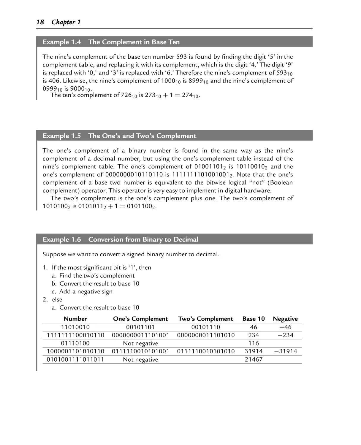
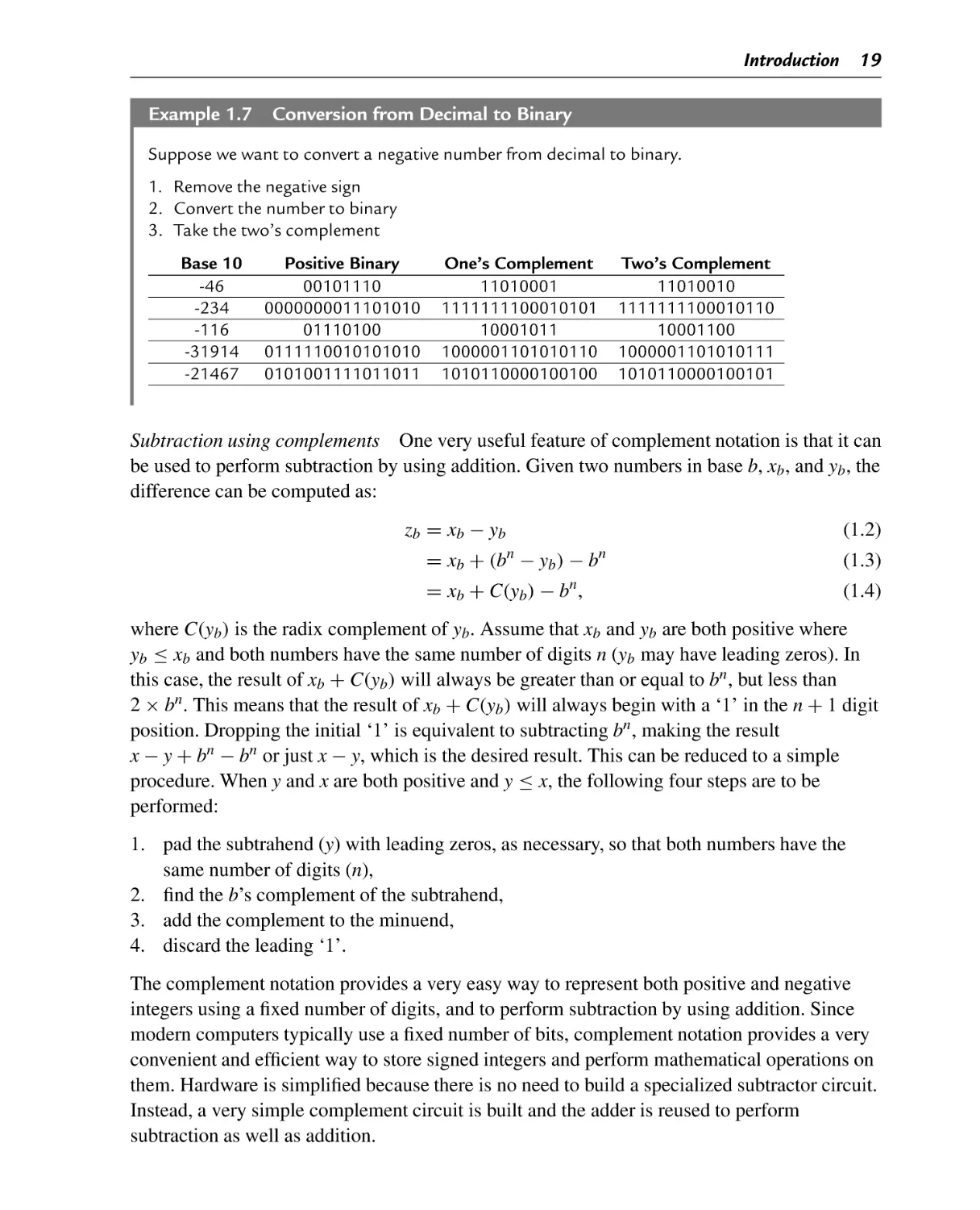
/


Author: Pyeatt
Tags: programming languages programming processors semiconductors arm architecture
Year: 2016


Text
Modern Assembly Language Programming
with the ARM Processor
This page intentionally left blank
Modern Assembly Language
Programming with the
ARM Processor
Larry D. Pyeatt
AMSTERDAM • BOSTON • HEIDELBERG • LONDON
NEW YORK • OXFORD • PARIS • SAN DIEGO
SAN FRANCISCO • SINGAPORE • SYDNEY • TOKYO
Newnes is an imprint of Elsevier
Newnes is an imprint of Elsevier
The Boulevard, Langford Lane, Kidlington, Oxford OX5 1GB, UK
50 Hampshire Street, 5th Floor, Cambridge, MA 02139, USA
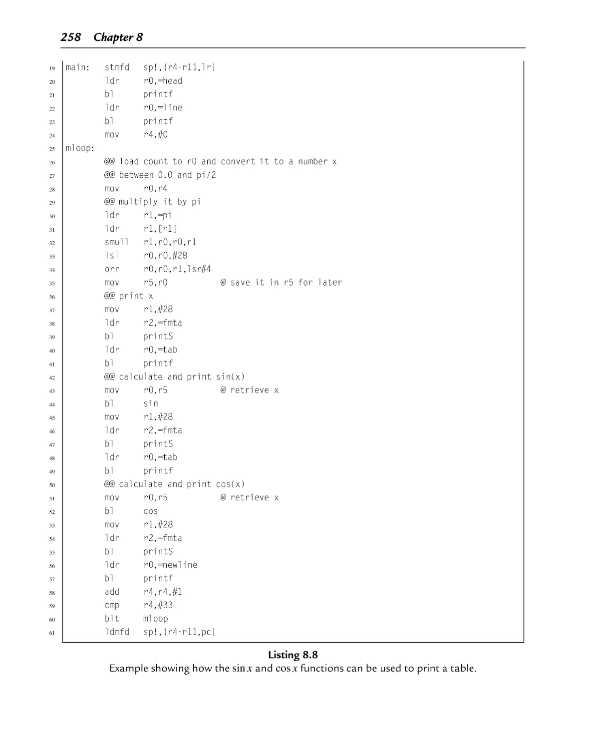
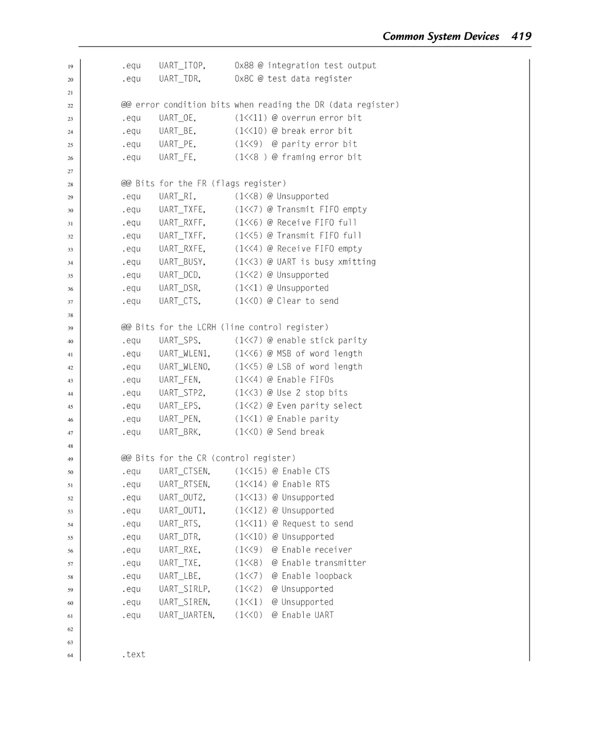
Copyright © 2016 Elsevier Inc. All rights reserved.
No part of this publication may be reproduced or transmitted in any form or by any means, electronic or
mechanical, including photocopying, recording, or any information storage and retrieval system, without
permission in writing from the publisher. Details on how to seek permission, further information about the
Publisher’s permissions policies and our arrangements with organizations such as the Copyright Clearance
Center and the Copyright Licensing Agency, can be found at our website:www.elsevier.com/permissions.
This book and the individual contributions contained in it are protected under copyright by the Publisher (other
than as may be noted herein).
Notices
Knowledge and best practice in this field are constantly changing. As new research and experience broaden our
understanding, changes in research methods, professional practices, or medical treatment may become necessary.
Practitioners and researchers must always rely on their own experience and knowledge in evaluating and using
any information, methods, compounds, or experiments described herein. In using such information or methods
they should be mindful of their own safety and the safety of others, including parties for whom they have a
professional responsibility.
To the fullest extent of the law, neither the Publisher nor the authors, contributors, or editors, assume any liability
for any injury and/or damage to persons or property as a matter of products liability, negligence or otherwise, or
from any use or operation of any methods, products, instructions, or ideas contained in the material herein.
Library of Congress Cataloging-in-Publication Data
A catalog record for this book is available from the Library of Congress
British Library Cataloging-in-Publication Data
A catalogue record for this book is available from the British Library
ISBN: 978-0-12-803698-3
For information on all Newnes publications
visit our website at https://www.elsevier.com/
Publisher: Joe Hayton
Acquisition Editor: Tim Pitts
Editorial Project Manager: Charlotte Kent
Production Project Manager: Julie-Ann Stansfield
Designer: Mark Rogers
Typeset by SPi Global, India
Contents
List of Tables.................................................................................... xiii
List of Figures....................................................................................xv
List of Listings ................................................................................. xvii
Preface........................................................................................... xxi
Companion Website ........................................................................... xxv
Acknowledgments ............................................................................ xxvii
PART I ASSEMBLY AS A LANGUAGE
1
Chapter 1: Introduction .........................................................................3
1.1 Reasons to Learn Assembly .................................................................... 4
1.2 The ARM Processor .............................................................................. 8
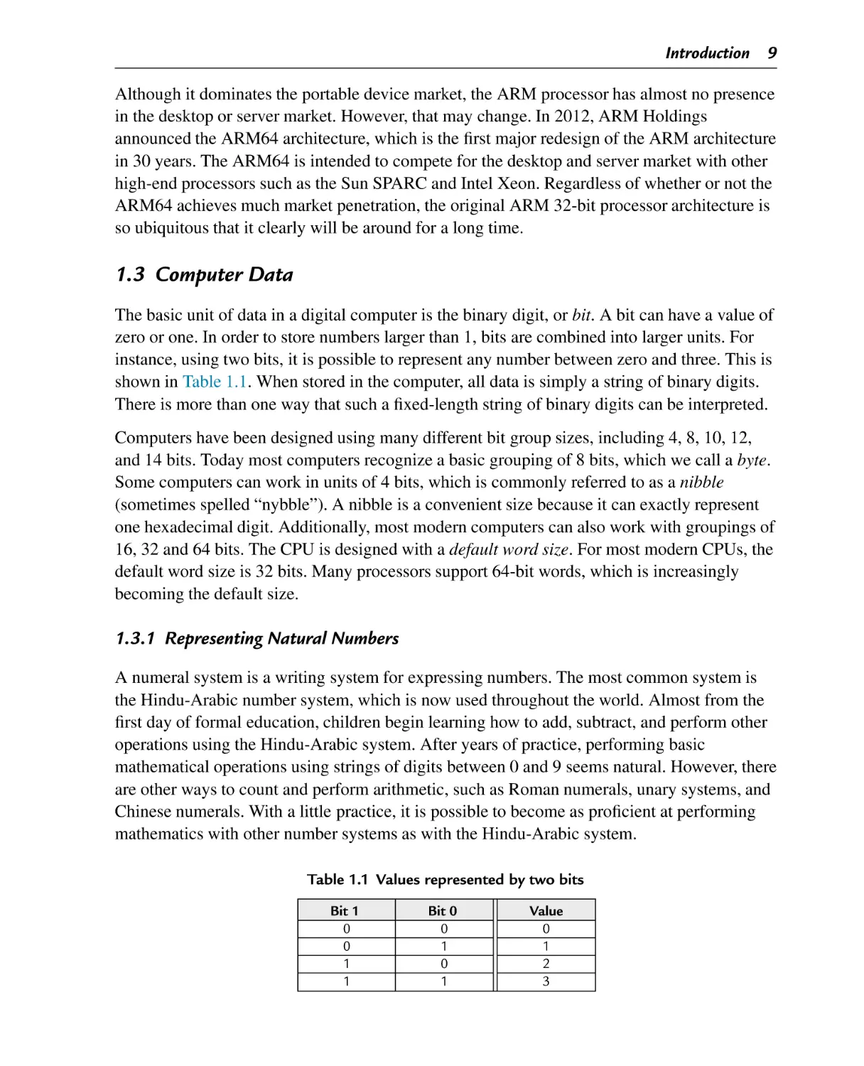
1.3 Computer Data ..................................................................................... 9
1.3.1 Representing Natural Numbers............................................................. 9
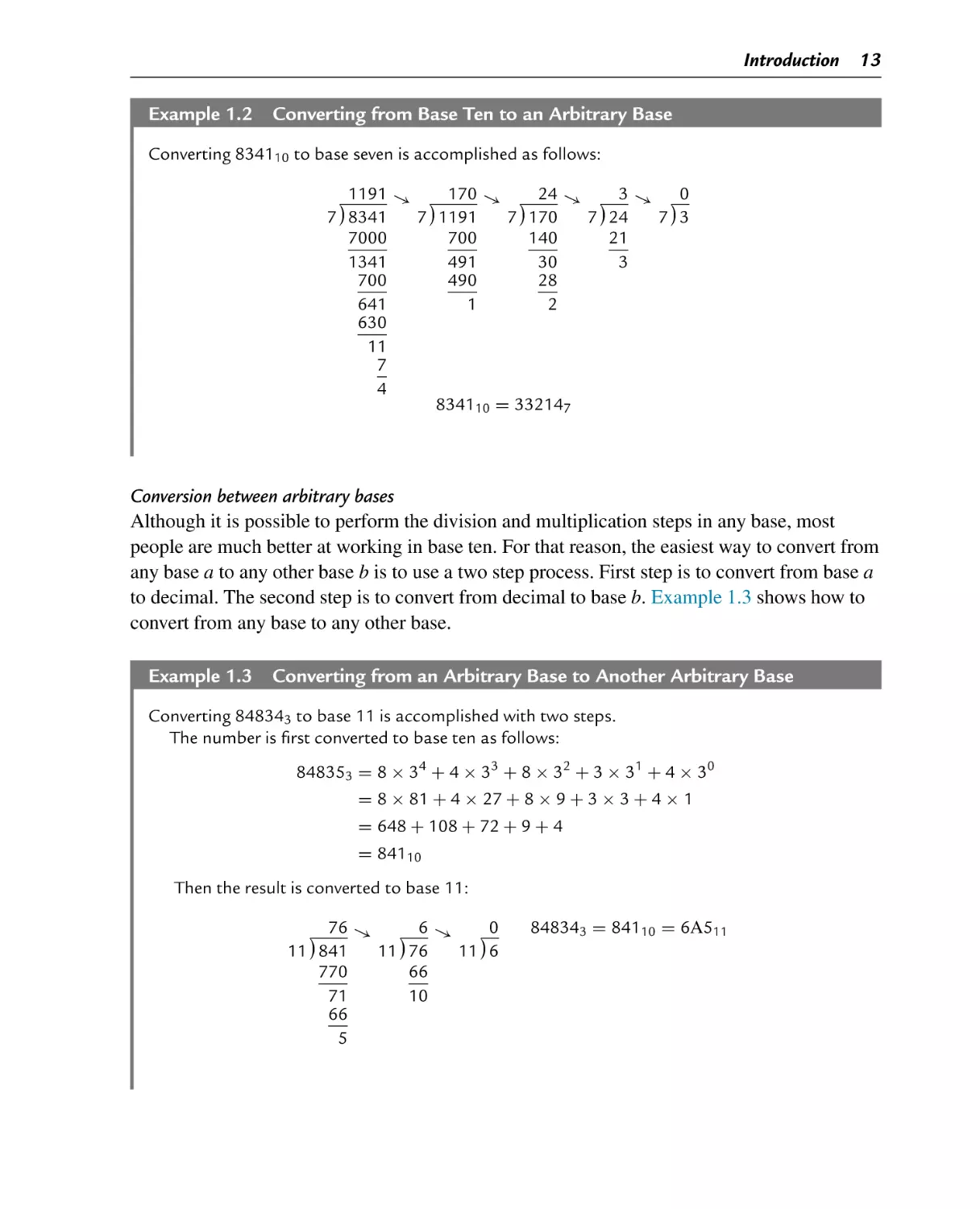
1.3.2 Base Conversion .............................................................................. 11
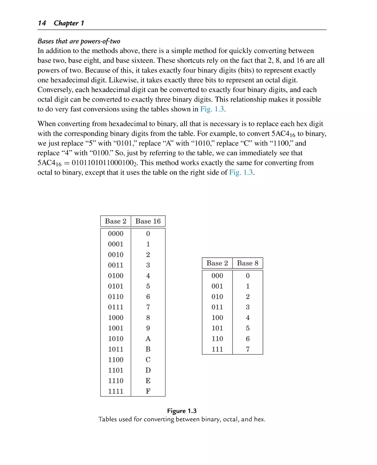
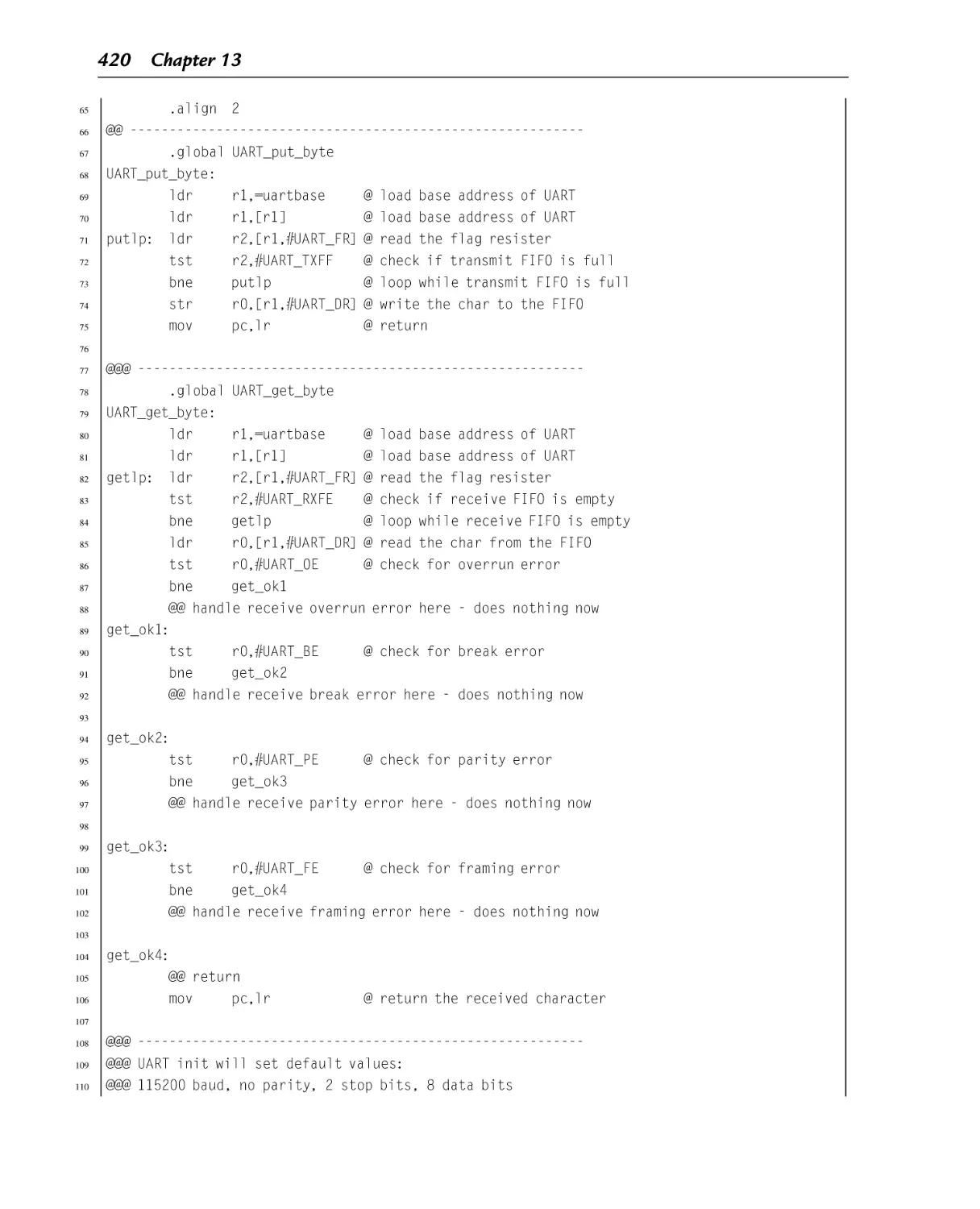
1.3.3 Representing Integers ........................................................................ 15
1.3.4 Representing Characters .................................................................... 20
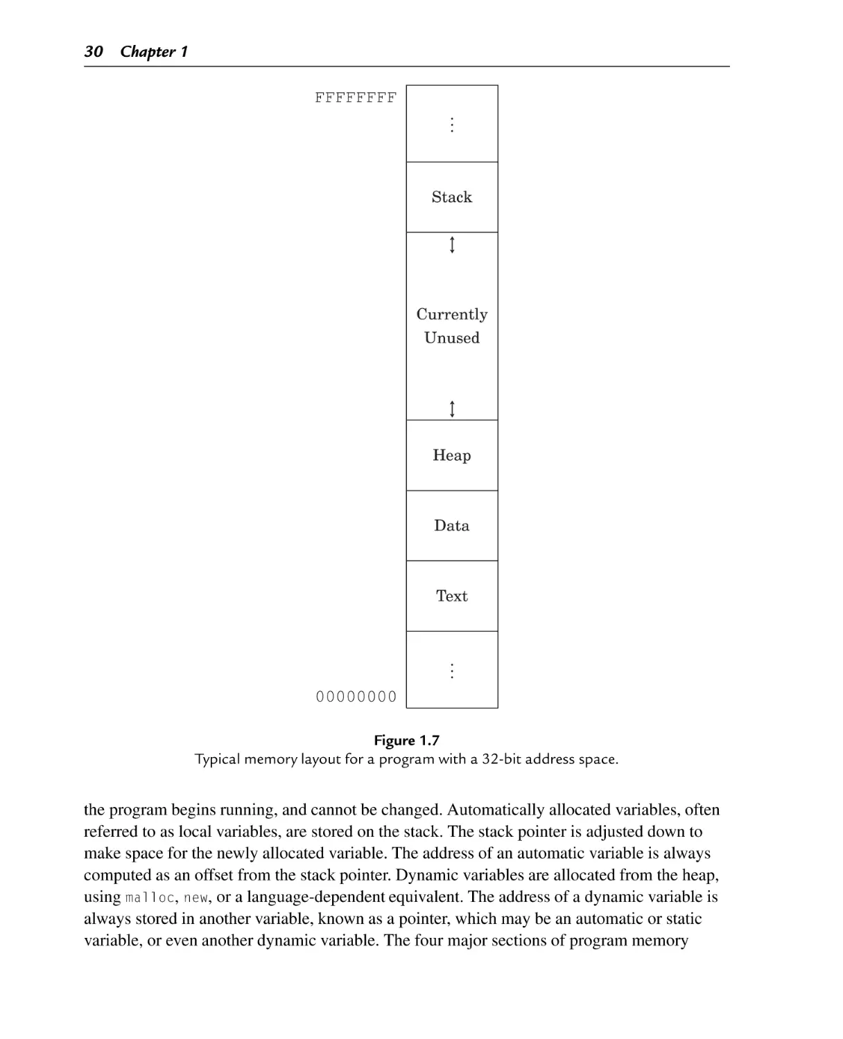
1.4 Memory Layout of an Executing Program ................................................ 28
1.5 Chapter Summary ............................................................................... 31
Chapter 2: GNU Assembly Syntax ........................................................... 35
2.1 Structure of an Assembly Program ......................................................... 36
2.1.1 Labels............................................................................................ 37
2.1.2 Comments ...................................................................................... 37
2.1.3 Directives ....................................................................................... 37
2.1.4 Assembly Instructions ....................................................................... 38
2.2 What the Assembler Does..................................................................... 38
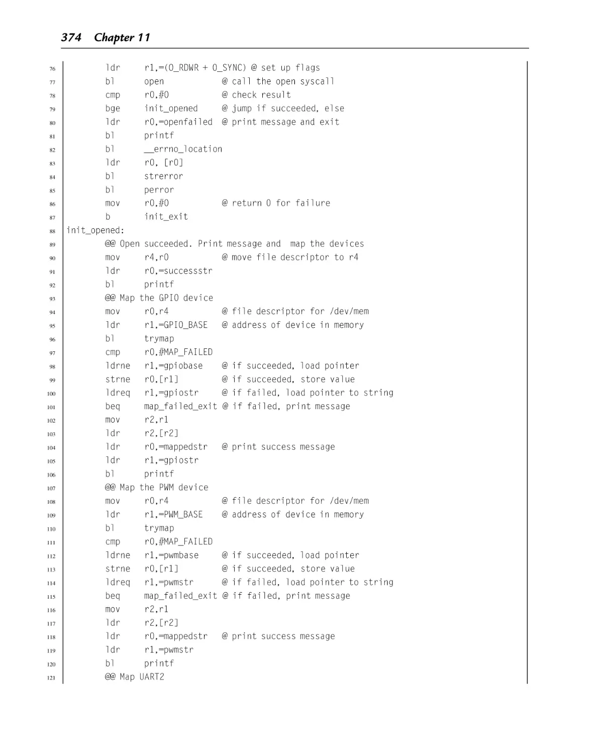
2.3 GNU Assembly Directives .................................................................... 40
2.3.1 Selecting the Current Section .............................................................. 40
2.3.2 Allocating Space for Variables and Constants ......................................... 41
2.3.3 Filling and Aligning.......................................................................... 43
2.3.4 Setting and Manipulating Symbols ....................................................... 45
v
vi
Contents
2.3.5 Conditional Assembly ....................................................................... 46
2.3.6 Including Other Source Files .............................................................. 47
2.3.7 Macros........................................................................................... 48
2.4 Chapter Summary ............................................................................... 50
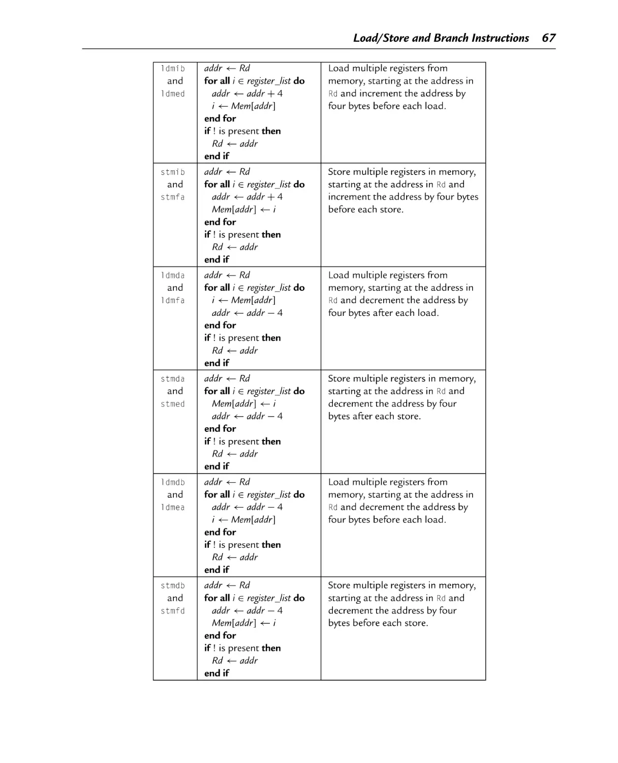
Chapter 3: Load/Store and Branch Instructions ............................................ 53
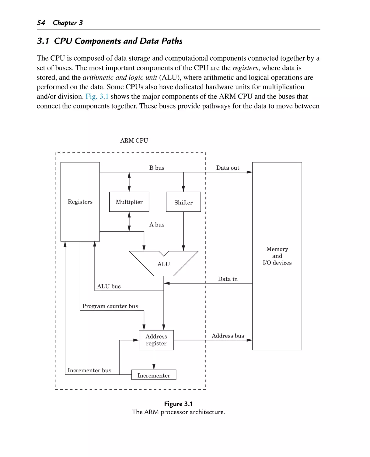
3.1 CPU Components and Data Paths ........................................................... 54
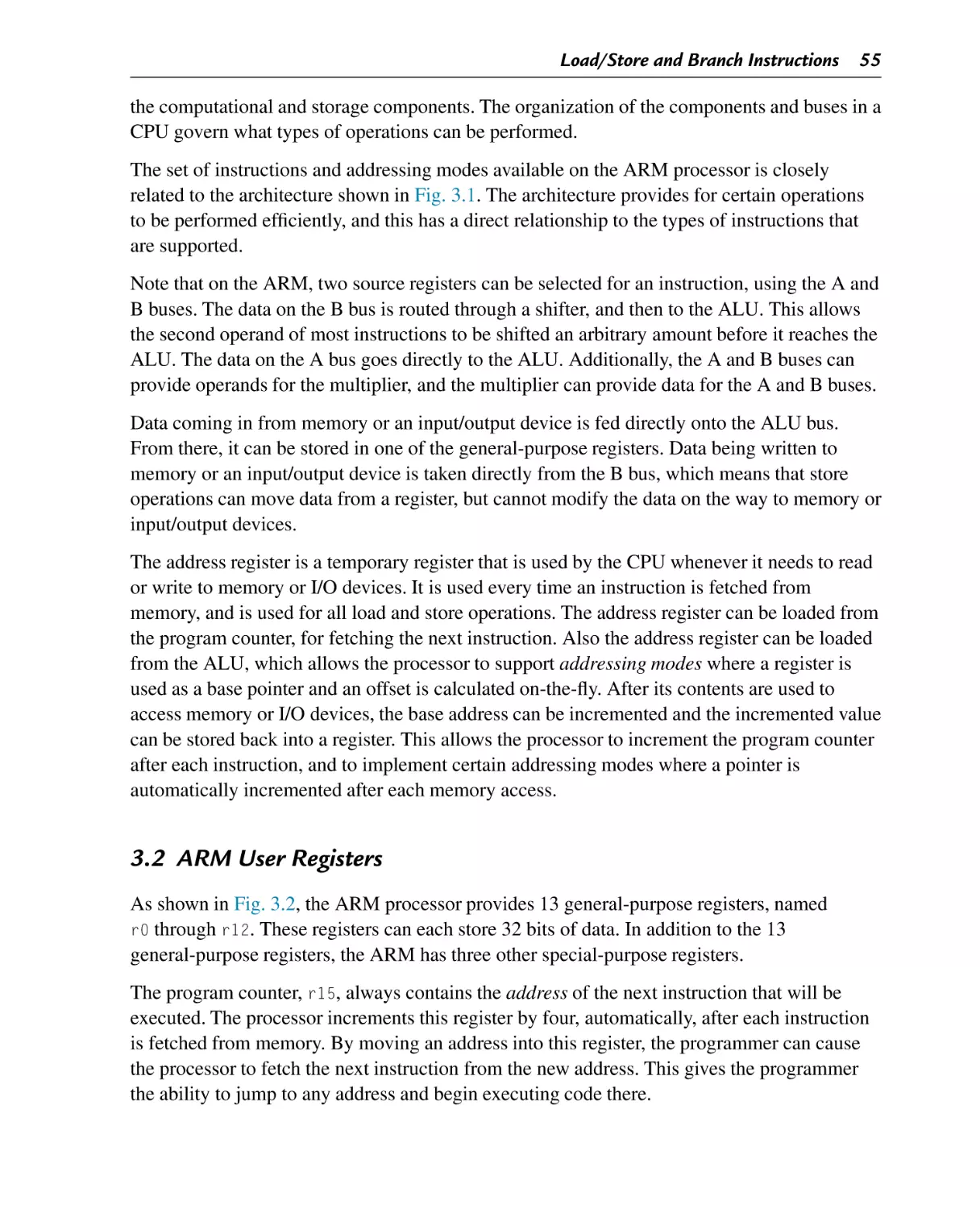
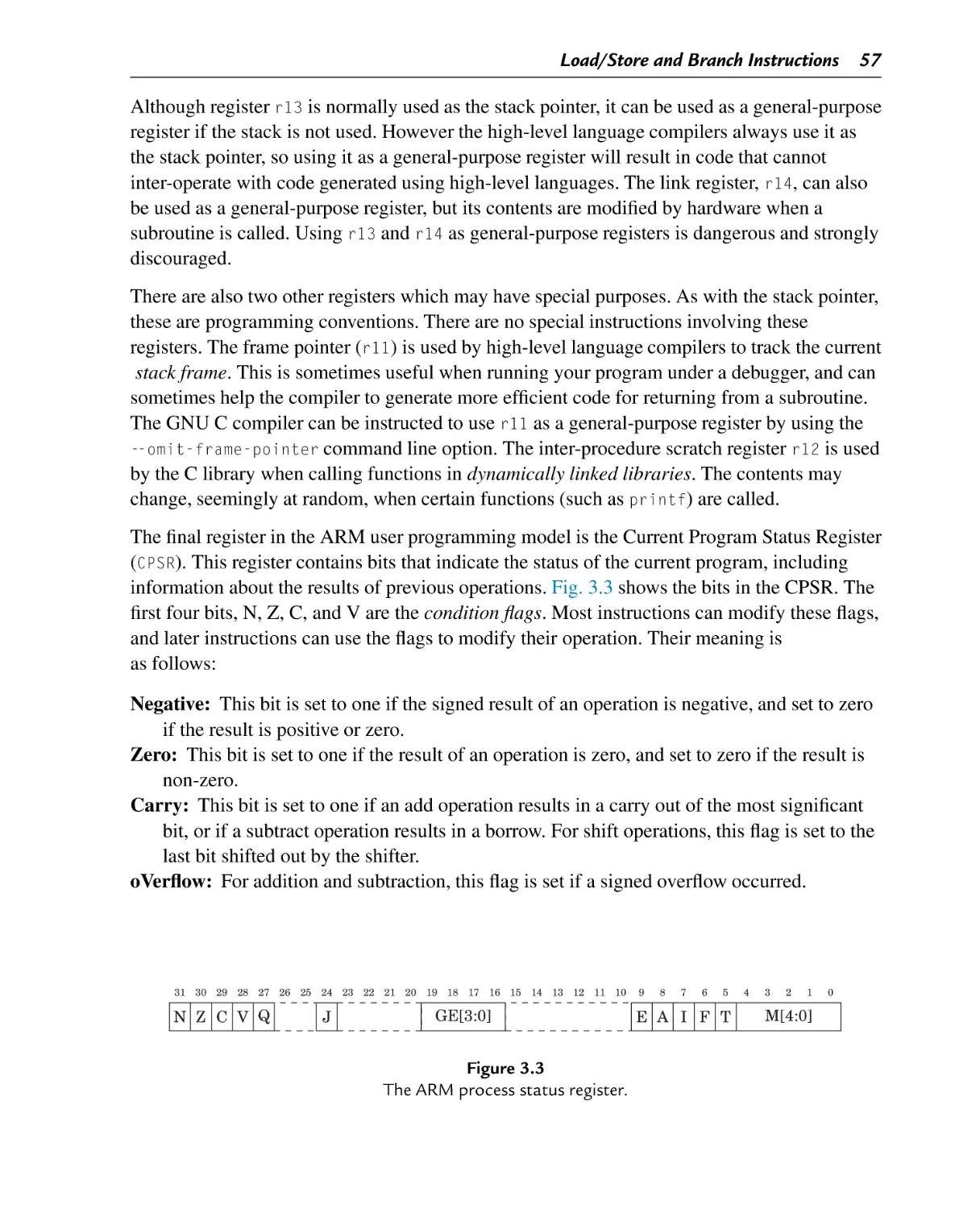
3.2 ARM User Registers ........................................................................... 55
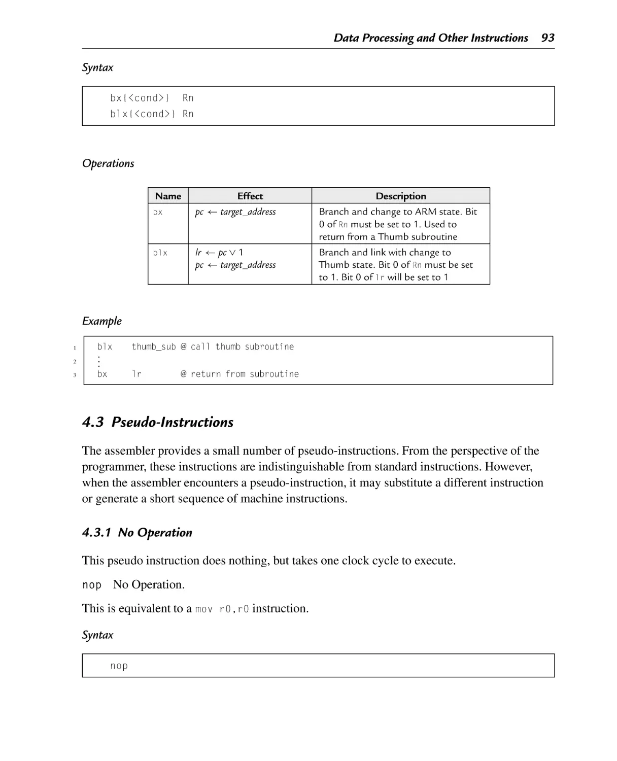
3.3 Instruction Components ....................................................................... 58
3.4
3.5
3.6
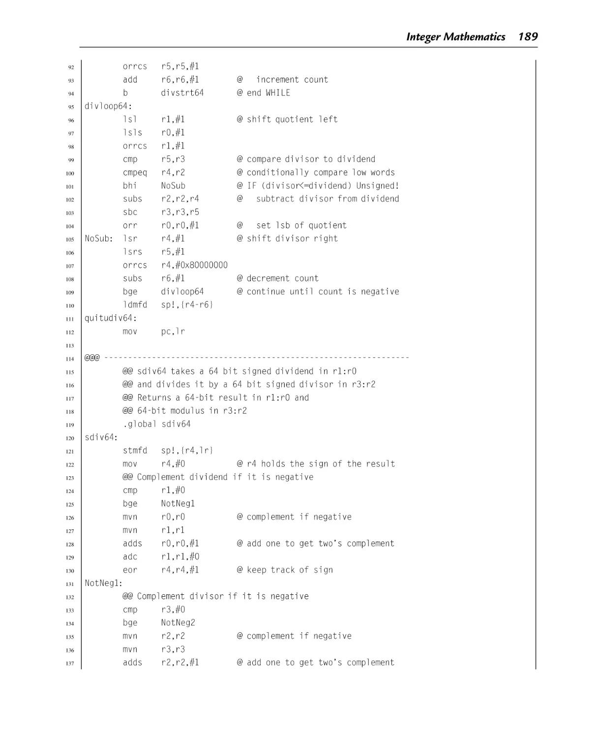
3.7
3.3.1 Setting and Using Condition Flags ....................................................... 58
3.3.2 Immediate Values ............................................................................. 59
Load/Store Instructions ........................................................................ 60
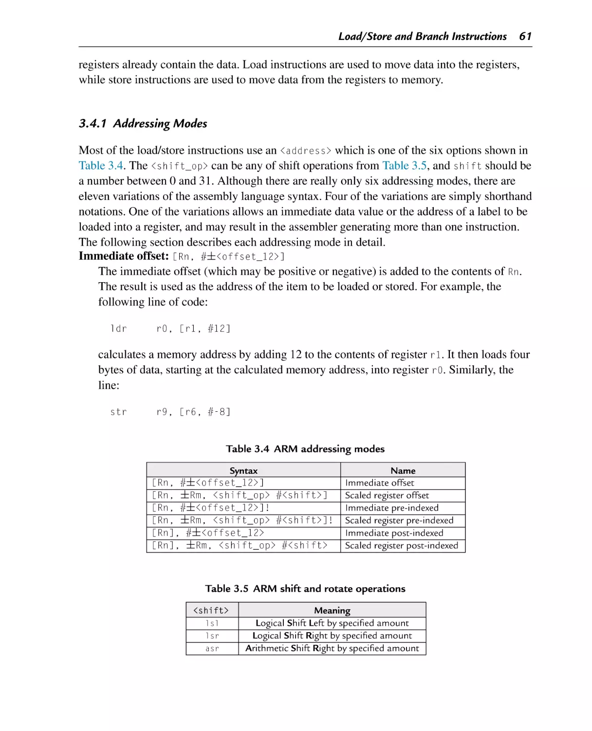
3.4.1 Addressing Modes ............................................................................ 61
3.4.2 Load/Store Single Register ................................................................. 64
3.4.3 Load/Store Multiple Registers ............................................................. 65
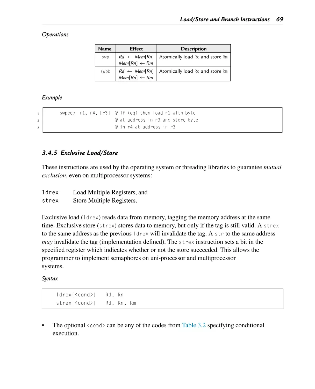
3.4.4 Swap ............................................................................................. 68
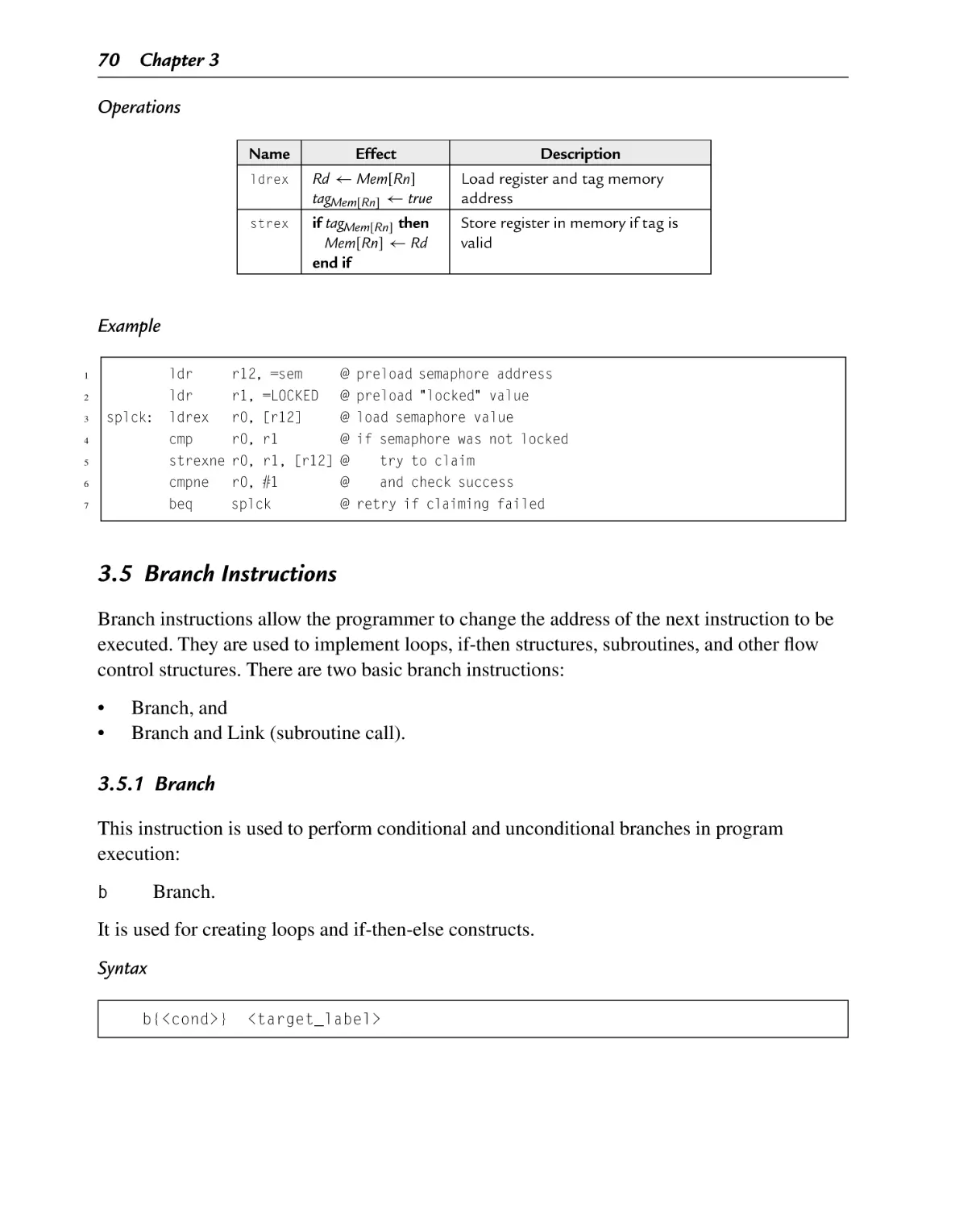
3.4.5 Exclusive Load/Store ........................................................................ 69
Branch Instructions ............................................................................. 70
3.5.1 Branch ........................................................................................... 70
3.5.2 Branch and Link .............................................................................. 71
Pseudo-Instructions ............................................................................. 73
3.6.1 Load Immediate ............................................................................... 73
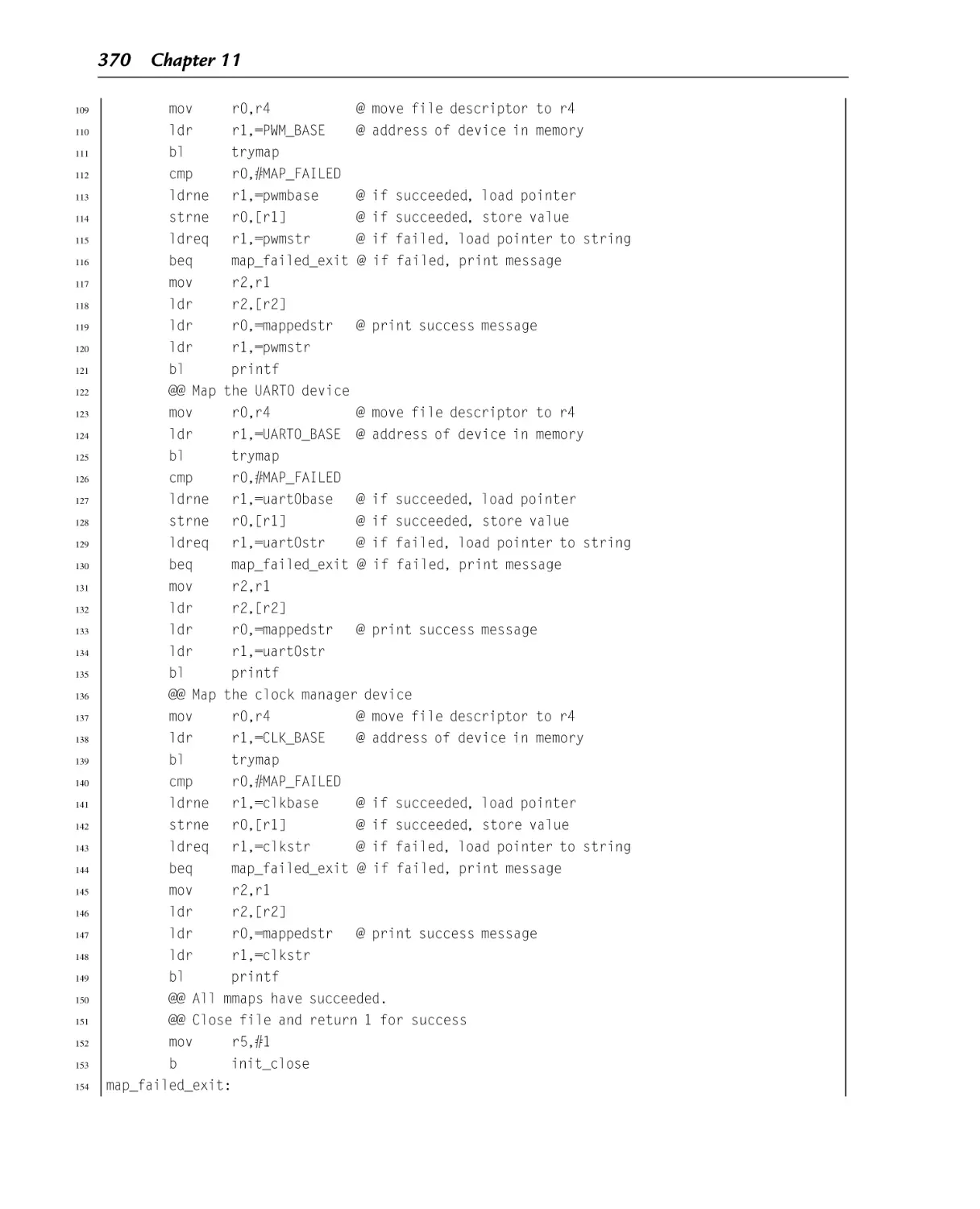
3.6.2 Load Address .................................................................................. 75
Chapter Summary ............................................................................... 76
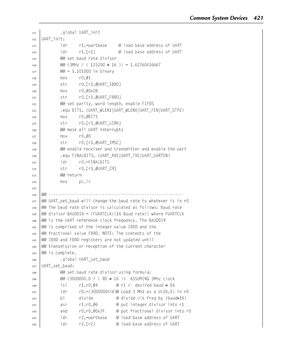
Chapter 4: Data Processing and Other Instructions ....................................... 79
4.1 Data Processing Instructions ................................................................. 79
4.2
4.3
4.4
4.5
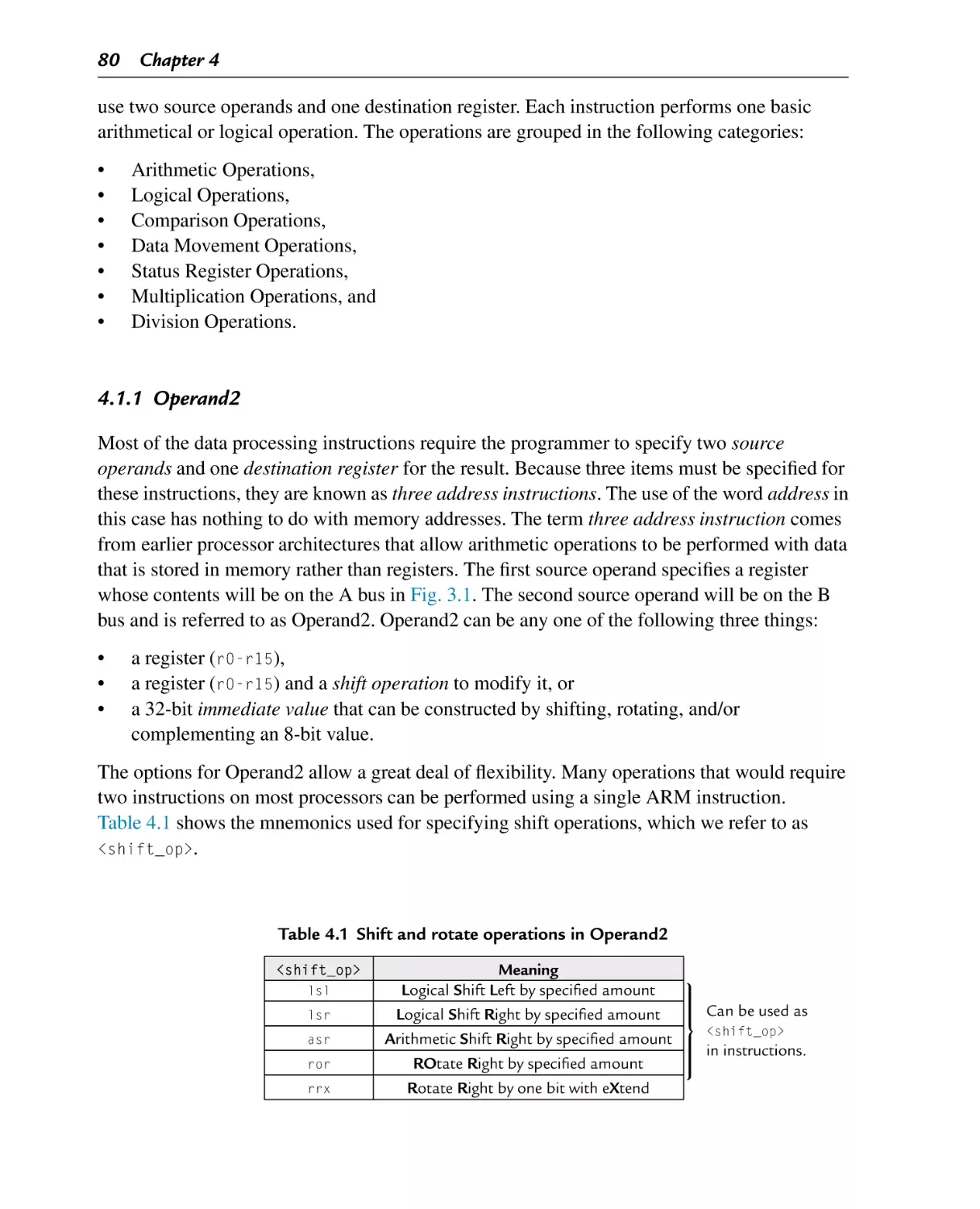
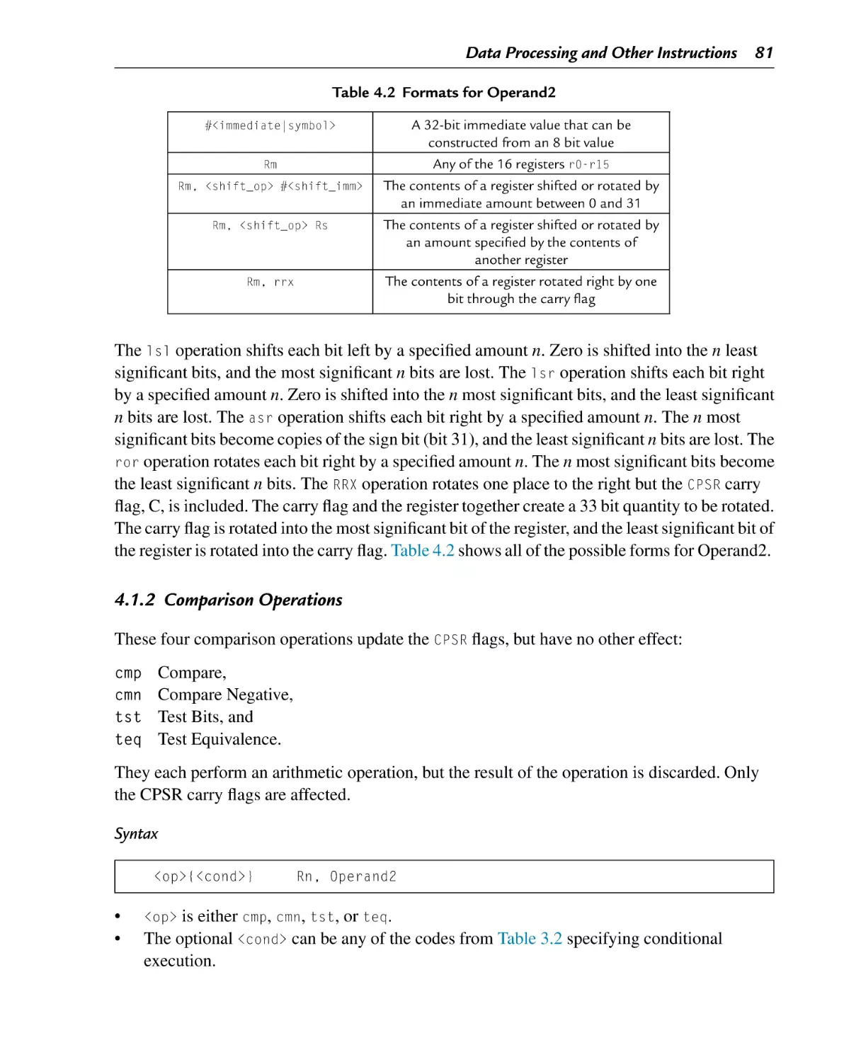
4.1.1 Operand2 ....................................................................................... 80
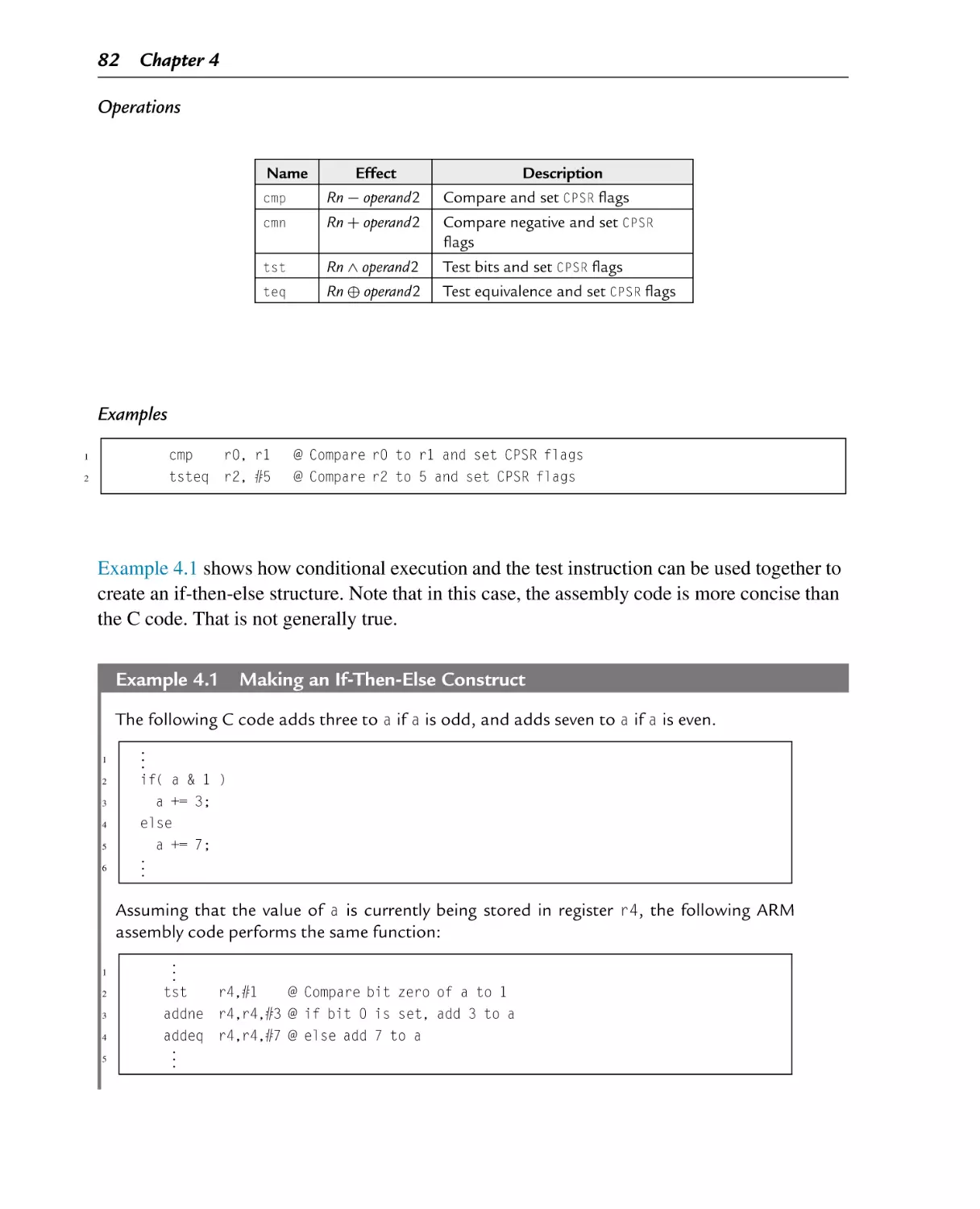
4.1.2 Comparison Operations ..................................................................... 81
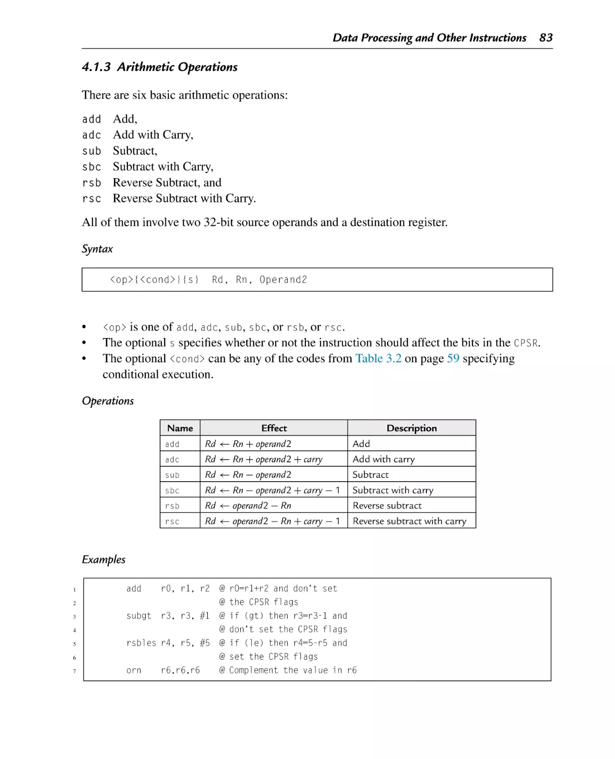
4.1.3 Arithmetic Operations ....................................................................... 83
4.1.4 Logical Operations ........................................................................... 85
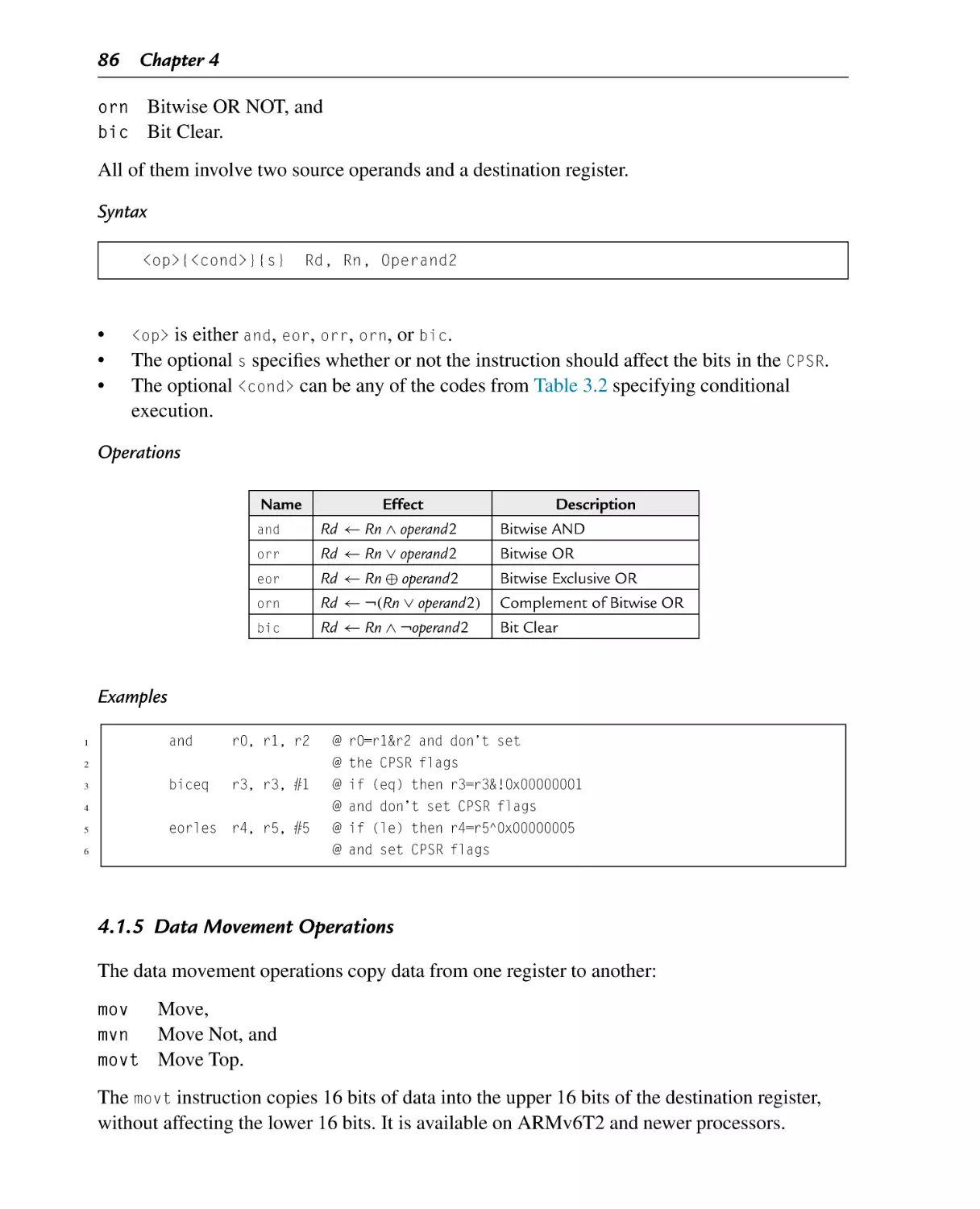
4.1.5 Data Movement Operations ................................................................ 86
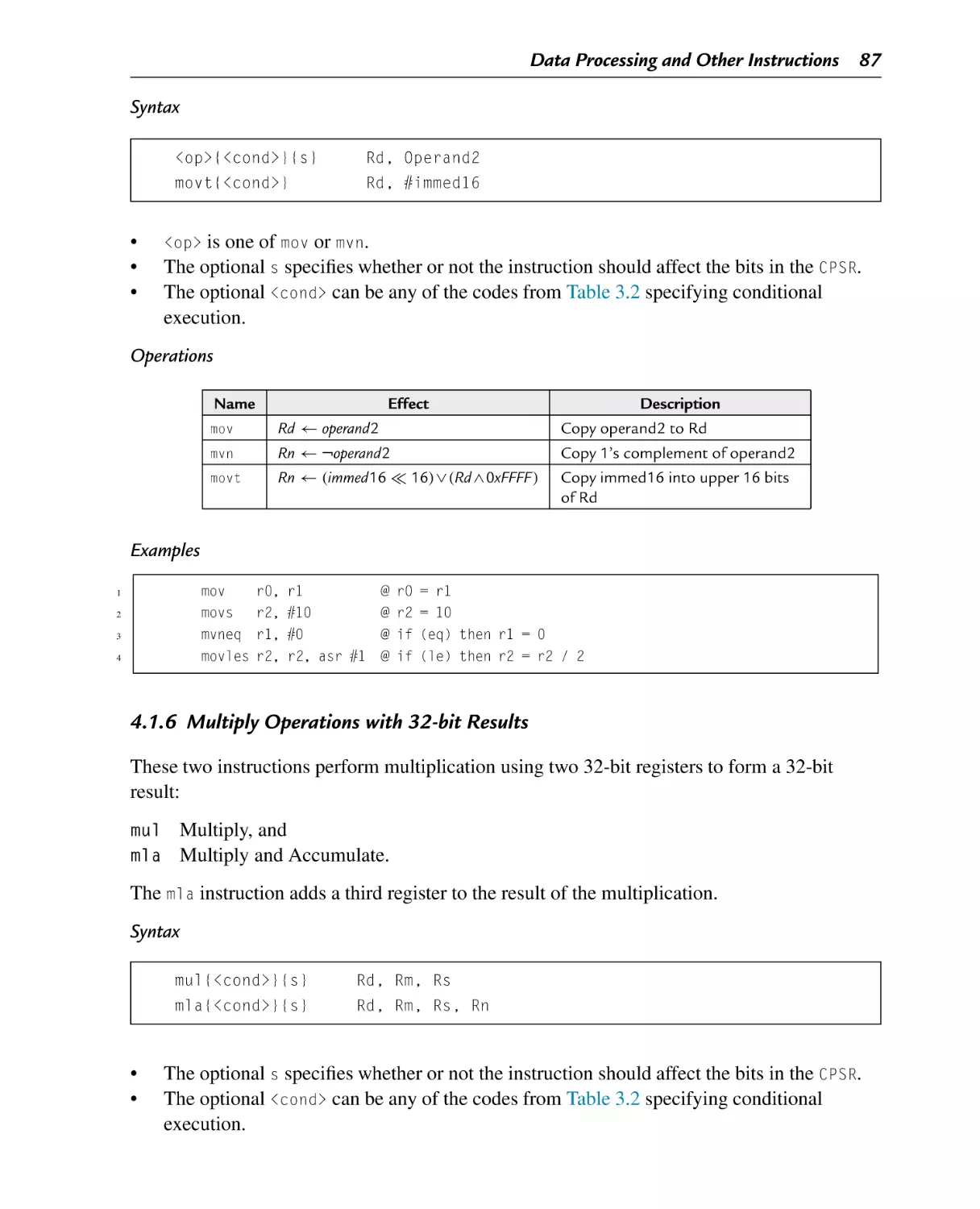
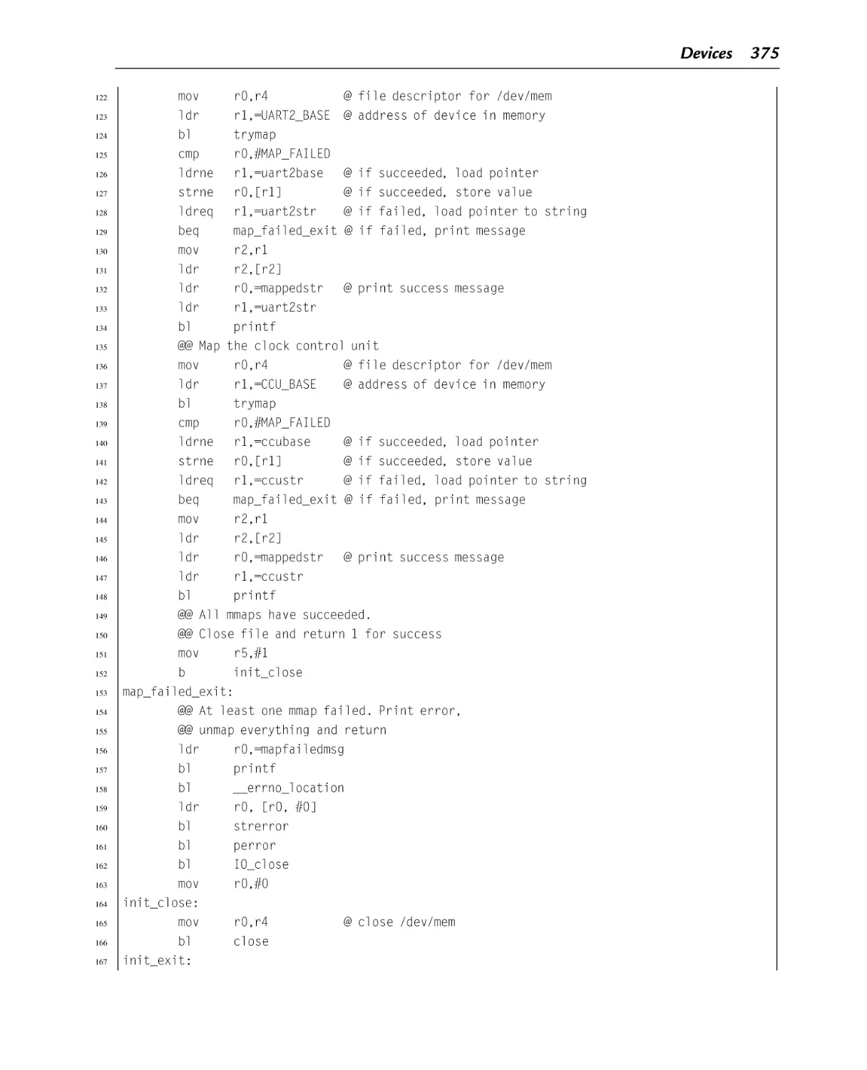
4.1.6 Multiply Operations with 32-bit Results ................................................ 87
4.1.7 Multiply Operations with 64-bit Results ................................................ 88
4.1.8 Division Operations .......................................................................... 89
Special Instructions ............................................................................. 90
4.2.1 Count Leading Zeros......................................................................... 90
4.2.2 Accessing the CPSR and SPSR ........................................................... 91
4.2.3 Software Interrupt ............................................................................ 91
4.2.4 Thumb Mode .................................................................................. 92
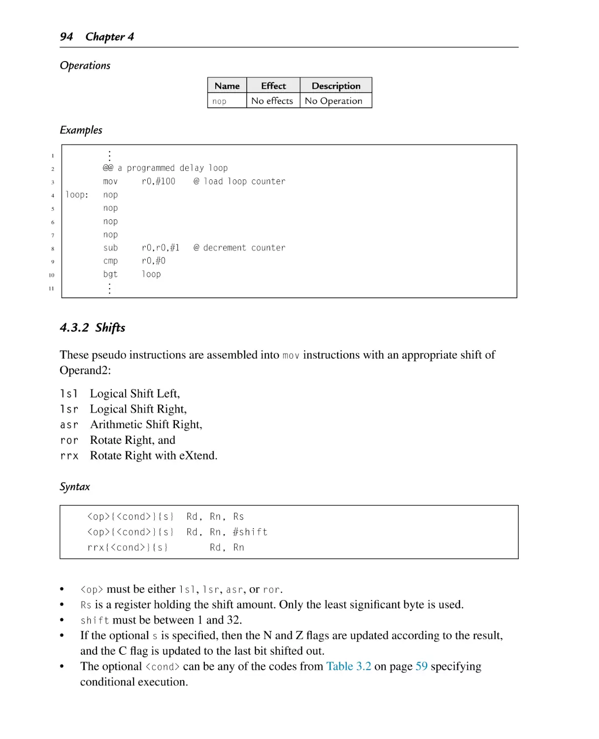
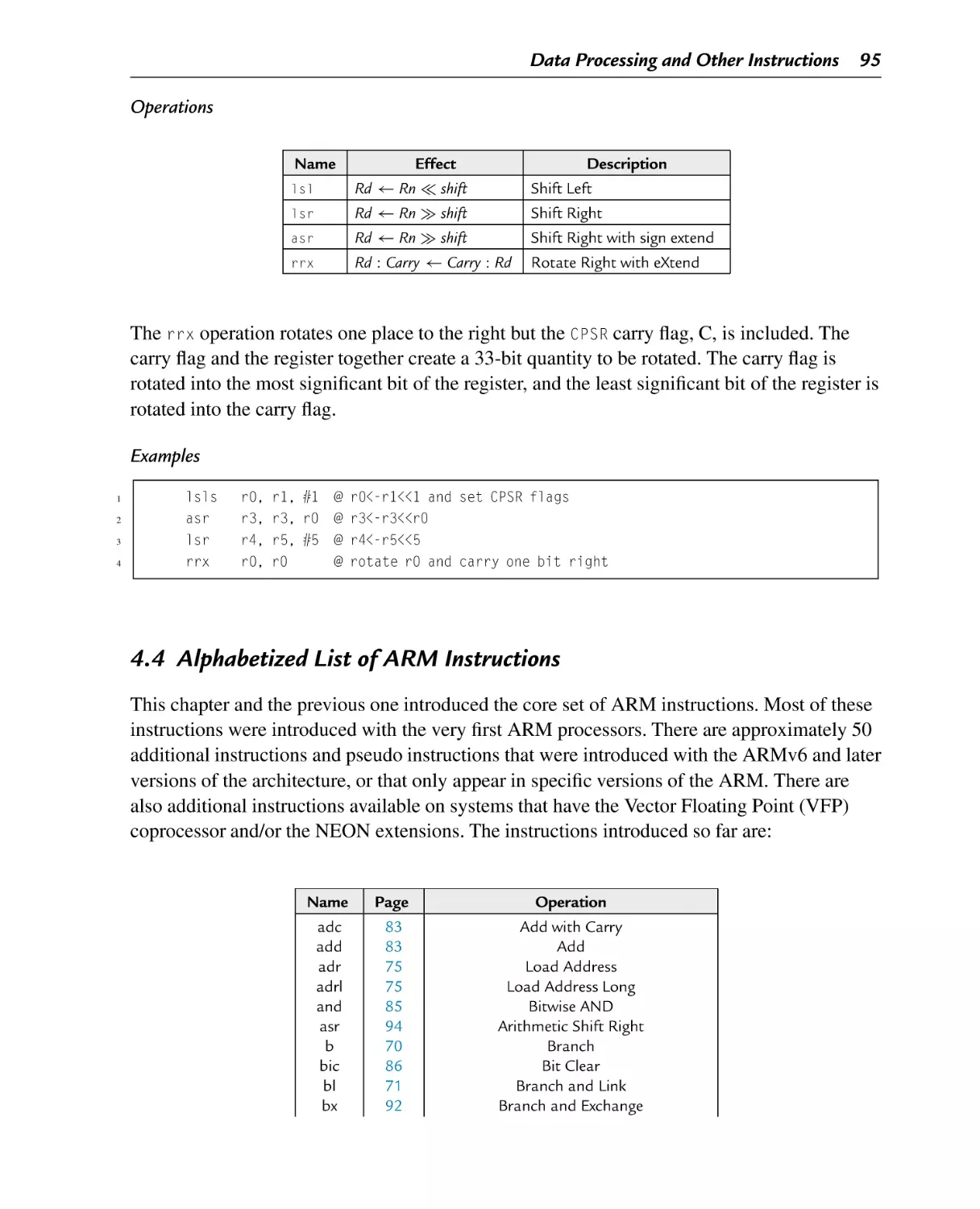
Pseudo-Instructions ............................................................................. 93
4.3.1 No Operation .................................................................................. 93
4.3.2 Shifts ............................................................................................. 94
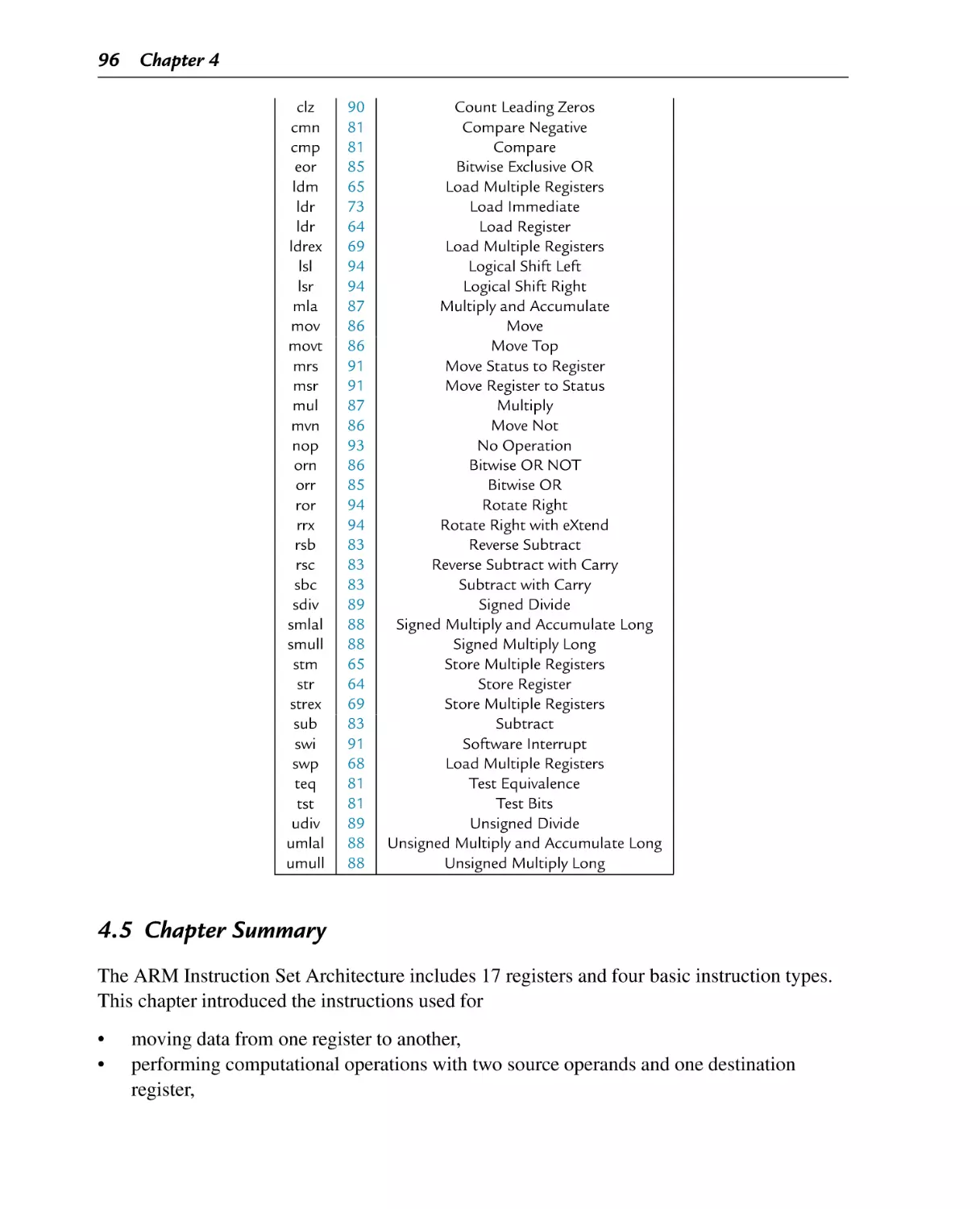
Alphabetized List of ARM Instructions ................................................... 95
Chapter Summary ............................................................................... 96
Contents vii
Chapter 5: Structured Programming......................................................... 99
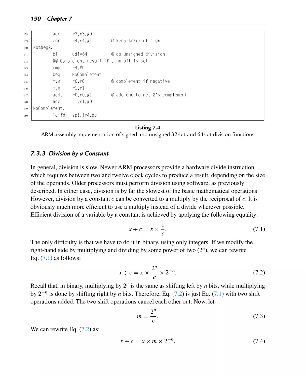
5.1 Sequencing....................................................................................... 100
5.2 Selection.......................................................................................... 101
5.3
5.4
5.5
5.6
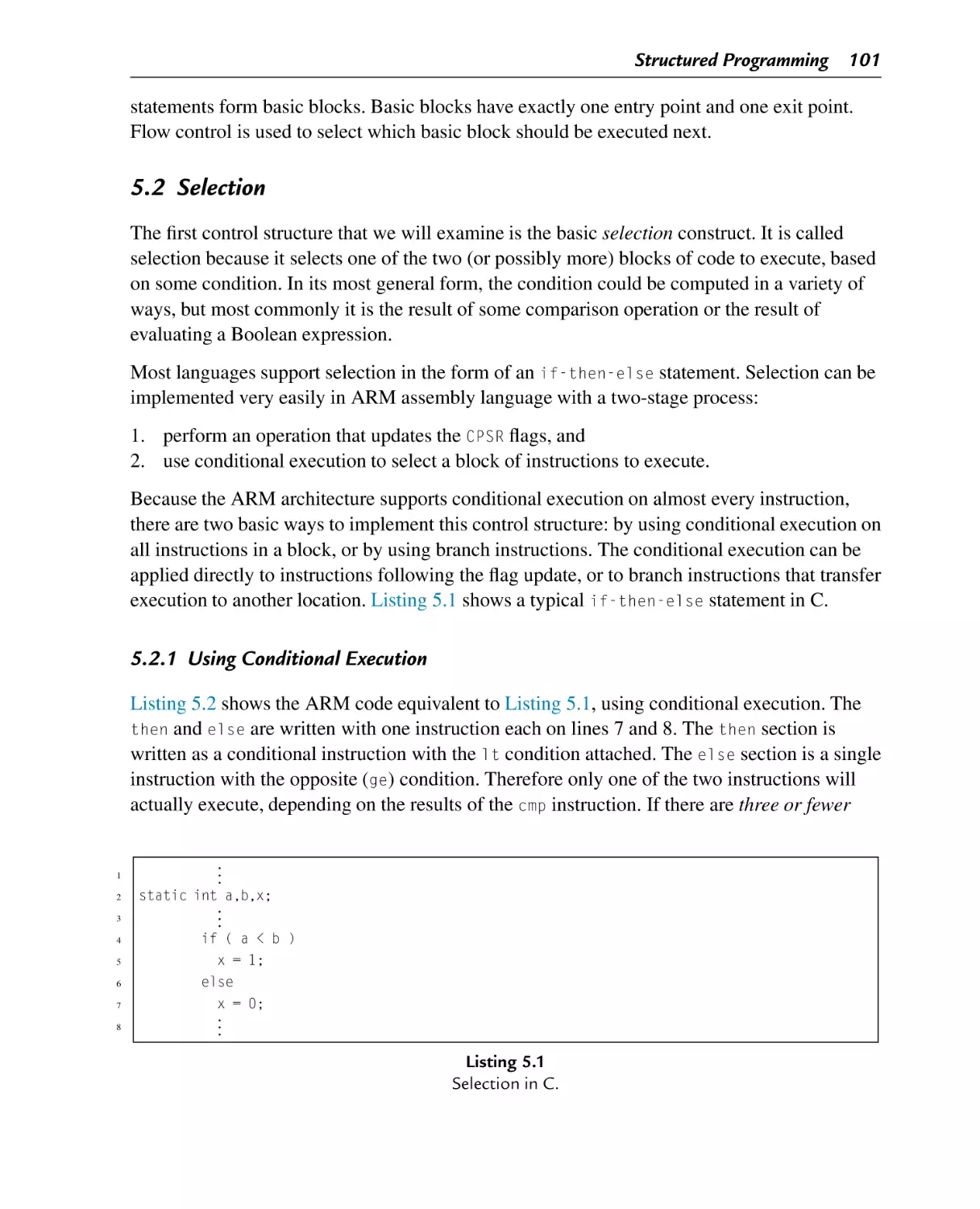
5.2.1 Using Conditional Execution ............................................................ 101
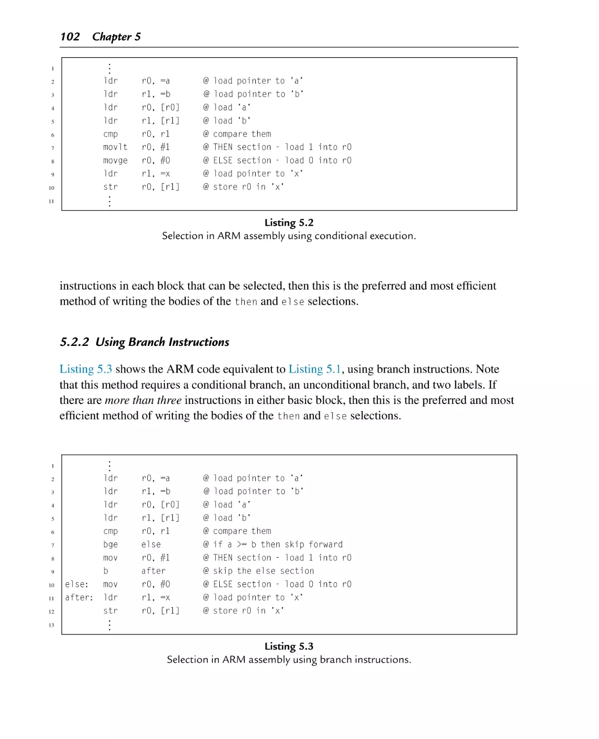
5.2.2 Using Branch Instructions ................................................................ 102
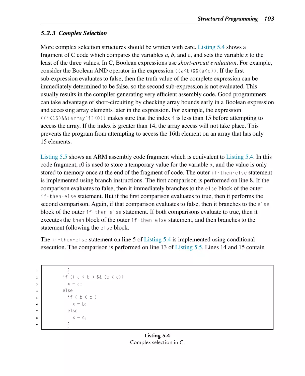
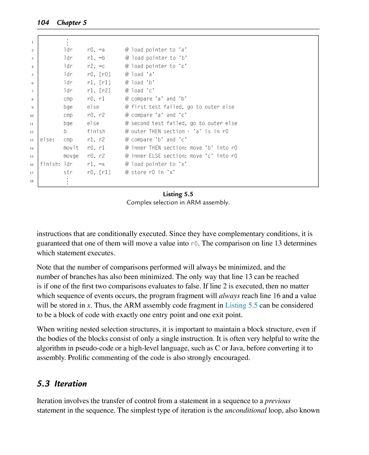
5.2.3 Complex Selection ......................................................................... 103
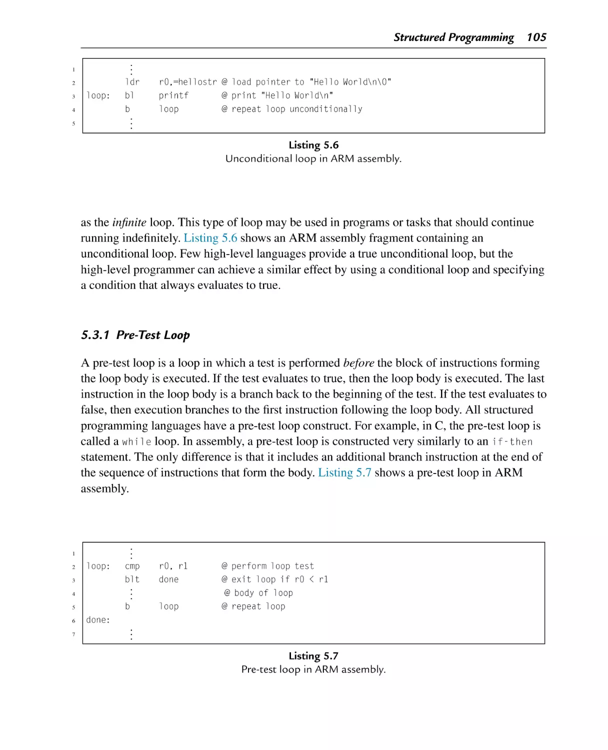
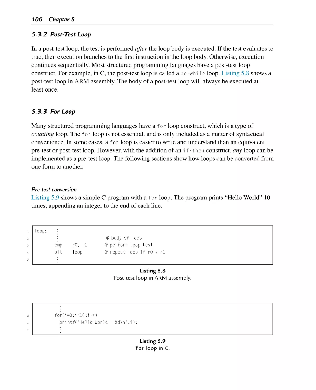
Iteration ........................................................................................... 104
5.3.1 Pre-Test Loop ................................................................................ 105
5.3.2 Post-Test Loop .............................................................................. 106
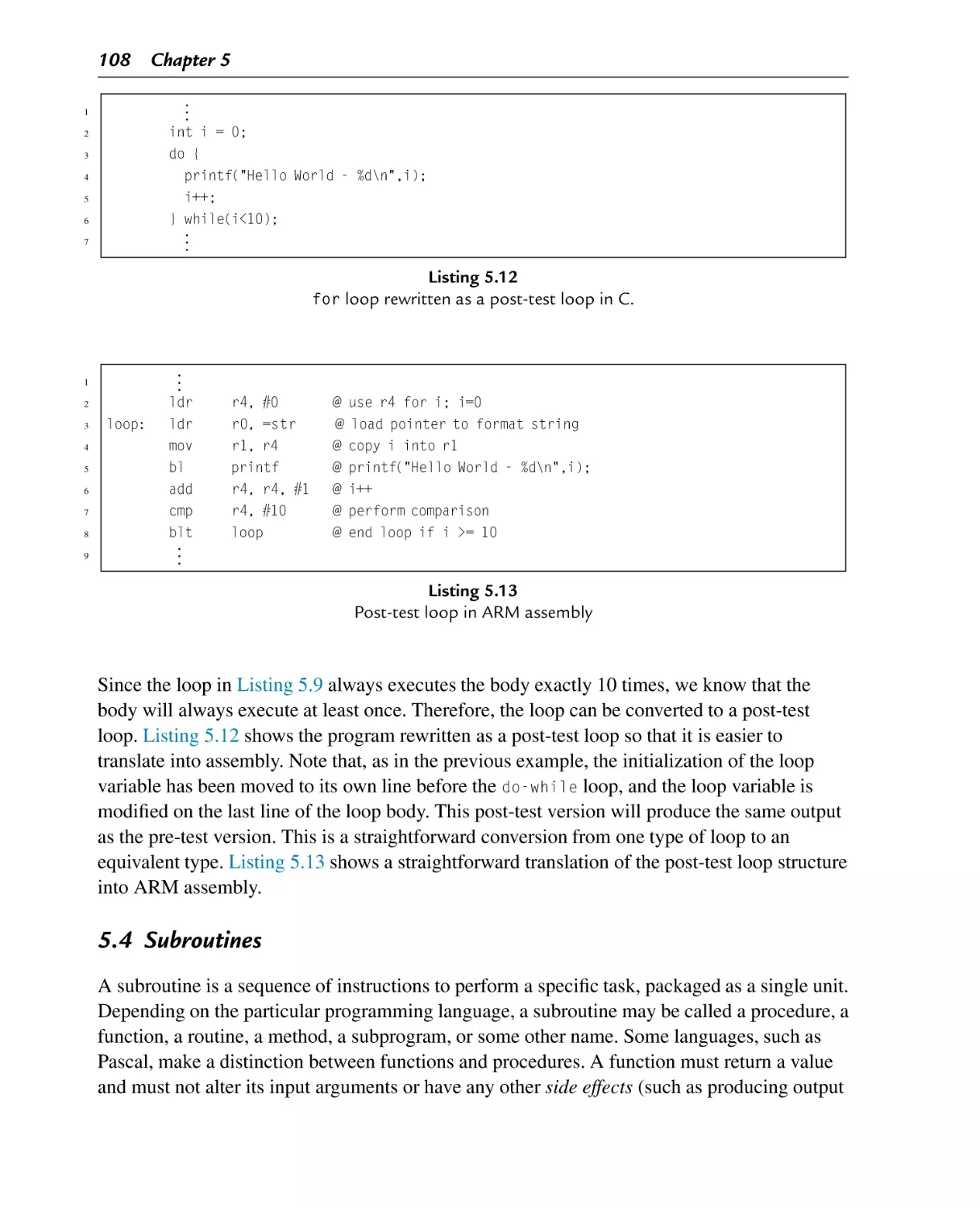
5.3.3 For Loop ...................................................................................... 106
Subroutines ...................................................................................... 108
5.4.1 Advantages of Subroutines ............................................................... 109
5.4.2 Disadvantages of Subroutines ........................................................... 110
5.4.3 Standard C Library Functions ........................................................... 110
5.4.4 Passing Arguments ......................................................................... 110
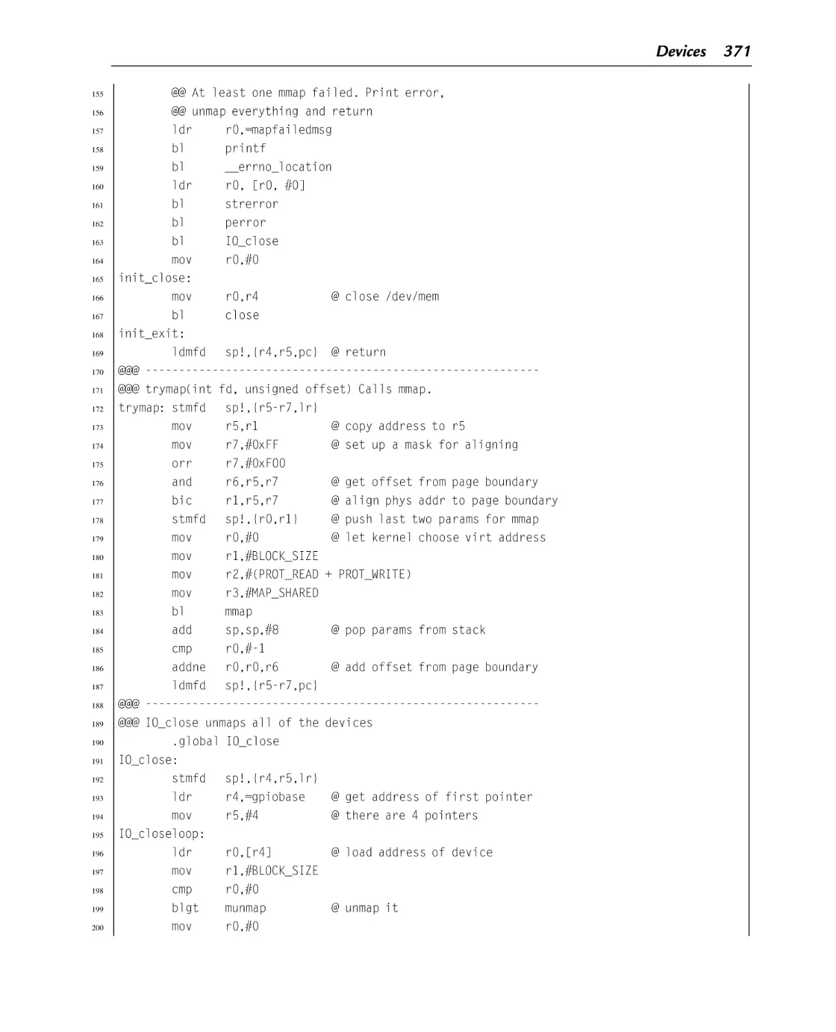
5.4.5 Calling Subroutines ........................................................................ 113
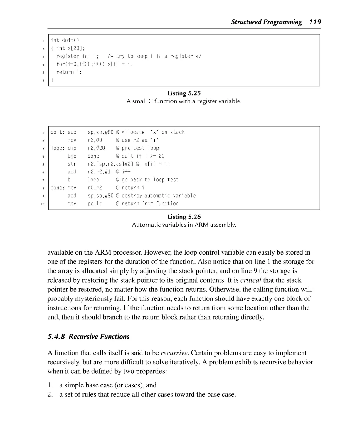
5.4.6 Writing Subroutines ........................................................................ 117
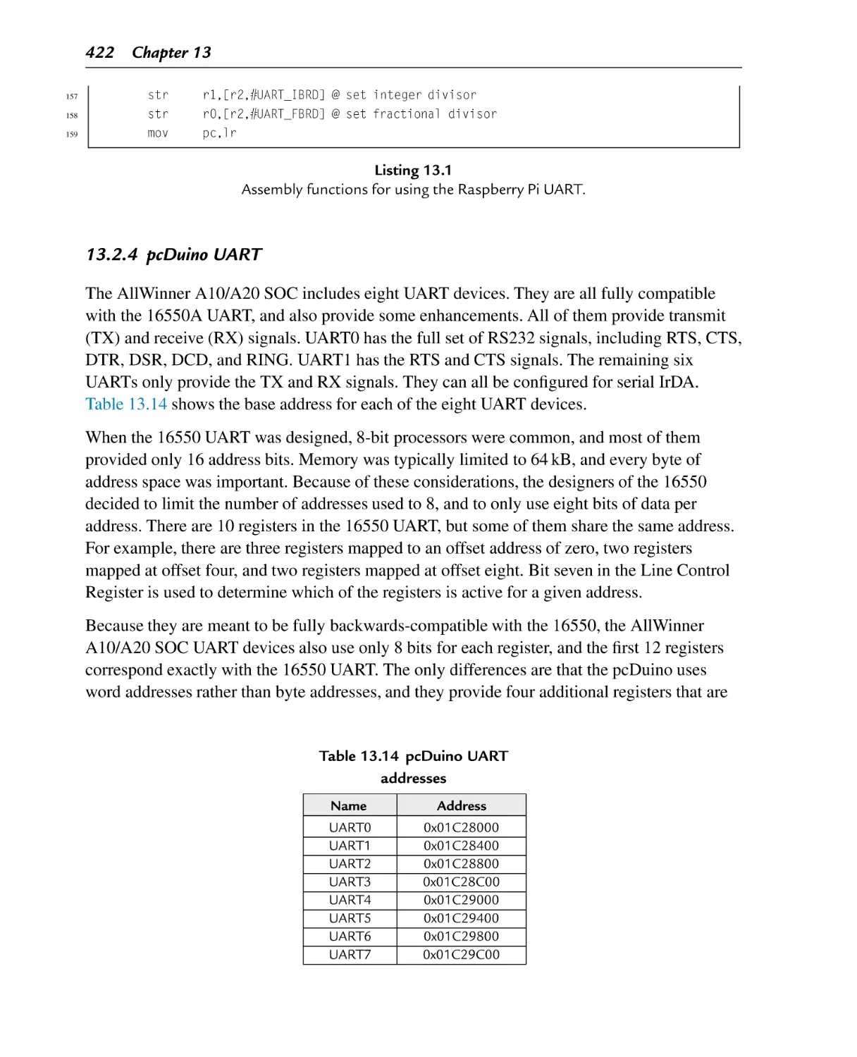
5.4.7 Automatic Variables........................................................................ 118
5.4.8 Recursive Functions........................................................................ 119
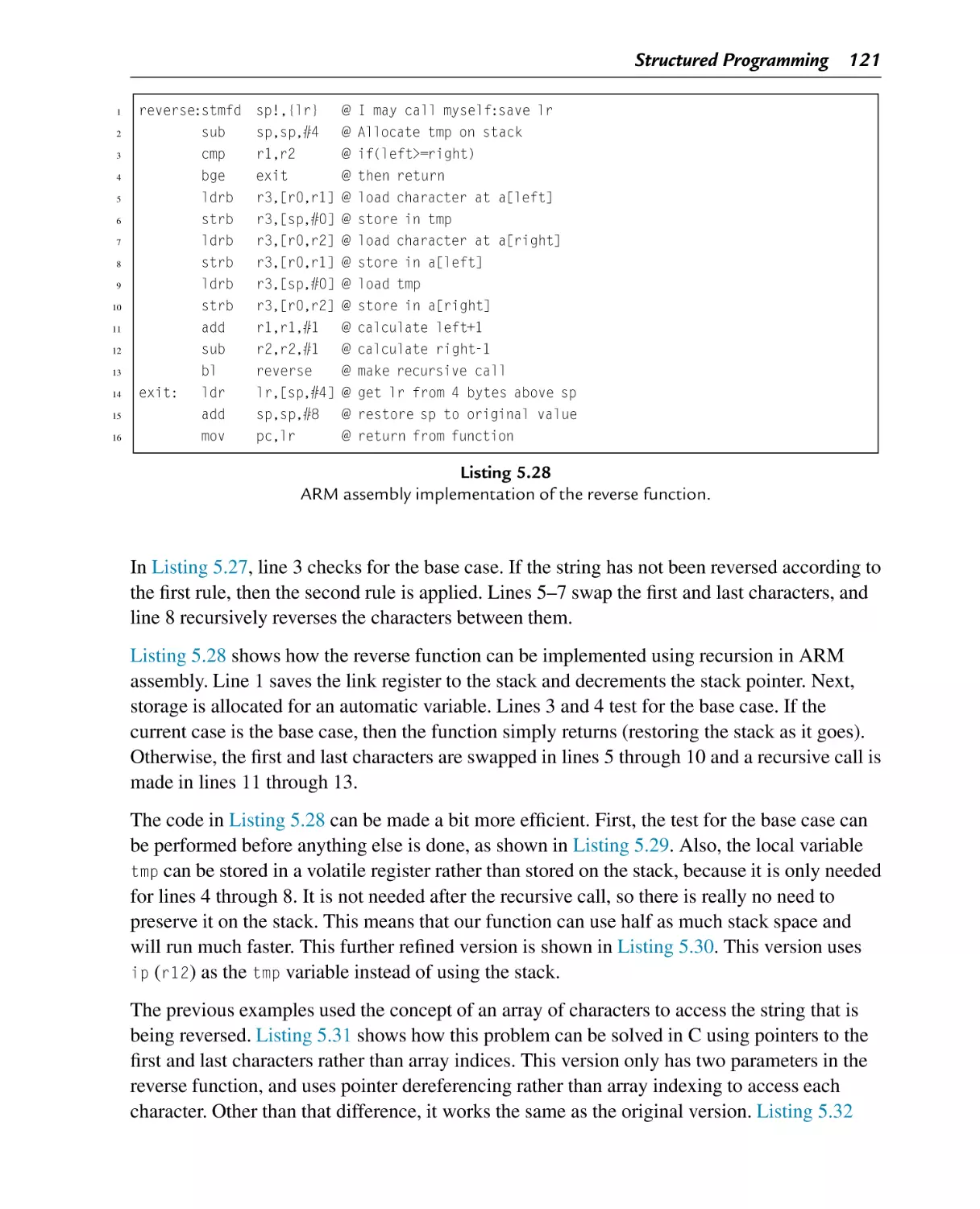
Aggregate Data Types ......................................................................... 123
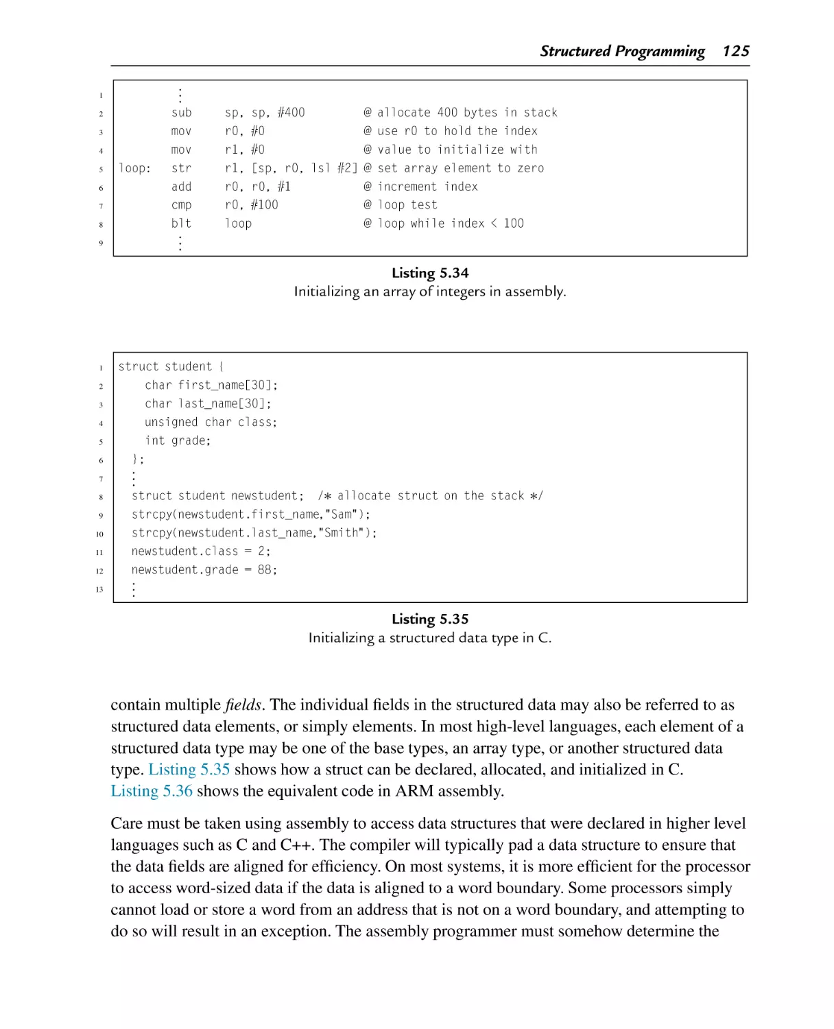
5.5.1 Arrays ......................................................................................... 124
5.5.2 Structured Data .............................................................................. 124
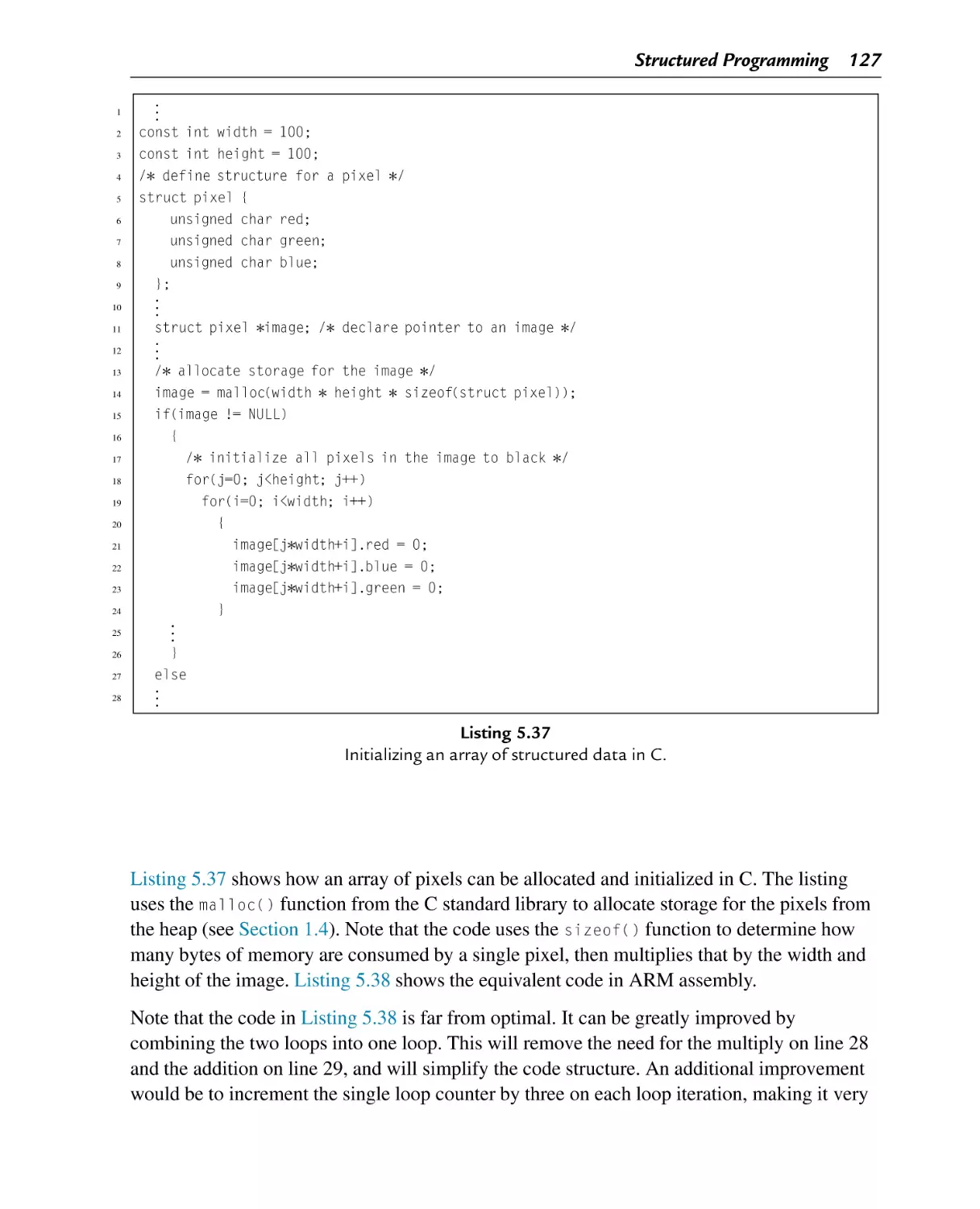
5.5.3 Arrays of Structured Data ................................................................ 126
Chapter Summary .............................................................................. 131
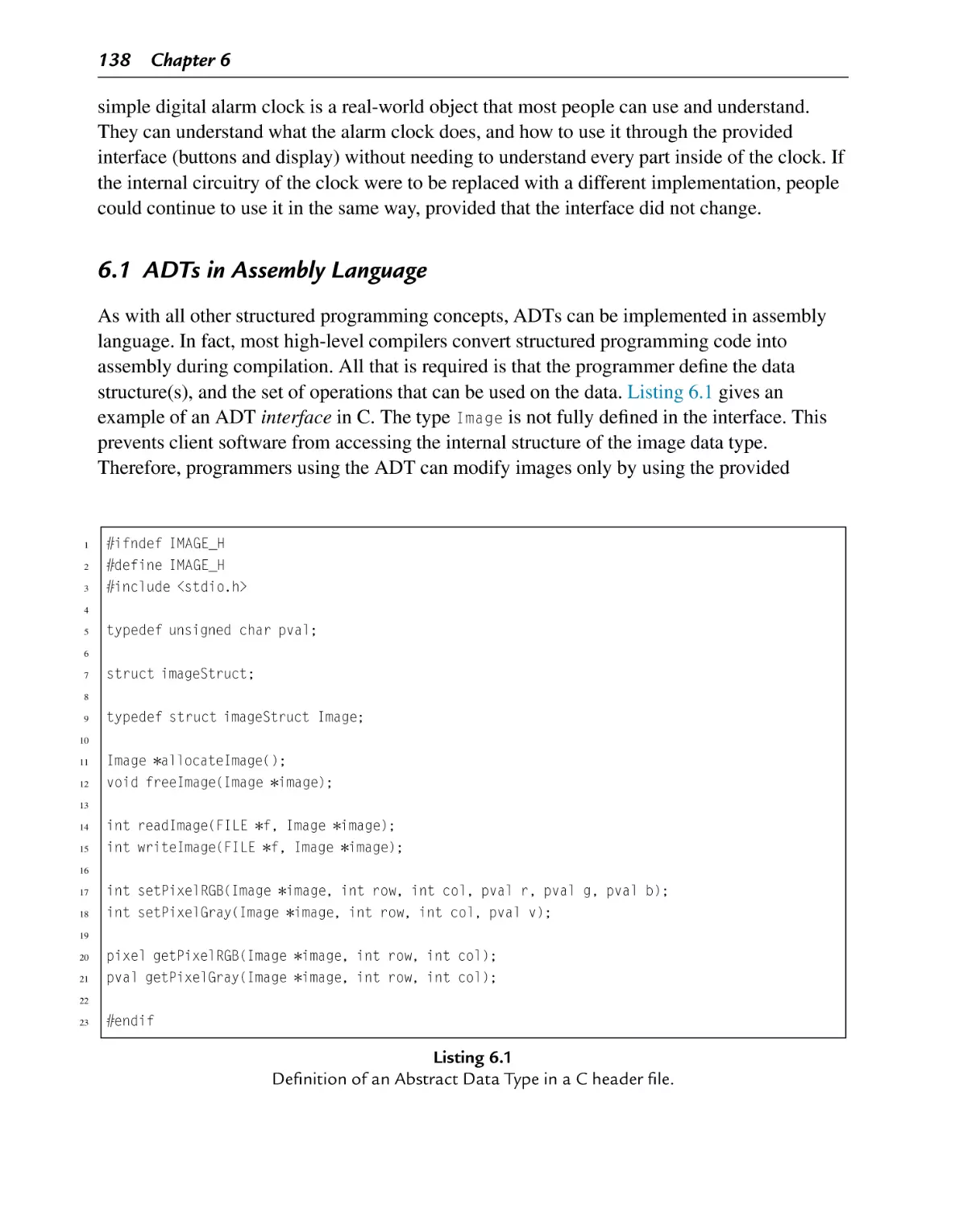
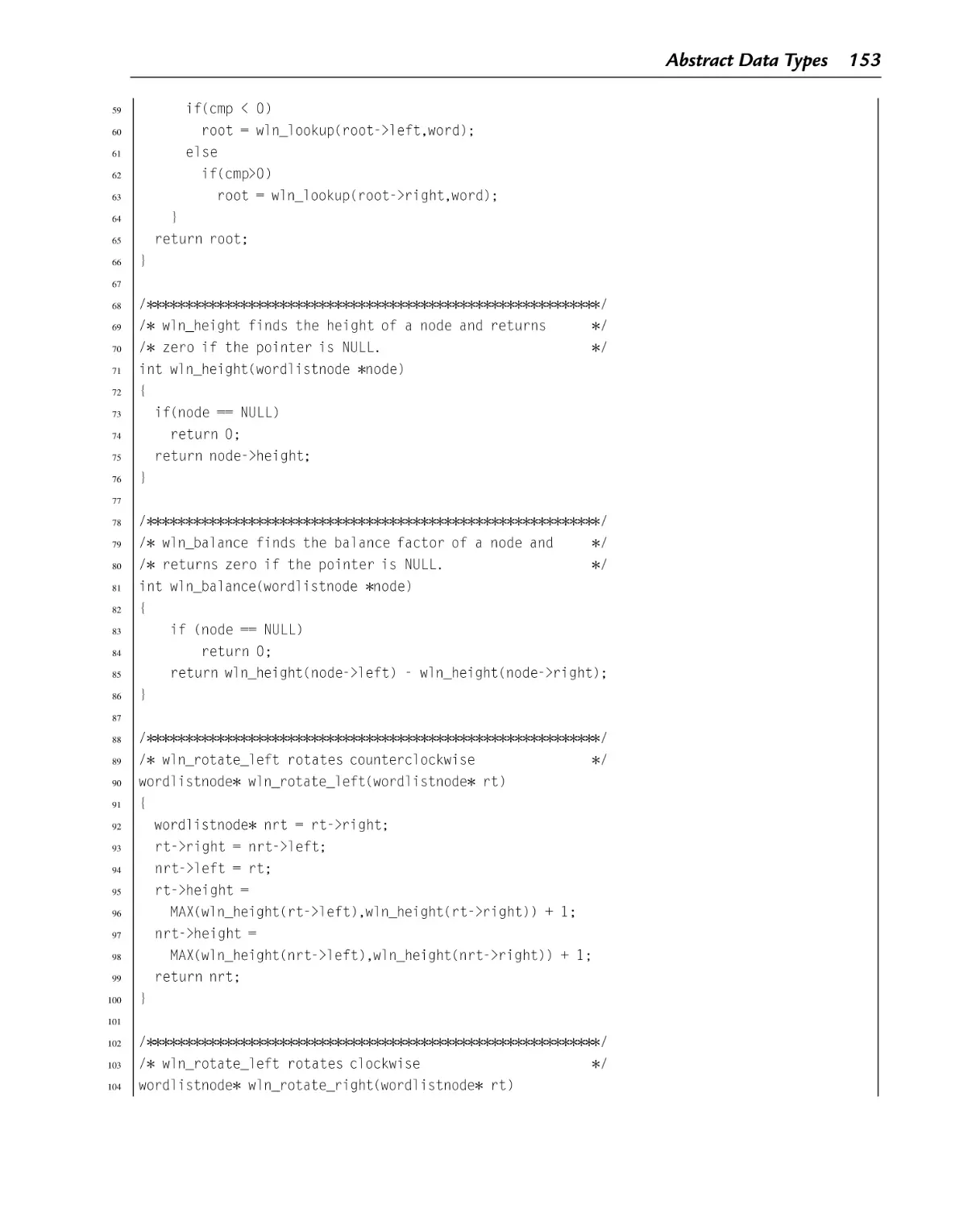
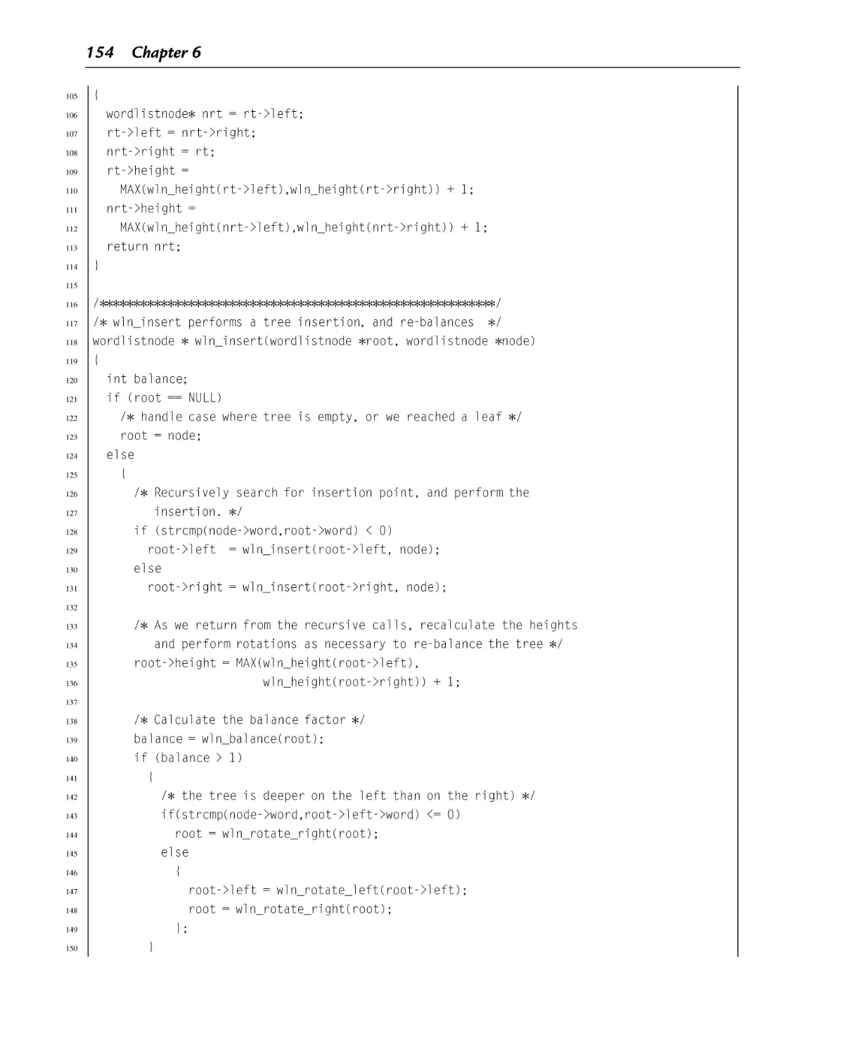
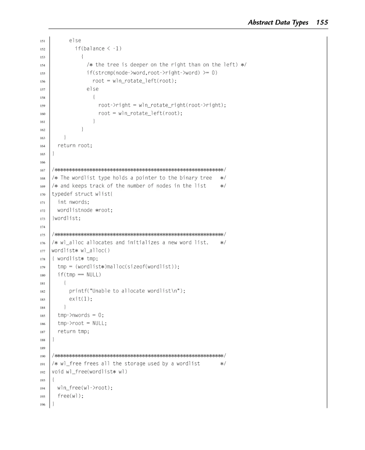
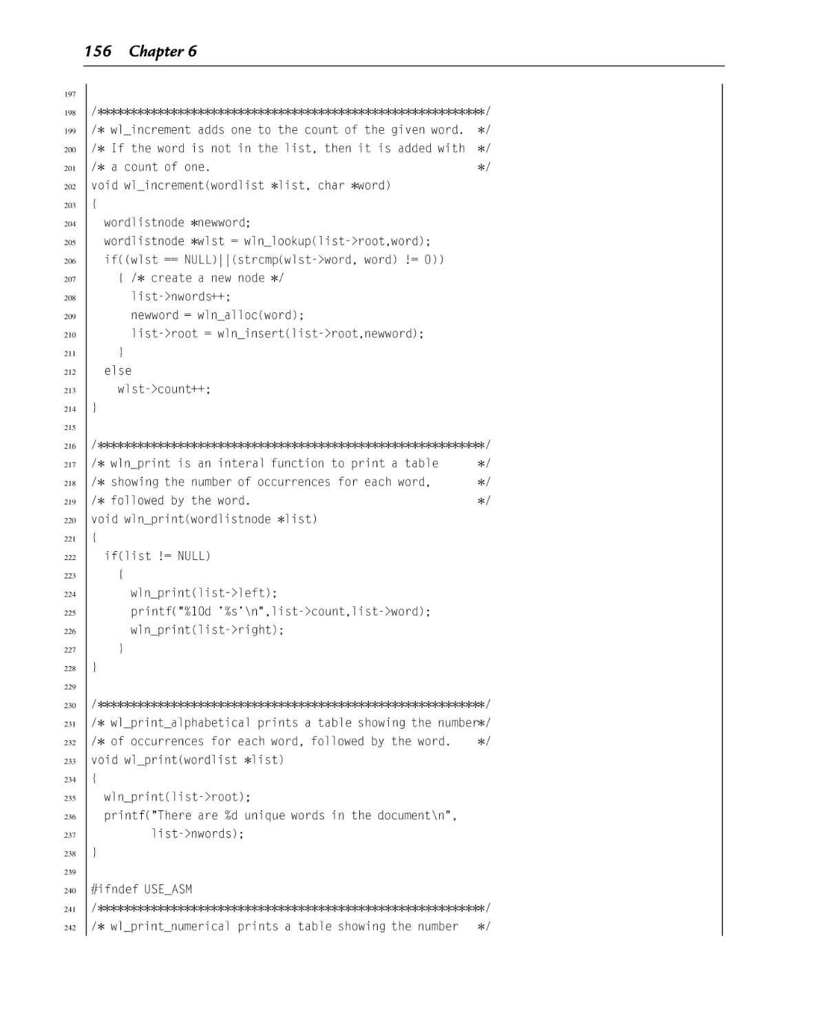
Chapter 6: Abstract Data Types ........................................................... 137
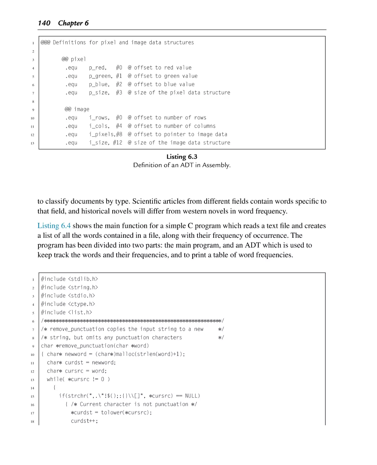
6.1 ADTs in Assembly Language ............................................................... 138
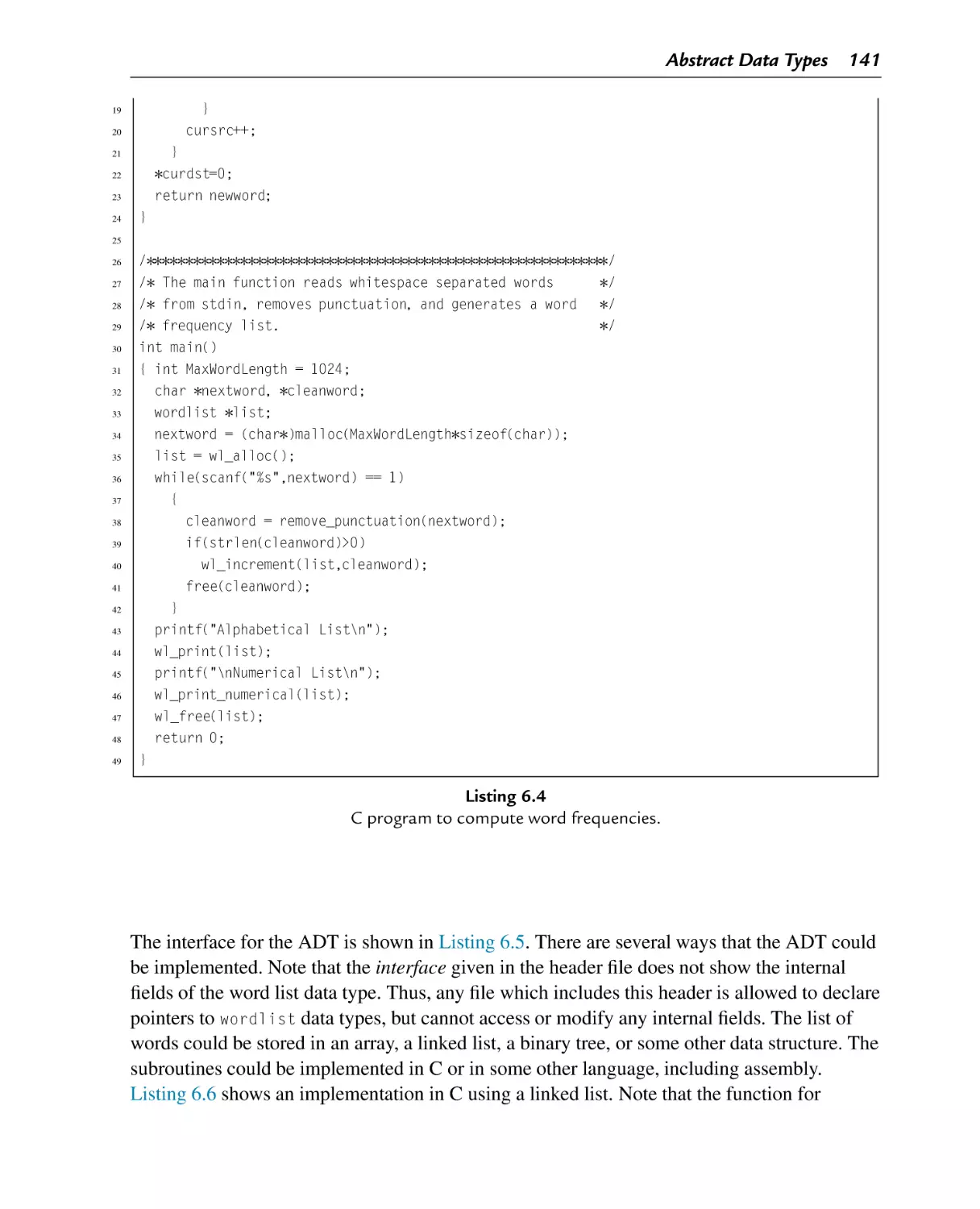
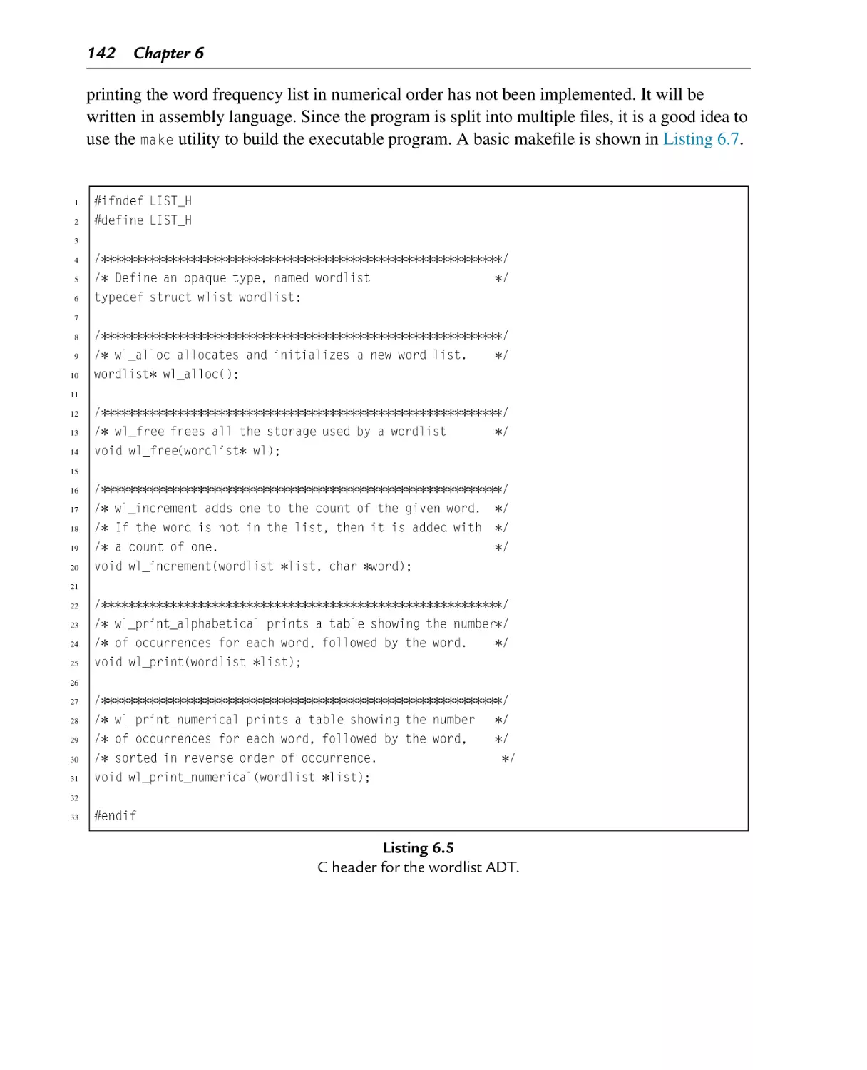
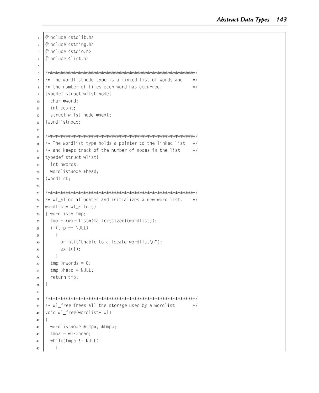
6.2 Word Frequency Counts ...................................................................... 139
6.2.1 Sorting by Word Frequency .............................................................. 147
6.2.2 Better Performance ......................................................................... 150
6.3 Ethics Case Study: Therac-25 ............................................................... 161
6.3.1 History of the Therac-25 .................................................................. 162
6.3.2 Overview of Design Flaws ............................................................... 163
6.4 Chapter Summary .............................................................................. 165
PART II
PERFORMANCE MATHEMATICS
169
Chapter 7: Integer Mathematics ........................................................... 171
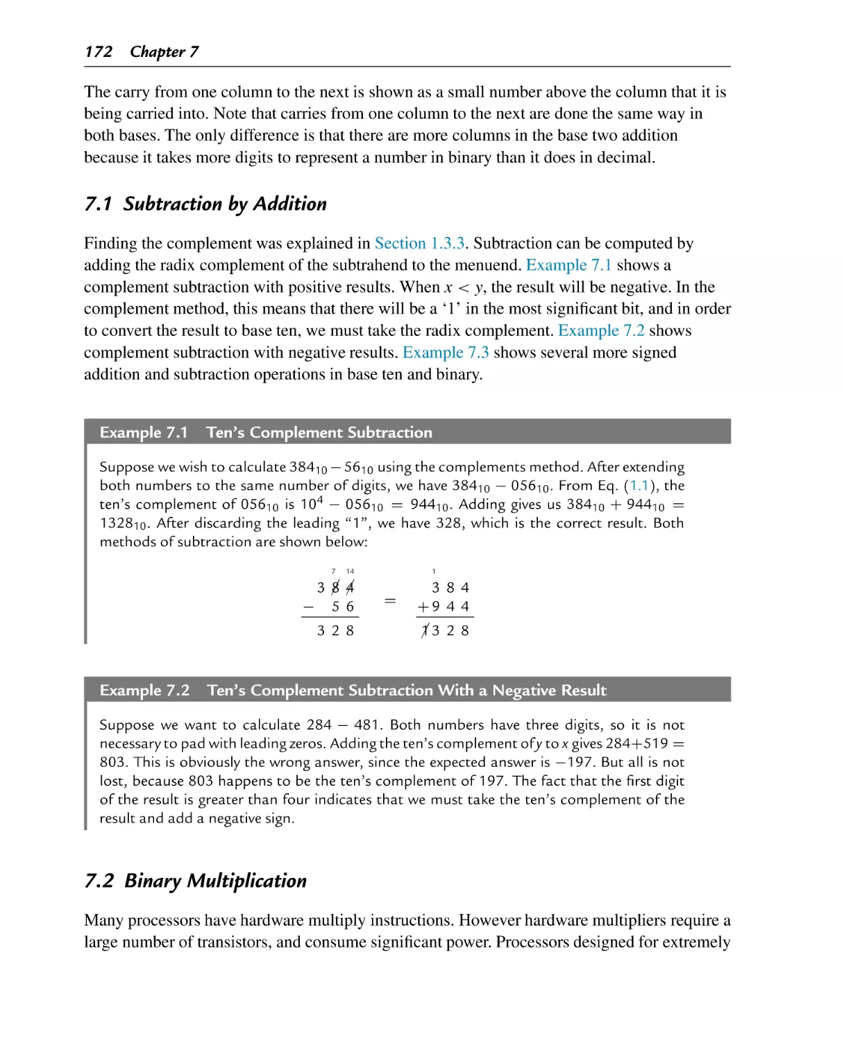
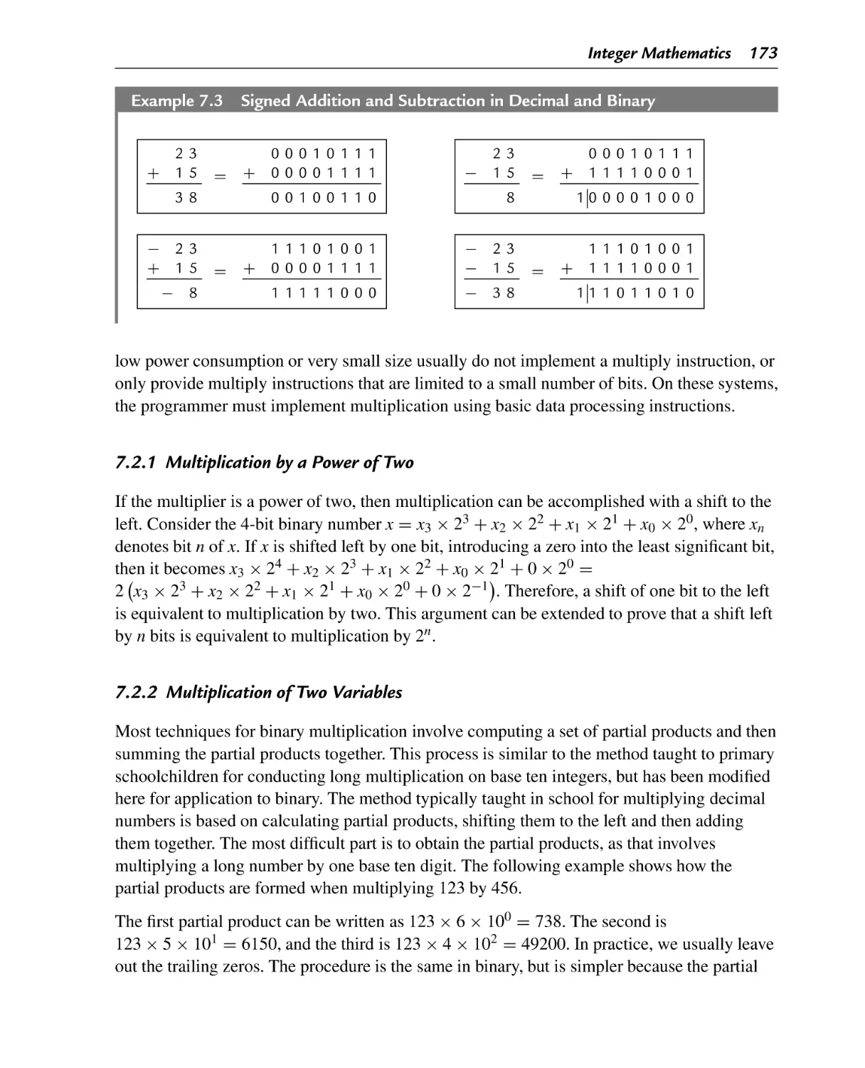
7.1 Subtraction by Addition ...................................................................... 172
7.2 Binary Multiplication ......................................................................... 172
7.2.1 Multiplication by a Power of Two ...................................................... 173
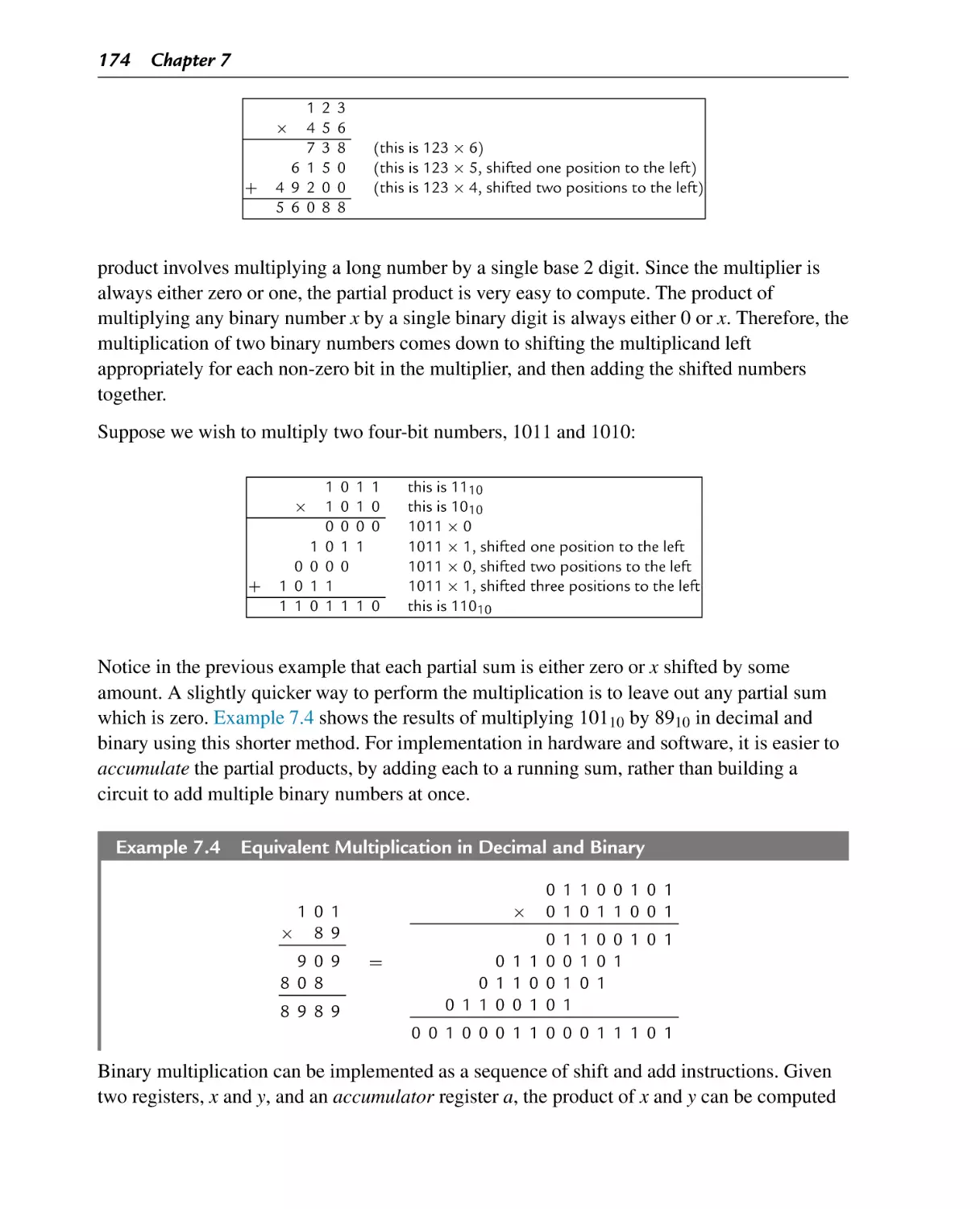
7.2.2 Multiplication of Two Variables......................................................... 173
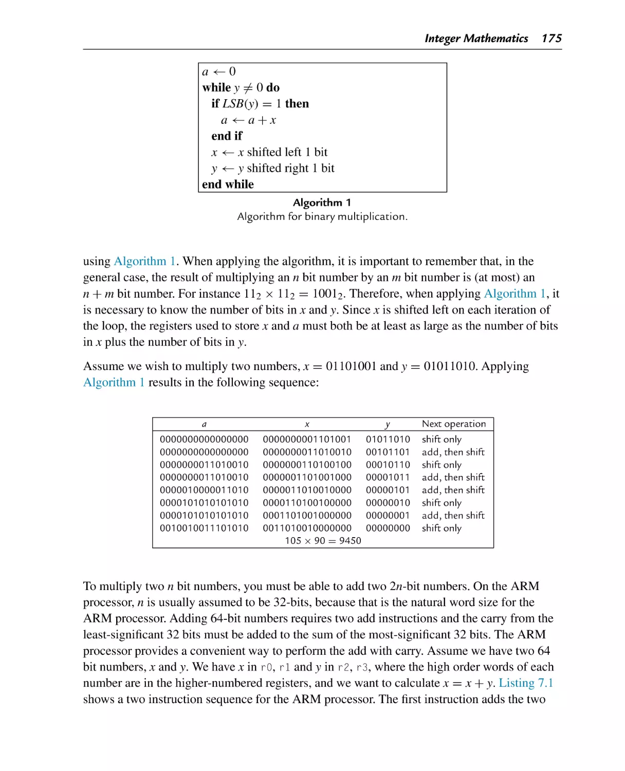
7.2.3 Multiplication of a Variable by a Constant ........................................... 177
viii
Contents
7.2.4 Signed Multiplication ...................................................................... 178
7.2.5 Multiplying Large Numbers ............................................................. 179
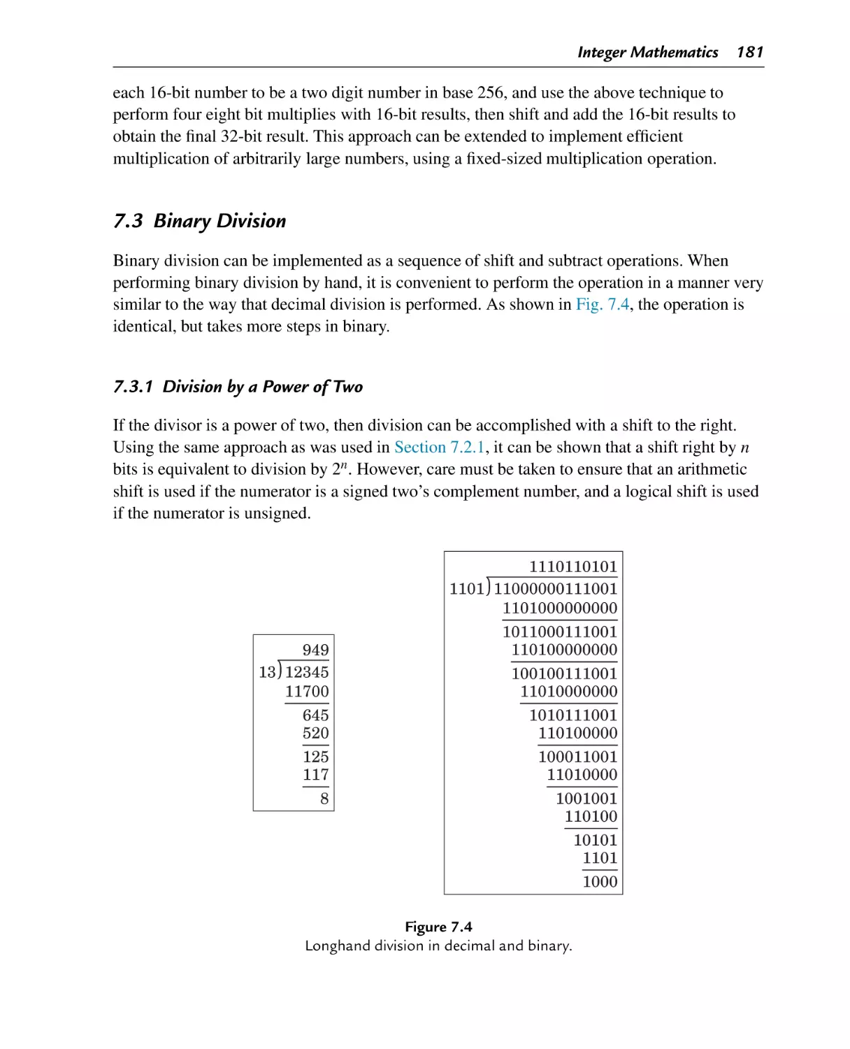
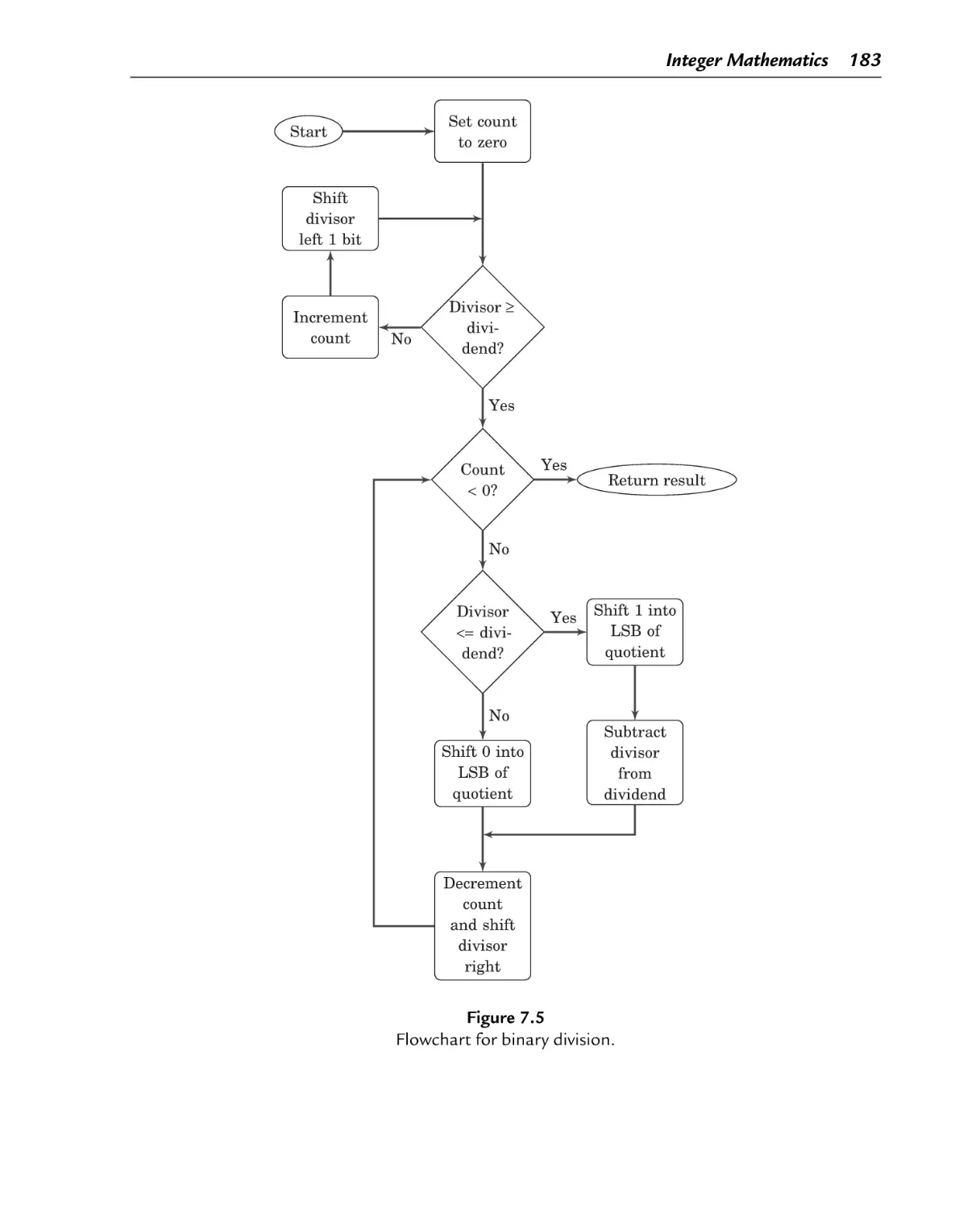
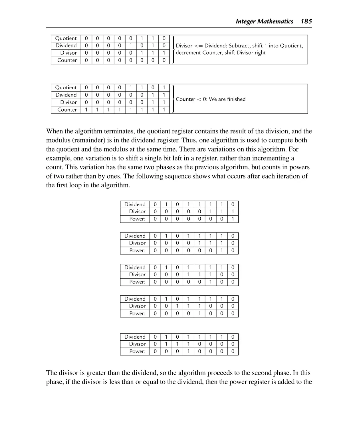
7.3 Binary Division ................................................................................. 181
7.3.1 Division by a Power of Two.............................................................. 181
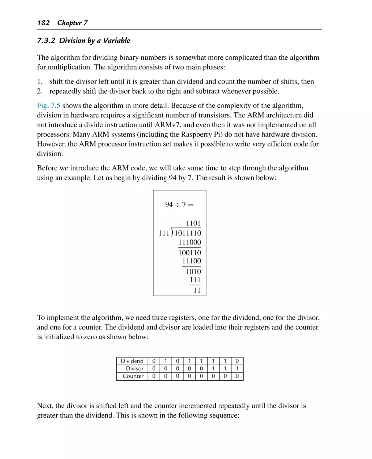
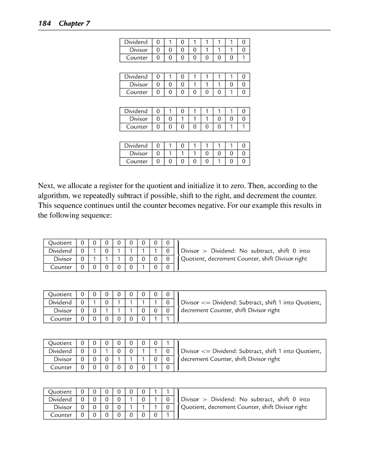
7.3.2 Division by a Variable ..................................................................... 182
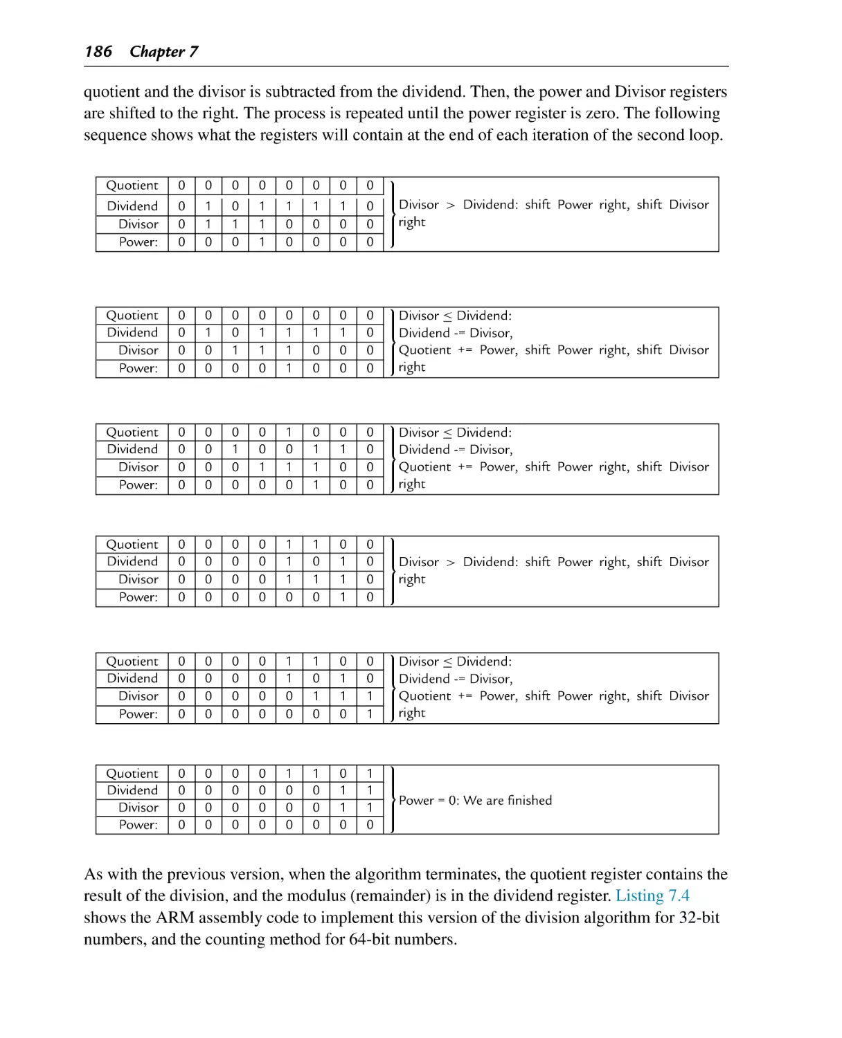
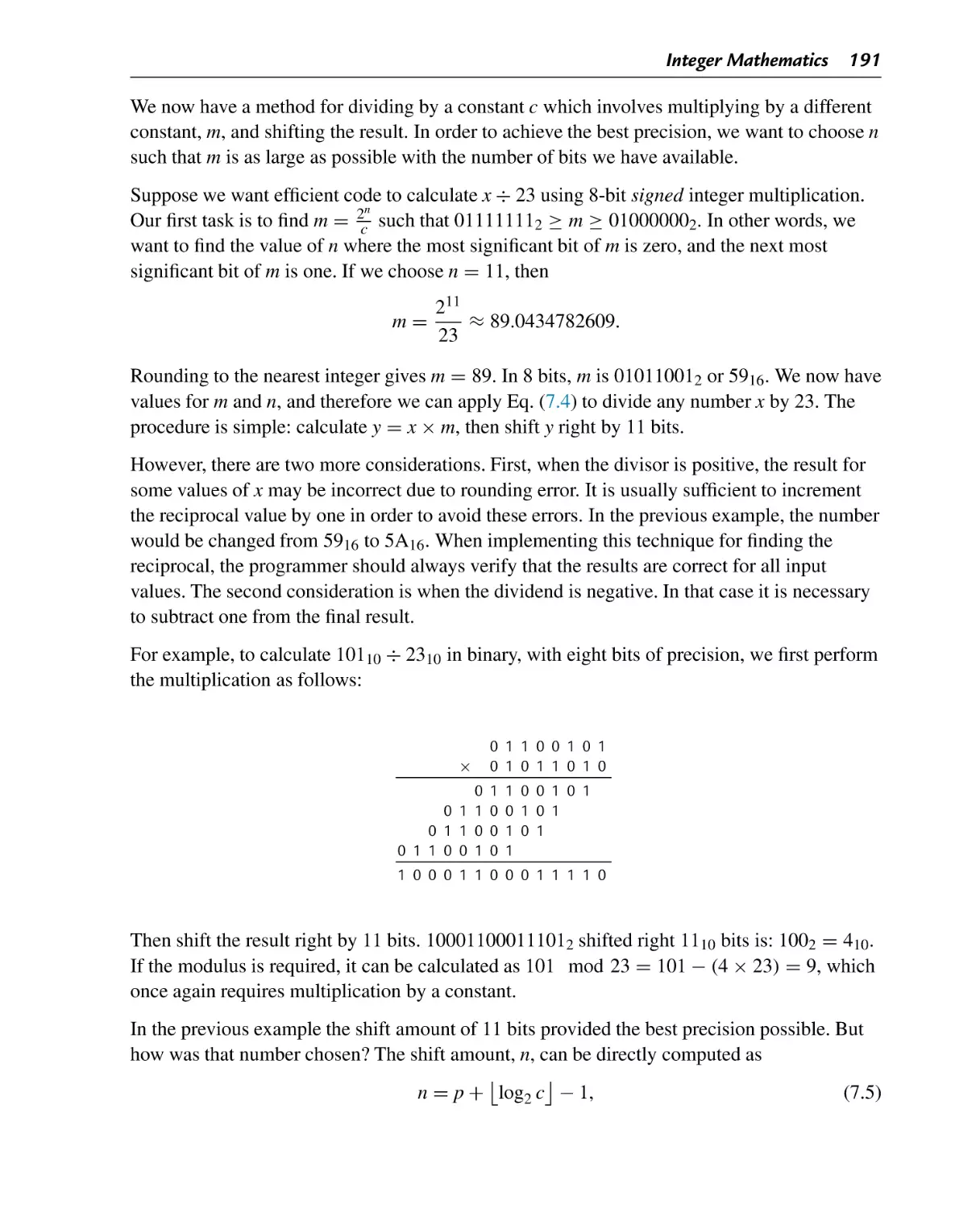
7.3.3 Division by a Constant .................................................................... 190
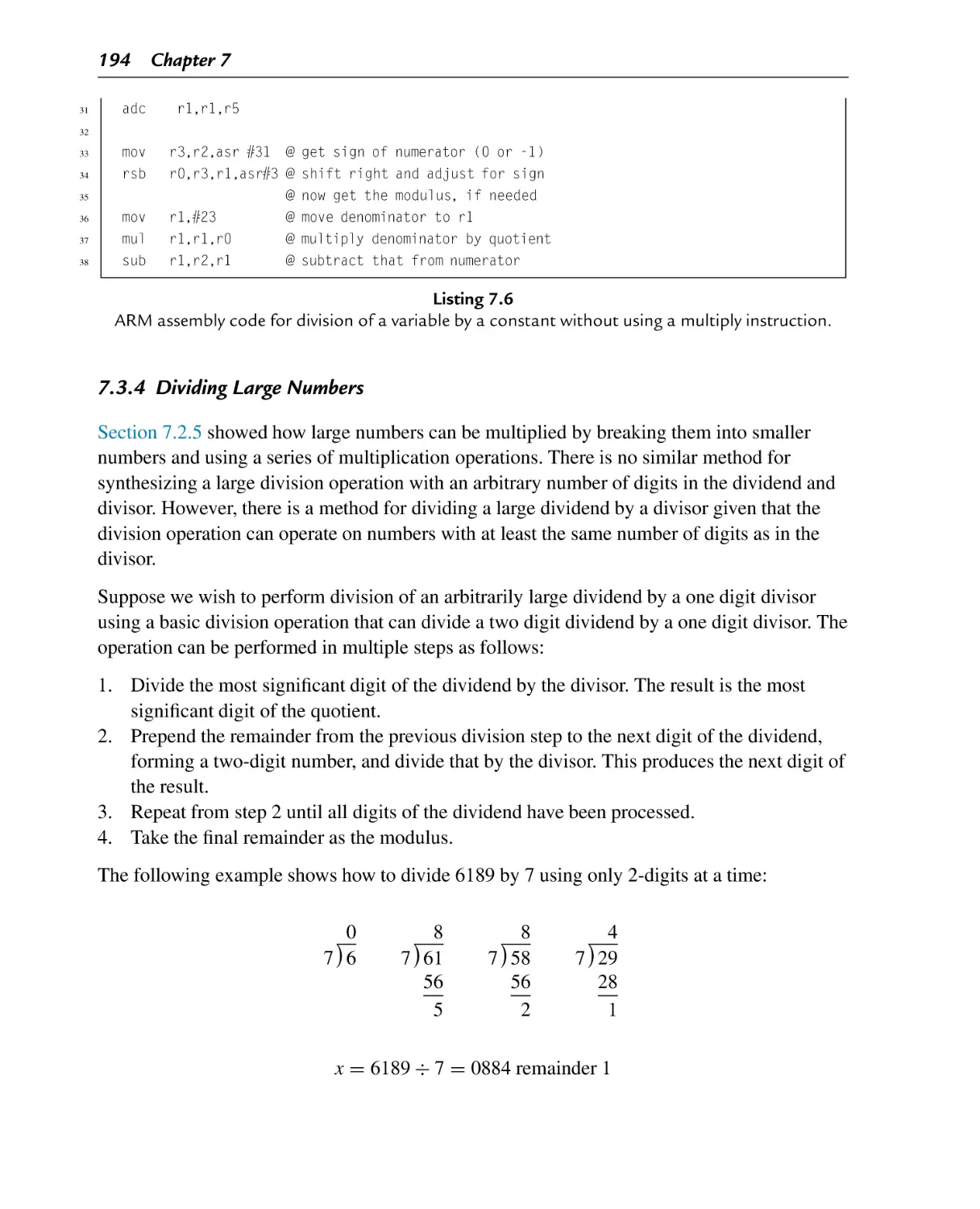
7.3.4 Dividing Large Numbers.................................................................. 194
7.4 Big Integer ADT................................................................................ 195
7.5 Chapter Summary .............................................................................. 216
Chapter 8: Non-Integral Mathematics ..................................................... 219
8.1 Base Conversion of Fractional Numbers ................................................. 220
8.2
8.3
8.4
8.5
8.6
8.7
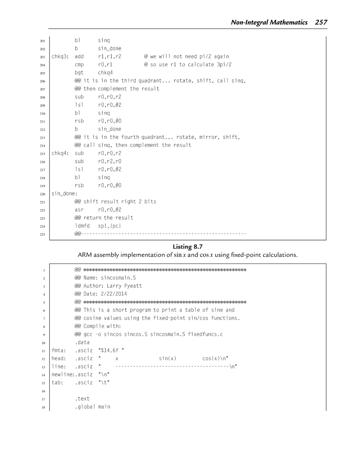
8.8
8.9
8.1.1 Arbitrary Base to Decimal................................................................ 220
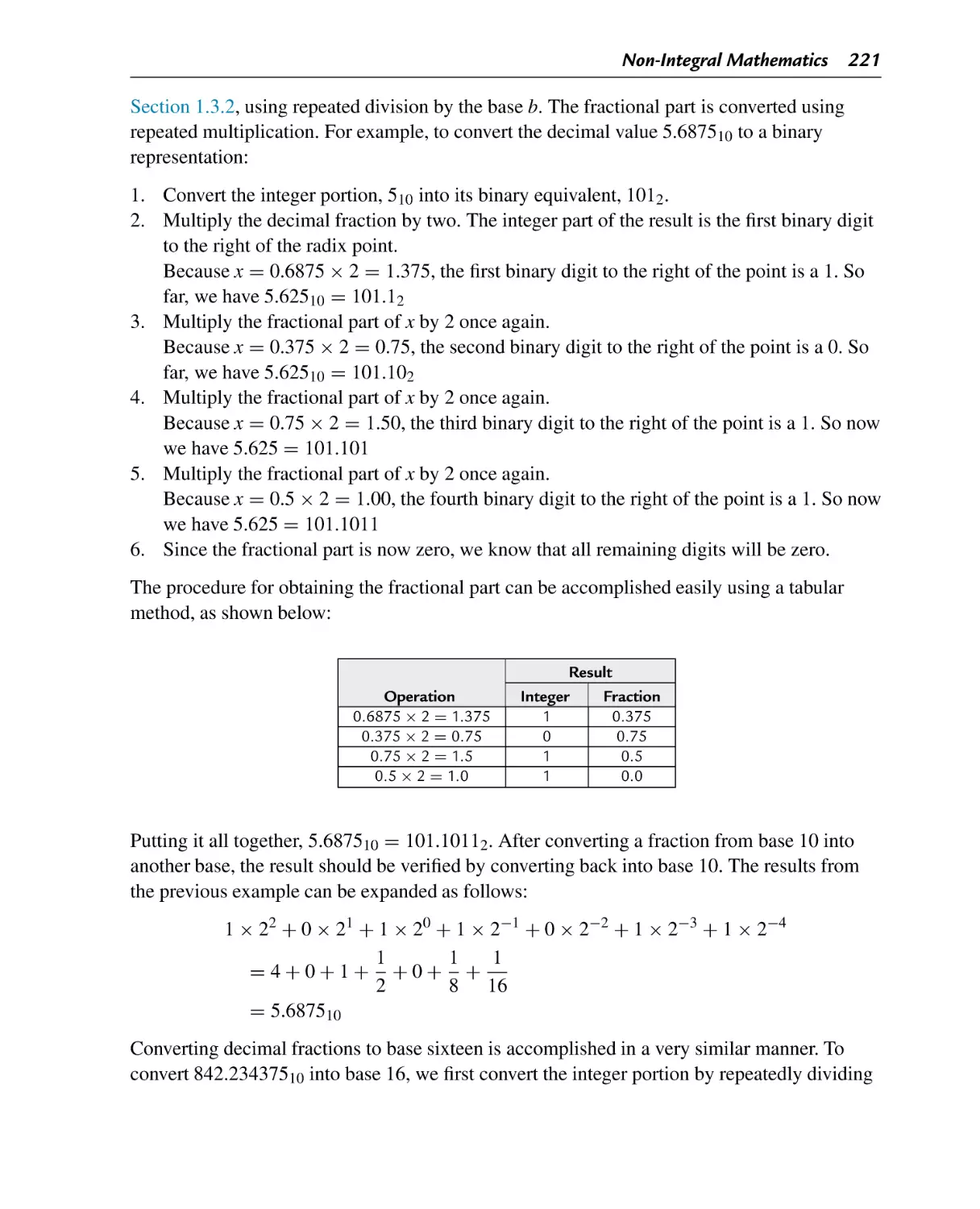
8.1.2 Decimal to Arbitrary Base ................................................................ 220
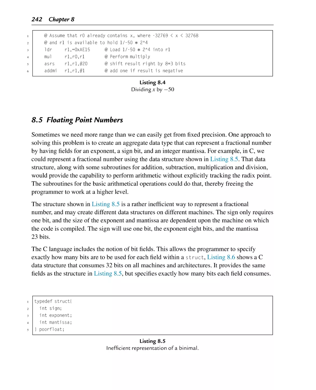
Fractions and Bases............................................................................ 223
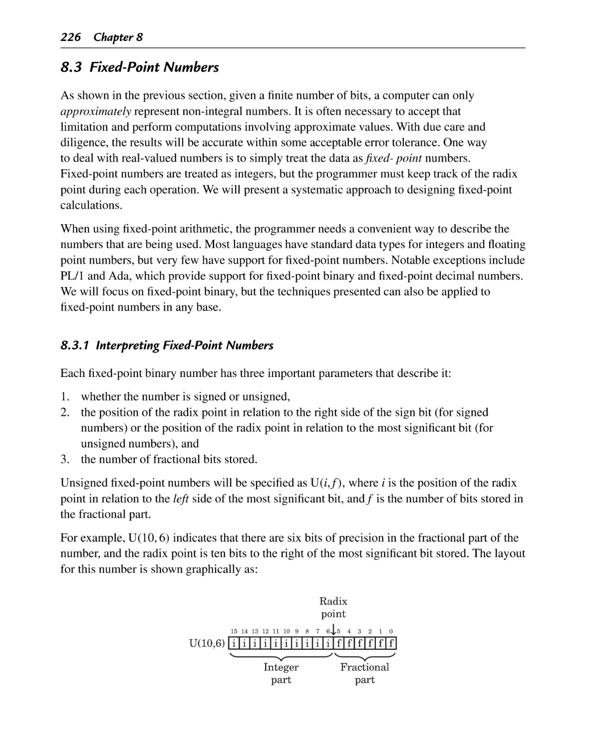
Fixed-Point Numbers.......................................................................... 226
8.3.1 Interpreting Fixed-Point Numbers ...................................................... 226
8.3.2 Q Notation .................................................................................... 230
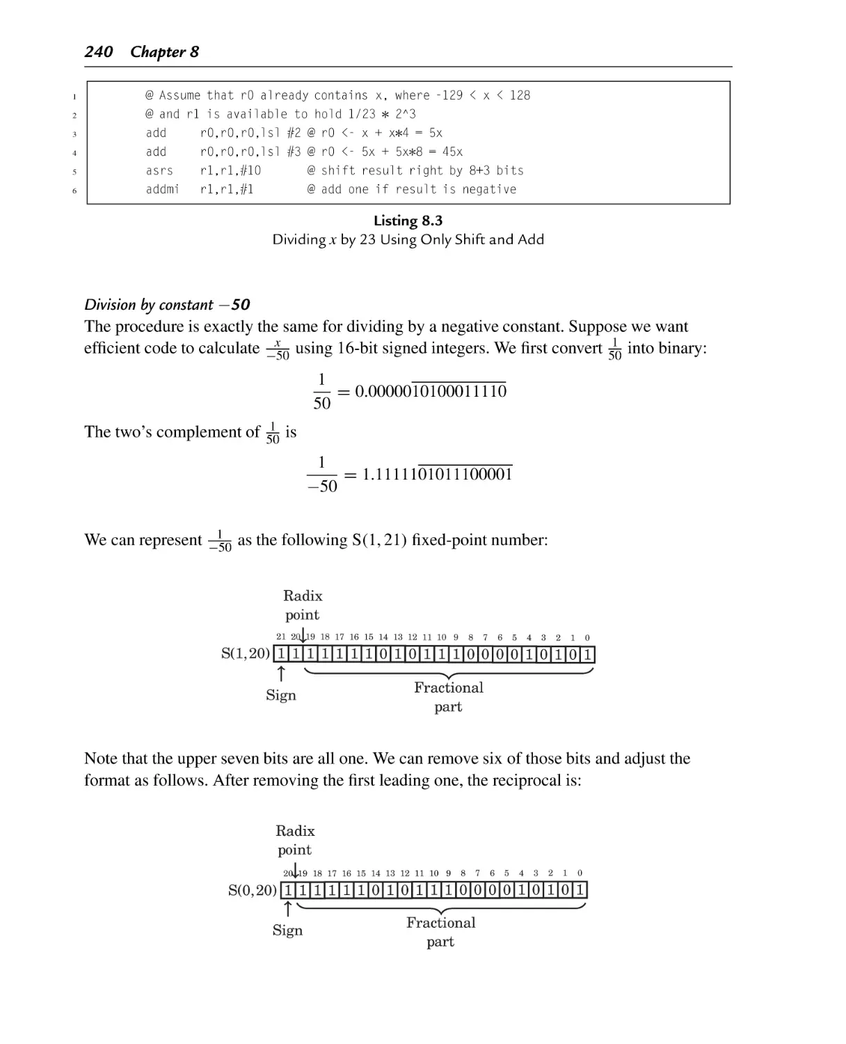
8.3.3 Properties of Fixed-Point Numbers .................................................... 230
Fixed-Point Operations ....................................................................... 231
8.4.1 Fixed-Point Addition and Subtraction ................................................. 231
8.4.2 Fixed Point Multiplication................................................................ 232
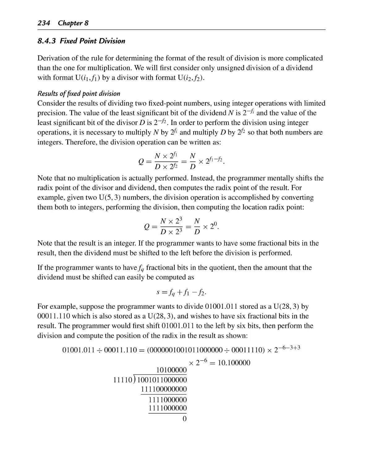
8.4.3 Fixed Point Division ....................................................................... 234
8.4.4 Division by a Constant .................................................................... 236
Floating Point Numbers ...................................................................... 242
8.5.1 IEEE 754 Half-Precision.................................................................. 243
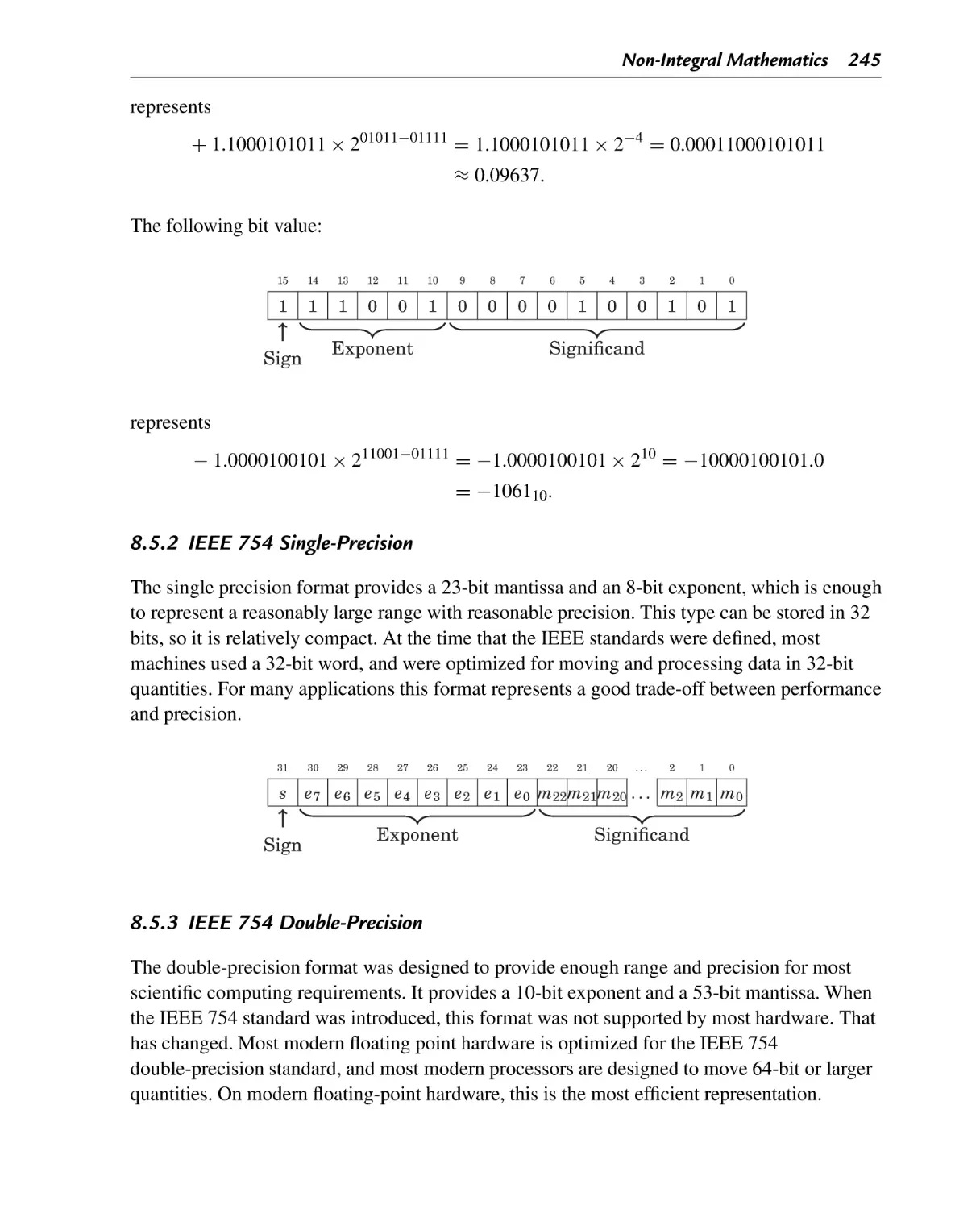
8.5.2 IEEE 754 Single-Precision ............................................................... 245
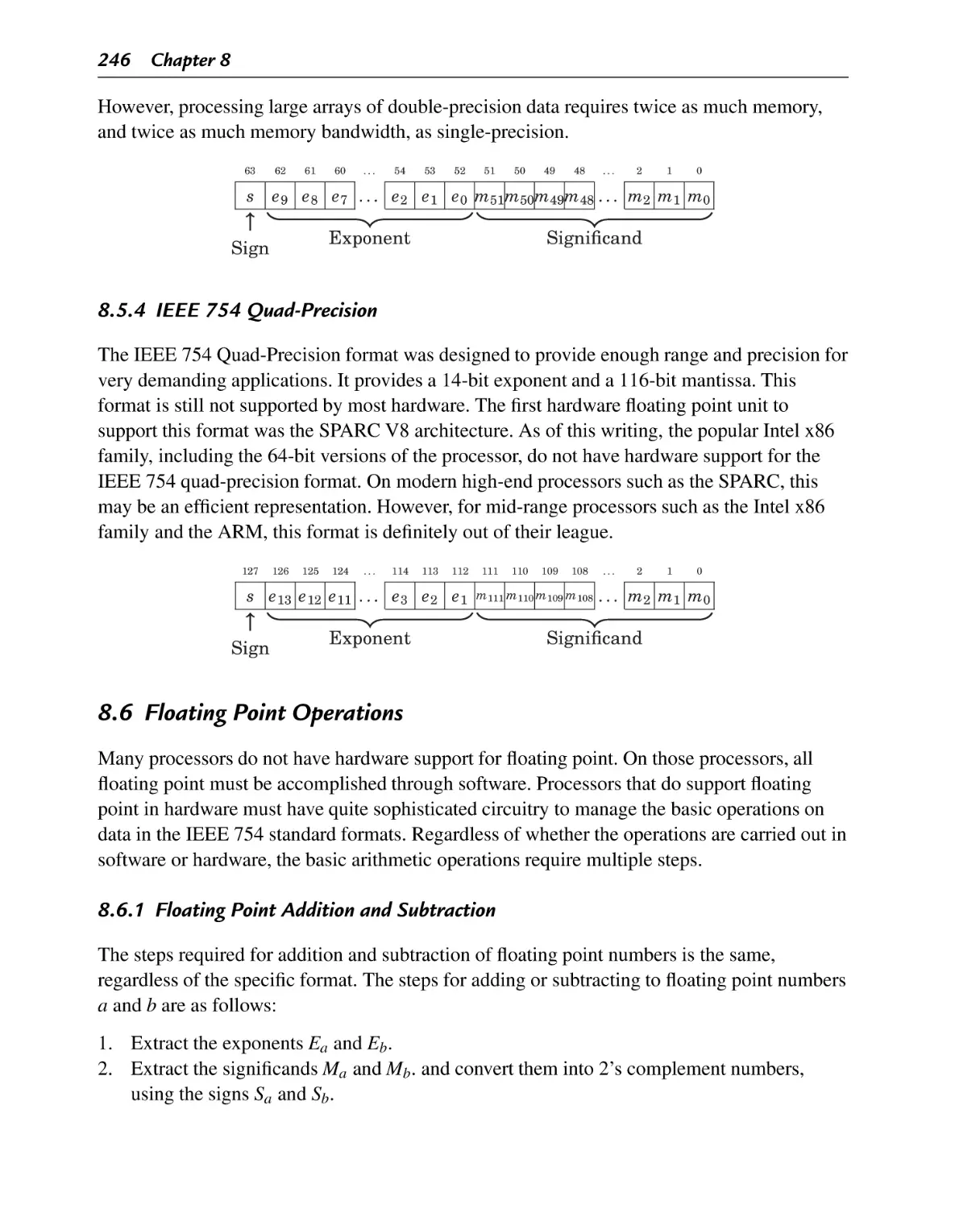
8.5.3 IEEE 754 Double-Precision .............................................................. 245
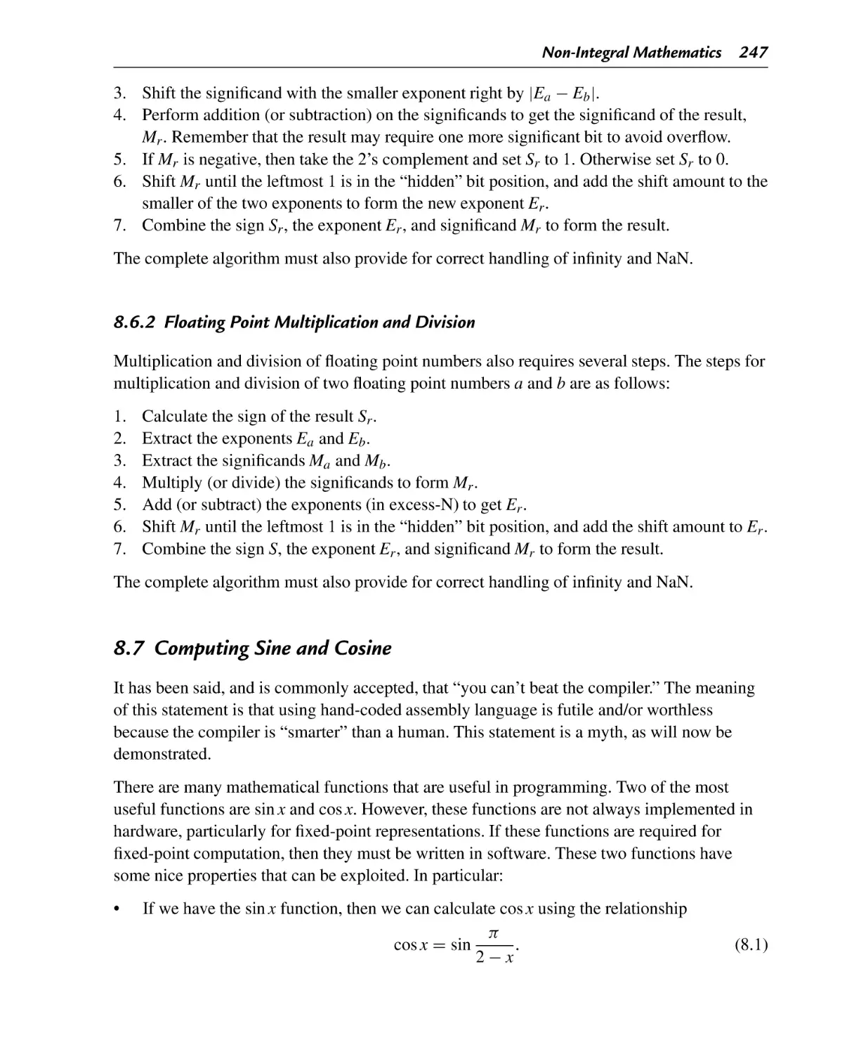
8.5.4 IEEE 754 Quad-Precision ................................................................ 246
Floating Point Operations .................................................................... 246
8.6.1 Floating Point Addition and Subtraction .............................................. 246
8.6.2 Floating Point Multiplication and Division........................................... 247
Computing Sine and Cosine ................................................................. 247
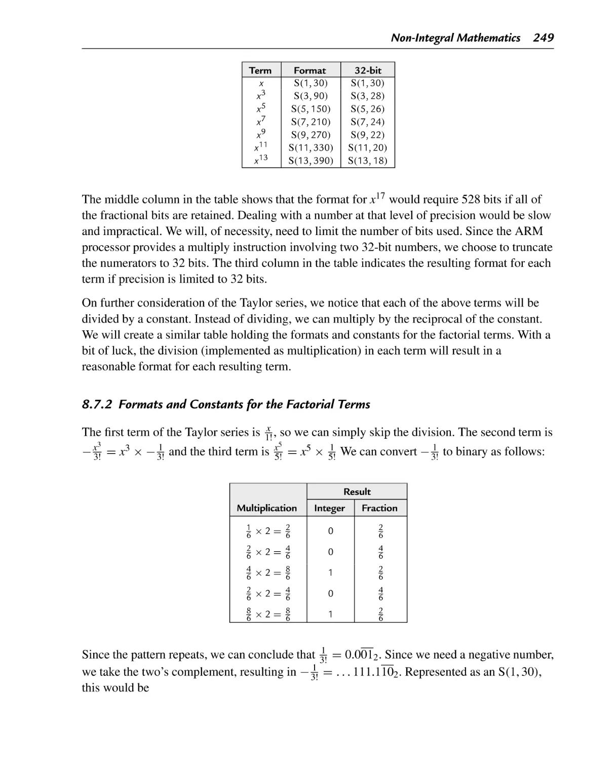
8.7.1 Formats for the Powers of x .............................................................. 248
8.7.2 Formats and Constants for the Factorial Terms...................................... 249
8.7.3 Putting it All Together ..................................................................... 251
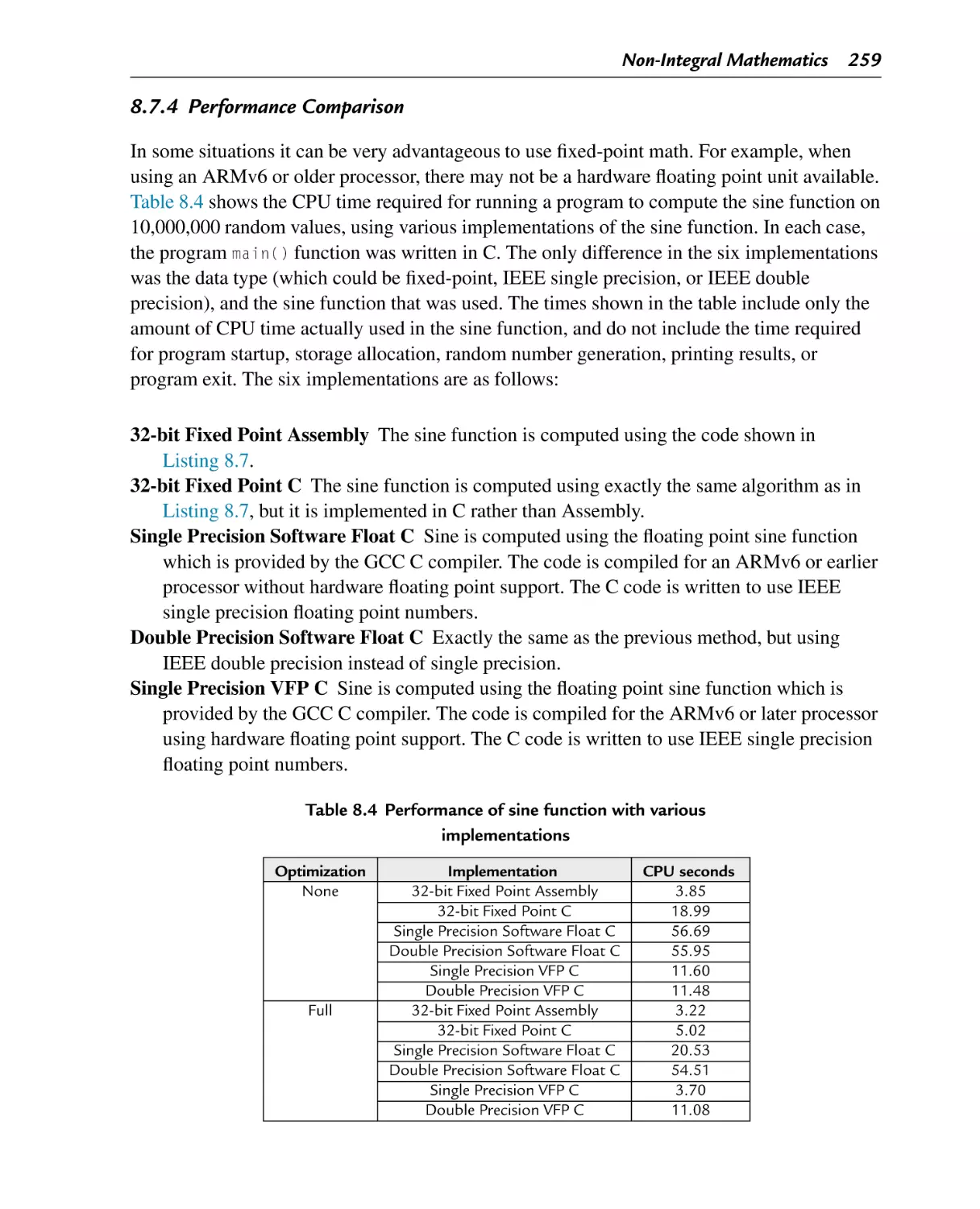
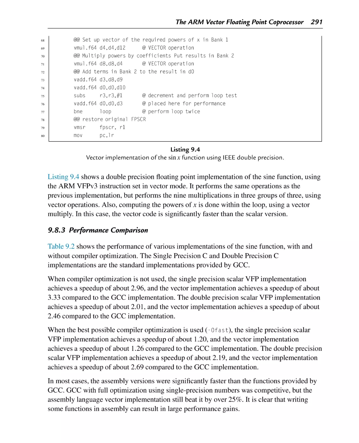
8.7.4 Performance Comparison ................................................................. 259
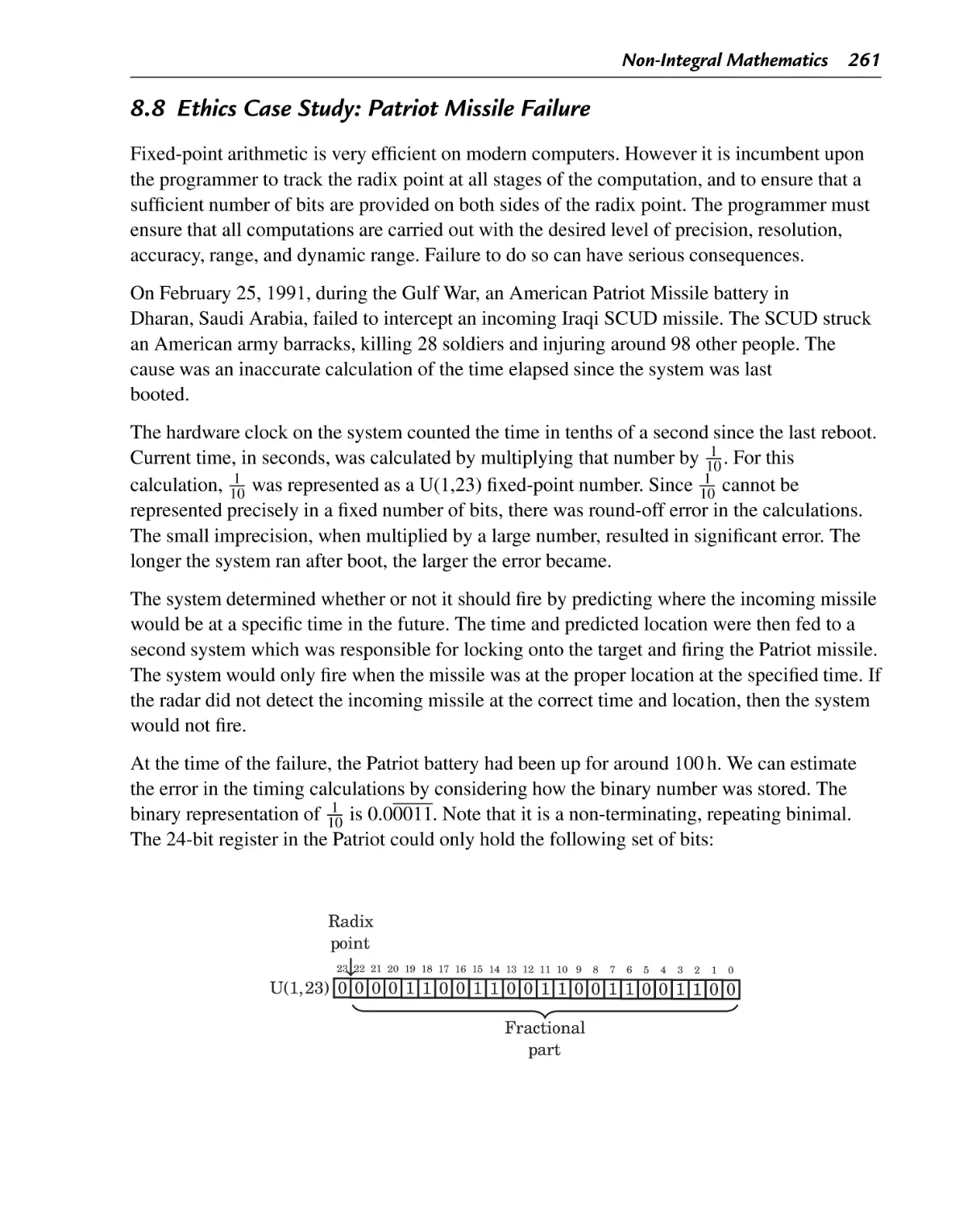
Ethics Case Study: Patriot Missile Failure ............................................... 261
Chapter Summary .............................................................................. 263
Chapter 9: The ARM Vector Floating Point Coprocessor ............................... 265
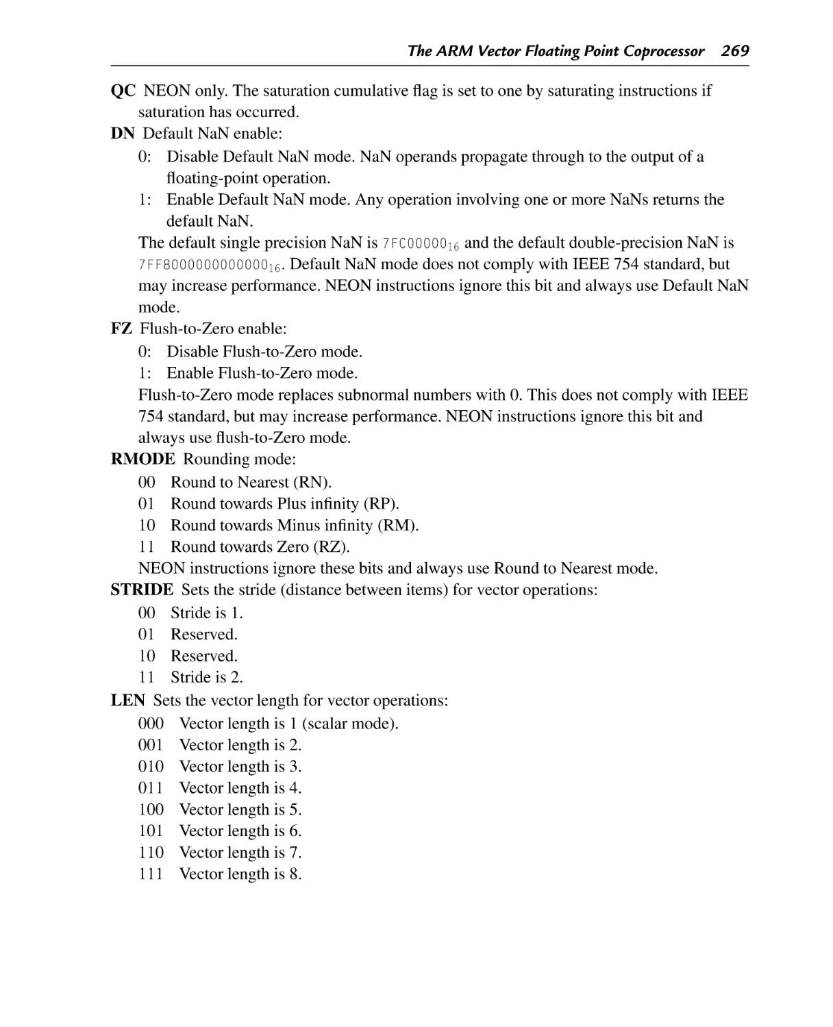
9.1 Vector Floating Point Overview ............................................................ 266
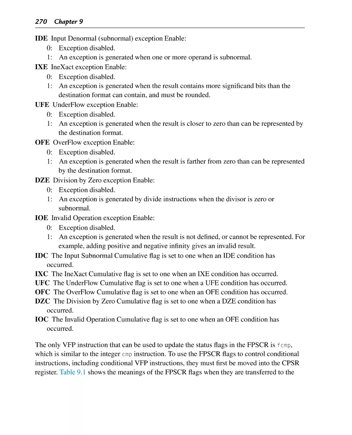
9.2 Floating Point Status and Control Register .............................................. 268
9.2.1 Performance Versus Compliance ....................................................... 271
9.2.2 Vector Mode ................................................................................. 272
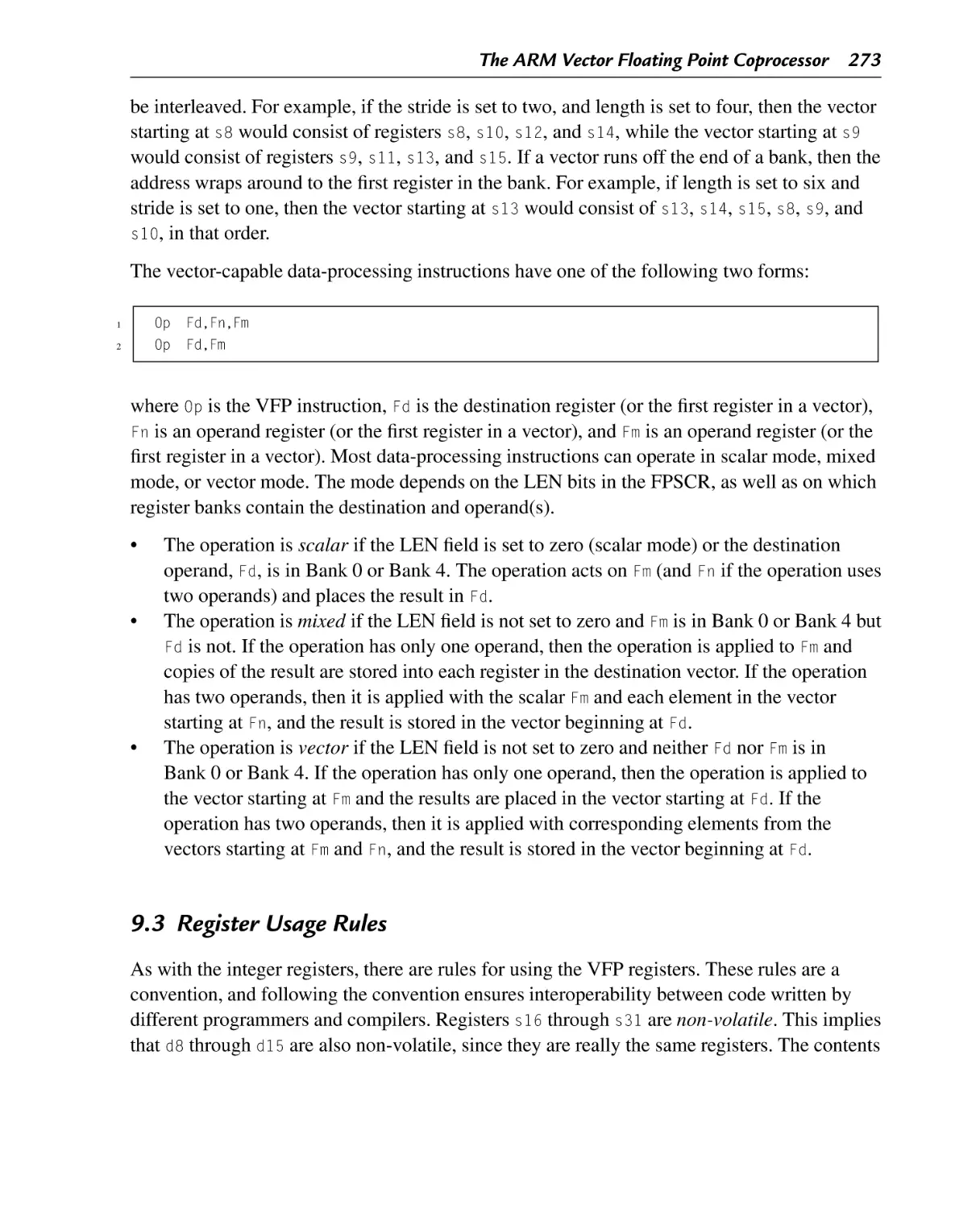
9.3 Register Usage Rules .......................................................................... 273
Contents ix
9.4 Load/Store Instructions ..................................................................... 274
9.4.1 Load/Store Single Register .......................................................... 274
9.4.2 Load/Store Multiple Registers ...................................................... 275
9.5 Data Processing Instructions ............................................................... 277
9.5.1 Copy, Absolute Value, Negate, and Square Root............................... 277
9.5.2 Add, Subtract, Multiply, and Divide .............................................. 278
9.5.3 Compare ................................................................................. 279
9.6 Data Movement Instructions ............................................................... 279
9.6.1 Moving Between Two VFP Registers ............................................ 279
9.6.2 Moving Between VFP Register and One Integer Register ................... 280
9.6.3 Moving Between VFP Register and Two Integer Registers ................. 281
9.6.4 Move Between ARM Register and VFP System Register ................... 282
9.7 Data Conversion Instructions .............................................................. 282
9.7.1 Convert Between Floating Point and Integer.................................... 282
9.7.2 Convert Between Fixed Point and Single Precision ........................... 284
9.8 Floating Point Sine Function .............................................................. 285
9.8.1 Sine Function Using Scalar Mode ................................................. 285
9.8.2 Sine Function Using Vector Mode................................................. 287
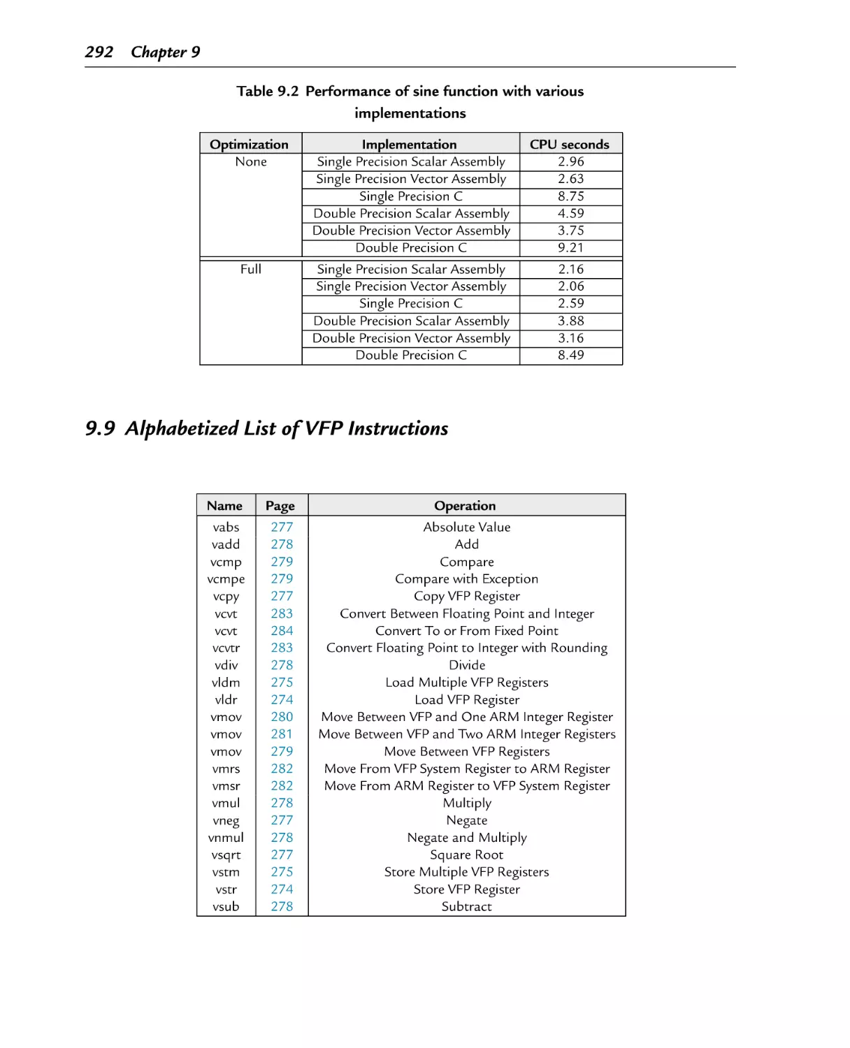
9.8.3 Performance Comparison ............................................................ 291
9.9 Alphabetized List of VFP Instructions .................................................. 292
9.10 Chapter Summary ............................................................................ 293
Chapter 10: The ARM NEON Extensions ................................................ 297
10.1 NEON Intrinsics .............................................................................. 299
10.2 Instruction Syntax ............................................................................ 299
10.3 Load and Store Instructions ................................................................ 302
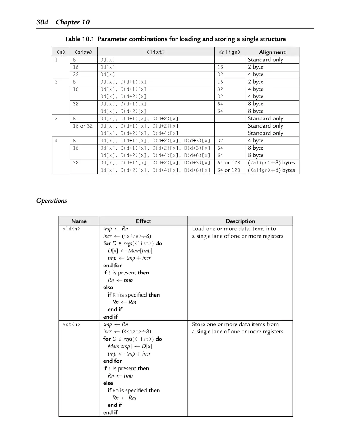
10.3.1 Load or Store Single Structure Using One Lane ............................... 303
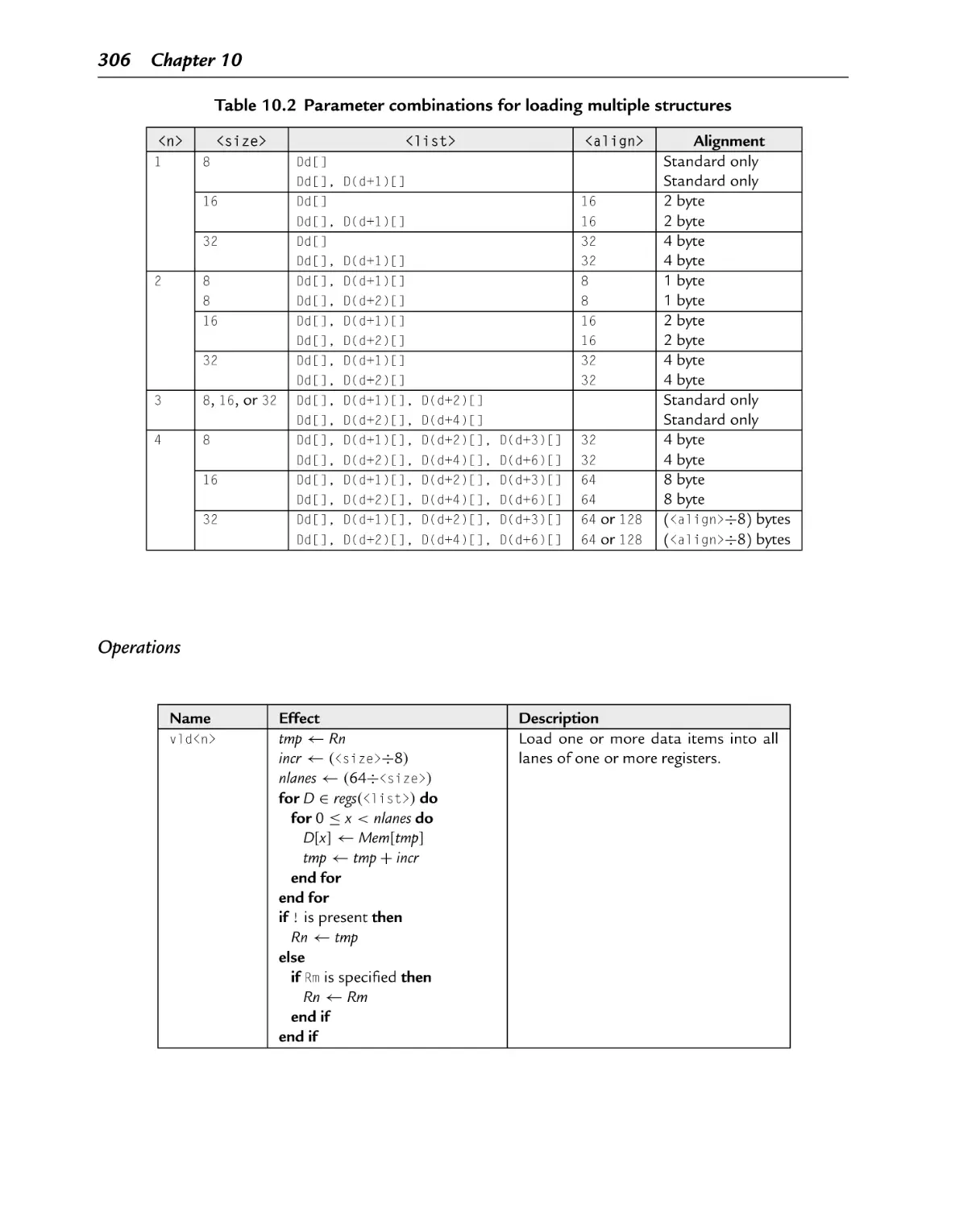
10.3.2 Load Copies of a Structure to All Lanes ......................................... 305
10.3.3 Load or Store Multiple Structures ................................................. 307
10.4 Data Movement Instructions ............................................................... 309
10.4.1 Moving Between NEON Scalar and Integer Register......................... 309
10.4.2 Move Immediate Data ................................................................ 310
10.4.3 Change Size of Elements in a Vector ............................................. 311
10.4.4 Duplicate Scalar........................................................................ 312
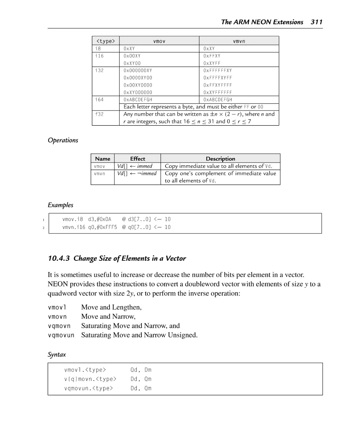
10.4.5 Extract Elements ....................................................................... 313
10.4.6 Reverse Elements ...................................................................... 314
10.4.7 Swap Vectors ........................................................................... 315
10.4.8 Transpose Matrix ...................................................................... 316
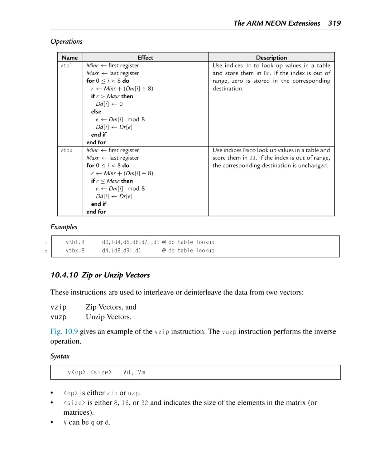
10.4.9 Table Lookup ........................................................................... 317
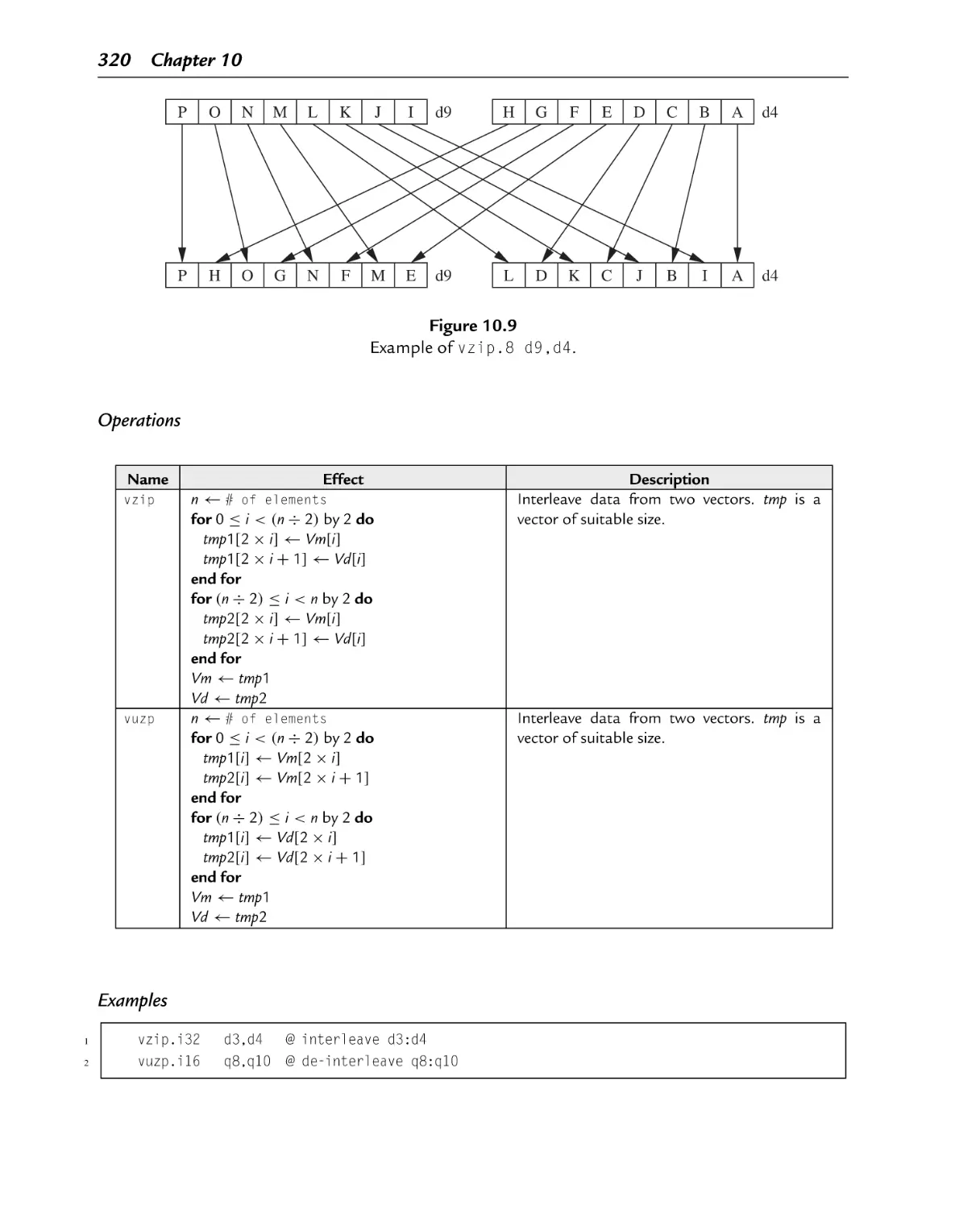
10.4.10 Zip or Unzip Vectors .................................................................. 319
10.5 Data Conversion .............................................................................. 321
10.5.1 Convert Between Fixed Point and Single-Precision ........................... 321
10.5.2 Convert Between Half-Precision and Single-Precision ....................... 322
10.6 Comparison Operations ..................................................................... 322
10.6.1 Vector Compare ........................................................................ 323
x
Contents
10.7
10.8
10.9
10.10
10.11
10.12
10.13
10.14
PART III
10.6.2 Vector Absolute Compare.......................................................... 324
10.6.3 Vector Test Bits ....................................................................... 325
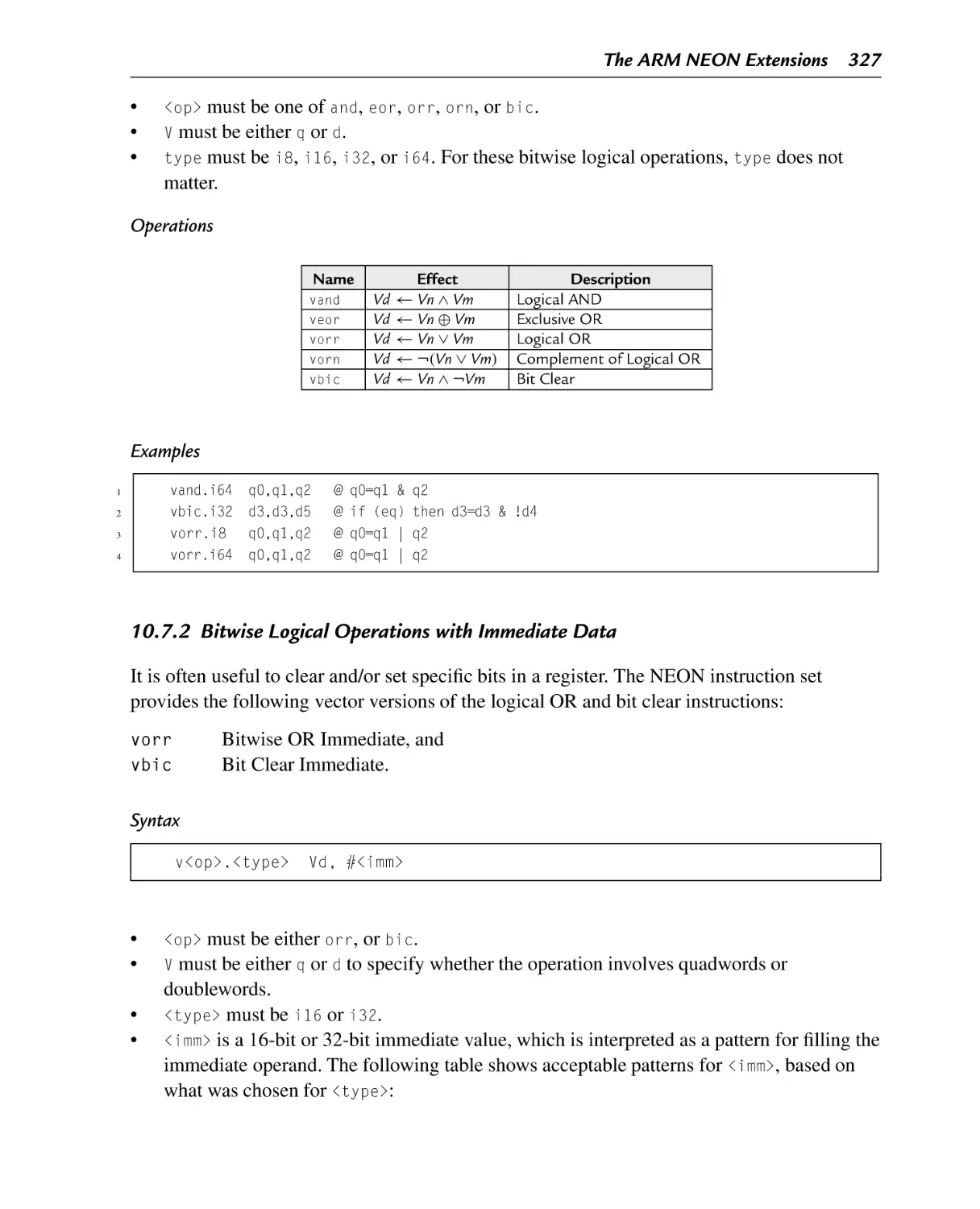
Bitwise Logical Operations............................................................... 326
10.7.1 Bitwise Logical Operations........................................................ 326
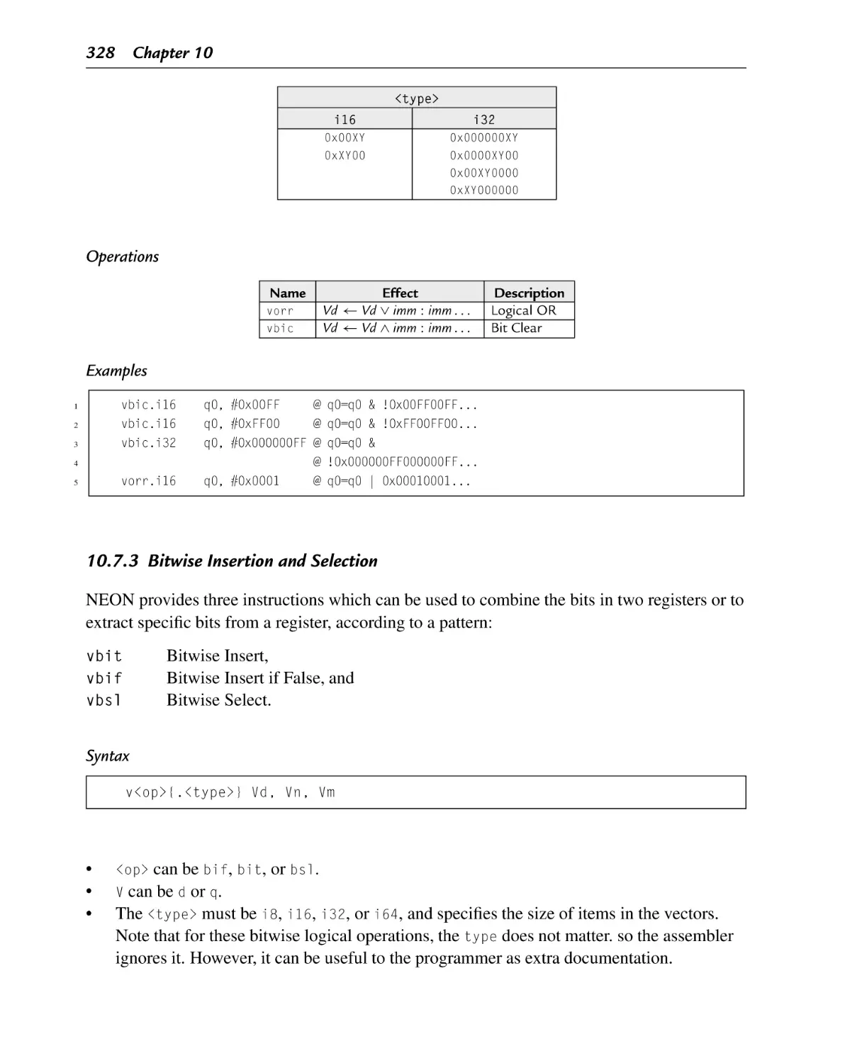
10.7.2 Bitwise Logical Operations with Immediate Data ........................... 327
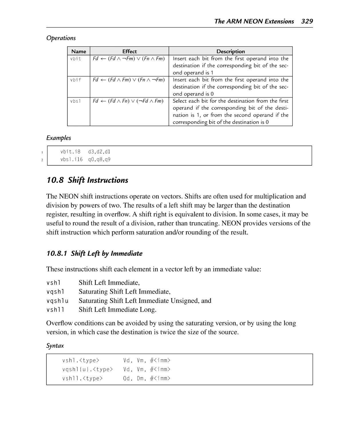
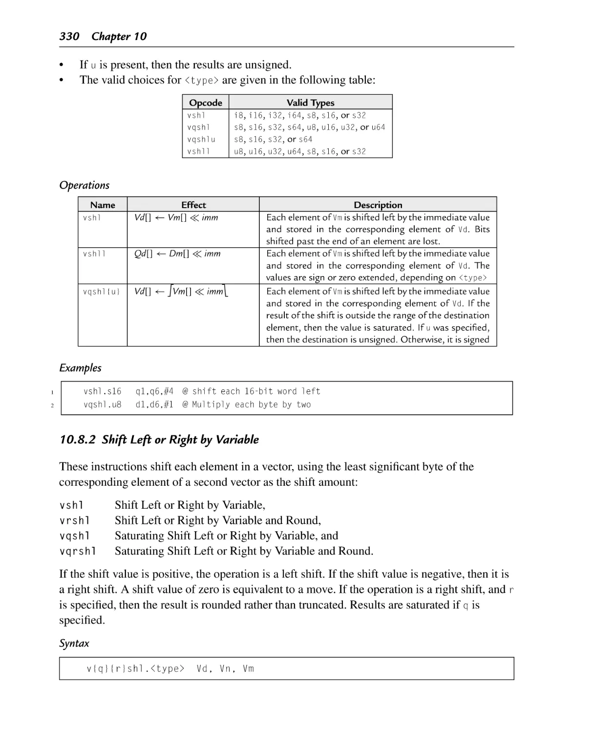
10.7.3 Bitwise Insertion and Selection................................................... 328
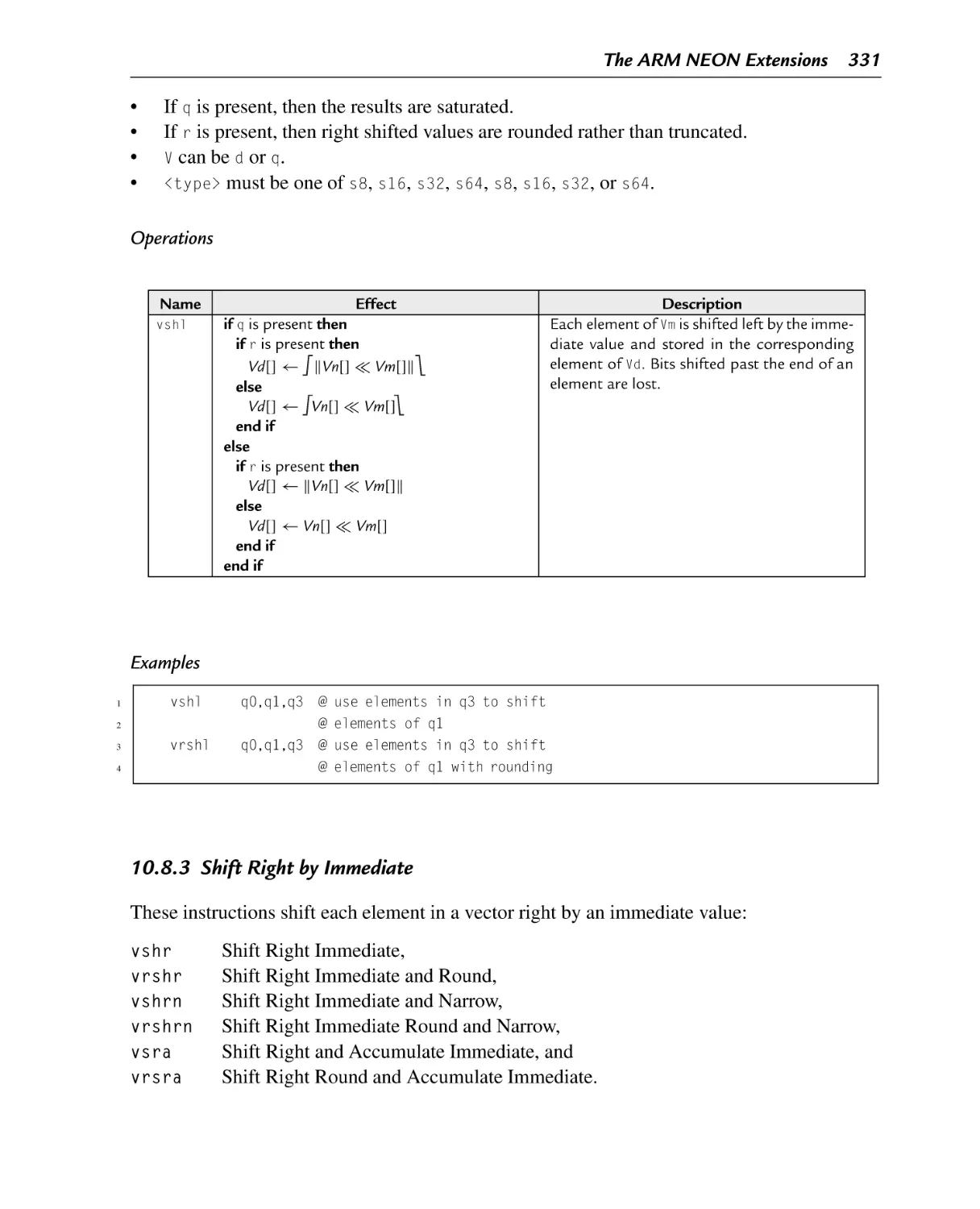
Shift Instructions ............................................................................ 329
10.8.1 Shift Left by Immediate ............................................................ 329
10.8.2 Shift Left or Right by Variable.................................................... 330
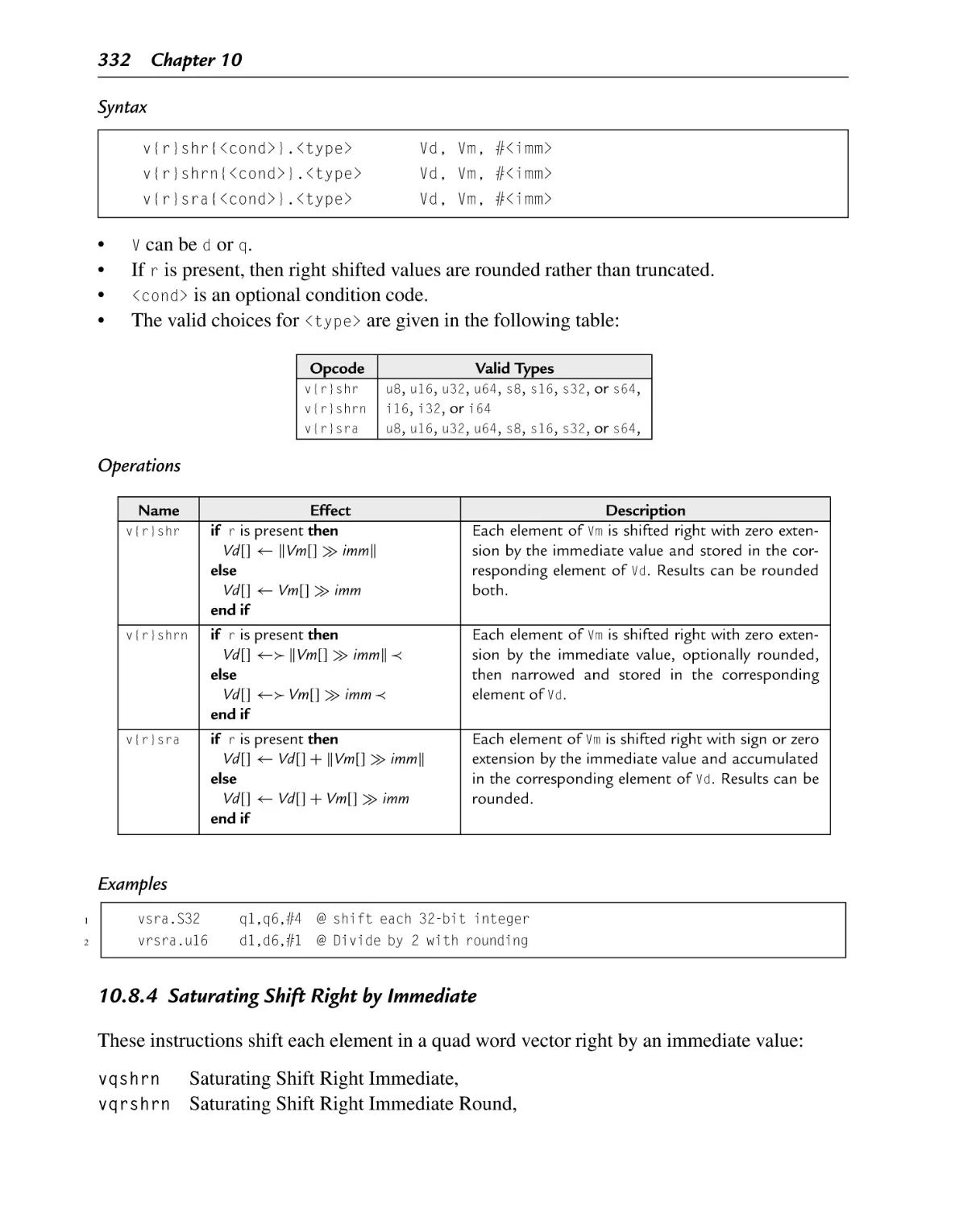
10.8.3 Shift Right by Immediate .......................................................... 331
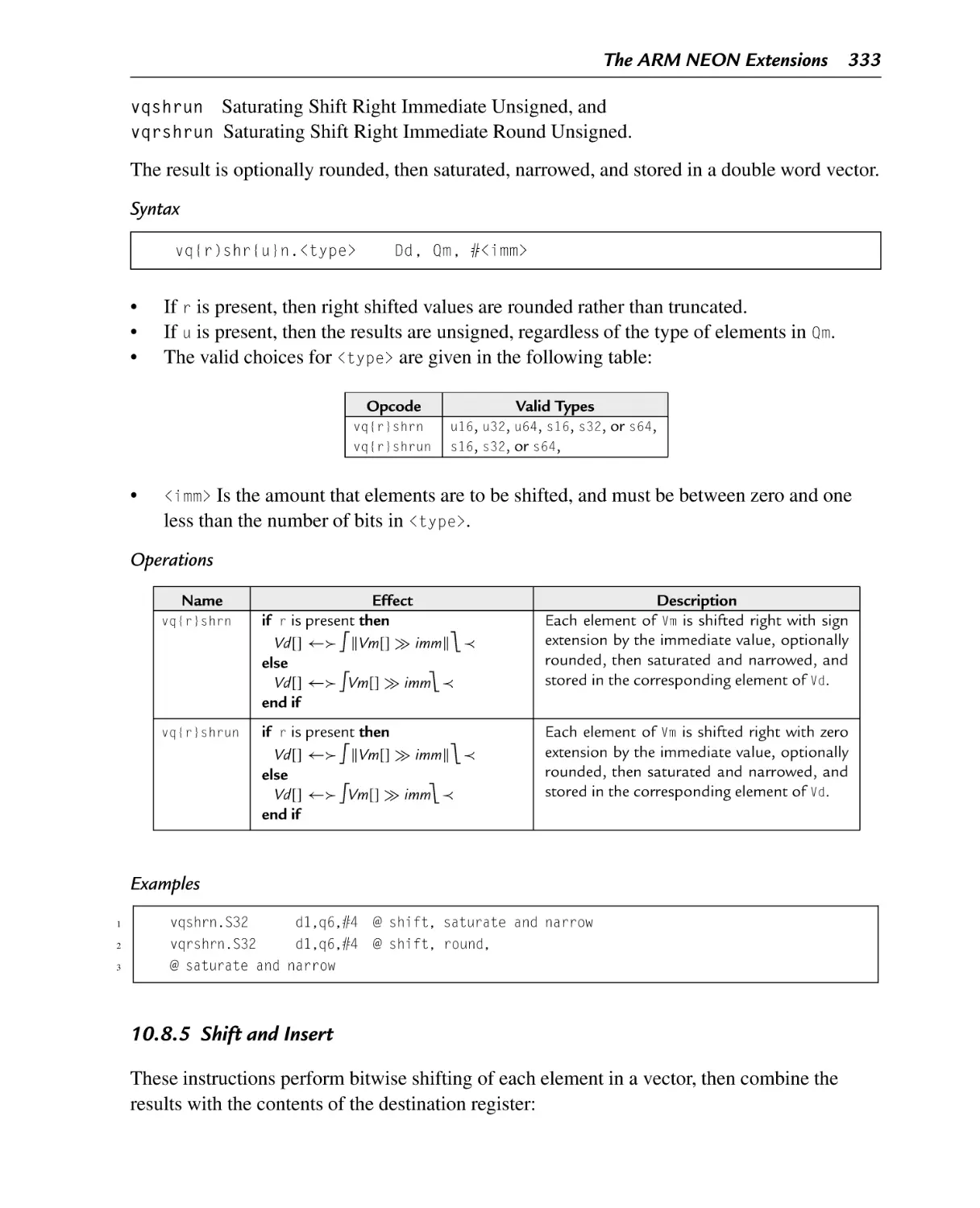
10.8.4 Saturating Shift Right by Immediate ............................................ 332
10.8.5 Shift and Insert ....................................................................... 333
Arithmetic Instructions .................................................................... 335
10.9.1 Vector Add and Subtract ........................................................... 335
10.9.2 Vector Add and Subtract with Narrowing ...................................... 336
10.9.3 Add or Subtract and Divide by Two ............................................. 337
10.9.4 Add Elements Pairwise ............................................................. 338
10.9.5 Absolute Difference ................................................................. 339
10.9.6 Absolute Value and Negate ........................................................ 340
10.9.7 Get Maximum or Minimum Elements .......................................... 341
10.9.8 Count Bits.............................................................................. 342
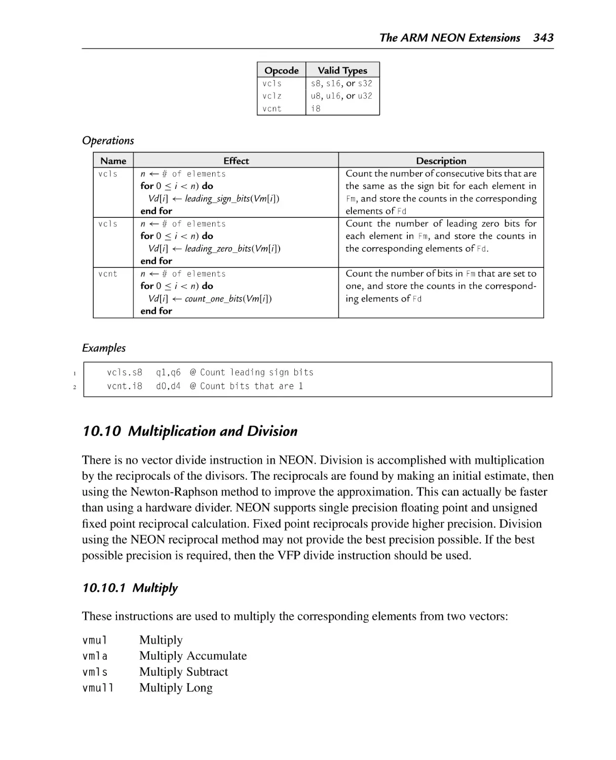
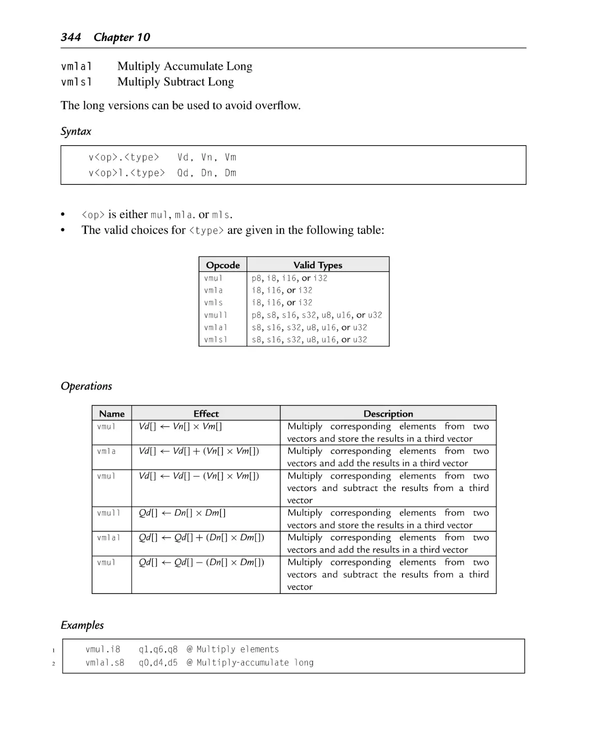
Multiplication and Division .............................................................. 343
10.10.1 Multiply ................................................................................ 343
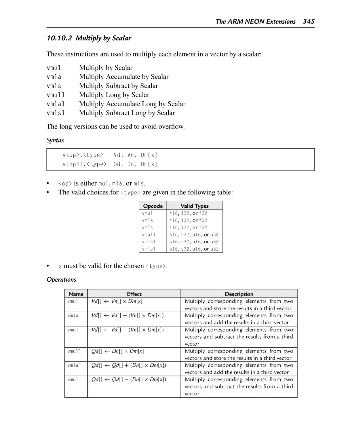
10.10.2 Multiply by Scalar ................................................................... 345
10.10.3 Fused Multiply Accumulate ....................................................... 346
10.10.4 Saturating Multiply and Double (Low) ......................................... 347
10.10.5 Saturating Multiply and Double (High) ........................................ 348
10.10.6 Estimate Reciprocals ................................................................ 348
10.10.7 Reciprocal Step ....................................................................... 349
Pseudo-Instructions......................................................................... 351
10.11.1 Load Constant ........................................................................ 351
10.11.2 Bitwise Logical Operations with Immediate Data ........................... 352
10.11.3 Vector Absolute Compare.......................................................... 353
Performance Mathematics: A Final Look at Sine ................................... 354
10.12.1 Single Precision ...................................................................... 354
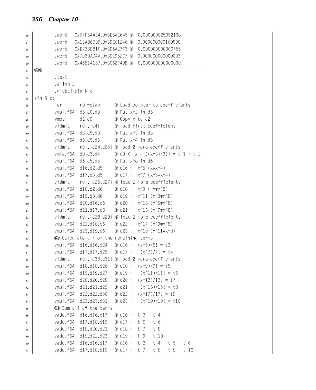
10.12.2 Double Precision ..................................................................... 355
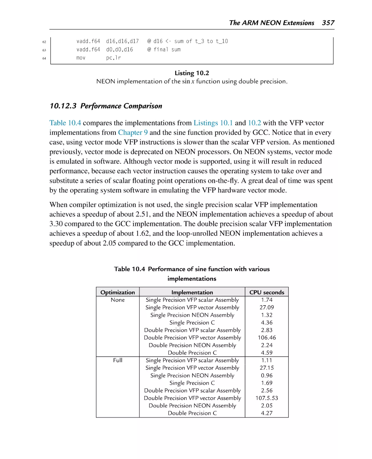
10.12.3 Performance Comparison .......................................................... 357
Alphabetized List of NEON Instructions.............................................. 358
Chapter Summary........................................................................... 361
ACCESSING DEVICES
363
Chapter 11: Devices ......................................................................... 365
11.1 Accessing Devices Directly Under Linux............................................. 365
Contents xi
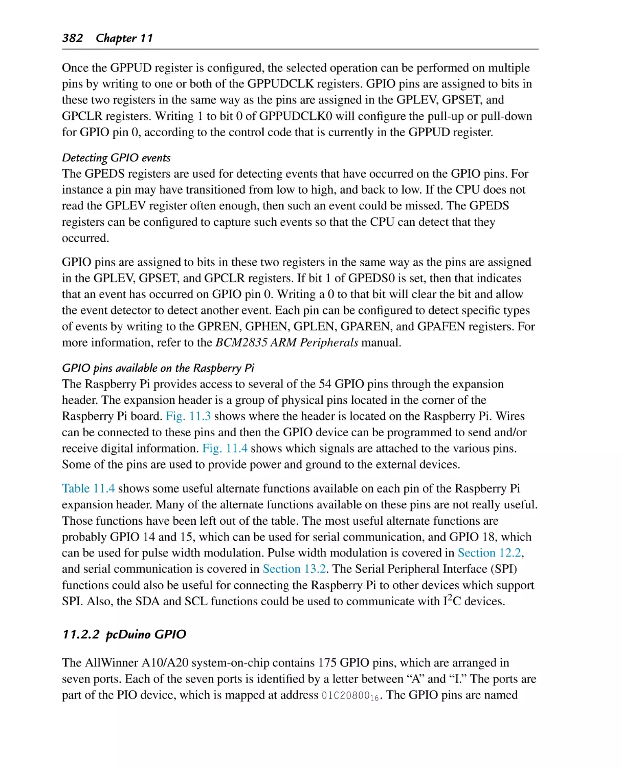
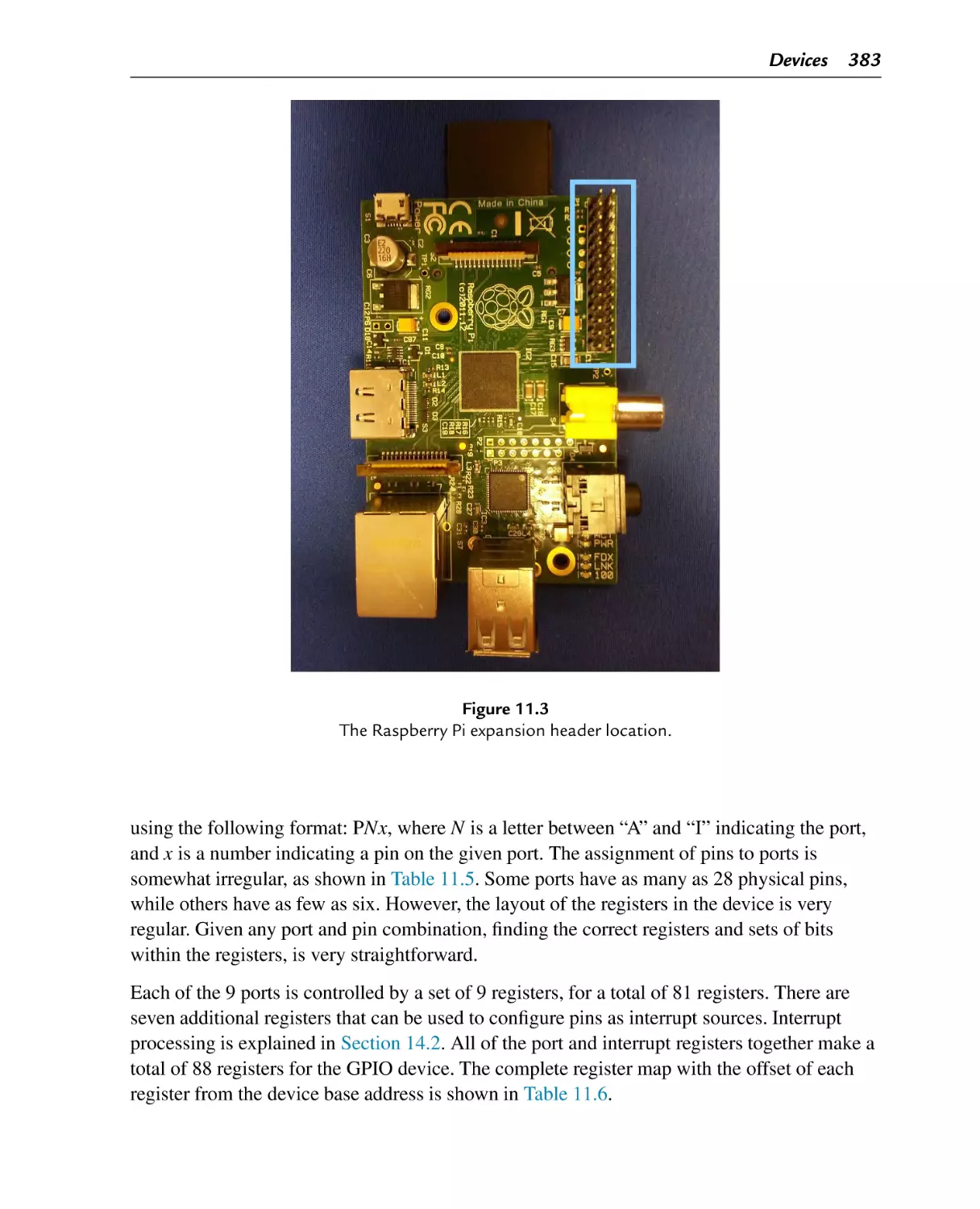
11.2 General Purpose Digital Input/Output ................................................... 376
11.2.1 Raspberry Pi GPIO...................................................................... 378
11.2.2 pcDuino GPIO ........................................................................... 382
11.3 Chapter Summary ............................................................................ 392
Chapter 12: Pulse Modulation.............................................................. 395
12.1 Pulse Density Modulation .................................................................. 396
12.2 Pulse Width Modulation .................................................................... 397
12.3 Raspberry Pi PWM Device................................................................. 398
12.4 pcDuino PWM Device ...................................................................... 400
12.5 Chapter Summary ............................................................................ 403
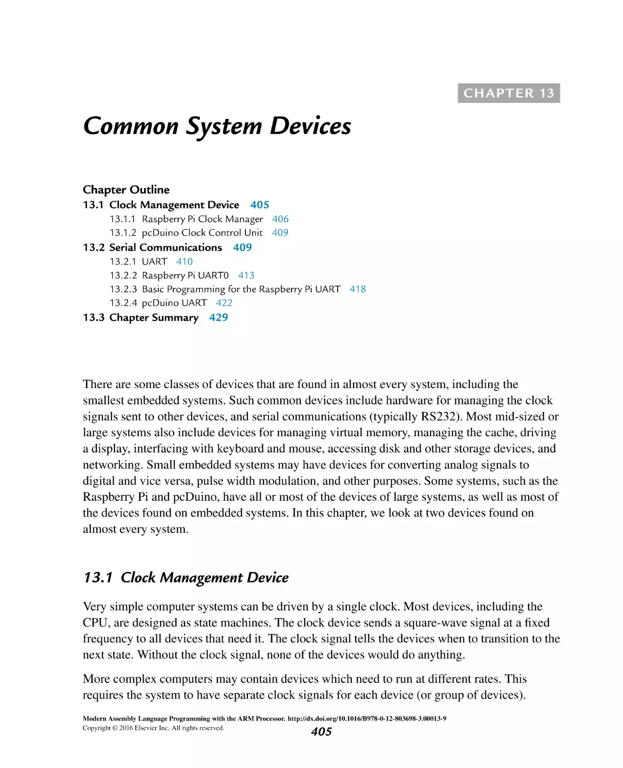
Chapter 13: Common System Devices ..................................................... 405
13.1 Clock Management Device ................................................................ 405
13.1.1 Raspberry Pi Clock Manager ......................................................... 406
13.1.2 pcDuino Clock Control Unit.......................................................... 409
13.2 Serial Communications ..................................................................... 409
13.2.1 UART ...................................................................................... 410
13.2.2 Raspberry Pi UART0 ................................................................... 413
13.2.3 Basic Programming for the Raspberry Pi UART ................................ 418
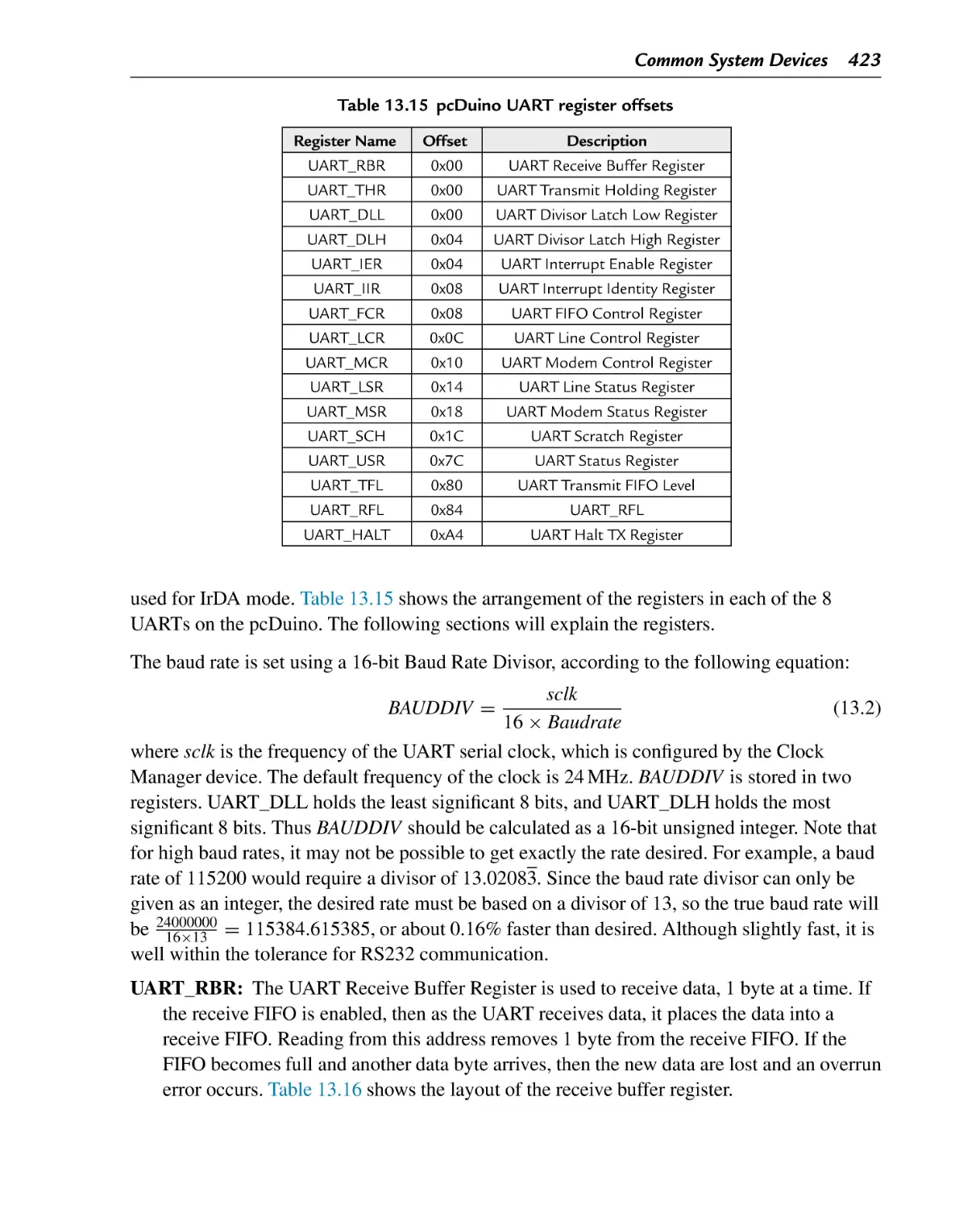
13.2.4 pcDuino UART .......................................................................... 422
13.3 Chapter Summary ............................................................................ 429
Chapter 14: Running Without an Operating System .................................... 431
14.1 ARM CPU Modes ............................................................................ 432
14.2 Exception Processing ........................................................................ 434
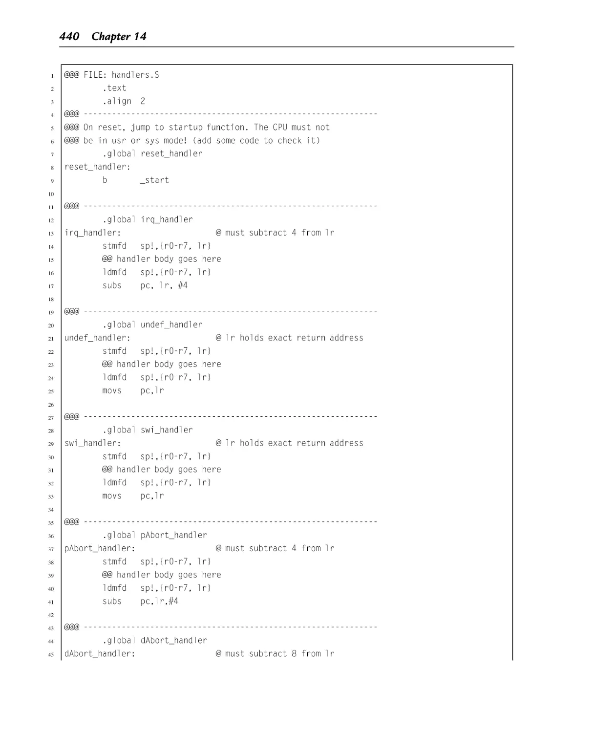
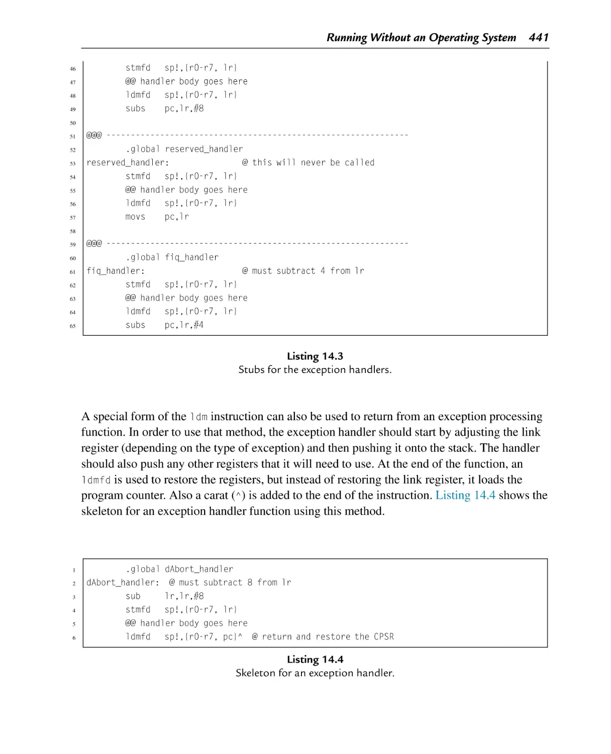
14.2.1 Handling Exceptions ................................................................... 438
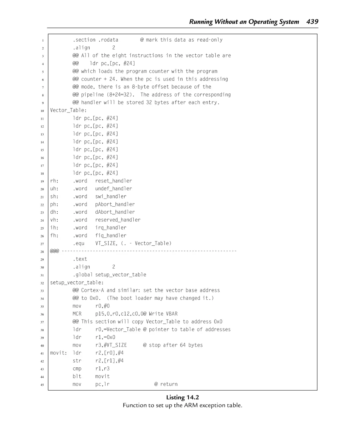
14.3 The Boot Process ............................................................................. 442
14.4 Writing a Bare-Metal Program ............................................................ 442
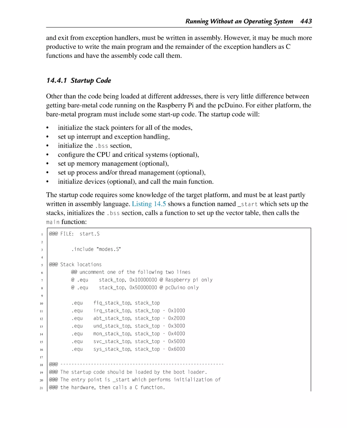
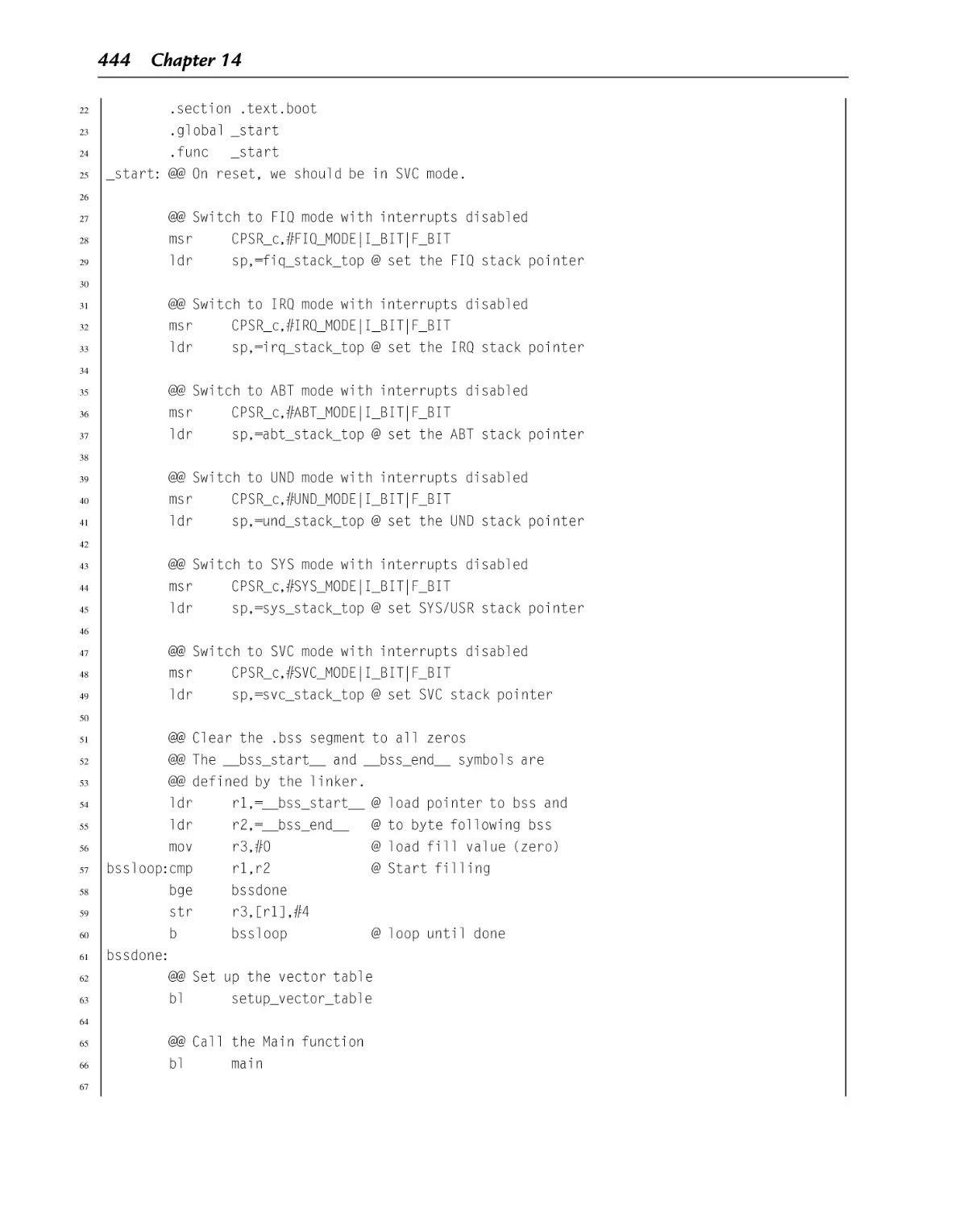
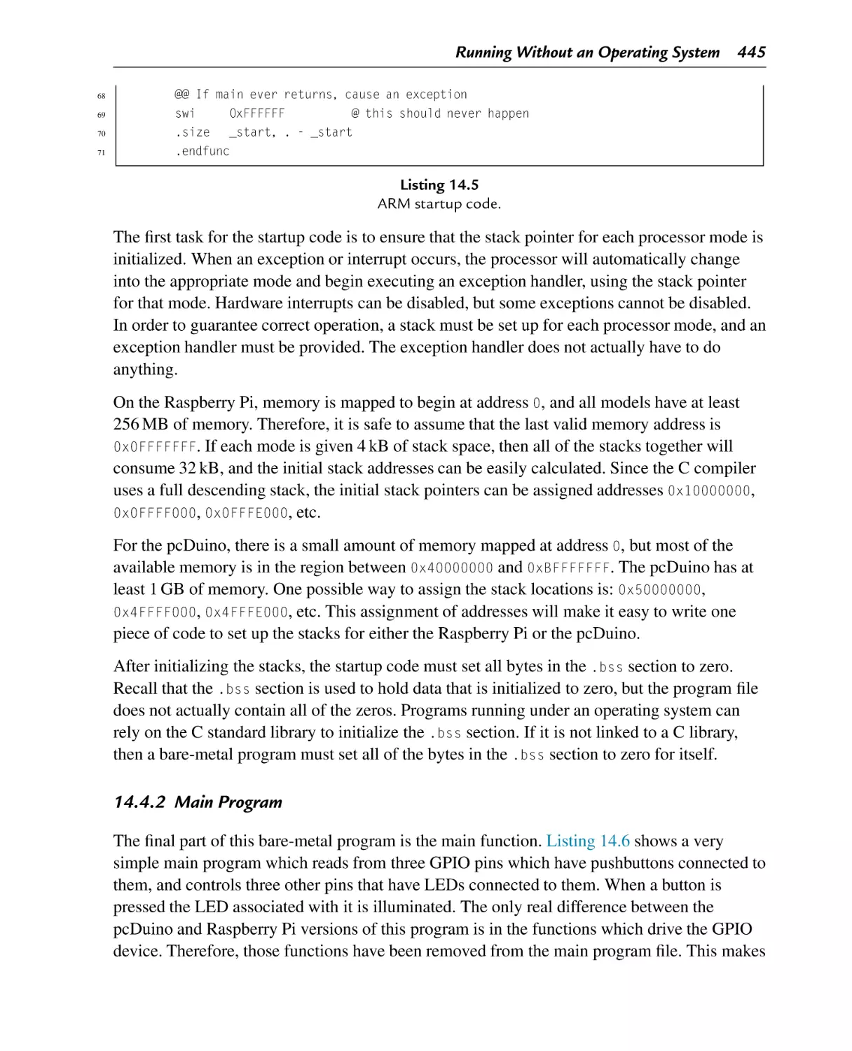
14.4.1 Startup Code .............................................................................. 443
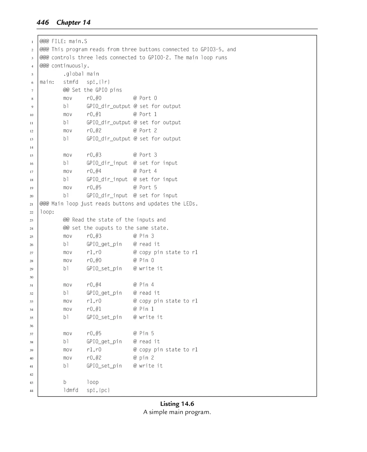
14.4.2 Main Program ............................................................................ 445
14.4.3 The Linker Script ........................................................................ 447
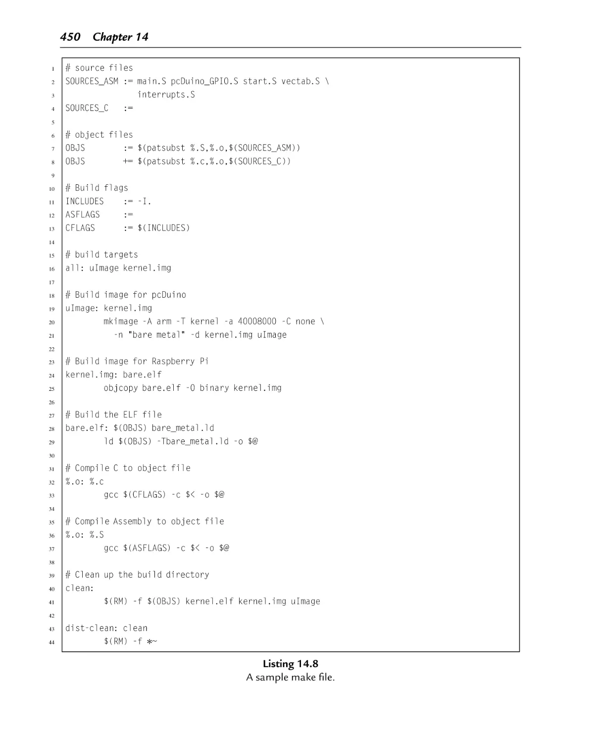
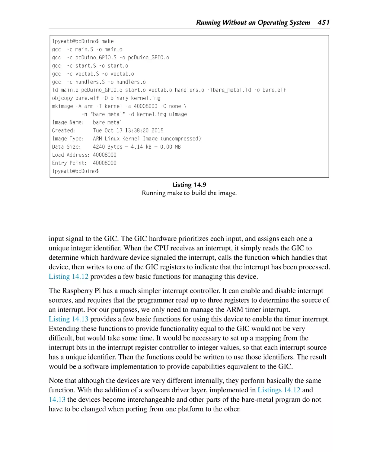
14.4.4 Putting it All Together.................................................................. 449
14.5 Using an Interrupt ............................................................................ 449
14.5.1 Startup Code .............................................................................. 449
14.5.2 Interrupt Controllers .................................................................... 449
14.5.3 Timers ...................................................................................... 458
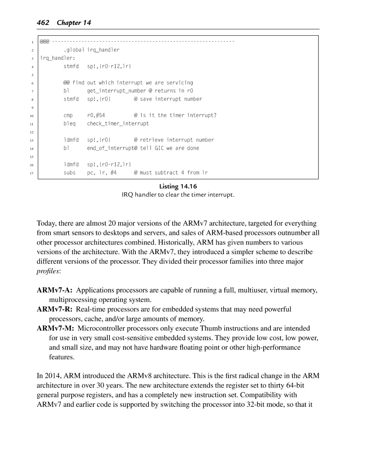
14.5.4 Exception Handling ..................................................................... 461
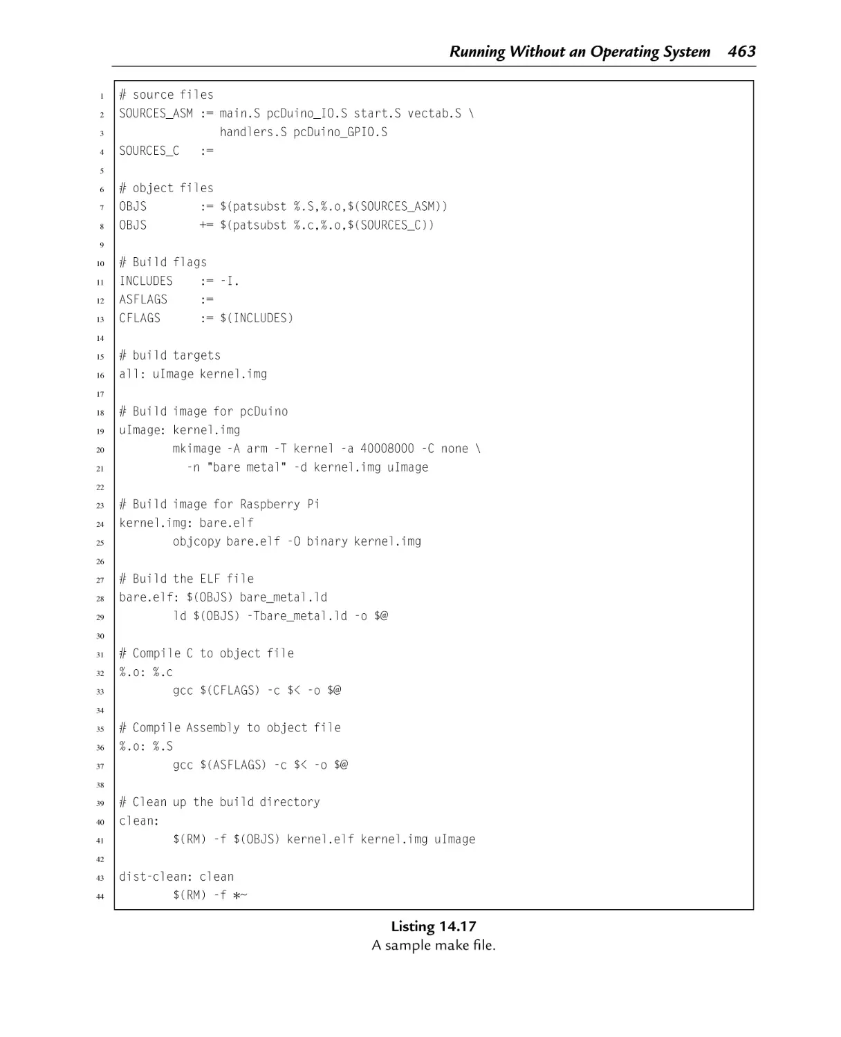
14.5.5 Building the Interrupt-Driven Program ............................................ 461
14.6 ARM Processor Profiles .................................................................... 461
14.7 Chapter Summary ............................................................................ 464
Index
467
This page intentionally left blank
List of Tables
Table 1.1
Table 1.2
Table 1.3
Table 1.4
Table 1.5
Table 1.6
Table 1.7
Table 1.8
Table 1.9
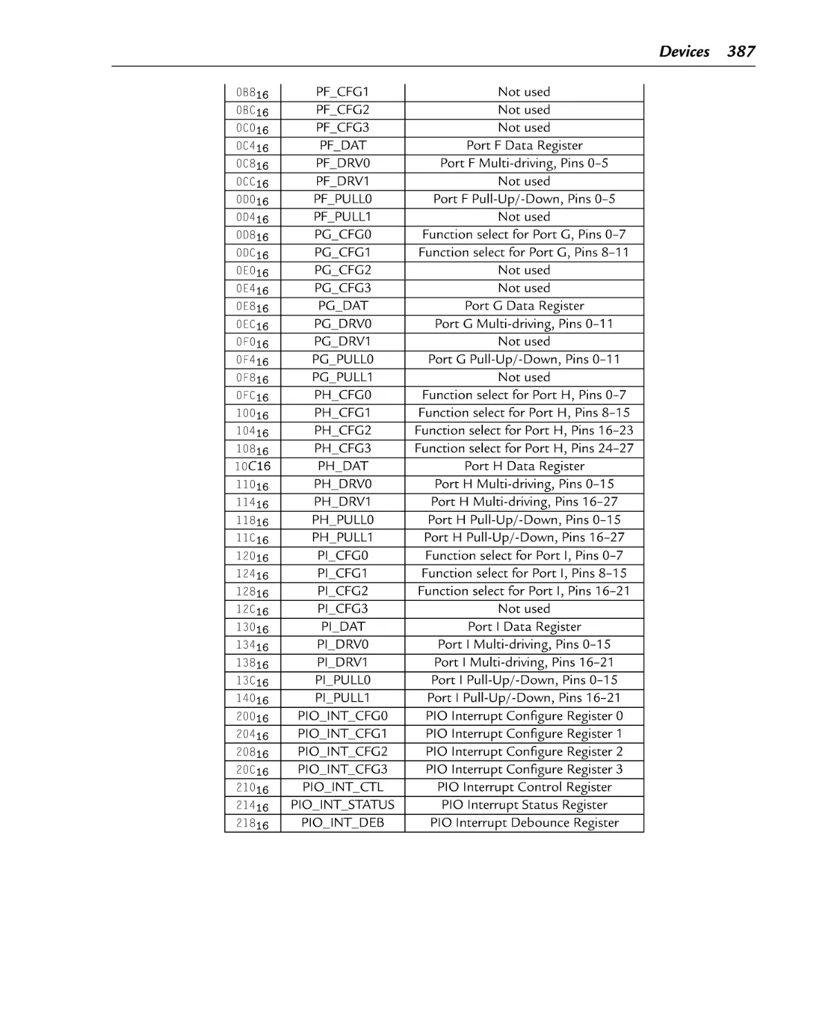
Table 3.1
Table 3.2
Table 3.3
Table 3.4
Table 3.5
Table 4.1
Table 4.2
Table 8.1
Table 8.2
Table 8.3
Table 8.4
Table 9.1
Table 9.2
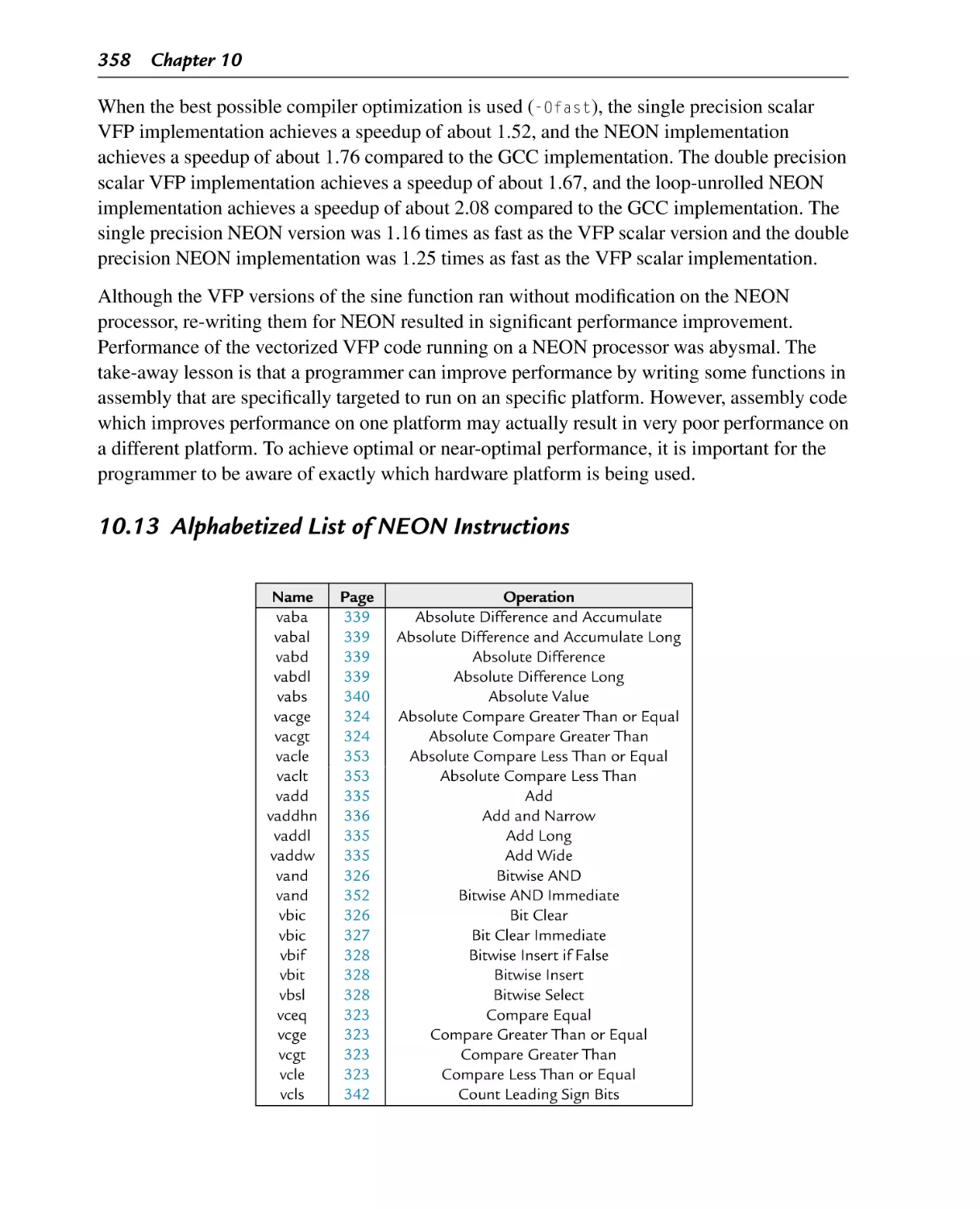
Table 10.1
Table 10.2
Table 10.3
Table 10.4
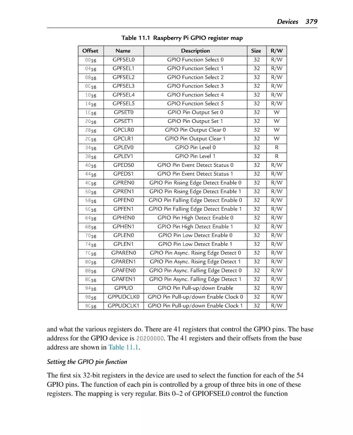
Table 11.1
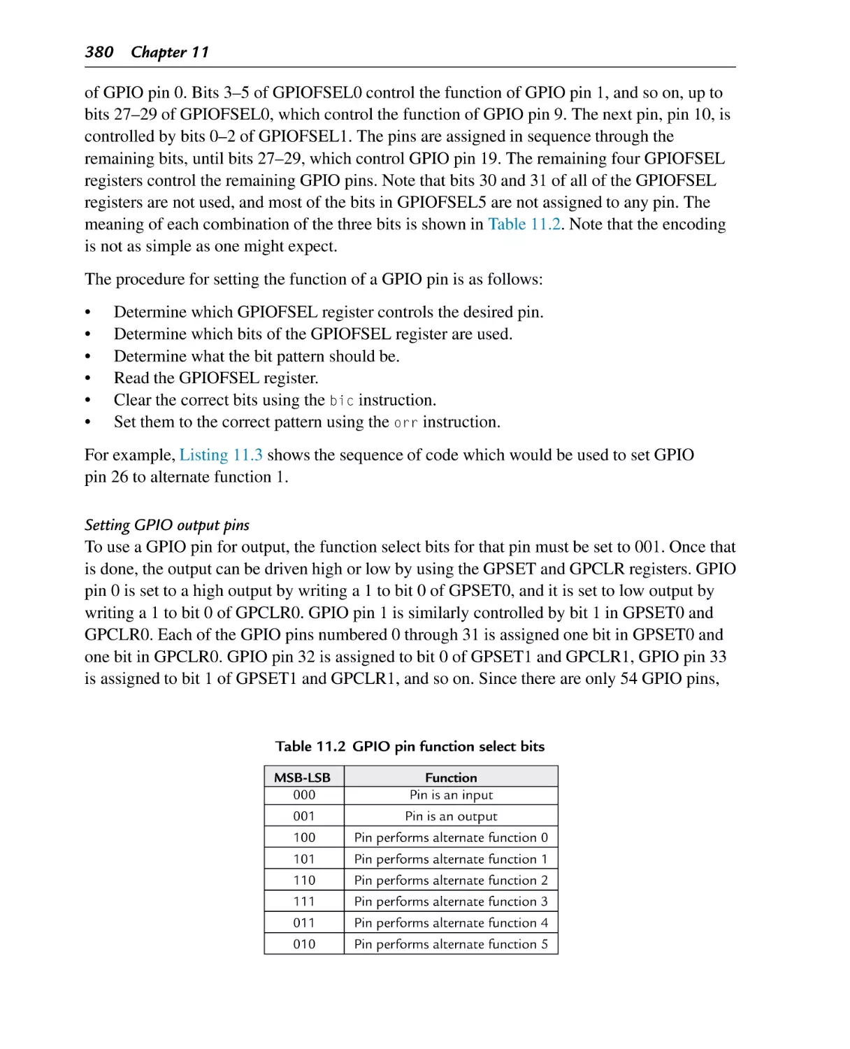
Table 11.2
Table 11.3
Table 11.4
Table 11.5
Table 11.6
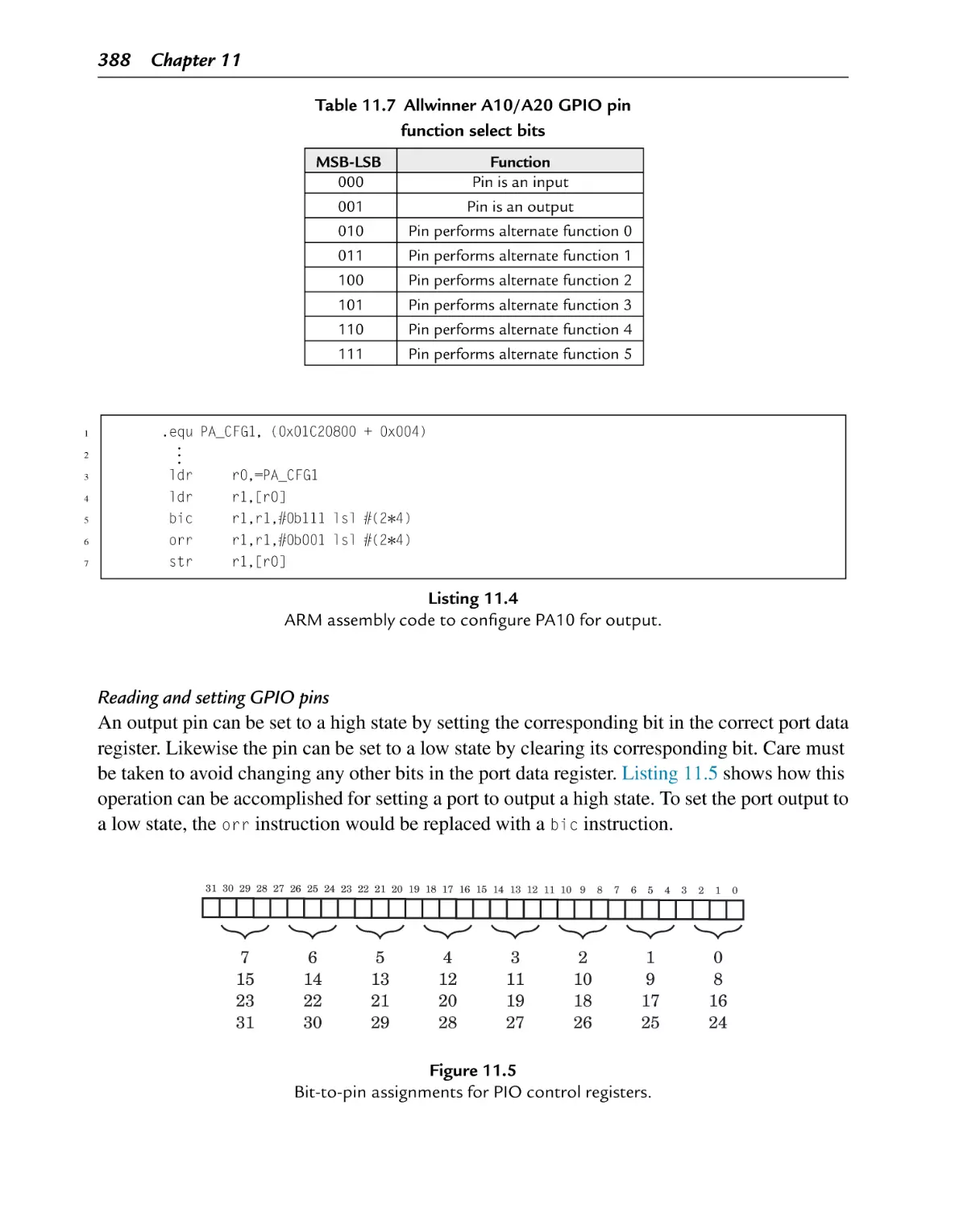
Table 11.7
Table 11.8
Table 11.9
Values represented by two bits
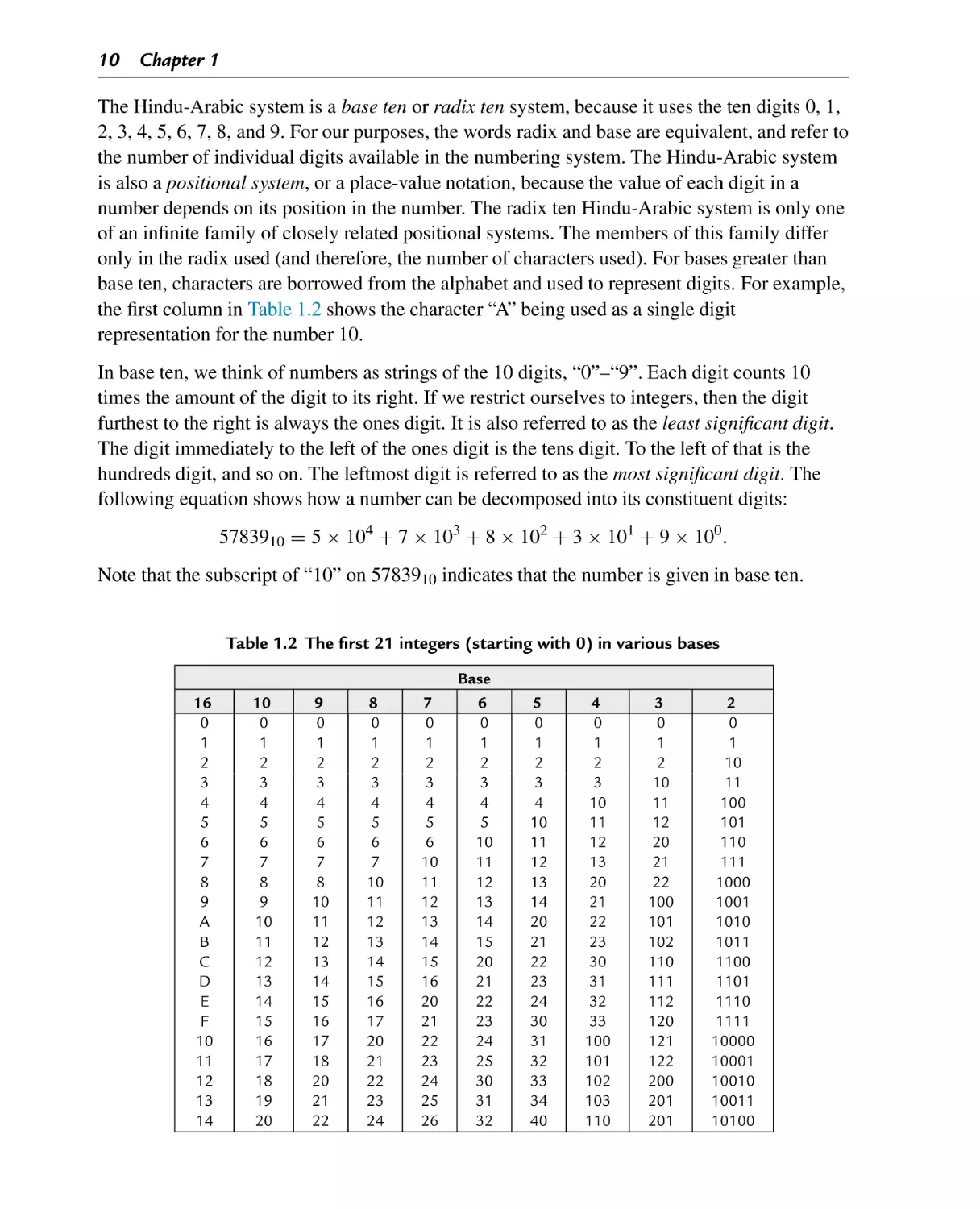
The first 21 integers (starting with 0) in various bases
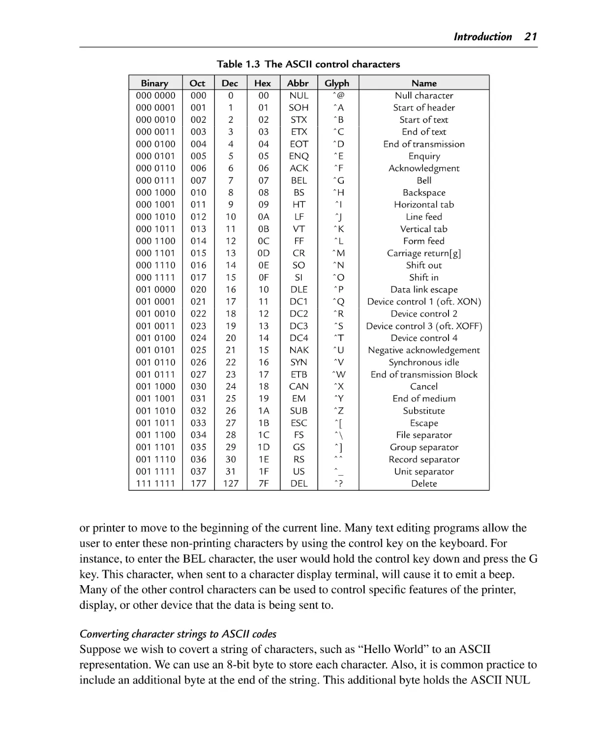
The ASCII control characters
The ASCII printable characters
Binary equivalents for each character in “Hello World”
Binary, hexadecimal, and decimal equivalents for each character in “Hello
World”
Interpreting a hexadecimal string as ASCII
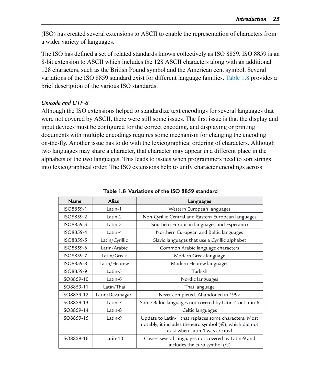
Variations of the ISO 8859 standard
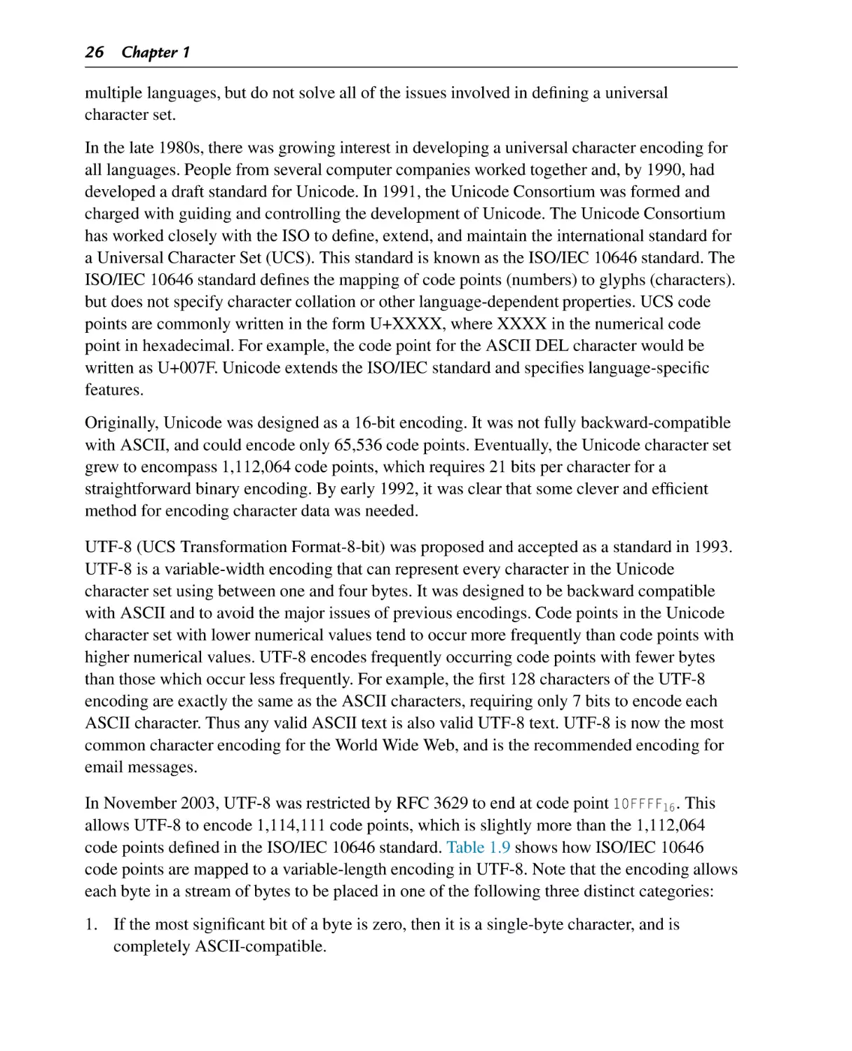
UTF-8 encoding of the ISO/IEC 10646 code points
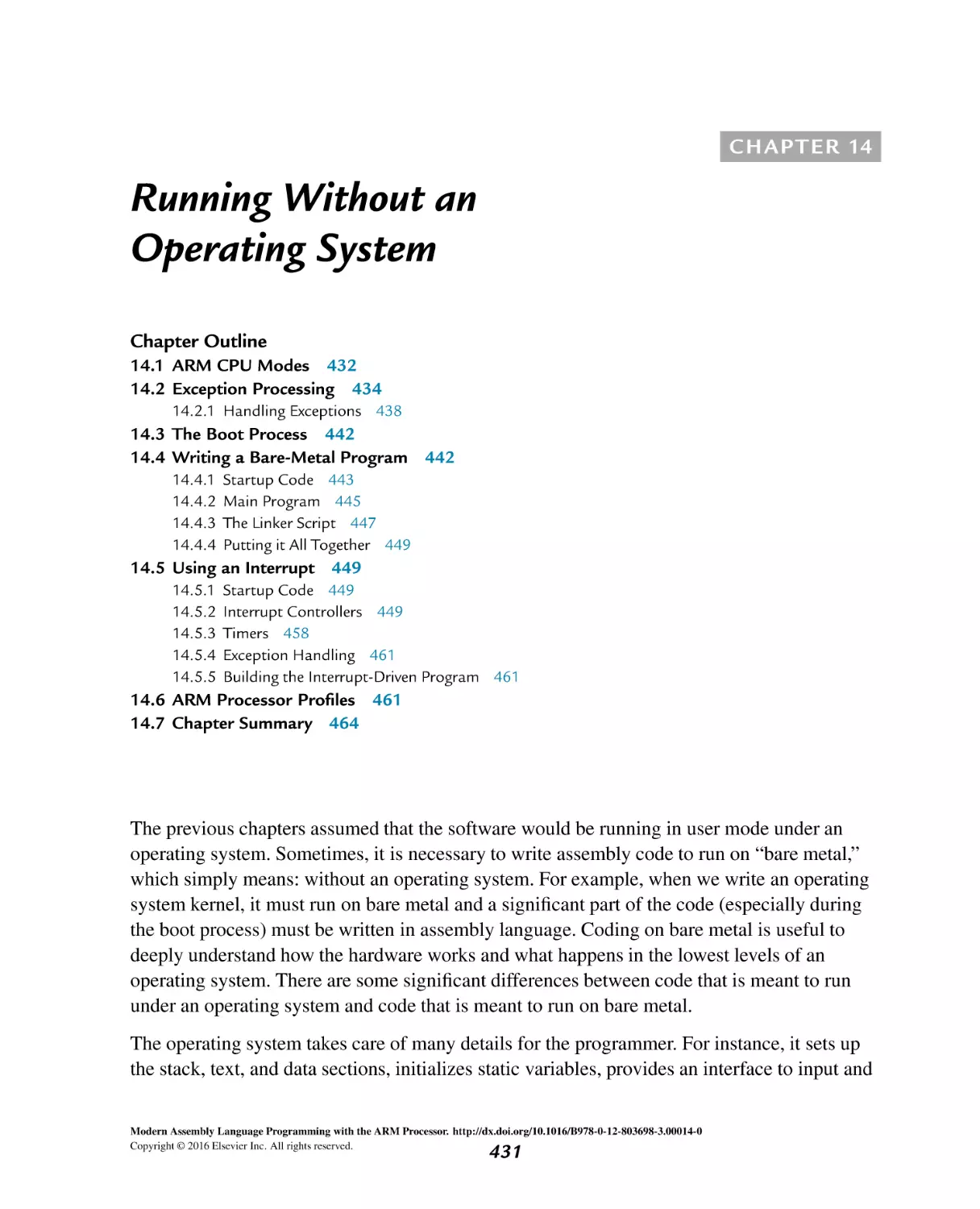
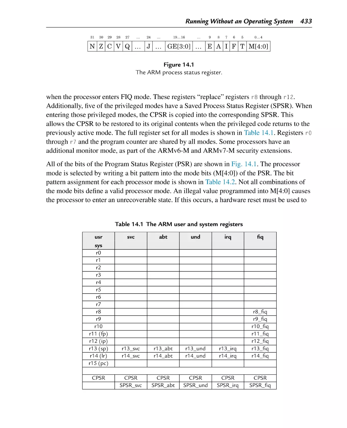
Flag bits in the CPSR register
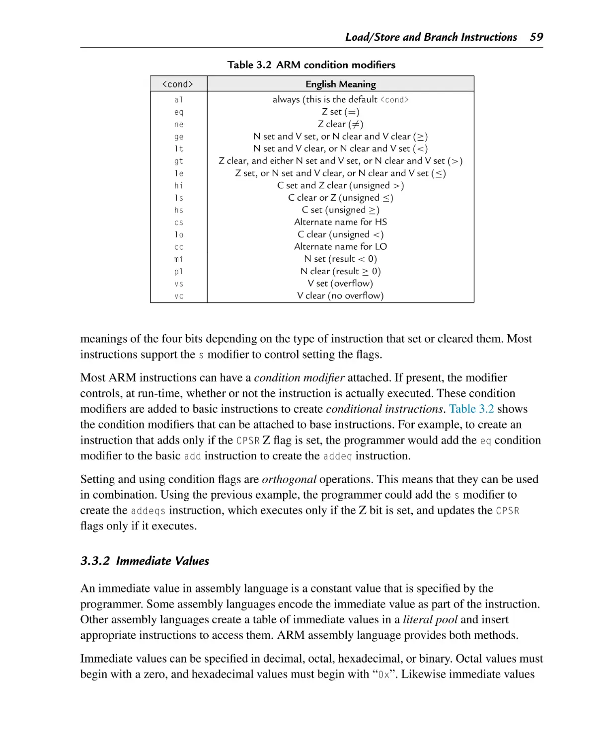
ARM condition modifiers
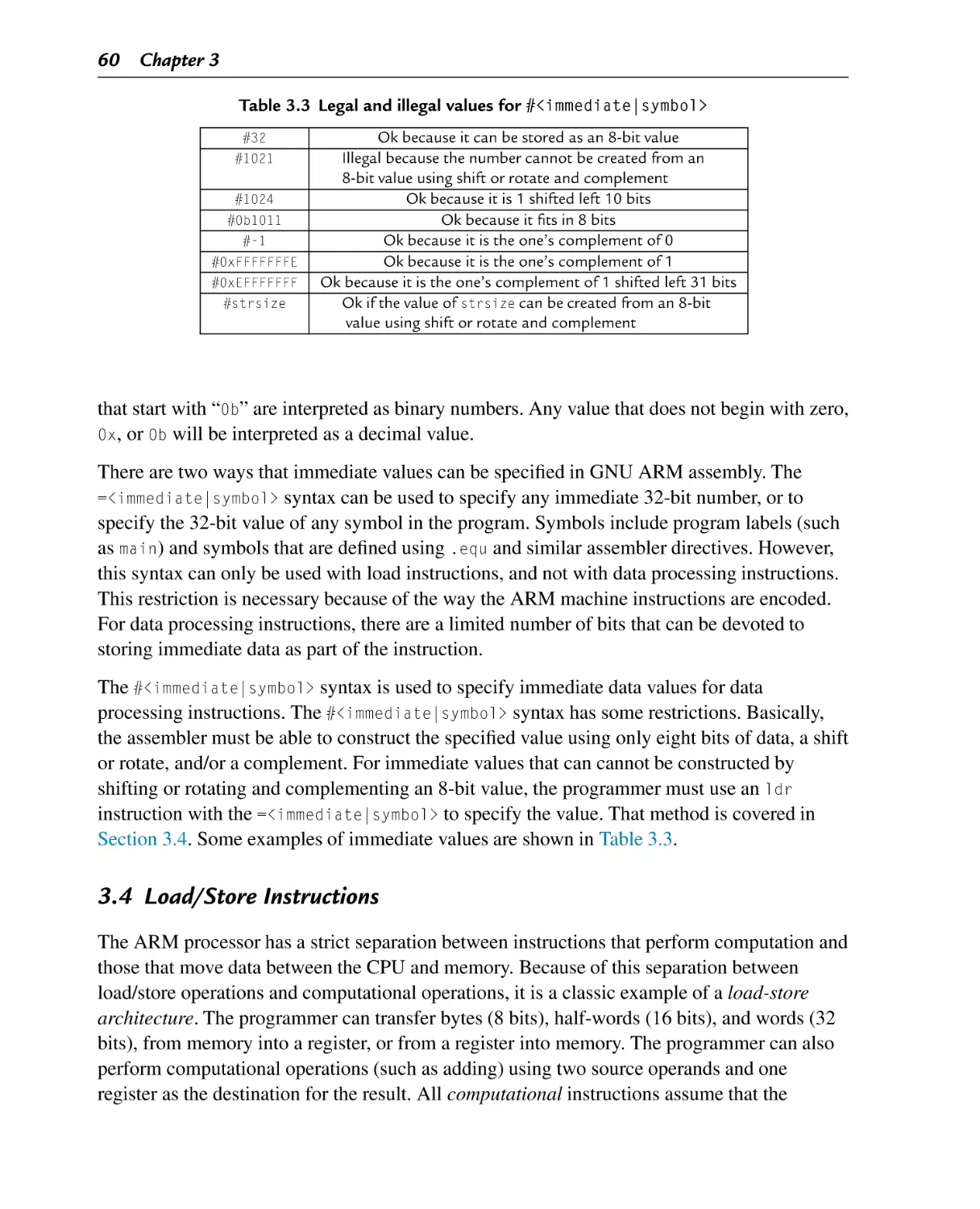
Legal and illegal values for #<immediate|symbol>
ARM addressing modes
ARM shift and rotate operations
Shift and rotate operations in Operand2
Formats for Operand2
Format for IEEE 754 half-precision
Result formats for each term
Shifts required for each term
Performance of sine function with various implementations
Condition code meanings for ARM and VFP
Performance of sine function with various implementations
Parameter combinations for loading and storing a single structure
Parameter combinations for loading multiple structures
Parameter combinations for loading copies of a structure
Performance of sine function with various implementations
Raspberry Pi GPIO register map
GPIO pin function select bits
GPPUD control codes
Raspberry Pi expansion header useful alternate functions
Number of pins available on each of the AllWinner A10/A20 PIO ports
Registers in the AllWinner GPIO device
Allwinner A10/A20 GPIO pin function select bits
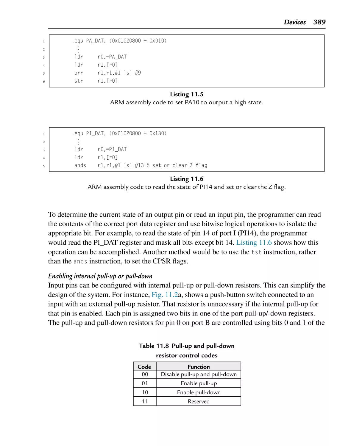
Pull-up and pull-down resistor control codes
pcDuino GPIO pins and function select code assignments.
xiii
9
10
21
22
23
24
24
25
27
58
59
60
61
61
80
81
244
252
252
259
271
292
304
306
308
357
379
380
381
385
385
386
388
389
392
xiv List of Tables
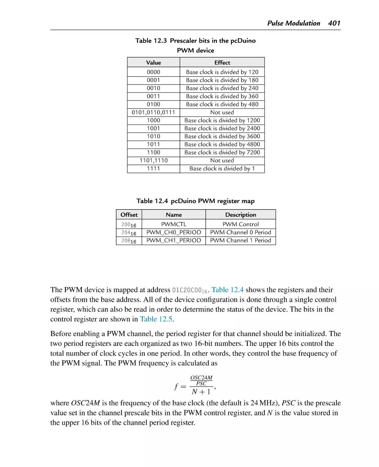
Table 12.1
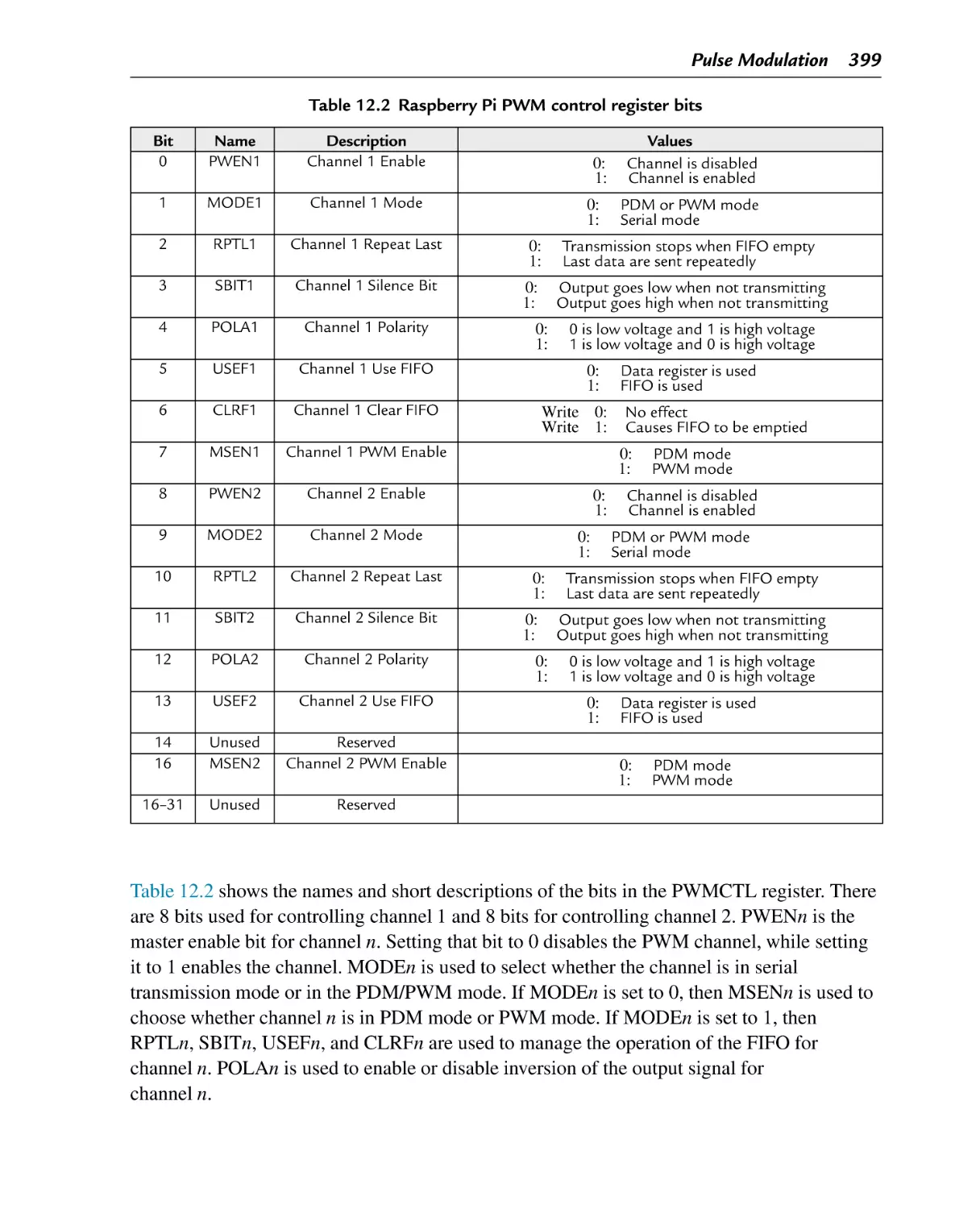
Table 12.2
Table 12.3
Table 12.4
Table 12.5
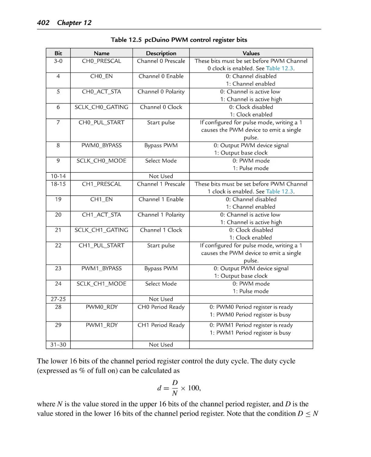
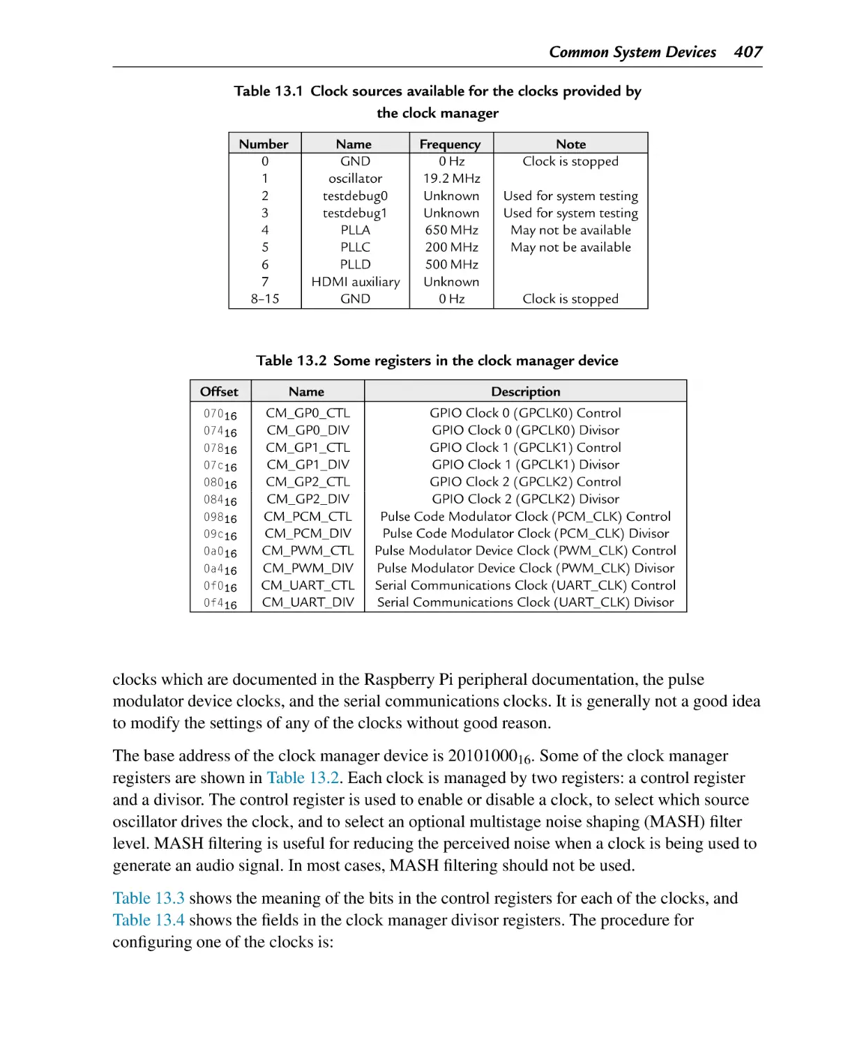
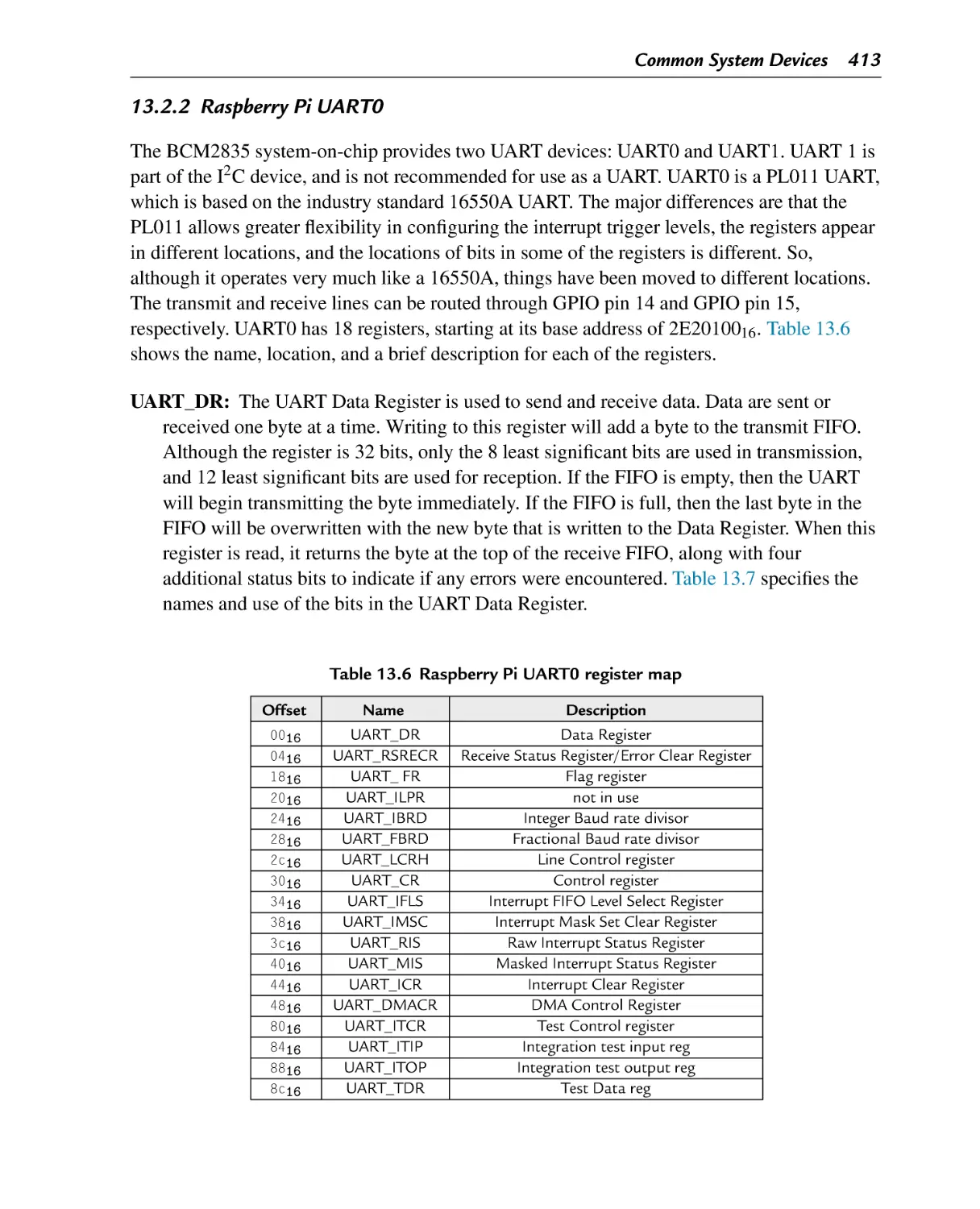
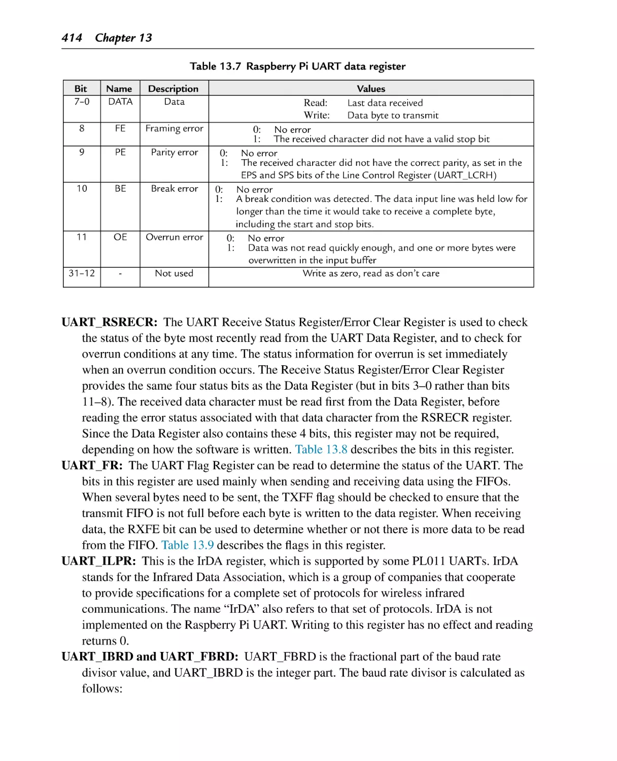
Table 13.1
Table 13.2
Table 13.3
Table 13.4
Table 13.5
Table 13.6
Table 13.7
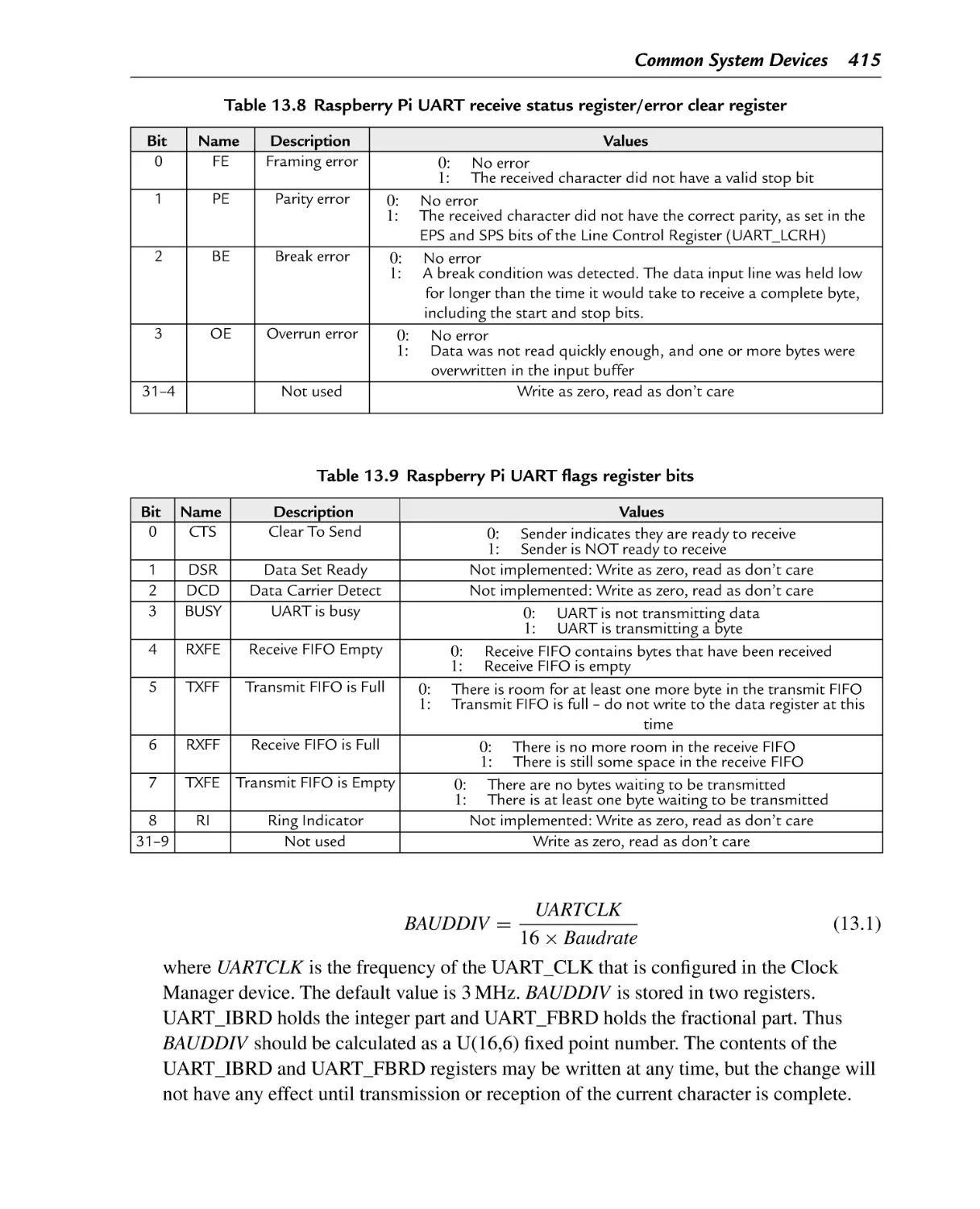
Table 13.8
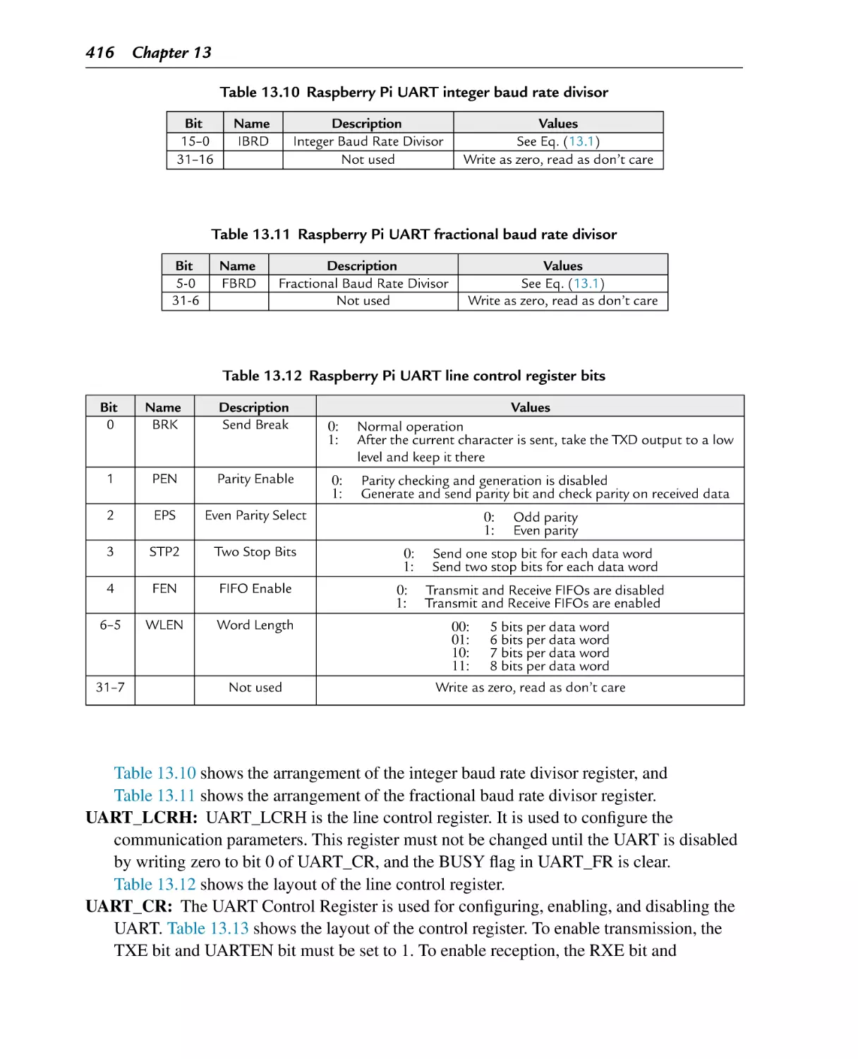
Table 13.9
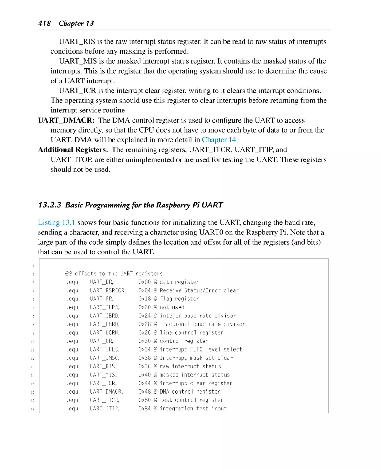
Table 13.10
Table 13.11
Table 13.12
Table 13.13
Table 13.14
Table 13.15
Table 13.16
Table 13.17
Table 13.18
Table 13.19
Table 13.20
Table 13.21
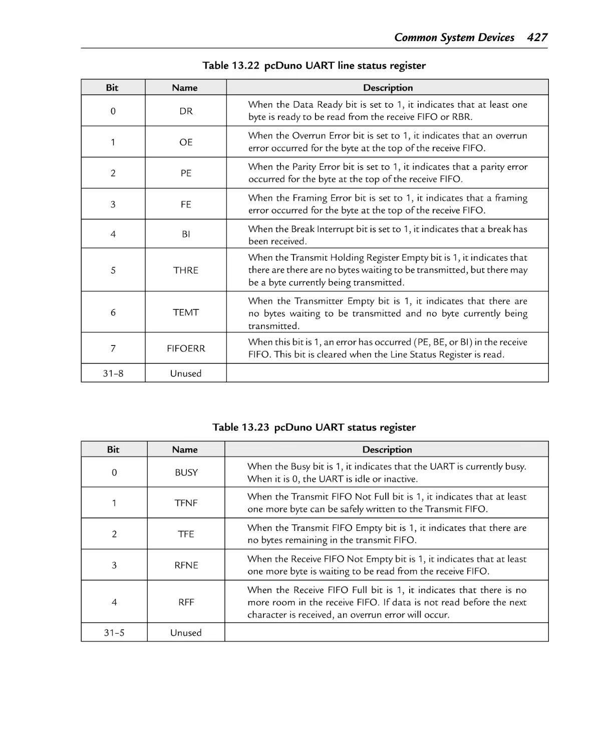
Table 13.22
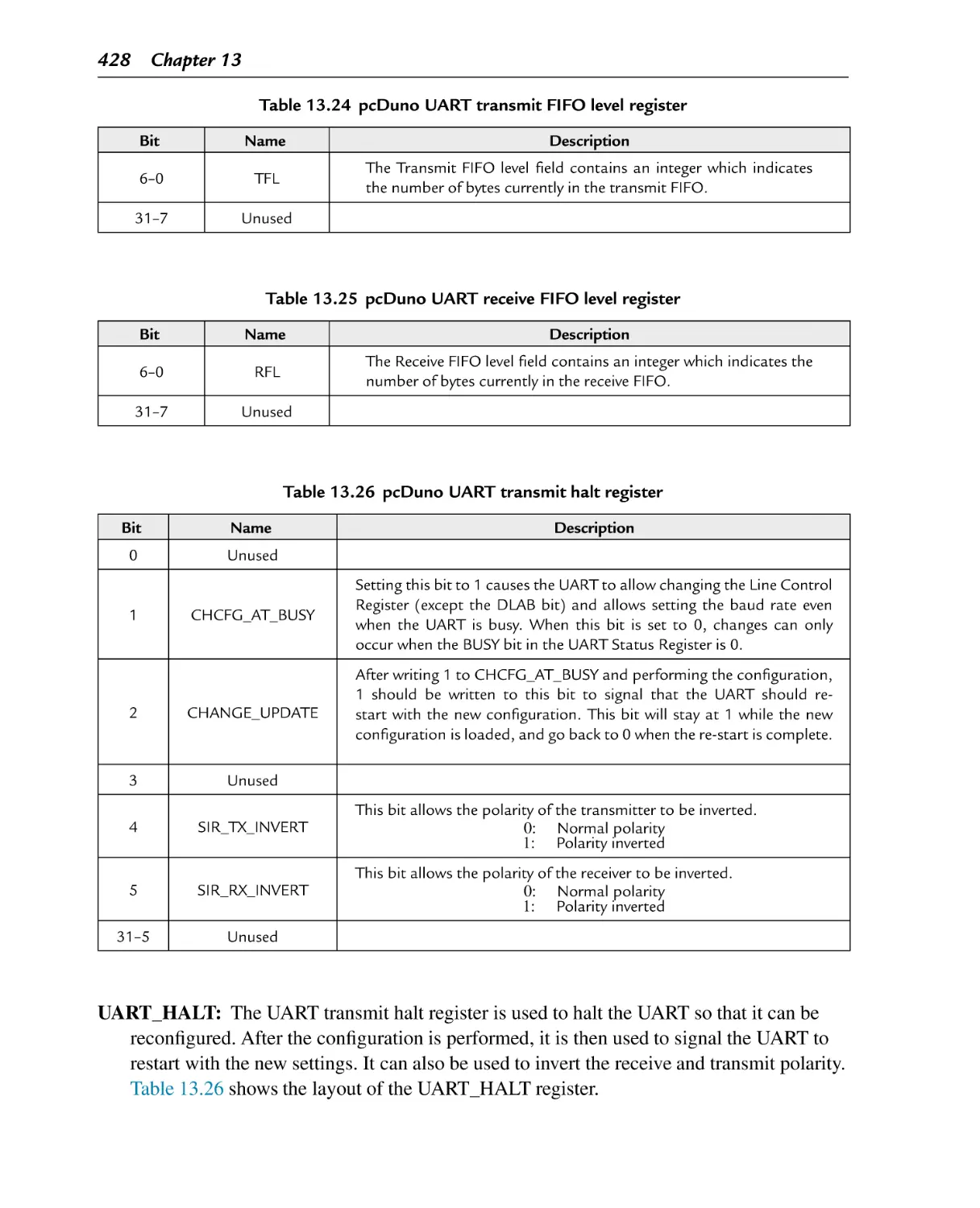
Table 13.23
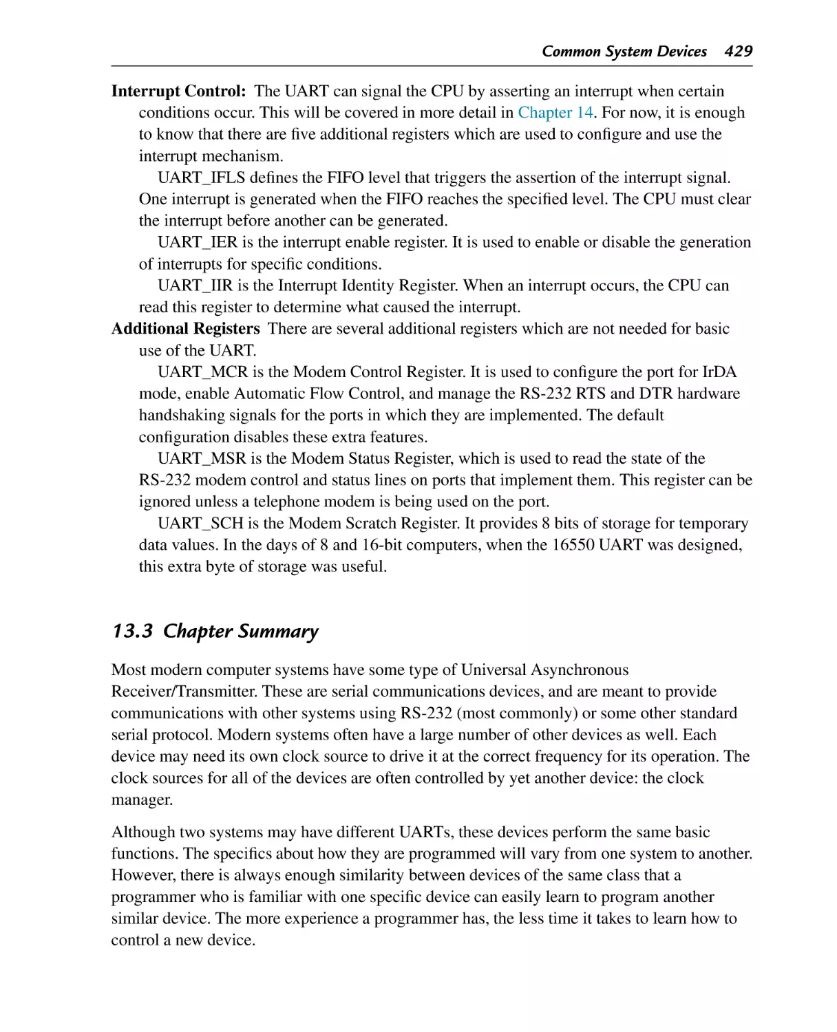
Table 13.24
Table 13.25
Table 13.26
Table 14.1
Table 14.2
Table 14.3
Raspberry Pi PWM register map
Raspberry Pi PWM control register bits
Prescaler bits in the pcDuino PWM device
pcDuino PWM register map
pcDuino PWM control register bits
Clock sources available for the clocks provided by the clock manager
Some registers in the clock manager device
Bit fields in the clock manager control registers
Bit fields in the clock manager divisor registers
Clock signals in the AllWinner A10/A20 SOC
Raspberry Pi UART0 register map
Raspberry Pi UART data register
Raspberry Pi UART receive status register/error clear register
Raspberry Pi UART flags register bits
Raspberry Pi UART integer baud rate divisor
Raspberry Pi UART fractional baud rate divisor
Raspberry Pi UART line control register bits
Raspberry Pi UART control register bits
pcDuino UART addresses
pcDuino UART register offsets
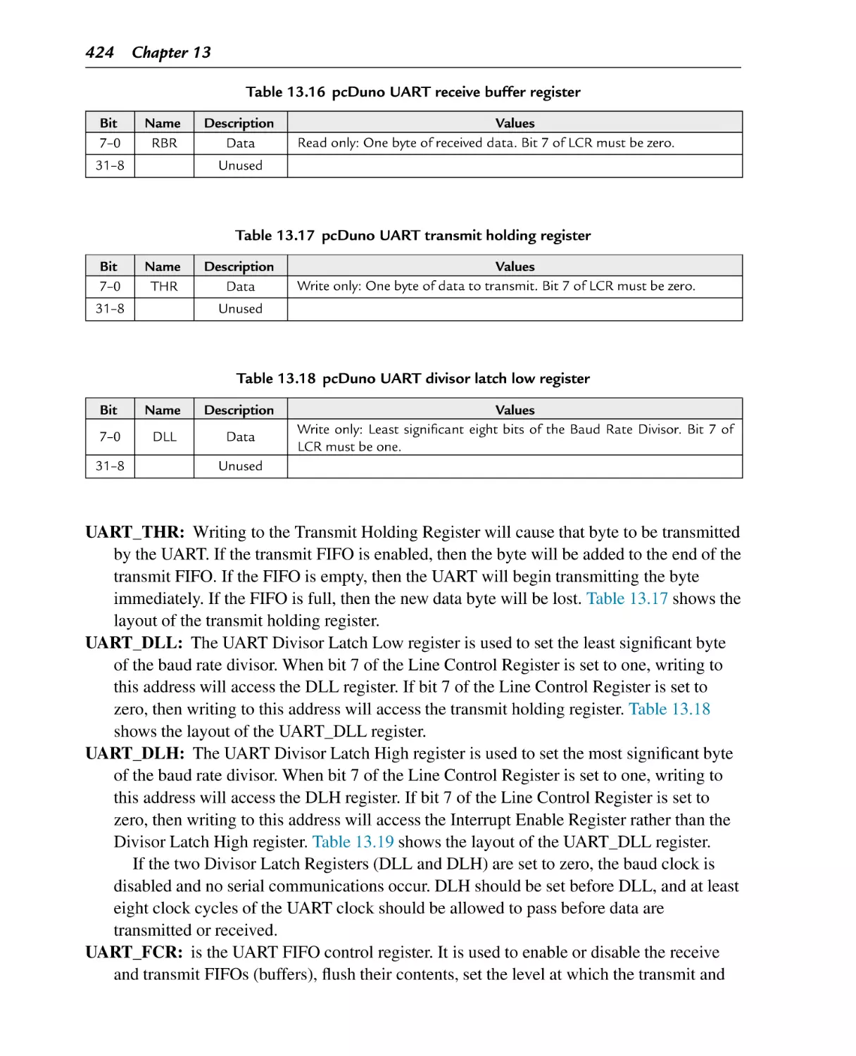
pcDuno UART receive buffer register
pcDuno UART transmit holding register
pcDuno UART divisor latch low register
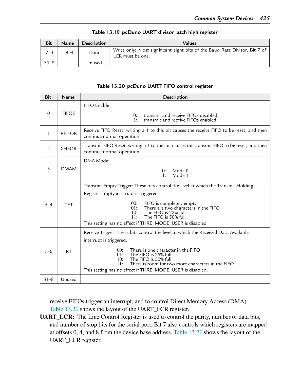
pcDuno UART divisor latch high register
pcDuno UART FIFO control register
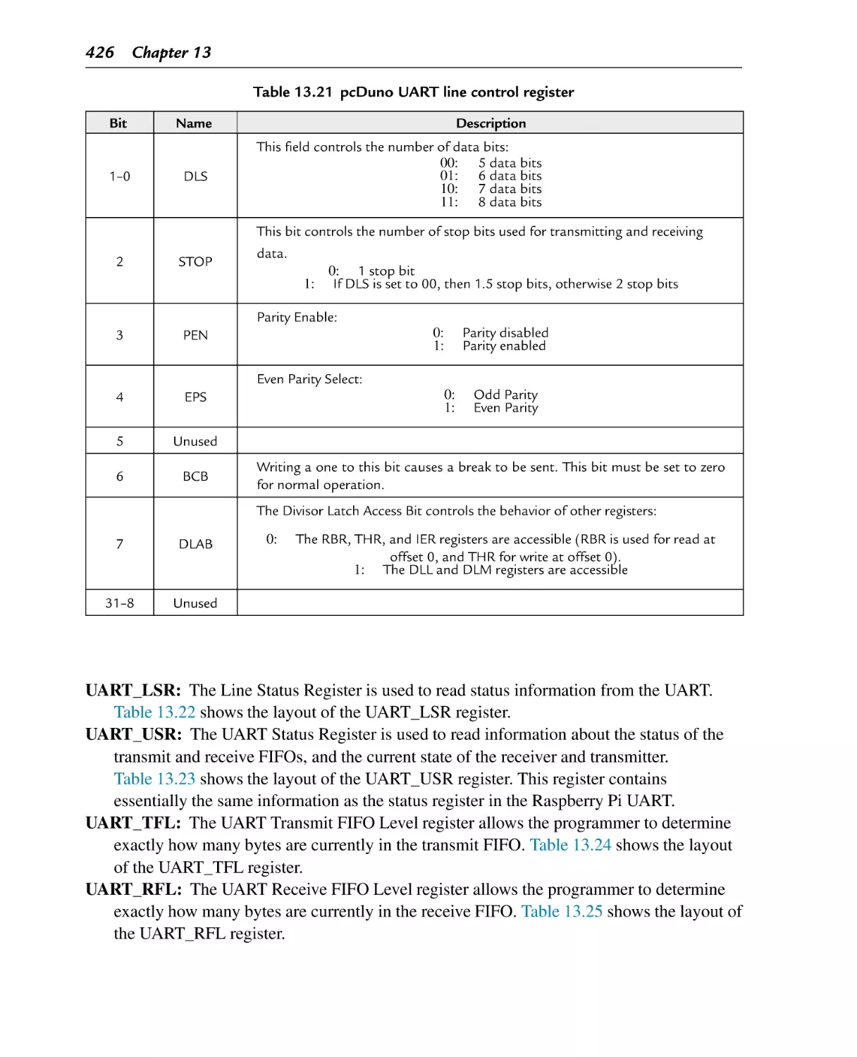
pcDuno UART line control register
pcDuno UART line status register
pcDuno UART status register
pcDuno UART transmit FIFO level register
pcDuno UART receive FIFO level register
pcDuno UART transmit halt register
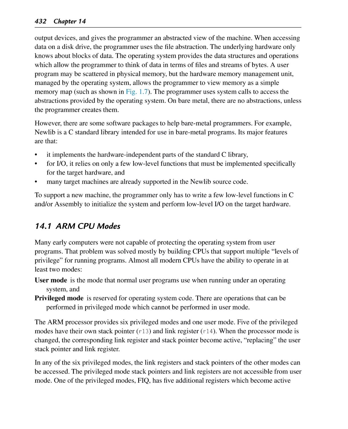
The ARM user and system registers
Mode bits in the PSR
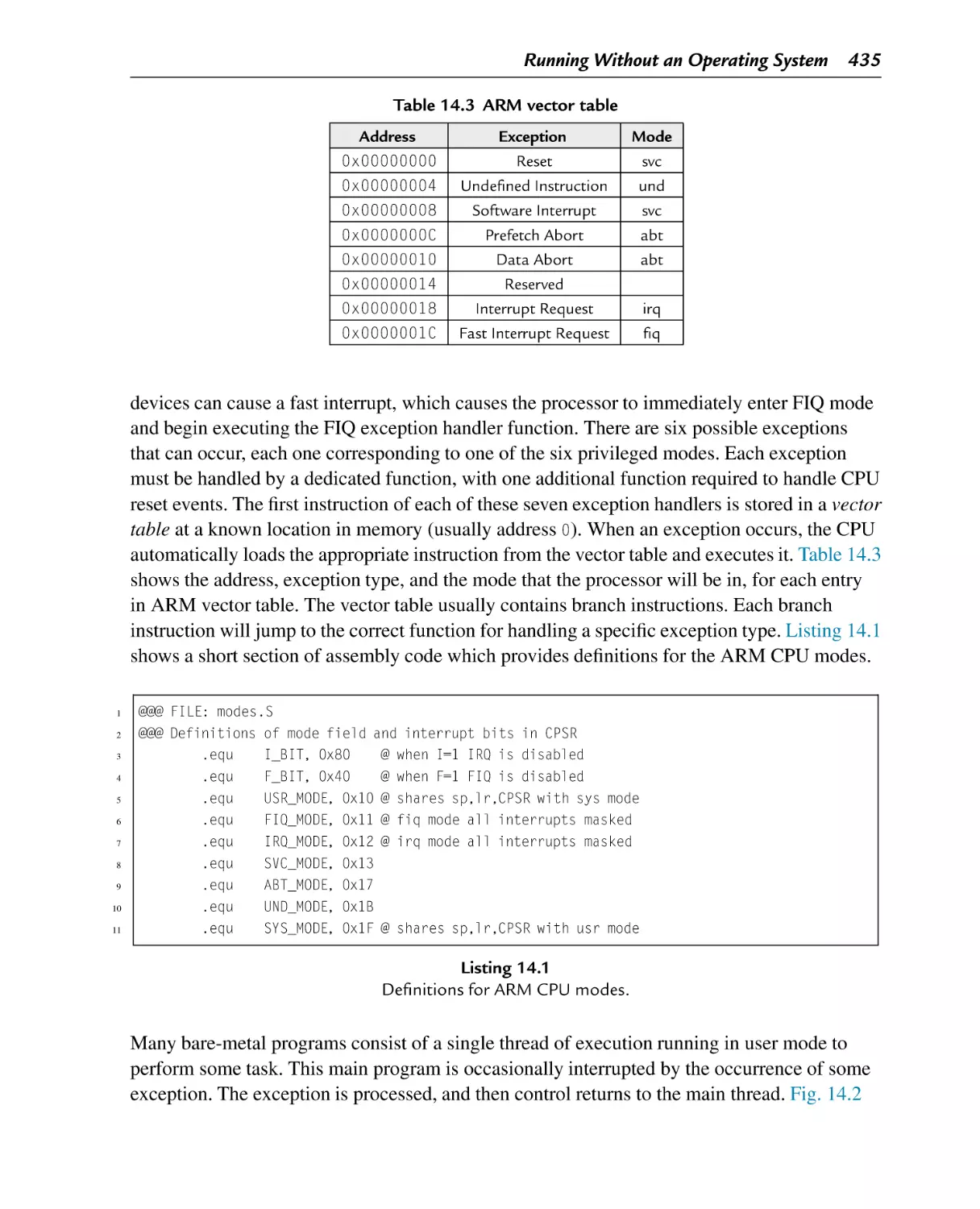
ARM vector table
398
399
401
401
402
407
407
408
408
409
413
414
415
415
416
416
416
417
422
423
424
424
424
425
425
426
427
427
428
428
428
433
434
435
List of Figures
Figure 1.1
Figure 1.2
Figure 1.3
Figure 1.4
Figure 1.5
Figure 1.6
Figure 1.7
Figure 2.1
Figure 3.1
Figure 3.2
Figure 3.3
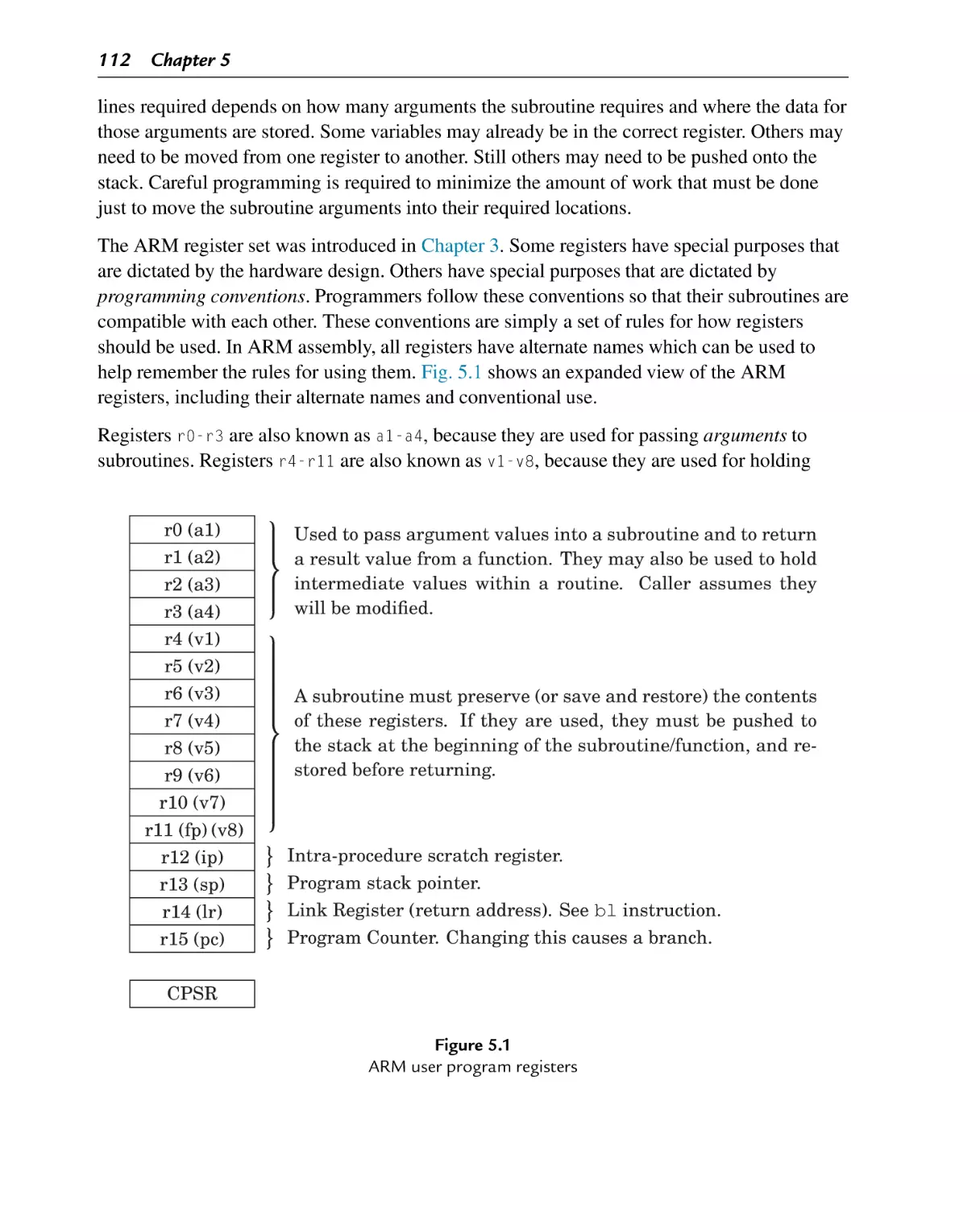
Figure 5.1
Figure 6.1
Figure 6.2
Figure 6.3
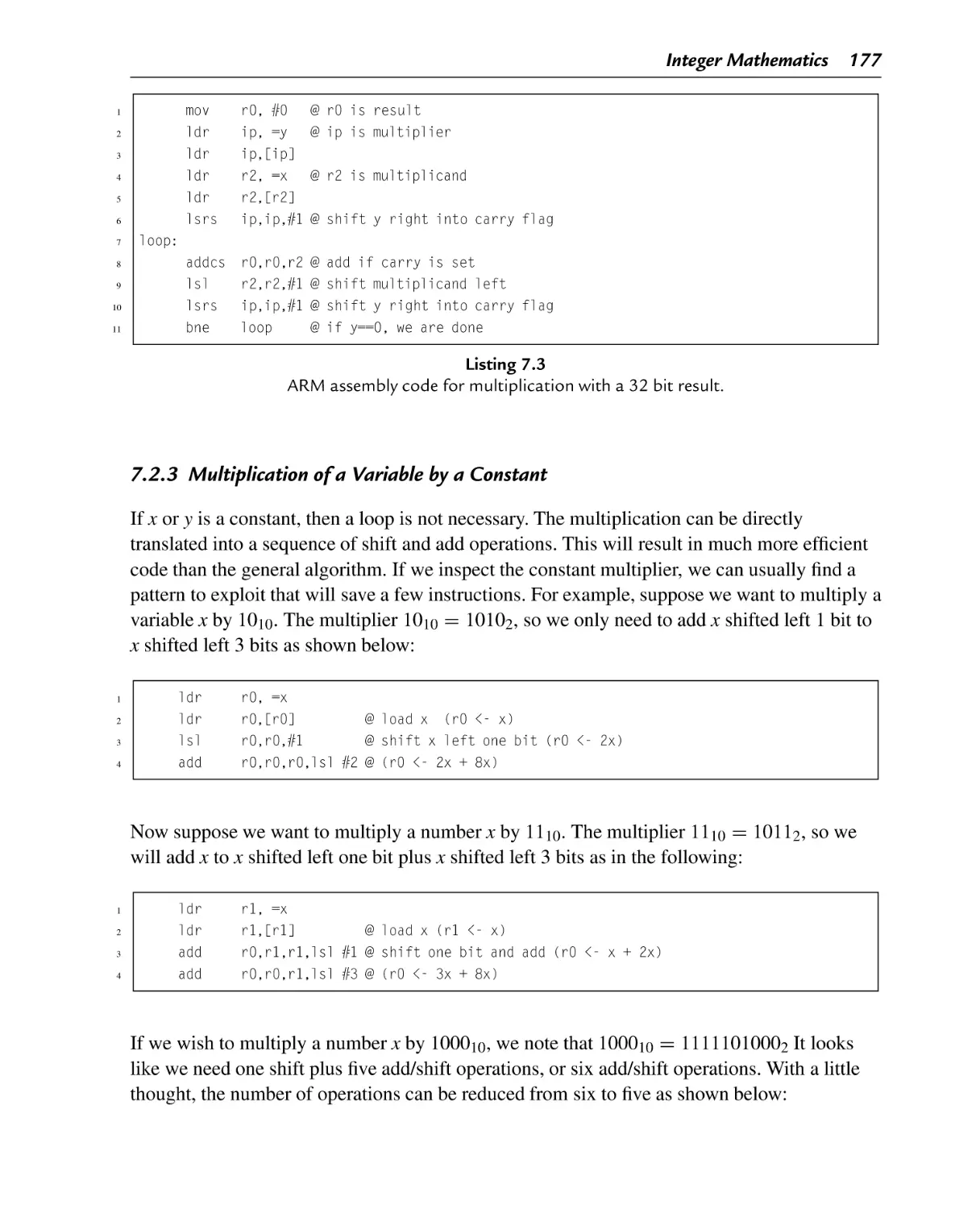
Figure 7.1
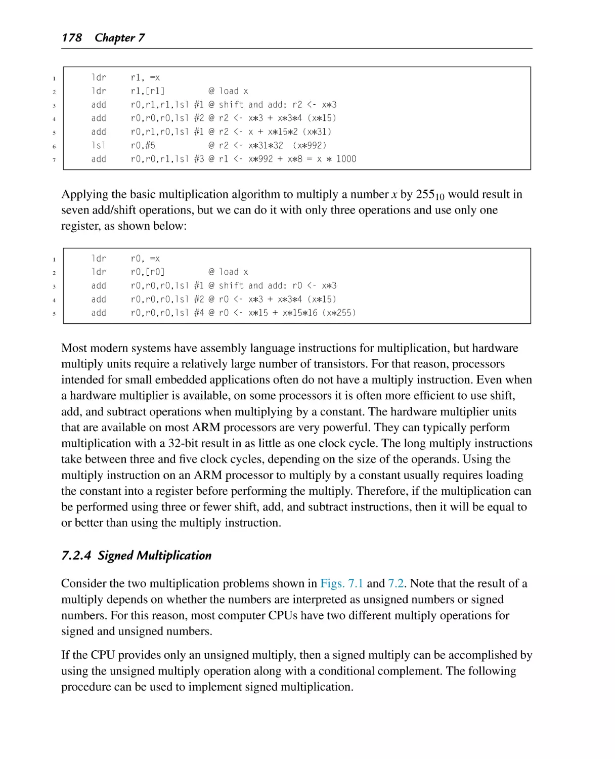
Figure 7.2
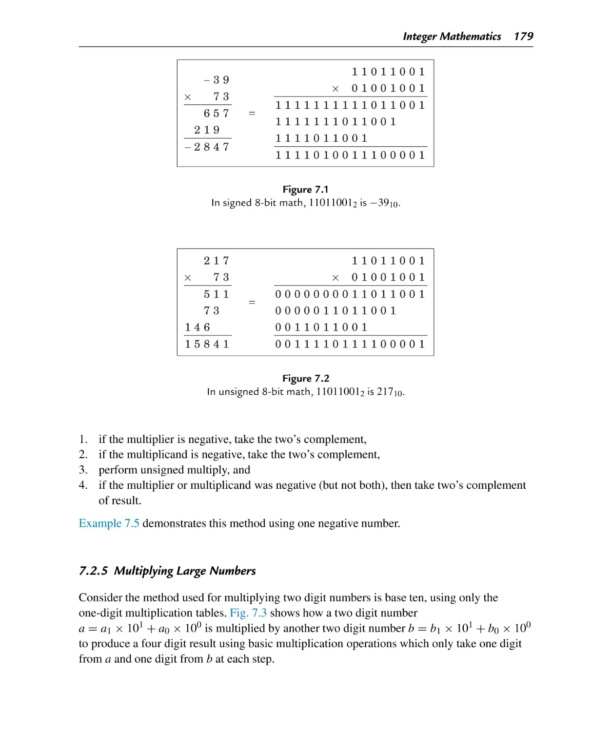
Figure 7.3
Figure 7.4
Figure 7.5
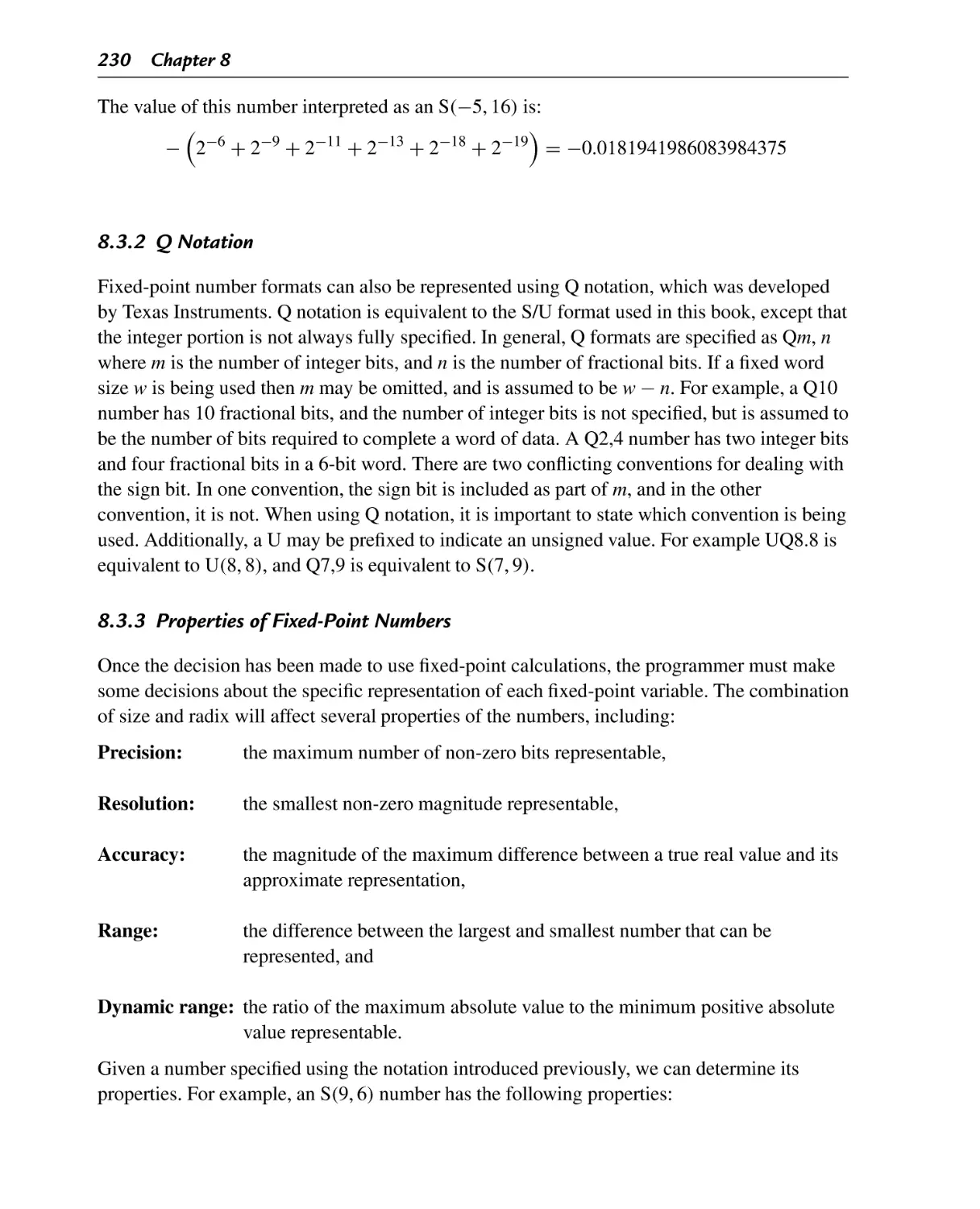
Figure 8.1
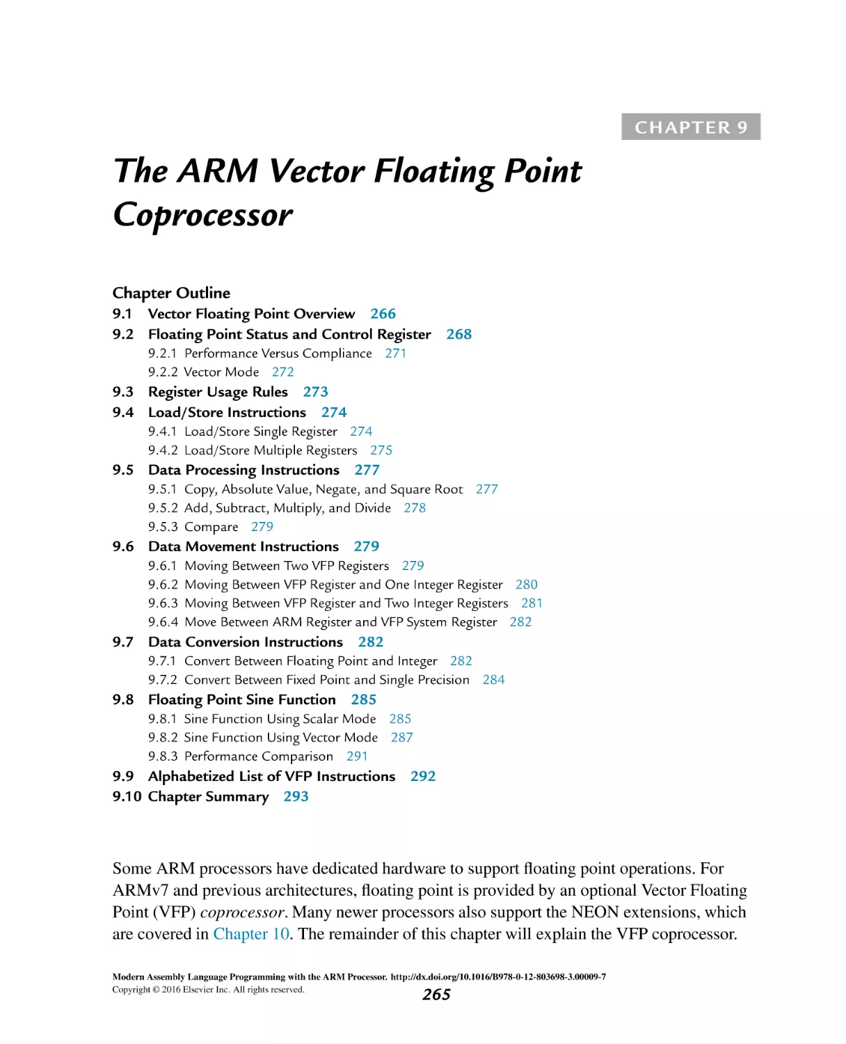
Figure 9.1
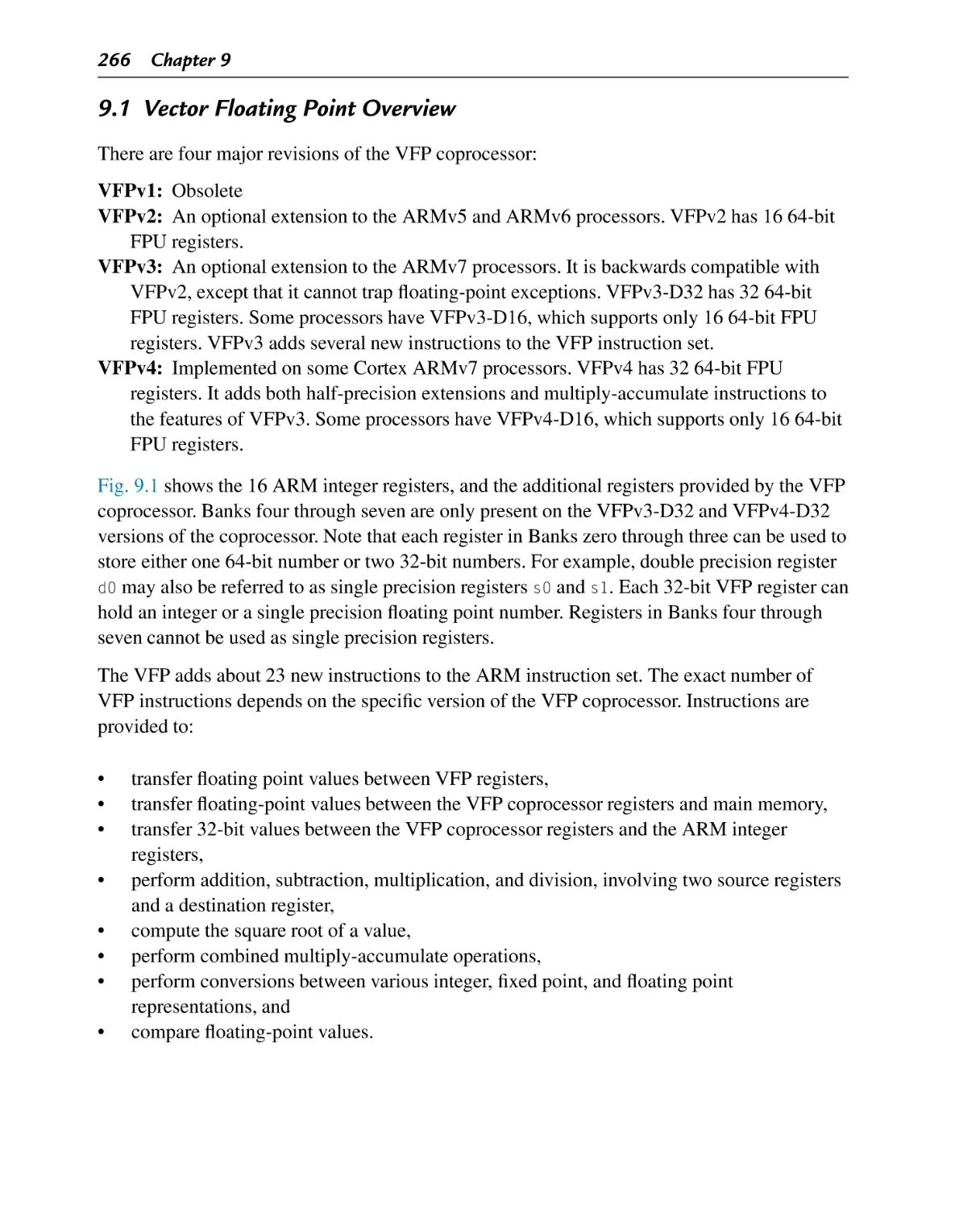
Figure 9.2
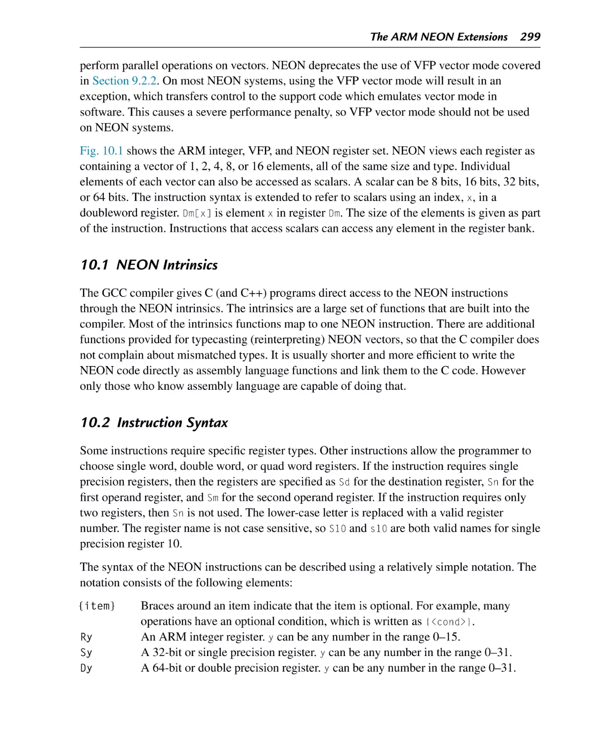
Figure 10.1
Figure 10.2
Figure 10.3
Figure 10.4
Figure 10.5
Figure 10.6
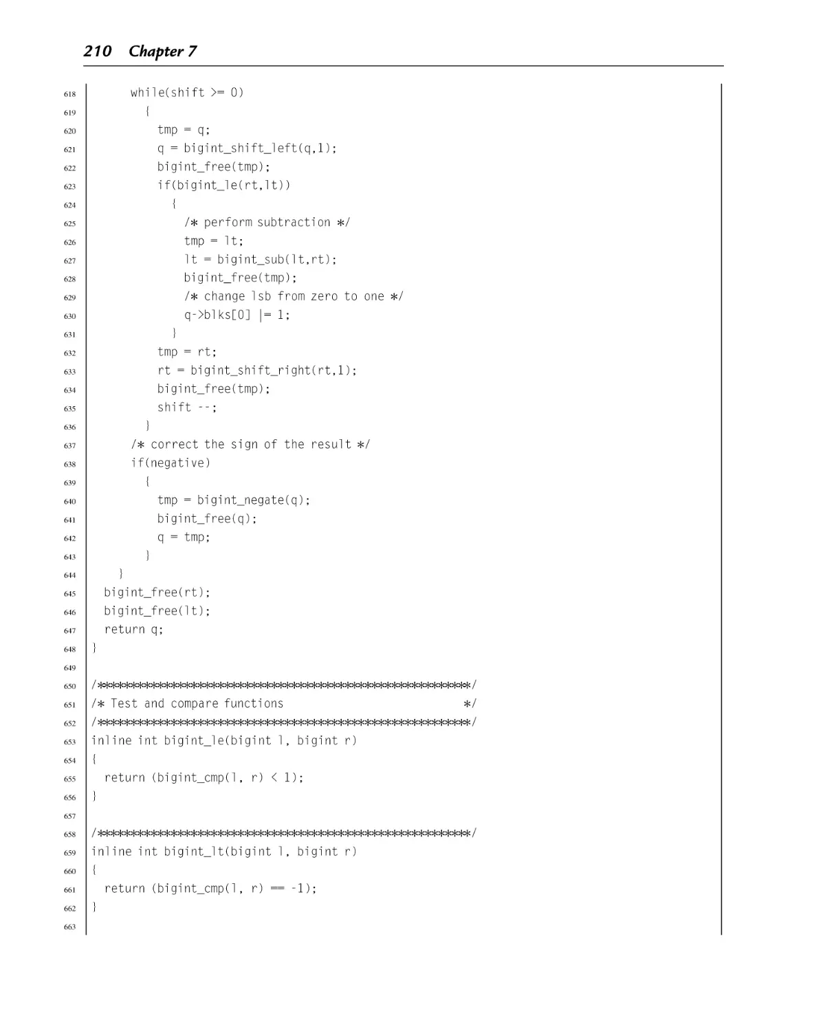
Simplified representation of a computer system
Stages of a typical compilation sequence
Tables used for converting between binary, octal, and hex
Four different representations for binary integers
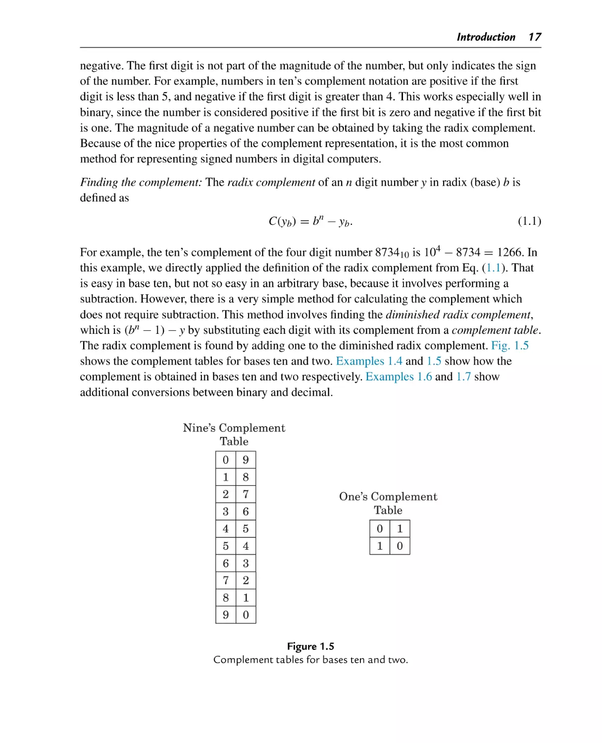
Complement tables for bases ten and two
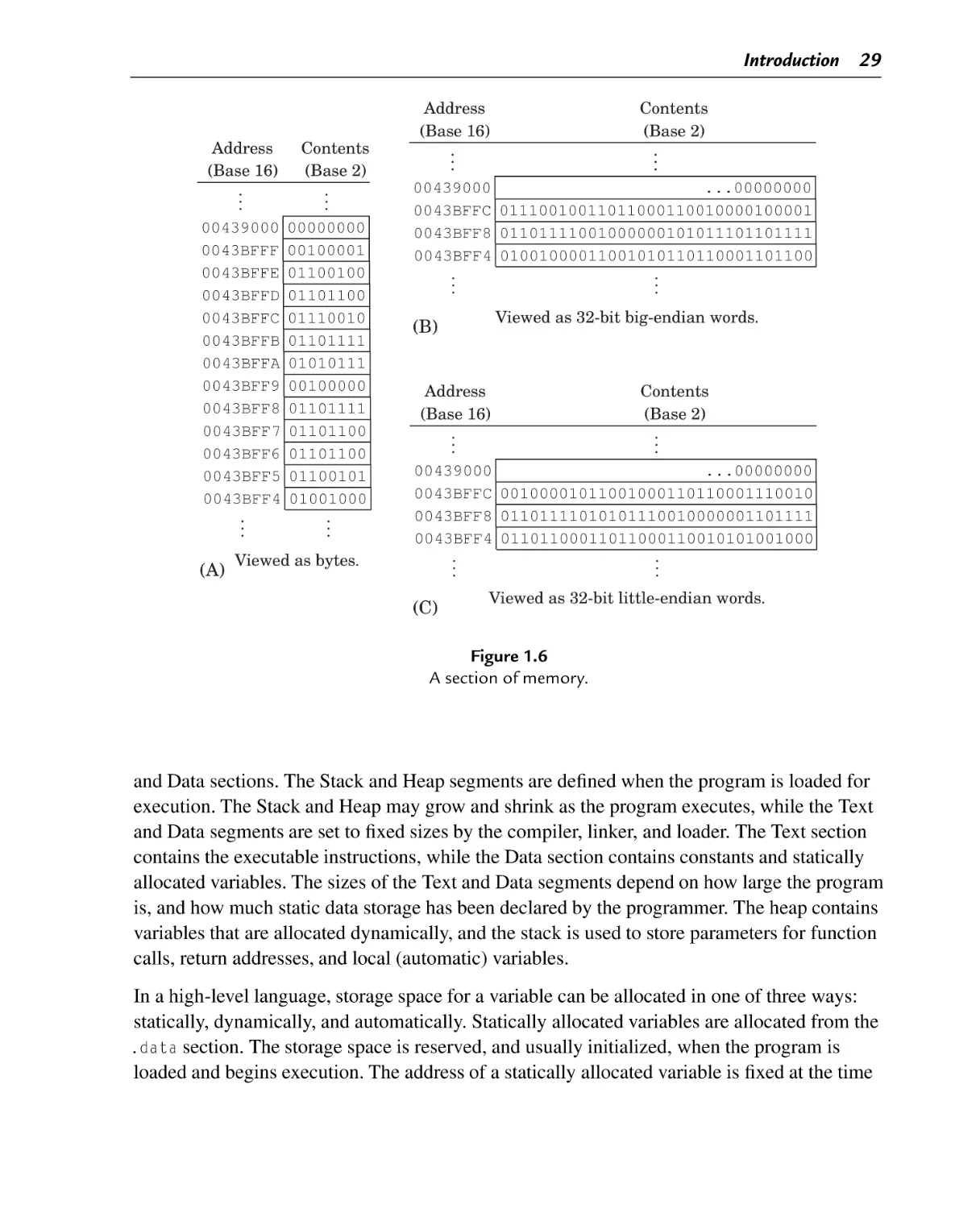
A section of memory
Typical memory layout for a program with a 32-bit address space
Equivalent static variable declarations in assembly and C
The ARM processor architecture
The ARM user program registers
The ARM process status register
ARM user program registers
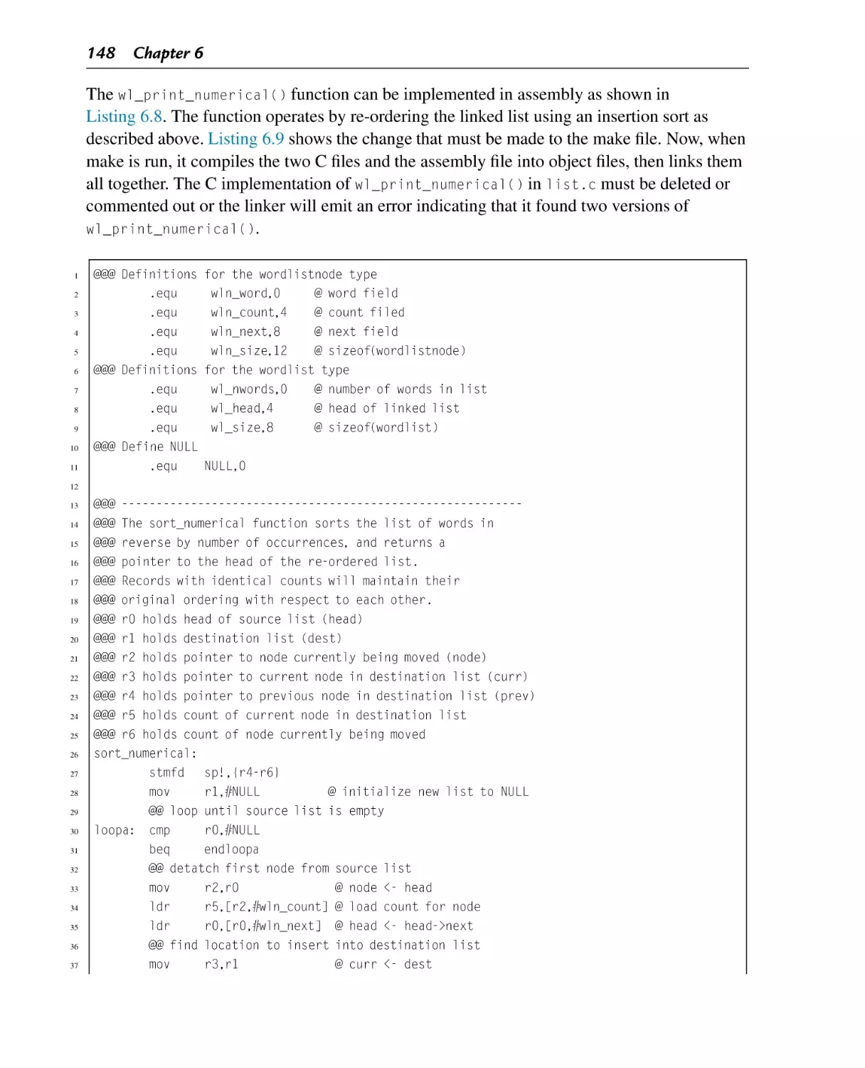
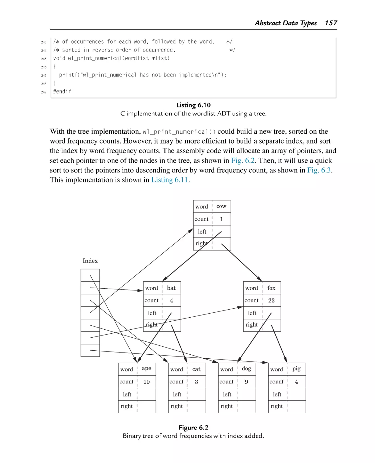
Binary tree of word frequencies
Binary tree of word frequencies with index added
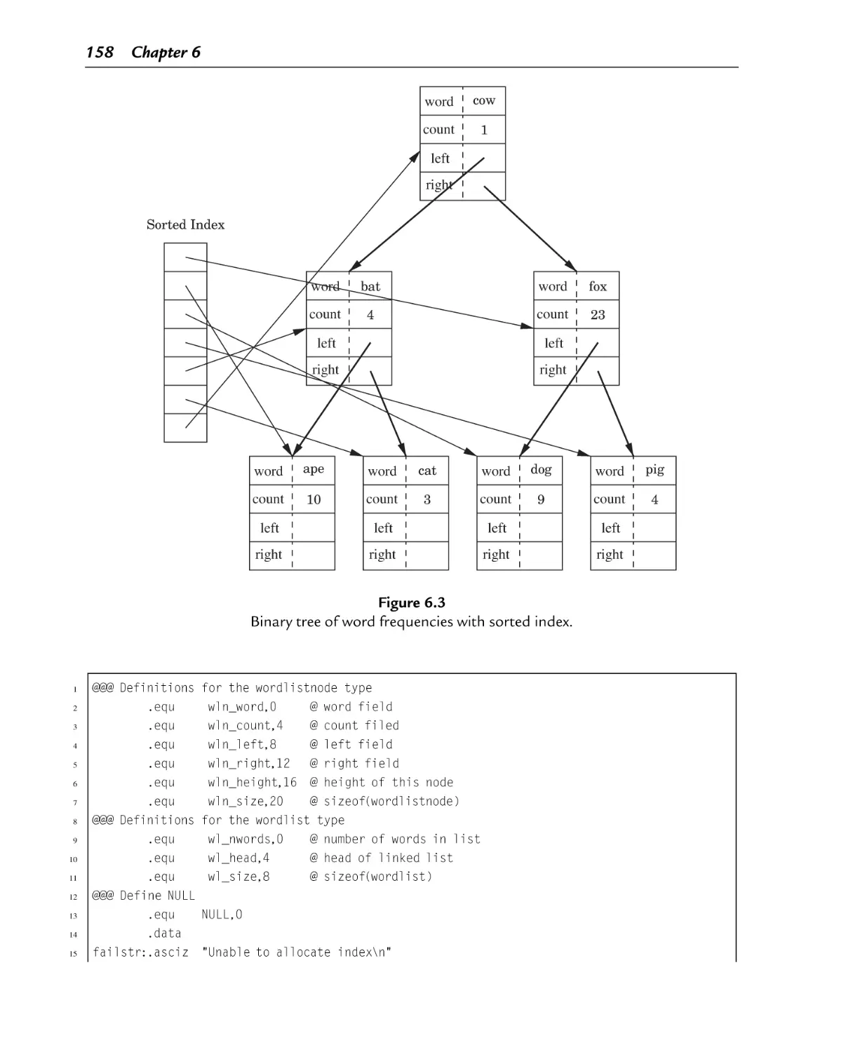
Binary tree of word frequencies with sorted index
In signed 8-bit math, 110110012 is −3910
In unsigned 8-bit math, 110110012 is 21710
Multiplication of large numbers
Longhand division in decimal and binary
Flowchart for binary division
Examples of fixed-point signed arithmetic
ARM integer and vector floating point user program registers
Bits in the FPSCR
ARM integer and NEON user program registers
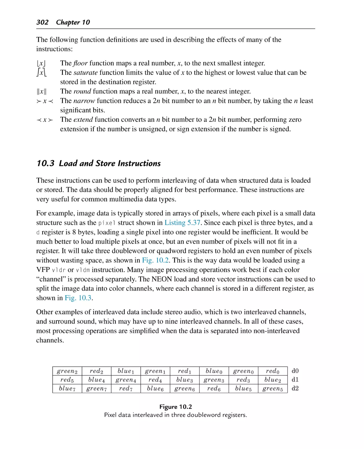
Pixel data interleaved in three doubleword registers
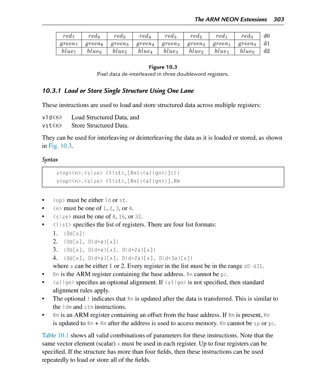
Pixel data de-interleaved in three doubleword registers
Example of vext.8 d12,d4,d9,#5
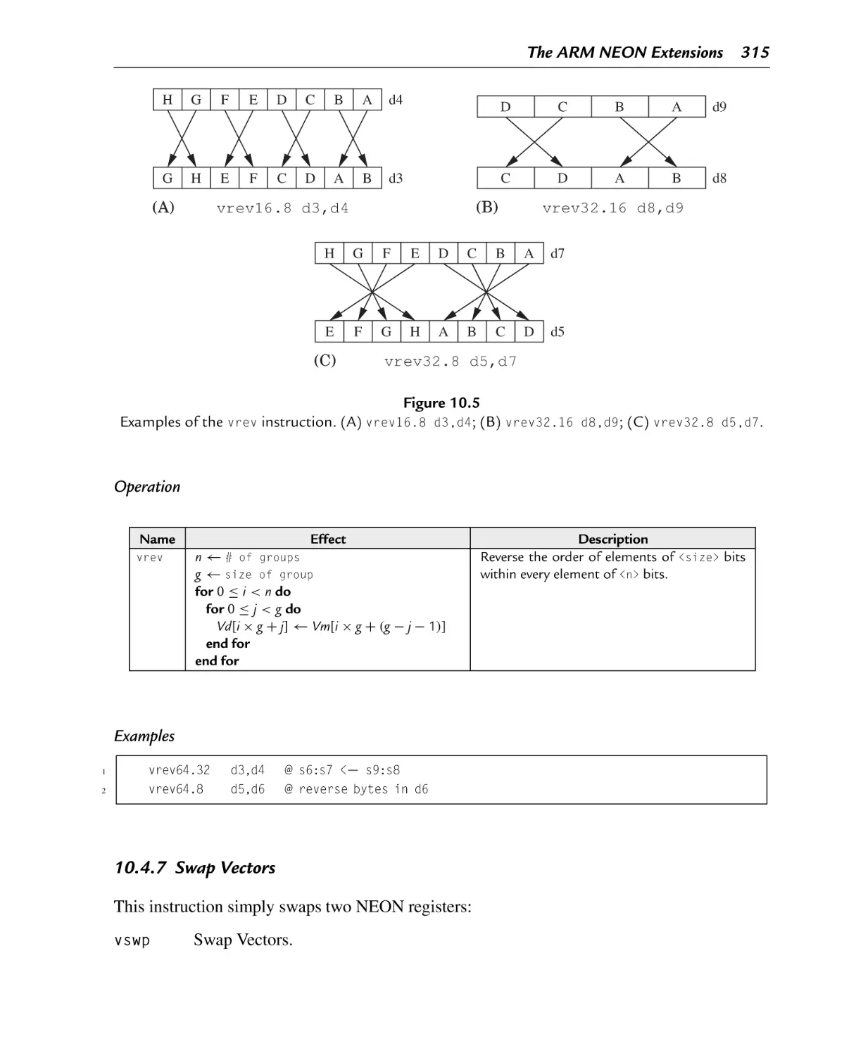
Examples of the vrev instruction. (A) vrev16.8 d3,d4; (B) vrev32.16
(C) vrev32.8 d5,d7
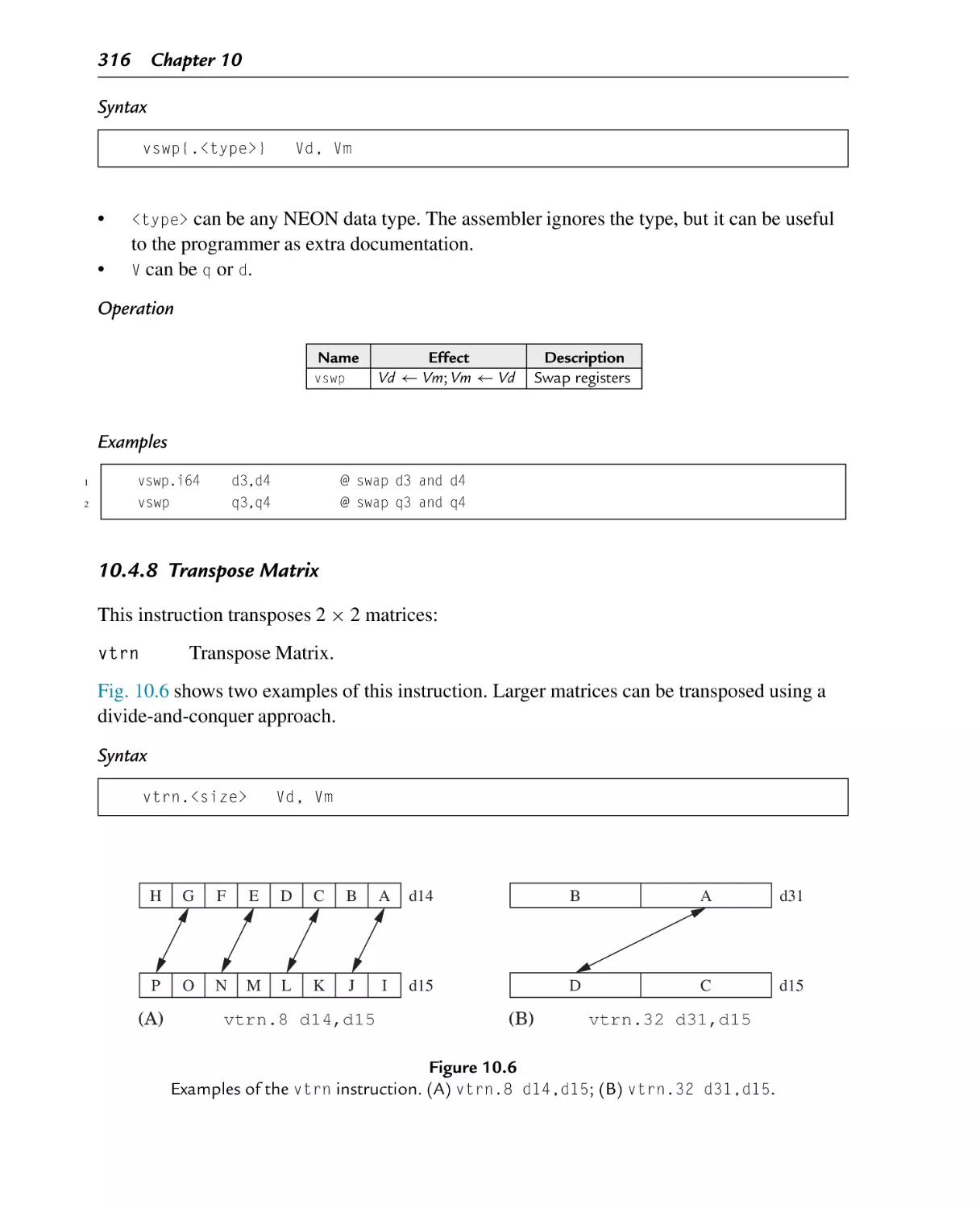
Examples of the vtrn instruction. (A) vtrn.8 d14,d15; (B)
vtrn.32 d31,d15
Figure 10.7
Figure 10.8
Figure 10.9
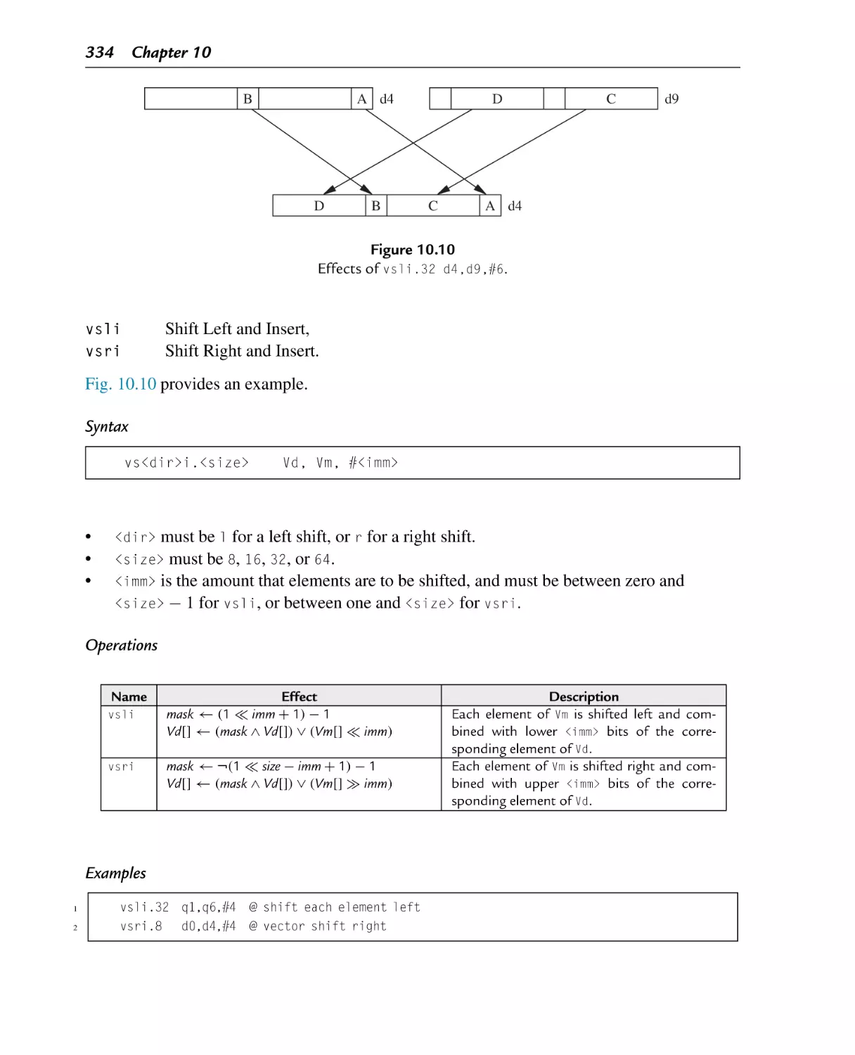
Figure 10.10
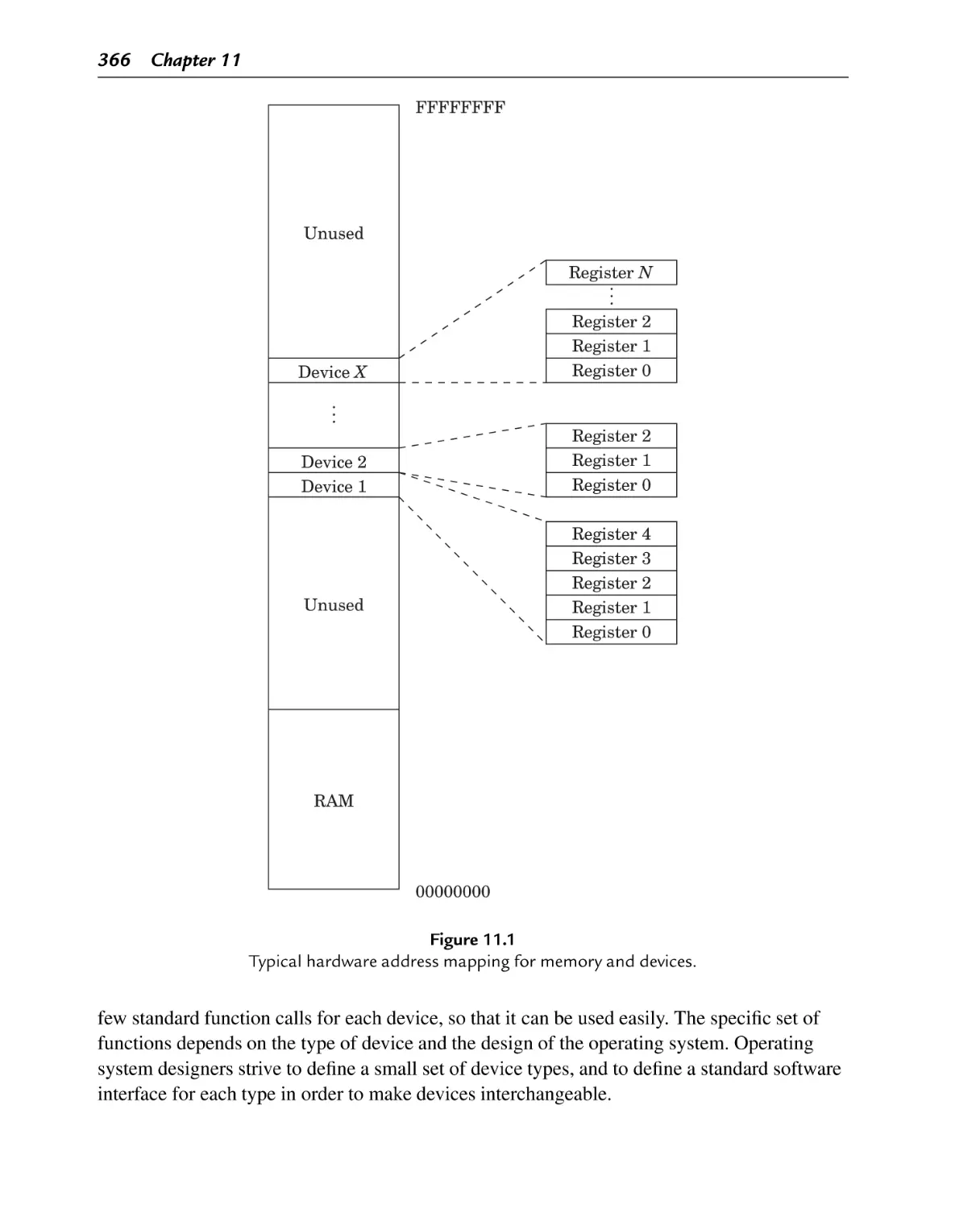
Figure 11.1
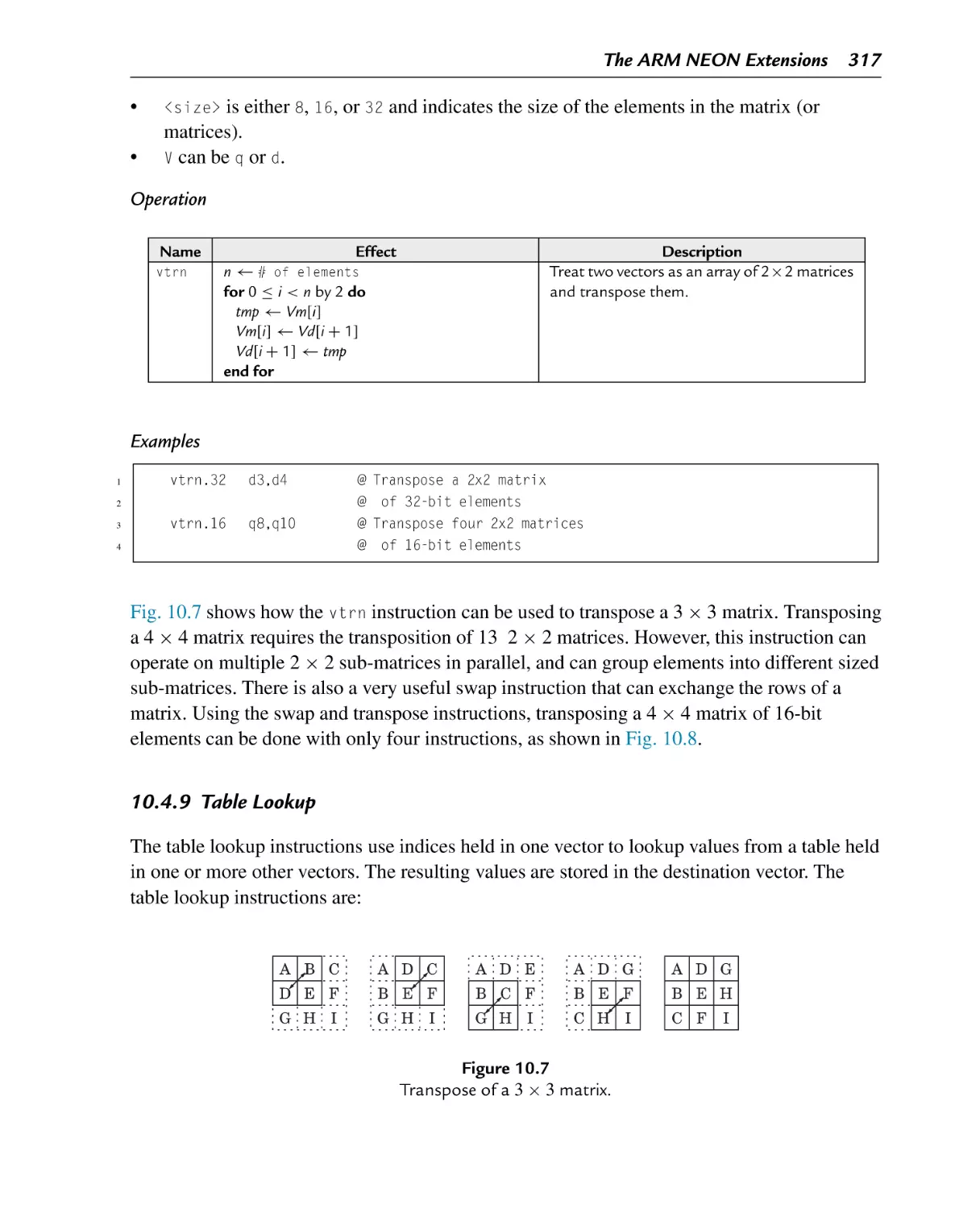
Transpose of a 3 × 3 matrix
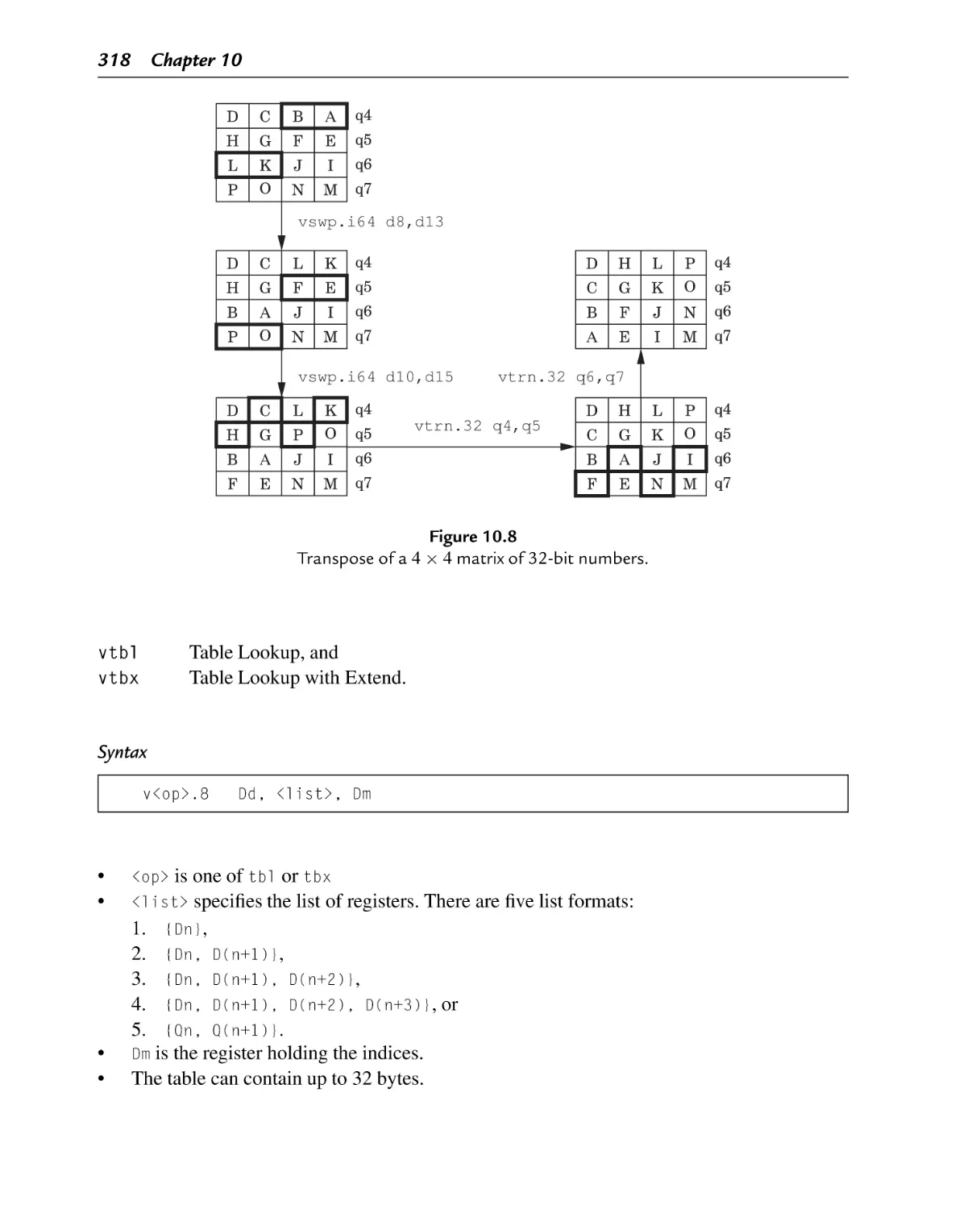
Transpose of a 4 × 4 matrix of 32-bit numbers
Example of vzip.8 d9,d4
Effects of vsli.32 d4,d9,#6
Typical hardware address mapping for memory and devices
xv
4
6
14
16
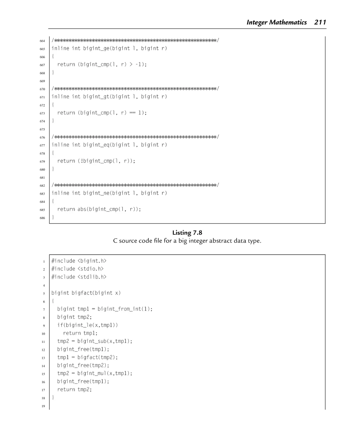
17
29
30
42
54
56
57
112
151
157
158
179
179
180
181
183
232
267
268
300
302
303
313
d8,d9;
315
316
317
318
320
334
366
xvi List of Figures
Figure 11.2
Figure 11.3
Figure 11.4
Figure 11.5
Figure 11.6
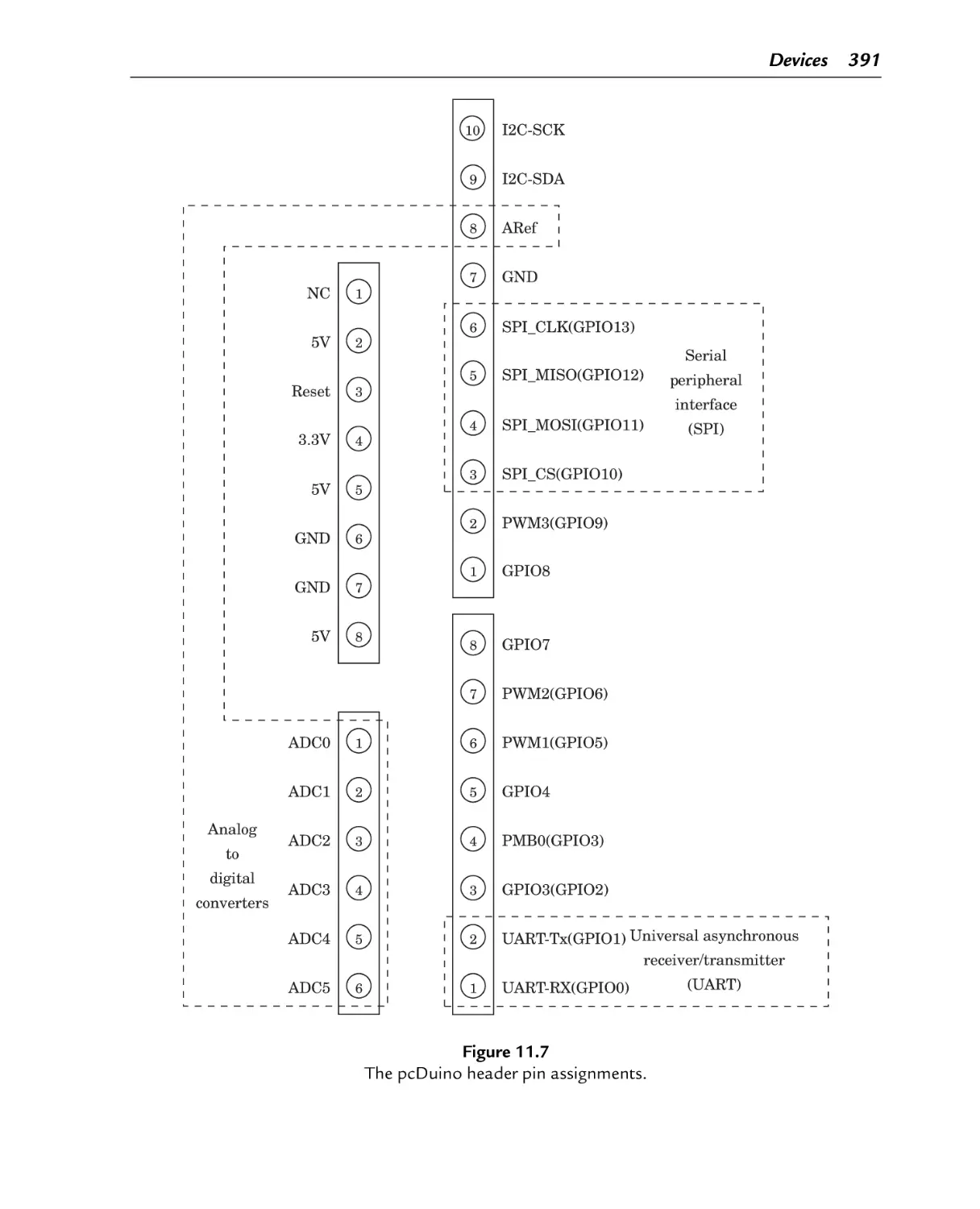
Figure 11.7
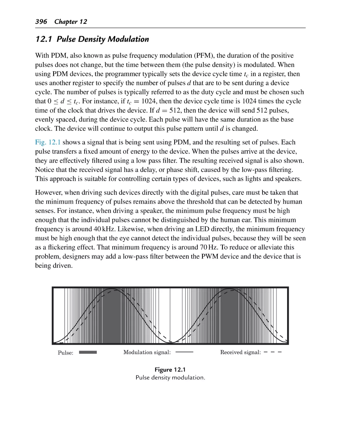
Figure 12.1
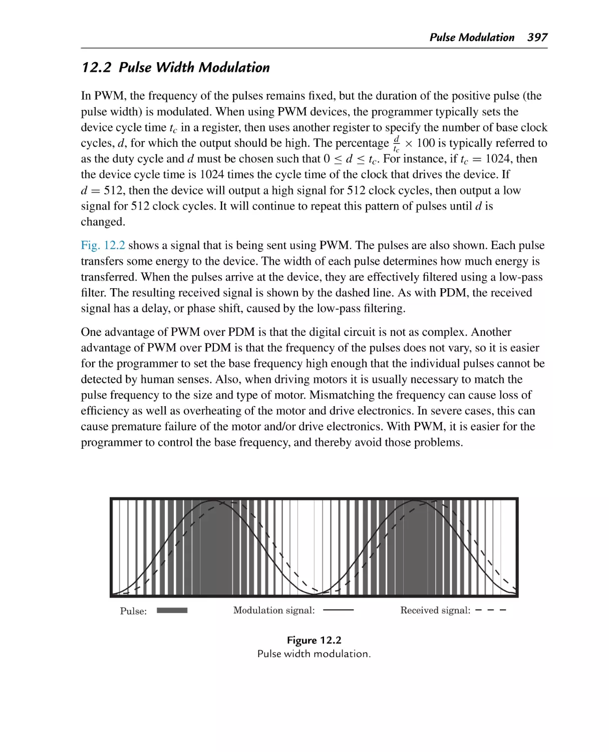
Figure 12.2
Figure 13.1
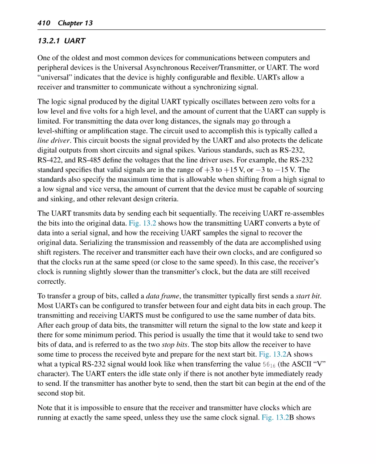
Figure 13.2
Figure 14.1
Figure 14.2
Figure 14.3
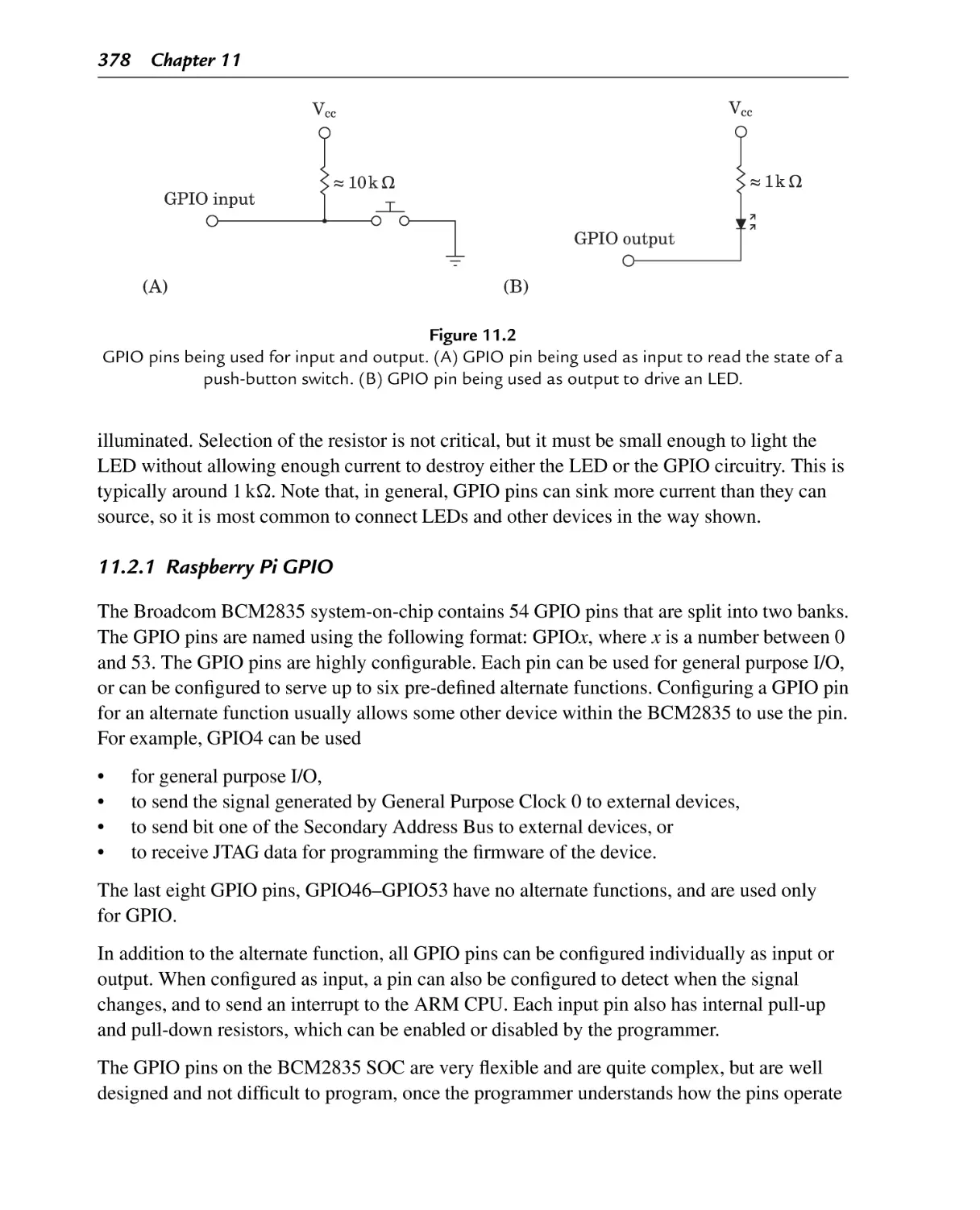
GPIO pins being used for input and output. (A) GPIO pin being used as
input to read the state of a push-button switch. (B) GPIO pin being used as
output to drive an LED
The Raspberry Pi expansion header location
The Raspberry Pi expansion header pin assignments
Bit-to-pin assignments for PIO control registers
The pcDuino header locations
The pcDuino header pin assignments
Pulse density modulation
Pulse width modulation
Typical system with a clock management device
Transmitter and receiver timings for two UARTS. (A) Waveform of a UART
transmitting a byte. (B) Timing of UART receiving a byte
The ARM process status register
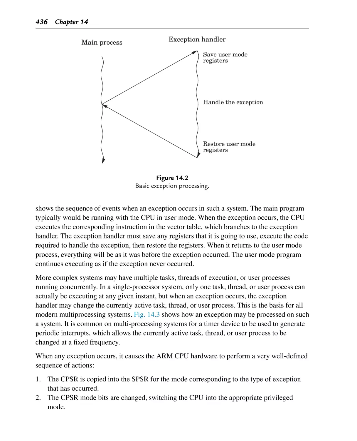
Basic exception processing
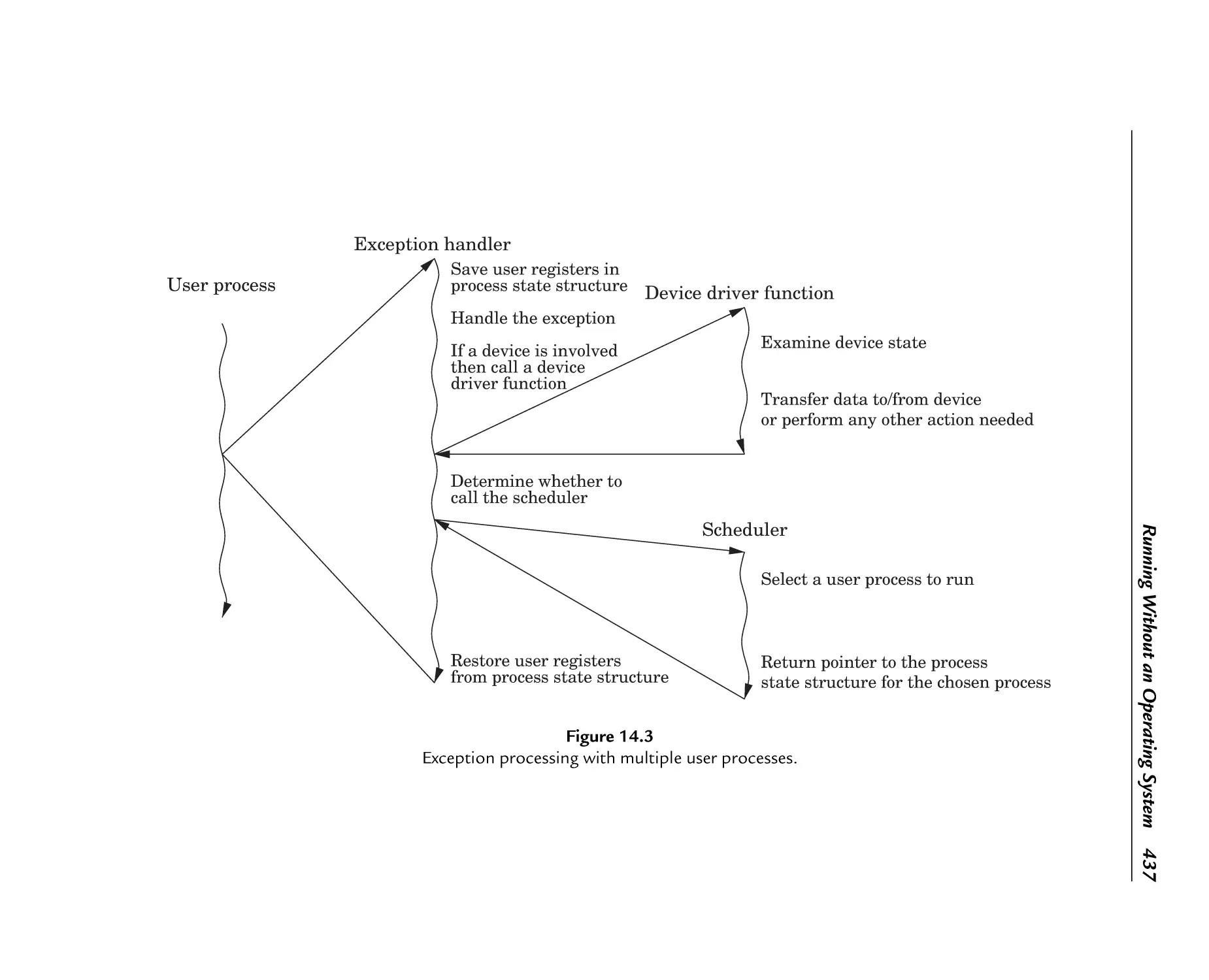
Exception processing with multiple user processes
378
383
384
388
390
391
396
397
406
411
433
436
437
List of Listings
Listing 2.1
Listing 2.2
Listing 2.3
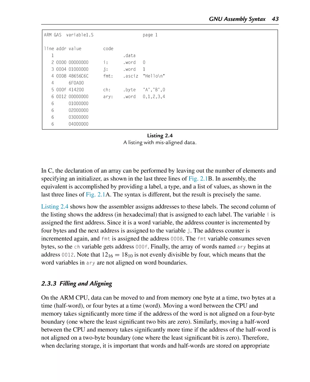
Listing 2.4
Listing 2.5
Listing 2.6
Listing 5.1
Listing 5.2
Listing 5.3
Listing 5.4
Listing 5.5
Listing 5.6
Listing 5.7
Listing 5.8
Listing 5.9
Listing 5.10
Listing 5.11
Listing 5.12
Listing 5.13
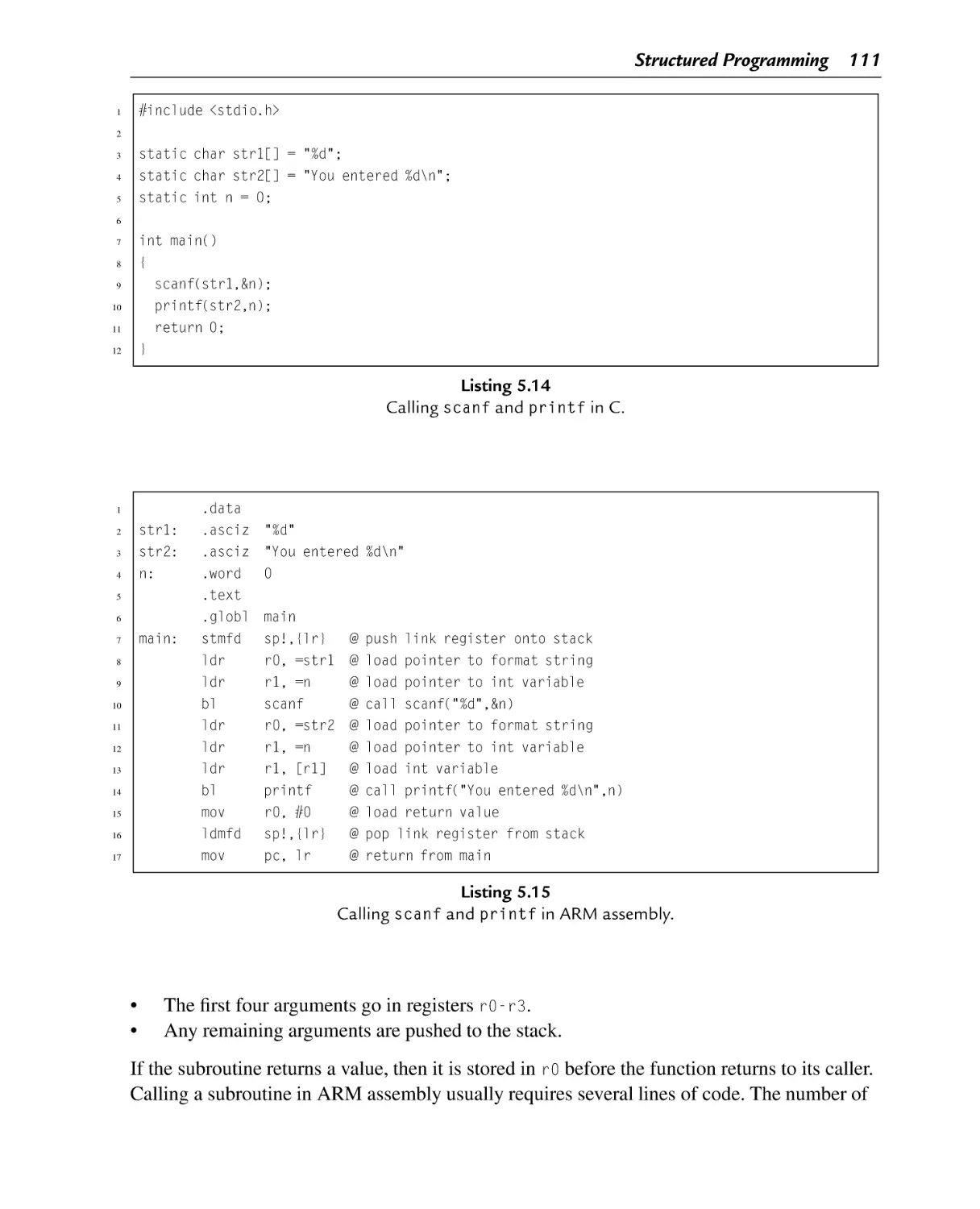
Listing 5.14
Listing 5.15
Listing 5.16
Listing 5.17
Listing 5.18
Listing 5.19
Listing 5.20
Listing 5.21
Listing 5.22
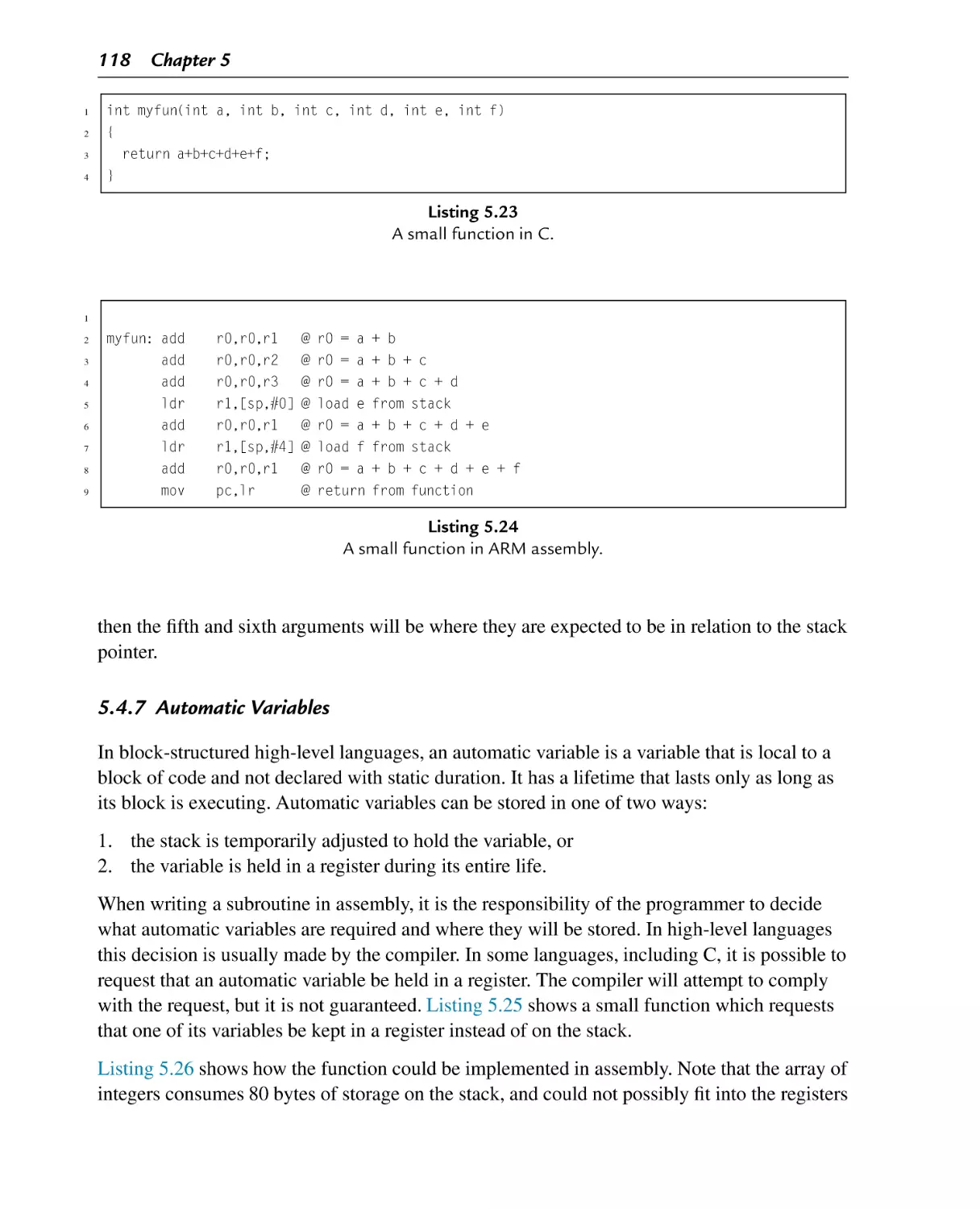
Listing 5.23
Listing 5.24
Listing 5.25
Listing 5.26
Listing 5.27
Listing 5.28
Listing 5.29
“Hello World” program in ARM assembly
“Hello World” program in C
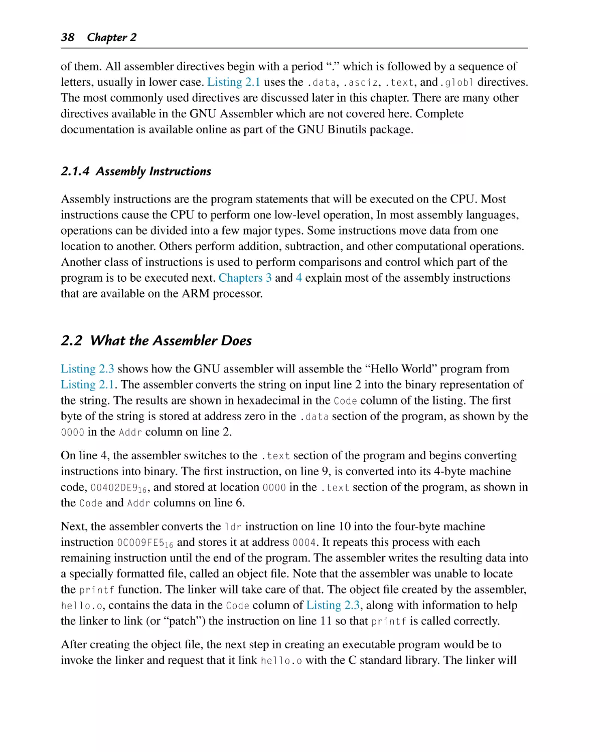
“Hello World” assembly listing
A listing with mis-aligned data
A listing with properly aligned data
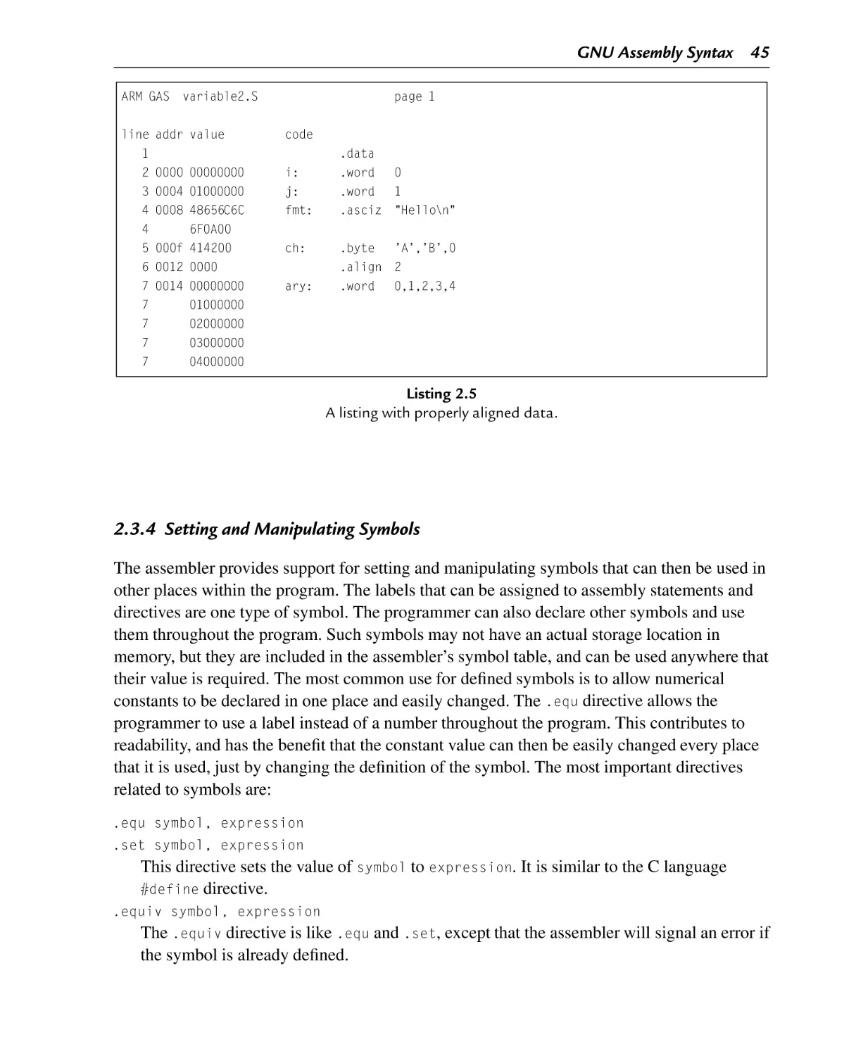
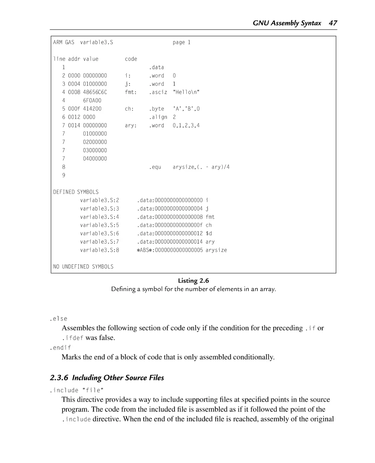
Defining a symbol for the number of elements in an array
Selection in C
Selection in ARM assembly using conditional execution
Selection in ARM assembly using branch instructions
Complex selection in C
Complex selection in ARM assembly
Unconditional loop in ARM assembly
Pre-test loop in ARM assembly
Post-test loop in ARM assembly
for loop in C
for loop rewritten as a pre-test loop in C
Pre-test loop in ARM assembly
for loop rewritten as a post-test loop in C
Post-test loop in ARM assembly
Calling scanf and printf in C
Calling scanf and printf in ARM assembly
Simple function call in C
Simple function call in ARM assembly
A larger function call in C
A larger function call in ARM assembly
A function call using the stack in C
A function call using the stack in ARM assembly
A function call using stm to push arguments onto the stack
A small function in C
A small function in ARM assembly
A small C function with a register variable
Automatic variables in ARM assembly
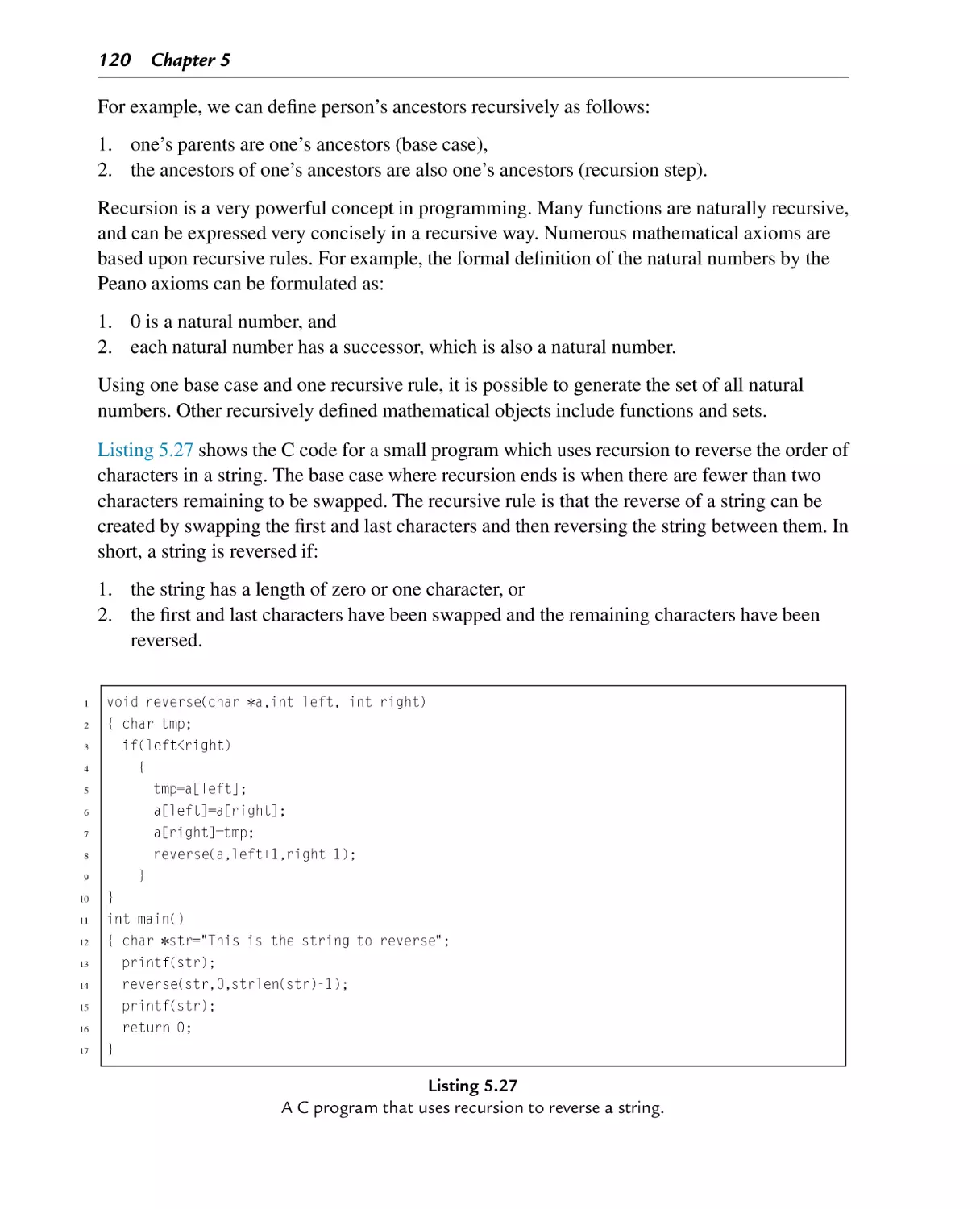
A C program that uses recursion to reverse a string
ARM assembly implementation of the reverse function
Better implementation of the reverse function
xvii
36
37
39
43
45
47
101
102
102
103
104
105
105
106
106
107
107
108
108
111
111
114
114
114
115
115
116
116
118
118
119
119
120
121
122
xviii List of Listings
Listing 5.30
Listing 5.31
Listing 5.32
Listing 5.33
Listing 5.34
Listing 5.35
Listing 5.36
Listing 5.37
Listing 5.38
Listing 5.39
Listing 5.40
Listing 6.1
Listing 6.2
Listing 6.3
Listing 6.4
Listing 6.5
Listing 6.6
Listing 6.7
Listing 6.8
Listing 6.9
Listing 6.10
Listing 6.11
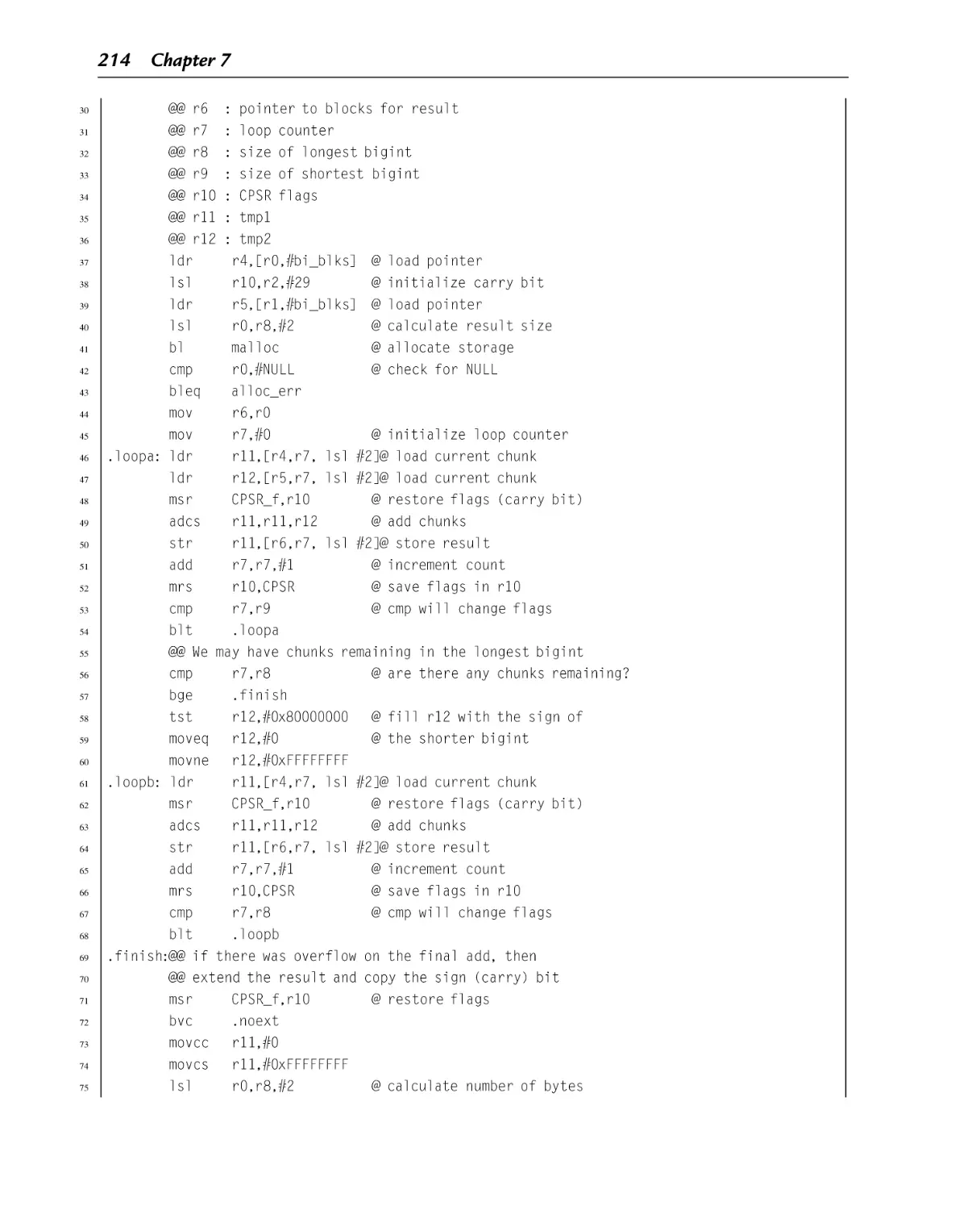
Listing 7.1
Listing 7.2
Listing 7.3
Listing 7.4
Listing 7.5
Listing 7.6
Listing 7.7
Listing 7.8
Listing 7.9
Listing 7.10
Listing 8.1
Listing 8.2
Listing 8.3
Listing 8.4
Listing 8.5
Listing 8.6
Listing 8.7
Listing 8.8
Listing 9.1
Listing 9.2
Listing 9.3
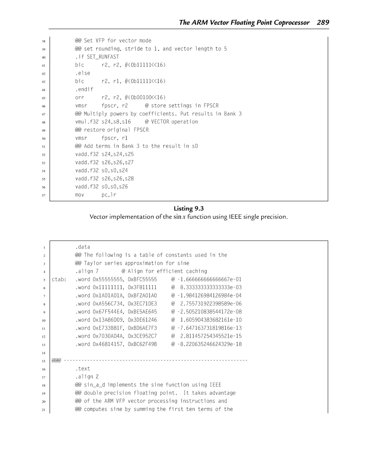
Listing 9.4
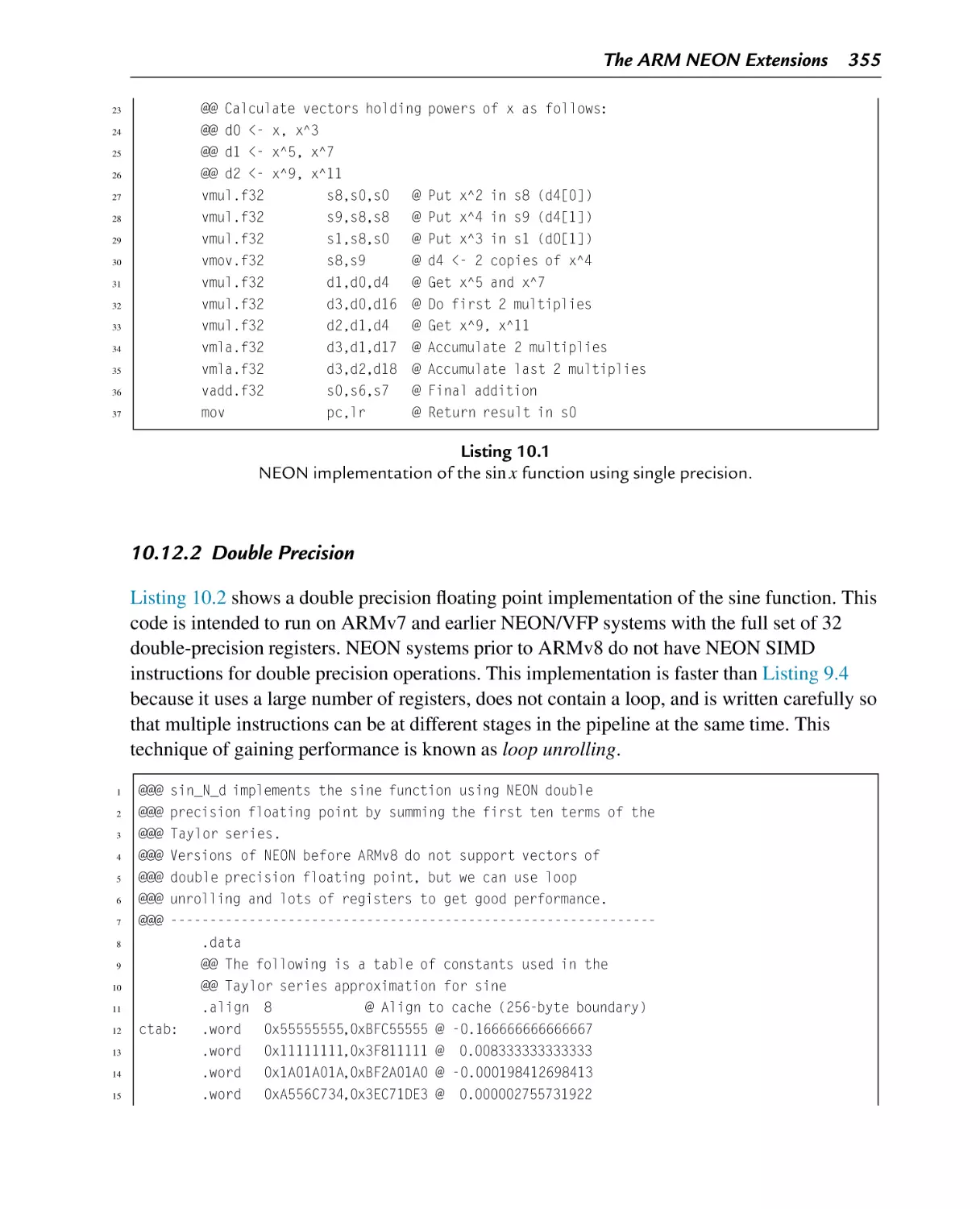
Listing 10.1
Even better implementation of the reverse function
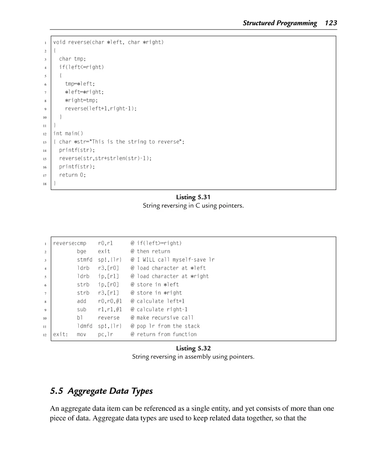
String reversing in C using pointers
String reversing in assembly using pointers
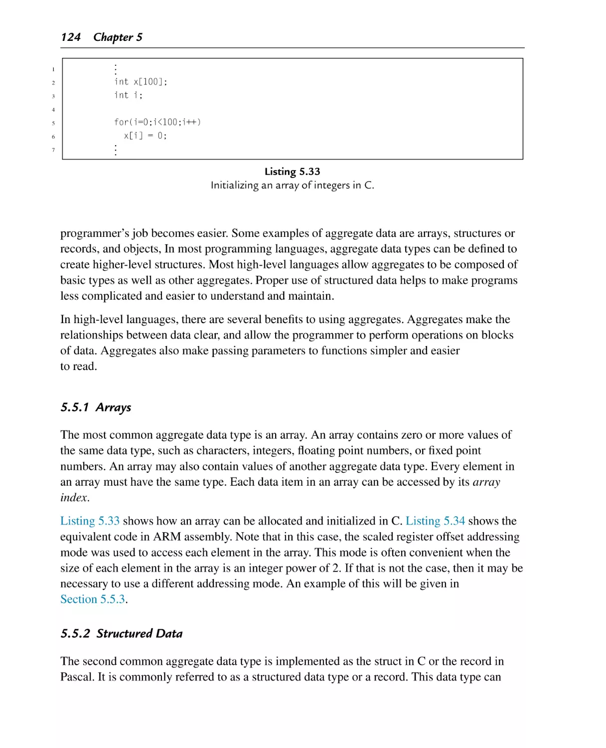
Initializing an array of integers in C
Initializing an array of integers in assembly
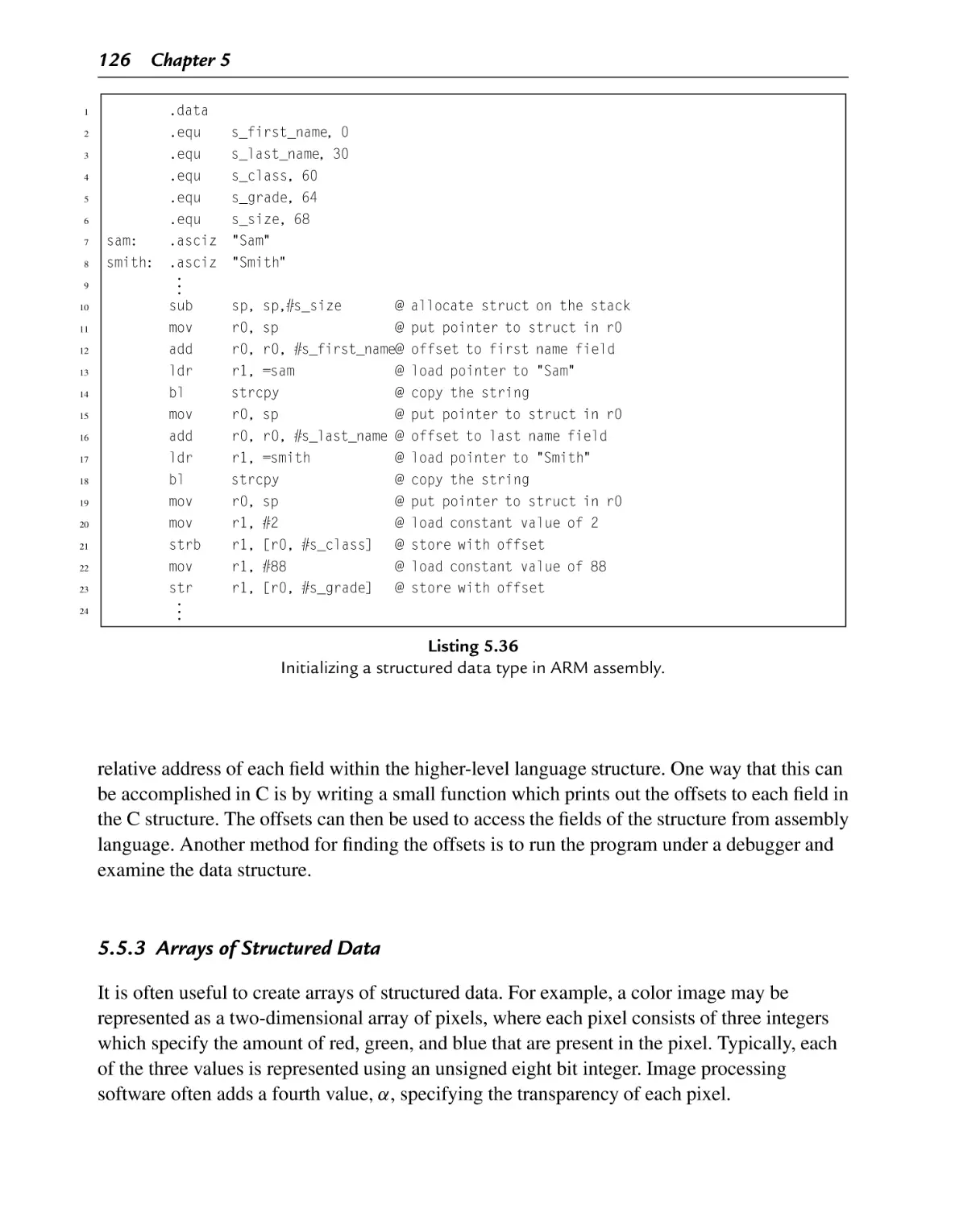
Initializing a structured data type in C
Initializing a structured data type in ARM assembly
Initializing an array of structured data in C
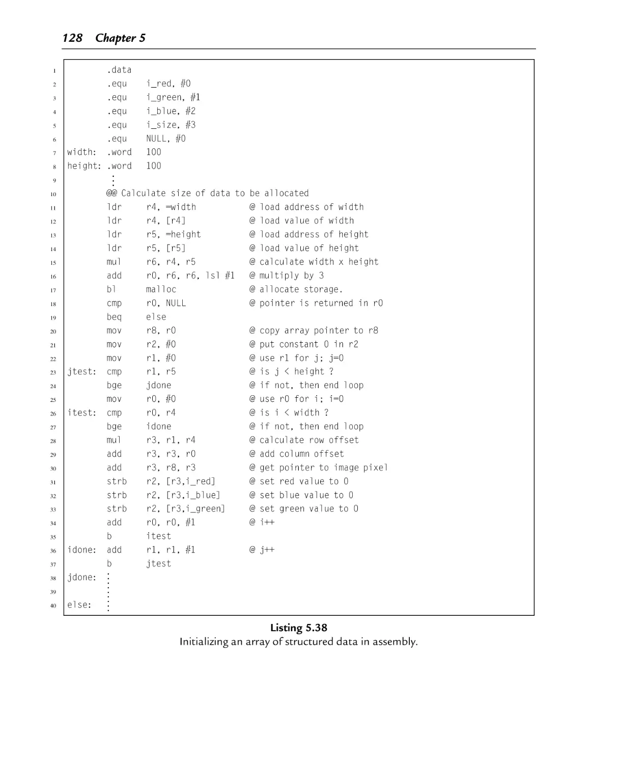
Initializing an array of structured data in assembly
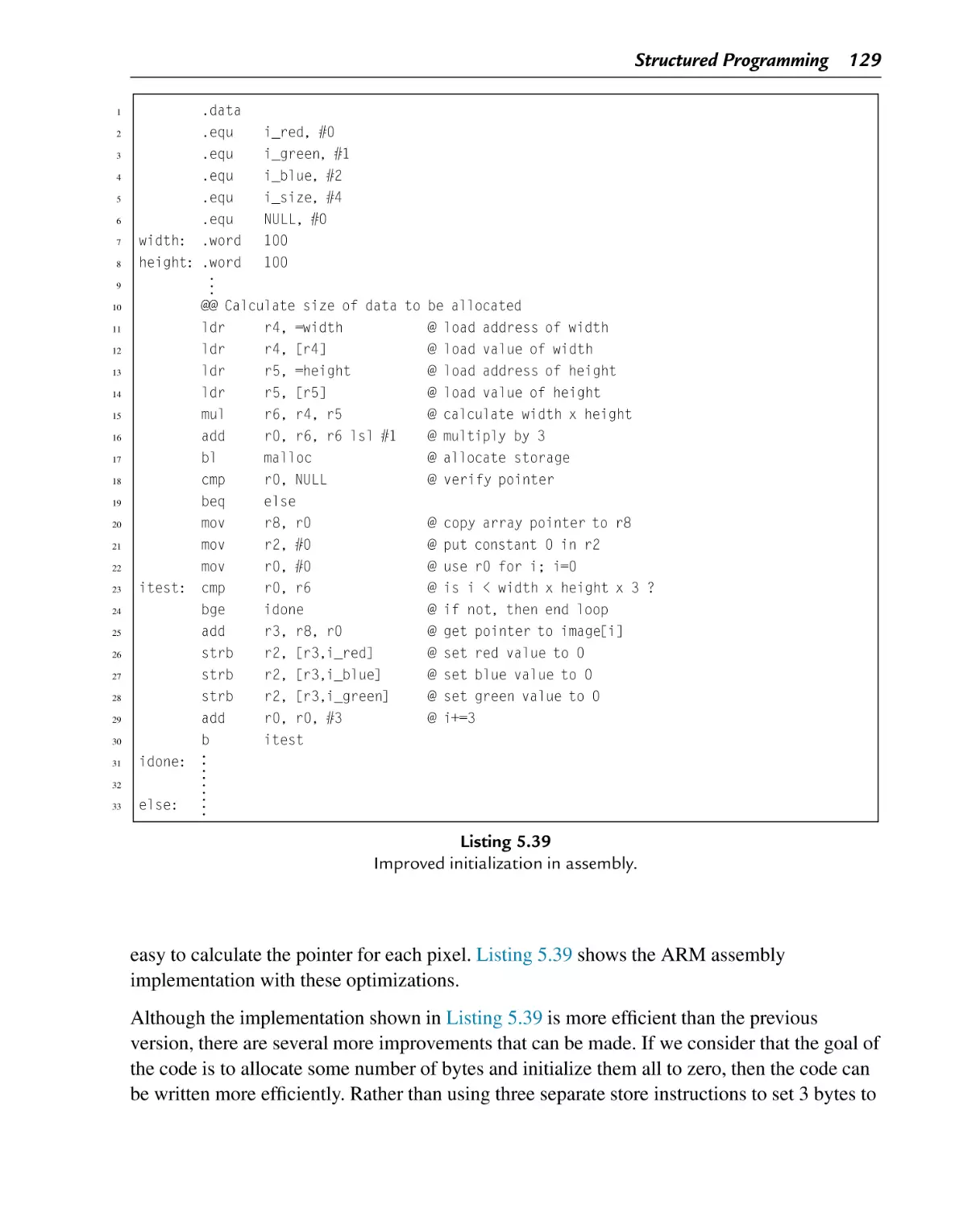
Improved initialization in assembly
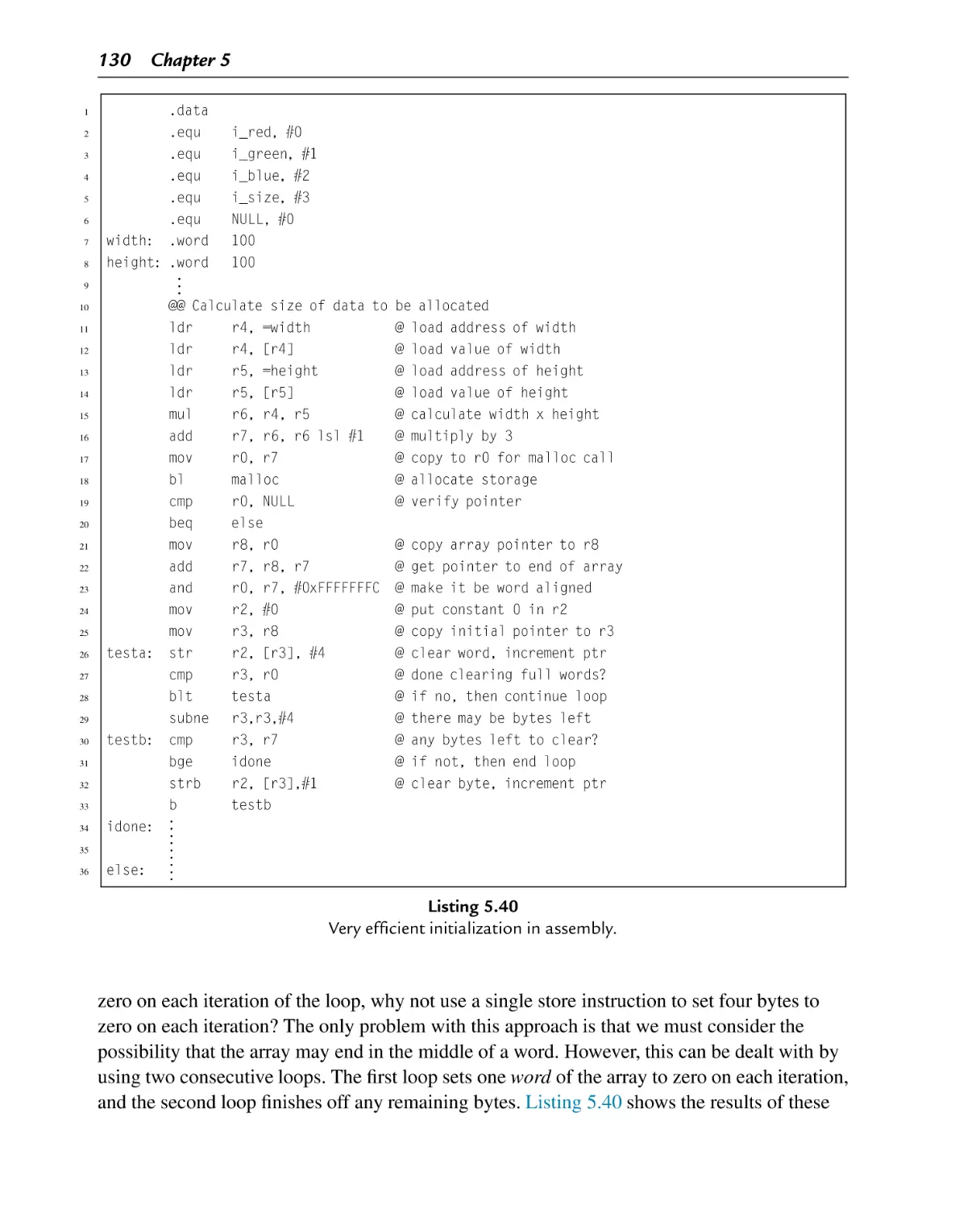
Very efficient initialization in assembly
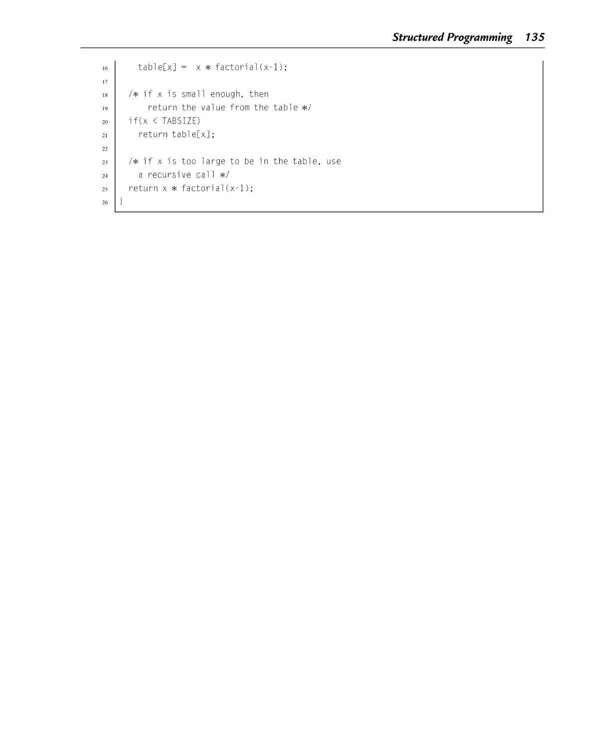
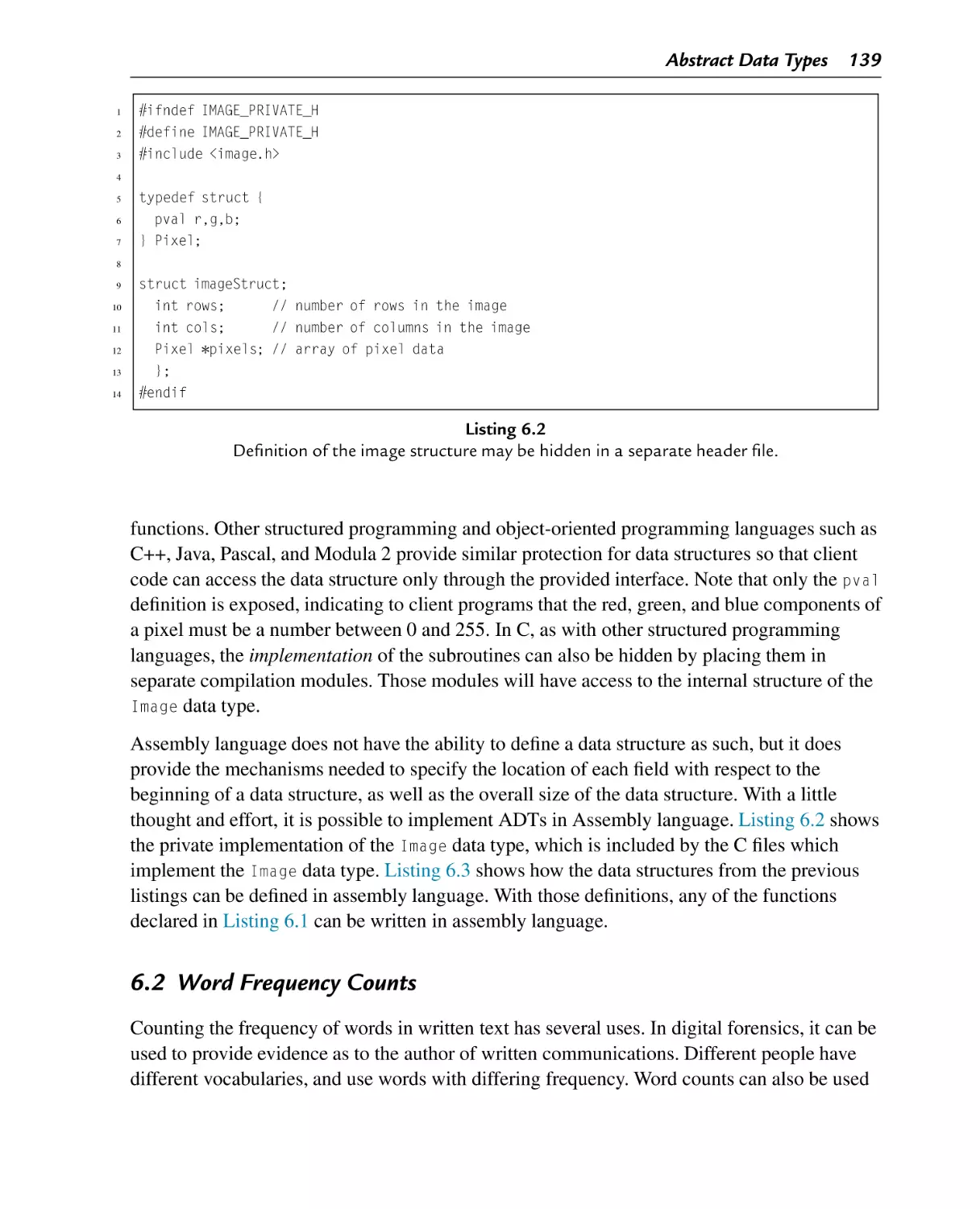
Definition of an Abstract Data Type in a C header file
Definition of the image structure may be hidden in a separate header file
Definition of an ADT in Assembly
C program to compute word frequencies
C header for the wordlist ADT
C implementation of the wordlist ADT
Makefile for the wordfreq program
ARM assembly implementation of wl_print_numerical()
Revised makefile for the wordfreq program
C implementation of the wordlist ADT using a tree
ARM assembly implementation of wl_print_numerical() with a tree
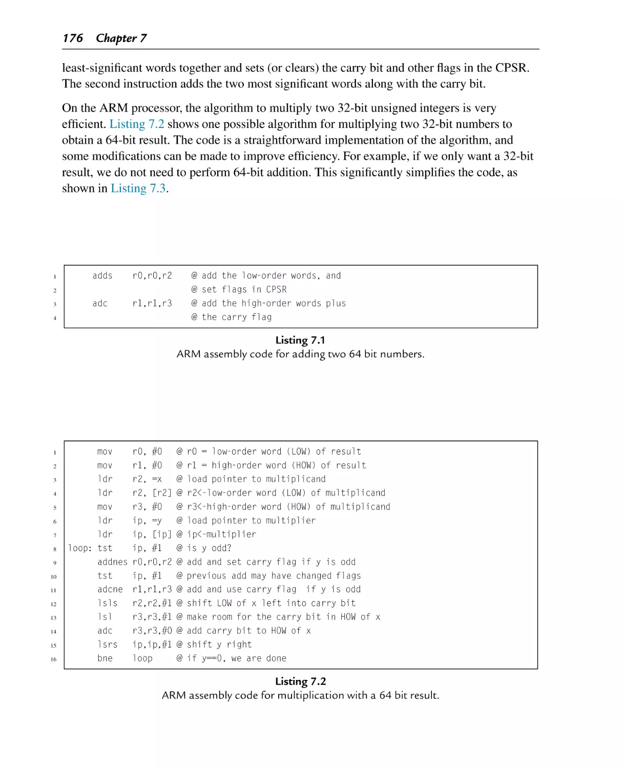
ARM assembly code for adding two 64 bit numbers
ARM assembly code for multiplication with a 64 bit result
ARM assembly code for multiplication with a 32 bit result
ARM assembly implementation of signed and unsigned 32-bit and 64-bit
division functions
ARM assembly code for division by constant 193
ARM assembly code for division of a variable by a constant without using a
multiply instruction
Header file for a big integer abstract data type
C source code file for a big integer abstract data type
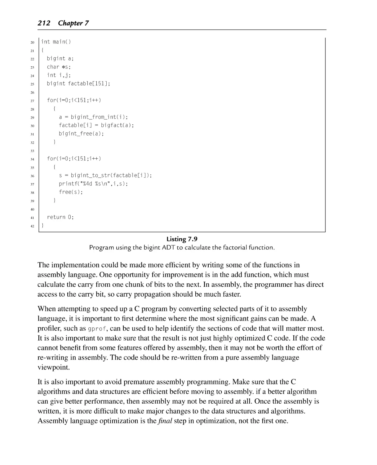
Program using the bigint ADT to calculate the factorial function
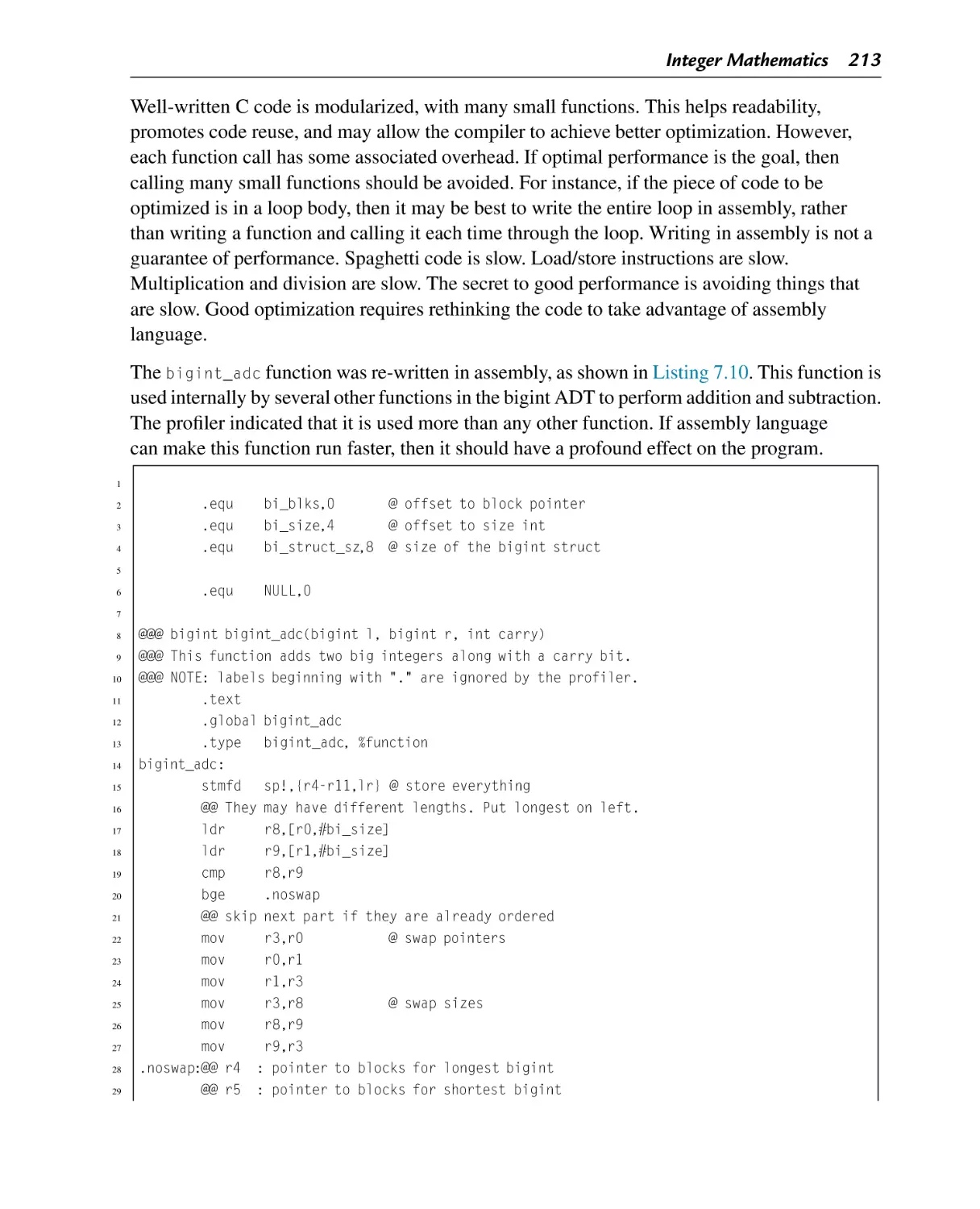
ARM assembly implementation if the bigint_adc function
Examples of fixed-point multiplication in ARM assembly
Dividing x by 23
Dividing x by 23 Using Only Shift and Add
Dividing x by −50
Inefficient representation of a binimal
Efficient representation of a binimal
ARM assembly implementation of sin x and cos x using fixed-point calculations
Example showing how the sin x and cos x functions can be used to print a table
Simple scalar implementation of the sin x function using IEEE single precision
Simple scalar implementation of the sin x function using IEEE double precision
Vector implementation of the sin x function using IEEE single precision
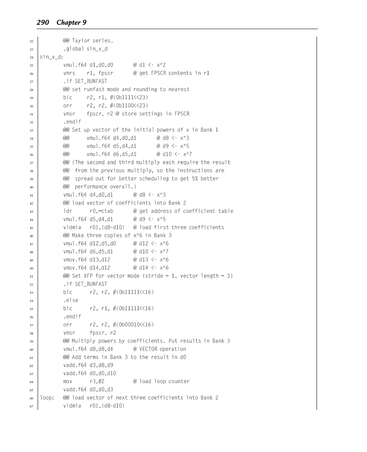
Vector implementation of the sin x function using IEEE double precision
NEON implementation of the sin x function using single precision
122
123
123
124
125
125
126
127
128
129
130
138
139
140
140
142
143
146
148
149
151
158
176
176
177
187
192
193
195
196
211
213
233
239
240
242
242
243
252
257
285
286
288
289
354
List of Listings xix
Listing 10.2
Listing 11.1
Listing 11.2
Listing 11.3
Listing 11.4
Listing 11.5
Listing 11.6
Listing 13.1
Listing 14.1
Listing 14.2
Listing 14.3
Listing 14.4
Listing 14.5
Listing 14.6
Listing 14.7
Listing 14.8
Listing 14.9
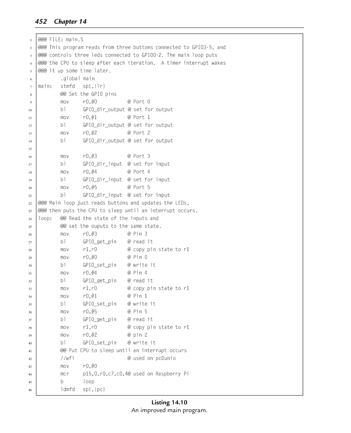
Listing 14.10
Listing 14.11
Listing 14.12
Listing 14.13
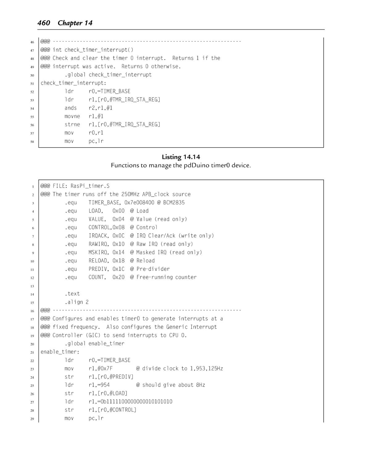
Listing 14.14
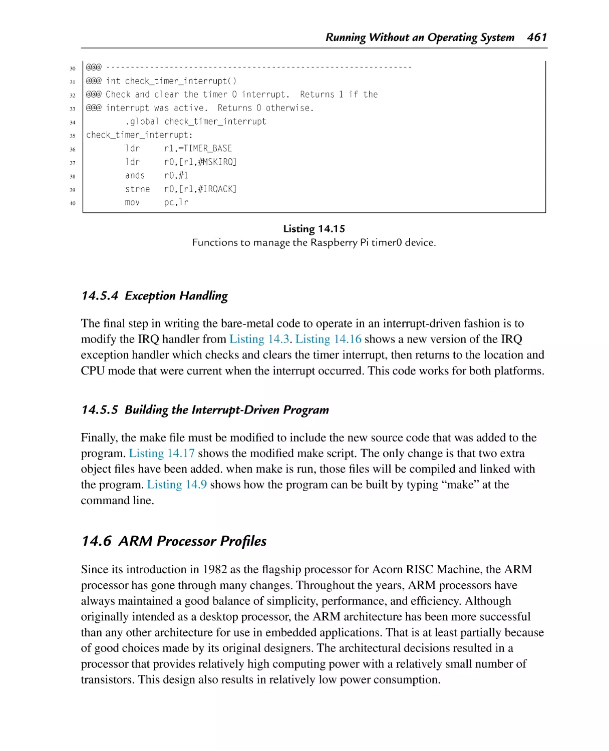
Listing 14.15
Listing 14.16
Listing 14.17
Listing 14.18
NEON implementation of the sin x function using double precision
Function to map devices into the user program memory on a Raspberry Pi
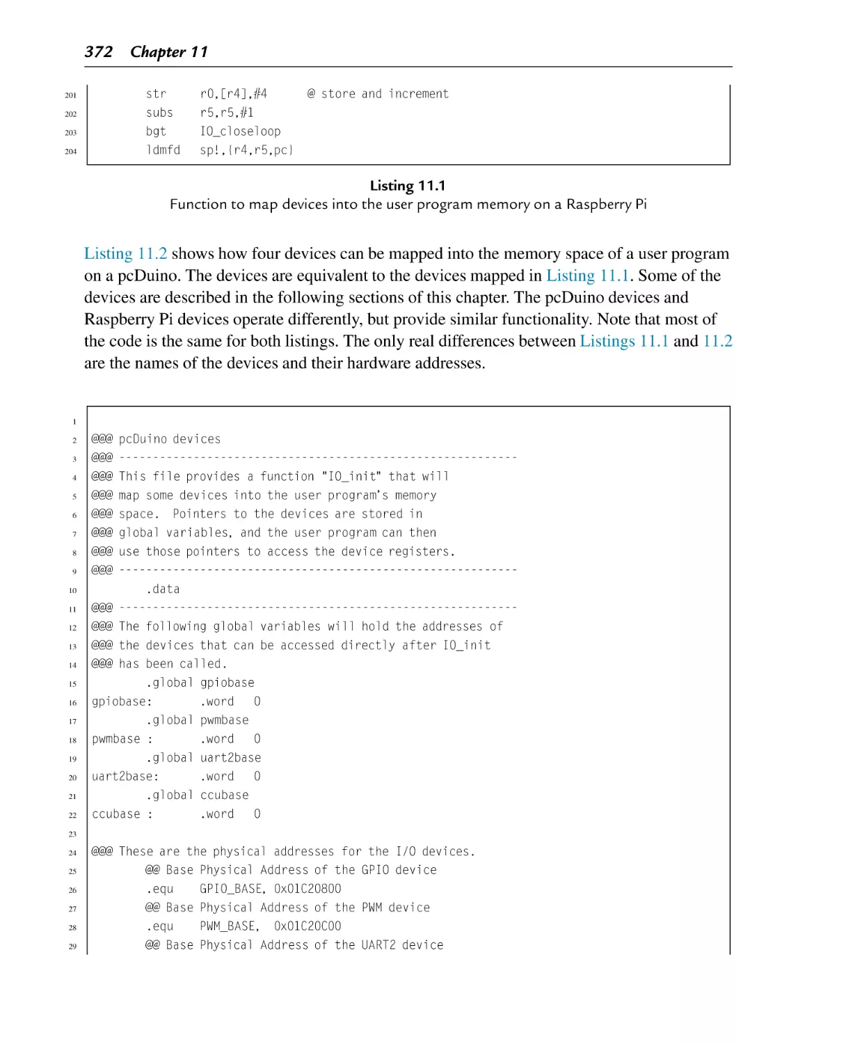
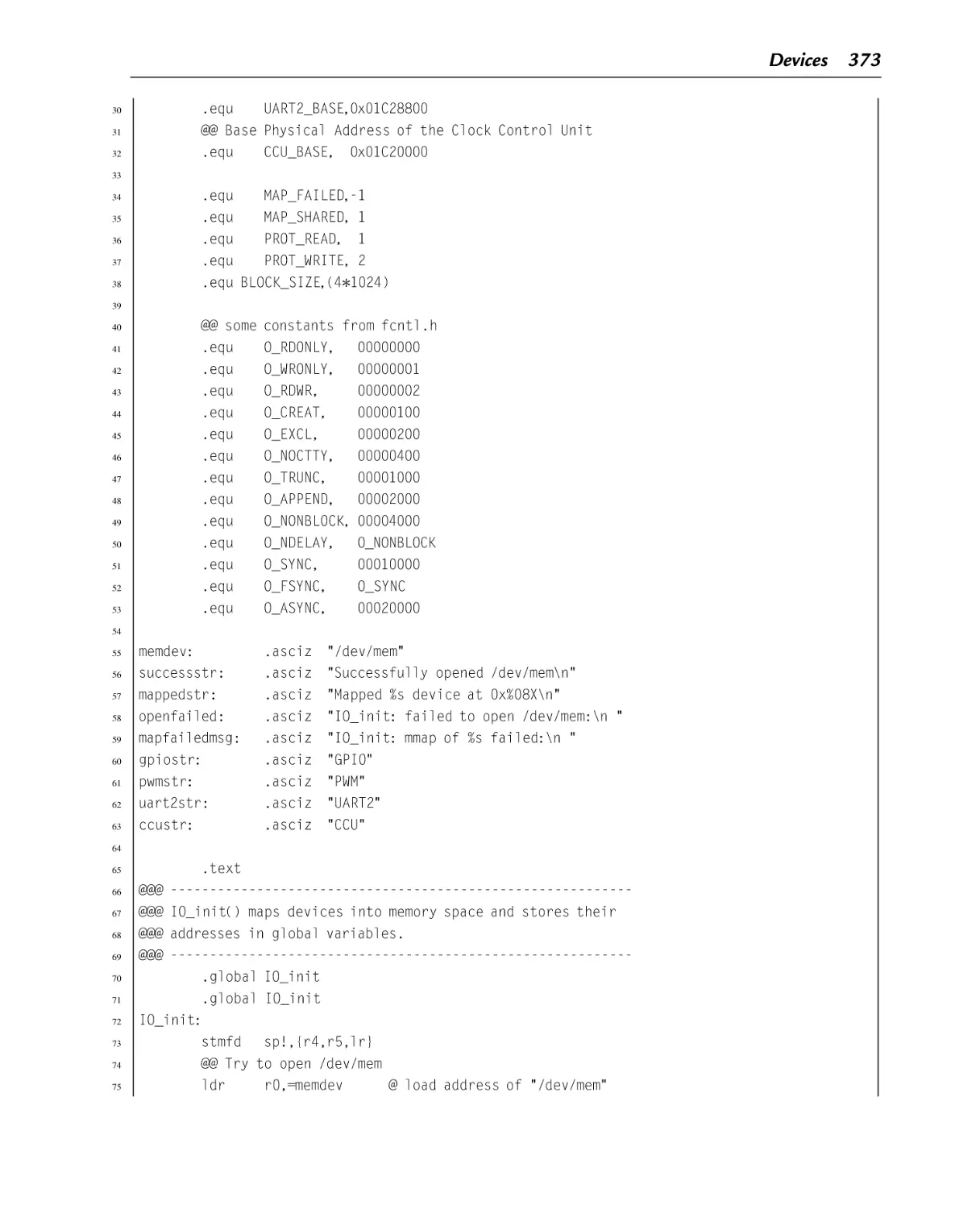
Function to map devices into the user program memory space on a pcDuino
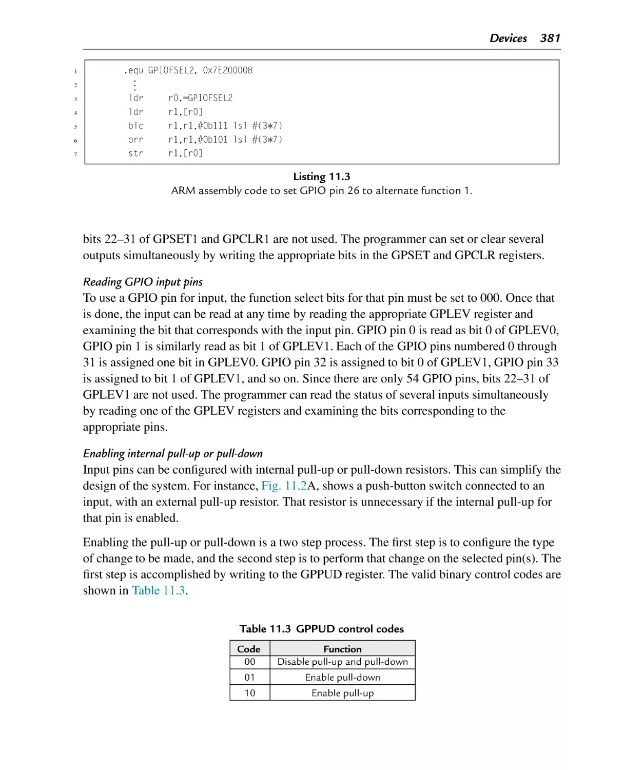
ARM assembly code to set GPIO pin 26 to alternate function 1
ARM assembly code to configure PA10 for output
ARM assembly code to set PA10 to output a high state
ARM assembly code to read the state of PI14 and set or clear the Z flag
Assembly functions for using the Raspberry Pi UART
Definitions for ARM CPU modes
Function to set up the ARM exception table
Stubs for the exception handlers
Skeleton for an exception handler
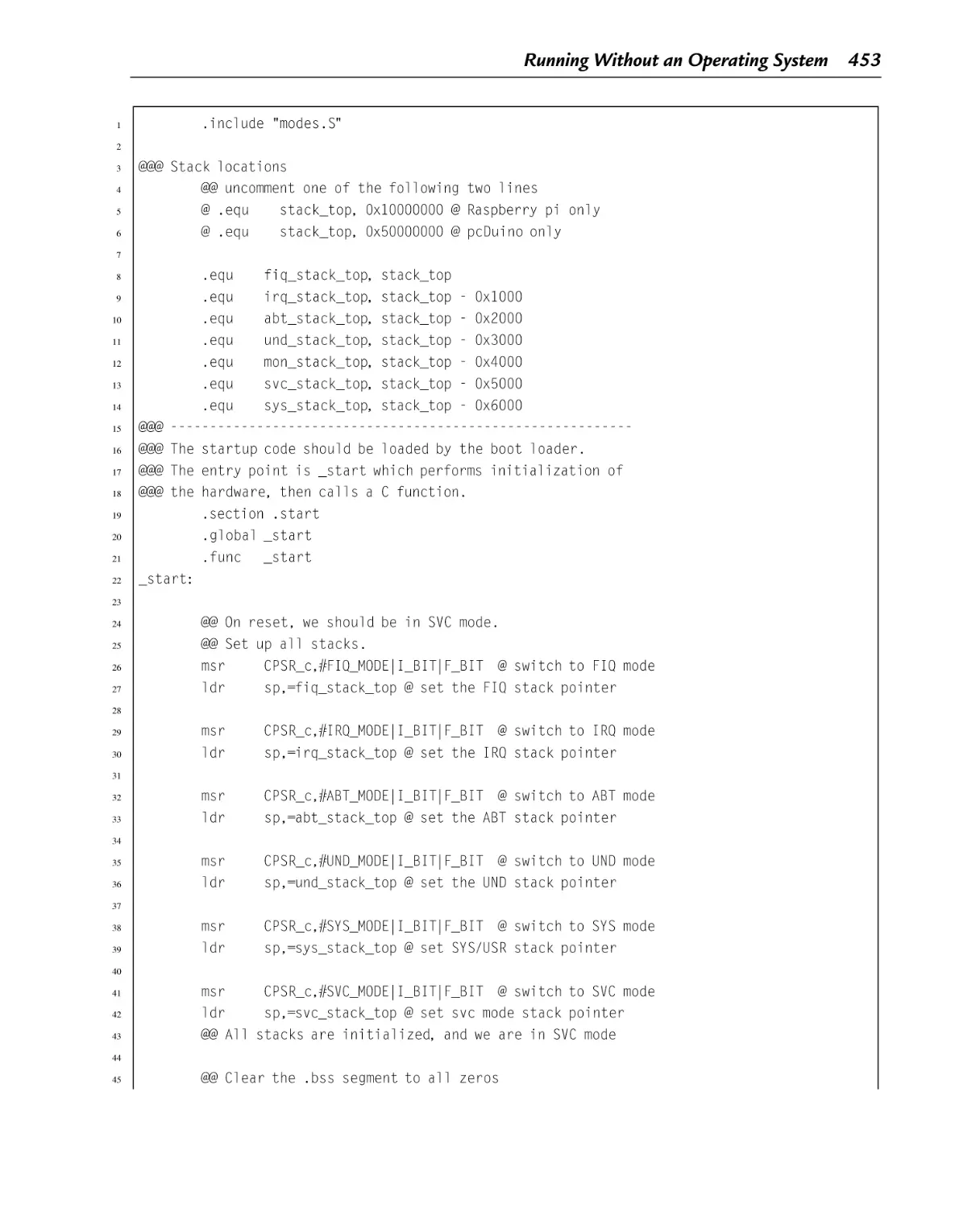
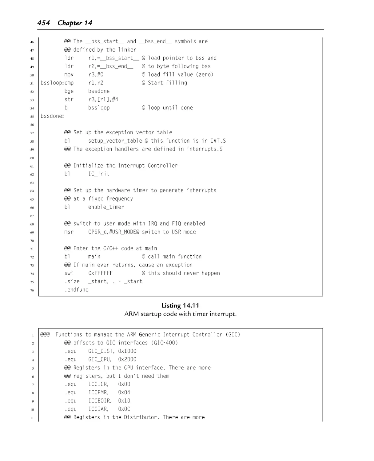
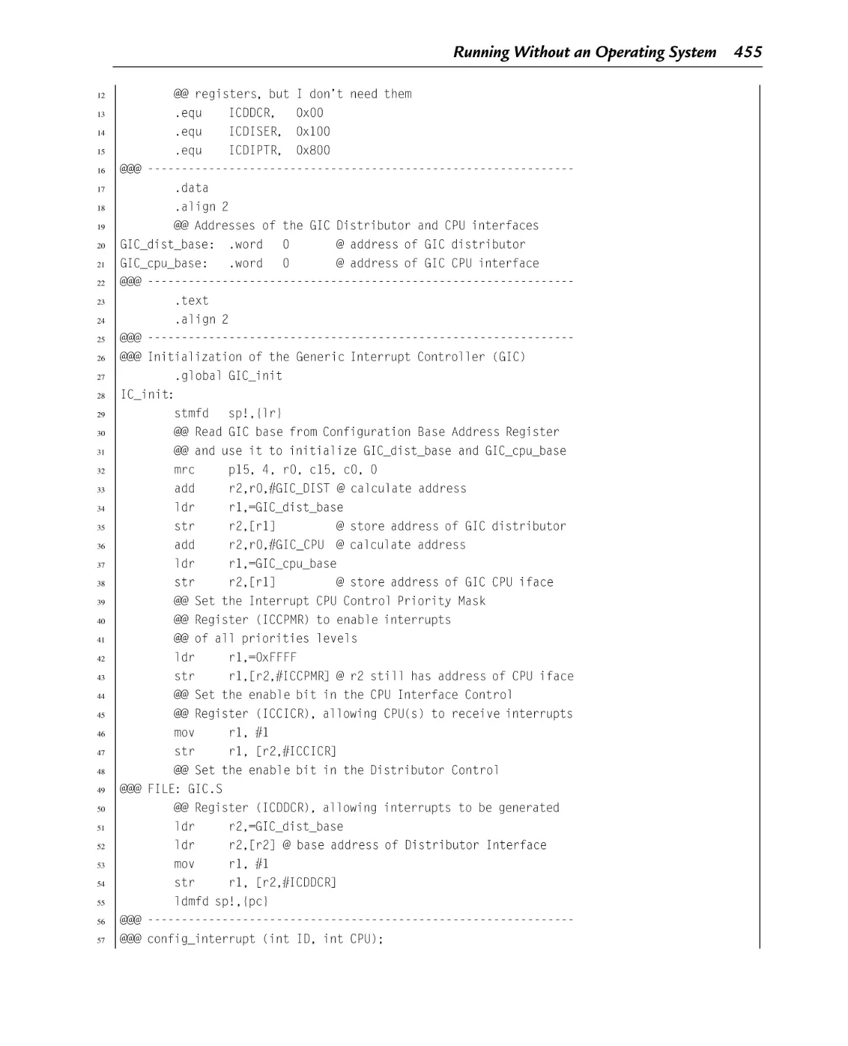
ARM startup code
A simple main program
A sample Gnu linker script
A sample make file
Running make to build the image
An improved main program
ARM startup code with timer interrupt
Functions to manage the pdDuino interrupt controller
Functions to manage the Raspberry Pi interrupt controller
Functions to manage the pdDuino timer0 device
Functions to manage the Raspberry Pi timer0 device
IRQ handler to clear the timer interrupt
A sample make file
Running make to build the image
355
367
372
381
388
389
389
418
435
439
440
441
443
446
448
450
451
452
453
454
457
459
460
462
463
464
This page intentionally left blank
Preface
This book is intended to be used in a first course in assembly language programming for
Computer Science (CS) and Computer Engineering (CE) students. It is assumed that students
using this book have already taken courses in programming and data structures, and are
competent programmers in at least one high-level language. Many of the code examples in the
book are written in C, with an assembly implementation following. The assembly examples
can stand on their own, but students who are familiar with C, C++, or Java should find the C
examples helpful.
Computer Science and Computer Engineering are very large fields. It is impossible to cover
everything that a student may eventually need to know. There are a limited number of course
hours available, so educators must strive to deliver degree programs that make a compromise
between the number of concepts and skills that the students learn and the depth at which they
learn those concepts and skills. Obviously, with these competing goals it is difficult to reach
consensus on exactly what courses should be included in a CS or CE curriculum.
Traditionally, assembly language courses have consisted of a mechanistic learning of a set of
instructions, registers, and syntax. Partially because of this approach, over the years, assembly
language courses have been marginalized in, or removed altogether from, many CS and CE
curricula. The author feels that this is unfortunate, because a solid understanding of assembly
language leads to better understanding of higher-level languages, compilers, interpreters,
architecture, operating systems, and other important CS an CE concepts.
One of the goals of this book is to make a course in assembly language more valuable by
introducing methods (and a bit of theory) that are not covered in any other CS or CE courses,
while using assembly language to implement the methods. In this way, the course in assembly
language goes far beyond the traditional assembly language course, and can once again play
an important role in the overall CS and CE curricula.
Choice of Processor Family
Because of their ubiquity, x86 based systems have been the platforms of choice for most
assembly language courses over the last two decades. The author believes that this is
xxi
xxii Preface
unfortunate, because in every respect other than ubiquity, the x86 architecture is the worst
possible choice for learning and teaching assembly language. The newer chips in the family
have hundreds of instructions, and irregular rules govern how those instructions can be used.
In an attempt to make it possible for students to succeed, typical courses use antiquated
assemblers and interface with the antiquated IBM PC BIOS, using only a small subset of the
modern x86 instruction set. The programming environment has little or no relevance to
modern computing.
Partially because of this tendency to use x86 platforms, and the resulting unnecessary burden
placed on students and instructors, as well as the reliance on antiquated and irrelevant
development environments, assembly language is often viewed by students as very difficult
and lacking in value. The author hopes that this textbook helps students to realize the value of
knowing assembly language. The relatively simple ARM processor family was chosen in
hopes that the students also learn that although assembly language programming may be more
difficult than high-level languages, it can be mastered.
The recent development of very low-cost ARM based Linux computers has caused a surge of
interest in the ARM architecture as an alternative to the x86 architecture, which has become
increasingly complex over the years. This book should provide a solution for a growing need.
Many students have difficulty with the concept that a register can hold variable x at one point
in the program, and hold variable y at some other point. They also often have difficulty with
the concept that, before it can be involved in any computation, data has to be moved from
memory into the CPU. Using a load-store architecture helps the students to more readily grasp
these concepts.
Another common difficulty that students have is in relating the concepts of an address and a
pointer variable. You can almost see the little light bulbs light up over their heads, when they
have the “eureka!” moment and realize that pointers are just variables that hold an address.
The author hopes that the approach taken in this book will make it easier for students to have
that “eureka!” moment. The author believes that load-store architectures make that realization
easier.
Many students also struggle with the concept of recursion, regardless of what language is
used. In assembly, the mechanisms involved are exposed and directly manipulated by the
programmer. Examples of recursion are scattered throughout this textbook. Again, the clean
architecture of the ARM makes it much easier for the students to understand what is going on.
Some students have difficulty understanding the flow of a program, and tend to put many
unnecessary branches into their code. Many assembly language courses spend so much time
and space on learning the instruction set that they never have time to teach good programming
practices. This textbook puts strong emphasis on using structured programming concepts. The
relative simplicity of the ARM architecture makes this possible.
Preface xxiii
One of the major reasons to learn and use assembly language is that it allows the programmer
to create very efficient mathematical routines. The concepts introduced in this book will
enable students to perform efficient non-integral math on any processor. These techniques are
rarely taught because of the time that it takes to cover the x86 instruction set. With the ARM
processor, less time is spent on the instruction set, and more time can be spent teaching how to
optimize the code.
The combination of the ARM processor and the Linux operating system provides the least
costly hardware platform and development environment available. A cluster of 10 Raspberry
Pis, or similar hosts, with power supplies and networking, can be assembled for 500 US
dollars or less. This cluster can support up to 50 students logging in through ssh. If their client
platform supports the X window system, then they can run GUI enabled applications.
Alternatively, most low-cost ARM systems can directly drive a display and take input from a
keyboard and mouse. With the addition of an NFS server (which itself could be a low-cost
ARM system and a hard drive), an entire Linux ARM based laboratory of 20 workstations
could be built for 250 US dollars per seat or less. Admittedly, it would not be a
high-performance laboratory, but could be used to teach C, assembly, and other languages.
The author would argue that inexperienced programmers should learn to program on
low-performance machines, because it reinforces a life-long tendency towards efficiency.
General Approach
The approach of this book is to present concepts in different ways throughout the book, slowly
building from simple examples towards complex programming on bare-metal embedded
systems. Students who don’t understand a concept when it is explained in a certain way may
easily grasp the concept when it is presented later from a different viewpoint.
The main objective of this book is to provide an improved course in assembly language by
replacing the x86 platform with one that is less costly, more ubiquitous, well-designed,
powerful, and easier to learn. Since students are able to master the basics of assembly
language quickly, it is possible to teach a wider range of topics, such as fixed and floating
point mathematics, ethical considerations, performance tuning, and interrupt processing. The
author hopes that courses using this book will better prepare students for the junior and senior
level courses in operating systems, computer architecture, and compilers.
This page intentionally left blank
Companion Website
Please visit the companion web site to access additional resources. Instructors may download
the author’s lecture slides and solution manual for the exercises. Students and instructors may
also access the laboratory manual and additional code examples. The author welcomes
suggestions for additional lecture slides, laboratory assignments, or other materials.
http://booksite.elsevier.com/9780128036983
xxv
This page intentionally left blank
Acknowledgments
I would like to thank Randy Warner for reading the manuscript, catching errors, and making
helpful suggestions. I would also like to thank the following students for suggesting exercises
with answers and catching numerous errors in the drafts: Zach Buechler, Preston Cook, Joshua
Daybrest, Matthew DeYoung, Josh Dodd, Matt Dyke, Hafiza Farzami, Jeremy Goens,
Lawrence Hoffman, Colby Johnson, Benjamin Kaiser, Lauren Keene, Jayson Kjenstad,
Murray LaHood-Burns, Derek Lane, Yanlin Li, Luke Meyer, Matthew Mielke, Forrest Miller,
Christopher Navarro, Girik Ranchhod, Josh Schweigert, Christian Sieh, Weston Silbaugh,
Jacob St. Amand, Njaal Tengesdal, Dylan Thoeny, Michael Vortherms, Dicheng Wu, and
Kekoa (Peter) Yamaguchi. Finally, I am also very grateful for my assistants, Scott Logan, Ian
Carlson, and Derek Stotz, who gave very valuable feedback during the writing of this book.
xxvii
This page intentionally left blank
PA R T I
Assembly as a Language
This page intentionally left blank
C H AP TER 1
Introduction
Chapter Outline
1.1 Reasons to Learn Assembly 4
1.2 The ARM Processor 8
1.3 Computer Data 9
1.3.1
1.3.2
1.3.3
1.3.4
Representing Natural Numbers 9
Base Conversion 11
Representing Integers 15
Representing Characters 20
1.4 Memory Layout of an Executing Program 28
1.5 Chapter Summary 31
An executable computer program is, ultimately, just a series of numbers that have very little or
no meaning to a human being. We have developed a variety of human-friendly languages in
which to express computer programs, but in order for the program to execute, it must
eventually be reduced to a stream of numbers. Assembly language is one step above writing
the stream of numbers. The stream of numbers is called the instruction stream. Each number
in the instruction stream instructs the computer to perform one (usually small) operation.
Although each instruction does very little, the ability of the programmer to specify any
sequence of instructions and the ability of the computer to perform billions of these small
operations every second makes modern computers very powerful and flexible tools. In
assembly language, one line of code usually gets translated into one machine instruction. In
high-level languages, a single line of code may generate many machine instructions.
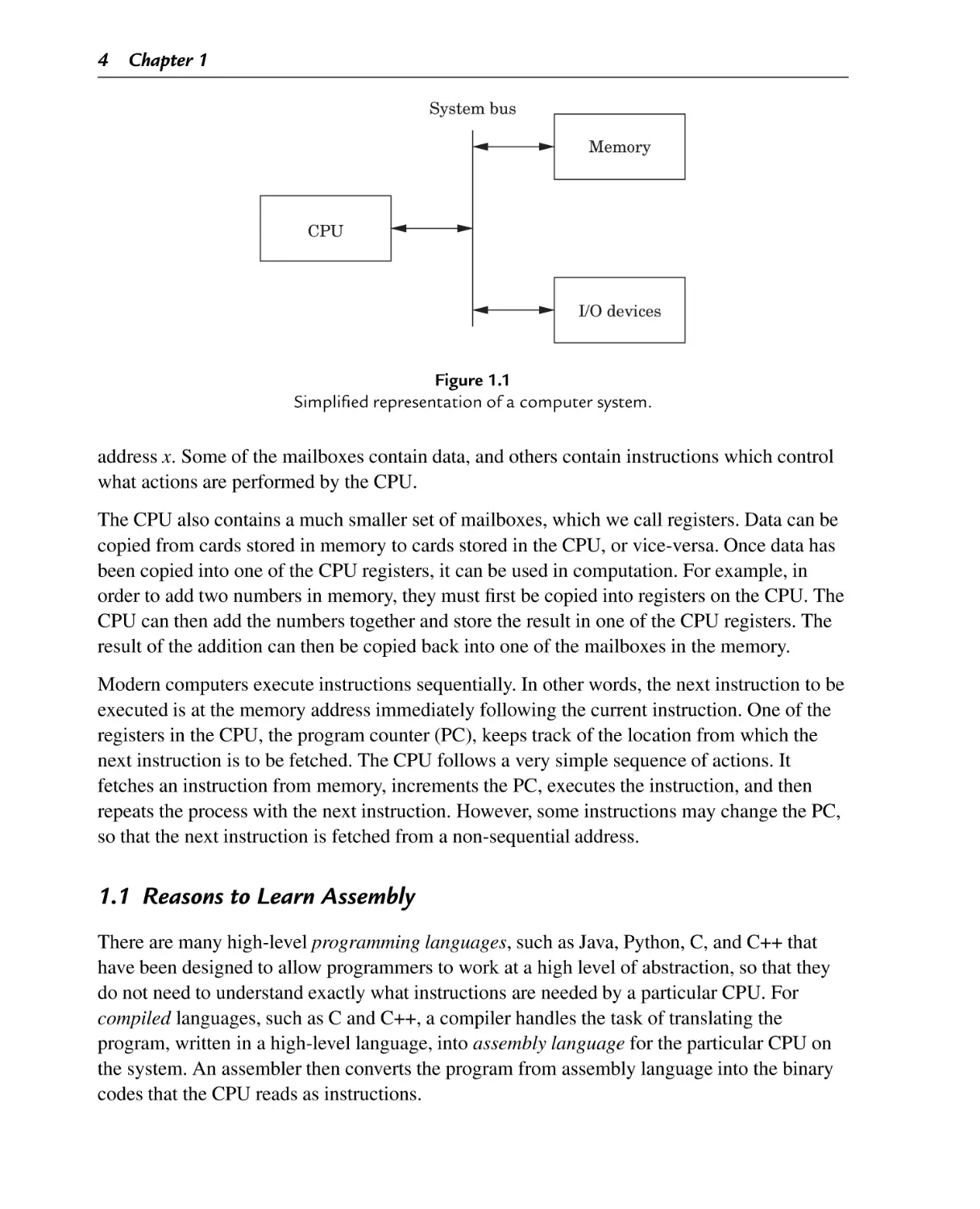
A simplified model of a computer system, as shown in Fig. 1.1, consists of memory,
input/output devices, and a central processing unit (CPU), connected together by a system bus.
The bus can be thought of as a roadway that allows data to travel between the components of
the computer system. The CPU is the part of the system where most of the computation
occurs, and the CPU controls the other devices in the system.
Memory can be thought of as a series of mailboxes. Each mailbox can hold a single postcard
with a number written on it, and each mailbox has a unique numeric identifier. The identifier, x
is called the memory address, and the number stored in the mailbox is called the contents of
Modern Assembly Language Programming with the ARM Processor. http://dx.doi.org/10.1016/B978-0-12-803698-3.00001-2
Copyright © 2016 Elsevier Inc. All rights reserved.
3
4 Chapter 1
System bus
Memory
CPU
I/O devices
Figure 1.1
Simplified representation of a computer system.
address x. Some of the mailboxes contain data, and others contain instructions which control
what actions are performed by the CPU.
The CPU also contains a much smaller set of mailboxes, which we call registers. Data can be
copied from cards stored in memory to cards stored in the CPU, or vice-versa. Once data has
been copied into one of the CPU registers, it can be used in computation. For example, in
order to add two numbers in memory, they must first be copied into registers on the CPU. The
CPU can then add the numbers together and store the result in one of the CPU registers. The
result of the addition can then be copied back into one of the mailboxes in the memory.
Modern computers execute instructions sequentially. In other words, the next instruction to be
executed is at the memory address immediately following the current instruction. One of the
registers in the CPU, the program counter (PC), keeps track of the location from which the
next instruction is to be fetched. The CPU follows a very simple sequence of actions. It
fetches an instruction from memory, increments the PC, executes the instruction, and then
repeats the process with the next instruction. However, some instructions may change the PC,
so that the next instruction is fetched from a non-sequential address.
1.1 Reasons to Learn Assembly
There are many high-level programming languages, such as Java, Python, C, and C++ that
have been designed to allow programmers to work at a high level of abstraction, so that they
do not need to understand exactly what instructions are needed by a particular CPU. For
compiled languages, such as C and C++, a compiler handles the task of translating the
program, written in a high-level language, into assembly language for the particular CPU on
the system. An assembler then converts the program from assembly language into the binary
codes that the CPU reads as instructions.
Introduction 5
High-level languages can greatly enhance programmer productivity. However, there are some
situations where writing assembly code directly is desirable or necessary. For example,
assembly language may be the best choice when writing
•
•
•
•
•
•
•
the first steps in booting the computer,
code to handle interrupts,
low-level locking code for multi-threaded programs,
code for machines where no compiler exists,
code which needs to be optimized beyond the limits of the compiler,
on computers with very limited memory, and
code that requires low-level access to architectural and/or processor features.
Aside from sheer necessity, there are several other reasons why it is still important for
computer scientists to learn assembly language.
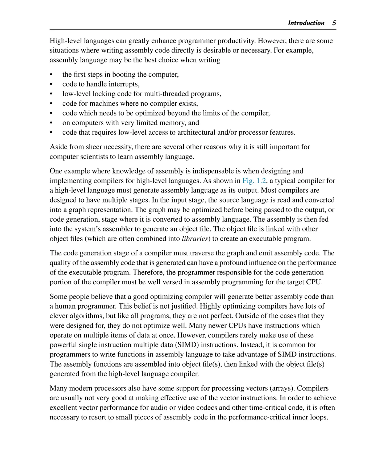
One example where knowledge of assembly is indispensable is when designing and
implementing compilers for high-level languages. As shown in Fig. 1.2, a typical compiler for
a high-level language must generate assembly language as its output. Most compilers are
designed to have multiple stages. In the input stage, the source language is read and converted
into a graph representation. The graph may be optimized before being passed to the output, or
code generation, stage where it is converted to assembly language. The assembly is then fed
into the system’s assembler to generate an object file. The object file is linked with other
object files (which are often combined into libraries) to create an executable program.
The code generation stage of a compiler must traverse the graph and emit assembly code. The
quality of the assembly code that is generated can have a profound influence on the performance
of the executable program. Therefore, the programmer responsible for the code generation
portion of the compiler must be well versed in assembly programming for the target CPU.
Some people believe that a good optimizing compiler will generate better assembly code than
a human programmer. This belief is not justified. Highly optimizing compilers have lots of
clever algorithms, but like all programs, they are not perfect. Outside of the cases that they
were designed for, they do not optimize well. Many newer CPUs have instructions which
operate on multiple items of data at once. However, compilers rarely make use of these
powerful single instruction multiple data (SIMD) instructions. Instead, it is common for
programmers to write functions in assembly language to take advantage of SIMD instructions.
The assembly functions are assembled into object file(s), then linked with the object file(s)
generated from the high-level language compiler.
Many modern processors also have some support for processing vectors (arrays). Compilers
are usually not very good at making effective use of the vector instructions. In order to achieve
excellent vector performance for audio or video codecs and other time-critical code, it is often
necessary to resort to small pieces of assembly code in the performance-critical inner loops.
6 Chapter 1
High-level
program
Other object
files
Lexical
analyzer
Linker
Executable
program
Object
file
Tokens
Parser
Assembler
Graph
representation
Optimizer
Optimized
graph
representation
Assembly
language
Code
generator
Figure 1.2
Stages of a typical compilation sequence.
A good example of this type of code is when performing vector and matrix multiplies. Such
operations are commonly needed in processing images and in graphical applications. The
ARM vector instructions are explained in Chapter 9.
Another reason for assembly is when writing certain parts of an operating system. Although
modern operating systems are mostly written in high-level languages, there are some portions
of the code that can only be done in assembly. Typical uses of assembly language are when
writing device drivers, saving the state of a running program so that another program can use
the CPU, restoring the saved state of a running program so that it can resume executing, and
managing memory and memory protection hardware. There are many other tasks central to a
modern operating system which can only be accomplished in assembly language. Careful
design of the operating system can minimize the amount of assembly required, but cannot
eliminate it completely.
Another good reason to learn assembly is for debugging. Simply understanding what is going
on “behind the scenes” of compiled languages such as C and C++ can be very valuable when
trying to debug programs. If there is a problem in a call to a third party library, sometimes the
Introduction 7
only way a developer can isolate and diagnose the problem is to run the program under a
debugger and step through it one machine instruction at a time. This does not require a deep
knowledge of assembly language coding but at least a passing familiarity with assembly is
helpful in that particular case. Analysis of assembly code is an important skill for C and C++
programmers, who may occasionally have to diagnose a fault by looking at the contents of
CPU registers and single-stepping through machine instructions.
Assembly language is an important part of the path to understanding how the machine works.
Even though only a small percentage of computer scientists will be lucky enough to work on
the code generator of a compiler, they all can benefit from the deeper level of understanding
gained by learning assembly language. Many programmers do not really understand pointers
until they have written assembly language.
Without first learning assembly language, it is impossible to learn advanced concepts such as
microcode, pipelining, instruction scheduling, out-of-order execution, threading, branch
prediction, and speculative execution. There are many other concepts, especially when dealing
with operating systems and computer architecture, which require some understanding of
assembly language. The best programmers understand why some language constructs perform
better than others, how to reduce cache misses, and how to prevent buffer overruns that
destroy security.
Every program is meant to run on a real machine. Even though there are many languages,
compilers, virtual machines, and operating systems to enable the programmer to use the
machine more conveniently, the strengths and weaknesses of that machine still determine what
is easy and what is hard. Learning assembly is a fundamental part of understanding enough
about the machine to make informed choices about how to write efficient programs, even
when writing in a high-level language.
As an analogy, most people do not need to know a lot about how an internal combustion engine
works in order to operate an automobile. A race car driver needs a much better understanding of
exactly what happens when he or she steps on the accelerator pedal in order to be able to judge
precisely when (and how hard) to do so. Also, who would trust their car to a mechanic who
could not tell the difference between a spark plug and a brake caliper? Worse still, should we
trust an engineer to build a car without that knowledge? Even in this day of computerized cars,
someone needs to know the gritty details, and they are paid well for that knowledge. Knowledge
of assembly language is one of the things that defines the computer scientist and engineer.
When learning assembly language, the specific instruction set is not critically important,
because what is really being learned is the fine detail of how a typical stored-program machine
uses different storage locations and logic operations to convert a string of bits into a meaningful
calculation. However, when it comes to learning assembly languages, some processors
make it more difficult than it needs to be. Because some processors have an instruction
set that is extremely irregular, non-orthogonal, large, and poorly designed, they are not a
8 Chapter 1
good choice for learning assembly. The author feels that teaching students their first assembly
language on one of those processors should be considered a crime, or at least a form of
mental abuse. Luckily, there are processors that are readily available, low-cost, and relatively
easy to learn assembly with. This book uses one of them as the model for assembly language.
1.2 The ARM Processor
In the late 1970s, the microcomputer industry was a fierce battleground, with several
companies competing to sell computers to small business and home users. One of those
companies, based in the United Kingdom, was Acorn Computers Ltd. Acorn’s flagship
product, the BBC Micro, was based on the same processor that Apple Computer had chosen
for their Apple IITM line of computers; the 8-bit 6502 made by MOS Technology. As the
1980s approached, microcomputer manufacturers were looking for more powerful 16-bit and
32-bit processors. The engineers at Acorn considered the processor chips that were available
at the time, and concluded that there was nothing available that would meet their needs for the
next generation of Acorn computers.
The only reasonably-priced processors that were available were the Motorola 68000
(a 32-bit processor used in the Apple Macintosh and most high-end Unix workstations)
and the Intel 80286 (a 16-bit processor used in less powerful personal computers
such as the IBM PC). During the previous decade, a great deal of research had been conducted
on developing high-performance computer architectures. One of the outcomes of that research
was the development of a new paradigm for processor design, known as Reduced Instruction
Set Computing (RISC). One advantage of RISC processors was that they could deliver higher
performance with a much smaller number of transistors than the older Complex Instruction Set
Computing (CISC) processors such as the 68000 and 80286. The engineers at Acorn decided to
design and produce their own processor. They used the BBC Micro to design and simulate their
new processor, and in 1987, they introduced the Acorn ArchimedesTM . The ArchimedesTM
was arguably the most powerful home computer in the world at that time, with graphics
and audio capabilities that IBM PCTM and Apple MacintoshTM users could only dream about.
Thus began the long and successful dynasty of the Acorn RISC Machine (ARM) processor.
Acorn never made a big impact on the global computer market. Although Acorn eventually
went out of business, the processor that they created has lived on. It was re-named to the
Advanced RISC Machine, and is now known simply as ARM. Stewardship of the ARM
processor belongs to ARM Holdings, LLC which manages the design of new ARM
architectures and licenses the manufacturing rights to other companies. ARM Holdings does
not manufacture any processor chips, yet more ARM processors are produced annually than
all other processor designs combined. Most ARM processors are used as components for
embedded systems and portable devices. If you have a smart phone or similar device, then
there is a very good chance that it has an ARM processor in it. Because of its enormous
market presence, clean architecture, and small, orthogonal instruction set, the ARM is a very
good choice for learning assembly language.
Introduction 9
Although it dominates the portable device market, the ARM processor has almost no presence
in the desktop or server market. However, that may change. In 2012, ARM Holdings
announced the ARM64 architecture, which is the first major redesign of the ARM architecture
in 30 years. The ARM64 is intended to compete for the desktop and server market with other
high-end processors such as the Sun SPARC and Intel Xeon. Regardless of whether or not the
ARM64 achieves much market penetration, the original ARM 32-bit processor architecture is
so ubiquitous that it clearly will be around for a long time.
1.3 Computer Data
The basic unit of data in a digital computer is the binary digit, or bit. A bit can have a value of
zero or one. In order to store numbers larger than 1, bits are combined into larger units. For
instance, using two bits, it is possible to represent any number between zero and three. This is
shown in Table 1.1. When stored in the computer, all data is simply a string of binary digits.
There is more than one way that such a fixed-length string of binary digits can be interpreted.
Computers have been designed using many different bit group sizes, including 4, 8, 10, 12,
and 14 bits. Today most computers recognize a basic grouping of 8 bits, which we call a byte.
Some computers can work in units of 4 bits, which is commonly referred to as a nibble
(sometimes spelled “nybble”). A nibble is a convenient size because it can exactly represent
one hexadecimal digit. Additionally, most modern computers can also work with groupings of
16, 32 and 64 bits. The CPU is designed with a default word size. For most modern CPUs, the
default word size is 32 bits. Many processors support 64-bit words, which is increasingly
becoming the default size.
1.3.1 Representing Natural Numbers
A numeral system is a writing system for expressing numbers. The most common system is
the Hindu-Arabic number system, which is now used throughout the world. Almost from the
first day of formal education, children begin learning how to add, subtract, and perform other
operations using the Hindu-Arabic system. After years of practice, performing basic
mathematical operations using strings of digits between 0 and 9 seems natural. However, there
are other ways to count and perform arithmetic, such as Roman numerals, unary systems, and
Chinese numerals. With a little practice, it is possible to become as proficient at performing
mathematics with other number systems as with the Hindu-Arabic system.
Table 1.1 Values represented by two bits
Bit 1
0
0
1
1
Bit 0
0
1
0
1
Value
0
1
2
3
10 Chapter 1
The Hindu-Arabic system is a base ten or radix ten system, because it uses the ten digits 0, 1,
2, 3, 4, 5, 6, 7, 8, and 9. For our purposes, the words radix and base are equivalent, and refer to
the number of individual digits available in the numbering system. The Hindu-Arabic system
is also a positional system, or a place-value notation, because the value of each digit in a
number depends on its position in the number. The radix ten Hindu-Arabic system is only one
of an infinite family of closely related positional systems. The members of this family differ
only in the radix used (and therefore, the number of characters used). For bases greater than
base ten, characters are borrowed from the alphabet and used to represent digits. For example,
the first column in Table 1.2 shows the character “A” being used as a single digit
representation for the number 10.
In base ten, we think of numbers as strings of the 10 digits, “0”–“9”. Each digit counts 10
times the amount of the digit to its right. If we restrict ourselves to integers, then the digit
furthest to the right is always the ones digit. It is also referred to as the least significant digit.
The digit immediately to the left of the ones digit is the tens digit. To the left of that is the
hundreds digit, and so on. The leftmost digit is referred to as the most significant digit. The
following equation shows how a number can be decomposed into its constituent digits:
5783910 = 5 × 10⁴ + 7 × 10³ + 8 × 10² + 3 × 101 + 9 × 100 .
Note that the subscript of “10” on 5783910 indicates that the number is given in base ten.
Table 1.2 The first 21 integers (starting with 0) in various bases
16
0
1
2
3
4
5
6
7
8
9
A
B
C
D
E
F
10
11
12
13
14
10
0
1
2
3
4
5
6
7
8
9
10
11
12
13
14
15
16
17
18
19
20
9
0
1
2
3
4
5
6
7
8
10
11
12
13
14
15
16
17
18
20
21
22
8
0
1
2
3
4
5
6
7
10
11
12
13
14
15
16
17
20
21
22
23
24
7
0
1
2
3
4
5
6
10
11
12
13
14
15
16
20
21
22
23
24
25
26
Base
6
0
1
2
3
4
5
10
11
12
13
14
15
20
21
22
23
24
25
30
31
32
5
0
1
2
3
4
10
11
12
13
14
20
21
22
23
24
30
31
32
33
34
40
4
0
1
2
3
10
11
12
13
20
21
22
23
30
31
32
33
100
101
102
103
110
3
0
1
2
10
11
12
20
21
22
100
101
102
110
111
112
120
121
122
200
201
201
2
0
1
10
11
100
101
110
111
1000
1001
1010
1011
1100
1101
1110
1111
10000
10001
10010
10011
10100
Introduction 11
Imagine that we only had 7 digits: 0, 1, 2, 3, 4, 5, and 6. We need 10 digits for base ten, so
with only 7 digits we are limited to base seven. In base seven, each digit in the string
represents a power of seven rather than a power of ten. We can represent any integer in base
seven, but it may take more digits than in base ten. Other than using a different base for the
power of each digit, the math works exactly the same as for base ten. For example, suppose we
have the following number in base seven: 3304257. We can convert this number to base ten
as follows:
3304257 = 3 × 75 + 3 × 74 + 0 × 73 + 4 × 72 + 2 × 71 + 5 × 70
= 5042110 + 720310 + 010 + 19610 + 1410 + 510
= 5783910
Base two, or binary is the “native” number system for modern digital systems. The reason for
this is mainly because it is relatively easy to build circuits with two stable states: on and off (or
1 and 0). Building circuits with more than two stable states is much more difficult and
expensive, and any computation that can be performed in a higher base can also be performed
in binary. The least significant (rightmost) digit in binary is referred to as the least
significant bit, or LSB, while the leftmost binary digit is referred to as the most significant bit,
or MSB.
1.3.2 Base Conversion
The most common bases used by programmers are base two (binary), base eight (octal), base
ten (decimal) and base sixteen (hexadecimal). Octal and hexadecimal are common because, as
we shall see later, they can be translated quickly and easily to and from base two, and are often
easier for humans to work with than base two. Note that for base sixteen, we need 16
characters. We use the digits 0 through 9 plus the letters A through F. Table 1.2 shows the
equivalents for all numbers between 0 and 20 in base two through base ten, and base sixteen.
Before learning assembly language it is essential to know how to convert from any base to any
other base. Since we are already comfortable working in base ten, we will use that as an
intermediary when converting between two arbitrary bases. For instance, if we want to convert
a number in base three to base five, we will do it by first converting the base three number to
base ten, then from base ten to base five. By using this two-stage process, we will only need to
learn to convert between base ten and any arbitrary base b.
Base b to decimal
Converting from an arbitrary base b to base ten simply involves multiplying each base b digit
d by bn , where n is the significance of digit d, and summing all of the results. For example,
converting the base five number 34215 to base ten is performed as follows:
12 Chapter 1
34215 = 3 × 53 + 4 × 52 + 2 × 51 + 1 × 50
= 37510 + 10010 + 1010 + 110
= 48610
This conversion procedure works for converting any integer from any arbitrary base b to its
equivalent representation in base ten. Example 1.1 gives another specific example of how to
convert from base b to base ten.
Example 1.1
Converting From an Arbitrary Base to Base Ten
Converting 73625 to base ten is accomplished by expanding and summing the terms:
73625 = 7 × 53 + 3 × 52 + 6 × 51 + 2 × 50
= 7 × 125 + 3 × 25 + 6 × 5 + 2 × 1
= 875 + 75 + 30 + 2
= 98210
Decimal to base b
Converting from base ten to an arbitrary base b involves repeated division by the base, b. After
each division, the remainder is used as the next more significant digit in the base b number,
and the quotient is used as the dividend for the next iteration. The process is repeated until the
quotient is zero. For example, converting 5610 to base four is accomplished as follows:
14→ 3→ 0
4 56 4 14 4 3
40
12
16
2
16
0
Reading the remainders from right to left yields: 3204 . This result can be double-checked by
converting it back to base ten as follows:
3204 = 3 × 42 + 2 × 41 + 0 × 40
= 48 + 8 + 0
= 5610 .
Since we arrived at the same number we started with, we have verified that 5610 = 3204 . This
conversion procedure works for converting any integer from base ten to any arbitrary base b.
Example 1.2 gives another example of converting from base ten to another base b.
Introduction 13
Example 1.2 Converting from Base Ten to an Arbitrary Base
Converting 834110 to base seven is accomplished as follows:
1191 → 170 → 24 → 3 → 0
7 8341
7 1191
7 170
7 24
7 3
7000
700
140
21
1341
491
30
3
700
490
28
641
1
2
630
11
7
4
834110 = 332147
Conversion between arbitrary bases
Although it is possible to perform the division and multiplication steps in any base, most
people are much better at working in base ten. For that reason, the easiest way to convert from
any base a to any other base b is to use a two step process. First step is to convert from base a
to decimal. The second step is to convert from decimal to base b. Example 1.3 shows how to
convert from any base to any other base.
Example 1.3 Converting from an Arbitrary Base to Another Arbitrary Base
Converting 848343 to base 11 is accomplished with two steps.
The number is first converted to base ten as follows:
848353 = 8 × 34 + 4 × 33 + 8 × 32 + 3 × 31 + 4 × 30
= 8 × 81 + 4 × 27 + 8 × 9 + 3 × 3 + 4 × 1
= 648 + 108 + 72 + 9 + 4
= 84110
Then the result is converted to base 11:
76 →
6→
0
11 841
11 76
11 6
770
66
71
10
66
5
848343 = 84110 = 6A511
14 Chapter 1
Bases that are powers-of-two
In addition to the methods above, there is a simple method for quickly converting between
base two, base eight, and base sixteen. These shortcuts rely on the fact that 2, 8, and 16 are all
powers of two. Because of this, it takes exactly four binary digits (bits) to represent exactly
one hexadecimal digit. Likewise, it takes exactly three bits to represent an octal digit.
Conversely, each hexadecimal digit can be converted to exactly four binary digits, and each
octal digit can be converted to exactly three binary digits. This relationship makes it possible
to do very fast conversions using the tables shown in Fig. 1.3.
When converting from hexadecimal to binary, all that is necessary is to replace each hex digit
with the corresponding binary digits from the table. For example, to convert 5AC416 to binary,
we just replace “5” with “0101,” replace “A” with “1010,” replace “C” with “1100,” and
replace “4” with “0100.” So, just by referring to the table, we can immediately see that
5AC416 = 01011010110001002. This method works exactly the same for converting from
octal to binary, except that it uses the table on the right side of Fig. 1.3.
Base 2
Base 16
0000
0001
0
1
0010
0011
2
3
Base 2
Base 8
0100
0101
4
5
000
001
0
1
0110
0111
6
7
010
011
2
3
1000
1001
8
9
100
101
4
5
1010
A
110
6
1011
1100
B
C
111
7
1101
1110
D
E
1111
F
Figure 1.3
Tables used for converting between binary, octal, and hex.
Introduction 15
Converting from binary to hexadecimal is also very easy using the table. Given a binary
number, n, take the four least significant digits of n and find them in the table on the left side of
Fig. 1.3. The hexadecimal digit on the matching line of the table is the least significant hex digit.
Repeat the process with the next set of four bits and continue until there are no bits remaining
in the binary number. For example, to convert 00111001010101112 to hexadecimal, just
divide the number into groups of four bits, starting on the right, to get: 0011|1001|0101|01112.
Now replace each group of four bits by looking up the corresponding hex digit in
the table on the left side of Fig. 1.3, to convert the binary number to 395716. In the case where
the binary number does not have enough bits, simply pad with zeros in the high-order bits. For
example, dividing the number 10011000100112 into groups of four yields 1|0011|0001|00112
and padding with zeros in the high-order bits results in 0001|0011|0001|00112.
Looking up the four groups in the table reveals that 0001|0011|0001|00112 = 131316.
1.3.3 Representing Integers
The computer stores groups of bits, but the bits by themselves have no meaning. The
programmer gives them meaning by deciding what the bits represent, and how they are
interpreted. Interpreting a group of bits as unsigned integer data is relatively simple. Each bit
is weighted by a power-of-two, and the value of the group of bits is the sum of the non-zero
bits multiplied by their respective weights. However, programmers often need to represent
negative as well as non-negative numbers, and there are many possibilities for storing and
interpreting integers whose value can be both positive and negative. Programmers and
hardware designers have developed several standard schemes for encoding such numbers. The
three main methods for storing and interpreting signed integer data are two’s complement,
sign-magnitude, and excess-N, Fig. 1.4 shows how the same binary pattern of bits can be
interpreted as a number in four different ways.
Sign-magnitude representation
The sign-magnitude representation simply reserves the most significant bit to represent the
sign of the number, and the remaining bits are used to store the magnitude of the number. This
method has the advantage that it is easy for humans to interpret, with a little practice.
However, addition and subtraction are slightly complicated. The addition/subtraction logic
must compare the sign bits, complement one of the inputs if they are different, implement an
end-around carry, and complement the result if there was no carry from the most significant
bit. Complements are explained in Section 1.3.3. Because of the complexity, most integer
CPUs do not directly support addition and subtraction of integers in sign-magnitude form.
However, this method is commonly used for mantissa in floating-point numbers, as will be
explained in Chapter 8. Another drawback to sign-magnitude is that it has two representations
for zero, which can cause problems if the programmer is not careful.
16 Chapter 1
Binary
Unsigned
Sign
Magnitude
Excess-127
Two’s
Complement
00000000
00000001
..
.
0
1
..
.
0
1
..
.
-127
-126
..
.
0
1
..
.
01111110
126
126
-1
126
01111111
10000000
127
128
127
-0
0
1
127
-128
10000001
..
.
129
..
.
-1
..
.
2
..
.
-127
..
.
11111110
11111111
254
255
-126
-127
127
128
-2
-1
Figure 1.4
Four different representations for binary integers.
Excess-(2n−1 − 1) representation
Another method for representing both positive and negative numbers is by using an excess-N
representation. With this representation, the number that is stored is N greater than the actual
value. This representation is relatively easy for humans to interpret. Addition and subtraction
are easily performed using the complement method, which is explained in Section 1.3.3. This
representation is just the same as unsigned math, with the addition of a bias which is usually
(2n−1 − 1). So, zero is represented as zero plus the bias. In n = 12 bits, the bias is
212−1 − 1 = 204710 , or 0111111111112. This method is commonly used to store the exponent
in floating-point numbers, as will be explained in Chapter 8.
Complement representation
A very efficient method for dealing with signed numbers involves representing negative
numbers as the radix complements of their positive counterparts. The complement is the
amount that must be added to something to make it “whole.” For instance, in geometry, two
angles are complementary if they add to 90◦ . In radix mathematics, the complement of
a digit x in base b is simply b − x. For example, in base ten, the complement of 4 is
10 − 4 = 6.
In complement representation, the most significant digit of a number is reserved to indicate
whether or not the number is negative. If the first digit is less than b2 (where b is the radix),
then the number is positive. If the first digit is greater than or equal to b2 , then the number is
Introduction 17
negative. The first digit is not part of the magnitude of the number, but only indicates the sign
of the number. For example, numbers in ten’s complement notation are positive if the first
digit is less than 5, and negative if the first digit is greater than 4. This works especially well in
binary, since the number is considered positive if the first bit is zero and negative if the first bit
is one. The magnitude of a negative number can be obtained by taking the radix complement.
Because of the nice properties of the complement representation, it is the most common
method for representing signed numbers in digital computers.
Finding the complement: The radix complement of an n digit number y in radix (base) b is
defined as
C(yb ) = bn − yb .
(1.1)
For example, the ten’s complement of the four digit number 873410 is 104 − 8734 = 1266. In
this example, we directly applied the definition of the radix complement from Eq. (1.1). That
is easy in base ten, but not so easy in an arbitrary base, because it involves performing a
subtraction. However, there is a very simple method for calculating the complement which
does not require subtraction. This method involves finding the diminished radix complement,
which is (bn − 1) − y by substituting each digit with its complement from a complement table.
The radix complement is found by adding one to the diminished radix complement. Fig. 1.5
shows the complement tables for bases ten and two. Examples 1.4 and 1.5 show how the
complement is obtained in bases ten and two respectively. Examples 1.6 and 1.7 show
additional conversions between binary and decimal.
Nine’s Complement
Table
0
9
1
8
2
7
3
6
4
5
0
1
5
4
1
0
6
3
7
2
8
1
9
0
One’s Complement
Table
Figure 1.5
Complement tables for bases ten and two.
18 Chapter 1
Example 1.4
The Complement in Base Ten
The nine’s complement of the base ten number 593 is found by finding the digit ‘5’ in the
complement table, and replacing it with its complement, which is the digit ‘4.’ The digit ‘9’
is replaced with ‘0,’ and ‘3’ is replaced with ‘6.’ Therefore the nine’s complement of 59310
is 406. Likewise, the nine’s complement of 100010 is 899910 and the nine’s complement of
099910 is 900010 .
The ten’s complement of 72610 is 27310 + 1 = 27410 .
Example 1.5
The One’s and Two’s Complement
The one’s complement of a binary number is found in the same way as the nine’s
complement of a decimal number, but using the one’s complement table instead of the
nine’s complement table. The one’s complement of 010011012 is 101100102 and the
one’s complement of 0000000010110110 is 11111111010010012. Note that the one’s
complement of a base two number is equivalent to the bitwise logical “not” (Boolean
complement) operator. This operator is very easy to implement in digital hardware.
The two’s complement is the one’s complement plus one. The two’s complement of
10101002 is 01010112 + 1 = 01011002 .
Example 1.6
Conversion from Binary to Decimal
Suppose we want to convert a signed binary number to decimal.
1. If the most significant bit is ‘1’, then
a. Find the two’s complement
b. Convert the result to base 10
c. Add a negative sign
2. else
a. Convert the result to base 10
Number
11010010
1111111100010110
01110100
1000001101010110
0101001111011011
One’s Complement
00101101
0000000011101001
Not negative
0111110010101001
Not negative
Two’s Complement
00101110
0000000011101010
0111110010101010
Base 10
46
234
116
31914
21467
Negative
−46
−234
−31914
Introduction 19
Example 1.7 Conversion from Decimal to Binary
Suppose we want to convert a negative number from decimal to binary.
1. Remove the negative sign
2. Convert the number to binary
3. Take the two’s complement
Base 10
-46
-234
-116
-31914
-21467
Positive Binary
00101110
0000000011101010
01110100
0111110010101010
0101001111011011
One’s Complement
11010001
1111111100010101
10001011
1000001101010110
1010110000100100
Two’s Complement
11010010
1111111100010110
10001100
1000001101010111
1010110000100101
Subtraction using complements One very useful feature of complement notation is that it can
be used to perform subtraction by using addition. Given two numbers in base b, xb , and yb , the
difference can be computed as:
zb = xb − yb
(1.2)
n
= xb + (b − yb ) − b
= xb + C(yb ) − bn ,
n
(1.3)
(1.4)
where C(yb ) is the radix complement of yb . Assume that xb and yb are both positive where
yb ≤ xb and both numbers have the same number of digits n (yb may have leading zeros). In
this case, the result of xb + C(yb ) will always be greater than or equal to bn , but less than
2 × bn . This means that the result of xb + C(yb ) will always begin with a ‘1’ in the n + 1 digit
position. Dropping the initial ‘1’ is equivalent to subtracting bn , making the result
x − y + bn − bn or just x − y, which is the desired result. This can be reduced to a simple
procedure. When y and x are both positive and y ≤ x, the following four steps are to be
performed:
1. pad the subtrahend (y) with leading zeros, as necessary, so that both numbers have the
same number of digits (n),
2. find the b’s complement of the subtrahend,
3. add the complement to the minuend,
4. discard the leading ‘1’.
The complement notation provides a very easy way to represent both positive and negative
integers using a fixed number of digits, and to perform subtraction by using addition. Since
modern computers typically use a fixed number of bits, complement notation provides a very
convenient and efficient way to store signed integers and perform mathematical operations on
them. Hardware is simplified because there is no need to build a specialized subtractor circuit.
Instead, a very simple complement circuit is built and the adder is reused to perform
subtraction as well as addition.
20 Chapter 1
1.3.4 Representing Characters
In the previous section, we discussed how the computer stores information as groups
of bits, and how we can interpret those bits as numbers in base two. Given that the computer
can only store information using groups of bits, how can we store textual information? The
answer is that we create a table, which assigns a numerical value to each character in our
language.
Early in the development of computers, several computer manufacturers developed such
tables, or character coding schemes. These schemes were incompatible and computers from
different manufacturers could not easily exchange textual data without the use of translation
software to convert the character codes from one coding scheme to another.
Eventually, a standard coding scheme, known as the American Standard Code for Information
Interchange (ASCII) was developed. Work on the ASCII standard began on October 6, 1960,
with the first meeting of the American Standards Association’s (ASA) X3.2 subcommittee.
The first edition of the standard was published in 1963. The standard was updated in 1967 and
again in 1986, and has been stable since then. Within a few years of its development, ASCII
was accepted by all major computer manufacturers, although some continue to support their
own coding schemes as well.
ASCII was designed for American English, and does not support some of the characters that
are used by non-English languages. For this reason, ASCII has been extended to create more
comprehensive coding schemes. Most modern multilingual coding schemes are based on
ASCII, though they support a wider range of characters.
At the time that it was developed, transmission of digital data over long distances was very
slow, and usually involved converting each bit into an audio signal which was transmitted over
a telephone line using an acoustic modem. In order to maximize performance, the standards
committee chose to define ASCII as a 7-bit code. Because of this decision, all textual data
could be sent using seven bits rather than eight, resulting in approximately 10% better overall
performance when transmitting data over a telephone modem. A possibly unforeseen benefit
was that this also provided a way for the code to be extended in the future. Since there are 128
possible values for a 7-bit number, the ASCII standard provides 128 characters. However, 33
of the ASCII characters are non-printing control characters. These characters, shown in
Table 1.3, are mainly used to send information about how the text is to be displayed and/or
printed. The remaining 95 printable characters are shown in Table 1.4.
Non-printing characters
The non-printing characters are used to provide hints or commands to the device that is
receiving, displaying, or printing the data. The FF character, when sent to a printer, will cause
the printer to eject the current page and begin a new one. The LF character causes the printer
or terminal to end the current line and begin a new one. The CR character causes the terminal
Introduction 21
Table 1.3 The ASCII control characters
Binary
000 0000
000 0001
000 0010
000 0011
000 0100
000 0101
000 0110
000 0111
000 1000
000 1001
000 1010
000 1011
000 1100
000 1101
000 1110
000 1111
001 0000
001 0001
001 0010
001 0011
001 0100
001 0101
001 0110
001 0111
001 1000
001 1001
001 1010
001 1011
001 1100
001 1101
001 1110
001 1111
111 1111
Oct
000
001
002
003
004
005
006
007
010
011
012
013
014
015
016
017
020
021
022
023
024
025
026
027
030
031
032
033
034
035
036
037
177
Dec
0
1
2
3
4
5
6
7
8
9
10
11
12
13
14
15
16
17
18
19
20
21
22
23
24
25
26
27
28
29
30
31
127
Hex
00
01
02
03
04
05
06
07
08
09
0A
0B
0C
0D
0E
0F
10
11
12
13
14
15
16
17
18
19
1A
1B
1C
1D
1E
1F
7F
Abbr
NUL
SOH
STX
ETX
EOT
ENQ
ACK
BEL
BS
HT
LF
VT
FF
CR
SO
SI
DLE
DC1
DC2
DC3
DC4
NAK
SYN
ETB
CAN
EM
SUB
ESC
FS
GS
RS
US
DEL
Glyph
ˆ@
ˆA
ˆB
ˆC
ˆD
ˆE
ˆF
ˆG
ˆH
ˆI
ˆJ
ˆK
ˆL
ˆM
ˆN
ˆO
ˆP
ˆQ
ˆR
ˆS
ˆT
ˆU
ˆV
ˆW
ˆX
ˆY
ˆZ
ˆ[
ˆ\
ˆ]
ˆˆ
ˆ_
ˆ?
Name
Null character
Start of header
Start of text
End of text
End of transmission
Enquiry
Acknowledgment
Bell
Backspace
Horizontal tab
Line feed
Vertical tab
Form feed
Carriage return[g]
Shift out
Shift in
Data link escape
Device control 1 (oft. XON)
Device control 2
Device control 3 (oft. XOFF)
Device control 4
Negative acknowledgement
Synchronous idle
End of transmission Block
Cancel
End of medium
Substitute
Escape
File separator
Group separator
Record separator
Unit separator
Delete
or printer to move to the beginning of the current line. Many text editing programs allow the
user to enter these non-printing characters by using the control key on the keyboard. For
instance, to enter the BEL character, the user would hold the control key down and press the G
key. This character, when sent to a character display terminal, will cause it to emit a beep.
Many of the other control characters can be used to control specific features of the printer,
display, or other device that the data is being sent to.
Converting character strings to ASCII codes
Suppose we wish to covert a string of characters, such as “Hello World” to an ASCII
representation. We can use an 8-bit byte to store each character. Also, it is common practice to
include an additional byte at the end of the string. This additional byte holds the ASCII NUL
22 Chapter 1
Table 1.4 The ASCII printable characters
Binary
010 0000
010 0001
010 0010
010 0011
010 0100
010 0101
010 0110
010 0111
010 1000
010 1001
010 1010
010 1011
010 1100
010 1101
010 1110
010 1111
011 0000
011 0001
011 0010
011 0011
011 0100
011 0101
011 0110
011 0111
011 1000
011 1001
011 1010
011 1011
011 1100
011 1101
011 1110
011 1111
100 0000
100 0001
100 0010
100 0011
100 0100
100 0101
100 0110
100 0111
100 1000
100 1001
100 1010
100 1011
100 1100
100 1101
100 1110
100 1111
Oct
040
041
042
043
044
045
046
047
050
051
052
053
054
055
056
057
060
061
062
063
064
065
066
067
070
071
072
073
074
075
076
077
100
101
102
103
104
105
106
107
110
111
112
113
114
115
116
117
Dec
32
33
34
35
36
37
38
39
40
41
42
43
44
45
46
47
48
49
50
51
52
53
54
55
56
57
58
59
60
61
62
63
64
65
66
67
68
69
70
71
72
73
74
75
76
77
78
79
Hex
20
21
22
23
24
25
26
27
28
29
2A
2B
2C
2D
2E
2F
30
31
32
33
34
35
36
37
38
39
3A
3B
3C
3D
3E
3F
40
41
42
43
44
45
46
47
48
49
4A
4B
4C
4D
4E
4F
Glyph
!
"
#
$
%
&
’
(
)
*
+
,
−
.
/
0
1
2
3
4
5
6
7
8
9
:
;
<
=
>
?
@
A
B
C
D
E
F
G
H
I
J
K
L
M
N
O
Binary
101 0000
101 0001
101 0010
101 0011
101 0100
101 0101
101 0110
101 0111
101 1000
101 1001
101 1010
101 1011
101 1100
101 1101
101 1110
101 1111
110 0000
110 0001
110 0010
110 0011
110 0100
110 0101
110 0110
110 0111
110 1000
110 1001
110 1010
110 1011
110 1100
110 1101
110 1110
110 1111
111 0000
111 0001
111 0010
111 0011
111 0100
111 0101
111 0110
111 0111
111 1000
111 1001
111 1010
111 1011
111 1100
111 1101
111 1110
Oct
120
121
122
123
124
125
126
127
130
131
132
133
134
135
136
137
140
141
142
143
144
145
146
147
150
151
152
153
154
155
156
157
160
161
162
163
164
165
166
167
170
171
172
173
174
175
176
Dec
80
81
82
83
84
85
86
87
88
89
90
91
92
93
94
95
96
97
98
99
100
101
102
103
104
105
106
107
108
109
110
111
112
113
114
115
116
117
118
119
120
121
122
123
124
125
126
Hex
50
51
52
53
54
55
56
57
58
59
5A
5B
5C
5D
5E
5F
60
61
62
63
64
65
66
67
68
69
6A
6B
6C
6D
6E
6F
70
71
72
73
74
75
76
77
78
79
7A
7B
7C
7D
7E
Glyph
P
Q
R
S
T
U
V
W
X
Y
Z
[
\
]
ˆ
_
‘
a
b
c
d
e
f
g
h
i
j
k
l
m
n
o
p
q
r
s
t
u
v
w
x
y
z
{
|
}
˜
Introduction 23
Table 1.5 Binary equivalents for each
character in “Hello World”
Character
Binary
H
01001000
e
01100101
l
01101100
l
01101100
o
01101111
00100000
W
01010111
o
01101111
r
01110010
l
01101100
d
01100100
NUL
00000000
character, which indicates the end of the string. Such an arrangement is referred to as a
null-terminated string.
To convert the string “Hello World” into a null-terminated string, we can build a table with
each character on the left and its equivalent binary, octal, hexadecimal, or decimal value (as
defined in the ASCII table) on the right. Table 1.5 shows the characters in “Hello World” and
their equivalent binary representations, found by looking in Table 1.4. Since most modern
computers use 8-bit bytes (or multiples thereof) as the basic storage unit, an extra zero bit is
shown in the most significant bit position.
Reading the Binary column from top to bottom results in the following sequence of bytes:
01001000 01100101 01101100 01101100 01101111 00100000 01010111 01101111
01110010 01101100 01100100 0000000. To convert the same string to a hexadecimal
representation, we can use the shortcut method that was introduced previously to convert each
4-bit nibble into its hexadecimal equivalent, or read the hexadecimal value from the ASCII
table. Table 1.6 shows the result of extending Table 1.5 to include hexadecimal and decimal
equivalents for each character. The string can now be converted to hexadecimal or decimal
simply by reading the correct column in the table. So “Hello World” expressed as a
null-terminated string in hexadecimal is “48 65 6C 6C 6F 20 57 6F 62 6C 64 00” and in
decimal it is ”72 101 108 108 111 32 87 111 98 108 100 0”.
Interpreting data as ASCII strings
It is sometimes necessary to convert a string of bytes in hexadecimal into ASCII characters.
This is accomplished simply by building a table with the hexadecimal value of each byte in
the left column, then looking in the ASCII table for each value and entering the equivalent
24 Chapter 1
Table 1.6 Binary, hexadecimal, and decimal
equivalents for each character in “Hello World”
Character
H
Binary
01001000
Hexadecimal
48
Decimal
72
e
l
01100101
65
101
01101100
6C
108
l
01101100
6C
108
o
01101111
6F
111
00100000
20
32
W
01010111
57
87
o
01101111
6F
111
r
01110010
62
98
l
01101100
6C
108
d
NUL
01100100
00000000
64
00
100
0
Table 1.7 Interpreting a
hexadecimal string as ASCII
Hexadecimal
ASCII
46
F
61
a
62
b
75
u
6C
l
6F
o
75
u
73
s
21
!
00
NUL
character representation in the right column. Table 1.7 shows how the ASCII table is used to
interpret the hexadecimal string “466162756C6F75732100” as an ASCII string.
ISO extensions to ASCII
ASCII was developed to encode all of the most commonly used characters in North American
English text. The encoding uses only 128 of the 256 codes that are available in a 8-bit byte.
ASCII does not include symbols frequently used in other countries, such as the British pound
symbol (£) or accented characters (ü). However, the International Standards Organization
Introduction 25
(ISO) has created several extensions to ASCII to enable the representation of characters from
a wider variety of languages.
The ISO has defined a set of related standards known collectively as ISO 8859. ISO 8859 is an
8-bit extension to ASCII which includes the 128 ASCII characters along with an additional
128 characters, such as the British Pound symbol and the American cent symbol. Several
variations of the ISO 8859 standard exist for different language families. Table 1.8 provides a
brief description of the various ISO standards.
Unicode and UTF-8
Although the ISO extensions helped to standardize text encodings for several languages that
were not covered by ASCII, there were still some issues. The first issue is that the display and
input devices must be configured for the correct encoding, and displaying or printing
documents with multiple encodings requires some mechanism for changing the encoding
on-the-fly. Another issue has to do with the lexicographical ordering of characters. Although
two languages may share a character, that character may appear in a different place in the
alphabets of the two languages. This leads to issues when programmers need to sort strings
into lexicographical order. The ISO extensions help to unify character encodings across
Table 1.8 Variations of the ISO 8859 standard
Name
Alias
Languages
ISO8859-1
Latin-1
Western European languages
ISO8859-2
ISO8859-3
Latin-2
Latin-3
Non-Cyrillic Central and Eastern European languages
Southern European languages and Esperanto
ISO8859-4
Latin-4
Northern European and Baltic languages
ISO8859-5
Latin/Cyrillic
Slavic languages that use a Cyrillic alphabet
ISO8859-6
Latin/Arabic
Common Arabic language characters
ISO8859-7
Latin/Greek
Modern Greek language
ISO8859-8
Latin/Hebrew
Modern Hebrew languages
ISO8859-9
Latin-5
Turkish
ISO8859-10
Latin-6
Nordic languages
ISO8859-11
Latin/Thai
Thai language
ISO8859-12
Latin/Devanagari
Never completed. Abandoned in 1997
ISO8859-13
ISO8859-14
Latin-7
Latin-8
Some Baltic languages not covered by Latin-4 or Latin-6
Celtic languages
ISO8859-15
Latin-9
Update to Latin-1 that replaces some characters. Most
notably, it includes the euro symbol (e), which did not
exist when Latin-1 was created
ISO8859-16
Latin-10
Covers several languages not covered by Latin-9 and
includes the euro symbol (e)
26 Chapter 1
multiple languages, but do not solve all of the issues involved in defining a universal
character set.
In the late 1980s, there was growing interest in developing a universal character encoding for
all languages. People from several computer companies worked together and, by 1990, had
developed a draft standard for Unicode. In 1991, the Unicode Consortium was formed and
charged with guiding and controlling the development of Unicode. The Unicode Consortium
has worked closely with the ISO to define, extend, and maintain the international standard for
a Universal Character Set (UCS). This standard is known as the ISO/IEC 10646 standard. The
ISO/IEC 10646 standard defines the mapping of code points (numbers) to glyphs (characters).
but does not specify character collation or other language-dependent properties. UCS code
points are commonly written in the form U+XXXX, where XXXX in the numerical code
point in hexadecimal. For example, the code point for the ASCII DEL character would be
written as U+007F. Unicode extends the ISO/IEC standard and specifies language-specific
features.
Originally, Unicode was designed as a 16-bit encoding. It was not fully backward-compatible
with ASCII, and could encode only 65,536 code points. Eventually, the Unicode character set
grew to encompass 1,112,064 code points, which requires 21 bits per character for a
straightforward binary encoding. By early 1992, it was clear that some clever and efficient
method for encoding character data was needed.
UTF-8 (UCS Transformation Format-8-bit) was proposed and accepted as a standard in 1993.
UTF-8 is a variable-width encoding that can represent every character in the Unicode
character set using between one and four bytes. It was designed to be backward compatible
with ASCII and to avoid the major issues of previous encodings. Code points in the Unicode
character set with lower numerical values tend to occur more frequently than code points with
higher numerical values. UTF-8 encodes frequently occurring code points with fewer bytes
than those which occur less frequently. For example, the first 128 characters of the UTF-8
encoding are exactly the same as the ASCII characters, requiring only 7 bits to encode each
ASCII character. Thus any valid ASCII text is also valid UTF-8 text. UTF-8 is now the most
common character encoding for the World Wide Web, and is the recommended encoding for
email messages.
In November 2003, UTF-8 was restricted by RFC 3629 to end at code point 10FFFF16 . This
allows UTF-8 to encode 1,114,111 code points, which is slightly more than the 1,112,064
code points defined in the ISO/IEC 10646 standard. Table 1.9 shows how ISO/IEC 10646
code points are mapped to a variable-length encoding in UTF-8. Note that the encoding allows
each byte in a stream of bytes to be placed in one of the following three distinct categories:
1. If the most significant bit of a byte is zero, then it is a single-byte character, and is
completely ASCII-compatible.
Introduction 27
Table 1.9 UTF-8 encoding of the ISO/IEC 10646 code points
UCS
Bits
7
11
16
21
First
Code
Point
U+0000
U+0080
U+0800
U+10000
Last
Code
Point
U+007F
U+07FF
U+FFFF
U+10FFFF
Bytes
1
2
3
4
Byte 1
0xxxxxxx
110xxxxx
1110xxxx
11110xxx
Byte 2
Byte 3
Byte 4
10xxxxxx
10xxxxxx
10xxxxxx
10xxxxxx
10xxxxxx
10xxxxxx
2. If the two most significant bits in a byte are set to one, then the byte is the beginning of a
multi-byte character.
3. If the most significant bit is set to one, and the second most significant bit is set to zero,
then the byte is part of a multi-byte character, but is not the first byte in that sequence.
The UTF-8 encoding of the UCS characters has several important features:
Backwards compatible with ASCII: This allows the vast number of existing ASCII
documents to be interpreted as UTF-8 documents without any conversion.
Self-synchronization: Because of the way code points are assigned, it is possible to find the
beginning of each character by looking only at the top two bits of each byte. This can have
important performance implications when performing searches in text.
Encoding of code sequence length: The number of bytes in the sequence is indicated by the
pattern of bits in the first byte of the sequence. Thus, the beginning of the next character
can be found quickly. This feature can also have important performance implications
when performing searches in text.
Efficient code structure: UTF-8 efficiently encodes the UCS code points. The high-order
bits of the code point go in the lead byte. Lower-order bits are placed in continuation
bytes. The number of bytes in the encoding is the minimum required to hold all the
significant bits of the code point.
Easily extended to include new languages: This feature will be greatly appreciated when
we contact intelligent species from other star systems.
With UTF-8 encoding, the first 128 characters of the UCS are each encoded in a single byte.
The next 1,920 characters require two bytes to encode. The two-byte encoding covers almost
all Latin alphabets, and also Arabic, Armenian, Cyrillic, Coptic, Greek, Hebrew, Syriac and
Tāna alphabets. It also includes combining diacritical marks, which are used in combination
with another character, such as á, ñ, and ö. Most of the Chinese, Japanese, and Korean (CJK)
characters are encoded using three bytes. Four bytes are needed for the less common CJK
characters, various historic scripts, mathematical symbols, and emoji (pictographic symbols).
Consider the UTF-8 encoding for the British Pound symbol (£), which is UCS code point
U+00A3. Since the code point is greater than 7F16 , but less than 80016 , it will require two
28 Chapter 1
bytes to encode. The encoding will be 110xxxxx 10xxxxxx, where the x characters are
replaced with the 11 least-significant bits of the code point, which are 00010100011. Thus, the
character £ is encoded in UTF-8 as 11000010 10100011 in binary, or C2 A3 in hexadecimal.
The UCS code point for the Euro symbol (e) is U+20AC. Since the code point is between
80016 and FFFF16 , it will require three bytes to encode in UTF-8. The three-byte
encoding is 1110xxxx 10xxxxxx 10xxxxxx where the x characters are replaced with the 16
least-significant bits of the code point. In this case the code point, in binary is
0010000010101100. Therefore, the UTF-8 encoding for e is 11100010 10000010 10101100
in binary, or E2 82 AC in hexadecimal.
In summary, there are three components to modern language support. The ISO/IEC 10646
defines a mapping from code points (numbers) to glyphs (characters). UTF-8 defines an
efficient variable-length encoding for code points (text data) in the ISO/IEC 10646 standard.
Unicode adds language specific properties to the ISO/IEC 10646 character set. Together, these
three elements currently provide support for textual data in almost every human written
language, and they continue to be extended and refined.
1.4 Memory Layout of an Executing Program
Computer memory consists of number of storage locations, or cells, each of which has a
unique numeric address. Addresses are usually written in hexadecimal. Each storage location
can contain a fixed number of binary digits. The most common size is one byte. Most
computers group bytes together into words. A computer CPU that is capable of accessing a
single byte of memory is said to have byte addressable memory. Some CPUs are only capable
of accessing memory in word-sized groups. They are said to have word addressable
memory.
Fig. 1.6A shows a section of memory containing some data. Each byte has a unique address
that is used when data is transferred to or from that memory cell. Most processors can also
move data in word-sized chunks. On a 32-bit system, four bytes are grouped together to form
a word. There are two ways that this grouping can be done. Systems that store the most
significant byte of a word in the smallest address, and the least significant byte in the largest
address, are said to be big-endian. The big-endian interpretation of a region of memory is
shown in Fig. 1.6B. As shown in Fig. 1.6C, little-endian systems store the least significant byte
in the lowest address and the most significant byte in the highest address. Some processors,
such as the ARM, can be configured as either little-endian or big-endian. The Linux operating
system, by default, configures the ARM processor to run in little-endian mode.
The memory layout for a typical program is shown in Fig. 1.7. The program is divided into
four major memory regions, or sections. The programmer specifies the contents of the Text
Introduction 29
Address
(Base 16)
..
.
00439000
0043BFFF
0043BFFE
0043BFFD
0043BFFC
0043BFFB
0043BFFA
0043BFF9
0043BFF8
0043BFF7
0043BFF6
0043BFF5
0043BFF4
..
.
(A)
Contents
(Base 2)
..
.
00000000
00100001
01100100
01101100
01110010
01101111
01010111
00100000
01101111
01101100
01101100
01100101
01001000
..
.
Viewed as bytes.
Address
Contents
(Base 16)
(Base 2)
..
..
.
.
00439000
...00000000
0043BFFC 01110010011011000110010000100001
0043BFF8 01101111001000000101011101101111
0043BFF4 01001000011001010110110001101100
..
..
.
.
(B)
Viewed as 32-bit big-endian words.
Address
Contents
(Base 16)
(Base 2)
..
..
.
.
00439000
...00000000
0043BFFC 00100001011001000110110001110010
0043BFF8 01101111010101110010000001101111
0043BFF4 01101100011011000110010101001000
..
..
.
.
(C)
Viewed as 32-bit little-endian words.
Figure 1.6
A section of memory.
and Data sections. The Stack and Heap segments are defined when the program is loaded for
execution. The Stack and Heap may grow and shrink as the program executes, while the Text
and Data segments are set to fixed sizes by the compiler, linker, and loader. The Text section
contains the executable instructions, while the Data section contains constants and statically
allocated variables. The sizes of the Text and Data segments depend on how large the program
is, and how much static data storage has been declared by the programmer. The heap contains
variables that are allocated dynamically, and the stack is used to store parameters for function
calls, return addresses, and local (automatic) variables.
In a high-level language, storage space for a variable can be allocated in one of three ways:
statically, dynamically, and automatically. Statically allocated variables are allocated from the
.data section. The storage space is reserved, and usually initialized, when the program is
loaded and begins execution. The address of a statically allocated variable is fixed at the time
30 Chapter 1
FFFFFFFF
..
.
Stack
Currently
Unused
Heap
Data
Text
..
.
00000000
Figure 1.7
Typical memory layout for a program with a 32-bit address space.
the program begins running, and cannot be changed. Automatically allocated variables, often
referred to as local variables, are stored on the stack. The stack pointer is adjusted down to
make space for the newly allocated variable. The address of an automatic variable is always
computed as an offset from the stack pointer. Dynamic variables are allocated from the heap,
using malloc, new, or a language-dependent equivalent. The address of a dynamic variable is
always stored in another variable, known as a pointer, which may be an automatic or static
variable, or even another dynamic variable. The four major sections of program memory
Introduction 31
correspond to executable code, statically allocated variables, dynamically allocated variables,
and automatically allocated variables.
1.5 Chapter Summary
There are several reasons for Computer Scientists and Computer Engineers to learn at least
one assembly language. There are programming tasks that can only be performed using
assembly language, and some tasks can be written to run much more efficiently and/or quickly
if written in assembly language. Programmers with assembly language experience tend to
write better code even when using a high-level language, and are usually better at finding and
fixing bugs.
Although it is possible to construct a computer capable of performing arithmetic in any base, it
is much cheaper to build one that works in base two. It is relatively easy to build an electrical
circuit with two states, using two discrete voltage levels, but much more difficult to build a
stable circuit with 10 discrete voltage levels. Therefore, modern computers work in base two.
Computer data can be viewed as simple bit strings. The programmer is responsible for
supplying interpretations to give meaning to those bit strings. A set of bits can be interpreted as
a number, a character, or anything that the programmer chooses. There are standard methods
for encoding and interpreting characters and numbers. Fig. 1.4 shows some common methods
for encoding integers. The most common encodings for characters are UTF-8 and ASCII.
Computer memory can be viewed as a sequence of bytes. Each byte has a unique address. A
running program has four regions of memory. One region holds the executable code. The other
three regions hold different types of variables.
Exercises
1.1
1.2
What is the two’s complement of 11011101?
Perform the base conversions to fill in the blank spaces in the following table:
Base 10
23
Base 2
Base 16
Base 21
010011
ABB
2HE
1.3
What is the 8-bit ASCII binary representation for the following characters?
(a) “A”
(b) “a”
(c) “!”
32 Chapter 1
What is \ minus ! given that \ and ! are ASCII characters? Give your answer in binary.
Representing characters:
(a) Convert the string “Super!” to its ASCII representation. Show your result as a
sequence of hexadecimal values.
(b) Convert the hexadecimal sequence into a sequence of values in base four.
1.6 Suppose that the string “This is a nice day” is stored beginning at address 4B3269AC16 .
What are the contents of the byte at address 4B3269B116 in hexadecimal?
1.7 Perform the following:
(a) Convert 1011012 to base ten.
(b) Convert 102310 to base nine.
(c) Convert 102310 to base two.
(d) Convert 30110 to base 16.
(e) Convert 30110 to base 2.
(f) Represent 30110 as a null-terminated ASCII string (write your answer in
hexadecimal).
(g) Convert 34205 to base ten.
(h) Convert 23145 to base nine.
(i) Convert 1167 to base three.
(j) Convert 129411 to base 5.
1.8 Given the following binary string:
01001001 01110011 01101110 00100111 01110100 00100000 01000001 01110011
01110011 01100101 01101101 01100010 01101100 01111001 00100000 01000110
01110101 01101110 00111111 00000000
(a) Convert it to a hexadecimal string.
(b) Convert the first four bytes to a string of base ten numbers.
(c) Convert the first (little-endian) halfword to base ten.
(d) Convert the first (big-endian) halfword to base ten.
(e) If this string of bytes were sent to an ASCII printer or terminal, what would be
printed?
1.9 The number 1,234,567 is stored as a 32-bit word starting at address F043900016 . Show
the address and contents of each byte of the 32-bit word on a
(a) little-endian system,
(b) big-endian system.
1.10 The ISO/IEC 10646 standard defines 1,112,064 code points (glyphs). Each code point
could be encoded using 24 bits, or three bytes. The UTF-8 encoding uses up to four
bytes to encode a code point. Give three reasons why UTF-8 is preferred over a simple
3-byte per code point encoding.
1.11 UTF-8 is often referred to as Unicode. Why is this not correct?
1.4
1.5
Introduction 33
1.12 Skilled assembly programmers can convert small numbers between binary,
hexadecimal, and decimal in their heads. Without referring to any tables or using a
calculator or pencil, fill in the blanks in the following table:
Binary
Decimal
5
Hexadecimal
1010
C
23
0101101
4B
1.13 What are the differences between a CPU register and a memory location?
This page intentionally left blank
C H AP TER 2
GNU Assembly Syntax
Chapter Outline
2.1 Structure of an Assembly Program 36
2.1.1
2.1.2
2.1.3
2.1.4
Labels 37
Comments 37
Directives 37
Assembly Instructions 38
2.2 What the Assembler Does 38
2.3 GNU Assembly Directives 40
2.3.1
2.3.2
2.3.3
2.3.4
2.3.5
2.3.6
2.3.7
Selecting the Current Section 40
Allocating Space for Variables and Constants 41
Filling and Aligning 43
Setting and Manipulating Symbols 45
Conditional Assembly 46
Including Other Source Files 47
Macros 48
2.4 Chapter Summary 50
All modern computers consist of three main components: the central processing unit (CPU),
memory, and devices. It can be argued that the major factor that distinguishes one computer
from another is the CPU architecture. The architecture determines the set of instructions that
can be performed by the CPU. The human-readable language which is closest to the CPU
architecture is assembly language.
When a new processor architecture is developed, its creators also define an assembly language
for the new architecture. In most cases, a precise assembly language syntax is defined and an
assembler is created by the processor developers. Because of this, there is no single syntax for
assembly language, although most assembly languages are similar in many ways and have
certain elements in common.
The GNU assembler (GAS) is a highly portable re-configurable assembler. GAS uses a
simple, general syntax that works for a wide variety of architectures. Although the syntax used
by GAS for the ARM processor is slightly different from the syntax defined by the developers
of the ARM processor, it provides the same capabilities.
Modern Assembly Language Programming with the ARM Processor. http://dx.doi.org/10.1016/B978-0-12-803698-3.00002-4
Copyright © 2016 Elsevier Inc. All rights reserved.
35
36 Chapter 2
2.1 Structure of an Assembly Program
An assembly program consists of four basic elements: assembler directives, labels, assembly
instructions, and comments. Assembler directives allow the programmer to reserve memory
for the storage of variables, control which program section is being used, define macros,
include other files, and perform other operations that control the conversion of assembly
instructions into machine code. The assembly instructions are given as mnemonics, or short
character strings that are easier for human brains to remember than sequences of binary, octal,
or hexadecimal digits. Each assembly instruction may have an optional label, and most
assembly instructions require the programmer to specify one or more operands.
Most assembly language programs are written in lines of 80 characters organized into four
columns. The first column is for optional labels. The second column is for assembly
instructions or assembler directives. The third column is for specifying operands, and the
fourth column is for comments. Traditionally, the first two columns are 8 characters wide, the
third column is 16 characters wide, and the last column is 48 characters wide. However, most
modern assemblers (including GAS) do not require a fixed column widths. Listing 2.1 shows a
basic “Hello World” program written in GNU ARM Assembly to run under Linux. For
comparison, Listing 2.2 shows an equivalent program written in C. The assembly language
version of the program is significantly longer than the C version, and will only work on an
ARM processor. The C version is at a higher level of abstraction, and can be compiled to run
on any system that has a C compiler. Thus, C is referred to as a high-level language, and
assembly is a low-level language.
1
2
str:
.data
.asciz "Hello World\n" @ Define a null-terminated string
3
4
.text
5
.globl main
/∗ This is the beginning of the main() function.
It will print "Hello World" and then return.
6
7
∗/
8
stmfd
ldr
sp!,{lr}
r0, =str
@ push return address onto stack
@ load pointer to format string
12
bl
mov
printf
r0, #0
@ printf("Hello World\n");
@ move return code into r0
13
ldmfd
sp!,{lr}
@ pop return address from stack
14
mov
pc, lr
@ return from main
9
10
11
main:
Listing 2.1
“Hello World” program in ARM assembly.
GNU Assembly Syntax 37
1
#include <stdio.h>
2
static char str[] = "Hello World\n";
3
int main()
{
4
printf(str);
5
return 0;
6
7
}
Listing 2.2
“Hello World” program in C.
2.1.1 Labels
Most modern assemblers are called two-pass assemblers because they read the input file twice.
On the first pass, the assembler keeps track of the location of each piece of data and each
instruction, and assigns an address or numerical value to each label and symbol in the input
file. The main goal of the first pass is to build a symbol table, which maps each label or
symbol to a numerical value.
On the second pass, the assembler converts the assembly instructions and data declarations
into binary, using the symbol table to supply numerical values whenever they are needed. In
Listing 2.1, there are two labels: main and str. During assembly, those labels are assigned the
value of the address counter at the point where they appear. Labels can be used anywhere in
the program to refer to the address of data, functions, or blocks of code. In GNU assembly
syntax, labels always end with a colon (:) character.
2.1.2 Comments
There are two basic comment styles: multi-line and single-line. Multi-line comments start
with /∗ and everything is ignored until a matching sequence of ∗/ is found. These comments
are exactly the same as multi-line comments in C and C++. In ARM assembly, single line
comments begin with an @ character, and all remaining characters on the line are ignored.
Listing 2.1 shows both types of comment. In addition, if the name of the file ends in .S, then
single line comments can begin with //. If the file name does not end with a capital .S, then
the // syntax is not allowed.
2.1.3 Directives
Directives are used mainly to define symbols, allocate storage, and control the behavior of the
assembler, allowing the programmer to control how the assembler does its job. The GNU
assembler has many directives, but assembly programmers typically need to know only a few
38 Chapter 2
of them. All assembler directives begin with a period “.” which is followed by a sequence of
letters, usually in lower case. Listing 2.1 uses the .data, .asciz, .text, and .globl directives.
The most commonly used directives are discussed later in this chapter. There are many other
directives available in the GNU Assembler which are not covered here. Complete
documentation is available online as part of the GNU Binutils package.
2.1.4 Assembly Instructions
Assembly instructions are the program statements that will be executed on the CPU. Most
instructions cause the CPU to perform one low-level operation, In most assembly languages,
operations can be divided into a few major types. Some instructions move data from one
location to another. Others perform addition, subtraction, and other computational operations.
Another class of instructions is used to perform comparisons and control which part of the
program is to be executed next. Chapters 3 and 4 explain most of the assembly instructions
that are available on the ARM processor.
2.2 What the Assembler Does
Listing 2.3 shows how the GNU assembler will assemble the “Hello World” program from
Listing 2.1. The assembler converts the string on input line 2 into the binary representation of
the string. The results are shown in hexadecimal in the Code column of the listing. The first
byte of the string is stored at address zero in the .data section of the program, as shown by the
0000 in the Addr column on line 2.
On line 4, the assembler switches to the .text section of the program and begins converting
instructions into binary. The first instruction, on line 9, is converted into its 4-byte machine
code, 00402DE916 , and stored at location 0000 in the .text section of the program, as shown in
the Code and Addr columns on line 6.
Next, the assembler converts the ldr instruction on line 10 into the four-byte machine
instruction 0C009FE516 and stores it at address 0004. It repeats this process with each
remaining instruction until the end of the program. The assembler writes the resulting data into
a specially formatted file, called an object file. Note that the assembler was unable to locate
the printf function. The linker will take care of that. The object file created by the assembler,
hello.o, contains the data in the Code column of Listing 2.3, along with information to help
the linker to link (or “patch”) the instruction on line 11 so that printf is called correctly.
After creating the object file, the next step in creating an executable program would be to
invoke the linker and request that it link hello.o with the C standard library. The linker will
GNU Assembly Syntax 39
ARM GAS hello.S
Addr Code
page 1
Source
.data
1
2 0000 48656C6C str:
2
2
6F20576F
726C640A
2
3
00
.asciz "Hello World\n"
4
.text
5
6
.globl main
/∗ This is the beginning of the main() function.
7
8
9 0000 00402DE9 main:
∗/
It will print Hello World’’ and then return.
stmfd
sp!,{lr} @ push return address onto stack
10 0004 0C009FE5
11 0008 FEFFFFEB
ldr
bl
r0, =str @ load pointer to format string
printf
@ printf("Hello World - %d\n",i);
12 000c 0000A0E3
mov
r0, #0
13 0010 0040BDE8
14 0014 0EF0A0E1
ldmfd
mov
sp!,{lr} @ pop return address from stack
pc, lr
@ return from main
14
@ move return code into r0
00000000
ARM GAS hello.S
page 2
DEFINED SYMBOLS
hello.S:2
hello.S:9
.data:0000000000000000 str
.text:0000000000000000 main
hello.S:9
.text:0000000000000000 $a
hello.S:14
.text:0000000000000018 $d
UNDEFINED SYMBOLS
printf
Listing 2.3
“Hello World” assembly listing.
generate the final executable file, containing the code assembled from hello.S, along with the
printf function and other start-up code from the C standard library. The GNU C compiler is
capable of automatically invoking the assembler for files that end in .s or .S, and can also be
used to invoke the linker. For example, if Listing 2.1 is stored in a file named hello.S in the
current directory, then the command
40 Chapter 2
gcc -o hello hello.S
will run the GNU C compiler, telling it to create an executable program file named hello, and
to use hello.S as the source file for the program. The C compiler will notice the .S extension,
and invoke the assembler to create an object file which is stored in a temporary file, possibly
named hello.o. Then the C compiler will invoke the linker to link hello.o with the C
standard library, which provides the printf function and some start-up code which calls the
main function. The linker will create an executable file named hello. When the linker has
finished, the C compiler will remove the temporary object file.
2.3 GNU Assembly Directives
Each processor architecture has its own assembly language, created by the designers of the
architecture. Although there are many similarities between assembly languages, the designers
may choose different names for various directives. The GNU assembler supports a relatively
large set of directives, some of which have more than one name. This is because it is designed
to handle assembling code for many different processors without drastically changing the
assembly language designed by the processor manufacturers. We will now cover some of the
most commonly used directives for the GNU assembler.
2.3.1 Selecting the Current Section
The instructions and data that make up a program are stored in different sections of the
program file. There are several standard sections that the programmer can choose to put code
and data in. Sections can also be further divided into numbered subsections. Each section has
its own address counter, which is used to keep track of the location of bytes within that
section. When a label is encountered, it is assigned the value of the current address counter for
the currently active section.
Selecting a section and subsection is done by using the appropriate assembly directive. Once a
section has been selected, all of the instructions and/or data will go into that section until
another section is selected. The most important directives for selecting a section are:
.data subsection
Instructs the assembler to append the following instructions or data to the data subsection
numbered subsection. If the subsection number is omitted, it defaults to zero. This
section is normally used for global variables and constants which have labels.
GNU Assembly Syntax 41
.text subsection
Tells the assembler to append the following statements to the end of the text subsection
numbered subsection. If the subsection number is omitted, subsection number zero is
used. This section is normally used for executable instructions, but may also contain
constant data.
.bss subsection
The bss (short for Block Started by Symbol) section is used for defining data storage areas
that should be initialized to zero at the beginning of program execution. The .bss directive
tells the assembler to append the following statements to the end of the bss subsection
numbered subsection. If the subsection number is omitted, subsection number zero is
used. This section is normally used for global variables which need to be initialized to
zero. Regardless of what is placed into the section at compile-time, all bytes will be set to
zero when the program begins executing. This section does not actually consume any
space in the object or executable file. It is really just a request for the loader to reserve
some space when the program is loaded into memory.
.section name
In addition to the three common sections, the programmer can create other sections using
this directive. However in order for custom sections to be linked into a program, the linker
must be made aware of them. Controlling the linker is covered in Section 14.4.3.
2.3.2 Allocating Space for Variables and Constants
There are several directives that allow the programmer to allocate and initialize static storage
space for variables and constants. The assembler supports bytes, integer types, floating point
types, and strings. These directives are used to allocate a fixed amount of space in memory
and optionally initialize the memory. Some of these directives allow the memory to be
initialized using an expression. An expression can be a simple integer, or a C-style expression.
The directives for allocating storage are as follows:
.byte expressions
expects zero or more expressions, separated by commas. Each expression is
assembled into the next byte. If no expressions are given, then the address counter is not
advanced and no bytes are reserved.
.byte
.hword expressions
.short expressions
For the ARM processor, these two directives do exactly the same thing. They expect zero
or more expressions, separated by commas, and emit a 16-bit number for each expression.
If no expressions are given, then the address counter is not advanced and no bytes are
reserved.
42 Chapter 2
.word expressions
.long expressions
For the ARM processor, these two directives do exactly the same thing. They expect zero
or more expressions, separated by commas. They will emit four bytes for each expression
given. If no expressions are given, then the address counter is not advanced and no bytes
are reserved.
.ascii "string"
The .ascii directive expects zero or more string literals, each enclosed in quotation marks
and separated by commas. It assembles each string (with no trailing ASCII NULL
character) into consecutive addresses.
.asciz "string"
.string "string"
The .asciz directive is similar to the .ascii directive, but each string is followed by an
ASCII NULL character (zero). The “z” in .asciz stands for zero. .string is just another
name for .asciz.
.float flonums
.single flonums
This directive assembles zero or more floating point numbers, separated by commas. On
the ARM, they are 4-byte IEEE standard single precision numbers. .float and .single
are synonymous.
.double flonums
The .double directive expects zero or more floating point numbers, separated by commas.
On the ARM, they are stored as 8-byte IEEE standard double precision numbers.
Fig. 2.1A shows how these directives are used to declare variables and constants. Fig. 2.1B
shows the equivalent statements for creating global variables in C or C++. Note that in both
cases, the variables created will be visible anywhere within the file that they are declared, but
not visible in other files which are linked into the program.
i:
j:
fmt:
ch:
ary:
(A)
.data
.word
.word
.asciz
.byte
.word
0
1
"Hello\n"
’A’,’B’,0
0,1,2,3,4
Declarations in assembly
static
static
static
static
static
(B)
int i = 0;
int j = 1;
char fmt[] = "Hello\n";
char ch[] = {’A’,’B’,0};
int ary[] = {0,1,2,3,4};
Declarations in C
Figure 2.1
Equivalent static variable declarations in assembly and C.
GNU Assembly Syntax 43
ARM GAS variable1.S
line addr value
1
page 1
code
.data
2 0000 00000000
i:
.word
3 0004 01000000
4 0008 48656C6C
j:
fmt:
.word
1
.asciz "Hello\n"
4
6F0A00
5 000f 414200
ch:
.byte
’A’,’B’,0
6 0012 00000000
ary:
.word
0,1,2,3,4
6
6
01000000
02000000
6
03000000
6
04000000
0
Listing 2.4
A listing with mis-aligned data.
In C, the declaration of an array can be performed by leaving out the number of elements and
specifying an initializer, as shown in the last three lines of Fig. 2.1B. In assembly, the
equivalent is accomplished by providing a label, a type, and a list of values, as shown in the
last three lines of Fig. 2.1A. The syntax is different, but the result is precisely the same.
Listing 2.4 shows how the assembler assigns addresses to these labels. The second column of
the listing shows the address (in hexadecimal) that is assigned to each label. The variable i is
assigned the first address. Since it is a word variable, the address counter is incremented by
four bytes and the next address is assigned to the variable j. The address counter is
incremented again, and fmt is assigned the address 0008. The fmt variable consumes seven
bytes, so the ch variable gets address 000f. Finally, the array of words named ary begins at
address 0012. Note that 1216 = 1810 is not evenly divisible by four, which means that the
word variables in ary are not aligned on word boundaries.
2.3.3 Filling and Aligning
On the ARM CPU, data can be moved to and from memory one byte at a time, two bytes at a
time (half-word), or four bytes at a time (word). Moving a word between the CPU and
memory takes significantly more time if the address of the word is not aligned on a four-byte
boundary (one where the least significant two bits are zero). Similarly, moving a half-word
between the CPU and memory takes significantly more time if the address of the half-word is
not aligned on a two-byte boundary (one where the least significant bit is zero). Therefore,
when declaring storage, it is important that words and half-words are stored on appropriate
44 Chapter 2
boundaries. The following directives allow the programmer to insert as much space as
necessary to align the next item on any boundary desired.
.align abs-expr, abs-expr, abs-expr
Pad the location counter (in the current subsection) to a particular storage boundary. For
the ARM processor, the first expression specifies the number of low-order zero bits the
location counter must have after advancement. The second expression gives the fill value
to be stored in the padding bytes. It (and the comma) may be omitted. If it is omitted, then
the fill value is assumed to be zero. The third expression is also optional. If it is
present, it is the maximum number of bytes that should be skipped by this alignment
directive.
.balign[lw] abs-expr, abs-expr, abs-expr
These directives adjust the location counter to a particular storage boundary. The first
expression is the byte-multiple for the alignment request. For example, .balign 16 will
insert fill bytes until the location counter is an even multiple of 16. If the location counter
is already a multiple of 16, then no fill bytes will be created. The second expression gives
the fill value to be stored in the fill bytes. It (and the comma) may be omitted. If it is
omitted, then the fill value is assumed to be zero. The third expression is also optional. If it
is present, it is the maximum number of bytes that should be skipped by this alignment
directive.
The .balignw and .balignl directives are variants of the .balign directive. The
.balignw directive treats the fill pattern as a 2-byte word value, and .balignl treats the
fill pattern as a 4-byte long word value. For example, “.balignw 4,0x368d” will
align to a multiple of four bytes. If it skips two bytes, they will be filled in with the value
0x368d (the exact placement of the bytes depends upon the endianness of the
processor).
.skip size, fill
.space size, fill
Sometimes it is desirable to allocate a large area of memory and initialize it all to the same
value. This can be accomplished by using these directives. These directives emit size
bytes, each of value fill. Both size and fill are absolute expressions. If the comma and
fill are omitted, fill is assumed to be zero. For the ARM processor, the .space and
.skip directives are equivalent. This directive is very useful for declaring large arrays in
the .bss section.
Listing 2.5 shows how the code in Listing 2.4 can be improved by adding an alignment
directive at line 6. The directive causes the assembler to emit two zero bytes between the end
of the ch variable and the beginning of the ary variable. These extra “padding” bytes cause the
following word data to be word aligned, thereby improving performance when the word data
is accessed. It is a good practice to always put an alignment directive after declaring character
or half-word data.
GNU Assembly Syntax 45
ARM GAS variable2.S
line addr value
1
page 1
code
.data
2 0000 00000000
i:
.word
3 0004 01000000
4 0008 48656C6C
j:
fmt:
.word
1
.asciz "Hello\n"
4
6F0A00
5 000f 414200
ch:
6 0012 0000
7 0014 00000000
7
01000000
7
02000000
7
7
03000000
04000000
.byte
0
’A’,’B’,0
.align 2
ary:
.word
0,1,2,3,4
Listing 2.5
A listing with properly aligned data.
2.3.4 Setting and Manipulating Symbols
The assembler provides support for setting and manipulating symbols that can then be used in
other places within the program. The labels that can be assigned to assembly statements and
directives are one type of symbol. The programmer can also declare other symbols and use
them throughout the program. Such symbols may not have an actual storage location in
memory, but they are included in the assembler’s symbol table, and can be used anywhere that
their value is required. The most common use for defined symbols is to allow numerical
constants to be declared in one place and easily changed. The .equ directive allows the
programmer to use a label instead of a number throughout the program. This contributes to
readability, and has the benefit that the constant value can then be easily changed every place
that it is used, just by changing the definition of the symbol. The most important directives
related to symbols are:
.equ symbol, expression
.set symbol, expression
This directive sets the value of symbol to expression. It is similar to the C language
#define directive.
.equiv symbol, expression
The .equiv directive is like .equ and .set, except that the assembler will signal an error if
the symbol is already defined.
46 Chapter 2
.global symbol
.globl symbol
This directive makes the symbol visible to the linker. If symbol is defined within a file, and
this directive is used to make it global, then it will be available to any file that is linked
with the one containing the symbol. Without this directive, symbols are visible only within
the file where they are defined.
.comm symbol, length
This directive declares symbol to be a common symbol, meaning that if it is defined in
more than one file, then all instances should be merged into a single symbol. If the symbol
is not defined anywhere, then the linker will allocate length bytes of uninitialized
memory. If there are multiple definitions for symbol, and they have different sizes, the
linker will merge them into a single instance using the largest size defined.
Listing 2.6 shows how the .equ directive can be used to create a symbol holding the number
of elements in an array. The symbol arysize is defined as the value of the current address
counter (denoted by the .) minus the value of the ary symbol, divided by four (each word in
the array is four bytes). The listing shows all of the symbols defined in this program segment.
Note that the four variables are shown to be in the data segment, and the arysize symbol is
marked as an “absolute” symbol, which simply means that it is a number and not an address.
The programmer can now use the symbol arysize to control looping when accessing the array
data. If the size of the array is changed by adding or removing constant values, the value of
arysize will change automatically, and the programmer will not have to search through the
code to change the original value, 5, to some other value in every place it is used.
2.3.5 Conditional Assembly
Sometimes it is desirable to skip assembly of portions of a file. The assembler provides some
directives to allow conditional assembly. One use for these directives is to optionally assemble
code to aid in debugging.
.if expression
marks the beginning of a section of code which is only considered part of the source
program being assembled if the argument (which must be an absolute expression) is
non-zero. The end of the conditional section of code must be marked by the .endif
directive. Optionally, code may be included for the alternative condition by using the
.else directive.
.if
.ifdef symbol
Assembles the following section of code if the specified symbol has been defined.
.ifndef symbol
Assembles the following section of code if the specified symbol has not been defined.
GNU Assembly Syntax 47
ARM GAS variable3.S
line addr value
1
page 1
code
.data
2 0000 00000000
i:
.word
3 0004 01000000
4 0008 48656C6C
j:
fmt:
.word
1
.asciz "Hello\n"
4
6F0A00
5 000f 414200
ch:
.byte
6 0012 0000
02000000
7
7
03000000
04000000
’A’,’B’,0
.align 2
7 0014 00000000
7
01000000
7
0
ary:
8
9
.word
0,1,2,3,4
.equ
arysize,(. - ary)/4
DEFINED SYMBOLS
variable3.S:2
.data:0000000000000000 i
variable3.S:3
.data:0000000000000004 j
variable3.S:4
variable3.S:5
.data:0000000000000008 fmt
.data:000000000000000f ch
variable3.S:6
variable3.S:7
.data:0000000000000012 $d
.data:0000000000000014 ary
variable3.S:8
∗ABS∗:0000000000000005
arysize
NO UNDEFINED SYMBOLS
Listing 2.6
Defining a symbol for the number of elements in an array.
.else
Assembles the following section of code only if the condition for the preceding .if or
.ifdef was false.
.endif
Marks the end of a block of code that is only assembled conditionally.
2.3.6 Including Other Source Files
.include "file"
This directive provides a way to include supporting files at specified points in the source
program. The code from the included file is assembled as if it followed the point of the
.include directive. When the end of the included file is reached, assembly of the original
48 Chapter 2
file continues. The search paths used can be controlled with the ‘-I’ command line
parameter. Quotation marks are required around file. This assembler directive is similar
to including header files in C and C++ using the #include compiler directive.
2.3.7 Macros
The directives .macro and .endm allow the programmer to define macros that the assembler
expands to generate assembly code. The GNU assembler supports simple macros. Some other
assemblers have much more powerful macro capabilities.
.macro macname
.macro macname macargs ...
Begin the definition of a macro called macname. If the macro definition requires arguments,
their names are specified after the macro name, separated by commas or spaces. The
programmer can supply a default value for any macro argument by following the name
with ‘=deflt’.
The following begins the definition of a macro called reserve_str, with two arguments. The
first argument has a default value, but the second does not:
1
.macro reserve_str p1=0 p2
When a macro is called, the argument values can be specified either by position, or by
keyword. For example, reserve_str 9,17 is equivalent to reserve_str p2=17,p1=9. After
the definition is complete, the macro can be called either as
reserve_str x,y
(with \p1 evaluating to x and \p2 evaluating to y), or as
reserve_str ,y
(with \p1 evaluating as the default, in this case 0, and \p2 evaluating to y). Other examples of
valid .macro statements are:
1
@ Begin the definition of a macro called comm,
2
3
@ which takes no arguments:
.macro comm
1
@ Begin the definition of a macro called plus1,
2
@ which takes two arguments:
3
.macro plus1 p, p1
@ Write \p or \p1 to use the arguments.
4
GNU Assembly Syntax 49
.endm
End the current macro definition.
.exitm
Exit early from the current macro definition. This is usually used only within a .if or
.ifdef directive.
\@
This is a pseudo-variable used by the assembler to maintain a count of how many
macros it has executed. That number can be accessed with ‘\@’, but only within a macro
definition.
Macro example
The following definition specifies a macro SHIFT that will emit the instruction to shift a given
register left by a specified number of bits. If the number of bits specified is negative, then it
will emit the instruction to perform a right shift instead of a left shift.
1
.macro SHIFT a,b
2
.if \b < 0
mov \a, \a, asr #-\b
3
5
.else
mov \a, \a, lsl #\b
6
.endm
4
After that definition, the following code:
1
2
SHIFT
SHIFT
r1, 3
r4, -6
will generate these instructions:
1
mov
r1, r1, asr #3
2
mov
r4, r4, lsl #6
The meaning of these instructions will be covered in Chapters 3 and 4.
Recursive macro example
The following definition specifies a macro enum that puts a sequence of numbers into memory
by using a recursive macro call to itself:
2
.macro enum first=0, last=5
.long
\first
3
.if
4
5
enum
.endif
6
.endm
1
\last-\first
"(\first+1)",\last
50 Chapter 2
With that definition, ‘enum
1
.long
0
2
.long
1
3
4
.long
.long
2
3
5
.long
4
6
.long
5
0,5’
is equivalent to this assembly input:
2.4 Chapter Summary
There are four elements to assembly syntax: labels, directives, instructions, and comments.
Directives are used mainly to define symbols, allocate storage, and control the behavior of the
assembler. The most common assembler directives were introduced in this chapter, but there
are many other directives available in the GNU assembler. Complete documentation is
available online as part of the GNU Binutils package.
Directives are used to declare statically allocated storage, which is equivalent to declaring
global static variables in C. In assembly, labels and other symbols are visible only within the
file that they are declared, unless they are explicitly made visible to other files with the
.global directive. In C, variables that are declared outside of any function are visible to all
files in the program, unless the static keyword is used to make them visible only within the
file where they are declared. Thus, both C and assembly support file and global scope for static
variables, but with the opposite defaults and different syntax.
Directives can also be used to declare macros. Macros are expanded by the assembler and may
generate multiple statements. Careful use of macros can automate some simple tasks, allowing
several lines of assembly code to be replaced with a single macro invocation.
Exercises
2.1
2.2
2.3
2.4
2.5
What is the difference between
(a) the .data section and .bss section?
(b) the .ascii and .asciz directives?
(c) the .word and the .long directives?
What is the purpose of the .align assembler directive? What does “.align 2” do in
GNU ARM assembly?
Assembly language has four main elements. What are they?
Using the directives presented in this chapter, show three different ways to create a
null-terminated string containing the phrase “segmentation fault”.
What is the total memory, in bytes, allocated for the following variables?
GNU Assembly Syntax 51
2
var1:
var2:
.word
.long
3
expr:
.ascii ">>"
1
2.6
23
0xC
Identify the directive(s), label(s), comment(s), and instruction(s) in the following code:
.global main
1
2
main:
3
mov
r0,#1
@ the program return code is 1
4
mov
pc,lr
@ return and exit the program
2.7
Write assembly code to declare variables equivalent to the following C code:
1
2
3
4
5
2.8
/∗ these variables are declared outside of any function ∗/
static int foo[3]; /∗ visible anywhere in the current file ∗/
static char bar[4]; /∗ visible anywhere in the current file ∗/
/∗ visible anywhere in the program ∗/
/∗ visible anywhere in the program ∗/
char barfoo;
int foobar;
Show how to store the following text as a single string in assembly language, while
making it readable and keeping each line shorter than 80 characters:
The three goals of the mission are:
1) Keep each line of code under 80 characters,
2) Write readable comments,
3) Learn a valuable skill for readability.
2.9
Insert the minimum number of .align directives necessary in the following code so
that all word variables are aligned on word boundaries and all halfword variables are
aligned on halfword boundaries, while minimizing the amount of wasted space.
.data
1
3
a:
.align 2
.byte
0
4
5
b:
c:
.word
.byte
6
d:
.hword 45
7
8
e:
f:
.hword 0
.byte
0
9
g:
.word
2
32
3
128
2.10 Re-order the directives in the previous problem so that no .align directives are necessary
to ensure proper alignment. How many bytes of storage were wasted by the original
ordering of directives, compared to the new one?
52 Chapter 2
2.11 What are the most important directives for selecting a section?
2.12 Why are .ascii and .asciz directives usually followed by an .align directive, but
.word directives are not?
2.13 Using the “Hello World” program shown in Listing 2.1 as a template, write a program
that will print your name.
2.14 Listing 2.3 shows that the assembler will assign the location 0000000016 to the main
symbol and also to the str symbol. Why does this not cause problems?
C H AP TER 3
Load/Store and Branch
Instructions
Chapter Outline
3.1 CPU Components and Data Paths 54
3.2 ARM User Registers 55
3.3 Instruction Components 58
3.3.1 Setting and Using Condition Flags 58
3.3.2 Immediate Values 59
3.4 Load/Store Instructions 60
3.4.1
3.4.2
3.4.3
3.4.4
3.4.5
Addressing Modes 61
Load/Store Single Register 64
Load/Store Multiple Registers 65
Swap 68
Exclusive Load/Store 69
3.5 Branch Instructions 70
3.5.1 Branch 70
3.5.2 Branch and Link 71
3.6 Pseudo-Instructions 73
3.6.1 Load Immediate 73
3.6.2 Load Address 75
3.7 Chapter Summary 76
The part of the computer architecture related to programming is referred to as the instruction
set architecture (ISA). The ISA includes the set of registers that the user program can access,
and the set of instructions that the processor supports, as well as data paths and processing
elements within the processor. The first step in learning a new assembly language is to become
familiar with the ISA. For most modern computer systems, data must be loaded in a register
before it can be used for any data processing instruction, but there are a limited number of
registers. Memory provides a place to store data that is not currently needed. Program
instructions are also stored in memory and fetched into the CPU as they are needed. This
chapter introduces the ISA for the ARM processor.
Modern Assembly Language Programming with the ARM Processor. http://dx.doi.org/10.1016/B978-0-12-803698-3.00003-6
Copyright © 2016 Elsevier Inc. All rights reserved.
53
54 Chapter 3
3.1 CPU Components and Data Paths
The CPU is composed of data storage and computational components connected together by a
set of buses. The most important components of the CPU are the registers, where data is
stored, and the arithmetic and logic unit (ALU), where arithmetic and logical operations are
performed on the data. Some CPUs also have dedicated hardware units for multiplication
and/or division. Fig. 3.1 shows the major components of the ARM CPU and the buses that
connect the components together. These buses provide pathways for the data to move between
ARM CPU
B bus
Registers
Multiplier
Data out
Shifter
A bus
Memory
and
I/O devices
ALU
Data in
ALU bus
Program counter bus
Address
register
Incrementer bus
Address bus
Incrementer
Figure 3.1
The ARM processor architecture.
Load/Store and Branch Instructions 55
the computational and storage components. The organization of the components and buses in a
CPU govern what types of operations can be performed.
The set of instructions and addressing modes available on the ARM processor is closely
related to the architecture shown in Fig. 3.1. The architecture provides for certain operations
to be performed efficiently, and this has a direct relationship to the types of instructions that
are supported.
Note that on the ARM, two source registers can be selected for an instruction, using the A and
B buses. The data on the B bus is routed through a shifter, and then to the ALU. This allows
the second operand of most instructions to be shifted an arbitrary amount before it reaches the
ALU. The data on the A bus goes directly to the ALU. Additionally, the A and B buses can
provide operands for the multiplier, and the multiplier can provide data for the A and B buses.
Data coming in from memory or an input/output device is fed directly onto the ALU bus.
From there, it can be stored in one of the general-purpose registers. Data being written to
memory or an input/output device is taken directly from the B bus, which means that store
operations can move data from a register, but cannot modify the data on the way to memory or
input/output devices.
The address register is a temporary register that is used by the CPU whenever it needs to read
or write to memory or I/O devices. It is used every time an instruction is fetched from
memory, and is used for all load and store operations. The address register can be loaded from
the program counter, for fetching the next instruction. Also the address register can be loaded
from the ALU, which allows the processor to support addressing modes where a register is
used as a base pointer and an offset is calculated on-the-fly. After its contents are used to
access memory or I/O devices, the base address can be incremented and the incremented value
can be stored back into a register. This allows the processor to increment the program counter
after each instruction, and to implement certain addressing modes where a pointer is
automatically incremented after each memory access.
3.2 ARM User Registers
As shown in Fig. 3.2, the ARM processor provides 13 general-purpose registers, named
r0 through r12. These registers can each store 32 bits of data. In addition to the 13
general-purpose registers, the ARM has three other special-purpose registers.
The program counter, r15, always contains the address of the next instruction that will be
executed. The processor increments this register by four, automatically, after each instruction
is fetched from memory. By moving an address into this register, the programmer can cause
the processor to fetch the next instruction from the new address. This gives the programmer
the ability to jump to any address and begin executing code there.
56 Chapter 3
r0
r1
r2
r3
r4
r5
r6
• Thirteen general-purpose registers (r0-r12)
r7
• The stack pointer (r13 or sp)
r8
r9
• The link register (r14 or lr)
r10
• The program counter (r15 or pc)
r11 (fp)
r12 (ip)
• Current Program Status Register (CPSR)
r13 (sp)
r14 (lr)
r15 (pc)
CPSR
Figure 3.2
The ARM user program registers.
The link register, r14, is used to hold the return address for subroutines. Certain instructions
cause the program counter to be copied to the link register, then the program counter is loaded
with a new address. These branch-and-link instructions are briefly covered in Section 3.5 and
in more detail in Section 5.4.
The program stack was introduced in Section 1.4. The stack pointer, r13, is used to hold the
address where the stack ends. This is commonly referred to as the top of the stack, although on
most systems the stack grows downwards and the stack pointer really refers to the bottom of
the stack. The address where the stack ends may change when registers are pushed onto the
stack, or when temporary local variables (automatic variables) are allocated or deleted. The
use of the stack for storing automatic variables is described in Chapter 5. The use of r13 as the
stack pointer is a programming convention. Some instructions (eg, branches) implicitly
modify the program counter and link registers, but there are no special instructions involving
the stack pointer. As far as the hardware is concerned, r13 is exactly the same as registers
r0–r12, but all ARM programmers use it for the stack pointer.
Load/Store and Branch Instructions 57
Although register r13 is normally used as the stack pointer, it can be used as a general-purpose
register if the stack is not used. However the high-level language compilers always use it as
the stack pointer, so using it as a general-purpose register will result in code that cannot
inter-operate with code generated using high-level languages. The link register, r14, can also
be used as a general-purpose register, but its contents are modified by hardware when a
subroutine is called. Using r13 and r14 as general-purpose registers is dangerous and strongly
discouraged.
There are also two other registers which may have special purposes. As with the stack pointer,
these are programming conventions. There are no special instructions involving these
registers. The frame pointer (r11) is used by high-level language compilers to track the current
stack frame. This is sometimes useful when running your program under a debugger, and can
sometimes help the compiler to generate more efficient code for returning from a subroutine.
The GNU C compiler can be instructed to use r11 as a general-purpose register by using the
--omit-frame-pointer command line option. The inter-procedure scratch register r12 is used
by the C library when calling functions in dynamically linked libraries. The contents may
change, seemingly at random, when certain functions (such as printf) are called.
The final register in the ARM user programming model is the Current Program Status Register
(CPSR). This register contains bits that indicate the status of the current program, including
information about the results of previous operations. Fig. 3.3 shows the bits in the CPSR. The
first four bits, N, Z, C, and V are the condition flags. Most instructions can modify these flags,
and later instructions can use the flags to modify their operation. Their meaning is
as follows:
Negative: This bit is set to one if the signed result of an operation is negative, and set to zero
if the result is positive or zero.
Zero: This bit is set to one if the result of an operation is zero, and set to zero if the result is
non-zero.
Carry: This bit is set to one if an add operation results in a carry out of the most significant
bit, or if a subtract operation results in a borrow. For shift operations, this flag is set to the
last bit shifted out by the shifter.
oVerflow: For addition and subtraction, this flag is set if a signed overflow occurred.
31 30 29 28 27 26 25 24 23 22 21 20 19 18 17 16 15 14 13 12 11 10
9
N Z C V Q
E A I F T
J
GE[3:0]
Figure 3.3
The ARM process status register.
8
7
6
5
4
3
2
1
M[4:0]
0
58 Chapter 3
The remaining bits are used by the operating system or for bare-metal programs, and are
described in Section 14.1.
3.3 Instruction Components
The ARM processor supports a relatively small set of instructions grouped into four basic
instruction types. Most instructions have optional modifiers which can be used to change their
behavior. For example, many instructions can have modifiers which set or check condition
codes in the CPSR. The combination of basic instructions with optional modifiers results in an
extremely rich assembly language. There are four general instruction types, or categories. The
following sections give a brief overview of the features which are common to instructions in
each category. The individual instructions are explained later in this chapter, and in the
following chapter.
3.3.1 Setting and Using Condition Flags
As mentioned previously, the CPSR contains four flag bits (bits 28–31), which can be used to
control whether or not certain instructions are executed. Most of the data processing
instructions have an optional modifier to control whether or not the flag bits are affected when
the instruction is executed. For example, the basic instruction for addition is add. When the
add instruction is executed, the result is stored in a register, but the flag bits in the CPSR are not
affected.
However, the programmer can add the s modifier to the add instruction to create the adds
instruction. When it is executed, this instruction will affect the CPSR flag bits. The flag bits can
be used by subsequent instructions to control execution and branching. The meaning of the
flags depends on the type of instruction that last set the flags. Table 3.1 shows the names and
Table 3.1 Flag bits in the CPSR register
Name
Logical Instruction
Arithmetic Instruction
N (Negative)
No meaning
Bit 31 of the result is set. Indicates a
negative number in signed operations
Z (Zero)
Result is all zeroes
Result of operation was zero
C (Carry)
After Shift operation, ‘1’ was left in carry flag
Result was greater than 32 bits
V (oVerflow)
No meaning
The signed two’s complement result
requires more than 32 bits. Indicates
a possible corruption of the result
Load/Store and Branch Instructions 59
Table 3.2 ARM condition modifiers
<cond>
English Meaning
al
always (this is the default <cond>
Z set (=)
Z clear (=)
N set and V set, or N clear and V clear (≥)
N set and V clear, or N clear and V set (<)
Z clear, and either N set and V set, or N clear and V set (>)
Z set, or N set and V clear, or N clear and V set (≤)
C set and Z clear (unsigned >)
C clear or Z (unsigned ≤)
C set (unsigned ≥)
Alternate name for HS
C clear (unsigned <)
Alternate name for LO
N set (result < 0)
N clear (result ≥ 0)
V set (overflow)
V clear (no overflow)
eq
ne
ge
lt
gt
le
hi
ls
hs
cs
lo
cc
mi
pl
vs
vc
meanings of the four bits depending on the type of instruction that set or cleared them. Most
instructions support the s modifier to control setting the flags.
Most ARM instructions can have a condition modifier attached. If present, the modifier
controls, at run-time, whether or not the instruction is actually executed. These condition
modifiers are added to basic instructions to create conditional instructions. Table 3.2 shows
the condition modifiers that can be attached to base instructions. For example, to create an
instruction that adds only if the CPSR Z flag is set, the programmer would add the eq condition
modifier to the basic add instruction to create the addeq instruction.
Setting and using condition flags are orthogonal operations. This means that they can be used
in combination. Using the previous example, the programmer could add the s modifier to
create the addeqs instruction, which executes only if the Z bit is set, and updates the CPSR
flags only if it executes.
3.3.2 Immediate Values
An immediate value in assembly language is a constant value that is specified by the
programmer. Some assembly languages encode the immediate value as part of the instruction.
Other assembly languages create a table of immediate values in a literal pool and insert
appropriate instructions to access them. ARM assembly language provides both methods.
Immediate values can be specified in decimal, octal, hexadecimal, or binary. Octal values must
begin with a zero, and hexadecimal values must begin with “0x”. Likewise immediate values
60 Chapter 3
Table 3.3 Legal and illegal values for #<immediate|symbol>
#32
#1021
#1024
#0b1011
#-1
#0xFFFFFFFE
#0xEFFFFFFF
#strsize
Ok because it can be stored as an 8-bit value
Illegal because the number cannot be created from an
8-bit value using shift or rotate and complement
Ok because it is 1 shifted left 10 bits
Ok because it fits in 8 bits
Ok because it is the one’s complement of 0
Ok because it is the one’s complement of 1
Ok because it is the one’s complement of 1 shifted left 31 bits
Ok if the value of strsize can be created from an 8-bit
value using shift or rotate and complement
that start with “0b” are interpreted as binary numbers. Any value that does not begin with zero,
0x, or 0b will be interpreted as a decimal value.
There are two ways that immediate values can be specified in GNU ARM assembly. The
=<immediate|symbol> syntax can be used to specify any immediate 32-bit number, or to
specify the 32-bit value of any symbol in the program. Symbols include program labels (such
as main) and symbols that are defined using .equ and similar assembler directives. However,
this syntax can only be used with load instructions, and not with data processing instructions.
This restriction is necessary because of the way the ARM machine instructions are encoded.
For data processing instructions, there are a limited number of bits that can be devoted to
storing immediate data as part of the instruction.
The #<immediate|symbol> syntax is used to specify immediate data values for data
processing instructions. The #<immediate|symbol> syntax has some restrictions. Basically,
the assembler must be able to construct the specified value using only eight bits of data, a shift
or rotate, and/or a complement. For immediate values that can cannot be constructed by
shifting or rotating and complementing an 8-bit value, the programmer must use an ldr
instruction with the =<immediate|symbol> to specify the value. That method is covered in
Section 3.4. Some examples of immediate values are shown in Table 3.3.
3.4 Load/Store Instructions
The ARM processor has a strict separation between instructions that perform computation and
those that move data between the CPU and memory. Because of this separation between
load/store operations and computational operations, it is a classic example of a load-store
architecture. The programmer can transfer bytes (8 bits), half-words (16 bits), and words (32
bits), from memory into a register, or from a register into memory. The programmer can also
perform computational operations (such as adding) using two source operands and one
register as the destination for the result. All computational instructions assume that the
Load/Store and Branch Instructions 61
registers already contain the data. Load instructions are used to move data into the registers,
while store instructions are used to move data from the registers to memory.
3.4.1 Addressing Modes
Most of the load/store instructions use an <address> which is one of the six options shown in
Table 3.4. The <shift_op> can be any of shift operations from Table 3.5, and shift should be
a number between 0 and 31. Although there are really only six addressing modes, there are
eleven variations of the assembly language syntax. Four of the variations are simply shorthand
notations. One of the variations allows an immediate data value or the address of a label to be
loaded into a register, and may result in the assembler generating more than one instruction.
The following section describes each addressing mode in detail.
Immediate offset: [Rn, #±<offset_12>]
The immediate offset (which may be positive or negative) is added to the contents of Rn.
The result is used as the address of the item to be loaded or stored. For example, the
following line of code:
ldr
r0, [r1, #12]
calculates a memory address by adding 12 to the contents of register r1. It then loads four
bytes of data, starting at the calculated memory address, into register r0. Similarly, the
line:
str
r9, [r6, #-8]
Table 3.4 ARM addressing modes
Syntax
[Rn, #±<offset_12>]
[Rn, ±Rm, <shift_op> #<shift>]
[Rn, #±<offset_12>]!
[Rn, ±Rm, <shift_op> #<shift>]!
[Rn], #±<offset_12>
[Rn], ±Rm, <shift_op> #<shift>
Name
Immediate offset
Scaled register offset
Immediate pre-indexed
Scaled register pre-indexed
Immediate post-indexed
Scaled register post-indexed
Table 3.5 ARM shift and rotate operations
<shift>
lsl
lsr
asr
Meaning
Logical Shift Left by specified amount
Logical Shift Right by specified amount
Arithmetic Shift Right by specified amount
62 Chapter 3
subtracts 8 from the contents of r6 and uses that as the address where it stores the contents
of r9 in memory.
Register immediate: [Rn]
When using immediate offset mode with an offset of zero, the comma and offset can be
omitted. That is, [Rn] is just shorthand notation for [Rn, #0]. This shorthand is referred
to as register immediate mode. For example, the following line of code:
ldr
r3, [r2]
uses the contents of register r2 as a memory address and loads four bytes of data, starting
at that address, into register r3. Likewise,
str
r8, [r0]
copies the contents of r8 to the four bytes of memory starting at the address that is in r0.
Scaled register offset: [Rn, ±Rm, <shift_op> #<shift>]
Rm is shifted as specified, then added to or subtracted from Rn. The result is used as the
address of the item to be loaded or stored. For example,
ldr r3, [r2, r1, lsl #2]
shifts the contents of r1 left two bits, adds the result to the contents of r2 and uses the sum
as an address in memory from which it loads four bytes into r3. Recall that shifting a
binary number left by two bits is equivalent to multiplying that number by four. This
addressing mode is typically used to access an array, where r2 contains the address of the
beginning of the array, and r1 is an integer index. The integer shift amount depends on the
size of the objects in the array. To store an item from register r0 into an array of
half-words, the following instruction could be used:
strh r0, [r4, r5, lsl #1]
where r4 holds the address of the first byte of the array, and r5 holds the integer index for
the desired array item.
Register offset: [Rn, ±Rm]
When using scaled register offset mode with a shift amount of zero, the comma and shift
specification can be omitted. That is, [Rn, ±Rm] is just shorthand notation for
[Rn, ±Rm, lsl #0]. This shorthand is referred to as register offset mode.
Immediate pre-indexed: [Rn, #±<offset_12>]!
The address is computed in the same way as immediate offset mode, but after the load or
store, the address that was used is stored in Rn. This mode can be used to step through
elements in an array, updating a pointer to the next array element before each element is
accessed.
Load/Store and Branch Instructions 63
Scaled register pre-indexed: [Rn, ±Rm, <shift_op> #<shift>]!
The address is computed in the same way as scaled register offset mode, but after the load
or store, the address that was used is stored in Rn. This mode can be used to step through
elements in an array, updating a pointer to the current array element before each
access.
Register pre-indexed: [Rn, ±Rm]!
When using scaled register pre-indexed mode with a shift amount of zero, the comma and
shift specification can be omitted. That is, [Rn, ±Rm]! is shorthand notation for
[Rn, ±Rm, lsl #0]!. This shorthand is referred to as register pre-indexed mode.
Immediate post-indexed: [Rn], #±<offset_12>
Register Rn is used as the address of the value to be loaded or stored. After the value is
loaded or stored, the value in Rn is updated by adding the immediate offset, which may be
negative or positive. This mode can be used to step through elements in an array, updating
a pointer to point at the next array element after each one is accessed.
Scaled register post-indexed: [Rn], ±Rm, <shift_op> #<shift>
Register Rn is used as the address of the value to be loaded or stored. After the value is
loaded or stored, the value in Rn is updated by adding or subtracting the contents of Rm
shifted as specified. This mode can be used to step through elements in an array, updating
a pointer to point at the next array element after each one is accessed.
Register post-indexed: [Rn], ±Rm
When using scaled register post-indexed mode with a shift amount of zero, the comma
and shift specification can be omitted. That is, [Rn], ±Rm is shorthand notation for
[Rn], ±Rm, lsl #0. This shorthand is referred to as register
post-indexed mode.
Load Immediate: [Rn], =<immediate|symbol>
This is really a pseudo-instruction. The assembler will generate a mov instruction if
possible. Otherwise it will store the value of immediate or the address of symbol in a
“literal table” and generate a load instruction, using one of the previous addressing modes,
to load the value into a register. This addressing mode can only be used with the ldr
instruction.
The load and store instructions allow the programmer to move data from memory to registers
or from registers to memory. The load/store instructions can be grouped into the following
types:
•
•
•
single register,
multiple register, and
atomic.
The following sections describe the seven load and store instructions that are available, and all
of their variations.
64 Chapter 3
3.4.2 Load/Store Single Register
These instructions transfer a single word, half-word, or byte from a register to memory or
from memory to a register:
ldr
str
Load Register, and
Store Register.
Syntax
<op>{<cond>}{<size>}
•
•
•
•
Rd, <address>
<op> is either ldr or str.
The optional <cond> can be any of the codes from Table 3.2 on page 59 specifying
conditional execution.
The optional <size> is one of:
b
unsigned byte
h
unsigned half-word
sb
signed byte
sh
signed half-word
The <address> is any valid address specifier described in Section 3.4.1.
Operations
Name
Effect
ldr
Rd ← Mem[address]
Mem[address] ← Rd
str
Description
Load register from memory at address
Store register in memory at address
Examples
1
ldrsh
r5, [r2]
strb
r1, [r9, #4]
@ Store the byte in r1 at
r5, [r3, r2]!
@ the address (r9 + 4)
@ Load r5 with word at the
2
3
4
5
ldr
@ address (r3 + r2), then
@ store the address in r3
6
7
8
9
10
@ Load r5 with signed half@ word at the address in r2
ldrh
r9, [r2, #2]! @ Load r9 with half-word at
@ the address (r2 + 2), then
@ store the address in r2
Load/Store and Branch Instructions 65
3.4.3 Load/Store Multiple Registers
ARM has two instructions for loading and storing multiple registers:
ldm
stm
Load Multiple Registers, and
Store Multiple Registers.
These instructions are used to store registers on the program stack, and for copying blocks of
data. The ldm and stm instructions each have four variants, and each variant has two
equivalent names. So, although there are only two basic instructions, there are sixteen
mnemonics. These are the most complex instructions in the ARM assembly language.
Syntax
<op><variant>
•
•
Rd{!}, <register_list>{ˆ}
is either ldm or stm.
<variant> is chosen from the following tables:
<op>
Block Copy Method
Variant
Description
ia
Increment After
ib
Increment Before
da
Decrement After
db
Decrement Before
•
•
Stack Type
Variant
Description
ea
Empty Ascending
fa
Full Ascending
ed
Empty Descending
fd
Full Descending
The optional ! specifies that the address register Rd should be modified after the registers
are stored.
An optional trailing ^ can only be used by operating system code. It causes the transfer to
affect user registers instead of operating system registers.
There are two equivalent mnemonics for each load/store multiple instruction. For example,
ldmia is exactly the same instruction as ldmfd, and stmdb is exactly the same instruction as
stmfd. There are two different names so that the programmer can indicate what the instruction
is being used for.
The mnemonics in the Block Copy Method table are used when the programmer is using the
instructions to move blocks of data. For instance, the programmer may want to copy eight
words from one address in memory to another address. One very efficient way to do that is to:
1. load the address of the first byte of the source into a register,
2. load the address of the first byte of the destination into another register,
3. use ldmia (load multiple increment after) to load eight registers from the source address,
then
4. use stmia (store multiple increment after) to store the registers to the destination address.
66 Chapter 3
Assuming source and dest are labeled blocks of data declared elsewhere, the following
listing shows the exact instructions needed to move eight words from source to dest:
2
ldr
ldr
r8,=source @ load address of source
r9,=dest
@ load address of destination
3
ldmia
r8,{r0-r7} @ load eight words from source
4
stmia
r9,{r0-r7} @ store them in destination
1
The mnemonics in the Stack Type table are used when the programmer is performing stack
operations. The most common variants are stmfd and ldmfd, which are used for pushing
registers onto the program stack and later popping them back off, respectively. In Linux, the C
compiler always uses the stmfd and ldmfd versions for accessing the stack. The following
code shows how the programmer could save the contents of registers r0-r9 on the stack, use
them to perform a block copy, then restore their contents:
1
stmfd
sp!{r0-r9} @ push r0...r9 to the stack
2
ldr
r8,=source @ load address of source
3
4
ldr
ldmia
r9,=dest
@ load address of destination
r8,{r0-r7} @ load eight words from source
5
stmia
r9,{r0-r7} @ store them in destination
6
ldmfd
sp!{r0-r9} @ restore contents of r0...r9
Note that in the previous example, after the stmfd sp!,{r0-r9} instruction, sp will contain
the address of the last word on the stack, because the optional ! was used to indicate that the
register should be updated.
Operations
Name
ldmia
and
ldmfd
stmia
and
stmea
Effect
Description
addr ← Rd
for all i ∈ register_list do
i ← Mem[addr]
addr ← addr + 4
end for
if ! is present then
Rd ← addr
end if
Load multiple registers from
memory, starting at the address
in Rd and increment the address
by four bytes after each load.
addr ← Rd
for all i ∈ register_list do
Mem[addr] ← i
addr ← addr + 4
end for
if ! is present then
Rd ← addr
end if
Store multiple registers in
memory, starting at the address
in Rd and increment the address
by four bytes after each store.
Load/Store and Branch Instructions 67
ldmib
and
ldmed
stmib
and
stmfa
ldmda
and
ldmfa
stmda
and
stmed
ldmdb
and
ldmea
stmdb
and
stmfd
addr ← Rd
for all i ∈ register_list do
addr ← addr + 4
i ← Mem[addr]
end for
if ! is present then
Rd ← addr
end if
Load multiple registers from
memory, starting at the address in
Rd and increment the address by
four bytes before each load.
addr ← Rd
for all i ∈ register_list do
addr ← addr + 4
Mem[addr] ← i
end for
if ! is present then
Rd ← addr
end if
Store multiple registers in memory,
starting at the address in Rd and
increment the address by four bytes
before each store.
addr ← Rd
for all i ∈ register_list do
i ← Mem[addr]
addr ← addr − 4
end for
if ! is present then
Rd ← addr
end if
Load multiple registers from
memory, starting at the address in
Rd and decrement the address by
four bytes after each load.
addr ← Rd
for all i ∈ register_list do
Mem[addr] ← i
addr ← addr − 4
end for
if ! is present then
Rd ← addr
end if
Store multiple registers in memory,
starting at the address in Rd and
decrement the address by four
bytes after each store.
addr ← Rd
for all i ∈ register_list do
addr ← addr − 4
i ← Mem[addr]
end for
if ! is present then
Rd ← addr
end if
Load multiple registers from
memory, starting at the address in
Rd and decrement the address by
four bytes before each load.
addr ← Rd
for all i ∈ register_list do
addr ← addr − 4
Mem[addr] ← i
end for
if ! is present then
Rd ← addr
end if
Store multiple registers in memory,
starting at the address in Rd and
decrement the address by four
bytes before each store.
68 Chapter 3
Examples
stmfd sp!,{r4-r7,fp,lr} @ store r4, r5, r6, r7, r11
@ and r14 (lr) on the stack,
1
2
@ and store the new stack
3
@ pointer in sp
ldmfd sp!,{r4-r7,fp,lr} @ load r4, r5, r6, r7, r11,
4
5
6
@ and r14 from the stack,
7
@ and store the new stack
@ pointer in sp
8
10
stmib r9!,{r0-r7}
@ Store 8 registers at the
@ location pointed to by r9,
11
@ and increment r9 BEFORE
12
@ each store. After executing,
@ r9 will point to the last
9
13
@ item stored.
14
ldmia r4,{r0,r2,r3}
15
16
@ Load r0, r2, and r3 at the
@ location pointed to by r4
18
@ and increment the address
@ AFTER each store. After
19
@ executing, r4 will contain
20
@ its original value.
17
3.4.4 Swap
Multiprogramming and threading require the ability to set and test values atomically. This
instruction is used by the operating system or threading libraries to guarantee mutual
exclusion:
swp
Atomic Load and Store
Note: swp and swpb are deprecated in favor of ldrex and strex, which work on
multiprocessor systems as well as uni-processor systems.
Syntax
•
•
swp{<cond>}{s}
Rd, Rm, [Rn]
swp{<cond>}{s}b
Rd, Rm, [Rn]
The optional s specifies whether or not the instruction should affect the bits in the CPSR.
The optional <cond> can be any of the codes from Table 3.2 specifying conditional
execution.
Load/Store and Branch Instructions 69
Operations
Name
Effect
Description
swp
Rd ← Mem[Rn]
Mem[Rn] ← Rm
Atomically load Rd and store Rm
swpb
Rd ← Mem[Rn]
Mem[Rn] ← Rm
Atomically load Rd and store Rm
Example
2
swpeqb r1, r4, [r3]
@ if (eq) then load r1 with byte
@ at address in r3 and store byte
3
@ in r4 at address in r3
1
3.4.5 Exclusive Load/Store
These instructions are used by the operating system or threading libraries to guarantee mutual
exclusion, even on multiprocessor systems:
ldrex
strex
Load Multiple Registers, and
Store Multiple Registers.
Exclusive load (ldrex) reads data from memory, tagging the memory address at the same
time. Exclusive store (strex) stores data to memory, but only if the tag is still valid. A strex
to the same address as the previous ldrex will invalidate the tag. A str to the same address
may invalidate the tag (implementation defined). The strex instruction sets a bit in the
specified register which indicates whether or not the store succeeded. This allows the
programmer to implement semaphores on uni-processor and multiprocessor
systems.
Syntax
•
ldrex{<cond>}
Rd, Rn
strex{<cond>}
Rd, Rn, Rm
The optional <cond> can be any of the codes from Table 3.2 specifying conditional
execution.
70 Chapter 3
Operations
Name
Effect
Description
ldrex
Rd ← Mem[Rn]
tagMem[Rn] ← true
Load register and tag memory
address
strex
if tagMem[Rn] then
Mem[Rn] ← Rd
end if
Store register in memory if tag is
valid
Example
1
ldr
r12, =sem
@ preload semaphore address
2
ldr
ldrex
r1, =LOCKED
r0, [r12]
@ preload "locked" value
@ load semaphore value
4
cmp
r0, r1
@ if semaphore was not locked
5
6
strexne r0, r1, [r12] @
cmpne
r0, #1
@
7
beq
splck:
3
splck
try to claim
and check success
@ retry if claiming failed
3.5 Branch Instructions
Branch instructions allow the programmer to change the address of the next instruction to be
executed. They are used to implement loops, if-then structures, subroutines, and other flow
control structures. There are two basic branch instructions:
•
•
Branch, and
Branch and Link (subroutine call).
3.5.1 Branch
This instruction is used to perform conditional and unconditional branches in program
execution:
b
Branch.
It is used for creating loops and if-then-else constructs.
Syntax
b{<cond>}
<target_label>
Load/Store and Branch Instructions 71
•
•
The optional <cond> can be any of the codes from Table 3.2 specifying conditional
execution.
The target_label can be any label in the current file, or any label that is defined as
.global or .globl in any file that is linked in.
Operations
Name
Effect
Description
b
pc ← target_address
load pc with new address (branch)
Examples
blt
1
l1
@ Branch to label ’l1’ if flags
@ indicate "less than"
@ Always branch to label ’there’
2
3
b
there
4
bcc
done
@ Branch to label ’done’ if carry
l45
@ flag is clear (zero)
@ Branch to ’l45’ if Z flag is set (one)
5
beq
6
3.5.2 Branch and Link
The following instruction is used to call subroutines:
bl
Branch and Link.
The branch and link instruction is identical to the branch instruction, except that it copies the
current program counter to the link register before performing the branch. This allows the
programmer to copy the link register back into the program counter at some later point. This is
how subroutines are called, and how subroutines return and resume executing at the next
instruction after the one that called them.
Syntax
bl{<cond>}
•
•
<target_address>
The optional <cond> can be any of the codes from Table 3.2 specifying conditional
execution.
The target_address can be any label in the current file, or any label that is defined as
.global or .globl in any file that is linked in.
72 Chapter 3
Operations
Name
bl
Effect
lr ← pc
pc ← target_address
Description
Save pc in lr, then load pc
with new address
Examples
1
mov r0, =fmt_string @ load pointer to format string
2
bl
printf
@ call printf
Example 3.1 shows how the bl instruction can be used to call a function from the C standard
library to read a single character from standard input. By convention, when a function is
called, it will leave its return value in r0. Example 3.2 shows how the bl instruction can be
used to call another function from the C standard library to print a message to standard output.
By convention, when a function is called, it will expect to find its first argument in r0. There
are other rules, which all ARM programmers must follow, regarding which registers are used
when passing arguments to functions and procedures. Those rules will be explained fully in
Section 5.4.
Example 3.1 Using the bl Instruction to Read a Character
Suppose we want to read a single character from standard input. This can be accomplished
in C by calling the getchar() function from the C standard library as follows:
1
..
.
2
c = getchar();
3
..
.
The above C code assumes that the variable c has been declared to hold the result of the
function. In ARM assembly language, functions always return their results in r0. The
assembly programmer may then move the result to any register or memory location they
choose. In the following example, it is assumed that r9 was chosen to hold the value of the
variable c:
1
..
.
2
bl
getchar @ Call the getchar function
3
mov
r9,r0
4
..
.
@ Move the result to register 9
Load/Store and Branch Instructions 73
Example 3.2 Using the bl Instruction to Print a Message
To print a string to standard output in C, we can use the printf() function from the C
standard library as follows:
..
.
1
printf("This is a message\n");
2
..
.
3
The C compiler will automatically create a constant array of characters and initialize it to
hold the message. Then it will load the address of the first character in the array into
register r0 before calling printf(). The printf() function will expect to see an address
in r0, which it will assume is the address of the format string to be printed. The function
call can be made as follows in ARM assembly:
..
.
1
.data
2
..
.
3
4
5
6
msg:
.asciz "This is a message\n"
..
.
.text
7
..
.
8
mov
r0, =msg @ Load address of message string
9
bl
printf
10
..
.
@ Call the printf function
3.6 Pseudo-Instructions
The assembler provides a small number of pseudo-instructions. From the perspective of the
programmer, these instructions are indistinguishable from standard instructions. However,
when the assembler encounters a pseudo-instruction, it may substitute a different instruction
or generate a short sequence of machine instructions.
3.6.1 Load Immediate
This pseudo-instruction loads a register with any 32-bit value:
ldr
Load Immediate
When this pseudo-instruction is encountered, the assembler first determines whether or not it
can substitute a mov Rd,#<immediate> or mvn Rd,#<immediate> instruction. If that is not
possible, then it reserves four bytes in a “literal pool” and stores the immediate value there.
74 Chapter 3
Then, the pseudo-instruction is translated into an ldr instruction using Immediate Offset
addressing mode with the pc as the base register.
Syntax
ldr{<cond>}
•
•
Rd, =<immediate>
The optional <cond> can be any of the codes from Table 3.2 specifying conditional
execution.
The <immediate> parameter is any valid 32-bit quantity.
Operations
Name
Effect
Description
ldr
Rd ← value
Load register with immediate value
Example
Example 3.3 shows how the assembler generates code from the load immediate
pseudo-instruction. Line 2 of the example listing just declares two 32-bit words. They cause
the next variable to be given a non-zero address for demonstration purposes, and are not used
anywhere in the program, but line 3 declares a string of characters in the data section. The
string is located at offset 0x00000008 from the beginning of the data section. The linker is
responsible for calculating the actual address, when it assigns a location for the data section.
Line 6 shows how a register can be loaded with an immediate value using the mov instruction.
The next line shows the equivalent using the ldr pseudo-instruction. Note that the assembler
generates the same machine instruction (FD5FE0E3) for both lines.
Example 3.3 Assembly of the Load Immediate Pseudo-Instruction
1
.data
2 0000 0A000000 dummy: .word
2
0B000000
3 0008 48656C6C str:
3
3
6F20576F
726C640A
3
00
4
5
10,11
.asciz "Hello World\n"
.text
.global main
6 0000 FD5FE0E3 main:
mov
r5, #-1013 @ Load r5
7 0004 FD5FE0E3
8 0008 B470DFE1
ldr
ldrh
r5, =-1013 @ Load r5
r7, =0xFFF @ Load r7
Load/Store and Branch Instructions 75
9 000c 04409FE5
ldr
10
11 0010 0EF0A0E1
11
11
mov
r4, =str
@ Load r4
pc,lr
@ with addr
@ return...
FF0F0000
08000000
DEFINED SYMBOLS
pseudoload.s:2
.data:00000000 dummy
pseudoload.s:3
.data:00000008 str
pseudoload.s:6
pseudoload.s:6
.text:00000000 main
.text:00000000 $a
pseudoload.s:11
.text:00000014 $d
Line 8 shows the ldr pseudo-instruction being used to load a value that cannot be loaded
using the mov instruction. The assembler generated a load half-word instruction using the
program counter as the base register, and an offset to the location where the value is stored.
The value is actually stored in a literal pool at the end of the text segment. The listing has three
lines labeled 11. The first line 11 is an instruction. The remaining lines are the
literal pool.
On line 9, the programmer used the ldr pseudo-instruction to request that the address of str
be loaded into r4. The assembler created a storage location to hold the address of str, and
generated a load word instruction using the program counter as the base register and an offset
to the location where the address is stored. The address of str is actually stored in the text
segment, on the third line 11.
3.6.2 Load Address
These pseudo instructions are used to load the address associated with a label:
adr
adrl
Load Address
Load Address Long
They are more efficient than the ldr rx,=label instruction, because they are translated into
one or two add or subtract operations, and do not require a load from memory. However, the
address must be in the same section as the adr or adrl pseudo-instruction, so they cannot be
used to load addresses of labels in the .data section.
Syntax
<op>{<cond>}{s}
Rd, label
76 Chapter 3
•
•
•
•
is either adr or adrl.
The adr pseudo-instruction will be translated into one or two pc-relative add or sub
instructions.
The adrl pseudo-instruction will always be translated into two instructions. The second
instruction may be a nop instruction.
The label must be defined in the same file and section where these pseudo-instructions are
used.
<op>
Operations
Name
Effect
Description
adr
Rd ← Address of Label
Load Address
adrl
Rd ← Address of Label
Load Address
Examples
adr
1
r0, str
@ load address of str into r0
3.7 Chapter Summary
The ARM Instruction Set Architecture includes 17 registers and a four basic instruction types.
This chapter explained the instructions used for
•
•
moving data between memory and registers, and
branching and calling subroutines.
The load and store operations are used to move data between memory and registers. The basic
load and store operations, ldr and str, have a very powerful set of addressing modes. To
facilitate moving multiple registers to or from memory, the ARM ISA provides the ldm and
stm instructions, which each have several variants. The assembler provides two
pseudo-instructions for loading addresses and immediate values.
The ARM processor provides only two types of branch instruction. The bl instruction is used
to call subroutines (functions). The b instruction can be used to create loops and to create
if-then-else constructs. The ability to append a condition to almost any instruction results in a
very rich instruction set.
Exercises
3.1
3.2
Which registers hold the stack pointer, return address, and program counter?
Which is more efficient for loading a constant value, the ldr pseudo-instruction, or the
mov instruction? Explain.
Load/Store and Branch Instructions 77
3.3
3.4
3.5
Which two variants of the Store Multiple instruction are used most often, and why?
The stm and ldm instructions include an optional ‘!’ after the address register. What
does it do?
The following C statement declares an array of four integers, and initializes their values
to 7, 3, 21, and 10, in that order.
int nums[]={7,3,21,10};
(a) Write the equivalent in GNU ARM assembly.
(b) Write the ARM assembly instructions to load all four numbers into registers r3,
r5, r6, and r9, respectively, using:
i. a single ldm instruction, and
ii. four ldr instructions.
3.6 What is the difference between a memory location and a CPU register?
3.7 How many registers are provided by the ARM Instruction Set Architecture?
3.8 Use ldm and stm to write a short sequence of ARM assembly language to copy 16
words of data from a source address to a destination address. Assume that the source
address is already loaded in r0 and the destination address is already loaded in r1. You
may use registers r2 through r5 to hold values as needed. Your code is allowed to
modify r0 and/or r1.
3.9 Assume that x is an array of integers. Convert the following C statements into ARM
assembly language.
(a) x[8] = 100;
(b) x[10] = x[0];
(c) x[9] = x[3];
3.10 Assume that x is an array of integers, and i and j are integers. Convert the following C
statements into ARM assembly language.
(a) x[i] = j;
(b) x[j] = x[i];
(c) x[i] = x[j*2];
3.11 What is the difference between the b instruction and the bl instruction? What is each
used for?
3.12 What are the meanings of the following instructions?
(a) ldreq
(b) ldrlt
(c) bgt
(d) bne
(e) bge
This page intentionally left blank
C H AP TER 4
Data Processing and Other
Instructions
Chapter Outline
4.1 Data Processing Instructions 79
4.1.1
4.1.2
4.1.3
4.1.4
4.1.5
4.1.6
4.1.7
4.1.8
Operand2 80
Comparison Operations 81
Arithmetic Operations 83
Logical Operations 85
Data Movement Operations 86
Multiply Operations with 32-bit Results 87
Multiply Operations with 64-bit Results 88
Division Operations 89
4.2 Special Instructions 90
4.2.1
4.2.2
4.2.3
4.2.4
Count Leading Zeros 90
Accessing the CPSR and SPSR 91
Software Interrupt 91
Thumb Mode 92
4.3 Pseudo-Instructions 93
4.3.1 No Operation 93
4.3.2 Shifts 94
4.4 Alphabetized List of ARM Instructions 95
4.5 Chapter Summary 96
The ARM processor has approximately 25 data processing instructions. The exact number
depends on the processor version. For example, older versions of the architecture did not have
the six multiply instructions, and the Cortex M3 and newer processors have two division
instructions. There are also a few special instructions that are used infrequently to perform
operations that are not classified as load/store, branch, or data processing.
4.1 Data Processing Instructions
The data processing instructions operate only on CPU registers, so data must first be moved
from memory into a register before processing can be performed. Most of these instructions
Modern Assembly Language Programming with the ARM Processor. http://dx.doi.org/10.1016/B978-0-12-803698-3.00004-8
Copyright © 2016 Elsevier Inc. All rights reserved.
79
80 Chapter 4
use two source operands and one destination register. Each instruction performs one basic
arithmetical or logical operation. The operations are grouped in the following categories:
•
•
•
•
•
•
•
Arithmetic Operations,
Logical Operations,
Comparison Operations,
Data Movement Operations,
Status Register Operations,
Multiplication Operations, and
Division Operations.
4.1.1 Operand2
Most of the data processing instructions require the programmer to specify two source
operands and one destination register for the result. Because three items must be specified for
these instructions, they are known as three address instructions. The use of the word address in
this case has nothing to do with memory addresses. The term three address instruction comes
from earlier processor architectures that allow arithmetic operations to be performed with data
that is stored in memory rather than registers. The first source operand specifies a register
whose contents will be on the A bus in Fig. 3.1. The second source operand will be on the B
bus and is referred to as Operand2. Operand2 can be any one of the following three things:
•
•
•
a register (r0-r15),
a register (r0-r15) and a shift operation to modify it, or
a 32-bit immediate value that can be constructed by shifting, rotating, and/or
complementing an 8-bit value.
The options for Operand2 allow a great deal of flexibility. Many operations that would require
two instructions on most processors can be performed using a single ARM instruction.
Table 4.1 shows the mnemonics used for specifying shift operations, which we refer to as
<shift_op>.
Table 4.1 Shift and rotate operations in Operand2
<shift_op>
lsl
lsr
asr
ror
rrx
Meaning
Logical Shift Left by specified amount
Logical Shift Right by specified amount
⎫
⎪
⎪
⎪
⎪
⎬ Can be used as
<shift_op>
Arithmetic Shift Right by specified amount ⎪
⎪
in instructions.
⎪
⎪
⎭
ROtate Right by specified amount
Rotate Right by one bit with eXtend
Data Processing and Other Instructions 81
Table 4.2 Formats for Operand2
A 32-bit immediate value that can be
constructed from an 8 bit value
#<immediate|symbol>
Rm
Any of the 16 registers r0-r15
Rm, <shift_op> #<shift_imm>
The contents of a register shifted or rotated by
an immediate amount between 0 and 31
Rm, <shift_op> Rs
The contents of a register shifted or rotated by
an amount specified by the contents of
another register
Rm, rrx
The contents of a register rotated right by one
bit through the carry flag
The lsl operation shifts each bit left by a specified amount n. Zero is shifted into the n least
significant bits, and the most significant n bits are lost. The lsr operation shifts each bit right
by a specified amount n. Zero is shifted into the n most significant bits, and the least significant
n bits are lost. The asr operation shifts each bit right by a specified amount n. The n most
significant bits become copies of the sign bit (bit 31), and the least significant n bits are lost. The
ror operation rotates each bit right by a specified amount n. The n most significant bits become
the least significant n bits. The RRX operation rotates one place to the right but the CPSR carry
flag, C, is included. The carry flag and the register together create a 33 bit quantity to be rotated.
The carry flag is rotated into the most significant bit of the register, and the least significant bit of
the register is rotated into the carry flag. Table 4.2 shows all of the possible forms for Operand2.
4.1.2 Comparison Operations
These four comparison operations update the CPSR flags, but have no other effect:
cmp
cmn
tst
teq
Compare,
Compare Negative,
Test Bits, and
Test Equivalence.
They each perform an arithmetic operation, but the result of the operation is discarded. Only
the CPSR carry flags are affected.
Syntax
<op>{<cond>}
•
•
Rn, Operand2
<op> is either cmp, cmn, tst, or teq.
The optional <cond> can be any of the codes from Table 3.2 specifying conditional
execution.
82 Chapter 4
Operations
cmp
Name
Effect
Rn − operand2
Description
Compare and set CPSR flags
cmn
Rn + operand2
Compare negative and set CPSR
flags
tst
Rn ∧ operand2
Test bits and set CPSR flags
teq
Rn ⊕ operand2
Test equivalence and set CPSR flags
Examples
1
cmp
2
tsteq r2, #5
r0, r1
@ Compare r0 to r1 and set CPSR flags
@ Compare r2 to 5 and set CPSR flags
Example 4.1 shows how conditional execution and the test instruction can be used together to
create an if-then-else structure. Note that in this case, the assembly code is more concise than
the C code. That is not generally true.
Example 4.1 Making an If-Then-Else Construct
The following C code adds three to a if a is odd, and adds seven to a if a is even.
1
..
.
2
if( a & 1 )
3
a += 3;
else
4
5
6
..
.
a += 7;
Assuming that the value of a is currently being stored in register r4, the following ARM
assembly code performs the same function:
1
..
.
2
tst
3
addne r4,r4,#3 @ if bit 0 is set, add 3 to a
4
addeq r4,r4,#7 @ else add 7 to a
5
..
.
r4,#1
@ Compare bit zero of a to 1
Data Processing and Other Instructions 83
4.1.3 Arithmetic Operations
There are six basic arithmetic operations:
add
adc
sub
sbc
rsb
rsc
Add,
Add with Carry,
Subtract,
Subtract with Carry,
Reverse Subtract, and
Reverse Subtract with Carry.
All of them involve two 32-bit source operands and a destination register.
Syntax
<op>{<cond>}{s}
•
•
•
Rd, Rn, Operand2
is one of add, adc, sub, sbc, or rsb, or rsc.
The optional s specifies whether or not the instruction should affect the bits in the CPSR.
The optional <cond> can be any of the codes from Table 3.2 on page 59 specifying
conditional execution.
<op>
Operations
Name
Effect
Description
add
Rd ← Rn + operand2
Add
adc
Rd ← Rn + operand2 + carry
Add with carry
sub
Rd ← Rn − operand2
Subtract
sbc
Rd ← Rn − operand2 + carry − 1
Subtract with carry
rsb
Rd ← operand2 − Rn
Reverse subtract
rsc
Rd ← operand2 − Rn + carry − 1
Reverse subtract with carry
Examples
1
add
r0, r1, r2
2
3
subgt r3, r3, #1
4
5
@ if (gt) then r3=r3-1 and
@ don’t set the CPSR flags
rsbles r4, r5, #5
@ if (le) then r4=5-r5 and
orn
@ set the CPSR flags
@ Complement the value in r6
6
7
@ r0=r1+r2 and don’t set
@ the CPSR flags
r6,r6,r6
84 Chapter 4
Example 4.2 shows a complete program for adding the contents of two statically allocated
variables and printing the result. The printf() function expects to find the address of a string
in r0. As it prints the string, it finds the %d formatting command, which indicates that the value
of an integer variable should be printed. It expects the variable to be stored in r1. Note that the
variable sum does not need to be stored in memory. It is stored in r1, where printf() expects
to find it.
Example 4.2 Adding the Contents of Two Variables
The following C program will add together two numbers stored in memory and print the
result.
2
#include <stdio.h>
static int x = 5;
3
static int y = 8;
4
int main()
{
1
5
7
int sum;
sum = x + y;
8
printf("The sum is %d\n",sum);
6
return 0;
9
10
}
The equivalent ARM assembly program is as follows:
.data
1
fmt:
.asciz "The sum is %d\n"
4
x:
.align
.word
5
5
y:
2
3
6
.word
.text
7
.global main
8
@ The bl instruction to call printf() will overwrite
@ the link register, so we save it to the stack.
9
sp!,{lr}
@ push link register to stack
ldr
ldr
r1,=x
r1,[r1]
@ Load address of x
@ Load value of x
14
ldr
ldr
r2,=y
r2,[r2]
@ Load address of y
@ Load value of y
15
add
r1,r1,r2
@ add x and y
16
17
ldr
bl
r0,=fmt
printf
@ Load address of format string
@ Call the printf function
18
ldmfd
sp!,{lr}
@ Pop link register from the stack
19
mov
mov
r0,#0
pc,lr
@ Load zero as return value
@ Return from main
10
11
12
13
20
main: stmfd
8
Data Processing and Other Instructions 85
Example 4.3 shows how the compare, branch, and add instructions can be used to create a
loop. There are basically three steps for creating a loop: allocating and initializing the loop
variable, testing the loop variable, and modifying the loop variable. In general, any of the
registers r0-r12 can be used to hold the loop variable. Section 5.4 introduces some
considerations for choosing an appropriate register. For now, it is assumed that r0 is available
for use as the loop variable for this example.
Example 4.3 Making a Loop
Suppose we want to implement a loop that is equivalent to the following C code:
..
.
1
for(i=1;i<=10;i++)
2
{
3
4
..
.
/∗ insert loop body statements here
5
..
.
6
7
..
.
8
∗/
}
The loop can be written with the following ARM assembly code:
..
1
.
2
3
4
5
mov
r0,#1
cmp
bgt
r0,#10
@ Loop from one to ten
endloop @ Exit loop if r0 > 10
loop:
@ Provide a label
..
.
6
7
@ Insert loop body instructions here
..
.
8
9
10
11
12
@ Use r0 as the loop counter (i)
add
b
endloop:
r0,r0,#1 @ Increment the loop counter
loop
@ Go back to top of loop
..
.
@ Provide a label
4.1.4 Logical Operations
There are five basic logical operations:
and
orr
eor
Bitwise AND,
Bitwise OR,
Bitwise Exclusive OR,
86 Chapter 4
orn
bic
Bitwise OR NOT, and
Bit Clear.
All of them involve two source operands and a destination register.
Syntax
<op>{<cond>}{s}
•
•
•
Rd, Rn, Operand2
is either and, eor, orr, orn, or bic.
The optional s specifies whether or not the instruction should affect the bits in the CPSR.
The optional <cond> can be any of the codes from Table 3.2 specifying conditional
execution.
<op>
Operations
Name
Effect
Description
and
Rd ← Rn ∧ operand2
Bitwise AND
orr
Rd ← Rn ∨ operand2
Bitwise OR
eor
Rd ← Rn ⊕ operand2
Bitwise Exclusive OR
orn
Rd ← ¬(Rn ∨ operand2)
Complement of Bitwise OR
bic
Rd ← Rn ∧ ¬operand2
Bit Clear
Examples
1
and
r0, r1, r2
@ r0=r1&r2 and don’t set
biceq
r3, r3, #1
@ the CPSR flags
@ if (eq) then r3=r3&!0x00000001
2
3
@ and don’t set CPSR flags
4
eorles r4, r5, #5
5
6
@ if (le) then r4=r5^0x00000005
@ and set CPSR flags
4.1.5 Data Movement Operations
The data movement operations copy data from one register to another:
mov
mvn
movt
Move,
Move Not, and
Move Top.
The movt instruction copies 16 bits of data into the upper 16 bits of the destination register,
without affecting the lower 16 bits. It is available on ARMv6T2 and newer processors.
Data Processing and Other Instructions 87
Syntax
•
•
•
<op>{<cond>}{s}
Rd, Operand2
movt{<cond>}
Rd, #immed16
<op> is one of mov or mvn.
The optional s specifies whether or not the instruction should affect the bits in the CPSR.
The optional <cond> can be any of the codes from Table 3.2 specifying conditional
execution.
Operations
Name
Effect
Description
mov
Rd ← operand2
Copy operand2 to Rd
mvn
Rn ← ¬operand2
Copy 1’s complement of operand2
movt
Rn ← (immed16 16)∨(Rd ∧0xFFFF)
Copy immed16 into upper 16 bits
of Rd
Examples
2
mov
movs
3
mvneq r1, #0
@ if (eq) then r1 = 0
4
movles r2, r2, asr #1
@ if (le) then r2 = r2 / 2
1
r0, r1
r2, #10
@ r0 = r1
@ r2 = 10
4.1.6 Multiply Operations with 32-bit Results
These two instructions perform multiplication using two 32-bit registers to form a 32-bit
result:
mul
mla
Multiply, and
Multiply and Accumulate.
The mla instruction adds a third register to the result of the multiplication.
Syntax
•
•
mul{<cond>}{s}
Rd, Rm, Rs
mla{<cond>}{s}
Rd, Rm, Rs, Rn
The optional s specifies whether or not the instruction should affect the bits in the CPSR.
The optional <cond> can be any of the codes from Table 3.2 specifying conditional
execution.
88 Chapter 4
Operations
Name
Effect
Description
mul
Rd ← Rm × Rs
Multiply
mla
Rd ← Rm × Rs + Rn
Multiply and accumulate
Examples
2
mul
mla
3
muleq r0, r1, r2
4
mlas
1
5
r0, r1, r2
@ multiply r1 by r2
r0, r1, r2, r3 @ r0 <= r1 ∗ r2 + r3
mulnes r0, r1, r2
6
@ if (eq) then r0<=r1∗r2
r0, r1, r2, r3 @ r0 <= r1 ∗ r2 + r3 and
@ set CPSR flags
@ if (ne) then r0<=r1∗r2
@ and set CPSR flags
7
4.1.7 Multiply Operations with 64-bit Results
These instructions perform multiplication using two 32-bit registers to form a 64-bit
result:
smull
umull
smlal
umlal
Signed Multiply Long,
Unsigned Multiply Long,
Signed Multiply and Accumulate Long, and
Unsigned Multiply and Accumulate Long.
The smlal and umlal instructions add a 64-bit quantity to the result of the multiplication.
Syntax
<type><op>l{<cond>}{s}
•
•
•
•
RdLo, RdHi, Rm, Rs
must be either s for signed or u for unsigned.
must be either mul, or mla.
The optional s specifies whether or not the instruction should affect the bits in the
CPSR.
The optional <cond> can be any of the codes from Table 3.2 specifying conditional
execution.
<type>
<op>
Data Processing and Other Instructions 89
Operations
Name
Effect
Description
smull
RdHi : RdLo ← Rm × Rs
Signed Multiply
umull
RdHi : RdLo ← Rm × Rs
Unsigned Multiply
smlal
RdHi : RdLo ← Rm × Rs +
RdHi : RdLo
Signed Multiply and
Accumulate
umlal
RdHi : RdLo ← Rm × Rs +
RdHi : RdLo
Unsigned Multiply and
Accumulate
Examples
smull
smulls
1
2
r0, r1, r3, r4 @ r1:r0<-r3∗r4
r3, r5, r3, r4 @ r5:r3<-r3∗r4 and
@ set CPSR flags
3
umlaleq r0, r1, r3, r4 @ if (eq) then
@ r1:r0<-r3∗r4 + r1:r0 and
4
5
@ set CPSR flags
6
4.1.8 Division Operations
Some ARM processors have the following instructions to perform division:
sdiv
udiv
Signed Divide, and
Unsigned Divide.
The divide operations are available on Cortex M3 and newer ARM processors. The processor
used on the Raspberry Pi does not have these instructions. The Raspberry Pi 2 does have them.
Syntax
<type>div{<cond>}{s}
•
•
•
Rd, Rm, Rn
must be either s for signed or u for unsigned.
The optional <cond> can be any of the codes from Table 3.2 specifying conditional
execution.
The optional s specifies whether or not the instruction should affect the bits in
the CPSR.
<type>
90 Chapter 4
Operations
Name
Effect
Description
sdiv
Rd ← Rm ÷ Rn
Signed Divide
udiv
Rd ← Rm ÷ Rn
Unsigned Divide
Examples
1
sdiv r0, r1, r2
@ r0 <= r1 / r2 (signed)
2
udivs r0, r1, r2
@ r0 <= r1 / r2 (unsigned)
@ and set CPSR flags
3
4.2 Special Instructions
There are a few instructions that do not fit into any of the previous categories. They are used to
request operating system services and access advanced CPU features.
4.2.1 Count Leading Zeros
This instruction counts the number of leading zeros in the operand register and stores the
result in the destination register:
clz
Count Leading Zeros.
Syntax
clz{<cond>}
•
Rd, Rm
The optional <cond> can be any of the codes from Table 3.2 specifying conditional
execution.
Operations
Name
clz
Example
1
clz
r8,r0
Effect
Rd ← 31 − log2 (Rm)
Description
Count leading zeros in Rm
Data Processing and Other Instructions 91
4.2.2 Accessing the CPSR and SPSR
These two instructions allow the programmer to access the status bits of the CPSR and SPSR:
mrs
msr
Move Status to Register, and
Move Register to Status.
The SPSR is covered in Section 14.1.
Syntax
•
mrs{<cond>}
Rd, <CPSR|SPSR>{_<fields>}
msr{<cond>}
<CPSR|SPSR>{_<fields>}, Rd
The optional <fields> is any combination of:
c
x
s
f
•
control field
extension field
status field
flags field
The optional <cond> can be any of the codes from Table 3.2 specifying conditional
execution.
Operations
Effect
Description
mrs
Name
Rd ← CPSR|SPSR
Move from Status Register
msr
CPSR|SPSR ← Rn
Move to Status Register
Examples
1
mrs
2
bic R0,R0, #0xF0000000
msr CPSR_f, R0
3
R0, CPSR
@ Read the CPSR into r0
@ Clear all of the flags
@ Write the flags to CPSR
4.2.3 Software Interrupt
The following instruction allows a user program to perform a system call to request operating
system services:
swi
Software Interrupt.
92 Chapter 4
In Unix and Linux, the system calls are documented in the second section of the online
manual. Each system call has a unique id number which is defined in the
/usr/include/syscall.h file.
Syntax
swi
•
•
<syscall_number>
The <syscall_number> is encoded in the instruction. The operating system may examine
it to determine which operating system service is being requested.
In Linux, <syscall_number> is ignored. The system call number is passed in r7, and up
to seven parameters are passed in r0-r6. No Linux system call requires more than seven
parameters.
Operations
Name
swi
Effect
Description
Request Operating System
Service
Perform software interrupt
Example
@ the following code asks the operating system
1
2
@ to write some characters to standard output
3
6
mov
ldr
ldr
mov
7
swi #0
4
5
r0,
r1,
r2,
r7,
#1
=msg
=len
#4
@
@
@
@
file descriptor 1 is stdout
load address of data to write
load number of bytes to write
syscall #4 is the write() function
@ invoke syscall
4.2.4 Thumb Mode
The ARM processor has an alternate mode where it executes a 16-bit instruction set known as
Thumb. This instruction allows the programmer to change the processor mode and branch to
Thumb code:
bx
Branch and Exchange.
The thumb instruction set is sometimes more efficient than the full ARM instruction set, and
may offer advantages on small systems.
Data Processing and Other Instructions 93
Syntax
bx{<cond>}
Rn
blx{<cond>} Rn
Operations
Name
Effect
Description
bx
pc ← target_address
Branch and change to ARM state. Bit
0 of Rn must be set to 1. Used to
return from a Thumb subroutine
blx
lr ← pc ∨ 1
pc ← target_address
Branch and link with change to
Thumb state. Bit 0 of Rn must be set
to 1. Bit 0 of lr will be set to 1
Example
blx
..
.
thumb_sub @ call thumb subroutine
2
3
bx
lr
1
@ return from subroutine
4.3 Pseudo-Instructions
The assembler provides a small number of pseudo-instructions. From the perspective of the
programmer, these instructions are indistinguishable from standard instructions. However,
when the assembler encounters a pseudo-instruction, it may substitute a different instruction
or generate a short sequence of machine instructions.
4.3.1 No Operation
This pseudo instruction does nothing, but takes one clock cycle to execute.
nop
No Operation.
This is equivalent to a mov
Syntax
nop
r0,r0 instruction.
94 Chapter 4
Operations
Name
nop
Effect
Description
No effects
No Operation
Examples
..
.
1
@@ a programmed delay loop
2
3
loop:
4
mov
nop
5
nop
6
nop
nop
7
r0,#100
@ load loop counter
@ decrement counter
9
sub
cmp
r0,r0,#1
r0,#0
10
bgt
loop
8
..
.
11
4.3.2 Shifts
These pseudo instructions are assembled into mov instructions with an appropriate shift of
Operand2:
lsl
lsr
asr
ror
rrx
Logical Shift Left,
Logical Shift Right,
Arithmetic Shift Right,
Rotate Right, and
Rotate Right with eXtend.
Syntax
<op>{<cond>}{s}
Rd, Rn, Rs
<op>{<cond>}{s}
Rd, Rn, #shift
rrx{<cond>}{s}
•
•
•
•
•
Rd, Rn
must be either lsl, lsr, asr, or ror.
Rs is a register holding the shift amount. Only the least significant byte is used.
shift must be between 1 and 32.
If the optional s is specified, then the N and Z flags are updated according to the result,
and the C flag is updated to the last bit shifted out.
The optional <cond> can be any of the codes from Table 3.2 on page 59 specifying
conditional execution.
<op>
Data Processing and Other Instructions 95
Operations
Name
Effect
Description
lsl
Rd ← Rn shift
Shift Left
lsr
Rd ← Rn shift
Shift Right
asr
Rd ← Rn shift
Shift Right with sign extend
rrx
Rd : Carry ← Carry : Rd
Rotate Right with eXtend
The rrx operation rotates one place to the right but the CPSR carry flag, C, is included. The
carry flag and the register together create a 33-bit quantity to be rotated. The carry flag is
rotated into the most significant bit of the register, and the least significant bit of the register is
rotated into the carry flag.
Examples
1
2
3
4
lsls
asr
r0, r1, #1
r3, r3, r0
@ r0<-r1<<1 and set CPSR flags
@ r3<-r3<<r0
lsr
rrx
r4, r5, #5
r0, r0
@ r4<-r5<<5
@ rotate r0 and carry one bit right
4.4 Alphabetized List of ARM Instructions
This chapter and the previous one introduced the core set of ARM instructions. Most of these
instructions were introduced with the very first ARM processors. There are approximately 50
additional instructions and pseudo instructions that were introduced with the ARMv6 and later
versions of the architecture, or that only appear in specific versions of the ARM. There are
also additional instructions available on systems that have the Vector Floating Point (VFP)
coprocessor and/or the NEON extensions. The instructions introduced so far are:
Name
Page
Operation
adc
add
adr
adrl
and
asr
b
bic
bl
bx
83
83
75
75
85
94
70
86
71
92
Add with Carry
Add
Load Address
Load Address Long
Bitwise AND
Arithmetic Shift Right
Branch
Bit Clear
Branch and Link
Branch and Exchange
96 Chapter 4
clz
cmn
cmp
eor
ldm
ldr
ldr
ldrex
lsl
lsr
mla
mov
movt
mrs
msr
mul
mvn
nop
orn
orr
ror
rrx
rsb
rsc
sbc
sdiv
smlal
smull
stm
str
strex
sub
swi
swp
teq
tst
udiv
umlal
umull
90
81
81
85
65
73
64
69
94
94
87
86
86
91
91
87
86
93
86
85
94
94
83
83
83
89
88
88
65
64
69
83
91
68
81
81
89
88
88
Count Leading Zeros
Compare Negative
Compare
Bitwise Exclusive OR
Load Multiple Registers
Load Immediate
Load Register
Load Multiple Registers
Logical Shift Left
Logical Shift Right
Multiply and Accumulate
Move
Move Top
Move Status to Register
Move Register to Status
Multiply
Move Not
No Operation
Bitwise OR NOT
Bitwise OR
Rotate Right
Rotate Right with eXtend
Reverse Subtract
Reverse Subtract with Carry
Subtract with Carry
Signed Divide
Signed Multiply and Accumulate Long
Signed Multiply Long
Store Multiple Registers
Store Register
Store Multiple Registers
Subtract
Software Interrupt
Load Multiple Registers
Test Equivalence
Test Bits
Unsigned Divide
Unsigned Multiply and Accumulate Long
Unsigned Multiply Long
4.5 Chapter Summary
The ARM Instruction Set Architecture includes 17 registers and four basic instruction types.
This chapter introduced the instructions used for
•
•
moving data from one register to another,
performing computational operations with two source operands and one destination
register,
Data Processing and Other Instructions 97
•
•
•
multiplication and division,
performing comparisons, and
performing special operations.
Most of the data processing instructions are three address instructions, because they involve
two source operands and produce one result. For most instructions, the second
source operand can be a register, a rotated or shifted register, or an immediate value. This
flexibility results in a relatively powerful assembly language. In addition, almost all
instructions can be executed conditionally, which, if used properly, results in very efficient and
compact code.
Exercises
4.1
If r0 initially contains 1, what will it contain after the third instruction in the sequence
below?
1
add
r0,r0,#1
2
mov
r1,r0
3
add
r0,r1,r0 lsl #1
4.2
What will r0 and r1 contain after each of the following instructions? Give your answers
in base 10.
1
mov
r0,#1
2
mov
r1,#0x20
3
4
orr
lsl
r1,r1,r0
r1,#0x2
5
orr
r1,r1,r0
6
eor
lsr
r0,r0,r1
r1,r0,#3
7
4.3
4.4
What is the difference between lsr and asr?
Write the ARM assembly code to load the numbers stored in num1 and num2, add them
together, and store the result in numsum. Use only r0 and r1.
Given the following variable definitions:
4.5
1
2
num1:
num2:
.word
.word
x
y
where you do not know the values of x and y, write a short sequence of ARM assembly
instructions to load the two numbers, compare them, and move the largest number into
register r0.
98 Chapter 4
4.6
Assuming that a is stored in register r0 and b is stored in register r1, show the ARM
assembly code that is equivalent to the following C code.
2
if ( a & 1 )
a = -a;
3
else
1
4
b = b+7;
4.7
Without using the mul instruction, give the instructions to multiply r3 by the following
constants, leaving the result in r0. You may also use r1 and r2 to hold temporary
results, and you do not need to preserve the original contents of r3.
(a) 10
(b) 100
(c) 575
(d) 123
4.8 Assume that r0 holds the least significant 32 bits of a 64-bit integer a, and r1 holds the
most significant 32 bits of a. Likewise, r2 holds the least significant 32 bits of a 64-bit
integer b, and r3 holds the most significant 32 bits of b. Show the shortest instruction
sequences necessary to:
(a) compare a to b, setting the CPSR flags,
(b) shift a left by one bit, storing the result in b,
(c) add b to a, and
(d) subtract b from a.
4.9 Write a loop to count the number of bits in r0 that are set to 1. Use any other registers
that are necessary.
4.10 The C standard library provides the open() function, which is documented in the
second section of the Linux manual pages. This function is a very small “wrapper” to
allow C programmers to access the open() system call. Assembly programmers can
access the system call directly. In ARM Linux, the system call number for open() is 5.
The values for flag constants used with open() are defined in
/usr/include/bits/fcntl-linux.h.
Write the ARM assembly instructions and directives necessary to make a Linux system
call to open a file named input.txt for reading, without using the C standard library. In
other words, write the assembly equivalent to: open("input.txt",O_RDONLY); using
the swi instruction.
C H AP TER 5
Structured Programming
Chapter Outline
5.1 Sequencing 100
5.2 Selection 101
5.2.1 Using Conditional Execution 101
5.2.2 Using Branch Instructions 102
5.2.3 Complex Selection 103
5.3 Iteration 104
5.3.1 Pre-Test Loop 105
5.3.2 Post-Test Loop 106
5.3.3 For Loop 106
5.4 Subroutines 108
5.4.1
5.4.2
5.4.3
5.4.4
5.4.5
5.4.6
5.4.7
5.4.8
Advantages of Subroutines 109
Disadvantages of Subroutines 110
Standard C Library Functions 110
Passing Arguments 110
Calling Subroutines 113
Writing Subroutines 117
Automatic Variables 118
Recursive Functions 119
5.5 Aggregate Data Types 123
5.5.1 Arrays 124
5.5.2 Structured Data 124
5.5.3 Arrays of Structured Data 126
5.6 Chapter Summary 131
Before IBM released FORTRAN in 1957, almost all programming was done in assembly
language. Part of the reason for this is that nobody knew how to design a good high-level
language, nor did they know how to write a compiler to generate efficient code. Early attempts
at high-level languages resulted in languages that were not well structured, difficult to read,
and difficult to debug. The first release of FORTRAN was not a particularly elegant language
by today’s standards, but it did generate efficient code.
Modern Assembly Language Programming with the ARM Processor. http://dx.doi.org/10.1016/B978-0-12-803698-3.00005-X
Copyright © 2016 Elsevier Inc. All rights reserved.
99
100 Chapter 5
In the 1960s, a new paradigm for designing high-level languages emerged. This new paradigm
emphasized grouping program statements into blocks of code that execute from beginning to
end. These basic blocks have only one entry point and one exit point. Control of which basic
blocks are executed, and in what order, is accomplished with highly structured flow control
statements. The structured program theorem provides the theoretical basis of structured
programming. It states that there are three ways of combining basic blocks: sequencing,
selection, and iteration. These three mechanisms are sufficient to express any computable
function. It has been proven that all programs can be written using only basic blocks, the
pre-test loop, and if-then-else structure. Although most high-level languages provide
additional statements for the convenience of the programmer, they are just “syntactical sugar.”
Other structured programming concepts include well-formed functions and procedures,
pass-by-reference and pass-by-value, separate compilation, and information hiding.
These structured programming languages enabled programmers to become much more
productive. Well-written programs that adhere to structured programming principles are much
easier to write, understand, debug, and maintain. Most successful high-level languages are
designed to enforce, or at least facilitate, good programming techniques. This is not generally
true for assembly language. The burden of writing a well-structured code lies with the
programmer, and not with the language.
The best assembly programmers rely heavily on structured programming concepts. Failure to
do so results in code that contains unnecessary branch instructions and, in the worst cases,
results in something called spaghetti code. Consider a code listing where a line has been
drawn from each branch instruction to its destination. If the result looks like someone spilled a
plate of spaghetti on the page, then the listing is spaghetti code. If a program is spaghetti code,
then the flow of control is difficult to follow. Spaghetti code is much more likely to have bugs
and is extremely difficult to debug. If the flow of control is too complex for the programmer to
follow, then it cannot be adequately debugged. It is the responsibility of the assembly
language programmer to write code that uses a block-structured approach.
Adherence to structured programming principles results in code that has a much higher
probability of working correctly. Well-written code also has fewer branch statements, making
the percentage of data processing statements versus branch statements is higher. High data
processing density results in higher throughput of data. In other words, writing code in a
structured manner leads to higher efficiency.
5.1 Sequencing
Sequencing simply means executing statements (or instructions) in a linear sequence. When
statement n is completed, statement n + 1 will be executed next. Uninterrupted sequences of
Structured Programming 101
statements form basic blocks. Basic blocks have exactly one entry point and one exit point.
Flow control is used to select which basic block should be executed next.
5.2 Selection
The first control structure that we will examine is the basic selection construct. It is called
selection because it selects one of the two (or possibly more) blocks of code to execute, based
on some condition. In its most general form, the condition could be computed in a variety of
ways, but most commonly it is the result of some comparison operation or the result of
evaluating a Boolean expression.
Most languages support selection in the form of an if-then-else statement. Selection can be
implemented very easily in ARM assembly language with a two-stage process:
1. perform an operation that updates the CPSR flags, and
2. use conditional execution to select a block of instructions to execute.
Because the ARM architecture supports conditional execution on almost every instruction,
there are two basic ways to implement this control structure: by using conditional execution on
all instructions in a block, or by using branch instructions. The conditional execution can be
applied directly to instructions following the flag update, or to branch instructions that transfer
execution to another location. Listing 5.1 shows a typical if-then-else statement in C.
5.2.1 Using Conditional Execution
Listing 5.2 shows the ARM code equivalent to Listing 5.1, using conditional execution. The
then and else are written with one instruction each on lines 7 and 8. The then section is
written as a conditional instruction with the lt condition attached. The else section is a single
instruction with the opposite (ge) condition. Therefore only one of the two instructions will
actually execute, depending on the results of the cmp instruction. If there are three or fewer
1
2
3
..
.
static int a,b,x;
..
.
5
if ( a < b )
x = 1;
6
else
4
7
8
x = 0;
..
.
Listing 5.1
Selection in C.
102 Chapter 5
1
..
.
2
ldr
r0, =a
@ load pointer to ’a’
3
4
ldr
ldr
r1, =b
r0, [r0]
@ load pointer to ’b’
@ load ’a’
5
ldr
r1, [r1]
@ load ’b’
6
cmp
movlt
r0, r1
r0, #1
@ compare them
@ THEN section - load 1 into r0
movge
ldr
r0, #0
r1, =x
@ ELSE section - load 0 into r0
@ load pointer to ’x’
str
r0, [r1]
@ store r0 in ’x’
7
8
9
10
..
.
11
Listing 5.2
Selection in ARM assembly using conditional execution.
instructions in each block that can be selected, then this is the preferred and most efficient
method of writing the bodies of the then and else selections.
5.2.2 Using Branch Instructions
Listing 5.3 shows the ARM code equivalent to Listing 5.1, using branch instructions. Note
that this method requires a conditional branch, an unconditional branch, and two labels. If
there are more than three instructions in either basic block, then this is the preferred and most
efficient method of writing the bodies of the then and else selections.
..
.
1
3
ldr
ldr
r0, =a
r1, =b
@ load pointer to ’a’
@ load pointer to ’b’
4
ldr
r0, [r0]
@ load ’a’
5
6
ldr
cmp
r1, [r1]
r0, r1
@ load ’b’
@ compare them
7
bge
else
@ if a >= b then skip forward
8
mov
b
r0, #1
after
@ THEN section - load 1 into r0
@ skip the else section
mov
ldr
r0, #0
r1, =x
@ ELSE section - load 0 into r0
@ load pointer to ’x’
str
r0, [r1]
@ store r0 in ’x’
2
9
10
11
12
13
else:
after:
..
.
Listing 5.3
Selection in ARM assembly using branch instructions.
Structured Programming 103
5.2.3 Complex Selection
More complex selection structures should be written with care. Listing 5.4 shows a
fragment of C code which compares the variables a, b, and c, and sets the variable x to the
least of the three values. In C, Boolean expressions use short-circuit evaluation. For example,
consider the Boolean AND operator in the expression ((a<b)&&(a<c)). If the first
sub-expression evaluates to false, then the truth value of the complete expression can be
immediately determined to be false, so the second sub-expression is not evaluated. This
usually results in the compiler generating very efficient assembly code. Good programmers
can take advantage of short-circuiting by checking array bounds early in a Boolean expression
and accessing array elements later in the expression. For example, the expression
((i<15)&&(array[i]<0)) makes sure that the index i is less than 15 before attempting to
access the array. If the index is greater than 14, the array access will not take place. This
prevents the program from attempting to access the 16th element on an array that has only
15 elements.
Listing 5.5 shows an ARM assembly code fragment which is equivalent to Listing 5.4. In this
code fragment, r0 is used to store a temporary value for the variable x, and the value is only
stored to memory once at the end of the fragment of code. The outer if-then-else statement
is implemented using branch instructions. The first comparison is performed on line 8. If the
comparison evaluates to false, then it immediately branches to the else block of the outer
if-then-else statement. But if the first comparison evaluates to true, then it performs the
second comparison. Again, if that comparison evaluates to false, then it branches to the else
block of the outer if-then-else statement. If both comparisons evaluate to true, then it
executes the then block of the outer if-then-else statement, and then branches to the
statement following the else block.
The if-then-else statement on line 5 of Listing 5.4 is implemented using conditional
execution. The comparison is performed on line 13 of Listing 5.5. Lines 14 and 15 contain
1
..
.
2
if (( a < b ) && (a < c))
3
x = a;
else
4
6
if ( b < c )
x = b;
7
else
5
8
9
..
.
x = c;
Listing 5.4
Complex selection in C.
104 Chapter 5
1
..
.
2
ldr
r0, =a
@ load pointer to ’a’
3
4
ldr
ldr
r1, =b
r2, =c
@ load pointer to ’b’
@ load pointer to ’c’
5
ldr
r0, [r0]
@ load ’a’
6
ldr
ldr
r1, [r1]
r1, [r2]
@ load ’b’
@ load ’c’
9
cmp
bge
r0, r1
else
@ compare ’a’ and ’b’
@ first test failed, go to outer else
10
cmp
r0, r2
@ compare ’a’ and ’c’
11
bge
b
else
finish
@ second test failed, go to outer else
@ outer THEN section - ’a’ is in r0
cmp
r1, r2
@ compare ’b’ and ’c’
movlt
movge
r0, r1
r0, r2
@ inner THEN section: move ’b’ into r0
@ inner ELSE section: move ’c’ into r0
r1, =x
r0, [r1]
@ load pointer to ’x’
@ store r0 in ’x’
7
8
12
13
14
15
16
17
18
else:
finish: ldr
str
..
.
Listing 5.5
Complex selection in ARM assembly.
instructions that are conditionally executed. Since they have complementary conditions, it is
guaranteed that one of them will move a value into r0. The comparison on line 13 determines
which statement executes.
Note that the number of comparisons performed will always be minimized, and the
number of branches has also been minimized. The only way that line 13 can be reached
is if one of the first two comparisons evaluates to false. If line 2 is executed, then no matter
which sequence of events occurs, the program fragment will always reach line 16 and a value
will be stored in x. Thus, the ARM assembly code fragment in Listing 5.5 can be considered
to be a block of code with exactly one entry point and one exit point.
When writing nested selection structures, it is important to maintain a block structure, even if
the bodies of the blocks consist of only a single instruction. It is often very helpful to write the
algorithm in pseudo-code or a high-level language, such as C or Java, before converting it to
assembly. Prolific commenting of the code is also strongly encouraged.
5.3 Iteration
Iteration involves the transfer of control from a statement in a sequence to a previous
statement in the sequence. The simplest type of iteration is the unconditional loop, also known
Structured Programming 105
..
.
1
2
3
loop:
4
ldr
r0,=hellostr @ load pointer to "Hello World\n\0"
bl
b
printf
loop
..
.
5
@ print "Hello World\n"
@ repeat loop unconditionally
Listing 5.6
Unconditional loop in ARM assembly.
as the infinite loop. This type of loop may be used in programs or tasks that should continue
running indefinitely. Listing 5.6 shows an ARM assembly fragment containing an
unconditional loop. Few high-level languages provide a true unconditional loop, but the
high-level programmer can achieve a similar effect by using a conditional loop and specifying
a condition that always evaluates to true.
5.3.1 Pre-Test Loop
A pre-test loop is a loop in which a test is performed before the block of instructions forming
the loop body is executed. If the test evaluates to true, then the loop body is executed. The last
instruction in the loop body is a branch back to the beginning of the test. If the test evaluates to
false, then execution branches to the first instruction following the loop body. All structured
programming languages have a pre-test loop construct. For example, in C, the pre-test loop is
called a while loop. In assembly, a pre-test loop is constructed very similarly to an if-then
statement. The only difference is that it includes an additional branch instruction at the end of
the sequence of instructions that form the body. Listing 5.7 shows a pre-test loop in ARM
assembly.
..
.
1
2
loop:
3
5
7
r0, r1
done
@ perform loop test
@ exit loop if r0 < r1
b
loop
@ body of loop
@ repeat loop
..
.
4
6
cmp
blt
done:
..
.
Listing 5.7
Pre-test loop in ARM assembly.
106 Chapter 5
5.3.2 Post-Test Loop
In a post-test loop, the test is performed after the loop body is executed. If the test evaluates to
true, then execution branches to the first instruction in the loop body. Otherwise, execution
continues sequentially. Most structured programming languages have a post-test loop
construct. For example, in C, the post-test loop is called a do-while loop. Listing 5.8 shows a
post-test loop in ARM assembly. The body of a post-test loop will always be executed at
least once.
5.3.3 For Loop
Many structured programming languages have a for loop construct, which is a type of
counting loop. The for loop is not essential, and is only included as a matter of syntactical
convenience. In some cases, a for loop is easier to write and understand than an equivalent
pre-test or post-test loop. However, with the addition of an if-then construct, any loop can be
implemented as a pre-test loop. The following sections show how loops can be converted from
one form to another.
Pre-test conversion
Listing 5.9 shows a simple C program with a for loop. The program prints “Hello World” 10
times, appending an integer to the end of each line.
1
loop:
..
..
..
3
cmp
r0, r1
@ body of loop
@ perform loop test
4
blt
loop
@ repeat loop if r0 < r1
2
5
..
.
Listing 5.8
Post-test loop in ARM assembly.
1
2
3
4
..
.
for(i=0;i<10;i++)
printf("Hello World - %d\n",i);
..
.
Listing 5.9
for loop in C.
Structured Programming 107
..
.
1
2
int i = 0;
3
while(i<10)
{
4
printf("Hello World - %d\n",i);
5
i++;
6
}
7
8
..
.
Listing 5.10
for loop rewritten as a pre-test loop in C.
..
.
1
mov
r4, #0
@ use r4 for i; i=0
cmp
r4, #10
@ perform comparison
bge
ldr
done
r0, =str
@ end loop if i >= 10
@ load pointer to format string
7
mov
bl
r1, r4
printf
@ copy i into r1
@ printf("Hello World - %d\n",i);
8
add
r4, r4, #1
@ i++
9
b
loop
@ repeat loop test
2
3
loop:
4
5
6
10
11
done:
..
.
Listing 5.11
Pre-test loop in ARM assembly.
In order to write an equivalent program in assembly, the programmer must first rewrite the for
loop as a pre-test loop. Listing 5.10 shows the program rewritten so that it is easier to translate
into assembly. Note that the initialization of the loop variable has been moved to its own line
before the while statement. Also, the loop variable is modified on the last line of the loop
body. This is a straightforward conversion from one type of loop to another type. Listing 5.11
shows a translation of the pre-test loop structure into ARM assembly.
Post-test conversion
If the programmer can guarantee that the body of a for loop will always execute at least once,
then the for loop can be converted to an equivalent post-test loop. This form of loop is more
efficient, because the loop control variable is tested one time less than for a pre-test loop. Also,
a post-test loop requires only one label and one conditional branch instruction, whereas a
pre-test loop requires two labels, a conditional branch, and an unconditional branch.
108 Chapter 5
..
.
1
2
int i = 0;
3
do {
printf("Hello World - %d\n",i);
4
i++;
5
} while(i<10);
6
..
.
7
Listing 5.12
for loop rewritten as a post-test loop in C.
..
.
1
ldr
r4, #0
@ use r4 for i; i=0
4
ldr
mov
r0, =str
r1, r4
@ load pointer to format string
@ copy i into r1
5
bl
printf
@ printf("Hello World - %d\n",i);
6
7
add
cmp
r4, r4, #1
r4, #10
@ i++
@ perform comparison
8
blt
loop
@ end loop if i >= 10
2
3
9
loop:
..
.
Listing 5.13
Post-test loop in ARM assembly
Since the loop in Listing 5.9 always executes the body exactly 10 times, we know that the
body will always execute at least once. Therefore, the loop can be converted to a post-test
loop. Listing 5.12 shows the program rewritten as a post-test loop so that it is easier to
translate into assembly. Note that, as in the previous example, the initialization of the loop
variable has been moved to its own line before the do-while loop, and the loop variable is
modified on the last line of the loop body. This post-test version will produce the same output
as the pre-test version. This is a straightforward conversion from one type of loop to an
equivalent type. Listing 5.13 shows a straightforward translation of the post-test loop structure
into ARM assembly.
5.4 Subroutines
A subroutine is a sequence of instructions to perform a specific task, packaged as a single unit.
Depending on the particular programming language, a subroutine may be called a procedure, a
function, a routine, a method, a subprogram, or some other name. Some languages, such as
Pascal, make a distinction between functions and procedures. A function must return a value
and must not alter its input arguments or have any other side effects (such as producing output
Structured Programming 109
or changing static or global variables). A procedure returns no value, but may alter the value
of its arguments or have other side effects.
Other languages, such as C, make no distinction between procedures and functions. In these
languages, functions may be described as pure or impure. A function is pure if:
1. the function always evaluates the same result value when given the same argument
value(s), and
2. evaluation of the result does not cause any semantically observable side effect or output.
The first condition implies that the result of the function cannot depend on any hidden
information or state that may change as program execution proceeds, or between different
executions of the program, nor can it depend on any external input from I/O devices. The
result value of a pure function does not depend on anything other than the argument values. If
the function returns multiple result values, then these two conditions must apply to all returned
values. Otherwise the function is impure. Another way to state this is that impure functions
have side effects while pure functions have no side effects.
Assembly language does not impose any distinction between procedures and functions, pure
or impure. Although every assembly language will provide a way to call subroutines and
return from them, it is up to the programmer to decide how to pass arguments to the
subroutines and how to pass return values back to the section of code that called the
subroutine. Once again, the expert assembly programmer will use structured programming
concepts to write efficient, readable, debugable, and maintainable code.
5.4.1 Advantages of Subroutines
Subroutines help programmers to design reliable programs by decomposing a large problem
into a set of smaller problems. It is much easier to write and debug a set of small code pieces
than it is to work on one large piece of code. Careful use of subroutines will often
substantially reduce the cost of developing and maintaining a large program, while increasing
its quality and reliability. The advantages of breaking a program into subroutines include:
•
•
•
•
•
•
enabling reuse of code across multiple programs,
reducing duplicate code within a program,
enabling the programming task to be divided between several programmers or teams,
decomposing a complex programming task into simpler steps that are easier to write,
understand, and maintain,
enabling the programming task to be divided into stages of development, to match various
stages of a project, and
hiding implementation details from users of the subroutine (a programming principle
known as information hiding).
110 Chapter 5
5.4.2 Disadvantages of Subroutines
There are two minor disadvantages in using subroutines. First, invoking a subroutine (versus
using in-line code) imposes overhead. The arguments to the subroutine must be put into some
known location where the subroutine can find them. if the subroutine is a function, then the
return value must be put into a known location where the caller can find it. Also, a subroutine
typically requires some standard entry and exit code to manage the stack and save and restore
the return address.
In most languages, the cost of using subroutines is hidden from the programmer. In assembly,
however, the programmer is often painfully aware of the cost, since they have to explicitly
write the entry and exit code for each subroutine, and must explicitly write the instructions to
pass the data into the subroutine. However, the advantages usually outweigh the costs.
Assembly programs can get very large and failure to modularize the code by using subroutines
will result in code that cannot be understood or debugged, much less maintained and extended.
5.4.3 Standard C Library Functions
Subroutines may be defined within a program, or a set of subroutines may be packaged
together in a library. Libraries of subroutines may be used by multiple programs, and most
languages provide some built-in library functions. The C language has a very large set of
functions in the C standard library. All of the functions in the C standard library are available
to any program that has been linked with the C standard library. Even assembly programs can
make use of this library. Linking is done automatically when gcc is used to assemble the
program source. All that the programmer needs to know is the name of the function and how
to pass arguments to it.
5.4.4 Passing Arguments
Listing 5.14 shows a very simple C program which reads an integer from standard input using
scanf and prints the integer to standard output using printf. An equivalent program written
in ARM assembly is shown in Listing 5.15. These examples show how arguments can be
passed to subroutines in C and equivalently in assembly language.
All processor families have their own standard methods, or function calling conventions,
which specify how arguments are passed to subroutines and how function values are returned.
The function call standard allows programmers to write subroutines and libraries of
subroutines that can be called by other programmers. In most cases, the function calling
standards are not enforced by hardware, but assembly programmers and compiler writers
conform to the standards in order to make their code accessible to other programmers. The
basic subroutine calling rules for the ARM processor are simple:
Structured Programming 111
#include <stdio.h>
1
2
4
static char str1[] = "%d";
static char str2[] = "You entered %d\n";
5
static int n = 0;
3
6
7
int main()
8
{
9
scanf(str1,&n);
10
printf(str2,n);
return 0;
11
}
12
Listing 5.14
Calling scanf and printf in C.
.data
1
3
str1:
str2:
.asciz "%d"
.asciz "You entered %d\n"
4
n:
.word
.text
main:
8
stmfd
ldr
9
ldr
r1, =n
10
bl
ldr
scanf
@ call scanf("%d",&n)
r0, =str2 @ load pointer to format string
13
ldr
ldr
r1, =n
r1, [r1]
14
bl
printf
@ call printf("You entered %d\n",n)
15
16
mov
ldmfd
r0, #0
sp!,{lr}
@ load return value
@ pop link register from stack
17
mov
pc, lr
@ return from main
2
5
0
.globl main
6
7
11
12
sp!,{lr}
@ push link register onto stack
r0, =str1 @ load pointer to format string
@ load pointer to int variable
@ load pointer to int variable
@ load int variable
Listing 5.15
Calling scanf and printf in ARM assembly.
•
•
The first four arguments go in registers r0-r3.
Any remaining arguments are pushed to the stack.
If the subroutine returns a value, then it is stored in r0 before the function returns to its caller.
Calling a subroutine in ARM assembly usually requires several lines of code. The number of
112 Chapter 5
lines required depends on how many arguments the subroutine requires and where the data for
those arguments are stored. Some variables may already be in the correct register. Others may
need to be moved from one register to another. Still others may need to be pushed onto the
stack. Careful programming is required to minimize the amount of work that must be done
just to move the subroutine arguments into their required locations.
The ARM register set was introduced in Chapter 3. Some registers have special purposes that
are dictated by the hardware design. Others have special purposes that are dictated by
programming conventions. Programmers follow these conventions so that their subroutines are
compatible with each other. These conventions are simply a set of rules for how registers
should be used. In ARM assembly, all registers have alternate names which can be used to
help remember the rules for using them. Fig. 5.1 shows an expanded view of the ARM
registers, including their alternate names and conventional use.
Registers r0-r3 are also known as a1-a4, because they are used for passing arguments to
subroutines. Registers r4-r11 are also known as v1-v8, because they are used for holding
r0 (a1)
r1 (a2)
r2 (a3)
r3 (a4)
r4 (v1)
r5 (v2)
r6 (v3)
r7 (v4)
r8 (v5)
r9 (v6)
r10 (v7)
r11 (fp) (v8)
r12 (ip)
r13 (sp)
r14 (lr)
r15 (pc)
Used to pass argument values into a subroutine and to return
a result value from a function. They may also be used to hold
intermediate values within a routine. Caller assumes they
will be modified.
A subroutine must preserve (or save and restore) the contents
of these registers. If they are used, they must be pushed to
the stack at the beginning of the subroutine/function, and restored before returning.
Intra-procedure scratch register.
Program stack pointer.
Link Register (return address). See bl instruction.
Program Counter. Changing this causes a branch.
CPSR
Figure 5.1
ARM user program registers
Structured Programming 113
local variables in a subroutine. As mentioned in Section 3.2, register r11 can also be referred
to as fp because it is used by the C compiler to track the stack frame, unless the code is
compiled using the --omit-frame-pointer command line option.
The intra-procedure scratch register, r12, is used by the C library when calling dynamically
linked functions. If a subroutine does not call any C library functions, then it can use r12 as
another register to store local variables. If a C library function is called, it may change the
contents of r12. Therefore, if r12 is being used to store a local variable, it should be saved to
another register or to the stack before a C library function is called.
5.4.5 Calling Subroutines
The stack pointer (sp), link register (lr), and program counter (pc), along with the argument
registers, are all involved in performing subroutine calls. The calling subroutine must place
arguments in the argument registers, and possibly on the stack as well. Placing the arguments
in their proper locations is known as marshaling the arguments. After marshaling the
arguments, the calling subroutine executes the bl instruction, which will modify the program
counter and link register. The bl instruction copies the contents of the program counter to the
link register, then loads the program counter with the address of the first instruction in the
subroutine that is being called. The CPU will then fetch and execute its next instruction from
the address in the program counter, which is the first instruction of the subroutine that is
being called.
Our first examples of calling a function will involve the printf function from the
C standard library. The printf function can be a bit confusing at first, but it is an
extremely useful and flexible function for printing formatted output. The printf function
examines its first argument to determine how many other arguments have been passed to it.
The first argument is a format string, which is a null-terminated ASCII string. The format
string may include conversion specifiers, which start with the % character. For each conversion
specifier, printf assumes that an argument has been passed in the correct register or location
on the stack. The argument is retrieved, converted according to the specified format, and
printed. Other specifiers include %X to print the matching argument as an integer in
hexadecimal, %c to print the matching argument as an ASCII character, %s to print a
zero-terminated string. The integer specifiers can include an optional width and zero-padding
specification. For example %8X will print an integer in hexadecimal, using 8 characters. Any
leading zeros will be printed as spaces. The format string %08X will print an integer in
hexadecimal, using 8 characters. In this case, any leading zeros will be printed as zeros.
Similarly, %15d can be used to print an integer in base 10 using spaces to pad the number up to
15 characters, while %015d will print an integer in base 10 using zeros to pad up to 15
characters.
114 Chapter 5
1
printf("Hello World");
Listing 5.16
Simple function call in C.
1
@ load first argument (pointer to
2
3
ldr
r0, =hellostr
@ call printf
4
bl
format string) in r0
printf
Listing 5.17
Simple function call in ARM assembly.
1
printf("The results are: %d %d %d\n",i,j,k);
Listing 5.18
A larger function call in C.
Listing 5.16 shows a call to printf in C. The printf function requires one argument, and can
accept more than one. In this case, there is only one argument, the format string. Listing 5.17
shows an equivalent call made in ARM assembly language. The single argument is loaded into
r0 in conformance with the ARM subroutine calling convention.
Passing arguments in registers
Listing 5.18 shows a call to printf in C having four arguments. The format string is the first
argument. The format string contains three conversion specifiers, and is followed by three
more arguments. Arguments are matched to conversion specifiers according to their positions.
The type of each argument matches the type indicated in the conversion specifier. The first
conversion specifier is applied to the second argument, the second conversion specifier is
applied to the third argument, and the third conversion specifier is applied to the fourth
argument. The %d conversion specifiers indicate that the arguments are to be interpreted as
integers and printed in base 10.
Listing 5.19 shows an equivalent call made in ARM assembly language. The arguments are
loaded into r0-r3 in conformance with the ARM subroutine calling convention. Note that we
assume that formatstr has previously been defined using a .asciz or .string assembler
directive or equivalent method. As long as there are four or fewer arguments that must be
passed, they can all fit in registers r0-r3 (a.k.a a1-a4), but when there are more arguments,
things become a little more complicated. Any remaining arguments must be passed on the
Structured Programming 115
1
@ load first argument (pointer to format string) in r0
2
ldr
r0, =formatstr
3
4
ldr
ldr
r1, =i
r1, [r1]
@ load pointer to i in r1
@ load value of i in r1
5
mov
r2, r6
@ value of j was in r6. copy to r2
6
ldr
ldr
r3, =k
r3, [r3]
@ load pointer to k in r3
@ load value of k in r3
7
8
9
@ call printf
bl
printf
Listing 5.19
A larger function call in ARM assembly.
1
printf("The results are: %d %d %d %d %d\n",i,j,k,l,m);
Listing 5.20
A function call using the stack in C.
program stack, using the stack pointer r13. Care must be taken to ensure that the arguments
are pushed to the stack in the proper order. Also, after the function call, the arguments must be
removed from the stack, so that the stack pointer is restored to its original value.
Passing arguments on the stack
Listing 5.20 shows a call to printf in C having more than four arguments. The format string
is the first argument. The format string contains five conversion specifiers, which implies that
the format string must be followed by five additional arguments. Arguments are matched to
conversion specifiers according to their positions. The type of each argument matches the type
indicated in the conversion specifier. The first conversion specifier is applied to the second
argument, the second conversion specifier is applied to the third argument, the third
conversion specifier is applied to the fourth argument, etc. The %d conversion specifiers
indicate that the arguments are to be interpreted as integers and printed in base 10.
Listing 5.21 shows an equivalent call made in ARM assembly language. Since there are six
arguments, the last two must be pushed to the program stack. The arguments are loaded into r0
one at a time and then the register pre-indexed addressing mode is used to subtract four bytes
from the stack pointer and then store the argument at the top of the stack. Note that the sixth
argument is pushed to the stack first, followed by the fifth argument. The remaining arguments
are loaded in r0-r3. Note that we assume that formatstr has previously been defined to be
"The results are: %d %d %d %d %d\n" using an .asciz or .string assembler directive.
116 Chapter 5
1
ldr
r0,=m
2
ldr
r0,[r0]
3
4
str
ldr
r0,[sp,#-4]! @ push it on the stack
r0,=l
@ load ’l’
5
ldr
r0,[r0]
6
str
r0,[sp,#-4]! @ push it on the stack
@ load first argument (pointer to format string) in r0
7
@ load last argument (’m’)
9
ldr
ldr
r0, =resultstr
r1, =i
@ load pointer to i in r1
10
ldr
r1, [r1]
@ load value of i in r1
11
mov
mov
r2, r6
r3, r7
@ value of j was in r6. copy to r2
@ value of k was in r7. copy to r3
8
12
13
@ call printf
14
bl
add
15
printf
sp,sp,#8
@ pop 2 words from the stack
Listing 5.21
A function call using the stack in ARM assembly.
1
ldr
r3,=m
@ load last argument (’m’)
2
3
ldr
ldr
r3,[r3]
r0,=l
@ load ’l’ in lower numbered reg
4
ldr
r0,[r0]
5
6
stmfd sp!,{r0,r3} @ push them on the stack
ldr
r0, =fmtstr @ load pointer to format string
7
ldr
r1, =i
@ load pointer to i in r1
8
ldr
mov
r1, [r1]
r2, r6
@ load value of i in r1
@ copy value of j from r6 to r2
11
mov
bl
r3, r7
printf
@ copy value of k from r7 to r3
@ call printf
12
add
sp,sp,#8
@ pop 2 words from stack
9
10
Listing 5.22
A function call using stm to push arguments onto the stack.
Listing 5.22 shows how the fifth and sixth arguments can be pushed to the stack using a single
stmfd instruction. The sixth argument is loaded into r3 and the fifth argument is loaded into
r0, then the stmfd instruction is used to store them on the stack and adjust the stack pointer.
A little care must be taken to ensure that the arguments are stored in the correct order on the
stack. Remember that the stmfd instruction will always push the lowest-numbered register to
the lowest address, and the stack grows downward. Therefore, r3, the sixth argument, will be
pushed onto the stack first, making it grow downward by four bytes. Next, r0 is pushed,
Structured Programming 117
making the stack grow downward by four more bytes. As in the previous example, the
remaining four arguments are loaded into a1-a4.
After the printf function is called, the fifth and sixth arguments must be popped from the
stack. If those values are no longer needed, then there is no need to load them into registers.
The quickest way to pop them from the stack is to simply adjust the stack pointer back to its
original value. In this case, we pushed two arguments onto the stack, using a total of eight
bytes. Therefore, all we need to do is add eight to the stack pointer, thereby restoring its
original value.
5.4.6 Writing Subroutines
We have looked at the conventions that are followed for calling functions. Now we will
examine these same conventions from the point of view of the function being called.
Because of the calling conventions, the programmer writing a function can
assume that
•
•
•
•
•
the first four arguments are in r0-r3,
any additional arguments can be accessed with ldr rd,[sp,#offset],
the calling function will remove arguments from the stack, if necessary,
if the function return type is not void, then they must enusure that the return value is in r0
(and possibly r1, r2, r3), and
the return address will be in lr.
Also because of the conventions, there are certain registers that can be used freely while others
must be preserved or restored so that the calling function can continue operating correctly.
Registers which can be used freely are referred to as volatile, and registers which must be
preserved or restored before returning are referred to as non-volatile. When writing a
subroutine (function),
•
•
•
•
registers r0-r3 and r12 are volatile,
registers r4-r11 and r13 are non-volatile (they can be used, but their contents must be
restored to their original value before the function returns),
register r14 can be used by the function, but its contents must be saved so that the return
address can be loaded into r15 when the function returns to its caller,
if the function calls another function, then it must save register r14 either on the stack or
in a non-volatile register before making the call.
Listing 5.23 shows a small C function that simply returns the sum of its six arguments. The
ARM assembly version of that function is shown in Listing 5.24. Note that on line 5, the fifth
argument is loaded from the stack, and on line 7, the sixth argument is loaded in a similar way,
using an offset from the stack pointer. If the calling function has followed the conventions,
118 Chapter 5
1
int myfun(int a, int b, int c, int d, int e, int f)
2
{
return a+b+c+d+e+f;
3
4
}
Listing 5.23
A small function in C.
1
2
myfun: add
r0,r0,r1
@ r0 = a + b
3
add
add
r0,r0,r2
r0,r0,r3
@ r0 = a + b + c
@ r0 = a + b + c + d
6
ldr
add
r1,[sp,#0] @ load e from stack
r0,r0,r1
@ r0 = a + b + c + d + e
7
ldr
r1,[sp,#4] @ load f from stack
8
add
mov
r0,r0,r1
pc,lr
4
5
9
@ r0 = a + b + c + d + e + f
@ return from function
Listing 5.24
A small function in ARM assembly.
then the fifth and sixth arguments will be where they are expected to be in relation to the stack
pointer.
5.4.7 Automatic Variables
In block-structured high-level languages, an automatic variable is a variable that is local to a
block of code and not declared with static duration. It has a lifetime that lasts only as long as
its block is executing. Automatic variables can be stored in one of two ways:
1. the stack is temporarily adjusted to hold the variable, or
2. the variable is held in a register during its entire life.
When writing a subroutine in assembly, it is the responsibility of the programmer to decide
what automatic variables are required and where they will be stored. In high-level languages
this decision is usually made by the compiler. In some languages, including C, it is possible to
request that an automatic variable be held in a register. The compiler will attempt to comply
with the request, but it is not guaranteed. Listing 5.25 shows a small function which requests
that one of its variables be kept in a register instead of on the stack.
Listing 5.26 shows how the function could be implemented in assembly. Note that the array of
integers consumes 80 bytes of storage on the stack, and could not possibly fit into the registers
Structured Programming 119
1
int doit()
2
{ int x[20];
register int i;
/∗ try to keep i in a register
for(i=0;i<20;i++) x[i] = i;
3
4
return i;
5
6
∗/
}
Listing 5.25
A small C function with a register variable.
1
doit: sub
sp,sp,#80 @ Allocate
2
3
mov
loop: cmp
r2,#0
r2,#20
@ use r2 as ’i’
@ pre-test loop
4
bge
done
@ quit if i >= 20
5
str
add
r2,[sp,r2,asl#2] @
r2,r2,#1 @ i++
b
loop
6
7
9
done: mov
add
10
mov
8
’x’ on stack
x[i] = i;
@ go back to loop test
r0,r2
@ return i
sp,sp,#80 @ destroy automatic variable
pc,lr
@ return from function
Listing 5.26
Automatic variables in ARM assembly.
available on the ARM processor. However, the loop control variable can easily be stored in
one of the registers for the duration of the function. Also notice that on line 1 the storage for
the array is allocated simply by adjusting the stack pointer, and on line 9 the storage is
released by restoring the stack pointer to its original contents. It is critical that the stack
pointer be restored, no matter how the function returns. Otherwise, the calling function will
probably mysteriously fail. For this reason, each function should have exactly one block of
instructions for returning. If the function needs to return from some location other than the
end, then it should branch to the return block rather than returning directly.
5.4.8 Recursive Functions
A function that calls itself is said to be recursive. Certain problems are easy to implement
recursively, but are more difficult to solve iteratively. A problem exhibits recursive behavior
when it can be defined by two properties:
1. a simple base case (or cases), and
2. a set of rules that reduce all other cases toward the base case.
120 Chapter 5
For example, we can define person’s ancestors recursively as follows:
1. one’s parents are one’s ancestors (base case),
2. the ancestors of one’s ancestors are also one’s ancestors (recursion step).
Recursion is a very powerful concept in programming. Many functions are naturally recursive,
and can be expressed very concisely in a recursive way. Numerous mathematical axioms are
based upon recursive rules. For example, the formal definition of the natural numbers by the
Peano axioms can be formulated as:
1. 0 is a natural number, and
2. each natural number has a successor, which is also a natural number.
Using one base case and one recursive rule, it is possible to generate the set of all natural
numbers. Other recursively defined mathematical objects include functions and sets.
Listing 5.27 shows the C code for a small program which uses recursion to reverse the order of
characters in a string. The base case where recursion ends is when there are fewer than two
characters remaining to be swapped. The recursive rule is that the reverse of a string can be
created by swapping the first and last characters and then reversing the string between them. In
short, a string is reversed if:
1. the string has a length of zero or one character, or
2. the first and last characters have been swapped and the remaining characters have been
reversed.
1
2
3
void reverse(char ∗a,int left, int right)
{ char tmp;
if(left<right)
{
4
tmp=a[left];
a[left]=a[right];
5
6
7
a[right]=tmp;
8
reverse(a,left+1,right-1);
}
9
10
11
12
}
int main()
{ char ∗str="This is the string to reverse";
14
printf(str);
reverse(str,0,strlen(str)-1);
15
printf(str);
13
return 0;
16
17
}
Listing 5.27
A C program that uses recursion to reverse a string.
Structured Programming 121
1
reverse:stmfd sp!,{lr}
@ I may call myself:save lr
2
sub
sp,sp,#4
@ Allocate tmp on stack
3
4
cmp
bge
r1,r2
exit
@ if(left>=right)
@ then return
5
ldrb
r3,[r0,r1] @ load character at a[left]
6
strb
ldrb
r3,[sp,#0] @ store in tmp
r3,[r0,r2] @ load character at a[right]
9
strb
ldrb
r3,[r0,r1] @ store in a[left]
r3,[sp,#0] @ load tmp
10
strb
r3,[r0,r2] @ store in a[right]
11
add
sub
r1,r1,#1
r2,r2,#1
@ calculate left+1
@ calculate right-1
@ make recursive call
7
8
12
bl
reverse
15
ldr
add
lr,[sp,#4] @ get lr from 4 bytes above sp
sp,sp,#8
@ restore sp to original value
16
mov
pc,lr
13
14
exit:
@ return from function
Listing 5.28
ARM assembly implementation of the reverse function.
In Listing 5.27, line 3 checks for the base case. If the string has not been reversed according to
the first rule, then the second rule is applied. Lines 5–7 swap the first and last characters, and
line 8 recursively reverses the characters between them.
Listing 5.28 shows how the reverse function can be implemented using recursion in ARM
assembly. Line 1 saves the link register to the stack and decrements the stack pointer. Next,
storage is allocated for an automatic variable. Lines 3 and 4 test for the base case. If the
current case is the base case, then the function simply returns (restoring the stack as it goes).
Otherwise, the first and last characters are swapped in lines 5 through 10 and a recursive call is
made in lines 11 through 13.
The code in Listing 5.28 can be made a bit more efficient. First, the test for the base case can
be performed before anything else is done, as shown in Listing 5.29. Also, the local variable
tmp can be stored in a volatile register rather than stored on the stack, because it is only needed
for lines 4 through 8. It is not needed after the recursive call, so there is really no need to
preserve it on the stack. This means that our function can use half as much stack space and
will run much faster. This further refined version is shown in Listing 5.30. This version uses
ip (r12) as the tmp variable instead of using the stack.
The previous examples used the concept of an array of characters to access the string that is
being reversed. Listing 5.31 shows how this problem can be solved in C using pointers to the
first and last characters rather than array indices. This version only has two parameters in the
reverse function, and uses pointer dereferencing rather than array indexing to access each
character. Other than that difference, it works the same as the original version. Listing 5.32
122 Chapter 5
1
reverse:cmp
2
bge
3
4
stmfd sp!,{lr}
sub
sp,sp,#4
5
ldrb
r3,[r0,r1] @ load character at a[left]
6
strb
ldrb
r3,[sp,#0] @ store in tmp
r3,[r0,r2] @ load character at a[right]
9
strb
ldrb
r3,[r0,r1] @ store in a[left]
r3,[sp,#0] @ load tmp
10
strb
r3,[r0,r2] @ store in a[right]
11
12
add
sub
r1,r1,#1
r2,r2,#1
@ calculate left+1
@ calculate right-1
13
bl
reverse
@ make recursive call
14
ldr
add
lr,[sp,#4] @ get lr from 4 bytes back
sp,sp,#8
@ pop tmp and lr
mov
pc,lr
7
8
15
16
exit:
r1,r2
@ if(left>=right)
exit
@ then return
@ I WILL call myself-save lr
@ Allocate tmp on stack
@ return from function
Listing 5.29
Better implementation of the reverse function.
1
reverse:cmp
r1,r2
@ if(left>=right)
3
bge
exit
stmfd sp!,{lr}
4
ldrb
r3,[r0,r1] @ load character at a[left]
5
6
ldrb
strb
ip,[r0,r2] @ load character at a[right]
r3,[r0,r2] @ store in a[right]
7
strb
ip,[r0,r1] @ store in a[left]
8
add
sub
r1,r1,#1
r2,r2,#1
2
9
10
11
12
exit:
@ then return
@ I WILL call myself-save lr
@ calculate left+1
@ calculate right-1
bl
reverse
ldmfd sp!,{lr}
@ make recursive call
@ pop lr from the stack
mov
@ return from function
pc,lr
Listing 5.30
Even better implementation of the reverse function.
shows how the reverse function can be implemented efficiently in ARM assembly. This
implementation has the same number of instructions as the previous version, but lines 4
through 7 use a different addressing mode. On the ARM processor, the pointer method and the
array index method are equally efficient. However, many processors do not have the rich set of
addressing modes available on the ARM. On those processors, the pointer method may be
significantly more efficient.
Structured Programming 123
1
void reverse(char ∗left, char ∗right)
2
{
4
char tmp;
if(left<=right)
5
{
3
6
7
8
reverse(left+1,right-1);
9
}
10
11
12
13
}
int main()
{ char ∗str="This is the string to reverse";
printf(str);
reverse(str,str+strlen(str)-1);
14
15
printf(str);
return 0;
16
17
18
tmp=∗left;
∗left=∗right;
∗right=tmp;
}
Listing 5.31
String reversing in C using pointers.
1
2
reverse:cmp
bge
r0,r1
exit
@ if(left>=right)
@ then return
3
stmfd sp!,{lr}
@ I WILL call myself-save lr
4
ldrb
ldrb
r3,[r0]
ip,[r1]
@ load character at
@ load character at
7
strb
strb
ip,[r0]
r3,[r1]
@ store in ∗left
@ store in ∗right
8
add
r0,r0,#1
@ calculate left+1
9
sub
bl
r1,r1,#1
reverse
@ calculate right-1
@ make recursive call
5
6
10
11
12
exit:
∗left
∗right
ldmfd sp!,{lr}
@ pop lr from the stack
mov
@ return from function
pc,lr
Listing 5.32
String reversing in assembly using pointers.
5.5 Aggregate Data Types
An aggregate data item can be referenced as a single entity, and yet consists of more than one
piece of data. Aggregate data types are used to keep related data together, so that the
124 Chapter 5
1
..
.
2
int x[100];
3
int i;
4
5
6
7
for(i=0;i<100;i++)
..
.
x[i] = 0;
Listing 5.33
Initializing an array of integers in C.
programmer’s job becomes easier. Some examples of aggregate data are arrays, structures or
records, and objects, In most programming languages, aggregate data types can be defined to
create higher-level structures. Most high-level languages allow aggregates to be composed of
basic types as well as other aggregates. Proper use of structured data helps to make programs
less complicated and easier to understand and maintain.
In high-level languages, there are several benefits to using aggregates. Aggregates make the
relationships between data clear, and allow the programmer to perform operations on blocks
of data. Aggregates also make passing parameters to functions simpler and easier
to read.
5.5.1 Arrays
The most common aggregate data type is an array. An array contains zero or more values of
the same data type, such as characters, integers, floating point numbers, or fixed point
numbers. An array may also contain values of another aggregate data type. Every element in
an array must have the same type. Each data item in an array can be accessed by its array
index.
Listing 5.33 shows how an array can be allocated and initialized in C. Listing 5.34 shows the
equivalent code in ARM assembly. Note that in this case, the scaled register offset addressing
mode was used to access each element in the array. This mode is often convenient when the
size of each element in the array is an integer power of 2. If that is not the case, then it may be
necessary to use a different addressing mode. An example of this will be given in
Section 5.5.3.
5.5.2 Structured Data
The second common aggregate data type is implemented as the struct in C or the record in
Pascal. It is commonly referred to as a structured data type or a record. This data type can
Structured Programming 125
1
..
.
2
sub
sp, sp, #400
@ allocate 400 bytes in stack
3
mov
mov
r0, #0
r1, #0
@ use r0 to hold the index
@ value to initialize with
str
r1, [sp, r0, lsl #2] @ set array element to zero
7
add
cmp
r0, r0, #1
r0, #100
@ increment index
@ loop test
8
blt
loop
@ loop while index < 100
4
5
loop:
6
..
.
9
Listing 5.34
Initializing an array of integers in assembly.
1
struct student {
char first_name[30];
char last_name[30];
2
3
unsigned char class;
int grade;
4
5
6
7
};
..
.
8
struct student newstudent; /∗ allocate struct on the stack ∗/
9
strcpy(newstudent.first_name,"Sam");
11
strcpy(newstudent.last_name,"Smith");
newstudent.class = 2;
12
newstudent.grade = 88;
10
13
..
.
Listing 5.35
Initializing a structured data type in C.
contain multiple fields. The individual fields in the structured data may also be referred to as
structured data elements, or simply elements. In most high-level languages, each element of a
structured data type may be one of the base types, an array type, or another structured data
type. Listing 5.35 shows how a struct can be declared, allocated, and initialized in C.
Listing 5.36 shows the equivalent code in ARM assembly.
Care must be taken using assembly to access data structures that were declared in higher level
languages such as C and C++. The compiler will typically pad a data structure to ensure that
the data fields are aligned for efficiency. On most systems, it is more efficient for the processor
to access word-sized data if the data is aligned to a word boundary. Some processors simply
cannot load or store a word from an address that is not on a word boundary, and attempting to
do so will result in an exception. The assembly programmer must somehow determine the
126 Chapter 5
1
.data
2
.equ
s_first_name, 0
3
4
.equ
.equ
s_last_name, 30
s_class, 60
5
.equ
s_grade, 64
6
.equ
s_size, 68
.asciz "Sam"
7
sam:
8
smith: .asciz "Smith"
9
..
.
10
sub
sp, sp,#s_size
11
12
mov
add
r0, sp
@ put pointer to struct in r0
r0, r0, #s_first_name@ offset to first name field
13
ldr
r1, =sam
@ load pointer to "Sam"
14
bl
mov
strcpy
r0, sp
@ copy the string
@ put pointer to struct in r0
17
add
ldr
r0, r0, #s_last_name @ offset to last name field
r1, =smith
@ load pointer to "Smith"
18
bl
strcpy
@ copy the string
19
20
mov
mov
r0, sp
r1, #2
@ put pointer to struct in r0
@ load constant value of 2
21
strb
r1, [r0, #s_class]
@ store with offset
22
mov
str
r1, #88
r1, [r0, #s_grade]
@ load constant value of 88
@ store with offset
15
16
23
24
..
.
@ allocate struct on the stack
Listing 5.36
Initializing a structured data type in ARM assembly.
relative address of each field within the higher-level language structure. One way that this can
be accomplished in C is by writing a small function which prints out the offsets to each field in
the C structure. The offsets can then be used to access the fields of the structure from assembly
language. Another method for finding the offsets is to run the program under a debugger and
examine the data structure.
5.5.3 Arrays of Structured Data
It is often useful to create arrays of structured data. For example, a color image may be
represented as a two-dimensional array of pixels, where each pixel consists of three integers
which specify the amount of red, green, and blue that are present in the pixel. Typically, each
of the three values is represented using an unsigned eight bit integer. Image processing
software often adds a fourth value, α, specifying the transparency of each pixel.
Structured Programming 127
1
..
.
2
const int width = 100;
3
4
const int height = 100;
/∗ define structure for a pixel ∗/
5
struct pixel {
unsigned char red;
unsigned char green;
6
7
8
9
10
11
12
13
14
15
unsigned char blue;
};
..
.
struct pixel ∗image; /∗ declare pointer to an image ∗/
..
.
/∗ allocate storage for the image ∗/
image = malloc(width
if(image != NULL)
{
16
∗
height
∗
sizeof(struct pixel));
17
/∗ initialize all pixels in the image to black ∗/
18
for(j=0; j<height; j++)
for(i=0; i<width; i++)
{
19
20
image[j∗width+i].red = 0;
21
image[j∗width+i].blue = 0;
image[j∗width+i].green = 0;
22
23
24
..
.
25
}
26
27
28
}
else
..
.
Listing 5.37
Initializing an array of structured data in C.
Listing 5.37 shows how an array of pixels can be allocated and initialized in C. The listing
uses the malloc() function from the C standard library to allocate storage for the pixels from
the heap (see Section 1.4). Note that the code uses the sizeof() function to determine how
many bytes of memory are consumed by a single pixel, then multiplies that by the width and
height of the image. Listing 5.38 shows the equivalent code in ARM assembly.
Note that the code in Listing 5.38 is far from optimal. It can be greatly improved by
combining the two loops into one loop. This will remove the need for the multiply on line 28
and the addition on line 29, and will simplify the code structure. An additional improvement
would be to increment the single loop counter by three on each loop iteration, making it very
128 Chapter 5
1
.data
2
.equ
i_red, #0
3
4
.equ
.equ
i_green, #1
i_blue, #2
5
.equ
i_size, #3
7
.equ
width: .word
NULL, #0
100
8
height: .word
100
6
..
.
9
10
@@ Calculate size of data to be allocated
11
12
ldr
ldr
r4, =width
r4, [r4]
13
ldr
r5, =height
@ load address of height
14
ldr
mul
r5, [r5]
r6, r4, r5
@ load value of height
@ calculate width x height
17
add
bl
r0, r6, r6, lsl #1
malloc
@ multiply by 3
@ allocate storage.
18
cmp
r0, NULL
@ pointer is returned in r0
19
20
beq
mov
else
r8, r0
@ copy array pointer to r8
21
mov
r2, #0
@ put constant 0 in r2
mov
cmp
r1, #0
r1, r5
@ use r1 for j; j=0
@ is j < height ?
bge
mov
jdone
r0, #0
@ if not, then end loop
@ use r0 for i; i=0
15
16
22
23
jtest:
24
25
cmp
r0, r4
@ is i < width ?
28
bge
mul
idone
r3, r1, r4
@ if not, then end loop
@ calculate row offset
29
add
r3, r3, r0
@ add column offset
30
add
strb
r3, r8, r3
r2, [r3,i_red]
@ get pointer to image pixel
@ set red value to 0
33
strb
strb
r2, [r3,i_blue]
r2, [r3,i_green]
@ set blue value to 0
@ set green value to 0
34
add
r0, r0, #1
@ i++
35
b
add
itest
r1, r1, #1
@ j++
b
jtest
26
itest:
@ load address of width
@ load value of width
27
31
32
36
idone:
37
38
jdone:
39
40
else:
..
..
..
..
.
Listing 5.38
Initializing an array of structured data in assembly.
Structured Programming 129
1
.data
2
.equ
i_red, #0
3
4
.equ
.equ
i_green, #1
i_blue, #2
5
.equ
i_size, #4
7
.equ
width: .word
NULL, #0
100
8
height: .word
100
6
..
.
9
10
@@ Calculate size of data to be allocated
11
12
ldr
ldr
r4, =width
r4, [r4]
13
ldr
r5, =height
@ load address of height
14
ldr
mul
r5, [r5]
r6, r4, r5
@ load value of height
@ calculate width x height
17
add
bl
r0, r6, r6 lsl #1
malloc
@ multiply by 3
@ allocate storage
18
cmp
r0, NULL
@ verify pointer
19
20
beq
mov
else
r8, r0
@ copy array pointer to r8
21
mov
r2, #0
@ put constant 0 in r2
22
mov
itest: cmp
r0, #0
r0, r6
@ use r0 for i; i=0
@ is i < width x height x 3 ?
15
16
23
@ load address of width
@ load value of width
25
bge
add
idone
r3, r8, r0
@ if not, then end loop
@ get pointer to image[i]
26
strb
r2, [r3,i_red]
@ set red value to 0
27
28
strb
strb
r2, [r3,i_blue]
r2, [r3,i_green]
@ set blue value to 0
@ set green value to 0
29
add
r0, r0, #3
@ i+=3
30
b
itest
24
31
idone:
32
33
else:
..
..
..
..
.
Listing 5.39
Improved initialization in assembly.
easy to calculate the pointer for each pixel. Listing 5.39 shows the ARM assembly
implementation with these optimizations.
Although the implementation shown in Listing 5.39 is more efficient than the previous
version, there are several more improvements that can be made. If we consider that the goal of
the code is to allocate some number of bytes and initialize them all to zero, then the code can
be written more efficiently. Rather than using three separate store instructions to set 3 bytes to
130 Chapter 5
1
.data
2
.equ
i_red, #0
3
4
.equ
.equ
i_green, #1
i_blue, #2
5
.equ
i_size, #3
7
.equ
width: .word
NULL, #0
100
8
height: .word
100
6
..
.
9
10
@@ Calculate size of data to be allocated
11
12
ldr
ldr
r4, =width
r4, [r4]
13
ldr
r5, =height
@ load address of height
14
ldr
mul
r5, [r5]
r6, r4, r5
@ load value of height
@ calculate width x height
17
add
mov
r7, r6, r6 lsl #1
r0, r7
@ multiply by 3
@ copy to r0 for malloc call
18
bl
malloc
@ allocate storage
19
r0, NULL
else
@ verify pointer
20
cmp
beq
21
mov
r8, r0
@ copy array pointer to r8
22
add
and
r7, r8, r7
r0, r7, #0xFFFFFFFC
@ get pointer to end of array
@ make it be word aligned
mov
mov
r2, #0
r3, r8
@ put constant 0 in r2
@ copy initial pointer to r3
15
16
23
24
25
26
testa:
27
28
29
30
testb:
31
32
33
34
idone:
35
36
else:
@ load address of width
@ load value of width
str
r2, [r3], #4
@ clear word, increment ptr
cmp
blt
r3, r0
testa
@ done clearing full words?
@ if no, then continue loop
subne
r3,r3,#4
@ there may be bytes left
cmp
bge
r3, r7
idone
@ any bytes left to clear?
@ if not, then end loop
strb
b
r2, [r3],#1
testb
@ clear byte, increment ptr
..
..
..
..
.
Listing 5.40
Very efficient initialization in assembly.
zero on each iteration of the loop, why not use a single store instruction to set four bytes to
zero on each iteration? The only problem with this approach is that we must consider the
possibility that the array may end in the middle of a word. However, this can be dealt with by
using two consecutive loops. The first loop sets one word of the array to zero on each iteration,
and the second loop finishes off any remaining bytes. Listing 5.40 shows the results of these
Structured Programming 131
additional improvements. This third implementation will run much faster than the previous
implementations.
5.6 Chapter Summary
Spaghetti code is the bane of assembly programming, but it can easily be avoided. Although
assembly language does not enforce structured programming, it does provide the low-level
mechanisms required to write structured programs. The assembly programmer must be aware
of, and assiduously practice, proper structured programming techniques. The burden of
writing properly structured code blocks, with selection structures and iteration structures, lies
with the programmer, and failure to apply structured programming techniques will result in
code that is difficult to understand, debug, and maintain.
Subroutines provide a way to split programs into smaller parts, each of which can be written
and debugged individually. This allows large projects to be divided among team members. In
assembly language, defining and using subroutines is not as easy as in higher level languages.
However, the benefits usually outweigh the costs. The C library provides a large number of
functions. These can be accessed by an assembly program as long as it is linked with the C
standard library.
Assembly provides the mechanisms to access aggregate data types. Arrays can be accessed
using various addressing modes on the ARM processor. The pre-indexing and post-indexing
modes allow array elements to be accessed using pointers, with the pointers being incremented
after each element access. Fields in structured data records can be accessed using immediate
offset addressing mode. The rich set of addressing modes available on the ARM processor
allows the programmer to use aggregate data types more efficiently than on most processors.
Exercises
5.1
What does it mean for a register to be volatile? Which ARM registers are considered
volatile according to the ARM function calling convention?
Fully explain the differences between static variables and automatic variables.
In ARM assembly language, write a function that is equivalent to the following C
function.
5.2
5.3
1
2
int max(int a, int b)
{
3
if( a > b )
4
return a;
return b;
5
6
}
132 Chapter 5
5.4
5.5
What are the two places where an automatic variable can be stored?
You are writing a function and you decided to use registers r4 and r5 within the
function. Your function will not call any other functions; it is self-contained. Modify the
following skeleton structure to ensure that r4 and r5 can be used within the function
and are restored to comply with the ARM standards, but without unnecessary memory
accesses.
1
myfunc: stmfd
..
.
2
@ function statements
3
..
.
4
ldmfd
5
5.6
sp!,{lr}
sp!,{lr}
Convert the following C program to ARM assembly, using a post-test loop:
1
int main()
2
{
for(i=0;i<10;i++)
3
printf("Hi!\n");
4
return 0;
5
6
5.7
}
Write a complete ARM function to shift a 64-bit value left by any given amount
between 0 and 63 bits. The function should expect its arguments to be in registers r0,
r1, and r2. The lower 32 bits of the value are passed in r0, the upper 32 bits of the
value are passed in r1, and the shift amount is passed in r2.
Write a complete subroutine in ARM assembly that is equivalent to the following C
subroutine.
5.8
1
2
3
/∗ This function copies ’count’ bytes from ’src’ to ’dest’.
void bytecopy(char dest[], char src[], int count)
{
4
count = count - 1;
5
while(count>=0)
{
6
dest[count] = src[count];
7
count = count - 1;
8
}
9
10
5.9
}
Write a complete function in ARM assembly that is equivalent to the following C
function.
1
2
3
4
/∗ This function returns the minimum of six values.
int minsix(int a, int b, int c, int d, int e, int f)
{
if(b < a)
Structured Programming 133
a = b;
5
7
if(d < c)
c = d;
8
if(c < a)
9
a = c;
if(f < e)
6
10
e = f;
11
if(e < a)
a = e;
12
13
return a;
14
15
}
5.10 Write an ARM assembly function to calculate the average of an array of integers, given
a pointer to the array and the number of items in the array. Your assembly function must
implement the following C function prototype:
int average(int *array, int number_of_items);
Assume that the processor does not support the div instruction, but there is a function
available to divide two integers. You do not have to write this function, but you may
need to call it. Its C prototype is:
int divide(int numerator, int denominator);
5.11 Write a complete function in ARM assembly that is equivalent to the following C
function. Note that a and b must be allocated on the stack, and their addresses must be
passed to scanf so that it can place their values into memory.
1
int read_and_add()
2
{
4
int a, b, sum;
scanf("%d",&a);
5
scanf("%d",&b);
6
sum = a + b;
return sum;
3
7
8
}
5.12 The factorial function can be defined as:
1
if x ≤ 1,
x! =
x × (x − 1)! otherwise.
The following C program repeatedly reads x from the user and calculates x! It quits
when it reads end-of-file or when the user enters a negative number or something that is
not an integer.
134 Chapter 5
Write this program in ARM assembly.
1
#include <stdio.h>
2
4
/∗ The factorial function calculates x!
int factorial(int x)
5
{
3
if(x<2)
return 1;
6
7
return x
8
9
∗/
∗
factorial(x-1);
}
10
12
/∗ main repeatedly asks for x, and prints x!
int main()
13
{
11
int x,goodval;
do{
14
15
17
printf("Enter x: ");
goodval = fscanf("%d",&x);
18
if(goodval == 1)
16
printf("%d! = %d\n",x,factorial(x));
} while(goodval == 1);
19
20
return 0;
21
22
∗/
}
5.13 For large x, the factorial function is slow. However, a lookup table can be added to the
function to improve average performance. This technique is commonly known as
memoization or tabling, but is sometimes called dynamic programming. The following
C implementation of the factorial function uses memoization. Modify your ARM
assembly program from the previous problem to include memoization.
1
#define TABSIZE 50
2
3
/∗ The factorial function calculates x!
4
int factorial(int x)
5
{
∗/
6
/∗ declare table and initialize to all zero ∗/
7
static int table[TABSIZE] = {0};
8
9
10
11
/∗ handle base case
∗/
if(x<2)
return 1;
12
14
/∗ if x! is not in the table and x is small enough,
then compute x! and put it in the table ∗/
15
if((x < TABSIZE) && table[x] == 0))
13
Structured Programming 135
table[x] =
16
x
∗
factorial(x-1);
17
/∗ if x is small enough, then
18
return the value from the table ∗/
19
if(x < TABSIZE)
return table[x];
20
21
22
/∗ if x is too large to be in the table, use
a recursive call ∗/
23
24
return x
25
26
}
∗
factorial(x-1);
This page intentionally left blank
C H AP TER 6
Abstract Data Types
Chapter Outline
6.1 ADTs in Assembly Language 138
6.2 Word Frequency Counts 139
6.2.1 Sorting by Word Frequency 147
6.2.2 Better Performance 150
6.3 Ethics Case Study: Therac-25 161
6.3.1 History of the Therac-25 162
6.3.2 Overview of Design Flaws 163
6.4 Chapter Summary 165
An abstract data type (ADT) is composed of data and the operations that work on that data.
The ADT is one of the cornerstones of structured programming. Proper use of ADTs has many
benefits. Most importantly, abstract data types help to support information hiding. A software
module hides information by encapsulating the information into a module or other construct
which presents an interface. The interface typically consists of the names of data types
provided by the ADT and a set of subroutine definitions, or prototypes, for operating on the
data types. The implementation of the ADT is hidden from the client code that uses the ADT.
A common use of information hiding is to hide the physical storage layout for data so that if it
is changed, the change is restricted to a small subset of the total program. For example, if a
three-dimensional point (x, y, z) is represented in a program with three floating point scalar
variables, and the representation is later changed to a single array variable of size three, a
module designed with information hiding in mind would protect the remainder of the program
from such a change.
Information hiding reduces software development risk by shifting the code’s dependency on
an uncertain implementation onto a well-defined interface. Clients of the interface perform
operations purely through the interface, which does not change. If the implementation
changes, the client code does not have to change.
Encapsulating software and data structures behind an interface allows the construction of
objects that mimic the behavior and interactions of objects in the real world. For example, a
Modern Assembly Language Programming with the ARM Processor. http://dx.doi.org/10.1016/B978-0-12-803698-3.00006-1
Copyright © 2016 Elsevier Inc. All rights reserved.
137
138 Chapter 6
simple digital alarm clock is a real-world object that most people can use and understand.
They can understand what the alarm clock does, and how to use it through the provided
interface (buttons and display) without needing to understand every part inside of the clock. If
the internal circuitry of the clock were to be replaced with a different implementation, people
could continue to use it in the same way, provided that the interface did not change.
6.1 ADTs in Assembly Language
As with all other structured programming concepts, ADTs can be implemented in assembly
language. In fact, most high-level compilers convert structured programming code into
assembly during compilation. All that is required is that the programmer define the data
structure(s), and the set of operations that can be used on the data. Listing 6.1 gives an
example of an ADT interface in C. The type Image is not fully defined in the interface. This
prevents client software from accessing the internal structure of the image data type.
Therefore, programmers using the ADT can modify images only by using the provided
1
#ifndef IMAGE_H
2
#define IMAGE_H
#include <stdio.h>
3
4
5
typedef unsigned char pval;
6
7
struct imageStruct;
8
9
typedef struct imageStruct Image;
10
11
12
Image ∗allocateImage();
void freeImage(Image ∗image);
13
14
15
int readImage(FILE ∗f, Image ∗image);
int writeImage(FILE ∗f, Image ∗image);
16
17
18
int setPixelRGB(Image ∗image, int row, int col, pval r, pval g, pval b);
int setPixelGray(Image ∗image, int row, int col, pval v);
19
20
21
pixel getPixelRGB(Image ∗image, int row, int col);
pval getPixelGray(Image ∗image, int row, int col);
22
23
#endif
Listing 6.1
Definition of an Abstract Data Type in a C header file.
Abstract Data Types 139
1
#ifndef IMAGE_PRIVATE_H
2
#define IMAGE_PRIVATE_H
3
#include <image.h>
4
5
typedef struct {
6
pval r,g,b;
} Pixel;
7
8
9
struct imageStruct;
10
int rows;
11
int cols;
// number of columns in the image
Pixel ∗pixels; // array of pixel data
12
13
};
14
#endif
// number of rows in the image
Listing 6.2
Definition of the image structure may be hidden in a separate header file.
functions. Other structured programming and object-oriented programming languages such as
C++, Java, Pascal, and Modula 2 provide similar protection for data structures so that client
code can access the data structure only through the provided interface. Note that only the pval
definition is exposed, indicating to client programs that the red, green, and blue components of
a pixel must be a number between 0 and 255. In C, as with other structured programming
languages, the implementation of the subroutines can also be hidden by placing them in
separate compilation modules. Those modules will have access to the internal structure of the
Image data type.
Assembly language does not have the ability to define a data structure as such, but it does
provide the mechanisms needed to specify the location of each field with respect to the
beginning of a data structure, as well as the overall size of the data structure. With a little
thought and effort, it is possible to implement ADTs in Assembly language. Listing 6.2 shows
the private implementation of the Image data type, which is included by the C files which
implement the Image data type. Listing 6.3 shows how the data structures from the previous
listings can be defined in assembly language. With those definitions, any of the functions
declared in Listing 6.1 can be written in assembly language.
6.2 Word Frequency Counts
Counting the frequency of words in written text has several uses. In digital forensics, it can be
used to provide evidence as to the author of written communications. Different people have
different vocabularies, and use words with differing frequency. Word counts can also be used
140 Chapter 6
1
@@@ Definitions for pixel and image data structures
2
3
4
@@ pixel
.equ
p_red,
#0
@ offset to red value
5
.equ
p_green, #1
@ offset to green value
6
.equ
.equ
p_blue,
p_size,
#2
#3
@ offset to blue value
@ size of the pixel data structure
#0
@ offset to number of rows
7
8
9
@@ image
10
.equ
i_rows,
11
12
.equ
.equ
i_cols, #4 @ offset to number of columns
i_pixels,#8 @ offset to pointer to image data
13
.equ
i_size, #12 @ size of the image data structure
Listing 6.3
Definition of an ADT in Assembly.
to classify documents by type. Scientific articles from different fields contain words specific to
that field, and historical novels will differ from western novels in word frequency.
Listing 6.4 shows the main function for a simple C program which reads a text file and creates
a list of all the words contained in a file, along with their frequency of occurrence. The
program has been divided into two parts: the main program, and an ADT which is used to
keep track the words and their frequencies, and to print a table of word frequencies.
1
#include <stdlib.h>
2
3
#include <string.h>
#include <stdio.h>
4
#include <ctype.h>
5
#include <list.h>
/∗∗∗∗∗∗∗∗∗∗∗∗∗∗∗∗∗∗∗∗∗∗∗∗∗∗∗∗∗∗∗∗∗∗∗∗∗∗∗∗∗∗∗∗∗∗∗∗∗∗∗∗∗∗∗∗∗∗∗/
6
7
8
9
10
11
12
13
14
15
16
17
18
/∗ remove_punctuation copies the input string to a new
/∗ string, but omits any punctuation characters
char ∗remove_punctuation(char ∗word)
{ char∗ newword = (char∗)malloc(strlen(word)+1);
char∗ curdst = newword;
char∗ cursrc = word;
while( ∗cursrc != 0 )
{
if(strchr(",.\"!$();:{}\\[]",
∗cursrc)
== NULL)
{ /∗ Current character is not punctuation
∗curdst = tolower(∗cursrc);
curdst++;
∗/
∗/
∗/
Abstract Data Types 141
}
19
cursrc++;
20
}
21
∗curdst=0;
22
return newword;
23
24
}
25
26
27
/∗∗∗∗∗∗∗∗∗∗∗∗∗∗∗∗∗∗∗∗∗∗∗∗∗∗∗∗∗∗∗∗∗∗∗∗∗∗∗∗∗∗∗∗∗∗∗∗∗∗∗∗∗∗∗∗∗∗∗/
/∗ The main function reads whitespace separated words
∗/
29
/∗ from stdin, removes punctuation, and generates a word
/∗ frequency list.
30
int main()
31
{ int MaxWordLength = 1024;
char ∗nextword, ∗cleanword;
28
32
wordlist
33
∗list;
nextword = (char∗)malloc(MaxWordLength∗sizeof(char));
list = wl_alloc();
34
35
while(scanf("%s",nextword) == 1)
{
36
37
38
cleanword = remove_punctuation(nextword);
39
if(strlen(cleanword)>0)
wl_increment(list,cleanword);
40
free(cleanword);
41
}
printf("Alphabetical List\n");
42
43
45
wl_print(list);
printf("\nNumerical List\n");
46
wl_print_numerical(list);
47
wl_free(list);
return 0;
44
48
49
∗/
∗/
}
Listing 6.4
C program to compute word frequencies.
The interface for the ADT is shown in Listing 6.5. There are several ways that the ADT could
be implemented. Note that the interface given in the header file does not show the internal
fields of the word list data type. Thus, any file which includes this header is allowed to declare
pointers to wordlist data types, but cannot access or modify any internal fields. The list of
words could be stored in an array, a linked list, a binary tree, or some other data structure. The
subroutines could be implemented in C or in some other language, including assembly.
Listing 6.6 shows an implementation in C using a linked list. Note that the function for
142 Chapter 6
printing the word frequency list in numerical order has not been implemented. It will be
written in assembly language. Since the program is split into multiple files, it is a good idea to
use the make utility to build the executable program. A basic makefile is shown in Listing 6.7.
1
#ifndef LIST_H
2
#define LIST_H
3
5
/∗∗∗∗∗∗∗∗∗∗∗∗∗∗∗∗∗∗∗∗∗∗∗∗∗∗∗∗∗∗∗∗∗∗∗∗∗∗∗∗∗∗∗∗∗∗∗∗∗∗∗∗∗∗∗∗∗∗/
/∗ Define an opaque type, named wordlist
∗/
6
typedef struct wlist wordlist;
4
7
8
9
10
/∗∗∗∗∗∗∗∗∗∗∗∗∗∗∗∗∗∗∗∗∗∗∗∗∗∗∗∗∗∗∗∗∗∗∗∗∗∗∗∗∗∗∗∗∗∗∗∗∗∗∗∗∗∗∗∗∗∗/
/∗ wl_alloc allocates and initializes a new word list.
wordlist∗ wl_alloc();
∗/
11
12
13
14
/∗∗∗∗∗∗∗∗∗∗∗∗∗∗∗∗∗∗∗∗∗∗∗∗∗∗∗∗∗∗∗∗∗∗∗∗∗∗∗∗∗∗∗∗∗∗∗∗∗∗∗∗∗∗∗∗∗∗/
/∗ wl_free frees all the storage used by a wordlist
∗/
void wl_free(wordlist∗ wl);
15
16
17
/∗∗∗∗∗∗∗∗∗∗∗∗∗∗∗∗∗∗∗∗∗∗∗∗∗∗∗∗∗∗∗∗∗∗∗∗∗∗∗∗∗∗∗∗∗∗∗∗∗∗∗∗∗∗∗∗∗∗/
/∗ wl_increment adds one to the count of the given word.
19
/∗ If the word is not in the list, then it is added with
/∗ a count of one.
20
void wl_increment(wordlist
18
∗list,
char ∗word);
∗/
∗/
∗/
21
22
/∗∗∗∗∗∗∗∗∗∗∗∗∗∗∗∗∗∗∗∗∗∗∗∗∗∗∗∗∗∗∗∗∗∗∗∗∗∗∗∗∗∗∗∗∗∗∗∗∗∗∗∗∗∗∗∗∗∗/
24
/∗ wl_print_alphabetical prints a table showing the number∗/
/∗ of occurrences for each word, followed by the word.
∗/
25
void wl_print(wordlist
23
∗list);
26
27
28
29
/∗∗∗∗∗∗∗∗∗∗∗∗∗∗∗∗∗∗∗∗∗∗∗∗∗∗∗∗∗∗∗∗∗∗∗∗∗∗∗∗∗∗∗∗∗∗∗∗∗∗∗∗∗∗∗∗∗∗/
/∗ wl_print_numerical prints a table showing the number
/∗ of occurrences for each word, followed by the word,
30
/∗ sorted in reverse order of occurrence.
31
void wl_print_numerical(wordlist
∗list);
∗/
∗/
∗/
32
33
#endif
Listing 6.5
C header for the wordlist ADT.
Abstract Data Types 143
1
#include <stdlib.h>
2
3
#include <string.h>
#include <stdio.h>
4
#include <list.h>
5
6
7
8
9
/∗∗∗∗∗∗∗∗∗∗∗∗∗∗∗∗∗∗∗∗∗∗∗∗∗∗∗∗∗∗∗∗∗∗∗∗∗∗∗∗∗∗∗∗∗∗∗∗∗∗∗∗∗∗∗∗∗∗/
/∗ The wordlistnode type is a linked list of words and
/∗ the number of times each word has occurred.
typedef struct wlist_node{
char ∗word;
int count;
10
11
struct wlist_node
12
13
∗/
∗/
∗next;
}wordlistnode;
14
15
16
17
18
19
/∗∗∗∗∗∗∗∗∗∗∗∗∗∗∗∗∗∗∗∗∗∗∗∗∗∗∗∗∗∗∗∗∗∗∗∗∗∗∗∗∗∗∗∗∗∗∗∗∗∗∗∗∗∗∗∗∗∗/
/∗ The wordlist type holds a pointer to the linked list
/∗ and keeps track of the number of nodes in the list
typedef struct wlist{
int nwords;
wordlistnode
20
21
∗/
∗/
∗head;
}wordlist;
22
23
24
25
26
27
/∗∗∗∗∗∗∗∗∗∗∗∗∗∗∗∗∗∗∗∗∗∗∗∗∗∗∗∗∗∗∗∗∗∗∗∗∗∗∗∗∗∗∗∗∗∗∗∗∗∗∗∗∗∗∗∗∗∗/
/∗ wl_alloc allocates and initializes a new word list.
wordlist∗ wl_alloc()
{ wordlist∗ tmp;
tmp = (wordlist∗)malloc(sizeof(wordlist));
if(tmp == NULL)
28
{
29
printf("Unable to allocate wordlist\n");
30
31
exit(1);
32
}
tmp->nwords = 0;
33
tmp->head = NULL;
return tmp;
34
35
36
∗/
}
37
38
39
40
41
/∗∗∗∗∗∗∗∗∗∗∗∗∗∗∗∗∗∗∗∗∗∗∗∗∗∗∗∗∗∗∗∗∗∗∗∗∗∗∗∗∗∗∗∗∗∗∗∗∗∗∗∗∗∗∗∗∗∗/
/∗ wl_free frees all the storage used by a wordlist
void wl_free(wordlist∗ wl)
{
43
wordlistnode ∗tmpa, ∗tmpb;
tmpa = wl->head;
44
while(tmpa != NULL)
42
45
{
∗/
144 Chapter 6
46
tmpb = tmpa;
47
tmpa = tmpa->next;
free(tmpb->word);
48
free(tmpb);
49
}
free(wl);
50
51
52
}
53
54
/∗∗∗∗∗∗∗∗∗∗∗∗∗∗∗∗∗∗∗∗∗∗∗∗∗∗∗∗∗∗∗∗∗∗∗∗∗∗∗∗∗∗∗∗∗∗∗∗∗∗∗∗∗∗∗∗∗/
61
∗/
∗/
/∗ the word is not in the list, then it returns a pointer∗/
/∗ to the place where the word should be inserted. If
∗/
/∗ the insertion point is the head of the list, then it ∗/
/∗ returns NULL.
∗/
wordlistnode∗ wln_lookup(wordlistnode∗ lst, char ∗word)
62
{
55
56
57
58
59
60
/∗ wln_lookup is used internally to search the list of
/∗ words. It returns a pointer to the wordlistnode. If
63
64
wordlistnode ∗prev = NULL;
while((lst != NULL)&&(strcmp(lst->word, word)<0))
{
65
prev = lst;
lst = lst->next;
66
67
}
68
if((lst != NULL)&&(strcmp(lst->word, word) == 0))
return lst;
69
70
else
return prev;
71
72
73
}
74
75
76
77
78
79
80
81
82
83
84
85
86
87
88
/∗∗∗∗∗∗∗∗∗∗∗∗∗∗∗∗∗∗∗∗∗∗∗∗∗∗∗∗∗∗∗∗∗∗∗∗∗∗∗∗∗∗∗∗∗∗∗∗∗∗∗∗∗∗∗∗∗∗/
/∗ wl_increment adds one to the count of the given word.
/∗ If the word is not in the list, then it is added with
/∗ a count of one.
void wl_increment(wordlist
{
char ∗word)
wordlistnode ∗newword;
wordlistnode ∗wlst = wln_lookup(list->head,word);
if((wlst == NULL)||(strcmp(wlst->word, word) != 0))
{
list->nwords++;
newword = (wordlistnode∗)malloc(sizeof(wordlistnode));
if(newword == NULL)
{
printf("Unable to allocate wordlistnode\n");
89
exit(1);
90
91
∗list,
∗/
∗/
∗/
}
Abstract Data Types 145
92
newword->word = strdup(word);
93
newword->count = 1;
if(wlst == NULL)
94
{
95
newword->next = list->head;
list->head = newword;
96
97
}
98
else
{
99
100
newword->next = wlst->next;
wlst->next = newword;
101
102
}
103
}
else
104
105
wlst->count++;
106
107
}
108
109
110
111
112
113
/∗∗∗∗∗∗∗∗∗∗∗∗∗∗∗∗∗∗∗∗∗∗∗∗∗∗∗∗∗∗∗∗∗∗∗∗∗∗∗∗∗∗∗∗∗∗∗∗∗∗∗∗∗∗∗∗∗∗/
/∗ wl_print_alphabetical prints a table showing the number∗/
/∗ of occurrences for each word, followed by the word.
void wl_print(wordlist
{
∗wlist
∗list)
114
wordlistnode
115
while(wlist != NULL) {
printf("%10d %s\n",wlist->count,wlist->word);
116
= list->head;
wlist=wlist->next;
117
118
}
119
printf("There are %d unique words in the document\n",
list->nwords);
120
121
∗/
}
122
123
124
/∗∗∗∗∗∗∗∗∗∗∗∗∗∗∗∗∗∗∗∗∗∗∗∗∗∗∗∗∗∗∗∗∗∗∗∗∗∗∗∗∗∗∗∗∗∗∗∗∗∗∗∗∗∗∗∗∗∗/
/∗ wl_print_numerical prints a table showing the number ∗/
126
/∗ of occurrences for each word, followed by the word,
/∗ sorted in reverse order of occurrence.
127
void wl_print_numerical(wordlist
128
{
125
printf("wl_print_numerical has not been implemented");
129
130
∗list)
∗/
∗/
}
Listing 6.6
C implementation of the wordlist ADT.
146 Chapter 6
2
C_OBJS=wordfreq.o list.o
ASM_OBJS=
3
OBJS=$(C_OBJS) $(ASM_OBJS)
1
4
5
LFLAGS=-O2 -g
6
7
CFLAGS=-I. -O2 -g -Wall
SFLAGS=-I. -O2 -g -Wall
8
DEPENDFLAGS=-I. -M
9
10
wordfreq: $(OBJS)
gcc $(LFLAGS) -o wordfreq $(OBJS)
11
12
13
.S.o:
gcc $(SFLAGS) -c $<
14
15
16
.c.o:
gcc $(CFLAGS) -c $<
17
18
19
clean:
rm -f
20
∗.o ∗~
wordfreq
21
22
23
# make depend will create a file ".depend" with all the dependencies
depend:
24
rm -f .depend
25
$(CC) $(DEPENDFLAGS) $(C_OBJS:.o=.c) > .depend
26
28
# if we have a .depend file, include it
ifeq (.depend,$(wildcard .depend))
29
include .depend
30
endif
27
Listing 6.7
Makefile for the wordfreq program.
Suppose we wish to implement one of the functions from Listing 6.6 in ARM assembly
language. We would delete the function from the C file, create a new file with the assembly
version of the function, and modify the makefile so that the new file is included in the
program. The header file and the main program file would not require any changes. The
header file provides function prototypes that the C compiler uses to determine how parameters
should be passed to the functions. As long as our new assembly function conforms to its C
header definition, the program will work correctly.
Abstract Data Types 147
6.2.1 Sorting by Word Frequency
The linked list is created in alphabetical order, but the wl_print_numerical() function is
required to print it sorted in reverse order of number of occurrences. There are several ways in
which this could be accomplished, with varying levels of efficiency. The possible approaches
include, but are not limited to:
•
•
Re-ordering the linked list using an insertion sort: This approach creates a complete new
list by removing each item, one at a time, from the original list, and inserting it into a new
list sorted by the number of occurrences rather than the words themselves. The time
complexity for this approach would be O(N 2 ), but would require no additional storage.
However, if the list were later needed in alphabetical order, or any more words were to be
added, then it would need to be re-sorted in the original order.
Sorting the linked list using a merge sort algorithm: Merge sort is one of the most efficient
sorting algorithms known and can be efficiently applied to data in files and linked lists.
The merge sort works as follows:
1. The sub-list size, i, is set to 1.
2. The list is divided into sub-lists, each containing i elements. Each sub-list is assumed
to be sorted. (A sub-list of length one is sorted by definition.)
3. The sub-lists are merged together to create a list of sub-lists of size 2i, where each
sub-list is sorted.
4. The sub-list size, i, is set to 2i.
5. The process is repeated from step 2 until i ≥ N, where N is the number of items to be
sorted.
•
The time complexity for the merge sort algorithm is N log N, which is far more efficient
than the insertion sort. This approach would also require no additional storage. However,
if the list were later needed in alphabetical order, or any more words were to be added,
then it would need to be re-sorted in the original alphabetical order.
Create an index, and sort the index rather than rebuilding the list. Since the number of
elements in the list is known, we can allocate an array of pointers. Each pointer in the
array is then initialized to point to one element in the linked list. The array forms an index,
and the pointers in the array can be re-sorted in any desired order, using any common
sorting method such as bubble sort (O(N 2 )), in-place insertion sort (O(N 2 )), quick sort
(O(N log N)), or others. This approach requires additional storage, but has the advantage
that it does not need to modify the original linked list.
There are many other possibilities for re-ordering the list. Regardless of which method is
chosen, the main program and the interface (header file) need not be changed. Different
implementations of the sorting function can be substituted without affecting any
other code.
148 Chapter 6
The wl_print_numerical() function can be implemented in assembly as shown in
Listing 6.8. The function operates by re-ordering the linked list using an insertion sort as
described above. Listing 6.9 shows the change that must be made to the make file. Now, when
make is run, it compiles the two C files and the assembly file into object files, then links them
all together. The C implementation of wl_print_numerical() in list.c must be deleted or
commented out or the linker will emit an error indicating that it found two versions of
wl_print_numerical().
1
2
@@@ Definitions for the wordlistnode type
.equ
wln_word,0
@ word field
3
.equ
wln_count,4
@ count filed
4
.equ
.equ
wln_next,8
wln_size,12
@ next field
@ sizeof(wordlistnode)
5
6
@@@ Definitions for the wordlist type
.equ
.equ
7
8
9
10
wl_nwords,0
wl_head,4
.equ
wl_size,8
@@@ Define NULL
.equ
11
@ number of words in list
@ head of linked list
@ sizeof(wordlist)
NULL,0
12
13
@@@ ----------------------------------------------------------
14
@@@ The sort_numerical function sorts the list of words in
15
@@@ reverse by number of occurrences, and returns a
@@@ pointer to the head of the re-ordered list.
16
18
@@@ Records with identical counts will maintain their
@@@ original ordering with respect to each other.
19
@@@ r0 holds head of source list (head)
20
21
@@@ r1 holds destination list (dest)
@@@ r2 holds pointer to node currently being moved (node)
22
@@@ r3 holds pointer to current node in destination list (curr)
23
@@@ r4 holds pointer to previous node in destination list (prev)
@@@ r5 holds count of current node in destination list
17
24
25
26
@@@ r6 holds count of node currently being moved
sort_numerical:
27
stmfd
28
mov
r1,#NULL
@ initialize new list to NULL
@@ loop until source list is empty
29
30
31
32
loopa:
cmp
sp!,{r4-r6}
r0,#NULL
beq
endloopa
@@ detatch first node from source list
34
mov
ldr
r2,r0
@ node <- head
r5,[r2,#wln_count] @ load count for node
35
ldr
r0,[r0,#wln_next]
36
@@ find location to insert into destination list
mov
r3,r1
@ curr <- dest
33
37
@ head <- head->next
Abstract Data Types 149
38
mov
r4,#NULL
@ prev <- NULL
39
r3,#NULL
found
@ Reached end of list?
40
loopb: cmp
beq
41
ldr
r6,[r3,#wln_count] @ load count for curr
42
r5,r6
found
@ compare with count for node
43
cmp
bgt
44
mov
r4,r3
@ previous <- current
45
ldr
b
r3,[r3,#wln_next]
loopb
@ current <- current->next
46
47
48
@@ insert into destination list at current location
found: str
r3,[r2,#wln_next] @ node-> next <- current
49
cmp
r4,#NULL
@ if prev == NULL
50
51
moveq
strne
r1,r2
r2,[r4,#wln_next]
@ dest <- node
@ else prev->next <- node
52
@@ repeat with next list item
53
54
b
endloopa:
loopa
56
mov
ldmfd
r0,r1
sp!,{r4-r6}
57
mov
pc,lr
55
@ return dest (sorted list)
58
59
@@@ ----------------------------------------------------------
60
@@@ wl_print_numerical prints a table showing the number
61
@@@ of occurrences for each word, followed by the word,
@@@ sorted in reverse order of occurrence.
62
63
64
.global wl_print_numerical
wl_print_numerical:
65
stmfd
sp!,{r0,lr}
66
67
ldr
bl
r0,[r0,#wl_head] @ load pointer to the linked list
sort_numerical
@ re-sort the list
68
ldmfd
sp!,{r1}
69
str
mov
r0,[r1,#wl_head] @ update list pointer
r0,r1
@ prepare to print
72
bl
ldmfd
wl_print
sp!,{lr}
@ print the sorted list
@ restore lr from stack
73
mov
pc,lr
@ return
70
71
@ save pointer to wordlist
@ load pointer to wordlist
Listing 6.8
ARM assembly implementation of wl_print_numerical().
1
C_OBJS=wordfreq.o list.o
2
ASM_OBJS=wl_print_numerical.o
3
OBJS=$(C_OBJS) $(ASM_OBJS)
4
5
LFLAGS=-O2 -g -marm
150 Chapter 6
6
CFLAGS=-I. -O2 -g -Wall -marm
7
SFLAGS=-I. -O2 -g -Wall -marm
DEPENDFLAGS=-I. -M
8
9
10
11
wordfreq: $(OBJS)
gcc $(LFLAGS) -o wordfreq $(OBJS)
12
13
.S.o:
gcc $(SFLAGS) -c $<
14
15
16
.c.o:
gcc $(CFLAGS) -c $<
17
18
19
clean:
rm -f
20
∗.o ∗~
wordfreq
21
22
# make depend will create a file ".depend" with all the dependencies
23
depend:
24
rm -f .depend
25
$(CC) $(DEPENDFLAGS) $(C_OBJS:.o=.c) > .depend
26
27
# if we have a .depend file, include it
28
ifeq (.depend,$(wildcard .depend))
29
include .depend
endif
30
Listing 6.9
Revised makefile for the wordfreq program.
6.2.2 Better Performance
The word frequency counter, as previously implemented, takes several minutes to count the frequency of words in the author’s manuscript for this textbook on a Raspberry Pi. Most of the time
is spent building the list of words and re-sorting the list in order of word frequency. Most of the
time for both of these operations is spent in searching for the word in the list before incrementing its count or inserting it in the list. There are more efficient ways to build ordered lists of data.
Since the code is well modularized using an ADT, the internal mechanism of the list can be
modified without affecting the main program. A major improvement can be made by changing
the data structure from a linked list to a binary tree. Fig. 6.1 shows an example binary tree
storing word frequency counts. The time required to insert into a linked list is O(N), but the
time required to insert into a binary tree is O(log2 N). To give some perspective, the author’s
manuscript for this textbook contains about 125,000 words. Since log2 (125,000) < 17, we
would expect the linked list implementation to require about 125,000
≈ 7353 times as long as a
17
binary tree implementation to process the author’s manuscript for this textbook. In reality,
Abstract Data Types 151
word
cow
count
1
left
right
word
bat
word
fox
count
4
count
23
left
left
right
right
word
ape
word
cat
word
dog
word
pig
count
10
count
3
count
9
count
4
left
left
left
left
right
right
right
right
Figure 6.1
Binary tree of word frequencies.
there is some overhead to the binary tree implementation. Even with the extra overhead, we
should see a significant speedup. Listing 6.10 shows the C implementation using a balanced
binary tree instead of a linked list.
1
#include <stdlib.h>
2
#include <string.h>
3
#include <stdio.h>
#include <list.h>
4
5
6
#define MAX(x,y) (x<y?y:x)
7
8
9
10
11
12
/∗∗∗∗∗∗∗∗∗∗∗∗∗∗∗∗∗∗∗∗∗∗∗∗∗∗∗∗∗∗∗∗∗∗∗∗∗∗∗∗∗∗∗∗∗∗∗∗∗∗∗∗∗∗∗∗∗∗/
/∗ The wordlistnode type is a binary tree of words and
∗/
/∗ the number of times each word has occurred.
typedef struct wlist_node{
char ∗word;
∗/
152 Chapter 6
13
int count;
14
struct wlist_node
int height;
15
16
∗left, ∗right;
}wordlistnode;
17
18
19
20
21
/∗∗∗∗∗∗∗∗∗∗∗∗∗∗∗∗∗∗∗∗∗∗∗∗∗∗∗∗∗∗∗∗∗∗∗∗∗∗∗∗∗∗∗∗∗∗∗∗∗∗∗∗∗∗∗∗∗/
/∗ wln_alloc allocates and initializes a wordlistnode
wordlistnode
{
∗wln_alloc(char ∗word)
23
wordlistnode ∗newword;
newword = (wordlistnode∗)malloc(sizeof(wordlistnode));
24
if(newword == NULL)
22
{
25
printf("Unable to allocate wordlistnode\n");
26
exit(1);
27
}
newword->word = strdup(word);
28
29
31
newword->count = 1;
newword->left = NULL;
32
newword->right = NULL;
33
newword->height = 1;
return newword;
30
34
35
∗/
}
36
37
/∗∗∗∗∗∗∗∗∗∗∗∗∗∗∗∗∗∗∗∗∗∗∗∗∗∗∗∗∗∗∗∗∗∗∗∗∗∗∗∗∗∗∗∗∗∗∗∗∗∗∗∗∗∗∗∗∗/
39
/∗ wln_free frees the storage of a wordlistnode
void wln_free(wordlistnode ∗root)
40
{
38
42
if(root == NULL)
return;
43
free(root->word);
44
wln_free(root->left);
wln_free(root->right);
41
45
free(root);
46
47
∗/
}
48
49
50
51
/∗∗∗∗∗∗∗∗∗∗∗∗∗∗∗∗∗∗∗∗∗∗∗∗∗∗∗∗∗∗∗∗∗∗∗∗∗∗∗∗∗∗∗∗∗∗∗∗∗∗∗∗∗∗∗∗∗/
/∗ wln_lookup is used to search the tree of words. It
∗/
/∗ returns a pointer to the wordlistnode. If the word is
53
/∗ not in the list, then it returns NULL.
wordlistnode∗ wln_lookup(wordlistnode∗ root, char ∗word)
54
{
52
55
int cmp;
56
if(root != NULL)
57
58
{
cmp = strcmp(word,root->word);
∗/
∗/
Abstract Data Types 153
59
if(cmp < 0)
60
root = wln_lookup(root->left,word);
else
61
if(cmp>0)
62
root = wln_lookup(root->right,word);
63
}
64
return root;
65
66
}
67
68
69
70
71
72
/∗∗∗∗∗∗∗∗∗∗∗∗∗∗∗∗∗∗∗∗∗∗∗∗∗∗∗∗∗∗∗∗∗∗∗∗∗∗∗∗∗∗∗∗∗∗∗∗∗∗∗∗∗∗∗∗∗∗/
/∗ wln_height finds the height of a node and returns
∗/
/∗ zero if the pointer is NULL.
int wln_height(wordlistnode ∗node)
{
73
if(node == NULL)
74
return 0;
return node->height;
75
76
∗/
}
77
78
/∗∗∗∗∗∗∗∗∗∗∗∗∗∗∗∗∗∗∗∗∗∗∗∗∗∗∗∗∗∗∗∗∗∗∗∗∗∗∗∗∗∗∗∗∗∗∗∗∗∗∗∗∗∗∗∗∗∗/
80
/∗ wln_balance finds the balance factor of a node and
/∗ returns zero if the pointer is NULL.
81
int wln_balance(wordlistnode
82
{
79
∗node)
∗/
∗/
83
if (node == NULL)
84
return 0;
return wln_height(node->left) - wln_height(node->right);
85
86
}
87
88
89
90
91
/∗∗∗∗∗∗∗∗∗∗∗∗∗∗∗∗∗∗∗∗∗∗∗∗∗∗∗∗∗∗∗∗∗∗∗∗∗∗∗∗∗∗∗∗∗∗∗∗∗∗∗∗∗∗∗∗∗∗/
/∗ wln_rotate_left rotates counterclockwise
wordlistnode∗ wln_rotate_left(wordlistnode∗ rt)
{
∗/
93
wordlistnode∗ nrt = rt->right;
rt->right = nrt->left;
94
nrt->left = rt;
95
96
rt->height =
MAX(wln_height(rt->left),wln_height(rt->right)) + 1;
97
nrt->height =
98
MAX(wln_height(nrt->left),wln_height(nrt->right)) + 1;
return nrt;
92
99
100
}
101
102
103
104
/∗∗∗∗∗∗∗∗∗∗∗∗∗∗∗∗∗∗∗∗∗∗∗∗∗∗∗∗∗∗∗∗∗∗∗∗∗∗∗∗∗∗∗∗∗∗∗∗∗∗∗∗∗∗∗∗∗∗/
/∗ wln_rotate_left rotates clockwise
wordlistnode∗ wln_rotate_right(wordlistnode∗ rt)
∗/
154 Chapter 6
105
{
107
wordlistnode∗ nrt = rt->left;
rt->left = nrt->right;
108
nrt->right = rt;
109
110
rt->height =
MAX(wln_height(rt->left),wln_height(rt->right)) + 1;
111
nrt->height =
112
MAX(wln_height(nrt->left),wln_height(nrt->right)) + 1;
return nrt;
106
113
114
}
115
116
/∗∗∗∗∗∗∗∗∗∗∗∗∗∗∗∗∗∗∗∗∗∗∗∗∗∗∗∗∗∗∗∗∗∗∗∗∗∗∗∗∗∗∗∗∗∗∗∗∗∗∗∗∗∗∗∗∗∗/
118
/∗ wln_insert performs a tree insertion, and re-balances ∗/
wordlistnode ∗ wln_insert(wordlistnode ∗root, wordlistnode ∗node)
119
{
117
120
121
122
123
124
125
126
127
128
129
130
131
int balance;
if (root == NULL)
/∗ handle case where tree is empty, or we reached a leaf
root = node;
∗/
else
{
/∗ Recursively search for insertion point, and perform the
insertion.
∗/
if (strcmp(node->word,root->word) < 0)
root->left = wln_insert(root->left, node);
else
root->right = wln_insert(root->right, node);
132
134
/∗ As we return from the recursive calls, recalculate the heights
and perform rotations as necessary to re-balance the tree ∗/
135
root->height = MAX(wln_height(root->left),
133
wln_height(root->right)) + 1;
136
137
139
/∗ Calculate the balance factor ∗/
balance = wln_balance(root);
140
if (balance > 1)
138
141
{
142
/∗ the tree is deeper on the left than on the right)
143
if(strcmp(node->word,root->left->word) <= 0)
144
root = wln_rotate_right(root);
else
145
{
146
root->left = wln_rotate_left(root->left);
147
root = wln_rotate_right(root);
148
};
149
150
}
∗/
Abstract Data Types 155
else
151
if(balance < -1)
{
152
153
/∗ the tree is deeper on the right than on the left)
154
156
if(strcmp(node->word,root->right->word) >= 0)
root = wln_rotate_left(root);
157
else
155
{
158
root->right = wln_rotate_right(root->right);
159
root = wln_rotate_left(root);
160
}
161
}
162
}
return root;
163
164
165
}
166
167
/∗∗∗∗∗∗∗∗∗∗∗∗∗∗∗∗∗∗∗∗∗∗∗∗∗∗∗∗∗∗∗∗∗∗∗∗∗∗∗∗∗∗∗∗∗∗∗∗∗∗∗∗∗∗∗∗∗∗/
169
/∗ The wordlist type holds a pointer to the binary tree
/∗ and keeps track of the number of nodes in the list
170
typedef struct wlist{
168
int nwords;
wordlistnode
171
172
173
∗/
∗/
∗root;
}wordlist;
174
175
176
177
178
/∗∗∗∗∗∗∗∗∗∗∗∗∗∗∗∗∗∗∗∗∗∗∗∗∗∗∗∗∗∗∗∗∗∗∗∗∗∗∗∗∗∗∗∗∗∗∗∗∗∗∗∗∗∗∗∗∗∗/
/∗ wl_alloc allocates and initializes a new word list.
wordlist∗ wl_alloc()
{ wordlist∗ tmp;
tmp = (wordlist∗)malloc(sizeof(wordlist));
if(tmp == NULL)
179
180
{
181
printf("Unable to allocate wordlist\n");
exit(1);
182
183
}
tmp->nwords = 0;
184
185
186
tmp->root = NULL;
187
return tmp;
188
∗/
}
189
190
191
192
193
/∗∗∗∗∗∗∗∗∗∗∗∗∗∗∗∗∗∗∗∗∗∗∗∗∗∗∗∗∗∗∗∗∗∗∗∗∗∗∗∗∗∗∗∗∗∗∗∗∗∗∗∗∗∗∗∗∗∗/
/∗ wl_free frees all the storage used by a wordlist
∗/
void wl_free(wordlist∗ wl)
{
wln_free(wl->root);
194
free(wl);
195
196
}
∗/
156 Chapter 6
197
198
199
200
/∗∗∗∗∗∗∗∗∗∗∗∗∗∗∗∗∗∗∗∗∗∗∗∗∗∗∗∗∗∗∗∗∗∗∗∗∗∗∗∗∗∗∗∗∗∗∗∗∗∗∗∗∗∗∗∗∗∗/
/∗ wl_increment adds one to the count of the given word. ∗/
/∗ If the word is not in the list, then it is added with
202
/∗ a count of one.
void wl_increment(wordlist
203
{
201
204
205
∗list,
char ∗word)
wordlistnode ∗newword;
wordlistnode ∗wlst = wln_lookup(list->root,word);
if((wlst == NULL)||(strcmp(wlst->word, word) != 0))
{ /∗ create a new node ∗/
206
207
208
list->nwords++;
209
newword = wln_alloc(word);
list->root = wln_insert(list->root,newword);
210
}
211
else
wlst->count++;
212
213
214
∗/
∗/
}
215
216
217
218
219
220
221
/∗∗∗∗∗∗∗∗∗∗∗∗∗∗∗∗∗∗∗∗∗∗∗∗∗∗∗∗∗∗∗∗∗∗∗∗∗∗∗∗∗∗∗∗∗∗∗∗∗∗∗∗∗∗∗∗∗∗/
/∗ wln_print is an interal function to print a table
/∗ showing the number of occurrences for each word,
/∗ followed by the word.
void wln_print(wordlistnode
{
∗list)
if(list != NULL)
{
222
223
224
wln_print(list->left);
225
printf("%10d ’%s’\n",list->count,list->word);
wln_print(list->right);
226
}
227
228
∗/
∗/
∗/
}
229
230
231
232
233
234
/∗∗∗∗∗∗∗∗∗∗∗∗∗∗∗∗∗∗∗∗∗∗∗∗∗∗∗∗∗∗∗∗∗∗∗∗∗∗∗∗∗∗∗∗∗∗∗∗∗∗∗∗∗∗∗∗∗∗/
/∗ wl_print_alphabetical prints a table showing the number∗/
/∗ of occurrences for each word, followed by the word.
void wl_print(wordlist
{
∗list)
235
wln_print(list->root);
236
printf("There are %d unique words in the document\n",
list->nwords);
237
238
∗/
}
239
240
241
242
#ifndef USE_ASM
/∗∗∗∗∗∗∗∗∗∗∗∗∗∗∗∗∗∗∗∗∗∗∗∗∗∗∗∗∗∗∗∗∗∗∗∗∗∗∗∗∗∗∗∗∗∗∗∗∗∗∗∗∗∗∗∗∗∗/
/∗ wl_print_numerical prints a table showing the number ∗/
Abstract Data Types 157
243
/∗ of occurrences for each word, followed by the word,
245
/∗ sorted in reverse order of occurrence.
void wl_print_numerical(wordlist ∗list)
246
{
244
∗/
∗/
printf("wl_print_numerical has not been implemented\n");
247
248
}
249
#endif
Listing 6.10
C implementation of the wordlist ADT using a tree.
With the tree implementation, wl_print_numerical() could build a new tree, sorted on the
word frequency counts. However, it may be more efficient to build a separate index, and sort
the index by word frequency counts. The assembly code will allocate an array of pointers, and
set each pointer to one of the nodes in the tree, as shown in Fig. 6.2. Then, it will use a quick
sort to sort the pointers into descending order by word frequency count, as shown in Fig. 6.3.
This implementation is shown in Listing 6.11.
word
cow
count
1
left
right
Index
word
bat
word
fox
count
4
count
23
left
left
right
right
word
ape
word
cat
word
dog
word
pig
count
10
count
3
count
9
count
4
left
left
left
left
right
right
right
right
Figure 6.2
Binary tree of word frequencies with index added.
158 Chapter 6
word
cow
count
1
left
right
Sorted Index
word
bat
word
fox
count
4
count
23
left
left
right
right
word
ape
word
cat
word
dog
word
pig
count
10
count
3
count
9
count
4
left
left
left
left
right
right
right
right
Figure 6.3
Binary tree of word frequencies with sorted index.
1
@@@ Definitions for the wordlistnode type
3
.equ
.equ
wln_word,0
wln_count,4
@ word field
@ count filed
4
.equ
wln_left,8
@ left field
5
.equ
.equ
wln_right,12
wln_height,16
@ right field
@ height of this node
2
6
7
8
.equ
wln_size,20
@ sizeof(wordlistnode)
@@@ Definitions for the wordlist type
9
.equ
wl_nwords,0
@ number of words in list
10
.equ
.equ
wl_head,4
wl_size,8
@ head of linked list
@ sizeof(wordlist)
11
12
13
14
15
@@@ Define NULL
.equ
.data
NULL,0
failstr:.asciz "Unable to allocate index\n"
Abstract Data Types 159
16
fmtstr: .asciz "%10d ’%s’\n"
17
18
.text
@@@ ----------------------------------------------------------
19
@@@ wordlistnode
20
21
@@@ this function recursively traverses the tree, filling in the
@@@ array of pointers.
22
@@@ r0 is incremented as each pointer is stored, so it returns
23
@@@ a pointer to the next pointer in the array that needs to
@@@ be set.
24
25
getptrs:
cmp
∗∗getptrs(wordlistnode ∗ptrs[],wordlistnode ∗node)
r1,#0
@ if node == NULL
27
moveq
pc,lr
@ exit immediately
28
29
stmfd
mov
sp!,{r4,lr}
r4,r1
@ save address of node
30
ldr
r1,[r4,#wln_left] @ get ptr to left child
31
bl
str
getptrs
r4,[r0],#4
34
ldr
bl
r1,[r4,#wln_right]@ get ptr to right child
getptrs
@ process right child
35
ldmfd
sp!,{r4,pc}
26
32
33
@ process left child
@ Store address of node
36
37
@@@ ----------------------------------------------------------
38
@@@ wl_print_numerical prints a table showing the number
39
@@@ of occurrences for each word, followed by the word,
@@@ sorted in reverse order of occurrence.
40
41
42
.global wl_print_numerical
wl_print_numerical:
43
stmfd
sp!,{r4-r6,lr}
44
45
mov
ldr
r4,r0
@ copy original pointer
r5,[r0,#wl_nwords]@ load nwords
46
lsl
r0,r5,#2
@ multiply by four
47
bl
cmp
malloc
r0,#0
@ allocate storage
@ check return value
50
bne
ldr
malloc_ok
r0,=failstr
@ load pointer to string
51
bl
printf
52
mov
bl
r0,#1
exit
48
49
53
54
@ save registers
@ exit(1)
malloc_ok:
mov
ldr
r6,r0
@ save pointer to array
r1,[r4,#wl_head]@ get pointer to tree
58
bl
mov
getptrs
r0,r6
59
add
r1,r0,r5,lsl #2 @ get pointer to end of array
60
sub
bl
r1,r1,#4
wl_quicksort
55
56
57
61
@ fill in the pointers
@ get pointer to array
@ re-sort the array of pointers
160 Chapter 6
@@ Print the word frequency list.
62
mov
cmp
r4,#0
r4,r5
65
bge
done
66
67
ldr
ldr
r0,=fmtstr
r3,[r6,r4,lsl #2] @ get next pointer
68
add
r4,r4,#1
69
ldr
ldr
r1,[r3,#wln_count]@load count
r2,[r3,#wln_word] @load ptr to word
bl
b
printf
loop
ldmfd
sp!,{r4-r6,pc}
63
64
loop:
70
71
72
73
done:
@ do a for loop
@ restore & return
74
75
@@@ ----------------------------------------------------------
76
@@@ function wl_quicksort(wln
77
@@@ the array of pointers in order of the word counts
wl_quicksort:
78
∗∗left,wln ∗∗right)
quicksorts
80
cmp
movge
r0,r1
pc,lr
81
stmfd
sp!,{r4-r7,lr}
82
83
ldr
ldr
r12,[r0]
@ use count of first item as
r12,[r12,#wln_count] @ pivot value in r12
84
mov
r4,r0
@ current left
85
mov
mov
r5,r1
r6,r0
@ current right
@ original left(first)
mov
cmp
r7,r1
r4,r5
@ original right(last)
@ while left <= right &&
89
bgt
finale
90
91
ldr
ldr
92
cmp
r1,r12
93
ble
add
loopb
r4,r4,#4
@ increment left
b
cmp
loopa
r4,r5
@ while left < right &&
97
bgt
finale
98
99
ldr
ldr
100
cmp
r3,r12
101
bge
sub
cmp
r5,r5,#4
@ decrement right
b
cmp
loopb
r4,r5
@ if( left <= right )
105
bgt
finale
106
str
str
r0,[r5],#-4
r2,[r4],#4
79
86
87
88
loopa:
94
95
96
loopb:
102
103
104
107
cmp:
@ return if length<=1
r0,[r4]
@ (∗left)->count > pivot
r1,[r0,#wln_count]
r2,[r5]
@ (∗right)->count < pivot
r3,[r2,#wln_count]
@ swap pointers and
@ change indices
Abstract Data Types 161
108
109
110
b
finale: mov
mov
loopa
r0,r6
r1,r5
111
bl
wl_quicksort
112
113
mov
mov
r0,r4
r1,r7
114
bl
wl_quicksort
115
ldmfd
sp!,{r4-r7,pc}
@ quicksort array from
@ first to current right
@ quicksort array from
@ current left to last)
Listing 6.11
ARM assembly implementation of wl_print_numerical() with a tree.
The tree-based implementation gets most of its speed improvement through using two
O(N log N) algorithms to replace O(N 2 ) algorithms. These examples show how a small part of
a program can be implemented in assembly language, and how to access C data structures
from assembly language. The functions could just as easily have been written in C rather than
assembly, without greatly affecting performance. Later chapters will show examples where the
assembly implementation does have significantly better performance than the C
implementation.
6.3 Ethics Case Study: Therac-25
The Therac-25 was a device designed for radiation treatment of cancer. It was produced by
Atomic Energy of Canada Limited (AECL), which had previously produced the Therac-6 and
Therac-20 units in partnership with CGR of France. It was capable of treating tumors close to
the skin surface using electron beam therapy, but could also be configured for Megavolt X-ray
therapy to treat deeper tumors. The X-ray therapy required the use of a tungsten radiation
shield to limit the area of the body that was exposed to the potentially lethal radiation
produced by the device.
The Therac-25 used a double pass accelerator, which provided more power, in a smaller space,
at less cost, compared to its predecessors. The second major innovation was that computer
control was a central part of the design, rather than an add-on component as in its
predecessors. Most of the hardware safety interlocks that were integral to the designs of the
Therac-6 and Therac-20 were seen as unnecessary, because the software would perform those
functions. Computer control was intended to allow operators to set up the machine more
quickly, allowing them to spend more time communicating with patients and to treat more
patients per day. It was also seen as a way to reduce production costs by relying on software,
rather than hardware, safety interlocks.
There were design issues with both the software and the hardware. Although this machine was
built with the goal of saving lives, between 1985 and 1986, three deaths and other injuries
162 Chapter 6
were attributed to the hardware and software design of this machine. Death due to radiation
exposure is usually slow and painful, and the problem was not identified until the damage had
been done.
6.3.1 History of the Therac-25
AECL was required to obtain US Food and Drug Administration (FDA) approval before
releasing the Therac-25 to the US market. They obtained approval quickly by declaring
“pre-market equivalence,” effectively claiming that the new machine was not significantly
different from its predecessors. This practice was common in 1984, but was overly optimistic,
considering that most of the safety features had been changed from hardware to software
implementations. With FDA approval, AECL made the Therac-25 commercially available and
performed a Fault Tree Analysis to evaluate the safety of the device.
Fault Tree Analysis, as its name implies, requires building a tree to describe every possible
fault and assigning probabilities to those faults. After building the tree, the probabilities of
hazards, such as overdose, can be calculated. Unfortunately, the engineers assumed that the
software (much of which was re-used from the previous Therac models) would operate
correctly. This turned out not to be the case, because the hardware interlocks present in the
previous models had hidden some of the software faults. The analysts did consider some
possible computer faults, such as an error being caused by cosmic rays, but assigned
extremely low probabilities to those faults. As a result, the assessment was very inaccurate.
When the first report of an overdose was reported to AECL in 1985, they sent an engineer to
the site to investigate. They also filed a report with the FDA and the Canadian Radiation
Protection Board (CRPB). AECL also notified all users of the fact that there had been a report
and recommended that operators should visually confirm hardware settings before each
treatment. The AECL engineers were unable to reproduce the fault, but suspected that it was
due to the design and placement of a microswitch. They redesigned the microswitch and
modified all of the machines that had been deployed. They also retracted their
recommendation that operators should visually confirm hardware settings before each
treatment.
Later that year, a second incident occurred. In this case, there is no evidence that AECL took
any action. In January of 1986, AECL received another incident report. An employee at AECL
responded by denying that the Therac-25 was at fault, and stated that no other similar
incidents had been reported. Another incident occurred in March of that year. AECL sent an
engineer to investigate. The engineer was unable to determine the cause, and suggested that it
was due to an electrical problem, which may have caused an electrical shock. An independent
engineering firm was called to examine the machine and reported that it was very unlikely that
the machine could have delivered an electrical shock to the patient. In April of 1986, another
incident was reported. In this case, the AECL engineers, working with the medical physicist at
the hospital, were able to reproduce the sequence of events that lead to the overdose.
Abstract Data Types 163
As required by law, AECL filed a report with the FDA. The FDA responded by declaring the
Therac-25 defective. AECL was ordered to notify all of the sites where the Therac-25 was in
use, investigate the problem, and file a corrective action plan. AECL notified all sites, and
recommended removing certain keys from the keyboard on the machines. The FDA responded
by requiring them to send another notification with more information about the defect and the
consequent hazards. Later in 1986, AECL filed a revised corrective action plan.
Another overdose occurred in January 1987, and was attributed to a different software fault. In
February, the FDA and CRPB both ordered that all Therac-25 units be shut down, pending
effective and permanent modifications. AECL spent six months developing a new corrective
action plan, which included a major overhaul of the software, the addition of mechanical
safety interlocks, and other safety-related modifications.
6.3.2 Overview of Design Flaws
The Therac-25 was controlled by a DEC PDP-11 computer, which was the most popular
minicomputer ever produced. Around 600,000 were produced between 1970 and 1990 and
used for a variety of purposes, including embedded systems, education, and general data
processing. It was a 16-bit computer and was far less powerful than a Raspberry Pi. The
Therac-25 computer was programmed in assembly language by one programmer and the
source code was not documented. Documentation for the hardware components was written in
French. After the faults were discovered, a commission concluded that the primary problems
with the Therac-25 were attributable to poor software design practices, and not due to any one
of several specific coding errors. This is probably the best known case where a poor overall
software design, and insufficient testing, led to loss of life.
The worst problems in the design and engineering of the machine were:
•
•
•
•
•
•
The code was not subjected to independent review.
The software design was not considered during the assessment of how the machine could
fail or malfunction.
The operator could ignore malfunctions and cause the machine to proceed with treatment.
The hardware and software were designed separately and not tested as a complete system
until the unit was assembled at the hospitals where it was to be used.
The design of the earlier Therac-6 and Therac-20 machines included hardware interlocks
which would ensure that the X-ray mode could not be activated unless the tungsten
radiation shield was in place. The hardware interlock was replaced with a software
interlock in the Therac-25.
Errors were displayed as numeric codes, and there was no indication of the severity of the
error condition.
The operator interface consisted of a keyboard and text-mode monitor, which was common in
the early 1980s. The interface had a data entry area in the middle of the screen and a command
164 Chapter 6
line at the bottom. The operator was required to enter parameters in the data entry area, then
move the cursor to the command line to initiate treatment. When the operator moved the
cursor to the command line, internal variables were updated and a flag variable was set to
indicate that data entry was complete. That flag was cleared when a command was entered on
the command line. If the operator moved the cursor back to the data entry area without
entering a command, then the flag was not cleared, and any subsequent changes to the data
entry area did not affect the internal variables.
A global variable was used to indicate that the magnets were currently being adjusted. This
variable was modified by two functions, and did not always contain the correct value.
Adjusting the magnets required about eight seconds, and the flag was correct for only a small
period at the beginning of this time period.
Due to the errors in the design and implementation of the software, the following sequence of
events could result in the machine causing injury to, or even the death of, the patient:
1. The operator mistakenly specified high-power mode during data entry.
2. The operator moved the cursor to the command line area.
3. The operator noticed the mistake, and moved the cursor back to the data entry area
without entering a command.
4. The operator corrected the mistake and moved the cursor back to the command line.
5. The operator entered the command line area, left it, made the correction, and returned
within the eight-second window required for adjusting the magnets.
If the above sequence occurred, then the operator screen could indicate that the machine was
in low power mode, although it was actually set in high-power mode. During a final check
before initiating the beam, the software would find that the magnets were set for high-power
mode but the operator setting was for low power mode. It displayed a numeric error code and
prevented the machine from starting. The operator could clear the error code by resetting the
computer (which only required one key to be pressed on the keyboard). This caused the
tungsten shield to withdraw but left the machine in X-ray mode. When the operator entered
the command to start the beam, the machine could be in high-power mode without having the
tungsten shield in place. X-rays were applied to the unprotected patient.
It took some time for this critical flaw to appear. The failure only occurred when the operator
initially made a one-keystroke mistake in entering the prescription data, moved to the
command area, and then corrected the mistake within eight seconds. Initially, operators were
slow to enter data, and spent a lot of time making sure that the prescription was correct before
initiating treatment. As they became more familiar with the machine, they were able to enter
data and correct mistakes more quickly. Eventually, operators became familiar enough with
the machine that they could enter data, make a correction, and return to the command area
within the critical eight-second window. Also, the operators became familiar with the machine
Abstract Data Types 165
reporting numeric error codes without any indication of the severity of the code. The operators
were given a table of codes and their meanings. The code reported was “no dose” and
indicated “treatment pause.” There is no reason why the operator should consider that to be a
serious problem; they had become accustomed to frequent malfunctions that did not have any
consequences to the patient.
Although the code was written in assembly language, that fact was not cited as an important
factor. The fundamental problems were poor software design and overconfidence. The reuse of
code in an application for which it was not initially designed also may have contributed to the
system flaws. A proper design using established software design principles, including
structured programming and abstract data types, would almost certainly have avoided these
fatalities.
6.4 Chapter Summary
The abstract data type is a structured programming concept which contributes to software
reliability, eases maintenance, and allows for major revisions to be performed in a safe way.
Many high-level languages enforce, or at least facilitate, the use of ADTs. Assembly language
does not. However, the ethical assembly language programmer will make the extra effort to
write code that conforms to the standards of structured programming and use abstract data
types to help ensure safety, reliability, and maintainability.
ADTs also facilitate the implementation of software modules in more than one language. The
interface specifies the components of the ADT, but not the implementation. The
implementation can be in any language. As long as assembly programmers and compiler
authors generate code that conforms to a well-known standard, their code can be linked with
code written in other languages.
Poor coding practices and poor design can lead to dire consequences, including loss of life. It
is the responsibility of the programmer, regardless of the language used, to make ethical
decisions in the design and implementation of software. Above all, the programmer must be
aware of the possible consequences of the decisions they make.
Exercises
6.1
6.2
6.3
What are the advantages of designing software using abstract data types?
Why is the internal structure of the Pixel data type hidden from client code in
Listing 6.2?
High-level languages provide mechanisms for information hiding, but assembly does
not. Why should the assembly programmer not simply bypass all information hiding
and access the internal data structures of any ADT directly?
166 Chapter 6
6.4
The assembly code in wl_print_numerical() accesses the internal structure of the
wordlistnode data type. Why is it allowed to do so? Should it be allowed to do so?
Given the following definitions for a stack ADT:
6.5
1
/∗ File: stack.h
∗/
2
3
typedef struct IntStackStruct ∗IntStack;
4
5
/∗ create an empty stack and return a pointer to it
6
IntStack InitStack ();
∗/
7
8
/∗ Push value onto the stack.
Return 1 for success. Return 0 if stack is full.
9
10
∗/
int Push (IntStack stack, int k);
11
13
/∗ Remove value from top of stack.
Return 1 for success. Return 0 if stack was empty.
14
int Pop (IntStack stack);
12
∗/
15
16
/∗ Return the value that is at the top of the stack.
17
int Top (IntStack stack);
∗/
18
19
/∗ Print the elements of the stack.
20
extern PrintStack (IntStack stack);
1
/∗ File: stack.c
∗/
∗/
2
3
#define STACKSIZE 100
4
6
/∗ The stack is implemented as an array of items and
the index of the item at the top ∗/
7
struct IntStackStruct {
5
8
9
10
int stackItems [STACKSIZE];
int top;
};
11
12
6.6
6.7
typedef struct IntStackStruct ∗IntStack;
Write the InitStack() function in ARM assembly language.
Referring to the previous question, write the Push() function in ARM assembly
language.
Referring to the previous two questions, write the Pop() function in ARM assembly
language.
Abstract Data Types 167
6.8
Referring to the previous three questions, write the Top() function in ARM assembly
language.
6.9 Referring to the previous three questions, write the PrintStack() function in ARM
assembly language.
6.10 Re-implement all of the previous stack functions using a linked list rather than a static
array.
6.11 The “Software Engineering Code of Ethics And Professional Practice” states that a
responsible software engineer should “Approve software only if they have well-founded
belief that it is safe, meets specifications, passes appropriate tests. . .” (sub-principle
1.03) and “Ensure adequate testing, debugging, and review of software. . .on which they
work.” (sub-principle 3.10). Unfortunately, defects did make their way into the system.
The software engineering code of ethics also states that a responsible software engineer
should “Treat all forms of software maintenance with the same professionalism as new
development.”
(a) Explain how the Software Engineering Code of Ethics And Professional Practice
were violated by the Therac 25 developers.
(b) How should the engineers and managers at AECL have responded when problems
were reported?
(c) What other ethical and non-ethical considerations may have contributed to the
deaths and injuries?
This page intentionally left blank
PA R T II
Performance Mathematics
This page intentionally left blank
C H AP TER 7
Integer Mathematics
Chapter Outline
7.1 Subtraction by Addition 172
7.2 Binary Multiplication 172
7.2.1
7.2.2
7.2.3
7.2.4
7.2.5
Multiplication by a Power of Two 173
Multiplication of Two Variables 173
Multiplication of a Variable by a Constant 177
Signed Multiplication 178
Multiplying Large Numbers 179
7.3 Binary Division 181
7.3.1
7.3.2
7.3.3
7.3.4
Division by a Power of Two 181
Division by a Variable 182
Division by a Constant 190
Dividing Large Numbers 194
7.4 Big Integer ADT 195
7.5 Chapter Summary 216
There are some differences between the way calculations are performed in a computer versus
the way most of us were taught as children. The first difference is that calculations are
performed in binary instead of base ten. Another difference is that the computer is limited to a
fixed number of binary digits, which raises the possibility of having a result that is too large to
fit in the number of bits available. This occurrence is referred to as overflow. The third
difference is that subtraction is performed using complement addition.
Addition in base b is very similar to base ten addition, except that the result of each column is
limited to b − 1. For example, binary addition works exactly the same as decimal addition,
except that the result of each column is limited to 0 or 1. The following figure shows an
addition in base ten and the equivalent addition in base two.
1
+
7 5
1 9
1 1
=
+
9 4
0 1 0 0 1 0 1 1
0 0 0 1 0 0 1 1
0 1 0 1 1 1 1 0
Modern Assembly Language Programming with the ARM Processor. http://dx.doi.org/10.1016/B978-0-12-803698-3.00007-3
Copyright © 2016 Elsevier Inc. All rights reserved.
171
172 Chapter 7
The carry from one column to the next is shown as a small number above the column that it is
being carried into. Note that carries from one column to the next are done the same way in
both bases. The only difference is that there are more columns in the base two addition
because it takes more digits to represent a number in binary than it does in decimal.
7.1 Subtraction by Addition
Finding the complement was explained in Section 1.3.3. Subtraction can be computed by
adding the radix complement of the subtrahend to the menuend. Example 7.1 shows a
complement subtraction with positive results. When x < y, the result will be negative. In the
complement method, this means that there will be a ‘1’ in the most significant bit, and in order
to convert the result to base ten, we must take the radix complement. Example 7.2 shows
complement subtraction with negative results. Example 7.3 shows several more signed
addition and subtraction operations in base ten and binary.
Example 7.1 Ten’s Complement Subtraction
Suppose we wish to calculate 38410 − 5610 using the complements method. After extending
both numbers to the same number of digits, we have 38410 − 05610 . From Eq. (1.1), the
ten’s complement of 05610 is 104 − 05610 = 94410 . Adding gives us 38410 + 94410 =
132810 . After discarding the leading “1”, we have 328, which is the correct result. Both
methods of subtraction are shown below:
7
14
38
4
− 56
328
1
=
3 84
+9 4 4
1
3 2 8
Example 7.2 Ten’s Complement Subtraction With a Negative Result
Suppose we want to calculate 284 − 481. Both numbers have three digits, so it is not
necessary to pad with leading zeros. Adding the ten’s complement of y to x gives 284+519 =
803. This is obviously the wrong answer, since the expected answer is −197. But all is not
lost, because 803 happens to be the ten’s complement of 197. The fact that the first digit
of the result is greater than four indicates that we must take the ten’s complement of the
result and add a negative sign.
7.2 Binary Multiplication
Many processors have hardware multiply instructions. However hardware multipliers require a
large number of transistors, and consume significant power. Processors designed for extremely
Integer Mathematics 173
Example 7.3 Signed Addition and Subtraction in Decimal and Binary
23
+ 15
=
38
− 23
+ 15
− 8
=
00010111
+ 00001111
23
− 15
00100110
8
11101001
+ 00001111
− 23
− 15
11111000
− 38
=
00010111
+ 11110001
10 0 0 0 1 0 0 0
=
11101001
+ 11110001
11 1 0 1 1 0 1 0
low power consumption or very small size usually do not implement a multiply instruction, or
only provide multiply instructions that are limited to a small number of bits. On these systems,
the programmer must implement multiplication using basic data processing instructions.
7.2.1 Multiplication by a Power of Two
If the multiplier is a power of two, then multiplication can be accomplished with a shift to the
left. Consider the 4-bit binary number x = x3 × 23 + x2 × 22 + x1 × 21 + x0 × 20 , where xn
denotes bit n of x. If x is shifted left by one bit, introducing a zero into the least significant bit,
then
x3 × 24 + x2 × 23 + x1 × 22 + x0 × 21 + 0 × 20 =
it becomes
3
2 x3 × 2 + x2 × 22 + x1 × 21 + x0 × 20 + 0 × 2−1 . Therefore, a shift of one bit to the left
is equivalent to multiplication by two. This argument can be extended to prove that a shift left
by n bits is equivalent to multiplication by 2n .
7.2.2 Multiplication of Two Variables
Most techniques for binary multiplication involve computing a set of partial products and then
summing the partial products together. This process is similar to the method taught to primary
schoolchildren for conducting long multiplication on base ten integers, but has been modified
here for application to binary. The method typically taught in school for multiplying decimal
numbers is based on calculating partial products, shifting them to the left and then adding
them together. The most difficult part is to obtain the partial products, as that involves
multiplying a long number by one base ten digit. The following example shows how the
partial products are formed when multiplying 123 by 456.
The first partial product can be written as 123 × 6 × 100 = 738. The second is
123 × 5 × 101 = 6150, and the third is 123 × 4 × 102 = 49200. In practice, we usually leave
out the trailing zeros. The procedure is the same in binary, but is simpler because the partial
174 Chapter 7
1
4
7
6 1
4 9 2
5 6 0
×
+
2
5
3
5
0
8
3
6
8
0
0
8
(this is 123 × 6)
(this is 123 × 5, shifted one position to the left)
(this is 123 × 4, shifted two positions to the left)
product involves multiplying a long number by a single base 2 digit. Since the multiplier is
always either zero or one, the partial product is very easy to compute. The product of
multiplying any binary number x by a single binary digit is always either 0 or x. Therefore, the
multiplication of two binary numbers comes down to shifting the multiplicand left
appropriately for each non-zero bit in the multiplier, and then adding the shifted numbers
together.
Suppose we wish to multiply two four-bit numbers, 1011 and 1010:
×
+
1
0 0
1 0 1
1 1 0
1
1
0
0
0
1
1
0
0
0
1
0
1 1
1 0
0 0
1
1 1 0
this is 1110
this is 1010
1011 × 0
1011 × 1, shifted one position to the left
1011 × 0, shifted two positions to the left
1011 × 1, shifted three positions to the left
this is 11010
Notice in the previous example that each partial sum is either zero or x shifted by some
amount. A slightly quicker way to perform the multiplication is to leave out any partial sum
which is zero. Example 7.4 shows the results of multiplying 10110 by 8910 in decimal and
binary using this shorter method. For implementation in hardware and software, it is easier to
accumulate the partial products, by adding each to a running sum, rather than building a
circuit to add multiple binary numbers at once.
Example 7.4 Equivalent Multiplication in Decimal and Binary
×
101
× 89
909
8 08
8 989
=
01 10010 1
01 01100 1
0
0 110
01 100
0110 010
1 10010 1
0 101
1 01
1
0 01000 1100 01110 1
Binary multiplication can be implemented as a sequence of shift and add instructions. Given
two registers, x and y, and an accumulator register a, the product of x and y can be computed
Integer Mathematics 175
a←0
while y = 0 do
if LSB(y) = 1 then
a←a+x
end if
x ← x shifted left 1 bit
y ← y shifted right 1 bit
end while
Algorithm 1
Algorithm for binary multiplication.
using Algorithm 1. When applying the algorithm, it is important to remember that, in the
general case, the result of multiplying an n bit number by an m bit number is (at most) an
n + m bit number. For instance 112 × 112 = 10012 . Therefore, when applying Algorithm 1, it
is necessary to know the number of bits in x and y. Since x is shifted left on each iteration of
the loop, the registers used to store x and a must both be at least as large as the number of bits
in x plus the number of bits in y.
Assume we wish to multiply two numbers, x = 01101001 and y = 01011010. Applying
Algorithm 1 results in the following sequence:
a
0000000000000000
0000000000000000
0000000011010010
0000000011010010
0000010000011010
0000101010101010
0000101010101010
0010010011101010
x
0000000001101001
0000000011010010
0000000110100100
0000001101001000
0000011010010000
0000110100100000
0001101001000000
0011010010000000
105 × 90 = 9450
y
Next operation
01011010
00101101
00010110
00001011
00000101
00000010
00000001
00000000
shift only
add, then shift
shift only
add, then shift
add, then shift
shift only
add, then shift
shift only
To multiply two n bit numbers, you must be able to add two 2n-bit numbers. On the ARM
processor, n is usually assumed to be 32-bits, because that is the natural word size for the
ARM processor. Adding 64-bit numbers requires two add instructions and the carry from the
least-significant 32 bits must be added to the sum of the most-significant 32 bits. The ARM
processor provides a convenient way to perform the add with carry. Assume we have two 64
bit numbers, x and y. We have x in r0, r1 and y in r2, r3, where the high order words of each
number are in the higher-numbered registers, and we want to calculate x = x + y. Listing 7.1
shows a two instruction sequence for the ARM processor. The first instruction adds the two
176 Chapter 7
least-significant words together and sets (or clears) the carry bit and other flags in the CPSR.
The second instruction adds the two most significant words along with the carry bit.
On the ARM processor, the algorithm to multiply two 32-bit unsigned integers is very
efficient. Listing 7.2 shows one possible algorithm for multiplying two 32-bit numbers to
obtain a 64-bit result. The code is a straightforward implementation of the algorithm, and
some modifications can be made to improve efficiency. For example, if we only want a 32-bit
result, we do not need to perform 64-bit addition. This significantly simplifies the code, as
shown in Listing 7.3.
1
adds
r0,r0,r2
@ add the low-order words, and
adc
r1,r1,r3
@ set flags in CPSR
@ add the high-order words plus
2
3
@ the carry flag
4
Listing 7.1
ARM assembly code for adding two 64 bit numbers.
1
mov
r0, #0
@ r0 = low-order word (LOW) of result
2
mov
ldr
r1, #0
r2, =x
@ r1 = high-order word (HOW) of result
@ load pointer to multiplicand
5
ldr
mov
r2, [r2] @ r2<-low-order word (LOW) of multiplicand
r3, #0
@ r3<-high-order word (HOW) of multiplicand
6
ldr
ip, =y
7
ldr
loop: tst
3
4
8
9
10
11
@ load pointer to multiplier
ip, [ip] @ ip<-multiplier
ip, #1
@ is y odd?
addnes r0,r0,r2 @ add and set carry flag if y is odd
tst
ip, #1
@ previous add may have changed flags
adcne r1,r1,r3 @ add and use carry flag if y is odd
13
lsls
lsl
r2,r2,#1 @ shift LOW of x left into carry bit
r3,r3,#1 @ make room for the carry bit in HOW of x
14
adc
r3,r3,#0 @ add carry bit to HOW of x
15
lsrs
bne
ip,ip,#1 @ shift y right
loop
@ if y==0, we are done
12
16
Listing 7.2
ARM assembly code for multiplication with a 64 bit result.
Integer Mathematics 177
1
mov
r0, #0
@ r0 is result
2
ldr
ip, =y
@ ip is multiplier
3
4
ldr
ldr
ip,[ip]
r2, =x
@ r2 is multiplicand
5
ldr
r2,[r2]
lsrs
ip,ip,#1 @ shift y right into carry flag
6
7
8
9
loop:
addcs r0,r0,r2 @ add if carry is set
lsl
r2,r2,#1 @ shift multiplicand left
10
lsrs
ip,ip,#1 @ shift y right into carry flag
11
bne
loop
@ if y==0, we are done
Listing 7.3
ARM assembly code for multiplication with a 32 bit result.
7.2.3 Multiplication of a Variable by a Constant
If x or y is a constant, then a loop is not necessary. The multiplication can be directly
translated into a sequence of shift and add operations. This will result in much more efficient
code than the general algorithm. If we inspect the constant multiplier, we can usually find a
pattern to exploit that will save a few instructions. For example, suppose we want to multiply a
variable x by 1010 . The multiplier 1010 = 10102, so we only need to add x shifted left 1 bit to
x shifted left 3 bits as shown below:
1
ldr
r0, =x
2
3
ldr
lsl
r0,[r0]
r0,r0,#1
4
add
r0,r0,r0,lsl #2 @ (r0 <- 2x + 8x)
@ load x (r0 <- x)
@ shift x left one bit (r0 <- 2x)
Now suppose we want to multiply a number x by 1110 . The multiplier 1110 = 10112 , so we
will add x to x shifted left one bit plus x shifted left 3 bits as in the following:
2
ldr
ldr
r1, =x
r1,[r1]
3
add
r0,r1,r1,lsl #1 @ shift one bit and add (r0 <- x + 2x)
4
add
r0,r0,r1,lsl #3 @ (r0 <- 3x + 8x)
1
@ load x (r1 <- x)
If we wish to multiply a number x by 100010 , we note that 100010 = 11111010002 It looks
like we need one shift plus five add/shift operations, or six add/shift operations. With a little
thought, the number of operations can be reduced from six to five as shown below:
178 Chapter 7
1
2
ldr
ldr
4
add
add
5
add
6
lsl
add
3
7
r1, =x
r1,[r1]
@ load x
r0,r1,r1,lsl #1 @ shift and add: r2 <- x∗3
r0,r0,r0,lsl #2 @ r2 <- x∗3 + x∗3∗4 (x∗15)
r0,r1,r0,lsl #1 @ r2 <- x + x∗15∗2 (x∗31)
r0,#5
@ r2 <- x∗31∗32 (x∗992)
r0,r0,r1,lsl #3 @ r1 <- x∗992 + x∗8 = x ∗ 1000
Applying the basic multiplication algorithm to multiply a number x by 25510 would result in
seven add/shift operations, but we can do it with only three operations and use only one
register, as shown below:
2
ldr
ldr
3
add
4
add
add
1
5
r0, =x
r0,[r0]
@ load x
r0,r0,r0,lsl #1 @ shift and add: r0 <- x∗3
r0,r0,r0,lsl #2 @ r0 <- x∗3 + x∗3∗4 (x∗15)
r0,r0,r0,lsl #4 @ r0 <- x∗15 + x∗15∗16 (x∗255)
Most modern systems have assembly language instructions for multiplication, but hardware
multiply units require a relatively large number of transistors. For that reason, processors
intended for small embedded applications often do not have a multiply instruction. Even when
a hardware multiplier is available, on some processors it is often more efficient to use shift,
add, and subtract operations when multiplying by a constant. The hardware multiplier units
that are available on most ARM processors are very powerful. They can typically perform
multiplication with a 32-bit result in as little as one clock cycle. The long multiply instructions
take between three and five clock cycles, depending on the size of the operands. Using the
multiply instruction on an ARM processor to multiply by a constant usually requires loading
the constant into a register before performing the multiply. Therefore, if the multiplication can
be performed using three or fewer shift, add, and subtract instructions, then it will be equal to
or better than using the multiply instruction.
7.2.4 Signed Multiplication
Consider the two multiplication problems shown in Figs. 7.1 and 7.2. Note that the result of a
multiply depends on whether the numbers are interpreted as unsigned numbers or signed
numbers. For this reason, most computer CPUs have two different multiply operations for
signed and unsigned numbers.
If the CPU provides only an unsigned multiply, then a signed multiply can be accomplished by
using the unsigned multiply operation along with a conditional complement. The following
procedure can be used to implement signed multiplication.
Integer Mathematics 179
−39
×
×
73
657
219
=
−2847
11011001
01001001
1111111111011001
1111111011001
1111011001
1111010011100001
Figure 7.1
In signed 8-bit math, 110110012 is −3910.
×
217
73
511
73
146
×
=
15841
11011001
01001001
0000000011011001
0000011011001
0011011001
0011110111100001
Figure 7.2
In unsigned 8-bit math, 110110012 is 21710.
1.
2.
3.
4.
if the multiplier is negative, take the two’s complement,
if the multiplicand is negative, take the two’s complement,
perform unsigned multiply, and
if the multiplier or multiplicand was negative (but not both), then take two’s complement
of result.
Example 7.5 demonstrates this method using one negative number.
7.2.5 Multiplying Large Numbers
Consider the method used for multiplying two digit numbers is base ten, using only the
one-digit multiplication tables. Fig. 7.3 shows how a two digit number
a = a1 × 101 + a0 × 100 is multiplied by another two digit number b = b1 × 101 + b0 × 100
to produce a four digit result using basic multiplication operations which only take one digit
from a and one digit from b at each step.
180 Chapter 7
Example 7.5 Signed Multiplication Using Unsigned Math
73 × −39 = 73 × 39 × −1
×
×
73
39
657
2 19
2 847
×
−1
−2 8 4 7
=
001 00111
010 01001
001 00111
00 1001 11
00100 111
00 00101 1000 11111
one’s complement:
11 11010 0111 00000
two’s complement:
11 11010 0111 00001
×
a1
a0
b1
b0
a0 × b0
a0 × b1
a1 × b0
+
a1 × b1
Product of a × b
Figure 7.3
Multiplication of large numbers.
This technique can be used for numbers in any base and for any number of digits. Recall that
one hexadecimal digit is equivalent to exactly four binary digits. If a and b are both 8-bit
numbers, then they are also 2-digit hexadecimal numbers. In other words 8-bit numbers can be
divided into groups of four bits, each representing one digit in base sixteen. Given a multiply
operation that is capable of producing an 8-bit result from two 4-bit inputs, the technique
shown above can then be used to multiply two 8-bit numbers using only 4-bit multiplication
operations.
Carrying this one step further, suppose we are given two 16-bit numbers, but our computer
only supports multiplying eight bits at a time and producing a 16-bit result. We can consider
Integer Mathematics 181
each 16-bit number to be a two digit number in base 256, and use the above technique to
perform four eight bit multiplies with 16-bit results, then shift and add the 16-bit results to
obtain the final 32-bit result. This approach can be extended to implement efficient
multiplication of arbitrarily large numbers, using a fixed-sized multiplication operation.
7.3 Binary Division
Binary division can be implemented as a sequence of shift and subtract operations. When
performing binary division by hand, it is convenient to perform the operation in a manner very
similar to the way that decimal division is performed. As shown in Fig. 7.4, the operation is
identical, but takes more steps in binary.
7.3.1 Division by a Power of Two
If the divisor is a power of two, then division can be accomplished with a shift to the right.
Using the same approach as was used in Section 7.2.1, it can be shown that a shift right by n
bits is equivalent to division by 2n . However, care must be taken to ensure that an arithmetic
shift is used if the numerator is a signed two’s complement number, and a logical shift is used
if the numerator is unsigned.
949
13 12345
11700
645
520
125
117
8
1110110101
1101 11000000111001
1101000000000
1011000111001
110100000000
100100111001
11010000000
1010111001
110100000
100011001
11010000
1001001
110100
10101
1101
1000
Figure 7.4
Longhand division in decimal and binary.
182 Chapter 7
7.3.2 Division by a Variable
The algorithm for dividing binary numbers is somewhat more complicated than the algorithm
for multiplication. The algorithm consists of two main phases:
1. shift the divisor left until it is greater than dividend and count the number of shifts, then
2. repeatedly shift the divisor back to the right and subtract whenever possible.
Fig. 7.5 shows the algorithm in more detail. Because of the complexity of the algorithm,
division in hardware requires a significant number of transistors. The ARM architecture did
not introduce a divide instruction until ARMv7, and even then it was not implemented on all
processors. Many ARM systems (including the Raspberry Pi) do not have hardware division.
However, the ARM processor instruction set makes it possible to write very efficient code for
division.
Before we introduce the ARM code, we will take some time to step through the algorithm
using an example. Let us begin by dividing 94 by 7. The result is shown below:
94 ÷ 7 =
1101
111 1011110
111000
100110
11100
1010
111
11
To implement the algorithm, we need three registers, one for the dividend, one for the divisor,
and one for a counter. The dividend and divisor are loaded into their registers and the counter
is initialized to zero as shown below:
Dividend
Divisor
Counter
0
0
0
1
0
0
0
0
0
1
0
0
1
0
0
1
1
0
1
1
0
0
1
0
Next, the divisor is shifted left and the counter incremented repeatedly until the divisor is
greater than the dividend. This is shown in the following sequence:
Integer Mathematics 183
Set count
to zero
Start
Shift
divisor
left 1 bit
Increment
count
No
Divisor ≥
dividend?
Yes
Count
< 0?
Yes
Return result
No
Divisor
<= dividend?
Yes
Shift 1 into
LSB of
quotient
No
Shift 0 into
LSB of
quotient
Subtract
divisor
from
dividend
Decrement
count
and shift
divisor
right
Figure 7.5
Flowchart for binary division.
184 Chapter 7
Dividend
Divisor
Counter
0
0
0
1
0
0
0
0
0
1
0
0
1
1
0
1
1
0
1
1
0
0
0
1
Dividend
Divisor
Counter
0
0
0
1
0
0
0
0
0
1
1
0
1
1
0
1
1
0
1
0
1
0
0
0
Dividend
Divisor
Counter
0
0
0
1
0
0
0
1
0
1
1
0
1
1
0
1
0
0
1
0
1
0
0
1
Dividend
Divisor
Counter
0
0
0
1
1
0
0
1
0
1
1
0
1
0
0
1
0
1
1
0
0
0
0
0
Next, we allocate a register for the quotient and initialize it to zero. Then, according to the
algorithm, we repeatedly subtract if possible, shift to the right, and decrement the counter.
This sequence continues until the counter becomes negative. For our example this results in
the following sequence:
Quotient
Dividend
Divisor
Counter
0
0
0
0
0
1
1
0
0
0
1
0
0
1
1
0
0
1
0
0
0
1
0
1
0
1
0
0
0
0
0
0
Quotient
Dividend
Divisor
Counter
0
0
0
0
0
1
0
0
0
0
1
0
0
1
1
0
0
1
1
0
0
1
0
0
0
1
0
1
0
0
0
1
Quotient
Dividend
Divisor
Counter
0
0
0
0
0
0
0
0
0
1
0
0
0
0
1
0
0
0
1
0
0
1
1
0
0
1
0
1
1
0
0
0
Quotient
Dividend
Divisor
Counter
0
0
0
0
0
0
0
0
0
0
0
0
0
0
0
0
0
1
1
0
0
0
1
0
1
1
1
0
1
0
0
1
⎫
⎪
⎪
⎬
Divisor > Dividend: No subtract, shift 0 into
⎪Quotient, decrement Counter, shift Divisor right
⎪
⎭
⎫
⎪
⎪
⎬
Divisor <= Dividend: Subtract, shift 1 into Quotient,
decrement Counter, shift Divisor right
⎪
⎪
⎭
⎫
⎪
⎪
⎬Divisor <= Dividend: Subtract, shift 1 into Quotient,
decrement Counter, shift Divisor right
⎪
⎪
⎭
⎫
⎪
⎪
⎬
Divisor > Dividend: No subtract, shift 0 into
Quotient, decrement Counter, shift Divisor right
⎪
⎪
⎭
Integer Mathematics 185
Quotient
Dividend
Divisor
Counter
0
0
0
0
0
0
0
0
0
0
0
0
0
0
0
0
0
1
0
0
1
0
1
0
1
1
1
0
0
0
1
0
Quotient
Dividend
Divisor
Counter
0
0
0
1
0
0
0
1
0
0
0
1
0
0
0
1
1
0
0
1
1
0
0
1
0
1
1
1
1
1
1
1
⎫
⎪
⎪
⎬
Divisor <= Dividend: Subtract, shift 1 into Quotient,
⎪decrement Counter, shift Divisor right
⎪
⎭
⎫
⎪
⎪
⎬
Counter < 0: We are finished
⎪
⎪
⎭
When the algorithm terminates, the quotient register contains the result of the division, and the
modulus (remainder) is in the dividend register. Thus, one algorithm is used to compute both
the quotient and the modulus at the same time. There are variations on this algorithm. For
example, one variation is to shift a single bit left in a register, rather than incrementing a
count. This variation has the same two phases as the previous algorithm, but counts in powers
of two rather than by ones. The following sequence shows what occurs after each iteration of
the first loop in the algorithm.
Dividend
Divisor
Power:
0
0
0
1
0
0
0
0
0
1
0
0
1
0
0
1
1
0
1
1
0
0
1
1
Dividend
Divisor
Power:
0
0
0
1
0
0
0
0
0
1
0
0
1
1
0
1
1
0
1
1
1
0
0
0
Dividend
Divisor
Power:
0
0
0
1
0
0
0
0
0
1
1
0
1
1
0
1
1
1
1
0
0
0
0
0
Dividend
Divisor
Power:
0
0
0
1
0
0
0
1
0
1
1
0
1
1
1
1
0
0
1
0
0
0
0
0
Dividend
Divisor
Power:
0
0
0
1
1
0
0
1
0
1
1
1
1
0
0
1
0
0
1
0
0
0
0
0
The divisor is greater than the dividend, so the algorithm proceeds to the second phase. In this
phase, if the divisor is less than or equal to the dividend, then the power register is added to the
186 Chapter 7
quotient and the divisor is subtracted from the dividend. Then, the power and Divisor registers
are shifted to the right. The process is repeated until the power register is zero. The following
sequence shows what the registers will contain at the end of each iteration of the second loop.
Quotient
0
0
0
0
0
0
0
Dividend
Divisor
Power:
0
0
0
1
1
0
0
1
0
1
1
1
1
0
0
1
0
0
1
0
0
⎫
0 ⎪
⎪
⎬Divisor > Dividend: shift Power right, shift Divisor
0
right
0 ⎪
⎪
⎭
0
Quotient
Dividend
Divisor
Power:
0
0
0
0
0
1
0
0
0
0
1
0
0
1
1
0
0
1
1
1
0
1
0
0
0
1
0
0
0
0
0
0
Quotient
Dividend
Divisor
Power:
0
0
0
0
0
0
0
0
0
1
0
0
0
0
1
0
1
0
1
0
0
1
1
1
0
1
0
0
0
0
0
0
Quotient
Dividend
Divisor
Power:
0
0
0
0
0
0
0
0
0
0
0
0
0
0
0
0
1
1
1
0
1
0
1
0
0
1
1
1
0
0
0
0
Quotient
Dividend
Divisor
Power:
0
0
0
0
0
0
0
0
0
0
0
0
0
0
0
0
1
1
0
0
1
0
1
0
0
1
1
0
0
0
1
1
Quotient
Dividend
Divisor
Power:
0
0
0
0
0
0
0
0
0
0
0
0
0
0
0
0
1
0
0
0
1
0
0
0
0
1
1
0
1
1
1
0
⎫
Divisor ≤ Dividend:
⎪
⎪
⎬
Dividend -= Divisor,
Quotient += Power, shift Power right, shift Divisor
⎪
⎪
⎭
right
⎫
Divisor ≤ Dividend:
⎪
⎪
⎬Dividend -= Divisor,
Quotient += Power, shift Power right, shift Divisor
⎪
⎪
⎭
right
⎫
⎪
⎪
⎬
Divisor > Dividend: shift Power right, shift Divisor
right
⎪
⎪
⎭
⎫
Divisor ≤ Dividend:
⎪
⎪
⎬
Dividend -= Divisor,
Quotient += Power, shift Power right, shift Divisor
⎪
⎪
⎭
right
⎫
⎪
⎪
⎬
Power = 0: We are finished
⎪
⎪
⎭
As with the previous version, when the algorithm terminates, the quotient register contains the
result of the division, and the modulus (remainder) is in the dividend register. Listing 7.4
shows the ARM assembly code to implement this version of the division algorithm for 32-bit
numbers, and the counting method for 64-bit numbers.
Integer Mathematics 187
1
2
@@@ -------------------------------------------------------------@@@ divide.S
4
@@@ Author: Larry Pyeatt
@@@ Date: 10/16/2014
5
@@@
6
@@@ Division functions in ARM assembly language
@@@ --------------------------------------------------------------
3
7
8
9
10
11
12
.text
.align 2
@@@ -------------------------------------------------------------@@ udiv32 takes a 32-bit unsigned dividend in r0 and
13
@@ divides it by a 32-bit unsigned divisor in r1.
14
15
@@ Returns the quotient in r0 and remainder in r1
@@ It calls no other functions and only
16
@@ uses r0-r3. We don’t need to use the stack
17
18
.global udiv32
udiv32: cmp
r1,#0
@ if divisor == zero
20
beq
mov
quitudiv32
r2,r1
@
exit immediately
@ move divisor to r2
21
mov
r1,r0
@ move dividend to r1
22
23
mov
mov
r0,#0
r3,#1
@ clear r0 to accumulate result
@ set "current" bit in r3
24
divstrt:cmp
r2,#0
@ WHILE ((msb of r2 != 1)
25
blt
cmp
divloop
r2,r1
@ && (divisor < dividend))
lslls
lslls
r2,r2,#1
r3,r3,#1
@
@
bls
divstrt
@ end WHILE
r1,r2
r1,r1,r2
@ if dividend >= divisor
@
subtract divisor from dividend
19
26
27
28
29
shift divisor left
shift "current" bit left
31
divloop:cmp
subhs
32
addhs
r0,r0,r3
@
33
34
lsr
lsrs
r2,r2,#1
r3,r3,#1
@ shift divisor right
@ Shift current bit right into carry
35
bcc
divloop
@ If carry not clear, R3 has
@ shifted one bit past where it
30
36
@ started, and we are done.
37
38
39
set "current" bit in the result
quitudiv32:
mov
pc,lr
40
41
42
@@@ ------------------------------------------------------------@@ sdiv32 takes a 32-bit signed dividend in r0 and
44
@@ divides it by a 32-bit signed divisor in r1.
@@ Returns the quotient in r0 and remainder in r1
45
@@ It calls udiv32 to do the real work
43
188 Chapter 7
.global sdiv32
46
47
48
sdiv32: stmfd sp!,{r4,lr}
@@ If dividend is negative
49
cmp
r0,#0
50
51
rsblt
movlt
r0,r0,#0
r4,#1
@ complement it
@ and set sign bit for result
52
movge
r4,#0
@ else clear sign bit for result
53
@@ If divisor is negative
cmp
r1,#0
54
56
rsblt
eorlt
r1,r1,#0
r4,#1
@ complement it
@ complement sign bit for result
57
bl
udiv32
@ perform division
58
59
@@ complement result if needed
cmp
r4,#0
60
rsbne
r0,r0,#0
61
ldmfd
sp!,{r4,pc}
55
62
63
64
@@@ ------------------------------------------------------------@@ udiv64 takes a 64 bit unsigned dividend in r1:r0
65
@@ and divides it by a 64 bit unsigned divisor in r3:r2
66
@@ Returns a 64-bit result in r1:r0 and
@@ 64-bit modulus in r3:r2
67
.global udiv64
68
69
udiv64:
70
@@ check for divisor of zero
71
72
cmp
cmpeq
r2,#0
r3,#0
73
beq
quitudiv64
74
75
stmfd
mov
sp!,{r4-r6}
r4,r2
76
mov
r5,r3
77
mov
mov
r2,r0
r3,r1
@ move dividend to r3:r2
mov
mov
r0,#0
r1,#0
@ clear r1:r0 to accumulate result
mov
r6,#0
@ set counter to zero
78
79
80
81
82
83
@ move divisor to r5:r4
divstrt64:
@@ shift divisor left until its msb is set, or
84
@@
85
cmp
blt
r5,#0
divloop64
@ is msb of divisor set?
@ end loop if msb of divisor is set
88
cmp
cmpeq
r5,r3
r4,r2
@ compare high words
@ conditionally compare low words
89
bhs
divloop64
@ end loop if divisor >= dividend
90
lsl
lsls
r5,#1
r4,#1
@
86
87
91
until divisor>=dividend
shift r5:r4 (divisor) left
Integer Mathematics 189
92
orrcs
r5,r5,#1
93
add
b
r6,r6,#1
divstrt64
@
increment count
@ end WHILE
r1,#1
r0,#1
@ shift quotient left
94
95
divloop64:
97
lsl
lsls
98
orrcs
r1,#1
99
cmp
cmpeq
r5,r3
r4,r2
@ compare divisor to dividend
@ conditionally compare low words
102
bhi
subs
NoSub
r2,r2,r4
@ IF (divisor<=dividend) Unsigned!
@
subtract divisor from dividend
103
sbc
r3,r3,r5
104
orr
NoSub: lsr
r0,r0,#1
r4,#1
96
100
101
105
106
lsrs
r5,#1
107
orrcs
subs
r4,#0x80000000
r6,#1
bge
ldmfd
divloop64
sp!,{r4-r6}
108
109
110
111
quitudiv64:
112
mov
@
set lsb of quotient
@ shift divisor right
@ decrement count
@ continue until count is negative
pc,lr
113
114
@@@ ---------------------------------------------------------------@@ sdiv64 takes a 64 bit signed dividend in r1:r0
@@ and divides it by a 64 bit signed divisor in r3:r2
115
116
@@ Returns a 64-bit result in r1:r0 and
@@ 64-bit modulus in r3:r2
117
118
.global sdiv64
119
120
sdiv64:
121
stmfd
sp!,{r4,lr}
122
mov
r4,#0
123
@@ Complement dividend if it is negative
cmp
r1,#0
124
@ r4 holds the sign of the result
126
bge
mvn
NotNeg1
r0,r0
127
mvn
r1,r1
128
adds
adc
r0,r0,#1
r1,r1,#0
@ add one to get two’s complement
eor
r4,r4,#1
@ keep track of sign
125
129
130
131
132
@ complement if negative
NotNeg1:
@@ Complement divisor if it is negative
134
cmp
bge
r3,#0
NotNeg2
135
mvn
r2,r2
@ complement if negative
136
mvn
adds
r3,r3
r2,r2,#1
@ add one to get two’s complement
133
137
190 Chapter 7
138
adc
r3,r3,#0
139
eor
NotNeg2:
r4,r4,#1
@ keep track of sign
udiv64
@ do unsigned division
140
141
bl
142
143
@@ Complement result if sign bit is set
cmp
r4,#0
144
beq
NoComplement
145
mvn
mvn
r0,r0
r1,r1
@ complement if negative
adds
adc
r0,r0,#1
r1,r1,#0
@ add one to get 2’s complement
146
147
148
149
NoComplement:
150
ldmfd
sp!,{r4,pc}
Listing 7.4
ARM assembly implementation of signed and unsigned 32-bit and 64-bit division functions
7.3.3 Division by a Constant
In general, division is slow. Newer ARM processors provide a hardware divide instruction
which requires between two and twelve clock cycles to produce a result, depending on the size
of the operands. Older processors must perform division using software, as previously
described. In either case, division is by far the slowest of the basic mathematical operations.
However, division by a constant c can be converted to a multiply by the reciprocal of c. It is
obviously much more efficient to use a multiply instead of a divide wherever possible.
Efficient division of a variable by a constant is achieved by applying the following equality:
1
x÷c =x× .
(7.1)
c
The only difficulty is that we have to do it in binary, using only integers. If we modify the
right-hand side by multiplying and dividing by some power of two (2n ), we can rewrite
Eq. (7.1) as follows:
2n
× 2−n .
(7.2)
c
Recall that, in binary, multiplying by 2n is the same as shifting left by n bits, while multiplying
by 2−n is done by shifting right by n bits. Therefore, Eq. (7.2) is just Eq. (7.1) with two shift
operations added. The two shift operations cancel each other out. Now, let
x÷c =x×
m=
2n
.
c
(7.3)
We can rewrite Eq. (7.2) as:
x ÷ c = x × m × 2−n .
(7.4)
Integer Mathematics 191
We now have a method for dividing by a constant c which involves multiplying by a different
constant, m, and shifting the result. In order to achieve the best precision, we want to choose n
such that m is as large as possible with the number of bits we have available.
Suppose we want efficient code to calculate x ÷ 23 using 8-bit signed integer multiplication.
n
Our first task is to find m = 2c such that 011111112 ≥ m ≥ 010000002. In other words, we
want to find the value of n where the most significant bit of m is zero, and the next most
significant bit of m is one. If we choose n = 11, then
m=
211
≈ 89.0434782609.
23
Rounding to the nearest integer gives m = 89. In 8 bits, m is 010110012 or 5916 . We now have
values for m and n, and therefore we can apply Eq. (7.4) to divide any number x by 23. The
procedure is simple: calculate y = x × m, then shift y right by 11 bits.
However, there are two more considerations. First, when the divisor is positive, the result for
some values of x may be incorrect due to rounding error. It is usually sufficient to increment
the reciprocal value by one in order to avoid these errors. In the previous example, the number
would be changed from 5916 to 5A16 . When implementing this technique for finding the
reciprocal, the programmer should always verify that the results are correct for all input
values. The second consideration is when the dividend is negative. In that case it is necessary
to subtract one from the final result.
For example, to calculate 10110 ÷ 2310 in binary, with eight bits of precision, we first perform
the multiplication as follows:
×
0 1 1 00 1 0 1
0 1 0 11 0 1 0
01
0 1 10
0 1 1 00
0 11 0 0 10
1 0 01 0 1
0 1 01
1 0 1
1
1 00 0 1 10 0 0 11 1 1 0
Then shift the result right by 11 bits. 100011000111012 shifted right 1110 bits is: 1002 = 410 .
If the modulus is required, it can be calculated as 101 mod 23 = 101 − (4 × 23) = 9, which
once again requires multiplication by a constant.
In the previous example the shift amount of 11 bits provided the best precision possible. But
how was that number chosen? The shift amount, n, can be directly computed as
n = p + log2 c − 1,
(7.5)
192 Chapter 7
where p is the desired number of bits of precision. The value of m can then be computed as
m=
2n
c
2n
c
+ 1 c > 0,
otherwise.
(7.6)
For example, to divide by the constant 33, with 16 bits of precision, we compute n as
n = 16 + log2 33 − 1 = 16 + 5.044394 − 1 = 16 + 5 − 1 = 20,
and then we compute m as
220
+ 1 = 31776.030303 ≈ 31776 = 7C2016 .
33
Therefore, multiplying a 16 bit number by 7C2016 and then shifting right 20 bits is equivalent
to dividing by 33.
m=
Example 7.6 Division by Constant 193
To divide by a constant 193, with 32 bits of precision, the multiplier is computed using
Eqs. (7.5) and 7.6 with p = 32 as follows:
m=
232+7−1
238
+1=
+ 1 = 1424237860.81 ≈ 1424237860 = 54E4252416 .
193
193
The shift amount, n, is 38 bits.
Example 7.6 shows how to calculate m and n for division by 193. On the ARM processor,
division by a constant can be performed very efficiently. Listing 7.5 shows how division by
193 can be implemented using only a few lines of code. In the listing, the numbers are 32 bits
1
@ The following code will calculate r2/193
2
@ It will leave the quotient in r0 and the remainder in r1
3
4
@ It will also use registers r2 and r3 for temporary variables
ldr
r3,=0x54E42524 @ load 1/193 shifted left by 38 bits
5
smull r0,r1,r3,r2
6
mov
rsb
r3,r2,asr #31 @ get sign of numerator (0 or -1)
r0,r3,r1,asr#6 @ shift right and adjust for sign
9
mov
r1,#193
@ now get the modulus, if needed
@ move denominator to r1
10
mul
r1,r1,r0
@ multiply denominator by quotient
11
sub
r1,r2,r1
@ subtract that from numerator
7
8
@ multiply (3 to 7 clock cycles)
Listing 7.5
ARM assembly code for division by constant 193.
Integer Mathematics 193
in length, so the constant m is much larger than in the example that was multiplied by hand,
but otherwise the method is the same.
On processors without the multiply instruction, we can use the technique of shifting and
adding shown previously. If we wish to divide by 23 using 32 bits of precision, we compute
the multiplier as
232+4−1
235
+1=
+ 1 = 1493901669.17 ≈ 1493901669 = 590B216516 .
23
23
That is 010110010000101100100001011001012. Note that there are only 12 non-zero bits,
and the pattern 1011001 appears three times in the 32-bit multiplier. The multiply can be
implemented as 224 (26 x + 24 x + 23 x + 20 x) + 213 (26 x + 24 x + 23 x + 20 x)+
22 (26 x + 24 x + 23 x + 20 x) + 20 x. So the following code sequence can be used on processors
that do not have the multiply instruction:
m=
1
2
@ The following code will calculate r2/23
@ It will leave the quotient in r0 and the remainder in r1
4
@ It will also use registers r2, r3, r4, and r5
movs
r4, r2
@ r4:r5 <- r2 extended to 64 bits
5
movlt r5, #0xFFFFFFFF
@ extend the sign if r2 < 0
6
7
movge r5, #0
mov
r0, r4
@
@ copy to r0 and r1
8
mov
9
10
@ calculate 2^6x+2^4x+2^3x+2^0x
adds
r4,r4,r0 lsl #3
11
adc
r5,r5,r0 asr #(32-3)
12
adds
adc
r4,r4,r0 lsl #4
r5,r5,r0 asr #(32-4)
adds
adc
r4,r4,r0 lsl #6
r5,r5,r0 asr #(32-6)
3
13
14
15
r1, r5
16
@ now perform three 64-bit shift-add operations
17
18
lsl
orr
r5,r5,#2
r5,r5,r4 lsr #(32-2)
19
lsl
r4,r4,#2
20
adds
adc
r0,r0,r4
r1,r1,r5
23
lsl
orr
r5,r5,#11
r5,r5,r4 lsr #(32-11)
24
lsl
r4,r4,#11
25
adds
adc
r0,r0,r4
r1,r1,r5
29
lsl
orr
lsl
r5,r5,#11
r5,r5,r4 lsr #(32-11)
r4,r4,#11
30
adds
r0,r0,r4
21
22
26
27
28
194 Chapter 7
31
adc
r1,r1,r5
32
33
mov
r3,r2,asr #31
34
rsb
r0,r3,r1,asr#3 @ shift right and adjust for sign
36
mov
r1,#23
@ now get the modulus, if needed
@ move denominator to r1
37
mul
r1,r1,r0
@ multiply denominator by quotient
38
sub
r1,r2,r1
@ subtract that from numerator
35
@ get sign of numerator (0 or -1)
Listing 7.6
ARM assembly code for division of a variable by a constant without using a multiply instruction.
7.3.4 Dividing Large Numbers
Section 7.2.5 showed how large numbers can be multiplied by breaking them into smaller
numbers and using a series of multiplication operations. There is no similar method for
synthesizing a large division operation with an arbitrary number of digits in the dividend and
divisor. However, there is a method for dividing a large dividend by a divisor given that the
division operation can operate on numbers with at least the same number of digits as in the
divisor.
Suppose we wish to perform division of an arbitrarily large dividend by a one digit divisor
using a basic division operation that can divide a two digit dividend by a one digit divisor. The
operation can be performed in multiple steps as follows:
1. Divide the most significant digit of the dividend by the divisor. The result is the most
significant digit of the quotient.
2. Prepend the remainder from the previous division step to the next digit of the dividend,
forming a two-digit number, and divide that by the divisor. This produces the next digit of
the result.
3. Repeat from step 2 until all digits of the dividend have been processed.
4. Take the final remainder as the modulus.
The following example shows how to divide 6189 by 7 using only 2-digits at a time:
0
7 6
8
7 61
56
5
8
7 58
56
2
4
7 29
28
1
x = 6189 ÷ 7 = 0884 remainder 1
Integer Mathematics 195
This method can be applied in any base and with any number of digits. The only restriction is
that the basic division operation must be capable of dividing a 2n digit number by an n digit
number and producing a 2n digit quotient and an n digit remainder. for example, the div
instruction available on Cortex M3 and newer processors is capable of dividing a 32-bit
dividend by a 32-bit divisor, producing a 32-bit quotient. The remainder can be calculated by
multiplying the quotient by the divisor and subtracting the product from the dividend. Using
this division operation it is possible to divide an arbitrarily large number by a 16-bit divisor.
We have seen that, given a divide operation capable of dividing an n digit number by an n digit
number, it is possible to divide a dividend with any number of digits by a divisor with n2 digits.
Unfortunately, there is no similar method to deal with an arbitrarily large divisor, or to divide
an arbitrarily large dividend by a divisor with more than n2 digits. In those cases the division
must be performed using a general division algorithm as shown previously.
7.4 Big Integer ADT
For some programming tasks, it may be helpful to deal with arbitrarily large integers. For
example, the factorial function and Ackerman’s function grow very quickly and will overflow
a 32-bit integer for small input values. In this section, we will outline an abstract data type
which provides basic operations for arbitrarily large integer values. Listing 7.7 shows the C
header for this ADT, and Listing 7.8 shows the C implementation. Listing 7.9 shows a small
program that uses the bigint ADT to create a table of x! for all x between 0 and 100.
1
2
#ifndef BIGINT_H
#define BIGINT_H
3
4
struct bigint_struct;
5
6
7
/∗ define bigint to be a pointer to a bigint_struct
typedef struct bigint_struct∗ bigint;
∗/
8
10
/∗ there are three ways to create a bigint ∗/
bigint bigint_from_str(char ∗s);
11
bigint bigint_from_int(int i);
12
bigint bigint_copy(bigint source);
9
13
15
/∗ bigints can be converted to integers ∗/
/∗ if it won’t fit in an integer, the program exits ∗/
16
int bigint_to_int(bigint b);
14
17
18
/∗ to print a bigint, you must convert it to a string ∗/
196 Chapter 7
19
char ∗bigint_to_str(bigint b);
20
21
/∗ this function frees the memory used by a bigint ∗/
22
void bigint_free(bigint b);
23
24
/∗ there are five arithmetic operations
25
bigint bigint_add(bigint l, bigint r);
26
bigint bigint_sub(bigint l, bigint r);
bigint bigint_mul(bigint l, bigint r);
27
28
29
∗/
bigint bigint_div(bigint l, bigint r);
bigint bigint_negate(bigint b);
30
32
/∗ There are seven comparison operations.
They return 1 for true, or 0 for false.
33
inline int bigint_is_zero(bigint b);
34
inline int bigint_le(bigint l, bigint r);
inline int bigint_lt(bigint l, bigint r);
31
35
37
inline int bigint_ge(bigint l, bigint r);
inline int bigint_gt(bigint l, bigint r);
38
inline int bigint_eq(bigint l, bigint r);
39
inline int bigint_ne(bigint l, bigint r);
36
∗/
40
41
#endif
Listing 7.7
Header file for a big integer abstract data type.
1
2
#include <bigint.h>
#include <string.h>
4
#include <math.h>
#include <stdlib.h>
5
#include <stdio.h>
6
#include <ctype.h>
#include <stdint.h>
3
7
8
9
10
#ifdef EIGHT_BIT
typedef uint8_t chunk;
12
typedef int8_t schunk;
typedef uint16_t bigchunk;
13
#define CHUNKMASK 0xFF
14
15
#else
#ifdef SIXTEEN_BIT
16
typedef uint16_t chunk;
17
18
typedef int16_t schunk;
typedef uint32_t bigchunk;
19
#define CHUNKMASK 0xFFFF
11
Integer Mathematics 197
20
#else
21
22
typedef uint32_t chunk;
typedef int32_t schunk;
23
typedef uint64_t bigchunk;
24
25
#define CHUNKMASK 0xFFFFFFFF
#endif
26
#endif
27
28
#define BITSPERCHUNK ((sizeof(chunk)<<3))
29
30
/∗ A bigint is an array of chunks of bits
31
struct bigint_struct{
chunk ∗blks;
int size;
32
33
34
∗/
/∗ array of bit chunks ∗/
/∗ number of chunks in the array ∗/
};
35
36
#define MAX(a,b) ((a<b)?b:a)
37
38
bigint bigint_adc(bigint l, bigint r, chunk carry);
39
40
41
42
43
44
/∗∗∗∗∗∗∗∗∗∗∗∗∗∗∗∗∗∗∗∗∗∗∗∗∗∗∗∗∗∗∗∗∗∗∗∗∗∗∗∗∗∗∗∗∗∗∗∗∗∗∗∗∗∗∗∗/
/∗ Utility functions
∗/
/∗∗∗∗∗∗∗∗∗∗∗∗∗∗∗∗∗∗∗∗∗∗∗∗∗∗∗∗∗∗∗∗∗∗∗∗∗∗∗∗∗∗∗∗∗∗∗∗∗∗∗∗∗∗∗∗/
void alloc_err()
{
printf("error allocating\n");
exit(1);
45
46
47
}
48
49
bigint bigint_alloc(int chunks)
50
{
bigint r;
if((r = (bigint)malloc(sizeof(struct bigint_struct))) == NULL)
51
52
{
53
perror("bigint_alloc");
54
exit(1);
55
}
r->size = chunks;
56
57
r->blks = (chunk∗)malloc(chunks
58
if(r->blks == NULL)
{
59
60
perror("bigint_alloc");
exit(1);
61
62
}
63
return r;
64
65
}
∗
sizeof(chunk));
198 Chapter 7
66
68
/∗∗∗∗∗∗∗∗∗∗∗∗∗∗∗∗∗∗∗∗∗∗∗∗∗∗∗∗∗∗∗∗∗∗∗∗∗∗∗∗∗∗∗∗∗∗∗∗∗∗∗∗∗∗∗∗/
void bigint_free(bigint b)
69
{
67
if(b != NULL)
{
70
71
72
if(b->blks != NULL)
73
free(b->blks);
free(b);
74
}
75
76
}
77
79
/∗∗∗∗∗∗∗∗∗∗∗∗∗∗∗∗∗∗∗∗∗∗∗∗∗∗∗∗∗∗∗∗∗∗∗∗∗∗∗∗∗∗∗∗∗∗∗∗∗∗∗∗∗∗∗∗/
void bigint_dump(bigint b)
80
{
78
int i;
printf("%d chunks:",b->size);
81
82
for(i=b->size-1;i>=0;i--)
printf(" %02X",b->blks[i]);
83
84
printf("\n");
85
86
}
87
88
89
90
/∗∗∗∗∗∗∗∗∗∗∗∗∗∗∗∗∗∗∗∗∗∗∗∗∗∗∗∗∗∗∗∗∗∗∗∗∗∗∗∗∗∗∗∗∗∗∗∗∗∗∗∗∗∗∗∗/
bigint bigint_trim(bigint b)
{
92
bigint d;
int i;
93
for(i=b->size-1; (i>0) && (!b->blks[i] || (b->blks[i]==CHUNKMASK)) ; i--);
94
if( i < (b->size-1) &&
((b->blks[i]>>(BITSPERCHUNK-1) && b->blks[i+1]==0)||
91
95
(!b->blks[i]>>(BITSPERCHUNK-1) && b->blks[i+1]==CHUNKMASK)))
96
++i;
++i;
97
98
if(i < b->size)
{
99
100
d = bigint_alloc(i);
101
memcpy(d->blks,b->blks,d->size∗sizeof(chunk));
102
}
103
104
else
105
d = bigint_copy(b);
return d;
106
107
}
108
109
110
111
/∗∗∗∗∗∗∗∗∗∗∗∗∗∗∗∗∗∗∗∗∗∗∗∗∗∗∗∗∗∗∗∗∗∗∗∗∗∗∗∗∗∗∗∗∗∗∗∗∗∗∗∗∗∗∗∗/
/∗ smallmod divides a bigint by a small number
and returns the modulus. b changes as a SIDE-EFFECT.
Integer Mathematics 199
This is used by the to_str function.
112
113
114
115
bigchunk tmp;
116
int i;
if(num >= (1<<(BITSPERCHUNK-1)))
117
{
118
fprintf(stderr,"bigint_smallmod: divisor out of range\n");
exit(1);
119
120
}
/∗ start with most significant chunk and work down, taking
121
122
two overlapping chunks at a time ∗/
123
tmp = b->blks[b->size-1];
for(i=b->size-1; i>0;i--)
124
125
{
126
b->blks[i] = tmp/num;
tmp = ((tmp % num) << BITSPERCHUNK) | b->blks[i-1];
127
128
130
}
b->blks[0] = tmp/num;
131
tmp = (tmp % num);
129
return tmp;
132
133
∗/
unsigned bigint_smallmod(bigint b,chunk num)
{
}
134
135
136
/∗∗∗∗∗∗∗∗∗∗∗∗∗∗∗∗∗∗∗∗∗∗∗∗∗∗∗∗∗∗∗∗∗∗∗∗∗∗∗∗∗∗∗∗∗∗∗∗∗∗∗∗∗∗∗∗/
/∗ bigint_cmp compares two bigints
returns -1 if l<r
returns 0 if l==r
137
138
139
returns 1 if l>r
140
∗/
141
int bigint_cmp(bigint l, bigint r)
142
{
143
144
145
146
147
148
149
150
151
152
int i=l->size-1;
int j=r->size-1;
while(i>j)
if(l->blks[i--])
return 1;
while(j>i)
if(r->blks[j--])
return -1;
while(i>=0)
{
154
if(l->blks[i]<r->blks[i])
return -1;
155
if(l->blks[i]>r->blks[i])
156
return 1;
i--;
153
157
200 Chapter 7
}
158
return 0;
159
160
}
161
163
/∗∗∗∗∗∗∗∗∗∗∗∗∗∗∗∗∗∗∗∗∗∗∗∗∗∗∗∗∗∗∗∗∗∗∗∗∗∗∗∗∗∗∗∗∗∗∗∗∗∗∗∗∗∗∗∗/
inline int bigint_is_zero(bigint b)
164
{
162
int i;
for(i=0;i<b->size;i++)
165
166
if(b->blks[i])
return 0;
167
168
return 1;
169
170
}
171
172
173
174
/∗∗∗∗∗∗∗∗∗∗∗∗∗∗∗∗∗∗∗∗∗∗∗∗∗∗∗∗∗∗∗∗∗∗∗∗∗∗∗∗∗∗∗∗∗∗∗∗∗∗∗∗∗∗∗∗/
bigint bigint_shift_left_chunk(bigint l, int chunks)
{
176
bigint tmp;
int i;
177
tmp=bigint_alloc(l->size+chunks);
178
for(i=-chunks;i<l->size;i++)
{
175
179
180
if(i<0)
181
tmp->blks[i+chunks]=0;
else
182
tmp->blks[i+chunks]=l->blks[i];
183
}
184
return tmp;
185
186
}
187
188
189
190
/∗∗∗∗∗∗∗∗∗∗∗∗∗∗∗∗∗∗∗∗∗∗∗∗∗∗∗∗∗∗∗∗∗∗∗∗∗∗∗∗∗∗∗∗∗∗∗∗∗∗∗∗∗∗∗∗/
bigint bigint_shift_right_chunk(bigint l, int chunks)
{
192
bigint tmp;
int i;
193
tmp=bigint_alloc(l->size-chunks);
194
for(i=0;i<tmp->size;i++)
{
191
195
196
if(i<chunks)
197
tmp->blks[i]=0;
else
198
tmp->blks[i]=l->blks[i-chunks];
199
}
200
return tmp;
201
202
203
}
Integer Mathematics 201
204
/∗∗∗∗∗∗∗∗∗∗∗∗∗∗∗∗∗∗∗∗∗∗∗∗∗∗∗∗∗∗∗∗∗∗∗∗∗∗∗∗∗∗∗∗∗∗∗∗∗∗∗∗∗∗∗∗/
206
/∗ Conversion and copy functions
∗/
/∗∗∗∗∗∗∗∗∗∗∗∗∗∗∗∗∗∗∗∗∗∗∗∗∗∗∗∗∗∗∗∗∗∗∗∗∗∗∗∗∗∗∗∗∗∗∗∗∗∗∗∗∗∗∗∗/
207
bigint bigint_copy(bigint source)
208
{
205
bigint r;
209
r = bigint_alloc(source->size);
210
memcpy(r->blks,source->blks,r->size∗sizeof(chunk));
return r;
211
212
213
}
214
215
216
217
/∗∗∗∗∗∗∗∗∗∗∗∗∗∗∗∗∗∗∗∗∗∗∗∗∗∗∗∗∗∗∗∗∗∗∗∗∗∗∗∗∗∗∗∗∗∗∗∗∗∗∗∗∗∗∗∗/
bigint bigint_complement(bigint b)
{
218
int i;
219
bigint r = bigint_copy(b);
for(i=0;i<r->size;i++)
220
r->blks[i] ^= CHUNKMASK;
return r;
221
222
223
}
224
225
/∗∗∗∗∗∗∗∗∗∗∗∗∗∗∗∗∗∗∗∗∗∗∗∗∗∗∗∗∗∗∗∗∗∗∗∗∗∗∗∗∗∗∗∗∗∗∗∗∗∗∗∗∗∗∗∗/
226
bigint bigint_negate(bigint b)
227
{
228
bigint tmp1,tmp2;
229
bigint r = bigint_complement(b);
tmp1=bigint_from_int(1);
230
231
tmp2=bigint_adc(r,tmp1,0);
232
bigint_free(tmp1);
bigint_free(r);
233
return tmp2;
234
235
}
236
238
/∗∗∗∗∗∗∗∗∗∗∗∗∗∗∗∗∗∗∗∗∗∗∗∗∗∗∗∗∗∗∗∗∗∗∗∗∗∗∗∗∗∗∗∗∗∗∗∗∗∗∗∗∗∗∗∗/
char ∗bigint_to_str(bigint b)
239
{
237
240
241
242
243
244
245
246
247
248
249
int chars,i,negative=0;
unsigned remainder;
char ∗s,∗r;
bigint tmp,tmp2;
/∗ rough estimate of the number of characters needed ∗/
chars = log10(pow(2.0,(b->size
i = chars-1;
∗
if((s = (char∗)malloc(1 + chars
{
perror("bigint_str");
BITSPERCHUNK)))+3;
∗
sizeof(char))) == NULL)
202 Chapter 7
exit(1);
250
252
}
s[i]=0;
253
tmp = bigint_copy(b);
254
if(tmp->blks[tmp->size-1] & (1<< (BITSPERCHUNK-1)))
{
251
255
256
negative=1;
257
tmp2 = bigint_negate(tmp);
bigint_free(tmp);
258
tmp=tmp2;
259
}
260
261
if(bigint_is_zero(tmp))
262
s[--i] = ’0’;
else
263
do
264
{
265
remainder = bigint_smallmod(tmp,10);
266
s[--i] = remainder + ’0’;
} while(!bigint_is_zero(tmp));
267
268
269
if(negative)
270
271
s[--i] = ’-’;
r = strdup(s+i);
272
bigint_free(tmp);
273
free(s);
return r;
274
275
}
276
277
278
279
/∗∗∗∗∗∗∗∗∗∗∗∗∗∗∗∗∗∗∗∗∗∗∗∗∗∗∗∗∗∗∗∗∗∗∗∗∗∗∗∗∗∗∗∗∗∗∗∗∗∗∗∗∗∗∗∗/
bigint bigint_from_str(char ∗s)
{
280
bigint d;
281
bigint power;
bigint ten;
282
284
bigint tmp;
bigint currprod;
285
int i,negative=0;
286
287
d = bigint_from_int(0);
ten =
bigint_from_int(10);
288
power = bigint_from_int(1);
283
289
290
if(∗s == ’-’)
{
negative = 1;
s++;
291
292
293
294
295
}
for(i=strlen(s)-1; i>=0;i--)
{
Integer Mathematics 203
if(!isdigit(s[i]))
296
{
297
fprintf(stderr,"Cannot convert string to bigint\n");
298
exit(1);
299
301
}
tmp = bigint_from_int(s[i]-’0’);
302
currprod = bigint_mul(tmp,power);
303
bigint_free(tmp);
tmp = bigint_adc(currprod,d,0);
300
304
306
bigint_free(d);
d=tmp;
307
bigint_free(currprod);
308
if(i>0)
{
305
309
310
tmp = bigint_mul(power,ten);
311
bigint_free(power);
power = tmp;
312
}
313
}
314
if(negative)
315
{
316
317
tmp=bigint_negate(d);
318
bigint_free(d);
d=tmp;
319
}
320
return d;
321
322
}
323
325
/∗∗∗∗∗∗∗∗∗∗∗∗∗∗∗∗∗∗∗∗∗∗∗∗∗∗∗∗∗∗∗∗∗∗∗∗∗∗∗∗∗∗∗∗∗∗∗∗∗∗∗∗∗∗∗∗/
int bigint_to_int(bigint b)
326
{
324
327
328
329
330
331
int i,negative=0,result=0;
bigint tmp1, tmp2;
tmp1 = bigint_trim(b); /∗ make a trimmed copy
if(tmp1->size∗sizeof(chunk) > sizeof(int))
{
fprintf(stderr,
"Cannot convert bigint to int\n%ld bytes\n",
332
333
(long)tmp1->size∗sizeof(chunk));
334
exit(1);
335
336
337
338
339
340
341
∗/
}
/∗ check sign and negate if necessary ∗/
if(tmp1->blks[tmp1->size-1] & (1<<(BITSPERCHUNK-1)))
{
negative=1;
tmp2=bigint_negate(tmp1);
204 Chapter 7
bigint_free(tmp1);
342
tmp1=tmp2;
343
}
344
for(i=tmp1->size-1;i>=0;i--)
345
347
result |= (tmp1->blks[i]<<(i∗BITSPERCHUNK));
bigint_free(tmp1);
348
if(negative)
349
result = -result;
return result;
346
350
351
}
352
353
354
355
/∗∗∗∗∗∗∗∗∗∗∗∗∗∗∗∗∗∗∗∗∗∗∗∗∗∗∗∗∗∗∗∗∗∗∗∗∗∗∗∗∗∗∗∗∗∗∗∗∗∗∗∗∗∗∗∗/
bigint bigint_from_int(int val)
{
356
bigint d,tmp;
357
int i;
int nchunks = sizeof(int)/sizeof(chunk);
358
d = bigint_alloc(nchunks);
for(i=0;i<d->size;i++)
359
360
d->blks[i] = (val >> (i∗BITSPERCHUNK)) & CHUNKMASK;
361
tmp = bigint_trim(d);
bigint_free(d);
362
363
return tmp;
364
365
}
366
368
/∗∗∗∗∗∗∗∗∗∗∗∗∗∗∗∗∗∗∗∗∗∗∗∗∗∗∗∗∗∗∗∗∗∗∗∗∗∗∗∗∗∗∗∗∗∗∗∗∗∗∗∗∗∗∗∗/
bigint bigint_extend(bigint b,int nchunks)
369
{
367
371
bigint tmp;
int i,negative;
372
negative=0;
373
if(b->blks[b->size-1] & (1<<(BITSPERCHUNK-1)))
negative=1;
370
374
tmp = bigint_alloc(nchunks);
for(i=0;i<nchunks;i++)
375
376
377
if(i < b->size)
378
tmp->blks[i] = b->blks[i];
else
379
380
if(negative)
381
tmp->blks[i] = CHUNKMASK;
else
382
tmp->blks[i] = 0;
return tmp;
383
384
385
}
386
387
#ifndef USE_ASM
Integer Mathematics 205
388
/∗∗∗∗∗∗∗∗∗∗∗∗∗∗∗∗∗∗∗∗∗∗∗∗∗∗∗∗∗∗∗∗∗∗∗∗∗∗∗∗∗∗∗∗∗∗∗∗∗∗∗∗∗∗∗∗/
390
/∗ this is the internal add function. It includes a
/∗ carry. Several other functions use it.
391
bigint bigint_adc(bigint l, bigint r, chunk carry)
392
{
389
∗/
∗/
bigint sum,tmpl,tmpr;
393
394
int i,nchunks;
395
bigchunk tmpsum;
/∗ allocate one extra chunk to make sure overflow
396
cannot occur ∗/
nchunks = MAX(l->size,r->size)+1;
397
398
/∗ make sure both operands are the same size ∗/
399
tmpl = bigint_extend(l,nchunks);
tmpr = bigint_extend(r,nchunks);
400
401
/∗ allocate space for the result ∗/
402
sum = bigint_alloc(nchunks);
/∗ perform the addition ∗/
403
404
for(i=0 ;i < nchunks ; i++)
{
405
406
/∗ add the current block of bits ∗/
407
tmpsum = tmpl->blks[i] + tmpr->blks[i] + carry;
sum->blks[i] = tmpsum & CHUNKMASK;
408
409
/∗ calculate the carry bit for the next block ∗/
410
carry = (tmpsum >> BITSPERCHUNK)&CHUNKMASK;
411
}
412
bigint_free(tmpl);
bigint_free(tmpr);
413
414
415
tmpl = bigint_trim(sum);
416
bigint_free(sum);
return tmpl;
417
418
}
419
#endif
420
421
422
423
/∗∗∗∗∗∗∗∗∗∗∗∗∗∗∗∗∗∗∗∗∗∗∗∗∗∗∗∗∗∗∗∗∗∗∗∗∗∗∗∗∗∗∗∗∗∗∗∗∗∗∗∗∗∗∗∗/
/∗ Mathematical operations
∗/
/∗∗∗∗∗∗∗∗∗∗∗∗∗∗∗∗∗∗∗∗∗∗∗∗∗∗∗∗∗∗∗∗∗∗∗∗∗∗∗∗∗∗∗∗∗∗∗∗∗∗∗∗∗∗∗∗/
424
425
426
/∗∗∗∗∗∗∗∗∗∗∗∗∗∗∗∗∗∗∗∗∗∗∗∗∗∗∗∗∗∗∗∗∗∗∗∗∗∗∗∗∗∗∗∗∗∗∗∗∗∗∗∗∗∗∗∗/
/∗ The add function calls adc to perform an add with
428
/∗ initial carry of zero
bigint bigint_add(bigint l, bigint r)
429
{
427
return bigint_adc(l,r,0);
430
431
∗/
∗/
}
432
433
/∗∗∗∗∗∗∗∗∗∗∗∗∗∗∗∗∗∗∗∗∗∗∗∗∗∗∗∗∗∗∗∗∗∗∗∗∗∗∗∗∗∗∗∗∗∗∗∗∗∗∗∗∗∗∗∗/
206 Chapter 7
434
bigint bigint_sub(bigint l, bigint r)
435
{
436
bigint tmp1,tmp2;
437
tmp1 = bigint_complement(r);
438
tmp2 = bigint_adc(l,tmp1,1);
bigint_free(tmp1);
439
return tmp2;
440
441
}
442
444
/∗∗∗∗∗∗∗∗∗∗∗∗∗∗∗∗∗∗∗∗∗∗∗∗∗∗∗∗∗∗∗∗∗∗∗∗∗∗∗∗∗∗∗∗∗∗∗∗∗∗∗∗∗∗∗∗/
bigint bigint_shift_left(bigint l, int shamt)
445
{
443
int extra,i;
bigint tmp;
446
447
448
l = bigint_extend(l,l->size+1);
449
extra = shamt % BITSPERCHUNK;
shamt = shamt / BITSPERCHUNK;
450
if(shamt)
{
451
452
453
tmp = l;
454
l = bigint_shift_left_chunk(l,shamt);
bigint_free(tmp);
455
}
456
if(extra)
{
457
458
for(i=l->size-1;i>0;i--)
{
459
460
l->blks[i] = (l->blks[i]<<extra) |
461
(l->blks[i-1]>>(BITSPERCHUNK-extra));
462
}
463
l->blks[0] = (l->blks[0]<<extra);
464
}
tmp = bigint_trim(l);
465
466
bigint_free(l);
return tmp;
467
468
469
}
470
471
/∗∗∗∗∗∗∗∗∗∗∗∗∗∗∗∗∗∗∗∗∗∗∗∗∗∗∗∗∗∗∗∗∗∗∗∗∗∗∗∗∗∗∗∗∗∗∗∗∗∗∗∗∗∗∗∗/
472
bigint bigint_shift_right(bigint l, int shamt)
473
{
474
int extra,i;
475
476
bigint tmp;
extra = shamt % BITSPERCHUNK;
477
shamt = shamt / BITSPERCHUNK;
478
l = bigint_shift_right_chunk(l,shamt);
if(extra)
479
Integer Mathematics 207
{
480
for(i=0;i<l->size;i++)
{
481
482
l->blks[i] = (l->blks[i]>>extra) |
483
(l->blks[i+1]<<(BITSPERCHUNK-extra));
484
}
485
}
486
tmp = bigint_trim(l);
bigint_free(l);
487
488
return tmp;
489
490
}
491
493
/∗∗∗∗∗∗∗∗∗∗∗∗∗∗∗∗∗∗∗∗∗∗∗∗∗∗∗∗∗∗∗∗∗∗∗∗∗∗∗∗∗∗∗∗∗∗∗∗∗∗∗∗∗∗∗∗/
bigint bigint_mul_uint(bigint l, unsigned r)
494
{
492
495
496
497
498
499
500
501
502
bigint sum;
bigint tmp1,tmp2;
int i,negative=0;
bigchunk tmpchunk;
sum = bigint_from_int(0);
/∗ make sure the right operand is not too large
if(r > CHUNKMASK)
{
fprintf(stderr,"bigint_mul_uint: Integer too large\n");
exit(1);
503
504
506
}
/∗ make sure the left operand is not negative
507
if(l->blks[l->size-1]&(1<<(BITSPERCHUNK-1)))
505
508
509
510
511
512
513
514
∗/
∗/
{
negative ^= 1;
l = bigint_negate(l);
}
/∗ perform the multiply
∗/
for(i=0;i<l->size;i++)
{
∗
515
tmpchunk = (bigchunk)l->blks[i]
516
517
tmp1 = bigint_alloc(3);
tmp1->blks[0] = tmpchunk & CHUNKMASK;
518
tmp1->blks[1] = (tmpchunk>>BITSPERCHUNK) & CHUNKMASK;
519
tmp1->blks[2] = 0;
tmp2 = bigint_shift_left_chunk(tmp1,i);
520
522
bigint_free(tmp1);
tmp1=bigint_adc(sum,tmp2,0);
523
bigint_free(sum);
524
bigint_free(tmp2);
sum = tmp1;
521
525
r;
208 Chapter 7
}
526
/∗ result may need to be negated ∗/
if(negative)
527
528
{
529
tmp1 = sum;
sum = bigint_negate(sum);
530
531
bigint_free(tmp1);
532
}
return sum;
533
534
535
}
536
537
/∗∗∗∗∗∗∗∗∗∗∗∗∗∗∗∗∗∗∗∗∗∗∗∗∗∗∗∗∗∗∗∗∗∗∗∗∗∗∗∗∗∗∗∗∗∗∗∗∗∗∗∗∗∗∗∗/
539
/∗ bigint_mul uses the algorithm from Section 7.2.5
bigint bigint_mul(bigint l, bigint r)
540
{
538
bigint sum;
bigint tmp1,tmp2;
541
542
int i,negative=0;
/∗ the result may require the sum
543
544
of the number of chunks in l and r
545
∗/
547
sum = bigint_from_int(0);
/∗ make sure the right operand is not negative
548
if(r->blks[r->size-1] & (1<<(BITSPERCHUNK-1)))
546
∗/
{
549
negative=1;
550
r=bigint_negate(r); /∗ make negated copy of r
551
∗/
}
552
for(i=0;i<r->size;i++)
553
{
554
tmp1 = bigint_mul_uint(l,r->blks[i]);
555
556
tmp2 = bigint_shift_left_chunk(tmp1,i);
557
bigint_free(tmp1);
tmp1 = sum;
558
sum = bigint_adc(sum,tmp2,0);
bigint_free(tmp1);
559
560
bigint_free(tmp2);
561
}
if(negative)
562
563
{
564
565
566
tmp1 = sum;
/∗ copy original ∗/
sum = bigint_negate(sum); /∗ create complement
bigint_free(tmp1); /∗ free original
bigint_free(r);
567
568
}
569
return sum;
570
571
∗/
}
∗/
∗/
Integer Mathematics 209
572
574
/∗∗∗∗∗∗∗∗∗∗∗∗∗∗∗∗∗∗∗∗∗∗∗∗∗∗∗∗∗∗∗∗∗∗∗∗∗∗∗∗∗∗∗∗∗∗∗∗∗∗∗∗∗∗∗∗/
bigint bigint_div(bigint l, bigint r)
575
{
573
576
577
bigint lt,rt,tmp,q;
int shift,chunkshift,negative=0;
578
q = bigint_from_int(0);
579
lt = bigint_trim(l);
rt = bigint_trim(r);
580
581
582
583
584
585
if(lt->size >= rt->size)
{
/∗ make sure the right operand is not negative
negative = 1; /∗ track sign of result ∗/
586
tmp = rt;
rt = bigint_negate(rt);
587
588
bigint_free(tmp);
589
590
591
592
593
}
/∗ make sure the left operand is not negative
negative ^= 1; /∗ track sign of result ∗/
tmp = lt;
lt = bigint_negate(lt);
595
596
bigint_free(tmp);
597
599
600
601
602
}
/∗ do shift by chunks ∗/
chunkshift = lt->size - rt->size - 1;
if(chunkshift>0)
{
tmp = rt;
rt = bigint_shift_left_chunk(rt,chunkshift);
603
604
bigint_free(tmp);
605
606
607
608
609
610
}
/∗ do remaining shift bit-by-bit
{
shift++;
tmp = rt;
612
rt = bigint_shift_left(rt,1);
bigint_free(tmp);
613
614
616
617
∗/
shift = 0;
while((shift < 31) && bigint_lt(rt,lt))
611
615
∗/
if(l->blks[l->size-1]&(1<<(BITSPERCHUNK-1)))
{
594
598
∗/
if(r->blks[r->size-1]&(1<<(BITSPERCHUNK-1)))
{
}
shift += (chunkshift ∗ BITSPERCHUNK); /∗ total shift ∗/
/∗ loop to shift right and subtract ∗/
210 Chapter 7
while(shift >= 0)
618
{
619
tmp = q;
620
621
q = bigint_shift_left(q,1);
622
bigint_free(tmp);
if(bigint_le(rt,lt))
623
{
624
625
626
/∗ perform subtraction
tmp = lt;
∗/
lt = bigint_sub(lt,rt);
bigint_free(tmp);
627
628
629
/∗ change lsb from zero to one
630
q->blks[0] |= 1;
}
631
632
tmp = rt;
633
rt = bigint_shift_right(rt,1);
bigint_free(tmp);
634
shift --;
635
}
636
/∗ correct the sign of the result ∗/
637
if(negative)
{
638
639
640
tmp = bigint_negate(q);
641
bigint_free(q);
q = tmp;
642
}
643
}
644
645
bigint_free(rt);
646
bigint_free(lt);
return q;
647
648
∗/
}
649
650
/∗∗∗∗∗∗∗∗∗∗∗∗∗∗∗∗∗∗∗∗∗∗∗∗∗∗∗∗∗∗∗∗∗∗∗∗∗∗∗∗∗∗∗∗∗∗∗∗∗∗∗∗∗∗∗∗/
652
/∗ Test and compare functions
∗/
/∗∗∗∗∗∗∗∗∗∗∗∗∗∗∗∗∗∗∗∗∗∗∗∗∗∗∗∗∗∗∗∗∗∗∗∗∗∗∗∗∗∗∗∗∗∗∗∗∗∗∗∗∗∗∗∗/
653
inline int bigint_le(bigint l, bigint r)
654
{
651
return (bigint_cmp(l, r) < 1);
655
656
}
657
658
659
660
/∗∗∗∗∗∗∗∗∗∗∗∗∗∗∗∗∗∗∗∗∗∗∗∗∗∗∗∗∗∗∗∗∗∗∗∗∗∗∗∗∗∗∗∗∗∗∗∗∗∗∗∗∗∗∗∗/
inline int bigint_lt(bigint l, bigint r)
{
return (bigint_cmp(l, r) == -1);
661
662
663
}
Integer Mathematics 211
664
665
666
/∗∗∗∗∗∗∗∗∗∗∗∗∗∗∗∗∗∗∗∗∗∗∗∗∗∗∗∗∗∗∗∗∗∗∗∗∗∗∗∗∗∗∗∗∗∗∗∗∗∗∗∗∗∗∗∗/
inline int bigint_ge(bigint l, bigint r)
{
return (bigint_cmp(l, r) > -1);
667
668
}
669
670
671
672
/∗∗∗∗∗∗∗∗∗∗∗∗∗∗∗∗∗∗∗∗∗∗∗∗∗∗∗∗∗∗∗∗∗∗∗∗∗∗∗∗∗∗∗∗∗∗∗∗∗∗∗∗∗∗∗∗/
inline int bigint_gt(bigint l, bigint r)
{
return (bigint_cmp(l, r) == 1);
673
674
}
675
677
/∗∗∗∗∗∗∗∗∗∗∗∗∗∗∗∗∗∗∗∗∗∗∗∗∗∗∗∗∗∗∗∗∗∗∗∗∗∗∗∗∗∗∗∗∗∗∗∗∗∗∗∗∗∗∗∗/
inline int bigint_eq(bigint l, bigint r)
678
{
676
return (!bigint_cmp(l, r));
679
680
}
681
682
/∗∗∗∗∗∗∗∗∗∗∗∗∗∗∗∗∗∗∗∗∗∗∗∗∗∗∗∗∗∗∗∗∗∗∗∗∗∗∗∗∗∗∗∗∗∗∗∗∗∗∗∗∗∗∗∗/
683
inline int bigint_ne(bigint l, bigint r)
684
{
return abs(bigint_cmp(l, r));
685
686
}
Listing 7.8
C source code file for a big integer abstract data type.
2
#include <bigint.h>
#include <stdio.h>
3
#include <stdlib.h>
1
4
5
bigint bigfact(bigint x)
6
{
7
bigint tmp1 = bigint_from_int(1);
8
bigint tmp2;
9
if(bigint_le(x,tmp1))
return tmp1;
10
tmp2 = bigint_sub(x,tmp1);
bigint_free(tmp1);
11
12
13
tmp1 = bigfact(tmp2);
14
15
bigint_free(tmp2);
tmp2 = bigint_mul(x,tmp1);
16
bigint_free(tmp1);
return tmp2;
17
18
19
}
212 Chapter 7
20
int main()
21
{
bigint a;
22
char ∗s;
23
int i,j;
bigint factable[151];
24
25
26
for(i=0;i<151;i++)
{
27
28
a = bigint_from_int(i);
factable[i] = bigfact(a);
29
30
bigint_free(a);
31
}
32
33
for(i=0;i<151;i++)
34
{
35
36
s = bigint_to_str(factable[i]);
37
printf("%4d %s\n",i,s);
free(s);
38
}
39
40
return 0;
41
42
}
Listing 7.9
Program using the bigint ADT to calculate the factorial function.
The implementation could be made more efficient by writing some of the functions in
assembly language. One opportunity for improvement is in the add function, which must
calculate the carry from one chunk of bits to the next. In assembly, the programmer has direct
access to the carry bit, so carry propagation should be much faster.
When attempting to speed up a C program by converting selected parts of it to assembly
language, it is important to first determine where the most significant gains can be made. A
profiler, such as gprof, can be used to help identify the sections of code that will matter most.
It is also important to make sure that the result is not just highly optimized C code. If the code
cannot benefit from some features offered by assembly, then it may not be worth the effort of
re-writing in assembly. The code should be re-written from a pure assembly language
viewpoint.
It is also important to avoid premature assembly programming. Make sure that the C
algorithms and data structures are efficient before moving to assembly. if a better algorithm
can give better performance, then assembly may not be required at all. Once the assembly is
written, it is more difficult to make major changes to the data structures and algorithms.
Assembly language optimization is the final step in optimization, not the first one.
Integer Mathematics 213
Well-written C code is modularized, with many small functions. This helps readability,
promotes code reuse, and may allow the compiler to achieve better optimization. However,
each function call has some associated overhead. If optimal performance is the goal, then
calling many small functions should be avoided. For instance, if the piece of code to be
optimized is in a loop body, then it may be best to write the entire loop in assembly, rather
than writing a function and calling it each time through the loop. Writing in assembly is not a
guarantee of performance. Spaghetti code is slow. Load/store instructions are slow.
Multiplication and division are slow. The secret to good performance is avoiding things that
are slow. Good optimization requires rethinking the code to take advantage of assembly
language.
The bigint_adc function was re-written in assembly, as shown in Listing 7.10. This function is
used internally by several other functions in the bigint ADT to perform addition and subtraction.
The profiler indicated that it is used more than any other function. If assembly language
can make this function run faster, then it should have a profound effect on the program.
1
2
.equ
bi_blks,0
@ offset to block pointer
3
.equ
.equ
bi_size,4
bi_struct_sz,8
@ offset to size int
@ size of the bigint struct
.equ
NULL,0
4
5
6
7
8
@@@ bigint bigint_adc(bigint l, bigint r, int carry)
9
@@@ This function adds two big integers along with a carry bit.
@@@ NOTE: labels beginning with "." are ignored by the profiler.
10
11
12
.text
.global bigint_adc
13
.type
14
bigint_adc:
stmfd
15
bigint_adc, %function
sp!,{r4-r11,lr} @ store everything
16
@@ They may have different lengths. Put longest on left.
17
ldr
ldr
r8,[r0,#bi_size]
r9,[r1,#bi_size]
20
cmp
bge
r8,r9
.noswap
21
@@ skip next part if they are already ordered
22
23
mov
mov
r3,r0
r0,r1
24
mov
r1,r3
25
mov
mov
r3,r8
r8,r9
18
19
26
28
mov
.noswap:@@ r4
29
@@ r5
27
@ swap pointers
@ swap sizes
r9,r3
: pointer to blocks for longest bigint
: pointer to blocks for shortest bigint
214 Chapter 7
30
@@ r6
: pointer to blocks for result
31
32
@@ r7
@@ r8
: loop counter
: size of longest bigint
33
@@ r9
: size of shortest bigint
34
35
@@ r10 : CPSR flags
@@ r11 : tmp1
36
@@ r12 : tmp2
37
ldr
lsl
r4,[r0,#bi_blks]
r10,r2,#29
@ load pointer
@ initialize carry bit
40
ldr
lsl
r5,[r1,#bi_blks]
r0,r8,#2
@ load pointer
@ calculate result size
41
bl
malloc
@ allocate storage
42
r0,#NULL
alloc_err
@ check for NULL
43
cmp
bleq
44
mov
r6,r0
45
mov
.loopa: ldr
38
39
46
r7,#0
@ initialize loop counter
r11,[r4,r7, lsl #2]@ load current chunk
48
ldr
msr
49
adcs
r11,r11,r12
50
51
str
add
r11,[r6,r7, lsl #2]@ store result
r7,r7,#1
@ increment count
52
mrs
r10,CPSR
@ save flags in r10
53
cmp
blt
r7,r9
.loopa
@ cmp will change flags
47
54
r12,[r5,r7, lsl #2]@ load current chunk
CPSR_f,r10
@ restore flags (carry bit)
@ add chunks
56
@@ We may have chunks remaining in the longest bigint
cmp
r7,r8
@ are there any chunks remaining?
57
bge
.finish
58
tst
moveq
r12,#0x80000000
r12,#0
movne
r12,#0xFFFFFFFF
55
59
60
61
62
.loopb: ldr
msr
@ fill r12 with the sign of
@ the shorter bigint
r11,[r4,r7, lsl #2]@ load current chunk
CPSR_f,r10
@ restore flags (carry bit)
64
adcs
str
r11,r11,r12
@ add chunks
r11,[r6,r7, lsl #2]@ store result
65
add
r7,r7,#1
@ increment count
66
mrs
cmp
r10,CPSR
r7,r8
@ save flags in r10
@ cmp will change flags
blt
.loopb
63
67
68
69
70
.finish:@@ if there was overflow on the final add, then
@@ extend the result and copy the sign (carry) bit
72
msr
bvc
CPSR_f,r10
.noext
73
movcc
r11,#0
74
movcs
lsl
r11,#0xFFFFFFFF
r0,r8,#2
71
75
@ restore flags
@ calculate number of bytes
Integer Mathematics 215
76
add
r0,r0,#4
@ increase storage space
77
78
bl
cmp
malloc
r0,#NULL
@ check for NULL
79
bleq
alloc_err
80
81
mov
mov
r4,r0
r1,r6
82
lsl
r2,r8,#2
@ calculate number of bytes
83
bl
mov
memcpy
r0,r6
@ copy the data
@ free the old storage
86
bl
str
free
r11,[r4,r8,lsl#2] @ store extended bits
87
add
r8,r8,#1
88
mov
b
r6,r4
.return
84
85
89
90
@ protect new pointer
@ get pointer to source
@ calculate new size
.noext: @@ if we did not extend, then we may need to trim
@@ r4
@@ r5
: current
: next
94
@@ r6
@@ r7
: pointer to blocks for result
: i
95
@@ r8
: size of result
96
97
@@ r9
subs
: new size of result
r7,r8,#1
@ i = size - 1
98
ble
.return
99
mov
ldr
r9,r8
@ newsize = size;
r5,[r6,r7,lsl #2] @ load next
102
tst
bne
r5,#0x80000000
.nloop
103
.ploop: mov
91
92
93
100
101
@ can’t be trimmed
r4,r5
@ current = next
105
subs
blt
r7,r7,#1
.trimit
@ decrement index
@ done if it is <= 0
106
ldr
r5,[r6,r7,lsl #2] @ load next chunk
107
cmp
bne
r4,#0x00000000
.trimit
@ done if not leading zeros
tst
bne
r5,#0x80000000
.trimit
@ done if next sign bit is set
110
111
sub
112
b
.nloop: mov
104
108
109
113
r9,r9,#1
@ current can be trimmed
.ploop
r4,r5
@ current = next
@ decrement index
114
subs
r7,r7,#1
115
blt
ldr
.trimit
@ done if it is <= 0
r5,[r6,r7,lsl #2] @ load next chunk
cmp
bne
r4,#0xFFFFFFFF
.trimit
@ done if not leading ones
118
119
tst
r5,#0x80000000
@ done if next sign bit not set
120
beq
sub
.trimit
r9,r9,#1
@ current can be trimmed
116
117
121
216 Chapter 7
122
b
.nloop
124
.trimit:cmp
beq
125
lsl
r0,r9,#2
126
127
bl
cmp
malloc
r0,#NULL
128
bleq
alloc_err
129
mov
mov
r10,r0
r1,r6
132
lsl
bl
r2,r9,#2
memcpy
133
mov
r0,r6
134
bl
mov
free
r6,r10
136
mov
r8,r9
137
.return:mov
bl
123
130
131
135
138
r8,r9
.return
@ check for NULL
r0,#bi_struct_sz
malloc
cmp
bleq
r0,#NULL
alloc_err
@ check for NULL
140
141
str
r8,[r0,#bi_size]
@ store size
142
str
ldmfd
r6,[r0,#bi_blks]
sp!,{r4-r11,pc}
@ store pointer to blocks
@ return
139
143
144
.size
bigint_adc, .-bigint_adc
Listing 7.10
ARM assembly implementation if the bigint_adc function.
The bigfact main function was executed 50 times on a Raspberry Pi, using the C version of
bigint_adc and then with the assembly version. The total time required using the C version
was 27.65 seconds, and the program spent 54.0% of its time (14.931 seconds) in the
bigint_adc function. The assembly version ran in 15.07 seconds, and the program spent
15.3% of its time (2.306 seconds) in the bigint_adc function. Therefore the assembly version
of the function achieved a speedup of 6.47 over the C implementation. Overall, the program
achieved a speedup of 1.83 by writing one function in assembly.
Running gprof on the improved program reveals that most of the time is now spent in the
bigint_mul function (63.2%) and two functions that it calls: bigint_mul_uint (39.1%) and
bigint_shift_left_chunk (21.6%). It seems clear that optimizing those two functions would
further improve performance.
7.5 Chapter Summary
Complement mathematics provides a method for performing all basic operations using only
the complement, add, and shift operations. Addition and subtraction are fast, but
Integer Mathematics 217
multiplication and division are relatively slow. In particular, division should be avoided
whenever possible. The exception to this rule is division by a power of the radix, which can be
implemented as a shift. Good assembly programmers replace division by a constant c with
multiplication by the reciprocal of c. They also replace the multiply instruction with a series of
shifts and add or subtract operations when it makes sense to do so. These optimizations can
make a big difference in performance.
Writing sections of a program in assembly can result in better performance, but it is not
guaranteed. The chance of achieving significant performance improvement is increased if the
following rules are used:
1.
2.
3.
4.
5.
6.
7.
8.
Only optimize the parts that really matter.
Design data structures with assembly in mind.
Use efficient algorithms and data structures.
Write the assembly code last.
Ignore the C version and write good, clean, assembly.
Reduce function calls wherever it makes sense.
Avoid unnecessary memory accesses.
Write good code. The compiler will beat poor assembly every time, but good assembly
will beat the compiler every time.
Understanding the basic mathematical operations can enable the assembly programmer to
work with integers of any arbitrary size with efficiency that cannot be matched by a C
compiler. However, it is best to focus the assembly programming on areas where the greatest
gains can be made.
Exercises
Multiply −90 by 105 using signed 8-bit binary multiplication to form a signed 16-bit
result. Show all of your work.
Multiply 166 by 105 using unsigned 8-bit binary multiplication to form an unsigned
16-bit result. Show all of your work.
Write a section of ARM assembly code to multiply the value in r1 by 1310 using only
shift and add operations.
The following code will multiply the value in r0 by a constant C. What is C?
7.1
7.2
7.3
7.4
1
2
7.5
7.6
add
add
r1,r0,r0,lsl #1
r0,r1,r0,lsl #2
Show the optimally efficient instruction(s) necessary to multiply a number in register r0
by the constant 6710 .
Show how to divide 7810 by 610 using binary long division.
218 Chapter 7
7.7
7.8
7.9
7.10
7.11
7.12
7.13
Demonstrate the division algorithm using a sequence of tables as shown in
Section 7.3.2 to divide 15510 by 1110 .
When dividing by a constant value, why is it desirable to have m as large as possible?
Modify your program from Exercise 5.13 in Chapter 5 to produce a 64-bit result, rather
than a 32-bit result.
Modify your program from Exercise 5.13 in Chapter 5 to produce a 128-bit result,
rather than a 32-bit result. How would you do this in C?
Write the bigint_shift_left_chunk function from Listing 7.8 in ARM assembly, and
measure the performance improvement.
Write the bigint_mul_uint function in ARM assembly, and measure the performance
improvement.
Write the bigint_mul function in ARM assembly, and measure the performance
improvement.
C H AP TER 8
Non-Integral Mathematics
Chapter Outline
8.1 Base Conversion of Fractional Numbers 220
8.1.1 Arbitrary Base to Decimal 220
8.1.2 Decimal to Arbitrary Base 220
8.2 Fractions and Bases 223
8.3 Fixed-Point Numbers 226
8.3.1 Interpreting Fixed-Point Numbers 226
8.3.2 Q Notation 230
8.3.3 Properties of Fixed-Point Numbers 230
8.4 Fixed-Point Operations 231
8.4.1
8.4.2
8.4.3
8.4.4
Fixed-Point Addition and Subtraction 231
Fixed Point Multiplication 232
Fixed Point Division 234
Division by a Constant 236
8.5 Floating Point Numbers 242
8.5.1
8.5.2
8.5.3
8.5.4
IEEE 754 Half-Precision 243
IEEE 754 Single-Precision 245
IEEE 754 Double-Precision 245
IEEE 754 Quad-Precision 246
8.6 Floating Point Operations 246
8.6.1 Floating Point Addition and Subtraction 246
8.6.2 Floating Point Multiplication and Division 247
8.7 Computing Sine and Cosine 247
8.7.1
8.7.2
8.7.3
8.7.4
Formats for the Powers of x 248
Formats and Constants for the Factorial Terms 249
Putting it All Together 251
Performance Comparison 259
8.8 Ethics Case Study: Patriot Missile Failure 261
8.9 Chapter Summary 263
Chapter 7 introduced methods for performing computation using integers. Although many
problems can be solved using only integers, it is often necessary (or at least more convenient)
to perform computation using real numbers or even complex numbers. For our purposes, a
non-integral number is any number that is not an integer. Many systems are only capable of
Modern Assembly Language Programming with the ARM Processor. http://dx.doi.org/10.1016/B978-0-12-803698-3.00008-5
Copyright © 2016 Elsevier Inc. All rights reserved.
219
220 Chapter 8
performing computation using binary integers, and have no hardware support for non-integral
calculations. In this chapter, we will examine methods for performing non-integral
calculations using only integer operations.
8.1 Base Conversion of Fractional Numbers
Section 1.3.2 explained how to convert integers in a given base into any other base. We will
now extend the methods to convert fractional values. A fractional number can be viewed as
consisting of an integer part, a radix point, and a fractional part. In base 10, the radix point is
also known as the decimal point. In base 2, it is called the binimal point. For base 16, it is the
heximal point, and in base 8 it is an octimal point. The term radix point is used as a general
term for a location that divides a number into integer and fractional parts, without specifying
the base.
8.1.1 Arbitrary Base to Decimal
The procedure for converting fractions from a given base b into base ten is very similar to the
procedure used for integers. The only difference is that the digit to the left of the radix point is
weighted by b0 and the exponents become increasingly negative for each digit right of the
radix point. The basic procedure is the same for any base b. For example, the value 101.01012
can be converted to base ten by expanding it as follows:
1 × 22 + 0 × 21 + 1 × 20 + 0 × 2−1 + 1 × 2−2 + 0 × 2−3 + 1 × 2−4
1
1
= 4+0+1+0+ +0+
4
16
= 5.312510
Likewise, the hexadecimal fraction 4F2.9A0 can be converted to base ten by expanding it as
follows:
4 × 162 + 15 × 161 + 2 × 160 + 9 × 16−1 + 10 × 16−2 + 0 × 16−3
9
10
0
= 1024 + 240 + 2 +
+
+
16 256 4096
= 1266.601562510
8.1.2 Decimal to Arbitrary Base
When converting from base ten into another base, the integer and fractional parts are treated
separately. The base conversion for the integer part is performed in exactly the same way as in
Non-Integral Mathematics 221
Section 1.3.2, using repeated division by the base b. The fractional part is converted using
repeated multiplication. For example, to convert the decimal value 5.687510 to a binary
representation:
1. Convert the integer portion, 510 into its binary equivalent, 1012 .
2. Multiply the decimal fraction by two. The integer part of the result is the first binary digit
to the right of the radix point.
Because x = 0.6875 × 2 = 1.375, the first binary digit to the right of the point is a 1. So
far, we have 5.62510 = 101.12
3. Multiply the fractional part of x by 2 once again.
Because x = 0.375 × 2 = 0.75, the second binary digit to the right of the point is a 0. So
far, we have 5.62510 = 101.102
4. Multiply the fractional part of x by 2 once again.
Because x = 0.75 × 2 = 1.50, the third binary digit to the right of the point is a 1. So now
we have 5.625 = 101.101
5. Multiply the fractional part of x by 2 once again.
Because x = 0.5 × 2 = 1.00, the fourth binary digit to the right of the point is a 1. So now
we have 5.625 = 101.1011
6. Since the fractional part is now zero, we know that all remaining digits will be zero.
The procedure for obtaining the fractional part can be accomplished easily using a tabular
method, as shown below:
Operation
0.6875 × 2 = 1.375
0.375 × 2 = 0.75
0.75 × 2 = 1.5
0.5 × 2 = 1.0
Result
Integer
Fraction
1
0.375
0
0.75
1
0.5
1
0.0
Putting it all together, 5.687510 = 101.10112. After converting a fraction from base 10 into
another base, the result should be verified by converting back into base 10. The results from
the previous example can be expanded as follows:
1 × 22 + 0 × 21 + 1 × 20 + 1 × 2−1 + 0 × 2−2 + 1 × 2−3 + 1 × 2−4
1
1
1
=4+0+1+ +0+ +
2
8 16
= 5.687510
Converting decimal fractions to base sixteen is accomplished in a very similar manner. To
convert 842.23437510 into base 16, we first convert the integer portion by repeatedly dividing
222 Chapter 8
by 16 to yield 34A. We then repeatedly multiply the fractional part, extracting the integer
portion of the result each time as shown in the table below:
Operation
0.234375 × 16 = 3.75
0.75 × 16 = 12.0
Result
Integer
Fraction
3
0.75
12
0.0
In the second line, the integer part is 12, which must be replaced with a hexadecimal
digit. The hexadecimal digit for 1210 is C, so the fractional part is 3C. Therefore,
842.23437510 = 34A.3C16 The result is verified by converting it back into base 10 as follows:
3 × 162 + 4 × 161 + 10 × 160 + 3 × 16−1 + 12 × 16−2
3
12
= 768 + 64 + 10 +
+
16 256
= 842.23437510
Bases that are powers-of-two
Converting fractional values between binary, hexadecimal, and octal can be accomplished in
the same manner as with integer values. However, care must be taken to align the radix point
properly. As with integers, converting from hexadecimal or octal to binary is accomplished by
replacing each hex or octal digit with the corresponding binary digits from the appropriate
table shown in Fig. 1.3.
For example, to convert 5AC.43B16 to binary, we just replace “5” with “0101,” replace “A”
with “1010,” replace “C” with “1100,” replace “4” with “0100,” replace “3” with “0011,”
replace “B” with “1011,” So, using the table, we can immediately see that
5AC.43B16 = 010110101100.0100001110112. This method works exactly the same way for
converting from octal to binary, except that it uses the table on the right side of Fig. 1.3.
Converting fractional numbers from binary to hexadecimal or octal is also very easy when
using the tables. The procedure is to split the binary string into groups of bits, working
outwards from the radix point, then replace each group with its hexadecimal or octal
equivalent. For example, to convert 01110010.10101112 to hexadecimal, just divide the
number into groups of four bits, starting at the radix point and working outwards in both
directions. It may be necessary to pad with zeroes to make a complete group on the left or
right, or both. Our example is grouped as follows: |0000|0111|0010.1010|1110|2. Now each
group of four bits is converted to hexadecimal by looking up the corresponding hex digit in the
table on the left side of Fig. 1.3. This yields 072.AE16 . For octal, the binary number would be
grouped as follows: |001|110|010.101|011|100|2. Now each group of three bits is converted to
octal by looking up the corresponding digit in the table on the right side of Fig. 1.3. This
yields 162.5348.
Non-Integral Mathematics 223
8.2 Fractions and Bases
One interesting phenomenon that is often encountered is that fractions which terminate in one
base may become non-terminating, repeating fractions in another base. For example, the
1
binary representation of the decimal fraction 10
is a repeating fraction, as shown in
Example 8.1. The resulting fractional part from the last step performed is exactly the same as
in the second step. Therefore, the sequence will repeat. If we continue, we will repeat the
sequence of steps 2–5 forever. Hence, the final binary representation will be:
0.110 = 0.00011001100110011 . . .2
= 0.000112
Because of this phenomenon, it is impossible to exactly represent 1.1010 (and many other
fractional quantities) as a binary fraction in a finite number of bits.
The fact that some base 10 fractions cannot be exactly represented in binary has lead to many
subtle software bugs and round-off errors, when programmers attempt to work with currency
(and other quantities) as real-valued numbers. In this section, we explore the idea that the
representation problem can be avoided by working in some base other than base 2. If that is
the case, then we can simply build hardware (or software) to work in that base, and will be
able to represent any fractional value precisely using a finite number of digits. For brevity, we
will refer to a binary fractional quantity as a binimal and a decimal fractional quantity as a
decimal. We would like to know whether there are more non-terminating decimals than
binimals, more non-terminating binimals than decimals, or neither. Since there are an infinite
number of non-terminating decimals and an infinite number of non-terminating binimals, we
could be tempted to conclude that they are equal. However, that is an oversimplification. If we
ask the question differently, we can discover some important information. A better way to ask
the question is as follows:
Question: Is the set of terminating decimals a subset of the set of terminating binimals, or
vice versa, or neither?
Example 8.1 A Non-Terminating, Repeating Binimal
.1 × 2 = 0.2
.2 × 2 = 0.4
.4 × 2 = 0.8
.8 × 2 = 1.6
.6 × 2 = 1.2
.2 × 2 = 0.4
224 Chapter 8
We start by introducing a lemma which can be used to predict whether or not a terminating
fraction in one base will terminate in another base. We introduce the notation x | y (read as “x
divides y”) to indicate that y can be evenly divided by x.
Lemma 8.2.1. If x, 0 < x < 1, terminates in some base B (a product of primes), then x =
and Dx = pk11 pk22 . . . pknn , where the pi are the prime factors of B.
Proof. Let x =
Nx
Dx ,
k
k
Nx
Dx ,
k
and Dx = p11 p22 . . . pnn , where the pi are the prime factors of B. Then
Dx | Nx × Bkmax , where kmax = max(k1 , k2 , . . . kn ), so x =
divisions.
Nx
Dx x
terminates after kmax or fewer
Nx
Let x = D
terminate after k divisions. Then Dx | Nx × Bk . Since Dx does not evenly divide
x
Nx , Dx must be composed of some combination of the prime factors of B. Thus, Dx can be
expressed as pk11 pk22 . . . pknn .
Theorem 8.2.1. The set of terminating binimals is a subset of the set of terminating Decimals.
Nb
Proof. Let b be a terminating binimal. Then, by Lemma 8.2.1, b = D
, such that Db = 2k , for
b
some k ≥ 0. Therefore, Db = 2k 5m , for some k, m > 0, and again by the Lemma, b is also a
terminating decimal.
Theorem 8.2.2. The set of terminating decimals is not a subset of the set of terminating
binimals.
Proof. Let d be a terminating decimal such that d =
the Lemma, d is a non-terminating binimal.
Nd
Dd ,
where Dd = 2k 5m . If m > 0, then by
Answer: The set of terminating binimals is a subset of the set of terminating decimals, but the
set of terminating decimals is not a subset of the set of terminating binimals.
Implications
Theorem 8.2.1 implies that any binary fraction can be expressed exactly as a decimal fraction,
but Theorem 8.2.2 implies that there are decimal fractions which cannot be expressed exactly
in binary. Every fraction (when expressed in lowest terms) which has a non-zero power of five
in its denominator cannot be represented in binary with a finite number of bits. Another
implication is that some fractions cannot be expressed exactly in either binary or decimal. For
example, let B = 30 = 2 ∗ 3 ∗ 5. Then any number with denominator 2k1 3k2 5k3 terminates in
base 30. However if k2 = 0, then the fraction will terminate in neither base two nor base ten,
because three is not a prime factor of ten or two.
Non-Integral Mathematics 225
Another implication of the theorem is that the more prime factors we have in our base, the
more fractions we can express exactly. For instance, the smallest base that has two, three, and
five as prime factors is base 30. Using that base, we can exactly express fractions in radix
notation that cannot be expressed in base ten or in base two with a finite number of digits. For
1 1
example, in base 30, the fraction 11
15 will terminate after one division since 15 = 3 5 . To see
what the number will look like, let us extend the hexadecimal system of using letters to
represent digits beyond 9. So we get this chart for base 30:
010 → 030
110 → 130
210 → 230
310 → 330
410 → 430
510 → 530
610 → 630
710 → 730
810 → 830
910 → 930
1010 → A30 1110 → B30
1210 → C30
1310 → D30 1410 → E30
1510 → F30
1610 → G30
1710 → H30
1810 → I30
2010 → K30
2110 → L30
2210 → M30 2310 → N30 2410 → O30
2510 → P30
2610 → Q30
2710 → R30
2810 → S30
1910 → J30
2910 → T30
22
13
Since 11
15 = 30 , the fraction can be expressed precisely as 0.M30 . Likewise, the fraction 45 is
0.2810 but terminates in base 30. Since 45 = 33 51 , this number will have three or fewer digits
following the radix point. To compute the value, we will have to raise it to higher terms. Using
302 as the denominator gives us:
13
260
=
45
900
Now we can convert it to base 30 by repeated division. 260
30 = 8 with remainder 20. Since
13
20 < 30, we cannot divide again. Therefore, 45 in base 30 is 0.8K.
Although base 30 can represent all fractions that can be expressed in bases two and ten, there
are still fractions that cannot be represented in base 30. For example, 17 has the prime factor
seven in its denominator, and therefore will only terminate in bases were seven is a prime
factor of the base. The fraction 17 will terminate in base 7, base 14, base 21, base 42 and many
others, but not in base 30. Since there are an infinite number of primes, no number system is
immune from this problem. No matter what base the computer works in, there are fractions
that cannot be expressed exactly with a finite number of digits. Therefore, it is incumbent
upon programmers and hardware designers to be aware of round-off errors and take
appropriate steps to minimize their effects.
For example, there is no reason why the hardware clocks in a computer should work in base
ten. They can be manufactured to measure time in base two. Instead of counting seconds in
tenths, hundredths or thousandths, they could be calibrated to measure in fourths, eighths,
sixteenths, 1024ths, etc. This would eliminate the round-off error problem in keeping
track of time.
226 Chapter 8
8.3 Fixed-Point Numbers
As shown in the previous section, given a finite number of bits, a computer can only
approximately represent non-integral numbers. It is often necessary to accept that
limitation and perform computations involving approximate values. With due care and
diligence, the results will be accurate within some acceptable error tolerance. One way
to deal with real-valued numbers is to simply treat the data as fixed- point numbers.
Fixed-point numbers are treated as integers, but the programmer must keep track of the radix
point during each operation. We will present a systematic approach to designing fixed-point
calculations.
When using fixed-point arithmetic, the programmer needs a convenient way to describe the
numbers that are being used. Most languages have standard data types for integers and floating
point numbers, but very few have support for fixed-point numbers. Notable exceptions include
PL/1 and Ada, which provide support for fixed-point binary and fixed-point decimal numbers.
We will focus on fixed-point binary, but the techniques presented can also be applied to
fixed-point numbers in any base.
8.3.1 Interpreting Fixed-Point Numbers
Each fixed-point binary number has three important parameters that describe it:
1. whether the number is signed or unsigned,
2. the position of the radix point in relation to the right side of the sign bit (for signed
numbers) or the position of the radix point in relation to the most significant bit (for
unsigned numbers), and
3. the number of fractional bits stored.
Unsigned fixed-point numbers will be specified as U(i, f ), where i is the position of the radix
point in relation to the left side of the most significant bit, and f is the number of bits stored in
the fractional part.
For example, U(10, 6) indicates that there are six bits of precision in the fractional part of the
number, and the radix point is ten bits to the right of the most significant bit stored. The layout
for this number is shown graphically as:
Radix
point
15 14 13 12 11 10 9
8
7
6
5
4
3
2
1
0
U(10,6) i i i i i i i i i i f f f f f f
Integer
part
Fractional
part
Non-Integral Mathematics 227
where i is an integer bit and f is a fractional bit. Very small numbers with no integer part may
have a negative i. For example, U(−8, 16) specifies an unsigned number with no integer part,
eight leading zero bits which are not actually stored, and 16 bits of fractional precision. The
layout for this number is shown graphically as:
Radix
point
15 14 13 12 11 10 9
8
7
6
5
4
3
2
1
0
U(− 8, 16) 0 0 0 0 0 0 0 0 f f f f f f f f f f f f f f f f
Fractional
part
Likewise, signed fixed-point numbers will be specified using the following notation: S(i, f ),
where i is the position of the radix point in relation to the right side of the sign bit, and f is the
number of fractional bits stored. As with integer two’s-complement notation, the sign bit is
always the leftmost bit stored. For example, S(9, 6) indicates that there are six bits in the
fractional part of the number, and the radix point is nine bits to the right of the sign bit. The
layout for this number is shown graphically as:
Radix
point
15 14 13 12 11 10 9
8
7
6
5
4
3
2
1
0
S(9,6) s i i i i i i i i i f f f f f f
Sign
Integer
part
Fractional
part
where i is an integer bit and f is a fractional bit. Very small numbers with no integer part may
have a negative i. For example, S(−7, 16) specifies a signed number with no integer part, six
leading sign bits which are not actually stored, a sign bit that is stored and 15 bits of fraction.
The layout for this number is shown graphically as:
Radix
point
Sign
15 14 13 12 11 10 9
8
7
6
5
4
3
2
1
0
S(− 7,16) s s s s s s s f f f f f f f f f f f f f f f
Fractional
part
Note that the “hidden” bits in a signed number are assumed to be copies of the sign bit, while
the “hidden” bits in an unsigned number are assumed to be zero.
228 Chapter 8
The following figure shows an unsigned fixed-point number with seven bits in the integer part
and nine bits in the fractional part. It is a U(7, 9) number. Note that the total number of bits is
7 + 9 = 16
Radix
point
15 14 13 12 11 10 9
8
7
6
4
5
3
2
0
1
U(7, 9) 0 0 1 0 1 1 1 0 0 0 1 0 1 0 1 1
Integer
part
Fractional
part
The value of this number in base 10 can be computed by summing the values of each non-zero
bit as follows:
213−9 + 211−9 + 210−9 + 29−9 + 25−9 + 23−9 + 21−9 + 20−9
= 24 + 22 + 21 + 20 + 2−4 + 2−6 + 2−8 + 2−9
1
1
1
1
= 16 + 4 + 2 + 1 +
+
+
+
16 64 256 512
= 23.08398437510
Likewise, the following figure shows a signed fixed-point number with nine bits in the integer
part and six bits in the fractional part. It is as S(9, 6) number. Note that the total number of bits
is 9 + 6 + 1 = 16.
Radix
point
15 14 13 12 11 10 9
8
7
6
5
4
3
2
1
0
S(9,6) 0 0 1 0 1 1 1 0 0 0 1 0 1 0 1 1
Sign
Integer
part
Fractional
part
The value of this number in base 10 can be computed by summing the values of each non-zero
bit as follows:
213−6 + 211−6 + 210−6 + 29−6 + 25−6 + 23−6 + 21−6 + 20−6
= 27 + 25 + 24 + 23 + 2−1 + 2−3 + 2−5 + 2−6
1 1
1
1
+
= 128 + 32 + 16 + 8 + + +
2 8 32 64
= 184.67187510
Note that in the above two examples, the pattern of bits are identical. The value of a number
depends upon how it is interpreted. The notation that we have introduced allows us to easily
specify exactly how a number is to be interpreted. For signed values, if the first bit is non-zero,
Non-Integral Mathematics 229
then the two’s complement should be taken before the number is evaluated. For example, the
following figure shows an S(8, 7) number that has a negative value.
Radix
point
15 14 13 12 11 10 9
8
7
6
5
4
3
2
1
0
S(8,7) 1 0 1 1 0 1 0 1 0 1 1 1 1 0 1 0
Sign
Integer
part
Fractional
part
The value of this number in base 10 can be computed by taking the two’s complement,
summing the values of the non-zero bits, and adding a negative sign to the result. The two’s
complement of 1011010101111010 is 0100101010000101 + 1 = 0100101010000110. The
value of this number is:
− 214−7 + 211−7 + 29−7 + 27−7 + 22−7 + 21−7
= − 27 + 24 + 22 + 20 + 2−5 + 2−6
1
1
= − 128 + 16 + 4 + 1 +
+
32 64
= −149.04687510
For a final example we will interpret this bit pattern as an S(−5, 16). In that format, the
layout is:
Radix
point
Sign
15 14 13 12 11 10 9
8
7
6
5
4
3
2
1
0
S(− 5, 16) 1 1 1 1 1 0 1 1 0 1 0 1 0 1 1 1 1 0 1 0
Fractional
part
The value of this number in base ten can be computed by taking the two’s complement,
summing the values of the non-zero bits, and adding a negative sign to the result. The two’s
complement is:
Radix
point
Sign
15 14 13 12 11 10 9
8
7
6
5
4
3
2
1
0
S(− 5, 16) 0 0 0 0 0 1 0 0 1 0 1 0 1 0 0 0 0 1 1 0
Fractional
part
230 Chapter 8
The value of this number interpreted as an S(−5, 16) is:
− 2−6 + 2−9 + 2−11 + 2−13 + 2−18 + 2−19 = −0.0181941986083984375
8.3.2 Q Notation
Fixed-point number formats can also be represented using Q notation, which was developed
by Texas Instruments. Q notation is equivalent to the S/U format used in this book, except that
the integer portion is not always fully specified. In general, Q formats are specified as Qm, n
where m is the number of integer bits, and n is the number of fractional bits. If a fixed word
size w is being used then m may be omitted, and is assumed to be w − n. For example, a Q10
number has 10 fractional bits, and the number of integer bits is not specified, but is assumed to
be the number of bits required to complete a word of data. A Q2,4 number has two integer bits
and four fractional bits in a 6-bit word. There are two conflicting conventions for dealing with
the sign bit. In one convention, the sign bit is included as part of m, and in the other
convention, it is not. When using Q notation, it is important to state which convention is being
used. Additionally, a U may be prefixed to indicate an unsigned value. For example UQ8.8 is
equivalent to U(8, 8), and Q7,9 is equivalent to S(7, 9).
8.3.3 Properties of Fixed-Point Numbers
Once the decision has been made to use fixed-point calculations, the programmer must make
some decisions about the specific representation of each fixed-point variable. The combination
of size and radix will affect several properties of the numbers, including:
Precision:
the maximum number of non-zero bits representable,
Resolution:
the smallest non-zero magnitude representable,
Accuracy:
the magnitude of the maximum difference between a true real value and its
approximate representation,
Range:
the difference between the largest and smallest number that can be
represented, and
Dynamic range: the ratio of the maximum absolute value to the minimum positive absolute
value representable.
Given a number specified using the notation introduced previously, we can determine its
properties. For example, an S(9, 6) number has the following properties:
Non-Integral Mathematics 231
Precision:
P = 16 bits
Resolution:
R = 2−6 = 0.015625
Accuracy:
A=
Range:
Minimum value is 1000000000.000000 = −512
Maximum value is 0111111111.111111 = 1023.9921875
Range is G = 1023.9921875 + 512 = 1535.9921875
R
2
= 0.0078125
Dynamic range: For a signed fixed-point rational representation, S(i, f ), the dynamic
range is
D =2×
2i
= 2i+f +1 = 2P .
2−f
Therefore, the dynamic range of an S(9, 6) is 216 = 65536.
Being aware of these properties, the programmer can select fixed-point representations that fit
the task that they are trying to solve. This allows the programmer to strive for very efficient
code by using the smallest fixed-point representation possible, while still guaranteeing that the
results of computations will be within some limits for error tolerance.
8.4 Fixed-Point Operations
Fixed-point numbers are actually stored as integers, and all of the integer mathematical
operations can be used. However, some care must be taken to track the radix point at each
stage of the computation. The advantages of fixed-point calculations are that the operations are
very fast and can be performed on any computer, even if it does not have special hardware
support for non-integral numbers.
8.4.1 Fixed-Point Addition and Subtraction
Fixed-point addition and subtraction work exactly like their integer counterparts. Fig. 8.1
gives some examples of fixed-point addition with signed numbers. Note that in each case, the
numbers are aligned so that they have the same number of bits in their fractional part. This
requirement is the only difference between integer and fixed-point addition. In fact, integer
arithmetic is just fixed-point arithmetic with no bits in the fractional part. The arithmetic that
was covered in Chapter 7 was fixed-point arithmetic using only S(i, 0) and U(i, 0) numbers.
Now we are simply extending our knowledge to deal with numbers where f = 0. There are
some rules which must be followed to ensure that the results are correct. The rules for
232 Chapter 8
2. 25
+ 1. 50
00010. 010
= + 00001. 100
11. 125
− 5. 625
01011. 001
= + 11010. 011
3. 75
00011. 110
5. 500
00101. 100
−1 2 . 3 7 5
+ 5. 250
10011. 101
= + 00101. 010
− 7. 125
11000. 111
Figure 8.1
Examples of fixed-point signed arithmetic.
subtraction are the same as the rules for addition. Since we are using two’s complement math,
subtraction is performed using addition.
Suppose we want to add an S(7, 8) number to an S(7, 4) number. The radix points are at
different locations, so we cannot simply add them. Instead, we must shift one of
the numbers, changing its format, until the radix points are aligned. The choice of which one
to shift depends on what format we desire for the result. If we desire eight bits of fraction in
our result, then we would shift the S(7, 4) left by four bits, converting it into an S(7, 8). With
the radix points aligned, we simply use an integer addition operation to add the two
numbers. The result will have it’s radix point in the same location as the two numbers
being added.
8.4.2 Fixed Point Multiplication
Recall that the result of multiplying an n bit number by an m bit number is an n + m bit
number. In the case of fixed-point numbers, the size of the fractional part of the result is the
sum of the number of fractional bits of each number, and the total size of the result is the sum
of the total number of bits in each number. Consider the following example where two U(5, 3)
numbers are multiplied together:
0 0
× 0 0
0 0 0 1
0 0 0 1 1 1
0 0 0 0 0 0 1 0 0 1
0
0
.
.
.
1
1
1
1
0
1
0
1
0
1
. 1 1 0
. 1 0 0
1 0
1 0 0 0
The result is a U(10, 6) number. The number of bits in the result is the sum of all of the bits of
the multiplicand and the multiplier. The number of fractional bits in the result is the sum of the
Non-Integral Mathematics 233
number of fractional bits in the multiplicand and the multiplier. There are three simple rules to
predict the resulting format when multiplying any two fixed-point numbers.
Unsigned Multiplication
The result of multiplying two unsigned numbers U(i1 , f1 ) and U(i2 , f2 ) is a
U(i1 + i2 , f1 + f2 ) number.
Mixed Multiplication
The result of multiplying a signed number S(i1 , f1 ) and an unsigned number U(i2 , f2 ) is an
S(i1 + i2 , f1 + f2 ) number.
Signed Multiplication
The result of multiplying two signed numbers S(i1 , f1 ) and S(i2 , f2 ) is an
S(i1 + i2 + 1, f1 + f2 ) number.
Note that this rule works for integers as well as fixed-point numbers, since integers are really
fixed-point numbers with f = 0. If the programmer desires a particular format for the result,
then the multiply is followed by an appropriate shift.
Listing 8.1 gives some examples of fixed-point multiplication using the ARM multiply
instructions. In each case, the result is shifted to produce the desired format. It is the
responsibility of the programmer to know what type of fixed-point number is produced after
each multiplication and to adjust the result by shifting if necessary.
1
@@ Multiply two S(10,5) numbers and produce an S(10,5) result.
2
mul
asr
3
@ x = a ∗ b -> S(21,10)
@ shift back to S(10,5)
r0,r1,r2
r0,r0,#5
4
6
@@ Multiply two U(12,4) numbers and produce a U(22,6) result.
mul
r3,r4,r5
@ x = a ∗ b -> U(24,8)
7
lsr
5
r3,r3,#2
@ shift back to U(22,6)
8
9
@@ Multiply two S(16,15) numbers and produce an S(16,15) result.
11
smull r0,r1,r2,r3
lsr
r0,r0,#17
12
orr
10
@ x = a ∗ b -> S(33,30)
@ get 15 bits from r0
r0,r1,lsl #15 @ combine with 17 bits from r1
13
14
@@ Multiply two U(10,22) numbers and produce a U(10,22) result.
15
umull r0,r1,r2,r3
16
lsr
orr
17
@ x = a
∗
b -> U(20,44)
r0,r0,#10
@ get 22 bits from r0
r0,r1,lsl #22 @ combine with 10 bits from r1
Listing 8.1
Examples of fixed-point multiplication in ARM assembly.
234 Chapter 8
8.4.3 Fixed Point Division
Derivation of the rule for determining the format of the result of division is more complicated
than the one for multiplication. We will first consider only unsigned division of a dividend
with format U(i1 , f1 ) by a divisor with format U(i2 , f2 ).
Results of fixed point division
Consider the results of dividing two fixed-point numbers, using integer operations with limited
precision. The value of the least significant bit of the dividend N is 2−fi and the value of the
least significant bit of the divisor D is 2−f2 . In order to perform the division using integer
operations, it is necessary to multiply N by 2fi and multiply D by 2f2 so that both numbers are
integers. Therefore, the division operation can be written as:
N × 2f1
N
= × 2f1 −f2 .
f
D×22
D
Note that no multiplication is actually performed. Instead, the programmer mentally shifts the
radix point of the divisor and dividend, then computes the radix point of the result. For
example, given two U(5, 3) numbers, the division operation is accomplished by converting
them both to integers, performing the division, then computing the location radix point:
Q=
N × 23
N
= × 20 .
3
D×2
D
Note that the result is an integer. If the programmer wants to have some fractional bits in the
result, then the dividend must be shifted to the left before the division is performed.
Q=
If the programmer wants to have fq fractional bits in the quotient, then the amount that the
dividend must be shifted can easily be computed as
s = fq + f1 − f2 .
For example, suppose the programmer wants to divide 01001.011 stored as a U(28, 3) by
00011.110 which is also stored as a U(28, 3), and wishes to have six fractional bits in the
result. The programmer would first shift 01001.011 to the left by six bits, then perform the
division and compute the position of the radix in the result as shown:
01001.011 ÷ 00011.110 = (0000001001011000000 ÷ 00011110) × 2−6−3+3
10100000
11110 1001011000000
111100000000
1111000000
1111000000
0
× 2−6 = 10.100000
Non-Integral Mathematics 235
Since the divisor may be between zero and one, the quotient may actually require more integer
bits than there are in the dividend. Consider that the largest possible value of the dividend is
Nmax = 2i1 − 2−f1 , and the smallest positive value for the divisor is Dmin = 2−f2 . Therefore,
the maximum quotient is given by:
2i1 − 2−f1
= 2i1 +f2 − 2f1 −f2 .
2−f2
Taking the limit of the previous equation,
Qmax =
lim
f1 −f2 →−∞
Qmax = 2i1 +f2 ,
provides the following bound on how many bits are required in the integer part of the quotient:
Qmax < 2i1 +f2 .
Therefore, in the worst case, the quotient will require i1 + f2 integer bits. For example, if we
divide a U(3, 5), a = 111.11111 = 7.9687510, by a U(5, 3), b = 00000.001 = 0.12510, we
end up with a U(6, 2) q = 111111.11 = 63.7510 .
The same thought process can be used to determine the results for signed division as well as
mixed division between signed and unsigned numbers. The results can be reduced to the
following three rules:
Unsigned Division
The result of dividing an unsigned fixed-point number U(i1 , f1 ) by an unsigned number
U(i2 , f2 ) is a U(i1 + f2 , f1 − f2 ) number.
Mixed Division
The result of dividing two fixed-point numbers where one of them is signed and the other
is unsigned is an S(i1 + f2 , f1 − f2 ) number.
Signed Division
The result of dividing two signed fixed-point numbers is an S(i1 + f2 + 1, f1 − f2 ) number.
Consider the results when a U(2, 3), a = 00000.001 = 0.12510 is divided by a U(4, 1),
b = 1000.0 = 8.010 . The quotient is q = 0.000001, which requires six bits in the fractional
part. However, if we simply perform the division, then according to the rules shown above, the
result will be a U(8, −2). There is no such thing as a U(8, −2), so the result is meaningless.
When f2 > f1 , blindly applying the rules will result in a negative fractional part. To avoid this,
the dividend can be shifted left so that it has at least as many fractional bits as the divisor. This
leads to the following rule: If f2 > f1 then convert the divisor to an S(i1 , x), where x ≥ f2 , then
apply the appropriate rule. For example, dividing an S(5, 2) by a U(3, 12) would result in an
S(17, −10). But shifting the S(5, 2) 16 bits to the left will result in an S(5, 18), and dividing
that by a U(3, 12) will result in an S(17, 6).
236 Chapter 8
Maintaining precision
Recall that integer division produces a result and a remainder. In order to maintain precision, it
is necessary to perform the integer division operation in such a way that all of the significant
bits are in the result and only insignificant bits are left in the remainder. The easiest way to
accomplish this is by shifting the dividend to the left before the division is performed.
To find a rule for determining the shift necessary to maintain full precision in the quotient,
consider the worst case. The minimum positive value of the dividend is Nmin = 2−f1 and the
largest positive value for the divisor is Dmin = 2i2 − 2−f2 . Therefore, the minimum positive
quotient is given by:
Qmin =
=
=
2−f1
2i2 − 2−f2
1
2f1
2i2 +f2
2f2
2f2
2f1 +i2 +f2
1
= f +i
1
2 2
= 2−(i2 +f1 )
Therefore, in the worst case, the quotient will require i2 + f1 fractional bits to maintain
precision. However, fewer bits can be reserved if full precision is not required.
Recall that the least significant bit of the quotient will be 2−(i2 +f1 ) . Shifting the dividend left
by i2 + f2 bits will convert it into a U(i1 , i2 + f1 + f2 ). Using the rule above, when it is divided
by a U(i2 , f2 ), the result is a U(i1 + f2 , i2 + f1 ). This is the minimum size which is guaranteed
to preserve all bits of precision. The general method for performing fixed-point division while
maintaining maximum precision is as follows:
1. shift the dividend left by i2 + f2 , then
2. perform integer division.
The result will be a U(i1 + f2 , i2 + f1 ) for unsigned division, or an S(i1 + f2 + 1, i2 + f1 ) for
signed division. The result for mixed division is left as an exercise for the student.
8.4.4 Division by a Constant
Section 7.3.3 introduced the idea of converting division by a constant into multiplication by
the reciprocal of that constant. In that section it was shown that by pre-multiplying the
reciprocal by a power of two (a shift operation), then dividing the final result by the same
Non-Integral Mathematics 237
power of two (a shift operation), division by a constant could be performed using only integer
operations with a more efficient multiply replacing the (usually) very slow divide.
This section presents an alternate way to achieve the same results, by treating division by an
integer constant as an application of fixed-point multiplication. Again, the integer constant
divisor is converted into its reciprocal, but this time the process is considered from the
viewpoint of fixed-point mathematics. Both methods will achieve exactly the same results, but
some people tend to grasp the fixed-point approach better than the purely integer approach.
When writing code to divide by a constant, the programmer must strive to achieve the largest
number of significant bits possible, while using the shortest (and most efficient) representation
possible. On modern computers, this usually means using 32-bit integers and integer multiply
operations which produce 64-bit results. That would be extremely tedious to show in a
textbook, so the principals will be demonstrated here using 8-bit integers and an integer
multiply which produces a 16-bit result.
Division by constant 23
Suppose we want efficient code to calculate x ÷ 23 using only 8-bit signed integer
multiplication. The reciprocal of 23, in binary, is
1
= 0.0000101100100001011 . . .2 .
23
If we store R as an S(1, 11), it would look like this:
R=
Radix
point
12 11 10 9
8
7
6
5
4
3
2
1
0
S(1, 11) 0 0 0 0 0 0 1 0 1 1 0 0 1
Fractional
part
Sign
Note that in this format, the reciprocal of 23 has five leading zeros. We can store R in eight bits
by shifting it left to remove some of the leading zeros. Each shift to the left changes the format
of R. After removing the first leading zero bit, we have:
Radix
point
11 10 9
8
7
6
5
4
3
2
1
0
S(0,11) 0 0 0 0 0 1 0 1 1 0 0 1
Sign
Fractional
part
238 Chapter 8
After removing the second leading zero bit, we have:
Radix
point
10 9
8
7
6
5
4
3
2
1
0
S(− 1, 11) 0 0 0 0 1 0 1 1 0 0 1
Fractional
part
Sign
After removing the third leading zero bit, we have:
Radix
point
9
6
7
8
5
4
3
2
1
0
S(− 2, 10) 0 0 0 0 1 0 1 1 0 0 1
Sign
Fractional
part
Note that the number in the previous format has a “hidden” bit between the radix point and the
sign bit. That bit is not actually stored, but is assumed to be identical to the sign bit. Removing
the fourth leading zero produces:
Radix Sign
point
8
7
6
5
4
3
2
1
0
S(− 3, 9) 0 0 0 0 1 0 1 1 0 0 1
Fractional
part
The number in the previous format has two “hidden” bits between the radix point and the sign
bit. Those bits are not actually stored, but are assumed to be identical to the sign bit.
Removing the fifth leading zero produces:
Radix
point
Sign
7
6
5
4
3
2
1
0
S(− 4, 8) 0 0 0 0 1 0 1 1 0 0 1
Fractional
part
We can only remove five leading zero bits, because removing one more would change the sign
bit from 0 to 1, resulting in a completely different number. Note that the final format has three
Non-Integral Mathematics 239
“hidden” bits between the radix point and the sign bit. These bits are all copies of the sign bit.
It is an S(−4, 8) number because the sign is four bits to the right of the radix point (resulting
in the three “hidden” bits). According to the rules of fixed-point multiplication given earlier,
an S(7, 0) number x multiplied by an S(−4, 8) number R will yield an S(4, 8) number y. The
x
value y will be 23 × 23
because we have three “hidden” bits to the right of the radix point.
Therefore,
x
= R × x × 2−3 ,
23
indicating that after the multiplication, we must shift the result right by three bits to restore the
1
radix. Since 23
is positive, the number R must be increased by one to avoid round-off error.
Therefore, we will use R + 1 = 01011010 = 9010 in our multiply operation. To calculate
y = 10110 ÷ 2310 , we can multiply and perform a shift as follows:
0 1
0 1 1
0 1 1 0 0
0 0 1 0 0 1 0
×
0
1
0
1
0
. 0
0
. 1
. 0
. 0
. 1
. 0
1
1
1
0
1
1
0
1
0
0
1
0
0
1
0
0
1
0 1 0 1
1 0 1 0
1 0 1 0
1
0 0 0 0 1 0
Because our task is to implement integer division, everything to the right of the
radix point can be immediately discarded, keeping only the upper eight bits as the integer
portion of the result. The integer portion, 1000112 , shifted right three bits, is 1002 = 410 . If
the modulus is required, it can be calculated as: 101 − (4 × 23) = 9. Some processors,
such as the Motorola HC11, have a special multiply instruction which keeps only the upper
half of the result. This method would be especially efficient on that processor. Listing 8.2
shows how the 8-bit division code would be implemented in ARM assembly. Listing 8.3
shows an alternate implementation which uses shift and add operations rather than
a multiply.
1
2
3
@ Assume that r0 already contains x, where -129 < x < 128
@ and r1 is available to hold 1/23 ∗ 2^3
ldr
r1,=0b01011010 @ Load 1/23 ∗ 2^3 into r1
5
mul
asrs
r1,r0,r1
r1,r1,#11
@ Perform multiply
@ shift result right by 8+3 bits
6
addmi
r1,r1,#1
@ add one if result is negative
4
Listing 8.2
Dividing x by 23
240 Chapter 8
1
@ Assume that r0 already contains x, where -129 < x < 128
∗
2
@ and r1 is available to hold 1/23
3
4
add
add
r0,r0,r0,lsl #2 @ r0 <- x + x∗4 = 5x
r0,r0,r0,lsl #3 @ r0 <- 5x + 5x∗8 = 45x
2^3
5
asrs
r1,r1,#10
@ shift result right by 8+3 bits
6
addmi
r1,r1,#1
@ add one if result is negative
Listing 8.3
Dividing x by 23 Using Only Shift and Add
Division by constant −50
The procedure is exactly the same for dividing by a negative constant. Suppose we want
x
1
efficient code to calculate −50
using 16-bit signed integers. We first convert 50
into binary:
1
= 0.0000010100011110
50
The two’s complement of
1
50
is
1
= 1.1111101011100001
−50
We can represent
1
−50
as the following S(1, 21) fixed-point number:
Radix
point
21 20 19 18 17 16 15 14 13 12 11 10 9
8
7
6
5
4
3
2
1
0
S(1, 20) 1 1 1 1 1 1 1 0 1 0 1 1 1 0 0 0 0 1 0 1 0 1
Sign
Fractional
part
Note that the upper seven bits are all one. We can remove six of those bits and adjust the
format as follows. After removing the first leading one, the reciprocal is:
Radix
point
20 19 18 17 16 15 14 13 12 11 10 9
8
7
6
5
4
3
2
1
0
S(0,20) 1 1 1 1 1 1 0 1 0 1 1 1 0 0 0 0 1 0 1 0 1
Sign
Fractional
part
Non-Integral Mathematics 241
Removing another leading one changes the format to:
Radix
point
19 18 17 16 15 14 13 12 11 10 9
8
7
6
5
4
3
2
1
0
S(− 1,20) 1 1 1 1 1 0 1 0 1 1 1 0 0 0 0 1 0 1 0 1
Fractional
part
Sign
On the next step, the format is:
Radix
point
18 17 16 15 14 13 12 11 10 9
8
7
6
5
4
3
2
1
0
S(− 2, 19) 1 1 1 1 1 0 1 0 1 1 1 0 0 0 0 1 0 1 0 1
Fractional
part
Sign
Note that we now have a “hidden” bit between the radix point and the sign bit. The hidden bit
is not actually part of the number that we store and use in the computation, but it is assumed to
be the same as the sign bit.
After three more leading ones are removed, the format is:
Radix
point
Sign
15 14 13 12 11 10 9
8
7
6
5
4
3
2
1
0
S(− 5, 16) 1 1 1 1 1 0 1 0 1 1 1 0 0 0 0 1 0 1 0 1
Fractional
part
Note that there are four “hidden” bits between the radix point and the sign. Since the
1
reciprocal −50
is negative, we do not need to round by adding one to the number R. Therefore,
we will use R = 10101110000101012 = AE1516 in our multiply operation.
Since we are using 16-bit integer operations, the dividend, x, will be an S(15, 0). The product
of an S(15, 0) and an S(−5, 16) will be an S(11, 16). We will remove the 16 fractional bits by
shifting right. The four “hidden” bits indicate that the result must be shifted an additional four
bits to the right, resulting in a total shift of 20 bits. Listing 8.4 shows how the 16-bit division
code would be implemented in ARM assembly.
242 Chapter 8
1
@ Assume that r0 already contains x, where -32769 < x < 32768
∗
2
@ and r1 is available to hold 1/-50
3
4
ldr
mul
r1,=0xAE15
r1,r0,r1
@ Load 1/-50 ∗ 2^4 into r1
@ Perform multiply
2^4
5
asrs
r1,r1,#20
@ shift result right by 8+3 bits
6
addmi
r1,r1,#1
@ add one if result is negative
Listing 8.4
Dividing x by −50
8.5 Floating Point Numbers
Sometimes we need more range than we can easily get from fixed precision. One approach to
solving this problem is to create an aggregate data type that can represent a fractional number
by having fields for an exponent, a sign bit, and an integer mantissa. For example, in C, we
could represent a fractional number using the data structure shown in Listing 8.5. That data
structure, along with some subroutines for addition, subtraction, multiplication and division,
would provide the capability to perform arithmetic without explicitly tracking the radix point.
The subroutines for the basic arithmetical operations could do that, thereby freeing the
programmer to work at a higher level.
The structure shown in Listing 8.5 is a rather inefficient way to represent a fractional
number, and may create different data structures on different machines. The sign only requires
one bit, and the size of the exponent and mantissa are dependent upon the machine on which
the code is compiled. The sign will use one bit, the exponent eight bits, and the mantissa
23 bits.
The C language includes the notion of bit fields. This allows the programmer to specify
exactly how many bits are to be used for each field within a struct, Listing 8.6 shows a C
data structure that consumes 32 bits on all machines and architectures. It provides the same
fields as the structure in Listing 8.5, but specifies exactly how many bits each field consumes.
1
typedef struct{
2
int sign;
int exponent;
3
4
5
int mantissa;
} poorfloat;
Listing 8.5
Inefficient representation of a binimal.
Non-Integral Mathematics 243
1
typedef struct{
2
int sign:1;
3
int exponent:8;
int mantissa: 23;
4
5
}IEEEsingle;
Listing 8.6
Efficient representation of a binimal.
The compiler will compress this data structure into 32 bits, regardless of the natural word size
of the machine.
The method of representing fractional numbers as a sign, exponent, and mantissa is very
powerful, and IEEE has set standards for various floating point formats. These formats can be
described using bit fields in C, as described above. Many processors have hardware that is
specifically designed to perform arithmetic using the standard IEEE formatted data. The
following sections highlight most of the IEEE defined numerical definitions.
The IEEE standard specifies the bitwise representation for numbers, and specifies parameters
for how arithmetic is to be performed. The IEEE standard for numbers includes the possibility
of having numbers that cannot be easily represented. For example, any quantity that is greater
than the most positive representable value is positive infinity, and any quantity that is less than
the most negative representable value is negative infinity. There are special bit patterns to
encode these quantities. The programmer or hardware designer is responsible for ensuring that
their implementation conforms to the IEEE standards. The following sections describe some
of the IEEE standard data formats.
8.5.1 IEEE 754 Half-Precision
The half-precision format gives a 16-bit encoding for fractional numbers with a small range
and low precision. There are situations where this format is adequate. If the computation is
being performed on a very small machine, then using this format may result in significantly
better performance than could be attained using one of the larger IEEE formats. However, in
most situations, the programmer can achieve better performance and/or precision by using a
fixed-point representation. The format is as follows:
15
14
s
e 4 e 3 e 2 e 1 e 0 m 9 m 8 m 7 m 6 m 5 m4 m3 m2 m1 m0
Sign
13
12
11
Exponent
10
9
8
7
6
5
4
3
Significand
2
1
0
244 Chapter 8
Table 8.1 Format for IEEE 754 half-precision
Significand = 0
Exponent
±0
00000
00001 . . . 11110
•
•
Equation
subnormal
−1sign × 2−14 × 0.significand
−1sign × 2exp−15 × 1.significand
normalized value
±∞
11111
•
Significand = 0
NaN
The Significand (a.k.a. “Mantissa”) is stored using a sign-magnitude coding, with bit 15
being the sign bit.
The exponent is an excess-15 number. That is, the number stored is 15 greater than the
actual exponent.
There are 10 bits of significand, but there are 11 bits of significand precision. There is a
“hidden” bit, m10 , between m9 and e0 . When a number is stored in this format, it is shifted
until its leftmost non-zero bit is in the hidden bit position, and the hidden bit is not
actually stored. The exception to this rule is when the number is zero or very close to zero.
The radix point is assumed to be between the hidden bit and the first bit stored. The radix
point is then shifted by the exponent.
Table 8.1 shows how to interpret IEEE 754 Half-Precision numbers. The exponents 00000 and
11111 have special meaning. The value 00000 is used to represent zero and numbers very
close to zero, and the exponent value 11111 is used to represent infinity and NaN. NaN, which
is the abbreviation for not a number, is a value representing an undefined or unrepresentable
value. One way to get NaN as a result is to divide infinity by infinity. Another is to divide zero
by zero. The NaN value can indicate that there is a bug in the program, or that a calculation
must be performed using a different method.
Subnormal means that the value is too close to zero to be completely normalized. The
minimum strictly positive (subnormal) value is 2−24 ≈ 5.96 × 10⁻⁸ . The minimum positive
normal value is 2−14 ≈ 6.10 × 10⁻⁵ . The maximum exactly representable value is
(2 − 2−10 ) × 215 = 65504.
Examples
The following bit value:
15
14
13
12
11
10
9
8
7
6
5
4
3
2
1
0
0
0
1
0
1
1
1
0
0
0
1
0
1
0
1
1
Sign
Exponent
Significand
Non-Integral Mathematics 245
represents
+ 1.1000101011 × 201011−01111 = 1.1000101011 × 2−4 = 0.00011000101011
≈ 0.09637.
The following bit value:
15
14
13
12
11
10
9
8
7
6
5
4
3
2
1
0
1
1
1
0
0
1
0
0
0
0
1
0
0
1
0
1
Exponent
Sign
Significand
represents
− 1.0000100101 × 211001−01111 = −1.0000100101 × 210 = −10000100101.0
= −106110 .
8.5.2 IEEE 754 Single-Precision
The single precision format provides a 23-bit mantissa and an 8-bit exponent, which is enough
to represent a reasonably large range with reasonable precision. This type can be stored in 32
bits, so it is relatively compact. At the time that the IEEE standards were defined, most
machines used a 32-bit word, and were optimized for moving and processing data in 32-bit
quantities. For many applications this format represents a good trade-off between performance
and precision.
31
30
s
e 7 e 6 e 5 e 4 e 3 e 2 e 1 e 0 m22m21m 20 . . . m2 m1 m0
Sign
29
28
27
26
25
Exponent
24
23
22
21
20
...
2
1
0
Significand
8.5.3 IEEE 754 Double-Precision
The double-precision format was designed to provide enough range and precision for most
scientific computing requirements. It provides a 10-bit exponent and a 53-bit mantissa. When
the IEEE 754 standard was introduced, this format was not supported by most hardware. That
has changed. Most modern floating point hardware is optimized for the IEEE 754
double-precision standard, and most modern processors are designed to move 64-bit or larger
quantities. On modern floating-point hardware, this is the most efficient representation.
246 Chapter 8
However, processing large arrays of double-precision data requires twice as much memory,
and twice as much memory bandwidth, as single-precision.
63
62
61
60
...
54
53
52
51
50
s
e 9 e 8 e 7 . . . e 2 e 1 e 0 m51m50m49m 48 . . . m2 m1 m0
Exponent
Sign
49
48
...
2
1
0
Significand
8.5.4 IEEE 754 Quad-Precision
The IEEE 754 Quad-Precision format was designed to provide enough range and precision for
very demanding applications. It provides a 14-bit exponent and a 116-bit mantissa. This
format is still not supported by most hardware. The first hardware floating point unit to
support this format was the SPARC V8 architecture. As of this writing, the popular Intel x86
family, including the 64-bit versions of the processor, do not have hardware support for the
IEEE 754 quad-precision format. On modern high-end processors such as the SPARC, this
may be an efficient representation. However, for mid-range processors such as the Intel x86
family and the ARM, this format is definitely out of their league.
127
126
125
124
...
114
113
112
s e 13 e 12 e 11 . . . e 3 e 2 e 1
Sign
111
110
109
108
m 111 m 110 m 109 m 108
Exponent
...
2
1
0
. . . m2 m1 m0
Significand
8.6 Floating Point Operations
Many processors do not have hardware support for floating point. On those processors, all
floating point must be accomplished through software. Processors that do support floating
point in hardware must have quite sophisticated circuitry to manage the basic operations on
data in the IEEE 754 standard formats. Regardless of whether the operations are carried out in
software or hardware, the basic arithmetic operations require multiple steps.
8.6.1 Floating Point Addition and Subtraction
The steps required for addition and subtraction of floating point numbers is the same,
regardless of the specific format. The steps for adding or subtracting to floating point numbers
a and b are as follows:
1. Extract the exponents Ea and Eb .
2. Extract the significands Ma and Mb . and convert them into 2’s complement numbers,
using the signs Sa and Sb .
Non-Integral Mathematics 247
3. Shift the significand with the smaller exponent right by |Ea − Eb |.
4. Perform addition (or subtraction) on the significands to get the significand of the result,
Mr . Remember that the result may require one more significant bit to avoid overflow.
5. If Mr is negative, then take the 2’s complement and set Sr to 1. Otherwise set Sr to 0.
6. Shift Mr until the leftmost 1 is in the “hidden” bit position, and add the shift amount to the
smaller of the two exponents to form the new exponent Er .
7. Combine the sign Sr , the exponent Er , and significand Mr to form the result.
The complete algorithm must also provide for correct handling of infinity and NaN.
8.6.2 Floating Point Multiplication and Division
Multiplication and division of floating point numbers also requires several steps. The steps for
multiplication and division of two floating point numbers a and b are as follows:
1.
2.
3.
4.
5.
6.
7.
Calculate the sign of the result Sr .
Extract the exponents Ea and Eb .
Extract the significands Ma and Mb .
Multiply (or divide) the significands to form Mr .
Add (or subtract) the exponents (in excess-N) to get Er .
Shift Mr until the leftmost 1 is in the “hidden” bit position, and add the shift amount to Er .
Combine the sign S, the exponent Er , and significand Mr to form the result.
The complete algorithm must also provide for correct handling of infinity and NaN.
8.7 Computing Sine and Cosine
It has been said, and is commonly accepted, that “you can’t beat the compiler.” The meaning
of this statement is that using hand-coded assembly language is futile and/or worthless
because the compiler is “smarter” than a human. This statement is a myth, as will now be
demonstrated.
There are many mathematical functions that are useful in programming. Two of the most
useful functions are sin x and cos x. However, these functions are not always implemented in
hardware, particularly for fixed-point representations. If these functions are required for
fixed-point computation, then they must be written in software. These two functions have
some nice properties that can be exploited. In particular:
•
If we have the sin x function, then we can calculate cos x using the relationship
π
cos x = sin
.
2−x
(8.1)
248 Chapter 8
•
•
•
•
Therefore, we only need to get the sine function working, and then we can implement
cosine with only a little extra effort.
sin x is cyclical, so . . . sin −2π = sin 0 = sin 2π . . .. This means that we can limit the
domain of our function to the range [−π , π ].
sin x is symmetric, so that sin −x = − sin x. This means that we can further restrict the
domain to [0, π ].
After we restrict the domain to [0, π], we notice another symmetry,
sin x = sin(π − x), π2 ≤ x ≤ π and we can further restrict the domain to [0, π2 ].
The range of both functions, sin x and cos x, is in the range [−1, 1].
If we exploit all of these properties, then we can write a single shared function to be used by
both sine and cosine. We will name this function sinq, and choose the following fixed-point
formats:
•
•
will accept x as an S(1, 30), and
sinq will return an S(1, 30)
sinq
These formats were chosen because S(1, 30) is a good format for storing a signed number
between zero and π2 , and also the optimal format for storing a signed number between one and
negative one.
The sine function will map x into the domain accepted by sinq and then call sinq to do the
actual work. If the result should be negative, then the sine function will negate it before
returning. The cosine function will use the relationship previously mentioned, and call the sine
function.
We have now reduced the problem to one of approximating sin x within the range [0, π2 ]. An
approximation to the function sin x can be calculated using the Taylor Series:
∞
x2n+1
sin x =
(−1)n
.
(2n + 1)!
(8.2)
n=0
The first few terms of the series should be sufficient to achieve a good approximation. The
)13
maximum value possible for the seventh term is (0.5×π
≈ 0.0000000510, which indicates
13!
that our function should be accurate to at least 25 bits using seven terms. If more accuracy is
desired, then additional terms can be added.
8.7.1 Formats for the Powers of x
The numerators in the first nine terms of the Taylor series approximation are: x, x3 , x5 , x7 , x9 ,
x11 , x13 , x15 , and x17 . Given an S(1, 30) format for x, we can predict the format for the
numerator of each successive term in the Taylor series. If we simply perform successive
multiplies, then we would get the following formats for the powers of x:
Non-Integral Mathematics 249
Term
x
x3
x5
x7
x9
x 11
x 13
Format
S(1, 30)
S(3, 90)
S(5, 150)
S(7, 210)
S(9, 270)
S(11, 330)
S(13, 390)
32-bit
S(1, 30)
S(3, 28)
S(5, 26)
S(7, 24)
S(9, 22)
S(11, 20)
S(13, 18)
The middle column in the table shows that the format for x17 would require 528 bits if all of
the fractional bits are retained. Dealing with a number at that level of precision would be slow
and impractical. We will, of necessity, need to limit the number of bits used. Since the ARM
processor provides a multiply instruction involving two 32-bit numbers, we choose to truncate
the numerators to 32 bits. The third column in the table indicates the resulting format for each
term if precision is limited to 32 bits.
On further consideration of the Taylor series, we notice that each of the above terms will be
divided by a constant. Instead of dividing, we can multiply by the reciprocal of the constant.
We will create a similar table holding the formats and constants for the factorial terms. With a
bit of luck, the division (implemented as multiplication) in each term will result in a
reasonable format for each resulting term.
8.7.2 Formats and Constants for the Factorial Terms
The first term of the Taylor series is
x3
− 3! = x3 × − 3!1 and the third term
x
1! , so we can simply skip the division. The second term is
5
is x5! = x5 × 5!1 We can convert − 3!1 to binary as follows:
Result
Multiplication
Integer
Fraction
1 ×2= 2
6
6
0
2
6
2 ×2= 4
6
6
0
4
6
4 ×2= 8
6
6
2 ×2= 4
6
6
1
2
6
0
4
6
8 ×2= 8
6
6
1
2
6
Since the pattern repeats, we can conclude that 3!1 = 0.0012 . Since we need a negative number,
we take the two’s complement, resulting in − 3!1 = . . . 111.1102 . Represented as an S(1, 30),
this would be
250 Chapter 8
Radix
point
34 33 32 31 30 29 28 27 26 25 24 23 22 21 20 19 18 17 16 15 14 13 12 11 10 9
8
7
6
5
4
3
2
1
0
S(1, 33) 1 1 1 1 0 1 0 1 0 1 0 1 0 1 0 1 0 1 0 1 0 1 0 1 0 1 0 1 0 1 0 1 0 1 0
Fractional
part
Sign
Since the first four bits are one, we can remove three bits and store it as:
Radix
point
31 30 29 28 27 26 25 24 23 22 21 20 19 18 17 16 15 14 13 12 11 10 9
8
7
6
5
4
3
2
1
0
S(− 2, 32) 1 1 0 1 0 1 0 1 0 1 0 1 0 1 0 1 0 1 0 1 0 1 0 1 0 1 0 1 0 1 0 1 0
Fractional
part
Sign
In hexadecimal, this is AAAAAAAA16 .
Performing the same operations, we find that
1
5!
can be converted to binary as follows:
Result
Multiplication
Integer
Fraction
1
2
120 × 2 = 120
0
2
120
2
4
120 × 2 = 120
0
4
120
4
8
120 × 2 = 120
0
8
120
8
16
120 × 2 = 120
0
16
120
16
32
120 × 2 = 120
0
32
120
32
64
120 × 2 = 120
0
64
120
64
128
120 × 2 = 120
1
8
120
Since the fraction in the seventh row is the same as the fraction in the third row, we know that
the table will repeat forever. Therefore, 5!1 = 0.00000012 . Since the first six bits to the right of
the radix are all zero, we can remove the first five bits. Also adding one to the least significant
bit to account for rounding error yields the following S(−6, 32):
Non-Integral Mathematics 251
Radix
point
Sign
S(− 6,32)
31 30 29 28 27 26 25 24 23 22 21 20 19 18 17 16 15 14 13 12 11 10 9
8
7
6
5
4
3
2
1
0
0 0 0 0 0 0 1 0 0 0 1 0 0 0 1 0 0 0 1 0 0 0 1 0 0 0 1 0 0 0 1 0 0 0 1 0 1
Fractional
part
In hexadecimal, the number to be multiplied is 4444444516. Note that since 5!1 is a positive
number, the reciprocal was incremented by one to avoid round-off errors. We can apply the
same procedure to the remaining terms, resulting in the following table:
Reciprocal
Reciprocal
Term
Format
Value (Hex)
1
− 3!
S(−2, 32)
AAAAAAAA
1
5!
1
− 7!
1
9!
1
− 11!
1
13!
S(−6, 32)
44444445
S(−12, 32)
97F97F97
S(−18, 32)
5C778E96
S(−25, 32)
9466EA60
S(−32, 32)
5849184F
8.7.3 Putting it All Together
We want to keep as much precision as is reasonably possible for our intermediate calculations.
Using 64 bits of precision for all intermediate calculations will give a good trade-off between
performance and precision. The integer portion should never require more than two bits, so we
choose an S(2, 61) as our intermediate representation. If we combine the previous two tables,
we can determine what the format of each complete term will be. This is shown in Table 8.2.
Note that the formats were truncated to fit in a 64-bit result. We can now see that the formats
for the first nine terms of the Taylor series are reasonably similar. They all require exactly 64
bits, and the radix points can be shifted so that they are aligned for addition. In order to make
the shifting and adding process easier, we will pre-compute the shift amounts and store them
in a look-up table.
Table 8.3 shows the shifts that are necessary to convert each term to an S(2, 61) so that it can
be added to the running total.
Note that the seventh term contributes very little to the final 32-bit sum which is stored in the
upper 32 bits of the running total. We now have all of the information that we need in order to
252 Chapter 8
Table 8.2 Result formats for each term
Term
1
Numerator
Value
Format
x
S(1, 30)
Reciprocal
Value
Format
Hex
Extend to 64 bits and shift right
Result
Format
S(2, 61)
S(3, 28)
1
− 3!
S(−2, 32)
AAAAAAAA
S(2, 61)
3
x5
S(5, 26)
S(−6, 32)
44444444
S(0, 63)
4
x7
S(7, 24)
S(−12, 32)
97F97F97
S(−4, 64)
5
x9
S(9, 22)
S(−18, 32)
5C778E96
S(−8, 64)
6
x 11
S(11, 20)
S(−25, 32)
9466EA60
S(−13, 64)
7
x 13
S(13, 18)
1
5!
1
− 7!
1
9!
1
− 11!
1
13!
S(−32, 32)
5849184F
S(−18, 64)
2
x3
Table 8.3 Shifts required for each term
Term
Number
1
Original
Format
S(1, 30)
Shift
Amount
1
Resulting
Format
S(2, 61)
2
S(2, 61)
0
S(2, 61)
3
S(0, 63)
2
S(2, 61)
4
S(−4, 64)
6
S(2, 61)
5
S(−8, 64)
10
S(2, 61)
6
S(−13, 64)
15
S(2, 61)
7
S(−18, 64)
20
S(2, 61)
implement the function. Listing 8.7 shows how the sine and cosine function can be
implemented in ARM assembly using fixed point computation, and Listing 8.8 shows a main
program which prints a table of values and their sine and cosines.
1
@@∗∗∗∗∗∗∗∗∗∗∗∗∗∗∗∗∗∗∗∗∗∗∗∗∗∗∗∗∗∗∗∗∗∗∗∗∗∗∗∗∗∗∗∗∗∗∗∗∗∗∗∗∗∗∗∗∗
2
@@ Name: sincos.S
3
@@ Author: Larry Pyeatt
@@ Date: 2/22/2014
4
5
@@∗∗∗∗∗∗∗∗∗∗∗∗∗∗∗∗∗∗∗∗∗∗∗∗∗∗∗∗∗∗∗∗∗∗∗∗∗∗∗∗∗∗∗∗∗∗∗∗∗∗∗∗∗∗∗∗∗
6
7
@@ This is a version of the sin/cos functions that uses
8
@@ symmetry to enhance precision. The actual sin and cos
@@ routines convert the input to lie in the range 0 to pi/2,
9
10
@@ then pass it to the worker routine that computes the
11
@@ result. The result is then converted back to correspond
@@ with the original input.
12
13
15
@@ We calculate sin(x) using the first seven terms of the
@@ Taylor Series: sin(x) = x - x^3/3! + x^5/5! - x^7/7! +
16
@@ x^9/9! - ... and we calculate cos(x) using the
14
Non-Integral Mathematics 253
17
@@ relationship: cos(x) = sin(pi/2-x)
18
19
@@ We start by defining a helper function, which we call sinq.
20
@@ The sinq function calculates sin(x) for 0<=x<=pi/2.
21
@@ input, x, must be an S(1,30) number. The factors of x that
@@ sinq will use are: x, x^3, x^5, x^7, x^9, x^11, and x^13.
22
The
23
24
25
@@ Dividing by (2n+1)! is changed to a multiply by a
@@ coefficient as we compute each term, we will add it to the
27
@@ sum, stored as an S(2,61). Therefore, we want the product
@@ of each power of x and its coefficient to be converted to
28
@@ an S(2,61) for the add. It turns out that this just
29
@@ requires a small shift.
26
30
31
@@ We build a table to decide how much to shift each product
32
@@ before adding it to the total. x^2 will be stored as an
@@ S(2,29), and x is given as an S(1,30). After multiplying
33
35
@@ x by x^2, we will shift left one bit, so the procedure is:
@@ x
will be an S(1,30) - multiply by x^2 and shift left
36
@@ x^3 will be an
S(3,28) - multiply by x^2 and shift left
37
38
@@ x^5 will be an
@@ x^7 will be an
S(5,26) - multiply by x^2 and shift left
S(7,24) - multiply by x^2 and shift left
39
@@ x^9 will be an
S(9,22) - multiply by x^2 and shift left
40
@@ x^11 will be an S(11,20)- multiply by x^2 and shift left
@@ x^13 will be an S(13,18)- multiply by x^2 and shift left
34
41
42
43
44
@@ The following table shows the constant coefficients
45
@@ needed for calculating each term.
46
47
@@ -1/3! = AAAAAAAA as an S(-2,32)
48
@@ 1/5! = 44444445 as an S(-6,32)
@@ -1/7! = 97F97F97 as an S(-12,32)
49
51
@@ 1/9! = 5C778E96 as an S(-18,32)
@@ -1/11! = 9466EA60 as an S(-25,32)
52
@@
50
1/13! = 5849184F as an S(-32,32)
53
54
@@ Combining the two tables of power and coefficient formats,
55
@@ we can now determine how much shift we need after each
56
@@ step in order to do all sums in S(2,61) format:
57
59
@@ power powerfmt
@@ x
S(1,30)
60
@@
x^3
S(3,28)
61
@@
@@
x^5
x^7
S(5,26)
S(7,24)
58
62
∗
∗
∗
∗
coef coeffmt
resultfmt right shift
1 (skip the multiply)
1 -> S(2,61)
-1/3!
S(-2,32)
= S(2,61)
1/5! S(-6,32) = S(0,63)
-1/7! S(-12,32) = S(-4,64)
0 -> S(2,61)
2 -> S(2,61)
6 -> S(2,61)
254 Chapter 8
63
@@
x^9
64
@@
@@
x^11 S(11,20)
x^13 S(13,18)
65
S(9,22)
∗
∗
∗
1/9! S(-18,32) = S(-8,64)
10-> S(2,61)
-1/11! S(-25,32) = S(-13,64) 15-> S(2,61)
1/13! S(-32,32) = S(-18,64) 20-> S(2,61)
66
67
68
.data
69
.align 2
70
@@ We will define a few constants that may be useful
.global pi
71
pi:
.word
0x3243F6A8
.global pi_2
@ pi as an S(3,28)
74
pi_2:
.word
0x1921FB54
@ pi/2 as an S(3,28)
75
.global pi_x2
pi_x2: .word
0x6487ED51
@ 2∗pi as an S(3,28)
72
73
76
77
78
79
sintab: @@ This is the table of coefficients and shifts
.word 0xAAAAAAAA, 0
@ -1/3! as an S(-2,32)
81
.word 0x44444445,
.word 0x97F97F97,
2
6
@ 1/5! as an S(-6,32)
@ -1/7! as an S(-12,32)
82
.word 0x5C778E96,
10
@ 1/9! as an S(-18,32)
83
84
.word 0x9466EA60,
.word 0x5849184F,
15
20
@ -1/11! as an S(-25,32)
@ 1/13! as an S(-32,32)
85
.equ tablen,(.-sintab)
86
87
@@ The ’.’ refers to the current address counter value.
@@ Subtracting the address of sintab from the current
88
@@ address gives the size of the table.
80
@ set tablen to the size of table.
89
90
.text
91
92
@@--------------------------------------------------------@@ sinq(x)
93
@@ input: x -> S(1,30) s.t. 0 <= x <= pi/2
94
95
sinq:
@@ returns sin(x) -> S(1,30)
stmfd sp!,{r4-r11,lr}
97
smull
r2,r4,r0,r0
@ r4 will hold x^2.
@@ The first term in the Taylor series is simply x, so
98
@@ convert x to an S(2,61) by doing an asr in 64 bits,
99
100
@@ and use it to initialize the sum.
mov
r10, r0,lsl #31 @ low 32 bits of sum
101
mov
102
103
@@ r11:r10 now contains the sum (currently x) as an S(2,61)
@@ We are going to convert x^2 to an S(2,28), and round it
104
adds
96
105
r11, r0,asr #1
@ high 32 bits of sum
r2,r2,#0x40000000 @ Round x^2 up by adding 1 to
@ the first bit that will be lost.
106
adccs
r4,r4,#0
107
lsl
orr
r4,r4,#1
@ Make room for one bit in LSB
r4,r4,r2,lsr#31 @ Copy least significant bit of x^2
108
@ Propagate the carry.
Non-Integral Mathematics 255
109
@@ r4 now contains x^2 as an S(2,28)
110
111
mov
r5,r0
@ r5 will keep x^(2n-1).
@@ r5 now contains x as an S(1,30)
112
@@ The multiply will take time, and on some processors,
113
114
@@ there is an extra clock cycle penalty if the next
@@ instruction requires the result, so do the multiply now.
115
smull
r0,r5,r4,r5
116
ldr
add
r6, =sintab
@ get pointer to beginning of table
r7, r6, #tablen @ get pointer to end of table
117
118
119
120
@ r5:r0 <- x^(2n+1) as an S(4,59)
@@ We know that we will always execute the loop 6 times,
@@ so we use a post-test loop.
sloop: ldmia
r6!,{r8,r9}
@ Load two values from the table
122
@@ r8 now has 1/(2n+1)!
@@ r9 contains the correcting shift
123
@@ the previous smull r0,r5,r4,r5 should be complete soon
124
lsl
orr
121
125
r5,r5,#1
@ Shift and copy the MSB of the
r5,r5,r0,lsr#31 @ LSW to LSB of MSW -> S(3,60)
127
@@ r5 now contains x^(2n+1) as an S(3,60)
@@ Start next multiply now
128
smull
126
r0,r1,r5,r8
@ multiply by reciprocal that we
r2,r9,#32
@ loaded earlier (5 cycles)
@ calculate inverse shift amount
129
130
rsb
131
@@ Apply correcting right shift to make an S(2,61).
132
@@ Note: r9 was loaded from the table earlier.
lsr
r0,r0,r9
@ Make room in low word for bits
133
135
orr
asr
136
@@ accumulate result in r10:r11
137
138
adds
adc
139
@@ check to see if there is another term to compute
140
cmp
r6, r7
@@ Start next multiply now
134
141
r0,r0,r1,lsl r2 @ paste bits into low word
r1,r1,r9
@ shift upper word right
r10,r10,r0
r11,r11,r1
143
smulllt r0,r5,r4,r5
@ r5:r0 <- x^(2n+1) as an S(4,59)
@@ The multiply will take three cycles, so start it now
144
blt
145
146
@@ shift result left 1 bit and move to r0
lsl
r11,r11,#1
147
orr
148
@@ return the result
ldmfd sp!,{r4-r11,pc}
142
149
sloop
@ Repeat for every table entry
r0,r11,r10,lsr #31
151
@@--------------------------------------------------------@@ cos(x) NOTE: The cos(x) function does not return.
152
@@
153
@@ input: x -> S(3,28)
@@ returns cos(x) -> S(3,28)
150
154
It is an alternate entry point to sin(x).
256 Chapter 8
.global fixed_cos
155
157
fixed_cos:
ldr
158
ldr
r1,[r1]
159
cmp
addle
r0,#0
r0,r0,r1
156
160
r1,=pi_x2
@ load pointer to 2∗pi
@ load 2∗pi
@ Add 2∗pi to x if needed, to make
@ sure x does not become too small
161
cosgood:ldr
r1,=pi_2
@ load pointer to pi/2
162
163
ldr
sub
r1,[r1]
r0,r1,r0
@ load pi/2
@ cos(x) = sin(pi/2-x)
164
@@ now we just fall through into the sin function
165
166
@@---------------------------------------------------------
167
@@ sin(x)
@@ input: x -> S(3,28)
168
@@ returns sin(x) -> S(3,28)
169
170
171
.global fixed_sin
fixed_sin:
173
stmfd
ldr
sp!,{lr}
r1,=pi_2
@ r1 has pointer to pi/2
174
ldr
r2,=pi
@ r2 has pointer to pi
175
176
ldr
ldr
r3,=pi_x2
r1,[r1]
@ r3 has pointer to pi∗2
@ r1 has pi/2
177
ldr
r2,[r2]
@ r2 has pi
178
ldr
r3,[r3]
172
@ r3 has pi∗2
179
180
181
negl:
addlt
182
183
184
@@ step 1: make sure x>=0.0 and x<=2pi
cmp
r0,#0
@ while(x < 0)
blt
nonneg: cmp
x = x + 2
∗
r0,r0,r3
@
negl
r0,r3
@ end while
@ while(x > pi/2)
185
subgt
r0,r0,r3
@
186
bgt
nonneg
@ end while
x = x - 2
∗
pi
pi
187
188
189
@@ step 2: find the quadrant and call sinq appropriately
inrange:cmp
r0,r1
190
bgt
191
192
@@ it is in the first quadrant... just shift and call sinq
lsl
r0,r0,#2
193
bl
sinq
194
b
cmp
sin_done
r0,r2
195
chkq2:
chkq2
197
bgt
chkq3
@@ it is in the second quadrant... mirror, shift, and call
198
@@ sinq
199
sub
lsl
196
200
r0,r2,r0
r0,r0,#2
Non-Integral Mathematics 257
bl
201
sinq
203
b
chkq3: add
204
cmp
205
206
bgt
chkq4
@@ it is in the third quadrant... rotate, shift, call sinq,
207
@@ then complement the result
208
sub
lsl
r0,r0,r2
r0,r0,#2
bl
rsb
sinq
r0,r0,#0
212
b
sin_done
213
@@ it is in the fourth quadrant... rotate, mirror, shift,
@@ call sinq, then complement the result
202
209
210
211
214
sin_done
r1,r1,r2
@ we will not need pi/2 again
r0,r1
@ so use r1 to calculate 3pi/2
215
chkq4: sub
r0,r0,r2
216
sub
lsl
r0,r2,r0
r0,r0,#2
bl
rsb
sinq
r0,r0,#0
217
218
219
220
sin_done:
222
@@ shift result right 2 bits
asr
r0,r0,#2
223
@@ return the result
224
ldmfd sp!,{pc}
@@---------------------------------------------------------
221
225
Listing 8.7
ARM assembly implementation of sin x and cos x using fixed-point calculations.
∗∗∗∗∗∗∗∗∗∗∗∗∗∗∗∗∗∗∗∗∗∗∗∗∗∗∗∗∗∗∗∗∗∗∗∗∗∗∗∗∗∗∗∗∗∗∗∗∗∗∗∗∗∗∗∗
1
@@
2
@@ Name: sincosmain.S
3
@@ Author: Larry Pyeatt
@@ Date: 2/22/2014
4
6
@@ ∗∗∗∗∗∗∗∗∗∗∗∗∗∗∗∗∗∗∗∗∗∗∗∗∗∗∗∗∗∗∗∗∗∗∗∗∗∗∗∗∗∗∗∗∗∗∗∗∗∗∗∗∗∗∗∗
@@ This is a short program to print a table of sine and
7
@@ cosine values using the fixed-point sin/cos functions.
8
@@ Compile with:
@@ gcc -o sincos sincos.S sincosmain.S fixedfuncs.c
5
9
.data
10
11
12
fmta:
head:
.asciz "%14.6f "
.asciz "
x
sin(x)
cos(x)\n"
14
line:
.asciz "
---------------------------------------\n"
newline:.asciz "\n"
15
tab:
13
.asciz "\t"
16
17
.text
18
.global main
258 Chapter 8
stmfd
sp!,{r4-r11,lr}
21
ldr
bl
r0,=head
printf
22
ldr
r0,=line
23
bl
mov
printf
r4,#0
19
main:
20
24
25
26
27
mloop:
@@ load count to r0 and convert it to a number x
@@ between 0.0 and pi/2
29
mov
r0,r4
@@ multiply it by pi
30
ldr
r1,=pi
31
32
ldr
smull
r1,[r1]
r1,r0,r0,r1
33
lsl
r0,r0,#28
34
orr
mov
r0,r0,r1,lsr#4
r5,r0
28
35
@ save it in r5 for later
37
@@ print x
mov
r1,#28
38
ldr
r2,=fmta
39
40
bl
ldr
printS
r0,=tab
41
bl
printf
42
@@ calculate and print sin(x)
mov
r0,r5
@ retrieve x
36
43
45
bl
mov
46
ldr
r2,=fmta
47
48
bl
ldr
printS
r0,=tab
49
bl
printf
50
@@ calculate and print cos(x)
mov
r0,r5
@ retrieve x
44
51
sin
r1,#28
53
bl
mov
54
ldr
r2,=fmta
55
56
bl
ldr
printS
r0,=newline
57
bl
printf
58
add
cmp
r4,r4,#1
r4,#33
blt
ldmfd
mloop
sp!,{r4-r11,pc}
52
59
60
61
cos
r1,#28
Listing 8.8
Example showing how the sin x and cos x functions can be used to print a table.
Non-Integral Mathematics 259
8.7.4 Performance Comparison
In some situations it can be very advantageous to use fixed-point math. For example, when
using an ARMv6 or older processor, there may not be a hardware floating point unit available.
Table 8.4 shows the CPU time required for running a program to compute the sine function on
10,000,000 random values, using various implementations of the sine function. In each case,
the program main() function was written in C. The only difference in the six implementations
was the data type (which could be fixed-point, IEEE single precision, or IEEE double
precision), and the sine function that was used. The times shown in the table include only the
amount of CPU time actually used in the sine function, and do not include the time required
for program startup, storage allocation, random number generation, printing results, or
program exit. The six implementations are as follows:
32-bit Fixed Point Assembly The sine function is computed using the code shown in
Listing 8.7.
32-bit Fixed Point C The sine function is computed using exactly the same algorithm as in
Listing 8.7, but it is implemented in C rather than Assembly.
Single Precision Software Float C Sine is computed using the floating point sine function
which is provided by the GCC C compiler. The code is compiled for an ARMv6 or earlier
processor without hardware floating point support. The C code is written to use IEEE
single precision floating point numbers.
Double Precision Software Float C Exactly the same as the previous method, but using
IEEE double precision instead of single precision.
Single Precision VFP C Sine is computed using the floating point sine function which is
provided by the GCC C compiler. The code is compiled for the ARMv6 or later processor
using hardware floating point support. The C code is written to use IEEE single precision
floating point numbers.
Table 8.4 Performance of sine function with various
implementations
Optimization
None
Full
Implementation
32-bit Fixed Point Assembly
32-bit Fixed Point C
Single Precision Software Float C
Double Precision Software Float C
Single Precision VFP C
Double Precision VFP C
32-bit Fixed Point Assembly
32-bit Fixed Point C
Single Precision Software Float C
Double Precision Software Float C
Single Precision VFP C
Double Precision VFP C
CPU seconds
3.85
18.99
56.69
55.95
11.60
11.48
3.22
5.02
20.53
54.51
3.70
11.08
260 Chapter 8
Double Precision VFP C Same as the previous method, but using IEEE double precision
instead of single precision.
Each of the six implementations was compiled both with and without compiler optimizations,
resulting in a total of 12 test cases. All cases were run on a standard Raspberry Pi model B
with the default CPU clock rate.
From Table 8.4, it is clear that the fixed-point implementation written in assembly beats the
code generated by the compiler in every case. The closest that the compiler can get is when it
can use the VFP hardware floating point unit and the compiler is run with full optimization.
Even in that case the fixed-point assembly implementation is almost 15% faster than the single
precision floating point implementation, and has 33% more precision (32 bits versus 24 bits).
In the worst case, when a VFP hardware unit is not available, the assembly code beats the
compiler by a whopping 638% in speed and 33% in precision for single precision floats, and is
1692% faster than double precision floating point at a cost of 41% in precision. Note that even
with floating point hardware support, fixed point in assembly is still 3.44 times as fast as the C
compiler code.
Similar results could be obtained on any processor architecture, and any reasonably complex
mathematical problem. When developing software for small systems, the developer must
weigh the costs and benefits of alternative implementations. For battery powered systems, it is
important to realize that choices of hardware and software can affect power consumption even
more strongly than computing performance. First, the power used by a system which includes
a hardware floating point processor will be consistently higher than that of a system without
one. Second, the reduction in processing time required for the job is closely related to the
reduction in power required. Therefore, for battery operated systems, A fixed-point
implementation could greatly extend battery life. The following statements summarize the
results from the experiment in this section:
1. A competent assembly programmer can beat the assembler, in some cases by a very large
margin.
2. If computational performance is critical, then a well-designed fixed-point implementation
will usually outperform even a hardware-accelerated floating point implementation.
3. If there is no hardware support for floating point, then floating point performance is
extremely poor, and fixed point will always provide the best performance.
4. If battery life is a consideration, then a fixed-point implementation can have an enormous
advantage.
Note also from the table that the assembly language version of the fixed-point sine function
beats the identical C version by a wide margin. Section 9.8.2 will demonstrate that a good
assembly language programmer who is familiar with the floating point hardware can beat the
compiler by an even wider performance margin.
Non-Integral Mathematics 261
8.8 Ethics Case Study: Patriot Missile Failure
Fixed-point arithmetic is very efficient on modern computers. However it is incumbent upon
the programmer to track the radix point at all stages of the computation, and to ensure that a
sufficient number of bits are provided on both sides of the radix point. The programmer must
ensure that all computations are carried out with the desired level of precision, resolution,
accuracy, range, and dynamic range. Failure to do so can have serious consequences.
On February 25, 1991, during the Gulf War, an American Patriot Missile battery in
Dharan, Saudi Arabia, failed to intercept an incoming Iraqi SCUD missile. The SCUD struck
an American army barracks, killing 28 soldiers and injuring around 98 other people. The
cause was an inaccurate calculation of the time elapsed since the system was last
booted.
The hardware clock on the system counted the time in tenths of a second since the last reboot.
1
Current time, in seconds, was calculated by multiplying that number by 10
. For this
1
1
calculation, 10 was represented as a U(1,23) fixed-point number. Since 10 cannot be
represented precisely in a fixed number of bits, there was round-off error in the calculations.
The small imprecision, when multiplied by a large number, resulted in significant error. The
longer the system ran after boot, the larger the error became.
The system determined whether or not it should fire by predicting where the incoming missile
would be at a specific time in the future. The time and predicted location were then fed to a
second system which was responsible for locking onto the target and firing the Patriot missile.
The system would only fire when the missile was at the proper location at the specified time. If
the radar did not detect the incoming missile at the correct time and location, then the system
would not fire.
At the time of the failure, the Patriot battery had been up for around 100 h. We can estimate
the error in the timing calculations by considering how the binary number was stored. The
1
binary representation of 10
is 0.00011. Note that it is a non-terminating, repeating binimal.
The 24-bit register in the Patriot could only hold the following set of bits:
Radix
point
23 22 21 20 19 18 17 16 15 14 13 12 11 10 9
8
7
6
5
4
3
2
1
0
U(1,23) 0 0 0 0 1 1 0 0 1 1 0 0 1 1 0 0 1 1 0 0 1 1 0 0
Fractional
part
262 Chapter 8
This resulted in an error of 0.0000000000000000000000011002 . The error can be computed
in base 10 as:
e = 2−24 + 2−25 + 2−28 + 2−29 + 2−32 + 2−33 + . . .
=
∞
2−(4i+24) + 2−(4i+25)
(8.3)
(8.4)
i=0
≈ 9.5 × 10⁻⁸ .
(8.5)
To find out how much error was in the total time calculation, we multiply e by the number of
tenths of a second in 100 h. This gives 9.5 × 10−8 × 100 × 60 × 60 × 10 = 0.34 s. A SCUD
missile travels at about 1,676 m/s. Therefore it travels about 570 m in 0.34 s. Because of this,
the targeting and firing system was expecting to find the SCUD at a location that was over half
a kilometer from where it really was. This was far enough that the incoming SCUD was
outside the “range gate” that the Patriot tracked. It did not detect the SCUD at its predicted
location, so it could not lock on and fire the Patriot.
This is an example of how a seemingly insignificant error can lead to a major failure. In this
case, it led to loss of life and serious injury. Ironically, one factor that contributed to the
problem was that part of the code had been modified to provide more accurate timing
calculations, while another part had not. This meant that the inaccuracies did not cancel each
other. Had both sections of code been re-written, or neither section changed, then the issue
probably would not have surfaced.
The Patriot system was originally designed in 1974 to be mobile and to defend against aircraft
that move much more slowly than ballistic missiles. It was expected that the system would be
moved often, and therefore the computer would be rebooted frequently. Also, the slow-moving
aircraft would be much easier to track, and the error in predicting where it is expected to be
would not be significant. The system was modified in 1986 to be capable of shooting down
Soviet ballistic missiles. A SCUD missile travels at about twice the speed of the Soviet
missiles that the system was re-designed for.
The system was deployed to Iraq in 1990, and successfully shot down a SCUD missile in
January of 1991. In mid-February of 1991, Israeli troops discovered that the system became
inaccurate if it was allowed to run for long periods of time. They claimed that the system
would become unreliable after 20 hours of operation. U.S. military did not think the discovery
was significant, but on February 16th, a software update was released. Unfortunately, the
update could not immediately reach all units because of wartime difficulties in transportation.
The Army released a memo on February 21st, stating that the system was not to be run for
“very long times,” but did not specify how long a “very long time” would be. The software
update reached Dhahran one day after the Patriot Missile system failed to intercept a SCUD
missile, resulting in the death of 28 Americans and many more injuries.
Non-Integral Mathematics 263
Part of the reason this error was not found sooner was that the program was written in
assembly language, and had been patched several times in its 15-year life. The code was
difficult to understand and maintain, and did not conform to good programming practices. The
people who worked to modify the code to handle the SCUD missiles were not as familiar with
the code as they would have been if it were written more recently, and time was a critical
factor. Prolonged testing could have caused a disaster by keeping the system out of the hands
of soldiers in a time of war. The people at Raytheon Labs had some tough decisions to make.
It cannot be said that Raytheon was guilty of negligence or malpractice. The problem with the
system was not necessarily the developers, but that the system was modified often and in
inconsistent ways, without complete understanding.
8.9 Chapter Summary
Sometimes it is desirable to perform calculations involving non-integral numbers. The two
common ways to represent non-integral numbers in a computer are fixed point and floating
point. A fixed point representation allows the programmer to perform calculations with
non-integral numbers using only integer operations. With fixed point, the programmer must
track the radix point throughout the computation. Floating point representations allow the
radix point to be tracked automatically, but require much more complex software and/or
hardware. Fixed point will usually provide better performance than floating point, but requires
more programming skill.
Fractional numbers in radix notation may not terminate in all bases. Numbers which terminate
in base two will also terminate in base ten, but the converse is not true. Programmers should
avoid counting using fractions which do not terminate in base two, because it leads to the
accumulation of round-off errors.
Exercises
8.1 Perform the following base conversions:
(a) Convert 10110.0012 to base ten.
(b) Convert 11000.01012 to base ten.
(c) Convert 10.12510 to binary.
8.2 Complete the following table (assume all values represent positive fixed-point numbers):
Base 10
49.125
Base 2
Base 16 Base 13
101011.011
AF.3
12
264 Chapter 8
8.3 You are working on a problem involving real numbers between −2 and 2 on a computer
that has 16-bit integer registers and no hardware floating point support. You decide to use
16-bit fixed-point arithmetic.
(a) What fixed-point format should you use?
(b) Draw a diagram showing the sign, if any, radix point, integer part, and fractional
part.
(c) What is the precision, resolution, accuracy, and range of your format?
8.4 What is the resulting type of each of the following fixed-point operations?
(a) S(24, 7) × S(27, 15)
(b) S(3, 4) ÷ U(4, 20)
8.5 Convert 26.64062510 to a binary U(18,14) representation. Show the ARM assembly code
necessary to load that value into register r4.
8.6 For each of the following fractions, indicate whether or not it will terminate in bases 2, 5,
7, and 10.
(a) 13
64
(b)
(c)
(d)
37
60
25
74
39
1250
17
343
(e)
8.7 What is the exact value of the binary number 0011011100011010 when interpreted as an
IEEE half-precision number? Give your answer in base ten.
8.8 The “Software Engineering Code of Ethics And Professional Practice” states that a
responsible software engineer should “Approve software only if they have well-founded
belief that it is safe, meets specifications, passes appropriate tests. . .” (sub-principle
1.03) and “Ensure adequate testing, debugging, and review of software. . .on which they
work” (sub-principle 3.10).
The software engineering code of ethics also states that a responsible software engineer
should “Treat all forms of software maintenance with the same professionalism as new
development.”
(a) Explain how the Software Engineering Code of Ethics And Professional Practice
were violated by the Patriot Missile system developers.
(b) How should the engineers and managers at Raytheon have responded when they
were asked to modify the Patriot Missile System to work outside of its original
design parameters?
(c) What other ethical and non-ethical considerations may have contributed to the
disaster?
C H AP TER 9
The ARM Vector Floating Point
Coprocessor
Chapter Outline
9.1 Vector Floating Point Overview 266
9.2 Floating Point Status and Control Register 268
9.2.1 Performance Versus Compliance 271
9.2.2 Vector Mode 272
9.3 Register Usage Rules 273
9.4 Load/Store Instructions 274
9.4.1 Load/Store Single Register 274
9.4.2 Load/Store Multiple Registers 275
9.5 Data Processing Instructions 277
9.5.1 Copy, Absolute Value, Negate, and Square Root 277
9.5.2 Add, Subtract, Multiply, and Divide 278
9.5.3 Compare 279
9.6 Data Movement Instructions 279
9.6.1
9.6.2
9.6.3
9.6.4
Moving Between Two VFP Registers 279
Moving Between VFP Register and One Integer Register 280
Moving Between VFP Register and Two Integer Registers 281
Move Between ARM Register and VFP System Register 282
9.7 Data Conversion Instructions 282
9.7.1 Convert Between Floating Point and Integer 282
9.7.2 Convert Between Fixed Point and Single Precision 284
9.8 Floating Point Sine Function 285
9.8.1 Sine Function Using Scalar Mode 285
9.8.2 Sine Function Using Vector Mode 287
9.8.3 Performance Comparison 291
9.9 Alphabetized List of VFP Instructions 292
9.10 Chapter Summary 293
Some ARM processors have dedicated hardware to support floating point operations. For
ARMv7 and previous architectures, floating point is provided by an optional Vector Floating
Point (VFP) coprocessor. Many newer processors also support the NEON extensions, which
are covered in Chapter 10. The remainder of this chapter will explain the VFP coprocessor.
Modern Assembly Language Programming with the ARM Processor. http://dx.doi.org/10.1016/B978-0-12-803698-3.00009-7
Copyright © 2016 Elsevier Inc. All rights reserved.
265
266 Chapter 9
9.1 Vector Floating Point Overview
There are four major revisions of the VFP coprocessor:
VFPv1: Obsolete
VFPv2: An optional extension to the ARMv5 and ARMv6 processors. VFPv2 has 16 64-bit
FPU registers.
VFPv3: An optional extension to the ARMv7 processors. It is backwards compatible with
VFPv2, except that it cannot trap floating-point exceptions. VFPv3-D32 has 32 64-bit
FPU registers. Some processors have VFPv3-D16, which supports only 16 64-bit FPU
registers. VFPv3 adds several new instructions to the VFP instruction set.
VFPv4: Implemented on some Cortex ARMv7 processors. VFPv4 has 32 64-bit FPU
registers. It adds both half-precision extensions and multiply-accumulate instructions to
the features of VFPv3. Some processors have VFPv4-D16, which supports only 16 64-bit
FPU registers.
Fig. 9.1 shows the 16 ARM integer registers, and the additional registers provided by the VFP
coprocessor. Banks four through seven are only present on the VFPv3-D32 and VFPv4-D32
versions of the coprocessor. Note that each register in Banks zero through three can be used to
store either one 64-bit number or two 32-bit numbers. For example, double precision register
d0 may also be referred to as single precision registers s0 and s1. Each 32-bit VFP register can
hold an integer or a single precision floating point number. Registers in Banks four through
seven cannot be used as single precision registers.
The VFP adds about 23 new instructions to the ARM instruction set. The exact number of
VFP instructions depends on the specific version of the VFP coprocessor. Instructions are
provided to:
•
•
•
•
•
•
•
•
transfer floating point values between VFP registers,
transfer floating-point values between the VFP coprocessor registers and main memory,
transfer 32-bit values between the VFP coprocessor registers and the ARM integer
registers,
perform addition, subtraction, multiplication, and division, involving two source registers
and a destination register,
compute the square root of a value,
perform combined multiply-accumulate operations,
perform conversions between various integer, fixed point, and floating point
representations, and
compare floating-point values.
The ARM Vector Floating Point Coprocessor 267
r0
r1
r2
r3
r4
r5
r6
r7
r8
r9
r10
r11 (fp)
r12 (ip)
r13 (sp)
r14 (lr)
r15 (pc)
s1
s3
s5
s7
s9
s11
s13
s15
s17
s19
s21
s23
s25
s27
s29
s31
CPSR
s0
s2
s4
s6
s8
s10
s12
s14
s16
s18
s20
s22
s24
s26
s28
s30
d0
d1
d2
d3
d4
d5
d6
d7
d8
d9
d10
d11
d12
d13
d14
d15
d16
d17
d18
d19
d20
d21
d22
d23
d24
d25
d26
d27
d28
d29
d30
d31
FPSCR
Figure 9.1
ARM integer and vector floating point user program registers.
Bank 0
Bank 1
Bank 2
Bank 3
Bank 4
Bank 5
Bank 6
Bank 7
268 Chapter 9
In addition to performing basic operations involving two source registers and one destination
register, VFP instructions can also perform operations involving registers arranged as short
vectors (arrays) of up to eight single-precision values or four double-precision values. A single
instruction can be used to perform operations on all of the elements of such vectors. This
feature can substantially accelerate computation on arrays and matrices of floating point data.
This type of data is common in graphics and signal processing applications. Vector mode can
reduce code size and increase speed of execution by supporting parallel operations and
multiple transfers.
9.2 Floating Point Status and Control Register
The Floating Point Status and Control Register (FPSCR) is similar to the CPSR register. The
FPSCR stores status bits from floating point operations in much the same way as the CPSR
stores status bits from integer operations. The programmer can also write to certain bits in the
FPSCR to control the behavior of the VFP coprocessor. The layout of the FPSCR is shown in
Fig. 9.2. The meaning of each field is as follows:
N
Z
C
V
The Negative flag is set to one by vcmp if Fd < Fm.
The Zero flag is Set to one by vcmp if Fd = Fm.
The Carry flag is set to one by vcmp if Fd = Fm, or Fd > Fm, or Fd and Fm are unordered.
The oVerflow flag is set to one by vcmp if Fd and Fm are unordered.
31 30 29 28 27 26 25 24 23 22 21 20 19 18 17 16 15 14 13 12 11 10
9
8
7
6
5
4
3
2
1
0
N Z C V
QC
DN
FZ
RMODE[1:0]
STRIDE[1:0]
LEN[2:0]
IDE
IXE
UFE
OFE
DZE
IOE
IOC
DZC
OFC
UFC
IXC
IDC
Figure 9.2
Bits in the FPSCR.
The ARM Vector Floating Point Coprocessor 269
QC NEON only. The saturation cumulative flag is set to one by saturating instructions if
saturation has occurred.
DN Default NaN enable:
0: Disable Default NaN mode. NaN operands propagate through to the output of a
floating-point operation.
1: Enable Default NaN mode. Any operation involving one or more NaNs returns the
default NaN.
The default single precision NaN is 7FC0000016 and the default double-precision NaN is
7FF800000000000016 . Default NaN mode does not comply with IEEE 754 standard, but
may increase performance. NEON instructions ignore this bit and always use Default NaN
mode.
FZ Flush-to-Zero enable:
0: Disable Flush-to-Zero mode.
1: Enable Flush-to-Zero mode.
Flush-to-Zero mode replaces subnormal numbers with 0. This does not comply with IEEE
754 standard, but may increase performance. NEON instructions ignore this bit and
always use flush-to-Zero mode.
RMODE Rounding mode:
00 Round to Nearest (RN).
01 Round towards Plus infinity (RP).
10 Round towards Minus infinity (RM).
11 Round towards Zero (RZ).
NEON instructions ignore these bits and always use Round to Nearest mode.
STRIDE Sets the stride (distance between items) for vector operations:
00 Stride is 1.
01 Reserved.
10 Reserved.
11 Stride is 2.
LEN Sets the vector length for vector operations:
000 Vector length is 1 (scalar mode).
001 Vector length is 2.
010 Vector length is 3.
011 Vector length is 4.
100 Vector length is 5.
101 Vector length is 6.
110 Vector length is 7.
111 Vector length is 8.
270 Chapter 9
IDE Input Denormal (subnormal) exception Enable:
0: Exception disabled.
1: An exception is generated when one or more operand is subnormal.
IXE IneXact exception Enable:
0: Exception disabled.
1: An exception is generated when the result contains more significand bits than the
destination format can contain, and must be rounded.
UFE UnderFlow exception Enable:
0: Exception disabled.
1: An exception is generated when the result is closer to zero than can be represented by
the destination format.
OFE OverFlow exception Enable:
0: Exception disabled.
1: An exception is generated when the result is farther from zero than can be represented
by the destination format.
DZE Division by Zero exception Enable:
0: Exception disabled.
1: An exception is generated by divide instructions when the divisor is zero or
subnormal.
IOE Invalid Operation exception Enable:
0: Exception disabled.
1: An exception is generated when the result is not defined, or cannot be represented. For
example, adding positive and negative infinity gives an invalid result.
IDC The Input Subnormal Cumulative flag is set to one when an IDE condition has
occurred.
IXC The IneXact Cumulative flag is set to one when an IXE condition has occurred.
UFC The UnderFlow Cumulative flag is set to one when a UFE condition has occurred.
OFC The OverFlow Cumulative flag is set to one when an OFE condition has occurred.
DZC The Division by Zero Cumulative flag is set to one when a DZE condition has
occurred.
IOC The Invalid Operation Cumulative flag is set to one when an OFE condition has
occurred.
The only VFP instruction that can be used to update the status flags in the FPSCR is fcmp,
which is similar to the integer cmp instruction. To use the FPSCR flags to control conditional
instructions, including conditional VFP instructions, they must first be moved into the CPSR
register. Table 9.1 shows the meanings of the FPSCR flags when they are transferred to the
The ARM Vector Floating Point Coprocessor 271
Table 9.1 Condition code meanings for ARM and VFP
<cond>
ARM Data Processing Instruction
VFP fcmp Instruction
AL
Always
Equal
Not Equal
Signed greater than or equal
Signed less than
Signed greater than
Signed less than or equal
Unsigned higher
Unsigned lower or same
Carry set/unsigned higher or same
Same as HS
Carry clear/ unsigned lower
Same as LO
Negative
Positive or zero
Overflow
No overflow
Always
Equal
Not equal, or unordered
Greater than or equal
Less than, or unordered
Greater than
Less than or equal, or unordered
Greater than, or unordered
Less than or equal
Greater than or equal, or unordered
Same as HS
less than
Same as LO
Less than
Greater than or equal, or unordered
Unordered (at least one NaN operand)
Not unordered
EQ
NE
GE
LT
GT
LE
HI
LS
HS
CS
LO
CC
MI
PL
VS
VC
CPSR and used for conditional execution on following instructions. The following rules
govern how the bits in the FPSCR may be changed by subroutines:
1. Bits 27-31, 0-4, and 7 do not need to be preserved.
2. Subroutines may modify bits 8-12, 15, and 22-25 but the practice is discouraged. These
bits should only be changed by specific support subroutines which change the global state
of the program. If they are modified within a subroutine, then their original value must be
restored before the function returns or calls another function.
3. Bits 16–18 and bits 20–21 may be changed by a subroutine, but must be set to zero before
the function returns or calls another function.
4. All other bits are reserved for future use and must not be modified.
9.2.1 Performance Versus Compliance
Floating point operations are complex, and there are many special cases, such as dealing with
NaNs, infinities, and subnormals. These special cases are a normal part of performing floating
point math, but they are relatively infrequent. In order to simplify the hardware, many special
situations which occur infrequently are handled by software. When one of these exceptional
situations occurs, the VFP hardware sets the appropriate flags in the FPSCR and generates an
interrupt. The ARM CPU then executes an interrupt handler to deal with the exceptional
situation. When the routine finishes, it returns to the point where the exception occurred and
272 Chapter 9
execution resumes just as if the situation had been dealt with by the hardware. This approach
is taken by many processor architectures to reduce the complexity, cost, and/or power
consumption of the floating point hardware, This approach also allows the programmer to
make a trade-off between performance and strict IEEE 754 compliance.
Full-compliance mode
The support code for dealing with VFP exceptions is included in most ARM-based operating
systems. Even bare-metal embedded systems can include the VFP support service routines.
With the support code enabled, the VFP coprocessor is fully compliant with the IEEE 754
standard. However, using the fully compliant mode does increase the average run-time for
floating point code, and increases the size of the operating system kernel or embedded system
code.
RunFast mode
When all of the VFP exceptions are disabled, Default NaN mode is enabled, and
Flush-to-Zero is enabled, the VFP is not fully compliant with the IEEE 754 standard.
However, floating point code runs significantly faster. For that reason, the state when bits 8–12
and bit 15 are set to zero while bits 24 and 25 are set to one is referred to as RunFast mode.
There is some loss of accuracy for very small values, but the hardware no longer has to check
for many of the conditions that may stall the floating point pipeline. This results in fewer stalls
and much higher throughput in the hardware, as well as eliminating the necessity to handle
exceptions in software. Many other floating point architectures have similar modes, so the
GCC developers have found it worthwhile to provide programmers with the option of using
them. User applications can be compiled to use this mode with GCC by using the
-ffast-math and/or -Ofast options during compilation and linking. The startup code in the C
standard library will then set the VFP to RunFast mode before calling the main function.
9.2.2 Vector Mode
A VFP vector consists of up to eight single-precision registers, or up to four double-precision
registers. All of the registers in a vector must be in the same bank. Also, vectors cannot be
stored in Bank 0 or Bank 4. For example, registers s8 through s10 could be treated as a vector
of three single-precision values. Registers s14 through s17 cannot be treated as a vector
because some of those registers are in Bank 1 and others are in Bank 2. Registers d0 through
d3 cannot be treated as a vector because they are in Bank 0.
The LEN field in the FPSCR controls the length of vectors that are used for vector operations.
In vector operations, the first register in the vector is given as the operand, and the remaining
registers are inferred from the settings of LEN and STRIDE. The STRIDE field allows data to
The ARM Vector Floating Point Coprocessor 273
be interleaved. For example, if the stride is set to two, and length is set to four, then the vector
starting at s8 would consist of registers s8, s10, s12, and s14, while the vector starting at s9
would consist of registers s9, s11, s13, and s15. If a vector runs off the end of a bank, then the
address wraps around to the first register in the bank. For example, if length is set to six and
stride is set to one, then the vector starting at s13 would consist of s13, s14, s15, s8, s9, and
s10, in that order.
The vector-capable data-processing instructions have one of the following two forms:
1
Op
Fd,Fn,Fm
2
Op
Fd,Fm
where Op is the VFP instruction, Fd is the destination register (or the first register in a vector),
Fn is an operand register (or the first register in a vector), and Fm is an operand register (or the
first register in a vector). Most data-processing instructions can operate in scalar mode, mixed
mode, or vector mode. The mode depends on the LEN bits in the FPSCR, as well as on which
register banks contain the destination and operand(s).
•
•
•
The operation is scalar if the LEN field is set to zero (scalar mode) or the destination
operand, Fd, is in Bank 0 or Bank 4. The operation acts on Fm (and Fn if the operation uses
two operands) and places the result in Fd.
The operation is mixed if the LEN field is not set to zero and Fm is in Bank 0 or Bank 4 but
Fd is not. If the operation has only one operand, then the operation is applied to Fm and
copies of the result are stored into each register in the destination vector. If the operation
has two operands, then it is applied with the scalar Fm and each element in the vector
starting at Fn, and the result is stored in the vector beginning at Fd.
The operation is vector if the LEN field is not set to zero and neither Fd nor Fm is in
Bank 0 or Bank 4. If the operation has only one operand, then the operation is applied to
the vector starting at Fm and the results are placed in the vector starting at Fd. If the
operation has two operands, then it is applied with corresponding elements from the
vectors starting at Fm and Fn, and the result is stored in the vector beginning at Fd.
9.3 Register Usage Rules
As with the integer registers, there are rules for using the VFP registers. These rules are a
convention, and following the convention ensures interoperability between code written by
different programmers and compilers. Registers s16 through s31 are non-volatile. This implies
that d8 through d15 are also non-volatile, since they are really the same registers. The contents
274 Chapter 9
of these registers must be preserved across subroutine calls. The remaining registers (s0
through s15, also known as d0 through d7) are volatile. They are used for passing arguments,
returning results, and for holding local variables. They do not need to be preserved by
subroutines. If registers d16 through d31 are present, then they are also considered volatile.
In addition to the FPSCR, all VFP implementations contain at least two additional system
registers. The Floating-point System ID register (FPSID) is a read-only register whose value
indicates which VFP implementation is being provided. The contents of the FPSID can be
transferred to an ARM integer register, then examined to determine which VFP version is
available. There is also a Floating-point Exception register (FPEXC). Two bits of the FPEXC
register provide system-level status and control. The remaining bits of this register are defined
by the sub-architecture. These additional system registers should not be accessed by user
applications.
9.4 Load/Store Instructions
The VFP provides several instructions for moving data between memory and the VFP
registers. There are instructions for loading and storing single and double precision registers,
and for moving multiple registers to or from memory.. All of the load and store instructions
require a memory address to be in one of the ARM integer registers.
9.4.1 Load/Store Single Register
The following instructions are used to load or store a single VFP register:
vldr
vstr
Load VFP Register, and
Store VFP Register.
Syntax
•
•
•
•
•
v<op>r{<cond>}{.<prec>}
Fd, [Rn{,#offset}]
v<op>r{<cond>}{.<prec>}
Fd, =label
may be either ld or st.
Fd may be any single or double precision register.
Rn may be any ARM integer register.
<cond> is an optional condition code.
<prec> may be either f32 or f64.
<op>
The ARM Vector Floating Point Coprocessor 275
Operations
Name
Effect
Description
vldr
Fd ← Mem[Rn + offset]
Load Fd using Rn as a pointer
vstr
Mem[Rn + offset] ← Fd
Store Fd using Rn as a pointer
Examples
1
vldr
s5,[r0]
@ load s5 from address in r0
2
vstr.f64
d4,[r2]
@ store d4 using address in r2
3
vstreq.f32
s0,[r1]
@ if eq condition is true,
@ store s0 using address in r1
4
9.4.2 Load/Store Multiple Registers
These instructions load or store multiple floating-point registers:
vldm
vstm
Load Multiple VFP Registers, and
Store Multiple VFP Registers.
As with the integer ldm and stm instructions, there are multiple versions for use in moving
data and accessing stacks.
Syntax
•
•
•
•
•
•
•
•
•
v<op>m<mode>{<cond>}{.<prec>}
Rn{!},<list>
vpush{<cond>}{.<prec>}
<list>
vpop{<cond>}{.<prec>}
<list>
may be either ld or st.
is one of
ia
Increment address after each transfer.
db
Decrement address before each transfer.
Rn may be any ARM integer register.
<cond> is an optional condition code.
<prec> may be either f32 or f64.
<list> may be any set of contiguous single precision registers, or any set of contiguous
double precision registers.
If mode is db then the ! is required.
vpop <list> is equivalent to vldmia sp!,<list>.
vpush <list> is equivalent to vstmdb sp!,<list>.
<op>
<mode>
276 Chapter 9
Operations
Name
Effect
Description
vldmia
addr ← Rd
for i ∈ register_list do
i ← Mem[addr]
if single then
addr ← addr + 4
else
addr ← addr + 8
end if
end for
if ! is present then
Rd ← addr
end if
Load multiple registers from memory starting at the address in Rd.
Increment address after each load.
vstmia
addr ← Rd
for i ∈ register_list do
Mem[addr] ← i
if single then
addr ← addr + 4
else
addr ← addr + 8
end if
end for
if ! is present then
Rd ← addr
end if
Store multiple registers in memory
starting at the address in Rd. Increment address after each store.
vldmdb
addr ← Rd
for i ∈ register_list do
if single then
addr ← addr − 4
else
addr ← addr − 8
end if
i ← Mem[addr]
end for
Rd ← addr
Load multiple registers from memory starting at the address in Rd.
Decrement address before each
load.
vstmdb
addr ← Rd
for i ∈ register_list do
if single then
addr ← addr − 4
else
addr ← addr − 8
end if
Mem[addr] ← i
end for
Rd ← addr
Store multiple registers in memory
starting at the address in Rd. Decrement address before each store.
The ARM Vector Floating Point Coprocessor 277
Examples
1
2
vstmdb
vstmia
sp!,{s0-s3}
r1,{s0-s31}
@ Store s0 through s3 on stack
@ Store all fp registers
vldmia
vldmiaeq
sp!,{d4-d7}
sp!,{d4-d7}
@ Pop four doubles from the stack
@ If eq, then pop four doubles
@ at address in r1
3
4
5
@ from the stack
6
9.5 Data Processing Instructions
These operations are vector-capable. For details on how to use vector mode, refer to
Section 9.2.2. Instructions are provided to perform the four basic arithmetic functions, plus
absolute value, negation, and square root. There are also special forms of the multiply
instructions that perform multiply-accumulate.
9.5.1 Copy, Absolute Value, Negate, and Square Root
The unary operations require on source operand and a destination register. The source and
destination can be the same register. There are four unary operations:
vcpy
vabs
vneg
vsqrt
Copy VFP Register (equivalent to move),
Absolute Value,
Negate, and
Square Root.
Syntax
v<op>{<cond>}.<prec>
•
•
•
Fd, Fm
is one of cpy, abs, neg, or sqrt.
is an optional condition code.
<prec> may be either f32 or f64.
<op>
<cond>
Operations
Name
Effect
Description
vcpy
Fd ← Fn
Copy
vabs
Fd ← |Fn|
Absolute Value
vneg
Fd ← −Fn
√
Fd ← Fn
Negate
vsqrt
Square Root
278 Chapter 9
Examples
vabs
d3, d5
@ Store absolute value of d1 in d3
vnegmi s15, s15 @ if mi, then negate s15
1
2
9.5.2 Add, Subtract, Multiply, and Divide
The basic mathematical operations require two source operands and one destination. There are
five basic mathematical operations:
vadd
vsub
vmul
vnmul
vdiv
Add,
Subtract,
Multiply,
Negate and Multiply, and
Divide.
Syntax
v<op>{<cond>}.<prec>
•
•
•
Fd, Fn, Fm
is one of add, sub, mul, nmul, or div.
is an optional condition code.
<prec> may be either f32 or f64.
<op>
<cond>
Operations
Name
Effect
Description
vadd
Fd ← Fn + Fm
Add
vsub
Fd ← Fn − Fm
Subtract
vmul
Fd ← Fn × Fm
Multiply
vnmul
Fd ← Fn × −Fm
Negate and multiply
vdiv
Fd ← Fn ÷ Fm
Divide
Examples
1
2
3
4
vadd.f64
d0, d1, d2
vaddgt.f32 s0, s1, s2
@ d0 <- d1 + d2
@ if (gt) then s0 <- s1 + s2
vnmul.f32 s10, s10, s14 @ s10 <- -(s10 ∗ s14)
vdivlt.f64 d0, d7, d8
@ if lt, then d0 <- d7 / d8
The ARM Vector Floating Point Coprocessor 279
9.5.3 Compare
The compare instruction subtracts the value in Fm from the value in Fd and sets the flags in the
FPSCR based on the result. The comparison operation will raise an exception if one of the
operations is a signalling NaN. There is also a version of the instruction that will raise an
exception if either operand is any type of NaN. The two comparison instructions are:
vcmp
vcmpe
Compare, and
Compare with Exception.
Syntax
vcmp{e}{<cond>}.<prec>
•
•
•
Fd, Fm
If e is present, an exception is raised if either operand is any kind of NaN. Otherwise, an
exception is raised only if either operand is a signaling NaN.
<cond> is an optional condition code.
<prec> may be either f32 or f64.
Operations
Name
fcmp
Effect
Description
FPSCR ← flags(Fd − Fm)
Compare two registers
Examples
1
vcmp.f32
2
@ FPSCR flags
s0, s1
@ Subtract s1 from s0 and set
9.6 Data Movement Instructions
With the addition of all of the VFP registers, there many more possibilities for how data can
be moved. There are many more registers, and VFP registers may be 32 or 64 bit. This results
in several possible combinations for moving data among all of the registers. The VFP
instruction set includes instructions for moving data between two VFP registers, between VFP
and integer registers, and between the various system registers.
9.6.1 Moving Between Two VFP Registers
The most basic move instruction involving VFP registers simply moves data between two
floating point registers. The instruction is:
vmov
Move Between VFP Registers.
280 Chapter 9
Syntax
vmov{<cond>}{.<prec>} Fd, Fm
•
•
•
•
can be s or d.
Fd and Fm must be the same size.
<cond> is an optional condition code.
<prec> is either f32 or f64.
F
Operations
Name
vmov
Effect
Description
Fd ← Fm
Move Fm to Fd
Examples
vmov.f64 d3,d4
vmov.f32 s5,s12
1
2
@ d3 <- d4
@ s5 <- s12
9.6.2 Moving Between VFP Register and One Integer Register
This version of the move instruction allows 32 bits of data to be moved between an ARM
integer register and a floating point register. The instruction is:
vmov
Move Between VFP and One ARM Integer Register.
Syntax
•
•
•
vmov{<cond>}
Rd, Sn
vmov{<cond>}
Sn, Rd
is an ARM integer register.
Sd is a VFP single precision register.
<cond> is an optional condition code.
Rd
Operations
Name
Effect
Description
vmov Rd,Sm
Rd ← Sm
Move Sm to Rd
vmov Sm,Rd
Sm ← Rd
Move Rd to Sm
The ARM Vector Floating Point Coprocessor 281
Examples
vmov r3,s4
vmov s12,r8
1
2
@ r2 <= s4
@ s12 <- r8
9.6.3 Moving Between VFP Register and Two Integer Registers
This version of the move instruction is used to transfer 64 bits of data between ARM integer
registers and floating point registers:
vmov
Move Between VFP and Two ARM Integer Registers.
Syntax
vmov{<cond>}
•
•
•
destination(s), source(s)
Source and destination must be VFP or integer registers. One of them must be a set of
ARM integer registers, and the other must be VFP coprocessor registers. The following
table shows the possible choices for sources and destinations.
ARM Integer
Floating Point
Rl,Rh
Dd
Sd,Sd’
Sd and Sd’ must be adjacent, and Sd’ must be the higher-numbered register.
<cond> is an optional condition code.
Operations
Effect
Description
vmov Dd,Rl,Rh
Name
Dd ← Rh : Rl
Move Rh and Rl to Dd
vmov Rl,Rh,Dm
Rh : Rl ← Dm
Sd ← Rh, Sd ← Rl
Move Dm to Rh and Rl
Move Rh and Rl to Sd and Sd’.
vmov Sd,Sd’,Rl,Rh
vmov Rl,Rh,Sd,Sd’
Rh ← Sd, Rl ← Sd
Examples
1
vmov d9,r0,r1
@ d9 <- r1:r0
2
3
vmov r2,r3,d12
vmov s1,s2,r2,r4
@ r3:r2 <- d12
@ s1 <- r2, s2 <- r4
4
vmov r5,r7,s0,s1
@ r1 <- s0, r7 <- s1
Move Sd and Sd’ to Rh and Rl.
282 Chapter 9
9.6.4 Move Between ARM Register and VFP System Register
There are two instructions which allow the programmer to examine and change bits in the
VFP system register(s):
vmrs
vmsr
Move From VFP System Register to ARM Register, and
Move From ARM Register to VFP System Register.
User programs should only access the FPSCR to check the flags and control vector mode.
Syntax
vmrs{<cond>} Rd, VFPsysreg
vmsr{<cond>} VFPsysreg, Rd
•
•
•
VFPsysreg can
be any of the VFP system registers.
can be APSR_nzcv or any ARM integer register.,
<cond> is an optional condition code.
Rd
Operations
mrs
Name
Effect
Rd ← VFP sysreg
Description
Move data from VFP system register to integer
register
msr
VFP sysreg ← Rd
Move data from integer register to VFP system
register
Examples
2
vmrs
vmrs
APSR_nzcv,fpscr @ Copy flags from FPSCR to CPSR
r3, FPSCR
@ Copy FPSCR flags to CPSR
3
vmsr
FPSCR,r5
1
@ Copy FPSCR flags to CPSR
9.7 Data Conversion Instructions
The ARM VFP provides several instructions for converting between various floating point and
integer formats. Some VFP versions also have instructions for converting between fixed point
and floating point formats.
9.7.1 Convert Between Floating Point and Integer
These instructions are used to convert integers to single or double precision floating point, or
for converting single or double precision to integer:
The ARM Vector Floating Point Coprocessor 283
vcvt
vcvtr
Convert Between Floating Point and Integer
Convert Floating Point to Integer with Rounding
These instructions always use a single precision register for the integer, but the floating point
argument can be single precision or double precision. Some versions of the VFP do not
support the double precision versions.
Syntax
•
•
•
•
vcvt{r}{<cond>}.<type>.f64
Sd, Dm
vcvt{r}{<cond>}.<type>.f32
Sd, Sm
vcvt{<cond>}.f64.<type>
Dd, Sm
vcvt{<cond>}.f32.<type>
Sd, Sm
The optional r makes the operation use the rounding mode specified in the FPSCR. The
default is to round toward zero.
<cond> is an optional condition code.
The <type> can be either u32 or s32 to specify unsigned or signed integer.
These instructions can also convert from fixed point to floating point if followed by an
appropriate vmul.
Operation
Opcode
Effect
Description
vcvt.f64.s32
Dd ← double(Sm)
Convert signed integer to double
vcvt.f32,s32
Sd ← single(Sm)
Convert signed integer to single
vcvt.f64.u32
Dd ← double(Sm)
Convert unsigned integer to double
vcvt.f32.u32
Sd ← single(Sm)
Convert unsigned integer to single
vcvt.s32.f32
Sd ← int(Sm)
Convert single to signed integer
vcvt.u32.f32
Sd ← unsigned(Sm)
Convert single to unsigned integer
vcvt.s32.f64
Sd ← int(Dm)
Sd ← unsigned(Dm)
Convert double to signed integer
Convert double to unsigned integer
vcvt.u32.f64
Examples
1
vcvt.f64.u32
d5, s7
@ Convert unsigned integer to double
2
3
vcvt.f64.f32
vcvt.u32.f64
d0, s4
s0, d7
@ Convert signed integer to double
@ Convert double to unsigned integer
4
vcvt.s32.f64
s1, d4
@ Convert double to signed integer
5
@@ Convert s10 to an S(15,16)
consta:
.float 65536.0
6
7
..
.
284 Chapter 9
8
vldr.f32
9
vmul.f32
s10,s10,s11
vcvt.s32.f32 s10,s10
10
s11,consta
@ Load floating point constant
@ Multiply equates to shift
@ Convert single to S(15,16)
9.7.2 Convert Between Fixed Point and Single Precision
VFPv3 and higher coprocessors have additional instructions used for converting between fixed
point and single precision floating point:
vcvt
Convert To or From Fixed Point.
Syntax
•
•
vcvt{<cond>}.<td>.f32
Sd, Sm, #fbits
vcvt{<cond>}.f32.<td>
Sd, Sm, #fbits
is an optional condition code.
<td> specifies the type and size of the fixed point number, and must be one of the
following:
<cond>
s32
u32
s16
u16
•
signed 32 bit value,
unsigned 32 bit value,
signed 16 bit value, or
unsigned 16 bit value.
The #fbits operand specifies the number of fraction bits in the fixed point number, and
must be less than or equal to the size of the fixed point number indicated by <td>.
Operations
Name
Effect
Description
vcvt.s32.f32
Dd ← fixed32(Sm)
Convert single precision to 32-bit signed fixed
point.
vcvt.u32.f32
Sd ← ufixed32(Sm)
Convert single precision to 32-bit unsigned
fixed point.
vcvt.s16.f32
Dd ← fixed16(Sm)
Convert single precision to 16-bit signed fixed
point.
vcvt.u16.f32
Sd ← ufixed16(Sm)
Convert single precision to 16-bit unsigned
fixed point.
vcvt.f32.s32
Dd ← single(Sm)
Convert signed 32-bit fixed point to single
precision
vcvt.f32.u32
Sd ← single(Sm)
Convert unsigned 32-bit fixed point to single
precision
The ARM Vector Floating Point Coprocessor 285
vcvt.f32.s16
Dd ← single(Sm)
Convert signed 16-bit fixed point to single
precision
vcvt.f32.16
Sd ← single(Sm)
Convert unsigned 16-bit fixed point to single
precision
Examples
1
2
vcvt.f32.u16
vcvt.s32.f32
s0,s0,#4 @ Convert from U(12,4) to single
s1,s1,#8 @ Convert from single to S(23,8)
9.8 Floating Point Sine Function
A fixed point implementation of the sine function was discussed in Section 8.7, and shown to
be superior to the floating point sine function provided by GCC. Now that we have covered the
VFP instructions, we can write an assembly version using floating point which also performs
better than the routines provided by GCC.
9.8.1 Sine Function Using Scalar Mode
Listing 9.1 shows a single precision floating point implementation of the sine function, using
the ARM VFPv3 instruction set. It works in a similar way to the previous fixed point code.
There is a table of constants, each of which is the reciprocal of one of the factorial divisors in
the Taylor series for sine. The subroutine calculates the powers of x one-by-one, and
multiplies each power by the next constant in the table, summing the results as it goes. Note
that the table of constants is shorter than the fixed point version of the code, because there are
fewer bits of precision in a single precision floating point number than there are in the fixed
point representation that was used previously.
1
.data
2
@@ The following is a table of constants used in the
@@ Taylor series approximation for sine
3
.align 5
.word
0xBE2AAAAA
@ Align to cache
@ -1.666666e-01
6
.word
0x3C088889
@
7
.word
.word
0xB9500D00
0x3638EF1D
@ -1.984126e-04
@ 2.755732e-06
.word
0xB2D7322A
@ -2.505210e-08
4
5
8
9
10
11
12
ctab:
8.333334e-03
@@@ -------------------------------------------------------------.text
.align 2
286 Chapter 9
13
@@ sin_a_f implements the sine function using IEEE single
14
@@ precision floating point. It computes sine by summing
@@ the first six terms of the Taylor series.
15
.global sin_a_f
16
17
18
sin_a_f:
@@ set runfast mode and rounding to nearest
19
fmrx
r1, fpscr
20
bic
orr
r2, r1, #(0b1111<<23)
r2, r2, #(0b1100<<23)
21
@ get FPSCR contents in r1
23
fmxr
fpscr, r2 @ store in FPSCR
@@ initialize variables
24
vmul.f32
s1,s0,s0 @ s1 <- x^2
25
vmul.f32
ldr
s3,s1,s0 @ s3 <- x^3
r0,=ctab @ load pointer to coefficients
22
26
mov
r3,#5
vldr.f32
add
s4,[r0] @ load coefficient
r0,r0,#4 @ increment pointer
vmul.f32
vadd.f32
s4,s3,s4 @ s4 <- next term
s0,s0,s4 @ add term to result
32
subs
r3,r3,#1 @ decrement and test loop count
33
34
vmulne.f32
bne
s3,s1,s3 @ s4 <- x^2n
loop
@ loop five times
35
@@ restore original FPSCR
36
fmxr
mov
27
28
loop:
29
30
31
37
@ load loop counter
fpscr, r1
pc,lr
Listing 9.1
Simple scalar implementation of the sin x function using IEEE single precision.
Listing 9.2 shows a double precision floating point implementation of the sine function, using
the ARM VFPv3 instruction set. Again, there is a table of constants, each of which is the
reciprocal of one of the factorial divisors in the Taylor series for sine. The subroutine
calculates the powers of x one-by-one, and multiplies each power by the next constant in the
table, summing the results as it goes. Note that the table of constants is longer than the fixed
point version of the code, because there are more bits of precision in a double precision
floating point number than there are in the fixed point representation that was used previously.
1
.data
2
@@ The following is a table of constants used in the
3
@@ Taylor series approximation for sine
.align 6
@ Align for efficient caching
4
.word 0x55555555, 0xBFC55555
@ -1.666666666666667e-01
7
.word 0x11111111, 0x3F811111
.word 0x1A01A01A, 0xBF2A01A0
@ 8.333333333333333e-03
@ -1.984126984126984e-04
8
.word 0xA556C734, 0x3EC71DE3
@
5
6
ctab:
2.755731922398589e-06
The ARM Vector Floating Point Coprocessor 287
9
.word 0x67F544E4, 0xBE5AE645
@ -2.505210838544172e-08
10
11
.word 0x13A86D09, 0x3DE61246
.word 0xE733B81F, 0xBD6AE7F3
@ 1.605904383682161e-10
@ -7.647163731819816e-13
12
.word 0x7030AD4A, 0x3CE952C7
@
13
14
2.811457254345521e-15
.word 0x46814157, 0xBC62F49B
@ -8.220635246624329e-18
@@@ ---------------------------------------------------------------
15
.text
16
.align 2
@@ sin_a_f_d implements the sine function using IEEE
17
@@ double precision floating point. It computes sine
@@ by summing the first ten terms of the Taylor series.
18
19
.global sin_a_d
20
21
22
sin_a_d:
@@ set runfast mode and rounding to nearest
23
fmrx
r1,fpscr
24
bic
orr
r2,r1, #(0b1111<<23)
r2,r2, #(0b1100<<23)
25
@ get FPSCR contents in r1
27
fmxr
fpscr, r2
@ store settings in FPSCR
@@ initialize variables
28
vmul.f64 d1,d0,d0
@ d1 <- x^2
29
vmul.f64 d3,d1,d0
ldr
r0,=ctab
@ d3 <- x^3
@ load pointer to coefficient table
mov
@ load loop counter
26
30
31
@ load coefficient
@ increment pointer
35
vmul.f64 d4,d3,d4
vadd.f64 d0,d0,d4
@ d4 <- next term
@ add term to result
36
subs
@ decrement and test loop counter
37
38
vmulne.f64 d3,d1,d3
bne
loop
39
@@ restore original FPSCR
40
fmxr
mov
33
34
41
loop:
r3,#9
vldr.f64 d4,[r0]
add
r0,r0,#8
32
r3,r3,#1
@ d4 <- x^2n
@ loop nine times
fpscr, r1
pc,lr
Listing 9.2
Simple scalar implementation of the sin x function using IEEE double precision.
9.8.2 Sine Function Using Vector Mode
The previous implementations are already faster than the implementations provided by GCC,
However, it may be possible to gain a little more performance by using VFP vector mode. In
the single precision code, there are five terms to be added. Since single precision vectors can
have up to eight elements, the code should not require any loop at all.
288 Chapter 9
Listing 9.3 shows a single precision floating point implementation of the sine function, using
the ARM VFPv3 instruction set in vector mode. It performs the same operations as the
previous implementation, but instead of using a loop, all of the data is pre-loaded into vector
banks and then a vector multiply operation is performed. The processor is then returned to
scalar mode, and the summation is performed. This implementation is slightly faster than the
previous version.
.data
@@ The following is a table of constants used in the
1
2
@@ Taylor series approximation for sine
.align 6
@ Align to cache
3
4
.word
0xBE2AAAAB
@ -1.666667e-01
7
.word
.word
0x3C088889
0xB9500D01
@ 8.333334e-03
@ -1.984127e-04
8
.word
0x3638EF1D
@
5
6
9
10
ctab:
2.755732e-06
.word
0xB2D7322B
@ -2.505211e-08
@@@ ---------------------------------------------------------------
11
.text
12
.align 2
@@ sin_a_f implements the sine function using IEEE single
13
15
@@ precision floating point. It takes advantage of the
@@ ARM VFP vector processing instructions. It computes
16
@@ sine by summing the first six terms of the Taylor
17
@@ series.
.global sin_v_f
14
18
19
20
21
sin_v_f:
vmrs
r1, fpscr
.if SET_RUNFAST
@ get FPSCR contents in r1
23
@@ set runfast mode and rounding to nearest
bic
r2, r1, #(0b1111<<23)
24
orr
r2, r2, #(0b1100<<23)
25
vmsr
.endif
fpscr, r2
22
26
@ store settings in FPSCR
27
@@ Put x^2 in s1
28
vmul.f32 s1,s0,s0
@ s1 = x^2
@@ load vector of coefficients into Bank 2
29
30
31
ldr
vldmia
r0,=ctab
r0!,{s16-s20}
@ get address of coefficients
32
@@ Set up vector containing powers of x in Bank 1
33
34
vmul.f32 s8,s0,s1
vmul.f32 s9,s8,s1
@ s8 = x^3
@ s9 = x^5
35
vmul.f32 s10,s9,s1
@ s10 = x^7
36
vmul.f32 s11,s10,s1
vmul.f32 s12,s11,s1
@ s11 = x^9
@ s11 = x^11
37
The ARM Vector Floating Point Coprocessor 289
38
@@ Set VFP for vector mode
39
40
@@ set rounding, stride to 1, and vector length to 5
.if SET_RUNFAST
41
bic
r2, r2, #(0b11111<<16)
42
43
.else
bic
r2, r1, #(0b11111<<16)
44
.endif
45
orr
vmsr
46
r2, r2, #(0b00100<<16)
fpscr, r2
@ store settings in FPSCR
48
@@ Multiply powers by coefficients. Put results in Bank 3
vmul.f32 s24,s8,s16
@ VECTOR operation
49
@@ restore original FPSCR
50
51
vmsr
fpscr, r1
@@ Add terms in Bank 3 to the result in s0
52
vadd.f32 s24,s24,s25
53
vadd.f32 s26,s26,s27
vadd.f32 s0,s0,s24
47
54
56
vadd.f32 s26,s26,s28
vadd.f32 s0,s0,s26
57
mov
55
pc,lr
Listing 9.3
Vector implementation of the sin x function using IEEE single precision.
1
.data
2
@@ The following is a table of constants used in the
3
@@ Taylor series approximation for sine
.align 7
@ Align for efficient caching
4
6
.word 0x55555555, 0xBFC55555
.word 0x11111111, 0x3F811111
@ -1.666666666666667e-01
@ 8.333333333333333e-03
7
.word 0x1A01A01A, 0xBF2A01A0
@ -1.984126984126984e-04
8
9
.word 0xA556C734, 0x3EC71DE3
.word 0x67F544E4, 0xBE5AE645
@ 2.755731922398589e-06
@ -2.505210838544172e-08
10
.word 0x13A86D09, 0x3DE61246
@
11
12
.word 0xE733B81F, 0xBD6AE7F3
.word 0x7030AD4A, 0x3CE952C7
@ -7.647163731819816e-13
@ 2.811457254345521e-15
13
.word 0x46814157, 0xBC62F49B
@ -8.220635246624329e-18
5
ctab:
1.605904383682161e-10
14
15
@@@ ---------------------------------------------------------------
17
.text
.align 2
18
@@ sin_a_d implements the sine function using IEEE
19
20
@@ double precision floating point. It takes advantage
@@ of the ARM VFP vector processing instructions and
21
@@ computes sine by summing the first ten terms of the
16
290 Chapter 9
@@ Taylor series.
22
23
24
.global sin_v_d
sin_v_d:
25
vmul.f64 d1,d0,d0
@ d1 <- x^2
26
@ get FPSCR contents in r1
27
vmrs
r1, fpscr
.if SET_RUNFAST
28
@@ set runfast mode and rounding to nearest
29
bic
orr
30
r2, r1, #(0b1111<<23)
r2, r2, #(0b1100<<23)
32
vmsr
fpscr, r2 @ store settings in FPSCR
.endif
33
@@ Set up vector of the initial powers of x in Bank 1
34
35
@@
@@
vmul.f64 d4,d0,d1
vmul.f64 d5,d4,d1
@ d8 <- x^3
@ d9 <- x^5
36
@@
vmul.f64 d6,d5,d1
@ d10 <- x^7
37
@@ (The second and third multiply each require the result
@@ from the previous multiply, so the instructions are
31
38
40
@@ spread out for better scheduling to get 5% better
@@ performance overall.)
41
vmul.f64 d4,d0,d1
42
43
@@ load vector of coefficients into Bank 2
ldr
r0,=ctab
@ get address of coefficient table
44
vmul.f64 d5,d4,d1
45
vldmia r0!,{d8-d10}
@ load first three coefficients
@@ Make three copies of x^6 in Bank 3
39
46
@ d8 <- x^3
@ d9 <- x^5
48
vmul.f64 d12,d5,d0
vmul.f64 d6,d5,d1
@ d12 <- x^6
@ d10 <- x^7
49
vmov.f64 d13,d12
@ d13 <- x^6
50
51
vmov.f64 d14,d12
@ d14 <- x^6
@@ Set VFP for vector mode (stride = 1, vector length = 3)
52
.if SET_RUNFAST
53
bic
.else
r2, r2, #(0b11111<<16)
bic
.endif
r2, r1, #(0b11111<<16)
56
57
orr
r2, r2, #(0b00010<<16)
58
59
vmsr
fpscr, r2
@@ Multiply powers by coefficients. Put results in Bank 3
60
vmul.f64 d8,d8,d4
61
@@ Add terms in Bank 3 to the result in d0
vadd.f64 d3,d8,d9
47
54
55
62
64
vadd.f64 d0,d0,d10
mov
r3,#2
65
vadd.f64 d0,d0,d3
63
66
67
loop:
@ VECTOR operation
@ load loop counter
@@ load vector of next three coefficients into Bank 2
vldmia r0!,{d8-d10}
The ARM Vector Floating Point Coprocessor 291
68
@@ Set up vector of the required powers of x in Bank 1
69
70
vmul.f64 d4,d4,d12
@ VECTOR operation
@@ Multiply powers by coefficients Put results in Bank 2
71
vmul.f64 d8,d8,d4
72
73
@@ Add terms in Bank 2 to the result in d0
vadd.f64 d3,d8,d9
74
vadd.f64 d0,d0,d10
75
subs
r3,r3,#1
vadd.f64 d0,d0,d3
76
@ VECTOR operation
@ decrement and perform loop test
@ placed here for performance
78
bne
loop
@ perform loop twice
@@ restore original FPSCR
79
vmsr
fpscr, r1
80
mov
pc,lr
77
Listing 9.4
Vector implementation of the sin x function using IEEE double precision.
Listing 9.4 shows a double precision floating point implementation of the sine function, using
the ARM VFPv3 instruction set in vector mode. It performs the same operations as the
previous implementation, but performs the nine multiplications in three groups of three, using
vector operations. Also, computing the powers of x is done within the loop, using a vector
multiply. In this case, the vector code is significantly faster than the scalar version.
9.8.3 Performance Comparison
Table 9.2 shows the performance of various implementations of the sine function, with and
without compiler optimization. The Single Precision C and Double Precision C
implementations are the standard implementations provided by GCC.
When compiler optimization is not used, the single precision scalar VFP implementation
achieves a speedup of about 2.96, and the vector implementation achieves a speedup of about
3.33 compared to the GCC implementation. The double precision scalar VFP implementation
achieves a speedup of about 2.01, and the vector implementation achieves a speedup of about
2.46 compared to the GCC implementation.
When the best possible compiler optimization is used (-Ofast), the single precision scalar
VFP implementation achieves a speedup of about 1.20, and the vector implementation
achieves a speedup of about 1.26 compared to the GCC implementation. The double precision
scalar VFP implementation achieves a speedup of about 2.19, and the vector implementation
achieves a speedup of about 2.69 compared to the GCC implementation.
In most cases, the assembly versions were significantly faster than the functions provided by
GCC. GCC with full optimization using single-precision numbers was competitive, but the
assembly language vector implementation still beat it by over 25%. It is clear that writing
some functions in assembly can result in large performance gains.
292 Chapter 9
Table 9.2 Performance of sine function with various
implementations
Optimization
None
Implementation
Single Precision Scalar Assembly
Single Precision Vector Assembly
Single Precision C
Double Precision Scalar Assembly
Double Precision Vector Assembly
Double Precision C
CPU seconds
2.96
2.63
8.75
4.59
3.75
9.21
Full
Single Precision Scalar Assembly
Single Precision Vector Assembly
Single Precision C
Double Precision Scalar Assembly
Double Precision Vector Assembly
Double Precision C
2.16
2.06
2.59
3.88
3.16
8.49
9.9 Alphabetized List of VFP Instructions
Name
Page
Operation
vabs
vadd
vcmp
vcmpe
vcpy
vcvt
vcvt
vcvtr
vdiv
vldm
vldr
vmov
vmov
vmov
vmrs
vmsr
vmul
vneg
vnmul
vsqrt
vstm
vstr
vsub
277
278
279
279
277
283
284
283
278
275
274
280
281
279
282
282
278
277
278
277
275
274
278
Absolute Value
Add
Compare
Compare with Exception
Copy VFP Register
Convert Between Floating Point and Integer
Convert To or From Fixed Point
Convert Floating Point to Integer with Rounding
Divide
Load Multiple VFP Registers
Load VFP Register
Move Between VFP and One ARM Integer Register
Move Between VFP and Two ARM Integer Registers
Move Between VFP Registers
Move From VFP System Register to ARM Register
Move From ARM Register to VFP System Register
Multiply
Negate
Negate and Multiply
Square Root
Store Multiple VFP Registers
Store VFP Register
Subtract
The ARM Vector Floating Point Coprocessor 293
9.10 Chapter Summary
The ARM VFP coprocessor adds a great deal of power to the ARM architecture. The register
set is expanded to hold up to four times the amount of data that can be held in the ARM
integer registers. The additional instructions allow the programmer to deal directly with the
most common IEEE 754 formats for floating point numbers. The ability to treat groups of
registers as vectors adds a significant performance improvement. Access to the vector features
is only possible through assembly language. The GCC compiler is not capable of using these
advanced features, which gives the assembly programmer a big advantage when
high-performance code is needed.
Exercises
9.1
9.2
How many registers does the VFP coprocessor add to the ARM architecture?
What is the purpose of the FZ, DN, and IDE, IXE, UFE, OFE, DZE, and IOE bits in the
FPSCR? What is it called when FZ and DN are set to one and all of the others are set to
zero?
If a VFP coprocessor is present, how are floating point parameters passed to
subroutines? How is a pointer to a floating point value (or array of values) passed to a
subroutine?
Write the following C code in ARM assembly:
9.3
9.4
1
2
for { x = 0.0; x != 10.0; x += 0.1)
{
.
.
3
4
.
5
6
9.5
9.6
9.7
}
In the previous exercise, the C code contains a subtle bug.
a. What is the bug?
b. Show two ways to fix the code in ARM assembly. Hint: One way is to change the
amount of the increment, which will change the number of times that the loop
executes.
The fixed point sine function from the previous chapter was not compared directly to
the hand-coded VFP implementation. Based on the information in Tables 9.2 and 8.4,
would you expect the fixed point sine function from the previous chapter to beat the
hand-coded assembly VFP sine function in this chapter? Why or why not?
3-D objects are often stored as an array of points, where each point is a vector (array)
consisting of four values, x, y, z, and the constant 1.0. Rotation, translation, scaling and
other operations are accomplished by multiplying each point by a 4 × 4 transformation
matrix. The following C code shows the data types and the transform operation:
294 Chapter 9
1
2
3
4
5
6
7
typedef float[4] point;
// Point is an array of floats
typedef float[4][4] matrix; // Matrix is a 2-D array of floats
.
.
.
void xform(matrix ∗m, point∗ p)
{
8
int i,j;
9
10
point result;
for(i=0;i<4;i++)
11
{
12
result[i] = 0.0;
13
for(j=0;j<4;j++)
result[i] += m[j][i]
14
∗
p[j];
}
15
∗p
16
= result;
}
17
Write the equivalent ARM assembly code.
9.8
Optimize the ARM assembly code you wrote in the previous exercise. Use vector mode
if possible.
Since the fourth element of the point is always 1.0, there is no need to actually store it.
This will reduce memory requirements by about 25%, and require one fewer multiply.
The C code would look something like this:
9.9
1
typedef float[3] point;
2
3
typedef float[4][4] matrix; // Matrix is a 2-D array of floats
.
4
.
5
.
void xform(matrix ∗m, point∗ p)
6
7
// Point is an array of floats
{
8
int i,j;
9
point result;
for(i=0;i<4;i++)
{
10
11
12
result[i] = m[3][i];
13
for(j=0;j<3;j++)
result[i] += m[j][i]
14
}
∗p = result;
15
16
17
}
∗
p[j];
The ARM Vector Floating Point Coprocessor 295
Write optimal ARM VFP code to implement this function.
9.10 The function in the previous problem would typically be called multiple times to
process an array of points, as in the following function:
1
2
void xformall(matrix ∗m, point∗ p, int num_points)
{
int i;
for(i=0;i<num_points;i++)
3
4
xform(m,p+i);
5
6
}
This could be somewhat inefficient. Re-write this function in assembly so that the
transformation of each point is done without resorting to a function call. Make your
code as efficient as possible.
This page intentionally left blank
C H AP TER 10
The ARM NEON Extensions
Chapter Outline
10.1 NEON Intrinsics 299
10.2 Instruction Syntax 299
10.3 Load and Store Instructions 302
10.3.1 Load or Store Single Structure Using One Lane 303
10.3.2 Load Copies of a Structure to All Lanes 305
10.3.3 Load or Store Multiple Structures 307
10.4 Data Movement Instructions 309
10.4.1
10.4.2
10.4.3
10.4.4
10.4.5
10.4.6
10.4.7
10.4.8
10.4.9
10.4.10
Moving Between NEON Scalar and Integer Register 309
Move Immediate Data 310
Change Size of Elements in a Vector 311
Duplicate Scalar 312
Extract Elements 313
Reverse Elements 314
Swap Vectors 315
Transpose Matrix 316
Table Lookup 317
Zip or Unzip Vectors 319
10.5 Data Conversion 321
10.5.1 Convert Between Fixed Point and Single-Precision 321
10.5.2 Convert Between Half-Precision and Single-Precision 322
10.6 Comparison Operations 322
10.6.1 Vector Compare 323
10.6.2 Vector Absolute Compare 324
10.6.3 Vector Test Bits 325
10.7 Bitwise Logical Operations 326
10.7.1 Bitwise Logical Operations 326
10.7.2 Bitwise Logical Operations with Immediate Data 327
10.7.3 Bitwise Insertion and Selection 328
10.8 Shift Instructions 329
10.8.1
10.8.2
10.8.3
10.8.4
10.8.5
Shift Left by Immediate 329
Shift Left or Right by Variable 330
Shift Right by Immediate 331
Saturating Shift Right by Immediate 332
Shift and Insert 333
Modern Assembly Language Programming with the ARM Processor. http://dx.doi.org/10.1016/B978-0-12-803698-3.00010-3
Copyright © 2016 Elsevier Inc. All rights reserved.
297
298 Chapter 10
10.9 Arithmetic Instructions 335
10.9.1
10.9.2
10.9.3
10.9.4
10.9.5
10.9.6
10.9.7
10.9.8
Vector Add and Subtract 335
Vector Add and Subtract with Narrowing 336
Add or Subtract and Divide by Two 337
Add Elements Pairwise 338
Absolute Difference 339
Absolute Value and Negate 340
Get Maximum or Minimum Elements 341
Count Bits 342
10.10 Multiplication and Division 343
10.10.1
10.10.2
10.10.3
10.10.4
10.10.5
10.10.6
10.10.7
Multiply 343
Multiply by Scalar 345
Fused Multiply Accumulate 346
Saturating Multiply and Double (Low) 347
Saturating Multiply and Double (High) 348
Estimate Reciprocals 348
Reciprocal Step 349
10.11 Pseudo-Instructions 351
10.11.1 Load Constant 351
10.11.2 Bitwise Logical Operations with Immediate Data 352
10.11.3 Vector Absolute Compare 353
10.12 Performance Mathematics: A Final Look at Sine 354
10.12.1 Single Precision 354
10.12.2 Double Precision 355
10.12.3 Performance Comparison 357
10.13 Alphabetized List of NEON Instructions 358
10.14 Chapter Summary 361
The ARM VFP coprocessor has been replaced or augmented by the NEON architecture on
ARMv7 and higher systems. NEON extends the VFP instruction set with about 125
instructions and pseudo-instructions to support not only floating point, but also integer and
fixed point. NEON also supports Single Instruction, Multiple Data (SIMD) operations. All
NEON processors have the full set of 32 double precision VFP registers, but NEON adds the
ability to view the register set as 16 128-bit (quadruple-word) registers, named q0 through q15.
A single NEON instruction can operate on up to 128 bits, which may represent multiple
integer, fixed point, or floating point numbers. For example, if two of the 128-bit registers each
contain eight 16-bit integers, then a single NEON instruction can add all eight integers from
one register to the corresponding integers in the other register, resulting in eight simultaneous
additions. For certain applications, this SIMD architecture can result in extremely fast and
efficient implementations. NEON is particularly useful at handling streaming video and audio,
but also can give very good performance on floating point intensive tasks. NEON instructions
The ARM NEON Extensions 299
perform parallel operations on vectors. NEON deprecates the use of VFP vector mode covered
in Section 9.2.2. On most NEON systems, using the VFP vector mode will result in an
exception, which transfers control to the support code which emulates vector mode in
software. This causes a severe performance penalty, so VFP vector mode should not be used
on NEON systems.
Fig. 10.1 shows the ARM integer, VFP, and NEON register set. NEON views each register as
containing a vector of 1, 2, 4, 8, or 16 elements, all of the same size and type. Individual
elements of each vector can also be accessed as scalars. A scalar can be 8 bits, 16 bits, 32 bits,
or 64 bits. The instruction syntax is extended to refer to scalars using an index, x, in a
doubleword register. Dm[x] is element x in register Dm. The size of the elements is given as part
of the instruction. Instructions that access scalars can access any element in the register bank.
10.1 NEON Intrinsics
The GCC compiler gives C (and C++) programs direct access to the NEON instructions
through the NEON intrinsics. The intrinsics are a large set of functions that are built into the
compiler. Most of the intrinsics functions map to one NEON instruction. There are additional
functions provided for typecasting (reinterpreting) NEON vectors, so that the C compiler does
not complain about mismatched types. It is usually shorter and more efficient to write the
NEON code directly as assembly language functions and link them to the C code. However
only those who know assembly language are capable of doing that.
10.2 Instruction Syntax
Some instructions require specific register types. Other instructions allow the programmer to
choose single word, double word, or quad word registers. If the instruction requires single
precision registers, then the registers are specified as Sd for the destination register, Sn for the
first operand register, and Sm for the second operand register. If the instruction requires only
two registers, then Sn is not used. The lower-case letter is replaced with a valid register
number. The register name is not case sensitive, so S10 and s10 are both valid names for single
precision register 10.
The syntax of the NEON instructions can be described using a relatively simple notation. The
notation consists of the following elements:
{item}
Ry
Sy
Dy
Braces around an item indicate that the item is optional. For example, many
operations have an optional condition, which is written as {<cond>}.
An ARM integer register. y can be any number in the range 0–15.
A 32-bit or single precision register. y can be any number in the range 0–31.
A 64-bit or double precision register. y can be any number in the range 0–31.
300 Chapter 10
r0
r1
r2
r3
r4
r5
r6
r7
r8
r9
r10
r11 (fp)
r12 (ip)
r13 (sp)
r14 (lr)
r15 (pc)
s1
s3
s5
s7
s9
s11
s13
s15
s17
s19
s21
s23
s25
s27
s29
s31
CPSR
s0
s2
s4
s6
s8
s10
s12
s14
s16
s18
s20
s22
s24
s26
s28
s30
d0
d1
d2
d3
d4
d5
d6
d7
d8
d9
d10
d11
d12
d13
d14
d15
d16
d17
d18
d19
d20
d21
d22
d23
d24
d25
d26
d27
d28
d29
d30
d31
FPSCR
Figure 10.1
ARM integer and NEON user program registers.
q0
q1
q2
q3
q4
q5
q6
q7
q8
q9
q10
q11
q12
q13
q14
q15
The ARM NEON Extensions 301
Qy
Fy
Ny
Vy
Vy[x]
<op>
<n>
<size>
<cond>
<type>
<list>
<align>
<imm>
<fbits>
A quad word register. y can be any number in the range 0–15.
A VFP register. F must be either s for a single word register, or d for a double
word register. y can be any valid register number.
A NEON or VFP register. N must be either s for a single word register, d for a
double word register, or q for a quad word register. y can be any valid register
number.
A NEON vector register. V must be replaced with d for a double word register, or
q for a quad word register. y can be any valid register number.
A NEON scalar (vector element). The size of the scalar is defined as part of the
instruction. V must be replaced with d for a double word register, or q for a quad
word register. y can be any valid register number. x specifies which scalar element
of Vy is to be used. Valid values for x can be deduced by the size of Vy and the
size of the scalars that the instruction uses.
Operation specific part of a general instruction format
An integer usually indicating a specific instruction version
An integer indicating the number of bits used
ARM condition code from Table 3.2
Many instructions operate on one or more of the following specific data types:
i8
Untyped 8 bits
i16 Untyped 16 bits
i32 Untyped 32 bits
i64 Untyped 64 bits
s8
Signed 8-bit integer
s16 Signed 16-bit integer
s32 Signed 32-bit integer
s64 Signed 64-bit integer
u8
Unsigned 8-bit integer
u16 Unsigned 16-bit integer
u32 Unsigned 32-bit integer
u64 Unsigned 64-bit integer
f16 IEEE 754 half precision floating point
f32 IEEE 754 single precision floating point
f64 IEEE 754 double precision floating point
A brace-delimited list of up to four NEON registers, vectors, or scalars. The
general form is {Dn,D(n+a),D(n+2a),D(n+3a)} where a is either 1 or 2.
Specifies the memory alignment of structured data for certain load and store
operations.
An immediate value. The required format for immediate values depends on the
instruction.
Specifies the number of fraction bits in fixed point numbers.
302 Chapter 10
The following function definitions are used in describing the effects of many of the
instructions:
x
x
The floor function maps a real number, x, to the next smallest integer.
The saturate function limits the value of x to the highest or lowest value that can be
stored in the destination register.
x
The round function maps a real number, x, to the nearest integer.
x ≺ The narrow function reduces a 2n bit number to an n bit number, by taking the n least
significant bits.
≺ x The extend function converts an n bit number to a 2n bit number, performing zero
extension if the number is unsigned, or sign extension if the number is signed.
10.3 Load and Store Instructions
These instructions can be used to perform interleaving of data when structured data is loaded
or stored. The data should be properly aligned for best performance. These instructions are
very useful for common multimedia data types.
For example, image data is typically stored in arrays of pixels, where each pixel is a small data
structure such as the pixel struct shown in Listing 5.37. Since each pixel is three bytes, and a
d register is 8 bytes, loading a single pixel into one register would be inefficient. It would be
much better to load multiple pixels at once, but an even number of pixels will not fit in a
register. It will take three doubleword or quadword registers to hold an even number of pixels
without wasting space, as shown in Fig. 10.2. This is the way data would be loaded using a
VFP vldr or vldm instruction. Many image processing operations work best if each color
“channel” is processed separately. The NEON load and store vector instructions can be used to
split the image data into color channels, where each channel is stored in a different register, as
shown in Fig. 10.3.
Other examples of interleaved data include stereo audio, which is two interleaved channels,
and surround sound, which may have up to nine interleaved channels. In all of these cases,
most processing operations are simplified when the data is separated into non-interleaved
channels.
green 2
red 5
blue 7
red2
blue 4
green7
blue 1
green 4
red 7
green 1
red 4
blue 6
red1
blue 3
green6
blue 0
green 3
red 6
green 0
red 3
blue 5
Figure 10.2
Pixel data interleaved in three doubleword registers.
red 0
blue 2
green5
d0
d1
d2
The ARM NEON Extensions 303
red 7
green7
blue 7
red 6
green 6
blue 6
red 5
green 5
blue 5
red4
green4
blue 4
red 3
green 3
blue 3
red 2
green 2
blue 2
red1
green1
blue 1
red 0
green 0
blue 0
d0
d1
d2
Figure 10.3
Pixel data de-interleaved in three doubleword registers.
10.3.1 Load or Store Single Structure Using One Lane
These instructions are used to load and store structured data across multiple registers:
vld<n>
vst<n>
Load Structured Data, and
Store Structured Data.
They can be used for interleaving or deinterleaving the data as it is loaded or stored, as shown
in Fig. 10.3.
Syntax
v<op><n>.<size> <list>,[Rn{:<align>}]{!}
v<op><n>.<size> <list>,[Rn{:<align>}],Rm
•
•
•
•
•
•
•
•
must be either ld or st.
must be one of 1, 2, 3, or 4.
<size> must be one of 8, 16, or 32.
<list> specifies the list of registers. There are four list formats:
1. {Dd[x]}
2. {Dd[x], D(d+a)[x]}
3. {Dd[x], D(d+a)[x], D(d+2a)[x]}
4. {Dd[x], D(d+a)[x], D(d+2a)[x], D(d+3a)[x]}
where a can be either 1 or 2. Every register in the list must be in the range d0-d31.
Rn is the ARM register containing the base address. Rn cannot be pc.
<align> specifies an optional alignment. If <align> is not specified, then standard
alignment rules apply.
The optional ! indicates that Rn is updated after the data is transferred. This is similar to
the ldm and stm instructions.
Rm is an ARM register containing an offset from the base address. If Rm is present, Rn
is updated to Rn + Rm after the address is used to access memory. Rm cannot be sp or pc.
<op>
<n>
Table 10.1 shows all valid combinations of parameters for these instructions. Note that the
same vector element (scalar) x must be used in each register. Up to four registers can be
specified. If the structure has more than four fields, then these instructions can be used
repeatedly to load or store all of the fields.
304 Chapter 10
Table 10.1 Parameter combinations for loading and storing a single structure
<n>
<size>
1
8
Dd[x]
16
Dd[x]
16
32
Dd[x]
32
8
Dd[x], D(d+1)[x]
16
16
Dd[x], D(d+1)[x]
32
Dd[x], D(d+2)[x]
32
Dd[x], D(d+1)[x]
64
Dd[x], D(d+2)[x]
64
2
32
3
8
16
<list>
<align>
Dd[x], D(d+1)[x], D(d+2)[x]
or 32
Dd[x], D(d+1)[x], D(d+2)[x]
Dd[x], D(d+2)[x], D(d+4)[x]
4
8
Dd[x], D(d+1)[x], D(d+2)[x], D(d+3)[x]
32
16
Dd[x], D(d+1)[x], D(d+2)[x], D(d+3)[x]
64
Dd[x], D(d+2)[x], D(d+4)[x], D(d+6)[x]
64
Dd[x], D(d+1)[x], D(d+2)[x], D(d+3)[x]
64
Dd[x], D(d+2)[x], D(d+4)[x], D(d+6)[x]
64
32
or 128
or 128
Alignment
Standard only
2 byte
4 byte
2 byte
4 byte
4 byte
8 byte
8 byte
Standard only
Standard only
Standard only
4 byte
8 byte
8 byte
(<align>÷8) bytes
(<align>÷8) bytes
Operations
Name
vld<n>
vst<n>
Effect
tmp ← Rn
incr ← (<size>÷8)
for D ∈ regs(<list>) do
D[x] ← Mem[tmp]
tmp ← tmp + incr
end for
if ! is present then
Rn ← tmp
else
if Rm is specified then
Rn ← Rm
end if
end if
tmp ← Rn
incr ← (<size>÷8)
for D ∈ regs(<list>) do
Mem[tmp] ← D[x]
tmp ← tmp + incr
end for
if ! is present then
Rn ← tmp
else
if Rm is specified then
Rn ← Rm
end if
end if
Description
Load one or more data items into
a single lane of one or more registers
Store one or more data items from
a single lane of one or more registers
The ARM NEON Extensions 305
Examples
1
vld3.8
{d0[0],d1[0],d2[0]},[r0]! @ load first pixel
2
vld3.8
{d0[1],d1[1],d2[1]},[r0]!
3
vld3.8
vld3.8
{d0[2],d1[2],d2[2]},[r0]!
{d0[3],d1[3],d2[3]},[r0]!
6
vld3.8
vld3.8
{d0[4],d1[4],d2[4]},[r0]!
{d0[5],d1[5],d2[5]},[r0]!
7
vld3.8
{d0[6],d1[6],d2[6]},[r0]!
8
vld3.8
{d0[7],d1[7],d2[7]},[r0]! @ load eighth pixel
4
5
10.3.2 Load Copies of a Structure to All Lanes
This instruction is used to load multiple copies of structured data across multiple registers:
vld<n>
Load Copies of Structured Data.
The data is copied to all lanes. This instruction is useful for initializing vectors for use in later
instructions.
Syntax
vld<n>.<size> <list>,[Rn{:<align>}]{!}
vld<n>.<size> <list>,[Rn{:<align>}],Rm
•
•
•
•
•
•
•
must be one of 1, 2, 3, or 4.
<size> must be one of 8, 16, or 32.
<list> specifies the list of registers. There are four list formats:
1. {Dd[]}
2. {Dd[], D(d+a)[]}
3. {Dd[], D(d+a)[], D(d+2a)[]}
4. {Dd[], D(d+a)[], D(d+2a)[], D(d+3a)[]}
where a can be either 1 or 2. Every register in the list must be in the range d0-d31.
Rn is the ARM register containing the base address. Rn cannot be pc.
<align> specifies an optional alignment. If <align> is not specified, then standard
alignment rules apply.
The optional ! indicates that Rn is updated after the data is transferred. This is similar to
the ldm and stm instructions.
Rm is an ARM register containing an offset from the base address. If Rm is present, Rn is
updated to Rn + Rm after the address is used to access memory. Rm cannot be sp or pc.
<n>
Table 10.2 shows all valid combinations of parameters for this instruction. Note that the vector
element number is not specified, but the brackets [] must be present. Up to four registers can
be specified. If the structure has more than four fields, then this instruction can be repeated to
load or store all of the fields.
306 Chapter 10
Table 10.2 Parameter combinations for loading multiple structures
<n>
1
<size>
8
<list>
<align>
Dd[]
Dd[], D(d+1)[]
16
Dd[]
16
Dd[], D(d+1)[]
16
Dd[]
32
Dd[], D(d+1)[]
32
8
Dd[], D(d+1)[]
8
8
Dd[], D(d+2)[]
8
16
Dd[], D(d+1)[]
16
Dd[], D(d+2)[]
16
Dd[], D(d+1)[]
32
Dd[], D(d+2)[]
32
32
2
32
3
8, 16,
4
8
or 32
Dd[], D(d+1)[], D(d+2)[]
Dd[], D(d+2)[], D(d+4)[]
16
32
Dd[], D(d+1)[], D(d+2)[], D(d+3)[]
32
Dd[], D(d+2)[], D(d+4)[], D(d+6)[]
32
Dd[], D(d+1)[], D(d+2)[], D(d+3)[]
64
Dd[], D(d+2)[], D(d+4)[], D(d+6)[]
64
Dd[], D(d+1)[], D(d+2)[], D(d+3)[]
64
Dd[], D(d+2)[], D(d+4)[], D(d+6)[]
64
or 128
or 128
Alignment
Standard only
Standard only
2 byte
2 byte
4 byte
4 byte
1 byte
1 byte
2 byte
2 byte
4 byte
4 byte
Standard only
Standard only
4 byte
4 byte
8 byte
8 byte
(<align>÷8) bytes
(<align>÷8) bytes
Operations
Name
vld<n>
Effect
tmp ← Rn
incr ← (<size>÷8)
nlanes ← (64÷<size>)
for D ∈ regs(<list>) do
for 0 ≤ x < nlanes do
D[x] ← Mem[tmp]
tmp ← tmp + incr
end for
end for
if ! is present then
Rn ← tmp
else
if Rm is specified then
Rn ← Rm
end if
end if
Description
Load one or more data items into all
lanes of one or more registers.
The ARM NEON Extensions 307
Examples
@ Load multiple copies of an rgb struct into
1
2
@ d0(red),d1(green),and d2(blue)
3
vld3.8
{d0[],d1[],d2[]},[r0]! @ load first pixel
10.3.3 Load or Store Multiple Structures
These instructions are used to load and store multiple data structures across multiple registers
with interleaving or deinterleaving:
vld<n>
vst<n>
Load Multiple Structured Data, and
Store Multiple Structured Data.
Syntax
v<op><n>.<size> <list>,[Rn{:<align>}]{!}
v<op><n>.<size> <list>,[Rn{:<align>}],Rm
•
•
•
•
•
•
•
•
must be either ld or st.
must be one of 1, 2, 3, or 4.
<size> must be one of 8, 16, or 32.
<list> specifies the list of registers. There are four list formats:
1. {Dd}
2. {Dd, D(d+a)}
3. {Dd, D(d+a), D(d+2a)}
4. {Dd, D(d+a), D(d+2a), D(d+3a)}
where a can be either 1 or 2. Every register in the list must be in the range d0-d31.
Rn is the ARM register containing the base address. Rn cannot be pc.
<align> specifies an optional alignment. If <align> is not specified, then standard
alignment rules apply.
The options ! indicates that Rn is updated after the data is transferred, similar to the ldm
and stm instructions.
Rm is an ARM register containing an offset from the base address. If Rm is present, Rn
is updated to Rn + Rm after the address is used to access memory. Rm cannot be sp
or pc.
<op>
<n>
Table 10.3 shows all valid combinations of parameters for this instruction. Note that the scalar
is not specified and the instructions work on all multiple vector elements. Up to four registers
can be specified. If the structure has more than four fields, then this instruction can be repeated
to load or store all of the fields.
308 Chapter 10
Table 10.3 Parameter combinations for loading copies of a structure
<n>
<size>
8, 16, 32,
1
8, 16,
2
or 64
or 32
<list>
<align>
Dd
64
Dd, D(d+1)
64
Dd, D(d+1), D(d+2)
64
Dd, D(d+1), D(d+2), D(d+3)
64, 128,
Dd, D(d+1)
64
Dd, D(d+1), D(d+2), D(d+3)
or 256
or 128
64 or 128
64, 128, or 256
Dd, D(d+1), D(d+2)
64
Dd, D(d+2), D(d+3)
64
Dd, D(d+1), D(d+2), D(d+3)
64, 128,
Dd, D(d+2), D(d+4), D(d+6)
64, 128,
Dd, D(d+2)
8, 16,
3
8, 16,
4
or 32
or 32
or 128
or 256
or 256
Alignment
8 bytes
(<align>÷8) bytes
8 bytes
(<align>÷8) bytes
(<align>÷8) bytes
(<align>÷8) bytes
(<align>÷8) bytes
8 bytes
8 bytes
(<align>÷8) bytes
(<align>÷8) bytes
Operations
Name
vld<n>
vst<n>
Effect
tmp ← Rn
incr ← (<size>÷8)
nlanes ← (64÷<size>)
for 0 ≤ x < nlanes do
for D ∈<list> do
D[x] ← Mem[tmp]
tmp ← tmp + incr
end for
end for
if ! is present then
Rn ← tmp
else
if Rm is specified then
Rn ← Rm
end if
end if
tmp ← Rn
incr ← (<size>÷8)
nlanes ← (64÷<size>)
for 0 ≤ x < nlanes do
for D ∈<list> do
Mem[tmp] ← D[x]
tmp ← tmp + incr
end for
end for
if ! is present then
Rn ← tmp
else
if Rm is specified then
Rn ← Rm
end if
end if
Description
Load one or more data items into all
lanes of one or more registers.
Load one or more data items into all
lanes of one or more registers.
The ARM NEON Extensions 309
Examples
@ Load multiple copies of an rgb struct into
1
2
@ d0(red),d1(green),and d2(blue)
3
vld3.8
{d0,d1,d2},[r0]! @ load 8 pixels, deinterlaced
10.4 Data Movement Instructions
Because they use the same set of registers, VFP and NEON share some instructions for
loading, storing, and moving registers. The shared instructions are vldr, vstr, vldm, vstm,
vpop, vpush, vmov, vmrs, and vmsr. These were explained in Chapter 9. NEON extends the
vmov instructions to allow specification of NEON scalars and quadwords, and adds the ability
to perform one’s complement during a move.
10.4.1 Moving Between NEON Scalar and Integer Register
This version of the move instruction allows data to be moved between the NEON registers and
the ARM integer registers as 8-bit, 16-bit, or 32-bit NEON scalars:
vmov
Move Between NEON and ARM.
Syntax
•
•
•
vmov{<cond>}.<size>
Dn[x],Rd
vmov{<cond>}.<type>
Rd,Dn[x]
is an optional condition code.
<size> must be 8, 16, or 32, and specifies the number of bits that are to be moved.
The <type> must be u8, u16, u32, s8, s16, s32, or f32, and specifies the number of bits
that are to be moved and whether or not the result should be sign-extended in the ARM
integer destination register.
<cond>
Operations
vmov Dd[x],Rm
Name
Effect
Dn[x] ← Rd
vmov Rd,Dn[x]
Rd ← Dn[x]
Description
Move least significant size bits of
Rd to NEON scalar Dn[x].
Move NEON scalar Dn[x] to Rd,
storing as specified type
310 Chapter 10
Examples
1
@ 32 bit moves ( x can be 0 or 1 )
2
vmov.32 d0[0],r6
@ d0[0] <- r6
3
4
vmov.f32 r7,d1[1]
vmov.u32 r8,d2[0]
@ r7 <- d1[1]
@ r8 <- d2[0]
5
vmoveq.s32 r9,d2[1] @ if eq, r9 <- d2[1]
6
7
@ 16 bit moves ( x can be 0, 1, 2, or 3)
8
vmov.16 d0[1],r8
@ d0[1] <- r8
@ (least significant 16 bits)
9
vmov.s16 r7,d1[2]
10
@ r7 <- d1[2] (sign extend)
11
12
@ 8 bit moves ( x can be 0, 1, 2, 3, 4, 5, 6, or 7)
13
14
vmov.8 d0[5],r6
@ d0[5] <- r6
@ (least significant 8 bits)
15
vmov.u8 r5,d1[5]
@ r5 <- d1[5] (no sign extend)
10.4.2 Move Immediate Data
NEON extends the VFP vmov instruction to include the ability to move an immediate value, or
the one’s complement of an immediate value, to every element of a register. The instructions
are:
vmov
vmvn
Move Immediate, and
Move Immediate NOT.
Syntax
v<op>.<type>
•
•
•
•
Vd, #<imm>
must be either <mov> or <mvn> .
<type> must be i8, i16, i32, f32, or i64, and specifies the size of items in the vector.
V can be s, d, or q.
<imm> is an immediate value that matches <type>, and is copied to every element in the
vector. The following table shows valid formats for imm:
<op>
The ARM NEON Extensions 311
<type>
vmov
vmvn
i8
0xXY
0xXY
i16
0x00XY
0xFFXY
0xXY00
0xXYFF
0x000000XY
0xFFFFFFXY
0x0000XY00
0xFFFFXYFF
0x00XY0000
0xFFXYFFFF
0xXY000000
0xXYFFFFFF
i64
0xABCDEFGH
0xABCDEFGH
f32
Each letter represents a byte, and must be either FF or 00
Any number that can be written as ±n × (2 − r), where n and
r are integers, such that 16 ≤ n ≤ 31 and 0 ≤ r ≤ 7
i32
Operations
Name
vmov
vmvn
Effect
Vd[] ← immed
Vd[] ← ¬immed
Description
Copy immediate value to all elements of Vd.
Copy one’s complement of immediate value
to all elements of Vd.
Examples
1
2
vmov.i8 d3,#0x0A
@ d3[7..0] <− 10
vmvn.i16 q0,#0xFFF5 @ q0[7..0] <− 10
10.4.3 Change Size of Elements in a Vector
It is sometimes useful to increase or decrease the number of bits per element in a vector.
NEON provides these instructions to convert a doubleword vector with elements of size y to a
quadword vector with size 2y, or to perform the inverse operation:
vmovl
vmovn
vqmovn
vqmovun
Move and Lengthen,
Move and Narrow,
Saturating Move and Narrow, and
Saturating Move and Narrow Unsigned.
Syntax
vmovl.<type>
Qd, Dm
v{q}movn.<type>
Dd, Qm
vqmovun.<type>
Dd, Qm
312 Chapter 10
•
The valid choices for <type> are given in the following table:
Opcode
s8, s16, s32, u8, u16,
vmovn
i8, i16,
vqmovn
vqmovun
•
q
Valid Types
vmovl
or u32
or i32
s8, s16, s32, u8, u16, or u32
s8, s16, or s32
indicates that the results are saturated.
Operations
Name
vmovl
v{q}movn
vqmovun
Effect
for 0 ≤ i < (64 ÷ size) do
Qd[i] ←≺ Dm[i]
end for
for 0 ≤ i < (64 ÷ size) do
if q is present then
Dd[i] ← Qm[i] ≺
else
Dd[i] ← Qm[i]) ≺
end if
end for
for 0 ≤ i < (64 ÷ size) do
Dd[i] ← Qm[i] ≺
end for
Description
Sign or zero extends (depending on <type>) each
element of a doubleword vector to twice their
length
Copy the least significant half of each element
of a quadword vector to the corresponding elements of a doubleword vector. If q is present,
then the value is saturated
Copy each element of the operand vector to the
corresponding element of the destination vector.
The destination element is unsigned, and the
value is saturated
Examples
1
vmovl.s16
q3,d2
@ Convert vector elements
@ from 16 to 32 bits
vqmovn.u16
d0,q4
@ Convert vector elements
@ from 16 to 8 bits
2
3
4
10.4.4 Duplicate Scalar
The duplicate instruction copies a scalar into every element of the destination vector. The
scalar can be in a NEON register or an ARM integer register. The instruction is:
vdup
Duplicate Scalar.
The ARM NEON Extensions 313
Syntax
•
•
•
vdup.<size>
Vd, Rm
vdup.<size>
Vd, Dm[x]
must be one of 8, 16 or 32.
V can be d or q.
Rm cannot be r15.
<size>
Operations
vdup.<size>
Name
Effect
Vd[] < −Rm
vdup.<size>
Vd[] < −Dm[x]
Description
Copy <size> least significant bits of Rm to all
elements of Vd
Copy element x of Dm to all elements of Vd
Examples
1
vdup.8
d0,r1
vdup.32
@ 8 8-bit elements of d0
q3,d2[1] @ copy top 32 bits to from d2
2
3
@ copy 8 bits from r1 to
@ to four 32-bit elements of q3
4
10.4.5 Extract Elements
This instruction extracts 8-bit elements from two vectors and concatenates them. Fig. 10.4
gives an example of what this instruction does. The instruction is:
vext
Extract Elements.
H
G
F
E
D
C
B
A
d4
E
D
C
B
A
P
P
O
N
O
N
d12
M
Figure 10.4
Example of vext.8 d12,d4,d9,#5.
L
K
J
I
d9
314 Chapter 10
Syntax
vext.<size>
•
•
•
Vd, Vn, Vm, #<imm>
must be one of 8, 16, 32, or 64.
V can be d or q.
<imm> is the number of elements to extract from the bottom of Vm. The remaining elements
required to fill Vd are taken from the top of Vn.
<size>
Operation
Name
vext
Effect
if V is double then
size ← 8
else
size ← 16
end if
for imm > i ≥ 0 do
Vd[i + size − imm] ← Vm[i]
end for
for size > i ≥ imm do
Vd[i − imm] ← Vm[i]
end for
Description
Concatenate the top of first operand to the bottom
of the second operand.
Examples
@ d0[7..0] <− d1[2..0]:d0[7..3]
@ d5[3..0] <− d6[1..0]:d3[3..2]
vext.8 d0,d0,d1,#3
vext.16 d5,d6,d3,#2
1
2
10.4.6 Reverse Elements
This instruction reverses the order of data in a register:
vrev
Reverse Elements.
One use of this instruction is for converting data from big-endian to little-endian order, or
from little-endian to big-endian order. It could also be useful for swapping data and
transforming matrices. Fig. 10.5 shows three examples.
Syntax
vrev<n>.<size>
•
•
•
Vd, Vm
can be 16, 32, or 64.
<size> is either 8, 16, or 32 and indicates the size of the elements to be reversed. <size>
must be less than <n>.
V can be q or d.
<n>
The ARM NEON Extensions 315
H
G
F
E
D
C
B
A
d4
D
C
B
A
d9
G
H
E
F
C
D
A
B
d3
C
D
A
B
d8
vrev16.8 d3,d4
(A)
vrev32.16 d8,d9
(B)
H
G
F
E
D
C
B
A
d7
E
F
G
H
A
B
C
D
d5
(C)
vrev32.8 d5,d7
Figure 10.5
Examples of the vrev instruction. (A) vrev16.8 d3,d4; (B) vrev32.16
d8,d9; (C) vrev32.8 d5,d7.
Operation
Name
vrev
Effect
n ← # of groups
g ← size of group
for 0 ≤ i < n do
for 0 ≤ j < g do
Vd[i × g + j] ← Vm[i × g + (g − j − 1)]
end for
end for
Examples
1
vrev64.32
d3,d4
@ s6:s7 <− s9:s8
2
vrev64.8
d5,d6
@ reverse bytes in d6
10.4.7 Swap Vectors
This instruction simply swaps two NEON registers:
vswp
Swap Vectors.
Description
Reverse the order of elements of <size> bits
within every element of <n> bits.
316 Chapter 10
Syntax
vswp{.<type>}
•
•
Vd, Vm
can be any NEON data type. The assembler ignores the type, but it can be useful
to the programmer as extra documentation.
V can be q or d.
<type>
Operation
Name
vswp
Effect
Vd ← Vm; Vm ← Vd
Description
Swap registers
Examples
1
vswp.i64
d3,d4
@ swap d3 and d4
2
vswp
q3,q4
@ swap q3 and q4
10.4.8 Transpose Matrix
This instruction transposes 2 × 2 matrices:
vtrn
Transpose Matrix.
Fig. 10.6 shows two examples of this instruction. Larger matrices can be transposed using a
divide-and-conquer approach.
Syntax
vtrn.<size>
Vd, Vm
H
G
F
E
D
C
B
A
d14
B
A
d31
P
O
N
M
L
K
J
I
d15
D
C
d15
(A)
vtrn.8 d14,d15
(B)
vtrn.32 d31,d15
Figure 10.6
Examples of the vtrn instruction. (A) vtrn.8 d14,d15; (B) vtrn.32 d31,d15.
The ARM NEON Extensions 317
•
•
is either 8, 16, or 32 and indicates the size of the elements in the matrix (or
matrices).
V can be q or d.
<size>
Operation
Name
vtrn
Effect
n ← # of elements
for 0 ≤ i < n by 2 do
tmp ← Vm[i]
Vm[i] ← Vd[i + 1]
Vd[i + 1] ← tmp
end for
Description
Treat two vectors as an array of 2×2 matrices
and transpose them.
Examples
1
vtrn.32
d3,d4
3
@ Transpose a 2x2 matrix
@ of 32-bit elements
2
vtrn.16
q8,q10
4
@ Transpose four 2x2 matrices
@ of 16-bit elements
Fig. 10.7 shows how the vtrn instruction can be used to transpose a 3 × 3 matrix. Transposing
a 4 × 4 matrix requires the transposition of 13 2 × 2 matrices. However, this instruction can
operate on multiple 2 × 2 sub-matrices in parallel, and can group elements into different sized
sub-matrices. There is also a very useful swap instruction that can exchange the rows of a
matrix. Using the swap and transpose instructions, transposing a 4 × 4 matrix of 16-bit
elements can be done with only four instructions, as shown in Fig. 10.8.
10.4.9 Table Lookup
The table lookup instructions use indices held in one vector to lookup values from a table held
in one or more other vectors. The resulting values are stored in the destination vector. The
table lookup instructions are:
A B C
A D C
A D E
A D G
A D G
D E F
B E F
B C F
B E F
B E H
G H I
G H
G H
C H I
C F
I
I
Figure 10.7
Transpose of a 3 × 3 matrix.
I
318 Chapter 10
D
C
B
A
q4
H
G
F
E
q5
L
K
J
I
q6
P
O
N
M
q7
vswp.i64 d8,d13
C
L
K
q4
D
H
L
H
G
F
E
q5
C
G
B
A
J
I
q6
B
F
P
O
M
q7
A
E
D
N
vswp.i64 d10,d15
D
C
L
K
q4
H
G
P
O
q5
B
A
J
I
q6
F
E
N
M
q7
vtrn.32 q4,q5
•
•
<list>
q5
N
q6
I
M
q7
H
L
P
q4
G
K
O
q5
B
A
J
I
q6
F
E
N
M
q7
Dd, <list>, Dm
is one of tbl or tbx
specifies the list of registers. There are five list formats:
1. {Dn},
2. {Dn, D(n+1)},
3. {Dn, D(n+1), D(n+2)},
4. {Dn, D(n+1), D(n+2), D(n+3)}, or
5. {Qn, Q(n+1)}.
Dm is the register holding the indices.
The table can contain up to 32 bytes.
<op>
O
J
C
Syntax
•
•
K
D
Table Lookup, and
Table Lookup with Extend.
v<op>.8
q4
vtrn.32 q6,q7
Figure 10.8
Transpose of a 4 × 4 matrix of 32-bit numbers.
vtbl
vtbx
P
The ARM NEON Extensions 319
Operations
Name
vtbl
vtbx
Effect
Minr ← first register
Maxr ← last register
for 0 ≤ i < 8 do
r ← Minr + (Dm[i] ÷ 8)
if r > Maxr then
Dd[i] ← 0
else
e ← Dm[i] mod 8
Dd[i] ← Dr[e]
end if
end for
Minr ← first register
Maxr ← last register
for 0 ≤ i < 8 do
r ← Minr + (Dm[i] ÷ 8)
if r ≤ Maxr then
e ← Dm[i] mod 8
Dd[i] ← Dr[e]
end if
end for
Description
Use indices Dm to look up values in a table
and store them in Dd. If the index is out of
range, zero is stored in the corresponding
destination.
Use indices Dm to look up values in a table and
store them in Dd. If the index is out of range,
the corresponding destination is unchanged.
Examples
1
vtbl.8
d0,{d4,d5,d6,d7},d1 @ do table lookup
2
vtbx.8
d4,{d8,d9},d1
@ do table lookup
10.4.10 Zip or Unzip Vectors
These instructions are used to interleave or deinterleave the data from two vectors:
vzip
vuzp
Zip Vectors, and
Unzip Vectors.
Fig. 10.9 gives an example of the vzip instruction. The vuzp instruction performs the inverse
operation.
Syntax
v<op>.<size>
•
•
•
Vd, Vm
is either zip or uzp.
<size> is either 8, 16, or 32 and indicates the size of the elements in the matrix (or
matrices).
V can be q or d.
<op>
320 Chapter 10
P
O
N
M
L
K
J
I
d9
H
G
F
E
D
C
B
A
d4
P
H
O
G
N
F
M
E
d9
L
D
K
C
J
B
I
A
d4
Figure 10.9
Example of vzip.8 d9,d4.
Operations
Name
vzip
vuzp
Effect
n ← # of elements
for 0 ≤ i < (n ÷ 2) by 2 do
tmp1[2 × i] ← Vm[i]
tmp1[2 × i + 1] ← Vd[i]
end for
for (n ÷ 2) ≤ i < n by 2 do
tmp2[2 × i] ← Vm[i]
tmp2[2 × i + 1] ← Vd[i]
end for
Vm ← tmp1
Vd ← tmp2
n ← # of elements
for 0 ≤ i < (n ÷ 2) by 2 do
tmp1[i] ← Vm[2 × i]
tmp2[i] ← Vm[2 × i + 1]
end for
for (n ÷ 2) ≤ i < n by 2 do
tmp1[i] ← Vd[2 × i]
tmp2[i] ← Vd[2 × i + 1]
end for
Vm ← tmp1
Vd ← tmp2
Examples
1
vzip.i32
d3,d4
@ interleave d3:d4
2
vuzp.i16
q8,q10
@ de-interleave q8:q10
Description
Interleave data from two vectors. tmp is a
vector of suitable size.
Interleave data from two vectors. tmp is a
vector of suitable size.
The ARM NEON Extensions 321
10.5 Data Conversion
When high precision is not required, The IEEE half-precision format can be used to store
floating point numbers in memory. This can reduce memory requirements by up to 50%. This
can also result in a significant performance improvement, since only half as much data needs
to be moved between the CPU and main memory. However, on most processors half-precision
data must be converted to single precision before it is used in calculations. NEON provides
enhanced versions of the vcvt instruction which support conversion to and from IEEE half
precision. There are also versions of vcvt which operate on vectors, and perform integer or
fixed-point to floating-point conversions.
10.5.1 Convert Between Fixed Point and Single-Precision
This instruction can be used to perform a data conversion between single precision and fixed
point on each element in a vector:
vcvt
Convert Data Format.
The elements in the vector must be a 32-bit single precision floating point or a 32-bit integer.
Fixed point (or integer) arithmetic operations are up to twice as fast as floating point
operations. In some cases it is much more efficient to make this conversion, perform the
calculations, then convert the results back to floating point.
Syntax
•
•
•
vcvt{<cond>}.<type>.f32
Sd, Sm{, #<fbits>}
vcvt{<cond>}.f32.<type>
Sd, Sm{, #<fbits>}
is an optional condition code.
must be either s32 or u32.
The optional <fbits> operand specifies the number of fraction bits for a fixed point
number, and must be between 0 and 32. If it is omitted, then it is assumed to be zero.
<cond>
<type>
Operations
vcvt.s32.f32
Name
Effect
Fd[] ← fixed(Fm[])
vcvt.u32.f32
Fd[] ← ufixed(Fm[])
vcvt.f32.s32
Fd[] ← single(Fm[])
vcvt.f32.u32
Fd[] ← single(Fm[])
Description
Convert single precision to 32-bit signed fixed
point or integer.
Convert single precision to 32-bit unsigned
fixed point or integer.
Convert signed 32-bit fixed point or integer to
single precision
Convert unsigned 32-bit fixed point or integer
to single precision
322 Chapter 10
Examples
1
vcvt.f32.u32
2
vcvteq.s32.f32 s1,s1
s0,s0,#4 @ Convert from U(28,4) to float
@ Convert from float to integer
10.5.2 Convert Between Half-Precision and Single-Precision
NEON systems with the half-precision extension provide the following instruction to perform
conversion between single precision and half precision floating point formats:
vcvt
Convert Between Half and Single.
Syntax
•
•
vcvt<op>{<cond>}.f16.f32
Sd, Sm
vcvt<op>{<cond>}.f32.f16
Sd, Sm
The <op> must be either b or t and specifies whether the top or bottom half of the register
should be used for the half-precision number.
<cond> is an optional condition code.
Operations
vcvtb.f16.f32
Name
Effect
Sd ← half (Sm)
vcvtt.f16.f32
Sd ← half (Sm)
vcvtb.f32.f16
Sd ← single(Sm)
vcvtt.f32.f16
Sd ← single(Sm)
Description
Convert single precision to half precision and
store in bottom half of destination
Convert single precision to half precision and
store in top half of destination
Convert half precision number from bottom
half of source to single precision
Convert half precision number from top half
of source to single precision
Examples
1
2
vcvtb.f32.f16 s0,s1 @ convert bottom of s1 to single
vcvtt.f16.f32 s3,s4 @ convert s4 to half precision
10.6 Comparison Operations
NEON adds the ability to perform integer comparisons between vectors. Since there are
multiple pairs of items to be compared, the comparison instructions set one element in a result
vector for each pair of items. After the comparison operation, each element of the result vector
The ARM NEON Extensions 323
will have every bit set to zero (for false) or one (for true). Note that if the elements of the
result vector are interpreted as signed two’s-complement numbers, then the value 0 represents
false and the value −1 represents true.
10.6.1 Vector Compare
The following instructions perform comparisons of all of the corresponding elements of two
vectors in parallel:
vceq
vcge
vcgt
vcle
vclt
Compare Equal,
Compare Greater Than or Equal,
Compare Greater Than,
Compare Less Than or Equal, and
Compare Less Than.
The vector compare instructions compare each element of a vector with the corresponding
element in a second vector, and sets an element in the destination vector for each comparison.
If the comparison is true, then all bits in the result element are set to one. Otherwise, all bits in
the result element are set to zero. Note that summing the elements of the result vector (as
signed integers) will give the two’s complement of the number of comparisons which
were true.
Note: vcle and vclt are actually pseudo-instructions. They are equivalent to vcgt and vcge
with the operands reversed.
Syntax
vc<op>.<type> Vd, Vn, Vm
vc<op>.<type> Vd, Vn, #0
•
•
•
•
•
<op> must be one of eq, ge, gt, le, or lt.
If <op> is eq, then <type> must be i8, i16, i32, or f32.
If <op> is not eq and Rop is #0, then <type> must be s8, s16, s32, or f32.
If <op> is not eq and the third operand is a register, then <type> must be s8, s16, s32, u8,
u16, u32, or f32.
The result data type is determined from the following table:
Operand Type
i32, s32, u32, or f32
i16, s16, or u16
i8, s8, or u8
Result Type
i32
i16
i8
324 Chapter 10
•
•
If the third operand is #0, then it is taken to be a vector of the correct size in which every
element is zero.
V can be d or q.
Operations
Name
vc<op>
Effect
for i ∈ vector_length do
if Fm[i]<op>Rop[i]
then
Fd[i] ← 111 . . .
else
Fd[i] ← 000 . . .
end if
end for
Description
Compare each scalar in Fn to the corresponding scalar in Fm. Set the corresponding scalar
in Fd to all ones if <op> is true, and all zeros if
<op> is not true.
Examples
1
vceq.i8 d0,d1,d2
@ 8 8-bit comparisons
2
vcge.s16 d0,d1,d2
vcgt.u16 q0,q1,q2
@ 4 16-bit signed comparisons
@ 8 16-bit unsigned comparisons
5
vcle.f32 d0,d1,d2
vclt.f32 q0,q1,q2
@ 2 single precision comparisons
@ 4 single precision comparisons
6
vceq.i8 q0,q1,#0
@ 16 8-bit comparisons
7
vcge.s16 d0,d1,#0
vcgt.f32 d0,d1,#0
@ 8 8-bit signed comparisons
@ 2 single precision comparisons
3
4
8
10.6.2 Vector Absolute Compare
The following instructions perform comparisons between the absolute values of all of the
corresponding elements of two vectors in parallel:
vacgt
vacge
Absolute Compare Greater Than, and
Absolute Compare Greater Than or Equal.
The vector absolute compare instruction compares the absolute value of each element of a
vector with the absolute value of the corresponding element in a second vector, and sets an
element in the destination vector for each comparison. If the comparison is true, then all bits in
the result element are set to one. Otherwise, all bits in the result element are set to zero. Note
that summing the elements of the result vector (as signed integers) will give the two’s
complement of the number of comparisons which were true.
The ARM NEON Extensions 325
Syntax
vac<op>.f32
•
•
•
•
Vd, Vn, Vm
must be either ge or gt.
can be d or q.
The operand element type must be f32.
The result element type is i32.
<op>
V
Operations
Name
vac<op>
Effect
for i ∈ vector_length do
if |Fm[i]|<op>|Fn[i]|
then
Fd[i] ← 111 . . .
else
Fd[i] ← 000 . . .
end if
end for
Description
Compare each scalar in Fn to the corresponding scalar in Fm. If the comparison is true,
then set all bits in the corresponding scalar
in Fd to one. Otherwise set all bits in the
corresponding scalar in Fd to zero.
Examples
1
vacgt.f32
d0,d1,d2
@ 2 single precision comparisons
2
vacge.f32
q0,q1,q2
@ 4 single precision comparisons
10.6.3 Vector Test Bits
NEON provides the following vector version of the ARM tst instruction:
vtst
Test Bits.
The vector test bits instruction performs a logical AND operation between each element of a
vector and the corresponding element in a second vector. If the result is not zero, then every
bit in the corresponding element of the result vector is set to one. Otherwise, every bit in the
corresponding element of the result vector is set to zero.
Syntax
vtst.<size>
•
•
•
Vd, Vn, Vm
can be d or q.
must be one of 8, 16 or 32
The result element type is defined by the following table:
V
<size>
326 Chapter 10
<size>
Result Type
32
i32
16
i16
8
i8
Operations
Name
vtst
Effect
for i ∈ vector_length do
if (Fm[i] ∧ Fn[i]) = 0 then
Fd[i] ← 111 . . .
else
Fd[i] ← 000 . . .
end if
end for
Description
Perform logical AND between each scalar in
Fn and the corresponding scalar in Fm. Set the
corresponding scalar in Fd to all ones if the
result is not zero, and all zeros otherwise
Examples
1
vtst.8
2
vtst.16 q0,q1,q2
d0,d1,d2
@ Test bits in d1, using d2
10.7 Bitwise Logical Operations
NEON adds the ability to perform integer and bitwise logical operations on the VFP register
set. Recall that integer operations can also be used on fixed-point data. These operations add a
great deal of power to the ARM processor.
10.7.1 Bitwise Logical Operations
NEON includes vector versions of the following five basic logical operations:
vand
veor
vorr
vorn
vbic
Bitwise AND,
Bitwise Exclusive-OR,
Bitwise OR,
Bitwise Complement and OR, and
Bit Clear.
All of them involve two source operands and a destination register.
Syntax
v<op>{.<type>}
Vd, Vn, Vm
The ARM NEON Extensions 327
•
•
•
must be one of and, eor, orr, orn, or bic.
V must be either q or d.
type must be i8, i16, i32, or i64. For these bitwise logical operations, type does not
matter.
<op>
Operations
Name
vand
veor
vorr
vorn
vbic
Effect
Vd ← Vn ∧ Vm
Vd ← Vn ⊕ Vm
Vd ← Vn ∨ Vm
Vd ← ¬(Vn ∨ Vm)
Vd ← Vn ∧ ¬Vm
Description
Logical AND
Exclusive OR
Logical OR
Complement of Logical OR
Bit Clear
Examples
1
2
3
4
vand.i64
vbic.i32
q0,q1,q2
d3,d3,d5
@ q0=q1 & q2
@ if (eq) then d3=d3 & !d4
vorr.i8
vorr.i64
q0,q1,q2
q0,q1,q2
@ q0=q1 | q2
@ q0=q1 | q2
10.7.2 Bitwise Logical Operations with Immediate Data
It is often useful to clear and/or set specific bits in a register. The NEON instruction set
provides the following vector versions of the logical OR and bit clear instructions:
vorr
vbic
Bitwise OR Immediate, and
Bit Clear Immediate.
Syntax
v<op>.<type>
•
•
•
•
Vd, #<imm>
must be either orr, or bic.
must be either q or d to specify whether the operation involves quadwords or
doublewords.
<type> must be i16 or i32.
<imm> is a 16-bit or 32-bit immediate value, which is interpreted as a pattern for filling the
immediate operand. The following table shows acceptable patterns for <imm>, based on
what was chosen for <type>:
<op>
V
328 Chapter 10
<type>
i16
i32
0x00XY
0x000000XY
0xXY00
0x0000XY00
0x00XY0000
0xXY000000
Operations
Name
vorr
vbic
Effect
Vd ← Vd ∨ imm : imm . . .
Vd ← Vd ∧ imm : imm . . .
Description
Logical OR
Bit Clear
Examples
2
vbic.i16
vbic.i16
q0, #0x00FF
q0, #0xFF00
3
vbic.i32
q0, #0x000000FF @ q0=q0 &
@ !0x000000FF000000FF...
vorr.i16
q0, #0x0001
1
4
5
@ q0=q0 & !0x00FF00FF...
@ q0=q0 & !0xFF00FF00...
@ q0=q0 | 0x00010001...
10.7.3 Bitwise Insertion and Selection
NEON provides three instructions which can be used to combine the bits in two registers or to
extract specific bits from a register, according to a pattern:
vbit
vbif
vbsl
Bitwise Insert,
Bitwise Insert if False, and
Bitwise Select.
Syntax
v<op>{.<type>} Vd, Vn, Vm
•
•
•
can be bif, bit, or bsl.
V can be d or q.
The <type> must be i8, i16, i32, or i64, and specifies the size of items in the vectors.
Note that for these bitwise logical operations, the type does not matter. so the assembler
ignores it. However, it can be useful to the programmer as extra documentation.
<op>
The ARM NEON Extensions 329
Operations
vbit
Name
Effect
Fd ← (Fd ∧ ¬Fm) ∨ (Fn ∧ Fm)
vbif
Fd ← (Fd ∧ Fm) ∨ (Fn ∧ ¬Fm)
vbsl
Fd ← (Fd ∧ Fn) ∨ (¬Fd ∧ Fm)
Description
Insert each bit from the first operand into the
destination if the corresponding bit of the second operand is 1
Insert each bit from the first operand into the
destination if the corresponding bit of the second operand is 0
Select each bit for the destination from the first
operand if the corresponding bit of the destination is 1, or from the second operand if the
corresponding bit of the destination is 0
Examples
1
2
vbit.i8
vbsl.i16
d3,d2,d1
q0,q8,q9
10.8 Shift Instructions
The NEON shift instructions operate on vectors. Shifts are often used for multiplication and
division by powers of two. The results of a left shift may be larger than the destination
register, resulting in overflow. A shift right is equivalent to division. In some cases, it may be
useful to round the result of a division, rather than truncating. NEON provides versions of the
shift instruction which perform saturation and/or rounding of the result.
10.8.1 Shift Left by Immediate
These instructions shift each element in a vector left by an immediate value:
vshl
vqshl
vqshlu
vshll
Shift Left Immediate,
Saturating Shift Left Immediate,
Saturating Shift Left Immediate Unsigned, and
Shift Left Immediate Long.
Overflow conditions can be avoided by using the saturating version, or by using the long
version, in which case the destination is twice the size of the source.
Syntax
vshl.<type>
Vd, Vm, #<imm>
vqshl{u}.<type>
Vd, Vm, #<imm>
vshll.<type>
Qd, Dm, #<imm>
330 Chapter 10
•
•
If u is present, then the results are unsigned.
The valid choices for <type> are given in the following table:
Opcode
Valid Types
vshl
i8, i16, i32, i64, s8, s16,
vqshl
s8, s16, s32, s64, u8, u16, u32,
or s32
or u64
vqshlu
s8, s16, s32,
vshll
u8, u16, u32, u64, s8, s16,
or s64
or s32
Operations
vshl
Name
Effect
Vd[] ← Vm[] imm
vshll
Qd[] ← Dm[] imm
vqshl{u}
Vd[] ← Vm[] imm
Description
Each element of Vm is shifted left by the immediate value
and stored in the corresponding element of Vd. Bits
shifted past the end of an element are lost.
Each element of Vm is shifted left by the immediate value
and stored in the corresponding element of Vd. The
values are sign or zero extended, depending on <type>
Each element of Vm is shifted left by the immediate value
and stored in the corresponding element of Vd. If the
result of the shift is outside the range of the destination
element, then the value is saturated. If u was specified,
then the destination is unsigned. Otherwise, it is signed
Examples
1
vshl.s16
q1,q6,#4 @ shift each 16-bit word left
2
vqshl.u8
d1,d6,#1 @ Multiply each byte by two
10.8.2 Shift Left or Right by Variable
These instructions shift each element in a vector, using the least significant byte of the
corresponding element of a second vector as the shift amount:
vshl
vrshl
vqshl
vqrshl
Shift Left or Right by Variable,
Shift Left or Right by Variable and Round,
Saturating Shift Left or Right by Variable, and
Saturating Shift Left or Right by Variable and Round.
If the shift value is positive, the operation is a left shift. If the shift value is negative, then it is
a right shift. A shift value of zero is equivalent to a move. If the operation is a right shift, and r
is specified, then the result is rounded rather than truncated. Results are saturated if q is
specified.
Syntax
v{q}{r}shl.<type>
Vd, Vn, Vm
The ARM NEON Extensions 331
•
•
•
•
If q is present, then the results are saturated.
If r is present, then right shifted values are rounded rather than truncated.
V can be d or q.
<type> must be one of s8, s16, s32, s64, s8, s16, s32, or s64.
Operations
Name
vshl
Effect
if q is present then
if r is present then
Vd[] ← Vn[] Vm[]
else
Vd[] ← Vn[] Vm[]
end if
else
if r is present then
Vd[] ← Vn[] Vm[]
else
Vd[] ← Vn[] Vm[]
end if
end if
Description
Each element of Vm is shifted left by the immediate value and stored in the corresponding
element of Vd. Bits shifted past the end of an
element are lost.
Examples
1
vshl
q0,q1,q3
@ use elements in q3 to shift
q0,q1,q3
@ elements of q1
@ use elements in q3 to shift
2
3
vrshl
@ elements of q1 with rounding
4
10.8.3 Shift Right by Immediate
These instructions shift each element in a vector right by an immediate value:
vshr
vrshr
vshrn
vrshrn
vsra
vrsra
Shift Right Immediate,
Shift Right Immediate and Round,
Shift Right Immediate and Narrow,
Shift Right Immediate Round and Narrow,
Shift Right and Accumulate Immediate, and
Shift Right Round and Accumulate Immediate.
332 Chapter 10
Syntax
•
•
•
•
v{r}shr{<cond>}.<type>
Vd, Vm, #<imm>
v{r}shrn{<cond>}.<type>
Vd, Vm, #<imm>
v{r}sra{<cond>}.<type>
Vd, Vm, #<imm>
can be d or q.
If r is present, then right shifted values are rounded rather than truncated.
<cond> is an optional condition code.
The valid choices for <type> are given in the following table:
V
Opcode
Valid Types
v{r}shr
u8, u16, u32, u64, s8, s16, s32,
v{r}shrn
i16, i32,
v{r}sra
or s64,
or i64
u8, u16, u32, u64, s8, s16, s32, or s64,
Operations
Name
Effect
if r is present then
Vd[] ← Vm[] imm
else
Vd[] ← Vm[] imm
end if
Description
Each element of Vm is shifted right with zero extension by the immediate value and stored in the corresponding element of Vd. Results can be rounded
both.
v{r}shrn
if r is present then
Vd[] ← Vm[] imm ≺
else
Vd[] ← Vm[] imm ≺
end if
Each element of Vm is shifted right with zero extension by the immediate value, optionally rounded,
then narrowed and stored in the corresponding
element of Vd.
v{r}sra
if r is present then
Vd[] ← Vd[] + Vm[] imm
else
Vd[] ← Vd[] + Vm[] imm
end if
Each element of Vm is shifted right with sign or zero
extension by the immediate value and accumulated
in the corresponding element of Vd. Results can be
rounded.
v{r}shr
Examples
1
vsra.S32
q1,q6,#4 @ shift each 32-bit integer
2
vrsra.u16
d1,d6,#1 @ Divide by 2 with rounding
10.8.4 Saturating Shift Right by Immediate
These instructions shift each element in a quad word vector right by an immediate value:
vqshrn
vqrshrn
Saturating Shift Right Immediate,
Saturating Shift Right Immediate Round,
The ARM NEON Extensions 333
vqshrun Saturating Shift Right Immediate Unsigned, and
vqrshrun Saturating Shift Right Immediate Round Unsigned.
The result is optionally rounded, then saturated, narrowed, and stored in a double word vector.
Syntax
vq{r)shr{u}n.<type>
•
•
•
Dd, Qm, #<imm>
If r is present, then right shifted values are rounded rather than truncated.
If u is present, then the results are unsigned, regardless of the type of elements in Qm.
The valid choices for <type> are given in the following table:
Opcode
•
Valid Types
vq{r}shrn
u16, u32, u64, s16, s32,
vq{r}shrun
s16, s32,
or s64,
or s64,
Is the amount that elements are to be shifted, and must be between zero and one
less than the number of bits in <type>.
<imm>
Operations
Name
vq{r}shrn
vq{r}shrun
Effect
if r is present then
Vd[] ← Vm[] imm ≺
else
Vd[] ← Vm[] imm ≺
end if
Description
Each element of Vm is shifted right with sign
extension by the immediate value, optionally
rounded, then saturated and narrowed, and
stored in the corresponding element of Vd.
if r is present then
Vd[] ← Vm[] imm ≺
else
Vd[] ← Vm[] imm ≺
end if
Each element of Vm is shifted right with zero
extension by the immediate value, optionally
rounded, then saturated and narrowed, and
stored in the corresponding element of Vd.
Examples
1
vqshrn.S32
2
vqrshrn.S32
d1,q6,#4 @ shift, round,
@ saturate and narrow
3
d1,q6,#4 @ shift, saturate and narrow
10.8.5 Shift and Insert
These instructions perform bitwise shifting of each element in a vector, then combine the
results with the contents of the destination register:
334 Chapter 10
B
A d4
D
B
D
C
C
d9
A d4
Figure 10.10
Effects of vsli.32 d4,d9,#6.
vsli
vsri
Shift Left and Insert,
Shift Right and Insert.
Fig. 10.10 provides an example.
Syntax
vs<dir>i.<size>
•
•
•
Vd, Vm, #<imm>
must be l for a left shift, or r for a right shift.
<size> must be 8, 16, 32, or 64.
<imm> is the amount that elements are to be shifted, and must be between zero and
<size> − 1 for vsli, or between one and <size> for vsri.
<dir>
Operations
Name
vsli
vsri
Effect
mask ← (1 imm + 1) − 1
Vd[] ← (mask ∧ Vd[]) ∨ (Vm[] imm)
mask ← ¬(1 size − imm + 1) − 1
Vd[] ← (mask ∧ Vd[]) ∨ (Vm[] imm)
Examples
1
vsli.32 q1,q6,#4
@ shift each element left
2
vsri.8
@ vector shift right
d0,d4,#4
Description
Each element of Vm is shifted left and combined with lower <imm> bits of the corresponding element of Vd.
Each element of Vm is shifted right and combined with upper <imm> bits of the corresponding element of Vd.
The ARM NEON Extensions 335
10.9 Arithmetic Instructions
NEON provides several instructions for addition, subtraction, and multiplication, but does not
provide a divide instruction. Whenever possible, division should be performed by multiplying
the reciprocal. When dividing by constants, the reciprocal can be calculated in advance,
as shown in Chapter 8. For dividing by variables, NEON provides instructions for quickly
calculating the reciprocals for all elements in a vector. In most cases, this is faster than using a
divide instruction. When division is absolutely unavoidable, the VFP divide instructions can
be used.
10.9.1 Vector Add and Subtract
The following eight instructions perform vector addition and subtraction:
vadd
vqadd
vaddl
vaddw
vsub
vqsub
vsubl
vsubw
Add
Saturating Add
Add Long
Add Wide
Subtract
Saturating Subtract
Subtract Long
Subtract Wide
The Vector Add (vadd) instruction adds corresponding elements in two vectors and stores the
results in the corresponding elements of the destination register. The Vector Subtract (vsub)
instruction subtracts elements in one vector from corresponding elements in another vector
and stores the results in the corresponding elements of the destination register. Other versions
allow mismatched operand and destination sizes, and the saturating versions prevent overflow
by limiting the range of the results.
Syntax
•
•
v{q}<op>.<type>
Vd, Vn, Vm
v<op>l.<type>
Qd, Dn, Dm
v<op>w.<type>
Qd, Qn, Dm
is either add or sub .
The valid choices for <type> are given in the following table:
<op>
Opcode
v<op>
vq<op>
v<op>l
v<op>w
Valid Types
or f32
s8, s16, s32, s64, u8, u16, u32, or u64
s8, s16, s32, u8, u16, or u32
s8, s16, s32, u8, u16, or u32
i8, i16, i32, i64,
336 Chapter 10
Operations
v<op>
Name
Effect
Vd[] ← Vn[]<op>Vm[]
vq<op>
Vd[] ← Vn[]<op>Vm[]
v<op>l
Qd[] ←≺ Dn[]<op>Dm[]
v<op>w
Qd[] ← Qn[]<op> ≺ Dm[]
Description
The operation is applied to corresponding
elements of Vn and Vm. The results are stored
in the corresponding elements of Vd.
The operation is applied to corresponding
elements of Vn and Vm. The results are saturated then stored in the corresponding elements of Vd.
The operation is applied to corresponding
elements of Dn and Dm. The results are zero or
sign extended then stored in the corresponding elements of Qd.
The elements of Vm are sign or zero extended, then the operation is applied with
corresponding elements of Vn. The results are
stored in the corresponding elements of Vd.
Examples
vadd.s8
vqadd.s8
1
2
q1,q6,q8
q1,q6,q8
@ Add elements
@ Add elements and saturate
10.9.2 Vector Add and Subtract with Narrowing
These instructions add or subtract the corresponding elements of two vectors, and narrow by
taking the most significant half of the result:
vaddhn
vraddhn
vsubhn
vrsubhn
Add and Narrow
Add, Round, and Narrow
Subtract and Narrow
Subtract, Round, and Narrow
The results are stored in the corresponding elements of the destination register. Results can be
optionally rounded instead of truncated.
Syntax
v{r}<op>hn.<type> Dd, Qn, Qm
•
•
•
<op> is either add or sub.
If <r> is specified, then the result is rounded instead of truncated.
<type> must be either i16, i32, or i64.
The ARM NEON Extensions 337
Operations
Name
v<op>hn
Effect
shift ← size ÷ 2
if r is present then
x ← Vn[]<op>Vm[]
Vd[] ← x shift ≺
else
x ← Vn[]<op>Vm[]
Vd[] ← x shift ≺
end if
Description
The operation is applied to corresponding
elements of Vn and Vm. The results are optionally rounded, then narrowed by taking
the most significant half, and stored in the
corresponding elements of Vd.
Examples
1
vaddhn.i32
d1,q6,q8
@ Add and narrow
2
vrsubhn.i16
d4,q5,q3
@ Subtract round and narrow
10.9.3 Add or Subtract and Divide by Two
These instructions add or subtract corresponding elements from two vectors then shift the
result right by one bit:
vhadd
vrhadd
vhsub
Halving Add
Halving Add and Round
Halving Subtract
The results are stored in corresponding elements of the destination vector. If the operation is
addition, then the results can be optionally rounded.
Syntax
v{r}hadd.<type> Vd, Vn, Vm
vhsub.<type>
•
•
Vd, Vn, Vm
If <r> is specified, then the result is rounded instead of truncated.
<type> must be either s8, s16, s32, u8, u16, ar u32.
Operations
Name
v{r}hadd
vhsub
Effect
if r is present then
Vd[] ← Vn[] + Vm[] 1
else
Vd[] ← Vn[] + Vm[] 1
end if
Description
The corresponding elements of Vn and Vm
are added together, optionally rounded, then
shifted right one bit. Results are stored in the
corresponding elements of Vd.
Vd[] ← Vn[] − Vm[] 1
The elements of Vn are subtracted from the
corresponding elements of Vm. Results are
shifted right one bit and stored in the corresponding elements of Vd.
338 Chapter 10
Examples
1
vrhadd.s8
q1,q6,q8
@ Add elements and divide by 2
2
vhsub.s16
q1,q6,q8
@ Subtract and divide by 2
10.9.4 Add Elements Pairwise
These instructions add vector elements pairwise:
vpadd
vpaddl
vpadal
Add Pairwise
Add Pairwise Long
Add Pairwises and Accumulate Long
The long versions can be used to prevent overflow.
Syntax
•
•
vpadd.<type>
Dd, Dn, Dm
vp<op>l.<type>
Vd, Vm
must be either add or ada.
The valid choices for <type> are given in the following table:
<op>
Opcode
vpadd
vp<op>l
Valid Types
or f32
s8, s16, s32, u8, u16, or u32
i8, i16, i32,
Operations
Name
vpadd
vpaddl
vpadal
Effect
n ← # of elements
for 0 ≤ i < (n ÷ 2) do
Dd[i] ← Dm[i] + Dm[i + 1]
end for
for (n ÷ 2) ≤ i < n do
j ← i − (n ÷ 2)
Dd[i] ← Dn[j] + Dn[j + 1]
end for
n ← # of elements
for 0 ≤ i < (n ÷ 2) by 2 do
Vd[i] ←≺ Vm[i] + ≺ Vm[i + 1]
end for
n ← # of elements
for 0 ≤ i < (n ÷ 2) by 2 do
Vd[i] ← Vd[i]+ ≺ Vm[i] + ≺ Vm[i + 1]
end for
Description
Add elements of two vectors pairwise and
store the results in another vector.
Add elements of a vector pairwise and
store the results in another vector.
Add elements of a vector pairwise and
accumulate the results in another vector.
The ARM NEON Extensions 339
Examples
1
vpadd.s16
d1,d6,d8
@ Add pairwise
2
vpadal.s8
q1,q6
@ Extend, add pairwise, and
@ accumulate
3
vpadal.s32
4
q0,q8
@ Extend and add pairwise
10.9.5 Absolute Difference
These instructions subtract the elements of one vector from another and store or accumulate
the absolute value of the results:
vaba
vabal
vabd
vabdl
Absolute Difference and Accumulate
Absolute Difference and Accumulate Long
Absolute Difference
Absolute Difference Long
The long versions can be used to prevent overflow.
Syntax
•
•
v<op>.<type>
Vd, Vn, Vm
v<op>l.<type>
Qd, Dn, Dm
is either aba or abd .
The valid choices for <type> are given in the following table:
<op>
Opcode
Valid Types
vabd
s8, s16, s32, u8, u16, u32,
vaba
s8, s16, s32, u8, u16,
vabdl
vabal
or f32
or u32
s8, s16, s32, u8, u16, or u32
s8, s16, s32, u8, u16, or u32
Operations
vabd
Name
Effect
Vd[] ← |Vn[] − Vm[]|
vaba
Vd[] ← Vd[] + |Vn[] − Vm[]|
vabdl
Qd[] ← |≺ Dn[] − ≺ Dm[] |
v<op>w
Qd[] ← Qd[] + |≺ Dn[] − ≺ Dm[] |
Description
Subtract corresponding elements and
take the absolute value
Subtract corresponding elements and
take the absolute value. Accumulate
the results
Extend and subtract corresponding elements, then take the absolute value
Extend and subtract corresponding elements, then take the absolute value.
Accumulate the results
340 Chapter 10
Examples
1
vaba.s8
q1,q6,q8
@ Accumulate absolute difference
2
vabd.s16
q3,q4,q5
@ Absolute value of differences
10.9.6 Absolute Value and Negate
These operations compute the absolute value or negate each element in a vector:
vabs
vneg
vqabs
vqneg
Absolute Value
Negate
Saturating Absolute Value
Saturating Negate
The saturating versions can be used to prevent overflow.
Syntax
v{q}<op>.<type>
•
•
•
Vd, Vm
If q is present then results are saturated.
<op> is either abs or neg .
The valid choices for <type> are given in the following table:
Opcode
vabs
vneg
vqabs
vqneg
Valid Types
or f32
s8, s16, s32, or f32
s8, s16, or s32
s8, s16, or s32
s8, s16, s32,
Operations
Name
v{q}abs
v{q}neg
Effect
if q is present then
Vd[] ← |Vm[]|
else
Vd[] ← |Vm[]|
end if
if q is present then
Vd[] ← − Vm[]
else
Vd[] ← −Vm[]
end if
Description
Copy absolute value of each element of Vm to
the corresponding element of Vd, optionally
saturating the result
Copy absolute value of each element of Vm to
the corresponding element of Vd, optionally
saturating the result
The ARM NEON Extensions 341
Examples
1
vabs.f32
q1,q6
@ Get absolute values
2
vqneg.s16
q3,q4
@ Negate and saturate
10.9.7 Get Maximum or Minimum Elements
The following four instructions select the maximum or minimum elements and store the
results in the destination vector:
vmax
vmin
vpmax
vpmin
Maximum
Minimum
Pairwise Maximum
Pairwise Minimum
Syntax
•
•
v<op>.<type>
Vd, Vn, Vm
vp<op>.<type>
Dd, Dn, Dm
<op>
is either max or min .
must be one of s8, s16, s32, u8, u16, u32, or f32.
<type>
Operations
Name
vmax
vpmax
Effect
n ← # of elements
for 0 ≤ i < n do
if Vn[i] > Vm[i] then
Vd[i] ← Vn[i]
else
Vd[i] ← Vm[i]
end if
end for
n ← # of elements
for 0 ≤ i < (n ÷ 2) do
if Dm[i] > Dm[i + 1] then
Dd[i] ← Dm[i]
else
Dd[i] ← Dm[i + 1]
end if
end for
for (n ÷ 2) ≤ i < n do
if Dn[i] > Dn[i + 1] then
Dd[i + (n ÷ 2)] ← Dn[i]
else
Dd[i + (n ÷ 2)] ← Dn[i + 1]
end if
end for
Description
Compare corresponding elements and copy
the greater of each pair into the corresponding element in the destination vector
Compare elements pairwise and copy the
greater of each pair into an element in the
destination vector, another vector
342 Chapter 10
vmin
vpmin
n ← # of elements
for 0 ≤ i < n do
if Vn[i] < Vm[i] then
Vd[i] ← Vn[i]
else
Vd[i] ← Vm[i]
end if
end for
n ← # of elements
for 0 ≤ i < (n ÷ 2) do
if Dm[i] < Dm[i + 1] then
Dd[i] ← Dm[i]
else
Dd[i] ← Dm[i + 1]
end if
end for
for (n ÷ 2) ≤ i < n do
if Dn[i] < Dn[i + 1] then
Dd[i + (n ÷ 2)] ← Dn[i]
else
Dd[i + (n ÷ 2)] ← Dn[i + 1]
end if
end for
Compare corresponding elements and copy
the lesser of each pair into the corresponding
element in the destination vector
Compare elements pairwise and copy the
lesser of each pair into an element in the
destination vector, another vector
Examples
1
vmin.u8
q1,q6,q7
@ Get minimum values
2
vpmax.f32
d0,d4,d5
@ Get maximum values
10.9.8 Count Bits
These instructions can be used to count leading sign bits or zeros, or to count the number of
bits that are set for each element in a vector:
vcls
vclz
vcnt
Count Leading Sign Bits
Count Leading Zero Bits
Count Set Bits
Syntax
v<op>.<type>
•
•
Vd, Vm
is either cls, clz or cnt.
The valid choices for <type> are given in the following table:
<op>
The ARM NEON Extensions 343
Opcode
vclz
Valid Types
or s32
u8, u16, or u32
vcnt
i8
vcls
s8, s16,
Operations
Name
vcls
vcls
vcnt
Effect
n ← # of elements
for 0 ≤ i < n) do
Vd[i] ← leading_sign_bits(Vm[i])
end for
n ← # of elements
for 0 ≤ i < n) do
Vd[i] ← leading_zero_bits(Vm[i])
end for
n ← # of elements
for 0 ≤ i < n) do
Vd[i] ← count_one_bits(Vm[i])
end for
Description
Count the number of consecutive bits that are
the same as the sign bit for each element in
Fm, and store the counts in the corresponding
elements of Fd
Count the number of leading zero bits for
each element in Fm, and store the counts in
the corresponding elements of Fd.
Count the number of bits in Fm that are set to
one, and store the counts in the corresponding elements of Fd
Examples
1
vcls.s8
q1,q6
@ Count leading sign bits
2
vcnt.i8
d0,d4
@ Count bits that are 1
10.10 Multiplication and Division
There is no vector divide instruction in NEON. Division is accomplished with multiplication
by the reciprocals of the divisors. The reciprocals are found by making an initial estimate, then
using the Newton-Raphson method to improve the approximation. This can actually be faster
than using a hardware divider. NEON supports single precision floating point and unsigned
fixed point reciprocal calculation. Fixed point reciprocals provide higher precision. Division
using the NEON reciprocal method may not provide the best precision possible. If the best
possible precision is required, then the VFP divide instruction should be used.
10.10.1 Multiply
These instructions are used to multiply the corresponding elements from two vectors:
vmul
vmla
vmls
vmull
Multiply
Multiply Accumulate
Multiply Subtract
Multiply Long
344 Chapter 10
vmlal
vmlsl
Multiply Accumulate Long
Multiply Subtract Long
The long versions can be used to avoid overflow.
Syntax
•
•
v<op>.<type>
Vd, Vn, Vm
v<op>l.<type>
Qd, Dn, Dm
is either mul, mla. or mls.
The valid choices for <type> are given in the following table:
<op>
Opcode
vmul
vmla
vmls
vmull
vmlal
vmlsl
Valid Types
or i32
i8, i16, or i32
i8, i16, or i32
p8, s8, s16, s32, u8, u16, or u32
s8, s16, s32, u8, u16, or u32
s8, s16, s32, u8, u16, or u32
p8, i8, i16,
Operations
vmul
Name
Effect
Vd[] ← Vn[] × Vm[]
vmla
Vd[] ← Vd[] + (Vn[] × Vm[])
vmul
Vd[] ← Vd[] − (Vn[] × Vm[])
vmull
Qd[] ← Dn[] × Dm[]
vmlal
Qd[] ← Qd[] + (Dn[] × Dm[])
vmul
Qd[] ← Qd[] − (Dn[] × Dm[])
Description
Multiply corresponding elements from two
vectors and store the results in a third vector
Multiply corresponding elements from two
vectors and add the results in a third vector
Multiply corresponding elements from two
vectors and subtract the results from a third
vector
Multiply corresponding elements from two
vectors and store the results in a third vector
Multiply corresponding elements from two
vectors and add the results in a third vector
Multiply corresponding elements from two
vectors and subtract the results from a third
vector
Examples
1
2
vmul.i8
vmlal.s8
q1,q6,q8
q0,d4,d5
@ Multiply elements
@ Multiply-accumulate long
The ARM NEON Extensions 345
10.10.2 Multiply by Scalar
These instructions are used to multiply each element in a vector by a scalar:
vmul
vmla
vmls
vmull
vmlal
vmlsl
Multiply by Scalar
Multiply Accumulate by Scalar
Multiply Subtract by Scalar
Multiply Long by Scalar
Multiply Accumulate Long by Scalar
Multiply Subtract Long by Scalar
The long versions can be used to avoid overflow.
Syntax
•
•
v<op>.<type>
Vd, Vn, Dm[x]
v<op>l.<type>
Qd, Dn, Dm[x]
is either mul, mla. or mls.
The valid choices for <type> are given in the following table:
<op>
Opcode
vmul
vmla
vmls
vmull
vmlal
vmlsl
•
x
Valid Types
or f32
i16, i32, or f32
i16, i32, or f32
s16, s32, u16, or u32
s16, s32, u16, or u32
s16, s32, u16, or u32
i16, i32,
must be valid for the chosen <type>.
Operations
vmul
Name
Effect
Vd[] ← Vn[] × Dm[x]
vmla
Vd[] ← Vd[] + (Vn[] × Dm[x])
vmul
Vd[] ← Vd[] − (Vn[] × Dm[x])
vmull
Qd[] ← Dn[] × Dm[x]
vmlal
Qd[] ← Qd[] + (Dn[] × Dm[x])
vmul
Qd[] ← Qd[] − (Dn[] × Dm[x])
Description
Multiply corresponding elements from two
vectors and store the results in a third vector
Multiply corresponding elements from two
vectors and add the results in a third vector
Multiply corresponding elements from two
vectors and subtract the results from a third
vector
Multiply corresponding elements from two
vectors and store the results in a third vector
Multiply corresponding elements from two
vectors and add the results in a third vector
Multiply corresponding elements from two
vectors and subtract the results from a third
vector
346 Chapter 10
Examples
1
vmul.s16
q1,q6,d7[1] @ Multiply elements
2
vmlal.u32
q0,d4,d5[0] @ Multiply-accumulate long
10.10.3 Fused Multiply Accumulate
A fused multiply accumulate operation does not perform rounding between the multiply and
add operations. The two operations are fused into one. NEON provides the following fused
multiply accumulate instructions:
vfma
vfnma
vfms
vfnms
Fused Multiply Accumulate
Fused Negate Multiply Accumulate
Fused Multiply Subtract
Fused Negate Multiply Subtract
Using the fused multiply accumulate can result in improved speed and accuracy for many
computations that involve the accumulation of products.
Syntax
<op>{<cond>}.<prec> Fd, Fn, Fm
is one of vfma, vfnma, vfms, or vfnms.
<cond> is an optional condition code.
<prec> may be either f32 or f64.
<op>
Operations
Name
vfma
vnfnma
vfms
vnfms
Effect
Fd ← Fd + Fn × Fm
Fd ← Fd + Fn × −Fm
Fd ← Fd − Fn × Fm
Fd ← Fd − Fn × −Fm
Examples
1
vfma.f64
d8, d0, d8
2
vfms.f32
s20, s24, s28
3
vfmsle.f32
s6, s0, s26
Description
Multiply and accumulate
Negate, multiply, and accumulate
Multiply and subtract
Negate multiply, and subtract
The ARM NEON Extensions 347
10.10.4 Saturating Multiply and Double (Low)
These instructions perform multiplication, double the results, and perform saturation:
vqdmull
vqdmlal
vqdmlsl
Saturating Multiply Double (Low)
Saturating Multiply Double Accumulate (Low)
Saturating Multiply Double Subtract (Low)
Syntax
•
•
vqd<op>l.<type>
Qd, Dn, Dm
vqd<op>l.<type>
Qd, Dn, Dm[x]
<op>
is either mul, mla. or mls.
must be either s16 or s32.
<type>
Operations
Name
vqdmull
vqdmull
vqdmull
Effect
if second operand is scalar then
Qd[] ← Dn[] × Dm[x] × 2
else
Qd[] ← Dn[] × Dm[] × 2
end if
if second operand is scalar then
Qd[] ← Qd[] + Dn[] × Dm[x] × 2
else
Qd[] ← Qd[] + Dn[] × Dm[] × 2
end if
if second operand is scalar then
Qd[] ← Qd[] − Dn[] × Dm[x] × 2
else
Qd[] ← Qd[] − Dn[] × Dm[] × 2
end if
Description
Multiply elements, double the results,
and store in the destination vector with
saturation
Multiply elements , double the results,
and add to the destination vector with
saturation
Multiply elements , double the results,
and subtract from the destination vector with saturation
Examples
1
vqdmull.s16
2
@ saturate
vqdmlal.s32 q0,d4,d5[0] @ Multiply elements, double, round,
3
4
q1,d6,d8
@ Multiply elements, double,
@ saturate, accumulate
348 Chapter 10
10.10.5 Saturating Multiply and Double (High)
These instructions perform multiplication, double the results, perform saturation, and store the
high half of the results:
vqdmulh Saturating Multiply Double (High)
vqrdmulh Saturating Multiply Double (High) and Round
Syntax
•
vq{r}dmulh.<type>
Vd, Vn, Vm
vq{r}dmulh.<type>
Vd, Vn, Dm[x]
<type>
must be either s16 or s32.
Operations
Name
vqdmulh
vqrdmulh
Effect
n ← size of <type>
if second operand is scalar then
Vd[] ← Vn[] × Dm[x] × 2 n
else
Vd[] ← Vn[] × Vm[] × 2 n
end if
n ← size of <type>
if second operand is scalar then
Vd[] ← Vn[] × Dm[x] × 2 n
else
Vd[] ← Vn[] × Vm[] × 2 n
end if
Description
Multiply elements, double the results and
store the high half in the destination vector
with saturation
Multiply elements, double the results, round,
and store the high half in the destination
vector with saturation
Examples
1
vqrdmulh.s16 q1,q6,q8
2
3
@ Multiply elements, double, round
@ saturate, store high half
vqdmulh.s32 q0,q4,d5[0] @ Multiply elements, double,
@ accumulate high half, saturate
4
10.10.6 Estimate Reciprocals
These instructions perform the initial estimates of the reciprocal values:
vrecpe
vrsqrte
Reciprocal Estimate
Reciprocal Square Root Estimate
The ARM NEON Extensions 349
These work on floating point and unsigned fixed point vectors. The estimates from this
instruction are accurate to within about eight bits. If higher accuracy is desired, then the
Newton-Raphson method can be used to improve the initial estimates. For more information,
see the Reciprocal Step instruction.
Syntax
v<op>.<type>
•
•
•
•
Vd, Vm
is either recpe or rsqrte.
must be either u32, or f32.
If <type> is u32, then the elements are assumed to be U(1, 31) fixed point numbers, and
the most significant fraction bit (bit 30) must be 1, and the integer part must be zero. The
vclz and shift by variable instructions can be used to put the data in the correct format.
The result elements are always f32.
<op>
<type>
Operations
Name
vrecpe
vrsqrte
Effect
n ← # of elements
for 0 ≤ i < n) do
Vd[i] ←≈ (1 ÷ Vm[i])
end for
n ← # of elements
for 0 ≤ i < n) do √
Vd[i] ←≈ (1 ÷ Vm[i])
end for
Description
Find an approximate reciprocal of each element in a vector
Find an approximate reciprocal square root
of each element in a vector
Examples
1
2
vrecpe.u32 q1,q6
vrecpe.f32 d4,d5
@ Get initial reciprocal estimates
@ Get initial reciprocal estimates
10.10.7 Reciprocal Step
These instructions are used to perform one Newton-Raphson step for improving the reciprocal
estimates:
vrecps
vrsqrts
Reciprocal Step
Reciprocal Square Root Step
350 Chapter 10
For each element in the vector, the following equation can be used to improve the estimates of
the reciprocals:
xn+1 = xn (2 − dxn ),
where xn is the estimated reciprocal from the previous step, and d is the number for which the
reciprocal is desired. This equation converges to d1 if x0 is obtained using vrecpe on d. The
vrecps instruction computes
xn+1 = 2 − dxn ,
so one additional multiplication is required to complete the update step. The initial estimate x0
must be obtained using the vrecpe instruction.
For each element in the vector, the following equation can be used to improve the estimates of
the reciprocals of the square roots:
3 − dx2n
,
2
where xn is the estimated reciprocal from the previous step, and d is the number for which the
reciprocal is desired. This equation converges to √1 if x0 is obtained using vrsqrte on d . The
d
vrsqrts instruction computes
xn+1 = xn
3 − dxn
,
2
so two additional multiplications are required to complete the update step. The initial estimate
x0 must be obtained using the vrsqrte instruction.
xn+1 =
Syntax
v<op>.<type>
•
•
<op>
Vd, Vn, Vm
is either recps or rsqrts.
must be either u32, or f32.
<type>
Operations
Name
vrecpe
vrsqrte
Effect
n ← # of elements
for 0 ≤ i < n) do
Vd[i] ← 2 − Vn[i] × Vm[i]
end for
n ← # of elements
for 0 ≤ i < n) do
Vd[i] ← (3 − Vn[i] × Vm[i]) ÷ 2
end for
Description
Perform most of the Newton-Raphson reciprocal improvement step.
Perform most of the Newton-Raphson reciprocal square root improvement step
The ARM NEON Extensions 351
Examples
1
@ Divide elements of q0 by elements of q1 and store in q3
2
@ Doing a loop and testing for convergence would be slow,
3
@ so we will just do two improvement steps and hope it is
@ close enough.
4
6
vrecpe.f32
vrecps.f32
q3,q1
@ Get initial reciprocal estimates
q4,q1,q3 @ Improve estimates
7
vmul.f32
q3,q3,q4 @ Finish improvement step
8
vrecps.f32
vmul.f32
q4,q1,q3 @ Improve estimates
q3,q3,q4 @ Finish improvement step
vmul.f32
q3,q3,q0 @ Perform division
5
9
10
10.11 Pseudo-Instructions
The GNU assembler supports five pseudo-instructions for NEON. Two of them are vcle and
vclt, which were covered in Section 10.6.1. The other three are explained in the following
sections.
10.11.1 Load Constant
This pseudo-instruction loads a constant value into every element of a NEON vector, or into a
VFP single-precision or double-precision register:
vldr
Load Constant.
This pseudo-instruction will use vmov if possible. Otherwise, it will create an entry in the
literal pool and use vldr.
Syntax
vldr{<cond>}.<type>
•
•
•
Vd, =<imm>
is an optional condition code.
<type> must be one of i8, i16, i32, i64, s8, s16, s32, s64, u8, u16, u32, u64, f32, or f64.
<imm> is a value appropriate for the specified <type>.
<cond>
Operations
Name
vldr
Effect
Vd ← <imm>
Description
Load a constant
352 Chapter 10
Examples
1
vldr.s8 d0,=45 @ load 45 into d0
2
vldr.s32 d0,=0xAAAAAAAA
10.11.2 Bitwise Logical Operations with Immediate Data
It is often useful to clear and/or set specific bits in a register. The following
pseudo-instructions can provide bitwise logical operations:
vand
vorn
Bitwise AND Immediate
Bitwise Complement and OR Immediate
Syntax
v<op>.<type>
•
•
•
•
Vd, #<imm>
must be either and, or orn.
V must be either q or d to specify whether the operation involves quadwords or
doublewords.
<type> must be i8, i16, i32, or i64.
<imm> is a 16-bit or 32-bit immediate value, which is interpreted as a pattern for filling the
immediate operand. The following table shows acceptable patterns for <imm>, based on
what was chosen for <type>:
<op>
<type>
i8,i16
i32,i64
0xFFXY
0xFFFFFFXY
0xXYFF
0xFFFFXYFF
0xFFXYFFFF
0xXYFFFFFF
Operations
Name
vand
vorn
Effect
Vd ← Vd ∧ imm : imm . . .
Vd ← ¬(Vd ∨ imm : imm . . .)
Description
Logical OR
Bit Clear
The ARM NEON Extensions 353
Examples
1
vand.i8 d0,#0x00FF
2
vorn.i32 d0,#0xAAFFFFFF
10.11.3 Vector Absolute Compare
The following pseudo-instructions perform comparisons between the absolute values of all of
the corresponding elements of two vectors in parallel:
vacle
vaclt
Absolute Compare Less Than or Equal
Absolute Compare Less Than
The vector absolute compare instruction compares the absolute value of each element of a
vector with the absolute value of the corresponding element in a second vector, and sets an
element in the destination vector for each comparison. If the comparison is true, then all bits in
the result element are set to one. Otherwise, all bits in the result element are set to zero. Note
that summing the elements of the result vector (as signed integers) will give the two’s
complement of the number of comparisons which were true.
Syntax
vac<op>.f32
•
•
•
•
Vd, Vn, Vm
must be either lt or lt.
can be d or q.
The operand element type must be f32.
The result element type is i32.
<op>
V
Operations
Name
vac<op>
Effect
for i ∈ vector_length do
if |Fm[i]|<op>|Fn[i]|
then
Fd[i] ← 111 . . .
else
Fd[i] ← 000 . . .
end if
end for
Description
Compare each scalar in Fn to the corresponding scalar in Fm. If the comparison is true,
then set all bits in the corresponding scalar
in Fd to one. Otherwise set all bits in the
corresponding scalar in Fd to zero.
354 Chapter 10
Examples
1
vacle.f32
d0,d4,d5
2
vaclt.f32
q2,q8,q9
10.12 Performance Mathematics: A Final Look at Sine
In Chapter 9, four versions of the sine function were given. Those implementations used scalar
and VFP vector modes for single-precision and double-precision. Those previous
implementations are already faster than the implementations provided by GCC, However, it
may be possible to gain a little more performance by taking advantage of the NEON
architecture. All versions of NEON are guaranteed to have a very large register set, and that
fact can be used to attain better performance.
10.12.1 Single Precision
Listing 10.1 shows a single precision floating point implementation of the sine function, using
the ARM NEON instruction set. It performs the same operations as the previous
implementations of the sine function, but performs many of the calculations in parallel. This
implementation is slightly faster than the previous version.
2
@@@ sin_N_f implements the sine function using NEON single
@@@ precision floating point. It computes sine by summing
3
@@@ the first 7 terms of the Taylor series.
4
@@@ -------------------------------------------------------------.data
1
5
@@ The following is a table of constants used in the
@@ Taylor series approximation for sine
6
7
.align 8
8
10
0x3F800000
0xBE2AAAAB
@ 1.000000000000000
@ -0.166666671633720
11
.word
0x3C088889
@
12
.word
.word
0xB9500D01
0x3638EF1D
@ -0.000198412701138
@ 0.000002755731884
13
14
15
ctab:
@ Align to cache (256-byte boundary)
.word
.word
9
.word
0xB2D7322B
@ -0.000000025052108
@@ --------------------------------------------------------------
16
.text
17
.align 2
.global sin_N_f
18
19
0.008333333767951
sin_N_f:
21
@@ Load the entire table into d16-d18
ldr
r0,=ctab
22
vldmia
20
r0,{d16-d18}
The ARM NEON Extensions 355
23
@@ Calculate vectors holding powers of x as follows:
24
25
@@ d0 <- x, x^3
@@ d1 <- x^5, x^7
26
@@ d2 <- x^9, x^11
27
28
vmul.f32
vmul.f32
s8,s0,s0
s9,s8,s8
29
vmul.f32
s1,s8,s0
@ Put x^3 in s1 (d0[1])
30
vmov.f32
vmul.f32
s8,s9
d1,d0,d4
@ d4 <- 2 copies of x^4
@ Get x^5 and x^7
33
vmul.f32
vmul.f32
d3,d0,d16
d2,d1,d4
@ Do first 2 multiplies
@ Get x^9, x^11
34
vmla.f32
d3,d1,d17
@ Accumulate 2 multiplies
35
36
vmla.f32
vadd.f32
d3,d2,d18
s0,s6,s7
@ Accumulate last 2 multiplies
@ Final addition
37
mov
pc,lr
@ Return result in s0
31
32
@ Put x^2 in s8 (d4[0])
@ Put x^4 in s9 (d4[1])
Listing 10.1
NEON implementation of the sin x function using single precision.
10.12.2 Double Precision
Listing 10.2 shows a double precision floating point implementation of the sine function. This
code is intended to run on ARMv7 and earlier NEON/VFP systems with the full set of 32
double-precision registers. NEON systems prior to ARMv8 do not have NEON SIMD
instructions for double precision operations. This implementation is faster than Listing 9.4
because it uses a large number of registers, does not contain a loop, and is written carefully so
that multiple instructions can be at different stages in the pipeline at the same time. This
technique of gaining performance is known as loop unrolling.
1
@@@ sin_N_d implements the sine function using NEON double
2
3
@@@ precision floating point by summing the first ten terms of the
@@@ Taylor series.
4
@@@ Versions of NEON before ARMv8 do not support vectors of
5
@@@ double precision floating point, but we can use loop
@@@ unrolling and lots of registers to get good performance.
6
7
8
@@@ -------------------------------------------------------------.data
@@ The following is a table of constants used in the
9
@@ Taylor series approximation for sine
.align 8
@ Align to cache (256-byte boundary)
10
11
.word
0x55555555,0xBFC55555 @ -0.166666666666667
14
.word
.word
0x11111111,0x3F811111 @ 0.008333333333333
0x1A01A01A,0xBF2A01A0 @ -0.000198412698413
15
.word
0xA556C734,0x3EC71DE3 @
12
13
ctab:
0.000002755731922
356 Chapter 10
16
.word
0x67F544E4,0xBE5AE645 @ -0.000000025052108
17
18
.word
.word
0x13A86D09,0x3DE61246 @ 0.000000000160590
0xE733B81F,0xBD6AE7F3 @ -0.000000000000765
19
.word
0x7030AD4A,0x3CE952C7 @
20
21
22
.text
23
.align 2
.global sin_N_d
24
25
26
0.000000000000003
.word
0x46814157,0xBC62F49B @ -0.000000000000000
@@@ --------------------------------------------------------------
sin_N_d:
ldr
r0,=ctab
@ Load pointer to coefficients
27
vmul.f64
d5,d0,d0
@ Put x^2 in d5
28
29
vmov
vldmia
d2,d0
r0!,{d4}
@ Copy x to d2
@ load first coefficient
30
vmul.f64
d3,d5,d0
@ Put x^3 in d3
31
vmul.f64
vldmia
d5,d5,d5
@ Put x^4 in d5
r0!,{d24,d25} @ load 2 more coefficients
34
vmla.f64
vmul.f64
d0,d3,d4
d6,d5,d5
35
vmul.f64
d16,d2,d5
@ d16 <- x^5 (x∗x^4)
36
37
vmul.f64
vldmia
d17,d3,d5
@ d17 <- x^7 (x^3∗x^4)
r0!,{d26,d27} @ load 2 more coefficients
38
vmul.f64
d18,d2,d6
@ d18 <- x^9 ( x∗x^8)
39
vmul.f64
vmul.f64
d19,d3,d6
d20,d16,d6
@ d19 <- x^11 (x^3∗x^8)
@ d20 <- x^13 (x^5∗x^8)
32
33
40
@ d0 <- x - ((x^3)/3!) = t_1 + t_2
@ Put x^8 in d6
42
vmul.f64
vldmia
d21,d17,d6
@ d21 <- x^15 (x^7∗x^8)
r0!,{d28-d29} @ load 2 more coefficients
43
vmul.f64
d22,d18,d6
@ d22 <- x^17 (x^9∗x^8)
45
vmul.f64 d23,d19,d6
@ d23 <- x^19 (x^11∗x^8)
@@ Calculate all of the remaining terms
46
vmul.f64
d16,d16,d24
@ d16 <- (x^5)/5! = t3
47
vmul.f64
vldmia
d17,d17,d25
@ d17 <- -(x^7)/7! = t4
r0!,{d30,d31} @ load 2 more coefficients
50
vmul.f64
vmul.f64
d18,d18,d26
d19,d19,d27
@ d18 <- (x^9)/9! = t5
@ d19 <- -(x^11)/11! = t6
51
vmul.f64
d20,d20,d28
@ d20 <- (x^13)/13! = t7
52
53
vmul.f64
vmul.f64
d21,d21,d29
d22,d22,d30
@ d21 <- -(x^15)/15! = t8
@ d22 <- (x^17)/17! = t9
54
vmul.f64
d23,d23,d31
@ d23 <- -(x^19)/19! = t10
55
@@ Sum all of the terms
vadd.f64 d16,d16,d17
@ d16 <- t_3 + t_4
41
44
48
49
56
58
vadd.f64
vadd.f64
d17,d18,d19
d18,d20,d21
@ d17 <- t_5 + t_6
@ d18 <- t_7 + t_8
59
vadd.f64
d19,d22,d23
@ d19 <- t_9 + t_10
60
vadd.f64
vadd.f64
d16,d16,d17
d17,d18,d19
@ d16 <- t_3 + t_4 + t_5 + t_6
@ d17 <- t_7 + t_8 + t_9 + t_10
57
61
The ARM NEON Extensions 357
62
vadd.f64
d16,d16,d17
@ d16 <- sum of t_3 to t_10
63
vadd.f64
mov
d0,d0,d16
pc,lr
@ final sum
64
Listing 10.2
NEON implementation of the sin x function using double precision.
10.12.3 Performance Comparison
Table 10.4 compares the implementations from Listings 10.1 and 10.2 with the VFP vector
implementations from Chapter 9 and the sine function provided by GCC. Notice that in every
case, using vector mode VFP instructions is slower than the scalar VFP version. As mentioned
previously, vector mode is deprecated on NEON processors. On NEON systems, vector mode
is emulated in software. Although vector mode is supported, using it will result in reduced
performance, because each vector instruction causes the operating system to take over and
substitute a series of scalar floating point operations on-the-fly. A great deal of time was spent
by the operating system software in emulating the VFP hardware vector mode.
When compiler optimization is not used, the single precision scalar VFP implementation
achieves a speedup of about 2.51, and the NEON implementation achieves a speedup of about
3.30 compared to the GCC implementation. The double precision scalar VFP implementation
achieves a speedup of about 1.62, and the loop-unrolled NEON implementation achieves a
speedup of about 2.05 compared to the GCC implementation.
Table 10.4 Performance of sine function with various
implementations
Optimization
None
Full
Implementation
Single Precision VFP scalar Assembly
Single Precision VFP vector Assembly
Single Precision NEON Assembly
Single Precision C
Double Precision VFP scalar Assembly
Double Precision VFP vector Assembly
Double Precision NEON Assembly
Double Precision C
Single Precision VFP scalar Assembly
Single Precision VFP vector Assembly
Single Precision NEON Assembly
Single Precision C
Double Precision VFP scalar Assembly
Double Precision VFP vector Assembly
Double Precision NEON Assembly
Double Precision C
CPU seconds
1.74
27.09
1.32
4.36
2.83
106.46
2.24
4.59
1.11
27.15
0.96
1.69
2.56
107.5.53
2.05
4.27
358 Chapter 10
When the best possible compiler optimization is used (-Ofast), the single precision scalar
VFP implementation achieves a speedup of about 1.52, and the NEON implementation
achieves a speedup of about 1.76 compared to the GCC implementation. The double precision
scalar VFP implementation achieves a speedup of about 1.67, and the loop-unrolled NEON
implementation achieves a speedup of about 2.08 compared to the GCC implementation. The
single precision NEON version was 1.16 times as fast as the VFP scalar version and the double
precision NEON implementation was 1.25 times as fast as the VFP scalar implementation.
Although the VFP versions of the sine function ran without modification on the NEON
processor, re-writing them for NEON resulted in significant performance improvement.
Performance of the vectorized VFP code running on a NEON processor was abysmal. The
take-away lesson is that a programmer can improve performance by writing some functions in
assembly that are specifically targeted to run on an specific platform. However, assembly code
which improves performance on one platform may actually result in very poor performance on
a different platform. To achieve optimal or near-optimal performance, it is important for the
programmer to be aware of exactly which hardware platform is being used.
10.13 Alphabetized List of NEON Instructions
Name
vaba
vabal
vabd
vabdl
vabs
vacge
vacgt
vacle
vaclt
vadd
vaddhn
vaddl
vaddw
vand
vand
vbic
vbic
vbif
vbit
vbsl
vceq
vcge
vcgt
vcle
vcls
Page
339
339
339
339
340
324
324
353
353
335
336
335
335
326
352
326
327
328
328
328
323
323
323
323
342
Operation
Absolute Difference and Accumulate
Absolute Difference and Accumulate Long
Absolute Difference
Absolute Difference Long
Absolute Value
Absolute Compare Greater Than or Equal
Absolute Compare Greater Than
Absolute Compare Less Than or Equal
Absolute Compare Less Than
Add
Add and Narrow
Add Long
Add Wide
Bitwise AND
Bitwise AND Immediate
Bit Clear
Bit Clear Immediate
Bitwise Insert if False
Bitwise Insert
Bitwise Select
Compare Equal
Compare Greater Than or Equal
Compare Greater Than
Compare Less Than or Equal
Count Leading Sign Bits
The ARM NEON Extensions 359
vclt
vclz
vcnt
vcvt
vcvt
vdup
veor
vext
vfma
vfms
vfnma
vfnms
vhadd
vhsub
vld<n>
vld<n>
vld<n>
vldr
vmax
vmin
vmla
vmla
vmlal
vmlal
vmls
vmls
vmlsl
vmlsl
vmov
vmov
vmovl
vmovn
vmul
vmul
vmull
vmull
vmvn
vneg
vorn
vorn
vorr
vorr
vpadal
vpadd
vpaddl
vpmax
vpmin
vqabs
vqadd
vqdmlal
323
342
342
322
321
312
326
313
346
346
346
346
337
337
305
307
303
351
341
341
343
345
344
345
343
345
344
345
310
309
311
311
343
345
343
345
310
340
326
352
326
327
338
338
338
341
341
340
335
347
Compare Less Than
Count Leading Zero Bits
Count Set Bits
Convert Between Half and Single
Convert Data Format
Duplicate Scalar
Bitwise Exclusive-OR
Extract Elements
Fused Multiply Accumulate
Fused Multiply Subtract
Fused Negate Multiply Accumulate
Fused Negate Multiply Subtract
Halving Add
Halving Subtract
Load Copies of Structured Data
Load Multiple Structured Data
Load Structured Data
Load Constant
Maximum
Minimum
Multiply Accumulate
Multiply Accumulate by Scalar
Multiply Accumulate Long
Multiply Accumulate Long by Scalar
Multiply Subtract
Multiply Subtract by Scalar
Multiply Subtract Long
Multiply Subtract Long by Scalar
Move Immediate
Move Between NEON and ARM
Move and Lengthen
Move and Narrow
Multiply
Multiply by Scalar
Multiply Long
Multiply Long by Scalar
Move Immediate Negative
Negate
Bitwise Complement and OR
Bitwise Complement and OR Immediate
Bitwise OR
Bitwise OR Immediate
Add Pairwises and Accumulate Long
Add Pairwise
Add Pairwise Long
Pairwise Maximum
Pairwise Minimum
Saturating Absolute Value
Saturating Add
Saturating Multiply Double Accumulate (Low)
360 Chapter 10
vqdmlsl
vqdmulh
vqdmull
vqmovn
vqmovun
vqneg
vqrdmulh
vqrshl
vqrshrn
vqrshrun
vqshl
vqshl
vqshlu
vqshrn
vqshrun
vqsub
vraddhn
vrecpe
vrecps
vrev
vrhadd
vrshl
vrshr
vrshrn
vrsqrte
vrsqrts
vrsra
vrsubhn
vshl
vshl
vshll
vshr
vshrn
vsli
vsra
vsri
vst<n>
vst<n>
vsub
vsubhn
vsubl
vsubw
vswp
vtbl
vtbx
vtrn
vtst
vuzp
vzip
347
348
347
311
311
340
348
330
332
333
329
330
329
332
333
335
336
348
349
314
337
330
331
331
348
349
331
336
329
330
329
331
331
334
331
334
307
303
335
336
335
335
315
318
318
316
325
319
319
Saturating Multiply Double Subtract (Low)
Saturating Multiply Double (High)
Saturating Multiply Double (Low)
Saturating Move and Narrow
Saturating Move and Narrow Unsigned
Saturating Negate
Saturating Multiply Double (High) and Round
Saturating Shift Left or Right by Variable and Round
Saturating Shift Right Immediate Round
Saturating Shift Right Immediate Round Unsigned
Saturating Shift Left Immediate
Saturating Shift Left or Right by Variable
Saturating Shift Left Immediate Unsigned
Saturating Shift Right Immediate
Saturating Shift Right Immediate Unsigned
Saturating Subtract
Add, Round, and Narrow
Reciprocal Estimate
Reciprocal Step
Reverse Elements
Halving Add and Round
Shift Left or Right by Variable and Round
Shift Right Immediate and Round
Shift Right Immediate Round and Narrow
Reciprocal Square Root Estimate
Reciprocal Square Root Step
Shift Right Round and Accumulate Immediate
Subtract, Round, and Narrow
Shift Left Immediate
Shift Left or Right by Variable
Shift Left Immediate Long
Shift Right Immediate
Shift Right Immediate and Narrow
Shift Left and Insert
Shift Right and Accumulate Immediate
Shift Right and Insert
Store Multiple Structured Data
Store Structured Data
Subtract
Subtract and Narrow
Subtract Long
Subtract Wide
Swap Vectors
Table Lookup
Table Lookup with Extend
Transpose Matrix
Test Bits
Unzip Vectors
Zip Vectors
The ARM NEON Extensions 361
10.14 Chapter Summary
NEON can dramatically improve performance of algorithms that can take advantage of data
parallelism. However, compiler support for automatically vectorizing and using NEON
instructions is still immature. NEON intrinsics allow C and C++ programmers to access
NEON instructions, by making them look like C functions. It is usually just as easy and more
concise to write NEON assembly code as it is to use the intrinsics functions. A careful
assembly language programmer can usually beat the compiler, sometimes by a wide margin.
The greatest gains usually come from converting an algorithm to avoid floating point, and
taking advantage of data parallelism.
Exercises
10.1 What is the advantage of using IEEE half-precision? What is the disadvantage?
10.2 NEON achieved relatively modest performance gains on the sine function, when
compared to VFP.
(a) Why?
(b) List some tasks for which NEON could significantly outperform VFP.
10.3 There are some limitations on the size of the structure that can be loaded or stored using
the vld<n> and vst<n> instructions. What are the limitations?
10.4 The sine function in Listing 10.2 uses a technique known as “loop unrolling” to achieve
higher performance. Name at least three reasons why this code is more efficient than
using a loop?
10.5 Reimplement the fixed-point sine function from Listing 8.7 using NEON instructions.
Hint: you should not need to use a loop. Compare the performance of your NEON
implementation with the performance of the original implementation.
10.6 Reimplement Exercise 9.10 using NEON instructions.
10.7 Fixed point operations may be faster than floating point operations. Modify your code
from the previous example so that it uses the following definitions for points and
transformation matrices:
1
2
typedef int[3] point;
// Point is an array of S(15,16)
typedef int[4][4] matrix; // Matrix is a 2-D array of S(15,16)
Use saturating instructions and/or any other techniques necessary to prevent overflow.
Compare the performance of the two implementations.
This page intentionally left blank
PA R T III
Accessing Devices
This page intentionally left blank
C H AP TER 11
Devices
Chapter Outline
11.1 Accessing Devices Directly Under Linux 365
11.2 General Purpose Digital Input/Output 376
11.2.1 Raspberry Pi GPIO 378
11.2.2 pcDuino GPIO 382
11.3 Chapter Summary 392
As mentioned in Chapter 1, a computer system consists of three main parts: the CPU,
memory, and devices. The typical computing system has many devices of various types for
performing specific functions. Some devices, such as data caches, are closely coupled to the
CPU, and are typically controlled by executing special CPU instructions that can only be
accessed in assembly language. However, most of the devices on a typical system are accessed
and controlled through the system data bus. These devices appear to the programmer to be
ordinary memory locations. The hardware in the system bus decodes the addresses coming
from the CPU, and some addresses correspond to devices rather than memory. Fig. 11.1 shows
the memory layout for a typical system. The exact locations of the devices and memory are
chosen by the system hardware designers. From the programmer’s standpoint, writing data to
certain memory addresses results in the data being transferred to a device rather than stored in
memory. The programmer must read documentation on the hardware design to determine
exactly where the devices are in memory.
11.1 Accessing Devices Directly Under Linux
There are devices that allow data to be read or written from external sources, devices that can
measure time, devices for moving data from one location in memory to another, devices for
modifying the addresses of memory regions, and devices for even more esoteric purposes.
Some devices are capable of sending signals to the CPU to indicate that they need attention,
while others simply wait for the CPU to check on their status.
A modern computer system, such as the Raspberry Pi, has dozens or even hundreds of
devices. Programmers write device driver software for each device. A device driver provides a
Modern Assembly Language Programming with the ARM Processor. http://dx.doi.org/10.1016/B978-0-12-803698-3.00011-5
Copyright © 2016 Elsevier Inc. All rights reserved.
365
366 Chapter 11
FFFFFFFF
Unused
Register N
..
.
Register 2
Register 1
Register 0
Device X
..
.
Register 2
Register 1
Register 0
Device 2
Device 1
Register 4
Register 3
Register 2
Register 1
Register 0
Unused
RAM
00000000
Figure 11.1
Typical hardware address mapping for memory and devices.
few standard function calls for each device, so that it can be used easily. The specific set of
functions depends on the type of device and the design of the operating system. Operating
system designers strive to define a small set of device types, and to define a standard software
interface for each type in order to make devices interchangeable.
Devices 367
Devices are typically controlled by writing specific values to the device’s internal device
registers. For the ARM processor, access to most device registers is accomplished using the
load and store instructions. Each device is assigned a base address in memory. This address
corresponds with the first register inside the device. The device may also have other registers
that are accessible at some pre-defined offset address from the base address. Some registers
are read-only, some are write-only, and some are read-write. To use the device, the
programmer must read from, and write appropriate data to, the correct device registers. For
every device, there is a programmer’s model and documentation explaining what each register
in the device does. Some devices are well designed, easy to use, and well documented. Some
devices are not, and the programmer must work harder to write software to use them.
Linux is a powerful, multiuser, multitasking operating system. The Linux kernel manages all
of the devices and protects them from direct access by user programs. User programs are
intended to access devices by making system calls. The kernel accesses the devices on behalf
of the user programs, ensuring that an errant user program cannot misuse the devices and other
resources on the system. Attempting to directly access the registers in any device will result in
an exception. The kernel will take over and kill the offending process.
However, our programs will need direct access to the device registers. Linux allows user
programs to gain direct access through the mmap() system call. Listing 11.1 shows how four
devices can be mapped into the memory space of a user program on a Raspberry Pi. In most
cases, the user program will need administrator privileges in order to perform the mapping.
The operating system does not usually give permission for ordinary users to access devices
directly. However Linux does provide the ability to change permissions on /dev/mem, or for
user programs to run with elevated privileges.
1
@@@ Raspberry Pi devices
2
3
@@@ ----------------------------------------------------------@@@ This file provides a function "IO_init" that will
4
@@@ map some devices into the user program’s memory
5
6
@@@ space. Pointers to the devices are stored in
@@@ global variables, and the user program can then
7
@@@ use those pointers to access the device registers.
8
@@@ ----------------------------------------------------------.data
9
11
@@@ ----------------------------------------------------------@@@ The following global variables will hold the addresses of
12
@@@ the devices that can be accessed directly after IO_init
13
14
@@@ has been called.
.global gpiobase
15
gpiobase:
10
16
.word
.global pwmbase
0
368 Chapter 11
17
pwmbase :
18
.global uart0base
uart0base:
.word
0
19
20
21
.word
0
.global clkbase
clkbase :
.word
0
22
23
@@@ These are the addresses for the I/O devices (after
24
@@@ the firmware boot code has remapped them).
.equ
PERI_BASE, 0x20000000 @ start of all devices
25
27
@@ Base Physical Address of the GPIO registers
.equ
GPIO_BASE, (PERI_BASE + 0x200000)
28
@@ Base Physical Address of the PWM registers
29
30
.equ
PWM_BASE, (PERI_BASE + 0x20C000)
@@ Base Physical Address of the UART 0 device
31
.equ
32
@@ Base Physical Address of the Clock/timer registers
.equ
CLK_BASE, (PERI_BASE + 0x101000)
26
33
UART0_BASE,(PERI_BASE + 0x201000)
34
35
.equ
MAP_FAILED,-1
36
.equ
MAP_SHARED, 1
37
38
.equ
.equ
PROT_READ, 1
PROT_WRITE, 2
39
.equ
BLOCK_SIZE,(4∗1024)
40
41
@@ some constants from fcntl.h
42
43
.equ
.equ
O_RDONLY,
O_WRONLY,
00000000
00000001
44
.equ
O_RDWR,
00000002
45
46
.equ
.equ
O_CREAT,
O_EXCL,
00000100
00000200
47
.equ
O_NOCTTY,
00000400
48
.equ
.equ
O_TRUNC,
O_APPEND,
00001000
00002000
51
.equ
.equ
O_NONBLOCK, 00004000
O_NDELAY,
O_NONBLOCK
52
.equ
O_SYNC,
00010000
53
.equ
.equ
O_FSYNC,
O_ASYNC,
O_SYNC
00020000
49
50
54
55
memdev:
successstr:
.asciz "/dev/mem"
.asciz "Successfully opened /dev/mem\n"
59
mappedstr:
openfailed:
.asciz "Mapped %s device at 0x%08X\n"
.asciz "IO_init: failed to open /dev/mem: "
60
mapfailedmsg:
.asciz "IO_init: mmap of %s failed: "
61
gpiostr:
pwmstr:
.asciz "GPIO"
.asciz "PWM"
56
57
58
62
Devices 369
63
uart0str:
.asciz "UART0"
64
clkstr:
.asciz "CLK"
65
66
68
.text
@@@ -----------------------------------------------------------
69
@@@ IO_init() maps devices into memory space and stores their
70
@@@ addresses in global variables.
@@@ -----------------------------------------------------------
67
71
72
73
.global IO_init
IO_init:
74
stmfd
75
76
@@ Try to open /dev/mem
ldr
r0,=memdev
@ load address of "/dev/mem"
77
ldr
r1,=(O_RDWR + O_SYNC) @ set up flags
78
bl
cmp
open
r0,#0
@ call the open syscall
@ check result
81
bge
ldr
init_opened
r0,=openfailed
@ if open failed,
@ print message and exit
82
bl
printf
83
84
bl
ldr
__errno_location
r0, [r0]
85
bl
strerror
86
bl
mov
perror
r0,#0
79
80
87
88
89
b
init_opened:
sp!,{r4,r5,lr}
@ return 0 for failure
init_exit
90
@@ Open succeeded. Now map the devices
91
92
mov
ldr
r4,r0
r0,=successstr
93
bl
printf
94
@@ Map the GPIO device
mov
r0,r4
@ move file descriptor to r4
95
@ move file descriptor to r4
97
ldr
bl
r1,=GPIO_BASE
trymap
98
cmp
r0,#MAP_FAILED
99
100
ldrne
strne
r1,=gpiobase
r0,[r1]
@ if succeeded, load pointer
@ if succeeded, store value
101
ldreq
r1,=gpiostr
@ if failed, load pointer to string
102
beq
mov
map_failed_exit @ if failed, print message
r2,r1
105
ldr
ldr
r2,[r2]
r0,=mappedstr
106
ldr
r1,=gpiostr
107
bl
printf
@@ Map the PWM device
96
103
104
108
@ address of device in memory
@ print success message
370 Chapter 11
109
mov
r0,r4
@ move file descriptor to r4
110
r1,=PWM_BASE
trymap
@ address of device in memory
111
ldr
bl
112
cmp
r0,#MAP_FAILED
113
114
ldrne
strne
r1,=pwmbase
r0,[r1]
@ if succeeded, load pointer
@ if succeeded, store value
115
ldreq
r1,=pwmstr
@ if failed, load pointer to string
116
beq
mov
map_failed_exit @ if failed, print message
r2,r1
119
ldr
ldr
r2,[r2]
r0,=mappedstr
120
ldr
r1,=pwmstr
121
122
bl
printf
@@ Map the UART0 device
123
mov
r0,r4
@ move file descriptor to r4
124
ldr
bl
r1,=UART0_BASE
trymap
@ address of device in memory
127
cmp
ldrne
r0,#MAP_FAILED
r1,=uart0base
@ if succeeded, load pointer
128
strne
r0,[r1]
@ if succeeded, store value
129
130
ldreq
beq
r1,=uart0str
@ if failed, load pointer to string
map_failed_exit @ if failed, print message
131
mov
r2,r1
132
ldr
ldr
r2,[r2]
r0,=mappedstr
135
ldr
bl
r1,=uart0str
printf
136
@@ Map the clock manager device
137
138
mov
ldr
r0,r4
r1,=CLK_BASE
139
bl
trymap
140
cmp
ldrne
r0,#MAP_FAILED
r1,=clkbase
@ if succeeded, load pointer
143
strne
ldreq
r0,[r1]
r1,=clkstr
@ if succeeded, store value
@ if failed, load pointer to string
144
beq
map_failed_exit @ if failed, print message
145
146
mov
ldr
r2,r1
r2,[r2]
147
ldr
r0,=mappedstr
148
ldr
bl
r1,=clkstr
printf
117
118
125
126
133
134
141
142
149
@ print success message
@ print success message
@ move file descriptor to r4
@ address of device in memory
@ print success message
151
@@ All mmaps have succeeded.
@@ Close file and return 1 for success
152
mov
150
153
154
r5,#1
b
init_close
map_failed_exit:
Devices 371
155
@@ At least one mmap failed. Print error,
156
157
@@ unmap everything and return
ldr
r0,=mapfailedmsg
158
bl
printf
159
160
bl
ldr
__errno_location
r0, [r0, #0]
161
bl
strerror
162
bl
bl
perror
IO_close
163
165
mov
init_close:
166
mov
164
167
168
169
170
171
172
173
bl
init_exit:
ldmfd
r0,#0
r0,r4
@ close /dev/mem
close
sp!,{r4,r5,pc}
@ return
@@@ ----------------------------------------------------------@@@ trymap(int fd, unsigned offset) Calls mmap.
trymap: stmfd
mov
sp!,{r5-r7,lr}
r5,r1
@ copy address to r5
174
mov
r7,#0xFF
@ set up a mask for aligning
175
176
orr
and
r7,#0xF00
r6,r5,r7
@ get offset from page boundary
177
bic
r1,r5,r7
@ align phys addr to page boundary
178
stmfd
mov
sp!,{r0,r1}
r0,#0
@ push last two params for mmap
@ let kernel choose virt address
181
mov
mov
r1,#BLOCK_SIZE
r2,#(PROT_READ + PROT_WRITE)
182
mov
r3,#MAP_SHARED
183
184
bl
add
mmap
sp,sp,#8
185
cmp
r0,#-1
186
addne
ldmfd
r0,r0,r6
sp!,{r5-r7,pc}
179
180
187
188
189
190
191
192
193
194
195
.global IO_close
IO_close:
stmfd
ldr
mov
IO_closeloop:
sp!,{r4,r5,lr}
r4,=gpiobase
@ get address of first pointer
r5,#4
@ there are 4 pointers
r0,[r4]
r1,#BLOCK_SIZE
@ load address of device
ldr
mov
198
cmp
r0,#0
199
blgt
mov
munmap
r0,#0
200
@ add offset from page boundary
@@@ ----------------------------------------------------------@@@ IO_close unmaps all of the devices
197
196
@ pop params from stack
@ unmap it
372 Chapter 11
201
str
r0,[r4],#4
202
203
subs
bgt
r5,r5,#1
IO_closeloop
204
ldmfd
sp!,{r4,r5,pc}
@ store and increment
Listing 11.1
Function to map devices into the user program memory on a Raspberry Pi
Listing 11.2 shows how four devices can be mapped into the memory space of a user program
on a pcDuino. The devices are equivalent to the devices mapped in Listing 11.1. Some of the
devices are described in the following sections of this chapter. The pcDuino devices and
Raspberry Pi devices operate differently, but provide similar functionality. Note that most of
the code is the same for both listings. The only real differences between Listings 11.1 and 11.2
are the names of the devices and their hardware addresses.
1
2
@@@ pcDuino devices
3
@@@ ----------------------------------------------------------@@@ This file provides a function "IO_init" that will
4
6
@@@ map some devices into the user program’s memory
@@@ space. Pointers to the devices are stored in
7
@@@ global variables, and the user program can then
8
@@@ use those pointers to access the device registers.
@@@ -----------------------------------------------------------
5
9
10
11
12
13
14
15
.data
@@@ ----------------------------------------------------------@@@ The following global variables will hold the addresses of
@@@ the devices that can be accessed directly after IO_init
@@@ has been called.
.global gpiobase
17
gpiobase:
.word
0
.global pwmbase
18
pwmbase :
19
.global uart2base
uart2base:
.word
0
16
20
21
22
.word
0
.global ccubase
ccubase :
.word
0
23
24
25
@@@ These are the physical addresses for the I/O devices.
@@ Base Physical Address of the GPIO device
26
.equ
27
28
@@ Base Physical Address of the PWM device
.equ
PWM_BASE, 0x01C20C00
GPIO_BASE, 0x01C20800
29
@@ Base Physical Address of the UART2 device
Devices 373
30
.equ
31
@@ Base Physical Address of the Clock Control Unit
.equ
CCU_BASE, 0x01C20000
32
UART2_BASE,0x01C28800
33
35
.equ
.equ
MAP_FAILED,-1
MAP_SHARED, 1
36
.equ
PROT_READ,
37
.equ
PROT_WRITE, 2
.equ BLOCK_SIZE,(4∗1024)
34
38
1
39
40
@@ some constants from fcntl.h
41
.equ
O_RDONLY,
00000000
42
43
.equ
.equ
O_WRONLY,
O_RDWR,
00000001
00000002
44
.equ
O_CREAT,
00000100
45
.equ
.equ
O_EXCL,
O_NOCTTY,
00000200
00000400
48
.equ
.equ
O_TRUNC,
O_APPEND,
00001000
00002000
49
.equ
O_NONBLOCK, 00004000
50
51
.equ
.equ
O_NDELAY,
O_SYNC,
52
.equ
O_FSYNC,
O_SYNC
53
.equ
O_ASYNC,
00020000
46
47
O_NONBLOCK
00010000
54
56
memdev:
successstr:
.asciz "/dev/mem"
.asciz "Successfully opened /dev/mem\n"
57
mappedstr:
.asciz "Mapped %s device at 0x%08X\n"
58
59
openfailed:
mapfailedmsg:
.asciz "IO_init: failed to open /dev/mem:\n "
.asciz "IO_init: mmap of %s failed:\n "
60
gpiostr:
.asciz "GPIO"
61
62
pwmstr:
uart2str:
.asciz "PWM"
.asciz "UART2"
63
ccustr:
.asciz "CCU"
55
64
65
.text
67
@@@ ----------------------------------------------------------@@@ IO_init() maps devices into memory space and stores their
68
@@@ addresses in global variables.
69
@@@ ----------------------------------------------------------.global IO_init
66
70
71
72
.global IO_init
IO_init:
73
stmfd
74
@@ Try to open /dev/mem
ldr
r0,=memdev
@ load address of "/dev/mem"
75
sp!,{r4,r5,lr}
374 Chapter 11
76
ldr
r1,=(O_RDWR + O_SYNC) @ set up flags
77
78
bl
cmp
open
r0,#0
@ call the open syscall
@ check result
79
bge
init_opened
@ jump if succeeded, else
80
r0,=openfailed
printf
@ print message and exit
81
ldr
bl
82
bl
__errno_location
83
ldr
bl
r0, [r0]
strerror
86
bl
mov
perror
r0,#0
87
b
init_exit
84
85
88
89
init_opened:
@@ Open succeeded. Print message and map the devices
90
mov
r4,r0
91
ldr
bl
r0,=successstr
printf
92
@ return 0 for failure
@ move file descriptor to r4
94
@@ Map the GPIO device
mov
r0,r4
@ file descriptor for /dev/mem
95
ldr
r1,=GPIO_BASE
96
97
bl
cmp
trymap
r0,#MAP_FAILED
98
ldrne
r1,=gpiobase
@ if succeeded, load pointer
99
strne
ldreq
r0,[r1]
r1,=gpiostr
@ if succeeded, store value
@ if failed, load pointer to string
102
beq
mov
map_failed_exit @ if failed, print message
r2,r1
103
ldr
r2,[r2]
104
105
ldr
ldr
r0,=mappedstr
r1,=gpiostr
106
bl
printf
107
@@ Map the PWM device
mov
r0,r4
93
100
101
108
@ address of device in memory
@ print success message
@ file descriptor for /dev/mem
110
ldr
bl
r1,=PWM_BASE
trymap
111
cmp
r0,#MAP_FAILED
112
113
ldrne
strne
r1,=pwmbase
r0,[r1]
@ if succeeded, load pointer
@ if succeeded, store value
114
ldreq
r1,=pwmstr
@ if failed, load pointer to string
115
beq
mov
map_failed_exit @ if failed, print message
r2,r1
118
ldr
ldr
r2,[r2]
r0,=mappedstr
119
ldr
r1,=pwmstr
120
bl
printf
@@ Map UART2
109
116
117
121
@ address of device in memory
@ print success message
Devices 375
122
mov
r0,r4
@ file descriptor for /dev/mem
123
r1,=UART2_BASE
trymap
@ address of device in memory
124
ldr
bl
125
cmp
r0,#MAP_FAILED
126
127
ldrne
strne
r1,=uart2base
r0,[r1]
@ if succeeded, load pointer
@ if succeeded, store value
128
ldreq
r1,=uart2str
@ if failed, load pointer to string
129
beq
mov
map_failed_exit @ if failed, print message
r2,r1
132
ldr
ldr
r2,[r2]
r0,=mappedstr
133
ldr
r1,=uart2str
134
135
bl
printf
@@ Map the clock control unit
136
mov
r0,r4
@ file descriptor for /dev/mem
137
ldr
bl
r1,=CCU_BASE
trymap
@ address of device in memory
140
cmp
ldrne
r0,#MAP_FAILED
r1,=ccubase
@ if succeeded, load pointer
141
strne
r0,[r1]
@ if succeeded, store value
142
143
ldreq
beq
r1,=ccustr
@ if failed, load pointer to string
map_failed_exit @ if failed, print message
144
mov
r2,r1
145
ldr
ldr
r2,[r2]
r0,=mappedstr
148
ldr
bl
r1,=ccustr
printf
149
@@ All mmaps have succeeded.
150
@@ Close file and return 1 for success
mov
r5,#1
130
131
138
139
146
147
151
152
153
154
b
@ print success message
@ print success message
init_close
map_failed_exit:
@@ At least one mmap failed. Print error,
156
@@ unmap everything and return
ldr
r0,=mapfailedmsg
157
bl
printf
158
159
bl
ldr
__errno_location
r0, [r0, #0]
160
bl
strerror
161
bl
bl
perror
IO_close
155
162
164
mov
init_close:
165
mov
163
166
167
bl
init_exit:
r0,#0
r0,r4
close
@ close /dev/mem
376 Chapter 11
168
ldmfd
sp!,{r4,r5,pc}
@ return
170
@@@ ----------------------------------------------------------@@@ trymap(int fd, unsigned offset) Calls mmap.
171
trymap: stmfd
169
sp!,{r5-r7,lr}
173
mov
mov
r5,r1
r7,#0xFF
174
orr
r7,#0xF00
175
and
bic
r6,r5,r7
r1,r5,r7
@ get offset from page boundary
@ align phys addr to page boundary
178
stmfd
mov
sp!,{r0,r1}
r0,#0
@ push last two params for mmap
@ let kernel choose virt address
179
mov
r1,#BLOCK_SIZE
180
181
mov
mov
r2,#(PROT_READ + PROT_WRITE)
r3,#MAP_SHARED
182
bl
mmap
183
add
cmp
sp,sp,#8
r0,#-1
@ pop params from stack
addne
ldmfd
r0,r0,r6
sp!,{r5-r7,pc}
@ add offset from page boundary
172
176
177
184
185
186
@ copy address to r5
@ set up a mask for aligning
187
@@@ -----------------------------------------------------------
188
189
@@@ IO_close unmaps all of the devices
.global IO_close
190
IO_close:
191
192
193
194
stmfd
ldr
mov
IO_closeloop:
sp!,{r4,r5,lr}
r4,=gpiobase
@ get address of first pointer
r5,#4
@ there are 4 pointers
@ load address of device
195
ldr
r0,[r4]
196
197
mov
cmp
r1,#BLOCK_SIZE
r0,#0
198
blgt
munmap
@ unmap the device
199
mov
str
r0,#0
r0,[r4],#4
@ store and increment
202
subs
bgt
r5,r5,#1
IO_closeloop
203
ldmfd
sp!,{r4,r5,pc}
200
201
Listing 11.2
Function to map devices into the user program memory space on a pcDuino.
11.2 General Purpose Digital Input/Output
One type of device, commonly found on embedded systems, is the General Purpose I/O
(GPIO) device. Although there are many variations on this device provided by different
manufacturers, they all provide similar capabilities. The device provides a set of input
Devices 377
and/or output bits, which allow signals to be transferred to or from the outside world. Each bit
of input or output in a GPIO device is generally referred to as a pin, and a group of pins is
referred to as a GPIO port. Ports commonly support 8 bits of input or output, but some devices
have 16 or 32 bit ports. Some GPIO devices support multiple ports, and some systems have
multiple GPIO devices in them.
A system with a GPIO device usually has some type of connector or wires that allow external
inputs or outputs to be connected to the system. For example, the IBM PC has a type of GPIO
device that was originally intended for communications with a parallel printer. On that
platform, the GPIO device is commonly referred to as the parallel printer port.
Some GPIO devices, such as the one on the IBM PC, are arranged as sets of pins that can be
switched as a group to either input or output. In many modern GPIO devices, each pin can be
individually configured to accept or source different input and output voltages. On some
devices, the amount of drive current available can be configured. Some include the ability to
configure built-in pull-up and/or pull-down resistors. On most older GPIO devices, the input
and output voltages are typically limited to the supply voltage of the GPIO device, and the
device may be damaged by greater voltages. Newer GPIO devices generally can tolerate 5 V
on inputs, regardless of the supply voltage of the device.
GPIO devices are very common in systems that are intended to be used for embedded
applications. For most GPIO devices:
•
•
•
•
•
•
individual pins or groups of pins can be configured,
pins can be configured to be input or output,
pins can be disabled so that they are neither input nor output,
input values can be read by the CPU (typically high=1, low=0),
output values can be read or written by the CPU, and
input pins can be configured to generate interrupt requests.
Some GPIO devices may also have more advanced features, such as the ability to use Direct
Memory Access (DMA) to send data without requiring the CPU to move each byte or word.
Fig. 11.2 shows two common ways to use GPIO pins. Fig. 11.2A shows a GPIO pin that has
been configured for input, and connected to a push-button switch. When the switch is open,
the pull-up resistor pulls the voltage on the pin to a high state. When the switch is closed, the
pin is pulled to a low state and some current flows through the pull-up resistor to ground.
Typically, the pull-up resistor would be around 10 k. The specific value is not critical, but it
must be high enough to limit the current to a small amount when the switch is closed.
Fig. 11.2B shows a GPIO pin that is configured as an output and is being used to drive an
LED. When a 1 is output on the pin, it is at the same voltage as Vcc (the power supply
voltage), and no current flows. The LED is off. When a 0 is output on the pin, current is drawn
through the resistor and the LED, and through the pin to ground. This causes the LED to be
378 Chapter 11
Vcc
Vcc
GPIO input
1k
10 k
GPIO output
(A)
(B)
Figure 11.2
GPIO pins being used for input and output. (A) GPIO pin being used as input to read the state of a
push-button switch. (B) GPIO pin being used as output to drive an LED.
illuminated. Selection of the resistor is not critical, but it must be small enough to light the
LED without allowing enough current to destroy either the LED or the GPIO circuitry. This is
typically around 1 k. Note that, in general, GPIO pins can sink more current than they can
source, so it is most common to connect LEDs and other devices in the way shown.
11.2.1 Raspberry Pi GPIO
The Broadcom BCM2835 system-on-chip contains 54 GPIO pins that are split into two banks.
The GPIO pins are named using the following format: GPIOx, where x is a number between 0
and 53. The GPIO pins are highly configurable. Each pin can be used for general purpose I/O,
or can be configured to serve up to six pre-defined alternate functions. Configuring a GPIO pin
for an alternate function usually allows some other device within the BCM2835 to use the pin.
For example, GPIO4 can be used
•
•
•
•
for general purpose I/O,
to send the signal generated by General Purpose Clock 0 to external devices,
to send bit one of the Secondary Address Bus to external devices, or
to receive JTAG data for programming the firmware of the device.
The last eight GPIO pins, GPIO46–GPIO53 have no alternate functions, and are used only
for GPIO.
In addition to the alternate function, all GPIO pins can be configured individually as input or
output. When configured as input, a pin can also be configured to detect when the signal
changes, and to send an interrupt to the ARM CPU. Each input pin also has internal pull-up
and pull-down resistors, which can be enabled or disabled by the programmer.
The GPIO pins on the BCM2835 SOC are very flexible and are quite complex, but are well
designed and not difficult to program, once the programmer understands how the pins operate
Devices 379
Table 11.1 Raspberry Pi GPIO register map
Offset
Name
Description
Size
R/W
0016
GPFSEL0
GPFSEL1
GPIO Function Select 0
GPIO Function Select 1
32
32
R/W
R/W
GPFSEL2
GPFSEL3
GPIO Function Select 2
GPIO Function Select 3
32
32
R/W
R/W
GPFSEL4
GPFSEL5
GPSET0
GPIO Function Select 4
GPIO Function Select 5
GPIO Pin Output Set 0
32
32
32
R/W
R/W
W
GPSET1
GPCLR0
GPCLR1
GPIO Pin Output Set 1
GPIO Pin Output Clear 0
GPIO Pin Output Clear 1
32
32
32
W
W
W
GPLEV0
GPLEV1
GPIO Pin Level 0
GPIO Pin Level 1
32
32
R
R
GPEDS0
GPEDS1
GPIO Pin Event Detect Status 0
GPIO Pin Event Detect Status 1
32
32
R/W
R/W
GPREN0
GPREN1
GPFEN0
GPIO Pin Rising Edge Detect Enable 0
GPIO Pin Rising Edge Detect Enable 1
GPIO Pin Falling Edge Detect Enable 0
32
32
32
R/W
R/W
R/W
GPFEN1
GPHEN0
GPIO Pin Falling Edge Detect Enable 1
GPIO Pin High Detect Enable 0
32
32
R/W
R/W
GPHEN1
GPLEN0
GPIO Pin High Detect Enable 1
GPIO Pin Low Detect Enable 0
32
32
R/W
R/W
GPLEN1
GPAREN0
GPAREN1
GPIO Pin Low Detect Enable 1
GPIO Pin Async. Rising Edge Detect 0
GPIO Pin Async. Rising Edge Detect 1
32
32
32
R/W
R/W
R/W
8C16
GPAFEN0
GPAFEN1
GPIO Pin Async. Falling Edge Detect 0
GPIO Pin Async. Falling Edge Detect 1
32
32
R/W
R/W
9416
GPPUD
GPIO Pin Pull-up/down Enable
32
R/W
9816
GPPUDCLK0
GPIO Pin Pull-up/down Enable Clock 0
32
R/W
9C16
GPPUDCLK1
GPIO Pin Pull-up/down Enable Clock 1
32
R/W
0416
0816
0C16
1016
1416
1C16
2016
2816
2C16
3416
3816
4016
4416
4C16
5016
5816
5C16
6416
6816
7016
7416
7C16
8016
8816
and what the various registers do. There are 41 registers that control the GPIO pins. The base
address for the GPIO device is 20200000. The 41 registers and their offsets from the base
address are shown in Table 11.1.
Setting the GPIO pin function
The first six 32-bit registers in the device are used to select the function for each of the 54
GPIO pins. The function of each pin is controlled by a group of three bits in one of these
registers. The mapping is very regular. Bits 0–2 of GPIOFSEL0 control the function
380 Chapter 11
of GPIO pin 0. Bits 3–5 of GPIOFSEL0 control the function of GPIO pin 1, and so on, up to
bits 27–29 of GPIOFSEL0, which control the function of GPIO pin 9. The next pin, pin 10, is
controlled by bits 0–2 of GPIOFSEL1. The pins are assigned in sequence through the
remaining bits, until bits 27–29, which control GPIO pin 19. The remaining four GPIOFSEL
registers control the remaining GPIO pins. Note that bits 30 and 31 of all of the GPIOFSEL
registers are not used, and most of the bits in GPIOFSEL5 are not assigned to any pin. The
meaning of each combination of the three bits is shown in Table 11.2. Note that the encoding
is not as simple as one might expect.
The procedure for setting the function of a GPIO pin is as follows:
•
•
•
•
•
•
Determine which GPIOFSEL register controls the desired pin.
Determine which bits of the GPIOFSEL register are used.
Determine what the bit pattern should be.
Read the GPIOFSEL register.
Clear the correct bits using the bic instruction.
Set them to the correct pattern using the orr instruction.
For example, Listing 11.3 shows the sequence of code which would be used to set GPIO
pin 26 to alternate function 1.
Setting GPIO output pins
To use a GPIO pin for output, the function select bits for that pin must be set to 001. Once that
is done, the output can be driven high or low by using the GPSET and GPCLR registers. GPIO
pin 0 is set to a high output by writing a 1 to bit 0 of GPSET0, and it is set to low output by
writing a 1 to bit 0 of GPCLR0. GPIO pin 1 is similarly controlled by bit 1 in GPSET0 and
GPCLR0. Each of the GPIO pins numbered 0 through 31 is assigned one bit in GPSET0 and
one bit in GPCLR0. GPIO pin 32 is assigned to bit 0 of GPSET1 and GPCLR1, GPIO pin 33
is assigned to bit 1 of GPSET1 and GPCLR1, and so on. Since there are only 54 GPIO pins,
Table 11.2 GPIO pin function select bits
MSB-LSB
000
Function
Pin is an input
001
Pin is an output
100
Pin performs alternate function 0
101
Pin performs alternate function 1
110
Pin performs alternate function 2
111
Pin performs alternate function 3
011
Pin performs alternate function 4
010
Pin performs alternate function 5
Devices 381
1
2
.equ GPIOFSEL2, 0x7E200008
..
.
4
ldr
ldr
5
bic
6
orr
str
3
7
r0,=GPIOFSEL2
r1,[r0]
r1,r1,#0b111 lsl #(3∗7)
r1,r1,#0b101 lsl #(3∗7)
r1,[r0]
Listing 11.3
ARM assembly code to set GPIO pin 26 to alternate function 1.
bits 22–31 of GPSET1 and GPCLR1 are not used. The programmer can set or clear several
outputs simultaneously by writing the appropriate bits in the GPSET and GPCLR registers.
Reading GPIO input pins
To use a GPIO pin for input, the function select bits for that pin must be set to 000. Once that
is done, the input can be read at any time by reading the appropriate GPLEV register and
examining the bit that corresponds with the input pin. GPIO pin 0 is read as bit 0 of GPLEV0,
GPIO pin 1 is similarly read as bit 1 of GPLEV1. Each of the GPIO pins numbered 0 through
31 is assigned one bit in GPLEV0. GPIO pin 32 is assigned to bit 0 of GPLEV1, GPIO pin 33
is assigned to bit 1 of GPLEV1, and so on. Since there are only 54 GPIO pins, bits 22–31 of
GPLEV1 are not used. The programmer can read the status of several inputs simultaneously
by reading one of the GPLEV registers and examining the bits corresponding to the
appropriate pins.
Enabling internal pull-up or pull-down
Input pins can be configured with internal pull-up or pull-down resistors. This can simplify the
design of the system. For instance, Fig. 11.2A, shows a push-button switch connected to an
input, with an external pull-up resistor. That resistor is unnecessary if the internal pull-up for
that pin is enabled.
Enabling the pull-up or pull-down is a two step process. The first step is to configure the type
of change to be made, and the second step is to perform that change on the selected pin(s). The
first step is accomplished by writing to the GPPUD register. The valid binary control codes are
shown in Table 11.3.
Table 11.3 GPPUD control codes
Code
00
Function
Disable pull-up and pull-down
01
Enable pull-down
10
Enable pull-up
382 Chapter 11
Once the GPPUD register is configured, the selected operation can be performed on multiple
pins by writing to one or both of the GPPUDCLK registers. GPIO pins are assigned to bits in
these two registers in the same way as the pins are assigned in the GPLEV, GPSET, and
GPCLR registers. Writing 1 to bit 0 of GPPUDCLK0 will configure the pull-up or pull-down
for GPIO pin 0, according to the control code that is currently in the GPPUD register.
Detecting GPIO events
The GPEDS registers are used for detecting events that have occurred on the GPIO pins. For
instance a pin may have transitioned from low to high, and back to low. If the CPU does not
read the GPLEV register often enough, then such an event could be missed. The GPEDS
registers can be configured to capture such events so that the CPU can detect that they
occurred.
GPIO pins are assigned to bits in these two registers in the same way as the pins are assigned
in the GPLEV, GPSET, and GPCLR registers. If bit 1 of GPEDS0 is set, then that indicates
that an event has occurred on GPIO pin 0. Writing a 0 to that bit will clear the bit and allow
the event detector to detect another event. Each pin can be configured to detect specific types
of events by writing to the GPREN, GPHEN, GPLEN, GPAREN, and GPAFEN registers. For
more information, refer to the BCM2835 ARM Peripherals manual.
GPIO pins available on the Raspberry Pi
The Raspberry Pi provides access to several of the 54 GPIO pins through the expansion
header. The expansion header is a group of physical pins located in the corner of the
Raspberry Pi board. Fig. 11.3 shows where the header is located on the Raspberry Pi. Wires
can be connected to these pins and then the GPIO device can be programmed to send and/or
receive digital information. Fig. 11.4 shows which signals are attached to the various pins.
Some of the pins are used to provide power and ground to the external devices.
Table 11.4 shows some useful alternate functions available on each pin of the Raspberry Pi
expansion header. Many of the alternate functions available on these pins are not really useful.
Those functions have been left out of the table. The most useful alternate functions are
probably GPIO 14 and 15, which can be used for serial communication, and GPIO 18, which
can be used for pulse width modulation. Pulse width modulation is covered in Section 12.2,
and serial communication is covered in Section 13.2. The Serial Peripheral Interface (SPI)
functions could also be useful for connecting the Raspberry Pi to other devices which support
SPI. Also, the SDA and SCL functions could be used to communicate with I2 C devices.
11.2.2 pcDuino GPIO
The AllWinner A10/A20 system-on-chip contains 175 GPIO pins, which are arranged in
seven ports. Each of the seven ports is identified by a letter between “A” and “I.” The ports are
part of the PIO device, which is mapped at address 01C2080016 . The GPIO pins are named
Devices 383
Figure 11.3
The Raspberry Pi expansion header location.
using the following format: PNx, where N is a letter between “A” and “I” indicating the port,
and x is a number indicating a pin on the given port. The assignment of pins to ports is
somewhat irregular, as shown in Table 11.5. Some ports have as many as 28 physical pins,
while others have as few as six. However, the layout of the registers in the device is very
regular. Given any port and pin combination, finding the correct registers and sets of bits
within the registers, is very straightforward.
Each of the 9 ports is controlled by a set of 9 registers, for a total of 81 registers. There are
seven additional registers that can be used to configure pins as interrupt sources. Interrupt
processing is explained in Section 14.2. All of the port and interrupt registers together make a
total of 88 registers for the GPIO device. The complete register map with the offset of each
register from the device base address is shown in Table 11.6.
384 Chapter 11
3V Power
1
2
5V Power
GPIO 2
3
4
5V
GPIO 3
5
6
Ground
GPIO 4 (GPCLK0)
7
8
GPIO 14 (TXD0)
Universal asynchronous
Receiver/Transmitter
Serial
Ground
9
10
GPIO 15 (RXD0)
GPIO 17
11
12
GPIO 18 (PWM0)
GPIO 27
13
14
Ground
GPIO 22
15
16
GPIO 23
3V Power
17
18
GPIO 24
GPIO 10
19
20
Ground
GPIO 9
21
22
GPIO 25
GPIO 11
23
24
GPIO 8
Ground
25
26
GPIO 7
(UART0)
peripheral
interface
(SPI0)
Figure 11.4
The Raspberry Pi expansion header pin assignments.
The GPIO pins are highly configurable. Each pin can be used either for general purpose I/O,
or can be configured to serve one of up to six pre-defined alternate functions. Configuring a
GPIO pin for an alternate function usually allows some other device within the A10/A20 SOC
to use the pin. For example PB2 (pin 2 of port B) can be used for general purpose I/O, or can
be used to output the signal from a Pulse Width Modulator (PWM) device (explained in
Section 12.2). Each input pin also has internal pull-up and pull-down resistors, which can be
enabled or disabled by the programmer.
Setting the GPIO pin function
The first four registers for each port are used to configure the functions for each of the pins.
The function of each pin is controlled by three bits in one of the four configuration registers.
Devices 385
Table 11.4 Raspberry Pi expansion
header useful alternate functions
Pin
GPIO 2
GPIO 3
GPIO 4
GPIO 7
GPIO 8
GPIO 9
GPIO 10
GPIO 11
GPIO 14
GPIO 15
GPIO 18
Alternate Function
0
5
SDA1
SCL1
GPCLK0
SPI0_CE1_N
SPI0_CE0_N
SPI0_MISO
SPI0_MOSI
SPI0_SCLK
TXD0
TXD1
RXD0
RXD1
PCM_CLK
PWM0
Table 11.5 Number of pins available on
each of the AllWinner A10/A20 PIO
ports
Port
A
B
C
D
E
F
G
H
I
Pins
18
24
25
28
12
6
12
28
22
Pins 0–7 are controlled using configuration register 0. Pins 8–15 are controlled by
configuration register 1, and so on. The assignment of pins to control bits is shown in
Fig. 11.5. Note that eight pins are controlled by each register, and there is an unused bit
between each group of three bits.
Each GPIO pin can be configured by writing a 3-bit code to the appropriate location in the
correct port configuration register. The meanings of each possible code is shown in Table 11.7.
For example, to configure port A, pin 10 (PA10) for output, the 3-bit code 001 must be written
to bits 8–10 the PA_CFG1 register, without changing any other bit in the register. Listing 11.4
shows how this operation can be accomplished.
386 Chapter 11
Table 11.6 Registers in the AllWinner GPIO device
Offset
00016
00416
00816
00C16
01016
01416
01816
01C16
02016
02416
02816
02C16
03016
03416
03816
03C16
04016
04416
04816
04C16
05016
05416
05816
05C16
06016
06416
06816
06C16
07016
07416
07816
07C16
08016
08416
08816
08C16
09016
09416
09816
09C16
0A016
0A416
0A816
0AC16
0B016
0B416
Name
PA_CFG0
PA_CFG1
PA_CFG2
PA_CFG3
PA_DAT
PA_DRV0
PA_DRV1
PA_PULL0
PA_PULL1
PB_CFG0
PB_CFG1
PB_CFG2
PB_CFG3
PB_DAT
PB_DRV0
PB_DRV1
PB_PULL0
PB_PULL1
PC_CFG0
PC_CFG1
PC_CFG2
PC_CFG3
PC_DAT
PC_DRV0
PC_DRV1
PC_PULL0
PC_PULL1
PD_CFG0
PD_CFG1
PD_CFG2
PD_CFG3
PD_DAT
PD_DRV0
PD_DRV1
PD_PULL0
PD_PULL1
PE_CFG0
PE_CFG1
PE_CFG2
PE_CFG3
PE_DAT
PE_DRV0
PE_DRV1
PE_PULL0
PE_PULL1
PF_CFG0
Description
Function select for Port A, Pins 0–7
Function select for Port A, Pins 8–15
Function select for Port A, Pins 16–17
Not used
Port A Data Register
Port A Multi-driving, Pins 0–15
Port A Multi-driving, Pins 16–17
Port A Pull-Up/-Down, Pins 0–15
Port A Pull-Up/-Down, Pins 16–17
Function select for Port B, Pins 0–7
Function select for Port B, Pins 8–15
Function select for Port B, Pins 16–23
Not used
Port B Data Register
Port B Multi-driving, Pins 0–15
Port B Multi-driving, Pins 16–23
Port B Pull-Up/-Down, Pins 0–15
Port B Pull-Up/-Down, Pins 16–23
Function select for Port C, Pins 0–7
Function select for Port C, Pins 8–15
Function select for Port C, Pins 16–23
Function select for Port C, Pin 24
Port C Data Register
Port C Multi-driving, Pins 0–15
Port C Multi-driving, Pins 16–23
Port C Pull-Up/-Down, Pins 0–15
Port C Pull-Up/-Down, Pins 16–23
Function select for Port D, Pins 0–7
Function select for Port D, Pins 8–15
Function select for Port D, Pins 16–23
Function select for Port D, Pins 24–27
Port D Data Register
Port D Multi-driving, Pins 0–15
Port D Multi-driving, Pins 16–27
Port D Pull-Up/-Down, Pins 0–15
Port D Pull-Up/-Down, Pins 16–27
Function select for Port E, Pins 0–7
Function select for Port E, Pins 8–11
Not used
Not used
Port E Data Register
Port E Multi-driving, Pins 0–11
Not used
Port E Pull-Up/-Down, Pins 0–11
Not used
Function select for Port F, Pins 0–5
Devices 387
0B816
0BC16
0C016
0C416
0C816
0CC16
0D016
0D416
0D816
0DC16
0E016
0E416
0E816
0EC16
0F016
0F416
0F816
0FC16
10016
10416
10816
10C16
11016
11416
11816
11C16
12016
12416
12816
12C16
13016
13416
13816
13C16
14016
20016
20416
20816
20C16
21016
21416
21816
PF_CFG1
PF_CFG2
PF_CFG3
PF_DAT
PF_DRV0
PF_DRV1
PF_PULL0
PF_PULL1
PG_CFG0
PG_CFG1
PG_CFG2
PG_CFG3
PG_DAT
PG_DRV0
PG_DRV1
PG_PULL0
PG_PULL1
PH_CFG0
PH_CFG1
PH_CFG2
PH_CFG3
PH_DAT
PH_DRV0
PH_DRV1
PH_PULL0
PH_PULL1
PI_CFG0
PI_CFG1
PI_CFG2
PI_CFG3
PI_DAT
PI_DRV0
PI_DRV1
PI_PULL0
PI_PULL1
PIO_INT_CFG0
PIO_INT_CFG1
PIO_INT_CFG2
PIO_INT_CFG3
PIO_INT_CTL
PIO_INT_STATUS
PIO_INT_DEB
Not used
Not used
Not used
Port F Data Register
Port F Multi-driving, Pins 0–5
Not used
Port F Pull-Up/-Down, Pins 0–5
Not used
Function select for Port G, Pins 0–7
Function select for Port G, Pins 8–11
Not used
Not used
Port G Data Register
Port G Multi-driving, Pins 0–11
Not used
Port G Pull-Up/-Down, Pins 0–11
Not used
Function select for Port H, Pins 0–7
Function select for Port H, Pins 8–15
Function select for Port H, Pins 16–23
Function select for Port H, Pins 24–27
Port H Data Register
Port H Multi-driving, Pins 0–15
Port H Multi-driving, Pins 16–27
Port H Pull-Up/-Down, Pins 0–15
Port H Pull-Up/-Down, Pins 16–27
Function select for Port I, Pins 0–7
Function select for Port I, Pins 8–15
Function select for Port I, Pins 16–21
Not used
Port I Data Register
Port I Multi-driving, Pins 0–15
Port I Multi-driving, Pins 16–21
Port I Pull-Up/-Down, Pins 0–15
Port I Pull-Up/-Down, Pins 16–21
PIO Interrupt Configure Register 0
PIO Interrupt Configure Register 1
PIO Interrupt Configure Register 2
PIO Interrupt Configure Register 3
PIO Interrupt Control Register
PIO Interrupt Status Register
PIO Interrupt Debounce Register
388 Chapter 11
Table 11.7 Allwinner A10/A20 GPIO pin
function select bits
MSB-LSB
000
1
Function
Pin is an input
001
Pin is an output
010
Pin performs alternate function 0
011
Pin performs alternate function 1
100
Pin performs alternate function 2
101
Pin performs alternate function 3
110
Pin performs alternate function 4
111
Pin performs alternate function 5
.equ PA_CFG1, (0x01C20800 + 0x004)
2
..
.
3
ldr
r0,=PA_CFG1
4
ldr
bic
r1,[r0]
r1,r1,#0b111 lsl #(2∗4)
5
6
7
orr
str
r1,r1,#0b001 lsl #(2∗4)
r1,[r0]
Listing 11.4
ARM assembly code to configure PA10 for output.
Reading and setting GPIO pins
An output pin can be set to a high state by setting the corresponding bit in the correct port data
register. Likewise the pin can be set to a low state by clearing its corresponding bit. Care must
be taken to avoid changing any other bits in the port data register. Listing 11.5 shows how this
operation can be accomplished for setting a port to output a high state. To set the port output to
a low state, the orr instruction would be replaced with a bic instruction.
31 30 29 28 27 26 25 24 23 22 21 20 19 18 17 16 15 14 13 12 11 10 9
7
15
23
31
6
14
22
30
5
13
21
29
4
12
20
28
3
11
19
27
2
10
18
26
8
7
6
5
1
9
17
25
Figure 11.5
Bit-to-pin assignments for PIO control registers.
4
3
2
1
0
8
16
24
0
Devices 389
1
2
.equ PA_DAT, (0x01C20800 + 0x010)
..
.
4
ldr
ldr
r0,=PA_DAT
r1,[r0]
5
orr
r1,r1,#1 lsl #9
6
str
r1,[r0]
3
Listing 11.5
ARM assembly code to set PA10 to output a high state.
1
.equ PI_DAT, (0x01C20800 + 0x130)
2
..
.
3
ldr
r0,=PI_DAT
4
ldr
ands
r1,[r0]
r1,r1,#1 lsl #13 % set or clear Z flag
5
Listing 11.6
ARM assembly code to read the state of PI14 and set or clear the Z flag.
To determine the current state of an output pin or read an input pin, the programmer can read
the contents of the correct port data register and use bitwise logical operations to isolate the
appropriate bit. For example, to read the state of pin 14 of port I (PI14), the programmer
would read the PI_DAT register and mask all bits except bit 14. Listing 11.6 shows how this
operation can be accomplished. Another method would be to use the tst instruction, rather
than the ands instruction, to set the CPSR flags.
Enabling internal pull-up or pull-down
Input pins can be configured with internal pull-up or pull-down resistors. This can simplify the
design of the system. For instance, Fig. 11.2a, shows a push-button switch connected to an
input with an external pull-up resistor. That resistor is unnecessary if the internal pull-up for
that pin is enabled. Each pin is assigned two bits in one of the port pull-up/-down registers.
The pull-up and pull-down resistors for pin 0 on port B are controlled using bits 0 and 1 of the
Table 11.8 Pull-up and pull-down
resistor control codes
Code
00
Function
Disable pull-up and pull-down
01
Enable pull-up
10
Enable pull-down
11
Reserved
390 Chapter 11
PB_PULL0 register. Likewise the pull-up and pull-down resistors for pin 19 of port C are
controlled using bits 6 and 7 of the PC_PULL1 register. Table 11.8 shows the bit patterns used
to configure the pull-up and pull-down resisters for a pin.
Detecting GPIO events
When configured as an input, most of the pins on the pdDuino can be configured to generate
an interrupt, which notifies the CPU than an event has occurred. Configuration of interrupts is
beyond the scope of this chapter. It is accomplished using the PIO_INT registers.
GPIO pins available on the pcDuino
The pcDuino provides access to several of the 175 GPIO pins through the expansion headers.
Fig. 11.6 shows where the headers are located on the pcDuino. Wires can be plugged into the
holes in these headers and then the GPIO device can be programmed to send and/or receive
digital and/or analog signals. The physical layout of the pcDuino header makes it compatible
with a wide range of expansion modules designed for the Arduino family of microcontroller
boards.
Figure 11.6
The pcDuino header locations.
Devices 391
NC
1
5V
2
Reset
Analog
to
digital
converters
10
I2C-SCK
9
I2C-SDA
8
ARef
7
GND
6
SPI_CLK(GPIO13)
5
SPI_MISO(GPIO12)
4
SPI_MOSI(GPIO11)
3
SPI_CS(GPIO10)
2
PWM3(GPIO9)
1
GPIO8
8
GPIO7
7
PWM2(GPIO6)
Serial
3
3.3V
4
5V
5
GND
6
GND
7
5V
8
peripheral
interface
(SPI)
ADC0
1
6
PWM1(GPIO5)
ADC1
2
5
GPIO4
ADC2
3
4
PMB0(GPIO3)
ADC3
4
3
GPIO3(GPIO2)
ADC4
5
2
UART-Tx(GPIO1) Universal asynchronous
receiver/transmitter
ADC5
6
1
UART-RX(GPIO0)
Figure 11.7
The pcDuino header pin assignments.
(UART)
392 Chapter 11
Some of the header holes can provide power and ground to the external devices. Analog
signals can be read into the pcDuino using the ADC header connections. Fig. 11.7 shows the
pcDuino names for the signals that are available on the headers. Table 11.9 shows how the
pcDuino header signal names are mapped to the actual port pins on the AllWinner A10/A20
chip. It also shows the most useful alternate functions available on each of the pins. Many
alternate functions are left out of the table because they are not really useful. Note that the
pcDunio and the Raspberry Pi both provide pins to perform PWM, UART communications,
and SPI.
11.3 Chapter Summary
All input and output are accomplished by using devices. There are many types of devices, and
each device has its own set of registers which are used to control the device. The programmer
must understand the operation of the device and the use of each register in order to use the
device at a low level. Computer system manufacturers usually can provide documentation
providing the necessary information for low-level programming. The quality of the
documentation can vary greatly, and a general understanding of various types of devices can
help in deciphering poor or incomplete documentation.
There are two major tasks where programming devices at the register level is required:
operating system drivers and very small embedded systems. Operating systems provide an
abstract view of each device and this allows programmers to use them more easily. However,
someone must write that driver, and that person must have intimate knowledge of the device.
On very small systems, there may not be a driver available. In that case, the device must be
Table 11.9 pcDuino GPIO pins and function select code assignments.
pcDuino Pin Name
UART-Rx(GPIO0)
UART-Tx(GPIO1)
GPIO3(GPIO2)
PWM0(GPIO3)
GPIO4
PWM1(GPIO5)
PWM2(GPIO6)
GPIO7
GPIO8
PWM3(GPIO9)
SPI_CS(GPIO10)
SPI_MOSI(GPIO11)
SPI_MISO(GPIO12)
SPI_CLK(GPIO13)
Port
I
I
H
H
H
B
I
H
H
H
I
I
I
I
Pin
19
18
7
6
8
2
3
9
10
5
10
12
13
11
010
Function Select Code Assignment
011
100
UART2_RX
UART2_TX
UART5_RX
UART5_TX
110
EINT31
EINT30
EINT7
EINT6
EINT8
PWM0
PWM1
SPI0_CS0
SPI0_MOSI
SPI0_MISO
SPI0_CLK
UART5_TX
UART6_TX
UART6_RX
UART5_RX
CLK_OUT_A
CLK_OUT_B
EINT9
EINT10
EINT5
EINT22
EINT24
EINT25
EINT23
Devices 393
accessed directly. Even when an operating system provides a driver, it is sometimes necessary
or desirable for the programmer to access the device directly. For example, some devices may
provide modes of operation or capabilities that are not supported by the operating system
driver. Linux provides a mechanism which allows the programmer to map a physical device
into the program’s memory space, thereby gaining access to the raw device registers.
Exercises
11.1 Explain the relationships and differences between device registers, memory locations,
and CPU registers.
11.2 Why is it necessary to map the device into user program memory before accessing it
under Linux? Would this step be necessary under all operating systems or in the case
where there is no operating system and our code is running on the “bare metal?”
11.3 What is the purpose of a GPIO device?
11.4 The Raspberry Pi and the PcDuino have very different GPIO devices.
(a) Are they functionally equivalent?
(b) Are they equally programmer-friendly?
(c) If you have answered no to either of the previous questions, then what are the
differences?
11.5 Draw a circuit diagram showing how to connect:
(a) a pushbutton switch to GPIO 23 and an LED to GPIO 27 on the Raspberry Pi, and
(b) a pushbutton switch to GPIO12 and an LED to GPIO13 on the PcDuino.
11.6 Assuming the systems are wired according to the previous exercise, write two
functions. One function must initialize the GPIO pins, and the other function must read
the state of the switch and turn the LED on if the button is pressed, and off if the button
is not pressed. Write the two functions for
(a) a Raspberry Pi, and
(b) a PcDuino.
11.7 Write the code necessary to route the output from PWM0 to GPIO 18 on a
Raspberry Pi.
11.8 Write the code necessary to route the output from PWM0 to GPIO 5 on a PcDuino.
This page intentionally left blank
C H AP TER 12
Pulse Modulation
Chapter Outline
12.1
12.2
12.3
12.4
12.5
Pulse Density Modulation 396
Pulse Width Modulation 397
Raspberry Pi PWM Device 398
pcDuino PWM Device 400
Chapter Summary 403
The GPIO device provides a method for sending digital signals to external devices. This can
be useful to control devices that have basically two states: on and off. In some situations, it is
useful to have the ability to turn a device on at varying levels. For instance, it could be useful
to control a motor at any required speed, or control the brightness of a light source. One way
that this can be accomplished is through pulse modulation.
The basic idea is that the computer sends a stream of pulses to the device. The device acts as a
low-pass filter, which averages the digital pulses into an analog voltage. By varying the
percentage of time that the pulses are high, versus low, the computer can control how much
average energy is sent to the device. The percentage of time that the pulses are high versus low
is known as the duty cycle. Varying the duty cycle is referred to as modulation. There are two
major types of pulse modulation: pulse density modulation (PDM) and pulse width
modulation (PWM). Most pulse modulation devices are configured in three steps as follows:
1. The base frequency of the clock that drives the PWM device is configured. This step is
usually optional.
2. The mode of operation for the pulse modulation device is configured by writing to one or
more configuration registers in the pulse modulation device.
3. The cycle time is set by writing a “range” value into a register in the pulse modulation
device. This value is usually set as a multiple of the base clock cycle time.
Once the device is configured, the duty cycle can be changed easily by writing to one or more
registers in the pulse modulation device.
Modern Assembly Language Programming with the ARM Processor. http://dx.doi.org/10.1016/B978-0-12-803698-3.00012-7
Copyright © 2016 Elsevier Inc. All rights reserved.
395
396 Chapter 12
12.1 Pulse Density Modulation
With PDM, also known as pulse frequency modulation (PFM), the duration of the positive
pulses does not change, but the time between them (the pulse density) is modulated. When
using PDM devices, the programmer typically sets the device cycle time tc in a register, then
uses another register to specify the number of pulses d that are to be sent during a device
cycle. The number of pulses is typically referred to as the duty cycle and must be chosen such
that 0 ≤ d ≤ tc . For instance, if tc = 1024, then the device cycle time is 1024 times the cycle
time of the clock that drives the device. If d = 512, then the device will send 512 pulses,
evenly spaced, during the device cycle. Each pulse will have the same duration as the base
clock. The device will continue to output this pulse pattern until d is changed.
Fig. 12.1 shows a signal that is being sent using PDM, and the resulting set of pulses. Each
pulse transfers a fixed amount of energy to the device. When the pulses arrive at the device,
they are effectively filtered using a low pass filter. The resulting received signal is also shown.
Notice that the received signal has a delay, or phase shift, caused by the low-pass filtering.
This approach is suitable for controlling certain types of devices, such as lights and speakers.
However, when driving such devices directly with the digital pulses, care must be taken that
the minimum frequency of pulses remains above the threshold that can be detected by human
senses. For instance, when driving a speaker, the minimum pulse frequency must be high
enough that the individual pulses cannot be distinguished by the human ear. This minimum
frequency is around 40 kHz. Likewise, when driving an LED directly, the minimum frequency
must be high enough that the eye cannot detect the individual pulses, because they will be seen
as a flickering effect. That minimum frequency is around 70 Hz. To reduce or alleviate this
problem, designers may add a low-pass filter between the PWM device and the device that is
being driven.
Pulse:
Modulation signal:
Figure 12.1
Pulse density modulation.
Received signal:
Pulse Modulation
397
12.2 Pulse Width Modulation
In PWM, the frequency of the pulses remains fixed, but the duration of the positive pulse (the
pulse width) is modulated. When using PWM devices, the programmer typically sets the
device cycle time tc in a register, then uses another register to specify the number of base clock
cycles, d, for which the output should be high. The percentage tdc × 100 is typically referred to
as the duty cycle and d must be chosen such that 0 ≤ d ≤ tc . For instance, if tc = 1024, then
the device cycle time is 1024 times the cycle time of the clock that drives the device. If
d = 512, then the device will output a high signal for 512 clock cycles, then output a low
signal for 512 clock cycles. It will continue to repeat this pattern of pulses until d is
changed.
Fig. 12.2 shows a signal that is being sent using PWM. The pulses are also shown. Each pulse
transfers some energy to the device. The width of each pulse determines how much energy is
transferred. When the pulses arrive at the device, they are effectively filtered using a low-pass
filter. The resulting received signal is shown by the dashed line. As with PDM, the received
signal has a delay, or phase shift, caused by the low-pass filtering.
One advantage of PWM over PDM is that the digital circuit is not as complex. Another
advantage of PWM over PDM is that the frequency of the pulses does not vary, so it is easier
for the programmer to set the base frequency high enough that the individual pulses cannot be
detected by human senses. Also, when driving motors it is usually necessary to match the
pulse frequency to the size and type of motor. Mismatching the frequency can cause loss of
efficiency as well as overheating of the motor and drive electronics. In severe cases, this can
cause premature failure of the motor and/or drive electronics. With PWM, it is easier for the
programmer to control the base frequency, and thereby avoid those problems.
Pulse:
Modulation signal:
Figure 12.2
Pulse width modulation.
Received signal:
398 Chapter 12
12.3 Raspberry Pi PWM Device
The Broadcom BCM2835 system-on-chip includes a device that can create two PWM signals.
One of the signals (PWM0) can be routed through GPIO pin 18 (alternate function 5), where it
is available on the Raspberry Pi expansion header at pin 12. PWM0 can also be routed through
GPIO pin 40. On the Raspberry Pi, pin 40 it is sent through a low-pass filter, and then to the
Raspberry Pi audio output port as the right stereo channel. The other signal (PWM1) can be
routed through GPIO pin 45. From there, it is sent through a low-pass filter, and then to the
Raspberry Pi audio output port as the left stereo channel. So, both PWM channels are
accessible, but PWM1 is only accessible through the audio output port after it has been
low-pass filtered. The raw PWM0 signal is available through the Raspberry Pi expansion
header at pin 12.
There are three modes of operation for the BCM2835 PWM device:
1. PDM mode,
2. PWM mode, and
3. serial transmission mode.
The following paragraphs explain how the device can be used in basic PWM mode, which is
the most simple and straightforward mode for this device. Information on how to use the PDM
and serial transmission modes, the FIFO, and DMA is available in the BCM2835 ARM
Peripherals manual.
The base address of the PWM device is 2020C00016 and it contains eight registers. Table 12.1
shows the offset, name, and a short description for each of the registers. The mode of
operation is selected for each channel independently by writing appropriate bits in the
PWMCTL register. The base clock frequency is controlled by the clock manager device,
which is explained in Section 13.1. By default, the system startup code sets the base clock for
the PWM device to 100 MHz.
Table 12.1 Raspberry Pi PWM register map
Offset
0016
0416
0816
1016
1416
1816
2016
2416
Name
PWMCTL
PWMSTA
PWMDMAC
PWMRNG1
PWMDAT1
PWMFIF1
PWMRNG2
PWMDAT2
Description
PWM Control
PWM FIFO Status
PWM DMA Configuration
PWM Channel 1 Range
PWM Channel 1 Data
PWM FIFO Input
PWM Channel 2 Range
PWM Channel 2 Data
Size
32
32
32
32
32
32
32
32
R/W
R/W
R/W
R/W
R/W
R/W
R/W
R/W
R/W
Pulse Modulation
399
Table 12.2 Raspberry Pi PWM control register bits
Bit
0
Name
PWEN1
Description
Channel 1 Enable
1
MODE1
Channel 1 Mode
2
RPTL1
Channel 1 Repeat Last
0:
1:
3
SBIT1
Channel 1 Silence Bit
0:
1:
4
POLA1
Channel 1 Polarity
5
USEF1
Channel 1 Use FIFO
6
CLRF1
Channel 1 Clear FIFO
7
MSEN1
Channel 1 PWM Enable
8
PWEN2
Channel 2 Enable
9
MODE2
Channel 2 Mode
10
RPTL2
Channel 2 Repeat Last
11
SBIT2
Channel 2 Silence Bit
12
POLA2
Channel 2 Polarity
13
USEF2
Channel 2 Use FIFO
14
16
Unused
MSEN2
Reserved
Channel 2 PWM Enable
16–31
Unused
Reserved
0:
1:
0:
1:
Values
Channel is disabled
Channel is enabled
PDM or PWM mode
Serial mode
Transmission stops when FIFO empty
Last data are sent repeatedly
Output goes low when not transmitting
Output goes high when not transmitting
0:
1:
0 is low voltage and 1 is high voltage
1 is low voltage and 0 is high voltage
0:
1:
Write 0:
Write 1:
Data register is used
FIFO is used
No effect
Causes FIFO to be emptied
0:
1:
0:
1:
0:
1:
0:
1:
0:
1:
0:
1:
PDM mode
PWM mode
Channel is disabled
Channel is enabled
PDM or PWM mode
Serial mode
Transmission stops when FIFO empty
Last data are sent repeatedly
Output goes low when not transmitting
Output goes high when not transmitting
0 is low voltage and 1 is high voltage
1 is low voltage and 0 is high voltage
0:
1:
Data register is used
FIFO is used
0:
1:
PDM mode
PWM mode
Table 12.2 shows the names and short descriptions of the bits in the PWMCTL register. There
are 8 bits used for controlling channel 1 and 8 bits for controlling channel 2. PWENn is the
master enable bit for channel n. Setting that bit to 0 disables the PWM channel, while setting
it to 1 enables the channel. MODEn is used to select whether the channel is in serial
transmission mode or in the PDM/PWM mode. If MODEn is set to 0, then MSENn is used to
choose whether channel n is in PDM mode or PWM mode. If MODEn is set to 1, then
RPTLn, SBITn, USEFn, and CLRFn are used to manage the operation of the FIFO for
channel n. POLAn is used to enable or disable inversion of the output signal for
channel n.
400 Chapter 12
Example 12.1 Example of Determining Clock Values on the Raspberry Pi
Suppose we wish to use PWM0 to perform PWM with a base frequency of 100 kHz and the
ability to control the duty cycle with a resolution of 0.1%. The steps would be as follows:
1. Verify that the clock manager device is configured to send a 100 MHz clock to the pulse
modulator device through PWM_CLK.
2. To obtain a frequency of 100 kHz from a 100-MHz clock, it is necessary to divide by 1000.
Therefore the second step is to store 1000 in the PWMRNG1 register.
3. Before enabling the PWM channel, it is prudent to initialize the duty cycle. The safest initial
value is 0%, or completely off. This is accomplished by writing zero to the PWMDAT1
register.
4. Enable PWM channel 1 to operate in PWM mode by setting bit zero of PWMCTL to 1, bit
one of PWMCTL to 0, bit five of PWMCTL to 0, and bit seven of PWMCTL to 1.
Once this initialization is performed, we can set or change the duty cycle at any time by writing
a value between 0 and 1000 to the PWMDAT1 register.
The PWMRNGn registers are used to define the base period for the corresponding channel. In
PDM mode, evenly distributed pulses are sent within a period of length defined by this
register, and the number of pulses sent during the base period is controlled by writing to the
corresponding PWMDATn register. In PWM mode, the PWMRNGn register defines the base
frequency for the pulses, and the duty cycle is controlled by writing to the corresponding
PWMDATn register. Example 12.1 gives an overview of the steps needed to configure PWM0
for use in PWM mode.
12.4 pcDuino PWM Device
The AllWinner A10/A20 SOCs have a hardware PWM device which is capable of generating
two PWM signals. The PWM device is driven by the OSC24M signal, which is generated by
the Clock Control Unit (CCU) in the AllWinner SOC. This base clock runs at 24 MHz by
default, and changing the base frequency could affect many other devices in the system. The
base clock can be divided by one of 11 predefined values using a prescaler built into the PWM
device. Each of the two channels has its own prescaler. Table 12.3 shows the possible settings
for the prescalers.
There are two modes of operation for the PWM device. In the first mode, the device operates
like a standard PWM device as described in Section 12.2. In the second mode, it sends a single
pulse and then waits until it is triggered again by the CPU. In this mode, it is a monostable
multivibrator, also known as a one-shot multivibrator, or just one-shot. The duration of the
pulse is controlled using the pre-scaler and the period register.
Pulse Modulation
401
Table 12.3 Prescaler bits in the pcDuino
PWM device
Value
Effect
0000
0001
0010
0011
0100
0101,0110,0111
1000
1001
1010
1011
1100
1101,1110
1111
Base clock is divided by 120
Base clock is divided by 180
Base clock is divided by 240
Base clock is divided by 360
Base clock is divided by 480
Not used
Base clock is divided by 1200
Base clock is divided by 2400
Base clock is divided by 3600
Base clock is divided by 4800
Base clock is divided by 7200
Not used
Base clock is divided by 1
Table 12.4 pcDuino PWM register map
Offset
Name
Description
20016
PWMCTL
PWM_CH0_PERIOD
PWM_CH1_PERIOD
PWM Control
PWM Channel 0 Period
PWM Channel 1 Period
20416
20816
The PWM device is mapped at address 01C20C0016 . Table 12.4 shows the registers and their
offsets from the base address. All of the device configuration is done through a single control
register, which can also be read in order to determine the status of the device. The bits in the
control register are shown in Table 12.5.
Before enabling a PWM channel, the period register for that channel should be initialized. The
two period registers are each organized as two 16-bit numbers. The upper 16 bits control the
total number of clock cycles in one period. In other words, they control the base frequency of
the PWM signal. The PWM frequency is calculated as
f =
OSC24M
PSC
,
N +1
where OSC24M is the frequency of the base clock (the default is 24 MHz), PSC is the prescale
value set in the channel prescale bits in the PWM control register, and N is the value stored in
the upper 16 bits of the channel period register.
402 Chapter 12
Table 12.5 pcDuino PWM control register bits
Bit
3-0
Name
CH0_PRESCAL
Description
Channel 0 Prescale
4
CH0_EN
Channel 0 Enable
5
CH0_ACT_STA
Channel 0 Polarity
6
SCLK_CH0_GATING
Channel 0 Clock
7
CH0_PUL_START
Start pulse
8
PWM0_BYPASS
Bypass PWM
9
SCLK_CH0_MODE
Select Mode
10-14
18-15
CH1_PRESCAL
Not Used
Channel 1 Prescale
19
CH1_EN
Channel 1 Enable
20
CH1_ACT_STA
Channel 1 Polarity
21
SCLK_CH1_GATING
Channel 1 Clock
22
CH1_PUL_START
Start pulse
23
PWM1_BYPASS
Bypass PWM
24
SCLK_CH1_MODE
Select Mode
27-25
28
PWM0_RDY
Not Used
CH0 Period Ready
29
PWM1_RDY
CH1 Period Ready
31–30
Values
These bits must be set before PWM Channel
0 clock is enabled. See Table 12.3.
0: Channel disabled
1: Channel enabled
0: Channel is active low
1: Channel is active high
0: Clock disabled
1: Clock enabled
If configured for pulse mode, writing a 1
causes the PWM device to emit a single
pulse.
0: Output PWM device signal
1: Output base clock
0: PWM mode
1: Pulse mode
These bits must be set before PWM Channel
1 clock is enabled. See Table 12.3.
0: Channel disabled
1: Channel enabled
0: Channel is active low
1: Channel is active high
0: Clock disabled
1: Clock enabled
If configured for pulse mode, writing a 1
causes the PWM device to emit a single
pulse.
0: Output PWM device signal
1: Output base clock
0: PWM mode
1: Pulse mode
0: PWM0 Period register is ready
1: PWM0 Period register is busy
0: PWM1 Period register is ready
1: PWM1 Period register is busy
Not Used
The lower 16 bits of the channel period register control the duty cycle. The duty cycle
(expressed as % of full on) can be calculated as
D
× 100,
N
where N is the value stored in the upper 16 bits of the channel period register, and D is the
value stored in the lower 16 bits of the channel period register. Note that the condition D ≤ N
d=
Pulse Modulation
403
must always remain true. If the programmer allows D to become greater than N, the results are
unpredictable.
The procedure for configuring the AllWinner A10/A20 PWM device is as follows:
1. Disable the desired channel:
a. Read the PWM control register into x.
b. Clear all of the bits in x for the desired PWM channel.
c. Write x back to the PWM control register
2. Initialize the period register for the desired channel.
a. Calculate the desired value for N.
b. Let D = 0.
c. Let y = N × 216 + D.
d. Write y to the desired channel period register.
3. Set the prescaler.
a. Select the four-bit code for the desired divisor from Table 12.3.
b. Set the prescaler code bits in x.
c. Write x back to the PWM control register.
4. Enable the PWM device.
a. Set the appropriate bits in x to enable the desired channel, select the polarity, and
enable the clock.
b. Write x to the PWM control register.
Once the control register is configured, the duty cycle can be controlled by calculating a new
value for D and then writing y = N × 216 + D to the desired channel period register.
12.5 Chapter Summary
Pulse modulation is a group of methods for generating analog signals using digital
equipment, and is commonly used in control systems to regulate the power sent to motors and
other devices. Pulse modulation techniques can have very low power loss compared to other
methods of controlling analog devices, and the circuitry required is relatively
simple.
The cycle frequency must be programmed to match the application. Typically, 10 Hz is
adequate for controlling an electric heating element, while 120 Hz would be more
appropriate for controlling an incandescent light bulb. Large electric motors may be controlled
with a cycle frequency as low as 100 Hz, while smaller motors may need frequencies around
10,000 Hz. It can take some experimentation to find the best frequency for any given
application.
404 Chapter 12
Exercises
12.1 Write ARM assembly programs to configure PWM0 and the GPIO device to send a
signal out on Raspberry Pi header pin 12 with:
(a) period of 1 ms and duty cycle of 25%, and
(b) frequency of 150 Hz and duty cycle of 63%.
12.2 Write ARM assembly programs to configure PWM0 and the GPIO device to send a
signal out on the pcDuino PWM1/GPIO5 pin with:
(a) period of 1 ms and duty cycle of 25%, and
(b) frequency of 150 Hz and duty cycle of 63%.
C H AP TER 13
Common System Devices
Chapter Outline
13.1 Clock Management Device 405
13.1.1 Raspberry Pi Clock Manager 406
13.1.2 pcDuino Clock Control Unit 409
13.2 Serial Communications 409
13.2.1
13.2.2
13.2.3
13.2.4
UART 410
Raspberry Pi UART0 413
Basic Programming for the Raspberry Pi UART 418
pcDuino UART 422
13.3 Chapter Summary 429
There are some classes of devices that are found in almost every system, including the
smallest embedded systems. Such common devices include hardware for managing the clock
signals sent to other devices, and serial communications (typically RS232). Most mid-sized or
large systems also include devices for managing virtual memory, managing the cache, driving
a display, interfacing with keyboard and mouse, accessing disk and other storage devices, and
networking. Small embedded systems may have devices for converting analog signals to
digital and vice versa, pulse width modulation, and other purposes. Some systems, such as the
Raspberry Pi and pcDuino, have all or most of the devices of large systems, as well as most of
the devices found on embedded systems. In this chapter, we look at two devices found on
almost every system.
13.1 Clock Management Device
Very simple computer systems can be driven by a single clock. Most devices, including the
CPU, are designed as state machines. The clock device sends a square-wave signal at a fixed
frequency to all devices that need it. The clock signal tells the devices when to transition to the
next state. Without the clock signal, none of the devices would do anything.
More complex computers may contain devices which need to run at different rates. This
requires the system to have separate clock signals for each device (or group of devices).
Modern Assembly Language Programming with the ARM Processor. http://dx.doi.org/10.1016/B978-0-12-803698-3.00013-9
Copyright © 2016 Elsevier Inc. All rights reserved.
405
406 Chapter 13
CPU
Cache
System bus
Clock
Memory
manager
I/O
I/O
device
device
···
I/O
device
Figure 13.1
Typical system with a clock management device.
System designers often solve this problem by adding a clock manager device to the system.
This device allows the programmer to configure the clock signals that are sent to the other
devices in the system. Fig. 13.1 shows a typical system. The clock manager, just like any other
device, is configured by the CPU writing data to its registers using the system bus.
13.1.1 Raspberry Pi Clock Manager
The BCM2835 system-on-chip contains an ARM CPU and several devices. Some of the
devices need their own clock to drive their operation at the correct frequency. Some devices,
such as serial communications receivers and transmitters, need configurable clocks so that the
programmer has control over the speed of the device. To provide this flexibility and allow the
programmer to have control over the clocks for each device, the BCM2835 includes a clock
manager device, which can be used to configure the clock signals driving the other devices in
the system.
The Raspberry Pi has a 19.2 MHz oscillator which can be used as a base frequency for any of
the clocks. The BCM2835 also has three phase-locked-loop circuits that boost the oscillator to
higher frequencies. Table 13.1 shows the frequencies that are available from various sources.
Each device clock can be driven by one of the PLLs, the external 19.2 MHz oscillator, a signal
from the HDMI port, or either of two test/debug inputs.
Among the clocks controlled by the clock manager device are the core clock (CM_VPU), the
system timer clock (PM_TIME) which controls the speed of the system timer, the GPIO
Common System Devices 407
Table 13.1 Clock sources available for the clocks provided by
the clock manager
Number
0
1
2
3
4
5
6
7
8–15
Name
GND
oscillator
testdebug0
testdebug1
PLLA
PLLC
PLLD
HDMI auxiliary
GND
Frequency
0 Hz
19.2 MHz
Unknown
Unknown
650 MHz
200 MHz
500 MHz
Unknown
0 Hz
Note
Clock is stopped
Used for system testing
Used for system testing
May not be available
May not be available
Clock is stopped
Table 13.2 Some registers in the clock manager device
Offset
Name
Description
07016
CM_GP0_CTL
CM_GP0_DIV
CM_GP1_CTL
CM_GP1_DIV
CM_GP2_CTL
CM_GP2_DIV
CM_PCM_CTL
CM_PCM_DIV
CM_PWM_CTL
CM_PWM_DIV
CM_UART_CTL
CM_UART_DIV
GPIO Clock 0 (GPCLK0) Control
GPIO Clock 0 (GPCLK0) Divisor
GPIO Clock 1 (GPCLK1) Control
GPIO Clock 1 (GPCLK1) Divisor
GPIO Clock 2 (GPCLK2) Control
GPIO Clock 2 (GPCLK2) Divisor
Pulse Code Modulator Clock (PCM_CLK) Control
Pulse Code Modulator Clock (PCM_CLK) Divisor
Pulse Modulator Device Clock (PWM_CLK) Control
Pulse Modulator Device Clock (PWM_CLK) Divisor
Serial Communications Clock (UART_CLK) Control
Serial Communications Clock (UART_CLK) Divisor
07416
07816
07c16
08016
08416
09816
09c16
0a016
0a416
0f016
0f416
clocks which are documented in the Raspberry Pi peripheral documentation, the pulse
modulator device clocks, and the serial communications clocks. It is generally not a good idea
to modify the settings of any of the clocks without good reason.
The base address of the clock manager device is 2010100016. Some of the clock manager
registers are shown in Table 13.2. Each clock is managed by two registers: a control register
and a divisor. The control register is used to enable or disable a clock, to select which source
oscillator drives the clock, and to select an optional multistage noise shaping (MASH) filter
level. MASH filtering is useful for reducing the perceived noise when a clock is being used to
generate an audio signal. In most cases, MASH filtering should not be used.
Table 13.3 shows the meaning of the bits in the control registers for each of the clocks, and
Table 13.4 shows the fields in the clock manager divisor registers. The procedure for
configuring one of the clocks is:
408 Chapter 13
Table 13.3 Bit fields in the clock manager control registers
Bit
Name
Description
3–0
SRC
4
ENAB
Clock source chosen from Table 13.1
Writing a 0 causes the clock to shut down. The clock will not stop
immediately. The BUSY bit will be 1 while the clock is shutting down.
When the BUSY bit becomes 0, the clock has stopped and it is safe to
reconfigure it. Writing a 1 to this bit causes the clock to start
5
KILL
Writing a 1 to this bit will stop and reset the clock. This does not shut
down the clock cleanly, and could cause a glitch in the clock output
6
7
BUSY
Unused
A 1 in this bit indicates that the clock is running
8
FLIP
Writing a 1 to this bit will invert the clock output. Do not change this
bit while the clock is running
10–9
MASH
Controls how the clock source is divided.
00: Integer division
01: 1-stage MASH division
10: 2-stage MASH division
11: 3-stage MASH division
Do not change this while the clock is running.
23–11
–
31–24
PASSWD
Unused
This field must be set to 5A16 every time the clock control register is
written to
Table 13.4 Bit fields in the clock manager divisor registers
Bit
Name
Description
11–0
DIVF
Fractional part of divisor. Do not change this
while the clock is running
23–12
DIVI
Integer part of divisor. Do not change this while
the clock is running
31–24
PASSWD
This field must be set to 5A16 every time the clock
divisor register is written to
1. Read the desired clock control register.
2. Clear bit 4 in the word that was read, then OR it with 5A00000016 and store the result
back to the desired clock control register.
3. Repeatedly read the desired clock control register, until bit 7 becomes 0.
4. Calculate the divisor required and store it into the desired clock divisor register.
5. Create a word to configure and start the clock. Begin with 5A00000016 , and set bits 3–0 to
select the desired clock source. Set bits 10–9 to select the type of division, and set bit 4 to
1 to enable the clock.
6. Store the control word into the desired clock control register.
Common System Devices 409
Table 13.5 Clock signals in the AllWinner A10/A20 SOC
Clock Domain
OSC24M
CPU32_clk
AHB_clk
APB_clk
SDRAM_clk
USB_clk
Modules
Most modules
CPU
AHB devices
Peripheral bus
SDRAM
USB
Frequency
24 MHz
2 kHz–1.2 GHz
8 kHz–276 MHz
500 Hz–138 MHz
0 Hz–400 MHz
480 MHz
Description
Main clock
Drives CPU
Drives some devices
Drives some devices
Drives SDRAM memory
Drives USB devices
Selection of the divisor depends on which clock source is used, what type of division is
selected, and the desired output of the clock being configured. For example, to set the PWM
clock to 100 kHz, the 19.20 MHz clock can be used. Dividing that clock by 192 will provide a
100-KHz clock. To accomplish this, it is necessary to stop the PWM clock as described, store
the value 5A0C000016 in the PWM clock divisor register, and then start the clock by writing
5A00001116 into the PWM clock control register.
13.1.2 pcDuino Clock Control Unit
The AllWinner A10/A20 SOCs have a relatively simple clock manager, which is referred to as
the Clock Control Unit. All of the clock signals in the system are driven by two crystal
oscillators: the main oscillator runs at 24 MHz, and the real-time-clock oscillator, which runs
at 32768 Hz. The real-time-clock oscillator is used only to provide a signal to the
real-time-clock device.
The main clock oscillator drives many of the devices in the system, but there are seven
phase-locked-loop circuits in the CCU which provide signals for devices which need clocks
that are faster or slower than 24 MHz. Table 13.5 shows which devices are driven by the nine
clock signals.
13.2 Serial Communications
There are basically two methods for transferring data between two digital devices: parallel and
serial. Parallel connections use multiple wires to carry several bits at one time, typically
including extra wires to carry timing information. Parallel communications are used for
transferring large amounts of data over very short distances. However, this approach becomes
very expensive when data must be transferred more than a few meters. Serial, on the other
hand, uses a single wire to transfer the data bits one at a time. When compared to parallel
transfer, the speed of serial transfer typically suffers. However, because it uses significantly
fewer wires, the distance may be greatly extended, reliability improved, and cost vastly
reduced.
410 Chapter 13
13.2.1 UART
One of the oldest and most common devices for communications between computers and
peripheral devices is the Universal Asynchronous Receiver/Transmitter, or UART. The word
“universal” indicates that the device is highly configurable and flexible. UARTs allow a
receiver and transmitter to communicate without a synchronizing signal.
The logic signal produced by the digital UART typically oscillates between zero volts for a
low level and five volts for a high level, and the amount of current that the UART can supply is
limited. For transmitting the data over long distances, the signals may go through a
level-shifting or amplification stage. The circuit used to accomplish this is typically called a
line driver. This circuit boosts the signal provided by the UART and also protects the delicate
digital outputs from short circuits and signal spikes. Various standards, such as RS-232,
RS-422, and RS-485 define the voltages that the line driver uses. For example, the RS-232
standard specifies that valid signals are in the range of +3 to +15 V, or −3 to −15 V. The
standards also specify the maximum time that is allowable when shifting from a high signal to
a low signal and vice versa, the amount of current that the device must be capable of sourcing
and sinking, and other relevant design criteria.
The UART transmits data by sending each bit sequentially. The receiving UART re-assembles
the bits into the original data. Fig. 13.2 shows how the transmitting UART converts a byte of
data into a serial signal, and how the receiving UART samples the signal to recover the
original data. Serializing the transmission and reassembly of the data are accomplished using
shift registers. The receiver and transmitter each have their own clocks, and are configured so
that the clocks run at the same speed (or close to the same speed). In this case, the receiver’s
clock is running slightly slower than the transmitter’s clock, but the data are still received
correctly.
To transfer a group of bits, called a data frame, the transmitter typically first sends a start bit.
Most UARTs can be configured to transfer between four and eight data bits in each group. The
transmitting and receiving UARTS must be configured to use the same number of data bits.
After each group of data bits, the transmitter will return the signal to the low state and keep it
there for some minimum period. This period is usually the time that it would take to send two
bits of data, and is referred to as the two stop bits. The stop bits allow the receiver to have
some time to process the received byte and prepare for the next start bit. Fig. 13.2A shows
what a typical RS-232 signal would look like when transferring the value 5616 (the ASCII “V”
character). The UART enters the idle state only if there is not another byte immediately ready
to send. If the transmitter has another byte to send, then the start bit can begin at the end of the
second stop bit.
Note that it is impossible to ensure that the receiver and transmitter have clocks which are
running at exactly the same speed, unless they use the same clock signal. Fig. 13.2B shows
Common System Devices 411
Idle
Start Bit 0 Bit 1 Bit 2 Bit 3 Bit 4 Bit 5 Bit 6 Bit 7
Stop
Stop
Idle
Stop
Stop
Idle
15V
3V
–3V
0
–15V
1
0
1
0
1
1
0
(A)
Idle
Start Bit 0 Bit 1 Bit 2 Bit 3 Bit 4 Bit 5 Bit 6 Bit 7
15V
3V
–3V
–15V
Start detected
0
1
0
1
0
1
1
0
(B)
Figure 13.2
Transmitter and receiver timings for two UARTS. (A) Waveform of a UART transmitting a byte.
(B) Timing of UART receiving a byte.
how the receiver can reassemble the original data, even with a slightly different clock rate.
When the start bit is detected by the receiver, it prepares to receive the data bits, which will be
sent by the transmitter at an expected rate (within some tolerance). The receive circuitry of
most UARTS is driven by a clock that runs 16 times as fast as the baud rate. The receive
412 Chapter 13
circuitry uses its faster clock to latch each bit in the middle of its expected time period. In
Fig. 13.2B, the receiver clock is running slower than the transmitter clock. By the end of the
data frame, the sample time is very far from the center of the bit, but the correct value is
received. If the clocks differed by much more, or if more than eight data bits were sent, then it
is very likely that incorrect data would be received. Thus, as long as their clocks are
synchronized within some tolerance (which is dependent on the number of data bits and the
baud rate), the data will be received correctly.
The RS-232 standard allows point-to-point communication between two devices for limited
distances. With the RS-232 standard, simple one-way communications can be accomplished
using only two wires: One to carry the serial bits, and another to provide a common ground.
For bi-directional communication, three wires are required. In addition, the RS-232 standard
specifies optional hand-shaking signals, which the UARTs can use to signal their readiness to
transmit or receive data. The RS-422 and RS-485 standards allow multiple devices to be
connected using only two wires.
The first UART device to enjoy widespread use was the 8250. The original version had 12
registers for configuration, sending, and receiving data. The most important registers are the
ones that allow the programmer to set the transmit and receive bit rates, or baud. One baud is
one bit per second. The baud is set by storing a 16 bit divisor in two of the registers in the
UART. The chip is driven by an external clock, and the divisor is used to reduce the frequency
of the external clock to a frequency that is appropriate for serial communication. For example,
if the external clock runs at 1 MHz, and the required baud is 1200, then the divisor must be
833.3 ≈ 833. Note that the divisor can only be an integer, so the device cannot achieve exactly
1200 baud. However, as explained previously, the sending and receiving devices do not have
to agree precisely on the baud. During the transmission and reception of a byte, 1200.48 baud
is close enough that the bits will be received correctly even if the other end is running slightly
below 1200 baud. In the 8250, there was only one 8-bit register for sending data and only one
8-bit register for receiving data. The UART could send an interrupt to the CPU after each byte
was transmitted or received. When receiving, the CPU had to respond to the interrupt very
quickly. If the current byte was not read quickly enough by the CPU, it would be overwritten
by the subsequent incoming byte. When transmitting, the CPU needed to respond quickly to
interrupts to provide the next byte to be sent, or the transmission rate would
suffer.
The next generation of UART device was the 16550A. This device is the model for most
UART devices today. It features 16-byte input and output buffers and the ability to trigger
interrupts when a buffer is partially full or partially empty. This allows the CPU to move
several bytes of data at a time and results in much lower CPU overhead and much higher
data transmission and reception rates. The 16550A also supports much higher baud rates
than the 8250.
Common System Devices 413
13.2.2 Raspberry Pi UART0
The BCM2835 system-on-chip provides two UART devices: UART0 and UART1. UART 1 is
part of the I2 C device, and is not recommended for use as a UART. UART0 is a PL011 UART,
which is based on the industry standard 16550A UART. The major differences are that the
PL011 allows greater flexibility in configuring the interrupt trigger levels, the registers appear
in different locations, and the locations of bits in some of the registers is different. So,
although it operates very much like a 16550A, things have been moved to different locations.
The transmit and receive lines can be routed through GPIO pin 14 and GPIO pin 15,
respectively. UART0 has 18 registers, starting at its base address of 2E2010016 . Table 13.6
shows the name, location, and a brief description for each of the registers.
UART_DR: The UART Data Register is used to send and receive data. Data are sent or
received one byte at a time. Writing to this register will add a byte to the transmit FIFO.
Although the register is 32 bits, only the 8 least significant bits are used in transmission,
and 12 least significant bits are used for reception. If the FIFO is empty, then the UART
will begin transmitting the byte immediately. If the FIFO is full, then the last byte in the
FIFO will be overwritten with the new byte that is written to the Data Register. When this
register is read, it returns the byte at the top of the receive FIFO, along with four
additional status bits to indicate if any errors were encountered. Table 13.7 specifies the
names and use of the bits in the UART Data Register.
Table 13.6 Raspberry Pi UART0 register map
Offset
Name
Description
0016
UART_DR
UART_RSRECR
UART_ FR
UART_ILPR
UART_IBRD
UART_FBRD
UART_LCRH
UART_CR
UART_IFLS
UART_IMSC
UART_RIS
UART_MIS
UART_ICR
UART_DMACR
UART_ITCR
UART_ITIP
UART_ITOP
UART_TDR
Data Register
Receive Status Register/Error Clear Register
Flag register
not in use
Integer Baud rate divisor
Fractional Baud rate divisor
Line Control register
Control register
Interrupt FIFO Level Select Register
Interrupt Mask Set Clear Register
Raw Interrupt Status Register
Masked Interrupt Status Register
Interrupt Clear Register
DMA Control Register
Test Control register
Integration test input reg
Integration test output reg
Test Data reg
0416
1816
2016
2416
2816
2c16
3016
3416
3816
3c16
4016
4416
4816
8016
8416
8816
8c16
414 Chapter 13
Table 13.7 Raspberry Pi UART data register
Bit
7–0
Name
DATA
Description
Data
8
FE
Framing error
9
PE
Parity error
10
BE
Break error
11
OE
Overrun error
31–12
-
Not used
Values
Read:
Last data received
Write:
Data byte to transmit
0: No error
1: The received character did not have a valid stop bit
0: No error
1: The received character did not have the correct parity, as set in the
EPS and SPS bits of the Line Control Register (UART_LCRH)
0: No error
1: A break condition was detected. The data input line was held low for
longer than the time it would take to receive a complete byte,
including the start and stop bits.
0: No error
1: Data was not read quickly enough, and one or more bytes were
overwritten in the input buffer
Write as zero, read as don’t care
UART_RSRECR: The UART Receive Status Register/Error Clear Register is used to check
the status of the byte most recently read from the UART Data Register, and to check for
overrun conditions at any time. The status information for overrun is set immediately
when an overrun condition occurs. The Receive Status Register/Error Clear Register
provides the same four status bits as the Data Register (but in bits 3–0 rather than bits
11–8). The received data character must be read first from the Data Register, before
reading the error status associated with that data character from the RSRECR register.
Since the Data Register also contains these 4 bits, this register may not be required,
depending on how the software is written. Table 13.8 describes the bits in this register.
UART_FR: The UART Flag Register can be read to determine the status of the UART. The
bits in this register are used mainly when sending and receiving data using the FIFOs.
When several bytes need to be sent, the TXFF flag should be checked to ensure that the
transmit FIFO is not full before each byte is written to the data register. When receiving
data, the RXFE bit can be used to determine whether or not there is more data to be read
from the FIFO. Table 13.9 describes the flags in this register.
UART_ILPR: This is the IrDA register, which is supported by some PL011 UARTs. IrDA
stands for the Infrared Data Association, which is a group of companies that cooperate
to provide specifications for a complete set of protocols for wireless infrared
communications. The name “IrDA” also refers to that set of protocols. IrDA is not
implemented on the Raspberry Pi UART. Writing to this register has no effect and reading
returns 0.
UART_IBRD and UART_FBRD: UART_FBRD is the fractional part of the baud rate
divisor value, and UART_IBRD is the integer part. The baud rate divisor is calculated as
follows:
Common System Devices 415
Table 13.8 Raspberry Pi UART receive status register/error clear register
Bit
0
Name
FE
Description
Framing error
1
PE
Parity error
2
BE
Break error
3
OE
Overrun error
31–4
Not used
Values
0: No error
1: The received character did not have a valid stop bit
0: No error
1: The received character did not have the correct parity, as set in the
EPS and SPS bits of the Line Control Register (UART_LCRH)
0: No error
1: A break condition was detected. The data input line was held low
for longer than the time it would take to receive a complete byte,
including the start and stop bits.
0: No error
1: Data was not read quickly enough, and one or more bytes were
overwritten in the input buffer
Write as zero, read as don’t care
Table 13.9 Raspberry Pi UART flags register bits
Bit
0
Name
CTS
Description
Clear To Send
1
2
3
DSR
DCD
BUSY
Data Set Ready
Data Carrier Detect
UART is busy
4
RXFE
Receive FIFO Empty
5
TXFF
Transmit FIFO is Full
6
RXFF
Receive FIFO is Full
7
TXFE
Transmit FIFO is Empty
8
31–9
RI
Ring Indicator
Not used
0:
1:
Values
0: Sender indicates they are ready to receive
1: Sender is NOT ready to receive
Not implemented: Write as zero, read as don’t care
Not implemented: Write as zero, read as don’t care
0: UART is not transmitting data
1: UART is transmitting a byte
0: Receive FIFO contains bytes that have been received
1: Receive FIFO is empty
There is room for at least one more byte in the transmit FIFO
Transmit FIFO is full – do not write to the data register at this
time
0: There is no more room in the receive FIFO
1: There is still some space in the receive FIFO
0: There are no bytes waiting to be transmitted
1: There is at least one byte waiting to be transmitted
Not implemented: Write as zero, read as don’t care
Write as zero, read as don’t care
UARTCLK
(13.1)
16 × Baudrate
where UARTCLK is the frequency of the UART_CLK that is configured in the Clock
Manager device. The default value is 3 MHz. BAUDDIV is stored in two registers.
UART_IBRD holds the integer part and UART_FBRD holds the fractional part. Thus
BAUDDIV should be calculated as a U(16,6) fixed point number. The contents of the
UART_IBRD and UART_FBRD registers may be written at any time, but the change will
not have any effect until transmission or reception of the current character is complete.
BAUDDIV =
416 Chapter 13
Table 13.10 Raspberry Pi UART integer baud rate divisor
Bit
15–0
31–16
Name
IBRD
Description
Integer Baud Rate Divisor
Not used
Values
See Eq. (13.1)
Write as zero, read as don’t care
Table 13.11 Raspberry Pi UART fractional baud rate divisor
Bit
5-0
31-6
Name
FBRD
Description
Fractional Baud Rate Divisor
Not used
Values
See Eq. (13.1)
Write as zero, read as don’t care
Table 13.12 Raspberry Pi UART line control register bits
Bit
0
Name
BRK
Description
Send Break
1
PEN
Parity Enable
2
EPS
Even Parity Select
3
STP2
Two Stop Bits
4
FEN
FIFO Enable
6–5
WLEN
Word Length
31–7
Not used
0:
1:
Values
Normal operation
After the current character is sent, take the TXD output to a low
level and keep it there
0:
1:
Parity checking and generation is disabled
Generate and send parity bit and check parity on received data
0:
1:
0:
1:
0:
1:
Odd parity
Even parity
Send one stop bit for each data word
Send two stop bits for each data word
Transmit and Receive FIFOs are disabled
Transmit and Receive FIFOs are enabled
00:
01:
10:
11:
5 bits per data word
6 bits per data word
7 bits per data word
8 bits per data word
Write as zero, read as don’t care
Table 13.10 shows the arrangement of the integer baud rate divisor register, and
Table 13.11 shows the arrangement of the fractional baud rate divisor register.
UART_LCRH: UART_LCRH is the line control register. It is used to configure the
communication parameters. This register must not be changed until the UART is disabled
by writing zero to bit 0 of UART_CR, and the BUSY flag in UART_FR is clear.
Table 13.12 shows the layout of the line control register.
UART_CR: The UART Control Register is used for configuring, enabling, and disabling the
UART. Table 13.13 shows the layout of the control register. To enable transmission, the
TXE bit and UARTEN bit must be set to 1. To enable reception, the RXE bit and
Common System Devices 417
Table 13.13 Raspberry Pi UART control register bits
Bit
0
Name
UARTEN
Description
UART Enable
1
2
3–6
7
SIREN
SIRLP
LBE
Not used
Not used
Not used
Loopback Enable
8
TXE
Transmit enable
9
RXE
Receive enable
10
11
12
13
14
DTR
RTS
OUT1
OUT2
RTSEN
Not used
Complement of nUARTRTS
Not used
Not used
RTS Enable
15
CTSEN
CTS Enable
16–31
Not used
Values
0: UART disabled
1: UART enabled.
Write as zero, read as don’t care
Write as zero, read as don’t care
Write as zero, read as don’t care
0: Loopback disabled
1: Loopback enabled. Transmitted
data is also fed back to the receiver.
0: Transmitter is disabled
1: Transmitter is enabled
0: Receiver is disabled
1: Receiver is enabled
Write as zero, read as don’t care
Write as zero, read as don’t care
Write as zero, read as don’t care
0: Hardware RTS disabled.
1: Hardware RTS Enabled
0: Hardware CTS disabled.
1: Hardware CTS Enabled
Write as zero, read as don’t care
UARTEN bit must be set to 1. In general, the following steps should be used to configure
or re-configure the UART:
1.
2.
3.
4.
5.
Disable the UART.
Wait for the end of transmission or reception of the current character.
Flush the transmit FIFO by setting the FEN bit to 0 in the Line Control Register.
Reprogram the Control Register.
Enable the UART.
Interrupt Control: The UART can signal the CPU by asserting an interrupt when certain
conditions occur. This will be covered in more detail in Chapter 14. For now, it is enough
to know that there are five additional registers which are used to configure and use the
interrupt mechanism.
UART_IFLS defines the FIFO level that triggers the assertion of the interrupt signal.
One interrupt is generated when the FIFO reaches the specified level. The CPU must clear
the interrupt before another can be generated.
UART_IMSC is the interrupt mask set/clear register. It is used to enable or disable
specific interrupts. This register determines which of the possible interrupt conditions are
allowed to generate an interrupt to the CPU.
418 Chapter 13
UART_RIS is the raw interrupt status register. It can be read to raw status of interrupts
conditions before any masking is performed.
UART_MIS is the masked interrupt status register. It contains the masked status of the
interrupts. This is the register that the operating system should use to determine the cause
of a UART interrupt.
UART_ICR is the interrupt clear register. writing to it clears the interrupt conditions.
The operating system should use this register to clear interrupts before returning from the
interrupt service routine.
UART_DMACR: The DMA control register is used to configure the UART to access
memory directly, so that the CPU does not have to move each byte of data to or from the
UART. DMA will be explained in more detail in Chapter 14.
Additional Registers: The remaining registers, UART_ITCR, UART_ITIP, and
UART_ITOP, are either unimplemented or are used for testing the UART. These registers
should not be used.
13.2.3 Basic Programming for the Raspberry Pi UART
Listing 13.1 shows four basic functions for initializing the UART, changing the baud rate,
sending a character, and receiving a character using UART0 on the Raspberry Pi. Note that a
large part of the code simply defines the location and offset for all of the registers (and bits)
that can be used to control the UART.
1
2
3
@@ offsets to the UART registers
.equ
UART_DR,
0x00 @ data register
5
.equ
.equ
UART_RSRECR,
UART_FR,
0x04 @ Receive Status/Error clear
0x18 @ flag register
6
.equ
UART_ILPR,
0x20 @ not used
7
8
.equ
.equ
UART_IBRD,
UART_FBRD,
0x24 @ integer baud rate divisor
0x28 @ fractional baud rate divisor
9
.equ
UART_LCRH,
0x2C @ line control register
10
.equ
.equ
UART_CR,
UART_IFLS,
0x30 @ control register
0x34 @ interrupt FIFO level select
13
.equ
.equ
UART_IMSC,
UART_RIS,
0x38 @ Interrupt mask set clear
0x3C @ raw interrupt status
14
.equ
UART_MIS,
0x40 @ masked interrupt status
15
16
.equ
.equ
UART_ICR,
UART_DMACR,
0x44 @ interrupt clear register
0x48 @ DMA control register
17
.equ
UART_ITCR,
0x80 @ test control register
18
.equ
UART_ITIP,
0x84 @ integration test input
4
11
12
Common System Devices 419
19
.equ
UART_ITOP,
0x88 @ integration test output
20
.equ
UART_TDR,
0x8C @ test data register
21
22
@@ error condition bits when reading the DR (data register)
23
24
.equ
.equ
UART_OE,
UART_BE,
(1<<11) @ overrun error bit
(1<<10) @ break error bit
25
.equ
UART_PE,
(1<<9)
26
.equ
UART_FE,
(1<<8 ) @ framing error bit
@ parity error bit
27
29
@@ Bits for the FR (flags register)
.equ
UART_RI,
(1<<8) @ Unsupported
30
.equ
UART_TXFE,
(1<<7) @ Transmit FIFO empty
31
32
.equ
.equ
UART_RXFF,
UART_TXFF,
(1<<6) @ Receive FIFO full
(1<<5) @ Transmit FIFO full
33
.equ
UART_RXFE,
(1<<4) @ Receive FIFO empty
34
.equ
.equ
UART_BUSY,
UART_DCD,
(1<<3) @ UART is busy xmitting
(1<<2) @ Unsupported
.equ
.equ
UART_DSR,
UART_CTS,
(1<<1) @ Unsupported
(1<<0) @ Clear to send
28
35
36
37
38
40
@@ Bits for the LCRH (line control register)
.equ
UART_SPS,
(1<<7) @ enable stick parity
41
.equ
UART_WLEN1,
(1<<6) @ MSB of word length
42
.equ
.equ
UART_WLEN0,
UART_FEN,
(1<<5) @ LSB of word length
(1<<4) @ Enable FIFOs
45
.equ
.equ
UART_STP2,
UART_EPS,
(1<<3) @ Use 2 stop bits
(1<<2) @ Even parity select
46
.equ
UART_PEN,
(1<<1) @ Enable parity
47
.equ
UART_BRK,
(1<<0) @ Send break
39
43
44
48
49
@@ Bits for the CR (control register)
50
.equ
.equ
UART_CTSEN,
UART_RTSEN,
(1<<15) @ Enable CTS
(1<<14) @ Enable RTS
53
.equ
.equ
UART_OUT2,
UART_OUT1,
(1<<13) @ Unsupported
(1<<12) @ Unsupported
54
.equ
UART_RTS,
(1<<11) @ Request to send
55
56
.equ
.equ
UART_DTR,
UART_RXE,
(1<<10) @ Unsupported
(1<<9) @ Enable receiver
57
.equ
UART_TXE,
(1<<8)
@ Enable transmitter
58
.equ
.equ
UART_LBE,
UART_SIRLP,
(1<<7)
(1<<2)
@ Enable loopback
@ Unsupported
.equ
.equ
UART_SIREN,
UART_UARTEN,
(1<<1)
(1<<0)
@ Unsupported
@ Enable UART
51
52
59
60
61
62
63
64
.text
420 Chapter 13
.align 2
65
67
@@ ---------------------------------------------------------.global UART_put_byte
68
UART_put_byte:
66
ldr
ldr
69
70
71
putlp:
72
73
74
75
r1,=uartbase
r1,[r1]
@ load base address of UART
@ load base address of UART
ldr
r2,[r1,#UART_FR] @ read the flag resister
tst
bne
r2,#UART_TXFF
putlp
str
mov
r0,[r1,#UART_DR] @ write the char to the FIFO
pc,lr
@ return
@ check if transmit FIFO is full
@ loop while transmit FIFO is full
76
78
@@@ --------------------------------------------------------.global UART_get_byte
79
UART_get_byte:
77
ldr
ldr
r1,=uartbase
r1,[r1]
83
ldr
tst
r2,[r1,#UART_FR] @ read the flag resister
r2,#UART_RXFE
@ check if receive FIFO is empty
84
bne
getlp
85
86
ldr
tst
r0,[r1,#UART_DR] @ read the char from the FIFO
r0,#UART_OE
@ check for overrun error
87
bne
get_ok1
80
81
82
88
89
getlp:
@ load base address of UART
@ load base address of UART
@ loop while receive FIFO is empty
@@ handle receive overrun error here - does nothing now
get_ok1:
91
tst
bne
92
@@ handle receive break error here - does nothing now
90
r0,#UART_BE
get_ok2
@ check for break error
93
94
get_ok2:
95
tst
96
bne
get_ok3
@@ handle receive parity error here - does nothing now
97
r0,#UART_PE
@ check for parity error
98
99
get_ok3:
100
tst
101
bne
get_ok4
@@ handle receive framing error here - does nothing now
102
r0,#UART_FE
@ check for framing error
103
104
105
106
get_ok4:
@@ return
mov
pc,lr
@ return the received character
107
108
@@@ ---------------------------------------------------------
109
@@@ UART init will set default values:
@@@ 115200 baud, no parity, 2 stop bits, 8 data bits
110
Common System Devices 421
111
.global UART_init
113
UART_init:
ldr
114
ldr
115
116
@@ set baud rate divisor
@@ (3MHz / ( 115200 ∗ 16 )) = 1.62760416667
117
@@ = 1.101000 in binary
118
mov
str
r0,#1
r0,[r1,#UART_IBRD]
121
mov
str
r0,#0x28
r0,[r1,#UART_FBRD]
122
@@ set parity, word length, enable FIFOS
123
124
.equ BITS, (UART_WLEN1|UART_WLEN0|UART_FEN|UART_STP2)
mov
r0,#BITS
125
str
126
@@ mask all UART interrupts
mov
r0,#0
112
119
120
127
r1,=uartbase
@ load base address of UART
r1,[r1]
@ load base address of UART
r0,[r1,#UART_LCRH]
129
str
r0,[r1,#UART_IMSC]
@@ enable receiver and transmitter and enable the uart
130
.equ FINALBITS, (UART_RXE|UART_TXE|UART_UARTEN)
131
132
ldr
str
133
@@ return
134
mov
128
r0,=FINALBITS
r0,[r1,#UART_CR]
pc,lr
135
137
@@ --------------------------------------------------------@@ UART_set_baud will change the baud rate to whatever is in r0
138
@@ The baud rate divisor is calculated as follows: Baud rate
139
140
@@ divisor BAUDDIV = (FUARTCLK/(16 Baud rate)) where FUARTCLK
@@ is the UART reference clock frequency. The BAUDDIV
141
@@ is comprised of the integer value IBRD and the
142
@@ fractional value FBRD. NOTE: The contents of the
@@ IBRD and FBRD registers are not updated until
136
143
144
145
146
147
148
@@ transmission or reception of the current character
@@ is complete.
.global UART_set_baud
UART_set_baud:
@@ set baud rate divisor using formula:
∗
149
@@ (3000000.0 / ( R0
150
lsl
ldr
r1,r0,#4
@ r1 <- desired baud ∗ 16
r0,=(3000000<<6)@ Load 3 MHz as a U(26,6) in r0
153
bl
asr
divide
r1,r0,#6
@ divide clk freq by (baud∗16)
@ put integer divisor into r1
154
and
r0,r0,#0x3F
@ put fractional divisor into r0
155
ldr
ldr
r2,=uartbase
r2,[r2]
@ load base address of UART
@ load base address of UART
151
152
156
16 )) ASSUMING 3Mhz clock
422 Chapter 13
157
str
r1,[r2,#UART_IBRD] @ set integer divisor
158
str
mov
r0,[r2,#UART_FBRD] @ set fractional divisor
pc,lr
159
Listing 13.1
Assembly functions for using the Raspberry Pi UART.
13.2.4 pcDuino UART
The AllWinner A10/A20 SOC includes eight UART devices. They are all fully compatible
with the 16550A UART, and also provide some enhancements. All of them provide transmit
(TX) and receive (RX) signals. UART0 has the full set of RS232 signals, including RTS, CTS,
DTR, DSR, DCD, and RING. UART1 has the RTS and CTS signals. The remaining six
UARTs only provide the TX and RX signals. They can all be configured for serial IrDA.
Table 13.14 shows the base address for each of the eight UART devices.
When the 16550 UART was designed, 8-bit processors were common, and most of them
provided only 16 address bits. Memory was typically limited to 64 kB, and every byte of
address space was important. Because of these considerations, the designers of the 16550
decided to limit the number of addresses used to 8, and to only use eight bits of data per
address. There are 10 registers in the 16550 UART, but some of them share the same address.
For example, there are three registers mapped to an offset address of zero, two registers
mapped at offset four, and two registers mapped at offset eight. Bit seven in the Line Control
Register is used to determine which of the registers is active for a given address.
Because they are meant to be fully backwards-compatible with the 16550, the AllWinner
A10/A20 SOC UART devices also use only 8 bits for each register, and the first 12 registers
correspond exactly with the 16550 UART. The only differences are that the pcDuino uses
word addresses rather than byte addresses, and they provide four additional registers that are
Table 13.14 pcDuino UART
addresses
Name
Address
UART0
UART1
UART2
UART3
UART4
UART5
UART6
UART7
0x01C28000
0x01C28400
0x01C28800
0x01C28C00
0x01C29000
0x01C29400
0x01C29800
0x01C29C00
Common System Devices 423
Table 13.15 pcDuino UART register offsets
Register Name
Offset
Description
UART_RBR
0x00
UART Receive Buffer Register
UART_THR
0x00
UART Transmit Holding Register
UART_DLL
0x00
UART Divisor Latch Low Register
UART_DLH
0x04
UART Divisor Latch High Register
UART_IER
0x04
UART Interrupt Enable Register
UART_IIR
0x08
UART Interrupt Identity Register
UART_FCR
0x08
UART FIFO Control Register
UART_LCR
0x0C
UART Line Control Register
UART_MCR
UART_LSR
0x10
0x14
UART Modem Control Register
UART Line Status Register
UART_MSR
0x18
UART Modem Status Register
UART_SCH
0x1C
UART Scratch Register
UART_USR
0x7C
UART Status Register
UART_TFL
0x80
UART Transmit FIFO Level
UART_RFL
0x84
UART_RFL
UART_HALT
0xA4
UART Halt TX Register
used for IrDA mode. Table 13.15 shows the arrangement of the registers in each of the 8
UARTs on the pcDuino. The following sections will explain the registers.
The baud rate is set using a 16-bit Baud Rate Divisor, according to the following equation:
sclk
(13.2)
16 × Baudrate
where sclk is the frequency of the UART serial clock, which is configured by the Clock
Manager device. The default frequency of the clock is 24 MHz. BAUDDIV is stored in two
registers. UART_DLL holds the least significant 8 bits, and UART_DLH holds the most
significant 8 bits. Thus BAUDDIV should be calculated as a 16-bit unsigned integer. Note that
for high baud rates, it may not be possible to get exactly the rate desired. For example, a baud
rate of 115200 would require a divisor of 13.02083. Since the baud rate divisor can only be
given as an integer, the desired rate must be based on a divisor of 13, so the true baud rate will
be 24000000
16×13 = 115384.615385, or about 0.16% faster than desired. Although slightly fast, it is
well within the tolerance for RS232 communication.
BAUDDIV =
UART_RBR: The UART Receive Buffer Register is used to receive data, 1 byte at a time. If
the receive FIFO is enabled, then as the UART receives data, it places the data into a
receive FIFO. Reading from this address removes 1 byte from the receive FIFO. If the
FIFO becomes full and another data byte arrives, then the new data are lost and an overrun
error occurs. Table 13.16 shows the layout of the receive buffer register.
424 Chapter 13
Table 13.16 pcDuno UART receive buffer register
Bit
7–0
Name
RBR
31–8
Description
Data
Values
Read only: One byte of received data. Bit 7 of LCR must be zero.
Unused
Table 13.17 pcDuno UART transmit holding register
Bit
7–0
Name
THR
31–8
Description
Data
Values
Write only: One byte of data to transmit. Bit 7 of LCR must be zero.
Unused
Table 13.18 pcDuno UART divisor latch low register
Bit
Name
Description
7–0
DLL
Data
31–8
Values
Write only: Least significant eight bits of the Baud Rate Divisor. Bit 7 of
LCR must be one.
Unused
UART_THR: Writing to the Transmit Holding Register will cause that byte to be transmitted
by the UART. If the transmit FIFO is enabled, then the byte will be added to the end of the
transmit FIFO. If the FIFO is empty, then the UART will begin transmitting the byte
immediately. If the FIFO is full, then the new data byte will be lost. Table 13.17 shows the
layout of the transmit holding register.
UART_DLL: The UART Divisor Latch Low register is used to set the least significant byte
of the baud rate divisor. When bit 7 of the Line Control Register is set to one, writing to
this address will access the DLL register. If bit 7 of the Line Control Register is set to
zero, then writing to this address will access the transmit holding register. Table 13.18
shows the layout of the UART_DLL register.
UART_DLH: The UART Divisor Latch High register is used to set the most significant byte
of the baud rate divisor. When bit 7 of the Line Control Register is set to one, writing to
this address will access the DLH register. If bit 7 of the Line Control Register is set to
zero, then writing to this address will access the Interrupt Enable Register rather than the
Divisor Latch High register. Table 13.19 shows the layout of the UART_DLL register.
If the two Divisor Latch Registers (DLL and DLH) are set to zero, the baud clock is
disabled and no serial communications occur. DLH should be set before DLL, and at least
eight clock cycles of the UART clock should be allowed to pass before data are
transmitted or received.
UART_FCR: is the UART FIFO control register. It is used to enable or disable the receive
and transmit FIFOs (buffers), flush their contents, set the level at which the transmit and
Common System Devices 425
Table 13.19 pcDuno UART divisor latch high register
Bit
Name
Description
7–0
DLH
Data
31–8
Values
Write only: Most significant eight bits of the Baud Rate Divisor. Bit 7 of
LCR must be one.
Unused
Table 13.20 pcDuno UART FIFO control register
Bit
Name
Description
0
FIFOE
1
RFIFOR
Receive FIFO Reset: writing a 1 to this bit causes the receive FIFO to be reset, and then
continue normal operation
2
XFIFOR
Transmit FIFO Reset: writing a 1 to this bit causes the transmit FIFO to be reset, and then
continue normal operation
3
DMAM
FIFO Enable
0:
1:
transmit and receive FIFOs disabled
transmit and receive FIFOs enabled
DMA Mode:
0:
1:
Mode 0
Mode 1
Transmit Empty Trigger: These bits control the level at which the Transmit Holding
Register Empty interrupt is triggered
5–4
TET
00: FIFO is completely empty
01: There are two characters in the FIFO
10: The FIFO is 25% full
11: The FIFO is 50% full
This setting has no effect if THRE_MODE_USER is disabled
Receive Trigger: These bits control the level at which the Received Data Available
interrupt is triggered.
7–6
RT
31–8
Unused
00: There is one character in the FIFO
01: The FIFO is 25% full
10: The FIFO is 50% full
11: There is room for two more characters in the FIFO
This setting has no effect if THRE_MODE_USER is disabled.
receive FIFOs trigger an interrupt, and to control Direct Memory Access (DMA)
Table 13.20 shows the layout of the UART_FCR register.
UART_LCR: The Line Control Register is used to control the parity, number of data bits,
and number of stop bits for the serial port. Bit 7 also controls which registers are mapped
at offsets 0, 4, and 8 from the device base address. Table 13.21 shows the layout of the
UART_LCR register.
426 Chapter 13
Table 13.21 pcDuno UART line control register
Bit
1–0
Name
DLS
Description
This field controls the number of data bits:
00: 5 data bits
01: 6 data bits
10: 7 data bits
11: 8 data bits
This bit controls the number of stop bits used for transmitting and receiving
2
STOP
data.
1:
0: 1 stop bit
If DLS is set to 00, then 1.5 stop bits, otherwise 2 stop bits
Parity Enable:
3
PEN
4
EPS
5
Unused
6
BCB
0:
1:
Parity disabled
Parity enabled
Even Parity Select:
0:
1:
Odd Parity
Even Parity
Writing a one to this bit causes a break to be sent. This bit must be set to zero
for normal operation.
The Divisor Latch Access Bit controls the behavior of other registers:
7
DLAB
31–8
Unused
0:
The RBR, THR, and IER registers are accessible (RBR is used for read at
offset 0, and THR for write at offset 0).
1: The DLL and DLM registers are accessible
UART_LSR: The Line Status Register is used to read status information from the UART.
Table 13.22 shows the layout of the UART_LSR register.
UART_USR: The UART Status Register is used to read information about the status of the
transmit and receive FIFOs, and the current state of the receiver and transmitter.
Table 13.23 shows the layout of the UART_USR register. This register contains
essentially the same information as the status register in the Raspberry Pi UART.
UART_TFL: The UART Transmit FIFO Level register allows the programmer to determine
exactly how many bytes are currently in the transmit FIFO. Table 13.24 shows the layout
of the UART_TFL register.
UART_RFL: The UART Receive FIFO Level register allows the programmer to determine
exactly how many bytes are currently in the receive FIFO. Table 13.25 shows the layout of
the UART_RFL register.
Common System Devices 427
Table 13.22 pcDuno UART line status register
Bit
Name
Description
0
DR
When the Data Ready bit is set to 1, it indicates that at least one
byte is ready to be read from the receive FIFO or RBR.
1
OE
When the Overrun Error bit is set to 1, it indicates that an overrun
error occurred for the byte at the top of the receive FIFO.
2
PE
When the Parity Error bit is set to 1, it indicates that a parity error
occurred for the byte at the top of the receive FIFO.
3
FE
When the Framing Error bit is set to 1, it indicates that a framing
error occurred for the byte at the top of the receive FIFO.
4
BI
When the Break Interrupt bit is set to 1, it indicates that a break has
been received.
5
THRE
When the Transmit Holding Register Empty bit is 1, it indicates that
there are there are no bytes waiting to be transmitted, but there may
be a byte currently being transmitted.
6
TEMT
When the Transmitter Empty bit is 1, it indicates that there are
no bytes waiting to be transmitted and no byte currently being
transmitted.
7
FIFOERR
When this bit is 1, an error has occurred (PE, BE, or BI) in the receive
FIFO. This bit is cleared when the Line Status Register is read.
31–8
Unused
Table 13.23 pcDuno UART status register
Bit
Name
Description
0
BUSY
When the Busy bit is 1, it indicates that the UART is currently busy.
When it is 0, the UART is idle or inactive.
1
TFNF
When the Transmit FIFO Not Full bit is 1, it indicates that at least
one more byte can be safely written to the Transmit FIFO.
2
TFE
When the Transmit FIFO Empty bit is 1, it indicates that there are
no bytes remaining in the transmit FIFO.
3
RFNE
When the Receive FIFO Not Empty bit is 1, it indicates that at least
one more byte is waiting to be read from the receive FIFO.
4
RFF
When the Receive FIFO Full bit is 1, it indicates that there is no
more room in the receive FIFO. If data is not read before the next
character is received, an overrun error will occur.
31–5
Unused
428 Chapter 13
Table 13.24 pcDuno UART transmit FIFO level register
Bit
Name
Description
6–0
TFL
The Transmit FIFO level field contains an integer which indicates
the number of bytes currently in the transmit FIFO.
31–7
Unused
Table 13.25 pcDuno UART receive FIFO level register
Bit
Name
Description
6–0
RFL
The Receive FIFO level field contains an integer which indicates the
number of bytes currently in the receive FIFO.
31–7
Unused
Table 13.26 pcDuno UART transmit halt register
Bit
Name
0
Unused
1
CHCFG_AT_BUSY
Description
Setting this bit to 1 causes the UART to allow changing the Line Control
Register (except the DLAB bit) and allows setting the baud rate even
when the UART is busy. When this bit is set to 0, changes can only
occur when the BUSY bit in the UART Status Register is 0.
After writing 1 to CHCFG_AT_BUSY and performing the configuration,
1 should be written to this bit to signal that the UART should restart with the new configuration. This bit will stay at 1 while the new
configuration is loaded, and go back to 0 when the re-start is complete.
2
CHANGE_UPDATE
3
Unused
4
SIR_TX_INVERT
This bit allows the polarity of the transmitter to be inverted.
0: Normal polarity
1: Polarity inverted
5
SIR_RX_INVERT
This bit allows the polarity of the receiver to be inverted.
0: Normal polarity
1: Polarity inverted
31–5
Unused
UART_HALT: The UART transmit halt register is used to halt the UART so that it can be
reconfigured. After the configuration is performed, it is then used to signal the UART to
restart with the new settings. It can also be used to invert the receive and transmit polarity.
Table 13.26 shows the layout of the UART_HALT register.
Common System Devices 429
Interrupt Control: The UART can signal the CPU by asserting an interrupt when certain
conditions occur. This will be covered in more detail in Chapter 14. For now, it is enough
to know that there are five additional registers which are used to configure and use the
interrupt mechanism.
UART_IFLS defines the FIFO level that triggers the assertion of the interrupt signal.
One interrupt is generated when the FIFO reaches the specified level. The CPU must clear
the interrupt before another can be generated.
UART_IER is the interrupt enable register. It is used to enable or disable the generation
of interrupts for specific conditions.
UART_IIR is the Interrupt Identity Register. When an interrupt occurs, the CPU can
read this register to determine what caused the interrupt.
Additional Registers There are several additional registers which are not needed for basic
use of the UART.
UART_MCR is the Modem Control Register. It is used to configure the port for IrDA
mode, enable Automatic Flow Control, and manage the RS-232 RTS and DTR hardware
handshaking signals for the ports in which they are implemented. The default
configuration disables these extra features.
UART_MSR is the Modem Status Register, which is used to read the state of the
RS-232 modem control and status lines on ports that implement them. This register can be
ignored unless a telephone modem is being used on the port.
UART_SCH is the Modem Scratch Register. It provides 8 bits of storage for temporary
data values. In the days of 8 and 16-bit computers, when the 16550 UART was designed,
this extra byte of storage was useful.
13.3 Chapter Summary
Most modern computer systems have some type of Universal Asynchronous
Receiver/Transmitter. These are serial communications devices, and are meant to provide
communications with other systems using RS-232 (most commonly) or some other standard
serial protocol. Modern systems often have a large number of other devices as well. Each
device may need its own clock source to drive it at the correct frequency for its operation. The
clock sources for all of the devices are often controlled by yet another device: the clock
manager.
Although two systems may have different UARTs, these devices perform the same basic
functions. The specifics about how they are programmed will vary from one system to another.
However, there is always enough similarity between devices of the same class that a
programmer who is familiar with one specific device can easily learn to program another
similar device. The more experience a programmer has, the less time it takes to learn how to
control a new device.
430 Chapter 13
Exercises
13.1 Write a function for setting the PWM clock on the Raspberry Pi to 2 MHz.
13.2 The UART_GET_BYTE function in Listing 13.1 contains skeleton code for handling errors,
but does not actually do anything when errors occur. Describe at least two ways that the
errors could be handled.
13.3 Listing 13.1 provides four functions for managing the UART on the Raspberry Pi.
Write equivalent functions for the pcDuino UART.
C H AP TER 14
Running Without an
Operating System
Chapter Outline
14.1 ARM CPU Modes 432
14.2 Exception Processing 434
14.2.1 Handling Exceptions 438
14.3 The Boot Process 442
14.4 Writing a Bare-Metal Program 442
14.4.1
14.4.2
14.4.3
14.4.4
Startup Code 443
Main Program 445
The Linker Script 447
Putting it All Together 449
14.5 Using an Interrupt 449
14.5.1
14.5.2
14.5.3
14.5.4
14.5.5
Startup Code 449
Interrupt Controllers 449
Timers 458
Exception Handling 461
Building the Interrupt-Driven Program 461
14.6 ARM Processor Profiles 461
14.7 Chapter Summary 464
The previous chapters assumed that the software would be running in user mode under an
operating system. Sometimes, it is necessary to write assembly code to run on “bare metal,”
which simply means: without an operating system. For example, when we write an operating
system kernel, it must run on bare metal and a significant part of the code (especially during
the boot process) must be written in assembly language. Coding on bare metal is useful to
deeply understand how the hardware works and what happens in the lowest levels of an
operating system. There are some significant differences between code that is meant to run
under an operating system and code that is meant to run on bare metal.
The operating system takes care of many details for the programmer. For instance, it sets up
the stack, text, and data sections, initializes static variables, provides an interface to input and
Modern Assembly Language Programming with the ARM Processor. http://dx.doi.org/10.1016/B978-0-12-803698-3.00014-0
Copyright © 2016 Elsevier Inc. All rights reserved.
431
432 Chapter 14
output devices, and gives the programmer an abstracted view of the machine. When accessing
data on a disk drive, the programmer uses the file abstraction. The underlying hardware only
knows about blocks of data. The operating system provides the data structures and operations
which allow the programmer to think of data in terms of files and streams of bytes. A user
program may be scattered in physical memory, but the hardware memory management unit,
managed by the operating system, allows the programmer to view memory as a simple
memory map (such as shown in Fig. 1.7). The programmer uses system calls to access the
abstractions provided by the operating system. On bare metal, there are no abstractions, unless
the programmer creates them.
However, there are some software packages to help bare-metal programmers. For example,
Newlib is a C standard library intended for use in bare-metal programs. Its major features
are that:
•
•
•
it implements the hardware-independent parts of the standard C library,
for I/O, it relies on only a few low-level functions that must be implemented specifically
for the target hardware, and
many target machines are already supported in the Newlib source code.
To support a new machine, the programmer only has to write a few low-level functions in C
and/or Assembly to initialize the system and perform low-level I/O on the target hardware.
14.1 ARM CPU Modes
Many early computers were not capable of protecting the operating system from user
programs. That problem was solved mostly by building CPUs that support multiple “levels of
privilege” for running programs. Almost all modern CPUs have the ability to operate in at
least two modes:
User mode is the mode that normal user programs use when running under an operating
system, and
Privileged mode is reserved for operating system code. There are operations that can be
performed in privileged mode which cannot be performed in user mode.
The ARM processor provides six privileged modes and one user mode. Five of the privileged
modes have their own stack pointer (r13) and link register (r14). When the processor mode is
changed, the corresponding link register and stack pointer become active, “replacing” the user
stack pointer and link register.
In any of the six privileged modes, the link registers and stack pointers of the other modes can
be accessed. The privileged mode stack pointers and link registers are not accessible from user
mode. One of the privileged modes, FIQ, has five additional registers which become active
Running Without an Operating System 433
31
30
29
28
27
…
24
…
19… 16
…
9
8
7
6
5
0… 4
N Z C V Q … J … GE[3:0] … E A I F T M[4:0]
Figure 14.1
The ARM process status register.
when the processor enters FIQ mode. These registers “replace” registers r8 through r12.
Additionally, five of the privileged modes have a Saved Process Status Register (SPSR). When
entering those privileged modes, the CPSR is copied into the corresponding SPSR. This
allows the CPSR to be restored to its original contents when the privileged code returns to the
previously active mode. The full register set for all modes is shown in Table 14.1. Registers r0
through r7 and the program counter are shared by all modes. Some processors have an
additional monitor mode, as part of the ARMv6-M and ARMv7-M security extensions.
All of the bits of the Program Status Register (PSR) are shown in Fig. 14.1. The processor
mode is selected by writing a bit pattern into the mode bits (M[4:0]) of the PSR. The bit
pattern assignment for each processor mode is shown in Table 14.2. Not all combinations of
the mode bits define a valid processor mode. An illegal value programmed into M[4:0] causes
the processor to enter an unrecoverable state. If this occurs, a hardware reset must be used to
Table 14.1 The ARM user and system registers
usr
sys
r0
r1
r2
r3
r4
r5
r6
r7
r8
r9
r10
r11 (fp)
r12 (ip)
r13 (sp)
r14 (lr)
r15 (pc)
CPSR
svc
abt
und
irq
fiq
r13_svc
r14_svc
r13_abt
r14_abt
r13_und
r14_und
r13_irq
r14_irq
r8_fiq
r9_fiq
r10_fiq
r11_fiq
r12_fiq
r13_fiq
r14_fiq
CPSR
SPSR_svc
CPSR
SPSR_abt
CPSR
SPSR_und
CPSR
SPSR_irq
CPSR
SPSR_fiq
434 Chapter 14
Table 14.2 Mode bits in the PSR
M[4:0]
10000
10001
10010
10011
10111
11011
11111
Mode
usr
fiq
irq
svc
abt
und
sys
Name
User
Fast Interrupt
Interrupt Request
Supervisor
Abort
Undefined Instruction
System
Register Set
R0-R14, CPSR, PC
R0-R7, R8_fiq-R14_fiq, CPSR, SPSR_fiq, PC
R0-R12, R13_irq, R14_irq, CPSR, SPSR_irq, PC
R0-R12, R13_svc R14_svc CPSR, SPSR_irq, PC
R0-R12, R13_abt R14_abt CPSR, SPSR_abt PC
R0-R12, R13_und R14_und, CPSR, SPSR_und PC
R0-R14, CPSR, PC
re-start the processor. Programs running in user mode cannot modify these bits directly. User
programs can only change the processor mode by executing the software interrupt (swi)
instruction (also known as the svc instruction), which automatically gives control to privileged
code in the operating system. The hardware is carefully designed so that the user program
cannot run its own code in privileged mode.
The swi instruction does not really cause an interrupt, but the hardware and operating system
handle it in a very similar way. The software interrupt is used by user programs to request that
the operating system perform some task on their behalf. Another general class of interrupt is
the “hardware interrupt.” This class of interrupt may occur at any time and is used by hardware
devices to signal that they require service. Another type of interrupt may be generated within
the CPU when certain conditions arise, such as attempting to execute an unknown instruction.
These are generally known as “exceptions” to distinguish them from hardware interrupts. On
the ARM processor, there are three bits in the CPSR which affect interrupt processing:
I: when set to one, normal hardware interrupts are disabled,
F: when set to one, fast hardware interrupts are disabled, and
A: (only on ARMv6 and later processors) when set to one, imprecise aborts are disabled
(this is an abort on a memory write that has been held in a write buffer in the processor
and not written to memory until later, perhaps after another abort).
Programs running in user mode cannot modify these bits. Therefore, the operating system
gains control of the CPU whenever an interrupt occurs and the user program cannot disable
interrupts and continue to run. Most operating systems use a hardware timer to generate
periodic interrupts, thus they are able to regain control of the CPU every few milliseconds.
14.2 Exception Processing
Most of the privileged modes are entered automatically by the hardware when certain
exceptional circumstances occur. For example, when a hardware device needs attention, it
can signal the processor by causing an interrupt. When this occurs, the processor immediately
enters IRQ mode and begins executing the IRQ exception handler function. Some
Running Without an Operating System 435
Table 14.3 ARM vector table
Address
Exception
Mode
0x00000000
Reset
svc
0x00000004
Undefined Instruction
und
0x00000008
Software Interrupt
svc
0x0000000C
Prefetch Abort
abt
0x00000010
Data Abort
abt
0x00000014
0x00000018
Reserved
Interrupt Request
irq
0x0000001C
Fast Interrupt Request
fiq
devices can cause a fast interrupt, which causes the processor to immediately enter FIQ mode
and begin executing the FIQ exception handler function. There are six possible exceptions
that can occur, each one corresponding to one of the six privileged modes. Each exception
must be handled by a dedicated function, with one additional function required to handle CPU
reset events. The first instruction of each of these seven exception handlers is stored in a vector
table at a known location in memory (usually address 0). When an exception occurs, the CPU
automatically loads the appropriate instruction from the vector table and executes it. Table 14.3
shows the address, exception type, and the mode that the processor will be in, for each entry
in ARM vector table. The vector table usually contains branch instructions. Each branch
instruction will jump to the correct function for handling a specific exception type. Listing 14.1
shows a short section of assembly code which provides definitions for the ARM CPU modes.
1
@@@ FILE: modes.S
2
@@@ Definitions of mode field and interrupt bits in CPSR
.equ
I_BIT, 0x80
@ when I=1 IRQ is disabled
3
4
.equ
F_BIT, 0x40
5
6
.equ
.equ
USR_MODE, 0x10 @ shares sp,lr,CPSR with sys mode
FIQ_MODE, 0x11 @ fiq mode all interrupts masked
7
.equ
IRQ_MODE, 0x12 @ irq mode all interrupts masked
8
.equ
.equ
SVC_MODE, 0x13
ABT_MODE, 0x17
.equ
.equ
UND_MODE, 0x1B
SYS_MODE, 0x1F @ shares sp,lr,CPSR with usr mode
9
10
11
@ when F=1 FIQ is disabled
Listing 14.1
Definitions for ARM CPU modes.
Many bare-metal programs consist of a single thread of execution running in user mode to
perform some task. This main program is occasionally interrupted by the occurrence of some
exception. The exception is processed, and then control returns to the main thread. Fig. 14.2
436 Chapter 14
Main process
Exception handler
Save user mode
registers
Handle the exception
Restore user mode
registers
Figure 14.2
Basic exception processing.
shows the sequence of events when an exception occurs in such a system. The main program
typically would be running with the CPU in user mode. When the exception occurs, the CPU
executes the corresponding instruction in the vector table, which branches to the exception
handler. The exception handler must save any registers that it is going to use, execute the code
required to handle the exception, then restore the registers. When it returns to the user mode
process, everything will be as it was before the exception occurred. The user mode program
continues executing as if the exception never occurred.
More complex systems may have multiple tasks, threads of execution, or user processes
running concurrently. In a single-processor system, only one task, thread, or user process can
actually be executing at any given instant, but when an exception occurs, the exception
handler may change the currently active task, thread, or user process. This is the basis for all
modern multiprocessing systems. Fig. 14.3 shows how an exception may be processed on such
a system. It is common on multi-processing systems for a timer device to be used to generate
periodic interrupts, which allows the currently active task, thread, or user process to be
changed at a fixed frequency.
When any exception occurs, it causes the ARM CPU hardware to perform a very well-defined
sequence of actions:
1. The CPSR is copied into the SPSR for the mode corresponding to the type of exception
that has occurred.
2. The CPSR mode bits are changed, switching the CPU into the appropriate privileged
mode.
Exception handler
User process
Save user registers in
process state structure
Device driver function
Handle the exception
If a device is involved
then call a device
driver function
Examine device state
Transfer data to/from device
or perform any other action needed
Determine whether to
call the scheduler
Select a user process to run
Restore user registers
from process state structure
Return pointer to the process
state structure for the chosen process
Figure 14.3
Exception processing with multiple user processes.
Running Without an Operating System 437
Scheduler
438 Chapter 14
3. The banked registers for the new mode become active.
4. The I bit of the CPSR is cleared, which disables interrupts.
5. If the exception was an FIQ, or if a reset has occurred, then the FIQ bit is cleared,
disabling fast interrupts.
6. The program counter is copied to the link register for the new mode.
7. The program counter is loaded with the address in the vector table corresponding with the
exception that has occurred.
8. The processor then fetches the next instruction using the program counter as usual. However, the program counter has been set so that in loads an instruction from the vector table.
The instruction in the vector table should cause the CPU to branch to a function which handles
the exception. At the end of that function, the program counter must be loaded with the
address of the instruction where the exception occurred, and the SPSR must be copied back
into the CPSR. That will cause the processor to branch back to where it was when the
exception occurred, and return to the mode that it was in at that time.
14.2.1 Handling Exceptions
Listing 14.2 shows in detail how the vector table is initialized. The vector table contains eight
identical instructions. These instructions load the program counter, which causes a branch. In
each case, the program counter is loaded with a value at the memory location that is 32 bytes
greater than the corresponding load instruction. An offset of 24 is used because the program
counter will have advanced 8 bytes by the time the load instruction is executed. The addresses
of the exception handlers have been stored in a second table, that begins at an address 32 bytes
after the first load instruction. Thus, each instruction in the vector table loads a unique address
into the program counter. Note that one of the slots in the vector table is not used and is
reserved by ARM for future use. That slot is treated like all of the others, but it will never be
used on any current ARM processor.
Listing 14.3 shows the stub functions for each of the exception handlers.
Note that the return sequence depends on the type of exception. For some exceptions, the
return address must be adjusted. This is because the program counter may have been advanced
past the instruction where the exception occurred. These stub functions simply return the
processor to the mode and location at which the exception occurred. To be useful, they will
need to be extended significantly. Note that these functions all return using a data processing
instruction with the optional s specified and with the program counter as the destination
register. This special form of data processing instruction indicates that the SPSR should be
copied into the CPSR at the same time that the program counter is loaded with the return
address. Thus, the function returns to the point where the exception occurred, and the
processer switches back into the mode that it was in when the exception occurred.
Running Without an Operating System 439
1
.section .rodata
2
.align
3
4
@@ All of the eight instructions in the vector table are
@@
ldr pc,[pc, #24]
5
@@ which loads the program counter with the program
6
@@ counter + 24. When the pc is used in this addressing
@@ mode, there is an 8-byte offset because of the
7
@@ pipeline (8+24=32). The address of the corresponding
@@ handler will be stored 32 bytes after each entry.
8
9
10
@ mark this data as read-only
2
Vector_Table:
12
ldr pc,[pc, #24]
ldr pc,[pc, #24]
13
ldr pc,[pc, #24]
14
ldr pc,[pc, #24]
ldr pc,[pc, #24]
11
15
ldr pc,[pc, #24]
ldr pc,[pc, #24]
16
17
ldr pc,[pc, #24]
18
20
rh:
uh:
.word
.word
reset_handler
undef_handler
21
sh:
.word
swi_handler
22
ph:
dh:
.word
.word
pAbort_handler
dAbort_handler
25
vh:
ih:
.word
.word
reserved_handler
irq_handler
26
fh:
.word
fiq_handler
27
.equ
VT_SIZE, (. - Vector_Table)
@@@ --------------------------------------------------------------
19
23
24
28
29
.text
30
.align
2
.global setup_vector_table
31
32
33
setup_vector_table:
@@ Cortex-A and similar: set the vector base address
34
@@ to 0x0.
35
36
mov
MCR
37
@@ This section will copy Vector_Table to address 0x0
38
ldr
ldr
39
(The boot loader may have changed it.)
r0,#0
p15,0,r0,c12,c0,0@ Write VBAR
r0,=Vector_Table @ pointer to table of addresses
r1,=0x0
41
mov
movit: ldr
42
str
r2,[r1],#4
43
44
cmp
blt
r1,r3
movit
45
mov
pc,lr
40
r3,#VT_SIZE
r2,[r0],#4
@ stop after 64 bytes
@ return
Listing 14.2
Function to set up the ARM exception table.
440 Chapter 14
1
2
@@@ FILE: handlers.S
.text
4
.align 2
@@@ --------------------------------------------------------------
5
@@@ On reset, jump to startup function. The CPU must not
6
7
@@@ be in usr or sys mode! (add some code to check it)
.global reset_handler
8
reset_handler:
3
9
b
_start
10
12
@@@ -------------------------------------------------------------.global irq_handler
13
irq_handler:
11
@ must subtract 4 from lr
15
stmfd sp!,{r0-r7, lr}
@@ handler body goes here
16
ldmfd
sp!,{r0-r7, lr}
17
subs
pc, lr, #4
14
18
20
@@@ -------------------------------------------------------------.global undef_handler
21
undef_handler:
19
@ lr holds exact return address
23
stmfd sp!,{r0-r7, lr}
@@ handler body goes here
24
ldmfd
sp!,{r0-r7, lr}
25
movs
pc,lr
22
26
28
@@@ -------------------------------------------------------------.global swi_handler
29
swi_handler:
27
@ lr holds exact return address
31
stmfd sp!,{r0-r7, lr}
@@ handler body goes here
32
ldmfd
sp!,{r0-r7, lr}
33
movs
pc,lr
30
34
36
@@@ -------------------------------------------------------------.global pAbort_handler
37
pAbort_handler:
35
@ must subtract 4 from lr
39
stmfd sp!,{r0-r7, lr}
@@ handler body goes here
40
ldmfd
sp!,{r0-r7, lr}
41
subs
pc,lr,#4
38
42
44
@@@ -------------------------------------------------------------.global dAbort_handler
45
dAbort_handler:
43
@ must subtract 8 from lr
Running Without an Operating System 441
46
stmfd
47
48
@@ handler body goes here
ldmfd sp!,{r0-r7, lr}
sp!,{r0-r7, lr}
49
subs
pc,lr,#8
50
51
52
53
54
@@@ -------------------------------------------------------------.global reserved_handler
reserved_handler:
@ this will never be called
stmfd sp!,{r0-r7, lr}
56
@@ handler body goes here
ldmfd sp!,{r0-r7, lr}
57
movs
55
pc,lr
58
59
60
61
62
@@@ -------------------------------------------------------------.global fiq_handler
fiq_handler:
stmfd
@ must subtract 4 from lr
sp!,{r0-r7, lr}
64
@@ handler body goes here
ldmfd sp!,{r0-r7, lr}
65
subs
63
pc,lr,#4
Listing 14.3
Stubs for the exception handlers.
A special form of the ldm instruction can also be used to return from an exception processing
function. In order to use that method, the exception handler should start by adjusting the link
register (depending on the type of exception) and then pushing it onto the stack. The handler
should also push any other registers that it will need to use. At the end of the function, an
ldmfd is used to restore the registers, but instead of restoring the link register, it loads the
program counter. Also a carat (^) is added to the end of the instruction. Listing 14.4 shows the
skeleton for an exception handler function using this method.
1
2
.global dAbort_handler
dAbort_handler: @ must subtract 8 from lr
4
sub
stmfd
5
@@ handler body goes here
6
ldmfd
3
lr,lr,#8
sp!,{r0-r7, lr}
sp!,{r0-r7, pc}^
@ return and restore the CPSR
Listing 14.4
Skeleton for an exception handler.
442 Chapter 14
14.3 The Boot Process
In order to create a bare-metal program, we must understand what the processor does when
power is first applied or after a reset. The ARM CPU begins to execute code at a
predetermined address. Depending on the configuration of the ARM processor, the program
counter starts either at address 0 or 0xFFFF0000. In order for the system to work, the startup
code must be at the correct address when the system starts up.
On the Raspberry Pi, when power is first applied, the ARM CPU is disabled and the graphics
processing unit (GPU) is enabled. The GPU runs a program that is stored in ROM. That
program, called the first stage boot loader, reads the second stage boot loader from a file
named (bootcode.bin) on the SD card. That program enables the SDRAM, and then loads the
third stage bootloader, start.elf. At this point, some basic hardware configuration is
performed, and then the kernel is loaded to address 0x8000 from the kernel.img file on the
SD card. Once the kernel image file is loaded, a “b #0x8000” instruction is placed at address
0, and the ARM CPU is enabled. The ARM CPU executes the branch instruction at address 0,
then immediately jumps to the kernel code at address 0x8000.
To run a bare-metal program on the Raspberry Pi, it is only necessary to build an executable
image and store it as kernel.img on the SD card. Then, the boot process will load the
bare-metal program instead of the Linux kernel image. Care must be taken to ensure that the
linker prepares the program to run at address 0x8000 and places the first executable instruction
at the beginning of the image file. It is also important to make a copy of the original kernel
image so that it can be restored (using another computer). If the original kernel image is lost,
then there will be no way to boot Linux until it is replaced.
The pcDuino uses u-boot, which is a highly configurable open-source boot loader. The boot
loader is configured to attempt booting from the SD card. If a bootable SD card is detected,
then it is used. Otherwise, the pcDuino boots from its internal NAND flash. In either case,
u-boot finds the Linux kernel image file, named uImage, loads it at address 0x40008000, and
then jumps to that location. The easiest way to run bare-metal code on the pcDuino is to create
a duplicate of the operating system on an SD card, then replace the uImage file with another
executable image. Care must be taken to ensure that the linker prepares the program to run at
address 0x40008000 and places the first executable instruction at the beginning of the image
file. If the SD card is inserted, then the bare-metal code will be loaded. Otherwise, it will boot
normally from the NAND flash memory.
14.4 Writing a Bare-Metal Program
A bare-metal program should be divided into several files. Some of the code may be written in
assembly, and other parts in C or some other language. The initial startup code, and the entry
Running Without an Operating System 443
and exit from exception handlers, must be written in assembly. However, it may be much more
productive to write the main program and the remainder of the exception handlers as C
functions and have the assembly code call them.
14.4.1 Startup Code
Other than the code being loaded at different addresses, there is very little difference between
getting bare-metal code running on the Raspberry Pi and the pcDuino. For either platform, the
bare-metal program must include some start-up code. The startup code will:
•
•
•
•
•
•
•
initialize the stack pointers for all of the modes,
set up interrupt and exception handling,
initialize the .bss section,
configure the CPU and critical systems (optional),
set up memory management (optional),
set up process and/or thread management (optional),
initialize devices (optional), and call the main function.
The startup code requires some knowledge of the target platform, and must be at least partly
written in assembly language. Listing 14.5 shows a function named _start which sets up the
stacks, initializes the .bss section, calls a function to set up the vector table, then calls the
main function:
1
@@@ FILE:
start.S
2
3
.include "modes.S"
4
5
6
@@@ Stack locations
@@ uncomment one of the following two lines
7
@ .equ
stack_top, 0x10000000 @ Raspberry pi only
8
@ .equ
stack_top, 0x50000000 @ pcDuino only
9
10
.equ
fiq_stack_top, stack_top
11
.equ
.equ
irq_stack_top, stack_top - 0x1000
abt_stack_top, stack_top - 0x2000
14
.equ
.equ
und_stack_top, stack_top - 0x3000
mon_stack_top, stack_top - 0x4000
15
.equ
svc_stack_top, stack_top - 0x5000
16
.equ
sys_stack_top, stack_top - 0x6000
12
13
17
18
@@@ -----------------------------------------------------------
19
20
@@@ The startup code should be loaded by the boot loader.
@@@ The entry point is _start which performs initialization of
21
@@@ the hardware, then calls a C function.
444 Chapter 14
22
.section .text.boot
23
.global _start
.func _start
24
25
_start: @@ On reset, we should be in SVC mode.
26
27
@@ Switch to FIQ mode with interrupts disabled
28
msr
CPSR_c,#FIQ_MODE|I_BIT|F_BIT
29
ldr
sp,=fiq_stack_top @ set the FIQ stack pointer
30
32
@@ Switch to IRQ mode with interrupts disabled
msr
CPSR_c,#IRQ_MODE|I_BIT|F_BIT
33
ldr
31
sp,=irq_stack_top @ set the IRQ stack pointer
34
35
@@ Switch to ABT mode with interrupts disabled
36
msr
CPSR_c,#ABT_MODE|I_BIT|F_BIT
37
ldr
sp,=abt_stack_top @ set the ABT stack pointer
38
40
@@ Switch to UND mode with interrupts disabled
msr
CPSR_c,#UND_MODE|I_BIT|F_BIT
41
ldr
39
sp,=und_stack_top @ set the UND stack pointer
42
43
@@ Switch to SYS mode with interrupts disabled
44
msr
CPSR_c,#SYS_MODE|I_BIT|F_BIT
45
ldr
sp,=sys_stack_top @ set SYS/USR stack pointer
46
48
@@ Switch to SVC mode with interrupts disabled
msr
CPSR_c,#SVC_MODE|I_BIT|F_BIT
49
ldr
47
sp,=svc_stack_top @ set SVC stack pointer
50
51
@@ Clear the .bss segment to all zeros
52
@@ The __bss_start__ and __bss_end__ symbols are
53
@@ defined by the linker.
ldr
r1,=__bss_start__ @ load pointer to bss and
54
56
ldr
mov
57
bssloop:cmp
58
bge
str
bssdone
r3,[r1],#4
b
bssloop
55
59
60
61
62
63
r2,=__bss_end__
r3,#0
@ to byte following bss
@ load fill value (zero)
r1,r2
@ Start filling
bl
setup_vector_table
64
65
@@ Call the Main function
66
bl
67
@ loop until done
bssdone:
@@ Set up the vector table
main
Running Without an Operating System 445
68
@@ If main ever returns, cause an exception
69
70
swi
.size
71
.endfunc
0xFFFFFF
@ this should never happen
_start, . - _start
Listing 14.5
ARM startup code.
The first task for the startup code is to ensure that the stack pointer for each processor mode is
initialized. When an exception or interrupt occurs, the processor will automatically change
into the appropriate mode and begin executing an exception handler, using the stack pointer
for that mode. Hardware interrupts can be disabled, but some exceptions cannot be disabled.
In order to guarantee correct operation, a stack must be set up for each processor mode, and an
exception handler must be provided. The exception handler does not actually have to do
anything.
On the Raspberry Pi, memory is mapped to begin at address 0, and all models have at least
256 MB of memory. Therefore, it is safe to assume that the last valid memory address is
0x0FFFFFFF. If each mode is given 4 kB of stack space, then all of the stacks together will
consume 32 kB, and the initial stack addresses can be easily calculated. Since the C compiler
uses a full descending stack, the initial stack pointers can be assigned addresses 0x10000000,
0x0FFFF000, 0x0FFFE000, etc.
For the pcDuino, there is a small amount of memory mapped at address 0, but most of the
available memory is in the region between 0x40000000 and 0xBFFFFFFF. The pcDuino has at
least 1 GB of memory. One possible way to assign the stack locations is: 0x50000000,
0x4FFFF000, 0x4FFFE000, etc. This assignment of addresses will make it easy to write one
piece of code to set up the stacks for either the Raspberry Pi or the pcDuino.
After initializing the stacks, the startup code must set all bytes in the .bss section to zero.
Recall that the .bss section is used to hold data that is initialized to zero, but the program file
does not actually contain all of the zeros. Programs running under an operating system can
rely on the C standard library to initialize the .bss section. If it is not linked to a C library,
then a bare-metal program must set all of the bytes in the .bss section to zero for itself.
14.4.2 Main Program
The final part of this bare-metal program is the main function. Listing 14.6 shows a very
simple main program which reads from three GPIO pins which have pushbuttons connected to
them, and controls three other pins that have LEDs connected to them. When a button is
pressed the LED associated with it is illuminated. The only real difference between the
pcDuino and Raspberry Pi versions of this program is in the functions which drive the GPIO
device. Therefore, those functions have been removed from the main program file. This makes
446 Chapter 14
1
@@@ FILE: main.S
2
@@@ This program reads from three buttons connected to GPIO3-5, and
3
@@@ controls three leds connected to GPIO0-2. The main loop runs
@@@ continuously.
4
.global main
5
6
main:
7
stmfd sp!,{lr}
@@ Set the GPIO pins
9
mov
bl
10
mov
r0,#1
11
12
bl
mov
GPIO_dir_output @ set for output
r0,#2
@ Port 2
13
bl
GPIO_dir_output @ set for output
8
r0,#0
@ Port 0
GPIO_dir_output @ set for output
@ Port 1
14
15
mov
r0,#3
@ Port 3
16
17
bl
mov
GPIO_dir_input
r0,#4
@ set for input
@ Port 4
18
bl
GPIO_dir_input
@ set for input
19
mov
bl
r0,#5
GPIO_dir_input
@ Port 5
@ set for input
20
21
@@@ Main loop just reads buttons and updates the LEDs.
22
loop:
23
@@ Read the state of the inputs and
24
25
@@ set the ouputs to the same state.
mov
r0,#3
@ Pin 3
26
bl
GPIO_get_pin
@ read it
27
28
mov
mov
r1,r0
r0,#0
@ copy pin state to r1
@ Pin 0
29
bl
GPIO_set_pin
@ write it
30
31
mov
r0,#4
@ Pin 4
32
33
bl
mov
GPIO_get_pin
r1,r0
@ read it
@ copy pin state to r1
34
mov
r0,#1
@ Pin 1
35
bl
GPIO_set_pin
@ write it
36
37
mov
r0,#5
@ Pin 5
38
bl
mov
GPIO_get_pin
r1,r0
@ read it
@ copy pin state to r1
mov
bl
r0,#2
GPIO_set_pin
@ pin 2
@ write it
b
ldmfd
loop
sp!,{pc}
39
40
41
42
43
44
Listing 14.6
A simple main program.
Running Without an Operating System 447
the main program portable; it can run on the pcDuino or the Raspberry Pi. It could also run on
any other ARM system, with the addition of another file to implement the mappings and
functions for using the GPIO device for that system.
14.4.3 The Linker Script
When compiling the program, it is necessary to perform a few extra steps to ensure that the
program is ready to be loaded and run by the boot code. The last step in compiling a program
is to link all of the object files together, possibly also including some object files from system
libraries. A linker script is a file that tells the linker which sections to include in the output file,
as well as which order to put them in, what type of file is to be produced, and what is to be the
address of the first instruction. The default linker script used by GCC creates an ELF
executable file, which includes startup code from the C library and also includes information
which tells the loader where the various sections reside in memory. The default linker script
creates a file that can be loaded by the operating system kernel, but which cannot be executed
on bare metal.
For a bare-metal program, the linker must be configured to link the program so that the first
instruction of the startup function is given the correct address in memory. This address
depends on how the boot loader will load and execute the program. On the Raspberry Pi
this address is 0x8000, and on the pcDuino this address is 0x40008000. The linker will
automatically adjust any other addresses as it links the code together. The most efficient way
to accomplish this is by providing a custom linker script to be used instead of the default
system script. Additionally, either the linker must be instructed to create a flat binary file,
rather than an ELF executable file, or a separate program (objcopy) must be used to convert
the ELF executable into a flat binary file.
Listing 14.7 is an example of a linker script that can be used to create a bare-metal program.
The first line is just a comment. The second line specifies the name of the function where the
program begins execution. In this case, it specifies that a function named _start is where the
program will begin execution. Next, the file specifies the sections that the output file will
contain. For each output section, it lists the input sections that are to be used.
The first output section is the .text section, and it is composed of any sections whose names
end in .text.boot followed by any sections whose names end in .text. In Listing 14.5, the
_start function was placed in the .text.boot section, and it is the only thing in that section.
Therefore the linker will put the _start function at the very beginning of the program. The
remaining text sections will be appended, and then the remaining sections, in the order that
they appear. After the sections are concatenated together, the linker will make a pass through
the resulting file, correcting the addresses of branch and load instructions as necessary so that
the program will execute correctly.
448 Chapter 14
1
/∗ FILE: bare_metal.ld - linker script for bare metal ∗/
2
ENTRY(_start)
3
4
SECTIONS
5
{
6
7
/∗ One of the following lines should be commented out!
. = 0x8000; /∗ Raspbery Pi will load the image here ∗/
. = 0x40008000; /∗ pcDuino will load the image here
8
∗/
∗/
9
10
__text_start__ = .;
11
.text :
{
12
KEEP(∗(.text.boot)) /∗
∗(.text)
13
14
put the start function first !
}
15
. = ALIGN(4096); /∗ align to page size ∗/
__text_end__ = .;
16
17
18
20
__rodata_start__ = .;
.rodata :
21
{
19
22
∗(.rodata)
}
23
. = ALIGN(4096); /∗ align to page size ∗/
__rodata_end__ = .;
24
25
26
28
__data_start__ = .;
.data :
29
{
27
30
∗(.data)
}
31
. = ALIGN(4096); /∗ align to page size ∗/
__data_end__ = .;
32
33
34
36
__bss_start__ = .;
.bss :
37
{
35
bss = .;
38
∗(.bss)
39
41
}
. = ALIGN(4096); /∗ align to page size ∗/
42
__bss_end__ = .;
40
_end = .;
43
44
}
Listing 14.7
A sample Gnu linker script.
∗/
Running Without an Operating System 449
14.4.4 Putting it All Together
Compiling a program that consists of multiple source files, a custom linker script, and special
commands to create an executable image can become tedious. The make utility was created
specifically to help in this situation. Listing 14.8 shows a make script that can be used to
combine all of the elements of the program together and produce a uImage file for the pcDuino
and a kernel.img file for the Raspberry Pi. Listing 14.9 shows how the program can be built
by typing “make” at the command line.
14.5 Using an Interrupt
The main program shown in Listing 14.6 is extremely wasteful because it runs the CPU in a
loop, repeatedly checking the status of the GPIO pins. It uses far more CPU time (and
electrical power) than is necessary. In reality, the pins are unlikely to change state very often,
and it is sufficient to check them a few times per second. It only takes a few nanoseconds to
check the input pins and set the output pins so the CPU only needs to be running for a few
nanoseconds at a time, a few times per second.
A much more efficient implementation would set up a timer to send interrupts at a fixed
frequency. Then the main loop can check the buttons, set the outputs, and put the CPU to
sleep. Listing 14.10 shows the main program, modified to put the processor to sleep after each
iteration of the main loop. The only difference between this main function and the one in
Listing 14.6 is the addition of a wfi instruction at line 43. The new implementation will
consume far less electrical power and allow the CPU to run cooler, thereby extending its life.
However, some additional work must be performed in order to set up the timer and interrupt
system before the main function is called.
14.5.1 Startup Code
Some changes must be made to the startup code in Listing 14.5 so that after setting up the
vector table, it calls a function to initialize the interrupt controller then calls another function
to set up the timer. Listing 14.5 shows the modified startup function.
Lines 50 through 57 have been added to initialize the interrupt controller, enable the timer, and
change the CPU into user mode before calling main. Of course, the hardware timers and
interrupt controllers on the pcDuino and Raspberry Pi are very different.
14.5.2 Interrupt Controllers
The pcDuino has an ARM Generic Interrupt Controller (GIC-400) device to manage
interrupts. The GIC device can handle a large number of interrupts. Each one is a separate
450 Chapter 14
1
# source files
2
SOURCES_ASM := main.S pcDuino_GPIO.S start.S vectab.S \
interrupts.S
3
4
SOURCES_C
:=
5
7
# object files
OBJS
:= $(patsubst %.S,%.o,$(SOURCES_ASM))
8
OBJS
6
+= $(patsubst %.c,%.o,$(SOURCES_C))
9
10
# Build flags
11
12
INCLUDES
ASFLAGS
:= -I.
:=
13
CFLAGS
:= $(INCLUDES)
14
15
# build targets
16
all: uImage kernel.img
17
18
# Build image for pcDuino
19
uImage: kernel.img
mkimage -A arm -T kernel -a 40008000 -C none \
20
-n "bare metal" -d kernel.img uImage
21
22
23
# Build image for Raspberry Pi
24
kernel.img: bare.elf
objcopy bare.elf -O binary kernel.img
25
26
27
28
# Build the ELF file
bare.elf: $(OBJS) bare_metal.ld
ld $(OBJS) -Tbare_metal.ld -o $@
29
30
31
# Compile C to object file
32
%.o: %.c
gcc $(CFLAGS) -c $< -o $@
33
34
35
36
# Compile Assembly to object file
%.o: %.S
gcc $(ASFLAGS) -c $< -o $@
37
38
39
# Clean up the build directory
40
clean:
41
$(RM) -f $(OBJS) kernel.elf kernel.img uImage
42
43
44
dist-clean: clean
$(RM) -f ∗~
Listing 14.8
A sample make file.
Running Without an Operating System 451
lpyeatt@pcDuino$ make
gcc -c main.S -o main.o
gcc -c pcDuino_GPIO.S -o pcDuino_GPIO.o
gcc -c start.S -o start.o
gcc -c vectab.S -o vectab.o
gcc -c handlers.S -o handlers.o
ld main.o pcDuino_GPIO.o start.o vectab.o handlers.o -Tbare_metal.ld -o bare.elf
objcopy bare.elf -O binary kernel.img
mkimage -A arm -T kernel -a 40008000 -C none \
-n "bare metal" -d kernel.img uImage
Image Name:
Created:
bare metal
Tue Oct 13 13:38:20 2015
Image Type:
ARM Linux Kernel Image (uncompressed)
Data Size:
4240 Bytes = 4.14 kB = 0.00 MB
Load Address: 40008000
Entry Point: 40008000
lpyeatt@pcDuino$
Listing 14.9
Running make to build the image.
input signal to the GIC. The GIC hardware prioritizes each input, and assigns each one a
unique integer identifier. When the CPU receives an interrupt, it simply reads the GIC to
determine which hardware device signaled the interrupt, calls the function which handles that
device, then writes to one of the GIC registers to indicate that the interrupt has been processed.
Listing 14.12 provides a few basic functions for managing this device.
The Raspberry Pi has a much simpler interrupt controller. It can enable and disable interrupt
sources, and requires that the programmer read up to three registers to determine the source of
an interrupt. For our purposes, we only need to manage the ARM timer interrupt.
Listing 14.13 provides a few basic functions for using this device to enable the timer interrupt.
Extending these functions to provide functionality equal to the GIC would not be very
difficult, but would take some time. It would be necessary to set up a mapping from the
interrupt bits in the interrupt register controller to integer values, so that each interrupt source
has a unique identifier. Then the functions could be written to use those identifiers. The result
would be a software implementation to provide capabilities equivalent to the GIC.
Note that although the devices are very different internally, they perform basically the same
function. With the addition of a software driver layer, implemented in Listings 14.12 and
14.13 the devices become interchangeable and other parts of the bare-metal program do not
have to be changed when porting from one platform to the other.
452 Chapter 14
1
@@@ FILE: main.S
2
@@@ This program reads from three buttons connected to GPIO3-5, and
3
4
@@@ controls three leds connected to GPIO0-2. The main loop puts
@@@ the CPU to sleep after each iteration. A timer interrupt wakes
5
@@@ it up some time later.
6
7
main:
.global main
stmfd sp!,{lr}
@@ Set the GPIO pins
mov
r0,#0
8
9
@ Port 0
10
bl
GPIO_dir_output @ set for output
11
12
mov
bl
r0,#1
@ Port 1
GPIO_dir_output @ set for output
13
mov
r0,#2
14
bl
GPIO_dir_output @ set for output
17
mov
bl
r0,#3
GPIO_dir_input
@ Port 3
@ set for input
18
mov
r0,#4
@ Port 4
19
bl
mov
GPIO_dir_input
r0,#5
@ set for input
@ Port 5
bl
GPIO_dir_input
@ set for input
@ Port 2
15
16
20
21
23
@@@ Main loop just reads buttons and updates the LEDs,
@@@ then puts the CPU to sleep until an interrupt occurs.
24
loop:
22
25
@@ Read the state of the inputs and
@@ set the ouputs to the same state.
26
mov
r0,#3
@ Pin 3
27
28
bl
mov
GPIO_get_pin
r1,r0
@ read it
@ copy pin state to r1
29
mov
r0,#0
@ Pin 0
30
bl
mov
GPIO_set_pin
r0,#4
@ write it
@ Pin 4
33
bl
mov
GPIO_get_pin
r1,r0
@ read it
@ copy pin state to r1
34
mov
r0,#1
@ Pin 1
35
36
bl
mov
GPIO_set_pin
r0,#5
@ write it
@ Pin 5
37
bl
GPIO_get_pin
@ read it
38
mov
mov
r1,r0
r0,#2
@ copy pin state to r1
@ pin 2
31
32
39
41
bl
GPIO_set_pin
@ write it
@@ Put CPU to sleep until an interrupt occurs
42
//wfi
43
mov
mcr
r0,#0
p15,0,r0,c7,c0,4@ used on Raspberry Pi
45
b
loop
46
ldmfd
sp!,{pc}
40
44
@ used on pcDunio
Listing 14.10
An improved main program.
Running Without an Operating System 453
.include "modes.S"
1
2
3
4
@@@ Stack locations
@@ uncomment one of the following two lines
5
@ .equ
stack_top, 0x10000000 @ Raspberry pi only
6
@ .equ
stack_top, 0x50000000 @ pcDuino only
7
8
.equ
fiq_stack_top, stack_top
9
.equ
.equ
irq_stack_top, stack_top - 0x1000
abt_stack_top, stack_top - 0x2000
12
.equ
.equ
und_stack_top, stack_top - 0x3000
mon_stack_top, stack_top - 0x4000
13
.equ
svc_stack_top, stack_top - 0x5000
10
11
15
.equ
sys_stack_top, stack_top - 0x6000
@@@ -----------------------------------------------------------
16
@@@ The startup code should be loaded by the boot loader.
17
@@@ The entry point is _start which performs initialization of
@@@ the hardware, then calls a C function.
14
18
.section .start
.global _start
19
20
.func
21
22
_start
_start:
23
24
@@ On reset, we should be in SVC mode.
25
26
@@ Set up all stacks.
msr
CPSR_c,#FIQ_MODE|I_BIT|F_BIT @ switch to FIQ mode
27
ldr
sp,=fiq_stack_top @ set the FIQ stack pointer
29
msr
CPSR_c,#IRQ_MODE|I_BIT|F_BIT @ switch to IRQ mode
30
ldr
sp,=irq_stack_top @ set the IRQ stack pointer
32
msr
CPSR_c,#ABT_MODE|I_BIT|F_BIT @ switch to ABT mode
33
ldr
sp,=abt_stack_top @ set the ABT stack pointer
msr
ldr
CPSR_c,#UND_MODE|I_BIT|F_BIT @ switch to UND mode
sp,=und_stack_top @ set the UND stack pointer
msr
ldr
CPSR_c,#SYS_MODE|I_BIT|F_BIT @ switch to SYS mode
sp,=sys_stack_top @ set SYS/USR stack pointer
42
msr
ldr
CPSR_c,#SVC_MODE|I_BIT|F_BIT @ switch to SVC mode
sp,=svc_stack_top @ set svc mode stack pointer
43
@@ All stacks are initialized, and we are in SVC mode
28
31
34
35
36
37
38
39
40
41
44
45
@@ Clear the .bss segment to all zeros
454 Chapter 14
46
@@ The __bss_start__ and __bss_end__ symbols are
47
48
@@ defined by the linker
ldr
r1,=__bss_start__ @ load pointer to bss and
49
ldr
50
51
mov
bssloop:cmp
52
bge
bssdone
53
str
b
r3,[r1],#4
bssloop
54
55
r2,=__bss_end__
@ to byte following bss
r3,#0
r1,r2
@ load fill value (zero)
@ Start filling
@ loop until done
bssdone:
56
57
@@ Set up the exception vector table
58
bl
setup_vector_table @ this function is in IVT.S
@@ The exception handlers are defined in interrupts.S
59
60
61
62
@@ Initialize the Interrupt Controller
bl
IC_init
63
64
@@ Set up the hardware timer to generate interrupts
65
@@ at a fixed frequency
66
bl
enable_timer
67
68
@@ switch to user mode with IRQ and FIQ enabled
69
msr
CPSR_c,#USR_MODE@ switch to USR mode
70
72
@@ Enter the C/C++ code at main
bl
main
@ call main function
73
@@ If main ever returns, cause an exception
74
75
swi
.size
76
.endfunc
71
0xFFFFFF
@ this should never happen
_start, . - _start
Listing 14.11
ARM startup code with timer interrupt.
1
2
@@@ Functions to manage the ARM Generic Interrupt Controller (GIC)
@@ offsets to GIC interfaces (GIC-400)
4
.equ
.equ
5
@@ Registers in the CPU interface. There are more
6
7
@@ registers, but I don’t need them
.equ
ICCICR,
0x00
8
.equ
ICCPMR,
0x04
9
10
.equ
.equ
ICCEOIR,
ICCIAR,
0x10
0x0C
11
@@ Registers in the Distributor. There are more
3
GIC_DIST, 0x1000
GIC_CPU, 0x2000
Running Without an Operating System 455
12
@@ registers, but I don’t need them
13
.equ
.equ
ICDDCR,
ICDISER,
0x00
0x100
.equ
ICDIPTR,
0x800
14
15
16
17
18
19
20
21
22
23
@@@ --------------------------------------------------------------.data
.align 2
@@ Addresses of the GIC Distributor and CPU interfaces
GIC_dist_base: .word
0
@ address of GIC distributor
GIC_cpu_base:
.word
0
@ address of GIC CPU interface
@@@ --------------------------------------------------------------.text
25
.align 2
@@@ ---------------------------------------------------------------
26
@@@ Initialization of the Generic Interrupt Controller (GIC)
27
.global GIC_init
IC_init:
24
28
30
stmfd sp!,{lr}
@@ Read GIC base from Configuration Base Address Register
31
@@ and use it to initialize GIC_dist_base and GIC_cpu_base
32
33
mrc
add
p15, 4, r0, c15, c0, 0
r2,r0,#GIC_DIST @ calculate address
34
ldr
r1,=GIC_dist_base
35
str
add
r2,[r1]
@ store address of GIC distributor
r2,r0,#GIC_CPU @ calculate address
38
ldr
str
r1,=GIC_cpu_base
r2,[r1]
@ store address of GIC CPU iface
39
@@ Set the Interrupt CPU Control Priority Mask
40
41
@@ Register (ICCPMR) to enable interrupts
@@ of all priorities levels
42
ldr
43
str
r1,[r2,#ICCPMR] @ r2 still has address of CPU iface
@@ Set the enable bit in the CPU Interface Control
29
36
37
44
r1,=0xFFFF
46
@@ Register (ICCICR), allowing CPU(s) to receive interrupts
mov
r1, #1
47
str
45
48
49
r1, [r2,#ICCICR]
@@ Set the enable bit in the Distributor Control
@@@ FILE: GIC.S
50
@@ Register (ICDDCR), allowing interrupts to be generated
51
ldr
ldr
r2,=GIC_dist_base
r2,[r2] @ base address of Distributor Interface
mov
str
r1, #1
r1, [r2,#ICDDCR]
52
53
54
55
56
57
ldmfd sp!,{pc}
@@@ --------------------------------------------------------------@@@ config_interrupt (int ID, int CPU);
456 Chapter 14
58
@@@ Configure one interrupt source to signal one or more CPU
59
@@@ CPU is an 8-bit bitmap, allowing up to eight CPUs to be
@@@ specified in the 8 bottom bits.
60
61
62
63
.global config_interrupt
config_interrupt:
stmfd sp!,{r4-r5, lr}
64
@@ Configure the "Distributor Interrupt Set-Enable
65
@@ Registers" (ICDISERn). (enable the interrupt)
@@ reg_offset = (N / 32) ∗ 4; (shift and clear some bits)
66
68
@@ value = 1 << (N mod 32);
ldr
r2,=GIC_dist_base
69
ldr
r2,[r2]
70
71
add
lsr
r2,r2,#ICDISER @ r2 <- base address of ICDSER regs
r4,r0,#3
@ calculate reg_offset
72
bic
r4,r4,#3
73
add
r4,r2,r4
@@ Create a bit mask
@ r4 <- address of ICDISERn
76
and
mov
r2,r0,#0x1F
r5,#1
@ r2 <- N mod 32
@ need to set one bit
77
lsl
r2,r5,r2
@ r2 <- value
78
79
@@ Using address in r4 and value in r2 set the correct bit
@@ in the GIC register
80
ldr
r3, [r4]
@ read ICDISERn
81
orr
str
r3, r3, r2
r3, [r4]
@ set the enable bit
@ store the new register value
67
74
75
82
@ Read GIC distributor base address
@ r4 <- reg_offset
84
@@ Configure the "Distributor Interrupt Processor Targets
@@ Register" (ICDIPTRn). (select target CPUs)
85
@@ reg_offset = (N / 4)
86
87
@@ index = N mod 4;
ldr
r2,=GIC_dist_base
88
ldr
r2,[r2]
89
add
bic
r2, r2, #ICDIPTR@ base address of ICDIPTR regs
r4, r0, #3
@ r4 <- reg_offset
83
90
∗
4; (clear 2 bottom bits)
@ Read GIC distributor base address
92
add
r4, r2, r4
@ r4 <- address of ICDIPTRn
@@ Get the address of the byte within ICDIPTRn
93
and
94
95
add
r4, r2, r4
@ r4 <- byte address to be set
@@ using address in r4 and value in r2, write to the
96
@@ appropriate byte
97
strb
ldmfd
91
98
r2, r0, #0x3
@ r2 <- index
r1, [r4]
sp!,{r4-r5, lr}
100
@@@ --------------------------------------------------------------@@@ int get_interrupt_number();
101
@@@ Get the interrupt ID for the current interrupt. This should be
102
@@@ called at the beginning of interrupt processing. It also
@@@ changes the state of the interrupt from pending to active,
99
103
Running Without an Operating System 457
104
@@@ which helps to prevent other CPUs from trying to handle it.
105
.global get_interrupt_number
get_interrupt_number: @ Read the ICCIAR from the CPU Interface
106
107
ldr
r0,=GIC_cpu_base
108
ldr
ldr
r0,[r0]
@ Read GIC CPU interface address
r0,[r0,#ICCIAR] @ Read from ICCIAR
mov
pc,lr
109
110
111
112
@@@ --------------------------------------------------------------@@@ void end_of_interrupt(int ID);
114
@@@ Notify the GIC that the interrupt has been processed.
@@@ The state goes from active to inactive, or it goes from
115
@@@ active and pending to pending.
116
.global end_of_interrupt
end_of_interrupt:
113
117
118
ldr
r1,=GIC_cpu_base
119
120
ldr
str
r1,[r1]
@ Read GIC CPU interface address
r0,[r1,#ICCEOIR]@ Write to ITTEOIR
121
mov
pc,lr
Listing 14.12
Functions to manage the pdDuino interrupt controller.
1
@@@ FILE: RasPiIC.S
2
@@@ Functions to manage the Interrupt Controller on the
3
@@@ Raspberry Pi
@@ Address of Interrupt Controller
4
5
.equ
6
@@ Register offsets
.equ
IRQBP, 0x200 @ IRQ basic pending
7
IC,
0x7e00B000
9
.equ
.equ
IRQP1,
IRQP2,
0x204 @ IRQ pending 1
0x208 @ IRQ pending 2
10
.equ
FIQC,
0x20C @ FIQ control
11
12
.equ
.equ
IRQEN1, 0x210 @ IRQ enable 1
IRQEN2, 0x214 @ IRQ enable 2
13
.equ
IRQBEN, 0x218 @ Enable basic IRQs
14
.equ
.equ
IRQDA1, 0x21C @ IRQ disable 1
IRQDA2, 0x220 @ IRQ disable 2
8
15
16
17
18
.equ
IRQBDA, 0x224 @ Disable basic IRQs
@@@ --------------------------------------------------------------.text
20
.align 2
@@@ ---------------------------------------------------------------
21
@@@ Initialization of the Interrupt Controller (IC)
22
.global IC_init
IC_init:
19
23
24
@@ disable all interrupts
458 Chapter 14
25
ldr
r0,=IC
26
27
mov
str
r1,#0
r1,[r0,#IRQEN1]
28
str
r1,[r0,#IRQEN2]
29
str
mov
r1,[r0,#IRQBEN]
pc,lr
30
31
@@@ ---------------------------------------------------------------
32
@@@ config_interrupt (int ID, int CPU);
@@@ On Raspberry Pi, this just enables the timer interrupt
33
34
35
.global config_interrupt
config_interrupt:
36
ldr
r0,=IC
37
mov
str
r1,#1
r1,[r0,#IRQBEN]
mov
pc,lr
38
39
40
41
42
43
44
45
46
47
48
49
@@@ --------------------------------------------------------------@@@ int get_interrupt_number();
@@@ Get the interrupt ID for the current interrupt.
@@@ On Raspberry Pi, just read and return the pending register.
.global get_interrupt_number
get_interrupt_number: @ Read the ICCIAR from the CPU Interface
ldr
r0,=IC
ldr
r0,[r0,#IRQBP]
mov
pc,lr
@@@ ---------------------------------------------------------------
51
@@@ void end_of_interrupt(int ID);
@@@ Notify the IC that the interrupt has been processed.
52
@@@ On Raspberry Pi, this does nothing
53
.global end_of_interrupt
end_of_interrupt:
50
54
55
mov
pc,lr
Listing 14.13
Functions to manage the Raspberry Pi interrupt controller.
14.5.3 Timers
The pcDuino provides several timers that could be used, Timer0 was chosen arbitrarily.
Listing 14.14 provides a few basic functions for managing this Device.
The Raspberry Pi also provides several timers that could be used, but the ARM timer is the
easiest to configure. Listing 14.15 provides a few basic functions for managing this device:
Running Without an Operating System 459
1
2
@@@ FILE: pcDuino_timer.S
.equ
TIMER_BASE, 0x01C20C00 @ Allwinner A10/A20
4
.equ
.equ
5
.equ
TMR0_CTRL_REG,
6
.equ
.equ
TMR0_INTV_VALUE_REG, 0x14
TMR0_CUR_VALUE_REG, 0x18
3
7
TMR_IRQ_EN_REG, 0x0
TMR_IRQ_STA_REG, 0x4
0x10
8
9
10
.text
.align 2
12
@@@ --------------------------------------------------------------@@@ Configures and enables timer0 to generate interrupts at a
13
@@@ fixed frequency.
14
15
@@@ Controller (GIC) to send interrupts to CPU 0.
.global enable_timer
16
enable_timer:
17
stmfd
ldr
11
18
Also configures the Generic Interrupt
sp!,{lr}
r0,=TIMER_BASE
20
@@ Clear the control register and current count.
mov
r1,#0
21
str
22
23
str
r1,[r0,#TMR0_CUR_VALUE_REG]
@@ Set the interval value to 24000000/8 clocks
24
ldr
25
str
r1,[r0,#TMR0_INTV_VALUE_REG]
@@ Configure and start the timer.
19
26
r1,[r0,#TMR0_CTRL_REG]
r1,=(24000000>>3) @ interrupt every 0.125 seconds
28
@@ continuous mode -> 0
@@ prescale 1:1 -> 000
29
@@ use 24MHz oscillator -> 01
30
31
@@ reload counter -> 1
@@ start timer -> 1
32
mov
33
str
r1,[r0,#TMR0_CTRL_REG] @ configure and start timer
@@ Enable timer 0 to generate interrupts
27
34
r1,#0b00000111
@ load configuration word
36
ldr
orr
r1,[r0,#TMR_IRQ_EN_REG]
r1,r1,#1
@ Set the IRQ enable bit
37
str
r1,[r0,#TMR_IRQ_EN_REG]
38
39
@@ Configure GIC to allow interrupts from Timer 0, which
@@ is source 54 of the GIC (Generic Interrupt Controller)
40
@@ on the Allwinner A10/A20
41
mov
mov
r0, #54 @ Timer 0 is SRC 54
r1, #1 @ bit mask: this is cpu 0 only
44
bl
ldmfd
config_interrupt
sp!,{lr}
45
mov
pc,lr
35
42
43
460 Chapter 14
46
@@@ ---------------------------------------------------------------
47
48
@@@ int check_timer_interrupt()
@@@ Check and clear the timer 0 interrupt.
49
@@@ interrupt was active. Returns 0 otherwise.
50
.global check_timer_interrupt
check_timer_interrupt:
51
52
ldr
r0,=TIMER_BASE
53
ldr
ands
r1,[r0,#TMR_IRQ_STA_REG]
r2,r1,#1
56
movne
strne
r1,#1
r1,[r0,#TMR_IRQ_STA_REG]
57
mov
r0,r1
58
mov
pc,lr
54
55
Returns 1 if the
Listing 14.14
Functions to manage the pdDuino timer0 device.
1
@@@ FILE: RasPi_timer.S
2
@@@ The timer runs off the 250MHz APB_clock source
.equ
.equ
TIMER_BASE, 0x7e008400 @ BCM2835
LOAD,
0x00 @ Load
6
.equ
.equ
VALUE, 0x04
CONTROL,0x08
@ Value (read only)
@ Control
7
.equ
IRQACK, 0x0C
@ IRQ Clear/Ack (write only)
8
9
.equ
.equ
RAWIRQ, 0x10
MSKIRQ, 0x14
@ Raw IRQ (read only)
@ Masked IRQ (read only)
10
.equ
RELOAD, 0x18
@ Reload
11
.equ
.equ
PREDIV, 0x1C
COUNT, 0x20
@ Pre-divider
@ Free-running counter
3
4
5
12
13
14
15
.text
.align 2
17
@@@ --------------------------------------------------------------@@@ Configures and enables timer0 to generate interrupts at a
18
@@@ fixed frequency.
19
@@@ Controller (GIC) to send interrupts to CPU 0.
.global enable_timer
16
20
21
22
enable_timer:
ldr
Also configures the Generic Interrupt
r0,=TIMER_BASE
23
mov
r1,#0x7F
24
25
str
ldr
r1,[r0,#PREDIV]
r1,=954
@ should give about 8Hz
@ divide clock to 1,953,125Hz
26
str
r1,[r0,#LOAD]
27
28
ldr
str
r1,=0b1111100000000010101010
r1,[r0,#CONTROL]
29
mov
pc,lr
Running Without an Operating System 461
30
@@@ ---------------------------------------------------------------
31
32
@@@ int check_timer_interrupt()
@@@ Check and clear the timer 0 interrupt.
33
@@@ interrupt was active. Returns 0 otherwise.
34
.global check_timer_interrupt
check_timer_interrupt:
35
36
ldr
r1,=TIMER_BASE
37
ldr
ands
r0,[r1,#MSKIRQ]
r0,#1
strne
mov
r0,[r1,#IRQACK]
pc,lr
38
39
40
Returns 1 if the
Listing 14.15
Functions to manage the Raspberry Pi timer0 device.
14.5.4 Exception Handling
The final step in writing the bare-metal code to operate in an interrupt-driven fashion is to
modify the IRQ handler from Listing 14.3. Listing 14.16 shows a new version of the IRQ
exception handler which checks and clears the timer interrupt, then returns to the location and
CPU mode that were current when the interrupt occurred. This code works for both platforms.
14.5.5 Building the Interrupt-Driven Program
Finally, the make file must be modified to include the new source code that was added to the
program. Listing 14.17 shows the modified make script. The only change is that two extra
object files have been added. when make is run, those files will be compiled and linked with
the program. Listing 14.9 shows how the program can be built by typing “make” at the
command line.
14.6 ARM Processor Profiles
Since its introduction in 1982 as the flagship processor for Acorn RISC Machine, the ARM
processor has gone through many changes. Throughout the years, ARM processors have
always maintained a good balance of simplicity, performance, and efficiency. Although
originally intended as a desktop processor, the ARM architecture has been more successful
than any other architecture for use in embedded applications. That is at least partially because
of good choices made by its original designers. The architectural decisions resulted in a
processor that provides relatively high computing power with a relatively small number of
transistors. This design also results in relatively low power consumption.
462 Chapter 14
1
2
3
4
@@@ -------------------------------------------------------------.global irq_handler
irq_handler:
stmfd
sp!,{r0-r12,lr}
5
7
@@ find out which interrupt we are servicing
bl
get_interrupt_number @ returns in r0
8
stmfd
6
sp!,{r0}
@ save interrupt number
@ is it the timer interrupt?
9
10
cmp
r0,#54
11
bleq
check_timer_interrupt
12
13
ldmfd
sp!,{r0}
14
bl
end_of_interrupt@ tell GIC we are done
@ retrieve interrupt number
ldmfd
subs
sp!,{r0-r12,lr}
pc, lr, #4
@ must subtract 4 from lr
15
16
17
Listing 14.16
IRQ handler to clear the timer interrupt.
Today, there are almost 20 major versions of the ARMv7 architecture, targeted for everything
from smart sensors to desktops and servers, and sales of ARM-based processors outnumber all
other processor architectures combined. Historically, ARM has given numbers to various
versions of the architecture. With the ARMv7, they introduced a simpler scheme to describe
different versions of the processor. They divided their processor families into three major
profiles:
ARMv7-A: Applications processors are capable of running a full, multiuser, virtual memory,
multiprocessing operating system.
ARMv7-R: Real-time processors are for embedded systems that may need powerful
processors, cache, and/or large amounts of memory.
ARMv7-M: Microcontroller processors only execute Thumb instructions and are intended
for use in very small cost-sensitive embedded systems. They provide low cost, low power,
and small size, and may not have hardware floating point or other high-performance
features.
In 2014, ARM introduced the ARMv8 architecture. This is the first radical change in the ARM
architecture in over 30 years. The new architecture extends the register set to thirty 64-bit
general purpose registers, and has a completely new instruction set. Compatibility with
ARMv7 and earlier code is supported by switching the processor into 32-bit mode, so that it
Running Without an Operating System 463
1
# source files
2
SOURCES_ASM := main.S pcDuino_IO.S start.S vectab.S \
handlers.S pcDuino_GPIO.S
3
4
SOURCES_C
:=
5
7
# object files
OBJS
:= $(patsubst %.S,%.o,$(SOURCES_ASM))
8
OBJS
6
+= $(patsubst %.c,%.o,$(SOURCES_C))
9
10
# Build flags
11
12
INCLUDES
ASFLAGS
:= -I.
:=
13
CFLAGS
:= $(INCLUDES)
14
15
# build targets
16
all: uImage kernel.img
17
18
# Build image for pcDuino
19
uImage: kernel.img
mkimage -A arm -T kernel -a 40008000 -C none \
20
-n "bare metal" -d kernel.img uImage
21
22
23
# Build image for Raspberry Pi
24
kernel.img: bare.elf
objcopy bare.elf -O binary kernel.img
25
26
27
28
# Build the ELF file
bare.elf: $(OBJS) bare_metal.ld
ld $(OBJS) -Tbare_metal.ld -o $@
29
30
31
# Compile C to object file
32
%.o: %.c
gcc $(CFLAGS) -c $< -o $@
33
34
35
36
# Compile Assembly to object file
%.o: %.S
gcc $(ASFLAGS) -c $< -o $@
37
38
39
# Clean up the build directory
40
clean:
41
$(RM) -f $(OBJS) kernel.elf kernel.img uImage
42
43
44
dist-clean: clean
$(RM) -f ∗~
Listing 14.17
A sample make file.
464 Chapter 14
lpyeatt@pcDuino$ make
gcc -c main.S -o main.o
gcc -c pcDuino_GPIO.S -o pcDuino_GPIO.o
gcc -c start.S -o start.o
gcc -c vectab.S -o vectab.o
gcc -c handlers.S -o handlers.o
ld main.o pcDuino_GPIO.o start.o vectab.o handlers.o -Tbare_metal.ld -o bare.elf
objcopy bare.elf -O binary kernel.img
mkimage -A arm -T kernel -a 40008000 -C none \
-n "bare metal" -d kernel.img uImage
Image Name:
Created:
bare metal
Tue Oct 13 13:38:20 2015
Image Type:
ARM Linux Kernel Image (uncompressed)
Data Size:
4240 Bytes = 4.14 kB = 0.00 MB
Load Address: 40008000
Entry Point: 40008000
lpyeatt@pcDuino$
Listing 14.18
Running make to build the image.
executes the 32-bit ARM instruction set. This is somewhat similar to the way that
the Thumb instructions are supported on 32-bit ARM cores, but the change to 32-bit
code can only be made when the processor is in privileged mode, and drops back to
unprivileged mode.
14.7 Chapter Summary
Writing bare-metal programs can be a daunting task. However, that task can be made easier by
writing and testing code under an operating system before attempting to run it bare metal.
There are some functions which cannot be tested in this way. In those cases, it is best to keep
those functions as simple as possible. Once the program works on bare metal, extra
capabilities can be added.
Interrupt-driven processing is the basis for all modern operating systems. The system timer
allows the O/S to take control periodically and select a different process to run on the CPU.
Interrupts allow hardware devices to do their jobs independently and signal the CPU when
they need service. The ability to restrict user access to devices and certain processor features
provides the basis for a secure and robust system.
Running Without an Operating System 465
Exercises
14.1
What are the advantages of a CPU which supports user mode and privileged mode
over a CPU which does not?
14.2 What are the six privileged modes supported by the ARM architecture?
14.3 The interrupt handling mechanism is somewhat complex and requires significant
programming effort to use. Why is it preferred over simply having the processor poll
I/O devices?
14.4 Where does program control transfer to when a hardware interrupt occurs?
14.5 What is the purpose of the Undefined Instruction exception? How can it be used to
allow an older processor to run programs that have new instructions? What other uses
does it have?
14.6 What is an swi instruction? What is its use in operating systems? What is the key
difference between an swi instruction and an interrupt?
14.7 Which of the following operations should be allowed only in privileged mode? Briefly
explain your decision for each one.
(a) Execute an swi instruction.
(b) Disable all interrupts.
(c) Read the time-of-day clock.
(d) Receive a packet of data from the network.
(e) Shutdown the computer.
14.8 The main program in Listing 14.10 has two different methods to put the processor to
sleep waiting for an interrupt. One method is for the Raspberry Pi, while the other is
for the pcDuino. In order to compile the code, the correct lines must be uncommented
and the unneeded lines must be commented out or removed. Explain two ways to
change the code so that exactly the same main program can be used on both systems.
14.9 The programs in this chapter assumed the existence of libraries of functions for
controlling the GPIO pins on the Raspberry Pi and the pcDuino. Both libraries provide
the same high-level functions, but one operates on the Raspberry Pi GPIO device and
the other operates on the pcDuino GPIO device. The C prototypes for the functions
are: int GPIO_get_pin(int pin), void GPIO_set_pin(int pin,int state),
GPIO_dir_input(int pin), and GPIO_dir_output(int pin). Write these libraries in
ARM assembly language for both platforms.
14.10 Write an interrupt-driven program to read characters from the serial port on either the
Raspberry Pi or the pcDuino. The UART on either system can be configured to send
an interrupt when a character is received.
When a character is received through the UART and an interrupt occurs, the character
should be echoed by transmitting it back to the sender. The character should also be
stored in a buffer. If the character received is newline (\n), or if the buffer becomes
full, then the contents of the buffer should be transmitted through the UART. Then, the
buffer cleared and prepared to receive more characters.
This page intentionally left blank
Index
Note: Page numbers followed by b indicate boxes, f indicate figures and t indicate tables.
A
Absolute difference, 339–340
Absolute value, 340–341
Abstract data type (ADT)
in assembly language,
138–139
big integer ADT, 195–196,
211
in C header file, 138
implementation of, 137
interface, 137
Therac-25
design flaws, 163–165
history of, 162–163
X-ray therapy, 161
use of, 137
word frequency counts
better performance,
150–161
C header for, 141–142
C implementation,
141–142, 145
C program to compute,
140–141
makefile for, 141–142, 146
revised makefile for,
148–150
sorting by, 147–150
wl_print_numerical
function, 147–150,
157–161
Accessing devices, Linux,
365–376
Acorn ArchimedesTM , 8
Acorn RISC Machine (ARM)
processor, 8–9
Addition
in decimal and binary, 173b
fixed-point operation,
231–232
floating point operation,
246–247
subtraction by, 172
vector, 335–337
VFP, 278
ADT. See Abstract data type
(ADT)
American Standard Code for
Information Interchange
(ASCII)
control characters, 20, 21t
converting character strings
to ASCII codes, 21–23,
23t, 24t
interpreting data as ASCII
strings, 23–24, 24t
ISO extensions to ASCII,
24–25, 25t
unicode and UTF-8, 25–28,
27t
Arbitrary base
base ten to, 11
to decimal, conversion,
220–223
Arithmetic and logic unit
(ALU), 54–55
Arithmetic instructions, ARM,
83–85
Arithmetic instructions, NEON,
335–343
absolute difference, 339–340
467
absolute value and negate,
340–341
add vector elements
pairwise, 338–339
count bits, 342–343
select maximum/minimum
elements, 341–342
vector addition and
subtraction, 335–337
ARM assembly
automatic variables, 118–119
calling scanf and printf,
110–111
complex selection, 103–104
function call using stack,
115–116
for loop re-written as a
post-test loop, 107–108
post-test loop, 106, 108
pre-test loop, 105–107
program, 36
reverse function
implementation,
121–122
simple function call, 114
structured data type,
124–126
unconditional loop, 104–105
ARM condition modifiers, 59t
ARM CPU modes, 432–435
ARM instruction set
architecture, 95–96
data processing instructions,
79–80
arithmetic operations,
83–85
468 Index
ARM instruction set
architecture (Continued)
comparison operations,
81–82
data movement operations,
86–87
division operations, 89–90
logical operations, 85–86
multiply operations with
32-bit results, 87–88
multiply operations with
64-bit results, 88–89
Operand2, 80, 80t, 81t
pseudo-instructions, ARM,
93
no operation, 93–94
shifts, 94–95
special instructions
accessing CPSR and
SPSR, 91
count leading zeros, 90
software interrupt, 91–92
thumb mode, 92–93
ARM processor
architecture, 54f
ARM user registers, 55–58,
56f, 57f
branch instructions, 70
branch, 70–71
branch and link, 71–72
load/store instructions,
60–61
addressing modes, 61–63,
61t
exclusive load/store,
69–70
multiple register, 65–68
single register, 64
swap, 68–69
profiles, 461–464
pseudo-instructions, 73
load address, 75–76
load immediate, 73–75
ARM user program registers,
112f
Assembler, 38–40
Assembly language, 3
ADTs, 138–139
reason to learn, 4–8
Atomic Energy of Canada
Limited (AECL),
161–162
B
Bare-metal programs
coding on, 431
compiling, 449
exception processing,
435–436
features, 432
linker script, 447–448
main program, 445–447
Raspberry Pi, 442
startup code, 443–445
writing, 442–449
Base address
clock manager device, 407
for GPIO device, 378–379
in memory, 367
PWM device, 398
Big integer ADT, 195–216
bigint_adc function,
213–216
C source code file, 211
factorial function calculation,
212
header file, 196
Binary division
constant, 190–194
flowchart for, 183f
large numbers, 194–195
power of two, 181
64-bit functions, signed and
unsigned, 190
32-bit functions, signed and
unsigned, 190
variable, 182–186
Binary multiplication
algorithm for, 175
large numbers, 179–181,
180f
power of two, 173
signed multiplication,
178–179, 179f, 180b
64 bit numbers, 175–176
32-bit numbers, 176–177
of two variables, 173–176
variable by constant,
177–178
Binary tree, of word frequency,
151f
index added, 157f
sorted index, 158f
Binimals, 223–224
non-terminating, repeating,
223b
terminating, 224
Bitwise logical operations,
NEON, 326–327
with immediate data,
327–328, 352–353
insertion and selection,
328–329
Boot loader, 442, 447
Boot process, 442
Branch instructions, ARM
processor, 70
branch, 70–71
branch and link, 71–72
C
Central processing unit (CPU)
components and data paths,
54–55
description, 3–4
C language
array of integers, 124
array of structured data, 127
calling scanf and printf,
110
complex selection, 103
larger function call, 114
for loop, 106
program, 36
using recursion to reverse a
string, 120–121
Clock Control Unit (CCU), 409
Clock management device,
405–409, 406f
control registers, 408t
divisor registers, 408t
pcDuino CCU, 409
Raspberry Pi, 406–409
registers, 407t
Communications
parallel, 409
serial, 409–429
pcDuino UART, 422–429
Index 469
Raspberry Pi UART0,
413–422
UART, 410–412
Compare instruction
ARM, 81–82
vector, 323–324
vector absolute, 353–354
VFP, 279
Compilation sequence, 5, 6f
Compiler, GNU C, 38–40
Complex Instruction Set
Computing (CISC)
processor, 8
Computer data, 9
base conversion
base b to decimal, 11–12,
12b
base conversion, 10t,
11–15
bases, powers-of-two,
14–15, 14f
conversion between
arbitrary bases, 13b
decimal to base b, 12, 13b
characters, 20–28, 21t, 22t
non-printing, 20–21
printing, 20, 22t
ISO, 24–25
Unicode and UTF-8,
25–28
integers, 15, 16f
complement
representation, 16–19,
17f, 18b, 19b
excess-(2n−−1 –1)
representation, 16
sign-magnitude
representation, 15
natural numbers, 9–11
Conditional assembly, 46–47
Control registers
clock management device,
407, 408t
pcDuino UART FIFO, 425t
Raspberry Pi UART, 416,
417t
Cosine function
ARM assembly
implementation, 251,
257
battery powered systems,
260
double precision software
float C, 259
double precision VFP C, 260
factorial terms, formats and
constants for, 249–251
formats for powers of x,
248–249
intermediate calculations,
251
performance comparison,
259–260
performance
implementations, 259t
properties, 247–248
single precision software
float C, 259
single precision VFP C, 259
table printing, 251, 258
32-bit fixed point assembly,
259
32-bit fixed point C, 259
Count bits, 342–343
CPU. See Central processing
unit (CPU)
Current Program Status
Register (CPSR), 57–58
accessing, 91
flag bits, 58, 58t
D
Data conversion instructions
NEON, 321–322
fixed point and
single-precision,
321–322
half-precision and
single-precision, 322
vector floating point
fixed point to single
precision, 284–285
floating point to integer,
282–284
Data frame, 410
Data movement instructions
ARM, 86–87
NEON, 309–320
change size of elements in
vector, 311–312
duplicate scalar, 312–313
extract elements, 313–314
move immediate data,
310–311
moving between NEON
scalar and integer
register, 309–310
reverse elements, 314–315
swap vectors, 315–316
table lookup, 317–319
transpose matrix, 316–317
zip/unzip vectors,
319–320
vector floating point,
279–282
ARM register and VFP
system register, 282
between two VFP
registers, 279–280
VFP register and one
integer register,
280–281
VFP register and two
integer registers, 281
Data processing instructions,
ARM, 79–80
arithmetic operations, 83–85
comparison operations,
81–82
data movement operations,
86–87
division operations, 89–90
logical operations, 85–86
multiply operations
with 64-bit results, 88–89
with 32-bit results, 87–88
Operand2, 80, 80t, 81t
vector floating point,
277–279
compare instruction, 279
mathematical operations,
278
unary operations, 277–278
Data register, Raspberry Pi
UART, 413, 414t
Data section, memory, 28–29
Decimal, 223–224
to arbitrary base, conversion,
220–223
terminating, 224
470 Index
Direct Memory Access (DMA),
377–378
control register, 418
Division
binary
constant, 190–194
flowchart for, 183f
large numbers, 194–195
power of two, 181
64-bit functions, signed
and unsigned, 190
32-bit functions, signed
and unsigned, 190
variable, 182–186
by constant, 236–241
in decimal and binary, 181f
fixed-point operation,
234–236
floating point operation, 247
maintaining precision, 236
mixed, 235
NEON, 343
results of, 234–235
signed, 235
unsigned, 235
of variable by constant, 193
VFP, 278
Divisor registers
clock management device,
408t
divisor latch high register,
424, 425t
divisor latch low register,
424, 424t
DMA. See Direct Memory
Access (DMA)
Double-precision floating point
number
IEEE 754, 245–246
sine function, 355, 357
Duty cycle, 395
E
Exception handling, 438–441,
461
skeleton for, 441
stub functions, 438–441
Exception processing,
434–441, 436f
ARM vector table, 434–435,
435t
bare-metal programs,
435–436
handling exceptions,
438–441
skeleton for, 441
stub functions, 438–441
with multiple user processes,
436, 437f
Executing program, memory
layout of, 28–31, 29f,
30f
Extract elements, 313–314
F
Fault Tree Analysis, 162
FIFO control register, 425t
Fixed-point numbers
interpreting, 226–230
properties of, 230–231
Q notation, 230
signed, 227–228
two’s complement, 229
unsigned, 226, 228
Fixed-point operation
addition, 231–232
division
by constant, 236–241
maintaining precision, 236
mixed, 235
results of, 234–235
signed, 235
unsigned, 235
multiplication, 232–233
to single-precision, 284–285,
321–322
subtraction, 231–232
Flags register, 414, 415t
Floating-point Exception
register (FPEXC), 274
Floating point numbers
binimal representation,
242–243
IEEE 754
double-precision, 245–246
half-precision, 243–245
quad-precision, 246
single-precision, 245
to integer, 282–284
Floating point operations
addition, 246–247
division, 247
multiplication, 247
subtraction, 246–247
Floating Point Status and
Control Register
(FPSCR), 268–273
bits in, 268–269, 268f
performance vs. compliance,
271–272
vector mode, 272–273
Floating-point System ID
register (FPSID), 274
Fractional baud rate divisor,
414, 416t
Fractional numbers, base
conversion, 223–225
arbitrary base to decimal,
220
decimal to arbitrary base,
220–223
powers-of-two, 222–223
Full-compliance mode, 272
Fused multiply accumulate
operation, 346
G
GAS. See GNU assembler
(GAS)
General Purpose I/O (GPIO)
device, 376–392, 395
applications, 377–378
features, 377–378
GPIO pin event detect status
registers, 382
GPIO pin pull-up/down
registers, 381–382
input and output, 378f
LED, 377–378
parallel printer port, 377
pcDuino, 382–392
detecting GPIO events,
390
enabling internal
pull-up/pull-down,
389–390
function select code
assignments, 392t
Index 471
GPIO pins available on,
390–392
header pin assignments,
391f
reading and setting GPIO
pins, 388–389
setting GPIO pin function,
384–385
pin function select bits, 380t
port, 376–377
Raspberry Pi, 378–382
detecting GPIO events,
382
enabling internal
pull-up/pull-down,
381–382
GPIO pins available on,
382
header pin assignments,
384f
reading GPIO input pins,
381
setting GPIO output pins,
380–381
setting GPIO pin function,
379–380
Generic Interrupt Controller
(GIC) device, 449–451
GNU assembler (GAS), 35, 40
directives, 40
allocating space for
variables and constants,
41–43, 42f
conditional assembly,
46–47
current section selection,
40–41
filling and aligning, 43–45
including other source
files, 47–48
macros, 48–50
setting and manipulating
symbols, 45–47
program structure, 36, 38
assembler directives,
36–38
assembly instructions, 36,
38
comments, 37
labels, 37
GNU C compiler, 38–40, 57
GPIO device. See General
Purpose I/O (GPIO)
device
H
Half-precision floating point
number
IEEE 754, 243–245
to single-precision, 322
Hardware interrupt, 434
High-level language
description, 4–5
structured data type, 73–74
Hindu-Arabic number system,
9–10
I
IBM PC, 377
Image data type, 138–139
Immediate data
bitwise logical operations
with, 327–328, 352–353
data movement NEON
instructions, 310–311
Information hiding, 137
Instruction components, 58
immediate values, 59–60, 60t
setting and using condition
flags, 58–59, 58t
Instruction set architecture
(ISA), 53
Instruction stream, 3
Integer baud rate divisor, 414,
416t
Integer mathematics
big integer ADT, 195–216
binary division
constant, 190–194
large numbers, 194–195
power of two, 181
variable, 182–186
binary multiplication by
large numbers, 179–181
power of two, 173
signed multiplication,
178–179, 180b
two variables, 173–176
variable by constant,
177–178
division, 236, 239
floating point to, 282–284
overflow, 171
subtraction by addition, 172
Integer register
moving between NEON
scalar and, 309–310
VFP register and, 280–281
Interrupt clear register, 418
Interrupt controllers, 449–451
Interrupt-driven program, 461
Interrupt enable register, 429
Interrupt Identity Register, 429
Interrupt mask set/clear
register, 417
ISA. See Instruction set
architecture (ISA)
L
Least significant bit (LSB), 11
LED, GPIO device, 377–378
Line control register
pcDuino UART, 425, 426t
Raspberry Pi UART, 416,
416t
Line driver, 410
Line status register, 426, 427t
Linked list
index creation, 147, 157f
re-ordering, 147
sorted index, 158f
sorting, 147
Linker, 38–40, 46
Linker script, 447–448
Linux, accessing devices under,
365–376
Load and store instructions,
60–61
ARM, 55–58
addressing modes, 61–63,
61t
exclusive load/store, 69–70
multiple register, 65–68
NEON, 302–309
load copies of structure to
all lanes, 305–307
multiple structures data,
307–309
single structure using one
lane, 303–305, 304t
472 Index
Load and store instructions
(Continued)
single register, 64
swap, 68–69
VFP, 274–277
Load constant, 351–352
Loop unrolling, 355
Low pass filter, 395–396, 398
M
Macros, GNU assembly
directives, 48–50
Masked interrupt status register,
418
Mathematical operations, VFP,
278
Memory
base address in, 367
of executing program,
28–31, 29f, 30f
hardware address mapping
for, 366f
on Raspberry Pi, 372
Modem Control Register, 429
Modem Scratch Register, 429
Modem Status Register, 429
Monostable multivibrator, 400
Most significant bit (MSB), 11
Multiplication
binary
algorithm for, 175
large numbers, 179–181,
180f
power of two, 173
signed multiplication,
178–179, 179f, 180b
64 bit numbers, 175–176
32-bit numbers, 176–177
of two variables, 173–176
variable by constant,
177–178
in decimal and binary, 174b
fixed-point operation,
232–233
floating point operation, 247
mixed, 233
NEON, 343–351
estimate reciprocals,
348–349
fused multiply
accumulate, 346
reciprocal step, 349–351
saturating multiply and
double, 347–348
by scalar, 345–346
signed, 233
unsigned, 233
VFP, 278
Multistage noise shaping
(MASH) filtering, 407
N
NEON instructions, 298–299,
358–361
arithmetic instructions,
335–343
absolute difference,
339–340
absolute value and negate,
340–341
add vector elements
pairwise, 338–339
count bits, 342–343
select maximum/minimum
elements, 341–342
vector addition and
subtraction, 335–337
bitwise logical operations,
326–327
with immediate data,
327–328
insertion and selection,
328–329
comparison operations,
322–326
vector absolute compare,
324–325
vector comparison,
323–324
vector test bits, 325–326
data conversion between
fixed point and
single-precision,
321–322
half-precision and
single-precision, 322
data movement instructions,
309–320
change size of elements in
vector, 311–312
duplicate scalar, 312–313
extract elements, 313–314
move immediate data,
310–311
moving between NEON
scalar and integer
register, 309–310
reverse elements,
314–315
swap vectors, 315–316
table lookup, 317–319
transpose matrix,
316–317
zip/unzip vectors,
319–320
intrinsics functions, 299
load and store instructions,
302–309
load copies of structure to
all lanes, 305–307, 308t
multiple structures, 306t,
307–309
single structure using one
lane, 303–305, 304t
multiplication and division,
343–351
estimate reciprocals,
348–349
fused multiply
accumulate, 346
reciprocal step, 349–351
saturating multiply and
double, 347–348
by scalar, 345–346
pseudo-instructions,
351–354
bitwise logical operations
with immediate data,
352–353
load constant, 351–352
vector absolute compare,
353–354
shift instructions, 329–334
saturating shift right by
immediate, 332–333
shift and insert, 333–334
shift left by immediate,
329–330
Index 473
shift left/right by variable,
330–331
shift right by immediate,
331–332
sine function, 354–358, 357t
double precision, 355, 357
performance comparison,
357–358, 357t
single precision, 354–355
syntax of, 299–302
user program registers, 300f
Newlib, 432
Newton-Raphson method, 343,
348–349
for improving reciprocal
estimates, 349–350
Non-integral mathematics
fixed-point numbers
interpreting, 226–230
properties of, 230–231
Q notation, 230
fixed-point operations
addition and subtraction,
231–232
division, 234–241
multiplication, 232–233
floating point numbers
double-precision, IEEE
754, 245–246
half-precision, IEEE 754,
243–245
quad-precision, IEEE 754,
246
single-precision, IEEE
754, 245
floating point operations
addition and subtraction,
246–247
multiplication and
division, 247
fractional numbers, base
conversion
arbitrary base to decimal,
220
decimal to arbitrary base,
220–223
fractions and bases, 223–225
Patriot missile failure,
261–263
sine and cosine function
factorial terms, formats
and constants, 249–251
formats for powers of x,
248–249
performance comparison,
259–260
table printing, 258
using fixed-point
calculations, 257
O
Operand2, 80, 80t, 81t
Operating system, 431–432
designers, 365–366
P
Parallel communications, 409
Patriot missile failure, 261–263
pcDuino, 382–392
bare-metal programs
linker script, 447
main program, 445–447
startup code, 445
boot process, 442
Clock Control Unit, 409
GPIO
detecting events, 390
enabling internal
pull-up/pull-down,
389–390
function select code
assignments, 392t
header locations, 390f
header pin assignments,
391f
pin function setting,
384–385
pins available on, 390–392
reading and setting GPIO
pins, 388–389
user program memory
space on, 372, 376
interrupt controllers,
449–451, 457
PWM device, 400–403
configuring, 403
control register bits, 402t
prescaler bits, 401t
register map, 401t
timer0 device, 458, 460
UART, 422–429
addresses, 422t
divisor latch high register,
424, 425t
divisor latch low register,
424, 424t
FIFO control register, 425t
interrupt control, 429
interrupt enable register,
429
Interrupt Identity Register,
429
line control register, 425,
426t
line status register, 426,
427t
Modem Control Register,
429
Modem Scratch Register,
429
Modem Status Register,
429
receive buffer register,
423, 424t
receive FIFO level
register, 426, 428t
register offsets, 423t
status register, 426, 427t
transmit FIFO level
register, 426, 428t
transmit halt register, 428,
428t
transmit holding register,
424, 424t
PDM. See Pulse density
modulation (PDM)
PDP-11, 163
Privileged mode, 432–433
Program Status Register (PSR),
433–434
mode bits, 434t
Pseudo-instructions, ARM
processor, 73, 93
load address, 75–76
load immediate, 73–75
NEON, 351–354
bitwise logical operations
with immediate data,
352–353
load constant, 351–352
474 Index
Pseudo-instructions, ARM
processor (Continued)
vector absolute compare,
353–354
no operation, 93–94
shifts, 94–95
Pulse density modulation
(PDM), 396, 396f
Pulse frequency modulation
(PFM), 396, 396f
Pulse modulation
pcDuino PWM device,
400–403
PDM, 396, 396f
PWM, 397, 397f
Raspberry Pi PWM device,
398–400, 400b
types, 395
Pulse width modulation
(PWM), 397, 397f
pcDuino PWM device,
400–403
Raspberry Pi PWM device,
398–400, 400b
Q
Q notation, 230
Quad-precision floating point
number, 246
R
Radix point, 220
Radix ten Hindu-Arabic
system, 10
Raspberry Pi, 365–367
bare-metal programs, 442
linker script, 447
main program, 445–447
startup code, 445
clock management device,
406–409
GPIO, 378–382
detecting events, 382
enabling internal
pull-up/pull-down,
381–382
header pin assignments,
384f
output pins setting,
380–381
pin alternate functions,
385t
pin function setting,
379–380
pins available on, 382
reading input pins, 381
register, 379t
user program memory on,
372
header location, 383f
interrupt controllers, 441,
451
PWM device, 398–400, 400b
clock values on, 400
control register bits, 399t
register map, 398t
timer0 device, 458–461
UART, 413–418
assembly functions for,
422
basic programming for,
418–422
control register, 416, 417t
data register, 413, 414t
DMA control register, 418
flags register bits, 414,
415t
fractional baud rate
divisor, 414, 416t
integer baud rate divisor,
414, 416t
interrupt clear register, 418
interrupt control, 417
interrupt mask set/clear
register, 417
line control register bits,
416, 416t
masked interrupt status
register, 418
raw interrupt status
register, 418
receive status register/error
clear register, 414, 415t
registers, 413t
Raw interrupt status register,
418
Receive buffer register, UART,
423, 424t
Receive FIFO level register,
UART, 426, 428t
Receive status register/error
clear register, 414, 415t
Reciprocals
estimate, 348–349
step, 349–351
Reduced Instruction Set
Computing (RISC)
processor, 8
Reverse elements, 314–315
RS-232 standard, 410, 412
RS-422 standards, 410, 412
RS-485 standards, 410, 412
RunFast mode, 272
S
Saved Process Status Register
(SPSR), 432–433
Scalar
duplication, 312–313
multiplication by, 345–346
sine function using, 285–286
Serial communications,
409–429
pcDuino UART, 422–429
addresses, 422t
divisor latch high register,
424, 425t
divisor latch low register,
424, 424t
FIFO control register, 425t
interrupt control, 429
line control register, 425,
426t
line status register, 426,
427t
receive buffer register,
423, 424t
receive FIFO level
register, 426, 428t
register offsets, 423t
status register, 426, 427t
transmit FIFO level
register, 426, 428t
transmit halt register, 428,
428t
transmit holding register,
424, 424t
Raspberry Pi UART0,
413–418
Index 475
assembly functions for,
422
basic programming for,
418–422
control register, 416, 417t
data register, 413, 414t
flags register bits, 414,
415t
fractional baud rate
divisor, 414, 416t
integer baud rate divisor,
414, 416t
interrupt control, 417
line control register bits,
416, 416t
receive status register/error
clear register, 414, 415t
register map, 413t
UART, 410–412
Serial Peripheral Interface
(SPI) functions, 382
Shift instructions, NEON,
329–334
saturating shift right by
immediate, 332–333
shift and insert, 333–334
shift left by immediate,
329–330
shift left/right by variable,
330–331
shift right by immediate,
331–332
Sine function
ARM assembly
implementation, 251,
257
battery powered systems,
260
double precision software
float C, 259
double precision VFP C, 260
factorial terms, formats and
constants for, 249–251
formats for powers of x,
248–249
intermediate calculations,
251
NEON, 354–358, 357t
double precision, 355, 357
performance comparison,
357–358, 357t
single precision, 354–355
performance comparison,
259–260
performance
implementations, 259t
properties, 247–248
scalar implementation,
286–287
single precision software
float C, 259
single precision VFP C, 259
sinq, 248
table printing, 251, 258
32-bit fixed point assembly,
259
32-bit fixed point C, 259
vector implementation, 289,
291
VFP
performances, 291, 292t
scalar mode, 285–286
vector mode, 287–291
Single instruction multiple data
(SIMD) instructions, 5
Single-precision floating point
number
fixed point to, 284–285,
321–322
half-precision to, 322
IEEE 754, 245
sine function, 354–355
Sorting
linked list, 147
by word frequency, 147–150
Spaghetti code, 100
Special instructions, ARM
accessing CPSR and SPSR,
91
count leading zeros, 90
software interrupt, 91–92
thumb mode, 92–93
Stack and Heap segments,
28–29
Status register
ARM process, 433f
pcDuino UART, 426, 427t
Structured programming
aggregate data types,
123–131
arrays, 124–125
arrays of structured data,
126–131
structured data, 124–126
description, 99–100
iteration, 104–108
for loop, 106–108
post-test loop, 106
pre-test loop, 105
selection, 101–104
complex selection,
103–104
using branch instructions,
102
using conditional
execution, 101–102
sequencing, 100–101
subroutines, 108–122
advantages, 109
automatic variables,
118–119
calling, 113–117
disadvantages, 110
passing parameters,
110–113
recursive functions,
119–122
standard C library
functions, 110
writing, 117–118
Subtraction
by addition, 172
in decimal and binary, 173b
fixed-point operation,
231–232
floating point operation,
246–247
ten’s complement, 172b
vector, 335–337
VFP, 278
Swap vectors, 315–316
T
Table lookup, 317–319
Text section, memory, 28–29
Therac-25
for cancer, 161
476 Index
Therac-25 (Continued)
design flaws, 163–165
double pass accelerator, 161
history of, 162–163
overdose, 162–163
X-ray therapy, 161
Three address instruction, 80
Transmit FIFO level register,
426, 428t
Transmit halt register, 428, 428t
Transmit holding register, 424,
424t
Transpose matrix, 316–317
U
UCS Transformation
Format-8-bit (UTF-8),
26–27
Unary operations, 277–278
Universal Asynchronous
Receiver/Transmitter
(UART), 410–412
line driver, 410
pcDuino, 422–429
addresses, 422t
divisor latch high register,
424, 425t
divisor latch low register,
424, 424t
FIFO control register, 425t
interrupt control, 429
line control register, 425,
426t
line status register, 426,
427t
receive buffer register,
423, 424t
receive FIFO level
register, 426, 428t
register offsets, 423t
status register, 426, 427t
transmit FIFO level
register, 426, 428t
transmit halt register, 428,
428t
transmit holding register,
424, 424t
Raspberry Pi, 413–418
assembly functions for,
422
basic programming for,
418–422
control register, 416, 417t
data register, 413, 414t
flags register bits, 414,
415t
fractional baud rate
divisor, 414, 416t
integer baud rate divisor,
414, 416t
interrupt control, 417
line control register bits,
416, 416t
receive status register/error
clear register, 414, 415t
register map, 413t
standards, 410
transmitter and receiver
timings for, 411f
Universal Character Set (UCS)
code, 26
Unzip vectors, 319–320
User mode, 432
UTF-8. See UCS
Transformation
Format-8-bit (UTF-8)
V
Vector absolute comparison,
324–325, 353–354
Vector floating point (VFP)
code meanings for, 271t
compare instruction, 279
coprocessor, 266–268
data conversion instructions,
282–285
data movement instructions
between, 279–282
ARM register and VFP
system register, 282
two VFP register, 279–280
VFP register and one
integer register,
280–281
VFP register and two
integer register, 281
data processing instructions,
277–279
compare instruction, 279
mathematical operations,
278
unary operations, 277–278
FPSCR, 268–273
instructions, 292
load and store instructions,
274–277
overview, 266–268
register usage rules, 273–274
sine function
performance, 291, 292t
using scalar mode,
285–286
using vector mode,
287–291
user program registers, 267f
Vectors, 268
addition and subtraction,
335–337
change size of elements,
311–312
comparison operation,
323–324
FPSCR, 272–273
sine function using, 287–291
swapping, 315–316
unzip, 319–320
zip, 319–320
Vector table, 434–435, 435t
Vector test bits, 325–326
VFP. See Vector floating point
(VFP)
W
wl_print_numerical function,
147–150
Word frequency counts, ADT
better performance, 150–161
binary tree of, 151f, 157f,
158f
C header for, 141–142
C implementation, 141–142,
145, 150–151, 157
C program to compute,
140–141
makefile for, 141–142, 146
revised makefile for,
148–150
sorting by, 147–150
Z
Zip vectors, 319–320