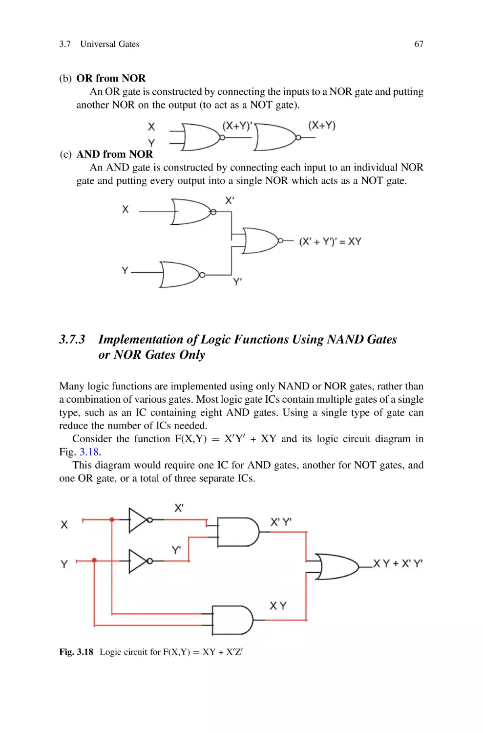
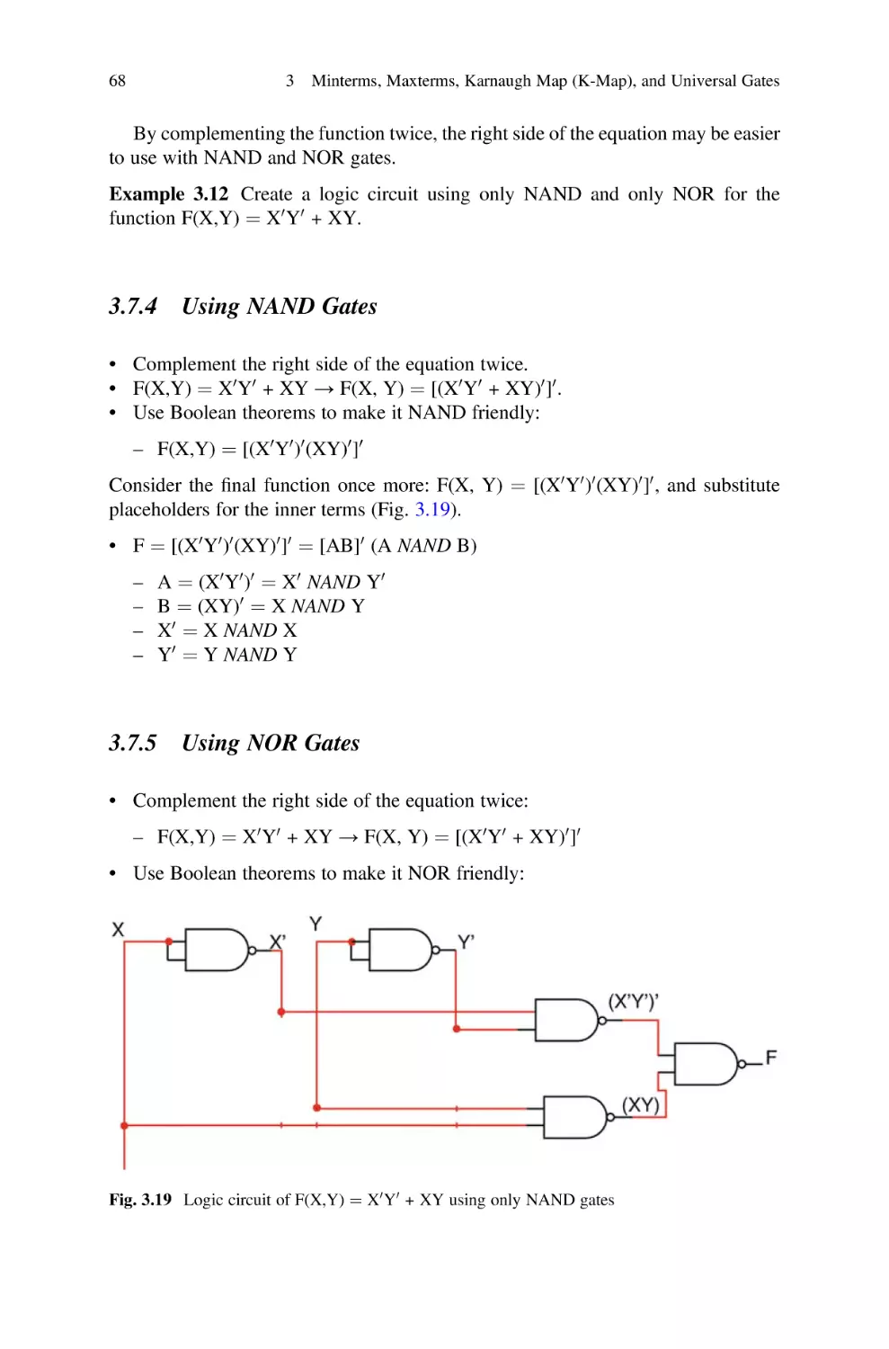
/


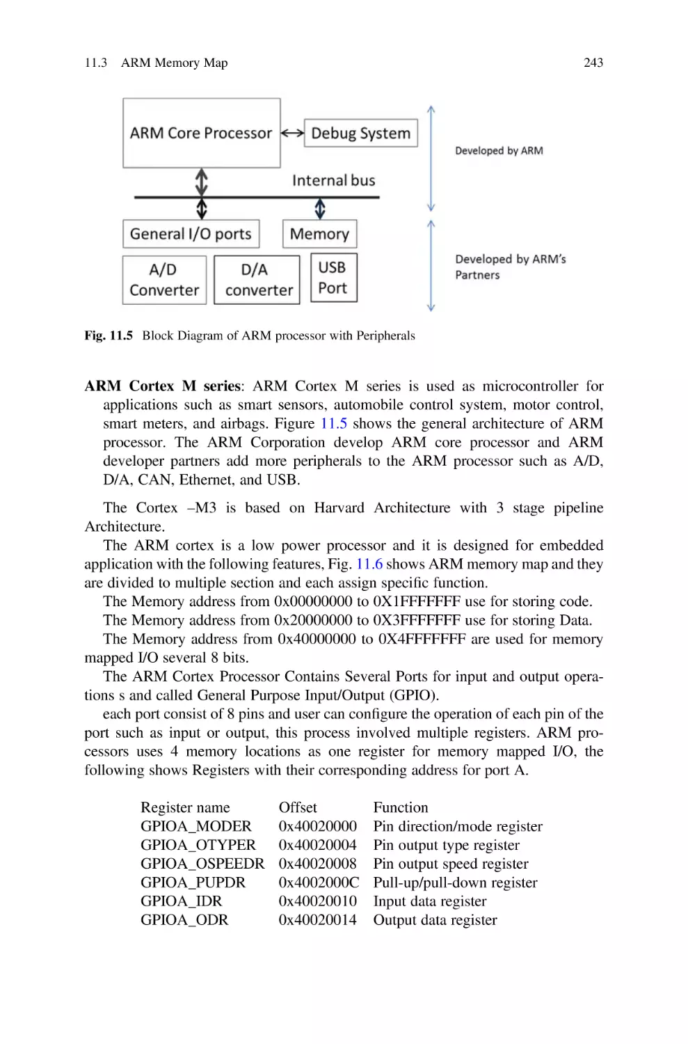


Text
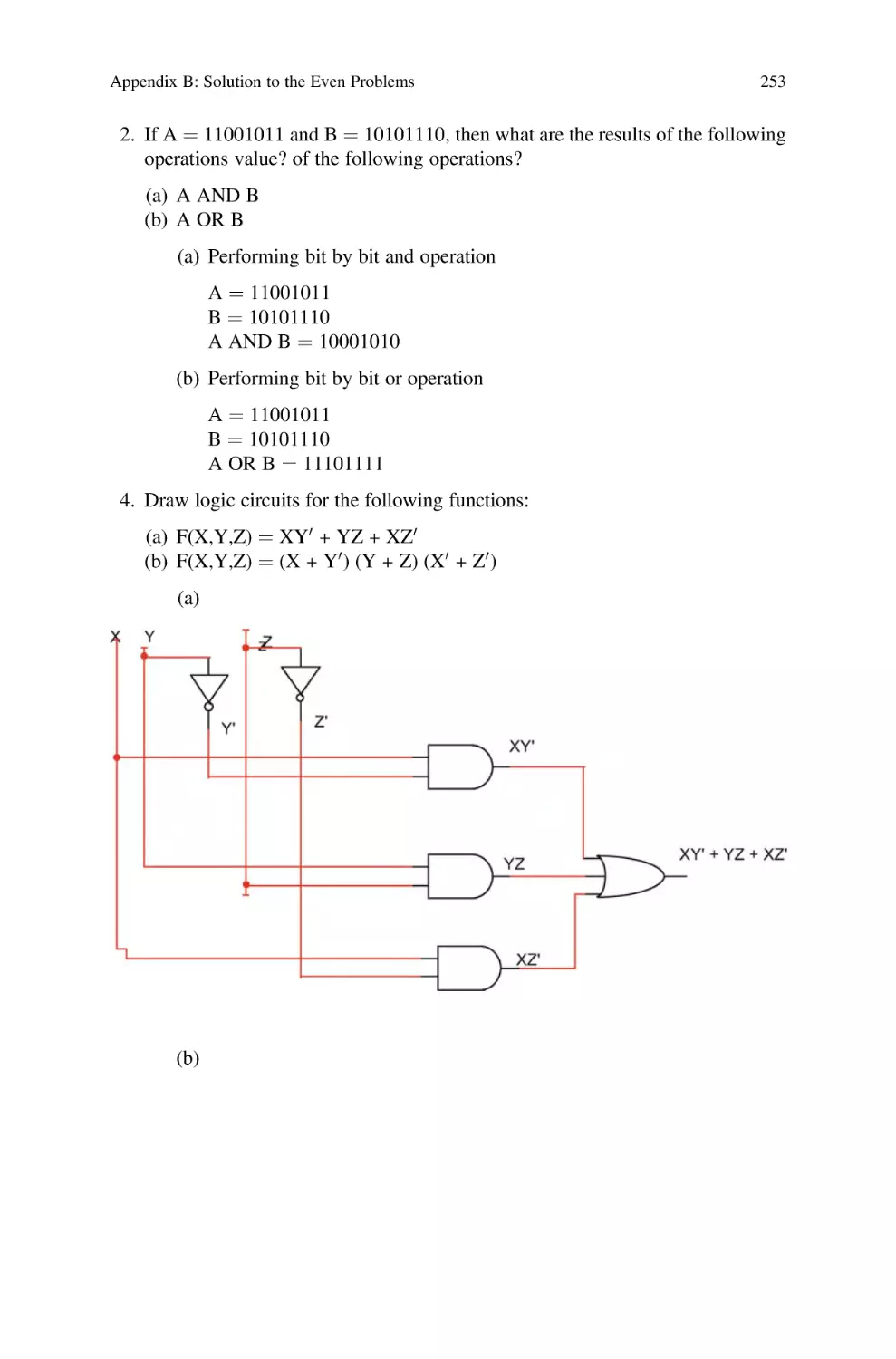
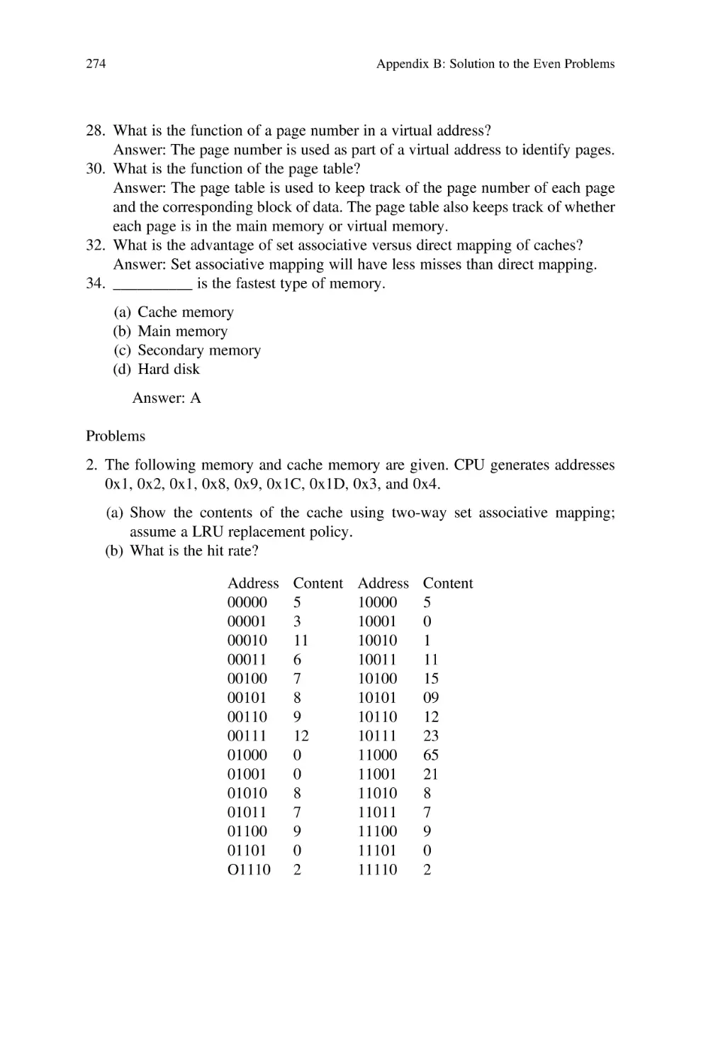
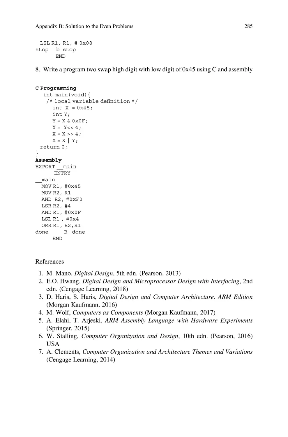
Computer Systems
Ata Elahi
Computer Systems
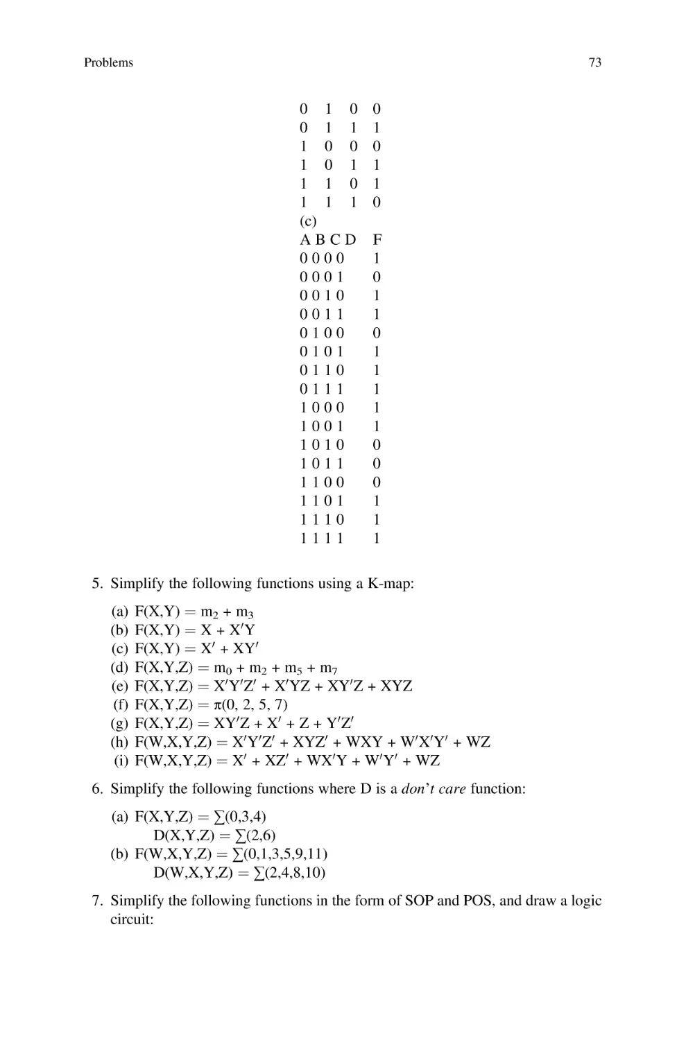
Digital Design, Fundamentals of Computer
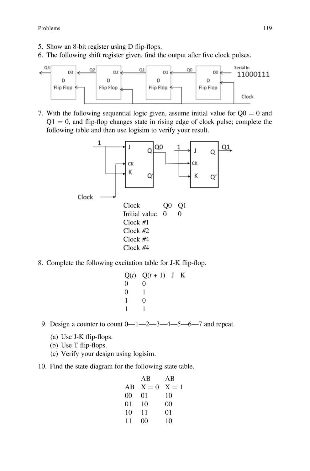
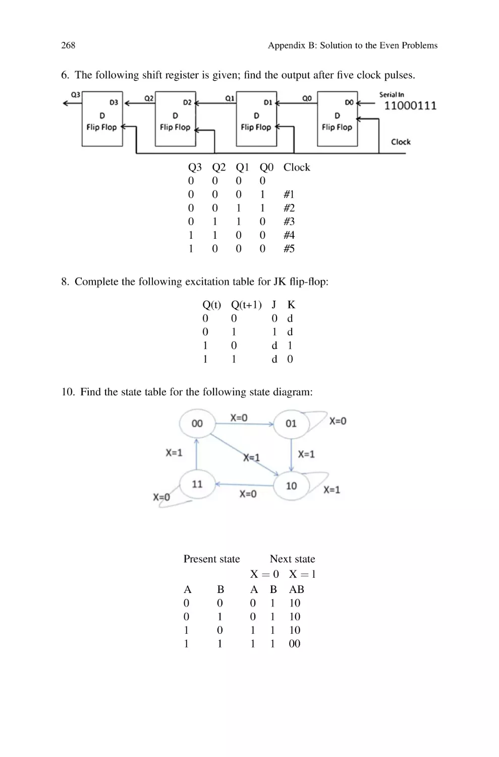
Architecture and ARM Assembly Language
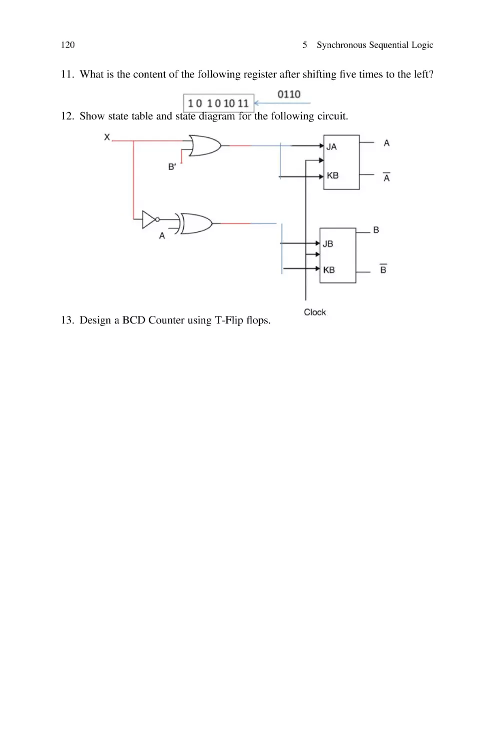
Second Edition
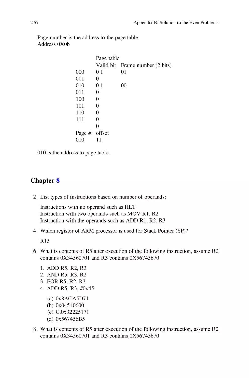
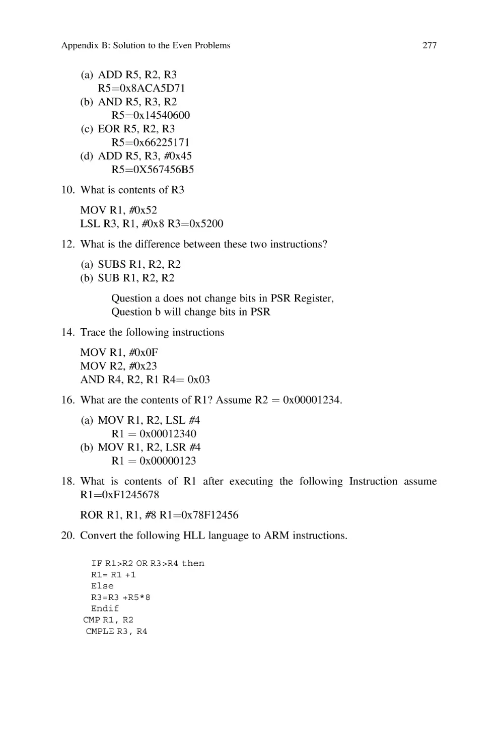
Ata Elahi
Southern Connecticut State University
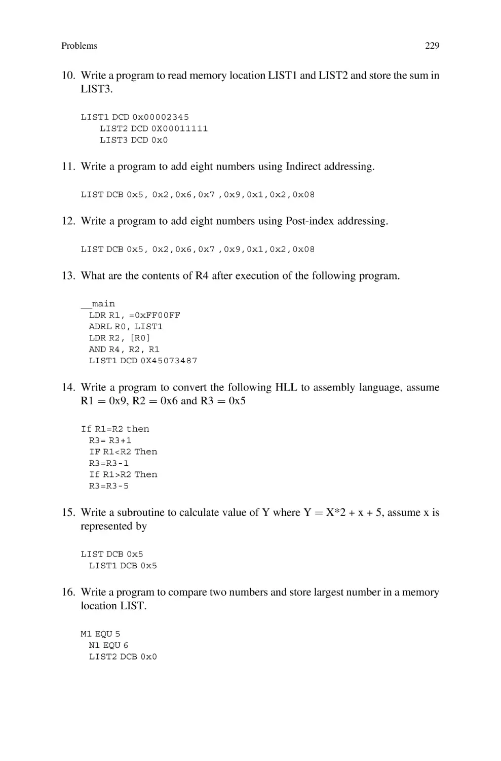
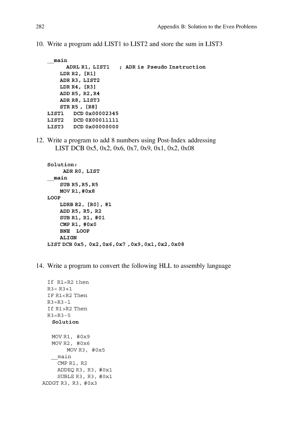
New Haven, CT, USA
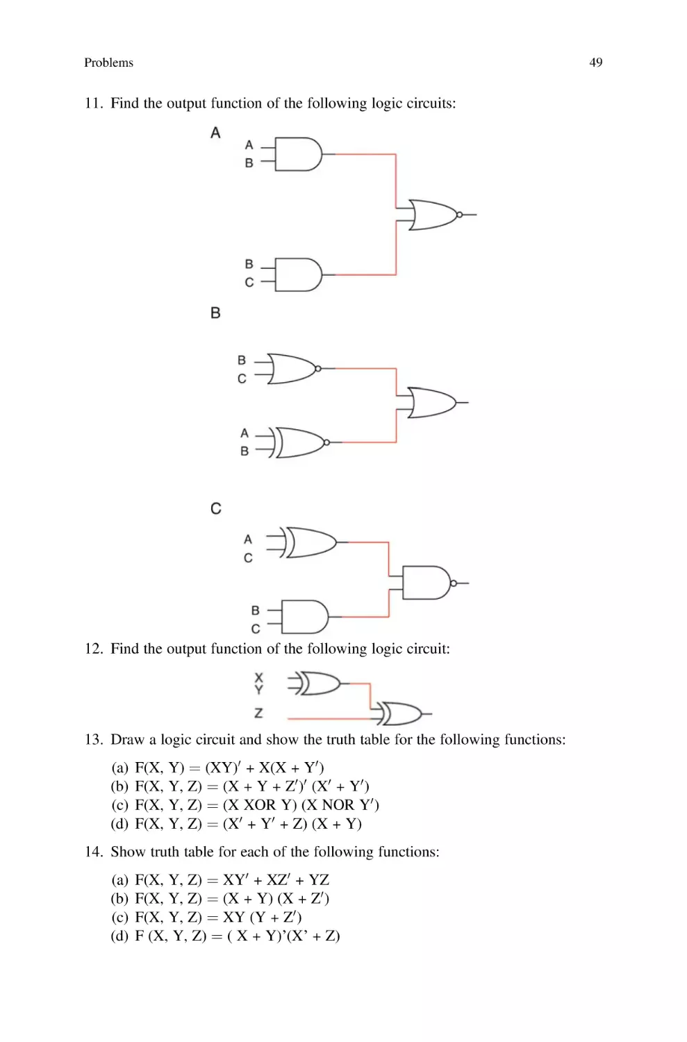
ISBN 978-3-030-93448-4
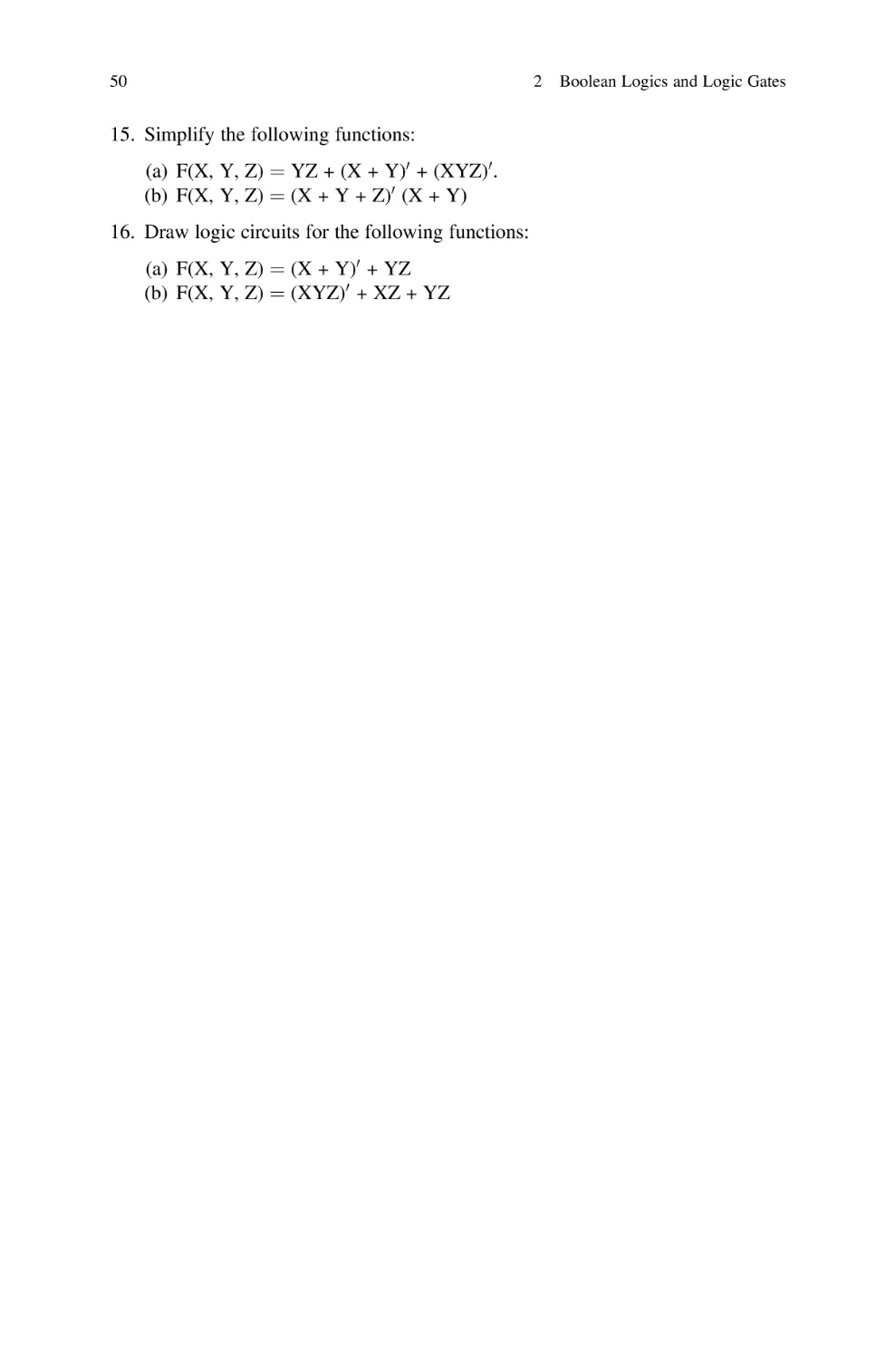
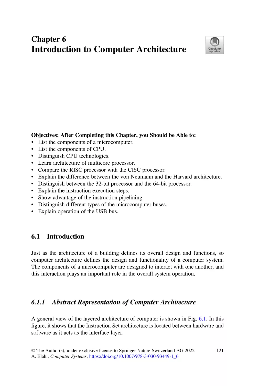
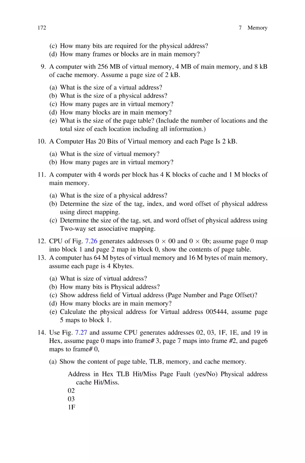
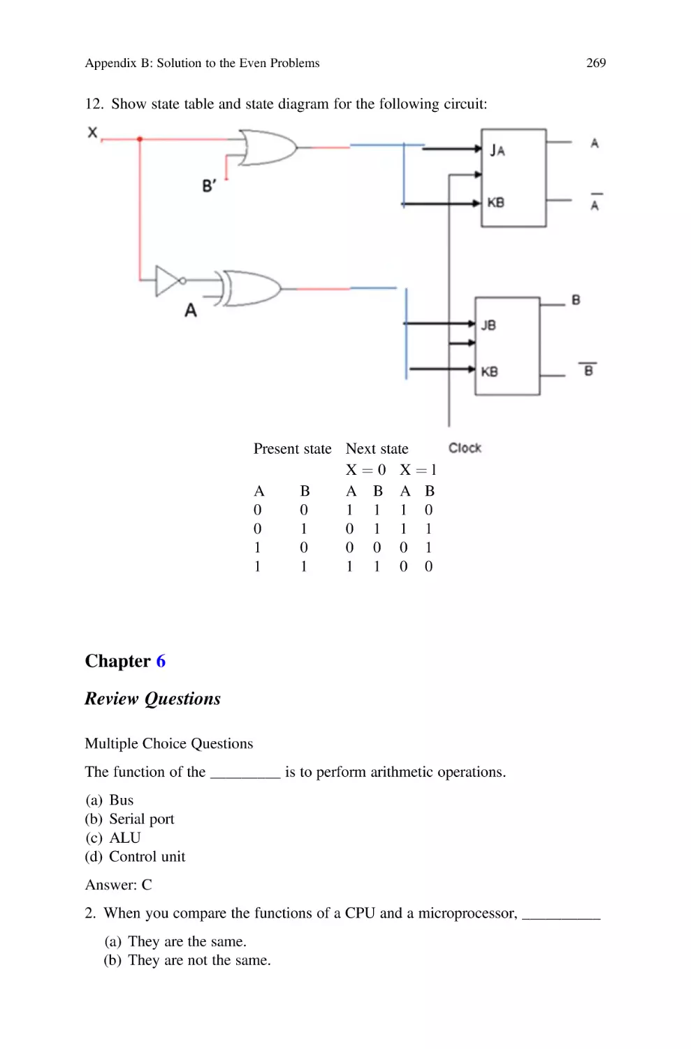
ISBN 978-3-030-93449-1
https://doi.org/10.1007/978-3-030-93449-1
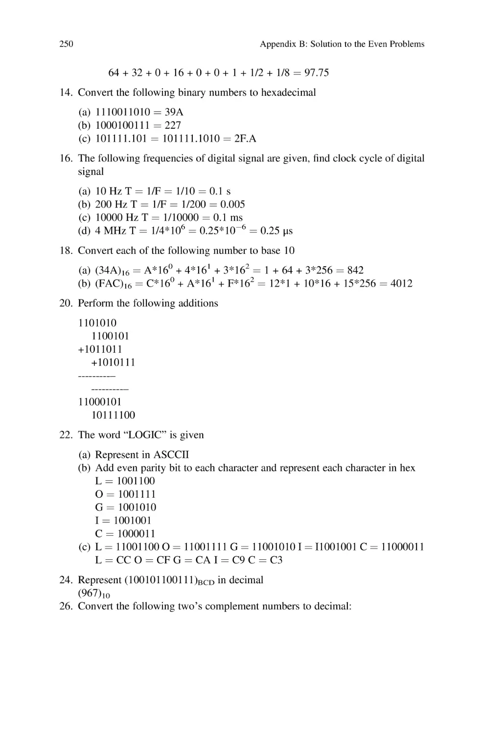
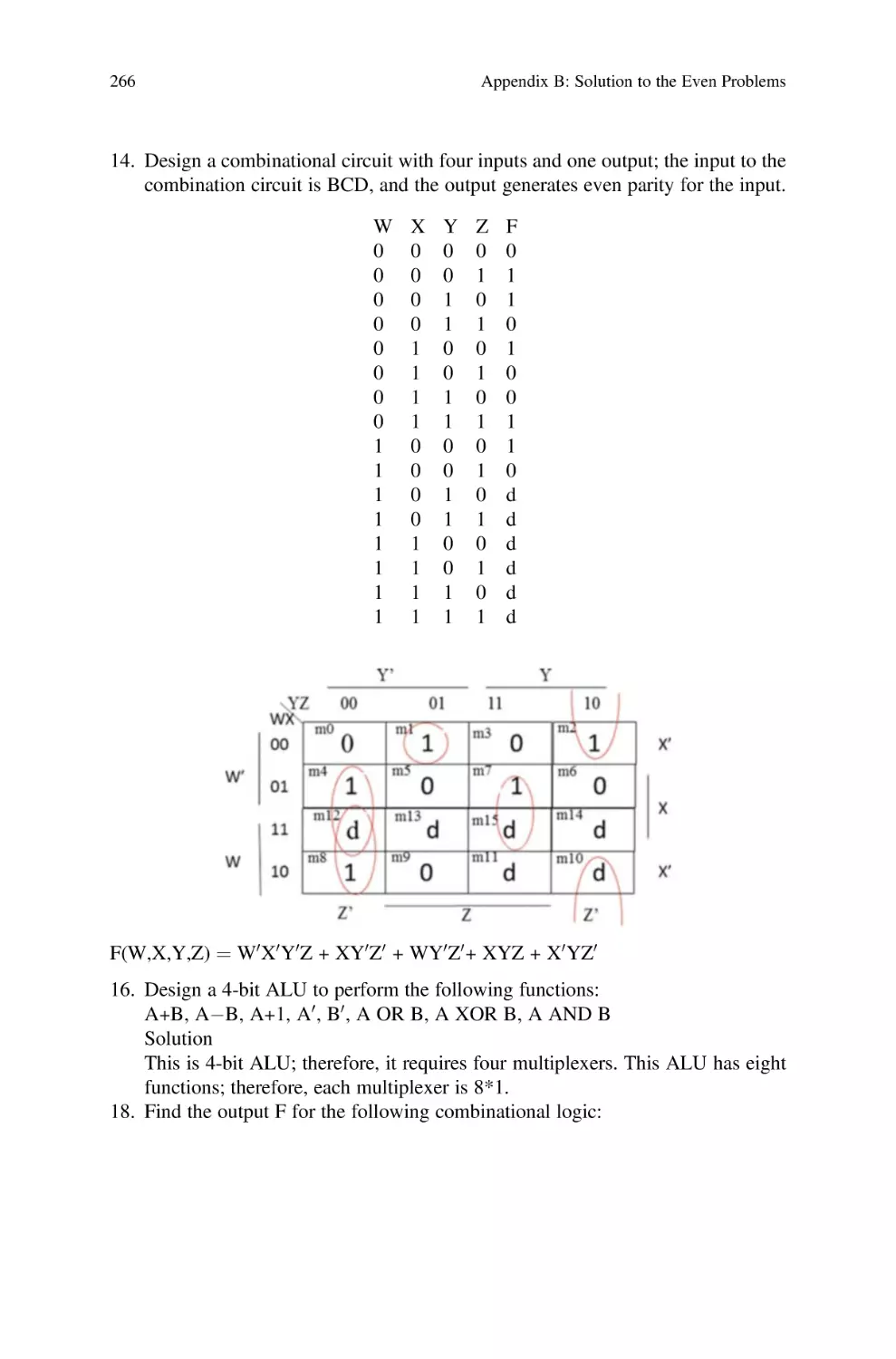
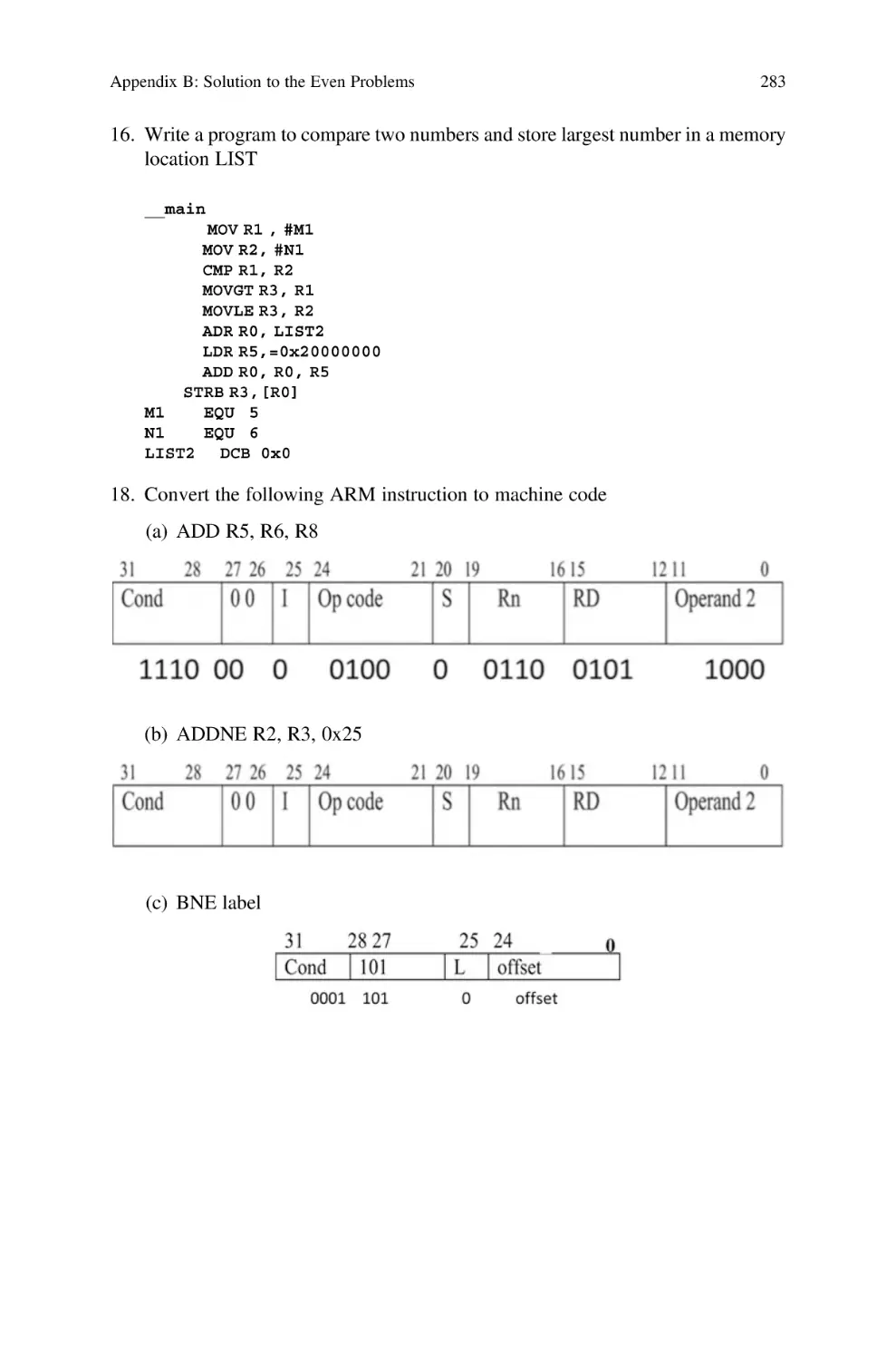
(eBook)
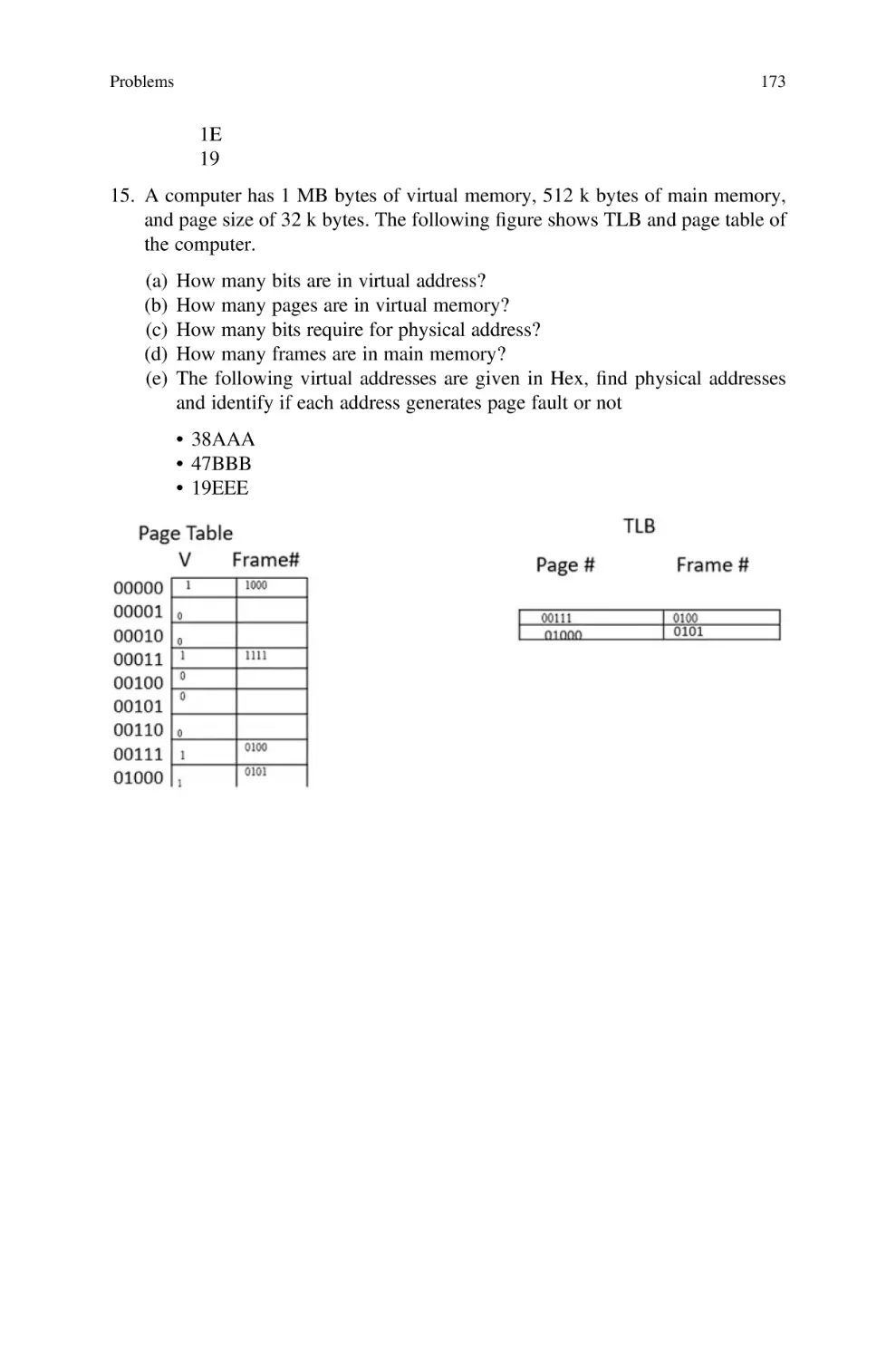
© The Editor(s) (if applicable) and The Author(s), under exclusive license to Springer Nature Switzerland
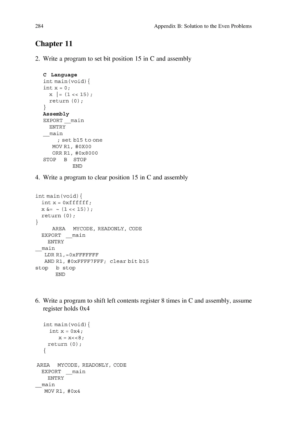
AG 2018, 2022
This work is subject to copyright. All rights are solely and exclusively licensed by the Publisher, whether
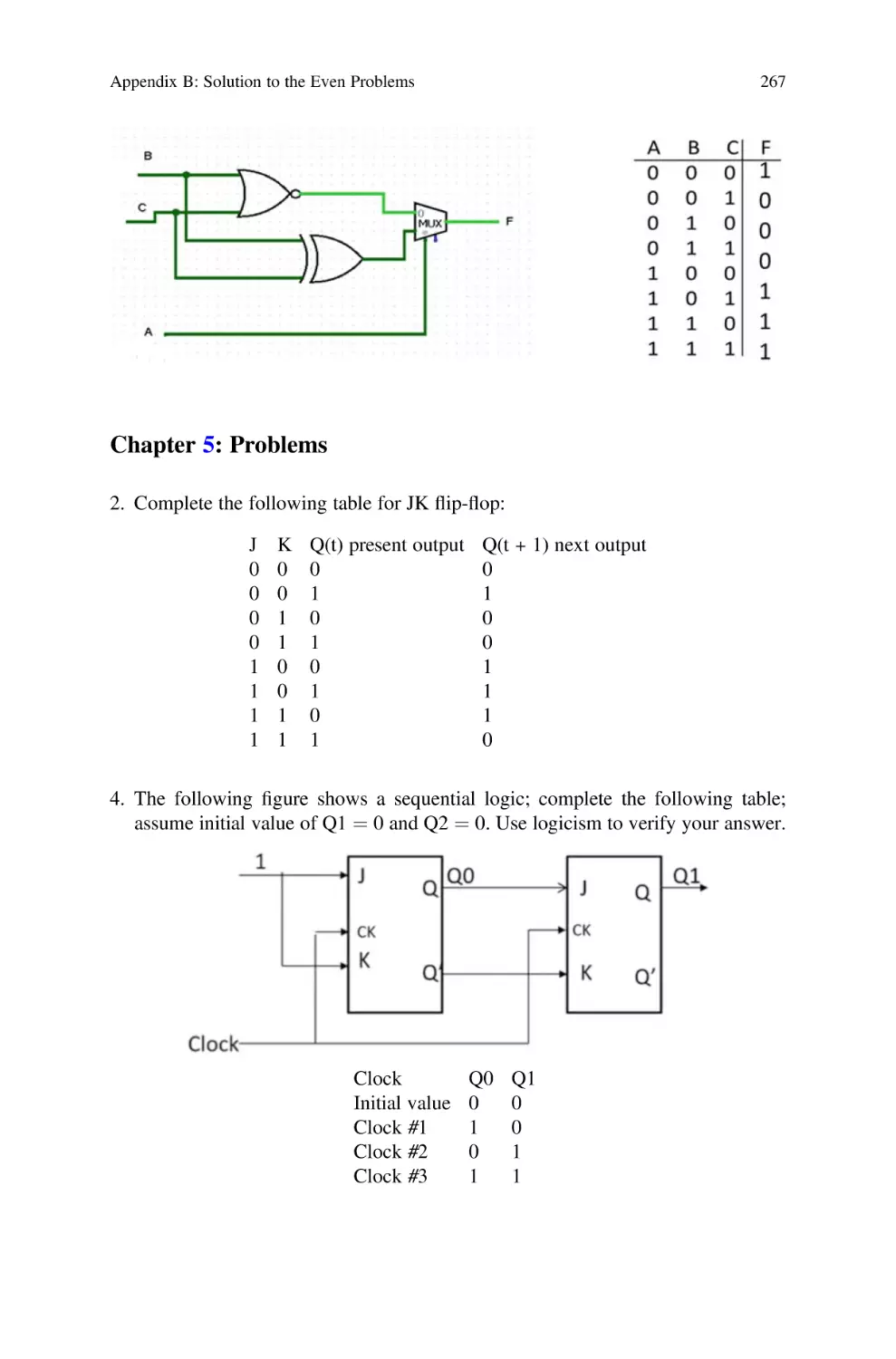
the whole or part of the material is concerned, specifically the rights of translation, reprinting, reuse of
illustrations, recitation, broadcasting, reproduction on microfilms or in any other physical way, and
transmission or information storage and retrieval, electronic adaptation, computer software, or by
similar or dissimilar methodology now known or hereafter developed.
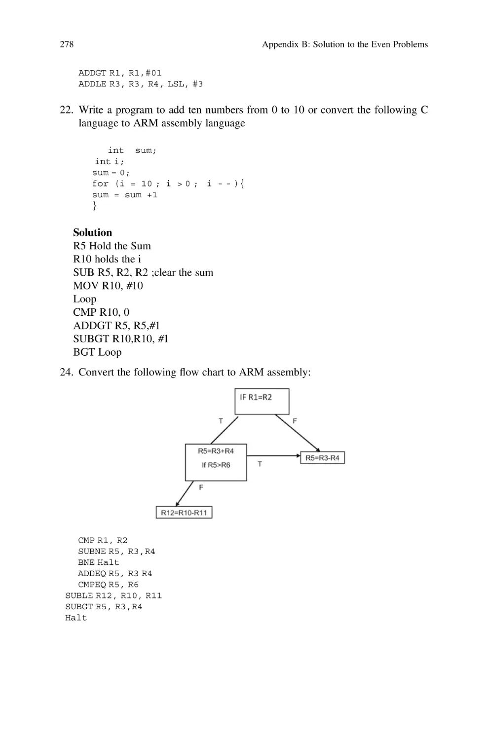
The use of general descriptive names, registered names, trademarks, service marks, etc. in this publication
does not imply, even in the absence of a specific statement, that such names are exempt from the relevant
protective laws and regulations and therefore free for general use.
The publisher, the authors and the editors are safe to assume that the advice and information in this
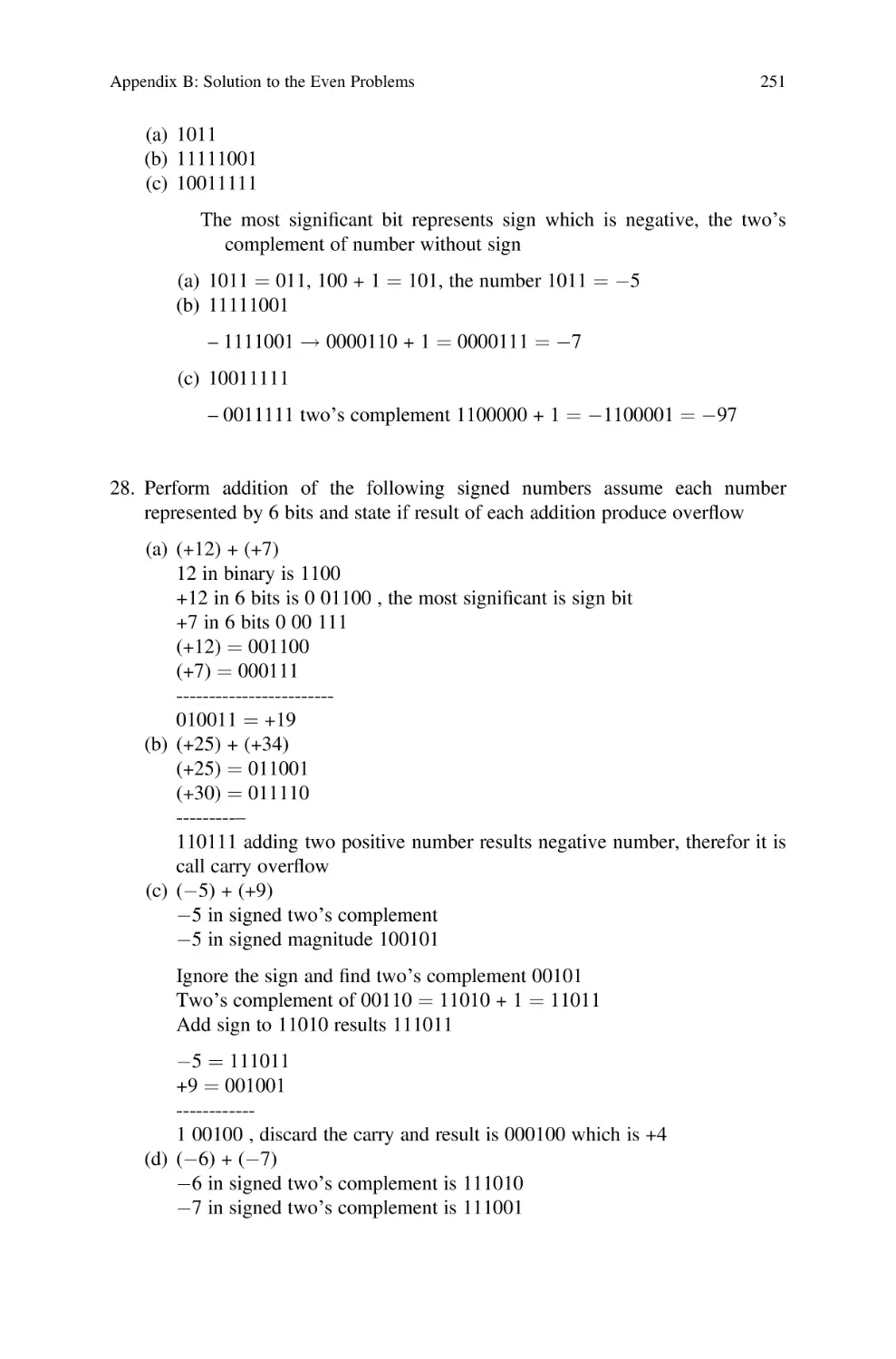
book are believed to be true and accurate at the date of publication. Neither the publisher nor the authors or
the editors give a warranty, expressed or implied, with respect to the material contained herein or for any
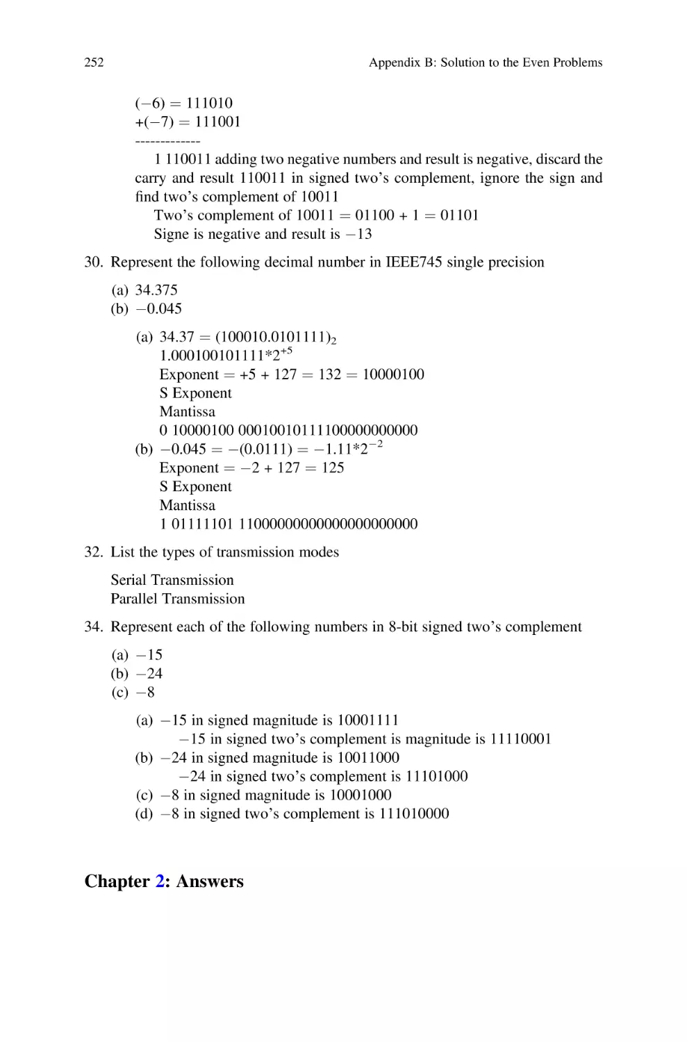
errors or omissions that may have been made. The publisher remains neutral with regard to jurisdictional
claims in published maps and institutional affiliations.
This Springer imprint is published by the registered company Springer Nature Switzerland AG
The registered company address is: Gewerbestrasse 11, 6330 Cham, Switzerland
This book is dedicated to Sara, Shabnam, and
Aria.
Preface
This textbook is the result of my experiences teaching computer systems at the
Computer Science Department at Southern Connecticut State University since 1986.
The book is divided into three sections: Digital Design, Introduction to Computer
Architecture and Memory, and ARM Architecture and Assembly Language. The
Digital Design section includes a laboratory manual with 15 experiments using
Logisim software to enforce important concepts. The ARM Architecture and Assembly Language section includes several examples of assembly language programs
using Keil μVision 5 development tools.
Intended Audience
This book is written primarily for a one-semester course as an introduction to
computer hardware and assembly language for students majoring in Computer
Science, Information Systems, and Engineering Technology.
Changes in the Second Edition
The expansion of Chap. 1 by adding history of computer and Types of Computers.
Expanded Chap. 6 “Introduction to Computer Architecture” by adding Computer
Abstraction Layers and CPU Instruction Execution Steps. The most revision done on
ARM Architecture and Assembly Language by incorporating Keil μvision5,
reordering Chaps. 9 and 10, and adding Chap. 11 “C Bitwise and Control Structures
used for Programming with C and ARM Assembly Language.”
Organization
The material of this book is presented in such a way that no special background is
required to understand the topics.
vii
viii
Preface
Chapter 1–Signals and Number Systems: Analog Signal, Digital Signal, Binary
Numbers, Addition and Subtraction of binary numbers, IEEE 754 Floating Point
representations, ASCII, Unicode, Serial Transmission, and Parallel Transmission
Chapter 2–Boolean Logics and Logic Gates: Boolean Logics, Boolean Algebra
Theorems, Logic Gates, Integrated Circuit (IC), Boolean Function, Truth Table of a
function and using Boolean Theorems to simplify Boolean Functions
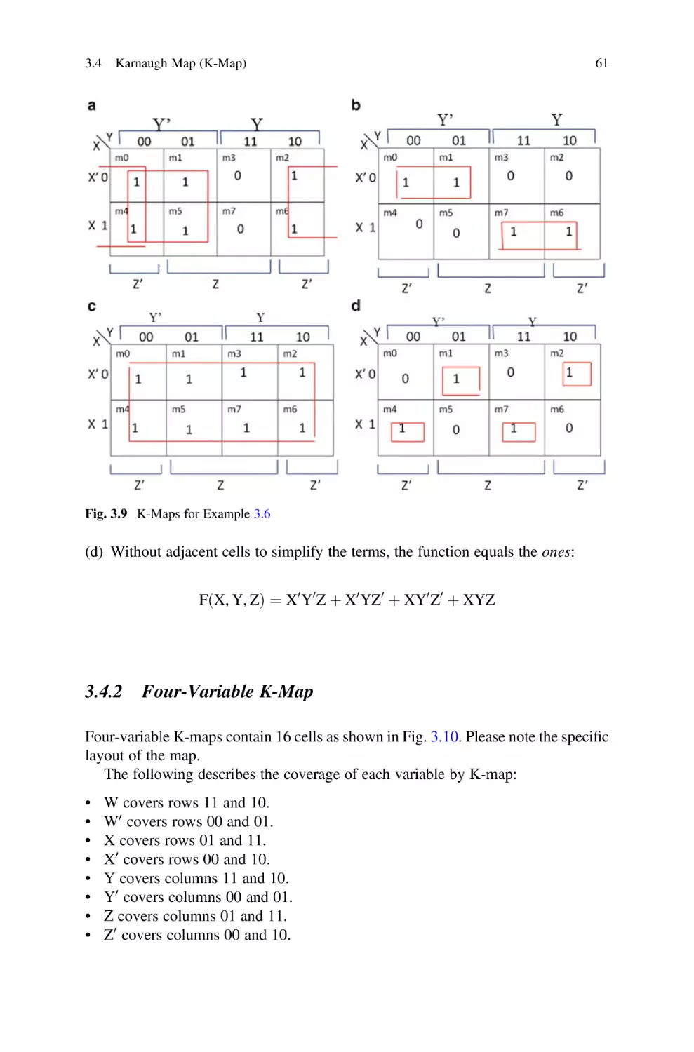
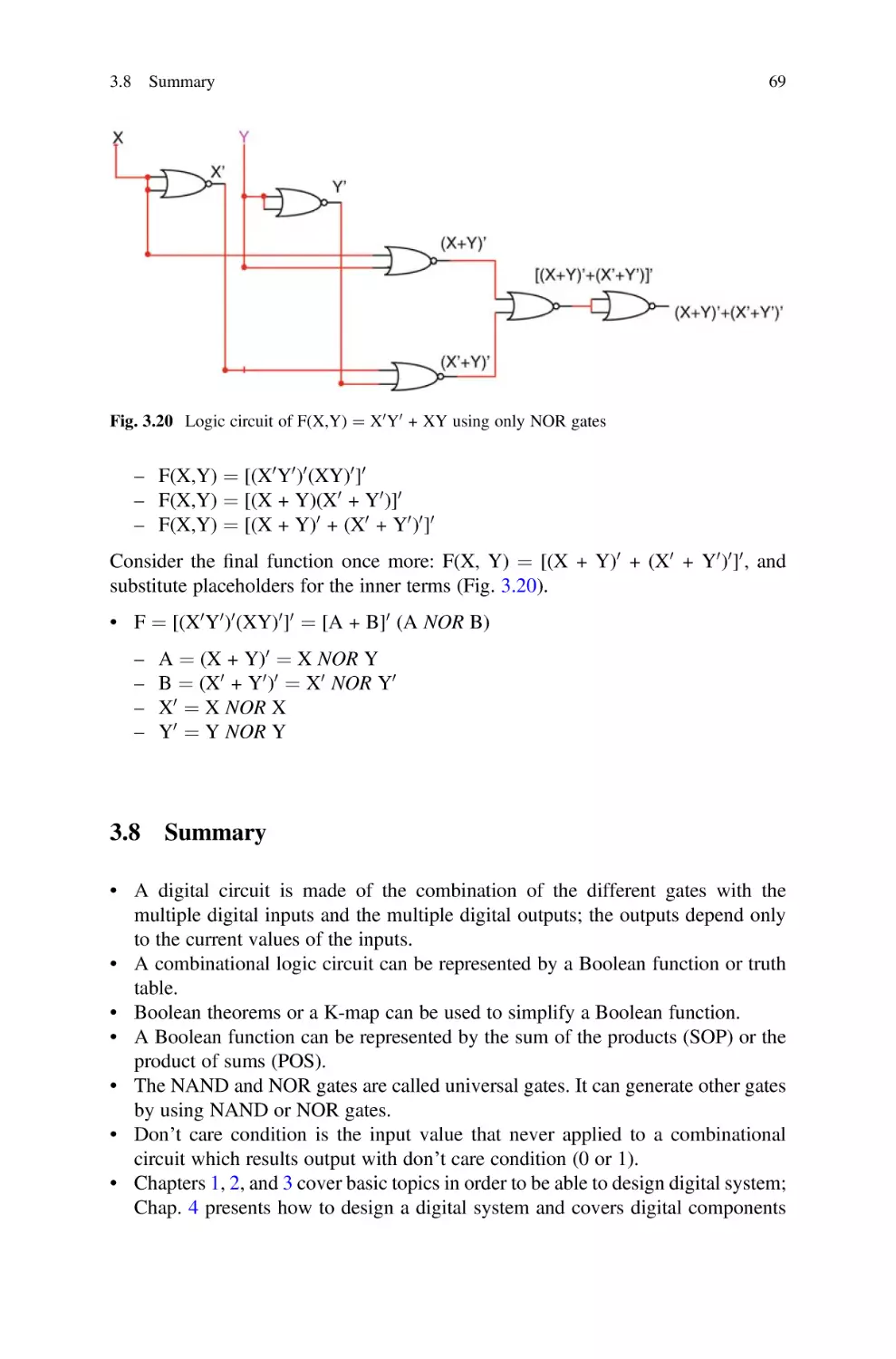
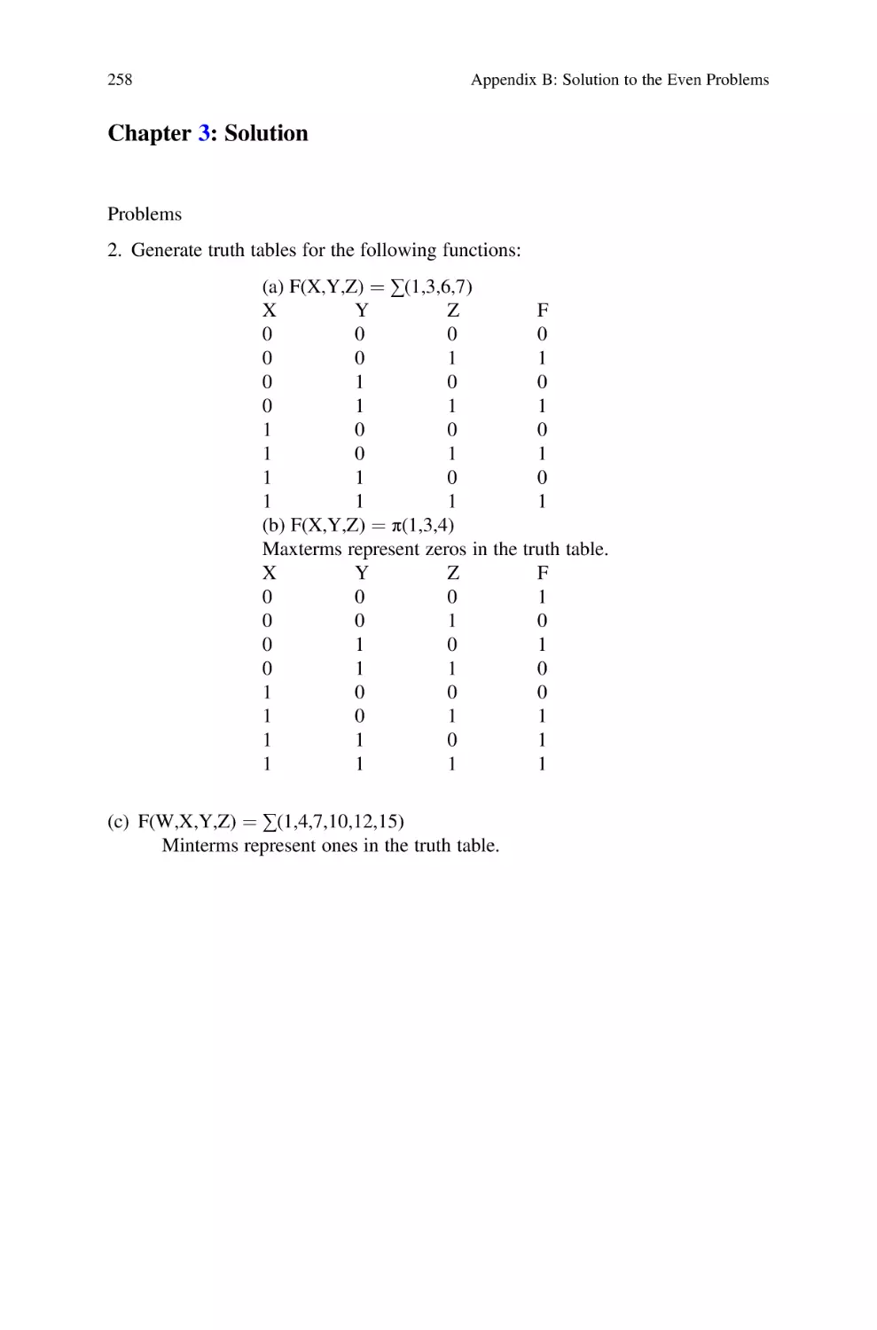
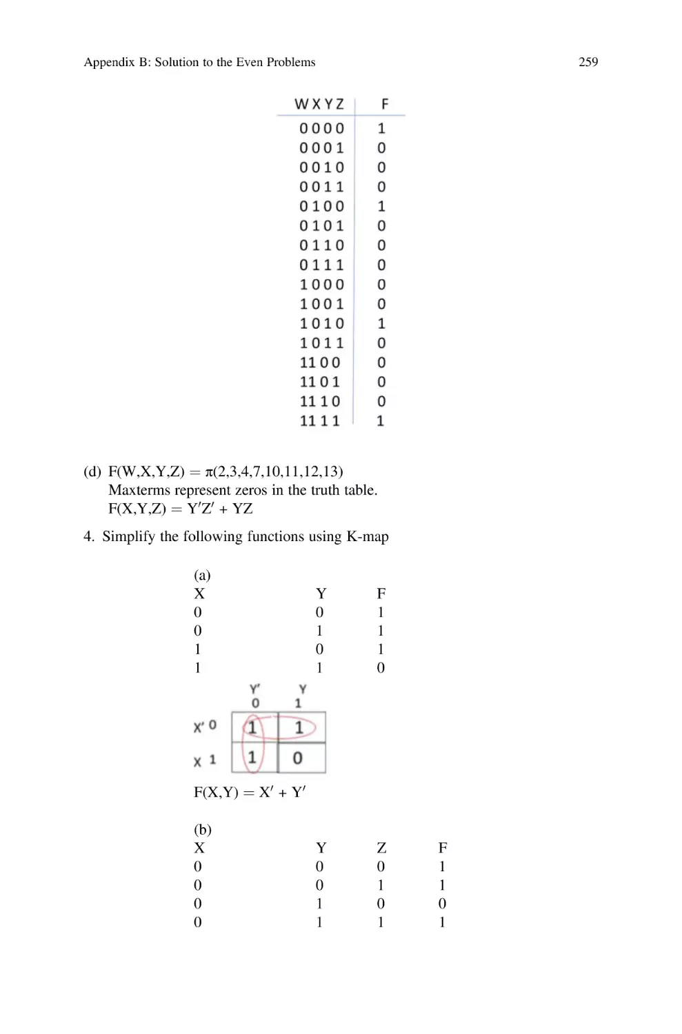
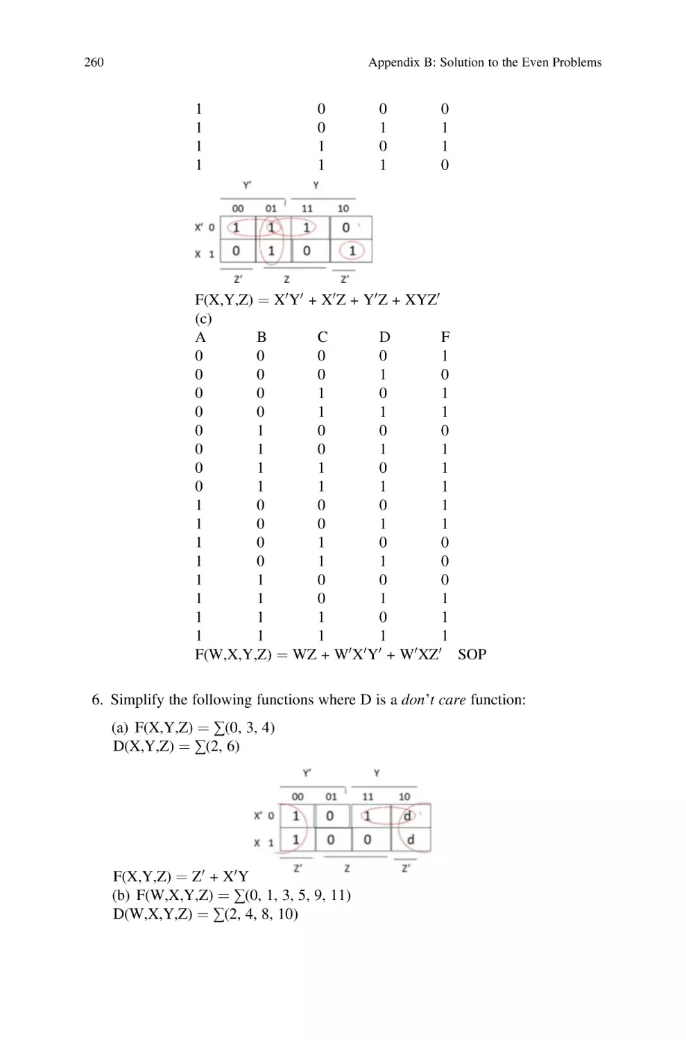
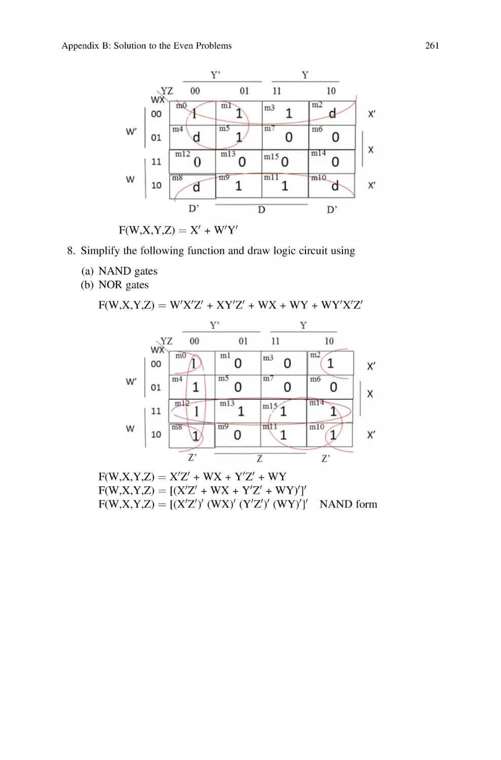
Chapter 3–Minterms, Maxterms, Karnaugh Map (K-Map) and Universal Gates:
Minterms, Maxterms, Karnaugh Map (K-Map) to simplify Boolean Functions,
Don’t Care Conditions and Universal Gates
Chapter 4–Combinational Logic: Analysis of Combination Logic, Design of
Combinational Logic, Decoder, Encoder, Multiplexer, Half Adder, Full Adder,
Binary Adder, Binary Subtractor, Designing Arithmetic Logic Unit (ALU), and
BCD to Seven Segment Decoder
Chapter 5–Synchronous Sequential Logic: Sequential Logic such as S-R Latch,
D-Flip Flop, J-K Flip Flop, T-Flip Flop, Register, Shift Register, Analysis of
Sequential Logic, State Diagram, State Table, Flip Flop Excitation Table, and
Designing Counter
Chapter 6–Introduction to Computer Architecture: Components of a Microcomputer, CPU Technology, CPU Architecture, Instruction Execution, Pipelining, PCI,
PCI Express, USB, and HDMI
Chapter 7–Memory: Memory including RAM, SRAM, DISK, SSD, Memory
Hierarchy, Cache Memory, Cache Memory Mapping Methods, Virtual Memory,
Page Table, and the memory organization of a computer
Chapter 8– Assembly Language and ARM Instructions Part I: ARM Processor
Architecture, and ARM Instruction Set such as Data Processing, Shift, Rotate,
Unconditional Instructions and Conditional Instructions, Stack Operation, Branch,
Multiply Instructions, and several examples of converting HLL to Assembly
Language.
Chapter 9–ARM Assembly Language Programming Using Keil Development
Tools: Covers how to use Keil development software for writing assembly language
using ARM Instructions, Compiling Assembly Language, and Debugging
Chapter 10–ARM Instructions Part II and Instruction Formats: This chapter is the
continuation of Chap. 8 which covers Load and Store Instructions, Pseudo Instructions, ARM Addressing Mode, and Instruction formats.
Chapter 11–C Bitwise and Control Structures Used for Programming with C and
ARM Assembly Language
Instruction Resources: The instruction resources contain
• 15 Laboratory experiments using Logisim.
• Solutions to the problems of each chapter.
• Power points of each chapter
New Haven, CT, USA
Ata Elahi
Acknowledgments
I would like to express my special thanks to Professor Lancor Chairman of Computer Science Department at Southern Connecticut State University for her support
as well as Professor Herv Podnar for his guidance.
I wish to acknowledge and thank Ms. Mary E. James, Senior Editor in Applied
Sciences and her assistant, Ms. Zoe Kennedy, for their support.
My special thanks to Eric Barbin, Alex Cushman, Marc Gajdosik, Nickolas
Santini, Nicholas Bittar, Omar Abid, and Alireza Ghods for their help in developing
the manuscript. Finally, I would like to thank the students of CSC 207 Computer
Systems of Spring 2020.
ix
Contents
1
Signals and Number Systems . . . . . . . . . . . . . . . . . . . . . . . . . . . .
1.1
Introduction . . . . . . . . . . . . . . . . . . . . . . . . . . . . . . . . . . . . .
1.1.1
CPU . . . . . . . . . . . . . . . . . . . . . . . . . . . . . . . . . . . .
1.2
Historical Development of the Computer . . . . . . . . . . . . . . . .
1.3
Hardware and Software Components of a Computer . . . . . . . .
1.4
Types of Computers . . . . . . . . . . . . . . . . . . . . . . . . . . . . . . .
1.5
Analog Signals . . . . . . . . . . . . . . . . . . . . . . . . . . . . . . . . . . .
1.5.1
Characteristics of an Analog Signal . . . . . . . . . . . . . .
1.6
Digital Signals . . . . . . . . . . . . . . . . . . . . . . . . . . . . . . . . . . .
1.7
Number System . . . . . . . . . . . . . . . . . . . . . . . . . . . . . . . . . .
1.7.1
Converting from Binary to Decimal . . . . . . . . . . . . . .
1.7.2
Converting from Decimal Integer to Binary . . . . . . . .
1.7.3
Converting Decimal Fraction to Binary . . . . . . . . . . .
1.7.4
Converting from Hex to Binary . . . . . . . . . . . . . . . . .
1.7.5
Binary Addition . . . . . . . . . . . . . . . . . . . . . . . . . . . .
1.8
Complement and Two’s Complement . . . . . . . . . . . . . . . . . . .
1.8.1
Subtraction of Unsigned Number Using Two’s
Complement . . . . . . . . . . . . . . . . . . . . . . . . . . . . . .
1.9
Unsigned, Signed Magnitude, and Signed Two’s Complement
Binary Number . . . . . . . . . . . . . . . . . . . . . . . . . . . . . . . . . . .
1.9.1
Unsigned Number . . . . . . . . . . . . . . . . . . . . . . . . . .
1.9.2
Signed Magnitude Number . . . . . . . . . . . . . . . . . . . .
1.9.3
Signed Two’s Complement . . . . . . . . . . . . . . . . . . . .
1.10 Binary Addition Using Signed Two’s Complement . . . . . . . . .
1.11 Floating Point Representation . . . . . . . . . . . . . . . . . . . . . . . .
1.11.1 Single and Double Precision Representations
of Floating Point . . . . . . . . . . . . . . . . . . . . . . . . . . .
1.12 Binary-Coded Decimal (BCD) . . . . . . . . . . . . . . . . . . . . . . . .
1.13 Coding Schemes . . . . . . . . . . . . . . . . . . . . . . . . . . . . . . . . . .
1.13.1 ASCII Code . . . . . . . . . . . . . . . . . . . . . . . . . . . . . . .
.
.
.
.
.
.
.
.
.
.
.
.
.
.
.
.
1
1
2
3
3
4
5
6
7
8
9
10
10
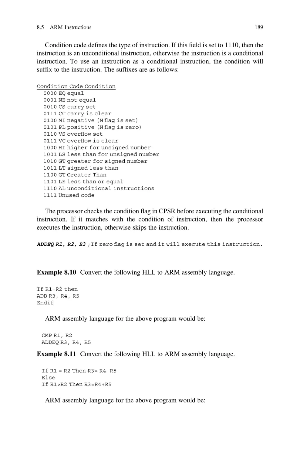
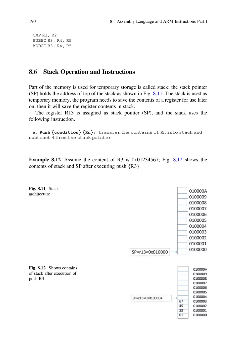
11
13
13
.
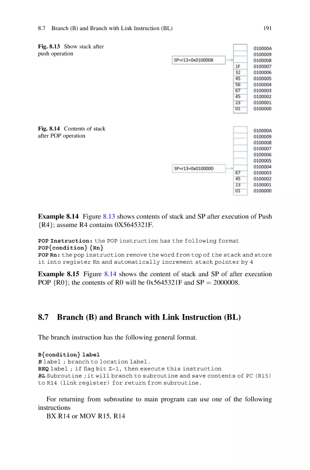
14
.
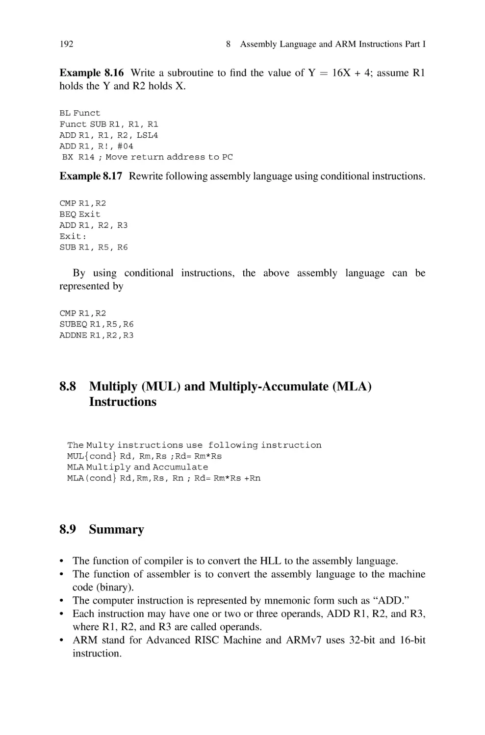
.
.
.
.
.
15
15
15
15
16
17
.
.
.
.
18
19
20
20
xi
xii
Contents
1.13.2 Universal Code or Unicode . . . . . . . . . . . . . . . . . . . . .
Parity Bit . . . . . . . . . . . . . . . . . . . . . . . . . . . . . . . . . . . . . . . .
1.14.1 Even Parity . . . . . . . . . . . . . . . . . . . . . . . . . . . . . . . .
1.14.2 Odd Parity . . . . . . . . . . . . . . . . . . . . . . . . . . . . . . . . .
Clock . . . . . . . . . . . . . . . . . . . . . . . . . . . . . . . . . . . . . . . . . . .
Transmission Modes . . . . . . . . . . . . . . . . . . . . . . . . . . . . . . . .
1.16.1 Asynchronous Transmission . . . . . . . . . . . . . . . . . . . .
1.16.2 Synchronous Transmission . . . . . . . . . . . . . . . . . . . . .
Transmission Methods . . . . . . . . . . . . . . . . . . . . . . . . . . . . . . .
1.17.1 Serial Transmission . . . . . . . . . . . . . . . . . . . . . . . . . .
1.17.2 Parallel Transmission . . . . . . . . . . . . . . . . . . . . . . . . .
Summary . . . . . . . . . . . . . . . . . . . . . . . . . . . . . . . . . . . . . . . .
20
23
24
24
24
25
25
26
26
27
27
27
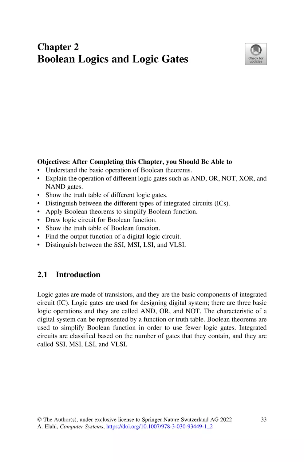
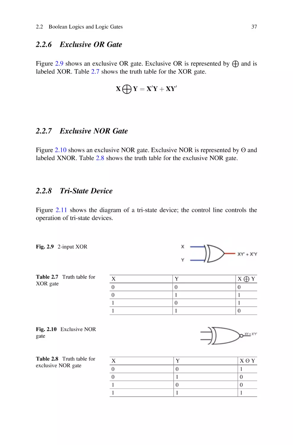
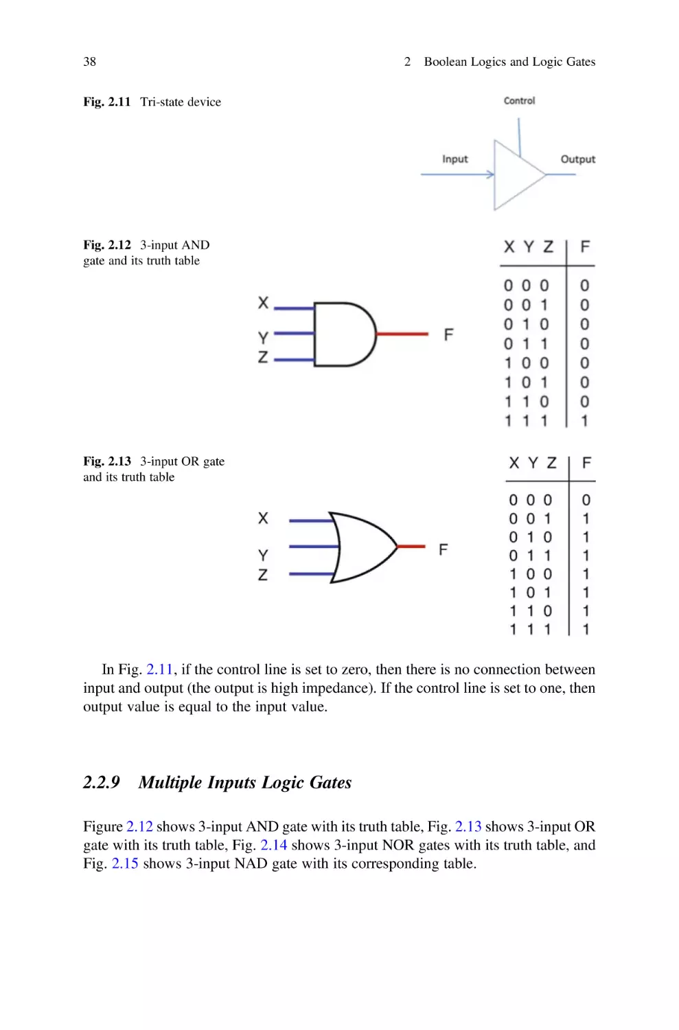
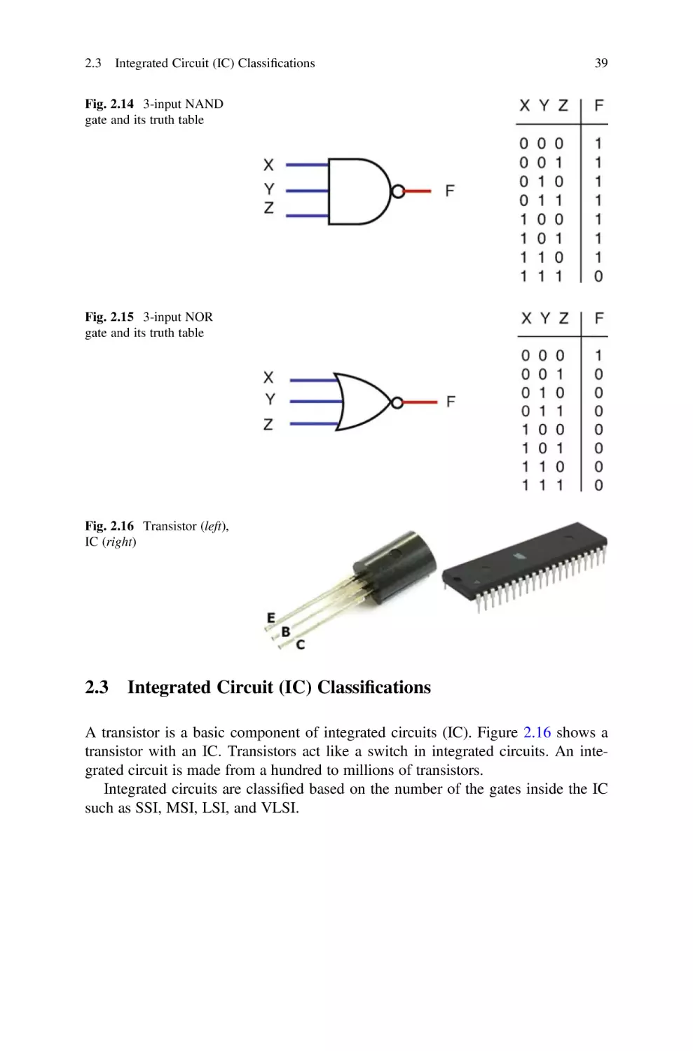
Boolean Logics and Logic Gates . . . . . . . . . . . . . . . . . . . . . . . . . . .
2.1
Introduction . . . . . . . . . . . . . . . . . . . . . . . . . . . . . . . . . . . . . .
2.2
Boolean Logics and Logic Gates . . . . . . . . . . . . . . . . . . . . . . .
2.2.1
AND Logic . . . . . . . . . . . . . . . . . . . . . . . . . . . . . . . .
2.2.2
OR Logic . . . . . . . . . . . . . . . . . . . . . . . . . . . . . . . . .
2.2.3
NOT Logic . . . . . . . . . . . . . . . . . . . . . . . . . . . . . . . .
2.2.4
NAND Gate . . . . . . . . . . . . . . . . . . . . . . . . . . . . . . . .
2.2.5
NOR Gate . . . . . . . . . . . . . . . . . . . . . . . . . . . . . . . . .
2.2.6
Exclusive OR Gate . . . . . . . . . . . . . . . . . . . . . . . . . . .
2.2.7
Exclusive NOR Gate . . . . . . . . . . . . . . . . . . . . . . . . .
2.2.8
Tri-State Device . . . . . . . . . . . . . . . . . . . . . . . . . . . . .
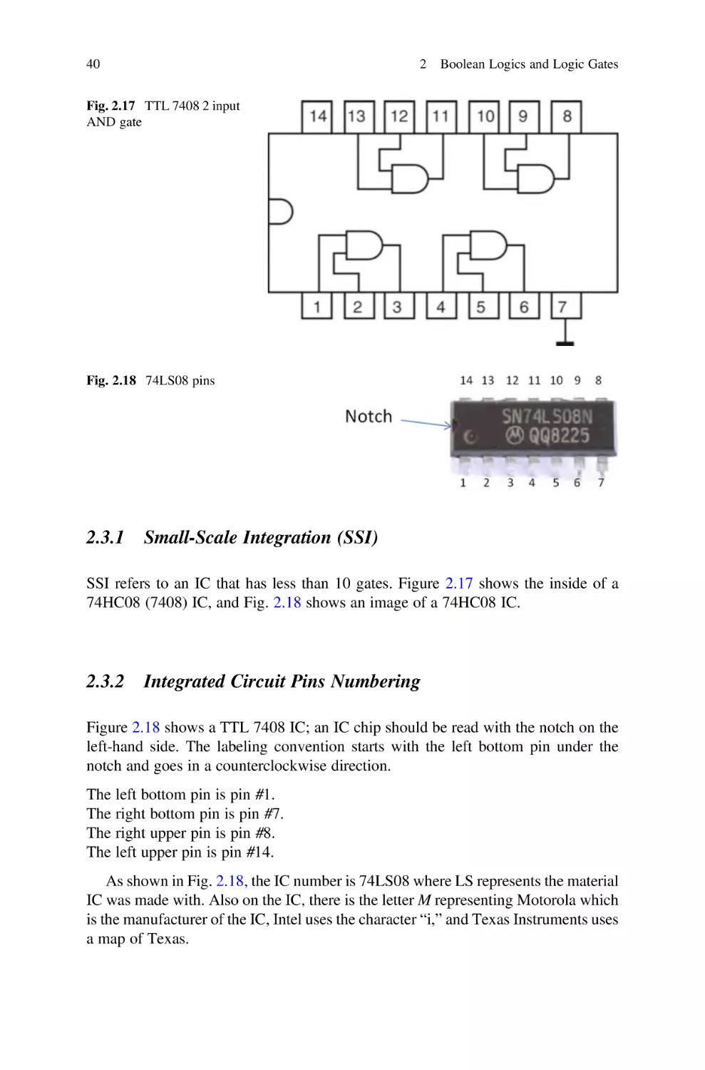
2.2.9
Multiple Inputs Logic Gates . . . . . . . . . . . . . . . . . . . .
2.3
Integrated Circuit (IC) Classifications . . . . . . . . . . . . . . . . . . . .
2.3.1
Small-Scale Integration (SSI) . . . . . . . . . . . . . . . . . . .
2.3.2
Integrated Circuit Pins Numbering . . . . . . . . . . . . . . . .
2.3.3
Medium-Scale Integration (MSI) . . . . . . . . . . . . . . . . .
2.3.4
Large-Scale Integration (LSI) . . . . . . . . . . . . . . . . . . .
2.3.5
Very-Large-Scale Integration (VLSI) . . . . . . . . . . . . . .
2.4
Boolean Algebra Theorems . . . . . . . . . . . . . . . . . . . . . . . . . . .
2.4.1
Distributive Theorem . . . . . . . . . . . . . . . . . . . . . . . . .
2.4.2
De Morgan’s Theorem I . . . . . . . . . . . . . . . . . . . . . . .
2.4.3
De Morgan’s Theorem II . . . . . . . . . . . . . . . . . . . . . .
2.4.4
Commutative Law . . . . . . . . . . . . . . . . . . . . . . . . . . .
2.4.5
Associative Law . . . . . . . . . . . . . . . . . . . . . . . . . . . . .
2.4.6
More Theorems . . . . . . . . . . . . . . . . . . . . . . . . . . . . .
2.5
Boolean Function . . . . . . . . . . . . . . . . . . . . . . . . . . . . . . . . . .
2.5.1
Complement of a Function . . . . . . . . . . . . . . . . . . . . .
2.6
Summary . . . . . . . . . . . . . . . . . . . . . . . . . . . . . . . . . . . . . . . .
Problems . . . . . . . . . . . . . . . . . . . . . . . . . . . . . . . . . . . . . . . . . . . . .
33
33
33
34
35
35
36
36
37
37
37
38
39
40
40
41
41
41
41
42
43
43
44
44
44
44
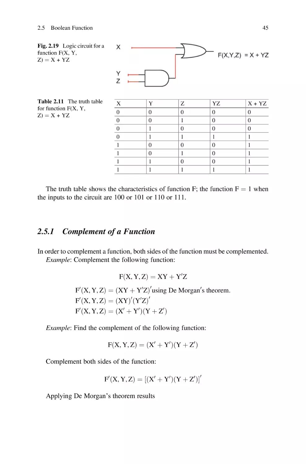
45
46
46
1.14
1.15
1.16
1.17
1.18
2
Contents
3
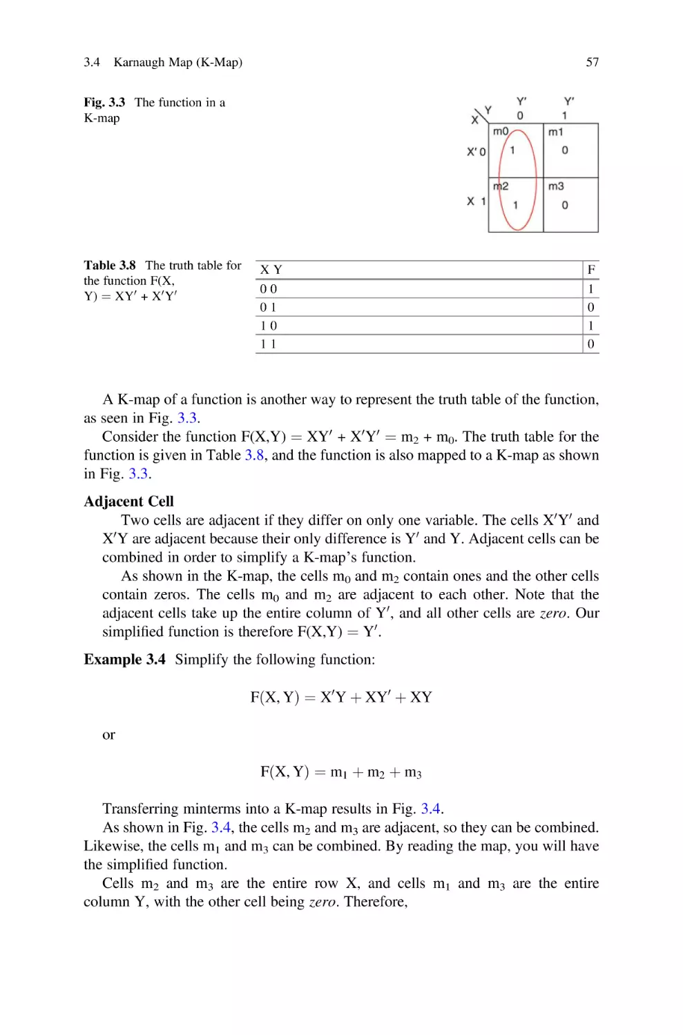
4
Minterms, Maxterms, Karnaugh Map (K-Map), and Universal
Gates . . . . . . . . . . . . . . . . . . . . . . . . . . . . . . . . . . . . . . . . . . . . . . . .
3.1
Introduction . . . . . . . . . . . . . . . . . . . . . . . . . . . . . . . . . . . . . .
3.2
Minterms . . . . . . . . . . . . . . . . . . . . . . . . . . . . . . . . . . . . . . . .
3.2.1
Application of Minterms . . . . . . . . . . . . . . . . . . . . . . .
3.2.2
Three-Variable Minterms . . . . . . . . . . . . . . . . . . . . . .
3.3
Maxterms . . . . . . . . . . . . . . . . . . . . . . . . . . . . . . . . . . . . . . . .
3.4
Karnaugh Map (K-Map) . . . . . . . . . . . . . . . . . . . . . . . . . . . . .
3.4.1
Three-Variable Map . . . . . . . . . . . . . . . . . . . . . . . . . .
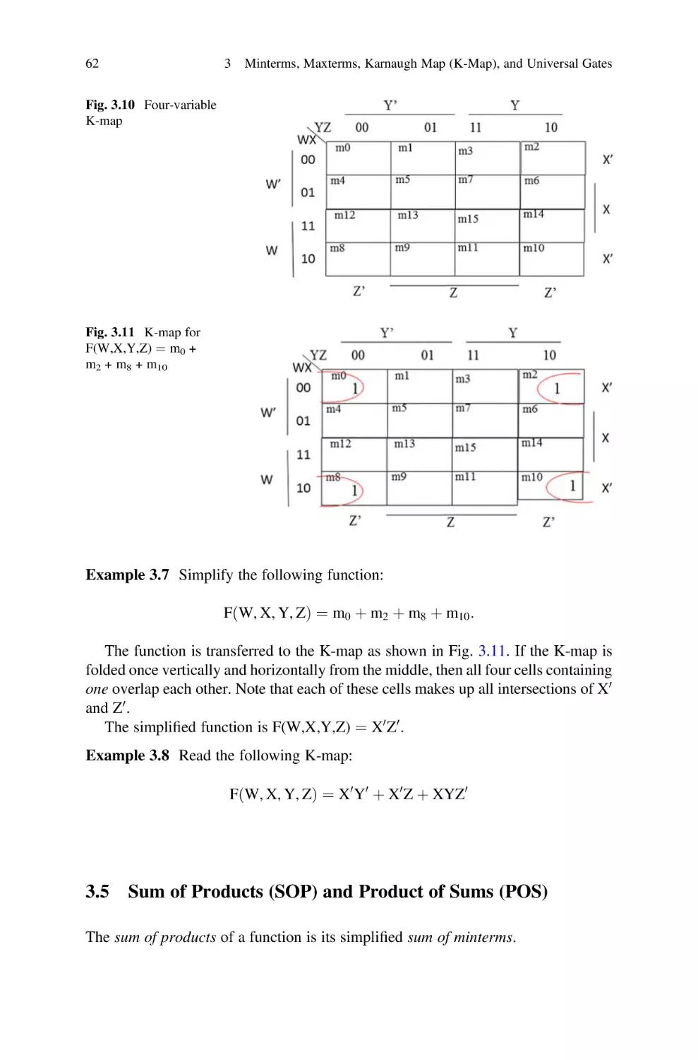
3.4.2
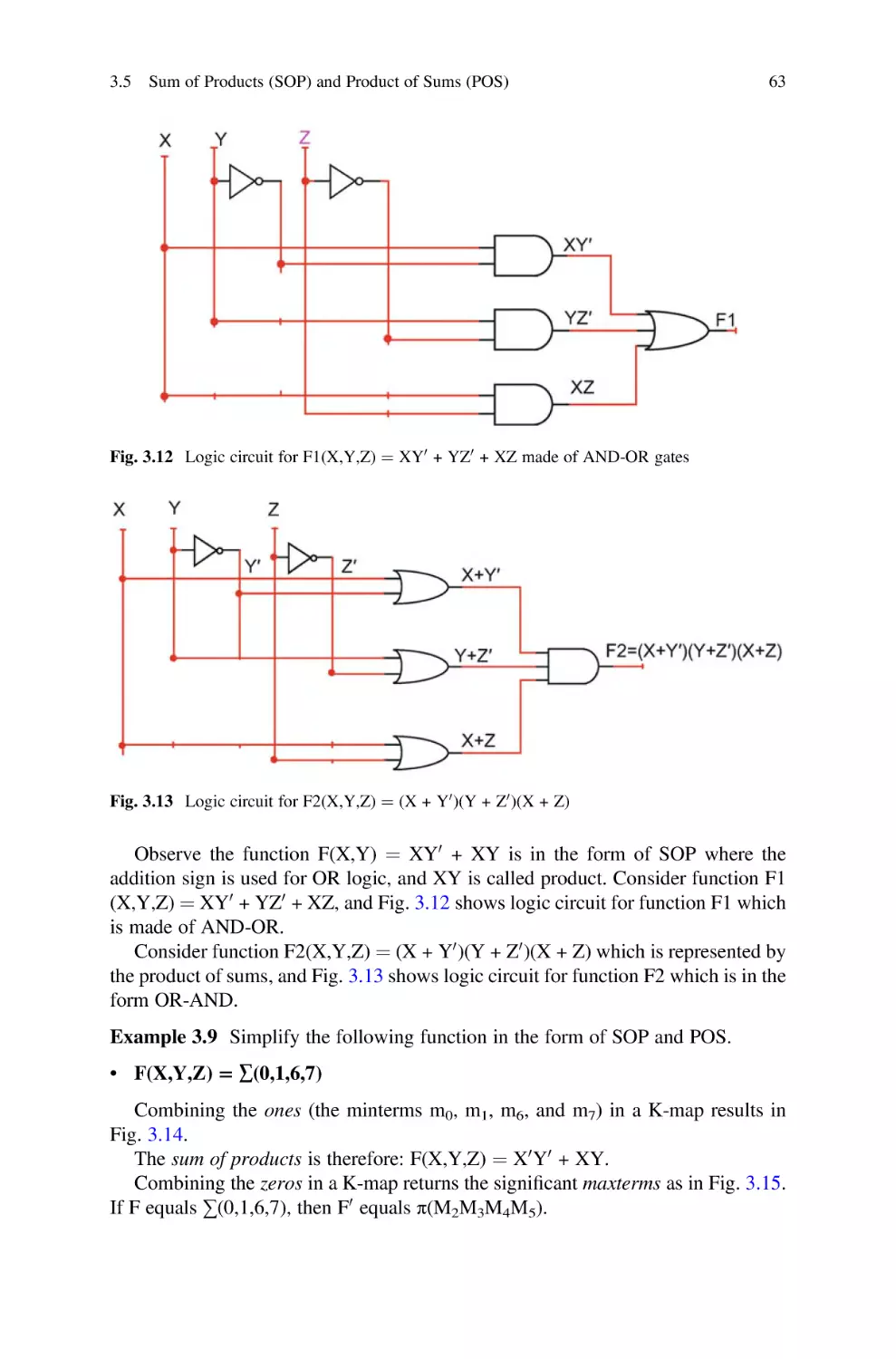
Four-Variable K-Map . . . . . . . . . . . . . . . . . . . . . . . . .
3.5
Sum of Products (SOP) and Product of Sums (POS) . . . . . . . . .
3.6
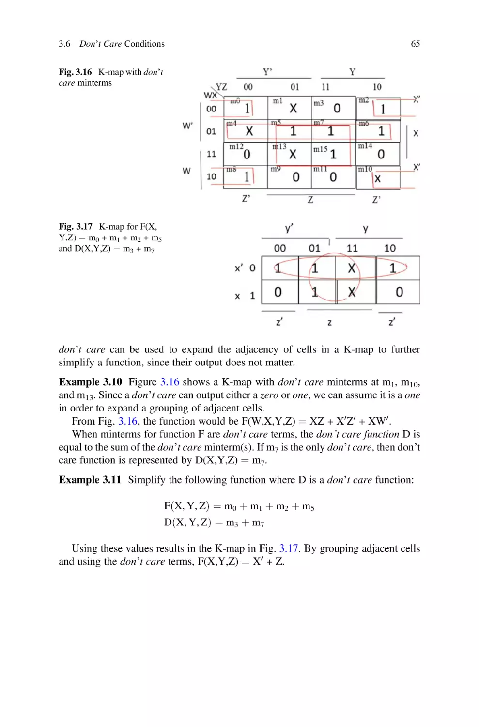
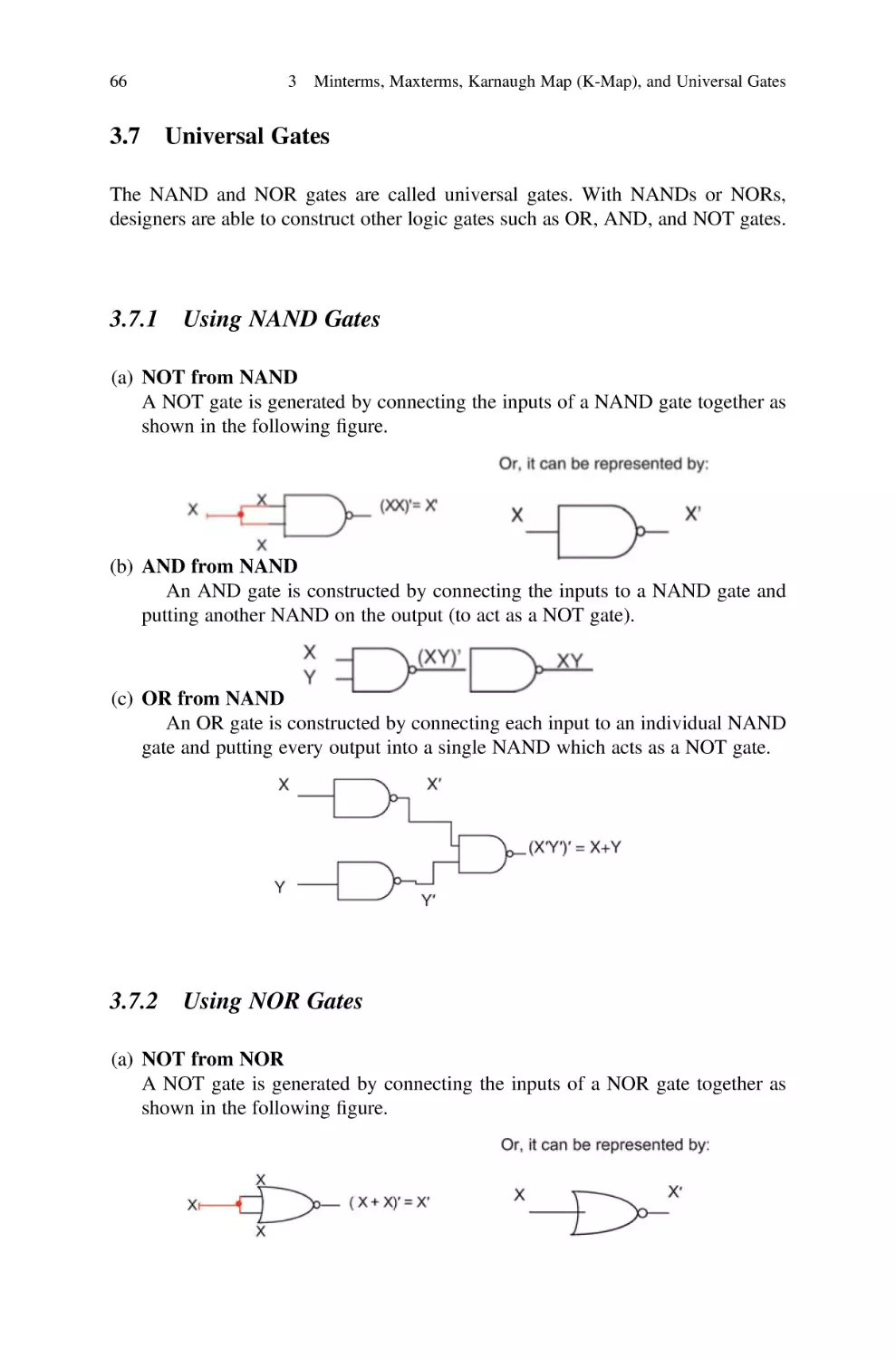
Don’t Care Conditions . . . . . . . . . . . . . . . . . . . . . . . . . . . . . .
3.7
Universal Gates . . . . . . . . . . . . . . . . . . . . . . . . . . . . . . . . . . .
3.7.1
Using NAND Gates . . . . . . . . . . . . . . . . . . . . . . . . . .
3.7.2
Using NOR Gates . . . . . . . . . . . . . . . . . . . . . . . . . . .
3.7.3
Implementation of Logic Functions Using NAND
Gates or NOR Gates Only . . . . . . . . . . . . . . . . . . . . . .
3.7.4
Using NAND Gates . . . . . . . . . . . . . . . . . . . . . . . . . .
3.7.5
Using NOR Gates . . . . . . . . . . . . . . . . . . . . . . . . . . .
3.8
Summary . . . . . . . . . . . . . . . . . . . . . . . . . . . . . . . . . . . . . . . .
Problems . . . . . . . . . . . . . . . . . . . . . . . . . . . . . . . . . . . . . . . . . . . . .
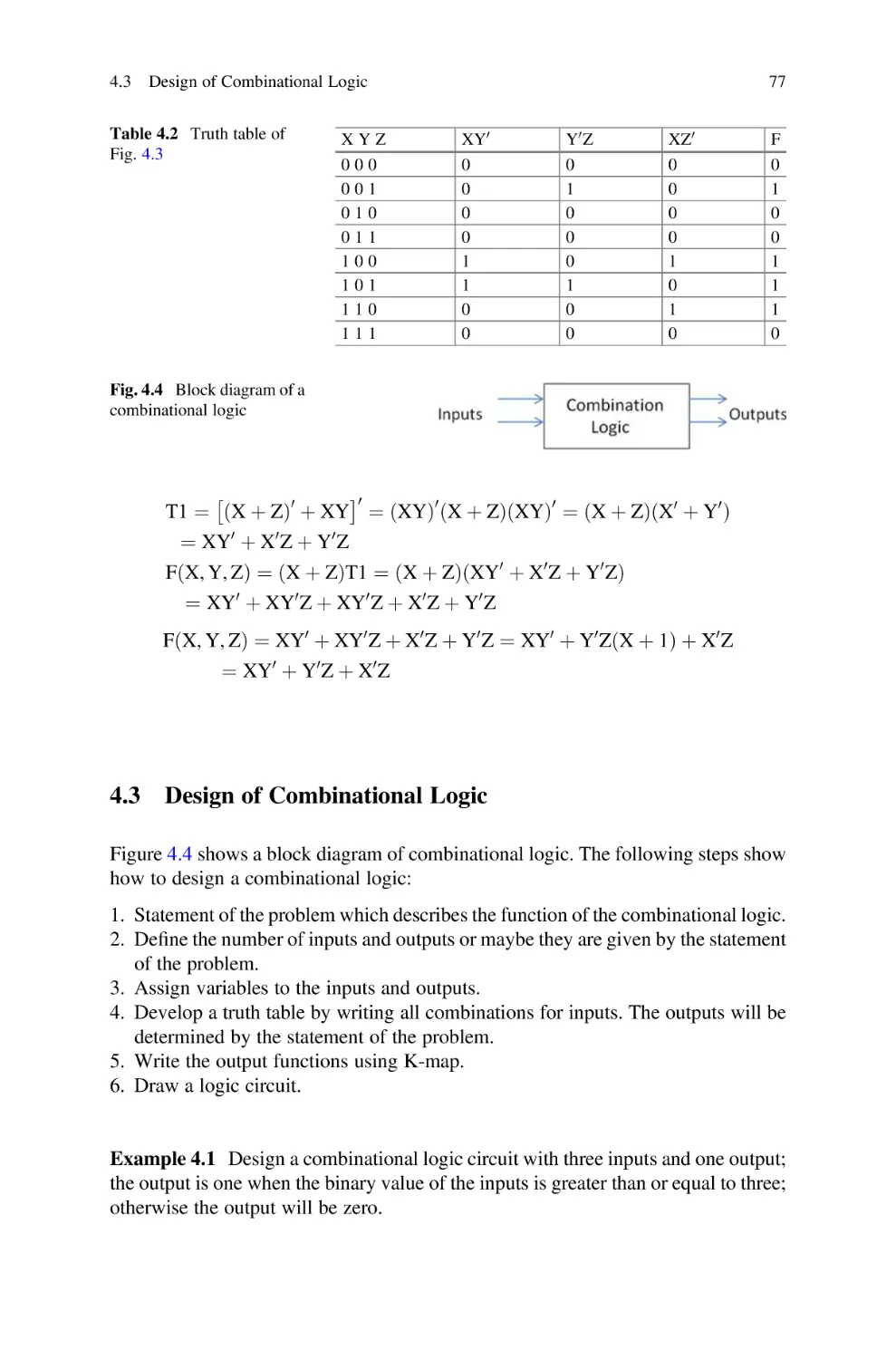
Combinational Logic . . . . . . . . . . . . . . . . . . . . . . . . . . . . . . . . . . . .
4.1
Introduction . . . . . . . . . . . . . . . . . . . . . . . . . . . . . . . . . . . . . .
4.2
Analysis of Combinational Logic . . . . . . . . . . . . . . . . . . . . . . .
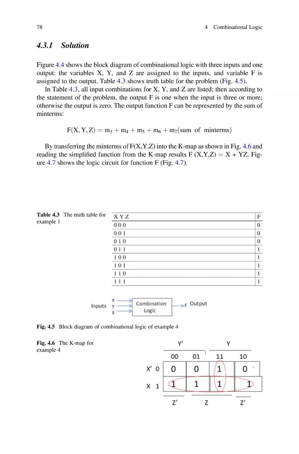
4.3
Design of Combinational Logic . . . . . . . . . . . . . . . . . . . . . . . .
4.3.1
Solution . . . . . . . . . . . . . . . . . . . . . . . . . . . . . . . . . . .
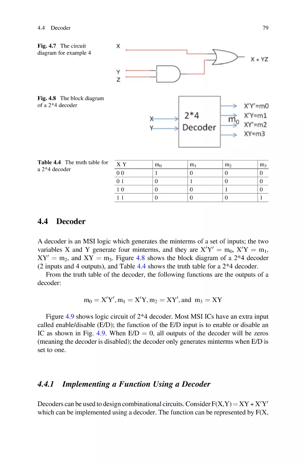
4.4
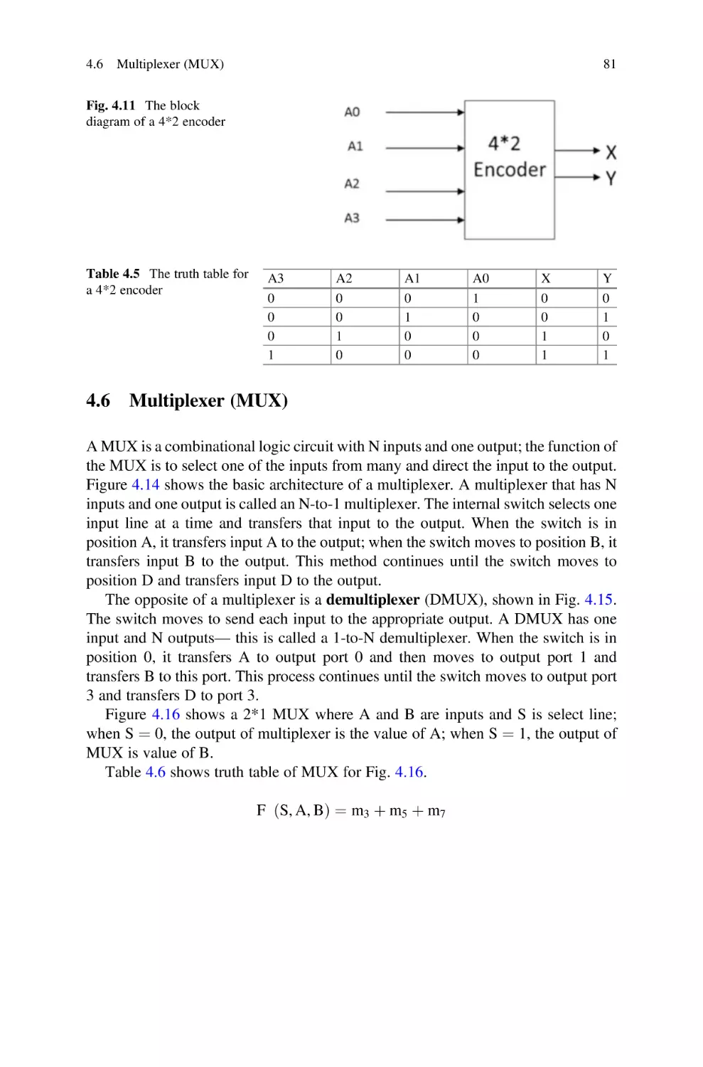
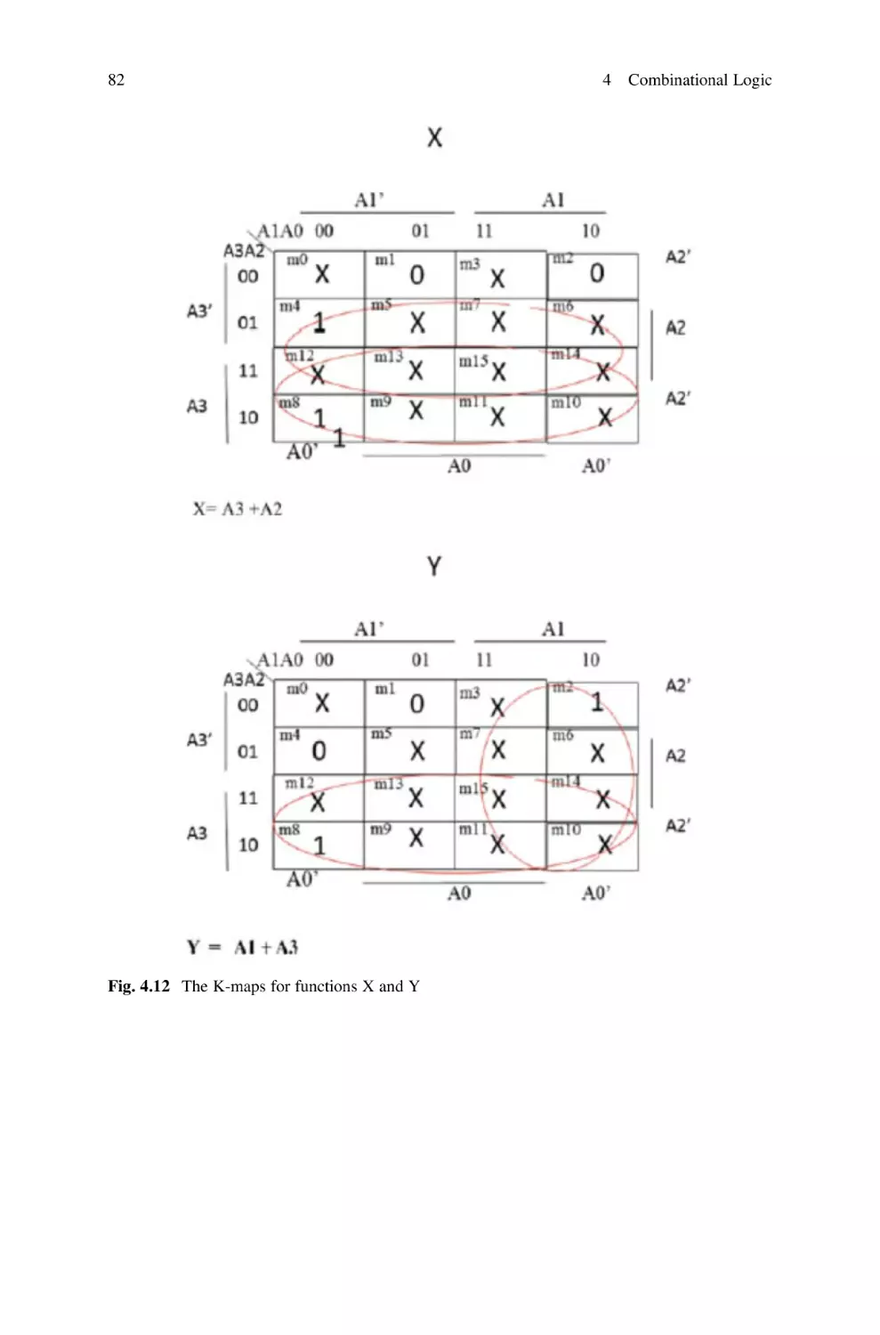
Decoder . . . . . . . . . . . . . . . . . . . . . . . . . . . . . . . . . . . . . . . . .
4.4.1
Implementing a Function Using a Decoder . . . . . . . . . .
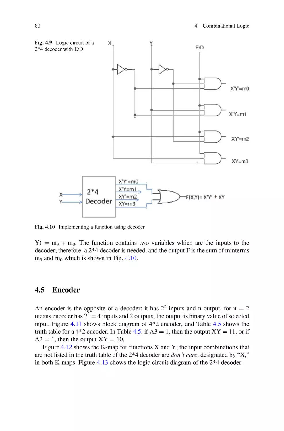
4.5
Encoder . . . . . . . . . . . . . . . . . . . . . . . . . . . . . . . . . . . . . . . . .
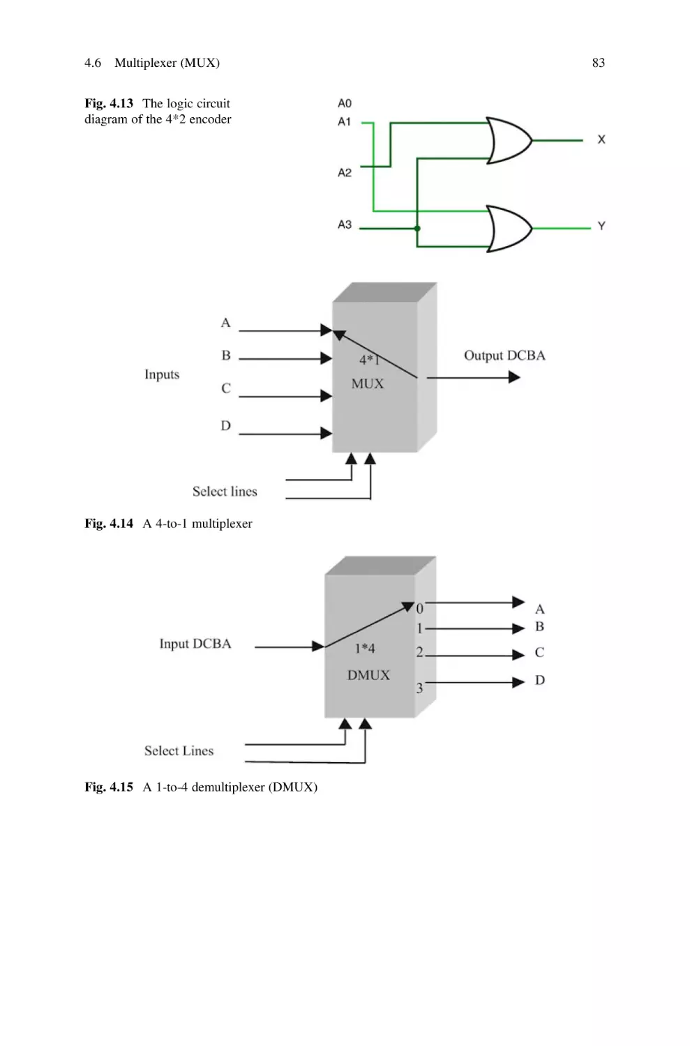
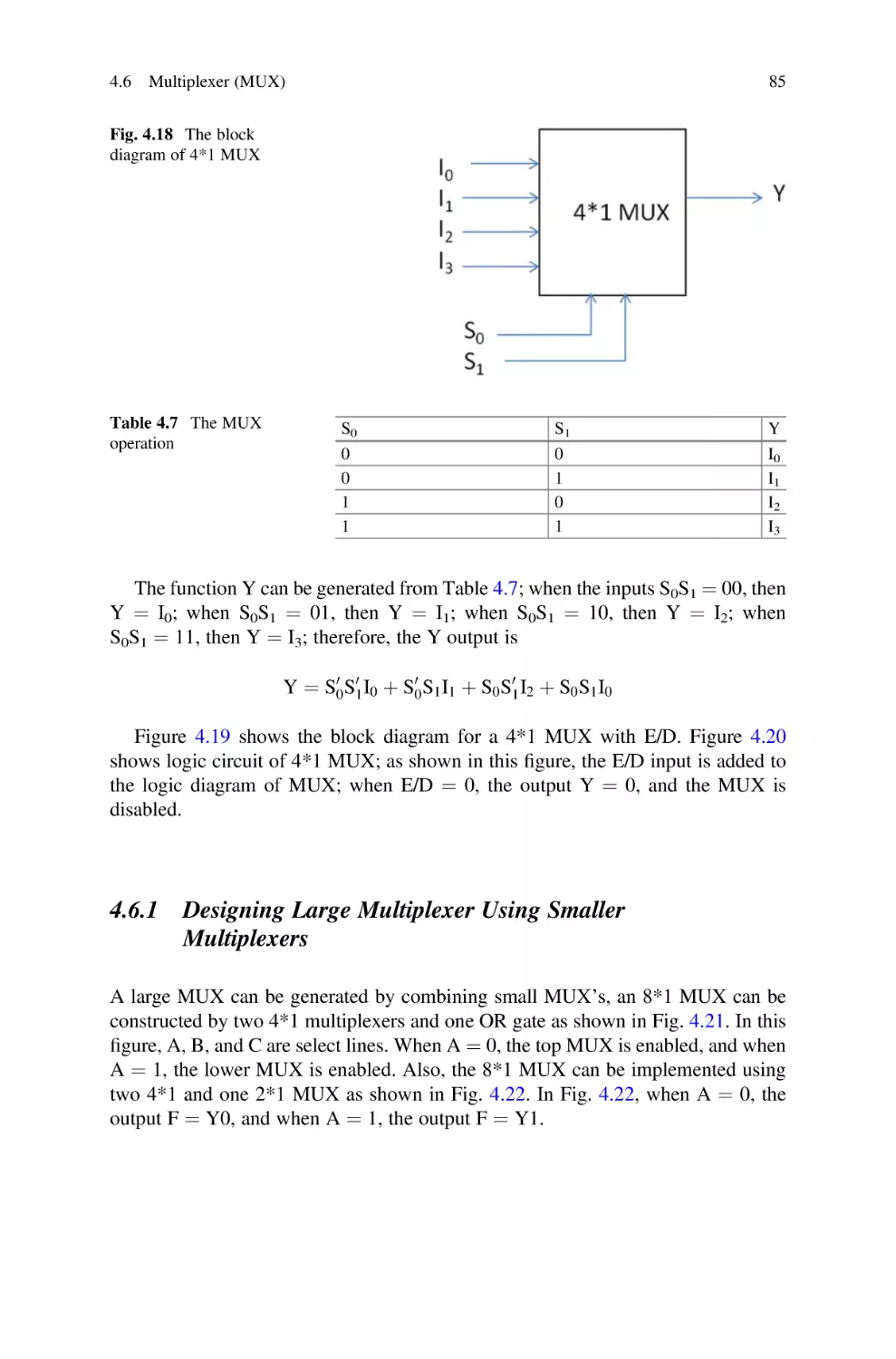
4.6
Multiplexer (MUX) . . . . . . . . . . . . . . . . . . . . . . . . . . . . . . . . .
4.6.1
Designing Large Multiplexer Using Smaller
Multiplexers . . . . . . . . . . . . . . . . . . . . . . . . . . . . . . .
4.6.2
Implementing Functions Using Multiplexer . . . . . . . . .
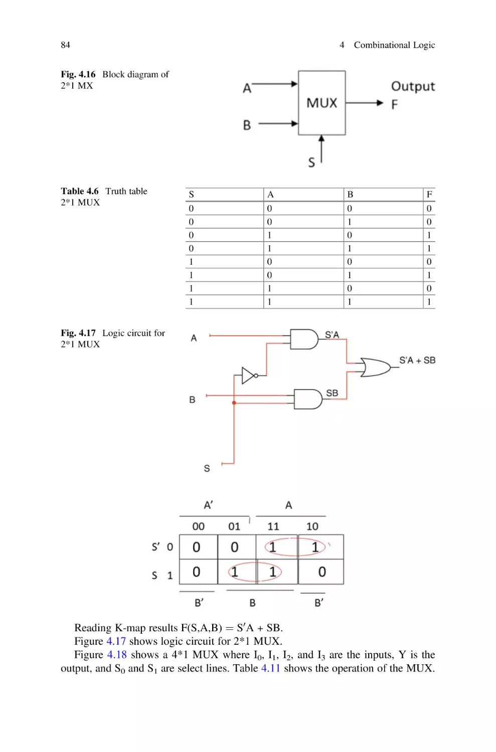
4.7
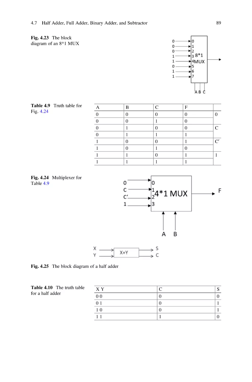
Half Adder, Full Adder, Binary Adder, and Subtractor . . . . . . .
4.7.1
Full Adder (FA) . . . . . . . . . . . . . . . . . . . . . . . . . . . . .
4.7.2
4-Bit Binary Adder . . . . . . . . . . . . . . . . . . . . . . . . . . .
4.7.3
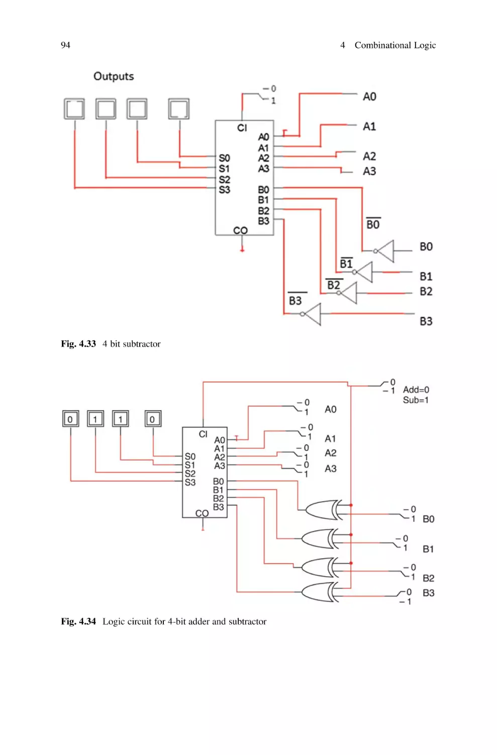
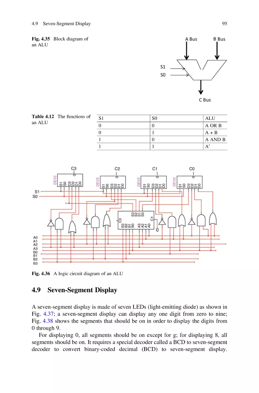
Subtractor . . . . . . . . . . . . . . . . . . . . . . . . . . . . . . . . .
4.8
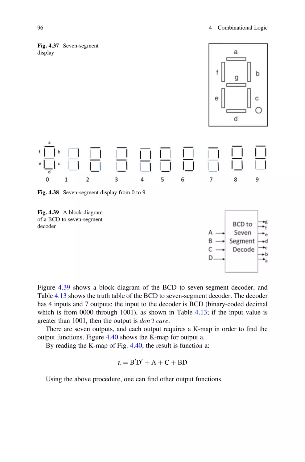
ALU (Arithmetic Logic Unit) . . . . . . . . . . . . . . . . . . . . . . . . .
4.9
Seven-Segment Display . . . . . . . . . . . . . . . . . . . . . . . . . . . . . .
4.10 Summary . . . . . . . . . . . . . . . . . . . . . . . . . . . . . . . . . . . . . . . .
Problems . . . . . . . . . . . . . . . . . . . . . . . . . . . . . . . . . . . . . . . . . . . . .
xiii
51
51
51
52
52
55
56
58
61
62
64
66
66
66
67
68
68
69
70
75
75
76
77
78
79
79
80
81
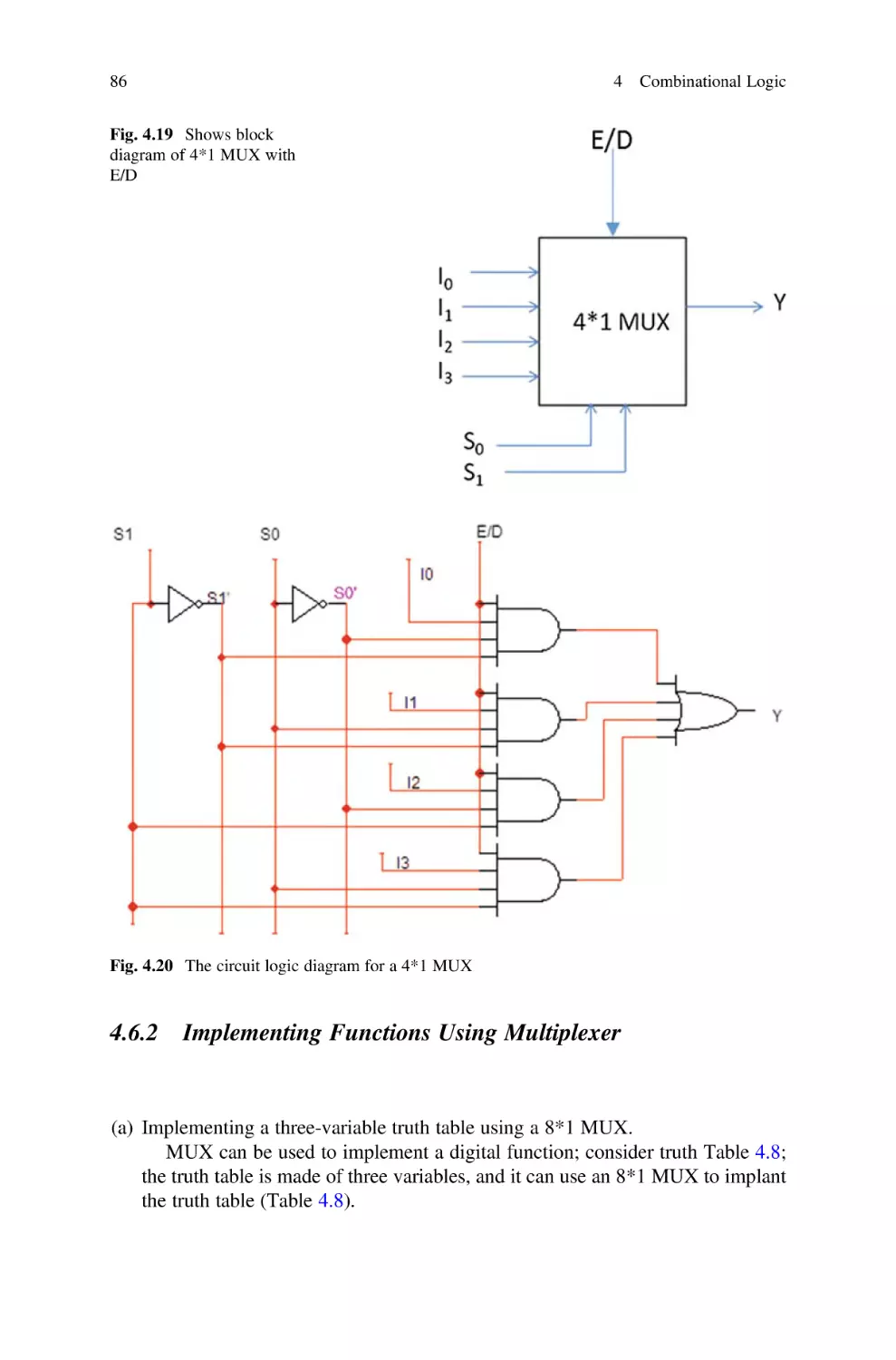
85
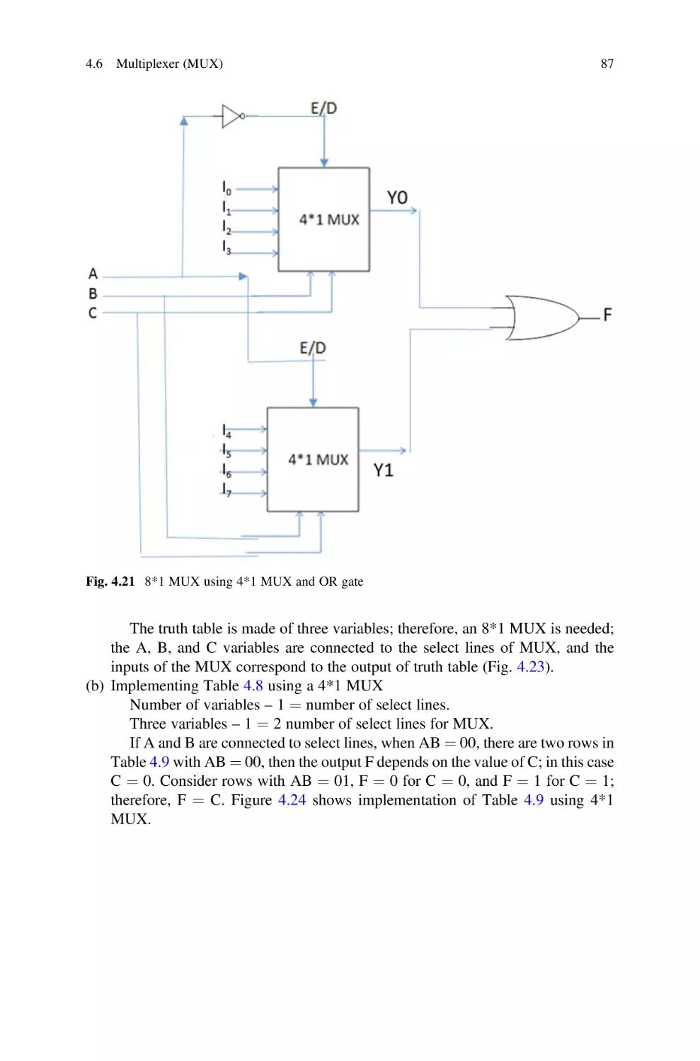
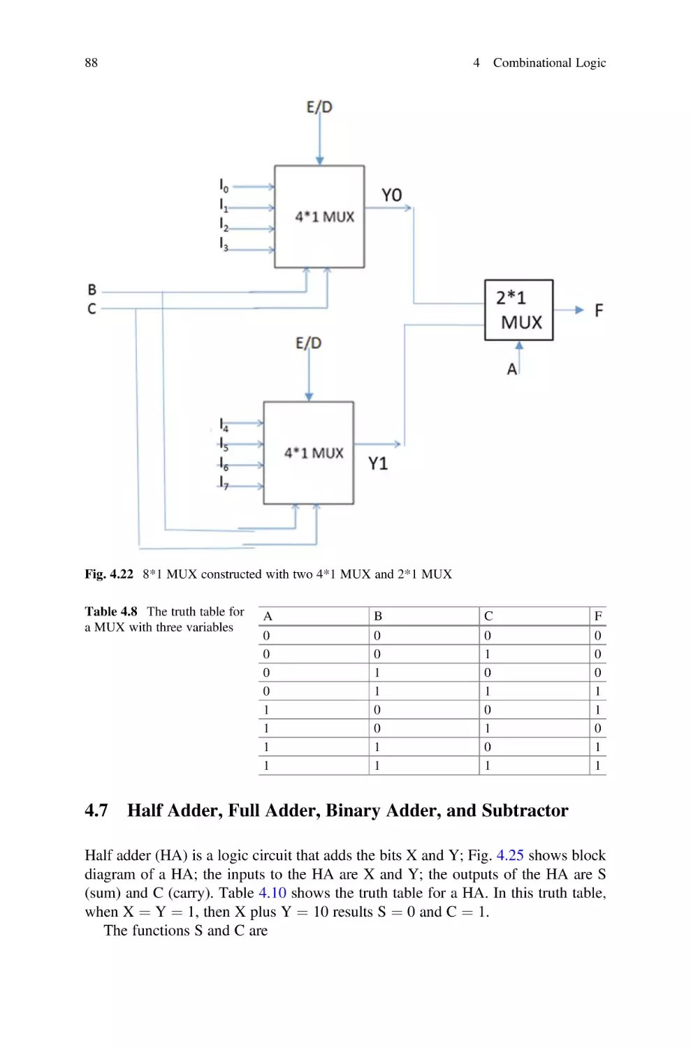
86
88
90
91
93
93
95
97
98
xiv
Contents
5
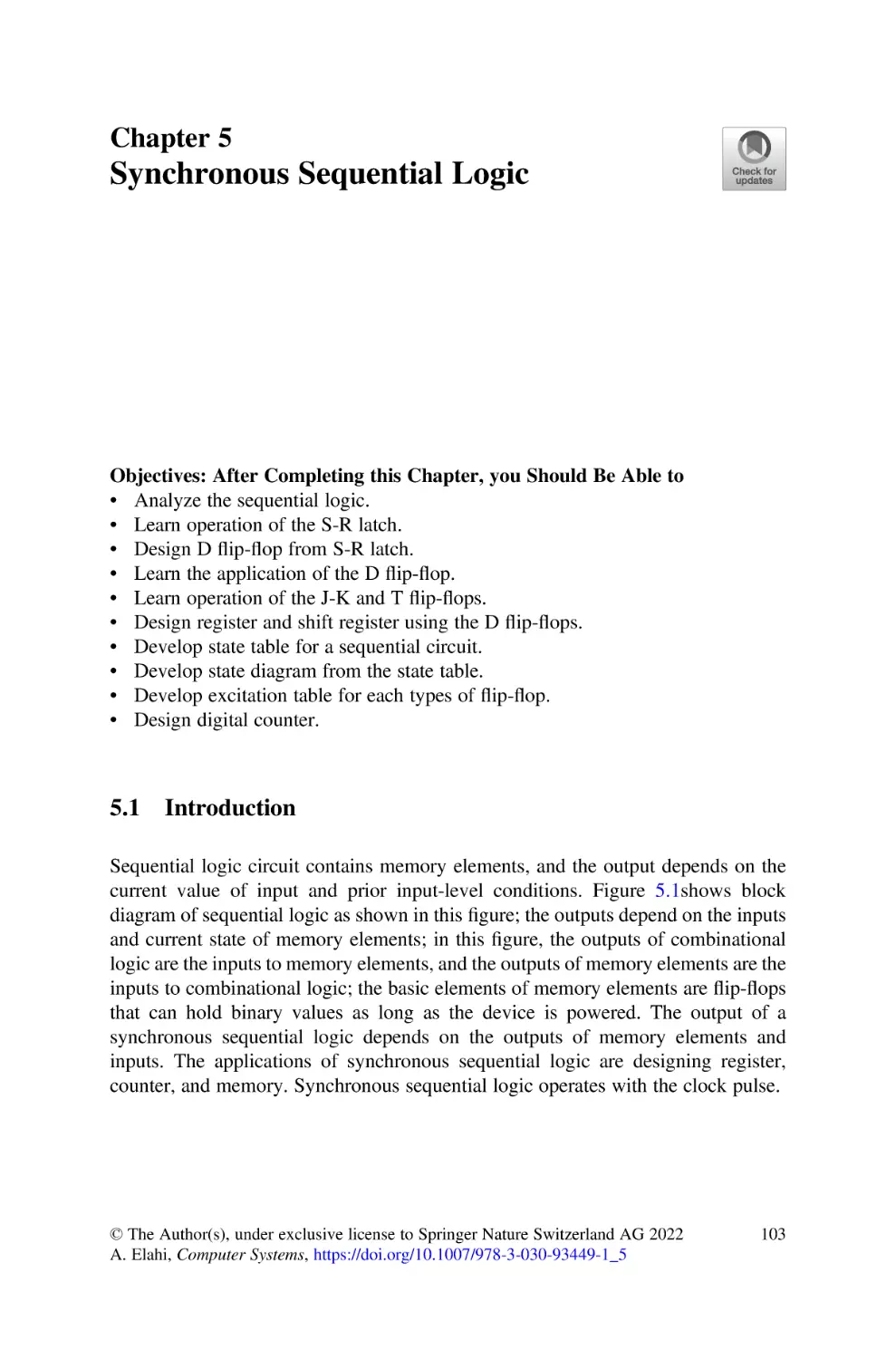
Synchronous Sequential Logic . . . . . . . . . . . . . . . . . . . . . . . . . . . .
5.1
Introduction . . . . . . . . . . . . . . . . . . . . . . . . . . . . . . . . . . . . .
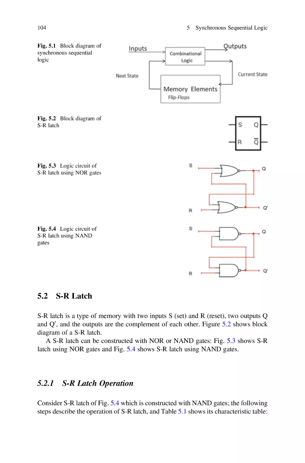
5.2
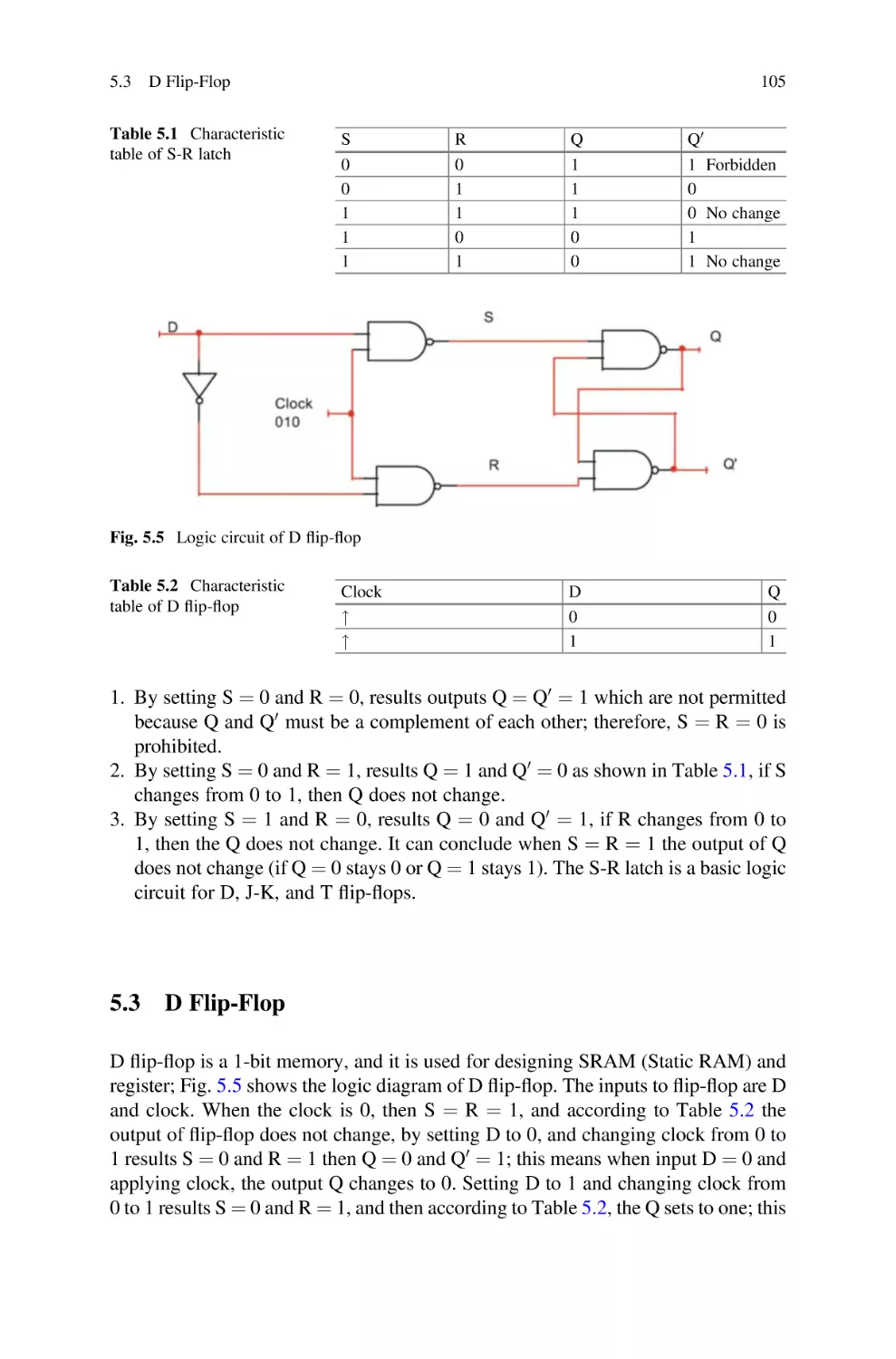
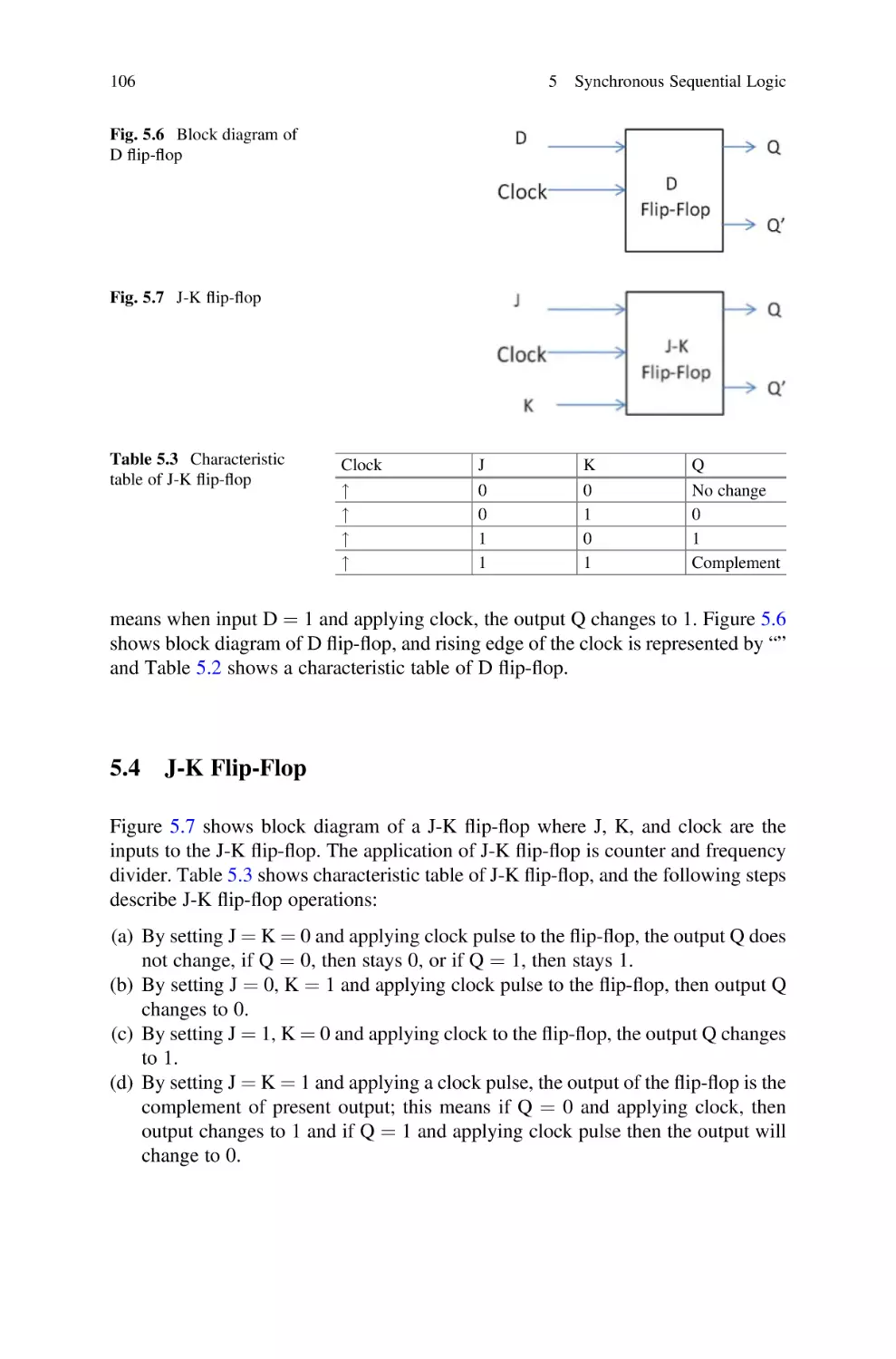
S-R Latch . . . . . . . . . . . . . . . . . . . . . . . . . . . . . . . . . . . . . . .
5.2.1
S-R Latch Operation . . . . . . . . . . . . . . . . . . . . . . . . .
5.3
D Flip-Flop . . . . . . . . . . . . . . . . . . . . . . . . . . . . . . . . . . . . .
5.4
J-K Flip-Flop . . . . . . . . . . . . . . . . . . . . . . . . . . . . . . . . . . . .
5.5
T Flip-Flop . . . . . . . . . . . . . . . . . . . . . . . . . . . . . . . . . . . . . .
5.6
Register . . . . . . . . . . . . . . . . . . . . . . . . . . . . . . . . . . . . . . . .
5.6.1
Shift Register . . . . . . . . . . . . . . . . . . . . . . . . . . . . . .
5.6.2
Barrel Shifter . . . . . . . . . . . . . . . . . . . . . . . . . . . . . .
5.7
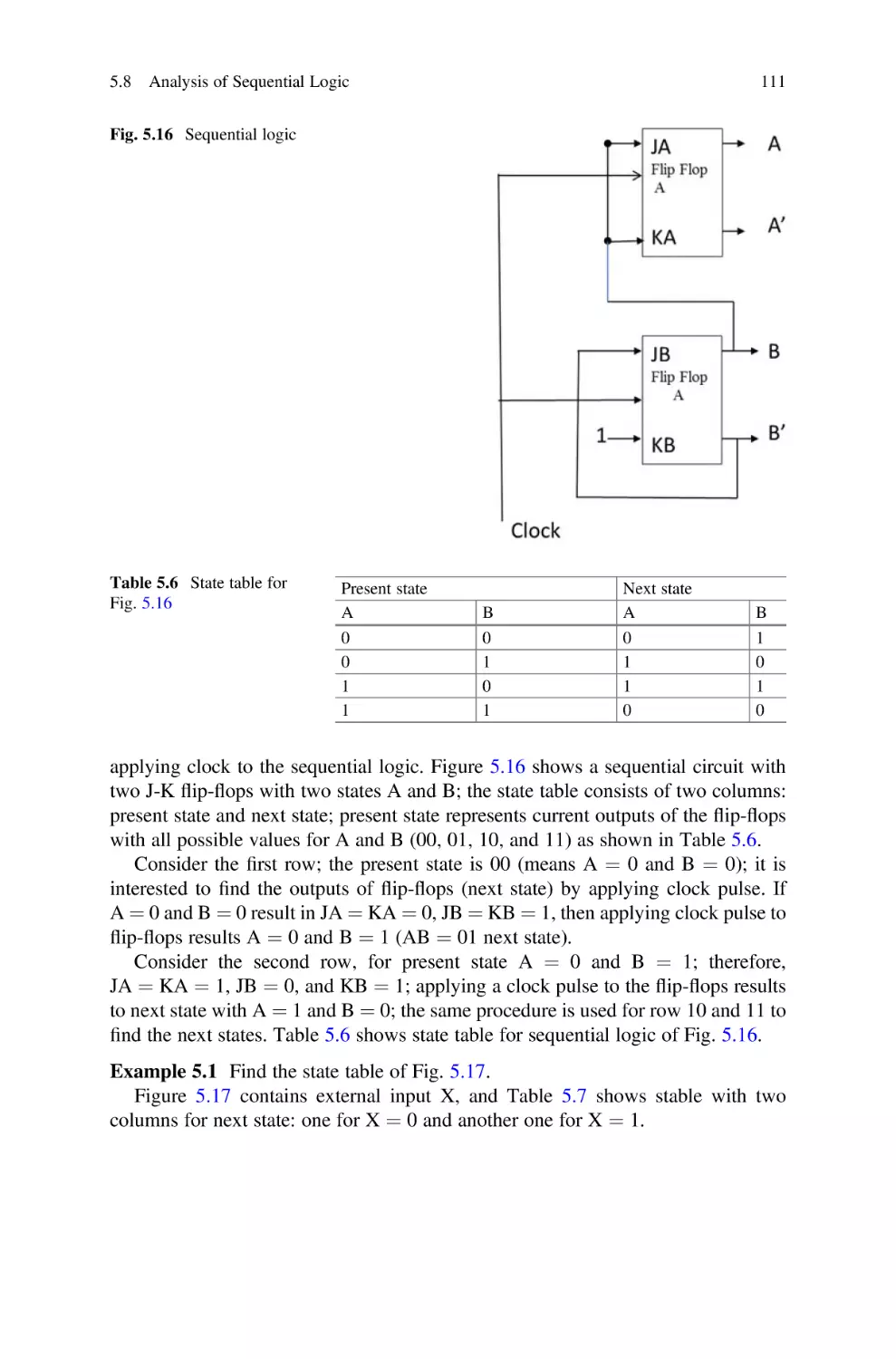
Frequency Divider Using J-K Flip-Flop . . . . . . . . . . . . . . . . .
5.8
Analysis of Sequential Logic . . . . . . . . . . . . . . . . . . . . . . . . .
5.9
State Diagram . . . . . . . . . . . . . . . . . . . . . . . . . . . . . . . . . . . .
5.9.1
D Flip-Flop State Diagram . . . . . . . . . . . . . . . . . . . .
5.10 Flip-Flop Excitation Table . . . . . . . . . . . . . . . . . . . . . . . . . . .
5.10.1 D Flip-Flop Excitation Table. . . . . . . . . . . . . . . . . . .
5.10.2 Excitation Table Operation . . . . . . . . . . . . . . . . . . . .
5.10.3 J-K Flip-Flop Excitation Table . . . . . . . . . . . . . . . . .
5.10.4 T Flip-Flop Excitation Table . . . . . . . . . . . . . . . . . . .
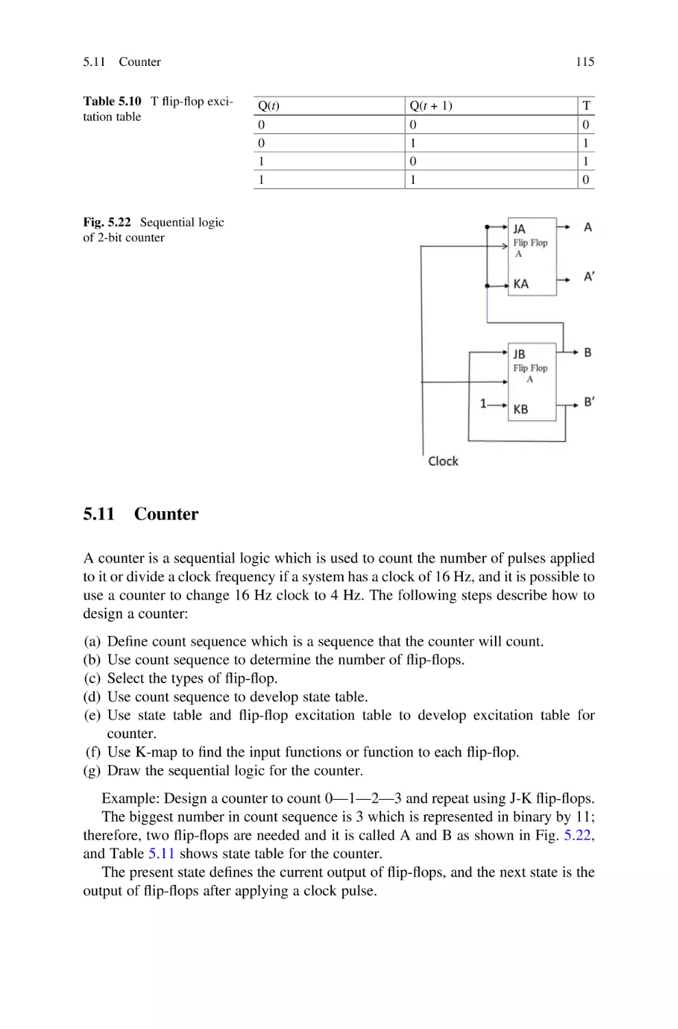
5.11 Counter . . . . . . . . . . . . . . . . . . . . . . . . . . . . . . . . . . . . . . . .
5.12 Summary . . . . . . . . . . . . . . . . . . . . . . . . . . . . . . . . . . . . . . .
Problems . . . . . . . . . . . . . . . . . . . . . . . . . . . . . . . . . . . . . . . . . . . .
.
.
.
.
.
.
.
.
.
.
.
.
.
.
.
.
.
.
.
.
.
.
103
103
103
104
105
106
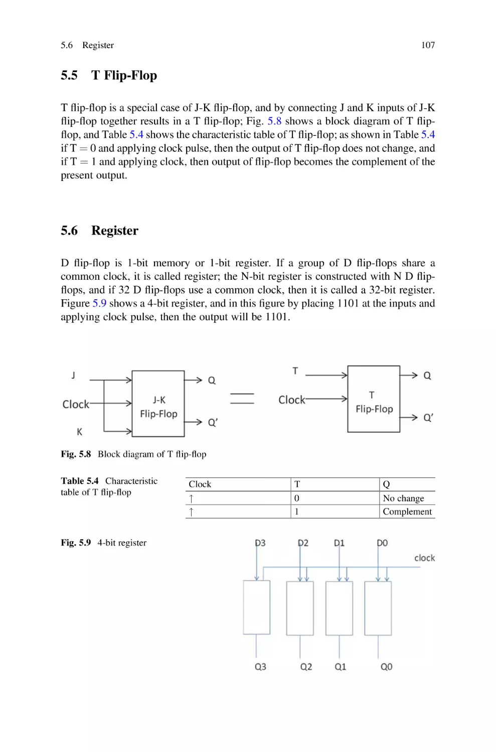
107
107
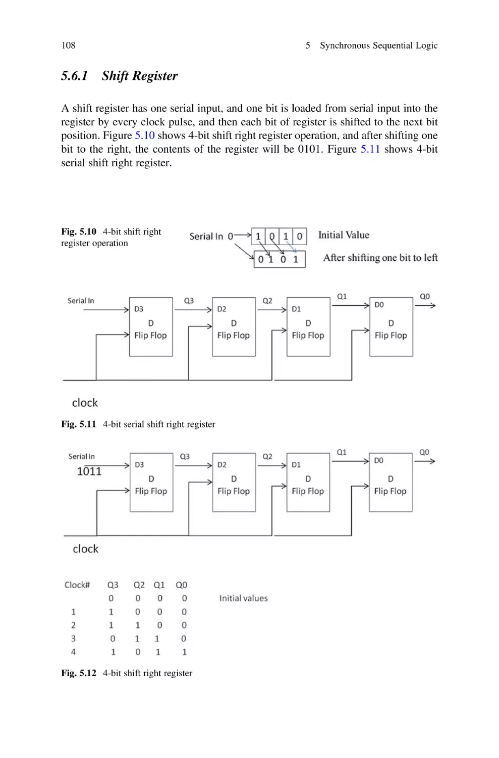
108
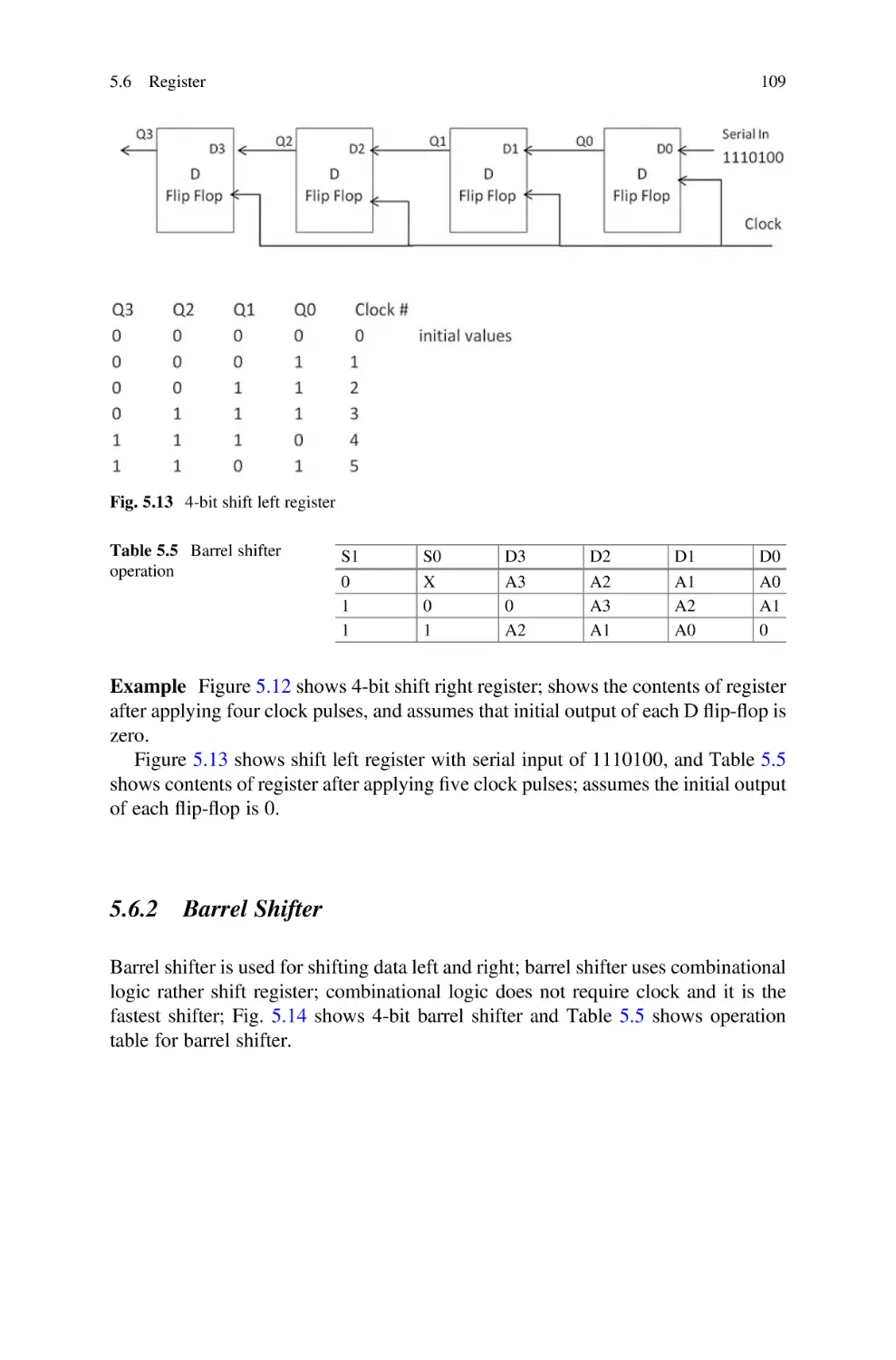
109
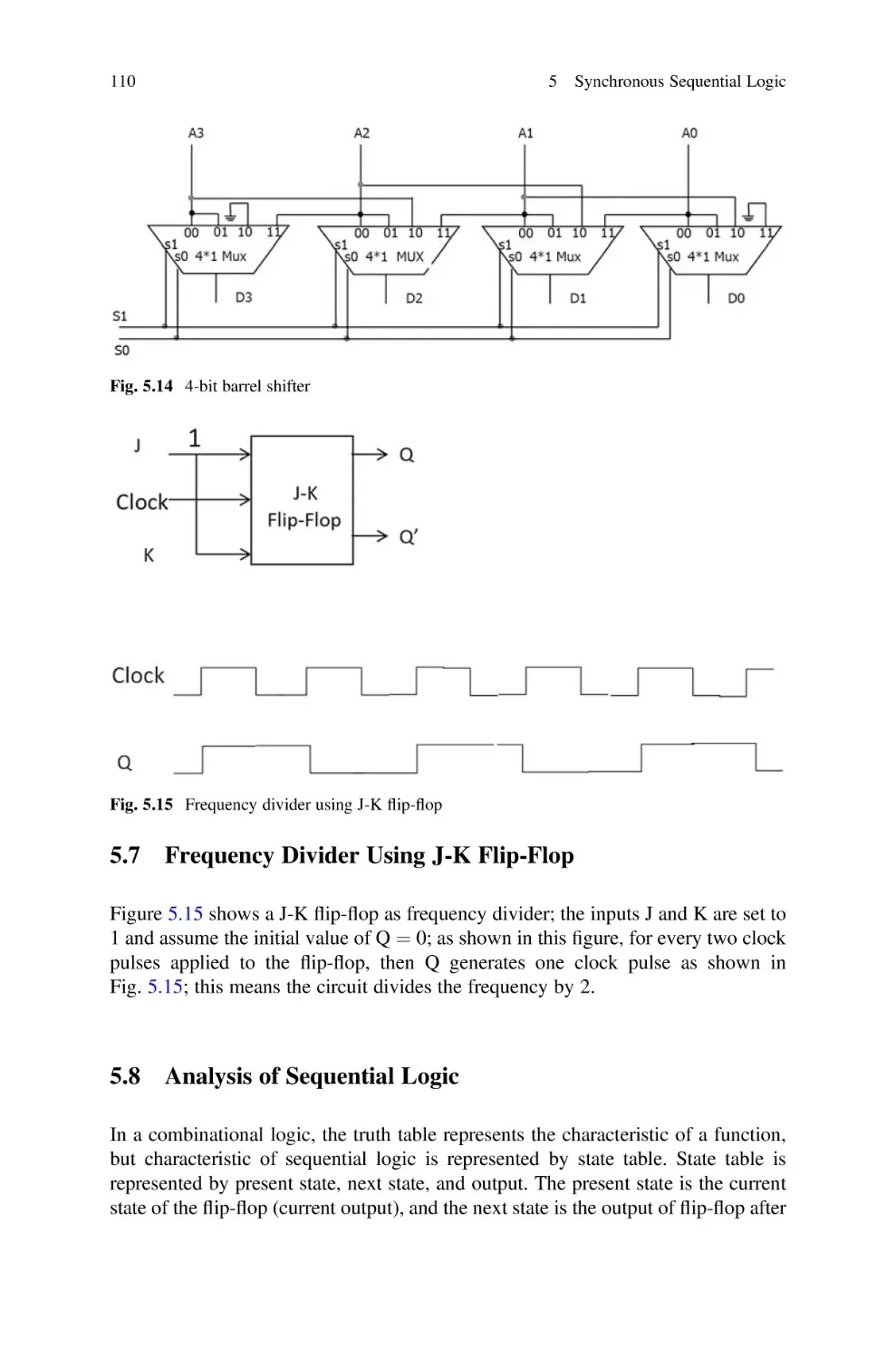
110
110
112
112
113
113
114
114
114
115
116
118
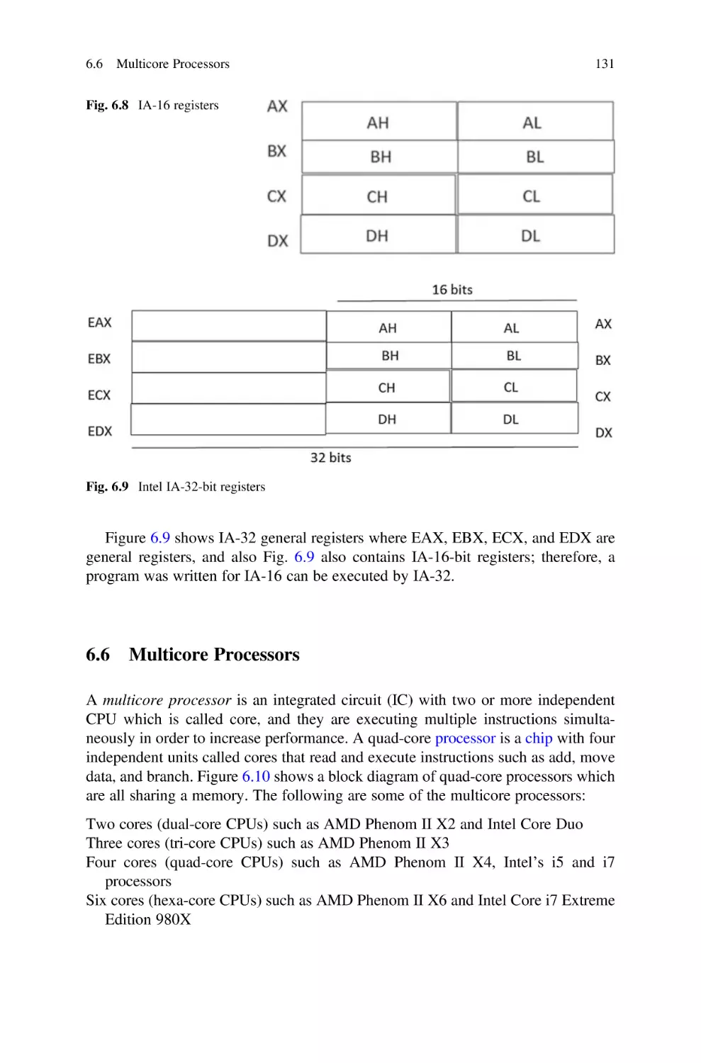
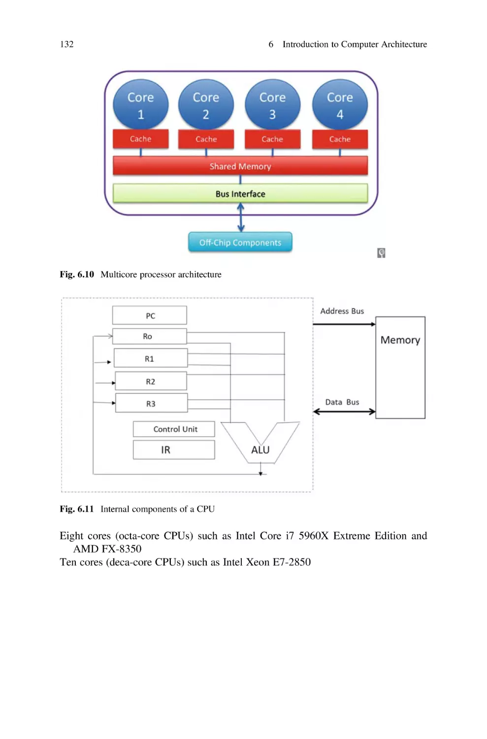
6
Introduction to Computer Architecture . . . . . . . . . . . . . . . . . . . . . .
6.1
Introduction . . . . . . . . . . . . . . . . . . . . . . . . . . . . . . . . . . . . . .
6.1.1
Abstract Representation of Computer Architecture . . . .
6.2
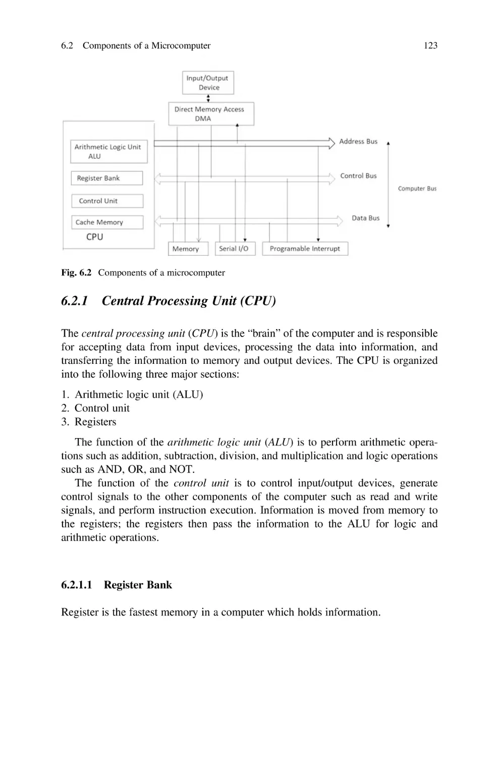
Components of a Microcomputer . . . . . . . . . . . . . . . . . . . . . . .
6.2.1
Central Processing Unit (CPU) . . . . . . . . . . . . . . . . . .
6.2.2
CPU Buses . . . . . . . . . . . . . . . . . . . . . . . . . . . . . . . .
6.2.3
Memory . . . . . . . . . . . . . . . . . . . . . . . . . . . . . . . . . .
6.2.4
Serial Input/Output . . . . . . . . . . . . . . . . . . . . . . . . . . .
6.2.5
Direct Memory Access (DMA) . . . . . . . . . . . . . . . . . .
6.2.6
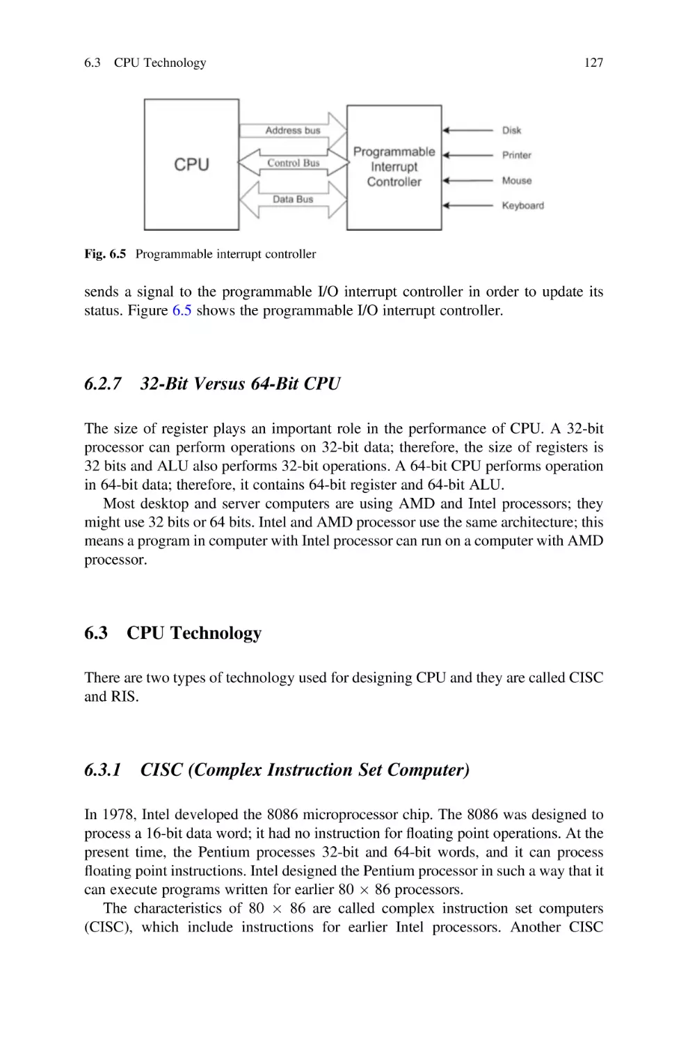
Programmable I/O Interrupt . . . . . . . . . . . . . . . . . . . .
6.2.7
32-Bit Versus 64-Bit CPU . . . . . . . . . . . . . . . . . . . . .
6.3
CPU Technology . . . . . . . . . . . . . . . . . . . . . . . . . . . . . . . . . .
6.3.1
CISC (Complex Instruction Set Computer) . . . . . . . . . .
6.3.2
RISC . . . . . . . . . . . . . . . . . . . . . . . . . . . . . . . . . . . . .
6.4
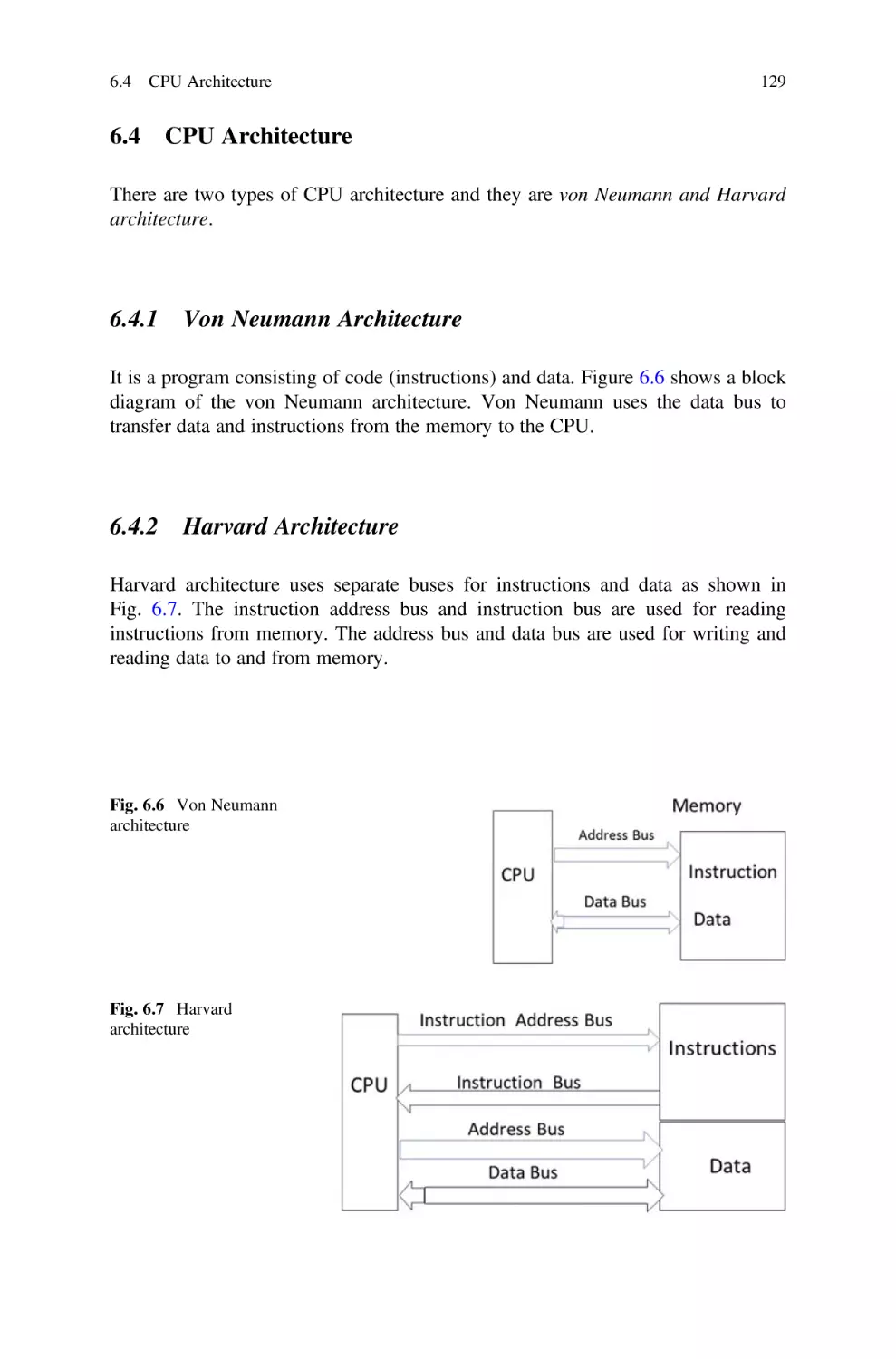
CPU Architecture . . . . . . . . . . . . . . . . . . . . . . . . . . . . . . . . . .
6.4.1
Von Neumann Architecture . . . . . . . . . . . . . . . . . . . . .
6.4.2
Harvard Architecture . . . . . . . . . . . . . . . . . . . . . . . . .
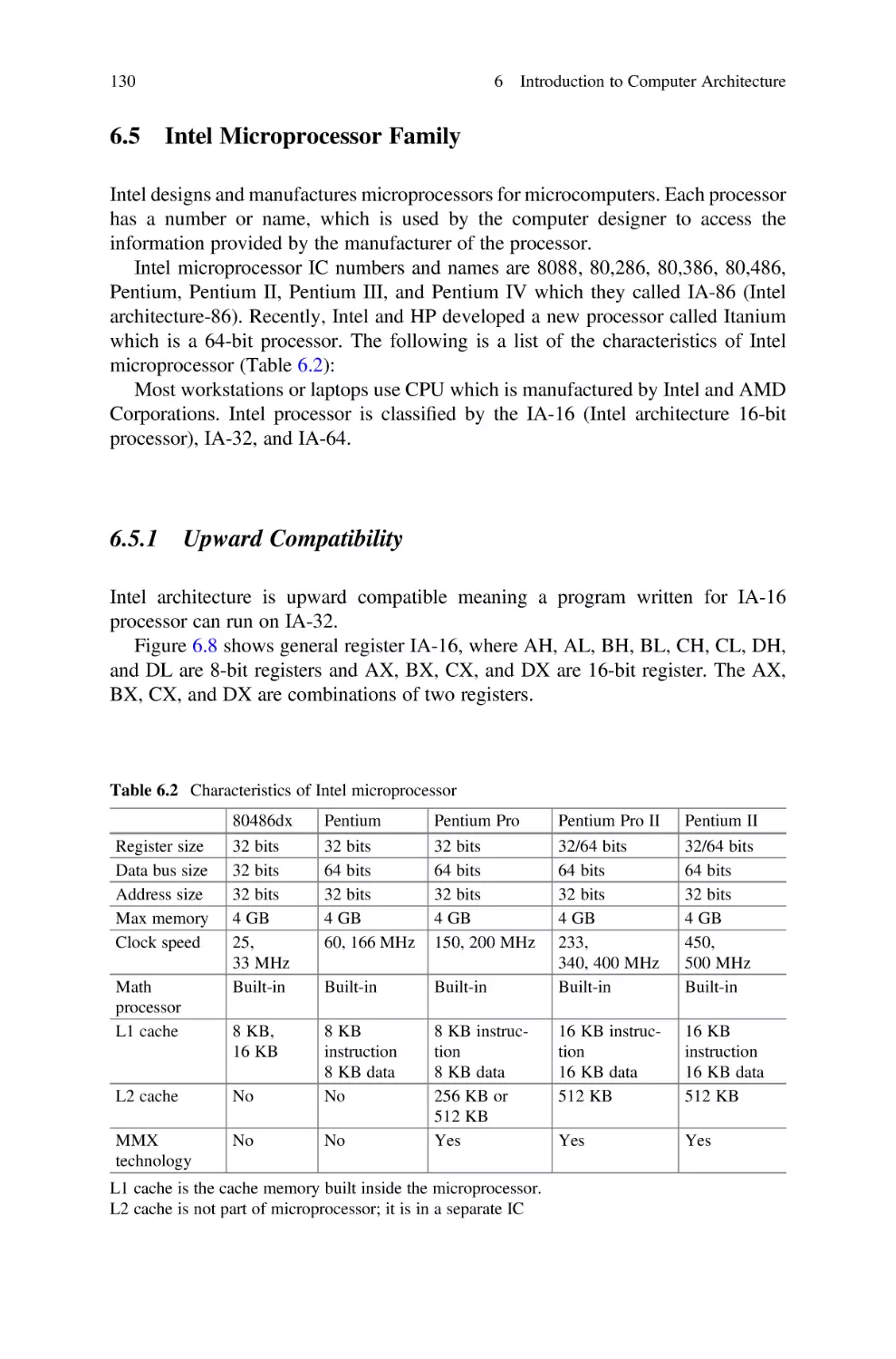
6.5
Intel Microprocessor Family . . . . . . . . . . . . . . . . . . . . . . . . . .
6.5.1
Upward Compatibility . . . . . . . . . . . . . . . . . . . . . . . .
6.6
Multicore Processors . . . . . . . . . . . . . . . . . . . . . . . . . . . . . . . .
6.7
CPU Instruction Execution Steps . . . . . . . . . . . . . . . . . . . . . . .
6.7.1
Pipelining . . . . . . . . . . . . . . . . . . . . . . . . . . . . . . . . .
121
121
121
122
123
124
125
126
126
126
127
127
127
128
129
129
129
130
130
131
133
133
Contents
xv
6.8
6.9
Disk Controller . . . . . . . . . . . . . . . . . . . . . . . . . . . . . . . . . . . .
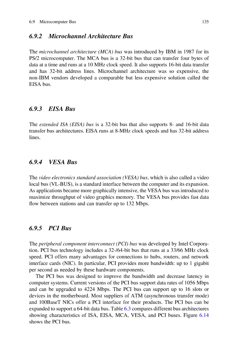
Microcomputer Bus . . . . . . . . . . . . . . . . . . . . . . . . . . . . . . . . .
6.9.1
ISA Bus . . . . . . . . . . . . . . . . . . . . . . . . . . . . . . . . . .
6.9.2
Microchannel Architecture Bus . . . . . . . . . . . . . . . . . .
6.9.3
EISA Bus . . . . . . . . . . . . . . . . . . . . . . . . . . . . . . . . .
6.9.4
VESA Bus . . . . . . . . . . . . . . . . . . . . . . . . . . . . . . . . .
6.9.5
PCI Bus . . . . . . . . . . . . . . . . . . . . . . . . . . . . . . . . . . .
6.9.6
Universal Serial BUS (USB) . . . . . . . . . . . . . . . . . . . .
6.9.7
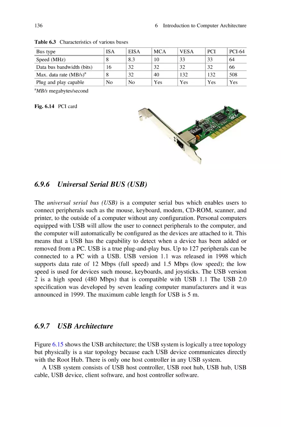
USB Architecture . . . . . . . . . . . . . . . . . . . . . . . . . . . .
6.9.8
PCI Express Bus . . . . . . . . . . . . . . . . . . . . . . . . . . . .
6.10 FireWire . . . . . . . . . . . . . . . . . . . . . . . . . . . . . . . . . . . . . . . . .
6.10.1 HDMI (High-Definition Multimedia Interface) . . . . . . .
6.11 Summary . . . . . . . . . . . . . . . . . . . . . . . . . . . . . . . . . . . . . . . .
Review Questions . . . . . . . . . . . . . . . . . . . . . . . . . . . . . . . . . . . . . . .
134
134
134
135
135
135
135
136
136
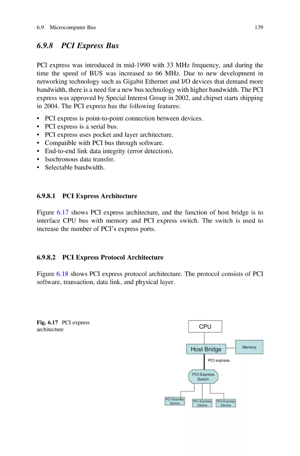
139
140
141
142
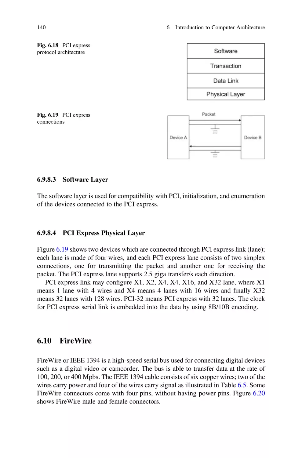
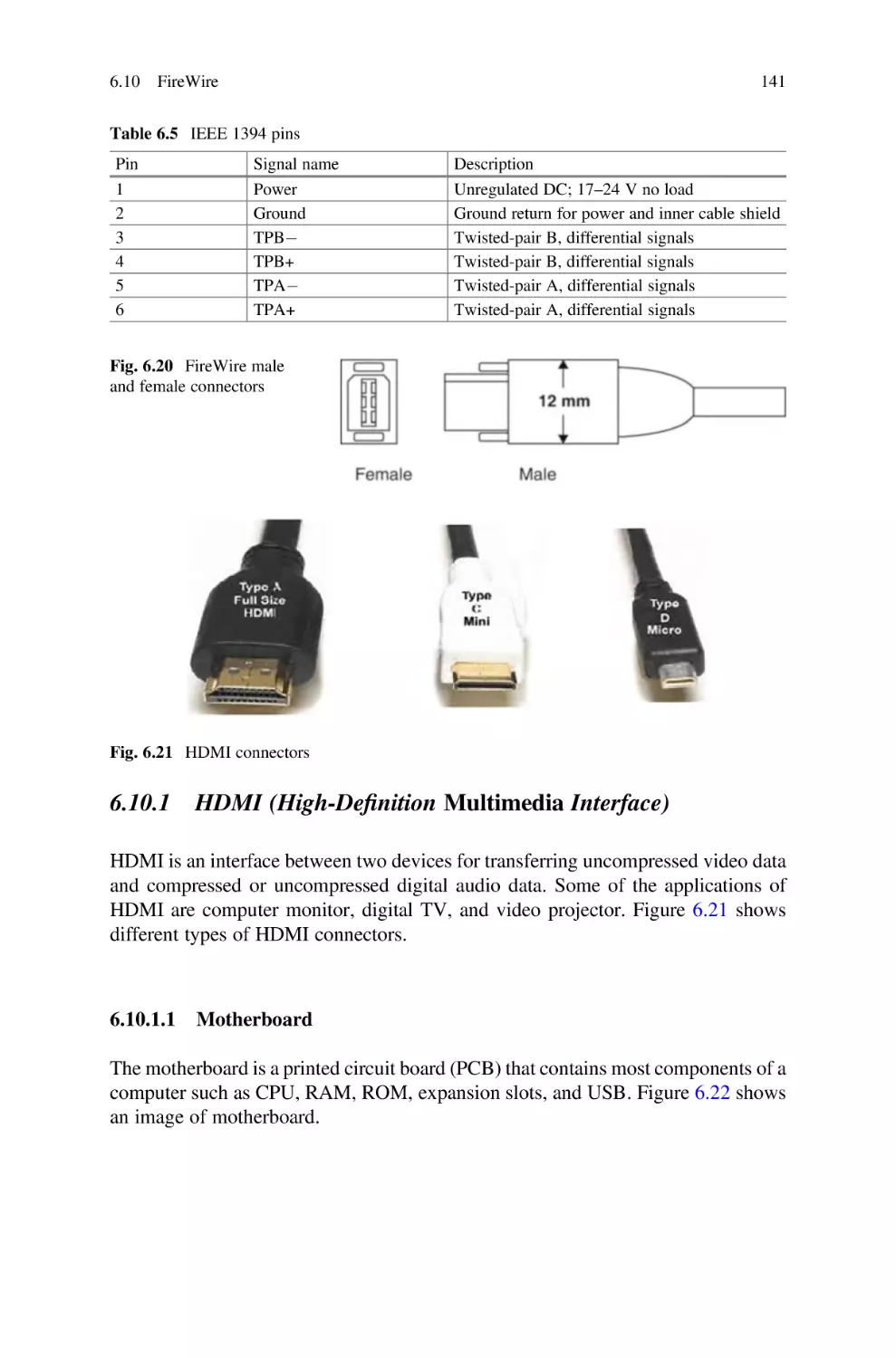
143
7
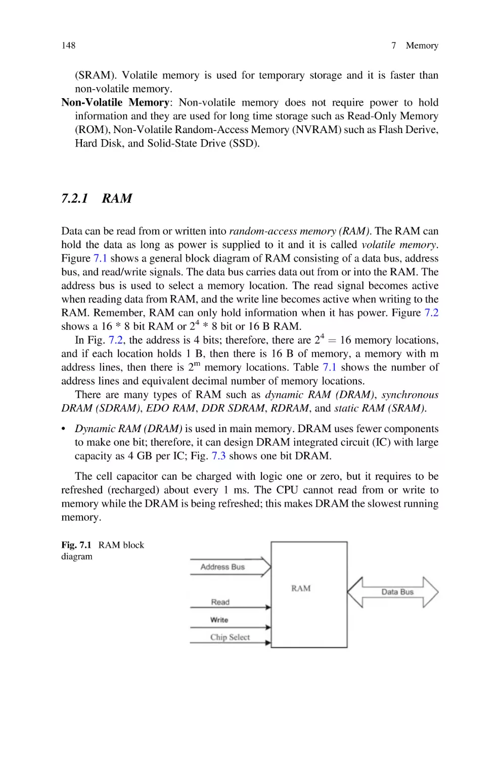
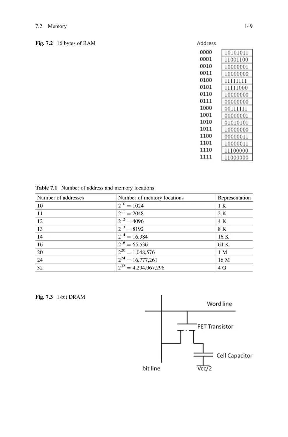
Memory . . . . . . . . . . . . . . . . . . . . . . . . . . . . . . . . . . . . . . . . . . . . .
7.1
Introduction . . . . . . . . . . . . . . . . . . . . . . . . . . . . . . . . . . . . . .
7.2
Memory . . . . . . . . . . . . . . . . . . . . . . . . . . . . . . . . . . . . . . . . .
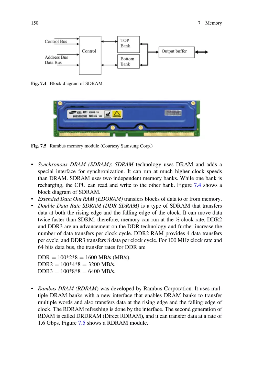
7.2.1
RAM . . . . . . . . . . . . . . . . . . . . . . . . . . . . . . . . . . . . .
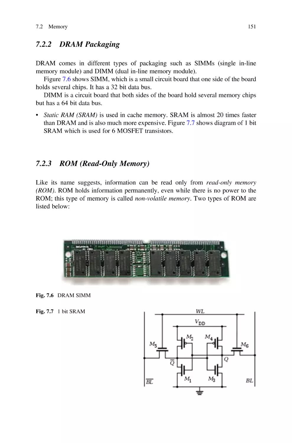
7.2.2
DRAM Packaging . . . . . . . . . . . . . . . . . . . . . . . . . . .
7.2.3
ROM (Read-Only Memory) . . . . . . . . . . . . . . . . . . . .
7.2.4
Memory Access Time . . . . . . . . . . . . . . . . . . . . . . . . .
7.3
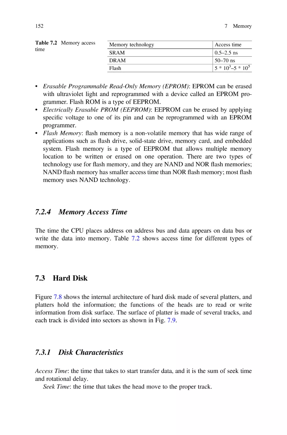
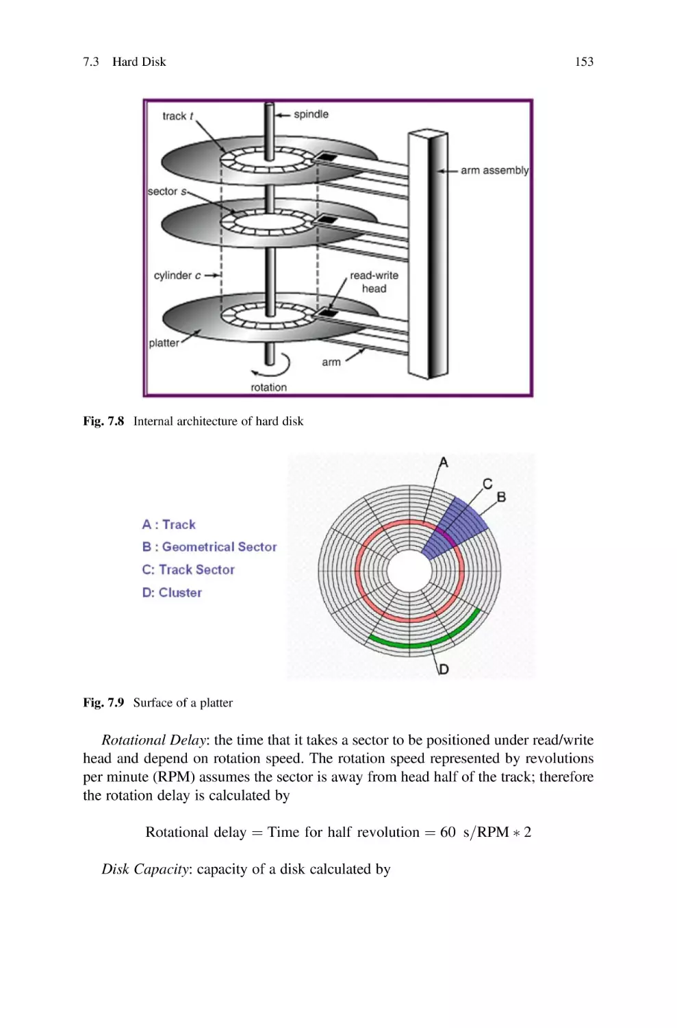
Hard Disk . . . . . . . . . . . . . . . . . . . . . . . . . . . . . . . . . . . . . . . .
7.3.1
Disk Characteristics . . . . . . . . . . . . . . . . . . . . . . . . . .
7.3.2
Cluster . . . . . . . . . . . . . . . . . . . . . . . . . . . . . . . . . . .
7.3.3
Disk File System . . . . . . . . . . . . . . . . . . . . . . . . . . . .
7.4
Solid-State Drive (SSD) . . . . . . . . . . . . . . . . . . . . . . . . . . . . .
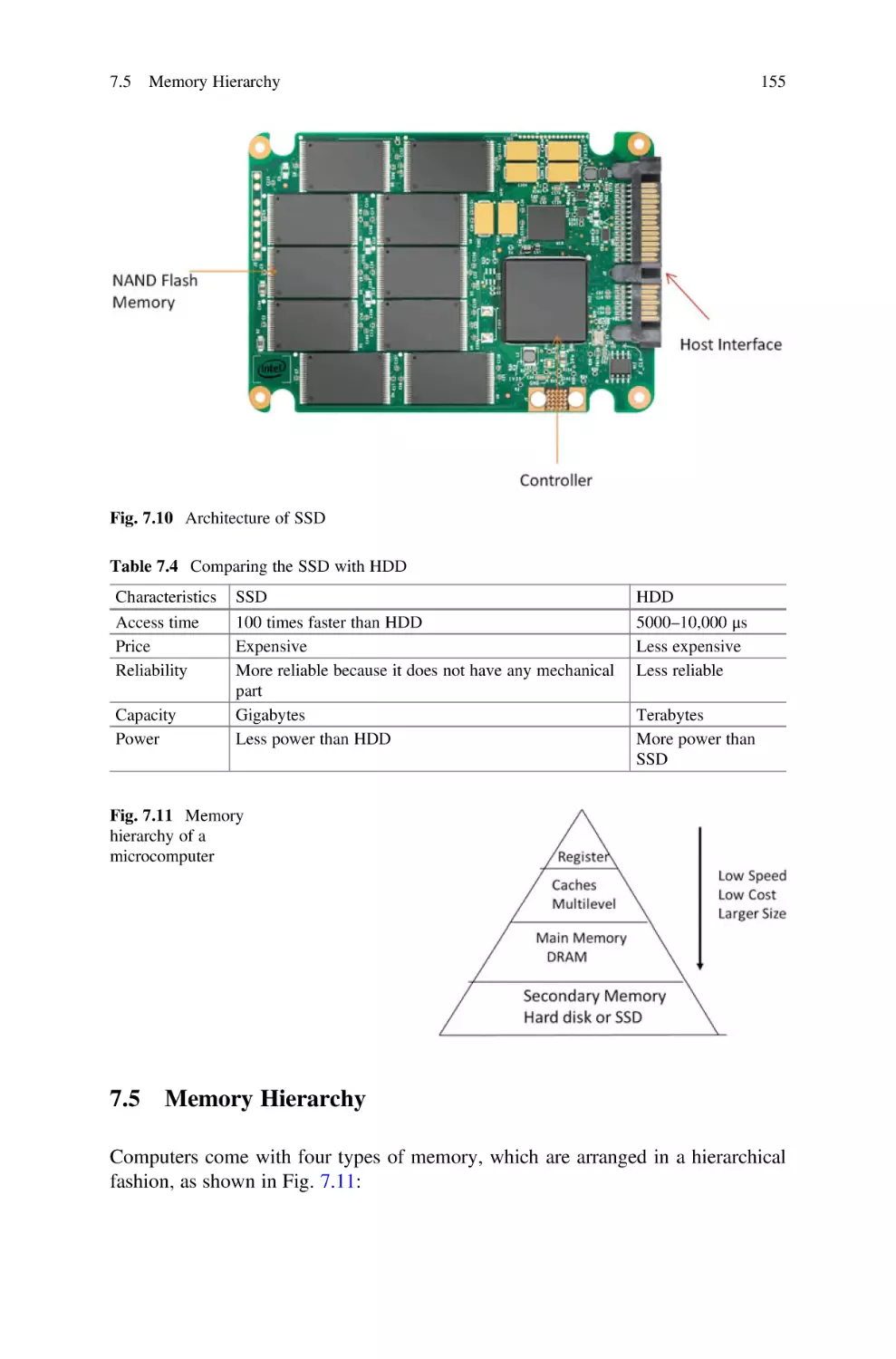
7.5
Memory Hierarchy . . . . . . . . . . . . . . . . . . . . . . . . . . . . . . . . .
7.5.1
Cache Memory . . . . . . . . . . . . . . . . . . . . . . . . . . . . .
7.5.2
Cache Terminology . . . . . . . . . . . . . . . . . . . . . . . . . .
7.5.3
Cache Memory Mapping Methods . . . . . . . . . . . . . . . .
7.5.4
Direct Mapping . . . . . . . . . . . . . . . . . . . . . . . . . . . . .
7.5.5
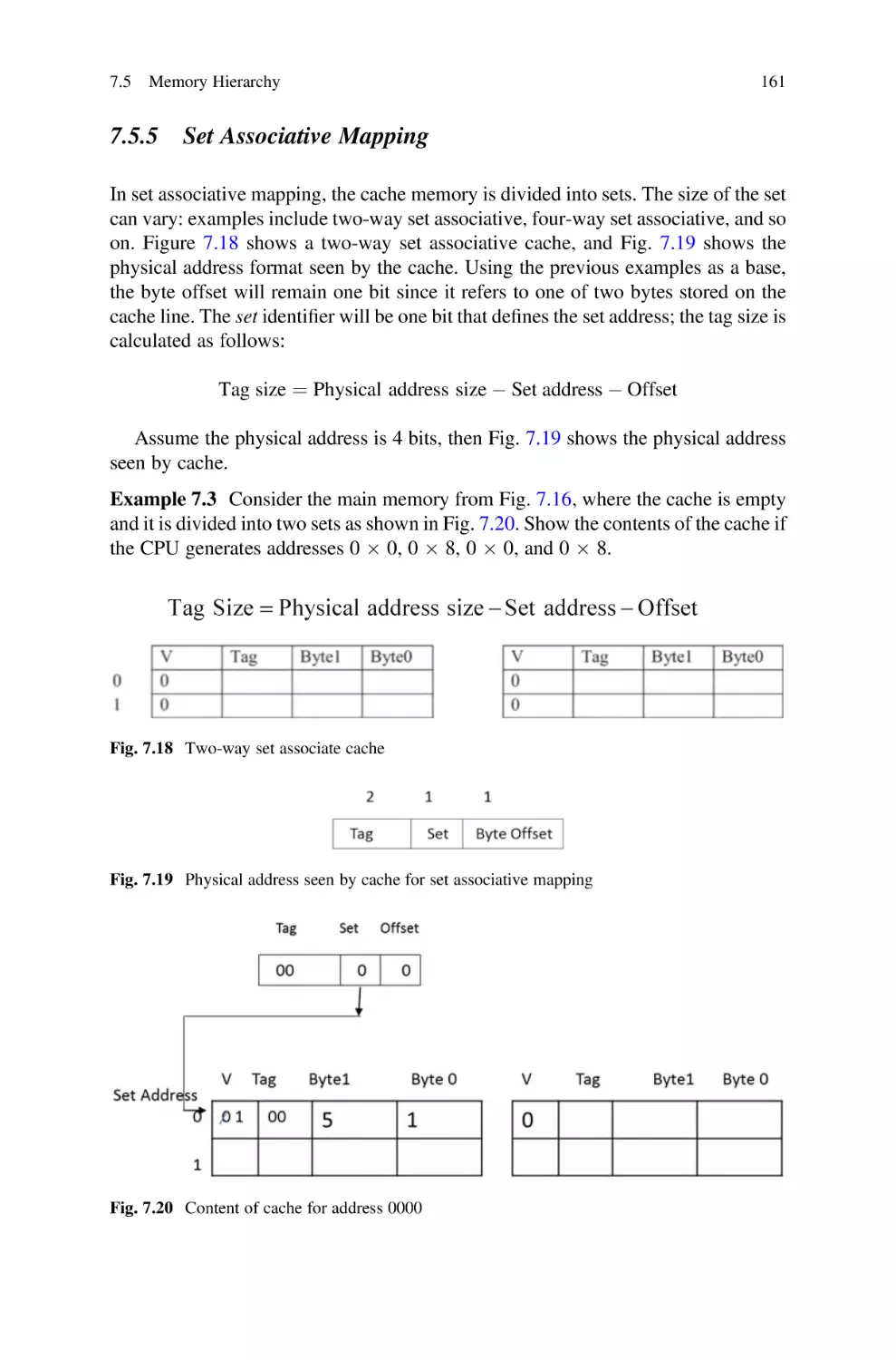
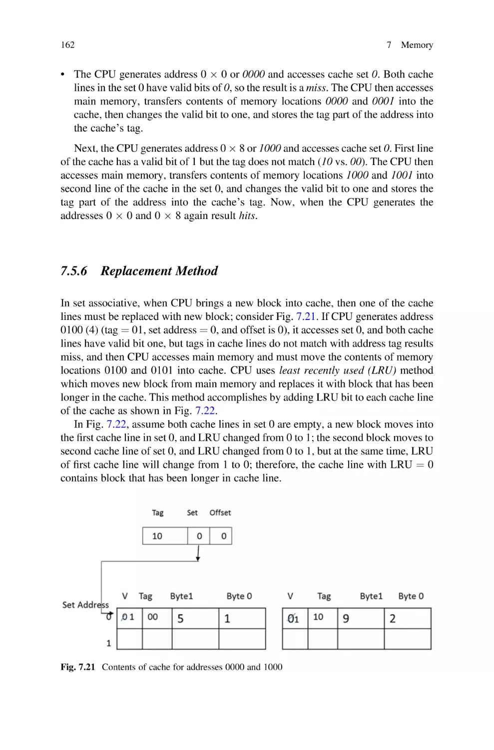
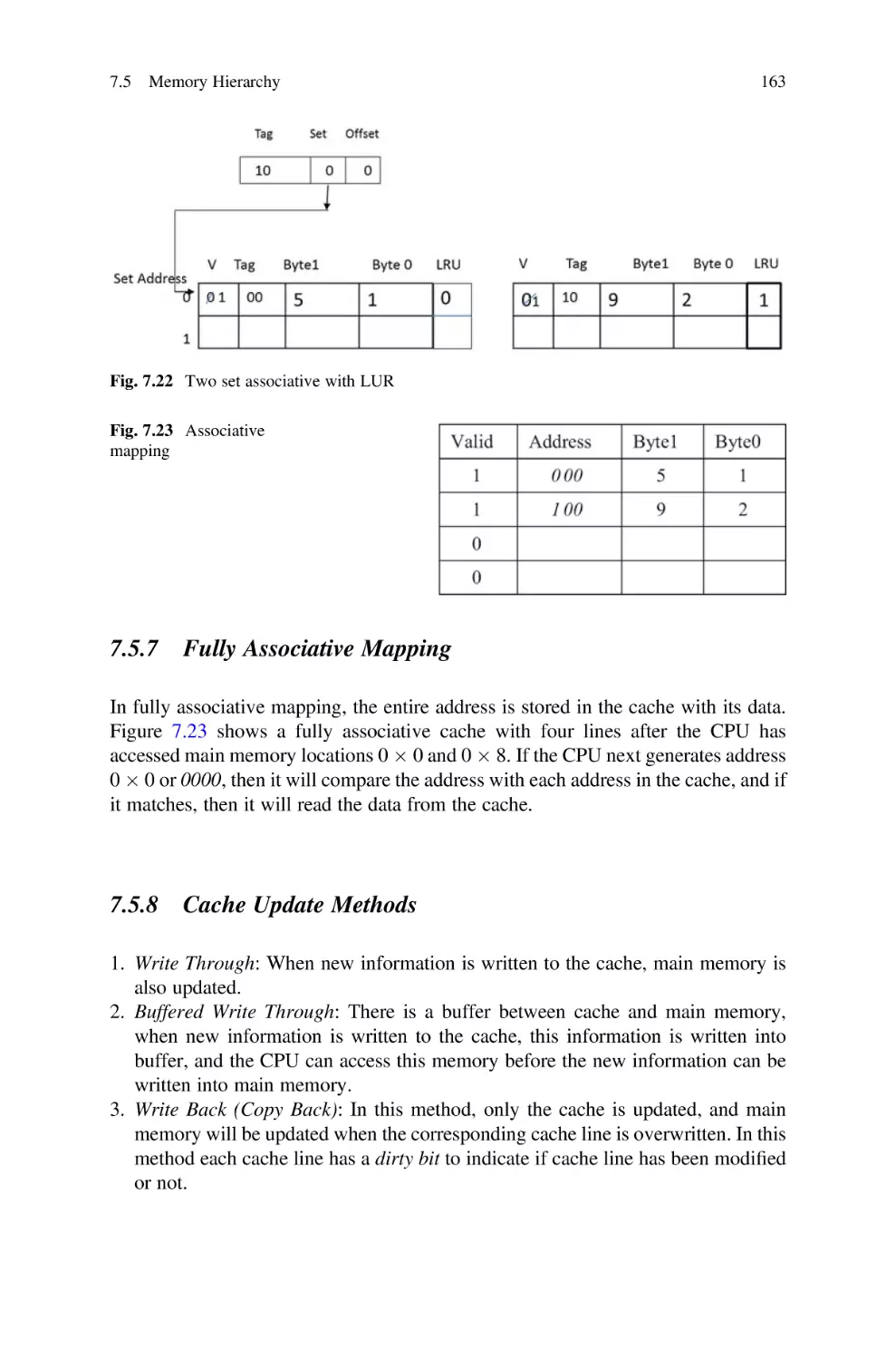
Set Associative Mapping . . . . . . . . . . . . . . . . . . . . . .
7.5.6
Replacement Method . . . . . . . . . . . . . . . . . . . . . . . . .
7.5.7
Fully Associative Mapping . . . . . . . . . . . . . . . . . . . . .
7.5.8
Cache Update Methods . . . . . . . . . . . . . . . . . . . . . . . .
7.5.9
Effective Access Time (EAT) of Memory . . . . . . . . . .
7.5.10 Virtual Memory . . . . . . . . . . . . . . . . . . . . . . . . . . . . .
7.5.11 Memory Organization of a Computer . . . . . . . . . . . . . .
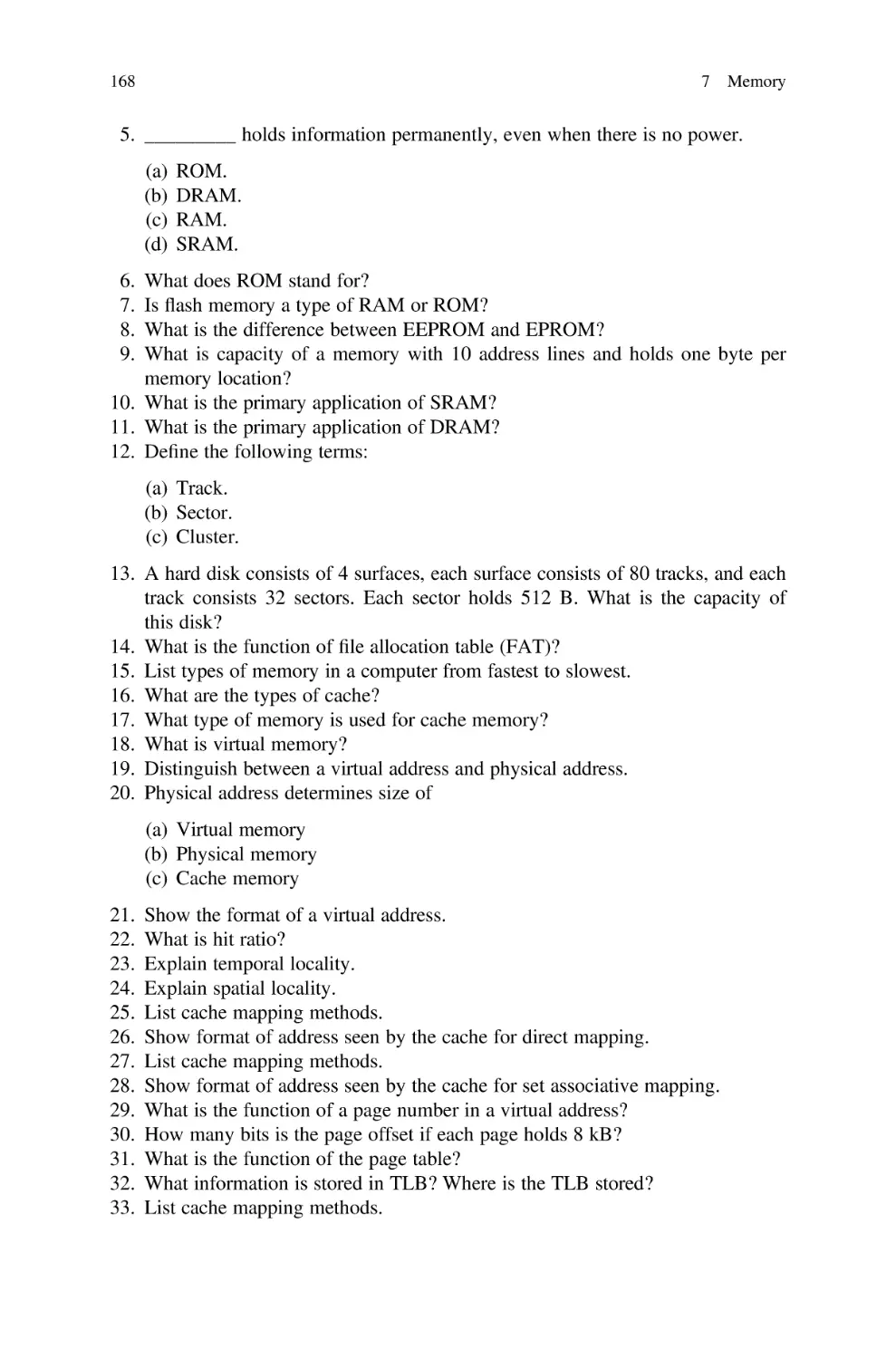
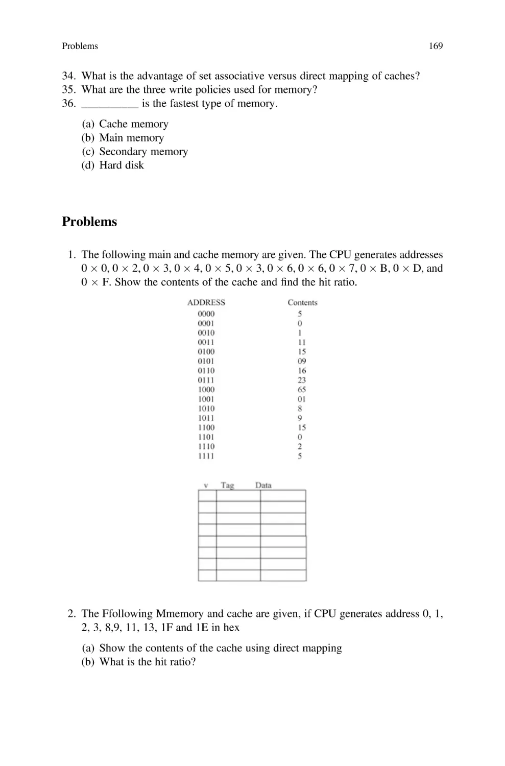
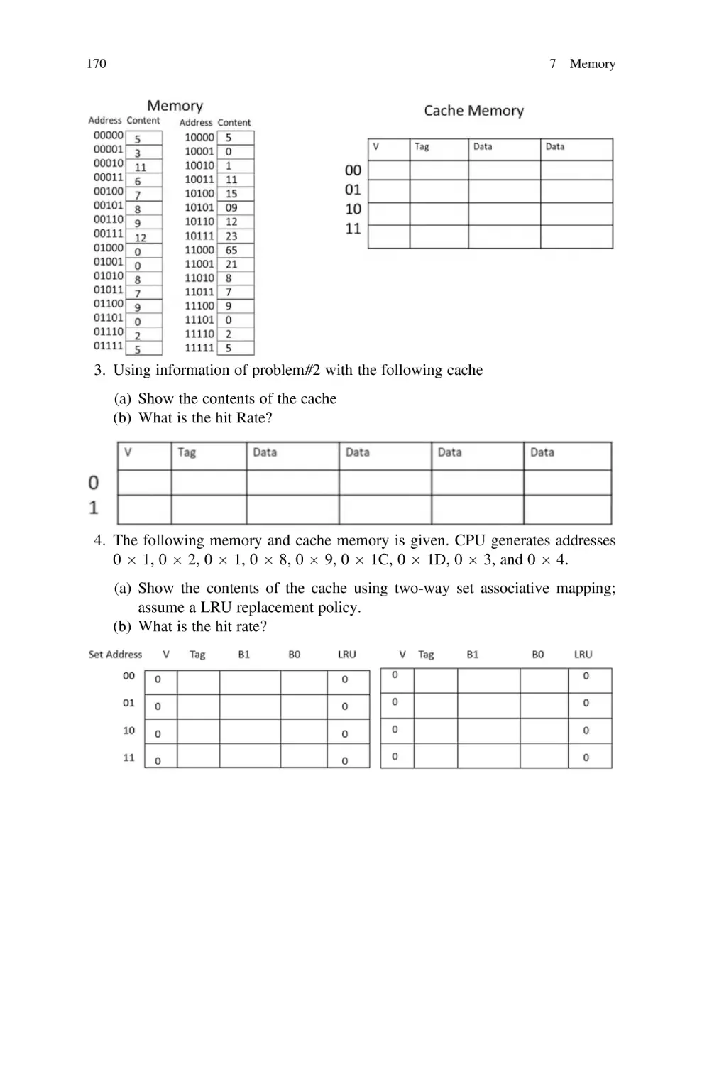
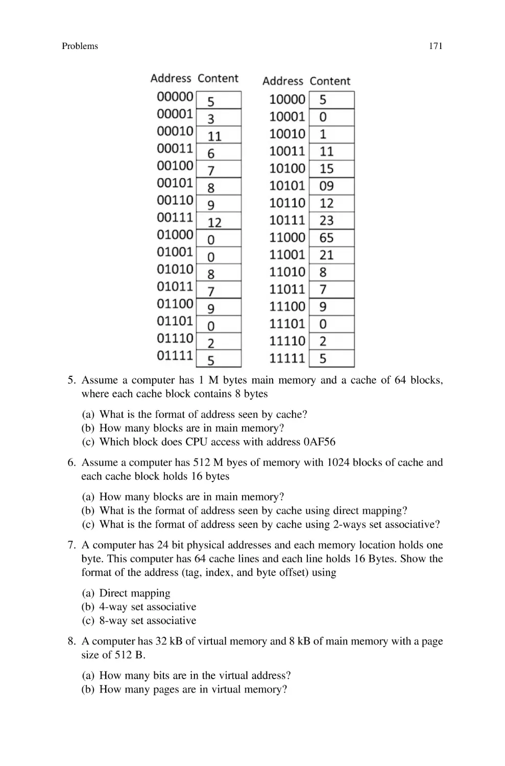
Questions and Problems . . . . . . . . . . . . . . . . . . . . . . . . . . . . . . . . . .
Problems . . . . . . . . . . . . . . . . . . . . . . . . . . . . . . . . . . . . . . . . . . . . .
147
147
147
148
151
151
152
152
152
154
154
154
155
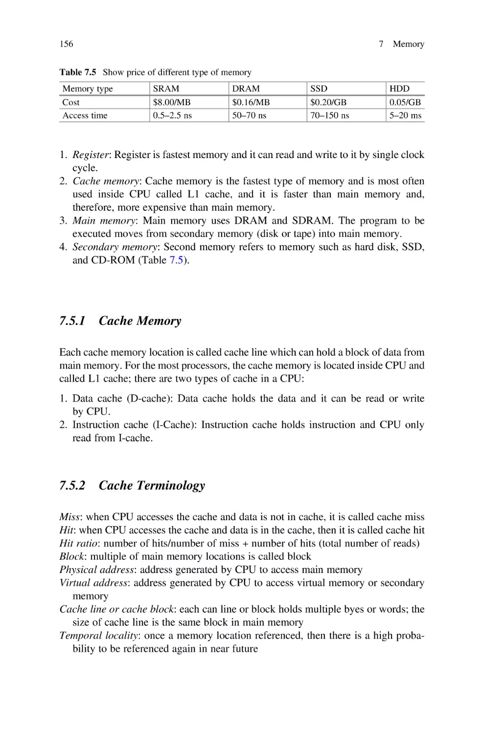
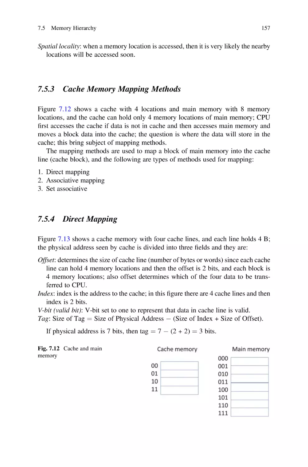
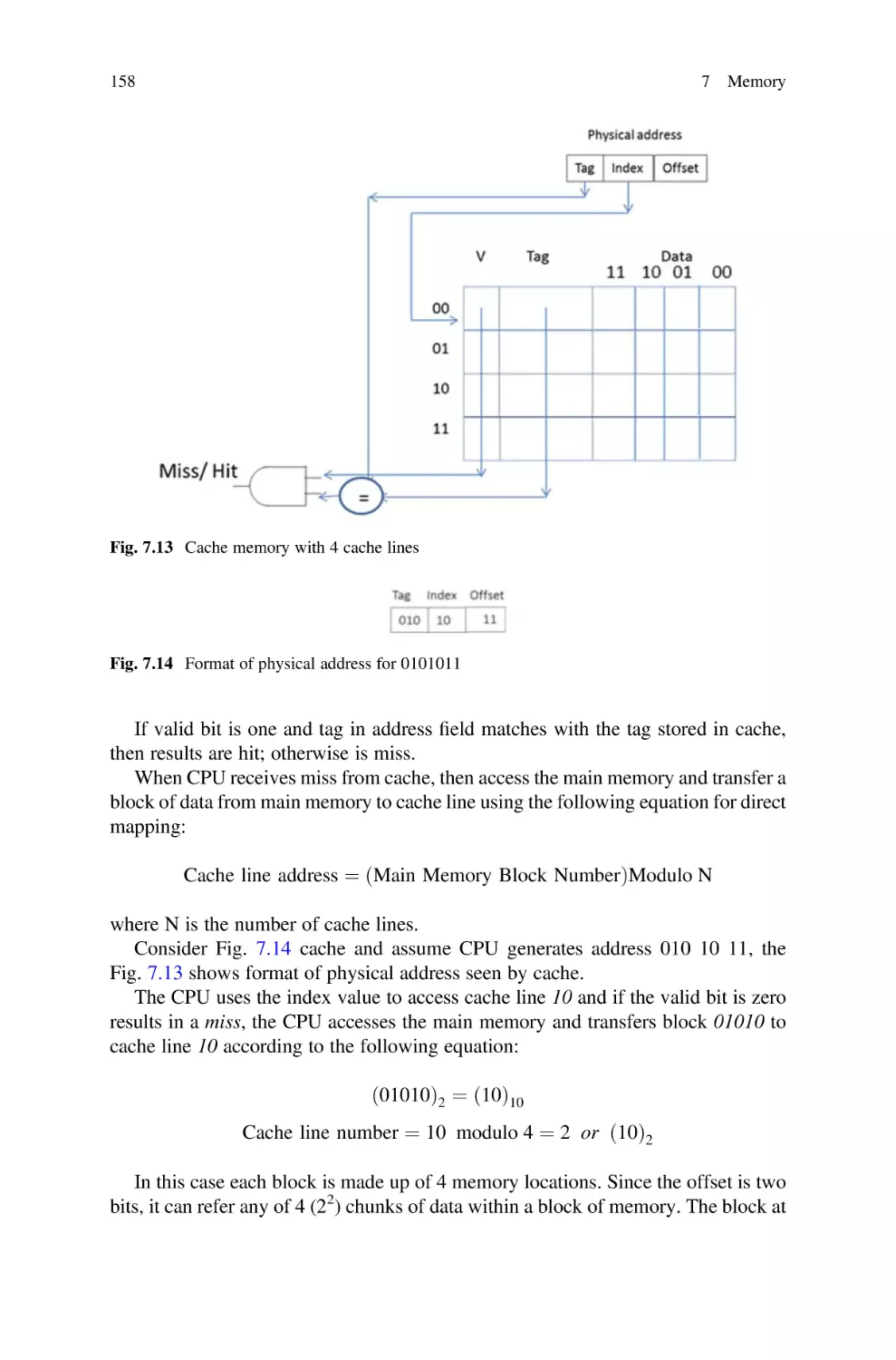
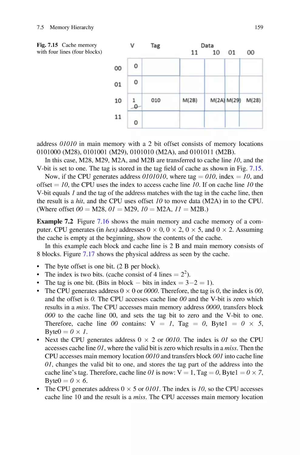
156
156
157
157
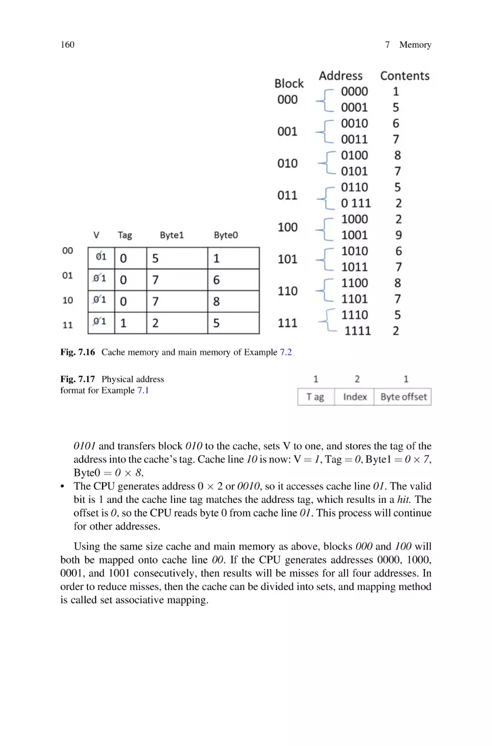
161
162
163
163
164
164
165
168
169
8
Assembly Language and ARM Instructions Part I . . . . . . . . . . . . . 175
8.1
Introduction . . . . . . . . . . . . . . . . . . . . . . . . . . . . . . . . . . . . . . 175
8.2
Instruction Set Architecture (ISA) . . . . . . . . . . . . . . . . . . . . . . 176
xvi
Contents
8.2.1
Classification of Instruction Based on Number of
Operands . . . . . . . . . . . . . . . . . . . . . . . . . . . . . . . . .
8.3
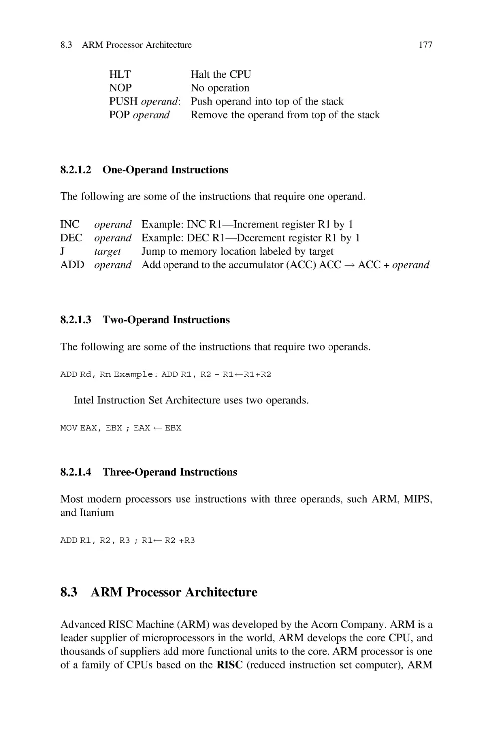
ARM Processor Architecture . . . . . . . . . . . . . . . . . . . . . . . . .
8.3.1
Instruction Decoder and Logic Control . . . . . . . . . . .
8.3.2
Address Register . . . . . . . . . . . . . . . . . . . . . . . . . . .
8.3.3
Address Increment . . . . . . . . . . . . . . . . . . . . . . . . . .
8.3.4
Register Bank . . . . . . . . . . . . . . . . . . . . . . . . . . . . .
8.3.5
Barrel Shifter . . . . . . . . . . . . . . . . . . . . . . . . . . . . . .
8.3.6
ALU . . . . . . . . . . . . . . . . . . . . . . . . . . . . . . . . . . . .
8.3.7
Write Data Register . . . . . . . . . . . . . . . . . . . . . . . . .
8.3.8
Read Data Register . . . . . . . . . . . . . . . . . . . . . . . . . .
8.3.9
ARM Operation Mode . . . . . . . . . . . . . . . . . . . . . . .
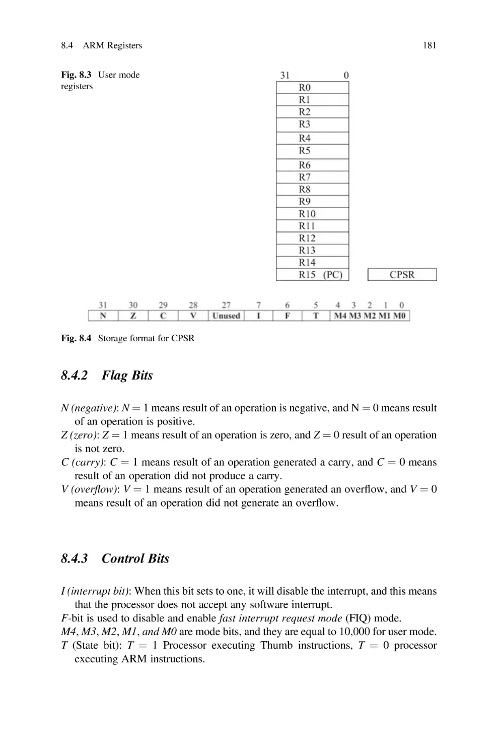
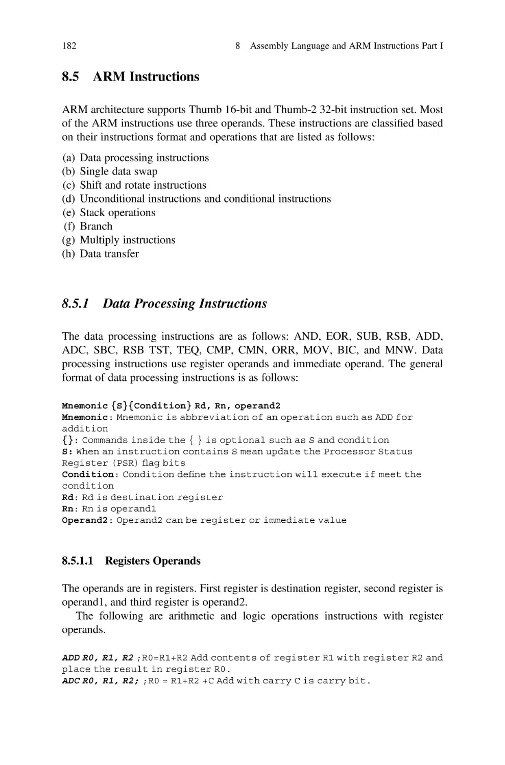
8.4
ARM Registers . . . . . . . . . . . . . . . . . . . . . . . . . . . . . . . . . . .
8.4.1
Current Program Status Register (CPSR) . . . . . . . . . .
8.4.2
Flag Bits . . . . . . . . . . . . . . . . . . . . . . . . . . . . . . . . .
8.4.3
Control Bits . . . . . . . . . . . . . . . . . . . . . . . . . . . . . . .
8.5
ARM Instructions . . . . . . . . . . . . . . . . . . . . . . . . . . . . . . . . .
8.5.1
Data Processing Instructions . . . . . . . . . . . . . . . . . . .
8.5.2
Compare and Test Instructions . . . . . . . . . . . . . . . . .
8.5.3
Register Swap Instructions (MOV and MVN) . . . . . .
8.5.4
Shift and Rotate Instructions . . . . . . . . . . . . . . . . . . .
8.5.5
ARM Unconditional Instructions and Conditional
Instructions . . . . . . . . . . . . . . . . . . . . . . . . . . . . . . .
8.6
Stack Operation and Instructions . . . . . . . . . . . . . . . . . . . . . .
8.7
Branch (B) and Branch with Link Instruction (BL) . . . . . . . . .
8.8
Multiply (MUL) and Multiply-Accumulate (MLA)
Instructions . . . . . . . . . . . . . . . . . . . . . . . . . . . . . . . . . . . . . .
8.9
Summary . . . . . . . . . . . . . . . . . . . . . . . . . . . . . . . . . . . . . . .
Problems and Questions . . . . . . . . . . . . . . . . . . . . . . . . . . . . . . . . .
9
.
.
.
.
.
.
.
.
.
.
.
.
.
.
.
.
.
.
.
.
176
177
178
178
178
178
179
179
180
180
180
180
180
181
181
182
182
183
185
186
. 188
. 190
. 191
. 192
. 192
. 193
ARM Assembly Language Programming Using Keil
Development Tools . . . . . . . . . . . . . . . . . . . . . . . . . . . . . . . . . . . . .
9.1
Introduction . . . . . . . . . . . . . . . . . . . . . . . . . . . . . . . . . . . . . .
9.2
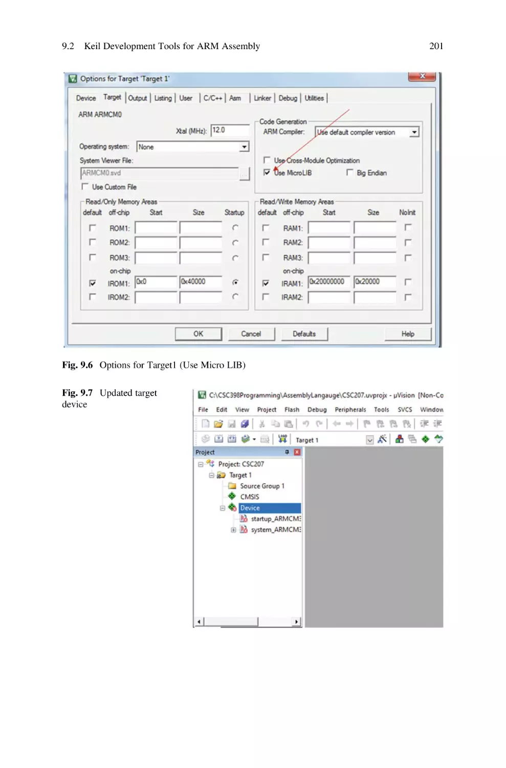
Keil Development Tools for ARM Assembly . . . . . . . . . . . . . .
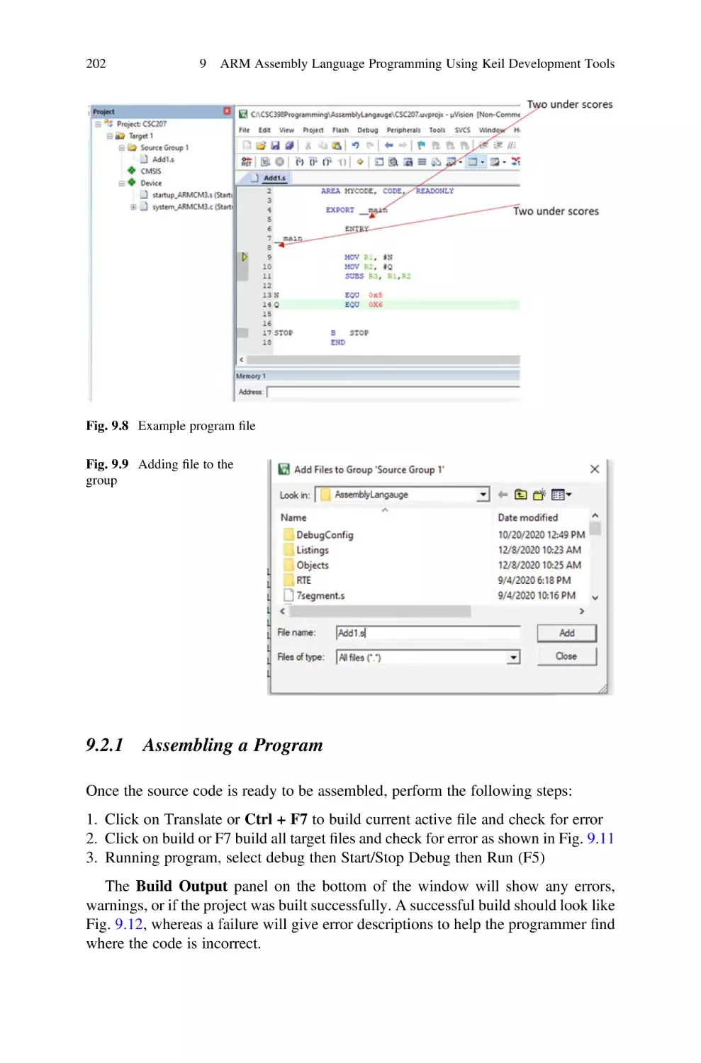
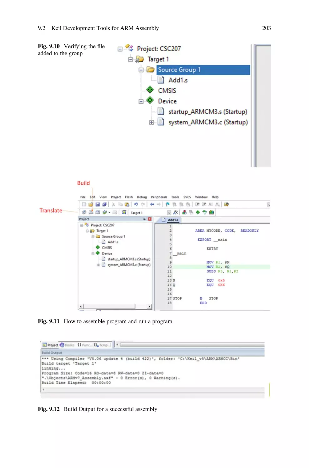
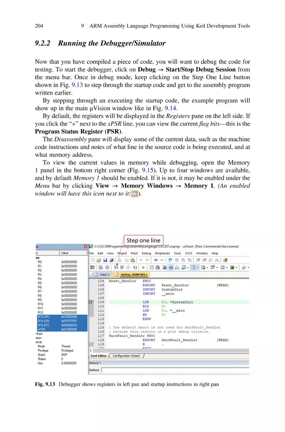
9.2.1
Assembling a Program . . . . . . . . . . . . . . . . . . . . . . . .
9.2.2
Running the Debugger/Simulator . . . . . . . . . . . . . . . .
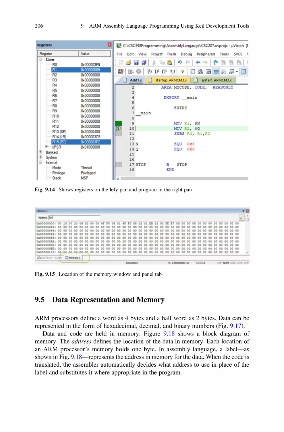
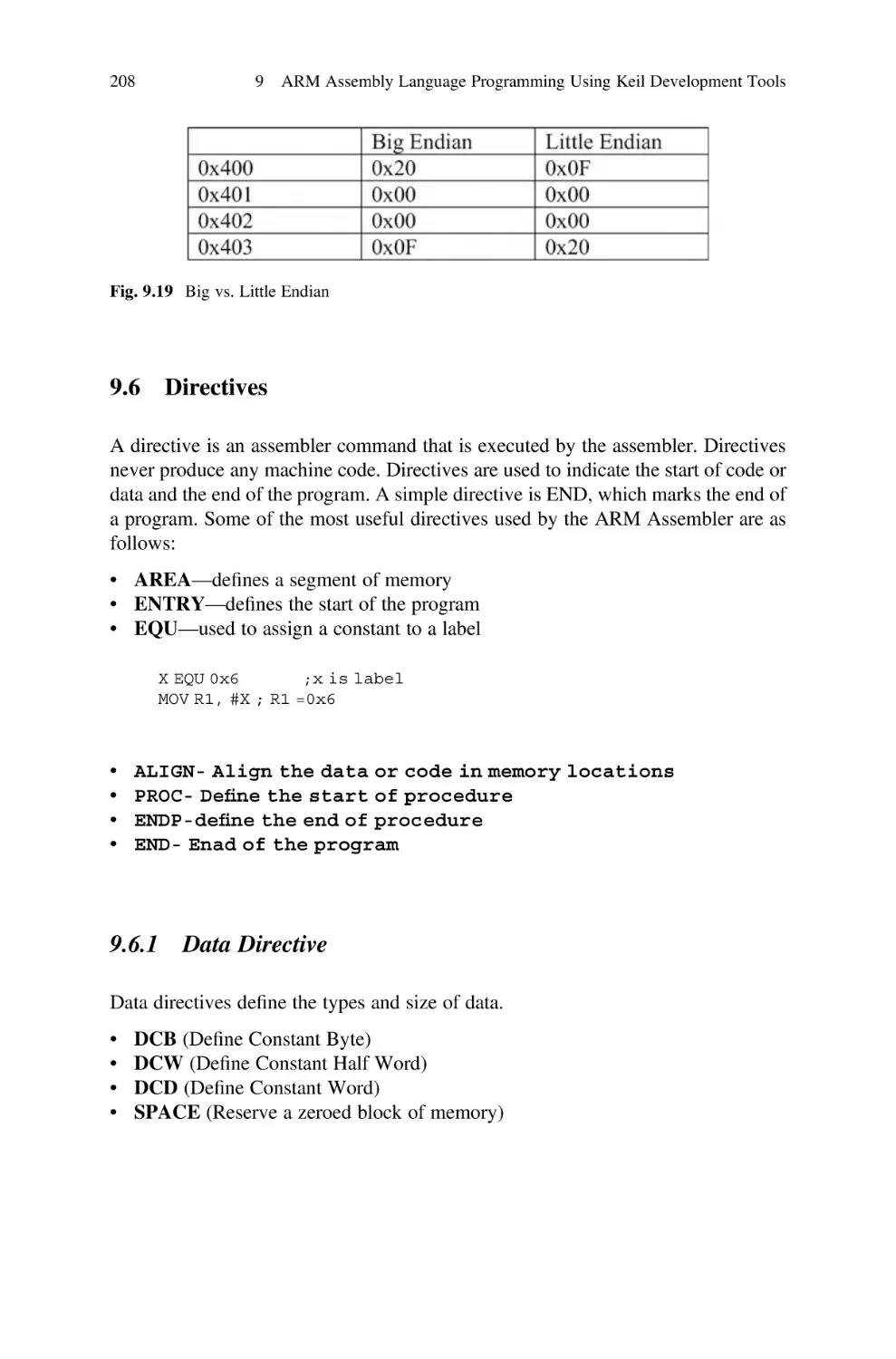
9.3
Program Template . . . . . . . . . . . . . . . . . . . . . . . . . . . . . . . . . .
9.4
Programming Rules . . . . . . . . . . . . . . . . . . . . . . . . . . . . . . . . .
9.4.1
CASE Rules . . . . . . . . . . . . . . . . . . . . . . . . . . . . . . .
9.4.2
Comments . . . . . . . . . . . . . . . . . . . . . . . . . . . . . . . . .
9.5
Data Representation and Memory . . . . . . . . . . . . . . . . . . . . . .
9.6
Directives . . . . . . . . . . . . . . . . . . . . . . . . . . . . . . . . . . . . . . . .
9.6.1
Data Directive . . . . . . . . . . . . . . . . . . . . . . . . . . . . . .
9.7
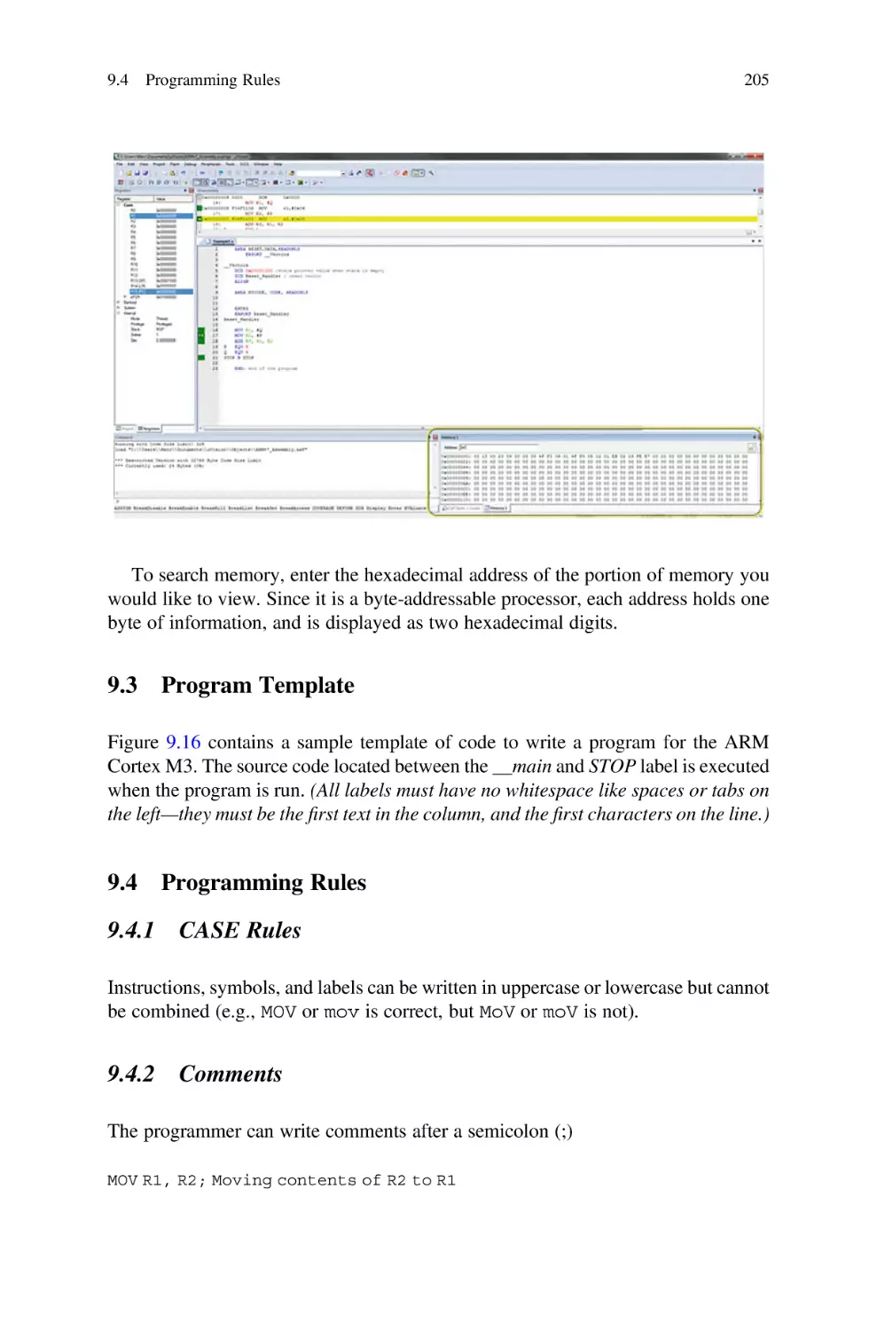
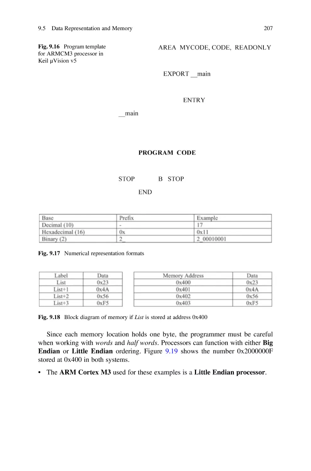
Memory in μVision v5 . . . . . . . . . . . . . . . . . . . . . . . . . . . . . .
9.8
Summary . . . . . . . . . . . . . . . . . . . . . . . . . . . . . . . . . . . . . . . .
Questions and Problems . . . . . . . . . . . . . . . . . . . . . . . . . . . . . . . . . .
197
197
198
202
204
205
205
205
205
206
208
208
210
211
212
Contents
10
11
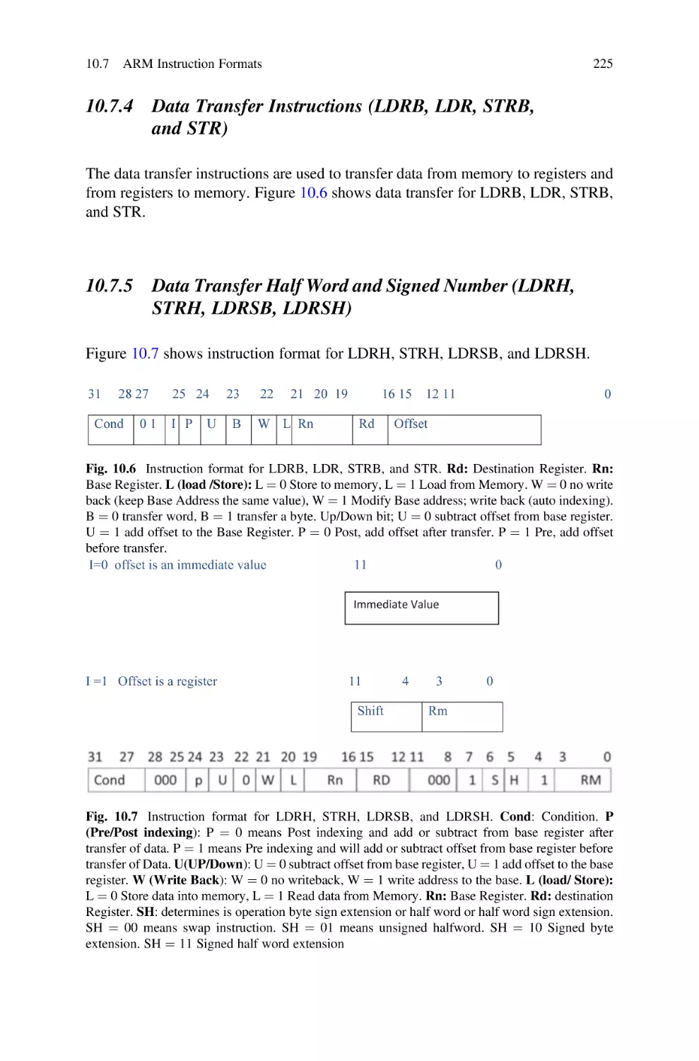
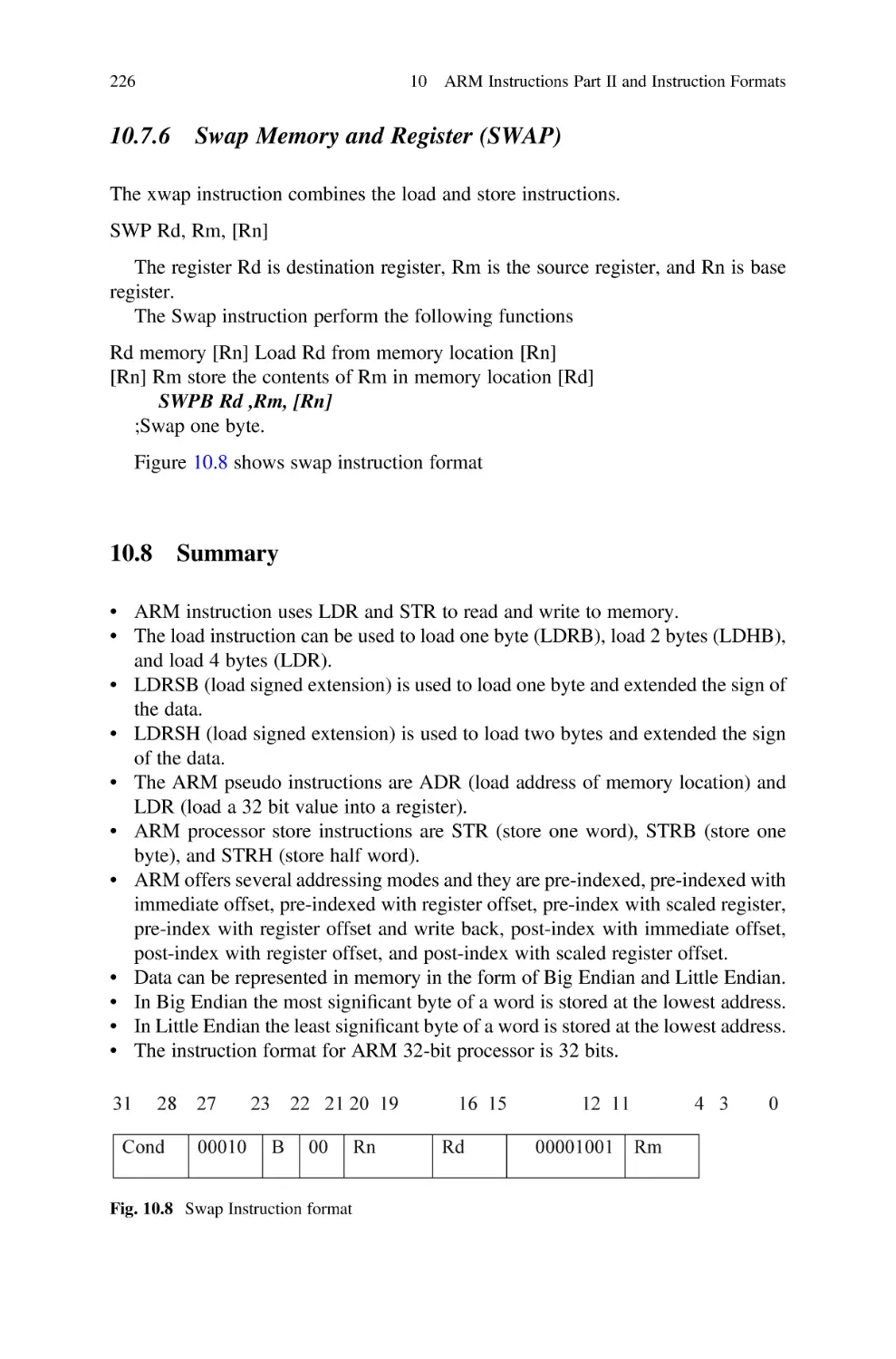
ARM Instructions Part II and Instruction Formats . . . . . . . . . . . . .
10.1 Introduction . . . . . . . . . . . . . . . . . . . . . . . . . . . . . . . . . . . . . .
10.2 ARM Data Transfer Instructions . . . . . . . . . . . . . . . . . . . . . . .
10.2.1 ARM Pseudo Instructions . . . . . . . . . . . . . . . . . . . . . .
10.2.2 Store Instructions (STR) . . . . . . . . . . . . . . . . . . . . . . .
10.3 ARM Addressing Mode . . . . . . . . . . . . . . . . . . . . . . . . . . . . .
10.3.1 Immediate Addressing . . . . . . . . . . . . . . . . . . . . . . . .
10.3.2 Pre-indexed . . . . . . . . . . . . . . . . . . . . . . . . . . . . . . . .
10.3.3 Pre-indexed with Write Back . . . . . . . . . . . . . . . . . . .
10.3.4 Post-index Addressing . . . . . . . . . . . . . . . . . . . . . . . .
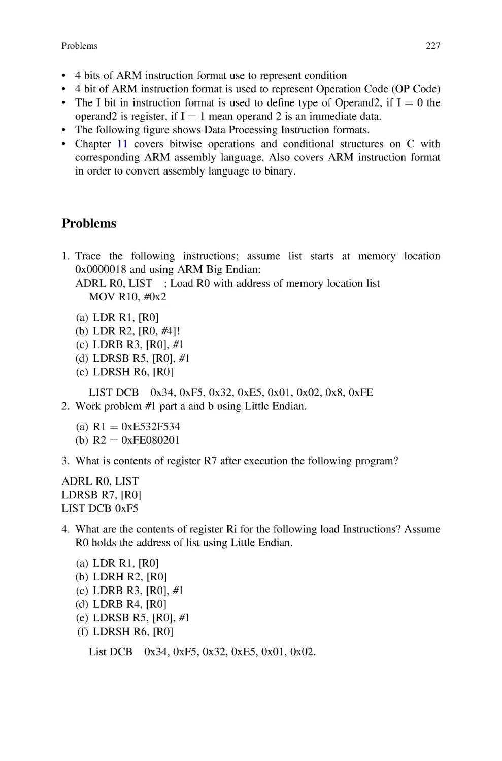
10.4 Swap Memory and Register (SWAP) . . . . . . . . . . . . . . . . . . . .
10.5 Storing Data Using Keil μVision 5 . . . . . . . . . . . . . . . . . . . . . .
10.6 Bits Field Instructions . . . . . . . . . . . . . . . . . . . . . . . . . . . . . . .
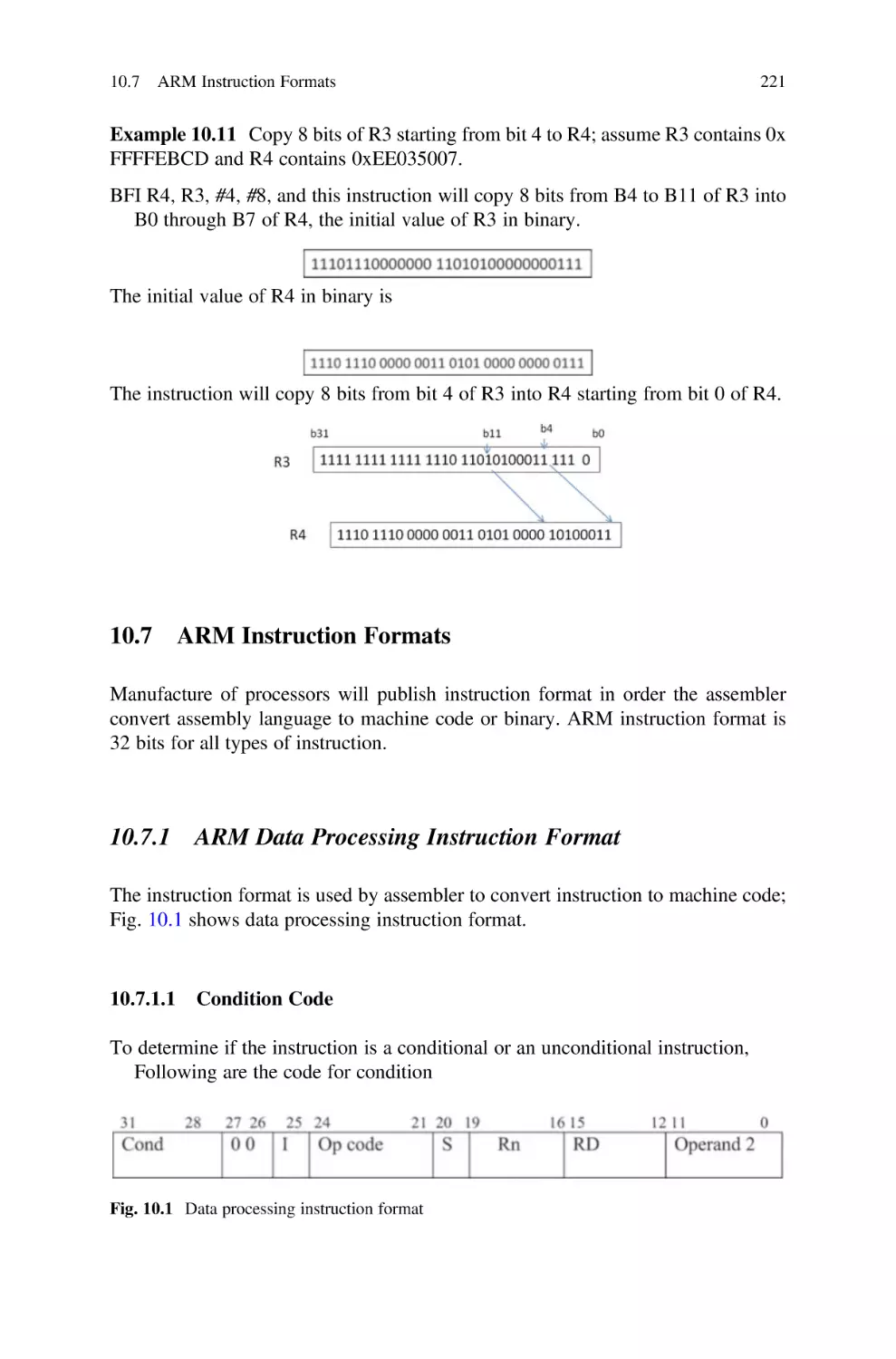
10.7 ARM Instruction Formats . . . . . . . . . . . . . . . . . . . . . . . . . . . .
10.7.1 ARM Data Processing Instruction Format . . . . . . . . . .
10.7.2 B and BL Instruction Format . . . . . . . . . . . . . . . . . . . .
10.7.3 Multiply Instruction Format . . . . . . . . . . . . . . . . . . . .
10.7.4 Data Transfer Instructions (LDRB, LDR, STRB,
and STR) . . . . . . . . . . . . . . . . . . . . . . . . . . . . . . . . . .
10.7.5 Data Transfer Half Word and Signed Number
(LDRH, STRH, LDRSB, LDRSH) . . . . . . . . . . . . . . .
10.7.6 Swap Memory and Register (SWAP) . . . . . . . . . . . . . .
10.8 Summary . . . . . . . . . . . . . . . . . . . . . . . . . . . . . . . . . . . . . . . .
Problems . . . . . . . . . . . . . . . . . . . . . . . . . . . . . . . . . . . . . . . . . . . . .
Bitwise and Control Structures Used for Programming
with C and ARM Assembly Language . . . . . . . . . . . . . . . . . . . . . . .
11.1 Introduction . . . . . . . . . . . . . . . . . . . . . . . . . . . . . . . . . . . . . .
11.1.1 C Bitwise Operations . . . . . . . . . . . . . . . . . . . . . . . . .
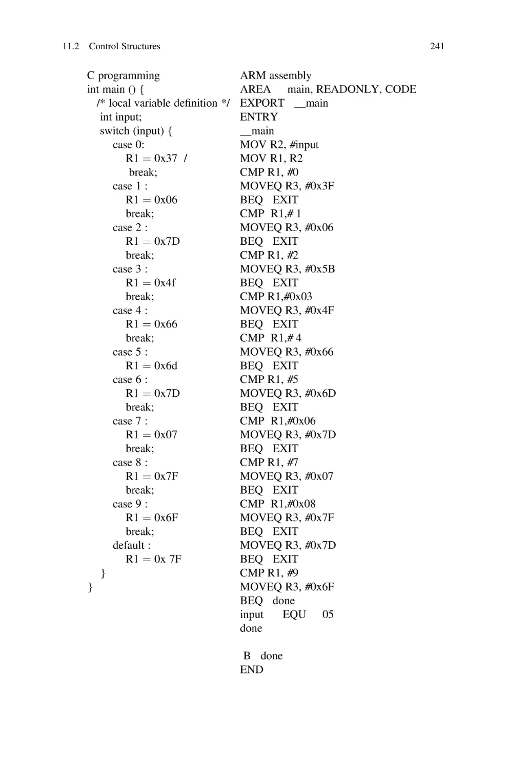
11.2 Control Structures . . . . . . . . . . . . . . . . . . . . . . . . . . . . . . . . . .
11.2.1 If-Then Structure . . . . . . . . . . . . . . . . . . . . . . . . . . . .
11.2.2 If-Then-Else Structure . . . . . . . . . . . . . . . . . . . . . . . .
11.2.3 While Loop Structure . . . . . . . . . . . . . . . . . . . . . . . . .
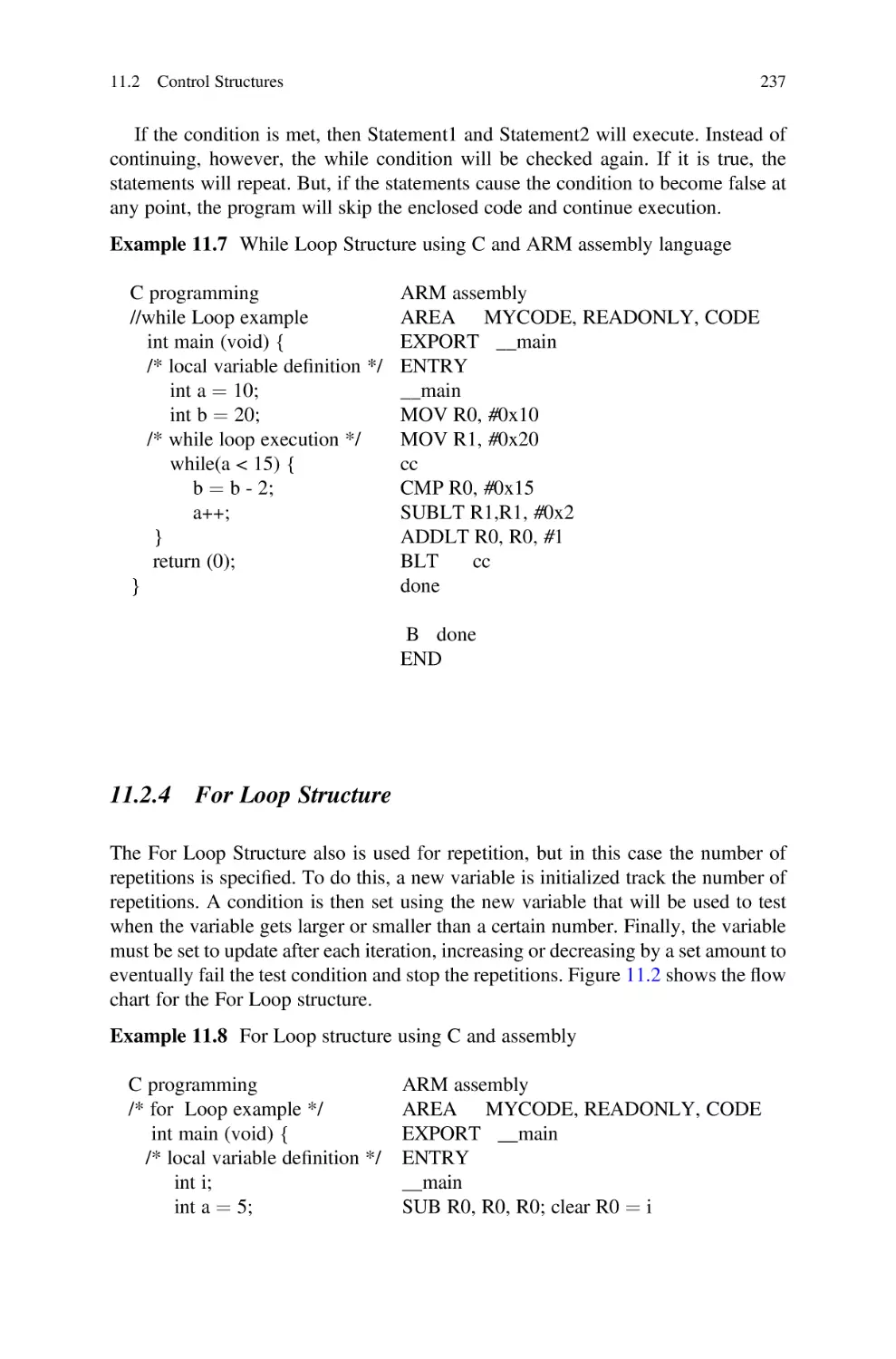
11.2.4 For Loop Structure . . . . . . . . . . . . . . . . . . . . . . . . . . .
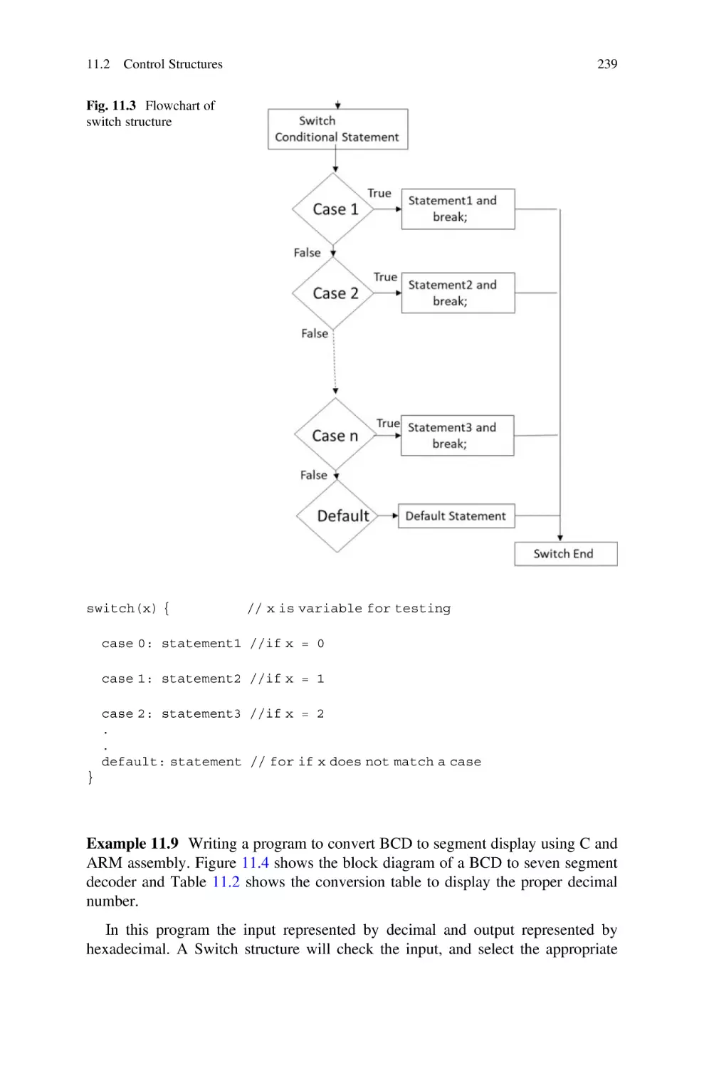
11.2.5 Switch Structure . . . . . . . . . . . . . . . . . . . . . . . . . . . . .
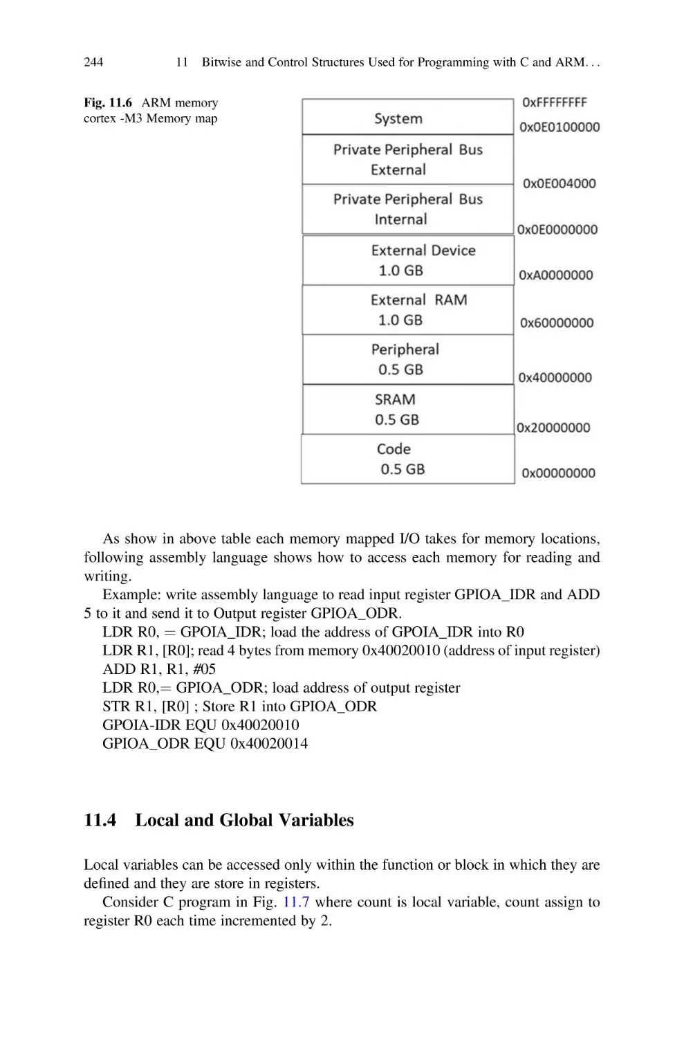
11.3 ARM Memory Map . . . . . . . . . . . . . . . . . . . . . . . . . . . . . . . .
11.3.1 Introduction . . . . . . . . . . . . . . . . . . . . . . . . . . . . . . . .
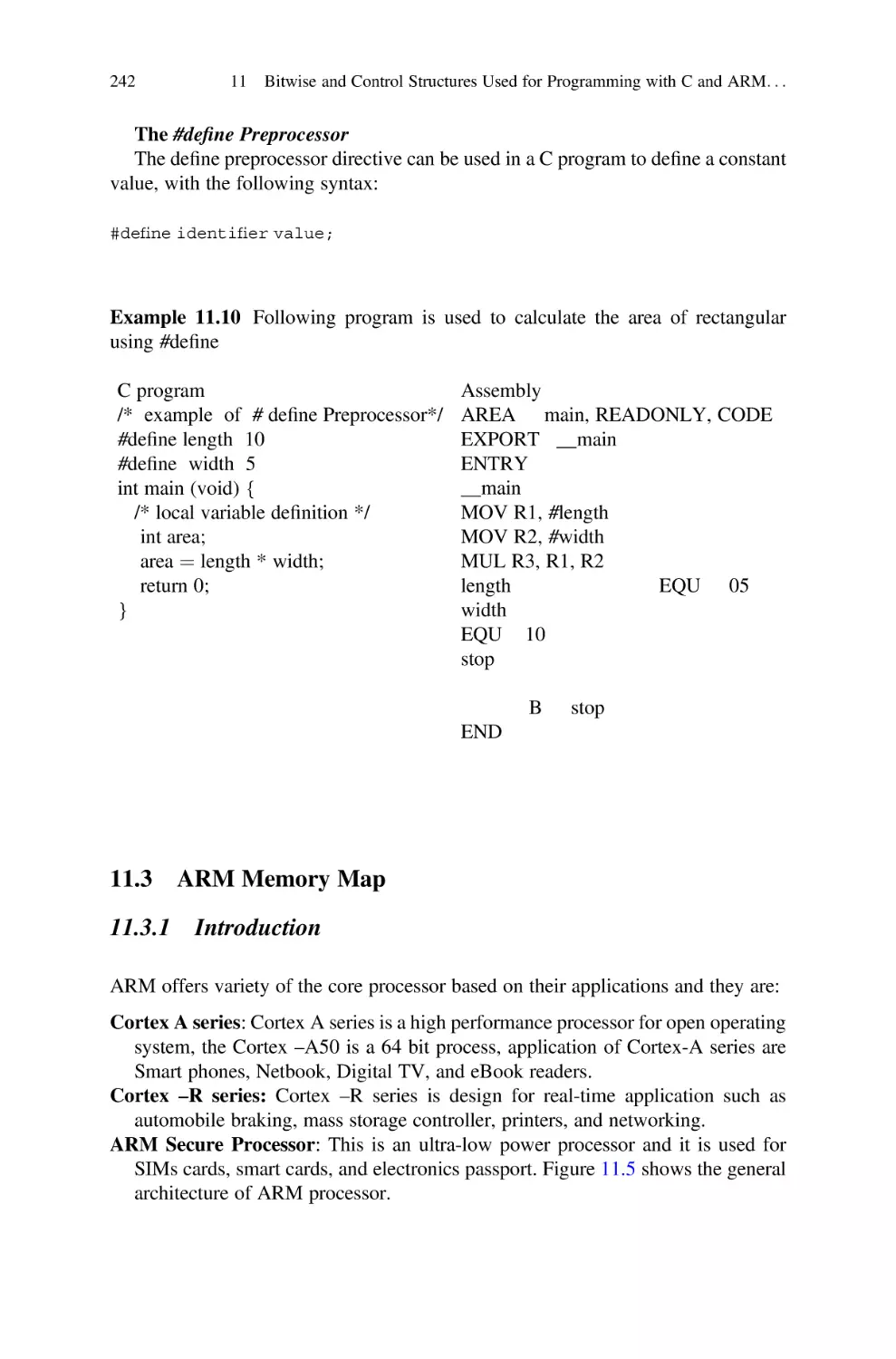
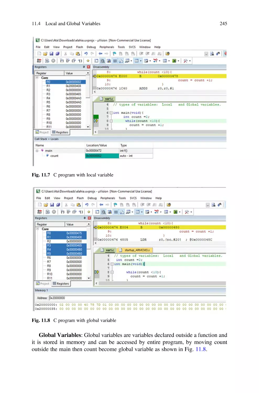
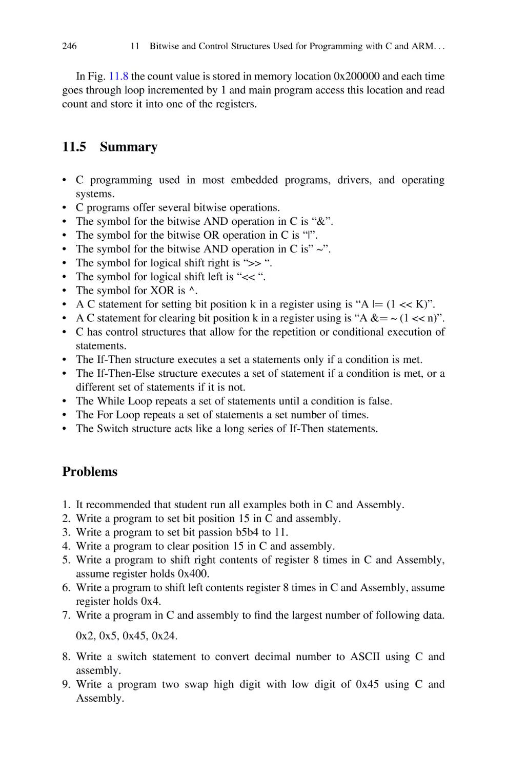
11.4 Local and Global Variables . . . . . . . . . . . . . . . . . . . . . . . . . . .
11.5 Summary . . . . . . . . . . . . . . . . . . . . . . . . . . . . . . . . . . . . . . . .
Problems . . . . . . . . . . . . . . . . . . . . . . . . . . . . . . . . . . . . . . . . . . . . .
xvii
213
213
213
214
215
215
216
216
217
218
219
219
220
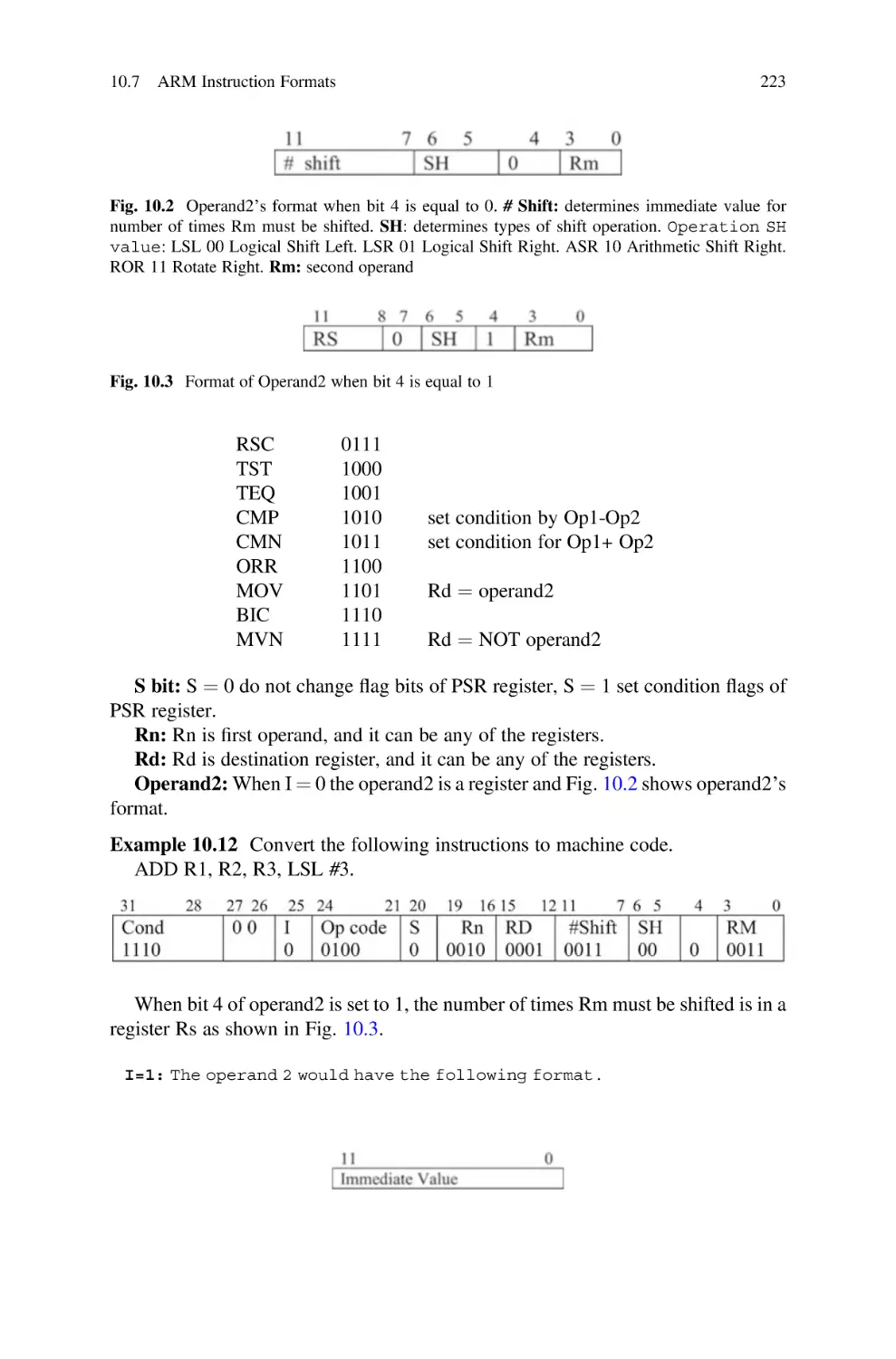
221
221
224
224
225
225
226
226
227
231
231
231
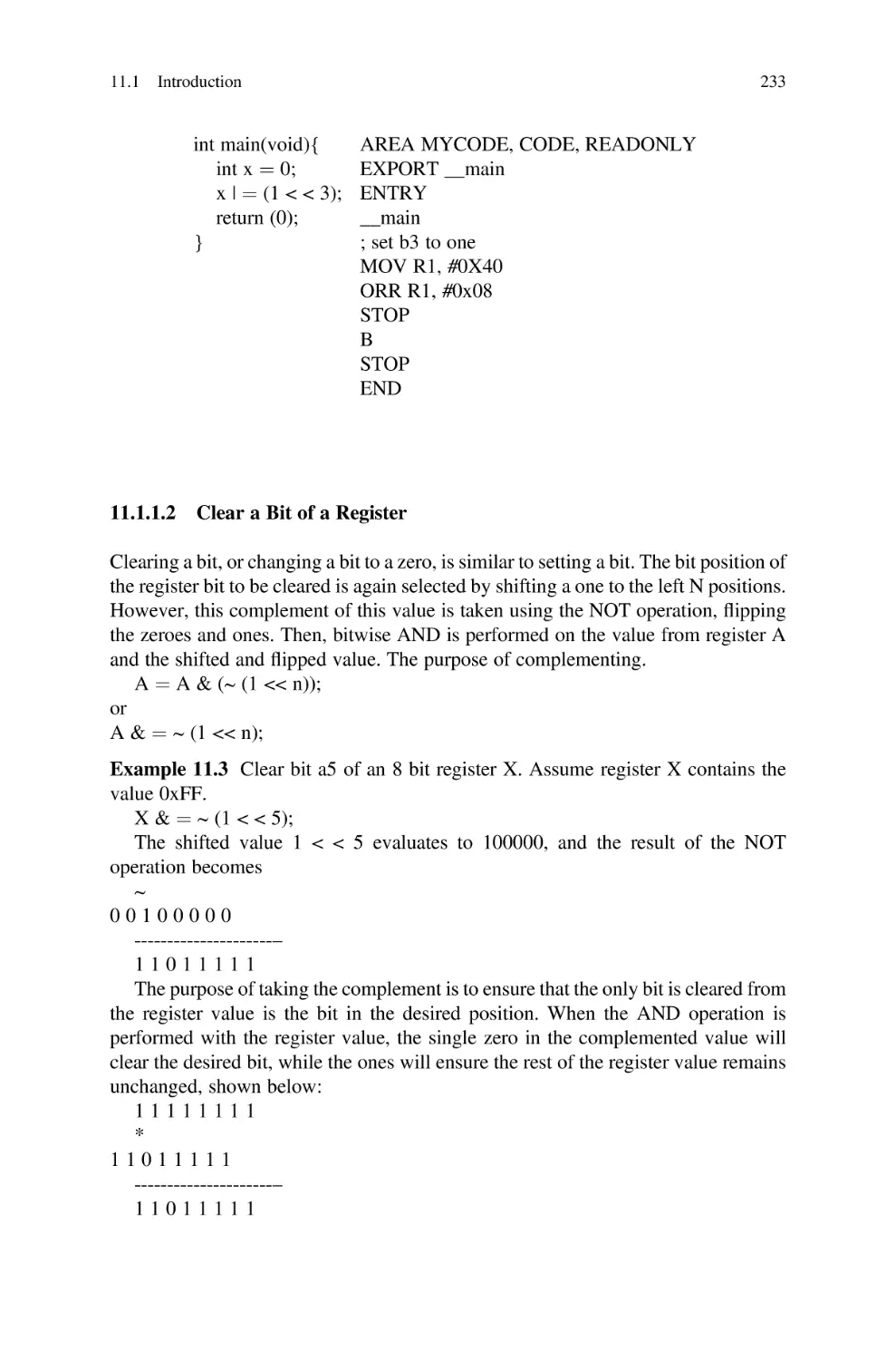
234
234
235
236
237
238
242
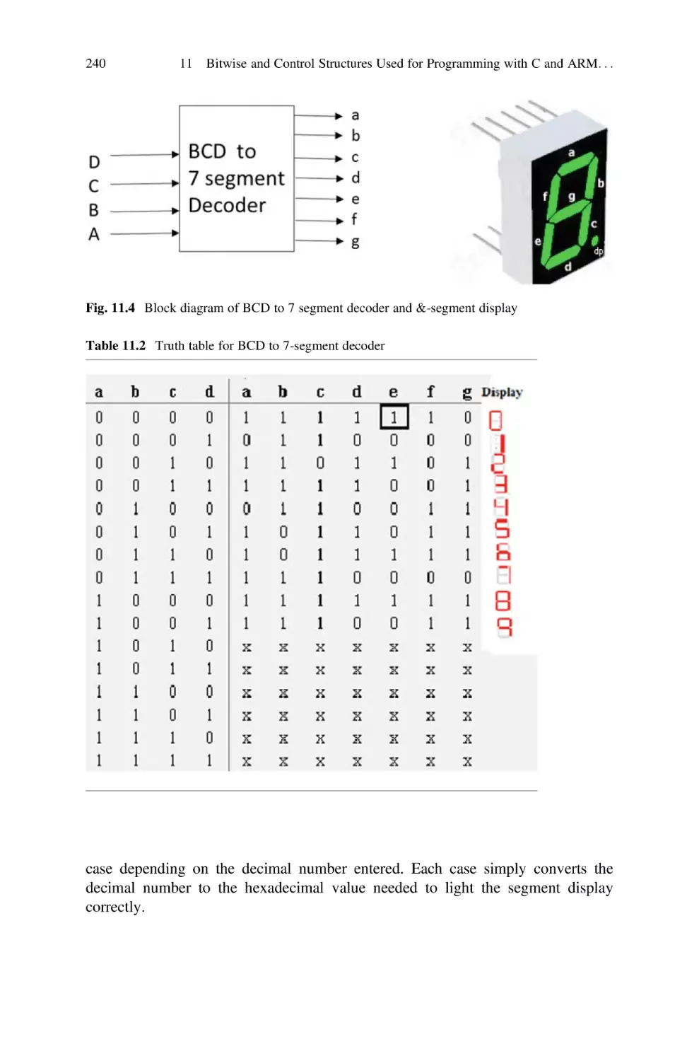
242
244
246
246
xviii
Contents
Appendix A: List of Digital Design Laboratory Experiments Using
LOGISIM . . . . . . . . . . . . . . . . . . . . . . . . . . . . . . . . . . . . . . . . . . . . . . . . 247
Appendix B: Solution to the Even Problems . . . . . . . . . . . . . . . . . . . . . . 249
Bibliography . . . . . . . . . . . . . . . . . . . . . . . . . . . . . . . . . . . . . . . . . . . . . . 287
Index . . . . . . . . . . . . . . . . . . . . . . . . . . . . . . . . . . . . . . . . . . . . . . . . . . . 291
Chapter 1
Signals and Number Systems
Objectives: After Completing this Chapter, you Should Be Able to
• Explain the basic components of a computer.
• Learn the historical development of the computer.
• Represent the hardware and software components of a computer.
• List different types of computers.
• Distinguish between analog and digital signal.
• Learn the characteristics of signal.
• Convert decimal numbers to binary and vice versa.
• Learn addition and subtraction of binary numbers.
• Represent floating numbers in binary.
• Convert from binary to hexadecimal and vice versa.
• Distinguish between serial and parallel transmission.
1.1
Introduction
Numerical values have become an integral part of our daily lives. Numerical values
can be represented by analog or digital; examples include an analog watch, digital
watch, or thermometer. The following are advantages of digital representation of
numerical values compared to analog representation:
1.
2.
3.
4.
5.
Digital representation is more accurate.
Digital information are easier to store.
Digital systems are easier to design.
Noise has less effect.
Digital systems can easily be fabricated in an integrated circuit.
A digital signal is a discrete signal (step by step), and an analog signal is a
continuous signal. Digital systems are widely used and its applications can be seen in
© The Author(s), under exclusive license to Springer Nature Switzerland AG 2022
A. Elahi, Computer Systems, https://doi.org/10.1007/978-3-030-93449-1_1
1
2
1 Signals and Number Systems
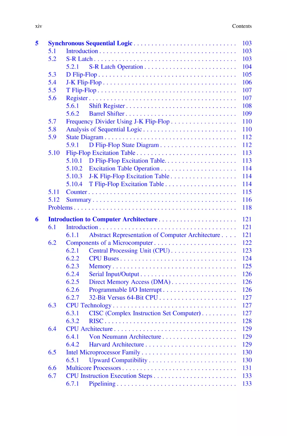
Fig. 1.1 Basic components
of a computer
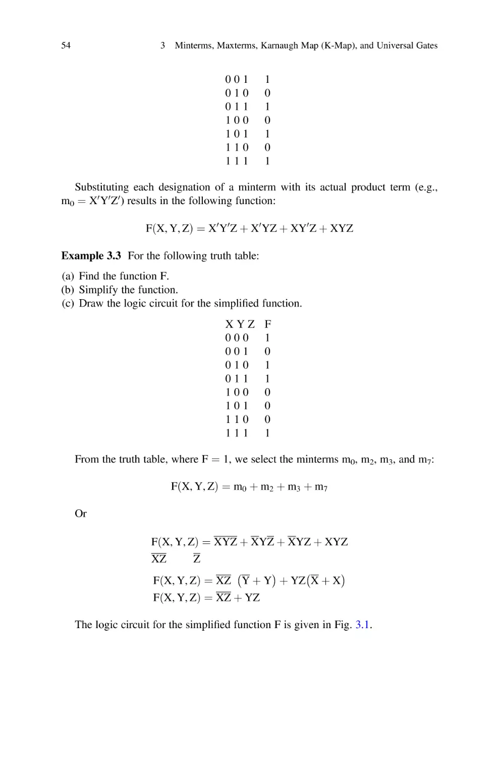
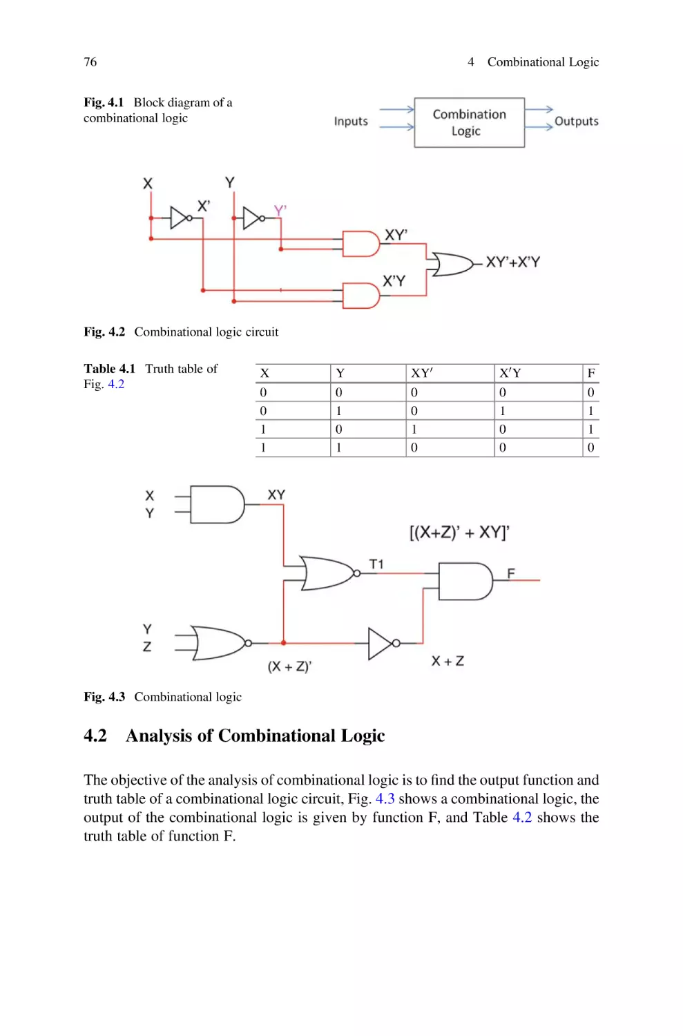
computers, calculators, and cell phones. In a digital system, information is transferred between components of the digital system in the form of digital signals.
A computer consists of two components: hardware and software. Hardware refers
to the physical components of a computer such as the keyboard, CPU, and memory.
Software refers to programs run by CPU including operating systems and application
programs. Computers can come in several different forms such as a desktop, laptop,
tablet, server, and iPhone. Regardless of the form, all computers consist of the same
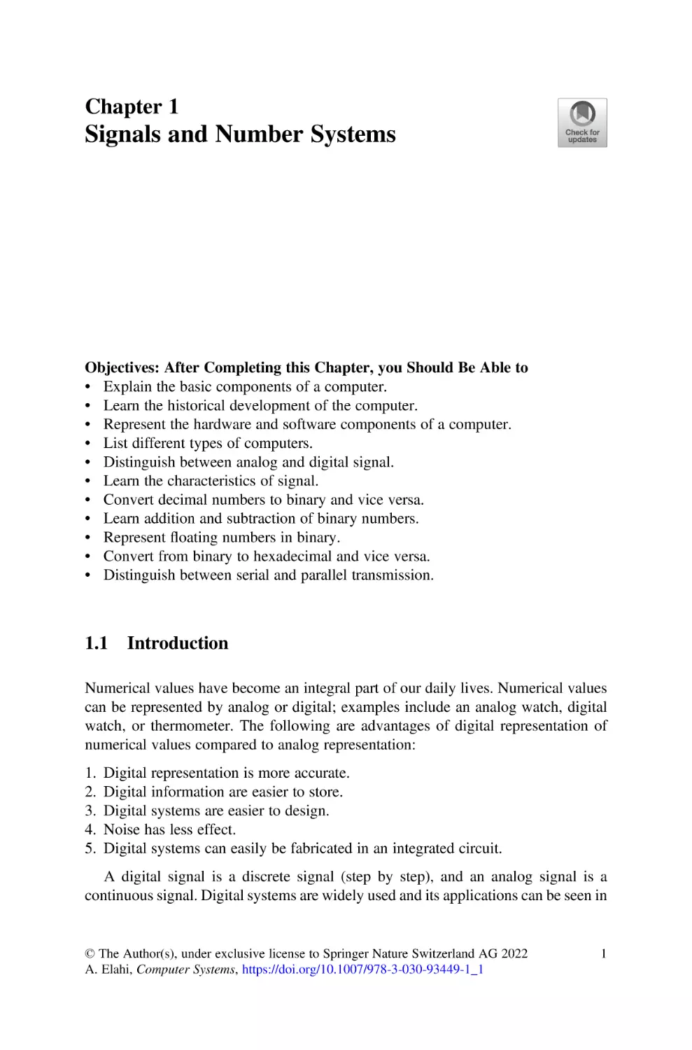
basic structures. Figure 1.1 shows the basic components of a computer.
1.1.1
CPU
1.1.1.1
CPU Execute Program
Input Device
The input device is used for entering information into memory. Examples of input
devices include the keyboard, mouse, touch pad screen, light pen, barcode reader,
and scanner. The input device converts information into bits, and the bits are stored
in memory.
Output Device
A computer’s memory transfers information to the output device in the form of bits
such as the output device converts bits to characters, images, and voices which can
be interpreted by humans.
Memory
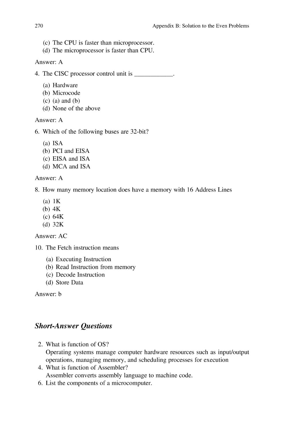
Memory is used to store information and programs. Memory comes in the form of
solid-state electronics such as RAM, ROM, flash drive, or hard disk.
1.3 Hardware and Software Components of a Computer
1.2
3
Historical Development of the Computer
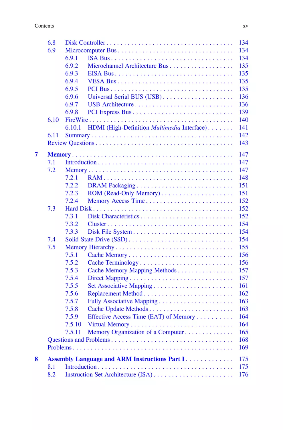
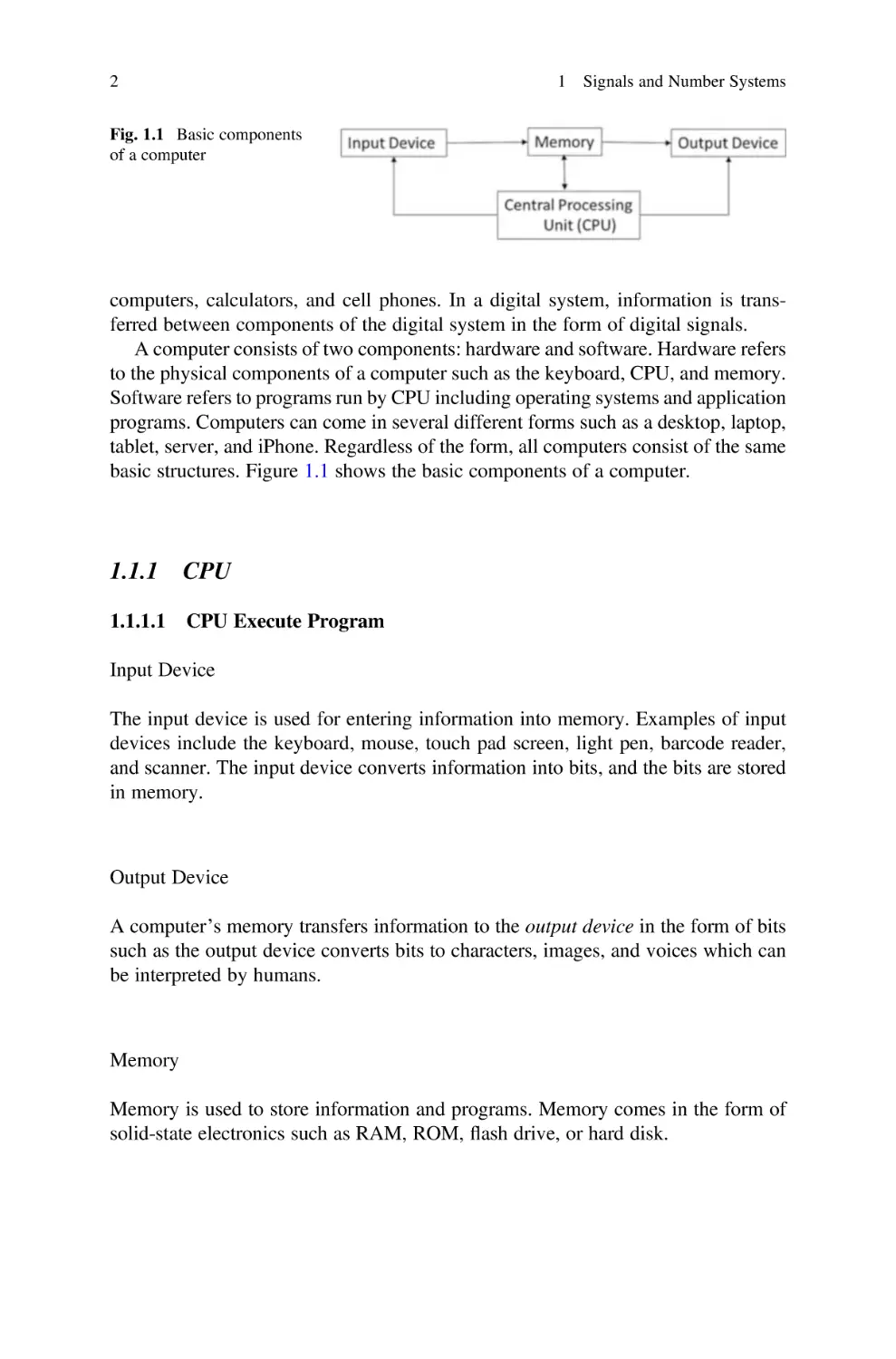
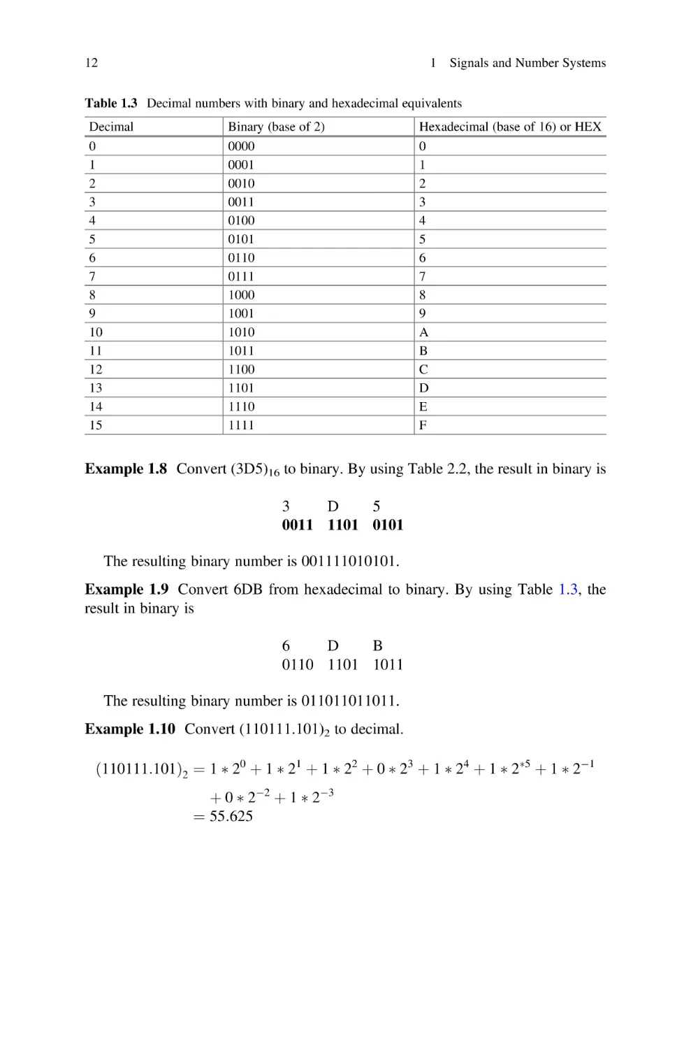
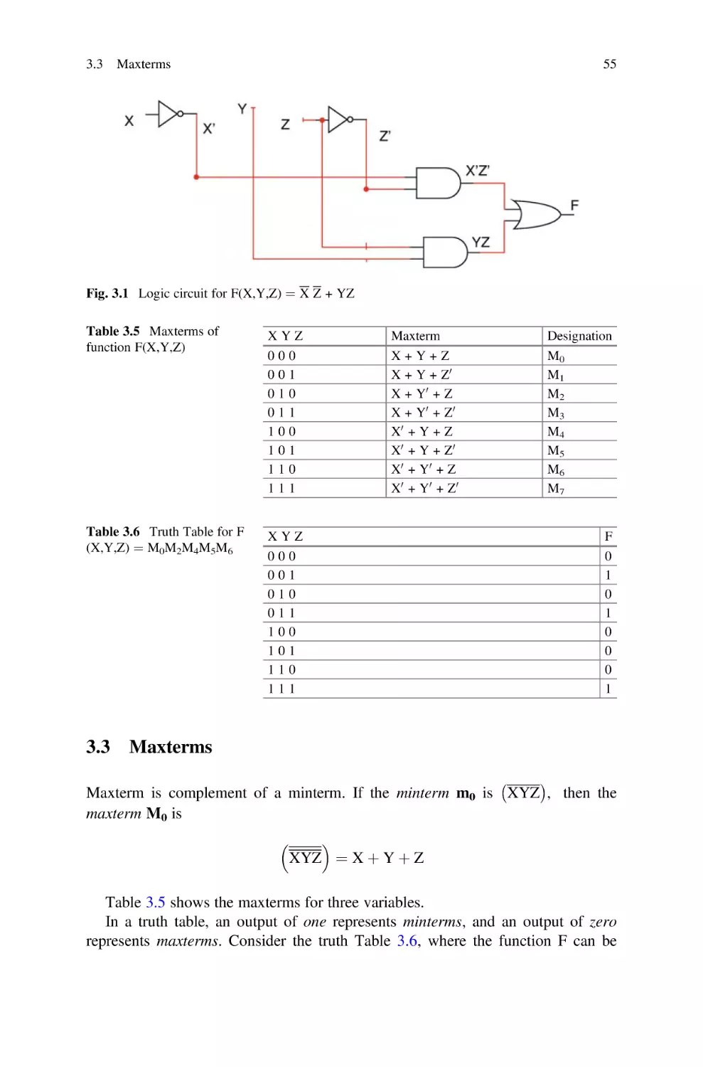
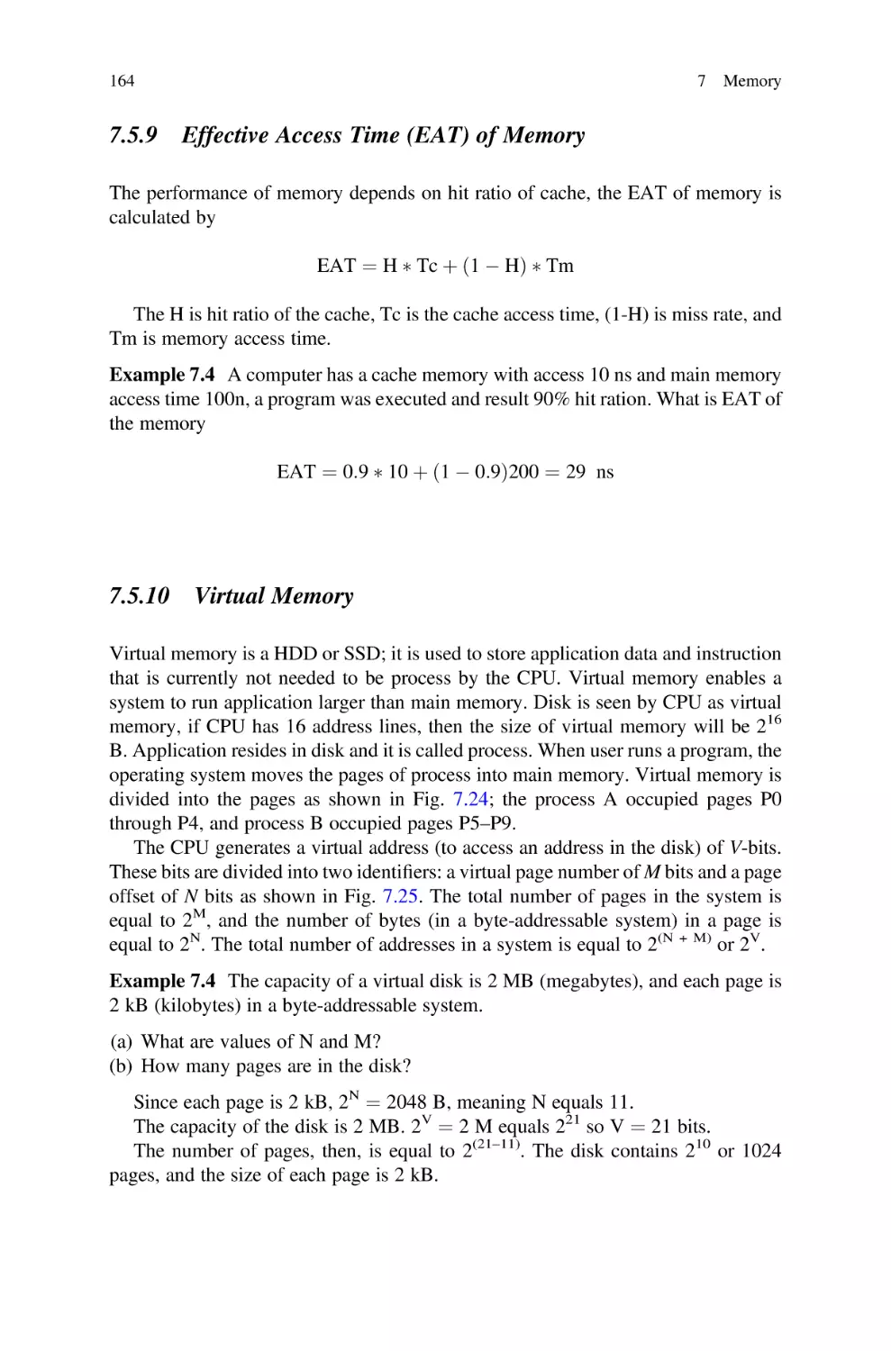
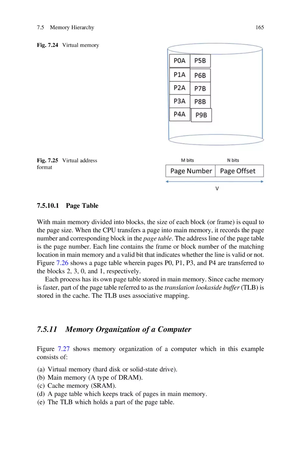
The historical development of the computer can be divided into distinct generations. The first generation of computer was constructed using vacuum tubes
and was known as ENIAC. ENIAC was developed by John Mauchly and J. Presper
Eckert at the University of Pennsylvania between 1945 and 1953. Figure 1.2 shows
an image of a vacuum tube.
The second generation of computer used transistors and were in use between
1954 and 1965. This generation of computers included the IBM 7094 (scientific)
and the Digital Equipment Corporation (DEC) PDP-1. An image of a transistor is
shown in Fig. 1.2.
The third generation of computer used integrated circuits (IC). These computers were developed between 1965 and 1980, and included the IBM 360, DEC
PDP-8 and PDP-11, and Cray-1 supercomputer. An image of an integrated circuit is
shown in Fig. 1.2.
The fourth generation of computer used VLSI (Very Large Scale Integration),
an evolution of IC technology. This started around 1980 and can be found in
processors like the Intel 8080. Figure 1.2 shows an image of VLSI.
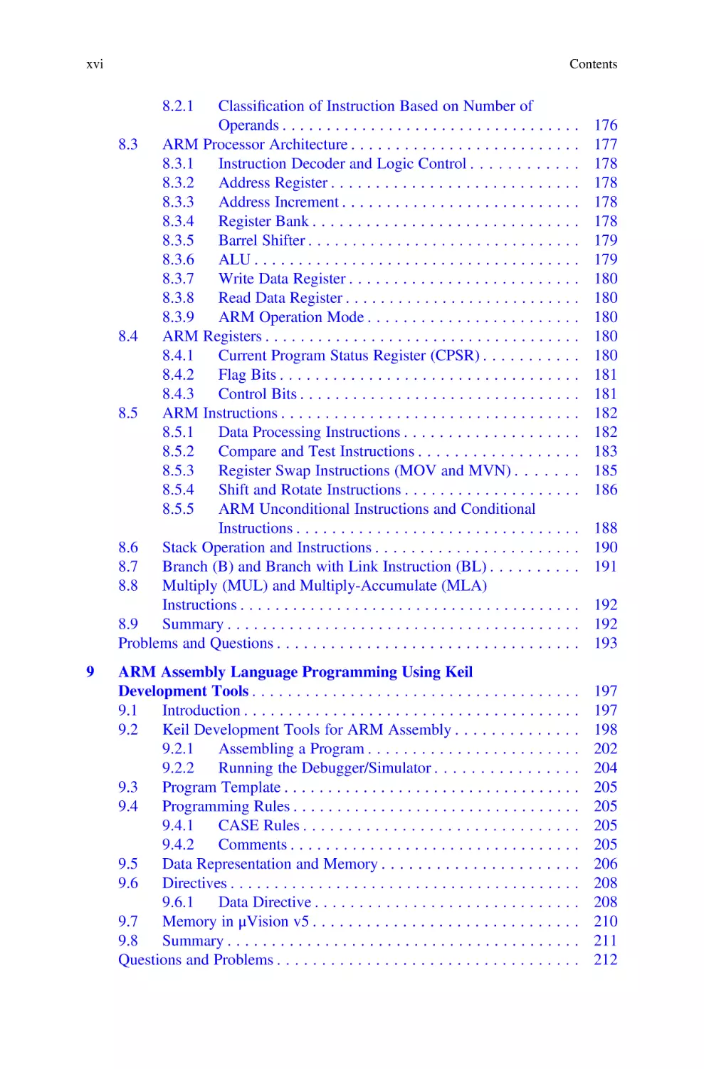
1.3
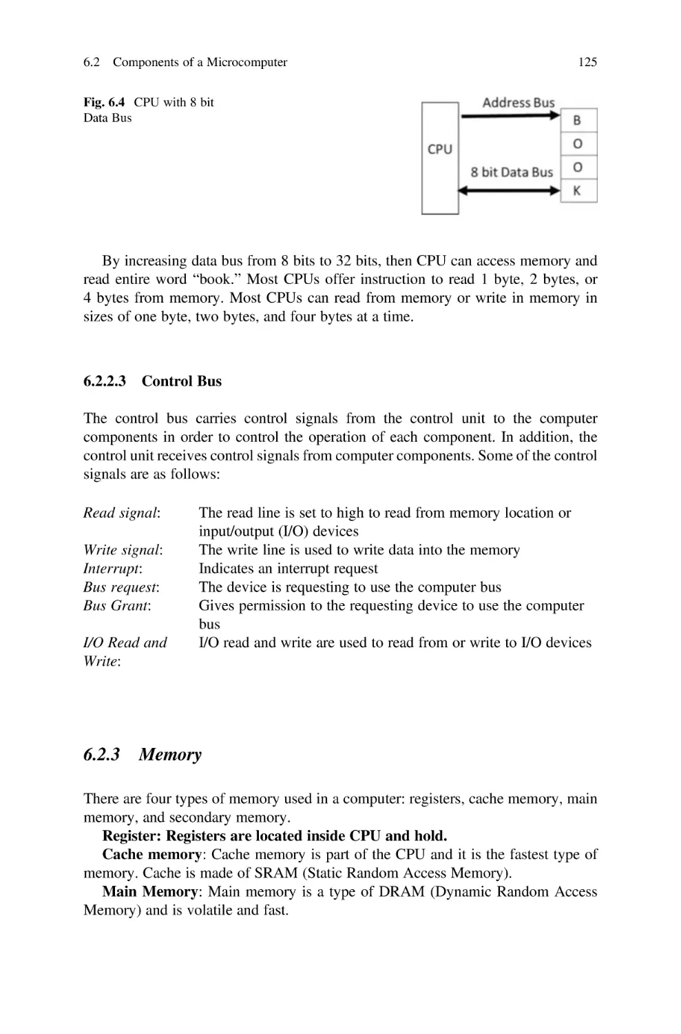
Hardware and Software Components of a Computer
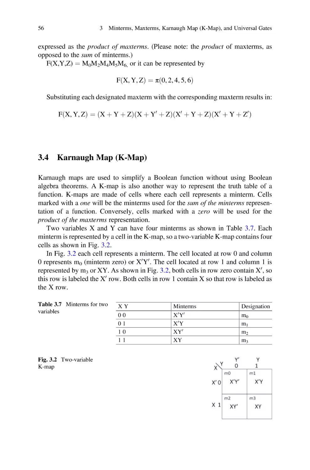
The hardware part of a computer is used for the execution of different types of
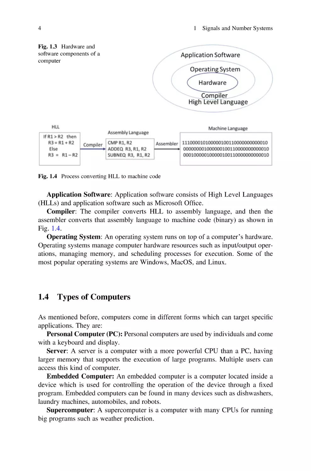
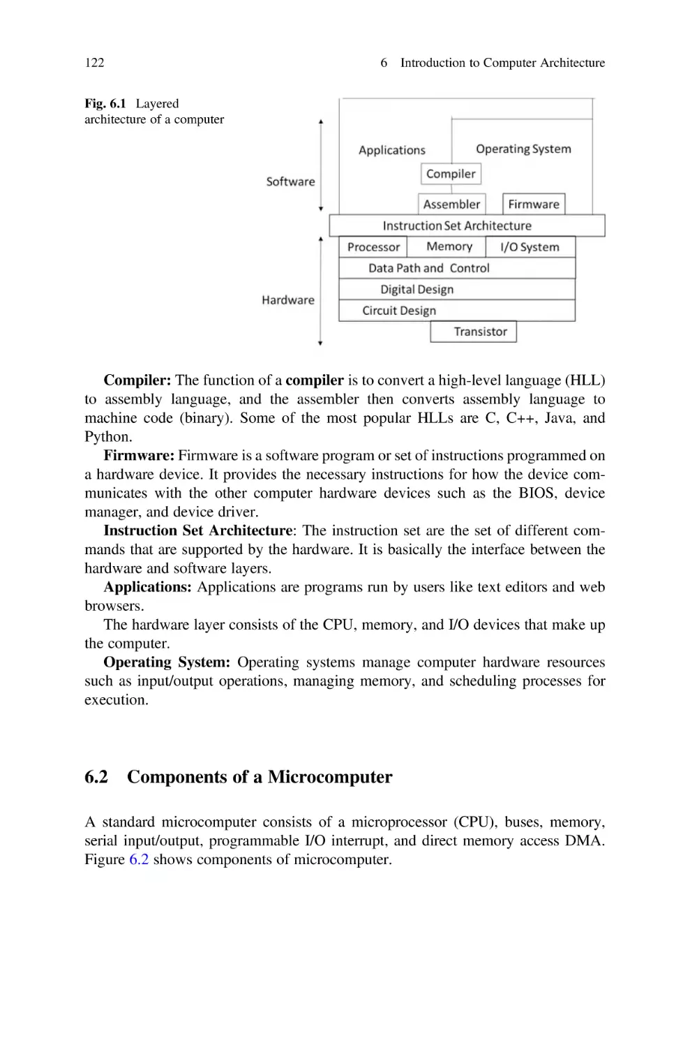
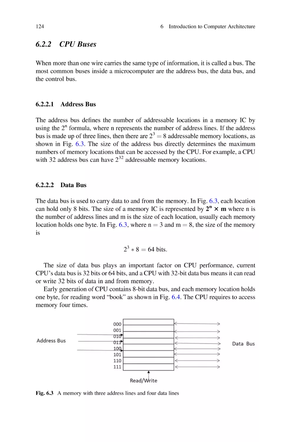
software. Figure 1.3 shows that the hardware is the lowest level component of the
computer with different types of software running on top of it.
Hardware: The hardware consists of the processor, memory, and I/O controllers.
System Software: The system software consists of the compiler and operating
system.
Vacuum Tube
Transistor
Integrated Circuit (IC)
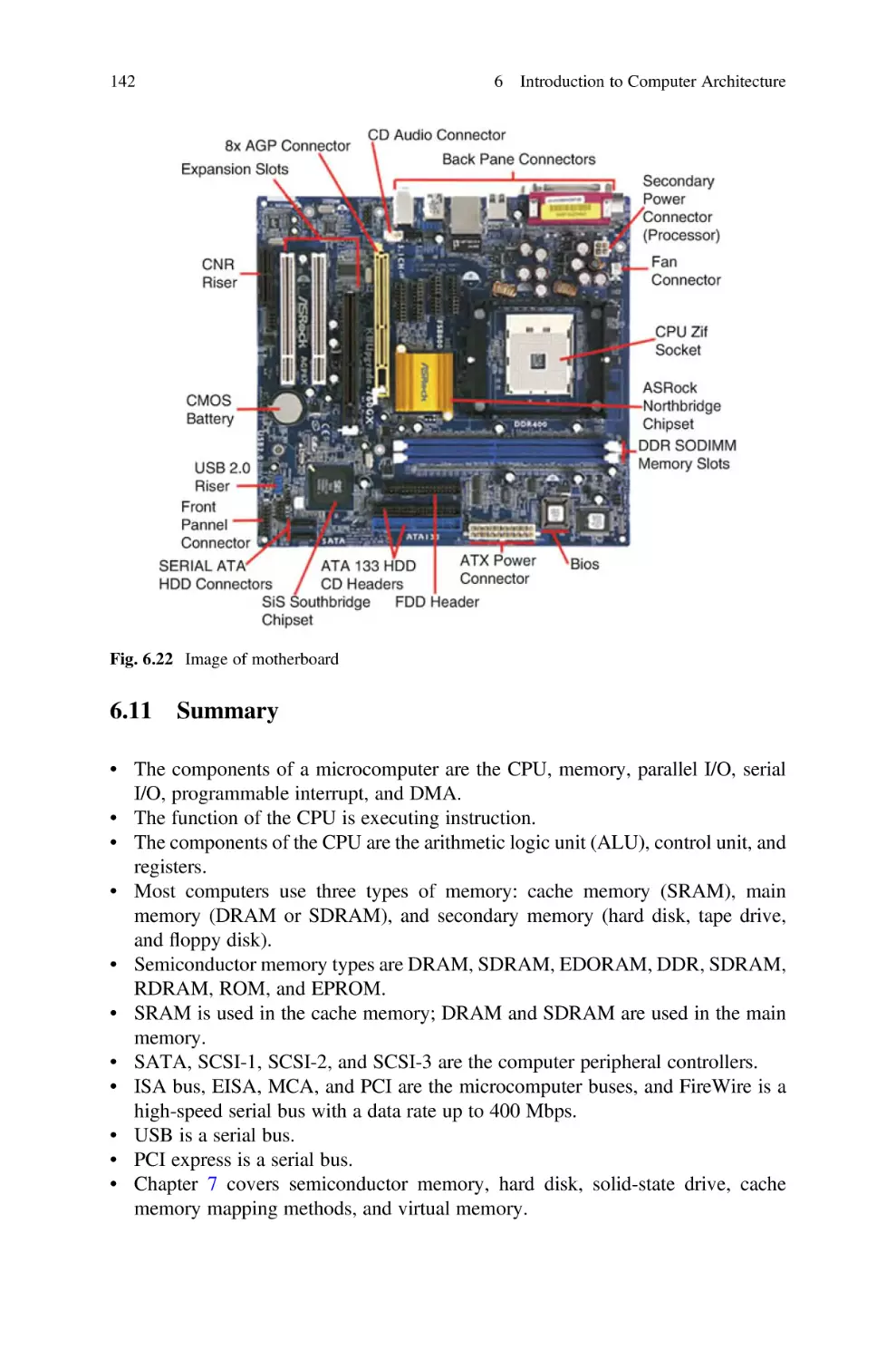
Fig. 1.2 Images of Vacuum Tube, Transistor, IC, and VLSI
VLSI
4
1 Signals and Number Systems
Fig. 1.3 Hardware and
software components of a
computer
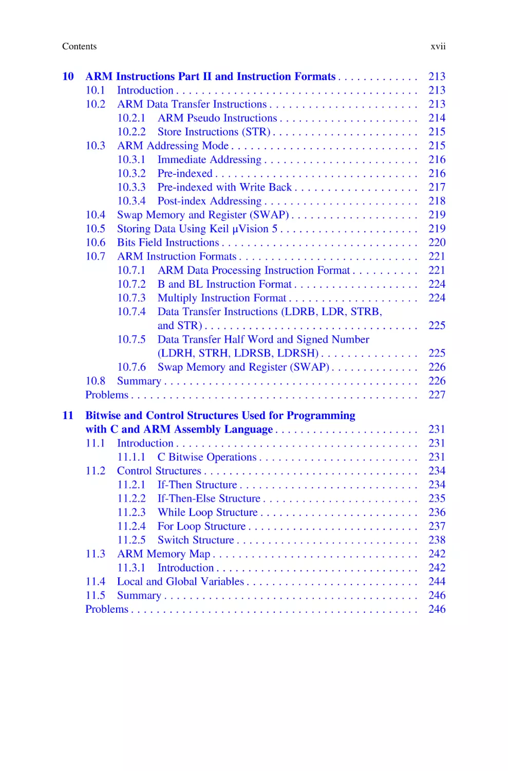
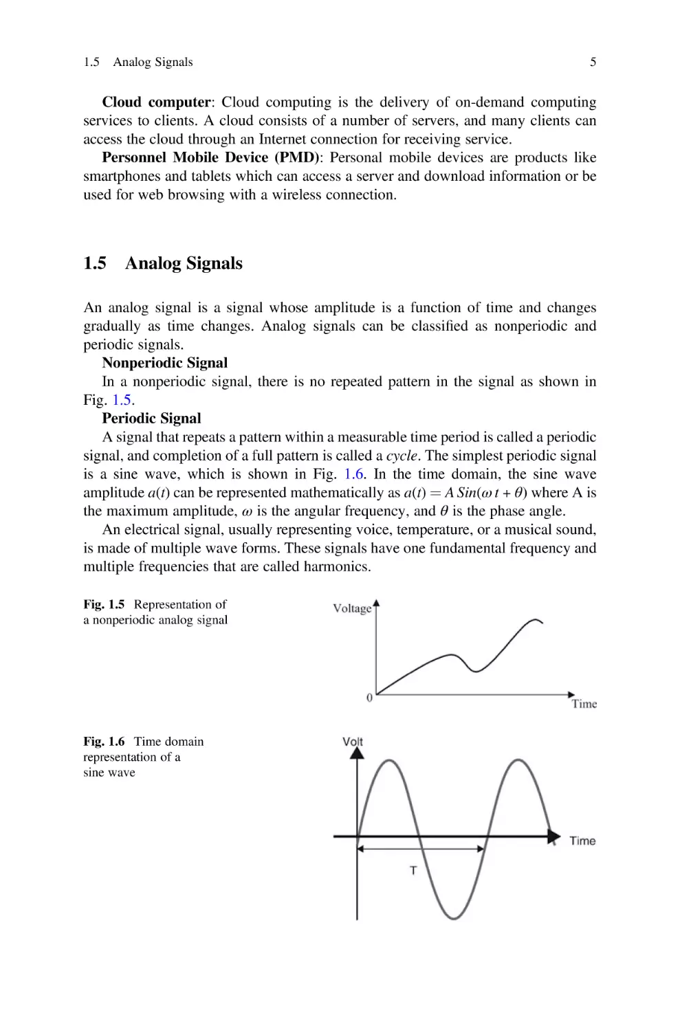
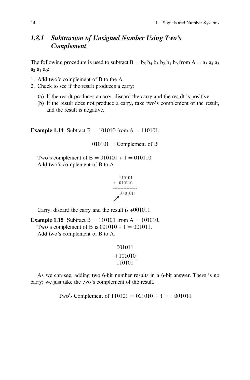
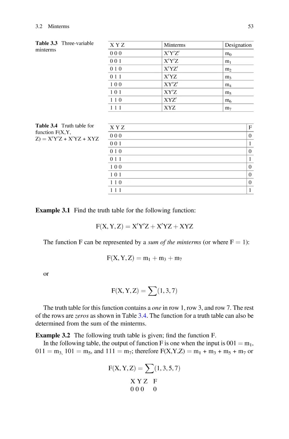
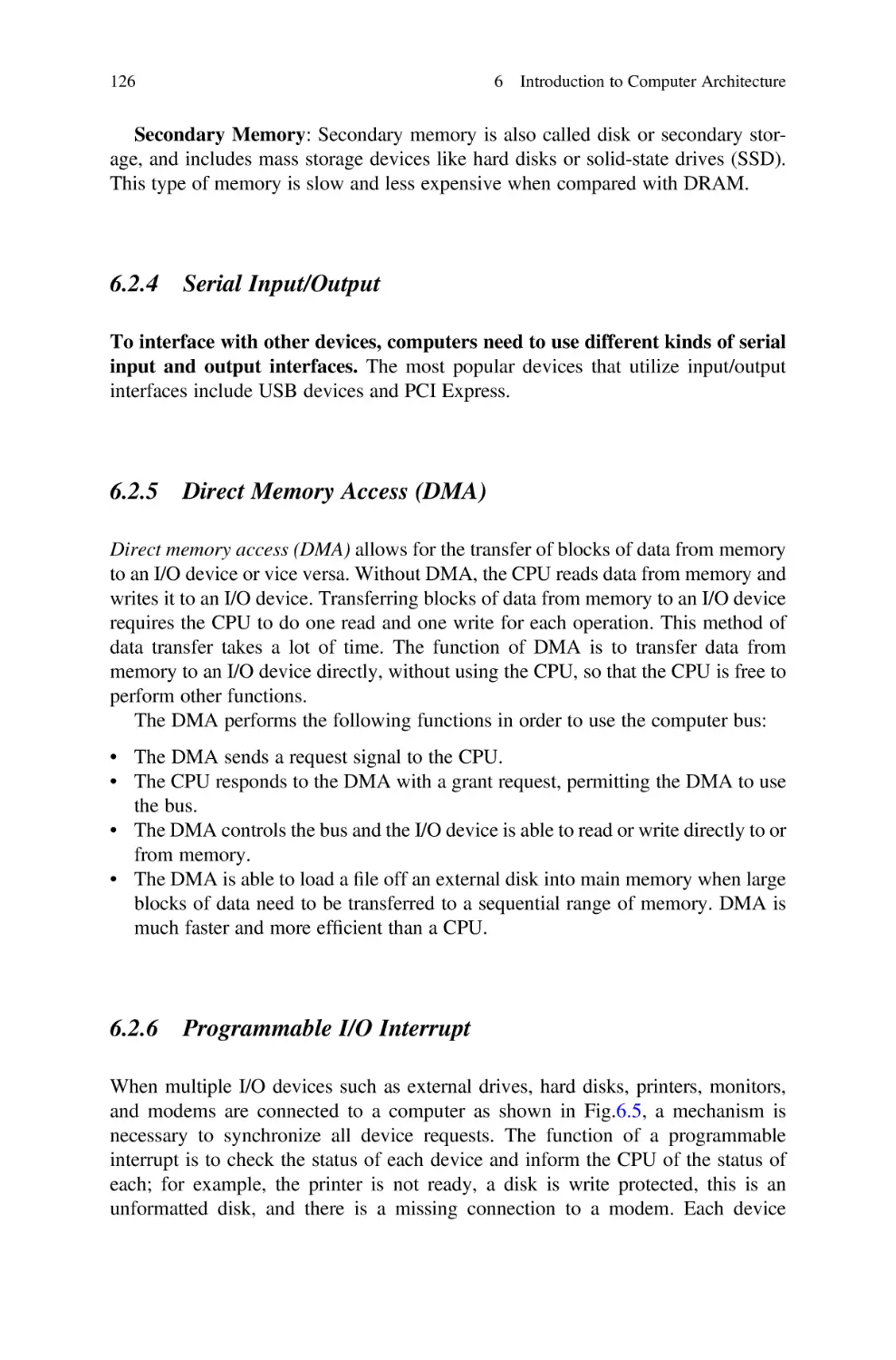
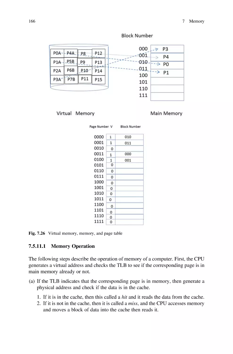
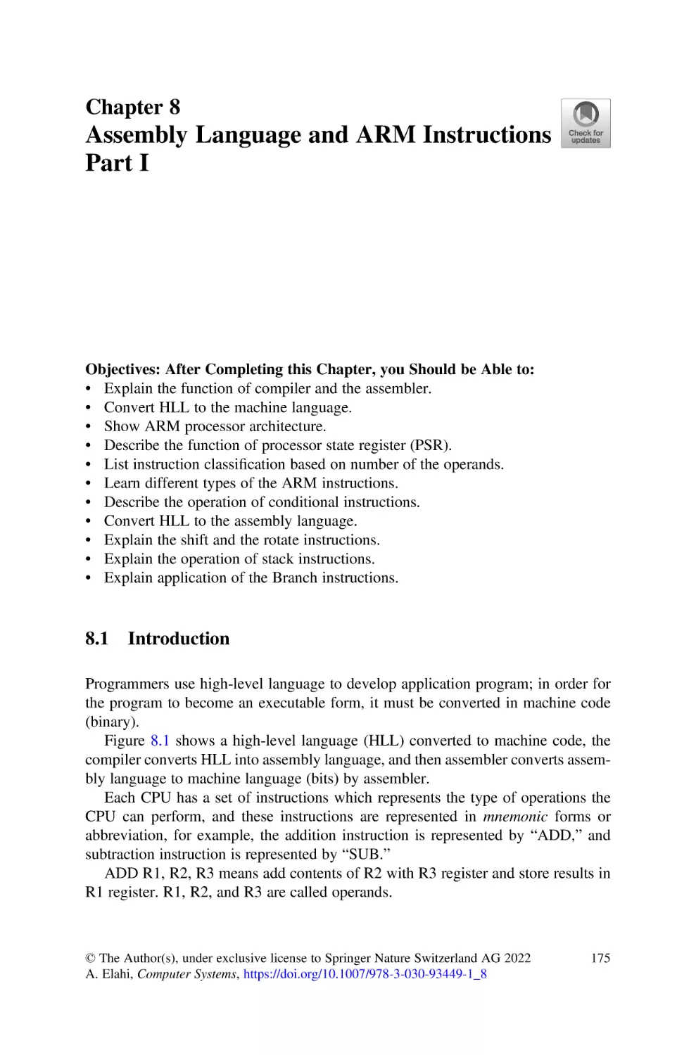
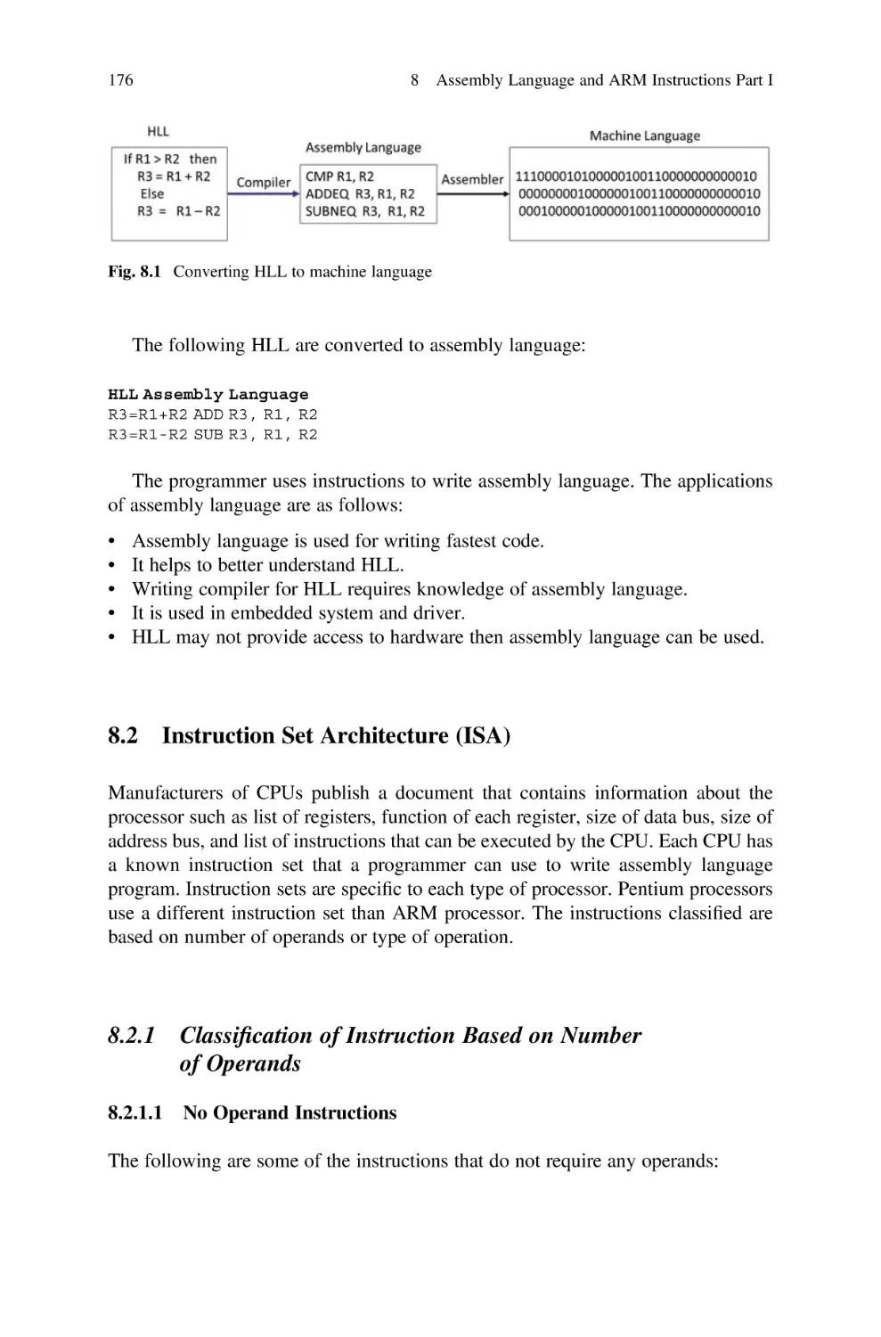
Fig. 1.4 Process converting HLL to machine code
Application Software: Application software consists of High Level Languages
(HLLs) and application software such as Microsoft Office.
Compiler: The compiler converts HLL to assembly language, and then the
assembler converts that assembly language to machine code (binary) as shown in
Fig. 1.4.
Operating System: An operating system runs on top of a computer’s hardware.
Operating systems manage computer hardware resources such as input/output operations, managing memory, and scheduling processes for execution. Some of the
most popular operating systems are Windows, MacOS, and Linux.
1.4
Types of Computers
As mentioned before, computers come in different forms which can target specific
applications. They are:
Personal Computer (PC): Personal computers are used by individuals and come
with a keyboard and display.
Server: A server is a computer with a more powerful CPU than a PC, having
larger memory that supports the execution of large programs. Multiple users can
access this kind of computer.
Embedded Computer: An embedded computer is a computer located inside a
device which is used for controlling the operation of the device through a fixed
program. Embedded computers can be found in many devices such as dishwashers,
laundry machines, automobiles, and robots.
Supercomputer: A supercomputer is a computer with many CPUs for running
big programs such as weather prediction.
1.5 Analog Signals
5
Cloud computer: Cloud computing is the delivery of on-demand computing
services to clients. A cloud consists of a number of servers, and many clients can
access the cloud through an Internet connection for receiving service.
Personnel Mobile Device (PMD): Personal mobile devices are products like
smartphones and tablets which can access a server and download information or be
used for web browsing with a wireless connection.
1.5
Analog Signals
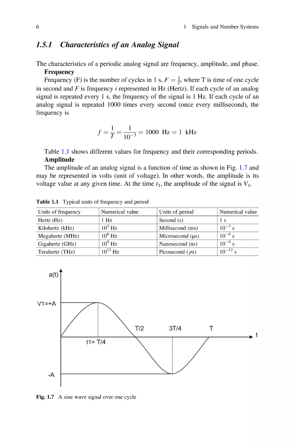
An analog signal is a signal whose amplitude is a function of time and changes
gradually as time changes. Analog signals can be classified as nonperiodic and
periodic signals.
Nonperiodic Signal
In a nonperiodic signal, there is no repeated pattern in the signal as shown in
Fig. 1.5.
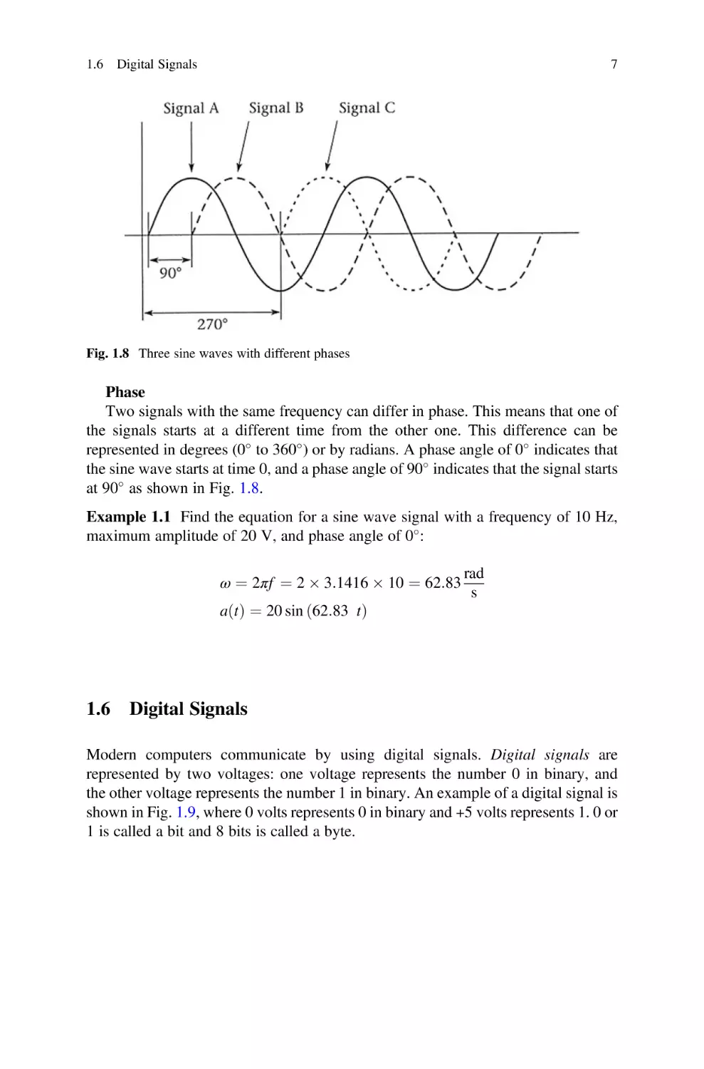
Periodic Signal
A signal that repeats a pattern within a measurable time period is called a periodic
signal, and completion of a full pattern is called a cycle. The simplest periodic signal
is a sine wave, which is shown in Fig. 1.6. In the time domain, the sine wave
amplitude a(t) can be represented mathematically as a(t) ¼ A Sin(ω t + θ) where A is
the maximum amplitude, ω is the angular frequency, and θ is the phase angle.
An electrical signal, usually representing voice, temperature, or a musical sound,
is made of multiple wave forms. These signals have one fundamental frequency and
multiple frequencies that are called harmonics.
Fig. 1.5 Representation of
a nonperiodic analog signal
Fig. 1.6 Time domain
representation of a
sine wave
6
1.5.1
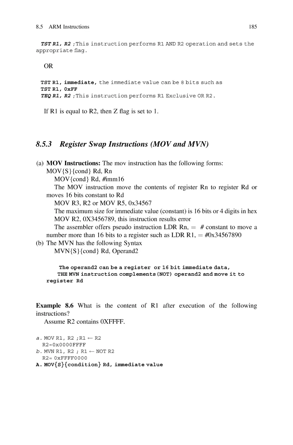
1 Signals and Number Systems
Characteristics of an Analog Signal
The characteristics of a periodic analog signal are frequency, amplitude, and phase.
Frequency
Frequency (F) is the number of cycles in 1 s, F ¼ T1, where T is time of one cycle
in second and F is frequency i represented in Hz (Hertz). If each cycle of an analog
signal is repeated every 1 s, the frequency of the signal is 1 Hz. If each cycle of an
analog signal is repeated 1000 times every second (once every millisecond), the
frequency is
f ¼
1
1
¼
¼ 1000 Hz ¼ 1 kHz
T 103
Table 1.1 shows different values for frequency and their corresponding periods.
Amplitude
The amplitude of an analog signal is a function of time as shown in Fig. 1.7 and
may be represented in volts (unit of voltage). In other words, the amplitude is its
voltage value at any given time. At the time t1, the amplitude of the signal is V1.
Table 1.1 Typical units of frequency and period
Units of frequency
Hertz (Hz)
Kilohertz (kHz)
Megahertz (MHz)
Gigahertz (GHz)
Terahertz (THz)
Numerical value
1 Hz
103 Hz
106 Hz
109 Hz
1012 Hz
Fig. 1.7 A sine wave signal over one cycle
Units of period
Second (s)
Millisecond (ms)
Microsecond (μs)
Nanosecond (ns)
Picosecond ( ps)
Numerical value
1s
103 s
106 s
109 s
1012 s
1.6 Digital Signals
7
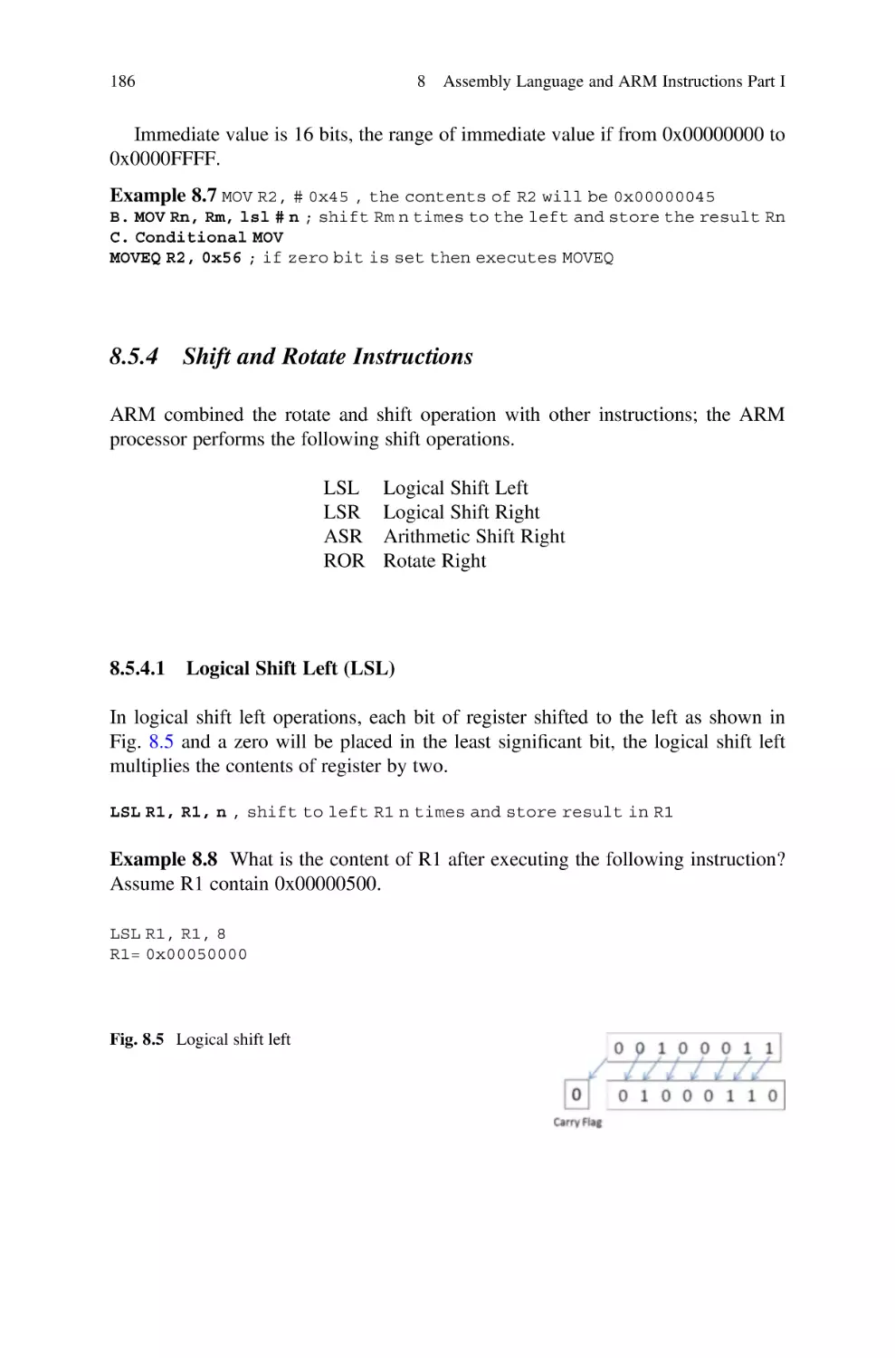
Fig. 1.8 Three sine waves with different phases
Phase
Two signals with the same frequency can differ in phase. This means that one of
the signals starts at a different time from the other one. This difference can be
represented in degrees (0 to 360 ) or by radians. A phase angle of 0 indicates that
the sine wave starts at time 0, and a phase angle of 90 indicates that the signal starts
at 90 as shown in Fig. 1.8.
Example 1.1 Find the equation for a sine wave signal with a frequency of 10 Hz,
maximum amplitude of 20 V, and phase angle of 0 :
ω ¼ 2πf ¼ 2 3:1416 10 ¼ 62:83
aðt Þ ¼ 20 sin ð62:83 t Þ
1.6
rad
s
Digital Signals
Modern computers communicate by using digital signals. Digital signals are
represented by two voltages: one voltage represents the number 0 in binary, and
the other voltage represents the number 1 in binary. An example of a digital signal is
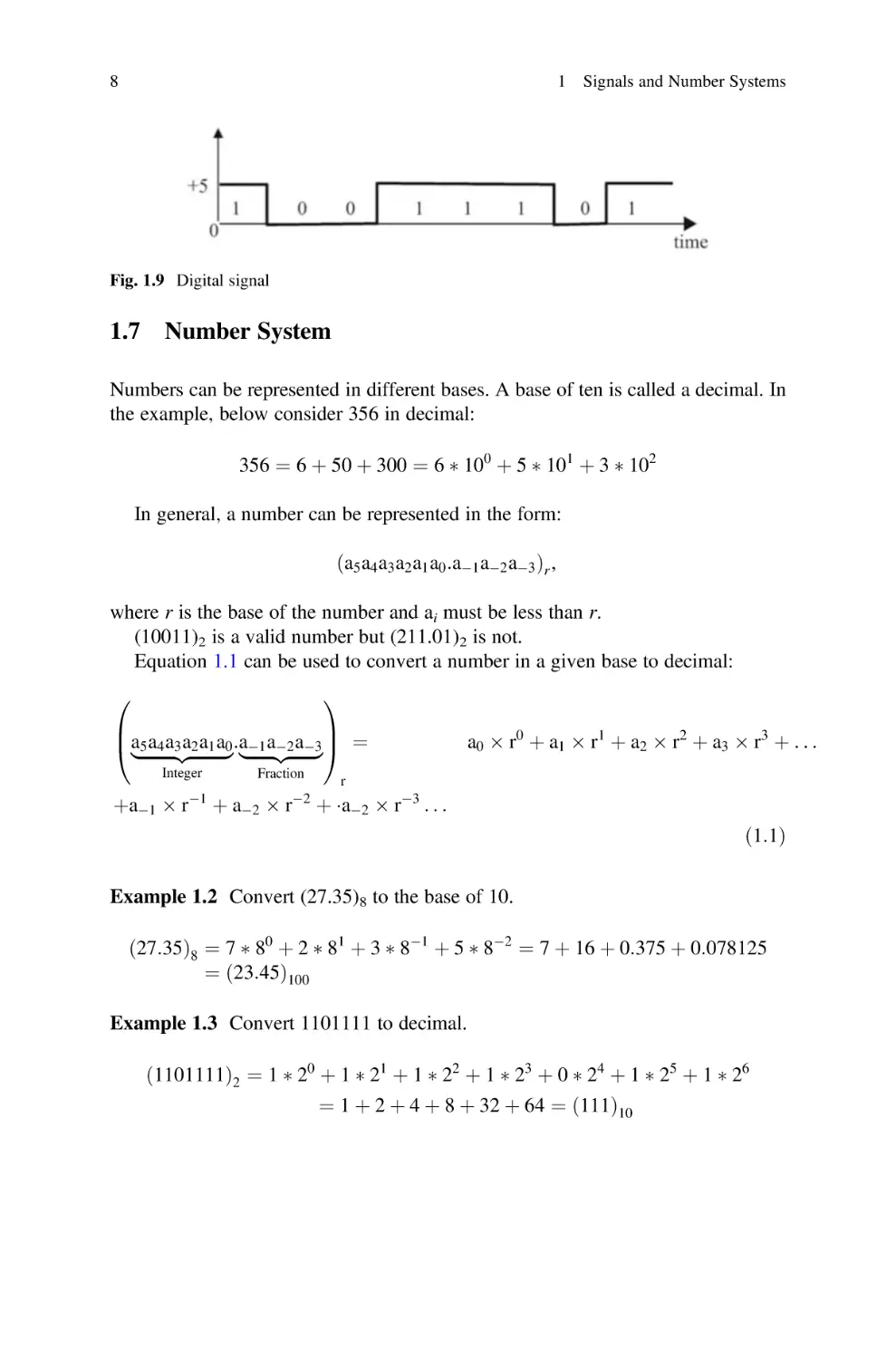
shown in Fig. 1.9, where 0 volts represents 0 in binary and +5 volts represents 1. 0 or
1 is called a bit and 8 bits is called a byte.
8
1 Signals and Number Systems
Fig. 1.9 Digital signal
1.7
Number System
Numbers can be represented in different bases. A base of ten is called a decimal. In
the example, below consider 356 in decimal:
356 ¼ 6 þ 50 þ 300 ¼ 6 100 þ 5 101 þ 3 102
In general, a number can be represented in the form:
ða5 a4 a3 a2 a1 a0 :a1 a2 a3 Þr ,
where r is the base of the number and ai must be less than r.
(10011)2 is a valid number but (211.01)2 is not.
Equation 1.1 can be used to convert a number in a given base to decimal:
0
1
B
C
a5 a4 a3 a2 a1 a0 :a1 a2 a3 A ¼
@|fflfflfflfflfflfflfflffl{zfflfflfflfflfflfflfflffl}
|fflfflfflfflfflffl{zfflfflfflfflfflffl}
Integer
þa1 r
1
Fraction
a0 r 0 þ a1 r 1 þ a2 r 2 þ a3 r 3 þ . . .
r
þ a2 r2 þ a2 r3 . . .
ð1:1Þ
Example 1.2 Convert (27.35)8 to the base of 10.
ð27:35Þ8 ¼ 7 80 þ 2 81 þ 3 81 þ 5 82 ¼ 7 þ 16 þ 0:375 þ 0:078125
¼ ð23:45Þ100
Example 1.3 Convert 1101111 to decimal.
ð1101111Þ2 ¼ 1 20 þ 1 21 þ 1 22 þ 1 23 þ 0 24 þ 1 25 þ 1 26
¼ 1 þ 2 þ 4 þ 8 þ 32 þ 64 ¼ ð111Þ10
1.7 Number System
1.7.1
9
Converting from Binary to Decimal
Equation 1.2 represents the general form of a binary number:
ða5 a4 a3 a2 a1 a0 :a1 a2 a3 Þ2
ð1:2Þ
where ai is a binary digit or bit (either 0 or 1).
Equation 1.2 can be converted to decimal number by using Eq. 1.1:
0
1
B
C
a5 a4 a3 a2 a1 a0 :a1 a2 a3 A ¼ a0 20 þ a1 21 þ a2 22 þ a3 23 þ . . .
@|fflfflfflfflfflfflfflffl{zfflfflfflfflfflfflfflffl}
|fflfflfflfflfflffl{zfflfflfflfflfflffl}
Integer
þa1 2
1
Fraction
2
þ a2 22 þ . . .
ð1:3Þ
ða5 a4 a3 a2 a1 a0 :a1 a2 a3 Þ2 ¼ a0 þ 2 a1 þ 4 a2 þ 8 a3 þ 16 a4 þ 32 a5 þ 64 a6
1
1
1
þ a1 þ a2 þ a3
2
4
8
Example 1.4 Convert (110111.101)2 to decimal.
ð110111:101Þ2 ¼ 1 20 þ 1 21 þ 1 22 þ 0 23 þ 1 24 þ 1 25 þ 1 21 þ 0 22 þ 1
¼ 55:625
Or
25 24 2 3 22 21 20
21 22 23
1 1 0 1 1 1 . 1
0
1
32 þ 16 þ 0 þ 4 þ 2 þ 1 þ 1=2 þ 0 þ 1=8
If a binary value is made of n bits of ones, then its decimal value is 2n 1.
Example 1.5
11 ¼ 22 1 ¼ 3
111 ¼ 23 1 ¼ 7
1111 ¼ 24 1 ¼ 15
11111 ¼ 25 1 ¼ 31
111111 ¼ 26 1 ¼ 63
10
1 Signals and Number Systems
Binary, or base of 2 numbers, is represented by 0 s and 1 s. A binary digit, 0 or
1, is called a bit, 8 bits is called a byte, 16 bits is called a half word, and 4 bytes is
called a word.
1.7.2
Converting from Decimal Integer to Binary
To convert an integer number from decimal to binary, divide the decimal number by
the new base (2 for binary), which will result in a quotient and a remainder (either
0 or 1). The first remainder will be the least significant bit of the binary number.
Continually divide the quotient by the new base, while taking the remainders as each
subsequent bit in the binary number, until the quotient becomes 0.
Example 1.6 Convert 34 in decimal to binary.
34/2 ¼
17/2¼
8/2
4/2
2/2
1/2
Therefore 34 ¼ (100010)2
Quotient
17
8
4
2
1
0
Remainder
0 ¼ a0
1 ¼ a1
0 ¼ a2
0 ¼ a3
0 ¼ a4
1 ¼ a5
If a binary number is made of all ones, then by using the equation 2n 1, it can be
converted to decimal.
Examples
Binary number
11
111
1111
11111
2n 1
22 – 1
23 – 1
24 – 1
25 – 1
Decimal number
3
7
15
32
A binary number is represented by a5 a4 a3 a2 a1 a0 where a0 is 20, a1 is 21, and a5
is 25. Table 1.2 shows 2n.
1.7.3
Converting Decimal Fraction to Binary
A decimal number representation of (0.XY)10 can be converted into base of 2 and
represented by (0.a1, a2, a3, etc.)2.
1.7 Number System
11
Table 1.2 2n with different values of n
2n
20
21
22
23
24
25
26
27
Decimal value
1
2
4
8
16
32
64
128
2n
28
29
210
211
212
213
214
215
Decimal value
256
512
1024 ¼ 1 K
2048 ¼ 2 K
4096 ¼ 4 K
8192 ¼ 8 K
16,384 ¼ 16 K
32,768 ¼ 32 K
2n
216
217
218
219
220
221
222
223
Decimal value
65,536 ¼ 64 K
131,072 ¼ 128 K
262,144 ¼ 256 K
524,288 ¼ 512 K
1,048,576 ¼ 1 M
2M
4M
8M
The fraction number is multiplied by 2, the result of integer part is a1 and
fraction part multiply by 2, and then separate integer part from fraction, the integer
part represents a2; this process continues until the fraction becomes 0.
(0.35) 10 ¼ (
)2
0.35*2
0.7*2
0.4*2
0.8*2
0.6*2
¼
¼
¼
¼
¼
0.7
1.4
0.8
1.6
1.2
¼
¼
¼
¼
¼
0
1
0
1
1
+
+
+
+
+
0.7
0.4
0.8
0.6
0.2
a1 ¼ 0
a2 ¼ 1
a3 ¼ 0
a4 ¼ 1
a5 ¼ 1
Sometimes, the fraction does not reach 0 and the number of bits use for the
fraction depends on the accuracy that the user defines, therefore 0.35 ¼ 0.010011 in
binary.
The hexadecimal number system has a base of 16 and therefore has 16 symbols
(0 through 9, and A through F). Table 1.3 shows the decimal numbers, their binary
values from 0 to 15, and their hexadecimal equivalents.
1.7.4
Converting from Hex to Binary
Table 1.3 can also be used to convert a number from hexadecimal to binary and from
binary to hexadecimal.
Example 1.7 Convert the binary number 001010011010 to hexadecimal. Each
4 bits are grouped from right to left. By using Table 2.2, each 4-bit group can be
converted to its hexadecimal equivalent.
0010 1001 1010
2
9
A
12
1 Signals and Number Systems
Table 1.3 Decimal numbers with binary and hexadecimal equivalents
Decimal
0
1
2
3
4
5
6
7
8
9
10
11
12
13
14
15
Binary (base of 2)
0000
0001
0010
0011
0100
0101
0110
0111
1000
1001
1010
1011
1100
1101
1110
1111
Hexadecimal (base of 16) or HEX
0
1
2
3
4
5
6
7
8
9
A
B
C
D
E
F
Example 1.8 Convert (3D5)16 to binary. By using Table 2.2, the result in binary is
3
D
5
0011 1101 0101
The resulting binary number is 001111010101.
Example 1.9 Convert 6DB from hexadecimal to binary. By using Table 1.3, the
result in binary is
6
D
B
0110 1101 1011
The resulting binary number is 011011011011.
Example 1.10 Convert (110111.101)2 to decimal.
ð110111:101Þ2 ¼ 1 20 þ 1 21 þ 1 22 þ 0 23 þ 1 24 þ 1 25 þ 1 21
þ 0 22 þ 1 23
¼ 55:625
1.8 Complement and Two’s Complement
1.7.5
13
Binary Addition
1 þ 0 ¼ 1, 1 þ 1 ¼ 10,
Carry bits
111
10101
þ01101
100010
In a binary number, the first bit from the left of number is called the most
significant bit (MSb), and the first bit from the right of number is called least
significant bit (LSb).
MSb ! 10010
1.8
LSb
Complement and Two’s Complement
The idea of the complement makes it simple for a digital computer to perform
subtraction and addition. The complement of 1 is 0 and the complement of 0 is 1.
The complement of a binary number is calculated by complementing each bit of
the number.
Example 1.11 The complement of 101101 is 010010.
Two0 s Complement of a number = Complement of a number þ 1
Example 1.12 The two’s complement of 101011 is
010100ðcomplementÞ þ 1 ¼ 010101
Example 1.13 Find the two’s complement of 10000:
01111ðcomplementÞ þ 1 ¼ 10000
14
1 Signals and Number Systems
1.8.1
Subtraction of Unsigned Number Using Two’s
Complement
The following procedure is used to subtract B ¼ b5 b4 b3 b2 b1 b0 from A ¼ a5 a4 a3
a 2 a 1 a 0:
1. Add two’s complement of B to the A.
2. Check to see if the result produces a carry:
(a) If the result produces a carry, discard the carry and the result is positive.
(b) If the result does not produce a carry, take two’s complement of the result,
and the result is negative.
Example 1.14 Subtract B ¼ 101010 from A ¼ 110101.
010101 ¼ Complement of B
Two’s complement of B ¼ 010101 + 1 ¼ 010110.
Add two’s complement of B to A.
Carry, discard the carry and the result is +001011.
Example 1.15 Subtract B ¼ 110101 from A ¼ 101010.
Two’s complement of B is 001010 + 1 ¼ 001011.
Add two’s complement of B to A.
001011
þ101010
110101
As we can see, adding two 6-bit number results in a 6-bit answer. There is no
carry; we just take the two’s complement of the result.
Two0 s Complement of 110101 ¼ 001010 þ 1 ¼ 001011
1.9 Unsigned, Signed Magnitude, and Signed Two’s Complement Binary Number
1.9
15
Unsigned, Signed Magnitude, and Signed Two’s
Complement Binary Number
A binary number can be represented in form unsigned number or signed number or
signed two’s complement, + sign represented by 0 and sign represented by 1.
1.9.1
Unsigned Number
In an unsigned number, all bits of a number are used to represent the number, but in a
signed number, the most significant bit of the number represents the sign. A 1 in the
most significant position of number represents a negative sign, and 0 in the most
significant position of number represents a positive sign.
The 1101 unsigned value is 13.
1.9.2
Signed Magnitude Number
In a signed number, the most significant bit represents the sign, where 1101 ¼ 5 or
0101 ¼ +5.
In unsigned number, 1101 ¼ 13.
1.9.3
Signed Two’s Complement
A signed two’s complement applies to a negative number. If the sign of the number
is one, then the number is represented by signed two’s complement.
Example 1.16 Representing (5)10 with 4 bits in signed two’s complement.
(5)10 in signed number is 1101, then the two’s complement of 101 is 011, and
by adding sign bit results in 1011 which represents 5 in signed two’s complement.
Example 1.17 Represent (23)10 with an 8-bit signed two’s complement.
(23)10 ¼ (1 0 1 1 1)2 in unsigned base-2
(1 00 10111)2 – Extended to signed 8 bits (notice the MSb is 1)
the two’s complement of (0010111)2 is (1101001)2
(11101001)2 is (23)10 in signed two’s complement.
16
1 Signals and Number Systems
1.10
Binary Addition Using Signed Two’s Complement
The following examples show the results of the addition of two signed numbers:
(a) (+3) + (+4)
Represent both numbers in binary, and the most significant bit represents the
sign, and the result is positive.
0011 þ 0100 ¼ 0111 ¼ þ7
(b) (+ 3)10 + (4)10
(4)10 in signed two’s complement is 1100, then
0011 + 1100 ¼ 1111; result does not generate carry of then take two’s
complement of result which is 1
ð3Þ þ ðþ5Þ ¼ 1101 þ 0101 ¼ 10010ðdiscard carry and result is þ 2Þ
(c) (7)10 + (5)10
By representing both numbers in 4-bit signed two’s complement,
ð7Þ10 ¼ 1001
ð5Þ10 ¼ 1011
1001 þ 1011 ¼ 10100
"
Sign bit
The addition of two negative numbers results positive, and it is called overflow:
ðþ7Þ þ ðþ6Þ ¼ ð0111Þ þ ð0110Þ ¼ 1101
The addition of two positive numbers results negative, and it is called overflow:
Example 1.18 A. The following addition using 8-bit signed two’s complement
(38)10 + (44)10
38
10
44
10
in signed two' complement 11011010
00101100
100000110 discard the carry and result is
00000110 6
1.11
Floating Point Representation
17
B. Add 38 to 44 using 8 bit signed two’s complement
38 ¼ 11011010
44 ¼ 11010100
----------–
10101110 ¼ 82
C. Add +100 to +44
100 ¼ 01100100
44 ¼ 00101100
------------10010000 the sign of result is negative then results produce overflow.
Addition Overflow
The following cases result overflow for adding two signed numbers if:
(a) Both numbers are negative, and results of addition become positive:
ðAÞ þ ðBÞ ¼ þC
(b) Both numbers are positive, and results of addition become negative:
ðþAÞ þ ðþBÞ ¼ C
1.11
Floating Point Representation
The central processing unit (CPU) typically consists of an arithmetic logic unit
(ALU), floating point unit (FLU/FPU), registers, control unit, and the cache
memory.
The arithmetic logic unit performs integer arithmetic operations such as addition,
subtraction, and logic operations such as AND, OR, XOR, etc. Integers are whole
numbers without fractional components. 1, 2, and 3 are integers, while 0.1, 2.2, and
3.0001 all have fractional components are called floating point numbers.
The floating point unit performs floating point operations. Floating point numbers
have a sign, a mantissa, and an exponent. The Institute of Electrical and Electronics
Engineers (IEEE) developed a standard to represent floating point numbers, referred
to as IEEE 754. This standard defines a format for both single (32-bit) and double
(64-bit) precision floating point numbers. Decimal floating points are represented by
M 10E, where M is the signed mantissa and E is the exponent.
18
1 Signals and Number Systems
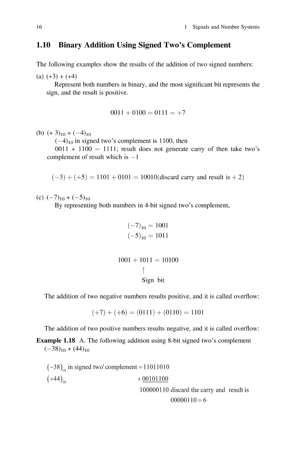
1.11.1 Single and Double Precision Representations
of Floating Point
Floating point numbers in single precision represented by 32 bits are as shown in
Fig. 1.10
1.11.1.1
Biased Exponent
The biased exponent is the exponent + 127 (01111111)2; therefore, the exponent is
represented by a positive number.
1.11.1.2
Normalized Mantissa
The mantissa is represented by 1. M, where M is called normalized mantissa; if
M ¼ 00101, then mantissa is 1.00101.
Example 1.19 Find normalized mantissa and biased exponent of (111.0000111)2.
111.0000111 can be written in the form of 1.110000111 * 210
where
M ¼ 110000111
Biased exponent ¼ 10 + 01111111 ¼ 10000001
The representation of 111.0000111 in single precision is
1bit 8 bits
23 bits
0
10000001 11000011100000000000000
Example 1.20 Convert the following single precision floating point to decimal
number.
101111101 11001000000000000000000
S ¼ 1 means mantissa is negative.
Biased exponent ¼ 01111101.
Exponent ¼ 01111101–01111111 ¼ 00000010.
Normalized mantissa ¼ 11001000000000000000000.
Mantissa ¼ 1. 11001000000000000000000.
Decimal number ¼ 1.11001000000000000000000 *210 ¼ 0.01110011.
Fig. 1.10 IEEE 745 floating point single precision (S ¼ represent sign of mantissa. S ¼ 0 means
mantissa is positive, and S ¼ 1 means mantissa is negative)
1.12
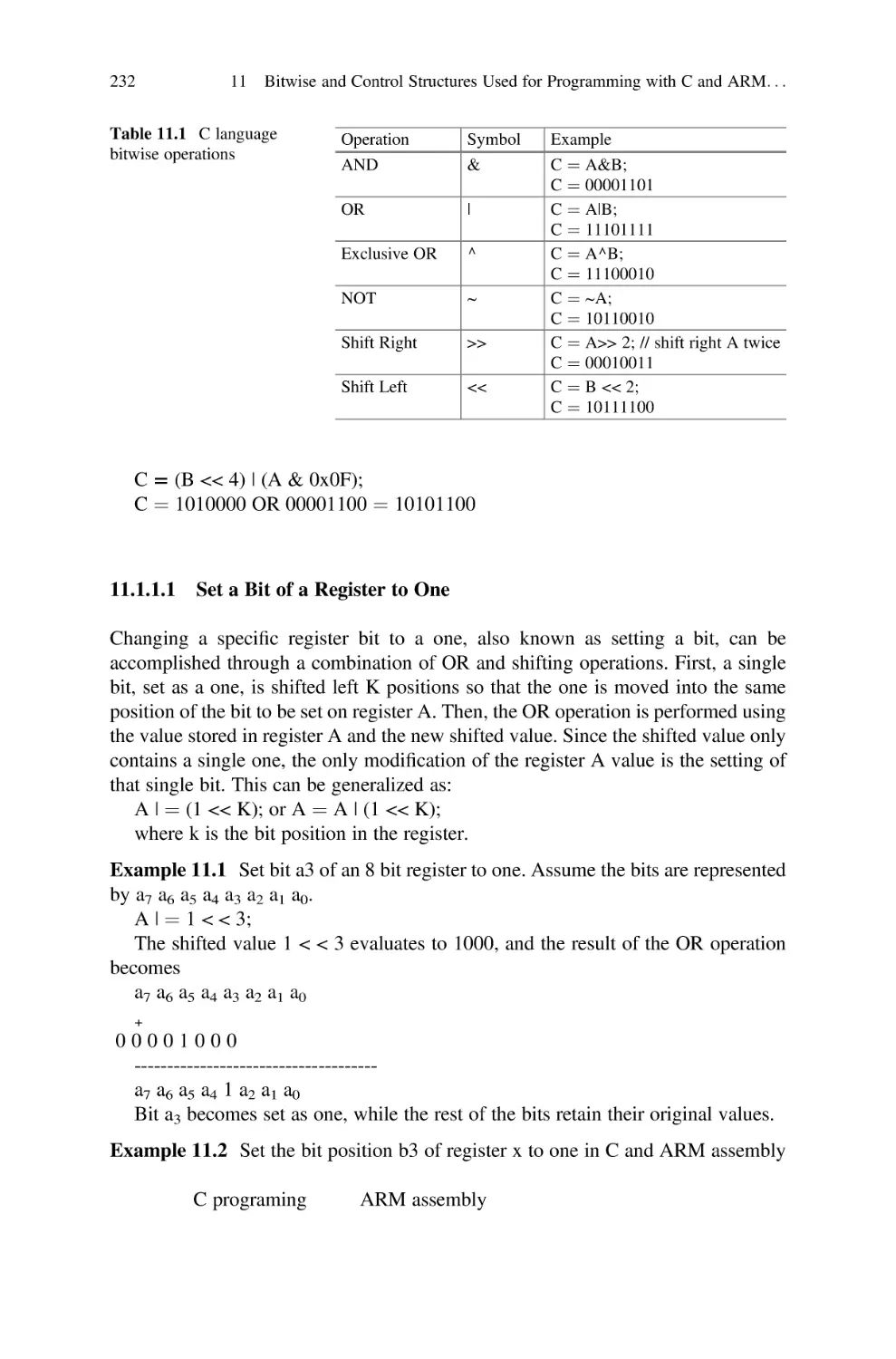
Binary-Coded Decimal (BCD)
1.11.1.3
19
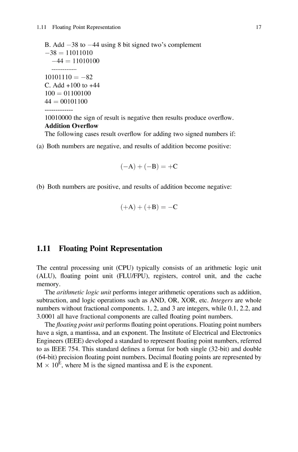
Double Precision
In order to increase the accuracy of a floating point number, IEEE 745 offers double
precision represented by 64 bits as shown in Fig. 1.11.
Biased exponent ¼ exponent + 1023
Example 1.21 Represent 5.75 in IEEE 745 single precision.
15. 625 ¼ (1111.101)2
1111.101 ¼ 1.11101101 * 211
S¼1
Normalized mantissa ¼0.11101101.
Biased exponent ¼ 11 + 01111111 ¼ 10000010.
IEEE745 single precision is 1 10000010 1110110100000000000000.
1.12
Binary-Coded Decimal (BCD)
In daily life, we use decimal numbers where the largest digit is 9, which is
represented by 1001 in binary. Table 1.4 shows decimal numbers and their
corresponding BCD code.
Example 1.22 Converting 345 to BCD
Using the table: 0011 0100 0101
Example 1.23 Convert (10100010010)BCD to decimal, separate each 4 bits from
right to left, and substitute the corresponding decimal number with BCD the results
in 512.
Fig. 1.11 IEEE 745 double
precision floating point
format
Table 1.4 Binary-coded decimal (BCD)
Decimal
0
1
2
3
4
5
6
7
8
9
BCD
0000
0001
0010
0011
0100
0101
0110
0111
1000
1001
20
1 Signals and Number Systems
1.13
Coding Schemes
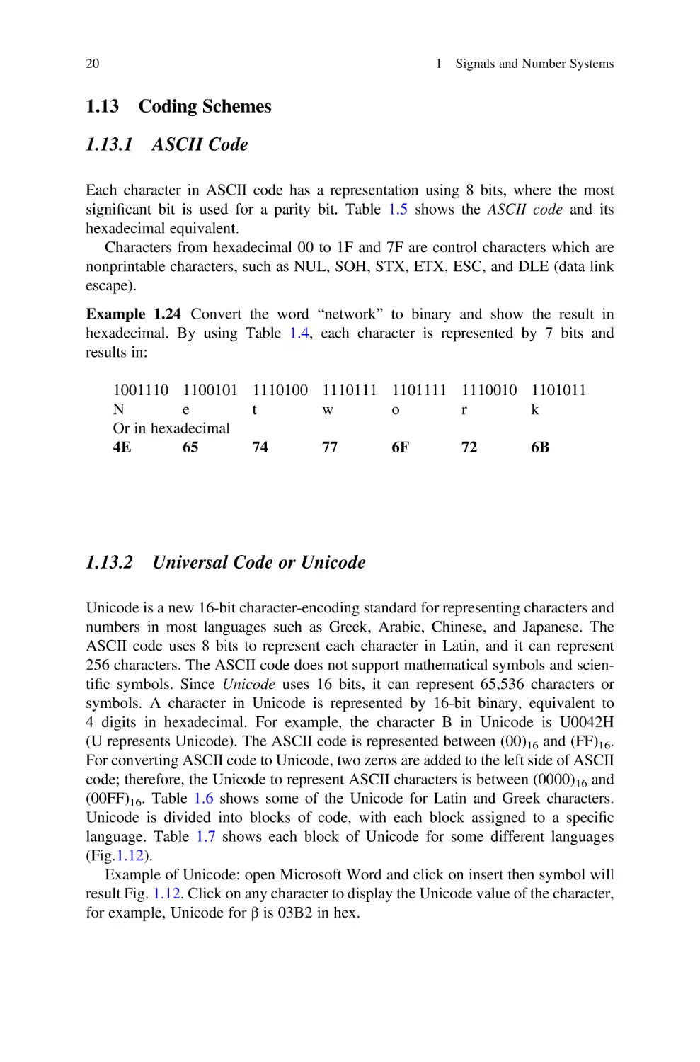
1.13.1 ASCII Code
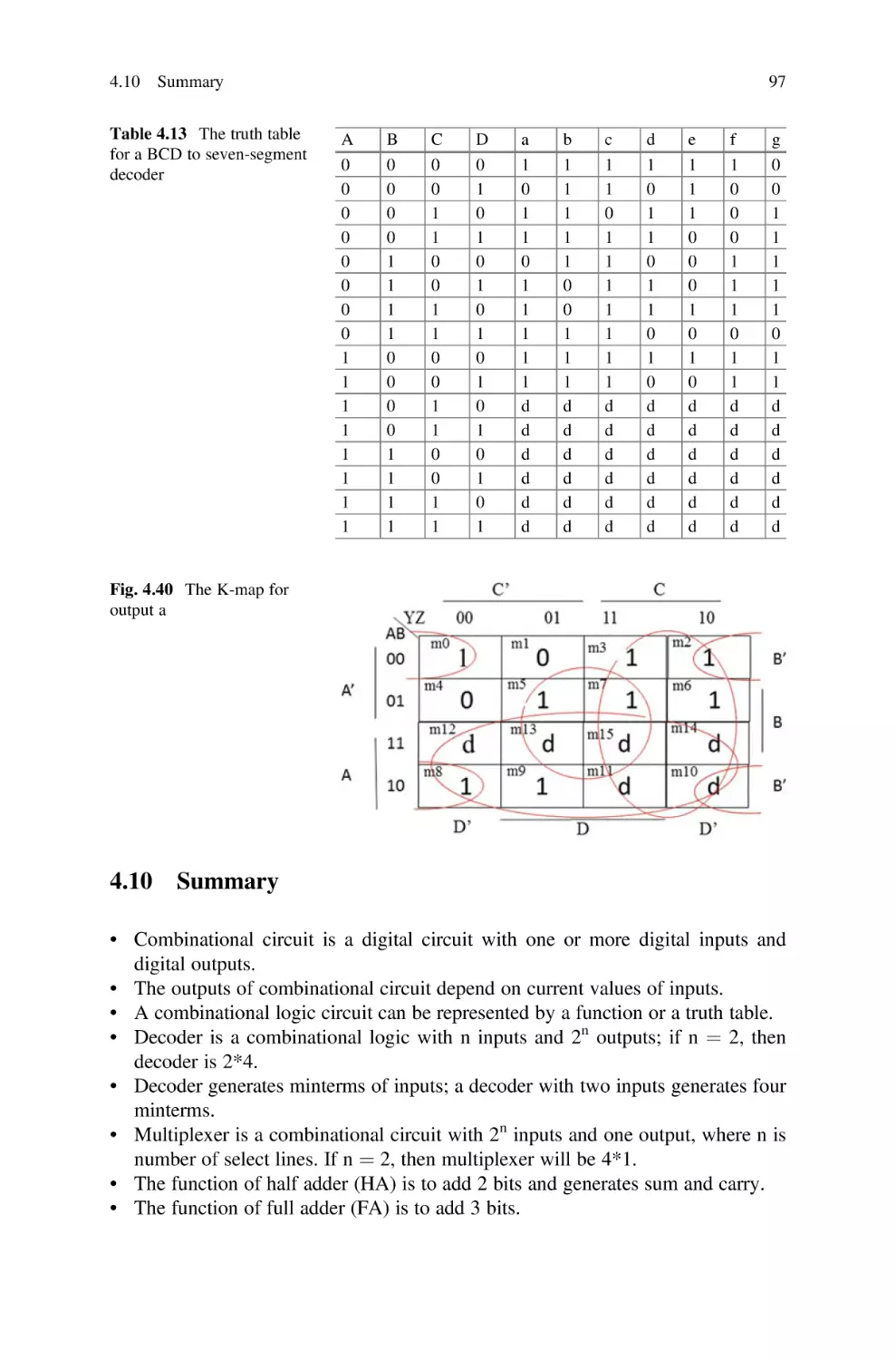
Each character in ASCII code has a representation using 8 bits, where the most
significant bit is used for a parity bit. Table 1.5 shows the ASCII code and its
hexadecimal equivalent.
Characters from hexadecimal 00 to 1F and 7F are control characters which are
nonprintable characters, such as NUL, SOH, STX, ETX, ESC, and DLE (data link
escape).
Example 1.24 Convert the word “network” to binary and show the result in
hexadecimal. By using Table 1.4, each character is represented by 7 bits and
results in:
1001110 1100101 1110100 1110111 1101111 1110010 1101011
N
e
t
w
o
r
k
Or in hexadecimal
4E
65
74
77
6F
72
6B
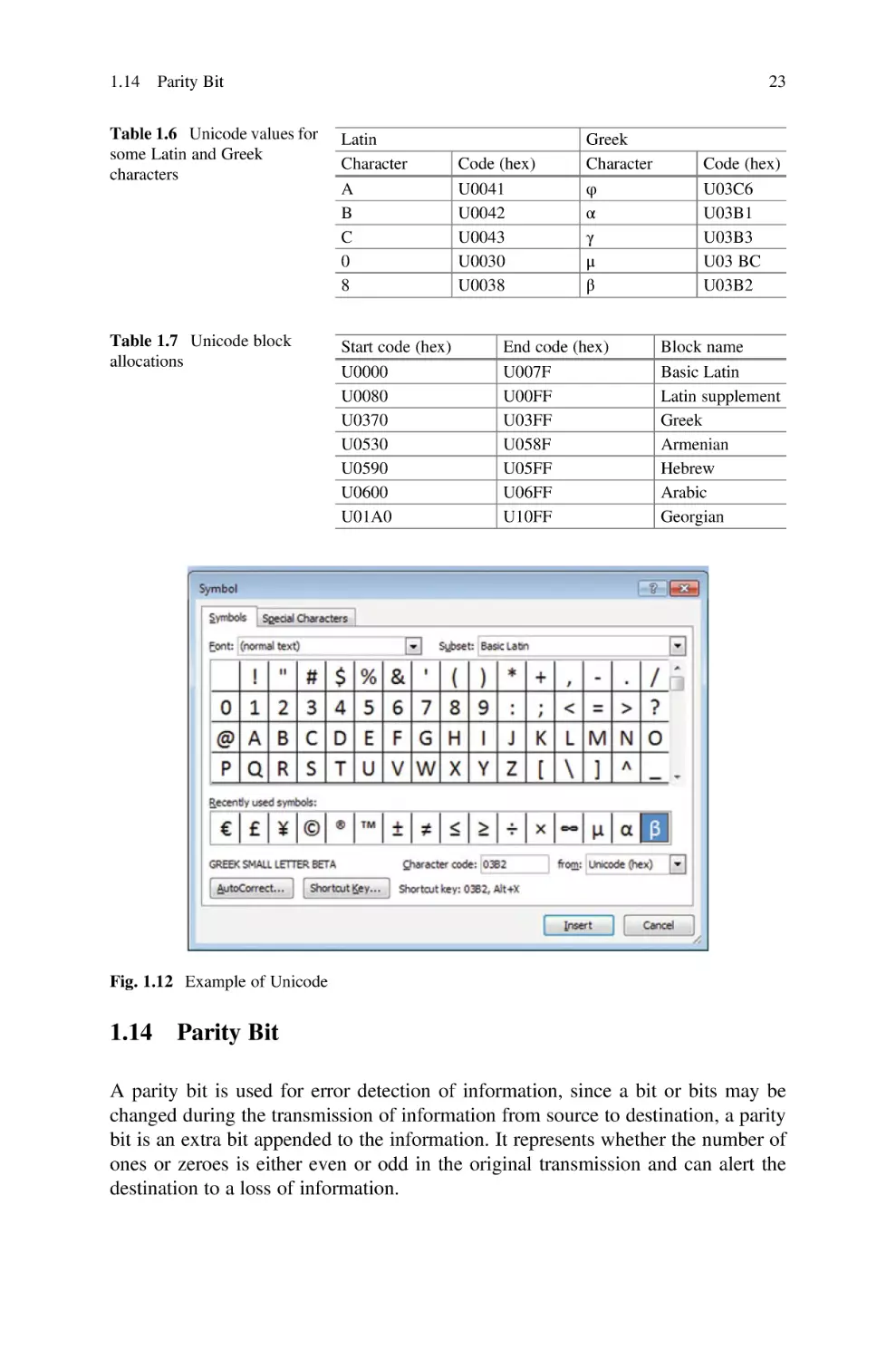
1.13.2 Universal Code or Unicode
Unicode is a new 16-bit character-encoding standard for representing characters and
numbers in most languages such as Greek, Arabic, Chinese, and Japanese. The
ASCII code uses 8 bits to represent each character in Latin, and it can represent
256 characters. The ASCII code does not support mathematical symbols and scientific symbols. Since Unicode uses 16 bits, it can represent 65,536 characters or
symbols. A character in Unicode is represented by 16-bit binary, equivalent to
4 digits in hexadecimal. For example, the character B in Unicode is U0042H
(U represents Unicode). The ASCII code is represented between (00)16 and (FF)16.
For converting ASCII code to Unicode, two zeros are added to the left side of ASCII
code; therefore, the Unicode to represent ASCII characters is between (0000)16 and
(00FF)16. Table 1.6 shows some of the Unicode for Latin and Greek characters.
Unicode is divided into blocks of code, with each block assigned to a specific
language. Table 1.7 shows each block of Unicode for some different languages
(Fig.1.12).
Example of Unicode: open Microsoft Word and click on insert then symbol will
result Fig. 1.12. Click on any character to display the Unicode value of the character,
for example, Unicode for β is 03B2 in hex.
Binary
0000000
0000001
0000010
0000011
0000100
0000101
0000110
0000111
0001000
0001001
0001010
0001011
0001100
0001101
0001110
0001111
0010000
0010001
0010010
0010011
0010100
0010101
0010110
0010111
0011000
Hex
00
01
02
03
04
05
06
07
08
09
0A
0B
0C
0D
0E
0F
10
11
12
13
14
15
16
17
18
Char
NUL
SOH
STX
ETX
EOT
ENQ
ACK
BEL
BS
HT
LF
VT
FF
CR
SO
SI
DLE
DC1
DC2
DC3
DC4
NACK
SYN
ETB
CAN
Binary
0100000
0100001
0100010
0100011
0100100
0100101
0100110
0100111
0101000
0101001
0101010
0101011
0101100
0101101
0101110
0101111
0110000
0110001
0110010
0110011
0110100
0110101
0110110
0110111
0111000
Hex
20
21
22
23
24
25
26
27
28
29
2A
2B
2C
2D
2E
2F
30
31
32
33
34
35
36
37
38
Char
SP
!
”
#
$
%
&
’
(
)
*
+
,
.
/
0
1
2
3
4
5
6
7
8
Table 1.5 American Standard Code for Information Interchange (ASCII)
Binary
1000000
1000001
1000010
1000011
1000100
1000101
1000110
1000111
1001000
1001001
1001010
1001011
1001100
1001101
1001110
1001111
1010000
1010001
1010010
1010011
1010100
1010101
1010110
1010111
1011000
Hex
40
41
42
43
44
45
46
47
8
49
4A
4B
4C
4D
4E
4F
50
51
52
53
54
55
56
57
58
Char
@
A
B
C
D
E
F
G
H
I
J
K
L
M
N
O
P
Q
R
S
T
U
V
W
X
Binary
1100000
1100001
1100010
1100011
1100100
1100101
1100110
1100111
1101000
1101001
1101010
1101011
1101100
1101101
1101110
1101111
1110000
1110001
1110010
1110011
1110100
1110101
1110110
1110111
1111000
Hex
60
61
62
63
64
65
66
67
68
69
6A
6B
6C
6D
6E
6F
70
71
72
73
74
75
76
77
78
Coding Schemes
(continued)
Char
,
a
b
c
d
e
f
g
h
i
j
k
l
m
n
o
P
q
r
s
t
u
v
w
x
1.13
21
Binary
0011001
0011010
0011011
0011100
0011101
0011110
0011111
Hex
19
1A
1B
1C
1D
1E
1F
Table 1.5 (continued)
Char
EM
SUB
ESC
FS
GS
RS
US
Binary
0111001
0111010
0111011
0111100
0111101
0111110
0111111
Hex
39
3A
3B
3C
3D
3E
3F
Char
9
:
;
<
¼
<
?
Binary
1011001
1011010
1011011
1011100
1011101
1011110
1011111
Hex
59
5A
5B
5C
5D
5E
5F
Char
Y
Z
[
\
]
^
-
Binary
1111001
1111010
1111011
1111100
1111101
1111110
1111111
Hex
79
7A
7B
7C
7D
7E
7F
Char
y
z
[
\
}
~
DEL
22
1 Signals and Number Systems
1.14
Parity Bit
23
Table 1.6 Unicode values for
some Latin and Greek
characters
Latin
Character
A
B
C
0
8
Table 1.7 Unicode block
allocations
Start code (hex)
U0000
U0080
U0370
U0530
U0590
U0600
U01A0
Code (hex)
U0041
U0042
U0043
U0030
U0038
Greek
Character
φ
α
γ
μ
β
End code (hex)
U007F
U00FF
U03FF
U058F
U05FF
U06FF
U10FF
Code (hex)
U03C6
U03B1
U03B3
U03 BC
U03B2
Block name
Basic Latin
Latin supplement
Greek
Armenian
Hebrew
Arabic
Georgian
Fig. 1.12 Example of Unicode
1.14
Parity Bit
A parity bit is used for error detection of information, since a bit or bits may be
changed during the transmission of information from source to destination, a parity
bit is an extra bit appended to the information. It represents whether the number of
ones or zeroes is either even or odd in the original transmission and can alert the
destination to a loss of information.
24
1 Signals and Number Systems
1.14.1 Even Parity
The extra bit (0 or 1) is chosen such that the number of ones becomes even.
Example 1.25 Our message is (00111)2. By appending a one to the left side of the
message, we create (100111)2. Our even parity bit has made the total number of ones
even (from 3 to 4 ones).
Our message is (10111)2. By appending a zero to the left side of the message, we
create (010111)2. Our even parity bit has left the total number of ones even (4 ones).
1.14.2 Odd Parity
The extra bit (0 or 1) is chosen such that the number of ones becomes odd.
Our message is (10111)2. By appending a one to the left side of the message, we
create (110111)2. Our odd parity bit has made the total number of ones even (from
4 to 5 ones).
1.15
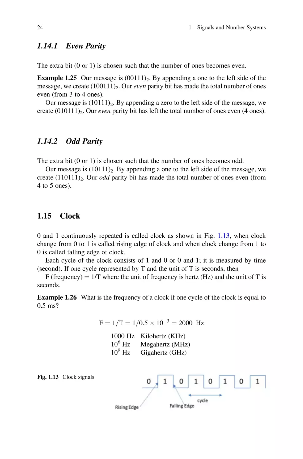
Clock
0 and 1 continuously repeated is called clock as shown in Fig. 1.13, when clock
change from 0 to 1 is called rising edge of clock and when clock change from 1 to
0 is called falling edge of clock.
Each cycle of the clock consists of 1 and 0 or 0 and 1; it is measured by time
(second). If one cycle represented by T and the unit of T is seconds, then
F (frequency) ¼ 1/T where the unit of frequency is hertz (Hz) and the unit of T is
seconds.
Example 1.26 What is the frequency of a clock if one cycle of the clock is equal to
0.5 ms?
F ¼ 1=T ¼ 1=0:5 103 ¼ 2000 Hz
1000 Hz Kilohertz (KHz)
106 Hz
Megahertz (MHz)
109 Hz
Gigahertz (GHz)
Fig. 1.13 Clock signals
1.16
1.16
Transmission Modes
25
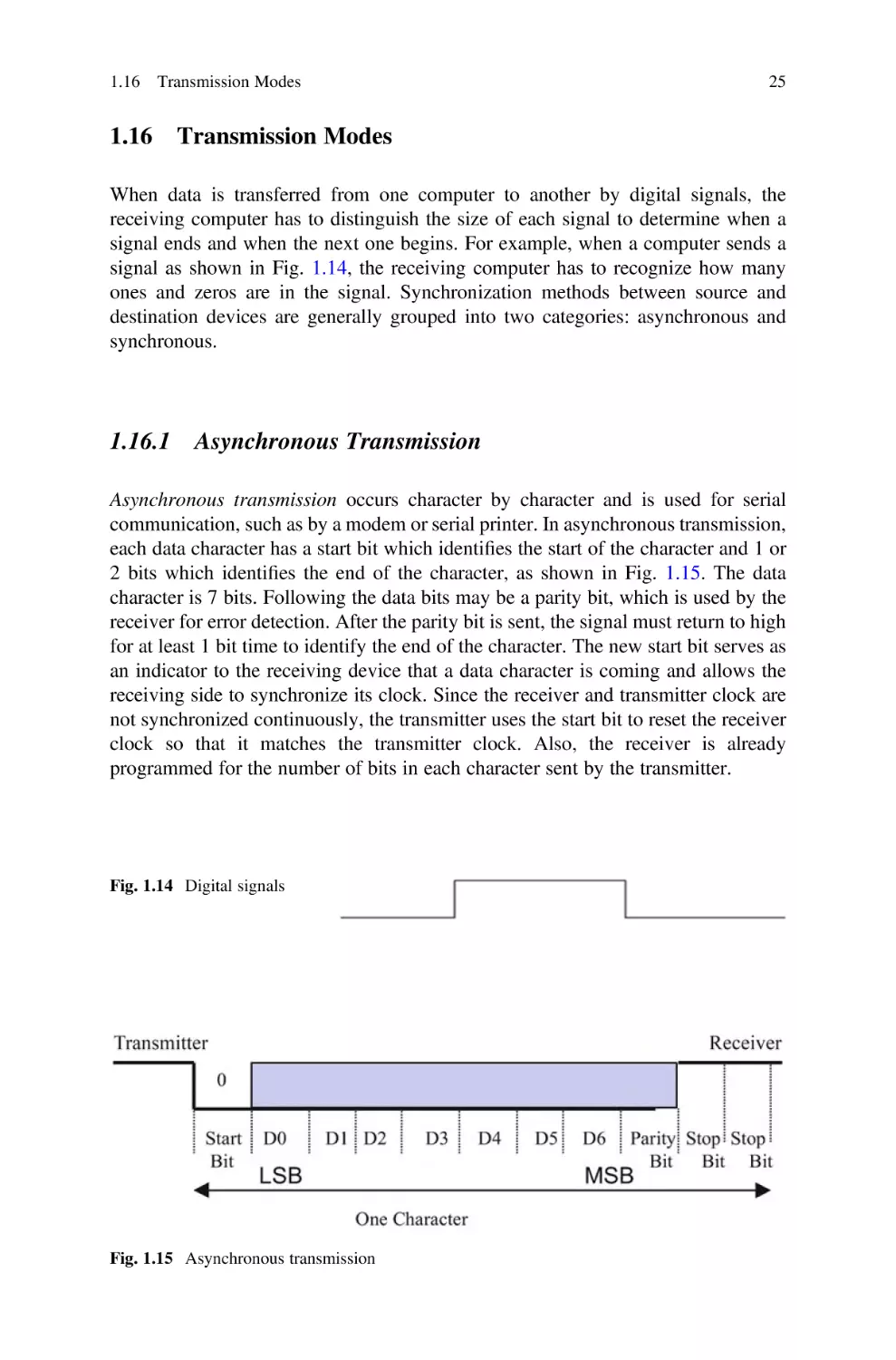
Transmission Modes
When data is transferred from one computer to another by digital signals, the
receiving computer has to distinguish the size of each signal to determine when a
signal ends and when the next one begins. For example, when a computer sends a
signal as shown in Fig. 1.14, the receiving computer has to recognize how many
ones and zeros are in the signal. Synchronization methods between source and
destination devices are generally grouped into two categories: asynchronous and
synchronous.
1.16.1 Asynchronous Transmission
Asynchronous transmission occurs character by character and is used for serial
communication, such as by a modem or serial printer. In asynchronous transmission,
each data character has a start bit which identifies the start of the character and 1 or
2 bits which identifies the end of the character, as shown in Fig. 1.15. The data
character is 7 bits. Following the data bits may be a parity bit, which is used by the
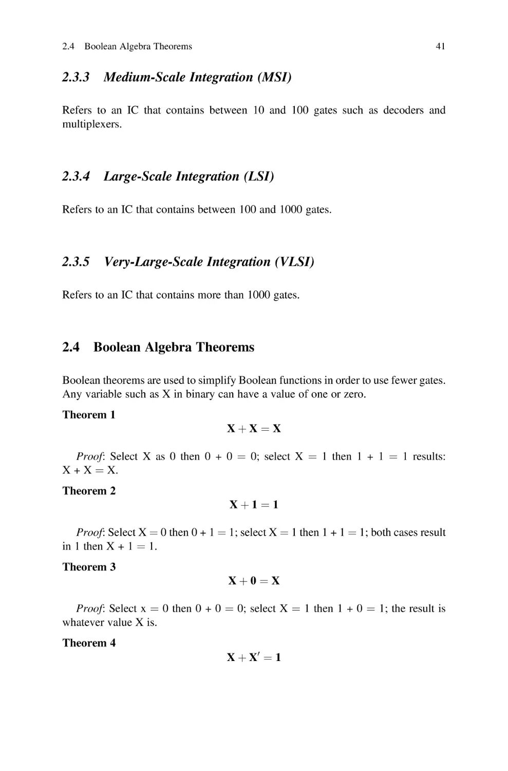
receiver for error detection. After the parity bit is sent, the signal must return to high
for at least 1 bit time to identify the end of the character. The new start bit serves as
an indicator to the receiving device that a data character is coming and allows the
receiving side to synchronize its clock. Since the receiver and transmitter clock are
not synchronized continuously, the transmitter uses the start bit to reset the receiver
clock so that it matches the transmitter clock. Also, the receiver is already
programmed for the number of bits in each character sent by the transmitter.
Fig. 1.14 Digital signals
Fig. 1.15 Asynchronous transmission
26
1 Signals and Number Systems
Fig. 1.16 Synchronous transmission
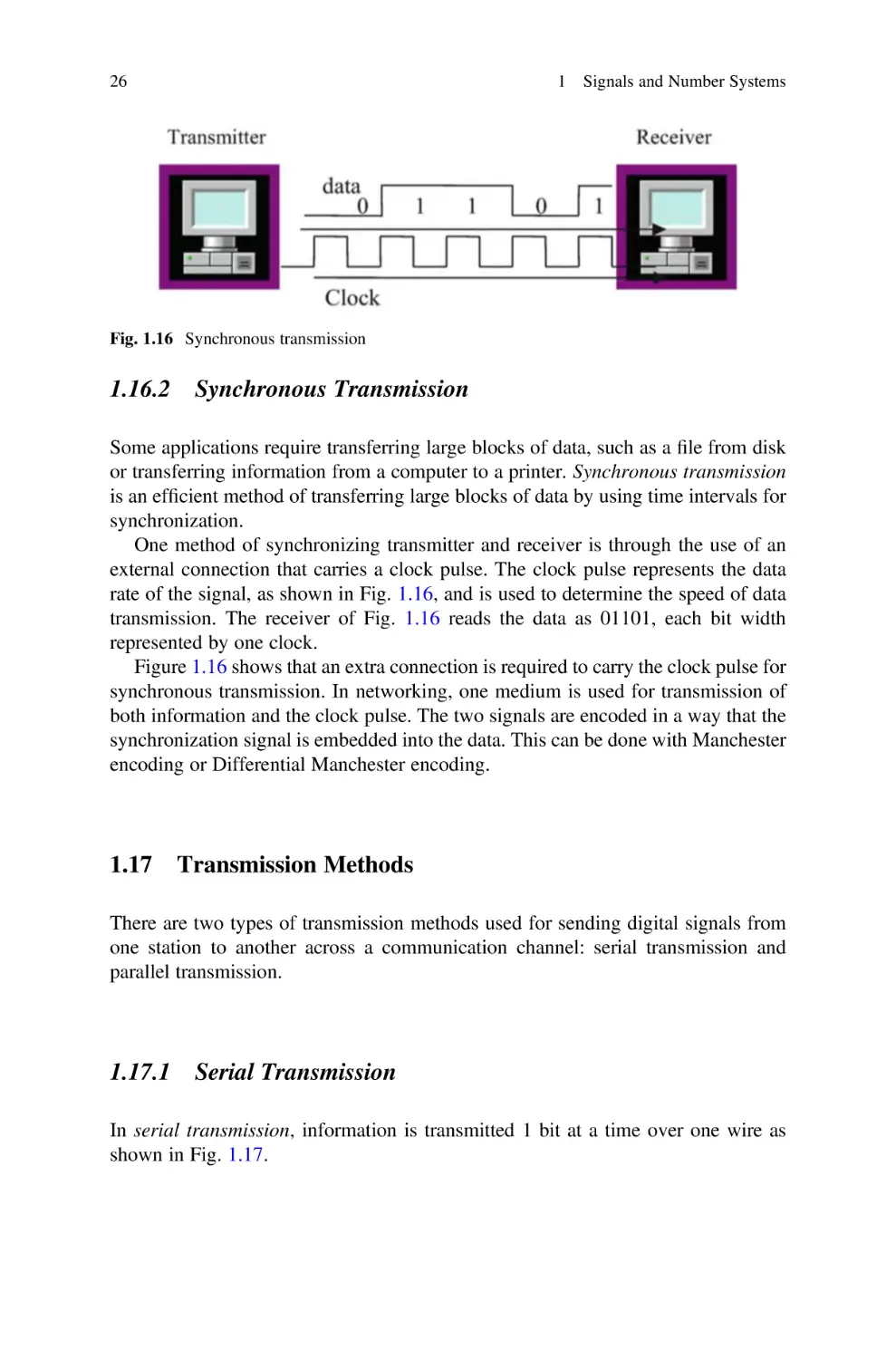
1.16.2 Synchronous Transmission
Some applications require transferring large blocks of data, such as a file from disk
or transferring information from a computer to a printer. Synchronous transmission
is an efficient method of transferring large blocks of data by using time intervals for
synchronization.
One method of synchronizing transmitter and receiver is through the use of an
external connection that carries a clock pulse. The clock pulse represents the data
rate of the signal, as shown in Fig. 1.16, and is used to determine the speed of data
transmission. The receiver of Fig. 1.16 reads the data as 01101, each bit width
represented by one clock.
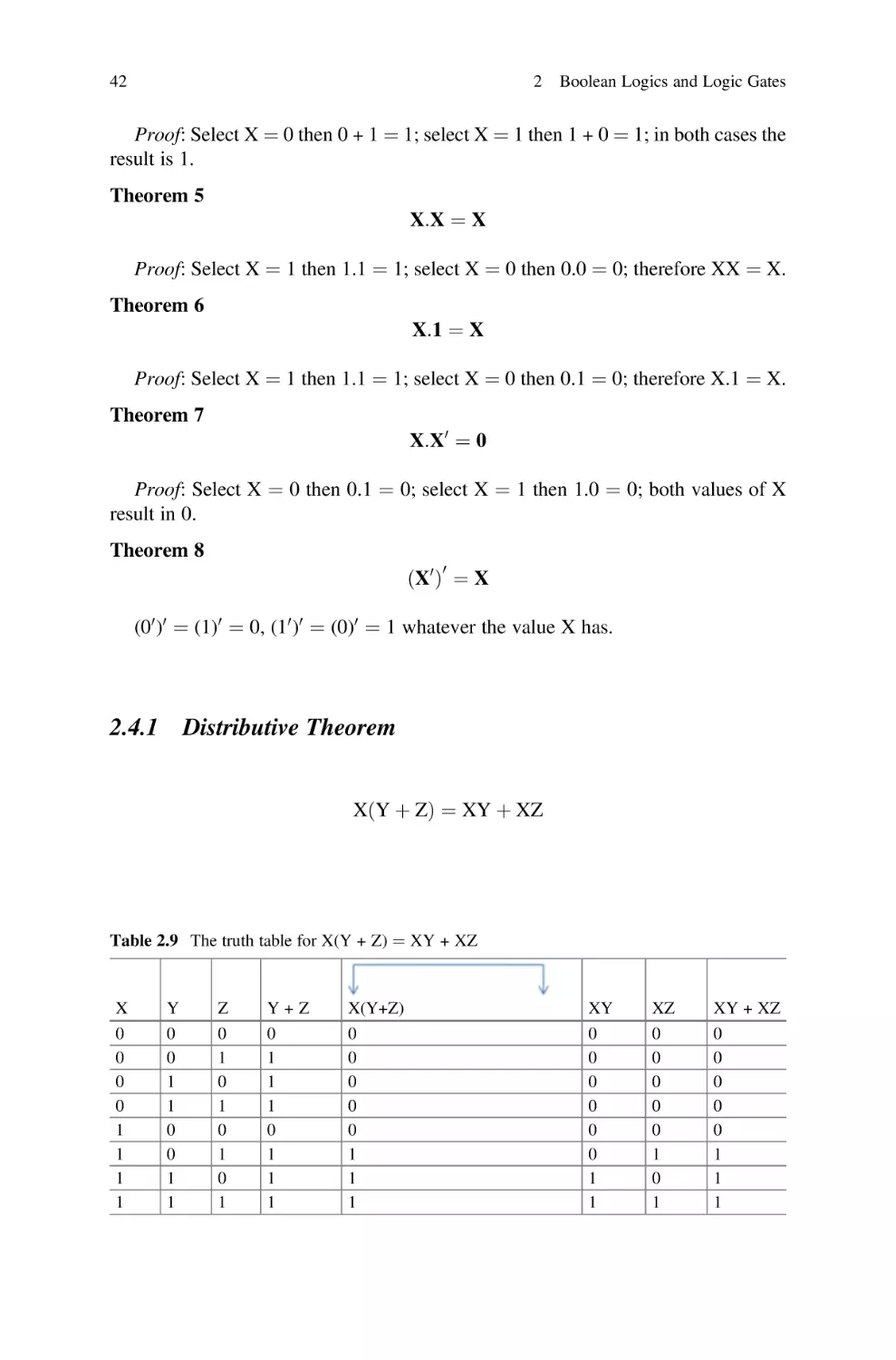
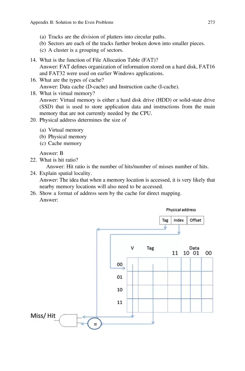
Figure 1.16 shows that an extra connection is required to carry the clock pulse for
synchronous transmission. In networking, one medium is used for transmission of
both information and the clock pulse. The two signals are encoded in a way that the
synchronization signal is embedded into the data. This can be done with Manchester
encoding or Differential Manchester encoding.
1.17
Transmission Methods
There are two types of transmission methods used for sending digital signals from
one station to another across a communication channel: serial transmission and
parallel transmission.
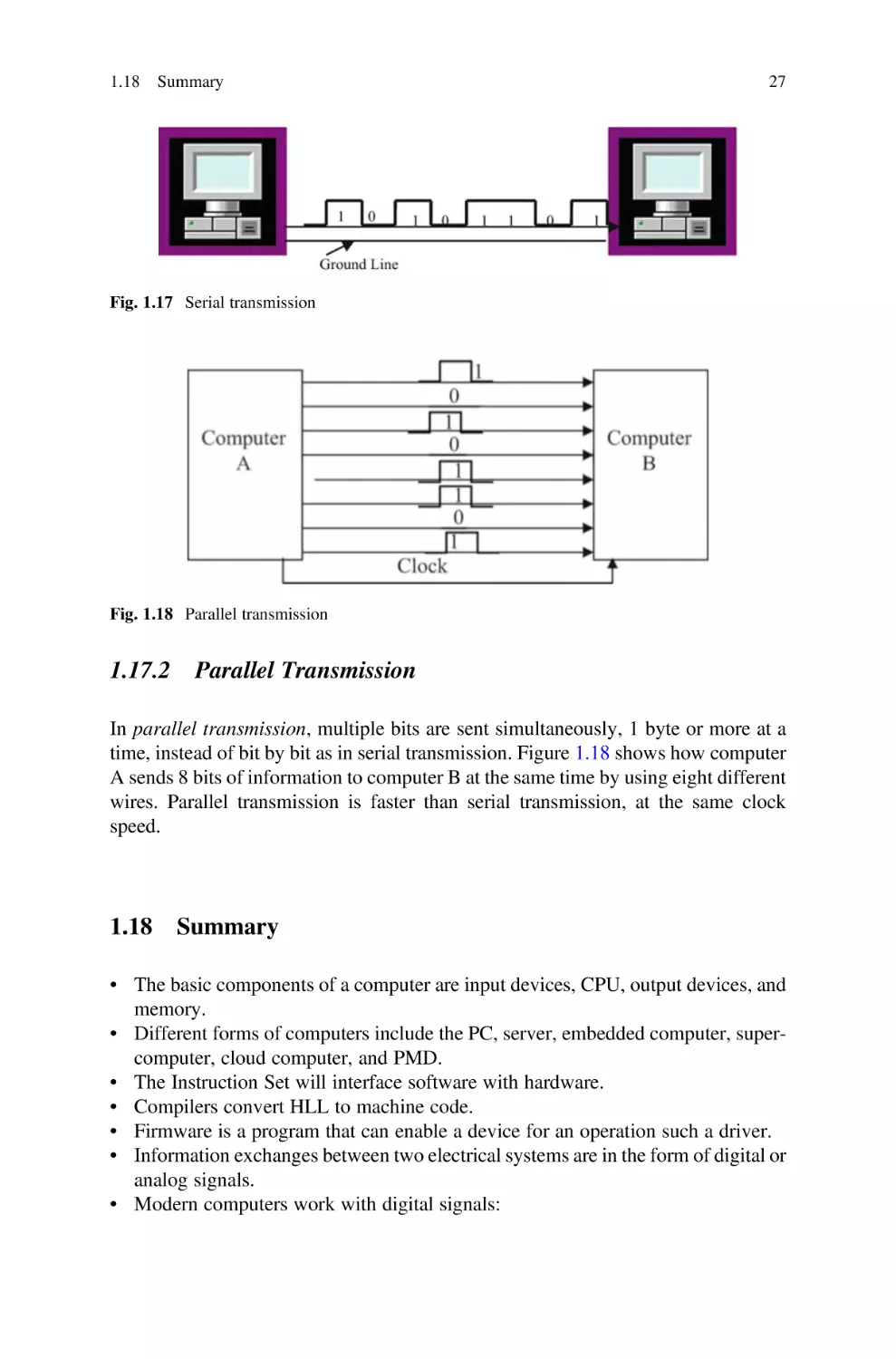
1.17.1 Serial Transmission
In serial transmission, information is transmitted 1 bit at a time over one wire as
shown in Fig. 1.17.
1.18
Summary
27
Fig. 1.17 Serial transmission
Fig. 1.18 Parallel transmission
1.17.2 Parallel Transmission
In parallel transmission, multiple bits are sent simultaneously, 1 byte or more at a
time, instead of bit by bit as in serial transmission. Figure 1.18 shows how computer
A sends 8 bits of information to computer B at the same time by using eight different
wires. Parallel transmission is faster than serial transmission, at the same clock
speed.
1.18
Summary
• The basic components of a computer are input devices, CPU, output devices, and
memory.
• Different forms of computers include the PC, server, embedded computer, supercomputer, cloud computer, and PMD.
• The Instruction Set will interface software with hardware.
• Compilers convert HLL to machine code.
• Firmware is a program that can enable a device for an operation such a driver.
• Information exchanges between two electrical systems are in the form of digital or
analog signals.
• Modern computers work with digital signals:
28
1 Signals and Number Systems
–
–
–
–
A digital signal is represented by two voltages.
Binary is the representation of a number in base of 2.
The frequency of a signal is the inverse of its cycle time.
One digit in binary is called a bit, 8 bits is called 1 byte, and 4 bytes is called
one word.
– Information is represented inside the computer by binary or base of 2.
– Negative numbers inside the computer are represented by the two’s
complement.
– The most significant bit in signed numbers is represented by the sign of the
number.
– Positive is represented by zero and negative is represented by one.
– One’s complement of a binary number is the complement of each bit of the
number.
– Two’s complement of a binary number is the complement of the number
plus one.
– Binary-coded decimal (BCD) is used for representing decimal numbers from
0 to 9.
– The hexadecimal number system is used in digital systems and computers in
an efficient way of representing binary quantities.
– Parity bit is used for error detection of one bit error.
– IEEE 757 standard is used to represent floating point number.
– Information is represented by ASCII code inside the computer; ASCII code is
made of 7 bits.
– Information between components of a computer can be transmitted in serial or
parallel form.
– In serial transmission, information is transmitted 1 bit at a time.
– In parallel transmission, information is transmitted in multiple bits at a time.
– The next chapter will cover Boolean logic, Boolean algebra theorems, and
logic gates. Logic gate is the basic component of an integrated circuit (IC).
Problems and Questions
1. List the components of a computer.
2. List the different types of computers.
3. What is the function of an operating system?
4. List the names of two operating systems.
5. What is the function of compiler?
6. List three computer input devices.
7. List three computer output devices.
8. Show a digital signal.
9. Show an analog signal.
10. How many bits is:
(a) Byte
(b) Half word
(c) Word
1.18
Summary
29
11. Convert the following decimal numbers to binary:
(a) 35
(b) 85
(c) 23.25
12. Convert the following binary numbers to decimal
(a) 111111
(b) 1010101
(c) 1101001.101
13. Convert the following binary numbers to decimal:
(a)
(b)
(c)
(d)
1111101
1010111.1011
11111111
10000000
14. Convert the following binary numbers to hexadecimal:
(a) 1110011010
(b) 1000100111
(c) 101111.101
15. Find the frequency of digital signal with the following clock cycles:
(a)
(b)
(c)
(d)
1s
s
0.02 s
0.02 ms
16. The following frequencies of a digital signal are given, find the clock cycle of
digital signal:
(a)
(b)
(c)
(d)
10 Hz
200 Hz
10,000 Hz
4 MHz
17. Convert each of the following numbers to base of 10:
(a) (34A)16
(b) (FAC)16
18. Convert the following decimal numbers to base of 16:
(a) (234)10
(b) (75)10
30
1 Signals and Number Systems
19. Convert the following numbers to binary:
(a) (3FDA)16
(b) (FDA.5F)16
20. Perform the following additions:
1101010
1011011
1100101
þ1010111
21. Find two’s complements of the following numbers:
(a)
(b)
(c)
(d)
11111111
10110000
10000000
00000000
22. The word “LOGIC” is given.
(a) Represent in ASCII.
(b) Add even parity bit to each character and represent each character in hex.
23. Represent (465)10 in BCD.
24. Represent (100101100111)BCD in decimal.
25. Convert the following two’s complement numbers to decimal:
(a) 1011
(b) 11111001
(c) 10011111
26. Subtract the following unsigned numbers using two’s complement:
(a)
(b)
(c)
(d)
11110011–11000011
10001101–11111000
11111101–11000001
10011001–11100001
27. Perform addition of the following signed numbers; assume each number is
represented by 6 bits and state if the result of each addition produces overflow:
(a)
(b)
(c)
(d)
(e)
(+12) + (+7)
(+25) + (+30)
(5) + (+ 9)
(6) + (7)
(36) + (12)
1.18
Summary
31
28. What is the largest 16-bit binary value that can be represented by:
(a) Unsigned number
(b) Signed magnitude
(c) Signed two’s complement
29. Represent the following decimal numbers in IEEE 745 single precision:
(a) 34.375
(b) 0.045
30. Convert the following IEEE 745 single precision to decimal number:
(a) 1 10000100 01110000000000000000000
(b) 0 01111100 11100000000000000000000
31. List the types of transmission modes.
32. Convert each of the following signed two’s complement numbers to decimal:
(a) 11000011
(b) 10001111
33. Represent each of the following numbers in 8-bit signed two’s complement:
(a) 15
(b) 24
(c) 8
34. Perform the following addition:
(a) (0F4A)16 + (420B)16
(b) (084C)16 + (1265)16
Chapter 2
Boolean Logics and Logic Gates
Objectives: After Completing this Chapter, you Should Be Able to
• Understand the basic operation of Boolean theorems.
• Explain the operation of different logic gates such as AND, OR, NOT, XOR, and
NAND gates.
• Show the truth table of different logic gates.
• Distinguish between the different types of integrated circuits (ICs).
• Apply Boolean theorems to simplify Boolean function.
• Draw logic circuit for Boolean function.
• Show the truth table of Boolean function.
• Find the output function of a digital logic circuit.
• Distinguish between the SSI, MSI, LSI, and VLSI.
2.1
Introduction
Logic gates are made of transistors, and they are the basic components of integrated
circuit (IC). Logic gates are used for designing digital system; there are three basic
logic operations and they are called AND, OR, and NOT. The characteristic of a
digital system can be represented by a function or truth table. Boolean theorems are
used to simplify Boolean function in order to use fewer logic gates. Integrated
circuits are classified based on the number of gates that they contain, and they are
called SSI, MSI, LSI, and VLSI.
© The Author(s), under exclusive license to Springer Nature Switzerland AG 2022
A. Elahi, Computer Systems, https://doi.org/10.1007/978-3-030-93449-1_2
33
34
2.2
2.2.1
2 Boolean Logics and Logic Gates
Boolean Logics and Logic Gates
AND Logic
The AND logic is denoted by a period “.,” but most of the time, the period is left
out. X.Y or XY is pronounced as X AND Y.
X AND Y ¼ Z,
Z ¼ 1 if and only if X ¼ 1 and Y ¼ 1 otherwise Z ¼ 0:
The AND logic operation can be represented by the electrical circuit in Fig. 2.1.
Assume X and Y are switches and Z is the light; X ¼ 0, Y ¼ 0 means the switches
are open and the light being off means zero and the light on means one. Then we can
make a table; Table 2.1 shows the operation of Fig. 2.1.
Figure 2.2 shows a 2-input AND gate and Table 2.2 shows the truth table for the
AND gate. The output of the AND gate is one when both inputs are one.
Fig. 2.1 Representation of
the AND operation
Table 2.1 Operation of
Fig. 2.1
X
Off
Off
On
On
Y
Off
On
Off
On
Light
Off
Off
Off
On
Y
0
1
0
1
Z
0
0
0
1
Fig. 2.2 2-input AND gate
Table 2.2 AND gate truth
table
X
0
0
1
1
2.2 Boolean Logics and Logic Gates
2.2.2
35
OR Logic
The OR operation is represented by a plus sign, “+” or a V, where “+” is the most
popular symbol used. X + Y is pronounced X OR Y.
X þ Y ¼ Z,
Z ¼ 1 if X ¼ 1 OR Y ¼ 1 or both X ¼ 1 and Y ¼ 1:
The OR operation can be represented by the electrical circuit in Fig. 2.3. In
Fig. 2.3, the light is off when both switches are off, and the light is on when at least
one switch is closed. Figure 2.4 shows a 2-input OR gate and Table 2.3 shows truth
table for the 2-input OR gate.
2.2.3
NOT Logic
The NOT logic performs a complement, meaning it converts a 1 to 0 and 0 to 1. Also
called an inverter, the NOT X is represented by X0 or X. Figure 2.5 shows the NOT
gate and Table 2.4 shows truth table for the NOT gate (inverter).
Fig. 2.3 Electrical circuit
representation of the OR
operation
Fig. 2.4 2-input OR gate
Table 2.3 Truth table of the
2-input OR gate
Fig. 2.5 NOT gate
X
0
0
1
1
Y
0
1
0
1
Z
0
1
1
1
36
2 Boolean Logics and Logic Gates
Table 2.4 Truth table for the
NOT gate
X0
1
0
X
0
1
Fig. 2.6 2-input NAND
gate
Fig. 2.7 AND-NOT gates
used together to act
as NAND
Table 2.5 Truth table of the
2-input NAND
X
0
0
1
1
Y
0
1
0
1
XY
1
1
1
0
Fig. 2.8 NOR gate
Table 2.6 Truth table for the
2-input NOR gate
2.2.4
X
0
0
1
1
Y
0
1
0
1
X+Y
1
0
0
0
NAND Gate
Figure 2.6 shows 2-input NAND gate. The NAND gate can be made from an AND
gate and a NOT gate as shown in Fig. 2.7. Table 2.5 shows the truth table of the
2-input NAND gate.
2.2.5
NOR Gate
Figure 2.8 shows a NOR logic gate. NOR gates are made of OR and NOT gates.
Table 2.6 shows the truth table of the 2-input NOR gate.
2.2 Boolean Logics and Logic Gates
2.2.6
37
Exclusive OR Gate
Figure 2.9 shows an exclusive OR gate. Exclusive OR is represented by
labeled XOR. Table 2.7 shows the truth table for the XOR gate.
X
2.2.7
M
L
and is
Y ¼ X0 Y þ XY0
Exclusive NOR Gate
Figure 2.10 shows an exclusive NOR gate. Exclusive NOR is represented by ʘ and
labeled XNOR. Table 2.8 shows the truth table for the exclusive NOR gate.
2.2.8
Tri-State Device
Figure 2.11 shows the diagram of a tri-state device; the control line controls the
operation of tri-state devices.
Fig. 2.9 2-input XOR
Table 2.7 Truth table for
XOR gate
X
0
0
1
1
Y
0
1
0
1
X
0
0
1
1
Y
0
1
0
1
X
0
1
1
0
L
Y
Fig. 2.10 Exclusive NOR
gate
Table 2.8 Truth table for
exclusive NOR gate
XʘY
1
0
0
1
38
2 Boolean Logics and Logic Gates
Fig. 2.11 Tri-state device
Fig. 2.12 3-input AND
gate and its truth table
Fig. 2.13 3-input OR gate
and its truth table
In Fig. 2.11, if the control line is set to zero, then there is no connection between
input and output (the output is high impedance). If the control line is set to one, then
output value is equal to the input value.
2.2.9
Multiple Inputs Logic Gates
Figure 2.12 shows 3-input AND gate with its truth table, Fig. 2.13 shows 3-input OR
gate with its truth table, Fig. 2.14 shows 3-input NOR gates with its truth table, and
Fig. 2.15 shows 3-input NAD gate with its corresponding table.
2.3 Integrated Circuit (IC) Classifications
39
Fig. 2.14 3-input NAND
gate and its truth table
Fig. 2.15 3-input NOR
gate and its truth table
Fig. 2.16 Transistor (left),
IC (right)
2.3
Integrated Circuit (IC) Classifications
A transistor is a basic component of integrated circuits (IC). Figure 2.16 shows a
transistor with an IC. Transistors act like a switch in integrated circuits. An integrated circuit is made from a hundred to millions of transistors.
Integrated circuits are classified based on the number of the gates inside the IC
such as SSI, MSI, LSI, and VLSI.
40
2 Boolean Logics and Logic Gates
Fig. 2.17 TTL 7408 2 input
AND gate
Fig. 2.18 74LS08 pins
2.3.1
Small-Scale Integration (SSI)
SSI refers to an IC that has less than 10 gates. Figure 2.17 shows the inside of a
74HC08 (7408) IC, and Fig. 2.18 shows an image of a 74HC08 IC.
2.3.2
Integrated Circuit Pins Numbering
Figure 2.18 shows a TTL 7408 IC; an IC chip should be read with the notch on the
left-hand side. The labeling convention starts with the left bottom pin under the
notch and goes in a counterclockwise direction.
The left bottom pin is pin #1.
The right bottom pin is pin #7.
The right upper pin is pin #8.
The left upper pin is pin #14.
As shown in Fig. 2.18, the IC number is 74LS08 where LS represents the material
IC was made with. Also on the IC, there is the letter M representing Motorola which
is the manufacturer of the IC, Intel uses the character “i,” and Texas Instruments uses
a map of Texas.
2.4 Boolean Algebra Theorems
2.3.3
41
Medium-Scale Integration (MSI)
Refers to an IC that contains between 10 and 100 gates such as decoders and
multiplexers.
2.3.4
Large-Scale Integration (LSI)
Refers to an IC that contains between 100 and 1000 gates.
2.3.5
Very-Large-Scale Integration (VLSI)
Refers to an IC that contains more than 1000 gates.
2.4
Boolean Algebra Theorems
Boolean theorems are used to simplify Boolean functions in order to use fewer gates.
Any variable such as X in binary can have a value of one or zero.
Theorem 1
XþX¼X
Proof: Select X as 0 then 0 + 0 ¼ 0; select X ¼ 1 then 1 + 1 ¼ 1 results:
X + X ¼ X.
Theorem 2
Xþ1¼1
Proof: Select X ¼ 0 then 0 + 1 ¼ 1; select X ¼ 1 then 1 + 1 ¼ 1; both cases result
in 1 then X + 1 ¼ 1.
Theorem 3
Xþ0¼X
Proof: Select x ¼ 0 then 0 + 0 ¼ 0; select X ¼ 1 then 1 + 0 ¼ 1; the result is
whatever value X is.
Theorem 4
X þ X0 ¼ 1
42
2 Boolean Logics and Logic Gates
Proof: Select X ¼ 0 then 0 + 1 ¼ 1; select X ¼ 1 then 1 + 0 ¼ 1; in both cases the
result is 1.
Theorem 5
X:X ¼ X
Proof: Select X ¼ 1 then 1.1 ¼ 1; select X ¼ 0 then 0.0 ¼ 0; therefore XX ¼ X.
Theorem 6
X:1 ¼ X
Proof: Select X ¼ 1 then 1.1 ¼ 1; select X ¼ 0 then 0.1 ¼ 0; therefore X.1 ¼ X.
Theorem 7
X:X0 ¼ 0
Proof: Select X ¼ 0 then 0.1 ¼ 0; select X ¼ 1 then 1.0 ¼ 0; both values of X
result in 0.
Theorem 8
0
ðX0 Þ ¼ X
(00 )0 ¼ (1)0 ¼ 0, (10 )0 ¼ (0)0 ¼ 1 whatever the value X has.
2.4.1
Distributive Theorem
XðY þ ZÞ ¼ XY þ XZ
Table 2.9 The truth table for X(Y + Z) ¼ XY + XZ
X
0
0
0
0
1
1
1
1
Y
0
0
1
1
0
0
1
1
Z
0
1
0
1
0
1
0
1
Y+Z
0
1
1
1
0
1
1
1
X(Y+Z)
0
0
0
0
0
1
1
1
XY
0
0
0
0
0
0
1
1
XZ
0
0
0
0
0
1
0
1
XY + XZ
0
0
0
0
0
1
1
1
2.4 Boolean Algebra Theorems
43
In order to prove the above theorem, the truth table of both sides of the theorem is
generated as shown in Table 2.9 and shows both sides generating the same truth
table.
2.4.2
De Morgan’s Theorem I
ðX þ YÞ0 ¼ X0 Y0
In this theorem the OR between X and Y is negated and changes the OR operation
to the AND operation.
Proof: By making a truth table for both sides of the theorem, it shows that both
sides of the theorem generate the same truth table (Table 2.10).
2.4.3
De Morgan’s Theorem II
ðXYÞ0 ¼ X0 þ Y0
In this theorem the XY is complemented and changes it from an AND operation
to an OR operation with each component complemented.
Example: (WXYZ)0 ¼ W0 + X0 + Y0 + Z0
If the truth table of both sides were generated, then it would show that both sides
have the same truth table result.
2.4.4
Commutative Law
Table 2.10 The truth table showing De Morgan’s Law
X
0
0
1
1
Y
0
1
0
1
X+Y
0
1
1
1
(X + Y)'
1
0
0
0
X'
1
1
0
0
Y'
1
0
1
0
X' Y'
1
0
0
0
44
2 Boolean Logics and Logic Gates
XþY¼YþX
XY ¼ YX
2.4.5
Associative Law
XðYZÞ ¼ ðXYÞZ
X þ ðY þ ZÞ ¼ ðX þ YÞ þ Z
2.4.6
More Theorems
The following are useful theorems:
(a)
(b)
(c)
(d)
X + X0 Y ¼ X + Y
X0 + XY ¼ X0 + Y
X + X0 Y0 ¼ X + Y0
X0 + XY0 ¼ X0 + Y0
Example: Simplify the Following Functions
(a) F(X, Y, Z) ¼ XY0 Z + XY0 Z0 + XY
F(X, Y, Z) ¼ XY0 (Z + Z0 ) + YZ where Z + Z0 ¼ 1 then
F(X, Y, Z) ¼ XY0 + XY ¼ X(Y + Y0 ) ¼ X
(b) F(X, Y, Z) ¼ (X0 + Y) (X + Y0 ) ¼ X0 X + X0 Y0 + XY + YY0 where X0 X and YY0
are zero then F(X, Y, Z) ¼ X0 Y0 + XY
2.5
Boolean Function
Boolean function is represented by algebraic expression which is made of binary
variables such as X, Y, and Z and logic operations between variables such as AND,
OR, and NOT.
F(X, Y, Z) ¼ X + YZ is a Boolean function.
Figure 2.19 shows the logic circuit for function F where X, Y, and Z are the inputs
and F is the output; Table 2.11 shows the truth table of the function F.
2.5 Boolean Function
45
Fig. 2.19 Logic circuit for a
function F(X, Y,
Z) ¼ X + YZ
Table 2.11 The truth table
for function F(X, Y,
Z) ¼ X + YZ
X
0
0
0
0
1
1
1
1
Y
0
0
1
1
0
0
1
1
Z
0
1
0
1
0
1
0
1
YZ
0
0
0
1
0
0
0
1
X + YZ
0
0
0
1
1
1
1
1
The truth table shows the characteristics of function F; the function F ¼ 1 when
the inputs to the circuit are 100 or 101 or 110 or 111.
2.5.1
Complement of a Function
In order to complement a function, both sides of the function must be complemented.
Example: Complement the following function:
FðX, Y, ZÞ ¼ XY þ Y0 Z
0
F0 ðX, Y, ZÞ ¼ ðXY þ Y0 ZÞ using De Morgan0 s theorem:
0
F0 ðX, Y, ZÞ ¼ ðXYÞ0 ðY0 ZÞ
F0 ðX, Y, ZÞ ¼ ðX0 þ Y0 ÞðY þ Z0 Þ
Example: Find the complement of the following function:
FðX, Y, ZÞ ¼ ðX0 þ Y0 ÞðY þ Z0 Þ
Complement both sides of the function:
F0 ðX, Y, ZÞ ¼ ½ðX0 þ Y0 ÞðY þ Z0 Þ
Applying De Morgan’s theorem results
0
46
2 Boolean Logics and Logic Gates
0
0
F0 ðX, Y, ZÞ ¼ ½ðX0 þ Y0 Þ þ ½ðY þ Z0 Þ
F0 ðX, Y, ZÞ ¼ ½ðXYÞ þ ½ðY0 ZÞ
F0 ðX, Y, ZÞ ¼ ðXYÞ þ ðY0 ZÞ
2.6
Summary
• Boolean logic consists of the AND, OR, and NOT logics.
• The output of the 2-input AND gate is one when both inputs are one; otherwise
the output is zero.
• The output of the 2-input OR gate is one when at least one of the inputs is one;
otherwise the output is zero.
• NOT gate performs one’s complement.
• The integrated circuits (IC) are classified by SSI (small-scale integration), MSI
(medium-scale integration), LSI (large-scale integration), and very-large-scale
integration.
• A NAND gate is equivalent of the AND-NOT.
• A NOR gate is equivalent of the NOR-NOT.
• The 2-input XOR has output one when the inputs are not equal; otherwise the
output is zero.
• The 2-input exclusive NOR (XNOR) is equivalent of the XOR-NOT.
• Chapter 3 will cover minterms and maxterms, apply K-map to simplify a function, and use universal gates to draw logic circuit.
Problems
1. Show truth table for 4-input AND, OR, NOR, and NAND gates.
2. If A ¼ 11001011 and B ¼ 10101110, then what is the value of the following
operations:
(a) A AND B
(b) A OR B
3. If A ¼ 11001011 and B ¼ 10101110, what is the value of the following
operations (F in hex ¼ 1111):
(a)
(b)
(c)
(d)
A NOT
A XOR B
A AND 0F
A AND F0
Problems
47
4. Draw a logic circuit for the following functions:
(a) F(X, Y, Z) ¼ XY0 + XZ0 + YZ
(b) F(X, Y, Z) ¼ (X + Y0 ) (X0 + Z0 )(Y + Z)
5. Boolean theorems to simplify the following expressions:
(a)
(b)
(c)
(d)
(e)
(f)
(g)
(h)
X+X+X
XY + XY
YYY
X + XY
XY0 + Y0
(X + Y)Y0
(XY) + (XY)0
X0 Y0 + XY
6. Simplify the following functions:
(a)
(b)
(c)
(d)
(e)
(f)
(g)
F(X, Y, Z) ¼ XY + X0 Y + XZ
F(X, Y, Z) ¼ (X + Y) (X0 + Y + Z)
F(X, Y, Z) ¼ XY0 Z + XYZ + Y0 Z
F(X, Y, Z) ¼ XY + X0 YZ
F(X, Y, Z) ¼ X0 Y + XYZ0
F(X, Y, Z) ¼ (XY) + (X + Y + Z)0 X + YZ
F(X, Y, Z) ¼ (XY)0 + (X + Y + Z)0
7. Find the truth table for the following functions:
(a) F(X, Y, Z) ¼ XY0 + YZ + XZ0 .
(b) F(X, Y, Z) ¼ (X + Y0 )(Y + Z)(X0 + Z0 )
8. If A ¼ 10110110 and B ¼ 10110011, then find
(a) A NAND B
(b) A NOR B
(c) A XOR B
9. Find the output of the following gates:
(a)
(b)
(c)
48
2 Boolean Logics and Logic Gates
(d)
(e)
10. Show the output of the following logic circuits:
(a)
(b)
(c)
Problems
49
11. Find the output function of the following logic circuits:
12. Find the output function of the following logic circuit:
13. Draw a logic circuit and show the truth table for the following functions:
(a)
(b)
(c)
(d)
F(X, Y) ¼ (XY)0 + X(X + Y0 )
F(X, Y, Z) ¼ (X + Y + Z0 )0 (X0 + Y0 )
F(X, Y, Z) ¼ (X XOR Y) (X NOR Y0 )
F(X, Y, Z) ¼ (X0 + Y0 + Z) (X + Y)
14. Show truth table for each of the following functions:
(a)
(b)
(c)
(d)
F(X, Y, Z) ¼ XY0 + XZ0 + YZ
F(X, Y, Z) ¼ (X + Y) (X + Z0 )
F(X, Y, Z) ¼ XY (Y + Z0 )
F (X, Y, Z) ¼ ( X + Y)’(X’ + Z)
50
2 Boolean Logics and Logic Gates
15. Simplify the following functions:
(a) F(X, Y, Z) ¼ YZ + (X + Y)0 + (XYZ)0 .
(b) F(X, Y, Z) ¼ (X + Y + Z)0 (X + Y)
16. Draw logic circuits for the following functions:
(a) F(X, Y, Z) ¼ (X + Y)0 + YZ
(b) F(X, Y, Z) ¼ (XYZ)0 + XZ + YZ
Chapter 3
Minterms, Maxterms, Karnaugh Map
(K-Map), and Universal Gates
Objectives: After Completing this Chapter, you Should Be Able to
• Represent a Boolean function in the form of sum of minters and product of
maxterm.
• Generate a truth table from a function that is represented by the sum of minterms.
• Generate a truth table from a function that is represented by the product of
minterms.
• Developed a function from the truth table.
• Use K-map to simplify a function.
• Apply don’t care condition in a K-map.
• Draw logic circuit using only NAND or NOR gates.
3.1
Introduction
Digital circuit can be represented by a truth table or Boolean function. In a digital
circuit with multiple digital inputs and multiple digital outputs, the outputs depend
on the current value of inputs. A Boolean function can be represented in the form of
sum of minterms or the product of maxterms, which enable the designer to make a
truth table more easily. Also, Boolean functions can be simplified using Karnaugh
map (K-map) without using Boolean theorems, by transferring a function to K-map
and reading simplified function from K-map. Most digital systems are designed by
using universal gates (NAND or NOR).
© The Author(s), under exclusive license to Springer Nature Switzerland AG 2022
A. Elahi, Computer Systems, https://doi.org/10.1007/978-3-030-93449-1_3
51
52
3.2
3 Minterms, Maxterms, Karnaugh Map (K-Map), and Universal Gates
Minterms
A minterm is associated with each combination of variables in a function. If a
function has n variables, then it has 2n minterms. Consider two Boolean variables,
X and Y. There are four different possible combinations that can be generated from
X AND Y, and they are XY, XY, X Y, and XY. These four combinations are called
the minterms for X AND Y. Table 3.1 shows the minterms and their designations for
F(X,Y) ¼ (X AND Y).
In Table 3.1, X Y ¼ 1, if X ¼ 0 and Y ¼ 0, then X Y is represented by m0
(decimal number of 00); XY ¼ 1, if X ¼ 0 and Y ¼ 1, then XY is represented by m1;
X Y ¼ 1, if X ¼ 1 and Y ¼ 0 and X Y is represented by m2; XY ¼ 1, if X ¼ 1 and
Y ¼ 1, then XY is represented by m3.
3.2.1
Application of Minterms
It is simple to generate a truth table from minterms and vice versa. Consider the
function F(X,Y) ¼ X Y + XY and its truth table (Table 3.2), this function can be
represented as F(X,Y) ¼ m1 + m2 or each minterm that represents a one in the truth
table. This may also be rewritten as F (X,Y) ¼ ∑(1, 2).
3.2.2
Three-Variable Minterms
The three variables X, Y, and Z generate eight minterms as shown in Table 3.3.
Table 3.1 Minterms of
F(X,Y)
XY
00
01
10
11
Table 3.2 Truth table for
function F(X,Y) ¼ X Y + XY
with minterms
X
0
0
1
1
Minterm
Designation
m0
m1
m2
m3
XY
XY
XY
XY
Y
0
1
0
1
F
0
1
1
0
m0
m1
m2
m3
3.2 Minterms
53
Table 3.3 Three-variable
minterms
XYZ
000
001
010
011
100
101
110
111
Table 3.4 Truth table for
function F(X,Y,
Z) ¼ X0 Y0 Z + X0 YZ + XYZ
XYZ
000
001
010
011
100
101
110
111
Minterms
X0 Y0 Z0
X0 Y0 Z
X0 YZ0
X0 YZ
XY0 Z0
XY0 Z
XYZ0
XYZ
Designation
m0
m1
m2
m3
m4
m5
m6
m7
F
0
1
0
1
0
0
0
1
Example 3.1 Find the truth table for the following function:
FðX, Y, ZÞ ¼ X0 Y0 Z þ X0 YZ þ XYZ
The function F can be represented by a sum of the minterms (or where F ¼ 1):
FðX, Y, ZÞ ¼ m1 þ m3 þ m7
or
FðX, Y, ZÞ ¼
X
ð1, 3, 7Þ
The truth table for this function contains a one in row 1, row 3, and row 7. The rest
of the rows are zeros as shown in Table 3.4. The function for a truth table can also be
determined from the sum of the minterms.
Example 3.2 The following truth table is given; find the function F.
In the following table, the output of function F is one when the input is 001 ¼ m1,
011 ¼ m3, 101 ¼ m5, and 111 ¼ m7; therefore F(X,Y,Z) ¼ m1 + m3 + m5 + m7 or
FðX, Y, ZÞ ¼
X
ð1, 3, 5, 7Þ
XYZ F
000 0
54
3 Minterms, Maxterms, Karnaugh Map (K-Map), and Universal Gates
001
010
011
100
101
110
111
1
0
1
0
1
0
1
Substituting each designation of a minterm with its actual product term (e.g.,
m0 ¼ X0 Y0 Z0 ) results in the following function:
FðX, Y, ZÞ ¼ X0 Y0 Z þ X0 YZ þ XY0 Z þ XYZ
Example 3.3 For the following truth table:
(a) Find the function F.
(b) Simplify the function.
(c) Draw the logic circuit for the simplified function.
XYZ
000
001
010
011
100
101
110
111
F
1
0
1
1
0
0
0
1
From the truth table, where F ¼ 1, we select the minterms m0, m2, m3, and m7:
FðX, Y, ZÞ ¼ m0 þ m2 þ m3 þ m7
Or
FðX, Y, ZÞ ¼ XYZ þ XYZ þ XYZ þ XYZ
XZ
Z
FðX, Y, ZÞ ¼ XZ Y þ Y þ YZ X þ X
FðX, Y, ZÞ ¼ XZ þ YZ
The logic circuit for the simplified function F is given in Fig. 3.1.
3.3 Maxterms
55
Fig. 3.1 Logic circuit for F(X,Y,Z) ¼ X Z + YZ
Table 3.5 Maxterms of
function F(X,Y,Z)
XYZ
000
001
010
011
100
101
110
111
Table 3.6 Truth Table for F
(X,Y,Z) ¼ M0M2M4M5M6
XYZ
000
001
010
011
100
101
110
111
3.3
Maxterm
X+Y+Z
X + Y + Z0
X + Y0 + Z
X + Y0 + Z0
X0 + Y + Z
X0 + Y + Z0
X0 + Y0 + Z
X0 + Y0 + Z0
Designation
M0
M1
M2
M3
M4
M5
M6
M7
F
0
1
0
1
0
0
0
1
Maxterms
Maxterm is complement of a minterm. If the minterm m0 is XYZ , then the
maxterm M0 is
XYZ ¼ X þ Y þ Z
Table 3.5 shows the maxterms for three variables.
In a truth table, an output of one represents minterms, and an output of zero
represents maxterms. Consider the truth Table 3.6, where the function F can be
56
3 Minterms, Maxterms, Karnaugh Map (K-Map), and Universal Gates
expressed as the product of maxterms. (Please note: the product of maxterms, as
opposed to the sum of minterms.)
F(X,Y,Z) ¼ M0M2M4M5M6, or it can be represented by
FðX, Y, ZÞ ¼ πð0, 2, 4, 5, 6Þ
Substituting each designated maxterm with the corresponding maxterm results in:
FðX, Y, ZÞ ¼ ðX þ Y þ ZÞðX þ Y0 þ ZÞðX0 þ Y þ ZÞðX0 þ Y þ Z0 Þ
3.4
Karnaugh Map (K-Map)
Karnaugh maps are used to simplify a Boolean function without using Boolean
algebra theorems. A K-map is also another way to represent the truth table of a
function. K-maps are made of cells where each cell represents a minterm. Cells
marked with a one will be the minterms used for the sum of the minterms representation of a function. Conversely, cells marked with a zero will be used for the
product of the maxterms representation.
Two variables X and Y can have four minterms as shown in Table 3.7. Each
minterm is represented by a cell in the K-map, so a two-variable K-map contains four
cells as shown in Fig. 3.2.
In Fig. 3.2 each cell represents a minterm. The cell located at row 0 and column
0 represents m0 (minterm zero) or X0 Y0 . The cell located at row 1 and column 1 is
represented by m3 or XY. As shown in Fig. 3.2, both cells in row zero contain X0 , so
this row is labeled the X0 row. Both cells in row 1 contain X so that row is labeled as
the X row.
Table 3.7 Minterms for two
variables
Fig. 3.2 Two-variable
K-map
XY
00
01
10
11
Minterms
X0 Y0
X0 Y
XY0
XY
Designation
m0
m1
m2
m3
3.4 Karnaugh Map (K-Map)
57
Fig. 3.3 The function in a
K-map
Table 3.8 The truth table for
the function F(X,
Y) ¼ XY0 + X0 Y0
XY
00
01
10
11
F
1
0
1
0
A K-map of a function is another way to represent the truth table of the function,
as seen in Fig. 3.3.
Consider the function F(X,Y) ¼ XY0 + X0 Y0 ¼ m2 + m0. The truth table for the
function is given in Table 3.8, and the function is also mapped to a K-map as shown
in Fig. 3.3.
Adjacent Cell
Two cells are adjacent if they differ on only one variable. The cells X0 Y0 and
0
X Y are adjacent because their only difference is Y0 and Y. Adjacent cells can be
combined in order to simplify a K-map’s function.
As shown in the K-map, the cells m0 and m2 contain ones and the other cells
contain zeros. The cells m0 and m2 are adjacent to each other. Note that the
adjacent cells take up the entire column of Y0 , and all other cells are zero. Our
simplified function is therefore F(X,Y) ¼ Y0 .
Example 3.4 Simplify the following function:
FðX, YÞ ¼ X0 Y þ XY0 þ XY
or
FðX, YÞ ¼ m1 þ m2 þ m3
Transferring minterms into a K-map results in Fig. 3.4.
As shown in Fig. 3.4, the cells m2 and m3 are adjacent, so they can be combined.
Likewise, the cells m1 and m3 can be combined. By reading the map, you will have
the simplified function.
Cells m2 and m3 are the entire row X, and cells m1 and m3 are the entire
column Y, with the other cell being zero. Therefore,
58
3 Minterms, Maxterms, Karnaugh Map (K-Map), and Universal Gates
Fig. 3.4 K-map for F(X,
Y) ¼ X0 Y + XY0 + XY
Fig. 3.5 Three-variable
Map
FðX, YÞ ¼ X þ Y
3.4.1
Three-Variable Map
A three-variable K-map contains eight cells, and each cell represents a minterm as
shown in Fig. 3.5.
Observe the following about the K-map in Fig. 3.5:
(a) At row 0, all four cells contain X0 ; therefore this row is labeled X0 .
(b) At row 1, all four cells contain X; therefore this row is labeled X.
(c) At the columns 11 and 10, all four cells contain Y; therefore these columns are
labeled Y.
(d) At the columns 00 and 01, all four cells contain Y0 ; therefore these columns are
labeled Y0 .
(e) At the columns 01 and 11, all four cells contain Z; therefore these columns are
labeled Z.
(f) At the columns 00 and 10, all four cells contain Z0 ; therefore these columns are
labeled Z0 .
3.4 Karnaugh Map (K-Map)
59
Fig. 3.6 The grouping of
four cells in a K-map where
the simplified F(X,Y,
Z) ¼ X0
Fig. 3.7 Combing the four
Z0 cells together in the
K-map
Adjacent cells can be grouped together in a K-map; in a K-map it can combine
2 cells, 4 cells, 8 cells, and 16 cells. Figure 3.6 shows how the ones could be grouped
in a K-map.
In Fig. 3.6, all four cells can be combined. Folding the K-map horizontally twice
will result in all of the ones overlapping, and row X0 covers all four ones.
For Fig. 3.7, consider folding a K-map once more. The four ones will overlap if
the map is folded once horizontally, then vertically. Also note that Z0 covers all four
ones.
Example 3.5 Simplify the following function:
FðX, Y, ZÞ ¼ X0 Y þ XZ þ XZ0
First, each term of the function must be transferred to the K-map.
60
3 Minterms, Maxterms, Karnaugh Map (K-Map), and Universal Gates
Fig. 3.8 The combination
of the cells of the example
function in a K-map
(a) The first term being X0 Y, place a one on each cell located at the intersection of
the X0 row and the Y column as shown in Fig. 3.8. (m3 and m2).
(b) The second term is XZ, so place a one on each cell located at the intersection of
the Y0 column and the X row. (m5 and m7).
(c) The third term being XZ0 , place a one on each cell in the intersection of the X
row and the Z column. (m4 and m6).
Since our adjacent cells include the entire row X and every cell in the columns Y,
a simplified form of this function would be F(X,Y,Z) ¼ X + Y.
Example 3.6 Read the K-maps of Fig. 3.9a–d to determine the simplified function.
(a) All adjacent cells in columns Z0 and columns Y are one.
FðX, Y, ZÞ ¼ Z0 þ Y
(b) The cells in row X0 , columns Y0 are adjacent, as are the cells in row X,
columns Y.
FðX, Y, ZÞ ¼ X0 Y0 þ XY
(c) All cells are one, so the function is always equal to one.
FðX, Y, ZÞ ¼ 1
3.4 Karnaugh Map (K-Map)
61
Fig. 3.9 K-Maps for Example 3.6
(d) Without adjacent cells to simplify the terms, the function equals the ones:
FðX, Y, ZÞ ¼ X0 Y0 Z þ X0 YZ0 þ XY0 Z0 þ XYZ
3.4.2
Four-Variable K-Map
Four-variable K-maps contain 16 cells as shown in Fig. 3.10. Please note the specific
layout of the map.
The following describes the coverage of each variable by K-map:
•
•
•
•
•
•
•
•
W covers rows 11 and 10.
W0 covers rows 00 and 01.
X covers rows 01 and 11.
X0 covers rows 00 and 10.
Y covers columns 11 and 10.
Y0 covers columns 00 and 01.
Z covers columns 01 and 11.
Z0 covers columns 00 and 10.
62
3 Minterms, Maxterms, Karnaugh Map (K-Map), and Universal Gates
Fig. 3.10 Four-variable
K-map
Fig. 3.11 K-map for
F(W,X,Y,Z) ¼ m0 +
m2 + m8 + m10
Example 3.7 Simplify the following function:
FðW, X, Y, ZÞ ¼ m0 þ m2 þ m8 þ m10 :
The function is transferred to the K-map as shown in Fig. 3.11. If the K-map is
folded once vertically and horizontally from the middle, then all four cells containing
one overlap each other. Note that each of these cells makes up all intersections of X0
and Z0 .
The simplified function is F(W,X,Y,Z) ¼ X0 Z0 .
Example 3.8 Read the following K-map:
FðW, X, Y, ZÞ ¼ X0 Y0 þ X0 Z þ XYZ0
3.5
Sum of Products (SOP) and Product of Sums (POS)
The sum of products of a function is its simplified sum of minterms.
3.5 Sum of Products (SOP) and Product of Sums (POS)
63
Fig. 3.12 Logic circuit for F1(X,Y,Z) ¼ XY0 + YZ0 + XZ made of AND-OR gates
Fig. 3.13 Logic circuit for F2(X,Y,Z) ¼ (X + Y0 )(Y + Z0 )(X + Z)
Observe the function F(X,Y) ¼ XY0 + XY is in the form of SOP where the
addition sign is used for OR logic, and XY is called product. Consider function F1
(X,Y,Z) ¼ XY0 + YZ0 + XZ, and Fig. 3.12 shows logic circuit for function F1 which
is made of AND-OR.
Consider function F2(X,Y,Z) ¼ (X + Y0 )(Y + Z0 )(X + Z) which is represented by
the product of sums, and Fig. 3.13 shows logic circuit for function F2 which is in the
form OR-AND.
Example 3.9 Simplify the following function in the form of SOP and POS.
• F(X,Y,Z) = ∑(0,1,6,7)
Combining the ones (the minterms m0, m1, m6, and m7) in a K-map results in
Fig. 3.14.
The sum of products is therefore: F(X,Y,Z) ¼ X0 Y0 + XY.
Combining the zeros in a K-map returns the significant maxterms as in Fig. 3.15.
If F equals ∑(0,1,6,7), then F0 equals π(M2M3M4M5).
64
3 Minterms, Maxterms, Karnaugh Map (K-Map), and Universal Gates
Fig. 3.14 K-map for F(X,
Y,Z) ¼ ∑(0,1,6,7)
Fig. 3.15 K-map for F0 (X,
Y,Z) ¼ π(M2M3M4M5)
Since the product of maxterms is equal to the complement of F, in order to find F,
both sides of the function will be complemented:
FðX, Y, ZÞ ¼ ðXY0 þ X0 YÞ
0
Using De Morgan’s theorem
0
FðX, Y, ZÞ ¼ ðXY0 Þ ðX0 YÞ
0
or
F(X,Y,Z) ¼ (X0 + Y)(X + Y0 ) in the final, product of sums form.
3.6
Don’t Care Conditions
In a truth table, if certain combinations of the input variables are impossible, they are
considered don’t care conditions. These conditions are where the output of the
function does not matter. For example, binary-coded decimal (BCD) is 4 bits and
only 0000 to 1001 are used, so from 1010 to 1111 are not BCD; the truth table or
K-map values are don’t cares. A truth table or K-map cell marked with a “X” or “d”
is a don’t care term, and output will not be affected whether it is a one or zero. The
3.6 Don’t Care Conditions
65
Fig. 3.16 K-map with don’t
care minterms
Fig. 3.17 K-map for F(X,
Y,Z) ¼ m0 + m1 + m2 + m5
and D(X,Y,Z) ¼ m3 + m7
don’t care can be used to expand the adjacency of cells in a K-map to further
simplify a function, since their output does not matter.
Example 3.10 Figure 3.16 shows a K-map with don’t care minterms at m1, m10,
and m13. Since a don’t care can output either a zero or one, we can assume it is a one
in order to expand a grouping of adjacent cells.
From Fig. 3.16, the function would be F(W,X,Y,Z) ¼ XZ + X0 Z0 + XW0 .
When minterms for function F are don’t care terms, the don’t care function D is
equal to the sum of the don’t care minterm(s). If m7 is the only don’t care, then don’t
care function is represented by D(X,Y,Z) ¼ m7.
Example 3.11 Simplify the following function where D is a don’t care function:
FðX, Y, ZÞ ¼ m0 þ m1 þ m2 þ m5
DðX, Y, ZÞ ¼ m3 þ m7
Using these values results in the K-map in Fig. 3.17. By grouping adjacent cells
and using the don’t care terms, F(X,Y,Z) ¼ X0 + Z.
66
3.7
3 Minterms, Maxterms, Karnaugh Map (K-Map), and Universal Gates
Universal Gates
The NAND and NOR gates are called universal gates. With NANDs or NORs,
designers are able to construct other logic gates such as OR, AND, and NOT gates.
3.7.1
Using NAND Gates
(a) NOT from NAND
A NOT gate is generated by connecting the inputs of a NAND gate together as
shown in the following figure.
(b) AND from NAND
An AND gate is constructed by connecting the inputs to a NAND gate and
putting another NAND on the output (to act as a NOT gate).
(c) OR from NAND
An OR gate is constructed by connecting each input to an individual NAND
gate and putting every output into a single NAND which acts as a NOT gate.
3.7.2
Using NOR Gates
(a) NOT from NOR
A NOT gate is generated by connecting the inputs of a NOR gate together as
shown in the following figure.
3.7 Universal Gates
67
(b) OR from NOR
An OR gate is constructed by connecting the inputs to a NOR gate and putting
another NOR on the output (to act as a NOT gate).
(c) AND from NOR
An AND gate is constructed by connecting each input to an individual NOR
gate and putting every output into a single NOR which acts as a NOT gate.
3.7.3
Implementation of Logic Functions Using NAND Gates
or NOR Gates Only
Many logic functions are implemented using only NAND or NOR gates, rather than
a combination of various gates. Most logic gate ICs contain multiple gates of a single
type, such as an IC containing eight AND gates. Using a single type of gate can
reduce the number of ICs needed.
Consider the function F(X,Y) ¼ X0 Y0 + XY and its logic circuit diagram in
Fig. 3.18.
This diagram would require one IC for AND gates, another for NOT gates, and
one OR gate, or a total of three separate ICs.
Fig. 3.18 Logic circuit for F(X,Y) ¼ XY + X0 Z0
68
3 Minterms, Maxterms, Karnaugh Map (K-Map), and Universal Gates
By complementing the function twice, the right side of the equation may be easier
to use with NAND and NOR gates.
Example 3.12 Create a logic circuit using only NAND and only NOR for the
function F(X,Y) ¼ X0 Y0 + XY.
3.7.4
Using NAND Gates
• Complement the right side of the equation twice.
• F(X,Y) ¼ X0 Y0 + XY → F(X, Y) ¼ [(X0 Y0 + XY)0 ]0 .
• Use Boolean theorems to make it NAND friendly:
– F(X,Y) ¼ [(X0 Y0 )0 (XY)0 ]0
Consider the final function once more: F(X, Y) ¼ [(X0 Y0 )0 (XY)0 ]0 , and substitute
placeholders for the inner terms (Fig. 3.19).
• F ¼ [(X0 Y0 )0 (XY)0 ]0 ¼ [AB]0 (A NAND B)
–
–
–
–
A ¼ (X0 Y0 )0 ¼ X0 NAND Y0
B ¼ (XY)0 ¼ X NAND Y
X0 ¼ X NAND X
Y0 ¼ Y NAND Y
3.7.5
Using NOR Gates
• Complement the right side of the equation twice:
– F(X,Y) ¼ X0 Y0 + XY → F(X, Y) ¼ [(X0 Y0 + XY)0 ]0
• Use Boolean theorems to make it NOR friendly:
Fig. 3.19 Logic circuit of F(X,Y) ¼ X0 Y0 + XY using only NAND gates
3.8 Summary
69
Fig. 3.20 Logic circuit of F(X,Y) ¼ X0 Y0 + XY using only NOR gates
– F(X,Y) ¼ [(X0 Y0 )0 (XY)0 ]0
– F(X,Y) ¼ [(X + Y)(X0 + Y0 )]0
– F(X,Y) ¼ [(X + Y)0 + (X0 + Y0 )0 ]0
Consider the final function once more: F(X, Y) ¼ [(X + Y)0 + (X0 + Y0 )0 ]0 , and
substitute placeholders for the inner terms (Fig. 3.20).
• F ¼ [(X0 Y0 )0 (XY)0 ]0 ¼ [A + B]0 (A NOR B)
–
–
–
–
3.8
A ¼ (X + Y)0 ¼ X NOR Y
B ¼ (X0 + Y0 )0 ¼ X0 NOR Y0
X0 ¼ X NOR X
Y0 ¼ Y NOR Y
Summary
• A digital circuit is made of the combination of the different gates with the
multiple digital inputs and the multiple digital outputs; the outputs depend only
to the current values of the inputs.
• A combinational logic circuit can be represented by a Boolean function or truth
table.
• Boolean theorems or a K-map can be used to simplify a Boolean function.
• A Boolean function can be represented by the sum of the products (SOP) or the
product of sums (POS).
• The NAND and NOR gates are called universal gates. It can generate other gates
by using NAND or NOR gates.
• Don’t care condition is the input value that never applied to a combinational
circuit which results output with don’t care condition (0 or 1).
• Chapters 1, 2, and 3 cover basic topics in order to be able to design digital system;
Chap. 4 presents how to design a digital system and covers digital components
70
3 Minterms, Maxterms, Karnaugh Map (K-Map), and Universal Gates
that are used for designing digital system such as decoder, multiplexer, binary
adder, binary subtractor, and arithmetic logic unit (ALU).
Problems
1. Find the output function of each truth table:
(a) As the sum of minterms
(b) As the product of maxterms
XYZ
000
001
010
011
100
101
110
111
ABCD
0000
0001
0010
0011
0100
0101
0110
0111
1000
1001
1010
1011
1100
1101
1110
1111
F
1
0
0
1
0
1
0
1
F
1
0
1
1
0
1
1
1
1
1
0
0
0
1
1
1
2. Generate truth table for the following functions:
(a)
(b)
(c)
(d)
F(X,Y,Z) ¼ ∑(1,3,6,7)
F(X,Y,Z) ¼ π(1,3,4)
F(W,X,Y,Z) ¼ ∑(1,4,7,10,12,15)
F(W,X,Y,Z) ¼ π(2,3,4,7,10,11,12,13)
Problems
3. Generate the function F for the following K-maps:
(a)
(b)
(c)
(d)
71
72
3 Minterms, Maxterms, Karnaugh Map (K-Map), and Universal Gates
(e)
(f)
4. Find the simplified output function for the following truth table using a K-map:
(a)
X
0
0
1
1
(b)
X
0
0
Y
0
1
0
1
F
1
1
1
0
Y Z F
0 0 1
0 1 1
Problems
73
0 1 0
0 1 1
1 0 0
1 0 1
1 1 0
1 1 1
(c)
ABCD
0000
0001
0010
0011
0100
0101
0110
0111
1000
1001
1010
1011
1100
1101
1110
1111
0
1
0
1
1
0
F
1
0
1
1
0
1
1
1
1
1
0
0
0
1
1
1
5. Simplify the following functions using a K-map:
(a)
(b)
(c)
(d)
(e)
(f)
(g)
(h)
(i)
F(X,Y) ¼ m2 + m3
F(X,Y) ¼ X + X0 Y
F(X,Y) ¼ X0 + XY0
F(X,Y,Z) ¼ m0 + m2 + m5 + m7
F(X,Y,Z) ¼ X0 Y0 Z0 + X0 YZ + XY0 Z + XYZ
F(X,Y,Z) ¼ π(0, 2, 5, 7)
F(X,Y,Z) ¼ XY0 Z + X0 + Z + Y0 Z0
F(W,X,Y,Z) ¼ X0 Y0 Z0 + XYZ0 + WXY + W0 X0 Y0 + WZ
F(W,X,Y,Z) ¼ X0 + XZ0 + WX0 Y + W0 Y0 + WZ
6. Simplify the following functions where D is a don’t care function:
(a) F(X,Y,Z) ¼ ∑(0,3,4)
D(X,Y,Z) ¼ ∑(2,6)
(b) F(W,X,Y,Z) ¼ ∑(0,1,3,5,9,11)
D(W,X,Y,Z) ¼ ∑(2,4,8,10)
7. Simplify the following functions in the form of SOP and POS, and draw a logic
circuit:
74
3 Minterms, Maxterms, Karnaugh Map (K-Map), and Universal Gates
(a) F(X,Y,Z) ¼ ∑(0,2,5,7)
(b) F(W,X,Y,Z) ¼ ∑(0,1,4,6,9,11,13,15)
8. Draw logic circuits for the simplified functions from Problem 6:
(a) Using NAND gates
(b) Using NOR gates
9. Simplify the following function and draw a logic circuit using:
(a) NAND gates
(b) NOR gates
F(W,X, Y, Z) ¼ W0 X0 Z + XY0 Z + WX, WY, WX0 Y0 Z0
10. Find the complement of the following functions:
(a) F(X, Y, Z) ¼ (X0 + Y)(X + Z)(Y + Z0 )
(b) F(X, Y, Z) ¼ X0 Y + XY0 Z + XYZ0
Chapter 4
Combinational Logic
Objectives: After Completing this Chapter, you Should Be Able to
• Find output function of a given digital circuit.
• Design a combinational logic circuit using problem description.
• Learn the operation of decoder and its application.
• Learn application of encoder.
• Design and learn the function of a multiplexer.
• Develop half adder, full adder from logic gates.
• Use full adder to design binary adder and subtractor.
• Learn how to design ALU (arithmetic logic unit).
• Use BCD to seven-segment decoder to display a number in decimal.
4.1
Introduction
Digital circuit is classified as combinational or sequential logic. Combinational logic
is a digital circuit with digital input or inputs and digital output or outputs, this digital
circuit performs a specific function, the output of combinational logic depends on
current value of inputs, and it is a memoryless circuit, but sequential logic contains
memory element. Figure 4.1 shows the block diagram of a combinational logic with
inputs and outputs; in combinational logic, the outputs are a function of the inputs.
Consider F(X,Y) ¼ XY0 + X0 Y which is given in Fig. 4.2; the logic circuit is made
of NOT, AND, and OR gates; the output of combinational logic will change by
changing the inputs. Table 4.1 shows truth table of Fig. 4.2.
© The Author(s), under exclusive license to Springer Nature Switzerland AG 2022
A. Elahi, Computer Systems, https://doi.org/10.1007/978-3-030-93449-1_4
75
76
4 Combinational Logic
Fig. 4.1 Block diagram of a
combinational logic
Fig. 4.2 Combinational logic circuit
Table 4.1 Truth table of
Fig. 4.2
X
0
0
1
1
Y
0
1
0
1
XY0
0
0
1
0
X0 Y
0
1
0
0
F
0
1
1
0
Fig. 4.3 Combinational logic
4.2
Analysis of Combinational Logic
The objective of the analysis of combinational logic is to find the output function and
truth table of a combinational logic circuit, Fig. 4.3 shows a combinational logic, the
output of the combinational logic is given by function F, and Table 4.2 shows the
truth table of function F.
4.3 Design of Combinational Logic
Table 4.2 Truth table of
Fig. 4.3
XYZ
000
001
010
011
100
101
110
111
77
XY0
0
0
0
0
1
1
0
0
Y0 Z
0
1
0
0
0
1
0
0
XZ0
0
0
0
0
1
0
1
0
F
0
1
0
0
1
1
1
0
Fig. 4.4 Block diagram of a
combinational logic
0
T1 ¼ ðX þ ZÞ0 þ XY ¼ ðXYÞ0 ðX þ ZÞðXYÞ0 ¼ ðX þ ZÞðX0 þ Y0 Þ
¼ XY0 þ X0 Z þ Y0 Z
FðX, Y, ZÞ ¼ ðX þ ZÞT1 ¼ ðX þ ZÞðXY0 þ X0 Z þ Y0 ZÞ
¼ XY0 þ XY0 Z þ XY0 Z þ X0 Z þ Y0 Z
FðX, Y, ZÞ ¼ XY0 þ XY0 Z þ X0 Z þ Y0 Z ¼ XY0 þ Y0 ZðX þ 1Þ þ X0 Z
¼ XY0 þ Y0 Z þ X0 Z
4.3
Design of Combinational Logic
Figure 4.4 shows a block diagram of combinational logic. The following steps show
how to design a combinational logic:
1. Statement of the problem which describes the function of the combinational logic.
2. Define the number of inputs and outputs or maybe they are given by the statement
of the problem.
3. Assign variables to the inputs and outputs.
4. Develop a truth table by writing all combinations for inputs. The outputs will be
determined by the statement of the problem.
5. Write the output functions using K-map.
6. Draw a logic circuit.
Example 4.1 Design a combinational logic circuit with three inputs and one output;
the output is one when the binary value of the inputs is greater than or equal to three;
otherwise the output will be zero.
78
4.3.1
4 Combinational Logic
Solution
Figure 4.4 shows the block diagram of combinational logic with three inputs and one
output: the variables X, Y, and Z are assigned to the inputs, and variable F is
assigned to the output. Table 4.3 shows truth table for the problem (Fig. 4.5).
In Table 4.3, all input combinations for X, Y, and Z are listed; then according to
the statement of the problem, the output F is one when the input is three or more;
otherwise the output is zero. The output function F can be represented by the sum of
minterms:
FðX, Y, ZÞ ¼ m3 þ m4 þ m5 þ m6 þ m7 ðsum of mintermsÞ
By transferring the minterms of F(X,Y,Z) into the K-map as shown in Fig. 4.6 and
reading the simplified function from the K-map results F (X,Y,Z) ¼ X + YZ. Figure 4.7 shows the logic circuit for function F (Fig. 4.7).
Table 4.3 The truth table for
example 1
XYZ
000
001
010
011
100
101
110
111
Fig. 4.5 Block diagram of combinational logic of example 4
Fig. 4.6 The K-map for
example 4
F
0
0
0
1
1
1
1
1
4.4 Decoder
79
Fig. 4.7 The circuit
diagram for example 4
Fig. 4.8 The block diagram
of a 2*4 decoder
Table 4.4 The truth table for
a 2*4 decoder
4.4
XY
00
01
10
11
m0
1
0
0
0
m1
0
1
0
0
m2
0
0
1
0
m3
0
0
0
1
Decoder
A decoder is an MSI logic which generates the minterms of a set of inputs; the two
variables X and Y generate four minterms, and they are X0 Y0 ¼ m0, X0 Y ¼ m1,
XY0 ¼ m2, and XY ¼ m3. Figure 4.8 shows the block diagram of a 2*4 decoder
(2 inputs and 4 outputs), and Table 4.4 shows the truth table for a 2*4 decoder.
From the truth table of the decoder, the following functions are the outputs of a
decoder:
m0 ¼ X0 Y0 , m1 ¼ X0 Y, m2 ¼ XY0 , and m3 ¼ XY
Figure 4.9 shows logic circuit of 2*4 decoder. Most MSI ICs have an extra input
called enable/disable (E/D); the function of the E/D input is to enable or disable an
IC as shown in Fig. 4.9. When E/D ¼ 0, all outputs of the decoder will be zeros
(meaning the decoder is disabled); the decoder only generates minterms when E/D is
set to one.
4.4.1
Implementing a Function Using a Decoder
Decoders can be used to design combinational circuits. Consider F(X,Y) ¼ XY + X0 Y0
which can be implemented using a decoder. The function can be represented by F(X,
80
4 Combinational Logic
Fig. 4.9 Logic circuit of a
2*4 decoder with E/D
Fig. 4.10 Implementing a function using decoder
Y) ¼ m3 + m0. The function contains two variables which are the inputs to the
decoder; therefore, a 2*4 decoder is needed, and the output F is the sum of minterms
m3 and m0 which is shown in Fig. 4.10.
4.5
Encoder
An encoder is the opposite of a decoder; it has 2n inputs and n output, for n ¼ 2
means encoder has 22 ¼ 4 inputs and 2 outputs; the output is binary value of selected
input. Figure 4.11 shows block diagram of 4*2 encoder, and Table 4.5 shows the
truth table for a 4*2 encoder. In Table 4.5, if A3 ¼ 1, then the output XY ¼ 11, or if
A2 ¼ 1, then the output XY ¼ 10.
Figure 4.12 shows the K-map for functions X and Y; the input combinations that
are not listed in the truth table of the 2*4 decoder are don’t care, designated by “X,”
in both K-maps. Figure 4.13 shows the logic circuit diagram of the 2*4 decoder.
4.6 Multiplexer (MUX)
81
Fig. 4.11 The block
diagram of a 4*2 encoder
Table 4.5 The truth table for
a 4*2 encoder
4.6
A3
0
0
0
1
A2
0
0
1
0
A1
0
1
0
0
A0
1
0
0
0
X
0
0
1
1
Y
0
1
0
1
Multiplexer (MUX)
A MUX is a combinational logic circuit with N inputs and one output; the function of
the MUX is to select one of the inputs from many and direct the input to the output.
Figure 4.14 shows the basic architecture of a multiplexer. A multiplexer that has N
inputs and one output is called an N-to-1 multiplexer. The internal switch selects one
input line at a time and transfers that input to the output. When the switch is in
position A, it transfers input A to the output; when the switch moves to position B, it
transfers input B to the output. This method continues until the switch moves to
position D and transfers input D to the output.
The opposite of a multiplexer is a demultiplexer (DMUX), shown in Fig. 4.15.
The switch moves to send each input to the appropriate output. A DMUX has one
input and N outputs— this is called a 1-to-N demultiplexer. When the switch is in
position 0, it transfers A to output port 0 and then moves to output port 1 and
transfers B to this port. This process continues until the switch moves to output port
3 and transfers D to port 3.
Figure 4.16 shows a 2*1 MUX where A and B are inputs and S is select line;
when S ¼ 0, the output of multiplexer is the value of A; when S ¼ 1, the output of
MUX is value of B.
Table 4.6 shows truth table of MUX for Fig. 4.16.
F ðS, A, BÞ ¼ m3 þ m5 þ m7
82
Fig. 4.12 The K-maps for functions X and Y
4 Combinational Logic
4.6 Multiplexer (MUX)
Fig. 4.13 The logic circuit
diagram of the 4*2 encoder
Fig. 4.14 A 4-to-1 multiplexer
Fig. 4.15 A 1-to-4 demultiplexer (DMUX)
83
84
4 Combinational Logic
Fig. 4.16 Block diagram of
2*1 MX
Table 4.6 Truth table
2*1 MUX
S
0
0
0
0
1
1
1
1
A
0
0
1
1
0
0
1
1
B
0
1
0
1
0
1
0
1
F
0
0
1
1
0
1
0
1
Fig. 4.17 Logic circuit for
2*1 MUX
Reading K-map results F(S,A,B) ¼ S0 A + SB.
Figure 4.17 shows logic circuit for 2*1 MUX.
Figure 4.18 shows a 4*1 MUX where I0, I1, I2, and I3 are the inputs, Y is the
output, and S0 and S1 are select lines. Table 4.11 shows the operation of the MUX.
4.6 Multiplexer (MUX)
85
Fig. 4.18 The block
diagram of 4*1 MUX
Table 4.7 The MUX
operation
S0
0
0
1
1
S1
0
1
0
1
Y
I0
I1
I2
I3
The function Y can be generated from Table 4.7; when the inputs S0S1 ¼ 00, then
Y ¼ I0; when S0S1 ¼ 01, then Y ¼ I1; when S0S1 ¼ 10, then Y ¼ I2; when
S0S1 ¼ 11, then Y ¼ I3; therefore, the Y output is
Y ¼ S00 S01 I0 þ S00 S1 I1 þ S0 S01 I2 þ S0 S1 I0
Figure 4.19 shows the block diagram for a 4*1 MUX with E/D. Figure 4.20
shows logic circuit of 4*1 MUX; as shown in this figure, the E/D input is added to
the logic diagram of MUX; when E/D ¼ 0, the output Y ¼ 0, and the MUX is
disabled.
4.6.1
Designing Large Multiplexer Using Smaller
Multiplexers
A large MUX can be generated by combining small MUX’s, an 8*1 MUX can be
constructed by two 4*1 multiplexers and one OR gate as shown in Fig. 4.21. In this
figure, A, B, and C are select lines. When A ¼ 0, the top MUX is enabled, and when
A ¼ 1, the lower MUX is enabled. Also, the 8*1 MUX can be implemented using
two 4*1 and one 2*1 MUX as shown in Fig. 4.22. In Fig. 4.22, when A ¼ 0, the
output F ¼ Y0, and when A ¼ 1, the output F ¼ Y1.
86
4 Combinational Logic
Fig. 4.19 Shows block
diagram of 4*1 MUX with
E/D
Fig. 4.20 The circuit logic diagram for a 4*1 MUX
4.6.2
Implementing Functions Using Multiplexer
(a) Implementing a three-variable truth table using a 8*1 MUX.
MUX can be used to implement a digital function; consider truth Table 4.8;
the truth table is made of three variables, and it can use an 8*1 MUX to implant
the truth table (Table 4.8).
4.6 Multiplexer (MUX)
87
Fig. 4.21 8*1 MUX using 4*1 MUX and OR gate
The truth table is made of three variables; therefore, an 8*1 MUX is needed;
the A, B, and C variables are connected to the select lines of MUX, and the
inputs of the MUX correspond to the output of truth table (Fig. 4.23).
(b) Implementing Table 4.8 using a 4*1 MUX
Number of variables – 1 ¼ number of select lines.
Three variables – 1 ¼ 2 number of select lines for MUX.
If A and B are connected to select lines, when AB ¼ 00, there are two rows in
Table 4.9 with AB ¼ 00, then the output F depends on the value of C; in this case
C ¼ 0. Consider rows with AB ¼ 01, F ¼ 0 for C ¼ 0, and F ¼ 1 for C ¼ 1;
therefore, F ¼ C. Figure 4.24 shows implementation of Table 4.9 using 4*1
MUX.
88
4 Combinational Logic
Fig. 4.22 8*1 MUX constructed with two 4*1 MUX and 2*1 MUX
Table 4.8 The truth table for
a MUX with three variables
4.7
A
0
0
0
0
1
1
1
1
B
0
0
1
1
0
0
1
1
C
0
1
0
1
0
1
0
1
F
0
0
0
1
1
0
1
1
Half Adder, Full Adder, Binary Adder, and Subtractor
Half adder (HA) is a logic circuit that adds the bits X and Y; Fig. 4.25 shows block
diagram of a HA; the inputs to the HA are X and Y; the outputs of the HA are S
(sum) and C (carry). Table 4.10 shows the truth table for a HA. In this truth table,
when X ¼ Y ¼ 1, then X plus Y ¼ 10 results S ¼ 0 and C ¼ 1.
The functions S and C are
4.7 Half Adder, Full Adder, Binary Adder, and Subtractor
89
Fig. 4.23 The block
diagram of an 8*1 MUX
Table 4.9 Truth table for
Fig. 4.24
A
0
0
0
0
1
1
1
1
B
0
0
1
1
0
0
1
1
C
0
1
0
1
0
1
0
1
F
0
0
0
1
1
0
1
1
0
C
C0
1
Fig. 4.24 Multiplexer for
Table 4.9
Fig. 4.25 The block diagram of a half adder
Table 4.10 The truth table
for a half adder
XY
00
01
10
11
C
0
0
0
1
S
0
1
1
0
90
4 Combinational Logic
Fig. 4.26 Logic circuit for
HA
Fig. 4.27 The block
diagram of a half adder
Table 4.11 The truth table
for a half adder
X Y Cin
000
001
010
011
100
101
110
111
Cout
0
0
0
1
0
1
1
1
s
0
1
1
0
1
0
0
1
S ¼ m1 þ m2 ¼ X0 Y þ XY0 ¼ X XOR Y
C ¼ XY ¼ X AND Y
Figure 4.26 shows logic circuit of half adder (HA).
4.7.1
Full Adder (FA)
Figure 4.27 shows the block diagram of a full adder (FA). The FA will add
X + Y + Cin (each is only 1 bit), the outputs of the FA are called S and Cout, and
Table 4.11 shows the truth table of a FA; in this table, X, Y, and Cin are added, and
the results generate the sum (S) and carry (Cout).
The function of S can be represented by the sum of minterms as shown in Eq. 4.1:
SðX, Y, CinÞ ¼ X0 Y0 Cin þ X0 YCin0 þ X0 YCin þ XY0 Cin0 þ XYcin
OR
ð4:1Þ
4.7 Half Adder, Full Adder, Binary Adder, and Subtractor
91
SðX, Y, CinÞ ¼ Cin ðX0 Y0 þ XYÞ þ Cin0 ðX0 Y þ X0 YÞ
ð4:2Þ
X0 Y þ X0 Y ¼ X XOR Y ¼ A
0
X0 Y0 þ XY ¼ ðX0 Y þ X0 YÞ ¼ A0
Therefore, Eq. 4.2 can be written in the form of Eq. 4.3:
SðX, Y, CinÞ ¼ CinA0 þ Cin0 A ¼ Cin XOR A
ð4:3Þ
Cout can be written in the form of the sum of minterms:
Cout ðX, Y, CinÞ ¼ X0 YCin, þ XY0 Cin þ XYCin0 þ XYCin
OR
Cout ðX, Y, CinÞ ¼ Cin ðX0 Y, þXY0 Þ þ XY ðCin0 þ CinÞ
OR
Cout ðX, Y, CinÞ ¼ Cin ðX0 Y, þXY0 Þ þ XY
Figure 4.28 shows the logic circuit for a full adder.
Figure 4.29 shows block diagram of a full adder (FA), where X, Y, and Cin are
the inputs and S and Cout are the outputs.
The full adder can be designed by using two half adders as shown in Fig. 4.30
4.7.2
4-Bit Binary Adder
The function of a 4-bit binary adder is to add two 4-bit numbers such as:
X3X2X1X0 + Y3Y2Y1Y0
When adding X0 by Y0, it results in a sum (S0) and a carry (C0); the C0 is then
added to X1 and Y1 which results in a S1 and a C1. Figure 4.31 shows 4-bit binary
adder; the Cin is connected to ground to represent zero.
The manufacturer diagram of the 4-bit binary adder is shown in Fig. 4.32 as one
IC, and the IC number is 7483.
92
Fig. 4.28 Full adder logic circuit
Fig. 4.29 Block diagram of
FA
Fig 4.30 Block Diagram of FA using HA
Fig. 4.31 4-bit binary adder
4 Combinational Logic
4.8 ALU (Arithmetic Logic Unit)
93
Fig. 4.32 7483 4-bit binary adder
4.7.3
Subtractor
A subtractor performs the subtraction of A B or A + B0 + 1. Figure 4.33 shows a
diagram of a subtractor using a 4-bit binary adder. The CI is set to one, and inputs
B0, B1, B2, and B3 are complemented.
Figure 4.34 is a modification of Fig. 4.33 which can perform both addition and
subtraction. CI is the carry in and CO is the carry out of the 4-bit binary adder. By
setting the Add/Sub switch to zero, it performs addition, and by setting Add/Sub
switch to one, it performs subtraction.
4.8
ALU (Arithmetic Logic Unit)
The function of the arithmetic logic unit (ALU) is to perform arithmetic operations
such as addition and subtraction and bit-wise logic operations such as AND, OR, and
NOT. Figure 4.35 shows the block diagram of an ALU.
In Fig. 4.35, A and B buses are the inputs, and the C bus is the output of the ALU;
S1 and S0 are select lines that select the function of the ALU; Table 4.12 shows the
function of an ALU; assume A and B are 4 bits and represented by A3, A2, A1, and
A0 and B3, B2, B1, and B0.
The select lines of ALU define the size of the multiplexer, since there are 2 select
lines; therefore, the size of the MUX is 4*1 (4 inputs and 1 output); the number of
bits define the number of multiplexer. A and B are 4 bits; therefore, four 4*1
multiplexers are needed. Figure 4.36 shows a diagram of an ALU.
94
Fig. 4.33 4 bit subtractor
Fig. 4.34 Logic circuit for 4-bit adder and subtractor
4 Combinational Logic
4.9 Seven-Segment Display
95
Fig. 4.35 Block diagram of
an ALU
Table 4.12 The functions of
an ALU
S1
0
0
1
1
S0
0
1
0
1
ALU
A OR B
A+B
A AND B
A0
Fig. 4.36 A logic circuit diagram of an ALU
4.9
Seven-Segment Display
A seven-segment display is made of seven LEDs (light-emitting diode) as shown in
Fig. 4.37; a seven-segment display can display any one digit from zero to nine;
Fig. 4.38 shows the segments that should be on in order to display the digits from
0 through 9.
For displaying 0, all segments should be on except for g; for displaying 8, all
segments should be on. It requires a special decoder called a BCD to seven-segment
decoder to convert binary-coded decimal (BCD) to seven-segment display.
96
4 Combinational Logic
Fig. 4.37 Seven-segment
display
Fig. 4.38 Seven-segment display from 0 to 9
Fig. 4.39 A block diagram
of a BCD to seven-segment
decoder
Figure 4.39 shows a block diagram of the BCD to seven-segment decoder, and
Table 4.13 shows the truth table of the BCD to seven-segment decoder. The decoder
has 4 inputs and 7 outputs; the input to the decoder is BCD (binary-coded decimal
which is from 0000 through 1001), as shown in Table 4.13; if the input value is
greater than 1001, then the output is don’t care.
There are seven outputs, and each output requires a K-map in order to find the
output functions. Figure 4.40 shows the K-map for output a.
By reading the K-map of Fig. 4.40, the result is function a:
a ¼ B0 D0 þ A þ C þ BD
Using the above procedure, one can find other output functions.
4.10
Summary
Table 4.13 The truth table
for a BCD to seven-segment
decoder
97
A
0
0
0
0
0
0
0
0
1
1
1
1
1
1
1
1
B
0
0
0
0
1
1
1
1
0
0
0
0
1
1
1
1
C
0
0
1
1
0
0
1
1
0
0
1
1
0
0
1
1
D
0
1
0
1
0
1
0
1
0
1
0
1
0
1
0
1
a
1
0
1
1
0
1
1
1
1
1
d
d
d
d
d
d
b
1
1
1
1
1
0
0
1
1
1
d
d
d
d
d
d
c
1
1
0
1
1
1
1
1
1
1
d
d
d
d
d
d
d
1
0
1
1
0
1
1
0
1
0
d
d
d
d
d
d
e
1
1
1
0
0
0
1
0
1
0
d
d
d
d
d
d
f
1
0
0
0
1
1
1
0
1
1
d
d
d
d
d
d
g
0
0
1
1
1
1
1
0
1
1
d
d
d
d
d
d
Fig. 4.40 The K-map for
output a
4.10
Summary
• Combinational circuit is a digital circuit with one or more digital inputs and
digital outputs.
• The outputs of combinational circuit depend on current values of inputs.
• A combinational logic circuit can be represented by a function or a truth table.
• Decoder is a combinational logic with n inputs and 2n outputs; if n ¼ 2, then
decoder is 2*4.
• Decoder generates minterms of inputs; a decoder with two inputs generates four
minterms.
• Multiplexer is a combinational circuit with 2n inputs and one output, where n is
number of select lines. If n ¼ 2, then multiplexer will be 4*1.
• The function of half adder (HA) is to add 2 bits and generates sum and carry.
• The function of full adder (FA) is to add 3 bits.
98
4 Combinational Logic
• The function of a 4-bit binary adder is to add two 4-bit numbers.
• Arithmetic logic unit (ALU) is a combinational logic that performs arithmetic
operations and logic operations.
• Seven-segment displays are used for displaying one digit of decimal number.
• BCD to seven-segment decoder converts 4-bit BCD to 7 bits for interfacing to
7-segment displays.
• Chapter 5 covers sequential logic circuit, and the topics presented in this chapter
are D, J-K, and T flip-flops, register, shift register, state diagram, state table, and
designing counter.
Problems
1. The following combinational circuit logic diagrams are given; find the output
function and truth table for each function.
(a)
(b)
(c)
(d)
Problems
99
2. Find the output of following gates.
3. Find the output F for each set of inputs.
4. Design a logic circuit with three inputs and one output; the output generates even
parity bit of the inputs.
(a) Show the truth table.
(b) Find output function.
(c) Draw logic circuit.
5. Implement function F(X,Y,Z) ¼ XY0 + XZ0 using:
(a) Decoder
(b) Multiplexer
6. Implement the following functions using only one decoder and external gates:
F1(X,Y,Z) ¼ ∑(0,3,4)
F2(X,Y,Z) ¼ ∑(2,3,5)
7. Implement a full adder using decoder.
8. The following multiplexer is given; complete its table.
100
4 Combinational Logic
A
0
0
0
1
1
1
1
0
9.
10.
11.
12.
13.
14.
15.
16.
B
0
1
1
1
0
0
1
0
C F
0
1
0
1
0
1
0
1
Implement function F(W,X,Y,Z) ¼ ∑(0,1,3,4,7,8,9,11,12,15) using MUX.
Design an 8-bit binary adder using 4-bit binary adders.
Design a 16-bit binary adder using 4-bit binary adders.
Design a combinational logic with three inputs and three outputs; if input 0, 1,
2, or 3, then output 3 more than input, if input 4, 5, 6, or 7, then output 3 less than
the input.
A train with 7 wagons carry passenger and numbered from 1 to 7; each wagon
contains a binary switch for emergency, and when any of the switches become
on, then display wagon number in conductor cabin in decimal. Verify your
design using logisim.
Design a combinational circuit with four inputs and one output; the input to the
combinational circuit is BCD, and output generates even parity for the input.
Design a 16*1 MUX using 4 *1 MUXs.
Design a 4-bit ALU to perform the following functions:
A + B, A B, A + 1, A0 , B0 , A OR B, A XOR B, A AND B
17. Design a combinational logic that compares X and Y, where X ¼ X1X0 and
Y ¼ Y1Y0; the output of combinational logic is 1, when X < Y; otherwise the
output is 0.
(a) Show truth table.
(b) Find output function using K-map.
18. Find the output F for the following combinational logic:
Problems
101
19. Design a combinational circuit with three inputs and one output, where the
output is one when the binary input has more ones than zeros.
Chapter 5
Synchronous Sequential Logic
Objectives: After Completing this Chapter, you Should Be Able to
• Analyze the sequential logic.
• Learn operation of the S-R latch.
• Design D flip-flop from S-R latch.
• Learn the application of the D flip-flop.
• Learn operation of the J-K and T flip-flops.
• Design register and shift register using the D flip-flops.
• Develop state table for a sequential circuit.
• Develop state diagram from the state table.
• Develop excitation table for each types of flip-flop.
• Design digital counter.
5.1
Introduction
Sequential logic circuit contains memory elements, and the output depends on the
current value of input and prior input-level conditions. Figure 5.1shows block
diagram of sequential logic as shown in this figure; the outputs depend on the inputs
and current state of memory elements; in this figure, the outputs of combinational
logic are the inputs to memory elements, and the outputs of memory elements are the
inputs to combinational logic; the basic elements of memory elements are flip-flops
that can hold binary values as long as the device is powered. The output of a
synchronous sequential logic depends on the outputs of memory elements and
inputs. The applications of synchronous sequential logic are designing register,
counter, and memory. Synchronous sequential logic operates with the clock pulse.
© The Author(s), under exclusive license to Springer Nature Switzerland AG 2022
A. Elahi, Computer Systems, https://doi.org/10.1007/978-3-030-93449-1_5
103
104
5 Synchronous Sequential Logic
Fig. 5.1 Block diagram of
synchronous sequential
logic
Fig. 5.2 Block diagram of
S-R latch
Fig. 5.3 Logic circuit of
S-R latch using NOR gates
Fig. 5.4 Logic circuit of
S-R latch using NAND
gates
5.2
S-R Latch
S-R latch is a type of memory with two inputs S (set) and R (reset), two outputs Q
and Q0 , and the outputs are the complement of each other. Figure 5.2 shows block
diagram of a S-R latch.
A S-R latch can be constructed with NOR or NAND gates: Fig. 5.3 shows S-R
latch using NOR gates and Fig. 5.4 shows S-R latch using NAND gates.
5.2.1
S-R Latch Operation
Consider S-R latch of Fig. 5.4 which is constructed with NAND gates; the following
steps describe the operation of S-R latch, and Table 5.1 shows its characteristic table:
5.3 D Flip-Flop
Table 5.1 Characteristic
table of S-R latch
105
S
0
0
1
1
1
R
0
1
1
0
1
Q
1
1
1
0
0
Q0
1 Forbidden
0
0 No change
1
1 No change
D
0
1
Q
0
1
Fig. 5.5 Logic circuit of D flip-flop
Table 5.2 Characteristic
table of D flip-flop
Clock
"
"
1. By setting S ¼ 0 and R ¼ 0, results outputs Q ¼ Q0 ¼ 1 which are not permitted
because Q and Q0 must be a complement of each other; therefore, S ¼ R ¼ 0 is
prohibited.
2. By setting S ¼ 0 and R ¼ 1, results Q ¼ 1 and Q0 ¼ 0 as shown in Table 5.1, if S
changes from 0 to 1, then Q does not change.
3. By setting S ¼ 1 and R ¼ 0, results Q ¼ 0 and Q0 ¼ 1, if R changes from 0 to
1, then the Q does not change. It can conclude when S ¼ R ¼ 1 the output of Q
does not change (if Q ¼ 0 stays 0 or Q ¼ 1 stays 1). The S-R latch is a basic logic
circuit for D, J-K, and T flip-flops.
5.3
D Flip-Flop
D flip-flop is a 1-bit memory, and it is used for designing SRAM (Static RAM) and
register; Fig. 5.5 shows the logic diagram of D flip-flop. The inputs to flip-flop are D
and clock. When the clock is 0, then S ¼ R ¼ 1, and according to Table 5.2 the
output of flip-flop does not change, by setting D to 0, and changing clock from 0 to
1 results S ¼ 0 and R ¼ 1 then Q ¼ 0 and Q0 ¼ 1; this means when input D ¼ 0 and
applying clock, the output Q changes to 0. Setting D to 1 and changing clock from
0 to 1 results S ¼ 0 and R ¼ 1, and then according to Table 5.2, the Q sets to one; this
106
5 Synchronous Sequential Logic
Fig. 5.6 Block diagram of
D flip-flop
Fig. 5.7 J-K flip-flop
Table 5.3 Characteristic
table of J-K flip-flop
Clock
"
"
"
"
J
0
0
1
1
K
0
1
0
1
Q
No change
0
1
Complement
means when input D ¼ 1 and applying clock, the output Q changes to 1. Figure 5.6
shows block diagram of D flip-flop, and rising edge of the clock is represented by “”
and Table 5.2 shows a characteristic table of D flip-flop.
5.4
J-K Flip-Flop
Figure 5.7 shows block diagram of a J-K flip-flop where J, K, and clock are the
inputs to the J-K flip-flop. The application of J-K flip-flop is counter and frequency
divider. Table 5.3 shows characteristic table of J-K flip-flop, and the following steps
describe J-K flip-flop operations:
(a) By setting J ¼ K ¼ 0 and applying clock pulse to the flip-flop, the output Q does
not change, if Q ¼ 0, then stays 0, or if Q ¼ 1, then stays 1.
(b) By setting J ¼ 0, K ¼ 1 and applying clock pulse to the flip-flop, then output Q
changes to 0.
(c) By setting J ¼ 1, K ¼ 0 and applying clock to the flip-flop, the output Q changes
to 1.
(d) By setting J ¼ K ¼ 1 and applying a clock pulse, the output of the flip-flop is the
complement of present output; this means if Q ¼ 0 and applying clock, then
output changes to 1 and if Q ¼ 1 and applying clock pulse then the output will
change to 0.
5.6 Register
5.5
107
T Flip-Flop
T flip-flop is a special case of J-K flip-flop, and by connecting J and K inputs of J-K
flip-flop together results in a T flip-flop; Fig. 5.8 shows a block diagram of T flipflop, and Table 5.4 shows the characteristic table of T flip-flop; as shown in Table 5.4
if T ¼ 0 and applying clock pulse, then the output of T flip-flop does not change, and
if T ¼ 1 and applying clock, then output of flip-flop becomes the complement of the
present output.
5.6
Register
D flip-flop is 1-bit memory or 1-bit register. If a group of D flip-flops share a
common clock, it is called register; the N-bit register is constructed with N D flipflops, and if 32 D flip-flops use a common clock, then it is called a 32-bit register.
Figure 5.9 shows a 4-bit register, and in this figure by placing 1101 at the inputs and
applying clock pulse, then the output will be 1101.
Fig. 5.8 Block diagram of T flip-flop
Table 5.4 Characteristic
table of T flip-flop
Fig. 5.9 4-bit register
Clock
"
"
T
0
1
Q
No change
Complement
108
5.6.1
5 Synchronous Sequential Logic
Shift Register
A shift register has one serial input, and one bit is loaded from serial input into the
register by every clock pulse, and then each bit of register is shifted to the next bit
position. Figure 5.10 shows 4-bit shift right register operation, and after shifting one
bit to the right, the contents of the register will be 0101. Figure 5.11 shows 4-bit
serial shift right register.
Fig. 5.10 4-bit shift right
register operation
Fig. 5.11 4-bit serial shift right register
Fig. 5.12 4-bit shift right register
5.6 Register
109
Fig. 5.13 4-bit shift left register
Table 5.5 Barrel shifter
operation
S1
0
1
1
S0
X
0
1
D3
A3
0
A2
D2
A2
A3
A1
D1
A1
A2
A0
D0
A0
A1
0
Example Figure 5.12 shows 4-bit shift right register; shows the contents of register
after applying four clock pulses, and assumes that initial output of each D flip-flop is
zero.
Figure 5.13 shows shift left register with serial input of 1110100, and Table 5.5
shows contents of register after applying five clock pulses; assumes the initial output
of each flip-flop is 0.
5.6.2
Barrel Shifter
Barrel shifter is used for shifting data left and right; barrel shifter uses combinational
logic rather shift register; combinational logic does not require clock and it is the
fastest shifter; Fig. 5.14 shows 4-bit barrel shifter and Table 5.5 shows operation
table for barrel shifter.
110
5 Synchronous Sequential Logic
Fig. 5.14 4-bit barrel shifter
Fig. 5.15 Frequency divider using J-K flip-flop
5.7
Frequency Divider Using J-K Flip-Flop
Figure 5.15 shows a J-K flip-flop as frequency divider; the inputs J and K are set to
1 and assume the initial value of Q ¼ 0; as shown in this figure, for every two clock
pulses applied to the flip-flop, then Q generates one clock pulse as shown in
Fig. 5.15; this means the circuit divides the frequency by 2.
5.8
Analysis of Sequential Logic
In a combinational logic, the truth table represents the characteristic of a function,
but characteristic of sequential logic is represented by state table. State table is
represented by present state, next state, and output. The present state is the current
state of the flip-flop (current output), and the next state is the output of flip-flop after
5.8 Analysis of Sequential Logic
111
Fig. 5.16 Sequential logic
Table 5.6 State table for
Fig. 5.16
Present state
A
0
0
1
1
B
0
1
0
1
Next state
A
0
1
1
0
B
1
0
1
0
applying clock to the sequential logic. Figure 5.16 shows a sequential circuit with
two J-K flip-flops with two states A and B; the state table consists of two columns:
present state and next state; present state represents current outputs of the flip-flops
with all possible values for A and B (00, 01, 10, and 11) as shown in Table 5.6.
Consider the first row; the present state is 00 (means A ¼ 0 and B ¼ 0); it is
interested to find the outputs of flip-flops (next state) by applying clock pulse. If
A ¼ 0 and B ¼ 0 result in JA ¼ KA ¼ 0, JB ¼ KB ¼ 1, then applying clock pulse to
flip-flops results A ¼ 0 and B ¼ 1 (AB ¼ 01 next state).
Consider the second row, for present state A ¼ 0 and B ¼ 1; therefore,
JA ¼ KA ¼ 1, JB ¼ 0, and KB ¼ 1; applying a clock pulse to the flip-flops results
to next state with A ¼ 1 and B ¼ 0; the same procedure is used for row 10 and 11 to
find the next states. Table 5.6 shows state table for sequential logic of Fig. 5.16.
Example 5.1 Find the state table of Fig. 5.17.
Figure 5.17 contains external input X, and Table 5.7 shows stable with two
columns for next state: one for X ¼ 0 and another one for X ¼ 1.
112
5 Synchronous Sequential Logic
Fig. 5.17 Sequential circuit
Table 5.7 State table for
Fig. 5.17
Present state
A
0
1
Next state for X ¼ 0
A
0
1
Next state for X ¼ 1
A
1
0
Fig. 5.18 State diagram
Fig. 5.19 State diagram for
D flip-flop
5.9
State Diagram
Another way to represent the characteristic of sequential logic is by state diagram, as
shown in Fig. 5.18. The present state is the current value of flip-flop, and applying
clock the present state changes to next state.
5.9.1
D Flip-Flop State Diagram
Figure 5.19shows state diagram of D flip-flop, and the following steps describe state
diagram:
5.10
Flip-Flop Excitation Table
113
Fig. 5.20 J-K and T flip-flops state diagrams
Table 5.8 Excitation table
for D flip-flop
Q(t)
0
0
1
1
Q(t + 1)
0
1
0
1
D
0
1
0
1
1. If Q ¼ 0 (present state), by setting D ¼ 1 and applying clock, then Q changes
from 0 to 1 (next state).
2. If Q ¼ 1, by setting D ¼ 1 and applying clock, then output stays 1.
3. If Q ¼ 1, by setting D ¼ 0 and applying clock, then output changes to 0.
4. If Q ¼ 0, by setting D ¼ 0 and applying clock, then output stays 0.
Figure 5.20 shows state diagram of J-K and T flip-flops.
5.10
Flip-Flop Excitation Table
The application of excitation table is to determine input or inputs of a flip-flop in
order to get predefined output.
5.10.1 D Flip-Flop Excitation Table
Table 5.8 shows excitation table for D flip-flop: Q(t) is present output (present state)
and Q(t + 1) is the next state.
114
5 Synchronous Sequential Logic
5.10.2 Excitation Table Operation
Consider the first row of Table 5.8, if Q(t) ¼0 (present state) and it is desired after
applying a clock pulse, the output Q(t + 1) stays 0 and then D must be set to 0.
Consider the second row, the current output of D flip-flop (present state) is 0, and
it is desired to change the output Q (t + 1) to one; therefore, the input D must set to 1.
Consider the third row, the present output is 1, and it is desired to change the
output (next state) to 0; therefore the input D must be set to 0.
Consider the fourth row, the present state is 1, and it is desired to stay 1; therefore,
D must set to one.
5.10.3 J-K Flip-Flop Excitation Table
Table 5.9 shows J-K flip-flop excitation table, and the following steps describe how
this table was generated:
1. Consider the first row of excitation table, the present state of the flip-flop is zero,
and it desired to stay 0 by applying clock pulse; therefore, J must set to zero and K
is don’t care (0 or 1).
2. Consider the second row, the present state of the flip-flop is 0, and it is desired to
change the output to 1 by applying clock pulse; therefore, J must set to 1 and K
can don’t care.
3. Consider the third row, the present state Q(t) is 1, and it is desired to change it to
0; therefore, the J can don’t care and k ¼ 1.
4. Consider the fourth row, the present state is 1, and it is desired to stay 1; therefore,
J can don’t care and K ¼ 0.
5.10.4 T Flip-Flop Excitation Table
Table 5.10 shows excitation table of T flip-flop.
Table 5.9 J-K flip-flop excitation table
Q(t)
0
0
1
1
Q(t + 1)
0
1
0
1
J
0
1
d
d
K
d
d
1
0
5.11
Counter
Table 5.10 T flip-flop excitation table
115
Q(t)
0
0
1
1
Q(t + 1)
0
1
0
1
T
0
1
1
0
Fig. 5.22 Sequential logic
of 2-bit counter
5.11
Counter
A counter is a sequential logic which is used to count the number of pulses applied
to it or divide a clock frequency if a system has a clock of 16 Hz, and it is possible to
use a counter to change 16 Hz clock to 4 Hz. The following steps describe how to
design a counter:
(a)
(b)
(c)
(d)
(e)
Define count sequence which is a sequence that the counter will count.
Use count sequence to determine the number of flip-flops.
Select the types of flip-flop.
Use count sequence to develop state table.
Use state table and flip-flop excitation table to develop excitation table for
counter.
(f) Use K-map to find the input functions or function to each flip-flop.
(g) Draw the sequential logic for the counter.
Example: Design a counter to count 0—1—2—3 and repeat using J-K flip-flops.
The biggest number in count sequence is 3 which is represented in binary by 11;
therefore, two flip-flops are needed and it is called A and B as shown in Fig. 5.22,
and Table 5.11 shows state table for the counter.
The present state defines the current output of flip-flops, and the next state is the
output of flip-flops after applying a clock pulse.
116
5 Synchronous Sequential Logic
Table 5.11 State table of
counter
Present state
A
0
0
1
1
Table 5.12 Excitation table
for counter
Present state
A
B
0
0
0
1
1
0
1
1
Next state
A
0
1
1
0
B
0
1
0
1
Next state
A
B
0
1
1
0
1
1
0
0
JA
0
1
d
d
KA
d
d
0
1
B
1
0
1
0
JB
1
d
1
d
KB
d
1
d
1
Table 5.12 shows excitation table for the counter which was developed by using
excitation table of JK flip-flop.
Consider the first row, the present output of J-K flip-flops is 00 (A ¼ 0, B ¼ 0),
and it is desired the outputs change to 01 (A ¼ 0 and B ¼ 1); therefore, it must set
JA ¼ 0, KA ¼ d (don’t care) in order for the A to stay 0 and set JB ¼ 1, KB ¼ d in
order for B to change from 0 to 1.
Consider the second row, the present state is 01 (A ¼ 0 and B ¼ 1), and it is
desired the output changes to 10 (A ¼ 1 and B ¼ 0); therefore, it must set JA ¼ 1,
KA ¼ d, and JB ¼ 0, KB ¼ d.
It is desired to find the input functions to the flip-flops, the present state are the
inputs, and JA, KA, JB, and KB are the outputs of the Table 5.12, by transferring the
outputs to the K-maps, and reading the K-maps results the input functions to the flipflops; Fig. 5.21 shows K-maps for JA, KA, JB, and KB.
The input functions to the flip-flops are JA ¼ JB ¼ B, JB ¼ B0 and KB ¼ 1, and
Fig. 5.22 shows the circuit of 2-bit counter.
5.12
•
•
•
•
•
Summary
Sequential logic circuit requires clock to operate.
A S-R latch is the basic component for flip-flop.
S-R latch can be constructed by the NAND or NOR gates.
The basic element of sequential logic is flip-flop.
Flip-flop is a memory element with the two outputs Q and Q0 .
5.12
Summary
117
Fig. 5.21 K-maps for 2-bit counter
• By applying clock to the D flip-flop, the value of the D input copies at the Q
output.
• D flip-flop use for designing register.
• Register is a group of the D flip-flop sharing the same clock.
• J-K flip-flop is used for the designing counter.
• Connecting inputs of a J-K flip-flop together results a T flip-flop.
• State table and state diagram show operation of a sequential circuit.
• Chapter 6 is an introduction to computer architecture which covers basic components of a microcomputer as well as CPU technologies, CPU architectures,
multicore processor, instruction execution steps, pipelining, and microcomputer
buses.
118
5 Synchronous Sequential Logic
Problems
1. Complete the following table for D flip-flop.
D
0
0
1
1
Q(t) present output Q(t + 1) next output
0
1
0
1
2. Complete the following table for J-K flip-flop.
J
0
0
0
0
1
1
1
1
K
0
0
1
1
0
0
1
1
Q(t) present output Q(t + 1) next output
0
1
0
1
0
1
0
1
3. Complete the following table for T flip-flop.
T
0
0
1
1
Q(t) present output Q(t + 1) next output
0
1
0
1
4. The following figure shows a sequential logic; complete the following table
assuming initial value of Q1 ¼ 0 and Q2 ¼ 0. Use logisim to verify your answer.
Clock
Q0 Q1
Initial value 0
0
Clock #1
Clock #2
Clock #3
Problems
119
5. Show an 8-bit register using D flip-flops.
6. The following shift register given, find the output after five clock pulses.
7. With the following sequential logic given, assume initial value for Q0 ¼ 0 and
Q1 ¼ 0, and flip-flop changes state in rising edge of clock pulse; complete the
following table and then use logisim to verify your result.
Clock
Q0 Q1
Initial value 0
0
Clock #1
Clock #2
Clock #4
Clock #4
8. Complete the following excitation table for J-K flip-flop.
Q(t)
0
0
1
1
Q(t + 1) J K
0
1
0
1
9. Design a counter to count 0—1—2—3—4—5—6—7 and repeat.
(a) Use J-K flip-flops.
(b) Use T flip-flops.
(c) Verify your design using logisim.
10. Find the state diagram for the following state table.
AB
00
01
10
11
AB
X¼0
01
10
11
00
AB
X¼1
10
00
01
10
120
5 Synchronous Sequential Logic
11. What is the content of the following register after shifting five times to the left?
12. Show state table and state diagram for the following circuit.
13. Design a BCD Counter using T-Flip flops.
Chapter 6
Introduction to Computer Architecture
Objectives: After Completing this Chapter, you Should be Able to:
• List the components of a microcomputer.
• List the components of CPU.
• Distinguish CPU technologies.
• Learn architecture of multicore processor.
• Compare the RISC processor with the CISC processor.
• Explain the difference between the von Neumann and the Harvard architecture.
• Distinguish between the 32-bit processor and the 64-bit processor.
• Explain the instruction execution steps.
• Show advantage of the instruction pipelining.
• Distinguish different types of the microcomputer buses.
• Explain operation of the USB bus.
6.1
Introduction
Just as the architecture of a building defines its overall design and functions, so
computer architecture defines the design and functionality of a computer system.
The components of a microcomputer are designed to interact with one another, and
this interaction plays an important role in the overall system operation.
6.1.1
Abstract Representation of Computer Architecture
A general view of the layered architecture of computer is shown in Fig. 6.1. In this
figure, it shows that the Instruction Set architecture is located between hardware and
software as it acts as the interface layer.
© The Author(s), under exclusive license to Springer Nature Switzerland AG 2022
A. Elahi, Computer Systems, https://doi.org/10.1007/978-3-030-93449-1_6
121
122
6 Introduction to Computer Architecture
Fig. 6.1 Layered
architecture of a computer
Compiler: The function of a compiler is to convert a high-level language (HLL)
to assembly language, and the assembler then converts assembly language to
machine code (binary). Some of the most popular HLLs are C, C++, Java, and
Python.
Firmware: Firmware is a software program or set of instructions programmed on
a hardware device. It provides the necessary instructions for how the device communicates with the other computer hardware devices such as the BIOS, device
manager, and device driver.
Instruction Set Architecture: The instruction set are the set of different commands that are supported by the hardware. It is basically the interface between the
hardware and software layers.
Applications: Applications are programs run by users like text editors and web
browsers.
The hardware layer consists of the CPU, memory, and I/O devices that make up
the computer.
Operating System: Operating systems manage computer hardware resources
such as input/output operations, managing memory, and scheduling processes for
execution.
6.2
Components of a Microcomputer
A standard microcomputer consists of a microprocessor (CPU), buses, memory,
serial input/output, programmable I/O interrupt, and direct memory access DMA.
Figure 6.2 shows components of microcomputer.
6.2 Components of a Microcomputer
123
Fig. 6.2 Components of a microcomputer
6.2.1
Central Processing Unit (CPU)
The central processing unit (CPU) is the “brain” of the computer and is responsible
for accepting data from input devices, processing the data into information, and
transferring the information to memory and output devices. The CPU is organized
into the following three major sections:
1. Arithmetic logic unit (ALU)
2. Control unit
3. Registers
The function of the arithmetic logic unit (ALU) is to perform arithmetic operations such as addition, subtraction, division, and multiplication and logic operations
such as AND, OR, and NOT.
The function of the control unit is to control input/output devices, generate
control signals to the other components of the computer such as read and write
signals, and perform instruction execution. Information is moved from memory to
the registers; the registers then pass the information to the ALU for logic and
arithmetic operations.
6.2.1.1
Register Bank
Register is the fastest memory in a computer which holds information.
124
6.2.2
6 Introduction to Computer Architecture
CPU Buses
When more than one wire carries the same type of information, it is called a bus. The
most common buses inside a microcomputer are the address bus, the data bus, and
the control bus.
6.2.2.1
Address Bus
The address bus defines the number of addressable locations in a memory IC by
using the 2n formula, where n represents the number of address lines. If the address
bus is made up of three lines, then there are 23 ¼ 8 addressable memory locations, as
shown in Fig. 6.3. The size of the address bus directly determines the maximum
numbers of memory locations that can be accessed by the CPU. For example, a CPU
with 32 address bus can have 232 addressable memory locations.
6.2.2.2
Data Bus
The data bus is used to carry data to and from the memory. In Fig. 6.3, each location
can hold only 8 bits. The size of a memory IC is represented by 2n 3 m where n is
the number of address lines and m is the size of each location, usually each memory
location holds one byte. In Fig. 6.3, where n ¼ 3 and m ¼ 8, the size of the memory
is
23 8 ¼ 64 bits:
The size of data bus plays an important factor on CPU performance, current
CPU’s data bus is 32 bits or 64 bits, and a CPU with 32-bit data bus means it can read
or write 32 bits of data in and from memory.
Early generation of CPU contains 8-bit data bus, and each memory location holds
one byte, for reading word “book” as shown in Fig. 6.4. The CPU requires to access
memory four times.
Fig. 6.3 A memory with three address lines and four data lines
6.2 Components of a Microcomputer
125
Fig. 6.4 CPU with 8 bit
Data Bus
By increasing data bus from 8 bits to 32 bits, then CPU can access memory and
read entire word “book.” Most CPUs offer instruction to read 1 byte, 2 bytes, or
4 bytes from memory. Most CPUs can read from memory or write in memory in
sizes of one byte, two bytes, and four bytes at a time.
6.2.2.3
Control Bus
The control bus carries control signals from the control unit to the computer
components in order to control the operation of each component. In addition, the
control unit receives control signals from computer components. Some of the control
signals are as follows:
Read signal:
Write signal:
Interrupt:
Bus request:
Bus Grant:
I/O Read and
Write:
6.2.3
The read line is set to high to read from memory location or
input/output (I/O) devices
The write line is used to write data into the memory
Indicates an interrupt request
The device is requesting to use the computer bus
Gives permission to the requesting device to use the computer
bus
I/O read and write are used to read from or write to I/O devices
Memory
There are four types of memory used in a computer: registers, cache memory, main
memory, and secondary memory.
Register: Registers are located inside CPU and hold.
Cache memory: Cache memory is part of the CPU and it is the fastest type of
memory. Cache is made of SRAM (Static Random Access Memory).
Main Memory: Main memory is a type of DRAM (Dynamic Random Access
Memory) and is volatile and fast.
126
6 Introduction to Computer Architecture
Secondary Memory: Secondary memory is also called disk or secondary storage, and includes mass storage devices like hard disks or solid-state drives (SSD).
This type of memory is slow and less expensive when compared with DRAM.
6.2.4
Serial Input/Output
To interface with other devices, computers need to use different kinds of serial
input and output interfaces. The most popular devices that utilize input/output
interfaces include USB devices and PCI Express.
6.2.5
Direct Memory Access (DMA)
Direct memory access (DMA) allows for the transfer of blocks of data from memory
to an I/O device or vice versa. Without DMA, the CPU reads data from memory and
writes it to an I/O device. Transferring blocks of data from memory to an I/O device
requires the CPU to do one read and one write for each operation. This method of
data transfer takes a lot of time. The function of DMA is to transfer data from
memory to an I/O device directly, without using the CPU, so that the CPU is free to
perform other functions.
The DMA performs the following functions in order to use the computer bus:
• The DMA sends a request signal to the CPU.
• The CPU responds to the DMA with a grant request, permitting the DMA to use
the bus.
• The DMA controls the bus and the I/O device is able to read or write directly to or
from memory.
• The DMA is able to load a file off an external disk into main memory when large
blocks of data need to be transferred to a sequential range of memory. DMA is
much faster and more efficient than a CPU.
6.2.6
Programmable I/O Interrupt
When multiple I/O devices such as external drives, hard disks, printers, monitors,
and modems are connected to a computer as shown in Fig.6.5, a mechanism is
necessary to synchronize all device requests. The function of a programmable
interrupt is to check the status of each device and inform the CPU of the status of
each; for example, the printer is not ready, a disk is write protected, this is an
unformatted disk, and there is a missing connection to a modem. Each device
6.3 CPU Technology
127
Fig. 6.5 Programmable interrupt controller
sends a signal to the programmable I/O interrupt controller in order to update its
status. Figure 6.5 shows the programmable I/O interrupt controller.
6.2.7
32-Bit Versus 64-Bit CPU
The size of register plays an important role in the performance of CPU. A 32-bit
processor can perform operations on 32-bit data; therefore, the size of registers is
32 bits and ALU also performs 32-bit operations. A 64-bit CPU performs operation
in 64-bit data; therefore, it contains 64-bit register and 64-bit ALU.
Most desktop and server computers are using AMD and Intel processors; they
might use 32 bits or 64 bits. Intel and AMD processor use the same architecture; this
means a program in computer with Intel processor can run on a computer with AMD
processor.
6.3
CPU Technology
There are two types of technology used for designing CPU and they are called CISC
and RIS.
6.3.1
CISC (Complex Instruction Set Computer)
In 1978, Intel developed the 8086 microprocessor chip. The 8086 was designed to
process a 16-bit data word; it had no instruction for floating point operations. At the
present time, the Pentium processes 32-bit and 64-bit words, and it can process
floating point instructions. Intel designed the Pentium processor in such a way that it
can execute programs written for earlier 80 86 processors.
The characteristics of 80 86 are called complex instruction set computers
(CISC), which include instructions for earlier Intel processors. Another CISC
128
6 Introduction to Computer Architecture
processor is VAX 11/780, which can execute programs for the PDP-11 computer.
The CISC processor contains many instructions with different addressing modes, for
example, the VAX 11/780 has more than 300 instructions with 16 different address
modes.
The major characteristics of CISC processor are as follows:
1.
2.
3.
4.
5.
A large number of instructions.
Many addressing modes.
Variable length of instructions.
Most instruction can manipulate operands in the memory.
Control unit is microprogrammed.
6.3.2
RISC
Until the mid-1990s, computer manufacturers were designing complex CPUs with
large sets of instructions. At that time, a number of computer manufacturers decided
to design CPUs capable of executing only a very limited set of instructions.
One advantage of reduced instruction set computer is that they can execute their
instructions very fast because the instructions are simple. In addition, the RISC chip
requires fewer transistors than the CISC chip. Some of the RISC processors are the
PowerPC, MIPS processor, IBM RISC System/6000, ARM, and SPARC.
The major characteristics of RISC processors are as follows:
1.
2.
3.
4.
5.
6.
Require few instructions.
All instructions are the same length (they can be easily decoded).
Most instructions are executed in one machine clock cycle.
Control unit is hardwired.
Few address modes.
A large number of registers.
RISC processor uses hardware and CISC processor microprogram for control
unit, and the control unit with hardware uses less space in a CPU; therefore, the
designer of CPU can add more registers to RISC processor compared with CISC.
The advantage of CISC processor is that designer can add new instruction without
changing the architecture of the processor. Table 6.1 shows the comparison of CISC
and RISC.
Table 6.1 Comparison of
RISC and CISC processor
CISC
Variable instruction length
Variable opcode length
Memory operands
Example: Pentium
RISC
Fixed instruction length
Fixed opcode length
Load/store instructions
ARM, MIPS
6.4 CPU Architecture
6.4
129
CPU Architecture
There are two types of CPU architecture and they are von Neumann and Harvard
architecture.
6.4.1
Von Neumann Architecture
It is a program consisting of code (instructions) and data. Figure 6.6 shows a block
diagram of the von Neumann architecture. Von Neumann uses the data bus to
transfer data and instructions from the memory to the CPU.
6.4.2
Harvard Architecture
Harvard architecture uses separate buses for instructions and data as shown in
Fig. 6.7. The instruction address bus and instruction bus are used for reading
instructions from memory. The address bus and data bus are used for writing and
reading data to and from memory.
Fig. 6.6 Von Neumann
architecture
Fig. 6.7 Harvard
architecture
130
6.5
6 Introduction to Computer Architecture
Intel Microprocessor Family
Intel designs and manufactures microprocessors for microcomputers. Each processor
has a number or name, which is used by the computer designer to access the
information provided by the manufacturer of the processor.
Intel microprocessor IC numbers and names are 8088, 80,286, 80,386, 80,486,
Pentium, Pentium II, Pentium III, and Pentium IV which they called IA-86 (Intel
architecture-86). Recently, Intel and HP developed a new processor called Itanium
which is a 64-bit processor. The following is a list of the characteristics of Intel
microprocessor (Table 6.2):
Most workstations or laptops use CPU which is manufactured by Intel and AMD
Corporations. Intel processor is classified by the IA-16 (Intel architecture 16-bit
processor), IA-32, and IA-64.
6.5.1
Upward Compatibility
Intel architecture is upward compatible meaning a program written for IA-16
processor can run on IA-32.
Figure 6.8 shows general register IA-16, where AH, AL, BH, BL, CH, CL, DH,
and DL are 8-bit registers and AX, BX, CX, and DX are 16-bit register. The AX,
BX, CX, and DX are combinations of two registers.
Table 6.2 Characteristics of Intel microprocessor
Register size
Data bus size
Address size
Max memory
Clock speed
Math
processor
L1 cache
80486dx
32 bits
32 bits
32 bits
4 GB
25,
33 MHz
Built-in
Pentium
32 bits
64 bits
32 bits
4 GB
60, 166 MHz
Pentium Pro
32 bits
64 bits
32 bits
4 GB
150, 200 MHz
Built-in
Built-in
8 KB,
16 KB
8 KB instruction
8 KB data
256 KB or
512 KB
Yes
L2 cache
No
8 KB
instruction
8 KB data
No
MMX
technology
No
No
L1 cache is the cache memory built inside the microprocessor.
L2 cache is not part of microprocessor; it is in a separate IC
Pentium Pro II
32/64 bits
64 bits
32 bits
4 GB
233,
340, 400 MHz
Built-in
Pentium II
32/64 bits
64 bits
32 bits
4 GB
450,
500 MHz
Built-in
16 KB instruction
16 KB data
512 KB
16 KB
instruction
16 KB data
512 KB
Yes
Yes
6.6 Multicore Processors
131
Fig. 6.8 IA-16 registers
Fig. 6.9 Intel IA-32-bit registers
Figure 6.9 shows IA-32 general registers where EAX, EBX, ECX, and EDX are
general registers, and also Fig. 6.9 also contains IA-16-bit registers; therefore, a
program was written for IA-16 can be executed by IA-32.
6.6
Multicore Processors
A multicore processor is an integrated circuit (IC) with two or more independent
CPU which is called core, and they are executing multiple instructions simultaneously in order to increase performance. A quad-core processor is a chip with four
independent units called cores that read and execute instructions such as add, move
data, and branch. Figure 6.10 shows a block diagram of quad-core processors which
are all sharing a memory. The following are some of the multicore processors:
Two cores (dual-core CPUs) such as AMD Phenom II X2 and Intel Core Duo
Three cores (tri-core CPUs) such as AMD Phenom II X3
Four cores (quad-core CPUs) such as AMD Phenom II X4, Intel’s i5 and i7
processors
Six cores (hexa-core CPUs) such as AMD Phenom II X6 and Intel Core i7 Extreme
Edition 980X
132
6 Introduction to Computer Architecture
Fig. 6.10 Multicore processor architecture
Fig. 6.11 Internal components of a CPU
Eight cores (octa-core CPUs) such as Intel Core i7 5960X Extreme Edition and
AMD FX-8350
Ten cores (deca-core CPUs) such as Intel Xeon E7-2850
6.7 CPU Instruction Execution Steps
6.7
133
CPU Instruction Execution Steps
Figure 6.11 shows the internal components of a CPU, which consists of data
registers R0, through R3, PC (Program Counter), IR (Instruction Register), ALU,
and Control Unit.
The PC (Program Counter) holds the address of the next instruction to be
executed in a program, and the IR (Instruction Register) holds that instruction.
In general, the CPU performs the following steps to execute one instruction:
1. Fetch instruction (IF): The Fetch instruction is when the operation system
uploads a program into the memory of the computer, then stores the starting
address of the program on the PC. Then the control unit places the contents of the
PC onto the address bus, reads the instruction from memory, and stores it in the
IR. The PC will then increment for the next instruction to be fetched. In summary,
the moving of an instruction from memory to the IR is called the Fetch
instruction.
2. Decode instruction (D): Now that the IR holds the instruction (such as ADD R3,
R2,R1, or AND R3,R1,R2), the control unit will decode the type of instruction
stored and move the specified register contents into inputs of the ALU.
3. Execute instruction (E): With ALU registers loaded with the correct data, the
instruction will be executed using the specified operation.
4. Write results (R): After execution, the results of the calculation (output of ALU)
are stored into a register or memory.
6.7.1
Pipelining
Pipelining will increase the performance of CPU meaning executing more instructions in less time.
Figure 6.12 shows execution of four instructions without pipelining; in this
figure, CPU executes one instruction at a time, and each stage takes T second;
then total execution time is 16 T.
Figure 6.13 shows execution of four instructions using pipeline; CPU fetches I1
instruction and moves it to decode unit; CPU while decoding I1 will fetch I2
instruction and this process will continue.
As shown in Fig. 6.13, it takes 7 T to complete the execution of four instructions.
Figure 6.13 shows that at time T4 CPU writes the results of execution I1 into
memory and at the same time fetches instruction I4 from memory, but it is
Fig. 6.12 Execution of instruction without pipeline
134
6 Introduction to Computer Architecture
Fig. 6.13 Execution of instruction using pipeline
impossible to read and write at the same time into or from memory; therefore, having
two separate caches (instruction cache and data cache) will overcome this conflict,
and this type of architecture is called Harvard architecture.
6.8
Disk Controller
The disk controller moves the disk drive head, reads, and/or writes data. The most
popular disk controllers are IDE (integrated disk electronics) and SATA (Serial
Advanced Technology Attachment) that is a computer bus interface that connects
host bus adapters to mass storage devices such as hard disk.
6.9
Microcomputer Bus
There are currently a number of different computer buses on the market that are
designed for microcomputers. Some of the computer BUS are ISA, MCA, EISA,
VESA PCI, FireWire, USB, and PCI Express. Universal serial bus (USB) and PC
Express are covered in more detail because they are more advanced than other buses.
6.9.1
ISA Bus
The industry standard architecture (ISA) bus was introduced by IBM for the IBM
PC using an 8088 microprocessor. The ISA bus has an 8-bit data bus and 20 address
lines at a clock speed of 8 MHz. The PC AT type uses the 80,286 processor which
has a 16-bit data bus and 24-bit address lines and is compatible with the PC.
6.9 Microcomputer Bus
6.9.2
135
Microchannel Architecture Bus
The microchannel architecture (MCA) bus was introduced by IBM in 1987 for its
PS/2 microcomputer. The MCA bus is a 32-bit bus that can transfer four bytes of
data at a time and runs at a 10 MHz clock speed. It also supports 16-bit data transfer
and has 32-bit address lines. Microchannel architecture was so expensive, the
non-IBM vendors developed a comparable but less expensive solution called the
EISA bus.
6.9.3
EISA Bus
The extended ISA (EISA) bus is a 32-bit bus that also supports 8- and 16-bit data
transfer bus architectures. EISA runs at 8-MHz clock speeds and has 32-bit address
lines.
6.9.4
VESA Bus
The video electronics standard association (VESA) bus, which is also called a video
local bus (VL-BUS), is a standard interface between the computer and its expansion.
As applications became more graphically intensive, the VESA bus was introduced to
maximize throughput of video graphics memory. The VESA bus provides fast data
flow between stations and can transfer up to 132 Mbps.
6.9.5
PCI Bus
The peripheral component interconnect (PCI) bus was developed by Intel Corporation. PCI bus technology includes a 32-/64-bit bus that runs at a 33/66 MHz clock
speed. PCI offers many advantages for connections to hubs, routers, and network
interface cards (NIC). In particular, PCI provides more bandwidth: up to 1 gigabit
per second as needed by these hardware components.
The PCI bus was designed to improve the bandwidth and decrease latency in
computer systems. Current versions of the PCI bus support data rates of 1056 Mbps
and can be upgraded to 4224 Mbps. The PCI bus can support up to 16 slots or
devices in the motherboard. Most suppliers of ATM (asynchronous transfer mode)
and 100BaseT NICs offer a PCI interface for their products. The PCI bus can be
expanded to support a 64-bit data bus. Table 6.3 compares different bus architectures
showing characteristics of ISA, EISA, MCA, VESA, and PCI buses. Figure 6.14
shows the PCI bus.
136
6 Introduction to Computer Architecture
Table 6.3 Characteristics of various buses
Bus type
Speed (MHz)
Data bus bandwidth (bits)
Max. data rate (MB/s)a
Plug and play capable
a
ISA
8
16
8
No
EISA
8.3
32
32
No
MCA
10
32
40
Yes
VESA
33
32
132
Yes
PCI
33
32
132
Yes
PCI-64
64
66
508
Yes
MB/s megabytes/second
Fig. 6.14 PCI card
6.9.6
Universal Serial BUS (USB)
The universal serial bus (USB) is a computer serial bus which enables users to
connect peripherals such as the mouse, keyboard, modem, CD-ROM, scanner, and
printer, to the outside of a computer without any configuration. Personal computers
equipped with USB will allow the user to connect peripherals to the computer, and
the computer will automatically be configured as the devices are attached to it. This
means that a USB has the capability to detect when a device has been added or
removed from a PC. USB is a true plug-and-play bus. Up to 127 peripherals can be
connected to a PC with a USB. USB version 1.1 was released in 1998 which
supports data rate of 12 Mbps (full speed) and 1.5 Mbps (low speed); the low
speed is used for devices such mouse, keyboards, and joysticks. The USB version
2 is a high speed (480 Mbps) that is compatible with USB 1.1 The USB 2.0
specification was developed by seven leading computer manufacturers and it was
announced in 1999. The maximum cable length for USB is 5 m.
6.9.7
USB Architecture
Figure 6.15 shows the USB architecture; the USB system is logically a tree topology
but physically is a star topology because each USB device communicates directly
with the Root Hub. There is only one host controller in any USB system.
A USB system consists of USB host controller, USB root hub, USB hub, USB
cable, USB device, client software, and host controller software.
6.9 Microcomputer Bus
137
Fig. 6.15 Architecture of USB
6.9.7.1
Host Controller
The host controller initiates all data transfer, and root hub provides a connection
between devices and host controller. The root hub receives transaction generated by
host controller and transmits to the USB devices. The host controller uses polling to
detect a new device and is connected to the bus or disconnected from. Also, USB
host controller performs the following functions:
(a)
(b)
(c)
(d)
(e)
(f)
(g)
(h)
(i)
Host controller sets up the device for operation (device configuration).
Packet generation.
Serializer/deserializer.
Process request from device and host.
Manage USB protocol.
Managing flow between host and USB devices.
Assign address to the devices.
Execute client software.
Collecting status bit from USB ports.
6.9.7.2
Root Hub
The root hub performs power distribution to the devices, enables and disables the
ports, and reports status of each port to the host controller. The root hub provides the
connection between the host controller and USB ports.
138
6.9.7.3
6 Introduction to Computer Architecture
Hub
Hubs are used to expand the number of devices connected to the USB system. Hubs
are able to detect when a device is attached or removed from port. Figure 6.16 shows
the architecture of hub. The upstream port is connected to the host, and USB devices
are connected to downstream port.
In downstream transmission, all devices that are connected to the hub will receive
the packet, but only the device accepts the packet that the device address matches
with address in the token. In upstream transmission, the device sends the packet to
the hub, and hub transmits the packet to its upstream port only. USB improves its
speed and every few years a new version was developed. Table 6.4 shows different
versions of USB.
6.9.7.4
USB Cable
Figure 6.15 shows USB port with four pins, which consists of four wires, with the V
bus used to power the devices. D+ and D are used for signal transmission.
6.9.7.5
USB Device
USB device is divided into the classes such as hub, printer, or mass storage. The
USB device has information about its configuration such as class, type, manufacture
ID, and data rate. Host controller uses this information to load device software from
the hard disk. USB device might have multiple functions such as a volume in a
speaker. Each function in a USB device is specified by the endpoint address.
Fig. 6.16 Architecture
of hub
Table 6.4 USB version and its data rate
USB version
USB 1.0
USB 1.1
USB 2.0
USB 3.0
USB 3.1
Release data
1996
1998
2000
2008
2013
Data rate
1.5 Mbps
12 Mbps
480 Mbps
5 Gbps
10 Gbps
Data rate designation
Low speed
Full speed
High speed
Super speed
Super speed +
6.9 Microcomputer Bus
6.9.8
139
PCI Express Bus
PCI express was introduced in mid-1990 with 33 MHz frequency, and during the
time the speed of BUS was increased to 66 MHz. Due to new development in
networking technology such as Gigabit Ethernet and I/O devices that demand more
bandwidth, there is a need for a new bus technology with higher bandwidth. The PCI
express was approved by Special Interest Group in 2002, and chipset starts shipping
in 2004. The PCI express has the following features:
•
•
•
•
•
•
•
PCI express is point-to-point connection between devices.
PCI express is a serial bus.
PCI express uses pocket and layer architecture.
Compatible with PCI bus through software.
End-to-end link data integrity (error detection).
Isochronous data transfer.
Selectable bandwidth.
6.9.8.1
PCI Express Architecture
Figure 6.17 shows PCI express architecture, and the function of host bridge is to
interface CPU bus with memory and PCI express switch. The switch is used to
increase the number of PCI’s express ports.
6.9.8.2
PCI Express Protocol Architecture
Figure 6.18 shows PCI express protocol architecture. The protocol consists of PCI
software, transaction, data link, and physical layer.
Fig. 6.17 PCI express
architecture
140
6 Introduction to Computer Architecture
Fig. 6.18 PCI express
protocol architecture
Fig. 6.19 PCI express
connections
6.9.8.3
Software Layer
The software layer is used for compatibility with PCI, initialization, and enumeration
of the devices connected to the PCI express.
6.9.8.4
PCI Express Physical Layer
Figure 6.19 shows two devices which are connected through PCI express link (lane);
each lane is made of four wires, and each PCI express lane consists of two simplex
connections, one for transmitting the packet and another one for receiving the
packet. The PCI express lane supports 2.5 giga transfer/s each direction.
PCI express link may configure X1, X2, X4, X4, X16, and X32 lane, where X1
means 1 lane with 4 wires and X4 means 4 lanes with 16 wires and finally X32
means 32 lanes with 128 wires. PCI-32 means PCI express with 32 lanes. The clock
for PCI express serial link is embedded into the data by using 8B/10B encoding.
6.10
FireWire
FireWire or IEEE 1394 is a high-speed serial bus used for connecting digital devices
such as a digital video or camcorder. The bus is able to transfer data at the rate of
100, 200, or 400 Mpbs. The IEEE 1394 cable consists of six copper wires; two of the
wires carry power and four of the wires carry signal as illustrated in Table 6.5. Some
FireWire connectors come with four pins, without having power pins. Figure 6.20
shows FireWire male and female connectors.
6.10
FireWire
141
Table 6.5 IEEE 1394 pins
Pin
1
2
3
4
5
6
Signal name
Power
Ground
TPB
TPB+
TPA
TPA+
Description
Unregulated DC; 17–24 V no load
Ground return for power and inner cable shield
Twisted-pair B, differential signals
Twisted-pair B, differential signals
Twisted-pair A, differential signals
Twisted-pair A, differential signals
Fig. 6.20 FireWire male
and female connectors
Fig. 6.21 HDMI connectors
6.10.1 HDMI (High-Definition Multimedia Interface)
HDMI is an interface between two devices for transferring uncompressed video data
and compressed or uncompressed digital audio data. Some of the applications of
HDMI are computer monitor, digital TV, and video projector. Figure 6.21 shows
different types of HDMI connectors.
6.10.1.1
Motherboard
The motherboard is a printed circuit board (PCB) that contains most components of a
computer such as CPU, RAM, ROM, expansion slots, and USB. Figure 6.22 shows
an image of motherboard.
142
6 Introduction to Computer Architecture
Fig. 6.22 Image of motherboard
6.11
Summary
• The components of a microcomputer are the CPU, memory, parallel I/O, serial
I/O, programmable interrupt, and DMA.
• The function of the CPU is executing instruction.
• The components of the CPU are the arithmetic logic unit (ALU), control unit, and
registers.
• Most computers use three types of memory: cache memory (SRAM), main
memory (DRAM or SDRAM), and secondary memory (hard disk, tape drive,
and floppy disk).
• Semiconductor memory types are DRAM, SDRAM, EDORAM, DDR, SDRAM,
RDRAM, ROM, and EPROM.
• SRAM is used in the cache memory; DRAM and SDRAM are used in the main
memory.
• SATA, SCSI-1, SCSI-2, and SCSI-3 are the computer peripheral controllers.
• ISA bus, EISA, MCA, and PCI are the microcomputer buses, and FireWire is a
high-speed serial bus with a data rate up to 400 Mbps.
• USB is a serial bus.
• PCI express is a serial bus.
• Chapter 7 covers semiconductor memory, hard disk, solid-state drive, cache
memory mapping methods, and virtual memory.
Review Questions
143
Review Questions
• Multiple choice questions
1. The function of the _________ is to perform arithmetic operations.
(a)
(b)
(c)
(d)
Bus
Serial port
ALU
Control unit
2. When you compare the functions of a CPU and a microprocessor,
__________.
(a)
(b)
(c)
(d)
They are the same
They are not the same
The CPU is faster than microprocessor
The microprocessor is faster than CPU
3. RISC processors use ___________.
(a)
(b)
(c)
(d)
Complex instruction sets
Reduced instruction sets
(a) and (b)
None of the above
4. The CISC processor control unit is ____________.
(a)
(b)
(c)
(d)
Hardware
Microcode
(a) and (b)
None of the above
5. Direct memory access allows for the transfer of blocks of data from memory
to an I/O device (or vice versa) without using the _______.
(a)
(b)
(c)
(d)
CPU
Data bus
Control bus
DMA controller
6. Which of the following buses are 32-bit?
(a)
(b)
(c)
(d)
ISA
PCI and EISA
EISA and ISA
MCA and ISA
144
6 Introduction to Computer Architecture
7. How many Memory location does have a memory with 12 Address Lines
(a)
(b)
(c)
(d)
1024
2048
4096
256
8. How many Memory location does have a memory with 16 Address Lines
(a)
(b)
(c)
(d)
1K
4K
64K
32K
9. How many Memory location does have a memory with 22 Address Lines
(a)
(b)
(c)
(d)
10K
1M
2M
4M
10. The Fetch instruction means
(a)
(b)
(c)
(d)
Executing Instruction
Read Instruction from memory
Decode Instruction
Store Data
• Short Answer Questions
1.
2.
3.
4.
5.
6.
7.
8.
9.
10.
11.
12.
13.
14.
15.
16.
17.
18.
19.
Show Abstract of a Computer?
What is function of OS?
What is function Compiler?
What is function of Assembler?
What is application of Firmware?
List the components of a microcomputer.
Explain the functions of a CPU.
List the functions of an ALU.
What is the function of a control unit?
List components of a CPU?
How many bits a half word?
How many bits is a word?
Explain the function of an address bus and a data bus.
Explain the function of DMA.
What is the application of a parallel port?
What is the application of a serial port?
What is maximum memory for a CPU with 16 address lines and 8 data lines?
List the types of memory use in a computer.
Whatis the type of memory use for cache memory?
Review Questions
20.
21.
22.
23.
24.
25.
26.
27.
28.
29.
30.
31.
32.
33.
34.
35.
36.
37.
38.
39.
40.
41.
42.
145
What is the type of memory use for main memory?
What are the type of memory use for secondary memory?
What are the characteristics of a 32- bit machine?
What are the characteristics of a 64- bit machine?
24.List characteristics of CISC processor.
List characteristics of RISC processor.
Distinguish between von Neumann architecture and Harvard architecture.
What is the advantage of multicore processor versus single core?
List CPU instruction execution steps.
Explain fetch instruction
Explain the decode instruction.
What does the PC (register) stand for, and what is its function?
What does IR stand for?
How long does it take for a CPU to execute five instructions using pipelining
if each stage of pipeline takes 20 min.
Calculate execution time for question#33 using non-pipeline processor.
List types of disk controller.
List two computer buses.
List two serial buses.
What is maximum number USB ports a computer can have?
Show pin connection of USB port.
Show diagram of PCIe lane.
What is the application of FireWire?
What is application of HDMI?
Chapter 7
Memory
Objectives: After Completing this Chapter, you Should Be Able to
• Distinguish different types of semiconductor memory.
• Explain sector, track on hard disk.
• To calculate disk capacity.
• Learn memory hierarchy.
• Explain cache miss, cache hit, and cache hit ratio.
• Describe types of memory use in a computer.
• Explain different mapping methods use in cache memory.
• Translate virtual address to physical address.
• Explain function of page table.
• Generate physical address from virtual address.
7.1
Introduction
In a computer, memory holds instructions (code) and data, memory plays an
important part of a computer performance, and register is a type of memory with
small capacity. There are two types of memory used in a computer, and they are
classified as semiconductor memory and hard disk. Semiconductor memory can be
volatile or non-volatile memory. Volatile memory loses its contents when power is
removed from it, while non-volatile memory will keep its contents without power.
7.2
Memory
Computer memory can be classified as volatile and non-volatile memory.
Volatile Memory: It requires power in order to hold information and they are
Random Access Memory (RAM) and Static Random-Access Memory
© The Author(s), under exclusive license to Springer Nature Switzerland AG 2022
A. Elahi, Computer Systems, https://doi.org/10.1007/978-3-030-93449-1_7
147
148
7 Memory
(SRAM). Volatile memory is used for temporary storage and it is faster than
non-volatile memory.
Non-Volatile Memory: Non-volatile memory does not require power to hold
information and they are used for long time storage such as Read-Only Memory
(ROM), Non-Volatile Random-Access Memory (NVRAM) such as Flash Derive,
Hard Disk, and Solid-State Drive (SSD).
7.2.1
RAM
Data can be read from or written into random-access memory (RAM). The RAM can
hold the data as long as power is supplied to it and it is called volatile memory.
Figure 7.1 shows a general block diagram of RAM consisting of a data bus, address
bus, and read/write signals. The data bus carries data out from or into the RAM. The
address bus is used to select a memory location. The read signal becomes active
when reading data from RAM, and the write line becomes active when writing to the
RAM. Remember, RAM can only hold information when it has power. Figure 7.2
shows a 16 * 8 bit RAM or 24 * 8 bit or 16 B RAM.
In Fig. 7.2, the address is 4 bits; therefore, there are 24 ¼ 16 memory locations,
and if each location holds 1 B, then there is 16 B of memory, a memory with m
address lines, then there is 2m memory locations. Table 7.1 shows the number of
address lines and equivalent decimal number of memory locations.
There are many types of RAM such as dynamic RAM (DRAM), synchronous
DRAM (SDRAM), EDO RAM, DDR SDRAM, RDRAM, and static RAM (SRAM).
• Dynamic RAM (DRAM) is used in main memory. DRAM uses fewer components
to make one bit; therefore, it can design DRAM integrated circuit (IC) with large
capacity as 4 GB per IC; Fig. 7.3 shows one bit DRAM.
The cell capacitor can be charged with logic one or zero, but it requires to be
refreshed (recharged) about every 1 ms. The CPU cannot read from or write to
memory while the DRAM is being refreshed; this makes DRAM the slowest running
memory.
Fig. 7.1 RAM block
diagram
7.2 Memory
149
Fig. 7.2 16 bytes of RAM
Table 7.1 Number of address and memory locations
Number of addresses
10
11
12
13
14
16
20
24
32
Fig. 7.3 1-bit DRAM
Number of memory locations
210 ¼ 1024
211 ¼ 2048
212 ¼ 4096
213 ¼ 8192
214 ¼ 16,384
216 ¼ 65,536
220 ¼ 1,048,576
224 ¼ 16,777,261
232 ¼ 4,294,967,296
Representation
1K
2K
4K
8K
16 K
64 K
1M
16 M
4G
150
7 Memory
Fig. 7.4 Block diagram of SDRAM
Fig. 7.5 Rambus memory module (Courtesy Samsung Corp.)
• Synchronous DRAM (SDRAM): SDRAM technology uses DRAM and adds a
special interface for synchronization. It can run at much higher clock speeds
than DRAM. SDRAM uses two independent memory banks. While one bank is
recharging, the CPU can read and write to the other bank. Figure 7.4 shows a
block diagram of SDRAM.
• Extended Data Out RAM (EDORAM) transfers blocks of data to or from memory.
• Double Data Rate SDRAM (DDR SDRAM) is a type of SDRAM that transfers
data at both the rising edge and the falling edge of the clock. It can move data
twice faster than SDRM; therefore, memory can run at the ½ clock rate. DDR2
and DDR3 are an advancement on the DDR technology and further increase the
number of data transfers per clock cycle. DDR2 RAM provides 4 data transfers
per cycle, and DDR3 transfers 8 data per clock cycle. For 100 MHz clock rate and
64 bits data bus, the transfer rates for DDR are
DDR ¼ 100*2*8 ¼ 1600 MB/s (MB/s).
DDR2 ¼ 100*4*8 ¼ 3200 MB/s.
DDR3 ¼ 100*8*8 ¼ 6400 MB/s.
• Rambus DRAM (RDRAM) was developed by Rambus Corporation. It uses multiple DRAM banks with a new interface that enables DRAM banks to transfer
multiple words and also transfers data at the rising edge and the falling edge of
clock. The RDRAM refreshing is done by the interface. The second generation of
RDAM is called DRDRAM (Direct RDRAM), and it can transfer data at a rate of
1.6 Gbps. Figure 7.5 shows a RDRAM module.
7.2 Memory
7.2.2
151
DRAM Packaging
DRAM comes in different types of packaging such as SIMMs (single in-line
memory module) and DIMM (dual in-line memory module).
Figure 7.6 shows SIMM, which is a small circuit board that one side of the board
holds several chips. It has a 32 bit data bus.
DIMM is a circuit board that both sides of the board hold several memory chips
but has a 64 bit data bus.
• Static RAM (SRAM) is used in cache memory. SRAM is almost 20 times faster
than DRAM and is also much more expensive. Figure 7.7 shows diagram of 1 bit
SRAM which is used for 6 MOSFET transistors.
7.2.3
ROM (Read-Only Memory)
Like its name suggests, information can be read only from read-only memory
(ROM). ROM holds information permanently, even while there is no power to the
ROM; this type of memory is called non-volatile memory. Two types of ROM are
listed below:
Fig. 7.6 DRAM SIMM
Fig. 7.7 1 bit SRAM
152
7 Memory
Table 7.2 Memory access
time
Memory technology
SRAM
DRAM
Flash
Access time
0.5–2.5 ns
50–70 ns
5 * 103–5 * 105
• Erasable Programmable Read-Only Memory (EPROM): EPROM can be erased
with ultraviolet light and reprogrammed with a device called an EPROM programmer. Flash ROM is a type of EEPROM.
• Electrically Erasable PROM (EEPROM): EEPROM can be erased by applying
specific voltage to one of its pin and can be reprogrammed with an EPROM
programmer.
• Flash Memory: flash memory is a non-volatile memory that has wide range of
applications such as flash drive, solid-state drive, memory card, and embedded
system. Flash memory is a type of EEPROM that allows multiple memory
location to be written or erased on one operation. There are two types of
technology use for flash memory, and they are NAND and NOR flash memories;
NAND flash memory has smaller access time than NOR flash memory; most flash
memory uses NAND technology.
7.2.4
Memory Access Time
The time the CPU places address on address bus and data appears on data bus or
write the data into memory. Table 7.2 shows access time for different types of
memory.
7.3
Hard Disk
Figure 7.8 shows the internal architecture of hard disk made of several platters, and
platters hold the information; the functions of the heads are to read or write
information from disk surface. The surface of platter is made of several tracks, and
each track is divided into sectors as shown in Fig. 7.9.
7.3.1
Disk Characteristics
Access Time: the time that takes to start transfer data, and it is the sum of seek time
and rotational delay.
Seek Time: the time that takes the head move to the proper track.
7.3 Hard Disk
153
Fig. 7.8 Internal architecture of hard disk
Fig. 7.9 Surface of a platter
Rotational Delay: the time that it takes a sector to be positioned under read/write
head and depend on rotation speed. The rotation speed represented by revolutions
per minute (RPM) assumes the sector is away from head half of the track; therefore
the rotation delay is calculated by
Rotational delay ¼ Time for half revolution ¼ 60 s=RPM 2
Disk Capacity: capacity of a disk calculated by
154
7 Memory
Table 7.3 Default
cluster size
Disk size
512–1024 MB
1024 MB–2 GB
2 GB–2 TB
NTFS cluster size
1 kB
2 kB
4 kB
Disk capacity ¼ Number of surfaces Number of track=Surface
Number of sectors=Track Number of bytes=Sector
7.3.2
Cluster
Each sector of a disk is 512 bytes (B), and cluster is made of one or more sectors, if a
cluster is 1 kB, then it is made of two sectors. The 2 kB cluster is made of 4 sectors.
Table 7.3 shows default values of cluster size.
Example 7.1 A disk drive has 8 surfaces, each surface has 1024 tracks, each track
has 64 sectors, and each sector can hold 512 B and rotation speed of 6000RPM.
(a) What is the capacity of disk?
(b) What is the rotational delay?
Disk capacity ¼ 8 * 1024 * 64 * 512 ¼ 268,435,456 B.
Rotation delay ¼ 60/6000 * 2 ¼ 0.005 s.
7.3.3
Disk File System
A file system defines organization of information stored in hard disk; the windows
OS (operating system) offers FAT16 (file allocation table) and FAT32 which are
used for early windows OS; currently most windows OS uses NTFS (New Technology File System). NTFS offers better security such as permission to restrict
access and encryption.
7.4
Solid-State Drive (SSD)
Hard drive is a slow device, and it can be replaced by SSD. SSD is made of
non-volatile NAND flash memory. Figure 7.10 shows architecture of SSD, and
Table 7.4 compares SSD with HDD.
7.5 Memory Hierarchy
155
Fig. 7.10 Architecture of SSD
Table 7.4 Comparing the SSD with HDD
Characteristics
Access time
Price
Reliability
Capacity
Power
SSD
100 times faster than HDD
Expensive
More reliable because it does not have any mechanical
part
Gigabytes
Less power than HDD
HDD
5000–10,000 μs
Less expensive
Less reliable
Terabytes
More power than
SSD
Fig. 7.11 Memory
hierarchy of a
microcomputer
7.5
Memory Hierarchy
Computers come with four types of memory, which are arranged in a hierarchical
fashion, as shown in Fig. 7.11:
156
7 Memory
Table 7.5 Show price of different type of memory
Memory type
Cost
Access time
SRAM
$8.00/MB
0.5–2.5 ns
DRAM
$0.16/MB
50–70 ns
SSD
$0.20/GB
70–150 ns
HDD
0.05/GB
5–20 ms
1. Register: Register is fastest memory and it can read and write to it by single clock
cycle.
2. Cache memory: Cache memory is the fastest type of memory and is most often
used inside CPU called L1 cache, and it is faster than main memory and,
therefore, more expensive than main memory.
3. Main memory: Main memory uses DRAM and SDRAM. The program to be
executed moves from secondary memory (disk or tape) into main memory.
4. Secondary memory: Second memory refers to memory such as hard disk, SSD,
and CD-ROM (Table 7.5).
7.5.1
Cache Memory
Each cache memory location is called cache line which can hold a block of data from
main memory. For the most processors, the cache memory is located inside CPU and
called L1 cache; there are two types of cache in a CPU:
1. Data cache (D-cache): Data cache holds the data and it can be read or write
by CPU.
2. Instruction cache (I-Cache): Instruction cache holds instruction and CPU only
read from I-cache.
7.5.2
Cache Terminology
Miss: when CPU accesses the cache and data is not in cache, it is called cache miss
Hit: when CPU accesses the cache and data is in the cache, then it is called cache hit
Hit ratio: number of hits/number of miss + number of hits (total number of reads)
Block: multiple of main memory locations is called block
Physical address: address generated by CPU to access main memory
Virtual address: address generated by CPU to access virtual memory or secondary
memory
Cache line or cache block: each can line or block holds multiple byes or words; the
size of cache line is the same block in main memory
Temporal locality: once a memory location referenced, then there is a high probability to be referenced again in near future
7.5 Memory Hierarchy
157
Spatial locality: when a memory location is accessed, then it is very likely the nearby
locations will be accessed soon.
7.5.3
Cache Memory Mapping Methods
Figure 7.12 shows a cache with 4 locations and main memory with 8 memory
locations, and the cache can hold only 4 memory locations of main memory; CPU
first accesses the cache if data is not in cache and then accesses main memory and
moves a block data into the cache; the question is where the data will store in the
cache; this bring subject of mapping methods.
The mapping methods are used to map a block of main memory into the cache
line (cache block), and the following are types of methods used for mapping:
1. Direct mapping
2. Associative mapping
3. Set associative
7.5.4
Direct Mapping
Figure 7.13 shows a cache memory with four cache lines, and each line holds 4 B;
the physical address seen by cache is divided into three fields and they are:
Offset: determines the size of cache line (number of bytes or words) since each cache
line can hold 4 memory locations and then the offset is 2 bits, and each block is
4 memory locations; also offset determines which of the four data to be transferred to CPU.
Index: index is the address to the cache; in this figure there are 4 cache lines and then
index is 2 bits.
V-bit (valid bit): V-bit set to one to represent that data in cache line is valid.
Tag: Size of Tag ¼ Size of Physical Address (Size of Index + Size of Offset).
If physical address is 7 bits, then tag ¼ 7 (2 + 2) ¼ 3 bits.
Fig. 7.12 Cache and main
memory
158
7 Memory
Fig. 7.13 Cache memory with 4 cache lines
Fig. 7.14 Format of physical address for 0101011
If valid bit is one and tag in address field matches with the tag stored in cache,
then results are hit; otherwise is miss.
When CPU receives miss from cache, then access the main memory and transfer a
block of data from main memory to cache line using the following equation for direct
mapping:
Cache line address ¼ ðMain Memory Block NumberÞModulo N
where N is the number of cache lines.
Consider Fig. 7.14 cache and assume CPU generates address 010 10 11, the
Fig. 7.13 shows format of physical address seen by cache.
The CPU uses the index value to access cache line 10 and if the valid bit is zero
results in a miss, the CPU accesses the main memory and transfers block 01010 to
cache line 10 according to the following equation:
ð01010Þ2 ¼ ð10Þ10
Cache line number ¼ 10 modulo 4 ¼ 2 or ð10Þ2
In this case each block is made up of 4 memory locations. Since the offset is two
bits, it can refer any of 4 (22) chunks of data within a block of memory. The block at
7.5 Memory Hierarchy
159
Fig. 7.15 Cache memory
with four lines (four blocks)
address 01010 in main memory with a 2 bit offset consists of memory locations
0101000 (M28), 0101001 (M29), 0101010 (M2A), and 0101011 (M2B).
In this case, M28, M29, M2A, and M2B are transferred to cache line 10, and the
V-bit is set to one. The tag is stored in the tag field of cache as shown in Fig. 7.15.
Now, if the CPU generates address 0101010, where tag ¼ 010, index ¼ 10, and
offset ¼ 10, the CPU uses the index to access cache line 10. If on cache line 10 the
V-bit equals 1 and the tag of the address matches with the tag in the cache line, then
the result is a hit, and the CPU uses offset 10 to move data (M2A) in to the CPU.
(Where offset 00 ¼ M28, 01 ¼ M29, 10 ¼ M2A, 11 ¼ M2B.)
Example 7.2 Figure 7.16 shows the main memory and cache memory of a computer. CPU generates (in hex) addresses 0 0, 0 2, 0 5, and 0 2. Assuming
the cache is empty at the beginning, show the contents of the cache.
In this example each block and cache line is 2 B and main memory consists of
8 blocks. Figure 7.17 shows the physical address as seen by the cache.
•
•
•
•
The byte offset is one bit. (2 B per block).
The index is two bits. (cache consist of 4 lines ¼ 22).
The tag is one bit. (Bits in block bits in index ¼ 32 ¼ 1).
The CPU generates address 0 0 or 0000. Therefore, the tag is 0, the index is 00,
and the offset is 0. The CPU accesses cache line 00 and the V-bit is zero which
results in a miss. The CPU accesses main memory address 0000, transfers block
000 to the cache line 00, and sets the tag bit to zero and the V-bit to one.
Therefore, cache line 00 contains: V ¼ 1, Tag ¼ 0, Byte1 ¼ 0 5,
Byte0 ¼ 0 1.
• Next the CPU generates address 0 2 or 0010. The index is 01 so the CPU
accesses cache line 01, where the valid bit is zero which results in a miss. Then the
CPU accesses main memory location 0010 and transfers block 001 into cache line
01, changes the valid bit to one, and stores the tag part of the address into the
cache line’s tag. Therefore, cache line 01 is now: V ¼ 1, Tag ¼ 0, Byte1 ¼ 0 7,
Byte0 ¼ 0 6.
• The CPU generates address 0 5 or 0101. The index is 10, so the CPU accesses
cache line 10 and the result is a miss. The CPU accesses main memory location
160
7 Memory
Fig. 7.16 Cache memory and main memory of Example 7.2
Fig. 7.17 Physical address
format for Example 7.1
0101 and transfers block 010 to the cache, sets V to one, and stores the tag of the
address into the cache’s tag. Cache line 10 is now: V ¼ 1, Tag ¼ 0, Byte1 ¼ 0 7,
Byte0 ¼ 0 8.
• The CPU generates address 0 2 or 0010, so it accesses cache line 01. The valid
bit is 1 and the cache line tag matches the address tag, which results in a hit. The
offset is 0, so the CPU reads byte 0 from cache line 01. This process will continue
for other addresses.
Using the same size cache and main memory as above, blocks 000 and 100 will
both be mapped onto cache line 00. If the CPU generates addresses 0000, 1000,
0001, and 1001 consecutively, then results will be misses for all four addresses. In
order to reduce misses, then the cache can be divided into sets, and mapping method
is called set associative mapping.
7.5 Memory Hierarchy
7.5.5
161
Set Associative Mapping
In set associative mapping, the cache memory is divided into sets. The size of the set
can vary: examples include two-way set associative, four-way set associative, and so
on. Figure 7.18 shows a two-way set associative cache, and Fig. 7.19 shows the
physical address format seen by the cache. Using the previous examples as a base,
the byte offset will remain one bit since it refers to one of two bytes stored on the
cache line. The set identifier will be one bit that defines the set address; the tag size is
calculated as follows:
Tag size ¼ Physical address size Set address Offset
Assume the physical address is 4 bits, then Fig. 7.19 shows the physical address
seen by cache.
Example 7.3 Consider the main memory from Fig. 7.16, where the cache is empty
and it is divided into two sets as shown in Fig. 7.20. Show the contents of the cache if
the CPU generates addresses 0 0, 0 8, 0 0, and 0 8.
Tag Size
Physical address size Set address Offset
Fig. 7.18 Two-way set associate cache
Fig. 7.19 Physical address seen by cache for set associative mapping
Fig. 7.20 Content of cache for address 0000
162
7 Memory
• The CPU generates address 0 0 or 0000 and accesses cache set 0. Both cache
lines in the set 0 have valid bits of 0, so the result is a miss. The CPU then accesses
main memory, transfers contents of memory locations 0000 and 0001 into the
cache, then changes the valid bit to one, and stores the tag part of the address into
the cache’s tag.
Next, the CPU generates address 0 8 or 1000 and accesses cache set 0. First line
of the cache has a valid bit of 1 but the tag does not match (10 vs. 00). The CPU then
accesses main memory, transfers contents of memory locations 1000 and 1001 into
second line of the cache in the set 0, and changes the valid bit to one and stores the
tag part of the address into the cache’s tag. Now, when the CPU generates the
addresses 0 0 and 0 8 again result hits.
7.5.6
Replacement Method
In set associative, when CPU brings a new block into cache, then one of the cache
lines must be replaced with new block; consider Fig. 7.21. If CPU generates address
0100 (4) (tag ¼ 01, set address ¼ 0, and offset is 0), it accesses set 0, and both cache
lines have valid bit one, but tags in cache lines do not match with address tag results
miss, and then CPU accesses main memory and must move the contents of memory
locations 0100 and 0101 into cache. CPU uses least recently used (LRU) method
which moves new block from main memory and replaces it with block that has been
longer in the cache. This method accomplishes by adding LRU bit to each cache line
of the cache as shown in Fig. 7.22.
In Fig. 7.22, assume both cache lines in set 0 are empty, a new block moves into
the first cache line in set 0, and LRU changed from 0 to 1; the second block moves to
second cache line of set 0, and LRU changed from 0 to 1, but at the same time, LRU
of first cache line will change from 1 to 0; therefore, the cache line with LRU ¼ 0
contains block that has been longer in cache line.
Fig. 7.21 Contents of cache for addresses 0000 and 1000
7.5 Memory Hierarchy
163
Fig. 7.22 Two set associative with LUR
Fig. 7.23 Associative
mapping
7.5.7
Fully Associative Mapping
In fully associative mapping, the entire address is stored in the cache with its data.
Figure 7.23 shows a fully associative cache with four lines after the CPU has
accessed main memory locations 0 0 and 0 8. If the CPU next generates address
0 0 or 0000, then it will compare the address with each address in the cache, and if
it matches, then it will read the data from the cache.
7.5.8
Cache Update Methods
1. Write Through: When new information is written to the cache, main memory is
also updated.
2. Buffered Write Through: There is a buffer between cache and main memory,
when new information is written to the cache, this information is written into
buffer, and the CPU can access this memory before the new information can be
written into main memory.
3. Write Back (Copy Back): In this method, only the cache is updated, and main
memory will be updated when the corresponding cache line is overwritten. In this
method each cache line has a dirty bit to indicate if cache line has been modified
or not.
164
7.5.9
7 Memory
Effective Access Time (EAT) of Memory
The performance of memory depends on hit ratio of cache, the EAT of memory is
calculated by
EAT ¼ H Tc þ ð1 HÞ Tm
The H is hit ratio of the cache, Tc is the cache access time, (1-H) is miss rate, and
Tm is memory access time.
Example 7.4 A computer has a cache memory with access 10 ns and main memory
access time 100n, a program was executed and result 90% hit ration. What is EAT of
the memory
EAT ¼ 0:9 10 þ ð1 0:9Þ200 ¼ 29 ns
7.5.10 Virtual Memory
Virtual memory is a HDD or SSD; it is used to store application data and instruction
that is currently not needed to be process by the CPU. Virtual memory enables a
system to run application larger than main memory. Disk is seen by CPU as virtual
memory, if CPU has 16 address lines, then the size of virtual memory will be 216
B. Application resides in disk and it is called process. When user runs a program, the
operating system moves the pages of process into main memory. Virtual memory is
divided into the pages as shown in Fig. 7.24; the process A occupied pages P0
through P4, and process B occupied pages P5–P9.
The CPU generates a virtual address (to access an address in the disk) of V-bits.
These bits are divided into two identifiers: a virtual page number of M bits and a page
offset of N bits as shown in Fig. 7.25. The total number of pages in the system is
equal to 2M, and the number of bytes (in a byte-addressable system) in a page is
equal to 2N. The total number of addresses in a system is equal to 2(N + M) or 2V.
Example 7.4 The capacity of a virtual disk is 2 MB (megabytes), and each page is
2 kB (kilobytes) in a byte-addressable system.
(a) What are values of N and M?
(b) How many pages are in the disk?
Since each page is 2 kB, 2N ¼ 2048 B, meaning N equals 11.
The capacity of the disk is 2 MB. 2V ¼ 2 M equals 221 so V ¼ 21 bits.
The number of pages, then, is equal to 2(21–11). The disk contains 210 or 1024
pages, and the size of each page is 2 kB.
7.5 Memory Hierarchy
165
Fig. 7.24 Virtual memory
Fig. 7.25 Virtual address
format
7.5.10.1
Page Table
With main memory divided into blocks, the size of each block (or frame) is equal to
the page size. When the CPU transfers a page into main memory, it records the page
number and corresponding block in the page table. The address line of the page table
is the page number. Each line contains the frame or block number of the matching
location in main memory and a valid bit that indicates whether the line is valid or not.
Figure 7.26 shows a page table wherein pages P0, P1, P3, and P4 are transferred to
the blocks 2, 3, 0, and 1, respectively.
Each process has its own page table stored in main memory. Since cache memory
is faster, part of the page table referred to as the translation lookaside buffer (TLB) is
stored in the cache. The TLB uses associative mapping.
7.5.11 Memory Organization of a Computer
Figure 7.27 shows memory organization of a computer which in this example
consists of:
(a)
(b)
(c)
(d)
(e)
Virtual memory (hard disk or solid-state drive).
Main memory (A type of DRAM).
Cache memory (SRAM).
A page table which keeps track of pages in main memory.
The TLB which holds a part of the page table.
166
7 Memory
Fig. 7.26 Virtual memory, memory, and page table
7.5.11.1
Memory Operation
The following steps describe the operation of memory of a computer. First, the CPU
generates a virtual address and checks the TLB to see if the corresponding page is in
main memory already or not.
(a) If the TLB indicates that the corresponding page is in memory, then generate a
physical address and check if the data is in the cache.
1. If it is in the cache, then this called a hit and it reads the data from the cache.
2. If it is not in the cache, then it is called a miss, and the CPU accesses memory
and moves a block of data into the cache then reads it.
Questions and Problems
167
Fig. 7.27 Memory organization of a computer
(b) If the corresponding page is not in the TLB, then the CPU checks the page table.
1. If the corresponding page is in main memory, then update the TLB and repeat
from step 1.
2. If corresponding page is not in main memory, then move the page from
virtual memory into main memory, update the page table, update the TLB,
and repeat from step 1.
(c) If the corresponding page is not in the page table, then the CPU moves the page
from virtual memory into main memory, updates the page table, updates the
TLB, and repeats from step 1.
Questions and Problems
1.
2.
3.
4.
Distinguish between volatile and non-volatile memory.
What does RAM stand for?
List three different types of RAM.
Which of the following memory types are used for main memory?
(a)
(b)
(c)
(d)
ROM and SDRAM.
SRAM and DRAM.
SDRAM and DRAM.
DRAM and EPROM.
168
7 Memory
5. _________ holds information permanently, even when there is no power.
(a)
(b)
(c)
(d)
ROM.
DRAM.
RAM.
SRAM.
6.
7.
8.
9.
What does ROM stand for?
Is flash memory a type of RAM or ROM?
What is the difference between EEPROM and EPROM?
What is capacity of a memory with 10 address lines and holds one byte per
memory location?
10. What is the primary application of SRAM?
11. What is the primary application of DRAM?
12. Define the following terms:
(a) Track.
(b) Sector.
(c) Cluster.
13. A hard disk consists of 4 surfaces, each surface consists of 80 tracks, and each
track consists 32 sectors. Each sector holds 512 B. What is the capacity of
this disk?
14. What is the function of file allocation table (FAT)?
15. List types of memory in a computer from fastest to slowest.
16. What are the types of cache?
17. What type of memory is used for cache memory?
18. What is virtual memory?
19. Distinguish between a virtual address and physical address.
20. Physical address determines size of
(a) Virtual memory
(b) Physical memory
(c) Cache memory
21.
22.
23.
24.
25.
26.
27.
28.
29.
30.
31.
32.
33.
Show the format of a virtual address.
What is hit ratio?
Explain temporal locality.
Explain spatial locality.
List cache mapping methods.
Show format of address seen by the cache for direct mapping.
List cache mapping methods.
Show format of address seen by the cache for set associative mapping.
What is the function of a page number in a virtual address?
How many bits is the page offset if each page holds 8 kB?
What is the function of the page table?
What information is stored in TLB? Where is the TLB stored?
List cache mapping methods.
Problems
169
34. What is the advantage of set associative versus direct mapping of caches?
35. What are the three write policies used for memory?
36. __________ is the fastest type of memory.
(a)
(b)
(c)
(d)
Cache memory
Main memory
Secondary memory
Hard disk
Problems
1. The following main and cache memory are given. The CPU generates addresses
0 0, 0 2, 0 3, 0 4, 0 5, 0 3, 0 6, 0 6, 0 7, 0 B, 0 D, and
0 F. Show the contents of the cache and find the hit ratio.
2. The Ffollowing Mmemory and cache are given, if CPU generates address 0, 1,
2, 3, 8,9, 11, 13, 1F and 1E in hex
(a) Show the contents of the cache using direct mapping
(b) What is the hit ratio?
170
7 Memory
3. Using information of problem#2 with the following cache
(a) Show the contents of the cache
(b) What is the hit Rate?
4. The following memory and cache memory is given. CPU generates addresses
0 1, 0 2, 0 1, 0 8, 0 9, 0 1C, 0 1D, 0 3, and 0 4.
(a) Show the contents of the cache using two-way set associative mapping;
assume a LRU replacement policy.
(b) What is the hit rate?
Problems
171
5. Assume a computer has 1 M bytes main memory and a cache of 64 blocks,
where each cache block contains 8 bytes
(a) What is the format of address seen by cache?
(b) How many blocks are in main memory?
(c) Which block does CPU access with address 0AF56
6. Assume a computer has 512 M byes of memory with 1024 blocks of cache and
each cache block holds 16 bytes
(a) How many blocks are in main memory?
(b) What is the format of address seen by cache using direct mapping?
(c) What is the format of address seen by cache using 2-ways set associative?
7. A computer has 24 bit physical addresses and each memory location holds one
byte. This computer has 64 cache lines and each line holds 16 Bytes. Show the
format of the address (tag, index, and byte offset) using
(a) Direct mapping
(b) 4-way set associative
(c) 8-way set associative
8. A computer has 32 kB of virtual memory and 8 kB of main memory with a page
size of 512 B.
(a) How many bits are in the virtual address?
(b) How many pages are in virtual memory?
172
7 Memory
(c) How many bits are required for the physical address?
(d) How many frames or blocks are in main memory?
9. A computer with 256 MB of virtual memory, 4 MB of main memory, and 8 kB
of cache memory. Assume a page size of 2 kB.
(a)
(b)
(c)
(d)
(e)
What is the size of a virtual address?
What is the size of a physical address?
How many pages are in virtual memory?
How many blocks are in main memory?
What is the size of the page table? (Include the number of locations and the
total size of each location including all information.)
10. A Computer Has 20 Bits of Virtual memory and each Page Is 2 kB.
(a) What is the size of virtual memory?
(b) How many pages are in virtual memory?
11. A computer with 4 words per block has 4 K blocks of cache and 1 M blocks of
main memory.
(a) What is the size of a physical address?
(b) Determine the size of the tag, index, and word offset of physical address
using direct mapping.
(c) Determine the size of the tag, set, and word offset of physical address using
Two-way set associative mapping.
12. CPU of Fig. 7.26 generates addresses 0 00 and 0 0b; assume page 0 map
into block 1 and page 2 map in block 0, show the contents of page table.
13. A computer has 64 M bytes of virtual memory and 16 M bytes of main memory,
assume each page is 4 Kbytes.
(a)
(b)
(c)
(d)
(e)
What is size of virtual address?
How many bits is Physical address?
Show address field of Virtual address (Page Number and Page Offset)?
How many blocks are in main memory?
Calculate the physical address for Virtual address 005444, assume page
5 maps to block 1.
14. Use Fig. 7.27 and assume CPU generates addresses 02, 03, 1F, 1E, and 19 in
Hex, assume page 0 maps into frame# 3, page 7 maps into frame #2, and page6
maps to frame# 0,
(a) Show the content of page table, TLB, memory, and cache memory.
Address in Hex TLB Hit/Miss Page Fault (yes/No) Physical address
cache Hit/Miss.
02
03
1F
Problems
173
1E
19
15. A computer has 1 MB bytes of virtual memory, 512 k bytes of main memory,
and page size of 32 k bytes. The following figure shows TLB and page table of
the computer.
(a)
(b)
(c)
(d)
(e)
How many bits are in virtual address?
How many pages are in virtual memory?
How many bits require for physical address?
How many frames are in main memory?
The following virtual addresses are given in Hex, find physical addresses
and identify if each address generates page fault or not
• 38AAA
• 47BBB
• 19EEE
Chapter 8
Assembly Language and ARM Instructions
Part I
Objectives: After Completing this Chapter, you Should be Able to:
• Explain the function of compiler and the assembler.
• Convert HLL to the machine language.
• Show ARM processor architecture.
• Describe the function of processor state register (PSR).
• List instruction classification based on number of the operands.
• Learn different types of the ARM instructions.
• Describe the operation of conditional instructions.
• Convert HLL to the assembly language.
• Explain the shift and the rotate instructions.
• Explain the operation of stack instructions.
• Explain application of the Branch instructions.
8.1
Introduction
Programmers use high-level language to develop application program; in order for
the program to become an executable form, it must be converted in machine code
(binary).
Figure 8.1 shows a high-level language (HLL) converted to machine code, the
compiler converts HLL into assembly language, and then assembler converts assembly language to machine language (bits) by assembler.
Each CPU has a set of instructions which represents the type of operations the
CPU can perform, and these instructions are represented in mnemonic forms or
abbreviation, for example, the addition instruction is represented by “ADD,” and
subtraction instruction is represented by “SUB.”
ADD R1, R2, R3 means add contents of R2 with R3 register and store results in
R1 register. R1, R2, and R3 are called operands.
© The Author(s), under exclusive license to Springer Nature Switzerland AG 2022
A. Elahi, Computer Systems, https://doi.org/10.1007/978-3-030-93449-1_8
175
176
8 Assembly Language and ARM Instructions Part I
Fig. 8.1 Converting HLL to machine language
The following HLL are converted to assembly language:
HLL Assembly Language
R3=R1+R2 ADD R3, R1, R2
R3=R1-R2 SUB R3, R1, R2
The programmer uses instructions to write assembly language. The applications
of assembly language are as follows:
•
•
•
•
•
Assembly language is used for writing fastest code.
It helps to better understand HLL.
Writing compiler for HLL requires knowledge of assembly language.
It is used in embedded system and driver.
HLL may not provide access to hardware then assembly language can be used.
8.2
Instruction Set Architecture (ISA)
Manufacturers of CPUs publish a document that contains information about the
processor such as list of registers, function of each register, size of data bus, size of
address bus, and list of instructions that can be executed by the CPU. Each CPU has
a known instruction set that a programmer can use to write assembly language
program. Instruction sets are specific to each type of processor. Pentium processors
use a different instruction set than ARM processor. The instructions classified are
based on number of operands or type of operation.
8.2.1
Classification of Instruction Based on Number
of Operands
8.2.1.1
No Operand Instructions
The following are some of the instructions that do not require any operands:
8.3 ARM Processor Architecture
HLT
NOP
PUSH operand:
POP operand
8.2.1.2
177
Halt the CPU
No operation
Push operand into top of the stack
Remove the operand from top of the stack
One-Operand Instructions
The following are some of the instructions that require one operand.
INC
DEC
J
ADD
operand
operand
target
operand
8.2.1.3
Example: INC R1—Increment register R1 by 1
Example: DEC R1—Decrement register R1 by 1
Jump to memory location labeled by target
Add operand to the accumulator (ACC) ACC ! ACC + operand
Two-Operand Instructions
The following are some of the instructions that require two operands.
ADD Rd, Rn Example: ADD R1, R2 – R1
R1+R2
Intel Instruction Set Architecture uses two operands.
MOV EAX, EBX ; EAX
8.2.1.4
EBX
Three-Operand Instructions
Most modern processors use instructions with three operands, such ARM, MIPS,
and Itanium
ADD R1, R2, R3 ; R1
8.3
R2 +R3
ARM Processor Architecture
Advanced RISC Machine (ARM) was developed by the Acorn Company. ARM is a
leader supplier of microprocessors in the world, ARM develops the core CPU, and
thousands of suppliers add more functional units to the core. ARM processor is one
of a family of CPUs based on the RISC (reduced instruction set computer), ARM
178
8 Assembly Language and ARM Instructions Part I
offers 32 bit, 64 bit, 128 bits processor. All ARM processors use the same instruction
set and they are targeted for different applications such as
Cortex-A: Use for performance and optimal power
Cortex-M: Use for most energy efficient embedded devices
Cortex-R: Use for real-time performance
Ethos – NPUs: Use for machine learning
SecurCore: Use for security application
Neoverse: Use for cloud computing
ARM uses two types of instruction called Thumb and Thumb-2. Thumb instructions are 16 bits and thumb-2 instructions are 32 bits; currently most ARM processors use 32-bit instructions.
ARM contains 15 registers called R0 through R15, R0 through R12 called general
propose registers. ARM is able to execute Thumb instructions (16-bit instructions)
and Thumb-2 32 bits instruction. Thumb instructions use registers R0 through R7.
ARM is intended for applications that require power efficient processors, such as
telecommunications, data communication (protocol converter), portable instrument,
portable computer, and smart card. ARM is basically a 32-bit RISC processor (32-bit
data bus and address bus) with fast interrupt response for the use in real-time
applications. A block diagram of ARM7 processor is shown in Fig. 8.2.
8.3.1
Instruction Decoder and Logic Control
The function of instruction decoder and logic control is to decode instructions and
generate control signals to other parts of processor for execution of instructions.
8.3.2
Address Register
To hold a 32-bit address for address bus.
8.3.3
Address Increment
It is used to increment an address by four and place it in address register.
8.3.4
Register Bank
Register bank contains 31 32-bit registers and 6 status registers.
8.3 ARM Processor Architecture
Fig. 8.2 Block diagram of ARM7 architecture
8.3.5
Barrel Shifter
It is used for fast shift operation.
8.3.6
ALU
32-bit ALU is used for arithmetic and logic operation.
179
180
8.3.7
8 Assembly Language and ARM Instructions Part I
Write Data Register
The processor put the data in Write Data Register for write operation.
8.3.8
Read Data Register
When processor reads from memory it places the result in this register.
8.3.9
ARM Operation Mode
ARM can operate in one of the following modes:
1.
2.
3.
4.
5.
6.
User mode: Use for normal operation.
IRQ mode: This interrupt mode is designed for handling interrupt operations.
Supervisory mode: Used by operating system.
FIQ mode: Fast interrupt mode.
Undefined mode: When an undefined instruction executed.
Abort mode: This mode indicates that current memory access cannot be completed, such as when data is not in memory and the processor requires more time
to access disk and transfer block of data to memory.
8.4
ARM Registers
ARM7 has 31 general registers and 6 status registers. At user mode, only 16 registers
and 1 Program Status Register (PSR) are available to programmers. The registers are
labeled R0 through R15. R15 is used for program counter (PC), R14 is used for link
register, and R13 is used for stack pointer (SP). Figure 8.3 shows user mode
registers.
8.4.1
Current Program Status Register (CPSR)
Figure 8.4 shows the format of PSR. This register is used to store control bits and flag
bits. The flag bits are N, Z, C, and V, and the control bits are I, F, and M0 through
M4. The flag bits may be changed during a logical, arithmetic, and compare
operation.
8.4 ARM Registers
181
Fig. 8.3 User mode
registers
Fig. 8.4 Storage format for CPSR
8.4.2
Flag Bits
N (negative): N ¼ 1 means result of an operation is negative, and N ¼ 0 means result
of an operation is positive.
Z (zero): Z ¼ 1 means result of an operation is zero, and Z ¼ 0 result of an operation
is not zero.
C (carry): C ¼ 1 means result of an operation generated a carry, and C ¼ 0 means
result of an operation did not produce a carry.
V (overflow): V ¼ 1 means result of an operation generated an overflow, and V ¼ 0
means result of an operation did not generate an overflow.
8.4.3
Control Bits
I (interrupt bit): When this bit sets to one, it will disable the interrupt, and this means
that the processor does not accept any software interrupt.
F-bit is used to disable and enable fast interrupt request mode (FIQ) mode.
M4, M3, M2, M1, and M0 are mode bits, and they are equal to 10,000 for user mode.
T (State bit): T ¼ 1 Processor executing Thumb instructions, T ¼ 0 processor
executing ARM instructions.
182
8 Assembly Language and ARM Instructions Part I
8.5
ARM Instructions
ARM architecture supports Thumb 16-bit and Thumb-2 32-bit instruction set. Most
of the ARM instructions use three operands. These instructions are classified based
on their instructions format and operations that are listed as follows:
(a)
(b)
(c)
(d)
(e)
(f)
(g)
(h)
Data processing instructions
Single data swap
Shift and rotate instructions
Unconditional instructions and conditional instructions
Stack operations
Branch
Multiply instructions
Data transfer
8.5.1
Data Processing Instructions
The data processing instructions are as follows: AND, EOR, SUB, RSB, ADD,
ADC, SBC, RSB TST, TEQ, CMP, CMN, ORR, MOV, BIC, and MNW. Data
processing instructions use register operands and immediate operand. The general
format of data processing instructions is as follows:
Mnemonic {S}{Condition} Rd, Rn, operand2
Mnemonic: Mnemonic is abbreviation of an operation such as ADD for
addition
{}: Commands inside the { } is optional such as S and condition
S: When an instruction contains S mean update the Processor Status
Register (PSR) flag bits
Condition: Condition define the instruction will execute if meet the
condition
Rd: Rd is destination register
Rn: Rn is operand1
Operand2: Operand2 can be register or immediate value
8.5.1.1
Registers Operands
The operands are in registers. First register is destination register, second register is
operand1, and third register is operand2.
The following are arithmetic and logic operations instructions with register
operands.
ADD R0, R1, R2 ;R0=R1+R2 Add contents of register R1 with register R2 and
place the result in register R0.
ADC R0, R1, R2; ;R0 = R1+R2 +C Add with carry C is carry bit.
8.5 ARM Instructions
183
SUB R0, R2, R3 ;R0=R2–R3 where R2 is first operand and R3 is second operand
SBC R0, R2, R3; ;R0=R2-R3+C-1 SUB with carry.
RSB R0, R2, R5 ;R0= R5-R2 Reverse SUB.
RSC R0, R2, R5 ;R0=R5-R2+C-1 Reverse sub with carry.
AND R0, R3, R5 ;R0= R3 AND R5.
ORR R7, R3, R5; ;R7=R3 OR R5.
EOR R0, R1, R2 ;R0 = R1 Exclusive OR with R2.
BIC R0, R1, R2 ;Bit clear. The one in second operand clears corresponding
bit in first operand and stores the results in destination register.
Example 8.1 Assume contents of R1 is 1111111111011111, and R2 is 1000 0100
1110 0011 after execution of BIC R0,R1, R2 the R0 contains 0111 101100011100.
8.5.1.2
Immediate Operand
In immediate operand, operand2 is an immediate value, and maximum can be 12 bits
ADD R1, R2, #&25 ;R1=R2+&25, # means immediate and & means the immediate
value is in hexadecimal.
AND R2, R3, #&45 ;R2 = R3 AND &45.
EOR R2, R3, #&45 ;R2= R3 Exclusive OR &45.
Example 8.2 What are the contents of R1 after executing the following instruction?
Assume R2 contains 0x12345678
ADD R1, R2, #0x345
The ADD instruction will add contains of R2 with 0x2345 and store the result in
R1, then R1 ¼ 0x123459BD.
Setting Flag Bits of PSR
The above instructions do not affect the flag bit of PSR because the instructions
do not have option S. By adding suffix S to the instruction, the instruction would
affect the flag bit.
ADDS R1, R2, R3 ;The suffix S means set appropriate flag bit.
SUBS R1, R2, R2; ;This will set zero flag to 1.
8.5.2
Compare and Test Instructions
ARM processor uses the compare and test instructions to set flag bits of PSR and the
following are compare and test instructions.
184
8 Assembly Language and ARM Instructions Part I
CMP, CMN, TST, and TEQ, these instruction use two operands for compare
and test, the result of their operations do not write to any register.
8.5.2.1
CMP Instruction (Compare Instruction)
The CMP instruction has the following format:
CMP Operand1, Operand2
The CMP instruction compares Operand1 with Operand2; this instruction subtracts Operand2 from Operand1 and sets the appropriate flag. The flag bit set based
on the result of the operation as follows:
Z flag set if Operand2 equal operand1
N flag is set if operand1 less than operand2
C flag is set if result of operation generate carry
Example 8.4 Assume R1 contains 0x00000024, and R2 contains 0x00000078; the
operation CMP R1, R2 will set N flag to 1.
CMP Rd, immediate value, the immediate value can be 8 bits such as
CMP R1, #0xFF
8.5.2.2
CMN Compare Negate
The CMN has the following format:
CMN Operand1, Operand2
The instruction will add operand1 with operand 2 and set appropriate flag bit.
Example 8.5 Assume R1 contains 0x00000024 and R2 contains 0x13458978: the
operation CMN R1, R2 with result carry and set C flag to 1.
8.5.2.3
TST (Test Instruction)
The test instruction has the following format:
TST Oprand1, Operand2
The test instruction performs AND operation between operand1 and Operand2
and sets appropriate flag bit. The operand can be immediate value or register such as
8.5 ARM Instructions
185
TST R1, R2 ;This instruction performs R1 AND R2 operation and sets the
appropriate flag.
OR
TST R1, immediate, the immediate value can be 8 bits such as
TST R1, 0xFF
TEQ R1, R2 ;This instruction performs R1 Exclusive OR R2.
If R1 is equal to R2, then Z flag is set to 1.
8.5.3
Register Swap Instructions (MOV and MVN)
(a) MOV Instructions: The mov instruction has the following forms:
MOV{S}{cond} Rd, Rn
MOV{cond} Rd, #imm16
The MOV instruction move the contents of register Rn to register Rd or
moves 16 bits constant to Rd
MOV R3, R2 or MOV R5, 0x34567
The maximum size for immediate value (constant) is 16 bits or 4 digits in hex
MOV R2, 0X3456789, this instruction results error
The assembler offers pseudo instruction LDR Rn, ¼ # constant to move a
number more than 16 bits to a register such as LDR R1, ¼ #0x34567890
(b) The MVN has the following Syntax
MVN{S}{cond} Rd, Operand2
The operand2 can be a register or 16 bit immediate data,
THE MVN instruction complements(NOT) operand2 and move it to
register Rd
Example 8.6 What is the content of R1 after execution of the following
instructions?
Assume R2 contains 0XFFFF.
a. MOV R1, R2 ;R1
R2
R2=0x0000FFFF
b. MVN R1, R2 ; R1
NOT R2
R2= 0xFFFF0000
A. MOV{S}{condition} Rd, immediate value
186
8 Assembly Language and ARM Instructions Part I
Immediate value is 16 bits, the range of immediate value if from 0x00000000 to
0x0000FFFF.
Example 8.7 MOV R2, # 0x45 , the contents of R2 will be 0x00000045
B. MOV Rn, Rm, lsl # n ; shift Rm n times to the left and store the result Rn
C. Conditional MOV
MOVEQ R2, 0x56 ; if zero bit is set then executes MOVEQ
8.5.4
Shift and Rotate Instructions
ARM combined the rotate and shift operation with other instructions; the ARM
processor performs the following shift operations.
LSL
LSR
ASR
ROR
8.5.4.1
Logical Shift Left
Logical Shift Right
Arithmetic Shift Right
Rotate Right
Logical Shift Left (LSL)
In logical shift left operations, each bit of register shifted to the left as shown in
Fig. 8.5 and a zero will be placed in the least significant bit, the logical shift left
multiplies the contents of register by two.
LSL R1, R1, n , shift to left R1 n times and store result in R1
Example 8.8 What is the content of R1 after executing the following instruction?
Assume R1 contain 0x00000500.
LSL R1, R1, 8
R1= 0x00050000
Fig. 8.5 Logical shift left
8.5 ARM Instructions
8.5.4.2
187
Logical Shift Right (LSR)
In logical shift right operation, each bit of register shifted to the right as shown in
Fig. 8.6, and a zero will be placed in the most significant bit; the logical right divides
the contents of register by two.
LSR R1, R1, n ,shift to right R1 n times and store result in R1
Example 8.9 What are the contents of R1 after executing the following instruction:
assume R1 contains 0x00000500.
LSR R1, R1, 4
R1= 0x00000050
8.5.4.3
Arithmetic Shift Right (ASR)
In arithmetic shift right, the most significant bit does not change and each bit shifted
to the right as shown in Fig. 8.7.
Fig. 8.6 Logical shift right
Fig. 8.7 Arithmetic shift
right
Fig. 8.8 Rotate right
operation
Fig. 8.9 One bit rotate right operation
188
8.5.4.4
8 Assembly Language and ARM Instructions Part I
Rotate Right
Figure 8.8 shows an 8-bit register and Fig. 8.9 shows the register after rotating one
time.
Example 8.10 What is the content of R1 after rotating 16 times? Assume R1
contains 0X0000FFFF
ROR R1, R1 , #16
R1= 0xFFFF0000
ARM combines data processing instructions and shift operation; shift operation is
applied to the second operand of the instruction.
Example 8.11 Register R2 contains 0XEEEEFFFF, by executing.
MOV R1, R2, ROR # 16 ;the R2 rotate 16 times and store results in R1
by rotating 16 times the contains of R1 will be xFFFFEEE
ADD R1, R2, R3, LSL #4 ;R1= R2 + R3 x 24, R3 is shifted 4 times to the left and
result is added to R3 and placed in R1.
Also a register can hold number of times the operand2 must be shifted.
ADD R1, R2, R3, LSL ;R1 ¼ R2 + R3 X 2R4, Number of times R3 to be shifted is
R4
in R4.
MOV R0, R1, LSL #3 ;Shift R1 to the left three times and move the result to R0.
8.5.5
ARM Unconditional Instructions and Conditional
Instructions
Figure 8.10 shows the general format of an ARM instruction. ARM instruction
defines two types of instructions, namely:
1. Unconditional instruction
2. Conditional instruction
Fig. 8.10 General format of
an ARM instruction
8.5 ARM Instructions
189
Condition code defines the type of instruction. If this field is set to 1110, then the
instruction is an unconditional instruction, otherwise the instruction is a conditional
instruction. To use an instruction as a conditional instruction, the condition will
suffix to the instruction. The suffixes are as follows:
Condition Code Condition
0000 EQ equal
0001 NE not equal
0010 CS carry set
0111 CC carry is clear
0100 MI negative (N flag is set)
0101 PL positive (N flag is zero)
0110 VS overflow set
0111 VC overflow is clear
1000 HI higher for unsigned number
1001 LS less than for unsigned number
1010 GT greater for signed number
1011 LT signed less than
1100 GT Greater Than
1101 LE less than or equal
1110 AL unconditional instructions
1111 Unused code
The processor checks the condition flag in CPSR before executing the conditional
instruction. If it matches with the condition of instruction, then the processor
executes the instruction, otherwise skips the instruction.
ADDEQ R1, R2, R3 ;If zero flag is set and it will execute this instruction.
Example 8.10 Convert the following HLL to ARM assembly language.
If R1=R2 then
ADD R3, R4, R5
Endif
ARM assembly language for the above program would be:
CMP R1, R2
ADDEQ R3, R4, R5
Example 8.11 Convert the following HLL to ARM assembly language.
If R1 = R2 Then R3= R4-R5
Else
If R1>R2 Then R3=R4+R5
ARM assembly language for the above program would be:
190
8 Assembly Language and ARM Instructions Part I
CMP R1, R2
SUBEQ R3, R4, R5
ADDGT R3, R4, R5
8.6
Stack Operation and Instructions
Part of the memory is used for temporary storage is called stack; the stack pointer
(SP) holds the address of top of the stack as shown in Fig. 8.11. The stack is used as
temporary memory, the program needs to save the contents of a register for use later
on, then it will save the register contents in stack.
The register R13 is assigned as stack pointer (SP), and the stack uses the
following instruction.
a. Push {condition} {Rn}: transfer the contains of Rn into stack and
subtract 4 from the stack pointer
Example 8.12 Assume the content of R3 is 0x01234567; Fig. 8.12 shows the
contents of stack and SP after executing push {R3}.
Fig. 8.11 Stack
architecture
Fig. 8.12 Shows contains
of stack after execution of
push R3
8.7 Branch (B) and Branch with Link Instruction (BL)
191
Fig. 8.13 Show stack after
push operation
Fig. 8.14 Contents of stack
after POP operation
Example 8.14 Figure 8.13 shows contents of stack and SP after execution of Push
{R4}; assume R4 contains 0X5645321F.
POP Instruction: the POP instruction has the following format
POP{condition} {Rn}
POP Rn: the pop instruction remove the word from top of the stack and store
it into register Rn and automatically increment stack pointer by 4
Example 8.15 Figure 8.14 shows the content of stack and SP of after execution
POP {R0}; the contents of R0 will be 0x5645321F and SP ¼ 2000008.
8.7
Branch (B) and Branch with Link Instruction (BL)
The branch instruction has the following general format.
B{condition} label
B label ; branch to location label.
BEQ label ; if flag bit Z=1, then execute this instruction
BL Subroutine ;it will branch to subroutine and save contents of PC (R15)
to R14 (link register) for return from subroutine.
For returning from subroutine to main program can use one of the following
instructions
BX R14 or MOV R15, R14
192
8 Assembly Language and ARM Instructions Part I
Example 8.16 Write a subroutine to find the value of Y ¼ 16X + 4; assume R1
holds the Y and R2 holds X.
BL Funct
Funct SUB R1, R1, R1
ADD R1, R1, R2, LSL4
ADD R1, R!, #04
BX R14 ; Move return address to PC
Example 8.17 Rewrite following assembly language using conditional instructions.
CMP R1,R2
BEQ Exit
ADD R1, R2, R3
Exit:
SUB R1, R5, R6
By using conditional instructions, the above assembly language can be
represented by
CMP R1,R2
SUBEQ R1,R5,R6
ADDNE R1,R2,R3
8.8
Multiply (MUL) and Multiply-Accumulate (MLA)
Instructions
The Multy instructions use following instruction
MUL{cond} Rd, Rm,Rs ;Rd= Rm*Rs
MLA Multiply and Accumulate
MLA(cond} Rd,Rm,Rs, Rn ; Rd= Rm*Rs +Rn
8.9
Summary
• The function of compiler is to convert the HLL to the assembly language.
• The function of assembler is to convert the assembly language to the machine
code (binary).
• The computer instruction is represented by mnemonic form such as “ADD.”
• Each instruction may have one or two or three operands, ADD R1, R2, and R3,
where R1, R2, and R3 are called operands.
• ARM stand for Advanced RISC Machine and ARMv7 uses 32-bit and 16-bit
instruction.
Problems and Questions
193
• ARMv7 contain 31 registers and only 16 registers R0 through R15 used by
programmer.
• The Register R15 is used for the program counter (PC), R14 is used for the link
register (LR), and R13 is used for the stack pointer (SP).
• The PSR register is used to store control bits (I, F, M, and T) and flag bits (N, Z,
C, and V).
• The ARM processor offers two types of instructions, and they are unconditional
and conditional instruction.
• The instructions CMP, CMN, TST, and TEQ will set processor status register.
• Part of the memory is used for the stack, and the stack pointer holds the address of
the top of the stack.
Chapter 9 covers how to use Keil development tools in order to run assembly
language, how to use μVision debugger, Programming Rules, data representation
and memory, and directives
Problems and Questions
1.
2.
3.
4.
5.
6.
Explain how HLL converted to machine code.
List types of instructions based on number of operands.
Which register of ARM processor is used for the program counter (PC)?
Which register of ARM processor is used for stack pointer (SP)?
Which register of ARM processor is used for link register?
What is contents of R5 after execution of following instruction, assume R2
contains 0X34560701 and R3 contains 0X56745670
(a)
(b)
(c)
(d)
ADD R5, R2, R3
AND R5, R3, R2
EOR R5, R2, R3
ADD R5, R3, #0x45
7. Trace the following instructions
MOV R1, 0x25 R1¼
ADD R2, R1, # 0x97 R2¼
8. Trace the following instructions
MOV R1, #0x10
MOV R2, #0x20
MOV R3, 0x0F
CMP R1, R2
ADDGT R3, R1, R2 R3¼
SUBLE R4, R2, R1 R4¼
194
8 Assembly Language and ARM Instructions Part I
9. Trace the following instructions
MOV R1, #0x0F
MOV R2, #0x23
AND R4, R2, R1 R4¼
10. What is contents of R3?
MOV R1, #0x52
LSL R3, R1, #0x8 R3¼
11. What are the contents of R1? Assume R2 ¼ 0x00001234.
(a) MOV R1, R2, LSL #4
(b) MOV R1, R2, LSR #4
12. What is the difference between these two instructions?
SUBS R1, R2, R2
SUB R1,R2, R2
13. Convert the following HLL language to ARM instructions.
IF R1>R2 AND R3>R4 then
R1= R1 +1
Else
R3=R3 +R3*8
Endif
14. What is contents of R1 after executing following Instruction assume
R1¼0x11245600
LSR R1, R1 , # 8 R1¼
15. What is contents of R1 after executing following Instruction assume
R1¼0xF1245678
ROR R1, R1, #8 R1¼
16. Convert the following HLL language to ARM instructions.
IF R1>R2 OR R3>R4 then
R1= R1 +1
Else
R3=R3 +R5*8
Endif
Problems and Questions
195
17. Convert the following flowchart to ARM assembly language.
18. Write a program to add ten numbers from 0 to 10 or convert the following C
language to ARM assembly language.
int sum;
int i;
sum = 0;
for (i = 10 ; i > 0 ; i - - ){
sum = sum +1
}
19. Write a program to convert the following HLL to ARM assembly.
a= 10;
b=45;
while ( a! =b ) {
if (a < b)
a = a +5;
else
b= b+5;
}
SOLUTION:
20. Convert the following HLL to ARM assembly.
IF R1>R2 AND R3>R4 then
R1= R1 +1
Else
R3=R3 +R5*8
Endif
196
8 Assembly Language and ARM Instructions Part I
21. Convert the following flowchart to ARM assembly.
Chapter 9
ARM Assembly Language Programming
Using Keil Development Tools
Objectives: After Completing this Chapter, you Should Be Able to
• Explain the function development tool.
• Explain the function of cross-assembler.
• List several development tools for running assembly language program.
• Install the Keil development tools.
• Run and debug a program.
• Use program template to write you own program.
• Learn programming rules.
• Represent data in memory for an assembly language program.
• Learn the application of directives.
• Distinguish the different types of data directives.
• Run a step-by-step program and observe the contents of each register.
9.1
Introduction
Processor manufacturers publish documentation that contains information about
their processors, such as lists of registers, the function of each register, size of the
data bus, size of the address bus, and a list of the instructions that can be executed.
Each CPU has a known instruction set that a programmer can use to write assembly
language programs. Instruction sets are specific to each type of processor. For
example, Pentium processors implement a different instruction set than ARM processors. Programs written using the instruction set of a processor are said to be
written in assembly language. The function of an assembler is to convert assembly
language to machine code (binary) that the CPU can execute.
When an assembler runs on one processor but can assemble instructions for a
different processor with a different instruction set it is called a cross-assembler.
Processor simulators are a key development tool, since they allow for a controllable
test environment in a setting such as a Windows or Linux workstation. They may
© The Author(s), under exclusive license to Springer Nature Switzerland AG 2022
A. Elahi, Computer Systems, https://doi.org/10.1007/978-3-030-93449-1_9
197
198
9
ARM Assembly Language Programming Using Keil Development Tools
also facilitate the transfer or download of the program to the target processor. The
following development tools are some which support ARM processors:
1. ARM Keil Microcontroller Tools (www.keil.com)
2. IAR Embedded Workbench (www.iar.com)
3. GNU ARM Assembler (www.gnu.org)
9.2
Keil Development Tools for ARM Assembly
For the examples in this book, Keil μVision® IDE (integrated development environment) from Keil’s Microcontroller Development Kit (MDK) version 5 is used.
A free version of this software can assemble and simulate the execution of ARMv7
instructions provided that the size is under 32 K. The download is available from
Keil’s website: http://www.keil.com.
When first installed, a dialog titled Pack Installer may open after the installer has
finished. This utility assists the user in downloading and installing environments for
μVision to enable the simulation of different boards and devices. By default,
however, several device templates come pre-installed with μVision (Fig. 9.1).
• To get started, open μVision and select Project ! New μVision Project. . ..
• Name your project and choose a location to save it in.
After saving, a dialog will open and prompt you to Select Device for Target
“Target 1”. . .. Depending on whether or not you have installed any additional
packs from the Pack Installer, this screen may look different. Several ARM
processors are included with the default installation. For the examples in this
book, the ARM Cortex M3 (ARMCM3) was selected.
• Select ARM Cortex M3 → ARMCM3 and press OK. (Fig. 9.2).
For each processor, μVision has several libraries available. Some are essential,
such as start-up configuration, while others are optional extensions to enable broader
functionality, such as Ethernet drivers and Graphics interfaces. To run simple
ARMv7 assembly programs, only the CORE and Start-up component are needed.
• Select CMSIS → select CORE
• Select Device ! Startup and select DEPRECETED and hit OK. (Fig. 9.3)
Now, you should have a blank project openin the Project pane. Next, the
project needs to be configured to use the simulator to run the programs.
Fig. 9.1 Creating a new project in Keil μVision® IDE v5.22
9.2 Keil Development Tools for ARM Assembly
199
Fig. 9.2 Selecting the ARM Cortex M3 processor
Fig. 9.3 The Manage Run-Time Environment setup
• Right click on the Target 1 folder and select Options for Target “Target 1”. . .
(Fig. 9.4).
• Click on the Debug tab and select Use Simulator. (Fig. 9.5)
200
9
ARM Assembly Language Programming Using Keil Development Tools
Fig. 9.4 Changing the
project configuration
Fig. 9.5 Setting the project to use the simulator
• Click on Target and select Use MicroLIB then click ok as shown in Fig. 9.6
• Click on Target1 then Device. If there is a red “X” on Device in the project
window, this means that the target must be updated, right click on
startup_ARMCM3.s and startup_ARMCM3.c one at a time and select update
config file as shown in Fig. 9.7.
On the μVision window select File then New to open a blank workspace to start
typing your program. Save the program with extension “.s” for an assembly program, or with the extension “.c” for a C language program. This example will add
two numbers as shown in Fig. 9.8.
Add your program to the Source Group 1 by right clicking on Source Group1 and
selecting add existing file to Group. Find the file, click add then close the file
explorer as shown in Fig. 9.9.
To verify the above action, click on the “+” to the left of Source Group1, and it
will display the file name as shown in Fig. 9.10.
9.2 Keil Development Tools for ARM Assembly
Fig. 9.6 Options for Target1 (Use Micro LIB)
Fig. 9.7 Updated target
device
201
202
9
ARM Assembly Language Programming Using Keil Development Tools
Fig. 9.8 Example program file
Fig. 9.9 Adding file to the
group
9.2.1
Assembling a Program
Once the source code is ready to be assembled, perform the following steps:
1. Click on Translate or Ctrl + F7 to build current active file and check for error
2. Click on build or F7 build all target files and check for error as shown in Fig. 9.11
3. Running program, select debug then Start/Stop Debug then Run (F5)
The Build Output panel on the bottom of the window will show any errors,
warnings, or if the project was built successfully. A successful build should look like
Fig. 9.12, whereas a failure will give error descriptions to help the programmer find
where the code is incorrect.
9.2 Keil Development Tools for ARM Assembly
Fig. 9.10 Verifying the file
added to the group
Fig. 9.11 How to assemble program and run a program
Fig. 9.12 Build Output for a successful assembly
203
204
9.2.2
9
ARM Assembly Language Programming Using Keil Development Tools
Running the Debugger/Simulator
Now that you have compiled a piece of code, you will want to debug the code for
testing. To start the debugger, click on Debug → Start/Stop Debug Session from
the menu bar. Once in debug mode, keep clicking on the Step One Line button
shown in Fig. 9.13 to step through the startup code and get to the assembly program
written earlier.
By stepping through an executing the startup code, the example program will
show up in the main μVision window like in Fig. 9.14.
By default, the registers will be displayed in the Registers pane on the left side. If
you click the “+” next to the xPSR line, you can view the current flag bits—this is the
Program Status Register (PSR).
The Disassembly pane will display some of the current data, such as the machine
code instructions and notes of what line in the source code is being executed, and at
what memory address.
To view the current values in memory while debugging, open the Memory
1 panel in the bottom right corner (Fig. 9.15). Up to four windows are available,
and by default Memory 1 should be enabled. If it is not, it may be enabled under the
Menu bar by clicking View → Memory Windows → Memory 1. (An enabled
window will have this icon next to it: ).
Fig. 9.13 Debugger shows registers in left pan and startup instructions in right pan
9.4 Programming Rules
205
To search memory, enter the hexadecimal address of the portion of memory you
would like to view. Since it is a byte-addressable processor, each address holds one
byte of information, and is displayed as two hexadecimal digits.
9.3
Program Template
Figure 9.16 contains a sample template of code to write a program for the ARM
Cortex M3. The source code located between the __main and STOP label is executed
when the program is run. (All labels must have no whitespace like spaces or tabs on
the left—they must be the first text in the column, and the first characters on the line.)
9.4
9.4.1
Programming Rules
CASE Rules
Instructions, symbols, and labels can be written in uppercase or lowercase but cannot
be combined (e.g., MOV or mov is correct, but MoV or moV is not).
9.4.2
Comments
The programmer can write comments after a semicolon (;)
MOV R1, R2; Moving contents of R2 to R1
206
9
ARM Assembly Language Programming Using Keil Development Tools
Fig. 9.14 Shows registers on the lefy pan and program in the right pan
Fig. 9.15 Location of the memory window and panel tab
9.5
Data Representation and Memory
ARM processors define a word as 4 bytes and a half word as 2 bytes. Data can be
represented in the form of hexadecimal, decimal, and binary numbers (Fig. 9.17).
Data and code are held in memory. Figure 9.18 shows a block diagram of
memory. The address defines the location of the data in memory. Each location of
an ARM processor’s memory holds one byte. In assembly language, a label—as
shown in Fig. 9.18—represents the address in memory for the data. When the code is
translated, the assembler automatically decides what address to use in place of the
label and substitutes it where appropriate in the program.
9.5 Data Representation and Memory
207
AREA MYCODE, CODE, READONLY
Fig. 9.16 Program template
for ARMCM3 processor in
Keil μVision v5
EXPORT __main
ENTRY
__main
PROGRAM CODE
STOP
B STOP
END
Fig. 9.17 Numerical representation formats
Fig. 9.18 Block diagram of memory if List is stored at address 0x400
Since each memory location holds one byte, the programmer must be careful
when working with words and half words. Processors can function with either Big
Endian or Little Endian ordering. Figure 9.19 shows the number 0x2000000F
stored at 0x400 in both systems.
• The ARM Cortex M3 used for these examples is a Little Endian processor.
208
9
ARM Assembly Language Programming Using Keil Development Tools
Fig. 9.19 Big vs. Little Endian
9.6
Directives
A directive is an assembler command that is executed by the assembler. Directives
never produce any machine code. Directives are used to indicate the start of code or
data and the end of the program. A simple directive is END, which marks the end of
a program. Some of the most useful directives used by the ARM Assembler are as
follows:
• AREA—defines a segment of memory
• ENTRY—defines the start of the program
• EQU—used to assign a constant to a label
X EQU 0x6
;x is label
MOV R1, #X ; R1 =0x6
•
•
•
•
ALIGN- Align the data or code in memory locations
PROC- Define the start of procedure
ENDP-define the end of procedure
END- Enad of the program
9.6.1
Data Directive
Data directives define the types and size of data.
•
•
•
•
DCB (Define Constant Byte)
DCW (Define Constant Half Word)
DCD (Define Constant Word)
SPACE (Reserve a zeroed block of memory)
9.6 Directives
9.6.1.1
209
DCB (Define Constant Byte)
This directive is used for allocating one or more bytes in memory.
list1 DCB 0xF,10,2_00010001
list1 : 0x0F
list1 + 1: 0x0A
list1 + 2: 0x11
9.6.1.2
DCW (Define Constant Half Word)
This directive defines constant half words (16 bits, 2 bytes) and requires two memory
locations per half word.
list1 DCW 0xFF00, 0x13
list1 : 0x00
list1 + 1: 0xFF
list1 + 2: 0x13
list1 + 3: 0x00
9.6.1.3
DCD (Define Constant Word)
DCD is used to define a word (32 bits, 4 bytes) and requires four memory locations
per word.
list1 DCD 0x12345678, 0xFF
list1 : 0x78
list1 + 1: 0x56
list1 + 2: 0x34
list1 + 3: 0x12
list1 + 4: 0xFF
list1 + 5: 0x00
list1 + 6: 0x00
list1 + 7: 0x00
9.6.1.4
Character Strings
A sequence of characters is called a character string. In ARM assembly, strings must
be null-terminated in that they must end with a 0 value when they are defined.
List1 DCB “Assembly”,0
List2 DCB “I have $250”,0
The assembler breaks the string into bytes and stores them each in Little Endian
order.
210
9
9.6.1.5
ARM Assembly Language Programming Using Keil Development Tools
Single Character
When storing a single character in a register or memory location, the character must
be inside single quotation marks. The assembler converts the ASCII to hexadecimal.
List DCB ‘A’
9.6.1.6
SPACE
Reserves memory locations for later use.
List SPACE 20
Reserves 20 bytes of memory starting at List.
9.7
Memory in μVision v5
Memory in μVision is simulated, and the program tries to replicate real-world
conditions. Many microprocessors use a combination of ROM (read-only memory)
and RAM and will have a program stored in ROM to respond to a power-up, reboot,
or other situation where RAM will not be propagated or reliable.
To do this, memory is marked as none, some, or all of the following permission
flags:
• Exec—Memory holds instructions and can be executed.
• Read—Memory can be read.
• Write—Memory can be written to.
By default, the area in memory that most directives will store their data in is
marked as both exec and read, but not write. This mimics ROM since the instructions stored there can be read and run, but attempts to write to those locations (with
STR or similar) will not work. The assembler is also unlikely to notify you of this
result.
Example 9.1 What are the contents of list1 after execution, if stored in ROM?
ADRL R0, list1 ;store the address of list1 in R0
MOV R1, #2 ;store 2 in R1
LDRB R2, [R0] ;load the byte at list1 into R2
ADD R3, R1, R2 ; R3 R1+R2 (0+2 = 2)
STRB R3, [R0] ;store R3 (#2) at list1
List1 = 0x00
9.8 Summary
211
While μVision and ARM source libraries allow for programs to more easily
utilize data stored in RAM rather than ROM, it goes beyond the scope of this
chapter. However, knowing what addresses are marked as read and write, you can
still use RAM to store data into memory.
By default, for the ARMCM3 processor, memory locations 0x20000000 –
0x20020000 are marked as read and write RAM in μVision.
Example 9.2 What are the contents of memory at 0x200000000 after the execution
of these instructions?
list1 DCB 0x0
ADR R0, list1 ; store the address of list1 in R0
MOV R1, #2 ;store 2 in R1
LDRB R2, [R0] ;load the byte at list1 into R2
ADD R3, R1, R2 ; R3 R1+R2 (0+2 = 2)
MOV R4, #0x20000000 ; store our initial RAM address in R4
STRB R3, [R4] ;store R3 (#2) at 0x20000000
List1 = 0x00
0x20000000 0x02
9.8
Summary
• The simulation of a processor which runs on different processor is called crossassembler.
• There are several development tools for the ARM processor such Keil, IAR,
and GNU.
• The ARM instructions and labels can be written in uppercase or lower case but
cannot combined.
• The ARM processor defines word as 4 bytes, half word as two bytes, and they can
be represented in binary (2_1000011), hex (0x24), or decimal 45.
• The data directives are DCB (Define Constant Byte), DCW (Define Constant Half
Word), DCD (Define Constant Word), and SPACE (reserved a zeroed block of
memory).
• The DCB is used to represent one byte in memory location such as
LIST DCB 0x32
• The DCW is used to represent half word in memory location such as
LIST DCW 0x3245
• The DCD is used to represent a word in memory location such as
LIST DCD 0x87673245
• The SPACE directive is used to reserve memory location with zero values in all of
the locations such as
212
9
ARM Assembly Language Programming Using Keil Development Tools
LIST SPACE 20
• The character string must be terminated by null (0) such as
List DCB “WELCOME,” 0
• The single catheter in a memory location must be inside of single quotations such
as
List DB “A”
• Chapter 10 covers load, store, pseudo instructions, bits field instructions, and
ARM addressing modes
Questions and Problems
1. List Data Directives
2. Show how the following data are stored in memory using Little Endian
List DCB 0x34, 0x22, 0x67,0x56
3. Show how the following data are stored in memory using Little Endian
List DCW 0x534, 0x22, 0x167,0x5692
4. What is application of ADR instruction
5. Show how the following data are stored in memory using Little Endian
List DCD 0x53456721, 0x00922, 0x16789677, 0x569234.
6. What is application of ADR instruction?
7. Represent CSC207 Computer system in the form of character string for ARM
assembly
8. Why character string terminated by null character in ARM assembly
Chapter 10
ARM Instructions Part II and Instruction
Formats
Objectives: After Completing this Chapter, you Should Be Able to
• Explain the different types of load instructions.
• List the different types of store instructions.
• Distinguish the different types of ARM addressing mode.
• List the ARMv7 pseudo instructions.
• Learn the application of ADR and LDR instructions.
• Explain the bit field instruction operation.
• Learn how the data are represented in memory.
• Able to convert data processing instructions to machine code.
• Able to convert LDR, STR, LDRB, and LDRH to machine2 code.
10.1
Introduction
The data transfer instructions are used to transfer data from memory to registers and
from registers to memory. ARM processor used LDR and STR instructions to access
memory. LDR and STR able to use register indirect, pre-index addressing, and postindex addressing to access memory. ARM offers several pseudo instructions which
are used by programmer and assembler to convert them to ARM instructions.
10.2
ARM Data Transfer Instructions
Load Instructions (LDR)
The LDR instruction is used to read data from memory and store it into a register,
and it has the following general format.
LDR[type]{condition} Rd, Address
Where “type” defines the following load instructions
© The Author(s), under exclusive license to Springer Nature Switzerland AG 2022
A. Elahi, Computer Systems, https://doi.org/10.1007/978-3-030-93449-1_10
213
214
10 ARM Instructions Part II and Instruction Formats
LDR
LDRB
LDRH
LDRS
LDRSB
LDRSH
LDM
Load 32 bits (word)
Load 1 byte
Load 16 bits (half word)
Load signed byte
Load sign extension
Load signed half word
Load multiple words
Condition is an optional such as LDREQ load data if Z flag ¼1 and Rd is
destination register.
Example 10.1 Assume R0 holds address 0000 and the following memory is given,
show the contents of R1 and R3 after executing the following instructions.
Address
0
1
2
3
Contents
0X85
0XF2
0X86
0XB6
LDRH R1, ½R0 R1 ¼ 0x0000F285
LDRSH R3, ½R0 R3 ¼ 0xFFFFF285
10.2.1 ARM Pseudo Instructions
ARM supports multiple pseudo instructions; the pseudo instruction is used by the
programmer, and assembler converts the pseudo instruction to ARM instruction.
ADRL Pseudo Instruction
ADR is used to load the address of memory location into a register and has the
following format.
ADRL Rd, AddressExample 10.2 The following instructions will read the
address of data and then load the data into register R3:
ADR R0, table
LDR R3, [R0]
Address
Table
LDR Pseudo Instruction
Move address represented by table
R3 ¼ 0x23456780
Data
0x23456780
10.3
ARM Addressing Mode
215
LDR pseudo instruction is used for loading a constant into a register. In order
to move a 32 bits contestant into a register, the instruction MOV Rd, #value only
can move 12 bits to the register Rd because the operand2 in instruction format for
MOV is 12 bits. The LDR pseudo instruction has the following format.
LDR Rd, = ValueExample 10.3 The following instruction will load the R1
with 0x23456789:
LDR R1, ¼0x23456789
10.2.2 Store Instructions (STR)
The STR instruction is used to transfer contents of a register into memory and has the
following general format.
STR[type]{condition} Rd, [address]
Where “type” defines the following instruction types
STR
STRB
STRH
STM
Store 32 bits (word)
Store 1 byte
Store 16 bits (half word)
Store multiple words
Example 10.4
STR R5,
[R3]
10.3
Store contents of R5 into the memory location that R3 holds the
address; R3 is the base register
ARM Addressing Mode
• The ARM processor support ARM offers several addressing modes and they are
pre-indexed, pre-indexed with immediate offset, pre-indexed with register offset,
pre-index with scaled register, pre-index with register offset and write back, postindex with immediate offset, post-index with register offset, and post-index with
scaled register offset; the following table shows a summary of ARM addressing
modes.
Assembler
Effective address
Addressing mode
syntax
(EA)
Immediate
MOV R1,
Data is part of
#0X25
instruction
Pre-indexed
[Rn]
EA ¼ Rn
216
10 ARM Instructions Part II and Instruction Formats
Pre-indexed with immediate offset
Pre-indexed with register offset
Per-index with scaled register
Pre-indexed with an immediate offset and
write back
Pre-index with register offset and write
back
Pre-index with scaled register offset and
write back
[Rn, # offset]
[Rn, Rm]
[Rn, Rm,
Shifted]
[Rn, offset]!
[Rn, Rm,]!
[Rn, Rm,
Shifted]!
Post-index with immediate offset
[Rn], offset
Post-index with register offset
[Rn], Rm
Post-index with scaled register offset
[Rn], Rm
SHL #n
EA ¼ Rn + offset
EA ¼ Rn Rm
EA ¼ RN + Rm
shifted
EA ¼ Rn + offset
Rn ¼ Rn + offset
EA ¼ Rn Rm
Rn ¼ Rn Rm
EA ¼ Rn Rm
shifted
Rn ¼ Rn Rm
shifted
EA ¼ Rn
Rn ¼ Rn + offset
EA ¼ Rn
Rn ¼ Rn Rm
EA ¼ Rn
Rn ¼ Rn Rm
shifted
10.3.1 Immediate Addressing
In immediate addressing, the operand is part of instruction such as
MOV R0, # 0x34
or
ADD R1, R2, #0x12
10.3.2 Pre-indexed
In pre-index addressing mode represented by [Rn], the effective address (EA) is
contents of Rn such as
LDR R2, [R3]
Pre-indexed with Immediate Offset
Pre-indexed with immediate offset is represented by [Rn, #offset] such as
LDR R0, [Rn, #Offset]
The offset is an immediate value such as
10.3
ARM Addressing Mode
217
LDR R1, ½Rn, #0x25
EA ¼ R2 þ 0x25
Pre-indexed with Register Offset
The offset can be register or register with shift operation:
LDR R0, ½R1, R2
EA ¼ R1 þ R2
Example 10.5 What is the effective address of the following address? Assume R5
contains 0X00002345
[R5, #0x25]
EA ¼ 0x000002345 + 0X25 ¼ 0x0000236A
Example 10.6 What is effective address of the following pre-index addressing,
assume R5 ¼ 0x00001542 and R2 ¼ 0X00001000
[R5, R2]
EA ¼ R5 + R2 ¼ 0X00001542 + 0X00001000 ¼ 0X00002542
Pre-indexed with Scaled Register
The offset contains register with shift operation:
LDR R0, [Rn, R2, LSL#2]
Example 10.7 What is EA of the following instruction?
LDR R0, [Rn, R2, LSL#2]
EA ¼ Rn + R2 * 4
R2 shifted to the left twice (multiply by 4) and added to Rn.
10.3.3 Pre-indexed with Write Back
The general format for pre-index addressing with write back is
[Rn, Offset]!
The exclamation (!) character is used for write back; the offset can be immediate
value or register or shifted register:
EA ¼ Rn + offset and Rn ¼ Rn + offset
Pre-index with Immediate Offset and Write Back
LDR R0, [R1,# 4]! ; Exclamation mark mean update the register
EA ¼ R1 + 4 and R1 updated by R1 ¼ R1 + 4.
218
10 ARM Instructions Part II and Instruction Formats
Example 10.8 What is the effective address and final value of R5 for the following
instruction? Assume the contents of R5 ¼ 0x 00002456:
LDR R0, ½R5, #0X4!
EA ¼ R5 þ 0x4 ¼ 0x000245A
R5 ¼ R5 þ 0x4 ¼ 0x000245A
Pre-index with Register Offset and Write Back
LDR R0, ½R1, R2!
EA ¼ R1 þ R2
R1 ¼ R1 þ R2
Correction EA = R1 + R2, R1 + R2.
Example 10.9 What is the effective address and final value of R5 of the following
instruction? Assume the contents of R5 ¼ 0x 00002456 and R2 0X00002222:
LDR R0, [R5, R2]!
EA ¼ R5 þ R2 ¼ 0x00004678
R5 ¼ R5 þ R2 ¼ 0x00004678
Pre-index with Scaled Register Offset and Write Back
LDR R1, [Rn, R2, LSL#2]!
EA ¼ Rn þ R2 4
Rn ¼ Rn þ þR2 4
10.3.4 Post-index Addressing
The general format of post-index addressing is
LDR R0, [Rn], offset
Offset can be immediate value or register or shifted register.
Post-index with an Immediate Value
LDR R0, [Rn], #4
Effective address ¼ Rn and Rn ¼ Rn + 4.
10.5
Storing Data Using Keil μVision 5
219
Post-index with Register Offset
LDR R0, ½Rn, Rm
Effective address ¼ Rn and Rn ¼ Rn þ Rm
Post-index with Scaled Register Offset
LDR R0, ½Rn, Rm, SHL#4
Effective address ¼ Rn and Rn ¼ Rn þ Rm 16
10.4
Swap Memory and Register (SWAP)
The swap instruction combines the load and stores instructions into one instruction,
and it has the following format.
SWP Rd, Rm, [Rn]
The register Rd is destination register, Rm Swap memory and register (SWAP) is the
source register, and Rn is base register.
The swap instruction performs the following functions.
Rd
memory [Rn] Load Rd from memory location [Rn]
[Rn]
Rm store the contents of Rm in memory location [Rd]
SWPB Rd, Rm, [Rn]
10.5
Swap one byte
Storing Data Using Keil μVision 5
By default memory location 0x20000000 through 0x20020000 is reserved for
writing and reading, for storing data at memory location list the address of list
must be added to 0x20000000.
Example: write a program to store 5 at memory location list.
AREA MYCODE, CODE, READONLY
EXPORT __main
ENTRY
__main
MOV R1, #0x5
ADRL R0, list
LDR R3, = 0x20000000
ADD R4, R0, R3
220
10 ARM Instructions Part II and Instruction Formats
STR R1, [R4]
SUB r3, r1, r1
list DCB 0
STOP
B STOP
END
By using debugger results the R0 contains R0 is 0x421 and R4 is 0x2000434, by
check memory location addressed by R4 should contains 0x5.
10.6
Bits Field Instructions
ARM offers two bit field instructions and they are bit field clear (BFC) and bit field
insertion (BFI).
BFC (Bit Field Clear Instruction): BFC has the following general format.
BFC {cond} Rd, # lsb, #width
Rd is destination register.
lsb determines start of bit position in the source register (Rd) to be clear.
Width determines number of bits to be clear from lsb to msb of the Rd register.
Example 10.10 Write an instruction to clear bits 7 through 15 of register R4;
assume R4 contains 0xFFFEFEFE.
BFC R4, #7, #8 clear bit 7 through bit 15 (8 bits) of register R4.
The initial value in R4 is.
After clearing bit 7 through 15 of R4 results.
BFI (Bit Insertion Instruction): Bit insertion is used to copy a set of bit from
one register Rn into register Rd starting from lsb of Rd; BFI has the following
format.
BFI{cond}Rd,Rn, #lsb, #width
Rd is destination Reg.
Rn is source register.
#lsb starting bit from Rn.
#width number of bit starting from lsb of Rn.
10.7
ARM Instruction Formats
221
Example 10.11 Copy 8 bits of R3 starting from bit 4 to R4; assume R3 contains 0x
FFFFEBCD and R4 contains 0xEE035007.
BFI R4, R3, #4, #8, and this instruction will copy 8 bits from B4 to B11 of R3 into
B0 through B7 of R4, the initial value of R3 in binary.
The initial value of R4 in binary is
The instruction will copy 8 bits from bit 4 of R3 into R4 starting from bit 0 of R4.
10.7
ARM Instruction Formats
Manufacture of processors will publish instruction format in order the assembler
convert assembly language to machine code or binary. ARM instruction format is
32 bits for all types of instruction.
10.7.1 ARM Data Processing Instruction Format
The instruction format is used by assembler to convert instruction to machine code;
Fig. 10.1 shows data processing instruction format.
10.7.1.1
Condition Code
To determine if the instruction is a conditional or an unconditional instruction,
Following are the code for condition
Fig. 10.1 Data processing instruction format
222
10 ARM Instructions Part II and Instruction Formats
Condition code defines the type of instruction. If this field is set to 1110, then the
instruction is an unconditional instruction, otherwise the instruction is a conditional
instruction. To use an instruction as a conditional instruction, the condition will
suffix to the instruction, the suffixes are as follows:
Condition code
0000
0001
0010
0111
0100
0101
0110
0111
1000
1001
1010
1011
1100
1101
1110
1111
10.7.1.2
Condition
EQ equal
NE not equal
CS carry set
CC carry is clear
MI negative (N flag is set)
PL positive (N flag is zero)
VS overflow set
VC overflow is clear
HI higher for unsigned number
LS less than for unsigned number
GT greater for signed number
LT signed less than
GT Greater Than
LE less than or equal
AL unconditional instructions
Unused code
I bit
I ¼ 0 means the operand2 is a register, I ¼ 1 means the operand 2 is an immediate
value.
10.7.1.3
Op Code
The OP Code determines types of instruction and following are the op codes for data
processing instructions
Instruction
AND
EOR
SUB
RSB
ADD
ADC
SBC
Op code
0000
0001
0010
0011
0100
0101
0110
10.7
ARM Instruction Formats
223
Fig. 10.2 Operand2’s format when bit 4 is equal to 0. # Shift: determines immediate value for
number of times Rm must be shifted. SH: determines types of shift operation. Operation SH
value: LSL 00 Logical Shift Left. LSR 01 Logical Shift Right. ASR 10 Arithmetic Shift Right.
ROR 11 Rotate Right. Rm: second operand
Fig. 10.3 Format of Operand2 when bit 4 is equal to 1
RSC
TST
TEQ
CMP
CMN
ORR
MOV
BIC
MVN
0111
1000
1001
1010
1011
1100
1101
1110
1111
set condition by Op1-Op2
set condition for Op1+ Op2
Rd ¼ operand2
Rd ¼ NOT operand2
S bit: S ¼ 0 do not change flag bits of PSR register, S ¼ 1 set condition flags of
PSR register.
Rn: Rn is first operand, and it can be any of the registers.
Rd: Rd is destination register, and it can be any of the registers.
Operand2: When I ¼ 0 the operand2 is a register and Fig. 10.2 shows operand2’s
format.
Example 10.12 Convert the following instructions to machine code.
ADD R1, R2, R3, LSL #3.
When bit 4 of operand2 is set to 1, the number of times Rm must be shifted is in a
register Rs as shown in Fig. 10.3.
I=1: The operand 2 would have the following format.
224
10 ARM Instructions Part II and Instruction Formats
The following figure shows instruction formats for different type of data
processing instructions.
10.7.2 B and BL Instruction Format
Figure 10.4 shows instruction format for B{Cond} label and BL{Cond} subroutine.
10.7.3 Multiply Instruction Format
Multiply instruction offers MUL and MULA with the following forms:
(a) MUL{Cond}{s} Rd,Rm,Rs;Rd ¼ Rm*Rs
(b) MLA{Cond}{s} Rd,Rm,Rs,Rn; Rd ¼ Rm*Rs + Rn
Figure 10.5 shows instruction format for MUL and MLA.
Fig. 10.4 Instruction format for B and BL instruction. L ¼ 0 means Branch and condition for
branch can be set by Cond field. L ¼ 1 Mean Branch and Link
Fig. 10.5 Instruction format for MUL and MLA. A ¼ 0 MUL instruction. A ¼ 1 MLA instruction.
S ¼ 0 Do not change flag bit. S ¼ 1 Set the flag bits. Rd is destination register. Rs, Rm and Rn are
the operands
10.7
ARM Instruction Formats
225
10.7.4 Data Transfer Instructions (LDRB, LDR, STRB,
and STR)
The data transfer instructions are used to transfer data from memory to registers and
from registers to memory. Figure 10.6 shows data transfer for LDRB, LDR, STRB,
and STR.
10.7.5 Data Transfer Half Word and Signed Number (LDRH,
STRH, LDRSB, LDRSH)
Figure 10.7 shows instruction format for LDRH, STRH, LDRSB, and LDRSH.
31
28 27
Cond
01
25 24
I P
U
23
B
22
21 20 19
W L Rn
16 15 12 11
Rd
0
Offset
Fig. 10.6 Instruction format for LDRB, LDR, STRB, and STR. Rd: Destination Register. Rn:
Base Register. L (load /Store): L ¼ 0 Store to memory, L ¼ 1 Load from Memory. W ¼ 0 no write
back (keep Base Address the same value), W ¼ 1 Modify Base address; write back (auto indexing).
B ¼ 0 transfer word, B ¼ 1 transfer a byte. Up/Down bit; U ¼ 0 subtract offset from base register.
U ¼ 1 add offset to the Base Register. P ¼ 0 Post, add offset after transfer. P ¼ 1 Pre, add offset
before transfer.
I=0 offset is an immediate value
11
0
Immediate Value
I =1 Offset is a register
11
Shift
4
3
0
Rm
Fig. 10.7 Instruction format for LDRH, STRH, LDRSB, and LDRSH. Cond: Condition. P
(Pre/Post indexing): P ¼ 0 means Post indexing and add or subtract from base register after
transfer of data. P ¼ 1 means Pre indexing and will add or subtract offset from base register before
transfer of Data. U(UP/Down): U ¼ 0 subtract offset from base register, U ¼ 1 add offset to the base
register. W (Write Back): W ¼ 0 no writeback, W ¼ 1 write address to the base. L (load/ Store):
L ¼ 0 Store data into memory, L ¼ 1 Read data from Memory. Rn: Base Register. Rd: destination
Register. SH: determines is operation byte sign extension or half word or half word sign extension.
SH ¼ 00 means swap instruction. SH ¼ 01 means unsigned halfword. SH ¼ 10 Signed byte
extension. SH ¼ 11 Signed half word extension
226
10 ARM Instructions Part II and Instruction Formats
10.7.6 Swap Memory and Register (SWAP)
The xwap instruction combines the load and store instructions.
SWP Rd, Rm, [Rn]
The register Rd is destination register, Rm is the source register, and Rn is base
register.
The Swap instruction perform the following functions
Rd memory [Rn] Load Rd from memory location [Rn]
[Rn] Rm store the contents of Rm in memory location [Rd]
SWPB Rd ,Rm, [Rn]
;Swap one byte.
Figure 10.8 shows swap instruction format
10.8
Summary
• ARM instruction uses LDR and STR to read and write to memory.
• The load instruction can be used to load one byte (LDRB), load 2 bytes (LDHB),
and load 4 bytes (LDR).
• LDRSB (load signed extension) is used to load one byte and extended the sign of
the data.
• LDRSH (load signed extension) is used to load two bytes and extended the sign
of the data.
• The ARM pseudo instructions are ADR (load address of memory location) and
LDR (load a 32 bit value into a register).
• ARM processor store instructions are STR (store one word), STRB (store one
byte), and STRH (store half word).
• ARM offers several addressing modes and they are pre-indexed, pre-indexed with
immediate offset, pre-indexed with register offset, pre-index with scaled register,
pre-index with register offset and write back, post-index with immediate offset,
post-index with register offset, and post-index with scaled register offset.
• Data can be represented in memory in the form of Big Endian and Little Endian.
• In Big Endian the most significant byte of a word is stored at the lowest address.
• In Little Endian the least significant byte of a word is stored at the lowest address.
• The instruction format for ARM 32-bit processor is 32 bits.
31
28
Cond
27
00010
23 22 21 20 19
B
00
Fig. 10.8 Swap Instruction format
Rn
16 15
Rd
12 11
00001001 Rm
4 3
0
Problems
227
• 4 bits of ARM instruction format use to represent condition
• 4 bit of ARM instruction format is used to represent Operation Code (OP Code)
• The I bit in instruction format is used to define type of Operand2, if I ¼ 0 the
operand2 is register, if I ¼ 1 mean operand 2 is an immediate data.
• The following figure shows Data Processing Instruction formats.
• Chapter 11 covers bitwise operations and conditional structures on C with
corresponding ARM assembly language. Also covers ARM instruction format
in order to convert assembly language to binary.
Problems
1. Trace the following instructions; assume list starts at memory location
0x0000018 and using ARM Big Endian:
ADRL R0, LIST ; Load R0 with address of memory location list
MOV R10, #0x2
(a)
(b)
(c)
(d)
(e)
LDR R1, [R0]
LDR R2, [R0, #4]!
LDRB R3, [R0], #1
LDRSB R5, [R0], #1
LDRSH R6, [R0]
LIST DCB 0x34, 0xF5, 0x32, 0xE5, 0x01, 0x02, 0x8, 0xFE
2. Work problem #1 part a and b using Little Endian.
(a) R1 ¼ 0xE532F534
(b) R2 ¼ 0xFE080201
3. What is contents of register R7 after execution the following program?
ADRL R0, LIST
LDRSB R7, [R0]
LIST DCB 0xF5
4. What are the contents of register Ri for the following load Instructions? Assume
R0 holds the address of list using Little Endian.
(a)
(b)
(c)
(d)
(e)
(f)
LDR R1, [R0]
LDRH R2, [R0]
LDRB R3, [R0], #1
LDRB R4, [R0]
LDRSB R5, [R0], #1
LDRSH R6, [R0]
List DCB
0x34, 0xF5, 0x32, 0xE5, 0x01, 0x02.
228
10 ARM Instructions Part II and Instruction Formats
5. The following memory is given, show the contents of each register, and assume
R1 ¼ 0x0001000 and R2 ¼ 0x00000004 (use Little Endian).
(a)
(b)
(c)
(d)
LDR
LDR
LDR
LDR
R0, [R1]
R0, [R1, #4]
R0, [R1, R2]
R0, [R1, #4]!
1000
23
13
56
00
1004 45
11
21
88
1008 03
08
35
89
100C 44
93
6. What are the effective address and contents of R5 after executing the following
instructions? Assume R5 contains 0x 18 and r6 contains 0X00000020.
(a)
(b)
(c)
(d)
(e)
STR
STR
STR
STR
STR
R4, [R5]
R4, [R5, #4]
R4, [R5, #8]
R4, [R5, R6]
R4, [R5], #4
7. Write a program to add elements of List1 and store in the List2.
List1 DCB 0x23, 0x45, 0x23, 0x11
List2 DCB 0x0
8. Write a program to find the largest number and store it in memory location List3.
List1 DCD 0x23456754
List2 DCD 0x34555555
List3 DCD 0x0
9. Write a program, find the sum of data in memory location LIST, and store the
SUM in memory location sum using loop.
List DCB 0x23, 0x24, 0x67, 0x22, 0x99
SUM DCD 0x0
Problems
229
10. Write a program to read memory location LIST1 and LIST2 and store the sum in
LIST3.
LIST1 DCD 0x00002345
LIST2 DCD 0X00011111
LIST3 DCD 0x0
11. Write a program to add eight numbers using Indirect addressing.
LIST DCB 0x5, 0x2,0x6,0x7 ,0x9,0x1,0x2,0x08
12. Write a program to add eight numbers using Post-index addressing.
LIST DCB 0x5, 0x2,0x6,0x7 ,0x9,0x1,0x2,0x08
13. What are the contents of R4 after execution of the following program.
__main
LDR R1, =0xFF00FF
ADRL R0, LIST1
LDR R2, [R0]
AND R4, R2, R1
LIST1 DCD 0X45073487
14. Write a program to convert the following HLL to assembly language, assume
R1 ¼ 0x9, R2 ¼ 0x6 and R3 ¼ 0x5
If R1=R2 then
R3= R3+1
IF R1<R2 Then
R3=R3-1
If R1>R2 Then
R3=R3-5
15. Write a subroutine to calculate value of Y where Y ¼ X*2 + x + 5, assume x is
represented by
LIST DCB 0x5
LIST1 DCB 0x5
16. Write a program to compare two numbers and store largest number in a memory
location LIST.
M1 EQU 5
N1 EQU 6
LIST2 DCB 0x0
230
10 ARM Instructions Part II and Instruction Formats
17. What are content of registers for the following load instructions, assume R0 hold
the address of list
ADRL R0, list
(a) LDRB R1, [R0, #0x1]
R1¼
(b) LDRH R2, [R0, # 0x1] R2¼
(c) LDRB R3, [R0]
R3¼
(d) LDRB R4, [R0 , #4]
R4¼
(e) LDRH R5, [R0, #2]
R5¼
(f) LDRH R6, [R0,#4]
R6¼
List DCB 0x04, 0x05, 0x32, 0xE5, 0x01, 0x02
18. Convert the following ARM instruction to machine code
(a) ADD R5, R6, R8
(b) ADDNE R2, R3, 0x25
(c) BNE label
19. Convert the following ARM instruction to machine code by hand then check
you result by u μVision debugger
(a) SUB R1, R2, R3, LSR #4
(b) MOV R5, R6
(c) LDR R4, [R0]
Chapter 11
Bitwise and Control Structures Used
for Programming with C and ARM
Assembly Language
Objectives: After Completing this Chapter, you Should Be Able to
• Write programs in both C and ARM assembly using AMD, OR, XOR, and NOT
operations.
• Write programs capable of clearing and setting register bits in both C and ARM
assembly.
• Write conditional statements such as If-Then, If-Then-Else, and loops in both C
and ARM assembly.
• Write programs using Switch cases and While loops in both in C and ARM
assembly.
• Learn the use and application of the C language in embedded programming.
11.1
Introduction
The C language is widely used for low level programming, meaning it gives the
programmer more direct access to hardware and memory. Low level programming is
needed for programming embedded systems, device drivers, assemblers, and operating systems. As it is necessary to access memory and specifically modify values at
the bit level, C and ARM assembly provide a number of bitwise logic operations,
while C allows for the utilization of control structures.
11.1.1 C Bitwise Operations
Table 11.1 shows the bitwise operations available in the C programming language,
with corresponding operator symbols and examples. For the examples, assume
A ¼ 01001101 and B ¼ 10101111
It possible to combine multiple bitwise operation in the same statement, such as:
© The Author(s), under exclusive license to Springer Nature Switzerland AG 2022
A. Elahi, Computer Systems, https://doi.org/10.1007/978-3-030-93449-1_11
231
232
11 Bitwise and Control Structures Used for Programming with C and ARM. . .
Table 11.1 C language
bitwise operations
Operation
AND
Symbol
&
OR
|
Exclusive OR
^
NOT
~
Shift Right
>>
Shift Left
<<
Example
C ¼ A&B;
C ¼ 00001101
C ¼ A|B;
C ¼ 11101111
C ¼ A^B;
C ¼ 11100010
C ¼ ~A;
C ¼ 10110010
C ¼ A>> 2; // shift right A twice
C ¼ 00010011
C ¼ B << 2;
C ¼ 10111100
C = (B << 4) | (A & 0x0F);
C ¼ 1010000 OR 00001100 ¼ 10101100
11.1.1.1
Set a Bit of a Register to One
Changing a specific register bit to a one, also known as setting a bit, can be
accomplished through a combination of OR and shifting operations. First, a single
bit, set as a one, is shifted left K positions so that the one is moved into the same
position of the bit to be set on register A. Then, the OR operation is performed using
the value stored in register A and the new shifted value. Since the shifted value only
contains a single one, the only modification of the register A value is the setting of
that single bit. This can be generalized as:
A | ¼ (1 << K); or A ¼ A | (1 << K);
where k is the bit position in the register.
Example 11.1 Set bit a3 of an 8 bit register to one. Assume the bits are represented
by a7 a6 a5 a4 a3 a2 a1 a0.
A | ¼ 1 < < 3;
The shifted value 1 < < 3 evaluates to 1000, and the result of the OR operation
becomes
a7 a6 a5 a4 a3 a2 a1 a0
+
00001000
------------------------------------a7 a6 a5 a4 1 a2 a1 a0
Bit a3 becomes set as one, while the rest of the bits retain their original values.
Example 11.2 Set the bit position b3 of register x to one in C and ARM assembly
C programing
ARM assembly
11.1
Introduction
int main(void){
int x ¼ 0;
x | ¼ (1 < < 3);
return (0);
}
11.1.1.2
233
AREA MYCODE, CODE, READONLY
EXPORT __main
ENTRY
__main
; set b3 to one
MOV R1, #0X40
ORR R1, #0x08
STOP
B
STOP
END
Clear a Bit of a Register
Clearing a bit, or changing a bit to a zero, is similar to setting a bit. The bit position of
the register bit to be cleared is again selected by shifting a one to the left N positions.
However, this complement of this value is taken using the NOT operation, flipping
the zeroes and ones. Then, bitwise AND is performed on the value from register A
and the shifted and flipped value. The purpose of complementing.
A ¼ A & (~ (1 << n));
or
A & ¼ ~ (1 << n);
Example 11.3 Clear bit a5 of an 8 bit register X. Assume register X contains the
value 0xFF.
X & ¼ ~ (1 < < 5);
The shifted value 1 < < 5 evaluates to 100000, and the result of the NOT
operation becomes
~
00100000
---------------------–
11011111
The purpose of taking the complement is to ensure that the only bit is cleared from
the register value is the bit in the desired position. When the AND operation is
performed with the register value, the single zero in the complemented value will
clear the desired bit, while the ones will ensure the rest of the register value remains
unchanged, shown below:
11111111
*
11011111
---------------------–
11011111
234
11 Bitwise and Control Structures Used for Programming with C and ARM. . .
Bit position 5 becomes cleared to zero, while the rest of the bits retain their
original values.
Example 11.4 Clear bit position 5 of x ¼ 0xFF in C and ARM assembly
C programming
int main(void){
int x ¼ 0xff;
x & ¼ ~ (1 < < 5));
return (0);
}
11.2
ARM assembly
AREA MYCODE, READONLY, CODE
EXPORT __main
ENTRY
__main
MOV R1, #0Xff
AND R1, #0xDF; clear bit b5
stop b stop
END
Control Structures
Control structures within a programming language allow for a programmer to
provide conditions within a program that can be used to repeat or jump to certain
sections of code. Conditional statements can be used to execute code only when a
condition is met, as well cause a block of statements to repeat. The amount of
repetitions can be specified in a few ways, such as:
1. Until a condition is met
2. While a condition is true
3. Specified number of times
11.2.1 If-Then Structure
The If-Then structure is a conditional structure that will execute statements only
condition is met (True or False), otherwise skipping those statements if the condition
is not fulfilled. The C implementation of this structure can be seen below:
If (a < b) {
statement1;
statement2;
}
Statement 1 and Statement 2 are placed within the brackets of the If statement
block, meaning that those statements will only be executed if the condition (a < b in
11.2
Control Structures
235
Fig. 11.1 If-Then Structure
Flowchart
this case) is met. Otherwise, the program execution will skip those statements and
continue normally. A flowchart of this structure can be seen in Fig. 11.1.
Example 11.5 If-Then Structure in C and ARM assembly language
C programming
int main(void){
int b ¼ 15;
int a ¼ 5;
int x ¼ 2;
if (a < b) {
b++;
x ¼ x + 1;
}
return(0);
}
ARM assembly
AREA MYCODE, CODE, READONLY
EXPORT __main
ENTRY
__main
MOV R1, #0X5 ; R1 ¼ a
MOV R2, #0x15 ;R2 ¼ b
MOV R3, #2 ; R3 ¼ x
CMP R1, R2
ADDLT R3, R3, #0x01 ; X ¼ X + 1
ADDLT R2, R2, #0x01 ; b ¼ b + 1
stop
b stop
END
11.2.2 If-Then-Else Structure
A modification of the previous structure is the If-Then-Else structure. Like the
If-Then structure, If-Then-Else will execute a set of statements if condition true.
However, if a condition is false a different set of statements can be specified before
the program returns to normal execution.
If (a < b) {
Statement1;
Statement2;
}
236
11 Bitwise and Control Structures Used for Programming with C and ARM. . .
Else {
Statement3;
Statement4;
}
Like the previous example, if the condition a < b is met, then Statement1 and
Statement2 will be executed, and then the program will continue sequential execution. But, if the condition is false, then Statement3 and Statement4 will be executed
instead, and again the program will return to normal execution. Since the condition
can only be true or false, when one block is executed, the other block will be skipped.
Example 11.6 If-Then-Else Structure in C and ARM assembly language
C programming
int main(void){
int i ¼ 5;
int j ¼ 6;
int k;
if (i < j) {
k ¼ i + j;
}
else {
k ¼ i - j;
}
return (0);
}
ARM assembly
AREA MYCODE, READONLY, CODE
EXPORT __main
__main
MOV R0, #0x5 ;i ¼ 5
MOV R1, #0X6 ;j ¼ 6
CMP R1,R2 ; compare
ADDLT R3, R2 , R1 ; If R1 < R2 add
; R2 with R1
SUBGT R3, R2, R1 ; If R1 > R2 ;subtract
done
B done
END
11.2.3 While Loop Structure
The While Loop will repeat a series of statements while a specified condition is still
true, checking the status of the condition at the beginning of every iteration. If the
condition is ever found to be false, then the enclosed statements will be skipped and
the program will resume normal execution.
while (a < b)
{
Statement1;
Statement2;
}
11.2
Control Structures
237
If the condition is met, then Statement1 and Statement2 will execute. Instead of
continuing, however, the while condition will be checked again. If it is true, the
statements will repeat. But, if the statements cause the condition to become false at
any point, the program will skip the enclosed code and continue execution.
Example 11.7 While Loop Structure using C and ARM assembly language
C programming
//while Loop example
int main (void) {
/* local variable definition */
int a ¼ 10;
int b ¼ 20;
/* while loop execution */
while(a < 15) {
b ¼ b - 2;
a++;
}
return (0);
}
ARM assembly
AREA MYCODE, READONLY, CODE
EXPORT __main
ENTRY
__main
MOV R0, #0x10
MOV R1, #0x20
cc
CMP R0, #0x15
SUBLT R1,R1, #0x2
ADDLT R0, R0, #1
BLT
cc
done
B done
END
11.2.4 For Loop Structure
The For Loop Structure also is used for repetition, but in this case the number of
repetitions is specified. To do this, a new variable is initialized track the number of
repetitions. A condition is then set using the new variable that will be used to test
when the variable gets larger or smaller than a certain number. Finally, the variable
must be set to update after each iteration, increasing or decreasing by a set amount to
eventually fail the test condition and stop the repetitions. Figure 11.2 shows the flow
chart for the For Loop structure.
Example 11.8 For Loop structure using C and assembly
C programming
/* for Loop example */
int main (void) {
/* local variable definition */
int i;
int a ¼ 5;
ARM assembly
AREA MYCODE, READONLY, CODE
EXPORT __main
ENTRY
__main
SUB R0, R0, R0; clear R0 ¼ i
238
11 Bitwise and Control Structures Used for Programming with C and ARM. . .
Fig. 11.2 Flow chart of For Loop structure
for (i ¼ 0; i < ¼10; i++){
a + ¼ 1;
}
return 0;
}
MOV R1, #05 ; R1 ¼ a
cc
CMP R0, # 10
ADDLT R1, #1
ADD R0, R0, #1
BLT cc
done
B done
END
11.2.5 Switch Structure
The Switch structure is combination of multiple If-Then structures, separated into
specific cases. A variable or expression is tested, and a matching case is chosen
depending on the value. If no case matches the tested value, then a default case can
be specified, acting like an Else structure. Only one case can match, but multiple
cases can be grouped together to execute the same statements on a match. Figure 11.3
shows flowchart of switch structure.
11.2
Control Structures
239
Fig. 11.3 Flowchart of
switch structure
switch(x) {
// x is variable for testing
case 0: statement1 //if x = 0
case 1: statement2 //if x = 1
case 2: statement3 //if x = 2
.
.
default: statement // for if x does not match a case
}
Example 11.9 Writing a program to convert BCD to segment display using C and
ARM assembly. Figure 11.4 shows the block diagram of a BCD to seven segment
decoder and Table 11.2 shows the conversion table to display the proper decimal
number.
In this program the input represented by decimal and output represented by
hexadecimal. A Switch structure will check the input, and select the appropriate
240
11 Bitwise and Control Structures Used for Programming with C and ARM. . .
Fig. 11.4 Block diagram of BCD to 7 segment decoder and &-segment display
Table 11.2 Truth table for BCD to 7-segment decoder
case depending on the decimal number entered. Each case simply converts the
decimal number to the hexadecimal value needed to light the segment display
correctly.
11.2
Control Structures
C programming
int main () {
/* local variable definition */
int input;
switch (input) {
case 0:
R1 ¼ 0x37 /
break;
case 1 :
R1 ¼ 0x06
break;
case 2 :
R1 ¼ 0x7D
break;
case 3 :
R1 ¼ 0x4f
break;
case 4 :
R1 ¼ 0x66
break;
case 5 :
R1 ¼ 0x6d
case 6 :
R1 ¼ 0x7D
break;
case 7 :
R1 ¼ 0x07
break;
case 8 :
R1 ¼ 0x7F
break;
case 9 :
R1 ¼ 0x6F
break;
default :
R1 ¼ 0x 7F
}
}
241
ARM assembly
AREA main, READONLY, CODE
EXPORT __main
ENTRY
__main
MOV R2, #input
MOV R1, R2
CMP R1, #0
MOVEQ R3, #0x3F
BEQ EXIT
CMP R1,# 1
MOVEQ R3, #0x06
BEQ EXIT
CMP R1, #2
MOVEQ R3, #0x5B
BEQ EXIT
CMP R1,#0x03
MOVEQ R3, #0x4F
BEQ EXIT
CMP R1,# 4
MOVEQ R3, #0x66
BEQ EXIT
CMP R1, #5
MOVEQ R3, #0x6D
BEQ EXIT
CMP R1,#0x06
MOVEQ R3, #0x7D
BEQ EXIT
CMP R1, #7
MOVEQ R3, #0x07
BEQ EXIT
CMP R1,#0x08
MOVEQ R3, #0x7F
BEQ EXIT
MOVEQ R3, #0x7D
BEQ EXIT
CMP R1, #9
MOVEQ R3, #0x6F
BEQ done
input
EQU 05
done
B done
END
242
11 Bitwise and Control Structures Used for Programming with C and ARM. . .
The #define Preprocessor
The define preprocessor directive can be used in a C program to define a constant
value, with the following syntax:
#define identifier value;
Example 11.10 Following program is used to calculate the area of rectangular
using #define
C program
/* example of # define Preprocessor*/
#define length 10
#define width 5
int main (void) {
/* local variable definition */
int area;
area ¼ length * width;
return 0;
}
Assembly
AREA main, READONLY, CODE
EXPORT __main
ENTRY
__main
MOV R1, #length
MOV R2, #width
MUL R3, R1, R2
length
EQU 05
width
EQU 10
stop
B
stop
END
11.3
ARM Memory Map
11.3.1 Introduction
ARM offers variety of the core processor based on their applications and they are:
Cortex A series: Cortex A series is a high performance processor for open operating
system, the Cortex –A50 is a 64 bit process, application of Cortex-A series are
Smart phones, Netbook, Digital TV, and eBook readers.
Cortex –R series: Cortex –R series is design for real-time application such as
automobile braking, mass storage controller, printers, and networking.
ARM Secure Processor: This is an ultra-low power processor and it is used for
SIMs cards, smart cards, and electronics passport. Figure 11.5 shows the general
architecture of ARM processor.
11.3
ARM Memory Map
243
Fig. 11.5 Block Diagram of ARM processor with Peripherals
ARM Cortex M series: ARM Cortex M series is used as microcontroller for
applications such as smart sensors, automobile control system, motor control,
smart meters, and airbags. Figure 11.5 shows the general architecture of ARM
processor. The ARM Corporation develop ARM core processor and ARM
developer partners add more peripherals to the ARM processor such as A/D,
D/A, CAN, Ethernet, and USB.
The Cortex –M3 is based on Harvard Architecture with 3 stage pipeline
Architecture.
The ARM cortex is a low power processor and it is designed for embedded
application with the following features, Fig. 11.6 shows ARM memory map and they
are divided to multiple section and each assign specific function.
The Memory address from 0x00000000 to 0X1FFFFFFF use for storing code.
The Memory address from 0x20000000 to 0X3FFFFFFF use for storing Data.
The Memory address from 0x40000000 to 0X4FFFFFFF are used for memory
mapped I/O several 8 bits.
The ARM Cortex Processor Contains Several Ports for input and output operations s and called General Purpose Input/Output (GPIO).
each port consist of 8 pins and user can configure the operation of each pin of the
port such as input or output, this process involved multiple registers. ARM processors uses 4 memory locations as one register for memory mapped I/O, the
following shows Registers with their corresponding address for port A.
Register name
GPIOA_MODER
GPIOA_OTYPER
GPIOA_OSPEEDR
GPIOA_PUPDR
GPIOA_IDR
GPIOA_ODR
Offset
0x40020000
0x40020004
0x40020008
0x4002000C
0x40020010
0x40020014
Function
Pin direction/mode register
Pin output type register
Pin output speed register
Pull-up/pull-down register
Input data register
Output data register
244
11 Bitwise and Control Structures Used for Programming with C and ARM. . .
Fig. 11.6 ARM memory
cortex -M3 Memory map
As show in above table each memory mapped I/O takes for memory locations,
following assembly language shows how to access each memory for reading and
writing.
Example: write assembly language to read input register GPIOA_IDR and ADD
5 to it and send it to Output register GPIOA_ODR.
LDR R0, ¼ GPOIA_IDR; load the address of GPOIA_IDR into R0
LDR R1, [R0]; read 4 bytes from memory 0x40020010 (address of input register)
ADD R1, R1, #05
LDR R0,¼ GPIOA_ODR; load address of output register
STR R1, [R0] ; Store R1 into GPIOA_ODR
GPOIA-IDR EQU 0x40020010
GPIOA_ODR EQU 0x40020014
11.4
Local and Global Variables
Local variables can be accessed only within the function or block in which they are
defined and they are store in registers.
Consider C program in Fig. 11.7 where count is local variable, count assign to
register R0 each time incremented by 2.
11.4
Local and Global Variables
245
Fig. 11.7 C program with local variable
Fig. 11.8 C program with global variable
Global Variables: Global variables are variables declared outside a function and
it is stored in memory and can be accessed by entire program, by moving count
outside the main then count become global variable as shown in Fig. 11.8.
11 Bitwise and Control Structures Used for Programming with C and ARM. . .
246
In Fig. 11.8 the count value is stored in memory location 0x200000 and each time
goes through loop incremented by 1 and main program access this location and read
count and store it into one of the registers.
11.5
Summary
• C programming used in most embedded programs, drivers, and operating
systems.
• C programs offer several bitwise operations.
• The symbol for the bitwise AND operation in C is “&”.
• The symbol for the bitwise OR operation in C is “|”.
• The symbol for the bitwise AND operation in C is” ~”.
• The symbol for logical shift right is “>> “.
• The symbol for logical shift left is “<< “.
• The symbol for XOR is ^.
• A C statement for setting bit position k in a register using is “A |¼ (1 << K)”.
• A C statement for clearing bit position k in a register using is “A &¼ ~ (1 << n)”.
• C has control structures that allow for the repetition or conditional execution of
statements.
• The If-Then structure executes a set a statements only if a condition is met.
• The If-Then-Else structure executes a set of statement if a condition is met, or a
different set of statements if it is not.
• The While Loop repeats a set of statements until a condition is false.
• The For Loop repeats a set of statements a set number of times.
• The Switch structure acts like a long series of If-Then statements.
Problems
1.
2.
3.
4.
5.
It recommended that student run all examples both in C and Assembly.
Write a program to set bit position 15 in C and assembly.
Write a program to set bit passion b5b4 to 11.
Write a program to clear position 15 in C and assembly.
Write a program to shift right contents of register 8 times in C and Assembly,
assume register holds 0x400.
6. Write a program to shift left contents register 8 times in C and Assembly, assume
register holds 0x4.
7. Write a program in C and assembly to find the largest number of following data.
0x2, 0x5, 0x45, 0x24.
8. Write a switch statement to convert decimal number to ASCII using C and
assembly.
9. Write a program two swap high digit with low digit of 0x45 using C and
Assembly.
Appendix A: List of Digital Design Laboratory
Experiments Using LOGISIM
Appendix A: List of the Digital Design Lab Experiments Using Logisim
Lab#1: Introduction to Logisim
Lab#2: Logic Gates I
Lab #3: Logic Gates II
Lab #4: Combinational Logic Circuit
Lab #5: Decoder
Lab#6: 4-bit Binary Adder
Lab #7: 4*1 Multiplexer
Lab#8: BCD to 7 Segment Decoder
Lab #9: Design a 4-bit Arithmetic Logic Unit (ALU)
Lab #10: S-R latch, D –Flip Flop and Register Operations
Lab #11: J-K Flip Flop and T-Flip Flop Operations
Lab #12: Shift Register Operation
Lab # 13: Register Transfer Operation
Lab #14: Designing Counter
Lab #15: Random Access Memory (RAM)
© The Editor(s) (if applicable) and The Author(s), under exclusive license to
Springer Nature Switzerland AG 2022
A. Elahi, Computer Systems, https://doi.org/10.1007/978-3-030-93449-1
247
Appendix B: Solution to the Even Problems
Chapter 1: Problems and Questions
2. List types of Computer?
PC, Server, Embedded system , supercomputer, Cloud computer and PMD
4. List the two Operating Systems
Windows and Linux
6. List three computer output devices.
Monitor, speaker, printer
8. Show a digital signal.
10. How many bits is?
(a) Byte ¼ 8 bits
(b) Half word ¼ 16 bits
(c) Word ¼ 32 bits
12. Convert the following binary to decimal
(a) 111111
26 – 1 ¼ 63
(b) 10 10101
64 + 0 + 16 + 4 + 1 ¼ 85
(c) 1101001.101
© The Editor(s) (if applicable) and The Author(s), under exclusive license to
Springer Nature Switzerland AG 2022
A. Elahi, Computer Systems, https://doi.org/10.1007/978-3-030-93449-1
249
250
Appendix B: Solution to the Even Problems
64 + 32 + 0 + 16 + 0 + 0 + 1 + 1/2 + 1/8 ¼ 97.75
14. Convert the following binary numbers to hexadecimal
(a) 1110011010 ¼ 39A
(b) 1000100111 ¼ 227
(c) 101111.101 ¼ 101111.1010 ¼ 2F.A
16. The following frequencies of digital signal are given, find clock cycle of digital
signal
(a)
(b)
(c)
(d)
10 Hz T ¼ 1/F ¼ 1/10 ¼ 0.1 s
200 Hz T ¼ 1/F ¼ 1/200 ¼ 0.005
10000 Hz T ¼ 1/10000 ¼ 0.1 ms
4 MHz T ¼ 1/4*106 ¼ 0.25*106 ¼ 0.25 μs
18. Convert each of the following number to base 10
(a) (34A)16 ¼ A*160 + 4*161 + 3*162 ¼ 1 + 64 + 3*256 ¼ 842
(b) (FAC)16 ¼ C*160 + A*161 + F*162 ¼ 12*1 + 10*16 + 15*256 ¼ 4012
20. Perform the following additions
1101010
1100101
+1011011
+1010111
---------–
---------–
11000101
10111100
22. The word “LOGIC” is given
(a) Represent in ASCCII
(b) Add even parity bit to each character and represent each character in hex
L ¼ 1001100
O ¼ 1001111
G ¼ 1001010
I ¼ 1001001
C ¼ 1000011
(c) L ¼ 11001100 O ¼ 11001111 G ¼ 11001010 I ¼ I1001001 C ¼ 11000011
L ¼ CC O ¼ CF G ¼ CA I ¼ C9 C ¼ C3
24. Represent (100101100111)BCD in decimal
(967)10
26. Convert the following two’s complement numbers to decimal:
Appendix B: Solution to the Even Problems
251
(a) 1011
(b) 11111001
(c) 10011111
The most significant bit represents sign which is negative, the two’s
complement of number without sign
(a) 1011 ¼ 011, 100 + 1 ¼ 101, the number 1011 ¼ 5
(b) 11111001
– 1111001 ! 0000110 + 1 ¼ 0000111 ¼ 7
(c) 10011111
– 0011111 two’s complement 1100000 + 1 ¼ 1100001 ¼ 97
28. Perform addition of the following signed numbers assume each number
represented by 6 bits and state if result of each addition produce overflow
(a) (+12) + (+7)
12 in binary is 1100
+12 in 6 bits is 0 01100 , the most significant is sign bit
+7 in 6 bits 0 00 111
(+12) ¼ 001100
(+7) ¼ 000111
-----------------------010011 ¼ +19
(b) (+25) + (+34)
(+25) ¼ 011001
(+30) ¼ 011110
---------–
110111 adding two positive number results negative number, therefor it is
call carry overflow
(c) (5) + (+9)
5 in signed two’s complement
5 in signed magnitude 100101
Ignore the sign and find two’s complement 00101
Two’s complement of 00110 ¼ 11010 + 1 ¼ 11011
Add sign to 11010 results 111011
5 ¼ 111011
+9 ¼ 001001
-----------1 00100 , discard the carry and result is 000100 which is +4
(d) (6) + (7)
6 in signed two’s complement is 111010
7 in signed two’s complement is 111001
252
Appendix B: Solution to the Even Problems
(6) ¼ 111010
+(7) ¼ 111001
------------1 110011 adding two negative numbers and result is negative, discard the
carry and result 110011 in signed two’s complement, ignore the sign and
find two’s complement of 10011
Two’s complement of 10011 ¼ 01100 + 1 ¼ 01101
Signe is negative and result is 13
30. Represent the following decimal number in IEEE745 single precision
(a) 34.375
(b) 0.045
(a) 34.37 ¼ (100010.0101111)2
1.000100101111*2+5
Exponent ¼ +5 + 127 ¼ 132 ¼ 10000100
S Exponent
Mantissa
0 10000100 00010010111100000000000
(b) 0.045 ¼ (0.0111) ¼ 1.11*22
Exponent ¼ 2 + 127 ¼ 125
S Exponent
Mantissa
1 01111101 11000000000000000000000
32. List the types of transmission modes
Serial Transmission
Parallel Transmission
34. Represent each of the following numbers in 8-bit signed two’s complement
(a) 15
(b) 24
(c) 8
(a) 15 in signed magnitude is 10001111
15 in signed two’s complement is magnitude is 11110001
(b) 24 in signed magnitude is 10011000
24 in signed two’s complement is 11101000
(c) 8 in signed magnitude is 10001000
(d) 8 in signed two’s complement is 111010000
Chapter 2: Answers
Appendix B: Solution to the Even Problems
253
2. If A ¼ 11001011 and B ¼ 10101110, then what are the results of the following
operations value? of the following operations?
(a) A AND B
(b) A OR B
(a) Performing bit by bit and operation
A ¼ 11001011
B ¼ 10101110
A AND B ¼ 10001010
(b) Performing bit by bit or operation
A ¼ 11001011
B ¼ 10101110
A OR B ¼ 11101111
4. Draw logic circuits for the following functions:
(a) F(X,Y,Z) ¼ XY0 + YZ + XZ0
(b) F(X,Y,Z) ¼ (X + Y0 ) (Y + Z) (X0 + Z0 )
(a)
(b)
254
Appendix B: Solution to the Even Problems
6. Simplify the following functions
(a) F(X, Y, Z) ¼ XY + X0 Y + XZ
Solution
F(X, Y, Z) ¼ Y(X + X0 ) + XZ ¼ Y + XZ
(b) F(X, Y, Z) ¼ (X + Y) (X0 + Y + Z)
Solution
F(X, Y, Z) ¼ (XX0 + XY + XZ + X0 Y + YY + YZ) where XX0 ¼ 0 and
YY ¼ Y
F(X, Y, Z) ¼ (XY + XZ + X0 Y + Y + YZ)
F(X, Y, Z) ¼ Y(X + X0 + 1 + Z) + XZ
F(X, Y, Z) ¼ Y + XZ
F(X, Y, Z) ¼ XY0 Z + XYZ + Y0 ZF(X, Y, Z) ¼ XZ(Y0 + Y) + Y0 Z
F(X, Y, Z) ¼ XZ + Y0 Z
(c) F(X, Y, Z) ¼ XY + YX0 Z
F(X, Y, Z) ¼ Y(X + X0 Z) where X + X0 Z ¼ X + Z
F(X, Y, Z) ¼ Y(X + Z)
(d) F(X, Y, Z) ¼ X0 Y + YXZ0
F(X, Y, Z) ¼ Y(X0 + XZ0 ) ¼ Y(X0 + Z0 )
(e) F(X, Y, Z) ¼ XY + (X + Y + Z)0 X + YZ
F(X, Y, Z) ¼ XY + (X0 Y0 Z0 )X + YZ
F(X, Y, Z) ¼ XY + YZ
(f) F(X, Y, Z) ¼ (XY)0 + (X0 + Y + Z0 )0 YZ
F(X, Y, Z) ¼ XY + (X0 Y0 Z0 )X + YZ
F(X, Y, Z) ¼ XY + YZ
(g) F(X, Y, Z) = (XY)0 + (X0 + Y + Z0 )0
F(X, Y, Z) ¼ X0 + Y0 + XY0 Z
F(X, Y, Z) ¼ Y0 (1 + XZ) + X0 ¼ X0 + Y0
Appendix B: Solution to the Even Problems
8. If A ¼ 10110110 and B ¼ 10110011, then find
(a) A NAND B
(b) A NOR B
(c) A XOR B
(a) NAND each bit of A with corresponding bit of B
A ¼ 10110110
B ¼ 10110011
A NAND B ¼ 01001101
(b) A ¼ 10110110
B ¼ 10110011
A NOR B ¼ 01001000
(c) A ¼ 10110110
B ¼ 10110011
A XOR B ¼ 00000101
10. Show the output of the following logic circuits:
(a)
(b)
(c)
255
256
Appendix B: Solution to the Even Problems
12. Find the output function of the following logic circuit:
14. Show the truth table for each of the following functions:
(a) F(X,Y,Z) ¼ XY0 + XZ0 + YZ
(b) F(X,Y,Z) ¼ (X + Y) (X + Z0 )
(c) F(X,Y,Z) ¼ XY (Y + Z0 )
(a)
X Y Z Y0 (XY)
(XY)0
(X + Y0 )
X (X + Y0 )
0
0
0
0
1
1
1
1
1
1
1
1
1
1
0
0
1
1
0
0
1
1
1
1
0
0
0
0
1
1
1
1
0
0
1
1
0
0
1
1
0
1
0
1
0
1
0
1
1
1
0
0
1
1
0
0
0
0
0
0
0
0
1
1
(XY)0 + X
(X + Y0 )
1
1
0
0
1
1
1
1
(b) F(X,Y,Z) ¼ (X + Y + Z0 )0 (X0 + Y0 )
X Y Z X0 Y0 Z0 (X0 + Y0 ) (X + Y + Z0 ) (X + Y + Z0 )0 (X + Y + Z0 )0
(X0 + Y0 )
0 0 0 1 1 1 1
1
0
0
0 0 1 1 1 0 1
0
1
1
0 1 0 1 0 1 1
1
0
0
0 1 1 1 0 0 1
1
0
0
1 0 0 0 1 1 1
1
0
0
1 0 1 0 1 0 1
1
0
0
1 1 0 0 0 1 0
1
0
0
1 1 1 0 0 0 0
1
0
0
(c)
X
0
0
0
0
1
1
1
1
Y
0
0
1
1
0
0
1
1
Z
0
1
0
1
0
1
0
1
Y0
1
1
0
0
1
1
0
0
(X XOR Y)
0
0
1
1
1
1
0
0
(X NOR Y0 )
0
0
1
1
0
0
0
0
(X XOR Y) (X NOR Y0 )
0
0
1
1
0
0
0
0
Appendix B: Solution to the Even Problems
(d)
X
0
0
0
0
1
1
1
1
Y
0
0
1
1
0
0
1
1
Z
0
1
0
1
0
1
0
1
X0
1
1
1
1
0
0
0
0
Y0
1
1
0
0
1
1
0
0
(X0 + Y0 + Z)
1
1
1
1
1
1
0
1
(X + Y)
0
0
1
1
1
1
1
1
16. Draw logic circuits for the following functions.
(a) F(X,Y,Z) ¼ (X + Y)0 + YZ
(b) F(X,Y,Z) ¼ (XYZ)0 + XZ + YZ
(a)
(b)
257
(X0 + Y0 + Z) (X + Y)
0
0
1
1
1
1
0
1
258
Appendix B: Solution to the Even Problems
Chapter 3: Solution
Problems
2. Generate truth tables for the following functions:
(a) F(X,Y,Z) ¼ ∑(1,3,6,7)
X
Y
Z
F
0
0
0
0
0
0
1
1
0
1
0
0
0
1
1
1
1
0
0
0
1
0
1
1
1
1
0
0
1
1
1
1
(b) F(X,Y,Z) ¼ π(1,3,4)
Maxterms represent zeros in the truth table.
X
Y
Z
F
0
0
0
1
0
0
1
0
0
1
0
1
0
1
1
0
1
0
0
0
1
0
1
1
1
1
0
1
1
1
1
1
(c) F(W,X,Y,Z) ¼ ∑(1,4,7,10,12,15)
Minterms represent ones in the truth table.
Appendix B: Solution to the Even Problems
259
(d) F(W,X,Y,Z) ¼ π(2,3,4,7,10,11,12,13)
Maxterms represent zeros in the truth table.
F(X,Y,Z) ¼ Y0 Z0 + YZ
4. Simplify the following functions using K-map
(a)
X
0
0
1
1
Y
0
1
0
1
F
1
1
1
0
Y
0
0
1
1
Z
0
1
0
1
F(X,Y) ¼ X0 + Y0
(b)
X
0
0
0
0
F
1
1
0
1
260
Appendix B: Solution to the Even Problems
1
1
1
1
0
0
1
1
0
1
0
1
0
1
1
0
F(X,Y,Z) ¼ X0 Y0 + X0 Z + Y0 Z + XYZ0
(c)
A
B
C
D
F
0
0
0
0
1
0
0
0
1
0
0
0
1
0
1
0
0
1
1
1
0
1
0
0
0
0
1
0
1
1
0
1
1
0
1
0
1
1
1
1
1
0
0
0
1
1
0
0
1
1
1
0
1
0
0
1
0
1
1
0
1
1
0
0
0
1
1
0
1
1
1
1
1
0
1
1
1
1
1
1
F(W,X,Y,Z) ¼ WZ + W0 X0 Y0 + W0 XZ0 SOP
6. Simplify the following functions where D is a don’t care function:
(a) F(X,Y,Z) ¼ ∑(0, 3, 4)
D(X,Y,Z) ¼ ∑(2, 6)
F(X,Y,Z) ¼ Z0 + X0 Y
(b) F(W,X,Y,Z) ¼ ∑(0, 1, 3, 5, 9, 11)
D(W,X,Y,Z) ¼ ∑(2, 4, 8, 10)
Appendix B: Solution to the Even Problems
261
F(W,X,Y,Z) ¼ X0 + W0 Y0
8. Simplify the following function and draw logic circuit using
(a) NAND gates
(b) NOR gates
F(W,X,Y,Z) ¼ W0 X0 Z0 + XY0 Z0 + WX + WY + WY0 X0 Z0
F(W,X,Y,Z) ¼ X0 Z0 + WX + Y0 Z0 + WY
F(W,X,Y,Z) ¼ [(X0 Z0 + WX + Y0 Z0 + WY)0 ]0
F(W,X,Y,Z) ¼ [(X0 Z0 )0 (WX)0 (Y0 Z0 )0 (WY)0 ]0
NAND form
262
Appendix B: Solution to the Even Problems
F(W,X,Y,Z) ¼ [(X0 Z0 )0 (WX)0 (Y0 Z0 )0 (WY)0 ]0
F(W,X,Y,Z) ¼ [(X + Z) (W0 + X0 ) (Y + Z) ( W0 + Y0 )]0
F(W,X,Y,Z) ¼ (X + Z)0 + (W0 + X0 )0 + (Y + Z)0 + (W0 + Y0 )0
10. Complement the following functions
(a) F(X, Y, Z) ¼ (X0 + Y)(X + Z)(Y0 + Z0 )
F0 (X, Y, Z) ¼ [(X0 + Y)(X + Z)(Y0 + Z0 )]0
F0 (X, Y, Z) ¼ [(X0 + Y)0 + (X + Z)0 + (Y0 + Z0 )0
F0 (X, Y, Z) ¼ (x0 )0 (y)0 + (X)0 (Z)0 + (y0 )0 (z0 )0
F0 (X, Y, Z) ¼ XY + XZ + YZ
(b) F(X, Y, Z) ¼ X0 Y + XY0 Z + XYZ0
NOR form
Appendix B: Solution to the Even Problems
263
F’(X, Y, Z) ¼ (X0 Y + XY0 Z + XYZ0 )0
F0 (X, Y, Z) ¼ (X0 Y)0 (XY0 Z)0 (XYZ0 )0
F’(X, Y, Z) ¼ ((X0 )0 + (Y)0 ) ((X)0 + (Y0 )0 + (Z)0 ) ((X)0 + (Y)0 + (Z0 )0 )
F0 (X,Y,Z) ¼ (X + Y0 )(X0 + Y + Z0 ) (X0 + Y0 + Z)
Chapter 4
2. Find the output of the following gates:
4. Design a logic circuit with three inputs and one output; the output generates even
parity bit of the inputs; assume zero is even.
(a) Show the truth table.
(b) Find output function.
(c) Draw logic circuit.
X
0
0
0
0
1
1
1
1
Y
0
0
1
1
0
0
1
1
Z
0
1
0
1
0
1
0
1
F
1
0
0
1
0
1
1
0
F(X,Y,Z) ¼ m0 + m3 + m5 + m6
F(X,Y,Z) ¼ X0 Y0 Z0 + X0 YZ + XY0 Z + XYZ0 ¼ X0 (Y0 Z0 + YZ) + X (Y0 Z + YZ0 )
If Y0 Z + YZ0 ¼ A, then Y0 Z0 + YZ ¼ A0
Therefore function F can be written as
F(X,Y,Z) ¼ X0 A0 + XA ¼ X XNOR A
264
Appendix B: Solution to the Even Problems
6. Implement the following functions using only one decoder and external gates:
F1(X,Y,Z) ¼ ∑(0, 3, 4)
F2(X,Y,Z) ¼ ∑( 2, 3, 5)
The function requires a 3*8 decoder.
8. The following multiplexer is given; complete its table.
10. Design an 8-bit binary adder using 4-bit binary adders.
12. Design a combination logic with three inputs and three outputs, if input 0, 1,
2, or 3, then output 3 more than input, if input 4, 5, 6, or 7 then output 3 less than
input.
X Y Z A B C
0 0 0 0 1 1
0 0 1 1 0 0
0 1 0 1 0 1
Appendix B: Solution to the Even Problems
0
1
1
1
1
1
0
0
1
1
265
1
0
1
0
1
1
0
0
0
1
1
0
1
1
0
0
1
0
1
0
Making K-map for A, B, and C
K-map for A
A (X,Y,Z) ¼ X0 Z + X0 Y + YZ
K-map for B
B (X,Y,Z) ¼ X0 Y0 Z0 + X0 YZ + XY0 Z + XYZ0 ¼ X0 (Y0 Z0 + YZ) + X(Y0 Z + YZ0 )
If Y0 Z + YZ0 ¼ W then
B (X,Y,Z) ¼ X0 W0 + XW ¼ X XNOR W and W ¼ Y XOR Z
Function for C—by looking at the truth table, the column for C is complement
of Z, then
C ¼ Z0
266
Appendix B: Solution to the Even Problems
14. Design a combinational circuit with four inputs and one output; the input to the
combination circuit is BCD, and the output generates even parity for the input.
W
0
0
0
0
0
0
0
0
1
1
1
1
1
1
1
1
X
0
0
0
0
1
1
1
1
0
0
0
0
1
1
1
1
Y
0
0
1
1
0
0
1
1
0
0
1
1
0
0
1
1
Z
0
1
0
1
0
1
0
1
0
1
0
1
0
1
0
1
F
0
1
1
0
1
0
0
1
1
0
d
d
d
d
d
d
F(W,X,Y,Z) ¼ W0 X0 Y0 Z + XY0 Z0 + WY0 Z0 + XYZ + X0 YZ0
16. Design a 4-bit ALU to perform the following functions:
A+B, AB, A+1, A0 , B0 , A OR B, A XOR B, A AND B
Solution
This is 4-bit ALU; therefore, it requires four multiplexers. This ALU has eight
functions; therefore, each multiplexer is 8*1.
18. Find the output F for the following combinational logic:
Appendix B: Solution to the Even Problems
267
Chapter 5: Problems
2. Complete the following table for JK flip-flop:
J
0
0
0
0
1
1
1
1
K
0
0
1
1
0
0
1
1
Q(t) present output
0
1
0
1
0
1
0
1
Q(t + 1) next output
0
1
0
0
1
1
1
0
4. The following figure shows a sequential logic; complete the following table;
assume initial value of Q1 ¼ 0 and Q2 ¼ 0. Use logicism to verify your answer.
Clock
Initial value
Clock #1
Clock #2
Clock #3
Q0
0
1
0
1
Q1
0
0
1
1
268
Appendix B: Solution to the Even Problems
6. The following shift register is given; find the output after five clock pulses.
Q3
0
0
0
0
1
1
Q2
0
0
0
1
1
0
Q1
0
0
1
1
0
0
Q0
0
1
1
0
0
0
Clock
#1
#2
#3
#4
#5
8. Complete the following excitation table for JK flip-flop:
Q(t)
0
0
1
1
Q(t+1)
0
1
0
1
J
0
1
d
d
K
d
d
1
0
10. Find the state table for the following state diagram:
Present state
A
0
0
1
1
B
0
1
0
1
Next state
X¼0 X¼l
A B AB
0 1 10
0 1 10
1 1 10
1 1 00
Appendix B: Solution to the Even Problems
269
12. Show state table and state diagram for the following circuit:
Present state Next state
X¼0 X¼l
A
B
A B A B
0
0
1 1 1 0
0
1
0 1 1 1
1
0
0 0 0 1
1
1
1 1 0 0
Chapter 6
Review Questions
Multiple Choice Questions
The function of the _________ is to perform arithmetic operations.
(a)
(b)
(c)
(d)
Bus
Serial port
ALU
Control unit
Answer: C
2. When you compare the functions of a CPU and a microprocessor, __________
(a) They are the same.
(b) They are not the same.
270
Appendix B: Solution to the Even Problems
(c) The CPU is faster than microprocessor.
(d) The microprocessor is faster than CPU.
Answer: A
4. The CISC processor control unit is ____________.
(a)
(b)
(c)
(d)
Hardware
Microcode
(a) and (b)
None of the above
Answer: A
6. Which of the following buses are 32-bit?
(a)
(b)
(c)
(d)
ISA
PCI and EISA
EISA and ISA
MCA and ISA
Answer: A
8. How many memory location does have a memory with 16 Address Lines
(a)
(b)
(c)
(d)
1K
4K
64K
32K
Answer: AC
10. The Fetch instruction means
(a)
(b)
(c)
(d)
Executing Instruction
Read Instruction from memory
Decode Instruction
Store Data
Answer: b
Short-Answer Questions
2. What is function of OS?
Operating systems manage computer hardware resources such as input/output
operations, managing memory, and scheduling processes for execution
4. What is function of Assembler?
Assembler converts assembly language to machine code.
6. List the components of a microcomputer.
Appendix B: Solution to the Even Problems
8.
10.
12.
14.
16.
18.
20.
22.
24.
26.
28.
30.
32.
34.
271
Answer: The components of a microcomputer consist of the following:
microprocessor(CPU), buses, memory, serial input/output, programmable I/O
interrupt, and direct memory access (DMA).
List the functions of an ALU.
Answer: The function of the ALU is to perform arithmetic operations such as
addition, subtraction, division and multiplication, and logic operations such as
AND, OR and NOT.
List components of a CPU?
Answer: The components of a CPU are the following: arithmetic logic unit
(ALU), control unit, and registers.
How many bits is a word?
32
Explain the function of DMA.
Answer: DMA (direct memory access) allows the transfer of blocks of data
from memory to an I/O device or vice versa. This is done directly without using
the CPU.
Answer: If the control unit registers and ALU are packaged into one integrated circuit, it is a microprocessor; if they are not packaged in the same unit, it
is a CPU.
What is the application of a serial port?
Answer: USB which has many applications is a type of serial port.
List the types of memory used in a computer.
Cache, Main Memory, and Disk
What is type of memory use for main memory?
DRAM
What are the characteristics of a 32-bit machine?
32- bit machine has 32-bit registers, 32-bit ALU and perform 32-bit
operations
List characteristics of CISC processor
Answer: The characteristics of a CISC processor are the following: A large
number of instructions, many addressing modes, variable length of instructions,
most instructions can manipulate operands in the memory and control unit is
microprogrammed.
Distinguish between von Neumann Architecture and Harvard architecture
Answer: In the von Neumann Architecture instructions are sent over the data
bus while the Harvard Architecture uses separate buses for data and instructions.
List CPU instruction execution steps
Answer: The CPU instruction and execution steps are the following: Fetch,
Decode, Execute, and Write.
Explain the decode instruction.
Answer: The control unit determines the type of instruction and move the
contents of registers to the input of ALU
What does IR stand for and its application
Answer: Instruction Register and holds instruction
List types of disk controller
272
Appendix B: Solution to the Even Problems
Answer: There are two types of disk controllers being integrated disk electronics (IDE) and small computer system interface (SCSI).
36. List the two most computer Buses
Answer: PCI-64 and PCI-express
40. Show diagram of PCIe lane
Packet
Answer:
Device A
Device B
42. What is application of HDMI?
Answer: HDMI is used to transfer uncompressed video data and compressed
or uncompressed digital audio signals from one device or another. This is used
for computer monitors, TVs, and video projectors.
Chapter 7: Questions and Problems
2. What does RAM stand for?
Answer: RAM stands for random-access memory.
4. Which of the following memory types are used for main memory?
(a)
(b)
(c)
(d)
ROM and SDRAM
SRAM and DRAM
SDRAM and DRAM
DRAM and EPROM
Answer: C
6. What does ROM stand for?
Answer: Read-only memory
8. What is the difference between EEPROM and EPROM?
Answer: EPROM requires the use of an ultraviolet light to be erased, while
EEPROM can be erased by applying a specific voltage to one of its pins.
10. What is the primary application of SRAM?
Answer: The primary application of SRAM is used as cache for the CPU.
12. Define the following terms:
(a) Track
(b) Sector
(c) Cluster
Answer:
Appendix B: Solution to the Even Problems
273
(a) Tracks are the division of platters into circular paths.
(b) Sectors are each of the tracks further broken down into smaller pieces.
(c) A cluster is a grouping of sectors.
14. What is the function of File Allocation Table (FAT)?
Answer: FAT defines organization of information stored on a hard disk, FAT16
and FAT32 were used on earlier Windows applications.
16. What are the types of cache?
Answer: Data cache (D-cache) and Instruction cache (I-cache).
18. What is virtual memory?
Answer: Virtual memory is either a hard disk drive (HDD) or solid-state drive
(SSD) that is used to store application data and instructions from the main
memory that are not currently needed by the CPU.
20. Physical address determines the size of
(a) Virtual memory
(b) Physical memory
(c) Cache memory
Answer: B
22. What is hit ratio?
Answer: Hit ratio is the number of hits/number of misses number of hits.
24. Explain spatial locality.
Answer: The idea that when a memory location is accessed, it is very likely that
nearby memory locations will also need to be accessed.
26. Show a format of address seen by the cache for direct mapping.
Answer:
274
Appendix B: Solution to the Even Problems
28. What is the function of a page number in a virtual address?
Answer: The page number is used as part of a virtual address to identify pages.
30. What is the function of the page table?
Answer: The page table is used to keep track of the page number of each page
and the corresponding block of data. The page table also keeps track of whether
each page is in the main memory or virtual memory.
32. What is the advantage of set associative versus direct mapping of caches?
Answer: Set associative mapping will have less misses than direct mapping.
34. __________ is the fastest type of memory.
(a)
(b)
(c)
(d)
Cache memory
Main memory
Secondary memory
Hard disk
Answer: A
Problems
2. The following memory and cache memory are given. CPU generates addresses
0x1, 0x2, 0x1, 0x8, 0x9, 0x1C, 0x1D, 0x3, and 0x4.
(a) Show the contents of the cache using two-way set associative mapping;
assume a LRU replacement policy.
(b) What is the hit rate?
Address
00000
00001
00010
00011
00100
00101
00110
00111
01000
01001
01010
01011
01100
01101
O1110
Content
5
3
11
6
7
8
9
12
0
0
8
7
9
0
2
Address
10000
10001
10010
10011
10100
10101
10110
10111
11000
11001
11010
11011
11100
11101
11110
Content
5
0
1
11
15
09
12
23
65
21
8
7
9
0
2
Appendix B: Solution to the Even Problems
01111
5
275
11111
Initial value for V-bit and LUR
Set address V Tag B1 B0 LRU
00
0
0
01
0
0
10
0
0
11
0
0
5
v Tag B1 B0 LRU
0
0
0
0
0
0
0
0
Format of address seen by cache
2 bits
Tag
Set address
00
01
10
11
2 bits
Set address
V
Tag B1 B0 LRU
0>l 00 0
5
0>l>0
0>1 00 11 3
0>1
0>1 11 0
9
0>1>0
0
0
1 bit
Byte offset
V
Tag B1 B0 LRU
0>1 01 0
5
0>1
0>1
0
0>1 00 7
6
0>1
0
0
4. A computer has 32 Kbytes of virtual memory and 8 Kbytes of main memory with
a page size of 512 bytes.
(a)
(b)
(c)
(d)
How many bits are in the virtual address?
How many pages are in the virtual memory?
How many bits are required for the physical address?
How many frames or blocks are in the main memory?
(a) 15 virtual address
(b) 215 / 29 ¼ 26 ¼ 64 pages
(c) 213 ¼ 8k physical address is 13 bits
6. A computer has 20 bits of virtual memory and each page is 2KB.
(a) What is the size of virtual memory?
(b) How many pages are in virtual memory?
Answer:
(a) 220 ¼ 1MB
(b) 220 / 211 ¼ 29pages
8. CPU of Fig. 7.24 generates addresses 0x00 and 0x0b; assumes Page0 map into
block1 and page 2 map in block 0; shows the contents of page table
Address 0X00
Page# Offset
000
00
276
Appendix B: Solution to the Even Problems
Page number is the address to the page table
Address 0X0b
Page table
Valid bit Frame number (2 bits)
000
01
01
001
0
010
01
00
011
0
100
0
101
0
110
0
111
0
0
Page # offset
010
11
010 is the address to page table.
Chapter 8
2. List types of instructions based on number of operands:
Instructions with no operand such as HLT
Instruction with two operands such as MOV R1, R2
Instruction with the operands such as ADD R1, R2, R3
4. Which register of ARM processor is used for Stack Pointer (SP)?
R13
6. What is contents of R5 after execution of the following instruction, assume R2
contains 0X34560701 and R3 contains 0X56745670
1.
2.
3.
4.
ADD R5, R2, R3
AND R5, R3, R2
EOR R5, R2, R3
ADD R5, R3, #0x45
(a)
(b)
(c)
(d)
0x8ACA5D71
0x04540600
C.0x32225171
0x567456B5
8. What is contents of R5 after execution of the following instruction, assume R2
contains 0X34560701 and R3 contains 0X56745670
Appendix B: Solution to the Even Problems
277
(a) ADD R5, R2, R3
R5¼0x8ACA5D71
(b) AND R5, R3, R2
R5¼0x14540600
(c) EOR R5, R2, R3
R5¼0x66225171
(d) ADD R5, R3, #0x45
R5¼0X567456B5
10. What is contents of R3
MOV R1, #0x52
LSL R3, R1, #0x8 R3¼0x5200
12. What is the difference between these two instructions?
(a) SUBS R1, R2, R2
(b) SUB R1, R2, R2
Question a does not change bits in PSR Register,
Question b will change bits in PSR
14. Trace the following instructions
MOV R1, #0x0F
MOV R2, #0x23
AND R4, R2, R1 R4¼ 0x03
16. What are the contents of R1? Assume R2 ¼ 0x00001234.
(a) MOV R1, R2, LSL #4
R1 ¼ 0x00012340
(b) MOV R1, R2, LSR #4
R1 ¼ 0x00000123
18. What is contents of R1 after executing the following Instruction assume
R1¼0xF1245678
ROR R1, R1, #8 R1¼0x78F12456
20. Convert the following HLL language to ARM instructions.
IF R1>R2 OR R3>R4 then
R1= R1 +1
Else
R3=R3 +R5*8
Endif
CMP R1, R2
CMPLE R3, R4
278
Appendix B: Solution to the Even Problems
ADDGT R1, R1,#01
ADDLE R3, R3, R4, LSL, #3
22. Write a program to add ten numbers from 0 to 10 or convert the following C
language to ARM assembly language
int sum;
int i;
sum = 0;
for (i = 10 ; i > 0 ; i - - ){
sum = sum +1
}
Solution
R5 Hold the Sum
R10 holds the i
SUB R5, R2, R2 ;clear the sum
MOV R10, #10
Loop
CMP R10, 0
ADDGT R5, R5,#1
SUBGT R10,R10, #1
BGT Loop
24. Convert the following flow chart to ARM assembly:
CMP R1, R2
SUBNE R5, R3,R4
BNE Halt
ADDEQ R5, R3 R4
CMPEQ R5, R6
SUBLE R12, R10, R11
SUBGT R5, R3,R4
Halt
Appendix B: Solution to the Even Problems
279
Chapter 9
Problem
2. Show how the following list is stored in memory using Little Endian
List DCW 0x534, 0x22, 0x167,0x5692
4. What is the application of the ADR instruction?
ADR use to transfer address of a label into a register
ARR R0, List
6. Why must a character string be terminated by a null character in ARM assembly?
To indicates the end of string
8. Write assembly language for the following HLL
IF R1 = R0
Then
ADD R3, R0, #5
Else
SUB R3, R0, #5
Solution
MOV R0, # N1
MOV R1, # M1
__main
CMP R1,R0
ADDEQ R3,R0,#0x5
SUBNE R3, R1,#0x05
10. Write a program to multiplying two number assume multiplicand is 0x2222222
and multiplier is 3, check your result with μVision
__main
LDR R1, =0x22222222
LDR R2, =0x3
MUL R3, R1,R2
280
Appendix B: Solution to the Even Problems
12. Write a subroutine to calculate value of Y where Y ¼ X*2 +x +5, assume X
represented by
N1 EQU 0x5
Solution
N1 EQU 0x5
__main
LDR R1, =N1
BL Fun
MOV R7, R2
Fun
MUL R2, R1, R1
ADD R2, R2, R1
ADD R2 , R2, # 0x5
BX R14 ; Return to main program
14. Write a program to read a word memory location LIST and Clear bit position B4
through B7 of register R5 , assume R5 contains 0XFFFFFFF
LDR R0, =0x000000F0
LDR R5, =0xFFFFFFFF
Solution
LDR R0, =0x000000F0
LDR R5, =0xFFFFFFFF
__main
BIC R4, R5, R0
Chapter 10
Solutions
For all program, the following templet were used:
AREA RESET, DATA, READONLY
EXPORT __main
ENTRY
__maim
Program Code
STOP B STOP
END ;End of the program
Default memory location 0x20000000 through 0x20020000 is reserved for
writing and reading
For storing data ay memory location list the address of list1 must be
added to 0x20000000.
ADR R0, List1
MOV R2, #0x20000000
ADD R0, R2, R0
R0 will hold the address of List1
Appendix B: Solution to the Even Problems
281
2. Work problem #1 part a and b using Little Endian.
(a) R1 ¼ 0xE532F534
(b) R2 ¼ 0xFE080201
4. What are the contents of register Ri for the following load Instructions? Assume
R0 holds the address of list using Little Endian.
(a)
(b)
(c)
(d)
(e)
(f)
LDR R1, [R0]
LDRH R2, [R0]
LDRB R3, [R0], #1
LDRB R4, [R0]
LDRSB R5, [R0], #1
LDRSH R6, [R0]
List DCB
Solution
(a)
(b)
(c)
(d)
(e)
(f)
0x34, 0xF5, 0x32, 0xE5, 0x01, 0x02
LDR R1, [R0]; R1¼0xE532F534
LDRH R2, [R0]; R2¼0x0000F534
LDRB R3, [R0], #1; R3¼0x00000034
LDRB R4, [R0]; R4¼ 0x000000F5
LDRSB R5, [R0], #1; R5¼0xFFFFFFF5
LDRSH R6, [R0]; R6¼0xFFFFE532
8. Write a program to find the largest number and store it in memory location LIST3,
Assume Numbers are in location LIST1 and LIST2
List1 DCB 0x23, 0x45, 0X23, 0x11
List2 DCB 0x0
__main
ADR R0,LIST1
LDR R1, [R0]
ADR R0, LIST2
LDR R2, [R0]
CMP R1, R2
BHI RESULT
; IF R1>R2
MOV R1, R2
RESULT
ADR R0, LIST3
LDR R4,=0x20000000
ADD R0, R4,R0
STR R1, [R0]
LIST1 DCD 0x23456754
LIST2 DCD 0X34555555
LIST3 DCD 0x0
282
Appendix B: Solution to the Even Problems
10. Write a program add LIST1 to LIST2 and store the sum in LIST3
__main
ADRL R1, LIST1
; ADR is Pseudo Instruction
LDR R2, [R1]
ADR R3, LIST2
LDR R4, [R3]
ADD R5, R2,R4
ADR R8, LIST3
STR R5 , [R8]
LIST1
DCD 0x00002345
LIST2
DCD 0X00011111
LIST3
DCD 0x00000000
12. Write a program to add 8 numbers using Post-Index addressing
LIST DCB 0x5, 0x2, 0x6, 0x7, 0x9, 0x1, 0x2, 0x08
Solution:
ADR R0, LIST
__main
SUB R5,R5,R5
MOV R1,#0x8
LOOP
LDRB R2, [R0], #1
ADD R5, R5, R2
SUB R1, R1, #01
CMP R1, #0x0
BNE LOOP
ALIGN
LIST DCB 0x5, 0x2,0x6,0x7 ,0x9,0x1,0x2,0x08
14. Write a program to convert the following HLL to assembly language
If R1=R2 then
R3= R3+1
IF R1<R2 Then
R3=R3-1
If R1>R2 Then
R3=R3-5
Solution
MOV R1, #0x9
MOV R2, #0x6
MOV R3, #0x5
__main
CMP R1, R2
ADDEQ R3, R3, #0x1
SUBLE R3, R3, #0x1
ADDGT R3, R3, #0x3
Appendix B: Solution to the Even Problems
283
16. Write a program to compare two numbers and store largest number in a memory
location LIST
__main
MOV R1 , #M1
MOV R2, #N1
CMP R1, R2
MOVGT R3, R1
MOVLE R3, R2
ADR R0, LIST2
LDR R5,=0x20000000
ADD R0, R0, R5
STRB R3,[R0]
M1
EQU 5
N1
EQU 6
LIST2 DCB 0x0
18. Convert the following ARM instruction to machine code
(a) ADD R5, R6, R8
(b) ADDNE R2, R3, 0x25
(c) BNE label
284
Appendix B: Solution to the Even Problems
Chapter 11
2. Write a program to set bit position 15 in C and assembly
C Language
int main(void){
int x = 0;
x |= (1 << 15);
return (0);
}
Assembly
EXPORT __main
ENTRY
__main
; set b15 to one
MOV R1, #0X00
ORR R1, #0x8000
STOP B STOP
END
4. Write a program to clear position 15 in C and assembly
int main(void){
int x = 0xffffff;
x &= ~ (1 << 15));
return (0);
}
AREA MYCODE, READONLY, CODE
EXPORT __main
ENTRY
__main
LDR R1,=0xFFFFFFF
AND R1, #0xFFFF7FFF; clear bit b15
stop b stop
END
6. Write a program to shift left contents register 8 times in C and assembly, assume
register holds 0x4
int main(void){
int x = 0x4;
x = x<<8;
return (0);
{
AREA MYCODE, READONLY, CODE
EXPORT __main
ENTRY
__main
MOV R1, #0x4
Appendix B: Solution to the Even Problems
285
LSL R1, R1, # 0x08
stop b stop
END
8. Write a program two swap high digit with low digit of 0x45 using C and assembly
C Programming
int main(void){
/* local variable definition */
int X = 0x45;
int Y;
Y = X & 0x0F;
Y = Y<< 4;
X = X >> 4;
X = X | Y;
return 0;
}
Assembly
EXPORT __main
ENTRY
__main
MOV R1, #0x45
MOV R2, R1
AND R2, #0xF0
LSR R2, #4
AND R1, #0x0F
LSL R1 , #0x4
ORR R1, R2,R1
done
B done
END
References
1. M. Mano, Digital Design, 5th edn. (Pearson, 2013)
2. E.O. Hwang, Digital Design and Microprocessor Design with Interfacing, 2nd
edn. (Cengage Learning, 2018)
3. D. Haris, S. Haris, Digital Design and Computer Architecture. ARM Edition
(Morgan Kaufmann, 2016)
4. M. Wolf, Computers as Components (Morgan Kaufmann, 2017)
5. A. Elahi, T. Arjeski, ARM Assembly Language with Hardware Experiments
(Springer, 2015)
6. W. Stalling, Computer Organization and Design, 10th edn. (Pearson, 2016)
USA
7. A. Clements, Computer Organization and Architecture Themes and Variations
(Cengage Learning, 2014)
286
8.
9.
10.
11.
12.
13.
14.
Appendix B: Solution to the Even Problems
NXP Corp., LPC16XX User Manual
http://infocenter.arm.com, ARM V7 Manual
Keil Corp., μvision Development Tool
ARM Cortex-M3 Technical Reference Manual
S.B. Furber, ARM System-on-Chip Architecture (Addison Wesley, 2000)
W. Holm, ARM Assembly Language (CRC Press, 2009)
K. Schindler, Introduction to Microprocessor Based System Using the ARM
Processor (Person, 2013)
15. J.W. Valvano, Embedded Systems Real-time Interfacing to the ARM Cortex-M3
(J.W. Valvano, 2011)
16. D. Lewis, Fundamentals of Embedded Software with ARM Cotex-M3 (Pearson,
2013)
17. R. Gibson, ARM Assembly Language—An Introduction (LuLu, 2007)
Bibliography
Chapter 1
1. A. Elahi, Computer Systems: Digital Design Fundamental of Computer Architecture and
Assembly Language (Springer, Cham, 2018)
2. A. Elahi, T. Arjeski, ARM Assembly Language with Hardware Experiments (Springer,
New York, 2015)
3. D. Patterson, J. Hennessy, Computer Organization and Design, The Hardware/Software
Interface (Morgan Kaufmann, Burlington, 2011)
4. L. Null, J. Lobur, The Essentials of Computer Organization and Architecture (Jones & Bartlett
Learning, Burlington, 2014)
5. C. Hamacher, Z. Vranesic, S. Zaky, Computer Organization, 5th edn. (McGraw-Hill,
New York, 2002)
6. U. Ramachandran, W.D. Leahy, Computer Systems an Integrated Approach to Architecture and
Operating Systems (Pearson, London, 2011)
7. M. Mano, Digital Design, 5th edn. (Pearson, 2013)
8. E.O. Hwang, Digital Design and Microprocessor Design with Interfacing, 2nd edn. (Cengage
Learning, Boston, 2018)
9. D. Haris, S. Harris, Digital Design and Computer Architecture ARM Edition (Morgan
Kaufmann, Burlington, 2016)
Chapter 2
10. 1. M. Mano, Digital Design, 5th edn. (Pearson, 2013)
2. A. Elahi, T. Arjeski, ARM Assembly Language with Hardware Experiments (Springer,
New York, 2015)
3. A. Elahi, Computer Systems: Digital Design Fundamental of Computer architecture and Assembly Language (Springer, Cham, 2018)
4. D. Haris, S. Haris, Digital Design and Computer Architecture ARM Edition (Morgan Kaufmann,
Burlington, 2016)
5. C. Unsalan, B. Tar, Digital System Design with FPGA: Implementation Using Verilog and VHDL
(McGraw-Hill Education, New York, 2017)
6. P. Halmos, S. Givant, Introduction to Boolean Algebras (Springer, New York, 2009)
© The Editor(s) (if applicable) and The Author(s), under exclusive license to
Springer Nature Switzerland AG 2022
A. Elahi, Computer Systems, https://doi.org/10.1007/978-3-030-93449-1
287
288
Bibliography
Chapter 3
16. A. Elahi, Computer Systems: Digital Design Fundamental of Computer Architecture and
Assembly Language (Springer, Cham, 2018)
17. A. Elahi, T. Arjeski, ARM Assembly Language with Hardware Experiments (Springer,
New York, 2015)
3. M. Mano, Digital Design, 5th edn. (Pearson, 2013)
4. M. Rafiguzzaman, Fundamentals of Digital Logic and Microcontroller (Wiley, Hoboken, 2005)
5. E.O. Hwang, Digital Design and Microprocessor Design with Interfacing, 2nd edn. (Cengage
Learning, Boston, 2018)
6. D. Haris, S. Haris, Digital Design and Computer Architecture ARM Edition (Morgan Kaufmann,
Burlington, 2016)
7. U. Ramachadrean, W. Leahy, Computer Systems an Integrated Approach to Architecture and
Operating System (Addison Wesley, Boston, 2011)
8. C. Unsalan, B. Tar, Digital System Design with FPGA: Implementation Using Verilog and VHDL
(McGraw-Hill Education, New York, 2017)
Chapter 4
24. A. Elahi, Computer Systems: Digital Design Fundamental of Computer Architecture and
Assembly Language (Springer, Cham, 2018)
2. M. Mano, Digital Design, 5th edn. (Pearson, 2013)
3. Logisim. https://www.cburch.com/logisim/.
4. M. Rafiguzzaman, Fundamentals of Digital Logic and Microcontroller (Wiley, Hoboken, 2005)
5. E.O. Hwang, Digital design and microprocessor design with interfacing, 2nd edn. (Cengage
Learning, Boston, 2018)
6. D. Haris, S. Haris, Digital Design and Computer Architecture. ARM Edition (Morgan Kaufmann,
Burlington, 2016)
7. U. Ramachadrean, W. Leahy, Computer Systems an Integrated Approach to Architecture and
Operating System (Addison Wesley, Boston, 2011)
Chapter 5
31. 1. M. Mano, Digital Design, 5th edn. (Pearson, 2013)
2. Logisim. https://www.cburch.com/logisim/.
3. M. Rafiguzzaman, Fundamentals of Digital Logic and Microcontroller (Wiley, Hoboken, 2005)
4. E.O. Hwang, Digital Design and Microprocessor Design with Interfacing, 2nd edn. (Cengage
Learning, Boston, 2018)
5. S. Haris, D. Haris, Digital Design and Computer Architecture: ARM Edition (Morgan
Kaufmann, Burlington, 2016)
6. U. Ramachadrean, W. Leahy, Computer Systems an Integrated Approach to Architecture and
Operating System (Addison Wesley, Boston, 2011)
Bibliography
289
Chapter 6
1. A. Elahi, Computer Systems: Digital Design Fundamental of Computer Architecture and
Assembly Language (Springer, Cham, 2018)
101. A. Elahi, T. Arjeski, ARM Assembly Language with Hardware Experiments (Springer,
New York, 2015)
3. W. Stallings, Computer Organization and Architecture, 9th edn. (Pearson, 2012)
4. U. Ramachandran, W.D. Leahy, Computer Systems an Integrated Approach to Architecture and
Operating Systems (Pearson, London, 2011)
5. D. Patterson, J. Hennessy, Computer Organization and Design, The Hardware/Software Interface (Morgan Kaufmann, Burlington, 2011)
6. L. Null, J. Lobur, The Essentials of Computer Organization and Architecture (Jones & Bartlett
Learning, Burlington, 2014)
7. C. Hamacher, Z. Vranesic, S. Zaky, Computer Organization, 5th edn. (McGraw-Hill, New York,
2002)
Chapter 7
44. A. Elahi, Computer Systems: Digital Design Fundamental of Computer Architecture and
Assembly Language (Springer, Cham, 2018)
011. A. Elahi, T. Arjeski, ARM Assembly Language with Hardware Experiments (Springer,
New York, 2015)
3. D. Anderson, T. Shanley, Pentium Pro and Pentium II Architecture (Addison-Wesley, Boston,
1998)
4. W. Stallings, Computer Organization and Architecture, 9th edn. (Pearson, 2012)
5. U. Ramachandran, W.D. Leahy, Computer Systems an Integrated Approach to Architecture and
Operating Systems (Pearson, London, 2011)
6. D. Patterson, J. Hennessy, Computer Organization and Design, The Hardware/Software Interface (Morgan Kaufmann, Burlington, 2011)
7. L. Null, J. Lobur, The Essentials of Computer Organization and Architecture (Jones & Bartlett
Learning, Burlington, 2014)
Chapter 8
1. A. Elahi, T. Arjeski, ARM Assembly Language with Hardware Experiments (Springer,
New York, 2015)
2. S. Fuber, ARM System-On-Chip Architecture (Addison-Wesly, Boston, 2000)
3. J.W. Valvano, Introduction to ARM Cortex-M Microcontrollers Embedded Systems (Jonathan
W. Valvano, 2013)
4. J. Yiu, The Definitive Guide to the ARM Cotex-M3 (Newnes, London, 2010)
5. Y. Bai, Pracrical Microcontroller Engineering with ARM Technology (IEEE Press, Piscataway,
2016)
6. R. Gibson, ARM Assembly Language—An Introduction. (LuLu, 2007)
57. ARM Limited. https://www.arm.com
8. ARM Limited. ARMv7 Architecture Reference Manual. (2008)
290
Bibliography
Chapter 9
59. A. Elahi, Computer Systems: Digital Design Fundamental of Computer Architecture and
Assembly Language (Springer, Cham, 2018)
60. A. Elahi, T. Arjeski, ARM Assembly Language with Hardware Experiments (Springer,
New York, 2015)
3. MDK- ARM version 5.35. https://Keil.com
4. ARMv7-M Architecture Reference Manual. https://developer.arm.com
5. D. Lewis, Fundamentals of Embedded Software with ARMCotex-M3 (Pearson, 2013)
Chapter 10
1. A. Elahi, T. Arjeski, ARM Assembly Language with Hardware Experiments (Springer,
New York, 2015)
2. L. Pyeatt, Modern Assembly Language with the ARM Processor (Elsevier, 2020)
3. S. Fuber, ARM System-On-Chip Architecture (Addiso-Wesly, Boston, 2000)
4. J.W. Valvano, Introduction to ARM Cortex-M Microcontrollers Embedded Systems (Jonathan
W. Valvano, 2013)
5. Y. Bai, Practical Microcontroller Engineering with ARM Technology (IEEE Press, Piscataway,
2016)
6. D. Lewis, Fundamentals of Embedded Software with ARMCotex-M3 (Pearson, 2013)
7. Y. Zhu, Embedded Systems with ARM Cortex-M Microcontroller in Assembly language and C
(E-Man Press LLC, 2017)
9. ARM Limited. https://www.arm.com
10. ARM Limited. ARMv7 Architecture Reference Manual (2008)
11. J. Bakos, Embedded Systems: ARM Programming and Optimization (Morgan Kaufmann,
Burlington, 2015)
12. Keil Embedded Development Tools for ARM, Cortex-M. https://www.keil.com
Chapter 11
75. A. Elahi, T. Arjeski, ARM Assembly Language with Hardware Experiments (Springer,
New York, 2015)
2. L. Pyeatt, Modern Assembly Language Programming with ARM Processor (Elsevier, 2020)
3. M. Mazidi, Freescale ARM Cortex-M Embedded Programming: Using C Language
4. D. Lewis, Fundamentals of Embedded Software with ARMCotex-M3 (Pearson, 2013)
5. R. Gibson, ARM Assembly Language—An Introduction. (Lulu, 2007)
6. Y. Zhu, Embedded Systems with ARM Cortex-M Microcontroller in Assembly language and C,
(E-Man Press LLC, 2017)
7. ARM Limited. https://www.arm.com
8. ARM Limited. ARMv7 Architecture Reference Manual (2008)
9. J. Bakos, Embedded Systems: ARM Programming and Optimization (Morgan Kaufman,
Burlington, 2015)
Index
A
Addressing mode, ARM, 128, 213,
215–219, 226
addressing modes, 215
immediate addressing, 216
post-index addressing, 213, 218, 219
pre-index addressing mode, 216, 217
pre-index addressing with write back,
217, 218
processor support, 215
Advanced RISC Machine (ARM)
address register, 178
B and BL instruction format, 224
barrel shifter, 179
32-bit ALU, 179
branch with link instruction (BL), 191
description, 177
instruction decoder and logic control, 178
modes, 180
multiply (MUL), 192
multiply-accumulate (MLA) instructions,
192
Read Data Register, 180
register bank, 178
registers, 178
stack operation and instructions, 190, 191
Write Data Register, 180
American Standard Code for Information
Interchange (ASCII), 20, 21, 30,
210, 246
Analog signals
amplitude, 5, 6
frequency (F), 6
nonperiodic signal, 5
periodic signal, 5
phase, 7
AND gate, 34, 36, 38, 40, 46, 66, 67
AND logic, 17, 28, 34, 44, 98, 123, 178, 179,
182, 271
AND-NOT gates, 36, 66
Arithmetic logic unit (ALU), 17, 70, 75, 93, 95,
98, 100, 123, 127, 133, 142–144, 179,
247, 266, 269, 271
Arithmetic shift right (ASR), 186, 187, 223
ARM data processing instructions, 221–224
ARM data transfer instructions
LDR pseudo instruction, 213–215
pseudo instructions, 214
STR instruction, 215
ARM instructions
compare and test instructions, 183, 184
data processing instructions, 182, 183
instructions format and operations, 182
register swap instructions (MOV and
MVN), 186
shift and rotate instructions, 186, 187
unconditional instructions and conditional
instructions, 188, 189
ARM pseudo instructions, 214–215, 226
ARM registers, 180–181
ASCII code, 20, 28
Assembler, 4, 122, 144, 175, 192, 197, 198,
206, 208–210, 213–215, 221, 231, 270
Asynchronous transmission, 25
B
Barrel shifter, 109, 110, 179
Biased exponent, 18, 19
Big Endian, 207, 226, 227
© The Editor(s) (if applicable) and The Author(s), under exclusive license to
Springer Nature Switzerland AG 2022
A. Elahi, Computer Systems, https://doi.org/10.1007/978-3-030-93449-1
291
292
Index
Binary-coded decimal (BCD), 19, 28, 30, 64,
75, 95–98, 100, 120, 239, 247, 250, 266
Binary to decimal conversion, 9–10
Bit, 7, 9, 10, 13, 15–17, 20, 23–28, 30, 90, 94,
99, 108, 125, 137, 145, 148, 151,
157–162, 164, 165, 171, 178, 181–187,
191, 220–227, 231–234, 242, 246, 250,
251, 253, 255, 263, 271, 275, 276,
280, 284
4-Bit binary adder, 91–93, 98, 247
1-Bit DRAM, 148, 149
Bit field clear (BFC), 220
Bit Field Clear Instruction (BFC), 220
Bit field insertion (BFI), 220, 221
Bit field instructions, 213, 220
Bit insertion instruction (BFI), 220
4-Bit shift left register, 109
Block, 20, 23, 26, 76, 77, 79–81, 84–86, 88–93,
95, 96, 104, 106, 107, 126, 129, 131,
143, 148, 150, 156–160, 162, 163, 165,
167, 171, 172, 178–180, 206–208, 211,
234, 236, 239, 243, 244, 271, 274, 275
Boolean algebra theorems
associative law, 44
commutative law, 43–44
De Morgan’s Theorem I, 43
De Morgan’s Theorem II, 43
description, 41
distributive theorem, 42–43
theorem, 41, 42
Boolean function, 33, 41, 44–46, 51, 56, 69
Boolean logics, 28, 33–50
Boolean theorems, 33, 47, 51, 68, 69
Byte, 7, 10, 27, 28, 124, 125, 135, 149, 154,
157, 159–161, 164, 168, 171–173,
205–207, 209–211, 214, 215, 219, 225,
226, 244, 249, 275
Intel microprocessor, 130
multicore processor, 131, 132
register, 17, 123
Von Neumann architecture, 129
Clock, 24–27, 29, 103, 105–119, 128, 130, 134,
135, 140, 150, 156, 250, 267, 268
Coding schemes
ASCII code, 20
Combinational logic
ALU, 93, 95
analysis of, 76, 77
binary subtractor, 91
block diagram, 75, 76, 78
decoder, 79
description, 75
design of, 77, 78
full adder (FA), 90, 91
half adder (HA), 88, 90
multiplexer (MUX), 81, 84, 85, 87
sequential logic, 75, 103
seven segment displays, 95, 96
Complement, 13–14, 17, 28, 30, 35, 45–46, 55,
64, 68, 74, 104–107, 185, 233, 262, 265
Complex instruction set computer (CISC), 121,
127–128, 143, 145, 270, 271
Computer
basic components of, 2, 27, 117
Condition code, 189, 221–222
Counter, 98, 103, 106, 115–117, 119, 120, 133,
180, 193, 247
CPU buses, 124
address bus, 124
control bus, 125
data bus, 124, 125
Cross-assembler, 197, 211
Current Program Status Register (CPSR), 180,
181, 189
C
Cache line/cache block, 156–162, 164, 171
Cache memory, 17, 125, 130, 142, 144, 147,
151, 156–161, 164–166, 168–170, 172,
173, 273, 274
Central processing unit (CPU), 2, 17, 122
architecture, 129
arithmetic logic unit (ALU), 123
32-bit processor, 127
64-bit CPU, 127
CISC, 127–128
control unit, 17, 123
harvard architecture, 129
instruction execution, 133
D
Data directives
character strings, 209
DCB, 209
DCD, 209
DCW, 209
single character, 210
SPACE, 210, 211
Data representation
and memory, 193, 206–207
Decimal to binary conversion, 10–11
Decoder, 41, 70, 75, 79–80, 95–99, 178, 239,
247, 264
Index
Define Constant Byte (DCB), 208–212, 220,
227–230, 281–283
Define Constant Half Word (DCW), 208, 209,
211, 212, 279
Define Constant Word (DCD), 208, 209, 211,
212, 228, 229, 281, 282
D flip-flop, 103, 105–107, 109, 112–114, 117,
118
Digital signals, 1, 2, 7, 8, 25–29, 249, 250
Direct memory access (DMA), 122, 126,
142–144, 271
Directives, 197, 208–212, 242
Disk controller
IDE, 134
SATA, 134, 142
SCSI, 142
Disk file system, 154
Don’t care conditions, 64–65
Double Data Rate SDRAM (DDR SDRAM),
148, 150
Double precision, 18–19
E
Electrical signal, 5
Electrically Erasable PROM (EEPROM), 152,
168, 272
Erasable Programmable Read-Only Memory
(EPROM), 142, 152, 168, 272
Exclusive NOR gate, 37
Exclusive OR gate, 37
Exponent, 17–19, 252
Extended Data Out RAM (EDORAM),
142, 150
Extended ISA (EISA) bus, 135
F
FireWire/IEEE 1394, 140
Flash memory, 152, 154, 168
Flip-flop excitation table, 113–115
Floating point representation, 17–19
Floating point unit (FLU/FPU), 17
Frequency (F), 6
Full adder (FA), 75, 88–93, 97, 99
Fully associative mapping, 163
H
Half adder (HA), 75, 88–93, 97
Hard disk
access time, 152
disk file system, 154
293
internal architecture, 152
rotational cluster, 154
rotational delay, 153
seek time, 152
Harvard architecture, 121, 129, 134, 145,
243, 271
Hexadecimal number, 11, 20, 28
High-definition multimedia interface (HDMI),
141, 145, 272
High-level language (HLL), 4, 27, 122, 175,
176, 189, 192–195, 229, 277, 279, 282
Hit, 147, 156, 158–160, 164, 167, 170, 173,
198, 274
Hit ratio, 147, 156, 164, 169, 170, 273
Hubs
architecture of, 138
I
Industry standard architecture (ISA) bus, 134
Input device, 2, 27, 28, 123
2-Input NAND gate, 36
Instruction set architecture (ISA)
description, 176
no operand instructions, 176–177
one operand instructions, 177
two operand instructions, 177
Integers, 10, 11, 17
Integrated circuits (IC)
integrated circuit pins numbering, 40
LSI, 41, 46
MSI, 41, 46
SSI, 40, 46
transistors, 39
Integrated disk electronics (IDE), 134, 198, 272
Intel Processor Family, 130
I/O devices, 122, 125, 126, 139
J
J-K flip-flop, 106, 107, 110, 114, 117–119, 247
J-K flip-flop excitation table, 114
K
Karnaugh map (K-map)
adjacent cells, 57, 59
combination of cells, 60
description, 56
four-variable, 61
function, 59
function F(X, Y), 57
minterms, 51, 56
294
Karnaugh map (K-map) (cont.)
simplified function, 51, 62
three-variable, 58
transferring minterms, 57
Keil development tools
ARM Cortex M3 processor, 199
ARMv7 assembly programs, 198
assembling a program, 202–203
build output panel, 202
debugger/simulator, running the, 204–205
directives, 193
Keil μVision® IDE v5.22, 198
Keil’s website, 198
pack installer, 198
program template, 205
μVision, 198
L
Large-scale integration (LSI), 33, 39, 41, 46
LDR pseudo instruction, 214, 215
Little Endian, 207–209, 212, 226–228,
279, 281
Load instructions (LDR), 185, 213–219,
225–230, 244, 279–284
Logic gates, 28, 31–50, 66, 67, 75, 247
Logical shift left (LSL), 186, 188, 194, 217,
218, 223, 277, 284, 285
Logical shift right (LSR), 186, 187, 194, 223,
230, 277, 285
M
Main memory, 125, 126, 142, 145, 148,
156–160, 162–169, 171–173, 271–275
Mantissa, 17–19, 252
Maxterm, 46, 51–74, 258, 259
Medium-scale integration (MSI), 33, 39, 41,
46, 79
Memory
in μVision, 210–211
Memory access time, 152, 164
Memory hierarchy
cache memory, 156, 157
direct mapping, 157–159
fully associative mapping, 163
main memory, 156
memory operation, 167
memory organization, of computer, 165
page table, 165
second memory, 156
set associative mapping, 161, 162
virtual memory, 164
Index
Microchannel architecture (MCA) bus, 135
Microcomputer
components of, 121–123, 142, 271
CPU, 117, 122, 123, 142, 271
disk controller, 134
microcomputer bus, 117, 121, 134–140, 142
standard, 122
Minterms
application of, 52
description, 52
of F(X,Y), 52, 78
logic circuit, 46, 54, 78, 79
sum of the minterms, 53, 56
three variables, 52
truth table, 51–54, 56
zeros, 53, 56, 65, 79
Miss, 147, 156, 158–160, 162, 164, 167, 173,
273, 274
Motherboard, 135, 141, 142
Multicore processor, 117, 121, 131–132, 145
Multiple inputs logic gates, 38
Multiplexer (MUX), 81, 84, 85, 87
basic architecture of, 81
1-to-N demultiplexer, 81, 83
description, 81
function Y, 85
implementing, 86–88
large and smaller multiplexers, 85
logic circuit, 84
truth table, 81
N
NAND gate, 33, 36, 39, 46, 66–68, 74, 104, 261
NOR gate, 36, 38, 39, 46, 51, 66–69, 74, 104,
116, 261
NOR logic, 36
Normalized mantissa, 18
NOT gate, 35, 36, 46, 66, 67
NOT logic, 35, 46
Number system, 8
binary addition, 13
from binary to decimal, 9–10
from decimal fraction to binary, 10–11
from decimal integer to binary, 10
from hex to binary, 11
O
OR gate, 35, 38, 46, 66, 67, 75, 85, 87
OR logic, 35, 63
OR operation, 35, 43, 232, 246, 253
Output device, 2, 27, 28, 123, 249
Index
P
Page table, 147, 165–167, 169, 172, 173,
274–276
Parallel transmission, 1, 26–28, 252
Parity bit
description, 23
even parity, 24, 30, 99, 250, 263
odd parity, 24
PCI express, 126, 134, 139–140, 142, 272
PCI express link (lane), 140
PCI express protocol architecture, 139, 140
Periodic signal, 5
Peripheral component interconnect (PCI)
bus, 135
Physical address, 147, 156–161, 167, 168,
171–173, 273, 275
Pipelining, 117, 121, 133–134, 145
Product of sums (POS), 62–64, 69, 73
Programmable I/O interrupt controller, 127
Programming Rules, ARM assembly
language, 205
Pseudo instruction, 212–215, 282
R
Rambus DRAM (RDRAM), 142, 148, 150
Random-access memory (RAM)
16 bites, 149
block diagram, 148
EDORAM, 150
memory locations, 148
RDRAM, 150
SDRAM, 150
types, 148
volatile memory, 148
Read-only memory (ROM)
EEPROM, 152
EPROM, 152
flash memory, 152
Reduced instruction set computer (RISC), 121,
128, 143, 145, 177, 178, 192
Register, 98, 103, 105, 107–109, 117, 119, 120,
123, 125, 127, 128, 130, 131, 133, 142,
145, 147, 156, 175–178, 180–188, 190,
191, 193, 197, 204, 210, 213–220,
222–228, 230–234, 243, 244, 246, 247,
271, 276, 277, 279–281, 284
S
Second memory, 156
Semiconductor memory, 142, 147
Serial advanced technology attachment
(SATA), 134, 142
295
Serial transmission, 26–28, 252
Set associative mapping, 160–162, 169, 170,
172, 274
Seven-segment display, 95–96
Shift register, 98, 103, 108–109, 119, 247, 268
Signed magnitude number, 15
Signed two’s complement, 15–17, 31, 251, 252
Single character, 210
Single precision, 18, 19, 31, 252
Small computer system interface (SCSI), 272
Small-scale integration (SSI), 33, 39, 40, 46
Software layer, 122, 140
Solid-state drive (SSD), 126, 142, 148, 152,
154–156, 164, 166, 273
SPACE, 128, 205, 208, 210–212
Spatial locality, 157, 169, 273
S-R latch, 103–105, 116, 247
Stack pointer (SP), 21, 180, 190, 191, 193, 276
State diagram
of D flip-flop, 112
Store instructions (STR), 128, 210, 213, 215,
220, 225, 226, 228, 244, 281, 282
Subtractor, 70, 75, 88–94
Sum of products (SOP), 62–64, 69, 73, 260
Swap memory and register (SWAP), 182,
185–186, 219, 225, 226, 246, 285
Synchronous DRAM (SDRAM), 142, 148,
150, 156, 168, 272
Synchronous sequential logic
analysis of, sequential logic, 110–112
applications of, 103
block diagram, 103, 104
counter, 115, 116
D flip-flop, 105, 107
J-K flip-flop, 106, 110
S-R latch, 104
state diagram, 112
T flip-flop, 107
Synchronous transmission, 26
T
T flip-flop, 107, 114, 117, 118, 247
T flip-flop excitation table, 114, 115
Temporal locality, 156, 169
Translation lookaside buffer (TLB), 165–167,
169, 173
Transmission methods
parallel transmission, 27
serial transmission, 26
Transmission modes
asynchronous transmission, 25
synchronous transmission, 26
Tri-state device, 37–38
296
Truth table, 33–39, 42–47, 49, 51–55, 57, 64,
69, 70, 72, 75–81, 84, 86–90, 96–100,
256, 258, 259, 263, 265
Two’s complement, 13–16, 28, 30, 250–252
U
Unicode, 20, 23
Universal code/unicode, 20, 23
Universal gates
description, 66
logic functions, implementation of, 67, 68
using NAND gates, 66, 68
using NOR gates, 66–68
Universal serial bus (USB), 121, 134, 136–138,
141, 142, 145, 243, 271
Unsigned number, 14, 15, 30, 31, 189, 222
USB architecture
host controller, 137
hubs, 138
Index
root hub, 137
USB cable, 136, 138
USB device, 126, 136–138
V
Very-large-scale integration (VLSI), 3, 33, 39,
41, 46
Video electronics standard association (VESA)
bus, 135
Virtual address, 147, 156, 165, 167–169, 172,
173, 273, 275
Virtual memory, 142, 156, 164–168, 172, 173,
273–275
von Neumann and Harvard architecture, 129
X
XOR gate, 37