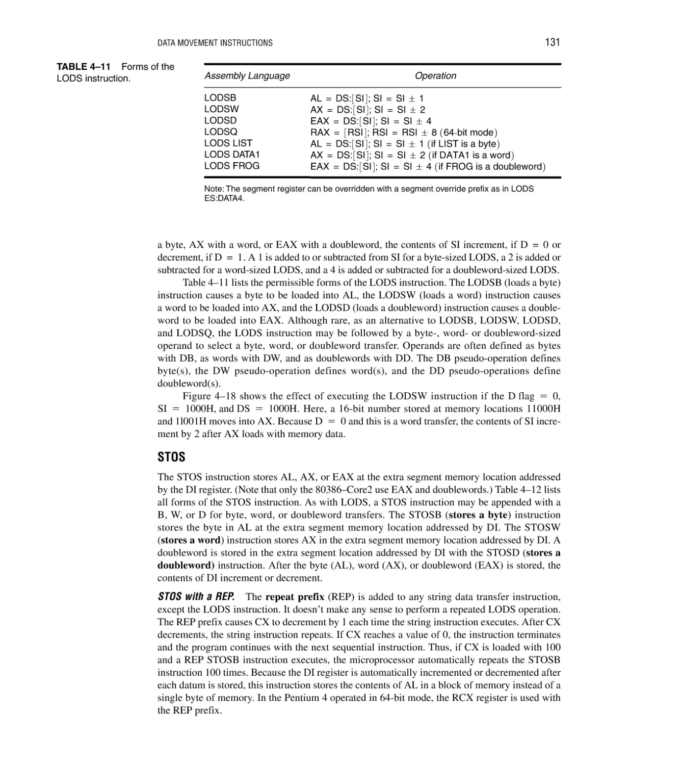
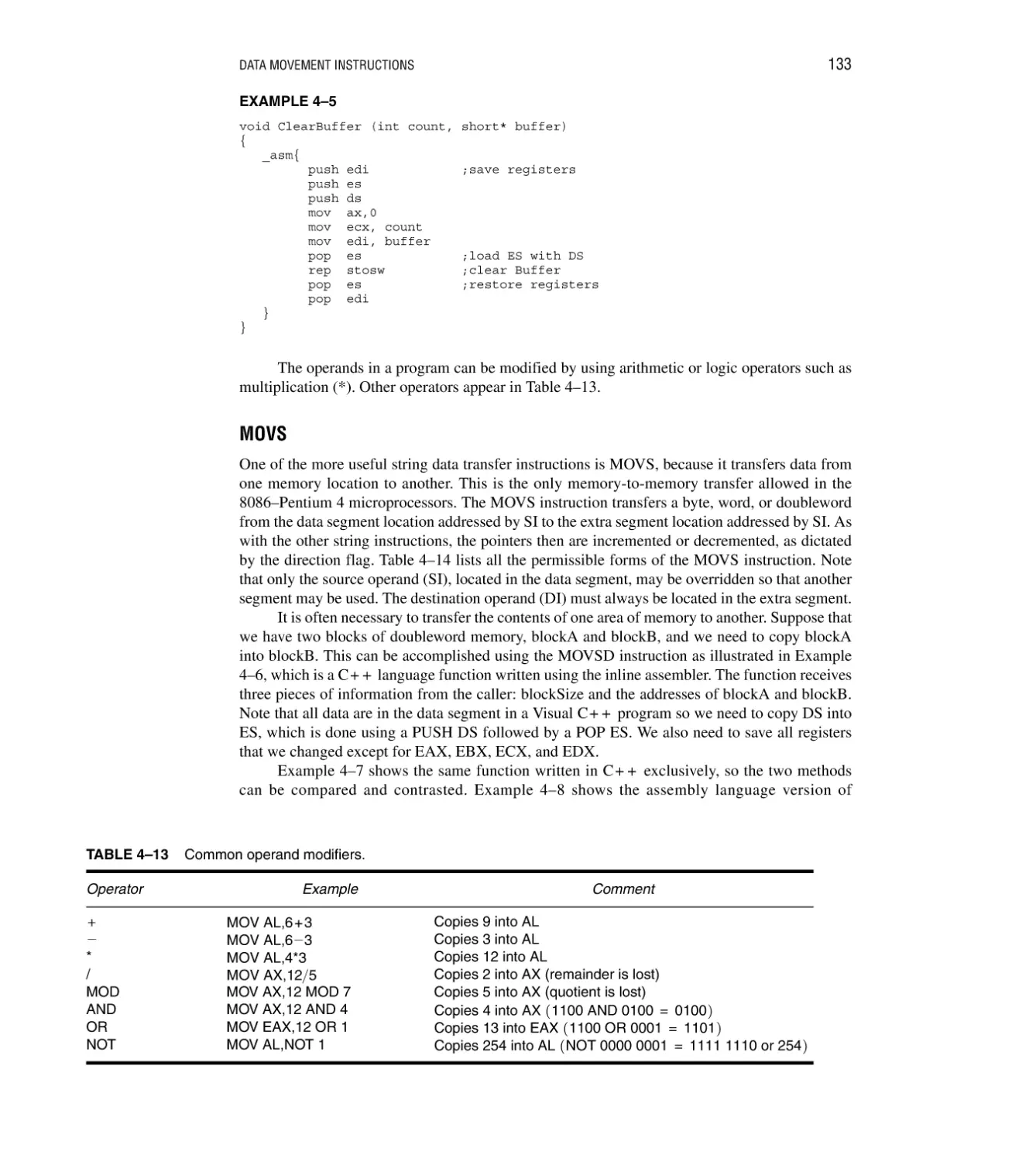
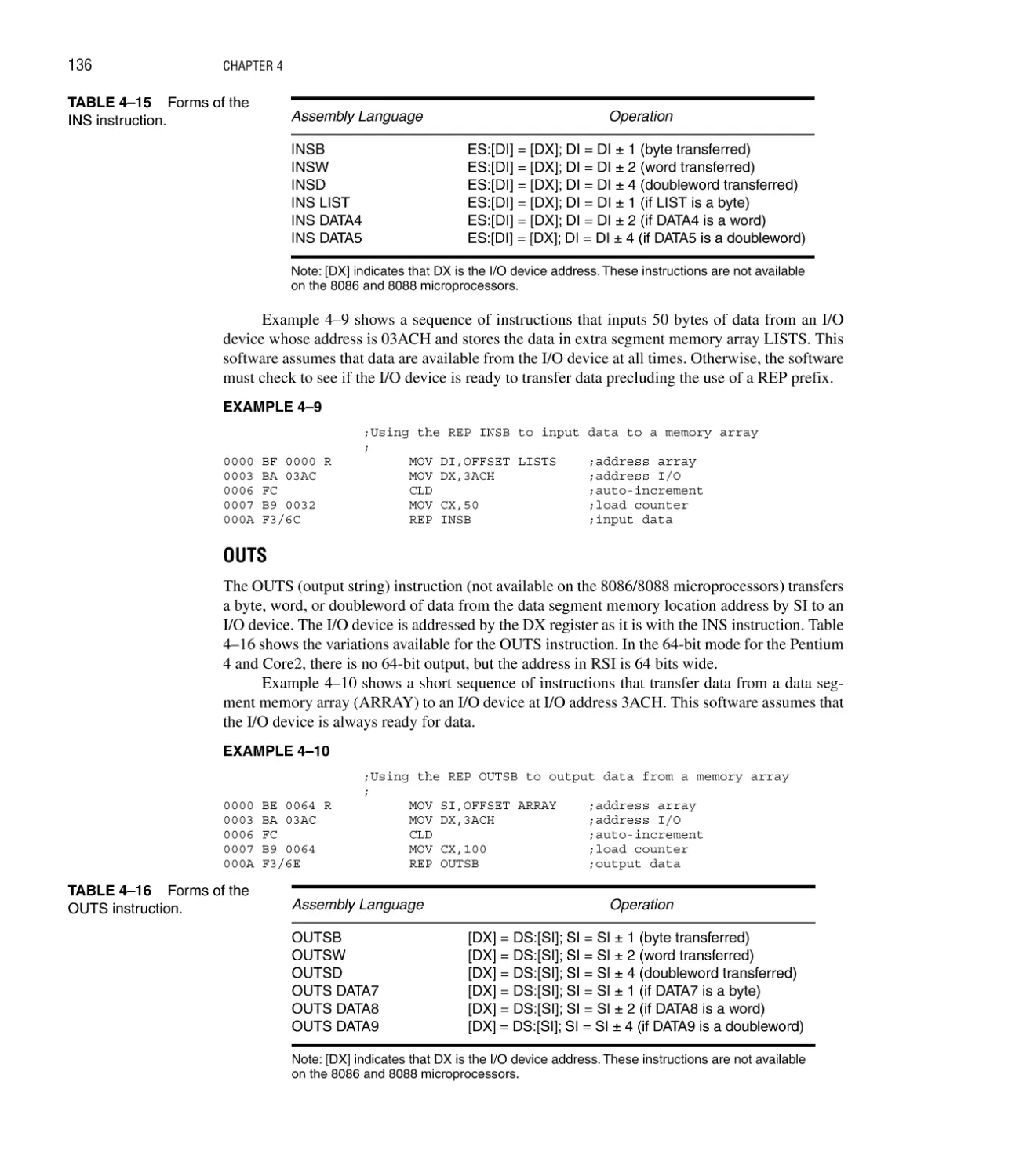
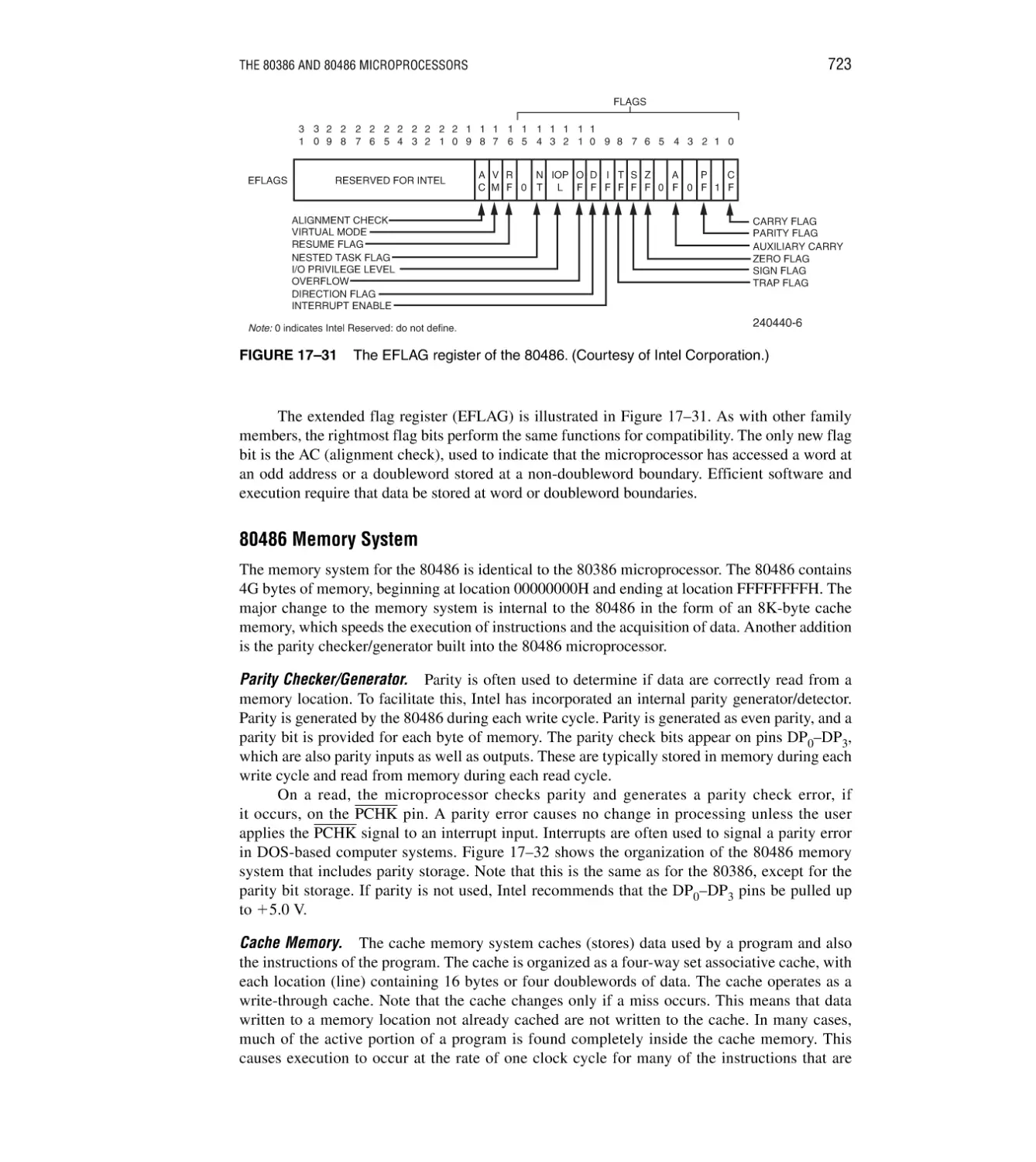
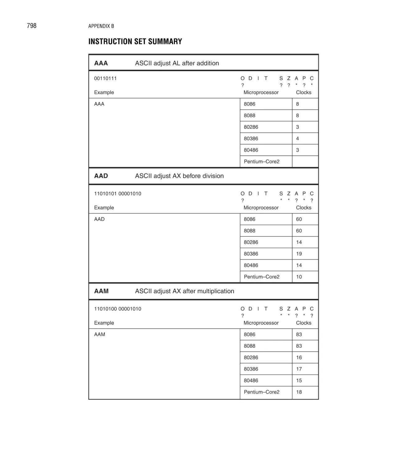
/


Text
THE INTEL MICROPROCESSORS
8086/8088, 80186/80188, 80286, 80386,
80486, Pentium, Pentium Pro Processor,
Pentium II, Pentium III, Pentium 4, and Core2
with 64-Bit Extensions
Architecture, Programming, and Interfacing
Eighth Edition
BARRY B. BREY
Upper Saddle River, New Jersey
Columbus, Ohio
Library of Congress Cataloging in Publication Data
Brey, Barry B.
The Intel microprocessors 8086/8088, 80186/80188, 80286, 80386, 80486, Pentium, Pentium
Pro processor, Pentium II, Pentium III, Pentium 4, and Core2 with 64-bit extensions:
architecture, programming, and interfacing / Barry B. Brey—8th ed.
p. cm.
Includes index.
ISBN 0-13-502645-8
1. Intel 80xxx series microprocessors. 2. Pentium (Microprocessor) 3. Computer interfaces.
I. Title.
QA76.8.I292B75 2009
004.165—dc22
2008009338
Editor in Chief: Vernon Anthony
Acquisitions Editor: Wyatt Morris
Editorial Assistant: Christopher Reed
Production Coordination: GGS Book Services
Project Manager: Jessica Sykes
Operations Specialist: Laura Weaver
Design Coordinator: Mike Fruhbeis
Cover Designer: Ilze Lemesis
Cover image: iStockphoto
Director of Marketing: David Gesell
Marketing Manager: Jimmy Stephens
Marketing Assistant: Les Roberts
This book was set in Times by GGS Book Services. It was printed and bound by Hamilton
Printing. The cover was printed by Phoenix Color Corp.
Copyright © 2009, 2006, 2003, 2000, 1997, 1994, 1991, 1987 by Pearson Education,
Inc., Upper Saddle River, New Jersey 07458. Pearson Prentice Hall. All rights reserved.
Printed in the United States of America. This publication is protected by Copyright and permission should be obtained from the publisher prior to any prohibited reproduction, storage
in a retrieval system, or transmission in any form or by any means, electronic, mechanical,
photocopying, recording, or likewise. For information regarding permission(s), write to:
Rights and Permissions Department.
Pearson Prentice Hall™ is a trademark of Pearson Education, Inc.
Pearson® is a registered trademark of Pearson plc
Prentice Hall® is a registered trademark of Pearson Education, Inc.
Pearson Education Ltd., London
Pearson Education Singapore Pte. Ltd.
Pearson Education Canada, Inc.
Pearson Education—Japan
Pearson Education Australia Pty. Limited
Pearson Education North Asia Ltd., Hong Kong
Pearson Educación de Mexico, S.A. de C.V.
Pearson Education Malaysia Pte. Ltd.
10 9 8 7 6 5 4 3 2 1
ISBN–13: 978–0–13–502645–8
ISBN–10:
0–13–502645–8
This text is dedicated to my progenies, Brenda (the programmer) and Gary (the
veterinarian technician), and to my constant four-legged companions: Romy,
Sassy, Sir Elton, Eye Envy, and Baby Hooter.
iii
This page intentionally left blank
PREFACE
This practical reference text is written for students who require a thorough knowledge of programming and interfacing of the Intel family of microprocessors. Today, anyone functioning or
striving to function in a field of study that uses computers must understand assembly language
programming, a version of C language, and interfacing. Intel microprocessors have gained wide,
and at times exclusive, application in many areas of electronics, communications, and control
systems, particularly in desktop computer systems. A major addition to this eighth edition
explains how to interface C/C++ using Visual C++ Express, which is a free download from
Microsoft, with assembly language for both the older DOS and the Windows environments.
Many applications include Visual C++ as a basis for learning assembly language using the inline
assembler. Updated sections that detail new events in the fields of microprocessors and microprocessor interfacing have been added.
ORGANIZATION AND COVERAGE
To cultivate a comprehensive approach to learning, each chapter begins with a set of objectives
that briefly define its content. Chapters contain many programming applications and examples
that illustrate the main topics. Each chapter ends with a numerical summary, which doubles as a
study guide, and reviews the information just presented. Questions and problems are provided
for reinforcement and practice, including research paper suggestions.
This text contains many example programs using the Microsoft Macro Assembler program
and the inline assembler in the Visual C++ environment, which provide a learning opportunity to
program the Intel family of microprocessors. Operation of the programming environment
includes the linker, library, macros, DOS function, BIOS functions, and Visual C/C++ program
development. The inline assembler (C/C++) is illustrated for both the 16- and 32-bit programming environments of various versions of Visual C++. The text is written to use Visual C++
Express 2005 or 2008 as a development environment, but any version of Visual Studio can also
be used with almost no change.
This text also provides a thorough description of family members, memory systems, and
various I/O systems that include disk memory, ADC and DAC, 16550 UART, PIAs, timers, keyboard/display controllers, arithmetic coprocessors, and video display systems. Also discussed are
v
vi
PREFACE
the personal computer system buses (AGP, ISA, PCI, PCI Express, USB, serial ports, and parallel
port). Through these systems, a practical approach to microprocessor interfacing can be learned.
APPROACH
Because the Intel family of microprocessors is quite diverse, this text initially concentrates on
real mode programming, which is compatible with all versions of the Intel family of microprocessors. Instructions for each family member, which include the 80386, 80486, Pentium,
Pentium Pro, Pentium II, Pentium III, and Pentium 4 processors, are compared and contrasted
with those for the 8086/8088 microprocessors. This entire series of microprocessors is very similar, which allows more advanced versions and their instructions to be learned with the basic
8086/8088. Please note that the 8086/8088 are still used in embedded systems along with their
updated counterparts, the 80186/80188 and 80386EX embedded microprocessor.
This text also explains the programming and operation of the numeric coprocessor, MMX
extension, and the SIMD extension, which function in a system to provide access to floatingpoint calculations that are important in control systems, video graphics, and computer-aided
design (CAD) applications. The numeric coprocessor allows a program to access complex
arithmetic operations that are otherwise difficult to achieve with normal microprocessor programming. The MMX and SIMD instructions allow both integer and floating-point data to be
manipulated in parallel at very high speed.
This text also describes the pin-outs and function of the 8086–80486 and all versions of the
Pentium microprocessor. First, interfacing is explained using the 8086/8088 with some of the
more common peripheral components. After explaining the basics, a more advanced emphasis is
placed on the 80186/80188, 80386, 80486, and Pentium through Pentium 4 microprocessors.
Coverage of the 80286, because of its similarity to the 8086 and 80386, is minimized so the
80386, 80486, and Pentium versions can be covered in complete detail.
Through this approach, the operation of the microprocessor and programming with the
advanced family members, along with interfacing all family members, provides a working and
practical background of the Intel family of microprocessors. Upon completing a course using
this text, you will be able to:
1. Develop software to control an application interface microprocessor. Generally, the software
developed will also function on all versions of the microprocessor. This software also
includes DOS-based and Windows-based applications. The main emphasis is on developing
inline assembly and C++ mixed language programs in the Windows environment.
2. Program using MFC controls, handlers, and functions to use the keyboard, video display
system, and disk memory in assembly language and C++.
3. Develop software that uses macro sequences, procedures, conditional assembly, and flow
control assembler directives that are linked to a Visual C++ program.
4. Develop software for code conversions using lookup tables and algorithms.
5. Program the numeric coprocessor to solve complex equations.
6. Develop software for the MMX and SIMD extensions.
7. Explain the differences between the family members and highlight the features of each member.
8. Describe and use real and protected mode operation of the microprocessor.
9. Interface memory and I/O systems to the microprocessor.
10. Provide a detailed and comprehensive comparison of all family members and their software
and hardware interfaces.
11. Explain the function of the real-time operating system in an embedded application.
12. Explain the operation of disk and video systems.
13. Interface small systems to the ISA, PCI, serial ports, parallel port, and USB bus in a personal
computer system.
PREFACE
vii
CONTENT OVERVIEW
Chapter 1 introduces the Intel family of microprocessors with an emphasis on the microprocessorbased computer system: its history, operation, and the methods used to store data in a
microprocessor-based system. Number systems and conversions are also included. Chapter 2
explores the programming model of the microprocessor and system architecture. Both real and
protected mode operations are explained.
Once an understanding of the basic machine is grasped, Chapters 3 through 6 explain how
each instruction functions with the Intel family of microprocessors. As instructions are
explained, simple applications are presented to illustrate the operation of the instructions and
develop basic programming concepts.
Chapter 7 introduces the use of Visual C/C++ Express with the inline assembler and separate assembly language programming modules. It also explains how to configure Visual C++
Express for use with assembly language applications.
After the basis for programming is developed, Chapter 8 provides applications using the
Visual C++ Express with the inline assembler program. These applications include programming
using the keyboard and mouse through message handlers in the Windows environment. Disk
files are explained using the File class, as well as keyboard and video operations on a personal
computer system through Windows. This chapter provides the tools required to develop virtually
any program on a personal computer system through the Windows environment.
Chapter 9 introduces the 8086/8088 family as a basis for learning basic memory and I/O
interfacing, which follow in later chapters. This chapter shows the buffered system as well as the
system timing.
Chapter 10 explains memory interface using both integrated decoders and programmable
logic devices using VHDL. The 8-, 16-, 32-, and 64-bit memory systems are provided so the
8086–80486 and the Pentium through Pentium 4 microprocessors can be interfaced to memory.
Chapter 11 provides a detailed look at basic I/O interfacing, including PIAs, timers, the
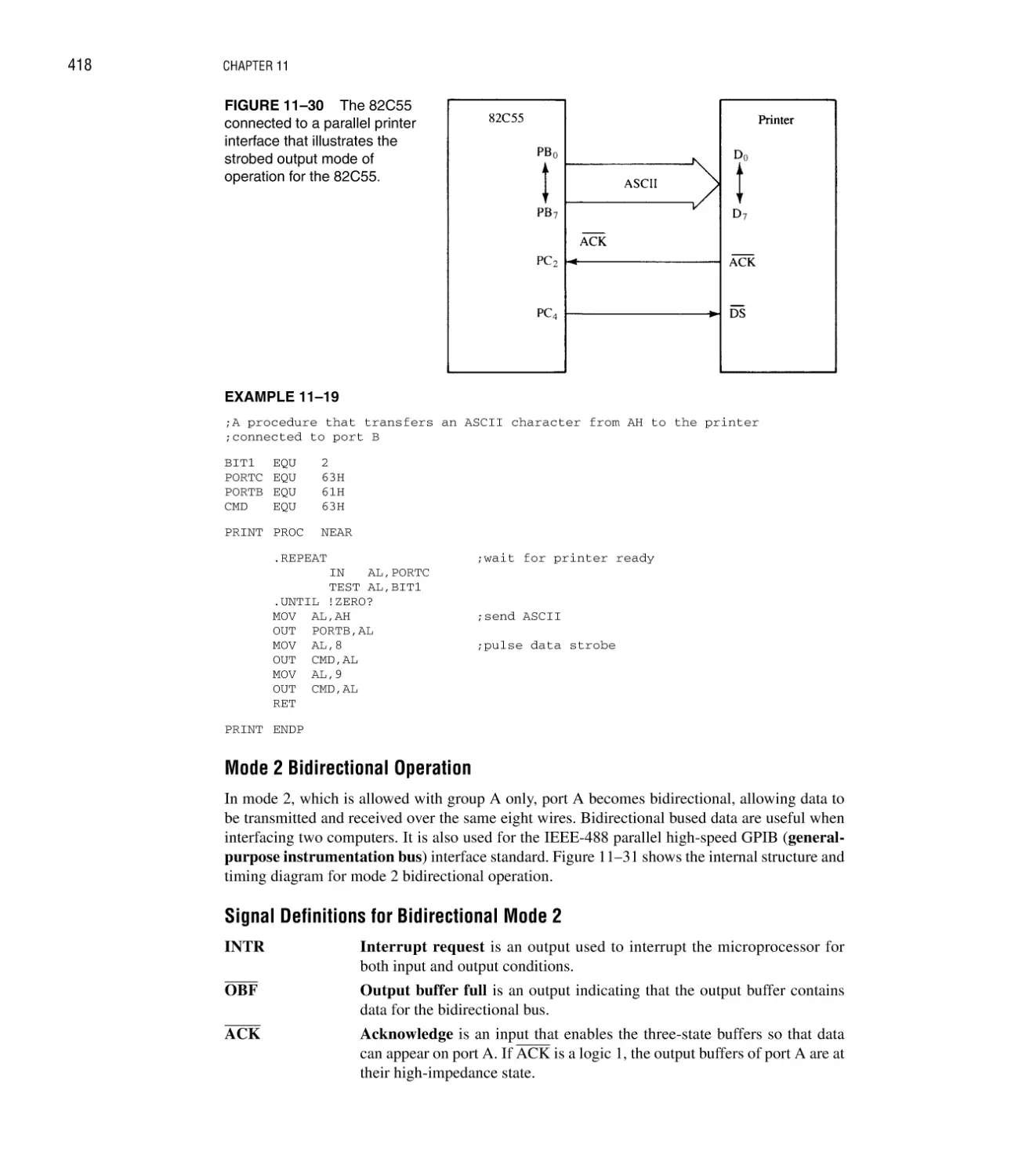
16550 UART, and ADC/DAC. It also describes the interface of both DC and stepper motors.
Once these basic I/O components and their interface to the microprocessor are understood,
Chapters 12 and 13 provide detail on advanced I/O techniques that include interrupts and direct
memory access (DMA). Applications include a printer interface, real-time clock, disk memory,
and video systems.
Chapter 14 details the operation and programming for the 8087–Pentium 4 family of arithmetic coprocessors, as well as MMX and SIMD instructions. Today few applications function
efficiently without the power of the arithmetic coprocessor. Remember that all Intel microprocessors since the 80486 contain a coprocessor; since the Pentium, an MMX unit; and since
the Pentium II, an SIMD unit.
Chapter 15 shows how to interface small systems to the personal computer through the use
of the parallel port, serial ports, and the ISA, and PCI bus interfaces.
Chapters 16 and 17 cover the advanced 80186/80188–80486 microprocessors and explore
their differences with the 8086/8088, as well as their enhancements and features. Cache memory,
interleaved memory, and burst memory are described with the 80386 and 80486 microprocessors. Chapter 16 also covers real-time operating systems (RTOS), and Chapter 17 also describes
memory management and memory paging.
Chapter 18 details the Pentium and Pentium Pro microprocessors. These microprocessors
are based upon the original 8086/8088.
Chapter 19 introduces the Pentium II, Pentium III, Pentium 4, and Core2 microprocessors.
It covers some of the new features, package styles, and the instructions that are added to the original instruction set.
Appendices are included to enhance the text. Appendix A provides an abbreviated listing
of the DOS INT 21H function calls because the use of DOS has waned. It also details the use of
viii
PREFACE
the assembler program and the Windows Visual C++ interface. A complete listing of all
8086–Pentium 4 and Core2 instructions, including many example instructions and machine coding in hexadecimal as well as clock timing information, is found in Appendix B. Appendix C
provides a compact list of all the instructions that change the flag bits. Answers for the evennumbered questions and problems are provided in Appendix D.
To access supplementary materials online, instructors need to request an instructor access
code. Go to www.pearsonhighered.com/irc, where you can register for an instructor access
code. Within 48 hours after registering, you will receive a confirming e-mail, including an
instructor access code. Once you have received your code, go to the site and log on for full
instructions on downloading the materials you wish to use.
Acknowledgments
I greatly appreciate the feedback from the following reviewers:
James K. Archibald, Brigham Young University
William H. Murray III, Broome Community College.
STAY IN TOUCH
We can stay in touch through the Internet. My Internet site contains information about all of my
textbooks and many important links that are specific to the personal computer, microprocessors,
hardware, and software. Also available is a weekly lesson that details many of the aspects of the
personal computer. Of particular interest is the “Technical Section,” which presents many notes
on topics that are not covered in this text. Please feel free to contact me at bbrey@ee.net if you
need any type of assistance. I usually answer all of my e-mail within 24 hours.
My website is http://members.ee.net/brey
BRIEF CONTENTS
CHAPTER 1
INTRODUCTION TO THE MICROPROCESSOR AND COMPUTER
CHAPTER 2
THE MICROPROCESSOR AND ITS ARCHITECTURE
51
CHAPTER 3
ADDRESSING MODES
77
CHAPTER 4
DATA MOVEMENT INSTRUCTIONS
111
CHAPTER 5
ARITHMETIC AND LOGIC INSTRUCTIONS
156
CHAPTER 6
PROGRAM CONTROL INSTRUCTIONS
192
CHAPTER 7
USING ASSEMBLY LANGUAGE WITH C/C++
223
CHAPTER 8
PROGRAMMING THE MICROPROCESSOR
250
CHAPTER 9
8086/8088 HARDWARE SPECIFICATIONS
302
CHAPTER 10
MEMORY INTERFACE
328
CHAPTER 11
BASIC I/O INTERFACE
377
CHAPTER 12
INTERRUPTS
451
CHAPTER 13
DIRECT MEMORY ACCESS AND DMA-CONTROLLED I/O
490
CHAPTER 14
THE ARITHMETIC COPROCESSOR, MMX, AND SIMD TECHNOLOGIES
531
CHAPTER 15
BUS INTERFACE
592
CHAPTER 16
THE 80185, 80188, AND 80286 MICROPROCESSORS
627
1
ix
x
BRIEF CONTENTS
CHAPTER 17
THE 80386 AND 80486 MICROPROCESSORS
677
CHAPTER 18
THE PENTIUM AND PENTIUM PRO MICROPROCESSORS
729
CHAPTER 19
THE PENTIUM II, PENTIUM III, PENTIUM 4, AND CORE2 MICROPROCESSORS
759
CONTENTS
CHAPTER 1
INTRODUCTION TO THE MICROPROCESSOR AND COMPUTER
1
Introduction/Chapter Objectives 1
1–1 A Historical Background 2
The Mechanical Age 2; The Electrical Age 2; Programming Advancements 4;
The Microprocessor Age 5; The Modern Microprocessor 7
1–2 The Microprocessor-Based Personal Computer System 17
The Memory and I/O System 17; The Microprocessor 25
1–3 Number Systems 29
Digits 29; Positional Notation 30; Conversion to Decimal 31; Conversion from Decimal 32;
Binary-Coded Hexadecimal 33
1–4 Computer Data Formats 35
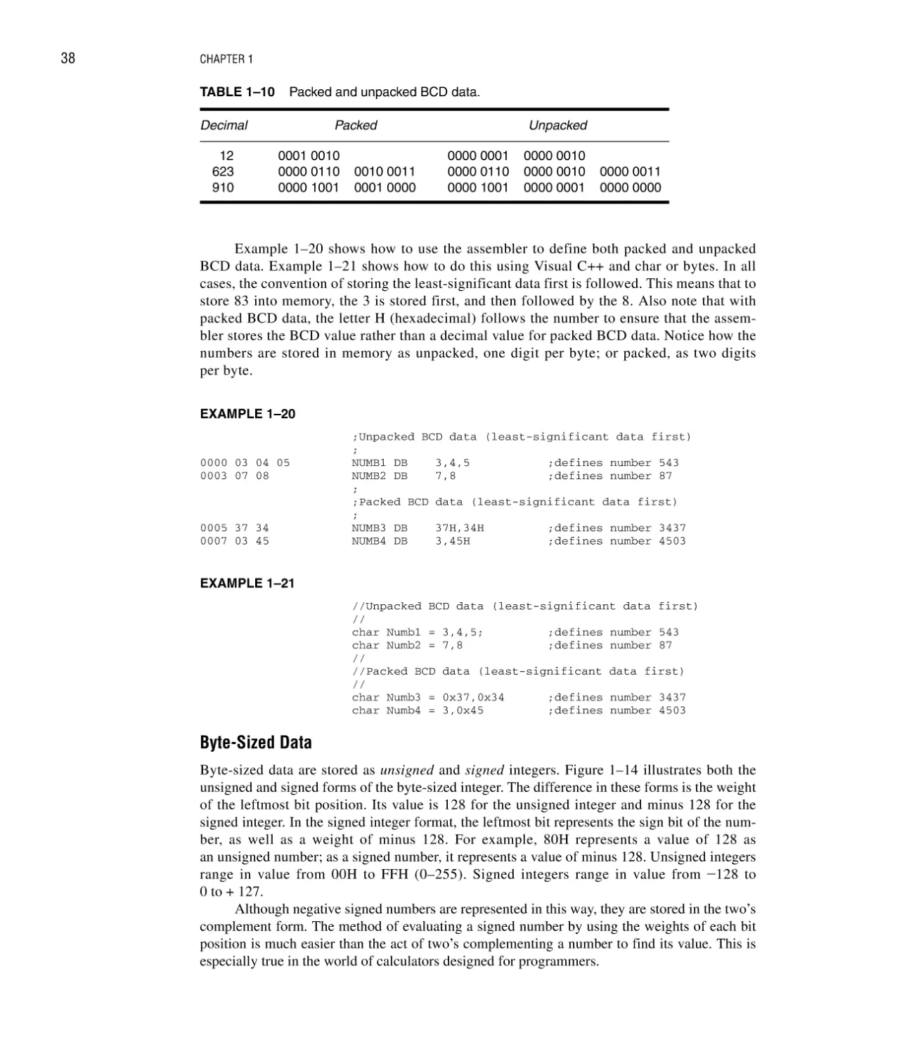
ASCII and Unicode Data 35; BCD (Binary-Coded Decimal) Data 37; Byte-Sized Data 38;
Word-Sized Data 40; Doubleword-Sized Data 41; Real Numbers 43
1–5 Summary 45
1–6 Questions and Problems 46
CHAPTER 2
THE MICROPROCESSOR AND ITS ARCHITECTURE
51
Introduction/Chapter Objectives 51
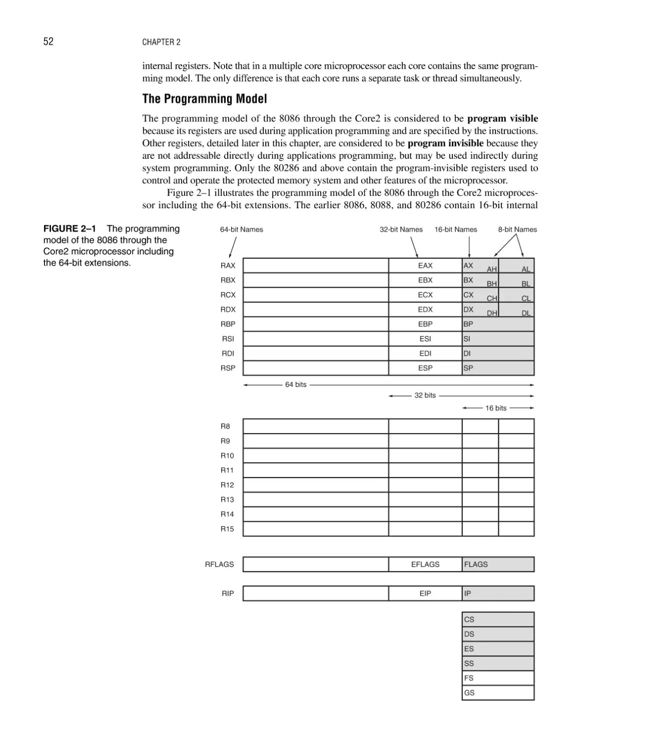
2–1 Internal Microprocessor Architecture 51
The Programming Model 52; Multipurpose Registers 54
2–2 Real Mode Memory Addressing 58
Segments and Offsets 58; Default Segment and Offset Registers 60;
Segment and Offset Addressing Scheme Allows Relocation 60
2–3 Introduction to Protected Mode Memory Addressing 63
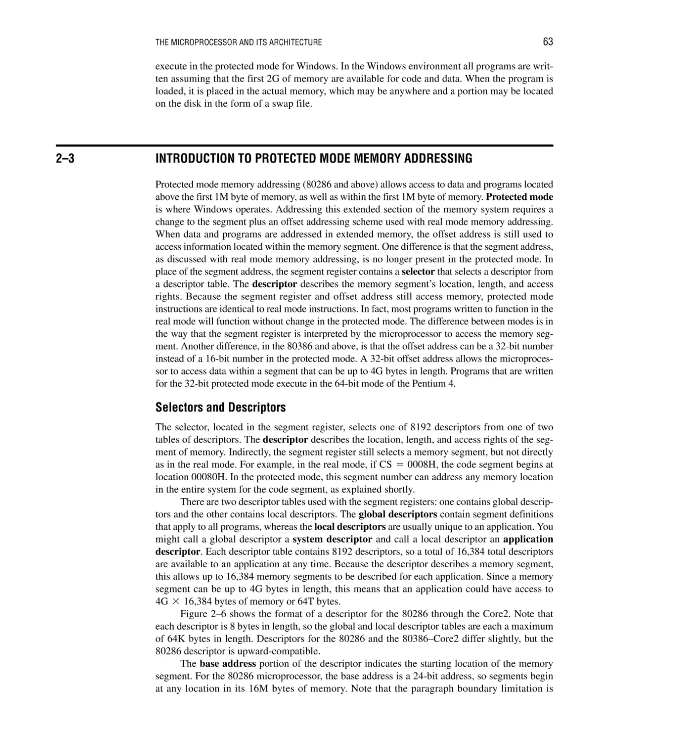
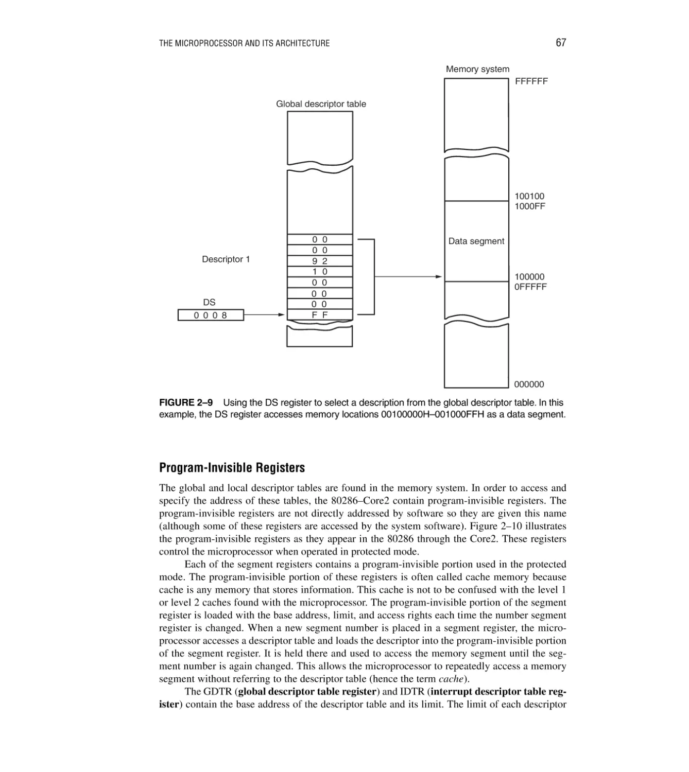
Selectors and Descriptors 63; Program-Invisible Registers 67
2–4 Memory Paging 68
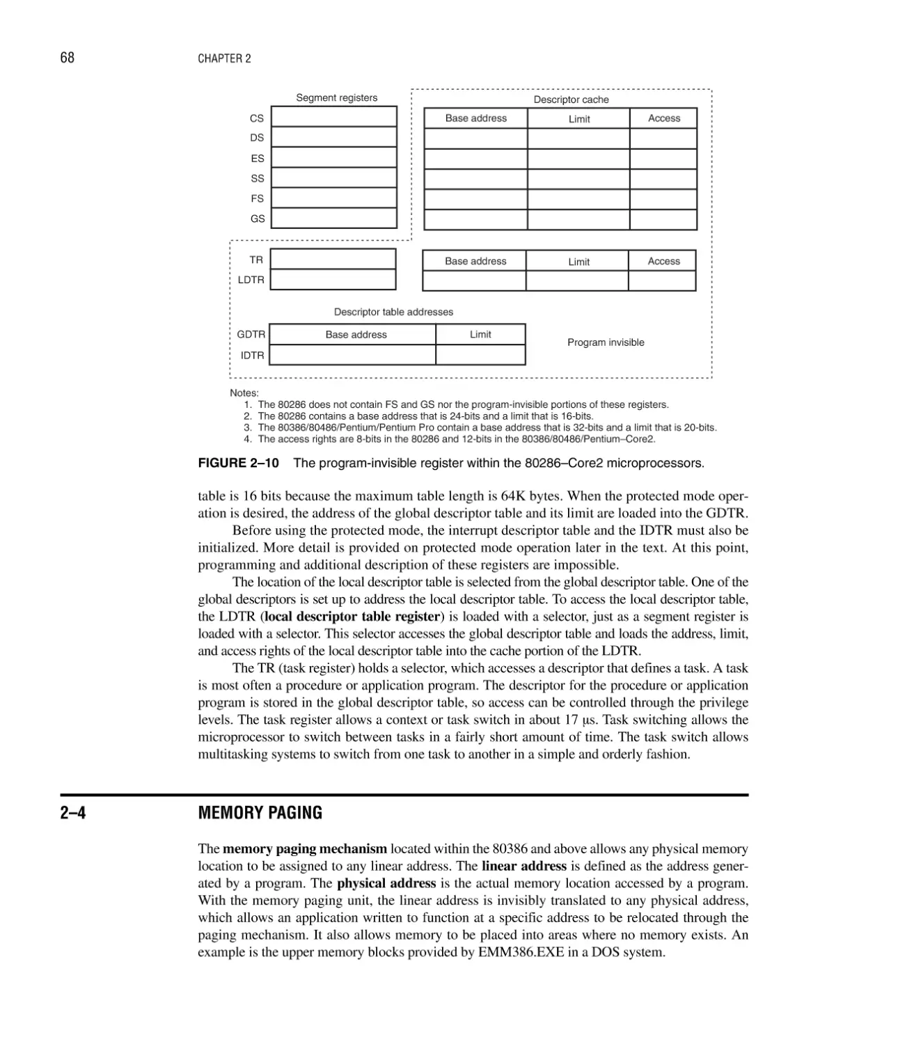
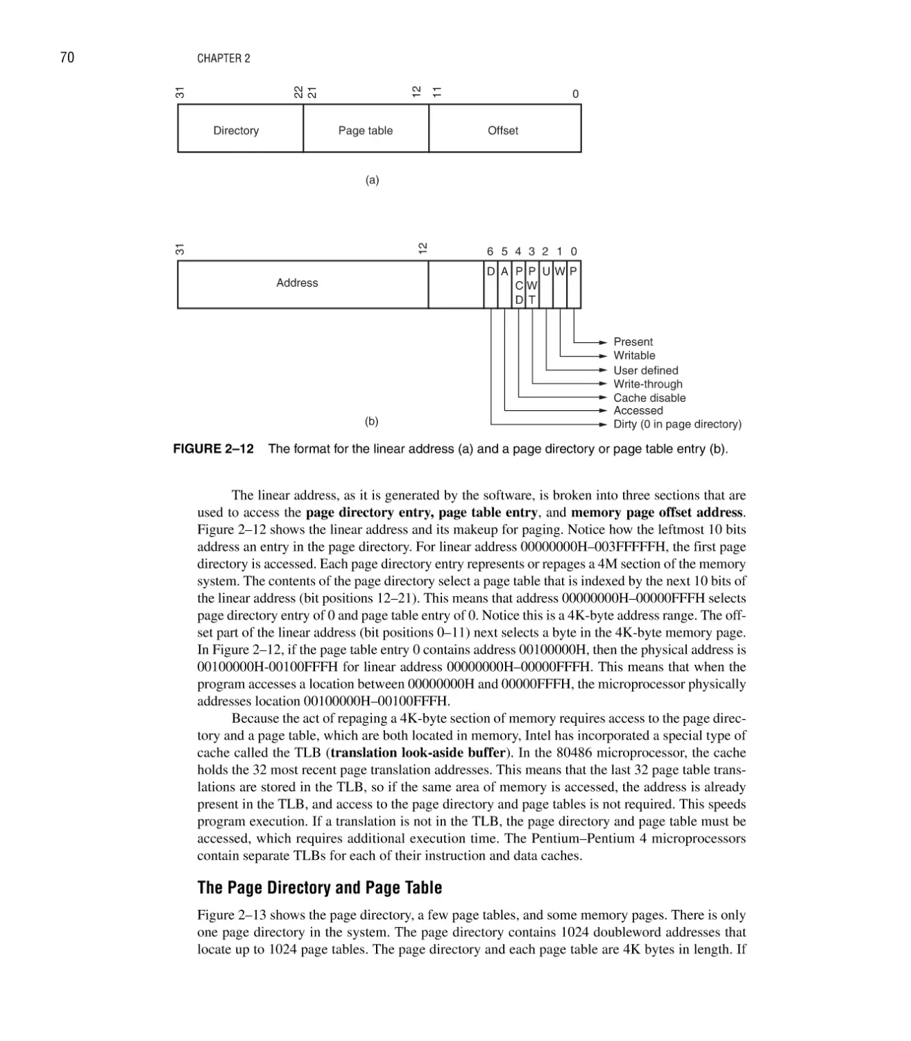
Paging Registers 69; The Page Directory and Page Table 70
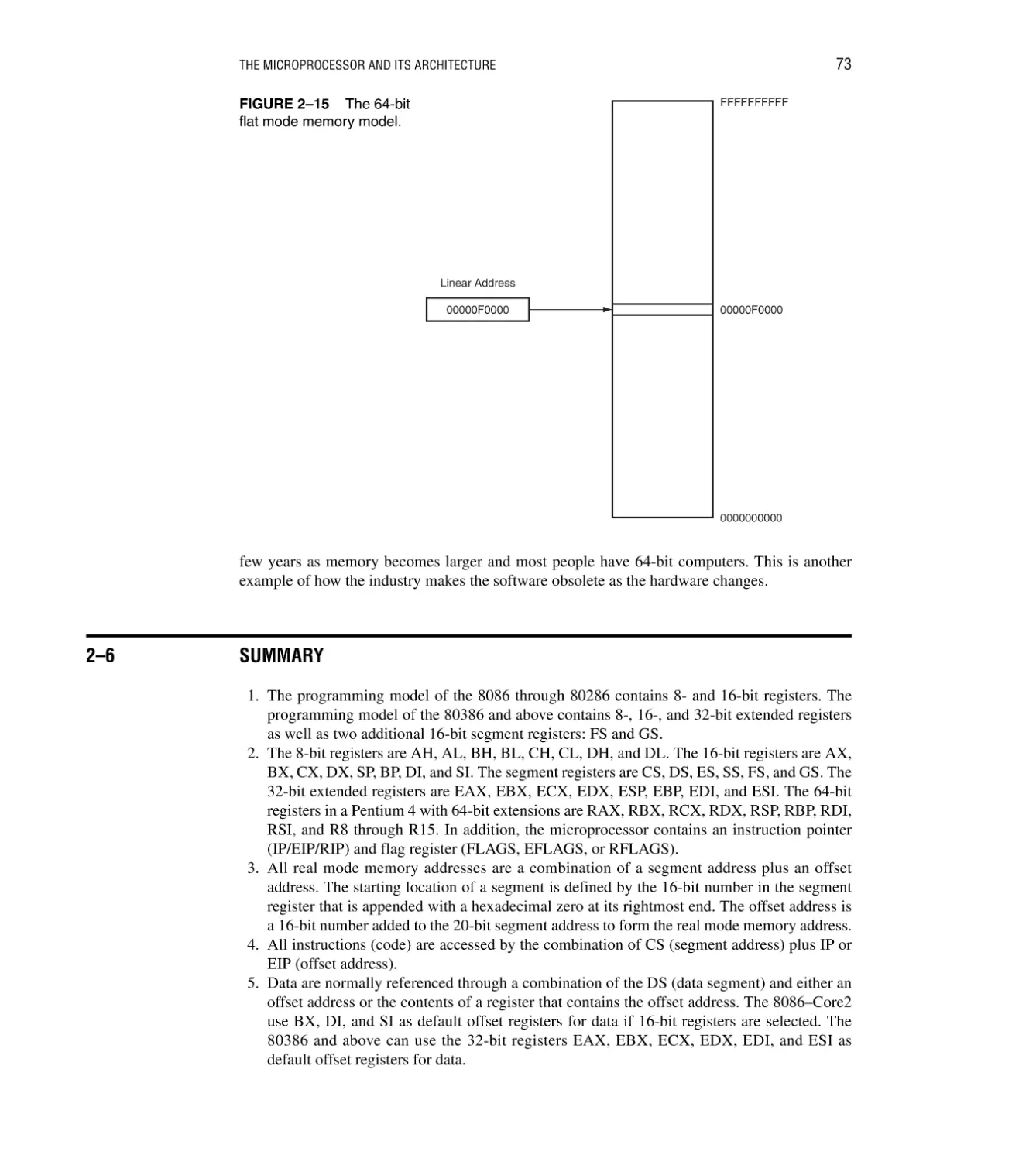
2–5 Flat Mode Memory 72
2–6 Summary 73
2–7 Questions and Problems 74
CHAPTER 3
ADDRESSING MODES
77
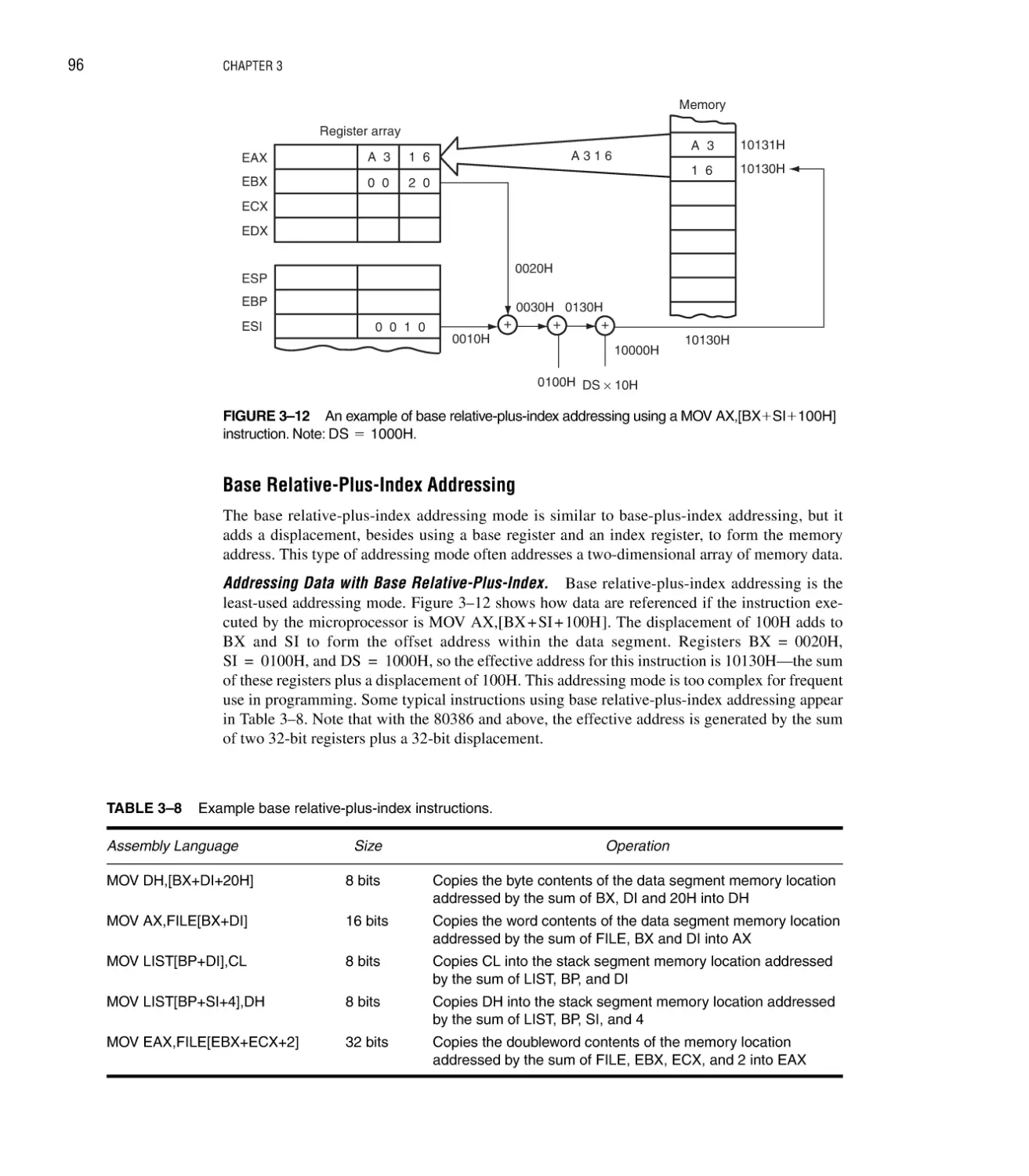
Introduction/Chapter Objectives 77
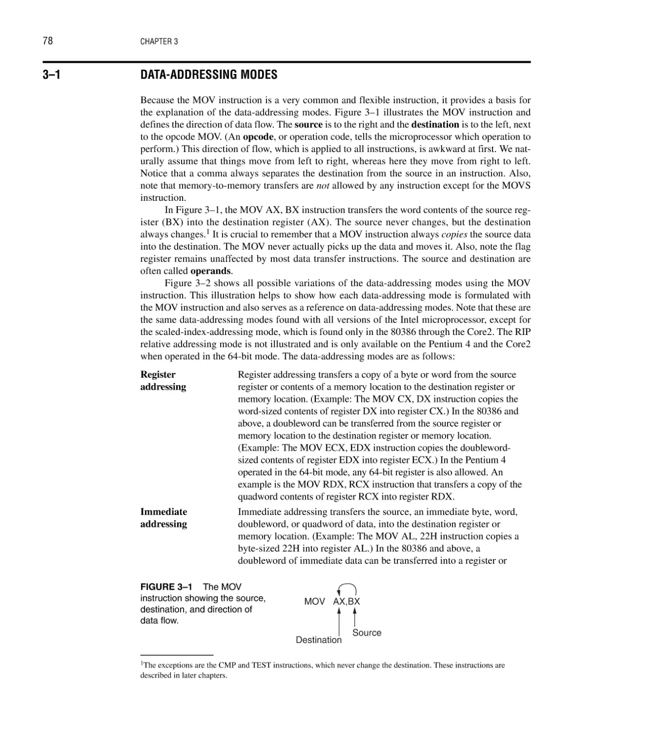
3–1 Data-Addressing Modes 78
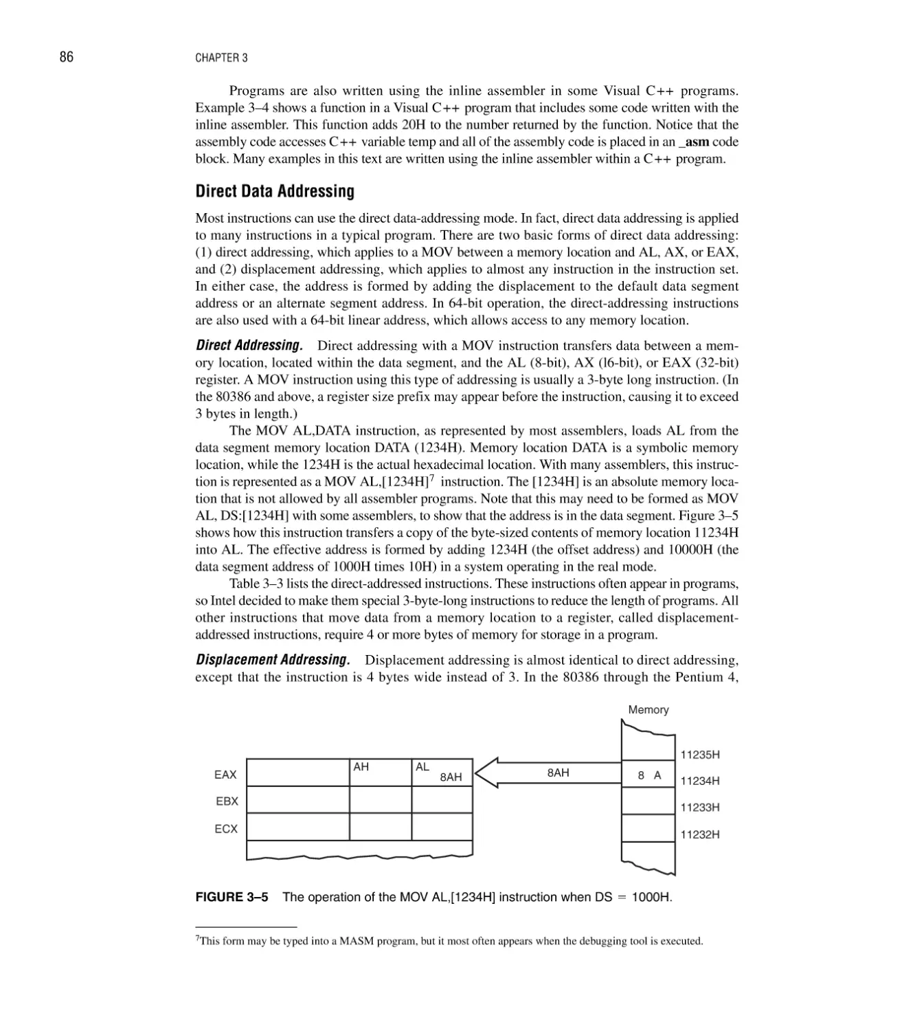
Register Addressing 81; Immediate Addressing 83; Direct Data Addressing 86;
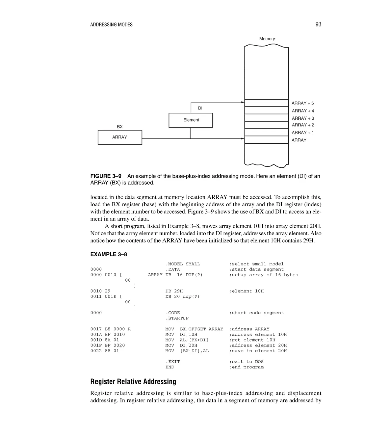
Register Indirect Addressing 88; Base-Plus-Index Addressing 91;
xi
xii
CONTENTS
3–2
3–3
3–4
3–5
CHAPTER 4
Register Relative Addressing 93; Base Relative-Plus-Index Addressing 96;
Scaled-Index Addressing 98; RIP Relative Addressing 99; Data Structures 99
Program Memory-Addressing Modes 100
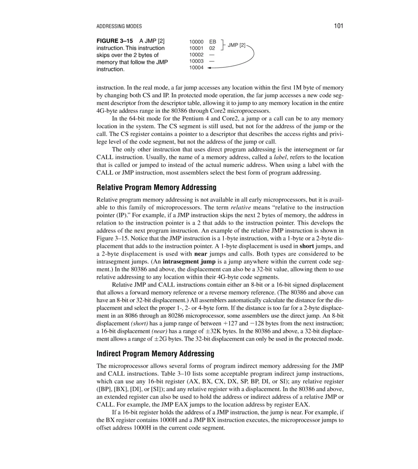
Direct Program Memory Addressing 100; Relative Program Memory Addressing 101;
Indirect Program Memory Addressing 101
Stack Memory-Addressing Modes 102
Summary 105
Questions and Problems 107
DATA MOVEMENT INSTRUCTIONS
111
Introduction/Chapter Objectives 111
4–1 MOV Revisited 112
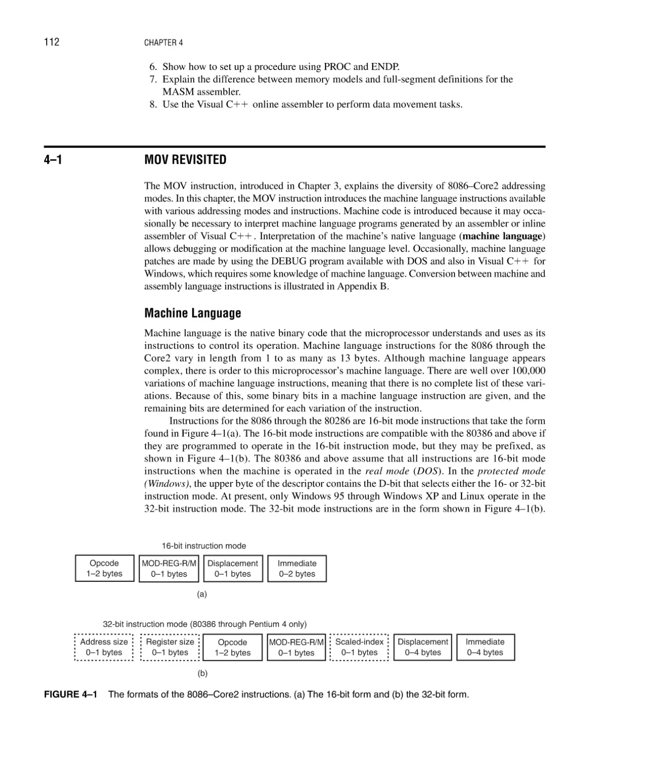
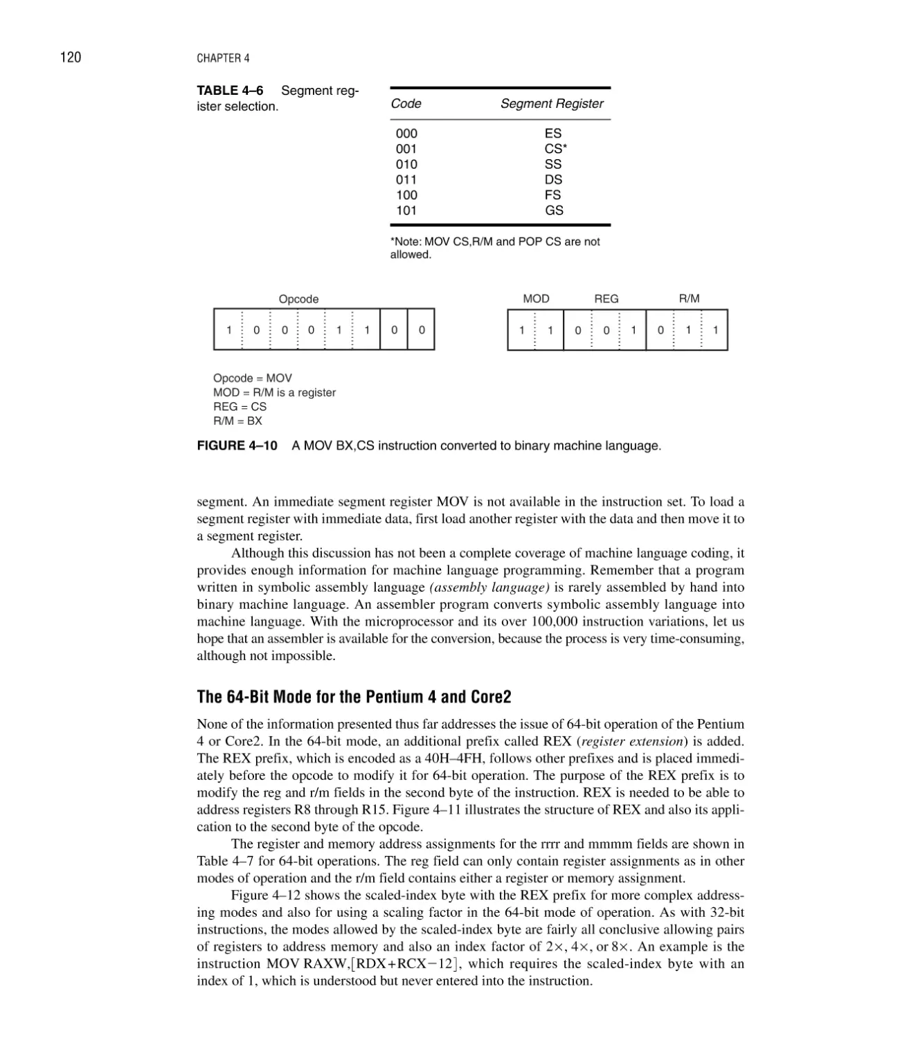
Machine Language 112; The 64-Bit Mode for the Pentium 4 and Core2 120
4–2 PUSH/POP 122
PUSH 122; POP 124; Initializing the Stack 124
4–3 Load-Effective Address 127
LEA 127; LDS, LES, LFS, LGS, and LSS 128
4–4 String Data Transfers 130
The Direction Flag 130; DI and SI 130; LODS 130; STOS 131; MOVS 133;
INS 135; OUTS 136
4–5 Miscellaneous Data Transfer Instructions 137
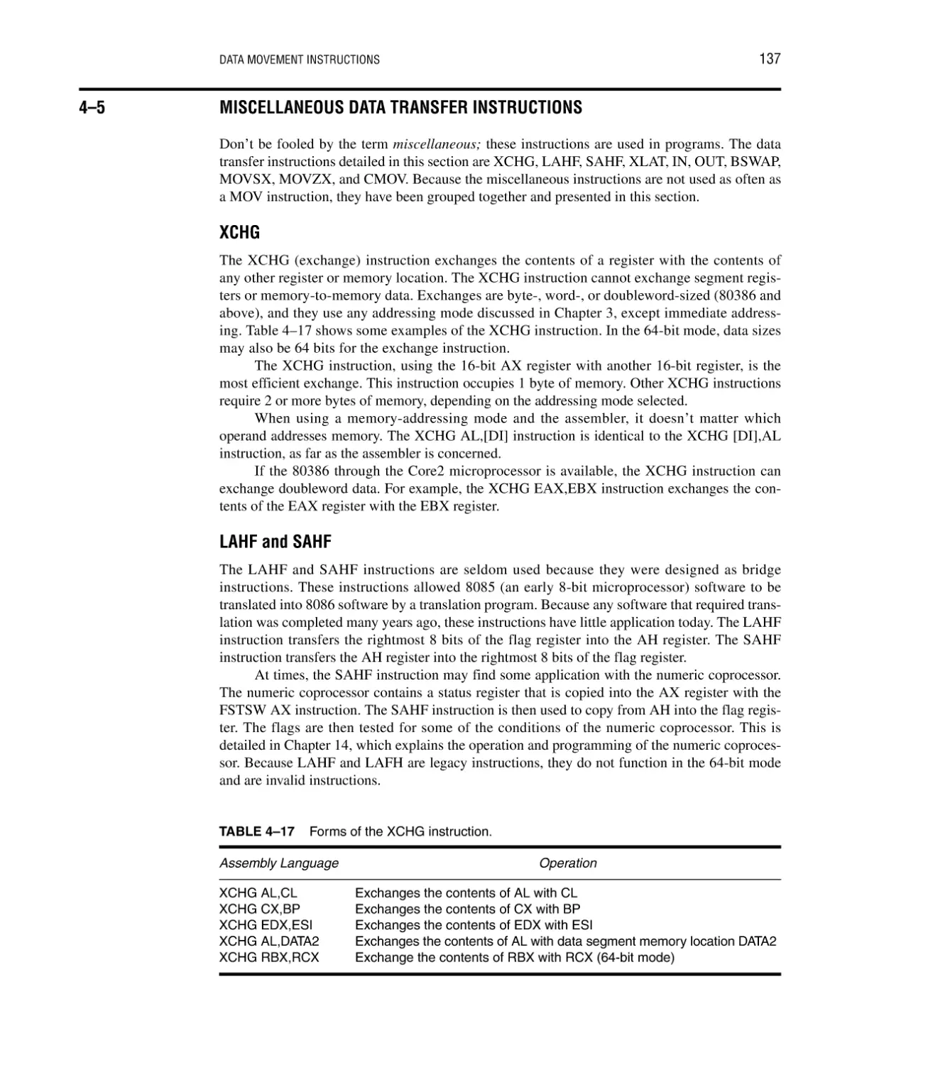
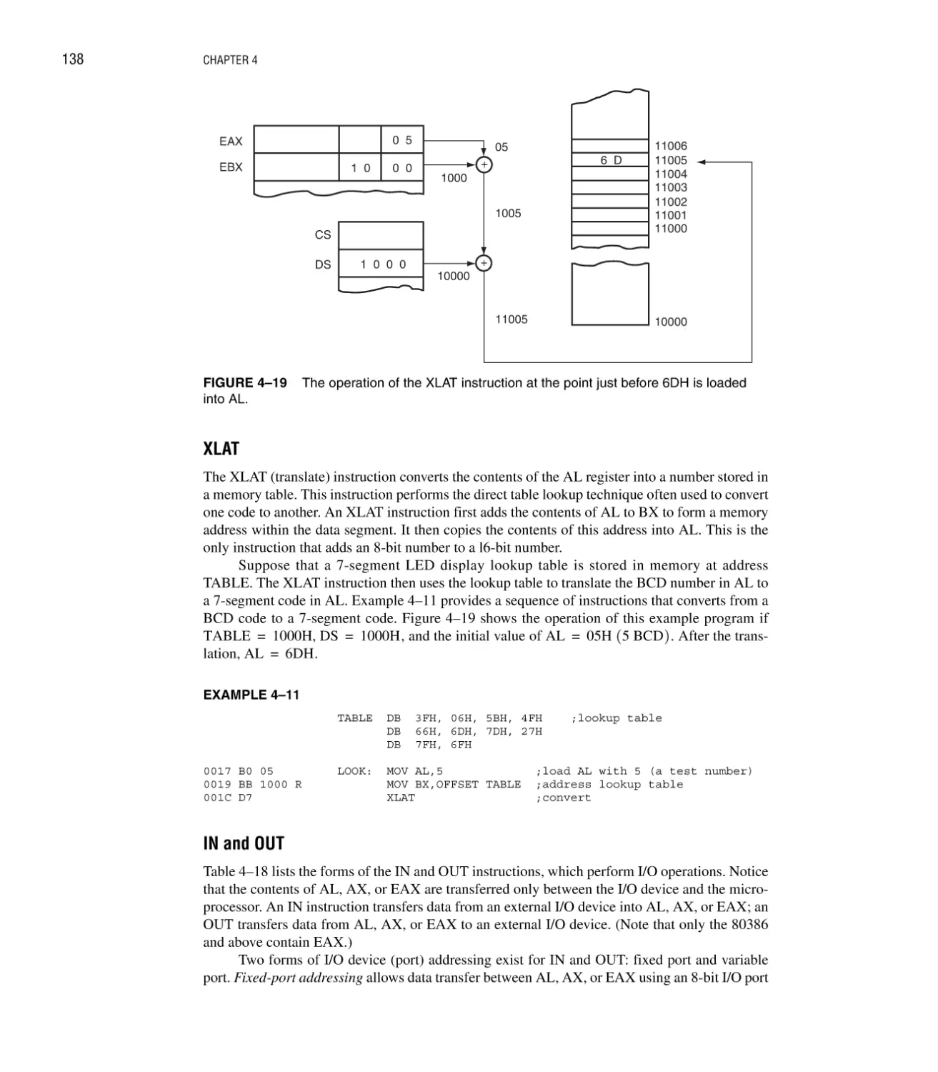
XCHG 137; LANF and SAHF 137; XLAT 138; IN and OUT 138;
MOVSX and MOVZX 140; BSWAP 140; CMOV 141
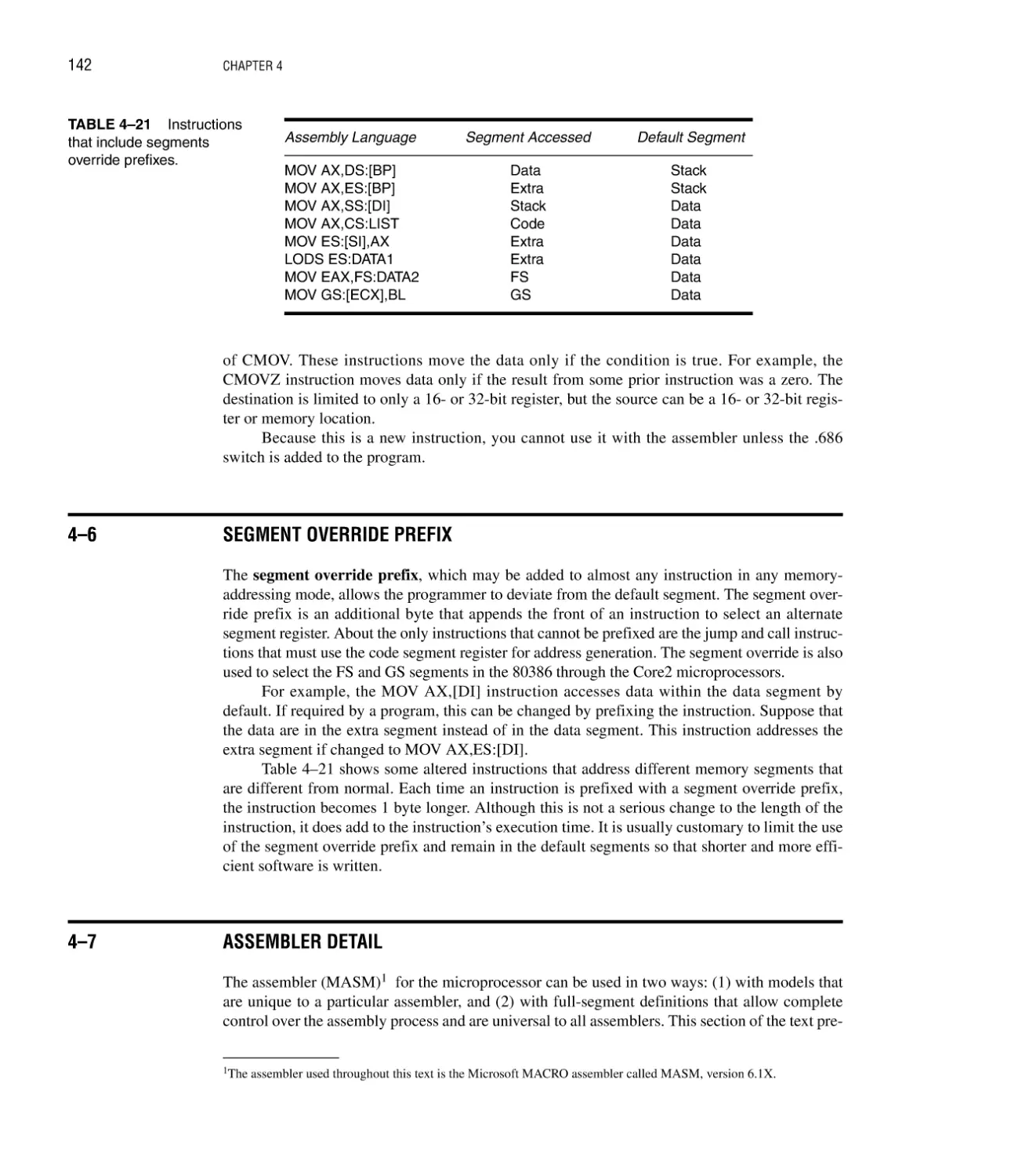
4–6 Segment Override Prefix 142
4–7 Assembler Detail 142
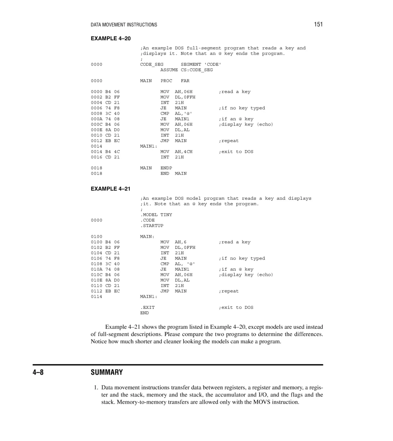
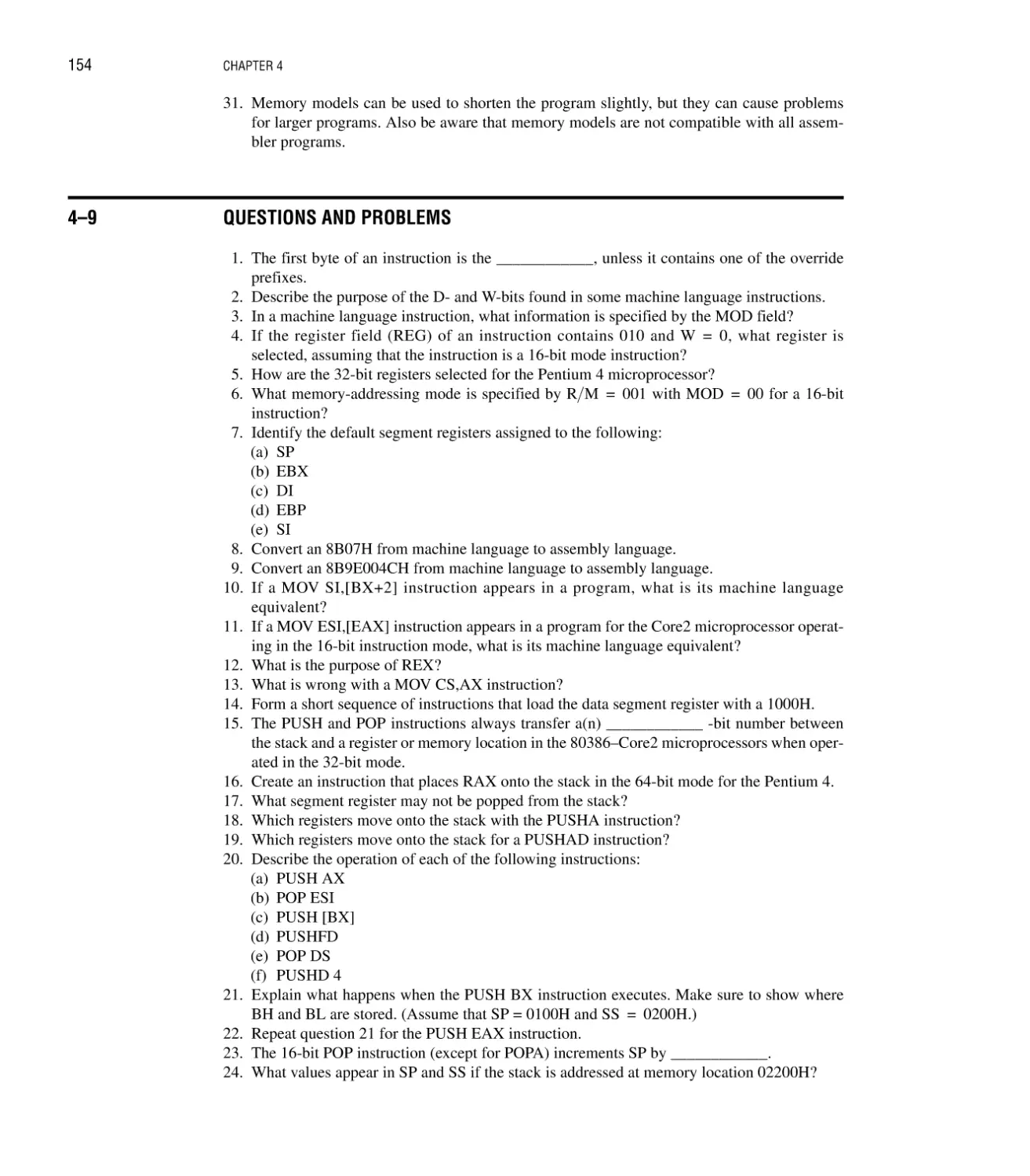
Directives 143; Memory Organization 147; A Sample Program 150
4–8 Summary 151
4–9 Questions and Problems 154
CHAPTER 5
ARITHMETIC AND LOGIC INSTRUCTIONS
156
Introduction/Chapter Objectives 156
5–1 Addition, Subtraction, and Comparison 156
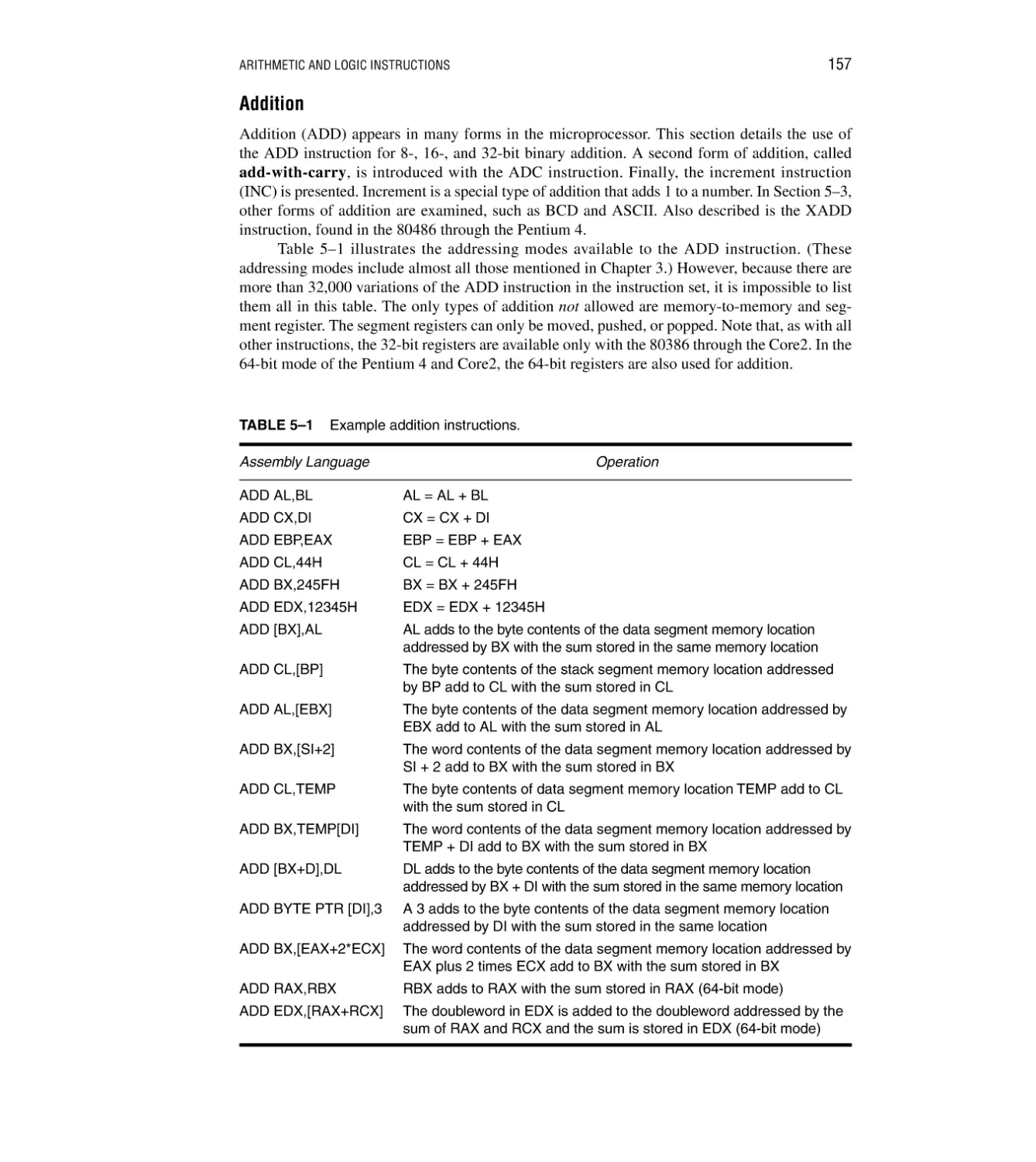
Addition 157; Subtraction 162; Comparison 165
5–2 Multiplication and Division 166
Multiplication 166; Division 169
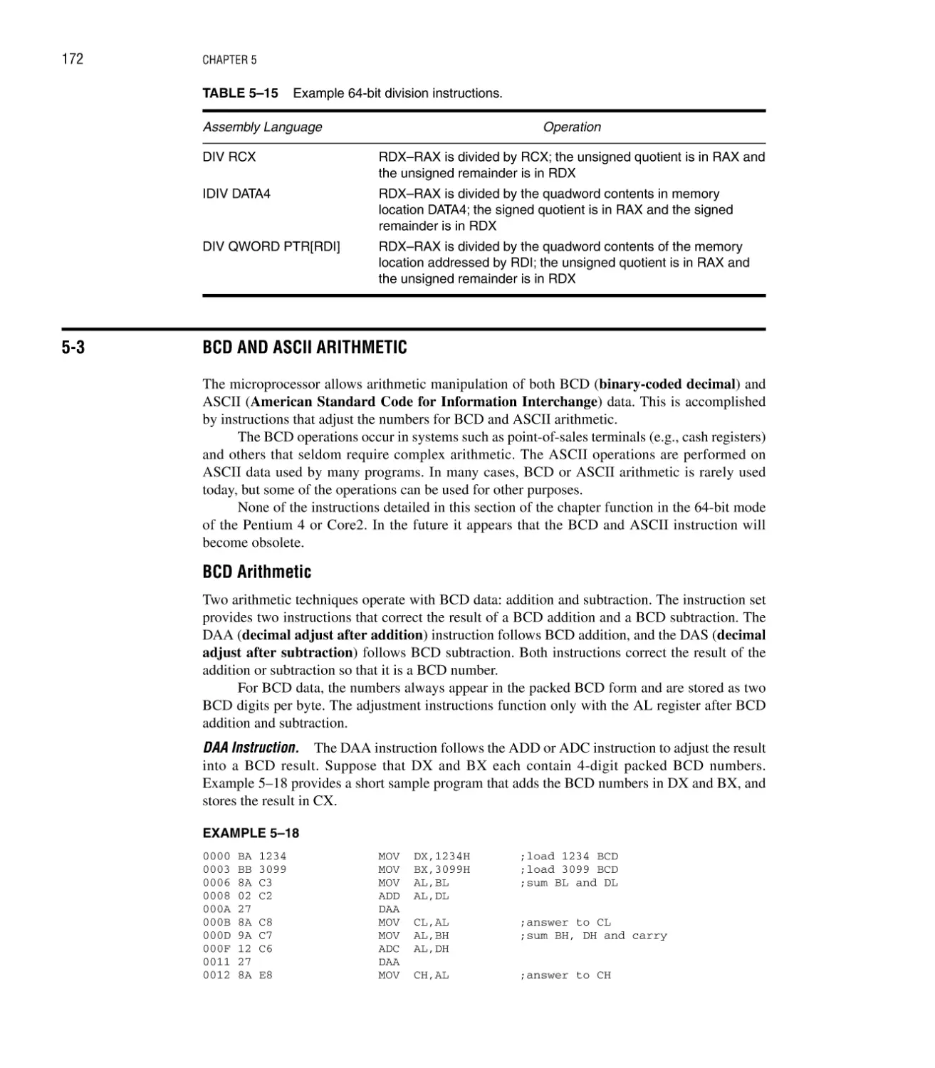
5–3 BCD and ASCII Arithmetic 172
BCD Arithmetic 172; ASCII Arithmetic 173
5–4 Basic Logic Instructions 175
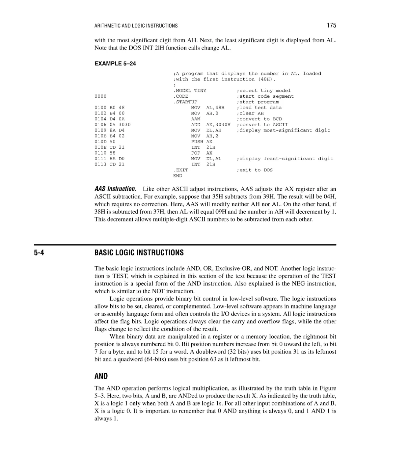
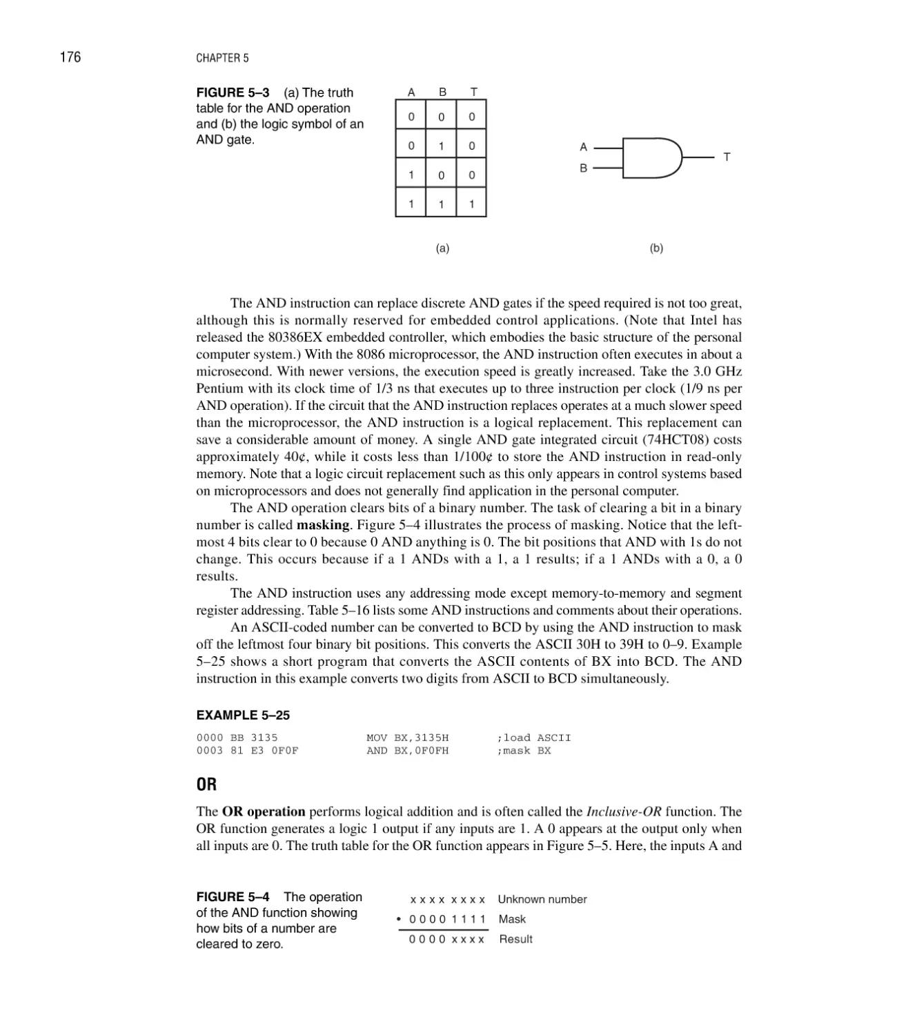
AND 175; OR 176; Test and Bit Test Instructions 180; NOT and NEG 181
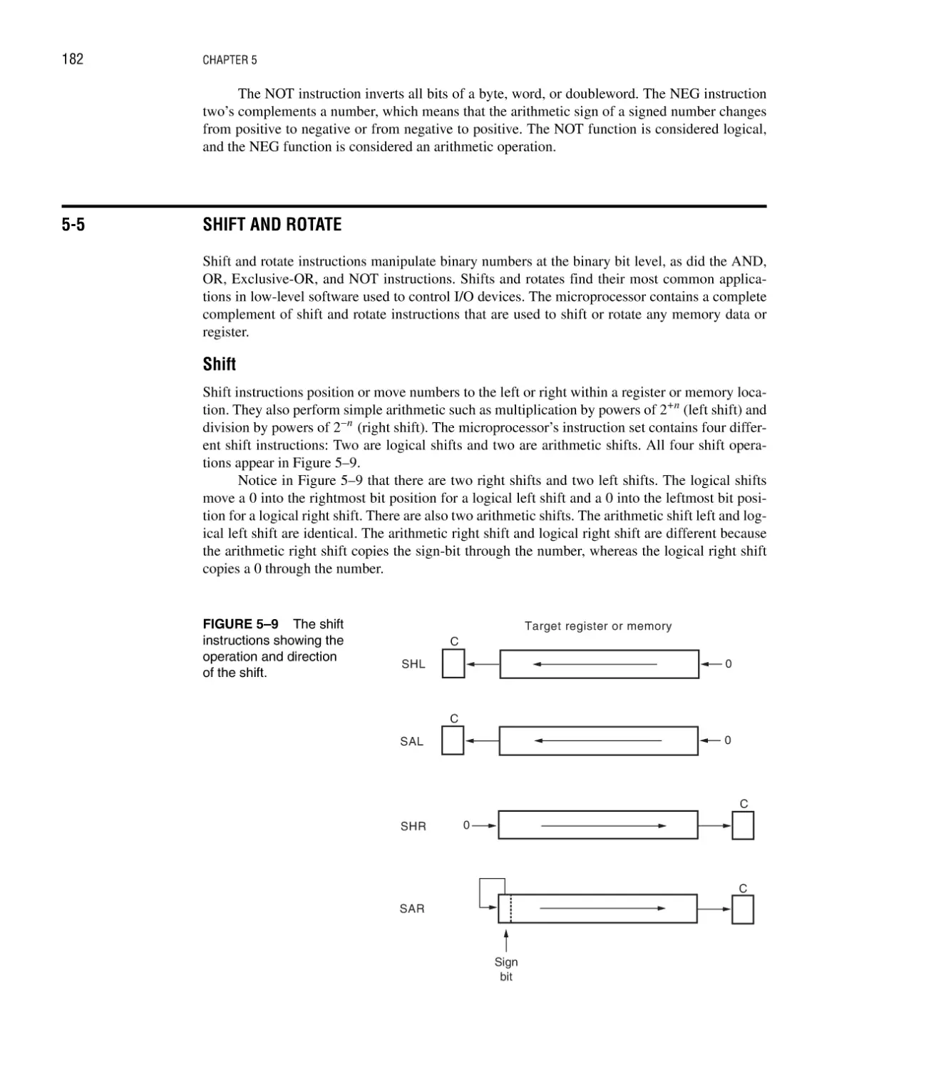
5–5 Shift and Rotate 182
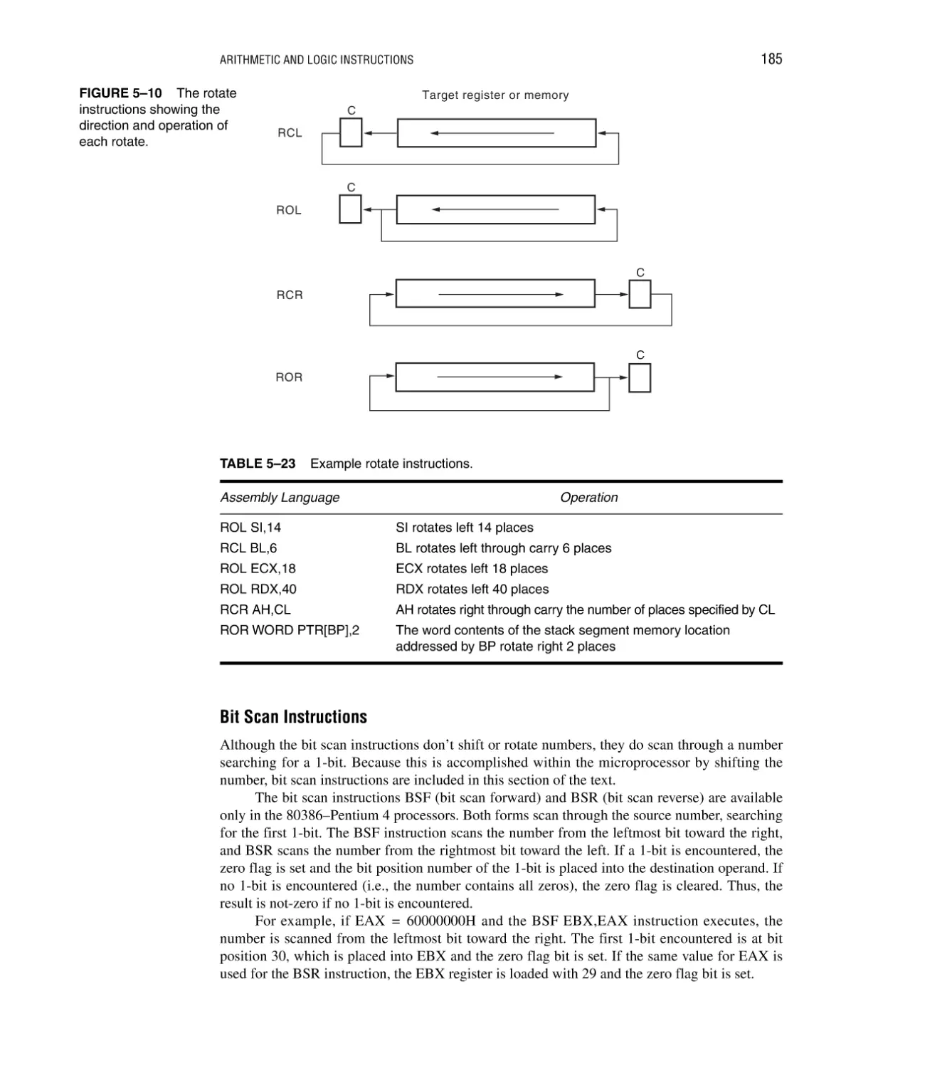
Shift 182; Rotate 184; Bit Scan Instructions 185
5–6 String Comparisons 186
SCAS 186; CMPS 187
5–7 Summary 187
5–8 Questions and Problems 189
CHAPTER 6
PROGRAM CONTROL INSTRUCTIONS
Introduction/Chapter Objectives 192
6–1 The Jump Group 192
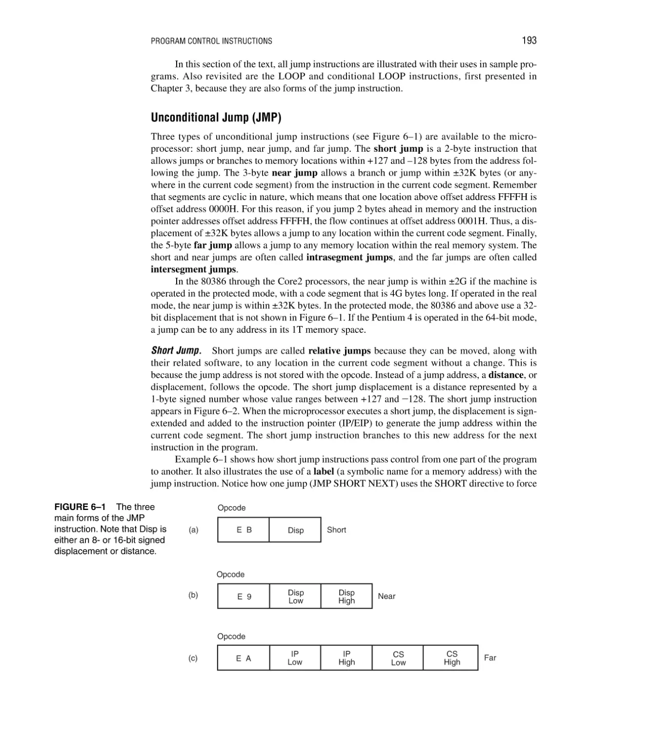
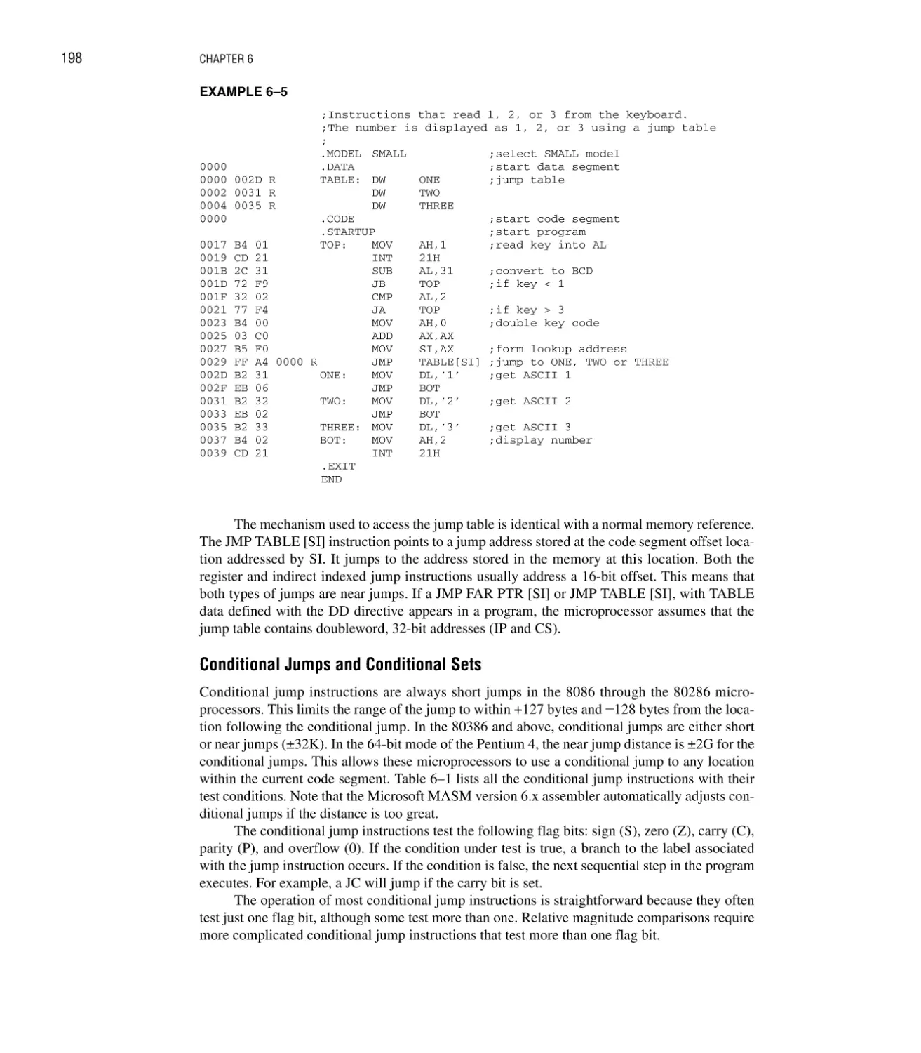
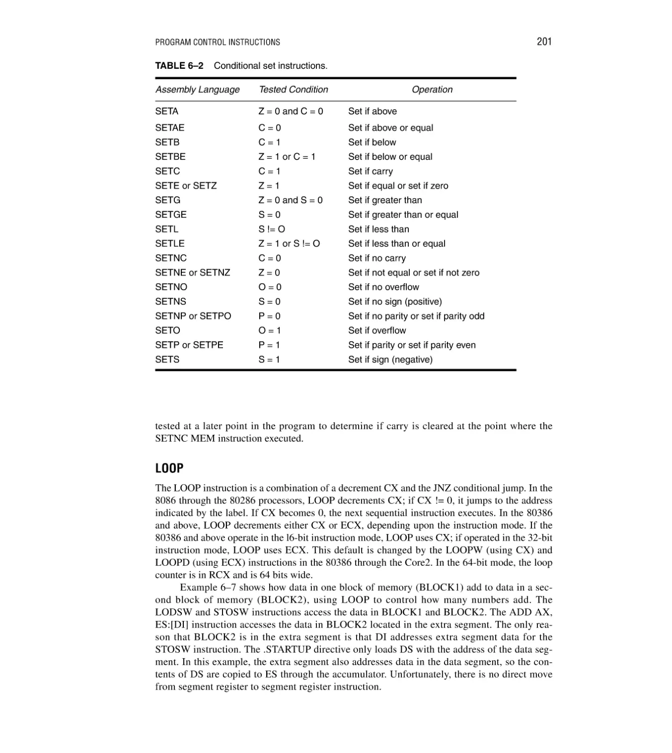
Unconditional Jump (JMP) 193; Conditional Jumps and Conditional Sets 198; LOOP 201
6–2 Controlling the Flow of the Program 202
WHILE Loops 205; REPEAT-UNTIL Loops 206
6–3 Procedures 208
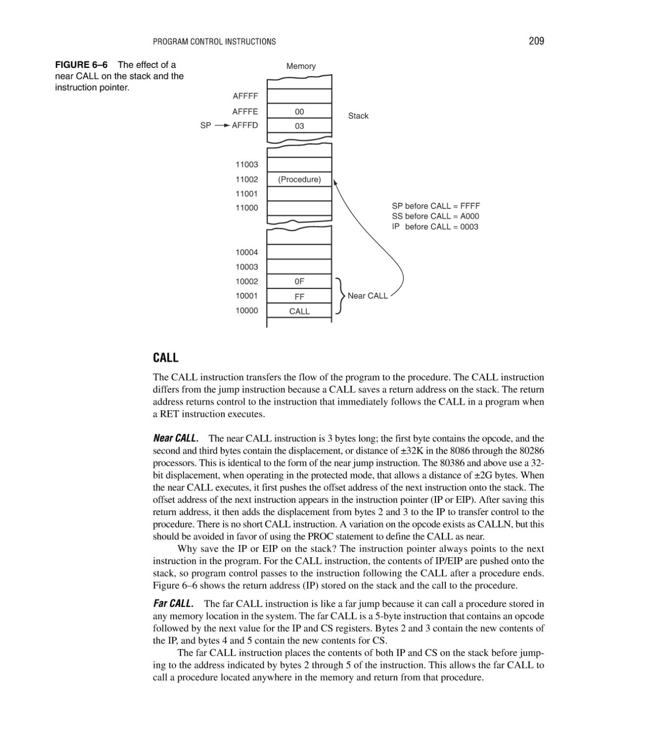
CALL 209; RET 211
192
CONTENTS
xiii
6–4 Introduction to Interrupts 213
Interrupt Vectors 213; Interrupt Instructions 214; Interrupt Control 215;
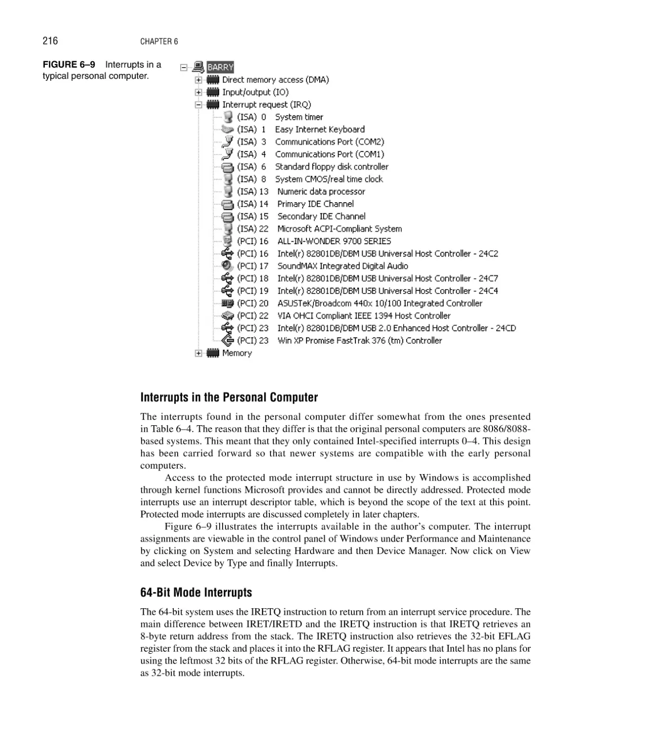
Interrupts in the Personal Computer 216; 64-Bit Mode Interrupts 216
6–5 Machine Control and Miscellaneous Instructions 217
Controlling the Carry Flag Bit 217; WAIT 217; HLT 217; NOP 217;
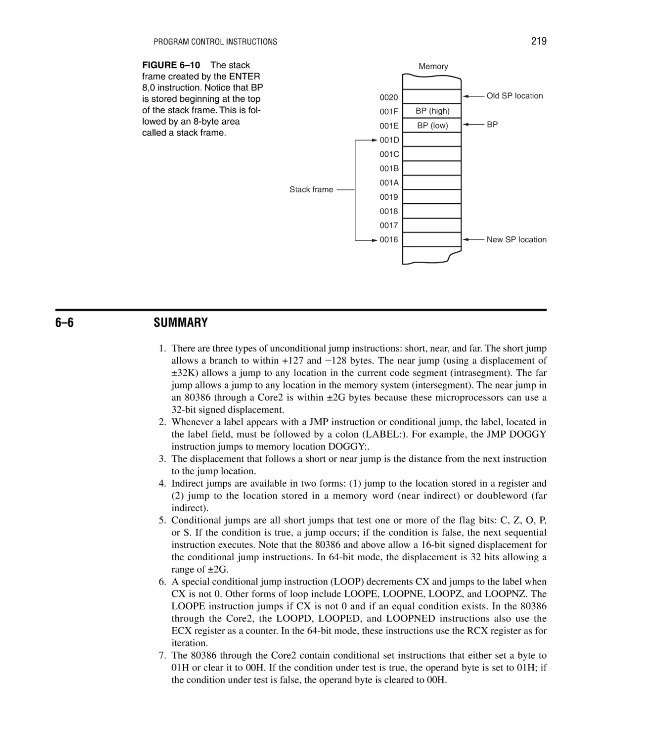
LOCK Prefix 218; ESC 218; BOUND 218; ENTER and LEAVE 218
6–6 Summary 219
6–7 Questions and Problems 221
CHAPTER 7
USING ASSEMBLY LANGUAGE WITH C/C++
223
Introduction/Chapter Objectives 223
7–1 Using Assembly Language with C++ for 16-Bit DOS Applications 224
Basic Rules and Simple Programs 224; What Cannot Be Used from MASM Inside
an _asm Block 226; Using Character Strings 226; Using Data Structures 227;
An Example of a Mixed-Language Program 229
7–2 Using Assembly Language with Visual C/C++ for 32-Bit Applications 231
An Example that Uses Console I/O to Access the Keyboard and Display 231;
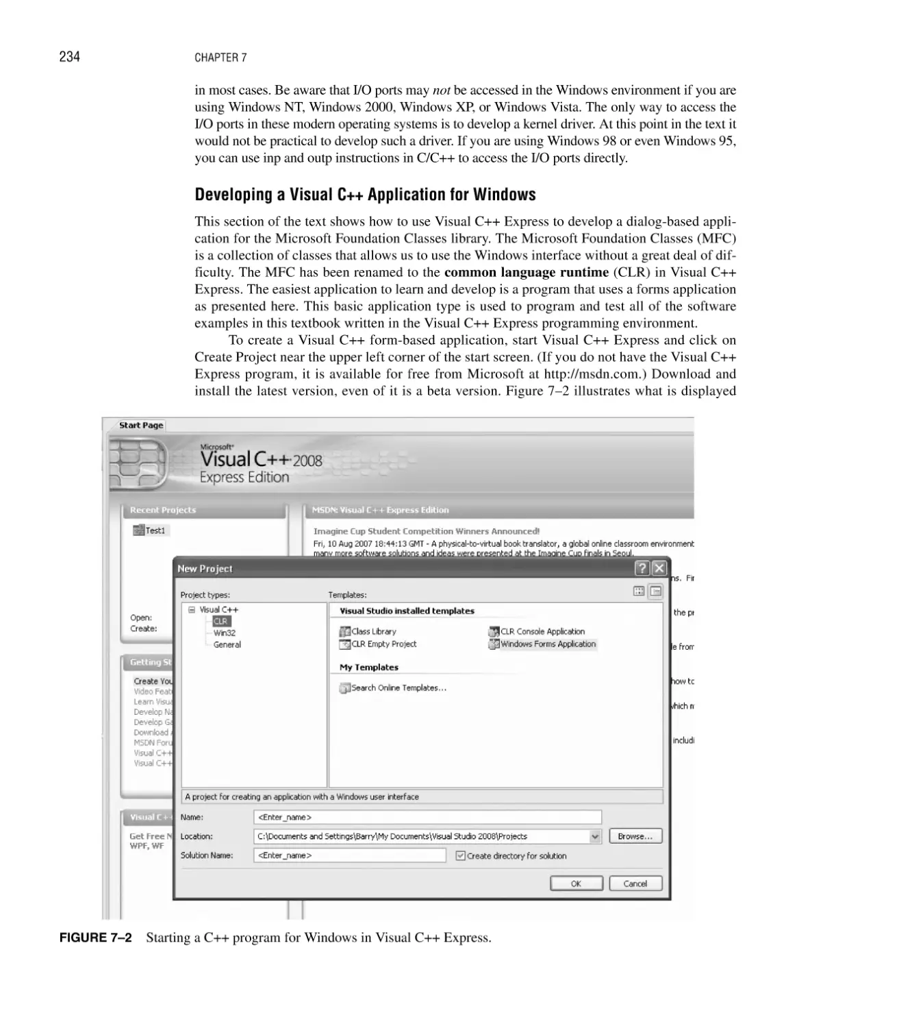
Directly Addressing I/O Ports 233; Developing a Visual C++ Application for Windows 234
7–3 Mixed Assembly and C++ Objects 242
Linking Assembly Language with Visual C++ 242; Adding New Assembly Language
Instructions to C/C++ Programs 247
7–4 Summary 247
7–5 Questions and Problems 248
CHAPTER 8
PROGRAMMING THE MICROPROCESSOR
250
Introduction/Chapter Objectives 250
8–1 Modular Programming 251
The Assembler and Linker 251; PUBLIC and EXTRN 253; Libraries 254; Macros 257
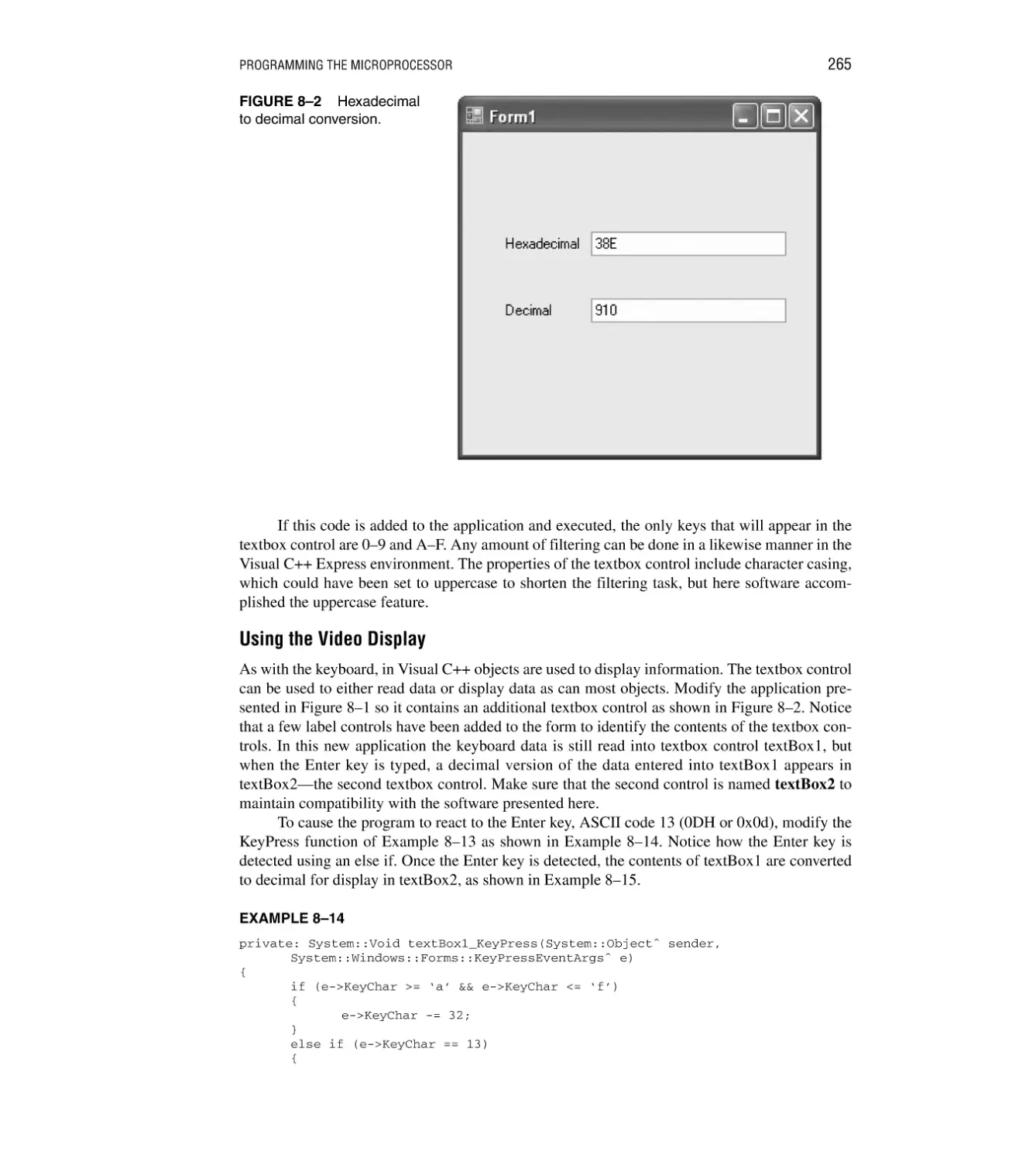
8–2 Using the Keyboard and Video Display 259
Reading the Keyboard 259; Using the Video Display 265; Using a Timer in a Program 267;
The Mouse 269
8–3 Data Conversions 271
Converting from Binary to ASCII 272; Converting from ASCII to Binary 274;
Displaying and Reading Hexadecimal Data 274; Using Lookup Tables for Data
Conversions 276; An Example Program Using a Lookup Table 278
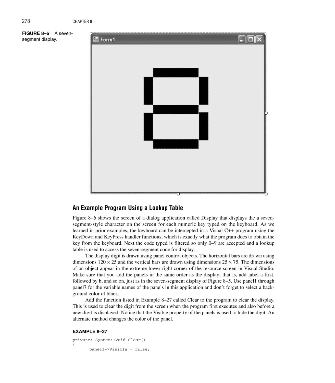
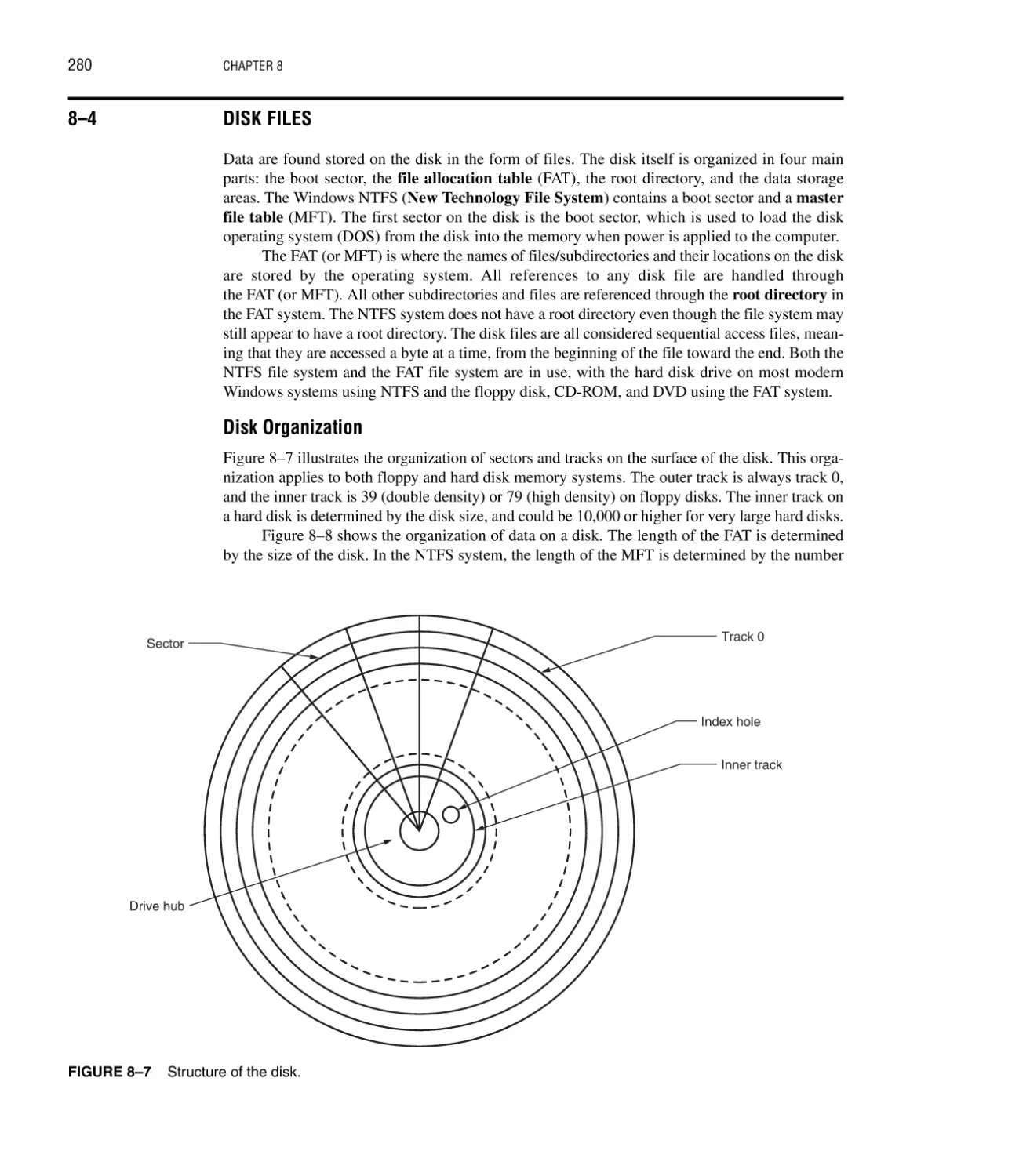
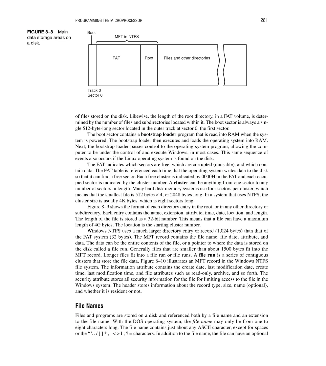
8–4 Disk Files 280
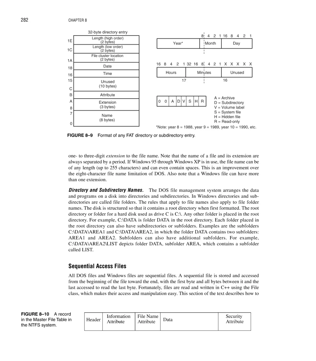
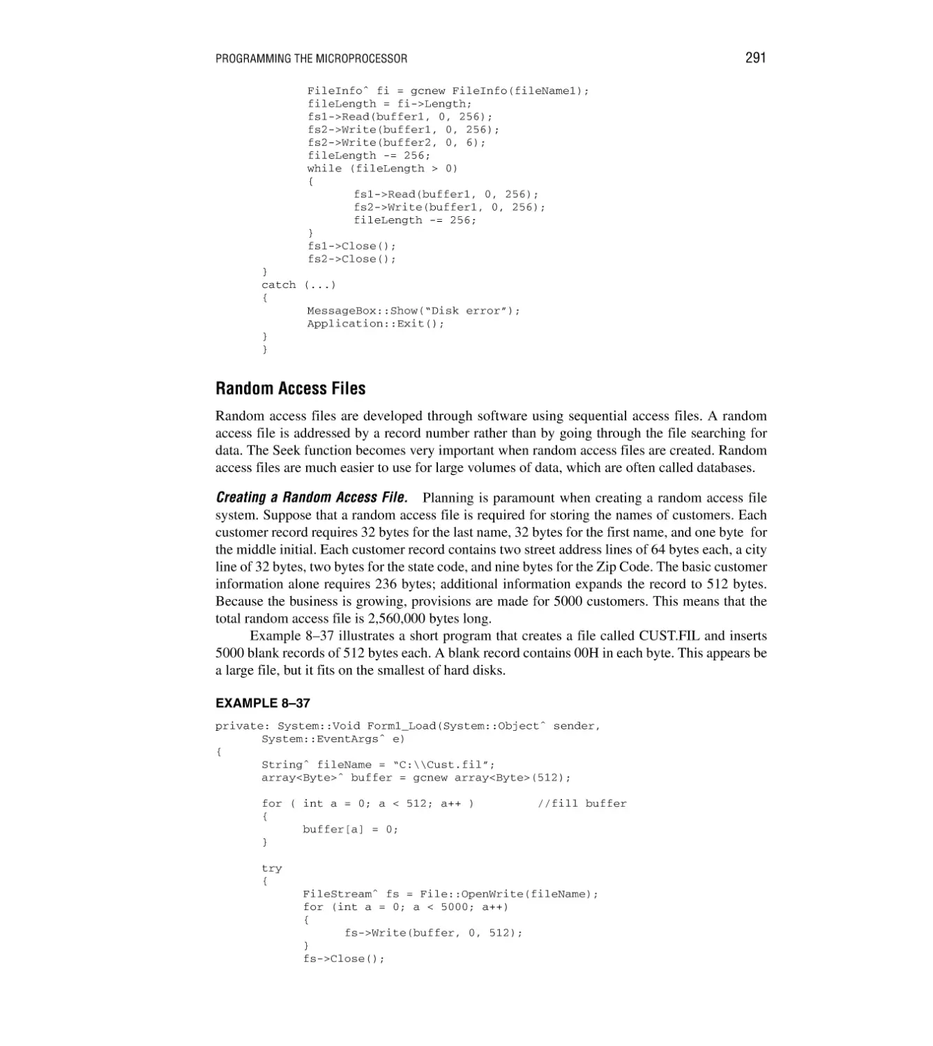
Disk Organization 280; File Names 281; Sequential Access Files 282;
Random Access Files 291
8–5 Example Programs 294
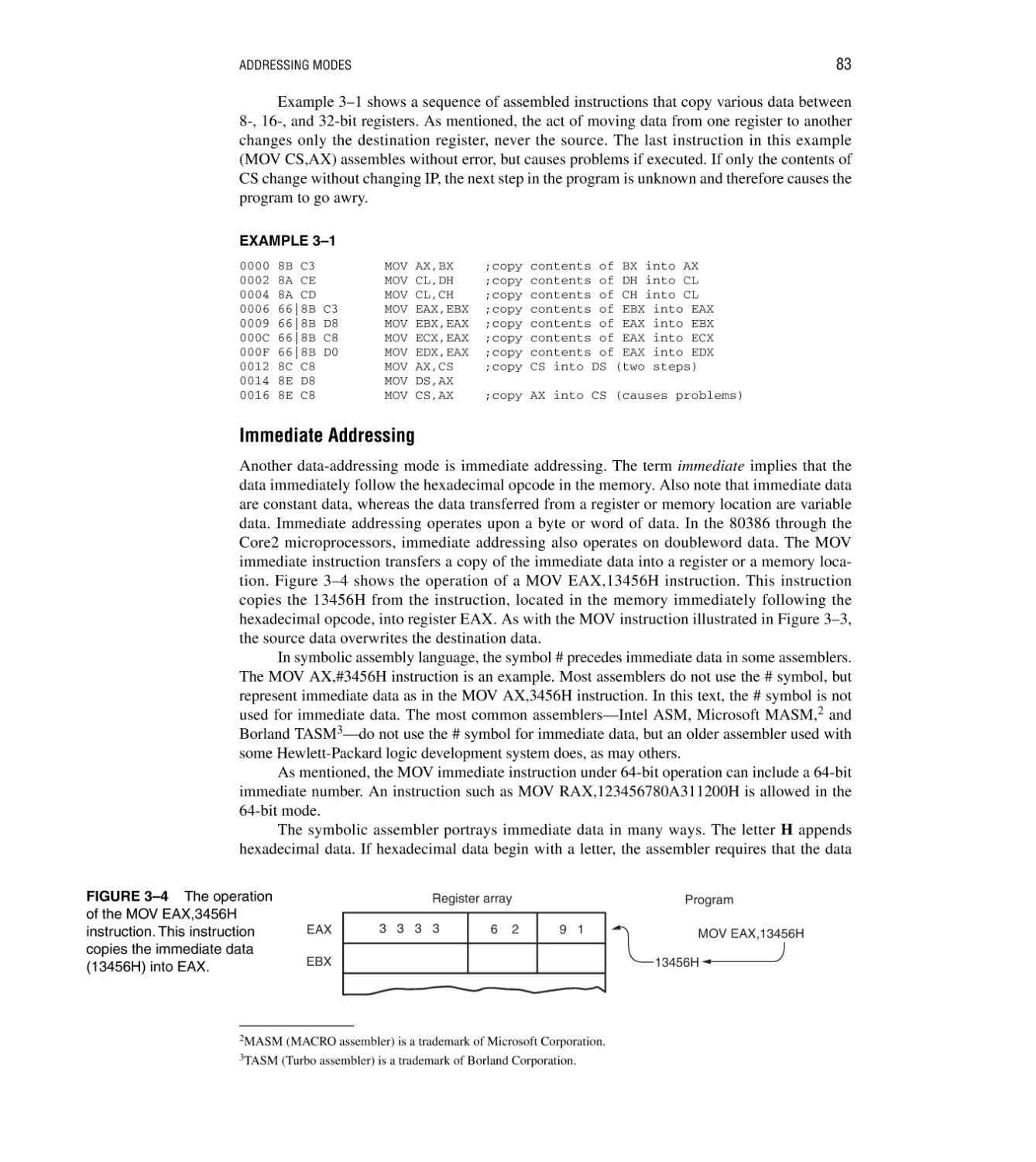
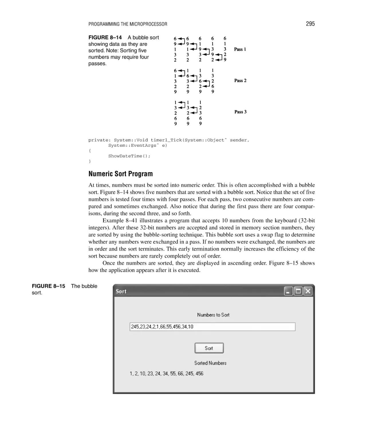
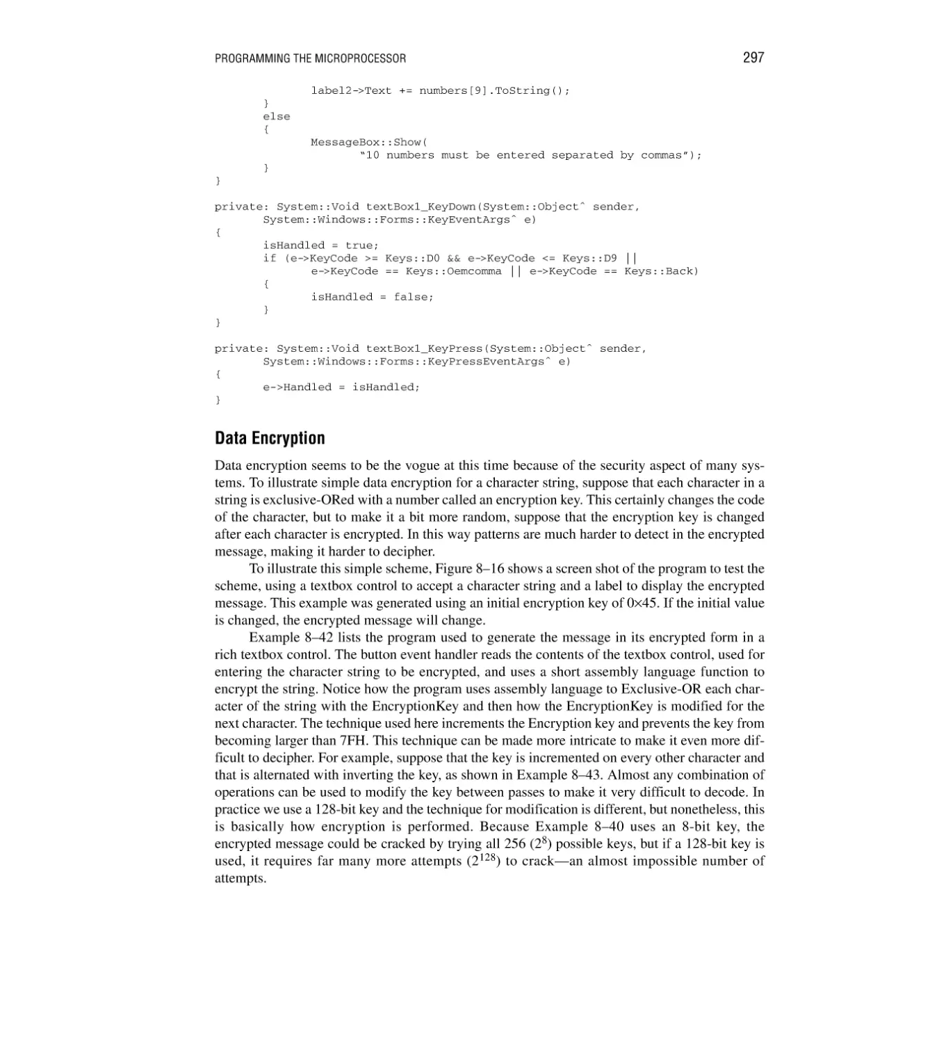
Time/Date Display Program 294; Numeric Sort Program 295; Data Encryption 297
8–6 Summary 299
8–7 Questions and Problems 300
CHAPTER 9
8086/8088 HARDWARE SPECIFICATIONS
Introduction/Chapter Objectives 302
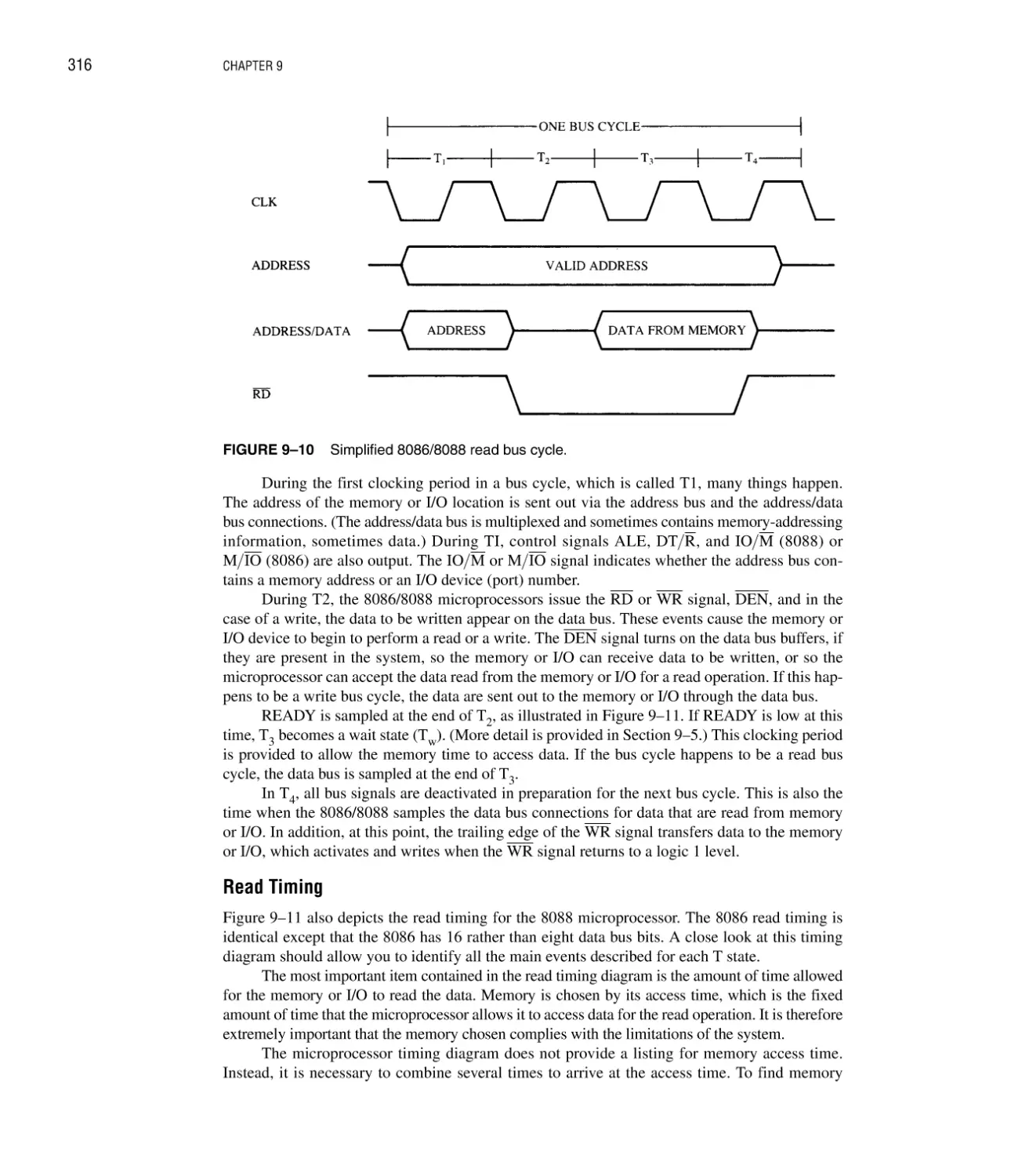
9–1 Pin-Outs and the Pin Functions 302
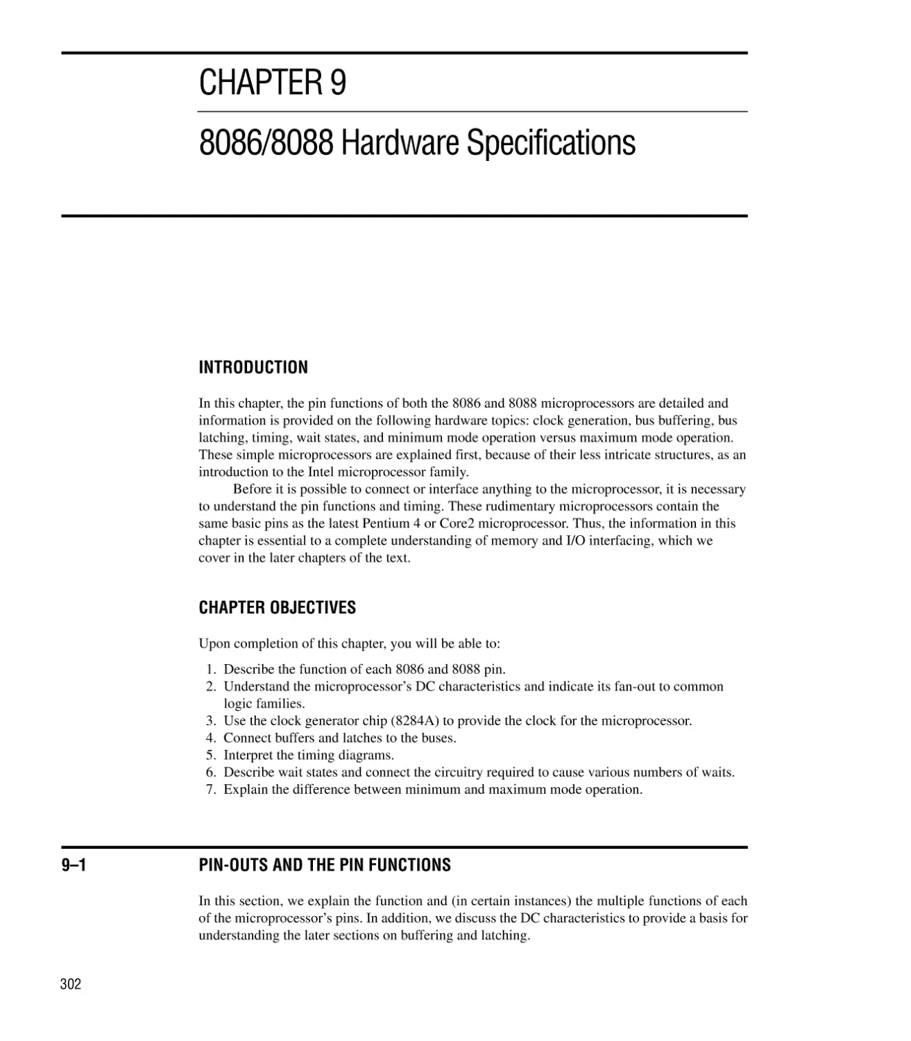
The Pin-Out 303; Power Supply Requirements 303; DC Characteristics 303;
Pin Connections 304
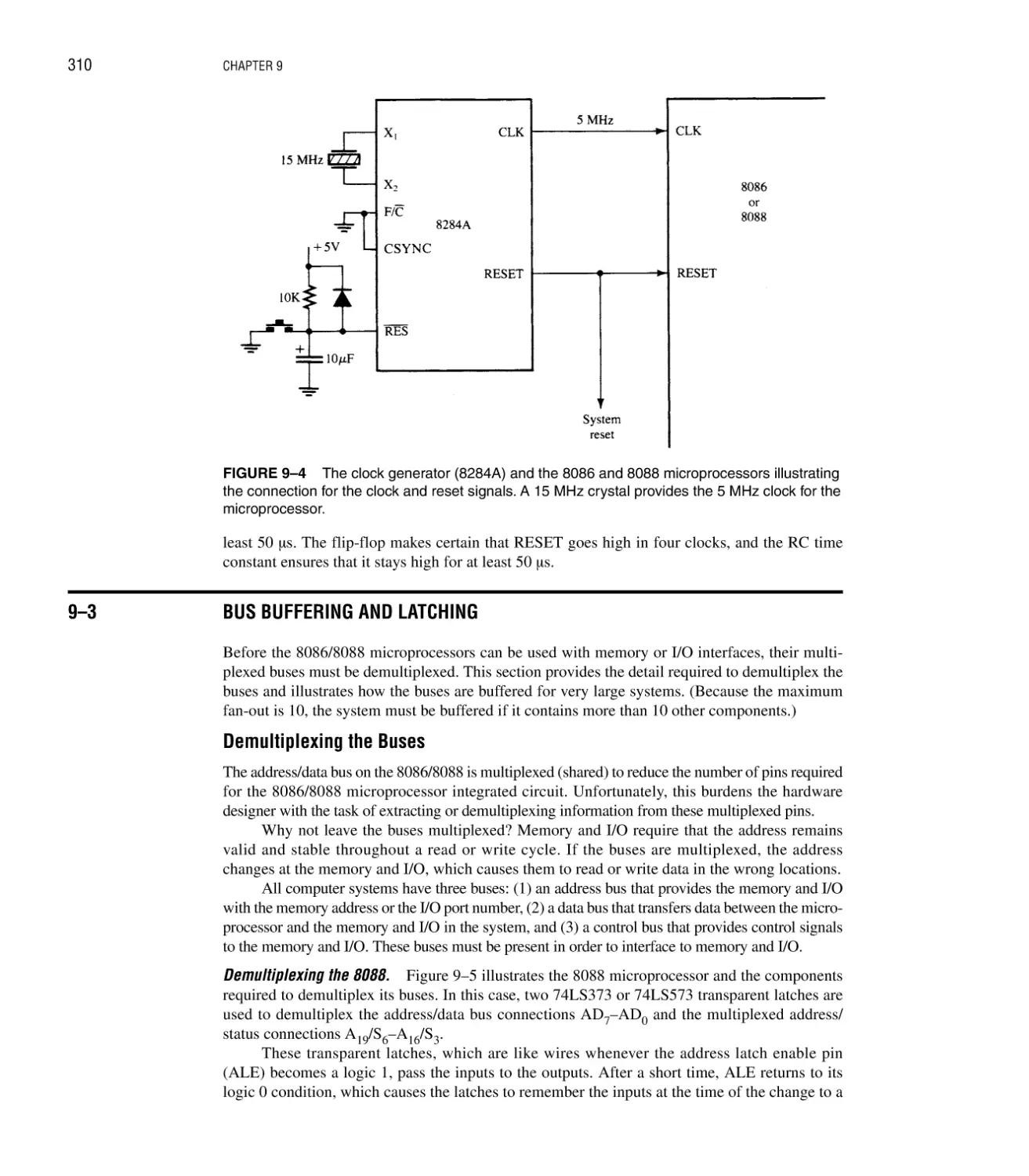
9–2 Clock Generator (8284A) 307
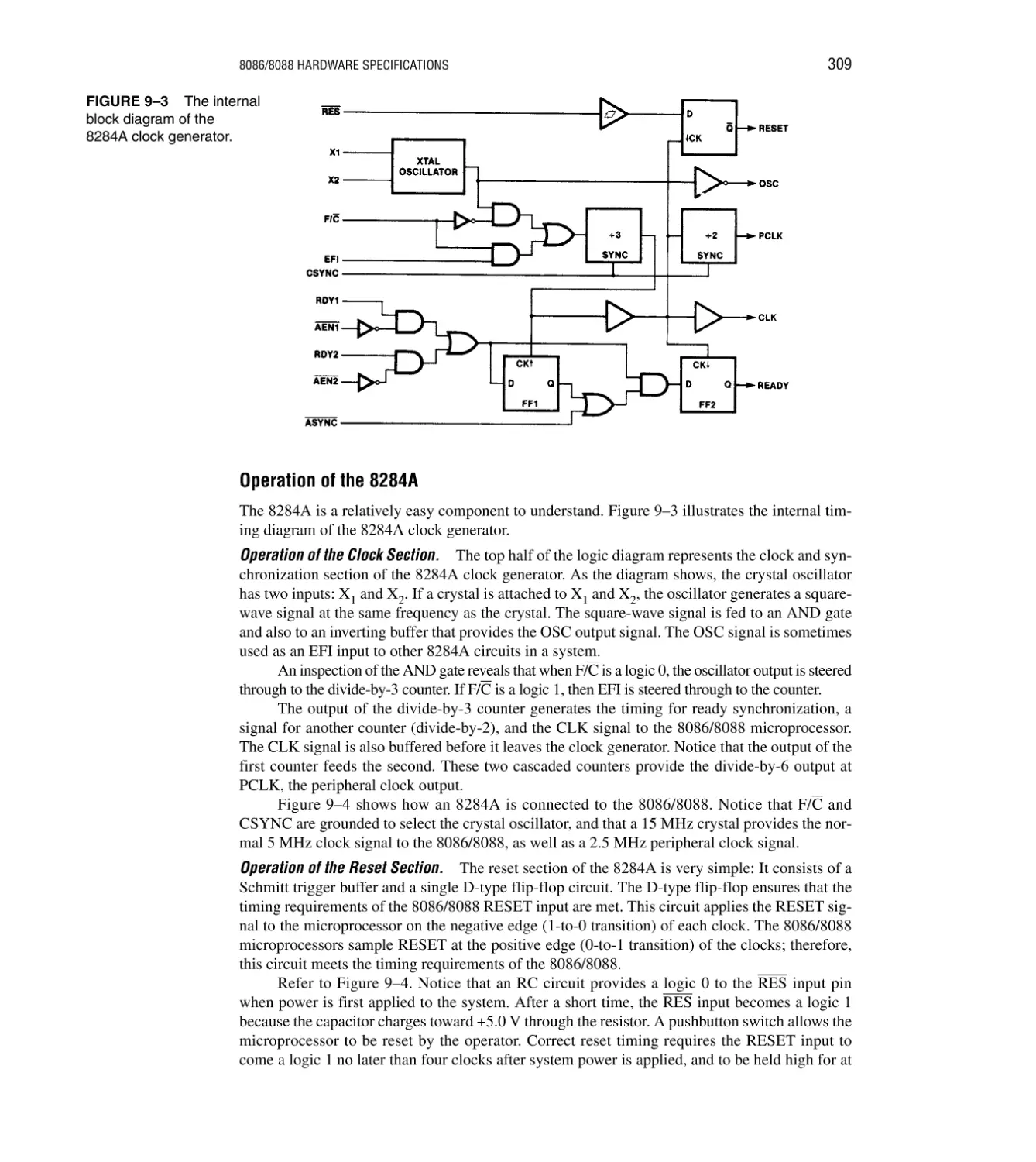
The 8284A Clock Generator 307; Operation of the 8284A 309
9–3 Bus Buffering and Latching 310
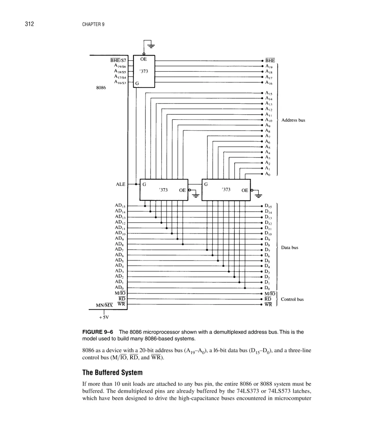
Demultiplexing the Buses 310; The Buffered System 312
9–4 Bus Timing 315
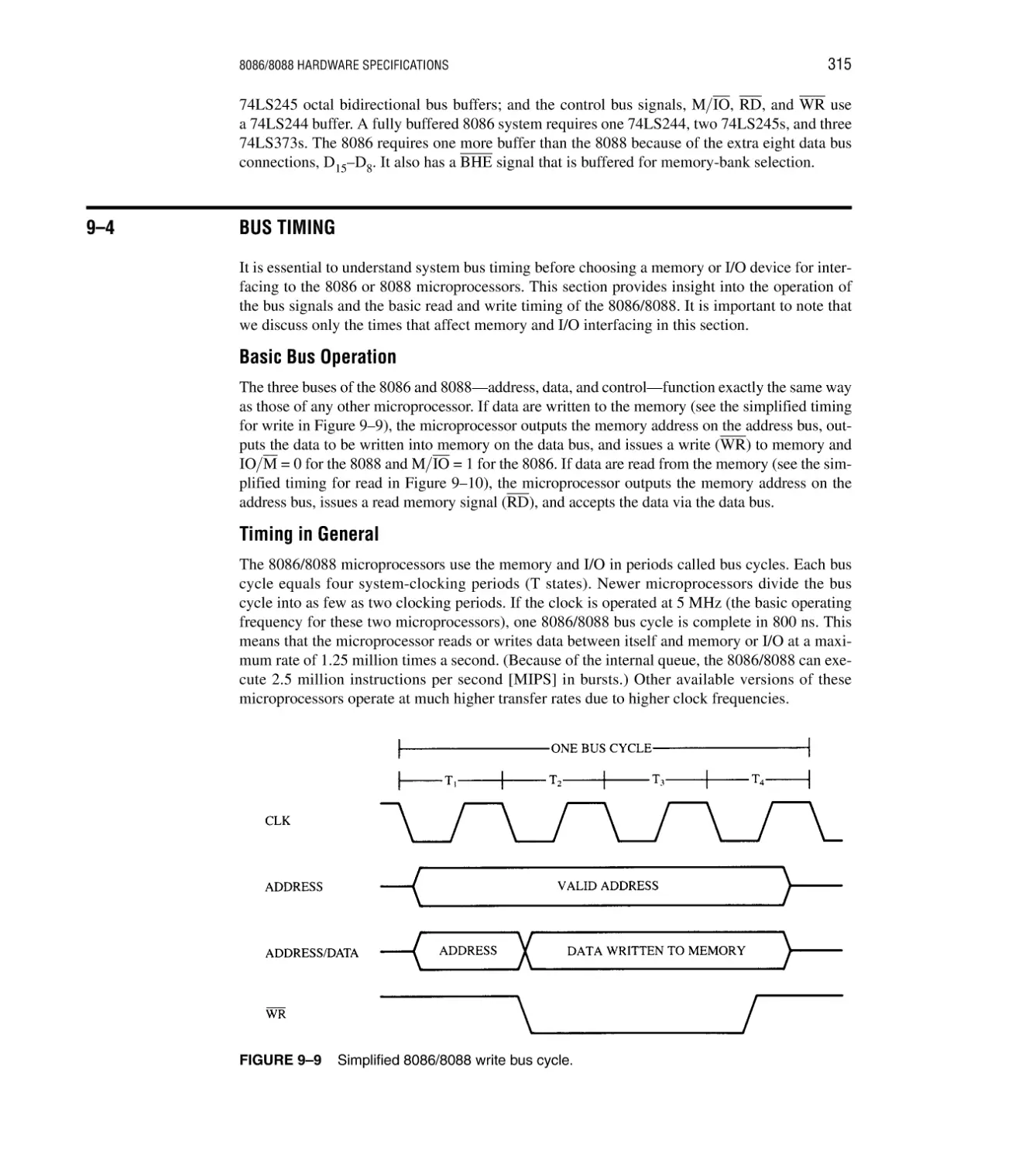
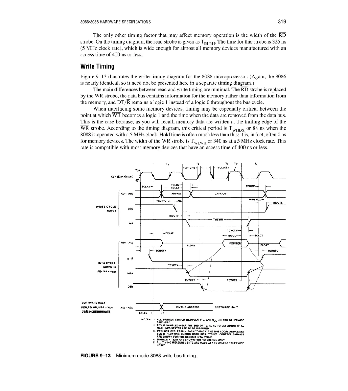
Basic Bus Operation 315; Timing in General 315; Read Timing 316; Write Timing 319
302
xiv
CONTENTS
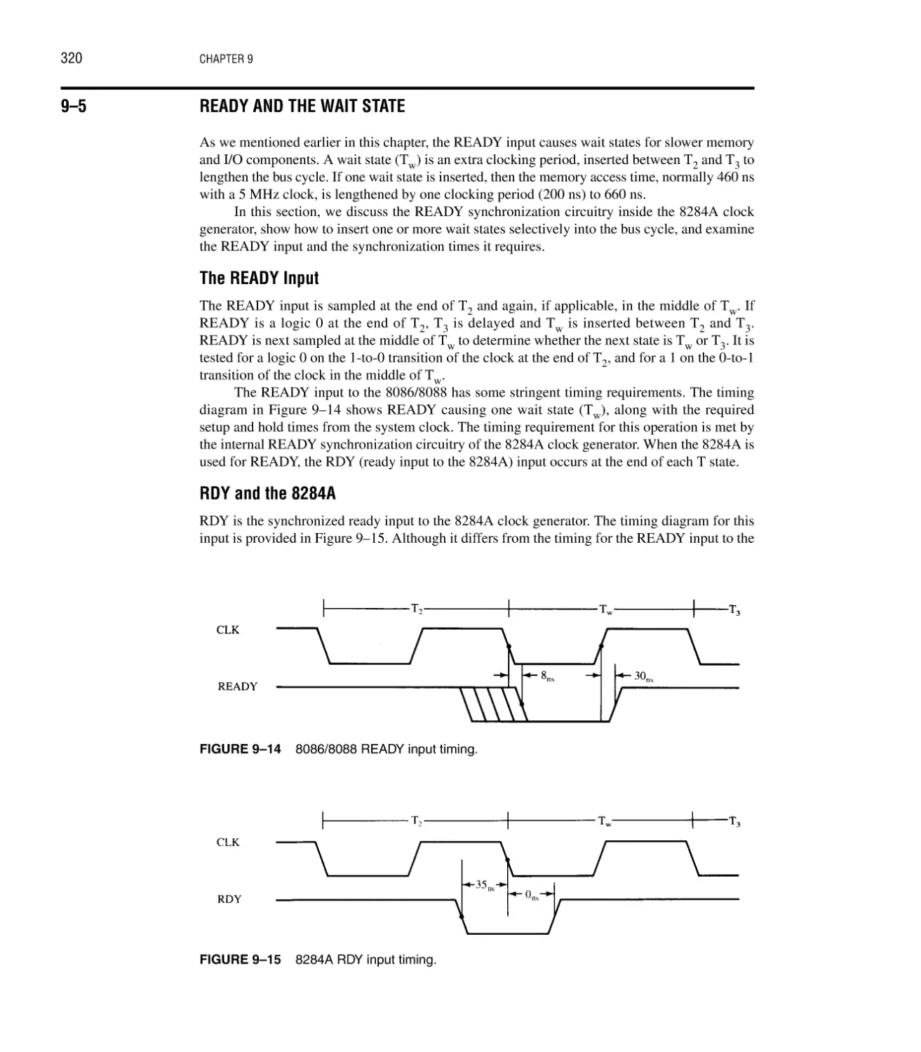
9–5 Ready and the Wait State 320
The READY Input 320; RDY and the 8284A 320
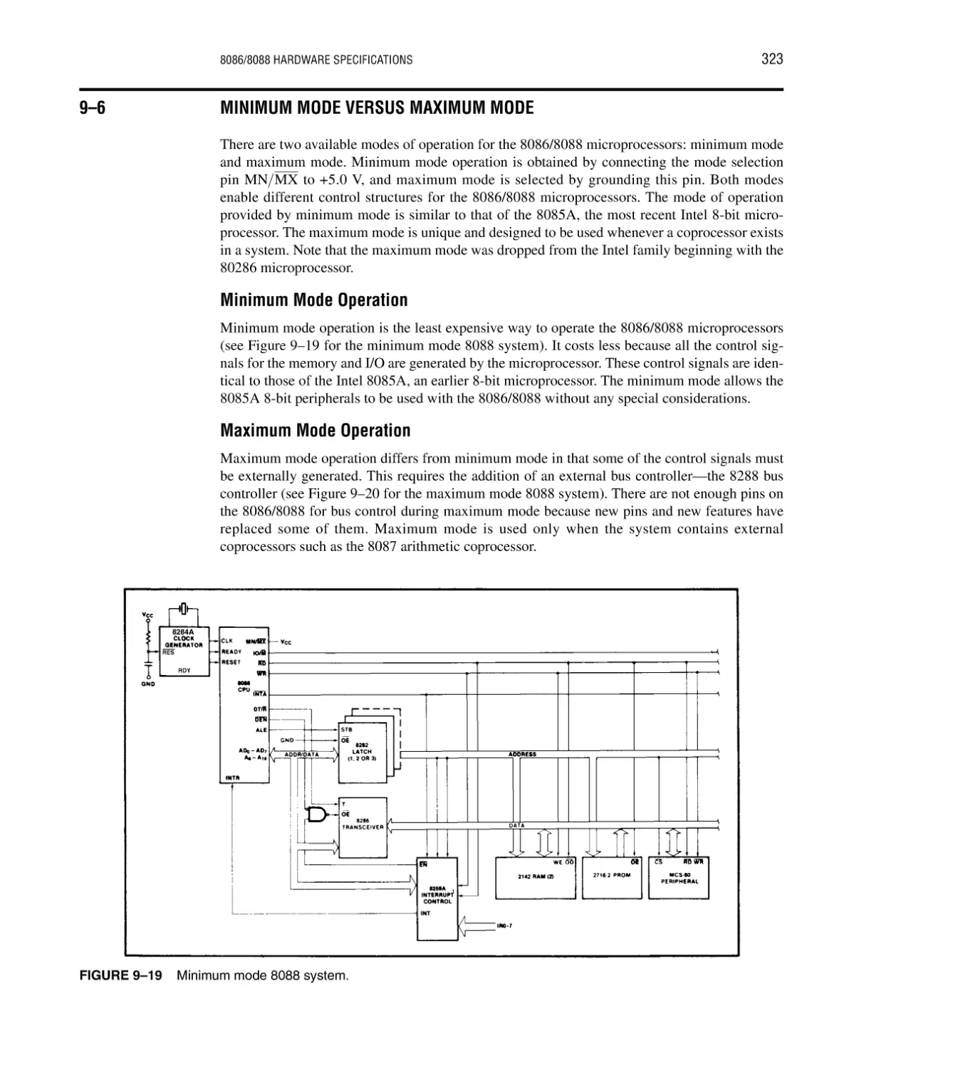
9–6 Minimum Mode versus Maximum Mode 323
Minimum Mode Operation 323; Maximum Mode Operation 323;
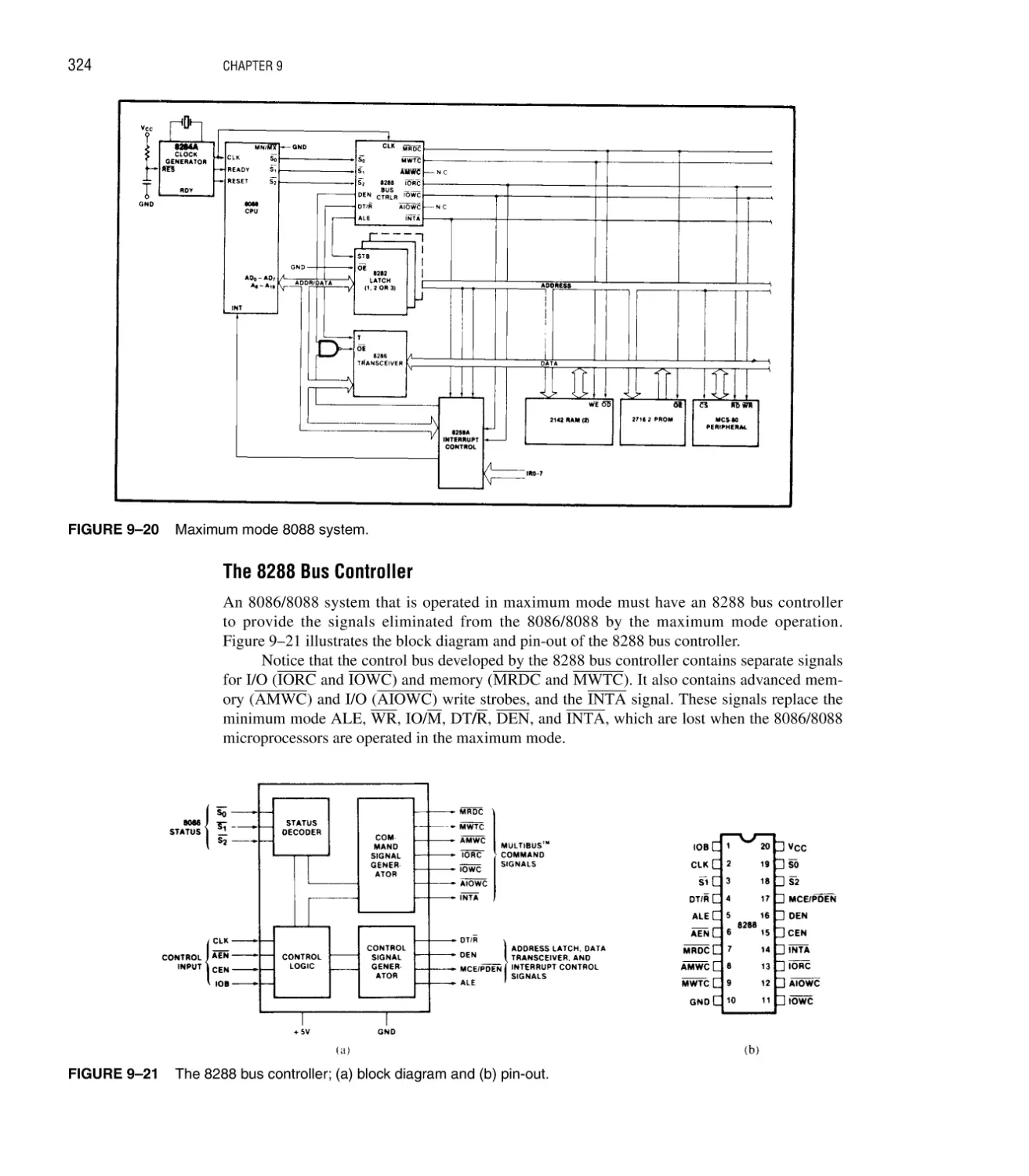
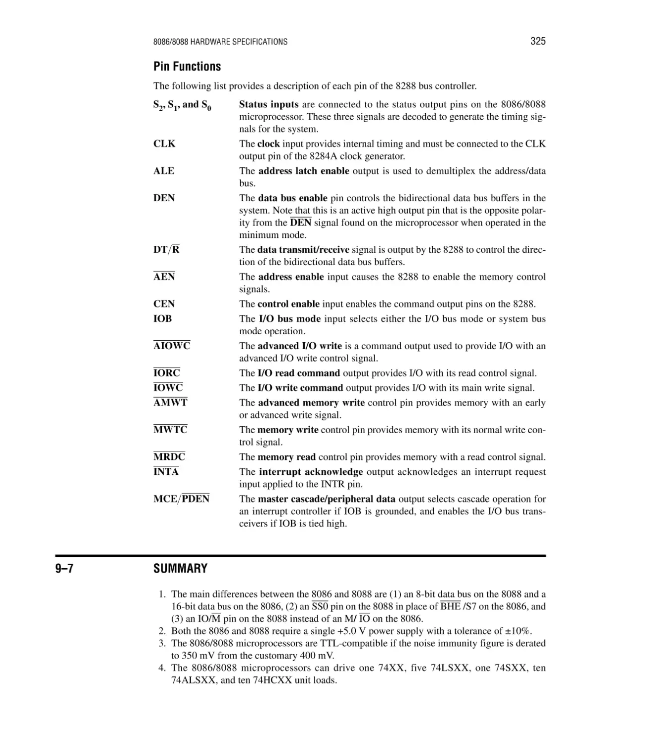
The 8288 Bus Controller 324; Pin Functions 325
9–7 Summary 325
9–8 Questions and Problems 326
CHAPTER 10
MEMORY INTERFACE
328
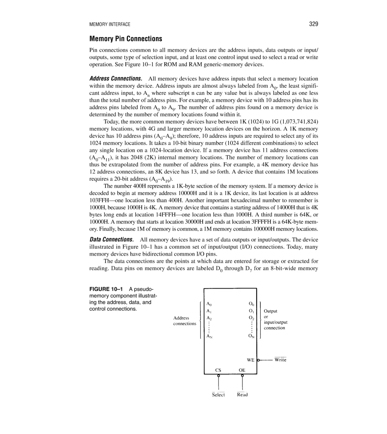
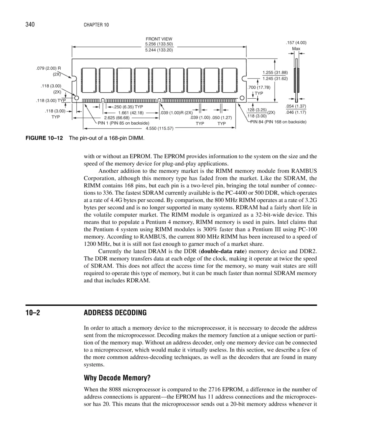
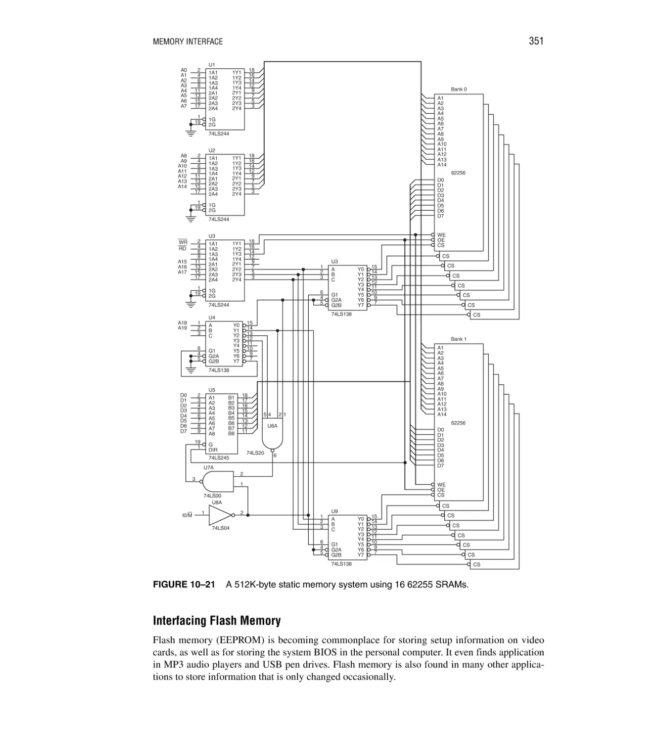
Introduction/Chapter Objectives 328
10–1 Memory Devices 328
Memory Pin Connections 329; ROM Memory 330; Static RAM (SRAM) Devices 332;
Dynamic RAM (DRAM) Memory 333
10–2 Address Decoding 340
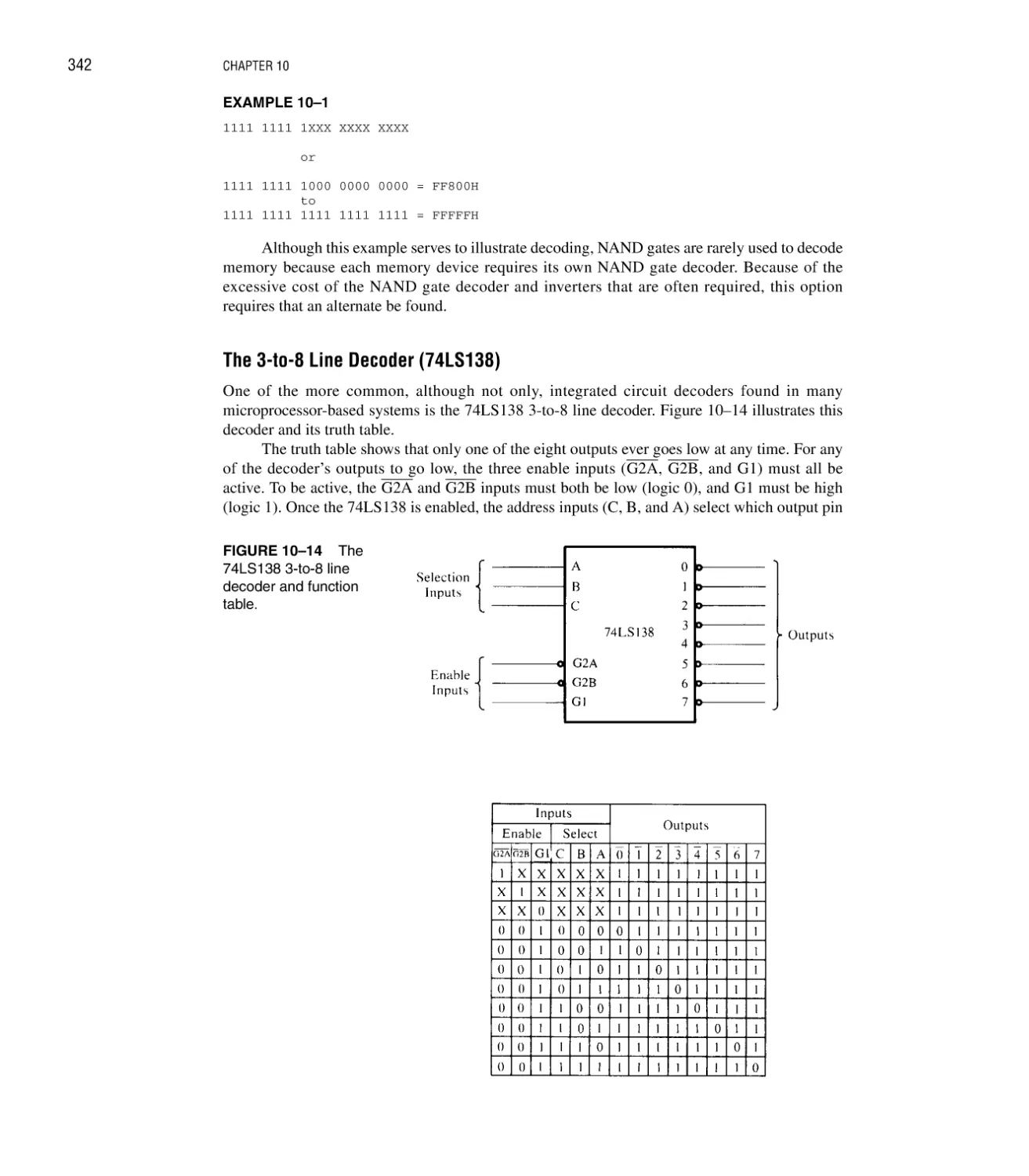
Why Decode Memory? 340; Simple NAND Gate Decoder 341; The 3-to-8 Line Decoder
(74LS138) 342; The Dual 2-to-4 Line Decoder (74LS139) 344; PLD Programmable
Decoders 344
10–3 8088 and 80188 (8-Bit) Memory Interface 349
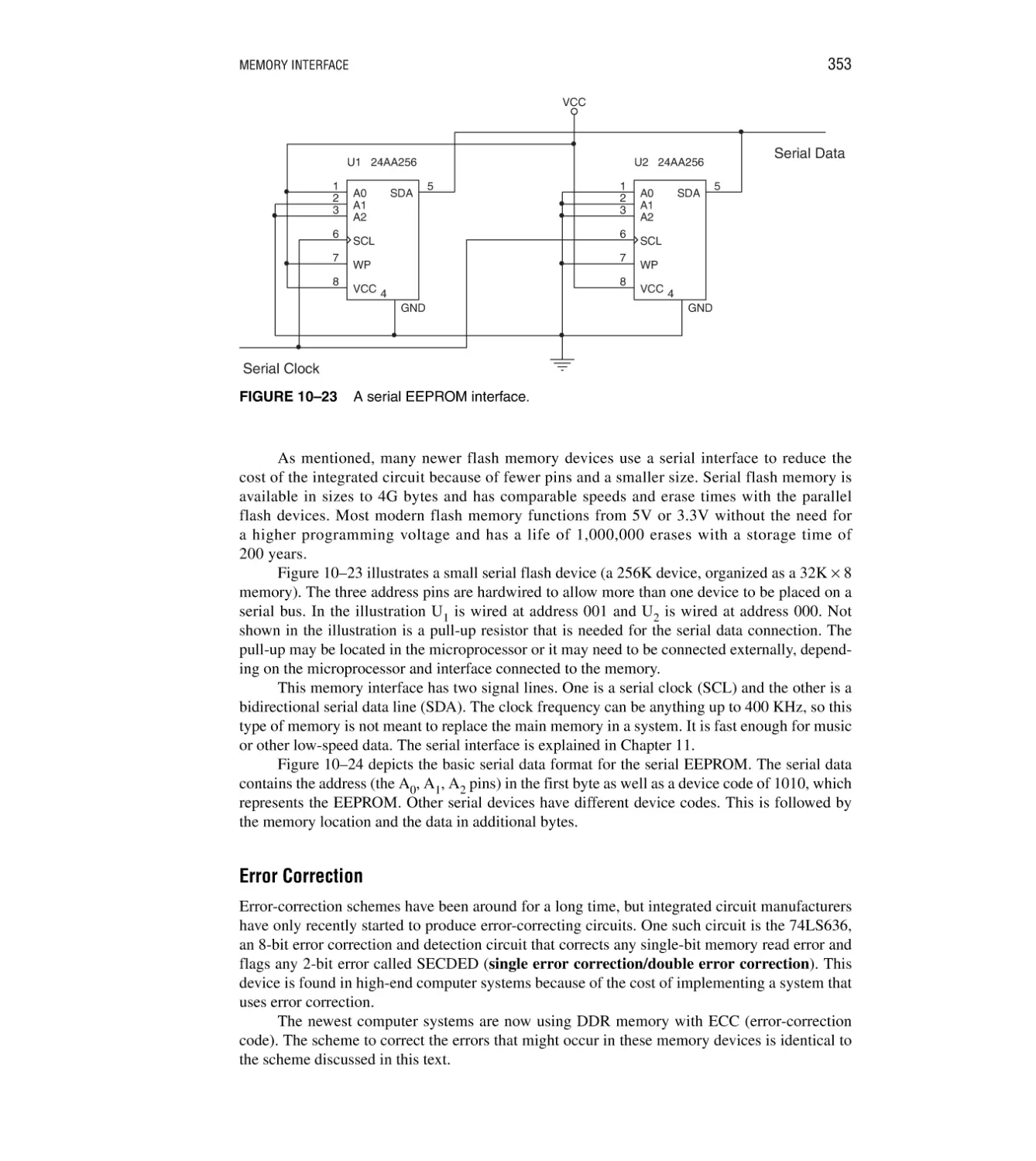
Basic 8088/80188 Memory Interface 349; Interfacing Flash Memory 351;
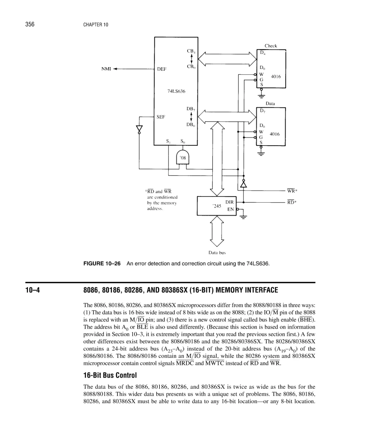
Error Correction 353
10–4 8086, 80186, 80286, and 80386SX (16-Bit) Memory Interface 356
16-Bit Bus Control 356
10–5 80386DX and 80486 (32-Bit) Memory Interface 363
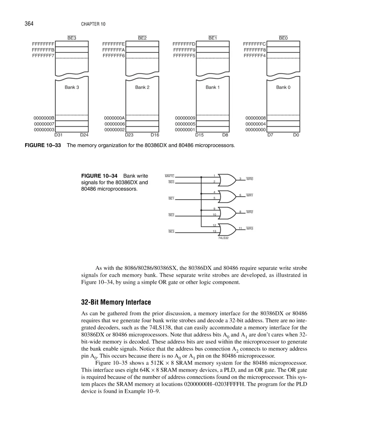
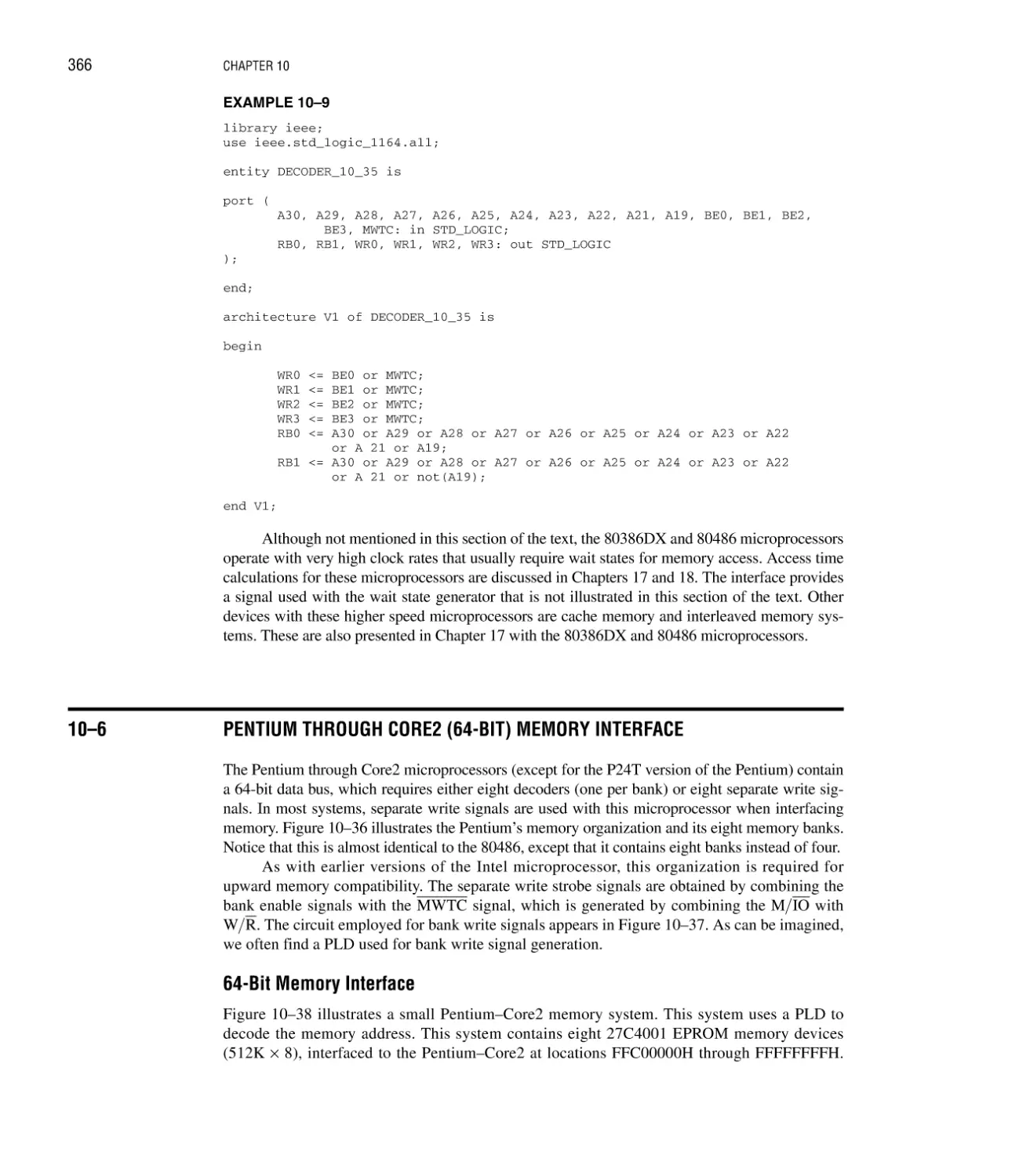
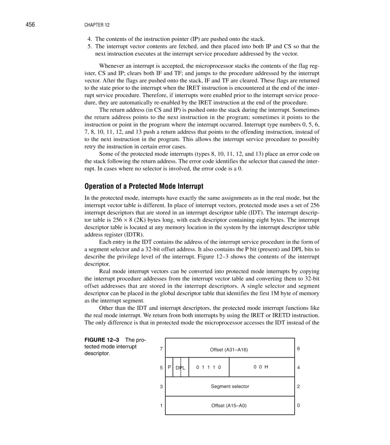
Memory Banks 363; 32-Bit Memory Interface 364
10–6 Pentium through Core2 (64-Bit) Memory Interface 366
64-Bit Memory Interface 366
10–7 Dynamic RAM 370
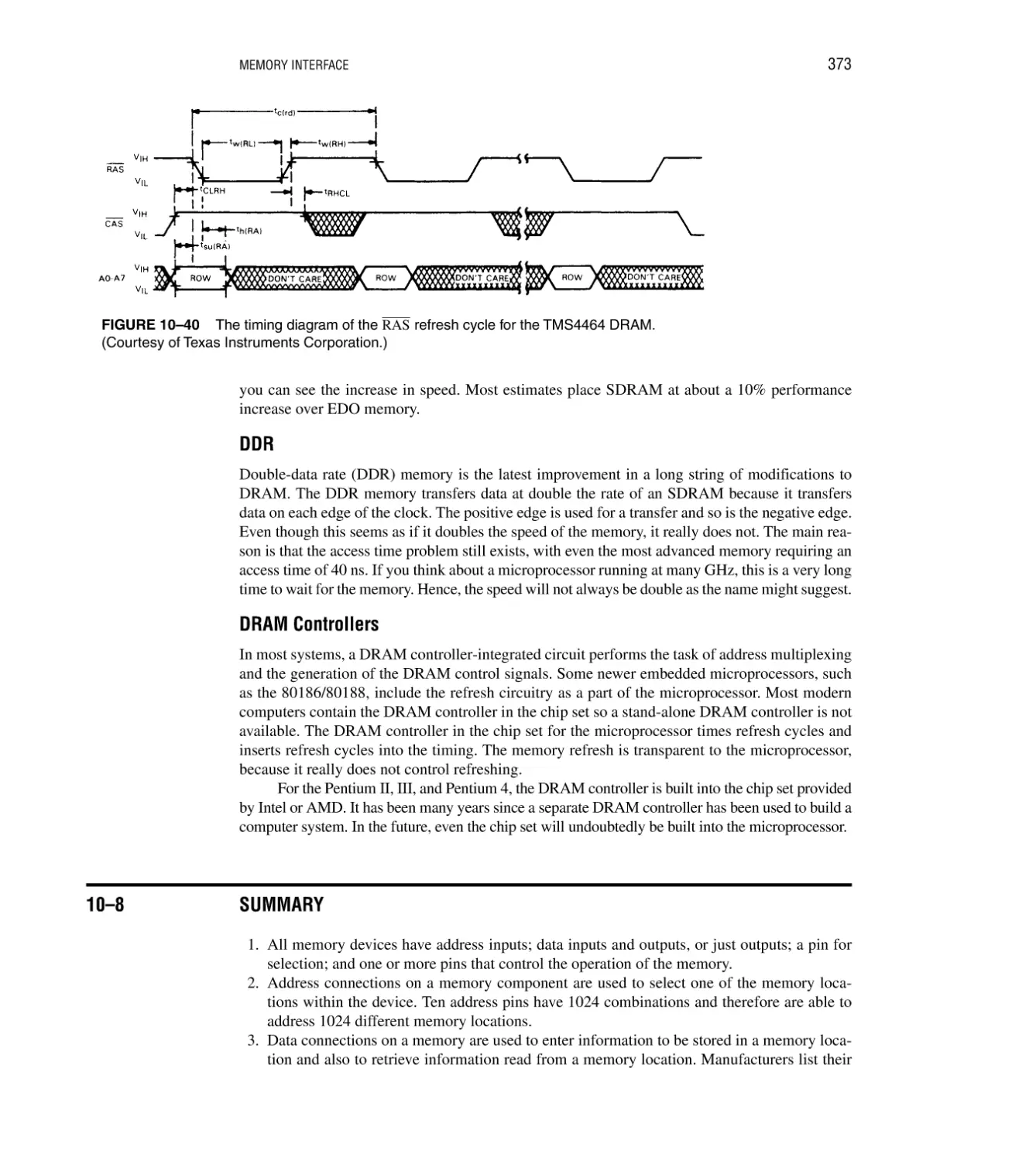
DRAM Revisited 370; EDO Memory 371; SDRAM 371; DDR 373; DRAM Controllers 373
10–8 Summary 373
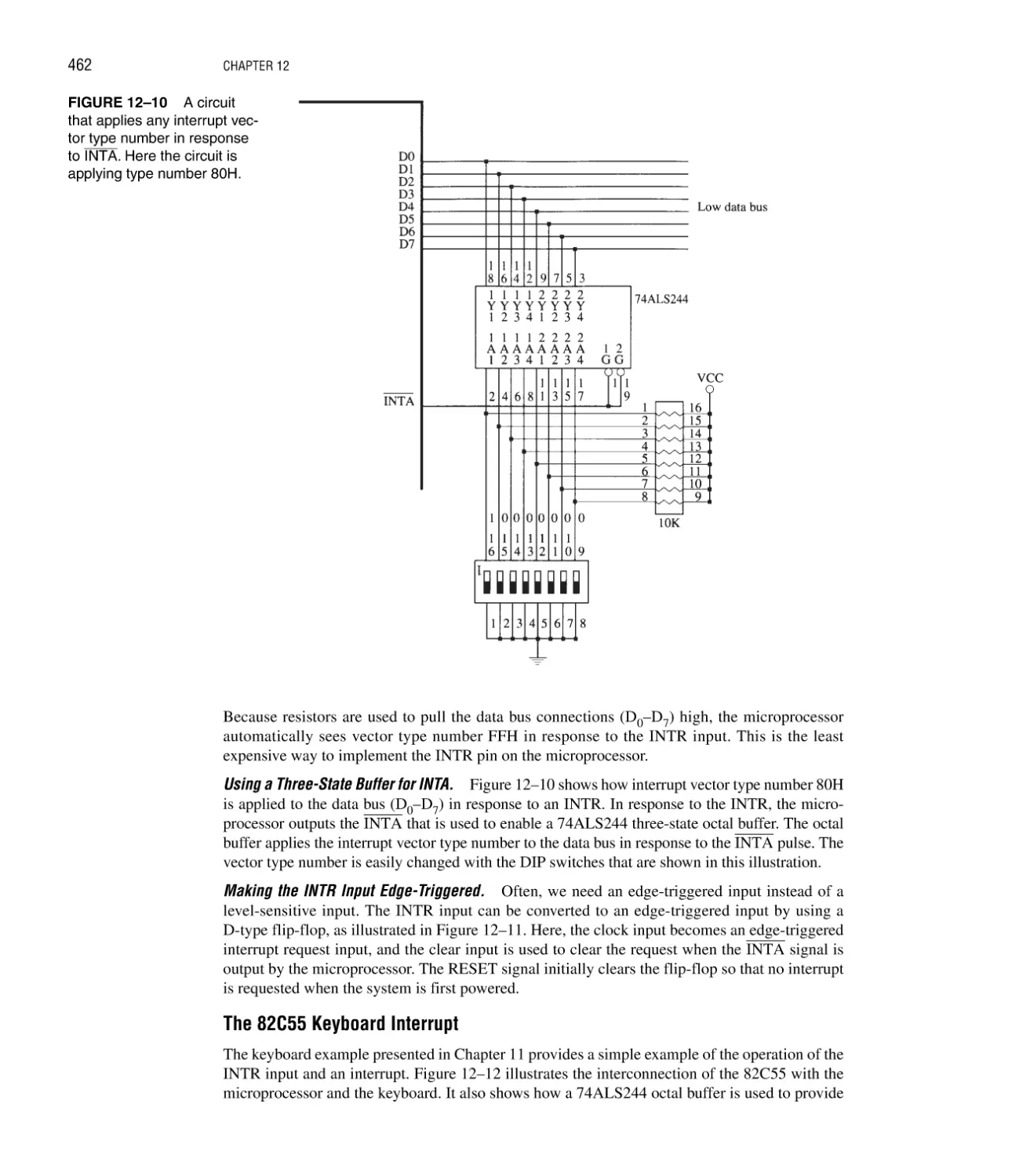
10–9 Questions and Problems 375
CHAPTER 11
BASIC I/O INTERFACE
Introduction/Chapter Objectives 377
11–1 Introduction to I/O Interface 377
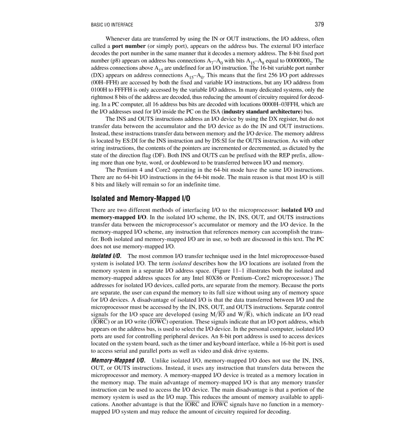
The I/O Instructions 378; Isolated and Memory-Mapped I/O 379; Personal Computer I/O
Map 380; Basic Input and Output Interfaces 380; Handshaking 382; Notes about
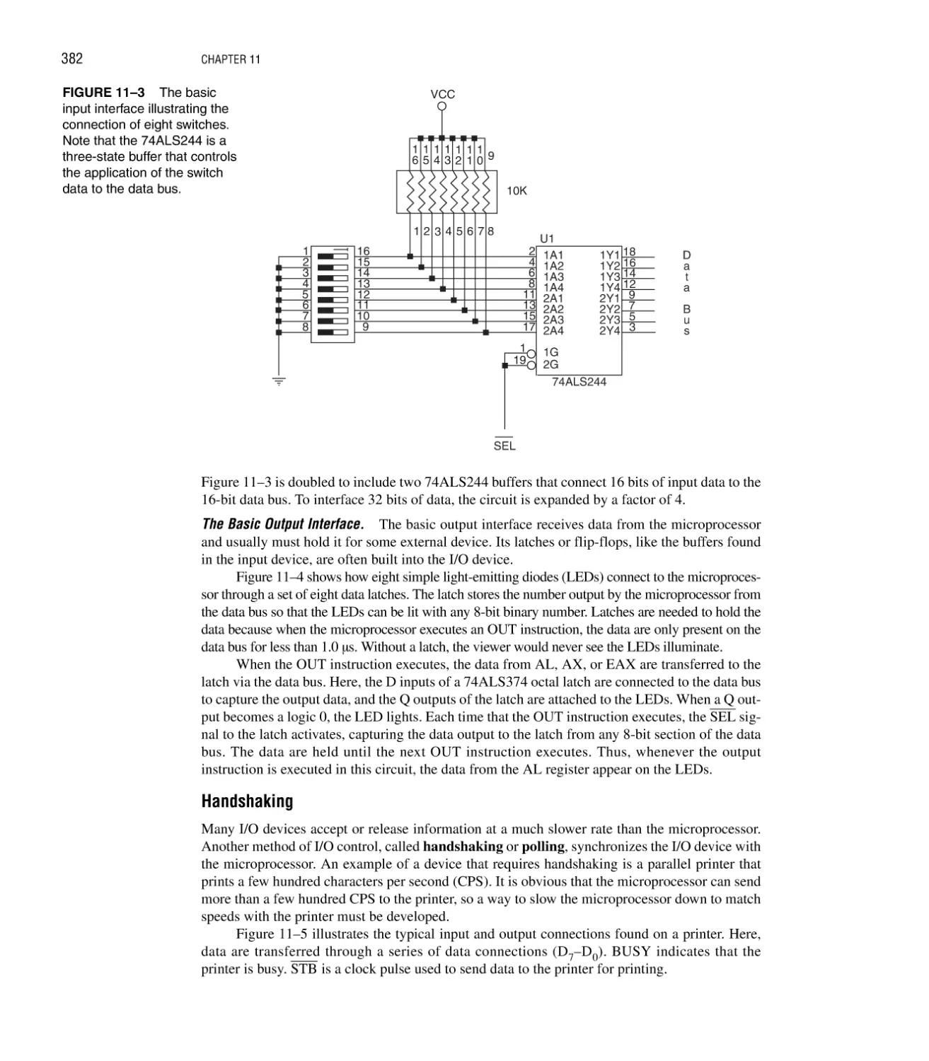
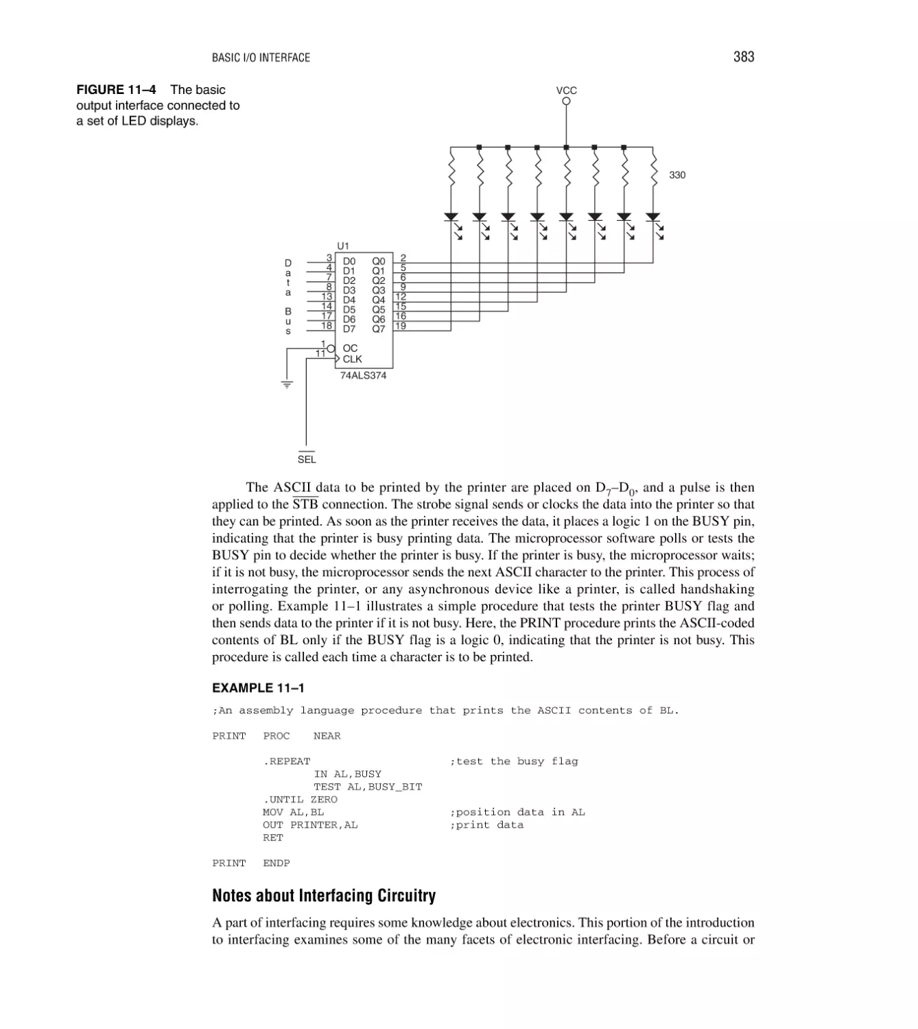
Interfacing Circuitry 383
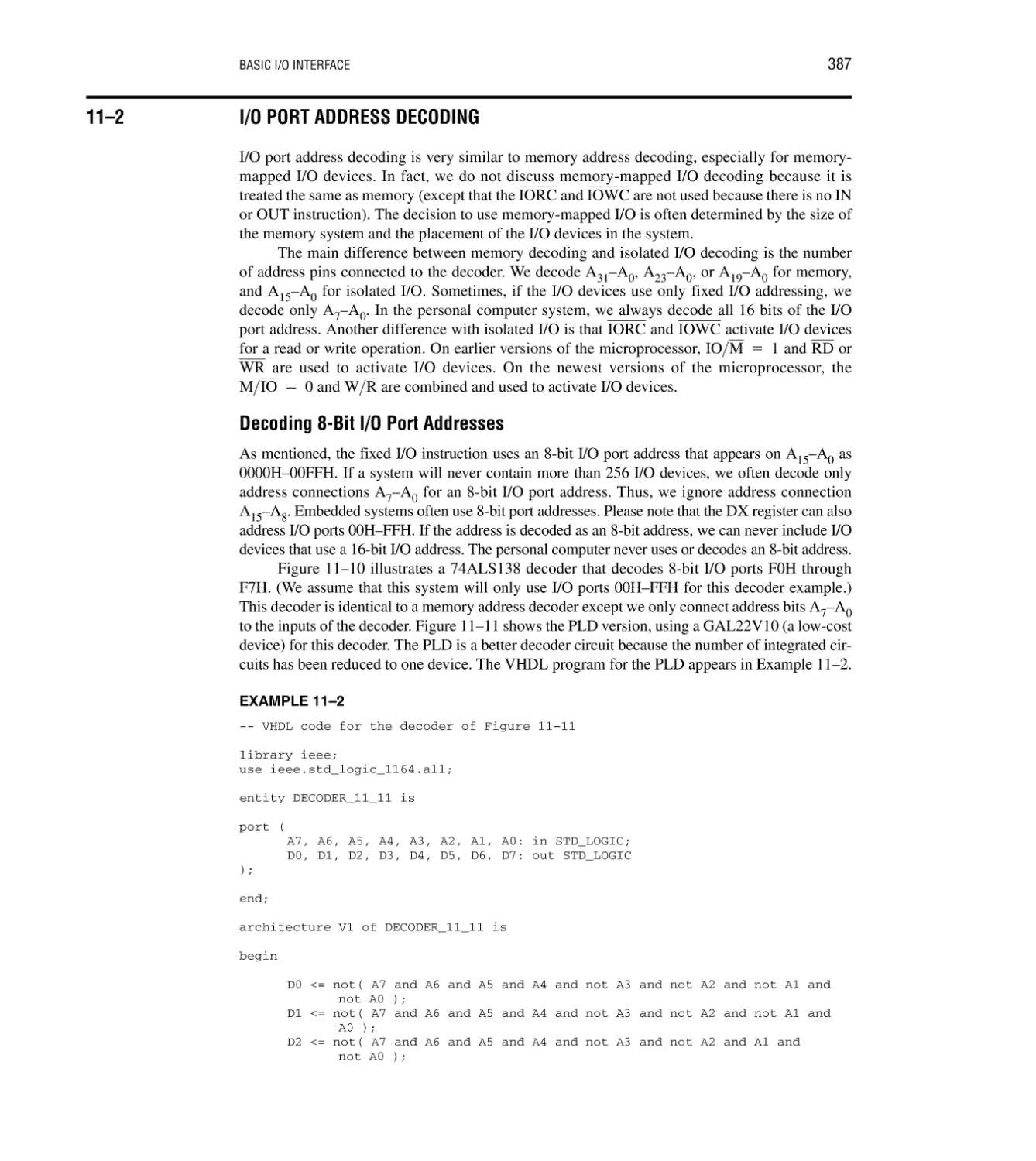
11–2 I/O Port Address Decoding 387
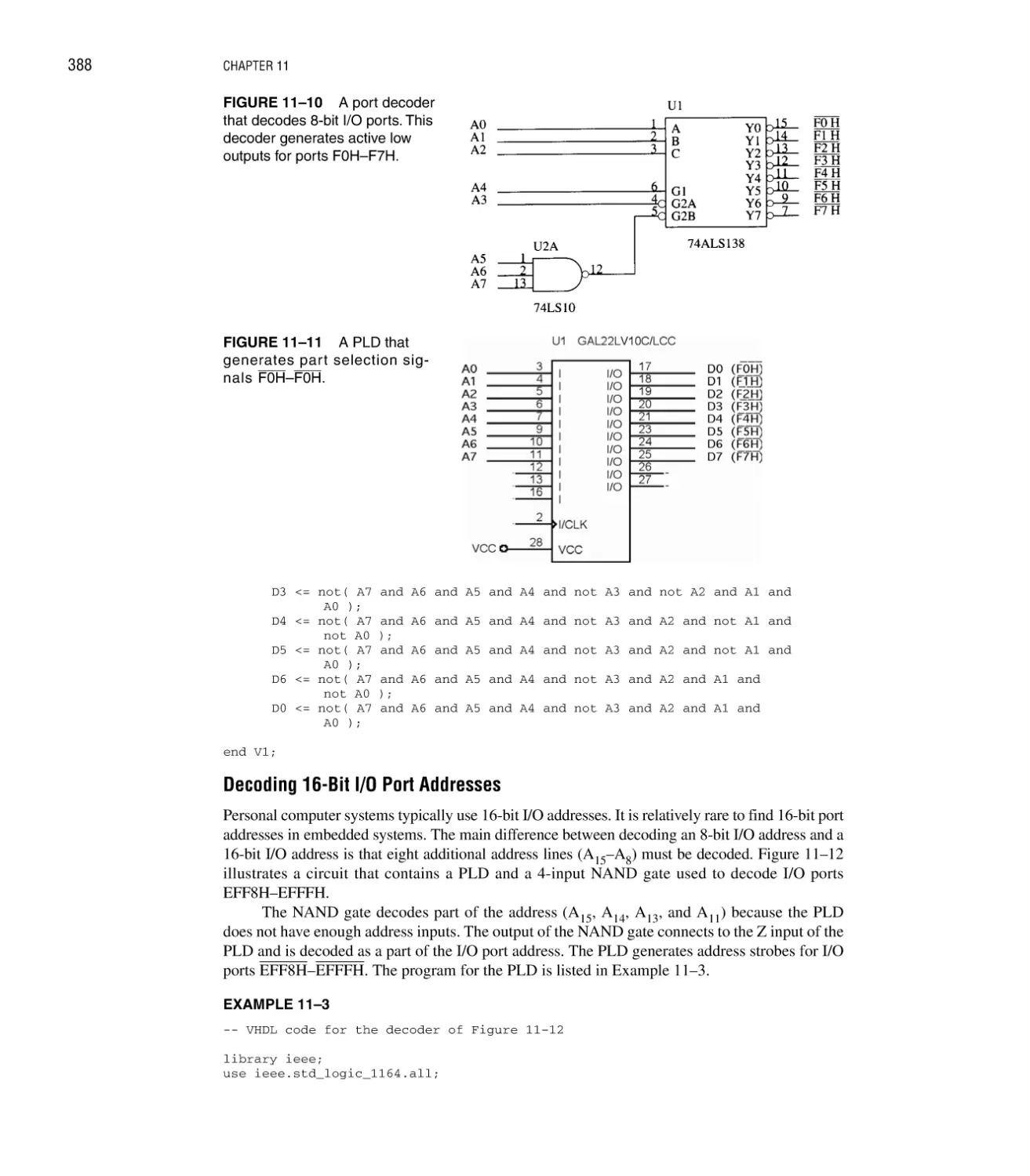
Decoding 8-Bit I/O Port Addresses 387; Decoding 16-Bit I/O Port Addresses 388;
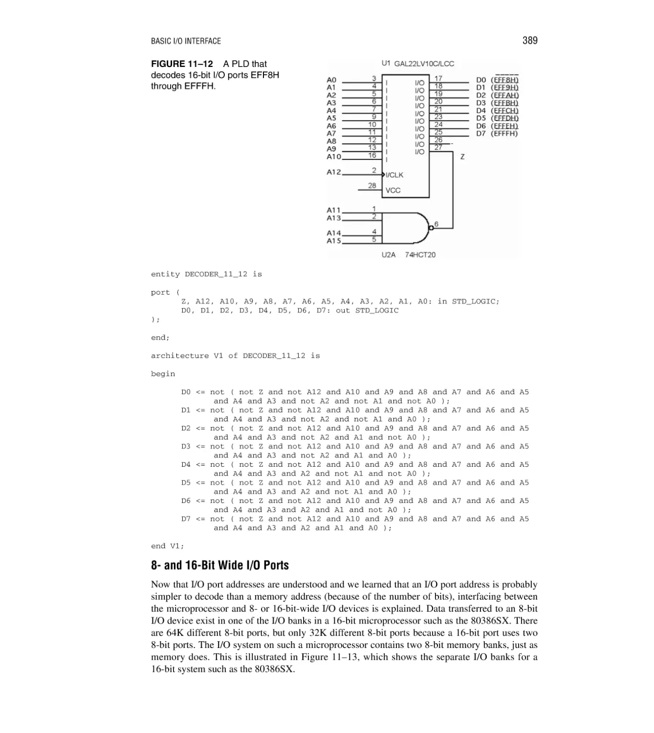
8- and 16-Bit-Wide I/O Ports 389; 32-Bit-Wide I/O Ports 392
11–3 The Programmable Peripheral Interface 395
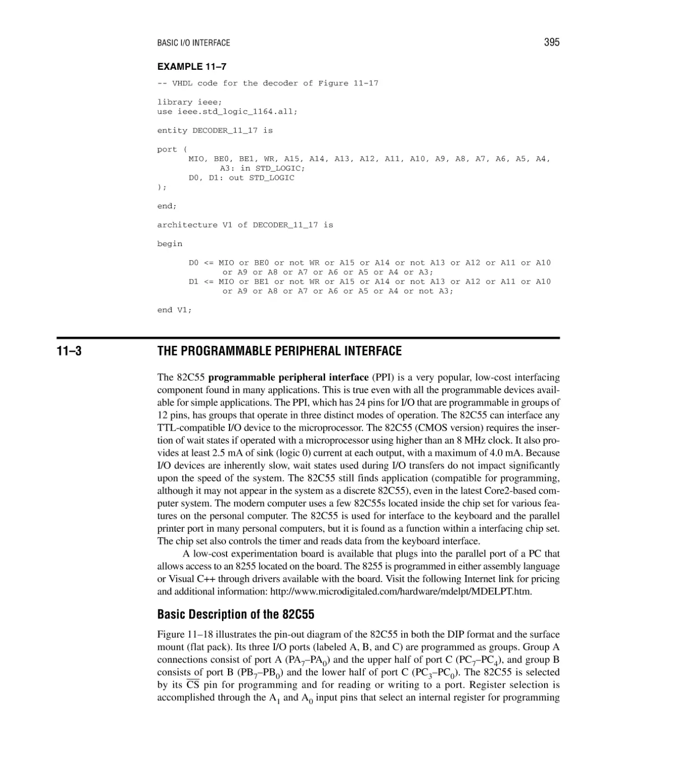
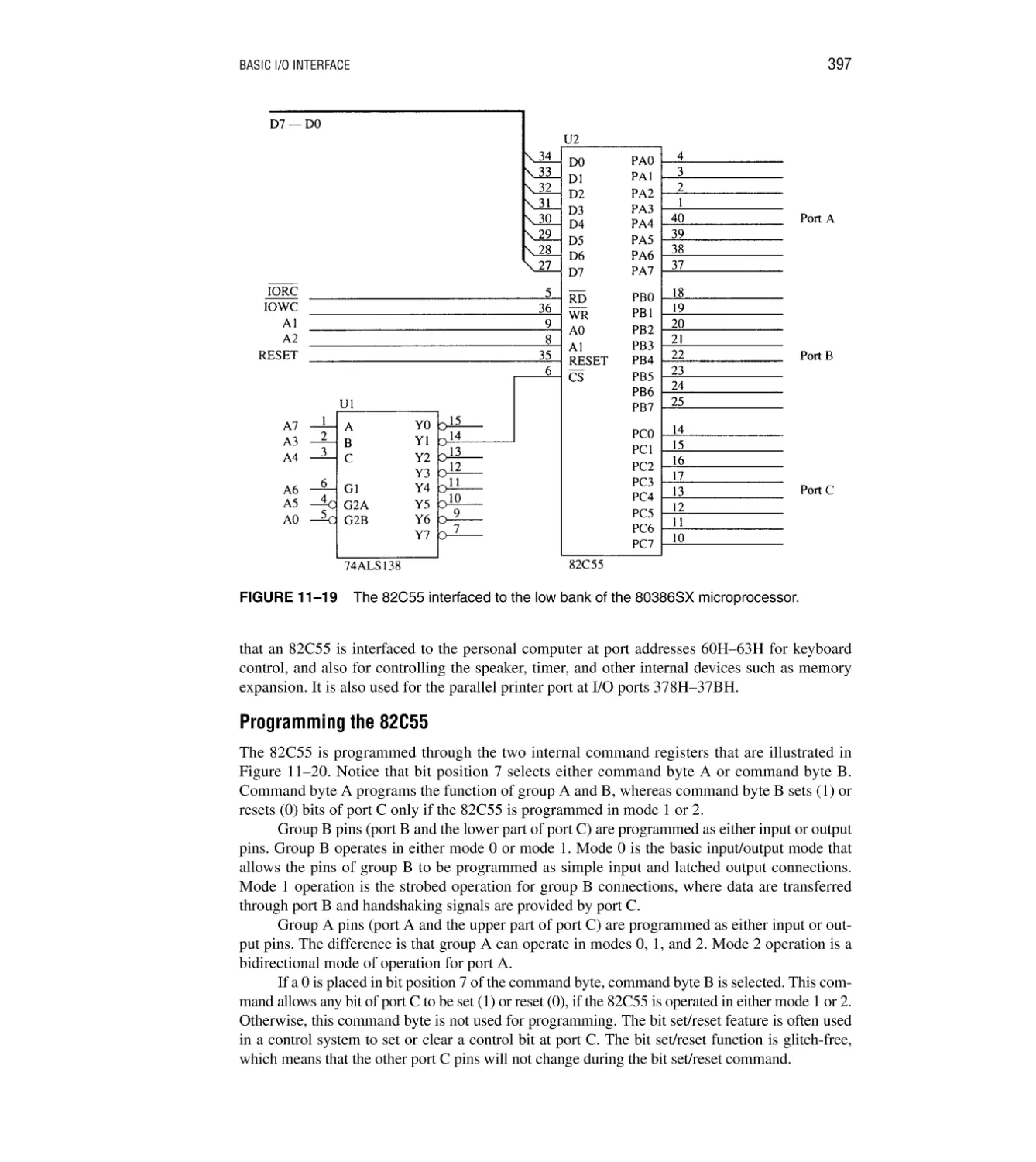
Basic Description of the 82C55 395; Programming the 82C55 397; Mode 0 Operation 398;
An LCD Display, Interfaced to the 82C55 403; Mode 1 Strobed Input 414; Signal
Definitions for Mode 1 Strobed Input 414; Mode 1 Strobed Output 416; Signal Definitions
for Mode 1 Strobed Output 416; Mode 2 Bidirectional Operation 418; Signal Definitions for
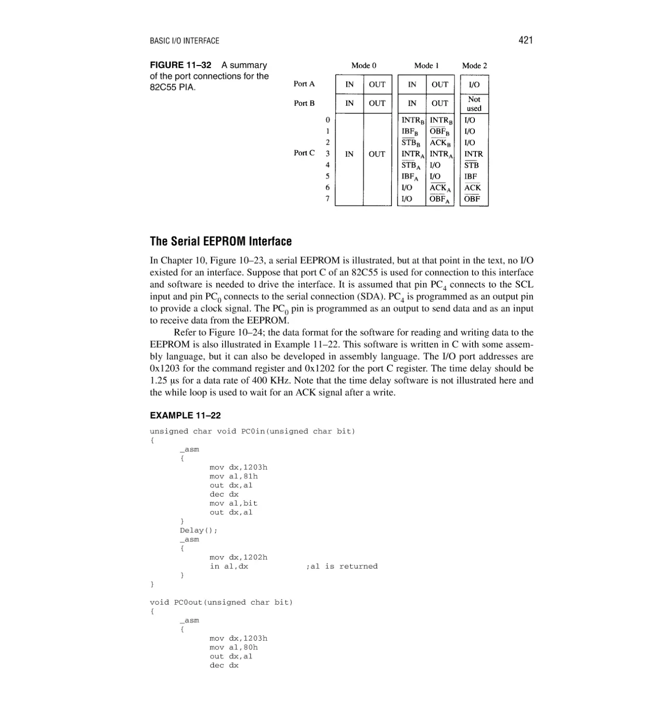
Bidirectional Mode 2 418; 82C55 Mode Summary 420; The Serial EEPROM Interface 421
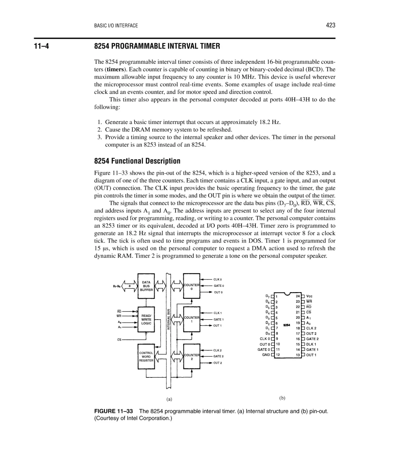
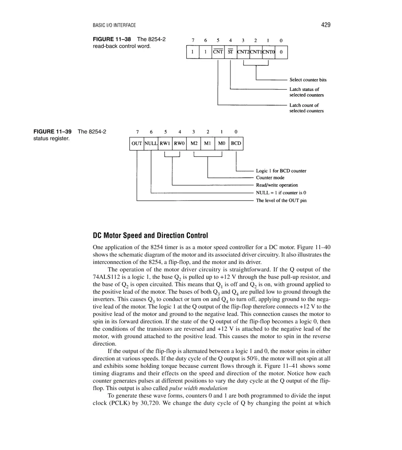
11–4 8254 Programmable Interval Timer 423
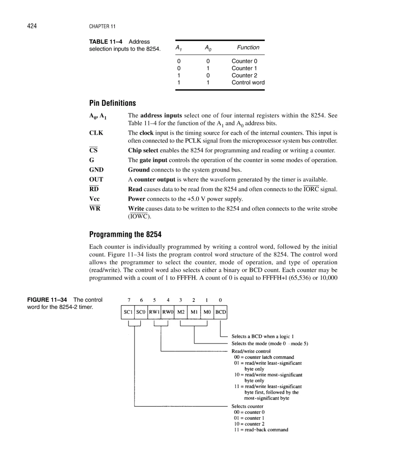
8254 Functional Description 423; Pin Definitions 424; Programming the 8254 424;
DC Motor Speed and Direction Control 429
11–5 16550 Programmable Communications Interface 433
Asynchronous Serial Data 433; 16550 Functional Description 433; 16550 Pin Functions 434;
Programming the 16550 435
11–6 Analog-to-Digital (ADC) and Digital-to-Analog (DAC) Converters 440
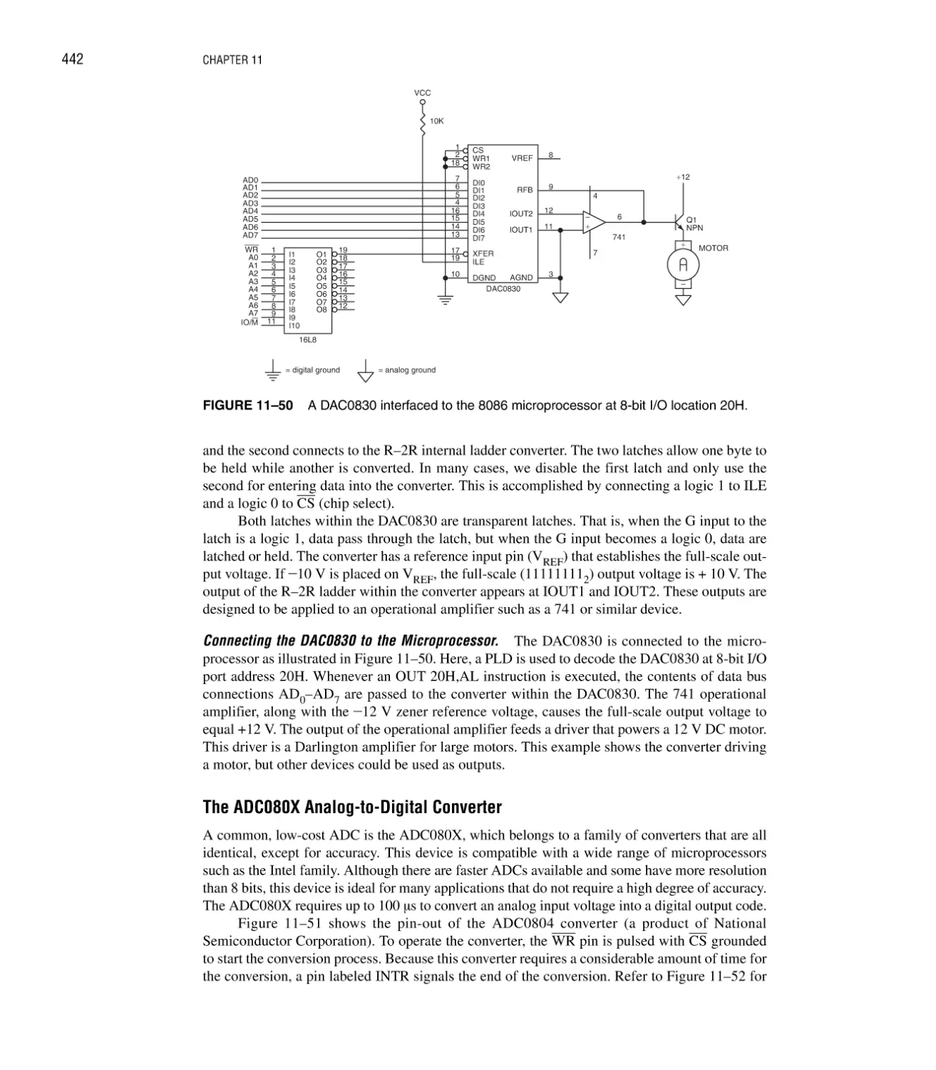
The DAC0830 Digital-to-Analog Converter 440; The ADC080X Analog-to-Digital
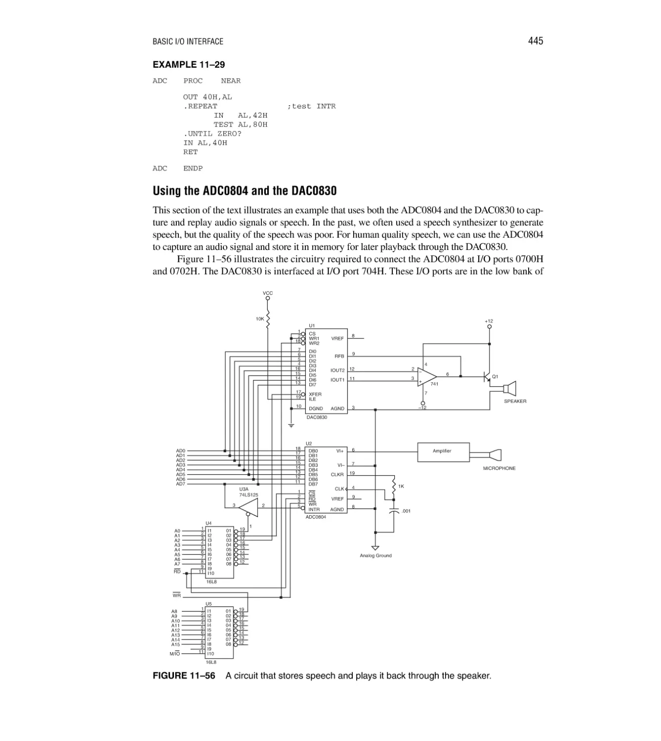
Converter 442; Using the ADC0804 and the DAC0830 445
377
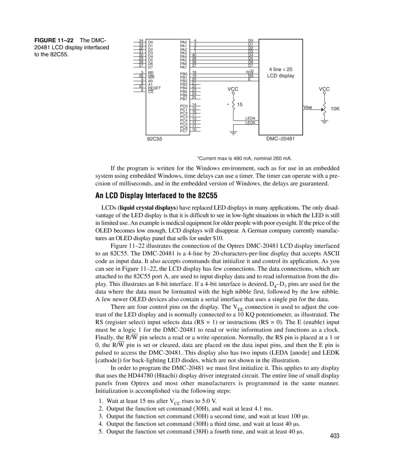
CONTENTS
xv
11–7 Summary 446
11–8 Questions and Problems 448
CHAPTER 12
INTERRUPTS
451
Introduction/Chapter Objectives 451
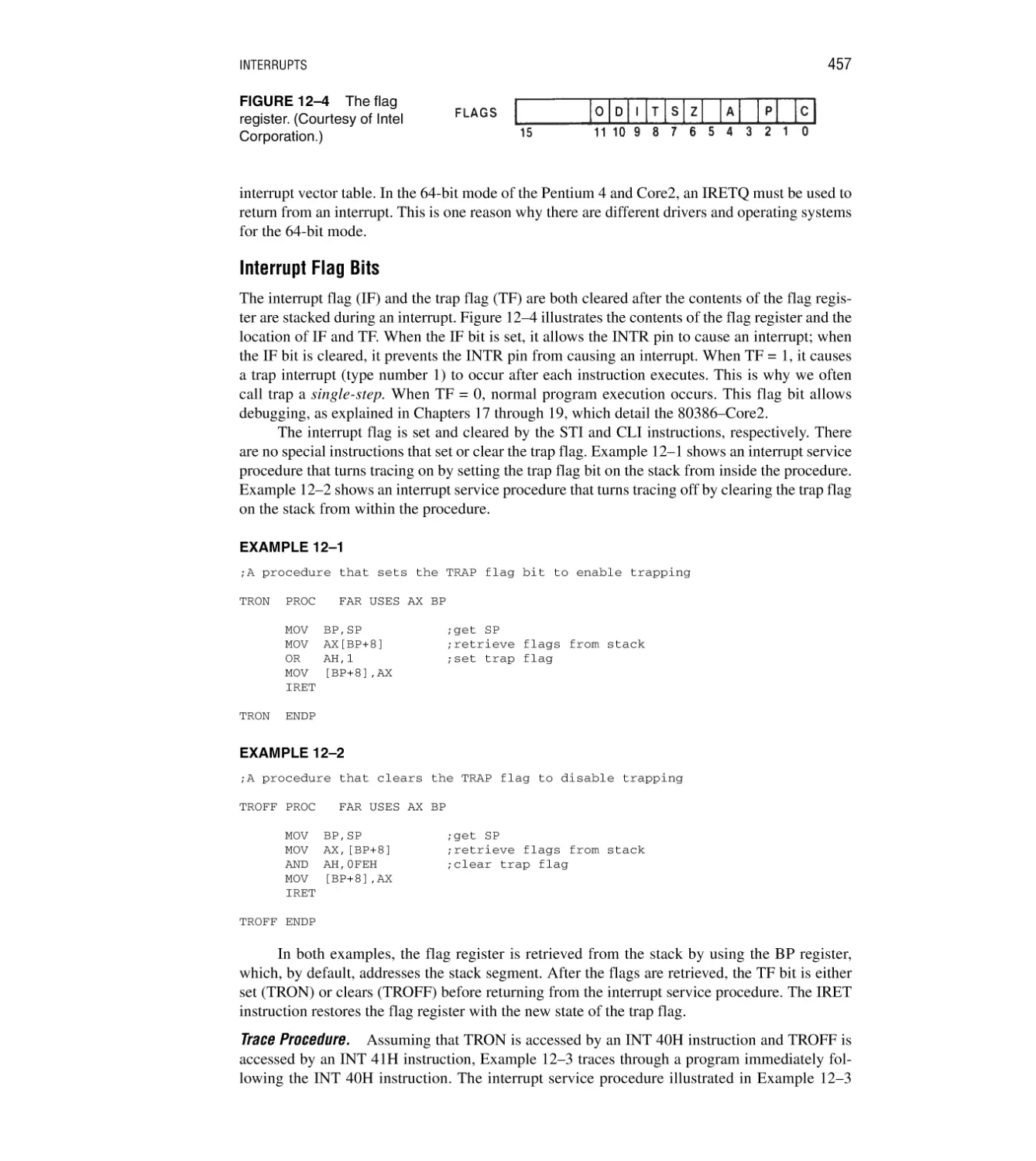
12–1 Basic Interrupt Processing 451
The Purpose of Interrupts 451; Interrupts 452; Interrupt Instructions: BOUND, INTO,
INT, INT 3, and IRET 455; The Operation of a Real Mode Interrupt 455; Operation of a
Protected Mode Interrupt 456; Interrupt Flag Bits 457; Storing an Interrupt Vector in the
Vector Table 458
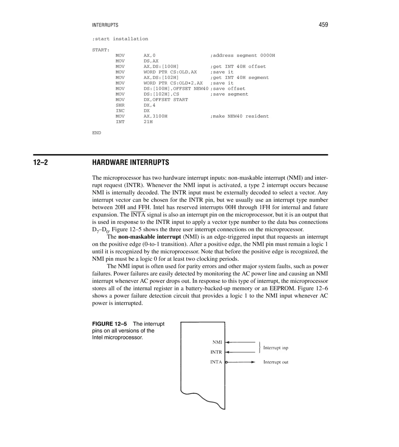
12–2 Hardware Interrupts 459
INTR and INTA 461; The 82C55 Keyboard Interrupt 462
12–3 Expanding the Interrupt Structure 465
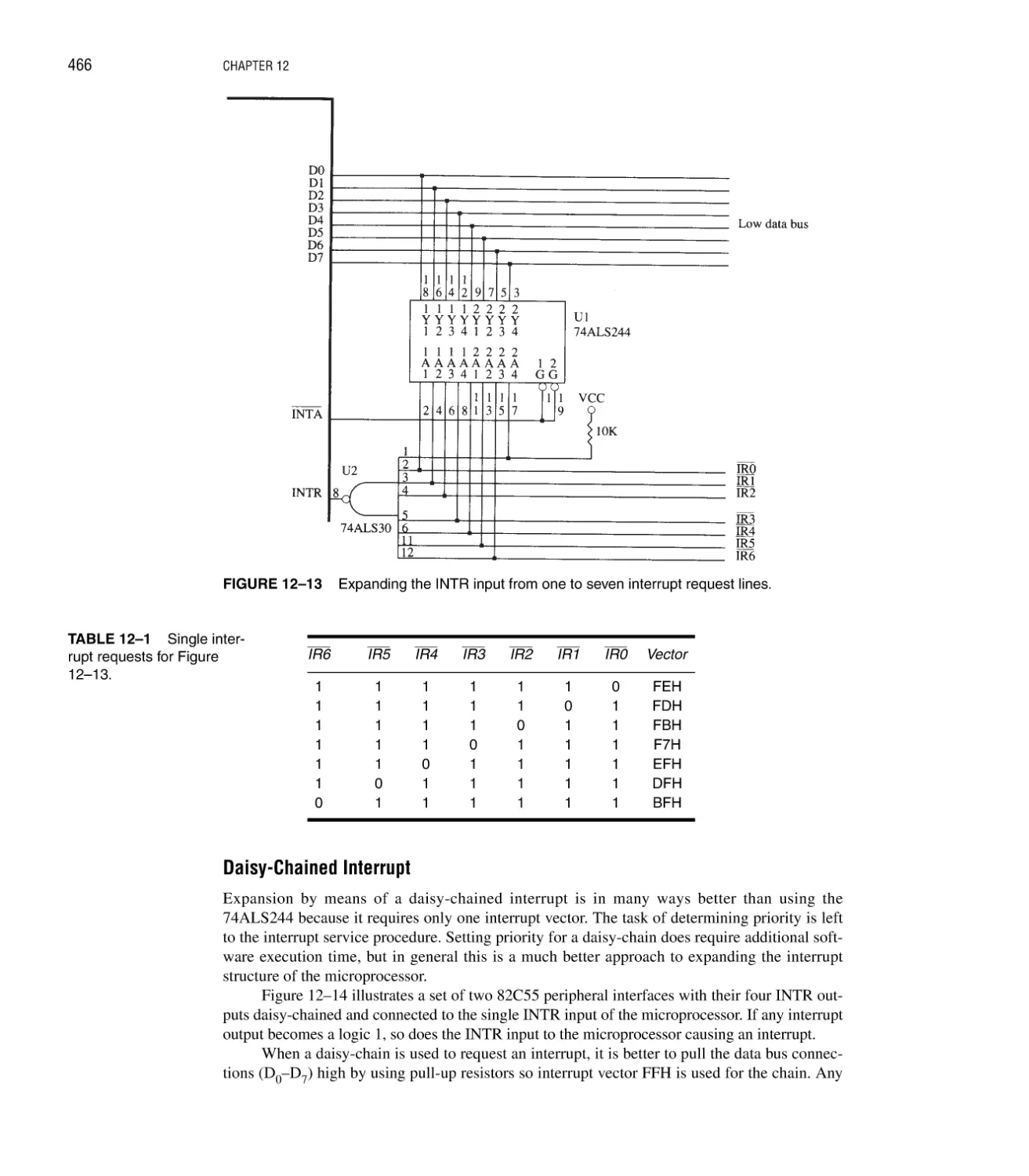
Using the 74ALS244 to Expand Interrupts 465; Daisy-Chained Interrupt 466
12–4 8259A Programmable Interrupt Controller 468
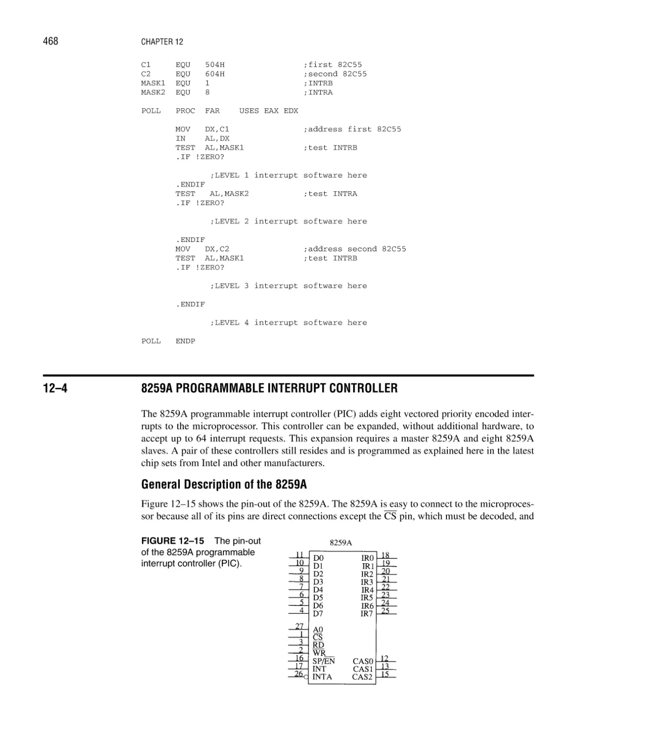
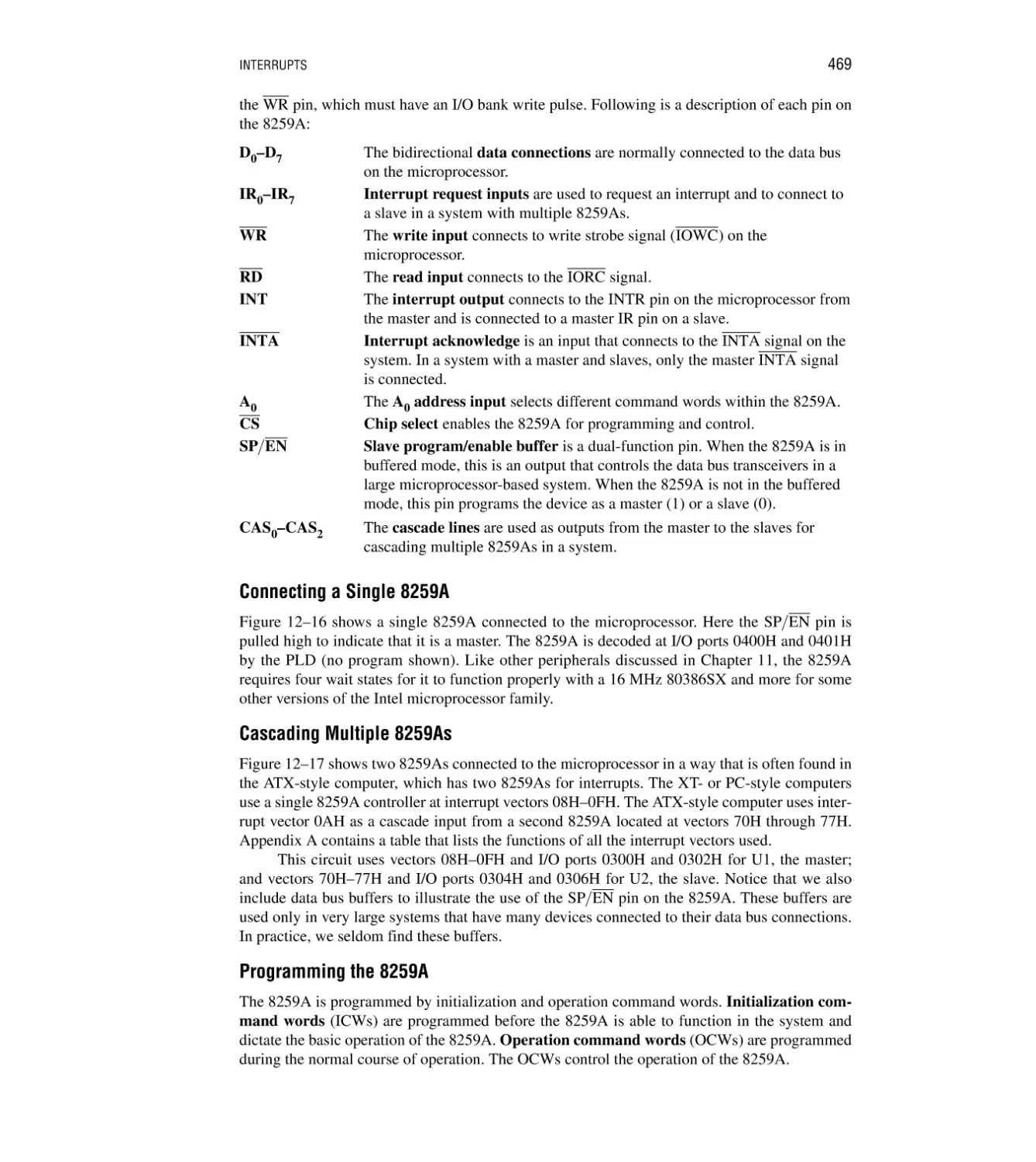
General Description of the 8259A 468; Connecting a Single 8259A 469; Cascading
Multiple 8259As 469; Programming the 8259A 469; 8259A Programming Example 475
12–5 Interrupt Examples 481
Real-Time Clock 482; Interrupt-Processed Keyboard 484
12–6 Summary 487
12–7 Questions and Problems 488
CHAPTER 13
DIRECT MEMORY ACCESS AND DMA-CONTROLLED I/O
490
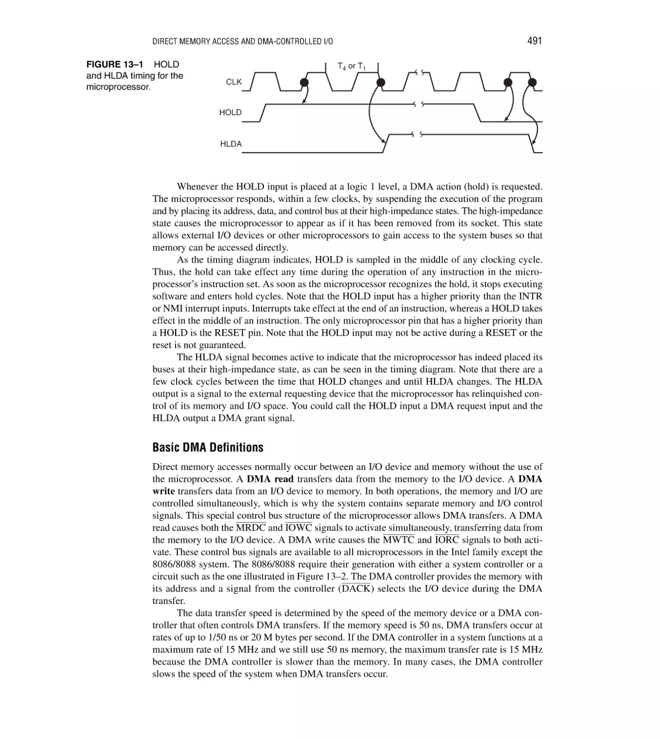
Introduction/Chapter Objectives 490
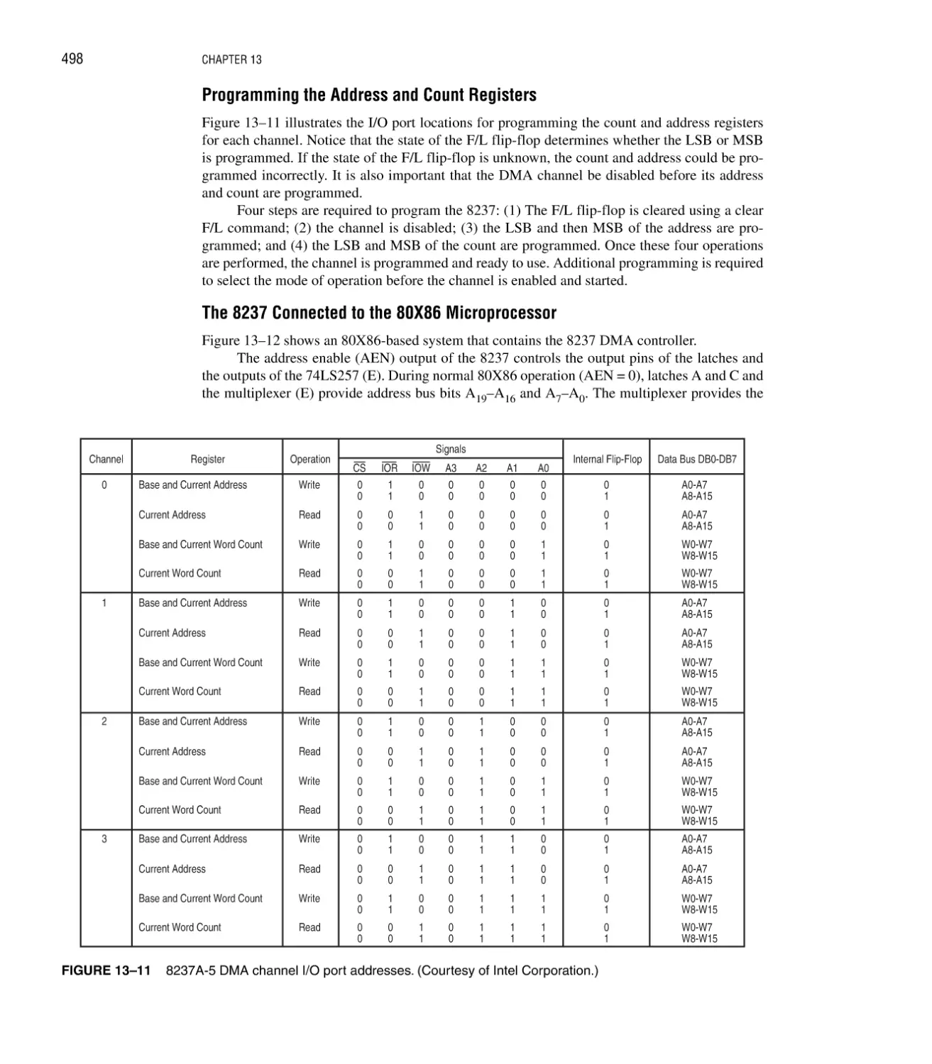
13–1 Basic DMA Operation 490
Basic DMA Definitions 491
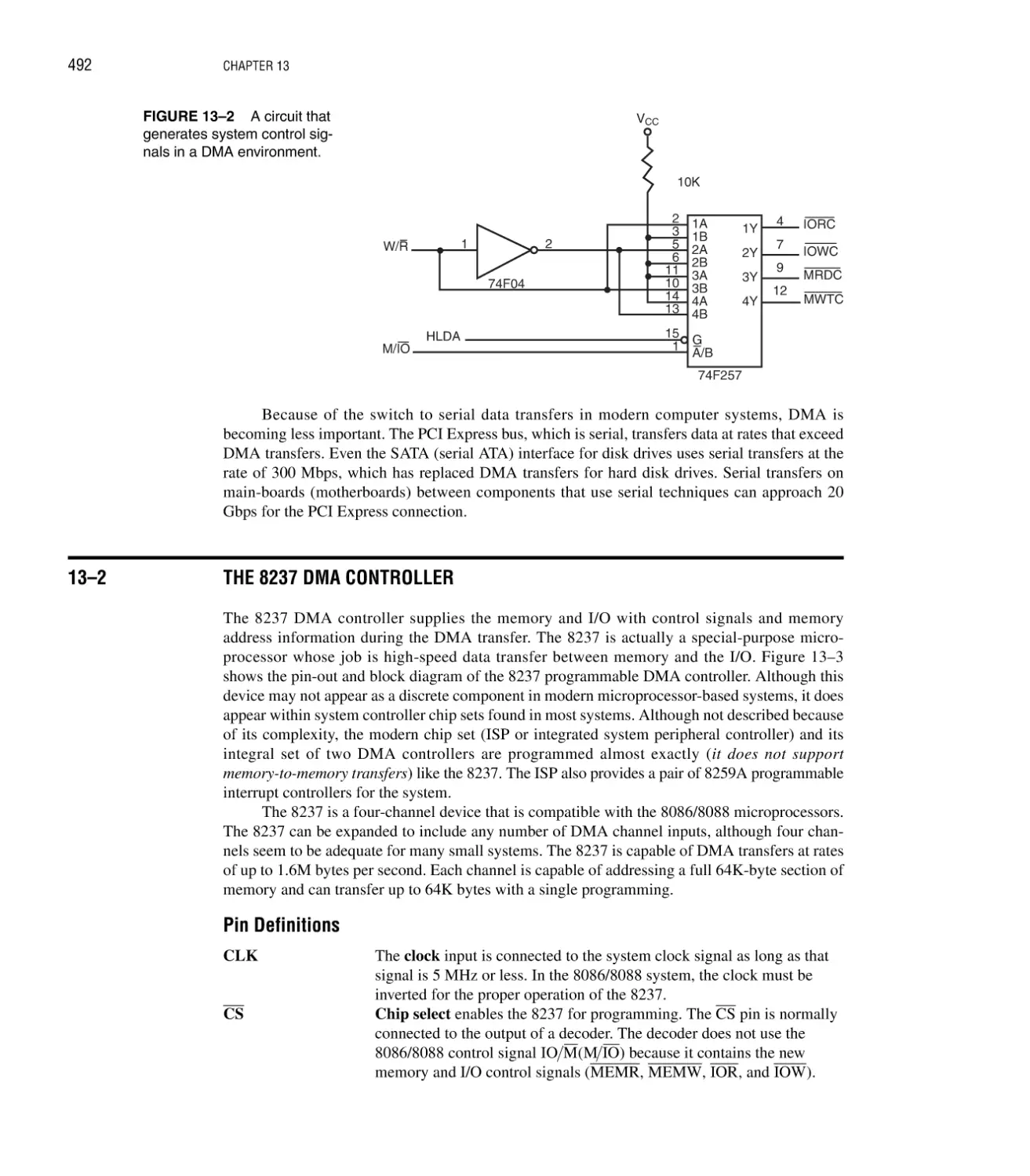
13–2 The 8237 DMA Controller 492
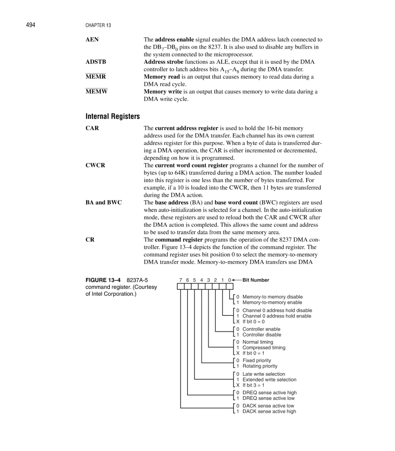
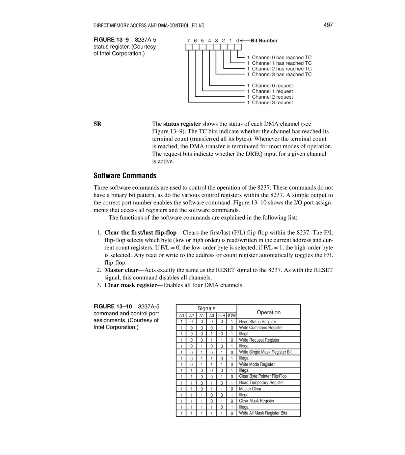
Pin Definitions 492; Internal Registers 494; Software Commands 497;
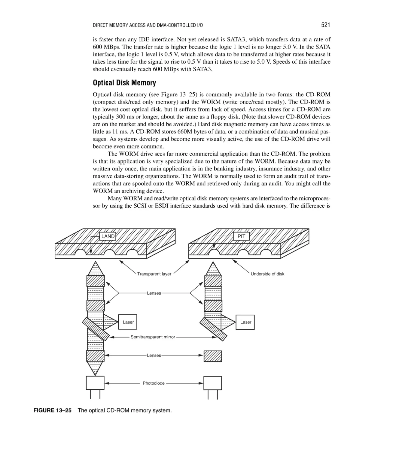
Programming the Address and Count Registers 498; The 8237 Connected
to the 80X86 Microprocessor 498; Memory-to-Memory Transfer with
the 8237 499; DMA-Processed Printer Interface 504
13–3 Shared-Bus Operation 506
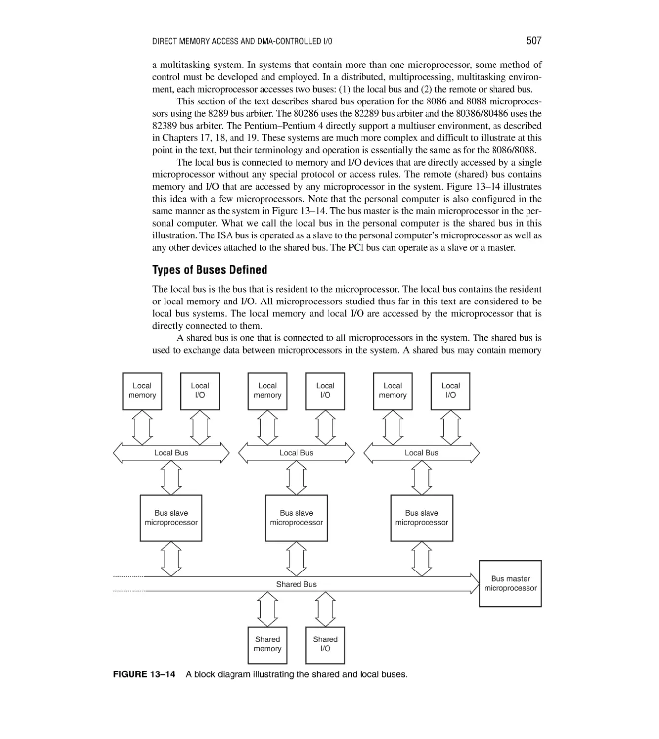
Types of Buses Defined 507; The Bus Arbiter 509; Pin Definitions 509
13–4 Disk Memory Systems 513
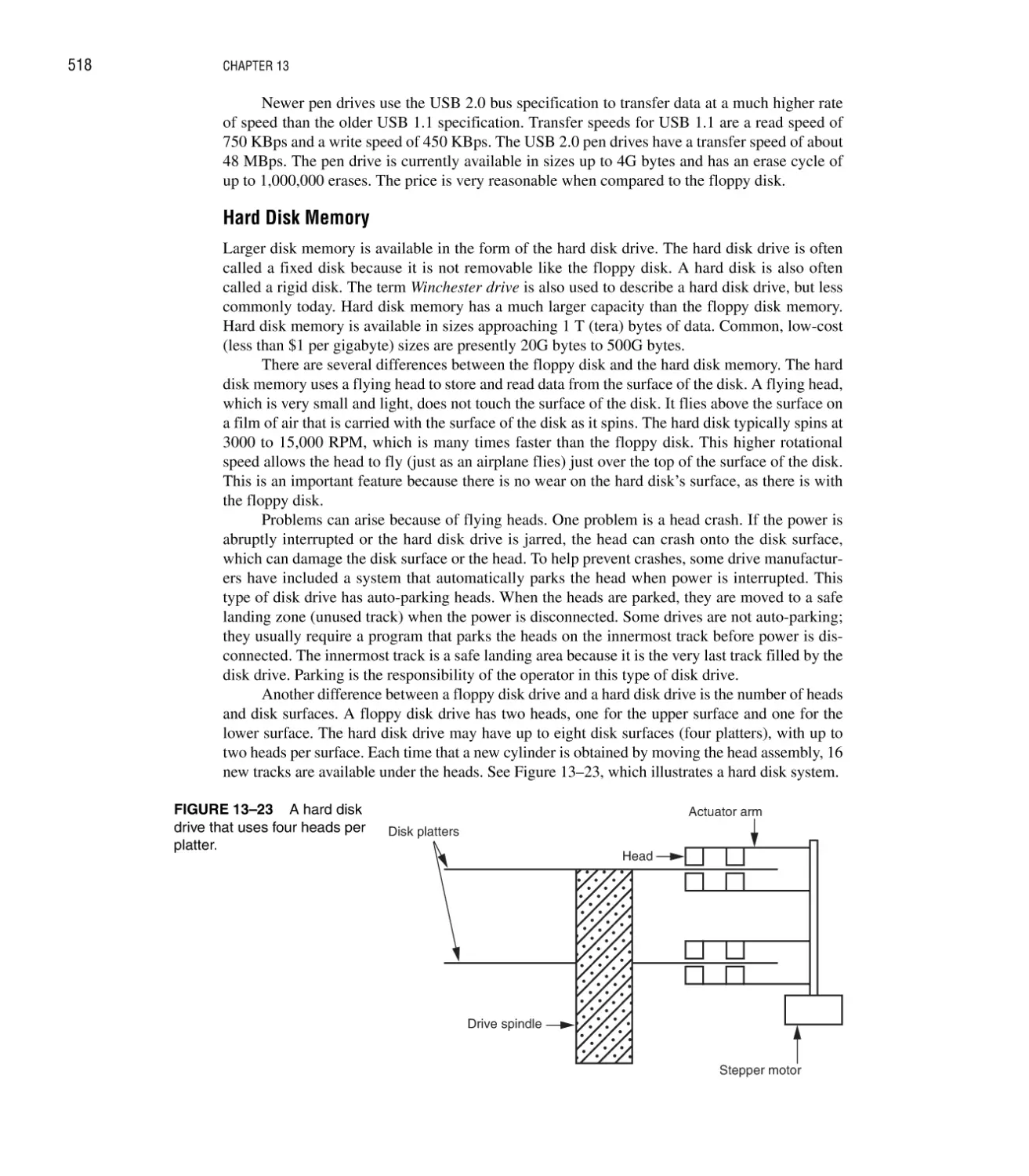
Floppy Disk Memory 513; Pen Drives 517; Hard Disk Memory 518;
Optical Disk Memory 521
13–5 Video Displays 522
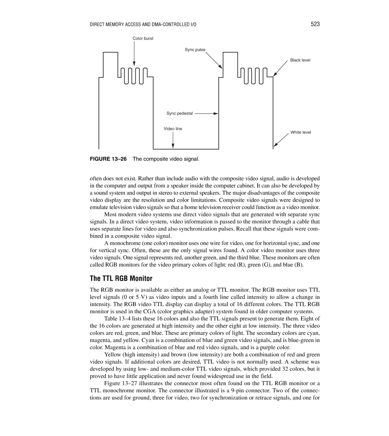
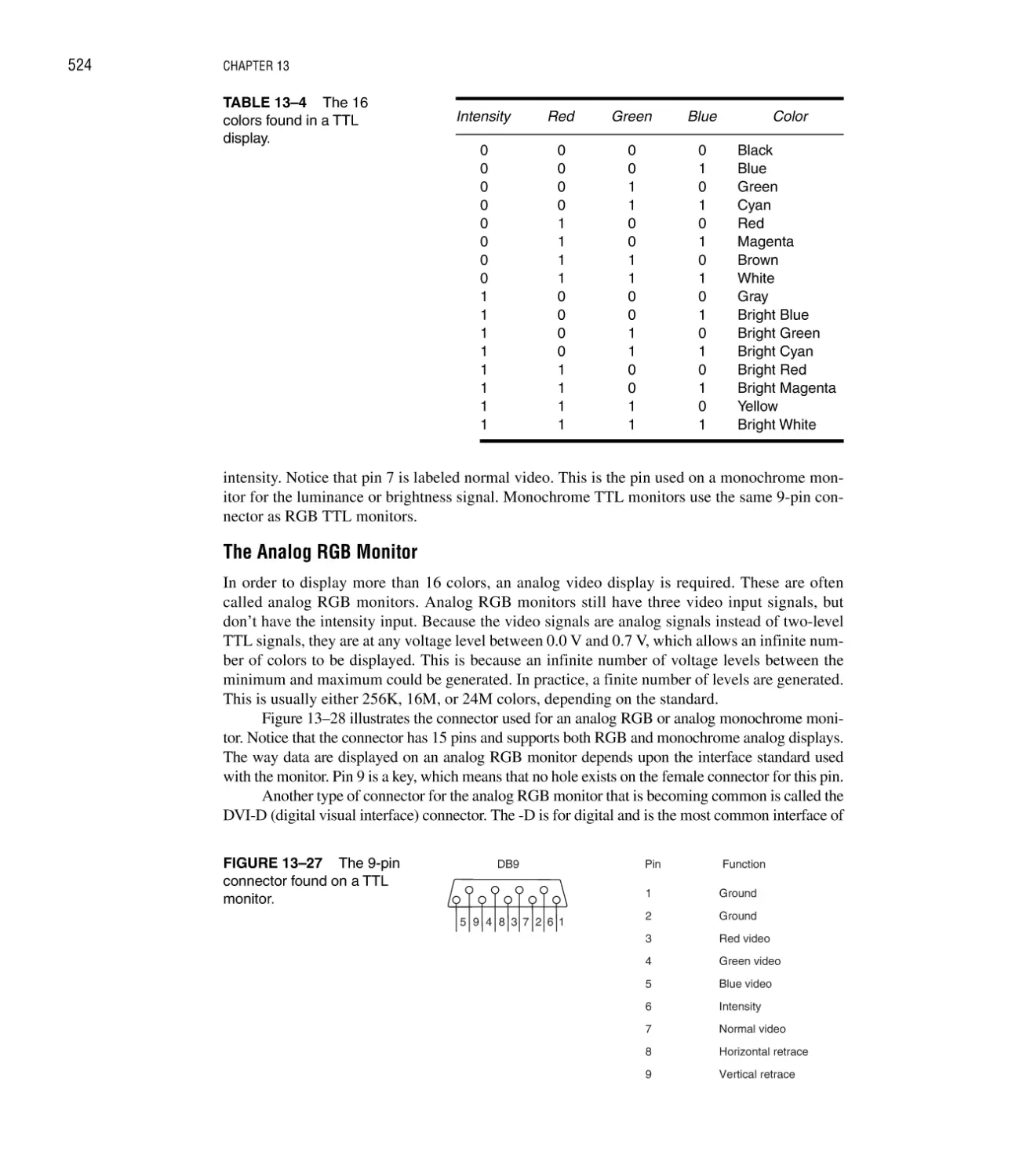
Video Signals 522; The TTL RGB Monitor 523; The Analog RGB Monitor 524
13–6 Summary 529
13–7 Questions and Problems 529
CHAPTER 14
THE ARITHMETIC COPROCESSOR, MMX, AND SIMD TECHNOLOGIES
Introduction/Chapter Objectives 531
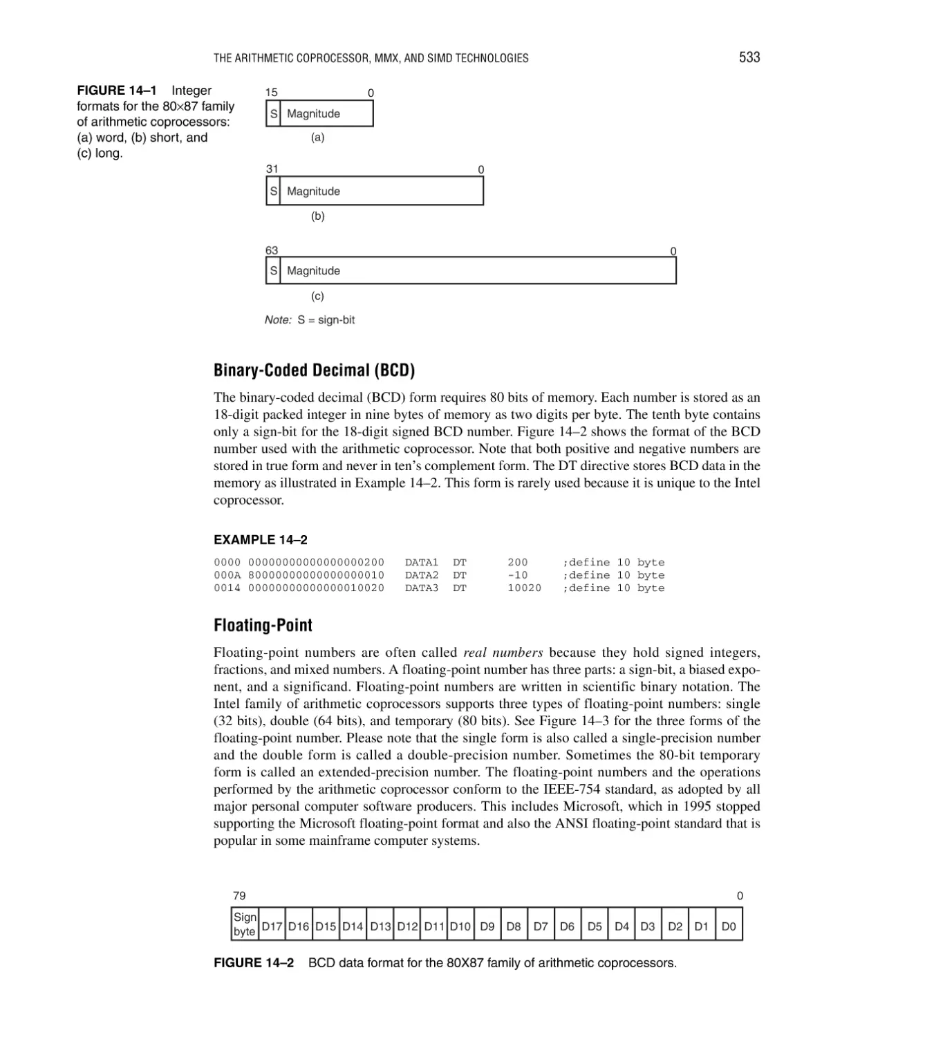
14–1 Data Formats for the Arithmetic Coprocessor 532
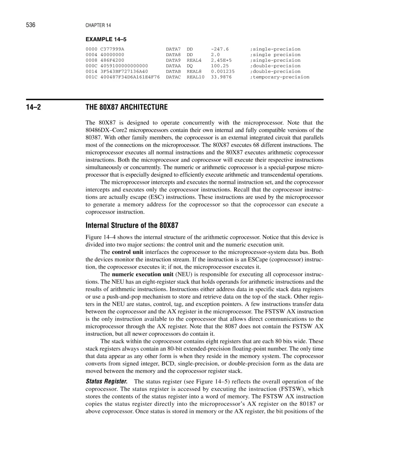
Signed Integers 532; Binary-Coded Decimal (BCD) 533; Floating-Point 533
14–2 The 80X87 Architecture 536
Internal Structure of the 80X87 536
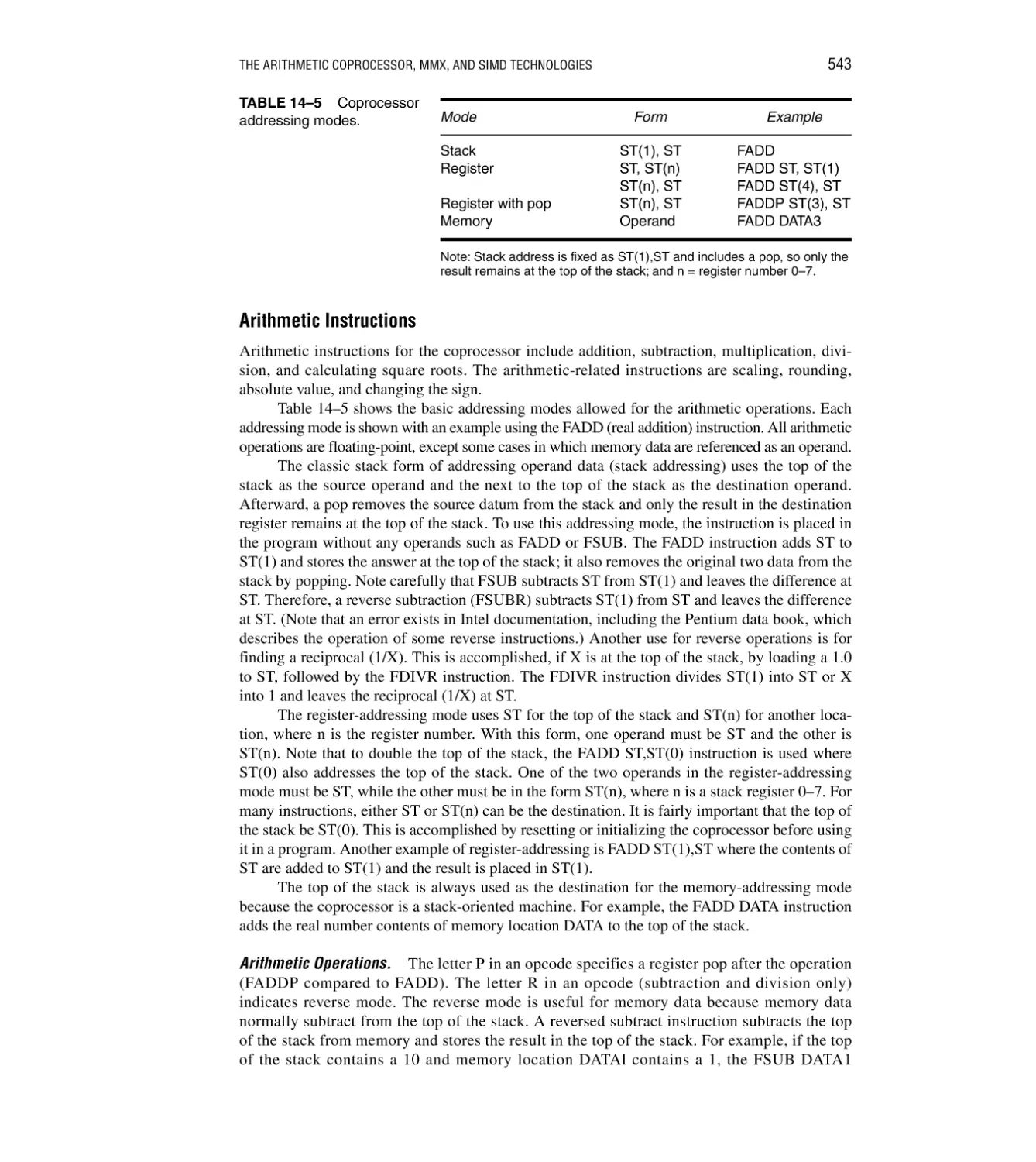
14–3 Instruction Set 541
Data Transfer Instructions 541; Arithmetic Instructions 543; Comparison Instructions 544;
Transcendental Operations 545; Constant Operations 546; Coprocessor Control
Instructions 546; Coprocessor Instructions 548
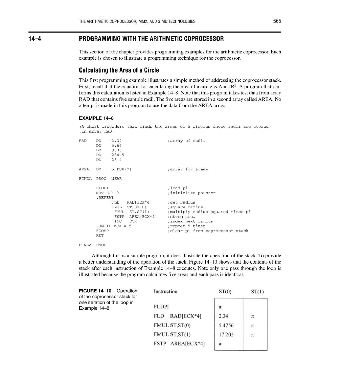
14–4 Programming with the Arithmetic Coprocessor 565
Calculating the Area of a Circle 565; Finding the Resonant Frequency 566; Finding the
Roots Using the Quadratic Equation 566; Using a Memory Array to Store Results 567;
Converting a Single-Precision Floating-Point Number to a String 568
531
xvi
CONTENTS
14–5 Introduction to MMX Technology 570
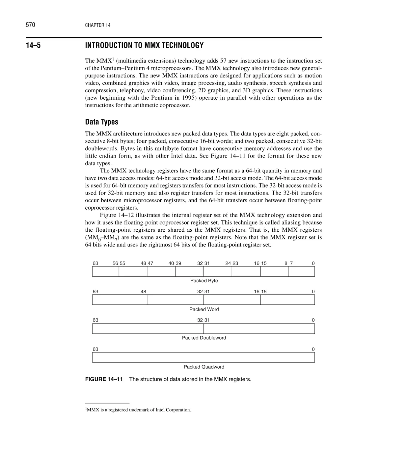
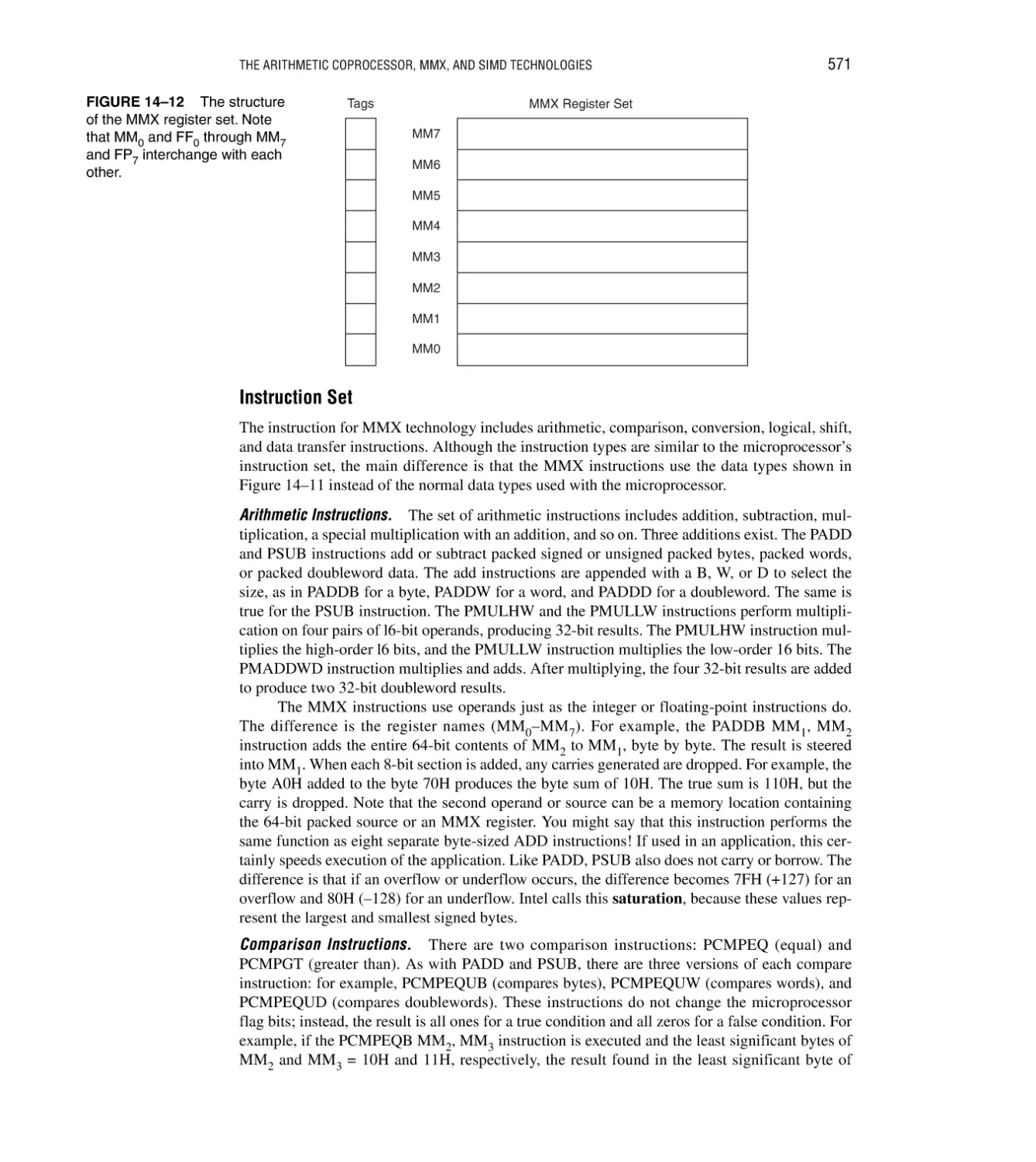
Data Types 570; Instruction Set 571
14–6 Introduction to SSE Technology 581
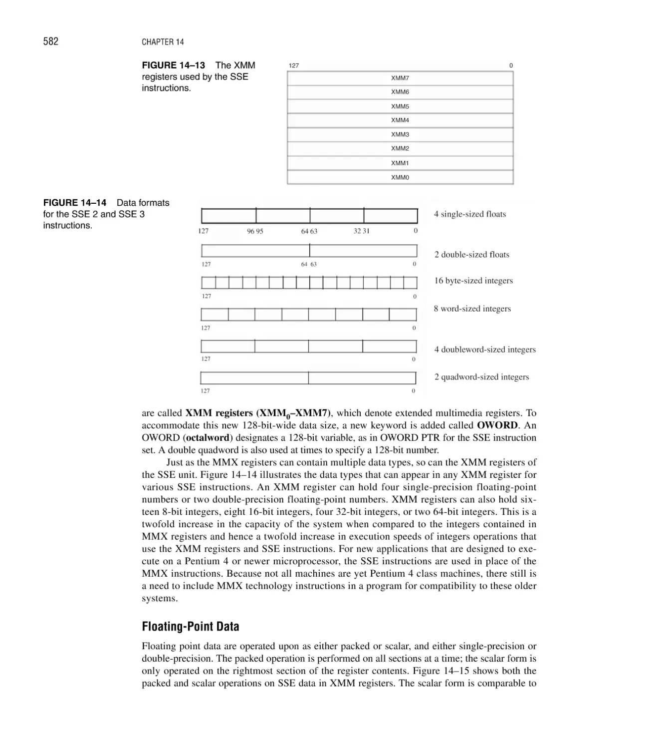
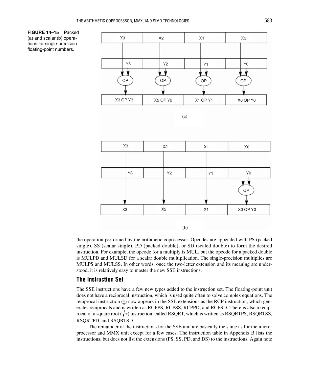
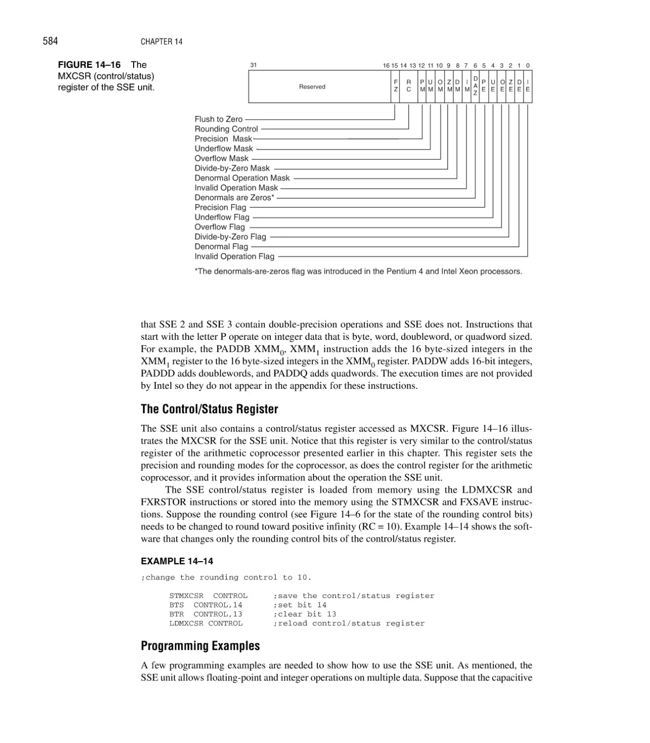
Floating-Point Data 582; The Instruction Set 583; The Control/Status Register 584;
Programming Examples 584; Optimization 587
14–7 Summary 587
14–8 Questions and Problems 589
CHAPTER 15
BUS INTERFACE
592
Introduction/Chapter Objectives 592
15–1 The ISA Bus 592
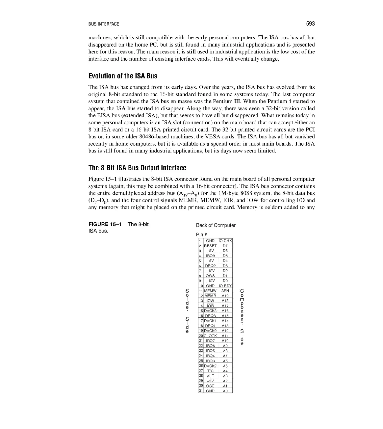
Evolution of the ISA Bus 593; The 8-Bit ISA Bus Output Interface 593; The 8-Bit ISA
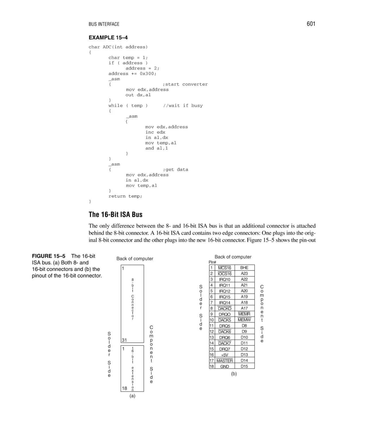
Bus Input Interface 598; The 16-Bit ISA Bus 601
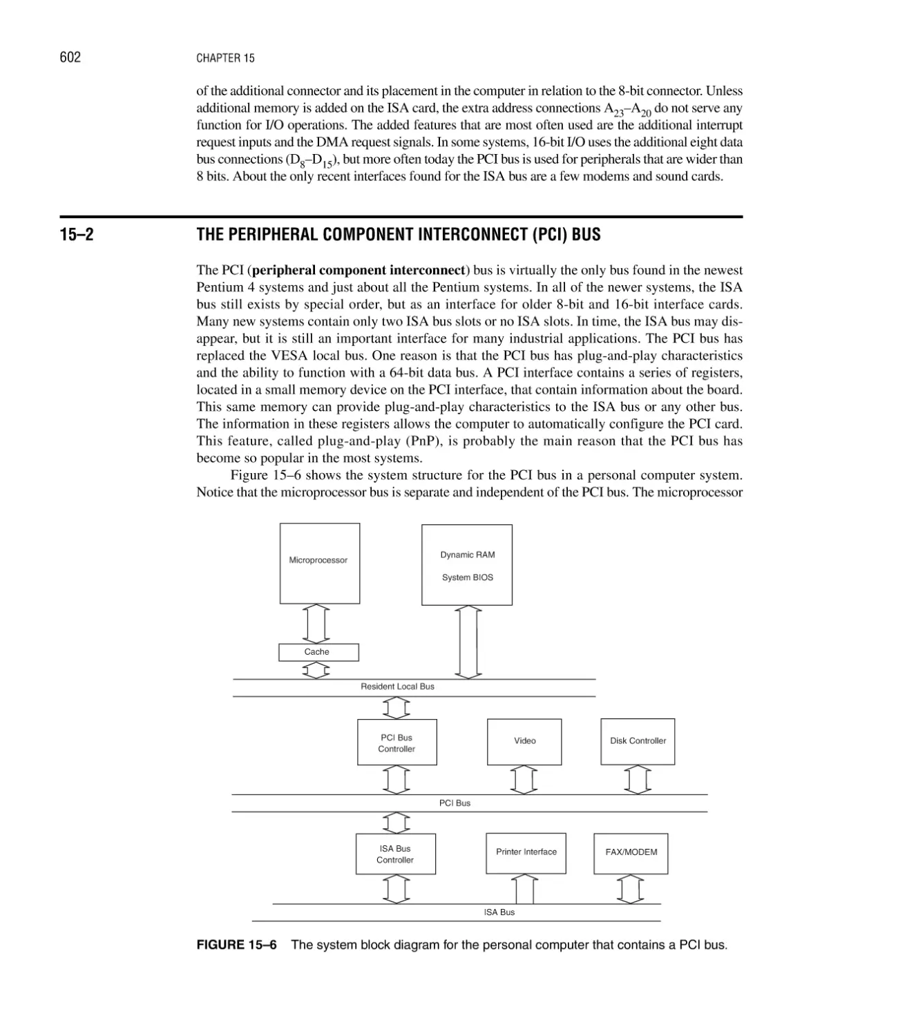
15–2 The Peripheral Component Interconnect (PCI) Bus 602
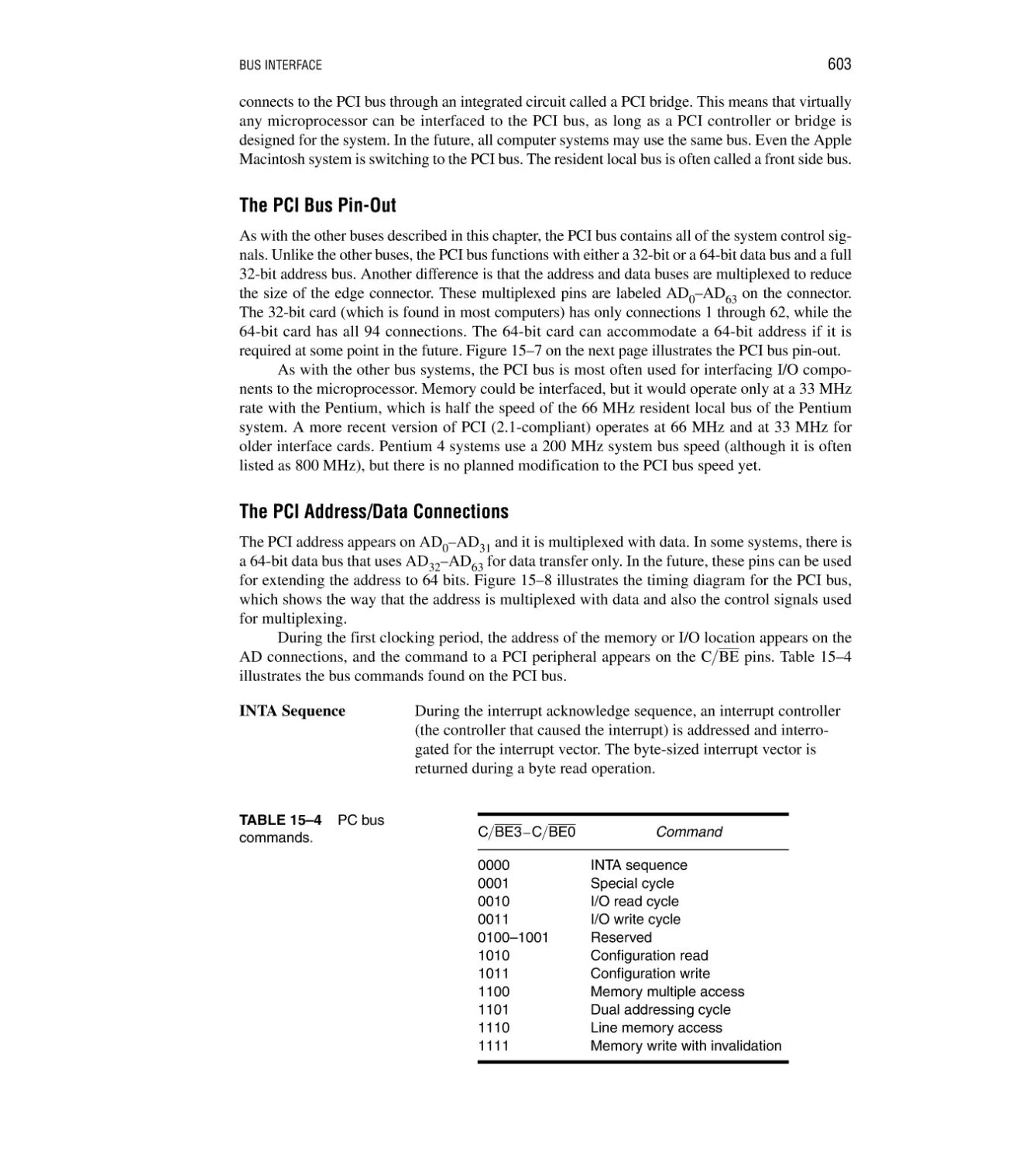
The PCI Bus Pin-Out 603; The PCI Address/Data Connections 603;
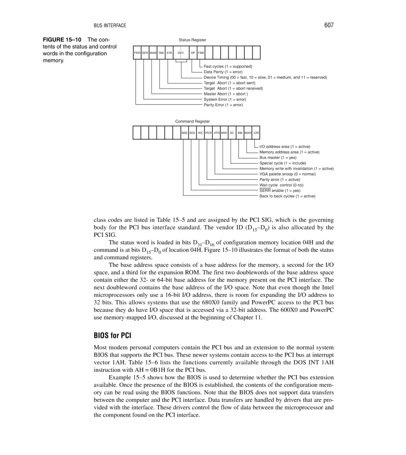
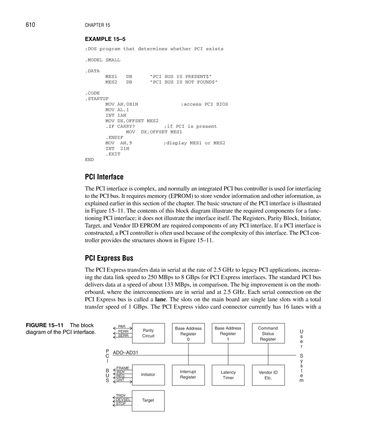
Configuration Space 605; BIOS for PCI 607; PCI Interface 610; PCI Express Bus 610
15–3 The Parallel Printer Interface (LPT) 612
Port Details 612; Using the Parallel Port Without ECP Support 614
15–4 The Serial COM Ports 614
Communication Control 615
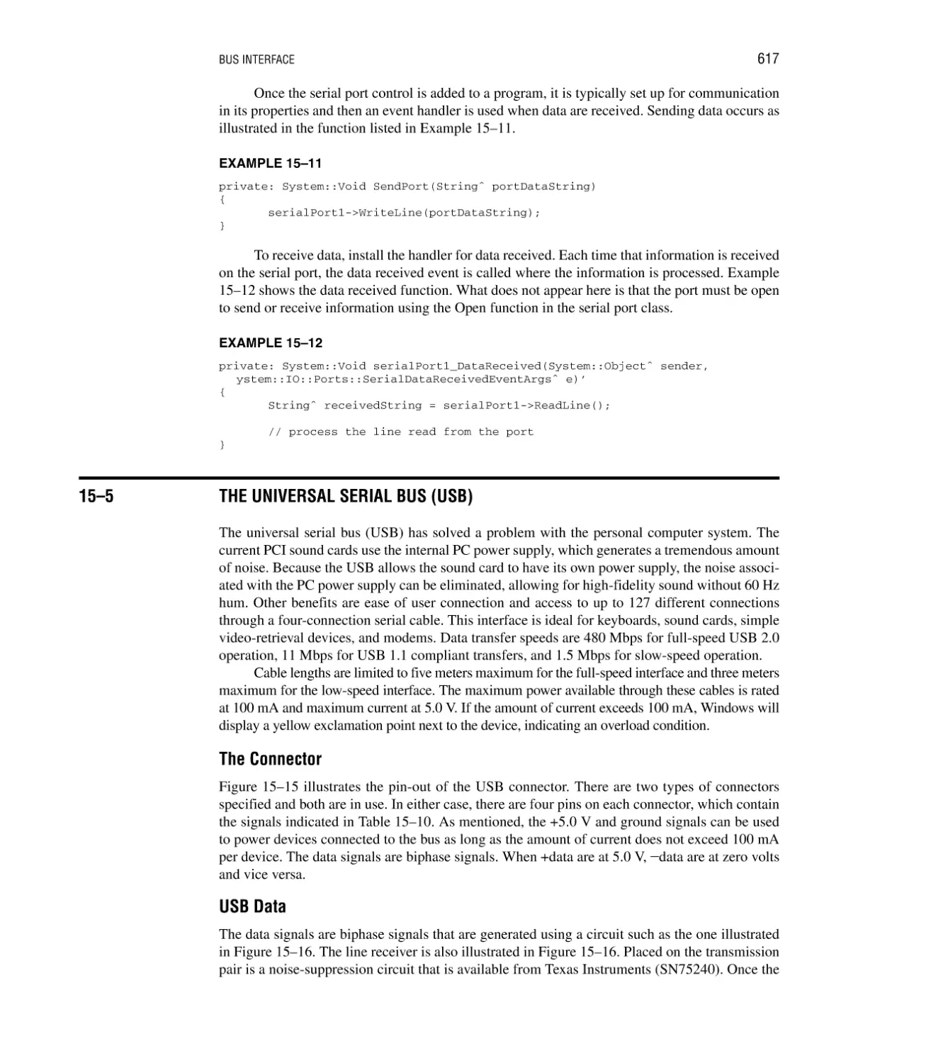
15–5 The Universal Serial Bus (USB) 617
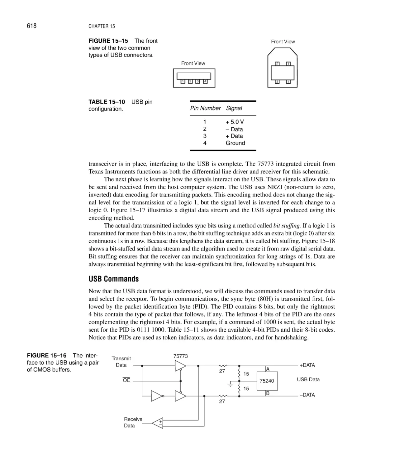
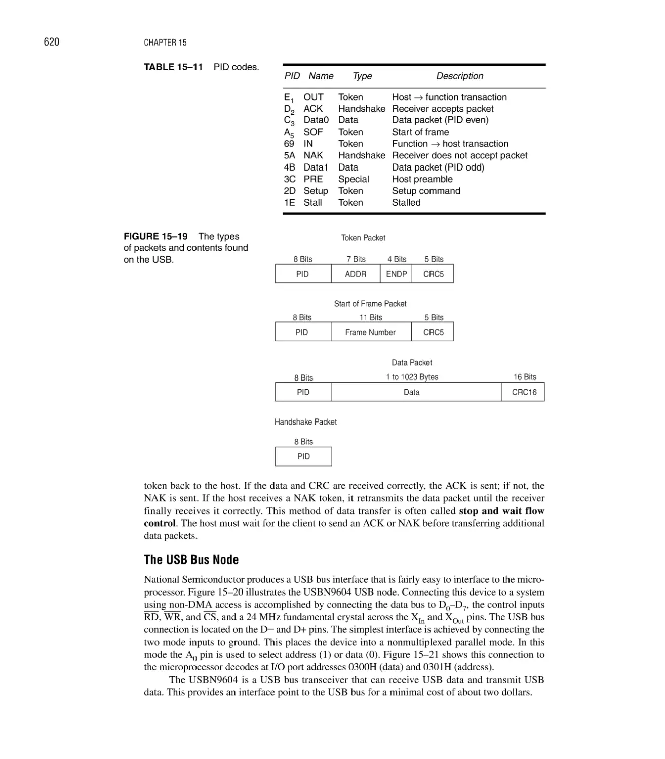
The Connector 617; USB Data 617; USB Commands 618; The USB Bus Node 620;
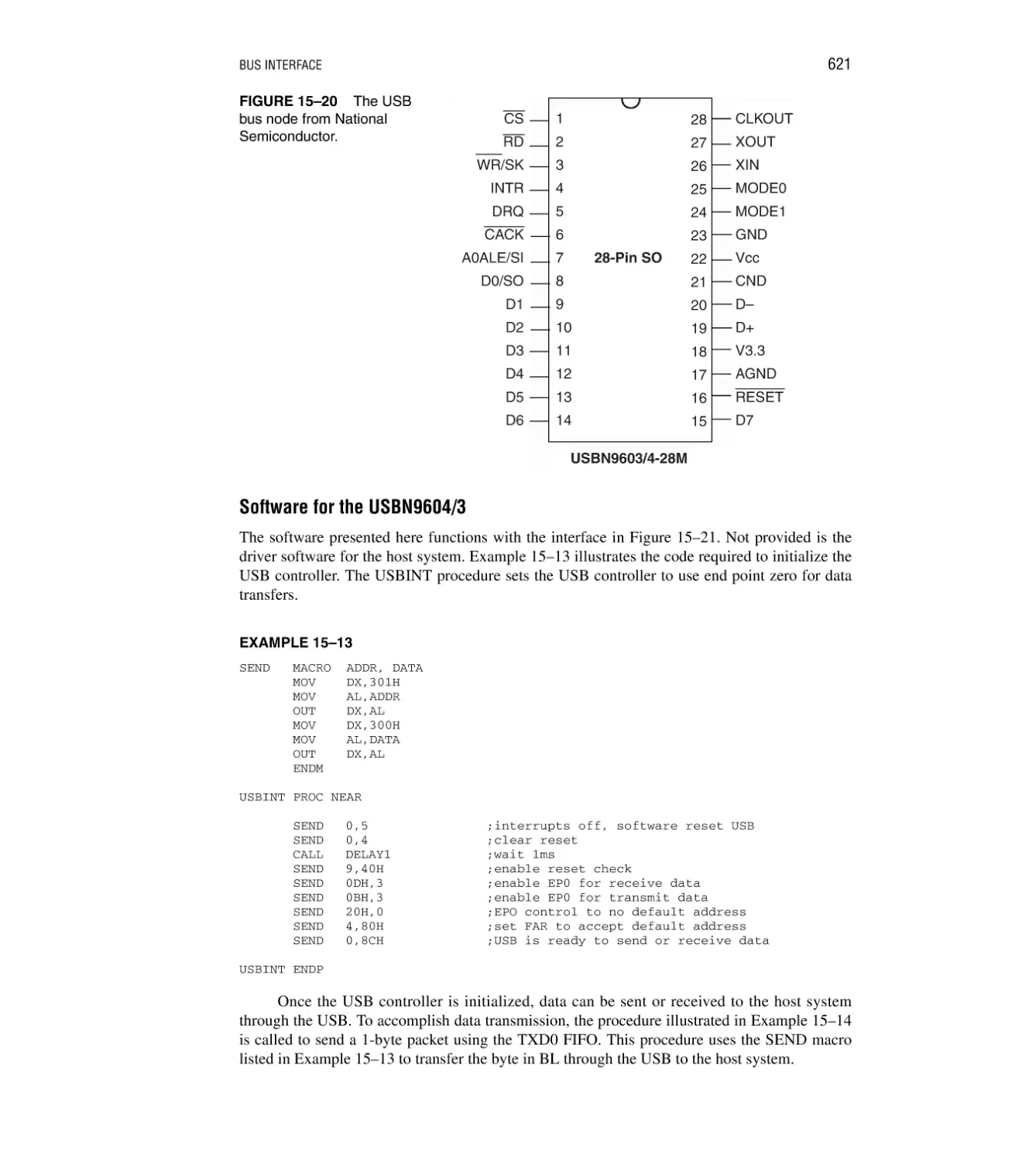
Software for the USBN9604/3 621
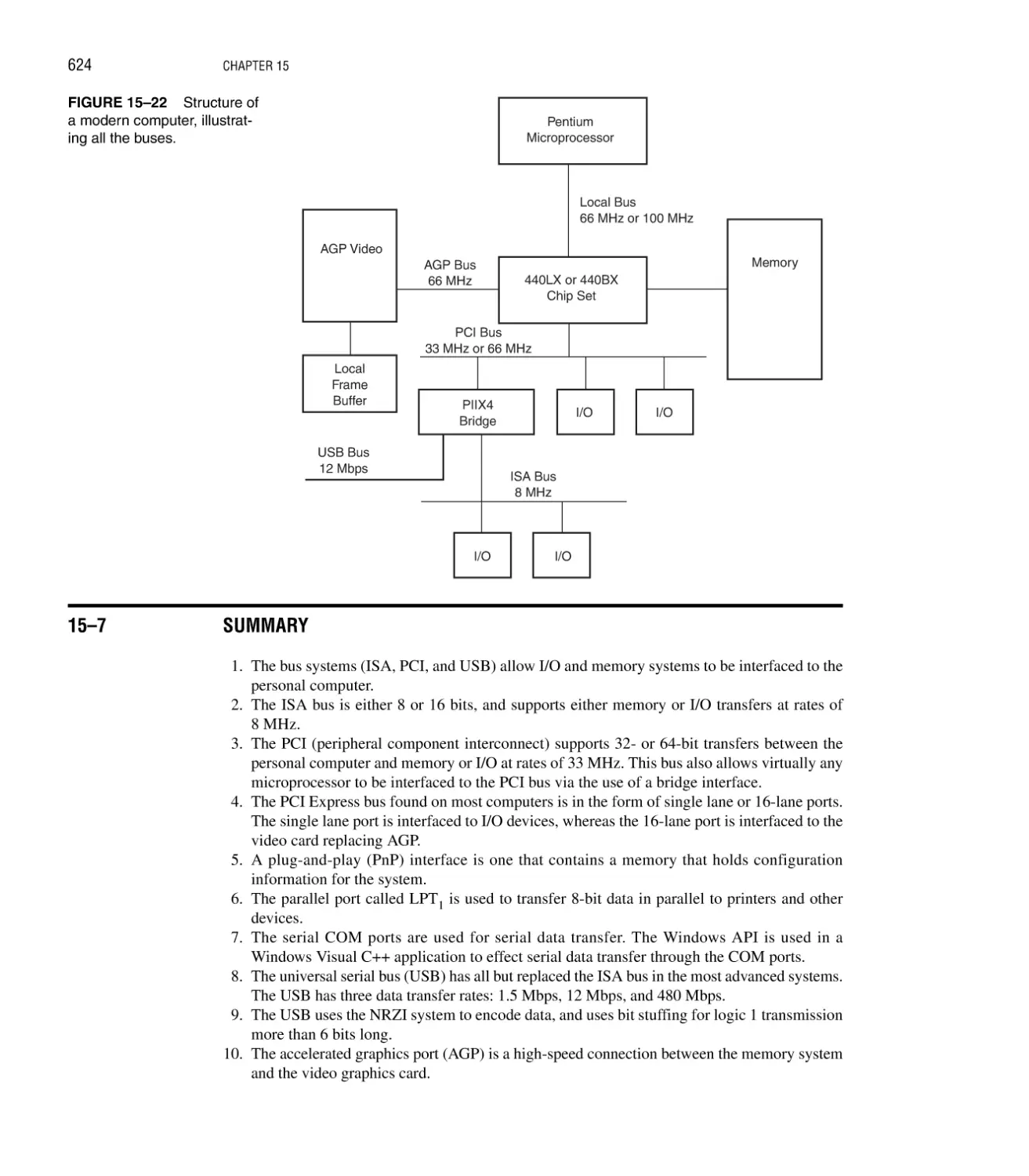
15–6 Accelerated Graphics Port (AGP) 623
15–7 Summary 624
15–8 Questions and Problems 625
CHAPTER 16
THE 80186, 80188, AND 80286 MICROPROCESSORS
627
Introduction/Chapter Objectives 627
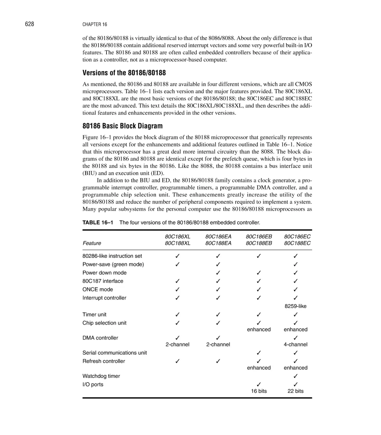
16–1 80186/80188 Architecture 627
Versions of the 80186/80188 628; 80186 Basic Block Diagram 628; 80186/80188 Basic
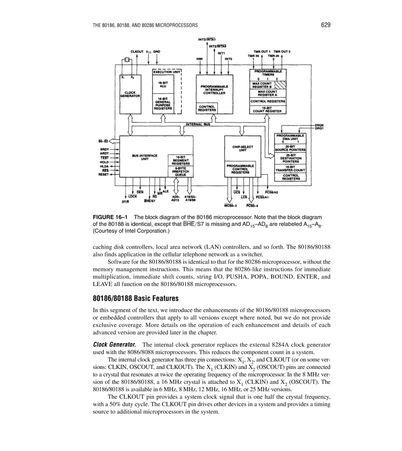
Features 629; Pin-Out 631; DC Operating Characteristics 634; 80186/80188 Timing 634
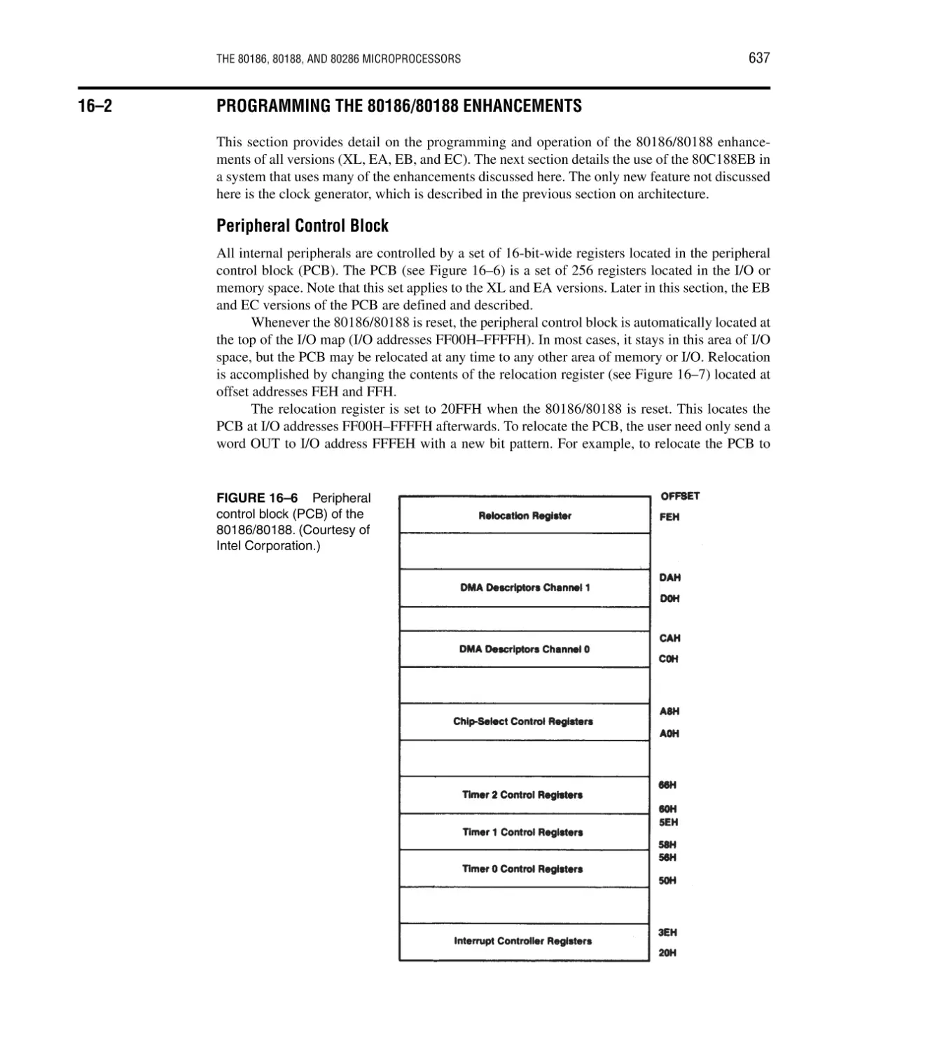
16–2 Programming the 80186/80188 Enhancements 637
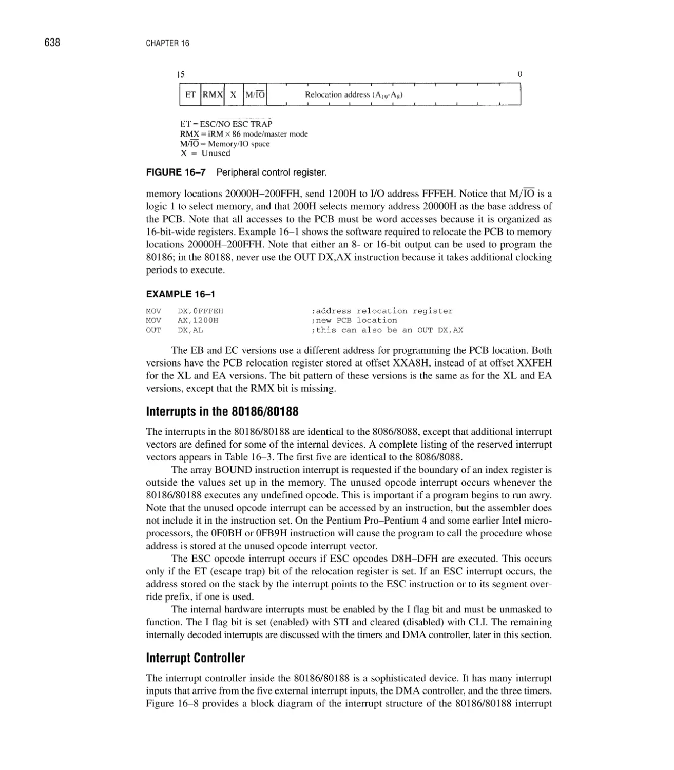
Peripheral Control Block 637; Interrupts in the 80186/80188 638; Interrupt Controller 638;
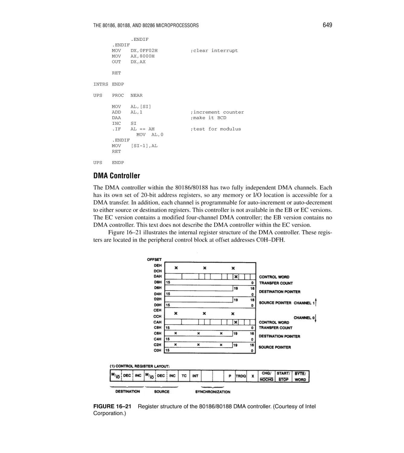
Timers 643; DMA Controller 649; Chip Selection Unit 651
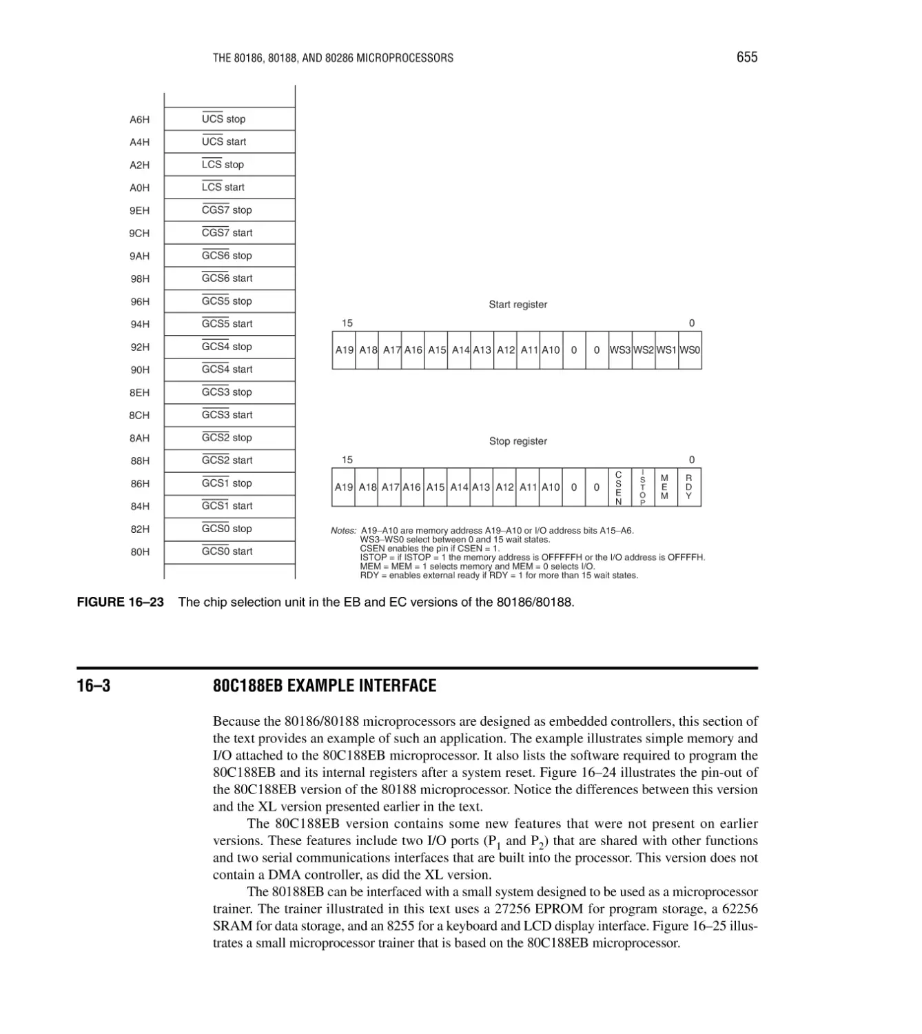
16–3 80C188EB Example Interface 655
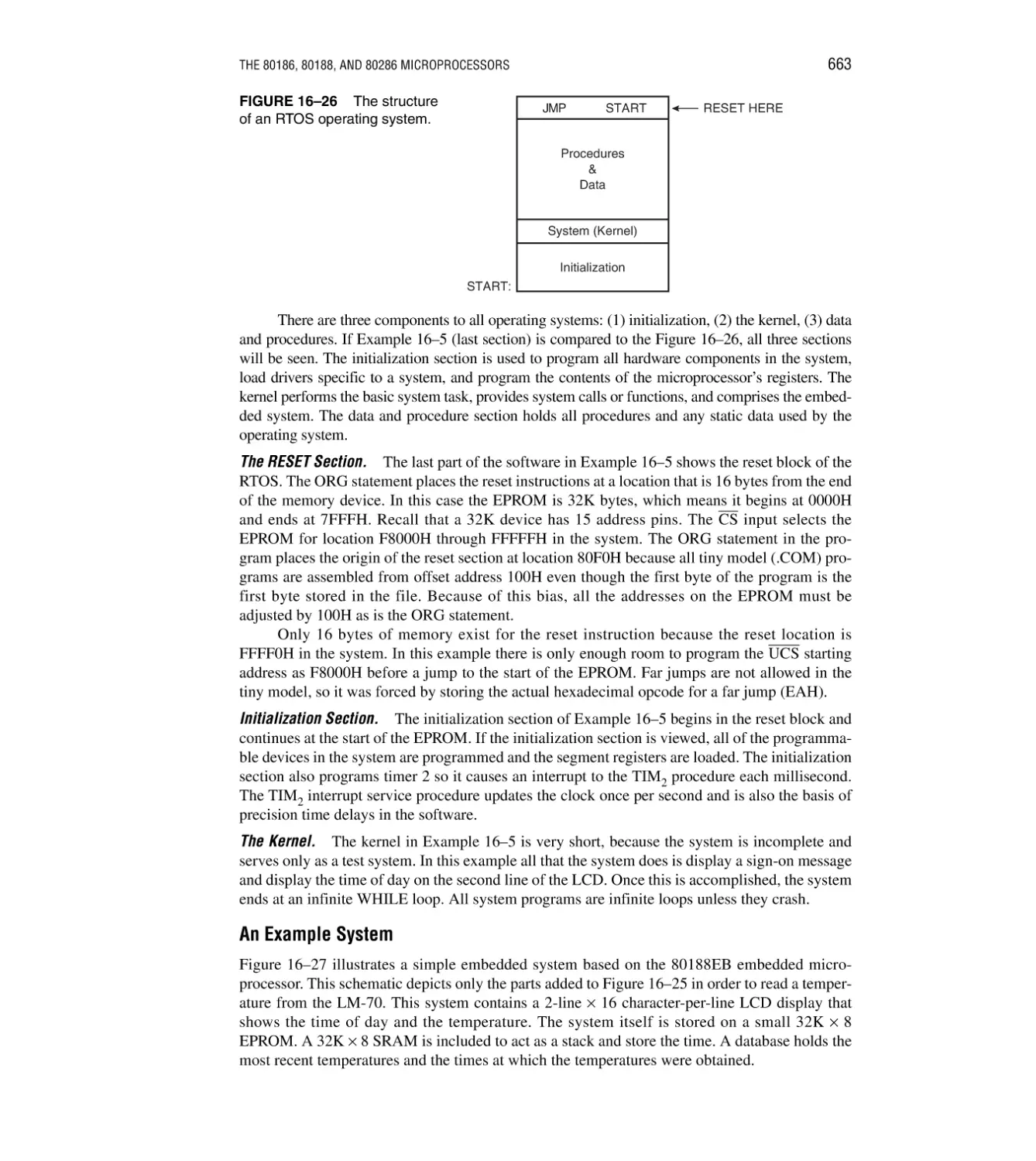
16–4 Real-Time Operating Systems (RTOS) 662
What Is a Real-Time Operating System (RTOS)? 662; An Example System 663;
A Threaded System 666
16–5 Introduction to the 80286 670
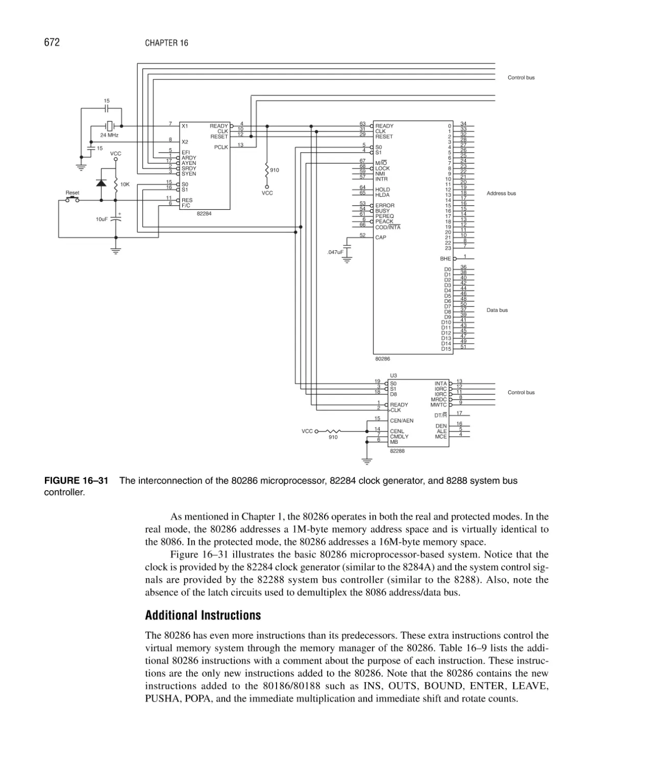
Hardware Features 670; Additional Instructions 672; The Virtual Memory Machine 674
16–6 Summary 674
16–7 Questions and Problems 675
CHAPTER 17
THE 80386 AND 80486 MICROPROCESSORS
Introduction/Chapter Objectives 677
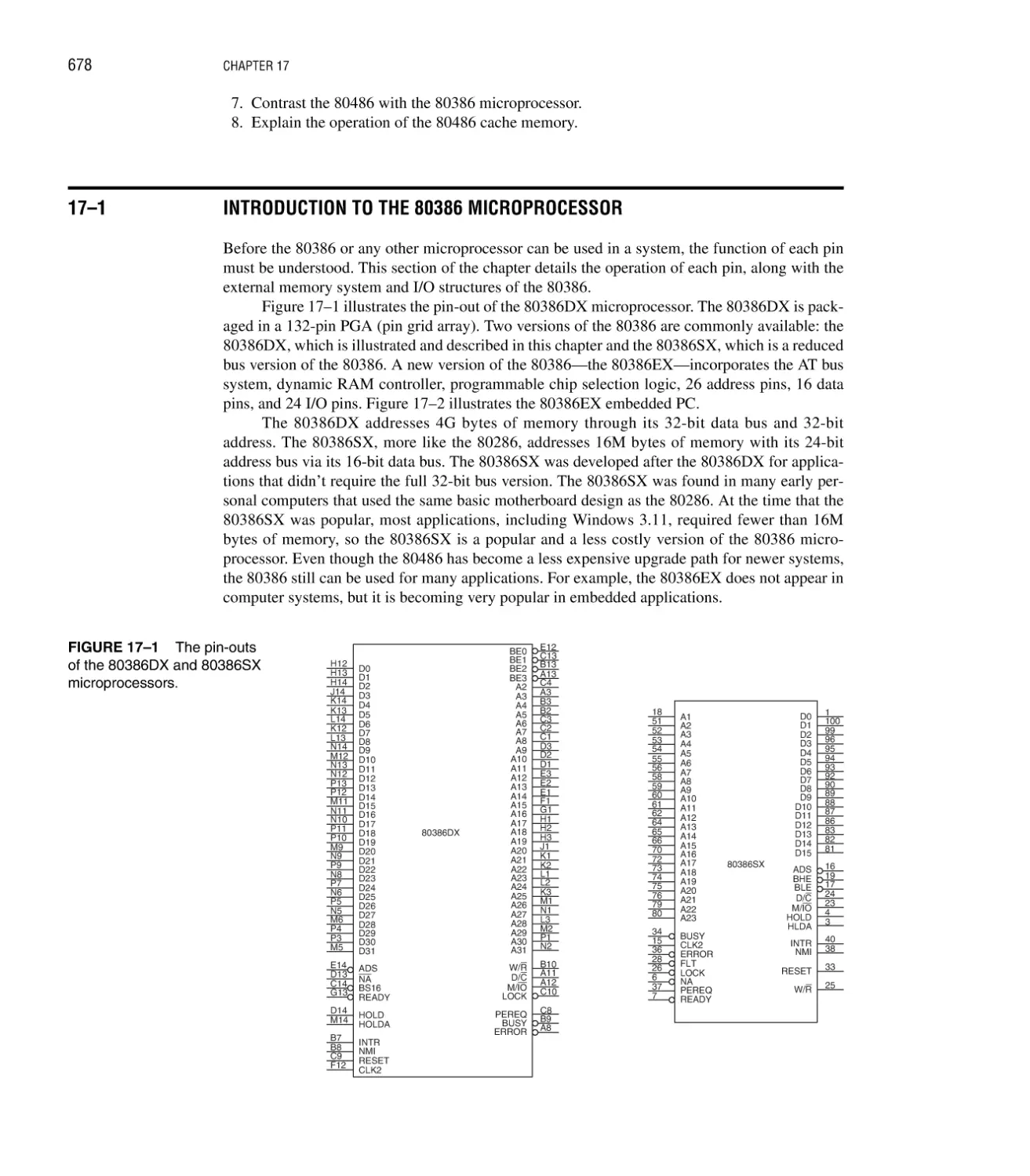
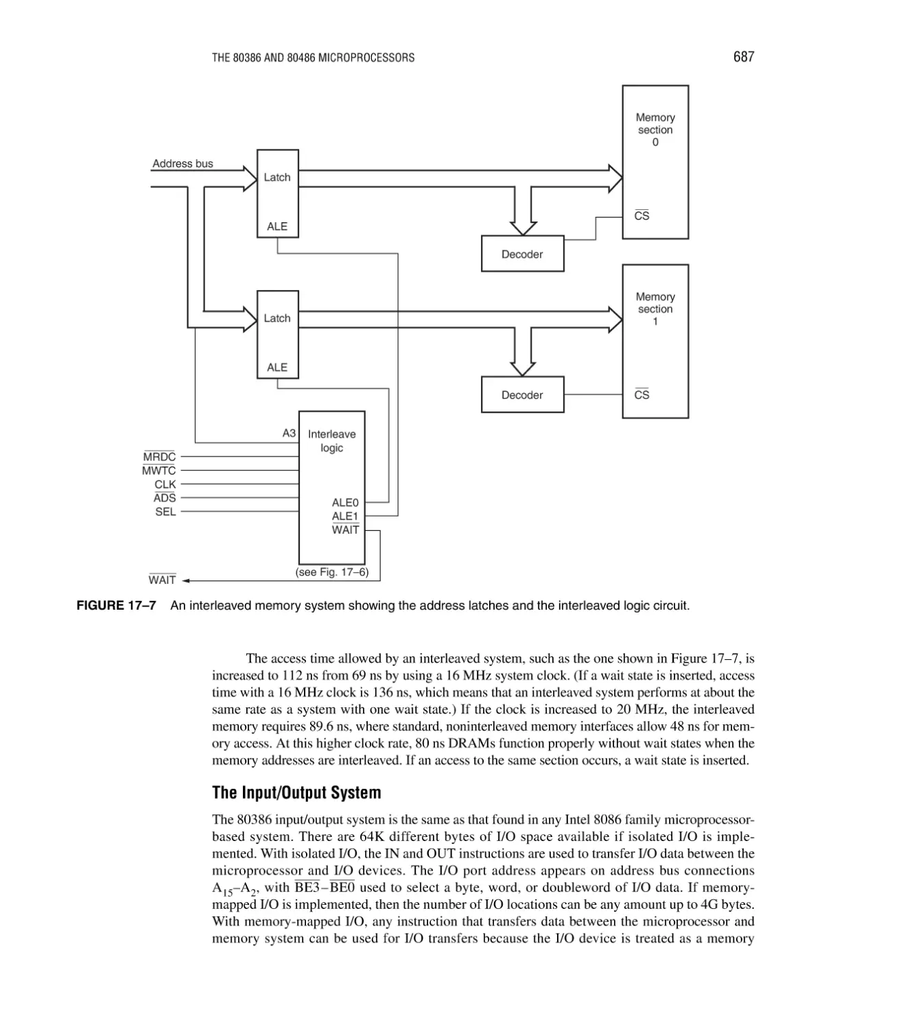
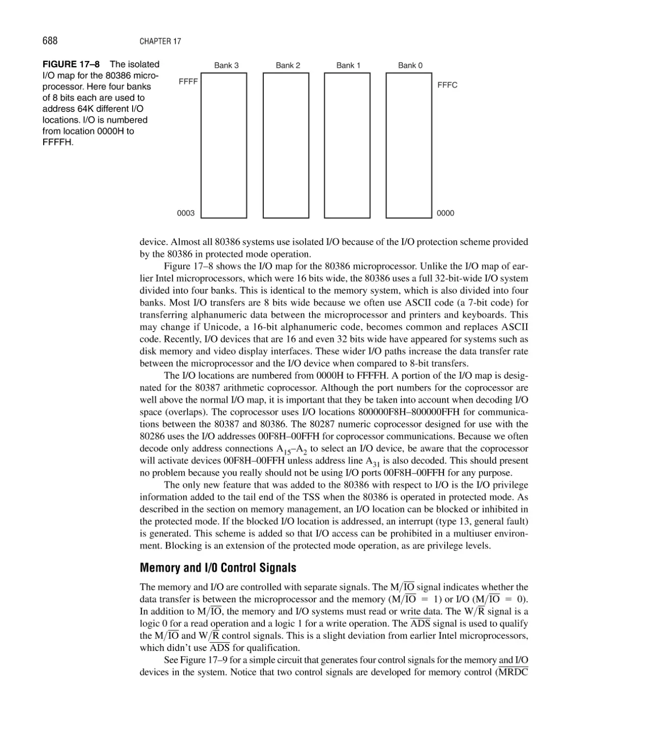
17–1 Introduction to the 80386 Microprocessor 678
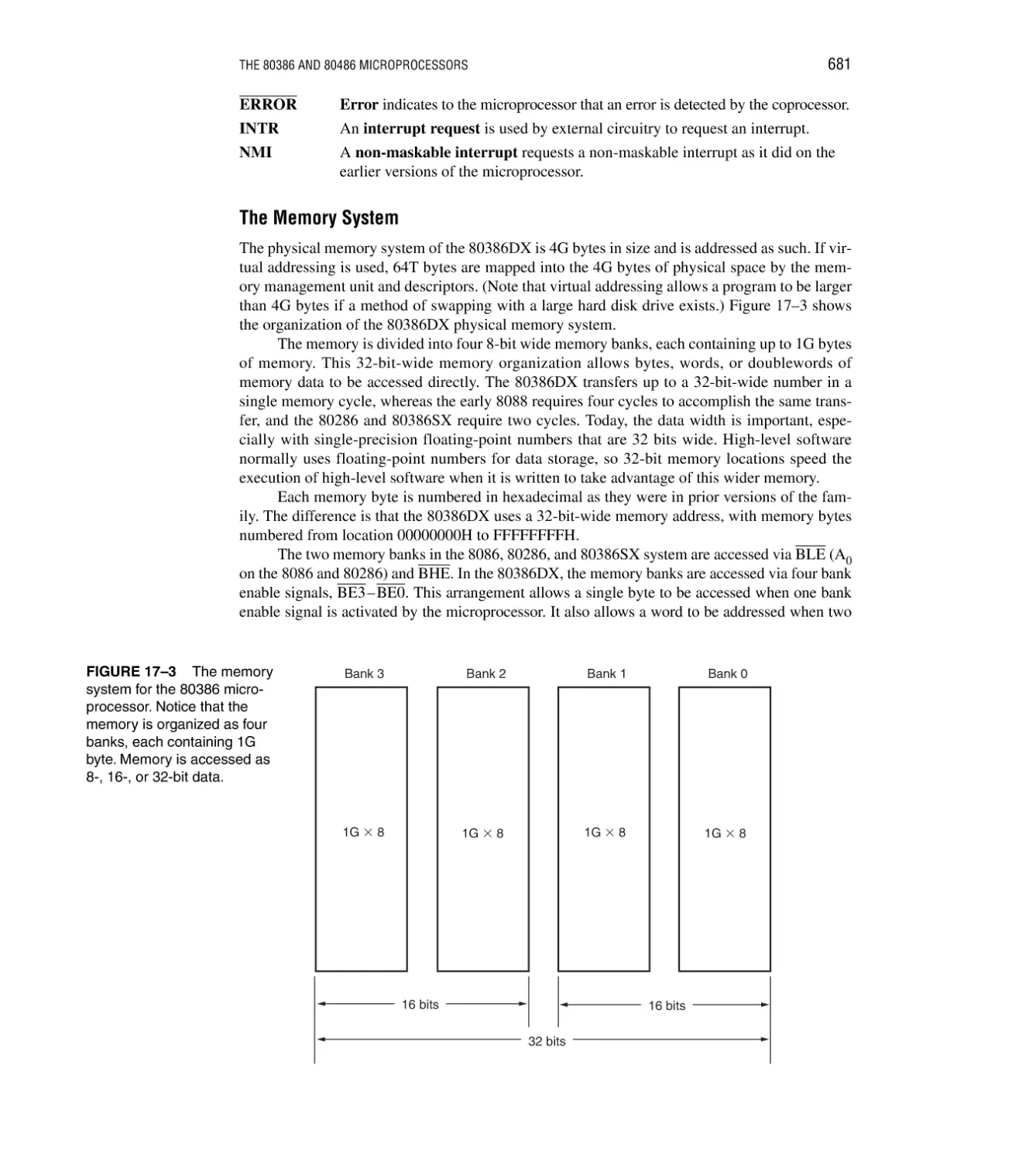
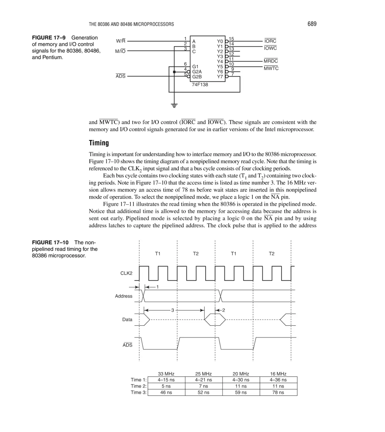
The Memory System 681; The Input/Output System 687; Memory and I/O Control
Signals 688; Timing 689; Wait States 691
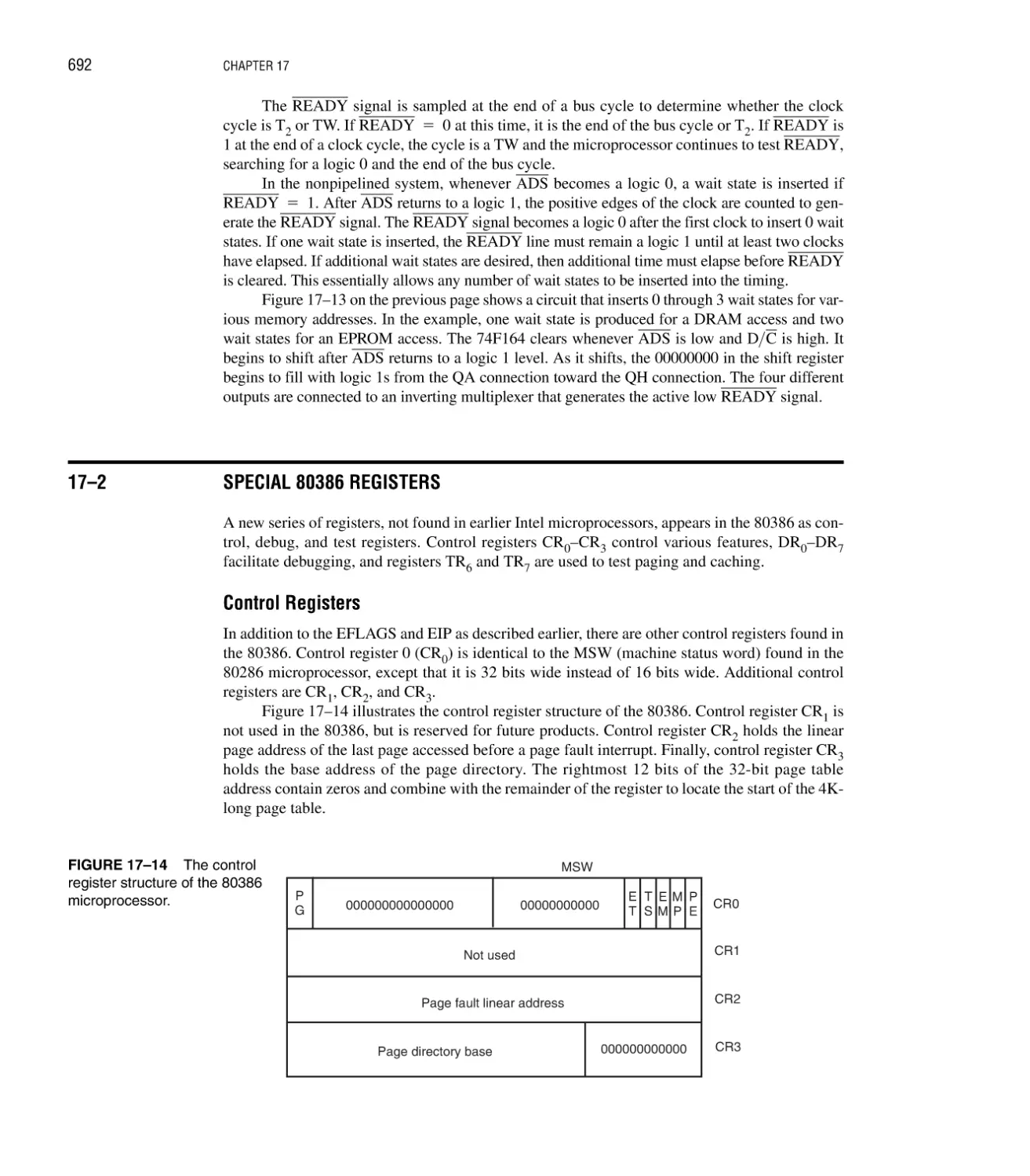
17–2 Special 80386 Registers 692
Control Registers 692; Debug and Test Registers 693
17–3 80386 Memory Management 695
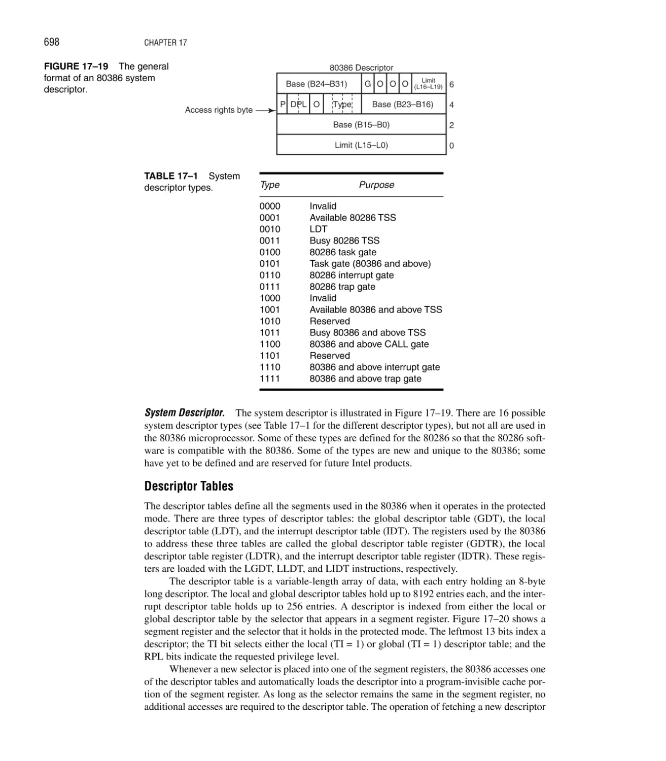
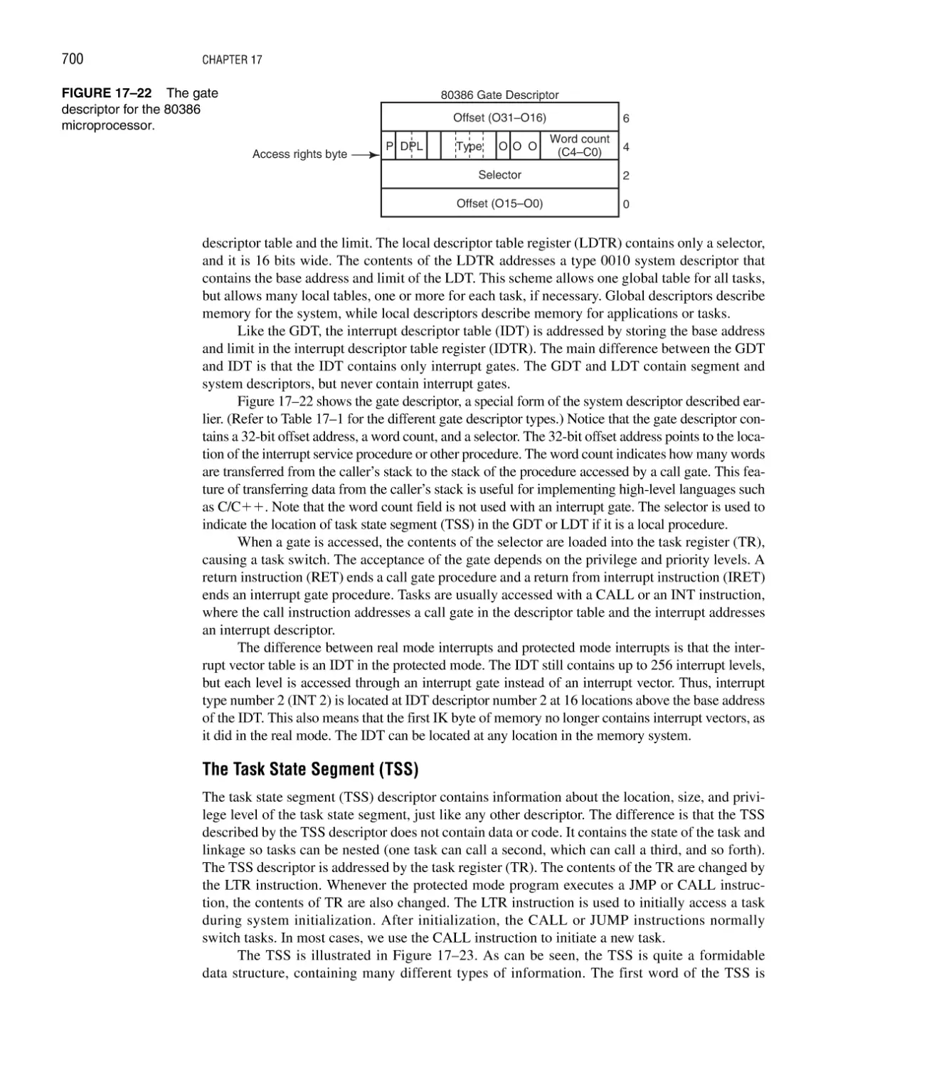
Descriptors and Selectors 695; Descriptor Tables 698; The Task State Segment (TSS) 700
17–4 Moving to Protected Mode 702
677
CONTENTS
xvii
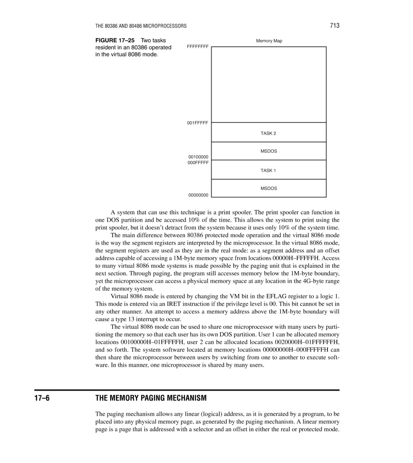
17–5 Virtual 8086 Mode 712
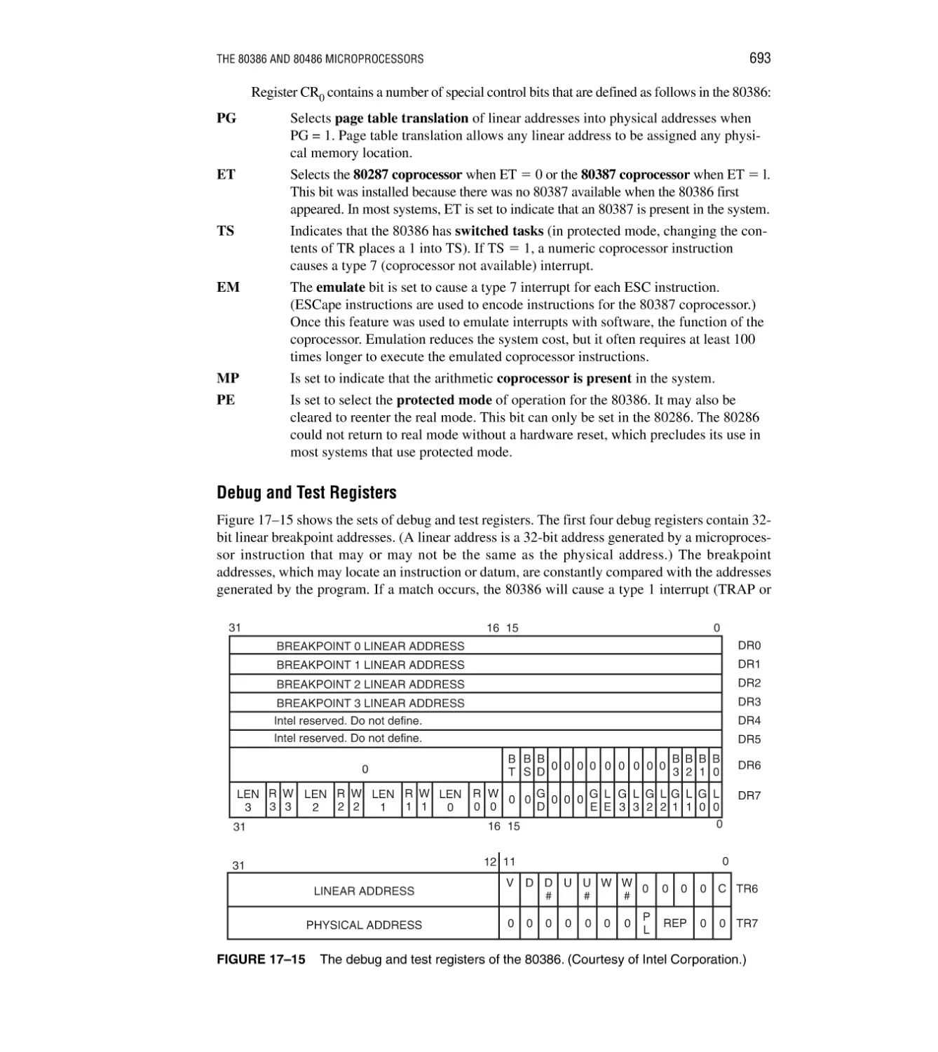
17–6 The Memory Paging Mechanism 713
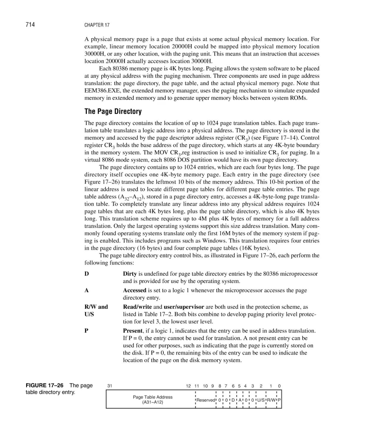
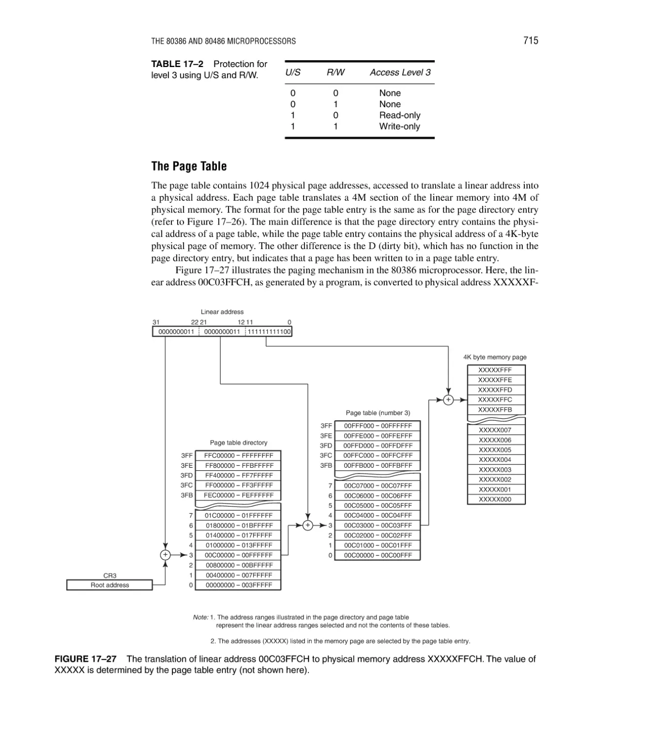
The Page Directory 714 The Page Table 715
17–7 Introduction to the 80486 Microprocessor 718
Pin-Out of the 80486DX and 80486SX Microprocessors 718; Pin Definitions 718;
Basic 80486 Architecture 722; 80486 Memory System 723
17–8 Summary 726
17–9 Questions and Problems 727
CHAPTER 18
THE PENTIUM AND PENTIUM PRO MICROPROCESSORS
729
Introduction/Chapter Objectives 729
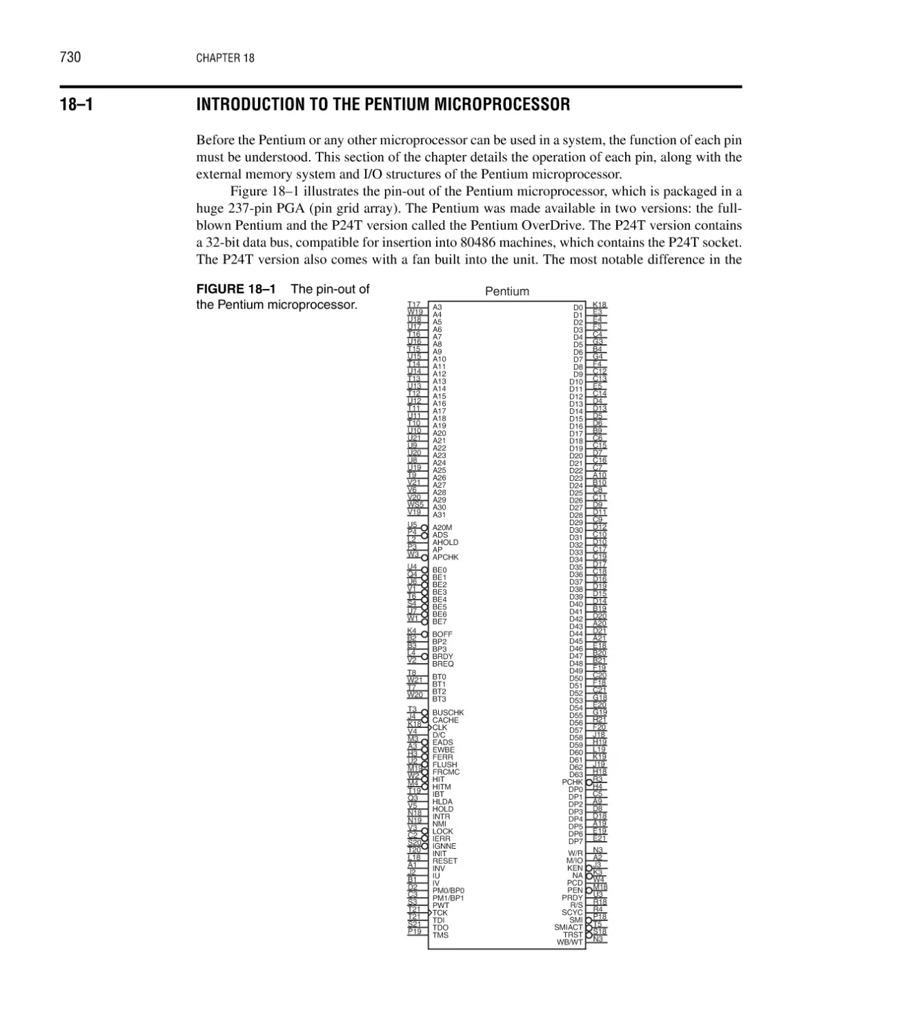
18–1 Introduction to the Pentium Microprocessor 730
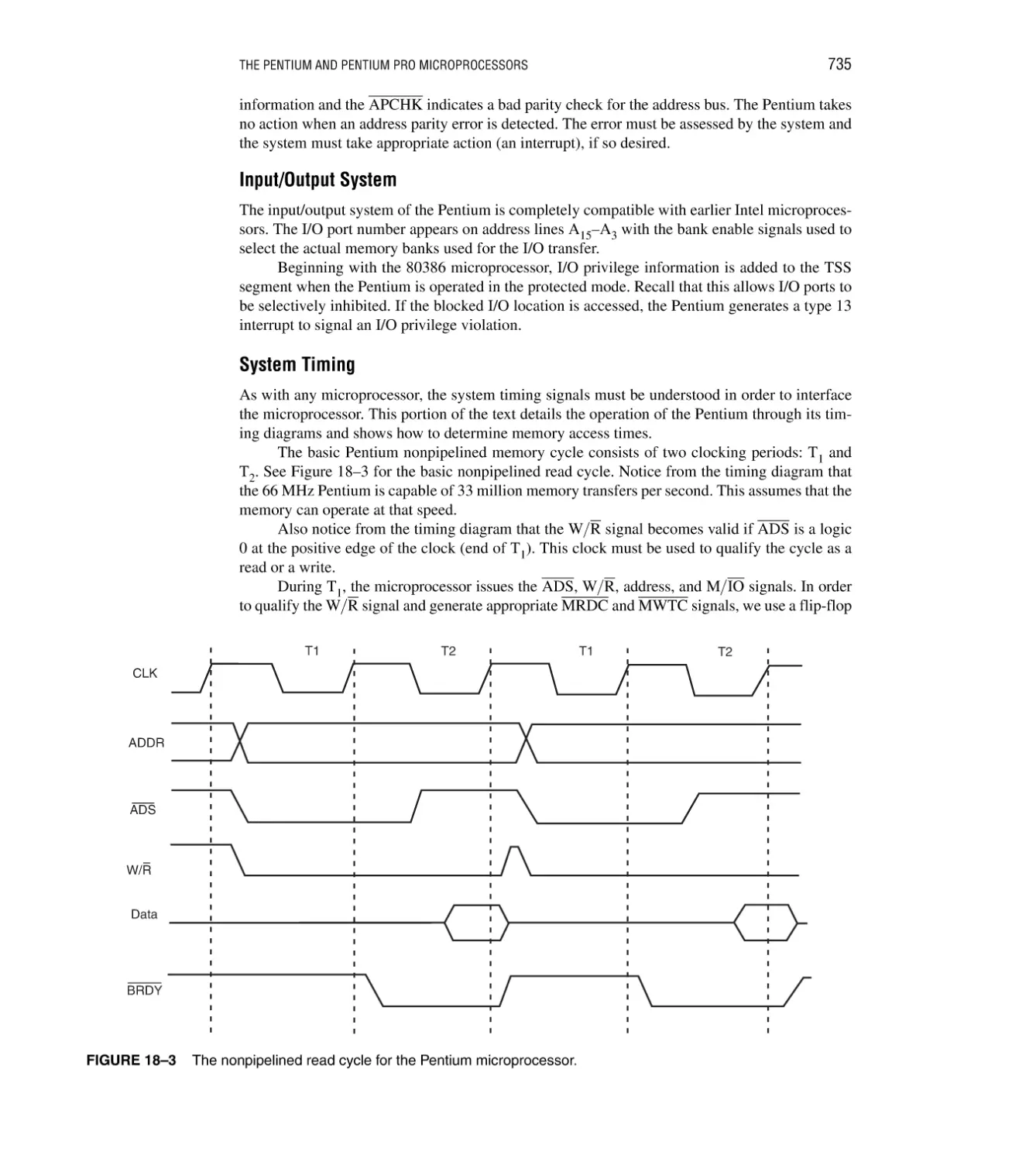
The Memory System 734; Input/Output System 735; System Timing 735;
Branch Prediction Logic 738; Cache Structure 738; Superscalar Architecture 738
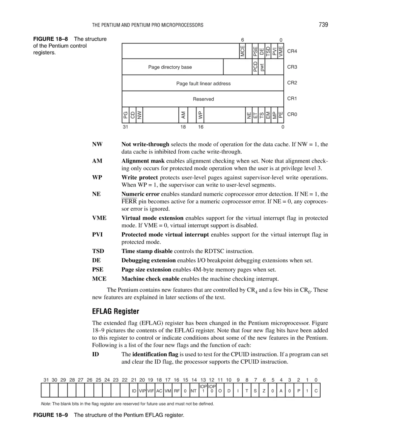
18–2 Special Pentium Registers 738
Control Registers 738; EFLAG Register 739; Built-In Self-Test (BIST) 740
18–3 Pentium Memory Management 740
Paging Unit 740; Memory-Management Mode 740
18–4 New Pentium Instructions 742
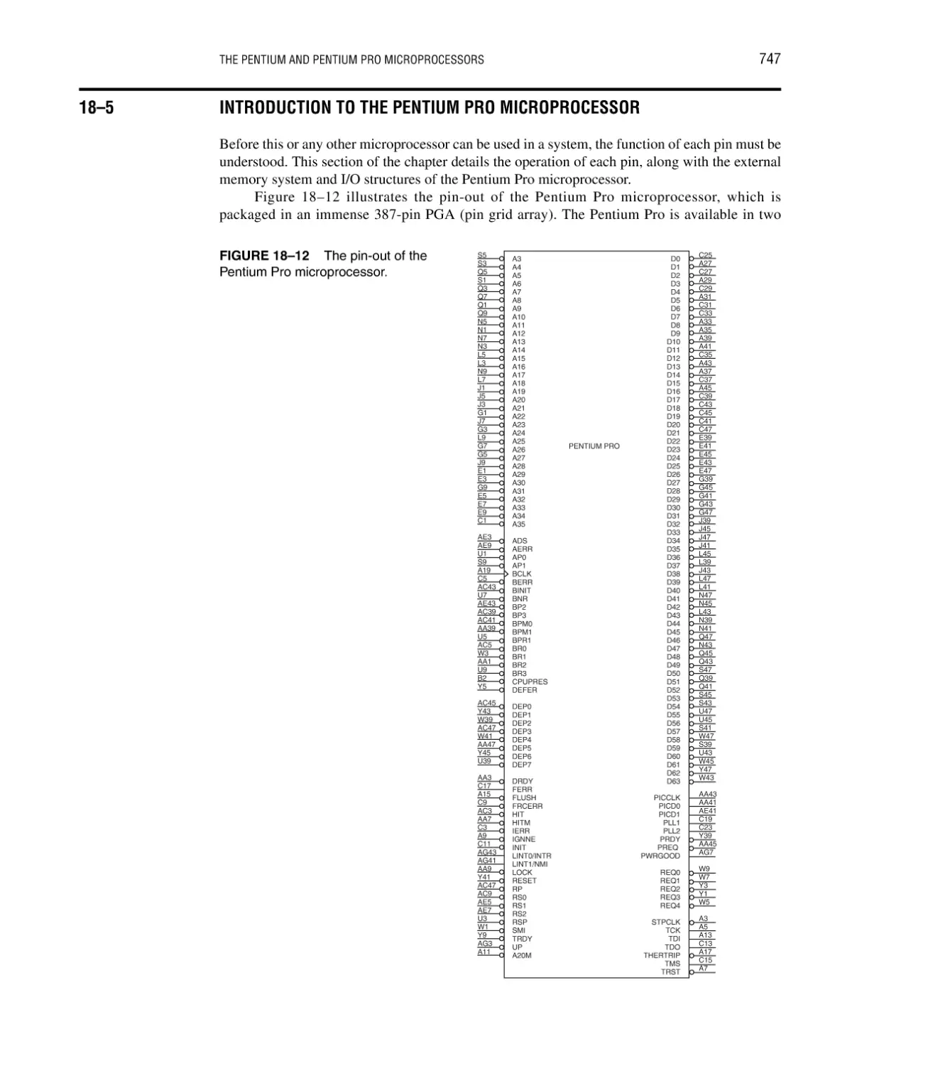
18–5 Introduction to the Pentium Pro Microprocessor 747
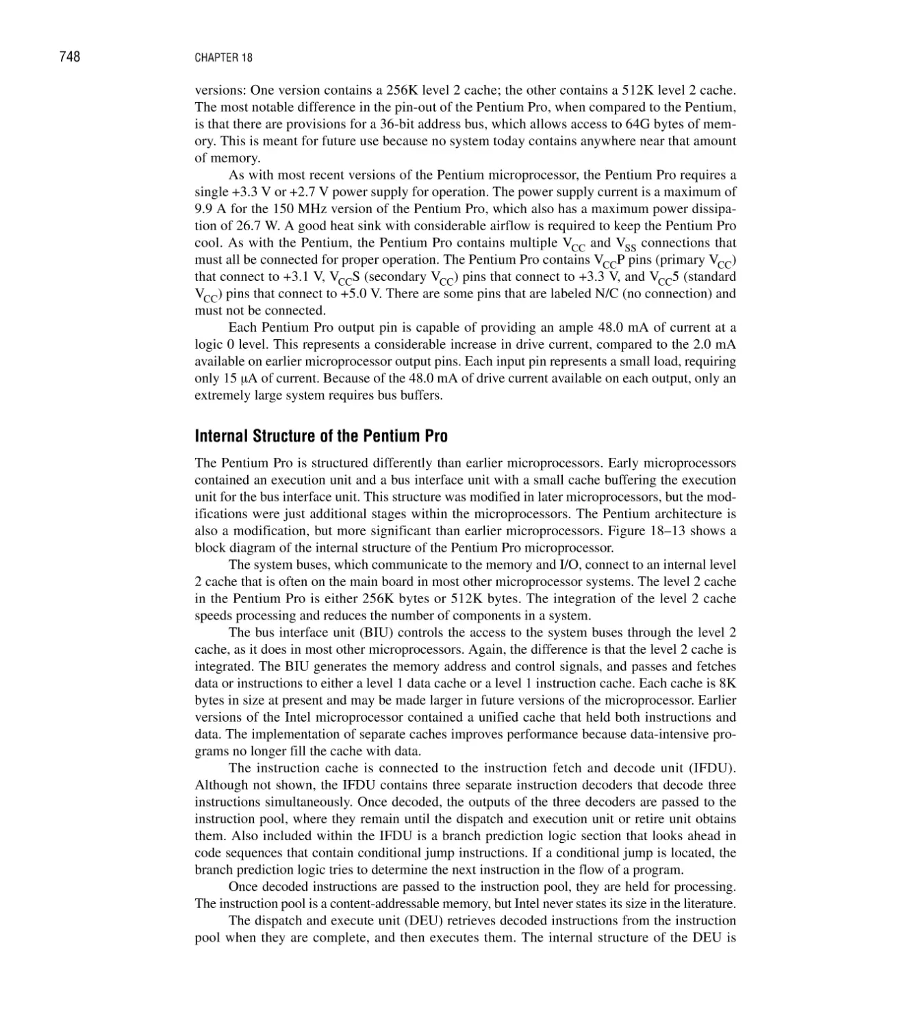
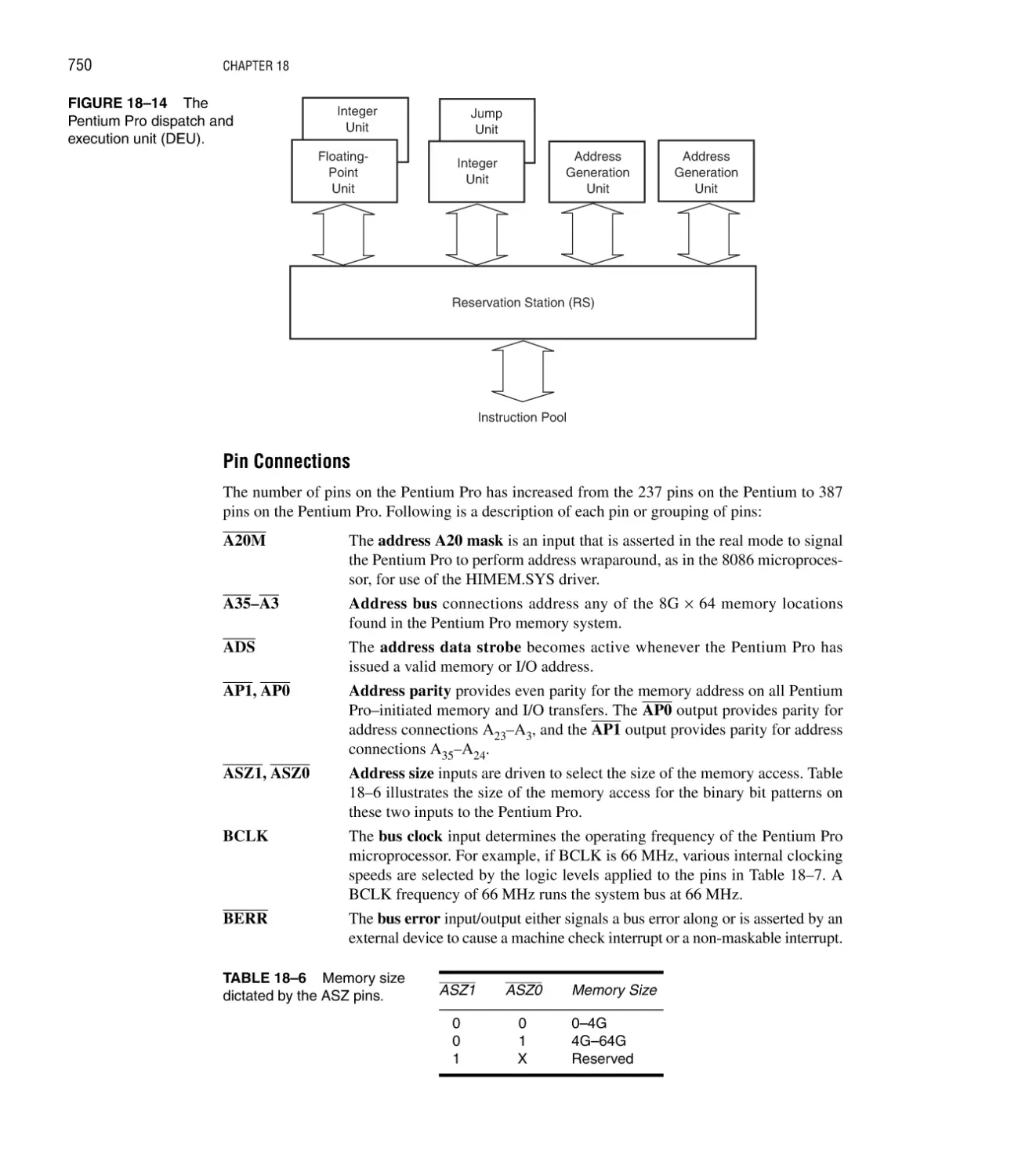
Internal Structure of the Pentium Pro 748; Pin Connections 750; The Memory System 754;
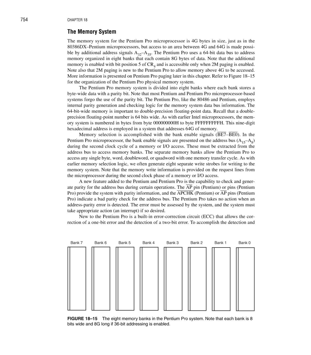
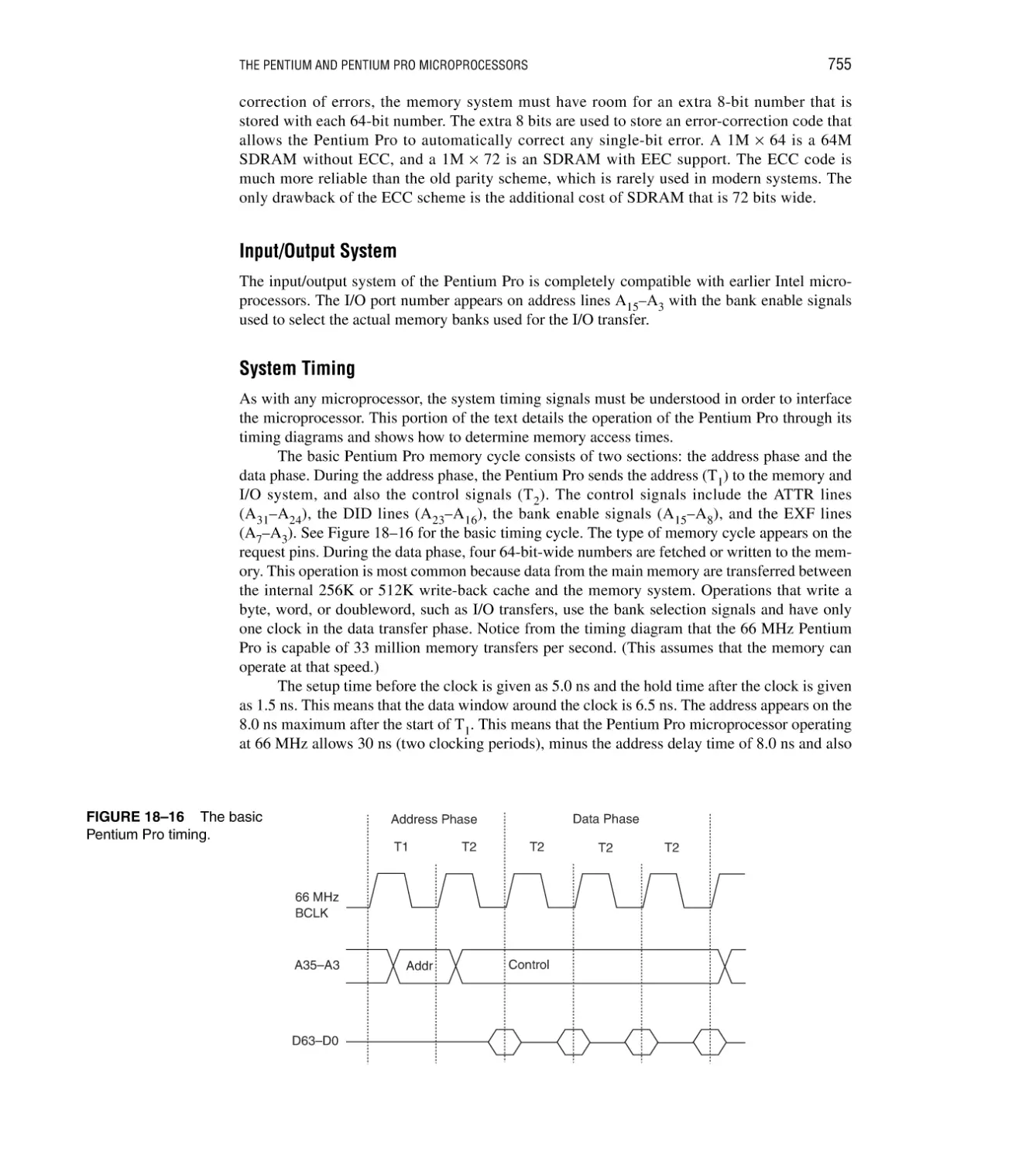
Input/Output System 755; System Timing 755
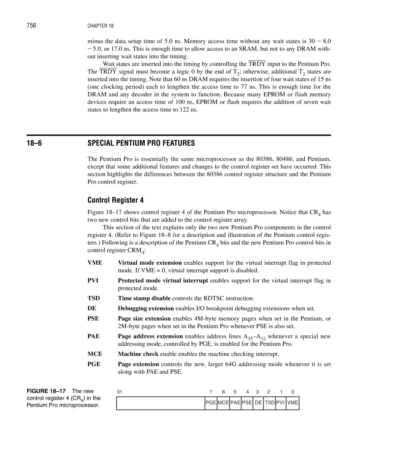
18–6 Special Pentium Pro Features 756
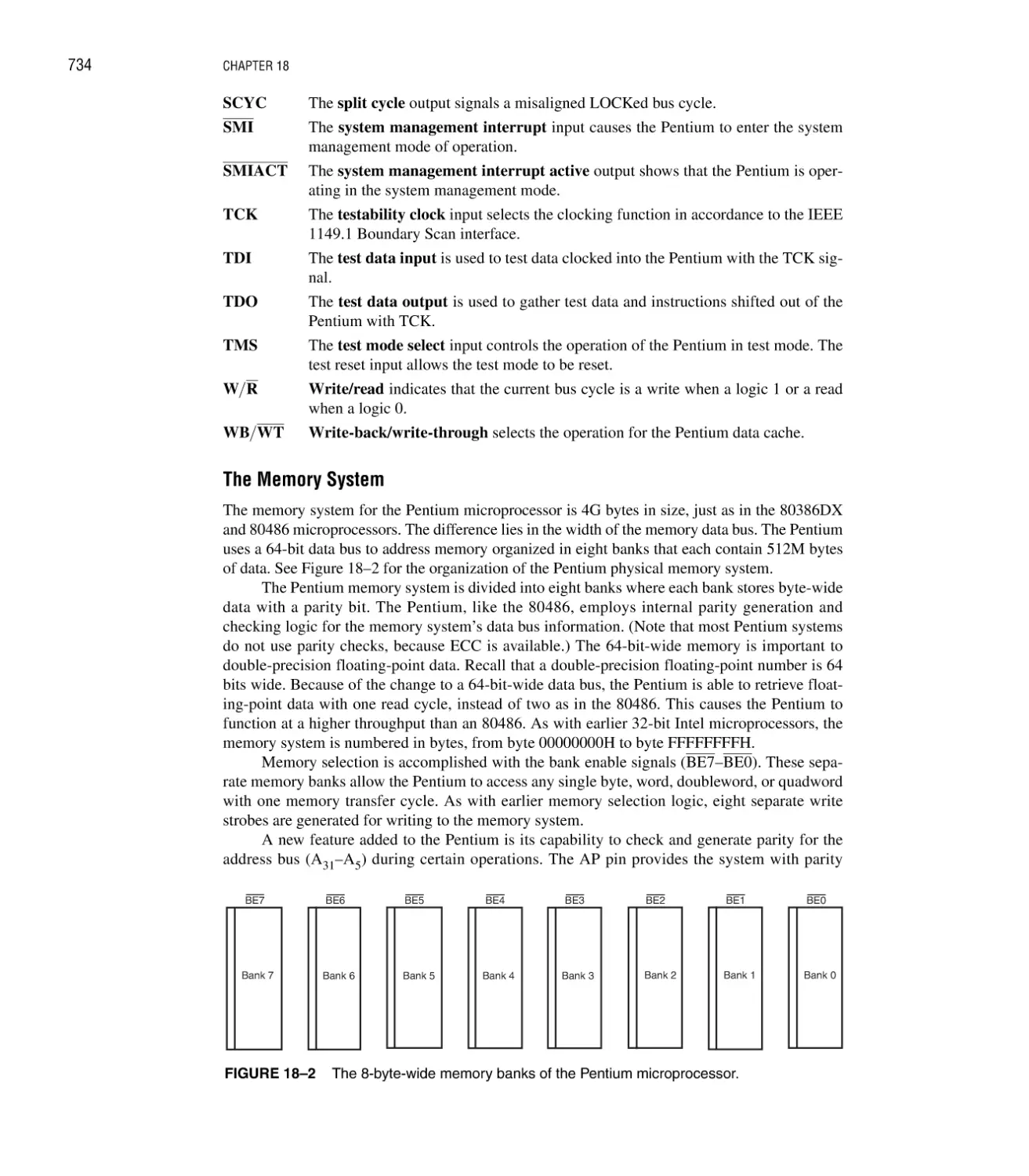
Control Register 4 756
18–7 Summary 757
18–8 Questions and Problems 758
CHAPTER 19
THE PENTIUM II, PENTIUM III, PENTIUM 4, AND CORE2 MICROPROCESSORS
759
Introduction/Chapter Objectives 759
19–1 Introduction to the Pentium II Microprocessor 760
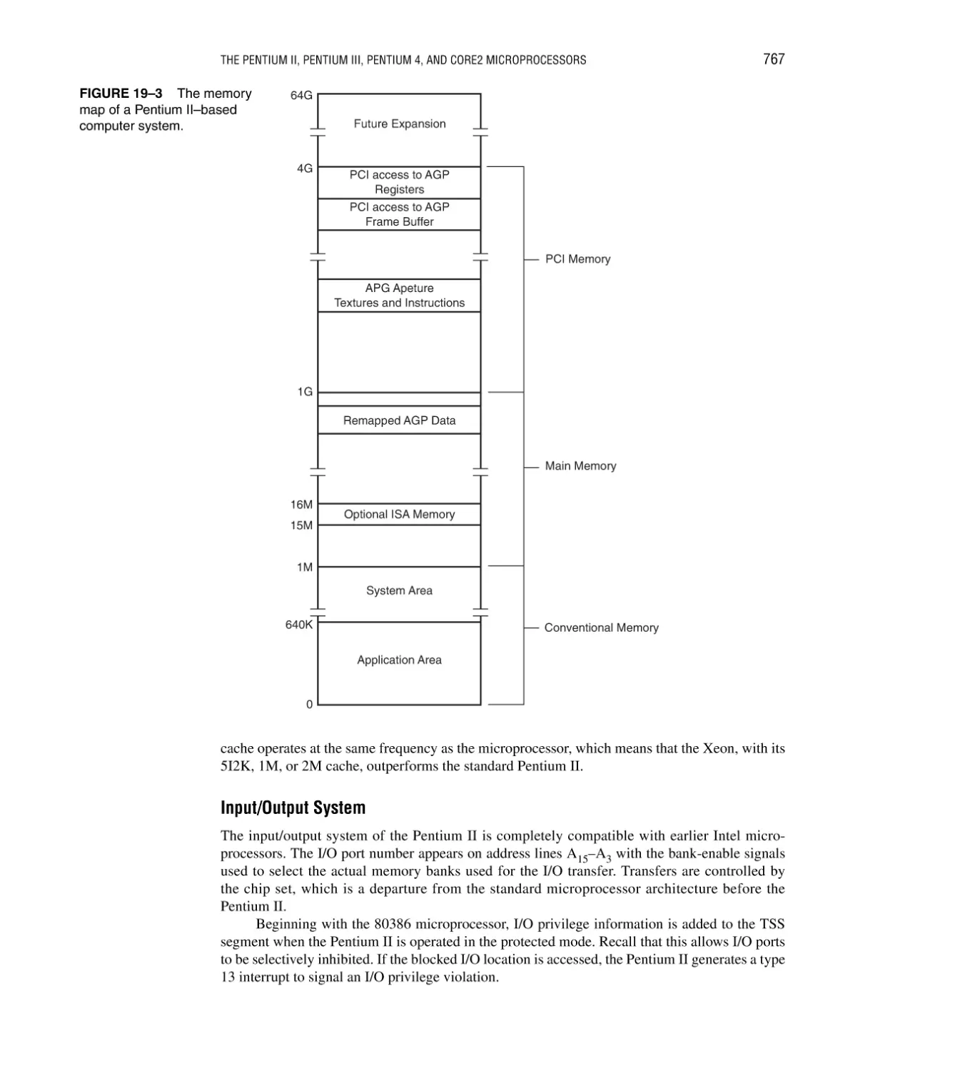
The Memory System 765; Input/Output System 767; System Timing 768
19–2 Pentium II Software Changes 768
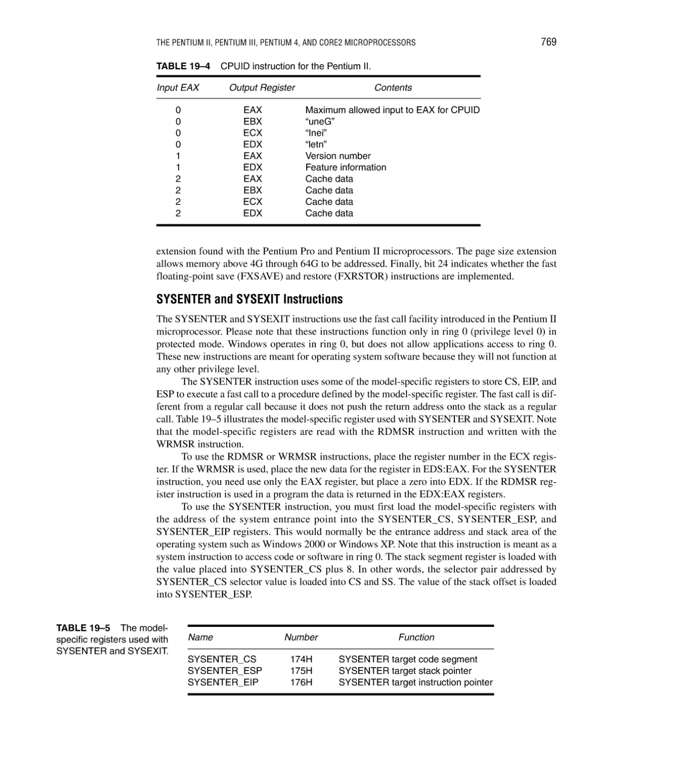
CPUID Instruction 768; SYSENTER and SYSEXIT Instructions 769;
FXSAVE and FXRSTOR Instructions 770
19–3 The Pentium III 770
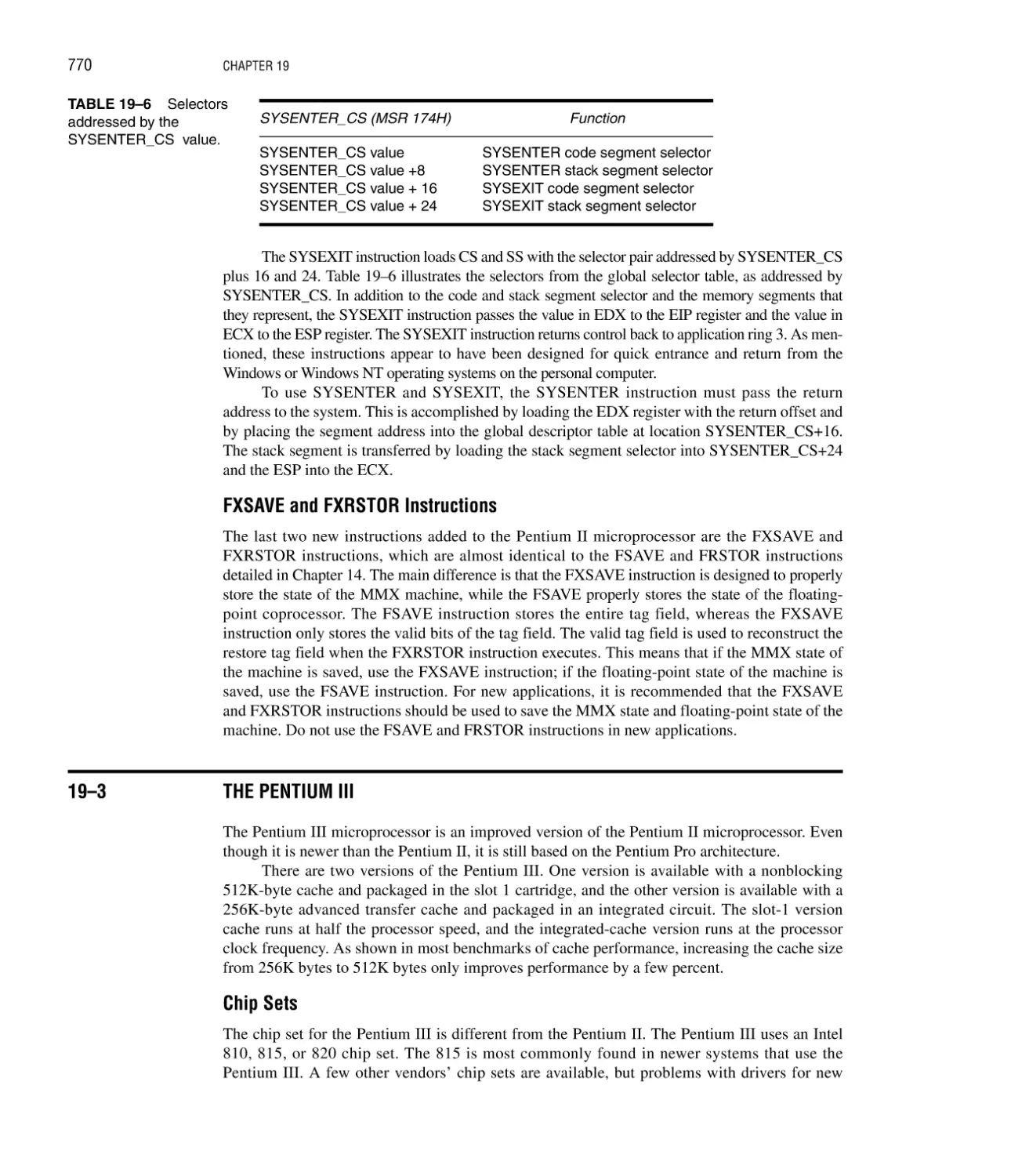
Chip Sets 770; Bus 771; Pin-Out 771
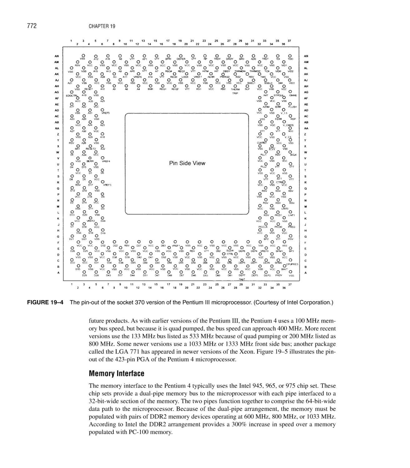
19–4 The Pentium 4 and Core2 771
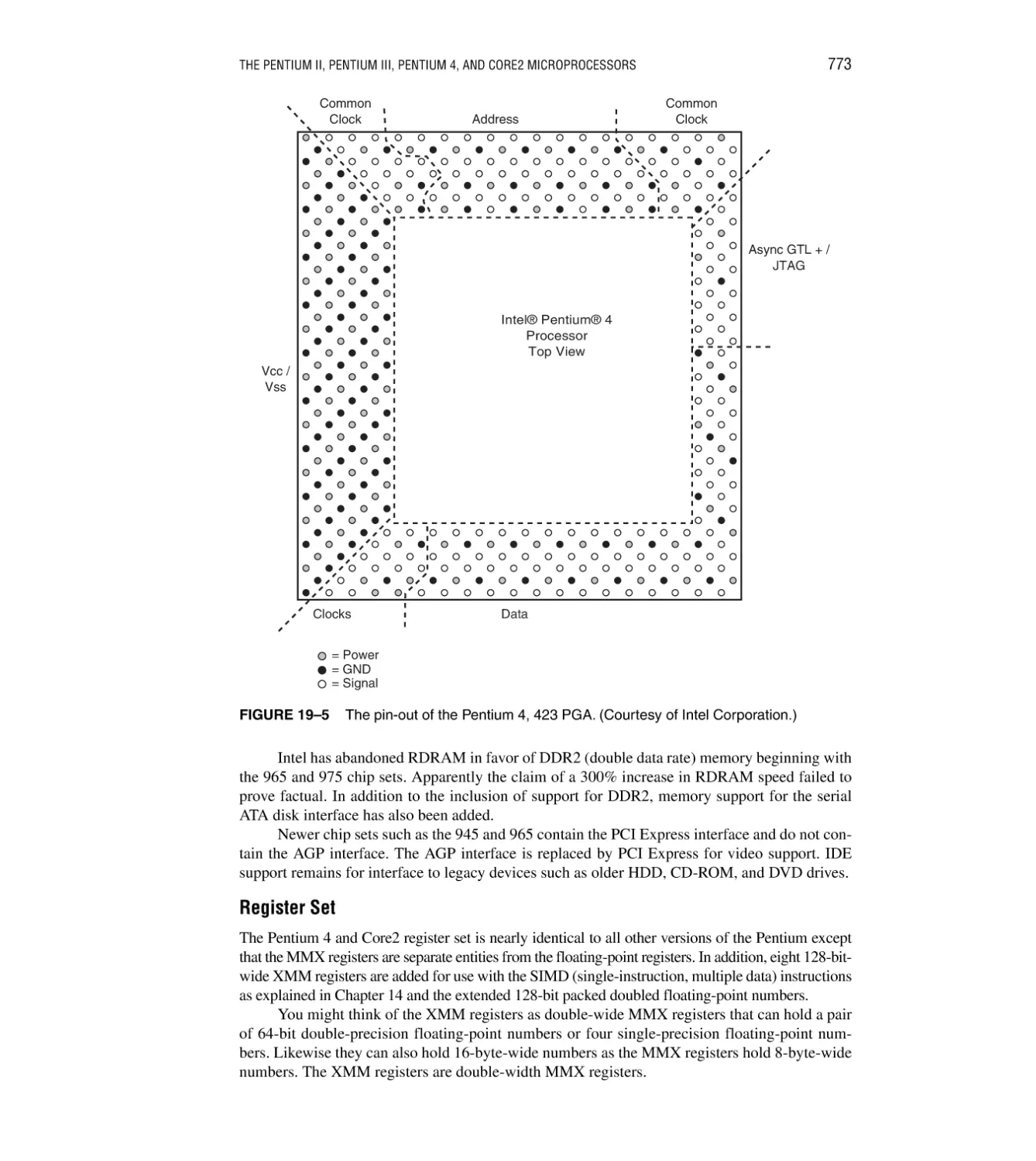
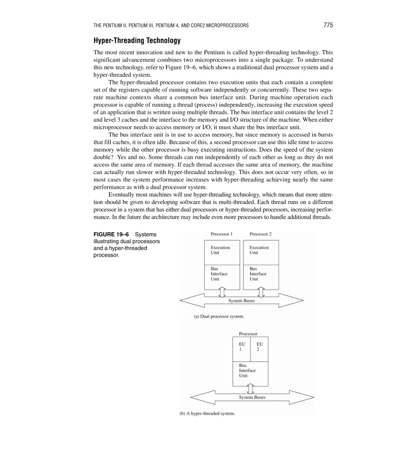
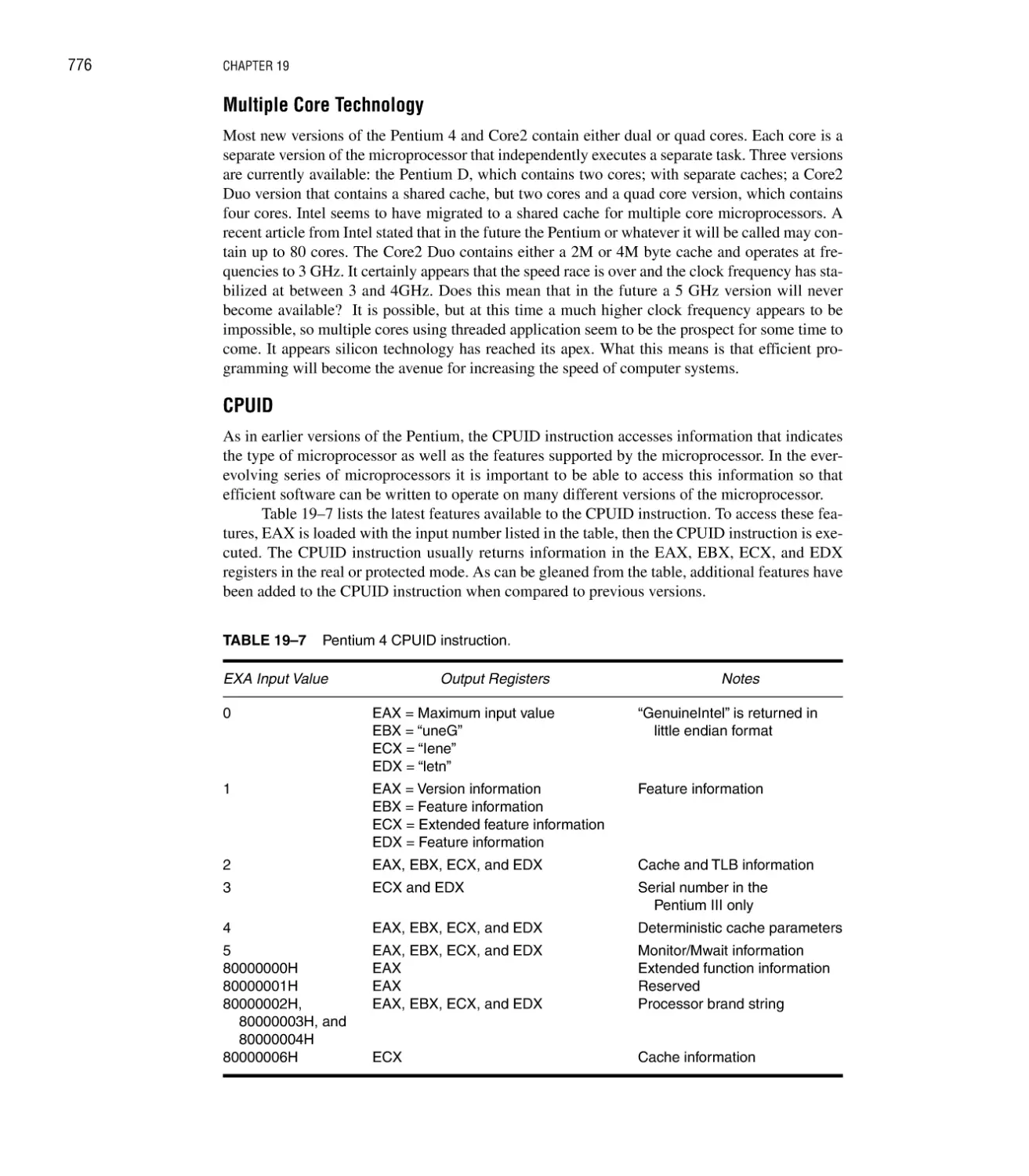
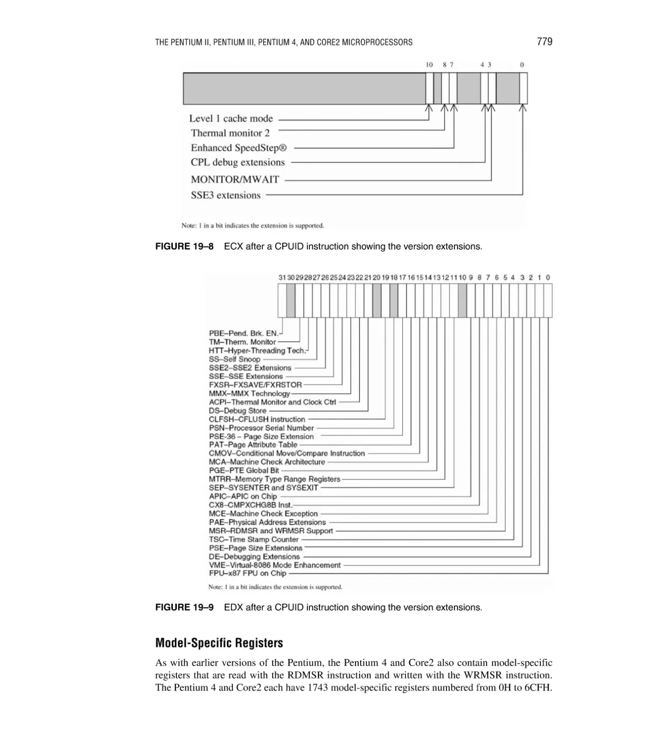
Memory Interface 772; Register Set 773; Hyper-Threading Technology 775;
Multiple Core Technology 776; CPUID 776; Model-Specific Registers 779;
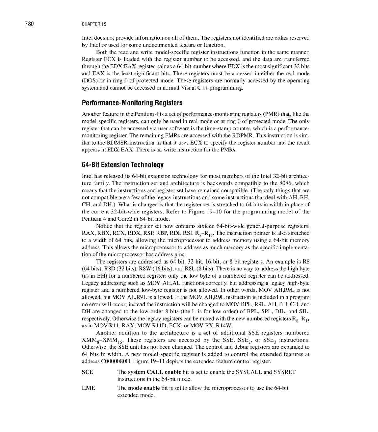
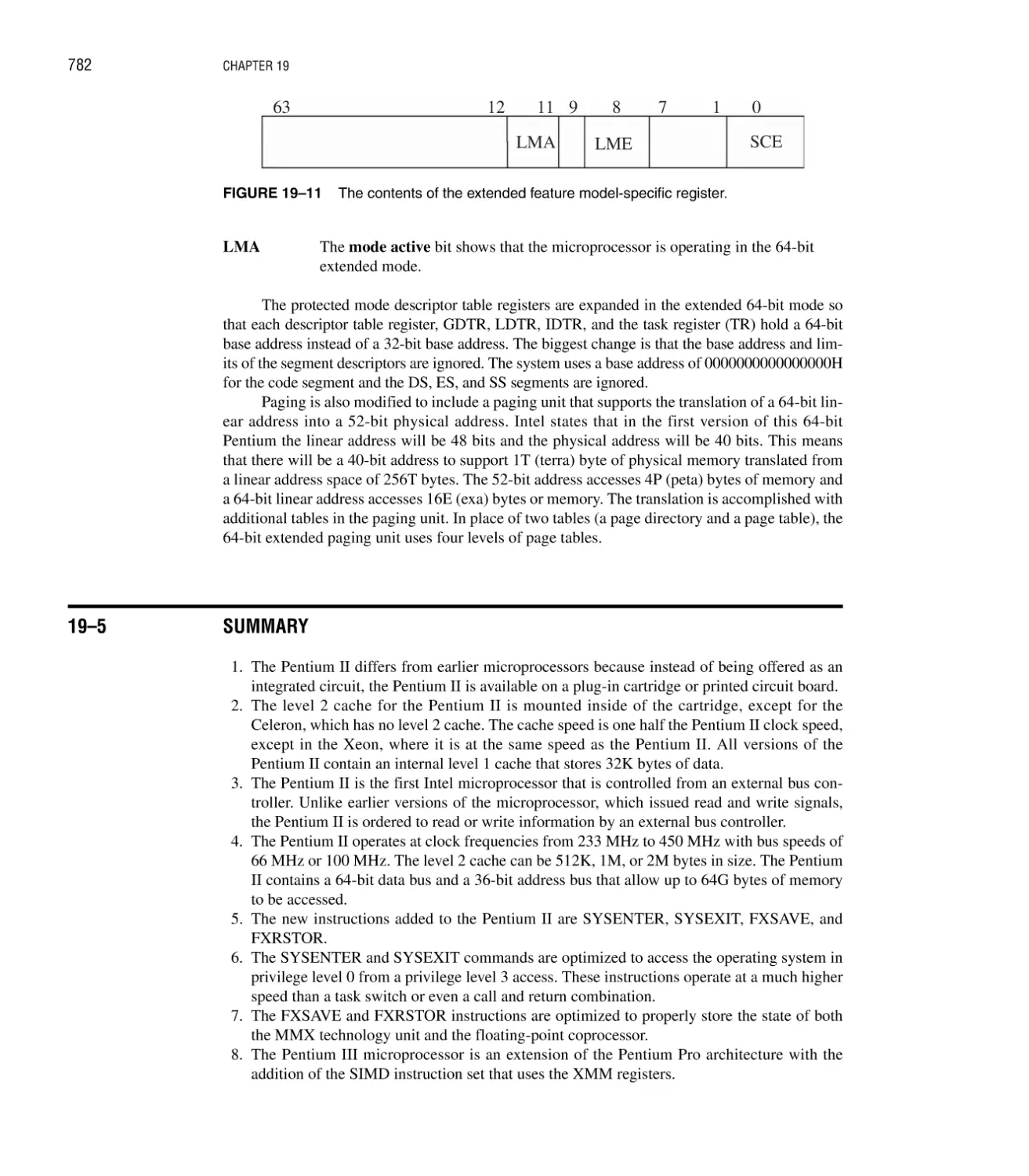
Performance-Monitoring Registers 780; 64-Bit Extension Technology 780
19–5 Summary 782
19–6 Questions and Problems 783
APPENDIX A: THE ASSEMBLER, VISUAL C++, AND DOS
785
The Assembler 785
Assembler Memory Models 786
Selected DOS Function Calls 787
Using Visual C++ 790
Create a Dialog Application 791
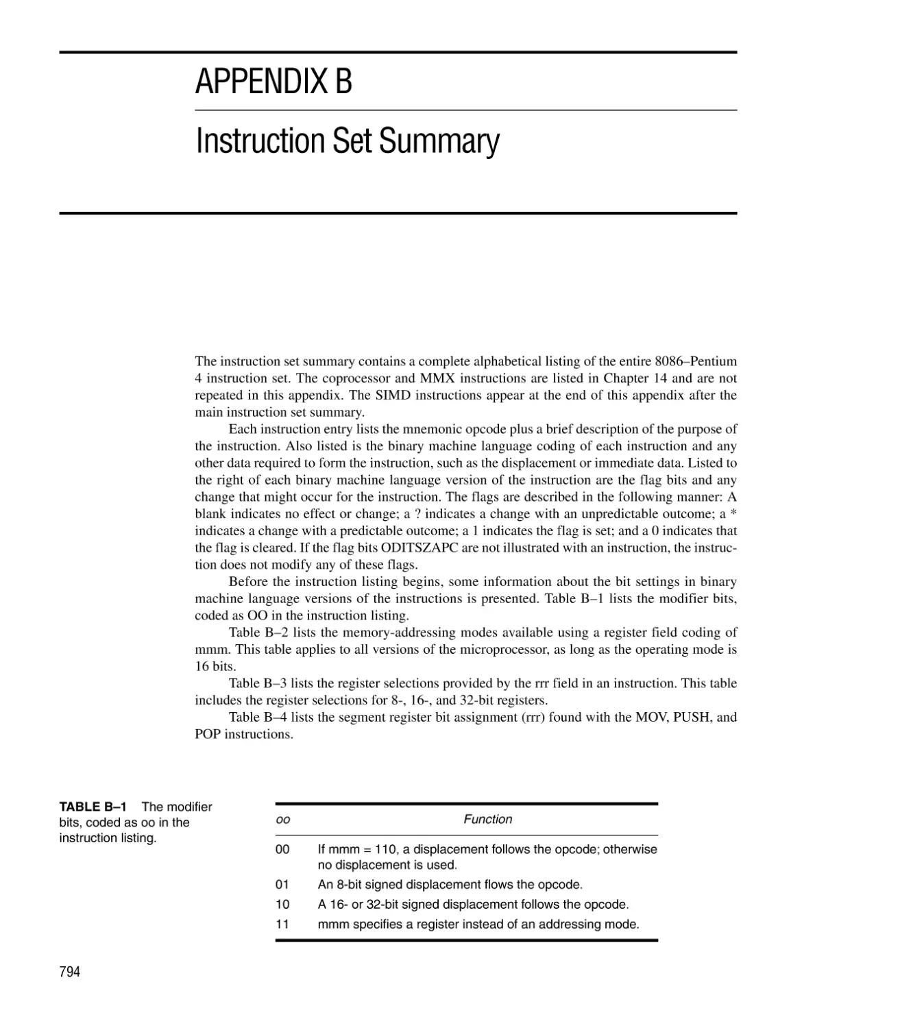
APPENDIX B: INSTRUCTION SET SUMMARY
Instruction Set Summary 798
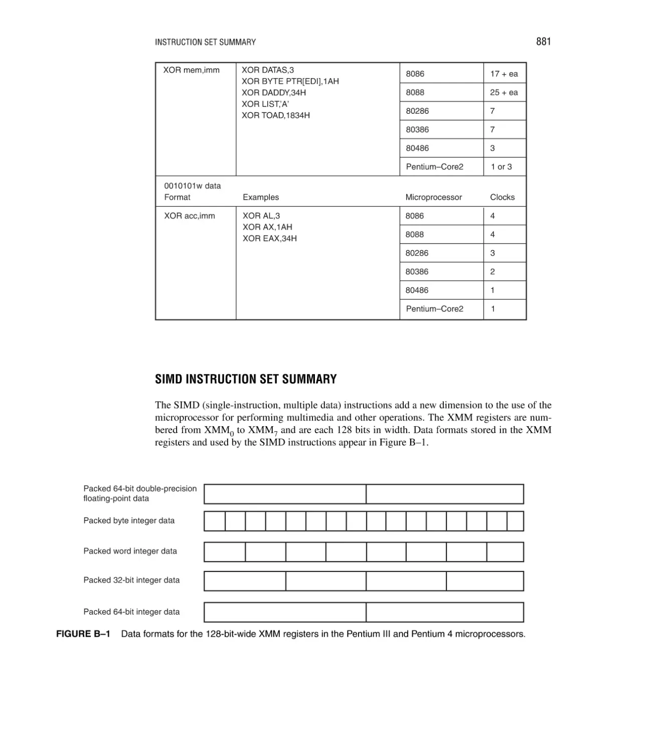
SIMD Instruction Set Summary 881
794
xviii
CONTENTS
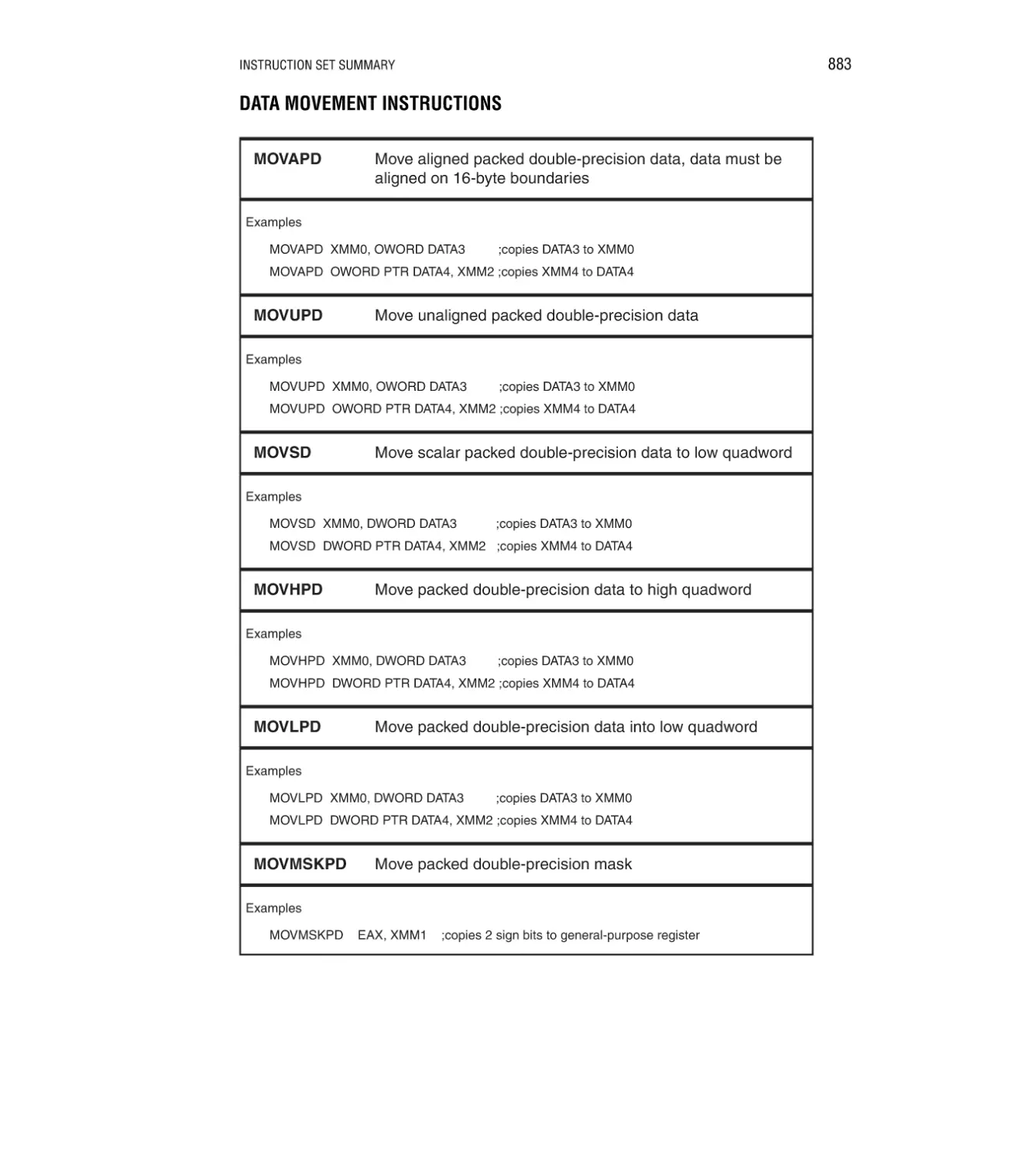
Data Movement Instructions 883
Arithmetic Instructions 885
Logic Instructions 891
Comparison Instructions 892
Data Conversion Instructions 894
APPENDIX C: FLAG-BIT CHANGES
895
APPENDIX D: ANSWERS TO SELECTED EVEN-NUMBERED QUESTIONS
AND PROBLEMS
897
INDEX
915
CHAPTER 1
Introduction to the Microprocessor
and Computer
INTRODUCTION
This chapter provides an overview of the Intel family of microprocessors. Included is a discussion of the history of computers and the function of the microprocessor in the microprocessorbased computer system. Also introduced are terms and jargon used in the computer field, so
that computerese is understood and applied when discussing microprocessors and computers.
The block diagram and a description of the function of each block detail the operation of
a computer system. Blocks, in the block diagram, show how the memory and input/output (I/O)
system of the personal computer interconnect. Detailed is the way data are stored in the memory so each data type can be used as software is developed. Numeric data are stored as integers,
floating-point, and binary-coded decimal (BCD); alphanumeric data are stored by using the
ASCII (American Standard Code for Information Interchange) code and the Unicode.
CHAPTER OBJECTIVES
Upon completion of this chapter, you will be able to:
1. Converse by using appropriate computer terminology such as bit, byte, data, real memory
system, protected mode memory system, Windows, DOS, I/O, and so forth.
2. Briefly detail the history of the computer and list applications performed by computer
systems.
3. Provide an overview of the various 80X86 and Pentium family members.
4. Draw the block diagram of a computer system and explain the purpose of each block.
5. Describe the function of the microprocessor and detail its basic operation.
6. Define the contents of the memory system in the personal computer.
7. Convert between binary, decimal, and hexadecimal numbers.
8. Differentiate and represent numeric and alphabetic information as integers, floating-point,
BCD, and ASCII data.
1
2
CHAPTER 1
1–1
A HISTORICAL BACKGROUND
This first section outlines the historical events leading to the development of the microprocessor
and, specifically, the extremely powerful and current 80X86,1 Pentium, Pentium Pro, Pentium III,
Pentium 4,2 and Core2 microprocessors. Although a study of history is not essential to understand
the microprocessor, it furnishes interesting reading and provides a historical perspective of the
fast-paced evolution of the computer.
The Mechanical Age
The idea of a computing system is not new—it has been around long before modem electrical and
electronic devices were developed. The idea of calculating with a machine dates to 500 BC when
the Babylonians, the ancestors of the present-day Iraqis, invented the abacus, the first mechanical
calculator. The abacus, which uses strings of beads to perform calculations, was used by the
ancient Babylonian priests to keep track of their vast storehouses of grain. The abacus, which was
used extensively and is still in use today, was not improved until 1642, when mathematician
Blaise Pascal invented a calculator that was constructed of gears and wheels. Each gear contained
10 teeth that, when moved one complete revolution, advanced a second gear one place. This is the
same principle that is used in the automobile’s odometer mechanism and is the basis of all
mechanical calculators. Incidentally, the PASCAL programming language is named in honor of
Blaise Pascal for his pioneering work in mathematics and with the mechanical calculator.
The arrival of the first practical geared mechanical machines used to automatically compute information dates to the early 1800s. This is before humans invented the lightbulb or before
much was known about electricity. In this dawn of the computer age, humans dreamed of
mechanical machines that could compute numerical facts with a program—not merely calculating facts, as with a calculator.
In 1937 it was discovered through plans and journals that one early pioneer of mechanical computing machinery was Charles Babbage, aided by Augusta Ada Byron, the Countess of Lovelace.
Babbage was commissioned in 1823 by the Royal Astronomical Society of Great Britain to produce
a programmable calculating machine. This machine was to generate navigational tables for the Royal
Navy. He accepted the challenge and began to create what he called his Analytical Engine. This
engine was a steam-powered mechanical computer that stored a thousand 20-digit decimal numbers and a variable program that could modify the function of the machine to perform various calculating tasks. Input to his engine was through punched cards, much as computers in the 1950s and
1960s used punched cards. It is assumed that he obtained the idea of using punched cards from Joseph
Jacquard, a Frenchman who used punched cards as input to a weaving machine he invented in 1801,
which is today called Jacquard’s loom. Jacquard’s loom used punched cards to select intricate weaving patterns in the cloth that it produced. The punched cards programmed the loom.
After many years of work, Babbage’s dream began to fade when he realized that the
machinists of his day were unable to create the mechanical parts needed to complete his work.
The Analytical Engine required more than 50,000 machined parts, which could not be made with
enough precision to allow his engine to function reliably.
The Electrical Age
The 1800s saw the advent of the electric motor (conceived by Michael Faraday); with it came a
multitude of motor-driven adding machines, all based on the mechanical calculator developed by
Blaise Pascal. These electrically driven mechanical calculators were common pieces of office
180X86
is an accepted acronym for 8086, 8088, 80186, 80188, 80286, 80386, and 80486 microprocessors
and also include the Pentium series.
2Pentium, Pentium Pro, Pentium II, Pentium III, Pentium 4, and Core2 are registered trademarks of Intel Corporation.
INTRODUCTION TO THE MICROPROCESSOR AND COMPUTER
3
equipment until well into the early 1970s, when the small handheld electronic calculator, first
introduced by Bomar Corporation and called the Bomar Brain, appeared. Monroe was also a
leading pioneer of electronic calculators, but its machines were desktop, four-function models
the size of cash registers.
In 1889, Herman Hollerith developed the punched card for storing data. Like Babbage, he
too apparently borrowed the idea of a punched card from Jacquard. He also developed a mechanical machine—driven by one of the new electric motors—that counted, sorted, and collated
information stored on punched cards. The idea of calculating by machinery intrigued the United
States government so much that Hollerith was commissioned to use his punched-card system to
store and tabulate information for the 1890 census.
In 1896, Hollerith formed a company called the Tabulating Machine Company, which
developed a line of machines that used punched cards for tabulation. After a number of mergers,
the Tabulating Machine Company was formed into the International Business Machines
Corporation, now referred to more commonly as IBM, Inc. The punched cards used in early
computer systems are often called Hollerith cards, in honor of Herman Hollerith. The 12-bit
code used on a punched card is called the Hollerith code.
Mechanical machines driven by electric motors continued to dominate the information
processing world until the construction of the first electronic calculating machine in 1941.
A German inventor named Konrad Zuse, who worked as an engineer for the Henschel Aircraft
Company in Berlin, invented the first modern electromechanical computer. His Z3 calculating
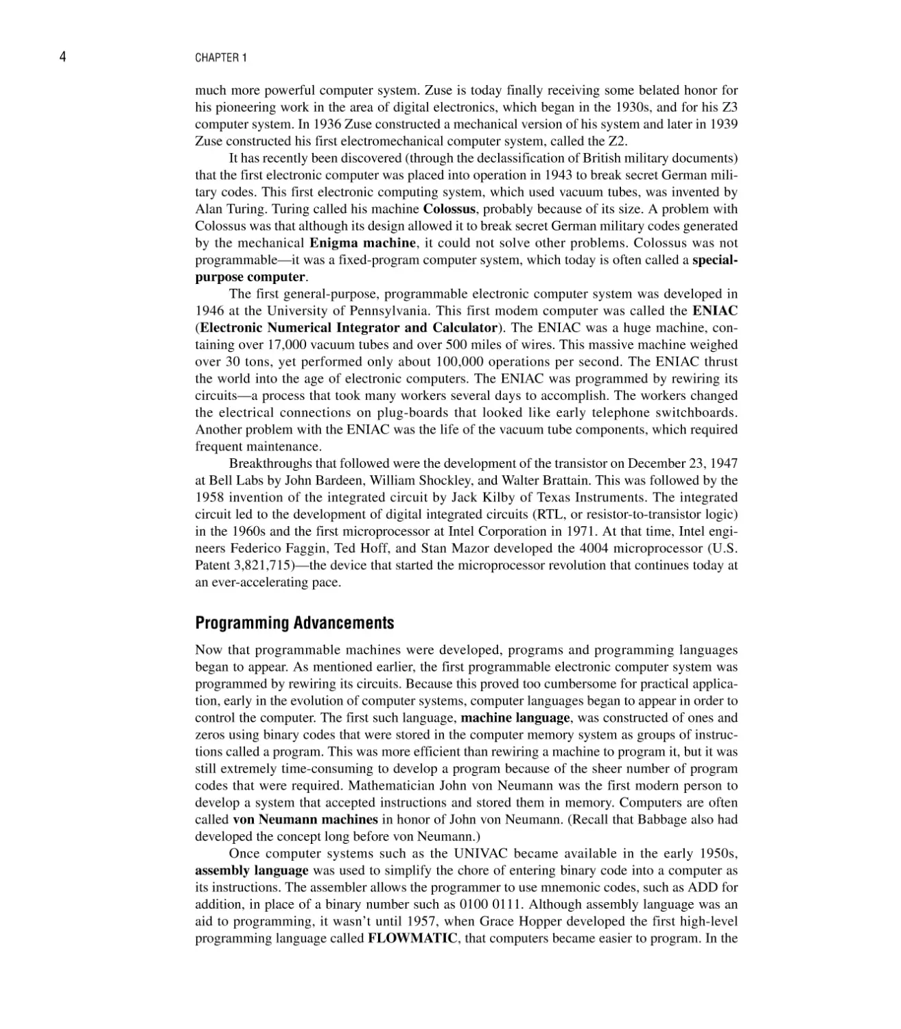
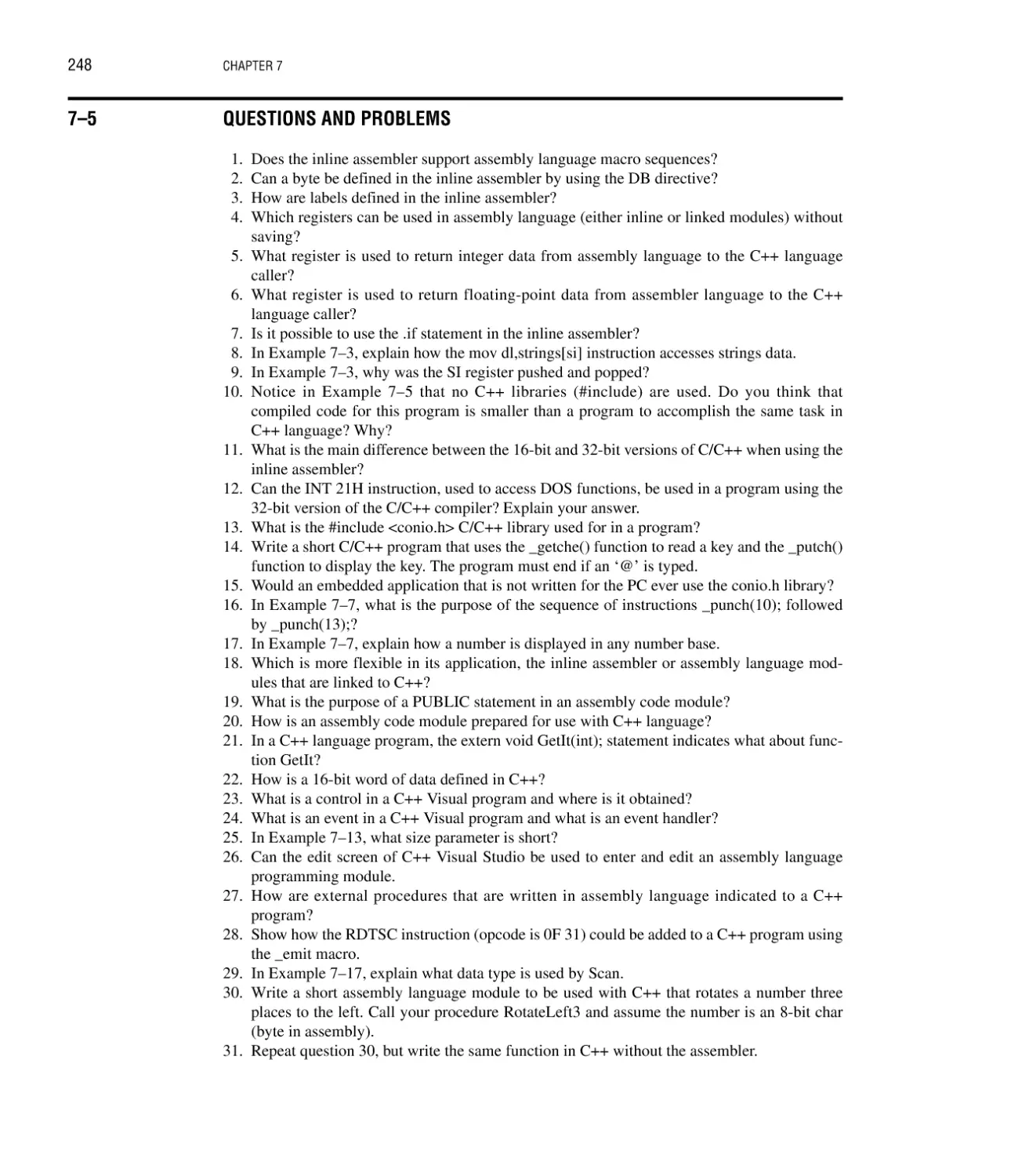
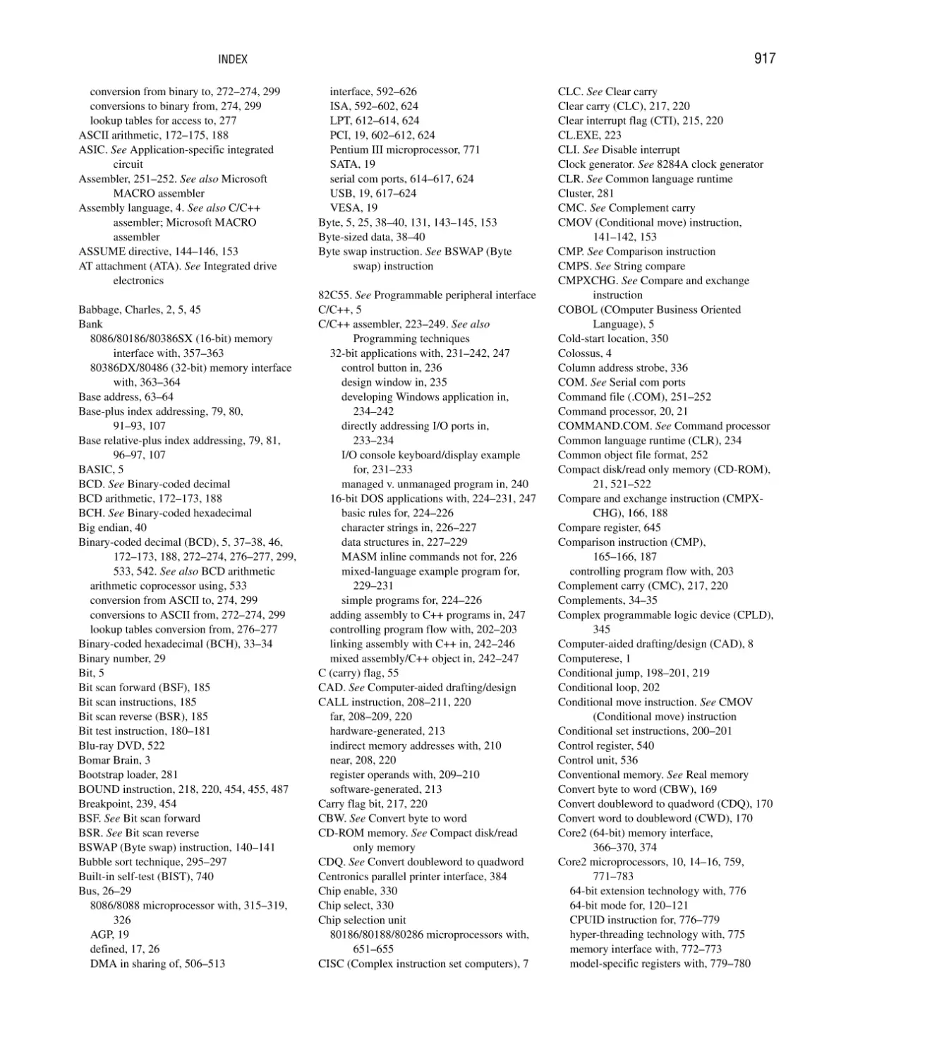
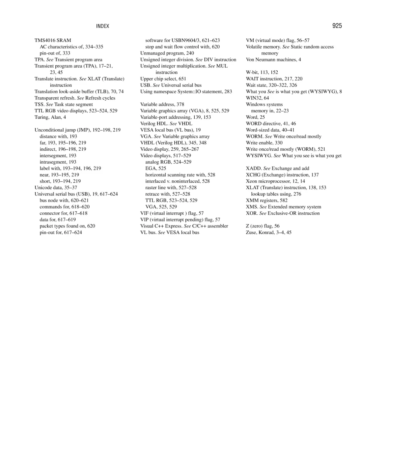
computer, as pictured in Figure 1–1, was probably invented for use in aircraft and missile design
during World War II for the German war effort. The Z3 was a relay logic machine that was
clocked at 5.33 Hz (far slower than the latest multiple GHz microprocessors). Had Zuse been
given adequate funding by the German government, he most likely would have developed a
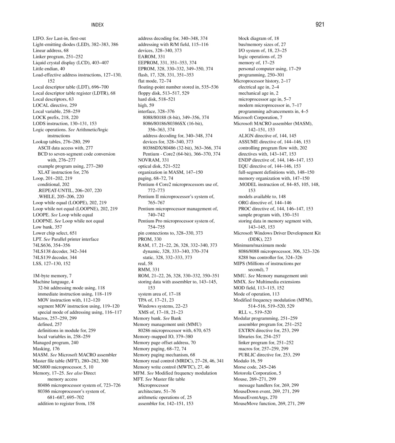
FIGURE 1–1 The Z3 computer developed by Konrad Zuse uses a 5.33 hertz clocking frequency. (Photo courtesy
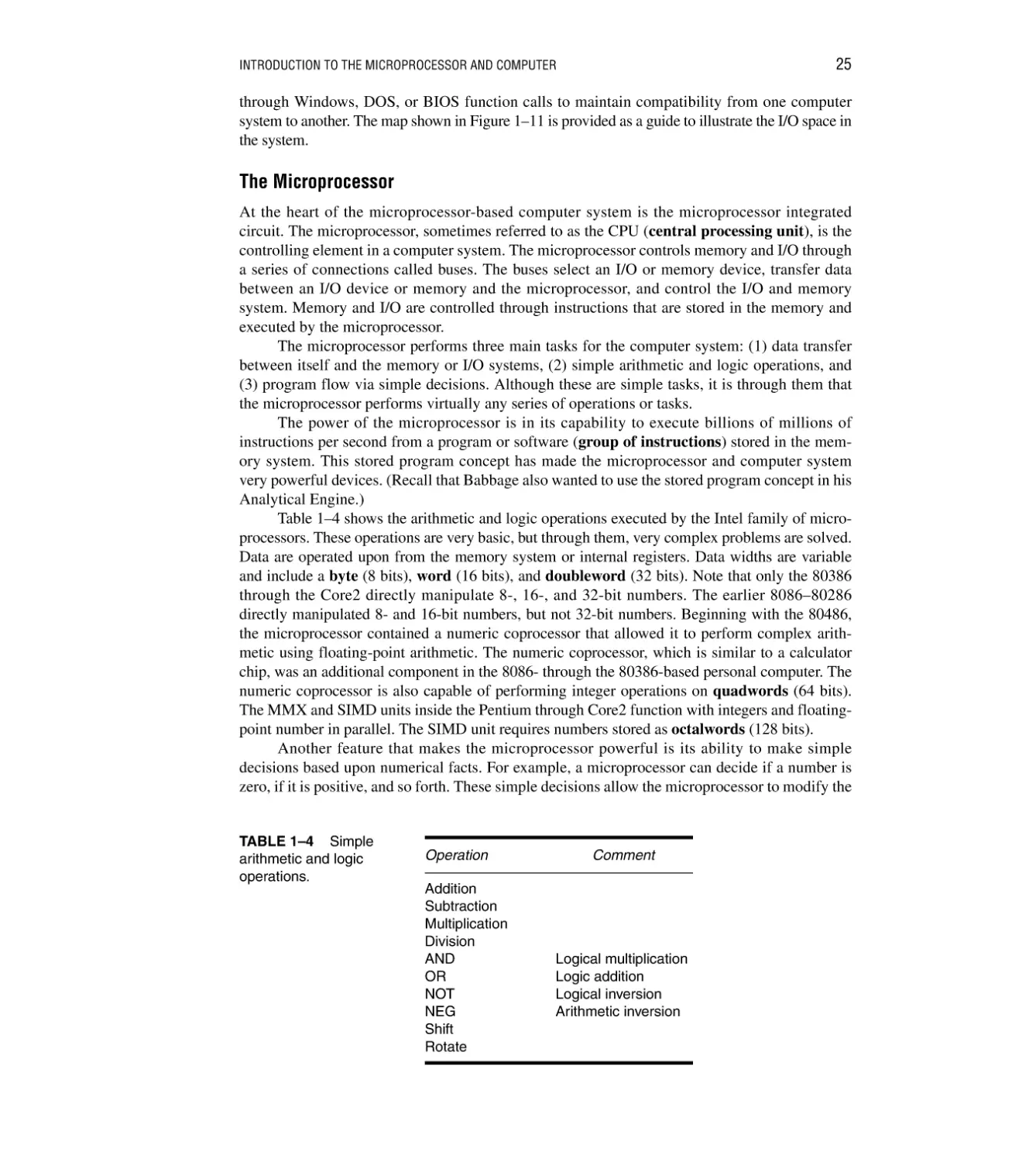
of Horst Zuse, the son of Konrad.)
4
CHAPTER 1
much more powerful computer system. Zuse is today finally receiving some belated honor for
his pioneering work in the area of digital electronics, which began in the 1930s, and for his Z3
computer system. In 1936 Zuse constructed a mechanical version of his system and later in 1939
Zuse constructed his first electromechanical computer system, called the Z2.
It has recently been discovered (through the declassification of British military documents)
that the first electronic computer was placed into operation in 1943 to break secret German military codes. This first electronic computing system, which used vacuum tubes, was invented by
Alan Turing. Turing called his machine Colossus, probably because of its size. A problem with
Colossus was that although its design allowed it to break secret German military codes generated
by the mechanical Enigma machine, it could not solve other problems. Colossus was not
programmable—it was a fixed-program computer system, which today is often called a specialpurpose computer.
The first general-purpose, programmable electronic computer system was developed in
1946 at the University of Pennsylvania. This first modem computer was called the ENIAC
(Electronic Numerical Integrator and Calculator). The ENIAC was a huge machine, containing over 17,000 vacuum tubes and over 500 miles of wires. This massive machine weighed
over 30 tons, yet performed only about 100,000 operations per second. The ENIAC thrust
the world into the age of electronic computers. The ENIAC was programmed by rewiring its
circuits—a process that took many workers several days to accomplish. The workers changed
the electrical connections on plug-boards that looked like early telephone switchboards.
Another problem with the ENIAC was the life of the vacuum tube components, which required
frequent maintenance.
Breakthroughs that followed were the development of the transistor on December 23, 1947
at Bell Labs by John Bardeen, William Shockley, and Walter Brattain. This was followed by the
1958 invention of the integrated circuit by Jack Kilby of Texas Instruments. The integrated
circuit led to the development of digital integrated circuits (RTL, or resistor-to-transistor logic)
in the 1960s and the first microprocessor at Intel Corporation in 1971. At that time, Intel engineers Federico Faggin, Ted Hoff, and Stan Mazor developed the 4004 microprocessor (U.S.
Patent 3,821,715)—the device that started the microprocessor revolution that continues today at
an ever-accelerating pace.
Programming Advancements
Now that programmable machines were developed, programs and programming languages
began to appear. As mentioned earlier, the first programmable electronic computer system was
programmed by rewiring its circuits. Because this proved too cumbersome for practical application, early in the evolution of computer systems, computer languages began to appear in order to
control the computer. The first such language, machine language, was constructed of ones and
zeros using binary codes that were stored in the computer memory system as groups of instructions called a program. This was more efficient than rewiring a machine to program it, but it was
still extremely time-consuming to develop a program because of the sheer number of program
codes that were required. Mathematician John von Neumann was the first modern person to
develop a system that accepted instructions and stored them in memory. Computers are often
called von Neumann machines in honor of John von Neumann. (Recall that Babbage also had
developed the concept long before von Neumann.)
Once computer systems such as the UNIVAC became available in the early 1950s,
assembly language was used to simplify the chore of entering binary code into a computer as
its instructions. The assembler allows the programmer to use mnemonic codes, such as ADD for
addition, in place of a binary number such as 0100 0111. Although assembly language was an
aid to programming, it wasn’t until 1957, when Grace Hopper developed the first high-level
programming language called FLOWMATIC, that computers became easier to program. In the
INTRODUCTION TO THE MICROPROCESSOR AND COMPUTER
5
same year, IBM developed FORTRAN (FORmula TRANslator) for its computer systems. The
FORTRAN language allowed programmers to develop programs that used formulas to solve
mathematical problems. Note that FORTRAN is still used by some scientists for computer
programming. Another similar language, introduced about a year after FORTRAN, was ALGOL
(ALGOrithmic Language).
The first truly successful and widespread programming language for business applications
was COBOL (COmputer Business Oriented Language). Although COBOL usage has diminished considerably in recent years, it is still a player in some large business and government
systems. Another once-popular business language is RPG (Report Program Generator), which
allows programming by specifying the form of the input, output, and calculations.
Since these early days of programming, additional languages have appeared. Some of the
more common modern programming languages are BASIC, C#, C/C++, Java, PASCAL, and
ADA. The BASIC and PASCAL languages were both designed as teaching languages, but have
escaped the classroom. The BASIC language is used in many computer systems and may be one
of the most common programming languages today. The BASIC language is probably the easiest
of all to learn. Some estimates indicate that the BASIC language is used in the personal computer
for 80% of the programs written by users. In the past decade, a new version of BASIC, Visual
BASIC, has made programming in the Windows environment easier. The Visual BASIC language may eventually supplant C/C++ and PASCAL as a scientific language, but it is doubtful.
It is more apparent that the C# language is gaining headway and may actually replace C/C++ and
most other languages including Java and may eventually replace BASIC. This of course is conjecture and only the future will show which language eventually becomes dominant.
In the scientific community, primarily C/C++ and occasionally PASCAL and FORTRAN
appear as control programs. One recent survey of embedded system developers showed that C
was used by 60% and that 30% used assembly language. The remainder used BASIC and JAVA.
These languages, especially C/C++, allow the programmer almost complete control over the programming environment and computer system. In many cases, C/C++ is replacing some of the
low-level machine control software or drivers normally reserved for assembly language. Even so,
assembly language still plays an important role in programming. Many video games written for
the personal computer are written almost exclusively in assembly language. Assembly language
is also interspersed with C/C++ to perform machine control functions efficiently. Some of the
newer parallel instructions found on the newest Pentium and Core2 microprocessors are only
programmable in assembly language.
The ADA language is used heavily by the Department of Defense. The ADA language was
named in honor of Augusta Ada Byron, Countess of Lovelace. The Countess worked with
Charles Babbage in the early 1800s in the development of software for his Analytical Engine.
The Microprocessor Age
The world’s first microprocessor, the Intel 4004, was a 4-bit microprocessor–programmable controller on a chip. It addressed a mere 4096, 4-bit-wide memory locations. (A bit is a binary digit
with a value of one or zero. A 4-bit-wide memory location is often called a nibble.) The 4004
instruction set contained only 45 instructions. It was fabricated with the then-current state-ofthe-art P-channel MOSFET technology that only allowed it to execute instructions at the slow
rate of 50 KIPs (kilo-instructions per second). This was slow when compared to the 100,000
instructions executed per second by the 30-ton ENIAC computer in 1946. The main difference
was that the 4004 weighed much less than an ounce.
At first, applications abounded for this device. The 4-bit microprocessor debuted in early
video game systems and small microprocessor-based control systems. One such early video game,
a shuffleboard game, was produced by Bailey. The main problems with this early microprocessor
were its speed, word width, and memory size. The evolution of the 4-bit microprocessor ended
6
CHAPTER 1
TABLE 1–1 Early 8-bit
microprocessors.
Manufacturer
Fairchild
Intel
MOS Technology
Motorola
National Semiconductor
Rockwell International
Zilog
Part Number
F-8
8080
6502
MC6800
IMP-8
PPS-8
Z-8
when Intel released the 4040, an updated version of the earlier 4004. The 4040 operated at a
higher speed, although it lacked improvements in word width and memory size. Other companies,
particularly Texas Instruments (TMS-1000), also produced 4-bit microprocessors. The 4-bit
microprocessor still survives in low-end applications such as microwave ovens and small control
systems and is still available from some microprocessor manufacturers. Most calculators are still
based on 4-bit microprocessors that process 4-bit BCD (binary-coded decimal) codes.
Later in 1971, realizing that the microprocessor was a commercially viable product, Intel
Corporation released the 8008—an extended 8-bit version of the 4004 microprocessor. The
8008 addressed an expanded memory size (16K bytes) and contained additional instructions
(a total of 48) that provided an opportunity for its application in more advanced systems.
(A byte is generally an 8-bit-wide binary number and a K is 1024. Often, memory size is specified in K bytes.)
As engineers developed more demanding uses for the 8008 microprocessor, they discovered that its somewhat small memory size, slow speed, and instruction set limited its usefulness.
Intel recognized these limitations and introduced the 8080 microprocessor in 1973—the first of
the modem 8-bit microprocessors. About six months after Intel released the 8080 microprocessor, Motorola Corporation introduced its MC6800 microprocessor. The floodgates opened and
the 8080—and, to a lesser degree, the MC6800—ushered in the age of the microprocessor. Soon,
other companies began to introduce their own versions of the 8-bit microprocessor. Table 1–1 lists
several of these early microprocessors and their manufacturers. Of these early microprocessor
producers, only Intel and Motorola (IBM also produces Motorola-style microprocessors) continue
successfully to create newer and improved versions of the microprocessor. Motorola has sold its
microprocessor division, and that company is now called Freescale Semiconductors, Inc. Zilog
still manufactures microprocessors, but remains in the background, concentrating on microcontrollers and embedded controllers instead of general-purpose microprocessors. Rockwell has all
but abandoned microprocessor development in favor of modem circuitry. Motorola has declined
from having nearly 50% share of the microprocessor market to a much smaller share. Intel today
has nearly 100% of the desktop and notebook market.
What Was Special about the 8080? Not only could the 8080 address more memory and execute additional instructions, but it executed them 10 times faster than the 8008. An addition that
took 20 μs (50,000 instructions per second) on an 8008-based system required only 2.0 μs
(500,000 instructions per second) on an 8080-based system. Also, the 8080 was compatible with
TTL (transistor-transistor logic), whereas the 8008 was not directly compatible. This made interfacing much easier and less expensive. The 8080 also addressed four times more memory
(64K bytes) than the 8008 (l6K bytes). These improvements are responsible for ushering in the
era of the 8080 and the continuing saga of the microprocessor. Incidentally, the first personal
computer, the MITS Altair 8800, was released in 1974. (Note that the number 8800 was probably chosen to avoid copyright violations with Intel.) The BASIC language interpreter, written for
the Altair 8800 computer, was developed in 1975 by Bill Gates and Paul Allen, the founders of
INTRODUCTION TO THE MICROPROCESSOR AND COMPUTER
7
Microsoft Corporation. The assembler program for the Altair 8800 was written by Digital
Research Corporation, which once produced DR-DOS for the personal computer.
The 8085 Microprocessor. In 1977, Intel Corporation introduced an updated version of the
8080—the 8085. The 8085 was to be the last 8-bit, general-purpose microprocessor developed
by Intel. Although only slightly more advanced than an 8080 microprocessor, the 8085 executed
software at an even higher speed. An addition that took 2.0 μs (500,000 instructions per second
on the 8080) required only 1.3 μs (769,230 instructions per second) on the 8085. The main
advantages of the 8085 were its internal clock generator, internal system controller, and higher
clock frequency. This higher level of component integration reduced the 8085’s cost and
increased its usefulness. Intel has managed to sell well over 100 million copies of the 8085
microprocessor, its most successful 8-bit, general-purpose microprocessor. Because the 8085 is
also manufactured (second-sourced) by many other companies, there are over 200 million
of these microprocessors in existence. Applications that contain the 8085 will likely continue to
be popular. Another company that sold 500 million 8-bit microprocessors is Zilog Corporation,
which produced the Z-80 microprocessor. The Z-80 is machine language–compatible with the
8085, which means that there are over 700 million microprocessors that execute 8085/Z-80
compatible code!
The Modern Microprocessor
In 1978, Intel released the 8086 microprocessor; a year or so later, it released the 8088. Both
devices are 16-bit microprocessors, which executed instructions in as little as 400 ns (2.5 MIPs,
or 2.5 millions of instructions per second). This represented a major improvement over the execution speed of the 8085. In addition, the 8086 and 8088 addressed 1M byte of memory, which
was 16 times more memory than the 8085. (A 1M-byte memory contains 1024K byte-sized
memory locations or 1,048,576 bytes.) This higher execution speed and larger memory size
allowed the 8086 and 8088 to replace smaller minicomputers in many applications. One other
feature found in the 8086/8088 was a small 4- or 6-byte instruction cache or queue that
prefetched a few instructions before they were executed. The queue sped the operation of many
sequences of instructions and proved to be the basis for the much larger instruction caches found
in modem microprocessors.
The increased memory size and additional instructions in the 8086 and 8088 have led to
many sophisticated applications for microprocessors. Improvements to the instruction set
included multiply and divide instructions, which were missing on earlier microprocessors.
In addition, the number of instructions increased from 45 on the 4004, to 246 on the 8085, to well
over 20,000 variations on the 8086 and 8088 microprocessors. Note that these microprocessors
are called CISC (complex instruction set computers) because of the number and complexity of
instructions. The additional instructions eased the task of developing efficient and sophisticated
applications, even though the number of instructions are at first overwhelming and timeconsuming to learn. The 16-bit microprocessor also provided more internal register storage
space than the 8-bit microprocessor. The additional registers allowed software to be written more
efficiently.
The 16-bit microprocessor evolved mainly because of the need for larger memory systems.
The popularity of the Intel family was ensured in 1981, when IBM Corporation decided to use
the 8088 microprocessor in its personal computer. Applications such as spreadsheets, word
processors, spelling checkers, and computer-based thesauruses were memory-intensive and
required more than the 64K bytes of memory found in 8-bit microprocessors to execute efficiently. The 16-bit 8086 and 8088 provided 1M byte of memory for these applications. Soon,
even the 1M-byte memory system proved limiting for large databases and other applications.
This led Intel to introduce the 80286 microprocessor, an updated 8086, in 1983.
8
CHAPTER 1
The 80286 Microprocessor. The 80286 microprocessor (also a 16-bit architecture microprocessor)
was almost identical to the 8086 and 8088, except it addressed a 16M-byte memory system instead
of a 1M-byte system. The instruction set of the 80286 was almost identical to the 8086 and 8088,
except for a few additional instructions that managed the extra 15M bytes of memory. The clock
speed of the 80286 was increased, so it executed some instructions in as little as 250 ns (4.0 MIPs)
with the original release 8.0 MHz version. Some changes also occurred to the internal execution of
the instructions, which led to an eightfold increase in speed for many instructions when compared to
8086/8088 instructions.
The 32-Bit Microprocessor. Applications began to demand faster microprocessor speeds, more
memory, and wider data paths. This led to the arrival of the 80386 in 1986 by Intel Corporation.
The 80386 represented a major overhaul of the 16-bit 8086–80286 architecture. The 80386 was
Intel’s first practical 32-bit microprocessor that contained a 32-bit data bus and a 32-bit memory
address. (Note that Intel produced an earlier, although unsuccessful, 32-bit microprocessor called
the iapx-432.) Through these 32-bit buses, the 80386 addressed up to 4G bytes of memory. (1G of
memory contains 1024M, or 1,073,741,824 locations.) A 4G-byte memory can store an astounding 1,000,000 typewritten, double-spaced pages of ASCII text data. The 80386 was available in a
few modified versions such as the 80386SX, which addressed 16M bytes of memory through a
16-bit data and 24-bit address bus, and the 80386SL/80386SLC, which addressed 32M bytes of
memory through a 16-bit data and 25-bit address bus. An 80386SLC version contained an internal
cache memory that allowed it to process data at even higher rates. In 1995, Intel released the
80386EX microprocessor. The 80386EX microprocessor is called an embedded PC because it
contains all the components of the AT class personal computer on a single integrated circuit. The
80386EX also contains 24 lines for input/output data, a 26-bit address bus, a 16-bit data bus, a
DRAM refresh controller, and programmable chip selection logic.
Applications that require higher microprocessor speeds and large memory systems include
software systems that use a GUI, or graphical user interface. Modem graphical displays often
contain 256,000 or more picture elements (pixels, or pels). The least sophisticated VGA
(variable graphics array) video display has a resolution of 640 pixels per scanning line with
480 scanning lines (this is the resolution used when the computer boots and display the boot
screen). To display one screen of information, each picture element must be changed, which
requires a high-speed microprocessor. Virtually all new software packages use this type of video
interface. These GUI-based packages require high microprocessor speeds and accelerated video
adapters for quick and efficient manipulation of video text and graphical data. The most striking
system, which requires high-speed computing for its graphical display interface, is Microsoft
Corporation’s Windows.3 We often call a GUI a WYSIWYG (what you see is what you get)
display.
The 32-bit microprocessor is needed because of the size of its data bus, which transfers
real (single-precision floating-point) numbers that require 32-bit-wide memory. In order to efficiently process 32-bit real numbers, the microprocessor must efficiently pass them between itself
and memory. If the numbers pass through an 8-bit data bus, it takes four read or write cycles;
when passed through a 32-bit data bus, however, only one read or write cycle is required. This
significantly increases the speed of any program that manipulates real numbers. Most high-level
languages, spreadsheets, and database management systems use real numbers for data storage.
Real numbers are also used in graphical design packages that use vectors to plot images on
the video screen. These include such CAD (computer-aided drafting/design) systems as
AUTOCAD, ORCAD, and so forth.
3Windows
is a registered trademark of Microsoft Corporation and is currently available as Windows 98, Windows 2000,
Windows ME, and Windows XP.
INTRODUCTION TO THE MICROPROCESSOR AND COMPUTER
9
Besides providing higher clocking speeds, the 80386 included a memory management unit
that allowed memory resources to be allocated and managed by the operating system. Earlier
microprocessors left memory management completely to the software. The 80386 included hardware circuitry for memory management and memory assignment, which improved its efficiency
and reduced software overhead.
The instruction set of the 80386 microprocessor was upward-compatible with the earlier
8086, 8088, and 80286 microprocessors. Additional instructions referenced the 32-bit registers
and managed the memory system. Note that memory management instructions and techniques
used by the 80286 are also compatible with the 80386 microprocessor. These features allowed
older, 16-bit software to operate on the 80386 microprocessor.
The 80486 Microprocessor. In 1989, Intel released the 80486 microprocessor, which incorporated an 80386-like microprocessor, an 80387-like numeric coprocessor, and an 8K-byte cache
memory system into one integrated package. Although the 80486 microprocessor was not radically different from the 80386, it did include one substantial change. The internal structure of the
80486 was modified from the 80386 so that about half of its instructions executed in one clock
instead of two clocks. Because the 80486 was available in a 50 MHz version, about half of the
instructions executed in 25 ns (50 MIPs). The average speed improvement for a typical mix
of instructions was about 50% over the 80386 that operated at the same clock speed. Later
versions of the 80486 executed instructions at even higher speeds with a 66 MHz double-clocked
version (80486DX2). The double-clocked 66 MHz version executed instructions at the rate of
66 MHz, with memory transfers executing at the rate of 33 MHz. (This is why it was called a
double-clocked microprocessor.) A triple-clocked version from Intel, the 80486DX4, improved
the internal execution speed to 100 MHz with memory transfers at 33 MHz. Note that the
80486DX4 microprocessor executed instructions at about the same speed as the 60 MHz Pentium.
It also contained an expanded 16K-byte cache in place of the standard 8K-byte cache found on
earlier 80486 microprocessors. Advanced Micro Devices (AMD) has produced a triple-clocked
version that runs with a bus speed of 40 MHz and a clock speed of 120 MHz. The future promises
to bring microprocessors that internally execute instructions at rates of up to 10 GHz or higher.
Other versions of the 80486 were called OverDrive4 processors. The OverDrive processor
was actually a double-clocked version of the 80486DX that replaced an 80486SX or slowerspeed 80486DX. When the OverDrive processor was plugged into its socket, it disabled or
replaced the 80486SX or 80486DX, and functioned as a doubled-clocked version of the microprocessor. For example, if an 80486SX, operating at 25 MHz, was replaced with an OverDrive
microprocessor, it functioned as an 80486DX2 50 MHz microprocessor using a memory transfer
rate of 25 MHz.
Table 1–2 lists many microprocessors produced by Intel and Motorola with information
about their word and memory sizes. Other companies produce microprocessors, but none have
attained the success of Intel and, to a lesser degree, Motorola.
The Pentium Microprocessor. The Pentium, introduced in 1993, was similar to the 80386 and
80486 microprocessors. This microprocessor was originally labeled the P5 or 80586, but Intel
decided not to use a number because it appeared to be impossible to copyright a number. The two
introductory versions of the Pentium operated with a clocking frequency of 60 MHz and
66 MHz, and a speed of 110 MIPs, with a higher-frequency 100 MHz one and one-half clocked
version that operated at 150 MIPs. The double-clocked Pentium, operating at 120 MHz and
133 MHz, was also available, as were higher-speed versions. (The fastest version produced by
Intel is the 233 MHz Pentium, which is a three and one-half clocked version.) Another difference
was that the cache size was increased to 16K bytes from the 8K cache found in the basic version
4OverDrive
is a registered trademark of Intel Corporation.
10
CHAPTER 1
TABLE 1–2
Manufacturer
Intel
Many modern Intel and Motorola microprocessors.
Part Number
8048
8051
8085A
8086
8088
8096
80186
80188
80251
80286
80386EX
80386DX
80386SL
80386SLC
80386SX
80486DX/DX2
80486SX
80486DX4
Pentium
Pentium OverDrive
Pentium Pro
8
8
8
16
8
16
16
8
8
16
16
32
16
16
16
32
32
32
64
32
64
Pentium II
64
Pentium III
64
Pentium 4
64
Pentium4 D
(Dual Core)
Core2
64
Itanium (Dual Core)
Motorola
Data Bus Width
6800
6805
6809
68000
68008D
68008Q
68010
68020
68030
68040
68050
68060
PowerPC
64
128
8
8
8
16
8
8
16
32
32
32
32
64
64
Memory Size
2K internal
8K internal
64K
1M
1M
8K internal
1M
1M
16K internal
16M
64M
4G
32M
32M + 8K cache
16M
4G + 8K cache
4G + 8K cache
4G + 16 cache
4G + 16K cache
4G + 16K cache
64G + 16K L1 cache +
256K L2 cache
64G + 32K L1 cache +
256K L2 cache
64G + 32K L1 cache +
256K L2 cache
64G+32K L1 cache+
512K L2 cache (or larger)
(1T for 64-bit extensions)
1T + 32K L1 cache + 2 or
4 M L2 cache
1T + 32K L1 cache + a shared
2 or 4 M L2 cache
1T + 2.5 M L1 and L2 cache
+ 24 M L3 cache
64K
2K
64K
16M
4M
1M
16M
4G
4G + 256 cache
4G + 8K cache
Proposed, but never released
4G + 16K cache
4G + 32K cache
INTRODUCTION TO THE MICROPROCESSOR AND COMPUTER
11
of the 80486. The Pentium contained an 8K-byte instruction cache and an 8K-byte data cache,
which allowed a program that transfers a large amount of memory data to still benefit from a
cache. The memory system contained up to 4G bytes, with the data bus width increased from the
32 bits found in the 80386 and 80486 to a full 64 bits. The data bus transfer speed was either
60 MHz or 66 MHz, depending on the version of the Pentium. (Recall that the bus speed of the
80486 was 33 MHz.) This wider data bus width accommodated double-precision floating-point
numbers used for modem high-speed, vector-generated graphical displays. These higher bus
speeds should allow virtual reality software and video to operate at more realistic rates on current
and future Pentium-based platforms. The widened data bus and higher execution speed of the
Pentium allow full-frame video displays to operate at scan rates of 30 Hz or higher—comparable
to commercial television. Recent versions of the Pentium also included additional instructions,
called multimedia extensions, or MMX instructions. Although Intel hoped that the MMX
instructions would be widely used, it appears that few software companies have used them. The
main reason is there is no high-level language support for these instructions.
Intel had also released the long-awaited Pentium OverDrive (P24T) for older 80486 systems
that operate at either 63 MHz or 83 MHz clock. The 63 MHz version upgrades older 80486DX2
50 MHz systems; the 83 MHz version upgrades the 80486DX2 66 MHz systems. The upgraded
83 MHz system performs at a rate somewhere between a 66 MHz Pentium and a 75 MHz
Pentium. If older VESA local bus video and disk-caching controllers seem too expensive to toss
out, the Pentium OverDrive represents an ideal upgrade path from the 80486 to the Pentium.
Probably the most ingenious feature of the Pentium is its dual integer processors. The
Pentium executes two instructions, which are not dependent on each other, simultaneously
because it contains two independent internal integer processors called superscaler technology.
This allows the Pentium to often execute two instructions per clocking period. Another feature
that enhances performance is a jump prediction technology that speeds the execution of program
loops. As with the 80486, the Pentium also employs an internal floating-point coprocessor to
handle floating-point data, albeit at a five times speed improvement. These features portend
continued success for the Intel family of microprocessors. Intel also may allow the Pentium to
replace some of the RISC (reduced instruction set computer) machines that currently execute
one instruction per clock. Note that some newer RISC processors execute more than one instruction per clock through the introduction of superscaler technology. Motorola, Apple, and IBM
produce the PowerPC, a RISC microprocessor that has two integer units and a floating-point
unit. The PowerPC certainly boosts the performance of the Apple Macintosh, but at present is
slow to efficiently emulate the Intel family of microprocessors. Tests indicate that the current
emulation software executes DOS and Windows applications at speeds slower than the 80486DX
25 MHz microprocessor. Because of this, the Intel family should survive for many years in personal computer systems. Note that there are currently 6 million Apple Macintosh5 systems and
well over 260 million personal computers based on Intel microprocessors. In 1998, reports
showed that 96% of all PCs were shipped with the Windows operating system.
Recently Apple computer replaced the PowerPC with the Intel Pentium in most of its computer systems. It appears that the PowerPC could not keep pace with the Pentium line from Intel.
In order to compare the speeds of various microprocessors, Intel devised the iCOMPrating index. This index is a composite of SPEC92, ZD Bench, and Power Meter. The iCOMP1
rating index is used to rate the speed of all Intel microprocessors through the Pentium.
Figure 1–2 shows relative speeds of the 80386DX 25 MHz version at the low end to the Pentium
233 MHz version at the high end of the spectrum.
Since the release of the Pentium Pro and Pentium II, Intel has switched to the iCOMP2-rating
index, which is scaled by a factor of 10 from the iCOMP1 index. A microprocessor with an index of
1000 using iCOMP1 is rated as 100 using iCOMP2. Another difference is the benchmarks used for
5Macintosh
is a registered trademark of Apple Computer Corporation.
12
CHAPTER 1
0
FIGURE 1–2 The Intel
iCOMP-rating index.
Pentium 200
Pentium 166
Pentium 133
Pentium 120
Pentium 100
Pentium 90
Pentium 75
Pentium 83*
Pentium 66
Pentium 60
Pentium 63*
486 DX4 100
486 DX4 75
486 DX2 66
486 DX 50
486 DX2 50
486 SX2 50
486 DX 33
486 SX2 40
486 SX 33
486 DX 25
486 SX 25
486 SX 20
386 DX 33
386 SX 33
386 DX 25
386 SX 25
386 SX 20
386 SX 16
100
200
400
600 800 1000 1200 1400 1600 1800
1810
1570
1110
1000
815
735
610
583
567
510
443
435
319
297
249
231
180
166
145
136
122
100
78
68
56
49
39
32
22
Note: *Pentium OverDrive, the first part of
the scale is not linear, and the 166 MHz
and 200 MHz are MMX technology.
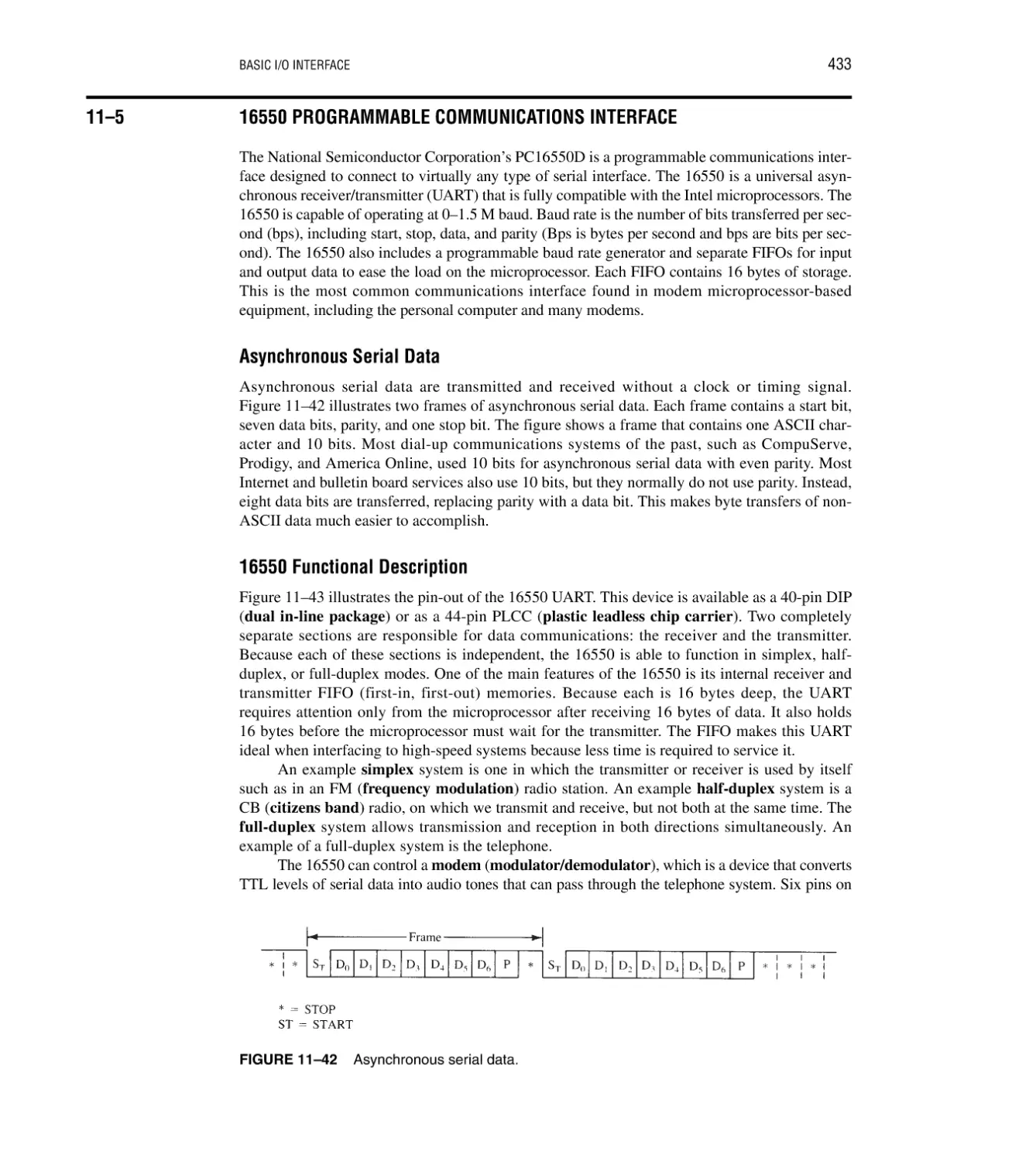
the scores. Figure 1–3 shows the iCOMP2 index listing the Pentium III at speeds up to 1000 MHz.
Figure 1–4 shows SYSmark 2002 for the Pentium III and Pentium 4. Unfortunately Intel has not
released any benchmarks that compare versions of the microprocessor since the SYSmark 2002.
Newer benchmarks are available, but they do not compare one version with another.
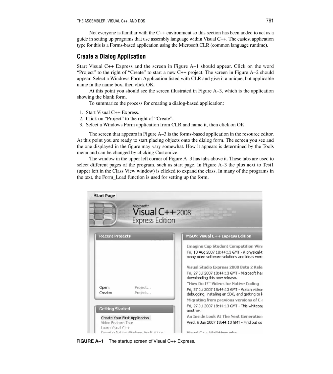
Pentium Pro Processor. A recent entry from Intel is the Pentium Pro processor, formerly
named the P6 microprocessor. The Pentium Pro processor contains 21 million transistors, integer
units, as well as a floating-point unit to increase the performance of most software. The basic
clock frequency was 150 MHz and 166 MHz in the initial offering made available in late 1995.
In addition to the internal 16K level-one (L1) cache (8K for data and 8K for instructions) the
Pentium Pro processor also contains a 256K level-two (L2) cache. One other significant change
is that the Pentium Pro processor uses three execution engines, so it can execute up to three
instructions at a time, which can conflict and still execute in parallel. This represents a
change from the Pentium, which executes two instructions simultaneously as long as they do not
conflict. The Pentium Pro microprocessor has been optimized to efficiently execute 32-bit code;
for this reason, it was often bundled with Windows NT rather than with normal versions of
Windows 95. Intel launched the Pentium Pro processor for the server market. Still another
change is that the Pentium Pro can address either a 4G-byte memory system or a 64G-byte memory system. The Pentium Pro has a 36-bit address bus if configured for a 64G memory system.
Pentium II and Pentium Xeon Microprocessors. The Pentium II microprocessor (released in
1997) represents a new direction for Intel. Instead of being an integrated circuit as with prior versions of the microprocessor, Intel has placed the Pentium II on a small circuit board. The main
reason for the change is that the L2 cache found on the main circuit board of the Pentium was not
13
INTRODUCTION TO THE MICROPROCESSOR AND COMPUTER
FIGURE 1–3 The Intel
iCOMP2-rating index.
Pentium III 1000 MHz
1277
Pentium III 933 MHz
1207
Pentium III 866 MHz
1125
Pentium III 800 MHz
1048
Pentium III 750 MHz
989
Pentium III 700 MHz
942
Pentium III 650 MHz
884
Pentium III 600 MHz
753
Pentium III 550 MHz
693
Pentium III 500 MHz
642
Pentium II 450 MHz
483
Pentium II 400 MHz
440
Pentium II 350 MHz
Pentium II 333 MHz
386
366
Pentium II 300 MHz
332
Pentium II 266 MHz
303
Pentium II 233 MHz
267
Pentium II* 266 MHz
213
Pentium 233 MHz
203
Note: *Pentium II Celeron, no cache.
iCOMP2 numbers are shown above. To
convert to iCOMP3, multiply by 2.568.
fast enough to function properly with the Pentium II. On the Pentium system, the L2 cache operates at the system bus speed of 60 MHz or 66 MHz. The L2 cache and microprocessor are on a
circuit board called the Pentium II module. This onboard L2 cache operates at a speed of
133 MHz and stores 512K bytes of information. The microprocessor on the Pentium II module is
actually Pentium Pro with MMX extensions.
In 1998, Intel changed the bus speed of the Pentium II. Because the 266 MHz through the
333 MHz Pentium II microprocessors used an external bus speed of 66 MHz, there was a bottleneck, so the newer Pentium II microprocessors use a 100 MHz bus speed. The Pentium II microprocessors rated at 350 MHz, 400 MHz, and 450 MHz all use this higher 100 MHz memory bus
speed. The higher speed memory bus requires the use of 8 ns SDRAM in place of the 10 ns
SDRAM found in use with the 66 MHz bus speed.
14
CHAPTER 1
FIGURE 1–4 Intel
microprocessor
performance using
SYSmark 2002.
Pentium 4 3.2
GHz
Pentium 4 2.8
GHz
Pentium 4 2.4
GHz
Pentium III
1000 MHz
0
200
400
In mid-1998 Intel announced a new version of the Pentium II called the Xeon,6 which was
specifically designed for high-end workstation and server applications. The main difference between
the Pentium II and the Pentium II Xeon is that the Xeon is available with a L1 cache size of 32K
bytes and a L2 cache size of either 512K, 1M, or 2M bytes. The Xeon functions with the 440GX
chip set. The Xeon is also designed to function with four Xeons in the same system, which is similar
to the Pentium Pro. This newer product represents a change in Intel’s strategy: Intel now produces a
professional version and a home/business version of the Pentium II microprocessor.
Pentium III Microprocessor. The Pentium III microprocessor uses a faster core than the
Pentium II, but it is still a P6 or Pentium Pro processor. It is also available in the slot 1 version
mounted on a plastic cartridge and a socket 370 version called a flip-chip, which looks like the
older Pentium package. Intel claims the flip-chip version costs less. Another difference is that the
Pentium III is available with clock frequencies of up to 1 GHz. The slot 1 version contains a
512K cache and the flip-chip version contains a 256K cache. The speeds are comparable because
the cache in the slot 1 version runs at one-half the clock speed, while the cache in the flip-chip
version runs at the clock speed. Both versions use a memory bus speed of 100 MHz, while the
Celeron7 uses memory bus clock speed of 66 MHz.
The speed of the front side bus, the connection from the microprocessor to the memory
controller, PCI controller, and AGP controller, is now either 100 MHz or 133 MHz. Although the
memory still runs at 100 MHz, this change has improved performance.
Pentium 4 and Core2 Microprocessors. The Pentium 4 microprocessor was first made
available in late 2000. The most recent version of the Pentium is called the Core2 by Intel. The
Pentium 4 and Core2, like the Pentium Pro through the Pentium III, use the Intel P6 architecture.
The main difference is that the Pentium 4 is available in speeds to 3.2 GHz and faster and the
chip sets that support the Pentium 4 use the RAMBUS or DDR memory technologies in place of
once standard SDRAM technology. The Core2 is available at speeds of up to 3 GHz. These
higher microprocessor speeds are made available by an improvement in the size of the internal
6Xeon
is a registered trademark of Intel Corporation.
is a trademark of Intel Corporation.
7Celeron
15
INTRODUCTION TO THE MICROPROCESSOR AND COMPUTER
TABLE 1–3 Intel
microprocessor core (P)
versions.
Core (P) Version
Microprocessor
P1
8086 and 8088 (80186 and 80188)
P2
80286
P3
80386
P4
80486
P5
Pentium
P6
Pentium Pro, Pentium II, Pentium III,
Pentium 4, and Core2
P7
Itanium
integration, which at present is the 0.045 micron or 45 nm technology. It is also interesting to
note that Intel has changed the level 1 cache size from 32K to 8K bytes and most recently to 64K.
Research must have shown that this size is large enough for the initial release version of the
microprocessor, with future versions possibly containing a 64K L1 cache. The level 2 cache
remains at 256K bytes as in the Pentium coppermine version with the latest versions containing
a 512K cache. The Pentium 4 Extreme Edition contains a 2M L2 cache and the Pentium 4e contains a 1M level 2 cache, whereas the Core2 contains either a 2M or 4M L2 cache.
Another change likely to occur is a shift from aluminum to copper interconnections inside
the microprocessor. Because copper is a better conductor, it should allow increased clock frequencies for the microprocessor in the future. This is especially true now that a method for using
copper has surfaced at IBM Corporation. Another event to look for is a change in the speed of the
front side bus, which will likely increase beyond the current maximum 1033 MHz.
Table 1–3 shows the various Intel P numbers and the microprocessors that belong to each
class. The P versions show what internal core microprocessor is found in each of the Intel microprocessors. Notice that all of the microprocessors since the Pentium Pro use the same basic
microprocessor core.
Pentium 4 and Core2, 64-bit and Multiple Core Microprocessors. Recently Intel has included
new modifications to the Pentium 4 and Core2 that include a 64-bit core and multiple cores. The
64-bit modification allows the microprocessor to address more than 4G bytes of memory through
a wider 64-bit address. Currently, 40 address pins in these newer versions allow up to 1T (terabytes) of memory to be accessed. The 64-bit machine also allows 64-bit integer arithmetic, but
this is much less important than the ability to address more memory.
The biggest advancement in the technology is not the 64-bit operation, but the inclusion of
multiple cores. Each core executes a separate task in a program, which increases the speed of
execution if a program is written to take advantage of the multiple cores. Programs that do this
are called multithreaded applications. Currently, Intel manufactures dual and quad core versions, but in the future the number of cores will likely increase to eight or even sixteen. The problem faced by Intel is that the clock speed cannot be increased to a much higher rate, so multiple
cores are the current solution to providing faster microprocessors. Does this mean that higher
clock speeds are not possible? Only the future portends whether they are or are not.
Intel recently demonstrated a version of the Core2 that contains 80 cores that uses the 45 nm
fabrication technology. Intel expects to release an 80-core version some time in the next 5 years. The
fabrication technology will become slightly smaller with 35 nm and possibly 25 nm technology.
The Future of Microprocessors. No one can really make accurate predictions, but the success of
the Intel family should continue for quite a few years. What may occur is a change to RISC technology, but more likely are improvements to a new technology jointly by Intel and Hewlett-Packard
16
CHAPTER 1
called hyper-threading technology. Even this new technology embodies the CISC instruction set of
the 80X86 family of microprocessors, so that software for the system will survive. The basic
premise behind this technology is that many microprocessors communicate directly with each
other, allowing parallel processing without any change to the instruction set or program. Currently,
the superscaler technology uses many microprocessors, but they all share the same register set. This
new technology contains many microprocessors, each containing its own register set that is linked
with the other microprocessors’ registers. This technology offers true parallel processing without
writing any special program.
The hyper-threading technology should continue into the future, bringing even more parallel processors (at present two processors). There are suggestions that Intel may also incorporate
the chip set into the microprocessor package.
In 2002, Intel released a new microprocessor architecture that is 64 bits in width and has
a 128-bit data bus. This new architecture, named the Itanium,8 is a joint venture called
EPIC (Explicitly Parallel Instruction Computing) of Intel and Hewlett-Packard. The Itanium
architecture allows greater parallelism than traditional architectures, such as the Pentium III or
Pentium 4. These changes include 128 general-purpose integer registers, 128 floating-point
registers, 64 predicate registers, and many execution units to ensure enough hardware resources
for software. The Itanium is designed for the server market and may or may not trickle down to
the home/business market in the future.
Figure 1–5 is a conceptual view, comparing the 80486 through Pentium 4 microprocessors.
Each view shows the internal structure of these microprocessors: the CPU, coprocessor, and
FIGURE 1–5 Conceptual
views of the 80486,
Pentium Pro, Pentium II,
Pentium III, Pentium 4, and
Core2 microprocessors.
CPU
Coprocessor
CPU1 CPU2
Copro
8K
L1 Cache
16K L1 Cache
80486DX
Pentium
CPU1 CPU2 CPU3
Copro
16K L1 Cache
CPU1 CPU2 CPU3
Copro
32K L1 Cache
256K L2 Cache
Pentium Pro
512K L2 Cache
or
236K L2 Cache
Pentium II, Pentium III,
Pentium 4, or Core2 Module
8Itanium
is a trademark of Intel Corporation.
INTRODUCTION TO THE MICROPROCESSOR AND COMPUTER
17
cache memory. This illustration shows the complexity and level of integration in each version of
the microprocessor.
Because clock frequencies seemed to have peaked and the surge to multiple cores
has begun, about the only major change to the Pentium will probably be a wider memory path
(128 bits). Another consideration is the memory speed. Today, dynamic RAMs are the mainstay,
but the speed of dynamic RAM memory has not changed for many years. A push to static RAM
memory will eventually appear and will increase the performance of the PC. The main problem
today with large static RAM is heat. Static RAM operates 50 times faster than dynamic RAM.
Imagine a computer that contains a memory composed of static RAM.
Another problem is the speed of the mass storage connected to a computer. The transfer
speed of hard disk drives has changed little in the past few years. A new technology is needed for
mass storage. Flash memory could be a solution, because its write speed is comparable to hard
disk memory. One change that would increase the speed of the computer system is the placement
of possibly 4G bytes of flash memory to store the operation system for common applications.
This would allow the operating system to load in a second or two instead of the many seconds
required to boot a modern computer system.
1–2
THE MICROPROCESSOR-BASED PERSONAL COMPUTER SYSTEM
Computer systems have undergone many changes recently. Machines that once filled large areas
have been reduced to small desktop computer systems because of the microprocessor. Although
these desktop computers are compact, they possess computing power that was only dreamed of a
few years ago. Million-dollar mainframe computer systems, developed in the early 1980s, are
not as powerful as the Pentium Core2-based computers of today. In fact, many smaller companies have replaced their mainframe computers with microprocessor-based systems. Companies
such as DEC (Digital Equipment Corporation, now owned by Hewlett-Packard Company) have
stopped producing mainframe computer systems in order to concentrate their resources on
microprocessor-based computer systems.
This section shows the structure of the microprocessor-based personal computer system.
This structure includes information about the memory and operating system used in many
microprocessor-based computer systems.
See Figure 1–6 for the block diagram of the personal computer. This diagram also applies to
any computer system, from the early mainframe computers to the latest microprocessor-based
systems. The block diagram is composed of three blocks that are interconnected by buses. (A bus
is the set of common connections that carry the same type of information. For example, the
address bus, which contains 20 or more connections, conveys the memory address to the memory.) These blocks and their function in a personal computer are outlined in this section of the text.
The Memory and I/O System
The memory structure of all Intel-based personal computers is similar. This includes the first personal computers based upon the 8088, introduced in 1981 by IBM, to the most powerful highspeed versions of today, based on the Pentium 4 or Core2. Figure 1–7 illustrates the memory map
of a personal computer system. This map applies to any IBM personal computer or to any of the
many IBM-compatible clones that are in existence.
The memory system is divided into three main parts: TPA (transient program area), system
area, and XMS (extended memory system). The type of microprocessor in your computer determines whether an extended memory system exists. If the computer is based upon a really old
8086 or 8088 (a PC or XT), the TPA and systems area exist, but there is no extended memory
18
CHAPTER 1
Buses
Memory system
Dynamic RAM (DRAM)
Static RAM (SRAM)
Cache
Read-only (ROM)
Flash memory
EEPROM
SDRAM
RAMBUS
DDR DRAM
FIGURE 1–6
Microprocessor
8086
8088
80186
80188
80286
80386
80486
Pentium
Pentium Pro
Pentium II
Pentium III
Pentium 4
Core2
I/O system
Printer
Serial communications
Floppy disk drive
Hard disk drive
Mouse
CD-ROM drive
Plotter
Keyboard
Monitor
Tape backup
Scanner
DVD
The block diagram of a microprocessor-based computer system.
area. The PC and XT computers contain 640K bytes of TPA and 384K bytes of system memory,
for a total memory size of 1M bytes. We often call the first 1M byte of memory the real or conventional memory system because each Intel microprocessor is designed to function in this area
by using its real mode of operation.
Computer systems based on the 80286 through the Core2 not only contain the TPA (640K
bytes) and system area (384K bytes), they also contain extended memory. These machines are
FIGURE 1–7 The memory
map of a personal computer.
Extended memory
15M bytes in the 80286 or 80386SX
31M bytes in the 80386SL/SLC
63M bytes in the 80386EX
4095M bytes in the 80386DX, 80486, and Pentium
64G bytes in the Pentium Pro, Pentium II, Pentium III,
Pentium 4, and Core2
System area
384K bytes
1M bytes of real (conventional) memory
TPA
640K bytes
INTRODUCTION TO THE MICROPROCESSOR AND COMPUTER
19
often called AT class machines. The PS/l and PS/2, produced by IBM, are other versions of the
same basic memory design. Sometimes, these machines are also referred to as ISA (industry
standard architecture) or EISA (extended ISA) machines. The PS/2 is referred to as a microchannel architecture system, or ISA system, depending on the model number.
A change beginning with the introduction of the Pentium microprocessor and the ATX
class machine is the addition of a bus called the PCI (peripheral component interconnect) bus,
now being used in all Pentium through Core2 systems. Extended memory contains up to 15M
bytes in the 80286 and 80386SX-based computers, and up to 4095M bytes in the 80386DX,
80486, and Pentium microprocessors, in addition to the first 1M byte of real or conventional
memory. The Pentium Pro through Core2 computer systems have up to 1M less than 4G or 1 M
less than 64G of extended memory. Servers tend to use the larger 64G memory map, while
home/business computers use the 4G-byte memory map. The ISA machine contains an 8-bit
peripheral bus that is used to interface 8-bit devices to the computer in the 8086/8088-based
PC or XT computer system. The AT class machine, also called an ISA machine, uses a l6-bit
peripheral bus for interface and may contain the 80286 or above microprocessor. The EISA bus
is a 32-bit peripheral interface bus found in a few older 80386DX- and 80486-based systems.
Note that each of these buses is compatible with the earlier versions. That is, the 8-bit interface
card functions in the 8-bit ISA, l6-bit ISA, or 32-bit EISA bus system. Likewise, a l6-bit interface card functions in the l6-bit ISA or 32-bit EISA system.
Another bus type found in many 80486-based personal computers is called the VESA local
bus, or VL bus. The local bus interfaces disk and video to the microprocessor at the local bus
level, which allows 32-bit interfaces to function at the same clocking speed as the microprocessor. A recent modification to the VESA local bus supports the 64-bit data bus of the Pentium
microprocessor and competes directly with the PCI bus, although it has generated little, if any,
interest. The ISA and EISA standards function at only 8 MHz, which reduces the performance of
the disk and video interfaces using these standards. The PCI bus is either a 32- or 64-bit bus that
is specifically designed to function with the Pentium through Core2 microprocessors at a bus
speed of 33 MHz.
Three newer buses have appeared in ATX class systems. The first to appear was the USB
(universal serial bus). The universal serial bus is intended to connect peripheral devices such as
keyboards, a mouse, modems, and sound cards to the microprocessor through a serial data path
and a twisted pair of wires. The main idea is to reduce system cost by reducing the number of
wires. Another advantage is that the sound system can have a separate power supply from the
PC, which means much less noise. The data transfer rates through the USB are 10 Mbps at present for USB1; they increase to 480 Mbps in USB2.
The second newer bus is the AGP (advanced graphics port) for video cards. The
advanced graphics port transfers data between the video card and the microprocessor at higher
speeds (66 MHz, with a 64-bit data path, or 533M bytes per second) than were possible through
any other bus or connection. The latest AGP speed is 8X or 2G bytes per second. This video subsystem change has been made to accommodate the new DVD players for the PC.
The latest new buses to appear are the serial ATA interface (SATA) for hard disk drives and
the PCI Express bus for the video card. The SATA bus transfers data from the PC to the hard disk
drive at rates of 150M bytes per second or 300M bytes for SATA-2. The serial ATA standard will
eventually reach speeds of 450M bytes per second. Today PCI Express bus video cards operate at
16X speeds.
The TPA. The transient program area (TPA) holds the DOS (disk operating system)
operating system and other programs that control the computer system. The TPA is a DOS concept and not really applicable in Windows. The TPA also stores any currently active or inactive
DOS application programs. The length of the TPA is 640K bytes. As mentioned, this area
of memory holds the DOS operating system, which requires a portion of the TPA to function.
20
CHAPTER 1
FIGURE 1–8 The memory
map of the TPA in a personal
computer. (Note that this map
will vary between systems.)
9FFFF
9FFF0
MSDOS program
Free TPA
08E30
08490
COMMAND.COM
Device drivers
such as MOUSE.SYS
02530
MSDOS program
01160
00700
00500
00400
IO.SYS program
DOS communications area
BIOS communications area
Interrupt vectors
00000
In practice, the amount of memory remaining for application software is about 628K bytes if
MSDOS9 version 7.x is used as an operating system. Earlier versions of DOS required more of
the TPA area and often left only 530K bytes or less for application programs. Figure 1–8 shows
the organization of the TPA in a computer system running DOS.
The DOS memory map shows how the many areas of the TPA are used for system programs, data, and drivers. It also shows a large area of memory available for application programs. To the left of each area is a hexadecimal number that represents the memory addresses
that begin and end each data area. Hexadecimal memory addresses or memory locations are
used to number each byte of the memory system. (A hexadecimal number is a number represented in radix 16 or base 16, with each digit representing a value from 0 to 9 and A to F. We
often end a hexadecimal number with an H to indicate that it is a hexadecimal value. For example, 1234H is 1234 hexadecimal. We also represent hexadecimal data as 0xl234 for a 1234
hexadecimal.)
9MSDOS
is a trademark of Microsoft Corporation and version 7.x is supplied with Windows XP.
INTRODUCTION TO THE MICROPROCESSOR AND COMPUTER
21
The Interrupt vectors access various features of the DOS, BIOS (basic I/O system), and
applications. The system BIOS is a collection of programs stored in either a read-only (ROM) or
flash memory that operates many of the I/O devices connected to your computer system. The
system BIOS and DOS communications areas contain transient data used by programs to access
I/O devices and the internal features of the computer system. These are stored in the TPA so they
can be changed as the DOS operates.
The IO.SYS is a program that loads into the TPA from the disk whenever an MSDOS system is started. The IO.SYS contains programs that allow DOS to use the keyboard, video display,
printer, and other I/O devices often found in the computer system. The IO.SYS program links
DOS to the programs stored on the system BIOS ROM.
The size of the driver area and number of drivers changes from one computer to another.
Drivers are programs that control installable I/O devices such as a mouse, disk cache, hand scanner, CD-ROM memory (Compact Disk Read-Only Memory), DVD (Digital Versatile Disk),
or installable devices, as well as programs. Installable drivers are programs that control or drive
devices or programs that are added to the computer system. DOS drivers are normally files that
have an extension of .SYS, such as MOUSE.SYS; in DOS version 3.2 and later, the files have an
extension of .EXE, such as EMM386.EXE. Note that even though these files are not used by
Windows, they are still used to execute DOS applications, even with Windows XP. Windows
uses a file called SYSTEM.INI to load drivers used by Windows. In newer versions of Windows
such as Windows XP, a registry is added to contain information about the system and the drivers
used by the system. You can view the registry with the REGEDIT program.
The COMMAND.COM program (command processor) controls the operation of the
computer from the keyboard when operated in the DOS mode. The COMMAND.COM program
processes the DOS commands as they are typed from the keyboard. For example, if DIR is typed,
the COMMAND.COM program displays a directory of the disk files in the current disk directory. If the COMMAND.COM program is erased, the computer cannot be used from the keyboard in DOS mode. Never erase COMMAND.COM, IO.SYS, or MSDOS.SYS to make room
for other software, or your computer will not function.
The System Area. The DOS system area, although smaller than the TPA, is just as important.
The system area contains programs on either a read-only memory (ROM) or flash memory, and
areas of read/write (RAM) memory for data storage. Figure 1–9 shows the system area of a
typical personal computer system. As with the map of the TPA, this map also includes the hexadecimal memory addresses of the various areas.
The first area of the system space contains video display RAM and video control programs
on ROM or flash memory. This area starts at location A0000H and extends to location C7FFFH.
The size and amount of memory used depends on the type of video display adapter attached to
the system. Display adapters generally have their video RAM located at A0000H–AFFFFH,
which stores graphical or bit-mapped data, and the memory at B0000H–BFFFFH stores text
data. The video BIOS, located on a ROM or flash memory, is at locations C0000H–C7FFFH and
contains programs that control the DOS video display.
The area at locations C8000H–DFFFFH is often open or free. This area is used for the
expanded memory system (EMS) in a PC or XT system, or for the upper memory system in an
AT system. Its use depends on the system and its configuration. The expanded memory system
allows a 64K-byte page frame of memory to be used by application programs. This 64K-byte
page frame (usually locations D0000H through DFFFFH) is used to expand the memory system
by switching in pages of memory from the EMS into this range of memory addresses.
Memory locations E0000H–EFFFFH contain the cassette BASIC language on ROM found in
early IBM personal computer systems. This area is often open or free in newer computer systems.
Finally, the system BIOS ROM is located in the top 64K bytes of the system area
(F0000H–FFFFFH). This ROM controls the operation of the basic I/O devices connected to the
22
CHAPTER 1
FIGURE 1–9 The system
area of a typical personal
computer.
FFFFF
BIOS system ROM
F0000
BASIC language ROM
(only on early PCs)
E0000
Free area
C8000
Hard disk controller ROM
LAN controller ROM
Video BIOS ROM
C0000
Video RAM
(text area)
B0000
Video RAM
(graphics area)
A0000
computer system. It does not control the operation of the video system, which has its own BIOS
ROM at location C0000H. The first part of the system BIOS (F0000H–F7FFFH) often contains
programs that set up the computer; the second part contains procedures that control the basic I/O
system.
Windows Systems. Modern computers use a different memory map with Windows than the
DOS memory maps of Figures 1–8 and 1–9. The Windows memory map appears in Figure 1–10
and has two main areas, a TPA and a system area. The difference between it and the DOS
memory map are the sizes and locations of these areas.
The Windows TPA is the first 2G bytes of the memory system from locations 00000000H
to 7FFFFFFFH. The Windows system area is the last 2G bytes of memory from locations
80000000H to FFFFFFFFH. It appears that the same idea used to construct the DOS memory
map was also used in a modern Windows-based system. The system area is where the system
BIOS is located and also the video memory. Also located in the system area is the actual
Windows program and drivers. Every program that is written for Windows can use up to 2G
bytes of memory located at linear addresses 00000000H through 7FFFFFFFH. This is even true
in a 64-bit system, which does allow access to more memory, but not as a direct part of Windows.
Information that is larger than 2G must be swapped into the Windows TPA area from another
area of memory. In future versions of Windows and the Pentium, this will most likely be
changed. The current version of Windows 64 (which is now a part of Windows Vista) supports
up to 8G bytes of Windows memory.
INTRODUCTION TO THE MICROPROCESSOR AND COMPUTER
23
FIGURE 1–10 The memory
map used by Windows XP.
Does this mean that any program written for Windows will begin at physical address
00000000H? No, the memory system physical map is much different for the linear programming
model shown in Figure 1–10. Every process in a Windows Vista, Windows XP, or Windows 2000
system has its own set of page tables, which define where in the physical memory each 4K-byte
page of the process is located. This means that the process can be located anywhere in the memory, even in noncontiguous pages. Page tables and the paging structure of the microprocessor are
discussed later in this chapter and are beyond the scope of the text at this point. As far as an
application is concerned, you will always have 2G bytes of memory even if the computer has less
memory. The operating system (Windows) handles assigning physical memory to the application
and if not enough physical memory exists, it uses the hard disk drive for any that is not available.
I/O Space. The I/O (input/output) space in a computer system extends from I/O port 0000H to
port FFFFH. (An I/O port address is similar to a memory address, except that instead
of addressing memory, it addresses an I/O device.) The I/O devices allow the microprocessor to
communicate between itself and the outside world. The I/O space allows the computer to access
up to 64K different 8-bit I/O devices, 32K different 16-bit devices, or 16K different 32-bit
devices. The 64-bit extensions support the same I/O space and I/O sizes as the 32-bit version and
does not add 64-bit I/O devices to the system. A great number of these locations are available for
expansion in most computer systems. Figure 1–11 shows the I/O map found in many personal
computer systems. To view the map on your computer in Windows, go to the Control Panel,
Performance and Maintenance, System, Hardware tab, Device Manager, View tab, then select
resources by type and click on the plus next to Input/Output (I/O).
24
CHAPTER 1
FIGURE 1–11 Some
I/O locations in a typical
personal computer.
The I/O area contains two major sections. The area below I/O location 0400H is considered reserved for system devices; many are depicted in Figure 1–11. The remaining area is
available I/O space for expansion that extends from I/O port 0400H through FFFFH. Generally,
I/O addresses between 0000H and 00FFH address components on the main board of the computer, while addresses between 0100H and 03FFH address devices located on plug-in cards (or
on the main board). Note that the limitation of I/O addresses between 0000 and 03FFH comes
from the original PC standard, as specified by IBM. When using the ISA bus, you must only use
addresses between 0000H and 03FFH. The PCI bus uses I/O address between 0400H and
FFFFH.
Various I/O devices that control the operation of the system are usually not directly addressed.
Instead, the system BIOS ROM addresses these basic devices, which can vary slightly in location
and function from one computer to the next. Access to most I/O devices should always be made
25
INTRODUCTION TO THE MICROPROCESSOR AND COMPUTER
through Windows, DOS, or BIOS function calls to maintain compatibility from one computer
system to another. The map shown in Figure 1–11 is provided as a guide to illustrate the I/O space in
the system.
The Microprocessor
At the heart of the microprocessor-based computer system is the microprocessor integrated
circuit. The microprocessor, sometimes referred to as the CPU (central processing unit), is the
controlling element in a computer system. The microprocessor controls memory and I/O through
a series of connections called buses. The buses select an I/O or memory device, transfer data
between an I/O device or memory and the microprocessor, and control the I/O and memory
system. Memory and I/O are controlled through instructions that are stored in the memory and
executed by the microprocessor.
The microprocessor performs three main tasks for the computer system: (1) data transfer
between itself and the memory or I/O systems, (2) simple arithmetic and logic operations, and
(3) program flow via simple decisions. Although these are simple tasks, it is through them that
the microprocessor performs virtually any series of operations or tasks.
The power of the microprocessor is in its capability to execute billions of millions of
instructions per second from a program or software (group of instructions) stored in the memory system. This stored program concept has made the microprocessor and computer system
very powerful devices. (Recall that Babbage also wanted to use the stored program concept in his
Analytical Engine.)
Table 1–4 shows the arithmetic and logic operations executed by the Intel family of microprocessors. These operations are very basic, but through them, very complex problems are solved.
Data are operated upon from the memory system or internal registers. Data widths are variable
and include a byte (8 bits), word (16 bits), and doubleword (32 bits). Note that only the 80386
through the Core2 directly manipulate 8-, 16-, and 32-bit numbers. The earlier 8086–80286
directly manipulated 8- and 16-bit numbers, but not 32-bit numbers. Beginning with the 80486,
the microprocessor contained a numeric coprocessor that allowed it to perform complex arithmetic using floating-point arithmetic. The numeric coprocessor, which is similar to a calculator
chip, was an additional component in the 8086- through the 80386-based personal computer. The
numeric coprocessor is also capable of performing integer operations on quadwords (64 bits).
The MMX and SIMD units inside the Pentium through Core2 function with integers and floatingpoint number in parallel. The SIMD unit requires numbers stored as octalwords (128 bits).
Another feature that makes the microprocessor powerful is its ability to make simple
decisions based upon numerical facts. For example, a microprocessor can decide if a number is
zero, if it is positive, and so forth. These simple decisions allow the microprocessor to modify the
TABLE 1–4 Simple
arithmetic and logic
operations.
Operation
Addition
Subtraction
Multiplication
Division
AND
OR
NOT
NEG
Shift
Rotate
Comment
Logical multiplication
Logic addition
Logical inversion
Arithmetic inversion
26
CHAPTER 1
TABLE 1–5 Decisions
found in the 8086 through
Core2 microprocessors.
Decision
Comment
Zero
Test a number for zero or not-zero
Sign
Test a number for positive or negative
Carry
Test for a carry after addition or a borrow after
subtraction
Parity
Test a number for an even or an odd number of
ones
Overflow
Test for an overflow that indicates an invalid result
after a signed addition or a signed subtraction
program flow, so that programs appear to think through these simple decisions. Table 1–5 lists
the decision-making capabilities of the Intel family of microprocessors.
Buses. A bus is a common group of wires that interconnect components in a computer system.
The buses that interconnect the sections of a computer system transfer address, data, and control
information between the microprocessor and its memory and I/O systems. In the microprocessorbased computer system, three buses exist for this transfer of information: address, data, and control. Figure 1–12 shows how these buses interconnect various system components such as the
microprocessor, read/write memory (RAM), read-only memory (ROM or flash), and a few I/O
devices.
The address bus requests a memory location from the memory or an I/O location from the
I/O devices. If I/O is addressed, the address bus contains a 16-bit I/O address from 0000H
through FFFFH. The 16-bit I/O address, or port number, selects one of 64K different I/O devices.
If memory is addressed, the address bus contains a memory address, which varies in width with
the different versions of the microprocessor. The 8086 and 8088 address 1M byte of memory,
using a 20-bit address that selects locations 00000H–FFFFFH. The 80286 and 80386SX address
16M bytes of memory using a 24-bit address that selects locations 000000H–FFFFFFH. The
80386SL, 80386SLC, and 80386EX address 32M bytes of memory, using 25-bit address that
selects locations 0000000H–1FFFFFFH. The 80386DX, 80486SX, and 80486DX address
Address bus
μp
Data bus
MWTC
MRDC
IOWC
IORC
Read-only
memory
ROM
Read/write
memory
RAM
Keyboard
Printer
FIGURE 1–12 The block diagram of a computer system showing the address, data, and
control bus structure.
27
INTRODUCTION TO THE MICROPROCESSOR AND COMPUTER
TABLE 1–6
The Intel family of microprocessor bus and memory sizes.
Microprocessor
8086
8088
80186
80188
80286
80386SX
80386DX
80386EX
80486
Pentium
Pentium Pro–Core2
Pentium Pro–Core2
(if extended addressing is enabled)
Pentium 4 and Core2
with 64-bit extensions enabled
Itanium
Data Bus Width
Address Bus Width
Memory Size
16
8
16
8
16
16
32
16
32
64
64
64
20
20
20
20
24
24
32
26
32
32
32
36
1M
1M
1M
1M
16M
16M
4G
64M
4G
4G
4G
64G
64
40
1T
128
40
1T
4G bytes of memory, using a 32-bit address that selects locations 00000000H–FFFFFFFFH. The
Pentium also addresses 4G bytes of memory, but it uses a 64-bit data bus to access up to 8 bytes
of memory at a time. The Pentium Pro through Core2 microprocessors have a 64-bit data bus and
a 32-bit address bus that address 4G of memory from location 00000000H–FFFFFFFFH, or a
36-bit address bus that addresses 64G of memory at locations 000000000H–FFFFFFFFFH,
depending on their configuration. Refer to Table 1–6 for complete listing of bus and memory
sizes of the Intel family of microprocessors.
The 64-bit extensions to the Pentium family provide 40 address pins in its current version
that allow up to 1T byte of memory to be accessed through its 10 digit hexadecimal address.
Note that 240 is 1 terra. In future editions of the 64-bit microprocessors Intel plans to expand the
number of address bits to 52, and ultimately to 64 bits. A 52-bit address bus allows 4P (Peta)
bytes of memory to be accessed and a 64-bit address bus allows 16E (Exa) bytes of memory.
The data bus transfers information between the microprocessor and its memory and I/O
address space. Data transfers vary in size, from 8 bits wide to 64 bits wide in various members of
the Intel microprocessor family. For example, the 8088 has an 8-bit data bus that transfers 8 bits
of data at a time. The 8086, 80286, 80386SL, 80386SX, and 80386EX transfer 16 bits of data
through their data buses; the 80386DX, 80486SX, and 80486DX transfer 32 bits of data; and the
Pentium through Core2 microprocessors transfer 64 bits of data. The advantage of a wider data
bus is speed in applications that use wide data. For example, if a 32-bit number is stored in memory, it takes the 8088 microprocessor four transfer operations to complete because its data bus
is only 8 bits wide. The 80486 accomplishes the same task with one transfer because its data
bus is 32 bits wide. Figure 1–13 shows the memory widths and sizes of the 8086–80486 and
Pentium through Core2 microprocessors. Notice how the memory sizes and organizations differ
between various members of the Intel microprocessor family. In all family members, the memory is numbered by byte. Notice that the Pentium through Core2 microprocessors all contain a
64-bit-wide data bus.
The control bus contains lines that select the memory or I/O and cause them to perform a
read or write operation. In most computer systems, there are four control bus connections: MRDC
(memory read control), MWTC (memory write control), IORC (I/O read control), and IOWC
(I/O write control). Note that the overbar indicates that the control signal is active-low; that is,
28
CHAPTER 1
it is active when a logic zero appears on the control line. For example, if IOWC = 0, the
microprocessor is writing data from the data bus to an I/O device whose address appears on
the address bus. Note that these control signal names are slightly different in various versions of
the microprocessor.
The microprocessor reads the contents of a memory location by sending the memory an
address through the address bus. Next, it sends the memory read control signal (MRDC) to cause
the memory to read data. Finally, the data read from the memory are passed to the microprocessor through the data bus. Whenever a memory write, I/O write, or I/O read occurs, the same
sequence ensues, except that different control signals are issued and the data flow out of the
microprocessor through its data bus for a write operation.
Low bank
(Even bank)
High bank
(Odd bank)
FFFFF
FFFFFF
FFFFFE
FFFFE
FFFFFD
FFFFFC
FFFFD
FFFFFB
FFFFFA
8 bits
8 bits
8 bits
1M byte
8M bytes
8M bytes
00002
000005
000004
00001
000003
000002
00000
000001
D7–D0
8088 microprocessor
000000
D15–D8
D7–D0
8086 microprocessor (memory is only 1M bytes)
80286 microprocessor
80386SX microprocessor
80386SL microprocessor (memory is 32M bytes)
80386SLC microprocessor (memory is 32M bytes)
Bank 3
Bank 2
Bank 1
Bank 0
FFFFFFFF
FFFFFFFE
FFFFFFFD
FFFFFFFC
FFFFFFFB
FFFFFFFA
FFFFFFF9
FFFFFFF8
FFFFFFF7
FFFFFFF6
FFFFFFF5
FFFFFFF4
8 bits
8 bits
8 bits
8 bits
1G byte
1G byte
1G byte
1G byte
0000000B
0000000A
00000009
00000008
00000007
00000006
00000005
00000004
00000003
00000002
00000001
D31–D24
D23–D16
00000000
D15–D8
80386DX microprocessor
80486SX microprocessor
80486DX microprocessor
FIGURE 1–13
The physical memory systems of the 8086 through the Core2 microprocessors.
D7–D0
29
INTRODUCTION TO THE MICROPROCESSOR AND COMPUTER
Bank 7
Bank 6
FFFFFFFF
FFFFFFFE
Bank 5
FFFFFFFD
Bank 4
FFFFFFFC
FFFFFFF7
FFFFFFF6
FFFFFFF5
FFFFFFF4
FFFFFFEF
FFFFFFEE
FFFFFFED
FFFFFFEC
8 bits
8 bits
8 bits
8 bits
512M bytes
512M bytes
512M bytes
512M bytes
00000017
00000016
00000015
00000014
0000000F
0000000E
0000000D
0000000C
00000007
00000006
00000005
00000004
D63–D56
D55–D48
Bank 3
D47–D40
Bank 2
FFFFFFFB
FFFFFFFA
D39–D32
Bank 1
FFFFFFF9
Bank 0
FFFFFFF8
FFFFFFF3
FFFFFFF2
FFFFFFF1
FFFFFFF0
FFFFFFEB
FFFFFFEA
FFFFFFE9
FFFFFFE8
8 bits
8 bits
8 bits
8 bits
512M bytes
512M bytes
512M bytes
1G byte
00000013
00000012
00000011
00000010
0000000B
0000000A
00000009
00000008
00000003
00000002
00000001
D31–D24
D23–D16
00000000
D15–D8
D7–D0
Pentium–Core2 microprocessors
FIGURE 1–13
1–3
(continued)
NUMBER SYSTEMS
The use of the microprocessor requires a working knowledge of binary, decimal, and hexadecimal numbering systems. This section of the text provides a background for those who are unfamiliar with these numbering systems. Conversions between decimal and binary, decimal and
hexadecimal, and binary and hexadecimal are described.
Digits
Before numbers are converted from one number base to another, the digits of a number system
must be understood. Early in our education, we learned that a decimal (base 10) number is
constructed with 10 digits: 0 through 9. The first digit in any numbering system is always zero.
For example, a base 8 (octal) number contains 8 digits: 0 through 7; a base 2 (binary) number
contains 2 digits: 0 and 1. If the base of a number exceeds 10, the additional digits use the
30
CHAPTER 1
letters of the alphabet, beginning with an A. For example, a base 12 number contains 10 digits:
0 through 9, followed by A for 10 and B for 11. Note that a base 10 number does contain a
10 digit, just as a base 8 number does not contain an 8 digit. The most common numbering
systems used with computers are decimal, binary, and hexadecimal (base 16). (Many years ago
octal numbers were popular.) Each of these number systems are described and used in this
section the chapter.
Positional Notation
Once the digits of a number system are understood, larger numbers are constructed by using
positional notation. In grade school, we learned that the position to the left of the units position
is the tens position, the position to the left of the tens position is the hundreds position, and so
forth. (An example is the decimal number 132: This number has 1 hundred, 3 tens, and 2 units.)
What probably was not learned was the exponential value of each position: The units position
has a weight of 100, or 1; the tens position has weight of 101, or 10; and the hundreds position has
a weight of 102, or 100. The exponential powers of the positions are critical for understanding
numbers in other numbering systems. The position to the left of the radix (number base) point,
called a decimal point only in the decimal system, is always the units position in any number system. For example, the position to the left of the binary point is always 20, or 1; the position to the
left of the octal point is 80, or 1. In any case, any number raised to its zero power is always 1, or
the units position.
The position to the left of the units position is always the number base raised to the first
power; in a decimal system, this is 101, or 10. In a binary system, it is 21, or 2; and in an octal
system, it is 8l, or 8. Therefore, an 11 decimal has a different value from an 11 binary. The decimal number is composed of 1 ten plus 1 unit, and has a value of 11 units; while the binary
number 11 is composed of 1 two plus 1 unit, for a value of 3 decimal units. The 11 octal has a
value of 9 decimal units.
In the decimal system, positions to the right of the decimal point have negative powers.
The first digit to the right of the decimal point has a value of 10-1, or 0.1. In the binary system the
first digit to the right of the binary point has a value of 2-1, or 0.5. In general, the principles that
apply to decimal numbers also apply to numbers in any other number system.
Example 1–1 shows 110.101 in binary (often written as 110.1012). It also shows the
power and weight or value of each digit position. To convert a binary number to decimal, add
weights of each digit to form its decimal equivalent. The 110.1012 is equivalent to a 6.625 in
decimal (4 + 2 + 0.5 + 0.125). Notice that this is the sum of 22 (or 4) plus 21 (or 2), but 20
(or 1) is not added because there are no digits under this position. The fraction part is composed of 2-1 (.5) plus 2-3 (or .125), but there is no digit under the 2-2 (or .25) so .25 is not
added.
EXAMPLE 1–1
Power
Weight
Number
Numeric Value
22
4
1
4 +
21
2
1
2 +
20
1
0 .
0 +
2-1
.5
1
.5 +
2-2
.25
0
0 +
2-3
.125
1
.125
=
6.625
Suppose that the conversion technique is applied to a base 6 number, such as 25.26.
Example 1–2 shows this number placed under the powers and weights of each position. In the
example, there is a 2 under 61, which has a value of 1210 (2 * 6), and a 5 under 60, which has
a value of 5 (5 * 1). The whole number portion has a decimal value of 12 + 5, or 17. The number to the right of the hex point is a 2 under 6-1, which has a value of .333 (2 * .167). The
number 25.26, therefore, has a value of 17.333.
31
INTRODUCTION TO THE MICROPROCESSOR AND COMPUTER
EXAMPLE 1–2
Power
Weight
Number
Numeric Value
61
6
2
12 +
60
1
5
5 +
6-1
.167
.2
.333 = 17.333
Conversion to Decimal
The prior examples have shown that to convert from any number base to decimal, determine the
weights or values of each position of the number, and then sum the weights to form the decimal
equivalent. Suppose that a 125.78 octal is converted to decimal. To accomplish this conversion,
first write down the weights of each position of the number. This appears in Example 1–3. The
value of 125.78 is 85.875 decimal, or 1 * 64 plus 2 * 8 plus 5 * 1 plus 7 * .125.
EXAMPLE 1–3
Power
Weight
Number
Numeric Value
82
64
1
64 +
81
8
2
16 +
80
1
5
5 +
8-1
.125
.7
.875 = 85.875
Notice that the weight of the position to the left of the units position is 8. This is 8 times 1.
Then notice that the weight of the next position is 64, or 8 times 8. If another position existed, it
would be 64 times 8, or 512. To find the weight of the next higher-order position, multiply the
weight of the current position by the number base (or 8, in this example). To calculate the
weights of position to the right of the radix point, divide by the number base. In the octal system,
the position immediately to the right of the octal point is 1/8, or .125. The next position is .125/8,
or .015625, which can also be written as 1/64. Also note that the number in Example 1–3 can also
be written as the decimal number 857/8.
Example 1–4 shows the binary number 11011.0111 written with the weights and powers of
each position. If these weights are summed, the value of the binary number converted to decimal
is 27.4375.
EXAMPLE 1–4
Power
Weight
Number
Numeric Value
24
16
1
16 +
23
8
1
8 +
22
4
0
0 +
21
2
1
2 +
20
1
1 .
1 +
2-1
.5
0
0 +
2-2
.25
1
.25 +
2-3
.125
1
.125 +
2-4
.0625
1
.0625 = 27.4375
It is interesting to note that 2-1 is also 1/2, 2-2 is 1/4, and so forth. It is also interesting to
note that 2-4 is 1/16, or .0625. The fractional part of this number is 7/16 or .4375 decimal. Notice
that 0111 is a 7 in binary code for the numerator and the rightmost one is in the 1/16 position for
the denominator. Other examples: The binary fraction of .101 is 5/8 and the binary fraction of
.001101 is 13/64.
Hexadecimal numbers are often used with computers. A 6A.CH (H for hexadecimal) is
illustrated with its weights in Example 1–5. The sum of its digits is 106.75, or 1063⁄4. The whole
number part is represented with 6 * 16 plus 10 1A2 * 1. The fraction part is 12 (C) as a numerator and 16 (16-1) as the denominator, or 12/16, which is reduced to 3/4.
32
CHAPTER 1
EXAMPLE 1–5
161
16
6
96 +
Power
Weight
Number
Number Value
160
1
A .
10 +
16-1
.0625
C
.75 = 106.75
Conversion from Decimal
Conversions from decimal to other number systems are more difficult to accomplish than conversion to decimal. To convert the whole number portion of a number to decimal, divide by 1
radix. To convert the fractional portion, multiply by the radix.
Whole Number Conversion from Decimal. To convert a decimal whole number to another
number system, divide by the radix and save the remainders as significant digits of the result. An
algorithm for this conversion as is follows:
1. Divide the decimal number by the radix (number base).
2. Save the remainder (first remainder is the least significant digit).
3. Repeat steps 1 and 2 until the quotient is zero.
For example, to convert a 10 decimal to binary, divide it by 2. The result is 5, with a remainder of 0. The first remainder is the units position of the result (in this example, a 0). Next divide
the 5 by 2. The result is 2, with a remainder of 1. The 1 is the value of the twos (21) position.
Continue the division until the quotient is a zero. Example 1–6 shows this conversion process. The
result is written as 10102 from the bottom to the top.
EXAMPLE 1–6
2) 10
2) 5
2) 2
2) 1
0
remainder
remainder
remainder
remainder
=
=
=
=
0
1
0
1
result = 1010
To convert a 10 decimal into base 8, divide by 8, as shown in Example 1–7. A 10 decimal
is a 12 octal.
EXAMPLE 1–7
8) 10
8) 1
0
remainder = 2
remainder = 1
result = 12
Conversion from decimal to hexadecimal is accomplished by dividing by 16. The remainders will range in value from 0 through 15. Any remainder of 10 through 15 is then converted to
the letters A through F for the hexadecimal number. Example 1–8 shows the decimal number 109
converted to a 6DH.
EXAMPLE 1–8
16) 109
16) 6
0
remainder = 13 (D)
remainder = 6
result = 6D
Converting from a Decimal Fraction. Conversion from a decimal fraction to another number
base is accomplished with multiplication by the radix. For example, to convert a decimal fraction
into binary, multiply by 2. After the multiplication, the whole number portion of the result is
INTRODUCTION TO THE MICROPROCESSOR AND COMPUTER
33
saved as a significant digit of the result, and the fractional remainder is again multiplied by the
radix. When the fraction remainder is zero, multiplication ends. Note that some numbers are
never-ending (repetend). That is, a zero is never a remainder. An algorithm for conversion from
a decimal fraction is as follows:
1. Multiply the decimal fraction by the radix (number base).
2. Save the whole number portion of the result (even if zero) as a digit. Note that the first result
is written immediately to the right of the radix point.
3. Repeat steps 1 and 2, using the fractional part of step 2 until the fractional part of step 2 is zero.
Suppose that a .125 decimal is converted to binary. This is accomplished with multiplications by 2, as illustrated in Example 1–9. Notice that the multiplication continues until the
fractional remainder is zero. The whole number portions are written as the binary fraction
(0.001) in this example.
EXAMPLE 1–9
x
x
x
.125
2
0.25
digit is 0
.25
2
0.5
digit is 0
.5
2
1.0
digit is 1
result = 0.0012
This same technique is used to convert a decimal fraction into any number base. Example 1–10
shows the same decimal fraction of .125 from Example 1–9 converted to octal by multiplying by 8.
EXAMPLE 1–10
x
.125
8
1.0
digit is 1
result = 0.18
Conversion to a hexadecimal fraction appears in Example 1–11. Here, the decimal .046875
is converted to hexadecimal by multiplying by 16. Note that .046875 is 0.0CH.
EXAMPLE 1–11
x
.046875
16
0.75
.75
x
16
12.0
digit is 0
digit is 12(C)
result = 0.0C16
Binary-Coded Hexadecimal
Binary-coded hexadecimal (BCH) is used to represent hexadecimal data in binary code.
A binary-coded hexadecimal number is a hexadecimal number written so that each digit is represented by a 4-bit binary number. The values for the BCH digits appear in Table 1–7.
Hexadecimal numbers are represented in BCH code by converting each digit to BCH code
with a space between each coded digit. Example 1–12 shows a 2AC converted to BCH code.
Note that each BCH digit is separated by a space.
34
CHAPTER 1
TABLE 1–7 Binary-coded
hexadecimal (BCH) code.
Hexadecimal Digit
BCH Code
0
1
2
3
4
5
6
7
8
9
A
B
C
D
E
F
0000
0001
0010
0011
0100
0101
0110
0111
1000
1001
1010
1011
1100
1101
1110
1111
EXAMPLE 1–12
2AC = 0010 1010 1100
The purpose of BCH code is to allow a binary version of a hexadecimal number to be
written in a form that can easily be converted between BCH and hexadecimal. Example 1–13
shows a BCH coded number converted back to hexadecimal code.
EXAMPLE 1–13
1000 0011 1101 . 1110 = 83D.E
Complements
At times, data are stored in complement form to represent negative numbers. There are two systems
that are used to represent negative data: radix and radix - 1 complements. The earliest system was
the radix -1 complement, in which each digit of the number is subtracted from the radix -1 to generate the radix -1 complement to represent a negative number.
Example 1–14 shows how the 8-bit binary number 01001100 is one’s (radix -1) complemented to represent it as a negative value. Notice that each digit of the number is subtracted
from one to generate the radix -1 (one’s) complement. In this example, the negative of
01001100 is 10110011. The same technique can be applied to any number system, as illustrated
in Example 1–15, in which the fifteen’s (radix -1) complement of a 5CD hexadecimal is computed by subtracting each digit from a fifteen.
EXAMPLE 1–14
1111 1111
- 0100 1100
1011 0011
EXAMPLE 1–15
-
15 15 15
5 C D
A 3 2
INTRODUCTION TO THE MICROPROCESSOR AND COMPUTER
35
Today, the radix -1 complement is not used by itself; it is used as a step for finding the
radix complement. The radix complement is used to represent negative numbers in modem computer systems. (The radix -1 complement was used in the early days of computer technology.)
The main problem with the radix -1 complement is that a negative or a positive zero exists; in the
radix complement system, only a positive zero can exist.
To form the radix complement, first find the radix -1 complement, and then add a one to
the result. Example 1–16 shows how the number 0100 1000 is converted to a negative value by
two’s (radix) complementing it.
EXAMPLE 1–16
1111
- 0100
1011
+
1011
1111
1000
0111
1
1000
(one’s complement)
(two’s complement)
To prove that a 0100 1000 is the inverse (negative) of a 1011 1000, add the two together to
form an 8-digit result. The ninth digit is dropped and the result is zero because a 0100 1000 is a
positive 72, while a 1011 1000 is a negative 72. The same technique applies to any number system.
Example 1–17 shows how the inverse of a 345 hexadecimal is found by first fifteen’s complementing the number, and then by adding one to the result to form the sixteen’s complement. As before,
if the original 3-digit number 345 is added to the inverse of CBB, the result is a 3-digit 000.
As before, the fourth bit (carry) is dropped. This proves that 345 is the inverse of CBB. Additional
information about one’s and two’s complements is presented with signed numbers in the next
section of the text.
EXAMPLE 1–17
15 15 15
3 4 5
C B A
+
1
C B B
-
1–4
(fifteen’s complement)
(sixteen’s complement)
COMPUTER DATA FORMATS
Successful programming requires a precise understanding of data formats. In this section, many
common computer data formats are described as they are used with the Intel family of microprocessors. Commonly, data appear as ASCII, Unicode, BCD, signed and unsigned integers, and
floating-point numbers (real numbers). Other forms are available, but are not presented here
because they are not commonly found.
ASCII and Unicode Data
ASCII (American Standard Code for Information Interchange) data represent alphanumeric
characters in the memory of a computer system (see Table 1–8). The standard ASCII code is a 7-bit
code, with the eighth and most significant bit used to hold parity in some antiquated systems.
If ASCII data are used with a printer, the most significant bits are a 0 for alphanumeric printing and
1 for graphics printing. In the personal computer, an extended ASCII character set is selected by
placing a 1 in the leftmost bit. Table 1–9 shows the extended ASCII character set, using code
80H–FFH. The extended ASCII characters store some foreign letters and punctuation, Greek
36
CHAPTER 1
TABLE 1–8
ASCII code.
Second
First
0X
1X
2X
3X
4X
5X
6X
7X
X0
X1
X2
X3
X4
X5
X6
X7
X8
X9
XA
XB
XC
XD
XE
XF
NUL
DLE
SP
0
@
P
‘
p
SOH
DC1
!
1
A
Q
a
q
STX
DC2
“
2
B
R
b
r
ETX
DC3
#
3
C
S
c
s
EOT
DC4
$
4
D
T
d
t
ENQ
NAK
%
5
E
U
e
u
ACK
SYN
&
6
F
V
f
v
BEL
ETB
’
7
G
W
g
w
BS
CAN
(
8
H
X
h
x
HT
EMS
)
9
I
Y
i
y
LF
SUB
*
:
J
Z
j
z
VT
ESC
+
;
K
[
k
{
FF
FS
,
<
L
\
l
|
CR
GS
=
M
]
m
}
SO
RS
.
>
N
^
n
~
SI
US
/
?
O
_
o
...
...
...
TABLE 1–9
Extended ASCII code, as printed by the IBM ProPrinter.
characters, mathematical characters, box-drawing characters, and other special characters. Note
that extended characters can vary from one printer to another. The list provided is designed to be
used with the IBM ProPrinter, which also matches the special character set found with most word
processors.
The ASCII control characters, also listed in Table 1–8, perform control functions in a computer system, including clear screen, backspace, line feed, and so on. To enter the control codes
through the computer keyboard, hold down the Control key while typing a letter. To obtain the
control code 01H, type a Control-A; a 02H is obtained by a Control-B, and so on. Note that the
control codes appear on the screen, from the DOS prompt, as ^A for Control-A, ^B for Control-B,
and so forth. Also note that the carriage return code (CR) is the Enter key on most modem keyboards. The purpose of CR is to return the cursor or print head to the left margin. Another code
that appears in many programs is the line feed code (LF), which moves the cursor down one line.
To use Table 1–8 or 1–9 for converting alphanumeric or control characters into ASCII
characters, first locate the alphanumeric code for conversion. Next, find the first digit of the
hexadecimal ASCII code. Then find the second digit. For example, the capital letter “A” is
ASCII code 41H, and the lowercase letter “a” is ASCII code 61H. Many Windows-based applications, since Windows 95, use the Unicode system to store alphanumeric data. This system
INTRODUCTION TO THE MICROPROCESSOR AND COMPUTER
37
stores each character as 16-bit data. The codes 0000H–00FFH are the same as standard ASCII
code. The remaining codes, 0100H–FFFFH, are used to store all special characters from
many worldwide character sets. This allows software written for the Windows environment
to be used in many countries around the world. For complete information on Unicode, visit
http://www.unicode.org.
ASCII data are most often stored in memory by using a special directive to the assembler
program called define byte(s), or DB. (The assembler is a program that is used to program a
computer in its native binary machine language.) An alternative to DB is the word BYTE. The
DB and BYTE directives, and several examples of their usage with ASCII-coded character
strings, are listed in Example 1–18. Notice how each character string is surrounded by apostrophes (’)—never use the quote (”). Also notice that the assembler lists the ASCII-coded value for
each character to the left of the character string. To the far left is the hexadecimal memory location where the character string is first stored in the memory system. For example, the character
string WHAT is stored beginning at memory address 001D, and the first letter is stored as
57 (W), followed by 68 (H), and so forth. Example 1–19 shows the same three strings defined as
String^ character strings for use with Visual C++ Express 2005 and 2008. Note that Visual C++
uses quotes to surround strings. If an earlier version of C++ is used, then the string is defined
with a CString for Microsoft Visual C++ instead of a String^. The ^ symbol indicates that String
is a member of the garbage collection heap for managing the storage. A garbage collector cleans
off the memory system (frees unused memory) when the object falls from visibility or scope in a
C++ program and it also prevents memory leaks.
EXAMPLE 1–18
0000
OOOD
001D
42
20
72
57
20
69
3F
57
69
20
74
61
42
65
68
63
74
72
2E
79
65
61
20
72 79
20 42
NAMES
DB
‘Barry B. Brey’
20 63
6E 20
62 65
MESS
DB
‘Where can it be?’
69 20 74 20
73 20 6F 6E
66 69 72 73
2E
WHAT
DB
‘What is on first.’
EXAMPLE 1–19
String^ NAMES = “Barry B. Brey”
// C++ Express version
String^ MESS = “Where can it be?”
String^ WHAT = “What is on first.”
BCD (Binary-Coded Decimal) Data
Binary-coded decimal (BCD) information is stored in either packed or unpacked forms. Packed
BCD data are stored as two digits per byte and unpacked BCD data are stored as one digit per
byte. The range of a BCD digit extends from 00002 to 10012, or 0–9 decimal. Unpacked BCD
data are returned from a keypad or keyboard. Packed BCD data are used for some of the instructions included for BCD addition and subtraction in the instruction set of the microprocessor.
Table 1–10 shows some decimal numbers converted to both the packed and unpacked BCD
forms. Applications that require BCD data are point-of-sales terminals and almost any device
that performs a minimal amount of simple arithmetic. If a system requires complex arithmetic,
BCD data are seldom used because there is no simple and efficient method of performing
complex BCD arithmetic.
38
CHAPTER 1
TABLE 1–10
Packed and unpacked BCD data.
Decimal
12
623
910
Packed
0001 0010
0000 0110
0000 1001
0010 0011
0001 0000
Unpacked
0000 0001
0000 0110
0000 1001
0000 0010
0000 0010
0000 0001
0000 0011
0000 0000
Example 1–20 shows how to use the assembler to define both packed and unpacked
BCD data. Example 1–21 shows how to do this using Visual C++ and char or bytes. In all
cases, the convention of storing the least-significant data first is followed. This means that to
store 83 into memory, the 3 is stored first, and then followed by the 8. Also note that with
packed BCD data, the letter H (hexadecimal) follows the number to ensure that the assembler stores the BCD value rather than a decimal value for packed BCD data. Notice how the
numbers are stored in memory as unpacked, one digit per byte; or packed, as two digits
per byte.
EXAMPLE 1–20
0000 03 04 05
0003 07 08
0005 37 34
0007 03 45
;Unpacked BCD data (least-significant data first)
;
NUMB1 DB
3,4,5
;defines number 543
NUMB2 DB
7,8
;defines number 87
;
;Packed BCD data (least-significant data first)
;
NUMB3 DB
37H,34H
;defines number 3437
NUMB4 DB
3,45H
;defines number 4503
EXAMPLE 1–21
//Unpacked BCD data (least-significant data first)
//
char Numb1 = 3,4,5;
;defines number 543
char Numb2 = 7,8
;defines number 87
//
//Packed BCD data (least-significant data first)
//
char Numb3 = 0x37,0x34
;defines number 3437
char Numb4 = 3,0x45
;defines number 4503
Byte-Sized Data
Byte-sized data are stored as unsigned and signed integers. Figure 1–14 illustrates both the
unsigned and signed forms of the byte-sized integer. The difference in these forms is the weight
of the leftmost bit position. Its value is 128 for the unsigned integer and minus 128 for the
signed integer. In the signed integer format, the leftmost bit represents the sign bit of the number, as well as a weight of minus 128. For example, 80H represents a value of 128 as
an unsigned number; as a signed number, it represents a value of minus 128. Unsigned integers
range in value from 00H to FFH (0–255). Signed integers range in value from -128 to
0 to + 127.
Although negative signed numbers are represented in this way, they are stored in the two’s
complement form. The method of evaluating a signed number by using the weights of each bit
position is much easier than the act of two’s complementing a number to find its value. This is
especially true in the world of calculators designed for programmers.
39
INTRODUCTION TO THE MICROPROCESSOR AND COMPUTER
128
64
32
16
8
4
2
1
Binary weights
4
2
1
Binary weights
Unsigned byte
-128
64
32
16
8
Signed byte
FIGURE 1–14
The unsigned and signed bytes illustrating the weights of each binary-bit position.
Whenever a number is two’s complemented, its sign changes from negative to positive or
positive to negative. For example, the number 00001000 is a +8. Its negative value (-8) is found
by two’s complementing the +8. To form a two’s complement, first one’s complement the
number. To one’s complement a number, invert each bit of a number from zero to one or from
one to zero. Once the one’s complement is formed, the two’s complement is found by adding a
one to the one’s complement. Example 1–22 shows how numbers are two’s complemented using
this technique.
EXAMPLE 1–22
+ 8 = 00001000
11110111
+
1
- 8 = 11111000
(one’s complement)
(two’s complement)
Another, and probably simpler, technique for two’s complementing a number starts with
the rightmost digit. Start by writing down the number from right to left. Write the number
exactly as it appears until the first one. Write down the first one, and then invert all bits to its left.
Example 1–23 shows this technique with the same number as in Example 1–22.
EXAMPLE 1–23
+8 = 00001000
1000 (write number to first 1)
1111
(invert the remaining bits)
-8 = 11111000
To store 8-bit data in memory using the assembler program, use the DB directive as in
prior examples or char as in Visual C++ examples. Example 1–24 lists many forms of 8-bit numbers stored in memory using the assembler program. Notice in the example that a hexadecimal
number is defined with the letter H following the number, and that a decimal number is written
as is, without anything special. Example 1–25 shows the same byte data defined for use with a
Visual C++ program. In C/C++ the hexadecimal value is preceded by a 0x to indicate a hexadecimal value.
40
CHAPTER 1
EXAMPLE 1–24
0000
0001
0002
FE
87
47
0003
0004
0005
0006
9C
64
FF
38
;Unsigned byte-sized data
;
DATA1 DB
254
;define 254 decimal
DATA2 DB
87H
;define 87 hexadecimal
DATA3 DB
71
;define 71 decimal
;
;Signed byte-sized data
;
DATA4 DB
-100 ;define -100 decimal
DARA5 DB
+100 ;define +100 decimal
DATA6 DB
-1
;define -1 decimal
DATA7 DB
56
;define 56 decimal
EXAMPLE 1–25
//Unsigned byte-sized data
//
unsigned char Data1 = 254;
unsigned char Data2 = 0x87;
unsigned char Data3 = 71
//
//Signed byte-sized data
//
char Data4 = -100;
char Data5 = +100;
char Data6 = -1;
char Data7 = 56;
//define 254 decimal
//define 87 hexadecimal
//define 71 decimal
//define
//define
//define
//define
-100 decimal
+100 decimal
-1 decimal
56 decimal
Word-Sized Data
A word (16-bits) is formed with two bytes of data. The least significant byte is always stored in the
lowest-numbered memory location, and the most significant byte is stored in the highest. This
method of storing a number is called the little endian format. An alternate method, not used with
the Intel family of microprocessors, is called the big endian format. In the big endian format,
numbers are stored with the lowest location containing the most significant data. The big endian
format is used with the Motorola family of microprocessors. Figure 1–15 (a) shows the weights of
each bit position in a word of data, and Figure 1–15 (b) shows how the number 1234H appears
when stored in the memory locations 3000H and 3001H. The only difference between a signed
and an unsigned word in the leftmost bit is position. In the unsigned form, the leftmost bit is
unsigned and has a weight of 32,768; in the signed form, its weight is -32,768. As with bytesized signed data, the signed word is in two’s complement form when representing a negative
number. Also, notice that the low-order byte is stored in the lowest-numbered memory location
(3000H) and the high-order byte is stored in the highest-numbered location (3001H).
Example 1–26 shows several signed and unsigned word-sized data stored in memory using
the assembler program. Example 1–27 shows how to store the same numbers in a Visual C++
EXAMPLE 1–26
0000
0002
0004
09F0
87AC
02C6
0006
0008
000A
CBA8
00C6
FFFF
;Unsigned word-sized data
;
DATA1 DW
2544
;define
DATA2 DW
87ACH
;define
DATA3 DW
710
;define
;
;Signed word-sized data
;
DATA4 DW
-13400
;define
DATA5 DW
+198
;define
DATA6 DW
-1
;define
2544 decimal
87AC hexadecimal
710 decimal
-13400 decimal
+198 decimal
-1 decimal
41
1
2
4
8
16
32
64
128
256
512
1024
2048
4096
8192
16,384
32,768
INTRODUCTION TO THE MICROPROCESSOR AND COMPUTER
Binary weights
(a) Unsigned word
3003H
3002H
3001H
12H
High-order byte
3000H
34H
Low-order byte
2FFFH
(b) The contents of memory location 3000H and 3001H are the word 1234H.
FIGURE 1–15
The storage format for a 16-bit word in (a) a register and (b) two bytes of memory.
EXAMPLE 1–27
//Unsigned word-sized data
//
unsigned short Data1 = 2544;
unsigned short Data2 = 0x87AC
unsigned short Data3 = 710;
//
//Signed word-sized data
//
short Data4 = -13400;
short Data5 = +198;
short Data6 = -1;
//define 2544 decimal
//define 87AC hexadecimal
//define 710 decimal
//define -13400 decimal
//define +198 decimal
//define -1 decimal
program (assuming version 5.0 or newer), which uses the short directive to store a 16-bit integer.
Notice that the define word(s) directive, or DW, causes the assembler to store words in the
memory instead of bytes, as in prior examples. The WORD directive can also be used to define a
word. Notice that the word data is displayed by the assembler in the same form as entered. For
example, a l000H is displayed by the assembler as a 1000. This is for our convenience because
the number is actually stored in the memory as 00 l0 in two consecutive memory bytes.
Doubleword-Sized Data
Doubleword-sized data requires four bytes of memory because it is a 32-bit number. Doubleword
data appear as a product after a multiplication and also as a dividend before a division. In the 80386
through the Core2, memory and registers are also 32 bits in width. Figure 1–16 shows the form
used to store doublewords in the memory and the binary weights of each bit position.
When a doubleword is stored in memory, its least significant byte is stored in the lowest
numbered memory location, and its most significant byte is stored in the highest-numbered
42
1
2
4
8
16
32
64
128
256
512
1024
2048
4096
8192
16,384
32,768
65,536
131,072
262,144
524,288
1,048,576
2,097,152
4,194,304
8,388,608
16,777,216
33,554,432
67,108,864
134,217,728
268,435,456
536,870,912
1,073,741,824
2,147,438,648
CHAPTER 1
Binary weights
(a) Unsigned doubleword
00103H
00102H
12H
00101H
34H
56H
00100H
78H
High-order byte
Low-order byte
000FFH
(b) The contents of memory location 00100H–00103H are the doubleword 12345678H.
FIGURE 1–16
The storage format for a 32-bit word in (a) a register and (b) 4 bytes of memory.
memory location using the little endian format. Recall that this is also true for word-sized data.
For example, 12345678H that is stored in memory locations 00100H–00103H is stored with the
78H in memory location 00100H, the 56H in location 00101H, the 34H in location 00102H, and
the 12H in location 00103H.
To define doubleword-sized data, use the assembler directive define doubleword(s), or
DD. (You can also use the DWORD directive in place of DD.) Example 1–28 shows both signed
and unsigned numbers stored in memory using the DD directive. Example 1–29 shows how to
define the same doublewords in Visual C++ using the int directive.
EXAMPLE 1–28
0000
0004
0008
0003E1C0
87AC1234
00000046
000C FFEB8058
0010 000000C6
0014 FFFFFFFF
;Unsigned doubleword-sized data
;
DATA1 DD
254400
;define
DATA2 DD
87AC1234H
;define
DATA3 DD
70
;define
;
;Signed doubleword-sized data
;
DATA4 DD
-1343400
;define
DATA5 DD
+198
;define
DATA6 DD
-1
;define
254400 decimal
87AC1234 hexadecimal
70 decimal
-1343400 decimal
+198 decimal
-1 decimal
EXAMPLE 1–29
//Unsigned doubleword-sized data
//
unsigned int Data1 = 254400;
unsigned int Data2 = 0x87AC1234;
unsigned int Data3 = 70;
//
//Signed doubleword-sized data
//
int Data4 = -1343400;
int Data5 = +198;
int Data6 = -1;
//define 254400 decimal
//define 87AC1234 hexadecimal
//define 70 decimal
//define -1342400 decimal
//define +198 decimal
//define -1 decimal
43
INTRODUCTION TO THE MICROPROCESSOR AND COMPUTER
Integers may also be stored in memory that is of any width. The forms listed here are
standard forms, but that doesn’t mean that a 256-byte wide integer can’t be stored in the memory.
The microprocessor is flexible enough to allow any size of data in assembly language. When nonstandard-width numbers are stored in memory, the DB directive is normally used to store them. For
example, the 24-bit number 123456H is stored using a DB 56H, 34H, 12H directive. Note that this
conforms to the little endian format. This could also be done in Visual C++ using the char directive.
Real Numbers
Because many high-level languages use the Intel family of microprocessors, real numbers are
often encountered. A real number, or a floating-point number, as it is often called, contains two
parts: a mantissa, significand, or fraction; and an exponent. Figure 1–17 depicts both the 4- and
8-byte forms of real numbers as they are stored in any Intel system. Note that the 4-byte number
is called single-precision and the 8-byte form is called double-precision. The form presented
here is the same form specified by the IEEE10 standard, IEEE-754, version 10.0. The standard
has been adopted as the standard form of real numbers with virtually all programming languages
and many applications packages. The standard also applies the data manipulated by the numeric
coprocessor in the personal computer. Figure 1–17 (a) shows the single-precision form that
contains a sign-bit, an 8-bit exponent, and a 24-bit fraction (mantissa). Note that because applications often require double-precision floating-point numbers [see Figure 1–17 (b)], the
Pentium–Core2 with their 64-bit data bus perform memory transfers at twice the speed of the
80386/80486 microprocessors.
Simple arithmetic indicates that it should take 33 bits to store all three pieces of data. Not
true—the 24-bit mantissa contains an implied (hidden) one-bit that allows the mantissa to represent 24 bits while being stored in only 23 bits. The hidden bit is the first bit of the normalized real
number. When normalizing a number, it is adjusted so that its value is at least 1, but less than 2.
For example, if 12 is converted to binary (11002), it is normalized and the result is 1.1 * 23. The
whole number 1 is not stored in the 23-bit mantissa portion of the number; the 1 is the hidden
one-bit. Table 1–11 shows the single-precision form of this number and others.
The exponent is stored as a biased exponent. With the single-precision form of the real
number, the bias is 127 (7FH) and with the double-precision form, it is 1023 (3FFH). The bias
31
30
S
23 22
0
Exponent
Significand
(a)
63
62
S
52 51
Exponent
0
Significand
(b)
FIGURE 1–17 The floating-point numbers in (a) single-precision using a bias of 7FH and
(b) double-precision using a bias of 3FFH.
10IEEE
is the Institute of Electrical and Electronic Engineers.
44
CHAPTER 1
TABLE 1–11
Decimal
+12
–12
+100
–1.75
+0.25
+0.0
Single-precision real numbers.
Binary
Normalized
1100
1100
1100100
1.11
0.01
0
1.1 * 23
1.1 * 23
1.1001 * 26
1.11 * 20
1.0 * 2-2
0
Sign Biased Exponent
0
1
0
1
0
0
10000010
10000010
10000101
01111111
01111101
00000000
Mantissa
10000000 00000000 00000000
10000000 00000000 00000000
10010000 00000000 00000000
11000000 00000000 00000000
00000000 00000000 00000000
00000000 00000000 00000000
and exponent are added before being stored in the exponent portion of the floating-point number.
In the previous example, there is an exponent of 23, represented as a biased exponent of 127 + 3
or 130 (82H) in the single-precision form, or as 1026 (402H) in the double-precision form.
There are two exceptions to the rules for floating-point numbers. The number 0.0 is stored
as all zeros. The number infinity is stored as all ones in the exponent and all zeros in the mantissa. The sign-bit indicates either a positive or a negative infinity.
As with other data types, the assembler can be used to define real numbers in both singleand double-precision forms. Because single-precision numbers are 32-bit numbers, use the DD
directive or use the define quadword(s), or DQ, directive to define 64-bit double-precision real
numbers. Optional directives for real numbers are REAL4, REAL8, and REAL10 for defining
single-, double-, and extended precision real numbers. Example 1–30 shows numbers defined in
real number format for the assembler. If using the inline assembler in Visual C++ singleprecision numbers are defined as float and double-precision numbers are defined as double as
shown in Example 1–31. There is no way to define the extended-precision floating-point number
for use in Visual C++.
EXAMPLE 1–30
0000
0004
0008
3F9DF3B6
C1BB3333
43D20000
000C
0014
405ED9999999999A
C1BB333333333333
001C
4005F6CCCCCCCCCCCCCD
EXAMPLE 1–31
//Single-precision real numbers
//
float Numb1 = 1.234;
float Numb2 = -23.4;
float Numb3 = 4.3e2;
//
//Double-precision real numbers
//
double Numb4 = 123.4;
double Numb5 = -23.4;
;single-precision real numbers
;
NUMB1
DD
1.234
;define
NUMB2
DD
-23.4
;define
NUMB3
REAL4 4.2E2
;define
;
;double-precision real numbers
;
NUMB4
DQ
123.4
;define
NUMB5
REAL8 -23.4
;define
;
;Extended-precision real numbers
;
NUMB6
REAL10 123.4
;define
1.234
-23.4
420
123.4
-23.4
123.4
INTRODUCTION TO THE MICROPROCESSOR AND COMPUTER
1–5
45
SUMMARY
1. The mechanical computer age began with the advent of the abacus in 500 B.C. This first
mechanical calculator remained unchanged until 1642, when Blaise Pascal improved it. An
early mechanical computer system was the Analytical Engine developed by Charles
Babbage in 1823. Unfortunately, this machine never functioned because of the inability to
create the necessary machine parts.
2. The first electronic calculating machine was developed during World War II by Konrad
Zuse, an early pioneer of digital electronics. His computer, the Z3, was used in aircraft and
missile design for the German war effort.
3. The first electronic computer, which used vacuum tubes, was placed into operation in 1943
to break secret German military codes. This first electronic computer system, the Colossus,
was invented by Alan Turing. Its only problem was that the program was fixed and could not
be changed.
4. The first general-purpose, programmable electronic computer system was developed in
1946 at the University of Pennsylvania. This first modern computer was called the ENIAC
(Electronics Numerical Integrator and Calculator).
5. The first high-level programming language, called FLOWMATIC, was developed for the
UNIVAC I computer by Grace Hopper in the early 1950s. This led to FORTRAN and other
early programming languages such as COBOL.
6. The world’s first microprocessor, the Intel 4004, was a 4-bit microprocessor—a programmable controller on a chip—that was meager by today’s standards. It addressed a mere 4096
4-bit memory locations. Its instruction set contained only 45 different instructions.
7. Microprocessors that are common today include the 8086/8088, which were the first 16-bit
microprocessors. Following these early 16-bit machines were the 80286, 80386, 80486,
Pentium, Pentium Pro, Pentium II, Pentium III, Pentium 4, and Core2 processors. The architecture has changed from 16 bits to 32 bits and, with the Itanium, to 64 bits. With each newer
version, improvements followed that increased the processor’s speed and performance. From
all indications, this process of speed and performance improvement will continue, although
the performance increases may not always come from an increased clock frequency.
8. The DOS-based personal computers contain memory systems that include three main areas:
TPA (transient program area), system area, and extended memory. The TPA hold: application programs, the operating system, and drivers. The system area contains memory used for
video display cards, disk drives, and the BIOS ROM. The extended memory area is only
available to the 80286 through the Core2 microprocessor in an AT-style or ATX-style personal computer system. The Windows-based personal computers contain memory systems
that include two main areas: TPA and systems area.
9. The 8086/8088 address 1M byte of memory from locations 00000H–FFFFFH. The 80286 and
80386SX address 16M bytes of memory from locations 000000H–FFFFFFH. The 80386SL
addresses 32M bytes of memory from locations 0000000H–1FFFFFFH. The 80386DX
through the Core2 address 4G bytes of memory from locations 00000000H–FFFFFFFFH.
In addition, the Pentium Pro through the Core2 can operate with a 36-bit address and access
up to 64G bytes of memory from locations 000000000H–FFFFFFFFFH. A Pentium 4 or
Core2 operating with 64-bit extensions addresses memory from locations 0000000000H–
FFFFFFFFFFH for 1T byte of memory.
10. All versions of the 8086 through the Core2 microprocessors address 64K bytes of I/O address
space. These I/O ports are numbered from 0000H to FFFFH with I/O ports 0000H–03FFH
reserved for use by the personal computer system. The PCI bus allows ports 0400H–FFFFH.
11. The operating system in early personal computers was either MSDOS (Microsoft disk operating system) or PCDOS (personal computer disk operating system from IBM). The operating
46
CHAPTER 1
12.
13.
14.
15.
16.
17.
18.
19.
20.
21.
1–6
system performs the task of operating or controlling the computer system, along with its I/O
devices. Modern computers use Microsoft Windows in place of DOS as an operating system.
The microprocessor is the controlling element in a computer system. The microprocessor
performs data transfers, does simple arithmetic and logic operations, and makes simple decisions. The microprocessor executes programs stored in the memory system to perform complex operations in short periods of time.
All computer systems contain three buses to control memory and I/O. The address bus is used to
request a memory location or I/O device. The data bus transfers data between the microprocessor and its memory and I/O spaces. The control bus controls the memory and I/O, and requests
reading or writing of data. Control is accomplished with IORC (I/O read control), IOWC (I/O
write control), MRDC (memory read control), and MWTC (memory write control).
Numbers are converted from any number base to decimal by noting the weights of each
position. The weight of the position to the left of the radix point is always the units position
in any number system. The position to the left of the units position is always the radix times
one. Succeeding positions are determined by multiplying by the radix. The weight of the
position to the right of the radix point is always determined by dividing by the radix.
Conversion from a whole decimal number to any other base is accomplished by dividing by
the radix. Conversion from a fractional decimal number is accomplished by multiplying by
the radix.
Hexadecimal data are represented in hexadecimal form or in a code called binary-coded
hexadecimal (BCH). A binary-coded hexadecimal number is one that is written with a 4-bit
binary number that represents each hexadecimal digit.
The ASCII code is used to store alphabetic or numeric data. The ASCII code is a 7-bit code;
it can have an eighth bit that is used to extend the character set from 128 codes to 256 codes.
The carriage return (Enter) code returns the print head or cursor to the left margin. The line
feed code moves the cursor or print head down one line. Most modern applications use
Unicode, which contains ASCII at codes 0000H–00FFH.
Binary-coded decimal (BCD) data are sometimes used in a computer system to store decimal data. These data are stored either in packed (two digits per byte) or unpacked (one digit
per byte) form.
Binary data are stored as a byte (8 bits), word (16 bits), or doubleword (32 bits) in a computer system. These data may be unsigned or signed. Signed negative data are always stored
in the two’s complement form. Data that are wider than 8 bits are always stored using the
little endian format. In 32-bit Visual C++ these data are represented with char (8 bits), short
(16 bits) and int (32 bits).
Floating-point data are used in computer systems to store whole, mixed, and fractional numbers. A floating-point number is composed of a sign, a mantissa, and an exponent.
The assembler directives DB or BYTE define bytes, DW or WORD define words, DD or
DWORD define doublewords, and DQ or QWORD define quadwords.
QUESTIONS AND PROBLEMS
1.
2.
3.
4.
5.
6.
7.
Who developed the Analytical Engine?
The 1890 census used a new device called a punched card. Who developed the punched card?
Who was the founder of IBM Corporation?
Who developed the first electronic calculator?
The first electronic computer system was developed for what purpose?
The first general-purpose, programmable computer was called the ____________.
The world’s first microprocessor was developed in 1971 by ____________.
INTRODUCTION TO THE MICROPROCESSOR AND COMPUTER
8.
9.
10.
11.
12.
13.
14.
15.
16.
17.
18.
19.
20.
21.
22.
23.
24.
25.
26.
27.
28.
29.
30.
31.
32.
33.
34.
35.
36.
37.
38.
39.
40.
41.
42.
43.
44.
45.
46.
47.
48.
49.
50.
51.
52.
53.
54.
55.
47
Who was the Countess of Lovelace?
Who developed the first high-level programming language called FLOWMATIC?
What is a von Neumann machine?
Which 8-bit microprocessor ushered in the age of the microprocessor?
The 8085 microprocessor, introduced in 1977, has sold ____________ copies.
Which Intel microprocessor was the first to address 1M bytes of memory?
The 80286 addresses ____________ bytes of memory.
How much memory is available to the 80486 microprocessor?
When did Intel introduce the Pentium microprocessor?
When did Intel introduce the Pentium Pro processor?
When did Intel introduce the Pentium 4 microprocessor?
Which Intel microprocessor addresses 1T of memory?
What is the acronym MIPs?
What is the acronym CISC?
A binary bit stores a(n) ____________or a(n) ____________.
A computer K (pronounced kay) is equal to ____________ bytes.
A computer M (pronounced meg) is equal to ____________ K bytes.
A computer G (pronounced gig) is equal to ____________ M bytes.
A computer P (pronounced peta) is equal to ____________ T bytes.
How many typewritten pages of information are stored in a 4G-byte memory?
The first 1M byte of memory in a DOS-based computer system contains a(n) ____________
and a(n) ____________area.
How large is the Windows application programming area?
How much memory is found in the DOS transient program area?
How much memory is found in the Windows systems area?
The 8086 microprocessor addresses ____________ bytes of memory.
The Core2 microprocessor addresses ____________ bytes of memory.
Which microprocessors address 4G bytes of memory?
Memory above the first 1M byte is called ____________ memory.
What is the system BIOS?
What is DOS?
What is the difference between an XT and an AT computer system?
What is the VESA local bus?
The ISA bus holds ____________-bit interface cards.
What is the USB?
What is the AGP?
What is the XMS?
What is the SATA interface and where is it used in a system?
A driver is stored in the ____________ area.
The personal computer system addresses ____________ bytes of I/O space.
What is the purpose of the BIOS?
Draw the block diagram of a computer system.
What is the purpose of the microprocessor in a microprocessor-based computer?
List the three buses found in all computer systems.
Which bus transfers the memory address to the I/O device or to the memory?
Which control signal causes the memory to perform a read operation?
What is the purpose of the IORC signal?
If the MRDC signal is a logic 0, which operation is performed by the microprocessor?
Define the purpose of the following assembler directives:
(a) DB
(b) DQ
48
CHAPTER 1
56.
57.
58.
59.
60.
61.
62.
63.
64.
(c) DW
(d) DD
Define the purpose of the following 32-bit Visual C++ directives:
(a) char
(b) short
(c) int
(d) float
(e) double
Convert the following binary numbers into decimal:
(a) 1101.01
(b) 111001.0011
(c) 101011.0101
(d) 111.0001
Convert the following octal numbers into decimal:
(a) 234.5
(b) 12.3
(c) 7767.07
(d) 123.45
(e) 72.72
Convert the following hexadecimal numbers into decimal:
(a) A3.3
(b) 129.C
(c) AC.DC
(d) FAB.3
(e) BB8.0D
Convert the following decimal integers into binary, octal, and hexadecimal:
(a) 23
(b) 107
(c) 1238
(d) 92
(e) 173
Convert the following decimal numbers into binary, octal, and hexadecimal:
(a) 0.625
(b) .00390625
(c) .62890625
(d) 0.75
(e) .9375
Convert the following hexadecimal numbers into binary-coded hexadecimal code (BCH):
(a) 23
(b) AD4
(c) 34.AD
(d) BD32
(e) 234.3
Convert the following binary-coded hexadecimal numbers into hexadecimal:
(a) 1100 0010
(b) 0001 0000 1111 1101
(c) 1011 1100
(d) 0001 0000
(e) 1000 1011 1010
Convert the following binary numbers to the one’s complement form:
(a) 1000 1000
(b) 0101 1010
INTRODUCTION TO THE MICROPROCESSOR AND COMPUTER
65.
66.
67.
68.
69.
70.
71.
72.
73.
74.
75.
76.
77.
78.
79.
80.
49
(c) 0111 0111
(d) 1000 0000
Convert the following binary numbers to the two’s complement form:
(a) 1000 0001
(b) 1010 1100
(c) 1010 1111
(d) 1000 0000
Define byte, word, and doubleword.
Convert the following words into ASCII-coded character strings:
(a) FROG
(b) Arc
(c) Water
(d) Well
What is the ASCII code for the Enter key and what is its purpose?
What is the Unicode?
Use an assembler directive to store the ASCII-character string ‘What time is it?’ in the memory.
Convert the following decimal numbers into 8-bit signed binary numbers:
(a) +32
(b) -12
(c) +100
(d) -92
Convert the following decimal numbers into signed binary words:
(a) +1000
(b) -120
(c) +800
(d) -3212
Use an assembler directive to store byte-sized -34 into the memory.
Create a byte-sized variable called Fred1 and store a -34 in it in Visual C++.
Show how the following 16-bit hexadecimal numbers are stored in the memory system (use
the standard Intel little endian format):
(a) 1234H
(b) A122H
(c) B100H
What is the difference between the big endian and little endian formats for storing numbers
that are larger than 8 bits in width?
Use an assembler directive to store a 123A hexadecimal into memory.
Convert the following decimal numbers into both packed and unpacked BCD forms:
(a) 102
(b) 44
(c) 301
(d) 1000
Convert the following binary numbers into signed decimal numbers:
(a) 10000000
(b) 00110011
(c) 10010010
(d) 10001001
Convert the following BCD numbers (assume that these are packed numbers) to decimal
numbers:
(a) 10001001
(b) 00001001
(c) 00110010
(d) 00000001
50
CHAPTER 1
81. Convert the following decimal numbers into single-precision floating-point numbers:
(a) +1.5
(b) –10.625
(c) +100.25
(d) –1200
82. Convert the following single-precision floating-point numbers into decimal numbers:
(a) 0 10000000 11000000000000000000000
(b) 1 01111111 00000000000000000000000
(c) 0 10000010 10010000000000000000000
83. Use the Internet to write a short report about any one of the following computer pioneers:
(a) Charles Babbage
(b) Konrad Zuse
(c) Joseph Jacquard
(d) Herman Hollerith
84. Use the Internet to write a short report about any one of the following computer languages:
(a) COBOL
(b) ALGOL
(c) FORTRAN
(d) PASCAL
85. Use the Internet to write a short report detailing the features of the Itanium 2 microprocessor.
86. Use the Internet to detail the Intel 45 nm (nanometer) fabrication technology.
CHAPTER 2
The Microprocessor and Its Architecture
INTRODUCTION
This chapter presents the microprocessor as a programmable device by first looking at its
internal programming model and then how its memory space is addressed. The architecture of
the family of Intel microprocessors is presented simultaneously, as are the ways that the family
members address the memory system.
The addressing modes for this powerful family of microprocessors are described for the real,
protected, and flat modes of operation. Real mode memory (DOS memory) exists at locations
00000H–FFFFFH, the first 1M byte of the memory system, and is present on all versions of the
microprocessor. Protected mode memory (Windows memory) exists at any location in the entire
protected memory system, but is available only to the 80286–Core2, not to the earlier 8086 or 8088
microprocessors. Protected mode memory for the 80286 contains 16M bytes; for the 80386–
Pentium, 4G bytes; and for the Pentium Pro through the Core2, either 4G or 64G bytes. With the
64-bit extensions enabled, the Pentium 4 and Core2 address 1T byte of memory in a flat memory
model. Windows Vista or Windows 64 is needed to operate the Pentium 4 or Core2 in 64-bit mode
using the flat mode memory to access the entire 1T byte of memory.
CHAPTER OBJECTIVES
Upon completion of this chapter, you will be able to:
1. Describe the function and purpose of each program-visible register in the 8086–Core2
microprocessors, including the 64-bit extensions.
2. Detail the flag register and the purpose of each flag bit.
3. Describe how memory is accessed using real mode memory-addressing techniques.
4. Describe how memory is accessed using protected mode memory-addressing techniques.
5. Describe how memory is accessed using the 64-bit flat memory model.
6. Describe the program-invisible registers found within the 80286 through Core2 microprocessors.
7. Detail the operation of the memory-paging mechanism.
2–1
INTERNAL MICROPROCESSOR ARCHITECTURE
Before a program is written or any instruction investigated, the internal configuration of the microprocessor must be known. This section of the chapter details the program-visible internal architecture of the 8086–Core2 microprocessors. Also detailed are the function and purpose of each of these
51
52
CHAPTER 2
internal registers. Note that in a multiple core microprocessor each core contains the same programming model. The only difference is that each core runs a separate task or thread simultaneously.
The Programming Model
The programming model of the 8086 through the Core2 is considered to be program visible
because its registers are used during application programming and are specified by the instructions.
Other registers, detailed later in this chapter, are considered to be program invisible because they
are not addressable directly during applications programming, but may be used indirectly during
system programming. Only the 80286 and above contain the program-invisible registers used to
control and operate the protected memory system and other features of the microprocessor.
Figure 2–1 illustrates the programming model of the 8086 through the Core2 microprocessor including the 64-bit extensions. The earlier 8086, 8088, and 80286 contain 16-bit internal
FIGURE 2–1 The programming
model of the 8086 through the
Core2 microprocessor including
the 64-bit extensions.
64-bit Names
32-bit Names
16-bit Names
RAX
EAX
AX
RBX
EBX
BX
RCX
ECX
CX
RDX
EDX
DX
RBP
EBP
BP
RSI
ESI
SI
RDI
EDI
DI
RSP
ESP
SP
8-bit Names
AH
AL
BH
BL
CH
CL
DH
DL
64 bits
32 bits
16 bits
R8
R9
R10
R11
R12
R13
R14
R15
RFLAGS
RIP
EFLAGS
EIP
FLAGS
IP
CS
DS
ES
SS
FS
GS
53
THE MICROPROCESSOR AND ITS ARCHITECTURE
architectures, a subset of the registers shown in Figure 2–1. The 80386 through the Core2
microprocessors contain full 32-bit internal architectures. The architectures of the earlier 8086
through the 80286 are fully upward-compatible to the 80386 through the Core2. The shaded areas
in this illustration represent registers that are found in early versions of the 8086, 8088, or 80286
microprocessors and are provided on the 80386–Core2 microprocessors for compatibility to the
early versions
The programming model contains 8-, 16-, and 32-bit registers. The Pentium 4 and Core2
also contain 64-bit registers when operated in the 64-bit mode as illustrated in the programming
model. The 8-bit registers are AH, AL, BH, BL, CH, CL, DH, and DL and are referred to when
an instruction is formed using these two-letter designations. For example, an ADD AL,AH
instruction adds the 8-bit contents of AH to AL. (Only AL changes due to this instruction.) The
16-bit registers are AX, BX, CX, DX, SP, BP, DI, SI, IP, FLAGS, CS, DS, ES, SS, FS, and GS.
Note that the first 4 16 registers contain a pair of 8-bit registers. An example is AX, which contains AH and AL. The 16-bit registers are referenced with the two-letter designations such as
AX. For example, an ADD DX, CX instruction adds the 16-bit contents of CX to DX. (Only DX
changes due to this instruction.) The extended 32-bit registers are EAX, EBX, ECX, EDX, ESP,
EBP, EDI, ESI, EIP, and EFLAGS. These 32-bit extended registers, and 16-bit registers FS and
GS, are available only in the 80386 and above. The 16-bit registers are referenced by the designations FS or GS for the two new 16-bit registers, and by a three-letter designation for the 32-bit
registers. For example, an ADD ECX, EBX instruction adds the 32-bit contents of EBX to ECX.
(Only ECX changes due to this instruction.)
Some registers are general-purpose or multipurpose registers, while some have special
purposes. The multipurpose registers include EAX, EBX, ECX, EDX, EBP, EDI, and ESI. These
registers hold various data sizes (bytes, words, or doublewords) and are used for almost any purpose, as dictated by a program.
The 64-bit registers are designated as RAX, RBX, and so forth. In addition to the renaming of the registers for 64-bit widths, there are also additional 64-bit registers that are called
R8 through R15. The 64-bit extensions have multiplied the available register space by more
than 8 times in the Pentium 4 and the Core2 when compared to the original microprocessor
architecture as indicated in the shaded area in Figure 2–1. An example 64-bit instruction is
ADD RCX, RBX, instruction, which adds the 64-bit contents of RBX to RCX. (Only RCX
changes due to this instruction.) One difference exists: these additional 64-bit registers (R8
through R15) are addressed as a byte, word, doubleword, or quadword, but only the rightmost
8 bits is a byte. R8 through R15 have no provision for directly addressing bits 8 through 15 as
a byte. In the 64-bit mode, a legacy high byte register (AH, BH, CH, or DH) cannot be
addressed in the same instruction with an R8 through R15 byte. Because legacy software does
not access R8 through R15, this causes no problems with existing 32-bit programs, which
function without modification.
Table 2–1 shows the overrides used to access portions of a 64-bit register. To access the
low-order byte of the R8 register, use R8B (where B is the low-order byte). Likewise, to access
the low-order word of a numbered register, such as R10, use R10W in the instruction. The letter
D is used to access a doubleword. An example instruction that copies the low-order doubleword
from R8 to R11 is MOV R11D, R8D. There is no special letter for the entire 64-bit register.
TABLE 2–1 Flat
mode 64-bit access to
numbered registers.
Register Size
8 bits
16 bits
32 bits
64 bits
Override
Bits Accessed
B
W
D
—
7–0
15–0
31–0
63–0
Example
MOV R9B, R10B
MOV R10W, AX
MOV R14D, R15D
MOV R13, R12
54
CHAPTER 2
Multipurpose Registers
RAX
(accumulator)
RAX is referenced as a 64-bit register (RAX), a 32-bit register
(EAX), a 16-bit register (AX), or as either of two 8-bit registers (AH
and AL). Note that if an 8- or 16-bit register is addressed, only that
portion of the 32-bit register changes without affecting the remaining
bits. The accumulator is used for instructions such as multiplication,
division, and some of the adjustment instructions. For these
instructions, the accumulator has a special purpose, but is generally
considered to be a multipurpose register. In the 80386 and above, the
EAX register may also hold the offset address of a location in the
memory system. In the 64-bit Pentium 4 and Core2, RAX holds a 64bit offset address, which allows 1T (terra) byte of memory to be
accessed through a 40-bit address bus. In the future, Intel plans to
expand the address bus to 52 bits to address 4P (peta) bytes of memory.
RBX
(base index)
RBX is addressable as RBX, EBX, BX, BH, or BL. The BX register
sometimes holds the offset address of a location in the memory
system in all versions of the microprocessor. In the 80386 and
above, EBX also can address memory data. In the 64-bit Pentium 4
and Core2, RBX can also address memory data.
RCX
(count)
RCX, which is addressable as RCX, ECX, CX, CH, or CL, is a
general-purpose register that also holds the count for various
instructions. In the 80386 and above, the ECX register also can hold
the offset address of memory data. In the 64-bit Pentium 4, RCX can
also address memory data. Instructions that use a count are the
repeated string instructions (REP/REPE/REPNE); and shift, rotate,
and LOOP/LOOPD instructions. The shift and rotate instructions use
CL as the count, the repeated string instructions use CX, and the
LOOP/LOOPD instructions use either CX or ECX. If operated in the
64-bit mode, LOOP uses the 64-bit RCX register for the loop counter.
RDX
(data)
RDX, which is addressable as RDX, EDX, DX, DH, or DL, is a
general-purpose register that holds a part of the result from a
multiplication or part of the dividend before a division. In the 80386
and above, this register can also address memory data.
RBP
(base pointer)
RBP, which is addressable as RBP, EBP, or BP, points to a memory
location in all versions of the microprocessor for memory data transfers.
RDI
(destination index)
RDI, which is addressable as RDI, EDI, or DI, often addresses
string destination data for the string instructions.
RSI
(source index)
RSI is used as RSI, ESI, or SI. The source index register often
addresses source string data for the string instructions. Like RDI,
RSI also functions as a general-purpose register. As a 16-bit
register, it is addressed as SI; as a 32-bit register, it is addressed as
ESI; and as a 64-bit register, it is addressed as RSI.
R8 through R15
These registers are only found in the Pentium 4 and Core2 if 64-bit
extensions are enabled. As mentioned, data in these registers are
addressed as 64-, 32-, 16-, or 8-bit sizes and are of general purpose.
Most applications will not use these registers until 64-bit processors
are common. Please note that the 8-bit portion is the rightmost 8-bit
only; bits 8 to 15 are not directly addressable as a byte.
55
THE MICROPROCESSOR AND ITS ARCHITECTURE
FIGURE 2–2 The EFLAG
and FLAG register counts for
the entire 8086 and Pentium
microprocessor family.
31
21 20 19 18 17 16
14 13 12 11 10
9
8
7
6
4
2
0
ID VIP VIF AC VM RF
NT IOP IOP O
I
T
S
Z
A
P
C
1
0
D
8086/8088/80186/80188
80286
80386/8986DX
80486SX
Pentium/Pentium 4
Special-Purpose Registers. The special-purpose registers include RIP, RSP, and RFLAGS;
and the segment registers include CS, DS, ES, SS, FS, and GS.
RIP
RIP addresses the next instruction in a section of memory defined as
(instruction pointer)
a code segment. This register is IP (16 bits) when the microprocessor
operates in the real mode and EIP (32 bits) when the 80386 and
above operate in the protected mode. Note that the 8086, 8088, and
80286 do not contain an EIP register and only the 80286 and above
operate in the protected mode. The instruction pointer, which points
to the next instruction in a program, is used by the microprocessor to
find the next sequential instruction in a program located within the
code segment. The instruction pointer can be modified with a jump
or a call instruction. In the 64-bit mode, RIP contains a 40-bit
address at present to address a 1T flat address space.
RSP
RSP addresses an area of memory called the stack. The stack memory
(stack pointer)
stores data through this pointer and is explained later in the text with
the instructions that address stack data. This register is referred to as
SP if used as a 16-bit register and ESP if referred to as a 32-bit register.
RFLAGS
RFLAGS indicate the condition of the microprocessor and control
its operation. Figure 2–2 shows the flag registers of all versions of the
microprocessor. (Note the flags are upward-compatible from the
8086/8088 through the Core2 microprocessors.) The 8086–80286
contain a FLAG register (16 bits) and the 80386 and above contain an
EFLAG register (32-bit extended flag register). The 64-bit RFLAGS
contain the EFLAG register, which is unchanged in the 64-bit version.
The rightmost five flag bits and the overflow flag change after many arithmetic and logic
instructions execute. The flags never change for any data transfer or program control operation.
Some of the flags are also used to control features found in the microprocessor. Following is a list of
each flag bit, with a brief description of their function. As instructions are introduced in subsequent
chapters, additional detail on the flag bits is provided. The rightmost five flags and the overflow flag
are changed by most arithmetic and logic operations, although data transfers do not affect them.
C (carry)
P (parity)
Carry holds the carry after addition or the borrow after subtraction. The
carry flag also indicates error conditions, as dictated by some programs
and procedures. This is especially true of the DOS function calls.
Parity is a logic 0 for odd parity and a logic 1 for even parity. Parity is
the count of ones in a number expressed as even or odd. For example,
if a number contains three binary one bits, it has odd parity. If a
number contains no one bits, it has even parity. The parity flag finds
little application in modern programming and was implemented in
early Intel microprocessors for checking data in data communications
environments. Today parity checking is often accomplished by the
data communications equipment instead of the microprocessor.
56
CHAPTER 2
A (auxiliary carry)
The auxiliary carry holds the carry (half-carry) after addition or the
borrow after subtraction between bit positions 3 and 4 of the result.
This highly specialized flag bit is tested by the DAA and DAS
instructions to adjust the value of AL after a BCD addition or
subtraction. Otherwise, the A flag bit is not used by the
microprocessor or any other instructions.
Z (zero)
The zero flag shows that the result of an arithmetic or logic operation is
zero. If Z = 1, the result is zero; if Z = 0, the result is not zero. This
may be confusing, but that is how Intel decided to name this flag.
S (sign)
The sign flag holds the arithmetic sign of the result after an arithmetic
or logic instruction executes. If S = 1, the sign bit (leftmost bit of a
number) is set or negative; if S = 0, the sign bit is cleared or positive.
T (trap)
The trap flag enables trapping through an on-chip debugging
feature. (A program is debugged to find an error or bug.) If the T
flag is enabled (1), the microprocessor interrupts the flow of the
program on conditions as indicated by the debug registers and
control registers. If the T flag is a logic 0, the trapping (debugging)
feature is disabled. The Visual C++ debugging tool uses the trap
feature and debug registers to debug faulty software.
I (interrupt)
The interrupt flag controls the operation of the INTR (interrupt
request) input pin. If I = 1, the INTR pin is enabled; if I = 0, the
INTR pin is disabled. The state of the I flag bit is controlled by the
STI (set I flag) and CLI (clear I flag) instructions.
D (direction)
The direction flag selects either the increment or decrement mode
for the DI and/or SI registers during string instructions. If D = 1,
the registers are automatically decremented; if D = 0, the registers
are automatically incremented. The D flag is set with the STD (set
direction) and cleared with the CLD (clear direction) instructions.
O (overflow)
Overflows occur when signed numbers are added or subtracted. An
overflow indicates that the result has exceeded the capacity of the
machine. For example, if 7FH ( +127) is added—using an 8-bit
addition—to 01H ( +1), the result is 80H (–128). This result represents
an overflow condition indicated by the overflow flag for signed
addition. For unsigned operations, the overflow flag is ignored.
IOPL
(I/O privilege level)
IOPL is used in protected mode operation to select the privilege
level for I/O devices. If the current privilege level is higher or more
trusted than the IOPL, I/O executes without hindrance. If the IOPL
is lower than the current privilege level, an interrupt occurs, causing
execution to suspend. Note that an IOPL of 00 is the highest or most
trusted and an IOPL of 11 is the lowest or least trusted.
NT (nested task)
The nested task flag indicates that the current task is nested within
another task in protected mode operation. This flag is set when the
task is nested by software.
RF (resume)
The resume flag is used with debugging to control the resumption of
execution after the next instruction.
VM (virtual mode)
The VM flag bit selects virtual mode operation in a protected mode
system. A virtual mode system allows multiple DOS memory
partitions that are 1M byte in length to coexist in the memory
THE MICROPROCESSOR AND ITS ARCHITECTURE
AC
(alignment check)
VIF
(virtual interrupt)
VIP (virtual
interrupt pending)
ID (identification)
57
system. Essentially, this allows the system program to execute
multiple DOS programs. VM is used to simulate DOS in the
modern Windows environment.
The alignment check flag bit activates if a word or doubleword is
addressed on a non-word or non-doubleword boundary. Only the
80486SX microprocessor contains the alignment check bit that is
primarily used by its companion numeric coprocessor, the
80487SX, for synchronization.
The VIF is a copy of the interrupt flag bit available to the Pentium–
Pentium 4 microprocessors.
VIP provides information about a virtual mode interrupt for the
Pentium–Pentium 4 microprocessors. This is used in multitasking
environments to provide the operating system with virtual interrupt
flags and interrupt pending information.
The ID flag indicates that the Pentium–Pentium 4 microprocessors
support the CPUID instruction. The CPUID instruction provides the
system with information about the Pentium microprocessor, such as
its version number and manufacturer.
Segment Registers. Additional registers, called segment registers, generate memory
addresses when combined with other registers in the microprocessor. There are either
four or six segment registers in various versions of the microprocessor. A segment register functions differently in the real mode when compared to the protected mode operation of the microprocessor. Details on their function in real and protected mode are provided later in this chapter.
In the 64-bit flat model, segment registers have little use in a program except for the code segment register. Following is a list of each segment register, along with its function in the system:
CS (code)
DS (data)
ES (extra)
SS (stack)
The code segment is a section of memory that holds the code
(programs and procedures) used by the microprocessor. The code
segment register defines the starting address of the section of memory
holding code. In real mode operation, it defines the start of a 64Kbyte section of memory; in protected mode, it selects a descriptor that
describes the starting address and length of a section of memory
holding code. The code segment is limited to 64K bytes in the
8088–80286, and 4G bytes in the 80386 and above when these
microprocessors operate in the protected mode. In the 64-bit mode,
the code segment register is still used in the flat model, but its use
differs from other programming modes as explained in Section 2-5.
The data segment is a section of memory that contains most data used
by a program. Data are accessed in the data segment by an offset
address or the contents of other registers that hold the offset address.
As with the code segment and other segments, the length is limited to
64K bytes in the 8086–80286, and 4G bytes in the 80386 and above.
The extra segment is an additional data segment that is used by
some of the string instructions to hold destination data.
The stack segment defines the area of memory used for the stack.
The stack entry point is determined by the stack segment and stack
pointer registers. The BP register also addresses data within the
stack segment.
58
CHAPTER 2
FS and GS
2–2
The FS and GS segments are supplemental segment registers available
in the 80386–Core2 microprocessors to allow two additional memory
segments for access by programs. Windows uses these segments for
internal operations, but no definition of their usage is available.
REAL MODE MEMORY ADDRESSING
The 80286 and above operate in either the real or protected mode. Only the 8086 and 8088 operate
exclusively in the real mode. In the 64-bit operation mode of the Pentium 4 and Core2, there is no
real mode operation. This section of the text details the operation of the microprocessor in the real
mode. Real mode operation allows the microprocessor to address only the first 1M byte of memory
space—even if it is the Pentium 4 or Core2 microprocessor. Note that the first 1M byte of memory is
called the real memory, conventional memory, or DOS memory system. The DOS operating system requires that the microprocessor operates in the real mode. Windows does not use the real mode.
Real mode operation allows application software written for the 8086/8088, which only contains 1M
byte of memory, to function in the 80286 and above without changing the software. The upward
compatibility of software is partially responsible for the continuing success of the Intel family of
microprocessors. In all cases, each of these microprocessors begins operation in the real mode by
default whenever power is applied or the microprocessor is reset. Note that if the Pentium 4 or Core2
operate in the 64-bit mode, it cannot execute real mode applications; hence, DOS applications will
not execute in the 64-bit mode unless a program that emulates DOS is written for the 64-bit mode.
Segments and Offsets
A combination of a segment address and an offset address accesses a memory location in the
real mode. All real mode memory addresses must consist of a segment address plus an offset
address. The segment address, located within one of the segment registers, defines the beginning address of any 64K-byte memory segment. The offset address selects any location within
the 64K byte memory segment. Segments in the real mode always have a length of 64K bytes.
Figure 2–3 shows how the segment plus offset addressing scheme selects a memory location.
This illustration shows a memory segment that begins at location 10000H and ends at location
IFFFFH—64K bytes in length. It also shows how an offset address, sometimes called a
displacement, of F000H selects location 1F000H in the memory system. Note that the offset
or displacement is the distance above the start of the segment, as shown in Figure 2–3.
The segment register in Figure 2–3 contains 1000H, yet it addresses a starting segment at
location 10000H. In the real mode, each segment register is internally appended with a 0H on its
rightmost end. This forms a 20-bit memory address, allowing it to access the start of a segment.
The microprocessor must generate a 20-bit memory address to access a location within the first
1M of memory. For example, when a segment register contains 1200H, it addresses a 64K-byte
memory segment beginning at location 12000H. Likewise, if a segment register contains 1201H,
it addresses a memory segment beginning at location 12010H. Because of the internally
appended 0H, real mode segments can begin only at a l6-byte boundary in the memory system.
This l6-byte boundary is often called a paragraph.
Because a real mode segment of memory is 64K in length, once the beginning address is
known, the ending address is found by adding FFFFH. For example, if a segment register contains 3000H, the first address of the segment is 30000H, and the last address is 30000H + FFFFH
or 3FFFFH. Table 2–2 shows several examples of segment register contents and the starting and
ending addresses of the memory segments selected by each segment address.
The offset address, which is a part of the address, is added to the start of the segment to
address a memory location within the memory segment. For example, if the segment address is
59
THE MICROPROCESSOR AND ITS ARCHITECTURE
FIGURE 2–3 The real
mode memory-addressing
scheme, using a segment
address plus an offset.
Real mode memory
FFFFF
1FFFF
Offset = F000
1F000
64K-byte
segment
10000
Segment register
1 0 0 0
00000
1000H and the offset address is 2000H, the microprocessor addresses memory location 12000H.
The offset address is always added to the starting address of the segment to locate the data. The
segment and offset address is sometimes written as 1000:2000 for a segment address of 1000H
with an offset of 2000H.
In the 80286 (with special external circuitry) and the 80386 through the Pentium 4, an extra
64K minus 16 bytes of memory is addressable when the segment address is FFFFH and the
HIMEM.SYS driver for DOS is installed in the system. This area of memory (0FFFF0H–
10FFEFH) is referred to as high memory. When an address is generated using a segment address
of FFFFH, the A20 address pin is enabled (if supported in older systems) when an offset is added.
For example, if the segment address is FFFFH and the offset address is 4000H, the machine
addresses memory location FFFF0H + 4000H or 103FF0H. Notice that the A20 address line is
the one in address 103FF0H. If A20 is not supported, the address is generated as 03FF0H because
A20 remains a logic zero.
Some addressing modes combine more than one register and an offset value to form an
offset address. When this occurs, the sum of these values may exceed FFFFH. For example, the
address accessed in a segment whose segment address is 4000H and whose offset address is
specified as the sum of F000H plus 3000H will access memory location 42000H instead of location 52000H. When the F000H and 3000H are added, they form a l6-bit (modulo 16) sum of
2000H used as the offset address; not 12000H, the true sum. Note that the carry of 1
(F000H + 3000H = 12000H) is dropped for this addition to form the offset address of 2000H.
The address is generated as 4000:2000 or 42000H.
TABLE 2–2 Example
of real mode segment
addresses.
Segment Register
Starting Address
Ending Address
2000H
20000H
2FFFFH
2001H
20010H
3000FH
2100H
21000H
30FFFH
AB00H
AB000H
BAFFFH
1234H
12340H
2233FH
60
CHAPTER 2
Default Segment and Offset Registers
The microprocessor has a set of rules that apply to segments whenever memory is addressed.
These rules, which apply in the real and protected mode, define the segment register and offset register combination. For example, the code segment register is always used with the
instruction pointer to address the next instruction in a program. This combination is CS:IP or
CS:EIP, depending upon the microprocessor’s mode of operation. The code segment register defines the start of the code segment and the instruction pointer locates the next instruction
within the code segment. This combination (CS:IP or CS:EIP) locates the next instruction executed by the microprocessor. For example, if CS = 1400H and IP>EIP = 1200H, the microprocessor fetches its next instruction from memory location 14000H + 1200H or 15200H.
Another of the default combinations is the stack. Stack data are referenced through the
stack segment at the memory location addressed by either the stack pointer (SP/ESP) or the
pointer (BP/EBP). These combinations are referred to as SS:SP (SS:ESP), or SS:BP (SS:EBP).
For example, if SS = 2000H and BP = 3000H, the microprocessor addresses memory location
23000H for the stack segment memory location. Note that in real mode, only the rightmost 16 bits
of the extended register address a location within the memory segment. In the 80386–Pentium 4,
never place a number larger than FFFFH into an offset register if the microprocessor is operated
in the real mode. This causes the system to halt and indicate an addressing error.
Other defaults are shown in Table 2–3 for addressing memory using any Intel microprocessor with 16-bit registers. Table 2–4 shows the defaults assumed in the 80386 and above
using 32-bit registers. Note that the 80386 and above have a far greater selection of segment/
offset address combinations than do the 8086 through the 80286 microprocessors.
The 8086–80286 microprocessors allow four memory segments and the 80386–Core2
microprocessors allow six memory segments. Figure 2–4 shows a system that contains four memory segments. Note that a memory segment can touch or even overlap if 64K bytes of memory are
not required for a segment. Think of segments as windows that can be moved over any area of
memory to access data or code. Also note that a program can have more than four or six segments,
but only access four or six segments at a time.
Suppose that an application program requires 1000H bytes of memory for its code, 190H
bytes of memory for its data, and 200H bytes of memory for its stack. This application does not
require an extra segment. When this program is placed in the memory system by DOS, it is loaded in
the TPA at the first available area of memory above the drivers and other TPA program. This area is
indicated by a free-pointer that is maintained by DOS. Program loading is handled automatically by
the program loader located within DOS. Figure 2–5 shows how an application is stored in the
memory system. The segments show an overlap because the amount of data in them does not require
64K bytes of memory. The side view of the segments clearly shows the overlap. It also shows how
segments can be moved over any area of memory by changing the segment starting address.
Fortunately, the DOS program loader calculates and assigns segment starting addresses.
Segment and Offset Addressing Scheme Allows Relocation
The segment and offset addressing scheme seems unduly complicated. It is complicated, but it also
affords an advantage to the system. This complicated scheme of segment plus offset addressing
TABLE 2–3 Default
16-bit segment and
offset combinations.
Segment
Offset
Special Purpose
CS
IP
Instruction address
SS
SP or BP
Stack address
DS
BX, DI, SI, an 8- or 16-bit number
Data address
ES
DI for string instructions
String destination address
61
THE MICROPROCESSOR AND ITS ARCHITECTURE
TABLE 2–4 Default
32-bit segment and
offset combinations.
Segment
Offset
Special Purpose
CS
EIP
Instruction address
SS
ESP or EBP
Stack address
DS
EAX, EBX, ECX, EDX, ESI, EDI,
an 8- or 32-bit number
Data address
ES
EDI for string instructions
String destination address
FS
No default
General address
GS
No default
General address
allows DOS programs to be relocated in the memory system. It also allows programs written to function in the real mode to operate in a protected mode system. A relocatable
program is one that can be placed into any area of memory and executed without change.
Relocatable data are data that can be placed in any area of memory and used without any change to
FIGURE 2–4 A memory
system showing the placement of four memory
segments.
Memory
FFFFF
59000
58FFF
Extra
49000
48FFF
44000
43FFF
4 9 0 0
ES
3 4 0 0
SS
2 0 0 0
CS
1 0 0 0
DS
Stack
34000
33FFF
30000
2FFFF
Code
20000
1FFFF
Data
10000
0FFFF
00000
62
CHAPTER 2
FIGURE 2–5 An application
program containing a code,
data, and stack segment
loaded into a DOS system
memory.
Imaginary side
view detailing
segment overlap
Memory
FFFFF
S
t
a
c
k D
a
t
a C
o
d
e
0A480
0A47F
Stack
0A280
0A27F
0 A 2 8
SS
0 A 0 F
DS
0 9 0 F
CS
Data
0A0F0
0A0EF
Code
090F0
0908F
DOS and drivers
00000
the program. The segment and offset addressing scheme allows both programs and data to be relocated without changing a thing in a program or data. This is ideal for use in a general-purpose computer system in which not all machines contain the same memory areas. The personal computer
memory structure is different from machine to machine, requiring relocatable software and data.
Because memory is addressed within a segment by an offset address, the memory segment can be moved to any place in the memory system without changing any of the offset
addresses. This is accomplished by moving the entire program, as a block, to a new area and
then changing only the contents of the segment registers. If an instruction is 4 bytes above the
start of the segment, its offset address is 4. If the entire program is moved to a new area of memory, this offset address of 4 still points to 4 bytes above the start of the segment. Only the contents of the segment register must be changed to address the program in the new area of memory. Without this feature, a program would have to be extensively rewritten or altered before it
is moved. This would require additional time or many versions of a program for the many
different configurations of computer systems. This concept also applies to programs written to
THE MICROPROCESSOR AND ITS ARCHITECTURE
63
execute in the protected mode for Windows. In the Windows environment all programs are written assuming that the first 2G of memory are available for code and data. When the program is
loaded, it is placed in the actual memory, which may be anywhere and a portion may be located
on the disk in the form of a swap file.
2–3
INTRODUCTION TO PROTECTED MODE MEMORY ADDRESSING
Protected mode memory addressing (80286 and above) allows access to data and programs located
above the first 1M byte of memory, as well as within the first 1M byte of memory. Protected mode
is where Windows operates. Addressing this extended section of the memory system requires a
change to the segment plus an offset addressing scheme used with real mode memory addressing.
When data and programs are addressed in extended memory, the offset address is still used to
access information located within the memory segment. One difference is that the segment address,
as discussed with real mode memory addressing, is no longer present in the protected mode. In
place of the segment address, the segment register contains a selector that selects a descriptor from
a descriptor table. The descriptor describes the memory segment’s location, length, and access
rights. Because the segment register and offset address still access memory, protected mode
instructions are identical to real mode instructions. In fact, most programs written to function in the
real mode will function without change in the protected mode. The difference between modes is in
the way that the segment register is interpreted by the microprocessor to access the memory segment. Another difference, in the 80386 and above, is that the offset address can be a 32-bit number
instead of a 16-bit number in the protected mode. A 32-bit offset address allows the microprocessor to access data within a segment that can be up to 4G bytes in length. Programs that are written
for the 32-bit protected mode execute in the 64-bit mode of the Pentium 4.
Selectors and Descriptors
The selector, located in the segment register, selects one of 8192 descriptors from one of two
tables of descriptors. The descriptor describes the location, length, and access rights of the segment of memory. Indirectly, the segment register still selects a memory segment, but not directly
as in the real mode. For example, in the real mode, if CS = 0008H, the code segment begins at
location 00080H. In the protected mode, this segment number can address any memory location
in the entire system for the code segment, as explained shortly.
There are two descriptor tables used with the segment registers: one contains global descriptors and the other contains local descriptors. The global descriptors contain segment definitions
that apply to all programs, whereas the local descriptors are usually unique to an application. You
might call a global descriptor a system descriptor and call a local descriptor an application
descriptor. Each descriptor table contains 8192 descriptors, so a total of 16,384 total descriptors
are available to an application at any time. Because the descriptor describes a memory segment,
this allows up to 16,384 memory segments to be described for each application. Since a memory
segment can be up to 4G bytes in length, this means that an application could have access to
4G * 16,384 bytes of memory or 64T bytes.
Figure 2–6 shows the format of a descriptor for the 80286 through the Core2. Note that
each descriptor is 8 bytes in length, so the global and local descriptor tables are each a maximum
of 64K bytes in length. Descriptors for the 80286 and the 80386–Core2 differ slightly, but the
80286 descriptor is upward-compatible.
The base address portion of the descriptor indicates the starting location of the memory
segment. For the 80286 microprocessor, the base address is a 24-bit address, so segments begin
at any location in its 16M bytes of memory. Note that the paragraph boundary limitation is
64
CHAPTER 2
80286
31
0
Access Rights
0000 0000 0000 0000
4
Base
B23
B16
0
Limit
Base
B15
B0
L15
L0
Offset
80386–P4
31
Base
B31
B24
A
G D 0
V
Limit
L19
0
Access Rights
L16
Base
4
Base
B23
B16
0
Limit
B15
B0
L15
L0
Offset
64–bit P4
31
0000 0000
G D L
A
V
0000 0000 0000 0000
0000
0
Access Rights
0000 0000
0000 0000 0000 0000
4
0
Offset
FIGURE 2–6
The 80286 through Core2 64-bit descriptors.
removed in these microprocessors when operated in the protected mode so segments may begin
at any address. The 80386 and above use a 32-bit base address that allows segments to begin at
any location in its 4G bytes of memory. Notice how the 80286 descriptor’s base address is
upward-compatible to the 80386 through the Pentium 4 descriptor because its most-significant
16 bits are 0000H. Refer to Chapters 18 and 19 for additional detail on the 64G memory space
provided by the Pentium Pro through the Core2.
The segment limit contains the last offset address found in a segment. For example, if a segment
begins at memory location F00000H and ends at location F000FFH, the base address is F00000H and
the limit is FFH. For the 80286 microprocessor, the base address is F00000H and the limit is 00FFH.
For the 80386 and above, the base address is 00F00000H and the limit is 000FFH. Notice that the
80286 has a 16-bit limit and the 80386 through the Pentium 4 have a 20-bit limit. An 80286 can
access memory segments that are between 1 and 64K bytes in length. The 80386 and above access
memory segments that are between 1 and 1M byte, or 4K and 4G bytes in length.
There is another feature found in the 80386 through the Pentium 4 descriptor that is not
found in the 80286 descriptor: the G bit, or granularity bit. If G = 0, the limit specifies a segment limit of 00000H to FFFFFH. If G = 1, the value of the limit is multiplied by 4K bytes
(appended with FFFH). The limit is then 00000FFFFH to FFFFFFFFH, if G = 1. This allows a
segment length of 4K to 4G bytes in steps of 4K bytes. The reason that the segment length is 64K
bytes in the 80286 is that the offset address is always 16 bits because of its 16-bit internal architecture. The 80386 and above use a 32-bit architecture that allows an offset address, in the protected mode operation, of the 32 bits. This 32-bit offset address allows segment lengths of 4G
bytes and the 16-bit offset address allows segment lengths of 64K bytes. Operating systems operate in a 16- or 32-bit environment. For example, DOS uses a 16-bit environment, while most
Windows applications use a 32-bit environment called WIN32.
In the 64-bit descriptor, the L bit (probably means large, but Intel calls it the 64-bit)
selects 64-bit addresses in a Pentium 4 or Core2 with 64-bit extensions when L = 1 and 32-bit
THE MICROPROCESSOR AND ITS ARCHITECTURE
65
compatibility mode when L = 0. In 64-bit protected operation, the code segment register is still
used to select a section of code from the memory. Notice that the 64-bit descriptor has no limit
or base address. It only contains an access rights byte and the control bits. In the 64-bit mode,
there is no segment or limit in the descriptor and the base address of the segment, although not
placed in the descriptor, is 00 0000 0000H. This means that all code segments start at address
zero for 64-bit operation. There are no limit checks for a 64-bit code segment.
Example 2-1 shows the segment start and end if the base address is 10000000H, the limit
is 001FFH, and the G bit = 0.
EXAMPLE 2–1
Base = Start = 10000000H
G = 0
End = Base + Limit = 10000000H + 001FFH = 100001FFH
Example 2-2 uses the same data as Example 2-1, except that the G bit = 1. Notice that the
limit is appended with FFFH to determine the ending segment address.
EXAMPLE 2–2
Base = Start = 10000000H
G = 1
End = Base + Limit = 10000000H + 001FFFFFH = 101FFFFFH
The AV bit, in the 80386 and above descriptor, is used by some operating systems to indicate
that the segment is available (AV = 1) or not available (AV = 0). The D bit indicates how the
80386 through the Core2 instructions access register and memory data in the protected or real mode.
If D = 0, the instructions are 16-bit instructions, compatible with the 8086–80286 microprocessors.
This means that the instructions use 16-bit offset addresses and 16-bit register by default. This mode
is often called the 16-bit instruction mode or DOS mode. If D = 1, the instructions are 32-bit
instructions. By default, the 32-bit instruction mode assumes that all offset addresses and all registers
are 32 bits. Note that the default for register size and offset address is overridden in both the 16- and
32-bit instruction modes. Both the MSDOS and PCDOS operating systems require that the instructions are always used in the 16-bit instruction mode. Windows 3.1, and any application that was written for it, also requires that the 16-bit instruction mode is selected. Note that the instruction mode is
accessible only in a protected mode system such as Windows Vista. More detail on these modes and
their application to the instruction set appears in Chapters 3 and 4.
The access rights byte (see Figure 2–7) controls access to the protected mode segment.
This byte describes how the segment functions in the system. The access rights byte allows
complete control over the segment. If the segment is a data segment, the direction of growth is
specified. If the segment grows beyond its limit, the microprocessor’s operating system program
is interrupted, indicating a general protection fault. You can even specify whether a data segment
can be written or is write-protected. The code segment is also controlled in a similar fashion and
can have reading inhibited to protect software. Again, note that in 64-bit mode there is only a
code segment and no other segment descriptor types. A 64-bit flat model program contains its
data and stacks in the code segment.
Descriptors are chosen from the descriptor table by the segment register. Figure 2–8 shows
how the segment register functions in the protected mode system. The segment register contains
a 13-bit selector field, a table selector bit, and a requested privilege level field. The 13-bit
selector chooses one of the 8192 descriptors from the descriptor table. The TI bit selects either
the global descriptor table (TI = 0) or the local descriptor table (TI = 1). The requested privilege level (RPL) requests the access privilege level of a memory segment. The highest privilege
level is 00 and the lowest is 11. If the requested privilege level matches or is higher in priority
than the privilege level set by the access rights byte, access is granted. For example, if the
66
CHAPTER 2
7
6
5
P
DPL
4
3
S
E
2
1
0
ED R/W A
/C
A = 0 Segment not accessed
A = 1 Segment has been accessed
E = 0 Descriptor describes a data segment
ED = 0 Segment expands upward (data segment)
ED = 1 Segment expands downward (stack segment)
W = 0 Data may not be written
W = 1 Data may be written
E = 1 Descriptor describes code segment
C=0
C=1
R=0
R=1
Ignore descriptor privilege level
Abide by privilege level
Code segment may not be read
Code segment may be read
S = 0 System descriptor
S = 1 Code or data segment descriptor
DLP = Sets the descriptor privilege level
P = 0 Descriptor is undefined
P = 1 Segment contains a valid base and limit
Note: Some of the letters used to describe the bits in the access rights bytes vary in Intel documentation.
FIGURE 2–7
The access rights byte for the 80286 through Core2 descriptor.
requested privilege level is 10 and the access rights byte sets the segment privilege level at 11,
access is granted because 10 is higher in priority than privilege level 11. Privilege levels are used
in multiuser environments. Windows uses privilege level 00 (ring 0) for the kernel and driver
programs and level 11 (ring 3) for applications. Windows does not use levels 01 or 10. If privilege levels are violated, the system normally indicates an application or privilege level violation.
Figure 2–9 shows how the segment register, containing a selector, chooses a descriptor from the
global descriptor table. The entry in the global descriptor table selects a segment in the memory system. In this illustration, DS contains 0008H, which accesses the descriptor number 1 from the global
descriptor table using a requested privilege level of 00. Descriptor number 1 contains a descriptor that
defines the base address as 00100000H with a segment limit of 000FFH. This means that a value of
0008H loaded into DS causes the microprocessor to use memory locations 00100000H–001000FFH
for the data segment with this example descriptor table. Note that descriptor zero is called the null
descriptor, must contain all zeros, and may not be used for accessing memory.
3 2
15
Selector
1 0
TI RPL
RPL = Requested privilege level where
00 is the highest and 11 is the lowest
TI = 0 Global descriptor table
TI = 1 Local descriptor table
Selects one descriptor from 8192 descriptors
in either the global or the local descriptor table
FIGURE 2–8 The contents of a segment register during protected mode operation of the
80286 through Core2 microprocessors.
67
THE MICROPROCESSOR AND ITS ARCHITECTURE
Memory system
FFFFFF
Global descriptor table
100100
1000FF
Descriptor 1
DS
0 0 0 8
0
0
9
1
0
0
0
F
0
0
2
0
0
0
0
F
Data segment
100000
0FFFFF
000000
FIGURE 2–9 Using the DS register to select a description from the global descriptor table. In this
example, the DS register accesses memory locations 00100000H–001000FFH as a data segment.
Program-Invisible Registers
The global and local descriptor tables are found in the memory system. In order to access and
specify the address of these tables, the 80286–Core2 contain program-invisible registers. The
program-invisible registers are not directly addressed by software so they are given this name
(although some of these registers are accessed by the system software). Figure 2–10 illustrates
the program-invisible registers as they appear in the 80286 through the Core2. These registers
control the microprocessor when operated in protected mode.
Each of the segment registers contains a program-invisible portion used in the protected
mode. The program-invisible portion of these registers is often called cache memory because
cache is any memory that stores information. This cache is not to be confused with the level 1
or level 2 caches found with the microprocessor. The program-invisible portion of the segment
register is loaded with the base address, limit, and access rights each time the number segment
register is changed. When a new segment number is placed in a segment register, the microprocessor accesses a descriptor table and loads the descriptor into the program-invisible portion
of the segment register. It is held there and used to access the memory segment until the segment number is again changed. This allows the microprocessor to repeatedly access a memory
segment without referring to the descriptor table (hence the term cache).
The GDTR (global descriptor table register) and IDTR (interrupt descriptor table register) contain the base address of the descriptor table and its limit. The limit of each descriptor
68
CHAPTER 2
Segment registers
CS
Descriptor cache
Base address
Limit
Access
Base address
Limit
Access
DS
ES
SS
FS
GS
TR
LDTR
Descriptor table addresses
GDTR
Base address
Limit
Program invisible
IDTR
Notes:
1. The 80286 does not contain FS and GS nor the program-invisible portions of these registers.
2. The 80286 contains a base address that is 24-bits and a limit that is 16-bits.
3. The 80386/80486/Pentium/Pentium Pro contain a base address that is 32-bits and a limit that is 20-bits.
4. The access rights are 8-bits in the 80286 and 12-bits in the 80386/80486/Pentium–Core2.
FIGURE 2–10
The program-invisible register within the 80286–Core2 microprocessors.
table is 16 bits because the maximum table length is 64K bytes. When the protected mode operation is desired, the address of the global descriptor table and its limit are loaded into the GDTR.
Before using the protected mode, the interrupt descriptor table and the IDTR must also be
initialized. More detail is provided on protected mode operation later in the text. At this point,
programming and additional description of these registers are impossible.
The location of the local descriptor table is selected from the global descriptor table. One of the
global descriptors is set up to address the local descriptor table. To access the local descriptor table,
the LDTR (local descriptor table register) is loaded with a selector, just as a segment register is
loaded with a selector. This selector accesses the global descriptor table and loads the address, limit,
and access rights of the local descriptor table into the cache portion of the LDTR.
The TR (task register) holds a selector, which accesses a descriptor that defines a task. A task
is most often a procedure or application program. The descriptor for the procedure or application
program is stored in the global descriptor table, so access can be controlled through the privilege
levels. The task register allows a context or task switch in about 17 μs. Task switching allows the
microprocessor to switch between tasks in a fairly short amount of time. The task switch allows
multitasking systems to switch from one task to another in a simple and orderly fashion.
2–4
MEMORY PAGING
The memory paging mechanism located within the 80386 and above allows any physical memory
location to be assigned to any linear address. The linear address is defined as the address generated by a program. The physical address is the actual memory location accessed by a program.
With the memory paging unit, the linear address is invisibly translated to any physical address,
which allows an application written to function at a specific address to be relocated through the
paging mechanism. It also allows memory to be placed into areas where no memory exists. An
example is the upper memory blocks provided by EMM386.EXE in a DOS system.
69
THE MICROPROCESSOR AND ITS ARCHITECTURE
The EMM386.EXE program reassigns extended memory, in 4K blocks, to the system
memory between the video BIOS and the system BIOS ROMS for upper memory blocks.
Without the paging mechanism, the use of this area of memory is impossible.
In Windows, each application is allowed a 2G linear address space from location
00000000H–7FFFFFFFH even though there may not be enough memory or memory available at
these addresses. Through paging to the hard disk drive and paging to the memory through the
memory paging unit, any Windows application can be executed.
Paging Registers
0
12
11
31
The paging unit is controlled by the contents of the microprocessor’s control registers. See Figure
2–11 for the contents of control registers CR0 through CR4. Note that these registers are available to
the 80386 through the Core2 microprocessors. Beginning with the Pentium, an additional control
register labeled CR4 controls extensions to the basic architecture provided in the Pentium or newer
microprocessor. One of these features is a 2M- or a 4M-byte page that is enabled by controlling CR4.
The registers important to the paging unit are CR0 and CR3. The leftmost bit (PG) position
of CR0 selects paging when placed at a logic 1 level. If the PG bit is cleared (0), the linear
address generated by the program becomes the physical address used to access memory. If the
PG bit is set (1), the linear address is converted to a physical address through the paging mechanism. The paging mechanism functions in both the real and protected modes.
CR3 contains the page directory base or root address, and the PCD and PWT bits. The PCD
and PWT bits control the operation of the PCD and PWT pins on the microprocessor. If PCD is set
(1), the PCD pin becomes a logic one during bus cycles that are not paged. This allows the external hardware to control the level 2 cache memory. (Note that the level 2 cache memory is an internal [on modern versions of the Pentium] high-speed memory that functions as a buffer between
the microprocessor and the main DRAM memory system.) The PWT bit also appears on the PWT
pin during bus cycles that are not paged to control the write-through cache in the system. The page
directory base address locates the directory for the page translation unit. Note that this address
locates the page directory at any 4K boundary in the memory system because it is appended internally with 000H. The page directory contains 1024 directory entries of 4 bytes each. Each page
directory entry addresses a page table that contains 1024 entries.
M
C
E
Page directory base address
FIGURE 2–11
P P
CW
DT
CR4 Pentium, Pentium Pro,
Pentium II, Pentium III,
Pentium 4 and Core2.
CR3
Page fault linear address
CR2
Reserved
CR1
W
P
N E T E M P
E T S M P E
16
A
M
18
P CN
G DW
P D T P V
S E S V M
D I E
E
The control register structure of the microprocessor.
CR0
70
Directory
11
12
22
21
31
CHAPTER 2
Page table
0
Offset
12
31
(a)
D A P P UWP
CW
D T
Address
(b)
FIGURE 2–12
6 5 4 3 2 1 0
Present
Writable
User defined
Write-through
Cache disable
Accessed
Dirty (0 in page directory)
The format for the linear address (a) and a page directory or page table entry (b).
The linear address, as it is generated by the software, is broken into three sections that are
used to access the page directory entry, page table entry, and memory page offset address.
Figure 2–12 shows the linear address and its makeup for paging. Notice how the leftmost 10 bits
address an entry in the page directory. For linear address 00000000H–003FFFFFH, the first page
directory is accessed. Each page directory entry represents or repages a 4M section of the memory
system. The contents of the page directory select a page table that is indexed by the next 10 bits of
the linear address (bit positions 12–21). This means that address 00000000H–00000FFFH selects
page directory entry of 0 and page table entry of 0. Notice this is a 4K-byte address range. The offset part of the linear address (bit positions 0–11) next selects a byte in the 4K-byte memory page.
In Figure 2–12, if the page table entry 0 contains address 00100000H, then the physical address is
00100000H-00100FFFH for linear address 00000000H–00000FFFH. This means that when the
program accesses a location between 00000000H and 00000FFFH, the microprocessor physically
addresses location 00100000H–00100FFFH.
Because the act of repaging a 4K-byte section of memory requires access to the page directory and a page table, which are both located in memory, Intel has incorporated a special type of
cache called the TLB (translation look-aside buffer). In the 80486 microprocessor, the cache
holds the 32 most recent page translation addresses. This means that the last 32 page table translations are stored in the TLB, so if the same area of memory is accessed, the address is already
present in the TLB, and access to the page directory and page tables is not required. This speeds
program execution. If a translation is not in the TLB, the page directory and page table must be
accessed, which requires additional execution time. The Pentium–Pentium 4 microprocessors
contain separate TLBs for each of their instruction and data caches.
The Page Directory and Page Table
Figure 2–13 shows the page directory, a few page tables, and some memory pages. There is only
one page directory in the system. The page directory contains 1024 doubleword addresses that
locate up to 1024 page tables. The page directory and each page table are 4K bytes in length. If
Memory pages
Dir
Page
Offset
Page tables
Page directory
+
CR3
Base
FIGURE 2–13
FIGURE 2–14 The page
directory, page table 0, and
two memory pages. Note
how the address of page
000C8000–000C9000 has
been moved to
00110000–00110FFF.
+
+
The paging mechanism in the 80386 through Core2 microprocessors.
Page table 0
00003FFC
0003F003
00003FF8
0003E003
00003FF4
0003D003
00110FFF
00003FF0
0003C003
00110FFE
00003328
00112003
00003324
00111003
00003320
00110003
00110002
00110001
00110000
Page 000C8
00003008
00002003
00003004
00001003
00000FFF
00003000
00000003
00000FFE
0000200C
00002008
00000002
00002004
00000001
00002000
00003003
Page directory
00000000
Page 00000H
71
72
CHAPTER 2
the entire 4G byte of memory is paged, the system must allocate 4K bytes of memory for the
page directory, and 4K times 1024 or 4M bytes for the 1024 page tables. This represents a considerable investment in memory resources.
The DOS system and EMM386.EXE use page tables to redefine the area of memory
between locations C8000H–EFFFFH as upper memory blocks. This is done by repaging
extended memory to backfill this part of the conventional memory system to allow DOS access
to additional memory. Suppose that the EMM386.EXE program allows access to 16M bytes of
extended and conventional memory through paging and locations C8000H–EFFFFH must be
repaged to locations 110000–138000H, with all other areas of memory paged to their normal
locations. Such a scheme is depicted in Figure 2–14.
Here, the page directory contains four entries. Recall that each entry in the page directory
corresponds to 4M bytes of physical memory. The system also contains four page tables with
1024 entries each. Recall that each entry in the page table repages 4K bytes of physical memory.
This scheme requires a total of 16K of memory for the four page tables and 16 bytes of memory
for the page directory.
As with DOS, the Windows program also repages the memory system. At present, Windows
version 3.11 supports paging for only 16M bytes of memory because of the amount of memory
required to store the page tables. Newer versions of Windows repage the entire memory system.
On the Pentium–Core2 microprocessors, pages can be 4K, 2M, or 4M bytes in length. In the 2M
and 4M variations, there is only a page directory and a memory page, but no page table.
2–5
FLAT MODE MEMORY
The memory system in a Pentium-based computer (Pentium 4 or Core2) that uses the 64-bit extensions uses a flat mode memory system. A flat mode memory system is one in which there is no segmentation. The address of the first byte in the memory is at 00 0000 0000H and the last location is
at FF FFFF FFFFH (address is 40-bits). The flat model does not use a segment register to address a
location in the memory. The CS segment register is used to select a descriptor from the descriptor
table that defines the access rights of only a code segment. The segment register still selects the
privilege level of the software. The flat model does not select the memory address of a segment
using the base and limit in the descriptor (see Figure 2–6). In 64-bit mode the actual address is not
modified by the descriptor as in 32-bit protected mode. The offset address is the actual physical
address in 64-bit mode. Refer to Figure 2–15 for the flat mode memory model.
This form of addressing is much easier to understand, but offers little protection to the system, through the hardware, as did the protected mode system discussed in Section 2.3. The real
mode system is not available if the processor operates in the 64-bit mode. Protection and paging
are allowed in the 64-bit mode. The CS register is still used in the protected mode operation in
the 64-bit mode.
In the 64-bit mode if set to IA32 compatibility (when the L bit -0 is in the descriptor), an
address is 64-bits, but since only 40 bits of the address are brought out to the address pins, any
address above 40 bits is truncated. Instructions that use a displacement address can only use a 32bit displacement, which allows a range of ;2G from the current instruction. This addressing
mode is called RIP relative addressing, and is explained in Chapter 3. The move immediate
instruction allows a full 64-bit address and access to any flat mode memory location. Other
instructions do not allow access to a location above 4G because the offset address is still 32-bits.
If the Pentium is operated in the full 64-bit mode (where the L = 1 in the descriptor), the
address may be 64-bits or 32-bits. This is shown in examples in the next chapter with addressing
modes and in more detail in Chapter 4. Most programs today are operated in the IA32 compatible mode so current versions of Windows software operates properly, but this will change in a
73
THE MICROPROCESSOR AND ITS ARCHITECTURE
FFFFFFFFFF
FIGURE 2–15 The 64-bit
flat mode memory model.
Linear Address
00000F0000
00000F0000
0000000000
few years as memory becomes larger and most people have 64-bit computers. This is another
example of how the industry makes the software obsolete as the hardware changes.
2–6
SUMMARY
1. The programming model of the 8086 through 80286 contains 8- and 16-bit registers. The
programming model of the 80386 and above contains 8-, 16-, and 32-bit extended registers
as well as two additional 16-bit segment registers: FS and GS.
2. The 8-bit registers are AH, AL, BH, BL, CH, CL, DH, and DL. The 16-bit registers are AX,
BX, CX, DX, SP, BP, DI, and SI. The segment registers are CS, DS, ES, SS, FS, and GS. The
32-bit extended registers are EAX, EBX, ECX, EDX, ESP, EBP, EDI, and ESI. The 64-bit
registers in a Pentium 4 with 64-bit extensions are RAX, RBX, RCX, RDX, RSP, RBP, RDI,
RSI, and R8 through R15. In addition, the microprocessor contains an instruction pointer
(IP/EIP/RIP) and flag register (FLAGS, EFLAGS, or RFLAGS).
3. All real mode memory addresses are a combination of a segment address plus an offset
address. The starting location of a segment is defined by the 16-bit number in the segment
register that is appended with a hexadecimal zero at its rightmost end. The offset address is
a 16-bit number added to the 20-bit segment address to form the real mode memory address.
4. All instructions (code) are accessed by the combination of CS (segment address) plus IP or
EIP (offset address).
5. Data are normally referenced through a combination of the DS (data segment) and either an
offset address or the contents of a register that contains the offset address. The 8086–Core2
use BX, DI, and SI as default offset registers for data if 16-bit registers are selected. The
80386 and above can use the 32-bit registers EAX, EBX, ECX, EDX, EDI, and ESI as
default offset registers for data.
74
CHAPTER 2
6. Protected mode operation allows memory above the first 1M byte to be accessed by the
80286 through the Core2 microprocessors. This extended memory system (XMS) is
accessed via a segment address plus an offset address, just as in the real mode. The difference is that the segment address is not held in the segment register. In the protected mode,
the segment starting address is stored in a descriptor that is selected by the segment register.
7. A protected mode descriptor contains a base address, limit, and access rights byte. The base
address locates the starting address of the memory segment; the limit defines the last location of
the segment. The access rights byte defines how the memory segment is accessed via a program.
The 80286 microprocessor allows a memory segment to start at any of its 16M bytes of memory
using a 24-bit base address. The 80386 and above allow a memory segment to begin at any of its
4G bytes of memory using a 32-bit base address. The limit is a 16-bit number in the 80286 and a
20-bit number in the 80386 and above. This allows an 80286 memory segment limit of 64K
bytes, and an 80386 and above memory segment limit of either 1M bytes (G = 0) or 4G bytes
(G = 1). The L bit selects 64-bit address operation in the code descriptor.
8. The segment register contains three fields of information in the protected mode. The leftmost 13 bits of the segment register address one of 8192 descriptors from a descriptor table.
The TI bit accesses either the global descriptor table (TI = 0) or the local descriptor table
(TI = 1). The rightmost 2 bits of the segment register select the requested priority level for
the memory segment access.
9. The program-invisible registers are used by the 80286 and above to access the descriptor
tables. Each segment register contains a cache portion that is used in protected mode to hold
the base address, limit, and access rights acquired from a descriptor. The cache allows the
microprocessor to access the memory segment without again referring to the descriptor table
until the segment register’s contents are changed.
10. A memory page is 4K bytes in length. The linear address, as generated by a program, can be
mapped to any physical address through the paging mechanism found within the 80386
through the Pentium 4 microprocessor.
11. Memory paging is accomplished through control registers CR0 and CR3. The PG bit of CR0
enables paging, and the contents of CR3 addresses the page directory. The page directory
contains up to 1024 page table addresses that are used to access paging tables. The page
table contains 1024 entries that locate the physical address of a 4K-byte memory page.
12. The TLB (translation look-aside buffer) caches the 32 most recent page table translations.
This precludes page table translation if the translation resides in the TLB, speeding the execution of the software.
13. The flat mode memory contains 1T byte of memory using a 40-bit address. In the future, Intel
plans to increase the address width to 52 bits to access 4P bytes of memory. The flat mode is
only available in the Pentium 4 and Core2 that have their 64-bit extensions enabled.
2–7
QUESTIONS AND PROBLEMS
1.
2.
3.
4.
5.
6.
7.
8.
9.
What are program-visible registers?
The 80286 addresses registers that are 8 and _________ bits wide.
The extended registers are addressable by which microprocessors?
The extended BX register is addressed as _________.
Which register holds a count for some instructions?
What is the purpose of the IP/EIP register?
The carry flag bit is not modified by which arithmetic operations?
Will an overflow occur if a signed FFH is added to a signed 01H?
A number that contains 3 one bits is said to have _________ parity.
THE MICROPROCESSOR AND ITS ARCHITECTURE
10.
11.
12.
13.
14.
15.
16.
17.
18.
19.
20.
21.
22.
23.
24.
25.
26.
27.
28.
75
Which flag bit controls the INTR pin on the microprocessor?
Which microprocessors contain an FS segment register?
What is the purpose of a segment register in the real mode operation of the microprocessor?
In the real mode, show the starting and ending addresses of each segment located by the following segment register values:
(a) 1000H
(b) 1234H
(c) 2300H
(d) E000H
(e) AB00H
Find the memory address of the next instruction executed by the microprocessor, when operated in the real mode, for the following CS:IP combinations:
(a) CS = 1000H and IP = 2000H
(b) CS = 2000H and IP = 1000H
(c) CS = 2300H and IP = 1A00H
(d) CS = 1A00H and IP = B000H
(e) CS = 3456H and IP = ABCDH
Real mode memory addresses allow access to memory below which memory address?
Which register or registers are used as an offset address for the string instruction destination
in the microprocessor?
Which 32-bit register or registers are used to hold an offset address for data segment data in
the Pentium 4 microprocessor?
The stack memory is addressed by a combination of the _________ segment plus
_________ offset.
If the base pointer (BP) addresses memory, the _________ segment contains the data.
Determine the memory location addressed by the following real mode 80286 register
combinations:
(a) DS = 1000H and DI = 2000H
(b) DS = 2000H and SI = 1002H
(c) SS = 2300H and BP = 3200H
(d) DS = A000H and BX = 1000H
(e) SS = 2900H and SP = 3A00H
Determine the memory location addressed by the following real mode Core2 register
combinations:
(a) DS = 2000H and EAX = 00003000H
(b) DS = 1A00H and ECX = 00002000H
(c) DS = C000H and ESI = 0000A000H
(d) SS = 8000H and ESP = 00009000H
(e) DS = 1239H and EDX = 0000A900H
Protected mode memory addressing allows access to which area of the memory in the 80286
microprocessor?
Protected mode memory addressing allows access to which area of the memory in the
Pentium 4 microprocessor?
What is the purpose of the segment register in protected mode memory addressing?
How many descriptors are accessible in the global descriptor table in the protected mode?
For an 80286 descriptor that contains a base address of A00000H and a limit of 1000H, what
starting and ending locations are addressed by this descriptor?
For a Core2 descriptor that contains a base address of 01000000H, a limit of 0FFFFH, and
G = 0, what starting and ending locations are addressed by this descriptor?
For a Core2 descriptor that contains a base address of 00280000H, a limit of 00010H, and
G = 1, what starting and ending locations are addressed by this descriptor?
76
CHAPTER 2
29. If the DS register contains 0020H in a protected mode system, which global descriptor table
entry is accessed?
30. If DS = 0103H in a protected mode system, the requested privilege level is _________.
31. If DS = 0105H in a protected mode system, which entry, table, and requested privilege
level are selected?
32. What is the maximum length of the global descriptor table in the Pentium 4 microprocessor?
33. Code a descriptor that describes a memory segment that begins at location 210000H and
ends at location 21001FH. This memory segment is a code segment that can be read. The
descriptor is for an 80286 microprocessor.
34. Code a descriptor that describes a memory segment that begins at location 03000000H and
ends at location 05FFFFFFH. This memory segment is a data segment that grows upward in
the memory system and can be written. The descriptor is for a Pentium 4 microprocessor.
35. Which register locates the global descriptor table?
36. How is the local descriptor table addressed in the memory system?
37. Describe what happens when a new number is loaded into a segment register when the
microprocessor is operated in the protected mode.
38. What are the program-invisible registers?
39. What is the purpose of the GDTR?
40. How many bytes are found in a memory page?
41. What register is used to enable the paging mechanism in the 80386, 80486, Pentium,
Pentium Pro, Pentium 4, and Core2 microprocessors?
42. How many 32-bit addresses are stored in the page directory?
43. Each entry in the page directory translates how much linear memory into physical memory?
44. If the microprocessor sends linear address 00200000H to the paging mechanism, which paging directory entry is accessed, and which page table entry is accessed?
45. What value is placed in the page table to redirect linear address 20000000H to physical
address 30000000H?
46. What is the purpose of the TLB located within the Pentium class microprocessor?
47. Using the Internet, write a short report that details the TLB. Hint: You might want to go to
the Intel Web site and search for information.
48. Locate articles about paging on the Internet and write a report detailing how paging is used
in a variety of systems.
49. What is the flat mode memory system?
50. A flat mode memory system in the current version of the 64-bit Pentium 4 and Core2 allow
these microprocessors to access _________ bytes of memory.
CHAPTER 3
Addressing Modes
INTRODUCTION
Efficient software development for the microprocessor requires a complete familiarity with
the addressing modes employed by each instruction. In this chapter, the MOV (move data)
instruction is used to describe the data-addressing modes. The MOV instruction transfers bytes
or words of data between two registers or between registers and memory in the 8086 through
the 80286. Bytes, words, or doublewords are transferred in the 80386 and above by a MOV.
In describing the program memory-addressing modes, the CALL and JUMP instructions
show how to modify the flow of the program.
The data-addressing modes include register, immediate, direct, register indirect, baseplus index, register-relative, and base relative-plus-index in the 8086 through the 80286 microprocessor. The 80386 and above also include a scaled-index mode of addressing memory data.
The program memory-addressing modes include program relative, direct, and indirect. This
chapter explains the operation of the stack memory so that the PUSH and POP instructions and
other stack operations will be understood.
CHAPTER OBJECTIVES
Upon completion of this chapter, you will be able to:
1.
2.
3.
4.
5.
6.
7.
8.
Explain the operation of each data-addressing mode.
Use the data-addressing modes to form assembly language statements.
Explain the operation of each program memory-addressing mode.
Use the program memory-addressing modes to form assembly and machine language
statements.
Select the appropriate addressing mode to accomplish a given task.
Detail the difference between addressing memory data using real mode and protected mode
operation.
Describe the sequence of events that place data onto the stack or remove data from the
stack.
Explain how a data structure is placed in memory and used with software.
77
78
CHAPTER 3
3–1
DATA-ADDRESSING MODES
Because the MOV instruction is a very common and flexible instruction, it provides a basis for
the explanation of the data-addressing modes. Figure 3–1 illustrates the MOV instruction and
defines the direction of data flow. The source is to the right and the destination is to the left, next
to the opcode MOV. (An opcode, or operation code, tells the microprocessor which operation to
perform.) This direction of flow, which is applied to all instructions, is awkward at first. We naturally assume that things move from left to right, whereas here they move from right to left.
Notice that a comma always separates the destination from the source in an instruction. Also,
note that memory-to-memory transfers are not allowed by any instruction except for the MOVS
instruction.
In Figure 3–1, the MOV AX, BX instruction transfers the word contents of the source register (BX) into the destination register (AX). The source never changes, but the destination
always changes.1 It is crucial to remember that a MOV instruction always copies the source data
into the destination. The MOV never actually picks up the data and moves it. Also, note the flag
register remains unaffected by most data transfer instructions. The source and destination are
often called operands.
Figure 3–2 shows all possible variations of the data-addressing modes using the MOV
instruction. This illustration helps to show how each data-addressing mode is formulated with
the MOV instruction and also serves as a reference on data-addressing modes. Note that these are
the same data-addressing modes found with all versions of the Intel microprocessor, except for
the scaled-index-addressing mode, which is found only in the 80386 through the Core2. The RIP
relative addressing mode is not illustrated and is only available on the Pentium 4 and the Core2
when operated in the 64-bit mode. The data-addressing modes are as follows:
Register
addressing
Immediate
addressing
Register addressing transfers a copy of a byte or word from the source
register or contents of a memory location to the destination register or
memory location. (Example: The MOV CX, DX instruction copies the
word-sized contents of register DX into register CX.) In the 80386 and
above, a doubleword can be transferred from the source register or
memory location to the destination register or memory location.
(Example: The MOV ECX, EDX instruction copies the doublewordsized contents of register EDX into register ECX.) In the Pentium 4
operated in the 64-bit mode, any 64-bit register is also allowed. An
example is the MOV RDX, RCX instruction that transfers a copy of the
quadword contents of register RCX into register RDX.
Immediate addressing transfers the source, an immediate byte, word,
doubleword, or quadword of data, into the destination register or
memory location. (Example: The MOV AL, 22H instruction copies a
byte-sized 22H into register AL.) In the 80386 and above, a
doubleword of immediate data can be transferred into a register or
FIGURE 3–1 The MOV
instruction showing the source,
destination, and direction of
data flow.
MOV AX,BX
Destination
1The
Source
exceptions are the CMP and TEST instructions, which never change the destination. These instructions are
described in later chapters.
Address Generation
Destination
Type
Instruction
Source
Register
MOV AX,BX
Register
BX
Register
AX
Immediate
MOV CH,3AH
Data
3AH
Register
CH
Direct
MOV [1234H],AX
Register
AX
Register indirect
MOV [BX],CL
Register
CL
Base-plus-index
MOV [BX+SI],BP
Register
SP
Register relative
MOV CL,[BX+4]
Memory
address
10304H
DS × 10H + BX + 4
10000H + 0300H + 4
Register
CL
Base relative-plus-index
MOV ARRAY[BX+SI],DX
Register
DX
DS × 10H + ARRAY + BX + SI
10000H + 1000H + 0300H + 0200H
Memory
address
11500H
Scaled index
MOV [EBX+2 × ESI],AX
Register
AX
DS × 10H + EBX + 2 × ESI
10000H + 00000300H + 00000400H
Memory
address
10700H
DS × 10H + DISP
10000H + 1234H
DS × 10H + BX
10000H + 0300H
DS × 10H + BX + SI
10000H + 0300H + 0200H
Notes: EBX = 00000300H, ESI = 00000200H, ARRAY = 1000H, and DS = 1000H
FIGURE 3–2
8086–Core2 data-addressing modes.
Memory
address
11234H
Memory
address
10300H
Memory
address
10500H
79
80
CHAPTER 3
Direct
addressing
Register indirect
addressing
Base-plus-index
addressing
Register relative
addressing
memory location. (Example: The MOV EBX, 12345678H instruction
copies a doubleword-sized l2345678H into the 32-bit-wide EBX
register.) In 64-bit operation of the Pentium 4 or Core2, only a MOV
immediate instruction allows access to any location in the memory
using a 64-bit linear address.
Direct addressing moves a byte or word between a memory location
and a register. The instruction set does not support a memory-tomemory transfer, except with the MOVS instruction. (Example: The
MOV CX, LIST instruction copies the word-sized contents of
memory location LIST into register CX.) In the 80386 and above, a
doubleword-sized memory location can also be addressed. (Example:
The MOV ESI, LIST instruction copies a 32-bit number, stored in
four consecutive bytes of memory, from location LIST into register
ESI.) The direct memory instructions in the 64-bit mode use a full
64-bit linear address.
Register indirect addressing transfers a byte or word between a
register and a memory location addressed by an index or base register.
The index and base registers are BP, BX, DI, and S1. (Example: The
MOV AX, [BX] instruction copies the word-sized data from the data
segment offset address indexed by BX into register AX.) In the 80386
and above, a byte, word, or doubleword is transferred between a
register and a memory location addressed by any register: EAX, EBX,
ECX, EDX, EBP, EDI, or ESI. (Example: The MOV AL, [ECX]
instruction loads AL from the data segment offset address selected by
the contents of ECX.) In 64-bit mode, the indirect address remains 32
bits in size, which means this form of addressing at present only allows
access to 4G bytes of address space if the program operates in the 32bit compatible mode. In the full 64-bit mode, any address is accessed
using either a 64-bit address or the address contained in a register.
Base-plus-index addressing transfers a byte or word between a
register and the memory location addressed by a base register (BP or
BX) plus an index register (DI or SI). (Example: The MOV [BX+DI ],
CL instruction copies the byte-sized contents of register CL into the
data segment memory location addressed by BX plus DI.) In the
80386 and above, any two registers (EAX, EBX, ECX, EDX, EBP,
EDI, or ESI) may be combined to generate the memory address.
(Example: The MOV [EAX+EBX], CL instruction copies the bytesized contents of register CL into the data segment memory location
addressed by EAX plus EBX.)
Register relative addressing moves a byte or word between a register
and the memory location addressed by an index or base register plus a
displacement. (Example: MOV AX,[BX+4] or MOV AX,ARRAY[BX].
The first instruction loads AX from the data segment address formed by
BX plus 4. The second instruction loads AX from the data segment
memory location in ARRAY plus the contents of BX.) The 80386 and
above use any 32-bit register except ESP to address memory. (Example:
MOV AX,[ECX+4 ] or MOV AX,ARRAY[EBX]. The first instruction
loads AX from the data segment address formed by ECX plus 4. The
second instruction loads AX from the data segment memory location
ARRAY plus the contents of EBX.)
81
ADDRESSING MODES
Base relative-plusindex addressing
Scaled-index
addressing
RIP relative
addressing
Base relative-plus-index addressing transfers a byte or word between a
register and the memory location addressed by a base and an index
register plus a displacement. (Example: MOV AX, ARRAY[BX+DI]
or MOV AX, [BX+DI+4 ]. These instructions load AX from a data
segment memory location. The first instruction uses an address formed
by adding ARRAY, BX, and DI and the second by adding BX, DI, and
4.) In the 80386 and above, MOV EAX, ARRAY[EBX+ECX] loads
EAX from the data segment memory location accessed by the sum of
ARRAY, EBX, and ECX.
Scaled-index addressing is available only in the 80386 through the
Pentium 4 microprocessor. The second register of a pair of registers is
modified by the scale factor of 2×, 4×, or 8× to generate the operand
memory address. (Example: A MOV EDX, [EAX+4*EBX ] instruction
loads EDX from the data segment memory location addressed by EAX
plus four times EBX.) Scaling allows access to word (2× ), doubleword
(4× ), or quadword (8× ) memory array data. Note that a scaling factor
of 1* also exists, but it is normally implied and does not appear
explicitly in the instruction. The MOV AL, [EBX+ECX ] is an example
in which the scaling factor is a one. Alternately, the instruction can be
rewritten as MOV AL, [EBX+1*ECX ]. Another example is a MOV
AL, [2*EBX] instruction, which uses only one scaled register to
address memory.
This addressing mode is only available to the 64-bit extensions on the
Pentium 4 or Core2. This mode allows access to any location in the
memory system by adding a 32-bit displacement to the 64-bit contents
of the 64-bit instruction pointer. For example, if RIP = 1000000000H
and a 32-bit displacement is 300H, the location accessed is 1000000300H.
The displacement is signed so data located within ;2G from the
instruction is accessible by this addressing mode.
Register Addressing
Register addressing is the most common form of data addressing and, once the register names are
learned, is the easiest to apply. The microprocessor contains the following 8-bit register names
used with register addressing: AH, AL, BH, BL, CH, CL, DH, and DL. Also present are the following 16-bit register names: AX, BX, CX, DX, SP, BP, SI, and DI. In the 80386 and above, the
extended 32-bit register names are: EAX, EBX, ECX, EDX, ESP, EBP, EDI, and ESI. In the 64bit mode of the Pentium 4, the register names are: RAX, RBX, RCX, RDX, RSP, RBP, RDI, RSI,
and R8 through R15. With register addressing, some MOV instructions and the PUSH and POP
instructions also use the 16-bit segment register names (CS, ES, DS, SS, FS, and GS). It is
important for instructions to use registers that are the same size. Never mix an 8-bit register with
a 16-bit register, an 8-bit register with a 32-bit register, or a l6-bit register with a 32-bit register
because this is not allowed by the microprocessor and results in an error when assembled.
Likewise never mix 64-bit registers with any other size register. This is even true when a MOV
AX, AL (MOV EAX, AL) instruction may seem to make sense. Of course, the MOV AX, AL or
MOV EAX, AL instructions are not allowed because the registers are of different sizes. Note that
a few instructions, such as SHL DX, CL, are exceptions to this rule, as indicated in later chapters.
It is also important to note that none of the MOV instructions affect the flag bits. The flag bits are
normally modified by arithmetic or logic instructions.
Table 3–1 shows many variations of register move instructions. It is impossible to show all
combinations because there are too many. For example, just the 8-bit subset of the MOV instruction
82
CHAPTER 3
TABLE 3–1 Examples
of register-addressed
instructions.
Assembly Language
Size
Operation
MOV AL,BL
8 bits
Copies BL into AL
MOV CH,CL
8 bits
Copies CL into CH
MOV R8B,CL
8 bits
Copies CL to the byte portion of R8 (64-bit mode)
MOV R8B,CH
8 bits
Not allowed
MOV AX,CX
16 bits
Copies CX into AX
MOV SP,BP
16 bits
Copies BP into SP
MOV DS,AX
16 bits
Copies AX into DS
MOV BP,R10W
16 bits
Copies R10 into BP (64-bit mode)
MOV SI,DI
16 bits
Copies DI into SI
MOV BX,ES
16 bits
Copies ES into BX
MOV ECX,EBX
32 bits
Copies EBX into ECX
MOV ESP,EDX
32 bits
Copies EDX into ESP
MOV EDX,R9D
32 bits
Copies R9 into EDX (64-bit mode)
MOV RAX,RDX
64 bits
Copies RDX into RAX
MOV DS,CX
16 bits
Copies CX into DS
MOV ES,DS
—
Not allowed (segment-to-segment)
MOV BL,DX
—
Not allowed (mixed sizes)
MOV CS,AX
—
Not allowed (the code segment register may not
be the destination register)
has 64 different variations. A segment-to-segment register MOV instruction is about the only
type of register MOV instruction not allowed. Note that the code segment register is not normally
changed by a MOV instruction because the address of the next instruction is found by both
IP/EIP and CS. If only CS were changed, the address of the next instruction would be unpredictable. Therefore, changing the CS register with a MOV instruction is not allowed.
Figure 3–3 shows the operation of the MOV BX, CX instruction. Note that the source register’s contents do not change, but the destination register’s contents do change. This instruction
moves (copies) a l234H from register CX into register BX. This erases the old contents
(76AFH) of register BX, but the contents of CX remain unchanged. The contents of the destination register or destination memory location change for all instructions except the CMP and
TEST instructions. Note that the MOV BX, CX instruction does not affect the leftmost 16 bits
of register EBX.
FIGURE 3–3 The effect
of executing the MOV BX,
CX instruction at the point
just before the BX register
changes. Note that only the
rightmost 16 bits of register
EBX change.
Register array
EAX
EBX
2 2 3 4
7
6
A F
ECX
1 1 A C
1
2
3 4
1
2 3 4
83
ADDRESSING MODES
Example 3–1 shows a sequence of assembled instructions that copy various data between
8-, 16-, and 32-bit registers. As mentioned, the act of moving data from one register to another
changes only the destination register, never the source. The last instruction in this example
(MOV CS,AX) assembles without error, but causes problems if executed. If only the contents of
CS change without changing IP, the next step in the program is unknown and therefore causes the
program to go awry.
EXAMPLE 3–1
0000
0002
0004
0006
0009
000C
000F
0012
0014
0016
8B C3
8A CE
8A CD
66|8B
66|8B
66|8B
66|8B
8C C8
8E D8
8E C8
C3
D8
C8
D0
MOV
MOV
MOV
MOV
MOV
MOV
MOV
MOV
MOV
MOV
AX,BX
CL,DH
CL,CH
EAX,EBX
EBX,EAX
ECX,EAX
EDX,EAX
AX,CS
DS,AX
CS,AX
;copy
;copy
;copy
;copy
;copy
;copy
;copy
;copy
contents of BX into AX
contents of DH into CL
contents of CH into CL
contents of EBX into EAX
contents of EAX into EBX
contents of EAX into ECX
contents of EAX into EDX
CS into DS (two steps)
;copy AX into CS (causes problems)
Immediate Addressing
Another data-addressing mode is immediate addressing. The term immediate implies that the
data immediately follow the hexadecimal opcode in the memory. Also note that immediate data
are constant data, whereas the data transferred from a register or memory location are variable
data. Immediate addressing operates upon a byte or word of data. In the 80386 through the
Core2 microprocessors, immediate addressing also operates on doubleword data. The MOV
immediate instruction transfers a copy of the immediate data into a register or a memory location. Figure 3–4 shows the operation of a MOV EAX,13456H instruction. This instruction
copies the 13456H from the instruction, located in the memory immediately following the
hexadecimal opcode, into register EAX. As with the MOV instruction illustrated in Figure 3–3,
the source data overwrites the destination data.
In symbolic assembly language, the symbol # precedes immediate data in some assemblers.
The MOV AX,#3456H instruction is an example. Most assemblers do not use the # symbol, but
represent immediate data as in the MOV AX,3456H instruction. In this text, the # symbol is not
used for immediate data. The most common assemblers—Intel ASM, Microsoft MASM,2 and
Borland TASM3—do not use the # symbol for immediate data, but an older assembler used with
some Hewlett-Packard logic development system does, as may others.
As mentioned, the MOV immediate instruction under 64-bit operation can include a 64-bit
immediate number. An instruction such as MOV RAX,123456780A311200H is allowed in the
64-bit mode.
The symbolic assembler portrays immediate data in many ways. The letter H appends
hexadecimal data. If hexadecimal data begin with a letter, the assembler requires that the data
FIGURE 3–4 The operation
of the MOV EAX,3456H
instruction. This instruction
copies the immediate data
(13456H) into EAX.
Register array
EAX
6
2
9 1
EBX
2MASM
3TASM
3 3 3 3
Program
(MACRO assembler) is a trademark of Microsoft Corporation.
(Turbo assembler) is a trademark of Borland Corporation.
MOV EAX,13456H
13456H
84
CHAPTER 3
TABLE 3–2
Examples of immediate addressing using the MOV instruction.
Assembly Language
Size
Operation
MOV BL,44
8 bits
Copies 44 decimal (2CH) into BL
MOV AX,44H
16 bits
Copies 0044H into AX
MOV SI,0
16 bits
Copies 0000H into SI
MOV CH,100
8 bits
Copies 100 decimal (64H) into CH
MOV AL,’A’
8 bits
Copies ASCII A into AL
MOV AH,1
8 bits
Not allowed in 64-bit mode, but allowed in 32or 16-bit modes
MOV AX,’AB’
16 bits
Copies ASCII BA* into AX
MOV CL,11001110B
8 bits
Copies 11001110 binary into CL
MOV EBX,12340000H
32 bits
Copies 12340000H into EBX
MOV ESI,12
32 bits
Copies 12 decimal into ESI
MOV EAX,100B
32 bits
Copies 100 binary into EAX
MOV RCX,100H
64 bits
Copies 100H into RCX
*Note: This is not an error. The ASCII characters are stored as BA, so exercise care when using word-sized
pairs of ASCII characters.
start with a 0. For example, to represent a hexadecimal F2, 0F2H is used in assembly language.
In some assemblers (though not in MASM, TASM, or this text), hexadecimal data are represented with an ’h, as in MOV AX,#’h1234. Decimal data are represented as is and require no
special codes or adjustments. (An example is the 100 decimal in the MOV AL,100 instruction.)
An ASCII-coded character or characters may be depicted in the immediate form if the ASCII
data are enclosed in apostrophes. (An example is the MOV BH, ‘A’ instruction, which moves an
ASCII-coded letter A [41H] into register BH.) Be careful to use the apostrophe (‘) for ASCII
data and not the single quotation mark (‘). Binary data are represented if the binary number is
followed by the letter B, or, in some assemblers, the letter Y. Table 3–2 shows many different
variations of MOV instructions that apply immediate data.
Example 3–2 shows various immediate instructions in a short assembly language program
that places 0000H into the 16-bit registers AX, BX, and CX. This is followed by instructions that
use register addressing to copy the contents of AX into registers SI, DI, and BP. This is a complete program that uses programming models for assembly and execution with MASM. The
.MODEL TINY statement directs the assembler to assemble the program into a single code segment. The .CODE statement or directive indicates the start of the code segment; the .STARTUP
statement indicates the starting instruction in the program; and the .EXIT statement causes the
program to exit to DOS. The END statement indicates the end of the program file. This program
is assembled with MASM and executed with CodeView4 (CV) to view its execution. Note
that the most recent version of TASM will also accept MASM code without any changes. To
store the program into the system use the DOS EDIT program, Windows NotePad,5 or
Programmer’s WorkBench6 (PWB). Note that a TINY program always assembles as a command
(.COM) program.
4CodeView
5NotePad
is a registered trademark of Microsoft Corporation.
is a registered trademark of Microsoft Corporation.
6Programmer’s
WorkBench is a registered trademark of Microsoft Corporation.
85
ADDRESSING MODES
EXAMPLE 3–2
0000
.MODEL TINY
.CODE
.STARTUP
;choose single segment model
;start of code segment
;start of program
0100 B8 0000
0103 BB 0000
0106 B9 0000
MOV AX,0
MOV BX,0
MOV CX,0
;place 0000H into AX
;place 0000H into BX
;place 0000H into CX
0109 8B F0
010B 8B F8
010D 8B E8
MOV SI,AX
MOV DI,AX
MOV BP,AX
;copy AX into SI
;copy AX into DI
;copy AX into BP
.EXIT
END
;exit to DOS
;end of program
Each statement in an assembly language program consists of four parts or fields, as illustrated in Example 3–3. The leftmost field is called the label and it is used to store a symbolic
name for the memory location that it represents. All labels must begin with a letter or one of the
following special characters: @, $, -, or ? A label may be of any length from 1 to 35 characters.
The label appears in a program to identify the name of a memory location for storing data and for
other purposes that are explained as they appear. The next field to the right is called the opcode
field; it is designed to hold the instruction, or opcode. The MOV part of the move data instruction
is an example of an opcode. To the right of the opcode field is the operand field, which contains
information used by the opcode. For example, the MOV AL,BL instruction has the opcode MOV
and operands AL and BL. Note that some instructions contain between zero and three operands.
The final field, the comment field, contains a comment about an instruction or a group of instructions. A comment always begins with a semicolon (;).
EXAMPLE 3–3
Label
Opcode
Operand
Comment
DATA1
DATA2
DB
DW
23H
1000H
;define DATA1 as a byte of 23H
;define DATA2 as a word of 1000H
START:
MOV
MOV
MOV
AL,BL
BH,AL
CX,200
;copy BL into AL
;copy AL into BH
;copy 200 into CX
When the program is assembled and the list (.LST) file is viewed, it appears as the program
listed in Example 3–2. The hexadecimal number at the far left is the offset address of the instruction
or data. This number is generated by the assembler. The number or numbers to the right of the offset address are the machine-coded instructions or data that are also generated by the assembler. For
example, if the instruction MOV AX,0 appears in a file and it is assembled, it appears in offset
memory location 0100 in Example 3–2. Its hexadecimal machine language form is B8 0000. The
B8 is the opcode in machine language and the 0000 is the 16-bit-wide data with a value of zero.
When the program was written, only the MOV AX,0 was typed into the editor; the assembler generated the machine code and addresses, and stored the program in a file with the extension .LST.
Note that all programs shown in this text are in the form generated by the assembler.
EXAMPLE 3–4
int MyFunction(int temp)
{
_asm
{
mov eax,temp
add eax,20h
mov temp,eax
}
return temp;
// return a 32-bit integer
}
86
CHAPTER 3
Programs are also written using the inline assembler in some Visual C++ programs.
Example 3–4 shows a function in a Visual C++ program that includes some code written with the
inline assembler. This function adds 20H to the number returned by the function. Notice that the
assembly code accesses C++ variable temp and all of the assembly code is placed in an _asm code
block. Many examples in this text are written using the inline assembler within a C++ program.
Direct Data Addressing
Most instructions can use the direct data-addressing mode. In fact, direct data addressing is applied
to many instructions in a typical program. There are two basic forms of direct data addressing:
(1) direct addressing, which applies to a MOV between a memory location and AL, AX, or EAX,
and (2) displacement addressing, which applies to almost any instruction in the instruction set.
In either case, the address is formed by adding the displacement to the default data segment
address or an alternate segment address. In 64-bit operation, the direct-addressing instructions
are also used with a 64-bit linear address, which allows access to any memory location.
Direct Addressing. Direct addressing with a MOV instruction transfers data between a memory location, located within the data segment, and the AL (8-bit), AX (l6-bit), or EAX (32-bit)
register. A MOV instruction using this type of addressing is usually a 3-byte long instruction. (In
the 80386 and above, a register size prefix may appear before the instruction, causing it to exceed
3 bytes in length.)
The MOV AL,DATA instruction, as represented by most assemblers, loads AL from the
data segment memory location DATA (1234H). Memory location DATA is a symbolic memory
location, while the 1234H is the actual hexadecimal location. With many assemblers, this instruction is represented as a MOV AL,[1234H]7 instruction. The [1234H] is an absolute memory location that is not allowed by all assembler programs. Note that this may need to be formed as MOV
AL, DS:[1234H] with some assemblers, to show that the address is in the data segment. Figure 3–5
shows how this instruction transfers a copy of the byte-sized contents of memory location 11234H
into AL. The effective address is formed by adding 1234H (the offset address) and 10000H (the
data segment address of 1000H times 10H) in a system operating in the real mode.
Table 3–3 lists the direct-addressed instructions. These instructions often appear in programs,
so Intel decided to make them special 3-byte-long instructions to reduce the length of programs. All
other instructions that move data from a memory location to a register, called displacementaddressed instructions, require 4 or more bytes of memory for storage in a program.
Displacement Addressing. Displacement addressing is almost identical to direct addressing,
except that the instruction is 4 bytes wide instead of 3. In the 80386 through the Pentium 4,
Memory
11235H
EAX
AH
AL
8AH
8AH
8 A
EBX
11233H
ECX
FIGURE 3–5
7This
11234H
11232H
The operation of the MOV AL,[1234H] instruction when DS = 1000H.
form may be typed into a MASM program, but it most often appears when the debugging tool is executed.
87
ADDRESSING MODES
TABLE 3–3 Direct
addressed instructions
using EAX, AX, and AL
and RAX in 64-bit mode.
Assembly Language
Size
Operation
MOV AL,NUMBER
8 bits
Copies the byte contents of data segment
memory location NUMBER into AL
MOV AX,COW
16 bits
Copies the word contents of data segment
memory location COW into AX
MOV EAX,WATER*
32 bits
Copies the doubleword contents of data
segment location WATER into EAX
MOV NEWS,AL
8 bits
Copies AL into byte memory location NEWS
MOV THERE,AX
16 bits
Copies AX into word memory location THERE
MOV HOME,EAX*
32 bits
Copies EAX into doubleword memory location
HOME
MOV ES:[2000H],AL
8 bits
Copies AL into extra segment memory at
offset address 2000H
MOV AL,MOUSE
8 bits
Copies the contents of location MOUSE into AL;
in 64-bit mode MOUSE can be any address
MOV RAX,WHISKEY
64 bits
Copies 8 bytes from memory location WHISKEY
into RAX
*Note: The 80386–Pentium 4 at times use more than 3 bytes of memory for 32-bit instructions.
this instruction can be up to 7 bytes wide if both a 32-bit register and a 32-bit displacement are
specified. This type of direct data addressing is much more flexible because most instructions
use it.
If the operation of the MOV CL,DS:[1234H] instruction is compared to that of the MOV
AL,DS:[1234H] instruction of Figure 3–5, we see that both basically perform the same operation
except for the destination register (CL versus AL). Another difference only becomes apparent
upon examining the assembled versions of these two instructions. The MOV AL,DS:[1234H]
instruction is 3 bytes long and the MOV CL,DS:[1234H] instruction is 4 bytes long, as illustrated
in Example 3–5. This example shows how the assembler converts these two instructions into
hexadecimal machine language. You must include the segment register DS: in this example,
before the [offset] part of the instruction. You may use any segment register, but in most cases,
data are stored in the data segment, so this example uses DS:[1234H].
EXAMPLE 3–5
0000 A0 1234 R
0003 BA 0E 1234 R
MOV AL,DS:[1234H]
MOV CL,DS:[1234H]
Table 3–4 lists some MOV instructions using the displacement form of direct addressing.
Not all variations are listed because there are many MOV instructions of this type. The segment
registers can be stored or loaded from memory.
Example 3–6 shows a short program using models that address information in the data segment.
Note that the data segment begins with a .DATA statement to inform the assembler where the data
segment begins. The model size is adjusted from TINY, as shown in Example 3–3, to SMALL so that
a data segment can be included. The SMALL model allows one data segment and one code segment.
The SMALL model is often used whenever memory data are required for a program. A SMALL
model program assembles as an execute (.EXE) program file. Notice how this example allocates
memory locations in the data segment by using the DB and DW directives. Here the .STARTUP statement not only indicates the start of the code, but it also loads the data segment register with the
88
CHAPTER 3
TABLE 3–4
Examples of direct data addressing using a displacement.
Assembly Language
Size
Operation
MOV CH,DOG
8 bits
Copies the byte contents of data segment memory
location DOG into CH
MOV CH,DS:[1000H]*
8 bits
Copies the byte contents of data segment memory offset
address 1000H into CH
MOV ES,DATA6
16 bits
Copies the word contents of data segment memory
location DATA6 into ES
MOV DATA7,BP
16 bits
Copies BP into data segment memory location DATA7
MOV NUMBER,SP
16 bits
Copies SP into data segment memory location NUMBER
MOV DATA1,EAX
32 bits
Copies EAX into data segment memory location DATA1
MOV EDI,SUM1
32 bits
Copies the doubleword contents of data segment memory
location SUM1 into EDI
*This form of addressing is seldom used with most assemblers because an actual numeric offset address is
rarely accessed.
segment address of the data segment. If this program is assembled and executed with CodeView, the
instructions can be viewed as they execute and change registers and memory locations.
EXAMPLE 3–6
0000
0000
0001
0002
0004
10
00
0000
AAAA
0000
0017
001A
001E
0021
A00000 R
8A 26 0001 R
A3 0002 R
8B 1E 0004 R
DATA1
DATA2
DATA3
DATA4
.MODEL SMALL
.DATA
;choose small model
;start data segment
DB
DB
DW
DW
;place
;place
;place
;place
10H
0
0
0AAAAH
10H into DATA1
00H into DATA2
0000H into DATA3
AAAAH into DATA4
.CODE
.STARTUP
;start code segment
;start program
MOV
MOV
MOV
MOV
;copy
;copy
;copy
;copy
AL,DATA1
AH,DATA2
DATA3,AX
BX,DATA4
.EXIT;
END;
DATA1 into AL
DATA2 into AH
AX into DATA3
DATA4 into BX
exit to DOS
end program listing
Register Indirect Addressing
Register indirect addressing allows data to be addressed at any memory location through an offset
address held in any of the following registers: BP, BX, DI, and SI. For example, if register BX contains 1000H and the MOV AX,[BX] instruction executes, the word contents of data segment offset
address 1000H are copied into register AX. If the microprocessor is operated in the real mode and
DS = 0100H, this instruction addresses a word stored at memory bytes 2000H and 2001H, and
transfers it into register AX (see Figure 3–6). Note that the contents of 2000H are moved into AL
and the contents of 2001H are moved into AH. The [ ] symbols denote indirect addressing in
assembly language. In addition to using the BP, BX, DI, and SI registers to indirectly address memory, the 80386 and above allow register indirect addressing with any extended register except ESP.
Some typical instructions using indirect addressing appear in Table 3–5. If a Pentium 4 or Core2 is
available that operates in the 64-bit mode, any 64-bit register is used to hold a 64-bit linear address.
In the 64-bit mode, the segment registers serve no purpose in addressing a location in the flat model.
89
ADDRESSING MODES
00002002
EAX
AH
3 4
AL
1 2
EBX
1 0
0 0
3412
1000
+
2000
3 4
00002001
1 2
00002000
ECX
00001002
00001001
CS
0 1 0 0
DS
*1000
00001000
*After DS is appended with a 0.
FIGURE 3–6 The operation of the MOV AX,[BX] instruction when BX = 1000H and DS = 0100H.
Note that this instruction is shown after the contents of memory are transferred to AX.
The data segment is used by default with register indirect addressing or any other addressing mode that uses BX, DI, or SI to address memory. If the BP register addresses memory, the
stack segment is used by default. These settings are considered the default for these four index and
base registers. For the 80386 and above, EBP addresses memory in the stack segment by default;
EAX, EBX, ECX, EDX, EDI, and ESI address memory in the data segment by fault. When using a
32-bit register to address memory in the real mode, the contents of the 32-bit register must never
TABLE 3–5
Examples of register indirect addressing.
Assembly Language
Size
Operation
MOV CX,[BX]
16 bits
Copies the word contents of the data segment memory
location addressed by BX into CX
MOV [BP],DL*
8 bits
Copies DL into the stack segment memory location
addressed by BP
MOV [DI],BH
8 bits
Copies BH into the data segment memory location
addressed by DI
MOV [DI],[BX]
—
MOV AL,[EDX]
8 bits
Copies the byte contents of the data segment memory
location addressed by EDX into AL
MOV ECX,[EBX]
32 bits
Copies the doubleword contents of the data segment
memory location addressed by EBX into ECX
MOV RAX,[RDX]
64 bits
Copies the quadword contents of the memory location
address by the linear address located in RDX into RAX
(64-bit mode)
Memory-to-memory transfers are not allowed except with
string instructions
*Note: Data addressed by BP or EBP are by default in the stack segment, while other indirect addressed
instructions use the data segment by default.
90
CHAPTER 3
exceed 0000FFFFH. In the protected mode, any value can be used in a 32-bit register that is used
to indirectly address memory, as long as it does not access a location outside of the segment, as
dictated by the access rights byte. An example 80386–Pentium 4 instruction is MOV
EAX,[EBX]. This instruction loads EAX with the doubleword-sized number stored at the data
segment offset address indexed by EBX. In the 64-bit mode, the segment registers are not used in
the address calculation because the register contains the actual linear memory address.
In some cases, indirect addressing requires specifying the size of the data. The size is specified by the special assembler directive BYTE PTR, WORD PTR, DWORD PTR, or QWORD
PTR. These directives indicate the size of the memory data addressed by the memory pointer
(PTR). For example, the MOV AL,[DI] instruction is clearly a byte-sized move instruction, but
the MOV [DI],10H instruction is ambiguous. Does the MOV [DI],10H instruction address a
byte-, word-, doubleword-, or quadword-sized memory location? The assembler can’t determine
the size of the 10H. The instruction MOV BYTE PTR [DI],10H clearly designates the location
addressed by DI as a byte-sized memory location. Likewise, the MOV DWORD PTR [DI],10H
clearly identifies the memory location as doubleword-sized. The BYTE PTR, WORD PTR,
DWORD PTR, and QWORD PTR directives are used only with instructions that address a memory location through a pointer or index register with immediate data, and for a few other instructions that are described in subsequent chapters. Another directive that is occasionally used is the
QWORD PTR, where a QWORD is a quadword (64-bits mode). If programs are using the SIMD
instructions, the OWORD PTR, an octal word, is also used to represent a 128-bit-wide number.
Indirect addressing often allows a program to refer to tabular data located in the memory
system. For example, suppose that you must create a table of information that contains 50 samples taken from memory location 0000:046C. Location 0000:046C contains a counter in DOS
that is maintained by the personal computer’s real-time clock. Figure 3–7 shows the table and the
BX register used to sequentially address each location in the table. To accomplish this task, load
the starting location of the table into the BX register with a MOV immediate instruction. After
initializing the starting address of the table, use register indirect addressing to store the 50 samples sequentially.
The sequence shown in Example 3–7 loads register BX with the starting address of the table
and it initializes the count, located in register CX, to 50. The OFFSET directive tells the assembler
to load BX with the offset address of memory location TABLE, not the contents of TABLE. For
example, the MOV BX,DATAS instruction copies the contents of memory location DATAS into BX,
while the MOV BX,OFFSET DATAS instruction copies the offset address DATAS into BX. When
the OFFSET directive is used with the MOV instruction, the assembler calculates the offset address
and then uses a MOV immediate instruction to load the address in the specified 16-bit register.
FIGURE 3–7 An array
(TABLE) containing 50 bytes
that are indirectly addressed
through register BX.
Memory
Table + 49
Table + 2
Table + 1
EBX
0 0 0 0
T A B L E
Table
91
ADDRESSING MODES
EXAMPLE 3–7
.MODEL SMALL
.DATA
0000
0000 0032 [
0000
]
0000
0017
001A
001C
001F
0022
0022
0026
0028
0029
002A
B8
8E
B8
B9
0000
C0
0000 R
0032
26:A1 046C
89 07
43
43
E2 F6
DATAS
DW
;select small model
;start data segment
50 DUP(?) ;setup array of 50 words
.CODE
.STARTUP
MOV AX,0
MOV ES,AX
MOV BX,OFFSET DATAS
MOV CX,50
AGAIN:
MOV AX,ES:[046CH]
MOV [BX],AX
INC BX
INC BX
LOOP AGAIN
.EXIT
END
;start code segment
;start program
;address segment 0000 with ES
;address DATAS array with BX
;load counter with 50
;get clock value
;save clock value in DATAS
;increment BX to next element
;repeat 50 times
;exit to DOS
;end program listing
Once the counter and pointer are initialized, a repeat-until CX = 0 loop executes. Here data
are read from extra segment memory location 46CH with the MOV AX,ES:[046CH] instruction
and stored in memory that is indirectly addressed by the offset address located in register BX.
Next, BX is incremented (1 is added to BX) twice to address the next word in the table. Finally,
the LOOP instruction repeats the LOOP 50 times. The LOOP instruction decrements (subtracts 1
from) the counter (CX); if CX is not zero, LOOP causes a jump to memory location AGAIN. If
CX becomes zero, no jump occurs and this sequence of instructions ends. This example copies the
most recent 50 values from the clock into the memory array DATAS. This program will often
show the same data in each location because the contents of the clock are changed only 18.2 times
per second. To view the program and its execution, use the CodeView program. To use CodeView,
type CV XXXX.EXE, where XXXX.EXE is the name of the program that is being debugged. You
can also access it as DEBUG from the Programmer’s WorkBench program under the RUN menu.
Note that CodeView functions only with .EXE or .COM files. Some useful CodeView switches
are /50 for a 50-line display and /S for use of high-resolution video displays in an application. To
debug the file TEST.COM with 50 lines, type CV /50 /S TEST.COM at the DOS prompt.
Base-Plus-Index Addressing
Base-plus-index addressing is similar to indirect addressing because it indirectly addresses memory data. In the 8086 through the 80286, this type of addressing uses one base register (BP or
BX) and one index register (DI or SI) to indirectly address memory. The base register often holds
the beginning location of a memory array, whereas the index register holds the relative position
of an element in the array. Remember that whenever BP addresses memory data, both the stack
segment register and BP generate the effective address.
In the 80386 and above, this type of addressing allows the combination of any two 32-bit
extended registers except ESP. For example, the MOV DL,[EAX+EBX ] instruction is an example using EAX (as the base) plus EBX (as the index). If the EBP register is used, the data are
located in the stack segment instead of in the data segment.
Locating Data with Base-Plus-Index Addressing. Figure 3–8 shows how data are addressed by
the MOV DX,[BX+DI ] instruction when the microprocessor operates in the real mode. In this
example, BX = 1000H, DI = 0010H, and DS = 0100H, which translate into memory address
02010H. This instruction transfers a copy of the word from location 02010H into the DX register.
92
CHAPTER 3
Memory
02015H
EAX
02014H
EBX
1 0
0 0
02013H
02012H
ECX
EDX
A B
0 3
AB03
A B
02011H
0 3
02010H
0200FH
ESP
EBP
1000H
ESI
2010H
0010H
EDI
+
0 0 1 0
1010H
+
1000H
DS × 10H
FIGURE 3–8 An example showing how the base-plus-index addressing mode functions for the MOV DX,[BX +DI]
instruction. Notice that memory address 02010H is accessed because DS = 0100H, BX = 100H, and DI = 0010H.
Table 3–6 lists some instructions used for base-plus-index addressing. Note that the Intel assembler requires that this addressing mode appear as [BX][DI] instead of [BX+DI ]. The MOV
DX,[BX+DI ] instruction is MOV DX,[BX][DI] for a program written for the Intel ASM assembler. This text uses the first form in all example programs, but the second form can be used in
many assemblers, including MASM from Microsoft. Instructions like MOV DI,[BX+DI ] will
assemble, but will not execute correctly.
Locating Array Data Using Base-Plus-Index Addressing. A major use of the base-plus-index
addressing mode is to address elements in a memory array. Suppose that the elements in an array
TABLE 3–6
Examples of base-plus-index addressing.
Assembly Language
Size
Operation
MOV CX,[BX+DI]
16 bits
Copies the word contents of the data segment memory
location addressed by BX plus DI into CX
MOV CH,[BP+SI]
8 bits
Copies the byte contents of the stack segment memory
location addressed by BP plus SI into CH
MOV [BX+SI],SP
16 bits
Copies SP into the data segment memory location
addressed by BX plus SI
MOV [BP+DI],AH
8 bits
Copies AH into the stack segment memory location
addressed by BP plus DI
MOV CL,[EDX+EDI]
8 bits
Copies the byte contents of the data segment memory
location addressed by EDX plus EDI into CL
MOV [EAX+EBX],ECX
32 bits
Copies ECX into the data segment memory location
addressed by EAX plus EBX
MOV [RSI+RBX],RAX
64 bit
Copies RAX into the linear memory location addressed
by RSI plus RBX (64-bit mode)
93
ADDRESSING MODES
Memory
ARRAY + 5
DI
ARRAY + 4
ARRAY + 3
Element
ARRAY + 2
BX
ARRAY + 1
ARRAY
ARRAY
FIGURE 3–9 An example of the base-plus-index addressing mode. Here an element (DI) of an
ARRAY (BX) is addressed.
located in the data segment at memory location ARRAY must be accessed. To accomplish this,
load the BX register (base) with the beginning address of the array and the DI register (index)
with the element number to be accessed. Figure 3–9 shows the use of BX and DI to access an element in an array of data.
A short program, listed in Example 3–8, moves array element 10H into array element 20H.
Notice that the array element number, loaded into the DI register, addresses the array element. Also
notice how the contents of the ARRAY have been initialized so that element 10H contains 29H.
EXAMPLE 3–8
.MODEL SMALL
.DATA
ARRAY DB 16 DUP(?)
0000
0000 0010 [
;select small model
;start data segment
;setup array of 16 bytes
00
]
0010 29
0011 001E [
DB 29H
DB 20 dup(?)
;element 10H
.CODE
.STARTUP
;start code segment
MOV
MOV
MOV
MOV
MOV
;address ARRAY
;address element 10H
;get element 10H
;address element 20H
;save in element 20H
00
]
0000
0017
001A
001D
001F
0022
B8
BF
8A
BF
88
0000 R
0010
01
0020
01
.EXIT
END
BX,OFFSET ARRAY
DI,10H
AL,[BX+DI]
DI,20H
[BX+DI],AL
;exit to DOS
;end program
Register Relative Addressing
Register relative addressing is similar to base-plus-index addressing and displacement
addressing. In register relative addressing, the data in a segment of memory are addressed by
94
CHAPTER 3
FIGURE 3–10 The operation
of the MOV AX, [BX+1000H]
instructon, when BX = 0100H
and DS = 0200H.
Memory
Register array
EAX
2222
A0
76
EBX
0000
01
00
A076
A 0
03101H
7 6
03100H
0100H
1000H
+
1100H
DS × 10H
+
2000H
3100H
adding the displacement to the contents of a base or an index register (BP, BX, DI, or SI).
Figure 3–10 shows the operation of the MOV AX,[BX+1000H] instruction. In this example,
BX = 0100H and DS = 0200H, so the address generated is the sum of DS * 0H, BX, and the
displacement of 1000H, which addresses location 03100H. Remember that BX, DI, or SI
addresses the data segment and BP addresses the stack segment. In the 80386 and above, the
displacement can be a 32-bit number and the register can be any 32-bit register except the ESP
register. Remember that the size of a real mode segment is 64K bytes long. Table 3–7 lists a
few instructions that use register relative addressing
The displacement is a number added to the register within the [ ], as in the MOV
AL,[DI+2] instruction, or it can be a displacement is subtracted from the register, as in MOV
AL,[SI–l]. A displacement also can be an offset address appended to the front of the [ ], as in
MOV AL,DATA[DI]. Both forms of displacements also can appear simultaneously, as in the
MOV AL,DATA[DI+3 ] instruction. Both forms of the displacement add to the base or base plus
index register within the [ ] symbols. In the 8086–80286 microprocessors, the value of the displacement is limited to a 16-bit signed number with a value ranging between +32,767 (7FFFH)
TABLE 3–7
Examples of register relative addressing.
Assembly Language
Size
Operation
MOV AX,[DI+100H]
16 bits
Copies the word contents of the data segment memory location
addressed by DI plus 100H into AX
MOV ARRAY[SI],BL
8 bits
Copies BL into the data segment memory location addressed by
ARRAY plus SI
MOV LIST[SI+2],CL
8 bits
Copies CL into the data segment memory location addressed by the
sum of LIST, SI, and 2
MOV DI,SET_IT[BX]
16 bits
Copies the word contents of the data segment memory location
addressed by SET_IT plus BX into DI
MOV DI,[EAX+10H]
16 bits
Copies the word contents of the data segment location addressed by
EAX plus 10H into DI
MOV ARRAY[EBX],EAX
32 bits
Copies EAX into the data segment memory location addressed by
ARRAY plus EBX
MOV ARRAY[RBX],AL
8 bits
Copies AL into the memory location ARRAY plus RBX (64-bit mode)
MOV ARRAY[RCX],EAX
32 bits
Copies EAX into memory location ARRAY plus RCX (64-bit mode)
95
ADDRESSING MODES
Memory
ARRAY + 6
ARRAY + 5
ARRAY + 4
ARRAY + 3
Element
ARRAY + 2
Displacement
ARRAY + 1
ARRAY
ARRAY
FIGURE 3–11 Register relative addressing used to address an element of ARRAY. The displacement addresses the start of ARRAY, and DI accesses an element.
and –32,768 (8000H); in the 80386 and above, a 32-bit displacement is allowed with a value
ranging between + 2,147,483,647 (7FFFFFFFH) and -2,147,483,648 (80000000H).
Addressing Array Data with Register Relative. It is possible to address array data with register
relative addressing, such as one does with base-plus-index addressing. In Figure 3–11, register
relative addressing is illustrated with the same example as for base-plus-index addressing.
This shows how the displacement ARRAY adds to index register DI to generate a reference to an
array element.
Example 3–9 shows how this new addressing mode can transfer the contents of array element 10H into array element 20H. Notice the similarity between this example and Example 3–8.
The main difference is that, in Example 3–9, register BX is not used to address memory ARRAY;
instead, ARRAY is used as a displacement to accomplish the same task.
EXAMPLE 3–9
0000
0000 0010 [
ARRAY
.MODEL SMALL
.DATA
DB 16 dup(?)
;select small model
;start data segment
;setup ARRAY
DB
DB
;element 10H
00
]
0010 29
0011 001E [
29
30 dup(?)
00
]
0000
0017
001A
001E
0021
BF
8A
BF
88
0010
85 0000 R
0020
85 0000 R
.CODE
.STARTUP
MOV DI,10H
MOV AL,ARRAY[DI]
MOV DI,20H
MOV ARRAY[DI],AL
.EXIT
END
;start code segment
;start program
;address element 10H
;get ARRAY element 10H
;address element 20H
;save it in element 20H
;exit to DOS
;end of program
96
CHAPTER 3
Memory
Register array
EAX
A 3
1 6
EBX
0 0
2 0
A316
A 3
10131H
1 6
10130H
ECX
EDX
0020H
ESP
EBP
ESI
0030H 0130H
0 0 1 0
+
0010H
+
+
10000H
10130H
0100H DS × 10H
FIGURE 3–12 An example of base relative-plus-index addressing using a MOV AX,[BX+SI+100H]
instruction. Note: DS = 1000H.
Base Relative-Plus-Index Addressing
The base relative-plus-index addressing mode is similar to base-plus-index addressing, but it
adds a displacement, besides using a base register and an index register, to form the memory
address. This type of addressing mode often addresses a two-dimensional array of memory data.
Addressing Data with Base Relative-Plus-Index. Base relative-plus-index addressing is the
least-used addressing mode. Figure 3–12 shows how data are referenced if the instruction executed by the microprocessor is MOV AX,[BX+SI+100H ]. The displacement of 100H adds to
BX and SI to form the offset address within the data segment. Registers BX = 0020H,
SI = 0100H, and DS = 1000H, so the effective address for this instruction is 10130H—the sum
of these registers plus a displacement of 100H. This addressing mode is too complex for frequent
use in programming. Some typical instructions using base relative-plus-index addressing appear
in Table 3–8. Note that with the 80386 and above, the effective address is generated by the sum
of two 32-bit registers plus a 32-bit displacement.
TABLE 3–8
Example base relative-plus-index instructions.
Assembly Language
Size
Operation
MOV DH,[BX+DI+20H]
8 bits
Copies the byte contents of the data segment memory location
addressed by the sum of BX, DI and 20H into DH
MOV AX,FILE[BX+DI]
16 bits
Copies the word contents of the data segment memory location
addressed by the sum of FILE, BX and DI into AX
MOV LIST[BP+DI],CL
8 bits
Copies CL into the stack segment memory location addressed
by the sum of LIST, BP, and DI
MOV LIST[BP+SI+4],DH
8 bits
Copies DH into the stack segment memory location addressed
by the sum of LIST, BP, SI, and 4
MOV EAX,FILE[EBX+ECX+2]
32 bits
Copies the doubleword contents of the memory location
addressed by the sum of FILE, EBX, ECX, and 2 into EAX
97
ADDRESSING MODES
FIGURE 3–13 Base relativeplus-index addressing used to
access a FILE that contains
multiple records (REC).
Memory
EDI
Element
REC C
REC B
EBX
REC C
REC A
Displacement
FILE
Addressing Arrays with Base Relative-Plus-Index. Suppose that a file of many records exists in
memory and each record contains many elements. The displacement addresses the file, the base
register addresses a record, and the index register addresses an element of a record. Figure 3–13
illustrates this very complex form of addressing.
Example 3–10 provides a program that copies element 0 of record A into element 2
of record C by using the base relative-plus-index mode of addressing. This example FILE
contains four records and each record contains 10 elements. Notice how the THIS BYTE
statement is used to define the label FILE and RECA as the same memory location.
EXAMPLE 3–10
0000
0000 = 0000
0000 000A [
FILE
RECA
.MODEL SMALL
.DATA
EQU THIS BYTE
DB 10 dup(?)
;select small model
;start data segment
;assign FILE to this byte
;10 bytes for record A
RECB
DB
10 dup(?)
;10 bytes for record B
RECC
DB
10 dup(?)
;10 bytes for record C
RECD
DB
10 dup(?)
;10 bytes for record D
00
]
000A 000A [
00
]
0014 000A [
00
]
001E 000A [
00
]
0000
0017
001A
001D
0021
0024
0027
BB
BF
8A
BB
BF
88
0000 R
0000
81 0000 R
0014 R
0002
81 0000 R
.CODE
.STARTUP
MOV BX,OFFSET RECA
MOV DI,0
MOV AL,FILE[BX+DI]
MOV BX,OFFSET RECC
MOV DI,2
MOV FILE[BX+DI],AL
.exit
end
;start code segment
;start program
;address record A
;address element 0
;get data
;address record C
;address element 2
;save data
;exit to DOS
;end of program
98
TABLE 3–9
CHAPTER 3
Examples of scaled-index addressing.
Assembly Language
Size
Operation
MOV EAX,[EBX+4*ECX]
32 bits
Copies the doubleword contents of the data segment memory
location addressed by the sum of 4 times ECX plus EBX into EAX
MOV [EAX+2*EDI+100H],CX
16 bits
Copies CX into the data segment memory location addressed by the
sum of EAX, 100H, and 2 times EDI
MOV AL,[EBP+2*EDI+2]
8 bits
Copies the byte contents of the stack segment memory location
addressed by the sum of EBP, 2, and 2 times EDI into AL
MOV EAX,ARRAY[4*ECX]
32 bits
Copies the doubleword contents of the data segment memory
location addressed by the sum of ARRAY and 4 times ECX into EAX
Scaled-Index Addressing
Scaled-index addressing is the last type of data-addressing mode discussed. This data-addressing
mode is unique to the 80386 through the Core2 microprocessors. Scaled-index addressing uses
two 32-bit registers (a base register and an index register) to access the memory. The second
register (index) is multiplied by a scaling factor. The scaling factor can be 1×, 2×, 4×, or 8× .
A scaling factor of 1 × is implied and need not be included in the assembly language instruction
(MOV AL,[EBX+ECX]). A scaling factor of 2× is used to address word-sized memory arrays,
a scaling factor of 4× is used with doubleword-sized memory arrays, and a scaling factor of
8× is used with quadword-sized memory arrays.
An example instruction is MOV AX,[EDI+2*ECX]. This instruction uses a scaling factor
of 2× , which multiplies the contents of ECX by 2 before adding it to the EDI register to form the
memory address. If ECX contains a 00000000H, word-sized memory element 0 is addressed; if
ECX contains a 00000001H, word-sized memory element 1 is accessed, and so forth. This scales
the index (ECX) by a factor of 2 for a word-sized memory array. Refer to Table 3–9 for some
examples of scaled-index addressing. As you can imagine, there are an extremely large number
of the scaled-index addressed register combinations. Scaling is also applied to instructions that
use a single indirect register to access memory. The MOV EAX,[ 4*EDI] is a scaled-index
instruction that uses one register to indirectly address memory. In the 64-bit mode, an instruction
such as MOV RAX,[8*RDI] might appear in a program.
Example 3–11 shows a sequence of instructions that uses scaled-index addressing to access
a word-sized array of data called LIST. Note that the offset address of LIST is loaded into register
EBX with the MOV EBX,OFFSET LIST instruction. Once EBX addresses array LIST, the elements (located in ECX) of 2, 4, and 7 of this word-wide array are added, using a scaling factor of
2 to access the elements. This program stores the 2 at element 2 into elements 4 and 7. Also notice
the .386 directive to select the 80386 microprocessor. This directive must follow the .MODEL
statement for the assembler to process 80386 instructions for DOS. If the 80486 is in use, the .486
directive appears after the .MODEL statement; if the Pentium is in use, then use .586; and if the
Pentium Pro, Pentium II, Pentium III, Pentium 4, or Core2 is in use, then use the .686 directive. If
the microprocessor selection directive appears before the .MODEL statement, the microprocessor
executes instructions in the 32-bit protected mode, which must execute in Windows.
EXAMPLE 3–11
0000
0000 0000 0001 0002 LIST
0003 0004
.MODEL SMALL
.386
.DATA
DW 0,1,2,3,4
;select small model
;select 80386 microprocessor
;start data segment
;define array LIST
99
ADDRESSING MODES
000A 0005 0006 0007
0008 0009
0000
0010 66|BB 00000000 R
0016 66|B9 00000002
001C 67&8B 04 4B
0020 66|B9 00000004
0026 67&89 04 4B
002A 66|B9 00000007
0030 67&89 04 4B
DW
5,6,7,8,9
.CODE
MOV EBX,OFFSET LIST
MOV ECX,2
MOV AX,EBX+2*ECX]
MOV ECX,4
MOV [EBX+2*ECX],AX
MOV ECX,7
MOV [EBX+2*ECX],AX
.exit
end
;start code segment
;address array LIST
;address element 2
;get element 2
;address element 4
;store in element 4
;address element 7
;store in element 7
;exit to DOS
RIP Relative Addressing
This form of addressing uses the 64-bit instruction pointer register in the 64-bit mode to address
a linear location in the flat memory model. The inline assembler program available to Visual
C++ does not contain any way of using this addressing mode or any other 64-bit addressing
mode. The Microsoft Visual C++ does not at present support developing 64-bit assembly code.
The instruction pointer is normally addressed using a * as in *+34 , which is 34 bytes ahead in a
program. When Microsoft finally places an inline assembler into Visual C++ for the 64-bit
mode, this most likely will be the way that RIP relative addressing will appear.
One source is Intel, which does produce a compiler with an inline assembler for 64-bit
code (http://www.intel.com/cd/software/products/asmo-na/eng/compilers/cwin/279582.htm).
Data Structures
A data structure is used to specify how information is stored in a memory array and can be quite
useful with applications that use arrays. It is best to think of a data structure as a template for
data. The start of a structure is identified with the STRUC assembly language directive and the
end with the ENDS statement. A typical data structure is defined and used three times in
Example 3–12. Notice that the name of the structure appears with the STRUC and with ENDS
statement. The example shows the data structure as it was typed without the assembled version.
EXAMPLE 3–12
;define the INFO data structure
;
INFO
STRUC
NAMES
STREET
CITY
STATE
ZIP
DB
DB
DB
DB
DB
32
32
16
2
5
dup(?)
dup(?)
dup(?)
dup(?)
dup(?)
;reserve
;reserve
;reserve
;reserve
;reserve
32 bytes for a name
32 bytes for the street address
16 bytes for the city
2 bytes for the state
5 bytes for the zipcode
INFO
ENDS
NAME1
NAME2
NAME3
INFO <'Bob Smith', '123 Main Street', 'Wanda', 'OH', '44444'>
INFO <'Steve Doe', '222 Moose Lane', 'Miller', 'PA', '18100'>
INFO <'Jim Dover', '303 Main Street', 'Orender', 'CA', '90000'>
The data structure in Example 3–12 defines five fields of information. The first is 32 bytes
long and holds a name; the second is 32 bytes long and holds a street address; the third is 16 bytes
long for the city; the fourth is 2 bytes long for the state; the fifth is 5 bytes long for the ZIP code.
Once the structure is defined (INFO), it can be filled, as illustrated, with names and addresses.
Three example uses for INFO are illustrated. Note that literals are surrounded with apostrophes
and the entire field is surrounded with < > symbols when the data structure is used to define data.
100
CHAPTER 3
When data are addressed in a structure, use the structure name and the field name to select
a field from the structure. For example, to address the STREET in NAME2, use the operand
NAME2.STREET, where the name of the structure is first followed by a period and then by the
name of the field. Likewise, use NAME3.CITY to refer to the city in structure NAME3.
A short sequence of instructions appears in Example 3-13 that clears the name field in
structure NAME1, the address field in structure NAME2, and the ZIP code field in structure
NAME3. The function and operation of the instructions in this program are defined in later chapters in the text. You may wish to refer to this example once you learn these instructions.
EXAMPLE 3–13
3–2
0000
0003
0005
0008
B9 0020
B0 00
BE 0000 R
F3/AA
000A
000D
000F
0012
B9 0020
B0 00
BE 0077 R
F3/AA
0014
0017
0019
001C
B9 0005
B0 00
BE 0100 R
F3/AA
;clear NAMES in array NAME1
;
MOV CX,32
MOV AL,0
MOV DI,OFFSET NAME1.NAMES
REP STOSB
;
;clear STREET in array NAME2
;
MOV CX,32
MOV AL,0
MOV DI,OFFSET NAME2.STREET
REP STOSB
;
;clear ZIP in NAME3
;
MOV CX,5
MOV AL,0
MOV DI,OFFSET NAME3.ZIP
REP STOSB
PROGRAM MEMORY-ADDRESSING MODES
Program memory-addressing modes, used with the JMP (jump) and CALL instructions, consist
of three distinct forms: direct, relative, and indirect. This section introduces these three addressing forms, using the JMP instruction to illustrate their operation.
Direct Program Memory Addressing
Direct program memory addressing is what many early microprocessors used for all jumps and
calls. Direct program memory addressing is also used in high-level languages, such as the
BASIC language GOTO and GOSUB instructions. The microprocessor uses this form of
addressing, but not as often as relative and indirect program memory addressing are used.
The instructions for direct program memory addressing store the address with the opcode.
For example, if a program jumps to memory location 10000H for the next instruction, the address
(10000H) is stored following the opcode in the memory. Figure 3–14 shows the direct intersegment
JMP instruction and the 4 bytes required to store the address 10000H. This JMP instruction loads
CS with 1000H and IP with 0000H to jump to memory location 10000H for the next instruction.
(An intersegment jump is a jump to any memory location within the entire memory system.) The
direct jump is often called a far jump because it can jump to any memory location for the next
FIGURE 3–14 The 5-byte
machine language version of
a JMP [10000H] instruction.
Opcode
Offset (low)
Offset (high)
E A
0 0
0 0
Segment (low) Segment (high)
0 0
1 0
101
ADDRESSING MODES
FIGURE 3–15 A JMP [2]
instruction. This instruction
skips over the 2 bytes of
memory that follow the JMP
instruction.
10000
10001
10002
10003
10004
EB
02
—
—
JMP [2]
instruction. In the real mode, a far jump accesses any location within the first 1M byte of memory
by changing both CS and IP. In protected mode operation, the far jump accesses a new code segment descriptor from the descriptor table, allowing it to jump to any memory location in the entire
4G-byte address range in the 80386 through Core2 microprocessors.
In the 64-bit mode for the Pentium 4 and Core2, a jump or a call can be to any memory
location in the system. The CS segment is still used, but not for the address of the jump or the
call. The CS register contains a pointer to a descriptor that describes the access rights and privilege level of the code segment, but not the address of the jump or call.
The only other instruction that uses direct program addressing is the intersegment or far
CALL instruction. Usually, the name of a memory address, called a label, refers to the location
that is called or jumped to instead of the actual numeric address. When using a label with the
CALL or JMP instruction, most assemblers select the best form of program addressing.
Relative Program Memory Addressing
Relative program memory addressing is not available in all early microprocessors, but it is available to this family of microprocessors. The term relative means “relative to the instruction
pointer (IP).” For example, if a JMP instruction skips the next 2 bytes of memory, the address in
relation to the instruction pointer is a 2 that adds to the instruction pointer. This develops the
address of the next program instruction. An example of the relative JMP instruction is shown in
Figure 3–15. Notice that the JMP instruction is a 1-byte instruction, with a 1-byte or a 2-byte displacement that adds to the instruction pointer. A 1-byte displacement is used in short jumps, and
a 2-byte displacement is used with near jumps and calls. Both types are considered to be
intrasegment jumps. (An intrasegment jump is a jump anywhere within the current code segment.) In the 80386 and above, the displacement can also be a 32-bit value, allowing them to use
relative addressing to any location within their 4G-byte code segments.
Relative JMP and CALL instructions contain either an 8-bit or a 16-bit signed displacement
that allows a forward memory reference or a reverse memory reference. (The 80386 and above can
have an 8-bit or 32-bit displacement.) All assemblers automatically calculate the distance for the displacement and select the proper 1-, 2- or 4-byte form. If the distance is too far for a 2-byte displacement in an 8086 through an 80286 microprocessor, some assemblers use the direct jump. An 8-bit
displacement (short) has a jump range of between +127 and -128 bytes from the next instruction;
a 16-bit displacement (near) has a range of ;32K bytes. In the 80386 and above, a 32-bit displacement allows a range of ;2G bytes. The 32-bit displacement can only be used in the protected mode.
Indirect Program Memory Addressing
The microprocessor allows several forms of program indirect memory addressing for the JMP
and CALL instructions. Table 3–10 lists some acceptable program indirect jump instructions,
which can use any 16-bit register (AX, BX, CX, DX, SP, BP, DI, or SI); any relative register
([BP], [BX], [DI], or [SI]); and any relative register with a displacement. In the 80386 and above,
an extended register can also be used to hold the address or indirect address of a relative JMP or
CALL. For example, the JMP EAX jumps to the location address by register EAX.
If a 16-bit register holds the address of a JMP instruction, the jump is near. For example, if
the BX register contains 1000H and a JMP BX instruction executes, the microprocessor jumps to
offset address 1000H in the current code segment.
102
TABLE 3–10
CHAPTER 3
Examples of indirect program memory addressing.
Assembly Language
Operation
JMP AX
Jumps to the current code segment location addressed by the contents of AX
JMP CX
Jumps to the current code segment location addressed by the contents of CX
JMP NEAR PTR[BX]
Jumps to the current code segment location addressed by the contents of the data
segment location addressed by BX
JMP NEAR PTR[DI+2]
Jumps to the current code segment location addressed by the contents of the data
segment memory location addressed by DI plus 2
JMP TABLE[BX]
Jumps to the current code segment location addressed by the contents of the data
segment memory location address by TABLE plus BX
JMP ECX
Jumps to the current code segment location addressed by the contents of ECX
JMP RDI
Jumps to the linear address contained in the RDI register (64-bit mode)
FIGURE 3–16 A jump table
that stores addresses of various
programs. The exact address
chosen from the TABLE is
determined by an index stored
with the jump instruction.
TABLE DW
DW
DW
DW
LOC0
LOC1
LOC2
LOC3
If a relative register holds the address, the jump is also considered to be an indirect jump. For
example, JMP [BX] refers to the memory location within the data segment at the offset address contained in BX. At this offset address is a l6-bit number that is used as the offset address in the intrasegment jump. This type of jump is sometimes called an indirect-indirect or double-indirect jump.
Figure 3–16 shows a jump table that is stored, beginning at memory location TABLE. This
jump table is referenced by the short program of Example 3–14. In this example, the BX register
is loaded with a 4 so, when it combines in the JMP TABLE[BX] instruction with TABLE, the
effective address is the contents of the second entry in the 16-bit-wide jump table.
EXAMPLE 3–14
0000 BB 0004
0003 FF A7 23A1 R
3–3
;Using indirect addressing for a jump
;
MOV BX,4
;address LOC2
JMP TABLE[BX]
;jump to LOC2
STACK MEMORY-ADDRESSING MODES
The stack plays an important role in all microprocessors. It holds data temporarily and stores the
return addresses used by procedures. The stack memory is an LIFO (last-in, first-out) memory,
which describes the way that data are stored and removed from the stack. Data are placed onto
the stack with a PUSH instruction and removed with a POP instruction. The CALL instruction
also uses the stack to hold the return address for procedures and a RET (return) instruction to
remove the return address from the stack.
The stack memory is maintained by two registers: the stack pointer (SP or ESP) and the stack
segment register (SS). Whenever a word of data is pushed onto the stack [see Figure 3–17(a)],
the high-order 8 bits are placed in the location addressed by SP – 1. The low-order 8 bits are placed
in the location addressed by SP – 2. The SP is then decremented by 2 so that the next word of data
103
ADDRESSING MODES
Memory
Register array
EAX
EBX
1 2
3 4
1 2 3 4
1 2
3 4
ECX
EDX
+
ESP
SS × 10H
(a)
Register array
Memory
EAX
EBX
ECX
1 2
3 4
1 2 3 4
3 4
EDX
ESP
1 2
+
SS × 10H
(b)
FIGURE 3–17 The PUSH and POP instructions: (a) PUSH BX places the contents of BX onto
the stack; (b) POP CX removes data from the stack and places them into CX. Both instructions
are shown after execution.
is stored in the next available stack memory location. The SP/ESP register always points to an area
of memory located within the stack segment. The SP/ESP register adds to SS * 10H to form the
stack memory address in the real mode. In protected mode operation, the SS register holds a selector that accesses a descriptor for the base address of the stack segment.
Whenever data are popped from the stack [see Figure 3–17(b)], the low-order 8 bits are
removed from the location addressed by SP. The high-order 8 bits are removed from the location
addressed by SP + 1. The SP register is then incremented by 2. Table 3–11 lists some of the
PUSH and POP instructions available to the microprocessor. Note that PUSH and POP store or
retrieve words of data—never bytes—in the 8086 through the 80286 microprocessors. The 80386
and above allow words or doublewords to be transferred to and from the stack. Data may be
pushed onto the stack from any 16-bit register or segment register; in the 80386 and above, from
any 32-bit extended register. Data may be popped off the stack into any register or any segment
register except CS. The reason that data may not be popped from the stack into CS is that this only
104
CHAPTER 3
TABLE 3–11
Example PUSH and POP instructions.
Assembly Language
Operation
POPF
Removes a word from the stack and places it into the flag register
POPFD
Removes a doubleword from the stack and places it into the
EFLAG register
PUSHF
Copies the flag register to the stack
PUSHFD
Copies the EFLAG register to the stack
PUSH AX
Copies the AX register to the stack
POP BX
Removes a word from the stack and places it into the BX register
PUSH DS
Copies the DS register to the stack
PUSH 1234H
Copies a word-sized 1234H to the stack
POP CS
This instruction is illegal
PUSH WORD PTR[BX]
Copies the word contents of the data segment memory location
addressed by BX onto the stack
PUSHA
Copies AX, CX, DX, BX, SP, BP, DI, and SI to the stack
POPA
Removes the word contents for the following registers from the
stack: SI, DI, BP, SP, BX, DX, CX, and AX
PUSHAD
Copies EAX, ECX, EDX, EBX, ESP, EBP, EDI, and ESI to the stack
POPAD
Removes the doubleword contents for the following registers from
the stack: ESI, EDI, EBP, ESP, EBX, EDX, ECX, and EAX
POP EAX
Removes a doubleword from the stack and places it into the EAX
register
POP RAX
Removes a quadword from the stack and places it into the RAC
register (64-bit mode)
PUSH EDI
Copies EDI to the stack
PUSH RSI
Copies RSI into the stack (64-bit mode)
PUSH QWORD PTR[RDX]
Copies the quadword contents of the memory location addressed
by RDX onto the stack
changes part of the address of the next instruction. In the Pentium 4 or Core2 operated in 64-bit
mode, the 64-bit registers can be pushed or popped from the stack, but they are 8 bytes in length.
The PUSHA and POPA instructions either push or pop all of the registers, except segment
registers, onto the stack. These instructions are not available on the early 8086/8088 processors.
The push immediate instruction is also new to the 80286 through the Core2 microprocessors. Note
the examples in Table 3–11, which show the order of the registers transferred by the PUSHA and
POPA instructions. The 80386 and above also allow extended registers to be pushed or popped. The
64-bit mode for the Pentium 4 and Core2 does not contain a PUSHA or POPA instruction.
Example 3–15 lists a short program that pushes the contents of AX, BX, and CX onto the stack.
The first POP retrieves the value that was pushed onto the stack from CX and places it into AX. The
second POP places the original value of BX into CX. The last POP places the value of AX into BX.
EXAMPLE 3–15
0000
0100 B8 1000
0103 BB 2000
.MODEL TINY
.CODE
.STARTUP
MOV
AX,1000H
MOV
BX,2000H
;select tiny model
;start code segment
;start program
;load test data
105
ADDRESSING MODES
3–4
0106 B9 3000
MOV
CX,3000H
0109 50
010A 53
010B 51
PUSH
PUSH
PUSH
AX
BX
CX
010C 58
010D 59
010E 5B
POP
AX
POP
CX
POP
BX
.exit
end
;1000H to stack
;2000H to stack
;3000H to stack
;3000H to AX
;2000H to CBX
;1000H to BX
;exit to DOS
;end program
SUMMARY
1. The data-addressing modes include register, immediate, direct, register indirect, basep1us-index, register relative, and base relative-plus-index addressing. The 80386 through
the Pentium 4 microprocessors have an additional addressing mode called scaled-index
addressing.
2. The program memory-addressing modes include direct, relative, and indirect addressing.
3. Table 3–12 lists all real mode data-addressing modes available to the 8086 through the
80286 microprocessors. Note that the 80386 and above use these modes, plus the many
defined through this chapter. In the protected mode, the function of the segment register is to
address a descriptor that contains the base address of the memory segment.
4. The 80386 through Core2 microprocessors have additional addressing modes that allow the
extended registers EAX, EBX, ECX, EDX, EBP, EDI, and ESI to address memory.
Although these addressing modes are too numerous to list in tabular form, in general, any of
these registers function in the same way as those listed in Table 3–12. For example, the
MOV AL,TABLE[EBX+2*ECX+10H ] is a valid addressing mode for the 80386–Core2
microprocessors.
5. The 64-bit mode for the Pentium 4 and Core2 microprocessors use the same addressing
modes as the Pentium 4 or Core2 in 32-bit mode, except the registers contain a linear
address and they are 64 bits in width. An additional addressing mode called RIP relative
exists for the 64-bit mode that addresses data relative to the address in the instruction
pointer.
6. The MOV instruction copies the contents of the source operand into the destination operand.
The source never changes for any instruction.
7. Register addressing specifies any 8-bit register (AH, AL, BH, BL, CH, CL, DH, or DL) or
any 16-bit register (AX, BX, CX, DX, SP, BP, SI, or DI). The segment registers (CS, DS, ES,
or SS) are also addressable for moving data between a segment register and a 16-bit register/memory location or for PUSH and POP. In the 80386 through the Core2 microprocessors, the extended registers also are used for register addressing; they consist of EAX, EBX,
ECX, EDX, ESP, EBP, EDI, and ESI. Also available to the 80386 and above are the FS and
GS segment registers. In the 64-bit mode, the registers are RAX, RBX, RCX, RDX, RSP,
RBP, RDI, RSI, and R8 through R15.
8. The MOV immediate instruction transfers the byte or word that immediately follows the
opcode into a register or a memory location. Immediate addressing manipulates constant
data in a program. In the 80386 and above, doubleword immediate data may also be loaded
into a 32-bit register or memory location.
9. The .MODEL statement is used with assembly language to identify the start of a file and the
type of memory model used with the file. If the size is TINY, the program exists in one segment, the code segment, and is assembled as a command (.COM) program. If the SMALL
106
CHAPTER 3
TABLE 3–12 Example
real mode data-addressing
modes.
Assembly Language
MOV AL,BL
MOV AX,BX
MOV EAX,ECX
MOV DS,DX
MOV AL,LIST
MOV CH,DATA1
MOV ES,DATA2
MOV AL,12
MOV AL,[BP]
MOV AL,[BX]
MOV AL,[DI]
MOV AL,[SI]
MOV AL,[BP+2]
MOV AL,[BX–4]
MOV AL,[ DI+1000H]
MOV AL,[ SI+300H]
MOV AL,LIST[BP]
MOV AL,LIST[BX]
MOV AL,LIST[DI]
MOV AL,LIST[SI]
MOV AL,LIST[BP+2]
MOV AL,LIST[BX–6]
MOV AL,LIST[DI+100H]
MOV AL,LIST[SI+200H]
MOV AL,[ BP+DI]
MOV AL,[BP+SI]
MOV AL,[BX+DI]
MOV AL,[BX+SI]
MOV AL,[BP+DI+8]
MOV AL,[BP+SI–8]
MOV AL,[BX+DI+10H]
MOV AL,[BX+SI–10H]
MOV AL,LIST[BP+DI]
MOV AL,LIST[BP+SI]
MOV AL,LIST[BX+DI]
MOV AL,LIST[BX+SI]
MOV AL,LIST[BP+DI+2]
MOV AL,LIST[BP+SI–7]
MOV AL,LIST[BX+DI+3]
MOV AL,LIST[BX+SI–2]
Address Generation
8-bit register addressing
16-bit register addressing
32-bit register addressing
Segment register addressing
(DS x 10H) + LIST
(DS x 10H) + DATA1
(DS x 10H) + DATA2
Immediate data of 12
(SS x 10H) + BP
(DS x 10H) + BX
(DS x 10H) + DI
(DS x 10H) + SI
(SS x 10H) + BP + 2
(DS x 10H) + BX – 4
(DS x 10H) + DI + 1000H
(DS x 10H) + SI + 300H
(SS x 10H) + LIST + BP
(DS x 10H) + LIST + BX
(DS x 10H) + LIST + DI
(DS x 10H) + LIST + SI
(SS x 10H) + LIST + BP + 2
(DS x 10H) + LIST + BX – 6
(DS x 10H) + LIST + DI + 100H
(DS x 10H) + LIST + SI + 200H
(SS x 10H) + BP + DI
(SS x 10H) + BP + SI
(DS x 10H) + BX + DI
(DS x 10H) + BX + SI
(SS x 10H) + BP + DI + 8
(SS x 10H) + BP + SI – 8
(DS x 10H) + BX + DI + 10H
(DS x 10H) + BX + SI – 10H
(SS x 10H) + LIST + BP + DI
(SS x 10H) + LIST + BP + SI
(DS x 10H) + LIST + BX + DI
(DS x 10H) + LIST + BX + SI
(SS x 10H) + LIST + BP + DI + 2
(SS x 10H) + LIST + BP + SI – 7
(DS x 10H) + LIST + BX + DI + 3
(DS x 10H) + LIST + BX + SI – 2
model is used, the program uses a code and data segment and assembles as an execute
(.EXE) program. Other model sizes and their attributes are listed in Appendix A.
10. Direct addressing occurs in two forms in the microprocessor: (1) direct addressing and (2)
displacement addressing. Both forms of addressing are identical except that direct addressing is used to transfer data between EAX, AX, or AL and memory; displacement addressing
is used with any register-memory transfer. Direct addressing requires 3 bytes of memory,
whereas displacement addressing requires 4 bytes. Note that some of these instructions in
the 80386 and above may require additional bytes in the form of prefixes for register and
operand sizes.
ADDRESSING MODES
107
11. Register indirect addressing allows data to be addressed at the memory location pointed to
by either a base (BP and BX) or index register (DI and SI). In the 80386 and above,
extended registers EAX, EBX, ECX, EDX, EBP, EDI, and ESI are used to address memory
data.
12. Base-plus-index addressing often addresses data in an array. The memory address for this
mode is formed by adding a base register, index register, and the contents of a segment register times 10H. In the 80386 and above, the base and index registers may be any 32-bit register except EIP and ESP.
13. Register relative addressing uses a base or index register, plus a displacement to access
memory data.
14. Base relative-plus-index addressing is useful for addressing a two-dimensional memory
array. The address is formed by adding a base register, an index register, displacement, and
the contents of a segment register times 10H.
15. Scaled-index addressing is unique to the 80386 through the Core2. The second of two registers (index) is scaled by a factor of 2*, 4*, or 8* to access words, doublewords, or quadwords in memory arrays. The MOV AX,[EBX+2*ECX ] and the MOV [4*ECX],EDX are
examples of scaled-index instructions.
16. Data structures are templates for storing arrays of data and are addressed by array name and
field. For example, array NUMBER and field TEN of array NUMBER is addressed as
NUMBER.TEN.
17. Direct program memory addressing is allowed with the JMP and CALL instructions to any
location in the memory system. With this addressing mode, the offset address and segment
address are stored with the instruction.
18. Relative program addressing allows a JMP or CALL instruction to branch forward or
backward in the current code segment by ;32K bytes. In the 80386 and above, the 32-bit
displacement allows a branch to any location in the current code segment by using a displacement value of ;2G bytes. The 32-bit displacement can be used only in protected
mode.
19. Indirect program addressing allows the JMP or CALL instructions to address another portion of the program or subroutine indirectly through a register or memory location.
20. The PUSH and POP instructions transfer a word between the stack and a register or memory location. A PUSH immediate instruction is available to place immediate data on the
stack. The PUSHA and POPA instructions transfer AX, CX, DX, BX, BP, SP, SI, and DI
between the stack and these registers. In the 80386 and above, the extended register and
extended flags can also be transferred between registers and the stack. A PUSHFD stores
the EFLAGS, whereas a PUSHF stores the FLAGS. POPA and PUSHA are not available
in the 64-bit mode.
3–5
QUESTIONS AND PROBLEMS
1. What do the following MOV instructions accomplish?
(a) MOV AX,BX
(b) MOV BX,AX
(c) MOV BL,CH
(d) MOV ESP,EBP
(e) MOV RAX,RCX
2. List the 8-bit registers that are used for register addressing.
108
CHAPTER 3
3. List the 16-bit registers that are used for register addressing.
4. List the 32-bit registers that are used for register addressing in the 80386 through the Core2
microprocessors.
5. List the 64-bit registers available to the 64-bit mode of the Pentium 4 and Core2.
6. List the 16-bit segment registers used with register addressing by MOV, PUSH, and POP.
7. What is wrong with the MOV BL,CX instruction?
8. What is wrong with the MOV DS,SS instruction?
9. Select an instruction for each of the following tasks:
(a) copy EBX into EDX
(b) copy BL into CL
(c) copy SI into BX
(d) copy DS into AX
(e) copy AL into AH
(f) copy R8 into R10
10. Select an instruction for each of the following tasks:
(a) move 12H into AL
(b) move 123AH into AX
(c) move 0CDH into CL
(d) move 1000H into RAX
(e) move 1200A2H into EBX
11. What special symbol is sometimes used to denote immediate data?
12. What is the purpose of the .MODEL TINY statement?
13. What assembly language directive indicates the start of the CODE segment?
14. What is a label?
15. The MOV instruction is placed in what field of a statement?
16. A label may begin with what characters?
17. What is the purpose of the .EXIT directive?
18. Does the .MODEL TINY statement cause a program to assemble as an execute (.EXE)
program?
19. What tasks does the .STARTUP directive accomplish in the small memory model?
20. What is a displacement? How does it determine the memory address in a MOV
DS:[2000H],AL instruction?
21. What do the symbols [ ] indicate?
22. Suppose that DS = 0200H, BX = 0300H, and DI = 400H. Determine the memory address
accessed by each of the following instructions, assuming real mode operation:
(a) MOV AL,[1234H]
(b) MOV EAX,[BX]
(c) MOV [DI],AL
23. What is wrong with a MOV [BX],[DI] instruction?
24. Choose an instruction that requires BYTE PTR.
25. Choose an instruction that requires WORD PTR.
26. Choose an instruction that requires DWORD PTR.
27. Select an instruction that requires QWORD PTR.
28. Explain the difference between the MOV BX,DATA instruction and the MOV BX,OFFSET
DATA instruction.
29. Suppose that DS = 1000H, SS = 2000H, BP = 1000H, and DI = 0100H. Determine the
memory address accessed by each of the following instructions, assuming real mode
operation:
(a) MOV AL,[BP+DI]
ADDRESSING MODES
30.
31.
32.
33.
34.
35.
36.
37.
38.
39.
40.
41.
42.
43.
44.
45.
46.
47.
48.
109
(b) MOV CX,[DI]
(c) MOV EDX,[BP]
What, if anything, is wrong with a MOV AL,[BX][SI] instruction?
Suppose that DS = 1200H, BX = 0100H, and SI = 0250H. Determine the address accessed
by each of the following instructions, assuming real mode operation:
(a) MOV [100H],DL
(b) MOV [SI+100H],EAX
(c) MOV DL,[BX+100H]
Suppose that DS = 1100H, BX = 0200H, LIST = 0250H, and SI = 0500H. Determine
the address accessed by each of the following instructions, assuming real mode operation:
(a) MOV LIST[SI],EDX
(b) MOV CL,LIST[BX+SI]
(c) MOV CH,[BX+SI]
Suppose that DS = 1300H, SS = 1400H, BP = 1500H, and SI = 0100H. Determine the
address accessed by each of the following instructions, assuming real mode operation:
(a) MOV EAX,[BP+200H]
(b) MOV AL,[BP+SI-200H]
(c) MOV AL,[SI-0100H]
Which base register addresses data in the stack segment?
Suppose that EAX = 00001000H, EBX = 00002000H, and DS = 0010H. Determine the
addresses accessed by the following instructions, assuming real mode operation:
(a) MOV ECX,[EAX+EBX]
(b) MOV [EAX+2*EBX],CL
(c) MOV DH,[EBX+4*EAX+1000H]
Develop a data structure that has five fields of one word each named Fl, F2, F3, F4, and F5
with a structure name of FIELDS.
Show how field F3 of the data structure constructed in question 36 is addressed in a program.
What are the three program memory-addressing modes?
How many bytes of memory store a far direct jump instruction? What is stored in each of
the bytes?
What is the difference between an intersegment and intrasegment jump?
If a near jump uses a signed 16-bit displacement, how can it jump to any memory location
within the current code segment?
The 80386 and above use a ____________-bit displacement to jump to any location within
the 4G-byte code segment.
What is a far jump?
If a JMP instruction is stored at memory location 100H within the current code segment, it
cannot be a ____________ jump if it is jumping to memory location 200H within the current
code segment.
Show which JMP instruction assembles (short, near, or far) if the JMP THERE instruction is
stored at memory address 10000H and the address of THERE is:
(a) l0020H
(b) 11000H
(c) 0FFFEH
(d) 30000H
Form a JMP instruction that jumps to the address pointed to by the BX register.
Select a JMP instruction that jumps to the location stored in memory at the location TABLE.
Assume that it is a near JMP.
How many bytes are stored on the stack by a PUSH AX?
110
CHAPTER 3
49.
50.
51.
52.
53.
Explain how the PUSH [DI] instruction functions.
What registers are placed on the stack by the PUSHA instruction? In what order?
What does the PUSHAD instruction accomplish?
Which instruction places the EFLAGS on the stack in the Pentium 4 microprocessor?
Is a PUSHA available in the 64-bit mode of the Pentium 4 or the Core2?
CHAPTER 4
Data Movement Instructions
INTRODUCTION
This chapter concentrates on the data movement instructions. The data movement instructions
include MOV, MOVSX, MOVZX, PUSH, POP, BSWAP, XCHG, XLAT, IN, OUT, LEA, LDS,
LES, LFS, LGS, LSS, LAHF, SAHF, and the string instructions MOVS, LODS, STOS, INS,
and OUTS. The latest data transfer instruction implemented on the Pentium Pro and above is
the CMOV (conditional move) instruction. The data movement instructions are presented first
because they are more commonly used in programs and are easy to understand.
The microprocessor requires an assembler program, which generates machine language,
because machine language instructions are too complex to efficiently generate by hand. This
chapter describes the assembly language syntax and some of its directives. [This text assumes
that the user is developing software on an IBM personal computer or clone. It is recommended
that the Microsoft MACRO assembler (MASM) be used as the development tool, but the Intel
Assembler (ASM), Borland Turbo assembler (TASM), or similar software function equally as
well. The most recent version of TASM completely emulates the MASM program. This text
presents information that functions with the Microsoft MASM assembler, but most programs
assemble without modification with other assemblers. Appendix A explains the Microsoft
assembler and provides detail on the linker program.] As a more modern alternative, the Visual
C⫹⫹ Express compiler and its inline assembler program may also be used as a development
system. Both are explained in detail in the text.
CHAPTER OBJECTIVES
Upon completion of this chapter, you will be able to:
1. Explain the operation of each data movement instruction with applicable addressing modes.
2. Explain the purposes of the assembly language pseudo-operations and key words such as
ALIGN, ASSUME, DB, DD, DW, END, ENDS, ENDP, EQU, .MODEL, OFFSET, ORG,
PROC, PTR, SEGMENT, USEI6, USE32, and USES.
3. Select the appropriate assembly language instruction to accomplish a specific data movement task.
4. Determine the symbolic opcode, source, destination, and addressing mode for a hexadecimal machine language instruction.
5. Use the assembler to set up a data segment, stack segment, and code segment.
111
112
CHAPTER 4
6. Show how to set up a procedure using PROC and ENDP.
7. Explain the difference between memory models and full-segment definitions for the
MASM assembler.
8. Use the Visual C⫹⫹ online assembler to perform data movement tasks.
4–1
MOV REVISITED
The MOV instruction, introduced in Chapter 3, explains the diversity of 8086–Core2 addressing
modes. In this chapter, the MOV instruction introduces the machine language instructions available
with various addressing modes and instructions. Machine code is introduced because it may occasionally be necessary to interpret machine language programs generated by an assembler or inline
assembler of Visual C⫹⫹ . Interpretation of the machine’s native language (machine language)
allows debugging or modification at the machine language level. Occasionally, machine language
patches are made by using the DEBUG program available with DOS and also in Visual C⫹⫹ for
Windows, which requires some knowledge of machine language. Conversion between machine and
assembly language instructions is illustrated in Appendix B.
Machine Language
Machine language is the native binary code that the microprocessor understands and uses as its
instructions to control its operation. Machine language instructions for the 8086 through the
Core2 vary in length from 1 to as many as 13 bytes. Although machine language appears
complex, there is order to this microprocessor’s machine language. There are well over 100,000
variations of machine language instructions, meaning that there is no complete list of these variations. Because of this, some binary bits in a machine language instruction are given, and the
remaining bits are determined for each variation of the instruction.
Instructions for the 8086 through the 80286 are 16-bit mode instructions that take the form
found in Figure 4–1(a). The 16-bit mode instructions are compatible with the 80386 and above if
they are programmed to operate in the 16-bit instruction mode, but they may be prefixed, as
shown in Figure 4–1(b). The 80386 and above assume that all instructions are 16-bit mode
instructions when the machine is operated in the real mode (DOS). In the protected mode
(Windows), the upper byte of the descriptor contains the D-bit that selects either the 16- or 32-bit
instruction mode. At present, only Windows 95 through Windows XP and Linux operate in the
32-bit instruction mode. The 32-bit mode instructions are in the form shown in Figure 4–1(b).
16-bit instruction mode
Opcode
1–2 bytes
Displacement
0–1 bytes
MOD-REG-R/M
0–1 bytes
Immediate
0–2 bytes
(a)
32-bit instruction mode (80386 through Pentium 4 only)
Address size
0–1 bytes
Register size
0–1 bytes
Opcode
1–2 bytes
MOD-REG-R/M
0–1 bytes
Scaled-index
0–1 bytes
Displacement
0–4 bytes
Immediate
0–4 bytes
(b)
FIGURE 4–1
The formats of the 8086–Core2 instructions. (a) The 16-bit form and (b) the 32-bit form.
113
DATA MOVEMENT INSTRUCTIONS
FIGURE 4–2 Byte 1 of
many machine language
instructions, showing the
position of the D- and W-bits.
D
W
Opcode
These instructions occur in the 16-bit instruction mode by the use of prefixes, which are
explained later in this chapter.
The first 2 bytes of the 32-bit instruction mode format are called override prefixes because
they are not always present. The first modifies the size of the operand address used by the instruction and the second modifies the register size. If the 80386 through the Pentium 4 operate as 16-bit
instruction mode machines (real or protected mode) and a 32-bit register is used, the register-size
prefix (66H) is appended to the front of the instruction. If operated in the 32-bit instruction mode
(protected mode only) and a 32-bit register is used, the register-size prefix is absent. If a 16-bit
register appears in an instruction in the 32-bit instruction mode, the register-size 16-bit instruction
mode, the register-size prefix is present to select a l6-bit register. The address size-prefix (67H) is
used in a similar fashion, as explained later in this chapter. The prefixes toggle the size of the register and operand address from l6-bit to 32-bit or from 32-bit to l6-bit for the prefixed instruction.
Note that the l6-bit instruction mode uses 8- and l6-bit registers and addressing modes, while the
32-bit instruction mode uses 8- and 32-bit registers and addressing modes by default. The prefixes
override these defaults so that a 32-bit register can be used in the l6-bit mode or a l6-bit register
can be used in the 32-bit mode. The mode of operation (16 or 32 bits) should be selected to function with the current application. If 8- and 32-bit data pervade the application, the 32-bit mode
should be selected; likewise, if 8- and l6-bit data pervade, the l6-bit mode should be selected.
Normally, mode selection is a function of the operating system. (Remember that DOS can operate
only in the l6-bit mode, where Windows can operate in both modes.)
The Opcode. The opcode selects the operation (addition, subtraction, move, and so on) that is
performed by the microprocessor. The opcode is either 1 or 2 bytes long for most machine language instructions. Figure 4–2 illustrates the general form of the first opcode byte of many, but
not all, machine language instructions. Here, the first 6 bits of the first byte are the binary
opcode. The remaining 2 bits indicate the direction (D)—not to be confused with the instruction
mode bit (16/32) or direction flag bit (used with string instructions)—of the data flow, and indicate whether the data are a byte or a word (W). In the 80386 and above, words and doublewords
are both specified when W⫽1. The instruction mode and register-size prefix (66H) determine
whether W represents a word or a doubleword.
If the direction bit 1D2⫽1, data flow to the register REG field from the R/M field located
in the second byte of an instruction. If the D-bit⫽0 in the opcode, data flow to the R/M field
from the REG field. If the W-bit ⫽1, the data size is a word or doubleword; if the W-bit ⫽0, the
data size is always a byte. The W-bit appears in most instructions, while the D-bit appears mainly
with the MOV and some other instructions. Refer to Figure 4–3 for the binary bit pattern of the
second opcode byte (reg-mod-r/m) of many instructions. Figure 4–3 shows the location of the
MOD (mode), REG (register), and R/M (register/memory) fields.
FIGURE 4–3 Byte 2 of
many machine language
instructions, showing the
position of the MOD, REG,
and R/M fields.
MOD
REG
R/M
114
CHAPTER 4
TABLE 4–1 MOD field for
the 16-bit instruction mode.
MOD
Function
00
01
10
11
No displacement
8-bit sign-extended displacement
16-bit signed displacement
R/M is a register
MOD Field. The MOD field specifies the addressing mode (MOD) for the selected instruction.
The MOD field selects the type of addressing and whether a displacement is present with the
selected type. Table 4–1 lists the operand forms available to the MOD field for l6-bit instruction
mode, unless the operand address-size override prefix (67H) appears. If the MOD field contains
an 11, it selects the register-addressing mode. Register addressing uses the R/M field to specify a
register instead of a memory location. If the MOD field contains a 00, 01, or 10, the R/M field
selects one of the data memory-addressing modes. When MOD selects a data memory addressing mode, it indicates that the addressing mode contains no displacement (00), an 8-bit signextended displacement (01), or a l6-bit displacement (10). The MOV AL,[DI] instruction is an
example that contains no displacement, a MOV AL,[DI⫹2] instruction uses an 8-bit displacement ( ⫹2), and a MOV AL,[DI⫹1000H] instruction uses a 16-bit displacement ( ⫹1000H).
All 8-bit displacements are sign-extended into 16-bit displacements when the microprocessor executes the instruction. If the 8-bit displacement is 00H–7FH (positive), it is signextended to 0000H–007FH before adding to the offset address. If the 8-bit displacement is
80H–FFH (negative), it is sign-extended to FF80H–FFFFH. To sign-extend a number, its sign-bit
is copied to the next higher-order byte, which generates either a 00H or an FFH in the next
higher-order byte. Some assembler programs do not use the 8-bit displacements and in place
default to all 16-bit displacements.
In the 80386 through the Core2 microprocessors, the MOD field may be the same as
shown in Table 4–1 for 16-bit instruction mode; if the instruction mode is 32 bits, the MOD field
is as it appears in Table 4–2. The MOD field is interpreted as selected by the address-size override prefix or the operating mode of the microprocessor. This change in the interpretation of the
MOD field and instruction supports many of the numerous additional addressing modes allowed
in the 80386 through the Core2. The main difference is that when the MOD field is a 10, this
causes the 16-bit displacement to become a 32-bit displacement, to allow any protected mode
memory location (4G bytes) to be accessed. The 80386 and above only allow an 8- or 32-bit displacement when operated in the 32-bit instruction mode, unless the address-size override prefix
appears. Note that if an 8-bit displacement is selected, it is sign-extended into a 32-bit displacement by the microprocessor.
Register Assignments. Table 4–3 lists the register assignments for the REG field and the R/M
field (MOD⫽11). This table contains three lists of register assignments: one is used when the
W bit⫽0 (bytes), and the other two are used when the W bit⫽1 (words or doublewords). Note
that doubleword registers are only available to the 80386 through the Core2.
TABLE 4–2 MOD field for
the 32-bit instruction mode
(80386–Core2 only).
MOD
00
01
10
11
Function
No displacement
8-bit sign-extended displacement
32-bit signed displacement
R/M is a register
115
DATA MOVEMENT INSTRUCTIONS
TABLE 4–3 REG and
R/M (when) MOD = 11
assignments.
Code
W = 0 (Byte)
W = 1 (Word)
W = 1 (Doubleword)
AL
CL
DL
BL
AH
CH
DH
BH
AX
CX
DX
BX
SP
BP
SI
DI
EAX
ECX
EDX
EBX
ESP
EBP
ESI
EDI
000
001
010
011
100
101
110
111
Suppose that a 2-byte instruction, 8BECH, appears in a machine language program.
Because neither a 67H (operand address-size override prefix) nor a 66H (register-size override
prefix) appears as the first byte, the first byte is the opcode. If the microprocessor is operated in the
16-bit instruction mode, this instruction is converted to binary and placed in the instruction format
of bytes 1 and 2, as illustrated in Figure 4–4. The opcode is 100010. If you refer to Appendix B,
which lists the machine language instructions, you will find that this is the opcode for a MOV
instruction. Notice that both the D and W bits are a logic 1, which means that a word moves into
the destination register specified in the REG field. The REG field contains a 101, indicating register BP, so the MOV instruction moves data into register BP. Because the MOD field contains a 11,
the R/M field also indicates a register. Here, R>M⫽100 (SP); therefore, this instruction moves
data from SP into BP and is written in symbolic form as a MOV BP,SP instruction.
Suppose that a 668BE8H instruction appears in an 80386 or above, operated in the 16-bit
instruction mode. The first byte (66H) is the register-size override prefix that selects 32-bit
register operands for the 16-bit instruction mode. The remainder of the instruction indicates that
the opcode is a MOV with a source operand of EAX and a destination operand of EBP. This
instruction is a MOV EBP,EAX. The same instruction becomes a MOV BP,AX instruction in the
80386 and above if it is operated in the 32-bit instruction mode, because the register-size override
prefix selects a 16-bit register. Luckily, the assembler program keeps track of the register- and
address-size prefixes and the mode of operation. Recall that if the .386 switch is placed before
the .MODEL statement, the 32-bit mode is selected; if it is placed after the .MODEL statement,
the 16-bit mode is selected. All programs written using the inline assembler in Visual C⫹⫹ are
always in the 32-bit mode.
R/M Memory Addressing. If the MOD field contains a 00, 01, or 10, the R/M field takes on a
new meaning. Table 4–4 lists the memory-addressing modes for the R/M field when MOD is a
00, 01, or 10 for the 16-bit instruction mode.
Opcode
1
0
0
0
1
0
D
W
1
1
MOD
1
1
R/M
REG
1
0
1
1
0
0
Opcode = MOV
D = Transfer to register (REG)
W = Word
MOD = R/M is a register
REG = BP
R/M = SP
FIGURE 4–4 The 8BEC instruction placed into bytes 1 and 2 formats from Figures 4–2 and
4–3. This instruction is a MOV BP,SP.
116
CHAPTER 4
TABLE 4–4 16-bit R/M
memory-addressing modes.
R/M Code
000
001
010
011
100
101
110
111
Addressing Mode
DS:3BX +SI4
DS:3BX +DI4
SS:3BP +SI4
SS:3BP +DI4
DS:[SI]
DS:[DI]
SS:[BP]*
DS:[BX]
*Note: See text section, Special Addressing
Mode.
All of the 16-bit addressing modes presented in Chapter 3 appear in Table 4–4. The displacement, discussed in Chapter 3, is defined by the MOD field. If MOD⫽00 and R>M ⫽101,
the addressing mode is [DI]. If MOD⫽01 or 10, the addressing mode is [DI⫹33H ], or LIST
[DI⫹22H] for the 16-bit instruction mode. This example uses LIST, 33H, and 22H as arbitrary
values for the displacement.
Figure 4–5 illustrates the machine language version of the 16-bit instruction MOV
DL,[DI] or instruction (8AI5H). This instruction is 2 bytes long and has an opcode 100010,
D⫽1 (to REG from R/M), W⫽0 (byte), MOD⫽00 (no displacement), REG⫽010 (DL), and
R>M⫽101 ([DI]). If the instruction changes to MOV DL,3DI⫹14, the MOD field changes to 01
for an 8-bit displacement, but the first 2 bytes of the instruction otherwise remain the same. The
instruction now becomes 8A5501H instead of 8A15H. Notice that the 8-bit displacement
appends to the first 2 bytes of the instruction to form a 3-byte instruction instead of 2 bytes. If the
instruction is again changed to a MOV DL,3DI⫹1000H], the machine language form becomes
8A750010H. Here, the 16-bit displacement of 1000H (coded as 0010H) appends the opcode.
Special Addressing Mode. There is a special addressing mode that does not appear in Tables
4–2, 4–3, or 4–4. It occurs whenever memory data are referenced by only the displacement mode
of addressing for 16-bit instructions. Examples are the MOV [1000H],DL and MOV NUMB,DL
instructions. The first instruction moves the contents of register DL into data segment memory
location 1000H. The second instruction moves register DL into symbolic data segment memory
location NUMB.
Whenever an instruction has only a displacement, the MOD field is always a 00 and the
R/M field is always 110. As shown in the tables, the instruction contains no displacement and uses
addressing mode [BP]. You cannot actually use addressing mode [BP] without a displacement in
machine language. The assembler takes care of this by using an 8-bit displacement (MOD⫽01)
Opcode
1
0
0
0
1
0
D
W
1
0
MOD
0
0
R/M
REG
0
1
0
1
Opcode = MOV
D = Transfer to register (REG)
W = Byte
MOD = No displacement
REG = DL
R/M = DS:[DI]
FIGURE 4–5
A MOV DL,[DI] instruction converted to its machine language form.
0
1
117
DATA MOVEMENT INSTRUCTIONS
Opcode
1
0
0
0
0
0
1
D
W
0
0
MOD
0
0
R/M
REG
0
1
0
1
Byte 1
Byte 2
Displacement—low
Displacement—high
0
0
0
0
0
0
0
0
0
0
1
Byte 3
0
0
1
0
0
0
Byte 4
Opcode = MOV
D = Transfer from register (REG)
W = Byte
MOD = because R/M is [BP] (special addressing)
REG = DL
R/M = DS:[BP]
Displacement = 1000H
FIGURE 4–6
The MOV [1000H],DI instruction uses the special addressing mode.
of 00H whenever the [BP] addressing mode appears in an instruction. This means that the [BP]
addressing mode assembles as a [BP⫹0], even though a [BP] is used in the instruction. The same
special addressing mode is also available for the 32-bit mode.
Figure 4–6 shows the binary bit pattern required to encode the MOV [1000H],DL instruction in machine language. If the individual translating this symbolic instruction into machine
language does not know about the special addressing mode, the instruction would incorrectly
translate to a MOV [BP],DL instruction. Figure 4–7 shows the actual form of the MOV [BP],DL
instruction. Notice that this is a 3-byte instruction with a displacement of 00H.
Opcode
1
0
0
0
1
0
D
W
0
0
MOD
0
1
R/M
REG
0
1
0
Byte 2
Byte 1
8-bit displacement
0
0
0
0
0
0
0
0
Byte 3
Opcode = MOV
D = Transfer from register (REG)
W = Byte
MOD = because R/M is [BP] (special addressing)
REG = DL
R/M = DS:[BP]
Displacement = 00H
FIGURE 4–7
The MOV [BP],DL instruction converted to binary machine language.
1
1
0
118
CHAPTER 4
TABLE 4–5 32-bit addressing modes selected by R/M.
R/M Code
Function
000
001
010
011
100
101
110
111
DS:[EAX]
DS:[ECX]
DS:[EDX]
DS:[EBX]
Uses scaled-index byte
SS:[EBP]*
DS:[ESI]
DS:[EDI]
*Note: See text section, Special Addressing Mode.
32-Bit Addressing Modes. The 32-bit addressing modes found in the 80386 and above are
obtained by either running these machines in the 32-bit instruction mode or in the 16-bit instruction mode by using the address-size prefix 67H. Table 4–5 shows the coding for R/M used to
specify the 32-bit addressing modes. Notice that when R>M⫽100, an additional byte called a
scaled-index byte appears in the instruction. The scaled-index byte indicates the additional forms
of scaled-index addressing that do not appear in Table 4–5. The scaled-index byte is mainly used
when two registers are added to specify the memory address in an instruction. Because the
scaled-index byte is added to the instruction, there are 7 bits in the opcode and 8 bits in the
scaled-index byte to define. This means that a scaled-index instruction has 215 (32K) possible
combinations. There are over 32,000 different variations of the MOV instruction alone in the
80386 through the Core2 microprocessors.
Figure 4–8 shows the format of the scaled-index byte as selected by a value of 100 in the
R/M field of an instruction when the 80386 and above use a 32-bit address. The leftmost 2 bits
select a scaling factor (multiplier) of 1×, 2×, 4×, or 8× . Note that a scaling factor of 1× is
implicit if none is used in an instruction that contains two 32-bit indirect address registers. The
index and base fields both contain register numbers, as indicated in Table 4–3 for 32-bit registers.
The instruction MOV EAX,3EBX+4*ECX4 is encoded as 67668B048BH. Notice that
both the address size (67H) and register size (66H) override prefixes appear in the instruction.
This coding (67668B048BH) is used when the 80386 and above microprocessors are operated in
the 16-bit instruction mode for this instruction. If the microprocessor operates in the 32-bit
instruction mode, both prefixes disappear and the instruction becomes an 8B048BH instruction.
The use of the prefixes depends on the mode of operation of the microprocessor. Scaled-index
addressing can also use a single register multiplied by a scaling factor. An example is the MOV
AL,[2*ECX] instruction. The contents of the data segment location addressed by two times ECX
are copied into AL.
An Immediate Instruction. Suppose that the MOV WORD PTR [BX+1000H ],1234H instruction is chosen as an example of a 16-bit instruction using immediate addressing. This instruction
moves a 1234H into the word-sized memory location addressed by the sum of 1000H, BX, and
FIGURE 4–8
index byte.
The scaled-
s
s
ss
00 =
01 =
10 =
11 =
×1
×2
×4
×8
Index
Base
119
DATA MOVEMENT INSTRUCTIONS
Opcode
1
0
0
1
0
0
0
0
W
0
1
1
1
R/M
MOD
1
0
0
0
0
1
1
0
0
0
0
1
0
1
Byte 1
Byte 2
Displacement—low
Displacement—high
0
1
0
0
0
0
0
0
0
0
1
0
Byte 3
Byte 4
Data—low
Data—high
1
0
1
0
0
Byte 5
0
0
0
1
0
Byte 6
Opcode = MOV (immediate)
W = Word
MOD = 16-bit displacement
REG = 000 (not used in immediate addressing)
R/M = DS:[BX]
Displacement = 1000H
Data = 1234H
FIGURE 4–9 A MOV WORD PTR [BX⫹ 1000H], 1234H instruction converted to binary
machine language.
DS × 10H. This 6-byte instruction uses 2 bytes for the opcode, W, MOD, and R/M fields. Two
of the 6 bytes are the data of 1234H; 2 of the 6 bytes are the displacement of 1000H. Figure 4–9
shows the binary bit pattern for each byte of this instruction.
This instruction, in symbolic form, includes WORD PTR. The WORD PTR directive indicates to the assembler that the instruction uses a word-sized memory pointer. If the instruction
moves a byte of immediate data, BYTE PTR replaces WORD PTR in the instruction. Likewise,
if the instruction uses a doubleword of immediate data, the DWORD PTR directive replaces
BYTE PTR. Most instructions that refer to memory through a pointer do not need the BYTE
PTR, WORD PTR, or DWORD PTR directives. These directives are necessary only when it is
not clear whether the operation is a byte, word, or doubleword. The MOV [BX],AL instruction is
clearly a byte move; the MOV [BX],9 instruction is not exact, and could therefore be a byte-,
word-, or doubleword-sized move. Here, the instruction must be coded as MOV BYTE PTR
[BX],9, MOV WORD PTR [BX],9, or MOV DWORD PTR [BX],9. If not, the assembler flags it
as an error because it cannot determine the intent of the instruction.
Segment MOV Instructions. If the contents of a segment register are moved by the MOV,
PUSH, or POP instructions, a special set of register bits (REG field) selects the segment register
(see Table 4–6).
Figure 4–10 shows a MOV BX,CS instruction converted to binary. The opcode for this
type of MOV instruction is different for the prior MOV instructions. Segment registers can be
moved between any 16-bit register or 16-bit memory location. For example, the MOV [DI],DS
instruction stores the contents of DS into the memory location addressed by DI in the data
120
CHAPTER 4
TABLE 4–6 Segment register selection.
Code
Segment Register
000
001
010
011
100
101
ES
CS*
SS
DS
FS
GS
*Note: MOV CS,R/M and POP CS are not
allowed.
MOD
Opcode
1
0
0
0
1
1
0
0
1
1
R/M
REG
0
0
1
0
1
1
Opcode = MOV
MOD = R/M is a register
REG = CS
R/M = BX
FIGURE 4–10
A MOV BX,CS instruction converted to binary machine language.
segment. An immediate segment register MOV is not available in the instruction set. To load a
segment register with immediate data, first load another register with the data and then move it to
a segment register.
Although this discussion has not been a complete coverage of machine language coding, it
provides enough information for machine language programming. Remember that a program
written in symbolic assembly language (assembly language) is rarely assembled by hand into
binary machine language. An assembler program converts symbolic assembly language into
machine language. With the microprocessor and its over 100,000 instruction variations, let us
hope that an assembler is available for the conversion, because the process is very time-consuming,
although not impossible.
The 64-Bit Mode for the Pentium 4 and Core2
None of the information presented thus far addresses the issue of 64-bit operation of the Pentium
4 or Core2. In the 64-bit mode, an additional prefix called REX (register extension) is added.
The REX prefix, which is encoded as a 40H–4FH, follows other prefixes and is placed immediately before the opcode to modify it for 64-bit operation. The purpose of the REX prefix is to
modify the reg and r/m fields in the second byte of the instruction. REX is needed to be able to
address registers R8 through R15. Figure 4–11 illustrates the structure of REX and also its application to the second byte of the opcode.
The register and memory address assignments for the rrrr and mmmm fields are shown in
Table 4–7 for 64-bit operations. The reg field can only contain register assignments as in other
modes of operation and the r/m field contains either a register or memory assignment.
Figure 4–12 shows the scaled-index byte with the REX prefix for more complex addressing modes and also for using a scaling factor in the 64-bit mode of operation. As with 32-bit
instructions, the modes allowed by the scaled-index byte are fairly all conclusive allowing pairs
of registers to address memory and also an index factor of 2×, 4×, or 8× . An example is the
instruction MOV RAXW,3RDX+RCX-124 , which requires the scaled-index byte with an
index of 1, which is understood but never entered into the instruction.
121
DATA MOVEMENT INSTRUCTIONS
FIGURE 4–11 The application
of REX without scaled index.
Second byte of opcode
REX prefix
0100
Opcode
MOD
REG
W R 0 M
R/M
R R R M M M
RR R R
MM M M
W ⫽ 1 (64 bits)
W ⫽ 0 (CS descriptor)
TABLE 4–7 The 64-bit register and memory designators
for rrrr and mmmm.
Code
Register
Memory
0000
0001
0010
0011
0100
0101
0110
0111
1000
1001
1010
1011
1100
1101
1110
1111
RAX
RCX
RDX
RBX
RSP
RBP
RSI
RDI
R8
R9
R10
R11
R12
R13
R14
R15
[RAX]
[RCX]
[RDX]
[RBX]
See note
[RBP]
[RSI]
[RDI]
[R8]
[R9]
[R10]
[R11]
[R12]
[R13]
[R14]
[R15]
Note: This addressing mode specifies the inclusion
of the scaled-index byte.
REX prefix
Opcode
Second byte of opcode
MOD
0
1
0
REG
R/M
1
0 W R X B
0
Scaled index
Scale
Index
0
R R R R
BB B B
X
W ⫽ 1 (64 bits)
W ⫽ 0 (CS descriptor)
FIGURE 4–12
The scaled-index byte and REX prefix for 64-bit operations.
Base
X X X
122
CHAPTER 4
4–2
PUSH/POP
The PUSH and POP instructions are important instructions that store and retrieve data from
the LIFO (last-in, first-out) stack memory. The microprocessor has six forms of the PUSH
and POP instructions: register, memory, immediate, segment register, flags, and all registers.
The PUSH and POP immediate and the PUSHA and POPA (all registers) forms are not available in the earlier 8086/8088 microprocessors, but are available to the 80286 through the
Core2.
Register addressing allows the contents of any 16-bit register to be transferred to or
from the stack. In the 80386 and above, the 32-bit extended registers and flags (EFLAGS) can
also be pushed or popped from the stack. Memory-addressing PUSH and POP instructions
store the contents of a 16-bit memory location (or 32 bits in the 80386 and above) on the
stack or stack data into a memory location. Immediate addressing allows immediate data to
be pushed onto the stack, but not popped off the stack. Segment register addressing allows the
contents of any segment register to be pushed onto the stack or removed from the stack (ES
may be pushed, but data from the stack may never be popped into ES). The flags may be
pushed or popped from that stack, and the contents of all the registers may be pushed or
popped.
PUSH
The 8086–80286 PUSH instruction always transfers 2 bytes of data to the stack; the 80386
and above transfer 2 or 4 bytes, depending on the register or size of the memory location.
The source of the data may be any internal 16- or 32-bit register, immediate data, any segment register, or any 2 bytes of memory data. There is also a PUSHA instruction that copies
the contents of the internal register set, except the segment registers, to the stack. The
PUSHA (push all) instruction copies the registers to the stack in the following order: AX,
CX, DX, BX, SP, BP, SI, and DI. The value for SP that is pushed onto the stack is whatever
it was before the PUSHA instruction executed. The PUSHF (push flags) instruction copies
the contents of the flag register to the stack. The PUSHAD and POPAD instructions push
and pop the contents of the 32-bit register set found in the 80386 through the Pentium 4. The
PUSHA and POPA instructions do not function in the 64-bit mode of operation for the
Pentium 4.
Whenever data are pushed onto the stack, the first (most-significant) data byte moves to
the stack segment memory location addressed by SP - 1. The second (least-significant) data
byte moves into the stack segment memory location addressed by SP - 2. After the data
are stored by a PUSH, the contents of the SP register decrement by 2. The same is true for a
doubleword push, except that 4 bytes are moved to the stack memory (most-significant byte
first), after which the stack pointer decrements by 4. Figure 4–13 shows the operation of the
PUSH AX instruction. This instruction copies the contents of AX onto the stack where address
SS:3SP - 14⫽ AH, SS:3SP - 24 ⫽ AL , and afterwards SP ⫽ SP - 2 . In 64-bit mode,
8 bytes of the stack are used to store the number pushed onto the stack.
The PUSHA instruction pushes all the internal 16-bit registers onto the stack, as illustrated
in Figure 4–14. This instruction requires 16 bytes of stack memory space to store all eight 16-bit
registers. After all registers are pushed, the contents of the SP register are decremented by 16.
The PUSHA instruction is very useful when the entire register set (microprocessor environment)
of the 80286 and above must be saved during a task. The PUSHAD instruction places the 32-bit
register set on the stack in the 80386 through the Core2. PUSHAD requires 32 bytes of stack
storage space.
123
DATA MOVEMENT INSTRUCTIONS
Stack segment
12FFF
03800
EAX
6 A B 3
6 A B 3
6 A
037FF
B 3
037FE
0 7 F E
ESP
CS
03000
07FE
DS
SS
0 3 0 0
+
3000
37FE
FIGURE 4–13 The effect of the PUSH AX instruction on ESP and stack memory locations
37FFH and 37FEH. This instruction is shown at the point after execution.
The PUSH immediate data instruction has two different opcodes, but in both cases, a 16bit immediate number moves onto the stack; if PUSHD is used, a 32-bit immediate datum is
pushed. If the values of the immediate data are 00H–FFH, the opcode is a 6AH; if the data are
0100H–FFFFH, the opcode is 68H. The PUSH 8 instruction, which pushes 0008H onto the
FIGURE 4–14 The operation of the PUSHA instruction,
showing the location and
order of stack data.
16-bits
AX
CX
DX
BX
SP
BP
SI
SP after PUSHA
DI
124
TABLE 4–8
instruction.
CHAPTER 4
The PUSH
Symbolic
PUSH reg16
PUSH reg32
PUSH mem16
PUSH mem32
PUSH mem64
PUSH seg
PUSH imm8
PUSH imm16
PUSHD imm32
PUSHA
PUSHAD
PUSHF
PUSHFD
Example
PUSH BX
PUSH EDX
PUSH WORD PTR[BX]
PUSH DWORD PTR[EBX]
PUSH QWORD PTR[RBX]
PUSH DS
PUSH ‘R’
PUSH 1000H
PUSHD 20
PUSHA
PUSHAD
PUSHF
PUSHFD
Note
16-bit register
32-bit register
16-bit pointer
32-bit pointer
64-bit pointer (64-bit mode)
Segment register
8-bit immediate
16-bit immediate
32-bit immediate
Save all 16-bit registers
Save all 32-bit registers
Save flags
Save EFLAGS
stack, assembles as 6A08H. The PUSH 1000H instruction assembles as 680010H. Another
example of PUSH immediate is the PUSH ‘A’ instruction, which pushes a 0041H onto the stack.
Here, the 41H is the ASCII code for the letter A.
Table 4–8 lists the forms of the PUSH instruction that include PUSHA and PUSHF. Notice
how the instruction set is used to specify different data sizes with the assembler.
POP
The POP instruction performs the inverse operation of a PUSH instruction. The POP instruction
removes data from the stack and places it into the target 16-bit register, segment register, or a 16bit memory location. In the 80386 and above, a POP can also remove 32-bit data from the stack
and use a 32-bit address. The POP instruction is not available as an immediate POP. The POPF
(pop flags) instruction removes a 16-bit number from the stack and places it into the flag register; the POPFD removes a 32-bit number from the stack and places it into the extended flag register. The POPA (pop all) instruction removes 16 bytes of data from the stack and places them
into the following registers, in the order shown: DI, SI, BP, SP, BX, DX, CX, and AX. This is the
reverse order from the way they were placed on the stack by the PUSHA instruction, causing the
same data to return to the same registers. In the 80386 and above, a POPAD instruction reloads
the 32-bit registers from the stack.
Suppose that a POP BX instruction executes. The first byte of data removed from the stack
(the memory location addressed by SP in the stack segment) moves into register BL. The second
byte is removed from stack segment memory location SP + 1 and is placed into register BH.
After both bytes are removed from the stack, the SP register is incremented by 2. Figure 4–15
shows how the POP BX instruction removes data from the stack and places them into register BX.
The opcodes used for the POP instruction and all of its variations appear in Table 4–9.
Note that a POP CS instruction is not a valid instruction in the instruction set. If a POP CS
instruction executes, only a portion of the address (CS) of the next instruction changes. This
makes the POP CS instruction unpredictable and therefore not allowed.
Initializing the Stack
When the stack area is initialized, load both the stack segment (SS) register and the stack pointer
(SP) register. It is normal to designate an area of memory as the stack segment by loading SS
with the bottom location of the stack segment.
125
DATA MOVEMENT INSTRUCTIONS
Stack segment
0FFFF
01008
EAX
EBX
392F
ESP
1008
392F
3 9
01007
2 F
01006
CS
1008
DS
SS
0000
00000
+
00000
1008
FIGURE 4–15 The POP BX instruction, showing how data are removed from the stack. This
instruction is shown after execution.
TABLE 4–9 The POP
instructions.
Symbolic
POP reg16
POP reg32
POP mem16
POP mem32
POP mem64
POP seg
POPA
POPAD
POPF
POPFD
Example
POP CX
POP EBP
POP WORD PTR[BX+1]
POP DATA3
POP FROG
POP FS
POPA
POPAD
POPF
POPFD
Note
16-bit register
32-bit register
16-bit pointer
32-bit memory address
64-bit memory address (64-bit mode)
Segment register
Pops all 16-bit registers
Pops all 32-bit registers
Pops flags
Pops EFLAGS
For example, if the stack segment is to reside in memory locations 10000H–1FFFFH, load SS
with a 1000H. (Recall that the rightmost end of the stack segment register is appended with a 0H for
real mode addressing.) To start the stack at the top of this 64K-byte stack segment, the stack pointer
(SP) is loaded with a 0000H. Likewise, to address the top of the stack at location 10FFFH, use a
value of 1000H in SP. Figure 4–16 shows how this value causes data to be pushed onto the top of the
stack segment with a PUSH CX instruction. Remember that all segments are cyclic in nature—that
is, the top location of a segment is contiguous with the bottom location of the segment.
In assembly language, a stack segment is set up as illustrated in Example 4–1. The first
statement identifies the start of the stack segment and the last statement identifies the end of the
stack segment. The assembler and linker programs place the correct stack segment address in SS
and the length of the segment (top of the stack) into SP. There is no need to load these registers
in your program unless you wish to change the initial values for some reason.
126
CHAPTER 4
EAX
Stack segment
EBX
1FFFF
ECX
A037
ESP
0000
A037
1FFFE
CS
0000
DS
SS
1000
+
10000
10000
10000
FIGURE 4–16 The PUSH CX instruction, showing the cyclical nature of the stack segment. This
instruction is shown just before execution, to illustrate that the stack bottom is contiguous to the top.
EXAMPLE 4–1
0000
0000 0100[
????
]
0200
STACK_SEG
SEGMENT STACK
DW
100H DUP(?)
STACK_SEG
ENDS
An alternative method for defining the stack segment is used with one of the memory models for the MASM assembler only (refer to Appendix A). Other assemblers do not use models; if
they do, the models are not exactly the same as with MASM. Here, the .STACK statement, followed by the number of bytes allocated to the stack, defines the stack area (see Example 4–2).
The function is identical to Example 4–1. The .STACK statement also initializes both SS and SP.
Note that this text uses memory models that are designed for the Microsoft Macro Assembler
program MASM.
EXAMPLE 4–2
.MODEL SMALL
.STACK 200H ;set stack size
If the stack is not specified by using either method, a warning will appear when the program is linked. The warning may be ignored if the stack size is 128 bytes or fewer. The system
automatically assigns (through DOS) at least 128 bytes of memory to the stack. This memory
section is located in the program segment prefix (PSP), which is appended to the beginning of
each program file. If you use more memory for the stack, you will erase information in the PSP
that is critical to the operation of your program and the computer. This error often causes the
computer program to crash. If the TINY memory model is used, the stack is automatically
located at the very end of the segment, which allows for a larger stack area.
127
DATA MOVEMENT INSTRUCTIONS
4–3
LOAD-EFFECTIVE ADDRESS
There are several load-effective address instructions in the microprocessor instruction set. The LEA
instruction loads any 16-bit register with the offset address, as determined by the addressing mode
selected for the instruction. The LDS and LES variations load any 16-bit register with the offset
address retrieved from a memory location, and then load either DS or ES with a segment address
retrieved from memory. In the 80386 and above, LFS, LGS, and LSS are added to the instruction set,
and a 32-bit register can be selected to receive a 32-bit offset from memory. In the 64-bit mode for
the Pentium 4, the LDS and LES instructions are invalid and not used because the segments have no
function in the flat memory model. Table 4–10 lists the load-effective address instructions.
LEA
The LEA instruction loads a 16- or 32-bit register with the offset address of the data specified by
the operand. As the first example in Table 4–9 shows, the operand address NUMB is loaded into
register AX, not the contents of address NUMB.
By comparing LEA with MOV, we observe that LEA BX,[DI] loads the offset address
specified by [DI] (contents of DI) into the BX register; MOV BX,[DI] loads the data stored at the
memory location addressed by [DI] into register BX.
Earlier in the text, several examples were presented by using the OFFSET directive. The
OFFSET directive performs the same function as an LEA instruction if the operand is a displacement. For example, the MOV BX,OFFSET LIST performs the same function as LEA
BX,LIST. Both instructions load the offset address of memory location LIST into the BX register. See Example 4–3 for a short program that loads SI with the address of DATA1 and DI with
the address of DATA2. It then exchanges the contents of these memory locations. Note that the
LEA and MOV with OFFSET instructions are both the same length (3 bytes).
EXAMPLE 4–3
0000
0000 2000
0002 3000
0000
0017
001A
001D
001F
0021
0023
TABLE 4–10
BE
BF
8B
8B
89
89
DATA1
DATA2
0000 R
0002 R
1C
0D
0C
1D
.MODEL SMALL
.DATA
DW
2000H
DW
3000H
.CODE
.STARTUP
LEA SI,DATA1
MOV DI,OFFSET DATA2
MOV BX,[SI]
MOV CX,[DI]
MOV [SI],CX
MOV [DI],BX
.EXIT
END
;select small model
;start data segment
;define DATA1
;define DATA2
;start code segment
;start program
;address DATA1 with SI
;address DATA2 with DI
;exchange DAT1 with DATA2
Load-effective address instructions.
Assembly Language
LEA AX,NUMB
LEA EAX,NUMB
LDS DI,LIST
LDS EDI,LIST1
LES BX,CAT
LFS DI,DATA1
LGS SI,DATA5
LSS SP,MEM
Operation
Loads AX with the offset address of NUMB
Loads EAX with the offset address of NUMB
Loads DS and DI with the 32-bit contents of data segment memory location LIST
Loads the DS and EDI with the 48-bit contents of data segment memory location LIST1
Loads ES and BX with the 32-bit contents of data segment memory location CAT
Loads FS and DI with the 32-bit contents of data segment memory location DATA1
Loads GS and SI with the 32-bit contents of data segment memory location DATA5
Loads SS and SP with the 32-bit contents of data segment memory location MEM
128
CHAPTER 4
But why is the LEA instruction available if the OFFSET directive accomplishes the same
task? First, OFFSET only functions with simple operands such as LIST. It may not be used for an
operand such as [DI], LIST [SI], and so on. The OFFSET directive is more efficient than the
LEA instruction for simple operands. It takes the microprocessor longer to execute the LEA
BX,LIST instruction than the MOV BX,OFFSET LIST. The 80486 microprocessor, for example,
requires two clocks to execute the LEA BX,LIST instruction and only one clock to execute MOV
BX,OFFSET LIST. The reason that the MOV BX,OFFSET LIST instruction executes faster is
because the assembler calculates the offset address of LIST, whereas the microprocessor calculates the address for the LEA instruction. The MOV BX,OFFSET LIST instruction is actually
assembled as a move immediate instruction and is more efficient.
Suppose that the microprocessor executes an LEA BX,[DI] instruction and DI contains a
1000H. Because DI contains the offset address, the microprocessor transfers a copy of DI into
BX. A MOV BX,DI instruction performs this task in less time and is often preferred to the LEA
BX,[DI] instruction.
Another example is LEA SI,[BX + DI]. This instruction adds BX to DI and stores the sum
in the SI register. The sum generated by this instruction is a modulo-64K sum. (A modulo-64K
sum drops any carry out of the 16-bit result.) If BX = 1000H and DI = 2000H , the offset
address moved into SI is 3000H. If BX = 1000H and DI = FF00H , the offset address is 0F00H
instead of 10F00H. Notice that the second result is a modulo-64K sum of 0F00H.
LDS, LES, LFS, LGS, and LSS
The LDS, LES, LFS, LGS, and LSS instructions load any 16-bit or 32-bit register with an offset
address, and the DS, ES, FS, GS, or SS segment register with a segment address. These instructions use any of the memory-addressing modes to access a 32-bit or 48-bit section of memory
that contains both the segment and offset address. The 32-bit section of memory contains a 16bit offset and segment address, while the 48-bit section contains a 32-bit offset and a segment
address. These instructions may not use the register addressing mode 1MOD = 112 . Note that
the LFS, LGS, and LSS instructions are only available on 80386 and above, as are the 32-bit
registers.
Figure 4–17 illustrates an example LDS BX,[DI] instruction. This instruction transfers the
32-bit number, addressed by DI in the data segment, into the BX and DS registers. The LDS,
LES, LFS, LGS, and LSS instructions obtain a new far address from memory. The offset address
appears first, followed by the segment address. This format is used for storing all 32-bit memory
addresses.
A far address can be stored in memory by the assembler. For example, the ADDR DD FAR
PTR FROG instruction stores the offset and segment address (far address) of FROG in 32 bits of
memory at location ADDR. The DD directive tells the assembler to store a doubleword (32-bit
number) in memory address ADDR.
In the 80386 and above, an LDS EBX,[DI] instruction loads EBX from the 4-byte section
of memory addressed by DI in the data segment. Following this 4-byte offset is a word that is
loaded to the DS register. Notice that instead of addressing a 32-bit section of memory, the 80386
and above address a 48-bit section of the memory whenever a 32-bit offset address is loaded to a
32-bit register. The first 4 bytes contain the offset value loaded to the 32-bit register and the last
2 bytes contain the segment address.
The most useful of the load instructions is the LSS instruction. Example 4–4 shows a short
program that creates a new stack area after saving the address of the old stack area. After executing some dummy instructions, the old stack area is reactivated by loading both SS and SP with
the LSS instruction. Note that the CLI (disable interrupt) and STI (enable interrupt) instructions must be included to disable interrupts. (This topic is discussed near the end of this chapter.)
Because the LSS instruction functions in the 80386 or above, the .386 statement appears after
129
DATA MOVEMENT INSTRUCTIONS
Data segment
1FFFF
EAX
EBX
6 F 2 A
ESP
EBP
ESI
3 0
11003
0 0
11002
1 2
11001
7 A
11000
1 0 0 0
EDI
1000
CS
DS
+
1 0 0 0
10000
10000
11000
FIGURE 4–17 The LDS BX,[DI] instruction loads register BX from addresses 11000H and
11001H and register DS from locations 11002H and 11003H. This instruction is shown at the
point just before DS changes to 3000H and BX changes to 127AH.
the .MODEL statement to select the 80386 microprocessor. Notice how the WORD PTR directive is used to override the doubleword (DD) definition for the old stack memory location. If an
80386 or newer microprocessor is in use, it is suggested that the .386 switch be used to develop
software for the 80386 microprocessor. This is true even if the microprocessor is a Pentium,
Pentium Pro, Pentium II, Pentium III, Pentium 4, or Core2. The reason is that the 80486–Core2
microprocessors add only a few additional instructions to the 80386 instruction set, which are
seldom used in software development. If the need arises to use any of the CMPXCHG, CMPXCHG8 (new to the Pentium), XADD or BSWAP instructions, select either the .486 switch for the
80486 microprocessor of the .586 switch for the Pentium. You can even specify the Pentium II
–Core2 using the .686 switch.
EXAMPLE 4–4
0000
0000 00000000
0004 1000 [
????
SADDR
SAREA
.MODEL SMALL
.386
.DATA
DD
?
DW
1000H DUP(?)
;select small model
;select 80386
;start data segment
;old stack address
;new stack area
]
2004 = 2004
0000
0010
0011
0013
0016
0018
FA
8B
A3
8C
A3
C4
0000 R
D0
0002 R
STOP
EQU THIS WORD
;define top of new stack
.CODE
;start code segment
.STARTUP
;start program
CLI
;disable interrupts
MOV AX,SP
;save old SP
MOV WORD PTR SADDR,AX
MOV AX,SS
;save old SS
MOV WORD PTR SADDR+2,AX
130
CHAPTER 4
001B
001D
001F
0022
0024
8C
8E
B8
8B
FB
D8
D0
2004 R
E0
0025 8B C0
0027 8B C0
0029 9F B2 26 0000 R
4–4
MOV
MOV
MOV
MOV
STI
AX,DS
SS,AX
AX,OFFSET STOP
SP,AX
MOV AX,AX
MOV AX,AX
LSS SP,SADDR
.EXIT
END
;load new SS
;load new SP
;enable interrupts
;do some dummy instructions
;get old stack
;exit to DOS
;end program listing
STRING DATA TRANSFERS
There are five string data transfer instructions: LODS, STOS, MOVS, INS, and OUTS. Each
string instruction allows data transfers that are either a single byte, word, or doubleword (or if
repeated, a block of bytes, words, or doublewords). Before the string instructions are presented,
the operation of the D flag-bit (direction), DI, and SI must be understood as they apply to the
string instructions. In the 64-bit mode of the Pentium 4 and Core2, quadwords are also used with
the string instructions such as LODSQ.
The Direction Flag
The direction flag (D, located in the flag register) selects the auto-increment 1D ⫽ 02 or
the auto-decrement 1D ⫽ 12 operation for the DI and SI registers during string operations.
The direction flag is used only with the string instructions. The CLD instruction clears the D
flag 1D ⫽ 02 and the STD instruction sets it 1D ⫽ 12. Therefore, the CLD instruction selects
the auto-increment mode 1D ⫽ 02 and STD selects the auto-decrement mode 1D ⫽ 12.
Whenever a string instruction transfers a byte, the contents of DI and/or SI are incremented
or decremented by 1. If a word is transferred, the contents of DI and/or SI are incremented or
decremented by 2. Doubleword transfers cause DI and/or SI to increment or decrement by 4. Only
the actual registers used by the string instruction are incremented or decremented. For example,
the STOSB instruction uses the DI register to address a memory location. When STOSB executes,
only the DI register is incremented or decremented without affecting SI. The same is true of the
LODSB instruction, which uses the SI register to address memory data. A LODSB instruction
will only increment or decrement SI without affecting DI.
DI and SI
During the execution of a string instruction, memory accesses occur through either or both of the DI
and SI registers. The DI offset address accesses data in the extra segment for all string instructions
that use it. The SI offset address accesses data, by default, in the data segment. The segment assignment of SI may be changed with a segment override prefix, as described later in this chapter. The DI
segment assignment is always in the extra segment when a string instruction executes. This assignment cannot be changed. The reason that one pointer addresses data in the extra segment and the
other in the data segment is so that the MOVS instruction can move 64K bytes of data from one segment of memory to another.
When operating in the 32-bit mode in the 80386 microprocessor or above, the EDI and ESI
registers are used in place of DI and SI. This allows string using any memory location in the
entire 4G-byte protected mode address space of the microprocessor.
LODS
The LODS instruction loads AL, AX, or EAX with data stored at the data segment offset address
indexed by the SI register. (Note that only the 80386 and above use EAX.) After loading AL with
131
DATA MOVEMENT INSTRUCTIONS
TABLE 4–11 Forms of the
LODS instruction.
Assembly Language
LODSB
LODSW
LODSD
LODSQ
LODS LIST
LODS DATA1
LODS FROG
Operation
AL = DS:3SI4; SI = SI ; 1
AX = DS:3SI4; SI = SI ; 2
EAX = DS:3SI4; SI = SI ; 4
RAX = 3RSI4; RSI = RSI ; 8 164-bit mode2
AL = DS:3SI4; SI = SI ; 1 1if LIST is a byte2
AX = DS:3SI4; SI = SI ; 2 1if DATA1 is a word2
EAX = DS:3SI4; SI = SI ; 4 1if FROG is a doubleword2
Note: The segment register can be overridden with a segment override prefix as in LODS
ES:DATA4.
a byte, AX with a word, or EAX with a doubleword, the contents of SI increment, if D = 0 or
decrement, if D = 1 . A 1 is added to or subtracted from SI for a byte-sized LODS, a 2 is added or
subtracted for a word-sized LODS, and a 4 is added or subtracted for a doubleword-sized LODS.
Table 4–11 lists the permissible forms of the LODS instruction. The LODSB (loads a byte)
instruction causes a byte to be loaded into AL, the LODSW (loads a word) instruction causes
a word to be loaded into AX, and the LODSD (loads a doubleword) instruction causes a doubleword to be loaded into EAX. Although rare, as an alternative to LODSB, LODSW, LODSD,
and LODSQ, the LODS instruction may be followed by a byte-, word- or doubleword-sized
operand to select a byte, word, or doubleword transfer. Operands are often defined as bytes
with DB, as words with DW, and as doublewords with DD. The DB pseudo-operation defines
byte(s), the DW pseudo-operation defines word(s), and the DD pseudo-operations define
doubleword(s).
Figure 4–18 shows the effect of executing the LODSW instruction if the D flag ⫽ 0,
SI ⫽ 1000H, and DS ⫽ 1000H. Here, a 16-bit number stored at memory locations 11000H
and 1l001H moves into AX. Because D ⫽ 0 and this is a word transfer, the contents of SI increment by 2 after AX loads with memory data.
STOS
The STOS instruction stores AL, AX, or EAX at the extra segment memory location addressed
by the DI register. (Note that only the 80386–Core2 use EAX and doublewords.) Table 4–12 lists
all forms of the STOS instruction. As with LODS, a STOS instruction may be appended with a
B, W, or D for byte, word, or doubleword transfers. The STOSB (stores a byte) instruction
stores the byte in AL at the extra segment memory location addressed by DI. The STOSW
(stores a word) instruction stores AX in the extra segment memory location addressed by DI. A
doubleword is stored in the extra segment location addressed by DI with the STOSD (stores a
doubleword) instruction. After the byte (AL), word (AX), or doubleword (EAX) is stored, the
contents of DI increment or decrement.
STOS with a REP. The repeat prefix (REP) is added to any string data transfer instruction,
except the LODS instruction. It doesn’t make any sense to perform a repeated LODS operation.
The REP prefix causes CX to decrement by 1 each time the string instruction executes. After CX
decrements, the string instruction repeats. If CX reaches a value of 0, the instruction terminates
and the program continues with the next sequential instruction. Thus, if CX is loaded with 100
and a REP STOSB instruction executes, the microprocessor automatically repeats the STOSB
instruction 100 times. Because the DI register is automatically incremented or decremented after
each datum is stored, this instruction stores the contents of AL in a block of memory instead of a
single byte of memory. In the Pentium 4 operated in 64-bit mode, the RCX register is used with
the REP prefix.
132
CHAPTER 4
Data segment
1FFFF
A 0 3 2
EAX
A 0 3 2
A 0
11001
3 2
11000
ESP
EBP
ESI
1 0 0 0
EDI
10000
1000
CS
DS
10000
1 0 0 0
+
11000
FIGURE 4–18 The operation of the LODSW instruction if DS = 1000H, D = 0, 11000H = 32,
and 11001H = A0. This instruction is shown after AX is loaded from memory, but before SI
increments by 2.
Suppose that the STOSW instruction is used to clear an area of memory called Buffer
using a count called Count and the program is to function call ClearBuffer in the C+ + environment using the inline assembler. (See Example 4–5.) Note that both the Count and Buffer
address are transferred to the function. The REP STOSW instruction clears the memory
buffer called Buffer. Notice that Buffer is a pointer to the actual buffer that is cleared by this
function.
TABLE 4–12 Forms of the
STOS instruction.
Assembly Language
STOSB
STOSW
STOSD
STOSQ
STOS LIST
STOS DATA3
STOS DATA4
Operation
ES:3DI4
ES:3DI4
ES:3DI4
3RDI4 =
ES:3DI4
ES:3DI4
ES:3DI4
= AL; DI = DI ; 1
= AX; DI = DI ; 2
= EAX; DI = DI ; 4
RAX; RDI = RDI ; 8 164-bit mode2
= AL; DI = DI ; 1 1if LIST is a byte2
= AX; DI = DI ; 2 1if DATA3 is a word2
= EAX; DI = DI ; 4 1if DATA4 is a doubleword2
133
DATA MOVEMENT INSTRUCTIONS
EXAMPLE 4–5
void ClearBuffer (int count,
{
_asm{
push edi
push es
push ds
mov ax,0
mov ecx, count
mov edi, buffer
pop es
rep stosw
pop es
pop edi
}
}
short* buffer)
;save registers
;load ES with DS
;clear Buffer
;restore registers
The operands in a program can be modified by using arithmetic or logic operators such as
multiplication (*). Other operators appear in Table 4–13.
MOVS
One of the more useful string data transfer instructions is MOVS, because it transfers data from
one memory location to another. This is the only memory-to-memory transfer allowed in the
8086–Pentium 4 microprocessors. The MOVS instruction transfers a byte, word, or doubleword
from the data segment location addressed by SI to the extra segment location addressed by SI. As
with the other string instructions, the pointers then are incremented or decremented, as dictated
by the direction flag. Table 4–14 lists all the permissible forms of the MOVS instruction. Note
that only the source operand (SI), located in the data segment, may be overridden so that another
segment may be used. The destination operand (DI) must always be located in the extra segment.
It is often necessary to transfer the contents of one area of memory to another. Suppose that
we have two blocks of doubleword memory, blockA and blockB, and we need to copy blockA
into blockB. This can be accomplished using the MOVSD instruction as illustrated in Example
4–6, which is a C+ + language function written using the inline assembler. The function receives
three pieces of information from the caller: blockSize and the addresses of blockA and blockB.
Note that all data are in the data segment in a Visual C+ + program so we need to copy DS into
ES, which is done using a PUSH DS followed by a POP ES. We also need to save all registers
that we changed except for EAX, EBX, ECX, and EDX.
Example 4–7 shows the same function written in C+ + exclusively, so the two methods
can be compared and contrasted. Example 4–8 shows the assembly language version of
TABLE 4–13
Operator
+
*
/
MOD
AND
OR
NOT
Common operand modifiers.
Example
MOV AL,6 + 3
MOV AL,6 -3
MOV AL,4*3
MOV AX,12>5
MOV AX,12 MOD 7
MOV AX,12 AND 4
MOV EAX,12 OR 1
MOV AL,NOT 1
Comment
Copies 9 into AL
Copies 3 into AL
Copies 12 into AL
Copies 2 into AX (remainder is lost)
Copies 5 into AX (quotient is lost)
Copies 4 into AX 11100 AND 0100 = 01002
Copies 13 into EAX 11100 OR 0001 = 11012
Copies 254 into AL 1NOT 0000 0001 = 1111 1110 or 2542
134
CHAPTER 4
TABLE 4–14
Forms of the MOVS instruction.
Assembly Language
Operation
MOVSB
ES:[DI] = DS:[SI]; DI = DI ± 1; SI = SI ± 1 (byte transferred)
MOVSW
ES:[DI] = DS:[SI]; DI = DI ± 2; SI = SI ± 2 (word transferred)
MOVSD
ES:[DI] = DS:[SI]; DI = DI ± 4; SI = SI ± 4 (doubleword transferred)
MOVSQ
[RDI] = [RSI]; RDI = RDI ± 8; RSI = RSI ± 8 (64-bit mode)
MOVS BYTE1, BYTE2
ES:[DI] = DS:[SI]; DI = DI ± 1; SI = SI ± 1 (byte transferred if
BYTE1 and BYTE2 are bytes)
MOVS WORD1,WORD2
ES:[DI] = DS:[SI]; DI = DI ± 2; SI = SI ± 2 (word transferred if
WORD1 and WORD2 are words)
MOVS TED,FRED
ES:[DI] = DS:[SI]; DI = DI ± 4; SI = SI ± 4 (doubleword transferred
if TED and FRED are doublewords)
Example 4–7 for comparison to Example 4–6. Notice how much shorter the assembly language
version is compared to the C+ + version generated in Example 4–8. Admittedly the C+ + version is a little easier to type, but if execution speed is important, Example 4–6 will run much
faster than Example 4–7.
EXAMPLE 4–6
//Function that copies blockA into blockB using the inline assembler
//
void TransferBlocks (int blockSize, int* blockA, int* blockB)
{
_asm{
push es
;save registers
push edi
push esi
push ds
;copy DS into ES
pop es
mov esi, blockA
;address blockA
mov edi, blockB
;address blockB
mov ecx, blockSize
;load count
rep movsd
;move data
pop esi
pop edi
pop es
;restore registers
}
}
EXAMPLE 4–7
//C++ version of Example 4–6
//
void TransferBlocks (int blockSize, int* blockA, int* blockB)
{
for (int a = 0; a < blockSize; a++)
{
blockA = blockB++;
blockA++;
}
}
DATA MOVEMENT INSTRUCTIONS
135
EXAMPLE 4–8
void TransferBlocks(int blockSize, int* blockA, int* blockB)
{
004136A0 push
ebp
004136A1 mov
ebp,esp
004136A3 sub
esp,0D8h
004136A9 push
ebx
004136AA push
esi
004136AB push
edi
004136AC push
ecx
004136AD lea
edi,[ebp-0D8h]
004136B3 mov
ecx,36h
004136B8 mov
eax,0CCCCCCCCh
004136BD rep stos
dword ptr [edi]
004136BF pop
ecx
004136C0 mov
dword ptr [ebp-8],ecx
for( int a = 0; a < blockSize; a++ )
004136C3 mov
dword ptr [a],0
004136CA jmp
TransferBlocks+35h (4136D5h)
004136CC mov
eax,dword ptr [a]
004136CF add
eax, 1
004136D2 mov
dword ptr [a],eax
004136D5 mov
eax,dword ptr [a]
004136D8 cmp
eax,dword ptr [blockSize]
004136DB jge
TransferBlocks+57h (4136F7h)
{
blockA = blockB++;
004136DD mov
eax,dword ptr [blockB]
004136E0 mov
dword ptr [blockA],eax
004136E3 mov
ecx,dword ptr [blockB]
004136E6 add
ecx,4
004136E9 mov
dword ptr [blockB],ecx
blockA++;
004136EC mov
eax,dword ptr [blockA]
004136EF add
eax,4
004136F2 mov
dword ptr [blockA],eax
}
004136F5 jmp
TransferBlocks+2Ch (4136CCh)
}
004136F7 pop
edi
004136F8 pop
esi
004136F9 pop
ebx
004136FA mov
esp,ebp
004136FC pop
ebp
004136FD ret
0Ch
INS
The INS (input string) instruction (not available on the 8086/8088 microprocessors) transfers a
byte, word, or doubleword of data from an I/O device into the extra segment memory location
addressed by the DI register. The I/O address is contained in the DX register. This instruction is
useful for inputting a block of data from an external I/O device directly into the memory. One
application transfers data from a disk drive to memory. Disk drives are often considered and
interfaced as I/O devices in a computer system.
As with the prior string instructions, there are three basic forms of the INS. The INSB
instruction inputs data from an 8-bit I/O device and stores it in the byte-sized memory location
indexed by SI. The INSW instruction inputs 16-bit I/O data and stores it in a word-sized memory location. The INSD instruction inputs a doubleword. These instructions can be repeated
using the REP prefix, which allows an entire block of input data to be stored in the memory
from an I/O device. Table 4–15 lists the various forms of the INS instruction. Note that in the
64-bit mode there is no 64-bit input, but the memory address is 64 bits and located in RDI for
the INS instructions.
136
CHAPTER 4
TABLE 4–15 Forms of the
INS instruction.
Assembly Language
INSB
INSW
INSD
INS LIST
INS DATA4
INS DATA5
Operation
ES:[DI] = [DX]; DI = DI ± 1 (byte transferred)
ES:[DI] = [DX]; DI = DI ± 2 (word transferred)
ES:[DI] = [DX]; DI = DI ± 4 (doubleword transferred)
ES:[DI] = [DX]; DI = DI ± 1 (if LIST is a byte)
ES:[DI] = [DX]; DI = DI ± 2 (if DATA4 is a word)
ES:[DI] = [DX]; DI = DI ± 4 (if DATA5 is a doubleword)
Note: [DX] indicates that DX is the I/O device address. These instructions are not available
on the 8086 and 8088 microprocessors.
Example 4–9 shows a sequence of instructions that inputs 50 bytes of data from an I/O
device whose address is 03ACH and stores the data in extra segment memory array LISTS. This
software assumes that data are available from the I/O device at all times. Otherwise, the software
must check to see if the I/O device is ready to transfer data precluding the use of a REP prefix.
EXAMPLE 4–9
0000
0003
0006
0007
000A
BF 0000 R
BA 03AC
FC
B9 0032
F3/6C
;Using the REP INSB to input
;
MOV DI,OFFSET LISTS
MOV DX,3ACH
CLD
MOV CX,50
REP INSB
data to a memory array
;address array
;address I/O
;auto-increment
;load counter
;input data
OUTS
The OUTS (output string) instruction (not available on the 8086/8088 microprocessors) transfers
a byte, word, or doubleword of data from the data segment memory location address by SI to an
I/O device. The I/O device is addressed by the DX register as it is with the INS instruction. Table
4–16 shows the variations available for the OUTS instruction. In the 64-bit mode for the Pentium
4 and Core2, there is no 64-bit output, but the address in RSI is 64 bits wide.
Example 4–10 shows a short sequence of instructions that transfer data from a data segment memory array (ARRAY) to an I/O device at I/O address 3ACH. This software assumes that
the I/O device is always ready for data.
EXAMPLE 4–10
0000
0003
0006
0007
000A
TABLE 4–16 Forms of the
OUTS instruction.
BE 0064 R
BA 03AC
FC
B9 0064
F3/6E
;Using the REP OUTSB to output data from a memory array
;
MOV SI,OFFSET ARRAY
;address array
MOV DX,3ACH
;address I/O
CLD
;auto-increment
MOV CX,100
;load counter
REP OUTSB
;output data
Assembly Language
OUTSB
OUTSW
OUTSD
OUTS DATA7
OUTS DATA8
OUTS DATA9
Operation
[DX] = DS:[SI]; SI = SI ± 1 (byte transferred)
[DX] = DS:[SI]; SI = SI ± 2 (word transferred)
[DX] = DS:[SI]; SI = SI ± 4 (doubleword transferred)
[DX] = DS:[SI]; SI = SI ± 1 (if DATA7 is a byte)
[DX] = DS:[SI]; SI = SI ± 2 (if DATA8 is a word)
[DX] = DS:[SI]; SI = SI ± 4 (if DATA9 is a doubleword)
Note: [DX] indicates that DX is the I/O device address. These instructions are not available
on the 8086 and 8088 microprocessors.
137
DATA MOVEMENT INSTRUCTIONS
4–5
MISCELLANEOUS DATA TRANSFER INSTRUCTIONS
Don’t be fooled by the term miscellaneous; these instructions are used in programs. The data
transfer instructions detailed in this section are XCHG, LAHF, SAHF, XLAT, IN, OUT, BSWAP,
MOVSX, MOVZX, and CMOV. Because the miscellaneous instructions are not used as often as
a MOV instruction, they have been grouped together and presented in this section.
XCHG
The XCHG (exchange) instruction exchanges the contents of a register with the contents of
any other register or memory location. The XCHG instruction cannot exchange segment registers or memory-to-memory data. Exchanges are byte-, word-, or doubleword-sized (80386 and
above), and they use any addressing mode discussed in Chapter 3, except immediate addressing. Table 4–17 shows some examples of the XCHG instruction. In the 64-bit mode, data sizes
may also be 64 bits for the exchange instruction.
The XCHG instruction, using the 16-bit AX register with another 16-bit register, is the
most efficient exchange. This instruction occupies 1 byte of memory. Other XCHG instructions
require 2 or more bytes of memory, depending on the addressing mode selected.
When using a memory-addressing mode and the assembler, it doesn’t matter which
operand addresses memory. The XCHG AL,[DI] instruction is identical to the XCHG [DI],AL
instruction, as far as the assembler is concerned.
If the 80386 through the Core2 microprocessor is available, the XCHG instruction can
exchange doubleword data. For example, the XCHG EAX,EBX instruction exchanges the contents of the EAX register with the EBX register.
LAHF and SAHF
The LAHF and SAHF instructions are seldom used because they were designed as bridge
instructions. These instructions allowed 8085 (an early 8-bit microprocessor) software to be
translated into 8086 software by a translation program. Because any software that required translation was completed many years ago, these instructions have little application today. The LAHF
instruction transfers the rightmost 8 bits of the flag register into the AH register. The SAHF
instruction transfers the AH register into the rightmost 8 bits of the flag register.
At times, the SAHF instruction may find some application with the numeric coprocessor.
The numeric coprocessor contains a status register that is copied into the AX register with the
FSTSW AX instruction. The SAHF instruction is then used to copy from AH into the flag register. The flags are then tested for some of the conditions of the numeric coprocessor. This is
detailed in Chapter 14, which explains the operation and programming of the numeric coprocessor. Because LAHF and LAFH are legacy instructions, they do not function in the 64-bit mode
and are invalid instructions.
TABLE 4–17
Forms of the XCHG instruction.
Assembly Language
XCHG AL,CL
XCHG CX,BP
XCHG EDX,ESI
XCHG AL,DATA2
XCHG RBX,RCX
Operation
Exchanges the contents of AL with CL
Exchanges the contents of CX with BP
Exchanges the contents of EDX with ESI
Exchanges the contents of AL with data segment memory location DATA2
Exchange the contents of RBX with RCX (64-bit mode)
138
CHAPTER 4
0 5
EAX
EBX
1 0
0 0
05
6 D
+
1000
1005
CS
DS
11006
11005
11004
11003
11002
11001
11000
+
1 0 0 0
10000
11005
FIGURE 4–19
into AL.
10000
The operation of the XLAT instruction at the point just before 6DH is loaded
XLAT
The XLAT (translate) instruction converts the contents of the AL register into a number stored in
a memory table. This instruction performs the direct table lookup technique often used to convert
one code to another. An XLAT instruction first adds the contents of AL to BX to form a memory
address within the data segment. It then copies the contents of this address into AL. This is the
only instruction that adds an 8-bit number to a l6-bit number.
Suppose that a 7-segment LED display lookup table is stored in memory at address
TABLE. The XLAT instruction then uses the lookup table to translate the BCD number in AL to
a 7-segment code in AL. Example 4–11 provides a sequence of instructions that converts from a
BCD code to a 7-segment code. Figure 4–19 shows the operation of this example program if
TABLE = 1000H, DS = 1000H , and the initial value of AL = 05H 15 BCD2 . After the translation, AL = 6DH .
EXAMPLE 4–11
0017 B0 05
0019 BB 1000 R
001C D7
TABLE
DB
DB
DB
3FH, 06H, 5BH, 4FH
66H, 6DH, 7DH, 27H
7FH, 6FH
LOOK:
MOV AL,5
MOV BX,OFFSET TABLE
XLAT
;lookup table
;load AL with 5 (a test number)
;address lookup table
;convert
IN and OUT
Table 4–18 lists the forms of the IN and OUT instructions, which perform I/O operations. Notice
that the contents of AL, AX, or EAX are transferred only between the I/O device and the microprocessor. An IN instruction transfers data from an external I/O device into AL, AX, or EAX; an
OUT transfers data from AL, AX, or EAX to an external I/O device. (Note that only the 80386
and above contain EAX.)
Two forms of I/O device (port) addressing exist for IN and OUT: fixed port and variable
port. Fixed-port addressing allows data transfer between AL, AX, or EAX using an 8-bit I/O port
139
DATA MOVEMENT INSTRUCTIONS
TABLE 4–18
instructions.
In and OUT
Assembly Language
IN AL,p8
IN AX,p8
IN EAX,p8
IN AL,DX
IN AX,DX
IN EAX,DX
OUT p8,AL
OUT p8,AX
OUT p8,EAX
OUT DX,AL
OUT DX,AX
OUT DX,EAX
Operation
8 bits are input to AL from I/O port p8
16 bits are input to AX from I/O port p8
32 bits are input to EAX from I/O port p8
8 bits are input to AL from I/O port DX
16 bits are input to AX from I/O port DX
32 bits are input to EAX from I/O port DX
8 bits are output to I/O port p8 from AL
16 bits are output to I/O port p8 from AX
32 bits are output to I/O port p8 from EAX
8 bits are output to I/O port DX from AL
16 bits are output to I/O port DX from AX
32 bits are output to I/O port DX from EAX
Note: p8 = an 8-bit I/O port number (0000H to 00FFH) and DX = the 16-bit I/O
port number (0000H to FFFFH) held in register DX.
address. It is called fixed-port addressing because the port number follows the instruction’s
opcode, just as it did with immediate addressing. Often, instructions are stored in ROM. A fixedport instruction stored in ROM has its port number permanently fixed because of the nature of
read-only memory. A fixed-port address stored in RAM can be modified, but such a modification
does not conform to good programming practices.
The port address appears on the address bus during an I/O operation. For the 8-bit
fixed-port I/O instructions, the 8-bit port address is zero-extended into a 16-bit address. For
example, if the IN AL,6AH instruction executes, data from I/O address 6AH are input to AL.
The address appears as a 16-bit 006AH on pins A0–A15 of the address bus. Address bus
bits A16–A19 (8086/8088), A16–A23 (80286/80386SX), A16–A24 (80386SL/80386SLC/
80386EX), or A16–A31 (80386–Core2) are undefined for an IN or OUT instruction. Note
that Intel reserves the last 16 I/O ports (FFF0H–FFFFH) for use with some of its peripheral
components.
Variable-port addressing allows data transfers between AL, AX, or EAX and a 16-bit port
address. It is called variable-port addressing because the I/O port number is stored in register DX,
which can be changed (varied) during the execution of a program. The 16-bit I/O port address
appears on the address bus pin connections A0–A15. The IBM PC uses a 16-bit port address to
access its I/O space. The ISA bus I/O space for a PC is located at I/O port 0000H–03FFH. Note
that PCI bus cards may use I/O addresses above 03FFH.
Figure 4–20 illustrates the execution of the OUT 19H,AX instruction, which transfers
the contents of AX to I/O port 19H. Notice that the I/O port number appears as a 0019H on
the 16-bit address bus and that the data from AX appears on the data bus of the microprocessor. The system control signal IOWC (I/O write control) is a logic zero to enable the I/O
device.
A short program that clicks the speaker in the personal computer appears in Example
4–12. The speaker (in DOS only) is controlled by accessing I/O port 61H. If the rightmost
2 bits of this port are set (11) and then cleared (00), a click is heard on the speaker. Note that
this program uses a logical OR instruction to set these 2 bits and a logical AND instruction to
clear them. These logic operation instructions are described in Chapter 5. The MOV
CX,8000H instruction, followed by the LOOP L1 instruction, is used as a time delay. If the
count is increased, the click will become longer; if shortened, the click will become shorter.
To obtain a series of clicks that can be heard, the program must be modified to repeat many
times.
140
CHAPTER 4
Microprocessor-based system
(Port data)
Contents of register AX
Data bus (D0–D15)
(Port address)
0019H
(Port control)
FIGURE 4–20
instruction.
Address bus (A0–A15)
IOWC
The signals found in the microprocessor-based system for an OUT 19H,AX
EXAMPLE 4–12
0000
0100
0102
0104
0106
0109
0109
010B
010D
010F
E4
0C
E6
B9
61
03
61
8000
E2
E4
24
E6
FE
61
FC
61
.MODEL TINY
.CODE
.STARTUP
IN AL,61H
OR AL,3
OUT 61H,AL
MOV CX,8000H
L1:
LOOP L1
IN AL,61H
AND AL,0FCH
OUT 61H,AL
.EXIT
END
;select tiny model
;start code segment
;start program
;read I/O port 61H
;set rightmost two bits
;speaker on
;load delay count
;time delay
;speaker off
MOVSX and MOVZX
The MOVSX (move and sign-extend) and MOVZX (move and zero-extend) instructions are
found in the 80386–Pentium 4 instruction sets. These instructions move data, and at the same time
either sign- or zero-extend it. Table 4–19 illustrates these instructions with several examples of each.
When a number is zero-extended, the most significant part fills with zeros. For example, if
an 8-bit 34H is zero-extended into a 16-bit number, it becomes 0034H. Zero-extension is often
used to convert unsigned 8- or 16-bit numbers into unsigned 16- or 32-bit numbers by using the
MOVZX instruction.
A number is sign-extended when its sign-bit is copied into the most significant part. For
example, if an 8-bit 84H is sign-extended into a 16-bit number, it becomes FF84H. The sign-bit
of an 84H is a 1, which is copied into the most significant part of the sign-extended result. Signextension is most often used to convert 8- or 16-bit signed numbers into 16- or 32-bit signed
numbers by using the MOVSX instruction.
BSWAP
The BSWAP (byte swap) instruction is available only in the 80486–Pentium 4 microprocessors. This instruction takes the contents of any 32-bit register and swaps the first byte with
the fourth, and the second with the third. For example, the BSWAP EAX instruction with
141
DATA MOVEMENT INSTRUCTIONS
TABLE 4–19 The MOVSX
and MOVZX instructions.
Assembly Language
Operation
MOVSX CX,BL
Sign-extends BL into CX
MOVSX ECX,AX
Sign-extends AX into ECX
MOVSX BX,DATA1
Sign-extends the byte at DATA1 into BX
MOVSX EAX,[EDI]
Sign-extends the word at the data segment memory
location addressed by EDI into EAX
MOVSX RAX,[RDI]
Sign-extends the doubleword at address RDI into
RAX (64-bit mode)
MOVZX DX,AL
Zero-extends AL into DX
MOVZX EBP,DI
Zero-extends DI into EBP
MOVZX DX,DATA2
Zero-extends the byte at DATA2 into DX
MOVZX EAX,DATA3
Zero-extends the word at DATA3 into EAX
MOVZX RBX,ECX
Zero-extends ECX into RBX
EAX = 00112233H swaps bytes in EAX, resulting in EAX = 33221100H . Notice that the
order of all 4 bytes is reversed by this instruction. This instruction is used to convert data
between the big and little endian forms. In 64-bit operation for the Pentium 4, all 8 bytes in
the selected operand are swapped.
CMOV
The CMOV (conditional move) class of instruction is new to the Pentium Pro–Core2 instruction
sets. There are many variations of the CMOV instruction. Table 4–20 lists these variations
TABLE 4–20
The conditional move instructions.
Assembly Language
CMOVB
CMOVAE
CMOVBE
CMOVA
CMOVE or CMOVZ
CMOVNE or CMOVNZ
CMOVL
CMOVLE
CMOVG
CMOVGE
CMOVS
CMOVNS
CMOVC
CMOVNC
CMOVO
CMOVNO
CMOVP or CMOVPE
CMOVNP or CMOVPO
Flag(s) Tested
Operation
C=1
C=0
Z = 1 or C = 1
Z = 0 and C = 0
Z=1
Z=0
S!=O
Z = 1 or S ! = O
Z = 0 and S = O
S=O
S=1
S=0
C=1
C=0
O=1
O=0
P=1
P=0
Move if below
Move if above or equal
Move if below or equal
Move of above
Move if equal or move if zero
Move if not equal or move if not zero
Move if less than
Move if less than or equal
Move if greater than
Move if greater than or equal
Move if sign (negative)
Move if no sign (positive)
Move if carry
Move if no carry
Move if overflow
Move if no overflow
Move if parity or move if parity even
Move if no parity or move if parity odd
142
CHAPTER 4
TABLE 4–21 Instructions
that include segments
override prefixes.
Assembly Language
Segment Accessed
Default Segment
MOV AX,DS:[BP]
MOV AX,ES:[BP]
MOV AX,SS:[DI]
MOV AX,CS:LIST
MOV ES:[SI],AX
LODS ES:DATA1
MOV EAX,FS:DATA2
MOV GS:[ECX],BL
Data
Extra
Stack
Code
Extra
Extra
FS
GS
Stack
Stack
Data
Data
Data
Data
Data
Data
of CMOV. These instructions move the data only if the condition is true. For example, the
CMOVZ instruction moves data only if the result from some prior instruction was a zero. The
destination is limited to only a 16- or 32-bit register, but the source can be a 16- or 32-bit register or memory location.
Because this is a new instruction, you cannot use it with the assembler unless the .686
switch is added to the program.
4–6
SEGMENT OVERRIDE PREFIX
The segment override prefix, which may be added to almost any instruction in any memoryaddressing mode, allows the programmer to deviate from the default segment. The segment override prefix is an additional byte that appends the front of an instruction to select an alternate
segment register. About the only instructions that cannot be prefixed are the jump and call instructions that must use the code segment register for address generation. The segment override is also
used to select the FS and GS segments in the 80386 through the Core2 microprocessors.
For example, the MOV AX,[DI] instruction accesses data within the data segment by
default. If required by a program, this can be changed by prefixing the instruction. Suppose that
the data are in the extra segment instead of in the data segment. This instruction addresses the
extra segment if changed to MOV AX,ES:[DI].
Table 4–21 shows some altered instructions that address different memory segments that
are different from normal. Each time an instruction is prefixed with a segment override prefix,
the instruction becomes 1 byte longer. Although this is not a serious change to the length of the
instruction, it does add to the instruction’s execution time. It is usually customary to limit the use
of the segment override prefix and remain in the default segments so that shorter and more efficient software is written.
4–7
ASSEMBLER DETAIL
The assembler (MASM)1 for the microprocessor can be used in two ways: (1) with models that
are unique to a particular assembler, and (2) with full-segment definitions that allow complete
control over the assembly process and are universal to all assemblers. This section of the text pre1The
assembler used throughout this text is the Microsoft MACRO assembler called MASM, version 6.1X.
143
DATA MOVEMENT INSTRUCTIONS
sents both methods and explains how to organize a program’s memory space by using the assembler. It also explains the purpose and use of some of the more important directives used with this
assembler. Appendix A provides additional detail about the assembler.
In most cases, the inline assembler found in Visual C+ + is used for developing assembly
code for use in a C+ + program, but there are occasions that require separate assembly modules
writing using the assembler. This section of the text contrasts, where possible, the inline assembler and the assembler.
Directives
Before the format of an assembly language program is discussed, some details about the directives (pseudo-operations) that control the assembly process must be learned. Some common
assembly language directives appear in Table 4–22. Directives indicate how an operand or section of a program is to be processed by the assembler. Some directives generate and store information in the memory; others do not. The DB (define byte) directive stores bytes of data in the
memory, whereas the BYTE PTR directive never stores data. The BYTE PTR directive indicates
the size of the data referenced by a pointer or index register. Note that none of the directives
function in the inline assembler program that is a part of Visual C+ + . If you are using the inline
assembler exclusively, you can skip this part of the text. Be aware that complex sections of
assembly code are still written using MASM.
Note that by default the assembler accepts only 8086/8088 instructions, unless a program
is preceded by the .686 or .686P directive or one of the other microprocessor selection switches.
The .686 directive tells the assembler to use the Pentium Pro instruction set in the real mode, and
the .686P directive tells the assembler to use the Pentium Pro protected mode instruction set.
Most modern software is written assuming that the microprocessor is a Pentium Pro or newer, so
the .686 switch is often used. Windows 95 was the first major operating system to use a 32-bit
architecture that conforms to the 80386. Windows XP requires a Pentium class machine (.586
switch) using at least a 233MHz microprocessor.
Storing Data in a Memory Segment. The DB (define byte), DW (define word), and DD
(define doubleword) directives, first presented in Chapter 1, are most often used with MASM to
define and store memory data. If a numeric coprocessor executes software in the system, the DQ
(define quadword) and DT (define ten bytes) directives are also common. These directives
label a memory location with a symbolic name and indicate its size.
Example 4–13 shows a memory segment that contains various forms of data definition
directives. It also shows the full-segment definition with the first SEGMENT statement to indicate
the start of the segment and its symbolic name. Alternately, as in past examples in this and prior
chapters, the SMALL model can be used with the .DATA statement. The last statement in this
example contains the ENDS directive, which indicates the end of the segment. The name of the
segment (LIST_SEG) can be anything that the programmer desires to call it. This allows a program to contain as many segments as required.
EXAMPLE 4–13
;Using the DB, DW, and DD directives
;
LIST_SEG
SEGMENT
0000
0000
0003
0004
0005
0006
000A
01 02 03
45
41
F0
000C 000D
0200
DATA1 DB
DB
DB
DB
DATA2 DW
DW
1,2,3
45H
'A'
11110000B
12,13
LIST1
;define bytes
;hexadecimal
;ASCII
;binary
;define words
;symbolic
144
CHAPTER 4
TABLE 4–22
Directive
.286
.286P
.386
.386P
.486
.486P
.586
.586P
.686
.686P
.287
.387
.CODE
.DATA
.EXIT
.MODEL
.STACK
.STARTUP
ALIGN n
ASSUME
BYTE
DB
DD
DQ
DT
DUP
DW
DWORD
END
ENDM
ENDP
ENDS
EQU
FAR
MACRO
NEAR
OFFSET
ORG
OWORD
PROC
PTR
QWORD
SEGMENT
STACK
STRUC
USES
USE16
USE32
WORD
Common MASM directives.
Function
Selects the 80286 instruction set
Selects the 80286 protected mode instruction set
Selects the 80386 instruction set
Selects the 80386 protected mode instruction set
Selects the 80486 instruction set
Selects the 80498 protected mode instruction set
Selects the Pentium instruction set
Selects the Pentium protected mode instruction set
Selects the Pentium Pro–Core2 instruction set
Selects the Pentium Pro–Core2 protected mode instruction set
Selects the 80287 math coprocessor
Selects the 80387 math coprocessor
Indicates the start of the code segment (models only)
Indicates the start of the data segment (models only)
Exits to DOS (models only)
Selects the programming model
Selects the start of the stack segment (models only)
Indicates the starting instruction in a program (models only)
Align to boundary n (n = 2 for words, n = 4 for doublewords)
Informs the assembler to name each segment (full segments only)
Indicates byte-sized as in BYTE PTR
Defines byte(s) (8 bits)
Defines doubleword(s) (32 bits)
Defines quadwords(s) (64 bits)
Defines ten byte(s) (80 bits)
Generates duplicates
Define word(s) (16 bits)
Indicates doubleword-sized, as in DWORD PTR
Ends a program file
Ends a MACRO sequence
Ends a procedure
Ends a segment or data structure
Equates data or a label to a label
Defines a far pointer, as in FAR PTR
Designates the start of a MACRO sequence
Defines a near pointer, as in NEAR PTR
Specifies an offset address
Sets the origin within a segment
Indicates octalwords, as in OWORD PTR
Starts a procedure
Designates a pointer
Indicates quadwords, as in QWORD PTR
Starts a segment for full segments
Starts a stack segment for full segments
Defines the start of a data structure
Automatically pushes and pops registers
Uses 16-bit instruction mode
Uses 32-bit instruction mode
Indicates word-sized, as in WORD PTR
145
DATA MOVEMENT INSTRUCTIONS
000C
000E
0012
0016
001A
001B
0025
0026
0226
027E
2345
00000300
4007DF3B
544269E1
00
000A[
??
]
00
0100[
0000
]
0016[
????????
]
0064[
06
]
02E2
DW
DATA3 DD
DD
DD
LISTA DB
LISTB DB
2345H
300H
2.123
3.34E+12
?
10 DUP(?)
ALIGN 2
;hexadecimal
;define doubleword
;real
;real
;reserve 1 byte
;reserve 10 bytes
;set word boundary
LISTC DW
LISTD DD
100H DUP(0)
22 DUP(?)
;reserve 100H words
;reserve 22 doublewords
SIXES DB
100 DUP(6)
;reserve 100 bytes
LIST_SEG
ENDS
Example 4–13 shows various forms of data storage for bytes at DATA1. More than 1 byte
can be defined on a line in binary, hexadecimal, decimal, or ASCII code. The DATA2 label
shows how to store various forms of word data. Doublewords are stored at DATA3; they include
floating-point, single-precision real numbers.
Memory is reserved for use in the future by using a question mark (?) as an operand for a
DB, DW, or DD directive. When a ? is used in place of a numeric or ASCII value, the assembler
sets aside a location and does not initialize it to any specific value. (Actually, the assembler usually stores a zero into locations specified with a?.) The DUP (duplicate) directive creates an
array, as shown in several ways in Example 4–12. A 10 DUP (?) reserves 10 locations of memory, but stores no specific value in any of the 10 locations. If a number appears within the ( ) part
of the DUP statement, the assembler initializes the reserved section of memory with the data
indicated. For example, the LIST2 DB 10 DUP (2) instruction reserves 10 bytes of memory for
array LIST2 and initializes each location with a 02H.
The ALIGN directive, used in this example, makes sure that the memory arrays are stored
on word boundaries. An ALIGN 2 places data on word boundaries and an ALIGN 4 places them
on doubleword boundaries. In the Pentium–Pentium 4, quadword data for double-precision
floating-point numbers should use ALIGN 8. It is important that word-sized data are placed at
word boundaries and doubleword-sized data are placed at doubleword boundaries. If not,
the microprocessor spends additional time accessing these data types. A word stored at an oddnumbered memory location takes twice as long to access as a word stored at an even-numbered
memory location. Note that the ALIGN directive cannot be used with memory models because
the size of the model determines the data alignment. If all doubleword data are defined first, followed by word-sized and then byte-sized data, the ALIGN statement is not necessary to align
data correctly.
ASSUME, EQU, and ORG. The equate directive (EQU) equates a numeric, ASCII, or label to
another label. Equates make a program clearer and simplify debugging. Example 4–14 shows
several equate statements and a few instructions that show how they function in a program.
EXAMPLE 4–14
= 000A
= 0009
0000 B0 0A
0002 04 09
;Using equate directive
;
TEN
EQU 10
NINE
EQU 9
MOV AL,TEN
ADD AL,NINE
146
CHAPTER 4
The THIS directive always appears as THIS BYTE, THIS WORD, THIS DWORD, or
THIS QWORD. In certain cases, data must be referred to as both a byte and a word. The assembler can only assign either a byte, word, or doubleword address to a label. To assign a byte label
to a word, use the software listed in Example 4–15.
EXAMPLE 4–15
0000
0300
;Using the THIS and ORG directives
;
DATA_SEG
SEGMENT
ORG
300H
= 0300
0300
0302
DATA1 EQU
DATA2 DW
DATA_SEG
THIS BYTE
?
ENDS
0000
0000 8A 1E 0300 R
0004 A1 0300 R
0007 8A 3E 0301 R
CODE_SEG
SEGMENT 'CODE'
ASSUME CS:CODE_SEG, DS:DATA_SEG
MOV BL,DATA1
MOV AX,DATA2
MOV BH,DATA1+1
000B
CODE_SEG
ENDS
This example also illustrates how the ORG (origin) statement changes the starting offset address of the data in the data segment to location 300H. At times, the origin of data or the
code must be assigned to an absolute offset address with the ORG statement. The ASSUME
statement tells the assembler what names have been chosen for the code, data, extra, and
stack segments. Without the ASSUME statement, the assembler assumes nothing and automatically uses a segment override prefix on all instructions that address memory data. The
ASSUME statement is only used with full-segment definitions, as described later in this section of the text.
PROC and ENDP. The PROC and ENDP directives indicate the start and end of a procedure
(subroutine). These directives force structure because the procedure is clearly defined. Note that
if structure is to be violated for whatever reason, use the CALLF, CALLN, RETF, and RETN
instructions. Both the PROC and ENDP directives require a label to indicate the name of the procedure. The PROC directive, which indicates the start of a procedure, must also be followed with
a NEAR or FAR. A NEAR procedure is one that resides in the same code segment as the
program. A FAR procedure may reside at any location in the memory system. Often the call
NEAR procedure is considered to be local, and the call FAR procedure is considered to be
global. The term global denotes a procedure that can be used by any program; local defines a
procedure that is only used by the current program. Any labels that are defined within the procedure block are also defined as either local (NEAR) or global (FAR).
Example 4–16 shows a procedure that adds BX, CX, and DX and stores the sum in register AX. Although this procedure is short and may not be particularly useful, it does illustrate how
to use the PROC and ENDP directives to delineate the procedure. Note that information about
the operation of the procedure should appear as a grouping of comments that show the registers
changed by the procedure and the result of the procedure.
EXAMPLE 4–16
0000
;A procedure that adds BX, CX, and DX with the
;sum stored in AX
;
ADDEM PROC FAR
;start of procedure
147
DATA MOVEMENT INSTRUCTIONS
0000
0002
0004
0006
03 D9
03 DA
8B C3
CB
ADD
ADD
MOV
RET
0007
BX,CX
BX,DX
AX,BX
ADDEM ENDP
;end of procedure
If version 6.x of the Microsoft MASM assembler program is available, the PROC directive
specifies and automatically saves any registers used within the procedure. The USES statement
indicates which registers are used by the procedure, so that the assembler can automatically save
them before your procedure begins and restore them before the procedure ends with the RET
instruction. For example, the ADDS PROC USES AX BX CX statement automatically pushes
AX, BX, and CX on the stack before the procedure begins and pops them from the stack before
the RET instruction executes at the end of the procedure. Example 4–17 illustrates a procedure
written using MASM version 6.x that shows the USES statement. Note that the registers in the
list are not separated by commas, but by spaces, and the PUSH and POP instructions are displayed in the procedure listing because it was assembled with the .LIST ALL directive. The
instructions prefaced with an asterisk (*) are inserted by the assembler and were not typed in the
source file. The USES statement appears elsewhere in this text, so if MASM version 5.10 is in
use, the code will need to be modified.
EXAMPLE 4–17
0000
ADDS
0000
0001
0002
0003
0005
0007
0009
53
51
52
03
03
03
8B
000B
000C
000D
000E
5A
59
5B
C3
000F
*
*
*
;A procedure that includes the USES directive to
;save BX, CX, and DX on the stack and restore them
;before the return instruction.
PROC
NEAR
USES BX CX DX
push
push
push
ADD
ADD
ADD
MOV
RET
pop
pop
pop
ret
D8
CB
D1
C2
*
*
*
*
ADDS
bx
cx
dx
BX,AX
CX,BX
DX,CX
AX,DX
dx
cx
bx
0000h
ENDP
Memory Organization
The assembler uses two basic formats for developing software: One method uses models and the
other uses full-segment definitions. Memory models, as presented in this section and briefly in
earlier chapters, are unique to the MASM assembler program. The TASM assembler also uses
memory models, but they differ somewhat from the MASM models. The full-segment definitions are common to most assemblers, including the Intel assembler, and are often used for software development. The models are easier to use for simple tasks. The full-segment definitions
offer better control over the assembly language task and are recommended for complex programs. The model was used in early chapters because it is easier to understand for the beginning
programmer. Models are also used with assembly language procedures that are used by highlevel languages such as C>C+ + . Although this text fully develops and uses the memory model
definitions for its programming examples, realize that full-segment definitions offer some advantages over memory models, as discussed later in this section.
148
CHAPTER 4
Models. There are many models available to the MASM assembler, ranging from tiny to huge.
Appendix A contains a table that lists all the models available for use with the assembler. To designate a model, use the .MODEL statement followed by the size of the memory system. The
TINY model requires that all software and data fit into one 64K-byte memory segment; it is useful for many small programs. The SMALL model requires that only one data segment be used
with one code segment for a total of 128K bytes of memory. Other models are available, up to the
HUGE model.
Example 4–18 illustrates how the .MODEL statement defines the parameters of a short
program that copies the contents of a 100-byte block of memory (LISTA) into a second 100byte block of memory (LISTB). It also shows how to define the stack, data, and code segments. The .EXIT 0 directive returns to DOS with an error code of 0 (no error). If no parameter is added to .EXIT, it still returns to DOS, but the error code is not defined. Also note
that special directives such as @DATA (see Appendix A) are used to identify various segments. If the .STARTUP directive is used (MASM version 6.x), the MOV AX,@DATA followed by MOV DS,AX statements can be eliminated. The .STARTUP directive also eliminates the need to store the starting address next to the END label. Models are important with
both Microsoft Visual C+ + and Borland C+ + development systems if assembly language is
included with C+ + programs. Both development systems use inline assembly programming
for adding assembly language instructions and require an understanding of programming
models.
EXAMPLE 4–18
.MODEL SMALL
.STACK 100H
.DATA
0000 0064[
??
]
0064 0064[
??
]
LISTA
DB
100 DUP(?)
LISTB
DB
100 DUP(?)
.CODE
0000
0003
0005
0007
0008
000B
000E
0011
0013
B9 —— ?
8E C0
8E D8
FC
BE 0000 R
BF 0064 R
B9 0064
F3/A4
HERE:
MOV
MOV
MOV
CLD
MOV
MOV
MOV
REP
;select small model
;define stack
;start data segment
;start code segment
AX,@DATA
ES,AX
DS,AX
;load ES and DS
;move data
SI,OFFSET LISTA
DI,OFFSET LISTB
CX,100
MOVSB
.EXIT 0
END HERE
;exit to DOS
Full-Segment Definitions. Example 4–19 illustrates the same program using full segment definitions. Full-segment definitions are also used with the Borland and Microsoft C>C+ + environments
for procedures developed in assembly language. The program in Example 4–19 appears longer than
the one pictured in Example 4–18, but it is more structured than the model method of setting up a
program. The first segment defined is the STACK_SEG, which is clearly delineated with the SEGMENT and ENDS directives. Within these directives, a DW 100 DUP (?) sets aside 100H words for
the stack segment. Because the word STACK appears next to SEGMENT, the assembler and linker
automatically load both the stack segment register (SS) and stack pointer (SP).
149
DATA MOVEMENT INSTRUCTIONS
EXAMPLE 4–19
0000
0000 0064[
????
]
0200
STACK_SEG
DW
SEGMENT
100H DUP(?)
STACK_SEG
ENDS
0000
0000 0064[
??
]
0064 0064[
??
]
00CB
DATA_SEG
LISTA DB
SEGMENT
100 DUP(?)
LISTB
100 DUP(?)
DATA_SEG
ENDS
0000
CODE_SEG
ASSUME
ASSUME
MAIN
PROC
MOV
MOV
MOV
CLD
MOV
MOV
MOV
REP
MOV
INT
MAIN
ENDP
CODE_SEG
END
SEGMENT
'CODE'
CS:CODE_SEG, DS:DATA_SEG
SS:STACK_SEG
FAR
AX,DATA_SEG
;load DS and ES
ES,AX
DS,AX
;save data
SI,OFFSET LISTA
DI,OFFSET LISTB
CX,100
MOVSB
AH,4CH
;exit to DOS
21H
0000
0000
0003
0005
0007
0008
000B
000E
0011
0013
0015
0017
0017
B8 —— R
8E C0
8E D8
FC
BE 0000 R
BF 0064 R
B9 0064
F3/A4
B4 4C
CD 21
DB
'STACK'
'DATA'
ENDS
MAIN
Next, the data are defined in the DATA_SEG. Here, two arrays of data appear as LISTA and
LISTB. Each array contains 100 bytes of space for the program. The names of the segments in this
program can be changed to any name. Always include the group name ‘DATA’, so that the
Microsoft program CodeView can be effectively used to symbolically debug this software.
CodeView is a part of the MASM package used to debug software. To access CodeView, type CV,
followed by the file name at the DOS command line; if operating from Programmer’s
WorkBench, select Debug under the Run menu. If the group name is not placed in a program,
CodeView can still be used to debug a program, but the program will not be debugged in symbolic
form. Other group names such as ‘STACK’, ‘CODE’, and so forth are listed in Appendix A.
You must at least place the word ‘CODE’ next to the code segment SEGMENT statement if you
want to view the program symbolically in CodeView.
The CODE_SEG is organized as a far procedure because most software is procedureoriented. Before the program begins, the code segment contains the ASSUME statement. The
ASSUME statement tells the assembler and linker that the name used for the code segment
(CS) is CODE_SEG; it also tells the assembler and linker that the data segment is
DATA_SEG and the stack segment is STACK_SEG. Notice that the group name ‘CODE’ is
used for the code segment for use by CodeView. Other group names appear in Appendix A
with the models.
After the program loads both the extra segment register and data segment register with the
location of the data segment, it transfers 100 bytes from LISTA to LISTB. Following this is a
sequence of two instructions that return control back to DOS (the disk operating system). Note
that the program loader does not automatically initialize DS and ES. These registers must be
loaded with the desired segment addresses in the program.
150
CHAPTER 4
The last statement in the program is END MAIN. The END statement indicates the end of
the program and the location of the first instruction executed. Here, we want the machine to execute the main procedure so the MAIN label follows the END directive.
In the 80386 and above, an additional directive is found attached to the code segment. The
USE16 or USE32 directive tells the assembler to use either the 16- or 32-bit instruction modes for
the microprocessor. Software developed for the DOS environment must use the USE16 directive
for the 80386 through the Core2 program to function correctly because MASM assumes that all
segments are 32 bits and all instruction modes are 32 bits by default.
A Sample Program
Example 4–20 provides a sample program, using full-segment definitions, that reads a character
from the keyboard and displays it on the CRT screen. Although this program is trivial, it illustrates a complete workable program that functions on any personal computer using DOS, from
the earliest 8088-based system to the latest Core2-based system. This program also illustrates the
use of a few DOS function calls. (Appendix A lists the DOS function calls with their parameters.) The BIOS function calls allow the use of the keyboard, printer, disk drives, and everything
else that is available in your computer system.
This example program uses only a code segment because there is no data. A stack segment
should appear, but it has been left out because DOS automatically allocates a l28-byte stack for
all programs. The only time that the stack is used in this example is for the INT 21H instructions
that call a procedure in DOS. Note that when this program is linked, the linker signals that no
stack segment is present. This warning may be ignored in this example because the stack is fewer
than 128 bytes.
Notice that the entire program is placed into a far procedure called MAIN. It is good programming practice to write all software in procedural form, which allows the program to be used
as a procedure at some future time if necessary. It is also fairly important to document register
use and any parameters required for the program in the program header, which is a section of
comments that appear at the start of the program.
The program uses DOS functions 06H and 4CH. The function number is placed in AH
before the INT 21H instruction executes. The 06H function reads the keyboard if DL = 0FFH ,
or displays the ASCII contents of DL if it is not 0FFH. Upon close examination, the first section
of the program moves 06H into AH and 0FFH into DL, so that a key is read from the keyboard.
The INT 21H tests the keyboard; if no key is typed, it returns equal. The JE instruction tests the
equal condition and jumps to MAIN if no key is typed.
When a key is typed, the program continues to the next step, which compares the contents
of AL with an @ symbol. Upon return from the INT 21H, the ASCII character of the typed key
is found in AL. In this program, if an @ symbol is typed, the program ends. If the @ symbol is
not typed, the program continues by displaying the character typed on the keyboard with the next
INT 21H instruction.
The second INT 21H instruction moves the ASCII character into DL so it can be displayed
on the CRT screen. After displaying the character, a JMP executes. This causes the program to
continue at MAIN, where it repeats reading a key.
If the @ symbol is typed, the program continues at MAIN1, where it executes the DOS
function code number 4CH. This causes the program to return to the DOS prompt so that the
computer can be used for other tasks.
More information about the assembler and its application appears in Appendix A and in
the next several chapters. Appendix A provides a complete overview of the assembler, linker, and
DOS functions. It also provides a list of the BIOS (basic I/O system) functions. The information
provided in the following chapters clarifies how to use the assembler for certain tasks at different
levels of the text.
151
DATA MOVEMENT INSTRUCTIONS
EXAMPLE 4–20
;An example DOS full-segment program that reads a key and
;displays it. Note that an @ key ends the program.
;
CODE_SEG
SEGMENT 'CODE'
ASSUME CS:CODE_SEG
0000
0000
0000
0002
0004
0006
0008
000A
000C
000E
0010
0012
0014
0014
0016
MAIN
B4
B2
CD
74
3C
74
B4
8A
CD
EB
06
FF
21
F8
40
08
06
D0
21
EC
PROC
FAR
MOV
MOV
INT
JE
CMP
JE
MOV
MOV
INT
JMP
AH,06H
DL,0FFH
21H
MAIN
AL,'@'
MAIN1
AH,06H
DL,AL
21H
MAIN
;read a key
MOV
INT
AH,4CH
21H
;exit to DOS
;if no key typed
;if an @ key
;display key (echo)
;repeat
MAIN1:
B4 4C
CD 21
0018
0018
MAIN
ENDP
END MAIN
EXAMPLE 4–21
;An example DOS model program that reads a key and displays
;it. Note that an @ key ends the program.
;
.MODEL TINY
.CODE
.STARTUP
0000
0100
0100
0102
0104
0106
0108
010A
010C
010E
0110
0112
0114
MAIN:
B4
B2
CD
74
3C
74
B4
8A
CD
EB
06
FF
21
F8
40
08
06
D0
21
EC
MOV
MOV
INT
JE
CMP
JE
MOV
MOV
INT
JMP
AH,6
DL,0FFH
21H
MAIN
AL, '@'
MAIN1
AH,06H
DL,AL
21H
MAIN
;read a key
;if no key typed
;if an @ key
;display key (echo)
;repeat
MAIN1:
.EXIT
END
;exit to DOS
Example 4–21 shows the program listed in Example 4–20, except models are used instead
of full-segment descriptions. Please compare the two programs to determine the differences.
Notice how much shorter and cleaner looking the models can make a program.
4–8
SUMMARY
1. Data movement instructions transfer data between registers, a register and memory, a register and the stack, memory and the stack, the accumulator and I/O, and the flags and the
stack. Memory-to-memory transfers are allowed only with the MOVS instruction.
152
CHAPTER 4
2. Data movement instructions include MOV, PUSH, POP, XCHG, XLAT, IN, OUT, LEA,
LOS, LES, LSS, LGS, LFS, LAHF, SAHF, and the following string instructions: LODS,
STOS, MOVS, INS, and OUTS.
3. The first byte of an instruction contains the opcode. The opcode specifies the operation performed by the microprocessor. The opcode may be preceded by one or more override prefixes in some forms of instructions.
4. The D-bit, located in many instructions, selects the direction of data flow. If D = 0, the data
flow from the REG field to the R/M field of the instruction. If D = 1, the data flow from the
R/M field to the REG field.
5. The W-bit, found in most instructions, selects the size of the data transfer. If W = 0, the data
are byte-sized; if W = 1, the data are word-sized. In the 80386 and above, W = 1 specifies
either a word or doubleword register.
6. MOD selects the addressing mode of operation for a machine language instruction’s R/M
field. If MOD = 00, there is no displacement; if MOD = 01, an 8-bit sign-extended displacement appears; if MOD = 10, a 16-bit displacement occurs; and if MOD = 11, a register is used instead of a memory location. In the 80386 and above, the MOD bits also specify
a 32-bit displacement.
7. A 3-bit binary register code specifies the REG and R/M fields when the MOD = 11. The 8bit registers are AH, AL, BH, BL, CH, CL, DH, and DL. The l6-bit registers are AX, BX,
CX, DX, SP, BP, DI, and SI. The 32-bit registers are EAX, EBX, ECX, EDX, ESP, EBP,
EDI, and ESI. To access the 64-bit registers, a new prefix is added called the REX prefix that
contains a fourth bit for accessing registers R8 through R15.
8. When the R/M field depicts a memory mode, a 3-bit code selects one of the following
modes: 3BX+DI4, 3BX+SI4, 3BP+DI4, 3BP+SI4, [BX], [BP], [DI], or [SI] for 16-bit
instructions. In the 80386 and above, the R/M field specifies EAX, EBX, ECX, EDX, EBP,
EDI, and ESI or one of the scaled-index modes of addressing memory data. If the scaledindex mode is selected 1R>M = 1002, an additional byte (scaled-index byte) is added to the
instruction to specify the base register, index register, and the scaling factor.
9. By default, all memory-addressing modes address data in the data segment unless BP or
EBP addresses memory. The BP or EBP register addresses data in the stack segment.
10. The segment registers are addressed only by the MOV, PUSH, or POP instructions. The
instruction may transfer a segment register to a 16-bit register, or vice versa. MOV CS,reg or
POP CS instructions are not allowed because they change only a portion of the address. The
80386 through the Pentium 4 include two additional segment registers, FS and GS.
11. Data are transferred between a register or a memory location and the stack by the PUSH and
POP instructions. Variations of these instructions allow immediate data to be pushed onto
the stack, the flags to be transferred between the stack, and all 16-bit registers can be transferred between the stack and the registers. When data are transferred to the stack, 2 bytes
(8086–80286) always move. The most significant byte is placed at the location addressed by
SP - 1, and the least significant byte is placed at the location addressed by SP - 2. After
placing the data on the stack, SP is decremented by 2. In the 80386–Core2, 4 bytes of data
from a memory location or register may also be transferred to the stack.
12. Opcodes that transfer data between the stack and the flags are PUSHF and POPF. Opcodes
that transfer all the 16-bit registers between the stack and the registers are PUSHA and
POPA. In the 80386 and above, PUSHFD and POPFD transfer the contents of the EFLAGS
between the microprocessor and the stack, and PUSHAD and POPAD transfer all the 32-bit
registers. The PUSHA and POPA instructions are invalid in the 64-bit mode.
13. LEA, LDS, and LES instructions load a register or registers with an effective address. The
LEA instruction loads any 16-bit register with an effective address; LDS and LES load any 16bit register and either DS or ES with the effective address. In the 80386 and above, additional
instructions include LFS, LGS, and LSS, which load a 16-bit register and FS, GS, or SS.
DATA MOVEMENT INSTRUCTIONS
153
14. String data transfer instructions use either or both DI and SI to address memory. The DI offset address is located in the extra segment, and the SI offset address is located in the data
segment. If the 80386–Core2 is operated in protected mode, ESI and EDI are used with the
string instructions.
15. The direction flag (D) chooses the auto-increment or auto-decrement mode of operation for
DI and SI for string instructions. To clear D to 0, use the CLD instruction to select the autoincrement mode; to set D to 1, use the STD instruction to select the auto-decrement mode.
Either or both DI and SI increment/decrement by 1 for a byte operation, by 2 for a word
operation, and by 4 for a doubleword operation.
16. LODS loads AL, AX, or EAX with data from the memory location addressed by SI; STOS stores
AL, AX, or EAX in the memory location addressed by DI; and MOVS transfers a byte, a word,
or a doubleword from the memory location addressed by SI into the location addressed by DI.
17. INS inputs data from an I/O device addressed by DX and stores it in the memory location
addressed by DI. The OUTS instruction outputs the contents of the memory location
addressed by SI and sends it to the I/O device addressed by DX.
18. The REP prefix may be attached to any string instruction to repeat it. The REP prefix repeats
the string instruction the number of times found in register CX.
19. Arithmetic and logic operators can be used in assembly language. An example is MOV
AX,34*3, which loads AX with 102.
20. Translate (XLAT) converts the data in AL into a number stored at the memory location
addressed by BX plus AL.
21. IN and OUT transfer data between AL, AX, or EAX and an external I/O device. The address
of the I/O device is either stored with the instruction (fixed-port addressing) or in register
DX (variable-port addressing).
22. The Pentium Pro–Core2 contain a new instruction called CMOV, or conditional move. This
instruction only performs the move if the condition is true.
23. The segment override prefix selects a different segment register for a memory location than
the default segment. For example, the MOV AX,[BX] instruction uses the data segment, but
the MOV AX,ES:[BX] instruction uses the extra segment because of the ES: override prefix.
Using the segment override prefix is the only way to address the FS and GS segments in the
80386 through the Pentium 4.
24. The MOVZX (move and zero-extend) and MOVSX (move and sign-extend) instructions,
found in the 80386 and above, increase the size of a byte to a word or a word to a doubleword. The zero-extend version increases the size of the number by inserting leading zeros.
The sign-extend version increases the size of the number by copying the sign-bit into the
more significant bits of the number.
25. Assembler directives DB (define byte), DW (define word), DD (define doubleword), and
DUP (duplicate) store data in the memory system.
26. The EQU (equate) directive allows data or labels to be equated to labels.
27. The SEGMENT directive identifies the start of a memory segment and ENDS identifies the
end of a segment when full-segment definitions are in use.
28. The ASSUME directive tells the assembler what segment names you have assigned to CS,
DS, ES, and SS when full-segment definitions are in effect. In the 80386 and above,
ASSUME also indicates the segment name for FS and GS.
29. The PROC and ENDP directives indicate the start and end of a procedure. The USES directive (MASM version 6.x) automatically saves and restores any number of registers on the
stack if they appear with the PROC directive.
30. The assembler assumes that software is being developed for the 8086/8088 microprocessor
unless the .286, .386, .486, .586, or .686 directive is used to select one of these other microprocessors. This directive follows the .MODEL statement to use the 16-bit instruction mode
and precedes it for the 32-bit instruction mode.
154
CHAPTER 4
31. Memory models can be used to shorten the program slightly, but they can cause problems
for larger programs. Also be aware that memory models are not compatible with all assembler programs.
4–9
QUESTIONS AND PROBLEMS
1. The first byte of an instruction is the ____________, unless it contains one of the override
prefixes.
2. Describe the purpose of the D- and W-bits found in some machine language instructions.
3. In a machine language instruction, what information is specified by the MOD field?
4. If the register field (REG) of an instruction contains 010 and W = 0, what register is
selected, assuming that the instruction is a 16-bit mode instruction?
5. How are the 32-bit registers selected for the Pentium 4 microprocessor?
6. What memory-addressing mode is specified by R>M = 001 with MOD = 00 for a 16-bit
instruction?
7. Identify the default segment registers assigned to the following:
(a) SP
(b) EBX
(c) DI
(d) EBP
(e) SI
8. Convert an 8B07H from machine language to assembly language.
9. Convert an 8B9E004CH from machine language to assembly language.
10. If a MOV SI,[BX+2] instruction appears in a program, what is its machine language
equivalent?
11. If a MOV ESI,[EAX] instruction appears in a program for the Core2 microprocessor operating in the 16-bit instruction mode, what is its machine language equivalent?
12. What is the purpose of REX?
13. What is wrong with a MOV CS,AX instruction?
14. Form a short sequence of instructions that load the data segment register with a 1000H.
15. The PUSH and POP instructions always transfer a(n) ____________ -bit number between
the stack and a register or memory location in the 80386–Core2 microprocessors when operated in the 32-bit mode.
16. Create an instruction that places RAX onto the stack in the 64-bit mode for the Pentium 4.
17. What segment register may not be popped from the stack?
18. Which registers move onto the stack with the PUSHA instruction?
19. Which registers move onto the stack for a PUSHAD instruction?
20. Describe the operation of each of the following instructions:
(a) PUSH AX
(b) POP ESI
(c) PUSH [BX]
(d) PUSHFD
(e) POP DS
(f) PUSHD 4
21. Explain what happens when the PUSH BX instruction executes. Make sure to show where
BH and BL are stored. (Assume that SP = 0100H and SS = 0200H.)
22. Repeat question 21 for the PUSH EAX instruction.
23. The 16-bit POP instruction (except for POPA) increments SP by ____________.
24. What values appear in SP and SS if the stack is addressed at memory location 02200H?
DATA MOVEMENT INSTRUCTIONS
155
25. Compare the operation of a MOV DI,NUMB instruction with an LEA DI,NUMB instruction.
26. What is the difference between an LEA SI,NUMB instruction and a MOV SI,OFFSET
NUMB instruction?
27. Which is more efficient, a MOV with an OFFSET or an LEA instruction?
28. Describe how the LDS BX,NUMB instruction operates.
29. What is the difference between the LDS and LSS instructions?
30. Develop a sequence of instructions that moves the contents of data segment memory locations NUMB and NUMB+1 into BX, DX, and SI.
31. What is the purpose of the direction flag?
32. Which instructions set and clear the direction flag?
33. Which string instruction(s) use both DI and SI to address memory data?
34. Explain the operation of the LODSB instruction.
35. Explain the operation of the LODSQ instruction for the 64-bit mode of the Pentium 4 or Core2.
36. Explain the operation of the OUTSB instruction.
37. Explain the operation of the STOSW instruction.
38. Develop a sequence of instructions that copy 12 bytes of data from an area of memory
addressed by SOURCE into an area of memory addressed by DEST.
39. What does the REP prefix accomplish and what type of instruction is it used with?
40. Select an assembly language instruction that exchanges the contents of the EBX register
with the ESI register.
41. Where is the I/O address (port number) stored for an INSB instruction?
42. Would the LAHF and SAHF instructions normally appear in software?
43. Write a short program that uses the XLAT instruction to convert the BCD numbers 0–9 into
ASCII-coded numbers 30H–39H. Store the ASCII-coded data in a TABLE located within
the data segment.
44. Explain how the XLAT instruction transforms the contents of the AL register.
45. Explain what the IN AL,12H instruction accomplishes.
46. Explain how the OUT DX,AX instruction operates.
47. What is a segment override prefix?
48. Select an instruction that moves a byte of data from the memory location addressed by the
BX register in the extra segment into the AH register.
49. Develop a sequence of instructions that exchanges the contents of AX with BX, ECX with
EDX, and SI with DI.
50. What is an assembly language directive?
51. What is accomplished by the CMOVNE CX,DX instruction in the Pentium 4 microprocessor?
52. Describe the purpose of the following assembly language directives: DB, DW, and DD.
53. Select an assembly language directive that reserves 30 bytes of memory for array LIST1.
54. Describe the purpose of the EQU directive.
55. What is the purpose of the .686 directive?
56. What is the purpose of the .MODEL directive?
57. If the start of a segment is identified with .DATA, what type of memory organization is in effect?
58. If the SEGMENT directive identifies the start of a segment, what type of memory organization is in effect?
59. What does the INT 21H accomplish if AH contains a 4CH?
60. What directives indicate the start and end of a procedure?
61. Explain the purpose of the USES statement as it applies to a procedure with version 6.x of MASM.
62. Develop a near procedure that stores AL in four consecutive memory locations within the
data segment, as addressed by the DI register.
63. How is the Pentium 4 microprocessor instructed to use the 16-bit instruction mode?
64. Develop a far procedure that copies contents of the word-sized memory location CS:DATA4
into AX, BX, CX, DX, and SI.
CHAPTER 5
Arithmetic and Logic Instructions
INTRODUCTION
In this chapter, we examine the arithmetic and logic instructions. The arithmetic instructions
include addition, subtraction, multiplication, division, comparison, negation, increment, and
decrement. The logic instructions include AND, OR, Exclusive-OR, NOT, shifts, rotates, and
the logical compare (TEST). This chapter also presents the 80386 through the Core2 instructions XADD, SHRD, SHLD, bit tests, and bit scans. The chapter concludes with a discussion
of string comparison instructions, which are used for scanning tabular data and for comparing
sections of memory data. Both comparison tasks are performed efficiently with the string scan
(SCAS) and string compare (CMPS) instructions.
If you are familiar with an 8-bit microprocessor, you will recognize that the 8086 through
the Core2 instruction set is superior to most 8-bit microprocessors because most of the instructions have two operands instead of one. Even if this is your first microprocessor, you will
quickly learn that this microprocessor possesses a powerful and easy-to-use set of arithmetic
and logic instructions.
CHAPTER OBJECTIVES
Upon completion of this chapter, you will be able to:
1.
2.
3.
4.
Use arithmetic and logic instructions to accomplish simple binary, BCD, and ASCII arithmetic.
Use AND, OR, and Exclusive-OR to accomplish binary bit manipulation.
Use the shift and rotate instructions.
Explain the operation of the 80386 through the Core2 exchange and add, compare and
exchange, double-precision shift, bit test, and bit scan instructions.
5. Check the contents of a table for a match with the string instructions.
5-1
ADDITION, SUBTRACTION, AND COMPARISON
The bulk of the arithmetic instructions found in any microprocessor include addition, subtraction, and comparison. In this section, addition, subtraction, and comparison instructions are
illustrated. Also shown are their uses in manipulating register and memory data.
156
157
ARITHMETIC AND LOGIC INSTRUCTIONS
Addition
Addition (ADD) appears in many forms in the microprocessor. This section details the use of
the ADD instruction for 8-, 16-, and 32-bit binary addition. A second form of addition, called
add-with-carry, is introduced with the ADC instruction. Finally, the increment instruction
(INC) is presented. Increment is a special type of addition that adds 1 to a number. In Section 5–3,
other forms of addition are examined, such as BCD and ASCII. Also described is the XADD
instruction, found in the 80486 through the Pentium 4.
Table 5–1 illustrates the addressing modes available to the ADD instruction. (These
addressing modes include almost all those mentioned in Chapter 3.) However, because there are
more than 32,000 variations of the ADD instruction in the instruction set, it is impossible to list
them all in this table. The only types of addition not allowed are memory-to-memory and segment register. The segment registers can only be moved, pushed, or popped. Note that, as with all
other instructions, the 32-bit registers are available only with the 80386 through the Core2. In the
64-bit mode of the Pentium 4 and Core2, the 64-bit registers are also used for addition.
TABLE 5–1
Example addition instructions.
Assembly Language
Operation
ADD AL,BL
AL = AL + BL
ADD CX,DI
CX = CX + DI
ADD EBP,EAX
EBP = EBP + EAX
ADD CL,44H
CL = CL + 44H
ADD BX,245FH
BX = BX + 245FH
ADD EDX,12345H
EDX = EDX + 12345H
ADD [BX],AL
AL adds to the byte contents of the data segment memory location
addressed by BX with the sum stored in the same memory location
ADD CL,[BP]
The byte contents of the stack segment memory location addressed
by BP add to CL with the sum stored in CL
ADD AL,[EBX]
The byte contents of the data segment memory location addressed by
EBX add to AL with the sum stored in AL
ADD BX,[SI+2]
The word contents of the data segment memory location addressed by
SI + 2 add to BX with the sum stored in BX
ADD CL,TEMP
The byte contents of data segment memory location TEMP add to CL
with the sum stored in CL
ADD BX,TEMP[DI]
The word contents of the data segment memory location addressed by
TEMP + DI add to BX with the sum stored in BX
ADD [BX+D],DL
DL adds to the byte contents of the data segment memory location
addressed by BX + DI with the sum stored in the same memory location
ADD BYTE PTR [DI],3
A 3 adds to the byte contents of the data segment memory location
addressed by DI with the sum stored in the same location
ADD BX,[EAX+2*ECX]
The word contents of the data segment memory location addressed by
EAX plus 2 times ECX add to BX with the sum stored in BX
ADD RAX,RBX
RBX adds to RAX with the sum stored in RAX (64-bit mode)
ADD EDX,[RAX+RCX]
The doubleword in EDX is added to the doubleword addressed by the
sum of RAX and RCX and the sum is stored in EDX (64-bit mode)
158
CHAPTER 5
Register Addition. Example 5–1 shows a simple sequence of instructions that uses register
addition to add the contents of several registers. In this example, the contents of AX, BX, CX,
and DX are added to form a 16-bit result stored in the AX register.
EXAMPLE 5–1
0000 03 C3
0002 03 C1
0004 03 C2
ADD AX,BX
ADD AX,CX
ADD AX,DX
Whenever arithmetic and logic instructions execute, the contents of the flag register change.
Note that the contents of the interrupt, trap, and other flags do not change due to arithmetic and
logic instructions. Only the flags located in the rightmost 8 bits of the flag register and the overflow
flag change. These rightmost flags denote the result of the arithmetic or a logic operation. Any
ADD instruction modifies the contents of the sign, zero, carry, auxiliary carry, parity, and overflow
flags. The flag bits never change for most of the data transfer instructions presented in Chapter 4.
Immediate Addition. Immediate addition is employed whenever constant or known data are
added. An 8-bit immediate addition appears in Example 5-2. In this example, DL is first loaded
with 12H by using an immediate move instruction. Next, 33H is added to the 12H in DL by an
immediate addition instruction. After the addition, the sum (45H) moves into register DL and the
flags change, as follows:
Z
C
A
S
P
O
=
=
=
=
=
=
0 1result not zero2
0 1no carry2
0 1no half-carry2
0 1result positive2
0 1odd parity2
0 1no overflow2
EXAMPLE 5–2
0000 B2 12
0002 80 C2 33
MOV DL,12H
ADD DL,33H
Memory-to-Register Addition. Suppose that an application requires memory data to be added
to the AL register. Example 5–3 shows an example that adds two consecutive bytes of data, stored
at the data segment offset locations NUMB and NUMB+1, to the AL register.
EXAMPLE 5–3
0000
0003
0005
0007
BF
B0
02
02
0000 R
00
05
45 01
MOV
MOV
ADD
ADD
DI,OFFSET NUMB
AL,0
AL,[DI]
AL,[DI+1]
;address NUMB
;clear sum
;add NUMB
;add NUMB+1
The first instruction loads the destination index register (DI) with offset address NUMB. The
DI register, used in this example, addresses data in the data segment beginning at memory location
NUMB. After clearing the sum to zero, the ADD AL,[DI] instruction adds the contents of memory
location NUMB to AL. Finally, the ADD AL,[ DI+I] instruction adds the contents of memory
location NUMB plus 1 byte to the AL register. After both ADD instructions execute, the result
appears in the AL register as the sum of the contents of NUMB plus the contents of NUMB+1.
Array Addition. Memory arrays are sequential lists of data. Suppose that an array of data
(ARRAY) contains 10 bytes, numbered from element 0 through element 9. Example 5–4 shows
how to add the contents of array elements 3, 5, and 7 together.
159
ARITHMETIC AND LOGIC INSTRUCTIONS
This example first clears AL to 0, so it can be used to accumulate the sum. Next, register SI
is loaded with a 3 to initially address array element 3. The ADD AL,ARRAY[SI] instruction
adds the contents of array element 3 to the sum in AL. The instructions that follow add array elements 5 and 7 to the sum in AL, using a 3 in SI plus a displacement of 2 to address element 5, and
a displacement of 4 to address element 7.
EXAMPLE 5–4
0000
0002
0005
0009
000D
B0
BE
02
02
02
00
0003
84 0000 R
84 0002 R
84 0004 R
MOV
MOV
ADD
ADD
ADD
AL,0
SI,3
AL,ARRAY[SI]
AL,ARRAY[SI+2]
AL,ARRAY[SI+4]
;clear sum
;address element 3
;add element 3
;add element 5
;add element 7
Suppose that an array of data contains 16-bit numbers used to form a 16-bit sum in register AX. Example 5–5 shows a sequence of instructions written for the 80386 and above, showing
the scaled-index form of addressing to add elements 3, 5, and 7 of an area of memory called
ARRAY. In this example, EBX is loaded with the address ARRAY, and ECX holds the array element number. Note how the scaling factor is used to multiply the contents of the ECX register by
2 to address words of data. (Recall that words are 2 bytes long.)
EXAMPLE 5–5
0000
0006
000C
0010
0016
001A
0020
66|BB
66|B9
67&8B
66|B9
67&03
66|B0
67&03
00000000 R
00000003
04 4B
00000005
04 4B
00000007
04 4B
MOV
MOV
MOV
MOV
ADD
MOV
ADD
EBX,OFFSET ARRAY
ECX,3
AX,[EBX+2*ECX]
ECX,5
AX,[EBX+2*ECX]
ECX,7
AX,[EBX+2*ECX]
;address ARRAY
;address element 3
;get element 3
;address element 5
;add element 5
;address element 7
;add element 7
Increment Addition. Increment addition (INC) adds 1 to a register or a memory location. The
INC instruction adds 1 to any register or memory location, except a segment register. Table 5–2
illustrates some of the possible forms of the increment instructions available to the 8086–Core2
processors. As with other instructions presented thus far, it is impossible to show all variations of
the INC instruction because of the large number available.
With indirect memory increments, the size of the data must be described by using the
BYTE PTR, WORD PTR, DWORD PTR, or QWORD PTR directives. The reason is that the
TABLE 5–2
Example increment instructions.
Assembly Language
Operation
INC BL
BL = BL + 1
INC SP
SP = SP + 1
INC EAX
EAX = EAX + 1
INC BYTE PTR[BX]
Adds 1 to the byte contents of the data segment memory location
addressed by BX
INC WORD PTR[SI]
Adds 1 to the word contents of the data segment memory location
addressed by SI
INC DWORD PTR[ECX]
Adds 1 to the doubleword contents of the data segment memory
location addressed by ECX
INC DATA1
Adds 1 to the contents of data segment memory location DATA1
INC RCX
Adds 1 to RCX (64-bit mode)
160
CHAPTER 5
assembler program cannot determine if, for example, the INC [DI] instruction is a byte-, word-,
or doubleword-sized increment. The INC BYTE PTR [DI] instruction clearly indicates bytesized memory data; the INC WORD PTR [DI] instruction unquestionably indicates a word-sized
memory data; and the INC DWORD PTR [DI] instruction indicates doubleword-sized data. In
64-bit mode operation of the Pentium 4 and Core2, the INC QWORD PTR [RSI] instruction
indicates quadword-sized data.
Example 5–6 shows how to modify Example 5–3 to use the increment instruction for
addressing NUMB and NUMB+1. Here, an INC DI instruction changes the contents of register
DI from offset address NUMB to offset address NUMB+1. Both program sequences shown in
Examples 5–3 and 5–6 add the contents of NUMB and NUMB+1. The difference between them
is the way that the address is formed through the contents of the DI register using the increment
instruction.
EXAMPLE 5–6
0000
0003
0005
0007
0008
BF
B0
02
47
02
0000 R
00
05
05
MOV
MOV
ADD
INC
ADD
DI,OFFSET NUMB
AL,0
AL,[DI]
DI
AL,[DI]
;address NUMB
;clear sum
;add NUMB
;increment DI
;add NUMB+1
Increment instructions affect the flag bits, as do most other arithmetic and logic operations.
The difference is that increment instructions do not affect the carry flag bit. Carry doesn’t change
because we often use increments in programs that depend upon the contents of the carry flag.
Note that increment is used to point to the next memory element in a byte-sized array of data
only. If word-sized data are addressed, it is better to use an ADD DI,2 instruction to modify the
DI pointer in place of two INC DI instructions. For doubleword arrays, use the ADD DI,4
instruction to modify the DI pointer. In some cases, the carry flag must be preserved, which may
mean that two or four INC instructions might appear in a program to modify a pointer.
Addition-with-Carry. An addition-with-carry instruction (ADC) adds the bit in the carry flag (C)
to the operand data. This instruction mainly appears in software that adds numbers that are wider
than 16 bits in the 8086–80286 or wider than 32 bits in the 80386–Core2.
Table 5–3 lists several add-with-carry instructions, with comments that explain their
operation. Like the ADD instruction, ADC affects the flags after the addition.
TABLE 5–3
Example add-with-carry instructions.
Assembly Language
Operation
ADC AL,AH
AL = AL + AH + carry
ADC CX,BX
CX = CX + BX + carry
ADC EBX,EDX
EBX = EBX + EDX + carry
ADC RBX,0
RBX = RBX + 0 + carry (64-bit mode)
ADC DH,[BX]
The byte contents of the data segment memory location addressed
by BX add to DH with the sum stored in DH
ADC BX,[BP+2]
The word contents of the stack segment memory location addressed
by BP plus 2 add to BX with the sum stored in BX
ADC ECX,[EBX]
The doubleword contents of the data segment memory location
addressed by EBX add to ECX with the sum stored in ECX
161
ARITHMETIC AND LOGIC INSTRUCTIONS
FIGURE 5–1 Additionwith-carry showing how the
carry flag (C) links the two
16-bit additions into one
32-bit addition.
CF
+
(ADC)
(ADD)
BX
AX
DX
CX
BX
AX
Suppose that a program is written for the 8086–80286 to add the 32-bit number in BX and
AX to the 32-bit number in DX and CX. Figure 5–1 illustrates this addition so that the placement
and function of the carry flag can be understood. This addition cannot be easily performed without adding the carry flag bit because the 8086–80286 only adds 8- or 16-bit numbers. Example
5–7 shows how the contents of registers AX and CX add to form the least significant 16 bits of
the sum. This addition may or may not generate a carry. A carry appears in the carry flag if the
sum is greater than FFFFH. Because it is impossible to predict a carry, the most significant
16 bits of this addition are added with the carry flag using the ADC instruction. The ADC
instruction adds the 1 or the 0 in the carry flag to the most significant 16 bits of the result. This
program adds BX–AX to DX–CX, with the sum appearing in BX–AX.
EXAMPLE 5–7
0000 03 C1
0002 13 DA
ADD AX,CX
ADC BX,DX
Suppose the same software is rewritten for the 80386 through the Core2, but modified to
add two 64-bit numbers in the 32-bit mode. The changes required for this operation are the use
of the extended registers to hold the data and modifications of the instructions for the 80386 and
above. These changes are shown in Example 5–8, which adds two 64-bit numbers. In the 64-bit
mode of the Pentium 4 and Core2, this addition is handled with a single ADD instruction if the
location of the operands is changed to RAX and RBX as in the instruction ADD RAX,RBX,
which adds RBX to RAX.
EXAMPLE 5–8
0000 66|03 C1
0003 66|13 DA
ADD EAX,ECX
ADC EBX,EDX
Exchange and Add for the 80486–Core2 Processors. A new type of addition called exchange
and add (XADD) appears in the 80486 instruction set and continues through the Core2. The
XADD instruction adds the source to the destination and stores the sum in the destination, as with
any addition. The difference is that after the addition takes place, the original value of the destination is copied into the source operand. This is one of the few instructions that change the source.
For example, if BL = 12H and DL = 02H, and the XADD BL,DL instruction executes,
the BL register contains the sum of 14H and DL becomes 12H. The sum of 14H is generated and
the original destination of 12H replaces the source. This instruction functions with any register
size and any memory operand, just as with the ADD instruction.
162
CHAPTER 5
Subtraction
Many forms of subtraction (SUB) appear in the instruction set. These forms use any addressing
mode with 8-, 16-, or 32-bit data. A special form of subtraction (decrement, or DEC) subtracts 1
from any register or memory location. Section 5–3 shows how BCD and ASCII data subtract. As
with addition, numbers that are wider than 16 bits or 32 bits must occasionally be subtracted. The
subtract-with-borrow instruction (SBB) performs this type of subtraction. In the 80486
through the Core2 processors, the instruction set also includes a compare and exchange instruction. In the 64-bit mode for the Pentium 4 and Core2, a 64-bit subtraction is also available.
Table 5–4 lists some of the many addressing modes allowed with the subtract instruction
(SUB). There are well over 1000 possible subtraction instructions, far too many to list here.
About the only types of subtraction not allowed are memory-to-memory and segment register
subtractions. Like other arithmetic instructions, the subtract instruction affects the flag bits.
Register Subtraction. Example 5–9 shows a sequence of instructions that perform register subtraction. This example subtracts the 16-bit contents of registers CX and DX from the contents of
register BX. After each subtraction, the microprocessor modifies the contents of the flag register.
The flags change for most arithmetic and logic operations.
EXAMPLE 5–9
0000 2B D9
0002 2B DA
SUB BX,CX
SUB BX,DX
Immediate Subtraction. As with addition, the microprocessor also allows immediate operands
for the subtraction of constant data. Example 5–10 presents a short sequence of instructions
that subtract 44H from 22H. Here, we first load the 22H into CH using an immediate move
TABLE 5–4
Example subtraction instructions.
Assembly Language
Operation
SUB CL,BL
CL = CL – BL
SUB AX,SP
AX = AX – SP
SUB ECX,EBP
ECX = ECX – EBP
SUB RDX,R8
RDX = RDX – R8 (64-bit mode)
SUB DH,6FH
DH = DH – 6FH
SUB AX,0CCCCH
AX = AX – 0CCCCH
SUB ESI,2000300H
ESI = ESI – 2000300H
SUB [DI],CH
Subtracts CH from the byte contents of the data segment memory
addressed by DI and stores the difference in the same memory location
SUB CH,[BP]
Subtracts the byte contents of the stack segment memory location
addressed by BP from CH and stores the difference in CH
SUB AH,TEMP
Subtracts the byte contents of memory location TEMP from AH and
stores the difference in AH
SUB DI,TEMP[ESI]
Subtracts the word contents of the data segment memory location
addressed by TEMP plus ESI from DI and stores the difference in DI
SUB ECX,DATA1
Subtracts the doubleword contents of memory location DATA1 from
ECX and stores the difference in ECX
SUB RCX,16
RCX = RCX – 18 (64-bit mode)
163
ARITHMETIC AND LOGIC INSTRUCTIONS
instruction. Next, the SUB instruction, using immediate data 44H, subtracts 44H from the 22H.
After the subtraction, the difference (0DEH) moves into the CH register. The flags change as follows for this subtraction:
Z
C
A
S
P
O
=
=
=
=
=
=
0 1result not zero2
1 1borrow2
1 1half-borrow2
1 1result negative2
1 1even parity2
0 1no overflow2
EXAMPLE 5–10
0000 B5 22
0002 80 ED 44
MOV CH,22H
SUB CH,44H
Both carry flags (C and A) hold borrows after a subtraction instead of carries, as after an
addition. Notice in this example that there is no overflow. This example subtracted 44H ( +68)
from 22H ( +34 ), resulting in a 0DEH ( –34). Because the correct 8-bit signed result is – 34, there
is no overflow in this example. An 8-bit overflow occurs only if the signed result is greater than
+127 or less than –128 .
Decrement Subtraction. Decrement subtraction (DEC) subtracts 1 from a register or the contents of a memory location. Table 5–5 lists some decrement instructions that illustrate register
and memory decrements.
The decrement indirect memory data instructions require BYTE PTR, WORD PTR,
DWORD PTR, or QWORD PTR because the assembler cannot distinguish a byte from a word or
doubleword when an index register addresses memory. For example, DEC [SI] is vague because
the assembler cannot determine whether the location addressed by SI is a byte, word, or doubleword. Using DEC BYTE PTR[SI], DEC WORD PTR[DI], or DEC DWORD PTR[SI] reveals
TABLE 5–5
Example decrement instructions.
Assembly Language
Operation
DEC BH
BH = BH – 1
DEC CX
CX = CX – 1
DEC EDX
EDX = EDX – 1
DEC R14
R14 = R14 – 1 (64-bit mode)
DEC BYTE PTR[DI]
Subtracts 1 from the byte contents of the data segment memory
location addressed by DI
DEC WORD PTR[BP]
Subtracts 1 from the word contents of the stack segment memory location addressed by BP
DEC DWORD PTR[EBX]
Subtracts 1 from the doubleword contents of the data segment
memory location addressed by EBX
DEC QWORD PTR[RSI]
Subtracts 1 from the quadword contents of the memory location
addressed by RSI (64-bit mode)
DEC NUMB
Subtracts 1 from the contents of data segment memory
location NUMB
164
CHAPTER 5
TABLE 5–6
Example subtraction-with-borrow instructions.
Assembly Language
Operation
SBB AH,AL
AH = AH – AL – carry
SBB AX,BX
AX = AX – BX – carry
SBB EAX,ECX
EAX = EAX – ECX – carry
SBB CL,2
CL = CL – 2 – carry
SBB RBP,8
RBP = RBP– 2 – carry (64-bit mode)
SBB BYTE PTR[DI],3
Both 3 and carry subtract from the data segment memory location
addressed by DI
SBB [DI],AL
Both AL and carry subtract from the data segment memory location addressed by DI
SBB DI,[BP+2]
Both carry and the word contents of the stack segment memory
location addressed by BP plus 2 subtract from DI
SBB AL,[EBX+ECX]
Both carry and the byte contents of the data segment memory
location addressed by EBX plus ECX subtract from AL
the size of the data to the assembler. In the 64-bit mode, a DEC QWORD PTR[RSI] decrement
the 64-bit number stored at the address pointed to by the RSI register.
Subtraction-with-Borrow. A subtraction-with-borrow (SBB) instruction functions as a regular
subtraction, except that the carry flag (C), which holds the borrow, also subtracts from the difference. The most common use for this instruction is for subtractions that are wider than 16 bits in
the 8086–80286 microprocessors or wider than 32 bits in the 80386–Core2. Wide subtractions
require that borrows propagate through the subtraction, just as wide additions propagate the carry.
Table 5–6 lists several SBB instructions with comments that define their operations. Like the
SUB instruction, SBB affects the flags. Notice that the immediate subtract from memory instruction in this table requires a BYTE PTR, WORD PTR, DWORD PTR, or QWORD PTR directive.
When the 32-bit number held in BX and AX is subtracted from the 32-bit number held in
SI and DI, the carry flag propagates the borrow between the two 16-bit subtractions. The carry
flag holds the borrow for subtraction. Figure 5–2 shows how the borrow propagates through the
carry flag (C) for this task. Example 5–11 shows how this subtraction is performed by a program.
With wide subtraction, the least significant 16- or 32-bit data are subtracted with the SUB
FIGURE 5–2 Subtractionwith-borrow showing how the
carry flag (C) propagates the
borrow.
CF
–
(SBB)
(SUB)
BX
AX
SI
DI
BX
AX
165
ARITHMETIC AND LOGIC INSTRUCTIONS
instruction. All subsequent and more significant data are subtracted by using the SBB instruction. The example uses the SUB instruction to subtract DI from AX, then uses SBB to subtractwith-borrow SI from BX.
EXAMPLE 5–11
0000 2B C7
0002 1B DE
SUB AX,DI
SBB BX,SI
Comparison
The comparison instruction (CMP) is a subtraction that changes only the flag bits; the destination operand never changes. A comparison is useful for checking the entire contents of a register
or a memory location against another value. A CMP is normally followed by a conditional jump
instruction, which tests the condition of the flag bits.
Table 5–7 lists a variety of comparison instructions that use the same addressing modes as
the addition and subtraction instructions already presented. Similarly, the only disallowed forms
of compare are memory-to-memory and segment register compares.
Example 5–12 shows a comparison followed by a conditional jump instruction. In this
example, the contents of AL are compared with 10H. Conditional jump instructions that often
follow the comparison are JA (jump above) or JB (jump below). If the JA follows the comparison, the jump occurs if the value in AL is above 10H. If the JB follows the comparison, the jump
occurs if the value in AL is below 10H. In this example, the JAE instruction follows the comparison. This instruction causes the program to continue at memory location SUBER if the value in
AL is 10H or above. There is also a JBE (jump below or equal) instruction that could follow the
comparison to jump if the outcome is below or equal to 10H. Later chapters provide additional
detail on the comparison and conditional jump instructions.
TABLE 5–7
Example comparison instructions.
Assembly Language
Operation
CMP CL,BL
CL – BL
CMP AX,SP
AX – SP
CMP EBP,ESI
EBP – ESI
CMP RDI,RSI
RDI – RSI (64-bit mode)
CMP AX,2000H
AX – 2000H
CMP R10W,12H
R10 (word portion) – 12H (64-bit mode)
CMP [DI],CH
CH subtracts from the byte contents of the data segment memory
location addressed by DI
CMP CL,[BP]
The byte contents of the stack segment memory location addressed
by BP subtracts from CL
CMP AH,TEMP
The byte contents of data segment memory location TEMP subtracts
from AH
CMP DI,TEMP[BX]
The word contents of the data segment memory location addressed
by TEMP plus BX subtracts from DI
CMP AL,[EDI+ESI]
The byte contents of the data segment memory location addressed
by EDI plus ESI subtracts from AL
166
CHAPTER 5
EXAMPLE 5–12
0000 3C 10
0002 73 1C
CMP AL,10H
JAE SUBER
;compare AL against 10H
;if AL is 10H or above
Compare and Exchange (80486–Core2 Processors Only). The compare and exchange instruction (CMPXCHG), found only in the 80486 through the Core2 instruction sets, compares the
destination operand with the accumulator. If they are equal, the source operand is copied into the
destination; if they are not equal, the destination operand is copied into the accumulator. This
instruction functions with 8-, 16-, or 32-bit data.
The CMPXCHG CX,DX instruction is an example of the compare and exchange instruction. This instruction first compares the contents of CX with AX. If CX equals AX, DX is copied
into AX; if CX is not equal to AX, CX is copied into AX. This instruction also compares AL
with 8-bit data and EAX with 32-bit data if the operands are either 8- or 32-bit.
In the Pentium–Core2 processors, a CMPXCHG8B instruction is available that compares
two quadwords. This is the only new data manipulation instruction provided in the Pentium–Core2
when they are compared with prior versions of the microprocessor. The compare-and-exchange8-bytes instruction compares the 64-bit value located in EDX:EAX with a 64-bit number located
in memory. An example is CMPXCHG8B TEMP. If TEMP equals EDX:EAX, TEMP is
replaced with the value found in ECX:EBX; if TEMP does not equal EDX:EAX, the number
found in TEMP is loaded into EDX:EAX. The Z (zero) flag bit indicates that the values are equal
after the comparison.
This instruction has a bug that will cause the operating system to crash. More information
about this flaw can be obtained at www.intel.com. There is also a CMPXCHG16B instruction
available to the Pentium 4 when operated in 64-bit mode.
5-2
MULTIPLICATION AND DIVISION
Only modern microprocessors contain multiplication and division instructions. Earlier 8-bit
microprocessors could not multiply or divide without the use of a program that multiplied or
divided by using a series of shifts and additions or subtractions. Because microprocessor manufacturers were aware of this inadequacy, they incorporated multiplication and division instructions
into the instruction sets of the newer microprocessors. The Pentium–Core2 processors contain
special circuitry that performs a multiplication in as little as one clocking period, whereas it took
over 40 clocking periods to perform the same multiplication in earlier Intel microprocessors.
Multiplication
Multiplication is performed on bytes, words, or doublewords, and can be signed integer (IMUL)
or unsigned integer (MUL). Note that only the 80386 through the Core2 processors multiply
32-bit doublewords. The product after a multiplication is always a double-width product. If two
8-bit numbers are multiplied, they generate a 16-bit product; if two 16-bit numbers are multiplied, they generate a 32-bit product; and if two 32-bit numbers are multiplied, a 64-bit product
is generated. In the 64-bit mode of the Pentium 4, two 64-bit numbers are multiplied to generate
a 128-bit product.
Some flag bits (overflow and carry) change when the multiply instruction executes and
produce predictable outcomes. The other flags also change, but their results are unpredictable
and therefore are unused. In an 8-bit multiplication, if the most significant 8 bits of the result are
zero, both C and O flag bits equal zero. These flag bits show that the result is 8 bits wide
(C = 0 ) or 16 bits wide (C = 1 ). In a 16-bit multiplication, if the most significant 16-bits part of
167
ARITHMETIC AND LOGIC INSTRUCTIONS
TABLE 5–8
Example 8-bit multiplication instructions.
Assembly Language
Operation
MUL CL
AL is multiplied by CL; the unsigned product is in AX
IMUL DH
AL is multiplied by DH; the signed product is in AX
IMUL BYTE PTR[BX]
AL is multiplied by the byte contents of the data segment memory
location addressed by BX; the signed product is in AX
MUL TEMP
AL is multiplied by the byte contents of data segment memory
location TEMP; the unsigned product is in AX
the product is 0, both C and O clear to zero. In a 32-bit multiplication, both C and O indicate that
the most significant 32 bits of the product are zero.
8-Bit Multiplication. With 8-bit multiplication, the multiplicand is always in the AL register,
whether signed or unsigned. The multiplier can be any 8-bit register or any memory location.
Immediate multiplication is not allowed unless the special signed immediate multiplication
instruction, discussed later in this section, appears in a program. The multiplication instruction
contains one operand because it always multiplies the operand times the contents of register AL.
An example is the MUL BL instruction, which multiplies the unsigned contents of AL by the
unsigned contents of BL. After the multiplication, the unsigned product is placed in AX—a
double-width product. Table 5–8 illustrates some 8-bit multiplication instructions.
Suppose that BL and CL each contain two 8-bit unsigned numbers, and these numbers
must be multiplied to form a 16-bit product stored in DX. This procedure cannot be accomplished by a single instruction because we can only multiply a number times the AL register for
an 8-bit multiplication. Example 5–13 shows a short program that generates DX = BL * CL .
This example loads register BL and CL with example data 5 and 10. The product, a 50, moves
into DX from AX after the multiplication by using the MOV DX,AX instruction.
EXAMPLE 5–13
0000
0002
0004
0006
0008
B3
B1
8A
F6
8B
05
0A
C1
E3
D0
MOV
MOV
MOV
MUL
MOV
BL,5
CL,10
AL,CL
BL
DX,AX
;load data
;position data
;multiply
;position product
For signed multiplication, the product is in binary form, if positive, and in two’s complement form, if negative. These are the same forms used to store all positive and negative signed
numbers used by the microprocessor. If the program of Example 5–13 multiplies two signed
numbers, only the MUL instruction is changed to IMUL.
16-Bit Multiplication. Word multiplication is very similar to byte multiplication. The difference
is that AX contains the multiplicand instead of AL, and the 32-bit product appears in DX–AX
instead of AX. The DX register always contains the most significant 16 bits of the product, and
AX contains the least significant 16 bits. As with 8-bit multiplication, the choice of the multiplier
is up to the programmer. Table 5–9 shows several different 16-bit multiplication instructions.
A Special Immediate 16-Bit Multiplication. The 8086/8088 microprocessors could not perform immediate multiplication; the 80186 through the Core2 processors can do so by using a
special version of the multiply instruction. Immediate multiplication must be signed multiplication, and the instruction format is different because it contains three operands. The first
operand is the 16-bit destination register; the second operand is a register or memory location
168
CHAPTER 5
TABLE 5–9
Example 16-bit multiplication instructions.
Assembly Language
Operation
MUL CX
AX is multiplied by CX; the unsigned product is in DX–AX
IMUL DI
AX is multiplied by DI; the signed product is in DX–AX
MUL WORD PTR[SI]
AX is multiplied by the word contents of the data segment memory
location addressed by SI; the unsigned product is in DX–AX
that contains the 16-bit multiplicand; and the third operand is either 8-bit or 16-bit immediate
data used as the multiplier.
The IMUL CX,DX,12H instruction multiplies 12H times DX and leaves a 16-bit signed
product in CX. If the immediate data are 8 bits, they sign-extend into a 16-bit number before the
multiplication occurs. Another example is IMUL BX,NUMBER,1000H, which multiplies NUMBER times 1000H and leaves the product in BX. Both the destination and multiplicand must be
16-bit numbers. Although this is immediate multiplication, the restrictions placed upon it limit its
utility, especially the fact that it is a signed multiplication and the product is 16 bits wide.
32-Bit Multiplication. In the 80386 and above, 32-bit multiplication is allowed because these
microprocessors contain 32-bit registers. As with 8- and 16-bit multiplication, 32-bit multiplication can be signed or unsigned by using the IMUL and MUL instructions. With 32-bit multiplication, the contents of EAX are multiplied by the operand specified with the instruction. The
product (64 bits wide) is found in EDX–EAX, where EAX contains the least significant 32 bits
of the product. Table 5–10 lists some of the 32-bit multiplication instructions found in the 80386
and above instruction set.
64-Bit Multiplication. The result of a 64-bit multiplication in the Pentium 4 appears in the
RDX:RAX register pair as a 128-bit product. Although multiplication of this size is relatively
rare, the Pentium 4 and Core2 can perform it on both signed and unsigned numbers. Table 5–11
shows a few examples of this high precision multiplication.
TABLE 5–10
Example 32-bit multiplication instructions.
Assembly Language
Operation
MUL ECX
EAX is multiplied by ECX; the unsigned product is in EDX–EAX
IMUL EDI
EAX is multiplied by EDI; the signed product is in EDX–EAX
MUL DWORD PTR[ESI]
EAX is multiplied by the doubleword contents of the data segment
memory location address by ESI; the unsigned product is in
EDX–EAX
TABLE 5–11
Example 64-bit multiplication instructions.
Assembly Language
Operation
MUL RCX
RAX is multiplied by RCX; the unsigned product is in RDX–RAX
IMUL RDI
RAX is multiplied by RDI; the signed product is in RDX–RAX
MUL QWORD PTR[RSI]
RAX is multiplied by the quadword contents of the memory
location address by RSI; the unsigned product is in RDX–RAX
169
ARITHMETIC AND LOGIC INSTRUCTIONS
Division
As with multiplication, division occurs on 8- or 16-bit numbers in the 8086–80286 microprocessors, and on 32-bit numbers in the 80386 and above microprocessor. These numbers are signed
(IDIV) or unsigned (DIV) integers. The dividend is always a double-width dividend that is
divided by the operand. This means that an 8-bit division divides a 16-bit number by an 8-bit
number; a 16-bit division divides a 32-bit number by a 16-bit number; and a 32-bit division
divides a 64-bit number by a 32-bit number. There is no immediate division instruction available
to any microprocessor. In the 64-bit mode of the Pentium 4 and Core2, a 64-bit division divides
a 128-bit number by a 64-bit number.
None of the flag bits change predictably for a division. A division can result in two different types of errors; one is an attempt to divide by zero and the other is a divide overflow. A divide
overflow occurs when a small number divides into a large number. For example, suppose that
AX = 3000 and that it is divided by 2. Because the quotient for an 8-bit division appears in AL,
the result of 1500 causes a divide overflow because the 1500 does not fit into AL. In either case,
the microprocessor generates an interrupt if a divide error occurs. In most systems, a divide error
interrupt displays an error message on the video screen. The divide error interrupt and all other
interrupts for the microprocessor are explained in Chapter 6.
8-Bit Division. An 8-bit division uses the AX register to store the dividend that is divided by
the contents of any 8-bit register or memory location. The quotient moves into AL after the division with AH containing a whole number remainder. For a signed division, the quotient is positive or negative; the remainder always assumes the sign of the dividend and is always an integer.
For example, if AX = 0010H 1+162 and BL = 0FDH1–32 and the IDIV BL instruction executes, AX = 01FBH . This represents a quotient of –5 1AL2 with a remainder of 1 (AH). If, on
the other hand, a –16 is divided by +3 , the result will be a quotient of –5 1AL2 with a remainder of –1 1AH2 . Table 5–12 lists some of the 8-bit division instructions.
With 8-bit division, the numbers are usually 8 bits wide. This means that one of them,
the dividend, must be converted to a 16-bit wide number in AX. This is accomplished differently for signed and unsigned numbers. For the unsigned number, the most significant 8 bits
must be cleared to zero (zero-extended). The MOVZX instruction described in Chapter 4 can
be used to zero-extend a number in the 80386 through the Core2 processors. For signed numbers, the least significant 8 bits are sign-extended into the most significant 8 bits. In the microprocessor, a special instruction sign-extends AL into AH, or converts an 8-bit signed number
in AL into a 16-bit signed number in AX. The CBW (convert byte to word) instruction performs this conversion. In the 80386 through the Core2, a MOVSX instruction (see Chapter 4)
sign-extends a number.
TABLE 5–12
Example 8-bit division instructions.
Assembly Language
Operation
DIV CL
AX is divided by CL; the unsigned quotient is in AL and the
unsigned remainder is in AH
IDIV BL
AX is divided by BL; the signed quotient is in AL and the signed
remainder is in AH
DIV BYTE PTR[BP]
AX is divided by the byte contents of the stack segment memory
location addressed by BP; the unsigned quotient is in AL and the
unsigned remainder is in AH
170
CHAPTER 5
EXAMPLE 5–14
0000
0003
0005
0009
000C
A0
B4
F6
A2
88
0000 R
00
36 0002 R
0003 R
26 0004 R
MOV
MOV
DIV
MOV
MOV
AL,NUMB
AH,0
NUMB1
ANSQ,AL
ANSR,AH
;get NUMB
;zero-extend
;divide by NUMB1
;save quotient
;save remainder
Example 5–14 illustrates a short program that divides the unsigned byte contents of memory location NUMB by the unsigned contents of memory location NUMB1. Here, the quotient is
stored in location ANSQ and the remainder is stored in location ANSR. Notice how the contents
of location NUMB are retrieved from memory and then zero-extended to form a 16-bit unsigned
number for the dividend.
16-Bit Division. Sixteen-bit division is similar to 8-bit division, except that instead of dividing
into AX, the 16-bit number is divided into DX–AX, a 32-bit dividend. The quotient appears in
AX and the remainder appears in DX after a 16-bit division. Table 5–13 lists some of the 16-bit
division instructions.
As with 8-bit division, numbers must often be converted to the proper form for the dividend.
If a 16-bit unsigned number is placed in AX, DX must be cleared to zero. In the 80386 and above,
the number is zero-extended by using the MOVZX instruction. If AX is a 16-bit signed number, the
CWD (convert word to doubleword) instruction sign-extends it into a signed 32-bit number. If the
80386 and above is available, the MOVSX instruction can also be used to sign-extend a number.
EXAMPLE 5–15
0000
0003
0006
0007
B8 FF9C
B9 0009
99
F7 F9
MOV AX,–100
MOV CX,9
CWD
IDIV CX
;load a –100
;load +9
;sign-extend
Example 5–15 shows the division of two 16-bit signed numbers. Here, – 100 in AX is
divided by + 9 in CX. The CWD instruction converts the –100 in AX to –100 in DX–AX before
the division. After the division, the results appear in DX–AX as a quotient of – 11 in AX and a
remainder of –1 in DX.
32-Bit Division. The 80386 through the Pentium 4 processors perform 32-bit division on
signed or unsigned numbers. The 64-bit contents of EDX–EAX are divided by the operand specified by the instruction, leaving a 32-bit quotient in EAX and a 32-bit remainder in EDX. Other
than the size of the registers, this instruction functions in the same manner as the 8- and 16-bit
divisions. Table 5–14 shows some 32-bit division instructions. The CDQ (convert doubleword
to quadword) instruction is used before a signed division to convert the 32-bit contents of EAX
into a 64-bit signed number in EDX–EAX.
TABLE 5–13
Example 16-bit division instructions.
Assembly Language
Operation
DIV CX
DX–AX is divided by CX; the unsigned quotient is AX and the
unsigned remainder is in DX
IDIV SI
DX–AX is divided by SI; the signed quotient is in AX and the
signed remainder is in DX
DIV NUMB
DX–AX is divided by the word contents of data segment memory
NUMB; the unsigned quotient is in AX and the unsigned
remainder is in DX
171
ARITHMETIC AND LOGIC INSTRUCTIONS
TABLE 5–14
Example 32-bit division instructions.
Assembly Language
Operation
DIV ECX
EDX–EAX is divided by ECX; the unsigned quotient is in EAX and
the unsigned remainder is in EDX
IDIV DATA4
EDX–EAX is divided by the doubleword contents in data segment
memory location DATA4; the signed quotient is in EAX and the
signed remainder is in EDX
DIV DWORD PTR[EDI]
EDX–EAX is divided by the doubleword contents of the data
segment memory location addressed by EDI; the unsigned
quotient is in EAX and the unsigned remainder is in EDX
The Remainder. What is done with the remainder after a division? There are a few possible
choices. The remainder could be used to round the quotient or just dropped to truncate the quotient. If the division is unsigned, rounding requires that the remainder be compared with half the
divisor to decide whether to round up the quotient. The remainder could also be converted to a
fractional remainder.
EXAMPLE 5–16
0000
0002
0004
0006
0008
000A
F6
02
3A
72
FE
F3
E4
E3
02
C0
DIV
ADD
CMP
JB
INC
BL
AH,AH
AH,BL
NEXT
AL
;divide
;double remainder
;test for rounding
;if OK
;round
NEXT:
Example 5–16 shows a sequence of instructions that divide AX by BL and round the unsigned
result. This program doubles the remainder before comparing it with BL to decide whether to round
the quotient. Here, an INC instruction rounds the contents of AL after the comparison.
Suppose that a fractional remainder is required instead of an integer remainder. A fractional
remainder is obtained by saving the quotient. Next, the AL register is cleared to zero. The number
remaining in AX is now divided by the original operand to generate a fractional remainder.
EXAMPLE 5–17
0000
0003
0005
0007
000A
000C
000E
B8
B3
F6
A2
B0
F6
A2
000D
02
F3
0003 R
00
F3
0004 R
MOV
MOV
DIV
MOV
MOV
DIV
MOV
AX,13
BL,2
BL
ANSQ,AL
AL,0
BL
ANSR,AL
;load 13
;load 2
;13/2
;save quotient
;clear AL
;generate remainder
;save remainder
Example 5–17 shows how 13 is divided by 2. The 8-bit quotient is saved in memory location ANSQ, and then AL is cleared. Next, the contents of AX are again divided by 2 to generate
a fractional remainder. After the division, the AL register equals 80H. This is 100000002. If the
binary point (radix) is placed before the leftmost bit of AL, the fractional remainder in AL is
0.100000002 or 0.5 decimal. The remainder is saved in memory location ANSR in this example.
64-Bit Division. The Pentium 4 processor operated in 64-bit mode performs 64-bit division on
signed or unsigned numbers. The 64-bit division uses the RDX:RAX register pair to hold the
dividend and the quotient is found in RAX and the remainder is in RDX after the division. Table
5–15 illustrates a few 64-bit division instructions.
172
CHAPTER 5
TABLE 5–15
Example 64-bit division instructions.
Assembly Language
5-3
Operation
DIV RCX
RDX–RAX is divided by RCX; the unsigned quotient is in RAX and
the unsigned remainder is in RDX
IDIV DATA4
RDX–RAX is divided by the quadword contents in memory
location DATA4; the signed quotient is in RAX and the signed
remainder is in RDX
DIV QWORD PTR[RDI]
RDX–RAX is divided by the quadword contents of the memory
location addressed by RDI; the unsigned quotient is in RAX and
the unsigned remainder is in RDX
BCD AND ASCII ARITHMETIC
The microprocessor allows arithmetic manipulation of both BCD (binary-coded decimal) and
ASCII (American Standard Code for Information Interchange) data. This is accomplished
by instructions that adjust the numbers for BCD and ASCII arithmetic.
The BCD operations occur in systems such as point-of-sales terminals (e.g., cash registers)
and others that seldom require complex arithmetic. The ASCII operations are performed on
ASCII data used by many programs. In many cases, BCD or ASCII arithmetic is rarely used
today, but some of the operations can be used for other purposes.
None of the instructions detailed in this section of the chapter function in the 64-bit mode
of the Pentium 4 or Core2. In the future it appears that the BCD and ASCII instruction will
become obsolete.
BCD Arithmetic
Two arithmetic techniques operate with BCD data: addition and subtraction. The instruction set
provides two instructions that correct the result of a BCD addition and a BCD subtraction. The
DAA (decimal adjust after addition) instruction follows BCD addition, and the DAS (decimal
adjust after subtraction) follows BCD subtraction. Both instructions correct the result of the
addition or subtraction so that it is a BCD number.
For BCD data, the numbers always appear in the packed BCD form and are stored as two
BCD digits per byte. The adjustment instructions function only with the AL register after BCD
addition and subtraction.
DAA Instruction. The DAA instruction follows the ADD or ADC instruction to adjust the result
into a BCD result. Suppose that DX and BX each contain 4-digit packed BCD numbers.
Example 5–18 provides a short sample program that adds the BCD numbers in DX and BX, and
stores the result in CX.
EXAMPLE 5–18
0000
0003
0006
0008
000A
000B
000D
000F
0011
0012
BA
BB
8A
02
27
8A
9A
12
27
8A
1234
3099
C3
C2
C8
C7
C6
E8
MOV
MOV
MOV
ADD
DAA
MOV
MOV
ADC
DAA
MOV
DX,1234H
BX,3099H
AL,BL
AL,DL
;load 1234 BCD
;load 3099 BCD
;sum BL and DL
CL,AL
AL,BH
AL,DH
;answer to CL
;sum BH, DH and carry
CH,AL
;answer to CH
173
ARITHMETIC AND LOGIC INSTRUCTIONS
Because the DAA instruction functions only with the AL register, this addition must
occur 8 bits at a time. After adding the BL and DL registers, the result is adjusted with a DAA
instruction before being stored in CL. Next, add BH and DH registers with carry; the result is
then adjusted with DAA before being stored in CH. In this example, a 1234 is added to 3099 to
generate a sum of 4333, which moves into CX after the addition. Note that 1234 BCD is the
same as 1234H.
DAS Instruction. The DAS instruction functions as does the DAA instruction, except that it follows a subtraction instead of an addition. Example 5-19 is the same as Example 5–18, except that
it subtracts instead of adds DX and BX. The main difference in these programs is that the DAA
instructions change to DAS, and the ADD and ADC instructions change to SUB and SBB
instructions.
EXAMPLE 5–19
0000
0003
0006
0008
000A
000B
000D
000F
0011
0012
BA
BB
8A
2A
2F
8A
9A
1A
2F
8A
1234
3099
C3
C2
C8
C7
C6
E8
MOV
MOV
MOV
SUB
DAS
MOV
MOV
SBB
DAS
MOV
DX,1234H
BX,3099H
AL,BL
AL,DL
;load 1234 BCD
;load 3099 BCD
;subtract DL from BL
CL,AL
AL,BH
AL,DH
;answer to CL
;subtract DH
CH,AL
;answer to CH
ASCII Arithmetic
The ASCII arithmetic instructions function with ASCII-coded numbers. These numbers range in
value from 30H to 39H for the numbers 0–9. There are four instructions used with ASCII arithmetic operations: AAA (ASCII adjust after addition), AAD (ASCII adjust before division),
AAM (ASCII adjust after multiplication), and AAS (ASCII adjust after subtraction). These
instructions use register AX as the source and as the destination.
AAA Instruction. The addition of two one-digit ASCII-coded numbers will not result in any
useful data. For example, if 31H and 39H are added, the result is 6AH. This ASCII addition
(1 + 9 ) should produce a two-digit ASCII result equivalent to a 10 decimal, which is a 31H and
a 30H in ASCII code. If the AAA instruction is executed after this addition, the AX register will
contain a 0100H. Although this is not ASCII code, it can be converted to ASCII code by adding
3030H to AX which generates 3130H. The AAA instruction clears AH if the result is less than 10,
and adds 1 to AH if the result is greater than 10.
EXAMPLE 5–20
0000
0003
0005
0006
B8 0031
04 39
37
05 3030
MOV
ADD
AAA
ADD
AX,31H
AL,39H
AX,3030H
;load ASCII 1
;add ASCII 9
;adjust sum
;answer to ASCII
Example 5–20 shows the way ASCII addition functions in the microprocessor. Please note
that AH is cleared to zero before the addition by using the MOV AX,31H instruction. The
operand of 0031H places 00H in AH and 31H into AL.
AAD Instruction. Unlike all other adjustment instructions, the AAD instruction appears before
a division. The AAD instruction requires that the AX register contain a two-digit unpacked BCD
number (not ASCII) before executing. After adjusting the AX register with AAD, it is divided by
an unpacked BCD number to generate a single-digit result in AL with any remainder in AH.
174
CHAPTER 5
Example 5–21 illustrates how 72 in unpacked BCD is divided by 9 to produce a quotient
of 8. The 0702H loaded into the AX register is adjusted by the AAD instruction to 0048H.
Notice that this converts a two-digit unpacked BCD number into a binary number so it can be
divided with the binary division instruction (DIV). The AAD instruction converts the unpacked
BCD numbers between 00 and 99 into binary.
EXAMPLE 5–21
0000
0002
0005
0007
B3
B8
D5
F6
09
0702
0A
F3
MOV
MOV
AAD
DIV
BL,9
AX,702H
BL
;load divisor
;load dividend
;adjust
;divide
AAM Instruction. The AAM instruction follows the multiplication instruction after multiplying
two one-digit unpacked BCD numbers. Example 5–22 shows a short program that multiplies 5
times 5. The result after the multiplication is 0019H in the AX register. After adjusting the result
with the AAM instruction, AX contains 0205H. This is an unpacked BCD result of 25. If 3030H
is added to 0205H, it has an ASCII result of 3235H.
EXAMPLE 5–22
0000
0002
0004
0006
B0
B1
F6
DA
05
03
E1
0A
MOV
MOV
MUL
AAM
AL,5
CL,3
CL
;load multiplicand
;load multiplier
;adjust
The AAM instruction accomplishes this conversion by dividing AX by 10. The remainder
is found in AL, and the quotient is in AH. Note that the second byte of the instruction contains
0AH. If the 0AH is changed to another value, AAM divides by the new value. For example, if the
second byte is changed to 0BH, the AAM instruction divides by 11. This is accomplished with
DB 0D4H, 0BH in place of AAM, which forces the AMM instruction to multiply by 11.
One side benefit of the AAM instruction is that AAM converts from binary to unpacked
BCD. If a binary number between 0000H and 0063H appears in the AX register, the AAM
instruction converts it to BCD. For example, if AX contains a 0060H before AAM, it will contain 0906H after AAM executes. This is the unpacked BCD equivalent of 96 decimal. If 3030H
is added to 0906H, the result changes to ASCII code.
Example 5–23 shows how the l6-bit binary content of AX is converted to a four-digit
ASCII character string by using division and the AAM instruction. Note that this works for numbers between 0 and 9999. First DX is cleared and then DX–AX is divided by 100. For example,
if AX = 24510 , AX = 2 and DX = 45 after the division. These separate halves are converted to
BCD using AAM, and then 3030H is added to convert to ASCII code.
EXAMPLE 5–23
0000
0002
0005
0007
0009
000C
000D
000F
33
B9
F7
D4
05
92
D4
05
D2
0064
F1
0A
3030
0A
3030
XOR DX,DX
MOV CX,100
DIV CX
AAM
ADD AX,3030H
XCHG AX,DX
AAM
ADD AX,3030H
;clear DX
;divide DX-AX by 100
;convert to BCD
;convert to ASCII
;repeat for remainder
Example 5–24 uses the DOS 21H function AH = 02H to display a sample number in decimal on the video display using the AAM instruction. Notice how AAM is used to convert AL
into BCD. Next, ADD AX,3030H converts the BCD code in AX into ASCII for display with
DOS INT 21H. Once the data are converted to ASCII code, they are displayed by loading DL
ARITHMETIC AND LOGIC INSTRUCTIONS
175
with the most significant digit from AH. Next, the least significant digit is displayed from AL.
Note that the DOS INT 2lH function calls change AL.
EXAMPLE 5–24
0000
0100
0102
0104
0106
0109
010B
010D
010E
0110
0111
0113
B0
B4
D4
05
8A
B4
50
CD
58
8A
CD
48
00
0A
3030
D4
02
21
D0
21
;A program that displays the number in AL, loaded
;with the first instruction (48H).
;
.MODEL TINY
;select tiny model
.CODE
;start code segment
.STARTUP
;start program
MOV AL,48H
;load test data
MOV AH,0
;clear AH
AAM
;convert to BCD
ADD AX,3030H ;convert to ASCII
MOV DL,AH
;display most-significant digit
MOV AH,2
PUSH AX
INT 21H
POP AX
MOV DL,AL
;display least-significant digit
INT 21H
.EXIT
;exit to DOS
END
AAS Instruction. Like other ASCII adjust instructions, AAS adjusts the AX register after an
ASCII subtraction. For example, suppose that 35H subtracts from 39H. The result will be 04H,
which requires no correction. Here, AAS will modify neither AH nor AL. On the other hand, if
38H is subtracted from 37H, then AL will equal 09H and the number in AH will decrement by 1.
This decrement allows multiple-digit ASCII numbers to be subtracted from each other.
5-4
BASIC LOGIC INSTRUCTIONS
The basic logic instructions include AND, OR, Exclusive-OR, and NOT. Another logic instruction is TEST, which is explained in this section of the text because the operation of the TEST
instruction is a special form of the AND instruction. Also explained is the NEG instruction,
which is similar to the NOT instruction.
Logic operations provide binary bit control in low-level software. The logic instructions
allow bits to be set, cleared, or complemented. Low-level software appears in machine language
or assembly language form and often controls the I/O devices in a system. All logic instructions
affect the flag bits. Logic operations always clear the carry and overflow flags, while the other
flags change to reflect the condition of the result.
When binary data are manipulated in a register or a memory location, the rightmost bit
position is always numbered bit 0. Bit position numbers increase from bit 0 toward the left, to bit
7 for a byte, and to bit 15 for a word. A doubleword (32 bits) uses bit position 31 as its leftmost
bit and a quadword (64-bits) uses bit position 63 as it leftmost bit.
AND
The AND operation performs logical multiplication, as illustrated by the truth table in Figure
5–3. Here, two bits, A and B, are ANDed to produce the result X. As indicated by the truth table,
X is a logic 1 only when both A and B are logic 1s. For all other input combinations of A and B,
X is a logic 0. It is important to remember that 0 AND anything is always 0, and 1 AND 1 is
always 1.
176
CHAPTER 5
FIGURE 5–3 (a) The truth
table for the AND operation
and (b) the logic symbol of an
AND gate.
A
B
T
0
0
0
0
1
0
1
0
0
1
1
1
A
T
B
(b)
(a)
The AND instruction can replace discrete AND gates if the speed required is not too great,
although this is normally reserved for embedded control applications. (Note that Intel has
released the 80386EX embedded controller, which embodies the basic structure of the personal
computer system.) With the 8086 microprocessor, the AND instruction often executes in about a
microsecond. With newer versions, the execution speed is greatly increased. Take the 3.0 GHz
Pentium with its clock time of 1/3 ns that executes up to three instruction per clock (1/9 ns per
AND operation). If the circuit that the AND instruction replaces operates at a much slower speed
than the microprocessor, the AND instruction is a logical replacement. This replacement can
save a considerable amount of money. A single AND gate integrated circuit (74HCT08) costs
approximately 40¢, while it costs less than 1/100¢ to store the AND instruction in read-only
memory. Note that a logic circuit replacement such as this only appears in control systems based
on microprocessors and does not generally find application in the personal computer.
The AND operation clears bits of a binary number. The task of clearing a bit in a binary
number is called masking. Figure 5–4 illustrates the process of masking. Notice that the leftmost 4 bits clear to 0 because 0 AND anything is 0. The bit positions that AND with 1s do not
change. This occurs because if a 1 ANDs with a 1, a 1 results; if a 1 ANDs with a 0, a 0
results.
The AND instruction uses any addressing mode except memory-to-memory and segment
register addressing. Table 5–16 lists some AND instructions and comments about their operations.
An ASCII-coded number can be converted to BCD by using the AND instruction to mask
off the leftmost four binary bit positions. This converts the ASCII 30H to 39H to 0–9. Example
5–25 shows a short program that converts the ASCII contents of BX into BCD. The AND
instruction in this example converts two digits from ASCII to BCD simultaneously.
EXAMPLE 5–25
0000 BB 3135
0003 81 E3 0F0F
MOV BX,3135H
AND BX,0F0FH
;load ASCII
;mask BX
OR
The OR operation performs logical addition and is often called the Inclusive-OR function. The
OR function generates a logic 1 output if any inputs are 1. A 0 appears at the output only when
all inputs are 0. The truth table for the OR function appears in Figure 5–5. Here, the inputs A and
FIGURE 5–4 The operation
of the AND function showing
how bits of a number are
cleared to zero.
xxxx xxxx
• 0000 1111
0000 xxxx
Unknown number
Mask
Result
177
ARITHMETIC AND LOGIC INSTRUCTIONS
TABLE 5–16
Example AND instructions.
Assembly Language
Operation
AND AL,BL
AL = AL and BL
AND CX,DX
CX = CX and DX
AND ECX,EDI
ECX = ECX and EDI
AND RDX,RBP
RDX = RDX and RBP 164-bit mode2
AND CL,33H
CL = CL and 33H
AND DI,4FFFH
DI = DI and 4FFFH
AND ESI,34H
ESI = ESI and 34H
AND RAX,1
RAX = RAX and 1 164-bit mode2
The word contents of the data segment memory location addressed
by DI are ANDed with AX
AND AX,[DI]
AND ARRAY[SI],AL
The byte contents of the data segment memory location addressed
by ARRAY plus SI are ANDed with AL
AND [EAX],CL
CL is ANDed with the byte contents of the data segment memory
location addressed by ECX
FIGURE 5–5 (a) The truth
table for the OR operation and
(b) the logic symbol of an OR
gate.
A
B
T
0
0
0
0
1
1
1
0
1
1
1
1
A
T
B
(b)
(a)
B OR together to produce the X output. It is important to remember that 1 ORed with anything
yields a 1.
In embedded controller applications, the OR instruction can also replace discrete OR
gates. This results in considerable savings because a quad, two-input OR gate (74HCT32) costs
about 40¢, while the OR instruction costs less than 1/100¢ to store in a read-only memory.
Figure 5–6 shows how the OR gate sets (1) any bit of a binary number. Here, an unknown
number (XXXX XXXX) ORs with a 0000 1111 to produce a result of XXXX 1111. The rightmost 4 bits set, while the leftmost 4 bits remain unchanged. The OR operation sets any bit; the
AND operation clears any bit.
The OR instruction uses any of the addressing modes allowed to any other instruction
except segment register addressing. Table 5–17 illustrates several example OR instructions with
comments about their operation.
FIGURE 5–6 The operation
of the OR function showing
how bits of a number are set
to one.
xxxx xxxx
+ 0000 1111
xxxx 1111
Unknown number
Mask
Result
178
CHAPTER 5
TABLE 5–17
Example OR instructions.
Assembly Language
Operation
OR AH,BL
AL = AL or BL
OR SI,DX
SI = SI or DX
OR EAX,EBX
EAX = EAX or EBX
OR R9,R10
R9 = R9 or R10 164-bit mode2
OR DH,0A3H
DH = DH or 0A3H
OR SP,990DH
SP = SP or 990DH
OR EBP,10
EBP = EBP or 10
OR RBP,1000H
RBP = RBP or 1000H 164-bit mode2
DX is ORed with the word contents of data segment memory
location addressed by BX
OR DX,[BX]
The byte contents of the data segment memory location
addressed by DI plus 2 are ORed with AL
OR DATES[DI + 2],AL
Suppose that two BCD numbers are multiplied and adjusted with the AAM instruction.
The result appears in AX as a two-digit unpacked BCD number. Example 5–26 illustrates this
multiplication and shows how to change the result into a two-digit ASCII-coded number using
the OR instruction. Here, OR AX,3030H converts the 0305H found in AX to 3335H. The OR
operation can be replaced with an ADD AX,3030H to obtain the same results.
EXAMPLE 5–26
0000
0002
0004
0006
0008
B0
B3
F6
D4
0D
05
07
E3
0A
3030
MOV
MOV
MUL
AAM
OR
AL,5
BL,7
BL
;load data
;adjust
;convert to ASCII
AX,3030H
Exclusive-OR
The Exclusive-OR instruction (XOR) differs from Inclusive-OR (OR). The difference is that a
1,1 condition of the OR function produces a 1; the 1,1 condition of the Exclusive-OR operation
produces a 0. The Exclusive-OR operation excludes this condition; the Inclusive-OR includes it.
Figure 5–7 shows the truth table of the Exclusive-OR function. (Compare this with
Figure 5–5 to appreciate the difference between these two OR functions.) If the inputs of the
FIGURE 5–7 (a) The truth
table for the Exclusive-OR
operation and (b) the logic
symbol of an Exclusive-OR
gate.
A
B
T
0
0
0
0
1
1
1
0
1
1
1
0
(a)
A
T
B
(b)
179
ARITHMETIC AND LOGIC INSTRUCTIONS
TABLE 5–18
Example Exclusive-OR instructions.
Assembly Language
Operation
XOR CH,DL
CH = CH xor DL
XOR SI,BX
SI = SI xor BX
XOR EBX,EDI
EBX = EBX xor EDI
XOR RAX,RBX
RAX = RAX xor RBX 164-bit mode2
XOR AH,0EEH
AH = AH xor 0EEH
XOR DI,00DDH
DI = DI xor 00DDH
XOR ESI,100
ESI = ESI xor 100
XOR R12,20
R12 = R12 xor 20 164-bit mode2
DX is Exclusive-ORed with the word contents of the data segment
memory location addressed by SI
XOR DX,[SI]
XOR DEAL[BP+2],AH
AH is Exclusive-ORed with the byte contents of the stack segment
memory location addressed by BP plus 2
Exclusive-OR function are both 0 or both 1, the output is 0. If the inputs are different, the output is 1. Because of this, the Exclusive-OR is sometimes called a comparator.
The XOR instruction uses any addressing mode except segment register addressing. Table
5–18 lists several Exclusive-OR instructions and their operations.
As with the AND and OR functions, Exclusive-OR can replace discrete logic circuitry in
embedded applications. The 74HCT86 quad, two-input Exclusive-OR gate is replaced by one
XOR instruction. The 74HCT86 costs about 40¢, whereas the instruction costs less than 1/100¢
to store in the memory. Replacing just one 74HCT86 saves a considerable amount of money,
especially if many systems are built.
The Exclusive-OR instruction is useful if some bits of a register or memory location must
be inverted. This instruction allows part of a number to be inverted or complemented. Figure 5–8
shows how just part of an unknown quantity can be inverted by XOR. Notice that when a 1
Exclusive-ORs with X, the result is X. If a 0 Exclusive-ORs with X, the result is X.
Suppose that the leftmost 10 bits of the BX register must be inverted without changing the
rightmost 6 bits. The XOR BX,0FFC0H instruction accomplishes this task. The AND instruction
clears (0) bits, the OR instruction sets (1) bits, and now the Exclusive-OR instruction inverts bits.
These three instructions allow a program to gain complete control over any bit stored in any register or memory location. This is ideal for control system applications in which equipment must
be turned on (1), turned off (0), and toggled from on to off or off to on.
A common use for the Exclusive-OR instruction is to clear a register to zero. For example,
the XOR CH,CH instruction clears register CH to 00H and requires 2 bytes of memory to store
the instruction. Likewise, the MOV CH, 00H instruction also clears CH to 00H, but requires
3 bytes of memory. Because of this saving, the XOR instruction is often used to clear a register
in place of a move immediate.
Example 5–27 shows a short sequence of instructions that clears bits 0 and 1 of CX, sets
bits 9 and 10 of CX, and inverts bit 12 of CX. The OR instruction is used to set bits, the AND
instruction is used to clear bits, and the XOR instruction inverts bits.
FIGURE 5–8 The operation
of the Exclusive-OR function
showing how bits of a number
are inverted.
xxxx xxxx
Unknown number
+ 0 0 0 0 1 1 1 1 Mask
xxxx xxxx
Result
180
CHAPTER 5
EXAMPLE 5–27
0000 81 C9 0600
0004 83 E1 FC
0007 81 F1 1000
OR
AND
XOR
CX,0600H
CX,0FFFCH
CX,1000H
;set bits 9 and 10
;clear bits 0 and 1
;invert bit 12
Test and Bit Test Instructions
The TEST instruction performs the AND operation. The difference is that the AND instruction
changes the destination operand, whereas the TEST instruction does not. A TEST only affects
the condition of the flag register, which indicates the result of the test. The TEST instruction uses
the same addressing modes as the AND instruction. Table 5–19 lists some TEST instructions and
their operations.
The TEST instruction functions in the same manner as a CMP instruction. The difference
is that the TEST instruction normally tests a single bit (or occasionally multiple bits), whereas
the CMP instruction tests the entire byte, word, or doubleword. The zero flag (Z) is a logic 1
(indicating a zero result) if the bit under test is a zero, and Z = 0 (indicating a nonzero result) if
the bit under test is not zero.
Usually the TEST instruction is followed by either the JZ (jump if zero) or JNZ (jump if
not zero) instruction. The destination operand is normally tested against immediate data. The
value of immediate data is 1 to test the rightmost bit position, 2 to test the next bit, 4 for the next,
and so on.
Example 5–28 lists a short program that tests the rightmost and leftmost bit positions of the
AL register. Here, 1 selects the rightmost bit and 128 selects the leftmost bit. (Note: A 128 is an
80H.) The JNZ instruction follows each test to jump to different memory locations, depending
on the outcome of the tests. The JNZ instruction jumps to the operand address (RIGHT or LEFT
in the example) if the bit under test is not zero.
EXAMPLE 5–28
0000
0002
0004
0006
A8
75
A8
75
01
1C
80
38
TEST
JNZ
TEST
JNZ
AL,1
RIGHT
AL,128
LEFT
;test right bit
;if set
;test left bit
;if set
The 80386 through the Pentium 4 processors contain additional test instructions that test
single bit positions. Table 5–20 lists the four different bit test instructions available to these
microprocessors.
All four forms of the bit test instruction test the bit position in the destination operand
selected by the source operand. For example, the BT AX,4 instruction tests bit position 4 in AX.
The result of the test is located in the carry flag bit. If bit position 4 is a 1, carry is set; if bit position 4 is a 0, carry is cleared.
TABLE 5–19 Example
TEST instructions.
Assembly Language
Operation
TEST DL,DH
DL is ANDed with DH
TEST CX,BX
CX is ANDed with BX
TEST EDX,ECX
EDX is ANDed with ECX
TEST RDX,R15
RDX is ANDed with R15 (64-bit mode)
TEST AH,4
AH is ANDed with 4
TEST EAX,256
EAX is ANDed with 256
181
ARITHMETIC AND LOGIC INSTRUCTIONS
TABLE 5–20
Bit test instructions.
Assembly Language
Operation
BT
Tests a bit in the destination operand specified by the source
operand
BTC
Tests and complements a bit in the destination operand specified
by the source operand
BTR
Tests and resets a bit in the destination operand specified by the
source operand
BTS
Tests and sets a bit in the destination operand specified by the
source operand
The remaining 3-bit test instructions also place the bit under test into the carry flag and
change the bit under test afterward. The BTC AX,4 instruction complements bit position 4 after
testing it, the BTR AX,4 instruction clears it (0) after the test, and the BTS AX,4 instruction sets
it (1) after the test.
Example 5–29 repeats the sequence of instructions listed in Example 5–27. Here, the BTR
instruction clears bits in CX, BTS sets bits in CX, and BTC inverts bits in CX.
EXAMPLE 5–29
0000
0004
0008
000C
0010
0F
0F
0F
0F
0F
BA
BA
BA
BA
BA
E9
E9
F1
F1
F9
09
0A
00
01
0C
BTS
BTS
BTR
BTR
BTC
CX,9
CX,10
CX,0
CX,1
CX,12
;set bit 9
;set bit 10
;clear bit 0
;clear bit 1
;complement bit 12
NOT and NEG
Logical inversion, or the one’s complement (NOT), and arithmetic sign inversion, or the two’s
complement (NEG), are the last two logic functions presented (except for shift and rotate in the
next section of the text). These are two of a few instructions that contain only one operand.
Table 5–21 lists some variations of the NOT and NEG instructions. As with most other instructions, NOT and NEG can use any addressing mode except segment register addressing.
TABLE 5–21
Example NOT and NEG instructions.
Assembly Language
Operation
NOT CH
CH is one’s complemented
NEG CH
CH is two’s complemented
NEG AX
AX is two’s complemented
NOT EBX
EBX is one’s complemented
NEG ECX
ECX is two’s complemented
NOT RAX
RAX is one’s complemented (64-bit mode)
NOT TEMP
The contents of data segment memory location TEMP is one’s
complemented
NOT BYTE PTR[BX]
The byte contents of the data segment memory location
addressed by BX are one’s complemented
182
CHAPTER 5
The NOT instruction inverts all bits of a byte, word, or doubleword. The NEG instruction
two’s complements a number, which means that the arithmetic sign of a signed number changes
from positive to negative or from negative to positive. The NOT function is considered logical,
and the NEG function is considered an arithmetic operation.
5-5
SHIFT AND ROTATE
Shift and rotate instructions manipulate binary numbers at the binary bit level, as did the AND,
OR, Exclusive-OR, and NOT instructions. Shifts and rotates find their most common applications in low-level software used to control I/O devices. The microprocessor contains a complete
complement of shift and rotate instructions that are used to shift or rotate any memory data or
register.
Shift
Shift instructions position or move numbers to the left or right within a register or memory location. They also perform simple arithmetic such as multiplication by powers of 2+n (left shift) and
division by powers of 2–n (right shift). The microprocessor’s instruction set contains four different shift instructions: Two are logical shifts and two are arithmetic shifts. All four shift operations appear in Figure 5–9.
Notice in Figure 5–9 that there are two right shifts and two left shifts. The logical shifts
move a 0 into the rightmost bit position for a logical left shift and a 0 into the leftmost bit position for a logical right shift. There are also two arithmetic shifts. The arithmetic shift left and logical left shift are identical. The arithmetic right shift and logical right shift are different because
the arithmetic right shift copies the sign-bit through the number, whereas the logical right shift
copies a 0 through the number.
FIGURE 5–9 The shift
instructions showing the
operation and direction
of the shift.
Target register or memory
C
0
SHL
C
0
SAL
C
SHR
0
C
SAR
Sign
bit
183
ARITHMETIC AND LOGIC INSTRUCTIONS
TABLE 5–22
Example shift instructions.
Assembly Language
Operation
SHL AX,1
AX is logically shifted left 1 place
SHR BX,12
BX is logically shifted right 12 places
SHR ECX,10
ECX is logically shifted right 10 places
SHL RAX,50
RAX is logically shifted left 50 places (64-bit mode)
SAL DATA1,CL
The contents of data segment memory location DATA1 are
arithmetically shifted left the number of spaces specified by CL
SHR RAX,CL
RAX is logically shifted right the number of spaces specified by CL
(64-bit mode)
SAR SI,2
SI is arithmetically shifted right 2 places
SAR EDX,14
EDX is arithmetically shifted right 14 places
Logical shift operations function with unsigned numbers, and arithmetic shifts function
with signed numbers. Logical shifts multiply or divide unsigned data, and arithmetic shifts multiply or divide signed data. A shift left always multiplies by 2 for each bit position shifted, and a
shift right always divides by 2 for each bit position shifted. Shifting a number two places, to the
left or right, multiplies or divides by 4.
Table 5–22 illustrates some addressing modes allowed for the various shift instructions. There are two different forms of shifts that allow any register (except the segment register) or memory location to be shifted. One mode uses an immediate shift count, and the
other uses register CL to hold the shift count. Note that CL must hold the shift count. When
CL is the shift count, it does not change when the shift instruction executes. Note that the
shift count is a modulo-32 count, which means that a shift count of 33 will shift the data one
place (33>32 = remainder of 1 ). The same applies to a 64-bit number, but the shift count is
modulo-64.
Example 5–30 shows how to shift the DX register left 14 places in two different ways. The
first method uses an immediate shift count of 14. The second method loads 14 into CL and then
uses CL as the shift count. Both instructions shift the contents of the DX register logically to the
left 14 binary bit positions or places.
EXAMPLE 5–30
0000 C1 E2 0E
SHL DX,14
or
0003 B1 0E
0005 D3 E2
MOV CL,14
SHL DX,CL
Suppose that the contents of AX must be multiplied by 10, as shown in Example 5–31.
This can be done in two ways: by the MUL instruction or by shifts and additions. A number is
doubled when it shifts left one place. When a number is doubled, and then added to the number
times 8, the result is 10 times the number. The number 10 decimal is 1010 in binary. A logic 1
appears in both the 2’s and 8’s positions. If 2 times the number is added to 8 times the number,
the result is 10 times the number. Using this technique, a program can be written to multiply by
any constant. This technique often executes faster than the multiply instruction found in earlier
versions of the Intel microprocessor.
184
CHAPTER 5
EXAMPLE 5–31
0000
0002
0004
0007
D1
8B
C1
03
E0
D8
E0 02
C3
0009
000B
000D
0010
D1
8B
C1
03
E0
D8
E0 03
C3
0012 8B D8
0014 C1 E0 02
0017 03 C3
;Multiply AX by 10 (1010)
;
SHL AX,1
MOV BX,AX
SHL AX,2
ADD AX,BX
;
;Multiply AX by 18 (10010)
;
SHL AX,1
MOV BX,AX
SHL AX,3
ADD AX,BX
;
;Multiply AX by 5 (101)
;
MOV BX,AX
SHL AX,2
ADD AX,BX
;AX times 2
;AX times 8
;AX times 10
;AX times 2
;AX times 16
;AX times 18
;AX times 4
;AX times 5
Double-Precision Shifts (80386–Core2 Only). The 80386 and above contain two double precision shifts: SHLD (shift left) and SHRD (shift right). Each instruction contains three operands,
instead of the two found with the other shift instructions. Both instructions function with two
16-or 32-bit registers, or with one 16- or 32-bit memory location and a register.
The SHRD AX,BX,12 instruction is an example of the double-precision shift right instruction. This instruction logically shifts AX right by 12 bit positions. The rightmost 12 bits of BX
shift into the leftmost 12 bits of AX. The contents of BX remain unchanged by this instruction.
The shift count can be an immediate count, as in this example, or it can be found in register CL,
as with other shift instructions.
The SHLD EBX,ECX,16 instruction shifts EBX left. The leftmost 16 bits of ECX fill the
rightmost 16 bits of EBX after the shift. As before, the contents of ECX, the second operand,
remain unchanged. This instruction, as well as SHRD, affects the flag bits.
Rotate
Rotate instructions position binary data by rotating the information in a register or memory location, either from one end to another or through the carry flag. They are often used to shift or position numbers that are wider than 16 bits in the 8086–80286 microprocessors or wider than 32 bits
in the 80386 through the Core2. The four available rotate instructions appear in Figure 5–10.
Numbers rotate through a register or memory location, through the C flag (carry), or through
a register or memory location only. With either type of rotate instruction, the programmer can select
either a left or a right rotate. Addressing modes used with rotate are the same as those used with
shifts. A rotate count can be immediate or located in register CL. Table 5–23 lists some of the possible rotate instructions. If CL is used for a rotate count, it does not change. As with shifts, the count
in CL is a modulo-32 count for a 32-bit operation and modulo-64 for a 64-bit operation.
Rotate instructions are often used to shift wide numbers to the left or right. The program
listed in Example 5–32 shifts the 48-bit number in registers DX, BX, and AX left one binary
place. Notice that the least significant 16 bits (AX) shift left first. This moves the leftmost bit of
AX into the carry flag bit. Next, the rotate BX instruction rotates carry into BX, and its leftmost
bit moves into carry. The last instruction rotates carry into DX, and the shift is complete.
EXAMPLE 5–32
0000 D1 E0
0002 D1 D3
0004 D1 D2
SHL AX,1
RCL BX,1
RCL DX,1
185
ARITHMETIC AND LOGIC INSTRUCTIONS
FIGURE 5–10 The rotate
instructions showing the
direction and operation of
each rotate.
Target register or memory
C
RCL
C
ROL
C
RCR
C
ROR
TABLE 5–23
Example rotate instructions.
Assembly Language
Operation
ROL SI,14
SI rotates left 14 places
RCL BL,6
BL rotates left through carry 6 places
ROL ECX,18
ECX rotates left 18 places
ROL RDX,40
RDX rotates left 40 places
RCR AH,CL
AH rotates right through carry the number of places specified by CL
ROR WORD PTR[BP],2
The word contents of the stack segment memory location
addressed by BP rotate right 2 places
Bit Scan Instructions
Although the bit scan instructions don’t shift or rotate numbers, they do scan through a number
searching for a 1-bit. Because this is accomplished within the microprocessor by shifting the
number, bit scan instructions are included in this section of the text.
The bit scan instructions BSF (bit scan forward) and BSR (bit scan reverse) are available
only in the 80386–Pentium 4 processors. Both forms scan through the source number, searching
for the first 1-bit. The BSF instruction scans the number from the leftmost bit toward the right,
and BSR scans the number from the rightmost bit toward the left. If a 1-bit is encountered, the
zero flag is set and the bit position number of the 1-bit is placed into the destination operand. If
no 1-bit is encountered (i.e., the number contains all zeros), the zero flag is cleared. Thus, the
result is not-zero if no 1-bit is encountered.
For example, if EAX = 60000000H and the BSF EBX,EAX instruction executes, the
number is scanned from the leftmost bit toward the right. The first 1-bit encountered is at bit
position 30, which is placed into EBX and the zero flag bit is set. If the same value for EAX is
used for the BSR instruction, the EBX register is loaded with 29 and the zero flag bit is set.
186
CHAPTER 5
5-6
STRING COMPARISONS
As illustrated in Chapter 4, the string instructions are very powerful because they allow the programmer to manipulate large blocks of data with relative ease. Block data manipulation occurs
with the string instructions MOVS, LODS, STOS, INS, and OUTS. In this section, additional
string instructions that allow a section of memory to be tested against a constant or against
another section of memory are discussed. To accomplish these tasks, use the SCAS (string scan)
or CMPS (string compare) instructions.
SCAS
The SCAS (string scan instruction) compares the AL register with a byte block of memory, the
AX register with a word block of memory, or the EAX register (80386-Core2) with a doubleword block of memory. The SCAS instruction subtracts memory from AL, AX, or EAX without
affecting either the register or the memory location. The opcode used for byte comparison is
SCASB, the opcode used for the word comparison is SCASW, and the opcode used for a doubleword comparison is SCASD. In all cases, the contents of the extra segment memory location
addressed by DI is compared with AL, AX, or EAX. Recall that this default segment (ES) cannot be changed with a segment override prefix.
Like the other string instructions, SCAS instructions use the direction flag (D) to select
either auto-increment or auto-decrement operation for DI. They also repeat if prefixed by a conditional repeat prefix.
Suppose that a section of memory is 100 bytes long and begins at location BLOCK. This
section of memory must be tested to see whether any location contains 00H. The program in
Example 5–33 shows how to search this part of memory for 00H using the SCASB instruction.
In this example, the SCASB instruction has an REPNE (repeat while not equal) prefix. The
REPNE prefix causes the SCASB instruction to repeat until either the CX register reaches 0, or
until an equal condition exists as the outcome of the SCASB instruction’s comparison. Another
conditional repeat prefix is REPE (repeat while equal). With either repeat prefix, the contents of
CX decrements without affecting the flag bits. The SCASB instruction and the comparison it
makes change the flags.
EXAMPLE 5–33
0000
0003
0004
0007
0009
BF 0011 R
FC
B9 0064
32 C0
F2/AE
MOV
CLD
MOV
XOR
REPNE
DI,OFFSET BLOCK
CX,100
AL,AL
SCASB
;address data
;auto-increment
;load counter
;clear AL
Suppose that you must develop a program that skips ASCII-coded spaces in a memory
array. (This task appears in the procedure listed in Example 5–34.) This procedure assumes that
the DI register already addresses the ASCII-coded character string and that the length of the
string is 256 bytes or fewer. Because this program is to skip spaces (20H), the REPE prefix is
used with a SCASB instruction. The SCASB instruction repeats the comparison, searching for a
20H, as long as an equal condition exists.
EXAMPLE 5–34
0000
0001
0004
0006
FC
B9 0100
B0 20
F3/AE
CLD
MOV CX,256
MOV AL,20H
REPE SCASB
;auto-increment
;load counter
;get space
187
ARITHMETIC AND LOGIC INSTRUCTIONS
CMPS
The CMPS (compare strings instruction) always compares two sections of memory data as bytes
(CMPSB), words (CMPSW), or doublewords (CMPSD). Note that only the 80386 through
Core2 can use doublewords. In the Pentium 4 or Core2 operated in 64-bit mode, a CMPSQ
instruction uses quadwords. The contents of the data segment memory location addressed by SI
are compared with the contents of the extra segment memory location addressed by DI. The
CMPS instruction increments or decrements both SI and DI. The CMPS instruction is normally
used with either the REPE or REPNE prefix. Alternates to these prefixes are REPZ (repeat while
zero) and REPNZ (repeat while not zero), but usually the REPE or REPNE prefixes are used in
programming.
Example 5–35 illustrates a short procedure that compares two sections of memory searching for a match. The CMPSB instruction is prefixed with REPE. This causes the search to
continue as long as an equal condition exists. When the CX register becomes 0 or an unequal
condition exists, the CMPSB instruction stops execution. After the CMPSB instruction ends, the
CX register is 0 or the flags indicate an equal condition when the two strings match. If CX is not
0 or the flags indicate a not-equal condition, the strings do not match.
EXAMPLE 5–35
0000
0003
0006
0007
000A
5–7
BE 0075 R
BF 007F R
FC
B9 000A
F3/A6
MOV
MOV
CLD
MOV
REPE
SI,OFFSET LINE
DI,OFFSET TABLE
CX,10
CMPSB
;address LINE
;address TABLE
;auto-increment
;load counter
;search
SUMMARY
1. Addition (ADD) can be 8, 16, 32, or 64 bits. The ADD instruction allows any addressing mode except segment register addressing. Most flags (C, A, S, Z, P, and O) change
when the ADD instruction executes. A different type of addition, add-with-carry
(ADC), adds two operands and the contents of the carry flag (C). The 80486 through the
Core2 processors have an additional instruction (XADD) that combines an addition with
an exchange.
2. The increment instruction (INC) adds 1 to the byte, word, or doubleword contents of a register or memory location. The INC instruction affects the same flag bits as ADD except the
carry flag. The BYTE PTR, WORD PTR, DWORD PTR, or QWORD PTR directives
appear with the INC instruction when the contents of a memory location are addressed by a
pointer.
3. Subtraction (SUB) is a byte, word, doubleword, or quadword and is performed on a register
or a memory location. The only form of addressing not allowed by the SUB instruction is
segment register addressing. The subtract instruction affects the same flags as ADD and subtracts carry if the SBB form is used.
4. The decrement (DEC) instruction subtracts 1 from the contents of a register or a memory
location. The only addressing modes not allowed with DEC are immediate or segment register addressing. The DEC instruction does not affect the carry flag and is often used with
BYTE PTR, WORD PTR, DWORD PTR, or QWORD PTR.
5. The comparison (CMP) instruction is a special form of subtraction that does not store the
difference; instead, the flags change to reflect the difference. Comparison is used to compare an entire byte or word located in any register (except segment) or memory location.
188
CHAPTER 5
6.
7.
8.
9.
10.
11.
12.
13.
14.
15.
16.
An additional comparison instruction (CMPXCHG), which is a combination of comparison and exchange instructions, is found in the 80486–Core2 processors. In the
Pentium–Core2 processors, the CMPXCHG8B instruction compares and exchanges
quadword data. In the 64-bit Pentium 4 and Core2, a COMPXCHG16B instruction is
available.
Multiplication is byte, word, or doubleword, and it can be signed (IMUL) or unsigned
(MUL). The 8-bit multiplication always multiplies register AL by an operand with the product found in AX. The 16-bit multiplication always multiplies register AX by an operand
with the product found in DX–AX. The 32-bit multiply always multiplies register EAX by
an operand with the product found in EDX–EAX. A special IMUL immediate instruction
exists on the 80186–Core2 processors that contains three operands. For example, the IMUL
BX,CX,3 instruction multiplies CX by 3 and leaves the product in BX. In the Pentium 4 and
Core2 with 64-bit mode enabled, multiplication is 64 bits.
Division is byte, word, or doubleword, and it can be signed (IDIV) or unsigned (DIV). For
an 8-bit division, the AX register divides by the operand, after which the quotient appears
in AL and the remainder appears in AH. In the 16-bit division, the DX–AX register
divides by the operand, after which the AX register contains the quotient and DX contains
the remainder. In the 32-bit division, the EDX–EAX register is divided by the operand,
after which the EAX register contains the quotient and the EDX register contains the
remainder. Note that the remainder after a signed division always assumes the sign of the
dividend.
BCD data add or subtract in packed form by adjusting the result of the addition with DAA or
the subtraction with DAS. ASCII data are added, subtracted, multiplied, or divided when the
operations are adjusted with AAA, AAS, AAM, and AAD. These instructions do not function in the 64-bit mode.
The AAM instruction has an interesting added feature that allows it to convert a binary number into unpacked BCD. This instruction converts a binary number between 00H–63H into
unpacked BCD in AX. The AAM instruction divides AX by 10, and leaves the remainder in
AL and quotient in AH. These instructions do not function in the 64-bit mode.
The AND, OR, and Exclusive-OR instructions perform logic functions on a byte, word, or
doubleword stored in a register or memory location. All flags change with these instructions,
with carry (C) and overflow (O) cleared.
The TEST instruction performs the AND operation, but the logical product is lost. This
instruction changes the flag bits to indicate the outcome of the test.
The NOT and NEG instructions perform logical inversion and arithmetic inversion. The
NOT instruction one’s complements an operand, and the NEG instruction two’s complements an operand.
There are eight different shift and rotate instructions. Each of these instructions shifts or
rotates a byte, word, or doubleword register or memory data. These instructions have two
operands: The first is the location of the data shifted or rotated, and the second is an immediate shift or rotate count or CL. If the second operand is CL, the CL register holds the shift
or rotate count. In the 80386 through the Core2 processors, two additional double-precision
shifts (SHRD and SHLD) exist.
The scan string (SCAS) instruction compares AL, AX, or EAX with the contents of the extra
segment memory location addressed by DI.
The string compare (CMPS) instruction compares the byte, word, or doubleword contents of
two sections of memory. One section is addressed by DI in the extra segment, and the other
is addressed by SI in the data segment.
The SCAS and CMPS instructions repeat with the REPE or REPNE prefixes. The REPE
prefix repeats the string instruction while an equal condition exists, and the REPNE repeats
the string instruction while a not-equal condition exists.
ARITHMETIC AND LOGIC INSTRUCTIONS
5–8
189
QUESTIONS AND PROBLEMS
1. Select an ADD instruction that will:
(a) add BX to AX
(b) add 12H to AL
(c) add EDI and EBP
(d) add 22H to CX
(e) add the data addressed by SI to AL
(f) add CX to the data stored at memory location FROG
(g) add 234H to RCX
2. What is wrong with the ADD RCX,AX instruction?
3. Is it possible to add CX to DS with the ADD instruction?
4. If AX = 1001H and DX = 20FFH , list the sum and the contents of each flag register bit
(C, A, S, Z, and O) after the ADD AX,DX instruction executes.
5. Develop a short sequence of instructions that adds AL, BL, CL, DL, and AH. Save the sum
in the DH register.
6. Develop a short sequence of instructions that adds AX, BX, CX, DX, and SP. Save the sum
in the DI register.
7. Develop a short sequence of instructions that adds ECX, EDX, and ESI. Save the sum in the
EDI register.
8. Develop a short sequence of instructions that adds RCX, RDX, and RSI. Save the sum in the
R12 register.
9. Select an instruction that adds BX to DX, and also adds the contents of the carry flag (C) to
the result.
10. Choose an instruction that adds 1 to the contents of the SP register.
11. What is wrong with the INC [BX] instruction?
12. Select a SUB instruction that will:
(a) subtract BX from CX
(b) subtract 0EEH from DH
(c) subtract DI from SI
(d) subtract 3322H from EBP
(e) subtract the data address by SI from CH
(f) subtract the data stored 10 words after the location addressed by SI from DX
(g) subtract AL from memory location FROG
(h) subtract R9 from R10
13. If DL = 0F3H and BH = 72H , list the difference after BH is subtracted from DL and show
the contents of the flag register bits.
14. Write a short sequence of instructions that subtracts the numbers in DI, SI, and BP from the
AX register. Store the difference in register BX.
15. Choose an instruction that subtracts 1 from register EBX.
16. Explain what the SBB [DI–4],DX instruction accomplishes.
17. Explain the difference between the SUB and CMP instruction.
18. When two 8-bit numbers are multiplied, where is the product found?
19. When two 16-bit numbers are multiplied, what two registers hold the product? Show the registers that contain the most and least significant portions of the product.
20. When two numbers multiply, what happens to the O and C flag bits?
21. Where is the product stored for the MUL EDI instruction?
22. Write a sequence of instructions that cube the 8-bit number found in DL. Load DL with a
5 initially, and make sure that your result is a l6-bit number.
190
CHAPTER 5
23.
24.
25.
26.
27.
28.
29.
30.
31.
32.
33.
34.
35.
36.
37.
38.
39.
40.
41.
42.
43.
What is the difference between the IMUL and MUL instructions?
Describe the operation of the IMUL BX,DX,100H instruction.
When 8-bit numbers are divided, in which register is the dividend found?
When l6-bit numbers are divided, in which register is the quotient found?
When 64-bit numbers are divided, in which register is the quotient found?
What errors are detected during a division?
Explain the difference between the IDIV and DIV instructions.
Where is the remainder found after an 8-bit division?
Where is the quotient found after a 64-bit division?
Write a short sequence of instructions that divides the number in BL by the number in CL
and then multiplies the result by 2. The final answer must be a 16-bit number stored in the
DX register.
Which instructions are used with BCD arithmetic operations?
Explain how the AAM instruction converts from binary to BCD.
Which instructions are used with ASCII arithmetic operations?
Develop a sequence of instructions that converts the unsigned number in AX (values of
0–65535) into a 5-digit BCD number stored in memory, beginning at the location addressed
by the BX register in the data segment. Note that the most significant character is stored first
and no attempt is made to blank leading zeros.
Develop a sequence of instructions that adds the 8-digit BCD number in AX and BX to the
8-digit BCD number in CX and DX. (AX and CX are the most significant registers. The
result must be found in CX and DX after the addition.)
Does the AAM instruction function in the 64-bit mode?
Select an AND instruction that will:
(a) AND BX with DX and save the result in BX
(b) AND 0EAH with DH
(c) AND DI with BP and save the result in DI
(d) AND 1122H with EAX
(e) AND the data addressed by BP with CX and save the result in memory
(f) AND the data stored in four words before the location addressed by SI with DX and save
the result in DX
(g) AND AL with memory location WHAT and save the result at location WHAT
Develop a short sequence of instructions that clears (0) the three leftmost bits of DH without
changing the remainder of DH and stores the result in BH.
Select an OR instruction that will:
(a) OR BL with AH and save the result in AH
(b) OR 88H with ECX
(c) OR DX with SI and save the result in SI
(d) OR 1122H with BP
(e) OR the data addressed by RBX with RCX and save the result in memory
(f ) OR the data stored 40 bytes after the location addressed by BP with AL and save the
result in AL
(g) OR AH with memory location WHEN and save the result in WHEN
Develop a short sequence of instructions that sets (1) the rightmost 5 bits of DI without
changing the remaining bits of DI. Save the results in SI.
Select the XOR instruction that will:
(a) XOR BH with AH and save the result in AH
(b) XOR 99H with CL
(c) XOR DX with DI and save the result in DX
(d) XOR lA23H with RSP
ARITHMETIC AND LOGIC INSTRUCTIONS
44.
45.
46.
47.
48.
49.
50.
51.
52.
53.
54.
55.
56.
191
(e) XOR the data addressed by EBX with DX and save the result in memory
(f) XOR the data stored 30 words after the location addressed by BP with DI and save the
result in DI
(g) XOR DI with memory location WELL and save the result in DI
Develop a sequence of instructions that sets (1) the rightmost 4 bits of AX; clears (0) the
leftmost 3 bits of AX; and inverts bits 7, 8, and 9 of AX.
Describe the difference between the AND and TEST instructions.
Select an instruction that tests bit position 2 of register CH.
What is the difference between the NOT and the NEG instruction?
Select the correct instruction to perform each of the following tasks:
(a) shift DI right three places, with zeros moved into the leftmost bit
(b) move all bits in AL left one place, making sure that a 0 moves into the rightmost bit
position
(c) rotate all the bits of AL left three places
(d) rotate carry right one place through EDX
(e) move the DH register right one place, making sure that the sign of the result is the same
as the sign of the original number
What does the SCASB instruction accomplish?
For string instructions, DI always addresses data in the ____________ segment.
What is the purpose of the D flag bit?
Explain what the REPE prefix does when coupled with the SCASB instruction.
What condition or conditions will terminate the repeated string instruction REPNE SCASB?
Describe what the CMPSB instruction accomplishes.
Develop a sequence of instructions that scans through a 300H-byte section of memory called
LIST, located in the data segment, searching for a 66H.
What happens if AH = 02H and DL = 43H when the INT 21H instruction is executed?
CHAPTER 6
Program Control Instructions
INTRODUCTION
The program control instructions direct the flow of a program and allow the flow to change. A
change in flow often occurs after a decision made with the CMP or TEST instruction is followed by a conditional jump instruction. This chapter explains the program control instructions,
including the jumps, calls, returns, interrupts, and machine control instructions.
This chapter also presents the relational assembly language statements (.IF, .ELSE,
.ELSEIF, .ENDIF, .WHILE, .ENDW, .REPEAT, and .UNTIL) that are available in version 6.xx
and above of MASM or TASM, with version 5.xx set for MASM compatibility. These relational assembly language commands allow the programmer to develop control flow portions of
the program with C/C++ language efficiency.
CHAPTER OBJECTIVES
Upon completion of this chapter, you will be able to:
1. Use both conditional and unconditional jump instructions to control the flow of a program.
2. Use the relational assembly language statements .IF, .REPEAT, .WHILE, and so forth in
programs.
3. Use the call and return instructions to include procedures in the program structure.
4. Explain the operation of the interrupts and interrupt control instructions.
5. Use machine control instructions to modify the flag bits.
6. Use ENTER and LEAVE to enter and leave programming structures.
6–1
THE JUMP GROUP
The main program control instruction, jump (JMP), allows the programmer to skip sections of a
program and branch to any part of the memory for the next instruction. A conditional jump
instruction allows the programmer to make decisions based upon numerical tests. The results of
numerical tests are held in the flag bits, which are then tested by conditional jump instructions.
Another instruction similar to the conditional jump, the conditional set, is explained with the
conditional jump instructions in this section.
192
193
PROGRAM CONTROL INSTRUCTIONS
In this section of the text, all jump instructions are illustrated with their uses in sample programs. Also revisited are the LOOP and conditional LOOP instructions, first presented in
Chapter 3, because they are also forms of the jump instruction.
Unconditional Jump (JMP)
Three types of unconditional jump instructions (see Figure 6–1) are available to the microprocessor: short jump, near jump, and far jump. The short jump is a 2-byte instruction that
allows jumps or branches to memory locations within +127 and –128 bytes from the address following the jump. The 3-byte near jump allows a branch or jump within ±32K bytes (or anywhere in the current code segment) from the instruction in the current code segment. Remember
that segments are cyclic in nature, which means that one location above offset address FFFFH is
offset address 0000H. For this reason, if you jump 2 bytes ahead in memory and the instruction
pointer addresses offset address FFFFH, the flow continues at offset address 0001H. Thus, a displacement of ±32K bytes allows a jump to any location within the current code segment. Finally,
the 5-byte far jump allows a jump to any memory location within the real memory system. The
short and near jumps are often called intrasegment jumps, and the far jumps are often called
intersegment jumps.
In the 80386 through the Core2 processors, the near jump is within ±2G if the machine is
operated in the protected mode, with a code segment that is 4G bytes long. If operated in the real
mode, the near jump is within ±32K bytes. In the protected mode, the 80386 and above use a 32bit displacement that is not shown in Figure 6–1. If the Pentium 4 is operated in the 64-bit mode,
a jump can be to any address in its 1T memory space.
Short Jump. Short jumps are called relative jumps because they can be moved, along with
their related software, to any location in the current code segment without a change. This is
because the jump address is not stored with the opcode. Instead of a jump address, a distance, or
displacement, follows the opcode. The short jump displacement is a distance represented by a
1-byte signed number whose value ranges between +127 and -128. The short jump instruction
appears in Figure 6–2. When the microprocessor executes a short jump, the displacement is signextended and added to the instruction pointer (IP/EIP) to generate the jump address within the
current code segment. The short jump instruction branches to this new address for the next
instruction in the program.
Example 6–1 shows how short jump instructions pass control from one part of the program
to another. It also illustrates the use of a label (a symbolic name for a memory address) with the
jump instruction. Notice how one jump (JMP SHORT NEXT) uses the SHORT directive to force
FIGURE 6–1 The three
main forms of the JMP
instruction. Note that Disp is
either an 8- or 16-bit signed
displacement or distance.
Opcode
(a)
E B
Disp
Short
Opcode
(b)
E 9
Disp
Low
Disp
High
IP
Low
IP
High
Near
Opcode
(c)
E A
CS
Low
CS
High
Far
194
CHAPTER 6
FIGURE 6–2 A short jump
to four memory locations
beyond the address of the
next instruction.
Memory
1000A
10009
10008
10007
10006
(Jump to here)
10005
10004
10003
10002
10001
04
10000
JMP
CS = 1000H
IP = 0002H
New IP = IP + 4
New IP = 0006H
a short jump, while the other does not. Most assembler programs choose the best form of the
jump instruction so the second jump instruction (JMP START) also assembles as a short jump. If
the address of the next instruction (0009H) is added to the sign-extended displacement (0017H)
of the first jump, the address of NEXT is at location 0017H + 0009H or 0020H.
EXAMPLE 6–1
0000
0002
0005
0007
33
B8
03
EB
DB
0001
C3
17
XOR
START: MOV
ADD
JMP
BX,BX
AX,1
AX,BX
SHORT NEXT
<skipped memory locations>
0020 8B D8
0022 EB DE
NEXT:
MOV
JMP
BX,AX
START
Whenever a jump instruction references an address, a label normally identifies the address.
The JMP NEXT instruction is an example; it jumps to label NEXT for the next instruction. It is
very rare to use an actual hexadecimal address with any jump instruction, but the assembler supports addressing in relation to the instruction pointer by using the $+a displacement. For example, the JMP $+2 instruction jumps over the next two memory locations (bytes) following the
JMP instruction. The label NEXT must be followed by a colon (NEXT:) to allow an instruction
to reference it for a jump. If a colon does not follow a label, you cannot jump to it. Note that the
only time a colon is used after a label is when the label is used with a jump or call instruction.
This is also true in Visual C++.
Near Jump. The near jump is similar to the short jump, except that the distance is farther. A
near jump passes control to an instruction in the current code segment located within ±32K bytes
from the near jump instruction. The distance is ±2G in the 80386 and above when operated in
protected mode. The near jump is a 3-byte instruction that contains an opcode followed by a
signed 16-bit displacement. In the 80386 through the Pentium 4 processors, the displacement is
32 bits and the near jump is 5 bytes long. The signed displacement adds to the instruction pointer
(IP) to generate the jump address. Because the signed displacement is in the range of ±32K, a
195
PROGRAM CONTROL INSTRUCTIONS
FIGURE 6–3 A near jump
that adds the displacement
(0002H) to the contents of IP.
Memory
1000A
10009
10008
10007
10006
10005
(Jump to here)
10004
CS = 1000H
IP = 0002H
New IP = 0005H
10003
10002
00
10001
02
10000
JMP
Near jump
near jump can jump to any memory location within the current real mode code segment. The protected mode code segment in the 80386 and above can be 4G bytes long, so the 32-bit displacement allows a near jump to any location within ±2G bytes. Figure 6–3 illustrates the operation of
the real mode near jump instruction.
The near jump is also relocatable (as was the short jump) because it is also a relative jump.
If the code segment moves to a new location in the memory, the distance between the jump
instruction and the operand address remains the same. This allows a code segment to be relocated by simply moving it. This feature, along with the relocatable data segments, makes the
Intel family of microprocessors ideal for use in a general-purpose computer system. Software
can be written and loaded anywhere in the memory and function without modification because of
the relative jumps and relocatable data segments.
Example 6–2 shows the same basic program that appeared in Example 6–1, except that the
jump distance is greater. The first jump (JMP NEXT) passes control to the instruction at offset
memory location 0200H within the code segment. Notice that the instruction assembles as E9
0200 R. The letter R denotes a relocatable jump address of 0200H. The relocatable address of
0200H is for the assembler program’s internal use only. The actual machine language instruction
assembles as E9 F6 01, which does not appear in the assembler listing. The actual displacement
is 01F6H for this jump instruction. The assembler lists the jump address as 0200 R, so the
address is easier to interpret as software is developed. If the linked execution file (.EXE) or command file (.COM) is displayed in hexadecimal code, the jump instruction appears as E9 F6 01.
EXAMPLE 6–2
0000
0002
0005
0007
33DB
B8 0001
03 C3
E9 0200 R
XOR
START: MOV
ADD
JMP
BX,BX
AX,1
AX,BX
NEXT
<skipped memory locations>
0200 8B D8
0202 E9 0002 R
NEXT:
MOV
JMP
BX,AX
START
Far Jump. A far jump instruction (see Figure 6–4) obtains a new segment and offset address to
accomplish the jump. Bytes 2 and 3 of this 5-byte instruction contain the new offset address; bytes
196
CHAPTER 6
FIGURE 6–4 A far jump
instruction replaces the contents of both CS and IP with 4
bytes following the opcode.
Memory
A3129
A3128
A3127
(Jump to here)
A3126
10004
A3
10003
00
10002
01
10001
27
10000
JMP
Far jump
4 and 5 contain the new segment address. If the microprocessor (80286 through the Core2) is
operated in the protected mode, the segment address accesses a descriptor that contains the base
address of the far jump segment. The offset address, which is either 16 or 32 bits, contains the offset address within the new code segment.
Example 6–3 lists a short program that uses a far jump instruction. The far jump instruction sometimes appears with the FAR PTR directive, as illustrated. Another way to obtain a far
jump is to define a label as a far label. A label is far only if it is external to the current code
segment or procedure. The JMP UP instruction in the example references a far label. The label
UP is defined as a far label by the EXTRN UP:FAR directive. External labels appear in programs that contain more than one program file. Another way of defining a label as global is to
use a double colon (LABEL::) following the label in place of the single colon. This is required
inside procedure blocks that are defined as near if the label is accessed from outside the procedure block.
When the program files are joined, the linker inserts the address for the UP label into the
JMP UP instruction. It also inserts the segment address in the JMP START instruction. The segment address in JMP FAR PTR START is listed as - - - - R for relocatable; the segment address
in JMP UP is listed as - - - - E for external. In both cases, the - - - - is filled in by the linker when
it links or joins the program files.
EXAMPLE 6–3
EXTRN
0000 33 DB
0002 B8 0001
0005 E9 0200 R
UP:FAR
XOR BX,BX
START: ADD AX,1
JMP NEXT
;<skipped memory locations>
0200 8B D8
NEXT:
0202 EA 0002 —— R
MOV BX,AX
JMP FAR PTR START
0207 EA 0000 —— R
JMP UP
Jumps with Register Operands. The jump instruction can also use a 16- or 32-bit register as
an operand. This automatically sets up the instruction as an indirect jump. The address of the
jump is in the register specified by the jump instruction. Unlike the displacement associated
PROGRAM CONTROL INSTRUCTIONS
197
with the near jump, the contents of the register are transferred directly into the instruction
pointer. An indirect jump does not add to the instruction pointer, as with short and near jumps.
The JMP AX instruction, for example, copies the contents of the AX register into the IP when
the jump occurs. This allows a jump to any location within the current code segment. In the
80386 and above, a JMP EAX instruction also jumps to any location within the current code
segment; the difference is that in protected mode the code segment can be 4G bytes long, so a
32-bit offset address is needed.
Example 6–4 shows how the JMP AX instruction accesses a jump table in the code segment. This DOS program reads a key from the keyboard and then modifies the ASCII code to
00H in AL for a ‘1’, 01H for a ‘2’, and 02H for a ‘3’. If a ‘1’, ‘2’, or ‘3’ is typed, AH is
cleared to 00H. Because the jump table contains 16-bit offset addresses, the contents of AX
are doubled to 0, 2, or 4, so a 16-bit entry in the table can be accessed. Next, the offset
address of the start of the jump table is loaded to SI, and AX is added to form the reference to
the jump address. The MOV AX,[SI] instruction then fetches an address from the jump table,
so the JMP AX instruction jumps to the addresses (ONE, TWO, or THREE) stored in the
jump table.
EXAMPLE 6–4
0000
0000 0030 R
0002 0034 R
0004 0038 R
0000
0017
0019
001B
001D
001F
0021
0023
0025
0027
002A
002C
002E
0030
0032
0034
0036
0038
003A
003C
B4
CD
2C
72
32
77
B4
03
BE
03
8B
FF
B2
EB
B2
EB
B2
B4
CD
01
21
31
F9
02
F4
00
C0
0000 R
F0
04
E0
31
06
32
02
33
02
21
;Instructions that read 1, 2, or 3 from the keyboard.
;The number is displayed as 1, 2, or 3 using a jump table
;
.MODEL SMALL
;select SMALL model
.DATA
;start data segment
TABLE: DW ONE
;jump table
DW TWO
DW THREE
.CODE
;start code segment
.STARTUP
;start program
TOP:
MOV AH,1
;read key into AL
INT 21H
SUB AL,31
;convert to BCD
JB TOP
;if key < 1
CMP AL,2
JA TOP
;if key > 3
MOV AH,0
;double key code
ADD AX,AX
MOV SI,OFFSET TABLE
;address TABLE
ADD SI,AX
;form lookup address
MOV AX,[SI]
;get ONE, TWO or THREE
JMP AX
;jump to ONE, TWO or THREE
ONE:
MOV DL,’1’
;get ASCII 1
JMP BOT
TWO:
MOV DL,’2’
;get ASCII 2
JMP BOT
THREE: MOV DL,’3’
;get ASCII 3
BOT:
MOV AH,2
;display number
INT 21H
.EXIT
END
Indirect Jumps Using an Index. The jump instruction may also use the [ ] form of addressing
to directly access the jump table. The jump table can contain offset addresses for near indirect
jumps, or segment and offset addresses for far indirect jumps. (This type of jump is also known
as a double-indirect jump if the register jump is called an indirect jump.) The assembler assumes
that the jump is near unless the FAR PTR directive indicates a far jump instruction. Here
Example 6–5 repeats Example 6–4 by using the JMP TABLE [SI] instead of JMP AX. This
reduces the length of the program.
198
CHAPTER 6
EXAMPLE 6–5
;Instructions that read 1, 2, or 3 from the keyboard.
;The number is displayed as 1, 2, or 3 using a jump table
;
.MODEL SMALL
;select SMALL model
0000
.DATA
;start data segment
0000 002D R
TABLE: DW
ONE
;jump table
0002 0031 R
DW
TWO
0004 0035 R
DW
THREE
0000
.CODE
;start code segment
.STARTUP
;start program
0017 B4 01
TOP:
MOV
AH,1
;read key into AL
0019 CD 21
INT
21H
001B 2C 31
SUB
AL,31
;convert to BCD
001D 72 F9
JB
TOP
;if key < 1
001F 32 02
CMP
AL,2
0021 77 F4
JA
TOP
;if key > 3
0023 B4 00
MOV
AH,0
;double key code
0025 03 C0
ADD
AX,AX
0027 B5 F0
MOV
SI,AX
;form lookup address
0029 FF A4 0000 R
JMP
TABLE[SI] ;jump to ONE, TWO or THREE
002D B2 31
ONE:
MOV
DL,’1’
;get ASCII 1
002F EB 06
JMP
BOT
0031 B2 32
TWO:
MOV
DL,’2’
;get ASCII 2
0033 EB 02
JMP
BOT
0035 B2 33
THREE: MOV
DL,’3’
;get ASCII 3
0037 B4 02
BOT:
MOV
AH,2
;display number
0039 CD 21
INT
21H
.EXIT
END
The mechanism used to access the jump table is identical with a normal memory reference.
The JMP TABLE [SI] instruction points to a jump address stored at the code segment offset location addressed by SI. It jumps to the address stored in the memory at this location. Both the
register and indirect indexed jump instructions usually address a 16-bit offset. This means that
both types of jumps are near jumps. If a JMP FAR PTR [SI] or JMP TABLE [SI], with TABLE
data defined with the DD directive appears in a program, the microprocessor assumes that the
jump table contains doubleword, 32-bit addresses (IP and CS).
Conditional Jumps and Conditional Sets
Conditional jump instructions are always short jumps in the 8086 through the 80286 microprocessors. This limits the range of the jump to within +127 bytes and -128 bytes from the location following the conditional jump. In the 80386 and above, conditional jumps are either short
or near jumps (±32K). In the 64-bit mode of the Pentium 4, the near jump distance is ±2G for the
conditional jumps. This allows these microprocessors to use a conditional jump to any location
within the current code segment. Table 6–1 lists all the conditional jump instructions with their
test conditions. Note that the Microsoft MASM version 6.x assembler automatically adjusts conditional jumps if the distance is too great.
The conditional jump instructions test the following flag bits: sign (S), zero (Z), carry (C),
parity (P), and overflow (0). If the condition under test is true, a branch to the label associated
with the jump instruction occurs. If the condition is false, the next sequential step in the program
executes. For example, a JC will jump if the carry bit is set.
The operation of most conditional jump instructions is straightforward because they often
test just one flag bit, although some test more than one. Relative magnitude comparisons require
more complicated conditional jump instructions that test more than one flag bit.
199
PROGRAM CONTROL INSTRUCTIONS
TABLE 6–1
Conditional jump instructions.
Assembly Language
Tested Condition
Operation
JA
Z = 0 and C = 0
Jump if above
JAE
C=0
Jump if above or equal
JB
C=1
Jump if below
JBE
Z = 1 or C = 1
Jump if below or equal
JC
C=1
Jump if carry
JE or JZ
Z=1
Jump if equal or jump if zero
JG
Z = 0 and S = 0
Jump if greater than
JGE
S=0
Jump if greater than or equal
JL
S != O
Jump if less than
JLE
Z = 1 or S != O
Jump if less than or equal
JNC
C=0
Jump if no carry
JNE or JNZ
Z=0
Jump if not equal or jump if not zero
JNO
O=0
Jump if no overflow
JNS
S=0
Jump if no sign (positive)
JNP or JPO
P=0
Jump if no parity or jump if parity odd
JO
O=1
Jump if overflow
JP or JPE
P=1
Jump if parity or jump if parity even
JS
S=1
Jump if sign (negative)
JCXZ
CX = 0
Jump if CX is zero
JECXZ
ECX = 0
Jump if ECX equals zero
JRCXZ
RCX = 0
Jump if RCX equals zero (64-bit mode)
Because both signed and unsigned numbers are used in programming, and because
the order of these numbers is different, there are two sets of conditional jump instructions
for magnitude comparisons. Figure 6–5 shows the order of both signed and unsigned 8-bit
FIGURE 6–5 Signed and
unsigned numbers follow
different orders.
255
254
Unsigned numbers
FFH
FEH
132
131
130
129
128
84H
83H
82H
81H
80H
+2
+1
+0
−1
−2
02H
01H
00H
FFH
FEH
4
3
2
1
0
04H
03H
02H
01H
00H
–124
–125
–126
−127
−128
84H
83H
82H
81H
80H
+127
+126
Signed numbers
7FH
7EH
200
CHAPTER 6
numbers. The 16- and 32-bit numbers follow the same order as the 8-bit numbers, except that
they are larger. Notice that an FFH (255) is above the 00H in the set of unsigned numbers, but
an FFH (-1) is less than 00H for signed numbers. Therefore, an unsigned FFH is above 00H,
but a signed FFH is less than 00H.
When signed numbers are compared, use the JG, JL, JGE, JLE, JE, and JNE instructions.
The terms greater than and less than refer to signed numbers. When unsigned numbers are compared, use the JA, JB, JAB, JBE, JE, and JNE instructions. The terms above and below refer to
unsigned numbers.
The remaining conditional jumps test individual flag bits, such as overflow and parity.
Notice that JE has an alternative opcode JZ. All instructions have alternates, but many aren’t
used in programming because they don’t usually fit the condition under test. (The alternates
appear in Appendix B with the instruction set listing.) For example, the JA instruction (jump if
above) has the alternative JNBE (jump if not below or equal). A JA functions exactly as a JNBE,
but a JNBE is awkward in many cases when compared to a JA.
The conditional jump instructions all test flag bits except for JCXZ (jump if CX = 0)
and JECXZ (jump if ECX = 0). Instead of testing flag bits, JCXZ directly tests the contents
of the CX register without affecting the flag bits, and JECXZ tests the contents of the ECX
register. For the JCXZ instruction, if CX = 0, a jump occurs, and if CX != 0, no jump occurs.
Likewise for the JECXZ instruction, if ECX = 0, a jump occurs; if ECX != 0, no jump occurs.
In the Pentium 4 or Core2 operated in the 64-bit mode, the JRCXZ instruction jumps is
RCX = 0.
A program that uses JCXZ appears in Example 6–6. Here, the SCASB instruction searches
a table for 0AH. Following the search, a JCXZ instruction tests CX to see if the count has
reached zero. If the count is zero, the 0AH is not found in the table. The carry flag is used in this
example to pass the not found condition back to the calling program. Another method used to
test to see if the data are found is the JNE instruction. If JNE replaces JCXZ, it performs the
same function. After the SCASB instruction executes, the flags indicate a not-equal condition if
the data were not found in the table.
EXAMPLE 6–6
0017
001A
001C
001D
001F
0020
0022
B9 0064
B0 0A
FC
F2/AE
F9
E3 01
;Instructions that search a table of 100H bytes for 0AH
;The offset address of TABLE is assumed to be in SI
;
MOV CX,100
;load counter
MOV AL,0AH
;load AL with 0AH
CLD
;auto-increment
REPNE SCASB
;search for 0AH
STC
;set carry if found
JCXZ NOT_FOUND
;if not found
NOT_FOUND
The Conditional Set Instructions. In addition to the conditional jump instructions, the
80386 through the Core2 processors also contain conditional set instructions. The conditions
tested by conditional jumps are put to work with the conditional set instructions. The conditional set instructions set a byte to either 01H or clear a byte to 00H, depending on the outcome of the condition under test. Table 6–2 lists the available forms of the conditional set
instructions.
These instructions are useful where a condition must be tested at a point much later in the
program. For example, a byte can be set to indicate that the carry is cleared at some point in the
program by using the SETNC MEM instruction. This instruction places 01H into memory location MEM if carry is cleared, and 00H into MEM if carry is set. The contents of MEM can be
201
PROGRAM CONTROL INSTRUCTIONS
TABLE 6–2
Conditional set instructions.
Assembly Language
Tested Condition
Operation
SETA
Z = 0 and C = 0
Set if above
SETAE
C=0
Set if above or equal
SETB
C=1
Set if below
SETBE
Z = 1 or C = 1
Set if below or equal
SETC
C=1
Set if carry
SETE or SETZ
Z=1
Set if equal or set if zero
SETG
Z = 0 and S = 0
Set if greater than
SETGE
S=0
Set if greater than or equal
SETL
S != O
Set if less than
SETLE
Z = 1 or S != O
Set if less than or equal
SETNC
C=0
Set if no carry
SETNE or SETNZ
Z=0
Set if not equal or set if not zero
SETNO
O=0
Set if no overflow
SETNS
S=0
Set if no sign (positive)
SETNP or SETPO
P=0
Set if no parity or set if parity odd
SETO
O=1
Set if overflow
SETP or SETPE
P=1
Set if parity or set if parity even
SETS
S=1
Set if sign (negative)
tested at a later point in the program to determine if carry is cleared at the point where the
SETNC MEM instruction executed.
LOOP
The LOOP instruction is a combination of a decrement CX and the JNZ conditional jump. In the
8086 through the 80286 processors, LOOP decrements CX; if CX != 0, it jumps to the address
indicated by the label. If CX becomes 0, the next sequential instruction executes. In the 80386
and above, LOOP decrements either CX or ECX, depending upon the instruction mode. If the
80386 and above operate in the l6-bit instruction mode, LOOP uses CX; if operated in the 32-bit
instruction mode, LOOP uses ECX. This default is changed by the LOOPW (using CX) and
LOOPD (using ECX) instructions in the 80386 through the Core2. In the 64-bit mode, the loop
counter is in RCX and is 64 bits wide.
Example 6–7 shows how data in one block of memory (BLOCK1) add to data in a second block of memory (BLOCK2), using LOOP to control how many numbers add. The
LODSW and STOSW instructions access the data in BLOCK1 and BLOCK2. The ADD AX,
ES:[DI] instruction accesses the data in BLOCK2 located in the extra segment. The only reason that BLOCK2 is in the extra segment is that DI addresses extra segment data for the
STOSW instruction. The .STARTUP directive only loads DS with the address of the data segment. In this example, the extra segment also addresses data in the data segment, so the contents of DS are copied to ES through the accumulator. Unfortunately, there is no direct move
from segment register to segment register instruction.
202
CHAPTER 6
EXAMPLE 6–7
0000
0000 0064[
0000
]
00C8 0064[
0000
]
0000
0017
0019
001B
001C
001F
0022
0025
0026
0029
002A
8C D8
8E C0
FC
B9 0064
BE 0000 R
BF 00C8 R
AD
26:03 05
AB
E2 F9
;A program that sums the contents of BLOCK1 and BLOCK2
;and stores the results on top of the data in BLOCK2.
;
.MODEL SMALL
;select SMALL model
.DATA
;start data segment
BLOCK1 DW 100 DUP(?)
;100 words for BLOCK1
BLOCK2 DW 100 DUP(?)
;100 words for BLOCK2
.CODE
.STARTUP
MOV AX,DS
MOV ES,AX
CLD
MOV CX,100
MOV SI,OFFSET BLOCK1
MOV DI,OFFSET BLOCK2
L1:
LODSW
ADD AX,ES:[DI]
STOSW
LOOP L1
.EXIT
END
;start code segment
;start program
;overlap DS and ES
;select auto-increment
;load counter
;address BLOCK1
;address BLOCK2
;load AX with BLOCK1
;add BLOCK2
;save answer
;repeat 100 times
Conditional LOOPs. As with REP, the LOOP instruction also has conditional forms: LOOPE and
LOOPNE. The LOOPE (loop while equal) instruction jumps if CX != 0 while an equal condition
exists. It will exit the loop if the condition is not equal or if the CX register decrements to 0. The
LOOPNE (loop while not equal) instruction jumps if CX != 0 while a not-equal condition exists.
It will exit the loop if the condition is equal or if the CX register decrements to 0. In the 80386
through the Core2 processors, the conditional LOOP instruction can use either CX or ECX as the
counter. The LOOPEW/LOOPED or LOOPNEW/LOOPNED instructions override the instruction
mode if needed. Under 64-bit operation, the loop counter uses RCX and is 64 bits in width.
As with the conditional repeat instructions, alternates exist for LOOPE and LOOPNE. The
LOOPE instruction is the same as LOOPZ, and the LOOPNE instruction is the same as
LOOPNZ. In most programs, only the LOOPE and LOOPNE apply.
6–2
CONTROLLING THE FLOW OF THE PROGRAM
It is much easier to use the assembly language statements .IF, .ELSE, .ELSEIF, and .ENDIF to
control the flow of the program than it is to use the correct conditional jump statement. These
statements always indicate a special assembly language command to MASM. Note that the control flow assembly language statements beginning with a period are only available to MASM
version 6.xx, and not to earlier versions of the assembler such as 5.10. Other statements developed in this chapter include the .REPEAT–.UNTIL and .WHILE–.ENDW statements. These
statements (the dot commands) do not function when using the Visual C++ inline assembler.
Example 6–8(a) shows how these statements are used to control the flow of a program by
testing AL for the ASCII letters A through F. If the contents of AL are A through F, 7 is subtracted from AL.
Accomplishing the same task using the Visual C++ inline assembler is usually handled in
C++ rather than in assembly language. Example 6–8(b) shows the same task using the inline
assembler in Visual C++ and conditional jumps in assembly language. It also shows how to use
203
PROGRAM CONTROL INSTRUCTIONS
a label in an assembly block in Visual C++. This illustrates that it is more difficult to accomplish
the same task without the dot commands. Never use uppercase for assembly language commands
with the inline assembler because some of them are reserved by C++ and will cause problems.
EXAMPLE 6–8 (a)
.IF AL >= ‘A’ && AL <= ‘F’
SUB AL,7
.ENDIF
SUB AL,30H
EXAMPLE 6–8 (b)
char temp;
_asm{
mov
cmp
jb
cmp
ja
sub
Later:
sub
mov
al,temp
al,41h
Later
al,46h
Later
al,7
al,30h
temp,al
}
In Example 6–8(a) notice how the && symbol represents the AND function in the .IF
statement. There is no .if in Example 6–8(b) because the same operation was performed by using
a few compare (CMP) instructions to accomplish the same task. See Table 6–3 for a complete list
of relational operators used with the .IF statement. Note that many of these conditions (such as
&&) are also used by many high-level languages such as C/C++.
Example 6–9 shows another example of the conditional .IF directive that converts all
ASCII-coded letters to uppercase. First, the keyboard is read without echo using DOS INT 21H
function 06H, and then the .IF statement converts the character into uppercase, if needed. In this
example, the logical AND function (&&) is used to determine if the character is in lowercase. If
it is lowercase, 20H is subtracted, converting to uppercase. This program reads a key from the
TABLE 6–3 Relational
operators used with the
.IF statement in assembly
language.
Operator
Function
==
Equal or the same as
!=
Not equal
>
Greater than
>=
Greater than or equal
<
Less than
<=
Less than or equal
&
Bit test
!
Logical inversion
&&
Logical AND
||
Logical OR
|
Or
204
CHAPTER 6
keyboard and converts it to uppercase before displaying it. Notice also how the program terminates
when the control C key (ASCII = 03H) is typed. The .LISTALL directive causes all assemblergenerated statements to be listed, including the label @Startup generated by the .STARTUP
directive. The .EXIT directive also is expanded by .LISTALL to show the use of the DOS INT
21H function 4CH, which returns control to DOS.
EXAMPLE 6–9
0000
0100
0100
0102
0104
0106
0108
010A
B4
B2
CD
74
3C
74
06
FF
21
F8
03
10
;A DOS program that reads the keyboard and converts all
;lowercase data to uppercase before displaying it.
;
;This program is terminated with a control-C
;
.MODEL TINY
;select tiny model
.LISTALL
;list all statements
.CODE
;start code segment
.STARTUP
;start program
* @Startup
MAIN1: MOV AH,6
;read key without echo
MOV DL,0FFH
INT 21H
JE
MAIN1
;if no key
CMP AL,3
;test for control-C
JE
MAIN2
;if control-C
.IF AL >= ‘a’ && AL <= ‘z’
010C
010E
0110
0112
3C
72
3C
77
61
06
7A
02
*
*
*
*
cmp
jb
cmp
ja
0114 2C 20
al,’a’
@C0001
al,’z’
@C0001
SUB AL,20H
.ENDIF
0116
0116 8A D0
0118 CD 21
011A EB E4
011C
* @C0001:
011C B4 4C
011E CD 21
*
*
MOV
INT
JMP
DL,AL
21H
MAIN1
;echo character to display
;repeat
MAIN2:
.EXIT
MOV AH,4CH
INT 21H
END
In this program, a lowercase letter is converted to uppercase by the use of the .IF AL >= ‘a’ &&
AL <= ‘z’ statement. If AL contains a value that is greater than or equal to a lowercase a, and less than
or equal to a lowercase z (a value of a through z), the statement between the .IF and .ENDIF executes.
This statement (SUB AL,20H) subtracts 20H from the lowercase letter to change it to an uppercase
letter. Notice how the assembler program implements the .IF statement (see lines that begin with *).
The label @C0001 is an assembler-generated label used by the conditional jump statements placed in
the program by the .IF statement.
Another example that uses the conditional .IF statement appears in Example 6–10. This
program reads a key from the keyboard, and then converts it to hexadecimal code. This program
is not listed in expanded form.
In this example, the .IF AL >=‘a’ && AL<=‘f’ statement causes the next instruction
(SUB AL,57H) to execute if AL contains letters a through f, converting them to hexadecimal.
If it is not between letters a and f, the next .ELSEIF statement tests it for the letters A through
F. If it is the letters A through F, 37H is subtracted from AL. If neither condition is true, 30H
PROGRAM CONTROL INSTRUCTIONS
205
is subtracted from AL before AL is stored at data segment memory location TEMP. The same
conversion can be performed in a C++ function as illustrated in the program snippet of
Example 6–10(b).
EXAMPLE 6–10(a)
0000
0000 00
0000
0017 B4 01
0019 CD 21
0023 2C 57
002F 2C 37
0033 2C 30
0035 A2 0000 R
;A DOS program that reads key and stores its hexadecimal
;value in memory location TEMP
;
.MODEL SMALL
;select small model
.DATA
;start data segment
TEMP
DB
?
;define TEMP
.CODE
;start code segment
.STARTUP
;start program
MOV AH,1
;read keyboard
INT 21H
.IF AL >= ‘a’ && AL <= ‘f’
SUB AL,57H
;if lowercase
.ELSEIF .IF AL >= ‘A’ && AL <= ‘F’
SUB AL,37H
;if uppercase
.ELSE
SUB AL,30H
; otherwise
.ENDIF
MOV TEMP,AL
;save it in TEMP
.EXIT
END
EXAMPLE 6–10(b)
char Convert(char temp)
{
if ( temp >= ‘a’ && temp <= ‘f’ )
temp -= 0x57;
else if ( temp >= ‘A’ && temp <= ‘F’ )
temp -= 0x37;
else
temp -= 0x30;
return temp;
}
WHILE Loops
As with most high-level languages, the assembler also provides the WHILE loop construct,
available to MASM version 6.x. The .WHILE statement is used with a condition to begin the
loop, and the .ENDW statement ends the loop.
Example 6–11 shows how the .WHILE statement is used to read data from the keyboard
and store it into an array called BOP until the enter key (0DH) is typed. This program assumes
that BUF is stored in the extra segment because the STOSB instruction is used to store the keyboard data in memory. Note that the .WHILE loop portion of the program is shown in expanded
form so that the statements inserted by the assembler (beginning with a *) can be studied. After
the Enter key (0DH) is typed, the string is appended with a $ so it can be displayed with DOS
INT 21H function number 9.
EXAMPLE 6–11
0000
0000 0D 0A
;A DOS program that reads a character string from the
;keyboard and then displays it again.
;
.MODEL SMALL
;select small model
.DATA
;start data segment
MES
DB 13,10
;return and line feed
206
CHAPTER 6
0002 0100[
BUF
DB 256 DUP(?)
;character string buffer
00
]
0000
0017
0019
001B
001C
8C D8
8C C0
FC
BF 0002 R
001F
0021
0021
0023
0025
EB 05
0026
0026
0028
002A
002E
0031
0033
B4
CD
AA
3C
75
C6
BA
B4
CD
.CODE
.STARTUP
MOV
MOV
CLD
MOV
AX,DX
ES,AX
DI,OFFSET BUF
.WHILE AL != 0DH
*
jmp @C0001
* @C0002:
01
MOV AH,1
21
INT 21H
STOSB
.ENDW
* @C0001:
0D
*
cmp al,0dh
F7
*
jne @C0002
45 FF 24
MOV BYTE PTR[DI–1]’&’
0000 R
MOV DX,OFFSET MES
09
MOV AH,9
21
INT 21H
.EXIT
END
;start code segment
;start program
;overlap DS with ES
;select auto-increment
;address buffer
;loop while not enter
;read key
;store key code
;display MES
The program in Example 6–11 functions perfectly, as long as we arrive at the .WHILE
statement with AL containing some other value except 0DH. This can be corrected by adding
a MOV AL,0DH instruction before the .WHILE statement in Example 6–11. Although not
shown in an example, the .BREAK and .CONTINUE statements are available for use with the
while loop. The .BREAK statement is often followed by the .IF statement to select the break
condition as in .BREAK .IF AL == 0DH. The .CONTINUE statement, which can be used to
allow the DO–.WHILE loop to continue if a certain condition is met, can be used with
.BREAK. For example, .CONTINUE .IF AL == 15 allows the loop to continue if AL equals
15. Note that the .BREAK and .CONTINUE commands function in the same manner in a C++
program.
REPEAT-UNTIL Loops
Also available to the assembler is the REPEAT–UNTIL construct. A series of instructions is
repeated until some condition occurs. The .REPEAT statement defines the start of the loop; the
end is defined with the .UNTIL statement, which contains a condition. Note that .REPEAT and
.UNTIL are available to version 6.x of MASM.
If Example 6–11 is again reworked by using the REPEAT-UNTIL construct, this appears
to be the best solution. See Example 6–12 for the program that reads keys from the keyboard
and stores keyboard data into extra segment array BUF until the enter key is pressed. This program also fills the buffer with keyboard data until the Enter key (0DH) is typed. Once the
Enter key is typed, the program displays the character string using DOS INT 2lH function
number 9, after appending the buffer data with the required dollar sign. Notice how the
.UNTIL AL == 0DH statement generates code (statements beginning with *) to test for the
Enter key.
EXAMPLE 6–12
;A DOS program that reads a character string from the
;keyboard and then displays it again.
;
207
PROGRAM CONTROL INSTRUCTIONS
0000
0000 0D 0A
0002 0100[
00
]
0000
0017
0019
001B
001C
8C D8
8C C0
FC
BF 0002 R
.MODEL SMALL
.DATA
MES
DB 13,10
BUF
DB 256 DUP(?)
;select small model
;start data segment
;return and line feed
;character string buffer
.CODE
.STARTUP
MOV
MOV
CLD
MOV
;start code segment
;start program
;overlap DS with ES
AX,DX
ES,AX
DI,OFFSET BUF
.REPEAT
001F
001F B4 01
0021 CD 21
0023 AA
*
@C0001:
MOV AH,1
INT 21H
STOSB
;select auto-increment
;address buffer
;repeat until enter
;read key
;store key code
.UNTIL AL == 0DH
0025
0027
0028
002C
002E
0031
3C
75
C6
BA
B4
CD
0D
*
F7
*
45 FF 24
0000 R
09
21
cmp al,0dh
jne @C0001
MOV BYTE PTR[DI–1]’&’
MOV DX,OFFSET MES
MOV AH,9
INT 21H
;display MES
.EXIT
END
There is also an .UNTILCXZ instruction available that uses the LOOP instruction to
check CX for a repeat loop. The .UNTILCXZ instruction uses the CX register as a counter to
repeat a loop a fixed number of times. Example 6–13 shows a sequence of instructions that
uses the .UNTILCXZ instruction used to add the contents of byte-sized array ONE to bytesized array TWO. The sums are stored in array THREE. Note that each array contains 100
bytes of data, so the loop is repeated 100 times. This example assumes that array THREE is in
the extra segment, and that arrays ONE and TWO are in the data segment. Notice how the
LOOP instruction is inserted for the .UNTILCXZ.
EXAMPLE 6–13
012C
012F
0132
0135
B9
BF
BE
BB
0064
00C8 R
0000 R
0064 R
MOV
MOV
MOV
MOV
CX,100
DI,OFFSET THREE
SI,OFFSET ONE
BX,OFFSET TWO
.REPEAT
0138
0138
0139
013B
013C
*
AC
02 07
AA
43
@C0001:
LODSB
ADD AL,[BX]
STOSB
INC BX
.UNTILCXZ
013D E2 F9
*
LOOP @C0001
;set count
;address arrays
208
CHAPTER 6
6–3
PROCEDURES
The procedure (subroutine, method, or function) is an important part of any computer system’s
architecture. A procedure is a group of instructions that usually performs one task. A procedure
is a reusable section of the software that is stored in memory once, but used as often as necessary.
This saves memory space and makes it easier to develop software. The only disadvantage of a
procedure is that it takes the computer a small amount of time to link to the procedure and return
from it. The CALL instruction links to the procedure, and the RET (return) instruction returns
from the procedure.
The stack stores the return address whenever a procedure is called during the execution of
a program. The CALL instruction pushes the address of the instruction following the CALL
(return address) on the stack. The RET instruction removes an address from the stack so the
program returns to the instruction following the CALL.
With the assembler, there are specific rules for storing procedures. A procedure begins with
the PROC directive and ends with the ENDP directive. Each directive appears with the name of
the procedure. This programming structure makes it easy to locate the procedure in a program
listing. The PROC directive is followed by the type of procedure: NEAR or FAR. Example 6–16
shows how the assembler uses the definition of both a near (intrasegment) and far (intersegment)
procedure. In MASM version 6.x, the NEAR or FAR type can be followed by the USES statement. The USES statement allows any number of registers to be automatically pushed to the
stack and popped from the stack within the procedure. The USES statement is also illustrated in
Example 6–14.
EXAMPLE 6–14
0000
0000
0002
0004
0006
0007
03 C3
03 C1
03 C2
C3
SUMS
0007
0007
0009
000B
000D
000E
03 C3
03 C1
03 C2
CB
SUMS
SUMS1
SUMS1
000E
0011 03 C3
0013 03 C1
0015 03 C2
SUMS3
001B
SUMS
PROC
ADD
ADD
ADD
RET
ENDP
NEAR
AX,BX
AX,CX
AX,DX
PROC
ADD
ADD
ADD
RET
ENDP
FAR
AX,BX
AX,CX
AX,DX
PROC
ADD
ADD
ADD
RET
ENDP
NEAR USE BX CX DX
AX,BX
AX,CX
AX,DX
When these first two procedures are compared, the only difference is the opcode of the
return instruction. The near return instruction uses opcode C3H and the far return uses opcode
CBH. A near return removes a 16-bit number from the stack and places it into the instruction
pointer to return from the procedure in the current code segment. A far return removes a 32-bit
number from the stack and places it into both IP and CS to return from the procedure to any
memory location.
Procedures that are to be used by all software (global) should be written as far procedures.
Procedures that are used by a given task (local) are normally defined as near procedures. Most
procedures are near procedures.
209
PROGRAM CONTROL INSTRUCTIONS
FIGURE 6–6 The effect of a
near CALL on the stack and the
instruction pointer.
Memory
AFFFF
SP
AFFFE
00
AFFFD
03
Stack
11003
11002
(Procedure)
11001
SP before CALL = FFFF
SS before CALL = A000
IP before CALL = 0003
11000
10004
10003
10002
0F
10001
FF
10000
CALL
Near CALL
CALL
The CALL instruction transfers the flow of the program to the procedure. The CALL instruction
differs from the jump instruction because a CALL saves a return address on the stack. The return
address returns control to the instruction that immediately follows the CALL in a program when
a RET instruction executes.
Near CALL. The near CALL instruction is 3 bytes long; the first byte contains the opcode, and the
second and third bytes contain the displacement, or distance of ±32K in the 8086 through the 80286
processors. This is identical to the form of the near jump instruction. The 80386 and above use a 32bit displacement, when operating in the protected mode, that allows a distance of ±2G bytes. When
the near CALL executes, it first pushes the offset address of the next instruction onto the stack. The
offset address of the next instruction appears in the instruction pointer (IP or EIP). After saving this
return address, it then adds the displacement from bytes 2 and 3 to the IP to transfer control to the
procedure. There is no short CALL instruction. A variation on the opcode exists as CALLN, but this
should be avoided in favor of using the PROC statement to define the CALL as near.
Why save the IP or EIP on the stack? The instruction pointer always points to the next
instruction in the program. For the CALL instruction, the contents of IP/EIP are pushed onto the
stack, so program control passes to the instruction following the CALL after a procedure ends.
Figure 6–6 shows the return address (IP) stored on the stack and the call to the procedure.
Far CALL. The far CALL instruction is like a far jump because it can call a procedure stored in
any memory location in the system. The far CALL is a 5-byte instruction that contains an opcode
followed by the next value for the IP and CS registers. Bytes 2 and 3 contain the new contents of
the IP, and bytes 4 and 5 contain the new contents for CS.
The far CALL instruction places the contents of both IP and CS on the stack before jumping to the address indicated by bytes 2 through 5 of the instruction. This allows the far CALL to
call a procedure located anywhere in the memory and return from that procedure.
210
CHAPTER 6
FIGURE 6–7 The effect of a
far CALL instruction.
Memory
AFFFF
SP
AFFFE
10
AFFFD
00
AFFFC
00
AFFFB
05
Stack
11003
11002
(Procedure)
11001
SP before CALL = FFFF
SS before CALL = A000
IP before CALL = 0005
11000
10004
11
10003
00
10002
00
10001
02
10000
CALL
Far CALL
Figure 6–7 shows how the far CALL instruction calls a far procedure. Here, the contents of
IP and CS are pushed onto the stack. Next, the program branches to the procedure. A variant of
the far call exists as CALLF, but this should be avoided in favor of defining the type of call
instruction with the PROC statement.
In the 64-bit mode a far call is to any memory location and the information placed onto the
stack is an 8-byte number. Likewise, the far return instruction also retrieves an 8-byte return
address from the stack and places it into RIP.
CALLs with Register Operands. Like jump instructions, call instructions also may contain a
register operand. An example is the CALL BX instruction, which pushes the contents of IP onto
the stack. It then jumps to the offset address, located in register BX, in the current code segment.
This type of CALL always uses a 16-bit offset address, stored in any 16-bit register except the
segment registers.
Example 6–15 illustrates the use of the CALL register instruction to call a procedure that
begins at offset address DISP. (This call could also directly call the procedure by using the CALL
DISP instruction.) The OFFSET address DISP is placed into the BX register, and then the CALL
BX instruction calls the procedure beginning at address DISP. This program displays an “OK”
on the monitor screen.
EXAMPLE 6–15
0000
;A DOS program that displays OK using the DISP procedure.
;
.MODEL TINY
;select tiny model
.CODE
;start code segment
.STARTUP
;start program
211
PROGRAM CONTROL INSTRUCTIONS
0100
0103
0105
0107
0109
BB
B2
FF
B2
FF
0110 R
4F
D3
4B
D3
MOV BX,OFFSET DISP
MOV DL,’O’
CALL BX
MOV DL,’K’
CALL BX
;load BX with offset DISP
;display O
;display K
.EXIT
;
;Procedure that displays the ASCII character in DL
;
DISP
PROC
NEAR
MOV AH,2
;select function 2
INT 21H
;execute DOS function 2
RET
DISP
ENDP
END
0110
0110 B4 02
0112 CD 21
0114 C3
0115
CALLs with Indirect Memory Addresses. A CALL with an indirect memory address is particularly useful whenever different subroutines need to be chosen in a program. This selection process
is often keyed with a number that addresses a CALL address in a lookup table. This is essentially
the same as the indirect jump that used a lookup table for a jump address earlier in this chapter.
Example 6–16 shows how to access a table of addresses using an indirect CALL instruction. This table illustrated in the example contains three separate subroutine addresses referenced
by the numbers 0, 1, and 2. This example uses the scaled-index addressing mode to multiply the
number in EBX by 2 so it properly accesses the correct entry in the lookup table.
EXAMPLE 6–16
TABLE
;Instruction that calls procedure ZERO, ONE, or
;depending on the value in EBX
;
DW
ZERO
;address of procedure
DW
ONE
;address of procedure
DW
TWO
;address of procedure
CALL
TWO
ZERO
ONE
TWO
TABLE[2*EBX]
The CALL instruction also can reference far pointers if the instruction appears as CALL
FAR PTR [4*EBX] or as CALL TABLE [4*EBX], if the data in the table are defined as doubleword data with the DD directive. These instructions retrieve a 32-bit address (4 bytes long) from
the data segment memory location addressed by EBX and use it as the address of a far procedure.
RET
The return instruction (RET) removes a 16-bit number (near return) from the stack and places
it into IP, or removes a 32-bit number (far return) and places it into IP and CS. The near and far
return instructions are both defined in the procedure’s PROC directive, which automatically
selects the proper return instruction. With the 80386 through the Pentium 4 processors operating
in the protected mode, the far return removes 6 bytes from the stack. The first 4 bytes contain the
new value for EIP and the last 2 contain the new value for CS. In the 80386 and above, a protected mode near return removes 4 bytes from the stack and places them into EIP.
When IP/EIP or IP/EIP and CS are changed, the address of the next instruction is at a new
memory location. This new location is the address of the instruction that immediately follows the
most recent CALL to a procedure. Figure 6–8 shows how the CALL instruction links to a procedure and how the RET instruction returns in the 8086–Core2 operating in the real mode.
There is one other form of the return instruction, which adds a number to the contents of
the stack pointer (SP) after the return address is removed from the stack. A return that uses an
immediate operand is ideal for use in a system that uses the C/C++ or PASCAL calling conventions. (This is true even though the C/C++ and PASCAL calling conventions require the caller to
remove stack data for many functions.) These conventions push parameters on the stack before
212
CHAPTER 6
FIGURE 6–8 The effect of a
near return instruction on the
stack and instruction pointer.
Memory
SP
AFFFF
AFFFE
00
AFFFD
03
11003
RET
Stack
Near RET
11002
11001
11000
SP before CALL = FFFD
SS before CALL = A000
IP before CALL = 1004
10004
10003
(Return here)
10002
OF
10001
FF
10000
CALL
calling a procedure. If the parameters are to be discarded upon return, the return instruction contains a number that represents the number of bytes pushed to the stack as parameters.
Example 6–17 shows how this type of return erases the data placed on the stack by a few
pushes. The RET 4 adds a 4 to SP after removing the return address from the stack. Because the
PUSH AX and PUSH BX together place 4 bytes of data on the stack, this return effectively
deletes AX and BX from the stack. This type of return rarely appears in assembly language
programs, but it is used in high-level programs to clear stack data after a procedure. Notice how
parameters are addressed on the stack by using the BP register, which by default addresses the
stack segment. Parameter stacking is common in procedures written for C++ or PASCAL by
using the C++ or PASCAL calling conventions.
EXAMPLE 6–17
0000
0003
0006
0007
0008
B8 001E
BB 0028
50
53
E8 0066
0071
0071
0072
0074
0077
007A
007B
007E
55
8B
8B
03
5D
C2
ADDM
EC
46 04
46 06
0004
ADDM
MOV
MOV
PUSH
PUSH
CALL
AX,30
BX,40
AX
BX
ADDM
;stack parameter 1
;stack parameter 2
;add stack parameters
PROC
PUSH
MOV
MOV
ADD
POP
RET
ENDP
NEAR
BP
BP,SP
AX,[BP+4]
AX,[BP+6]
BP
4
;save BP
;address stack with BP
;get parameter 1
;add parameter 2
;restore BP
;return, dump parameters
As with the CALLN and CALLF instructions, there are also variants of the return instruction: RETN and RETF. As with the CALLN and CALLF instructions, these variants should also
be avoided in favor of using the PROC statement to define the type of call and return.
213
PROGRAM CONTROL INSTRUCTIONS
6–4
INTRODUCTION TO INTERRUPTS
An interrupt is either a hardware-generated CALL (externally derived from a hardware
signal) or a software-generated CALL (internally derived from the execution of an instruction
or by some other internal event). At times, an internal interrupt is called an exception. Either
type interrupts the program by calling an interrupt service procedure (ISP) or interrupt
handler.
This section explains software interrupts, which are special types of CALL instructions.
This section describes the three types of software interrupt instructions (INT, INTO, and INT 3),
provides a map of the interrupt vectors, and explains the purpose of the special interrupt return
instruction (IRET).
Interrupt Vectors
An interrupt vector is a 4-byte number stored in the first 1024 bytes of the memory
(00000H–003FFH) when the microprocessor operates in the real mode. In the protected mode,
the vector table is replaced by an interrupt descriptor table that uses 8-byte descriptors to
describe each of the interrupts. There are 256 different interrupt vectors, and each vector contains the address of an interrupt service procedure. Table 6–4 lists the interrupt vectors, with a
brief description and the memory location of each vector for the real mode. Each vector contains
a value for IP and CS that forms the address of the interrupt service procedure. The first 2 bytes
contain the IP, and the last 2 bytes contain the CS.
TABLE 6–4
Interrupt vectors defined by Intel.
Number
Address
Microprocessor
Function
0
1
2
3
4
5
6
7
8
9
A
B
C
D
E
F
10
11
12
13–1F
20–FF
0H–3H
4H–7H
8–BH
CH–FH
10H–13H
14H–17H
18H–1BH
1CH–1FH
20H–23H
24H–27H
28H–2BH
2CH–2FH
30H–33H
34H–37H
38H–3BH
3CH–3FH
40H–43H
44H–47H
48H–4BH
4CH–7FH
80H–3FFH
All
All
All
All
All
80186–Core2
80186–Core2
80186–Core2
80386–Core2
80386
80386–Core2
80386–Core2
80386–Core2
80386–Core2
80386–Core2
—
80286–Core2
80486SX
Pentium–Core2
—
—
Divide error
Single-step
NMI pin
Breakpoint
Interrupt on overflow
Bound instruction
Invalid opcode
Coprocessor emulation
Double fault
Coprocessor segment overrun
Invalid task state segment
Segment not present
Stack fault
General protection fault (GPF)
Page fault
Reserved
Floating-point error
Alignment check interrupt
Machine check exception
Reserved
User interrupts
214
CHAPTER 6
Intel reserves the first 32 interrupt vectors for the present and future microprocessor products. The remaining interrupt vectors (32–255) are available for the user. Some of the reserved
vectors are for errors that occur during the execution of software, such as the divide error interrupt. Some vectors are reserved for the coprocessor. Still others occur for normal events in the
system. In a personal computer, the reserved vectors are used for system functions, as detailed
later in this section. Vectors 1–6, 7, 9, 16, and 17 function in the real mode and protected mode;
the remaining vectors function only in the protected mode.
Interrupt Instructions
The microprocessor has three different interrupt instructions that are available to the programmer: INT, INTO, and INT 3. In the real mode, each of these instructions fetches a vector from the
vector table, and then calls the procedure stored at the location addressed by the vector. In the
protected mode, each of these instructions fetches an interrupt descriptor from the interrupt
descriptor table. The descriptor specifies the address of the interrupt service procedure. The
interrupt call is similar to a far CALL instruction because it places the return address (IP/EIP and
CS) on the stack.
INTs. There are 256 different software interrupt instructions (INTs) available to the programmer.
Each INT instruction has a numeric operand whose range is 0 to 255 (00H–FFH). For example, the
INT 100 uses interrupt vector 100, which appears at memory address 190H–193H. The address of
the interrupt vector is determined by multiplying the interrupt type number by 4. For example, the
INT 10H instruction calls the interrupt service procedure whose address is stored beginning at
memory location 40H (10H × 4) in the real mode. In the protected mode, the interrupt descriptor is
located by multiplying the type number by 8 instead of 4 because each descriptor is 8 bytes long.
Each INT instruction is 2 bytes long. The first byte contains the opcode, and the second
byte contains the vector type number. The only exception to this is INT 3, a 1-byte special software interrupt used for breakpoints.
Whenever a software interrupt instruction executes, it (1) pushes the flags onto the stack,
(2) clears the T and I flag bits, (3) pushes CS onto the stack, (4) fetches the new value for CS
from the interrupt vector, (5) pushes IP/EIP onto the stack, (6) fetches the new value for IP/EIP
from the vector, and (7) jumps to the new location addressed by CS and IP/EIP.
The INT instruction performs as a far CALL except that it not only pushes CS and IP onto
the stack, but it also pushes the flags onto the stack. The INT instruction performs the operation
of a PUSHF, followed by a far CALL instruction.
Notice that when the INT instruction executes, it clears the interrupt flag (I), which controls the external hardware interrupt input pin INTR (interrupt request). When I = 0, the microprocessor disables the INTR pin; when I = 1, the microprocessor enables the INTR pin.
Software interrupts are most commonly used to call system procedures because the
address of the system function need not be known. The system procedures are common to all
system and application software. The interrupts often control printers, video displays, and disk
drives. Besides relieving the program from remembering the address of the system call, the INT
instruction replaces a far CALL that would otherwise be used to call a system function. The INT
instruction is 2 bytes long, whereas the far CALL is 5 bytes long. Each time that the INT instruction replaces a far CALL, it saves 3 bytes of memory in a program. This can amount to a sizable
saving if the INT instruction often appears in a program, as it does for system calls.
IRET/IRETD. The interrupt return instruction (IRET) is used only with software or hardware
interrupt service procedures. Unlike a simple return instruction (RET), the IRET instruction will
(1) pop stack data back into the IP, (2) pop stack data back into CS, and (3) pop stack data back
into the flag register. The IRET instruction accomplishes the same tasks as the POPF, followed
by a far RET instruction.
215
PROGRAM CONTROL INSTRUCTIONS
Whenever an IRET instruction executes, it restores the contents of I and T from the stack.
This is important because it preserves the state of these flag bits. If interrupts were enabled
before an interrupt service procedure, they are automatically re-enabled by the IRET instruction
because it restores the flag register.
In the 80386 through the Core2 processors, the IRETD instruction is used to return from an
interrupt service procedure that is called in the protected mode. It differs from the IRET because
it pops a 32-bit instruction pointer (EIP) from the stack. The IRET is used in the real mode and
the IRETD is used in the protected mode.
INT 3. An INT 3 instruction is a special software interrupt designed to function as a breakpoint.
The difference between it and the other software interrupts is that INT 3 is a 1-byte instruction,
while the others are 2-byte instructions.
It is common to insert an INT 3 instruction in software to interrupt or break the flow of the
software. This function is called a breakpoint. A breakpoint occurs for any software interrupt, but
because INT 3 is 1 byte long, it is easier to use for this function. Breakpoints help to debug faulty
software.
INTO. Interrupt on overflow (INTO) is a conditional software interrupt that tests the overflow
flag (O). If O = 0, the INTO instruction performs no operation; if O = 1 and an INTO instruction
executes, an interrupt occurs via vector type number 4.
The INTO instruction appears in software that adds or subtracts signed binary numbers.
With these operations, it is possible to have an overflow. Either the JO instruction or INTO
instruction detects the overflow condition.
An Interrupt Service Procedure. Suppose that, in a particular system, a procedure is required to
add the contents of DI, SI, BP, and BX and then save the sum in AX. Because this is a common
task in this system, it may occasionally be worthwhile to develop the task as a software interrupt.
Realize that interrupts are usually reserved for system events and this is merely an example
showing how an interrupt service procedure appears. Example 6–18 shows this software interrupt. The main difference between this procedure and a normal far procedure is that it ends with
the IRET instruction instead of the RET instruction, and the contents of the flag register are
saved on the stack during its execution. It is also important to save all registers that are changed
by the procedure using USES.
EXAMPLE 6–18
0000
0000
0002
0004
0006
0008
0009
INTS
03
03
03
03
CF
C3
05
C7
C6
INTS
PROC
ADD
ADD
ADD
ADD
IRET
ENDP
FAR USES AX
AX,BX
AX,BP
AX,DI
AX,SI
Interrupt Control
Although this section does not explain hardware interrupts, two instructions are introduced that
control the INTR pin. The set interrupt flag instruction (STI) places a 1 into the I flag bit, which
enables the INTR pin. The clear interrupt flag instruction (CLI) places a 0 into the I flag bit,
which disables the INTR pin. The STI instruction enables INTR and the CLI instruction disables
INTR. In a software interrupt service procedure, hardware interrupts are enabled as one of the
first steps. This is accomplished by the STI instruction. The reason interrupts are enabled early in
an interrupt service procedure is that just about all of the I/O devices in the personal computer
are interrupt-processed. If the interrupts are disabled too long, severe system problems result.
216
CHAPTER 6
FIGURE 6–9 Interrupts in a
typical personal computer.
Interrupts in the Personal Computer
The interrupts found in the personal computer differ somewhat from the ones presented
in Table 6–4. The reason that they differ is that the original personal computers are 8086/8088based systems. This meant that they only contained Intel-specified interrupts 0–4. This design
has been carried forward so that newer systems are compatible with the early personal
computers.
Access to the protected mode interrupt structure in use by Windows is accomplished
through kernel functions Microsoft provides and cannot be directly addressed. Protected mode
interrupts use an interrupt descriptor table, which is beyond the scope of the text at this point.
Protected mode interrupts are discussed completely in later chapters.
Figure 6–9 illustrates the interrupts available in the author’s computer. The interrupt
assignments are viewable in the control panel of Windows under Performance and Maintenance
by clicking on System and selecting Hardware and then Device Manager. Now click on View
and select Device by Type and finally Interrupts.
64-Bit Mode Interrupts
The 64-bit system uses the IRETQ instruction to return from an interrupt service procedure. The
main difference between IRET/IRETD and the IRETQ instruction is that IRETQ retrieves an
8-byte return address from the stack. The IRETQ instruction also retrieves the 32-bit EFLAG
register from the stack and places it into the RFLAG register. It appears that Intel has no plans for
using the leftmost 32 bits of the RFLAG register. Otherwise, 64-bit mode interrupts are the same
as 32-bit mode interrupts.
PROGRAM CONTROL INSTRUCTIONS
6–5
217
MACHINE CONTROL AND MISCELLANEOUS INSTRUCTIONS
The last category of real mode instructions found in the microprocessor is the machine control
and miscellaneous group. These instructions provide control of the carry bit, sample the
BUSY/TEST pin, and perform various other functions. Because many of these instructions are
used in hardware control, they need only be explained briefly at this point.
Controlling the Carry Flag Bit
The carry flag (C) propagates the carry or borrow in multiple-word/doubleword addition and subtraction. It also can indicate errors in assembly language procedures. Three instructions control
the contents of the carry flag: STC (set carry), CLC (clear carry), and CMC (complement carry).
Because the carry flag is seldom used except with multiple-word addition and subtraction,
it is available for other uses. The most common task for the carry flag is to indicate an error upon
return from a procedure. Suppose that a procedure reads data from a disk memory file. This operation can be successful, or an error such as file-not-found can occur. Upon return from this procedure, if C = 1, an error has occurred; if C = 0, no error occurred. Most of the DOS and BIOS
procedures use the carry flag to indicate error conditions. This flag is not available in Visual
C/C++ for use with C++.
WAIT
The WAIT instruction monitors the hardware BUSY pin on the 80286 and 80386, and the TEST
pin on the 8086/8088. The name of this pin was changed beginning with the 80286 microprocessor from TEST to BUSY. If the WAIT instruction executes while the BUSY pin = 1, nothing happens and the next instruction executes. If the BUSY pin = 0 when the WAIT instruction executes,
the microprocessor waits for the BUSY pin to return to a logic 1. This pin inputs a busy condition
when at a logic 0 level.
The BUSY/TEST pin of the microprocessor is usually connected to the BUSY pin of the
8087 through the 80387 numeric coprocessors. This connection allows the microprocessor to
wait until the coprocessor finishes a task. Because the coprocessor is inside an 80486 through the
Core2, the BUSY pin is not present in these microprocessors.
HLT
The halt instruction (HLT) stops the execution of software. There are three ways to exit a halt: by
an interrupt, by a hardware reset, or during a DMA operation. This instruction normally appears
in a program to wait for an interrupt. It often synchronizes external hardware interrupts with the
software system. Note that DOS and Windows both use interrupts extensively, so HLT will not
halt the computer when operated under these operating systems.
NOP
When the microprocessor encounters a no operation instruction (NOP), it takes a short time to
execute. In early years, before software development tools were available, a NOP, which performs absolutely no operation, was often used to pad software with space for future machine language instructions. If you are developing machine language programs, which are extremely rare,
it is recommended that you place 10 or so NOPS in your program at 50-byte intervals. This is
done in case you need to add instructions at some future point. A NOP may also find application
in time delays to waste time. Realize that a NOP used for timing is not very accurate because of
the cache and pipelines in modem microprocessors.
218
CHAPTER 6
LOCK Prefix
The LOCK prefix appends an instruction and causes the LOCK pin to become a logic 0. The
LOCK pin often disables external bus masters or other system components. The LOCK prefix
causes the LOCK pin to activate for only the duration of a locked instruction. If more than one
sequential instruction is locked, the LOCK pin remains a logic 0 for the duration of the sequence
of locked instructions. The LOCK:MOV AL,[SI] instruction is an example of a locked instruction.
ESC
The escape (ESC) instruction passes instructions to the floating-point coprocessor from the
microprocessor. Whenever an ESC instruction executes, the microprocessor provides the memory address, if required, but otherwise performs a NOP. Six bits of the ESC instruction provide
the opcode to the coprocessor and begin executing a coprocessor instruction.
The ESC opcode never appears in a program as ESC and in itself is considered obsolete as
an opcode. In its place are a set of coprocessor instructions (FLD, FST, FMUL, etc.) that assemble as ESC instructions for the coprocessor. More detail is provided in Chapter 13, which details
the 8087–Core2 numeric coprocessors.
BOUND
The BOUND instruction, first made available in the 80186 microprocessor, is a comparison
instruction that may cause an interrupt (vector type number 5). This instruction compares the
contents of any 16-bit or 32-bit register against the contents of two words or doublewords of
memory: an upper and a lower boundary. If the value in the register compared with memory is
not within the upper and lower boundary, a type 5 interrupt ensues. If it is within the boundary,
the next instruction in the program executes.
For example, if the BOUND SI,DATA instruction executes, word-sized location DATA
contains the lower boundary, and word-sized location DATA+2 bytes contains the upper boundary. If the number contained in SI is less than memory location DATA or greater than memory
location DATA+2 bytes, a type 5 interrupt occurs. Note that when this interrupt occurs, the return
address points to the BOUND instruction, not to the instruction following BOUND. This differs
from a normal interrupt, where the return address points to the next instruction in the program.
ENTER and LEAVE
The ENTER and LEAVE instructions, first made available to the 80186 microprocessor, are used
with stack frames, which are mechanisms used to pass parameters to a procedure through the
stack memory. The stack frame also holds local memory variables for the procedure. Stack
frames provide dynamic areas of memory for procedures in multiuser environments.
The ENTER instruction creates a stack frame by pushing BP onto the stack and then loading BP with the uppermost address of the stack frame. This allows stack frame variables to be
accessed through the BP register. The ENTER instruction contains two operands: The first
operand specifies the number of bytes to reserve for variables on the stack frame, and the second
specifies the level of the procedure.
Suppose that an ENTER 8,0 instruction executes. This instruction reserves 8 bytes of
memory for the stack frame and the zero specifies level 0. Figure 6–10 shows the stack frame set
up by this instruction. Note that this instruction stores BP onto the top of the stack. It then subtracts 8 from the stack pointer, leaving 8 bytes of memory space for temporary data storage. The
uppermost location of this 8-byte temporary storage area is addressed by BP. The LEAVE
instruction reverses this process by reloading both SP and BP with their prior values. The
ENTER and LEAVE instructions were used to call C++ functions in Windows 3.1, but since
then, CALL has been used in modern versions of Windows for C++ functions.
219
PROGRAM CONTROL INSTRUCTIONS
FIGURE 6–10 The stack
frame created by the ENTER
8,0 instruction. Notice that BP
is stored beginning at the top
of the stack frame. This is followed by an 8-byte area
called a stack frame.
Memory
Old SP location
0020
001F
BP (high)
001E
BP (low)
BP
001D
001C
001B
Stack frame
001A
0019
0018
0017
0016
6–6
New SP location
SUMMARY
1. There are three types of unconditional jump instructions: short, near, and far. The short jump
allows a branch to within +127 and -128 bytes. The near jump (using a displacement of
±32K) allows a jump to any location in the current code segment (intrasegment). The far
jump allows a jump to any location in the memory system (intersegment). The near jump in
an 80386 through a Core2 is within ±2G bytes because these microprocessors can use a
32-bit signed displacement.
2. Whenever a label appears with a JMP instruction or conditional jump, the label, located in
the label field, must be followed by a colon (LABEL:). For example, the JMP DOGGY
instruction jumps to memory location DOGGY:.
3. The displacement that follows a short or near jump is the distance from the next instruction
to the jump location.
4. Indirect jumps are available in two forms: (1) jump to the location stored in a register and
(2) jump to the location stored in a memory word (near indirect) or doubleword (far
indirect).
5. Conditional jumps are all short jumps that test one or more of the flag bits: C, Z, O, P,
or S. If the condition is true, a jump occurs; if the condition is false, the next sequential
instruction executes. Note that the 80386 and above allow a 16-bit signed displacement for
the conditional jump instructions. In 64-bit mode, the displacement is 32 bits allowing a
range of ±2G.
6. A special conditional jump instruction (LOOP) decrements CX and jumps to the label when
CX is not 0. Other forms of loop include LOOPE, LOOPNE, LOOPZ, and LOOPNZ. The
LOOPE instruction jumps if CX is not 0 and if an equal condition exists. In the 80386
through the Core2, the LOOPD, LOOPED, and LOOPNED instructions also use the
ECX register as a counter. In the 64-bit mode, these instructions use the RCX register as for
iteration.
7. The 80386 through the Core2 contain conditional set instructions that either set a byte to
01H or clear it to 00H. If the condition under test is true, the operand byte is set to 01H; if
the condition under test is false, the operand byte is cleared to 00H.
220
CHAPTER 6
8. The .IF and .ENDIF statements are useful in assembly language for making decisions. The
instructions cause the assembler to generate conditional jump statements that modify the
flow of the program.
9. The .WHILE and .ENDW statements allow an assembly language program to use the
WHILE construction, and the .REPEAT and .UNTIL statements allow an assembly language program to use the REPEAT-UNTIL construct.
10. Procedures are groups of instructions that perform one task and are used from any point in
a program. The CALL instruction links to a procedure and the RET instruction returns
from a procedure. In assembly language, the PROC directive defines the name and type of
procedure. The ENDP directive declares the end of the procedure.
11. The CALL instruction is a combination of a PUSH and a JMP instruction. When CALL executes, it pushes the return address on the stack and then jumps to the procedure. A near
CALL places the contents of IP on the stack, and a far CALL places both IP and CS on the
stack.
12. The RET instruction returns from a procedure by removing the return address from the stack
and placing it into IP (near return), or IP and CS (far return).
13. Interrupts are either software instructions similar to CALL or hardware signals used to call
procedures. This process interrupts the current program and calls a procedure. After the procedure, a special IRET instruction returns control to the interrupted software.
14. Real mode interrupt vectors are 4 bytes long and contain the address (IP and CS) of the interrupt service procedure. The microprocessor contains 256 interrupt vectors in the first 1K
bytes of memory. The first 32 are defined by Intel; the remaining 224 are user interrupts. In
protected mode operation, the interrupt vector is 8 bytes long and the interrupt vector table
may be relocated to any section of the memory system.
15. Whenever an interrupt is accepted by the microprocessor, the flags IP and CS are pushed
onto the stack. Besides pushing the flags, the T and I flag bits are cleared to disable both the
trace function and the INTR pin. The final event that occurs for the interrupt is that the
interrupt vector is fetched from the vector table and a jump to the interrupt service procedure
occurs.
16. Software interrupt instructions (INT) often replace system calls. Software interrupts save
3 bytes of memory each time they replace CALL instructions.
17. A special return instruction (IRET) must be used to return from an interrupt service procedure. The IRET instruction not only removes IP and CS from the stack, it also removes the
flags from the stack.
18. Interrupt on an overflow (INTO) is a conditional interrupt that calls an interrupt service
procedure if the overflow flag (O) = 1.
19. The interrupt enable flag (I) controls the INTR pin connection on the microprocessor. If the
STI instruction executes, it sets I to enable the INTR pin. If the CLI instruction executes, it
clears I to disable the INTR pin.
20. The carry flag bit (C) is clear, set, and complemented by the CLC, STC, and CMC
instructions.
21. The WAIT instruction tests the condition of the BUSY or TEST pin on the microprocessor.
If BUSY or TEST = 1, WAIT does not wait; but if BUSY or TEST = 0, WAIT continues testing the BUSY or TEST pin until it becomes a logic 1. Note that the 8086/8088 contains the
TEST pin, while the 80286–80386 contain the BUSY pin. The 80486 through the Core2 do
not contain a BUSY or TEST pin.
22. The LOCK prefix causes the LOCK pin to become a logic 0 for the duration of the locked
instruction. The ESC instruction passes instruction to the numeric coprocessor.
23. The BOUND instruction compares the contents of any 16-bit register against the contents
of two words of memory: an upper and a lower boundary. If the value in the register
compared with memory is not within the upper and lower boundary, a type 5 interrupt ensues.
PROGRAM CONTROL INSTRUCTIONS
221
24. The ENTER and LEAVE instructions are used with stack frames. A stack frame is a mechanism used to pass parameters to a procedure through the stack memory. The stack frame also
holds local memory variables for the procedure. The ENTER instruction creates the stack
frame, and the LEAVE instruction removes the stack frame from the stack. The BP register
addresses stack frame data.
6–7
QUESTIONS AND PROBLEMS
1. What is a short JMP?
2. Which type of JMP is used when jumping to any location within the current code
segment?
3. Which JMP instruction allows the program to continue execution at any memory location in
the system?
4. Which JMP instruction is 5 bytes long?
5. What is the range of a near jump in the 80386–Core2 microprocessors?
6. Which type of JMP instruction (short, near, or far) assembles for the following:
(a) if the distance is 0210H bytes
(b) if the distance is 0020H bytes
(c) if the distance is 10000H bytes
7. What can be said about a label that is followed by a colon?
8. The near jump modifies the program address by changing which register or registers?
9. The far jump modifies the program address by changing which register or registers?
10. Explain what the JMP AX instruction accomplishes. Also identify it as a near or a far jump
instruction.
11. Contrast the operation of a JMP DI with a JMP [DI].
12. Contrast the operation of a JMP [DI] with a JMP FAR PTR [DI].
13. List the five flag bits tested by the conditional jump instructions.
14. Describe how the JA instruction operates.
15. When will the JO instruction jump?
16. Which conditional jump instructions follow the comparison of signed numbers?
17. Which conditional jump instructions follow the comparison of unsigned numbers?
18. Which conditional jump instructions test both the Z and C flag bits?
19. When does the JCXZ instruction jump?
20. Which SET instruction is used to set AL if the flag bits indicate a zero condition?
21. The 8086 LOOP instruction decrements register ____________ and tests it for a 0 to decide
if a jump occurs.
22. The Pentium 4 LOOPD instruction decrements register ____________ and tests it for a 0 to
decide if a jump occurs.
23. The Core2 operated in 64-bit mode for a LOOP instruction decrements register
____________ and tests it for a 0 to decide if a jump occurs.
24. Develop a short sequence of instructions that stores 00H into 150H bytes of memory, beginning at extra segment memory location DATAZ. You must use the LOOP instruction to help
perform this task.
25. Explain how the LOOPE instruction operates.
26. Show the assembly language instructions are generated by the following sequence:
.IF AL==3
ADD AL,2
.ENDIF
222
CHAPTER 6
27. Develop a sequence of instructions that searches through a block of 100H bytes of memory.
This program must count all the unsigned numbers that are above 42H and all that are below
42H. Byte-sized data segment memory location UP must contain the count of numbers above
42H, and data segment location DOWN must contain the count of numbers below 42H.
28. Develop a short sequence of instructions that uses the REPEAT-UNTIL construct to copy
the contents of byte-sized memory BLOCKA into byte-sized memory BLOCKB until 00H
is moved.
29. What happens if the .WHILE 1 instruction is placed in a program?
30. Using the WHILE construct, develop a sequence of instructions that add the byte-sized contents of BLOCKA to BLOCKB while the sum is not 12H.
31. What is the purpose of the .BREAK directive?
32. What is a procedure?
33. Explain how the near and far CALL instructions function.
34. The last executable instruction in a procedure must be a(n) ____________.
35. How does the near RET instruction function?
36. How is a procedure identified as near or far?
37. Which directive identifies the start of a procedure?
38. Write a near procedure that cubes the contents of the CX register. This procedure may not
affect any register except CX.
39. Explain what the RET 6 instruction accomplishes.
40. Write a procedure that multiplies DI by SI and then divides the result by 100H. Make sure
that the result is left in AX upon returning from the procedure. This procedure may not
change any register except AX.
41. Write a procedure that sums EAX, EBX, ECX, and EDX. If a carry occurs, place a logic 1 in
EDI. If no carry occurs, place a 0 in EDI. The sum should be found in EAX after the execution of your procedure.
42. What is an interrupt?
43. Which software instructions call an interrupt service procedure?
44. How many different interrupt types are available in the microprocessor?
45. Illustrate the contents of an interrupt vector and explain the purpose of each part.
46. What is the purpose of interrupt vector type number 0?
47. How does the IRET instruction differ from the RET instruction?
48. What is the IRETD instruction?
49. What is the IRETQ instruction?
50. The INTO instruction only interrupts the program for what condition?
51. The interrupt vector for an INT 40H instruction is stored at which memory locations?
52. What instructions control the function of the INTR pin?
53. What instruction tests the BUSY pin?
54. When will the BOUND instruction interrupt a program?
55. An ENTER 16,0 instruction creates a stack frame that contains ____________ bytes.
56. Which register moves to the stack when an ENTER instruction executes?
57. Which instruction passes opcodes to the numeric coprocessor?
CHAPTER 7
Using Assembly Language with C/C++
INTRODUCTION
Today, it is rare to develop a complete system using only assembly language. We often use
C/C++ with some assembly language to develop a system. The assembly language portion usually solves tasks (difficult or inefficient to accomplish in C/C++) that often include control software for peripheral interfaces and driver programs that use interrupts. Another application of
assembly language in C/C++ programs is the MMX and SEC instructions that are part of the
Pentium class microprocessor and not supported in C/C++. Although C++ does have macros
for these commands, they are more complicated to use than using assembly language. This
chapter develops the idea of mixing C/C++ and assembly language. Many applications in later
chapters also illustrate the use of both assembly language and C/C++ to accomplish tasks for
the microprocessor.
This text uses Microsoft Visual C/C++ Express, but programs can often be adapted to any
version of C/C++, as long as it is standard ANSI (American National Standards Institute)
format C/C++. If you want, you can use C/C++ to enter and execute all the programming
applications in this text. The 16-bit applications are written by using Microsoft Visual C/C++
version 1.52 or newer (available [CL.EXE] for no cost as a legacy application in the Microsoft
Windows Driver Development Kit [DDK]); the 32-bit applications are written using Microsoft
Visual C/C++ version 6 or newer and preferably Microsoft Visual C/C++ version .NET 2003
or Visual C++ Express. The examples in the text are written assuming that you have the latest
version of Visual C++ Express, which is a free downloadable version of Visual C++. Please
visit http://msdn.com to obtain the Visual C++ Express program.
CHAPTER OBJECTIVES
Upon completion of this chapter, you will be able to:
1.
2.
3.
4.
Use assembly language in _asm blocks within C/C+.
Learn the rules that apply to mixed language software development.
Use common C/C++ data and structures with assembly language.
Use both the 16-bit (DOS) interface and the 32-bit (Microsoft Windows) interface with
assembly language code.
5. Use assembly language objects with C/C++ programs.
223
224
CHAPTER 7
7–1
USING ASSEMBLY LANGUAGE WITH C++ FOR 16-BIT DOS APPLICATIONS
This section shows how to incorporate assembly language commands within a C/C++ program.
This is important because the performance of a program often depends on the incorporation of
assembly language sequences to speed its execution. As mentioned in the introduction to the
chapter, assembly language is also used for I/O operations in embedded systems. This text
assumes that you are using a version of the Microsoft C/C++ program, but any C/C++ program
should function as shown, if it supports inline assembly commands. The only change might be
setting up the C/C++ package to function with assembly language. This section of the text
assumes that you are building l6-bit applications for DOS. Make sure that your software can
build l6-bit applications before attempting any of the programs in this section. If you build a
32-bit application and attempt to use the DOS INT 21H function, the program will crash because
DOS calls are not directly allowed. In fact, they are inefficient to use in a 32-bit application.
To build a 16-bit DOS application, you will need the legacy 16-bit compiler usually found
in the C:\WINDDK\2600.1106\bin\win_me\bin16 directory of the Windows DDK. (The
Windows driver development kit can be obtained for a small shipping charge from Microsoft
Corporation.) The compiler is CL.EXE and the 16-bit linker program is LINK.EXE, both located
in the directory or folder listed. Because the path in the computer that you are using probably
points to the 32-bit linker program, it would be wise to work from this directory so the proper
linker is used when linking the object files generated by the compiler. Compilation and linking
must be performed at the command line because there is no visual interface or editor provided
with the compiler and linker. Programs are generated using either Notepad or DOS Edit.
Basic Rules and Simple Programs
Before assembly language code can be placed in a C/C++ program, some rules must be learned.
Example 7–1 shows how to place assembly code inside an assembly language block within a short
C/C++ program. Note that all the assembly code in this example is placed in the _asm block.
Labels are used as illustrated by the label big: in this example. It is also extremely important to use
lowercase characters for any inline assembly code. If you use uppercase, you will find that some of
the assembly language commands and registers are reserved or defined words in C/C++ language.
Example 7–1 uses no C/C++ commands except for the main procedure. Enter the program
using either WordPad or Edit. This program (Example 7–1) reads one character from the console
keyboard, and then filters it through assembly language so that only the numbers 0 through 9 are
sent back to the video display. Although this programming example does not accomplish much,
it does show how to set up and use some simple programming constructs in the C/C++ environment and also how to use the inline assembler.
EXAMPLE 7–1
//Accepts and displays one character of 1 through 9,
//all others are ignored.
void main(void)
{
_asm
{
mov
int
cmp
jb
cmp
ja
mov
ah,8
21h
al,‘0’
big
al,‘9’
big
dl,al
;read key no echo
;filter key code
;echo 0 – 9
225
USING ASSEMBLY LANGUAGE WITH C/C++
mov
int
ah,2
21h
big:
}
}
The register AX was not saved in Example 7–1, but it was used by the program. It is very
important to note that the AX, BX, CX, DX, and ES registers are never used by Microsoft
C/C++. (The function of AX on a return from a procedure is explained later in this chapter.)
These registers, which might be considered scratchpad registers, are available to use with
assembly language. If you wish to use any of the other registers, make sure that you save them
with a PUSH before they are used and restore them with a POP afterwards. If you fail to save the
registers used by a program, the program may not function correctly and can crash the computer.
If the 80386 or above microprocessor is used as a base for the program, the EAX, EBX, ECX,
EDX, and ES registers do not need to be saved. If any other registers are used, they must be saved
or the program will crash.
To compile the program, start the Command Prompt program located in the Start Menu
under Accessories. Change the path to C:\WINDDK\2600.1106\bin\win_me\bin16 if that is
where you have your Windows DDK. You will also need to go to the C:\WINDDK\2600.1106\
lib\win_me directory and copy slibce.lib to the C:\WINDDK\2600.1106\bin\win_me\bin16
directory. Make sure you saved the program in the same path and use the extension .c with the
file name. If using Notepad, make sure you select All Files under File Type when saving. To
compile the program, type CL /G3 filename.c>. This will generate the .exe file (/G3 is the 80386)
for the program. (See Table 7–1 for a list of the /G compiler switches.) Any errors that appear are
ignored by pressing the Enter key. These errors generate warnings that will not cause a problem
when the program is executed. When the program is executed, you will only see a number
echoed back to the DOS screen.
Example 7–2 shows how to use variables from C with a short assembly language program.
In this example, the char variable type (a byte in C) is used to save space for a few 8-bit bytes of
data. The program itself performs the operation X + Y = Z, where X and Y are two one-digit
numbers, and Z is the result. As you might imagine, you could use the inline assembly in C to
learn assembly language and write many of the programs in this textbook. The semicolon adds
comments to the listing in the _asm block, just as with the normal assembler.
EXAMPLE 7–2
void main(void)
{
char a, b;
_asm
{
mov
int
mov
mov
TABLE 7–1 Compiler
(16-bit) G options.
ah,1
21h
a,al
ah,1
;read first digit
;read a + sign
Compiler Switch
Function
/G1
/G2
/G3
/G4
/G5
/G6
Selects the 8088/8086
Selects the 80188/80186/80286
Selects the 80386
Selects the 80486
Selects the Pentium
Selects the Pentium Pro–Pentium 4
Note: The 32-bit C++ compiler does not recognize /G1 or /G2.
226
CHAPTER 7
int
cmp
jne
mov
int
mov
mov
mov
int
mov
mov
add
aaa
add
cmp
je
push
mov
mov
int
pop
21h
al,‘+’
end1
ah,1
21h
b,al
ah,2
dl,‘=’
21h
ah,0
al,a
al,b
ax,3030h
ah,‘0’
down
ax
dl,ah
ah,2
21h
ax
mov
mov
int
dl,al
ah,2
21h
;if not plus
;read second number
;display =
;generate sum
;ASCII adjust for addition
;display 10’s position
down:
;display units position
end1:
}
}
What Cannot Be Used from MASM Inside an _asm Block
Although MASM contains some nice features, such as conditional commands (.IF, .WHILE,
.REPEAT, etc.), the inline assembler does not include the conditional commands from MASM,
nor does it include the MACRO feature found in the assembler. Data allocation with the inline
assembler is handled by C instead of by using DB, DW, DD, etc. Just about all other features are
supported by the inline assembler. These omissions from the inline assembler can cause some
slight problems, as will be discussed in later sections of this chapter.
Using Character Strings
Example 7–3 illustrates a simple program that uses a character string defined with C and displays
it so that each word is listed on a separate line. Notice the blend of both C statements and assembly language statements. The WHILE statement repeats the assembly language commands until
the null (00H) is discovered at the end of the character string. If the null is not discovered, the
assembly language instructions display a character from the string unless a space is located. For
each space, the program displays a carriage return/line feed combination. This causes each word
in the string to be displayed on a separate line.
EXAMPLE 7–3
// Example that displays showing one word per line
void main(void)
{
char strings[] = “This is my first test application using _asm. \n”;
int sc = -1;
while (strings[sc++] != 0)
{
_asm
{
push si
mov si,sc
;get pointer
227
USING ASSEMBLY LANGUAGE WITH C/C++
mov
cmp
jne
mov
mov
int
mov
next: mov
int
pop
}
dl,strings[si]
dl,‘ ’
next
ah,2
dl,10
21h
dl,13
ah,2
21h
si
;get character
;if not space
;display new line
;display character
}
}
Suppose that you want to display more than one string in a program, but you still want
to use assembly language to develop the software to display a string. Example 7–4 illustrates a
program that creates a procedure displaying a character string. This procedure is called each time
that a string is displayed in the program. Note that this program displays one string on each line,
unlike Example 7–3.
EXAMPLE 7–4
// A program illustrating an assembly language procedure that
// displays C language character strings
char string1[] = “This is my first test program using _asm.”;
char string2[] = “This is the second line in this program.”;
char string3[] = “This is the third.”;
void main(void)
{
Str (string1);
Str (string2);
Str (string3);
}
Str (char *string_adr)
{
_asm
{
mov bx,string_adr
mov ah,2
top:
mov dl,[bx]
inc bx
cmp al,0
je
bot
int 21h
jmp top
bot:
mov dl,13
int 21h
mov dl,10
int 21h
}
}
;get address of string
;if null
;display character
;display CR + LF
Using Data Structures
Data structures are an important part of most programs. This section shows how to interface a data
structure created in C with an assembly language section that manipulates the data in the structure.
Example 7–5 illustrates a short program that uses a data structure to store names, ages, and
228
CHAPTER 7
salaries. The program then displays each of the entries by using a few assembly language procedures. Although the string procedure displays a character string, shown in Example 7–4, no carriage return/line feed combination is displayed—instead, a space is displayed. The Crlf
procedure displays a carriage return/line feed combination. The Numb procedure displays the
integer.
EXAMPLE 7–5
// Program illustrating an assembly language procedure that
// displays the contents of a C data structure.
// A simple data structure
typedef struct records
{
char first_name[16];
char last_name[16];
int age;
int salary;
} RECORD;
// Fill some records
RECORD record[4] =
{ {“Bill” ,”Boyd” , 56, 23000},
{“Page”, “Turner”, 32, 34000},
{“Bull”, “Dozer”, 39. 22000},
{“Hy”, “Society”, 48, 62000}
};
// Program
void main(void)
{
int pnt = -1;
while (pnt++ < 3)
{
Str(record[pnt].last_name);
Str(record[pnt].first_name);
Numb(record[pnt].age);
Numb(record[pnt].salary);
Crlf();
}
}
Str (char *string_adr[])
{
_asm
{
mov bx,string_adr
mov ah,2
top:
mov dl,[bx]
inc bx
cmp al,0
je
bot
int 21h
jmp top
bot:
mov al,20h
int 21h
}
}
USING ASSEMBLY LANGUAGE WITH C/C++
229
Crlf()
{
_asm
{
mov
mov
int
mov
int
ah,2
dl,13
21h
dl,10
21h
}
}
Numb (int temp)
{
_asm
{
mov
mov
push
L1:
mov
div
push
cmp
jne
L2:
pop
cmp
je
mov
add
int
jmp
L3:
mov
int
}
}
ax,temp
bx,10
bx
dx,0
bx
dx
ax,0
L1
dx
dl,bl
L3
ah,2
dl,30h
21h
L2
dl,20h
21h
An Example of a Mixed-Language Program
To see how this technique can be applied to any program, Example 7–6 shows how the program
can do some operations in assembly language and some in C language. Here, the only assembly
language portions of the program are the Dispn procedure that displays an integer and the
Readnum procedure, which reads an integer. The program in Example 7–6 makes no attempt to
detect or correct errors. Also, the program functions correctly only if the result is positive and
less than 64K. Notice that this example uses assembly language to perform the I/O; the C portion
performs all other operations to form the shell of the program.
EXAMPLE 7–6
/*
A program that functions as a simple calculator to perform addition,
subtraction, multiplication, and division. The format is X <oper> Y =.
*/
int temp;
void main(void)
{
230
CHAPTER 7
int temp1, oper;
while (1)
{
oper = Readnum();
//get first number and operation
temp1 = temp;
if ( Readnum() == ‘=’ )
//get second number
{
switch (oper)
{
case ‘+’:
temp += temp1;
break;
case ‘-’:
temp = temp1 – temp;
break;
case ‘/’:
temp = temp1 / temp;
break;
case ‘*’:
temp *= temp1;
break;
}
Dispn(temp);
//display result
}
else
Break;
}
}
}
int Readnum()
{
int a;
temp = 0;
_asm
{
Readnum1:
mov
int
cmp
jb
cmp
ja
sub
shl
mov
shl
add
add
adc
jmp
Readnum2:
Mov
mov
}
return a;
}
ah,1
21h
al,30h
Readnum2
al,39h
Readnum2
al,30h
temp,1
bx,temp
temp,2
temp,bx
byte ptr temp,al
byte ptr temp+1,0
Readnum1
ah,0
a,ax
Dispn (int DispnTemp)
{
_asm
{
mov ax,DispnTemp
mov bx,10
push bx
Dispn1:
mov dx,0
USING ASSEMBLY LANGUAGE WITH C/C++
div
push
cmp
jne
Dispn2:
pop
cmp
je
add
mov
int
jmp
Dispn3:
mov
int
mov
int
}
231
bx
dx
ax,0
Dispn1
dx
dl,bl
Dispn3
dl,30h
ah,2
21h
Dispn2
dl,13
21h
dl,10
21h
}
7–2
USING ASSEMBLY LANGUAGE WITH VISUAL C/C++ FOR 32-BIT APPLICATIONS
A major difference exists between l6-bit and 32-bit applications. The 32-bit applications are written
using Microsoft Visual C/C++ Express for Windows and the l6-bit applications are written using
Microsoft C++ for DOS. The main difference is that Visual C/C++ Express for Windows is more
common today, but Visual C/C++ Express cannot easily call DOS functions such as INT 2lH. It is
suggested that embedded applications that do not require a visual interface be written in l6-bit C or
C++, and applications that incorporate Microsoft Windows or Windows CE (available for use on a
ROM or Flash1 device for embedded applications) use 32-bit Visual C/C++ Express for Windows.
A 32-bit application is written by using any of the 32-bit registers, and the memory space
is essentially limited to 2G bytes for Windows. The free version of Visual C++ Express does not
support 64-bit applications written in assembly language at this time. The only difference is that
you may not use the DOS function calls; instead use the console getch() or getche() and putch
C/C++ language functions available for use with DOS console applications. Embedded applications use direct assembly language instructions to access I/O devices in an embedded system. In
the Visual interface, all I/O is handled by the Windows operating system framework.
Console applications in WIN32 run in native mode, which allow assembly language to be
included in the program without anything other than the _asm keyword. Windows forms applications are more challenging because they operate in the managed mode, which does not run in
the native mode of the microprocessor. Managed applications operate in a pseudo mode that does
not generate native code.
An Example that Uses Console I/O to Access the Keyboard and Display
Example 7–7 illustrates a simple console application that uses the console I/O commands to read
and write data from the console. To enter this application (assuming Visual Studio .NET 2003 or
Visual C++ Express is available), select a WIN32 console application in the new project option (see
Figure 7–1). Notice that instead of using the customary stdio.h library, we use the conio.h library in
this application. This example program displays any number between 0 and 1000 in all number
bases between base 2 and base 16. Notice that the main program is not called main as it was in earlier versions of C/C++, but is called _tmain in the current version of Visual C/C++ Express when
used with a console application. The argc is the argument count passed to the _tmain procedure
from the command line, and the argv[] is an array that contains the command line argument strings.
1Flash
is a trademark of Intel Corporation.
232
FIGURE 7–1
CHAPTER 7
The new project screen selection of a WIN32 console application.
EXAMPLE 7–7
// Program that displays any number in all numbers bases
// between base 2 and base 16.
#include “stdafx.h”
#include <conio.h>
char *buffer = “Enter a number between 0 and 1000: “;
char *buffer1 = “Base: “;
int a, b = 0;
void disps(int base, int data);
int _tmain(int argc, _TCHAR* argv[])
{
int i;
_cputs(buffer);
a = _getche();
while ( a >= ‘0’ && a <= ‘9’ )
{
_asm sub a, 30h;
b = b * 10 + a;
a = _getche();
}
233
USING ASSEMBLY LANGUAGE WITH C/C++
_putch(10);
_putch(10);
_putch(13);
for ( i = 2; i < 17; i++ )
{
_cputs(buffer1);
disps(10,i );
_putch(‘ ’);
_putch(‘=’);
_putch(‘ ’);
disps(i, b);
_putch(10);
_putch(13);
}
getche();
return 0;
//wait for any key
}
void disps(int base, int data)
{
int temp;
_asm
{
mov eax, data
mov ebx, base
push ebx
disps1:
mov edx,0
div ebx
push edx
cmp eax,0
jne disps1
disps2:
pop edx
cmp ebx,edx
je
disps4
add dl,30h
cmp dl,39h
jbe disps3
add dl,7
disps3:
mov temp,edx
}
_putch(temp);
_asm jmp disps2;
disps4:;
}
This example presents a mixture of assembly language and C/C++ language commands.
The procedure disps (base,data) does most of the work for this program. It allows any integer
(unsigned) to be displayed in any number base, which can be any value between base 2 and base 36.
The upper limit occurs because letters of the alphabet only extend to the letter Z. If you need to
convert larger number bases, a new scheme for bases over 36 must be developed. Perhaps
the lowercase letters a through z can be used for base 37 to 52. Example 7–7 only displays the
number that is entered in base 2 through base 16.
Directly Addressing I/O Ports
If a program is written that must access an actual port number, we can use console I/O commands
such as the _inp(port) command to input byte data, and the _outp(port,byte_data) command to output byte data. When writing software for the personal computer, it is rare to directly address an I/O
port, but when software is written for an embedded system, we often directly address an I/O port.
An alternate to using the _inp and _outp commands is assembly language, which is more efficient
234
CHAPTER 7
in most cases. Be aware that I/O ports may not be accessed in the Windows environment if you are
using Windows NT, Windows 2000, Windows XP, or Windows Vista. The only way to access the
I/O ports in these modern operating systems is to develop a kernel driver. At this point in the text it
would not be practical to develop such a driver. If you are using Windows 98 or even Windows 95,
you can use inp and outp instructions in C/C++ to access the I/O ports directly.
Developing a Visual C++ Application for Windows
This section of the text shows how to use Visual C++ Express to develop a dialog-based application for the Microsoft Foundation Classes library. The Microsoft Foundation Classes (MFC)
is a collection of classes that allows us to use the Windows interface without a great deal of difficulty. The MFC has been renamed to the common language runtime (CLR) in Visual C++
Express. The easiest application to learn and develop is a program that uses a forms application
as presented here. This basic application type is used to program and test all of the software
examples in this textbook written in the Visual C++ Express programming environment.
To create a Visual C++ form-based application, start Visual C++ Express and click on
Create Project near the upper left corner of the start screen. (If you do not have the Visual C++
Express program, it is available for free from Microsoft at http://msdn.com.) Download and
install the latest version, even of it is a beta version. Figure 7–2 illustrates what is displayed
FIGURE 7–2
Starting a C++ program for Windows in Visual C++ Express.
USING ASSEMBLY LANGUAGE WITH C/C++
FIGURE 7–3
235
Design window screen shot.
when the CLR Windows Forms application type is selected under Visual C++ Express
Projects. Enter a name for the project and select an appropriate path for the project, then click
on OK.
After a few moments the design screen should appear as in Figure 7–3. In the middle
section is the form created by this application. To test the application, as it appears, just find the
green arrow located somewhere above the form and below the Windows menu bar at the top
of the screen and click on it to compile, link, and execute the dialog application. (Answer yes to
“Would you like to build the application?”). Click on the X in the title bar to close the application. You have just created and tested your very first Visual C++ Express application.
When looking at the screen shot in Figure 7–3, several items are located in the image
that are important to program creation and development. The right margin of the screen
contains a Properties window, which contains the properties of the form. The left margin
contains Solution Explorer. The tabs, located at the bottom of the Solution Explorer window, allow other views to be displayed such as a class view and so forth in this area. The tabs
at the bottom of the Properties window allow the classes, properties, dynamic help, or output
to be displayed in this window. Your screen may or may not appear as the one illustrated
in Figure 7–3 because it can be modified and probably will be modified as you use the
program.
To create a simple application, select the toolbox by clicking on Tools at the top of the
screen or by opening the View dropdown menu and selecting Toolbox from the list. Windows is
236
CHAPTER 7
A button control
placed on the form.
FIGURE 7–4
an events-driven system so an object or a control is needed on the form to initiate an event. The
control could be a button or almost any control object selected from the toolbox. Click on the
button control near the top of the toolbox, which selects the button. Now move the mouse pointer
(do not drag the button) over to the dialog application in the middle of the screen and draw, by
left-clicking and resizing the button near the center (see Figure 7–4).
Once the button is placed on the screen, an event handler must be added to the application
so that the act of pressing or clicking on the button can be handled. The event handlers are
selected by going to the Properties window and clicking on the yellow lightning bolt . Make
sure that the item selected for events is the button1 object. To switch back to the Properties
window from the event window, click on the icon just to the left of the lightning bolt. Locate the
Click event (should be the first event) and then double-click on the textbox to the right to install
the event handler for Click. The view will now switch to the code view and change the location
of the button click software.
The software currently in view is the button1_Click function, which is called when the
user clicks on the button. This procedure is illustrated in Example 7–8. To test the button, change
the software in Example 7–8 to the software in Example 7–9(a). Click on the green arrow to
compile, link, and execute the dialog application and click on button1 when it is running. The
label on button1 will change to “Wow, Hello” if the button has been made wide enough. This is
the first working application, but it does not use any assembly code. Example 7–9(a) uses the
Text member property of the button1 object to change the text displayed on button1. A variant
that uses a character string object (String^) appears in Example 7–9(b) to display “Wow, Hello
World.”
USING ASSEMBLY LANGUAGE WITH C/C++
237
EXAMPLE 7–8
private: System::Void button1_Click(System::Object^ sender,
System::EventArgs^ e)
{
}
EXAMPLE 7–9
//Version (a)
private: System::Void button1_Click(System::Object^ sender,
System::EventArgs^ e)
{
button1->Text = “Wow, Hello”;
}
//Version (b)
private: System::Void button1_Click(System::Object^ sender,
System::EventArgs^ e)
{
String^ str1 = “Wow, Hello World”;
button1->Text = str1;
}
Now that a simple application has been written, we can modify it to illustrate a more complicated application as shown in Figure 7–5. The caption on the button has been changed to the word
“Convert.” To return to the design screen, select the tab at the top of the program window that is
labeled Form1.h[design]*. When in the Design window, change the caption on the button1 object
by clicking the button and then finding the Text property from the properties of button1 in the
Properties window. Change the Text property to “Convert.” In Figure 7–5 notice that there are three
Label controls and three textbox controls in the illustration below and to the left of the Convert button. These controls are located in the toolbox. Draw them on the screen in approximately the same
FIGURE 7–5
application.
The first
238
CHAPTER 7
place as in Figure 7–5. The labels are changed in properties for each label control. Change the text
for each label as indicated.
Our goal in this example is to display any decimal number entered in the Decimal Number
box as a number with any radix (number base) as selected by the number entered in the Radix
box. The result appears in the Result box when the Convert button is clicked. To switch the view
to the program view, click on the Form1.h tab at the top of the Design window.
To obtain the value from an edit control, use Text property to obtain a string version of the
number. The problem is that in this case an integer is needed and not a string. The string must be
converted to an integer. The Convert class provided in C++ performs conversion from most data
types to most data types. In this case, the Convert class member function ToInt32 is used to transform the string into an integer. The difficult portion of this example is the conversion from base 10
to any number base. Example 7–10 shows how the Convert class is used to convert the string from
the textbox into an integer. This will only function correctly if the number entered into textbox1 is
an integer. If a letter or anything else is entered, the program will crash and display
an error.
EXAMPLE 7–10
private: System::Void button1_Click(System::Object^ sender,
System::EventArgs^ e)
{
int number = Convert::ToInt32(textBox1->Text);
}
To handle input errors, a try-catch code block is used as illustrated in Example 7–11. The
try portion tries the code and the catch statement catches any error and displays a message using
the MessageBox class Show member function.
EXAMPLE 7–11
private: System::Void button1_Click(System::Object^ sender,
System::EventArgs^ e)
{
try
{
int number = Convert::ToInt32(textBox1->Text);
}
catch (...)
// catch any error
{
MessageBox::Show(“The input must be an integer!”);
}
}
The remainder of the application appears in the button1_Click function of Example 7–12.
This program uses the Horner’s algorithm to convert to any radix from 2 through 36. This conversion algorithm divides the number to be converted by the desired radix until the result is zero.
After each division, the remainder is saved as a significant digit in the result and the quotient is
divided again by the radix. Note that Windows does not use ASCII code, it uses Unicode so the
Char (16-bit Unicode) is needed in place of the 8-bit char. Notice how the order of the remainders is placed into the result string by concatenating each digit to the left of the string. A 0x30 is
added to each digit to convert to ASCII code in the example.
Horner’s algorithm:
1. Divide the number by the desired radix.
2. Save the remainder and replace the number with the quotient.
3. Repeat steps 1 and 2 until the quotient is zero.
USING ASSEMBLY LANGUAGE WITH C/C++
239
EXAMPLE 7–12
private: System::Void button1_Click(System::Object^ sender,
System::EventArgs^ e)
{
String^ result = “”;
int number;
int radix;
try
{
number = Convert::ToInt32(textBox1->Text);
radix = Convert::ToInt32(textBox2->Text);
}
catch (...)
// catch all Convert errors
{
MessageBox::Show(“All inputs must be integers!”);
}
if (radix < 2 || radix > 36)
{
MessageBox::Show(“The radix must range between 2 and 36”);
}
else
{
do
// conversion algorithm
{
char digit = number % radix;
number /= radix;
if (digit > 9)
// for letters
{
digit += 7;
// add bias
}
digit += 0x30;
// convert to ASCII
result = digit + result;
}
while (number != 0);
}
textBox3->Text = result;
}
Since this is an assembly language text, the Convert class is not going to be used for good
reason; the function is quite large. To see just how large, you can put a breakpoint in the software
to the left of a Convert function by clicking on the gray bar to the left of the line of code. A brown
circle, a breakpoint, will appear. If you run the program, it will break (stop) at this point and
enter the debugging mode so it can be viewed in assembly language form. To display the disassembled code, run the program until it breaks, and then go to the Debug menu and select
Windows. In the Windows menu, near the bottom, find “Disassembly.” The registers can also be
displayed to step through a program in assembly language.
As you can see, if the program is debugged as described, this is a substantial amount of
code that can be significantly reduced if it is rewritten using the inline assembler. Example
7–13 depicts the assembly language version of Convert::ToInt32 function. This function is
considerably shorter (if debugged and viewed in the Disassemble window) and executes
many times faster than the Convert in Example 7–12. This example points out the inefficiency of the code generated by a high-level language, which may not always be important,
but many cases require tight and efficient code, and that can only be written in assembly
language. My guess is that as a plateau is reached on processor speed, more things will be
written in assembly language. In addition, the new instructions such as MMX and SSE are
not available in high-level languages. They require a very good working knowledge of assembly code.
The main problem with using inline assembly code is that the code cannot be placed into a
Windows-managed forms application in a managed class. In order to use the assembler, the
240
FIGURE 7–6
CHAPTER 7
Changing to /clr for assembly language.
function must be placed before the managed class in order for it to compile. Therefore, in the
project properties, Common Runtime Support must also be changed to /clr from the default setting of /clr:pure so it will compile successfully. (Refer to Figure 7–6 for a screen shot of how to
change Common Language Runtime support to /clr.) A managed program runs under the virtual
machine called .net and an unmanaged application operated in the native mode of the computer.
The inline assembler generates native code for the microprocessor so it must be unmanaged and
reside before the managed class in a program.
Example 7–13 illustrates how to replace part of the Horner’s algorithm with assembly
code in a function called Adjust. The adjust function tests the number for 9, and if it’s greater
than 9, it adds 0x07 and then 0x30 to convert it to ASCII, which is returned. Notice in the example that the assembly code is placed immediately following the using statements at the top of the
program. This is where any assembly functions must be placed so a program can function correctly. The application starts in native mode and switches to managed mode when it encounters
the managed class. By placing the assembly code before the managed class, it is available to the
entire application and it executes in unmanaged or native mode.
At the end of Example 7–13 an alternative version of Adjust appears that is more efficient. The alternative version does not have a return instruction, so how can it function? What
does not appear is that any assembly language function returns the value in AL for a byte, AX
for a word or short, and EAX for an int. Note that the return value dictates the size of the value
returned.
USING ASSEMBLY LANGUAGE WITH C/C++
241
EXAMPLE 7–13
#pragma once
namespace FirstApp {
using
using
using
using
using
using
namespace
namespace
namespace
namespace
namespace
namespace
System;
System::ComponentModel;
System::Collections;
System::Windows::Forms;
System::Data;
System::Drawing;
// short is for a 16-bit variable.
short Adjust(short n)
{
_asm
{
mov ax,n
cmp ax,9
jle later
add ax,7
later:
add ax,30h
mov n,ax
}
return n;
}
/* as an alternative version
short Adjust(short n)
{
_asm
{
mov ax,n
add ax,30h
cmp ax,39h
jle later
add ax,7
later:
}
}
*/
// managed class follows
Figure 7–14 shows the modification to the button1_click function so that Adjust is called
in place of the code that appears in Example 7–12. The code used to set up the form application
that appears between Examples 7–13 and 7–14 is not shown. Notice that the assembly function
uses short in place of character. A short is a 16-bit number used in unmanaged mode and a Char
is a 16-bit number used in managed mode to represent a Unicode character. Here a cast is used to
convert to a Char because without it, the numeric values are displayed instead of ASCII code.
EXAMPLE 7–14
// The sole event handler in this application.
private: System::Void button1_Click(System::Object^ sender,
System::EventArgs^ e)
{
String^ result = “”;
try
242
CHAPTER 7
{
unsigned int number = Convert::ToUInt32(textBox1->Text);
unsigned int radix = Convert::ToUInt32(textBox2->Text);
if (radix < 2 || radix > 36)
{
MessageBox::Show(“The radix must range between 2 and 36”);
}
else
{
do
{
result = (Char)Adjust(number % radix) + result;
number /= radix;
}
while (number != 0);
textBox3->Text = result;
}
}
catch (...)
// catch any error
{
MessageBox::Show
(“The decimal input must between 0 and 4294967295!”);
}
}
7–3
MIXED ASSEMBLY AND C++ OBJECTS
As mentioned in the prior sections, the inline assembler is limited because it cannot use MACRO
sequences and the conditional program flow directives presented in Chapter 6. In some cases, it
is better to develop assembly language modules that are then linked with C++ for more flexibility. This is especially true if the application is being developed by a team of programmers. This
section of the chapter details the use of different objects that are linked to form a program using
both assembly language and C++.
Linking Assembly Language with Visual C++
Example 7–15 illustrates a flat model procedure that will be linked to a C++ program. We denote
that the assembly module is a C++ module by using the letter C after the word flat in the model
statement. The linkage specified by the letter C is the same for the C or C++ languages. The flat
model allows assembly language software to be any length up to 2G bytes. Note that the .586
switch appears before the model statement, which causes the assembler to generate code that
functions in the protected 32-bit mode. The Reverse procedure, shown in Example 7–15, accepts
a character string from a C++ program, reverses its order, and returns to the C++ program.
Notice how this program uses conditional program flow instructions, which are not available
with the inline assembler described in prior sections of this chapter. The assembly language
module can have any name and it can contain more than one procedure, as long as each procedure contains a PUBLIC statement defining the name of the procedure as public. Any parameters
that are transferred in the C++ program and the assembly language program are indicated with
the backslash following the name of the procedure. This names the parameter for the assembly
language program (it can be a different name in C++) and indicates the size of the parameter. The
only thing that is not different in the C++ calling program and the assembly program is the order
of the parameters. In this example, the parameter is a pointer to a character string and the result
is returned as a replacement for the original string.
243
USING ASSEMBLY LANGUAGE WITH C/C++
EXAMPLE 7–15
;
;External function that reverses the order of a string of characters
;
.586
;select Pentium and 32-bit model
.model flat, C
;select flat model with C/C++ linkage
.stack 1024
;allocate stack space
.code
;start code segment
public Reverse
;define Reverse as a public function
Reverse proc uses esi, \
arraychar:ptr
;define procedure
;define external pointer
mov esi,arraychar
mov eax,0
push eax
;address string
;indicate end of string
.repeat
mov al,[esi]
push eax
inc esi
.until byte ptr [esi] == 0
;push all the characters to the stack
mov esi,arraychar
;address string start
.while eax
pop
mov
inc
.endw
Ret
;pop in reverse order
Reverse
End
!= 0
’eax
[esi],al
esi
endp
Example 7–16 illustrates a C++ language program for DOS console applications that uses
the Reverse assembly language procedure. The EXTERN statement is used to indicate that an
external procedure called Reverse is to be used in the C++ program. The name of the procedure
is case-sensitive, so make sure that it is spelled the same in both the assembly language module
and the C++ language module. The EXTERN statement in Example 7–16 shows that the external assembly language procedure transfers a character string to the procedure and returns no
data. If data are returned from the assembly language procedure, data are returned as a value in
register EAX for bytes, words, or doublewords. If floating-point numbers are returned, they must
be returned on the floating-point coprocessor stack. If a pointer is returned, it must be in EAX.
EXAMPLE 7–16
/* Program that reverses the order of a character string */
#include <stdio.h>
#include <conio.h>
extern “C” void Reverse(char *);
char chararray[17] = “So what is this?”;
int main(int argc, char* argv[]
{
printf (“%s \n”, chararray);
Reverse (char array);
printf (“%s\n”, chararray);
getche();
return 0;
}
//wait to see result
244
CHAPTER 7
Once both the C++ program and the assembly language program are written, the Visual
C++ development system must be set up to link the two together. For linking and assembly, we
will assume that the assembly language module is called Reverse.txt (you cannot add an .asm
extension file to the file list for inclusion into a project, so just use the .txt extension and add a
.txt file) and the C++ language module is called Main.cpp. Both modules are stored in the
C:\PROJECT\MINE directory or some other directory of your choosing. After the modules are
placed in the same project workspace, the Programmer’s Workbench program is used to edit both
assembly language and C++ language modules.
To set up the Visual C++ developer studio to compile, assemble, and link these files, follow
these steps:
1. Start the developer studio and select New from the File menu.
a. Choose New Project.
b. When the Application Wizard appears, click on Visual C++ Projects.
c. Select C++ Console Application, and name the project Mine.
d. Then click on OK.
2. You will see the project in the Solution window at the left margin in the center. It will have a
single file called Main.cpp, which is the C++ program file. Modify this to appear as in
Example 7–16.
3. To add the assembly language module, right-click on the line Source Files and select Add
from the menu. Choose Add New Item from the list. Scroll down the list of file types until
you find Text Files and select it, then enter the file name as Reverse and click on Open. This
creates the assembly module called Reverse.txt. You may enter the assembly code from
Example 7–15 in this file.
4. Under the Source Files listing in the Solution Explorer, right-click on Reverse.txt and select
Properties. Figure 7–7 shows what to enter in this wizard after you click on the Custom
Build step. Make sure you enter the object file name (Reverse.obj) in the Outputs box and
ml /c /Cx /coff Reverse.txt in the Command Line box. The Reverse assembly language file
will assemble and be included in the project.
5. Assuming both Examples 7–15 and 7–16 have been entered and you have completed all
steps, the program will function.
Using the
assembler to assemble a
module in Visual C++.
FIGURE 7–7
245
USING ASSEMBLY LANGUAGE WITH C/C++
TABLE 7–2
Morse code.
A
B
C
D
E
F
G
H
I
._
_...
_._.
_..
.
.._.
__.
....
..
J
K
L
M
N
O
P
Q
R
___
_._
._..
__
_.
___
.__.
__._
._.
S
T
U
V
W
X
Y
Z
...
_
.._
..._
.__
_.._
_.__
__..
At last, you can execute the program. Click on the green arrow. You should see two lines of
ASCII text data displayed. The first line is in correct forward order and the second is in reverse
order. Although this is a trivial application, it does illustrate how to create and link C++ language
with assembly language.
Now that we have a good understanding of interfacing assembly language with C++, we
need a longer example that uses a few assembly language procedures with a C++ language program. Example 7–17 illustrates an assembly language package that includes a procedure (Scan)
to test a character input against a lookup table and return a number that indicates the relative
position in the table. A second procedure (Look) uses a number transferred to it and returns
with a character string that represents Morse code. (The code is not important, but if you are
interested, Table 7–2 lists Morse code.)
EXAMPLE 7–17
.586
.model flat, C
.data
table db
db
db
db
db
db
db
2,1,4,8,4,10,3,4
1,0,4,2,3,6,4,0
2,0,4,7,3,5,4,4
2,3,2,2,3,7,4,6
4,13,3,2,3,0,1,1
3,1,4,1,3,3,4,9
4,11,4,12
.code
Public Scan
Public Look
Scan proc uses ebx,\
char:dword
mov ebx,char
.if bl >= ‘a’ && bl <= ‘z’
sub bl,20h
.endif
sub bl,41h
add bl,bl
add ebx,offset table
mov ax,word ptr[ebx]
ret
Scan
endp
Look proc uses ebx ecx,\
numb:dword,\
pntr:ptr
;ABCD
;EFGH
;IJKL
;MNOP
;QRST
;UVWX
;YZ
246
CHAPTER 7
mov ebx,pntr
mov eax,numb
mov ecx,0
mov cl,al
.repeat
shr ah,1
.if carry?
mov byte ptr[ebx],‘_’
.else
mov byte ptr[ebx],‘.’
.endif
inc ebx
.untilcxz
mov byte ptr[ebx],0
ret
Look
end
endp
The lookup table in Example 7–17 contains 2 bytes for each character between A and Z.
For example, the code for A is a 2 for a Morse-coded character two of any combination of dashes
or dots, and the 1 is the code for the letter a (. – ), where the binary equivalent 01 (for two digits)
is a dot followed by a dash. This lookup table is accessed by the Scan procedure to obtain the
correct Morse code from the lookup table, which is returned in AX as a parameter to the C++
language call. The remaining assembly code is mundane.
Example 7–18 lists the C++ program, which calls the two procedures listed in Example 7–17.
This software is simple to understand, so we do not explain it.
EXAMPLE 7–18
// Moorse.cpp : Defines the entry point for the console application.
#include <iostream>
using namespace std;
extern “C” int Scan(int);
extern “C” void Look(int, char *);
int main(int argc, char* argv[])
{
int a = 0;
char chararray[] = “This, is the trick!\n”;
char chararray1[10];
while ( chararray[a] != ‘\n’ )
{
if ( chararray[a] < ‘A’ || chararray[a] > ‘z’ )
cout << chararray[a] << ‘\n’;
else
{
Look ( Scan ( chararray[a] ), chararray1 );
cout << chararray[a] << “ = ” << chararray1 << ‘\n’;
}
a++;
}
cout << “Type enter to quit!”;
cin.get();
return 0;
}
Although the examples presented here are for console applications, the same method of
instructing Visual Studio to assemble and link an assembly language module is also used for
Visual applications for Windows. The main difference is that Windows applications do not use
printf or cout. The next chapter explains how library files can also be used with Visual C++ and
also gives many more programming examples.
USING ASSEMBLY LANGUAGE WITH C/C++
247
Adding New Assembly Language Instructions to C/C++ Programs
From time to time, as new microprocessors are introduced by Intel, new assembly language
instructions are also introduced. These new instructions cannot be used in C++ unless you
develop a macro for C++ to include them in the program. An example is the CPUID assembly
language instruction. This will function in an _asm block within C++ because the inline assembler does not recognize it. Another group of newer instructions includes the MMX and SEC
instructions. These are also recognized, but in order to illustrate how a new instruction is added
that is not in the assembler, we show the technique. To use any new instructions, first look up the
machine language code from Appendix B or from Intel’s website at www.intel.com. For example, the machine code for the CPUlD instruction is 0F A2. This 2-byte instruction can be defined
as a C++ macro, as illustrated in Example 7–19. To use the new macro in a C++ program, all we
need to type is CPUID. The _emit macro stores the byte that follows it in the program.
EXAMPLE 7–19
#define CPUID _asm _emit 0x0f _asm _emit 0xa2
7–4
SUMMARY
1. The inline assembler is used to insert short, limited assembly language sequences into a C++
program. The main limitation of the inline assembler is that it cannot use macro sequences
or conditional program flow instructions.
2. Two versions of C++ language are available. One is designed for 16-bit DOS console applications and the other for 32-bit Windows applications. The type chosen for an application
depends on the environment, but in most cases programmers today use Windows and the
32-bit Visual Express version.
3. The 16-bit assembly language applications use the DOS INT 21H commands to access
devices in the system. The 32-bit assembly language applications cannot efficiently or easily
access the DOS INT 21H function calls even though many are available.
4. The most flexible and often-used method of interfacing assembly language in a C++
program is through separate assembly language modules. The only difference is that these
separate assembly language modules must be defined by using the C directive following the
.model statement to define the module linkage as C/C++ compatible.
5. The PUBLIC statement is used in an assembly language module to indicate that the procedure name is public and available to use with another module. External parameters are
defined in an assembly language module by using the name of the procedure in the PROC
statement. Parameters are returned through the EAX register to the calling C/C++ procedure
from the assembly language procedure.
6. Assembly language modules are declared external to the C++ program by using the extern
directive. If the extern directive is followed by the letter C, the directive is used in a C/C++
language program.
7. When using Visual Studio, we can instruct it to assemble an assembly language module by
clicking on Properties for the module and adding the assembler language program (ml /c /Cx /
coff Filename.txt) and output file as an object file (Filename.obj) in the Custom Build step for
the module.
8. Assembly language modules can contain many procedures, but can never contain programs
using the .startup directive.
248
CHAPTER 7
7–5
QUESTIONS AND PROBLEMS
1.
2.
3.
4.
5.
6.
7.
8.
9.
10.
11.
12.
13.
14.
15.
16.
17.
18.
19.
20.
21.
22.
23.
24.
25.
26.
27.
28.
29.
30.
31.
Does the inline assembler support assembly language macro sequences?
Can a byte be defined in the inline assembler by using the DB directive?
How are labels defined in the inline assembler?
Which registers can be used in assembly language (either inline or linked modules) without
saving?
What register is used to return integer data from assembly language to the C++ language
caller?
What register is used to return floating-point data from assembler language to the C++
language caller?
Is it possible to use the .if statement in the inline assembler?
In Example 7–3, explain how the mov dl,strings[si] instruction accesses strings data.
In Example 7–3, why was the SI register pushed and popped?
Notice in Example 7–5 that no C++ libraries (#include) are used. Do you think that
compiled code for this program is smaller than a program to accomplish the same task in
C++ language? Why?
What is the main difference between the 16-bit and 32-bit versions of C/C++ when using the
inline assembler?
Can the INT 21H instruction, used to access DOS functions, be used in a program using the
32-bit version of the C/C++ compiler? Explain your answer.
What is the #include <conio.h> C/C++ library used for in a program?
Write a short C/C++ program that uses the _getche() function to read a key and the _putch()
function to display the key. The program must end if an ‘@’ is typed.
Would an embedded application that is not written for the PC ever use the conio.h library?
In Example 7–7, what is the purpose of the sequence of instructions _punch(10); followed
by _punch(13);?
In Example 7–7, explain how a number is displayed in any number base.
Which is more flexible in its application, the inline assembler or assembly language modules that are linked to C++?
What is the purpose of a PUBLIC statement in an assembly code module?
How is an assembly code module prepared for use with C++ language?
In a C++ language program, the extern void GetIt(int); statement indicates what about function GetIt?
How is a 16-bit word of data defined in C++?
What is a control in a C++ Visual program and where is it obtained?
What is an event in a C++ Visual program and what is an event handler?
In Example 7–13, what size parameter is short?
Can the edit screen of C++ Visual Studio be used to enter and edit an assembly language
programming module.
How are external procedures that are written in assembly language indicated to a C++
program?
Show how the RDTSC instruction (opcode is 0F 31) could be added to a C++ program using
the _emit macro.
In Example 7–17, explain what data type is used by Scan.
Write a short assembly language module to be used with C++ that rotates a number three
places to the left. Call your procedure RotateLeft3 and assume the number is an 8-bit char
(byte in assembly).
Repeat question 30, but write the same function in C++ without the assembler.
USING ASSEMBLY LANGUAGE WITH C/C++
249
32. Write a short assembly language module that receives a parameter (byte-sized) and returns a
byte-sized result to a caller. Your procedure must take this byte and convert it into an uppercase letter. If an uppercase letter or anything else appears, the byte should not be modified.
33. How is a CLR Visual C++ Express application executed from Visual Studio?
34. What are properties in a Visual C++ application?
35. What is an ActiveX control or object?
36. Show how a single instruction assembly language instruction, such as inc ptr, is inserted into
a Visual C++ program.
CHAPTER 8
Programming the Microprocessor
INTRODUCTION
This chapter develops programs and programming techniques using the inline assembler program from Visual C++ Express. The Visual C++ inline assembler has already been explained
and demonstrated in prior chapters, but there are still more features to learn at this point.
Some programming techniques explained in this chapter include assembly language modules, keyboard and display manipulation, program modules, library files, using the mouse,
using timers, and other important programming techniques. As an introduction to programming,
this chapter provides a wealth of background on valuable programming techniques so that
programs can be easily developed for the personal computer by using the inline assembler as a
springboard for Visual C++ Express applications created for Windows.
CHAPTER OBJECTIVES
Upon completion of this chapter, you will be able to:
1. Use the MASM assembler and linker program to create programs that contain more than
one module.
2. Explain the use of EXTRN and PUBLIC as they apply to modular programming.
3. Set up a library file that contains commonly used subroutines and learn how to use the
DUMPBIN program.
4. Write and use MACRO and ENDM to develop macro sequences used with linear programming in modules that link to C++ code.
5. Show how both sequential and random access files are developed for use in a system.
6. Develop programs using event handlers to perform keyboard and display tasks.
7. Use conditional assembly language statements in programs.
8. Use the mouse in program examples.
250
PROGRAMMING THE MICROPROCESSOR
8–1
251
MODULAR PROGRAMMING
Many programs are too large to be developed by one person. This means that programs are
routinely developed by teams of programmers. The linker program is provided with Visual
Studio so that programming modules can be linked together into a complete program. Linking is
also available from the command prompt provided by Windows. This section of the text
describes the linker, the linking task, library files, EXTRN, and PUBLIC as they apply to program modules and modular programming.
The Assembler and Linker
The assembler program converts a symbolic source module (file) into a hexadecimal object file.
It is even a part of Visual Studio, located in the C:\Program Files\Microsoft Visual Studio .NET
2003\Vc7\bin folder. We have seen many examples of symbolic source files, written in assembly
language, in prior chapters. Example 8–1 shows how the assembler dialog that appears as a source
module named NEW.ASM is assembled. Note that this dialog is used with version 6.15 at the DOS
command line. The version that comes with Visual C will not work for 16-bit DOS programs. If a
16-bit assembler and linker are needed, they can be obtained in the Windows Driver Development
Kit (DDK). Whenever you create a source file, it should have the extension of ASM, but as we
learned in the last chapter, that is not always possible. Source files are created by using NotePad or
almost any other word processor or editor capable of generating an ASCII file.
EXAMPLE 8–1
C:\masm611\BIN>ml new.asm
Microsoft (R) Macro Assembler Version 6.11
Copyright (C) Microsoft Corp 1981–1993. All rights reserved.
Assembling: new.asm
Microsoft (R) Segmented Executable Linker Version 5.60.220 Sep 9 1994
Copyright (C) Microsoft Corp 1984–1993. All rights reserved.
Object Modules [.obj]: new.obj
Run File [new.exe]: “new.exe”
List File [nul.map]: NUL
Libraries [.lib]:
Definitions File [nul.def]:
The assembler program (ML) requires the source file name following ML. In Example 8–1,
the /Fl switch is used to create a listing file named NEW.LST. Although this is optional, it is recommended so that the output of the assembler can be viewed for troubleshooting problems. The
source listing file (.LST) contains the assembled version of the source file and its hexadecimal
machine language equivalent. The cross-reference file (.CRF), which is not generated in this
example, lists all labels and pertinent information required for cross-referencing. An object file is
also generated by ML as an input to the linker program. In many cases we only need to generate
an object file, which is accomplished by using the /c switch.
The linker program, which executes as the second part of ML, reads the object files that
are created by the assembler program and links them together into a single execution file. An
execution file is created with the file name extension EXE. Execution files are selected by typing the file name at the DOS prompt (C:\). An example execution file is FROG.EXE, which is
executed by typing FROG at the command prompt.
If a file is short enough (less than 64K bytes long), it can be converted from an execution
file to a command file (.COM). The command file is slightly different from an execution file in
252
CHAPTER 8
that the program must be originated at location 0100H before it can execute. This means that the
program must be no larger than 64K–100H in length. The ML program generates a command file
if the tiny model is used with a starting address of 100H. Command files are only used with DOS
or if a true binary version (for a EPROM/FLASH burner) is needed. The main advantage of a
command file is that it loads off the disk into the computer much more quickly than an execution
file. It also requires less disk storage space than the equivalent execution file.
Example 8–2 shows the linker program protocol when it is used to link the files NEW,
WHAT, and DONUT. The linker also links library files (LIBS) so procedures, located with LIBS,
can be used with the linked execution file. To invoke the linker, type LINK at the command
prompt, as illustrated in Example 8–2. Note that before files are linked, they must first be assembled and they must be error-free. ML not only links the files, but it also assembles them prior to
linking.
EXAMPLE 8–2
C:\masm611\BIN>ml new.asm what.asm donut.asm
Microsoft (R) Macro Assembler Version 6.11
Copyright (C) Microsoft Corp 1981–1993. All rights reserved.
Assembling: new.asm
Assembling: what.asm
Assembling: donut.asm
Microsoft (R) Segmented Executable Linker Version 5.60.220 Sep 9 1994
Copyright (C) Microsoft Corp 1984–1993. All rights reserved.
Object Modules [.obj]: new.obj+
Object Modules [.obj]: “what.obj”+
Object Modules [.obj]: “donut.obj”/t
Run File [new.com]: “new.com”
List File [nul.map]: NUL
Libraries [.lib]:
Definitions File [nul.def]:
In this example, after typing ML, the linker program asks for the “Object Modules,” which
are created by the assembler. In this example, we have three object modules: NEW, WHAT, and
DONUT. If more than one object file exists, type the main program file first (NEW, in this example), followed by any other supporting modules.
Library files are entered after the file name and after the switch /LINK. In this example,
library files were not entered. To use a library called NUMB.LIB while assembling a program
called NEW.ASM, type ML NEW.ASM /LINK NUMB.LIB.
In the Windows environment you cannot link a program—you can only assemble a program. You must use Visual Studio to link the program files during the build. You can assemble a
file or files and generate objects for use with Visual C++. Example 8–3 illustrates how a module
is compiled, but not linked with ML. The /c switch (lowercase c) tells the assembler to compile
and generate object files, /Cx preserves the case of all functions and variables, and /coff generates a common object file format output for the object files used in a 32-bit environment.
EXAMPLE 8–3
C:\Program Files\Microsoft Visual Studio .NET 2003\Vc7\bin>ml /c /Cx /coff new.asm
Microsoft (R) Macro Assembler Version 7.10.3077
Copyright (C) Microsoft Corporation. All rights reserved.
Assembling: new.asm
253
PROGRAMMING THE MICROPROCESSOR
PUBLIC and EXTRN
The PUBLIC and EXTRN directives are very important to modular programming because they
allow communications between modules. We use PUBLIC to declare that labels of code, data, or
entire segments are available to other program modules. EXTRN (external) declares that labels
are external to a module. Without these statements, modules could not be linked together to create a program by using modular programming techniques. They might link, but one module
would not be able to communicate to another.
The PUBLIC directive is placed in the opcode field of an assembly language statement to
define a label as public, so that the label can be used (seen by) by other modules. The label
declared as public can be a jump address, a data address, or an entire segment. Example 8–4
shows the PUBLIC statement used to define some labels and make them public to other modules
in a program fragment. When segments are made public, they are combined with other public
segments that contain data with the same segment name.
EXAMPLE 8–4
.model
.data
flat,
c
public Data1
public Data2
0000 0064[
00
]
0064 0064[
00
]
Data1
db
100 dup(?)
Data2
db
100 dup(?)
;declare Data1 and Data2 public
.code
.startup
public Read
Read
0006 B4 06
;declare Read public
proc
far
mov ah,6
The EXTRN statement appears in both data and code segments to define labels as external
to the segment. If data are defined as external, their sizes must be defined as BYTE, WORD, or
DWORD. If a jump or call address is external, it must be defined as NEAR or FAR. Example 8–5
shows how the external statement is used to indicate that several labels are external to the program listed. Notice in this example that any external address or data is defined with the letter E
in the hexadecimal assembled listing. It is assumed that Example 8–4 and Example 8–5 are
linked together.
EXAMPLE 8–5
0005 Bf 0000 E
0008 B9 000A
000B
.model flat,
.data
extrn
extrn
extrn
extrn
.code
extrn
.startup
mov
mov
Start:
c
Data1:byte
Data2:byte
Data3:word
Data4:dword
Read:far
dx,offset Data1
cx,10
254
CHAPTER 8
000B 9A 0000 ---- E
0010 AA
0011 E2 F8
call
stosb
loop
Read
Start
.exit
End
Libraries
Library files are collections of procedures that are used by many different programs. These procedures are assembled and compiled into a library file by the LIB program that accompanies the
MASM assembler program. Libraries allow common procedures to be collected into one place
so they can be used by many different applications. You may have noticed when setting up Visual
C++ to build the assembly language modules in Chapter 7 that many library files were in the link
list used by Visual C++. The library file (FILENAME.LIB) is invoked when a program is linked
with the linker program.
Why bother with library files? A library file is a good place to store a collection of related
procedures. When the library file is linked with a program, only the procedures required by that
program are removed from the library file and added to the program. If any amount of assembly
language programming is to be accomplished efficiently, a good set of library files is essential
and saves many hours in recoding common functions.
Creating a Library File. A library file is created with the LIB command, which executes the
LIB.EXE program that is supplied with Visual Studio. A library file is a collection of assembled
.OBJ files that contains procedures or tasks written in assembly language or any other language.
Example 8–6 shows two separate functions (UpperCase and LowerCase) included in a module
that is written for Windows, which will be used to structure a library file. Please notice that the
name of the procedure must be declared PUBLIC in a library file and does not necessarily need
to match the file name, although it does in this example. A variable is transferred to each file, so
the EXTRN statement also appears in each procedure to gain access to an external variable.
Example 8–7 shows the C++ protocols that are required to use the functions in this library file in
a C++ program, provided the library is linked to the program.
EXAMPLE 8–6
.586
.model flat,c
.code
public UpperCase
public LowerCase
UpperCase proc ,\
Data1:byte
mov
al,Data1
.if al >= 'a' && al <= 'z'
sub al,20h
.endif
ret
UpperCase endp
LowerCase proc ,\
Data2:byte
mov
al,Data2
.if al >= 'A' && al <= 'Z'
add al,20h
.endif
ret
LowerCase endp
End
PROGRAMMING THE MICROPROCESSOR
255
EXAMPLE 8–7
extern “C” char UpperCase(char);
extern “C” char LowerCase(char);
The LIB program begins with the copyright message from Microsoft, followed by the
prompt Library name. The library name chosen is case for the CASE.LIB file. Because this is a
new file, the library program must be prompted with the object file name. You must first assemble CASE.ASM with ML. The actual LIB command is listed in Example 8–8. Notice that the
LIB program is invoked with the object name following it on the command line.
EXAMPLE 8–8
C:\Program Files\Microsoft Visual Studio .NET 2003\Vc7\bin>lib case.obj
Microsoft (R) Library Manager Version 7.10.3077
Copyright (C) Microsoft Corporation. All rights reserved.
A utility program called DUMPBIN.EXE is provided to display the contents of the library or
any other file. Example 8–9 shows the outcome of a binary dump using the /all switch to show the
library module CASE.LIB and all its components. Near the top of this listing are the public names
for _UpperCase and _LowerCase. The Raw Data #1 section contains the actual hexadecimal-coded
instructions for the two procedures.
EXAMPLE 8–9
C:\Program Files\Microsoft Visual Studio .NET 2003\Vc7\bin>dumpbin /all case.lib
Microsoft (R) COFF/PE Dumper Version 7.10.3077
Copyright (C) Microsoft Corporation. All rights reserved.
Dump of file case.lib
File Type: LIBRARY
Archive member name at 8: /
401D4A83 time/date Sun Feb 01 13:50:43 2004
uid
gid
0 mode
22 size
correct header end
2 public symbols
C8 _LowerCase
C8 _UpperCase
Archive member name at 66: /
401D4A83 time/date Sun Feb 01 13:50:43 2004
uid
gid
0 mode
26 size
correct header end
1 offsets
1
C8
2 public symbols
1 _LowerCase
1 _UpperCase
256
CHAPTER 8
Archive member name at C8: case.obj/
401D43A6 time/date Sun Feb 01 13:21:26 2004
uid
gid
100666 mode
228 size
correct header end
FILE HEADER VALUES
14C machine (x86)
3 number of sections
401D43A6 time date stamp Sun Feb 01 13:21:26 2004
124 file pointer to symbol table
D number of symbols
0 size of optional header
0 characteristics
SECTION HEADER #1
.text name
0 physical address
0 virtual address
24 size of raw data
8C file pointer to raw data (0000008C to 000000AF)
0 file pointer to relocation table
0 file pointer to line numbers
0 number of relocations
0 number of line numbers
60500020 flags
Code
16 byte align
Execute Read
RAW DATA #1
00000000: 55 8B EC 8A 45 08 3C 61 72 06 3C 7A 77 02 2C 20 U.ì.E.<ar.<zw.,
00000010: C9 C3 55 8B EC 8A 45 08 3C 41 72 06 3C 5A 77 02 ÉAU.ì.E.<Ar.<Zw.
00000020: 04 20 C9 C3
. ÉA
SECTION HEADER #2
.data name
24 physical address
0 virtual address
0 size of raw data
0 file pointer to raw data
0 file pointer to relocation table
0 file pointer to line numbers
0 number of relocations
0 number of line numbers
C0500040 flags
Initialized Data
16 byte align
Read Write
SECTION HEADER #3
.debug$S name
24 physical address
0 virtual address
74 size of raw data
B0 file pointer to raw data (000000B0 to 00000123)
0 file pointer to relocation table
0 file pointer to line numbers
0 number of relocations
0 number of line numbers
42100040 flags
Initialized Data
Discardable
1 byte align
Read Only
257
PROGRAMMING THE MICROPROCESSOR
RAW DATA #3
00000000:
00000010:
00000020:
00000030:
00000040:
00000050:
00000060:
00000070:
04
00
4D
5C
16
0A
29
72
00
00
49
62
11
00
20
00
00
00
43
69
03
05
4D
00
00
00
52
6E
02
0C
61
00
F1
43
4F
5C
00
4D
63
00
3A
53
63
00
69
72
00
5C
7E
61
05
63
6F
00
50
31
73
00
72
20
00
52
2E
65
00
6F
41
00
4F
4E
2E
00
73
73
00
47
45
6F
00
6F
73
00
52
54
62
00
66
65
30
41
5C
6A
00
74
6D
00
7E
56
00
00
20
62
01
31
63
34
07
28
6C
11 ....ñ.......0...
5C ....C:\PROGRA~1\
37 MICROS~1.NET\Vc7
00 \bin\case.obj.4.
00 ................
52 ....Microsoft (R
65 ) Macro Assemble
r...
COFF SYMBOL TABLE
000 00000000 DEBUG notype
Filename
| .file
C:\PROGRA~1\MICROS~1.NET\Vc7\bin\case.asm
004 000F0C05 ABS
notype
Static
| @comp.id
005 00000000 SECT1 notype
Static
| .text
Section length
24, #relocs
0, #linenums
0, checksum
007 00000000 SECT2 notype
Static
| .data
Section length
0, #relocs
0, #linenums
0, checksum
009 00000000 SECT3 notype
Static
| .debug$S
Section length
74, #relocs
0, #linenums
0, checksum
00B 00000000 SECT1 notype ()
External
| _UpperCase
00C 00000012 SECT1 notype ()
External
| _LowerCase
0
0
0
String Table Size = 0x1A bytes
Summary
0 .data
74 .debug$S
24 .text
Once the library file is linked to your program file, only the library procedures actually
used by your program are placed in the execution file. Don’t forget to use the extern “C” statement in the C++ program to use a function from a library file.
In Visual C++ Express, a library is created by selecting the Class Library choice at the
Create menu. This feature creates a DLL (dynamic link library) file that can be included in any
C++ application. The DLL can contain C++ code or assembly code. To include the DLL in any
program, under Project, select the “add reference” choice and browse to the DLL file. Once the
DLL is added, place an #include at the start of the class where the DLL is to be used in a program.
Macros
A macro is a group of instructions that perform one task, just as a procedure performs one task. The
difference is that a procedure is accessed via a CALL instruction, whereas a macro, and all the instructions defined in the macro, is inserted in the program at the point of usage. Creating a macro is very
similar to creating a new opcode, which is actually a sequence of instructions, in this case, that can be
used in the program. You type the name of the macro and any parameters associated with it, and the
assembler then inserts them into the program. Macro sequences execute faster than procedures
because there is no CALL or RET instruction to execute. The instructions of the macro are placed in
your program by the assembler at the point where they are invoked. Be aware that macros will not
function using the inline assembler; they only function in external assembly language modules.
The MACRO and ENDM directives delineate a macro sequence. The first statement of a
macro is the MACRO instruction, which contains the name of the macro and any parameters
associated with it. An example is MOVE MACRO A,B, which defines the macro name as
MOVE. This new pseudo opcode uses two parameters: A and B. The last statement of a macro is
the ENDM instruction, which is placed on a line by itself. Never place a label in front of the
ENDM statement. If a label appears before ENDM, the macro will not assemble.
258
CHAPTER 8
Example 8–10 shows how a macro is created and used in a program. The first six lines of
code define the macro. This macro moves the word-sized contents of memory location B into
word-sized memory location A. After the macro is defined in the example, it is used twice. The
macro is expanded by the assembler in this example, so that you can see how it assembles to generate the moves. Any hexadecimal machine language statement followed by a number (1, in this
example) is a macro expansion statement. The expansion statements are not typed in the source
program; they are generated by the assembler (if .LISTALL is included in the program) to show
that the assembler has inserted them into the program. Notice that the comment in the macro is
preceded with ;; instead of ; as is customary. Macro sequences must always be defined before
they are used in a program, so they generally appear at the top of the code segment.
EXAMPLE 8–10
MOVE
MACRO
PUSH
MOV
MOV
POP
ENDM
A,B
AX
AX,B
A,AX
AX
MOVE VAR1,VAR2
0000
0001
0004
0007
50
A1 0002 R
A3 0000 R
58
1
1
1
1
PUSH
MOV
MOV
POP
AX
AX,VAR2
VAR1,AX
AX
0008
0009
000C
000F
50
A1 0006 R
A3 0004 R
58
1
1
1
1
MOVE
PUSH
MOV
MOV
POP
VAR3,VAR4
AX
AX,VAR4
VAR3,AX
AX
;;move VAR2 into VAR1
;;move VAR4 into VAR3
Local Variables in a Macro. Sometimes, macros contain local variables. A local variable is one
that appears in the macro, but is not available outside the macro. To define a local variable, we use
the LOCAL directive. Example 8–11 shows how a local variable, used as a jump address, appears
in a macro definition. If this jump address is not defined as local, the assembler will flag it with
errors on the second and subsequent attempts to use the macro.
EXAMPLE 8–11
FILL
MACRO
LOCAL
PUSH
PUSH
MOV
MOV
MOV
FILL1: MOV
INC
LOOP
POP
POP
ENDM
FILL
0014
0015
0016
0019
001C
0029
56
51
BE
B9
B0
88
0000 R
0005
00
04
1
1
1
1
1
1
1
LOCAL
PUSH
PUSH
MOV
MOV
MOV
??0000:MOV
WHERE, HOW_MANY
FILL1
SI
CX
SI,OFFSET WHERE
CX,HOW_MANY
AL,0
[SI],AL
SI
FILL1
CX
SI
MES1,5
FILL1
SI
CX
SI,OFFSET MES1
CX,5
AL,0
[SI],AL
;;fill memory
259
PROGRAMMING THE MICROPROCESSOR
002B
002C
002E
002F
0030
0031
0032
0035
0038
003A
003C
003D
003F
0040
46
E2 FB
59
5E
56
51
BE
B9
B0
88
46
E2
59
5E
0014 R
000A
00
04
FB
1
1
1
1
1
1
1
1
1
1
1
1
1
1
1
INC
LOOP
POP
POP
SI
??0000
CX
SI
FILL
MES2,10
LOCAL
PUSH
PUSH
MOV
MOV
MOV
??0001:MOV
INC
LOOP
POP
POP
.EXIT
FILL1
SI
CX
SI,OFFSET MES2
CX,10
AL,0
[SI],AL
SI
??0001
CX
SI
Example 8–11 shows a FILL macro that stores any number (parameter HOW_MANY) of
00H into the memory location addressed by parameter WHERE. Notice how the address FILL1
is treated when the macros are expanded. The assembler uses labels that start with ?? to designate
them are assembler-generated labels.
The LOCAL directive must always be used on the line immediately following the MACRO
statement or an error occurs. The LOCAL statement may have up to 35 labels, all separated with
commas.
Placing MACRO Definitions in Their Own Module. Macro definitions can be placed in the program
file as shown, or they can be placed in their own macro module. A file can be created that contains
only macros to be included with other program files. We use the INCLUDE directive to indicate that
a program file will include a module that contains external macro definitions. Although this is not a
library file, for all practical purposes it functions as a library of macro sequences.
When macro sequences are placed in a file (often with the extension INC or MAC), they do
not contain PUBLIC statements as does a library. If a file called MACRO.MAC contains macro
sequences, the INCLUDE statement is placed in the program file as INCLUDE
C:\ASSM\MACRO.MAC. Notice that the macro file is on drive C, subdirectory ASSM in this
example. The INCLUDE statement includes these macros, just as if you had typed them into the
file. No EXTRN statement is needed to access the macro statements that have been included.
Programs may contain both macro include files and library files.
8–2
USING THE KEYBOARD AND VIDEO DISPLAY
Today, there are few programs that don’t use the keyboard and video display. This section of the
text explains how to use the keyboard and video display connected to the IBM PC or any compatible computer running under Windows.
Reading the Keyboard
The keyboard of the personal computer is read by many different objects available to Visual
C++. Data read from the keyboard are either in ASCII-coded or in extended ASCII-coded form.
They are then either stored in 8-bit ASCII form or in 16-bit Unicode form. As mentioned in an
earlier chapter, Unicode contains ASCII code in the codes 0000H–00FFH. The remaining codes
are used for foreign language character sets. Do not use cin or getch to read keys in Visual C++
as we do in a DOS C++ console application; in place of cin or getch we use controls in Visual
C++ that accomplish the same task.
260
CHAPTER 8
TABLE 8–1 The keyboard
scanning and extended ASCII
codes as returned from the
keyboard.
Extended ASCII code with....
Key
Scan Code
Esc
1
2
3
4
5
6
7
8
9
0
+
Bksp
Tab
Q
W
E
R
T
Y
U
I
O
P
[
]
Enter
Enter
Lctrl
Rctrl
A
S
D
F
G
H
J
K
L
;
‘
’
Lshft
\
01
02
03
04
05
06
07
08
09
0A
0B
0C
0D
0E
0F
10
11
12
13
14
15
16
17
18
19
1A
1B
1C
1C
1D
1D
1E
1F
20
21
22
23
24
25
26
27
28
29
2A
2B
Nothing
Shift
Control
03
0F
94
Alternate
01
78
79
7A
7B
7C
7D
7E
7F
80
81
82
83
0E
A5
10
11
12
13
14
15
16
17
18
19
1A
1B
1C
A6
1E
1F
20
21
22
23
24
25
26
27
28
29
(continued on next page)
261
PROGRAMMING THE MICROPROCESSOR
TABLE 8–1
(continued)
Extended ASCII code with....
Key
Scan Code
Z
X
C
V
B
N
M
,
.
/
Gray/
Rshft
PrtSc
L alt
R alt
Space
Caps
F1
F2
F3
F4
F5
F6
F7
F8
F9
F10
F11
F12
Num
Scroll
Home
Up
Pgup
GrayLeft
Center
Right
Gray +
End
Down
Pgdn
Ins
Del
Pause
2C
2D
2E
2F
30
31
32
33
34
35
35
36
E0 2A E0 37
38
38
39
3A
3B
3C
3D
3E
3F
40
41
42
43
44
57
58
45
46
E0 47
48
E0 49
4A
4B
4C
4D
4E
E0 4F
E0 50
E0 51
E0 52
E0 53
E0 10 45
Nothing
Shift
Control
Alternate
95
2C
2D
2E
2F
30
31
32
33
34
35
A4
3B
3C
3D
3E
3F
40
41
42
43
44
85
86
54
55
56
57
58
59
5A
5B
5C
5D
87
88
5E
5F
60
61
62
63
64
65
66
67
89
8A
68
69
6A
6B
6C
6D
6E
6F
70
71
8B
8C
47
48
49
47
48
49
77
8D
84
97
98
99
4B
4B
73
9B
4D
4D
74
9D
4F
50
51
52
53
4F
50
51
52
53
75
91
76
92
93
9F
A0
A1
A2
A3
262
CHAPTER 8
FIGURE 8–1 Using the
textbox with filtering.
The ASCII-coded data appear as outlined in Table 1–8 in Section 1–4. The extended character set of Table 1–9 applies to printed or displayed data only, and not to keyboard data. Notice
that the ASCII codes in Table 1–8 correspond to most of the keys on the keyboard. Also available
through the keyboard are extended ASCII-coded keyboard data. Table 8–1 lists most of the
extended ASCII codes obtained with various keys and key combinations. Notice that most keys
on the keyboard have alternative key codes. Each function key has four sets of codes selected by
the function key alone, the Shift-function key combination, the alternate-function key combination, and the Control-function key combination.
Creating a Visual C++ Express application that contains a simple textbox gives a better
understanding of reading a key in Windows. Figure 8–1 shows such an application written as a
forms-based application. Recall that to create a forms-based application:
1. Start Visual C++ Express.
2. Click on Create: Project.
3. Select a CLR Windows Forms Application, then give it a name and click on OK.
Once the new forms-based application is created, select the textbox control from the toolbox and draw it on the screen of the dialog box, as illustrated in Figure 8–1.
Setting Focus. The first thing that should be added to the application is a set focus to the
textbox control. When focus is set, the cursor moves to the object, in this case the textbox. Focus
is set to a control by using textBox1->Focus(), which in our case is because the textbox control
is named textBox1. This statement is placed in the Form1_Load function, which must be
installed by double-clicking on a blank area of the form. The Form1_Load function can also be
installed by clicking on the yellow lightning bolt and selecting Load and then adding it by doubleclicking on the blank textbox to its right. The application will now set focus to the textbox1 control when started. This means that the blinking cursor appears inside the textbox control.
When the application is executed and keys are typed into the textbox control, the program
reads the keyboard and displays each character as it is typed. In some cases this may be undesirable and may require some filtering. One such case is if the program requires that the user enter
only hexadecimal data. In order to intercept keystrokes as they are typed, the event handlers
PROGRAMMING THE MICROPROCESSOR
263
KeyDown and KeyPress are used for the textbox. The KeyDown event handler is called when the
key is pressed down, which is followed by a call to the KeyPress event handler. To insert these
functions into the application for the textbox control, click on the textbox and then select the
Properties window. Next find the yellow lightning bolt and click on it, and install KeyDown and
KeyPress events handlers for the textbox1 control.
To illustrate filtering, this application uses the KeyDown function to look at each keyboard
character that is typed before the program uses the keystroke. This allows the characters to be
modified. Here the program only allows the numbers 0 through 9 and the letters A through F to
be typed from the keyboard. If a lowercase letter is typed, it is converted into uppercase. If any
other key is typed, it is ignored.
To accomplish filtering, use the KeyEventArgsˆ class argument e, which is passed to the
KeyDown functon as illustrated in Example 8–12. In this example, C++ is used to accomplish the task
of filtering the keyboard entry into the textbox control. The variable keyHandled is used to indicate
whether or not the key is handled by the filtering. If keyHandled is set to false, the key has not been handled and it will appear in the textbox. Likewise, if keyhandled is set to true, the key has been handled
and will not appear in the textbox. The condition of keyHandled is passed to Windows in the KeyPress
event that also appears in Example 8–12. Note that Keys::D0 through Keys::D9 are the number keys on
the QWERTY keyboard and Keys::NumPad0 through Keys::NumPad9 are on the numeric keypad. A
D8 with the shift equal to false is the eight key and a D8 with shift equal to true is an asterisk key.
EXAMPLE 8–12
private: System::Void Form1_Load(System::Objectˆ sender,
System::EventArgsˆ e)
{
textBox1->Focus();
// set Focus to textbox1
}
bool keyHandled;
private: System::Void textBox1_KeyDown(System::Objectˆ sender,
System::Windows::Forms::KeyEventArgsˆ e)
{
// this is called first
keyHandled = true;
if (e->KeyCode >= Keys::NumPad0 && e->KeyCode <= Keys::NumPad9 ||
e->KeyCode >= Keys::D0 && e->KeyCode <= Keys::D9 &&
e->Shift == false ||
e->KeyCode >= Keys::A && e->KeyCode <= Keys::F ||
e->KeyCode == Keys::Back)
{
keyHandled = false;
}
}
private: System::Void textBox1_KeyPress(System::Objectˆ sender,
System::Windows::Forms::KeyPressEventArgsˆ e)
{
// this is called second
if (e->KeyChar >= ‘a’ && e->KeyChar <= ‘f’)
{
e->KeyChar -= 32;
// make uppercase
}
e->Handled = keyHandled;
}
The if statement in KeyPress event tests the e->KeyCode value for the letters a, b, c d, e,
and f, which can be either uppercase or lowercase. The KeyDown event tests for the numbers 0–9
on both the keyboard and the number pad. Also the backspace key is tested. If any of these are
typed, keyHandled is set to false to indicate that these keys are not handled by the KeyDown
function. The KeyPress event determines if the letter a–f is typed and converts it into uppercase
by subtracting 32. The 32 is the bias between uppercase and lowercase letters in the ASCII code.
264
CHAPTER 8
Next, a return with e->Handled set into true or false occurs. A return true causes Windows to dispose of the keystroke. In this case, if a number is typed, or the letters a through f or A through F,
the keystroke is passed to Windows framework by the normal return false at the end of the
KeyPress function. This filters the keystrokes so only A–F or 0–9 appears in the edit box.
Example 8–12 is repeated using the inline assembler to accomplish the same task in
Example 8–13. Here a function, called filter, returns a true or false that is passed to keyHandled
in the KeyDown function. In this example, C++ seems to require less typing than assembly language, but it is important to be able to visualize both forms. Don’t forget to change the project
property, Common Language Runtime Support to /CLR, so this will function correctly (see
Chapter 7). Notice that KeyValue is used with the assembly version to pass a char to the Filter
function. Also note that an integer return value of 0 is false and 1 is true.
EXAMPLE 8–13
// Placed at the top of the program following the uses statements
int Filter(char key)
{
int retval;
// 0 = false, 1 = true
_asm
{
mov eax,1
cmp key,8
; backspace
jb good
cmp key,30h
jb bad
cmp key,39h
jbe good
cmp key,41h
jb bad
cmp key,46h
jbe good
cmp key,61h
jb bad
cmp key,66h
jbe good
good:
dec eax
bad:
mov retval,eax
}
return retval;
}
private: System::Void Form1_Load(System::Objectˆ sender,
System::EventArgsˆ e)
{
textBox1->Focus();
}
bool keyHandled;
// new version of textbox1_KeyDown
private: System::Void textBox1_KeyDown(System::Objectˆ sender,
System::Windows::Forms::KeyEventArgsˆ e)
{
keyHandled = Filter(e->KeyValue);
}
private: System::Void textBox1_KeyPress(System::Objectˆ sender,
System::Windows::Forms::KeyPressEventArgsˆ e)
{
if (e->KeyChar >= ‘a’ && e->KeyChar <= ‘f’)
{
e->KeyChar -= 32;
}
e->Handled = keyHandled;
}
PROGRAMMING THE MICROPROCESSOR
265
FIGURE 8–2 Hexadecimal
to decimal conversion.
If this code is added to the application and executed, the only keys that will appear in the
textbox control are 0–9 and A–F. Any amount of filtering can be done in a likewise manner in the
Visual C++ Express environment. The properties of the textbox control include character casing,
which could have been set to uppercase to shorten the filtering task, but here software accomplished the uppercase feature.
Using the Video Display
As with the keyboard, in Visual C++ objects are used to display information. The textbox control
can be used to either read data or display data as can most objects. Modify the application presented in Figure 8–1 so it contains an additional textbox control as shown in Figure 8–2. Notice
that a few label controls have been added to the form to identify the contents of the textbox controls. In this new application the keyboard data is still read into textbox control textBox1, but
when the Enter key is typed, a decimal version of the data entered into textBox1 appears in
textBox2—the second textbox control. Make sure that the second control is named textBox2 to
maintain compatibility with the software presented here.
To cause the program to react to the Enter key, ASCII code 13 (0DH or 0x0d), modify the
KeyPress function of Example 8–13 as shown in Example 8–14. Notice how the Enter key is
detected using an else if. Once the Enter key is detected, the contents of textBox1 are converted
to decimal for display in textBox2, as shown in Example 8–15.
EXAMPLE 8–14
private: System::Void textBox1_KeyPress(System::Objectˆ sender,
System::Windows::Forms::KeyPressEventArgsˆ e)
{
if (e->KeyChar >= ‘a’ && e->KeyChar <= ‘f’)
{
e->KeyChar -= 32;
}
else if (e->KeyChar == 13)
{
266
CHAPTER 8
// software to display the decimal version in textBox2
keyHandled = true;
}
e->Handled = keyHandled;
}
A slight problem arises with textbox data; the data entered into a textbox control is
accessed as a string, but not as a hexadecimal number. In this example program (see Example
8–15), a function called Converts changes the hexadecimal character string into a number. The
program now has two functions that contain assembly code.
EXAMPLE 8–15
// placed after the using statements at the top of the program
int Filter(char key)
{
int retval;
_asm
{
mov eax,1
cmp key,8
je good
cmp key,30h
jb bad
cmp key,39h
jbe good
cmp key,41h
jb bad
cmp key,46h
jbe good
cmp key,61h
jb bad
cmp key,66h
jbe good
good:
dec al
bad:
mov retval,eax
}
return retval;
}
; backspace
int Converts(int number, short digit)
{
_asm
{
mov eax,number
shl eax,4
mov dx,digit
sub dx,30h
cmp dx,9
jbe later
sub dx,7
later:
or al,dl
mov number,eax
}
return number;
}
private: System::Void Form1_Load(System::Objectˆ sender,
System::EventArgsˆ e)
{
textBox1->Focus();
}
bool keyHandled;
PROGRAMMING THE MICROPROCESSOR
267
private: System::Void textBox1_KeyDown(System::Objectˆ sender,
System::Windows::Forms::KeyEventArgsˆ e)
{
keyHandled = Filter(e->KeyValue);
}
private: System::Void textBox1_KeyPress(System::Objectˆ sender,
System::Windows::Forms::KeyPressEventArgsˆ e)
{
if (e->KeyChar >= ‘a’ && e->KeyChar <= ‘f’)
{
e->KeyChar -= 32;
}
else if (e->KeyChar == 13)
{
int number = 0;
for (int a = 0; a < textBox1->Text->Length; a++)
{
number = Converts(number, textBox1->Text[a]);
}
textBox2->Text = Convert::ToString(number);
keyHandled = true;
}
e->Handled = keyHandled;
}
Example 8–15 shows the completed application. When the Enter key is pressed, the program obtains the character string from textBox1 and converts it, a character at a time, into an
integer using the Converts function. Once an integer is created, it is changed into a character
string using the Convert class and its member function ToString for display in textBox2.
The assembly language in the Converts function converts from ASCII to binary by subtracting 30h from each digit. This action converts ASCII numbers (0–9) 30H through 39H to the
binary numbers 0 through 9. It does not convert the letters 41H through 46H (A through F) to
binary because the result is 11H through 16H and not 0AH through 0FH. To adjust the values
obtained for the letters, use a cmp (compare) instruction to detect 11H through 16H and then
subtract an additional 7 to convert from 11H through 16H to 0AH to 0FH. Once the ASCII digit
is in binary form, the integer at number is shifted left four binary places and the binary version of
the ASCII digit is ORed to it to accumulate the converted digits in temp1.
Once the hexadecimal number from textBox1 is converted to binary in variable number, it
is displayed in textBox2 using the ToString function in the Convert class. As before, a return true
informs the Windows interface that the Enter key has been processed by the program. If a return
false is used in KeyPress for the Enter key, the computer generates an error beep.
Using a Timer in a Program
Timers are important in programming. A timer is programmed to fire or trigger after a known
amount of time, which is given in milliseconds. The allowable range for the timer is from 1 to 2G
milliseconds. This allows a timer to be programmed for just about any time needed. If programmed
with 1000, the timer fires in 1 second, and if programmed with 60000, the timer fires in 1 minute and
so forth. A timer may be used a single time or multiple times and as many timers as needed (up to
2 billion) may appear in a program. The timer is found in the toolbox at the Design window.
To illustrate the timer and its use in a program, a design appears in Figure 8–3 that allows
a user to demonstrate a shift or a rotate on a binary number. The shift or rotate is animated with
the timer in this program. The design contains two label controls and two button controls plus the
timer control. Add all five of these controls to the application. The timer does not appear on the
form, but in an area near the bottom of the design screen. Notice that a few properties of the form
are changed so the icon is not shown and the Text property of the form is changed to Shift/Rotate
instead of Form1. Also the Text properties of the labels and buttons are changed as indicated.
268
CHAPTER 8
FIGURE 8–3 The Shift/
Rotate application design
screen.
Once the form appears as shown in Figure 8–3, add event handler functions ( yellow lightning bolt) for the two command buttons (Click) and for the timer (Tick). To add an event handler,
click on the button or timer, go to the Properties window at the right of the screen, and click on
the yellow lightning bolt and select the event. The program contains three handlers, two for button clicks and one for a timer tick.
At the design screen go to the properties of the timer and set the interval to 500, which is 1⁄2
second. Do not enable the timer. The timer is enabled in the software when a button is clicked to
either rotate a number or shift a number in 1⁄2-second animation steps.
Example 8–16 illustrates the software added to the application in the three handlers
required to implement the application for Figure 8–3. The software for the two button click handlers is nearly identical except for the Boolean variable shift. The two statements in each place
text onto the labels. If the shift button is pressed, “Shifted” is displayed, and if the rotate button
is pressed, “Rotated” is displayed on label1. The second label has the test number 00011001 displayed. The Boolean variable shift is set to true for the shift button and false for the rotate button.
In both button handlers, count is set to 8 to shift or rotate the number 8 places. Finally, the last
statement in each button handler starts the timer. As an alternative, the enabled member could be
set to true to start the timer. Once the timer is started or enabled, it fires in 1⁄2 second and calls the
Tick handler for timer1 where all the work is accomplished in this program.
The first statement in the timer tick function sets the digit string to zero. This is the number
that shifts into the right end of label2. For a shift, it will remain a zero and for a rotate it depends
on the leftmost digit of the number in label2. If shift is false (rotate) and the leftmost digit of
label2 is 1, the digit is changed to 1. After the if statement, the number is shifted or rotated and
placed on label2. If the count reaches 0, after 8 iterations in 4 seconds, the timer is disabled by
setting the enabled member to false to stop the animation.
EXAMPLE 8–16
bool shift;
int count;
private: System::Void button1_Click(System::Objectˆ sender,
System::EventArgsˆ e)
{
269
PROGRAMMING THE MICROPROCESSOR
label1->Text = “Shifted”;
label2->Text = “00011001”;
shift = true;
count = 8;
timer1->Start();
}
private: System::Void button2_Click(System::Objectˆ sender,
System::EventArgsˆ e)
{
label1->Text = “Rotated”;
label2->Text = “00011001”;
shift = false;
count = 8;
timer1->Start();
}
private: System::Void timer1_Tick(System::Objectˆ sender,
System::EventArgsˆ e)
{
Stringˆ digit = “0”;
if (shift == false && label2->Text[0] == ‘1’)
{
digit = “1”;
}
label2->Text = label2->Text->Remove(0,1) + digit;
if (—count == 0)
{
timer1->Enabled = false;
}
}
This application is embellished by adding a pair of radio buttons to select right and left for
the direction of the shift or rotate. Label2 can also be replaced with a textbox so the user could
enter any binary number (with appropriate filtering) and shift or rotate it left or right.
The program does not use any assembly language, but if a breakpoint is inserted in the
timer function, the assembly code can be viewed in Visual C++ Express. When the program
Breaks, go to the Debug menu and select Windows. Next, select the Disassembly window to
show the assembly language for the timer tick function.
The Mouse
The mouse pointing device, as well as a track ball, is accessed from within the framework of
Visual C++ Express. Like many other devices under the control of Windows, the mouse can have
message handlers installed in an application so that mouse movement and other functions can be
used in a program. As we saw in prior examples, message handlers (event handlers) are installed
in an application in the Properties section by clicking on the icon to the right of the lightning bolt.
The mouse handlers are listed in Table 8–2.
For an illustration of how to use the mouse, refer to the example application presented in
Figure 8–4. This example shows the mouse pointer coordinates as the pointer is moved within
TABLE 8–2 Mouse
message handlers.
Handler
MouseDown
MouseEnter
MouseHover
MouseLeave
MouseMove
MouseUp
Trigger
Mouse button down
Mouse pointer enters the control
Mouse not moved for awhile
Mouse pointer leaves the control
Mouse moved
Mouse button released
270
CHAPTER 8
FIGURE 8–4 Displaying
the mouse coordinates.
the dialog application. Although the software listing (see Example 8–17) does not use any
assembly language, it does illustrate how to obtain and display the position of the mouse pointer.
Notice how the MouseEventArgsˆ are used to obtain the location of the mouse pointer using the
X and Y coordinates.
EXAMPLE 8–17
private: System::Void Form1_MouseMove(System::Objectˆ sender,
System::Windows::Forms::MouseEventArgsˆ e)
{
label1->Text = “X-coordinate = ” + Convert::ToString(e->Location.X);
label2->Text = “Y-coordinate = ” + Convert::ToString(e->Location.Y);
}
Example 8–17 illustrates the only part of the application that is modified to display the
mouse coordinates. The MouseMove function is installed when the MouseMove event handler is
installed in the program. This application uses two labels to display the mouse coordinates.
These two objects are named label1 and label2 for the application. The MouseMove function
returns the position of the mouse pointer in the Location data structure as members X and Y. This
example uses the Convert class to convert the integer returned as the mouse point X or Y into an
ASCII character string for placement on a label.
The mouse pointer does not track through the two labels in the application. In order to have
the application display the coordinates in the labels as well as the form, two additional
MouseMove handlers must be installed for the labels. Example 8–18 shows the addition of two
PROGRAMMING THE MICROPROCESSOR
271
more MouseMove functions and biases added to the X and Y coordinates so the mouse tracks
through the labels. Where are the bias numbers obtained? The biases are in the Location properties of each label where the label position is given as X, Y. The numbers in the application
will depend on where the labels are placed on the form and could be obtained by using
label1->Location.X and so forth.
EXAMPLE 8–18
private: System::Void Form1_MouseMove(System::Objectˆ sender,
System::Windows::Forms::MouseEventArgsˆ ’e)
{
label1->Text = “X-coordinate = ” + Convert::ToString(e->Location.X);
label2->Text = “Y-coordinate = ” + Convert::ToString(e->Location.Y);
}
private: System::Void label1_MouseMove(System::Objectˆ sender,
System::Windows::Forms::MouseEventArgsˆ e)
{
label1->Text = “X-coordinate = ” + Convert::ToString(e->Location.X+159);
label2->Text = “Y-coordinate = ” + Convert::ToString(e->Location.Y+232);
}
private: System::Void label2_MouseMove(System::Objectˆ sender,
System::Windows::Forms::MouseEventArgsˆ e)
{
label1->Text = “X-coordinate = ” + Convert::ToString(e->Location.X+159);
label2->Text = “Y-coordinate = ” + Convert::ToString(e->Location.Y+246);
}
Install a mouse handler for the MouseDown event. Modify the application by adding the
MouseDown event handler as illustrated in Example 8–19. The function causes the left button to
change the color of the labels to red when clicked and the right button changes the color of the
labels to blue when pushed. The color codes used with most functions in Visual C++ are found
in the Color class for most common colors. The application tests for the left and right mouse buttons using the Button member of the MouseEventArgs object as shown. (Microsoft chose the
name mouses for the MouseButtons enumerator.)
EXAMPLE 8–19
private: System::Void Form1_MouseDown(System::Objectˆ sender,
System::Windows::Forms::MouseEventArgsˆ e)
{
if (e->Button == ::mouses::MouseButtons::Left)
{
label1->ForeColor = Color::Red;
label2->ForeColor = Color::Red;
}
else if (e->Button == ::mouses::MouseButtons::Right)
{
label1->ForeColor = Color::Blue;
label2->ForeColor = Color::Blue;
}
}
8–3
DATA CONVERSIONS
In computer systems, data are seldom in the correct form. One main task of the system is to convert data from one form to another. This section of the chapter describes conversions between
binary and ASCII data. Binary data are removed from a register or memory and converted to
ASCII for the video display. In many cases, ASCII data are converted to binary as they are typed
on the keyboard. We also explain converting between ASCII and hexadecimal data.
272
CHAPTER 8
Converting from Binary to ASCII
Conversion from binary to ASCII is accomplished in three ways: (1) by the AAM instruction if
the number is less than 100 (provided the 64-bit extensions are not used for the conversion), (2)
by a series of decimal divisions (divide by 10), or (3) by using the C++ Convert class function
ToString. Techniques 1 and 2 are presented in this section.
The AAM instruction converts the value in AX into a two-digit unpacked BCD number in
AX. If the number in AX is 0062H (98 decimal) before AAM executes, AX contains 0908H after
AAM executes. This is not ASCII code, but it is converted to ASCII code by adding 3030H to
AX. Example 8–20 illustrates a program that uses the procedure that processes the binary value
in AL (0–99) and displays it on the video screen as a decimal number. The procedure blanks a
leading zero, which occurs for the numbers 0–9, with an ASCII space code. This example program displays the number 74 (testdata) on the video screen. To implement this program, create
a forms-based application in Visual C++ and place a single label called label1 on the form. The
number 74 will appear if the assembly language function in Example 8–20 is placed at the top of
the program after the last using statement and the project is changed to a /CLR program. The call
to the assembly language function is placed in the Load event handler for the form.
EXAMPLE 8–20
// place at top of program
// will not function in 64-bit mode
void ConvertAam(char number, char* data)
{
_asm
{
mov ebx,data
;pointer to ebx
mov al,number
;get test data
mov ah,0
;clear AH
aam
;convert to BCD
add ah,20h
cmp al,20h
;test for leading zero
je D1
;if leading zero
add ah,10h
;convert to ASCII
D1:
mov [ebx], ah
add al,30h
;convert to ASCII
mov [ebx+1], al
}
}
private: System::Void Form1_Load(System::Objectˆ sender,
System::EventArgsˆ e)
{
char temp[2];
// place for result
ConvertAam(74, temp);
Char a = temp[0];
Char b = temp[1];
label1->Text = Convert::ToString(a) + Convert::ToString(b);
}
The reason that AAM converts any number between 0 and 99 to a two-digit unpacked
BCD number is because it divides AX by 10. The result is left in AX so AH contains the quotient
and AL the remainder. This same scheme of dividing by 10 can be expanded to convert any
whole number of any number system (if the divide-by number is changed) from binary to an
ASCII-coded character string that can be displayed on the video screen. For example, if AX is
divided by 8 instead of 10, the number is displayed in octal.
273
PROGRAMMING THE MICROPROCESSOR
The algorithm (called Horner’s algorithm) for converting from binary to decimal ASCII
code is:
1. Divide by 10, then save the remainder on the stack as a significant BCD digit.
2. Repeat step 1 until the quotient is a 0.
3. Retrieve each remainder and add 30H to convert to ASCII before displaying or printing.
Example 8–21 shows how the unsigned 32-bit number is converted to ASCII and displayed
on the video screen. Here, we divide EAX by 10 (for decimal) and save the remainder on the
stack after each division for later conversion to ASCII. After all the digits have been converted,
the result is displayed on the video screen by removing the remainders from the stack and converting them to ASCII code. This program also blanks any leading zeros that occur. As mentioned, any number base can be used by changing the radix variable in this example. Again, to
implement this example create a forms application with the /CLR option and a single label called
label1. If the number base is greater than 10, letters are used for the representation of characters
beyond 9. The software functions from base 2 to base 36.
EXAMPLE 8–21
void Converts(int number, int radix,
{
_asm
{
mov
ebx,data
push radix
mov
eax, number
L1:
mov
edx,0
div
radix
push edx
cmp
eax,0
jnz
L1
L2:
pop
edx
cmp
edx,radix
je
L4
add
dl,30h
cmp
dl,39h
jbe
L3
add
dl,7
L3:
mov
[ebx],dl
inc
ebx
jmp
l2
L4:
mov
byte ptr[ebx],0
}
}
char* data)
;initialize pointer
;get test data
;clear edx
;divide by base
;save remainder
;repeat until 0
;get remainder
;if finished
;convert to ASCII
;save digit
;point to next
;repeat until done
;save null in string
private: System::Void Form1_Load(System::Objectˆ sender,
System::EventArgsˆ e)
{
char temp[32];
// place for result
Converts(7423, 10, temp);
Stringˆ a = “”;
int count = 0;
while (temp[count] != 0)
// convert to string
{
Char b = temp[count++];
a += b;
}
label1->Text = a;
}
274
CHAPTER 8
Converting from ASCII to Binary
Conversions from ASCII to binary usually start with keyboard entry. If a single key is typed,
the conversion occurs when 30H is subtracted from the number. If more than one key is
typed, conversion from ASCII to binary still requires 30H to be subtracted, but there is one
additional step. After subtracting 30H, the number is added to the result after the prior result
is first multiplied by 10.
The algorithm for converting from ASCII to binary is:
1.
2.
3.
4.
Begin with a binary result of 0.
Subtract 30H from the character to convert it to BCD.
Multiply the result by 10, and then add the new BCD digit.
Repeat steps 2 and 3 for each character of the number.
Example 8–22 illustrates a program that implements this algorithm. Here, the binary number is displayed from variable temp on label1 using the Convert class to convert it to a string.
Each time this program executes, it reads a number from the char variable array numb and converts it to binary for display on the label.
EXAMPLE 8–22
int ConvertAscii(char* data)
{
int number = 0;
_asm
{
mov ebx,data
mov ecx,0
B1:
mov cl,[ebx]
inc ebx
cmp cl,0
je
B2
sub cl,30h
mov eax,10
mul number
add eax,ecx
mov number,eax
jmp B1
B2:
}
return number;
}
;intialize pointer
;get digit
;address next digit
;if null found
;convert from ASCII to BCD
;x10
;add digit
;save result
private: System::Void Form1_Load(System::Objectˆ sender,
System::EventArgsˆ e)
{
char temp[] = “2316”;
// string
int number = ConvertAscii(temp);
label1->Text = Convert::ToString(number);
}
Displaying and Reading Hexadecimal Data
Hexadecimal data are easier to read from the keyboard and display than decimal data. These
types of data are not used at the application level, but at the system level. System-level data are
often hexadecimal, and must either be displayed in hexadecimal form or read from the keyboard
as hexadecimal data.
PROGRAMMING THE MICROPROCESSOR
275
Reading Hexadecimal Data. Hexadecimal data appear as 0 to 9 and A to F. The ASCII
codes obtained from the keyboard for hexadecimal data are 30H to 39H for the numbers
0 through 9, and 41H to 46H (A–F) or 61H to 66H (a–f) for the letters. To be useful, a program that reads hexadecimal data must be able to accept both lowercase and uppercase letters
as well as numbers.
Example 8–23 shows two functions: One (Conv) converts the contents of an unsigned
char from ASCII code to a single hexadecimal digit, and the other (Readh) converts a String
with up to eight hexadecimal digits into a numeric value that is returned as a 32-bit unsigned
integer. This example illustrates a balanced mixture of C++ and assembly language to perform
the conversion.
EXAMPLE 8–23
unsigned char Conv(unsigned char temp)
{
_asm
{
cmp temp,‘9’
jbe Conv2
;if 0 – 9
cmp temp,‘a’
jb
Conv1
;if A - F
sub temp,20h
;to uppercase
Conv1:
sub temp,7
Conv2:
sub temp,30h
}
return temp;
}
private: System::UInt32 ReadH(Stringˆ temp)
{
unsigned int numb = 0;
for ( int a = 0; a < temp->Length; a++ )
{
numb <= 4;
numb += Conv(temp[a]);
}
return numb;
}
private: System::Void Form1_Load(System::Objectˆ sender,
System::EventArgsˆ e)
{
unsigned int temp = ReadH(“2AB4”);
label1->Text = Convert::ToString(temp);
// display in decimal
}
Displaying Hexadecimal Data. To display hexadecimal data, a number must be divided into 2-,
4-, or 8-bit sections that are converted into hexadecimal digits. Conversion is accomplished by
adding 30H to the numbers 0 to 9 or 37H to the letters A to F for each section.
A function (Disph) stores a string of the contents of the unsigned integer parameter
passed to the function. This function converts the unsigned into a two-, four-, or eight-digit
character string as selected by parameter size. The function is listed in Example 8–24.
Disph(number, 2) converts an unsigned integer number into a two-digit hexadecimal String,
where Disph(number, 4) converts it to a four-digit hexadecimal string and Disph(number, 8)
converts to an eight-digit hexadecimal character string.
276
CHAPTER 8
EXAMPLE 8–24
void Disph(unsigned int number, unsigned int size, char* temp)
{
int a;
number <i<= ( 8 - size ) * 4;
//adjust position
for (a = 0; a < size; a++)
{
char temp1;
_asm
{
rol number, 4;
mov al,byte ptr number
and al,0fh
;make 0 – f
add al,30h
;convert to ASCII
cmp al,39h
jbe Disph1
add al,7
Disph1:
mov temp1,al
}
temp[a] = temp1;
//add digit to string
}
temp[a] = 0;
// null string end
}
private: System::Void Form1_Load(System::Objectˆ sender,
System::EventArgsˆ e)
{
char temp[9];
Disph(1000,4,temp);
Stringˆ a = “”;
int count = 0;
while (temp[count] != 0)
// convert to string
{
Char b = temp[count++];
a += b;
}
label1->Text = a;
}
Using Lookup Tables for Data Conversions
Lookup tables are often used to convert data from one form to another. A lookup table is formed
in the memory as a list of data that is referenced by a procedure to perform conversions. In many
lookup tables, the XLAT instruction is often used to look up data in a table, provided that the
table contains 8-bit-wide data and its length is less than or equal to 256 bytes.
Converting from BCD to Seven-Segment Code. One simple application that uses a lookup table
is BCD to seven-segment code conversion. Example 8–25 illustrates a lookup table that contains
the seven-segment codes for the numbers 0 to 9. These codes are used with the seven-segment
display pictured in Figure 8–5. This seven-segment display uses active high (logic 1) inputs to
light a segment. The lookup table code (array temp1) is arranged so that the a segment is in bit
position 0 and the g segment is in bit position 6. Bit position 7 is 0 in this example, but it can be
used for displaying a decimal point, if required.
EXAMPLE 8–25
unsigned char LookUp(unsigned char temp)
{
unsigned char temp1[] = {0x3f, 6, 0x5b, 0x4f, 0x66,
0x6d, 0x7d, 7, 0x7f, 0x6f};
_asm
{
lea ebx,temp1
mov al,temp
277
PROGRAMMING THE MICROPROCESSOR
FIGURE 8–5 The sevensegment display.
a
f
b
Control byte
0 g
f e d
c b a
g
e
c
d
xlat
mov temp,al
}
return temp;
}
The LookUp function, which performs the conversion, contains only a few instructions
and assumes that the temp parameter contains the BCD digit (0–9) to be converted to sevensegment code that is returned as an unsigned char. The first instruction addresses the lookup table
by loading its address into EBX, and the others perform the conversion and return the sevensegment code as an unsigned char. Here the temp1 array is indexed by the BCD passed to the
function in temp.
Using a Lookup Table to Access ASCII Data. Some programming techniques require that
numeric codes be converted to ASCII character strings. For example, suppose that you need to
display the days of the week for a calendar program. Because the number of ASCII characters in
each day is different, some type of lookup table must be used to reference the ASCII-coded days
of the week.
The program in Example 8–26 shows a table, formed as an array, which references
ASCII-coded character strings. Each character string contains an ASCII-coded day of the week.
The table contains references to each day of the week. The function that accesses the day of the
week uses the day parameter, with the numbers 0 to 6 to refer to Sunday through Saturday. If
day contains a 2 when this function is invoked, the word Tuesday is displayed on the video
screen. Please note that this function does not use any assembly code, since we are merely
accessing an element in an array using the day of the week as an index. It is shown so additional
uses for arrays can be presented, because they may have application in programs used with
embedded microprocessors.
EXAMPLE 8–26
private: System::Stringˆ GetDay(unsigned char day)
{
array<Stringˆ>ˆ temp =
{
“Sunday”,
“Monday”,
“Tuesday”,
“Wednesday”,
“Thurday”,
“Friday”,
“Saturday”,
};
return temp[day];
}
278
CHAPTER 8
FIGURE 8–6 A sevensegment display.
An Example Program Using a Lookup Table
Figure 8–6 shows the screen of a dialog application called Display that displays the a sevensegment-style character on the screen for each numeric key typed on the keyboard. As we
learned in prior examples, the keyboard can be intercepted in a Visual C++ program using the
KeyDown and KeyPress handler functions, which is exactly what the program does to obtain the
key from the keyboard. Next the code typed is filtered so only 0–9 are accepted and a lookup
table is used to access the seven-segment code for display.
The display digit is drawn using panel control objects. The horizontal bars are drawn using
dimensions 120 × 25 and the vertical bars are drawn using dimensions 25 × 75. The dimensions
of an object appear in the extreme lower right corner of the resource screen in Visual Studio.
Make sure that you add the panels in the same order as the display; that is, add label a first,
followed by b, and so on, just as in the seven-segment display of Figure 8–5. Use panel1 through
panel7 for the variable names of the panels in this application and don’t forget to select a background color of black.
Add the function listed in Example 8–27 called Clear to the program to clear the display.
This is used to clear the digit from the screen when the program first executes and also before a
new digit is displayed. Notice that the Visible property of the panels is used to hide the digit. An
alternate method changes the color of the panel.
EXAMPLE 8–27
private: System::Void Clear()
{
panel1->Visible = false;
PROGRAMMING THE MICROPROCESSOR
panel2->Visible
panel3->Visible
panel4->Visible
panel5->Visible
panel6->Visible
panel7->Visible
=
=
=
=
=
=
279
false;
false;
false;
false;
false;
false;
}
Once a key is typed, the KeyDown function (see Example 8–28) filters the keystroke
and converts the keystroke into seven-segment code using the lookup table. After converting
to seven-segment code, the ShowDigit function is called to show the digit on the screen.
The ShowDigit function tests each bit of the seven-segment code and changes the visibility of each panel to display a digit. This program does not use any assembly code for its
operation.
EXAMPLE 8–28
private: System::Void Clear()
{
panel1->Visible = false;
panel2->Visible = false;
panel3->Visible = false;
panel4->Visible = false;
panel5->Visible = false;
panel6->Visible = false;
panel7->Visible = false;
}
private: System::Void Form1_KeyDown(System::Objectˆ sender,
System::Windows::Forms::KeyEventArgsˆ e)
{
char lookup[] = {0x3f, 6, 0x5b, 0x4f, 0x66, 0x6d, 0x7d, 7, 0x7f, 0x6f};
if (e->KeyCode >= Keys::D0 && e->KeyCode <= Keys::D9)
{
ShowDigit(lookup[e->KeyValue - 0x30]); //display the digit
}
}
private: System::Void ShowDigit(unsigned char code)
{
Clear();
if (( code & 1 ) == 1)
//test a segment
panel1->Visible = true;
if (( code & 2 ) == 2)
//test b segment
panel4->Visible = true;
if (( code & 4 ) == 4)
//test c segment
panel5->Visible = true;
if (( code & 8 ) == 8)
//test d segment
panel3->Visible = true;
if (( code & 16 ) == 16)
//test e segment
panel6->Visible = true;
if (( code & 32 ) == 32)
//test f segment
panel7->Visible = true;
if (( code & 64 ) == 64)
//test g segment
panel2->Visible = true;
}
private: System::Void Form1_Load(System::Objectˆ sender,
System::EventArgsˆ e)
{
Clear();
}
280
CHAPTER 8
8–4
DISK FILES
Data are found stored on the disk in the form of files. The disk itself is organized in four main
parts: the boot sector, the file allocation table (FAT), the root directory, and the data storage
areas. The Windows NTFS (New Technology File System) contains a boot sector and a master
file table (MFT). The first sector on the disk is the boot sector, which is used to load the disk
operating system (DOS) from the disk into the memory when power is applied to the computer.
The FAT (or MFT) is where the names of files/subdirectories and their locations on the disk
are stored by the operating system. All references to any disk file are handled through
the FAT (or MFT). All other subdirectories and files are referenced through the root directory in
the FAT system. The NTFS system does not have a root directory even though the file system may
still appear to have a root directory. The disk files are all considered sequential access files, meaning that they are accessed a byte at a time, from the beginning of the file toward the end. Both the
NTFS file system and the FAT file system are in use, with the hard disk drive on most modern
Windows systems using NTFS and the floppy disk, CD-ROM, and DVD using the FAT system.
Disk Organization
Figure 8–7 illustrates the organization of sectors and tracks on the surface of the disk. This organization applies to both floppy and hard disk memory systems. The outer track is always track 0,
and the inner track is 39 (double density) or 79 (high density) on floppy disks. The inner track on
a hard disk is determined by the disk size, and could be 10,000 or higher for very large hard disks.
Figure 8–8 shows the organization of data on a disk. The length of the FAT is determined
by the size of the disk. In the NTFS system, the length of the MFT is determined by the number
Sector
Track 0
Index hole
Inner track
Drive hub
FIGURE 8–7
Structure of the disk.
281
PROGRAMMING THE MICROPROCESSOR
FIGURE 8–8 Main
data storage areas on
a disk.
Boot
MFT in NTFS
FAT
Root
Files and other directories
Track 0
Sector 0
of files stored on the disk. Likewise, the length of the root directory, in a FAT volume, is determined by the number of files and subdirectories located within it. The boot sector is always a single 512-byte-long sector located in the outer track at sector 0, the first sector.
The boot sector contains a bootstrap loader program that is read into RAM when the system is powered. The bootstrap loader then executes and loads the operating system into RAM.
Next, the bootstrap loader passes control to the operating system program, allowing the computer to be under the control of and execute Windows, in most cases. This same sequence of
events also occurs if the Linux operating system is found on the disk.
The FAT indicates which sectors are free, which are corrupted (unusable), and which contain data. The FAT table is referenced each time that the operating system writes data to the disk
so that it can find a free sector. Each free cluster is indicated by 0000H in the FAT and each occupied sector is indicated by the cluster number. A cluster can be anything from one sector to any
number of sectors in length. Many hard disk memory systems use four sectors per cluster, which
means that the smallest file is 512 bytes × 4, or 2048 bytes long. In a system that uses NTFS, the
cluster size is usually 4K bytes, which is eight sectors long.
Figure 8–9 shows the format of each directory entry in the root, or in any other directory or
subdirectory. Each entry contains the name, extension, attribute, time, date, location, and length.
The length of the file is stored as a 32-bit number. This means that a file can have a maximum
length of 4G bytes. The location is the starting cluster number.
Windows NTFS uses a much larger directory entry or record (1,024 bytes) than that of
the FAT system (32 bytes). The MFT record contains the file name, file date, attribute, and
data. The data can be the entire contents of the file, or a pointer to where the data is stored on
the disk called a file run. Generally files that are smaller than about 1500 bytes fit into the
MFT record. Longer files fit into a file run or file runs. A file run is a series of contiguous
clusters that store the file data. Figure 8–10 illustrates an MFT record in the Windows NTFS
file system. The information attribute contains the create date, last modification date, create
time, last modification time, and file attributes such as read-only, archive, and so forth. The
security attribute stores all security information for the file for limiting access to the file in the
Windows system. The header stores information about the record type, size, name (optional),
and whether it is resident or not.
File Names
Files and programs are stored on a disk and referenced both by a file name and an extension
to the file name. With the DOS operating system, the file name may only be from one to
eight characters long. The file name contains just about any ASCII character, except for spaces
or the “ \ . / [ ] * , : < > I ; ? = characters. In addition to the file name, the file can have an optional
282
CHAPTER 8
32-byte directory entry
1A
Length (high order)
(2 bytes)
Length (low order)
(2 bytes)
File cluster location
(2 bytes)
18
Date
16
15
Time
1E
1C
C
Attribute
A
Extension
(3 bytes)
0
FIGURE 8–9
Year*
16 8 4
Name
(8 bytes)
2
Month
1 32 16 8
Hours
2
1
Day
4 2 1 X X X X X
Minutes
17
Unused
(10 bytes)
B
8
7
8 4 2 1 16 8 4
Unused
16
A = Archive
D = Subdirectory
V = Volume label
S = System file
H = Hidden file
R = Read-only
*Note: year 8 = 1988, year 9 = 1989, year 10 = 1990, etc.
0
0
A D V S H R
Format of any FAT directory or subdirectory entry.
one- to three-digit extension to the file name. Note that the name of a file and its extension are
always separated by a period. If Windows 95 through Windows XP is in use, the file name can be
of any length (up to 255 characters) and can even contain spaces. This is an improvement over
the eight-character file name limitation of DOS. Also note that a Windows file can have more
than one extension.
Directory and Subdirectory Names. The DOS file management system arranges the data
and programs on a disk into directories and subdirectories. In Windows directories and subdirectories are called file folders. The rules that apply to file names also apply to file folder
names. The disk is structured so that it contains a root directory when first formatted. The root
directory or folder for a hard disk used as drive C is C:\. Any other folder is placed in the root
directory. For example, C:\DATA is folder DATA in the root directory. Each folder placed in
the root directory can also have subdirectories or subfolders. Examples are the subfolders
C:\DATA\AREA1 and C:\DATA\AREA2, in which the folder DATA contains two subfolders:
AREA1 and AREA2. Subfolders can also have additional subfolders. For example,
C:\DATA\AREA2\LIST depicts folder DATA, subfolder AREA, which contains a subfolder
called LIST.
Sequential Access Files
All DOS files and Windows files are sequential files. A sequential file is stored and accessed
from the beginning of the file toward the end, with the first byte and all bytes between it and the
last accessed to read the last byte. Fortunately, files are read and written in C++ using the File
class, which makes their access and manipulation easy. This section of the text describes how to
FIGURE 8–10 A record
in the Master File Table in
the NTFS system.
PROGRAMMING THE MICROPROCESSOR
283
create, read, write, delete, and rename a sequential access file. To gain access to the File class, a
new using must be added to the list of using statements at the top of the program. If file access is
needed, add a using namespace System::IO; statement to the program.
File Creation. Before a file can be used, it must exist on the disk. A file is created by the File
class using Create as an attribute that directs File to create a file. A file is created with create as
illustrated in Example 8–29. Here the name of the file that is created by the program is stored in
a Stringˆ called FileName. Next, the File class is used to test and see if the file already exists
before creating it. Finally, in the if statement the file is created.
In this example, if the file fails to open because the disk is full or the folder is not found,
a Windows message box displays Cannot create file followed by the file name, and an exit
from the program occurs when OK is clicked in the message box. To try this example, create a
dialog application and place the code in the Load event handler. Choose a folder name that
does not exist (test should probably work) and run the application. You should see the error
message. If you change the FileName so it does not include the folder, you will not get the
error message.
EXAMPLE 8–29
Stringˆ fileName = “C:\\Test.txt”;
if (File::Exists(fileName) == false)
{
// don’t forget using namespace System::IO;
try
{
File::Create(fileName);
}
catch (...)
{
MessageBox::Show(“Cannot create ” + fileName);
Application::Exit();
}
}
// Test.txt now exists with a length of 0 bytes
Writing to a File. Once a file exists, it can be written to. In fact, it would be highly unusual to
create a file without writing something to it. Data are written to a file one byte at a time. The
FileStream class is used to write a stream of data to the file. Data are always written starting at
the very first byte in a file. Example 8–30 lists a program that creates a file in the root directory
called Test1.txt and stores the letter A in each of its 256 bytes. If you execute this code and look
at Test1.txt with NotePad, you will see a file filled with 256 letter As. Note that the file stream
should be closed when finished using Close( ) function. Also notice in this example that an array
of size byte is created using the garbage collection class in C++. It is important to use this class
to create a managed array of data.
EXAMPLE 8–30
Stringˆ fileName = “C:\\Test1.txt”;
array<Byte>ˆ buffer = gcnew array<Byte>(256);
try
{
FileStreamˆ fs = File::OpenWrite(fileName);
for (int a = 0; a < 256; a++)
{
buffer[a] = ‘A’;
}
284
CHAPTER 8
fs->Write(buffer, 0, buffer->Length);
fs->Close();
}
catch (...)
{
MessageBox::Show(“Disk error”);
Application::Exit();
}
Suppose that a 32-bit integer must be written to a file. Because only bytes can be written, a
method must be used to convert the four bytes of the integer into a form that can be written to a
file. In C++ shifts are used to place the byte into the proper location to store in the array.
Assembly language can also accomplish the same task in fewer bytes, as listed in Example 8–31.
If you look at the assembly code for each method, you see that the assembly language method is
much shorter and much faster. If speed and size are important, then the assembly code is by far
the best choice, although in this case the code generated by C++ is fairly efficient.
EXAMPLE 8–31
int number = 0x20000;
array<Byte>ˆ buf = gcnew array<Byte>(4);
//C++ conversion
buf[0]
buf[1]
buf[2]
buf[3]
=
=
=
=
number;
number >> 8;
number >> 16;
number >> 24;
//Assembly language conversion
_asm
{
mov
eax,number
mov
buf[0],al
mov
buf[1],ah
bswap eax
;little endian to big endian
mov
buf[2],ah
mov
buf[3],al
}
Reading File Data. File data are read from the beginning of the file toward the end using the
OpenRead member of File. Example 8–32 shows an example that reads the file written in
Example 8–30 into a buffer called buffer1. The OpenRead function returns the number of bytes
actually read from the file, but not used in this example. This works fine if the size of the file is
known as it is here, but suppose that the length of the file is not known. The FileInfo class is used
to find the length of a file as illustrated in Example 8–33.
EXAMPLE 8–32
Stringˆ fileName = “C:\\Test1.txt”;
array<Byte>ˆ buffer1 = gcnew array<Byte>(256);
try
{
FileStreamˆ fs = File::OpenRead(fileName);
fs->Read(buffer1, 0, 256);
fs->Close();
}
catch (...)
{
MessageBox::Show(“Disk error”);
Application::Exit();
}
EXAMPLE 8–33
Stringˆ fileName = “C:\\Test1.txt”;
PROGRAMMING THE MICROPROCESSOR
FIGURE 8–11
285
The HexDump program.
FileInfoˆ fi = gcnew FileInfo(fileName);
int fileLength = fi->Length;
An Example Binary Dump Program. One tool not available with Windows is a program that
displays the contents of a file in hexadecimal code. Although this may not be used by most programmers, it is used whenever software is developed so that the actual contents of a file can be
viewed in hexadecimal format. Start a forms application in Windows and call it HexDump. Place
a control called a Rich Textbox onto the form as illustrated in Figure 8–11. Under Properties for
the Rich Textbox Control, make sure you change Locked to true and Scroll bars to Vertical. If
you display a very large file, you will want to be able to scroll down through the code. Very large
files take some time to load in this program.
This program uses the function (Disph) shown earlier in Example 8–24 to display the address
as an eight-digit hexadecimal address and also to display the contents of the address in hexadecimal
form as a two-digit number. Add Disph function to the program so it returns a String at the location
addressed by char temp as the third parameter. The first two parameters contain two integers: one
for the number and one for the number of digits called size, as shown in Example 8–34.
Example 8–34 shows the entire program required to perform a hexadecimal dump. Most of
the program is generated by Visual C++, only the function at the top and a few at the end were
entered to create the application. Note that to change the file for this program requires a change
of the name of the file in the program. This can be modified by using an edit box to enter the file
name, but it was not done in this example for sake of brevity. In this program 16 bytes are read at
a time and formatted for display. This process continues until no bytes remain in the file. The
286
CHAPTER 8
ASCII data that are displayed at the end of the hexadecimal listing are filtered so that any ASCII
character under 32 (a space) are displayed as a period. This is important or control characters
such as line feed, backspace, and the like will destroy the screen formatting of the ASCII text,
and that is undesirable.
EXAMPLE 8–34
#pragma once
namespace HexDump1 {
using
using
using
using
using
using
using
namespace
namespace
namespace
namespace
namespace
namespace
namespace
System;
System::ComponentModel;
System::Collections;
System::Windows::Forms;
System::Data;
System::Drawing;
System::IO;
// assembly code here compiled using the /CLR switch
void Disph(unsigned int number, unsigned int size, char* temp)
{
int a;
number <= ( 8 - size ) * 4;
//adjust position
for (a = 0; a < size; a++)
{
char temp1;
_asm
{
rol number, 4;
mov al,byte ptr number
and al,0fh
;make 0 - f
add al,30h
;convert to ASCII
cmp al,39h
jbe Disph1
add al,7
Disph1:
mov temp1,al
}
temp[a] = temp1;
//add digit to string
}
temp[a] = 0;
// null string end
}
/// <summary>
/// Summary for Form1
///
/// WARNING: If you change the name of this class, you will need to
change the
///
‘Resource File Name’ property for the managed resource
compiler tool
///
associated with all .resx files this class depends on.
Otherwise,
///
the designers will not be able to interact properly with
localized
///
resources associated with this form.
/// </summary>
public ref class Form1 : public System::Windows::Forms::Form
{
public:
Form1(void)
{
InitializeComponent();
//
//TODO: Add the constructor code here
//
}
PROGRAMMING THE MICROPROCESSOR
287
protected:
/// <summary>
/// Clean up any resources being used.
/// </summary>
~Form1()
{
if (components)
{
delete components;
}
}
private: System::Windows::Forms::RichTextBoxˆ richTextBox1;
private: System::Windows::Forms::OpenFileDialogˆ openFileDialog1;
private: System::Windows::Forms::Buttonˆ button1;
protected:
private:
/// <summary>
/// Required designer variable.
/// </summary>
System::ComponentModel::Container ˆcomponents;
#pragma region Windows Form Designer generated code
/// <summary>
/// Required method for Designer support - do not modify
/// the contents of this method with the code editor.
/// </summary>
void InitializeComponent(void)
{
this->richTextBox1 = (gcnew
System::Windows::Forms::RichTextBox());
this->openFileDialog1 = (gcnew
System::Windows::Forms::OpenFileDialog());
this->button1 = (gcnew System::Windows::Forms::Button());
this->SuspendLayout();
//
// richTextBox1
//
this->richTextBox1->Font = (gcnew
System::Drawing::Font(L“Courier New”, 9.75F,
System::Drawing::FontStyle::Regular,
System::Drawing::GraphicsUnit::Point,
static_cast<System::Byte>(0)));
this->richTextBox1->Location = System::Drawing::Point(12,
12);
this->richTextBox1->Name = L“richTextBox1”;
this->richTextBox1->ScrollBars =
System::Windows::Forms::RichTextBoxScrollBars::Vertical;
this->richTextBox1->Size = System::Drawing::Size(657, 420);
this->richTextBox1->TabIndex = 0;
this->richTextBox1->Text = L“”;
//
// openFileDialog1
//
this->openFileDialog1->FileName = L“openFileDialog1”;
//
// button1
//
this->button1->Location = System::Drawing::Point(601, 438);
this->button1->Name = L“button1”;
this->button1->Size = System::Drawing::Size(68, 25);
this->button1->TabIndex = 1;
this->button1->Text = L“Open”;
this->button1->UseVisualStyleBackColor = true;
this->button1->Click += gcnew System::EventHandler(this,
&Form1::button1_Click);
//
// Form1
//
this->AutoScaleDimensions = System::Drawing::SizeF(6, 13);
288
CHAPTER 8
this->AutoScaleMode =
System::Windows::Forms::AutoScaleMode::Font;
this->ClientSize = System::Drawing::Size(681, 468);
this->Controls->Add(this->button1);
this->Controls->Add(this->richTextBox1);
this->Name = L“Form1”;
this->ShowIcon = false;
this->StartPosition =
System::Windows::Forms::FormStartPosition::CenterScreen;
this->Text = L“HexDump”;
this->ResumeLayout(false);
}
#pragma endregion
private: System::Stringˆ Disp(int number, int size)
{
char temp[9];
Disph(number,size,temp);
Stringˆ a = ““;
int count = 0;
while (temp[count] != 0)
// convert to string
{
Char b = temp[count++];
a += b;
}
return a;
}
private: System::Void button1_Click(System::Objectˆ sender,
System::EventArgsˆ e)
{
array<Byte>ˆ buffer = gcnew array<Byte>(1000000);
int fileLength;
Stringˆ line = “”;
if (openFileDialog1->ShowDialog() ==
System::Windows::Forms::DialogResult::OK)
{
try
{
FileStreamˆ fs = File::OpenRead(openFileDialog1->FileName);
fs->Read(buffer, 0, 1000000);
fs->Close();
FileInfoˆ fi = gcnew FileInfo(openFileDialog1->FileName);
fileLength = fi->Length;
this->Text = “HexDump -- ” + openFileDialog1->FileName;
}
catch (...)
{
MessageBox::Show(“Disk error”);
Application::Exit();
}
for (int a = 0; a < fileLength; a++)
{
if (a % 16 == 0)
{
if (a != 0)
{
richTextBox1->Text += “ ” + line;
line = “”;
richTextBox1->Text += “\n”;
}
richTextBox1->Text += Disp(a, 8);
}
richTextBox1->Text += “ ” + Disp(buffer[a], 2);
if (buffer[a] >= 32 && buffer[a] < 128)
line += Convert::ToChar(buffer[a]);
else
line += “.”;
PROGRAMMING THE MICROPROCESSOR
289
}
richTextBox1->Text += “ ” + line;
}
else
{
this->Text = “HexDump”;
}
}
};
}
The File Pointer and Seek. When a file is opened, written, or read, the file pointer addresses
the current location in the sequential file. When a file is opened, the file pointer always addresses
the first byte of the file. If a file is 1024 bytes long, and a read function reads 1023 bytes, the file
pointer addresses the last byte of the file, but not the end of the file.
The file pointer is a 32-bit number that addresses any byte in a file. The File Append
member function is used to add new information to the end of a file. The file pointer can be
moved from the start of the file or from the end of the file. Open moves the pointer to the start of
the file. In practice, both are used to access different parts of the file. The FileStream member
function Seek allows the file pointer to be moved to the start of a file (SeekOrigin::Begin), the
end of a file (SeekOrigin::End), or the current location in the file (SeekOrigin::Current). The first
number in the Seek function is the offset. If the third byte in the file is accessed, it is accessed
with a Seek(2, SeekOrigin::Begin) function. (The third byte is at offset 2.) Note that the second
number in the Write function is also an offset and can be used in the same manner as a Seek.
Suppose that a file exists on the disk and that you must append the file with 256 bytes of
new information. When the file is opened, the file pointer addresses the first byte of the file. If
you attempt to write without moving the file pointer to the end of the file, the new data will
overwrite the first 256 bytes of the file. Example 8–35 shows a sequence of instructions for
Appends, which adds 256 bytes of data to the end of the file, and then closes the file. This file is
appended with 256 new bytes of data from area Buffer.
EXAMPLE 8–35
Stringˆ fileName = “C:\\Test1.txt”;
array<Byte>ˆ buffer = gcnew array<Byte>(256);
try
{
FileStreamˆ fs = File::OpenWrite(fileName);
for (int a = 0; a < 256; a++)
{
buffer[a] = ‘S’;
}
fs->Seek(0, SeekOrigin::End);
fs->Write(buffer, 0, buffer->Length);
fs->Close();
}
catch (...)
{
MessageBox::Show(“Disk error”);
Application::Exit();
}
// or the same operation is performed using the offset number
// in the Write function as follows:
Stringˆ fileName = “C:\\Test1.txt”;
array<Byte>ˆ buffer = gcnew array<Byte>(256);
290
CHAPTER 8
FIGURE 8–12 Inserting
new data within an old file.
Old file
New file
Old file
Insert data
Insert point
Insert data
Old file
try
{
FileStreamˆ fs = File::OpenWrite(fileName);
for (int a = 0; a < 256; a++)
{
buffer[a] = ‘S’;
}
fs->Write(buffer, 256, buffer->Length);
fs->Close();
}
catch (...)
{
MessageBox::Show(“Disk error”);
Application::Exit();
}
One of the more difficult file maneuvers is inserting new data in the middle of the file.
Figure 8–12 shows how this is accomplished by creating a second file. Notice that the part of the
file before the insertion point is copied into the new file. This is followed by the new information
before the remainder of the file is appended after the insertion in the new file. Once the new file
is complete, the old file is deleted and the new file is renamed to the old file name.
Example 8–36 shows a program that inserts new data into an old file. This program copies
the Data.new file into the Data.old file at a point after the first 256 bytes of the Data.old file. The
new data from buffer2 is next added to the file and then this is followed by the remainder of the
old file. New File member functions are used to delete the old file and rename the new file to the
old file name.
EXAMPLE 8–36
private: System::Void Form1_Load(System::Objectˆ sender,
System::EventArgsˆ e)
{
Stringˆ fileName1 = “C:\\Data.old”;
Stringˆ fileName2 = “C:\\Data.new”;
int fileLength;
array<Byte>ˆ buffer1 = gcnew array<Byte>(256);
array<Byte>ˆ buffer2 = gcnew array<Byte>(6);
try
{
FileStreamˆ fs1 = File::OpenWrite(fileName1);
FileStreamˆ fs2 = File::OpenWrite(fileName2);
291
PROGRAMMING THE MICROPROCESSOR
FileInfoˆ fi = gcnew FileInfo(fileName1);
fileLength = fi->Length;
fs1->Read(buffer1, 0, 256);
fs2->Write(buffer1, 0, 256);
fs2->Write(buffer2, 0, 6);
fileLength -= 256;
while (fileLength > 0)
{
fs1->Read(buffer1, 0, 256);
fs2->Write(buffer1, 0, 256);
fileLength -= 256;
}
fs1->Close();
fs2->Close();
}
catch (...)
{
MessageBox::Show(“Disk error”);
Application::Exit();
}
}
Random Access Files
Random access files are developed through software using sequential access files. A random
access file is addressed by a record number rather than by going through the file searching for
data. The Seek function becomes very important when random access files are created. Random
access files are much easier to use for large volumes of data, which are often called databases.
Creating a Random Access File. Planning is paramount when creating a random access file
system. Suppose that a random access file is required for storing the names of customers. Each
customer record requires 32 bytes for the last name, 32 bytes for the first name, and one byte for
the middle initial. Each customer record contains two street address lines of 64 bytes each, a city
line of 32 bytes, two bytes for the state code, and nine bytes for the Zip Code. The basic customer
information alone requires 236 bytes; additional information expands the record to 512 bytes.
Because the business is growing, provisions are made for 5000 customers. This means that the
total random access file is 2,560,000 bytes long.
Example 8–37 illustrates a short program that creates a file called CUST.FIL and inserts
5000 blank records of 512 bytes each. A blank record contains 00H in each byte. This appears be
a large file, but it fits on the smallest of hard disks.
EXAMPLE 8–37
private: System::Void Form1_Load(System::Objectˆ sender,
System::EventArgsˆ e)
{
Stringˆ fileName = “C:\\Cust.fil”;
array<Byte>ˆ buffer = gcnew array<Byte>(512);
for ( int a = 0; a < 512; a++ )
{
buffer[a] = 0;
}
//fill buffer
try
{
FileStreamˆ fs = File::OpenWrite(fileName);
for (int a = 0; a < 5000; a++)
{
fs->Write(buffer, 0, 512);
}
fs->Close();
292
CHAPTER 8
}
catch (...)
{
MessageBox::Show(“Disk error”);
Application::Exit();
}
}
Reading and Writing a Record. Whenever a record must be read, the record number is found by
using a Seek. Example 8–38 lists a function that is used to Seek to a record. This function assumes
that a file has been opened as CustomerFile and that the CUST.FIL remains open at all times.
Notice how the record number is multiplied by 512 to obtain a count to move the file pointer
using a Seek. In each case, the file pointer is moved from the start of the file to the desired record.
EXAMPLE 8–38
void CCusDatabaseDlg::FindRecord(unsigned int RecordNumber)
{
File.Seek( RecordNumber * 512, CFile::begin );
}
Other functions (listed in Example 8–39) are needed to manage the customer database.
These include WriteRecord, ReadRecord, FindLastNameRecord, FindBlankRecord, and so on.
Some of these are listed in the example as well as the data structure that contains the information
for each record.
EXAMPLE 8–39
// class placed before the form1 class for containing a record
public ref class Customer
{
public: static array<Byte>ˆ
public: static array<Byte>ˆ
public: static array<Byte>ˆ
public: static array<Byte>ˆ
public: static array<Byte>ˆ
public: static array<Byte>ˆ
public: static array<Byte>ˆ
public: static array<Byte>ˆ
public: static array<Byte>ˆ
};
FirstName = gcnew array<Byte>(32);
Mi = gcnew array<Byte>(1);
LastName = gcnew array<Byte>(32);
Street1 = gcnew array<Byte>(64);
Street2 = gcnew array<Byte>(64);
City = gcnew array<Byte>(32);
State = gcnew array<Byte>(2);
ZipCode = gcnew array<Byte>(9);
Other = gcnew array<Byte>(276);
// functions placed at the end of the form1 class
static
static
static
static
array<Byte>ˆ buffer = gcnew array<Byte>(512);
Stringˆ fileName = “C:\\Cust.fil”;
FileStreamˆ fs;
Customer Record;
private: System::Void Form1_Load(System::Objectˆ sender,
System::EventArgsˆ e)
{
// open the file when the application starts
Customer Record;
try
{
fs = File::OpenWrite(fileName);
for (int a = 0; a < 5000; a++)
{
fs->Write(buffer, 0, 512);
}
fs->Close();
}
catch (...)
{
PROGRAMMING THE MICROPROCESSOR
MessageBox::Show(“Disk error”);
Application::Exit();
}
}
private: System::Void FindRecord(unsigned int RecordNumber)
{
fs->Seek(RecordNumber * 512, SeekOrigin::Begin);
}
private: System::Void WriteRecord(unsigned int RecordNumber)
{
FindRecord(RecordNumber);
fs->Write(Record.FirstName, 0, 32);
fs->Write(Record.Mi, 0, 1);
fs->Write(Record.LastName, 0, 32);
fs->Write(Record.Street1, 0, 64);
fs->Write(Record.Street2, 0, 64);
fs->Write(Record.City, 0, 32);
fs->Write(Record.State, 0, 2);
fs->Write(Record.ZipCode, 0, 9);
}
private: System::Void ReadRecord(unsigned int RecordNumber)
{
FindRecord(RecordNumber);
fs->Read(Record.FirstName, 0, 32);
fs->Read(Record.Mi, 0, 1);
fs->Read(Record.LastName, 0, 32);
fs->Read(Record.Street1, 0, 64);
fs->Read(Record.Street2, 0, 64);
fs->Read(Record.City, 0, 32);
fs->Read(Record.State, 0, 2);
fs->Read(Record.ZipCode, 0, 9);
}
private: System::UInt32 FindFirstName(array<Byte>ˆ FirstName)
{
for ( int a = 0; a < 5000; a++ )
{
ReadRecord(a);
if (Record.FirstName == FirstName)
{
return a;
//if found return record number
}
}
return 5001;
//if not found return 5001
}
private: System::UInt32 FindBlankRecord()
{
for ( int a = 0; a < 5000; a++ )
{
ReadRecord(a);
if (Record.LastName[0] == 0 )
{
return a;
}
}
return 0;
}
293
294
CHAPTER 8
FIGURE 8–13 The
DataTime application.
8–5
EXAMPLE PROGRAMS
Now that many of the basic programming building blocks have been discussed, we present
some example application programs. Although these example programs may seem trivial,
they show some additional programming techniques and illustrate programming styles for the
microprocessor.
Time/Date Display Program
Although this program does not use assembly language, it does demonstrate how to obtain the
date and time from the Windows API and how to format it for display. It also illustrates how to
use a timer in Visual C++. Example 8–40 illustrates a program that uses a timer, set to interrupt
the program once per second, to display the time and date. The time and date are obtained by
using DateTime object to read the computer time and date into a variable called dt. The format
member TimeDate is used to format the dt variable. Create a dialog application called DateTime
and place two labels on it as shown in Figure 8–13.
EXAMPLE 8–40
private: System::Void Form1_Load(System::Objectˆ sender,
System::EventArgsˆ e)
{
ShowDateTime();
}
private: System::Void ShowDateTime()
{
DateTime dt = DateTime::Now;
// get current time
label1->Text = dt.Hour.ToString() + “:” + dt.Minute.ToString();
label2->Text = dt.Date.ToLongDateString();
}
PROGRAMMING THE MICROPROCESSOR
295
FIGURE 8–14 A bubble sort
showing data as they are
sorted. Note: Sorting five
numbers may require four
passes.
private: System::Void timer1_Tick(System::Objectˆ sender,
System::EventArgsˆ e)
{
ShowDateTime();
}
Numeric Sort Program
At times, numbers must be sorted into numeric order. This is often accomplished with a bubble
sort. Figure 8–14 shows five numbers that are sorted with a bubble sort. Notice that the set of five
numbers is tested four times with four passes. For each pass, two consecutive numbers are compared and sometimes exchanged. Also notice that during the first pass there are four comparisons, during the second three, and so forth.
Example 8–41 illustrates a program that accepts 10 numbers from the keyboard (32-bit
integers). After these 32-bit numbers are accepted and stored in memory section numbers, they
are sorted by using the bubble-sorting technique. This bubble sort uses a swap flag to determine
whether any numbers were exchanged in a pass. If no numbers were exchanged, the numbers are
in order and the sort terminates. This early termination normally increases the efficiency of the
sort because numbers are rarely completely out of order.
Once the numbers are sorted, they are displayed in ascending order. Figure 8–15 shows
how the application appears after it is executed.
FIGURE 8–15
sort.
The bubble
296
CHAPTER 8
EXAMPLE 8–41
void Sort(int* data)
{
char flag;
_asm
{
mov ecx,9
;9 for 10 numbers
L1:
mov flag,0
;clear flag
mov edx,0
L2:
mov ebx,data
mov eax,[ebx+edx*4]
cmp eax,[ebx+edx*4+4]
jbe L3
push eax
;swap
mov eax,[ebx+edx*4+4]
mov [ebx+edx*4], eax
pop dword ptr [ebx+edx*4+4]
mov flag,1
;set flag
L3:
inc edx
cmp edx,ecx
jne L2
cmp flag,0
jz
L4
;if no swaps
loop L1
L4:
}
}
bool isHandled;
private: System::Void button1_Click(System::Objectˆ sender,
System::EventArgsˆ e)
{
int numbers[10];
int count = 0;
int digit = 0;
int a;
for(a = 0; a < 10; a++)
{
numbers[a] = 0;
while (digit < textBox1->Text->Length && textBox1->Text[digit]
!= ‘,’)
{
numbers[a] = numbers[a] * 10 +
(int)(textBox1->Text[digit] - 0x30);
digit++;
}
digit++;
if (digit >= textBox1->Text->Length)
{
break;
}
}
if (a == 9)
{
Sort(numbers);
label2->Text = “”;
for (int a = 0; a < 9; a++)
{
label2->Text += numbers[a].ToString() + “, ”;
}
PROGRAMMING THE MICROPROCESSOR
297
label2->Text += numbers[9].ToString();
}
else
{
MessageBox::Show(
“10 numbers must be entered separated by commas”);
}
}
private: System::Void textBox1_KeyDown(System::Objectˆ sender,
System::Windows::Forms::KeyEventArgsˆ e)
{
isHandled = true;
if (e->KeyCode >= Keys::D0 && e->KeyCode <= Keys::D9 ||
e->KeyCode == Keys::Oemcomma || e->KeyCode == Keys::Back)
{
isHandled = false;
}
}
private: System::Void textBox1_KeyPress(System::Objectˆ sender,
System::Windows::Forms::KeyPressEventArgsˆ e)
{
e->Handled = isHandled;
}
Data Encryption
Data encryption seems to be the vogue at this time because of the security aspect of many systems. To illustrate simple data encryption for a character string, suppose that each character in a
string is exclusive-ORed with a number called an encryption key. This certainly changes the code
of the character, but to make it a bit more random, suppose that the encryption key is changed
after each character is encrypted. In this way patterns are much harder to detect in the encrypted
message, making it harder to decipher.
To illustrate this simple scheme, Figure 8–16 shows a screen shot of the program to test the
scheme, using a textbox control to accept a character string and a label to display the encrypted
message. This example was generated using an initial encryption key of 0×45. If the initial value
is changed, the encrypted message will change.
Example 8–42 lists the program used to generate the message in its encrypted form in a
rich textbox control. The button event handler reads the contents of the textbox control, used for
entering the character string to be encrypted, and uses a short assembly language function to
encrypt the string. Notice how the program uses assembly language to Exclusive-OR each character of the string with the EncryptionKey and then how the EncryptionKey is modified for the
next character. The technique used here increments the Encryption key and prevents the key from
becoming larger than 7FH. This technique can be made more intricate to make it even more difficult to decipher. For example, suppose that the key is incremented on every other character and
that is alternated with inverting the key, as shown in Example 8–43. Almost any combination of
operations can be used to modify the key between passes to make it very difficult to decode. In
practice we use a 128-bit key and the technique for modification is different, but nonetheless, this
is basically how encryption is performed. Because Example 8–40 uses an 8-bit key, the
encrypted message could be cracked by trying all 256 (28) possible keys, but if a 128-bit key is
used, it requires far many more attempts (2128) to crack—an almost impossible number of
attempts.
298
CHAPTER 8
FIGURE 8–16 Data encryption application.
EXAMPLE 8–42
char EncryptionKey = 0x45;
char Encrypt(char code)
{
_asm
{
mov al,code
xor al,EncryptionKey
mov code,al
mov al,EncryptionKey
inc al
and al,7fh
mov EncryptionKey,al
}
return code;
}
private: System::Void button1_Click(System::Objectˆ sender,
System::EventArgsˆ e)
{
richTextBox1->Text = “”;
for (int a = 0; a < textBox1->Text->Length; a++)
{
richTextBox1->Text += Convert::ToChar(Encrypt(textBox1->Text[a]));
}
}
EXAMPLE 8–43
//just the assembly language part of the program
PROGRAMMING THE MICROPROCESSOR
299
char EncryptionKey = 0x45;
char everyOther = 0;
char Encrypt(char code)
{
_asm
{
mov al,code
xor al,EncryptionKey
mov code,al
mov al,everyOther
inc al
and al,1
mov everyOther,al
mov bl,EncryptionKey
cmp al,0
jz
L1
inc bl
jmp L2
L1:
not bl
L2:
and bl,7fh
mov EncryptionKey,bl
}
return code;
}
8–6
SUMMARY
1. The assembler program (ML.EXE) assembles modules that contain PUBLIC variables and
segments, plus EXTRN (external) variables. The linker program (LINK.EXE) links modules and library files to create a run-time program executed from the DOS command line.
The run-time program usually has the extension EXE, but might contain the extension
COM.
2. The MACRO and ENDM directives create a new opcode for use in programs. These macros
are similar to procedures, except that there is no call or return. In place of them, the assembler inserts the code of the macro sequence into a program each time it is invoked. Macros
can include variables that pass information and data to the macro sequence.
3. Setting focus to an object is accomplished by using the Focus( ) member variable found with
most objects.
4. The Convert class in C++ is used to convert from one form to another in many cases, but not
in all cases.
5. The mouse driver is accessed from Windows by installing handlers for various Windows
events such as MouseMove, MouseDown, etc.
6. Conversion from binary to BCD is accomplished with the AAM instruction for numbers
that are less than 100 or by repeated division by 10 for larger numbers. Once the number is
converted to BCD, 30H is added to convert each digit to ASCII code for placement in a string.
7. When converting from an ASCII number to BCD, 30H is subtracted from each digit. To
obtain the binary equivalent, multiply by 10 and then add each new digit.
8. Lookup tables are used for code conversion with the XLAT instruction if the code is an 8-bit
code. If the code is wider than 8 bits, a short procedure that accesses a lookup table provides
the conversion. Lookup tables are also used to hold addresses so that different parts of a program or different procedures can be selected.
9. Conditional assembly language statements allow portions of a program to be assembled
if a condition is met. These are useful for tailoring software to an application. In Visual
300
CHAPTER 8
C++ Express, a program that contains assembly code must be compiled with the /CLR
switch.
10. The disk, memory system contains tracks that hold information stored in sectors. Many disk systems store 512 bytes of information per sector. Data on the disk are organized in a boot sector, file
allocation table, root directory, and data storage area. The boot sector loads the DOS system from
the disk into the computer memory system. The FAT or MFT indicates which sectors are present
and whether they contain data. The root directory contains file names and subdirectories through
which all disk files are accessed. The data storage area contains all subdirectories and data files.
11. Files are manipulated with the File object in Visual C++. To read a disk file, the file must be
opened, read, and then closed. To write to a disk file, it must be opened, written, and then
closed. When a file is opened, the file pointer addresses the first byte of the file. To access
data at other locations, the file pointer is moved using a Seek before data are read or written.
12. A sequential access file is a file that is accessed sequentially from the beginning to the end.
A random access file is a file that is accessed at any point. Although all disk files are sequential, they can be treated as random access files by using software.
8–7
QUESTIONS AND PROBLEMS
1.
2.
3.
4.
5.
6.
7.
8.
9.
10.
11.
12.
13.
14.
15.
16.
17.
18.
19.
20.
The assembler converts a source file to a(n) _________ file.
What files are generated from the source file TEST.ASM if it is processed by ML.EXE?
The linker program links object files and _________ files to create an execution file.
What does the PUBLIC directive indicate when placed in a program module?
What does the EXTRN directive indicate when placed in a program module?
What directive appears with labels defined as external?
Describe how a library file works when it is linked to other object files by the linker program.
What assembler language directives delineate a macro sequence?
What is a macro sequence?
How are parameters transferred to a macro sequence?
Develop a macro called ADD32 that adds the 32-bit contents of DX-CX to the 32-bit contents of BX-AX.
How is the LOCAL directive used within a macro sequence?
Develop a macro called ADDLIST PARA1,PARA2 that adds the contents of PARA1 to
PARA2. Each of these parameters represents an area of memory. The number of bytes added
are indicated by register CX before the macro is invoked.
Develop a macro that sums a list of byte-sized data invoked by the macro ADDM LIST,LENGTH.
The label LIST is the starting address of the data block and LENGTH is the number of data added.
The result must be a 16-bit sum found in AX at the end of the macro sequence.
What is the purpose of the INCLUDE directive?
Modify the function in Example 8–12 so that it filters the numbers 0 through 9 from only the
keyboard and not the keypad and ignores all other characters.
Modify the function in Example 8–12 so that it generates a random 8-bit number in class
variable char Random. (Hint: To accomplish this, increment Random each time that the
KeyDown function is called.)
Modify the software you developed in question 17 so that it generates a random number
between 9 and 62.
Modify the function listed in Example 8–15 so that the hexadecimal numbers use lowercase
letters a through f instead of the uppercase letters.
Modify Example 8–16 so it will shift/rotate left or right. This is accomplished by adding a
pair of radio buttons to select the direction.
PROGRAMMING THE MICROPROCESSOR
301
21. What event handlers are used to access the mouse in the Visual C++ programming environment and what event causes each handler to be called?
22. How is the right mouse button detected in a program?
23. How is a double-click detected with the mouse?
24. Develop software that detects when both the right and left mouse buttons are pressed
simultaneously.
25. How is a color selected in a program using Visual C++?
26. What is the purpose of the ForeColor property?
27. When a number is converted from binary to BCD, the _________ instruction accomplishes
the conversion, provided the number is less than 100 decimal.
28. How is a large number (over 100 decimal) converted from binary to BCD?
29. How could a binary number be displayed as an octal number?
30. A BCD digit is converted to ASCII code by adding a(n) _________.
31. An ASCII-coded number is converted to BCD by subtracting _________.
32. Develop a function that reads an ASCII number from a textbox control as keys are typed
(use KeyDown) on the keyboard and returns it as an unsigned int. The number in the textbox
is an octal number that is converted to binary by the function.
33. Explain how a three-digit ASCII-coded number is converted to binary.
34. Develop a function that converts all lowercase ASCII-coded letters into uppercase ASCIIcoded letters. Your procedure may not change any other character except the letters a–z and
must return the converted character as a char.
35. Develop a lookup table that converts hexadecimal data 00H–0FH into the ASCII-coded
characters that represent the hexadecimal digits. Make sure to show the lookup table and any
software required for the conversion. It is suggested that a function is created to perform the
conversion.
36. Explain the purpose of a boot sector, FAT, and root directory in the FAT system.
37. Explain the purpose of the MFT in the NTFS file system.
38. The surface of a disk is divided into tracks that are further subdivided into _________.
39. What is a bootstrap loader and where is it found?
40. What is a cluster?
41. The NTFS file system often uses cluster of _________ bytes in length.
42. What is the maximum length of a file?
43. What code is used to store the name of a file when long file names are in use?
44. DOS file names are at most _________ characters in length.
45. How many characters normally appear in an extension?
46. How many characters may appear in a long file name?
47. Develop a program that opens a file called TEST.LST, reads 512 bytes from the file into
memory area Array, and closes the file.
48. Show how to rename file TEST.LST to TEST.LIS.
49. What is the purpose of the File Move member function?
50. What is a control?
51. Write a program that reads any decimal number between 0 and 2G and displays the 32-bit
binary version on the video display.
52. Write a program that displays the binary powers of 2 (in decimal) on the video screen for the
powers 0 through 7. Your display shows 2n = value for each power of 2.
53. Using a timer to generate a random number, develop a program that displays random numbers between 1 and 47 (or whatever) for your state’s lottery.
54. Modify the program in Example 8–28 so it also displays the letters A, b, C, d, E, and F for a
hexadecimal seven-segment display.
55. Modify Example 8–42 to encrypt the message using an algorithm of your own design.
56. Develop a Decryption function (for a String) to accompany the encryption of question 55.
CHAPTER 9
8086/8088 Hardware Specifications
INTRODUCTION
In this chapter, the pin functions of both the 8086 and 8088 microprocessors are detailed and
information is provided on the following hardware topics: clock generation, bus buffering, bus
latching, timing, wait states, and minimum mode operation versus maximum mode operation.
These simple microprocessors are explained first, because of their less intricate structures, as an
introduction to the Intel microprocessor family.
Before it is possible to connect or interface anything to the microprocessor, it is necessary
to understand the pin functions and timing. These rudimentary microprocessors contain the
same basic pins as the latest Pentium 4 or Core2 microprocessor. Thus, the information in this
chapter is essential to a complete understanding of memory and I/O interfacing, which we
cover in the later chapters of the text.
CHAPTER OBJECTIVES
Upon completion of this chapter, you will be able to:
1. Describe the function of each 8086 and 8088 pin.
2. Understand the microprocessor’s DC characteristics and indicate its fan-out to common
logic families.
3. Use the clock generator chip (8284A) to provide the clock for the microprocessor.
4. Connect buffers and latches to the buses.
5. Interpret the timing diagrams.
6. Describe wait states and connect the circuitry required to cause various numbers of waits.
7. Explain the difference between minimum and maximum mode operation.
9–1
PIN-OUTS AND THE PIN FUNCTIONS
In this section, we explain the function and (in certain instances) the multiple functions of each
of the microprocessor’s pins. In addition, we discuss the DC characteristics to provide a basis for
understanding the later sections on buffering and latching.
302
303
8086/8088 HARDWARE SPECIFICATIONS
The Pin-Out
Figure 9–1 illustrates the pin-outs of the 8086 and 8088 microprocessors. As a close comparison
reveals, there is virtually no difference between these two microprocessors—both are packaged
in 40-pin dual in-line packages (DIPs).
As mentioned in Chapter 1, the 8086 is a 16-bit microprocessor with a 16-bit data bus and
the 8088 is a 16-bit microprocessor with an 8-bit data bus. (As the pin-outs show, the 8086 has
pin connections AD0–AD15, and the 8088 has pin connections AD0–AD7.) Data bus width therefore the only major difference between these microprocessors. This allows the 8086 to transfer
16-bit data more efficiently.
There is, however, a minor difference in one of the control signals. The 8086 has an M>IO
pin, and the 8088 has an IO/M pin. The only other hardware difference appears on Pin 34 of both
integrated circuits: on the 8088, it is an SS0 pin, whereas on the 8086, it is a BHE /S7 pin.
Power Supply Requirements
Both the 8086 and 8088 microprocessors require +5.0 V with a supply voltage tolerance of ±10
percent. The 8086 uses a maximum supply current of 360 mA, and the 8088 draws a maximum
of 340 mA. Both microprocessors operate in ambient temperatures of between 32° F and 180° F.
This range is not wide enough to be used outdoors in the winter or even in the summer, but
extended temperature-range versions of the 8086 and 8088 microprocessors are available. There
is also a CMOS version, which requires a very low supply current and has an extended temperature
range. The 80C88 and 80C86 are CMOS versions that require only 10 mA of power supply current and function in temperature extremes of -40° F through +225° F.
DC Characteristics
It is impossible to connect anything to the pins of the microprocessor without knowing the input
current requirement for an input pin and the output current drive capability for an output pin.
This knowledge allows the hardware designer to select the proper interface components for use
with the microprocessor without the fear of damaging anything.
FIGURE 9–1 (a) The
pin-out of the 8086 in
maximum mode; (b) the
pin-out of the 8086 in
minimum mode.
16
15
14
13
12
11
10
9
19
18
33
17
22
31
30
21
23
AD0
AD1
AD2
AD3
AD4
AD5
AD6
AD7
AD8
AD9
AD10
AD11
AD12
AD13
AD14
AD15
CLK
A16/S3
A17/S4
A18/S5
A19/S6
INTR
MX
NMI
READY
RQ/GT0
RQ/GT1
RST
TEST
S0
S1
S2
BHE/S7
LOCK
QS0
QS1
RD
8086MAX
8
7
6
5
4
3
2
39
16
15
14
13
12
11
10
9
38
37
36
35
19
26
27
28
34
29
25
24
32
31
18
33
17
22
21
23
AD0
AD1
AD2
AD3
AD4
AD5
AD6
AD7
AD8
AD9
AD10
AD11
AD12
AD13
AD14
AD15
CLK
A16/S3
A17/S4
A18/S5
A19/S6
HOLD
INTR
MN
NMI
READY
RST
TEST
ALE
BHE/S7
DEN
DT/R
HLDA
INTA
M/IO
RD
WR
8086MIN
(a)
(b)
8
7
6
5
4
3
2
39
38
37
36
35
25
34
26
27
30
24
28
32
29
304
CHAPTER 9
TABLE 9–1 Input
characteristics of
the 8086 and 8088
microprocessors.
Logic Level
0
1
Voltage
Current
0.8 V maximum
2.0 V minimum
±10 μA maximum
±10 μA maximum
Input Characteristics. The input characteristics of these microprocessors are compatible with all the
standard logic components available today. Table 9–1 depicts the input voltage levels and the input
current requirements for any input pin on either microprocessor. The input current levels are very
small because the inputs are the gate connections of MOSFETs and represent only leakage currents.
Output Characteristics. Table 9–2 illustrates the output characteristics of all the output pins of
these microprocessors. The logic 1 voltage level of the 8086/8088 is compatible with that of most
standard logic families, but the logic 0 level is not. Standard logic circuits have a maximum logic 0
voltage of 0.4 V, and the 8086/8088 has a maximum of 0.45 V. Thus, there is a difference of 0.05 V.
This difference reduces the noise immunity from a standard level of 400 mV (0.8 V – 0.45 V)
to 350 mV. (The noise immunity is the difference between the logic 0 output voltage and the
logic 0 input voltage levels.) The reduction in noise immunity may result in problems with long
wire connections or too many loads. It is therefore recommended that no more than 10 loads of
any type or combination be connected to an output pin without buffering. If this loading factor is
exceeded, noise will begin to take its toll in timing problems.
Table 9–3 lists some of the more common logic families and the recommended fan-out
from the 8086/8088. The best choice of component types for the connection to an 8086/8088
output pin is an LS, 74ALS, or 74HC logic component. Note that some of the fan-out currents
calculate to more than 10 unit loads. It is therefore recommended that if a fan-out of more than
10 unit loads is required, the system should be buffered.
Pin Connections
AD7–AD0
The 8088 address/data bus lines are the multiplexed address data bus of the
8088 and contain the rightmost 8 bits of the memory address or I/O port number
whenever ALE is active (logic 1) or data whenever ALE is inactive (logic 0).
These pins are at their high-impedance state during a hold acknowledge.
TABLE 9–2 Output
characteristics of
the 8086 and 8088
microprocessors.
TABLE 9–3 Recommended
fan-out from any 8086/8088 pin
connection.
Logic Level
0
1
Family
TTL (74)
TTL (74LS)
TTL (74S)
TTL (74ALS)
TTL (74AS)
TTL (74F)
CMOS (74HC)
CMOS (CD)
NMOS
Voltage
Current
0.45V maximum
2.4 V minimum
2.0 mA maximum
–400 μA maximum
Sink Current
Source Current
Fan-out
-1.6 mA
-0.4 mA
-2.0 mA
-0.1 mA
-0.5 mA
-0.5 mA
- 10 μA
- 10 μA
- 10 μA
40 μA
20 μA
50 μA
20 μA
25 μA
25 μA
10 μA
10 μA
10 μA
1
5
1
10
10
10
10
10
10
305
8086/8088 HARDWARE SPECIFICATIONS
TABLE 9–4 Function of
status bits S3 and S4.
A15–A8
AD15–AD8
A19/S6–A16/S3
RD
READY
INTR
TEST
NMI
RESET
CLK
VCC
S4
S3
Function
0
0
1
1
0
1
0
1
Extra segment
Stack segment
Code or no segment
Data segment
The 8088 address bus provides the upper-half memory address bits that are
present throughout a bus cycle. These address connections go to their highimpedance state during a hold acknowledge.
The 8086 address/data bus lines compose the upper multiplexed
address/data bus on the 8086. These lines contain address bits A15–A8 whenever ALE is a logic 1, and data bus connections D15–D8 when ALE is a logic 0.
These pins enter a high-impedance state when a hold acknowledge occurs.
The address/status bus bits are multiplexed to provide address signals
A19–A16 and also status bits S6–S3. These pins also attain a high-impedance
state during the hold acknowledge.
Status bit S6 is always a logic 0, bit S5 indicates the condition of the IF
flag bit, and S4 and S3 show which segment is accessed during the current
bus cycle. See Table 9–4 for the truth table of S4 and S3. These two status
bits could be used to address four separate 1M byte memory banks by
decoding them as A21 and A20.
Whenever the read signal is a logic 0, the data bus is receptive to data from
the memory or I/O devices connected to the system. This pin floats to its
high-impedance state during a hold acknowledge.
The READY input is controlled to insert wait states into the timing of the
microprocessor. If the READY pin is placed at a logic 0 level, the microprocessor enters into wait states and remains idle. If the READY pin is placed
at a logic 1 level, it has no effect on the operation of the microprocessor.
Interrupt request is used to request a hardware interrupt. If INTR is held
high when IF = 1, the 8086/8088 enters an interrupt acknowledge cycle
(INTA becomes active) after the current instruction has completed execution.
The Test pin is an input that is tested by the WAIT instruction. If TEST is a
logic 0, the WAIT instruction functions as an NOP and if TEST is a logic 1,
the WAIT instruction waits for TEST to become a logic 0. The TEST pin
is most often connected to the 8087 numeric coprocessor.
The non-maskable interrupt input is similar to INTR except that the NMI
interrupt does not check to see whether the IF flag bit is a logic 1. If NMI is
activated, this interrupt input uses interrupt vector 2.
The reset input causes the microprocessor to reset itself if this pin is held
high for a minimum of four clocking periods. Whenever the 8086 or 8088 is
reset, it begins executing instructions at memory location FFFFOH and disables future interrupts by clearing the IF flag bit.
The clock pin provides the basic timing signal to the microprocessor. The clock
signal must have a duty cycle of 33 % (high for one third of the clocking period
and low for two thirds) to provide proper internal timing for the 8086/8088.
This power supply input provides a +5.0 V, ±10 % signal to the microprocessor.
306
CHAPTER 9
GND
MN/MX
BHE S7
The ground connection is the return for the power supply. Note that the
8086/8088 microprocessors have two pins labeled GND—both must be
connected to ground for proper operation.
The minimum/maximum mode pin selects either minimum mode or maximum mode operation for the microprocessor. If minimum mode is
selected, the MN/MX pin must be connected directly to +5.0 V.
The bus high enable pin is used in the 8086 to enable the most-significant
data bus bits (D15–D8) during a read or a write operation. The state of S7 is
always a logic 1.
Minimum Mode Pins. Minimum mode operation of the 8086/8088 is obtained by connecting
the MN/MX pin directly to +5.0 V. Do not connect this pin to +5.0 V through a pull-up register,
or it will not function correctly.
IO/M or M/ IO
WR
INTA
ALE
DT/ R
DEN
HOLD
HLDA
SS0
The IO/M (8088) or the M/ IO (8086) pin selects memory or I/O. This pin
indicates that the microprocessor address bus contains either a memory
address or an I/O port address. This pin is at its high-impedance state during a hold acknowledge.
The write line is a strobe that indicates that the 8086/8088 is outputting
data to a memory or I/O device. During the time that the WR is a logic 0,
the data bus contains valid data for memory or I/O. This pin floats to a highimpedance during a hold acknowledge.
The interrupt acknowledge signal is a response to the INTR input pin.
The INTA pin is normally used to gate the interrupt vector number onto the
data bus in response to an interrupt request.
Address latch enable shows that the 8086/8088 address/data bus contains
address information. This address can be a memory address or an I/O port
number. Note that the ALE signal does not float during a hold acknowledge.
The data transmit/receive signal shows that the microprocessor data bus is
transmitting (DT/R ⫽ 1) or receiving (DT/R ⫽ 0) data. This signal is
used to enable external data bus buffers.
Data bus enable activates external data bus buffers.
The hold input requests a direct memory access (DMA). If the HOLD signal is a logic 1, the microprocessor stops executing software and places its
address, data, and control bus at the high-impedance state. If the HOLD pin
is a logic 0, the microprocessor executes software normally.
Hold acknowledge indicates that the 8086/8088 has entered the hold state.
The SS0 status line is equivalent to the S0 pin in maximum mode operation
of the microprocessor. This signal is combined with IO/M and DT/R to
decode the function of the current bus cycle (see Table 9–5).
Maximum Mode Pins. In order to achieve maximum mode for use with external coprocessors,
connect the MN/MX pin to ground.
S2, S1 , and S0
RQ /GT1 and
RQ>GT0
The status bits indicate the function of the current bus cycle. These signals are
normally decoded by the 8288 bus controller described later in this chapter.
Table 9–6 shows the function of these three status bits in the maximum mode.
The request/grant pins request direct memory accesses (DMA) during
maximum mode operation. These lines are bidirectional and are used to
both request and grant a DMA operation.
307
8086/8088 HARDWARE SPECIFICATIONS
TABLE 9–5
using SS0.
Bus cycle status (8088)
TABLE 9–6 Bus control function
generated by the bus controller
(8288).
TABLE 9–7
DT/R
SS0
Function
0
0
0
0
1
1
1
1
0
0
1
1
0
0
1
1
0
1
0
1
0
1
0
1
Interrupt acknowledge
Memory read
Memory write
Halt
Opcode fetch
I/O read
I/O write
Passive
S2
S1
S0
Function
0
0
0
0
1
1
1
1
0
0
1
1
0
0
1
1
0
1
0
1
0
1
0
1
Interrupt acknowledge
I/O read
I/O write
Halt
Opcode fetch
Memory read
Memory write
Passive
Queue status bits.
LOCK
QS1 and QS0
9–2
IO/M
QS1
QS0
Function
0
0
1
1
0
1
0
1
Queue is idle
First byte of opcode
Queue is empty
Subsequent byte of opcode
The lock output is used to lock peripherals off the system. This pin is activated by using the LOCK: prefix on any instruction.
The queue status bits show the status of the internal instruction queue.
These pins are provided for access by the numeric coprocessor (8087). See
Table 9–7 for the operation of the queue status bits.
CLOCK GENERATOR (8284A)
This section describes the clock generator (8284A) and the RESET signal, and introduces the
READY signal for the 8086/8088 microprocessors. (The READY signal and its associated circuitry are treated in detail in Section 9–5.)
The 8284A Clock Generator
The 8284A is an ancillary component to the 8086/8088 microprocessors. Without the clock generator, many additional circuits are required to generate the clock (CLK) in an 8086/8088-based
system. The 8284A provides the following basic functions or signals: clock generation, RESET
synchronization, READY synchronization, and a TTL-level peripheral clock signal. Figure 9–2
illustrates the pin-out of the 8284A clock generator.
308
CHAPTER 9
FIGURE 9–2 The pin-out of
the 8284A clock generator.
3
7
14
12
17
16
15
1
13
4
6
11
AEN1
AEN2
EFI
OSC
X1
X2
CLK
PCLK
READY
RESET
8
2
5
10
ASYNC
CSYNC
F/C
RDY1
RDY2
RES
8284A
Pin Functions. The 8284A is an 18-pin integrated circuit designed specifically for use with the
8086/8088 microprocessor. The following is a list of each pin and its function.
AEN1 and AEN2
RDY1 and RDY2
ASYNC
READY
X1 and X2
F/C
CLK
PCLK
OSC
RES
RESET
CSYNC
GND
VCC
The address enable pins are provided to qualify the bus ready signals,
RDY1 and RDY2, respectively. Section 9–5 illustrates the use of these two
pins, which are used to cause wait states, along with the RDY1 and RDY2
inputs. Wait states are generated by the READY pin of the 8086/8088
microprocessors, which is controlled by these two inputs.
The bus ready inputs are provided, in conjunction with the AEN1 and
AEN2 pins, to cause wait states in an 8086/8088-based system.
The ready synchronization selection input selects either one or two stages
of synchronization for the RDY1 and RDY2 inputs.
Ready is an output pin that connects to the 8086/8088 READY input. This
signal is synchronized with the RDY1 and RDY2 inputs.
The crystal oscillator pins connect to an external crystal used as the timing
source for the clock generator and all its functions.
The frequency/crystal select input chooses the clocking source for the
8284A. If this pin is held high, an external clock is provided to the EFI
input pin; if it is held low, the internal crystal oscillator provides the timing
signal. The external frequency input is used when the F/C pin is pulled
high. EFI supplies the timing whenever the F/C pin is high.
The clock output pin provides the CLK input signal to the 8086/8088
microprocessors and other components in the system. The CLK pin has an
output signal that is one third of the crystal or EFI input frequency, and has
a 33% duty cycle, which is required by the 8086/8088.
The peripheral clock signal is one sixth the crystal or EFI input frequency,
and has a 50% duty cycle. The PCLK output provides a clock signal to the
peripheral equipment in the system.
The oscillator output is a TTL-level signal that is at the same frequency as
the crystal or EFI input. The OSC output provides an EFI input to other
8284A clock generators in some multiple-processor systems.
The reset input is an active-low input to the 8284A. The RES pin is often
connected to an RC network that provides power-on resetting.
The reset output is connected to the 8086/8088 RESET input pin.
The clock synchronization pin is used whenever the EFI input provides
synchronization in systems with multiple processors. If the internal crystal
oscillator is used, this pin must be grounded.
The ground pin connects to ground.
This power supply pin connects to +5.0 V with a tolerance of ±10%.
8086/8088 HARDWARE SPECIFICATIONS
309
FIGURE 9–3 The internal
block diagram of the
8284A clock generator.
Operation of the 8284A
The 8284A is a relatively easy component to understand. Figure 9–3 illustrates the internal timing diagram of the 8284A clock generator.
Operation of the Clock Section. The top half of the logic diagram represents the clock and synchronization section of the 8284A clock generator. As the diagram shows, the crystal oscillator
has two inputs: X1 and X2. If a crystal is attached to X1 and X2, the oscillator generates a squarewave signal at the same frequency as the crystal. The square-wave signal is fed to an AND gate
and also to an inverting buffer that provides the OSC output signal. The OSC signal is sometimes
used as an EFI input to other 8284A circuits in a system.
An inspection of the AND gate reveals that when F/C is a logic 0, the oscillator output is steered
through to the divide-by-3 counter. If F/C is a logic 1, then EFI is steered through to the counter.
The output of the divide-by-3 counter generates the timing for ready synchronization, a
signal for another counter (divide-by-2), and the CLK signal to the 8086/8088 microprocessor.
The CLK signal is also buffered before it leaves the clock generator. Notice that the output of the
first counter feeds the second. These two cascaded counters provide the divide-by-6 output at
PCLK, the peripheral clock output.
Figure 9–4 shows how an 8284A is connected to the 8086/8088. Notice that F/ C and
CSYNC are grounded to select the crystal oscillator, and that a 15 MHz crystal provides the normal 5 MHz clock signal to the 8086/8088, as well as a 2.5 MHz peripheral clock signal.
Operation of the Reset Section. The reset section of the 8284A is very simple: It consists of a
Schmitt trigger buffer and a single D-type flip-flop circuit. The D-type flip-flop ensures that the
timing requirements of the 8086/8088 RESET input are met. This circuit applies the RESET signal to the microprocessor on the negative edge (1-to-0 transition) of each clock. The 8086/8088
microprocessors sample RESET at the positive edge (0-to-1 transition) of the clocks; therefore,
this circuit meets the timing requirements of the 8086/8088.
Refer to Figure 9–4. Notice that an RC circuit provides a logic 0 to the RES input pin
when power is first applied to the system. After a short time, the RES input becomes a logic 1
because the capacitor charges toward +5.0 V through the resistor. A pushbutton switch allows the
microprocessor to be reset by the operator. Correct reset timing requires the RESET input to
come a logic 1 no later than four clocks after system power is applied, and to be held high for at
310
CHAPTER 9
FIGURE 9–4 The clock generator (8284A) and the 8086 and 8088 microprocessors illustrating
the connection for the clock and reset signals. A 15 MHz crystal provides the 5 MHz clock for the
microprocessor.
least 50 μs. The flip-flop makes certain that RESET goes high in four clocks, and the RC time
constant ensures that it stays high for at least 50 μs.
9–3
BUS BUFFERING AND LATCHING
Before the 8086/8088 microprocessors can be used with memory or I/O interfaces, their multiplexed buses must be demultiplexed. This section provides the detail required to demultiplex the
buses and illustrates how the buses are buffered for very large systems. (Because the maximum
fan-out is 10, the system must be buffered if it contains more than 10 other components.)
Demultiplexing the Buses
The address/data bus on the 8086/8088 is multiplexed (shared) to reduce the number of pins required
for the 8086/8088 microprocessor integrated circuit. Unfortunately, this burdens the hardware
designer with the task of extracting or demultiplexing information from these multiplexed pins.
Why not leave the buses multiplexed? Memory and I/O require that the address remains
valid and stable throughout a read or write cycle. If the buses are multiplexed, the address
changes at the memory and I/O, which causes them to read or write data in the wrong locations.
All computer systems have three buses: (1) an address bus that provides the memory and I/O
with the memory address or the I/O port number, (2) a data bus that transfers data between the microprocessor and the memory and I/O in the system, and (3) a control bus that provides control signals
to the memory and I/O. These buses must be present in order to interface to memory and I/O.
Demultiplexing the 8088. Figure 9–5 illustrates the 8088 microprocessor and the components
required to demultiplex its buses. In this case, two 74LS373 or 74LS573 transparent latches are
used to demultiplex the address/data bus connections AD7–AD0 and the multiplexed address/
status connections A19/S6–A16/S3.
These transparent latches, which are like wires whenever the address latch enable pin
(ALE) becomes a logic 1, pass the inputs to the outputs. After a short time, ALE returns to its
logic 0 condition, which causes the latches to remember the inputs at the time of the change to a
8086/8088 HARDWARE SPECIFICATIONS
311
FIGURE 9–5 The 8088 microprocessor shown with a demultiplexed address bus. This is the
model used to build many 8088-based systems.
logic 0. In this case, A7–A0 are stored in the bottom latch and A19–A16 are stored in the top latch.
This yields a separate address bus with connections A19–A0. These address connections allow
the 8088 to address 1M byte of memory space. The fact that the data bus is separate allows it to
be connected to any 8-bit peripheral device or memory component.
Demultiplexing the 8086. Like the 8088, the 8086 system requires separate address, data, and
control buses. It differs primarily in the number of multiplexed pins. In the 8088, only AD7–AD0
and A19/S6–A16/S3 are multiplexed. In the 8086, the multiplexed pins include AD15–AD0
A19/S6–A16/S3, and BHE/S7. All of these signals must be demultiplexed.
Figure 9–6 illustrates a demultiplexed 8086 with all three buses: address (A19–A0 and
BHE), data (D15–D0), and control (M>IO, RD, and WR).
This circuit shown in Figure 9–6 is almost identical to the one pictured in Figure 9–5,
except that an additional 74LS373 latch has been added to demultiplex the address/data bus pins
AD15–AD8 and a BHE/S7 input has been added to the top 74LS373 to select the high-order
memory bank in the l6-bit memory system of the 8086. Here, the memory and I/O system see the
312
CHAPTER 9
FIGURE 9–6 The 8086 microprocessor shown with a demultiplexed address bus. This is the
model used to build many 8086-based systems.
8086 as a device with a 20-bit address bus (A19–A0), a l6-bit data bus (D15–D0), and a three-line
control bus (M>IO, RD, and WR).
The Buffered System
If more than 10 unit loads are attached to any bus pin, the entire 8086 or 8088 system must be
buffered. The demultiplexed pins are already buffered by the 74LS373 or 74LS573 latches,
which have been designed to drive the high-capacitance buses encountered in microcomputer
8086/8088 HARDWARE SPECIFICATIONS
313
systems. The buffer’s output currents have been increased so that more TTL unit loads may be
driven: A logic 0 output provides up to 32 mA of sink current, and a logic 1 output provides up
to 5.2 mA of source current.
A fully buffered signal will introduce a timing delay to the system. This causes no difficulty unless memory or I/O devices are used, which function at near the maximum speed of the
bus. Section 9–4 discusses this problem and the time delays involved in more detail.
The Fully Buffered 8088. Figure 9–7 depicts a fully buffered 8088 microprocessor. Notice that
the remaining eight address pins, A15–A8, use a 74LS244 octal buffer; the eight data bus pins,
D7–D0, use a 74LS245 octal bidirectional bus buffer; and the control bus signals, M>IO, RD,
FIGURE 9–7
A fully buffered 8088 microprocessor.
314
CHAPTER 9
and WR, use a 74LS244 buffer. A fully buffered 8088 system requires two 74LS244s, one
74LS245, and two 74LS373s. The direction of the 74LS245 is controlled by the DT/R signal and
is enabled and disabled by the DEN signal.
The Fully Buffered 8086. Figure 9–8 illustrates a fully buffered 8086 microprocessor. Its
address pins are already buffered by the 74LS373 address latches; its data bus employs two
FIGURE 9–8
A fully buffered 8086 microprocessor.
8086/8088 HARDWARE SPECIFICATIONS
315
74LS245 octal bidirectional bus buffers; and the control bus signals, M>IO, RD, and WR use
a 74LS244 buffer. A fully buffered 8086 system requires one 74LS244, two 74LS245s, and three
74LS373s. The 8086 requires one more buffer than the 8088 because of the extra eight data bus
connections, D15–D8. It also has a BHE signal that is buffered for memory-bank selection.
9–4
BUS TIMING
It is essential to understand system bus timing before choosing a memory or I/O device for interfacing to the 8086 or 8088 microprocessors. This section provides insight into the operation of
the bus signals and the basic read and write timing of the 8086/8088. It is important to note that
we discuss only the times that affect memory and I/O interfacing in this section.
Basic Bus Operation
The three buses of the 8086 and 8088—address, data, and control—function exactly the same way
as those of any other microprocessor. If data are written to the memory (see the simplified timing
for write in Figure 9–9), the microprocessor outputs the memory address on the address bus, outputs the data to be written into memory on the data bus, and issues a write (WR) to memory and
IO>M = 0 for the 8088 and M>IO = 1 for the 8086. If data are read from the memory (see the simplified timing for read in Figure 9–10), the microprocessor outputs the memory address on the
address bus, issues a read memory signal (RD), and accepts the data via the data bus.
Timing in General
The 8086/8088 microprocessors use the memory and I/O in periods called bus cycles. Each bus
cycle equals four system-clocking periods (T states). Newer microprocessors divide the bus
cycle into as few as two clocking periods. If the clock is operated at 5 MHz (the basic operating
frequency for these two microprocessors), one 8086/8088 bus cycle is complete in 800 ns. This
means that the microprocessor reads or writes data between itself and memory or I/O at a maximum rate of 1.25 million times a second. (Because of the internal queue, the 8086/8088 can execute 2.5 million instructions per second [MIPS] in bursts.) Other available versions of these
microprocessors operate at much higher transfer rates due to higher clock frequencies.
FIGURE 9–9
Simplified 8086/8088 write bus cycle.
316
CHAPTER 9
FIGURE 9–10
Simplified 8086/8088 read bus cycle.
During the first clocking period in a bus cycle, which is called T1, many things happen.
The address of the memory or I/O location is sent out via the address bus and the address/data
bus connections. (The address/data bus is multiplexed and sometimes contains memory-addressing
information, sometimes data.) During TI, control signals ALE, DT>R, and IO>M (8088) or
M>IO (8086) are also output. The IO>M or M>IO signal indicates whether the address bus contains a memory address or an I/O device (port) number.
During T2, the 8086/8088 microprocessors issue the RD or WR signal, DEN, and in the
case of a write, the data to be written appear on the data bus. These events cause the memory or
I/O device to begin to perform a read or a write. The DEN signal turns on the data bus buffers, if
they are present in the system, so the memory or I/O can receive data to be written, or so the
microprocessor can accept the data read from the memory or I/O for a read operation. If this happens to be a write bus cycle, the data are sent out to the memory or I/O through the data bus.
READY is sampled at the end of T2, as illustrated in Figure 9–11. If READY is low at this
time, T3 becomes a wait state (Tw). (More detail is provided in Section 9–5.) This clocking period
is provided to allow the memory time to access data. If the bus cycle happens to be a read bus
cycle, the data bus is sampled at the end of T3.
In T4, all bus signals are deactivated in preparation for the next bus cycle. This is also the
time when the 8086/8088 samples the data bus connections for data that are read from memory
or I/O. In addition, at this point, the trailing edge of the WR signal transfers data to the memory
or I/O, which activates and writes when the WR signal returns to a logic 1 level.
Read Timing
Figure 9–11 also depicts the read timing for the 8088 microprocessor. The 8086 read timing is
identical except that the 8086 has 16 rather than eight data bus bits. A close look at this timing
diagram should allow you to identify all the main events described for each T state.
The most important item contained in the read timing diagram is the amount of time allowed
for the memory or I/O to read the data. Memory is chosen by its access time, which is the fixed
amount of time that the microprocessor allows it to access data for the read operation. It is therefore
extremely important that the memory chosen complies with the limitations of the system.
The microprocessor timing diagram does not provide a listing for memory access time.
Instead, it is necessary to combine several times to arrive at the access time. To find memory
8086/8088 HARDWARE SPECIFICATIONS
FIGURE 9–11
317
Minimum mode 8088 bus timing for a read operation.
access time in this diagram, first locate the point in T3 when data are sampled. If you examine the
timing diagram closely, you will notice a line that extends from the end of T3 down to the data
bus. At the end of T3, the microprocessor samples the data bus.
Memory access time starts when the address appears on the memory address bus and continues until the microprocessor samples the memory data at T3. Approximately three T states
elapse between these times. (See Figure 9–12 for the following times.) The address does not
appear until TCLAV time (110 ns if the clock is 5 MHz) after the start of T1. This means that
TCLAV time must be subtracted from the three clocking states (600 ns) that separate the appearance of the address (T1) and the sampling of the data (T3). One other time must also be subtracted: the data setup time (TDVCL), which occurs before T3. Memory access time is thus three
clocking states minus the sum of TCLAV and TDVCL. Because TDVCL is 30 ns with a 5 MHz clock,
the allowed memory access time is only 460 ns (access time = 600 ns - 110 ns - 30 ns).
The memory devices chosen for connection to the 8086/8088 operating at 5 MHz must be
able to access data in less than 460 ns, because of the time delay introduced by the address
decoders and buffers in the system. At least a 30- or 40-ns margin should exist for the operation
of these circuits. Therefore, the memory speed should be no slower than about 420 ns to operate
correctly with the 8086/8088 microprocessors.
FIGURE 9–12 8088 AC
characteristics.
318
8086/8088 HARDWARE SPECIFICATIONS
319
The only other timing factor that may affect memory operation is the width of the RD
strobe. On the timing diagram, the read strobe is given as TRLRH. The time for this strobe is 325 ns
(5 MHz clock rate), which is wide enough for almost all memory devices manufactured with an
access time of 400 ns or less.
Write Timing
Figure 9–13 illustrates the write-timing diagram for the 8088 microprocessor. (Again, the 8086
is nearly identical, so it need not be presented here in a separate timing diagram.)
The main differences between read and write timing are minimal. The RD strobe is replaced
by the WR strobe, the data bus contains information for the memory rather than information from
the memory, and DT>R remains a logic 1 instead of a logic 0 throughout the bus cycle.
When interfacing some memory devices, timing may be especially critical between the
point at which WR becomes a logic 1 and the time when the data are removed from the data bus.
This is the case because, as you will recall, memory data are written at the trailing edge of the
WR strobe. According to the timing diagram, this critical period is TWHDX or 88 ns when the
8088 is operated with a 5 MHz clock. Hold time is often much less than this; it is, in fact, often 0 ns
for memory devices. The width of the WR strobe is TWLWH or 340 ns at a 5 MHz clock rate. This
rate is compatible with most memory devices that have an access time of 400 ns or less.
FIGURE 9–13
Minimum mode 8088 write bus timing.
320
CHAPTER 9
9–5
READY AND THE WAIT STATE
As we mentioned earlier in this chapter, the READY input causes wait states for slower memory
and I/O components. A wait state (Tw) is an extra clocking period, inserted between T2 and T3 to
lengthen the bus cycle. If one wait state is inserted, then the memory access time, normally 460 ns
with a 5 MHz clock, is lengthened by one clocking period (200 ns) to 660 ns.
In this section, we discuss the READY synchronization circuitry inside the 8284A clock
generator, show how to insert one or more wait states selectively into the bus cycle, and examine
the READY input and the synchronization times it requires.
The READY Input
The READY input is sampled at the end of T2 and again, if applicable, in the middle of Tw. If
READY is a logic 0 at the end of T2, T3 is delayed and Tw is inserted between T2 and T3.
READY is next sampled at the middle of Tw to determine whether the next state is Tw or T3. It is
tested for a logic 0 on the 1-to-0 transition of the clock at the end of T2, and for a 1 on the 0-to-1
transition of the clock in the middle of Tw.
The READY input to the 8086/8088 has some stringent timing requirements. The timing
diagram in Figure 9–14 shows READY causing one wait state (Tw), along with the required
setup and hold times from the system clock. The timing requirement for this operation is met by
the internal READY synchronization circuitry of the 8284A clock generator. When the 8284A is
used for READY, the RDY (ready input to the 8284A) input occurs at the end of each T state.
RDY and the 8284A
RDY is the synchronized ready input to the 8284A clock generator. The timing diagram for this
input is provided in Figure 9–15. Although it differs from the timing for the READY input to the
FIGURE 9–14
8086/8088 READY input timing.
FIGURE 9–15
8284A RDY input timing.
8086/8088 HARDWARE SPECIFICATIONS
321
FIGURE 9–16 The internal
block diagram of the 8284A
clock generator. (Courtesy of
Intel Corporation.)
8086/8088, the internal 8284A circuitry guarantees the accuracy of the READY synchronization
provided to the 8086/8088 microprocessors.
Figure 9–16 again depicts the internal structure of the 8284A. The bottom half of this diagram is the READY synchronization circuitry. At the leftmost side, the RDY1 and AEN1 inputs
are ANDed, as are the RDY2 and AEN2 inputs. The outputs of the AND gates are then ORed to
generate the input to the one or two stages of synchronization. In order to obtain a logic 1 at the
inputs to the flip-flops, RDY1 ANDed with AEN1 must be active or RDY2 ANDed with AEN2
must be active.
The ASYNC input selects one stage of synchronization when it is a logic 1 and two stages
when it is a logic 0. If one stage is selected, then the RDY signal is kept from reaching the
8086/8088 READY pin until the next negative edge of the clock. If two stages are selected, the
first positive edge of the clock captures RDY in the first flip-flop. The output of this flip-flop is
fed to the second flip-flop, so on the next negative edge of the clock, the second flip-flop
captures RDY.
Figure 9–17 illustrates a circuit used to introduce almost any number of wait states for the
8086/8088 microprocessors. Here, an 8-bit serial shift register (74LS164) shifts a logic 0 for one
or more clock periods from one of its Q outputs through to the RDY1 input of the 8284A. With
appropriate strapping, this circuit can provide various numbers of wait states. Notice also how
the shift register is cleared back to its starting point. The output of the register is forced high
when the RD, WR, and INTA pins are all logic 1s. These three signals are high until state T2, so
the shift register shifts for the first time when the positive edge of the T2 arrives. If one wait is
desired, output QB is connected to the OR gate. If two waits are desired, output QC is connected,
and so forth.
Notice in Figure 9–17 that this circuit does not always generate wait states. It is enabled
from the memory only for memory devices that require the insertion of waits. If the selection
signal from a memory device is a logic 0, the device is selected; then this circuit will generate a
wait state.
Figure 9–18 illustrates the timing diagram for this shift register wait state generator when
it is wired to insert one wait state. The timing diagram also illustrates the internal contents of the
shift register’s flip-flops to present a more detailed view of its operation. In this example, one
wait state is generated.
322
FIGURE 9–17
A circuit that will cause between 0 and 7 wait states.
FIGURE 9–18
Wait state generation timing of the circuit of Figure 9–17.
8086/8088 HARDWARE SPECIFICATIONS
9–6
323
MINIMUM MODE VERSUS MAXIMUM MODE
There are two available modes of operation for the 8086/8088 microprocessors: minimum mode
and maximum mode. Minimum mode operation is obtained by connecting the mode selection
pin MN>MX to +5.0 V, and maximum mode is selected by grounding this pin. Both modes
enable different control structures for the 8086/8088 microprocessors. The mode of operation
provided by minimum mode is similar to that of the 8085A, the most recent Intel 8-bit microprocessor. The maximum mode is unique and designed to be used whenever a coprocessor exists
in a system. Note that the maximum mode was dropped from the Intel family beginning with the
80286 microprocessor.
Minimum Mode Operation
Minimum mode operation is the least expensive way to operate the 8086/8088 microprocessors
(see Figure 9–19 for the minimum mode 8088 system). It costs less because all the control signals for the memory and I/O are generated by the microprocessor. These control signals are identical to those of the Intel 8085A, an earlier 8-bit microprocessor. The minimum mode allows the
8085A 8-bit peripherals to be used with the 8086/8088 without any special considerations.
Maximum Mode Operation
Maximum mode operation differs from minimum mode in that some of the control signals must
be externally generated. This requires the addition of an external bus controller—the 8288 bus
controller (see Figure 9–20 for the maximum mode 8088 system). There are not enough pins on
the 8086/8088 for bus control during maximum mode because new pins and new features have
replaced some of them. Maximum mode is used only when the system contains external
coprocessors such as the 8087 arithmetic coprocessor.
FIGURE 9–19
Minimum mode 8088 system.
324
FIGURE 9–20
CHAPTER 9
Maximum mode 8088 system.
The 8288 Bus Controller
An 8086/8088 system that is operated in maximum mode must have an 8288 bus controller
to provide the signals eliminated from the 8086/8088 by the maximum mode operation.
Figure 9–21 illustrates the block diagram and pin-out of the 8288 bus controller.
Notice that the control bus developed by the 8288 bus controller contains separate signals
for I/O (IORC and IOWC) and memory (MRDC and MWTC). It also contains advanced memory (AMWC) and I/O (AIOWC) write strobes, and the INTA signal. These signals replace the
minimum mode ALE, WR, IO/M, DT/R, DEN, and INTA, which are lost when the 8086/8088
microprocessors are operated in the maximum mode.
FIGURE 9–21
The 8288 bus controller; (a) block diagram and (b) pin-out.
8086/8088 HARDWARE SPECIFICATIONS
325
Pin Functions
The following list provides a description of each pin of the 8288 bus controller.
S2, S1, and S0
CLK
ALE
DEN
DT>R
AEN
CEN
IOB
AIOWC
IORC
IOWC
AMWT
MWTC
MRDC
INTA
MCE>PDEN
9–7
Status inputs are connected to the status output pins on the 8086/8088
microprocessor. These three signals are decoded to generate the timing signals for the system.
The clock input provides internal timing and must be connected to the CLK
output pin of the 8284A clock generator.
The address latch enable output is used to demultiplex the address/data
bus.
The data bus enable pin controls the bidirectional data bus buffers in the
system. Note that this is an active high output pin that is the opposite polarity from the DEN signal found on the microprocessor when operated in the
minimum mode.
The data transmit/receive signal is output by the 8288 to control the direction of the bidirectional data bus buffers.
The address enable input causes the 8288 to enable the memory control
signals.
The control enable input enables the command output pins on the 8288.
The I/O bus mode input selects either the I/O bus mode or system bus
mode operation.
The advanced I/O write is a command output used to provide I/O with an
advanced I/O write control signal.
The I/O read command output provides I/O with its read control signal.
The I/O write command output provides I/O with its main write signal.
The advanced memory write control pin provides memory with an early
or advanced write signal.
The memory write control pin provides memory with its normal write control signal.
The memory read control pin provides memory with a read control signal.
The interrupt acknowledge output acknowledges an interrupt request
input applied to the INTR pin.
The master cascade/peripheral data output selects cascade operation for
an interrupt controller if IOB is grounded, and enables the I/O bus transceivers if IOB is tied high.
SUMMARY
1. The main differences between the 8086 and 8088 are (1) an 8-bit data bus on the 8088 and a
16-bit data bus on the 8086, (2) an SS0 pin on the 8088 in place of BHE /S7 on the 8086, and
(3) an IO/M pin on the 8088 instead of an M/ IO on the 8086.
2. Both the 8086 and 8088 require a single +5.0 V power supply with a tolerance of ±10%.
3. The 8086/8088 microprocessors are TTL-compatible if the noise immunity figure is derated
to 350 mV from the customary 400 mV.
4. The 8086/8088 microprocessors can drive one 74XX, five 74LSXX, one 74SXX, ten
74ALSXX, and ten 74HCXX unit loads.
326
CHAPTER 9
5. The 8284A clock generator provides the system clock (CLK), READY synchronization, and
RESET synchronization.
6. The standard 5 MHz 8086/8088 operating frequency is obtained by attaching a 15 MHz
crystal to the 8284A clock generator. The PCLK output contains a TTL-compatible signal at
one half the CLK frequency.
7. Whenever the 8086/8088 microprocessors are reset, they begin executing software at memory location FFFF0H (FFFF:0000) with the interrupt request pin disabled.
8. Because the 8086/8088 buses are multiplexed and most memory and I/O devices aren’t, the
system must be demultiplexed before interfacing with memory or I/O. Demultiplexing is
accomplished by an 8-bit latch whose clock pulse is obtained from the ALE signal.
9. In a large system, the buses must be buffered because the 8086/8088 microprocessors are
capable of driving only 10 unit loads, and large systems often have many more.
10. Bus timing is very important to the remaining chapters in the text. A bus cycle that consists
of four clocking periods acts as the basic system timing. Each bus cycle is able to read or
write data between the microprocessor and the memory or I/O system.
11. A bus cycle is broken into four states, or T periods: T1 is used by the microprocessor to send
the address to the memory or I/O and the ALE signal to the demultiplexers; T2 is used to
send data to memory for a write and to test the READY pin and activate control signals RD
or WR; T3 allows the memory time to access data and allows data to be transferred between
the microprocessor and the memory or I/O; and T4 is where data are written.
12. The 8086/8088 microprocessors allow the memory and I/O 460 ns to access data when they
are operated with a 5 MHz clock.
13. Wait states (Tw) stretch the bus cycle by one or more clocking periods to allow the memory
and I/O additional access time. Wait states are inserted by controlling the READY input to
the 8086/8088. READY is sampled at the end of T2 and during Tw.
14. Minimum mode operation is similar to that of the Intel 8085A microprocessor, whereas
maximum mode operation is new and specifically designed for the operation of the 8087
arithmetic coprocessor.
15. The 8288 bus controller must be used in the maximum mode to provide the control bus signals to the memory and I/O. This is because the maximum mode operation of the 8086/8088
removes some of the system’s control signal lines in favor of control signals for the
coprocessors. The 8288 reconstructs these removed control signals.
9–8
QUESTIONS AND PROBLEMS
1. List the differences between the 8086 and the 8088 microprocessors.
2. Is the 8086/8088 TTL-compatible? Explain your answer.
3. What is the fan-out from the 8086/8088 to the following devices:
(a) 74XXX TTL
(b) 74ALSXXX TTL
(c) 74HCXXX CMOS
4. What information appears on the address/data bus of the 8088 while ALE is active?
5. What are the purposes of status bits S3 and S4?
6. What condition does a logic 0 on the 8086/8088 RD pin indicate?
7. Explain the operation of the TEST pin and the WAIT instruction.
8. Describe the signal that is applied to the CLK input pin of the 8086/8088 microprocessors.
9. What mode of operation is selected when MN>MX is grounded?
10. What does the WR strobe signal from the 8086/8088 indicate about the operation of the
8086/8088?
8086/8088 HARDWARE SPECIFICATIONS
327
11. When does ALE float to its high-impedance state?
12. When DT>R is a logic 1, what condition does it indicate about the operation of the
8086/8088?
13. What happens when the HOLD input to the 8086/8088 is placed at its logic 1 level?
14. What three minimum mode 8086/8088 pins are decoded to discover whether the processor is
halted?
15. Explain the operation of the LOCK pin.
16. What conditions do the QS1 and QS0 pins indicate about the 8086/8088?
17. What three housekeeping chores are provided by the 8284A clock generator?
18. By what factor does the 8284A clock generator divide the crystal oscillator’s output
frequency?
19. If the F>C pin is placed at a logic 1 level, the crystal oscillator is disabled. Where is the
timing input signal attached to the 8284A under this condition?
20. The PCLK output of the 8284A is ____________ MHz if the crystal oscillator is operating
at 14 MHz.
21. The RES input to the 8284A is placed at a logic ____________ level in order to reset the
8086/8088.
22. Which bus connections on the 8086 microprocessor are typically demultiplexed?
23. Which bus connections on the 8088 microprocessor are typically demultiplexed?
24. Which TTL-integrated circuit is often used to demultiplex the buses on the 8086/8088?
25. What is the purpose of the demultiplexed BHE signal on the 8086 microprocessor?
26. Why are buffers often required in an 8086/8088-based system?
27. What 8086/8088 signal is used to select the direction of the data flows through the 74LS245
bidirectional bus buffer?
28. A bus cycle is equal to clocking ____________ periods.
29. If the CLK input to the 8086/8088 is 4 MHz, how long is one bus cycle?
30. What two 8086/8088 operations occur during a bus cycle?
31. How many MIPS is the 8086/8088 capable of obtaining when operated with a 10 MHz
clock?
32. Briefly describe the purpose of each T state listed:
(a) T1
(b) T2
(c) T3
(d) T4
(e) Tw
33. How much time is allowed for memory access when the 8086/8088 is operated with a
5 MHz clock?
34. How wide is DEN if the 8088 is operated with a 5 MHz clock?
35. If the READY pin is grounded, it will introduce____________ states into the bus cycle of
the 8086/8088.
36. What does the ASYNC input to the 8284A accomplish?
37. What logic levels must be applied to AEN1 and RDY1 to obtain a logic 1 at the READY pin?
(Assume that AEN2 is at a logic 1 level.)
38. Contrast minimum and maximum mode 8086/8088 operation.
39. What main function is provided by the 8288 bus controller when used with 8086/8088 maximum mode operation?
CHAPTER 10
Memory Interface
INTRODUCTION
Whether simple or complex, every microprocessor-based system has a memory system. The
Intel family of microprocessors is no different from any other in this respect. Almost all systems contain two main types of memory: read-only memory (ROM) and random access
memory (RAM) or read/write memory. Read-only memory contains system software and
permanent system data, while RAM contains temporary data and application software. This
chapter explains how to interface both memory types to the Intel family of microprocessors.
We demonstrate memory interface to an 8-, 16-, 32-, and 64-bit data bus by using various
memory address sizes. This allows virtually any microprocessor to be interfaced to any
memory system.
CHAPTER OBJECTIVES
Upon completion of this chapter, you will be able to:
1. Decode the memory address and use the outputs of the decoder to select various memory
components.
2. Use programmable logic devices (PLDs) to decode memory addresses.
3. Explain how to interface both RAM and ROM to a microprocessor.
4. Explain how error correction code (ECC) is used with memory.
5. Interface memory to an 8-, 16-, 32-, and 64-bit data bus.
6. Explain the operation of a dynamic RAM controller.
7. Interface dynamic RAM to the microprocessor.
10–1
MEMORY DEVICES
Before attempting to interface memory to the microprocessor, it is essential to completely understand the operation of memory components. In this section, we explain the functions of the four
common types of memory: read-only memory (ROM), flash memory (EEPROM), static random
access memory (SRAM), and dynamic random access memory (DRAM).
328
MEMORY INTERFACE
329
Memory Pin Connections
Pin connections common to all memory devices are the address inputs, data outputs or input/
outputs, some type of selection input, and at least one control input used to select a read or write
operation. See Figure 10–1 for ROM and RAM generic-memory devices.
Address Connections. All memory devices have address inputs that select a memory location
within the memory device. Address inputs are almost always labeled from A0, the least significant address input, to An where subscript n can be any value but is always labeled as one less
than the total number of address pins. For example, a memory device with 10 address pins has its
address pins labeled from A0 to A9. The number of address pins found on a memory device is
determined by the number of memory locations found within it.
Today, the more common memory devices have between 1K (1024) to 1G (1,073,741,824)
memory locations, with 4G and larger memory location devices on the horizon. A 1K memory
device has 10 address pins (A0–A9); therefore, 10 address inputs are required to select any of its
1024 memory locations. It takes a 10-bit binary number (1024 different combinations) to select
any single location on a 1024-location device. If a memory device has 11 address connections
(A0–A11), it has 2048 (2K) internal memory locations. The number of memory locations can
thus be extrapolated from the number of address pins. For example, a 4K memory device has
12 address connections, an 8K device has 13, and so forth. A device that contains 1M locations
requires a 20-bit address (A0–A19).
The number 400H represents a 1K-byte section of the memory system. If a memory device is
decoded to begin at memory address 10000H and it is a 1K device, its last location is at address
103FFH—one location less than 400H. Another important hexadecimal number to remember is
1000H, because 1000H is 4K. A memory device that contains a starting address of 14000H that is 4K
bytes long ends at location 14FFFH—one location less than 1000H. A third number is 64K, or
10000H. A memory that starts at location 30000H and ends at location 3FFFFH is a 64K-byte memory. Finally, because 1M of memory is common, a 1M memory contains 100000H memory locations.
Data Connections. All memory devices have a set of data outputs or input/outputs. The device
illustrated in Figure 10–1 has a common set of input/output (I/O) connections. Today, many
memory devices have bidirectional common I/O pins.
The data connections are the points at which data are entered for storage or extracted for
reading. Data pins on memory devices are labeled D0 through D7 for an 8-bit-wide memory
FIGURE 10–1 A pseudomemory component illustrating the address, data, and
control connections.
330
CHAPTER 10
device. In this sample memory device there are 8 I/O connections, meaning that the memory
device stores 8 bits of data in each of its memory locations. An 8-bit-wide memory device is
often called a byte-wide memory. Although most devices are currently 8 bits wide, some devices
are 16 bits, 4 bits, or just 1 bit wide.
Catalog listings of memory devices often refer to memory locations times bits per location.
For example, a memory device with 1K memory locations and 8 bits in each location is often
listed as a 1K × 8 by the manufacturer. A 16K × 1 is a memory device containing 16K 1-bit memory locations. Memory devices are often classified according to total bit capacity. For example, a
1K × 8-bit memory device is sometimes listed as an 8K memory device, or a 64K × 4 memory is
listed as a 256K device. These variations occur from one manufacturer to another.
Selection Connections. Each memory device has an input—sometimes more than one—that
selects or enables the memory device. This type of input is most often called a chip select (CS),
chip enable (CE), or simply select (S) input. RAM memory generally has at least one CS or S
input, and ROM has at least one CE. If the CE, CS, or S input is active (a logic 0, in this case,
because of the overbar), the memory device performs a read or write operation; if it is inactive (a
logic 1, in this case), the memory device cannot do a read or a write because it is turned off or
disabled. If more than one CS connection is present, all must be activated to read or write data.
Control Connections. All memory devices have some form of control input or inputs. A ROM
usually has only one control input, while a RAM often has one or two control inputs.
The control input most often found on a ROM is the output enable (OE) or gate (G) connection, which allows data to flow out of the output data pins of the ROM. If OE and the selection input (CE) are both active, the output is enabled; if OE is inactive, the output is disabled at
its high-impedance state. The OE connection enables and disables a set of three-state buffers
located within the memory device and must be active to read data.
A RAM memory device has either one or two control inputs. If there is only one control input,
it is often called R>W. This pin selects a read operation or a write operation only if the device is
selected by the selection input (CS). If the RAM has two control inputs, they are usually labeled WE
(or W), and OE (or G). Here, WE (write enable) must be active to perform a memory write, and OE
must be active to perform a memory read operation. When these two controls (WE and OE) are present, they must never both be active at the same time. If both control inputs are inactive (logic 1s),
data are neither written nor read, and the data connections are at their high-impedance state.
ROM Memory
The read-only memory (ROM) permanently stores programs and data that are resident to the system and must not change when power supply is disconnected. The ROM is permanently programmed so that data are always present, even when power is disconnected. This type of memory is
often called nonvolatile memory, because its contents do not change even if power is disconnected.
Today, the ROM is available in many forms. A device we call a ROM is purchased in mass
quantities from a manufacturer and programmed during its fabrication at the factory. The
EPROM (erasable programmable read-only memory), a type of ROM, is more commonly
used when software must be changed often or when too few are in demand to make the ROM
economical. For a ROM to be practical, we usually must purchase at least 10,000 devices to
recoup the factory programming charge. An EPROM is programmed in the field on a device
called an EPROM programmer. The EPROM is also erasable if exposed to high-intensity ultraviolet light for about 20 minutes or so, depending on the type of EPROM.
PROM memory devices are also available, although they are not as common today. The
PROM (programmable read-only memory) is also programmed in the field by burning open
tiny NI-chrome or silicon oxide fuses; but once it is programmed, it cannot be erased.
331
MEMORY INTERFACE
MODE SELECTION
PINS
CS
(20)
VPP
(21)
V IL
V IH
+5
+5
D OUT
Don't care
+5
+5
High Z
V IH
Don't care
+5
+5
High Z
Pulsed V IL to V IH
V IL
V IH
+25
+5
DIN
Program Verify
V IL
+25
+5
DOUT
Program Inhibit
V IL
V IH
+25
+5
High Z
MODE
PIN CONFIGURATION
Read
V IL
Deselect
A7
A6
A5
A4
A3
A2
A1
A0
O0
O1
O2
GND
24
23
22
21
20
19
18
17
16
15
14
13
1
2
3
4
5
6
7
8
9
10
11
12
V CC
A8
A9
V PP
CS
A 10
PD/PGM
O7
O6
O5
O4
O3
Power Down
Program
ADDRESSES
POWER DOWN/PROGRAM
CS
CHIP SELECT
O0 –O 7
OUTPUTS
FIGURE 10–2
DATA OUTPUTS
O0 –O7
V CC
GND
V PP
CS
PD/PGM
A 0 –A 10
VCC OUTPUTS
(24) (9-11, 13-17)
BLOCK DIAGRAM
PIN NAMES
PD/PGM
PD/PGM
(18)
A 0 –A 10
ADDRESS
INPUTS
CHIP SELECT,
POWER DOWN,
AND PROG. LOGIC
OUTPUT BUFFERS
Y
DECODER
Y-GATING
X
DECODER
16,384-BIT
CELL MATRIX
The pin-out of the 2716, 2K × 8 EPROM. (Courtesy of Intel Corporation.)
Still another, newer type of read-mostly memory (RMM) is called the flash memory. The
flash memory1 is also often called an EEPROM (electrically erasable programmable ROM),
EAROM (electrically alterable ROM), or a NOVRAM (nonvolatile RAM). These memory
devices are electrically erasable in the system, but they require more time to erase than a normal
RAM. The flash memory device is used to store setup information for systems such as the video
card in the computer. It has all but replaced the EPROM in most computer systems for the BIOS
memory. Some systems contain a password stored in the flash memory device. Flash memory
has its biggest impact in memory cards for digital cameras and memory in MP3 audio players.
Figure 10–2 illustrates the 2716 EPROM, which is representative of most common
EPROMs. This device contains 11 address inputs and eight data outputs. The 2716 is a 2K × 8
read-only memory device. The 27XXX series of the EPROMs includes the following part numbers: 2704 (512 × 8), 2708 (1K × 8), 2716 (2K × 8), 2732 (4K × 8), 2764 (8K × 8), 27128
(16K × 8), 27256 (32K × 8), 27512 (64K × 8), and 271024 (128K × 8). Each of these parts contains address pins, eight data connections, one or more chip selection inputs (CE), and an output
enable pin (OE).
Figure 10–3 illustrates the timing diagram for the 2716 EPROM. Data appear on the output connections only after a logic 0 is placed on both CE and OE pin connections. If CE and OE
are not both logic 0s, the data output connections remain at their high-impedance or off states.
Note that the VPP pin must be placed at a logic 1 level for data to be read from the EPROM. In
some cases, the VPP pin is in the same position as the WE pin on the SRAM. This will allow a
single socket to hold either an EPROM or an SRAM. An example is the 27256 EPROM and the
62256 SRAM, both 32K × 8 devices that have the same pin-out, except for VPP on the EPROM
and WE on the SRAM.
1Flash
memory is a trademark of Intel Corporation.
332
CHAPTER 10
FIGURE 10–3 The timing diagram of AC characteristics of the 2716 EPROM. (Courtesy of
Intel Corporation.)
One important piece of information provided by the timing diagram and data sheet is the memory access time—the time that it takes the memory to read information. As Figure 10–3 illustrates,
memory access time (TACC) is measured from the appearance of the address at the address inputs until
the appearance of the data at the output connections. This is based on the assumption that the CE input
goes low at the same time that the address inputs become stable. Also, OE must be a logic 0 for the
output connections to become active. The basic speed of this EPROM is 450 ns. (Recall that the
8086/8088 operated with a 5 MHz clock allowed memory 460 ns to access data.) This type of memory component requires wait states to operate properly with the 8086/8088 microprocessors because
of its rather long access time. If wait states are not desired, higher-speed versions of the EPROM are
available at an additional cost. Today, EPROM memory is available with access times of as little as
100 ns. Obviously, wait states are required in modern microprocessors for any EPROM device.
Static RAM (SRAM) Devices
Static RAM memory devices retain data for as long as DC power is applied. Because no special
action (except power) is required to retain stored data, these devices are called static memory.
They are also called volatile memory because they will not retain data without power. The main
MEMORY INTERFACE
333
FIGURE 10–4 The pin-out
of the TMS4016, 2K × 8 static
RAM (SRAM). (Courtesy of
Texas Instruments
Incorporated.)
difference between a ROM and a RAM is that a RAM is written under normal operation,
whereas a ROM is programmed outside the computer and normally is only read. The SRAM,
which stores temporary data, is used when the size of the read/write memory is relatively small.
Today, a small memory is one that is less than 1M byte.
Figure 10–4 illustrates the 4016 SRAM, which is a 2K × 8 read/write memory. This device
has 11 address inputs and eight data input/output connections. This device is representative of all
SRAM devices, except for the number of address and data connections.
The control inputs of this RAM are slightly different from those presented earlier. The OE
pin is labeled G, the CS pin is S, and the WE pin is W. Despite the altered designations, the control pins function exactly the same as those outlined previously. Other manufacturers make this
popular SRAM under the part numbers 2016 and 6116.
Figure 10–5 depicts the timing diagram for the 4016 SRAM. As the read cycle timing
reveals, the access time is ta(A). On the slowest version of the 4016, this time is 250 ns, which is
fast enough to connect directly to an 8088 or an 8086 operated at 5 MHz without wait states.
Again, it is important to remember that the access time must be checked to determine the compatibility of memory components with the microprocessor.
Figure 10–6 on p. 336 illustrates the pin-out of the 62256, 32K × 8 static RAM. This device
is packaged in a 28-pin integrated circuit and is available with access times of 120 ns or 150 ns.
Other common SRAM devices are available in 8K × 8, 128K × 8, 256K × 8, 512K × 8, and 1M × 8
sizes, with access times of as little as 1.0 ns for SRAM used in computer cache memory systems.
Dynamic RAM (DRAM) Memory
About the largest static RAM available today is a 1M × 8. Dynamic RAM, on the other hand, is
available in much larger sizes: up to 256M × 8 (2G bits). In all other respects, DRAM is essentially the same as SRAM, except that it retains data for only 2 or 4 ms on an integrated capacitor.
After 2 or 4 ms, the contents of the DRAM must be completely rewritten (refreshed) because the
capacitors, which store a logic 1 or logic 0, lose their charges.
Instead of requiring the almost impossible task of reading the contents of each memory
location with a program and then rewriting them, the manufacturer has internally constructed the
DRAM differently from the SRAM. In the DRAM, the entire contents of the memory are
334
CHAPTER 10
refreshed with 256 reads in a 2- or 4-ms interval. Refreshing also occurs during a write, a read,
or during a special refresh cycle. Much more information about DRAM refreshing is provided in
Section 10–6.
Another disadvantage of DRAM memory is that it requires so many address pins that the
manufacturers have decided to multiplex the address inputs. Figure 10–7 illustrates a 64K × 4
DRAM, the TMS4464, which stores 256K bits of data. Notice that it contains only eight address
inputs where it should contain 16—the number required to address 64K memory locations. The
FIGURE 10–5 (a) The AC characteristics of the TMS4016 SRAM. (b) The timing diagrams of the TMS4016 SRAM.
(Courtesy of Texas Instruments Incorporated.)
FIGURE 10–5
(continued)
335
336
CHAPTER 10
FIGURE 10–6 Pin diagram
of the 62256, 32K × 8 static
RAM.
FIGURE 10–7 The pin-out
of the TMS4464, 64K × 4
dynamic RAM (DRAM).
(Courtesy of Texas
Instruments Incorporated.)
only way that 16 address bits can be forced into eight address pins is in two 8-bit increments.
This operation requires two special pins: the column address strobe (CAS) and row address
strobe (RAS). First, A0–A7 are placed on the address pins and strobed into an internal row latch
by RAS as the row address. Next, the address bits A8-A15 are placed on the same eight address
MEMORY INTERFACE
337
inputs and strobed into an internal column latch by CAS as the column address (see Figure 10–8
for this timing). The 16-bit address held in these internal latches addresses the contents of one of
the 4-bit memory locations. Note that CAS also performs the function of the chip selection input
to the DRAM.
Figure 10–9 illustrates a set of multiplexers used to strobe the column and row addresses
into the eight address pins on a pair of TMS4464 DRAMs. Here, the RAS signal not only strobes
FIGURE 10–8 RAS, CAS, and address input timing for the TMS4464 DRAM. (Courtesy of
Texas Instruments Incorporated.)
FIGURE 10–9
Address multiplexer for the TMS4464 DRAM.
338
CHAPTER 10
FIGURE 10–10 The 41256
dynamic RAM organized as
a 256K × 1 memory device.
the row address into the DRAMs, but it also selects which part of the address is applied to the
address inputs. This is possible due to the long propagation-delay time of the multiplexers. When
RAS is a logic 1, the B inputs are connected to the Y outputs of the multiplexers; when the RAS
input goes to a logic 0, the A inputs connect to the Y outputs. Because the internal row address
latch is edge-triggered, it captures the row address before the address at the inputs changes to the
column address. More detail on DRAM and DRAM interfacing is provided in Section 10–6.
As with the SRAM, the R>W pin writes data to the DRAM when a logic 0, but there is no
pin labeled G or enable. There also is no S (select) input to the DRAM. As mentioned, the CAS
input selects the DRAM. If selected, the DRAM is written if R>W ⫽ 0 and read if R>W ⫽ 1.
Figure 10–10 shows the pin-out of the 41256 dynamic RAM. This device is organized as a
256K × 1 memory, requiring as little as 70 ns to access data.
More recently, larger DRAMs have become available that are organized as a 16M × 1,
256M × 1, 512M × 1, 1G × 1, and 2G × 1 memory. On the horizon is the 4G × 1 memory, which
is in the planning stages. DRAM memory is often placed on small circuit boards called SIMMs
(Single In-Line Memory Modules). Figure 10–11 shows the pin-outs of the two most common
SIMMs. The 30-pin SIMM is organized most often as 1M × 8 or 1M × 9, and 4M × 8 or 4M × 9.
(Illustrated in Figure 10–11 is a 4M × 9.) The ninth bit is the parity bit. Also shown is a newer
72 pin SIMM. The 72-pin SIMMs are often organized as 1M × 32 or 1M × 36 (with parity).
Other sizes are 2M × 32, 4M × 32, 8M × 32, and 16M × 32. These are also available with parity.
Figure 10–11 illustrates a 4M × 36 SIMM, which has 16M bytes of memory.
Lately, many systems are using the Pentium–Pentium 4 microprocessors. These microprocessors have a 64-bit wide data bus, which precludes the use of the 8-bit-wide SIMMs
described here. Even the 72-pin SIMMs are cumbersome to use because they must be used in
pairs to obtain a 64-bit-wide data connection. Today, the 64-bit-wide DIMMs (Dual In-line
Memory Modules) have become the standard in most systems. The memory on these modules is
organized as 64 bits wide. The common sizes available are 16M bytes (2M × 64), 32M bytes
(4M × 64), 64M bytes (8M × 64), 128M bytes (16M × 64), 256M bytes (32M × 64), 512M bytes
(64M × 64), and 1G bytes (128M × 64). The pin-out of the DIMM is illustrated in Figure 10–12.
The DIMM module is available in DRAM, EDO, SDRAM, and DDR (double-data rate) forms,
(b)
(a)
(TOPVIEW)
(TOPVIEW)
V CC
CAS
DQ1
A0
A1
DQ2
A2
A3
V SS
DQ3
A4
A5
DQ4
A6
A7
DQ5
A8
A9
A10
DQ6
W
V ss
DQ7
NC
DQ8
Q9
RAS
CAS9
D9
V CC
1
2
3
4
5
6
7
8
9
10
11
12
13
14
15
16
17
18
19
20
21
22
23
24
25
26
27
28
29
30
VSS
DQ0
DQ16
DQ1
DQ17
DQ2
DQ18
DQ3
DQ19
VCC
NC
A0
A1
A2
A3
A4
A5
A6
A10
DQ4
DQ20
DQ5
DQ21
DQ6
DQ22
DQ7
DQ23
A7
NC
VCC
A8
A9
NC
RAS2
NC
NC
1
2
3
4
5
6
7
8
9
10
11
12
13
14
15
16
17
18
19
20
21
22
23
24
25
26
27
28
29
30
31
32
33
34
35
36
NC
NC
VSS
CAS0
CAS2
CAS3
CAS1
RAS0
NC
NC
W
NC
DQ8
DQ24
DQ9
DQ25
DQ10
DQ26
DQ11
DQ27
DQ12
DQ28
VCC
DQ29
DQ13
DQ30
DQ14
DQ31
DQ15
NC
PD1
PD2
PD3
PD4
NC
VSS
37
38
39
40
41
42
43
44
45
46
47
48
49
50
51
52
53
54
55
56
57
58
59
60
61
62
63
64
65
66
67
68
69
70
71
72
FIGURE 10–11 The pin-outs of the 30-pin and 72-pin SIMM. (a) A 30-pin SIMM organized as 4M × 9 and (b) a 72-pin
SIMM organized as 4M × 36.
339
340
CHAPTER 10
FRONT VIEW
5.256 (133.50)
5.244 (133.20)
.079 (2.00) R
(2X)
.157 (4.00)
Max
1.255 (31.88)
1.245 (31.62)
.118 (3.00)
(2X)
.700 (17.78)
TYP
.118 (3.00) TYP
.118 (3.00)
TYP
FIGURE 10–12
.250 (6.35) TYP
.039 (1.00)R (2X)
1.661 (42.18)
.039 (1.00) .050 (1.27)
2.625 (66.68)
PIN 1 (PIN 85 on backside)
TYP
TYP
4.550 (115.57)
.054 (1.37)
.128 (3.25)
.046 (1.17)
(2X)
.118 (3.00)
PIN 84 (PIN 168 on backside)
The pin-out of a 168-pin DIMM.
with or without an EPROM. The EPROM provides information to the system on the size and the
speed of the memory device for plug-and-play applications.
Another addition to the memory market is the RIMM memory module from RAMBUS
Corporation, although this memory type has faded from the market. Like the SDRAM, the
RIMM contains 168 pins, but each pin is a two-level pin, bringing the total number of connections to 336. The fastest SDRAM currently available is the PC-4400 or 500 DDR, which operates
at a rate of 4.4G bytes per second. By comparison, the 800 MHz RIMM operates at a rate of 3.2G
bytes per second and is no longer supported in many systems. RDRAM had a fairly short life in
the volatile computer market. The RIMM module is organized as a 32-bit-wide device. This
means that to populate a Pentium 4 memory, RIMM memory is used in pairs. Intel claims that
the Pentium 4 system using RIMM modules is 300% faster than a Pentium III using PC-100
memory. According to RAMBUS, the current 800 MHz RIMM has been increased to a speed of
1200 MHz, but it is still not fast enough to garner much of a market share.
Currently the latest DRAM is the DDR (double-data rate) memory device and DDR2.
The DDR memory transfers data at each edge of the clock, making it operate at twice the speed
of SDRAM. This does not affect the access time for the memory, so many wait states are still
required to operate this type of memory, but it can be much faster than normal SDRAM memory
and that includes RDRAM.
10–2
ADDRESS DECODING
In order to attach a memory device to the microprocessor, it is necessary to decode the address
sent from the microprocessor. Decoding makes the memory function at a unique section or partition of the memory map. Without an address decoder, only one memory device can be connected
to a microprocessor, which would make it virtually useless. In this section, we describe a few of
the more common address-decoding techniques, as well as the decoders that are found in many
systems.
Why Decode Memory?
When the 8088 microprocessor is compared to the 2716 EPROM, a difference in the number of
address connections is apparent—the EPROM has 11 address connections and the microprocessor has 20. This means that the microprocessor sends out a 20-bit memory address whenever it
MEMORY INTERFACE
341
reads or writes data. Because the EPROM has only 11 address pins, there is a mismatch that must
be corrected. If only 11 of the 8088’s address pins are connected to the memory, the 8088 will
see only 2K bytes of memory instead of the 1M bytes that it “expects” the memory to contain.
The decoder corrects the mismatch by decoding the address pins that do not connect to the memory component.
Simple NAND Gate Decoder
When the 2K × 8 EPROM is used, address connections A10–A0 of the 8088 are connected to
address inputs A10–A0 of the EPROM. The remaining nine address pins (A19–A11) are connected
to the inputs of a NAND gate decoder (see Figure 10–13). The decoder selects the EPROM from
one of the 2K-byte sections of the 1M-byte memory system in the 8088 microprocessor.
In this circuit, a single NAND gate decodes the memory address. The output of the NAND
gate is a logic 0 whenever the 8088 address pins attached to its inputs (A19–A11) are all logic 1s.
The active low, logic 0 output of the NAND gate decoder is connected to the CE input pin
that selects (enables) the EPROM. Recall that whenever CE is a logic 0, data will be read from
the EPROM only if OE is also a logic 0. The OE pin is activated by the 8088 RD signal or the
MRDC (memory read control) signal of other family members.
If the 20-bit binary address, decoded by the NAND gate, is written so that the leftmost nine
bits are 1s and the rightmost 11 bits are don’t cares (X), the actual address range of the EPROM
can be determined. (A don’t care is a logic 1 or a logic 0, whichever is appropriate.)
Example 10–1 illustrates how the address range for this EPROM is determined by writing
down the externally decoded address bits (A19–A11) and the address bits decoded by the EPROM
(A10–A0) as don’t cares. We really do not care about the address pins on the EPROM because
they are internally decoded. As the example illustrates, the don’t cares are first written as 0s to
locate the lowest address and then as 1s to find the highest address. Example 10–1 also shows
these binary boundaries as hexadecimal addresses. Here, the 2K EPROM is decoded at memory
address locations FF800H–FFFFFH. Notice that this is a 2K-byte section of the memory and is
also located at the reset location for the 8086/8088 (FFFF0H), the most likely place for an
EPROM in a system.
FIGURE 10–13 A simple NAND gate decoder that selects a 2716 EPROM for memory location
FF800H–FFFFFH.
342
CHAPTER 10
EXAMPLE 10–1
1111 1111 1XXX XXXX XXXX
or
1111 1111 1000 0000 0000 = FF800H
to
1111 1111 1111 1111 1111 = FFFFFH
Although this example serves to illustrate decoding, NAND gates are rarely used to decode
memory because each memory device requires its own NAND gate decoder. Because of the
excessive cost of the NAND gate decoder and inverters that are often required, this option
requires that an alternate be found.
The 3-to-8 Line Decoder (74LS138)
One of the more common, although not only, integrated circuit decoders found in many
microprocessor-based systems is the 74LS138 3-to-8 line decoder. Figure 10–14 illustrates this
decoder and its truth table.
The truth table shows that only one of the eight outputs ever goes low at any time. For any
of the decoder’s outputs to go low, the three enable inputs (G2A, G2B, and G1) must all be
active. To be active, the G2A and G2B inputs must both be low (logic 0), and G1 must be high
(logic 1). Once the 74LS138 is enabled, the address inputs (C, B, and A) select which output pin
FIGURE 10–14 The
74LS138 3-to-8 line
decoder and function
table.
MEMORY INTERFACE
343
FIGURE 10–15 A circuit that uses eight 2764 EPROMs for a 64K × 8 section of memory in an
8088 microprocessor-based system. The addresses selected in this circuit are F0000H–FFFFFH.
goes low. Imagine eight EPROM CE inputs connected to the eight outputs of the decoder! This
is a very powerful device because it selects eight different memory devices at the same time.
Even today this device still finds wide application.
Sample Decoder Circuit. Notice that the outputs of the decoder, illustrated in Figure 10–15, are
connected to eight different 2764 EPROM memory devices. Here, the decoder selects eight 8Kbyte blocks of memory for a total memory capacity of 64K bytes. This figure also illustrates the
address range of each memory device and the common connections to the memory devices. Notice
that all of the address connections from the 8088 are connected to this circuit. Also, notice that the
decoder’s outputs are connected to the CE inputs of the EPROMs, and the RD signal from the 8088
is connected to the OE inputs of the EPROMs. This allows only the selected EPROM to be enabled
and to send its data to the microprocessor through the data bus whenever RD becomes a logic 0.
In this circuit, a three-input NAND gate is connected to address bits A19–A17. When all
three address inputs are high, the output of this NAND gate goes low and enables input G2B of
the 74LS138. Input G1 is connected directly to A16. In other words, in order to enable this
decoder, the first four address connections (A19–A16) must all be high.
The address inputs C, B, and A connect to microprocessor address pins A15–A13. These
three address inputs determine which output pin goes low and which EPROM is selected whenever the 8088 outputs a memory address within this range to the memory system.
Example 10–2 shows how the address range of the entire decoder is determined. Notice
that the range is location F0000H–FFFFFH. This is a 64K-byte span of the memory.
EXAMPLE 10–2
1111 XXXX XXXX XXXX XXXX
or
1111 0000 0000 0000 0000 = FOOOOH
to
1111 1111 1111 1111 1111 = FFFFFH
344
CHAPTER 10
How is it possible to determine the address range of each memory device attached to the
decoder’s outputs? Again, the binary bit pattern is written down; this time the C, B, and
A address inputs are not don’t cares. Example 10–3 shows how output 0 of the decoder is made
to go low to select the EPROM attached to that pin. Here, C, B, and A are shown as logic 0s.
EXAMPLE 10–3
CBA
1111 OOOX XXXX XXXX XXXX
or
1111 0000 0000 0000 0000 = FOOOOH
to
1111 0001 1111 1111 1111 = F1FFFH
If the address range of the EPROM connected to output 1 of the decoder is required, it is
determined in exactly the same way as that of output 0. The only difference is that now the C, B,
and A inputs contain a 001 instead of a 000 (see Example 10–4). The remaining output address
ranges are determined in the same manner by substituting the binary address of the output pin
into C, B, and A.
EXAMPLE 10–4
CBA
1111 001X XXXX XXXX XXXX
or
1111 0010 0000 0000 0000 = F2000H
to
1111 0011 1111 1111 1111 = F3FFFH
The Dual 2-to-4 Line Decoder (74LS139)
Another decoder that finds some application is the 74LS139 dua1 2-to-4 line decoder. Figure
10–16 illustrates both the pin-out and the truth table for this decoder. The 74LS139 contains two
separate 2-to-4 line decoders—each with its own address, enable, and output connections.
A more complicated decoder using the 74LS139 decoder appears in Figure 10–17. This
circuit uses a 128K × 8 EPROM (271000) and a 128K × 8 SRAM (621000). The EPROM is
decoded at memory locations E0000H–FFFFFH and the SRAM is decoded at addresses
00000H–1FFFFH. This is fairly typical of a small embedded system, where the EPROM is
located at the top of the memory space and the SRAM at the bottom.
Output Y0 of decoder U1A activates the SRAM whenever address bits A17 and A18 are
both logic 0s if the IO>M signal is a logic 0 and address line A19 is a logic 0. This selects the
SRAM for any address between 00000H and 1FFFFH. The second decoder (U1B) is slightly
more complicated because the NAND gate (U4B) selects the decoder when IO>M is a logic 0
while A19 is a logic 1. This selects the EPROM for addresses E0000H through FFFFFH.
PLD Programmable Decoders
This section of the text explains the use of the programmable logic device, or PLD, as a decoder.
There are three SPLD (simple PLD) devices that function in the same manner but have different
names: PLA (programmable logic array), PAL (programmable array logic), and GAL (gated
array logic). Although these devices have been in existence since the mid-1970s, they have only
appeared in memory system and digital designs since the early 1990s. The PAL and the PLA are
fuse-programmed, as is the PROM, and some PLD devices are erasable devices (as are
EPROMs). In essence, all three devices are arrays of logic elements that are programmable.
MEMORY INTERFACE
345
FIGURE 10–16 The pin-out
and truth table of the 74LS139,
dual 2-to-4 line decoder.
Other PLDs are also available, such as CPLDs (complex programmable logic devices),
FPGAs (field programmable gate arrays), and FPICs (field programmable interconnect).
These types of PLDs are much more complex than the SPLDs that are used more commonly in
designing a complete system. If the concentration is on decoding addresses, the SPLD is used and
if the concentration is on a complete system, then the CPLD, FPLG, or FPIC is used to implement
the design. These devices are also referred to as an ASIC (application-specific integrated circuit).
Combinatorial Programmable Logic Arrays. One of the two basic types of PALs is the combinatorial programmable logic array. This device is internally structured as a programmable array of
combinational logic circuits. Figure 10–18 illustrates the internal structure of the PAL16L8 that is
constructed with AND/OR gate logic. This device, which is representative of a PLD, has 10 fixed
inputs, two fixed outputs, and six pins that are programmable as inputs of outputs. Each output signal is generated from a seven-input OR gate that has an AND gate attached to each input. The outputs of the OR gates pass through a three-state inverter that defines each output as an AND/NOR
function. Initially, all of the fuses connect all of the vertical/horizontal connections illustrated in
Figure 10–18. Programming is accomplished by blowing fuses to connect various inputs to the OR
gate array. The wired-AND function is performed at each input connection, which allows a product
term of up to 16 inputs. A logic expression using the PAL16L8 can have up to seven product terms
with up to 16 inputs NORed together to generate the output expression. This device is ideal as a
memory address decoder because of its structure. It is also ideal because the outputs are active low.
Fortunately, we don’t have to choose the fuses by number for programming, as was customary when this device was first introduced. A PAL is programmed with a software package such as
PALASM, the PAL assembler program. More recently, PLD design is accomplished using HDL
(hardware description language) or VHDL (verilog HDL). The VHDL language and its syntax
are currently the industry standard for programming PLD devices. Example 10–5 shows a program that decodes the same areas of memory as decoded in Figure 10–17. Note that this program
346
CHAPTER 10
FIGURE 10–17
A sample memory system constructed with a 74HCT139.
was developed by using a text editor such as EDIT, available with Microsoft DOS version 7.1 with
XP or NotePad in Windows. The program can also be developed by using an editor than comes
with any of the many programming packages for PLDs. Various editors attempt to ease the task of
defining the pins, but we believe it is easier to use NotePad and the listing as shown.
EXAMPLE 10–5
-- VHDL code for the decoder of Figure 10–17
library ieee;
use ieee.std_logic_1164.all;
entity DECODER_10_19 is
port (
A19, A18, A17, MIO: in STD_LOGIC;
ROM, RAM, AX19: out STD_LOGIC
MEMORY INTERFACE
347
FIGURE 10–18 The PAL16L8. (Copyright Advanced Micro Devices, Inc., 1988. Reprinted with
permission of copyright owner. All rights reserved.)
);
end;
architecture V1 of DECODER_10_19 is
begin
ROM <= A19 or A18 or A17 or MIO;
RAM <= not (A18 and A17 and (not MIO));
AX19 <= not A19;
end V1;
348
CHAPTER 10
Comments in VHDL programming begin with a pair of minus signs as illustrated in the
first line of the VHDL code in Example 10–5. The library and use statements specify the standard IEEE library using standard logic. The entity statement names the VHDL module, in this
case DECODER_10_17. The port statements define the in, out, and in-out pins used in the
equations for the logic expression, which appears in the begin block. A19, A18, A17, and MIO
(this signal cannot be defined as IO>M so it was called MIO) are defined as input pins and
ROM and RAM are the output pins for connection to the CS pins on the memory devices. The
architecture statement merely refers to the version (V1) of this design. Finally, the equations
for the design are placed in the begin block. Each output pin has its own equation. The keyword not is used for logical inversion and the keyword and is used for the logical and operation. In this case the ROM equation causes the ROM pin to become a logic zero only when the
A19, A18, A17, and MIO are all logic zeros (00000H–1FFFFH). The RAM equation causes the
RAM pin to become a logic zero when A18 and A17 are all ones at the same time that MIO is a
logic zero. A19 is connected to the active high CE2 pin after being inverted by the PLD. The
RAM is selected for addresses 60000H–7FFFFH. See Figure 10–19 for the PLD realization of
Example 10–5.
FIGURE 10–19
A RAM and ROM interface using a programmable logic device.
MEMORY INTERFACE
10–3
349
8088 AND 80188 (8-BIT) MEMORY INTERFACE
This text contains separate sections on memory interfacing for the 8088 and 80188 with their
8-bit data buses; the 8086, 80186, 80286, and 80386SX with their 16-bit data buses; the 80386DX
and 80486 with their 32-bit data buses; the Pentium–Core2 with their 64-bit data buses. Separate
sections are provided because the methods used to address the memory are slightly different in
microprocessors that contain different data bus widths. Hardware engineers or technicians who
wish to broaden their expertise in interfacing 16-bit, 32-bit, and 64-bit memory interface should
cover all sections. This section is much more complete than the sections on the 16-, 32-, and
64-bit-wide memory interface, which cover material not explained in the 8088/80188 section.
In this section, we examine the memory interface to both RAM and ROM and explain the
error-correction code (ECC), which is still is currently available to memory system designers. Many
home computer systems do not use ECC because of the cost, but business machines often do use it.
Basic 8088/80188 Memory Interface
The 8088 and 80188 microprocessors have an 8-bit data bus, which makes them ideal to connect
to the common 8-bit memory devices available today. The 8-bit memory size makes the 8088,
and especially the 80188, ideal as a simple controller. For the 8088/80188 to function correctly
with the memory, however, the memory system must decode the address to select a memory
component. It must also use the RD, WR, and IO>M control signals provided by the 8088/80188
to control the memory system.
The minimum mode configuration is used in this section and is essentially the same as the
maximum mode system for memory interface. The main difference is that, in maximum mode,
the IO/M signal is combined with RD to generate the MRDC signal, and IO/M is combined
with WR to generate the MWTC signal. The maximum mode control signals are developed
inside the 8288 bus controller. In minimum mode, the memory sees the 8088 or the 80188 as a
device with 20 address connections (A19–A0), eight data bus connections (AD7–AD0), and the
control signals IO>M, RD, and WR.
Interfacing EPROM to the 8088. You will find this section very similar to Section 10–2 on
decoders. The only difference is that, in this section, we discuss wait states and the use of the
IO>M signal to enable the decoder.
Figure 10–20 illustrates an 8088/80188 microprocessor connected to three 27256
EPROMs, 32K × 8 memory devices. The 27256 has one more address input (A15) than the 27128
and twice the memory. The 74HCT138 decoder in this illustration decodes three 32K × 8 blocks
of memory for a total of 96K × 8 bits of the physical address space for the 8088/80188.
The decoder (74HCT138) is connected a little differently than might be expected because the
slower version of this type of EPROM has a memory access time of 450 ns. Recall from Chapter 9
that when the 8088 is operated with a 5 MHz clock, it allows 460 ns for the memory to access data.
Because of the decoder’s added time delay (8 ns), it is impossible for this memory to function within
460 ns. In order to correct this problem, the output from the NAND gate can be used to generate a
signal to enable the decoder and a signal for the wait state generator, covered in Chapter 9. (Note that
the 80188 can internally insert from 0 to 15 wait states without any additional external hardware, so
it does not require this NAND gate.) With a wait state inserted every time this section of the memory
is accessed, the 8088 will allow 660 ns for the EPROM to access data. Recall that an extra wait state
adds 200 ns (1 clock) to the access time. The 660 ns is ample time for a 450 ns memory component
to access data, even with the delays introduced by the decoder and any buffers added to the data bus.
The wait states are inserted in this system for memory locations C0000H–FFFFFH. If this creates a
problem, a three-input OR gate can be added to the three outputs of the decoder to generate a wait
signal only for the actual addresses for this system (E8000H–FFFFFH).
350
CHAPTER 10
FIGURE 10–20
Three 27256 EPROMs interfaced to the 8088 microprocessor.
Notice that the decoder is selected for a memory address range that begins at location
E8000H and continues through location FFFFFH—the upper 96K bytes of memory. This section
of memory is an EPROM because FFFF0H is where the 8088 starts to execute instructions after
a hardware reset. We often call location FFFF0H the cold-start location. The software stored in
this section of memory would contain a JMP instruction at location FFFF0H that jumps to location E8000H so the remainder of the program can execute. In this circuit, U1 is decoded at
addresses E8000H–EFFFFH, U2 is decoded at F0000H–F7FFFH, and U3 is decoded at
F8000H–FFFFFH.
Interfacing RAM to the 8088. RAM is a little easier to interface than EPROM because most
RAM memory components do not require wait states. An ideal section of the memory for the
RAM is the very bottom, which contains vectors for interrupts. Interrupt vectors (discussed in
more detail in Chapter 12) are often modified by software packages, so it is rather important to
encode this section of the memory with RAM.
Figure 10–21 shows sixteen 62256, 32K × 8 static RAMs interfaced to the 8088, beginning
at memory location 00000H. This circuit board uses two decoders to select the 16 different RAM
memory components and a third to select the other decoders for the appropriate memory sections. Sixteen 32K RAMs fill memory from location 00000H through location 7FFFFH, for
512K bytes of memory.
The first decoder (U4) in this circuit selects the other two decoders. An address beginning with
00 selects decoder U3 and an address that begins with 01 selects decoder U9. Notice that extra pins
remain at the output of decoder U4 for future expansion. These pins allow more 256K × 8 blocks of
RAM for a total of 1M × 8, simply by adding the RAM and the additional secondary decoders.
Also notice from the circuit in Figure 10–21 that all the address inputs to this section of
memory are buffered, as are the data bus connections and control signals RD and WR. Buffering
is important when many devices appear on a single board or in a single system. Suppose that
three other boards like this are plugged into a system. Without the buffers on each board, the load
on the system address, data, and control buses would be enough to prevent proper operation.
(Excessive loading causes the logic 0 output to rise above the 0.8 V maximum allowed in a system.) Buffers are normally used if the memory will contain additions at some future date. If the
memory will never grow, then buffers may not be needed.
351
MEMORY INTERFACE
U1
A0
A1
A2
A3
A4
A5
A6
A7
2
4
6
8
11
13
15
17
1A1
1A2
1A3
1A4
2A1
2A2
2A3
2A4
1
19
1Y1
1Y2
1Y3
1Y4
2Y1
2Y2
2Y3
2Y4
18
16
14
12
9
7
5
3
1Y1
1Y2
1Y3
1Y4
2Y1
2Y2
2Y3
2Y4
18
16
14
12
9
7
5
3
1Y1
1Y2
1Y3
1Y4
2Y1
2Y2
2Y3
2Y4
18
16
14
12
9
7
5
3
Bank 0
A1
A2
A3
A4
A5
A6
A7
A8
A9
A10
A11
A12
A13
A14
1G
2G
74LS244
U2
A8
A9
A10
A11
A12
A13
A14
2
4
6
8
11
13
15
17
1A1
1A2
1A3
1A4
2A1
2A2
2A3
2A4
1
19
62256
D0
D1
D2
D3
D4
D5
D6
D7
1G
2G
74LS244
WE
OE
CS
U3
WR
RD
A15
A16
A17
2
4
6
8
11
13
15
17
1A1
1A2
1A3
1A4
2A1
2A2
2A3
2A4
1
19
CS
U3
1
2
3
1G
2G
6
4
5
74LS244
1
2
3
G1
G2A
G2B
A1
A2
A3
A4
A5
A6
A7
A8
19
1
CS
CS
CS
Bank 1
A1
A2
A3
A4
A5
A6
A7
A8
A9
A10
A11
A12
A13
A14
U5
2
3
4
5
6
7
8
9
CS
CS
74LS138
D0
D1
D2
D3
D4
D5
D6
D7
CS
15
14
13
12
11
10
9
7
15
14
13
12
11
10
9
7
Y0
Y1
Y2
Y3
Y4
Y5
Y6
Y7
A
B
C
6
4
5
G1
G2A
G2B
Y0
Y1
Y2
Y3
Y4
Y5
Y6
Y7
74LS138
U4
A18
A19
A
B
C
B1
B2
B3
B4
B5
B6
B7
B8
18
17
16
15
14
13
12
11
G
DIR
54
74LS20
74LS245
21
62256
U6A
D0
D1
D2
D3
D4
D5
D6
D7
6
U7A
2
3
1
WE
OE
CS
74LS00
U8A
I0/M
CS
1
2
74LS04
U9
1
2
3
6
4
5
A
B
C
G1
G2A
G2B
Y0
Y1
Y2
Y3
Y4
Y5
Y6
Y7
15
14
13
12
11
10
9
7
CS
CS
CS
CS
CS
74LS138
FIGURE 10–21
CS
A 512K-byte static memory system using 16 62255 SRAMs.
Interfacing Flash Memory
Flash memory (EEPROM) is becoming commonplace for storing setup information on video
cards, as well as for storing the system BIOS in the personal computer. It even finds application
in MP3 audio players and USB pen drives. Flash memory is also found in many other applications to store information that is only changed occasionally.
352
CHAPTER 10
The only difference between a flash memory device and SRAM is that the flash memory
device requires a 12V programming voltage to erase and write new data. The 12V can be available either at the power supply or a 5V to 12V converter designed for use with flash memory can
be obtained. The newest versions of flash memory are erased with a 5.0V or even a 3.3V signal
so that a converter is not needed.
EEPROM is available as either a memory device with a parallel interface or as devices that
are serial. The serial device is extremely small and is not suited for memory expansion, but as an
I/O device it can store information such as in a flash drive. This section of the text details both
memory types.
Figure 10–22 illustrates the 28F400 Intel flash memory device interfaced to the 8088 microprocessor using its parallel interface. The 28F400 can be used as either a 512K × 8 memory device
or as a 256K × 16 memory device. Because it is interfaced to the 8088, its configuration is 512K × 8.
Notice that the control connections on this device are identical to that of an SRAM: CE, OE, and
WE. The only new pins are VPP, which is connected to 12V for erase and programming; PWD,
which selects the power-down mode when a logic 0 and is also used for programming; and BYTE,
which selects byte (0) or word (1) operation. Note that the pin DQ15 functions as the least significant address input when operated in the byte mode. Another difference is the amount of time
required to accomplish a write operation. The SRAM can perform a write operation in as little as
10 ns, but the flash memory requires approximately 0.4 seconds to erase a byte. The topic of programming the flash memory device is covered in Chapter 11, along with I/O devices. The flash
memory device has internal registers that are programmed by using I/O techniques not yet
explained. This chapter concentrates on its interface to the microprocessor.
Notice in Figure 10–22 that the decoder chosen is the 74LS139 because only a simple
decoder is needed for a flash memory device this large. The decoder uses address connection A19
and IO>M as inputs. The A15 signal selects the flash memory for locations 80000H through
FFFFFH, and IO>M enables the decoder.
A0
U1
A1
A2
A3
A4
A5
A6
A7
A8
A9
A10
A11
A12
A13
A14
A15
A16
A17
A18
A19
IO/M
33
11
10
9
8
7
6
5
4
42
41
40
39
38
37
36
35
34
3
U2
2 A
3 B
1 G
Y0
Y1
Y2
Y3
74LS139
4
5
6
7
RD
WR
14
12
43
44
1
BYTE
A0
A1
A2
A3
A4
A5
A6
A7
A8
A9
A10
A11
A12
A13
A14
A15
A16
A17
DQ0
DQ1
DQ2
DQ3
DQ4
DQ5
DQ6
DQ7
DQ8
DQ9
DQ10
DQ11
DQ12
DQ13
DQ14
DQ15
15
17
19
21
24
26
28
30
16
18
20
22
25
27
29
31
D0
D1
D2
D3
D4
D5
D6
D7
OE
CE
WE
PWD
VPP
28F400
PWRDN
VPP
FIGURE 10–22
The 28F400 flash memory device interfaced to the 8088 microprocessor.
353
MEMORY INTERFACE
VCC
U1 24AA256
1
2
3
6
7
8
A0
A1
A2
SDA
Serial Data
U2 24AA256
5
1
2
3
6
SCL
7
WP
8
VCC 4
GND
A0
A1
A2
SDA
5
SCL
WP
VCC 4
GND
Serial Clock
FIGURE 10–23
A serial EEPROM interface.
As mentioned, many newer flash memory devices use a serial interface to reduce the
cost of the integrated circuit because of fewer pins and a smaller size. Serial flash memory is
available in sizes to 4G bytes and has comparable speeds and erase times with the parallel
flash devices. Most modern flash memory functions from 5V or 3.3V without the need for
a higher programming voltage and has a life of 1,000,000 erases with a storage time of
200 years.
Figure 10–23 illustrates a small serial flash device (a 256K device, organized as a 32K × 8
memory). The three address pins are hardwired to allow more than one device to be placed on a
serial bus. In the illustration U1 is wired at address 001 and U2 is wired at address 000. Not
shown in the illustration is a pull-up resistor that is needed for the serial data connection. The
pull-up may be located in the microprocessor or it may need to be connected externally, depending on the microprocessor and interface connected to the memory.
This memory interface has two signal lines. One is a serial clock (SCL) and the other is a
bidirectional serial data line (SDA). The clock frequency can be anything up to 400 KHz, so this
type of memory is not meant to replace the main memory in a system. It is fast enough for music
or other low-speed data. The serial interface is explained in Chapter 11.
Figure 10–24 depicts the basic serial data format for the serial EEPROM. The serial data
contains the address (the A0, A1, A2 pins) in the first byte as well as a device code of 1010, which
represents the EEPROM. Other serial devices have different device codes. This is followed by
the memory location and the data in additional bytes.
Error Correction
Error-correction schemes have been around for a long time, but integrated circuit manufacturers
have only recently started to produce error-correcting circuits. One such circuit is the 74LS636,
an 8-bit error correction and detection circuit that corrects any single-bit memory read error and
flags any 2-bit error called SECDED (single error correction/double error correction). This
device is found in high-end computer systems because of the cost of implementing a system that
uses error correction.
The newest computer systems are now using DDR memory with ECC (error-correction
code). The scheme to correct the errors that might occur in these memory devices is identical to
the scheme discussed in this text.
354
CHAPTER 10
Write Address
S 1 0 1 0
A AAAAA
A
A
AAA
AA AAAAAAAA
C
0 C x 1 1 1 1 1
C
2 1 0
9 8
7 6 5 4 3 2 1 0
K 4 3 2 1 0
K
K
Followed by for a Read Byte
S 1 0 1 0
A
A
AAA
DDDDDDDD
1 C
C P
2 1 0
7 6 5 4 3 2 1 0
K
K
or Followed by for a Write Byte
A
DDDDDDDD
C P
7 6 5 4 3 2 1 0
K
FIGURE 10–24
S ⫽ Start
P ⫽ Stop
ACK ⫽ acknowledge
The data signals to the serial EEPROM for a read or a write.
The 74LS636 corrects errors by storing five parity bits with each byte of memory data. This
does increase the amount of memory required, but it also provides automatic error correction for
single-bit errors. If more than two bits are in error, this circuit may not detect it. Fortunately, this
is rare, and the extra effort required to correct more than a single-bit error is very expensive and
not worth the effort. Whenever a memory component fails completely, its bits are all high or all
low. In this case, the circuit flags the processor with a multiple-bit error indication.
Figure 10–25 depicts the pin-out of the 74LS636. Notice that it has eight data I/O pins, five
check bit I/O pins, two control inputs (SO and SI), and two error outputs: single-error flag (SEF)
and double-error flag (DEF). The control inputs select the type of operation to be performed and
are listed in the truth table of Table 10–1.
When a single error is detected, the 74LS636 goes through an error-correction cycle. It
places a 01 on S0 and S1 by causing a wait and then a read following error correction.
Figure 10–26 illustrates a circuit used to correct single-bit errors with the 74LS636 and to
interrupt the processor through the NMI pin for double-bit errors. To simplify the illustration, we
depict only one 2K × 8 RAM and a second 2K × 8 RAM to store the 5-bit check code.
The connection of this memory component is different from that of the previous example. Notice that the S or CS pin is grounded, and data bus buffers control the flow to the system bus. This is necessary if the data are to be accessed from the memory before the RD strobe
goes low.
On the next negative edge of the clock after the RD signal, the 74LS636 checks the singleerror flag (SEF) to determine whether an error has occurred. If it has, a correction cycle causes
the single-error defect to be corrected. If a double error occurs, an interrupt request is generated
by the double-error flag (DEF) output, which is connected to the NMI pin of the microprocessor.
Modern DDR error-correction memory (ECC) does not actually have logic circuitry on
board that detects and corrects errors. Since the Pentium, the microprocessor incorporates the
logic circuitry to detect/correct errors provided the memory can store the extra 8 bits required for
storing the ECC code. ECC memory is 72-bits wide using the additional 8 bits to store the ECC
code. If an error occurs, the microprocessor runs the correction cycle to correct the error. Some
memory devices such as Samsung memory also perform an internal error check. The Samsung
ECC uses 3 bytes to check every 256 bytes of memory, which is far more efficient. Additional
information on the Samsung ECC algorithm is available at the Samsung website.
355
MEMORY INTERFACE
FIGURE 10–25 (a) The pin connections of the 74LS636. (b) The block diagram of the
74LS636. (Courtesy of Texas Instruments Incorporated.)
TABLE 10–1 Control
bits S0 and S1 for the
74LS636.
S1
S0
0
0
1
1
0
1
0
1
Function
Write check word
Correct data word
Read data
Latch data
SEF
DEF
0
*
0
*
0
*
0
*
*Note: These levels are determined by the error type.
356
CHAPTER 10
FIGURE 10–26
10–4
An error detection and correction circuit using the 74LS636.
8086, 80186, 80286, AND 80386SX (16-BIT) MEMORY INTERFACE
The 8086, 80186, 80286, and 80386SX microprocessors differ from the 8088/80188 in three ways:
(1) The data bus is 16 bits wide instead of 8 bits wide as on the 8088; (2) the IO>M pin of the 8088
is replaced with an M>IO pin; and (3) there is a new control signal called bus high enable (BHE).
The address bit A0 or BLE is also used differently. (Because this section is based on information
provided in Section 10–3, it is extremely important that you read the previous section first.) A few
other differences exist between the 8086/80186 and the 80286/80386SX. The 80286/80386SX
contains a 24-bit address bus (A23–A0) instead of the 20-bit address bus (A19–A0) of the
8086/80186. The 8086/80186 contain an M>IO signal, while the 80286 system and 80386SX
microprocessor contain control signals MRDC and MWTC instead of RD and WR.
16-Bit Bus Control
The data bus of the 8086, 80186, 80286, and 80386SX is twice as wide as the bus for the
8088/80188. This wider data bus presents us with a unique set of problems. The 8086, 80186,
80286, and 80386SX must be able to write data to any 16-bit location—or any 8-bit location.
357
MEMORY INTERFACE
FIGURE 10–27 The high
(odd) and low (even) 8-bit
memory banks of the
8086/80286/80386SX
microprocessors.
This means that the 16-bit data bus must be divided into two separate sections (or banks) that are
8 bits wide so that the microprocessor can write to either half (8-bit) or both halves (16-bit).
Figure 10–27 illustrates the two banks of the memory. One bank (low bank) holds all the evennumbered memory locations, and the other bank (high bank) holds all the odd-numbered
memory locations.
The 8086, 80186, 80286, and 80386SX use the BHE signal (high bank) and the A0 address
bit or BLE (bus low enable) to select one or both banks of memory used for the data transfer.
Table 10–2 depicts the logic levels on these two pins and the bank or banks selected.
Bank selection is accomplished in two ways: (1) A separate write signal is developed to
select a write to each bank of the memory, or (2) separate decoders are used for each bank. As a
careful comparison reveals, the first technique is by far the least costly approach to memory
interface for the 8086, 80186, 80286, and 80386SX microprocessors. The second technique is
only used in a system that must achieve the most efficient use of the power supply.
Separate Bank Decoders. The use of separate bank decoders is often the least effective way to
decode memory addresses for the 8086, 80186, 80286, and 80386SX microprocessors. This
method is sometimes used, but it is difficult to understand why in most cases. One reason may be
to conserve energy, because only the bank or banks selected are enabled. This is not always the
case, as with the separate bank read and write signals that are discussed later.
Figure 10–28 illustrates two 74LS138 decoders used to select 64K RAM memory components for the 80386SX microprocessor (24-bit address). Here, decoder U2 has the BLE (A0)
attached to G2A, and decoder U3 has the BHE signal attached to its G2A input. Because the
decoder will not activate until all of its enable inputs are active, decoder U2 activates only for a 16bit operation or an 8-bit operation from the low bank. Decoder U3 activates for a 16-bit operation
TABLE 10–2 Memory
bank selection using BHE
and BLE (A0).
BHE
BLE
Function
0
0
1
1
0
1
0
1
Both banks enabled for a 16-bit transfer
High bank enabled for an 8-bit transfer
Low bank enabled for an 8-bit transfer
No bank enabled
358
CHAPTER 10
D9-D15
D0-D7
High bank
A1-A16
VCC
64K × 8
D0-D7
10K
U1
A20
A21
A22
1
2
3
A23
6
4
5
A
B
C
G1
G2A
G2B
Y0
Y1
Y2
Y3
Y4
Y5
Y6
Y7
A0-A15
15
14
13
12
11
10
9
7
S
S
74LS138
S
1
2
3
A17
A18
A19
M/IO
BHE
6
4
5
U2
A
B
C
G1
G2A
G2B
Y0
Y1
Y2
Y3
Y4
Y5
Y6
Y7
15
14
13
12
11
10
9
7
S
S
S
S
S
74LS138
Low bank
64K × 8
D0-D7
A0-A15
S
S
S
BLE
1
2
3
U3
A
B
C
6
4
5
G1
G2A
G2B
Y0
Y1
Y2
Y3
Y4
Y5
Y6
Y7
15
14
13
12
11
10
9
7
S
S
S
S
S
74LS138
FIGURE 10–28
Separate bank decoders.
or an 8-bit operation to the high bank. These two decoders and the sixteen 64K-byte RAMs they
control represent a 1M range of the 80386SX memory system. Decoder U1 enables U2 and U3
for memory address range 000000H–0FFFFFH.
Notice in Figure 10–28 that the A0 address pin does not connect to the memory because it
does not exist on the 80386SX microprocessor. Also notice that address bus bit position A1 is
connected to memory address input A0, A2 is connected to A1, and so forth. The reason is that A0
from the 8086/80186 (or BLE from the 80286/80386SX) is already connected to decoder U2 and
does not need to be connected again to the memory. If A0 or BLE is attached to the A0 address
pin of memory, every other memory location in each bank of memory would be used. This means
that half of the memory is wasted if A0 or BLE is connected to A0.
MEMORY INTERFACE
359
FIGURE 10–29 The
memory bank write selection
input signals: HWR (high
bank write) and LWR (low
bank write).
Separate Bank Write Strobes. The most effective way to handle bank selection is to develop a
separate write strobe for each memory bank. This technique requires only one decoder to select a
16-bit-wide memory, which often saves money and reduces the number of components in a system.
Why not also generate separate read strobes for each memory bank? This is usually unnecessary because the 8086, 80186, 80286, and 80386SX microprocessors read only the byte of data
that they need at any given time from half of the data bus. If 16-bit sections of data are always
presented to the data bus during a read, the microprocessor ignores the 8-bit section that it doesn’t
need, without any conflicts or special problems.
Figure 10–29 depicts the generation of separate 8086 write strobes for the memory. Here,
a 74LS32 OR gate combines A0 with WR for the low bank selection signal (LWR), and BHE
combines with WR for the high bank selection signal ( HWR). Write strobes, for the
80286/80386SX, are generated by using the MWTC signal instead of WR.
A memory system that uses separate write strobes is constructed differently from either the
8-bit system (8088) or the system using separate memory banks. Memory in a system that uses
separate write strobes is decoded as 16-bit-wide memory. For example, suppose that a memory
system will contain 64K bytes of SRAM memory. This memory requires two 32K-byte memory
devices (62256) so that a 16-bit-wide memory can be constructed. Because the memory is 16 bits
wide and another circuit generates the bank write signals, address bit A0 becomes a don’t care. In
fact, A0 is not even a pin on the 80386SX microprocessor.
Example 10–6 shows how a 16-bit-wide memory stored at locations 060000H–06FFFFH
is decoded for the 80286 or 80386 microprocessor. Memory in this example is decoded, so bit A0
is a don’t care for the decoder. Bit positions A1–A15 are connected to memory component
address pins A0–A14. The decoder (GAL22V10) enables both memory devices by using address
connection A23–A15 to select memory whenever address 06XXXXH appears on the address bus.
EXAMPLE 10–6
0000 0110 0000 0000 0000 0000 = 060000H
to
0000 0110 1111 1111 1111 1111 = 06FFFFH
0000 0110 XXXX XXXX xxxx XXXX = 06XXXXH
Figure 10–30 illustrates this simple circuit by using a GAL22V10 to both decode memory
and generate the separate write strobe. The program for the GAL22V10 decoder is illustrated in
Example 10–7. Notice that not only is the memory selected, but both the lower and upper write
strobes are also generated by the PLD.
EXAMPLE 10–7
-- VHDL code for the decoder of Figure 10–30
library ieee;
use ieee.std_logic_1164.all;
entity DECODER_10_30 is
port (
A23, A22, A21, A20, A19, A18, A17, A16, A0, BHE, MWTC: in STD_LOGIC;
SEL, LWR, HWR: out STD_LOGIC
);
end;
360
CHAPTER 10
architecture V1 of DECODER_10_30 is
begin
SEL <= A23 or A22 or A21 or A20 or A19 or (not A18) or (not A17) or A16;
LWR <= A0 or MWTC;
HWR <= BHE or MWTC;
end V1;
Figure 10–31 depicts a small memory system for the 8086 microprocessor that contains an
EPROM section and a RAM section. Here, there are four 27128 EPROMs (16K × 8) that compose a 32K × 16-bit memory at locations F0000–FFFFFH and four 62256 (32K × 8) RAMs that
compose 64K × 16-bit memory at locations 00000H–1FFFFH. (Remember that even though the
memory is 16 bits wide, it is still numbered in bytes.)
This circuit uses a 74HC139 dual 2-to-4 line decoder that selects EPROM with one half
and RAM with the other half. It decodes memory that is 16 bits wide, not 8 bits, as before. Notice
that the RD strobe is connected to all the EPROM OE inputs and all RAM OE input pins. This is
done because even if the 8086 is reading only 8 bits of data, the application of the remaining 8
bits to the data bus has no effect on the operation of the 8086.
The LWR and HWR strobes are connected to different banks of the RAM memory. Here, it
does matter whether the microprocessor is doing a 16-bit or an 8-bit write. If the 8086 writes a 16-bit
number to memory, both LWR and HWR go low and enable the WE pins in both memory banks.
But if the 8086 does an 8-bit write, only one of the write strobes goes low, writing to only one memory bank. Again, the only time that the banks make a difference is for a memory write operation.
Notice that an EPROM decoder signal is sent to the 8086 wait state generator because
EPROM memory usually requires a wait state. The signal comes from the NAND gate used to
select the EPROM decoder section, so that if EPROM is selected, a wait state is requested.
Figure 10–32 illustrates a memory system connected to the 80386SX microprocessor by
using a GAL22V10 as a decoder. This interface contains 256K bytes of EPROM in the form of
FIGURE 10–30
A 16-bit-wide memory interfaced at memory locations 06000H–06FFFH.
D8 - - D15
D0 - - D7
A1 - - A15
2
4
6
8
1
U11A 74LS240
18
A1
Y 1 16
A2
Y 2 14
A3
Y 3 12
A4
Y4
U1 HY62256
10
9
8
7
6
5
4
3
25
24
21
23
2
26
1
G
U12A 74LS10
13
2
1
12
___
RD
____
LWR
22
27
20
A0
A1
A2
A3
A4
A5
A6
A7
A8
A9
A10
A11
A12
A13
A14
D1
D2
D3
D4
D5
D6
D7
D8
U2 HY62256
11
12
13
15
16
17
18
19
10
9
8
7
6
5
4
3
25
24
21
23
2
26
1
22
27
20
OE
WE
CE
A0
A1
A2
A3
A4
A5
A6
A7
A8
A9
A10
A11
A12
A13
A14
D1
D2
D3
D4
D5
D6
D7
D8
U3 HY62256
11
12
13
15
16
17
18
19
10
9
8
7
6
5
4
3
25
24
21
23
2
26
1
A0
A1
A2
A3
A4
A5
A6
A7
A8
A9
A10
A11
A12
A13
A14
22
27
20
OE
WE
CE
D1
D2
D3
D4
D5
D6
D7
D8
U4 HY62256
11
12
13
15
16
17
18
19
10
9
8
7
6
5
4
3
25
24
21
23
2
26
1
22
27
20
OE
WE
CE
A0
A1
A2
A3
A4
A5
A6
A7
A8
A9
A10
A11
A12
A13
A14
D1
D2
D3
D4
D5
D6
D7
D8
11
12
13
15
16
17
18
19
OE
WE
CE
____
HWR
U9A 74HC139
A16
A17
2
3
1
A14
A15
14
13
15
A
B
G
A
B
G
Y0
Y1
Y2
Y3
Y0
Y1
Y2
Y3
4
5
6
7
12
11
10
9
U5 27128
U9B 74HC139
__
M/IO
1
2
3
4
U10
8
A16
A17
A18
A19
5
6
11
12
VCC
74HCT30
R1
1K
10
9
8
7
6
5
4
3
25
24
21
23
2
26
22
27
20
1
FIGURE 10–31
A0
A1
A2
A3
A4
A5
A6
A7
A8
A9
A10
A11
A12
A13
OE
PGM
CE
VPP
D0
D1
D2
D3
D4
D5
D6
D7
U6 27128
11
12
13
15
16
17
18
19
10
9
8
7
6
5
4
3
25
24
21
23
2
26
22
27
20
1
A0
A1
A2
A3
A4
A5
A6
A7
A8
A9
A10
A11
A12
A13
OE
PGM
CE
VPP
D0
D1
D2
D3
D4
D5
D6
D7
U7 27128
11
12
13
15
16
17
18
19
10
9
8
7
6
5
4
3
25
24
21
23
2
26
22
27
20
1
A memory system for the 8086 that contains a 64K-byte EPROM and a 128K-byte SRAM.
A0
A1
A2
A3
A4
A5
A6
A7
A8
A9
A10
A11
A12
A13
OE
PGM
CE
VPP
D0
D1
D2
D3
D4
D5
D6
D7
U8 27128
11
12
13
15
16
17
18
19
10
9
8
7
6
5
4
3
25
24
21
23
2
26
22
27
20
1
A0
A1
A2
A3
A4
A5
A6
A7
A8
A9
A10
A11
A12
A13
OE
PGM
CE
VPP
D0
D1
D2
D3
D4
D5
D6
D7
11
12
13
15
16
17
18
19
361
362
D8–D15
D0–D7
A1–A16
U2
10
9
8
7
6
5
4
3
25
24
21
23
2
26
27
1
22
20
M27512
A0
A1
A2
A3
A4
A5
A6
A7
A8
A9
A10
A11
A12
A13
A14
A15
O0
O1
O2
O3
O4
O5
O6
O7
U3
11
12
13
15
16
17
18
19
10
9
8
7
6
5
4
3
25
24
21
23
2
26
27
1
22
20
OE
CE
M27512
A0
A1
A2
A3
A4
A5
A6
A7
A8
A9
A10
A11
A12
A13
A14
A15
O0
O1
O2
O3
O4
O5
O6
O7
U4
11
12
13
15
16
17
18
19
10
9
8
7
6
5
4
3
25
24
21
23
2
26
27
1
22
20
OE
CE
M27512
A0
A1
A2
A3
A4
A5
A6
A7
A8
A9
A10
A11
A12
A13
A14
A15
O0
O1
O2
O3
O4
O5
O6
O7
U5
11
12
13
15
16
17
18
19
10
9
8
7
6
5
4
3
25
24
21
23
2
26
27
1
22
20
OE
CE
M27512
A0
A1
A2
A3
A4
A5
A6
A7
A8
A9
A10
A11
A12
A13
A14
A15
O0
O1
O2
O3
O4
O5
O6
O7
11
12
13
15
16
17
18
19
OE
CE
#MRDC
#MWTC
A0
A23
A22
A21
A20
A19
A18
A17
A16
#BHE
3
4
5
6
7
9
10
11
12
13
16
2
VCC
28
I
I
I
I
I
I
I
I
I
I
I
I/O
I/O
I/O
I/O
I/O
I/O
I/O
I/O
I/O
I/O
17
18
19
20
21
23
24
25
26
27
I/CLK
VCC
U1
GAL22LV10C/LCC
LWR
HWR
RB0
RB1
RB2
RB3
U6
10
9
8
7
6
5
4
3
25
24
21
23
2
26
1
22
27
20
28
FIGURE 10–32
HM62256
A0
A1
A2
A3
A4
A5
A6
A7
A8
A9
A10
A11
A12
A13
A14
OE
WE
CE
VCC
D0
D1
D2
D3
D4
D5
D6
D7
U7
11
12
13
15
16
17
18
19
10
9
8
7
6
5
4
3
25
24
21
23
2
26
1
22
27
20
28
HM62256
A0
A1
A2
A3
A4
A5
A6
A7
A8
A9
A10
A11
A12
A13
A14
OE
WE
CE
VCC
D0
D1
D2
D3
D4
D5
D6
D7
U8
11
12
13
15
16
17
18
19
10
9
8
7
6
5
4
3
25
24
21
23
2
26
1
22
27
20
28
HM62256
A0
A1
A2
A3
A4
A5
A6
A7
A8
A9
A10
A11
A12
A13
A14
OE
WE
CE
VCC
An 80386SX memory system containing 256K of EPROM and 128K of SRAM.
D0
D1
D2
D3
D4
D5
D6
D7
U9
11
12
13
15
16
17
18
19
10
9
8
7
6
5
4
3
25
24
21
23
2
26
1
22
27
20
28
HM62256
A0
A1
A2
A3
A4
A5
A6
A7
A8
A9
A10
A11
A12
A13
A14
OE
WE
CE
VCC
D0
D1
D2
D3
D4
D5
D6
D7
11
12
13
15
16
17
18
19
363
MEMORY INTERFACE
four 27512 (64K × 8) EPROMs and 128K bytes of SRAM memory found in four 62256 (32K × 8)
SRAMs.
Notice in Figure 10–32 that the PLD also generates the memory bank write signals LWR
and HWR . As can be gleaned from this circuit, the number of components required to
interface memory has been reduced to just one, in most cases (the PLD). The program listing for
the PLD is located in Example 10–8. The PLD decodes the 16-bit-wide memory addresses at
locations 000000H–01FFFFH for the SRAM and locations FC0000H–FFFFFFH for the
EPROM.
EXAMPLE 10–8
-- VHDL code for the decoder of Figure 10–32
library ieee;
use ieee.std_logic_1164.all;
entity DECODER_10_32 is
port (
A23, A22, A21, A20, A19, A18, A17, A16, A0, BHE, MWTC: in STD_LOGIC;
LWR, HWR, RB0, RB1, RB2, RB3: out STD_LOGIC
);
end;
architecture V1 of DECODER_10_32 is
begin
LWR
HWR
RB0
RB1
RB2
RB3
end V1;
10–5
<=
<=
<=
<=
<=
<=
A0 or MWTC;
BHE or MWTC;
A23 or A22 or A21 or A20 or
A23 or A22 or A21 or A20 or
not(A23 and A22 and A21 and
not(A23 and A22 and A21 and
A19
A19
A20
A20
or A18 or A17 or A16;
or A18 or A17 or not(A16));
and A19 and A18 and A17);
and A19 and A18 and not(A17));
80386DX AND 80486 (32-BIT) MEMORY INTERFACE
As with 8- and 16-bit memory systems, the microprocessor interfaces to memory through its data
bus and control signals that select separate memory banks. The only difference with a 32-bit
memory system is that the microprocessor has a 32-bit data bus and four banks of memory,
instead of one or two. Another difference is that both the 80386DX and 80486 (both SX and DX)
contain a 32-bit address bus that usually requires PLD decoders instead of integrated decoders
because of the sizable number of address bits.
Memory Banks
The memory banks for both the 80386DX and 80486 microprocessors are illustrated in Figure
10–33. Notice that these large memory systems contain four 8-bit-wide banks that each contain
up to 1G bytes of memory. Bank selection is accomplished by the bank selection signals BE3,
BE2, BE1, and BE0. If a 32-bit number is transferred, all four banks are selected; if a 16-bit
number is transferred, two banks (usually BE3 and BE2 or BE1 and BE0) are selected; and if
8 bits are transferred, a single bank is selected.
364
CHAPTER 10
BE3
BE2
FFFFFFFF
FFFFFFFB
FFFFFFF7
BE1
FFFFFFFE
FFFFFFFA
FFFFFFF6
Bank 3
Bank 2
0000000B
00000007
00000003
FIGURE 10–33
D24
D23
FFFFFFFC
FFFFFFF8
FFFFFFF4
Bank 1
0000000A
00000006
00000002
D31
BE0
FFFFFFFD
FFFFFFF9
FFFFFFF5
00000009
00000005
00000001
D15
D16
Bank 0
00000008
00000004
00000000
D8
D7
D0
The memory organization for the 80386DX and 80486 microprocessors.
FIGURE 10–34 Bank write
signals for the 80386DX and
80486 microprocessors.
MWTC
1
BE0
2
3
WR0
6
WR1
8
WR2
11
WR3
4
BE1
5
BE2
10
9
12
BE3
13
74LS32
As with the 8086/80286/80386SX, the 80386DX and 80486 require separate write strobe
signals for each memory bank. These separate write strobes are developed, as illustrated in
Figure 10–34, by using a simple OR gate or other logic component.
32-Bit Memory Interface
As can be gathered from the prior discussion, a memory interface for the 80386DX or 80486
requires that we generate four bank write strobes and decode a 32-bit address. There are no integrated decoders, such as the 74LS138, that can easily accommodate a memory interface for the
80386DX or 80486 microprocessors. Note that address bits A0 and A1 are don’t cares when 32bit-wide memory is decoded. These address bits are used within the microprocessor to generate
the bank enable signals. Notice that the address bus connection A2 connects to memory address
pin A0. This occurs because there is no A0 or A1 pin on the 80486 microprocessor.
Figure 10–35 shows a 512K × 8 SRAM memory system for the 80486 microprocessor.
This interface uses eight 64K × 8 SRAM memory devices, a PLD, and an OR gate. The OR gate
is required because of the number of address connections found on the microprocessor. This system places the SRAM memory at locations 02000000H–0203FFFFH. The program for the PLD
device is found in Example 10–9.
D0–D7
D8–D15
D16–D23
D24–D31
A0–A18
U1
U10A
A31
1
A20
2
74HCT32
3
12
11
10
9
8
7
6
5
27
26
23
25
4
28
3
31
2
24
29
22
30
MS621000
A0
A1
A2
A3
A4
A5
A6
A7
A8
A9
A10
A11
A12
A13
A14
A15
A16
D1
D2
D3
D4
D5
D6
D7
D8
U2
13
14
15
17
18
19
20
21
12
11
10
9
8
7
6
5
27
26
23
25
4
28
3
31
2
24
29
22
30
OE
WE
CE1
CE2
MS621000
A0
A1
A2
A3
A4
A5
A6
A7
A8
A9
A10
A11
A12
A13
A14
A15
A16
D1
D2
D3
D4
D5
D6
D7
D8
U3
13
14
15
17
18
19
20
21
12
11
10
9
8
7
6
5
27
26
23
25
4
28
3
31
2
24
29
22
30
OE
WE
CE1
CE2
MS621000
A0
A1
A2
A3
A4
A5
A6
A7
A8
A9
A10
A11
A12
A13
A14
A15
A16
D1
D2
D3
D4
D5
D6
D7
D8
U4
13
14
15
17
18
19
20
21
12
11
10
9
8
7
6
5
27
26
23
25
4
28
3
31
2
24
29
22
30
OE
WE
CE1
CE2
MS621000
A0
A1
A2
A3
A4
A5
A6
A7
A8
A9
A10
A11
A12
A13
A14
A15
A16
D1
D2
D3
D4
D5
D6
D7
D8
13
14
15
17
18
19
20
21
OE
WE
CE1
CE2
#MRDC
A30
A29
A28
A27
A26
A25
A24
A23
A22
A21
A19
3
4
5
6
7
9
10
11
12
13
16
#MWTC
2
VCC
28
U9
#BE0
#BE1
#BE2
#BE3
I/O
I/O
I/O
I/O
I/O
I/O
I/O
I/O
I/O
I/O
I
I
I
I
I
I
I
I
I
I
I
17
18
19
20
21
23
24
25
26
27
I/CLK
VCC
GAL22LV10C/LCC
RB0
RB1
WR0
WR1
WR2
WR3
U5
12
11
10
9
8
7
6
5
27
26
23
25
4
28
3
31
2
24
29
22
30
FIGURE 10–35
MS621000
A0
A1
A2
A3
A4
A5
A6
A7
A8
A9
A10
A11
A12
A13
A14
A15
A16
OE
WE
CE1
CE2
D1
D2
D3
D4
D5
D6
D7
D8
U6
13
14
15
17
18
19
20
21
12
11
10
9
8
7
6
5
27
26
23
25
4
28
3
31
2
24
29
22
30
MS621000
A0
A1
A2
A3
A4
A5
A6
A7
A8
A9
A10
A11
A12
A13
A14
A15
A16
D1
D2
D3
D4
D5
D6
D7
D8
U7
13
14
15
17
18
19
20
21
OE
WE
CE1
CE2
A small 512K-byte SRAM memory system for the 80486 microprocessor.
12
11
10
9
8
7
6
5
27
26
23
25
4
28
3
31
2
24
29
22
30
MS621000
A0
A1
A2
A3
A4
A5
A6
A7
A8
A9
A10
A11
A12
A13
A14
A15
A16
OE
WE
CE1
CE2
D1
D2
D3
D4
D5
D6
D7
D8
U8
13
14
15
17
18
19
20
21
12
11
10
9
8
7
6
5
27
26
23
25
4
28
3
31
2
24
29
22
30
MS621000
A0
A1
A2
A3
A4
A5
A6
A7
A8
A9
A10
A11
A12
A13
A14
A15
A16
OE
WE
CE1
CE2
D1
D2
D3
D4
D5
D6
D7
D8
13
14
15
17
18
19
20
21
365
366
CHAPTER 10
EXAMPLE 10–9
library ieee;
use ieee.std_logic_1164.all;
entity DECODER_10_35 is
port (
A30, A29, A28, A27, A26, A25, A24, A23, A22, A21, A19, BE0, BE1, BE2,
BE3, MWTC: in STD_LOGIC;
RB0, RB1, WR0, WR1, WR2, WR3: out STD_LOGIC
);
end;
architecture V1 of DECODER_10_35 is
begin
WR0
WR1
WR2
WR3
RB0
<=
<=
<=
<=
<=
BE0 or MWTC;
BE1 or MWTC;
BE2 or MWTC;
BE3 or MWTC;
A30 or A29 or A28 or A27 or A26 or A25 or A24 or A23 or A22
or A 21 or A19;
RB1 <= A30 or A29 or A28 or A27 or A26 or A25 or A24 or A23 or A22
or A 21 or not(A19);
end V1;
Although not mentioned in this section of the text, the 80386DX and 80486 microprocessors
operate with very high clock rates that usually require wait states for memory access. Access time
calculations for these microprocessors are discussed in Chapters 17 and 18. The interface provides
a signal used with the wait state generator that is not illustrated in this section of the text. Other
devices with these higher speed microprocessors are cache memory and interleaved memory systems. These are also presented in Chapter 17 with the 80386DX and 80486 microprocessors.
10–6
PENTIUM THROUGH CORE2 (64-BIT) MEMORY INTERFACE
The Pentium through Core2 microprocessors (except for the P24T version of the Pentium) contain
a 64-bit data bus, which requires either eight decoders (one per bank) or eight separate write signals. In most systems, separate write signals are used with this microprocessor when interfacing
memory. Figure 10–36 illustrates the Pentium’s memory organization and its eight memory banks.
Notice that this is almost identical to the 80486, except that it contains eight banks instead of four.
As with earlier versions of the Intel microprocessor, this organization is required for
upward memory compatibility. The separate write strobe signals are obtained by combining the
bank enable signals with the MWTC signal, which is generated by combining the M>IO with
W>R. The circuit employed for bank write signals appears in Figure 10–37. As can be imagined,
we often find a PLD used for bank write signal generation.
64-Bit Memory Interface
Figure 10–38 illustrates a small Pentium–Core2 memory system. This system uses a PLD to
decode the memory address. This system contains eight 27C4001 EPROM memory devices
(512K × 8), interfaced to the Pentium–Core2 at locations FFC00000H through FFFFFFFFH.
367
MEMORY INTERFACE
BE7
BE6
FFFFFFFF
FFFFFFF7
FFFFFFEF
FFFFFFFE
FFFFFFF6
FFFFFFEE
00000017
0000000F
00000007
00000016
0000000E
00000006
D63
D56
D55
BE3
FFFFFFFA
FFFFFFF2
FFFFFFEA
00000013
0000000B
00000003
00000012
0000000A
00000002
FIGURE 10–36
D24
BE4
D48
FFFFFFFC
FFFFFFF4
FFFFFFEC
00000015
0000000D
00000005
D47
BE2
FFFFFFFB
FFFFFFF3
FFFFFFEB
D31
BE5
FFFFFFFD
FFFFFFF5
FFFFFFED
00000014
0000000C
00000004
D40
BE1
D16
00000011
00000009
00000001
D15
D32
BE0
FFFFFFF9
FFFFFFF1
FFFFFFE9
D23
D39
FFFFFFF8
FFFFFFF0
FFFFFFE8
00000010
00000008
00000000
D8
D7
D0
The memory organization of the Pentium–Core2 microprocessors.
This is a total memory size of 4M bytes organized so that each bank contains two memory
components. Note that the Pentium Pro through the Core2 can be configured with 36 address
connections, allowing up to 64G of memory. The Pentium 4 and the Core2 can also be configured in the flat mode and may contain up to 40 address connections. (The Core2 contains
only 36.)
Memory decoding, as illustrated in Example 10–10, is similar to the earlier examples,
except that with the Pentium–Core2 the rightmost three address bits (A2–A0) are ignored. In this
case, the decoder selects sections of memory that are 64 bits wide and contain 4M bytes of
EPROM memory.
The A0 address input of each memory device connects to the A3 address output of the
Pentium and above. This A1 address input of each memory device connects to the A4 address
output of the Pentium and above. This skewed address connection continues until the A18
address input to the memory is connected to the A22 address output of the Pentium. Address
positions A22–A31 are decoded by PLD. The program for the PLD device is listed in Example
10–10 for memory locations FFC00000H–FFFFFFFFH.
368
D24 − D31
D16 − D23
D8 − D15
D0 − D7
A3 − A18
U3
U1
A29
A30
A31
1
2
3
4
5
6
7
8
9
11
I1
I2
I3
I4
I5
I6
I7
I8
I9
I10
01
02
03
04
05
06
07
08
19
18
17
16
15
14
13
12
16L8
10
9
8
7
6
5
4
3
25
24
21
23
2
26
27
1
20
22
A0
A1
A2
A3
A4
A5
A6
A7
A8
A9
A10
A11
A12
A13
A14
A15
U4
00
01
02
03
04
05
06
07
11
12
13
15
16
17
18
19
10
9
8
7
6
5
4
3
25
24
21
23
2
26
27
1
20
22
CE
OE
27512
U2
A19
A20
A21
A22
A23
A24
A25
A26
A27
A28
1
2
3
4
5
6
7
8
9
11
I1
I2
I3
I4
I5
I6
I7
I8
I9
I10
01
02
03
04
05
06
07
08
16L8
MRDC
19
18
17
16
15
14
13
12
20
22
A0
A1
A2
A3
A4
A5
A6
A7
A8
A9
A10
A11
A12
A13
A14
A15
CE
OE
27512
U5
00
01
02
03
04
05
06
07
11
12
13
15
16
17
18
19
10
9
8
7
6
5
4
3
25
24
21
23
2
26
27
1
20
22
CE
OE
27512
U7
10
9
8
7
6
5
4
3
25
24
21
23
2
26
27
1
A0
A1
A2
A3
A4
A5
A6
A7
A8
A9
A10
A11
A12
A13
A14
A15
11
12
13
15
16
17
18
19
10
9
8
7
6
5
4
3
25
24
21
23
2
26
27
1
20
22
A0
A1
A2
A3
A4
A5
A6
A7
A8
A9
A10
A11
A12
A13
A14
A15
CE
OE
27512
U6
00
01
02
03
04
05
06
07
11
12
13
15
16
17
18
19
20
22
CE
OE
U9
00
01
02
03
04
05
06
07
11
12
13
15
16
17
18
19
10
9
8
7
6
5
4
3
25
24
21
23
2
26
27
1
20
22
A0
A1
A2
A3
A4
A5
A6
A7
A8
A9
A10
A11
A12
A13
A14
A15
A0
A1
A2
A3
A4
A5
A6
A7
A8
A9
A10
A11
A12
A13
A14
A15
00
01
02
03
04
05
06
07
11
12
13
15
16
17
18
19
CE
OE
27512
U10
00
01
02
03
04
05
06
07
11
12
13
15
16
17
18
19
CE
OE
27512
D32 − D39
D40 − D47
D48 − D55
D56 − D63
FIGURE 10–37
10
9
8
7
6
5
4
3
25
24
21
23
2
26
27
1
27512
U8
00
01
02
03
04
05
06
07
A0
A1
A2
A3
A4
A5
A6
A7
A8
A9
A10
A11
A12
A13
A14
A15
A small 512K-byte EPROM memory interfaced to the Pentium–Core2 microprocessors.
10
9
8
7
6
5
4
3
25
24
21
23
2
26
27
1
20
22
A0
A1
A2
A3
A4
A5
A6
A7
A8
A9
A10
A11
A12
A13
A14
A15
CE
OE
27512
00
01
02
03
04
05
06
07
11
12
13
15
16
17
18
19
D0–D7
D8–D15
D16–D23
D24–D31
A4–A21
U2
12
11
10
9
8
7
6
5
27
26
23
25
4
28
29
3
2
30
31
24
22
1
VCC
M27C4001/LCC
A0
A1
A2
A3
A4
A5
A6
A7
A8
A9
A10
A11
A12
A13
A14
A15
A16
A17
A18
Q0
Q1
Q2
Q3
Q4
Q5
Q6
Q7
U3
13
14
15
17
18
19
20
21
12
11
10
9
8
7
6
5
27
26
23
25
4
28
29
3
2
30
31
24
22
OE
CE
1
VCC
VPP
M27C4001/LCC
A0
A1
A2
A3
A4
A5
A6
A7
A8
A9
A10
A11
A12
A13
A14
A15
A16
A17
A18
Q0
Q1
Q2
Q3
Q4
Q5
Q6
Q7
U4
13
14
15
17
18
19
20
21
12
11
10
9
8
7
6
5
27
26
23
25
4
28
29
3
2
30
31
24
22
OE
CE
1
VCC
VPP
M27C4001/LCC
A0
A1
A2
A3
A4
A5
A6
A7
A8
A9
A10
A11
A12
A13
A14
A15
A16
A17
A18
Q0
Q1
Q2
Q3
Q4
Q5
Q6
Q7
U5
13
14
15
17
18
19
20
21
12
11
10
9
8
7
6
5
27
26
23
25
4
28
29
3
2
30
31
24
22
OE
CE
1
VCC
VPP
M27C4001/LCC
A0
A1
A2
A3
A4
A5
A6
A7
A8
A9
A10
A11
A12
A13
A14
A15
A16
A17
A18
Q0
Q1
Q2
Q3
Q4
Q5
Q6
Q7
13
14
15
17
18
19
20
21
OE
CE
VPP
W/#R
3
4
5
6
7
9
10
11
12
13
16
A31
A30
A29
A28
A27
A26
A25
A24
A23
A22
2
VCC
28
U1
I
I
I
I
I
I
I
I
I
I
I
I/O
I/O
I/O
I/O
I/O
I/O
I/O
I/O
I/O
I/O
17
18
19
20
21
23
24
25
26
27
U6
12
11
10
9
8
7
6
5
27
26
23
25
4
28
29
3
2
30
31
I/CLK
VCC
GAL22LV10C/LCC
24
22
VCC
1
M27C4001/LCC
A0
A1
A2
A3
A4
A5
A6
A7
A8
A9
A10
A11
A12
A13
A14
A15
A16
A17
A18
Q0
Q1
Q2
Q3
Q4
Q5
Q6
Q7
U7
13
14
15
17
18
19
20
21
12
11
10
9
8
7
6
5
27
26
23
25
4
28
29
3
2
30
31
24
22
OE
CE
VPP
VCC
1
M27C4001/LCC
A0
A1
A2
A3
A4
A5
A6
A7
A8
A9
A10
A11
A12
A13
A14
A15
A16
A17
A18
Q0
Q1
Q2
Q3
Q4
Q5
Q6
Q7
U8
13
14
15
17
18
19
20
21
12
11
10
9
8
7
6
5
27
26
23
25
4
28
29
3
2
30
31
24
22
OE
CE
VPP
VCC
1
M27C4001/LCC
A0
A1
A2
A3
A4
A5
A6
A7
A8
A9
A10
A11
A12
A13
A14
A15
A16
A17
A18
Q0
Q1
Q2
Q3
Q4
Q5
Q6
Q7
12
11
10
9
8
7
6
5
27
26
23
25
4
28
29
3
2
30
31
24
22
OE
CE
VPP
D32–D39
D40–D47
D48–D55
D56–D63
FIGURE 10–38
U9
13
14
15
17
18
19
20
21
A small 4M-byte EPROM memory system for the Pentium–Core2 microprocessors.
VCC
1
M27C4001/LCC
A0
A1
A2
A3
A4
A5
A6
A7
A8
A9
A10
A11
A12
A13
A14
A15
A16
A17
A18
OE
CE
VPP
Q0
Q1
Q2
Q3
Q4
Q5
Q6
Q7
13
14
15
17
18
19
20
21
369
370
CHAPTER 10
EXAMPLE 10–10
library ieee;
use ieee.std_logic_1164.all;
entity DECODER_10_38 is
port (
A31, A30, A29, A28, A27, A26, A25, A24, A23, A22: in STD_LOGIC;
SEL: out STD_LOGIC
);
end;
architecture V1 of DECODER_10_38 is
begin
SEL <= not(A31 and A30 and A29 and A28 and A27 and A26 and A25 and A24
and A23 and A22);
end V1;
Not explained in this text is the memory interface for an Itanium and Itanium II from Intel,
which contains a data bus width of 128 bits. From the information presented in this section of the
chapter, it is a fairly easy task to create a memory with 16 banks for the Itanium.
10–7
DYNAMIC RAM
Because RAM memory is often very large, it requires many SRAM devices at a great cost or just
a few DRAMs (dynamic RAMs) at a much reduced cost. The DRAM memory, as briefly discussed in Section 10–1, is fairly complex because it requires address multiplexing and refreshing. Luckily, the integrated circuit manufacturers have provided a dynamic RAM controller that
includes the address multiplexers and all the timing circuitry necessary for refreshing.
This section of the text covers the DRAM memory device in much more detail than in
Section 10–1 and provides information on the use of a dynamic controller in a memory system.
DRAM Revisited
As mentioned in Section 10–1, a DRAM retains data for only 2–4 ms and requires the multiplexing of address inputs. Although address multiplexers have already been covered in Section 10–1,
the operation of the DRAM during refresh is explained in detail here.
As previously mentioned, a DRAM must be refreshed periodically because it stores data
internally on capacitors that lose their charge in a short period of time. To refresh a DRAM, the
contents of a section of the memory must periodically be read or written. Any read or write automatically refreshes an entire section of the DRAM. The number of bits that are refreshed
depends on the size of the memory component and its internal organization.
Refresh cycles are accomplished by doing a read, a write, or a special refresh cycle that
doesn’t read or write data. The refresh cycle is internal to the DRAM and is often accomplished
while other memory components in the system operate. This type of memory refresh is called
either hidden refresh, transparent refresh, or sometimes cycle stealing.
In order to accomplish a hidden refresh while other memory components are functioning,
an RAS-only cycle strobes a row address into the DRAM to select a row of bits to be refreshed.
The RAS input also causes the selected row to be read out internally and rewritten into the
selected bits. This recharges the internal capacitors that store the data. This type of refresh is
MEMORY INTERFACE
371
hidden from the system because it occurs while the microprocessor is reading or writing to other
sections of the memory.
The DRAM’s internal organization contains a series of rows and columns. A 256K × 1
DRAM has 256 columns, each containing 256 bits, or rows organized into four sections of 64K
bits each. Whenever a memory location is addressed, the column address selects a column (or
internal memory word) of 1024 bits (one per section of the DRAM). Refer to Figure 10–39 for
the internal structure of a 256K × 1 DRAM. Note that larger memory devices are structured similarly to the 256K × 1 device. The difference usually lies in either the size of each section or the
number of sections in parallel.
Figure 10–40 illustrates the timing for an RAS-only refresh cycle. The difference between
the RAS and a read or write is that it applies only a refresh address, which is usually obtained
from a 7- or 8-bit binary counter. The size of the counter is determined by the type of DRAM
being refreshed. The refresh counter is incremented at the end of each refresh cycle so all the
rows are refreshed in 2 or 4 ms, depending on the type of DRAM.
If there are 256 rows to be refreshed within 4 ms, as in a 256K × 1 DRAM, then the refresh
cycle must be activated at least once every 15.6 μs in order to meet the refresh specification. For
example, it takes the 8086/8088, running at a 5 MHz clock rate, 800 ns to do a read or a write.
Because the DRAM must have a refresh cycle every 15.6 μs, for every 19 memory reads or writes,
the memory system must run a refresh cycle or else memory data will be lost. This represents a
loss of 5% of the computer’s time, a small price to pay for the savings represented by using the
dynamic RAM. In a modern system such as a 3.0 GHz Pentium 4, 15.6 μs is a great deal of time.
Since the 3.0 GHz Pentium 4 executes an instruction in about one-third ns (many instructions execute in a single clock), it can execute about 46,000 instructions between refreshes. This means that
in the new machines much less than 1% (≈ 0.002 %) is required for a refresh.
EDO Memory
A slight modification to the structure of the DRAM changes the device into an EDO (extended
data output) DRAM device. In the EDO memory, any memory access, including a refresh,
stores the 256 bits selected by RAS into latches. These latches hold the next 256 bits of information, so in most programs, which are sequentially executed, the data are available without any
wait states. This slight modification to the internal structure of the DRAM increases system performance by about 15% to 25%. Although EDO memory is no longer available, this technique is
still employed in all modern DRAM.
SDRAM
Synchronous dynamic RAM (SDRAM) is used with most newer systems in one form or another
because of its speed. Versions are available with access times of 10 ns for use with a 66 MHz system bus; 8 ns for use with a 100 MHz system bus; and 7 ns for the 133 MHz bus. At first, the
access time may lead one to think that these devices operate without wait states, but that is not
true. After all, DRAM access time is 60 ns and SDRAM access time is 10 ns. The 10 ns access
time is misleading because it only applies to the second, third, and fourth 64-bit reads from the
device. The first read requires the same number of waits as a standard DRAM.
When a burst transfer occurs to the SDRAM from the microprocessor, it takes three or four
bus clocks before the first 64-bit number is read. Each subsequent number is read without wait
states and in one bus cycle each. Because SDRAM bursts read four 64-bit numbers, and the second
through the fourth require no waits and can be read in one bus cycle each, SDRAM outperforms
standard DRAM or even EDO memory. This means that if it takes three bus cycles for the first
number and three more for the next three, it takes a total of seven bus clocks to read four
64-bit numbers. If this is compared to DRAM, which takes three clocks per number or 12 clocks,
372
FIGURE 10–39
The internal structure of a 256K × 1 DRAM. Note that each of the internal 256 words are 1024 bits wide.
MEMORY INTERFACE
373
FIGURE 10–40 The timing diagram of the RAS refresh cycle for the TMS4464 DRAM.
(Courtesy of Texas Instruments Corporation.)
you can see the increase in speed. Most estimates place SDRAM at about a 10% performance
increase over EDO memory.
DDR
Double-data rate (DDR) memory is the latest improvement in a long string of modifications to
DRAM. The DDR memory transfers data at double the rate of an SDRAM because it transfers
data on each edge of the clock. The positive edge is used for a transfer and so is the negative edge.
Even though this seems as if it doubles the speed of the memory, it really does not. The main reason is that the access time problem still exists, with even the most advanced memory requiring an
access time of 40 ns. If you think about a microprocessor running at many GHz, this is a very long
time to wait for the memory. Hence, the speed will not always be double as the name might suggest.
DRAM Controllers
In most systems, a DRAM controller-integrated circuit performs the task of address multiplexing
and the generation of the DRAM control signals. Some newer embedded microprocessors, such
as the 80186/80188, include the refresh circuitry as a part of the microprocessor. Most modern
computers contain the DRAM controller in the chip set so a stand-alone DRAM controller is not
available. The DRAM controller in the chip set for the microprocessor times refresh cycles and
inserts refresh cycles into the timing. The memory refresh is transparent to the microprocessor,
because it really does not control refreshing.
For the Pentium II, III, and Pentium 4, the DRAM controller is built into the chip set provided
by Intel or AMD. It has been many years since a separate DRAM controller has been used to build a
computer system. In the future, even the chip set will undoubtedly be built into the microprocessor.
10–8
SUMMARY
1. All memory devices have address inputs; data inputs and outputs, or just outputs; a pin for
selection; and one or more pins that control the operation of the memory.
2. Address connections on a memory component are used to select one of the memory locations within the device. Ten address pins have 1024 combinations and therefore are able to
address 1024 different memory locations.
3. Data connections on a memory are used to enter information to be stored in a memory location and also to retrieve information read from a memory location. Manufacturers list their
374
CHAPTER 10
4.
5.
6.
7.
8.
9.
10.
11.
12.
13.
14.
15.
16.
17.
18.
19.
memory as, for example, 4K × 4, which means that the device has 4K memory locations
(4096) and that four bits are stored in each location.
Memory selection is accomplished via a chip selection pin (CS) on many RAMs or a chip
enable pin (CE) on many EPROM or ROM memories.
Memory function is selected by an output enable pin (CE) for reading data, which normally
connects to the system read signal (RD or MRDC). The write enable pin (WE), for writing
data, normally connects to the system write signal (WR or MWTC).
An EPROM memory is programmed by an EPROM programmer and can be erased if
exposed to ultraviolet light. Today, EPROMs are available in sizes from 1K × 8 all the way
up to 512K × 8 and larger.
The flash memory (EEPROM) is programmed in the system by using a 12 V or 5.0 V programming pulse.
Static RAM (SRAM) retains data for as long as the system power supply is attached. These
memory types are available in sizes up to 128K × 8.
Dynamic RAM (DRAM) retains data for only a short period, usually 2–4 ms. This creates
problems for the memory system designer because the DRAM must be refreshed periodically. DRAMs also have multiplexed address inputs that require an external multiplexer to
provide each half of the address at the appropriate time.
Memory address decoders select an EPROM or RAM at a particular area of the memory.
Commonly found address decoders include the 74LS138 3-to-8 line decoder, the 74LS139
2-to-4 line decoder, and programmed selection logic in the form of a PLD.
The PLD address decoder for microprocessors like the 8088 through the Pentium 4 reduce
the number of integrated circuits required to complete a functioning memory system.
The 8088 minimum mode memory interface contains 20 address lines, eight data lines, and
three control lines: RD, WR, and IO>M. The 8088 memory functions correctly only when
all these lines are used for memory interface.
The access speed of the EPROM must be compatible with the microprocessor to which it is
interfaced. Many EPROMs available today have an access time of 450 ns, which is too slow
for the 5 MHz 8088. In order to circumvent this problem, a wait state is inserted to increase
memory access time to 660 ns.
Error-correction features are also available for memory systems, but these require the
storage of many more bits. If an 8-bit number is stored with an error-correction
circuit, it actually takes 13 bits of memory: five for an error checking code and eight for
the data. Most error-correction integrated circuits are able to correct only a single-bit
error.
The 8086/80286/80386SX memory interface has a 16-bit data bus and contains an M>IO
control pin, whereas the 8088 has an 8-bit data bus and contains an IO>M pin. In addition to
these changes, there is an extra control signal, bus high enable (BHE).
The 8086/80386/80386SX memory is organized in two 8-bit banks: high bank and low
bank. The high bank of memory is enabled by the BHE control signal and the low bank is
enabled by the A0 address signal or by the BLE control signal.
Two common schemes for selecting the banks in an 8086/80286/80386SX-based system
include (1) a separate decoder for each bank and (2) separate WR control signals for each
bank with a common decoder.
Memory interfaced to the 80386DX and 80486 is 32 bits wide, as selected by a 32-bit
address bus. Because of the width of this memory, it is organized in four memory banks that
are each 8 bits wide. Bank selection signals are provided by the microprocessor as BE3, BE2,
BE1, and BE0.
Memory interfaced to the Pentium–Core2 is 64 bits wide, as selected by a 32-bit address
bus. Because of the width of the memory, it is organized in eight banks that are each 8 bits
wide. Bank selection signals are provided by the microprocessor as BE7–BE0.
MEMORY INTERFACE
375
20. Dynamic RAM controllers are designed to control DRAM memory components. Many
DRAM controllers today are built into the chip set and contain address multiplexers, refresh
counters, and the circuitry required to do a periodic DRAM memory refresh.
10–9
QUESTIONS AND PROBLEMS
1. What types of connections are common to all memory devices?
2. List the number of words found in each memory device for the following numbers of
address connections:
(a) 8
(b) 11
(c) 12
(d) 13
(e) 20
3. List the number of data items stored in each of the following memory devices and the number of bits in each datum:
(a) 2K × 4
(b) 1K × l
(c) 4K × 8
(d) 16K × 1
(e) 64K × 4
4. What is the purpose of the CS or CE pin on a memory component?
5. What is the purpose of the OE pin on a memory device?
6. What is the purpose of the WE pin on a SRAM?
7. How many bytes of storage do the following EPROM memory devices contain?
(a) 2708
(b) 2716
(c) 2732
(d) 2764
(e) 27512
8. Why won’t a 450 ns EPROM work directly with a 5 MHz 8088?
9. What can be stated about the amount of time needed to erase and write a location in a flash
memory device?
10. SRAM is an acronym for what type of device?
11. The 4016 memory has a G pin, an S pin, and a W pin. What are these pins used for in this RAM?
12. How much memory access time is required by the slowest 4016?
13. DRAM is an acronym for what type of device?
14. The 256M DIMM has 28 address inputs, yet it is a 256M DRAM. Explain how a 28-bit
memory address is forced into 14 address inputs.
15. What are the purposes of the CAS and RAS inputs of a DRAM?
16. How much time is required to refresh the typical DRAM?
17. Why are memory address decoders important?
18. Modify the NAND gate decoder of Figure 10–13 to select the memory for address range
DF800H–DFFFFH.
19. Modify the NAND gate decoder in Figure 10–13 to select the memory for address range
40000H–407FFH.
20. When the G1 input is high and both G2A and G2B are low, what happens to the outputs of
the 74HCT138 3-to-8 line decoder?
21. Modify the circuit of Figure 10–15 to address memory range 70000H–7FFFFH.
376
CHAPTER 10
22.
23.
24.
25.
26.
27.
28.
29.
30.
31.
32.
33.
34.
35.
36.
37.
38.
39.
40.
41.
42.
43.
44.
45.
46.
47.
48.
49.
50.
51.
52.
53.
Modify the circuit of Figure 10–15 to address memory range 40000H–4FFFFH.
Describe the 74LS139 decoder.
What is VHDL?
What are the five major keywords in VHDL for the five major logic functions (AND, OR,
NAND, NOR, and invert)?
Equations are placed in what major block of a VHDL program?
Modify the circuit of Figure 10–19 by rewriting the PLD program to address memory at
locations A0000H–BFFFFH for the ROM.
The RD and WR minimum mode control signals are replaced by what two control signals in
the 8086 maximum mode?
Modify the circuit of Figure 10–20 to select memory at location 60000H–77FFFH.
Modify the circuit of Figure 10–20 to select eight 27256 32K × 8 EPROMs at memory locations 40000H–7FFFFH.
Add another decoder to the circuit of Figure 10–21 so that an additional eight 62256 SRAMs
are added at locations C0000H–FFFFFH.
The 74LS636 error-correction and detection circuit stores a check code with each byte of
data. How many bits are stored for the check code?
What is the purpose of the SEF pin on the 74LS636?
The 74LS636 will correct ________ bits that are in error.
Outline the major difference between the buses of the 8086 and 8088 microprocessors.
What is the purpose of the BHE and A0 pins on the 8086 microprocessor?
What is the BLE pin and what other pin has it replaced?
What two methods are used to select the memory in the 8086 microprocessor?
If BHE is a logic 0, then the ________ memory bank is selected.
If A0 is a logic 0, then the ________ memory bank is selected.
Why don’t separate bank read (RD) strobes need to be developed when interfacing memory
to the 8086?
Modify the circuit of Figure 10–30 so that the RAM is located at memory range
30000H–4FFFFH.
Develop a 16-bit-wide memory interface that contains SRAM memory at locations
200000H–21FFFFH for the 80386SX microprocessor.
Develop a 32-bit-wide memory interface that contains EPROM memory at locations
FFFF0000H–FFFFFFFFH.
Develop a 64-bit-wide memory for the Pentium–Core2 that contains EPROM at locations
FFF00000H–FFFFFFFFH and SRAM at locations 00000000H–003FFFFFH.
On the Internet, search for the largest size EEPROM you can find. List its size and manufacturer.
What is an RAS-only cycle?
Can a DRAM refresh be done while other sections of the memory operate?
If a 1M × 1 DRAM requires 4 ms for a refresh and has 256 rows to be refreshed, no more
than ________ of time must pass before another row is refreshed.
How wide is the data bus in the Intel Itanium?
Scour the Internet to find the largest DRAM currently available.
Write a report on DDR memory. (Hint: Samsung makes them.)
Write a report that details RAMBUS RAM. Try to determine why this technology appears to
have fallen by the wayside.
CHAPTER 11
Basic I/O Interface
INTRODUCTION
A microprocessor is great at solving problems, but if it can’t communicate with the outside
world, it is of little worth. This chapter outlines some of the basic methods of communications,
both serial and parallel, between humans or machines and the microprocessor.
In this chapter, we first introduce the basic I/O interface and discuss decoding for I/O
devices. Then, we provide detail on parallel and serial interfacing, both of which have a variety
of applications. To study applications, we connect analog-to-digital and digital-to-analog
converters, as well as both DC and stepper motors to the microprocessor.
CHAPTER OBJECTIVES
Upon completion of this chapter, you will be able to:
1.
2.
3.
4.
5.
6.
7.
8.
9.
11–1
Explain the operation of the basic input and output interfaces.
Decode an 8-, 16-, and 32-bit I/O device so that they can be used at any I/O port address.
Define handshaking and explain how to use it with I/O devices.
Interface and program the 82C55 programmable parallel interface.
Interface LCD displays, LED displays, keyboards, ADC, DAC, and various other devices
to the 82C55.
Interface and program the 16550 serial communications interface adapter.
Interface and program the 8254 programmable interval timer.
Interface an analog-to-digital converter and a digital-to-analog converter to the microprocessor.
Interface both DC and stepper motors to the microprocessor.
INTRODUCTION TO I/O INTERFACE
In this section of the text I/O instructions (IN, INS, OUT, and OUTS) are explained and used in
example applications. Also explained here is the concept of isolated (sometimes called direct or
I/O mapped I/O) and memory-mapped I/O, the basic input and output interfaces, and handshaking. A working knowledge of these topics makes it easier to understand the connection and
377
378
CHAPTER 11
operation of the programmable interface components and I/O techniques presented in the
remainder of this chapter and text.
The I/O Instructions
The instruction set contains one type of instruction that transfers information to an I/O device
(OUT) and another to read information from an I/O device (IN). Instructions (INS and OUTS,
found on all versions except the 8086/8088) are also provided to transfer strings of data between
the memory and an I/O device. Table 11–1 lists all versions of each instruction found in the
microprocessor’s instruction set.
Instructions that transfer data between an I/O device and the microprocessor’s accumulator
(AL, AX, or EAX) are called IN and OUT. The I/O address is stored in register DX as a 16-bit
I/O address or in the byte (p8) immediately following the opcode as an 8-bit I/O address. Intel
calls the 8-bit form (p8) a fixed address because it is stored with the instruction, usually in a
ROM. The 16-bit I/O address in DX is called a variable address because it is stored in a DX,
and then used to address the I/O device. Other instructions that use DX to address I/O are the INS
and OUTS instructions. I/O ports are 8 bits in width so whenever a 16-bit port is accessed two
consecutive 8-bit ports are actually addressed. A 32-bit I/O port is actually four 8-bit ports. For
example, port 100H is accessed as a word, then 100H and 101H are actually accessed. Port 100H
contains the least significant part of the data and port 101H the most significant part.
TABLE 11–1
Instruction
Input/Output instructions.
Data Width
Function
IN AL, p8
8
A byte is input into AL from port p8
IN AX, p8
16
A word is input into AX from port p8
IN EAX, p8
32
A doubleword is input into EAX from port p8
IN AL, DX
8
A byte is input into AL from the port addressed by DX
IN AX, DX
16
A word is input into AX from the port addressed by DX
IN EAX, DX
32
A doubleword is input into EAX from the port addressed by DX
INSB
8
A byte is input from the port addressed by DI and stored into the extra segment
memory location addressed by DI, then DI = DI ± 1
INSW
16
A word is input from the port addressed by DI and stored into the extra segment
memory location addressed by DI, then DI = DI ± 2
INSD
32
A doubleword is input from the port addressed by DI and stored into the extra segment
memory location addressed by DI, then DI = DI ± 4
OUT p8, AL
8
A byte is output from AL into port p8
OUT p8, AX
16
A word is output from AL into port p8
OUT p8, EAX
32
A doubleword is output from EAX into port p8
OUT DX, AL
8
A byte is output from AL into the port addressed by DX
OUT DX, AX
16
A word is output from AX into the port addressed by DX
OUT DX, EAX
32
A doubleword is output from EAX into the port addressed by DX
OUTSB
8
A byte is output from the data segment memory location addressed by SI into the port
addressed by DX, then SI = SI ± 1
OUTSW
16
A word is output from the data segment memory location addressed by SI into the
port addressed by DX, then SI = SI ± 2
OUTSD
32
A doubleword is output from the data segment memory location addressed by SI into
the port addressed by DX, then SI = SI ± 4
BASIC I/O INTERFACE
379
Whenever data are transferred by using the IN or OUT instructions, the I/O address, often
called a port number (or simply port), appears on the address bus. The external I/O interface
decodes the port number in the same manner that it decodes a memory address. The 8-bit fixed port
number (p8) appears on address bus connections A7–A0 with bits A15–A8 equal to 000000002. The
address connections above A15 are undefined for an I/O instruction. The 16-bit variable port number
(DX) appears on address connections A15–A0. This means that the first 256 I/O port addresses
(00H–FFH) are accessed by both the fixed and variable I/O instructions, but any I/O address from
0100H to FFFFH is only accessed by the variable I/O address. In many dedicated systems, only the
rightmost 8 bits of the address are decoded, thus reducing the amount of circuitry required for decoding. In a PC computer, all 16 address bus bits are decoded with locations 0000H–03FFH, which are
the I/O addresses used for I/O inside the PC on the ISA (industry standard architecture) bus.
The INS and OUTS instructions address an I/O device by using the DX register, but do not
transfer data between the accumulator and the I/O device as do the IN and OUT instructions.
Instead, these instructions transfer data between memory and the I/O device. The memory address
is located by ES:DI for the INS instruction and by DS:SI for the OUTS instruction. As with other
string instructions, the contents of the pointers are incremented or decremented, as dictated by the
state of the direction flag (DF). Both INS and OUTS can be prefixed with the REP prefix, allowing more than one byte, word, or doubleword to be transferred between I/O and memory.
The Pentium 4 and Core2 operating in the 64-bit mode have the same I/O instructions.
There are no 64-bit I/O instructions in the 64-bit mode. The main reason is that most I/O is still
8 bits and likely will remain so for an indefinite time.
Isolated and Memory-Mapped I/O
There are two different methods of interfacing I/O to the microprocessor: isolated I/O and
memory-mapped I/O. In the isolated I/O scheme, the IN, INS, OUT, and OUTS instructions
transfer data between the microprocessor’s accumulator or memory and the I/O device. In the
memory-mapped I/O scheme, any instruction that references memory can accomplish the transfer. Both isolated and memory-mapped I/O are in use, so both are discussed in this text. The PC
does not use memory-mapped I/O.
Isolated I/O. The most common I/O transfer technique used in the Intel microprocessor-based
system is isolated I/O. The term isolated describes how the I/O locations are isolated from the
memory system in a separate I/O address space. (Figure 11–1 illustrates both the isolated and
memory-mapped address spaces for any Intel 80X86 or Pentium–Core2 microprocessor.) The
addresses for isolated I/O devices, called ports, are separate from the memory. Because the ports
are separate, the user can expand the memory to its full size without using any of memory space
for I/O devices. A disadvantage of isolated I/O is that the data transferred between I/O and the
microprocessor must be accessed by the IN, INS, OUT, and OUTS instructions. Separate control
signals for the I/O space are developed (using M>IO and W>R), which indicate an I/O read
(IORC) or an I/O write (IOWC) operation. These signals indicate that an I/O port address, which
appears on the address bus, is used to select the I/O device. In the personal computer, isolated I/O
ports are used for controlling peripheral devices. An 8-bit port address is used to access devices
located on the system board, such as the timer and keyboard interface, while a 16-bit port is used
to access serial and parallel ports as well as video and disk drive systems.
Memory-Mapped I/O. Unlike isolated I/O, memory-mapped I/O does not use the IN, INS,
OUT, or OUTS instructions. Instead, it uses any instruction that transfers data between the
microprocessor and memory. A memory-mapped I/O device is treated as a memory location in
the memory map. The main advantage of memory-mapped I/O is that any memory transfer
instruction can be used to access the I/O device. The main disadvantage is that a portion of the
memory system is used as the I/O map. This reduces the amount of memory available to applications. Another advantage is that the IORC and IOWC signals have no function in a memorymapped I/O system and may reduce the amount of circuitry required for decoding.
380
CHAPTER 11
FIGURE 11–1 The memory
and I/O maps for the 8086/
8088 microprocessors.
(a) Isolated I/O. (b) Memorymapped I/O.
Personal Computer I/O Map
The personal computer uses part of the I/O map for dedicated functions. Figure 11–2 shows the
I/O map for the PC. Note that I/O space between ports 0000H and 03FFH is normally reserved
for the computer system and the ISA bus. The I/O ports located at 0400H–FFFFH are generally
available for user applications, main-board functions, and the PCI bus. Note that the 80287 arithmetic coprocessor uses I/O address 00F8H–00FFH for communications. For this reason, Intel
reserves I/O ports 00F0H–00FFH. The 80386–Core2 use I/O ports 800000F8–800000FFH for
communications to their coprocessors. The I/O ports located between 0000H and 00FFH are
accessed via the fixed port I/O instructions; the ports located above 00FFH are accessed via the
variable I/O port instructions.
Basic Input and Output Interfaces
The basic input device is a set of three-state buffers. The basic output device is a set of data
latches. The term IN refers to moving data from the I/O device into the microprocessor and the
term OUT refers to moving data out of the microprocessor to the I/O device.
The Basic Input Interface. Three-state buffers are used to construct the 8-bit input port depicted in
Figure 11–3. The external TTL data (simple toggle switches in this example) are connected to the
381
BASIC I/O INTERFACE
FIGURE 11–2 The I/O map of
a personal computer illustrating
many of the fixed I/O areas.
FFFF
I/O Expansion area
0400
03FF
03F8
0357
03F0
03EF
03E0
03DF
03D0
03CF
0380
037F
0378
0377
0330
032F
0320
031F
0300
02FF
02F8
02F7
0064
0063
0060
005F
0044
0043
0040
003F
0024
0023
0020
001F
0010
000F
0000
COM 1
Floppy disk
CGA adapter
LPT 1
Hard disk
COM 2
8255 (PPI)
Timer
Interrupt controller
DMA controller
inputs of the buffers. The outputs of the buffers connect to the data bus. The exact data bus connections depend on the version of the microprocessor. For example, the 8088 has data bus connections
D7–D0, the 80386/80486 has connections D31–D0, and the Pentium–Core2 have connections D63–D0.
The circuit of Figure 11–3 allows the microprocessor to read the contents of the eight switches that
connect to any 8-bit section of the data bus when the select signal SEL becomes a logic 0. Thus,
whenever the IN instruction executes, the contents of the switches are copied into the AL register.
When the microprocessor executes an IN instruction, the I/O port address is decoded to generate the logic 0 on SEL. A 0 placed on the output control inputs (1G and 2G) of the 74ALS244
buffer causes the data input connections (A) to be connected to the data output (Y) connections. If
a logic 1 is placed on the output control inputs of the 74ALS244 buffer, the device enters the threestate high-impedance mode that effectively disconnects the switches from the data bus.
This basic input circuit is not optional and must appear any time that input data are interfaced to the microprocessor. Sometimes it appears as a discrete part of the circuit, as shown in
Figure 11–3; many times it is built into a programmable I/O device.
Sixteen- or 32-bit data can also be interfaced to various versions of the microprocessor,
but this is not nearly as common as using 8-bit data. To interface 16 bits of data, the circuit in
382
CHAPTER 11
FIGURE 11–3 The basic
input interface illustrating the
connection of eight switches.
Note that the 74ALS244 is a
three-state buffer that controls
the application of the switch
data to the data bus.
VCC
1111111
65432109
10K
12 3 4 5 6 78
1
2
3
4
5
6
7
8
16
15
14
13
12
11
10
9
2
4
6
8
11
13
15
17
1
19
U1
1A1
1A2
1A3
1A4
2A1
2A2
2A3
2A4
1Y1 18
1Y2 16
1Y3 14
1Y4 12
2Y1 9
2Y2 7
2Y3 5
2Y4 3
D
a
t
a
B
u
s
1G
2G
74ALS244
SEL
Figure 11–3 is doubled to include two 74ALS244 buffers that connect 16 bits of input data to the
16-bit data bus. To interface 32 bits of data, the circuit is expanded by a factor of 4.
The Basic Output Interface. The basic output interface receives data from the microprocessor
and usually must hold it for some external device. Its latches or flip-flops, like the buffers found
in the input device, are often built into the I/O device.
Figure 11–4 shows how eight simple light-emitting diodes (LEDs) connect to the microprocessor through a set of eight data latches. The latch stores the number output by the microprocessor from
the data bus so that the LEDs can be lit with any 8-bit binary number. Latches are needed to hold the
data because when the microprocessor executes an OUT instruction, the data are only present on the
data bus for less than 1.0 μs. Without a latch, the viewer would never see the LEDs illuminate.
When the OUT instruction executes, the data from AL, AX, or EAX are transferred to the
latch via the data bus. Here, the D inputs of a 74ALS374 octal latch are connected to the data bus
to capture the output data, and the Q outputs of the latch are attached to the LEDs. When a Q output becomes a logic 0, the LED lights. Each time that the OUT instruction executes, the SEL signal to the latch activates, capturing the data output to the latch from any 8-bit section of the data
bus. The data are held until the next OUT instruction executes. Thus, whenever the output
instruction is executed in this circuit, the data from the AL register appear on the LEDs.
Handshaking
Many I/O devices accept or release information at a much slower rate than the microprocessor.
Another method of I/O control, called handshaking or polling, synchronizes the I/O device with
the microprocessor. An example of a device that requires handshaking is a parallel printer that
prints a few hundred characters per second (CPS). It is obvious that the microprocessor can send
more than a few hundred CPS to the printer, so a way to slow the microprocessor down to match
speeds with the printer must be developed.
Figure 11–5 illustrates the typical input and output connections found on a printer. Here,
data are transferred through a series of data connections (D7–D0). BUSY indicates that the
printer is busy. STB is a clock pulse used to send data to the printer for printing.
383
BASIC I/O INTERFACE
FIGURE 11–4 The basic
output interface connected to
a set of LED displays.
VCC
330
U1
3
4
7
8
13
14
17
18
D
a
t
a
B
u
s
D0
D1
D2
D3
D4
D5
D6
D7
1
11
2
Q0
5
Q1
6
Q2
9
Q3
Q4 12
15
Q5
Q6 16
Q7 19
OC
CLK
74ALS374
SEL
The ASCII data to be printed by the printer are placed on D7–D0, and a pulse is then
applied to the STB connection. The strobe signal sends or clocks the data into the printer so that
they can be printed. As soon as the printer receives the data, it places a logic 1 on the BUSY pin,
indicating that the printer is busy printing data. The microprocessor software polls or tests the
BUSY pin to decide whether the printer is busy. If the printer is busy, the microprocessor waits;
if it is not busy, the microprocessor sends the next ASCII character to the printer. This process of
interrogating the printer, or any asynchronous device like a printer, is called handshaking
or polling. Example 11–1 illustrates a simple procedure that tests the printer BUSY flag and
then sends data to the printer if it is not busy. Here, the PRINT procedure prints the ASCII-coded
contents of BL only if the BUSY flag is a logic 0, indicating that the printer is not busy. This
procedure is called each time a character is to be printed.
EXAMPLE 11–1
;An assembly language procedure that prints the ASCII contents of BL.
PRINT
PROC
NEAR
.REPEAT
IN AL,BUSY
TEST AL,BUSY_BIT
.UNTIL ZERO
MOV AL,BL
OUT PRINTER,AL
RET
PRINT
;test the busy flag
;position data in AL
;print data
ENDP
Notes about Interfacing Circuitry
A part of interfacing requires some knowledge about electronics. This portion of the introduction
to interfacing examines some of the many facets of electronic interfacing. Before a circuit or
384
CHAPTER 11
FIGURE 11–5 The DB25 connector found on computers and the Centronics 36-pin connector found on printers for the
Centronics parallel printer interface.
device can be interfaced to the microprocessor, the terminal characteristics of the microprocessor
and its associated interfacing components must be known. (This subject was introduced at the
start of Chapter 9.)
Input Devices. Input devices are already TTL and compatible, and therefore can be connected
to the microprocessor and its interfacing components, or they are switch-based. Most switchbased devices are either open or connected. These are not TTL levels—TTL levels are a logic 0
(0.0 V–0.8 V) or a logic 1 (2.0 V–5.0 V).
For a switch-based device to be used as a TTL-compatible input device, some conditioning
must be applied. Figure 11–6 shows a simple toggle switch that is properly connected to function
as an input device. Notice that a pull-up resistor is used to ensure that when the switch is open,
the output signal is a logic 1; when the switch is closed, it connects to ground, producing a valid
logic 0 level. The value of the pull-up resistor is not critical—it merely assures that the signal is
385
BASIC I/O INTERFACE
FIGURE 11–6 A singlepole, single-throw switch
interfaced as a TTL device.
VCC
2.2K
TTL Output
SPST
FIGURE 11–7 Debouncing
switch contacts: (a) conventional
debouncing and (b) practical
debouncing.
VCC
1K
Q
Q
1K
1A
3
2
74LS00
4B
6
5
74LS00
A
1
Q
Q
B
2
74LS04
Q
3
4
Q
74LS04
Q
Q
VCC
(a)
(b)
at a logic 1 level. A standard range of values for pull-up resistors is usually anywhere between
1K Ω and 10K Ω.
Mechanical switch contacts physically bounce when they are closed, which can create a
problem if a switch is used as a clocking signal for a digital circuit. To prevent problems with
bounces, one of the two circuits depicted in Figure 11–7 can be constructed. The first circuit
(a) is a classical textbook bounce eliminator; the second (b) is a more practical version of the same
circuit. Because the first version costs more money to construct, in practice, the second would be
used because it requires no pull-up resistors and only two inverters instead of two NAND gates.
You may notice that both circuits in Figure 11–7 are asynchronous flip-flops. The circuit of
(b) functions in the following manner: Suppose that the switch is currently at position Q. If it is
moved toward Q but does not yet touch Q, the Q output of the circuit is a logic 0. The logic 0
state is remembered by the inverters. The output of inverter B connects to the input of inverter A.
Because the output of inverter B is a logic 0, the output of inverter A is a logic 1. The logic 1 output of inverter A maintains the logic 0 output of inverter B. The flip-flop remains in this state
until the moving switch-contact first touches the Q connection. As soon as the Q input from the
switch becomes a logic 0, it changes the state of the flip-flop. If the contact bounces back away
from the Q input, the flip-flop remembers and no change occurs, thus eliminating any bounce.
Output Devices. Output devices are far more diverse than input devices, but many are interfaced in a uniform manner. Before any output device can be interfaced, we must understand what
the voltages and currents are from the microprocessor or a TTL interface component. The voltages are TTL-compatible from the microprocessor of the interfacing element. (Logic 0 = 0.0 V
to 0.4 V; logic 1 = 2.4 V to 5.0 V.) The currents for a microprocessor and many microprocessorinterfacing components are less than for standard TTL components. (Logic 0 = 0.0 to 2.0 mA;
logic 1 = 0.0 to 400 μA.)
Once the output currents are known, a device can now be interfaced to one of the outputs.
Figure 11–8 shows how to interface a simple LED to a microprocessor peripheral pin. Notice
that a transistor driver is used in Figure 11–8(a) and a TTL inverter is used in Figure 11–8(b).
The TTL inverter (standard version) provides up to 16 mA of current at a logic 0 level, which is
more than enough to drive a standard LED. A standard LED requires 10 mA of forward bias current to light. In both circuits, we assume that the voltage drop across the LED is about 2.0 V.
386
CHAPTER 11
FIGURE 11–8 Interfacing
an LED: (a) using a transistor
and (b) using an inverter.
VCC
VCC
LED
LED
330
Input
18K
330
2N2222
Input
1
A
2
7404
(a)
(b)
The data sheet for an LED states that the nominal drop is 1.65 V, but it is known from experience
that the drop is anywhere between 1.5 V and 2.0 V. This means that the value of the currentlimiting resistor is 3.0 V ÷ 10 mA or 300 Ω. Because 300 Ω is not a standard resistor value (the
lowest cost), a 330 Ω resistor is chosen for this interface.
In the circuit of Figure 11–8(a), we elected to use a switching transistor in place of the TTL
buffer. The 2N2222 is a good low-cost, general-purpose switching transistor that has a minimum
gain of 100. In this circuit, the collector current is 10 mA, so the base current will be 1/100 of the
collector current of 0.1 mA. To determine the value of the base current–limiting resistor, use the
0.1 mA base current and a voltage drop of 1.7 V across the base current–limiting resistor. The TTL
input signal has a minimum value of 2.4 V and the drop across the emitter-base junction is 0.7 V.
The difference is 1.7 V, which is the voltage drop across the resistor. The value of the resistor is
1.7 V ÷ 0.1 mA or 17K Ω. Because 17K Ω is not a standard value, an 18K Ω resistor is chosen.
Suppose that we need to interface a 12 V DC motor to the microprocessor and the motor
current is 1A. Obviously, we cannot use a TTL inverter for two reasons: The 12 V signal would
burn out the inverter and the amount of current far exceeds the 16 mA maximum current from the
inverter. We cannot use a 2N2222 transistor either, because the maximum amount of current
is 250 mA to 500 mA, depending on the package style chosen. The solution is to use a
Darlington-pair, such as a TIP120. The TIP120 costs 25¢ and with the proper heat sink can
handle 4A of current.
Figure 11–9 illustrates a motor connected to the Darlington-pair. The Darlington-pair has a
minimum current gain of 7000 and a maximum current of 4A. The value of the bias resistor is
calculated exactly the same as the one used in the LED driver. The current through the resistor is
1.0 A ÷ 7000, or about 0.143 mA. The voltage drop across the resistor is 0.9 V because of the
two diode drops (base/emitter junctions) instead of one. The value of the bias resistor is 0.9 V ÷
0.143 mA or 6.29K Ω. The standard value of 6.2 K Ω is used in the circuit. The Darlington-pair
must use a heat sink because of the amount of current going through it. Typically any device that
passes more than 1⁄2 A of current needs a heat sink. The diode must also be present to prevent the
Darlington-pair from being destroyed by the inductive kickback from the motor. This circuit is
also used to interface mechanical relays or just about any device that requires a large amount of
current or a change in voltage.
FIGURE 11–9 A DC motor
interfaced to a system by
using a Darlington-pair.
12V
+
A
–
Input
6.2K
387
BASIC I/O INTERFACE
11–2
I/O PORT ADDRESS DECODING
I/O port address decoding is very similar to memory address decoding, especially for memorymapped I/O devices. In fact, we do not discuss memory-mapped I/O decoding because it is
treated the same as memory (except that the IORC and IOWC are not used because there is no IN
or OUT instruction). The decision to use memory-mapped I/O is often determined by the size of
the memory system and the placement of the I/O devices in the system.
The main difference between memory decoding and isolated I/O decoding is the number
of address pins connected to the decoder. We decode A31–A0, A23–A0, or A19–A0 for memory,
and A15–A0 for isolated I/O. Sometimes, if the I/O devices use only fixed I/O addressing, we
decode only A7–A0. In the personal computer system, we always decode all 16 bits of the I/O
port address. Another difference with isolated I/O is that IORC and IOWC activate I/O devices
for a read or write operation. On earlier versions of the microprocessor, IO>M ⫽ 1 and RD or
WR are used to activate I/O devices. On the newest versions of the microprocessor, the
M>IO ⫽ 0 and W>R are combined and used to activate I/O devices.
Decoding 8-Bit I/O Port Addresses
As mentioned, the fixed I/O instruction uses an 8-bit I/O port address that appears on A15–A0 as
0000H–00FFH. If a system will never contain more than 256 I/O devices, we often decode only
address connections A7–A0 for an 8-bit I/O port address. Thus, we ignore address connection
A15–A8. Embedded systems often use 8-bit port addresses. Please note that the DX register can also
address I/O ports 00H–FFH. If the address is decoded as an 8-bit address, we can never include I/O
devices that use a 16-bit I/O address. The personal computer never uses or decodes an 8-bit address.
Figure 11–10 illustrates a 74ALS138 decoder that decodes 8-bit I/O ports F0H through
F7H. (We assume that this system will only use I/O ports 00H–FFH for this decoder example.)
This decoder is identical to a memory address decoder except we only connect address bits A7–A0
to the inputs of the decoder. Figure 11–11 shows the PLD version, using a GAL22V10 (a low-cost
device) for this decoder. The PLD is a better decoder circuit because the number of integrated circuits has been reduced to one device. The VHDL program for the PLD appears in Example 11–2.
EXAMPLE 11–2
-- VHDL code for the decoder of Figure 11–11
library ieee;
use ieee.std_logic_1164.all;
entity DECODER_11_11 is
port (
A7, A6, A5, A4, A3, A2, A1, A0: in STD_LOGIC;
D0, D1, D2, D3, D4, D5, D6, D7: out STD_LOGIC
);
end;
architecture V1 of DECODER_11_11 is
begin
D0 <= not( A7
not A0
D1 <= not( A7
A0 );
D2 <= not( A7
not A0
and A6 and A5 and A4 and not A3 and not A2 and not A1 and
);
and A6 and A5 and A4 and not A3 and not A2 and not A1 and
and A6 and A5 and A4 and not A3 and not A2 and A1 and
);
388
CHAPTER 11
FIGURE 11–10 A port decoder
that decodes 8-bit I/O ports. This
decoder generates active low
outputs for ports F0H–F7H.
FIGURE 11–11 A PLD that
generates part selection signals F0H–F0H.
D3 <= not( A7
A0 );
D4 <= not( A7
not A0
D5 <= not( A7
A0 );
D6 <= not( A7
not A0
D0 <= not( A7
A0 );
and A6 and A5 and A4 and not A3 and not A2 and A1 and
and A6 and A5 and A4 and not A3 and A2 and not A1 and
);
and A6 and A5 and A4 and not A3 and A2 and not A1 and
and A6 and A5 and A4 and not A3 and A2 and A1 and
);
and A6 and A5 and A4 and not A3 and A2 and A1 and
end V1;
Decoding 16-Bit I/O Port Addresses
Personal computer systems typically use 16-bit I/O addresses. It is relatively rare to find 16-bit port
addresses in embedded systems. The main difference between decoding an 8-bit I/O address and a
16-bit I/O address is that eight additional address lines (A15–A8) must be decoded. Figure 11–12
illustrates a circuit that contains a PLD and a 4-input NAND gate used to decode I/O ports
EFF8H–EFFFH.
The NAND gate decodes part of the address (A15, A14, A13, and A11) because the PLD
does not have enough address inputs. The output of the NAND gate connects to the Z input of the
PLD and is decoded as a part of the I/O port address. The PLD generates address strobes for I/O
ports EFF8H–EFFFH. The program for the PLD is listed in Example 11–3.
EXAMPLE 11–3
-- VHDL code for the decoder of Figure 11–12
library ieee;
use ieee.std_logic_1164.all;
389
BASIC I/O INTERFACE
FIGURE 11–12 A PLD that
decodes 16-bit I/O ports EFF8H
through EFFFH.
entity DECODER_11_12 is
port (
Z, A12, A10, A9, A8, A7, A6, A5, A4, A3, A2, A1, A0: in STD_LOGIC;
D0, D1, D2, D3, D4, D5, D6, D7: out STD_LOGIC
);
end;
architecture V1 of DECODER_11_12 is
begin
D0 <= not ( not Z
and A4 and
D1 <= not ( not Z
and A4 and
D2 <= not ( not Z
and A4 and
D3 <= not ( not Z
and A4 and
D4 <= not ( not Z
and A4 and
D5 <= not ( not Z
and A4 and
D6 <= not ( not Z
and A4 and
D7 <= not ( not Z
and A4 and
and not A12 and A10 and A9 and A8 and A7
A3 and not A2 and not A1 and not A0 );
and not A12 and A10 and A9 and A8 and A7
A3 and not A2 and not A1 and A0 );
and not A12 and A10 and A9 and A8 and A7
A3 and not A2 and A1 and not A0 );
and not A12 and A10 and A9 and A8 and A7
A3 and not A2 and A1 and A0 );
and not A12 and A10 and A9 and A8 and A7
A3 and A2 and not A1 and not A0 );
and not A12 and A10 and A9 and A8 and A7
A3 and A2 and not A1 and A0 );
and not A12 and A10 and A9 and A8 and A7
A3 and A2 and A1 and not A0 );
and not A12 and A10 and A9 and A8 and A7
A3 and A2 and A1 and A0 );
and A6 and A5
and A6 and A5
and A6 and A5
and A6 and A5
and A6 and A5
and A6 and A5
and A6 and A5
and A6 and A5
end V1;
8- and 16-Bit Wide I/O Ports
Now that I/O port addresses are understood and we learned that an I/O port address is probably
simpler to decode than a memory address (because of the number of bits), interfacing between
the microprocessor and 8- or 16-bit-wide I/O devices is explained. Data transferred to an 8-bit
I/O device exist in one of the I/O banks in a 16-bit microprocessor such as the 80386SX. There
are 64K different 8-bit ports, but only 32K different 8-bit ports because a 16-bit port uses two
8-bit ports. The I/O system on such a microprocessor contains two 8-bit memory banks, just as
memory does. This is illustrated in Figure 11–13, which shows the separate I/O banks for a
16-bit system such as the 80386SX.
390
CHAPTER 11
FIGURE 11–13 The I/O
banks found in the 8086,
80186, 80286, and 80386SX.
(BLE)
A0
BHE
FFFF
FFFD
FFFE
FFFC
FFFB
FFFA
High bank
Low bank
0005
0003
0004
0002
0001
0000
D15
D8
D7
D0
Because two I/O banks exist, any 8-bit I/O write requires a separate write strobe to function correctly. I/O reads do not require separate read strobes. As with memory, the microprocessor reads only the byte it expects and ignores the other byte. The only time that a read can cause
problems is when the I/O device responds incorrectly to a read operation. In the case of an I/O
device that responds to a read from the wrong bank, we may need to include separate read
signals. This is discussed later in this chapter.
Figure 11–14 illustrates a system that contains two different 8-bit output devices, located at
8-bit I/O address 40H and 41H. Because these are 8-bit devices and because they appear in different I/O banks, separate I/O write signals are generated to clock a pair of latches that capture
port data. Note that all I/O ports use 8-bit addresses. Thus, ports 40H and 41H can each be
addressed as separate 8-bit ports, or together as one 16-bit port. The program for the PLD
decoder used in Figure 11–14 is illustrated in Example 11–4.
EXAMPLE 11–4
-- VHDL code for the decoder of Figure 11–14
library ieee;
use ieee.std_logic_1164.all;
entity DECODER_11_14 is
port (
BHE, IOWC, A7, A6, A5, A4, A3, A2, A1, A0: in STD_LOGIC;
D0, D1: out STD_LOGIC
);
end;
architecture V1 of DECODER_11_14 is
begin
D0 <= BHE or IOWC or A7 or not A6 or A5 or A4 or A3 or A2 or A1 or A0;
D1 <= BHE or IOWC or A7 or not A6 or A5 or A4 or A3 or A2 or A1 or
not A0;
end V1;
391
BASIC I/O INTERFACE
FIGURE 11–14
An I/O port decoder that selects ports 40H and 41H for output data.
When selecting 16-bit-wide I/O devices, the BLE (A0) and BHE pins have no function
because both I/O banks are selected together. Although 16-bit I/O devices are relatively rare, a few
do exist for analog-to-digital and digit-to-analog converters, as well as for some video and disk
interfaces.
Figure 11–15 illustrates a 16-bit input device connected to function at 8-bit I/O addresses
64H and 65H. Notice that the PLD decoder does not have a connection for address bits BLE (A0)
and BHE because these signals do not apply to 16-bit-wide I/O devices. The program for the
PLD, illustrated in Example 11–5, shows how the enable signals are generated for the three-state
buffers (74HCT244) used as input devices.
EXAMPLE 11–5
-- VHDL code for the decoder of Figure 11–15
library ieee;
use ieee.std_logic_1164.all;
entity DECODER_11_15 is
port (
IORC, A7, A6, A5, A4, A3, A2, A1: in STD_LOGIC;
D0: out STD_LOGIC
);
392
CHAPTER 11
D0 -- D7
U2 74HCT244
18
16
14
12
9
7
5
3
U1 GAL22V10C/LCC
#IORC
A1
A2
A3
A4
A5
A6
A7
3
4
5
6
7
9
10
11
12
13
16
2
VCC
28
I
I
I
I
I
I
I
I
I
I
I
I/O
I/O
I/O
I/O
I/O
I/O
I/O
I/O
I/O
I/O
I/CLK
VCC
A1
A2
A3
A4
A5
A6
A7
A8
1OE
2OE
17
18
19
20
21
23
24
25
26
27
2
4
6
8
11
13
15
17
Port 64H
1
19
U3 74HCT244
18
16
14
12
9
7
5
3
Y1
Y2
Y3
Y4
Y5
Y6
Y7
Y8
A1
A2
A3
A4
A5
A6
A7
A8
1OE
2OE
D8 -- D15
FIGURE 11–15
Y1
Y2
Y3
Y4
Y5
Y6
Y7
Y8
2
4
6
8
11
13
15
17
Port 65H
1
19
A 16-bit-wide port decoded at I/O addresses 64H and 65H.
end;
architecture V1 of DECODER_11_15 is
begin
D0 <= IORC or A7 or not A6 or not A5 or A4 or A3 or not A2 or A1;
end V1;
32-Bit-Wide I/O Ports
Although 32-bit-wide I/O ports are not common, they may eventually become commonplace because
of newer buses found in computer systems. The once-promising EISA system bus supports 32-bit I/O
as well as the VESA local and current PCI bus, but not many I/O devices are 32 bits in width.
The circuit of Figure 11–16 illustrates a 32-bit input port for the 80386DX through the
80486DX microprocessor. As with prior interfaces, this circuit uses a single PLD to decode the
I/O ports and four 74HCT244 buffers to connect the I/O data to the data bus. The I/O ports
decoded by this interface are the 8-bit ports 70H–73H, as illustrated by the PLD program in
Example 11–6. Again, we only decode an 8-bit I/O port address. When writing software to access
this port, it is crucial to use the address 70H for the 32-bit input as in the instruction IN EAX, 70H.
EXAMPLE 11–6
-- VHDL code for the decoder of Figure 11–16
library ieee;
use ieee.std_logic_1164.all;
entity DECODER_11_16 is
port (
BASIC I/O INTERFACE
FIGURE 11–16
A 32-bit-wide port decoded at 70H through 73H for the 80486DX microprocessor.
IORC, A7, A6, A5, A4, A3, A2: in STD_LOGIC;
D0: out STD_LOGIC
);
end;
architecture V1 of DECODER_11_16 is
begin
D0 <= IORC or A7 or not A6 or not A5 or not A4 or A3 or A2;
end V1;
393
394
FIGURE 11–17
CHAPTER 11
A Pentium 4 interfaced to a 16-bit-wide I/O port at port addresses 2000H and 2001H.
With the Pentium–Core2 microprocessors and their 64-bit data buses, I/O ports appear in various banks, as determined by the I/O port address. For example, 8-bit I/O port 0034H appears in
Pentium I/O bank 4, while the l6-bit I/O ports 0034H–0035H appear in Pentium banks 4 and 5.
A 32-bit I/O access in the Pentium system can appear in any four consecutive I/O banks. For example,
32-bit I/O ports 0100H–0103H appear in banks 0–3. The I/O address range must begin at a location
where the rightmost two bits are zeros. Hence, 0100H–0103H is allowable but 0101H–0104H is not.
How is a 64-bit I/O device interfaced? The widest I/O transfers are 32 bits, and currently
there are no 64-bit I/O instructions to support 64-bit transfers. This event is true for the Pentium 4
or Core2 operated in the 64-bit mode.
Suppose that we need to interface a simple 16-bit-wide output port at I/O port address
2000H and 2001H. The rightmost three bits of the lowest port address are 000 for port 2000H.
This means that port 2000H is in memory bank 0. Likewise the rightmost three binary bits of I/O
port 2001H are 001, which means that port 2001H is in bank 1. An interface is illustrated in
Figure 11–17 and the PLD program is listed in Example 11–7.
The control signal M/IO and W/R must be combined to generate an I/O write signal for the
latches and both BE0 and BE1 bank enable signals must be used to steer the write signal to the
correct latch clock for address 2000H (bank 0) and 2001H (bank 1). The only problem that can
arise in interfacing is when the I/O port spans across a 64-bit boundary, for example, a 16-bitwide port located at 2007H and 2008H. In this case, port 2007H uses bank 7 and 2008H uses
bank 0, but the address that is decoded is different for each location. A 0010 0000 0000 0XXX is
decoded for 2007H and 0010 0000 0000 1XXX is decoded for 2008H. It is probably best to
avoid situations such as this.
395
BASIC I/O INTERFACE
EXAMPLE 11–7
-- VHDL code for the decoder of Figure 11–17
library ieee;
use ieee.std_logic_1164.all;
entity DECODER_11_17 is
port (
MIO, BE0, BE1, WR, A15, A14, A13, A12, A11, A10, A9, A8, A7, A6, A5, A4,
A3: in STD_LOGIC;
D0, D1: out STD_LOGIC
);
end;
architecture V1 of DECODER_11_17 is
begin
D0 <= MIO
or
D1 <= MIO
or
or
A9
or
A9
BE0 or not WR or A15
or A8 or A7 or A6 or
BE1 or not WR or A15
or A8 or A7 or A6 or
or
A5
or
A5
A14 or not A13 or A12 or A11 or A10
or A4 or A3;
A14 or not A13 or A12 or A11 or A10
or A4 or not A3;
end V1;
11–3
THE PROGRAMMABLE PERIPHERAL INTERFACE
The 82C55 programmable peripheral interface (PPI) is a very popular, low-cost interfacing
component found in many applications. This is true even with all the programmable devices available for simple applications. The PPI, which has 24 pins for I/O that are programmable in groups of
12 pins, has groups that operate in three distinct modes of operation. The 82C55 can interface any
TTL-compatible I/O device to the microprocessor. The 82C55 (CMOS version) requires the insertion of wait states if operated with a microprocessor using higher than an 8 MHz clock. It also provides at least 2.5 mA of sink (logic 0) current at each output, with a maximum of 4.0 mA. Because
I/O devices are inherently slow, wait states used during I/O transfers do not impact significantly
upon the speed of the system. The 82C55 still finds application (compatible for programming,
although it may not appear in the system as a discrete 82C55), even in the latest Core2-based computer system. The modern computer uses a few 82C55s located inside the chip set for various features on the personal computer. The 82C55 is used for interface to the keyboard and the parallel
printer port in many personal computers, but it is found as a function within a interfacing chip set.
The chip set also controls the timer and reads data from the keyboard interface.
A low-cost experimentation board is available that plugs into the parallel port of a PC that
allows access to an 8255 located on the board. The 8255 is programmed in either assembly language
or Visual C++ through drivers available with the board. Visit the following Internet link for pricing
and additional information: http://www.microdigitaled.com/hardware/mdelpt/MDELPT.htm.
Basic Description of the 82C55
Figure 11–18 illustrates the pin-out diagram of the 82C55 in both the DIP format and the surface
mount (flat pack). Its three I/O ports (labeled A, B, and C) are programmed as groups. Group A
connections consist of port A (PA7–PA0) and the upper half of port C (PC7–PC4), and group B
consists of port B (PB7–PB0) and the lower half of port C (PC3–PC0). The 82C55 is selected
by its CS pin for programming and for reading or writing to a port. Register selection is
accomplished through the A1 and A0 input pins that select an internal register for programming
396
CHAPTER 11
FIGURE 11–18 The pin-out
of the 82C55 peripheral
interface adapter (PPI).
or operation. Table 11–2 shows the I/O port assignments used for programming and access to the
I/O ports. In the personal computer a pair of 82C55s, or their equivalents, are decoded at I/O
ports 60H–63H and also at ports 378H–37BH.
The 82C55 is a fairly simple device to interface to the microprocessor and program. For
the 82C55 to be read or written, the CS input must be a logic 0 and the correct I/O address must
be applied to the A1 and A0 pins. The remaining port address pins are don’t cares as far as the
82C55 is concerned, and are externally decoded to select the 82C55.
Figure 11–19 shows an 82C55 connected to the 80386SX so that it functions at 8-bit I/O
port addresses C0H (port A), C2H (port B), C4H (port C), and C6H (command register). This
interface uses the low bank of the 80386SX I/O map. Notice from this interface that all the
82C55 pins are direct connections to the 80386SX, except for the CS pin. The CS pin is decoded
and selected by a 74ALS138 decoder.
The RESET input to the 82C55 initializes the device whenever the microprocessor is reset.
A RESET input to the 82C55 causes all ports to be set up as simple input ports using mode 0
operation. Because the port pins are internally programmed as input pins after a RESET, damage
is prevented when the power is first applied to the system. After a RESET, no other commands
are needed to program the 82C55, as long as it is used as an input device for all three ports. Note
TABLE 11–2 I/O port
assignments for the 82C55.
A1
A0
Function
0
0
1
1
0
1
0
1
Port A
Port B
Port C
Command register
397
BASIC I/O INTERFACE
FIGURE 11–19
The 82C55 interfaced to the low bank of the 80386SX microprocessor.
that an 82C55 is interfaced to the personal computer at port addresses 60H–63H for keyboard
control, and also for controlling the speaker, timer, and other internal devices such as memory
expansion. It is also used for the parallel printer port at I/O ports 378H–37BH.
Programming the 82C55
The 82C55 is programmed through the two internal command registers that are illustrated in
Figure 11–20. Notice that bit position 7 selects either command byte A or command byte B.
Command byte A programs the function of group A and B, whereas command byte B sets (1) or
resets (0) bits of port C only if the 82C55 is programmed in mode 1 or 2.
Group B pins (port B and the lower part of port C) are programmed as either input or output
pins. Group B operates in either mode 0 or mode 1. Mode 0 is the basic input/output mode that
allows the pins of group B to be programmed as simple input and latched output connections.
Mode 1 operation is the strobed operation for group B connections, where data are transferred
through port B and handshaking signals are provided by port C.
Group A pins (port A and the upper part of port C) are programmed as either input or output pins. The difference is that group A can operate in modes 0, 1, and 2. Mode 2 operation is a
bidirectional mode of operation for port A.
If a 0 is placed in bit position 7 of the command byte, command byte B is selected. This command allows any bit of port C to be set (1) or reset (0), if the 82C55 is operated in either mode 1 or 2.
Otherwise, this command byte is not used for programming. The bit set/reset feature is often used
in a control system to set or clear a control bit at port C. The bit set/reset function is glitch-free,
which means that the other port C pins will not change during the bit set/reset command.
398
CHAPTER 11
FIGURE 11–20 The command
byte of the command register in
the 82C55. (a) Programs ports
A, B, and C. (b) Sets or resets
the bit indicated in the select a
bit field.
Mode 0 Operation
Mode 0 operation causes the 82C55 to function either as a buffered input device or as a latched
output device. These are the same as the basic input and output circuits discussed in the first
section of this chapter.
BASIC I/O INTERFACE
399
Figure 11–21 shows the 82C55 connected to a set of eight seven-segment LED displays.
These are standard LEDs, but the interface can be modified with a change in resistor values for an
organic LED (OLED) display or high-brightness LEDs. In this circuit, both ports A and B are programmed as (mode 0) simple latched output ports. Port A provides the segment data inputs to the
display and port B provides a means of selecting one display position at a time for multiplexing the
displays. The 82C55 is interfaced to an 8088 microprocessor through a PLD so that it functions at
I/O port numbers 0700H–0703H. The program for the PLD is listed in Example 11–8. The PLD
decodes the I/O address and develops the write strobe for the WR pin of the 82C55.
EXAMPLE 11–8
-- VHDL code for the decoder of Figure 11–21
library ieee;
use ieee.std_logic_1164.all;
entity DECODER_11_21 is
port (
IOM, A15, A14, A13, A12, A11, A10, A9, A8, A7, A6, A5, A4, A3,
A2: in STD_LOGIC;
D0: out STD_LOGIC
);
end;
architecture V1 of DECODER_11_17 is
begin
D0 <= not IOM or A15 or A14 or A13 or A12 or A11 or not A10
or not A9 or not A8 or A7 or A6 or A5 or A4 or A3 or A2;
end V1;
The resistor values are chosen in Figure 11–21 so that the segment current is 80 mA. This
current is required to produce an average current of 10 mA per segment as the displays are multiplexed. A six-digit display uses a segment current of 60 mA for an average of 10 mA per segment. In this type of display system, only one of the eight display positions is on at any given
instant. The peak anode current in an eight-digit display is 560 mA (seven segments × 80 mA),
but the average anode current is 80 mA. In a six-digit display, the peak current would be 420 mA
(seven segments × 60 mA). Whenever displays are multiplexed, we increase the segment current
from 10 mA (for a display that uses 10 mA per segment as the nominal current) to a value equal
to the number of display positions times 10 mA. This means that a four-digit display uses 40 mA
per segment, a five-digit display uses 50 mA, and so on.
In this display, the segment load resistor passes 80 mA of current and has a voltage of
approximately 3.0 V across it. The LED (1.65 V nominally) and a few tenths are dropped across
the anode switch and the segment switch, hence a voltage of 3.0 V appears across the segment
load resistor. The value of the resistor is 3.0 V ÷ 180 mA = 37.5 Ω. The closest standard resistor
value of 39 Ω is used in Figure 11–21 for the segment load.
The resistor in series with the base of the segment switch assumes that the minimum gain
of the transistor is 100. The base current is therefore 80 mA ÷ 100 = 0.8 mA. The voltage across
the base resistor is approximately 3.0 V (the minimum logic 1 voltage level of the 82C55), minus
the drop across the emitter-base junction (0.7 V), or 2.3 V. The value of the base resistor is therefore 2.3 V ÷ 0.8mA = 2.875 KΩ. The closest standard resistor value is 2.7 KΩ, but 2.2 KΩ is
chosen for this circuit.
The anode switch has a single resistor on its base. The current through the resistor is
560 mA ÷ 100 = 5.6 mA because the minimum gain of the transistor is 100. This exceeds the
400
39
D0
D1
D2
D3
D4
D5
D6
D7
14
13
12
11
10
9
8
1
2
3
4
5
6
7
2N2907
VCC
U1
D0
D1
D2
D3
D4
D5
D6
D7
34
33
32
31
30
29
28
27
RD
WR
A0
A1
RESET
5
36
9
8
35
6
PA0
PA1
PA2
PA3
PA4
PA5
PA6
PA7
RD
WR
A0
A1
RESET
CS
PB0
PB1
PB2
PB3
PB4
PB5
PB6
PB7
PC0
PC1
PC2
PC3
PC4
PC5
PC6
PC7
U2
A2
A3
A4
A5
A6
A7
A8
A9
A10
A11
1
2
3
4
5
6
7
8
9
11
I1
I2
I3
I4
I5
I6
I7
I8
I9
I10
16L8
01
02
03
04
05
06
07
08
19
18
17
16
15
14
13
12
2.2K
D0
D1
D2
D3
D4
D5
D6
D7
4
3
2
1
40
39
38
37
1
2
3
4
5
6
7
14
13
12
11
10
9
8
18
19
20
21
22
23
24
25
1
2
3
4
5
6
7
8
16
15
14
13
12
11
10
9
14
15
16
17
13
12
11
10
2N2222
690
8255
IO/M
A12
A13
A14
A15
FIGURE 11–21
An 8-digit LED display interfaced to the 8088 microprocessor through an 82C55 PIA.
401
BASIC I/O INTERFACE
maximum current of 4.0 mA from the 82C55, but this is close enough so that it will work without problems. The maximum current assumes that you are using the port pin as a TIL input to
another circuit. If the amount of current were over 8.0–10.0 mA, then appropriate circuitry (in
the form of either a Darlington-pair or another transistor switch) would be required. Here, the
voltage across the base resistor is 5.0 V, minus the drop across the emitter-base junction (0.7 V),
minus the voltage at the port pin (0.4 V), for a logic 0 level. The value of the resistor is 3.9 V ÷
5.66 mA = 68.9 Ω. The closest standard resistor value is 69 Ω, which is chosen for this example.
Before software to operate the display is examined, we must first program the 82C55. This
is accomplished with the short sequence of instructions listed in Example 11–9. Here, ports A
and B are both programmed as outputs.
EXAMPLE 11–9
;programming the 82C55 PIA
MOV AL,10000000B
MOV DX,703H
OUT DX,AL
;command
;address port 703H
;send command to port 703H
The procedure to multiplex the displays is listed in Example 11–10 in both assembly language and C++ with assembly language. For the display system to function correctly, we must call
this procedure often. Notice that the procedure calls another procedure (DELAY) that causes a
1.0 ms time delay. The time delay is not illustrated in this example, but it is used to allow time for
each display position to turn on. Manufacturers of LED displays recommend that the display
flashes between 100 and 1500 times per second. Using a 1.0 ms time delay, each digit is displayed
for 1.0 ms for a total display flash rate of 1000 Hz ÷ 8 or a flash rate of 125 Hz for all eight digits.
EXAMPLE 11–10
;An assembly language procedure that multiplexes the 8-digit display.
;This procedure must be called often for the display
;to appear correctly.
DISP
PROC
PUSHF
MOV
MOV
MOV
MOV
NEAR USES AX BX DX SI
BX,8
AH,7FH
SI,OFFSET MEM-1
DX,701H
;load counter
;load selection pattern
;address display data
;address Port B
;display all 8 digits
.REPEAT
MOV
OUT
DEC
MOV
OUT
CALL
ROR
INC
DEC
.UNTIL BX ==
AL,AH
DX,AL
DX
AL,[BX+SI]
DX,AL
DELAY
AH,1
DX
BX
0
;send selection pattern to Port B
;send data to Port A
;wait 1.0 ms
;adjust selection pattern
;decrement counter
POPF
RET
DISP
ENDP
// A C/C++ function that multiplexes the 8-digit displays
// uses char sized array MEM
402
CHAPTER 11
void Disp()
{
unsigned int *Mem = &MEM[0];
//point to array element 0
for ( int a = 0; a < 8; a++ )
{
unsigned char b = 0xff ^ ( 1 << a );
//form select pattern
_asm
{
mov al,b
mov dx,701H
out dx,al
;send select pattern to Port B
mov al,Mem[a]
dec dx
out dx,al
;send data to Port A
}
Sleep(1);
;wait 1.0 ms
}
}
The display procedure (DISP) addresses an area of memory where the data, in sevensegment code, are stored for the eight display digits called MEM. The AH register is loaded with
a code (7FH) that initially addresses the most significant display position. Once this position is
selected, the contents of memory location MEM +7 is addressed and sent to the most significant
digit. The selection code is then adjusted to select the next display digit. This process repeats eight
times to display the contents of location MEM through MEM +7 on the eight display digits.
The time delay of 1.0 ms can be obtained by writing a procedure that uses the system clock
frequency to determine how long each instruction requires to execute. The procedure listed in
Example 11–11 causes a time delay of a duration determined by the number of times that the
LOOP instruction executes. Here XXXX was used and will be filled in with a value after a few
facts are discussed. The LOOP instruction requires a certain number of clocks to execute—how
many can be located in Appendix B. Suppose that the interface is using the 80486 microprocessor running with a 20 MHz clock. Appendix B represents that the LOOP instruction requires
7/6 clocks. The first number is the number of clocks required when a jump to D1 occurs and
the second number is when the jump does not occur. With a 20 MHz clock, one clock requires
1 ÷ 20 MHz = 50 ns. The LOOP instruction, in this case, requires 350 ns to execute in all but the
very last iteration. To determine the count (XXXX) needed to accomplish a 1.0 ms time delay,
divide 1.0 ms by 350 ns. In this case XXXX = 2,857 to accomplish a 1.0 ms time delay. If a
larger count occurs, a LOOPD instruction can be used with the ECX register. The time required
to execute the MOV CX, XXXX, and RET instructions can usually be ignored.
Suppose a Core2 with a 2.0 GHz clock is used for the delay. Here one clock is 0.5 ns and
LOOP requires five clocks per iteration. This requires a count of 400,000, so LOOPD would be
used with ECX.
EXAMPLE 11–11
;equation for the delay
;
;
Delay Time
;XXXX = ------------;
time for LOOP
;
DELAY
PROC NEAR USES CX
MOV CX,XXXX
D1:
LOOP D1
RET
DELAY
ENDP
FIGURE 11–22 The DMC20481 LCD display interfaced
to the 82C55.
34
33
32
31
30
29
28
27
D0
D1
D2
D3
D4
D5
D6
D7
PA0
PA1
PA2
PA3
PA4
PA5
PA6
PA7
4
3
2
1
40
39
38
37
D0
D1
D2
D3
D4
D5
D6
D7
5
36
9
8
35
6
RD
WR
A0
A1
RESET
CS
PB0
PB1
PB2
PB3
PB4
PB5
PB6
PB7
18
19
20
21
22
23
24
25
R/W
RS
E
PC0
PC1
PC2
PC3
PC4
PC5
PC6
PC7
14
15
16
17
13
12
11
10
4 line × 20
LCD display
VCC
VCC
*
15
Vee
10K
LEDA
LEDK
DMC–20481
82C55
*Current max is 480 mA, nominal 260 mA.
If the program is written for the Windows environment, such as for use in an embedded
system using embedded Windows, time delays can use a timer. The timer can operate with a precision of milliseconds, and in the embedded version of Windows, the delays are guaranteed.
An LCD Display Interfaced to the 82C55
LCDs (liquid crystal displays) have replaced LED displays in many applications. The only disadvantage of the LED display is that it is difficult to see in low-light situations in which the LED is still
in limited use. An example is medical equipment for older people with poor eyesight. If the price of the
OLED becomes low enough, LCD displays will disappear. A German company currently manufactures an OLED display panel that sells for under $10.
Figure 11–22 illustrates the connection of the Optrex DMC-20481 LCD display interfaced
to an 82C55. The DMC-20481 is a 4-line by 20-characters-per-line display that accepts ASCII
code as input data. It also accepts commands that initialize it and control its application. As you
can see in Figure 11–22, the LCD display has few connections. The data connections, which are
attached to the 82C55 port A, are used to input display data and to read information from the display. This illustrates an 8-bit interface. If a 4-bit interface is desired, D4–D7 pins are used for the
data where the data must be formatted with the high nibble first, followed by the low nibble.
A few newer OLED devices also contain a serial interface that uses a single pin for the data.
There are four control pins on the display. The VEE connection is used to adjust the contrast of the LED display and is normally connected to a 10 KQ potentiometer, as illustrated. The
RS (register select) input selects data (RS = 1) or instructions (RS = 0). The E (enable) input
must be a logic 1 for the DMC-20481 to read or write information and functions as a clock.
Finally, the R/W pin selects a read or a write operation. Normally, the RS pin is placed at a 1 or
0, the R/W pin is set or cleared, data are placed on the data input pins, and then the E pin is
pulsed to access the DMC-20481. This display also has two inputs (LEDA [anode] and LEDK
[cathode]) for back-lighting LED diodes, which are not shown in the illustration.
In order to program the DMC-20481 we must first initialize it. This applies to any display
that uses the HD44780 (Hitachi) display driver integrated circuit. The entire line of small display
panels from Optrex and most other manufacturers is programmed in the same manner.
Initialization is accomplished via the following steps:
1.
2.
3.
4.
5.
Wait at least 15 ms after VCC rises to 5.0 V.
Output the function set command (30H), and wait at least 4.1 ms.
Output the function set command (30H) a second time, and wait at least 100 μs.
Output the function set command (30H) a third time, and wait at least 40 μs.
Output the function set command (38H) a fourth time, and wait at least 40 μs.
403
404
CHAPTER 11
6.
7.
8.
9.
Output 08H to disable the display, and wait at least 40 μs.
Output a 01H to home the cursor and clear the display, and wait at least 1.64 ms.
Output the enable display cursor off (0CH), and wait at least 40 μs.
Output 06H to select auto-increment, shift the cursor, and wait at least 40 μs.
The software to accomplish the initialization of the LCD display is listed in Example 11–12.
It is long, but the display controller requires the long initialization dialog. Note that the software for
the three time delays is not included in the listing. If you are interfacing to a PC, you can use the
RDTSC instruction as discussed in the Pentium chapter for the time delay. If you are developing the
interface for another application, then you must write separate time delays, which must provide the
delay times indicated in the initialization dialog. The time delays can also be obtained by using a
timer in C++.
EXAMPLE 11–12
PORTA_ADDRESS
EQU 700H
PORTB_ADDRESS
EQU 701H
COMMAND_ADDRESS EQU 703H
;set port addresses
;macro to send a command or data to the LCD display
;
SEND MACRO PORTA_DATA, PORTB_DATA, DELAY
MOV
MOV
OUT
MOV
MOV
OUT
OR
OUT
AND
NOP
NOP
OUT
MOV
CALL
ENDM
AL,PORTA_DATA
DX,PORTA_ADDRESS
DX,AL
AL,PORTB_DATA
DX,PORTB_ADDRESS
DX,AL
AL,00000100B
DX,AL
AL,11111011B
DX,AL
BL,DELAY
MS_DELAY
;PORTA_DATA to Port A
;PORTB_DATA to Port B
;Set E bit
;send to Port B
;Clear E bit
;a small delay
;send to Port B
;BL = delay count
;ms Time Delay
;Program to initialize the LCD display
START:
MOV
MOV
OUT
MOV
MOV
SEND
SEND
SEND
SEND
SEND
SEND
SEND
SEND
AL,80H
DX,COMMAND_ADDRESS
DX,AL
AL,0
DX,PORTB_ADDRESS
30H, 2, 16
30H, 2, 5
30H, 2, 1
38H, 2, 1
8, 2, 1
1, 2, 2
0CH, 2, 1
6, 2, 1
;Program the 82C55
;Clear Port B
;send 30H for
;send 30H for
;send 30H for
;send 38H for
;send 8 for 1
;send 1 for 2
;send 0CH for
;send 6 for 1
16 ms
5 ms
1 ms
1 ms
ms
ms
1 ms
ms
The NOP instructions are added in the SEND macro to ensure that the E bit remains a logic
1 long enough to activate the LCD display. This process should work in most systems at most clock
frequencies, but additional NOP instructions may be needed to lengthen this time in some cases.
Also notice that equate statements are used to equate the port addresses to labels. This is done so
that the software can be changed easily if the port numbers differ from those used in the program.
Before programming the display, the commands used in the initialization dialog must be
explained. See Table 11–3 for a complete listing of the commands or instructions for the LCD display. Compare the commands sent to the LCD display in the initialization program to Table 11–3.
405
BASIC I/O INTERFACE
TABLE 11–3
Instructions for most LCD displays.
Instruction
Code
Description
Time
Clear display
0000 0001
Clears the display and homes the cursor
1.64 ms
Cursor home
0000 0010
Homes the cursor
1.64 ms
Entry mode set
0000 00AS
Sets cursor movement direction
(A = 1, increment) and shift
(S = 1, shift)
40 μs
Display on/off
0000 1DCB
Sets display on/off (D = 1, on)
(C = 1, cursor on)
(B = 1, cursor blink)
40 μs
Cursor/display shift
0001 SR00
Sets cursor movement and display shift
(S = 1, shift display)
(R = 1, right)
40 μs
Function set
001L NF00
Programs LCD circuit (L = 1,
8-bit interface) (N = 1, 2 lines)
(F = 1, 5 × 10 characters)
(F = 0, 5 × 7 characters)
40 μs
Set CGRAM address
01XX XXXX
Sets character generator RAM address
40 μs
Set DRAM address
10XX XXXX
Sets display RAM address
40 μs
Read busy flag
B000 0000
Reads busy flag (B = 1, busy)
0
Write data
Data
Writes data to the display RAM
or the character generator RAM
40 μs
Read data
Data
Reads data from the display RAM
or character generator RAM
40 μs
Once the LCD display is initialized, a few procedures are needed to display information
and control the display. After initialization, time delays are no longer needed when sending data
or many commands to the display. The clear display command still needs a time delay because
the busy flag is not used with that command. Instead of a time delay, the busy flag is tested to see
whether the display has completed an operation. A procedure to test the busy flag appears in
Example 11–13. The BUSY procedure tests the LCD display and only returns when the display
has completed a prior instruction.
EXAMPLE 11–13
PORTA_ADDRESS
EQU 700H
PORTB_ADDRESS
EQU 701H
COMMAND_ADDRESS EQU 703H
BUSY
PROC
;set port addresses
NEAR USES DX AX
PUSHF
MOV DX,COMMAND_ADDRESS
MOV AL,90H
;program Port A as IN
OUT DX,AL
.REPEAT
MOV AL,5
;select read from LCD
MOV DX,PORTB_ADDRESS
OUT DX,AL
;and pulse E
NOP
NOP
MOV AL,1
OUT DX,AL
406
CHAPTER 11
MOV DX,PORTA_ADDRESS
MOV AL,DX
;read busy command
SHL AL,1
.UNTIL !CARRY?
;until not busy
NOV DX,COMMAND_ADDRESS
MOV AL,80H
OUT DX,AL
;program Port A as OUT
POPF
RET
BUSY
ENDP
Once the BUSY procedure is available, data can be sent to the display by writing another procedure called WRITE. The WRITE procedure uses BUSY to test before trying to write new data to
the display. Example 11–14 shows the WRITE procedure, which transfers the ASCII character
from the BL register to the current cursor position of the display. Note that the initialization dialog
has sent the cursor for auto-increment, so if WRITE is called more than once, the characters written to the display will appear one next to the other, as they would on a video display.
EXAMPLE 11–14
WRITE PROC
MOV
MOV
OUT
MOV
MOV
OUT
OR
OUT
AND
NOP
NOP
OUT
CALL
RET
WRITE ENDP
NEAR
AL,BL
DX,PORTA_ADDRESS
DX,AL
AL,0
DX,PORTB_ADDRESS
DX,AL
AL,00000100B
DX,AL
AL,11111011B
DX,AL
BUSY
;BL to Port A
;write ASCII
;Set E bit
;send to Port B
;Clear E bit
;a small delay
;send to Port B
;wait for completion
The only other procedure that is needed for a basic display is the clear and home cursor
procedure, called CLS, shown in Example 11–15. This procedure uses the SEND macro from the
initialization software to send the clear command to the display. With CLS and the procedures
presented thus far, you can display any message on the display, clear it, display another message,
and basically operate the display. As mentioned earlier, the clear command requires a time delay
(at least 1.64 ms) instead of a call to BUSY for proper operation.
EXAMPLE 11–15
CLS
CLS
PROC
SEND
RET
ENDP
NEAR
1, 2, 2
Additional procedures that could be developed might select a display RAM position. The
display RAM address starts at 0 and progresses across the display until the last character address on
the first line is location 19, location 20 is the first display position of the second line, and so forth.
Once you can move the display address, you can change individual characters on the display and
even read data from the display. These procedures are for you to develop if they are needed.
A word about the display RAM inside of the LCD display. The LCD contains 128 bytes of
memory, addressed from 00H to 7FH. Not all of this memory is always used. For example, the
407
BASIC I/O INTERFACE
one-line × 20-character display uses only the first 20 bytes of memory (00–13H.) The first line of
any of these displays always starts at address 00H. The second line of any display powered by the
HD44780 always begins at address 40H. For example, a two-line × 40-character display uses
addresses 00H–27H to store ASCII-coded data from the first line. The second line is stored at
addresses 40H–67H for this display. In the four-line displays, the first line is at 00H, the second
is at 40H, the third is at 14H, and the last line is at 54H. The largest display device that uses the
HD44780 is a two-line × 40-character display. The four-line by 40-character display uses an
M50530 or a pair of HD44780s. Because information on these devices can be readily found on
the Internet, they are not covered in the text.
A Stepper Motor Interlaced to the 82C55. Another device often interfaced to a computer system is the stepper motor. A stepper motor is a digital motor because it is moved in discrete steps
as it traverses through 360°. A common stepper motor is geared to move perhaps 15° per step in
an inexpensive stepper motor, to 1° per step in a more costly, high-precision stepper motor. In all
cases, these steps are gained through many magnetic poles and/or gearing. Notice that two coils
are energized in Figure 11–23. If less power is required, one coil may be energized at a time,
causing the motor to step at 45°, 135°, 225°, and 315°.
Figure 11–23 shows a four-coil stepper motor that uses an armature with a single pole.
Notice that the stepper motor is shown four times with the armature (permanent magnetic)
rotated to four discrete places. This is accomplished by energizing the coils, as shown. This is an
illustration of full stepping. The stepper motor is driven by using NPN Darlington amplifier pairs
to provide a large current to each coil.
A circuit that can drive this stepper motor is illustrated in Figure 11–24, with the four coils
shown in place. This circuit uses the 82C55 to provide it with the drive signals that are used to
rotate the armature of the motor in either the right-hand or left-hand direction.
FIGURE 11–23 The stepper
motor showing full-step
operation: (a) 45° (b) 135°
(c) 225° (d) 315°.
N
N
S
S
(a)
S
N
(b)
S
N
(c)
(d)
408
CHAPTER 11
Motor stepper
Q1
U1
D0
D1
D2
D3
D4
D5
D6
D7
34
33
32
31
30
29
28
27
∗I0WC
∗I0RC
A0
A1
RESET
5
36
9
8
35
6
D0
D1
D2
D3
D4
D5
D6
D7
PA0
PA1
PA2
PA3
PA4
PA5
PA6
PA7
RD
WR
A0
A1
RESET
CS
PB0
PB1
PB2
PB3
PB4
PB5
PB6
PB7
PC0
PC1
PC2
PC3
PC4
PC5
PC6
PC7
4
3
2
1
40
39
38
37
Q2
12 V
18
19
20
21
22
23
24
25
Q3
Q4
14
15
16
17
13
12
11
10
Note: ∗ = active low
82C55
FIGURE 11–24
decoder.
10K
A stepper motor interfaced to the 82C55. This illustration does not show the
A simple procedure that drives the motor (assuming that port A is programmed in mode 0 as
an output device) is listed in Example 11–16 in both assembly language and as a function in C++.
This subroutine is called, with CX holding the number of steps and direction of the rotation. If CX
is greater than 8000H, the motor spins in the right-hand direction; if CX is less than 8000H, it spins
in the left-hand direction. For example, if the number of steps is 0003H, the motor moves in the
left-hand direction three steps and if the number of steps is 8003H, it moves three steps in the righthand direction. The leftmost bit of CX is removed and the remaining 15 bits contain the number of
steps. Notice that the procedure uses a time delay (not illustrated) that causes a l ms time delay. This
time delay is required to allow the stepper-motor armature time to move to its next position.
EXAMPLE 11–16
PORT
EQU
40H
;An assembly language procedure that controls the stepper motor
STEP
PROC
NEAR USES CX AX
MOV AL,POS
OR CX,CX
IF !ZERO?
.IF !SIGN?
.REPEAT
ROL AL,1
OUT PORT,AL
CALL DELAY
.UNTILCXZ
.ELSE
AND CX,7FFFH
.REPEAT
ROR AL,1
OUT PORT,AL
CALL DELAY
.UNTILCXZ
.ENDIF
.ENDIF
MOV POS,AL
RET
STEP
ENDP
;get position
;set flag bits
;if no sign
;rotate step left
;wait 1 ms
;make CX positive
;rotate step right
;wait 1 ms
409
BASIC I/O INTERFACE
// A C++ function that controls the stepper motor
char Step(char Pos, short Step)
{
char Direction = 0;
if (Step < 0)
{
Direction = 1;
Step =& 0x8000;
}
while (Step)
{
if (Direction)
{
if ((Pos & 1) ==
{
Pos = (Pos
}
else
{
Pos >>= 1;
}
}
else
{
if ((Pos & 0x80)
{
Pos = (Pos
}
else
{
Pos <<= 1;
}
}
_asm
{
mov al,Pos
out 40h, al
}
}
return Pos;
}
1)
>> 1) | 0x80;
== 0x80)
<< 1) | 1;
The current position is stored in memory location POS, which must be initialized with
33H, 66H, 0EEH, or 99H. This allows a simple ROR (step right) or ROL (step left) instruction to
rotate the binary bit pattern for the next step.
The C++ version has two parameters: Pos is the current position of the stepper motor and
Step is the number of steps as described earlier. The new Pos is returned in the C++ version
instead of being stored in a variable.
Stepper motors can also be operated in the half-step mode, which allows eight steps per
sequence. This is accomplished by using the full-step sequence described with a half step obtained
by energizing one coil interspersed between the full steps. Half-stepping allows the armature to be
positioned at 0°, 90°, 180°, and 270°. The half-step position codes are 11H, 22H, 44H, and 88H.
A complete sequence of eight steps would be as follows: 11H, 33H, 22H, 66H, 44H, 0CCH, 88H,
and 99H. This sequence could be either output from a lookup table or generated with software.
Key Matrix Interface. Keyboards come in a vast variety of sizes, from the standard 101-key
QWERTY keyboards interfaced to the microprocessor to small specialized keyboards that may
contain only four to 16 keys. This section of the text concentrates on the smaller keyboards that
may be purchased preassembled or may be constructed from individual key switches.
Figure 11–25 illustrates a small key-matrix that contains 16 switches interfaced to ports A
and B of an 82C55. In this example, the switches are formed into a 4 × 4 matrix, but any matrix
could be used, such as a 2 × 8. Notice how the keys are organized into four rows (ROW0–ROW3)
410
VCC
U1
WR
AD0
AD1
AD2
AD3
AD4
AD5
AD6
AD7
34
33
32
31
30
29
28
27
RD
5
36
9
8
35
6
A0
A1
RESET
D0
D1
D2
D3
D4
D5
D6
D7
PA0
PA1
PA2
PA3
PA4
PA5
PA6
PA7
4
3
2
1
40
39
38
37
RD
WR
A0
A1
RESET
CS
PB0
PB1
PB2
PB3
PB4
PB5
PB6
PB7
18
19
20
21
22
23
24
25
PC0
PC1
PC2
PC3
PC4
PC5
PC6
PC7
14
15
16
17
13
12
11
10
Ports 50H–53H
1
2
3
4
5
6
7
8
9
11
I1
I2
I3
I4
I5
I6
I7
I8
I9
I10
4
8
C
1
5
9
D
2
6
A
E
3
7
B
F
O1
O2
O3
O4
O5
O6
O7
O8
Row1
Row2
Row3
Col0
Col1
19
18
17
16
15
14
13
12
16L8
IO/M
A12
A13
A14
A15
FIGURE 11–25
10K
Row0
82C55
U2
A2
A3
A4
A5
A6
A7
A8
A9
A10
A11
0
A 4 × 4 keyboard matrix connected to an 8088 microprocessor through the 82C55 PIA.
Col2
Col3
411
BASIC I/O INTERFACE
and four columns (COL0–COL3). Each row is connected to 5.0 V through a 10 KΩ pull-up
resistor to ensure that the row is pulled high when no push-button switch is closed.
The 82C55 is decoded (the PLD program is not shown) at I/O ports 50H–53H for an 8088
microprocessor. Port A is programmed as an input port to read the rows and port B is programmed as an output port to select a column. For example, if 1110 is output to port B pins
PB3–PB0, column 0 has a logic 1, so the four keys in column 0 are selected. Notice that with
a logic 0 on PB0, the only switches that can place a logic 0 onto port A are switches 0–3.
If switches 4–F are closed, the corresponding port A pins remain a logic 1. Likewise, if 1101 is
output to port B, switches 4–7 are selected, and so forth.
A flowchart of the software required to read a key from the keyboard matrix and debounce
the key is illustrated in Figure 11–26. Keys must be debounced, which is normally accomplished
with a short time delay of 10–20 ms. The flowchart contains three main sections. The first waits
for the release of a key. This seems awkward, but software executes very quickly in a microprocessor and there is a possibility that the program will return to the top of this program before
FIGURE 11–26 The
flowchart of a keyboardscanning procedure.
KEY
Scan keys
Time delay
for de-bounce
Wait for release
Scan keys
If key closed
Check
keys
Scan keys
Wait for keystroke
Time delay
for de-bounce
Scan keys
If key open
Check
keys
Calculate key
code
Return
412
CHAPTER 11
the key is released, so we must wait for a release first. Next, the flowchart shows that we wait for
a keystroke. Once the keystroke is detected, the position of the key is calculated in the final part
of the flowchart.
The software uses a procedure called SCAN to scan the keys and another called DELAY10
(not shown in this example) to waste 10 ms of time for debouncing. The main keyboard procedure is called KEY and it appears with the others in Example 11–17. Example 11–17 also lists a
C++ function to accomplish a key read operation. Note that the KEY procedure is generic, so it
can handle any keyboard configuration from a 1 × 1 matrix to an 8 × 8 matrix. Changing the two
equates at the start of the program (ROWS and COLS) will change the configuration of the software for any size keyboard. Also note that the steps required to initialize the 82C55 so that port
A is an input port and port B is an output port are not shown.
With certain keyboards that do not follow the way keys are scanned, a lookup table may be
needed to convert the raw key codes returned by KEY into key codes that match the keys on the
keyboard. The lookup software is placed just before returning from KEY. It is merely a MOV
BX,OFFSET TABLE followed by the XLAT instruction.
EXAMPLE 11–17(a)
;assembly language version;
;KEY scans the keyboard and returns the key code in AL.
KEY
COLS
ROWS
PORTA
PORTB
EQU
EQU
EQU
EQU
4
4
50H
51H
PROC
NEAR USES CX BX
MOV
SHL
BL,FFH
BL,ROWS
MOV
OUT
AL,0
PORTB,AL
.REPEAT
.REPEAT
CALL SCAN
.UNTIL ZERO?
CALL DELAY10
CALL SCAN
.UNTIL ZERO?
.REPEAT
.REPEAT
CALL SCAN
.UNTIL !ZERO?
CALL DELAY10
CALL SCAN
.UNTIL !ZERO?
MOV CX,00FEH
.WHILE 1
MOV AL,CL
OUT PORTB,AL
CALL SHORTDELAY
CALL SCAN
.BREAK !ZERO?
ADD CH,COLS
ROL CL,1
.ENDW
.WHILE 1
SHR AL,1
.BREAK .IF !CARRY?
INC CH
.ENDW
;compute row mask
;place zeros on Port B
;wait for release
;wait for key
;find column
;see text
;find row
413
BASIC I/O INTERFACE
MOV AL,CH
RET
KEY
ENDP
SCAN
PROC
NEAR
IN AL,PORTA
OR AL,BL
CMP AL,0FFH
RET
SCAN
;get key code
;read rows
;test for no keys
ENDP
EXAMPLE 11–17(b)
// C++ language version of keyboard scanning software
#define
#define
#define
#define
ROWS 4
COLS 4
PORTA 50h
PORTB 51h
char Key()
{
char mask = 0xff << ROWS;
_asm
{
mov al,0
out PORTB,al
}
do
{
while (Scan(mask));
Delay();
}
while (Scan(mask));
do
{
while (!Scan(mask));
Delay();
}
while (!Scan(mask));
unsigned char select = 0xfe;
char key = 0;
_asm
{
mov al,select
out PortB,al
}
ShortDelay();
while(!Scan(mask))
{
_asm
{
mov al,select
rol al,1
mov select,al
out PortB,al
}
ShortDelay();
key += COLS;
}
_asm
{
in
al,PortA
mov select,al
}
;select all columns
//wait for release
//wait for key press
//calculate key code
414
CHAPTER 11
while ((Select & 1) != 0)
{
Select <<= 1;
key ++;
}
return key;
}
bool Scan(mask)
{
bool flag;
_asm
{
in
al,PORTA
mov flag,al
}
return (flag | mask);
}
The ShortDelay procedure is needed because the computer changes port B at a very high rate of
speed. The short time delay allows time for the data sent to port B to settle to their final state. In most
cases, this is not needed if the scan rate (time between output instructions) of this part of the software
does not exceed 30 KHz. If the scanning frequency is higher, the device generates radio interference.
If it does, the Federal Communications Commission (FCC) will not approve its application in any
accepted system. Without FCC Type A or Type B certification the system cannot be sold.
Mode 1 Strobed Input
Mode 1 operation causes port A and/or port B to function as latching input devices. This allows
external data to be stored into the port until the microprocessor is ready to retrieve it. Port C is
also used in mode 1 operation—not for data, but for control or handshaking signals that help
operate either or both port A and port B as strobed input ports. Figure 11–27 shows how both
ports are structured for mode 1 strobed input operation and the timing diagram.
The strobed input port captures data from the port pins when the strobe (STB) is activated.
Note that the strobe captures the port data on the 0-to-1 transition. The STB signal causes data to be
captured in the port, and it activates the IBF (input buffer full) and INTR (interrupt request) signals. Once the microprocessor, through software (IBF) or hardware (INTR), notices that data are
strobed into the port, it executes an IN instruction to read the port RD. The act of reading the port
restores both IBF and INTR to their inactive states until the next datum is strobed into the port.
Signal Definitions for Mode 1 Strobed Input
STB
IBF
INTR
INTE
PC7, PC6
The strobe input loads data into the port latch, which holds the information until
it is input to the microprocessor via the IN instruction.
Input buffer full is an output indicating that the input latch contains information.
Interrupt request is an output that requests an interrupt. The INTR pin
becomes a logic 1 when the STB input returns to a logic 1, and is cleared when
the data are input from the port by the microprocessor.
The interrupt enable signal is neither an input nor an output; it is an internal bit
programmed via the port PC4 (port A) or PC2 (port B) bit position.
The port C pins 7 and 6 are general-purpose I/O pins that are available for any
purpose.
Strobed Input Example. An excellent example of a strobed input device is a keyboard. The
keyboard encoder debounces the key switches and provides a strobe signal whenever a key is
FIGURE 11–27 Strobed input operation (mode 1) of the 82C55. (a) Internal structure and
(b) timing diagram.
FIGURE 11–28 Using the
82C55 for strobed input
operation of a keyboard.
415
416
CHAPTER 11
depressed and the data output contain the ASCII-coded key code. Figure 11–28 illustrates a keyboard connected to strobed input port A. Here DAV (data available) is activated for 1.0 μs each
time that a key is typed on the keyboard. This causes data to be strobed into port A because DAV
is connected to the STB input of port A. Each time a key is typed, therefore, it is stored into port A
of the 82C55. The STB input also activates the IBF signal, indicating that data are in port A.
Example 11–17 shows a procedure that reads data from the keyboard each time a key is
typed. This procedure reads the key from port A and returns with the ASCII code in AL. To
detect a key, port C is read and the IBF bit (bit position PC5) is tested to see whether the buffer is
full. If the buffer is empty (IBF = 0), then the procedure keeps testing this bit, waiting for a character to be typed on the keyboard.
EXAMPLE 11–18
;A procedure that reads the keyboard encoder and
;returns the ASCII key code in AL
BIT5 EQU
PORTC EQU
PORTA EQU
20H
22H
20H
READ
NEAR
PROC
.REPEAT
IN
AL,PORTC
TEST AL,BIT5
.UNTIL !ZERO?
IN
AL.PORTA
RET
READ
;poll IBF bit
;get ASCII data
ENDP
Mode 1 Strobed Output
Figure 11–29 illustrates the internal configuration and timing diagram of the 82C55 when it is
operated as a strobed output device under mode 1. Strobed output operation is similar to mode 0
output operation, except that control signals are included to provide handshaking.
Whenever data are written to a port programmed as a strobed output port, the OBF (output
buffer full) signal becomes a logic 0 to indicate that data are present in the port latch. This signal indicates that data are available to an external I/O device that removes the data by strobing
the ACK (acknowledge) input to the port. The ACK signal returns the OBF signal to a logic 1,
indicating that the buffer is not full.
Signal Definitions for Mode 1 Strobed Output
OBF
ACK
INTR
INTE
Output buffer full is an output that goes low whenever data are output
(OUT) to the port A or port B latch. This signal is set to a logic 1 whenever
the ACK pulse returns from the external device.
The acknowledge signal causes the OBF pin to return to a logic 1 level.
The ACK signal is a response from an external device, indicating that it has
received the data from the 82C55 port.
Interrupt request is a signal that often interrupts the microprocessor
when the external device receives the data via the ACK signal. This pin is
qualified by the internal INTE (interrupt enable) bit.
Interrupt enable is neither an input nor an output; it is an internal bit
programmed to enable or disable the INTR pin. The INTE A bit is programmed using the PC6 bit and INTE B is programmed using the PC2 bit.
417
BASIC I/O INTERFACE
FIGURE 11–29 Strobed output operation (mode 1) of the 82C55. (a) Internal structure and
(b) timing diagram.
PC4, PC5
Port C pins PC4 and PC5 are general-purpose I/O pins. The bit set and reset
command is used to set or reset these two pins.
Strobed Output Example. The printer interface discussed in Section 11–1 is used here to
demonstrate how to achieve strobed output synchronization between the printer and the 82C55.
Figure 11–30 illustrates port B connected to a parallel printer, with eight data inputs for receiving ASCII-coded data, a DS (data strobe) input to strobe data into the printer, and an ACK output to acknowledge the receipt of the ASCII character.
In this circuit, there is no signal to generate the DS signal to the printer, so PC4 is used with
software that generates the DS signal. The ACK signal that is returned from the printer acknowledges the receipt of the data and is connected to the ACK input of the 82C55.
Example 11–19 lists the software that sends the ASCII-coded character in AH to the
printer. The procedure first tests OBF to decide whether the printer has removed the data from
port B. If not, the procedure waits for the ACK signal to return from the printer. If OBF = 1,
then the procedure sends the contents of AH to the printer through port B and also sends
the DS signal.
418
CHAPTER 11
FIGURE 11–30 The 82C55
connected to a parallel printer
interface that illustrates the
strobed output mode of
operation for the 82C55.
EXAMPLE 11–19
;A procedure that transfers an ASCII character from AH to the printer
;connected to port B
BIT1
PORTC
PORTB
CMD
EQU
EQU
EQU
EQU
PRINT PROC
2
63H
61H
63H
NEAR
.REPEAT
;wait for printer ready
IN
AL,PORTC
TEST AL,BIT1
.UNTIL !ZERO?
MOV AL,AH
OUT PORTB,AL
MOV AL,8
OUT CMD,AL
MOV AL,9
OUT CMD,AL
RET
;send ASCII
;pulse data strobe
PRINT ENDP
Mode 2 Bidirectional Operation
In mode 2, which is allowed with group A only, port A becomes bidirectional, allowing data to
be transmitted and received over the same eight wires. Bidirectional bused data are useful when
interfacing two computers. It is also used for the IEEE-488 parallel high-speed GPIB (generalpurpose instrumentation bus) interface standard. Figure 11–31 shows the internal structure and
timing diagram for mode 2 bidirectional operation.
Signal Definitions for Bidirectional Mode 2
INTR
OBF
ACK
Interrupt request is an output used to interrupt the microprocessor for
both input and output conditions.
Output buffer full is an output indicating that the output buffer contains
data for the bidirectional bus.
Acknowledge is an input that enables the three-state buffers so that data
can appear on port A. If ACK is a logic 1, the output buffers of port A are at
their high-impedance state.
BASIC I/O INTERFACE
FIGURE 11–31
419
Mode 2 operation of the 82C55. (a) Internal structure and (b) timing diagram.
STB
The strobe input loads the port A input latch with external data from the
bidirectional port A bus.
IBF
Input buffer full is an output used to signal that the input buffer contains
data for the external bidirectional bus.
INTE
Interrupt enable are internal bits (INTE1 and INTE2) that enable the
INTR pin. The state of the INTR pin is controlled through port C bits PC6
(INTE1) and PC4 (INTE2).
PC0, PC1, and PC2 These pins are general-purpose I/O pins in mode 2 controlled by the bit set
and reset command.
The Bidirectional Bus. The bidirectional bus is used by referencing port A with the IN and OUT
instructions. To transmit data through the bidirectional bus, the program first tests the OBF signal
420
CHAPTER 11
to determine whether the output buffer is empty. If it is, then data are sent to the output buffer via
the OUT instruction. The external circuitry also monitors the OBF signal to decide whether the
microprocessor has sent data to the bus. As soon as the output circuitry sees a logic 0 on OBF, it
sends back the ACK signal to remove it from the output buffer. The ACK signal sets the OBF bit
and enables the three-state output buffers so that data may be read. Example 11–20 lists a procedure that transmits the contents of the AH register through bidirectional port A.
EXAMPLE 11–20
;A procedure transmits AH through the bidirectional bus
BIT7 EQU
PORTC EQU
PORTA EQU
80H
62H
60H
TRANS PROC NEAR
.REPEAT
IN
AL,PORTC
TEST AL,BIT7
.UNTIL !ZERO?
MOV AL,AH
OUT PORTA,AL
RET
;test OBF
;send data
TRANS ENDP
To receive data through the bidirectional port A bus, the IBF bit is tested with software to
decide whether data have been strobed into the port. If IBF = 1, then data is input using the IN
instruction. The external interface sends data into the port by using the STB signal. When STB is
activated, the IBF signal becomes a logic 1 and the data at port A are held inside the port in a
latch. When the IN instruction executes, the IBF bit is cleared and the data in the port are moved
into AL. Example 11–21 lists a procedure that reads data from the port.
EXAMPLE 11–21
;A procedure that reads data from the bidirectional bus into AL
BIT5 EQU
PORTC EQU
PORTA EQU
READ
20H
62H
60H
PROC NEAR
.REPEAT
IN
AL,PORTC
TEST AL,BIT5
.UNTIL !ZERO?
IN AL,PORTA
RET
READ
;test IBF
ENDP
The INTR (interrupt request) pin can be activated from both directions of data flow
through the bus. If INTR is enabled by both INTE bits, then the output and input buffers both
cause interrupt requests. This occurs when data are strobed into the buffer using STB or when
data are written using OUT.
82C55 Mode Summary
Figure 11–32 shows a graphical summary of the three modes of operation for the 82C55. Mode 0
provides simple I/O, mode 1 provides strobed I/O, and mode 2 provides bidirectional I/O. As
mentioned, these modes are selected through the command register of the 82C55.
BASIC I/O INTERFACE
421
FIGURE 11–32 A summary
of the port connections for the
82C55 PIA.
The Serial EEPROM Interface
In Chapter 10, Figure 10–23, a serial EEPROM is illustrated, but at that point in the text, no I/O
existed for an interface. Suppose that port C of an 82C55 is used for connection to this interface
and software is needed to drive the interface. It is assumed that pin PC4 connects to the SCL
input and pin PC0 connects to the serial connection (SDA). PC4 is programmed as an output pin
to provide a clock signal. The PC0 pin is programmed as an output to send data and as an input
to receive data from the EEPROM.
Refer to Figure 10–24; the data format for the software for reading and writing data to the
EEPROM is also illustrated in Example 11–22. This software is written in C with some assembly language, but it can also be developed in assembly language. The I/O port addresses are
0x1203 for the command register and 0x1202 for the port C register. The time delay should be
1.25 μs for a data rate of 400 KHz. Note that the time delay software is not illustrated here and
the while loop is used to wait for an ACK signal after a write.
EXAMPLE 11–22
unsigned char void PC0in(unsigned char bit)
{
_asm
{
mov dx,1203h
mov al,81h
out dx,al
dec dx
mov al,bit
out dx,al
}
Delay();
_asm
{
mov dx,1202h
in al,dx
;al is returned
}
}
void PC0out(unsigned char bit)
{
_asm
{
mov dx,1203h
mov al,80h
out dx,al
dec dx
422
CHAPTER 11
mov al,bit
out dx,al
}
Delay();
}
unsigned char void SendByte(unsigned char data)
{
for (int a = 7; a >= 0; a—)
{
PC0out((data >> a) & 0xef);
PC0out((data >> a) | 0x10);
}
PC0in(0xef);
//ack bit
return PC0in(0x10);
}
unsigned char GetByte()
{
unsigned char temp = 0;
for (int a = 7; a >= 0; a—)
{
PC0in(0xef);
temp |= PC0in(0x10) << a;
}
PC0in(0xef);
//ack bit
PC0in(0x10);
return temp;
}
void SendStart()
{
// start is one
PC0out(0xef);
PC0out(0x10);
}
void SendStop()
{
// stop is zero
PC0out(0xee);
PC0out(0x10);
}
void SendData(char device, short address, unsigned char data)
{
Char c = 0;
SendStart();
SendByte(0xa0 | device << 1);
SendByte(address >> 8);
SendByte(address);
SendByte(data);
while (c == 0)
{
// wait for ACK = 1;
C = SendByte(0xa0 | device << 1);
}
SendStop();
}
unsigned char ReadData(char device, short address)
{
SendStart();
SendByte(0xa0 | device << 1);
SendByte(address >> 8);
SendByte(address);
SendByte(0xa1 | device << 1);
unsigned char temp = GetByte();
SendStop();
return temp;
}
BASIC I/O INTERFACE
11–4
423
8254 PROGRAMMABLE INTERVAL TIMER
The 8254 programmable interval timer consists of three independent 16-bit programmable counters (timers). Each counter is capable of counting in binary or binary-coded decimal (BCD). The
maximum allowable input frequency to any counter is 10 MHz. This device is useful wherever
the microprocessor must control real-time events. Some examples of usage include real-time
clock and an events counter, and for motor speed and direction control.
This timer also appears in the personal computer decoded at ports 40H–43H to do the
following:
1. Generate a basic timer interrupt that occurs at approximately 18.2 Hz.
2. Cause the DRAM memory system to be refreshed.
3. Provide a timing source to the internal speaker and other devices. The timer in the personal
computer is an 8253 instead of an 8254.
8254 Functional Description
Figure 11–33 shows the pin-out of the 8254, which is a higher-speed version of the 8253, and a
diagram of one of the three counters. Each timer contains a CLK input, a gate input, and an output
(OUT) connection. The CLK input provides the basic operating frequency to the timer, the gate
pin controls the timer in some modes, and the OUT pin is where we obtain the output of the timer.
The signals that connect to the microprocessor are the data bus pins (D7–D0), RD, WR, CS,
and address inputs A1 and A0. The address inputs are present to select any of the four internal
registers used for programming, reading, or writing to a counter. The personal computer contains
an 8253 timer or its equivalent, decoded at I/O ports 40H–43H. Timer zero is programmed to
generate an 18.2 Hz signal that interrupts the microprocessor at interrupt vector 8 for a clock
tick. The tick is often used to time programs and events in DOS. Timer 1 is programmed for
15 μs, which is used on the personal computer to request a DMA action used to refresh the
dynamic RAM. Timer 2 is programmed to generate a tone on the personal computer speaker.
FIGURE 11–33 The 8254 programmable interval timer. (a) Internal structure and (b) pin-out.
(Courtesy of Intel Corporation.)
424
CHAPTER 11
TABLE 11–4 Address
selection inputs to the 8254.
A1
A0
Function
0
0
1
1
0
1
0
1
Counter 0
Counter 1
Counter 2
Control word
Pin Definitions
A0, A1
CLK
CS
G
GND
OUT
RD
Vcc
WR
The address inputs select one of four internal registers within the 8254. See
Table 11–4 for the function of the A1 and A0 address bits.
The clock input is the timing source for each of the internal counters. This input is
often connected to the PCLK signal from the microprocessor system bus controller.
Chip select enables the 8254 for programming and reading or writing a counter.
The gate input controls the operation of the counter in some modes of operation.
Ground connects to the system ground bus.
A counter output is where the waveform generated by the timer is available.
Read causes data to be read from the 8254 and often connects to the IORC signal.
Power connects to the +5.0 V power supply.
Write causes data to be written to the 8254 and often connects to the write strobe
(IOWC).
Programming the 8254
Each counter is individually programmed by writing a control word, followed by the initial
count. Figure 11–34 lists the program control word structure of the 8254. The control word
allows the programmer to select the counter, mode of operation, and type of operation
(read/write). The control word also selects either a binary or BCD count. Each counter may be
programmed with a count of 1 to FFFFH. A count of 0 is equal to FFFFH+l (65,536) or 10,000
FIGURE 11–34 The control
word for the 8254-2 timer.
425
BASIC I/O INTERFACE
in BCD. The minimum count of 1 applies to all modes of operation except modes 2 and 3, which
have a minimum count of 2. Timer 0 is used in the personal computer with a divide-by count of
64K (FFFFH) to generate the 18.2 Hz (18.196 Hz) interrupt clock tick. Timer 0 has a clock input
frequency of 4.77 MHz + 4 or 1.1925 MHz.
The control word uses the BCD bit to select a BCD count (BCD = 1) or a binary count
(BCD = 0). The M2, M1, and M0 bits select one of the six different modes of operation (000–101)
for the counter. The RW1 and RW0 bits determine how the data are read from or written to the
counter. The SC1 and SC0 bits select a counter or the special read-back mode of operation, discussed later in this section.
Each counter has a program control word used to select the way the counter operates. If
two bytes are programmed into a counter, then the first byte (LSB) will stop the count, and the
second byte (MSB) will start the counter with the new count. The order of programming is
important for each counter, but programming of different counters may be interleaved for better
control. For example, the control word may be sent to each counter before the counts for individual programming. Example 11–23 shows a few ways to program counters 1 and 2. The first
method programs both control words, then the LSB of the count for each counter, which stops
them from counting. Finally, the MSB portion of the count is programmed, starting both counters
with the new count. The second example shows one counter programmed before the other.
EXAMPLE 11–23
PROGRAM
PROGRAM
PROGRAM
PROGRAM
CONTROL WORD 1 PROGRAM CONTROL WORD 2 PROGRAM LSB 1
LSB 2
MSB 1
MSB 2
;setup counter 1
;setup counter 2
;stop counter 1 and program LSB
;stop counter 2 and program LSB ;program MSB of counter 1 and start it
;program MSB of counter 2 and start it
or
PROGRAM
PROGRAM
PROGRAM
PROGRAM
CONTROL WORD 1 PROGRAM LSB 1
MSB 1
CONTROL WORD 2 PROGRAM LSB 2
MSB 2
;setup counter 1
;stop counter 1 and program LSB ;program MSB of counter 1 and start it
;setup counter 2
;stop counter 2 and program LSB ;program MSB of counter 2 and start it
Modes of Operation. Six modes (mode 0–mode 5) of operation are available to each of the
8254 counters. Figure 11–35 shows how each of these modes functions with the CLK input, the
gate (G) control signal, and OUT signal. A description of each mode follows:
MODE 0
MODE 1
Allows the 8254 counter to be used as an events counter. In this mode, the
output becomes a logic 0 when the control word is written and remains
there until N plus the number of programmed counts. For example, if a
count of 5 is programmed, the output will remain a logic 0 for 6 counts
beginning with N. Note that the gate (G) input must be a logic 1 to allow the
counter to count. If G becomes a logic 0 in the middle of the count, the
counter will stop until G again becomes a logic 1.
Causes the counter to function as a retriggerable, monostable multivibrator
(one-shot). In this mode the G input triggers the counter so that it develops
a pulse at the OUT connection that becomes a logic 0 for the duration of the
426
CHAPTER 11
FIGURE 11–35 The six modes of operation for the 8254-2 programmable interval timer. The G input stops the
count when 0 in modes 2, 3, and 4.
MODE 2
count. If the count is 10, then the OUT connection goes low for 10 clocking
periods when triggered. If the G input occurs within the duration of the output pulse, the counter is again reloaded with the count and the OUT connection continues for the total length of the count.
Allows the counter to generate a series of continuous pulses that are one
clock pulse wide. The separation between pulses is determined by the
count. For example, for a count of 10, the output is a logic 1 for nine clock
periods and low for one clock period. This cycle is repeated until the
counter is programmed with a new count or until the G pin is placed at a
logic 0 level. The G input must be a logic 1 for this mode to generate a continuous series of pulses.
427
BASIC I/O INTERFACE
MODE 3
Generates a continuous square wave at the OUT connection, provided that
the G pin is a logic 1. If the count is even, the output is high for one half of
the count and low for one half of the count. If the count is odd, the output is
high for one clocking period longer than it is low. For example, if the
counter is programmed for a count of 5, the output is high for three clocks
and low for two clocks.
Allows the counter to produce a single pulse at the output. If the count is
programmed as a 10, the output is high for 10 clocking periods and low for
one clocking period. The cycle does not begin until the counter is loaded
with its complete count. This mode operates as a software triggered oneshot. As with modes 2 and 3, this mode also uses the G input to enable the
counter. The G input must be a logic 1 for the counter to operate for these
three modes.
A hardware triggered one-shot that functions as mode 4, except that it is
started by a trigger pulse on the G pin instead of by software. This mode is
also similar to mode 1 because it is retriggerable.
MODE 4
MODE 5
Generating a Waveform with the 8254. Figure 11–36 shows an 8254 connected to function
at I/O ports 0700H, 0702H, 0704H, and 0706H of an 80386SX microprocessor. The addresses
are decoded by using a PLD that also generates a write strobe signal for the 8254, which is
connected to the low-order data bus connections. The PLD also generates a wait signal for the
microprocessor that causes two wait states when the 8254 is accessed. The wait state generator
connected to the microprocessor actually controls the number of wait states inserted into the timing. The program for the PLD is not illustrated here because it is the same as many of the prior
examples.
(8 MHz)
VCC
CLOCK
D0
D1
D2
D3
D4
D5
D6
D7
RD
A1
A2
WR
WAIT2
A11
A12
A13
A14
A15
1
2
3
4
5
6
7
8
9
11
I1
I2
I3
I4
I5
I6
I7
I8
I9
I10
U2
D0
D1
D2
D3
D4
D5
D6
D7
22
23
19
20
RD
WR
A0
A1
21
CS
10K
CLK0
G0
OUT0
9
11
10
100 KHz square wave
CLK1
G1
OUT1
15
14
13
200 KHz continuous pulses
CLK2
G2
OUT2
18
16
17
8254
U1
M/IO
A0
A3
A4
A5
A6
A7
A8
A9
A10
8
7
6
5
4
3
2
1
O1
O2
O3
O4
O5
O6
O7
O8
19
18
17
16
15
14
13
12
16L8
FIGURE 11–36 The 8254 interfaced to an 8 MHz 8086 so that it generates a 100 KHz square
wave at OUT0 and a 200 KHz continuous pulse at OUT1.
428
CHAPTER 11
Example 11–24 lists the program that generates a 100 KHz square-wave at OUT0 and a
200 KHz continuous pulse at OUT1. Counter 0 uses mode 3 and counter 1 uses mode 2. The
count programmed into counter 0 is 80 and the count for counter 1 is 40. These counts generate
the desired output frequencies with an 8 MHz input clock.
EXAMPLE 11–24
;A procedure that programs the 8254 timer to function
;as illustrated in Figure 11–36
TIME
PROC
NEAR USES AX DX
MOV
MOV
OUT
MOV
OUT
DX,706H
AL,00110110B
DX,AL
AL,01110100B
DX,AL
;program counter 0 for mode 3
MOV
MOV
OUT
MOV
OUT
DX,700H
AL,80
DX,AL
AL,0
DX,AL
;program counter 0 with 80
MOV
MOV
OUT
MOV
OUT
DX,702H
AL,40
DX,AL
AL,0
DX,AL
;program counter 1 with 40
;program counter 1 for mode 2
RET
TIME
ENDP
Reading a Counter. Each counter has an internal latch that is read with the read counter port
operation. These latches will normally follow the count. If the contents of the counter are needed,
then the latch can remember the count by programming the counter latch control word (see
Figure 11–37), which causes the contents of the counter to be held in a latch until they is read.
Whenever a read from the latch or the counter is programmed, the latch tracks the contents of the
counter.
When it is necessary for the contents of more than one counter to be read at the same time,
we use the read-back control word, illustrated in Figure 11–38. With the read-back control word,
the CNT bit is a logic 0 to cause the counters selected by CNT0, CNT1, and CNT2 to be latched.
If the status register is to be latched, then the ST bit is placed at a logic 0. Figure 11–39 shows the
status register, which shows the state of the output pin, whether the counter is at its null state (0),
and how the counter is programmed.
FIGURE 11–37 The 8254-2
counter latch control word.
BASIC I/O INTERFACE
429
FIGURE 11–38 The 8254-2
read-back control word.
FIGURE 11–39
status register.
The 8254-2
DC Motor Speed and Direction Control
One application of the 8254 timer is as a motor speed controller for a DC motor. Figure 11–40
shows the schematic diagram of the motor and its associated driver circuitry. It also illustrates the
interconnection of the 8254, a flip-flop, and the motor and its driver.
The operation of the motor driver circuitry is straightforward. If the Q output of the
74ALS112 is a logic 1, the base Q2 is pulled up to +12 V through the base pull-up resistor, and
the base of Q2 is open circuited. This means that Q1 is off and Q2 is on, with ground applied to
the positive lead of the motor. The bases of both Q3 and Q4 are pulled low to ground through the
inverters. This causes Q3 to conduct or turn on and Q4 to turn off, applying ground to the negative lead of the motor. The logic 1 at the Q output of the flip-flop therefore connects +12 V to the
positive lead of the motor and ground to the negative lead. This connection causes the motor to
spin in its forward direction. If the state of the Q output of the flip-flop becomes a logic 0, then
the conditions of the transistors are reversed and +12 V is attached to the negative lead of the
motor, with ground attached to the positive lead. This causes the motor to spin in the reverse
direction.
If the output of the flip-flop is alternated between a logic 1 and 0, the motor spins in either
direction at various speeds. If the duty cycle of the Q output is 50%, the motor will not spin at all
and exhibits some holding torque because current flows through it. Figure 11–41 shows some
timing diagrams and their effects on the speed and direction of the motor. Notice how each
counter generates pulses at different positions to vary the duty cycle at the Q output of the flipflop. This output is also called pulse width modulation
To generate these wave forms, counters 0 and 1 are both programmed to divide the input
clock (PCLK) by 30,720. We change the duty cycle of Q by changing the point at which
430
+12V
U4A
1
U4C
2
*
Q1
Q3
6
5
*
7406
7406
+
*open-collector inverters
(8 MHz)
−
3
4
*
U2
D0
D1
D2
D3
D4
D5
D6
D7
8
7
6
5
4
3
2
1
RD
22
23
19
20
RD
WR
A0
A1
21
CS
WR
A1
A2
WAIT2
A11
A12
A13
A14
A15
1
2
3
4
5
6
7
8
9
11
I1
I2
I3
I4
I5
I6
I7
I8
I9
I10
7406
10K
CLK0< 9
G0 11
OUT0 10
CLK1< 15
G1 14
OUT1 13
CLK2< 18
G2 16
OUT2 17
4
3
J
1
CLK
2
K
P
R
Q
C
L
Q
U3A
5
6
74ALS112
1
5
8254
U1
M/IO
A0
A3
A4
A5
A6
A7
A8
A9
A10
D0
D1
D2
D3
D4
D5
D6
D7
O1
O2
O3
O4
O5
O6
O7
O8
19
18
17
16
15
14
13
12
16L8
FIGURE 11–40
U4D
U4B
VCC
CLOCK
Motor speed and direction control using the 8254 timer.
Q2
Q4
8
9
*
7406
BASIC I/O INTERFACE
431
FIGURE 11–41 Timing for the motor speed and direction control circuit of Figure 11–40. (a) No rotation,
(b) high-speed rotation in the reverse direction, and (c) high-speed rotation in the forward direction.
counter 1 is started in relationship to counter 0. This changes the direction and speed of
the motor. But why divide the 8 MHz clock by 30,720? The divide rate of 30,720 is divisible
by 256, so we can develop a short program that allows 256 different speeds. This also produces
a basic operating frequency for the motor of about 260 Hz, which is low enough in frequency
to power the motor. It is important to keep this operating frequency below 1000 Hz, but
above 60 Hz.
Example 11–25 lists a procedure that controls the speed and direction of the motor. The
speed is controlled by the value of AH when this procedure is called. Because we have an 8-bit
number to represent speed, a 50% duty cycle, for a stopped motor, is a count of 128. By changing the value in AH when the procedure is called, we can adjust the motor speed. The speed of
the motor will increase in either direction by changing the number in AH when this procedure is
called. As the value in AH approaches 00H, the motor begins to increase its speed in the reverse
432
CHAPTER 11
direction. As the value of AH approaches FFH, the motor increases its speed in the forward
direction.
EXAMPLE 11–25
;A procedure that controls the speed and direction of the motor
;in Figure 11–40.
;
;AH determines the speed and direction of the motor where
;AH is between 00H and FFH.
CNTR
CNT0
CNT1
COUNT
EQU
EQU
EQU
EQU
706H
700H
702H
30720
SPEED PROC NEAR USES BX DX AX
MOV
MOV
MUL
MOV
MOV
SUB
MOV
BL,AH
AX,120
BL
BX,AX
AX,COUNT
AX,BX
BX,AX
MOV
MOV
OUT
MOV
OUT
DX,CNTR
AL,00110100B
DX,AL
AL,01110100B
DX,AL
MOV
MOV
OUT
MOV
OUT
DX,CNT1
AX,COUNT
DX,AL
AL,AH
DX,AL
;calculate count
;program control words
;program counter 1
;to generate a clear
.REPEAT
IN
AL,DX
XCHG AL,AH
IN
AL,DX
XCHG AL,AH
.UNTIL BX == AX
;wait for counter 1
MOV
MOV
OUT
MOV
OUT
;program counter 0
;to generate a set
DX,CNT0
AX,COUNT
DX,AL
AL,AH
DX,AL
RET
SPEED ENDP
The procedure adjusts the wave form at Q by first calculating the count at which counter 0
is to start in relationship to counter 1. This is accomplished by multiplying AH by 120 and then
subtracting it from 30,720. This is required because the counters are down-counters that count
from the programmed count to 0 before restarting. Next, counter 1 is programmed with a count
of 30,720 and started so it generates the clear-wave form for the flip-flop. After counter 1 is
started, it is read and compared with the calculated count. Once it reaches this count, counter 0 is
started with a count of 30,720. From this point forward, both counters continue generating the
clear and set wave forms until the procedure is again called to adjust the speed and direction of
the motor.
433
BASIC I/O INTERFACE
11–5
16550 PROGRAMMABLE COMMUNICATIONS INTERFACE
The National Semiconductor Corporation’s PC16550D is a programmable communications interface designed to connect to virtually any type of serial interface. The 16550 is a universal asynchronous receiver/transmitter (UART) that is fully compatible with the Intel microprocessors. The
16550 is capable of operating at 0–1.5 M baud. Baud rate is the number of bits transferred per second (bps), including start, stop, data, and parity (Bps is bytes per second and bps are bits per second). The 16550 also includes a programmable baud rate generator and separate FIFOs for input
and output data to ease the load on the microprocessor. Each FIFO contains 16 bytes of storage.
This is the most common communications interface found in modem microprocessor-based
equipment, including the personal computer and many modems.
Asynchronous Serial Data
Asynchronous serial data are transmitted and received without a clock or timing signal.
Figure 11–42 illustrates two frames of asynchronous serial data. Each frame contains a start bit,
seven data bits, parity, and one stop bit. The figure shows a frame that contains one ASCII character and 10 bits. Most dial-up communications systems of the past, such as CompuServe,
Prodigy, and America Online, used 10 bits for asynchronous serial data with even parity. Most
Internet and bulletin board services also use 10 bits, but they normally do not use parity. Instead,
eight data bits are transferred, replacing parity with a data bit. This makes byte transfers of nonASCII data much easier to accomplish.
16550 Functional Description
Figure 11–43 illustrates the pin-out of the 16550 UART. This device is available as a 40-pin DIP
(dual in-line package) or as a 44-pin PLCC (plastic leadless chip carrier). Two completely
separate sections are responsible for data communications: the receiver and the transmitter.
Because each of these sections is independent, the 16550 is able to function in simplex, halfduplex, or full-duplex modes. One of the main features of the 16550 is its internal receiver and
transmitter FIFO (first-in, first-out) memories. Because each is 16 bytes deep, the UART
requires attention only from the microprocessor after receiving 16 bytes of data. It also holds
16 bytes before the microprocessor must wait for the transmitter. The FIFO makes this UART
ideal when interfacing to high-speed systems because less time is required to service it.
An example simplex system is one in which the transmitter or receiver is used by itself
such as in an FM (frequency modulation) radio station. An example half-duplex system is a
CB (citizens band) radio, on which we transmit and receive, but not both at the same time. The
full-duplex system allows transmission and reception in both directions simultaneously. An
example of a full-duplex system is the telephone.
The 16550 can control a modem (modulator/demodulator), which is a device that converts
TTL levels of serial data into audio tones that can pass through the telephone system. Six pins on
FIGURE 11–42
Asynchronous serial data.
434
CHAPTER 11
FIGURE 11–43 The pin-out
of the 16550 UART.
28
27
26
12
13
14
35
22
21
19
18
25
16
17
24
29
23
30
A0
A1
A2
CS0
CS1
CS2
MR
RD
RD
WR
WR
ADS
XIN
XOUT
TXRDY
RXRDY
DDIS
INTR
16550
D0
D1
D2
D3
D4
D5
D6
D7
SIN
SOUT
BAUDOUT
RCLK
RTS
CTS
DTR
DSR
DCD
RI
OUT 1
OUT 2
1
2
3
4
5
6
7
8
10
11
15
9
32
36
33
37
38
39
34
31
the 16650 are devoted to modem control: DSR (data set ready), DTR (data terminal ready),
CTS (clear-to-send), RTS (request-to-send), RI (ring indicator), and DCD (data carrier
detect). The modem is referred to as the data set and the 16550 is referred to as the data terminal.
16550 Pin Functions
A0, A1, A2
The address inputs are used to select an internal register for programming
and also data transfer. See Table 11–5 for a list of each combination of the
address inputs and the registers selected.
The address strobe input is used to latch the address lines and chip select
lines. If not needed (as in the Intel system), connect this pin to ground. The
ADS pin is designed for use with Motorola microprocessors.
The baud out pin is where the clock signal generated by the baud rate generator from the transmitter section is made available. It is most often connected to the RCLK input to generate a receiver clock that is equal to the
transmitter clock.
The chip select inputs must all be active to enable the 16550 UART.
The clear-to-send (if low) indicates that the modem or data set is ready to
exchange information. This pin is often used in a half-duplex system to turn
the line around.
ADS
BAUDOUT
CS0, CS1, CS2
CTS
TABLE 11–5 The register
selected by A0, A1, and A2.
A2
A1
A0
Function
0
0
0
0
1
1
1
1
0
0
1
1
0
0
1
1
0
1
0
1
0
1
0
1
Receiver buffer (read) and transmitter holding (write)
Interrupt enable
Interrupt identification (read) and FIFO control (write)
Line control
Modem control
Line status
Modem status
Scratch
435
BASIC I/O INTERFACE
D0–D7
DCD
DDIS
DSR
DTR
INTR
MR
OUT1, OUT2
RCLK
RD, RD
RI
RTS
SIN, SOUT
RXRDY
TXRDY
WR, WR
XIN, XOUT
The data bus pins are connected to the microprocessor data bus.
The data carrier detect input is used by the modem to signal the 16550
that a carrier is present.
The disable driver output becomes a logic 0 to indicate that the microprocessor is reading data from the UART. DDIS can be used to change the
direction of data flow through a buffer.
Data set ready is an input to the 16550, indicating that the modem or data
set is ready to operate.
Data terminal ready is an output that indicates that the data terminal
(16550) is ready to function.
Interrupt request is an output to the microprocessor used to request an
interrupt (INTR = 1) whenever the 16550 has a receiver error, it has
received data, and the transmitter is empty.
Master reset initializes the 16550 and should be connected to the system
RESET signal.
User-defined output pins that can provide signals to a modem or any other
device as needed in a system.
Receiver clock is the clock input to the receiver section of the UART. This
input is always 16 times the desired receiver baud rate.
Read inputs (either may be used) cause data to be read from the register
specified by the address inputs to the UART.
The ring indicator input is placed at the logic 0 level by the modem to indicate that the telephone is ringing.
Request-to-send is a signal to the modem indicating that the UART wishes
to send data.
These are the serial data pins. SIN accepts serial data and SOUT transmits
serial data.
Receiver ready is a signal used to transfer received data via DMA techniques (see text).
Transmitter ready is a signal used to transfer transmitter data via DMA
techniques (see text).
Write (either may be used) connects to the microprocessor write signal to
transfer commands and data to the 16550.
These are the main clock connections. A crystal is connected across these
pins to form a crystal oscillator, or XIN is connected to an external timing
source.
Programming the 16550
Programming the 16550 is simple, although it may be slightly more involved when compared to
some of the other programmable interfaces described in this chapter. Programming is a two-part
process that includes the initialization dialog and operational dialog.
In the personal computer, which uses the 16550 or its programming equivalent, the I/O
port addresses are decoded at 3F8H through 3FFH for COM port 0 and 2F8H through 2FFH for
COM port 2. Although the examples in this section of the chapter are not written specifically for
the personal computer, they can be adapted by changing the port numbers to control the COM
ports on the PC.
436
CHAPTER 11
FIGURE 11–44 The contents
of the 16550 line control
register.
7
Line Control Register
6 5 4
3 2 1
DL SB ST P
PE S
0
L1 L0
Data Length
00 = 5 bits
01= 6 bits
10 = 7 bits
11 = 8 bits
Stop bits
0 = 1 stop bit
1 = 1.5 or 2 stop bits
Parity enable
0 = no parity
1 = parity enabled
Parity type
0 = odd parity
1 = even parity
Stick bit
0 = stick parity off
1 = stick parity on
Send break
0 = no break sent
1 = send break on SOUT
Enable Divisor Latch
0 = divisor latch off
1 = enable divisor latch
Initializing the 16550. Initialization dialog, which occurs after a hardware or software reset,
consists of two parts: programming the line control register and the baud rate generator. The line
control register selects the number of data bits, number of stop bits, and parity (whether it’s even
or odd, or if parity is sent as a 1 or a 0). The baud rate generator is programmed with a divisor
that determines the baud rate of the transmitter section.
Figure 11–44 illustrates the line control register. The line control register is programmed
by outputting information to I/O port 011 (A2, A1, A0). The rightmost two bits of the line control
register select the number of transmitted data bits (5, 6, 7, or 8). The number of stop bits is
selected by S in the line control register. If S = 0, one stop bit is used; if S = 1, 1.5 stop bits are
used for five data bits, and two stop bits are used with six, seven, or eight data bits.
The next three bits are used together to send even or odd parity, to send no parity, or to send
a 1 or a 0 in the parity bit position. To send even or odd parity, the ST (stick) bit must be placed
at a logic 0 level, and parity enable must be a logic 1. The value of the parity bit then determines
even or odd parity. To send no parity (common in Internet connections), ST = 0 as well as the
parity enable bit. This sends and receives data without parity. Finally, if a 1 or a 0 must be
sent and received in the parity bit position for all data, ST = 1 with a 1 in parity enable. To send
a 1 in the parity bit position, place a 0 in the parity bit; to send a 0, place a 1 in the parity bit. (See
Table 11–6 for the operation of the parity and stick bits.)
TABLE 11–6 The operation
of the ST and parity bits.
ST
P
PE
Function
0
0
0
0
1
1
1
1
0
0
1
1
0
0
1
1
0
1
0
1
0
1
0
1
No parity
Odd parity
No parity
Even parity
Undefined
Send/receive 1
Undefined
Send/receive 0
437
BASIC I/O INTERFACE
TABLE 11–7 The divisor
used with the baud rate
generator for an 18.432 MHz
crystal illustrating common
baud rates.
Baud Rate
Divisor Value
110
300
1200
2400
4800
9600
19,200
38,400
57,600
115,200
10,473
3840
920
480
240
120
60
30
20
10
The remaining bits in the line control register are used to send a break and to select
programming for the baud rate divisor. If bit position 6 of the line control register is a logic 1, a
break is transmitted. As long as this bit is a 1, the break is sent from the SOUT pin. A break, by
definition, is at least two frames of logic 0 data. The software in the system is responsible for
timing the transmission of the break. To end the break, bit position 6 or the line control register
is returned to a logic 0 level. The baud rate divisor is only programmable when bit position 7 of
the line control register is a logic 1.
Programming the Baud Rate. The baud rate generator is programmed at I/O addresses 000 and
001 (A2, A1, A0). Port 000 is used to hold the least significant part of the 16-bit divisor and port
001 is used to hold the most significant part. The value used for the divisor depends on the external clock or crystal frequency. Table 11–7 illustrates common baud rates obtainable if an 18.432
MHz crystal is used as a timing source. It also shows the divisor values programmed into the
baud rate generator to obtain these baud rates. The actual number programmed into the baud rate
generator causes it to produce a clock that is 16 times the desired baud rate. For example, if 240
is programmed into the baud rate divisor, the baud rate is (18.432 MHz ÷ 16) × 240 = 4800 baud.
Sample Initialization. Suppose that an asynchronous system requires seven data bits, odd parity a baud rate of 9600, and one stop bit. Example 11–24 lists a procedure that initializes the
16550 to function in this manner. Figure 11–45 shows the interface to the 8088 microprocessor,
using a PLD to decode the 8-bit port addresses F0H through F7H. (The PLD program is not
shown.) Here port F3H accesses the line control register and F0H and F1H access the baud
rate divisor registers. The last part of Example 11–26 is described with the function of the FIFO
control register in the next few paragraphs.
EXAMPLE 11–26
;Initialization dialog for Figure 11–45
;Baud rate 9600, 7 data, odd parity, 1 stop
LINE
LSB
MSB
FIFO
EQU
EQU
EQU
EQU
0F3H
0F0H
0F1H
0F2H
INIT
PROC
NEAR
MOV
OUT
AL,10001010B
LINE,AL
;enable baud rate divisor
MOV
OUT
AL,120
LSB,AL
;program baud 9600
438
CHAPTER 11
FIGURE 11–45 The 16550
interfaced to the 8088 microprocessor at ports
00F0H–00F7H.
VCC
10K
Data Bus
(D0-D7)
IO/M
A3
A4
A5
A6
A7
A8
A9
A10
A11
A12
1
2
3
4
5
6
7
8
9
11
I1
I2
I3
I4
I5
I6
I7
I8
I9
I10
01
02
03
04
05
06
07
08
16L8
A13
A14
A15
19
18
17
16
15
14
13
12
U2
A0
A1
A2
RESET
RD
WR
18.432 MHz
28
27
26
A0
A1
A2
12
13
14
CS0
CS1
CS2
35
22
21
19
18
25
MR
RD
RD
WR
WR
ADS
16
17
XIN
XOUT
24
29
23
30
TXRDY
RXRDY
DDIS
INTR
D1
D2
D3
D4
D5
D6
D7
D8
1
2
3
4
5
6
7
8
SIN
SOUT
10
11
BAUDOUT
RCLK
15
9
RTS
CTS
DTR
DSR
DCD
RI
32
36
33
37
38
39
OUT 1
OUT 2
34
31
Serial
data
16550
MOV
OUT
AL,0
MSB,AL
MOV
OUT
AL,00001010B
LINE,AL
;program 7 data, odd
;parity, 1 stop
MOV
OUT
AL,00000111B
FIFO,AL
;enable transmitter and
;receiver
RET
INIT
ENDP
After the line control register and baud rate divisor are programmed into the 16550, it is
still not ready to function. After programming the line control register and baud rate, we still
must program the FIFO control register, which is at port F2H in the circuit of Figure 11–45.
Figure 11–46 illustrates the FIFO control register for the 16550. This register enables the
transmitter and receiver (bit 0 = 1), and clears the transmitter and receiver FIFOs. It also provides
control for the 16550 interrupts, which are discussed in Chapter 12. Notice that the last section of
Example 11–26 places a 7 into the FIFO control register. This enables the transmitter and
receiver, and clears both FIFOs. The 16550 is now ready to operate, but without interrupts.
Interrupts are automatically disabled when the MR (master reset) input is placed at a logic 1 by
the system RESET signal.
Sending Serial Data. Before serial data can be sent or received through the 16550, we need to
know the function of the line status register (see Figure 11–47). The line status register contains
information about error conditions and the state of the transmitter and receiver. This register is
tested before a byte is transmitted or can be received.
Suppose that a procedure (see Example 11–27) is written to transmit the contents of AH
to the 16550 and out through its serial data pin (SOUT). The TH bit is polled by software to
determine whether the transmitter is ready to receive data. This procedure uses the circuit of
Figure 11–45.
439
BASIC I/O INTERFACE
FIGURE 11–46 The FIFO
control register of the 16550
UART.
7
FIFO Control Register
6 5 4
3 2 1
RT1 RT0
0
0
DMA
XMIT REVC
RST
0
EN
RST
FIFO Enable
0 = disable the FIFO
1 = enable the FIFO
Receiver Reset
0 = no effect
1 = reset receiver FIFO
Transmitter Reset
0 = no effect
1 = reset transmitter FIFO
DMA mode control
0 = set to function as 16450 UART
1 = FIFO mode
Receiver Trigger level
00 = 1 bytes in FIFO
01 = 4 bytes in FIFO
10 = 8 bytes in FIFO
11 = 14 bytes in FIFO
FIGURE 11–47 The contents of the line status register of the 16550 UART.
7
Line Status Register
6 5 4
3 2
1
0
ER TE TH BI FE PE OE DR
Data Ready
0 = no data to read
1 = data in FIFO
Overrun Error
0 = no overrun error
1 = overrun error
Parity Error
0 = no parity error
1 = parity error
Framing Error
0 = no framing error
1 = framing error
Break Indicator
0 = no break
1 = break being received
Transmitter Holding Register
0 = wait for transmitter
1 = transmitter ready for data
Transmitter Empty
0 = transmitter not empty
1 = transmitter empty
Error
0 = no error
1 = at least one error in FIFO
EXAMPLE 11–27
;A procedure that transmits AH via the 16650 UART
LSTAT EQU
DATA EQU
0F5H
0F0H
SEND
NEAR USES AX
SEND
PROC
.REPEAT
IN
AL,LSTAT
TEST AL,20H
.UNTIL !ZERO?
;test the TH bit
MOV
OUT
RET
;send data
ENDP
AL,AH
DATA,AL
440
CHAPTER 11
Receiving Serial Data. To read received information from the 16550, test the DR bit of the line
status register. Example 11–28 lists a procedure that tests the DR bit to decide whether the 16550
has received any data. Upon the reception of data, the procedure tests for errors. If an error is
detected, the procedure returns with AL equal to an ASCII ‘?’. If no error has occurred, then the
procedure returns with AL equal to the received character.
EXAMPLE 11–28
;A procedure that receives data from the 16550 UART and
;returns it in AL.
LSTAT EQU
DATA EQU
0F5H
0F0H
REVC
NEAR
PROC
.REPEAT
IN
AL,LSTAT
TEST AL,1
.UNTIL !ZERO?
TEST AL,0EH
.IF ZERO?
IN
AL,DATA
.ELSE
MOV AL,’?’
.ENDIF
RET
RECV
;test DR bit
;test for any error
;no error
;any error
ENDP
UART Errors. The types of errors detected by the 16550 are parity error, framing error, and overrun error. A parity error indicates that the received data contain the wrong parity. A framing
error indicates that the start and stop bits are not in their proper places. An overrun error
indicates that data have overrun the internal receiver FIFO buffer. These errors should not occur
during normal operation. If a parity error occurs, it indicates that noise was encountered during
reception. A framing error occurs if the receiver is receiving data at an incorrect baud rate. An
overrun error occurs only if the software fails to read the data from the UART before the receiver
FIFO is full. This example does not test the BI (break indicator bit) for a break condition. Note
that a break is two consecutive frames of logic 0s on the SIN pin of the UART. The remaining registers, which are used for interrupt control and modem control, are developed in Chapter 12.
11–6
ANALOG-TO-DIGITAL (ADC) AND DIGITAL-TO-ANALOG (DAC) CONVERTERS
Analog-to-digital (ADC) and digital-to-analog (DAC) converters are used to interface the microprocessor to the analog world. Many events that are monitored and controlled by the microprocessor are analog events. These can range from monitoring all forms of events, even speech,
to controlling motors and like devices. In order to interface the microprocessor to these events,
we must have an understanding of the interface and control of the ADC and DAC, which convert
between analog and digital data.
The DAC0830 Digital-to-Analog Converter
A fairly common and low-cost digital-to-analog converter is the DAC0830 (a product of
National Semiconductor Corporation). This device is an 8-bit converter that transforms an 8-bit
binary number into an analog voltage. Other converters are available that convert from 10-, 12-,
BASIC I/O INTERFACE
441
FIGURE 11–48 The pin-out
of the DAC0830 digital-toanalog converter.
or 16-bit binary numbers into analog voltages. The number of voltage steps generated by the
converter is equal to the number of binary input combinations. Therefore, an 8-bit converter generates 256 different voltage levels, a 10-bit converter generates 1024 levels, and so forth. The
DAC0830 is a medium-speed converter that transforms a digital input to an analog output in
approximately 1.0 μs.
Figure 11–48 illustrates the pin-out of the DAC0830. This device has a set of eight data bus
connections for the application of the digital input code, and a pair of analog outputs labeled
IOUT1 and IOUT2 that are designed as inputs to an external operational amplifier. Because this
is an 8-bit converter, its output step voltage is defined as -VREF (reference voltage), divided by
255. For example, if the reference voltage is -5.0 V, its output step voltage is +.0196 V. Note that
the output voltage is the opposite polarity of the reference voltage. If an input of 1001 00102 is
applied to the device, the output voltage will be the step voltage times 1001 00102, or, in this
case, +2.862 V. By changing the reference voltage to -5.1 V, the step voltage becomes +.02 V.
The step voltage is also often called the resolution of the converter.
Internal Structure of the DAC0830. Figure 11–49 illustrates the internal structure of the
DAC0830. Notice that this device contains two internal registers. The first is a holding register,
FIGURE 11–49 The internal
structure of the DAC0830.
442
CHAPTER 11
VCC
10K
AD0
AD1
AD2
AD3
AD4
AD5
AD6
AD7
WR
A0
A1
A2
A3
A4
A5
A6
A7
IO/M
1
2
3
4
5
6
7
8
9
11
I1
I2
I3
I4
I5
I6
I7
I8
I9
I10
O1
O2
O3
O4
O5
O6
O7
O8
19
18
17
16
15
14
13
12
1
2
18
CS
WR1
WR2
7
6
5
4
16
15
14
13
DI0
DI1
DI2
DI3
DI4
DI5
DI6
DI7
VREF
8
RFB
9
IOUT2
12
IOUT1
11
+12
17
19
XFER
ILE
10
AGND
DGND
DAC0830
4
−
+
6
741
Q1
NPN
+
7
MOTOR
3
−
16L8
= digital ground
FIGURE 11–50
= analog ground
A DAC0830 interfaced to the 8086 microprocessor at 8-bit I/O location 20H.
and the second connects to the R–2R internal ladder converter. The two latches allow one byte to
be held while another is converted. In many cases, we disable the first latch and only use the
second for entering data into the converter. This is accomplished by connecting a logic 1 to ILE
and a logic 0 to CS (chip select).
Both latches within the DAC0830 are transparent latches. That is, when the G input to the
latch is a logic 1, data pass through the latch, but when the G input becomes a logic 0, data are
latched or held. The converter has a reference input pin (VREF) that establishes the full-scale output voltage. If -10 V is placed on VREF, the full-scale (111111112) output voltage is + 10 V. The
output of the R–2R ladder within the converter appears at IOUT1 and IOUT2. These outputs are
designed to be applied to an operational amplifier such as a 741 or similar device.
Connecting the DAC0830 to the Microprocessor. The DAC0830 is connected to the microprocessor as illustrated in Figure 11–50. Here, a PLD is used to decode the DAC0830 at 8-bit I/O
port address 20H. Whenever an OUT 20H,AL instruction is executed, the contents of data bus
connections AD0–AD7 are passed to the converter within the DAC0830. The 741 operational
amplifier, along with the -12 V zener reference voltage, causes the full-scale output voltage to
equal +12 V. The output of the operational amplifier feeds a driver that powers a 12 V DC motor.
This driver is a Darlington amplifier for large motors. This example shows the converter driving
a motor, but other devices could be used as outputs.
The ADC080X Analog-to-Digital Converter
A common, low-cost ADC is the ADC080X, which belongs to a family of converters that are all
identical, except for accuracy. This device is compatible with a wide range of microprocessors
such as the Intel family. Although there are faster ADCs available and some have more resolution
than 8 bits, this device is ideal for many applications that do not require a high degree of accuracy.
The ADC080X requires up to 100 μs to convert an analog input voltage into a digital output code.
Figure 11–51 shows the pin-out of the ADC0804 converter (a product of National
Semiconductor Corporation). To operate the converter, the WR pin is pulsed with CS grounded
to start the conversion process. Because this converter requires a considerable amount of time for
the conversion, a pin labeled INTR signals the end of the conversion. Refer to Figure 11–52 for
443
BASIC I/O INTERFACE
FIGURE 11–51 The pin-out
of the ADC0804 analog-todigital converter.
FIGURE 11–52
The timing diagram for the ADC0804 analog-to-digital converter.
a timing diagram that shows the interaction of the control signals. As can be seen, we start the
converter with the WR pulse, we wait for INTR to return to a logic 0 level, and then we read the
data from the converter. If a time delay is used that allows at least 100 μs of time, then we don’t
need to test the INTR pin. Another option is to connect the INTR pin to an interrupt input, so that
when the conversion is complete, an interrupt occurs.
The Analog Input Signal. Before the ADC0804 can be connected to the microprocessor, its analog inputs must be understood. There are two analog inputs to the ADC0804: VIN(+) and VIN(-).
These inputs are connected to an internal operational amplifier and are differential inputs,
as shown in Figure 11–53. The differential inputs are summed by the operational amplifier to
FIGURE 11–53 The analog
inputs to the ADC0804 converter. (a) To sense a 0- to
+5.0 V input. (b) To sense an
input offset from ground.
444
CHAPTER 11
FIGURE 11–54 Connecting
the RC circuit to the CLK IN
and CLK R pins on the
ADC0804.
produce a signal for the internal analog-to-digital converter. Figure 11–53 shows a few ways to
use these differential inputs. The first way (see Figure 11–53a) uses a single input that can vary
between 0 V and +5.0 V. The second way (see Figure 11–53b) shows a variable voltage applied
to the VIN(-) pin, so the zero reference for VIN(+) can be adjusted.
Generating the Clock Signal. The ADC0804 requires a clock source for operation. The clock
can be an external clock applied to the CLK IN pin or it can be generated with an RC circuit. The
permissible range of clock frequencies is between 100 KHz and 1460 KHz. It is desirable to use
a frequency that is as close as possible to 1460 KHz, so conversion time is kept to a minimum.
If the clock is generated with an RC circuit, we use the CLK IN and CLK R pins connected
to an RC circuit, as illustrated in Figure 11–54. When this connection is in use, the clock
frequency is calculated by the following equation:
Fclk ⫽
1
1.1RC
Connecting the ADC0804 to the Microprocessor. The ADC0804 is interfaced to the 8086 microprocessor, as illustrated in Figure 11–55. Note that the VREF signal is not attached to anything,
which is normal. Suppose that the ADC0804 is decoded at 8-bit I/O port address 40H for the data
and port address 42H for the INTR signal, and a procedure is required to start and read the data
from the ADC. This procedure is listed in Example 11–29. Notice that the INTR bit is polled and
if it becomes a logic 0, the procedure ends with AL, containing the converted digital code.
FIGURE 11–55 The
ADC0804 interfaced to the
microprocessor.
U1
18
17
16
15
14
13
12
11
AD0
AD1
AD2
AD3
AD4
AD5
AD6
AD7
U2A
74LS125
3
2
1
RD
A0
A1
A2
A3
A4
A5
A6
A7
IO/M
1
2
3
4
5
6
7
8
9
11
I1
I2
I3
I4
I5
I6
I7
I8
I9
I10
O1
O2
O3
O4
O5
O6
O7
O8
16L8
WR
19
18
17
16
15
14
13
12
1
2
3
5
DB0
DB1
DB2
DB3
DB4
DB5
DB6
DB7
VI +
VI −
CLKR
CLK<
CS
RD
VREF
WR
INTR
AGND
ADC0804
6
Analog input
7
19
4
1K
9
8
.001 uF
445
BASIC I/O INTERFACE
EXAMPLE 11–29
ADC
PROC
NEAR
OUT 40H,AL
.REPEAT
IN
AL,42H
TEST AL,80H
.UNTIL ZERO?
IN AL,40H
RET
ADC
;test INTR
ENDP
Using the ADC0804 and the DAC0830
This section of the text illustrates an example that uses both the ADC0804 and the DAC0830 to capture and replay audio signals or speech. In the past, we often used a speech synthesizer to generate
speech, but the quality of the speech was poor. For human quality speech, we can use the ADC0804
to capture an audio signal and store it in memory for later playback through the DAC0830.
Figure 11–56 illustrates the circuitry required to connect the ADC0804 at I/O ports 0700H
and 0702H. The DAC0830 is interfaced at I/O port 704H. These I/O ports are in the low bank of
VCC
10K
+12
U1
1
2
18
CS
WR1
WR2
7
6
5
4
16
15
14
13
DI0
DI1
DI2
DI3
DI4
DI5
DI6
DI7
17
19
XFER
ILE
10
DGND
VREF
RFB
8
9
4
IOUT2 12
2
11
3
IOUT1
–
6
+
Q1
741
7
SPEAKER
AGND
3
VI+
6
VI–
7
CLKR
19
CLK
4
VREF
9
–12
DAC0830
U2
18
17
16
15
14
13
12
11
AD0
AD1
AD2
AD3
AD4
AD5
AD6
AD7
U3A
74LS125
3
2
1
2
3
5
DB0
DB1
DB2
DB3
DB4
DB5
DB6
DB7
CS
RD
WR
INTR
AGND
Amplifier
MICROPHONE
1K
8
.001
ADC0804
U4
A0
A1
A2
A3
A4
A5
A6
A7
RD
1
2
3
4
5
6
7
8
9
11
I1
I2
I3
I4
I5
I6
I7
I8
I9
I10
01
02
03
04
05
06
07
08
19
18
17
16
15
14
13
12
01
02
03
04
05
06
07
08
19
18
17
16
15
14
13
12
1
Analog Ground
16L8
WR
U5
A8
A9
A10
A11
A12
A13
A14
A15
M/IO
1
2
3
4
5
6
7
8
9
11
I1
I2
I3
I4
I5
I6
I7
I8
I9
I10
16L8
FIGURE 11–56
A circuit that stores speech and plays it back through the speaker.
446
CHAPTER 11
a 16-bit microprocessor such as the 8086 or 80386SX. The software used to run these converters
appears in Example 11–30. This software reads a 1-second burst of speech and then plays it back
10 times. One procedure reads the speech called READS and the other, called PLAYS, plays it
back. The speech is sampled and stored in a section of memory called WORDS. The sample rate
is chosen at 2048 samples per second, which renders acceptable-sounding speech.
EXAMPLE 11–30
;Software that records a second of speech and plays it back
;10 times.
;Assumes the clock frequency is 20 MHz on an 80386EX microprocessor
READS PROC
NEAR USES ECX DX
MOV ECX,2048
MOV DX,700H
.REPEAT
OUT DX,AL
ADD DX,2
.REPEAT
IN
AL,DX
TEST AL,80H
.UNTIL ZERO?
SUB DX,2
IN
AL,DX
MOV WORDS[ECX-1]
CALL DELAY
.UNTILCXZ
RET
;count = 2048
;address port 700H
;start conversion
;address status port
;wait for converter
;address data port
;get data
;wait for 1/2048 sec
READS ENDP
PLAYS PROC
NEAR USES DX ECX
MOV ECX,2048
;count = 2048
MOV DX,704H
;address DAC
.REPEAT
MOV AL,WORDS[EAX-1]
OUT DX,AL
;send byte to DAC
CALL DELAY
;wait for 1/2048 sec
.UNTILCXZ
RET
PLAYS ENDP
DELAY PROC
NEAR USES CX
MOV CX,888
.REPEAT
.UNTILCXZ
RET
DELAY
11–7
;waste 1/2048 sec
ENDP
SUMMARY
1. The 8086–Core2 microprocessors have two basic types of I/O instructions: IN and OUT.
The IN instruction inputs data from an external I/O device into either the AL (8-bit) or AX
(16-bit) register. The IN instruction is available as a fixed port instruction, a variable port
instruction, or a string instruction (80286–Pentium 4) INSB or INSW. The OUT instruction
BASIC I/O INTERFACE
2.
3.
4.
5.
6.
7.
8.
9.
10.
11.
12.
13.
447
outputs data from AL or AX to an external I/O device and is available as a fixed, variable, or
string instruction OUTSB or OUTSW. The fixed port instruction uses an 8-bit I/O port
address, while the variable and string I/O instructions use a 16-bit port number found in the
DX register.
Isolated I/O, sometimes called direct I/O, uses a separate map for the I/O space, freeing the
entire memory for use by the program. Isolated I/O uses the IN and OUT instructions to
transfer data between the I/O device and the microprocessor. The control structure of the isolated I/O map uses IORC (I/O read control) and IOWC (I/O write control), plus the bank
selection signals BHE and BLE (A0 on the 8086 and 80286), to effect the I/O transfer. The
early 8086/8088 used the M/IO (IO/M) signal with RD and WR to generate the I/O control
signals.
Memory-mapped I/O uses a portion of the memory space for I/O transfers. This reduces the
amount of memory available, but it negates the need to use the IORC and IOWC signals for
I/O transfers. In addition, any instruction that addresses a memory location using any
addressing mode can be used to transfer data between the microprocessor and the I/O device
using memory-mapped I/O.
All input devices are buffered so that the I/O data are connected only to the data bus during
the execution of the IN instruction. The buffer is either built into a programmable peripheral
or located separately.
All output devices use a latch to capture output data during the execution of the OUT
instruction. This is necessary because data appear on the data bus for less than 100 ns for an
OUT instruction, and most output devices require the data for a longer time. In many cases,
the latch is built into the peripheral.
Handshaking or polling is the act of two independent devices synchronizing with a few
control lines. For example, the computer asks a printer if it is busy by inputting the BUSY
signal from the printer. If it isn’t busy, the computer outputs data to the printer and informs
the printer that data are available with a data strobe (DS) signal. This communication
between the computer and the printer is a handshake or a poll.
Interfaces are required for most switch-based input devices and for most output devices that
are not TTL-compatible.
The I/O port number appears on address bus connections A7–A0 for a fixed port I/O instruction and on A15–A0 for a variable port I/O instruction (note that A15–A8 contains zeros for
an 8-bit port). In both cases, address bits above A15 are undefined.
Because the 8086/80286/80386SX microprocessors contain a 16-bit data bus and the I/O
addresses reference byte-sized I/O locations, the I/O space is also organized in banks, as is
the memory system. In order to interface an 8-bit I/O device to the 16-bit data bus, we often
require separate write strobes (an upper and a lower) for I/O write operations. Likewise, the
80486 and Pentium–Core2 also have I/O arranged in banks.
The I/O port decoder is much like the memory address decoder, except instead of decoding
the entire address, the I/O port decoder decodes only a l6-bit address for variable port
instructions and often an 8-bit port number for fixed I/O instructions.
The 82C55 is a programmable peripheral interface (PIA) that has 24 I/O pins that are
programmable in two groups of 12 pins each (group A and group B). The 82C55 operates in
three modes: simple I/O (mode 0), strobed I/O (mode 1), and bidirectional I/O (mode 2).
When the 82C55 is interfaced to the 8086 operating at 8 MHz, we insert two wait states
because the speed of the microprocessor is faster than the 82C55 can handle.
The LCD display device requires a fair amount of software, but it displays ASCII-coded
information.
The 8254 is a programmable interval timer that contains three l6-bit counters that count
in binary or binary-coded decimal (BCD). Each counter is independent and operates in six
different modes: (1) events counter, (2) retriggerable, monostable multivibrator, (3) pulse
448
CHAPTER 11
generator, (4) square-wave generator, (5) software-triggered pulse generator, and (6) hardwaretriggered pulse generator.
14. The 16550 is a programmable communications interface, capable of receiving and transmitting
asynchronous serial data.
15. The DAC0830 is an 8-bit digital-to-analog converter that converts a digital signal to an analog
voltage within 1.0 μs.
16. The ADC0804 is an 8-bit analog-to-digital converter that converts an analog signal into a
digital signal within 100 μs.
11–8
QUESTIONS AND PROBLEMS
1.
2.
3.
4.
5.
6.
7.
8.
9.
10.
11.
12.
13.
14.
15.
16.
17.
18.
19.
20.
21.
22.
23.
24.
25.
26.
Explain which way the data flow for an IN and an OUT instruction.
Where is the I/O port number stored for a fixed I/O instruction?
Where is the I/O port number stored for a variable I/O instruction?
Where is the I/O port number stored for a string I/O instruction?
To which register are data input by the 16-bit IN instruction?
Describe the operation of the OUTSB instruction.
Describe the operation of the INSW instruction.
Contrast a memory-mapped I/O system with an isolated I/O system.
What is the basic input interface?
What is the basic output interface?
Explain the term handshaking as it applies to computer I/O systems.
An even-number I/O port address is found in the ____________ I/O bank in the 8086
microprocessor.
In the Pentium 4, what bank contains I/O port number 000AH?
How many I/O banks are found in the Pentium 4 or Core2 microprocessor?
Show the circuitry that generates the upper and lower I/O write strobes.
What is the purpose of a contact bounce eliminator?
Develop an interface to correctly drive a relay. The relay is 12 V and requires a coil current
of 150 mA.
Develop a relay coil driver that can control a 5.0 V relay that requires 60 mA of coil current.
Develop an I/O port decoder, using a 74ALS138, that generates low-bank I/O strobes, for a
16-bit microprocessor, for the following 8-bit I/O port addresses: 10H, 12H, 14H, 16H, 18H,
1AH, 1CH, and 1EH.
Develop an I/O port decoder, using a 74ALS138, that generates high-bank I/O strobes, for a
16-bit microprocessor, for the following 8-bit I/O port addresses: 11H, 13H, 15H, 17H, 19H,
1BH, 1DH, and 1FH.
Develop an I/O port decoder, using a PLD, that generates 16-bit I/O strobes for the following
16-bit I/O port addresses: 1000H–1001H, 1002H–103H, 1004H–1005H, 1006H–1007H,
1008H–1009H, 100AH–100BH, 100CH–100DH, and 100EH–100FH.
Develop an I/O port decoder, using a PLD, that generates the following low-bank I/O
strobes: 00A8H, 00B6H, and 00EEH.
Develop an I/O port decoder, using a PLD, that generates the following high-bank I/O
strobes: 300DH, 300BH, 1005H, and 1007H.
Why are both BHE and BLE (A0) ignored in a 16-bit port address decoder?
An 8-bit I/O device, located at I/O port address 0010H, is connected to which data bus
connections in a Pentium 4?
An 8-bit I/O device, located at I/O port address 100DH, is connected to which data bus
connections in a Core2 microprocessor?
BASIC I/O INTERFACE
27.
28.
29.
30.
31.
32.
33.
34.
35.
36.
37.
38.
39.
40.
41.
42.
43.
44.
45.
46.
47.
48.
49.
50.
51.
52.
53.
54.
55.
56.
57.
58.
59.
60.
61.
62.
63.
64.
449
The 82C55 has how many programmable I/O pin connections?
List the pins that belong to group A and to group B in the 82C55.
Which two 82C55 pins accomplish internal I/O port address selection?
The RD connection on the 82C55 is attached to which 8086 system control bus connection?
Using a PLD, interface an 82C55 to the 8086 microprocessor so that it functions at I/O
locations 0380H, 0382H, 0384H, and 0386H.
When the 82C55 is reset, its I/O ports are all initialized as ____________.
What three modes of operation are available to the 82C55?
What is the purpose of the STB signal in strobed input operation of the 82C55?
Develop a time delay procedure for the 2.0 GHz Pentium 4 that waits for 80 μs.
Develop a time delay procedure for the 3.0 GHz Pentium 4 that waits for 12 ms.
Explain the operation of a simple four-coil stepper motor.
What sets the IBF pin in strobed input operation of the 82C55?
Write the software required to place a logic 1 on the PC7 pin of the 82C55 during strobed
input operation.
How is the interrupt request pin (INTR) enabled in the strobed input mode of operation of
the 82C55?
In strobed output operation of the 82C55, what is the purpose of the ACK signal?
What clears the OBF signal in strobed output operation of the 82C55?
Write the software required to decide whether PC4 is a logic 1 when the 82C55 is operated
in the strobed output mode.
Which group of pins is used during bidirectional operation of the 82C55?
Which pins are general-purpose I/O pins during mode 2 operation of the 82C55?
Describe how the display is cleared in the LCD display.
How is a display position selected in the LCD display?
Write a short procedure that places an ASCII null string in display position 6 on the LCD
display.
How is the busy flag tested in the LCD display?
What changes must be made to Figure 11–25 so that it functions with a keyboard matrix that
contains three rows and five columns?
What time is usually used to debounce a keyboard?
Develop the interface to a three- by four-key telephone-style keypad. You will need to use a
lookup table to convert to the proper key code.
The 8254 interval timer functions from DC to ____________ Hz.
Each counter in the 8254 functions in how many different modes?
Interface an 8254 to function at I/O port addresses XX10H, XX12H, XX14H, and XX16H.
Write the software that programs counter 2 to generate an 80 KHz square wave if the CLK
input to counter 2 is 8 MHz.
What number is programmed in an 8254 counter to count 300 events?
If a 16-bit count is programmed into the 8254, which byte of the count is programmed first?
Explain how the read-back control word functions in the 8254.
Program counter 1 of the 8254 so that it generates a continuous series of pulses that have a
high time of 100 μs and a low time of 1 μs. Make sure to indicate the CLK frequency
required for this task.
Why does a 50% duty cycle cause the motor to stand still in the motor speed and direction
control circuit presented in this chapter?
What is asynchronous serial data?
What is baud rate?
Program the 16550 for operation using six data bits, even parity, one stop bit, and a baud
rate of 19,200 using a 18.432 MHz clock. (Assume that the I/O ports are numbered 20H
and 22H.)
450
CHAPTER 11
65. If the 16550 is to generate a serial signal at a baud rate of 2400 baud and the baud rate divisor is programmed for 16, what is the frequency of the signal?
66. Describe the following terms: simplex, half-duplex, and full-duplex.
67. How is the 16550 reset?
68. Write a procedure for the 16550 that transmits 16 bytes from a small buffer in the data
segment address (DS is loaded externally) by SI (SI is loaded externally).
69. The DAC0830 converts an 8-bit digital input to an analog output in approximately___________.
70. What is the step voltage at the output of the DAC0830 if the reference voltage is -2.55 V?
71. Interface a DAC0830 to the 8086 so that it operates at I/O port 400H.
72. Develop a program for the interface of question 71 so the DAC0830 generates a triangular
voltage wave-form. The frequency of this wave-form must be approximately 100 Hz.
73. The ADC080X requires approximately ____________ to convert an analog voltage into a
digital code.
74. What is the purpose of the INTR pin on the ADC080X?
75. The WR pin on the ADC080X is used for what purpose?
76. Interface an ADC080X at I/O port 0260H for data and 0270H to test the INTR pin.
77. Develop a program for the ADC080X in question 76 so that it reads an input voltage once
per 100 ms and stores the results in a memory array that is 100H bytes long.
78. Rewrite Example 11–29 using C++ with inline assembly code.
CHAPTER 12
Interrupts
INTRODUCTION
In this chapter, the coverage of basic I/O and programmable peripheral interfaces is expanded
by examining a technique called interrupt-processed I/O. An interrupt is a hardware-initiated
procedure that interrupts whatever program is currently executing. This chapter provides
examples and a detailed explanation of the interrupt structure of the entire Intel family of
microprocessors.
CHAPTER OBJECTIVES
Upon completion of this chapter, you will be able to:
1.
2.
3.
4.
Explain the interrupt structure of the Intel family of microprocessors.
Explain the operation of software interrupt instructions INT, INTO, INT 3, and BOUND.
Explain how the interrupt enable flag bit (IF) modifies the interrupt structure.
Describe the function of the trap interrupt flag bit (TF) and the operation of trap-generated
tracing.
5. Develop interrupt-service procedures that control lower-speed, external peripheral devices.
6. Expand the interrupt structure of the microprocessor by using the 82S9A programmable
interrupt controller and other techniques.
7. Explain the purpose and operation of a real-time clock.
12–1
BASIC INTERRUPT PROCESSING
In this section, we discuss the function of an interrupt in a microprocessor-based system, and the
structure and features of interrupts available to the Intel family of microprocessors.
The Purpose of Interrupts
Interrupts are particularly useful when interfacing I/O devices that provide or require data at relatively low data transfer rates. In Chapter 11, for instance, we showed a keyboard example using
strobed input operation of the 82C55. In that example, software polled the 82C55 and its IBF bit
to decide whether data were available from the keyboard. If the person using the keyboard typed
451
452
CHAPTER 12
FIGURE 12–1 A time line
that indicates interrupt usage
in a typical system.
one character per second, the software for the 82C55 waited an entire second between each keystroke for the person to type another key. This process was such a tremendous waste of time that
designers developed another process, interrupt processing, to handle this situation.
Unlike the polling technique, interrupt processing allows the microprocessor to execute
other software while the keyboard operator is thinking about what key to type next. As soon as a
key is pressed, the keyboard encoder debounces the switch and puts out one pulse that interrupts
the microprocessor. The microprocessor executes other software until the key is actually pressed,
when it reads a key and returns to the program that was interrupted. As a result, the microprocessor can print reports or complete any other task while the operator is typing a document
and thinking about what to type next.
Figure 12–1 shows a time line that indicates a typist typing data on a keyboard, a printer
removing data from the memory, and a program executing. The program is the main program
that is interrupted for each keystroke and each character that is to print on the printer. Note that
the keyboard interrupt service procedure, called by the keyboard interrupt, and the printer interrupt service procedure each take little time to execute.
Interrupts
The interrupts of the entire Intel family of microprocessors include two hardware pins that
request interrupts (INTR and NMI), and one hardware pin (INTA) that acknowledges the interrupt requested through INTR. In addition to the pins, the microprocessor also has software interrupts INT, INTO, INT 3, and BOUND. Two flag bits, IF (interrupt flag) and TF (trap flag), are
also used with the interrupt structure and a special return instruction, IRET (or IRETD in the
80386, 80486, or Pentium–Pentium 4).
Interrupt Vectors. The interrupt vectors and vector table are crucial to an understanding of
hardware and software interrupts. The interrupt vector table is located in the first 1024 bytes of
memory at addresses 000000H–0003FFH. It contains 256 different four-byte interrupt vectors.
An interrupt vector contains the address (segment and offset) of the interrupt service procedure.
Figure 12–2 illustrates the interrupt vector table for the microprocessor. The first five interrupt vectors are identical in all Intel microprocessor family members, from the 8086 to the
Pentium. Other interrupt vectors exist for the 80286 that are upward-compatible to the 80386,
80486, and Pentium–Core2, but not downward-compatible to the 8086 or 8088. Intel reserves the
first 32 interrupt vectors for their use in various microprocessor family members. The last 224
vectors are available as user interrupt vectors. Each vector is four bytes long in the real mode and
contains the starting address of the interrupt service procedure. The first two bytes of the vector
contain the offset address and the last two bytes contain the segment address.
The following list describes the function of each dedicated interrupt in the microprocessor:
TYPE 0
TYPE 1
The divide error whenever the result from a division overflows or an attempt is
made to divide by zero.
Single-step or trap occurs after the execution of each instruction if the trap (TF)
flag bit is set. Upon accepting this interrupt, the TF bit is cleared so that the
453
INTERRUPTS
FIGURE 12–2 (a) The interrupt vector table for the microprocessor and (b) the contents of an interrupt
vector.
Type 32
255
User interrupt vectors
080H
Type 14
31
Reserved
040H
03CH
038H
034H
030H
02CH
028H
024H
020H
01CH
018H
014H
010H
00CH
008H
004H
000H
Type 16
Coprocessor error
Type 15
Unassigned
Type 14
Page fault
Type 13
General protection
Type 12
Stack segment overrun
Type 11
Segment not present
Type 10
Invalid task state segment
Type 9
Coprocessor segment overrun
Type 8
Double fault
Type 7
Coprocessor not available
Type 6
Undefined opcode
Type 5
BOUND
Type 4
Overflow (INTO)
Type 3
1-byte breakpoint
Type 2
NMI pin
Type 1
Single-step
Type 0
Divide error
(a)
TYPE 2
Any interrupt vector
3
Segment (high)
2
Segment (low)
1
Offset (high)
0
Offset (low)
(b)
interrupt service procedure executes at full speed. (More detail is provided about
this interrupt later in this section of the chapter.)
The non-maskable interrupt occurs when a logic 1 is placed on the NMI input
pin to the microprocessor. This input is non-maskable, which means that it
cannot be disabled.
454
CHAPTER 12
TYPE 3
A special one-byte instruction (INT 3) that uses this vector to access its interruptservice procedure. The INT 3 instruction is often used to store a breakpoint in a
program for debugging.
TYPE 4
Overflow is a special vector used with the INTO instruction. The INTO
instruction interrupts the program if an overflow condition exists, as reflected
by the overflow flag (OF).
TYPE 5
The BOUND instruction compares a register with boundaries stored in the
memory. If the contents of the register are greater than or equal to the first word
in memory and less than or equal to the second word, no interrupt occurs because
the contents of the register are within bounds. If the contents of the register are
out of bounds, a type 5 interrupt ensues.
TYPE 6
An invalid opcode interrupt occurs whenever an undefined opcode is encountered
in a program.
TYPE 7
The coprocessor not available interrupt occurs when a coprocessor is not found
in the system, as dictated by the machine status word (MSW or CR0)
coprocessor control bits. If an ESC or WAIT instruction executes and the
coprocessor is not found, a type 7 exception or interrupt occurs.
TYPE 8
A double fault interrupt is activated whenever two separate interrupts occur
during the same instruction.
TYPE 9
The coprocessor segment overrun occurs if the ESC instruction (coprocessor
opcode) memory operand extends beyond offset address FFFFH in real mode.
TYPE 10
An invalid task state segment interrupt occurs in the protected mode if the TSS
is invalid because the segment limit field is not 002BH or higher. In most cases,
this is caused because the TSS is not initialized.
TYPE 11
The segment not present interrupt occurs when the protected mode P bit (P = 0)
in a descriptor indicates that the segment is not present or not valid.
TYPE 12
A stack segment overrun occurs if the stack segment is not present (P = 0) in
the protected mode or if the limit of the stack segment is exceeded.
TYPE 13
The general protection fault occurs for most protection violations in the
80286–Core2 protected mode system. (These errors occur in Windows as general
protection faults.) A list of these protection violations follows:
(a) Descriptor table limit exceeded
(b) Privilege rules violated
(c) Invalid descriptor segment type loaded
(d) Write to code segment that is protected
(e) Read from execute-only code segment
(f) Write to read-only data segment
(g) Segment limit exceeded
(h) CPL = IOPL when executing CTS, HLT, LGDT, LIDT, LLDT, LMSW,
or LTR
(i) CPL > IOPL when executing CLI, IN, INS, LOCK, OUT, OUTS,
and STI
TYPE 14
Page fault interrupts occur for any page fault memory or code access in the
80386, 80486, and Pentium–Core2 microprocessors.
TYPE 16
Coprocessor error takes effect whenever a coprocessor error (ERROR = 0)
occurs for the ESCape or WAIT instructions for the 80386, 80486, and
Pentium–Core2 microprocessors only.
455
INTERRUPTS
TYPE 17
TYPE 18
Alignment checks indicate that word and doubleword data are addressed at an
odd memory location (or an incorrect location, in the case of a doubleword). This
interrupt is active in the 80486 and Pentium–Core2 microprocessors.
A machine check activates a system memory management mode interrupt in the
Pentium–Core2 microprocessors.
Interrupt Instructions: BOUND, INTO, INT, INT 3, and IRET
Of the five software interrupt instructions available to the microprocessor, INT and INT 3 are very
similar, BOUND and INTO are conditional, and IRET is a special interrupt return instruction.
The BOUND instruction, which has two operands, compares a register with two words of
memory data. For example, if the instruction BOUND AX,DATA is executed, AX is compared
with the contents of DATA and DATA+1 and also with DATA+2 and DATA+3. If AX is less than
the contents of DATA and DATA+1, a type 5 interrupt occurs. If AX is greater than DATA+2 and
DATA+3, a type 5 interrupt occurs. If AX is within the bounds of these two memory words, no
interrupt occurs.
The INTO instruction checks or tests the overflow flag (O). If O = 1, the INTO instruction
calls the procedure whose address is stored in interrupt vector type number 4. If O = 0, then the
INTO instruction performs no operation and the next sequential instruction in the program executes.
The INT n instruction calls the interrupt service procedure that begins at the address represented in vector number n. For example, an INT 80H or INT 128 calls the interrupt service procedure whose address is stored in vector type number 80H (000200H–00203H). To determine
the vector address, just multiply the vector type number (n) by 4, which gives the beginning
address of the four-byte long interrupt vector. For example, INT 5 = 4 × 5 or 20 (14H). The vector for INT 5 begins at address 0014H and continues to 0017H. Each INT instruction is stored in
two bytes of memory: The first byte contains the opcode, and the second byte contains the interrupt type number. The only exception to this is the INT 3 instruction, a one-byte instruction. The
INT 3 instruction is often used as a breakpoint-interrupt because it is easy to insert a one-byte
instruction into a program. Breakpoints are often used to debug faulty software.
The IRET instruction is a special return instruction used to return for both software and
hardware interrupts. The IRET instruction is much like a far RET, because it retrieves the return
address from the stack. It is unlike the near return because it also retrieves a copy of the flag register from the stack. An IRET instruction removes six bytes from the stack: two for the IP, two
for the CS, and two for the flags.
In the 80386–Core2, there is also an IRETD instruction because these microprocessors can
push the EFLAG register (32 bits) on the stack, as well as the 32-bit EIP in the protected mode
and 16-bit code segment register. If operated in the real mode, we use the IRET instruction with
the 80386–Core2 microprocessors. If the Pentium 4 operates in 64-bit mode, an IRETQ instruction is used to return from an interrupt. The IRETQ instruction pops the EFLAG register into
RFLAGS and also the 64-bit return address is placed into the RIP register.
The Operation of a Real Mode Interrupt
When the microprocessor completes executing the current instruction, it determines whether an
interrupt is active by checking (1) instruction executions, (2) single-step, (3) NMI, (4) coprocessor segment overrun, (5) INTR, and (6) INT instructions in the order presented. If one or more of
these interrupt conditions are present, the following sequence of events occurs:
1. The contents of the flag register are pushed onto the stack.
2. Both the interrupt (IF) and trap (TF) flags are cleared. This disables the INTR pin and the
trap or single-step feature.
3. The contents of the code segment register (CS) are pushed onto the stack.
456
CHAPTER 12
4. The contents of the instruction pointer (IP) are pushed onto the stack.
5. The interrupt vector contents are fetched, and then placed into both IP and CS so that the
next instruction executes at the interrupt service procedure addressed by the vector.
Whenever an interrupt is accepted, the microprocessor stacks the contents of the flag register, CS and IP; clears both IF and TF; and jumps to the procedure addressed by the interrupt
vector. After the flags are pushed onto the stack, IF and TF are cleared. These flags are returned
to the state prior to the interrupt when the IRET instruction is encountered at the end of the interrupt service procedure. Therefore, if interrupts were enabled prior to the interrupt service procedure, they are automatically re-enabled by the IRET instruction at the end of the procedure.
The return address (in CS and IP) is pushed onto the stack during the interrupt. Sometimes
the return address points to the next instruction in the program; sometimes it points to the
instruction or point in the program where the interrupt occurred. Interrupt type numbers 0, 5, 6,
7, 8, 10, 11, 12, and 13 push a return address that points to the offending instruction, instead of
to the next instruction in the program. This allows the interrupt service procedure to possibly
retry the instruction in certain error cases.
Some of the protected mode interrupts (types 8, 10, 11, 12, and 13) place an error code on
the stack following the return address. The error code identifies the selector that caused the interrupt. In cases where no selector is involved, the error code is a 0.
Operation of a Protected Mode Interrupt
In the protected mode, interrupts have exactly the same assignments as in the real mode, but the
interrupt vector table is different. In place of interrupt vectors, protected mode uses a set of 256
interrupt descriptors that are stored in an interrupt descriptor table (IDT). The interrupt descriptor table is 256 × 8 (2K) bytes long, with each descriptor containing eight bytes. The interrupt
descriptor table is located at any memory location in the system by the interrupt descriptor table
address register (IDTR).
Each entry in the IDT contains the address of the interrupt service procedure in the form of
a segment selector and a 32-bit offset address. It also contains the P bit (present) and DPL bits to
describe the privilege level of the interrupt. Figure 12–3 shows the contents of the interrupt
descriptor.
Real mode interrupt vectors can be converted into protected mode interrupts by copying
the interrupt procedure addresses from the interrupt vector table and converting them to 32-bit
offset addresses that are stored in the interrupt descriptors. A single selector and segment
descriptor can be placed in the global descriptor table that identifies the first 1M byte of memory
as the interrupt segment.
Other than the IDT and interrupt descriptors, the protected mode interrupt functions like
the real mode interrupt. We return from both interrupts by using the IRET or IRETD instruction.
The only difference is that in protected mode the microprocessor accesses the IDT instead of the
FIGURE 12–3 The protected mode interrupt
descriptor.
7
5
6
Offset (A31–A16)
P DPL
0 1 1 1 0
0 0 H
4
3
Segment selector
2
1
Offset (A15–A0)
0
457
INTERRUPTS
FIGURE 12–4 The flag
register. (Courtesy of Intel
Corporation.)
interrupt vector table. In the 64-bit mode of the Pentium 4 and Core2, an IRETQ must be used to
return from an interrupt. This is one reason why there are different drivers and operating systems
for the 64-bit mode.
Interrupt Flag Bits
The interrupt flag (IF) and the trap flag (TF) are both cleared after the contents of the flag register are stacked during an interrupt. Figure 12–4 illustrates the contents of the flag register and the
location of IF and TF. When the IF bit is set, it allows the INTR pin to cause an interrupt; when
the IF bit is cleared, it prevents the INTR pin from causing an interrupt. When TF = 1, it causes
a trap interrupt (type number 1) to occur after each instruction executes. This is why we often
call trap a single-step. When TF = 0, normal program execution occurs. This flag bit allows
debugging, as explained in Chapters 17 through 19, which detail the 80386–Core2.
The interrupt flag is set and cleared by the STI and CLI instructions, respectively. There
are no special instructions that set or clear the trap flag. Example 12–1 shows an interrupt service
procedure that turns tracing on by setting the trap flag bit on the stack from inside the procedure.
Example 12–2 shows an interrupt service procedure that turns tracing off by clearing the trap flag
on the stack from within the procedure.
EXAMPLE 12–1
;A procedure that sets the TRAP flag bit to enable trapping
TRON
PROC
MOV
MOV
OR
MOV
IRET
TRON
FAR USES AX BP
BP,SP
AX[BP+8]
AH,1
[BP+8],AX
;get SP
;retrieve flags from stack
;set trap flag
ENDP
EXAMPLE 12–2
;A procedure that clears the TRAP flag to disable trapping
TROFF PROC
MOV
MOV
AND
MOV
IRET
FAR USES AX BP
BP,SP
AX,[BP+8]
AH,0FEH
[BP+8],AX
;get SP
;retrieve flags from stack
;clear trap flag
TROFF ENDP
In both examples, the flag register is retrieved from the stack by using the BP register,
which, by default, addresses the stack segment. After the flags are retrieved, the TF bit is either
set (TRON) or clears (TROFF) before returning from the interrupt service procedure. The IRET
instruction restores the flag register with the new state of the trap flag.
Trace Procedure. Assuming that TRON is accessed by an INT 40H instruction and TROFF is
accessed by an INT 41H instruction, Example 12–3 traces through a program immediately following the INT 40H instruction. The interrupt service procedure illustrated in Example 12–3
458
CHAPTER 12
responds to interrupt type number 1 or a trap interrupt. Each time that a trap occurs—after each
instruction executes following INT 40H—the TRACE procedure stores the contents of all the
32-bit microprocessor registers in an array called REGS. This provides a register trace of all the
instructions between the INT 40H (TRON) and INT 41H (TROFF) if the contents of the registers
stored in the array are saved.
EXAMPLE 12–3
REGS
DD
TRACE
PROC FAR USES EBX
MOV
MOV
POP
PUSH
MOV
MOV
MOV
MOV
MOV
MOV
MOV
IRET
TRACE
8 DUP(?)
EBX,OFFSET REGS
[EBX],EAX
EAX
EAX
[EBX+4],EAX
[EBX+8],ECX
[EBX+12],EDX
[EBX+16],ESP
[EBX+20],EBP
[EBX+24],ESI
[EBX+28],EDI
;space for registers
;save EAX
;save
;save
;save
;save
;save
;save
;save
EBX
ECX
EDX
ESP
EBP
ESI
EDI
ENDP
Storing an Interrupt Vector in the Vector Table
In order to install an interrupt vector—sometimes called a hook—the assembler must address
absolute memory. Example 12–4 shows how a new vector is added to the interrupt vector table
by using the assembler and a DOS function call. Here, the vector for INT 40H, for interrupt procedure NEW40, is installed in memory at real mode vector location 100H–103H. The first thing
accomplished by the procedure is that the old interrupt vector contents are saved in case we need
to uninstall the vector. This step can be skipped if there is no need to uninstall the interrupt.
The function AX = 3100H for INT 21H, the DOS access function, installs the NEW40 procedure in memory until the computer is shut off. The number in DX is the length of the software
in paragraphs (16-byte chunks). Refer to Appendix A for more detail about this DOS function.
Notice that the INT40 function has an IRET instruction before ENDP. This is required
because the assembler has no way of determining if the FAR procedure is an interrupt procedure.
Normal FAR procedures do not need a return instruction, but an interrupt procedure does need an
IRET. Interrupts must always be defined as FAR.
EXAMPLE 12–4
.MODEL TINY
.CODE
.STARTUP
JMP
OLD
DD
START
?
;space for old vector
NEW40
FAR
PROC
;must be FAR
;
;Interrupt software for INT 40H
;
IRET
NEW40
ENDP
;must have an IRET
459
INTERRUPTS
;start installation
START:
MOV
MOV
MOV
MOV
MOV
MOV
MOV
MOV
MOV
SHR
INC
MOV
INT
AX,0
;address segment 0000H
DS,AX
AX,DS:[100H]
;get INT 40H offset
WORD PTR CS:OLD,AX
;save it
AX,DS:[102H]
;get INT 40H segment
WORD PTR CS:OLD+2,AX
;save it
DS:[100H],OFFSET NEW40 ;save offset
DS:[102H],CS
;save segment
DX,OFFSET START
DX,4
DX
AX,3100H
;make NEW40 resident
21H
END
12–2
HARDWARE INTERRUPTS
The microprocessor has two hardware interrupt inputs: non-maskable interrupt (NMI) and interrupt request (INTR). Whenever the NMI input is activated, a type 2 interrupt occurs because
NMI is internally decoded. The INTR input must be externally decoded to select a vector. Any
interrupt vector can be chosen for the INTR pin, but we usually use an interrupt type number
between 20H and FFH. Intel has reserved interrupts 00H through 1FH for internal and future
expansion. The INTA signal is also an interrupt pin on the microprocessor, but it is an output that
is used in response to the INTR input to apply a vector type number to the data bus connections
D7–D0. Figure 12–5 shows the three user interrupt connections on the microprocessor.
The non-maskable interrupt (NMI) is an edge-triggered input that requests an interrupt
on the positive edge (0-to-1 transition). After a positive edge, the NMI pin must remain a logic 1
until it is recognized by the microprocessor. Note that before the positive edge is recognized, the
NMI pin must be a logic 0 for at least two clocking periods.
The NMI input is often used for parity errors and other major system faults, such as power
failures. Power failures are easily detected by monitoring the AC power line and causing an NMI
interrupt whenever AC power drops out. In response to this type of interrupt, the microprocessor
stores all of the internal register in a battery-backed-up memory or an EEPROM. Figure 12–6
shows a power failure detection circuit that provides a logic 1 to the NMI input whenever AC
power is interrupted.
FIGURE 12–5 The interrupt
pins on all versions of the
Intel microprocessor.
460
CHAPTER 12
FIGURE 12–6
A power failure detection circuit.
In this circuit, an optical isolator provides isolation from the AC power line. The output of
the isolator is shaped by a Schmitt-trigger inverter that provides a 60 Hz pulse to the trigger input
of the 74LS122 retriggerable, monostable multivibrator. The values of R and C are chosen so
that the 74LS122 has an active pulse width of 33 ms or 2 AC input periods. Because the 74LS122
is retriggerable, as long as AC power is applied, the Q output remains triggered at a logic 1 and
Q remains a logic 0.
If the AC power fails, the 74LS122 no longer receives trigger pulses from the 74ALS14, which
means that Q becomes a logic 0 and Q becomes a logic 1, interrupting the microprocessor through the
NMI pin. The interrupt service procedure, not shown here, stores the contents of all internal registers
and other data into a battery-backed-up memory. This system assumes that the system power supply
has a large enough filter capacitor to provide energy for at least 75 ms after the AC power ceases.
Figure 12–7 shows a circuit that supplies power to a memory after the DC power fails.
Here, diodes are used to switch supply voltages from the DC power supply to the battery. The
diodes used are standard silicon diodes because the power supply to this memory circuit is elevated above +5.0 V to +5.7 V. The resistor is used to trickle-charge the battery, which is either
NiCAD, lithium, or a gel cell.
When DC power fails, the battery provides a reduced voltage to the VCC connection on the
memory device. Most memory devices will retain data with VCC voltages as low as 1.5 V, so the
battery voltage does not need to be +5.0 V. The WR pin is pulled to VCC during a power outage,
so no data will be written to the memory.
FIGURE 12–7 A batterybacked-up memory system
using a NiCad, lithium, or
gel cell.
461
INTERRUPTS
INTR
INTA
LOCK
INTA
D7 – D0
*
Vector number
FIGURE 12–8 The timing of the INTR input and INTA output. *This portion of the data bus
is ignored and usually contains the vector number.
INTR and INTA
The interrupt request input (INTR) is level-sensitive, which means that it must be held at a logic
1 level until it is recognized. The INTR pin is set by an external event and cleared inside the
interrupt service procedure. This input is automatically disabled once it is accepted by the microprocessor and re-enabled by the IRET instruction at the end of the interrupt service procedure.
The 80386–Core2 use the IRETD instruction in the protected mode of operation. In the 64-bit
mode, an IRETQ is used in protected mode.
The microprocessor responds to the INTR input by pulsing the INTA output in anticipation
of receiving an interrupt vector type number on data bus connections D7–D0. Figure 12–8 shows
the timing diagram for the INTR and INTA pins of the microprocessor. There are two INTA
pulses generated by the system that are used to insert the vector type number on the data bus.
Figure 12–9 illustrates a simple circuit that applies interrupt vector type number FFH to
the data bus in response to an INTR. Notice that the INTA pin is not connected in this circuit.
FIGURE 12–9 A simple
method for generating interrupt vector type number FFH
in response to INTR.
462
CHAPTER 12
FIGURE 12–10 A circuit
that applies any interrupt vector type number in response
to INTA. Here the circuit is
applying type number 80H.
Because resistors are used to pull the data bus connections (D0–D7) high, the microprocessor
automatically sees vector type number FFH in response to the INTR input. This is the least
expensive way to implement the INTR pin on the microprocessor.
Using a Three-State Buffer for INTA. Figure 12–10 shows how interrupt vector type number 80H
is applied to the data bus (D0–D7) in response to an INTR. In response to the INTR, the microprocessor outputs the INTA that is used to enable a 74ALS244 three-state octal buffer. The octal
buffer applies the interrupt vector type number to the data bus in response to the INTA pulse. The
vector type number is easily changed with the DIP switches that are shown in this illustration.
Making the INTR Input Edge-Triggered. Often, we need an edge-triggered input instead of a
level-sensitive input. The INTR input can be converted to an edge-triggered input by using a
D-type flip-flop, as illustrated in Figure 12–11. Here, the clock input becomes an edge-triggered
interrupt request input, and the clear input is used to clear the request when the INTA signal is
output by the microprocessor. The RESET signal initially clears the flip-flop so that no interrupt
is requested when the system is first powered.
The 82C55 Keyboard Interrupt
The keyboard example presented in Chapter 11 provides a simple example of the operation of the
INTR input and an interrupt. Figure 12–12 illustrates the interconnection of the 82C55 with the
microprocessor and the keyboard. It also shows how a 74ALS244 octal buffer is used to provide
FIGURE 12–11 Converting
INTR into an edge-triggered
interrupt request input.
FIGURE 12–12
An 82C55 interfaced to a keyboard from the microprocessor system using interrupt vector 40H.
463
464
CHAPTER 12
the microprocessor with interrupt vector type number 40H in response to the keyboard interrupt
during the INTA pulse.
The 82C55 is decoded at 80386SX I/O port address 0500H, 0502H, 0504H, and 0506H by
a PLD (the program is not illustrated). The 82C55 is operated in mode 1 (strobed input mode), so
whenever a key is typed, the INTR output (PC3) becomes a logic 1 and requests an interrupt
through the INTR pin on the microprocessor. The INTR pin remains high until the ASCII data
are read from port A. In other words, every time a key is typed, the 82C55 requests a type 40H
interrupt through the INTR pin. The DAV signal from the keyboard causes data to be latched
into port A and causes INTR to become a logic 1.
Example 12–5 illustrates the interrupt service procedure for the keyboard. It is very important that all registers affected by an interrupt are saved before they are used. In the software
required to initialize the 82C55 (not shown here), the FIFO is initialized so that both pointers are
equal, the INTR request pin is enabled through the INTE bit inside the 82C55, and the mode of
operation is programmed.
EXAMPLE 12–5
;An interrupt service procedure that reads a key from
;the keyboard depicted in Figure 12-12.
PORTA
CNTR
EQU
EQU
500H
506H
FIFO
DB
256 DUP(?)
;queue
INP
OUTP
DD
DD
FIFO
FIFO
;input pointer
;output pointer
KEY
PROC
FAR USES EAX EBX EDX EDI
MOV
MOV
EBX,CS:INP
EDI,CS:OUTP
INC
BL
.IF BX ==
MOV
MOV
OUT
.ELSE
DEC
MOV
IN
MOV
INC
.ENDIF
IRET
KEY
DI
AL,8
DX,CNTR
DX,AL
;get pointers
;if full
;disable 82C55 interrupt
;if not full
BL
DX,PORTA
AL,DX
;read key code
CS:[BX]
;save in queue
BYTE PTR CS:INP
ENDP
The procedure is short because the microprocessor already knows that keyboard data are
available when the procedure is called. Data are input from the keyboard and then stored in the
FIFO (first-in, first-out) buffer or queue. Most keyboard interfaces contain an FIFO that is at
least 16 bytes in depth. The FIFO in this example is 256 bytes, which is more than adequate for
a keyboard interface. Note how the INC BYTE PTR CX:INP is used to add 1 to the input pointer
and also make sure that it always addresses data in the queue.
This procedure first checks to see whether the FIFO is full. A full condition is indicated
when the input pointer (INP) is one byte below the output pointer (OUTP). If the FIFO is full, the
interrupt is disabled with a bit set/reset command to the 82C55, and a return from the interrupt
occurs. If the FIFO is not full, the data are input from port A, and the input pointer is incremented
before a return occurs.
465
INTERRUPTS
Example 12–6 shows the procedure that removes data from the FIFO. This procedure first
determines whether the FIFO is empty by comparing the two pointers. If the pointers are equal,
the FIFO is empty, and the software waits at the EMPTY loop where it continuously tests the
pointers. The EMPTY loop is interrupted by the keyboard interrupt, which stores data into the
FIFO so that it is no longer empty. This procedure returns with the character in register AH.
EXAMPLE 12–6
;A procedure that reads data from the queue of Example 12-5
;and returns it in AH;
READQ
PROC
FAR USES EBX EDI EDX
.REPEAT
MOV EBX,CS:INP
NOV EDI,CS:OUTP
.UNTIL EBX == EDI
MOV
MOV
MOV
OUT
INC
RET
READQ
12–3
AH,CS:[EDI]
AL,9
DX,CNTR
DX,AL
BYTE PTR CS:OUTP
;get pointers
;while empty
;get data
;enable 52C55 interrupt
ENDP
EXPANDING THE INTERRUPT STRUCTURE
This text covers three of the more common methods of expanding the interrupt structure of the
microprocessor. In this section, we explain how, with software and some hardware modification
of the circuit shown in Figure 12–10, it is possible to expand the INTR input so that it accepts
seven interrupt inputs. We also explain how to “daisy-chain” interrupts by software polling. In
the next section, we describe a third technique in which up to 63 interrupting inputs can be added
by means of the 8259A programmable interrupt controller.
Using the 74ALS244 to Expand Interrupts
The modification shown in Figure 12–13 allows the circuit of Figure 12–10 to accommodate up
to seven additional interrupt inputs. The only hardware change is the addition of an eight-input
NAND gate, which provides the INTR signal to the microprocessor when any of the IR inputs
becomes active.
Operation. If any of the IR inputs becomes a logic 0, then the output of the NAND gate goes to
a logic 1 and requests an interrupt through the INTR input. The interrupt vector that is fetched
during the INTA pulse depends on which interrupt request line becomes active. Table 12–1
shows the interrupt vectors used by a single interrupt request input.
If two or more interrupt request inputs are simultaneously active, a new interrupt vector is
generated. For example, if IR1 and IR0 are both active, the interrupt vector generated is FCH
(252). Priority is resolved at this location. If the IR0 input is to have the higher priority, the vector address for IR0 is stored at vector location FCH. The entire top half of the vector table and its
128 interrupt vectors must be used to accommodate all possible conditions of these seven interrupt request inputs. This seems wasteful, but in many dedicated applications it is a cost-effective
approach to interrupt expansion.
466
CHAPTER 12
FIGURE 12–13
TABLE 12–1 Single interrupt requests for Figure
12–13.
Expanding the INTR input from one to seven interrupt request lines.
IR6
IR5
IR4
IR3
IR2
IR1
IR0
Vector
1
1
1
1
1
1
0
1
1
1
1
1
0
1
1
1
1
1
0
1
1
1
1
1
0
1
1
1
1
1
0
1
1
1
1
1
0
1
1
1
1
1
0
1
1
1
1
1
1
FEH
FDH
FBH
F7H
EFH
DFH
BFH
Daisy-Chained Interrupt
Expansion by means of a daisy-chained interrupt is in many ways better than using the
74ALS244 because it requires only one interrupt vector. The task of determining priority is left
to the interrupt service procedure. Setting priority for a daisy-chain does require additional software execution time, but in general this is a much better approach to expanding the interrupt
structure of the microprocessor.
Figure 12–14 illustrates a set of two 82C55 peripheral interfaces with their four INTR outputs daisy-chained and connected to the single INTR input of the microprocessor. If any interrupt
output becomes a logic 1, so does the INTR input to the microprocessor causing an interrupt.
When a daisy-chain is used to request an interrupt, it is better to pull the data bus connections (D0–D7) high by using pull-up resistors so interrupt vector FFH is used for the chain. Any
INTERRUPTS
467
FIGURE 12–14 Two 82C55
PIAs connected to the INTR
outputs are daisy-chained to
produce an INTR signal.
interrupt vector can be used to respond to a daisy-chain. In the circuit, any of the four INTR outputs from the two 82C55s will cause the INTR pin on the microprocessor to go high, requesting
an interrupt.
When the INTR pin does go high with a daisy-chain, the hardware gives no direct indication as to which 82C55 or which INTR output caused the interrupt. The task of locating which
INTR output became active is up to the interrupt service procedure, which must poll the 82C55s
to determine which output caused the interrupt.
Example 12–7 illustrates the interrupt service procedure that responds to the daisy-chain
interrupt request. The procedure polls each 82C55 and each INTR output to decide which interrupt service procedure to utilize.
EXAMPLE 12–7
;A procedure that services the daisy-chain interrupt
;of Figure 12-14.
468
CHAPTER 12
C1
C2
MASK1
MASK2
EQU
EQU
EQU
EQU
504H
604H
1
8
POLL
PROC
FAR
;first 82C55
;second 82C55
;INTRB
;INTRA
USES EAX EDX
MOV
DX,C1
IN
AL,DX
TEST AL,MASK1
.IF !ZERO?
;address first 82C55
;test INTRB
;LEVEL 1 interrupt software here
.ENDIF
TEST
AL,MASK2
;test INTRA
.IF !ZERO?
;LEVEL 2 interrupt software here
.ENDIF
MOV
DX,C2
TEST AL,MASK1
.IF !ZERO?
;address second 82C55
;test INTRB
;LEVEL 3 interrupt software here
.ENDIF
;LEVEL 4 interrupt software here
POLL
12–4
ENDP
8259A PROGRAMMABLE INTERRUPT CONTROLLER
The 8259A programmable interrupt controller (PIC) adds eight vectored priority encoded interrupts to the microprocessor. This controller can be expanded, without additional hardware, to
accept up to 64 interrupt requests. This expansion requires a master 8259A and eight 8259A
slaves. A pair of these controllers still resides and is programmed as explained here in the latest
chip sets from Intel and other manufacturers.
General Description of the 8259A
Figure 12–15 shows the pin-out of the 8259A. The 8259A is easy to connect to the microprocessor because all of its pins are direct connections except the CS pin, which must be decoded, and
FIGURE 12–15 The pin-out
of the 8259A programmable
interrupt controller (PIC).
469
INTERRUPTS
the WR pin, which must have an I/O bank write pulse. Following is a description of each pin on
the 8259A:
D0–D7
IR0–IR7
WR
RD
INT
INTA
A0
CS
SP>EN
CAS0–CAS2
The bidirectional data connections are normally connected to the data bus
on the microprocessor.
Interrupt request inputs are used to request an interrupt and to connect to
a slave in a system with multiple 8259As.
The write input connects to write strobe signal (IOWC) on the
microprocessor.
The read input connects to the IORC signal.
The interrupt output connects to the INTR pin on the microprocessor from
the master and is connected to a master IR pin on a slave.
Interrupt acknowledge is an input that connects to the INTA signal on the
system. In a system with a master and slaves, only the master INTA signal
is connected.
The A0 address input selects different command words within the 8259A.
Chip select enables the 8259A for programming and control.
Slave program/enable buffer is a dual-function pin. When the 8259A is in
buffered mode, this is an output that controls the data bus transceivers in a
large microprocessor-based system. When the 8259A is not in the buffered
mode, this pin programs the device as a master (1) or a slave (0).
The cascade lines are used as outputs from the master to the slaves for
cascading multiple 8259As in a system.
Connecting a Single 8259A
Figure 12–16 shows a single 8259A connected to the microprocessor. Here the SP>EN pin is
pulled high to indicate that it is a master. The 8259A is decoded at I/O ports 0400H and 0401H
by the PLD (no program shown). Like other peripherals discussed in Chapter 11, the 8259A
requires four wait states for it to function properly with a 16 MHz 80386SX and more for some
other versions of the Intel microprocessor family.
Cascading Multiple 8259As
Figure 12–17 shows two 8259As connected to the microprocessor in a way that is often found in
the ATX-style computer, which has two 8259As for interrupts. The XT- or PC-style computers
use a single 8259A controller at interrupt vectors 08H–0FH. The ATX-style computer uses interrupt vector 0AH as a cascade input from a second 8259A located at vectors 70H through 77H.
Appendix A contains a table that lists the functions of all the interrupt vectors used.
This circuit uses vectors 08H–0FH and I/O ports 0300H and 0302H for U1, the master;
and vectors 70H–77H and I/O ports 0304H and 0306H for U2, the slave. Notice that we also
include data bus buffers to illustrate the use of the SP>EN pin on the 8259A. These buffers are
used only in very large systems that have many devices connected to their data bus connections.
In practice, we seldom find these buffers.
Programming the 8259A
The 8259A is programmed by initialization and operation command words. Initialization command words (ICWs) are programmed before the 8259A is able to function in the system and
dictate the basic operation of the 8259A. Operation command words (OCWs) are programmed
during the normal course of operation. The OCWs control the operation of the 8259A.
470
CHAPTER 12
FIGURE 12–16 An 8259A
interfaced to the 8086
microprocessor.
VCC
10K
U2
D0
D1
D2
D3
D4
D5
D6
D7
11
10
9
8
7
6
5
4
A1
27
1
3
2
16
17
26
RD
WR
INTR
INTA
WAIT2
D0
D1
D2
D3
D4
D5
D6
D7
A0
CS
RD
WR
SP/EN
INT
INTA
IR0
IR1
IR2
IR3
IR4
IR5
IR6
IR7
18
19
20
21
22
23
24
25
CAS0
CAS1
CAS2
12
13
15
Interrupt inputs
8259A
U1
M/IO
A0
A2
A3
A4
A5
A6
A7
A8
A9
A10
A11
A12
A13
A14
A15
1
2
3
4
5
6
7
8
9
11
I1
I2
I3
I4
I5
I6
I7
I8
I9
I10
O1
O2
O3
O4
O5
O6
O7
O8
19
18
17
16
15
14
13
12
16L8
Initialization Command Words. There are four initialization command words (ICWs) for the
8259A that are selected when the A0 pin is a logic 1. When the 8259A is first powered up, it must
be sent ICW1, ICW2, and ICW4. If the 8259A is programmed in cascade mode by ICW1, then we
also must program ICW3. So if a single 8259A is used in a system, ICW1, ICW2, and ICW4 must
be programmed. If cascade mode is used in a system, then all four ICWs must be programmed.
Refer to Figure 12–18 for the format of all four ICWs. The following is a description of
each ICW:
ICW1
Programs the basic operation of the 8259A. To program this ICW for
8086–Pentium 4 operation, place a logic 1 in bit IC4. Bits AD1, A7, A6,
and A5 are don’t cares for microprocessor operation and only apply to the
8259A when used with an 8-bit 8085 microprocessor (not covered in this
textbook). This ICW selects single or cascade operation by programming
the SNGL bit. If cascade operation is selected, we must also program
ICW3. The LTIM bit determines whether the interrupt request inputs are
positive edge-triggered or level-triggered.
ICW2
Selects the vector number used with the interrupt request inputs. For
example, if we decide to program the 8259A so it functions at vector
locations 08H–0FH, we place 08H into this command word. Likewise, if
we decide to program the 8259A for vectors 70H–77H, we place 70H in this ICW.
ICW3
Only used when ICW1 indicates that the system is operated in cascade
mode. This ICW indicates where the slave is connected to the master. For
example, in Figure 12–18 we connected a slave to IR2. To program ICW3
VCC
10K
18
17
16
15
14
13
12
11
D0
D1
D2
D3
D4
D5
D6
D7
U4A
WAIT2
A1
A2
A3
A4
A5
A6
A7
A8
G
DIR
74ALS245
1
3
U5
B1
B2
B3
B4
B5
B6
B7
B8
2
2
3
4
5
6
7
8
9
19
1
Master
11
10
9
8
7
6
5
4
U1
D0
D1
D2
D3
D4
D5
D6
D7
IR0
IR1
IR2
IR3
IR4
IR5
IR6
IR7
18
19
20
21
22
23
24
25
CAS0
CAS1
CAS2
12
13
15
(08H)
(09H)
IR0
IR1
(0BH)
(0CH)
(0DH)
(0EH)
(0FH)
IR3
IR4
IR5
IR6
IR7
(70H)
(71H)
(72H)
(73H)
(74H)
(75H)
(76H)
(77H)
IR8
IR9
IR10
IR11
IR12
IR13
IR14
IR15
U7A
2
27
1
3
2
16
17
26
1
74ALS04
74ALS08
INTA
A1
INTR
A0
CS
RD
WR
SP/EN
INT
INTA
8259A
RD
WR
M/IO
A0
A2
A3
A4
A5
A6
A7
A8
A9
1
2
3
4
5
6
7
8
9
11
U3
I1
I2
I3
I4
I5
I6
I7
I8
I9
I10
01
02
03
04
05
06
07
08
19
18
17
16
15
14
13
12
16L8
A10
A11
A14
A15
4
A13
5
U5
B1
B2
B3
B4
B5
B6
B7
B8
A1
A2
A3
A4
A5
A6
A7
A8
2
3
4
5
6
7
8
9
G
DIR
74ALS245
19
1
11
10
9
8
7
6
5
4
U2
D0
D1
D2
D3
D4
D5
D6
D7
IR0
IR1
IR2
IR3
IR4
IR5
IR6
IR7
18
19
20
21
22
23
24
25
CAS0
CAS1
CAS2
12
13
15
U7B
4
27
1
3
2
16
17
26
3
74ALS04
10K
U4B
A12
18
17
16
15
14
13
12
11
A0
CS
RD
WR
SP/EN
INT
INTA
8259A
Slave
6
74ALS08
FIGURE 12–17
VCC
Two 8259As interfaced to the 8259A at I/O ports 0300H and 0302H for the master and 0304H and 0306H for the slave.
471
472
CHAPTER 12
FIGURE 12–18 The 8259A initialization command words
(ICWs). (Courtesy of Intel
Corporation.)
for this connection, in both master and slave, we place 04H in ICW3.
Suppose we have two slaves connected to a master using IR0 and IR1. The
master is programmed with an ICW3 of 03H; one slave is programmed
with an ICW3 of 01H and the other with an ICW3 of 02H.
ICW4
Programmed for use with the 8086–Pentium 4 microprocessors, but is not
programmed in a system that functions with the 8085 microprocessor. The
rightmost bit must be a logic 1 to select operation with the 8086–Pentium 4
microprocessors, and the remaining bits are programmed as follows:
SFNM—Selects the special fully nested mode of operation for the 8259A if a
logic 1 is placed in this bit. This allows the highest priority interrupt request from
a slave to be recognized by the master while it is processing another interrupt
from a slave. Normally, only one interrupt request is processed at a time and
others are ignored until the process is complete.
BUF and M/S—Buffered and master slave are used together to select
buffered operation or nonbuffered operation for the 8259A as a master or a
slave.
AEOI—Selects automatic or normal end of interrupt (discussed more fully
under operation command words). The EOI commands of OCW2 are used only
if the AEOI mode is not selected by ICW4. If AEOI is selected, the interrupt
automatically resets the interrupt request bit and does not modify priority. This
is the preferred mode of operation for the 8259A and reduces the length of the
interrupt service procedure.
Operation Command Words. The operation command words (OCWs) are used to direct the
operation of the 8259A once it is programmed with the ICW. The OCWs are selected when the A0
pin is at a logic 0 level, except for OCW1, which is selected when A0 is a logic 1. Figure 12–19
lists the binary bit patterns for all three operation command words of the 8259A. Following is a
list describing the function of each OCW:
OCW1
OCW2
Used to set and read the interrupt mask register. When a mask bit is set, it will turn
off (mask) the corresponding interrupt input. The mask register is read when OCW1
is read. Because the state of the mask bits is unknown when the 8259A is first
initialized, OCW1 must be programmed after programming the ICW upon
initialization.
Programmed only when the AEOI mode is not selected for the 8259A. In this
case, this OCW selects the way that the 8259A responds to an interrupt. The
modes are listed as follows:
Nonspecific End-of-Interrupt—A command sent by the interrupt service procedure
to signal the end of the interrupt. The 8259A automatically determines which
interrupt level was active and resets the correct bit of the interrupt status register.
Resetting the status bit allows the interrupt to take action again or a lower priority
interrupt to take effect.
Specific End-of-Interrupt—A command that allows a specific interrupt request to
be reset. The exact position is determined with bits L2–L0 of OCW2.
Rotate-on-Nonspecific EOI—A command that functions exactly like the Nonspecific
End-of-Interrupt command, except that it rotates interrupt priorities after resetting the
interrupt status register bit. The level reset by this command becomes the lowest
priority interrupt. For example, if IR4 was just serviced by this command, it becomes
the lowest priority interrupt input and IR5 becomes the highest priority.
Rotate-on-Automatic EOI—A command that selects automatic EOI with rotating
priority. This command must only be sent to the 8259A once if this mode is
desired. If this mode must be turned off, use the clear command.
Rotate-on-Specific EOI—Functions as the specific EOI, except that it selects
rotating priority.
Set priority—Allows the programmer to set the lowest priority interrupt input
using the L2–L0 bits.
473
FIGURE 12–19 The 8259A
operation command words
(OCWs). (Courtesy of Intel
Corporation.)
OCW3
Selects the register to be read, the operation of the special mask register, and the
poll command. If polling is selected, the P bit must be set and then output to the
8259A. The next read operation will read the poll word. The rightmost three
bits of the poll word indicate the active interrupt request with the highest priority.
The leftmost bit indicates whether there is an interrupt and must be checked to
determine whether the rightmost three bits contain valid information.
Status Register. Three status registers are readable in the 8259A: interrupt request register
(IRR), in-service register (ISR), and interrupt mask register (IMR). (See Figure 12–20 for all
FIGURE 12–20 The 8259A in-service register (ISR). (a) Before IR4 is accepted and (b) after
IR4 is accepted. (Courtesy of Intel Corporation.)
474
475
INTERRUPTS
three status registers; they all have the same bit configuration.) The IRR is an 8-bit register that
indicates which interrupt request inputs are active. The ISR is an 8-bit register that contains the
level of the interrupt being serviced. The IMR is an 8-bit register that holds the interrupt mask
bits and indicates which interrupts are masked off.
Both the IRR and ISR are read by programming OCW3, and IMR is read through OCW1.
To read the IMR, A0 = 1; to read either IRR or ISR, A0 = 0. Bit positions D0 and D1 of OCW3
select which register (IRR or ISR) is read when A0 = 0.
8259A Programming Example
Figure 12–21 illustrates the 8259A programmable interrupt controller connected to a 16550 programmable communications controller. In this circuit, the INTR pin from the 16550 is connected
to the programmable interrupt controller’s interrupt request input IR0. An IR0 occurs whenever
(1) the transmitter is ready to send another character, (2) the receiver has received a character, (3)
an error is detected while receiving data, and (4) a modem interrupt occurs. Notice that the 16550
RESET
A0
A1
A2
VCC
10K
Data Bus (D0–D7)
U1
1
2
3
4
5
6
7
8
10
11
Serial Data
A1
A2
A3
A4
A5
A6
A7
A9
A10
1
2
3
4
5
6
7
8
9
11
U2
I1
01
I2
02
I3
03
I4
04
I5
05
I6
06
I7
07
I8
08
I9
I10
16L8
48H–49H
INTR
I N TA
VCC
WR
RD
FIGURE 12–21
BAUDOUT
RCLK
32
36
33
37
38
39
RTS
CTS
DTR
DSR
DCD
RI
34
31
OUT 1
OUT 2
CS0
CS1
CS2
12
13
14
MR
RD
RD
WR
WR
ADS
35
22
21
19
18
25
XIN
XOUT
16
17
TXRDY
RXRDY
DDIS
INTR
24
29
23
30
18.432 MHz
16550
11
10
9
8
7
6
5
4
I0/M
A11
A12
A13
A14
A15
28
27
26
SIN
SOUT
15
9
40H–47H
19
18
17
16
15
14
13
12
A0
A1
A2
D0
D1
D2
D3
D4
D5
D6
D7
27
1
3
2
16
17
26
U3
D0
D1
D3
D4
D5
D6
D7
A0
CS
RD
WR
SP/EN
INT
I N TA
8259A
IR0
IR1
IR2
IR3
IR4
IR5
IR6
IR7
CAS0
CAS1
CAS2
18
19
20
21
22
23
24
25
12
13
15
10K
The 16550 UART interfaced to the 8088 microprocessor through the 8259A.
Other Interrupt Requests
476
CHAPTER 12
is decoded at I/O ports 40H and 47H, and the 8259A is decoded at 8-bit I/O ports 48H and 49H.
Both devices are interfaced to the data bus of an 8088 microprocessor.
Initialization Software. The first portion of the software for this system must program both
the 16550 and the 8259A, and then enable the INTR pin on the 8088 so that interrupts can
take effect. Example 12–8 lists the software required to program both devices and enable
INTR. This software uses two memory FIFOs that hold data for the transmitter and for the
receiver. Each memory FIFO is 16K bytes long and is addressed by a pair of pointers (input
and output).
EXAMPLE 12–8
;Initialization software for the 16650 and 8259A
;of the circuit in Figure 12-21
PIC1
PIC2
ICW1
ICW2
ICW4
OCW1
LINE
LSB
MSB
FIFO
ITR
INIT
EQU
EQU
EQU
EQU
EQU
EQU
EQU
EQU
EQU
EQU
EQU
PROC
48H
49H
1BH
80H
3
0FEH
43H
40H
41H
42H
41H
control A0 = 0
control A0 = 1
ICW1
ICW2
ICW4
OCW1
line register
baud divisor LSB
baud divisor MSB
FIFO register
interrupt register
NEAR
;
;setup 16650
;
MOV AL,10001010B
OUT LINE,AL
;enable baud rate divisor
MOV
OUT
MOV
OUT
AL,120
LSB,AL
AL,0
MSB,AL
;program baud 9600
MOV
OUT
AL,00001010B
LINE,AL
;program 7 data, odd
;parity, 1 stop
MOV
OUT
AL,00000111B
FIFO,AL
;enable transmitter and
;receiver
;
;program 8259A
;
MOV AL,ICW1
OUT PIC1,AL
MOV AL,ICW2
OUT PIC2,AL
MOV AL,ICW4
OUT PIC2,AL
MOV AL,OCW1
OUT PIC2,AL
STI
;
;enable 16650 interrupts
;
MOV AL,5
OUT ITR,AL
RET
INIT
;8259A
;8259A
;8259A
;8259A
;8259A
;8259A
;16650
;16650
;16650
;16650
;16650
ENDP
;program ICW1
;program ICW2
;program ICW4
;program OCW1
;enable INTR pin
;enable interrupts
477
INTERRUPTS
The first portion of the procedure (INIT) programs the 16550 UART for operation with
seven data bits, odd parity, one stop bit, and a baud rate clock of 9600. The FIFO control register
also enables both the transmitter and receiver.
The second part of the procedure programs the 8259A, with its three ICWs and one OCW.
The 8259A is set up so that it functions at interrupt vectors 80H–87H and operates with automatic EOI. The OCW enables the interrupt for the 16550 UART. The INTR pin of the microprocessor is also enabled by using the STI instruction.
The final part of the software enables the receiver and error interrupts of the 16550 UART
through the interrupt control register. The transmitter interrupt is not enabled until data are available for transmission. See Figure 12–22 for the contents of the interrupt control register of the
16550 UART. Notice that the control register can enable or disable the receiver, transmitter, line
status (error), and modem interrupts.
Handling the 16550 UART Interrupt Request. Because the 16550 generates only one interrupt
request for various interrupts, the interrupt handler must poll the 16550 to determine what type
of interrupt has occurred. This is accomplished by examining the interrupt identification register
(see Figure 12–23). Note that the interrupt identification register (read-only) shares the same I/O
port as the FIFO control register (write-only).
The interrupt identification register indicates whether an interrupt is pending, the type of
interrupt, and whether the transmitter and receiver FIFO memories are enabled. See Table 12–2
for the contents of the interrupt control bits.
The interrupt service procedure must examine the contents of the interrupt identification register to determine what event caused the interrupt and pass control to the appropriate
procedure for the event. Example 12–9 shows the first part of an interrupt handler that
passes control to RECV for a receiver data interrupt, TRANS for a transmitter data interrupt,
and ERR for a line status error interrupt. Note that the modem status is not tested in this
example.
FIGURE 12–22 The 16550
interrupt control register.
7
Interrupt Control Register
6 5 4
3 2
1
0
0
0
0
0
EM EL ET ER
Enable Receiver Interrupt
0 = disabled
1 = enabled
Enable Transmitter Interrupt
0 = disabled
1 = enabled
Enable Line Interrupt
0 = disabled
1 = enabled
Enable Modem Interrupt
0 = disabled
1 = enabled
FIGURE 12–23 The 16550
interrupt identification register.
7
0
Interrupt Identification Register
6 5 4 3 2 1
0
0
0
0
ID ID
ID PN
Interrupt Pending
0 = interrupt pending
1 = no interrupt
Interrupt Identification Bits
(see Table 12–2)
478
CHAPTER 12
TABLE 12–2
The interrupt control bits of the 16650.
Bit 3
Bit 2
Bit 1
Bit 0
Priority
Type
Reset Control
0
0
0
1
—
No interrupt
—
0
1
1
0
1
Receiver error (parity, framing,
overrun, or break)
Reset by reading the register
0
1
0
0
2
Receiver data available
Reset by reading the data
1
1
0
0
2
Character time-out, nothing
has been removed from the
receiver FIFO for at least four
character times
Reset by reading the data
0
0
1
0
3
Transmitter empty
Reset by writing the transmitter
0
0
0
0
4
Modem status
Reset by reading the modem status
EXAMPLE 12–9
;Interrupt handler for the 16650 UART of Figure 12-21
INT80 PROC
IN
.IF
FAR USES AX BX DI SI
AL,42H
AL == 6
;read interrupt ID
;handle receiver error
.ELSEIF AL == 2
;handle transmitter empty
JMP
TRAN
;example 12-13
.ELSEIF AL == 4
;handle receiver ready
JMP
RECV
;example 12-11
.ENDIF
IRET
INT80
ENDP
Receiving data from the 16550 requires two procedures. One procedure reads the data register of the 16550 each time that the INTR pin requests an interrupt and stores it into the memory
FIFO. The other procedure reads data from the memory FIFO from the main program.
Example 12–10 lists the procedure used to read data from the memory FIFO from the main
program. This procedure assumes that the pointers (IIN and IOUT) are initialized in the initialization dialog for the system (not shown). The READ procedure returns with AL containing a
character read from the memory FIFO. If the memory FIFO is empty, the procedure returns with
the carry flag bit set to a logic 1. If AL contains a valid character, the carry flag bit is cleared
upon return from READ.
Notice how the FIFO is reused by changing the address from the top of the FIFO to the
bottom whenever it exceeds the start of the FIFO plus 16K. Notice that interrupts are enabled at
the end of this procedure, in case they are disabled by a full memory FIFO condition by the
RECV interrupt procedure.
479
INTERRUPTS
EXAMPLE 12–10
;A procedure that reads one character from the FIFO
;and returns it on AL. If the FIFO is empty the return
;occurs with carry = 1.
READC
PROC
MOV
MOV
.IF
NEAR USES BX DX
DI,IOUT
BX,IIN
BX == DI
STC
;if empty
;set carry
;if not empty
MOV AL,ES:[DI]
;get data
INC DI
;increment pointer
.IF DI == OFFSET FIFO+16*1024
MOV DI,OFFSET FIFO
.ENDIF
MOV IOUT,DI
CLC
.ELSE
.ENDIF
PUSHF
IN
AL,41H
OR
AL,5
OUT
41H,AL
POPF
RET
READC
;get pointer
;enable receiver
ENDP
Example 12–11 lists the RECV interrupt service procedure that is called each time the
16550 receives a character for the microprocessor. In this example, the interrupt uses vector type
number 80H, which must address the interrupt handler of Example 12–9. Each time that this
interrupt occurs, the REVC procedure is accessed by the interrupt handler reading a character
from the 16550. The RECV procedure stores the character into the memory FIFO. If the memory
FIFO is full, the receiver interrupt is disabled by the interrupt control register within the 16550.
This may result in lost data, but at least it will not cause the interrupt to overrun valid data
already stored in the memory FIFO. Any error conditions detected by the 8251A store a ? (3FH)
in the memory FIFO. Note that errors are detected by the ERR portion of the interrupt handler
(not shown).
EXAMPLE 12–11
;RECV portion of the interrupt handler of Example 12-9
RECV:
MOV
MOV
MOV
INC
.IF
BX,IOUT
;get pointers
DI,IIN
SI,DI
SI
SI == OFFSET FIFO+16*1024
MOV
SI,OFFSET FIFO
.ENDIF
.IF SI == BX
IN
AL,41H
AND AL,0FAH
OUT 41H,AL
.ENDIF
IN AL,40H
STOSB
MOV IIN,SI
MOV AL,20H
OUT 49H,AL
IRET
;if FIFO full
;disable receiver
;read data
;8259A EOI command
480
CHAPTER 12
Transmitting Data to the 16550. Data are transmitted to the 16550 in much the same manner as
they are received, except that the interrupt service procedure removes transmit data from a second 16K-byte memory FIFO.
Example 12–12 lists the procedure that fills the output FIFO. It is similar to the procedure
listed in Example 12–10, except it determines whether the FIFO is full instead of empty.
EXAMPLE 12–12
;A procedure that places data into the memory FIFO for
;transmission by the transmitter interrupt. AL = the
;character transmitted.
SAVEC
PROC
NEAR USES BX DI SI
MOV SI,OIN
;load pointers
MOV BX,OOUT
MOV DI,SI
INC SI
.IF SI == OFFSET OFIFO+16*1024
MOV SI,OFFSET OFIFO
.ENDIF
.IF BX == SI
;if OFIFO full
STC
.ELSE
STOSB
MOV OIN,SI
CLC
.ENDIF
PUSHF
IN
AL,41H
;enable transmitter
OR
AL,1
OUT 41H,AL
RET
SAVEC
ENDP
Example 12–13 lists the interrupt service subroutine for the 16550 UART transmitter. This
procedure is a continuation of the interrupt handler presented in Example 12–9 and is similar to
the RECV procedure of Example 12–11, except that it determines whether the FIFO is empty
rather than full. Note that we do not include an interrupt service procedure for the break interrupt
or any errors.
EXAMPLE 12–13
;Interrupt service for the 16650 transmitter
TRAN:
MOV BX,OIN
;load pointers
MOV DI,OOUT
.IF BX == DI
;if empty
IN
AL,41H
AND AL,0FDH
;disable transmitter
OUT 41H,AL
.ELSE
;if not empty
MOV AL,ES:[DI]
OUT 40H,AL
;send data
INC DI
.IF DI == OFFSET OFIFO+16*1024
MOV DI,OFFSET OFIFO
.ENDIF
MOV OFIFO,DI
.ENDIF
MOV AL,20H
;send EOI to 8259A
OUT 49H,AL
IRET
481
INTERRUPTS
The 16550 also contains a scratch register, which is a general-purpose register that can be
used in any way deemed necessary by the programmer. Also contained in the 16550 are a modem
control register and a modem status register. These registers allow the modem to cause interrupt
and control the operation of the 16550 with a modem. See Figure 12–24 for the contents of both
the modem status register and the modem control register.
The modem control register uses bit positions 0–3 to control various pins on the 16550. Bit
position 4 enables the internal loop-back test for testing purposes. The modem status register
allows the status of the modem pins to be tested; it also allows the modem pins to be checked for
a change or, in the case of RI, a trailing edge.
Figure 12–25 illustrates the 16550 UART, connected to an RS-232C interface that is often
used to control a modem. Included in this interface are line driver and receiver circuits used to
convert between TTL levels on the 16550 to RS-232C levels found on the interface. Note that
RS-232C levels are usually +12 V for a logic 0 and -12 V for a logic 1 level.
In order to transmit or receive data through the modem, the DTR pin is activated (logic
0) and the UART then waits for the DSR pin to become a logic 0 from the modem, indicating
that the modem is ready. Once this handshake is complete, the UART sends the modem a logic
0 on the RTS pin. When the modem is ready, it returns the CTS signal (logic 0) to the UART.
Communications can now commence. The DCD signal from the modem is an indication that
the modem has detected a carrier. This signal must also be tested before communications
can begin.
12–5
INTERRUPT EXAMPLES
This section of the text presents a real-time clock and an interrupt-processed keyboard as examples of interrupt applications. A real-time (RTC) clock keeps time in real time—that is, in hours
and minutes. It is also used for precision time delays. The example illustrated here keeps time in
Modem Control Register
7
0
6
0
5
0
4
3
2
1
Modem Status Register
0
7
6
5
4
3
2
1
LB OUT OUT RTS DTR
2
1
DTR pin
0 = 1 on DTR pin
1 = 0 on DTR pin
RTS pin
0 = 1 on RTS pin
1 = 0 on RTS pin
OUT 1 pin
0 = 1 on OUT 1 pin
1 = 0 on OUT 1 pin
OUT 2 pin
0 = 1 on OUT 2 pin
1 = 0 on OUT 2 pin
Loopback control
0 = no operation
1 = selects loopback test
FIGURE 12–24
0
D
TE D
DCD RI DSR CTS D
DCD RI DSR CTS
The 16550 modem control and modem status registers.
CTS has changed
0 = no change
1 = CTS has changed
DSR has changed
0 = no change
1 = DSR has changed
Trailing edge of RI
0 = no change
1 = trailing edge of RI
DCD has changed
0 = no change
1 = DCD has changed
CTS pin
0 = 1 on CTS pin
1 = 0 on CTS pin
DSR pin
0 = 1 on DSR pin
1 = 0 on DSR pin
RI pin
0 = 1 on RI pin
1 = 0 on RI pin
DCD pin
0 = 1 on DCD pin
1 = 0 on DCD pin
482
CHAPTER 12
2
28
27
26
U1
A0
A1
A2
12
13
14
CS0
CS1
CS2
35
22
21
19
18
25
MR
RD
RD
WR
WR
ADS
16
17
XIN
XOUT
24
29
23
30
TXRDY
RXRDY
DDIS
INTR
1
1489
D0
D1
D2
D3
D4
D5
D6
D7
1
2
3
4
5
6
7
8
P1
3
4
13
25
12
24
11
23
10
22
9
21
8
20
7
19
6
18
5
17
4
16
3
15
2
14
1
1489
6
5
1489
SIN
SOUT
10
11
BAUDOUT
RCLK
15
9
RTS
CTS
DTR
DSR
DCD
RI
32
36
33
37
38
39
OUT1
OUT2
34
31
1
2
1488
3
4
1488
5
6
16550
1488
VCC
FIGURE 12–25
receivers.
RS–232C
8
10K
9
1489
The 16550 interfaced to an RS-232C using 1488 line drivers and 1489 line
hours, minutes, seconds, and l/60 second, using four memory locations to hold the BCD time of
day. The interrupt-processed keyboard uses a periodic interrupt to scan through the keys of the
keyboard.
Real-Time Clock
Figure 12–26 illustrates a simple circuit that uses the 60 Hz AC power line to generate a periodic
interrupt request signal for the NMI interrupt input pin. Although we are using a signal from the
AC power line, which varies slightly in frequency from time to time, it is accurate over a period
of time as mandated by the Federal Trade Commission (FTC).
The circuit uses a signal from the 120 V AC power line that is conditioned by a Schmitt
trigger inverter before it is applied to the NMI interrupt input. Note that you must make certain
that the power line ground is connected to the system ground in this schematic. The power line
neutral (white wire) connection is the wide flat pin on the power line. The narrow flat pin is the
hot (black wire) side or 120 V AC side of the line.
FIGURE 12–26 Converting
the AC power line to a
60 Hz TTL signal for the
NMI input.
483
INTERRUPTS
The software for the real-time clock contains an interrupt service procedure that is called
60 times per second and a procedure that updates the count located in four memory locations.
Example 12–14 lists both procedures, along with the four bytes of memory used to hold the BCD
time of day. The memory locations for the TIME are stored somewhere in the system memory at
the segment address (SEGMENT) and at the offset address TIME, which is first loaded in the
TIMEP procedure. The lookup table (LOOK) for the modulus or each counter is stored in the
code segment with the procedure.
EXAMPLE 12–14
TIME
DB
DB
DB
DB
?
?
?
?
LOOK
DB
60H, 60H, 60H, 24H
TIMEP
PROC
FAR USES AX BX DS
MOV
MOV
MOV
AX,SEGMENT
DS,AX
BX,0
;1/60 sec counter (÷60)
;second counter (÷60)
;minute counter (÷60)
;hour counter (÷24)
;load segment address of TIME
;initialize pointer
.REPEAT
;crank clock
MOV AL,DS:TIME[BX]
ADD AL,1
;increment count
DAA
;adjust for BCD
.IF AL == BYTE PTR CS:LOOK[BX]
MOV AL,0
.ENDIF
MOV DS:TIME[BX],AL
INC BX
.UNTIL AL != 0 || BX == 4
IRET
TIMEP
ENDP
Another way to handle time is to use a single counter to store the time in memory and then
determine the actual time with software. For example, the time can be stored in one single 32-bit
counter (there are 5,184,000 1/60 sec in a day). In a counter such as this, a count of 0 is
12:00:00:00 AM and a count of 5,183,999 is 11:59:59:59 PM. Example 12–15 shows the interrupt
procedure for this type of RTC, which requires the least of amount of time to execute.
EXAMPLE 12–15
TIME
DD
?
TIMEP
PROC
FAR USES EAX
MOV
MOV
;modulus 5,184,000 counter
AX,SEGMENT
DS,AX
INC DS:TIME
.IF DS:TIME == 5184000
MOV DWORD PTR DS:TIME,0
.ENDIF
IRET
TIMEP
ENDP
Software to convert the count in the modulus 5,184,000 counter into hours, minutes, and
seconds appears in Example 12–16. The procedure returns with the number of hours (0–23) in
BL, number of minutes in BH, and number of seconds in AL. No attempt was made to retrieve
the 1/60 second count.
484
CHAPTER 12
EXAMPLE 12–16
;Time is returned as BL = hours, BH = minutes and AL = seconds
GETT
PROC
MOV
MOV
SUB
DIV
MOV
MOV
MOV
DIV
MOV
SUB
MOV
DIV
RET
GETT
NEAR ECX EDX
ECX,216000
EAX,TIME
EDX,EDX
ECX
BL,AL
EAX,EDX
ECX,3600
ECX
BH,AL
EAX,EDX
ECX,60
ECX
;divide by 216,000
;clear EDX
;get hours
;divide by 3600
;get minutes
;divide by 60
ENDP
Suppose a time delay is needed. Time delays can be achieved using the RTC in Example
12–15 for any amount from 1/60 of a second to 24 hours. Example 12–17 shows a procedure that
uses the RTC to perform time delays of the number of seconds passed to the procedure in the
EAX register. This can be 1 second to an entire day’s worth of seconds. It has an accuracy to
within 1/60 second, the resolution of the RTC.
EXAMPLE 12–17
SEC
PROC
MOV
MUL
ADD
.IF
NEAR USES EAX EDX
EDX,60
EDX
;get seconds as 1/60s count
EAX,TIME
;advance the TIME in EAX
EAX >= 51840000
SUB EAX,5184000
.ENDIF
.REPEAT
.UNTIL EAX == TIME
RET
SEC
;wait for TIME to catch up
ENDP
Interrupt-Processed Keyboard
The interrupt-processed keyboard scans through the keys on a keyboard through a periodic
interrupt. Each time the interrupt occurs, the interrupt-service procedure tests for a key or
debounces the key. Once a valid key is detected, the interrupt service procedure stores the key
code into a keyboard queue for later reading by the system. The basis for this system is a periodic interrupt that can be caused by a timer, RTC, or other device in the system. Note that most
systems already have a periodic interrupt for the real-time clock. In this example, we assume
the interrupt calls the interrupt service procedure every 10 ms or, if the RTC is used with a 60
Hz clock, every 16.7 ms.
Figure 12–27 shows the keyboard interfaced to an 82C55. It does not show the timer or other
circuitry required to call the interrupt once in every 10 ms or 16.7 ms. (Not shown in the software is
programming of the 82C55.) The 82C55 must be programmed so that port A is an input port, port B
is an output port, and the initialization software must store 00H at port B. This interfaces uses
memory that is stored in the code segment for a queue and a few bytes that keep track of the
keyboard scanning. Example 12–18 lists the interrupt service procedure for the keyboard.
485
INTERRUPTS
FIGURE 12–27 A telephonestyle keypad interfaced to
the 82C55.
VCC
10K
34
33
32
31
30
29
28
27
D0
D1
D2
D3
D4
D5
D6
D7
PA0
PA1
PA2
PA3
PA4
PA5
PA6
PA7
4
3
2
1
40
39
38
37
5
36
9
8
35
6
RD
WR
A0
A1
RESET
CS
PB0
PB1
PB2
PB3
PB4
PB5
PB6
PB7
18
19
20
21
22
23
24
25
PC0
PC1
PC2
PC3
PC4
PC5
PC6
PC7
14
15
16
17
13
12
11
10
82C55
EXAMPLE 12–18
;Interrupt procedure for the keyboard of Figure 12-27
PORTA
PORTB
EQU
EQU
1000H
1001H
DBCNT
DBF
PNTR
OPNTR
QUEUE
DB
DB
DW
DW
DB
0
0
QUEUE
QUEUE
16 DUP(?)
INTK
PROC
FAR USES AX BX DX
;de-bounce counter
;de-bounce flag
;input pointer to queue
;output pointer to queue
;16 byte queue
MOV DX,PORTA
;test for a key
IN
AL,DX
OR
AL,0F0H
.IF AL != 0FFH
;if key down
INC DBCNT
;increment de-bounce count
.IF DBCNT == 3
;if key down for > 20 ms
DEC DBCNT
.IF DBF == 0
MOV DBF,1
MOV BX,00FEH
.WHILE 1
;find key
MOV AL,BL
MOV DX,PORTB
OUT DX,AL
ROL BL,1
MOV DX,PORTA
IN
AL,DX
OR
AL,0F0H
.BREAK .IF AL != 0
ADD BH,4
.ENDW
MOV BL,AL
MOV AL,0
MOV DX,PORTB
OUT DX,AL
DEC BH
.REPEAT
1 2 3
4 5 6
7 8 9
0 #
*
486
CHAPTER 12
SHR BL,1
INC BH
.UNTIL !CARRY?
MOV AL,BH
MOV BX,PNTR
MOV [BX],AL
;key code to queue
INC
BX
.IF BX == OFFSET QUEUE+16
MOV DX,OFFSET QUEUE
.ENDIF
MOV PNTR,BX
.ENDIF
.ENDIF
;if no key down
DEC DBCNT
;decrement de-bounce count
.IF SIGN?
;if below zero
MOV DBCNT,0
MOV DBF,0
.ENDIF
.ELSE
INTK
.ENDIF
IRET
ENDP
The keyboard-interrupt finds the key and stores the key code in the queue. The code stored
in the queue is a raw code that does not indicate the key number. For example, the key code for
the 1-key is 00H, the key code for the 4-key is 01H, and so on. There is no provision for a queue
overflow in this software. It could be added, but in almost all cases it is difficult to out-type a
16-byte queue.
Example 12–19 illustrates a procedure that removes data from the keyboard queue. This
procedure is not interrupt-driven and is called only when information from the keyboard is
needed in a program. Example 12–20 shows the caller software for the key procedure.
EXAMPLE 12–19
LOOK
DB
DB
DB
1,4,7,10
2,5,8,0
3,6,9,11
KEY
PROC
NEAR USES BX
;lookup table
MOV
BX,OPNTR
.IF BX == PNTR
;if queue empty
STC
.ELSE
MOV AL,[BX]
;get queue data
INC BX
.IF BX == OFFSET QUEUE+16
MOV BX,OFFSET QUEUE
.ENDIF
MOV OPNTR,BX
MOV BX,LOOK
XLAT
CLC
.ENDIF
RET
KEY
ENDP
EXAMPLE 12–20
.REPEAT
CALL KEY
.UNTIL !CARRY?
INTERRUPTS
12–6
487
SUMMARY
1. An interrupt is a hardware- or software-initiated call that interrupts the currently executing
program at any point and calls a procedure. The procedure is called by the interrupt handler
or an interrupt service procedure.
2. Interrupts are useful when an I/O device needs to be serviced only occasionally at low data
transfer rates.
3. The microprocessor has five instructions that apply to interrupts: BOUND, INT, INT 3,
INTO, and IRET. The INT and INT 3 instructions call procedures with addresses stored in
the interrupt vector whose type is indicated by the instruction. The BOUND instruction is a
conditional interrupt that uses interrupt vector type number 5. The INTO instruction is a
conditional interrupt that interrupts a program only if the overflow flag is set. Finally, the
IRET, IRETD, or IRETQ instruction is used to return from interrupt service procedures.
4. The microprocessor has three pins that apply to its hardware interrupt structure: INTR, NMI,
and INTA. The interrupt inputs are INTR and NMI, which are used to request interrupts, and
INTA, an output used to acknowledge the INTR interrupt request.
5. Real mode interrupts are referenced through a vector table that occupies memory locations
0000H–03FFH. Each interrupt vector is four bytes long and contains the offset and segment
addresses of the interrupt service procedure. In protected mode, the interrupts reference the
interrupt descriptor table (IDT) that contains 256 interrupt descriptors. Each interrupt
descriptor contains a segment selector and a 32-bit offset address.
6. Two flag bits are used with the interrupt structure of the microprocessor: trap (TF) and interrupt enable (IF). The IF flag bit enables the INTR interrupt input, and the TF flag bit causes
interrupts to occur after the execution of each instruction, as long as TF is active.
7. The first 32 interrupt vector locations are reserved for Intel use, with many predefined in the
microprocessor. The last 224 interrupt vectors are for the user’s use and can perform any
function desired.
8. Whenever an interrupt is detected, the following events occur: (1) the flags are pushed onto
the stack, (2) the IF and TF flag bits are both cleared, (3) the IP and CS registers are both
pushed onto the stack, and (4) the interrupt vector is fetched from the interrupt vector table
and the interrupt service subroutine is accessed through the vector address.
9. Tracing or single-stepping is accomplished by setting the TF flag bit. This causes an interrupt to occur after the execution of each instruction for debugging.
10. The non-maskable interrupt input (NMI) calls the procedure whose address is stored at interrupt vector type number 2. This input is positive edge-triggered.
11. The INTR pin is not internally decoded, as is the NMI pin. Instead, INTA is used to apply
the interrupt vector type number to data bus connections D0–D7 during the INTA pulse.
12. Methods of applying the interrupt vector type number to the data bus during INTA vary
widely. One method uses resisters to apply interrupt type number FFH to the data bus, while
another uses a three-state buffer to apply any vector type number.
13. The 8259A programmable interrupt controller (PIC) adds at least eight interrupt inputs to
the microprocessor. If more interrupts are needed, this device can be cascaded to provide up
to 64 interrupt inputs.
14. Programming the 8259A is a two-step process. First, a series of initialization command
words (ICWs) are sent to the 8259A, then a series of operation command words (OCWs)
are sent.
15. The 8259A contains three status registers: IMR (interrupt mask register), ISR (in-service
register), and IRR (interrupt request register).
16. A real-time clock is used to keep time in real time. In most cases, time is stored in either
binary or BCD form in several memory locations.
488
CHAPTER 12
12–7
QUESTIONS AND PROBLEMS
1.
2.
3.
4.
5.
6.
7.
8.
9.
10.
11.
12.
13.
14.
15.
16.
17.
18.
19.
20.
21.
22.
23.
24.
25.
26.
27.
28.
29.
30.
31.
32.
33.
34.
35.
36.
37.
38.
39.
40.
41.
42.
43.
44.
What is interrupted by an interrupt?
Define the term interrupt.
What is called by an interrupt?
Why do interrupts free up time for the microprocessor?
List the interrupt pins found on the microprocessor.
List the five interrupt instructions for the microprocessor.
What is an interrupt vector?
Where are the interrupt vectors located in the microprocessor’s memory?
How many different interrupt vectors are found in the interrupt vector table?
Which interrupt vectors are reserved by Intel?
Explain how a type 0 interrupt occurs.
Where is the interrupt descriptor table located for protected mode operation?
Each protected mode interrupt descriptor contains what information?
Describe the differences between a protected and real mode interrupt.
Describe the operation of the BOUND instruction.
Describe the operation of the INTO instruction.
What memory locations contain the vector for an INT 44H instruction?
Explain the operation of the IRET instruction.
Where is the IRETQ instruction used?
What is the purpose of interrupt vector type number 7?
List the events that occur when an interrupt becomes active.
Explain the purpose of the interrupt flag (IF).
Explain the purpose of the trap flag (TF).
How is IF cleared and set?
How is TF cleared and set?
The NMI interrupt input automatically vectors through which vector type number?
Does the INTA signal activate for the NMI pin?
The INTR input is ___________-sensitive.
The NMI input is ___________-sensitive.
When the INTA signal becomes a logic 0, it indicates that the microprocessor is waiting for
an interrupt ___________ number to be placed on the data bus (D0–D7).
What is an FIFO?
Develop a circuit that places interrupt type number CCH on the data bus in response to the
INTR input.
Develop a circuit that places interrupt type number 86H on the data bus in response to the
INTR input.
Explain why pull-up resistors on D0–D7 cause the microprocessor to respond with interrupt
vector type number FFH for the INTA pulse.
What is a daisy-chain?
Why must interrupting devices be polled in a daisy-chained interrupt system?
What is the 8259A?
How many 8259As are required to have 64 interrupt inputs?
What is the purpose of the IR0–IR7 pins on the 8259A?
When are the CAS2–CAS0 pins used on the 8259A?
Where is a slave INT pin connected on the master 8259A in a cascaded system?
What is an OCW?
What is an ICW?
Where is the vector type number stored in the 8259A?
INTERRUPTS
489
45. How many ICWs are needed to program the 8259A when operated as a single master in a
system?
46. What is the purpose of ICW1?
47. Where is the sensitivity of the IR pins programmed in the 8259A?
48. Explain priority rotation in the 8259A.
49. What is a nonspecific EOI?
50. At which interrupt vectors is the master 8259A found in the personal computer?
51. What is the purpose of IRR in the 8259A?
52. At which interrupt vectors is the slave 8259A found in the personal computer?
CHAPTER 13
Direct Memory Access
and DMA-Controlled I/O
INTRODUCTION
In previous chapters, we discussed basic and interrupt-processed I/O. Now we turn to the final
form of I/O called direct memory access (DMA). The DMA I/O technique provides direct
access to the memory while the microprocessor is temporarily disabled. This allows data to be
transferred between memory and the I/O device at a rate that is limited only by the speed of the
memory components in the system or the DMA controller. The DMA transfer speed can
approach 33 to 150 M-byte transfer rates with today’s high-speed RAM memory components.
DMA transfers are used for many purposes, but more common are DRAM refresh, video
displays for refreshing the screen, and disk memory system reads and writes. The DMA transfer is also used to do high-speed memory-to-memory transfers.
This chapter also explains the operation of disk memory systems and video systems that
are often DMA-processed. Disk memory includes floppy, fixed, and optical disk storage. Video
systems include digital and analog monitors.
CHAPTER OBJECTIVES
Upon completion of this chapter, you will be able to:
1.
2.
3.
4.
5.
6.
13–1
Describe a DMA transfer.
Explain the operation of the HOLD and HLDA direct memory access control signals.
Explain the function of the 8237 DMA controller when used for DMA transfers.
Program the 8237 to accomplish DMA transfers.
Describe the disk standards found in personal computer systems.
Describe the various video interface standards that are found in the personal computer.
BASIC DMA OPERATION
Two control signals are used to request and acknowledge a direct memory access (DMA) transfer in the microprocessor-based system. The HOLD pin is an input that is used to request a DMA
action and the HLDA pin is an output that acknowledges the DMA action. Figure 13–1 shows the
timing that is typically found on these two DMA control pins.
490
491
DIRECT MEMORY ACCESS AND DMA-CONTROLLED I/O
FIGURE 13–1 HOLD
and HLDA timing for the
microprocessor.
T4 or T1
CLK
HOLD
HLDA
Whenever the HOLD input is placed at a logic 1 level, a DMA action (hold) is requested.
The microprocessor responds, within a few clocks, by suspending the execution of the program
and by placing its address, data, and control bus at their high-impedance states. The high-impedance
state causes the microprocessor to appear as if it has been removed from its socket. This state
allows external I/O devices or other microprocessors to gain access to the system buses so that
memory can be accessed directly.
As the timing diagram indicates, HOLD is sampled in the middle of any clocking cycle.
Thus, the hold can take effect any time during the operation of any instruction in the microprocessor’s instruction set. As soon as the microprocessor recognizes the hold, it stops executing
software and enters hold cycles. Note that the HOLD input has a higher priority than the INTR
or NMI interrupt inputs. Interrupts take effect at the end of an instruction, whereas a HOLD takes
effect in the middle of an instruction. The only microprocessor pin that has a higher priority than
a HOLD is the RESET pin. Note that the HOLD input may not be active during a RESET or the
reset is not guaranteed.
The HLDA signal becomes active to indicate that the microprocessor has indeed placed its
buses at their high-impedance state, as can be seen in the timing diagram. Note that there are a
few clock cycles between the time that HOLD changes and until HLDA changes. The HLDA
output is a signal to the external requesting device that the microprocessor has relinquished control of its memory and I/O space. You could call the HOLD input a DMA request input and the
HLDA output a DMA grant signal.
Basic DMA Definitions
Direct memory accesses normally occur between an I/O device and memory without the use of
the microprocessor. A DMA read transfers data from the memory to the I/O device. A DMA
write transfers data from an I/O device to memory. In both operations, the memory and I/O are
controlled simultaneously, which is why the system contains separate memory and I/O control
signals. This special control bus structure of the microprocessor allows DMA transfers. A DMA
read causes both the MRDC and IOWC signals to activate simultaneously, transferring data from
the memory to the I/O device. A DMA write causes the MWTC and IORC signals to both activate. These control bus signals are available to all microprocessors in the Intel family except the
8086/8088 system. The 8086/8088 require their generation with either a system controller or a
circuit such as the one illustrated in Figure 13–2. The DMA controller provides the memory with
its address and a signal from the controller (DACK) selects the I/O device during the DMA
transfer.
The data transfer speed is determined by the speed of the memory device or a DMA controller that often controls DMA transfers. If the memory speed is 50 ns, DMA transfers occur at
rates of up to 1/50 ns or 20 M bytes per second. If the DMA controller in a system functions at a
maximum rate of 15 MHz and we still use 50 ns memory, the maximum transfer rate is 15 MHz
because the DMA controller is slower than the memory. In many cases, the DMA controller
slows the speed of the system when DMA transfers occur.
492
CHAPTER 13
FIGURE 13–2 A circuit that
generates system control signals in a DMA environment.
VCC
10K
2
1
W/R
74F04
HLDA
M/IO
2
3
5
6
11
10
14
13
15
1
1A
1B
2A
2B
3A
3B
4A
4B
1Y
2Y
3Y
4Y
4
7
9
12
IORC
IOWC
MRDC
MWTC
G
A/B
74F257
Because of the switch to serial data transfers in modern computer systems, DMA is
becoming less important. The PCI Express bus, which is serial, transfers data at rates that exceed
DMA transfers. Even the SATA (serial ATA) interface for disk drives uses serial transfers at the
rate of 300 Mbps, which has replaced DMA transfers for hard disk drives. Serial transfers on
main-boards (motherboards) between components that use serial techniques can approach 20
Gbps for the PCI Express connection.
13–2
THE 8237 DMA CONTROLLER
The 8237 DMA controller supplies the memory and I/O with control signals and memory
address information during the DMA transfer. The 8237 is actually a special-purpose microprocessor whose job is high-speed data transfer between memory and the I/O. Figure 13–3
shows the pin-out and block diagram of the 8237 programmable DMA controller. Although this
device may not appear as a discrete component in modern microprocessor-based systems, it does
appear within system controller chip sets found in most systems. Although not described because
of its complexity, the modern chip set (ISP or integrated system peripheral controller) and its
integral set of two DMA controllers are programmed almost exactly (it does not support
memory-to-memory transfers) like the 8237. The ISP also provides a pair of 8259A programmable
interrupt controllers for the system.
The 8237 is a four-channel device that is compatible with the 8086/8088 microprocessors.
The 8237 can be expanded to include any number of DMA channel inputs, although four channels seem to be adequate for many small systems. The 8237 is capable of DMA transfers at rates
of up to 1.6M bytes per second. Each channel is capable of addressing a full 64K-byte section of
memory and can transfer up to 64K bytes with a single programming.
Pin Definitions
CLK
CS
The clock input is connected to the system clock signal as long as that
signal is 5 MHz or less. In the 8086/8088 system, the clock must be
inverted for the proper operation of the 8237.
Chip select enables the 8237 for programming. The CS pin is normally
connected to the output of a decoder. The decoder does not use the
8086/8088 control signal IO>M(M>IO) because it contains the new
memory and I/O control signals (MEMR, MEMW, IOR, and IOW).
493
DIRECT MEMORY ACCESS AND DMA-CONTROLLED I/O
INC/DECREMENTOR
TEMP WORD
COUNT REG (16)
TEMP ADDRESS
REG (16)
A0-A3
I/O BUFFER
16 BIT BUS
16 BIT BUS
TIMING
AND
CONTROL
READ BUFFER
BASE
ADDRESS
(16)
BASE
WORD
COUNT
(16)
OUTPUT
BUFFER
READ/WRITE BUFFER
CURRENT
ADDRESS
(16)
CURRENT
WORD
COUNT
(16)
A8-A15
EOP
RESET
CS
READY
CLOCK
AEN
ADSTB
MEMR
DECREMENTOR
MEMW
IOR
IOW
COMMAND
CONTROL
WRITE BUFFER
DREQ0- 4
DREQ3
HLDA
HRQ
DACK0- 4
DACK3
PRIORITY
ENCODER
AND
ROTATING
PRIORITY
LOGIC
COMMAND (8)
MASK (4)
REQUEST (4)
D0-D1
I/O BUFFER
INTERNAL DATA BUS
READ WRITE
MODE
(4 × 6)
STATUS (8)
(a)
FIGURE 13–3
Corporation.)
READ BUFFER
TEMPORARY (8)
IOR
IOW
MEMR
MEMW
(NOTE 11)
READY
HLDA
ADSTB
AEN
HRQ
CS
CLK
RESET
DACK2
D80-D87
DACK3
DREQ3
DREQ2
DREQ1
DREQ0
(GND) VSS
A4-A7
1
2
3
4
5
6
7
8
9
10 8237/
11 8237-2
12
13
14
15
16
17
18
19
20
40
39
38
37
36
35
34
33
32
31
30
29
28
27
26
25
24
23
22
21
A7
A6
A5
A4
EOP
A3
A2
A1
A0
VCC (+5V)
D80
D81
D82
D83
D84
DACK0
DACK1
DB5
DB6
DB7
(b)
The 8237A-5 programmable DMA controller. (a) Block diagram and (b) pin-out. (Courtesy of Intel
RESET
READY
HLDA
DREQ0–DREQ3
DB0–DB7
IOR
IOW
EOP
A0–A3
HRQ
DACK0–DACK3
The reset pin clears the command, status, request, and temporary registers. It also clears the first/last flip-flop and sets the mask register. This
input primes the 8237 so it is disabled until programmed otherwise.
A logic 0 on the ready input causes the 8237 to enter wait states for
slower memory components.
A hold acknowledge signals the 8237 that the microprocessor has relinquished control of the address, data, and control buses.
The DMA request inputs are used to request a DMA transfer for each
of the four DMA channels. Because the polarity of these inputs is programmable, they are either active-high or active-low inputs.
The data bus pins are connected to the microprocessor data bus connections and are used during the programming of the DMA controller.
I/O read is a bidirectional pin used during programming and during a
DMA write cycle.
I/O write is a bidirectional pin used during programming and during a
DMA read cycle.
End-of-process is a bidirectional signal that is used as an input to terminate a DMA process or as an output to signal the end of the DMA
transfer. This input is often used to interrupt a DMA transfer at the end
of a DMA cycle.
These address pins select an internal register during programming and
also provide part of the DMA transfer address during a DMA action.
The address pins are outputs that provide part of the DMA transfer
address during a DMA action.
Hold request is an output that connects to the HOLD input of the
microprocessor in order to request a DMA transfer.
DMA channel acknowledge outputs acknowledge a channel DMA
request. These outputs are programmable as either active-high or activelow signals. The DACK outputs are often used to select the DMAcontrolled I/O device during the DMA transfer.
494
CHAPTER 13
AEN
ADSTB
MEMR
MEMW
The address enable signal enables the DMA address latch connected to
the DB7–DB0 pins on the 8237. It is also used to disable any buffers in
the system connected to the microprocessor.
Address strobe functions as ALE, except that it is used by the DMA
controller to latch address bits A15–A8 during the DMA transfer.
Memory read is an output that causes memory to read data during a
DMA read cycle.
Memory write is an output that causes memory to write data during a
DMA write cycle.
Internal Registers
CAR
CWCR
BA and BWC
CR
The current address register is used to hold the 16-bit memory
address used for the DMA transfer. Each channel has its own current
address register for this purpose. When a byte of data is transferred during a DMA operation, the CAR is either incremented or decremented,
depending on how it is programmed.
The current word count register programs a channel for the number of
bytes (up to 64K) transferred during a DMA action. The number loaded
into this register is one less than the number of bytes transferred. For
example, if a 10 is loaded into the CWCR, then 11 bytes are transferred
during the DMA action.
The base address (BA) and base word count (BWC) registers are used
when auto-initialization is selected for a channel. In the auto-initialization
mode, these registers are used to reload both the CAR and CWCR after
the DMA action is completed. This allows the same count and address
to be used to transfer data from the same memory area.
The command register programs the operation of the 8237 DMA controller. Figure 13–4 depicts the function of the command register. The
command register uses bit position 0 to select the memory-to-memory
DMA transfer mode. Memory-to-memory DMA transfers use DMA
FIGURE 13–4 8237A-5
command register. (Courtesy
of Intel Corporation.)
7 6 5 4 3 2 1 0
Bit Number
0 Memory-to memory disable
1 Memory-to-memory enable
0 Channel 0 address hold disable
1 Channel 0 address hold enable
X If bit 0 = 0
0
1
0
1
X
0
1
Controller enable
Controller disable
Normal timing
Compressed timing
If bit 0 = 1
Fixed priority
Rotating priority
0
1
X
0
1
Late write selection
Extended write selection
If bit 3 = 1
DREQ sense active high
DREQ sense active low
0 DACK sense active low
1 DACK sense active high
495
DIRECT MEMORY ACCESS AND DMA-CONTROLLED I/O
MR
channel 0 to hold the source address and DMA channel 1 to hold the
destination address. (This is similar to the operation of a MOVSB
instruction.) A byte is read from the address accessed by channel 0 and
saved within the 8237 in a temporary holding register. Next, the 8237
initiates a memory write cycle in which the contents of the temporary
holding register are written into the address selected by DMA channel
1. The number of bytes transferred is determined by the channel 1 count
register.
The channel 0 address hold enable bit (bit position 1) programs
channel 0 for memory-to-memory transfers. For example, if you must
fill an area of memory with data, channel 0 can be held at the same
address while channel 1 changes for memory-to-memory transfer. This
copies the contents of the address accessed by channel 0 into a block of
memory accessed by channel 1.
The controller enable/disable bit (bit position 2) turns the entire
controller on and off. The normal and compressed bit (bit position 3)
determine whether a DMA cycle contains two (compressed) or four
(normal) clocking periods. Bit position 5 is used in normal timing to
extend the write pulse so it appears one clock earlier in the timing for
I/O devices that require a wider write pulse.
Bit position 4 selects priority for the four DMA channel DREQ
inputs. In the fixed priority scheme, channel 0 has the highest priority
and channel 3 has the lowest. In the rotating priority scheme, the most
recently serviced channel assumes the lowest priority. For example,
if channel 2 just had access to a DMA transfer, it assumes the lowest
priority and channel 3 assumes the highest priority position. Rotating
priority is an attempt to give all channels equal priority.
The remaining two bits (bit positions 6 and 7) program the polarities of the DREQ inputs and the DACK outputs.
The mode register programs the mode of operation for a channel. Note
that each channel has its own mode register (see Figure 13–5), as
selected by bit positions 1 and 0. The remaining bits of the mode register select the operation, auto-initialization, increment/decrement, and
FIGURE 13–5 8237A-5
mode register. (Courtesy of
Intel Corporation.)
7 6 5 4 3 2 1 0
Bit Number
00
01
10
11
Channel 0 select
Channel 1 select
Channel 2 select
Channel 3 select
00
01
10
11
XX
Verify transfer
Write transfer
Read transfer
Illegal
If bits 6 and 7 = 11
0 Autoinitialization disable
1 Autoinitialization enable
0 Address increment select
1 Address decrement select
00
01
10
11
Demand mode select
Single mode select
Block mode select
Cascade mode select
496
CHAPTER 13
BR
MRSR
MSR
mode for the channel. Verification operations generate the DMA
addresses without generating the DMA memory and I/O control signals.
The modes of operation include demand mode, single mode, block
mode, and cascade mode. Demand mode transfers data until an external
EOP is input or until the DREQ input becomes inactive. Single mode
releases the HOLD after each byte of data is transferred. If the DREQ
pin is held active, the 8237 again requests a DMA transfer through the
DRQ line to the microprocessor’s HOLD input. Block mode automatically transfers the number of bytes indicated by the count register for
the channel. DREQ need not be held active through the block mode
transfer. Cascade mode is used when more than one 8237 is present
in a system.
The bus request register is used to request a DMA transfer via software (see Figure 13–6). This is very useful in memory-to-memory
transfers, where an external signal is not available to begin the DMA
transfer.
The mask register set/reset sets or clears the channel mask, as illustrated in Figure 13–7. If the mask is set, the channel is disabled. Recall
that the RESET signal sets all channel masks to disable them.
The mask register (see Figure 13–8) clears or sets all of the masks with
one command instead of individual channels, as with the MRSR.
FIGURE 13–6 8237A-5
request register. (Courtesy
of Intel Corporation.)
7 6 5 4 3 2 1 0
Don't Care
Bit Number
00
01
10
11
Select channel 0
Select channel 1
Select channel 2
Select channel 3
0 Reset request bit
1 Set request bit
FIGURE 13–7 8237A-5
mask register set/reset mode.
(Courtesy of Intel
Corporation.)
7 6 5 4 3 2 1 0
Don't Care
Bit Number
00
01
10
11
Select channel 0 mask bit
Select channel 1 mask bit
Select channel 2 mask bit
Select channel 3 mask bit
0 Clear mask bit
1 Set mask bit
FIGURE 13–8 8237A-5
mask register. (Courtesy
of Intel Corporation.)
7 6 5 4 3 2 1 0
Don't Care
Bit Number
0 Clear channel 0 mask bit
1 Set channel 0 mask bit
0 Clear channel 1 mask bit
1 Set channel 1 mask bit
0 Clear channel 2 mask bit
1 Set channel 2 mask bit
0 Clear channel 3 mask bit
1 Set channel 3 mask bit
497
DIRECT MEMORY ACCESS AND DMA-CONTROLLED I/O
FIGURE 13–9 8237A-5
status register. (Courtesy
of Intel Corporation.)
SR
7 6 5 4 3 2 1 0
Bit Number
1
1
1
1
Channel 0 has reached TC
Channel 1 has reached TC
Channel 2 has reached TC
Channel 3 has reached TC
1
1
1
1
Channel 0 request
Channel 1 request
Channel 2 request
Channel 3 request
The status register shows the status of each DMA channel (see
Figure 13–9). The TC bits indicate whether the channel has reached its
terminal count (transferred all its bytes). Whenever the terminal count
is reached, the DMA transfer is terminated for most modes of operation.
The request bits indicate whether the DREQ input for a given channel
is active.
Software Commands
Three software commands are used to control the operation of the 8237. These commands do not
have a binary bit pattern, as do the various control registers within the 8237. A simple output to
the correct port number enables the software command. Figure 13–10 shows the I/O port assignments that access all registers and the software commands.
The functions of the software commands are explained in the following list:
1. Clear the first/last flip-flop—Clears the first/last (F/L) flip-flop within the 8237. The F/L
flip-flop selects which byte (low or high order) is read/written in the current address and current count registers. If F/L = 0, the low-order byte is selected; if F/L = 1, the high-order byte
is selected. Any read or write to the address or count register automatically toggles the F/L
flip-flop.
2. Master clear—Acts exactly the same as the RESET signal to the 8237. As with the RESET
signal, this command disables all channels.
3. Clear mask register—Enables all four DMA channels.
FIGURE 13–10 8237A-5
command and control port
assignments. (Courtesy of
Intel Corporation.)
Signals
A3
1
1
1
1
1
1
1
1
1
1
1
1
1
1
1
1
A2
0
0
0
0
0
0
0
0
1
1
1
1
1
1
1
1
A1
0
0
0
0
1
1
1
1
0
0
0
0
1
1
1
1
Operation
A0 IOR IOW
0
0
1 Read Status Register
0 Write Command Register
1
0
1 Illegal
0
1
0 Write Request Register
1
1
1 Illegal
0
0
0 Write Single Mask Register Bit
1
0
1 Illegal
0
1
0 Write Mode Register
1
1
1 Illegal
0
0
0 Clear Byte Pointer Flip/Flop
1
0
1 Read Temporary Register
0
1
0 Master Clear
1
1
1 Illegal
0
0
0 Clear Mask Register
1
0
1 Illegal
0
1
0 Write All Mask Register Bits
1
1
498
CHAPTER 13
Programming the Address and Count Registers
Figure 13–11 illustrates the I/O port locations for programming the count and address registers
for each channel. Notice that the state of the F/L flip-flop determines whether the LSB or MSB
is programmed. If the state of the F/L flip-flop is unknown, the count and address could be programmed incorrectly. It is also important that the DMA channel be disabled before its address
and count are programmed.
Four steps are required to program the 8237: (1) The F/L flip-flop is cleared using a clear
F/L command; (2) the channel is disabled; (3) the LSB and then MSB of the address are programmed; and (4) the LSB and MSB of the count are programmed. Once these four operations
are performed, the channel is programmed and ready to use. Additional programming is required
to select the mode of operation before the channel is enabled and started.
The 8237 Connected to the 80X86 Microprocessor
Figure 13–12 shows an 80X86-based system that contains the 8237 DMA controller.
The address enable (AEN) output of the 8237 controls the output pins of the latches and
the outputs of the 74LS257 (E). During normal 80X86 operation (AEN = 0), latches A and C and
the multiplexer (E) provide address bus bits A19–A16 and A7–A0. The multiplexer provides the
Channel
0
1
2
3
Register
Operation
Signals
CS
0
0
IOR
1
1
IOW
0
0
A3
0
0
A2
0
0
A1
0
0
A0
0
0
Internal Flip-Flop
Data Bus DB0-DB7
0
1
A0-A7
A8-A15
Base and Current Address
Write
Current Address
Read
0
0
0
0
1
1
0
0
0
0
0
0
0
0
0
1
A0-A7
A8-A15
Base and Current Word Count
Write
0
0
1
1
0
0
0
0
0
0
0
0
1
1
0
1
W0-W7
W8-W15
Current Word Count
Read
0
0
0
0
1
1
0
0
0
0
0
0
1
1
0
1
W0-W7
W8-W15
Base and Current Address
Write
0
0
1
1
0
0
0
0
0
0
1
1
0
0
0
1
A0-A7
A8-A15
Current Address
Read
0
0
0
0
1
1
0
0
0
0
1
1
0
0
0
1
A0-A7
A8-A15
Base and Current Word Count
Write
0
0
1
1
0
0
0
0
0
0
1
1
1
1
0
1
W0-W7
W8-W15
Current Word Count
Read
0
0
0
0
1
1
0
0
0
0
1
1
1
1
0
1
W0-W7
W8-W15
Base and Current Address
Write
0
0
1
1
0
0
0
0
1
1
0
0
0
0
0
1
A0-A7
A8-A15
Current Address
Read
0
0
0
0
1
1
0
0
1
1
0
0
0
0
0
1
A0-A7
A8-A15
Base and Current Word Count
Write
0
0
1
1
0
0
0
0
1
1
0
0
1
1
0
1
W0-W7
W8-W15
Current Word Count
Read
0
0
0
0
1
1
0
0
1
1
0
0
1
1
0
1
W0-W7
W8-W15
Base and Current Address
Write
0
0
1
1
0
0
0
0
1
1
1
1
0
0
0
1
A0-A7
A8-A15
Current Address
Read
0
0
0
0
1
1
0
0
1
1
1
1
0
0
0
1
A0-A7
A8-A15
Base and Current Word Count
Write
0
0
1
1
0
0
0
0
1
1
1
1
1
1
0
1
W0-W7
W8-W15
Current Word Count
Read
0
0
0
0
1
1
0
0
1
1
1
1
1
1
0
1
W0-W7
W8-W15
FIGURE 13–11
8237A-5 DMA channel I/O port addresses. (Courtesy of Intel Corporation.)
499
DIRECT MEMORY ACCESS AND DMA-CONTROLLED I/O
TABLE 13–1 DMA page
register ports.
Channel
Port for A16–A23
Port for A24–A31
0
1
2
3
4
5
6
7
87H
83H
81H
82H
8FH
8BH
89H
8AH
487H
483H
481H
482H
48FH
48BH
489H
486H
system control signals as long as the 80X86 is in control of the system. During a DMA action
(AEN = 1), latches A and C are disabled along with the multiplexer (E). Latches D and B now
provide address bits A19–A16 and A15–A8. Address bus bits A7–A0 are provided directly by the
8237 and contain a part of the DMA transfer address. The control signals MEMR, MEMW, IOR,
and IOW are provided by the DMA controller.
The address strobe output (ADSTB) of the 8237 clocks the address (A15–A8) into latch D
during the DMA action so that the entire DMA transfer address becomes available on the address
bus. Address bus bits A19–A16 are provided by latch B, which must be programmed with these
four address bits before the controller is enabled for the DMA transfer. The DMA operation of
the 8237 is limited to a transfer of not more than 64K bytes within the same 64K-byte section of
the memory.
The decoder (F) selects the 8237 for programming and the 4-bit latch (B) for the uppermost four address bits. The latch in a PC is called the DMA page register (8 bits) that holds
address bits A16–A23 for a DMA transfer. A high page register also exists, but its address is chipdependent. The port numbers for the DMA page registers are listed in Table 13–1 (these are for
the Intel ISP). The decoder in this system enables the 8237 for I/O port addresses
XX60H–XX7FH, and the I/O latch (B) for ports XX00H–XX1FH. Notice that the decoder output is combined with the IOW signal to generate an active-high clock for the latch (B).
During normal 80X86 operation, the DMA controller and integrated circuits B and D are
disabled. During a DMA action, integrated circuits A, C, and E are disabled so that the 8237 can
take control of the system through the address, data, and control buses.
In the personal computer, the two DMA controllers are programmed at I/O ports
0000H–000FH for DMA channels 0–3, and at ports 00C0H–00DFH for DMA channels 4–7.
Note that the second controller is programmed at even addresses only, so the channel 4 base and
current address is programmed at I/O port 00C0H and the channel 4 base and current count is
programmed at port 00C2H. The page register, which holds address bits A23–A16 of the DMA
address, is located at I/O ports 0087H (CH-0), 0083H (CH-1), 0081H (CH-2), 0082H (CH-3),
(no channel 4), 008BH (CH-5), 0089H (CH-6), and 008AH (CH-7). The page register functions
as the address latch described with the examples in this text.
Memory-to-Memory Transfer with the 8237
The memory-to-memory transfer is much more powerful than even the automatically repeated
MOVSB instruction. (Note: Most modern chip sets do not support the memory-to-memory feature.) Although the repeated MOVSB instruction tables show that the 8088 requires 4.2 μs per
byte, the 8237 requires only 2.0 μs per byte, which is over twice as fast as a software data transfer. This is not true if an 80386, 80846, or Pentium through Pentium 4 is in use in the system.
Sample Memory-to-Memory DMA Transfer. Suppose that the contents of memory locations
10000H–13FFFH are to be transferred into memory locations 14000H–17FFFH. This is accomplished with a repeated string move instruction or, at a much faster rate, with the DMA controller.
500
FIGURE 13–12
Complete 8088 minimum mode DMA system.
8088
A19/S6
A18/S5
A17/S4
A16/S3
D7
D6
D5
D4
G
D7
D6
D5
D4
G
A
'373
Q7
Q6
Q5
Q4
OE
B
'373
A19
A18
A17
A16
Q7
Q6
Q5
Q4
OE
A15
A14
A13
A12
A11
A10
A9
A8
A15
A14
A13
A12
A11
A10
A9
A8
D7
D6
D5
D4
D3
D2
D1
D0
G
C
'373
Q7
Q6
Q5
Q4
Q3
Q2
Q1
Q0
OE
A7
A6
A5
A4
A3
A2
A1
A0
ALE
A7
A6
A5
A4
A3
A2
A1
A0
D7
D6
D5
D4
D3
D2
D1
D0
D
'373
D7
D6
D5
D4
D3
D2
D1
D0
Q7
Q6
Q5
Q4
Q3
Q2
Q1
Q0
G
OE
'02
D6 D4 D2 D0
D7 D5 D3 D1
HLDA
AEN ADSTB
A7
A6
A4
A3
A2
A1
A0
HLDA
8237A-5
DMA controller
HRQ
HOLD
MN/MX
A5
CLK RESET
CS
0
1
2
3
4
5
6
7
F
'138
A
B
C
E1
E2
E3
MEMW MEMR IOW IOR
Q
D
CLK
CLR
+5V
CLK RESET
(from 8284A)
IO/M RD WR
+5V
1K
A0
B0
A1
B1
A2
B2
A3
B3
B
E
'257
Y0
MEMW
Y1
MEMR
Y2
IOW
Y3
IOR
OE
501
502
CHAPTER 13
Example 13–1 illustrates the software required to initialize the 8237 and program latch B
in Figure 13–12 for this DMA transfer. This software is written for an embedded application. For
it to function in the PC (if your chip set supports this feature), you must use the port addresses
listed in Table 13–1 for the page registers.
EXAMPLE 13–1
;A procedure that transfers a block of data using the 8237A
;DMA controller in Figure 13–12. This is a memory-to-memory
;transfer.
;Calling
;
SI =
;
DI =
;
CX =
;
ES =
LATCHB
CLEARF
CHOA
CH1A
CH1C
MODE
CMMD
MASKS
REQ
STATUS
parameters:
source address
destination address
count
segment of source and destination
EQU
EQU
EQU
EQU
EQU
EQU
EQU
EQU
EQU
EQU
TRANS PROC
10H
7CH
70H
72H
73H
7BH
78H
7FH
79H
78H
NEAR USES AX
MOV
MOV
SHR
OUT
OUT
AX,ES
AL,AH
AL,4
LATCHB,AL
CLEARF,AL
;program latch B
MOV
SHL
ADD
OUT
MOV
OUT
AX,ES
AX,4
AX,SI
CH0A,AL
AL,AH
CH0A
;program source address
MOV
SHL
ADD
OUT
MOV
OUT
AX,ES
AX,4
AX,DI
CH1A,AL
AL,AH
CH1A,AL
;program destination address
MOV
DEC
OUT
MOV
OUT
AX,CX
AX
CH1C,AL
AL,AH
CH1C,AL
;program count
MOV
OUT
MOV
OUT
AL,88H
MODE,AL
AL,85H
MODE,AL
;program mode
MOV
OUT
AL,1
CMMD,AL
;enable block transfer
MOV
OUT
AL,0EH
MASKS,AL
;unmask channel 0
;clear F/L
DIRECT MEMORY ACCESS AND DMA-CONTROLLED I/O
MOV
OUT
AL,4
REQ,AL
.REPEAT
IN AL,STATUS
.UNTIL AL & 1
RET
503
;start DMA
;wait for completion
TRANS ENDP
Programming the DMA controller requires a few steps, as illustrated in Example 13–1.
The leftmost digit of the 5-digit address is sent to latch B. Next, the channels are programmed
after the F/L flip-flop is cleared. Note that we use channel 0 as the source and channel 1 as the
destination for a memory-to-memory transfer. The count is next programmed with a value that is
one less than the number of bytes to be transferred. Next, the mode register of each channel is
programmed, the command register selects a block move, channel 0 is enabled, and a software
DMA request is initiated. Before return is made from the procedure, the status register is tested
for a terminal count. Recall that the terminal count flag indicates that the DMA transfer is completed. The TC also disables the channel, preventing additional transfers.
Sample Memory Fill Using the 8237. In order to fill an area of memory with the same data, the
channel 0 source register is programmed to point to the same address throughout the transfer. This is
accomplished with the channel 0 hold mode. The controller copies the contents of this single memory
location to an entire block of memory addressed by channel 1. This has many useful applications.
For example, suppose that a DOS video display must be cleared. This operation can be performed using the DMA controller with the channel 0 hold mode and a memory-to-memory transfer. If the video display contains 80 columns and 25 lines, it has 2000 display positions that must
be set to 20H (an ASCII space) to clear the screen.
Example 13–2 shows a procedure that clears an area of memory addressed by ES:DI. The
CX register transfers the number of bytes to be cleared to the CLEAR procedure. Notice that this
procedure is nearly identical to Example 13–1, except that the command register is programmed
so the channel 0 address is held. The source address is programmed as the same address as
ES:DI, and then the destination is programmed as one location beyond ES:DI. Also note that this
program is designed to function with the hardware in Figure 13–12 and will not function in the
personal computer unless you have the same hardware.
EXAMPLE 13–2
;A procedure that clears the DOS mode video screen using the DMA
;controller as depicted in Figure 13–12.
;Calling
;
DI
;
ES
;
CX
sequence:
= offset address of area cleared
= segment address of area cleared
= number of bytes cleared
LATCHB
CLEARF
CHOA
CH1A
CH1C
MODE
CMMD
MASKS
REQ
STATUS
ZERO
EQU
EQU
EQU
EQU
EQU
EQU
EQU
EQU
EQU
EQU
EQU
10H
7CH
70H
72H
73H
7BH
78H
7FH
79H
78H
0
CLEAR
PROC
NEAR USES AX
504
CHAPTER 13
MOV
MOV
SHR
OUT
OUT
AX,ES
AL,AH
AL,4
LATCHB,AL
CLEARF,AL
;program latch B
MOV
MOV
AL,ZERO
ES:[DI],AL
;save zero in first byte
MOV
SHL
ADD
OUT
MOV
OUT
AX,ES
AX,4
AX,SI
CH0A,AL
AL,AH
CH0A
;program source address
MOV
SHL
ADD
OUT
MOV
OUT
AX,ES
AX,4
AX,DI
CH1A,AL
AL,AH
CH1A,AL
;program destination address
MOV
DEC
OUT
MOV
OUT
AX,CX
AX
CH1C,AL
AL,AH
CH1C,AL
;program count
MOV
OUT
MOV
OUT
AL,88H
MODE,AL
AL,85H
MODE,AL
;program mode
MOV
OUT
AL,03H
CMMD,AL
;enable block hold transfer
MOV
OUT
AL,0EH
MASKS,AL
;enable channel 0
MOV
OUT
AL,4
REQ,AL
;start DMA
;clear F/L
.REPEAT
IN
AL,STATUS
.UNTIL AL & 1
RET
CLEAR
ENDP
DMA-Processed Printer Interface
Figure 13–13 illustrates the hardware added to Figure 13–12 for a DMA-controlled printer interface. Little additional circuitry is added for this interface to a Centronics-type parallel printer. The
latch is used to capture the data as it is sent to the printer during the DMA transfer. The write pulse
passed through to the latch during the DMA action also generates the data strobe (DS) signal to
the printer through the single-shot. The ACK signal returns from the printer each time it is ready
for additional data. In this circuit, ACK is used to request a DMA action through a flip-flop.
Notice that the I/O device is not selected by decoding the address on the address bus.
During the DMA transfer, the address bus contains the memory address and cannot contain the
I/O port address. In place of the I/O port address, the DACK3 output from the 8237 selects the
latch by gating the write pulse through an OR gate.
Software that controls this interface is simple because only the address of the data and
the number of characters to be printed are programmed. Once programmed, the channel is
505
DIRECT MEMORY ACCESS AND DMA-CONTROLLED I/O
FIGURE 13–13 DMAprocessed printer interface.
+5V
8237A-5
1K
SET
DREQ3
J
Q
CLK
CLEAR
ACK
K
DACK3
Data
bus
D7
D6
D5
D4
D3
D2
D1
D0
'373
G
D7
D6
D5
D4
D3
D2
D1
D0
OE
Data to
printer
IORC
Q
'122
TR16
Q
DS
enabled, and the DMA action transfers a byte at a time to the printer interface each time that the
interface receives the ACK signal from the printer.
The procedure that prints data from the current data segment is illustrated in Example
13–3. This procedure programs the 8237, but doesn’t actually print anything. Printing is accomplished by the DMA controller and the printer interface.
EXAMPLE 13–3
;A procedure that prints data via the printer interface in
;Figure 13–13
;Calling sequence:
;
BX = offset address of printer data
;
DS = segment address of printer data
;
CX = number of bytes to print
LATCHB
CLEARF
CH3A
CH1C
MODE
CMMD
MASKS
REQ
EQU
EQU
EQU
EQU
EQU
EQU
EQU
EQU
10H
7CH
76H
77H
7BH
78H
7FH
79H
PRINT
PROC
NEAR USES AX CX BX
MOV
MOV
EAX,0
AX,DS
;program latch B
506
CHAPTER 13
SHR
PUSH
SHR
OUT
EAX,4
AX
EAX,16
LATCHB,AL
POP
OUT
MOV
OUT
AX
CH3A,AL
AL,AH
CH3A,AL
;program address
MOV
DEC
OUT
MOV
OUT
AX,CX
AX
CH3C,AL
AL,AH
CH3C,AL
;program count
MOV
OUT
AL,0BH
MODE,AL
;program mode
MOV
OUT
AL,00H
CMMD,AL
;enable block mode transfer
MOV
OUT
RET
AL,7
MASKS,AL
;enable channel 3
PRINT
ENDP
A secondary procedure is needed to determine whether the DMA action has been completed. Example 13–4 lists the secondary procedure that tests the DMA controller to see whether
the DMA transfer is complete. The TESTP procedure is called before programming the DMA
controller to see whether the prior transfer is complete.
EXAMPLE 13–4
;A procedure that tests for completion of the DMA action
STATUS
EQU
78H
TESTP
PROC
NEAR USES AX
.REPEAT
IN AL,STATUS
.UNTIL AL & 8
RET
TESTP
ENDP
Printed data can be double-buffered by first loading buffer 1 with data to be printed. Next,
the PRINT procedure is called to begin printing buffer 1. Because it takes very little time to program the DMA controller, a second buffer (buffer 2) can be filled with new printer data while the
first buffer (buffer 1) is printed by the printer interface and DMA controller. This process is
repeated until all data are printed.
13–3
SHARED-BUS OPERATION
Complex present-day computer systems have so many tasks to perform that some systems are using
more than one microprocessor to accomplish the work. This is called a multiprocessing system. We
also sometimes call this a distributed system. A system that performs more than one task is called
507
DIRECT MEMORY ACCESS AND DMA-CONTROLLED I/O
a multitasking system. In systems that contain more than one microprocessor, some method of
control must be developed and employed. In a distributed, multiprocessing, multitasking environment, each microprocessor accesses two buses: (1) the local bus and (2) the remote or shared bus.
This section of the text describes shared bus operation for the 8086 and 8088 microprocessors using the 8289 bus arbiter. The 80286 uses the 82289 bus arbiter and the 80386/80486 uses the
82389 bus arbiter. The Pentium–Pentium 4 directly support a multiuser environment, as described
in Chapters 17, 18, and 19. These systems are much more complex and difficult to illustrate at this
point in the text, but their terminology and operation is essentially the same as for the 8086/8088.
The local bus is connected to memory and I/O devices that are directly accessed by a single
microprocessor without any special protocol or access rules. The remote (shared) bus contains
memory and I/O that are accessed by any microprocessor in the system. Figure 13–14 illustrates
this idea with a few microprocessors. Note that the personal computer is also configured in the
same manner as the system in Figure 13–14. The bus master is the main microprocessor in the personal computer. What we call the local bus in the personal computer is the shared bus in this
illustration. The ISA bus is operated as a slave to the personal computer’s microprocessor as well as
any other devices attached to the shared bus. The PCI bus can operate as a slave or a master.
Types of Buses Defined
The local bus is the bus that is resident to the microprocessor. The local bus contains the resident
or local memory and I/O. All microprocessors studied thus far in this text are considered to be
local bus systems. The local memory and local I/O are accessed by the microprocessor that is
directly connected to them.
A shared bus is one that is connected to all microprocessors in the system. The shared bus is
used to exchange data between microprocessors in the system. A shared bus may contain memory
Local
memory
Local
I/O
Local
memory
Local
I/O
Local
memory
Local
I/O
Local Bus
Local Bus
Local Bus
Bus slave
microprocessor
Bus slave
microprocessor
Bus slave
microprocessor
Shared Bus
Shared
memory
FIGURE 13–14
Shared
I/O
A block diagram illustrating the shared and local buses.
Bus master
microprocessor
508
CHAPTER 13
and I/O devices that are accessed by all microprocessors in the system. Access to the shared bus is
controlled by some form or arbiter that allows only a single microprocessor to access the system’s
shared bus space. As mentioned, the shared bus in the personal computer is what we often call the
local bus in the personal computer because it is local to the microprocessor in the personal computer.
Figure 13–15 shows an 8088 microprocessor that is connected as a remote bus master. The
term bus master applies to any device (microprocessor or otherwise) that can control a bus
15 MHz
AEN2
AEN1
8284
READY
(Local)
READY
(Shared)
RDY2 RDY1
READY CLK
READY CLK
8088
8289
STATUS (S2, S1, S0)
Multibus Control
RESB
IOB
CLK
+5V
ANY RQST
SYSB/
AEN RESB
SYSB/RESB
CEN
Local
bus
Control
AEN CEN
8288
8288
CLK
Control
CLK
DT/R
DEN IOB
ALE
DT/R
DEN
ALE
Decoder
OE
G
ADDRESS
DATA
FIGURE 13–15
'373
X3
'373
X3
DIR
OE
'245
OE
G
DIR
ADDRESS/DATA
ADDRESS
OE
'245
DATA
The 8088 operated in the remote mode, illustrating the local and shared bus connections.
Shared
bus
DIRECT MEMORY ACCESS AND DMA-CONTROLLED I/O
509
containing memory and I/O. The 8237 DMA controller presented earlier in the chapter is an
example of a remote bus master. The DMA controller gained access to the system memory and
I/O space to cause a data transfer. Likewise, a remote bus master gains access to the shared bus
for the same purpose. The difference is that the remote bus master microprocessor can execute
variable software, whereas the DMA controller can only transfer data.
Access to the shared bus is accomplished by using the HOLD pin on the microprocessor
for the DMA controller. Access to the shared bus for the remote bus master is accomplished via
a bus arbiter, which functions to resolve priority between bus masters and allows only one device
at a time to access the shared bus.
Notice in Figure 13–15 that the 8088 microprocessor has an interface to both a local, resident bus and the shared bus. This configuration allows the 8088 to access local memory and I/O
or, through the bus arbiter and buffers, the shared bus. The task assigned to the microprocessor
might be data communications. It may, after collecting a block of data from the communications
interface, pass those data on to the shared bus and shared memory so that other microprocessors
attached to the system can access the data. This allows many microprocessors to share common
data. In the same manner, multiple microprocessors can be assigned various tasks in the system,
drastically improving throughput.
The Bus Arbiter
Before Figure 13–15 can be fully understood, the operation of the bus arbiter must be grasped.
The 8289 bus arbiter controls the interface of a bus master to a shared bus. Although the 8289 is
not the only bus arbiter, it is designed to function with the 8086/8088 microprocessors, so it is
presented here. Each bus master or microprocessor requires an arbiter for the interface to the
shared bus, which Intel calls the Multibus and IBM calls the Micro Channel.
The shared bus is used only to pass information from one microprocessor to another; otherwise, the bus masters function in their own local bus modes by using their own local programs,
memory, and I/O space. Microprocessors connected in this kind of system are often called parallel or distributed processors because they can execute software and perform tasks in parallel.
8289 Architecture. Figure 13–16 illustrates the pin-out and block diagram of the 8289 bus
arbiter. The left side of the block diagram depicts the connections to the microprocessor. The
right side denotes the 8289 connection to the shared (remote) bus or Multibus.
The 8289 controls the shared bus by causing the READY input to the microprocessor to
become a logic 0 (not ready) if access to the shared bus is denied. The blocking occurs whenever
another microprocessor is accessing the shared bus. As a result, the microprocessor requesting access
is blocked by the logic 0 applied to its READY input. When the READY pin is a logic 0, the microprocessor and its software wait until access to the shared bus is granted by the arbiter. In this manner,
one microprocessor at a time gains access to the shared bus. No special instructions are required for
bus arbitration with the 8289 bus arbiter because arbitration is accomplished strictly by the hardware.
Pin Definitions
AEN
ANYRQST
BCLK
BPRN
The address enable output causes the bus drivers in a system to switch
to their three-state, high-impedance state.
The any request input is a strapping option that prevents a lowerpriority microprocessor from gaining access to the shared bus. If tied to a
logic 0, normal arbitration occurs and a lower priority microprocessor
can gain access to the shared bus if CBRQ is also a logic O.
The bus clock input synchronizes all shared-bus masters.
The bus priority input allows the 8289 to acquire the shared bus on the
next falling edge of the BCLK signal.
510
CHAPTER 13
FIGURE 13–16 The 8289
pin-out and block diagram.
(Courtesy of Intel
Corporation.)
S2
1
20
VCC
IOB
2
19
S1
SYSB/RESB
3
18
S0
RESB
4
17
CLK
BCLK
INIT
8289
5 BUS 16
ARBITER
15
6
LOCK
CRQLCK
BREQ
7
14
ANYRQST
BPRO
8
13
AEN
BPRN
9
12
CBRQ
10
11
BUSY
GND
(a)
ARBITRATION
8086/8088/8089
STATUS
PROCESSOR
CONTROL
S2
S1
S0
LOCK
CLK
CRQLCK
RESB
ANYRQST
IOB
MULTIBUS
INTERFACE
STATE
GENERATOR
CONTROL
LOCAL
BUS
INTERFACE
INIT
BCLK
BREQ
BPRN
BPRO
BUSY
CBRQ
MULTIBUSTM
COMMAND
SIGNALS
AEN
SYSTEM
SIGNALS
SYSB/RESB
GND
+5V
BPRO
BREQ
BUSY
CBRQ
CLK
CRQLCK
INIT
IOB
LOCK
RESB
(b)
The bus priority output is a signal that is used to resolve priority in a
system that contains multiple bus masters.
The bus request output is used to request access to the shared bus.
The busy input/output indicates, as an output, that an 8289 has acquired
the shared bus. As an input, BUSYis used to detect that another 8289
has acquired the shared bus.
The common bus request input/output is used when a lower priority
microprocessor is asking for the use of the shared bus. As an output,
CBRQ becomes a logic 0 whenever the 8289 requests the shared bus
and remains low until the 8289 obtains access to the shared bus.
The clock input is generated by the 8284A clock generator and provides
the internal timing source to the 8289.
The common request lock input prevents the 8289 from surrendering
the shared bus to any of the 8289s in the system. This signal functions
in conjunction with the CBRQ pin.
The initialization input resets the 8289 and is normally connected to
the system RESET signal.
The I/O bus input selects whether the 8289 operates in a shared-bus
system (if selected by RESB) with I/O (IOB ⫽ 0) or with memory and
I/O (IOB ⫽ 1).
The lock input prevents the 8289 from allowing any other microprocessor from gaining access to the shared bus. An 8086/8088 instruction that
contains a LOCK prefix will prevent other microprocessors from
accessing the shared bus.
The resident-bus input is a strapping connection that allows the 8289 to
operate in systems that have either a shared-bus or resident-bus system.
511
DIRECT MEMORY ACCESS AND DMA-CONTROLLED I/O
TABLE 13–2
of operation.
8289 modes
Mode
Single bus
Resident bus
I/O bus
I/O bus and resident bus
S0, S1, and S2
SYSB>RESB
Pin Connections
IOB
IOB
IOB
IOB
⫽
⫽
⫽
⫽
1 and RESB = 0
1 and RESB = 1
0 and RESB = 0
0 and RESB = 1
If RESB is a logic 1, the 8289 is configured as a shared-bus master. If
RESB is a logic 0, the 8289 is configured as a local-bus master. When
configured as a shared-bus master, access is requested through the
SYSB>RESB input pin.
The status inputs initiate shared-bus requests and surrenders. These
pins connect to the 8288 system bus controller status pins.
The system bus/resident bus input selects the shared-bus system when
placed at a logic 1 or the resident local bus when placed at a logic 0.
General 8289 Operation. As the pin descriptions demonstrate, the 8289 can be operated in
three basic modes: (1) I/O peripheral-bus mode, (2) resident-bus mode, and (3) single-bus mode.
See Table 13–2 for the connections required to operate the 8289 in these modes. In the I/O
peripheral bus mode, all devices on the local bus are treated as I/O, including memory, and are
accessed by all instructions. All memory references access the shared bus and all I/O access the
resident-local bus. The resident-bus mode allows memory and I/O accesses on both the local and
shared buses. Finally, the single-bus mode interfaces a microprocessor to a shared bus, but the
microprocessor has no local memory or local I/O. In many systems, one microprocessor is set up
as the shared-bus master (single-bus mode) to control the shared bus and become the shared-bus
master. The shared-bus master controls the system through shared memory and I/O. Additional
microprocessors are connected to the shared bus as resident- or I/O peripheral-bus masters.
These additional bus masters usually perform independent tasks that are reported to the sharedbus master through the shared bus.
System Illustrating Single-Bus and Resident-Bus Connections. Single-bus operation interfaces a microprocessor to a shared bus that contains both I/O and memory resources that are
shared by other microprocessors. Figure 13–17 illustrates three 8088 microprocessors, each connected to a shared bus. Two of the three microprocessors operate in the resident-bus mode, while
the third operates in the single-bus mode. Microprocessor A, in Figure 13–17, operates in the
single-bus mode and has no local bus. This microprocessor accesses only the shared memory and
I/O space. Microprocessor A is often referred to as the system-bus master because it is responsible for coordinating the main memory and I/O tasks. The remaining two microprocessors (B and
C) are connected in the resident-bus mode, which allows them access to both the shared bus and
their own local buses. These resident-bus microprocessors are used to perform tasks that are
independent from the system-bus master. In fact, the only time that the system-bus master is
interrupted from performing its tasks are when one of the two resident-bus microprocessors
needs to transfer data between itself and the shared bus. This connection allows all three microprocessors to perform tasks simultaneously, yet data can be shared between microprocessors
when needed.
In Figure 13–17, the bus master (A) allows the user to operate with a video terminal that
allows the execution of programs and generally controls the system. Microprocessor B handles
all telephone communications and passes this information to the shared memory in blocks. This
means that microprocessor B waits for each character to be transmitted or received and controls
the protocol used for the transfers. For example, suppose that a 1K-byte block of data is transmitted across the telephone interface at the rate of 100 characters per second. This means that the
512
CHAPTER 13
Bus Slave B
Data Bus
Address Bus
Telephone
Interface
Local Memory
S0
S1
S2
4
B
8088
LOCK
CLK RDY
3
74LS04
OE DIR
CLK AEN LOCK
CLK AEN
OE
DEN
DT/R
74LS244
74LS373
74LS245
G
AEN1
8289
8288
ALE
CLK RDY
RDY2
8284 AEN2
Vcc
RDY1
Shared Control Bus
Shared Address Bus
Shared Data Bus
G
74LS244
74LS373
74LS245
OE
DIR
DT/R
C
8288
AEN2
8284 RDY2
8289
Vcc
DEN
AEN CLK
OE
6
RDY1
ALE
LOCK AEN CLK
AEN1 CLK RDY1
5
74LS04
LOCK
S0
S1
S2
Printer Interface
Disk Memory
Local Memory
CLK RDY
8068
Address Bus
Data Bus
Bus Slave C
FIGURE 13–17 Three 8088 microprocessors that share a common bus system. Microprocessor A is the bus master in
control of the shared memory and CRT terminal. Microprocessor B is a bus slave controlling its local telephone interface
and memory. Microprocessor C is also a slave that controls a printer, disk memory system, and local memory.
transfer requires 10 seconds. Rather than tie up the bus master for 10 seconds, microprocessor B
patiently performs the data transfer from its own local memory and the local communications
interface. This frees the bus master for other tasks. The only time the microprocessor B interrupts
the bus master is to transfer data between the shared memory and its local memory system. This
data transfer between microprocessor B and the bus master requires only a few hundred
microseconds.
Microprocessor C is used as a print spooler. Its only task is to print data on the printer.
Whenever the bus master requires printed output, it transfers the task to microprocessor C.
Microprocessor C then accesses the shared memory and captures the data to be printed and stores it
in its own local memory. Data are then printed from the local memory, freeing the bus master to
perform other tasks. This allows the system to execute a program with the bus master, transfer data
through the communications interface with microprocessor B, and print information on the printer
with microprocessor C. These tasks all execute simultaneously. There is no limit to the number of
microprocessors connected to a system or the number of tasks performed simultaneously using this
513
DIRECT MEMORY ACCESS AND DMA-CONTROLLED I/O
Bus Master A
Data Bus
Address Bus
S0
S1
S2
2
A
8088
LOCK
1
CLK RDY
74LS04
OE DIR
CLK
OE
AEN
CLK AEN LOCK
AEN1
DEN
74LS244
74LS373
74LS245
DT/R
G
8288
CLK RDY
RDY2
8284 AEN2
8289
ALE
Vcc
RDY1
BCLK
10 Mhz
Oscillator
CBRQ
BUSY
3 2 1 (BREQ)
Shared Memory
CRT Terminal
BPRN
FIGURE 13–17
10K
Vcc
Parallel
Priority
Resolver
(continued )
technique. The only limit is that introduced by the system design and the designer’s ingenuity.
Lawrence Livermore Labs in California has a system that contains 4096 Pentium microprocessors.
13–4
DISK MEMORY SYSTEMS
Disk memory is used to store long-term data. Many types of disk storage systems are available
today and they use magnetic media, except the optical disk memory that stores data on a plastic
disk. Optical disk memory is either a CD-ROM (compact disk/read only memory) that is read,
but never written, or a WORM (write once/read mostly) that is read most of the time, but can be
written once by a laser beam. Also becoming available is optical disk memory that can be read
and written many times, but there is still a limitation on the number of write operations allowed.
The latest optical disk technology is called DVD (digital-versatile disk). The DVD (8.5G) is also
available in high-resolution versions for video and data storage as Blu-ray (50G) or HD-DVD
(30G). This section of the chapter provides an introduction to disk memory systems so that they
may be used with computer systems. It also provides details of their operation.
Floppy Disk Memory
Once the most common and the most basic form of disk memory was the floppy, or flexible disk.
Today the floppy is beginning to vanish and may completely disappear shortly in favor of the
USB pen drive. The floppy disk magnetic recording media have been made available in three
sizes: the 8⬙ standard, 51/4⬙ mini-floppy, and the 31/2⬙ micro-floppy. Today, the 8⬙ standard version
and 51/4⬙ mini-floppy have all but disappeared, giving way to the micro-floppy disks and more
514
CHAPTER 13
recently pen drives. The 8⬙ disk is too large and difficult to handle and stockpile. To solve this
problem, industry developed the 51/4⬙ mini-floppy disk. Today, the micro-floppy disk has just
about replaced the mini-floppy in newer systems because of its reduced size, ease of storage, and
durability. Even so, systems are still marketed with the micro-floppy disk drives.
All disks and even the pen drives have several things in common. They are all organized so
that data are stored in tracks. A track is a concentric ring of data that is stored on a surface of a
disk. Figure 13–18 illustrates the surface of a 51/4⬙ mini-floppy disk, showing a track that is
divided into sectors. A sector is a common subdivision of a track that is designed to hold a reasonable amount of data. In many systems, a sector holds either 512 or 1024 bytes of data. The
size of a sector can vary from 128 bytes to the length of one entire track.
Notice in Figure 13–18 that there is a hole through the disk that is labeled an index hole.
The index hole is designed so that the electronic system that reads the disk can find the beginning
of a track and its first sector (00). Tracks are numbered from track 00, the outermost track, in
increasing value toward the center or innermost track. Sectors are often numbered from sector 00
on the outermost track to whatever value is required to reach the innermost track and its last
sector.
The 5 1/4 ⬙ Mini-floppy Disk. Today, the 51/4⬙ floppy is very difficult to find and is used only with
older microcomputer systems. Figure 13–19 illustrates this mini-floppy disk. The floppy disk is
rotated at 300 RPM inside its semi-rigid plastic jacket. The head mechanism in a floppy disk
drive makes physical contact with the surface of the disk, which eventually causes wear and
damage to the disk.
Most mini-floppy disks are double-sided. This means that data are written on both the top
and bottom surfaces of the disk. A set of tracks called a cylinder consists of one top and one
bottom track. Cylinder 00, for example, consists of the outermost top and bottom tracks.
Floppy disk data are stored in the double-density format, which uses a recording technique
called MFM (modified frequency modulation) to store the information. Double-density,
double-sided (DSDD) disks are normally organized with 40 tracks of data on each side of the
FIGURE 13–18 The format
of a 51/4⬙ mini-floppy disk.
Sector
Drive
hub
Inner
track
Index
hole
Outer track
(00)
515
DIRECT MEMORY ACCESS AND DMA-CONTROLLED I/O
FIGURE 13–19 The 51/4⬙
mini-floppy disk.
Write protect notch
Drive hub
Index
hole
Head slot
disk. A double-density disk track is typically divided into nine sectors, with each sector containing 512 bytes of information. This means that the total capacity of a double-density, double-sided
disk is 40 tracks per side × 2 sides × 9 sectors per track × 512 bytes per sector, or 368,640 (360K)
bytes of information.
Also common are high-density (HD) mini-floppy disks. A high-density mini-floppy disk
contains 80 tracks of information per side, with eight sectors per track. Each sector contains 1024
bytes of information. This gives the 51/4⬙ high-density, mini-floppy disk a total capacity of 80
tracks per side × 2 sides × 15 sectors per track × 512 bytes per sector, or 1,228,800 (approximately 1.2 M) bytes of information.
The magnetic recording technique used to store data on the surface of the disk is called
non-return to zero (NRZ) recording. With NRZ recording, magnetic flux placed on the surface of
the disk never returns to zero. Figure 13–20 illustrates the information stored in a portion of a
track. It also shows how the magnetic field encodes the data. Note that arrows are used in this
illustration to show the polarity of the magnetic field stored on the surface of the disk.
The main reason that this form of magnetic encoding was chosen is that it automatically
erases old information when new information is recorded. If another technique were used, a separate erase head would be required. The mechanical alignment of a separate erase head and a
Data
Track
FIGURE 13–20
The non-return to zero (NRZ) recording technique.
516
CHAPTER 13
FIGURE 13–21 Modified
frequency modulation (MFM)
used with disk memory.
1
C
0
D
C
0
D
C
1
D
C
0
D
C
1
D
C
1
D
C
D
separate read/write head is virtually impossible. The magnetic flux density of the NRZ signal is
so intense that it completely saturates (magnetizes) the surface of the disk, erasing all prior data.
It also ensures that information will not be affected by noise because the amplitude of the magnetic field contains no information. The information is stored in the placement of the changes of
the magnetic field.
Data are stored in the form of MFM (modified frequency modulation) in modern floppy
disk systems. The MFM recording technique stores data in the form illustrated in Figure 13–21.
Notice that each bit time is 2.0 μs wide on a double-density disk. This means that data are
recorded at the rate of 500,000 bits per second. Each 2.0 μs bit time is divided into two parts: One
part is designated to hold a clock pulse and the other holds a data pulse. If a clock pulse is present, it is 1.0 μs wide, as is a data pulse. Clock and data pulses are never present at the same time
in one bit period. (Note that high-density disk drives halve these times so that a bit time is 1.0 μs
and a clock or data pulse is 0.5 μs wide. This also doubles the transfer rate to 1 million bits per
second [1 Mbps]).
If a data pulse is present, the bit time represents a logic 1. If no data or no clock is
present, the bit time represents a logic 0. If a clock pulse is present with no data pulse, the bit
time also represents a logic 0. The rules followed when data are stored using MFM are as
follows:
1. A data pulse is always stored for a logic l.
2. No data and no clock are stored for the first logic 0 in a string of logic 0s.
3. The second and subsequent logic 0s in a row contain a clock pulse, but no data pulse.
The reason that a clock is inserted as the second and subsequent zero in a row is to maintain synchronization as data are read from the disk. The electronics used to recapture the data
from the disk drive use a phase-locked loop to generate a clock and a data window. The phaselocked loop needs a clock or data to maintain synchronized operation.
The 3 1/2 ⬙ Micro-Floppy Disk. A popular disk size is the 31/2⬙ micro-floppy disk. Recently, this
size floppy disk has begun to be replaced by the USB pen drive as the dominant transportable
media. The micro-floppy disk is a much improved version of the mini-floppy disk described earlier. Figure 13–22 illustrates the 31/2⬙ micro-floppy disk.
Disk designers noticed several shortcomings of the mini-floppy, which is a scaled down
version of the 8⬙ standard floppy, soon after it was released. Probably one of the biggest problems with the mini-floppy is that it is packaged in a semi-rigid plastic cover that bends easily.
The micro-floppy is packaged in a rigid plastic jacket that will not bend easily. This provides a
much greater degree of protection to the disk inside the jacket.
Another problem with the mini-floppy is the head slot that continually exposes the surface
of the disk to contaminants. This problem is also corrected on the micro-floppy because it is constructed with a spring-loaded sliding head door. The head door remains closed until the disk is
inserted into the drive. Once inside the drive, the drive mechanism slides open the door, exposing
the surface of the disk to the read/write heads. This provides a great deal of protection to the surface of the micro-floppy disk.
517
DIRECT MEMORY ACCESS AND DMA-CONTROLLED I/O
FIGURE 13–22 The 31/2⬙
micro-floppy disk.
Write protect
Drive hub
Head slot
Head door
Yet another improvement is the sliding plastic write-protection mechanism on the microfloppy disk. On the mini-floppy disk, a piece of tape was placed over a notch on the side of the
jacket to prevent writing. This plastic tape easily became dislodged inside disk drives, causing
problems. On the micro-floppy, an integrated plastic slide has replaced the tape write-protection
mechanism. To write-protect (prevent writing) the micro-floppy disk, the plastic slide is moved
to open the hole through the disk jacket. This allows light to strike a sensor that inhibits writing.
Still another improvement is the replacement of the index hole with a different drive mechanism. The drive mechanism on the mini-floppy allows the disk drive to grab the disk at any
point. This requires an index hole so that the electronics can find the beginning of a track. The
index hole is another trouble spot because it collects dirt and dust. The micro-floppy has a drive
mechanism that is keyed so that it only fits one way inside the disk drive. The index hole is no
longer required because of this keyed drive mechanism. Because of the sliding head mechanism
and the fact that no index hole exists, the micro-floppy disk has no place to catch dust or dirt.
Two types of micro-floppy disks are widely available: the double-sided, double-density
(DSDD) and the high-density (HD). The double-sided, double-density micro-floppy disk has 80
tracks per side, with each track containing nine sectors. Each sector contains 512 bytes of information. This allows 80 tracks per side × 2 sides × 9 sectors × 512 bytes per sector, or 737,280
(720K) bytes of data to be stored on a double-density, double-sided floppy disk.
The high-density, double-sided micro-floppy disk stores even more information. The highdensity version has 80 tracks per side, but the number of sectors is doubled to 18 per track. This
format still uses 512 bytes per sector, as did the double-density format. The total number of bytes
on a high-density, double-sided micro-floppy disk is 80 tracks per side × 2 sides × 18 sectors per
track × 512 bytes per sector, or 1,474,560 (1.44M) bytes of information.
Pen Drives
Pen drives, or flash drives, as they are often called, are replacements for floppy disk drives that
use flash memory to store data. A driver, which is part of Windows (except for Windows 98),
treats the pen drive as a floppy with tracks and sectors even though it really does not contain
tracks and sectors. As with a floppy, the FAT system is used for the file structure. The memory in
this type of drive is serial memory. When a pen drive is connected to the USB bus, the operating
system recognizes it and allows data to be transferred between it and the computer.
518
CHAPTER 13
Newer pen drives use the USB 2.0 bus specification to transfer data at a much higher rate
of speed than the older USB 1.1 specification. Transfer speeds for USB 1.1 are a read speed of
750 KBps and a write speed of 450 KBps. The USB 2.0 pen drives have a transfer speed of about
48 MBps. The pen drive is currently available in sizes up to 4G bytes and has an erase cycle of
up to 1,000,000 erases. The price is very reasonable when compared to the floppy disk.
Hard Disk Memory
Larger disk memory is available in the form of the hard disk drive. The hard disk drive is often
called a fixed disk because it is not removable like the floppy disk. A hard disk is also often
called a rigid disk. The term Winchester drive is also used to describe a hard disk drive, but less
commonly today. Hard disk memory has a much larger capacity than the floppy disk memory.
Hard disk memory is available in sizes approaching 1 T (tera) bytes of data. Common, low-cost
(less than $1 per gigabyte) sizes are presently 20G bytes to 500G bytes.
There are several differences between the floppy disk and the hard disk memory. The hard
disk memory uses a flying head to store and read data from the surface of the disk. A flying head,
which is very small and light, does not touch the surface of the disk. It flies above the surface on
a film of air that is carried with the surface of the disk as it spins. The hard disk typically spins at
3000 to 15,000 RPM, which is many times faster than the floppy disk. This higher rotational
speed allows the head to fly (just as an airplane flies) just over the top of the surface of the disk.
This is an important feature because there is no wear on the hard disk’s surface, as there is with
the floppy disk.
Problems can arise because of flying heads. One problem is a head crash. If the power is
abruptly interrupted or the hard disk drive is jarred, the head can crash onto the disk surface,
which can damage the disk surface or the head. To help prevent crashes, some drive manufacturers have included a system that automatically parks the head when power is interrupted. This
type of disk drive has auto-parking heads. When the heads are parked, they are moved to a safe
landing zone (unused track) when the power is disconnected. Some drives are not auto-parking;
they usually require a program that parks the heads on the innermost track before power is disconnected. The innermost track is a safe landing area because it is the very last track filled by the
disk drive. Parking is the responsibility of the operator in this type of disk drive.
Another difference between a floppy disk drive and a hard disk drive is the number of heads
and disk surfaces. A floppy disk drive has two heads, one for the upper surface and one for the
lower surface. The hard disk drive may have up to eight disk surfaces (four platters), with up to
two heads per surface. Each time that a new cylinder is obtained by moving the head assembly, 16
new tracks are available under the heads. See Figure 13–23, which illustrates a hard disk system.
FIGURE 13–23 A hard disk
drive that uses four heads per
platter.
Actuator arm
Disk platters
Head
Drive spindle
Stepper motor
519
DIRECT MEMORY ACCESS AND DMA-CONTROLLED I/O
Heads are moved from track to track by using either a stepper motor or a voice coil.
The stepper motor is slow and noisy, while the voice coil mechanism is quiet and
quick. Moving the head assembly requires one step per cylinder in a system that uses a stepper
motor to position the heads. In a system that uses a voice coil, the heads can be moved
many cylinders with one sweeping motion. This makes the disk drive faster when seeking new
cylinders.
Another advantage of the voice coil system is that a servo mechanism can monitor the
amplitude of the signal as it comes from the read head and make slight adjustments in the position of the heads. This is not possible with a stepper motor, which relies strictly on mechanics to
position the head. Stepper-motor-type head positioning mechanisms can often become misaligned with use, while the voice coil mechanism corrects for any misalignment.
Hard disk drives often store information in sectors that are 512 bytes long. Data are
addressed in clusters of eight or more sectors, which contain 4096 bytes (or more) on most hard
disk drives. Hard disk drives use either MFM or RLL to store information. MFM is described
with floppy disk drives. Run-length limited (RLL) is described here.
A typical older MFM hard disk drive uses 18 sectors per track so that 18 K bytes of data
are stored per track. If a hard disk drive has a capacity of 40M bytes, it contains approximately
2280 tracks. If the disk drive has two heads, this means that it contains 1140 cylinders; if it contains four heads, then it has 570 cylinders. These specifications vary from disk drive to disk
drive.
RLL Storage. Run-length limited (RLL) disk drives use a different method for encoding the
data than MFM. The term RLL means that the run of zeros (zeros in a row) is limited. A common
RLL encoding scheme in use today is RLL 2,7. This means that the run of zeros is always
between two and seven. Table 13–3 illustrates the coding used with standard RLL.
Data are first encoded by using Table 13–3 before being sent to the drive electronics for
storage on the disk surface. Because of this encoding technique, it is possible to achieve a 50%
increase in data storage on a disk drive when compared to MFM. The main difference is that the
RLL drive often contains 27 tracks instead of the 18 found on the MFM drive. (Some RLL drives
also use 35 sectors per track.)
In most cases, RLL encoding requires no change to the drive electronics or surface of the
disk. The only difference is a slight decrease in the pulse width using RLL, which may require
slightly finer oxide particles on the surface of the disk. Disk manufacturers test the surface of the
disk and grade the disk drive as either an MFM-certified or an RLL-certified drive. Other than
grading, there is no difference in the construction of the disk drive or the magnetic material that
coats the surface of the disks.
Figure 13–24 shows a comparison of MFM data and RLL data. Notice that the amount of
time (space) required to store RLL data is reduced when compared to MFM. Here 101001011 is
coded in both MFM and RLL so that these two standards can be compared. Notice that the width
TABLE 13–3 Standard RLL
2,7 encoding.
Input Data Stream
000
10
010
0010
11
011
0011
RLL Output
000100
0100
100100
00100100
1000
001000
00001000
520
CHAPTER 13
Data
RLL
101001011 = 010001001001001000
1
MFM
0
1
d
0
d
0
c
1
0
d
1
1
d
d
RLL
010
FIGURE 13–24
001
001
001
001
000
A comparison of MFM with RLL using data 101001011.
of the RLL signal has been reduced so that three pulses fit in the same space as a clock and a data
pulse for MFM. A 40M-byte MFM disk can hold 60M bytes of RLL-encoded data. Besides
holding more information, the RLL drive can be written and read at a higher rate.
All hard disk drives use today RLL encoding. There are a number of disk drive interfaces
in use today. The oldest is the ST-506 interface, which uses either MFM or RLL data. A disk system using this interface is also called either MFM or RLL disk system. Newer standards are also
found in use today, which include ESDI, SCSI, and IDE. All of these newer standards use RLL,
even though they normally do not call attention to it. The main difference is the interface
between the computer and the disk drive. The IDE system is becoming the standard hard disk
memory interface.
The enhanced small disk interface (ESDI) system, which has disappeared, is capable of
transferring data between itself and the computer at rates approaching 10M bytes per second. An
ST-506 interface can approach a transfer rate of 860K bytes per second.
The small computer system interface (SCSI) system is also in use because it allows up to
seven different disk or other interfaces to be connected to the computer through same interface
controller. SCSI is found in some PC-type computers and also in the Apple Macintosh system.
An improved version, SCSI-II, has started to appear in some systems. In the future, this interface
may be replaced with IDE in most applications.
Today one of the most common systems is the integrated drive electronics (IDE) system,
which incorporates the disk controller in the disk drive and attaches the disk drive to the host system through a small interface cable. This allows many disk drives to be connected to a system
without worrying about bus conflicts or controller conflicts. IDE drives are found in newer IBM
PS-2 systems and many clones. Even Apple computer systems are starting to be found with IDE
drives in place of the SCSI drives found in older Apple computers. The IDE interface is also
capable of driving other I/O devices besides the hard disk. This interface also usually contains at
least a 256K- to 8M-byte cache memory for disk data. The cache speeds disk transfers. Common
access times for an IDE drive are often less than 8 ms, whereas the access time for a floppy-disk
is about 200 ms.
Sometimes IDE is also called ATA. ATA is an acronym for AT attachment where the AT
means the Advanced Technology computer. The latest system is the serial ATA interface or
SATA. This interface transfers serial data at rates of 150 MBps (or 300 MBps for SATA2), which
521
DIRECT MEMORY ACCESS AND DMA-CONTROLLED I/O
is faster than any IDE interface. Not yet released is SATA3, which transfers data at a rate of
600 MBps. The transfer rate is higher because the logic 1 level is no longer 5.0 V. In the SATA
interface, the logic 1 level is 0.5 V, which allows data to be transferred at higher rates because it
takes less time for the signal to rise to 0.5 V than it takes to rise to 5.0 V. Speeds of this interface
should eventually reach 600 MBps with SATA3.
Optical Disk Memory
Optical disk memory (see Figure 13–25) is commonly available in two forms: the CD-ROM
(compact disk/read only memory) and the WORM (write once/read mostly). The CD-ROM is
the lowest cost optical disk, but it suffers from lack of speed. Access times for a CD-ROM are
typically 300 ms or longer, about the same as a floppy disk. (Note that slower CD-ROM devices
are on the market and should be avoided.) Hard disk magnetic memory can have access times as
little as 11 ms. A CD-ROM stores 660M bytes of data, or a combination of data and musical passages. As systems develop and become more visually active, the use of the CD-ROM drive will
become even more common.
The WORM drive sees far more commercial application than the CD-ROM. The problem
is that its application is very specialized due to the nature of the WORM. Because data may be
written only once, the main application is in the banking industry, insurance industry, and other
massive data-storing organizations. The WORM is normally used to form an audit trail of transactions that are spooled onto the WORM and retrieved only during an audit. You might call the
WORM an archiving device.
Many WORM and read/write optical disk memory systems are interfaced to the microprocessor by using the SCSI or ESDI interface standards used with hard disk memory. The difference is
LAND
PIT
Transparent layer
Underside of disk
Lenses
Laser
Laser
Semitransparent mirror
Lenses
Photodiode
FIGURE 13–25
The optical CD-ROM memory system.
522
CHAPTER 13
that the current optical disk drives are no faster than the most floppy drives. Some CD-ROM drives
are interfaced to the microprocessor through proprietary interfaces that are not compatible with other
disk drives.
The main advantage of the optical disk is its durability. Because a solid-state laser beam is
used to read the data from the disk, and the focus point is below a protective plastic coating, the
surface of the disk may contain small scratches and dirt particles and still be read correctly. This
feature allows less care of the optical disk than a comparable floppy disk. About the only way to
destroy data on an optical disk is to break it or deeply scar it.
The read/write CD-ROM drive is here and its cost is dropping rapidly. In the near future,
we should start seeing the read/write CD-ROM replacing floppy disk drives. The main advantage
is the vast storage available on the read/write CD-ROM. Soon, the format will change so that
many G bytes of data will be available. The new versatile read/write CD-ROM, called a DVD,
became available in late 1996 or early 1997. The DVD functions exactly like the CD-ROM
except that the bit density is much higher. The CD-ROM stores 660M bytes of data, while the
current-genre DVD stores 4.7G bytes or 9.4G bytes, depending on the current standard. Look for
the DVD to eventually replace the CD-ROM format completely, at least for computer data storage, but maybe not for audio.
New to this technology are the Blu-ray DVD from Sony Corporation and the HD-DVD
from Toshiba Corporation. The Blu-ray DVD has a capacity of 50 GB and the HD-DVD has a
capacity of 30 GB. Which format will eventually become the standard is conjecture. The main
advantage is to video, where high-resolution HD video (1080p) can be stored on either Blu-ray
or HD-DVD. Because there are rumors of a higher resolution video standard in the future, even
Blu-ray and HD-DVD may be replaced by some other technology. The big change from older
DVDs and the newer technology is a switch from a red laser to a blue laser. A blue laser has a
higher frequency, which means that it can read more information per second from the DVD,
hence a high storage density.
13–5
VIDEO DISPLAYS
Modern video displays are OEM (original equipment manufacturer) devices that are usually purchased and incorporated into a system. Today, there are many different types of video displays
available in either color or monochrome versions.
Monochrome versions usually display information using amber, green, or paper-white displays. The paper-white displays were once extremely popular for many applications. The most
common of these applications are desktop publishing and computer-aided drafting (CAD).
The color displays are more diverse and have all but replaced the black-and-white display.
Color display systems are available that accept information as a composite video signal, much
like your home television, as TIL voltage level signals (0 or 5 V), and as analog signals (0–0.7 V).
Composite video displays are disappearing because the available resolution is too low. Today,
many applications require high-resolution graphics that cannot be displayed on a composite display such as a home television receiver. Early composite video displays were found with
Commodore 64, Apple 2, and similar computer systems.
Video Signals
Figure 13–26 illustrates the signal sent to a composite video display. This signal is composed of several parts that are required for this type of display. The signals illustrated represent the signals sent to
a color composite-video monitor. Notice that these signals include not only video, but also include
sync pulses, sync pedestals, and a color burst. Notice that no audio signal is illustrated because one
523
DIRECT MEMORY ACCESS AND DMA-CONTROLLED I/O
Color burst
Sync pulse
Black level
Sync pedestal
Video line
FIGURE 13–26
White level
The composite video signal.
often does not exist. Rather than include audio with the composite video signal, audio is developed
in the computer and output from a speaker inside the computer cabinet. It can also be developed by
a sound system and output in stereo to external speakers. The major disadvantages of the composite
video display are the resolution and color limitations. Composite video signals were designed to
emulate television video signals so that a home television receiver could function as a video monitor.
Most modern video systems use direct video signals that are generated with separate sync
signals. In a direct video system, video information is passed to the monitor through a cable that
uses separate lines for video and also synchronization pulses. Recall that these signals were combined in a composite video signal.
A monochrome (one color) monitor uses one wire for video, one for horizontal sync, and one
for vertical sync. Often, these are the only signal wires found. A color video monitor uses three
video signals. One signal represents red, another green, and the third blue. These monitors are often
called RGB monitors for the video primary colors of light: red (R), green (G), and blue (B).
The TTL RGB Monitor
The RGB monitor is available as either an analog or TTL monitor. The RGB monitor uses TTL
level signals (0 or 5 V) as video inputs and a fourth line called intensity to allow a change in
intensity. The RGB video TTL display can display a total of 16 different colors. The TTL RGB
monitor is used in the CGA (color graphics adapter) system found in older computer systems.
Table 13–4 lists these 16 colors and also the TTL signals present to generate them. Eight of
the 16 colors are generated at high intensity and the other eight at low intensity. The three video
colors are red, green, and blue. These are primary colors of light. The secondary colors are cyan,
magenta, and yellow. Cyan is a combination of blue and green video signals, and is blue-green in
color. Magenta is a combination of blue and red video signals, and is a purple color.
Yellow (high intensity) and brown (low intensity) are both a combination of red and green
video signals. If additional colors are desired, TTL video is not normally used. A scheme was
developed by using low- and medium-color TTL video signals, which provided 32 colors, but it
proved to have little application and never found widespread use in the field.
Figure 13–27 illustrates the connector most often found on the TTL RGB monitor or a
TTL monochrome monitor. The connector illustrated is a 9-pin connector. Two of the connections are used for ground, three for video, two for synchronization or retrace signals, and one for
524
CHAPTER 13
TABLE 13–4 The 16
colors found in a TTL
display.
Intensity
Red
Green
Blue
Color
0
0
0
0
0
0
0
0
1
1
1
1
1
1
1
1
0
0
0
0
1
1
1
1
0
0
0
0
1
1
1
1
0
0
1
1
0
0
1
1
0
0
1
1
0
0
1
1
0
1
0
1
0
1
0
1
0
1
0
1
0
1
0
1
Black
Blue
Green
Cyan
Red
Magenta
Brown
White
Gray
Bright Blue
Bright Green
Bright Cyan
Bright Red
Bright Magenta
Yellow
Bright White
intensity. Notice that pin 7 is labeled normal video. This is the pin used on a monochrome monitor for the luminance or brightness signal. Monochrome TTL monitors use the same 9-pin connector as RGB TTL monitors.
The Analog RGB Monitor
In order to display more than 16 colors, an analog video display is required. These are often
called analog RGB monitors. Analog RGB monitors still have three video input signals, but
don’t have the intensity input. Because the video signals are analog signals instead of two-level
TTL signals, they are at any voltage level between 0.0 V and 0.7 V, which allows an infinite number of colors to be displayed. This is because an infinite number of voltage levels between the
minimum and maximum could be generated. In practice, a finite number of levels are generated.
This is usually either 256K, 16M, or 24M colors, depending on the standard.
Figure 13–28 illustrates the connector used for an analog RGB or analog monochrome monitor. Notice that the connector has 15 pins and supports both RGB and monochrome analog displays.
The way data are displayed on an analog RGB monitor depends upon the interface standard used
with the monitor. Pin 9 is a key, which means that no hole exists on the female connector for this pin.
Another type of connector for the analog RGB monitor that is becoming common is called the
DVI-D (digital visual interface) connector. The -D is for digital and is the most common interface of
FIGURE 13–27 The 9-pin
connector found on a TTL
monitor.
DB9
5 9 4 8 3 7 2 6 1
Pin
Function
1
Ground
2
Ground
3
Red video
4
Green video
5
Blue video
6
Intensity
7
Normal video
8
Horizontal retrace
9
Vertical retrace
525
DIRECT MEMORY ACCESS AND DMA-CONTROLLED I/O
DB15
1
1
1
1
1
8 5 7 4 6 3 5 2 4 0 2 9 1
FIGURE 13–28
Pin
Function
1
Red video
2
Green video (monochrome video)
3
Blue video
4
Ground
5
Ground
6
Red ground
7
Green ground (monochrome ground)
8
Blue ground
9
Blocked as a key
10
Ground
11
Color detect (ground on a color monitor)
12
Monochrome detect (ground on a monochrome monitor)
13
Horizontal retrace
14
Vertical retrace
15
Ground
The 15-pin connector found on an analog monitor.
this type. Figure 13–29 illustrates the female connector found on newer monitors and video cards.
Also found on television and video equipment is the HDMI (high-definition multimedia interface)
connector. This has not made its way to digital video cards, but will probably appear in the future.
Eventually all video equipment will use the HDMI connector for its connection.
Most analog displays use a digital-to-analog converter (DAC) to generate each color video
voltage. A common standard uses a 8-bit DAC for each video signal to generate 256 different
voltage levels between 0 V and 0.7 V. There are 256 different red video levels, 256 different
green video levels, and 256 different blue video levels. This allows 256 × 256 × 256, or
16,777,216 (16 M) colors to be displayed.
Figure 13–30 illustrates the video generation circuit employed in many common video
standards such as the short-lived EGA (enhanced graphics adapter) and VGA (variable graphics
array), as used with an IBM PC. This circuit is used to generate VGA video. Notice that each
color is generated with an 18-bit digital code. Six of the 18 bits are used to generate each video
color voltage when applied to the inputs of a 6-bit DAC.
FIGURE 13–29
The DVI-D interface found on many newer monitors and video cards.
526
CHAPTER 13
3
4
7
8
13
14
17
18
1
11
3
4
7
8
13
14
17
18
1
11
Data
D0 – D7
3
4
7
8
13
14
17
18
D0 – D5
1
11
3
4
7
8
13
14
17
18
2
U11A
74F04
1
RTC
S0
S1
S2
WR
25 MHz
2
3
4
5
6
7
8
9
1
11
U12
I1
I2
I3
I4
I5
I6
I7
I8
O1
O2
O3
O4
O5
O6
O7
O8
19
18
17
16
15
14
13
12
U10
D0
D1
D2
D3
D4
D5
D6
D7
Q0
Q1
Q2
Q3
Q4
Q5
Q6
Q7
OC
CLK
74F374
2
5
6
9
12
15
16
19
U1
D0
D1
D2
D3
D4
D5
D6
D7
Q0
Q1
Q2
Q3
Q4
Q5
Q6
Q7
18
16
14
12
9
7
5
3
U2
D0
D1
D2
D3
D4
D5
D6
D7
Q0
Q1
Q2
Q3
Q4
Q5
Q6
Q7
2
5
6
9
12
15
16
19
18
16
14
12
9
7
5
3
D0
D1
D2
D3
D4
D5
D6
D7
Q0
Q1
Q2
Q3
Q4
Q5
Q6
Q7
2
5
6
9
12
15
16
19
OC
CLK
74F374
CS
OE
WE
256 X 18
Palette RAM
1A1
1A2
1A3
1A4
2A1
2A2
2A3
2A4
2
4
6
8
11
13
15
17
U5
1Y1
1Y2
1Y3
1Y4
2Y1
2Y2
2Y3
2Y4
1A1
1A2
1A3
1A4
2A1
2A2
2A3
2A4
2
4
6
8
11
13
15
17
1G 1
2G 19
74F244
OC
CLK
74F374
U3
U4
1Y1
1Y2
1Y3
1Y4
2Y1
2Y2
2Y3
2Y4
1G 1
2G 19
74F244
OC
CLK
74F374
A0
A1
A2
A3
A4
A5
A6
A7
1
11 CLK
OE
16R8
2
5
6
9
12
15
16
19
D0
D1
D2
D3
D4
D5
D6
D7
D8
D9
D10
D11
D12
D13
D14
D15
D16
D17
18
16
14
12
9
7
5
3
U6
1Y1
1Y2
1Y3
1Y4
2Y1
2Y2
2Y3
2Y4
1A1
1A2
1A3
1A4
2A1
2A2
2A3
2A4
2
4
6
8
11
13
15
17
1G 1
2G 19
74F244
3
4
7
8
13
14
17
18
1
11
3
4
7
8
13
14
17
18
1
11
3
4
7
8
13
14
17
18
1
11
FIGURE 13–30
U7
D0
D1
D2
D3
D4
D5
D6
D7
Q0
Q1
Q2
Q3
Q4
Q5
Q6
Q7
2
5
6
9
12
15
16
19
DAC
2
5
6
9
12
15
16
19
DAC
2
5
6
9
12
15
16
19
DAC
Blue video
OC
CLK
74F374
U8
D0
D1
D2
D3
D4
D5
D6
D7
Q0
Q1
Q2
Q3
Q4
Q5
Q6
Q7
Green video
OC
CLK
74F374
U9
D0
D1
D2
D3
D4
D5
D6
D7
Q0
Q1
Q2
Q3
Q4
Q5
Q6
Q7
Red video
OC
CLK
74F374
Generation of VGA video signals.
A high-speed palette SRAM (access time of less than 40 ns) is used to store 256 different
18-bit codes that represent 256 different hues. This 18-bit code is applied to the digital-to-analog
converters. The address input to the SRAM selects one of the 256 colors stored as 18-bit binary
codes. This system allows 256 colors out of a possible 256K colors to be displayed at one time.
In order to select any of 256 colors, an 8-bit code that is stored in the computer’s video display
RAM is used to specify the color of a picture element. If more colors are used in a system, the
DIRECT MEMORY ACCESS AND DMA-CONTROLLED I/O
527
code must be wider. For example, a system that displays 1024 colors out of 256K colors requires
a 10-bit code to address the SRAM that contains 1024 locations, each containing an 18-bit color
code. Some newer systems use a larger palette SRAM to store up to 64K of different color codes.
Whenever a color is placed on the video display, provided that RTC is a logic 0, the system
sends the 8-bit code that represents a color to the D0 –D7 connections. The PLD then generates a
clock pulse for U10, which latches the color code. After 40 ns (one 25 MHz clock), the PLD generates a clock pulse for the DAC latches (U7, U8, and U9). This amount of time is required for the
palette SRAM to look up the 18-bit contents of the memory location selected by U10. Once the
color code (18-bit) is latched into U7–U9, the three DACs convert it to three video voltages for
the monitor. This process is repeated for each 40-ns-wide picture element (pixel) that is displayed. The pixel is 40 ns wide because a 25 MHz clock is used in this system. Higher resolution
is attainable if a higher clock frequency is used with the system.
If the color codes (18-bits) stored in the SRAM must be changed, this is always accomplished during retrace when RTC is a logic 1. This prevents any video noise from disrupting the
image displayed on the monitor.
In order to change a color, the system uses the S0, S1, and S2 inputs of the PLD to select U1,
U2, U3, and U10. First, the address of the color to be changed is sent to latch U10, which addresses
a location in the palette SRAM. Next, each new video color is loaded into U1, U2, and U3.
Finally, the PLD generates a write pulse for the WE input to the SRAM to write the new color
code into the palette SRAM.
Retrace occurs 70.1 times per second in the vertical direction and 31,500 times per second
in the horizontal direction for a 640 × 480 display. During retrace, the video signal voltage sent
to the display must be 0 V, which causes black to be displayed during the retrace. Retrace itself
is used to move the electron beam to the upper left-hand corner for vertical retrace and to the left
margin of the screen for horizontal retrace.
The circuit illustrated causes U4 – U6 buffers to be enabled so that they apply 000000 each
to the DAC latch for retrace. The DAC latches capture this code and generate 0 V for each video
color signal to blank the screen. By definition, 0 V is considered to be the black level for video
and 0.7 V is considered to be the full intensity on a video color signal.
The resolution of the display, for example, 640 × 480, determines the amount of memory
required for the video interface card. If this resolution is used with a 256-color display (8 bits per
pixel), then 640 × 480 bytes of memory (307,200) are required to store all of the pixels for the
display. Higher resolution displays are possible, but, as you can imagine, even more memory is
required. A 640 × 480 display has 480 video raster lines and 640 pixels per line. A raster line is
the horizontal line of video information that is displayed on the monitor. A pixel is the smallest
subdivision of this horizontal line.
Figure 13–31 illustrates the video display, showing the video lines and retrace. The slant of
each video line in this illustration is greatly exaggerated, as is the spacing between lines. This
illustration shows retrace in both the vertical and horizontal directions. In the case of a VGA display, as described, the vertical retrace occurs exactly 70.1 times per second and the horizontal
retrace occurs exactly 31,500 times per second.
In order to generate 640 pixels across one line, it takes 40 ns × 640, or 25.6 μs. A horizontal time of 31,500 Hz allows a horizontal line time of 1/31,500, or 31.746 μs. The difference
between these two times is the retrace time allowed to the monitor. (The Apple Macintosh has a
horizontal line time of 28.57 μs.)
Because the vertical retrace repetition rate is 70.1 Hz, the number of lines generated is
determined by dividing the vertical time into the horizontal time. In the case of a VGA display (a
640 × 400 display), this is 449.358 lines. Only 400 of these lines are used to display information;
the rest are lost during the retrace. Because 49.358 lines are lost during the retrace, the retrace
time is 49.358 × 31.766 μs, or 1568 μs. It is during this relatively large amount of time that the
color palette SRAM is changed or the display memory system is updated for a new video display.
528
CHAPTER 13
FIGURE 13–31 A video
screen illustrating the raster
lines and retrace.
Video line
Horizontal retrace
Vertical retrace
In the Apple Macintosh computer (640 × 480), the number of lines generated is 525 lines. Of the
total number of lines, 45 are lost during vertical retrace.
Other display resolutions are 800 × 600 and 1024 × 768. The 800 × 600 SVGA (super VGA)
display is ideal for a 14⬙ color monitor, while the 1024 × 768 EVGA or XVGA (extended VGA) is
ideal for a 21⬙ or 25⬙ monitor used in CAD systems. These resolutions sound like just another set of
numbers, but realize that an average home television receiver has a resolution approximately 400 ×
300. The high-resolution display available on computer systems is much clearer than that available
as home television. A resolution of 1024 × 768 approaches that found in 35 mm film. The only disadvantage of the video display on a computer screen is the number of colors displayed at a time, but
as time passes, this will surely improve. Additional colors allow the image to appear more realistically because of subtle shadings that are required for a true high-quality, lifelike image.
If a display system operates with a 60 Hz vertical time and a 15,600 Hz horizontal time, the
number of lines generated is 15,600/60, or 260 lines. The number of usable lines in this system
is most likely 240, where 20 are lost during vertical retrace. It is clear that the number of scanning lines is adjustable by changing the vertical and horizontal scanning rates. The vertical scanning rate must be greater than or equal to 50 Hz or flickering will occur. The vertical rate must
not be higher than about 75 Hz or problems with the vertical deflection coil may occur. The electron beam in a monitor is positioned by an electrical magnetic field generated by coils in a yoke
that surrounds the neck of the picture tube. Because the magnetic field is generated by coils, the
frequency of the signal applied to the coil is limited.
The horizontal scanning rate is also limited by the physical design of the coils in the yoke.
Because of this, it is normal to find the frequency applied to the horizontal coils within a narrow
range. This is usually 30,000 Hz–37,000 Hz or 15,000 Hz–17,000 Hz. Some newer monitors are
called multisync monitors because the deflection coil is taped so that it can be driven with different deflection frequencies. Sometimes, both the vertical and horizontal coils are both taped for
different vertical and horizontal scanning rates.
High-resolution displays use either interlaced or noninterlaced scanning. The noninterlaced scanning system is used in all standards except the highest. In the interlaced system, the
video image is displayed by drawing half the image first with all of the odd scanning lines, then
the other half is drawn using the even scanning lines. Obviously, this system is more complex and
is only more efficient because the scanning frequencies are reduced by 50% in an interlaced
DIRECT MEMORY ACCESS AND DMA-CONTROLLED I/O
529
system. For example, a video system that uses 60 Hz for the vertical scanning frequency and
15,720 Hz for the horizontal frequency generates 262 (15,720/60) lines of video at the rate of
60 full frames per second. If the horizontal frequency is changed slightly to 15,750 Hz, 262.5
(15,750/60) lines are generated, so two full sweeps are required to draw one complete picture of
525 video lines. Notice how just a slight change in horizontal frequency doubled the number of
raster lines.
13–6
SUMMARY
1. The HOLD input is used to request a DMA action, and the HLDA output signals that the hold
is in effect. When a logic 1 is placed on the HOLD input, the microprocessor (1) stops executing the program; (2) places its address, data, and control bus at their high-impedance state;
and (3) signals that the hold is in effect by placing a logic 1 on the HLDA pin.
2. A DMA read operation transfers data from a memory location to an external I/O device. A
DMA write operation transfers data from an I/O device into the memory. Also available is a
memory-to-memory transfer that allows data to be transferred between two memory locations by using DMA techniques.
3. The 8237 direct memory access (DMA) controller is a four-channel device that can be
expanded to include an additional channel of DMA.
4. Disk memory comes in the form of floppy disk storage that is found as 31⁄ 2" micro-floppy
disks. Disks are found as double-sided, double-density (DSDD), or as high-density (HD)
storage devices. The DSDD 31⁄ 2" disk stores 720K bytes of data and the HD 31⁄ 2" disk stores
1.44M bytes of data.
5. Floppy disk memory data are stored using NRZ (non-return to zero) recording. This method
saturates the disk with one polarity of magnetic energy for a logic 1 and the opposite polarity for a logic 0. In either case, the magnetic field never returns to 0. This technique eliminates the need for a separate erase head.
6. Data are recorded on disks by using either modified frequency modulation (MFM) or runlength limited (RLL) encoding schemes. The MFM scheme records a data pulse for a logic 1,
no data or clock for the first logic 0 of a string of zeros, and a clock pulse for the second and
subsequent logic 0 in a string of zeros. The RLL scheme encodes data so that 50% more
information can be packed onto the same disk area. Most modern disk memory systems use
the RLL encoding scheme.
7. Video monitors are either TTL or analog. The TTL monitor uses two discrete voltage levels
of 0 V and 5.0 V. The analog monitor uses an infinite number of voltage levels between 0.0 V
and 0.7 V. The analog monitor can display an infinite number of video levels, while the TTL
monitor is limited to two video levels.
8. The color TTL monitor displays 16 different colors. This is accomplished through three video
signals (red, green, and blue) and an intensity input. The analog color monitor can display an
infinite number of colors through its three video inputs. In practice, the most common form of
color analog display system (VGA) can display 16 M different colors.
9. The video standards found today include VGA (640 × 480), SVGA (800 × 600), and EVGA
or XVGA (1024 × 768). In all three cases, the video information can be 16M colors.
13–7
QUESTIONS AND PROBLEMS
1. Which microprocessor pins are used to request and acknowledge a DMA transfer?
2. Explain what happens whenever a logic 1 is placed on the HOLD input pin.
530
CHAPTER 13
3. A DMA read transfers data from ____________ to ____________.
4. A DMA write transfers data from ____________ to ____________.
5. The DMA controller selects the memory location used for a DMA transfer through what bus
signals?
6. The DMA controller selects the I/O device used during a DMA transfer by which pin?
7. What is a memory-to-memory DMA transfer?
8. Describe the effect on the microprocessor and DMA controller when the HOLD and HLDA
pins are at their logic 1 levels.
9. Describe the effect on the microprocessor and DMA controller when the HOLD and HLDA
pins are at their logic 0 levels.
10. The 8237 DMA controller is a(n) ____________ channel DMA controller.
11. If the 8237 DMA controller is decoded at I/O ports 2000H –200FH, what ports are used to
program channel 1?
12. Which 8237 DMA controller register is programmed to initialize the controller?
13. How many bytes can be transferred by the 8237 DMA controller?
14. Write a sequence of instructions that transfer data from memory location 21000H –210FFH
to 20000H –200FFH by using channel 2 of the 8237 DMA controller. You must initialize the
8237 and use the latch described in Section 12–1 to hold A19 –A16.
15. Write a sequence of instructions that transfers data from memory to an external I/O device by
using Channel 3 of the 8237. The memory area to be transferred is at location 20000H – 20FFFH.
16. What is a pen drive?
17. The 3 1/2⬙ disk is known as a(n) ____________ floppy disk.
18. Data are recorded in concentric rings on the surface of a disk known as a(n) ____________.
19. A track is divided into sections of data called ____________.
20. On a double-sided disk, the upper and lower tracks together are called a(n) ____________.
21. Why is NRZ recording used on a disk memory system?
22. Draw the timing diagram generated to write a 1001010000 using MFM encoding.
23. Draw the timing diagram generated to write a 1001010000 using RLL encoding.
24. What is a flying head?
25. Why must the heads on a hard disk be parked?
26. What is the difference between a voice coil head position mechanism and a stepper motor
head positioning mechanism?
27. What is a WORM?
28. What is a CD-ROM?
29. How much data can be stored on a common DVD, an HD-DVD, and a Blu-ray DVD?
30. What is the difference between a TTL monitor and an analog monitor?
31. What are the three primary colors of light?
32. What are the three secondary colors of light?
33. What is a pixel?
34. A video display with a resolution of 1280 × 1024 contains ____________ lines, with each
line divided into ____________ pixels.
35. Explain how a TTL RGB monitor can display 16 different colors.
36. What are the DVI-D and HDMI connectors?
37. Explain how an analog RGB monitor can display an infinite number of colors.
38. If an analog RGB video system uses 8-bit DACs, it can generate ____________ different colors.
39. If a video system uses a vertical frequency of 60 Hz and a horizontal frequency of 32,400 Hz,
how many raster lines are generated?
CHAPTER 14
The Arithmetic Coprocessor, MMX,
and SIMD Technologies
INTRODUCTION
The Intel family of arithmetic coprocessors includes the 8087, 80287, 80387SX, 80387DX, and
the 80487SX for use with the 80486SX microprocessor. The 80486DX–Core2 microprocessors
contain their own built-in arithmetic coprocessors. Be aware that some of the cloned 80486
microprocessors (from IBM and Cyrix) did not contain arithmetic coprocessors. The instruction
sets and programming for all devices are almost identical; the main difference is that each
coprocessor is designed to function with a different Intel microprocessor. This chapter provides
detail on the entire family of arithmetic coprocessors. Because the coprocessor is a part of the
80486DX–Core2, and because these microprocessors are commonplace, many programs now
require or at least benefit from a coprocessor.
The family of coprocessors, which is labeled the 80X87, is able to multiply, divide, add,
subtract, find the square root, and calculate the partial tangent, partial arctangent, and logarithms.
Data types include 16-, 32-, and 64-bit signed integers; l8-digit BCD data; and 32-, 64-, and 80-bit
floating-point numbers. The operations performed by the 80X87 generally execute many times
faster than equivalent operations written with the most efficient programs that use the microprocessor’s normal instruction set. With the improved Pentium coprocessor, operations execute about five
times faster than those performed by the 80486 microprocessor with an equal clock frequency.
Note that the Pentium can often execute a coprocessor instruction and two integer instructions
simultaneously. The Pentium Pro through Core2 coprocessors are similar in performance to the
Pentium coprocessor, except that a few new instructions have been added: FCMOV and FCOMI.
The multimedia extensions (MMX) to the Pentium–Core2 are instructions that share the
arithmetic coprocessor register set. The MMX extension is a special internal processor designed
to execute integer instructions at high-speed for external multimedia devices. For this reason,
the MMX instruction set and specifications have been placed in this chapter. The SIMD (singleinstruction, multiple data) extensions, which are called SSE (streaming SIMD extensions), are
similar to the MMX instructions, but function with floating-point numbers instead of integers
and do not use the coprocessor register space as do MMX instructions.
CHAPTER OBJECTIVES
Upon completion of this chapter, you will be able to:
1. Convert between decimal data and signed integer, BCD, and floating-point data for use by
the arithmetic coprocessor, MMX, and SIMD technologies.
531
532
CHAPTER 14
2. Explain the operation of the 80X87 arithmetic coprocessor and the MMX and SIMD units.
3. Explain the operation and addressing modes of each arithmetic coprocessor, MMX, and
SSE instruction.
4. Develop programs that solve complex arithmetic problems using the arithmetic coprocessor, MMX, and SIMD instructions.
14–1
DATA FORMATS FOR THE ARITHMETIC COPROCESSOR
This section of the text presents the types of data used with all arithmetic coprocessor family
members. (See Table 14–1 for a listing of all Intel microprocessors and their companion
coprocessors.) These data types include signed integer, BCD, and floating-point. Each has a specific use in a system, and many systems require all three data types. Note that assembly language
programming with the coprocessor is often limited to modifying the coding generated by a highlevel language such as C/C++. In order to accomplish any such modification, the instruction set
and some basic programming concepts are required, which are presented in this chapter.
Signed Integers
The signed integers used with the coprocessor are the same as those described in Chapter 1.
When used with the arithmetic coprocessor, signed integers are 16- (word), 32- (doubleword
integer), or 64-bits (quadword integer) wide. The long integer is new to the coprocessor and is
not described in Chapter 1, but the principles are the same. Conversion between decimal and
signed integer format is handled in exactly the same manner as for the signed integers described
in Chapter 1. As you will recall, positive numbers are stored in true form with a leftmost sign-bit
of 0, and negative numbers are stored in two’s complement form with a leftmost sign-bit of 1.
The word integers range in value from -32,768 to +32,767, the doubleword integer range
is ±2 ×10⁹, and the quadword integer range is ±9 × 10¹⁸. Integer data types are found in some
applications that use the arithmetic coprocessor. See Figure 14–1, which shows these three forms
of signed integer data.
Data are stored in memory using the same assembler directives described and used in earlier chapters. The DW directive defines words, DD defines doubleword integers, and DQ defines
quadword integers. Example 14–1 shows how several different sizes of signed integers are
defined for use by the assembler and arithmetic coprocessor.
EXAMPLE 14–1
0000
0002
0004
0008
000C
0014
0002
FFDE
000004D2
FFFFFF9C
0000000000005BA0
FFFFFFFFFFFFFF86
DATA1
DATA2
DATA3
DATA4
DATA5
DATA6
TABLE 14–1 Microprocessor
and coprocessor compatibility.
DW
DW
DD
DD
DQ
DQ
2
-34
1234
-100
23456
-122
Microprocessor
8086/8088
80186/80188
80286
80386
80486SX
80486DX–Core2
;16-bit
;16-bit
;32-bit
;32-bit
;64-bit
;64-bit
integer
integer
integer
integer
integer
integer
Coprocessor
8087
80187
80287
80387
80487SX
Built into the microprocessor
533
THE ARITHMETIC COPROCESSOR, MMX, AND SIMD TECHNOLOGIES
FIGURE 14–1 Integer
formats for the 80×87 family
of arithmetic coprocessors:
(a) word, (b) short, and
(c) long.
15
0
S Magnitude
(a)
31
0
S Magnitude
(b)
63
0
S Magnitude
(c)
Note: S = sign-bit
Binary-Coded Decimal (BCD)
The binary-coded decimal (BCD) form requires 80 bits of memory. Each number is stored as an
18-digit packed integer in nine bytes of memory as two digits per byte. The tenth byte contains
only a sign-bit for the 18-digit signed BCD number. Figure 14–2 shows the format of the BCD
number used with the arithmetic coprocessor. Note that both positive and negative numbers are
stored in true form and never in ten’s complement form. The DT directive stores BCD data in the
memory as illustrated in Example 14–2. This form is rarely used because it is unique to the Intel
coprocessor.
EXAMPLE 14–2
0000 00000000000000000200
000A 80000000000000000010
0014 00000000000000010020
DATA1
DATA2
DATA3
DT
DT
DT
200
-10
10020
;define 10 byte
;define 10 byte
;define 10 byte
Floating-Point
Floating-point numbers are often called real numbers because they hold signed integers,
fractions, and mixed numbers. A floating-point number has three parts: a sign-bit, a biased exponent, and a significand. Floating-point numbers are written in scientific binary notation. The
Intel family of arithmetic coprocessors supports three types of floating-point numbers: single
(32 bits), double (64 bits), and temporary (80 bits). See Figure 14–3 for the three forms of the
floating-point number. Please note that the single form is also called a single-precision number
and the double form is called a double-precision number. Sometimes the 80-bit temporary
form is called an extended-precision number. The floating-point numbers and the operations
performed by the arithmetic coprocessor conform to the IEEE-754 standard, as adopted by all
major personal computer software producers. This includes Microsoft, which in 1995 stopped
supporting the Microsoft floating-point format and also the ANSI floating-point standard that is
popular in some mainframe computer systems.
79
0
Sign
byte D17 D16 D15 D14 D13 D12 D11 D10 D9
FIGURE 14–2
D8
D7
D6
D5
D4 D3
D2
BCD data format for the 80X87 family of arithmetic coprocessors.
D1
D0
534
CHAPTER 14
FIGURE 14–3 Floatingpoint (real) format for the
80X87 family of arithmetic
coprocessors. (a) Short
(single-precision) with a bias
of 7FH, (b) long (doubleprecision) with a bias of
3FFH, and (c) temporary
(extended-precision) with
a bias of 3FFFH.
31 30
S
23 22
Exp.
0
Fraction
(a)
63 62
S
52 51
Exp.
0
Fraction
(b)
79 78
S
64 63
Exp.
1
0
Fraction
(c)
Note: S = sign-bit and Exp. = exponent
In Visual C++ 2008 or the Express edition, float, double, and decimal are used for the three
data types. The float is a 32-bit version, double is the 64-bit version, and decimal is a special version developed for Visual studio that develops a very accurate floating-point number for use in
banking transactions or anything else that requires a high degree of precision. The decimal variable form is new to Visual Studio 2005 and 2008.
Converting to Floating-Point Form. Converting from decimal to the floating-point form is a
simple task that is accomplished through the following steps:
1.
2.
3.
4.
Convert the decimal number to binary.
Normalize the binary number.
Calculate the biased exponent.
Store the number in the floating-point format.
These four steps are illustrated for the decimal number 100.2510 in Example 14–3. Here,
the decimal number is converted to a single-precision (32-bit) floating-point number.
EXAMPLE 14–3
Step
Result
1
100.25 => 1100100.01
2
1100100.01 => 1.10010001 × 26
3
110 + 01111111 => 10000101
4
Sign => 0
Exponent => 10000101
Significand => 10010001000000000000000
In step 3 of Example 14–3, the biased exponent is the exponent, a 26 or 110, plus a bias of
01111111 (7FH) or 10000101 (85H). All single-precision numbers use a bias of 7FH, doubleprecision numbers use a bias of 3FFH, and extended-precision numbers use a bias of 3FFFH.
In step 4 of Example 14–3, the information found in the prior steps is combined to form the
floating-point number. The leftmost bit is the sign-bit of the number. In this case, it is a 0 because
the number is +100.2510. The biased exponent follows the sign-bit. The significand is a 23-bit
number with an implied one-bit. Note that the significand of a number l.XXXX is the XXXX
THE ARITHMETIC COPROCESSOR, MMX, AND SIMD TECHNOLOGIES
535
portion. The 1. is an implied one-bit that is only stored in the extended temporary-precision form
of the floating-point number as an explicit one-bit.
Some special rules apply to a few numbers. The number 0, for example, is stored as all
zeros except for the sign-bit, which can be a logic 1 to represent a negative zero. The plus and
minus infinity is stored as logic 1s in the exponent with a significand of all zeros and the sign-bit
that represents plus or minus. A NAN (not-a-number) is an invalid floating-point result that has
all ones in the exponent with a significand that is not all zeros.
Converting from Floating-Point Form. Conversion to a decimal number from a floating-point
number is summarized in the following steps:
1.
2.
3.
4.
5.
Separate the sign-bit, biased exponent, and significand.
Convert the biased exponent into a true exponent by subtracting the bias.
Write the number as a normalized binary number.
Convert it to a denormalized binary number.
Convert the denormalized binary number to decimal.
These five steps convert a single-precision floating-point number to decimal, as shown in
Example 14–4. Notice how the sign-bit of 1 makes the decimal result negative. Also notice that
the implied one-bit is added to the normalized binary result in step 3.
EXAMPLE 14–4
Step
Result
1
Sign => 1
Exponent => 10000011
Significand => 10010010000000000000000
2
100 = 10000011 - 01111111
3
1.1001001 × 24
4
11001.001
5
-25.125
Storing Floating-Point Data in Memory. Floating-point numbers are stored with the assembler
using the DD directive for single-precision, DQ for double-precision, and DT for extended
temporary-precision. Some examples of floating-point data storage are shown in Example 14–5.
The author discovered that the Microsoft macro assembler contains an error that does not allow
a plus sign to be used with positive floating-point numbers. A +92.45 must be defined as 92.45
for the assembler to function correctly. Microsoft has assured the author that this error has been
corrected in version 6.11 of MASM if the REAL4, REAL8, or REAL10 directives are used in
place of DD, DQ, and DT to specify floating-point data. The assembler provides access 8087
emulator if your system does not contain a microprocessor with a coprocessor. The emulator
comes with all Microsoft high-level languages or as shareware programs such as EM87. Access
the emulator by including the OPTION EMULATOR statement immediately following the
.MODEL statement in a program. Be aware that the emulator does not emulate some of the
coprocessor instructions. Do not use this option if your system contains a coprocessor. In all
cases, you must include the .8087, .80187, .80287, .80387, .80487, .80587, or .80687 switch to
enable the generation of coprocessor instructions.
536
CHAPTER 14
EXAMPLE 14–5
0000
0004
0008
000C
0014
001C
14–2
C377999A
40000000
486F4200
4059100000000000
3F543BF727136A40
400487F34D6A161E4F76
DATA7
DATA8
DATA9
DATAA
DATAB
DATAC
DD
DD
REAL4
DQ
REAL8
REAL10
-247.6
2.0
2,45E+5
100.25
0.001235
33.9876
;single-precision
;single precision
;single-precision
;double-precision
;double-precision
;temporary-precision
THE 80X87 ARCHITECTURE
The 80X87 is designed to operate concurrently with the microprocessor. Note that the
80486DX–Core2 microprocessors contain their own internal and fully compatible versions of the
80387. With other family members, the coprocessor is an external integrated circuit that parallels
most of the connections on the microprocessor. The 80X87 executes 68 different instructions. The
microprocessor executes all normal instructions and the 80X87 executes arithmetic coprocessor
instructions. Both the microprocessor and coprocessor will execute their respective instructions
simultaneously or concurrently. The numeric or arithmetic coprocessor is a special-purpose microprocessor that is especially designed to efficiently execute arithmetic and transcendental operations.
The microprocessor intercepts and executes the normal instruction set, and the coprocessor
intercepts and executes only the coprocessor instructions. Recall that the coprocessor instructions are actually escape (ESC) instructions. These instructions are used by the microprocessor
to generate a memory address for the coprocessor so that the coprocessor can execute a
coprocessor instruction.
Internal Structure of the 80X87
Figure 14–4 shows the internal structure of the arithmetic coprocessor. Notice that this device is
divided into two major sections: the control unit and the numeric execution unit.
The control unit interfaces the coprocessor to the microprocessor-system data bus. Both
the devices monitor the instruction stream. If the instruction is an ESCape (coprocessor) instruction, the coprocessor executes it; if not, the microprocessor executes it.
The numeric execution unit (NEU) is responsible for executing all coprocessor instructions. The NEU has an eight-register stack that holds operands for arithmetic instructions and the
results of arithmetic instructions. Instructions either address data in specific stack data registers
or use a push-and-pop mechanism to store and retrieve data on the top of the stack. Other registers in the NEU are status, control, tag, and exception pointers. A few instructions transfer data
between the coprocessor and the AX register in the microprocessor. The FSTSW AX instruction
is the only instruction available to the coprocessor that allows direct communications to the
microprocessor through the AX register. Note that the 8087 does not contain the FSTSW AX
instruction, but all newer coprocessors do contain it.
The stack within the coprocessor contains eight registers that are each 80 bits wide. These
stack registers always contain an 80-bit extended-precision floating-point number. The only time
that data appear as any other form is when they reside in the memory system. The coprocessor
converts from signed integer, BCD, single-precision, or double-precision form as the data are
moved between the memory and the coprocessor register stack.
Status Register. The status register (see Figure 14–5) reflects the overall operation of the
coprocessor. The status register is accessed by executing the instruction (FSTSW), which
stores the contents of the status register into a word of memory. The FSTSW AX instruction
copies the status register directly into the microprocessor’s AX register on the 80187 or
above coprocessor. Once status is stored in memory or the AX register, the bit positions of the
537
THE ARITHMETIC COPROCESSOR, MMX, AND SIMD TECHNOLOGIES
Control unit (CU)
Numeric execution unit (NEU)
Control register
Status register
Data
buffer
Data
Status
Address
Exponent
module
Shifter
Instruction
decoder
Arithmetic
module
Operand
queue
Temporary
registers
(7)
(6)
(5)
(4)
(3)
(2)
(1)
T
a
g
Bus tracking
Exceptions
r
e
g
i
s
t
e
r
(0)
80-bit wide stack
FIGURE 14–4
The internal structure of the 80X87 arithmetic coprocessor.
15
8
B C3
ST
7
0
C2 C1 C0 ES
PE UE OE ZE DE IE
Invalid operation error
Denormalized operand error
Division by zero error
Overflow
Underflow
Precision error
Error summary
Condition code bits C3–C0
Stack top pointer
Busy
FIGURE 14–5
The 80X87 arithmetic coprocessor status register.
status register can be examined by normal software. The coprocessor/microprocessor communications are carried out through the I/O ports 00FAH–00FFH on the 80187 and 80287,
and I/O ports 800000FAH–800000FFH on the 80386 through the Pentium 4. Never use these
I/O ports for interfacing I/O devices to the microprocessor.
The newer coprocessors (80187 and above) use status bit position 6 (SF) to indicate a stack
overflow or underflow error. Following is a list of the status bits, except for SF, and their applications:
B
The busy bit indicates that the coprocessor is busy executing a task. Busy is tested
by examining the status register or by using the FWAIT instruction. Newer
coprocessors automatically synchronize with the microprocessor, so the busy flag
need not be tested before performing additional coprocessor tasks.
538
TABLE 14–2
CHAPTER 14
The coprocessor status register condition code bits.
Instruction
C3
C2
C1
C0
Indication
FTST, FCOM
0
0
1
1
Q1
?
0
0
0
0
0
0
0
0
1
1
1
1
1
1
1
1
0
0
0
1
0
1
0
0
0
0
1
1
1
1
0
0
0
0
1
1
1
1
X
X
X
X
Q0
?
0
0
1
1
0
0
1
1
0
0
1
1
0
0
1
1
0
1
1
1
Q2
?
0
1
0
1
0
1
0
1
0
1
0
1
0
1
0
1
ST > Operand
ST < Operand
ST = Operand
ST is not comparable
Rightmost 3 bits of quotient
Incomplete
+ un-normal
+ NAN
- un-normal
- NAN
+ normal
+∞
- normal
-∞
+0
Empty
-0
Empty
+ denormal
Empty
- denormal
Empty
FPREM
FXAM
Notes: Un-normal = leading bits of the significand are zero; denormal = exponent is at its most negative value; normal = standard
floating-point form; NAN (not-a-number) = an exponent of all ones and a significand not equal to zero; and the operand for TST is zero.
C0–C3
TOP
ES
PE
UE
OE
ZE
DE
IE
The condition code bits indicate conditions about the coprocessor (see Table 14–2
for a complete listing of each combination of these bits and their functions). Note
that these bits have different meanings for different instructions, as indicated in the
table. The top of the stack is denoted as ST in this table.
The top-of-stack (ST) bit indicates the current register addressed as the top-of-thestack (ST). This is normally register ST(0).
The error summary bit is set if any unmasked error bit (PE, UE, OE, ZE, DE, or IE)
is set. In the 8087 coprocessor, the error summary also caused a coprocessor interrupt. Since the 80187, the coprocessor interrupt has been absent from the family.
The precision error indicates that the result or operands exceed the selected
precision.
An underflow error indicates a nonzero result that is too small to represent with
the current precision selected by the control word.
An overflow error indicates a result that is too large to be represented. If this error
is masked, the coprocessor generates infinity for an overflow error.
A zero error indicates the divisor was zero while the dividend is a noninfinity or
nonzero number.
A denormalized error indicates that at least one of the operands is denormalized.
An invalid error indicates a stack overflow or underflow, indeterminate form
(0 ÷ 0, +∞, -∞, etc.), or the use of a NAN as an operand. This flag indicates errors
such as those produced by taking the square root of a negative number, etc.
539
THE ARITHMETIC COPROCESSOR, MMX, AND SIMD TECHNOLOGIES
TABLE 14–3 Coprocessor
conditions tested with conditional jumps as illustrated in
Example 14–6.
C3
C2
C0
Condition
0
0
1
0
0
0
0
1
0
ST > Operand
ST < Operand
ST = Operand
Jump Instruction
JA (jump if ST above)
JB (jump if ST below)
JE (jump if ST equal)
There are two ways to test the bits of the status register once they are moved into the AX
register with the FSTSW AX instruction. One method uses the TEST instruction to test individual
bits of the status register. The other uses the SAHF instruction to transfer the leftmost 8 bits of the
status register into the microprocessor’s flag register. Both methods are illustrated in Example
14–6. This example uses the DIV instruction to divide the top of the stack by the contents of
DATA1 and the FSQRT instruction to find the square root of the top of the stack. The example
also uses the FCOM instruction to compare the contents of the stack top with DATA1. Note that
the conditional jump instructions are used with the SAHF instruction to test for the condition
listed in Table 14–3. Although SAHF and conditional jumps cannot test all possible operating
conditions of the coprocessor, they can help to reduce the complexity of certain tested conditions.
Note that SAHF places C0 into the carry flag, C2 into the parity flag, and C3 into the zero flag.
If the Pentium 4 or Core2 is operated in the 64-bit mode, the SAHF instruction does not
function. In the 64-bit mode, another method of testing the coprocessor flags is needed, such as
testing each bit of AX for C0, C2, and C3. (See Example 14–6.)
EXAMPLE 14–6
;testing for a divide by zero error
FDIV
FSTSW
TEST
JNZ
DATA1
AX
AX,4
DIVIDE_ERROR
;copy status register into AX
;test ZE bit
;testing for an invalid operation after a FSQRT
FSQRT
FSTSW
TEST
JNZ
AX
AX,1
FSQRT_ERROR
;test IE
;testing with SAHF so conditional jumps can be used
FCOM
FSTSW
SAHF
JE
JB
JA
DATA1
AX
;copy coprocessor flags to flags
ST_EQUAL
ST_BELOW
ST_ABOVE
;in the 64-bit mode of the Pentium 4 or Core2,
;the following code is needed to test for the prior conditions
;because the SAHF instruction does not function in 64-bit mode
;testing for conditions
FCOM
FSTSW
TEST
JNZ
TEST
JNZ
JMP
DATA1
AX
AX,100H
ST_BELOW
AX,4000H
ST_EQUAL
ST_ABOVE
;copy status register into AX
540
CHAPTER 14
15
8 7
IC
RC
PC
0
PM UM OM ZM DM IM
Invalid operation mask
Denormalized operand mask
Division by zero mask
Overflow mask
Underflow mask
Precision error mask
Precision control
00 = Single-precision (short)
01 = Reserved
10 = Double-precision (long)
11 = Extended precision (temporary)
Rounding control
00 = Round to nearest or even
01 = Round down toward minus infinity
10 = Round up toward plus infinity
11 = Chop or truncate toward zero
Infinity control
0 = Projective
1 = Affine
FIGURE 14–6
The 80X87 arithmetic coprocessor control register.
When the FXAM instruction and FSTSW AX are executed and followed by the SAHF
instruction, the zero flag will contain C3. The FXAM instruction could be used to test a divisor
before a division for a zero value by using the JZ instruction following FXAM, FSTSW AX,
and SAHF.
Control Register. The control register is pictured in Figure 14–6. The control register selects
the precision, rounding control, and infinity control. It also masks and unmasks the exception
bits that correspond to the rightmost 6 bits of the status register. The FLDCW instruction is used
to load a value into the control register.
Following is a description of each bit or grouping of bits found in the control register:
IC
RC
PC
Exception
masks
Infinity control selects either affine or projective infinity. Affine allows positive
and negative infinity; projective assumes infinity is unsigned.
Rounding control determines the type of rounding, as defined in Figure 14–6.
The precision control sets the precision of the result, as defined in Figure 14–6.
Determine whether the error indicated by the exception affects the error bit in
the status register. If a logic 1 is placed in one of the exception control bits, the
corresponding status register bit is masked off.
Tag Register. The tag register indicates the contents of each location in the coprocessor stack.
Figure 14–7 illustrates the tag register and the status indicated by each tag. The tag indicates
whether a register is valid; zero; invalid or infinity; or empty. The only way that a program can
view the tag register is by storing the coprocessor environment using the FSTENV, FSAVE, or
FRSTOR instructions. Each of these instructions stores the tag register along with other
coprocessor data.
541
THE ARITHMETIC COPROCESSOR, MMX, AND SIMD TECHNOLOGIES
FIGURE 14–7 The 80X87
arithmetic coprocessor tag
register.
15
8
7
0
TAG (7) TAG (6) TAG (5) TAG (4) TAG (3) TAG (2) TAG (1) TAG (0)
TAG VALUES:
00 = VALID
01 = ZERO
10 = INVALID or INFINITY
11 = EMPTY
14–3
INSTRUCTION SET
The arithmetic coprocessor executes over 68 different instructions. Whenever a coprocessor
instruction references memory, the microprocessor automatically generates the memory address
for the instruction. The coprocessor uses the data bus for data transfers during coprocessor
instructions and the microprocessor uses it during normal instructions. Also note that the 80287
uses the Intel-reserved I/O ports 00F8H–00FFH for communications between the coprocessor
and the microprocessor (even though the coprocessor only uses ports 00FCH–00FFH). These
ports are used mainly for the FSTSW AX instruction. The 80387–Core2 use I/O ports
800000F8H–800000FFH for these communications.
This section of the text describes the function of each instruction and lists its assembly language form. Because the coprocessor uses the microprocessor memory-addressing modes, not
all forms of each instruction are illustrated. Each time that the assembler encounters a coprocessor mnemonic opcode, it converts it into a machine language ESC instruction. The ESC instruction represents an opcode to the coprocessor.
Data Transfer Instructions
There are three basic data transfers: floating-point, signed integer, and BCD. The only time that
data ever appear in the signed integer or BCD form is in the memory. Inside the coprocessor, data
are always stored as an 80-bit extended-precision floating-point number.
Floating-Point Data Transfers. There are four traditional floating-point data transfer instructions in the coprocessor instruction set: FLD (load real), FST (store real), FSTP (store real and
pop), and FXCH (exchange). A new instruction is added to the Pentium Pro through Core2
called a conditional floating-point move instruction that uses the opcode FCMOV with a floating-point condition.
The FLD instruction loads floating-point memory data to the top of the internal stack,
referred to as ST (stack top). This instruction stores the data on the top of the stack and then
decrements the stack pointer by 1. Data loaded to the top of the stack are from any memory location or from another coprocessor register. For example, an FLD ST(2) instruction copies the contents of register 2 to the stack top, which is ST. The top of the stack is register 0 when the
coprocessor is reset or initialized. Another example is the FLD DATA7 instruction, which copies
the contents of memory location DATA 7 to the top of the stack. The size of the transfer is automatically determined by the assembler through the directives DD or REAL4 for single-precision,
DQ or REAL 8 for double-precision, and DT or REAL10 for extended temporary-precision.
The FST instruction stores a copy of the top of the stack into the memory location or
coprocessor register indicated by the operand. At the time of storage, the internal, extended
temporary-precision floating-point number is rounded to the size of the floating-point number
indicated by the control register.
542
CHAPTER 14
TABLE 14–4 The FCMOV
instructions and conditions
tested by them.
Instruction
FCMOVB
FCMOVE
FCMOVBE
FCMOVU
FCMOVNB
FCMOVNE
FCMOVNBE
FCMOVNU
Condition
Move if below
Move if equal
Move if below or equal
Move if unordered
Move if not below
Move if not equal
Move if not below or equal
Move if not unordered
The FSTP (floating-point store and pop) instruction stores a copy of the top of the stack
into memory or any coprocessor register, and then pops the data from the top of the stack. You
might think of FST as a copy instruction and FSTP as a removal instruction.
The FXCH instruction exchanges the register indicated by the operand with the top of the
stack. For example, the FXCH ST(2) instruction exchanges the top of the stack with register 2.
Integer Data Transfer Instructions. The coprocessor supports three integer data transfer
instructions: FILD (load integer), FIST (store integer), and FISTP (store integer and pop). These
three instructions function as did FLD, FST, and FSTP, except that the data transferred are integer data. The coprocessor automatically converts the internal extended temporary-precision
floating-point data to integer data. The size of the data is determined by the way that the label is
defined with DW, DD, or DQ in the assembly language program.
BCD Data Transfer Instructions. Two instructions load or store BCD signed-integer data. The
FBLD instruction loads the top of the stack with BCD memory data, and the FBSTP stores the
top of the stack and does a pop.
The Pentium Pro through Pentium 4 FCMOV Instruction. The Pentium Pro–Pentium 4 microprocessors contain a new instruction called FCMOV, which also contains a condition. If the condition is true, the FCMOV instruction copies the source to the destination. The conditions tested
by FCMOV and the opcodes used with FCMOV appear in Table 14–4. Notice that these conditions check for either an ordered or unordered condition. The testing for NAN and denormalized
numbers are not checked with FCMOV.
Example 14–7 shows how the FCMOVB (move if below) instruction is used to copy the
contents of ST(2) to the stack top (ST) if the contents of ST(2) is below ST. Notice that the
FCOM instruction must be used to perform the compare and the contents of the status register
must still be copied to the flags for this instruction to function. More about the FCMOV instruction appears with the FCOMI instruction, which is also new to the Pentium Pro through the
Core2 microprocessors.
EXAMPLE 14–7
FCOM
FSTSW
SAHF
FCMOVB
;
;OR
;
FCOMI
FCMOVB
ST(2)
AX
ST(2)
ST(2)
ST(2)
;compare ST and ST(2)
;floating flags to AX
;floating flags to flags
;copy ST(2) to ST if below
543
THE ARITHMETIC COPROCESSOR, MMX, AND SIMD TECHNOLOGIES
TABLE 14–5 Coprocessor
addressing modes.
Mode
Stack
Register
Register with pop
Memory
Form
Example
ST(1), ST
ST, ST(n)
ST(n), ST
ST(n), ST
Operand
FADD
FADD ST, ST(1)
FADD ST(4), ST
FADDP ST(3), ST
FADD DATA3
Note: Stack address is fixed as ST(1),ST and includes a pop, so only the
result remains at the top of the stack; and n = register number 0–7.
Arithmetic Instructions
Arithmetic instructions for the coprocessor include addition, subtraction, multiplication, division, and calculating square roots. The arithmetic-related instructions are scaling, rounding,
absolute value, and changing the sign.
Table 14–5 shows the basic addressing modes allowed for the arithmetic operations. Each
addressing mode is shown with an example using the FADD (real addition) instruction. All arithmetic
operations are floating-point, except some cases in which memory data are referenced as an operand.
The classic stack form of addressing operand data (stack addressing) uses the top of the
stack as the source operand and the next to the top of the stack as the destination operand.
Afterward, a pop removes the source datum from the stack and only the result in the destination
register remains at the top of the stack. To use this addressing mode, the instruction is placed in
the program without any operands such as FADD or FSUB. The FADD instruction adds ST to
ST(1) and stores the answer at the top of the stack; it also removes the original two data from the
stack by popping. Note carefully that FSUB subtracts ST from ST(1) and leaves the difference at
ST. Therefore, a reverse subtraction (FSUBR) subtracts ST(1) from ST and leaves the difference
at ST. (Note that an error exists in Intel documentation, including the Pentium data book, which
describes the operation of some reverse instructions.) Another use for reverse operations is for
finding a reciprocal (1/X). This is accomplished, if X is at the top of the stack, by loading a 1.0
to ST, followed by the FDIVR instruction. The FDIVR instruction divides ST(1) into ST or X
into 1 and leaves the reciprocal (1/X) at ST.
The register-addressing mode uses ST for the top of the stack and ST(n) for another location, where n is the register number. With this form, one operand must be ST and the other is
ST(n). Note that to double the top of the stack, the FADD ST,ST(0) instruction is used where
ST(0) also addresses the top of the stack. One of the two operands in the register-addressing
mode must be ST, while the other must be in the form ST(n), where n is a stack register 0–7. For
many instructions, either ST or ST(n) can be the destination. It is fairly important that the top of
the stack be ST(0). This is accomplished by resetting or initializing the coprocessor before using
it in a program. Another example of register-addressing is FADD ST(1),ST where the contents of
ST are added to ST(1) and the result is placed in ST(1).
The top of the stack is always used as the destination for the memory-addressing mode
because the coprocessor is a stack-oriented machine. For example, the FADD DATA instruction
adds the real number contents of memory location DATA to the top of the stack.
Arithmetic Operations. The letter P in an opcode specifies a register pop after the operation
(FADDP compared to FADD). The letter R in an opcode (subtraction and division only)
indicates reverse mode. The reverse mode is useful for memory data because memory data
normally subtract from the top of the stack. A reversed subtract instruction subtracts the top
of the stack from memory and stores the result in the top of the stack. For example, if the top
of the stack contains a 10 and memory location DATAl contains a 1, the FSUB DATA1
544
CHAPTER 14
instruction results in a +9 on the stack top, and the FSUBR instruction results in a –9.
Another example is FSUBR ST,ST(1), which will subtract ST from ST(1) and store the result
on ST. A variant is FSUBR ST(1),ST, which will subtract ST(1) from ST and store the result
on ST(1).
The letter I as a second letter in an opcode indicates that the memory operand is an integer. For example, the FADD DATA instruction is a floating-point addition, while the FIADD
DATA is an integer addition that adds the integer at memory location DATA to the floatingpoint number at the top of the stack. The same rules apply to FADD, FSUB, FMUL, and FDIV
instructions.
Arithmetic-Related Operations. Other operations that are arithmetic in nature include
FSQRT (square root), FSCALE (scale a number), FPREM/FPREM1 (find partial remainder),
FRNDINT (round to integer), FXTRACT (extract exponent and significand), FABS (find
absolute value), and FCHG (change sign). These instructions and the functions that they perform follow:
FSQRT
FSCALE
FPREM/FPREM1
FRNDINT
FXTRACT
FABS
FCHS
Finds the square root of the top of the stack and leaves the resultant
square root at the top of the stack. An invalid error occurs for the
square root of a negative number. For this reason, the IE bit of the
status register should be tested whenever an invalid result can occur.
The IE bit can be tested by loading the status register to AX with
the FSTSW AX instruction, followed by TEST AX,1 to test the IE
status bit.
Adds the contents of ST(1) (interpreted as an integer) to the
exponent at the top of the stack. FSCALE multiplies or divides
rapidly by powers of two. The value in ST(1) must be between 2–15
and 2+15.
Performs modulo division of ST by ST(1). The resultant remainder is
found in the top of the stack and has the same sign as the original dividend. Note that a modulo division results in a remainder without a
quotient. Note also that FPREM is supported for the 8086 and 80287,
and FPREM1 should be used in newer coprocessors.
Rounds the top of the stack to an integer.
Decomposes the number at the top of the stack into two separate parts
that represent the value of the unbiased exponent and the value of the
significand. The extracted significand is found at the top of the stack
and the unbiased exponent at ST(1). This instruction is often used to
convert a floating-point number into a form that can be printed as a
mixed number.
Changes the sign of the top of the stack to positive.
Changes the sign from positive to negative or negative to positive.
Comparison Instructions
The comparison instructions all examine data at the top of the stack in relation to another element and return the result of the comparison in the status register condition code bits C3–C0.
Comparisons that are allowed by the coprocessor are FCOM (floating-point compare), FCOMP
(floating-point compare with a pop), FCOMPP (floating-point compare with two pops),
FICOM (integer compare), FICOMP (integer compare and pop), FSTS (test), and FXAM
(examine). New with the introduction of the Pentium Pro is the floating compare and move
THE ARITHMETIC COPROCESSOR, MMX, AND SIMD TECHNOLOGIES
545
results to flags or FCOMI instruction. Following is a list of these instructions with a description
of their functions:
FCOM
FCOMP/FCOMPP
FICOM/FICOMP
FTST
FXAM
FCOMI/FUCOMI
Compares the floating-point data at the top of the stack with an
operand, which may be any register or any memory operand. If the
operand is not coded with the instruction, the next stack element ST(1)
is compared with the stack top ST.
Both instructions perform as FCOM, but they also pop one or two data
from the stack.
The top of the stack is compared with the integer stored at a memory
operand. In addition to the compare, FICOMP also pops the top of
the stack.
Tests the contents of the top of the stack against a zero. The result of
the comparison is coded in the status register condition code bits, as
illustrated in Table 14–2 with the status register. Also, refer to Table
14–3 for a way of using SAHF and the conditional jump instruction
with FTST.
Examines the stack top and modifies the condition code bits to indicate whether the contents are positive, negative, normalized, and so on.
Refer to the status register in Table 14–2.
New to the Pentium Pro through the Pentium 4, this instruction compares in exactly the same manner as the FCOM instruction, with one
additional feature: It moves the floating-point flags into the flag register, just as the FNSTSW AX and SAHF instructions do in Example
14–8. Intel has combined the FCOM, FNSTSW AX, and SAHF
instructions to form FCOMI. Also available is the unordered compare
or FUCOMI. Each is also available with a pop by appending the
opcode with a P.
Transcendental Operations
The transcendental instructions include FPT AN (partial tangent), FPATAN (partial arctangent),
FSIN (sine), FCOS (cosine), FSINCOS (sine and cosine), F2XM1 (2X - 1), FYL2X (Y log2 X),
and FYL2XP1 [Y log2 (X + 1)]. A list of these operations follows with a description of each transcendental operation:
FPTAN
FPATAN
F2XM1
Finds the partial tangent of Y/X = tan θ. The value of θ is at the top of the
stack. It must be between 0 and n/4 radians for the 8087 and 80287, and must
be less than 263 for the 80387, 80486/7, and Pentium–Core2 microprocessors. The result is a ratio found as ST = X and ST(1) = Y. If the value is outside of the allowable range, an invalid error occurs, as indicated by the status
register IE bit. Also note that ST(7) must be empty for this instruction to
function properly.
Finds the partial arctangent as θ = ARCTAN X/Y. The value of X is at the
top of the stack and Y is at ST(1). The values of X and Y must be as follows:
0 ≤ Y < X <∞. The instruction pops the stack and leaves θ in radians at the
top of the stack.
Finds the function 2X - 1. The value of X is taken from the top of the stack
and the result is returned to the top of the stack. To obtain 2X add one to the
546
CHAPTER 14
TABLE 14–6
functions.
Exponential
Function
10Y`
εY
XY
FSIN/FCOS
FSINCOS
FYL2X
FYL2P1
Equation
2Y × log2 10
2Y × log2 ε
2Y × log2 X
result at the top of the stack. The value of X must be in the range of -1 and +1.
The F2XM1 instruction is used to derive the functions listed in Table 14–6.
Note that the constants log2 10 and log2 ε are built in as standard values for the
coprocessor.
Finds the sine or cosine of the argument located in ST expressed in radians
(360° = 2π radians), with the result found in ST. The values of ST must be
less than 263.
Finds the sine and cosine of ST, expressed in radians, and leaves the results
as ST = sine and ST(1) = cosine. As with FSIN or FCOS, the initial value of
ST must be less than 263.
Finds Y log2 X. The value X is taken from the stack top, and Y is taken from
ST(1). The result is found at the top of the stack after a pop. The value of X
must range between 0 and ∞, and the value of Y must be between -∞ and +∞.
A logarithm with any positive base (b) is found by the equation LOGb X =
(LOG2 b)-1 × LOG2 X.
Finds Y log2 (X + 1). The value of X is taken from the stack top and Y is
taken from ST(1). The result is found at the top of the stack after a pop. The
value of X must range between 0 and 1 - 2>2 and the value of Y must be
between -∞ and +∞.
Constant Operations
The coprocessor instruction set includes opcodes that return constants to the top of the stack.
A list of these instructions appears in Table 14–7.
Coprocessor Control Instructions
The coprocessor has control instructions for initialization, exception handling, and task switching. The control instructions have two forms. For example, FINIT initializes the coprocessor, as
does FNINIT. The difference is that FNINIT does not cause any wait states, while FINIT does
TABLE 14–7
operations.
Constant
Instruction
FLDZ
FLD1
FLDPI
FLDL2T
FLDL2E
FLDLG2
FLDLN2
Constant Pushed in ST
+ 0.0
+ 1.0
π
log2 10
log2 ε
log10 2
logε 2
547
THE ARITHMETIC COPROCESSOR, MMX, AND SIMD TECHNOLOGIES
TABLE 14–8 Coprocessor
state after the FINIT
instruction.
Field
Infinity
Rounding
Precision
Error masks
Busy
C0–C3
TOP
ES
Error bits
All tags
Registers
Value
0
00
11
11111
0
????
000
0
00000
11
ST(0)–ST(7)
Condition
Projective
Round to nearest
Extended-precision
Error bits disabled
Not busy
Unknown
Register 000 or ST(0)
No errors
No errors
Empty
Not changed
cause waits. The microprocessor waits for the FINIT instruction by testing the BUSY pin on the
coprocessor. All control instructions have these two forms. Following is a list of each control
instruction with its function:
FINIT/FNINIT
FSETPM
FLDCW
FSTCW
FSTSW AX
FCLEX
FSAVE
FRSTOR
FSTENV
FLDENV
FINCSP
FDECSP
FFREE
FNOP
FWAIT
Performs a reset (initialize) operation on the arithmetic coprocessor
(see Table 14–8 for the reset conditions). The coprocessor operates
with a closure of projective (unsigned infinity), rounds to the nearest
or even, and uses extended-precision when reset or initialized. It also
sets register 0 as the top of the stack.
Changes the addressing mode of the coprocessor to the protectedaddressing mode. This mode is used when the microprocessor is also
operated in the protected mode. As with the microprocessor, protected
mode can only be exited by a hardware reset or, in the case of the
80386 through the Pentium 4, with a change to the control register.
Loads the control register with the word addressed by the operand.
Stores the control register into the word-sized memory operand.
Copies the contents of the control register to the AX register. This
instruction is not available to the 8087 coprocessor.
Clears the error flags in the status register and also the busy flag.
Writes the entire state of the machine to memory. Figure 14–8 shows
the memory layout for this instruction.
Restores the state of the machine from memory. This instruction is
used to restore the information saved by FSAVE.
Stores the environment of the coprocessor, as shown in Figure 14–9.
Reloads the environment saved by FSTENV.
Increments the stack pointer.
Decrements the stack pointer.
Frees a register by changing the destination register’s tag to empty. It
does not affect the contents of the register.
Floating-point coprocessor NOP.
Causes the microprocessor to wait for the coprocessor to finish an
operation. FWAIT should be used before the microprocessor accesses
memory data that are affected by the coprocessor.
548
CHAPTER 14
FIGURE 14–8 Memory
format when the 80X87
registers are saved with
the FSAVE instruction.
Offset 15
0
5CH S
Exponent 0–14
5AH
Fraction 48–63
58H
Fraction 32–47
56H
Fraction 16–31
54H
Fraction 0–15
20H S
Exponent 0–14
1EH
Fraction 48–63
1CH
Fraction 32–47
1AH
Fraction 16–31
18H
Fraction 0–15
16H
S
Fraction 48–63
12H
Fraction 32–47
10H
Fraction 16–31
0EH
Fraction 0–15
Stack top
element ST(0)
0
0CH OP 16–19
Operand pointer (OP) 0–15
0AH
FIGURE 14–9 Memory
format for the FSTENV
instruction: (a) real mode
and (b) protected mode.
Next stack
element ST(1)
Exponent 0–14
14H
08H
Last stack
element ST(7)
Opcode
IP 16–19
06H
IP 0–15
04H
Tag register
02H
Status register
00H
Control register
Offset
0CH
0AH
08H
06H
04H
Offset
0
OP 16–19
Operand pointer 0–15
IP 16–19
Opcode
0CH
Operand selector
0AH
08H
Operand offset
CS selector
Instruction pointer 0–15
06H
IP offset
Tag register
04H
Tag register
02H
Status register
02H
Status register
00H
Control register
00H
Control register
(a)
(b)
Coprocessor Instructions
Although the microprocessor circuitry has not been discussed, the instruction sets of these
coprocessors and their differences from the other versions of the coprocessor can be discussed.
These newer coprocessors contain the same basic instructions provided by the earlier versions,
with a few additional instructions.
The 80387, 80486, 80487SX, and Pentium through the Core2 contain the following additional instructions: FCOS (cosine), FPREM1 (partial remainder), FSIN (sine), FSINCOS (sine and
THE ARITHMETIC COPROCESSOR, MMX, AND SIMD TECHNOLOGIES
549
cosine), and FUCOM/FUCOMP/FUCOMPP (unordered compare). The sine and cosine instructions are the most significant addition to the instruction set. In the earlier versions of the coprocessor, the sine and cosine is calculated from the tangent. The Pentium Pro through the Core2 contain
two new floating-point instructions: FCMOV (a conditional move) and FCOMI (a compare and
move to flags).
Table 14–9 lists the instruction sets for all versions of the coprocessor. It also lists the number of clocking periods required to execute each instruction. Execution times are listed for the
8087, 80287, 80387, 80486, 80487, and Core2. (The timings for the Pentium through the
Pentium 4 are the same because the coprocessor is identical in each of these microprocessors.)
To determine the execution time of an instruction, the clock time is multiplied times the listed
execution time. The FADD instruction requires 70–143 clocks for the 80287. Suppose that an 8
MHz clock is used with the 80287. The clocking period is 1/8 MHz, or 125 ns. The FADD
instruction requires between 8.75 μs and 17.875 μs to execute. Using a 33 MHz (33 ns)
80486DX2, this instruction requires between 0.264 μs and 0.66 μs to execute. On the Pentium
the FADD instruction requires from 1–7 clocks, so if operated at 133 MHz (7.52 ns), the FADD
requires between 0.00752 μs and 0.05264 μs. The Pentium Pro through the Core2 are even faster
than the Pentium. For example, in a 3 GHz Pentium 4, which has a clock period of 0.333 ns, the
FADD instruction requires between 0.333 ns and 2.333 ns to execute.
Table 14–9 uses some shorthand notations to represent the displacement that may or may
not be required for an instruction that uses a memory-addressing mode. It also uses the abbreviation mmm to represent a register/memory addressing mode and uses rrr to represent one of the
floating-point coprocessor registers ST(0)–ST(7). The d (destination) bit that appears in some
instruction opcodes defines the direction of the data flow, as in FADD ST,ST(2) or FADD
ST(2),ST. The d bit is a logic 0 for flow toward ST, as in FADD ST,ST(2), where ST holds the
sum after the addition; and a logic 1 for FADD ST(2),ST, where ST(2) holds the sum.
Also note that some instructions allow a choice of whether a wait is inserted. For example,
the FSTSW AX instruction copies the status register into AX. The FNSTSW AX instruction also
copies the status register to AX, but without a wait.
550
CHAPTER 14
TABLE 14–9
F2XM1
The instruction set of the arithmetic coprocessor.
2ST – 1
11011001 11110000
Example
Clocks
F2XM1
FABS
8087
310–630
80287
310–630
80387
211–476
80486/7
140–279
Pentium–Core2
13–57
8087
10–17
80287
10–17
80387
22
80486/7
3
Pentium–Core2
1
Absolute value of ST
11011001 11100001
Example
Clocks
FABS
FADD/FADDP/FIADD
11011000
11011100
11011d00
11011110
11011110
11011010
oo000mmm
oo000mmm
11000rrr
11000rrr
oo000mmm
oo000mmm
Addition
disp
disp
disp
disp
Format
Examples
FADD
FADDP
FIADD
FADD DATA
FADD ST,ST(1)
FADDP
FIADD NUMBER
FADD ST,ST(3)
FADDP ST,ST(2)
FADD ST(2),ST
32-bit memory (FADD)
64-bit memory (FADD)
FADD ST,ST(rrr)
FADDP ST,ST(rrr)
16-bit memory (FIADD)
32-bit memory (FIADD)
Clocks
8087
70–143
80287
70–143
80387
23–72
80486/7
8–20
Pentium–Core2
1–7
551
THE ARITHMETIC COPROCESSOR, MMX, AND SIMD TECHNOLOGIES
FCLEX/FNCLEX
Clear errors
11011011 11100010
Example
Clocks
FCLEX
FNCLEX
FCOM/FCOMP/FCOMPP/FICOM/FICOMP
11011000
11011100
11011000
11011000
11011100
11011000
11011110
11011110
11011010
11011110
11011010
oo010mmm
oo010mmm
11010rrr
oo011mmm
oo011mmm
11011rrr
11011001
oo010mmm
oo010mmm
oo011mmm
oo011mmm
disp
disp
8087
2–8
80287
2–8
80387
11
80486/7
7
Pentium–Core2
9
Compare
32-bit memory (FCOM)
64-bit memory (FCOM)
FCOM ST(rrr)
32-bit memory (FCOMP)
64-bit memory (FCOMP)
FCOMP ST(rrr)
FCOMPP
16-bit memory (FICOM)
32-bit memory (FICOM)
16-bit memory (FICOMP)
32-bit memory (FICOMP)
disp
disp
disp
disp
disp
disp
Format
Examples
Clocks
FCOM
FCOMP
FCOMPP
FICOM
FICOMP
FCOM ST(2)
FCOMP DATA
FCOMPP
FICOM NUMBER
FICOMP DATA3
8087
40–93
80287
40–93
80387
24–63
80486/7
15–20
Pentium–Core2
FCOMI/FUCOMI/COMIP/FUCOMIP
11011011 11110rrr
11011011 11101rrr
11011111 11110rrr
11011111 11101rrr
1–8
Compare and Load Flags
FCOMI ST(rrr)
FUCOMI ST(rrr)
FCOMIP ST(rrr)
FUCOMIP ST(rrr)
Format
Examples
FCOM
FUCOMI
FCOMIP
FUCOMIP
FCOMI ST(2)
FUCOMI ST(4)
FCOMIP ST(0)
FUCOMIP ST(1)
Clocks
8087
—
80287
—
80387
—
80486/7
—
Pentium–Core2
—
552
CHAPTER 14
FCMOVcc
Conditional Move
11011010 11000rrr
11011010 11001rrr
11011010 11010rrr
11011010 11011rrr
11011011 11000rrr
11011011 11001rrr
11011011 11010rrr
11011011 11011rrr
FCMOVB ST(rrr)
FCMOVE ST(rrr)
FCMOVBE ST(rrr)
FCMOVU ST(rrr)
FCMOVNB ST(rrr)
FCMOVNE ST(rrr)
FCMOVENBE ST(rrr)
FCMOVNU ST(rrr)
Format
Examples
FCMOVB FCMOVB ST(2)
FCMOVE FCMOVE ST(3)
FCOS
Clocks
8087
—
80287
—
80387
—
80486/7
—
Pentium–Core2
—
8087
—
80287
—
80387
123–772
80486/7
193–279
Pentium–Core2
18–124
Cosine of ST
11011001 11111111
Example
Clocks
FCOS
FDECSTP
Decrement stack pointer
11011001 11110110
Example
FDECSTP
Clocks
8087
6–12
80287
6–12
80387
22
80486/7
3
Pentium–Core2
1
553
THE ARITHMETIC COPROCESSOR, MMX, AND SIMD TECHNOLOGIES
FDISI/FNDISI
Disable interrupts
11011011 11100001
(Ignored on the 80287, 80387, 80486/7, Pentium–Core 2)
Example
Clocks
FDISI
FNDISI
FDIV/FDIVP/FIDIV
11011000
11011100
11011d00
11011110
11011110
11011010
oo110mmm
oo100mmm
11111rrr
11111rrr
oo110mmm
oo110mmm
disp
disp
80287
—
80387
—
80486/7
—
Pentium–Core2
—
32-bit memory (FDIV)
64-bit memory (FDIV)
FDIV ST,ST(rrr)
FDIVP ST,ST(rrr)
16-bit memory (FIDIV)
32-bit memory (FIDIV)
disp
disp
Format
Examples
FDIV DATA
FDIV ST,ST(3)
FDIVP
FIDIV NUMBER
FDIV ST,ST(5)
FDIVP ST,ST(2)
FDIV ST(2),ST
FDIVR/FDIVRP/FIDIVR
oo111mmm
oo111mmm
11110rrr
11110rrr
oo111mmm
oo111mmm
2–8
Division
FDIV
FDIVP
FIDIV
11011000
11011100
11011d00
11011110
11011110
11011010
8087
Clocks
8087
191–243
80287
191–243
80387
88–140
80486/7
8–89
Pentium–Core2
39–42
8087
191–243
80287
191–243
80387
88–140
80486/7
8–89
Pentium–Core2
39–42
Division reversed
disp
disp
disp
disp
Format
Examples
FDIVR
FDIVRP
FIDIVR
FDIVR DATA
FDIVR ST,ST(3)
FDIVRP
FIDIVR NUMBER
FDIVR ST,ST(5)
FDIVRP ST,ST(2)
FDIVR ST(2),ST
32-bit memory (FDIVR)
64-bit memory (FDIVR)
FDIVR ST,ST(rrr)
FDIVRP ST,ST(rrr)
16-bit memory (FIDIVR)
32-bit memory (FIDIVR)
Clocks
554
CHAPTER 14
FENI/FNENI
Disable interrupts
11011011 11100000
(Ignored on the 80287, 80387, 80486/7, Pentium–Core 2)
Example
Clocks
FENI
FNENI
FFREE
8087
2–8
80287
—
80387
—
80486/7
—
Pentium–Core2
—
Free register
11011101 11000rrr
Format
Examples
FFREE
FFREE
FFREE ST(1)
FFREE ST(2)
FINCSTP
Clocks
8087
9–16
80287
9–16
80387
18
80486/7
3
Pentium–Core2
1
Increment stack pointer
11011001 11110111
Example
FINCSTP
Clocks
8087
6–12
80287
6–12
80387
21
80486/7
3
Pentium–Core2
1
555
THE ARITHMETIC COPROCESSOR, MMX, AND SIMD TECHNOLOGIES
FINIT/FNINIT
Initialize coprocessor
11011001 11110110
Example
Clocks
FINIT
FNINIT
FLD/FILD/FBLD
11011001
11011101
11011011
11011111
11011011
11011111
11011111
2–8
80287
2–8
80387
33
80486/7
17
Pentium–Core2
12–16
Load data to ST(0)
oo000mmm
oo000mmm
oo101mmm
oo000mmm
oo000mmm
oo101mmm
oo100mmm
disp
disp
disp
disp
disp
disp
disp
Format
Examples
FLD
FILD
FBLD
FLD DATA
FILD DATA1
FBLD DEC_DATA
FLD1
8087
32-bit memory (FLD)
64-bit memory (FLD)
80-bit memory (FLD)
16-bit memory (FILD)
32-bit memory (FILD)
64-bit memory (FILD)
80-bit memory (FBLD)
Clocks
8087
17–310
80287
17–310
80387
14–275
80486/7
3–103
Pentium–Core2
1–3
Load +1.0 to ST(0)
11011001 11101000
Example
FLD1
Clocks
8087
15–21
80287
15–21
80387
24
80486/7
4
Pentium–Core2
2
556
CHAPTER 14
FLDZ
Load +0.0 to ST(0)
11011001 11101110
Example
Clocks
FLDZ
FLDPI
8087
11–17
80287
11–17
80387
20
80486/7
4
Pentium–Core2
2
Load π to ST(0)
11011001 11101011
Example
Clocks
FLDPI
FLDL2E
8087
16–22
80287
16–22
80387
40
80486/7
8
Pentium–Core2
3–5
Load log2e to ST(0)
11011001 11101010
Example
Clocks
FLDL2E
FLDL2T
8087
15–21
80287
15–21
80387
40
80486/7
8
Pentium–Core2
3–5
8087
16–22
80287
16–22
80387
40
Load log210 to ST(0)
11011001 11101001
Example
FLDL2T
Clocks
80486/7
8
Pentium–Core2
3–5
557
THE ARITHMETIC COPROCESSOR, MMX, AND SIMD TECHNOLOGIES
FLDLG2
Load log102 to ST(0)
11011001 11101000
Example
Clocks
FLDLG2
FLDLN2
8087
18–24
80287
18–24
80387
41
80486/7
8
Pentium–Core2
3–5
Load loge2 to ST(0)
11011001 11101101
Example
Clocks
FLDLN2
FLDCW
8087
17–23
80287
17–23
80387
41
80486/7
8
Pentium–Core2
3–5
8087
7–14
80287
7–14
80387
19
80486/7
4
Pentium–Core2
7
Load control register
11011001 oo101mmm disp
Format
Examples
FLDCW
FLDCW DATA
FLDCW STATUS
FLDENV
Clocks
Load environment
11011001 oo100mmm disp
Format
Examples
FLDENV
FLDENV ENVIRON
FLDENV DATA
Clocks
8087
35–45
80287
25–45
80387
71
80486/7
34–44
Pentium–Core2
32–37
558
CHAPTER 14
FMUL/FMULP/FIMUL
11011000
11011100
11011d00
11011110
11011110
11011010
oo001mmm
oo001mmm
11001rrr
11001rrr
oo001mmm
oo001mmm
Multiplication
disp
disp
disp
disp
Format
Examples
FMUL
FMULP
FIMUL
FMUL DATA
FMUL ST,ST(2)
FMUL ST(2),ST
FMULP
FIMUL DATA3
FNOP
32-bit memory (FMUL)
64-bit memory (FMUL)
FMUL ST,ST(rrr)
FMULP ST,ST(rrr)
16-bit memory (FIMUL)
32-bit memory (FIMUL)
Clocks
8087
110–168
80287
110–168
80387
29–82
80486/7
11–27
Pentium–Core2
1–7
No operation
11011001 11010000
Example
Clocks
FNOP
FPATAN
8087
10–16
80287
10–16
80387
12
80486/7
3
Pentium–Core2
1
8087
250–800
80287
250–800
80387
314–487
80486/7
218–303
Pentium–Core2
17–173
Partial arctangent of ST(0)
11011001 11110011
Example
FPATAN
Clocks
559
THE ARITHMETIC COPROCESSOR, MMX, AND SIMD TECHNOLOGIES
FPREM
Partial remainder
11011001 11111000
Example
Clocks
FPREM
FPREM1
8087
15–190
80287
15–190
80387
74–155
80486/7
70–138
Pentium–Core2
16–64
Partial remainder (IEEE)
11011001 11110101
Example
Clocks
FPREM1
FPTAN
8087
—
80287
—
80387
95–185
80486/7
72–167
Pentium–Core2
20–70
8087
30–450
80287
30–450
80387
191–497
80486/7
200–273
Pentium–Core2
17–173
Partial tangent of ST(0)
11011001 11110010
Example
Clocks
FPTAN
FRNDINT
Round ST(0) to an integer
11011001 11111100
Example
FRNDINT
Clocks
8087
16–50
80287
16–50
80387
66–80
80486/7
21–30
Pentium–Core2
9–20
560
CHAPTER 14
FRSTOR
Restore state
11011101 oo110mmm disp
Format
Examples
FRSTOR
FRSTOR DATA
FRSTOR STATE
FRSTOR MACHINE
FSAVE/FNSAVE
Clocks
8087
197–207
80287
197–207
80387
308
80486/7
120–131
Pentium–Core 2
70–95
Save machine state
11011101 oo110mmm disp
Format
Examples
FSAVE
FNSAVE
FSAVE STATE
FNSAVE STATUS
FSAVE MACHINE
FSCALE
Clocks
8087
197–207
80287
197–207
80387
375
80486/7
143–154
Pentium–Core2
124–151
8087
32–38
80287
32–38
80387
67–86
80486/7
30–32
Pentium–Core2
20–31
Scale ST(0) by ST(1)
11011001 11111101
Example
Clocks
FSCALE
FSETPM
Set protected mode
11011011 11100100
Example
FSETPM
Clocks
8087
—
80287
2–18
80387
12
80486/7
—
Pentium–Core2
—
561
THE ARITHMETIC COPROCESSOR, MMX, AND SIMD TECHNOLOGIES
FSIN
Sine of ST(0)
11011001 11111110
Example
Clocks
FSIN
FSINCOS
8087
—
80287
—
80387
122–771
80486/7
193–279
Pentium–Core2
16–126
Find sine and cosine of ST(0)
11011001 11111011
Example
Clocks
FSINCOS
FSQRT
8087
—
80287
—
80387
194–809
80486/7
243–329
Pentium–Core2
17–137
Square root of ST(0)
11011001 11111010
Example
FSQRT
Clocks
8087
180–186
80287
180–186
80387
122–129
80486/7
83–87
Pentium–Core2
70
562
CHAPTER 14
FST/FSTP/FIST/FISTP/FBSTP
11011001
11011101
11011101
11011011
11011101
11011011
11011101
11011111
11011011
11011111
11011011
11011111
11011111
oo010mmm
oo010mmm
11010rrr
oo011mmm
oo011mmm
oo111mmm
11001rrr
oo010mmm
oo010mmm
oo011mmm
oo011mmm
oo111mmm
oo110mmm
disp
disp
32-bit memory (FST)
64-bit memory (FST)
FST ST(rrr)
32-bit memory (FSTP)
64-bit memory (FSTP)
80-bit memory (FSTP)
FSTP ST(rrr)
16-bit memory (FIST)
32-bit memory (FIST)
16-bit memory (FISTP)
32-bit memory (FISTP)
64-bit memory (FISTP)
80-bit memory (FBSTP)
disp
disp
disp
disp
disp
disp
disp
disp
disp
Format
Examples
FST
FSTP
FIST
FISTP
FBSTP
FST DATA
FST ST(3)
FST
FSTP
FIST DATA2
FBSTP DATA6
FISTP DATA9
FSTCW/FNSTCW
Store
Clocks
8087
15–540
80287
15–540
80387
11–534
80486/7
3–176
Pentium–Core2
1–3
Store control register
11011001 oo111mmm disp
Format
Examples
FSTCW
FNSTCW
FSTCW CONTROL
FNSTCW STATUS
FSTCW MACHINE
FSTENV/FNSTENV
Clocks
8087
12–18
80287
12–18
80387
15
80486/7
3
Pentium–Core2
2
Store environment
11011001 oo110mmm disp
Format
Examples
FSTENV
FNSTENV
FSTENV CONTROL
FNSTENV STATUS
FSTENV MACHINE
Clocks
8087
40–50
80287
40–50
80387
103–104
80486/7
58–67
Pentium–Core2
48–50
563
THE ARITHMETIC COPROCESSOR, MMX, AND SIMD TECHNOLOGIES
FSTSW/FNSTSW
Store status register
11011101 oo111mmm disp
Format
Examples
FSTSW
FNSTSW
FSTSW CONTROL
FNSTSW STATUS
FSTSW MACHINE
FSTSW AX
FSUB/FSUBP/FISUB
11011000
11011100
11011d00
11011110
11011110
11011010
oo100mmm
oo100mmm
11101rrr
11101rrr
oo100mmm
oo100mmm
Clocks
disp
disp
disp
disp
Examples
FSUB
FSUBP
FISUB
FSUB DATA
FSUB ST,ST(2)
FSUB ST(2),ST
FSUBP
FISUB DATA3
FSUBR/FSUBRP/FISUBR
oo101mmm
oo101mmm
11100rrr
11100rrr
oo101mmm
oo101mmm
12–18
80287
12–18
80387
15
80486/7
3
Pentium–Core2
2–5
Subtraction
Format
11011000
11011100
11011d00
11011110
11011110
11011010
8087
disp
disp
disp
disp
Format
Examples
FSUBR
FSUBRP
FISUBR
FSUBR DATA
FSUBR ST,ST(2)
FSUBR ST(2),ST
FSUBRP
FISUBR DATA3
32-bit memory (FSUB)
64-bit memory (FSUB)
FSUB ST,ST(rrr)
FSUBP ST,ST(rrr)
16-bit memory (FISUB)
32-bit memory (FISUB)
Clocks
8087
70–143
80287
70–143
80387
29–82
80486/7
8–35
Pentium–Core2
1–7
Reverse subtraction
32-bit memory (FSUBR)
64-bit memory (FSUBR)
FSUBR ST,ST(rrr)
FSUBRP ST,ST(rrr)
16-bit memory (FISUBR)
32-bit memory (FISUBR)
Clocks
8087
70–143
80287
70–143
80387
29–82
80486/7
8–35
Pentium–Core2
1–7
564
CHAPTER 14
FTST
Compare ST(0) with + 0.0
11011001 11100100
Example
Clocks
FTST
FUCOM/FUCOMP/FUCOMPP
11011101 11100rrr
11011101 11101rrr
11011101 11101001
Format
Examples
FUCOM
FUCOMP
FUCOMPP
FUCOM ST,ST(2)
FUCOM
FUCOMP ST,ST(3)
FUCOMP
FUCOMPP
FWAIT
8087
38–48
80287
38–48
80387
28
80486/7
4
Pentium–Core2
1–4
Unordered compare
FUCOM ST,ST(rrr)
FUCOMP ST,ST(rrr)
FUCOMPP
Clocks
8087
—
80287
—
80387
24–26
80486/7
4–5
Pentium–Core2
1–4
8087
4
80287
3
80387
6
Wait
10011011
Example
Clocks
FWAIT
FXAM
80486/7
1–3
Pentium–Core2
1–3
8087
12–23
80287
12–23
80387
30–38
80486/7
8
Pentium–Core2
21
Examine ST(0)
11011001 11100101
Example
FXAM
Clocks
THE ARITHMETIC COPROCESSOR, MMX, AND SIMD TECHNOLOGIES
14–4
565
PROGRAMMING WITH THE ARITHMETIC COPROCESSOR
This section of the chapter provides programming examples for the arithmetic coprocessor. Each
example is chosen to illustrate a programming technique for the coprocessor.
Calculating the Area of a Circle
This first programming example illustrates a simple method of addressing the coprocessor stack.
First, recall that the equation for calculating the area of a circle is A = πR2. A program that performs this calculation is listed in Example 14–8. Note that this program takes test data from array
RAD that contains five sample radii. The five areas are stored in a second array called AREA. No
attempt is made in this program to use the data from the AREA array.
EXAMPLE 14–8
;A short procedure that finds the areas of 5 circles whose radii are stored
;in array RAD.
RAD
DD
DD
DD
DD
DD
2.34
5.66
9.33
234.5
23.4
;array of radii
AREA
DD
5 DUP(?)
;array for areas
FINDA
PROC
NEAR
FLDPI
MOV ECX,0
.REPEAT
FLD
RAD[ECX*4]
FMUL ST,ST(0)
FMUL ST,ST(1)
FSTP AREA[ECX*4]
INC
ECX
.UNTIL ECX = 5
FCOMP
RET
FINDA
;load pi
;initialize pointer
;get radius
;square radius
;multiply radius squared times pi
;store area
;index next radius
;repeat 5 times
;clear pi from coprocessor stack
ENDP
Although this is a simple program, it does illustrate the operation of the stack. To provide
a better understanding of the operation of the stack, Figure 14–10 shows that the contents of the
stack after each instruction of Example 14–8 executes. Note only one pass through the loop is
illustrated because the program calculates five areas and each pass is identical.
FIGURE 14–10 Operation
of the coprocessor stack for
one iteration of the loop in
Example 14–8.
566
CHAPTER 14
The first instruction loads π to the top of the stack. Next, the contents of memory location
RAD [ECX*4], one of the elements of the array, is loaded to the top of the stack. This pushes π
to ST(1). Next, the FMUL ST,ST(0) instruction squares the radius on the top of the stack. The
FMUL ST,ST(1) instruction forms the area. Finally, the top of the stack is stored in the AREA
array and also pops it from the stack in preparation for the next iteration.
Notice how care is taken to always remove all stack data. The last instruction before the
RET pops π from the stack. This is important because if data remain on the stack at the end of the
procedure, the stack top will no longer be register 0. This could cause problems because software
assumes that the top of the stack is register 0. Another way of ensuring that the coprocessor is
initialized is to place the FINIT (initialization) instruction at the start of the program.
Finding the Resonant Frequency
An equation commonly used in electronics is the formula for determining the resonant frequency
of an LC circuit. The equation solved by the program illustrated in Example 14–9 is
Fr ⫽
1
2π
LC
This example uses L1 for the inductance L, C1 for the capacitor C, and RES for the resultant resonant frequency.
EXAMPLE 14–9
RES
L1
C1
DD
DD
DD
?
0.0001
47E–6
FR
PROC
NEAR
FLD
FMUL
FSQRT
FLDPI
FADD
FMUL
FLD1
FDIVR
FSTP
RET
L1
C1
FR
ST,ST(0)
;resonant frequency
;1 mH inductor
;47 μF capacitor
;get L
;form LC
;form square root of LC
;get pi
;form 2 pi
;form 2 pi square root LC
;form reciprocal
RES
ENDP
Notice the straightforward manner in which the program solves this equation. Very little
extra data manipulation is required because of the stack inside the coprocessor. Notice how
FDIVR, using classic stack addressing, is used to form the reciprocal. If you own a reverse Polish
notation calculator, such as those produced by Hewlett-Packard, you are familiar with stack
addressing. If not, using the coprocessor will increase your experience with this type of entry.
Finding the Roots Using the Quadratic Equation
This example illustrates how to find the roots of a polynomial expression (ax2 + bx + c = 0) by
using the quadratic equation. The quadratic equation is:
b;
b2 - 4ac
2a
THE ARITHMETIC COPROCESSOR, MMX, AND SIMD TECHNOLOGIES
567
Example 14–10 illustrates a program that finds the roots (R1 and R2) for the quadratic equation. The constants are stored in memory locations A1, B1, and C1. Note that no attempt is made to
determine the roots if they are imaginary. This example tests for imaginary roots and then exits to
DOS with a zero in the roots (R1 and R2), if it finds them. In practice, imaginary roots could be
solved for and stored in a separate set of result memory locations.
EXAMPLE 14–10
;A procedure that finds the roots of a polynomial equation using
;the quadratic equation. Imaginary roots are indicated if both
;R1 and R2 are returned as zero.
FOUR
A1
B1
C1
R1
R2
DW
DD
DD
DD
DD
DD
4
?
?
?
?
?
ROOTS
PROC
NEAR
;integer of 4
;value for a
;value for b
;value for c
;root 1
;root 2
FLDZ
;get 0.0
FST
R1
;clear roots
FSTP R2
FLD
A1
;form 2a
FADD ST,ST(0)
FILD FOUR
;get 4
FMUL A1
;form 4ac
FMUL C1
FLD
B1
;from b2
FMUL ST,ST(0)
FSUBR
;form b2 – 4ac
FTST
;test result against zero
SAHF
.IF !ZERO?
FSQRT
;find square root of b2 – 4ac
FSTSW AX
;test for invalid error
TEST AX,1
.IF !ZERO?
FCOMPP
;clear stack
RET
.ENDIF
.ENDIF
FLD
B1
FSUB ST,ST(1)
FDIV ST,ST(2)
FSTP R1
;save root 1
FLD
B1
FADD
FDIVR
FSTP R2
;save root 2
RET
ROOTS
ENDP
Using a Memory Array to Store Results
The next programming example illustrates the use of a memory array and the scaled-indexed
addressing mode to access the array. Example 14–11 shows a program that calculates 100 values
of inductive reactance. The equation for inductive reactance is XL = 2πFL. In this example, the
frequency range is from 10 Hz to 1000 Hz for F and an inductance of 4 mH. Notice how the
instruction FSTP XL[ECX*4 + 4] is used to store the reactance for each frequency, beginning
with the last at 1000 Hz and ending with the first at 10 Hz. Also notice how the FCOMP instruction is used to clear the stack just before the RET instruction.
568
CHAPTER 14
EXAMPLE 14–11
;A procedure that calculates the inductive reactance of L at a
;frequencies from 10 Hz to 1000 Hz in steps of 10 Hz and stores
;them in array called XL.
XL
L
F
DD
DD
DW
100 DUP(?)
4E-3
10
XLS
PROC
NEAR
MOV
ECX,100
FLDPI
FADD
ST,ST(0)
FMUL
L
.REPEAT
FILD
F
FMUL
ST,ST(1)
FSTP
XL[ECX*4+4]
MOV
AX,F
ADD
AX,10
MOV
F,AX
.UNTILCXZ
FCOMP
RET
XLS
;array for XL
;L = 4 mH
;integer of 10 for F
;count = 100
;get pi
;form 2 pi
;form 2 pi L
;get F
;find XL
;save result
;add 10 to F
;clear stack
ENDP
Converting a Single-Precision Floating-Point Number to a String
This section of the text shows how to take the floating-point contents of a 32-bit single-precision
floating-point number and store it as an ASCII character string. The procedure converts the
floating-point number as a mixed number with an integer part and a fractional part, separated
by a decimal point. In order to simplify the procedure, a limit is placed on the size of the
mixed number so the integer portion is a 32-bit binary number (±2 G) and the fraction is a
24-bit binary number (1/16M). The procedure will not function properly for larger or smaller
numbers.
Example 14–12 lists a procedure that converts the contents of memory location NUMB
to a string stored in the STR array. The procedure first tests the sign of the number and stores
a minus sign for a negative number. After storing a minus sign, if needed, the number is
made positive by the FABS instruction. Next, it is divided into an integer and fractional part
and stored at WHOLE and FRACT. Notice how the FRNDINT instruction is used to
round (using the chop mode) the top of the stack to form the whole number part of NUMB.
The whole number part is then subtracted from the original number to generate the fractional
part. This is accomplished with the FSUB instruction that subtracts the contents of ST(1)
from ST.
EXAMPLE 14–12
;A procedure that converts a floating-point number into an ASCII
;character string.
STR
NUMB
WHOLE
FRACT
TEMP
TEN
DB
DD
DD
DD
DW
DW
40 DUP(?)
–2224.125
?
?
?
10
;storage for string
;test number
;place for CW
;integer of 10
THE ARITHMETIC COPROCESSOR, MMX, AND SIMD TECHNOLOGIES
FTOA
PROC
NEAR USES EBX ECX EDX
MOV
ECX,0
;initialize pointer
FSTCW
TEMP
;save current control word
MOV
AX,TEMP
;change rounding to chop
PUSH
AX
OR
AX,0C00H
MOV
TEMP,AX
FLDCW
TEMP
FTST
NUMB
;test NUMB
FSTSW
AX
AND
AX,4500H
;get C0, C2, and C3
.IF AX == 100H
;if negative
MOV STR[ECX],'–'
INC ECX
FABS
;make positive
.ENDIF
FRNDINT
;round to integer
FIST
WHOLE
;save whole number part
FLD
NUMB
;form and store fraction
FABS
FSUBR
FSTP
FRACT
MOV
EAX,WHOLE
;convert whole part
MOV
EBX,10
PUSH
EBX
.REPEAT
MOV
EDX,0
DIV
EBX
ADD
DL,30H
;convert to ASCII
PUSH EDX
.UNTIL EAX == 0
POP
EDX
MOV
AH,3
;comma counter
.WHILE EDX !== 10
;whole part to ASCII
POP
EBX
DEC
AH
.IF AH == 0 && EBX != 10
MOV
STR[ECX],'–'
INC
ECX
MOV
AH,3
.ENDIF
MOV
STR[ECX],DL
INC
ECX
MOV
EDX,EBX
.ENDW
MOV
STR[ECX],'–'
;store decimal point
INC
ECX
POP
TEMP
;restore original CW
FLDCW
TEMP
FLD
FRACT
;convert fractional part
.REPEAT
FIMUL TEN
FIST TEMP
MOV
AX,TEMP
ADD
AL,30H
MOV
STR[ECX],AL
INC
ECX
FISUB TEMP
FXAM
SAHF
.UNTIL ZERO?
FCOMP
;clear stack
MOV
STR[ECX],0
;store null
RET
FTOA
ENDP
569
570
CHAPTER 14
14–5
INTRODUCTION TO MMX TECHNOLOGY
The MMX1 (multimedia extensions) technology adds 57 new instructions to the instruction set
of the Pentium–Pentium 4 microprocessors. The MMX technology also introduces new generalpurpose instructions. The new MMX instructions are designed for applications such as motion
video, combined graphics with video, image processing, audio synthesis, speech synthesis and
compression, telephony, video conferencing, 2D graphics, and 3D graphics. These instructions
(new beginning with the Pentium in 1995) operate in parallel with other operations as the
instructions for the arithmetic coprocessor.
Data Types
The MMX architecture introduces new packed data types. The data types are eight packed, consecutive 8-bit bytes; four packed, consecutive 16-bit words; and two packed, consecutive 32-bit
doublewords. Bytes in this multibyte format have consecutive memory addresses and use the
little endian form, as with other Intel data. See Figure 14–11 for the format for these new
data types.
The MMX technology registers have the same format as a 64-bit quantity in memory and
have two data access modes: 64-bit access mode and 32-bit access mode. The 64-bit access mode
is used for 64-bit memory and registers transfers for most instructions. The 32-bit access mode is
used for 32-bit memory and also register transfers for most instructions. The 32-bit transfers
occur between microprocessor registers, and the 64-bit transfers occur between floating-point
coprocessor registers.
Figure 14–12 illustrates the internal register set of the MMX technology extension and
how it uses the floating-point coprocessor register set. This technique is called aliasing because
the floating-point registers are shared as the MMX registers. That is, the MMX registers
(MM0–MM7) are the same as the floating-point registers. Note that the MMX register set is
64 bits wide and uses the rightmost 64 bits of the floating-point register set.
63
56 55
48 47
40 39
32 31
24 23
16 15
8 7
0
Packed Byte
63
48
32 31
16 15
0
Packed Word
63
32 31
0
Packed Doubleword
63
0
Packed Quadword
FIGURE 14–11
1MMX
The structure of data stored in the MMX registers.
is a registered trademark of Intel Corporation.
THE ARITHMETIC COPROCESSOR, MMX, AND SIMD TECHNOLOGIES
FIGURE 14–12 The structure
of the MMX register set. Note
that MM0 and FF0 through MM7
and FP7 interchange with each
other.
Tags
571
MMX Register Set
MM7
MM6
MM5
MM4
MM3
MM2
MM1
MM0
Instruction Set
The instruction for MMX technology includes arithmetic, comparison, conversion, logical, shift,
and data transfer instructions. Although the instruction types are similar to the microprocessor’s
instruction set, the main difference is that the MMX instructions use the data types shown in
Figure 14–11 instead of the normal data types used with the microprocessor.
Arithmetic Instructions. The set of arithmetic instructions includes addition, subtraction, multiplication, a special multiplication with an addition, and so on. Three additions exist. The PADD
and PSUB instructions add or subtract packed signed or unsigned packed bytes, packed words,
or packed doubleword data. The add instructions are appended with a B, W, or D to select the
size, as in PADDB for a byte, PADDW for a word, and PADDD for a doubleword. The same is
true for the PSUB instruction. The PMULHW and the PMULLW instructions perform multiplication on four pairs of l6-bit operands, producing 32-bit results. The PMULHW instruction multiplies the high-order l6 bits, and the PMULLW instruction multiplies the low-order 16 bits. The
PMADDWD instruction multiplies and adds. After multiplying, the four 32-bit results are added
to produce two 32-bit doubleword results.
The MMX instructions use operands just as the integer or floating-point instructions do.
The difference is the register names (MM0–MM7). For example, the PADDB MM1, MM2
instruction adds the entire 64-bit contents of MM2 to MM1, byte by byte. The result is steered
into MM1. When each 8-bit section is added, any carries generated are dropped. For example, the
byte A0H added to the byte 70H produces the byte sum of 10H. The true sum is 110H, but the
carry is dropped. Note that the second operand or source can be a memory location containing
the 64-bit packed source or an MMX register. You might say that this instruction performs the
same function as eight separate byte-sized ADD instructions! If used in an application, this certainly speeds execution of the application. Like PADD, PSUB also does not carry or borrow. The
difference is that if an overflow or underflow occurs, the difference becomes 7FH (+127) for an
overflow and 80H (–128) for an underflow. Intel calls this saturation, because these values represent the largest and smallest signed bytes.
Comparison Instructions. There are two comparison instructions: PCMPEQ (equal) and
PCMPGT (greater than). As with PADD and PSUB, there are three versions of each compare
instruction: for example, PCMPEQUB (compares bytes), PCMPEQUW (compares words), and
PCMPEQUD (compares doublewords). These instructions do not change the microprocessor
flag bits; instead, the result is all ones for a true condition and all zeros for a false condition. For
example, if the PCMPEQB MM2, MM3 instruction is executed and the least significant bytes of
MM2 and MM3 = 10H and 11H, respectively, the result found in the least significant byte of
572
CHAPTER 14
MM2 is 00H. This indicates that the least significant bytes were not equal. If the least significant
byte contained an FFH, it indicates that the two bytes were equal.
Conversion Instructions. There are two basic conversion instructions: PACK and PUNPCK.
PACK is available as PACKSS (signed saturation) and PACKUS (unsigned saturation). PUNPCK is available as PUNPCKH (unpack high data) and PUNPCKL (unpack low data). Similar to
the prior instructions, these can be appended with B, W, or D for byte, word, and doubleword
pack and unpack, but they must be used in combinations WB (word to byte) or DW (doubleword
to word). For example, the PACKUSWB MM3, MM6 instruction packs the words from MM6
into bytes in MM3. If the unsigned word does not fit (too large) into a byte, the destination byte
becomes an FFH. For signed saturation, we use the same values explained under addition.
Logic Instructions. The logic instructions are PAND (AND), PANDN (NAND), POR (OR),
and PXOR (Exclusive-OR). These instructions do not have size extensions, and perform these
bit-wise operations on all 64 bits of the data. For example, the POR MM2, MM3 instruction ORs
all 64 bits of MM3 with MM2. The logical sum is placed into MM2 after the OR operation.
Shift Instruction. This instruction contains logical shifts and an arithmetic shift right instruction. The logic shifts are PSLL (left) and PSRL (right). Variations are word (W), doubleword
(D), and quadword (Q). For example, the PSLLQ MM3,2 instruction shifts all 64 bits in MM3 left
two places. Another example is the PSLLD MM3,2 instruction that shifts the two 32-bit doublewords in MM3 left two places each.
The PSRA (arithmetic right shift) instruction functions in the same manner as the logical
shifts, except that the sign-bit is preserved.
Data Transfer Instructions. There are two data transfer instructions: MOVED and MOVEQ.
These instructions allow transfers between registers and between a register and memory. The
MOVED instruction transfers 32 bits of data between an integer register or memory location and
an MMX register. For example, the MOVED ECX, MM2 instruction copies the rightmost 32 bits
of MM2 into ECX. There is no instruction to transfer the leftmost 32 bits of an MMX register.
You could use a shift right before a MOVED to do the transfer.
The MOVEQ instruction copies all 64 bits of an MMX register between memory or another
MMX register. The MOVEQ MM2, MM3 instruction transfers all 64 bits of MM3 into MM2.
EMMS Instruction. The EMMS (empty MMX-state) instruction sets (11) all the tags in the
floating-point unit, so the floating-point registers are listed as empty. The EMMS instruction
must be executed before the return instruction at the end of any MMX procedure, or a subsequent
floating-point operation will cause a floating-point interrupt error, crashing Windows or any
other application. If you plan to use floating-point instructions within an MMX procedure, you
must use the EMMS instruction before executing the floating-point instruction. All other MMX
instructions clear the tags, which indicate that all floating-point registers are in use.
Instruction Listing. Table 14–10 lists all the MMX instructions with the machine code so these
instructions can be used with the assembler. At present, MASM does not support these new
instructions unless you have upgraded to the latest version (6.15). The latest version can be found
in the Windows Driver Development Kit (Windows DDK), which is available for a small shipping charge from Microsoft Corporation. It is also available in Visual Studio Express (search for
ML.EXE). Any MMX instruction can be used inside Visual C++ using the inline assembler.
Programming Example. Example 14–13 on p. 581 illustrates a simple programming example
that uses the MMAX instructions to perform a task that takes eight times longer using normal
microprocessor instruction. In this example an array of 1000 bytes of data (BLOCKA) is added
to a second array of 1000 bytes (BLOCKB). The result is stored in a third array called BLOCKC.
Example 14–13(a) lists a procedure that uses traditional assembly language to perform the addition and Example 14–13(b) shows the same process using MMX instructions.
573
THE ARITHMETIC COPROCESSOR, MMX, AND SIMD TECHNOLOGIES
TABLE 14–10
EMMS
The MMX instruction set extension.
Empty MMX state
0000 1111 0111 1111
Example
EMMS
MOVED
Move doubleword
0000 1111 0110 1110 11 xxx rrr
reg → xreg
Examples
MOVED MM3, EDX
MOVED MM4, EAX
0000 1111 0111 1110 11 xxx rrr
xreg → reg
Examples
MOVED EAX, MM3
MOVED EBP, MM7
0000 1111 0110 1110 oo xxx mmm
mem → xreg
Examples
MOVED MM3, DATA1
MOVED MM5, BIG_ONE
0000 1111 0111 1110 oo xxx mmm
xreg → mem
Examples
MOVED DATA2, MM3
MOVED SMALL_POTS, MM7
MOVEQ
Move quadword
0000 1111 0110 1111 11 xxx1 xxx2
xreg2 → xreg1
Examples
MOVEQ MM3, MM2
MOVEQ MM7, MM3
;copies MM2 to MM3
0000 1111 0111 1111 11 xxx1 xxx2
xreg1 → reg2
Examples
MOVEQ MM3, MM2
MOVEQ MM7, MM3
;copies MM3 to MM2
0000 1111 0110 1111 oo xxx mmm
mem → xreg
Examples
MOVEQ MM3, DATA1
MOVEQ MM5, DATA3
0000 1111 0111 1111 oo xxx mmm
Examples
MOVEQ DATA2, MM0
MOVEQ SMALL_POTS, MM3
xreg → mem
574
CHAPTER 14
PACKSSDW
Pack signed doubleword to word
0000 1111 0110 1011 11 xxx1 xxx2
xreg2 → xreg1
Examples
PACKSSDW MM1, MM2
PACKSSDW MM7, MM3
0000 1111 0111 1011 oo xxx mmm
mem → xreg
Examples
PACKSSDW MM3, BUTTON
PACKSSDW MM7, SOUND
PACKSSWB
Pack signed word to byte
0000 1111 0110 0011 11 xxx1 xxx2
xreg2 → xreg1
Examples
PACKSSWB MM1, MM2
PACKSSWB MM7, MM3
0000 1111 0111 0011 oo xxx mmm
mem → xreg
Examples
PACKSSWB MM3, BUTTON
PACKSSWB MM7, SOUND
PACKUSWB
Pack unsigned word to byte
0000 1111 0110 0111 11 xxx1 xxx2
xreg2 → xreg1
Examples
PACKUSWB MM1, MM2
PACKUSWB MM7, MM3
0000 1111 0111 0111 oo xxx mmm
mem → xreg
Examples
PACKUSWB MM3, BUTTON
PACKUSWB MM7, SOUND
PADD
Add with truncation
0000 1111 1111 11gg 11 xxx1 xxx2
Byte, word, and doubleword
xreg2 → xreg1
Examples
PADDB MM1, MM2
PADDW MM7, MM3
PADDD MM3, MM4
0000 1111 1111 11gg oo xxx mmm
Examples
PADDB MM3, BUTTON
PADDW MM7, SOUND
PADDD MM3, BUTTER
mem → xreg
575
THE ARITHMETIC COPROCESSOR, MMX, AND SIMD TECHNOLOGIES
PADDS
Add with signed saturation
0000 1111 1110 11gg 11 xxx1 xxx2
Byte and word
xreg2 → xreg1
Examples
PADDSB MM1, MM2
PADDSW MM7, MM3
0000 1111 1110 11gg oo xxx mmm
mem → xreg
Examples
PADDSB MM3, BUTTON
PADDSW MM7, SOUND
PADDUS
Add with unsigned saturation
0000 1111 1101 11gg 11 xxx1 xxx2
Byte and word
xreg2 → xreg1
Examples
PADDUSB MM1, MM2
PADDUSW MM7, MM3
0000 1111 1101 11gg oo xxx mmm
mem → xreg
Examples
PADDUSB MM3, BUTTON
PADDUSW MM7, SOUND
PAND
And
0000 1111 1101 1011 11 xxx1 xxx2
xreg2 → xreg1
Examples
PAND MM1, MM2
PAND MM7, MM3
0000 1111 1101 1011 oo xxx mmm
mem → xreg
Examples
PAND MM3, BUTTON
PAND MM7, SOUND
PANDN
Nand
0000 1111 1101 1111 11 xxx1 xxx2
xreg2 → xreg1
Examples
PANDN MM1, MM2
PANDN MM7, MM3
0000 1111 1101 1111 oo xxx mmm
Examples
PANDN MM3, BUTTON
PANDN MM7, SOUND
mem → xreg
576
CHAPTER 14
PCMPEQU
Compare for equality
0000 1111 0111 01gg 11 xxx1 xxx2
Byte, word, and doubleword
xreg2 → xreg1
Examples
PCMPEQUB MM1, MM2
PCMPEQUW MM7, MM3
PCMPEQUD MM0, MM5
0000 1111 0111 01gg oo xxx mmm
mem → xreg
Examples
PCMPEQUB MM3, BUTTON
PCMPEQUW MM7, SOUND
PCMPEQUD MM0, FROG
PCMPGT
Compare for greater than
0000 1111 0110 01gg 11 xxx1 xxx2
Byte, word, and doubleword
xreg2 → xreg1
Examples
PCMPGTB MM1, MM2
PCMPGTW MM7, MM3
PCMPGTD MM0, MM5
0000 1111 0110 01gg oo xxx mmm
mem → xreg
Examples
PCMPGTB MM3, BUTTON
PCMPGTW MM7, SOUND
PCMPGTD MM0, FROG
PMADD
Multiply and add
0000 1111 1111 0101 11 xxx1 xxx2
xreg2 → xreg1
Examples
PMADD MM1, MM2
PMADD MM7, MM3
0000 1111 1111 0101 oo xxx mmm
mem → xreg
Examples
PMADD MM3, BUTTON
PMADD MM7, SOUND
PMULH
Multiplication–high
0000 1111 1110 0101 11 xxx1 xxx2
xreg2 → xreg1
Examples
PMULH MM1, MM2
PMULH MM7, MM3
0000 1111 1110 0101 oo xxx mmm
Examples
PMULH MM3, BUTTON
PMULH MM7, SOUND
mem → xreg
577
THE ARITHMETIC COPROCESSOR, MMX, AND SIMD TECHNOLOGIES
PMULL
Multiplication–low
0000 1111 1101 0101 11 xxx1 xxx2
xreg2 → xreg1
Examples
PMULL MM1, MM2
PMULL MM7, MM3
0000 1111 1101 0101 oo xxx mmm
mem → xreg
Examples
PMULL MM3, BUTTON
PMULL MM7, SOUND
POR
Or
0000 1111 1110 1011 11 xxx1 xxx2
xreg2 → xreg1
Examples
POR MM1, MM2
POR MM7, MM3
0000 1111 1110 1011 oo xxx mmm
mem → xreg
Examples
POR MM3, BUTTON
POR MM7, SOUND
PSLL
Shift left
0000 1111 1111 00gg 11 xxx1 xxx2
Word, doubleword, and quadword
xreg2 → xreg1
Examples
PSLLW MM1, MM2
PSLLD MM7, MM3
PSLLQ MM6, MM5
0000 1111 1111 00gg oo xxx mmm
mem → xreg
shift count in memory
Examples
PSLLW MM3, BUTTON
PSLLD MM7, SOUND
PSLLQ MM2, COUNT1
0000 1111 0111 00gg 11 110 mmm data8
Examples
PSLLW MM3, 2
PSLLD MM0, 6
PSLLQ MM7, 1
xreg by count
shift count is data8
578
CHAPTER 14
PSRA
Shift arithmetic right
0000 1111 1110 00gg 11 xxx1 xxx2
Word, doubleword, and quadword
xreg2 → xreg1
Examples
PSRAW MM1, MM2
PSRAD MM7, MM3
PSRAQ MM6, MM5
0000 1111 1110 00gg oo xxx mmm
mem → xreg
shift count in memory
Examples
PSRAW MM3, BUTTON
MM7, SOUND
PSRAQ MM2, COUNT1
0000 1111 0111 00gg 11 100 mmm data8
xreg by count
shift count is data8
Examples
PSRAW MM3, 2
PSRAD MM0, 6
PSRAQ MM7, 1
PSRL
Shift right
0000 1111 1101 00gg 11 xxx1 xxx2
Word, doubleword, and quadword
xreg2 → xreg1
Examples
PSRLW MM1, MM2
PSRLD MM7, MM3
PSRLQ MM6, MM5
0000 1111 1101 00gg oo xxx mmm
mem → xreg
shift count in memory
Examples
PSRLW MM3, BUTTON
PSRLD MM7, SOUND
PSRLQ MM2, COUNT1
0000 1111 0111 00gg 11 010 mmm data8
Examples
PSRLW MM3, 2
PSRLD MM0, 6
PSRLQ MM7, 1
xreg by count
shift count is data8
579
THE ARITHMETIC COPROCESSOR, MMX, AND SIMD TECHNOLOGIES
PSUB
Subtract with truncation
0000 1111 1111 10gg 11 xxx1 xxx2
Byte, word, and doubleword
xreg2 → xreg1
Examples
PSUBB MM1, MM2
PSUBW MM7, MM3
PSUBD MM3, MM4
0000 1111 1111 10gg oo xxx mmm
mem → xreg
Examples
PSUBB MM3, BUTTON
PSUBW MM7, SOUND
PSUBD MM3, BUTTER
PSUBS
Subtract with signed saturation
0000 1111 1110 10gg 11 xxx1 xxx2
Byte, word, and doubleword
xreg2 → xreg1
Examples
PSUBSB MM1, MM2
PSUBSW MM7, MM3
PSUBSD MM3, MM4
0000 1111 1110 10gg oo xxx mmm
mem → xreg
Examples
PSUBSB MM3, BUTTON
PSUBSW MM7, SOUND
PSUBSD MM3, BUTTER
PSUBUS
Subtract with unsigned saturation
0000 1111 1101 10gg 11 xxx1 xxx2
Byte, word, and doubleword
xreg2 → xreg1
Examples
PSUBUSB MM1, MM2
PSUBUSW MM7, MM3
PSUBUSD MM3, MM4
0000 1111 1101 10gg oo xxx mmm
Examples
PSUBUSB MM3, BUTTON
PSUBUSW MM7, SOUND
PSUBUSD MM3, BUTTER
mem → xreg
580
CHAPTER 14
PUNPCKH
Unpack high data to next larger
0000 1111 0110 10gg 11 xxx1 xxx2
Byte, word, doubleword
xreg2 → xreg1
Examples
PUNPCKH MM1, MM2
PUNPCKH MM3, MM4
0000 1111 0110 10gg oo xxx mmm
mem → xreg
Examples
PUNPCKH MM7, WATER
PUNPCKH MM2, DOGGY
PUNPCKL
Unpack low data to next larger
0000 1111 0110 00gg 11 xxx1 xxx2
Byte, word, doubleword
xreg2 → xreg1
Examples
PUNPCKL MM1, MM2
PUNPCKL MM3, MM4
0000 1111 0110 00gg oo xxx mmm
mem → xreg
Examples
PUNPCKL MM7, WATER
PUNPCKL MM2, DOGGY
PXOR
Bitwise Exclusive-OR
0000 1111 1110 1111 11 xxx1 xxx2
Byte, word, doubleword
xreg2 → xreg1
Examples
PXOR MM2, MM3
PXOR MM4, MM7
PXOR MM0, MM1
0000 1111 1110 1111 oo xxx mmm
Examples
PXOR MM2, FROGS
PXOR MM4, WALTER
mem → xreg
THE ARITHMETIC COPROCESSOR, MMX, AND SIMD TECHNOLOGIES
581
EXAMPLE 14–13(a)
;Procedure that adds BLOCKA0 to BLOCKB and stores the sums in BLOCKC
BLOCKA DB
BLOCKB DB
BLOCKC DB
1000 DUP(?)
1000 DUP(?)
1000 DUP(?)
SUM
NEAR
PROC
MOV
ECX,1000
.REPEAT
MOV
AL,BLOCKA[ECX-1]
ADD
AL.BLOCKB[ECX-1]
MOV
BLOCKC[ECX-1]
.UNTILCXZ
RET
SUM
ENDP
EXAMPLE 14–13(b)
;Procedure that adds BLOCKA0 to BLOCKB and stores the sums in BLOCKC
BLOCKA DB
BLOCKB DB
BLOCKC DB
1000 DUP(?)
1000 DUP(?)
1000 DUP(?)
SUMM
NEAR
PROC
MOV
ECX,125
.REPEAT
MOVEQ MM0,QWORD PTR BLOCKA[ECX-8]
PADDB MM0,QWORD PTR BLOCKB[ECX-8]
MOVEQ QWORD PTR BLOCKC[ECX-8],MM0
.UNTILCXZ
RET
SUMM
ENDP
If you closely compare the programs, notice that the MMX version goes through its loop of
three instructions 125 times, while the traditional software goes through its loop 1000 times. The
MMX version executes eight times faster than the traditional version. This occurs because eight
bytes (QWORD) are added at a time.
14–6
INTRODUCTION TO SSE TECHNOLOGY
The latest type of instruction added to the instruction set of the Pentium 4 is SIMD (singleinstruction multiple data). As the name implies, a single instruction operates on multiple data
in much the same way as do the MMX instructions, which are SIMD instructions that operate on
multiple data. The MMX instruction set functions with integers; the SIMD instruction set functions with floating-point numbers as well as integers. The SIMD extension instructions first
appeared in the Pentium III as SSE (streaming SIMD extensions) instructions. Later, SSE 2
instructions were added to the Pentium 4, and new to the Pentium 4 (beginning with the 90nanometer E model) are SSE 3 instructions. The SSE 3 extensions are also found in the Core2
microprocessor.
Recall that the MMX instructions shared registers with the arithmetic coprocessor. The SSE
instructions use a new and separate register array to operate on data. Figure 14–13 illustrates an
array of eight 128-bit-wide registers that function with the SSE instructions. These new registers
582
CHAPTER 14
FIGURE 14–13 The XMM
registers used by the SSE
instructions.
0
127
XMM7
XMM6
XMM5
XMM4
XMM3
XMM2
XMM1
XMM0
FIGURE 14–14 Data formats
for the SSE 2 and SSE 3
instructions.
4 single-sized floats
127
96 95
64 63
32 31
0
2 double-sized floats
127
64 63
0
16 byte-sized integers
127
0
8 word-sized integers
127
0
127
0
127
0
4 doubleword-sized integers
2 quadword-sized integers
are called XMM registers (XMM0–XMM7), which denote extended multimedia registers. To
accommodate this new 128-bit-wide data size, a new keyword is added called OWORD. An
OWORD (octalword) designates a 128-bit variable, as in OWORD PTR for the SSE instruction
set. A double quadword is also used at times to specify a 128-bit number.
Just as the MMX registers can contain multiple data types, so can the XMM registers of
the SSE unit. Figure 14–14 illustrates the data types that can appear in any XMM register for
various SSE instructions. An XMM register can hold four single-precision floating-point
numbers or two double-precision floating-point numbers. XMM registers can also hold sixteen 8-bit integers, eight 16-bit integers, four 32-bit integers, or two 64-bit integers. This is a
twofold increase in the capacity of the system when compared to the integers contained in
MMX registers and hence a twofold increase in execution speeds of integers operations that
use the XMM registers and SSE instructions. For new applications that are designed to execute on a Pentium 4 or newer microprocessor, the SSE instructions are used in place of the
MMX instructions. Because not all machines are yet Pentium 4 class machines, there still is
a need to include MMX technology instructions in a program for compatibility to these older
systems.
Floating-Point Data
Floating point data are operated upon as either packed or scalar, and either single-precision or
double-precision. The packed operation is performed on all sections at a time; the scalar form is
only operated on the rightmost section of the register contents. Figure 14–15 shows both the
packed and scalar operations on SSE data in XMM registers. The scalar form is comparable to
583
THE ARITHMETIC COPROCESSOR, MMX, AND SIMD TECHNOLOGIES
FIGURE 14–15 Packed
(a) and scalar (b) operations for single-precision
floating-point numbers.
X3
X2
Y3
X1
Y2
X3
Y1
OP
OP
OP
X3 OP Y3
X2 OP Y2
X1 OP Y1
Y0
OP
X0 OP Y0
(a)
X3
X2
Y3
X1
Y2
Y1
X0
Y0
OP
X3
X2
X1
X0 OP Y0
(b)
the operation performed by the arithmetic coprocessor. Opcodes are appended with PS (packed
single), SS (scalar single), PD (packed double), or SD (scaled double) to form the desired
instruction. For example, the opcode for a multiply is MUL, but the opcode for a packed double
is MULPD and MULSD for a scalar double multiplication. The single-precision multiplies are
MULPS and MULSS. In other words, once the two-letter extension and its meaning are understood, it is relatively easy to master the new SSE instructions.
The Instruction Set
The SSE instructions have a few new types added to the instruction set. The floating-point unit
does not have a reciprocal instruction, which is used quite often to solve complex equations. The
reciprocal instruction (n1 ) now appears in the SSE extensions as the RCP instruction, which generates reciprocals and is written as RCPPS, RCPSS, RCPPD, and RCPSD. There is also a recip1
rocal of a square root ( n ) instruction, called RSQRT, which is written as RSQRTPS, RSQRTSS,
RSQRTPD, and RSQRTSD.
The remainder of the instructions for the SSE unit are basically the same as for the microprocessor and MMX unit except for a few cases. The instruction table in Appendix B lists the
instructions, but does not list the extensions (PS, SS, PD, and DS) to the instructions. Again note
584
CHAPTER 14
FIGURE 14–16 The
MXCSR (control/status)
register of the SSE unit.
31
16 15 14 13 12 11 10 9 8 7 6 5 4 3 2 1 0
Reserved
F
Z
R
C
D
P U O Z D I
P U O Z D I
A
E E E E E E
M M M M M M
Z
Flush to Zero
Rounding Control
Precision Mask
Underflow Mask
Overflow Mask
Divide-by-Zero Mask
Denormal Operation Mask
Invalid Operation Mask
Denormals are Zeros*
Precision Flag
Underflow Flag
Overflow Flag
Divide-by-Zero Flag
Denormal Flag
Invalid Operation Flag
*The denormals-are-zeros flag was introduced in the Pentium 4 and Intel Xeon processors.
that SSE 2 and SSE 3 contain double-precision operations and SSE does not. Instructions that
start with the letter P operate on integer data that is byte, word, doubleword, or quadword sized.
For example, the PADDB XMM0, XMM1 instruction adds the 16 byte-sized integers in the
XMM1 register to the 16 byte-sized integers in the XMM0 register. PADDW adds 16-bit integers,
PADDD adds doublewords, and PADDQ adds quadwords. The execution times are not provided
by Intel so they do not appear in the appendix for these instructions.
The Control/Status Register
The SSE unit also contains a control/status register accessed as MXCSR. Figure 14–16 illustrates the MXCSR for the SSE unit. Notice that this register is very similar to the control/status
register of the arithmetic coprocessor presented earlier in this chapter. This register sets the
precision and rounding modes for the coprocessor, as does the control register for the arithmetic
coprocessor, and it provides information about the operation the SSE unit.
The SSE control/status register is loaded from memory using the LDMXCSR and
FXRSTOR instructions or stored into the memory using the STMXCSR and FXSAVE instructions. Suppose the rounding control (see Figure 14–6 for the state of the rounding control bits)
needs to be changed to round toward positive infinity (RC = 10). Example 14–14 shows the software that changes only the rounding control bits of the control/status register.
EXAMPLE 14–14
;change the rounding control to 10.
STMXCSR CONTROL
BTS CONTROL,14
BTR CONTROL,13
LDMXCSR CONTROL
;save the control/status register
;set bit 14
;clear bit 13
;reload control/status register
Programming Examples
A few programming examples are needed to show how to use the SSE unit. As mentioned, the
SSE unit allows floating-point and integer operations on multiple data. Suppose that the capacitive
585
THE ARITHMETIC COPROCESSOR, MMX, AND SIMD TECHNOLOGIES
reactance is needed for a circuit that contains a 1.0 μF capacitor at various frequencies from 100
Hz to 10,000 Hz in 100 Hz steps. The equation used to calculate capacitive reactance is:
XC ⫽
1
2πFC
Example 14–15 illustrates a procedure that generates the 100 outcomes for this equation
using the SSE unit and single-precision floating-point data. The program listed in Example
14–15(a) uses the SSE unit to perform four calculations per iteration, while the program
in Example 14–15(b) uses the floating-point coprocessor to calculate XC one at a time.
Example 14–15(c) is yet another example in C++. Examine the loop to see that the first example goes through the loop 25 times and the second goes through the loop 100 times. Each
time the loop executes in Example 14–15(a) it executes seven instructions (25 × 7 = 175), which
takes 175 instruction times. Example 14–15(b) executes eight instructions per iteration of its
loop (100 × 8 = 800), which requires 800 instruction times. By using this parallelism, the SSE
unit allows the calculations to be accomplished in much less time than any other method. The
C++ version in Example 14–15(c) uses the directive __declspec(align(16)) before
each variable to make certain that they are aligned properly in the memory. If these are missing,
the program will not function because the SSE memory variables must be aligned on at least
quadword boundaries (16). This final version executes at about 41/2 times faster than
Example 14–15(b);
EXAMPLE 14–15(a)
;using the SSE unit
XC
CAP
F
INCR
PI
DD
DD
DD
DD
DD
100 DUP(?)
1.0E-6, 1.0E-6, 1.0E-6, 1.0E-6
100.0, 200.0, 300.0, 400.0
400.0, 400.0, 400.0, 400.0
4 DUP(?)
FXC
PROC
NEAR
MOV
FLDPI
FADD
FST
FST
FST
FSTP
MOVUPS
MOVUPS
.REPEAT
ECX,0
ST,ST(0)
PI
PI+4
PI+8
PI+12
XMM0,OWORD PTR PI
XMM1,OWORD PTR INCR
MOVUPS
MULPS
MULPS
RCPPS
MOVUPS
ADD
ADDPS
.UNTIL ECX ==
RET
FXC
XMM2,OWORD PTR F
XMM2,XMM0
XMM2,CAPS
XMM3,XMM2
OWORD PTR XC[ECX],XMM3
ECX,16
OWORD PTR F,XMM1
100
ENDP
EXAMPLE 14–15(b)
;using the coprocessor
XC
CAP
DD
DD
100 DUP(?)
1.0E-6
;get π
;double π
;store four 2π
;get four 2πs
;get increment
;load frequencies
;generate 2πFs
;2πFC
;find reciprocal
;save four XCs
;move pointer
;increment Fs
586
CHAPTER 14
F
INCR
DD
DD
0
100.0
FXC1
PROC
NEAR
;get π
;form 2π
;form 2πC
FLDPI
FADD
ST,ST(0)
FMUL
ST,CAP
MOV
ECX,0
.REPEAT
FLD
F
FADD
INCR
FST
F
FMUL
ST,ST(1)
FLD1
FDIVR
FSTP
XC[ECX*4]
INC
ECX
.UNTIL ECX == 100
FCOMP
RET
FXC1
;get frequency
;add increment
;save it for next time
;2πFC
;form reciprocal
;save XC
;clear coprocessor stack
ENDP
EXAMPLE 14–15(c)
void FindXC()
{
//floating-point example using C++ with the inline assembler
__declspec(align(16))
__declspec(align(16))
__declspec(align(16))
__declspec(align(16))
__declspec(align(16))
_asm
{
float
float
float
float
float
f[4] = {-300,-200,-100,0};
pi[4];
caps[4] = {1.0E-6, 1.0E-6, 1.0E-6, 1.0E-6};
incr[4] = {400, 400, 400, 400};
Xc[400];
fldpi
fadd
fst
fst
fst
fstp
movaps
movaps
movaps
mulps
mov
st,st(0)
pi
pi+4
pi+8
pi+12
xmm0,oword
xmm1,oword
xmm3,oword
xmm0,oword
ecx,0
;form 2π
movaps
addps
movaps
mulps
rcpps
movaps
add
cmp
jnz
xmm2,xmm3
xmm2,xmm1
xmm3,xmm2
xmm2,xmm0
xmm2,xmm2
oword ptr Xc[ecx],xmm2
ecx,16
ecx,400
LOOP1
ptr
ptr
ptr
ptr
pi
incr
f
caps
;2πC
LOOP1:
;recipocal
}
}
The first example in this section (Example 14–15) used floating-point number to perform
multiple calculations, but the SSE unit can also operate on integers. The example illustrated in
Example 14–16 uses integer operation to add BlockA to BlockB and store the sum in BlockC.
Each block contains 4000 eight-bit numbers. Example 14–16(a) lists an assembly language
THE ARITHMETIC COPROCESSOR, MMX, AND SIMD TECHNOLOGIES
587
procedure that forms the sums using the standard integer unit of the microprocessor, which
requires 4000 iterations to accomplish.
EXAMPLE 14–16(a)
;A procedure that forms 4000 eight-bit sums
SUMS
PROC
NEAR
MOV
ECX,0
.REPEAT
MOV AL,BLOCKA[ECX]
ADD AL,BLOCKB[ECX]
MOV BLOCKC,[ECX]
INC ECX
.UNTIL ECX == 4000
RET
SUMS
EMDP
EXAMPLE 14–16(b)
;A procedure that uses SSE to form 4000 eight-bit sums
SUMS1
PROC
NEAR
MOV
ECX,0
.REPEAT
MOVDQA
PADDB
MOVDQA
ADD
.UNTIL ECX ==
RET
SUMS1
XMM0,OWORD PTR BLOCKA[ECX]
XMM0,OWORD PTR BLOCKB[ECX]
OWORD PTR BLOCKC[ECX]
ECX,16
4000
ENDP
Both example programs generate 4000 sums, but the second example using the SSE unit
does it by passing through its loop 250 times, while the first example requires 4000 passes.
Hence, the second example functions 16 times faster because of the SSE unit. Notice how the
PADDB (an instruction presented with the MMX unit) is used with the SSE unit. The SSE unit
uses the same commands as the MMX except the registers are different. The MMX unit uses
64-bit-wide MM registers and the SSE unit uses 128-bit-wide XMM registers.
Optimization
The compiler in Visual C++ does have optimization for the SSE unit, but it does not optimize the
examples presented in this chapter. It will attempt to optimize a single equation in a statement if the
SSE unit can be utilized for the equation. It does not look at a program for blocks of operations that
can be optimized as in the examples presented here. Until a compiler and extensions are developed
so parallel operations such as these can be included, programs that require high speeds will require
hand-coded assembly language for optimization. This is especially true of the SSE unit.
14–7
SUMMARY
1. The arithmetic coprocessor functions in parallel with the microprocessor. This means that the
microprocessor and coprocessor can execute their respective instructions simultaneously.
588
CHAPTER 14
2. The data types manipulated by the coprocessor include signed integer, floating-point, and
binary-coded decimal (BCD).
3. Three forms of integers are used with the coprocessor: word (16 bits), short (32 bits), and
long (64 bits). Each integer contains a signed number in true magnitude for positive numbers
and two’s complement form for negative numbers.
4. A BCD number is stored as an 18-digit number in 10 bytes of memory. The most significant byte
contains the sign-bit, and the remaining nine bytes contain an 18-digit packed BCD number.
5. The coprocessor supports three types of floating-point numbers: single-precision (32 bits),
double-precision (64 bits), and temporary extended-precision (80 bits). A floating-point
number has three parts: the sign, biased exponent, and significant. In the coprocessor, the
exponent is biased with a constant and the integer bit of the normalized number is not stored
in the significant, except in the temporary extended-precision form.
6. Decimal numbers are converted to floating-point numbers by (a) converting the number to
binary, (b) normalizing the binary number, (c) adding the bias to the exponent, and (d) storing the number in floating-point form.
7. Floating-point numbers are converted to decimal by (a) subtracting the bias from the exponent, (b) un-normalizing the number, and (c) converting it to decimal.
8. The 80287 uses I/O space for the execution of some of its instructions. This space is invisible
to the program and is used internally by the 80286/80287 system. These 16-bit I/O addresses
(00F8H–00FFH) must not be used for I/O data transfers in a system that contains an 80287.
The 80387, 80486/7, and Pentium through Core2 use I/O addresses 800000F8H–800000FFH.
9. The coprocessor contains a status register that indicates busy, the conditions that follow a
compare or test, the location of the top of the stack, and the state of the error bits. The
FSTSW AX instruction, followed by SAHF, is often used with conditional jump instructions
to test for some coprocessor conditions.
10. The control register of the coprocessor contains control bits that select infinity, rounding,
precision, and error masks.
11. The following directives are often used with the coprocessor for storing data: DW
(defineword), DD (define doubleword), DQ (define quadword), and DT (define 10 bytes).
12. The coprocessor uses a stack to transfer data between itself and the memory system. Generally,
data are loaded to the top of the stack or removed from the top of the stack for storage.
13. All internal coprocessor data are always in the 80-bit extended-precision form. The only
time that data are in any other form is when they are stored or loaded from the memory.
14. The coprocessor addressing modes include the classic stack mode, register, register with
apop, and memory. Stack addressing is implied. The data at ST become the source, at ST(1)
the destination, and the result is found in ST after a pop.
15. The coprocessor’s arithmetic operations include addition, subtraction, multiplication, division, and square root calculation.
16. There are transcendental functions in the coprocessor’s instruction set. These functions find
the partial tangent or arctangent, 2X - 1, Y log2 X, and Y log2 (X + 1). The 80387, 80486/7,
and Pentium–Core2 also include sine and cosine functions.
17. Constants are stored inside the coprocessor that provide +0.0, +1.0, π, log2 10, log2 ε,
log2 2, and logε 2.
18. The 80387 functions with the 80386 microprocessor and the 80487SX functions with the
80486SX microprocessor, but the 80486DX and Pentium–Core2 contain their own internal
arithmetic coprocessor. The instructions performed by the earlier versions are available on
these coprocessors. In addition to these instructions, the 80387, 80486/7, and Pentium–Core2
also can find the sine and cosine.
19. The Pentium Pro through Core2 contain two new floating-point instructions: FCMOV and
FCOMI. The FCMOV instruction is a conditional move and the FCOMI performs the same
task as FCOM, but it also places the floating-point flags into the system flag register.
THE ARITHMETIC COPROCESSOR, MMX, AND SIMD TECHNOLOGIES
589
20. The MMX extension uses the arithmetic coprocessor registers for MM0–MM7. Therefore, it is
important that coprocessor software and MMX software do not try to use them at the same time.
21. The instructions for the MMX extensions perform arithmetic and logic operations on bytes
(eight at a time), words (four at a time), doublewords (two at a time), and quadwords. The
operations performed are addition, subtraction, multiplication, division, AND, OR,
Exclusive-OR, and NAND.
22. Both the MMX unit and the SSE unit employ SIMD techniques to perform parallel operations on multiple data with a single instruction. The SSE unit performs operations on integers and floating-point numbers. The registers in the SSE unit are 128 bits in width and can
hold (SSE 2 or newer) 16 bytes at a time or four single-precision floating-point numbers.
The SSE unit contains registers XMM0–XMM7.
23. New applications written for the Pentium 4 should contain SSE instructions in place of
MMX instructions.
24. The OWORD pointer has been added to address 128-bit-wide numbers, which are referred
to as octal words or double quadwords.
14–8
QUESTIONS AND PROBLEMS
1. List the three types of data that are loaded or stored in memory by the coprocessor.
2. List the three integer data types, the range of the integers stored in them, and the number of
bits allotted to each.
3. Explain how a BCD number is stored in memory by the coprocessor.
4. List the three types of floating-point numbers used with the coprocessor and the number of
binary bits assigned to each.
5. Convert the following decimal numbers into single-precision floating-point numbers:
(a) 28.75
(b) 624
(c) – 0.615
(d) + 0.0
(e) – 1000.5
6. Convert the following single-precision floating-point numbers into decimal:
(a) 11000000 11110000 00000000 00000000
(b) 00111111 00010000 00000000 00000000
(c) 01000011 10011001 00000000 00000000
(d) 01000000 00000000 00000000 00000000
(e) 01000001 00100000. 00000000 00000000
(f) 00000000 00000000 00000000 00000000
7. Explain what the coprocessor does when a normal microprocessor instruction executes.
8. Explain what the microprocessor does when a coprocessor instruction executes.
9. What is the purpose of the C3–C0 bits in the status register?
10. What operation is accomplished with the FSTSW AX instruction?
11. What is the purpose of the IE bit in the status register?
12. How can SAHF and a conditional jump instruction be used to determine whether the top of
the stack (ST) is equal to register ST(2)?
13. How is the rounding mode selected in the 80X87?
14. What coprocessor instruction uses the microprocessor’s AX register?
15. What I/O ports are reserved for coprocessor use with the 80287?
16. How are data stored inside the coprocessor?
17. What is a NAN?
590
CHAPTER 14
18. Whenever the coprocessor is reset, the top of the stack register is register number
__________.
19. What does the term chop mean in the rounding control bits of the control register?
20. What is the difference between affine and projective infinity control?
21. What microprocessor instruction forms the opcodes for the coprocessor?
22. The FINIT instruction selects __________-precision for all coprocessor operations.
23. Using assembler pseudo-opcodes, form statements that accomplish the following:
(a) Store a 23.44 into a double-precision floating-point memory location FROG.
(b) Store a –123 into a 32-bit signed integer location DATA3.
(c) Store a –23.8 into a single-precision floating-point memory location DATAL.
(d) Reserve double-precision memory location DATA2.
24. Describe how the FST DATA instruction functions. Assume that DATA is defined as a 64-bit
memory location.
25. What does the FILD DATA instruction accomplish?
26. Form an instruction that adds the contents of register 3 to the top of the stack.
27. Describe the operation of the FADD instruction.
28. Choose an instruction that subtracts the contents of register 2 from the top of the stack and
stores the result in register 2.
29. What is the function of the FBSTP DATA instruction?
30. What is the difference between a forward and a reverse division?
31. What is the purpose of the Pentium Pro FCOMI instruction?
32. What does a Pentium Pro FCMOVB instruction accomplish?
33. What must occur before executing any FCMOV instruction?
34. Develop a procedure that finds the reciprocal of the single-precision floating-point number.
The number is passed to the procedure in EAX and must be returned as a reciprocal in EAX.
35. What is the difference between the FTST instruction and FXAM?
36. Explain what the F2XM1 instruction calculates.
37. Which coprocessor status register bit should be tested after the FSQRT instruction executes?
38. Which coprocessor instruction pushes π onto the top of the stack?
39. Which coprocessor instruction places 1.0 at the top of the stack?
40. What will FFREE ST(2) accomplish when executed?
41. Which instruction stores the environment?
42. What does the FSAVE instruction save?
43. Develop a procedure that finds the area of a rectangle (A = L × W). Memory locations for this
procedure are single-precision floating-point locations A, L, and W.
1
44. Write a procedure that finds the capacitive reactance (XC = 2pFC
). Memory locations for this
procedure are single-precision floating-point locations XC, F, and C1 for C.
45. Develop a procedure that generates a table of square roots for the integers 2 through 10. The
results must be stored as single-precision floating-point numbers in an array called ROOTS.
46. When is the FWAIT instruction used in a program?
47. What is the difference between the FSTSW and FNSTSW instructions?
48. Given the series/parallel circuit and equation illustrated in Figure 14–17, develop a program
using single-precision values for R1, R2, R3, and R4 that finds the total resistance and stores
the result at single-precision location RT.
49. Develop a procedure that finds the cosine of a single-precision floating-point number. The
angle, in degrees, is passed to the procedure in EAX and the cosine is returned in EAX.
Recall that FCOS finds the cosine of an angle expressed in radians.
50. Given two arrays of double-precision floating-point data (ARRAY1 and ARRAY2) that each
contain 100 elements, develop a procedure that finds the product of ARRAY1 times ARRAY2,
and then stores the double-precision floating-point result in a third array (ARRAY3).
591
THE ARITHMETIC COPROCESSOR, MMX, AND SIMD TECHNOLOGIES
FIGURE 14–17 The
series/parallel circuit
(question 48).
R1
R2
R3
R4
RT
RT = R1 +
1
1 + 1 + 1
R2 R3 R4
51. Develop a procedure that takes the single-precision contents of register EBX times π and
stores the result in register EBX as a single-precision floating-point number. You must use
memory to accomplish this task.
52. Write a procedure that raises a single-precision floating-point number X to the power Y.
Parameters are passed to the procedure with EAX = X and EBX = Y. The result is passed
back to the calling sequence in ECX.
53. Given that the LOG10 X = (LOG2 10)-1 × LOG2 X, write a procedure called LOG10 that
finds the LOG10 of the value (X) at the stack top. Return the LOG10 at the stack top at the
end of the procedure.
54. Use the procedure developed in question 53 to solve the equation
Gain in decibels ⫽ 20log10
Vout
Vin
54. The program should take arrays of single-precision values for Vout and Vin and store the
decibel gains in a third array called DBG. These are 100 values Vout and Vin.
55. What is the MMX extension to the Pentium–Core2 microprocessors?
56. What is the purpose of the EMMS instruction?
57. Where are the MM0–MM7 registers found in the microprocessor?
58. What is signed saturation?
59. What is unsigned saturation?
60. How could all of the MMX registers be stored in the memory with one instruction?
61. Write a short program that uses MMX instruction to multiply the word-size numbers in
arrays and store the 32-bit results in a third array. The source arrays are 256 words long.
62. What are SIMD instructions?
63. What are SSE instructions?
64. The XMM registers are __________ bits wide.
65. A single XMM register can hold __________ single-precision floating-point numbers.
66. A single XMM register can hold __________ byte-sized integers.
67. What is an OWORD?
68. Can floating-point instructions for the arithmetic coprocessor execute at the same time as
SSE instructions?
69. Develop a C++ function (using inline assembly code) that computes (using scalar SSE
instructions and floating-point instructions) and returns a single-precision number that represents the resonant frequency from parameters (L and C) passed to it to solve the following
equation:
1
Fr ⫽
2π LC
CHAPTER 15
Bus Interface
INTRODUCTION
Many applications require some knowledge of the bus systems located within the personal computer. At times, main boards from personal computers are used as core systems in industrial
applications. These systems often require custom interfaces that are attached to one of the buses
on the main board. This chapter presents the ISA (industry standard architecture) bus, the PCI
(peripheral component interconnect) and PCI Express buses, the USB (universal serial bus),
and the AGP (advanced graphics port). Also provided are some simple interfaces to many of
these bus systems as design guides.
Although it is likely that they will not be on personal computers of the future, the parallel
port and serial communications ports are discussed. These were the first I/O ports on the personal computer and they have stood the test of time, but the universal serial bus seems to have
all but replaced their utility.
CHAPTER OBJECTIVES
Upon completion of this chapter, you will be able to:
1. Detail the pin connections and signal bus connections on the parallel and serial ports as
well as on ISA, AGP, PCI, and PCI Express buses.
2. Develop simple interfaces that connect to the parallel and serial ports and the ISA and PCI
buses.
3. Program interfaces located on boards that connect to the ISA and PCI buses.
4. Describe the operation of the USB and develop some short programs that transfer data.
5. Explain how the AGP increases the efficiency of the graphics subsystem.
15–1
THE ISA BUS
The ISA, or industry standard architecture, bus has been around since the very start of the IBMcompatible personal computer system (circa 1982). In fact, any card from the very first personal
computer will plug into and function in any of the modern Pentium 4-based computers provided
they have an ISA slot. This is all made possible by the ISA bus interface found in some of these
592
593
BUS INTERFACE
machines, which is still compatible with the early personal computers. The ISA bus has all but
disappeared on the home PC, but is still found in many industrial applications and is presented
here for this reason. The main reason it is still used in industrial application is the low cost of the
interface and the number of existing interface cards. This will eventually change.
Evolution of the ISA Bus
The ISA bus has changed from its early days. Over the years, the ISA bus has evolved from its
original 8-bit standard to the 16-bit standard found in some systems today. The last computer
system that contained the ISA bus en masse was the Pentium III. When the Pentium 4 started to
appear, the ISA bus started to disappear. Along the way, there was even a 32-bit version called
the EISA bus (extended ISA), but that seems to have all but disappeared. What remains today in
some personal computers is an ISA slot (connection) on the main board that can accept either an
8-bit ISA card or a 16-bit ISA printed circuit card. The 32-bit printed circuit cards are the PCI
bus or, in some older 80486-based machines, the VESA cards. The ISA bus has all but vanished
recently in home computers, but it is available as a special order in most main boards. The ISA
bus is still found in many industrial applications, but its days now seem limited.
The 8-Bit ISA Bus Output Interface
Figure 15–1 illustrates the 8-bit ISA connector found on the main board of all personal computer
systems (again, this may be combined with a 16-bit connector). The ISA bus connector contains
the entire demultiplexed address bus (A19–A0) for the 1M-byte 8088 system, the 8-bit data bus
(D7–D0), and the four control signals MEMR, MEMW, IOR, and IOW for controlling I/O and
any memory that might be placed on the printed circuit card. Memory is seldom added to any
FIGURE 15–1
ISA bus.
The 8-bit
Back of Computer
Pin #
S
o
l
d
e
r
S
i
d
e
1 GND IO CHK
D7
2 RESET
+5V
D6
3
D5
4 IRQ9
–5V
D4
5
D3
6 DRQ2
D2
7 –12V
D1
8 OWS
D0
9 +12V
10 GND IO RDY
11 MEMW AEN
12 MEMR
A19
13 IOW
A18
14 IOR
A17
15 DACK3 A16
16 DRQ3
A15
17 DACK1 A14
18 DRQ1
A13
19 DACK0 A12
20 CLOCK A11
21 IRQ7
A10
22 IRQ6
A9
23 IRQ5
A8
24 IRQ4
A7
25 IRQ3
A6
26 DACK2
A5
27 T/C
A4
28 ALE
A3
29 +5V
A2
30 OSC
A1
31 GND
A0
C
o
m
p
o
n
e
n
t
S
i
d
e
594
CHAPTER 15
ISA bus card today because the ISA card only operates at an 8 MHz rate. There might be an
EPROM or flash memory used for setup information on some ISA cards, but never any RAM.
Other signals, which are useful for I/O interface, are the interrupt request lines
IRQ2–IRQ7. Note that IRQ2 is redirected to IRQ9 on modern systems and is so labeled on the
connector in Figure 15–1. The DMA channels 0–3 control signals are also present on the connector. The DMA request inputs are labeled DRQ1–DRQ3 and the DMA acknowledge outputs
are labeled DACK0–DACK3. Notice that the DRQ0 input pin is missing because the early personal computers used it and the DACK0 output as a refresh signal to refresh any DRAM that
might be located on the ISA card. Today, this output pin contains a 15.2 μs clock signal that was
used for refreshing DRAM. The remaining pins are for power and RESET.
Suppose that a series of four 8-bit latches must be interfaced to the personal computer for
32 bits of parallel data. This is accomplished by purchasing an ISA interface card (part number
4713-1) from a company like Vector Electronics or other companies. In addition to the edge connector for the ISA bus, the card also contains room at the back for interface connectors. A 37-pin
subminiature D-type connector can be placed on the back of the card to transfer the 32 bits of
data to the external source.
Figure 15–2 shows a simple interface for the ISA bus, which provides 32 bits of parallel
TTL data. This example system illustrates some important points about any system interface.
First, it is extremely important that the loading to the ISA bus be kept to one low-power (LS)
TTL load. In this circuit, a 74LS244 buffer is used to reduce the loading on the data bus. If the
U1
D0
D1
D2
D3
D4
D5
D6
D7
2
4
6
8
11
13
15
17
U2
1Y1
1Y2
1Y3
1Y4
2Y1
2Y2
2Y3
2Y4
1A1
1A2
1A3
1A4
2A1
2A2
2A3
2A4
10
16
14
12
9
7
5
3
3
4
7
8
13
14
17
18
1 1G
19 2G
A3
U3
1 A
2 B
3 C
Y0
Y1
Y2
Y3
Y4
6
G1
Y5
4
Y6
5 G2A
G2B
Y7
74LS138
A4
A5
A8
U5
1 A
2 B
3 C
A9
A7
A6
6 G1
4 G2A
5 G2B
A11
A12
A13
A10
A14
A15
6 G1
4 G2A
5 G2B
74LS138
Y0
Y1
Y2
Y3
Y4
Y5
Y6
Y7
3
4
7
8
13
14
17
18
15
14
13
12
11
10
9
7
43
2
5
6
9
12
15
16
19
2
5
6
9
12
15
16
19
1
11 OC
CLK
74LS374
U8
S1
Y0
Y1
Y2
Y3
Y4
Y5
Y6
Y7
Q0
Q1
Q2
Q3
Q4
Q5
Q6
Q7
1
11 OC
CLK
74LS374
U6
3
D0
Q0
4
Q1
7 D1
D2
Q2
8
Q3
13 D3
Q4
14 D4
D5
Q5
17
Q6
18 D6
D7
Q7
15
14
13
12
11
10
9
7
15
14
13
12
11
10
9
7
D0
D1
D2
D3
D4
D5
D6
D7
12
3
4
7
8
13
14
17
18
D0
D1
D2
D3
D4
D5
D6
D7
Q0
Q1
Q2
Q3
Q4
Q5
Q6
Q7
1
11 OC
CLK
74LS374
FIGURE 15–2
2
5
6
9
12
15
16
19
74LS374
U4
74LS138
U7
1 A
2 B
3 C
Q0
Q1
Q2
Q3
Q4
Q5
Q6
Q7
1
11 OC
CLK
74LS244
A0
A1
I0W
D0
D1
D2
D3
D4
D5
D6
D7
A 32-bit parallel port interfaced to the 8-bit ISA bus.
2
5
6
9
12
15
16
19
P1
19
37
18
36
17
35
16
34
15
33
14
32
13
31
12
30
11
29
10
28
9
27
8
26
7
25
6
24
5
23
4
22
3
21
2
20
1
CONNECTOR DB37
595
BUS INTERFACE
TABLE 15–1
The I/O port assignments of Figure 15–2.
DIP Switch
1–4 On
2–3 On
Latch U2
Latch U4
Latch U6
0608H or 060CH
0E08H or 0E0CH
0609H or 060DH
0E09H or 0E0DH
060AH or 060EH
0E0AH or 0E0EH
Latch U8
060BH or 060FH
0E0BH or 0E0FH
74LS244 were not there, this system would present the data bus with four unit loads. If all bus
cards were to present heavy loads, the system would not operate properly (or perhaps not at all).
Output from the ISA card is provided in this circuit by a 37-pin connector labeled P1.
The output pins from the circuit connect to P1, and a ground wire is attached. You must provide
ground to the outside world, or else the TTL data on the parallel ports are useless. If needed, the
output control pins 1OC2 on each of the 74LS374 latch chips can also be removed from ground
and connected to the four remaining pins on P1. This allows an external circuit to control the outputs from the latches.
A small DIP switch is placed on two of the outputs of D7, so the address can be changed if
an address conflict occurs with another card. This is unlikely, unless you plan to use two of these
cards in the same system. Address connection A2 is not decoded in this system so it becomes a
don’t care (x). See Table 15–1 for the addresses of each latch and each position of the S1. Note
that only one of the two switches may be on at a time and that each port has two possible
addresses for each switch setting because A2 is not connected.
In the personal computer, the ISA bus is designed to operate at I/O address 0000H through
03FFH. Depending on the version and manufacturer of the main board, ISA cards may or may
not function above these locations. Some newer systems often allow ISA ports at locations above
03FFH, but older systems do not. The ports in this example may need to be changed for some
systems. Some older cards only decode I/O addresses 0000H–03FFH and may have address conflicts if the port addresses above 03FFH conflict. The ports are decoded in this example by three
74LS138 decoders. It would be more efficient and cost-effective to decode the ports with a programmable logic device.
Figure 15–3 shows the circuit of Figure 15–2 reworked using a PLD to decode the
addresses for the system. Notice that address bits A15–A4 are decoded by the PLD and the switch
is connected to two of the PLD inputs. This change allows four different I/O port addresses for
each latch, making the circuit more flexible. Table 15–2 shows the port number selected by
switch 1–4 and switch 2–3. Example 15–1 shows the program for the PLD that causes the port
assignments of Table 15–2.
EXAMPLE 15–1
-- VHDL code for the decoder of Figure 15-3
library ieee;
use ieee.std_logic_1164.all;
entity DECODER_15_3 is
port (
IOW, A14, A13, A12, A11, A10, A9, A8, A7, A6
A5, A4, A3, A2, A1, A0, S1, S2: in STD_LOGIC;
U3, U4, U5, U6: out STD_LOGIC
);
end;
architecture V1 of DECODER_15_3 is
596
FIGURE 15–3
A 32-bit parallel interface for the ISA bus.
597
BUS INTERFACE
TABLE 15–2
Port assignments of Figure 15–3.
S2
S1
U3
U4
U5
U6
On
On
Off
Off
On
Off
On
Off
0300H
0304H
0308H
030CH
0301H
0305H
0309H
030DH
0302H
0306H
030AH
030EH
0303H
0307H
030BH
030FH
Note: On is a closed switch (0) and off is open (1).
begin
U3 <= IOW or A14 or A13 or A12 or A11 or A10 or not A9 or not A8 or A7
or A6 or A5 or A4 or A1 or A0 or (S2 or S1 or A3 or A2) and (S2 or
not S1 or A3 or not A2) and (not S2 or S1 or not A3 or A2) and
(not S2 or not S1 or not A3 or not A2);
U4 <= IOW or A14 or A13 or A12 or A11 or A10 or not A9 or not A8 or A7
or A6 or A5 or A4 or A1 or not A0 or (S2 or S1 or A3 or A2) and
(S2 or not S1 or A3 or not A2) and (not S2 or S1 or not A3 or A2)
and (not S2 or not S1 or not A3 or not A2);
U5 <= IOW or A14 or A13 or A12 or A11 or A10 or not A9 or not A8 or A7
or A6 or A5 or A4 or not A1 or A0 or (S2 or S1 or A3 or A2) and
(S2 or not S1 or A3 or not A2) and (not S2 or S1 or not A3 or A2)
and (not S2 or not S1 or not A3 or not A2);
U6 <= IOW or A14 or A13 or A12 or A11 or A10 or not A9 or not A8 or A7
or A6 or A5 or A4 or not A1 or not A0 or (S2 or S1 or A3 or A2)
and (S2 or not S1 or A3 or not A2) and (not S2 or S1 or not A3 or
A2) and (not S2 or not S1 or not A3 or not A2);
end V1;
Notice in Example 15–1 how the first term (U3) generates a logic 0 on the output to the
decoder only when both switches are in their off positions for I/O port 0300H. It also generates a
clock for U3 for I/O ports 304H, 308H, or 30CH, depending on the switch settings. The second
term (U4) is active for ports 301H, 305H, 309H, or 30DH, depending on the switch settings.
Again, refer to Table 15–2 for the complete set of port assignments for various switch settings.
Since A15 is connected to the bottom of the switches, this circuit will also activate the latches for
other I/O locations, because it is not decoded. I/O addresses 830XH will also generate clock signals to the latch because A15 is not decoded.
Example 15–2 shows two C++ functions that transfer an integer to the 32-bit port. Either
of these functions sends data to the port; the first is more efficient, but the second may be more
readable. (Example 15–2(c) shows Example 15–2(b) in disassembled form.) Two parameters are
passed to the function: One is the data to be sent to the port, and the other is the base port address.
The base address is 0300H, 0304H, 0308H, or 030CH and must match the switch settings of
Figure 15–3.
EXAMPLE 15–2(a)
void OutPort(int
{
_asm
{
mov
mov
mov
OutPort1:
out
shr
address, int data)
edx,address
eax,data
ecx,4
dx,al
eax,8
;output 8-bits
;get next 8-bit section
598
CHAPTER 15
inc dx
loop OutPort1
;address next port
;repeat 4 times
}
}
EXAMPLE 15–2(b)
void OutPrt(int address, int data)
{
for ( int a = address; a < address + 4; a++ )
{
_asm
{
mov edx,a
mov eax,data
out dx,al
}
data >>= 8;
//get next 8-bit section
}
}
EXAMPLE 15–2(c)
//Example 15-2(b) disassembled
00413823
00413826
00413829
0041382B
0041382E
00413831
00413834
00413837
0041383A
0041383D
{
for ( int a = address; a < address + 4; a++ )
mov
eax,dword ptr [address]
mov
dword ptr [a],eax
jmp
CSSEDlg::OutPrt+54h (413834h)
mov
eax,dword ptr [a]
add
eax,1
mov
dword ptr [a],eax
mov
eax,dword ptr [address]
add
eax,4
cmp
dword ptr [a],eax
jge
CSSEDlg::OutPrt+71h (413851h)
_asm
{
mov edx,a
edx,dword ptr [a]
mov eax,data
eax,dword ptr [data]
out dx,al
dx,al
0041383F
mov
00413842
mov
00413845
out
}
data >>= 8;
//get next 8-bit section
mov
eax,dword ptr [data]
sar
eax,8
mov
dword ptr [data],eax
00413846
00413849
0041384C
}
0041384F
jmp
CSSEDlg::OutPrt+4Bh (41382Bh)
The 8-Bit ISA Bus Input Interface
To illustrate the input interface to the ISA bus, a pair of ADC804 analog-to-digital converters are
interfaced to the ISA bus in Figure 15–4. The connections to the converters are made through a
nine-pin DB9 connector. The task of decoding the I/O port addresses is more complex, because
each converter needs a write pulse to start a conversion, a read pulse to read the digital data once
they have been converted from the analog input data, and a pulse to enable the selection of the
INTR output. Notice that the INTR output is connected to data bus bit position D0. When INTR is
FIGURE 15–4
A pair of analog-to-digital converters interfaced to the ISA bus.
599
600
CHAPTER 15
TABLE 15–3 Port assignments for Figure 15–4.
Device
Start ADC (U3)
Read ADC (U3)
Read INTR (U3)
Start ADC (U4)
Read SDC (U4)
Read INTR (U4)
Port
0300H
0300H
0301H
0302H
0302H
0303H
input to the microprocessor, the rightmost bit of AL is tested to determine whether the converter is
busy.
As before, great care is taken so that the connections to the ISA bus present one unit load
to the system. Table 15–3 illustrates the I/O port assignment decoded by the PLD (see Example
15–3 for the program). In this example we assumed that the standard ISA bus is used, which only
contains address connection A0 through A9.
EXAMPLE 15–3
-- VHDL code for the decoder of Figure 15-4
library ieee;
use ieee.std_logic_1164.all;
entity DECODER_15_4 is
port (
IOW, IOR, A9, A8, A7, A6 A5, A4, A3, A2, A1, A0: in STD_LOGIC;
A, B, C, D, E, F: out STD_LOGIC
);
end;
architecture V1 of DECODER_15_4 is
begin
A <= not A9 or not A8
IOR;
B <= not A9 or not A8
IOW;
C <= not A9 or not A8
or IOR;
D <= not A9 or not A8
not A0 or IOR;
E <= not A9 or not A8
or IOR;
F <= not A9 or not A8
or IOW;
or A7 or A6 or A5 or A4 or A3 or A2 or A1 or A0 or
or A7 or A6 or A5 or A4 or A3 or A2 or A1 or A0 or
or A7 or A6 or A5 or A4 or A3 or A2 or A1 or not A0
or A7 or A6 or A5 or A4 or A3 or A2 or not A1 or
or A7 or A6 or A5 or A4 or A3 or A2 or not A1 or A0
or A7 or A6 or A5 or A4 or A3 or A2 or not A1 or A0
end V1;
Example l5–4 lists a function that can read either ADC U3 or U4. The address is generated by passing either a 0 for U3 or a 1 for U4 to the address parameter of the function. The
function starts the converter by writing to it, and then waits until the INTR pin returns to a
logic 0, indicating that the conversion is complete before the data are read and returned by the
function as a char.
601
BUS INTERFACE
EXAMPLE 15–4
char ADC(int address)
{
char temp = 1;
if ( address )
address = 2;
address += 0x300;
_asm
{
;start converter
mov edx,address
out dx,al
}
while ( temp )
//wait if busy
{
_asm
{
mov edx,address
inc edx
in al,dx
mov temp,al
and al,1
}
}
_asm
{
;get data
mov edx,address
in al,dx
mov temp,al
}
return temp;
}
The 16-Bit ISA Bus
The only difference between the 8- and 16-bit ISA bus is that an additional connector is attached
behind the 8-bit connector. A 16-bit ISA card contains two edge connectors: One plugs into the original 8-bit connector and the other plugs into the new 16-bit connector. Figure 15–5 shows the pin-out
FIGURE 15–5 The 16-bit
ISA bus. (a) Both 8- and
16-bit connectors and (b) the
pinout of the 16-bit connector.
Back of computer
Back of computer
1
8
b
i
t
S
o
l
d
e
r
C
o
n
n
e
c
t
o
r
S
o
l
d
e
r
31
1
S
i
d
e
18
1
6
b
i
t
e
x
t
e
n
s
i
o
n
(a)
C
o
m
p
o
n
e
n
t
S
i
d
e
S
i
d
e
Pin#
1 MCS16
2 IOCS16
3
IRQ10
4
IRQ11
5
IRQ12
6
IRQ15
7
IRQ14
8 DACKO
9 DRQO
10 DACK5
11 DRQ5
12 DACK6
13 DRQ6
14 DACK7
15 DRQ7
16
+5V
17 MASTER
18
GND
(b)
BHE
A23
A22
A21
A20
A19
A18
A17
MEMR
MEMW
D8
D9
D10
D11
D12
D13
D14
D15
C
o
m
p
o
n
e
n
t
S
i
d
e
602
CHAPTER 15
of the additional connector and its placement in the computer in relation to the 8-bit connector. Unless
additional memory is added on the ISA card, the extra address connections A23–A20 do not serve any
function for I/O operations. The added features that are most often used are the additional interrupt
request inputs and the DMA request signals. In some systems, 16-bit I/O uses the additional eight data
bus connections (D8–D15), but more often today the PCI bus is used for peripherals that are wider than
8 bits. About the only recent interfaces found for the ISA bus are a few modems and sound cards.
15–2
THE PERIPHERAL COMPONENT INTERCONNECT (PCI) BUS
The PCI (peripheral component interconnect) bus is virtually the only bus found in the newest
Pentium 4 systems and just about all the Pentium systems. In all of the newer systems, the ISA
bus still exists by special order, but as an interface for older 8-bit and 16-bit interface cards.
Many new systems contain only two ISA bus slots or no ISA slots. In time, the ISA bus may disappear, but it is still an important interface for many industrial applications. The PCI bus has
replaced the VESA local bus. One reason is that the PCI bus has plug-and-play characteristics
and the ability to function with a 64-bit data bus. A PCI interface contains a series of registers,
located in a small memory device on the PCI interface, that contain information about the board.
This same memory can provide plug-and-play characteristics to the ISA bus or any other bus.
The information in these registers allows the computer to automatically configure the PCI card.
This feature, called plug-and-play (PnP), is probably the main reason that the PCI bus has
become so popular in the most systems.
Figure 15–6 shows the system structure for the PCI bus in a personal computer system.
Notice that the microprocessor bus is separate and independent of the PCI bus. The microprocessor
Dynamic RAM
Microprocessor
System BIOS
Cache
Resident Local Bus
PCI Bus
Controller
Video
Disk Controller
PCI Bus
ISA Bus
Controller
Printer Interface
FAX/MODEM
ISA Bus
FIGURE 15–6
The system block diagram for the personal computer that contains a PCI bus.
603
BUS INTERFACE
connects to the PCI bus through an integrated circuit called a PCI bridge. This means that virtually
any microprocessor can be interfaced to the PCI bus, as long as a PCI controller or bridge is
designed for the system. In the future, all computer systems may use the same bus. Even the Apple
Macintosh system is switching to the PCI bus. The resident local bus is often called a front side bus.
The PCI Bus Pin-Out
As with the other buses described in this chapter, the PCI bus contains all of the system control signals. Unlike the other buses, the PCI bus functions with either a 32-bit or a 64-bit data bus and a full
32-bit address bus. Another difference is that the address and data buses are multiplexed to reduce
the size of the edge connector. These multiplexed pins are labeled AD0–AD63 on the connector.
The 32-bit card (which is found in most computers) has only connections 1 through 62, while the
64-bit card has all 94 connections. The 64-bit card can accommodate a 64-bit address if it is
required at some point in the future. Figure 15–7 on the next page illustrates the PCI bus pin-out.
As with the other bus systems, the PCI bus is most often used for interfacing I/O components to the microprocessor. Memory could be interfaced, but it would operate only at a 33 MHz
rate with the Pentium, which is half the speed of the 66 MHz resident local bus of the Pentium
system. A more recent version of PCI (2.1-compliant) operates at 66 MHz and at 33 MHz for
older interface cards. Pentium 4 systems use a 200 MHz system bus speed (although it is often
listed as 800 MHz), but there is no planned modification to the PCI bus speed yet.
The PCI Address/Data Connections
The PCI address appears on AD0–AD31 and it is multiplexed with data. In some systems, there is
a 64-bit data bus that uses AD32–AD63 for data transfer only. In the future, these pins can be used
for extending the address to 64 bits. Figure 15–8 illustrates the timing diagram for the PCI bus,
which shows the way that the address is multiplexed with data and also the control signals used
for multiplexing.
During the first clocking period, the address of the memory or I/O location appears on the
AD connections, and the command to a PCI peripheral appears on the C>BE pins. Table 15–4
illustrates the bus commands found on the PCI bus.
INTA Sequence
TABLE 15–4
commands.
PC bus
During the interrupt acknowledge sequence, an interrupt controller
(the controller that caused the interrupt) is addressed and interrogated for the interrupt vector. The byte-sized interrupt vector is
returned during a byte read operation.
C>BE3–C>BE0
0000
0001
0010
0011
0100–1001
1010
1011
1100
1101
1110
1111
Command
INTA sequence
Special cycle
I/O read cycle
I/O write cycle
Reserved
Configuration read
Configuration write
Memory multiple access
Dual addressing cycle
Line memory access
Memory write with invalidation
604
CHAPTER 15
FIGURE 15–7 The pin-out
of the PCI bus.
Back of computer
Pin #
–12V
TRST
41
+3.3V
SBO
2
TCK
+12V
42
SERR
GND
3
GND
TM5
43
+3.3V
PAR
4
TD0
TD1
44
C/BE1
AD15
5
+5V
+5V
45
AD14
+3.3V
6
+5V
INTA
46
GND
AD13
7
INTB
INTC
47
AD12
AD11
8
INTD
+5V
48
AD10
GND
9
PRSNT 1
49
GND
AD9
50
KEY
KEY
51
KEY
KEY
52
AD8
C/BE0
53
AD7
+3.3V
54
+3.3V
AD6
55
AD5
AD4
56
AD3
GND
57
GND
AD2
58
AD1
AD0
59
+V IO
+V IO
60
ACK64F
REQ64
61
+5V
+5V
62
+5V
+5V
10
S
o
l
d
e
r
S
i
d
e
Pin #
1
+VI/O
11
PRSNT 2
12
KEY
KEY
13
KEY
KEY
14
15
C
o
m
p
o
n
e
n
t
S
o
l
d
e
r
GND
RST
16
CLK
VI/O
17
GND
VNT
18
REQ
GND
19
+V I0
20
AD31
AD30
21
AD29
+3.3V
22
GND
AD28
23
AD27
AD26
24
AD25
GND
64
GND
C/BE7
C/BE5
S
i
d
e
S
i
d
e
63
GND
25
+3.3V
AD24
65
C/BE6
26
C/BE3
IDSEL
66
C/BE4
+V IO
27
AD23
+3.3V
67
GND
PAR64
28
GND
AD22
68
AD63
AD62
29
AD21
AD20
69
AD61
GND
30
AD19
GND
70
+V IO
AD60
31
+3.3V
AD18
71
AD59
AD58
32
AD17
AD16
72
AD57
GND
33
C/BE2
+3.3V
73
GND
AD56
34
GND
FRAME
74
AD55
AD54
35
IRDY
GND
75
AD53
+V IO
36
+3.3V
TRDY
76
GND
AD52
37
DEVSEL
GND
77
AD51
AD50
38
GND
STOP
78
AD49
GND
39
LOCK
+3.3V
79
+V IO
AD48
40
PERR
SDONE
80
AD47
AD46
81
AD45
GND
82
GND
AD44
83
AD43
AD42
84
AD41
+VI/O
85
GND
AD40
86
AD39
AD38
87
AD37
GND
88
+VI/O
AD36
89
AD35
AD34
90
AD33
GND
91
GND
AD32
Notes: (1) pins 63–94 exist only on the 64-bit PCI card
(2) + VI/O is 3.3V on a 3.3V board and +5V on
a 5V board
(3) blank pins are reserved
C
o
m
p
o
n
e
n
t
S
i
d
e
92
93
94
Special Cycle
I/O Read Cycle
I/O Write Cycle
GND
GND
The special cycle is used to transfer data to all PCI components.
During this cycle, the rightmost 16 bits of the data bus contain a
0000H, indicating a processor shutdown, 0001H for a processor
halt, or 0002H for 80X86 specific code or data.
Data are read from an I/O device using the I/O address that appears
on AD0–AD15. Burst reads are not supported for I/O devices.
As with I/O read, this cycle accesses an I/O device, but writes data.
605
BUS INTERFACE
T0
T1
T2
T3
T4
T5
T6
PCICLK
FRAME
AD bus
Address
Data1
Data2
Data3
Data4
C/BE
Command
BE's
BE's
BE's
BE's
FIGURE 15–8 The basic burst mode timing for the PCI bus system. Note that this transfers
either four 32-bit numbers (32-bit PCI) or four 64-bit numbers (64-bit PCI).
Memory Read Cycle
Memory Write Cycle
Configuration Read
Configuration Write
Memory Multiple
Access
Dual Addressing
Cycle
Line Memory
Addressing
Memory Write with
Invalidation
Data are read from a memory device located on the PCI bus.
As with memory read, data are accessed in a device located on the
PCI bus. The location is written.
Configuration information is read from the PCI device using the
configuration read cycle.
The configuration write allows data to be written to the configuration area in a PCI device. Note that the address is specified by the
configuration read.
This is similar to the memory read access, except that it is usually
used to access many data instead of one.
Used for transferring address information to a 64-bit PCI device,
which only contains a 32-bit data path.
Used to read more than two 32-bit numbers from the PCI bus.
This is the same as line memory access, but it is used with a write.
This write bypasses the write-back function of the cache.
Configuration Space
The PCI interface contains a 256-byte configuration memory that allows the computer to interrogate the PCI interface. This feature allows the system to automatically configure itself for the
PCI plug-board. Microsoft Corporation calls this plug-and-play (PnP). Figure 15–9 illustrates
the configuration memory and its contents.
The first 64 bytes of the configuration memory contain the header that holds information
about the PCI interface. The first 32-bit doubleword contains the unit ID code and the vendor ID
code. The unit ID code is a 16-bit number (D31–D16) that is an FFFFH if the unit is not installed,
and a number between 0000H and FFFEH that identifies the unit if it is installed. The class codes
identify the class of the PCI interface. The class code is found in bits D31–D16 of configuration
memory at location 08H. Note that bits D15–D0 are defined by the manufacturer. The current
606
CHAPTER 15
FIGURE 15–9 The contents
of the configuration memory
on a PCI expansion board.
Header
00H
Header (64 bytes)
3FH
40H
Identification
Status/Command
Class/PowerDown
BIST
Base Address
Available (192 bytes)
Reserved
Reserved
Extra ROM address
Reserved
Reserved
Special
FFH
TABLE 15–5
codes.
00H
04H
08H
0CH
10H
The class
Class Code
0000H
0001H
0100H
0101H
0102H
0103H
0180H
0200H
0201H
0202H
0280H
0300H
0301H
0380H
0400H
0480H
0500H
0580H
0600H
0601H
0602H
0603H
0604H
0605H
0680H
0700H–FFFEH
FFFFH
Function
Older non-VGA device (not PnP)
Older VGA device (not PnP)
SCSI controller
IDE controller
Floppy disk controller
IPI controller
Other hard/floppy controller
Ethernet controller
Token ring controller
FDDI
Other network controller
VGA controller
XGA controller
Other video controller
Video multimedia
Other multimedia controller
RAM controller
Other memory bridge controller
Host bridge
ISA bridge
EISA bridge
MCA bridge
PCI–PCI bridge
PCMIA bridge
Other bridge
Reserved
Not installed
24H
28H
2CH
3CH
34H
38H
3CH
607
BUS INTERFACE
FIGURE 15–10 The contents of the status and control
words in the configuration
memory.
Status Register
PER SER MAB TAB STA
DEV
DP FBB
Fast cycles (1 = supported)
Data Parity (1 = error)
Device Timing (00 = fast, 10 = slow, 01 = medium, and 11 = reserved)
Target Abort (1 = abort sent)
Target Abort (1 = abort received)
Master Abort (1 = abort )
System Error (1 = error)
Parity Error (1 = error)
Command Register
BBE SEE WC PER VPS MWI SC
BM MAR IOR
I/O address area (1 = active)
Memory address area (1 = active)
Bus master (1 = yes)
Special cycle (1 = include)
Memory write with invalidation (1 = active)
VGA palette snoop (0 = normal)
Parity error (1 = active)
Wait cycle control (0 no)
SERR enable (1 = yes)
Back to back cycles (1 = active)
class codes are listed in Table 15–5 and are assigned by the PCI SIG, which is the governing
body for the PCI bus interface standard. The vendor ID (D15–D0) is also allocated by the
PCI SIG.
The status word is loaded in bits D31–D16 of configuration memory location 04H and the
command is at bits D15–D0 of location 04H. Figure 15–10 illustrates the format of both the status
and command registers.
The base address space consists of a base address for the memory, a second for the I/O
space, and a third for the expansion ROM. The first two doublewords of the base address space
contain either the 32- or 64-bit base address for the memory present on the PCI interface. The
next doubleword contains the base address of the I/O space. Note that even though the Intel
microprocessors only use a 16-bit I/O address, there is room for expanding the I/O address to
32 bits. This allows systems that use the 680X0 family and PowerPC access to the PCI bus
because they do have I/O space that is accessed via a 32-bit address. The 600X0 and PowerPC
use memory-mapped I/O, discussed at the beginning of Chapter 11.
BIOS for PCI
Most modem personal computers contain the PCI bus and an extension to the normal system
BIOS that supports the PCI bus. These newer systems contain access to the PCI bus at interrupt
vector 1AH. Table 15–6 lists the functions currently available through the DOS INT 1AH
instruction with AH = 0B1H for the PCI bus.
Example 15–5 shows how the BIOS is used to determine whether the PCI bus extension
available. Once the presence of the BIOS is established, the contents of the configuration memory can be read using the BIOS functions. Note that the BIOS does not support data transfers
between the computer and the PCI interface. Data transfers are handled by drivers that are provided with the interface. These drivers control the flow of data between the microprocessor and
the component found on the PCI interface.
608
CHAPTER 15
TABLE 15–6
BIOS INT1AH functions for the PCI bus.
01H
BIOS Available?
Entry
AH = 0B1H
AL = 01H
AH = 00H if PCI BIOS extension is available
BX = version number
EDX = ASCII string ‘PCI’
CARRY = 1 if no PCI extension present
Exit
02H
PCI Unit Search
Entry
AH = 0B1H
AL = 02H
CX = Unit
DX = Manufacturer
SI = index
AH = result code (see notes)
BX = bus and unit number
Carry = 1 for error
The result codes are:
00H = successful search
81H = function not supported
83H = invalid manufacturer ID code
86H = unit not found
87H = invalid register number
Exit
Notes
03H
PCI Class Code Search
Entry
AH = 0B1H
AL = 03H
ECX = class code
SI = index
AH = result code (see notes for function 02H)
BX = bus and unit number
Carry = 1 for an error
Exit
06H
Start Special Cycle
Entry
AH = 0B1H
AL = 06H
BX = bus and unit number
EDX = data
AH = result code (see notes for function 02H)
Carry = 1 for error
The value passed in EDX is sent to the PCI bus during the address
phase.
Exit
Notes
08H
Configuration Byte-Sized Read
Entry
AH = 0B1H
AL = 08H
BX = bus and unit number
DI = register number
AH = result code (see notes for function 02H)
CL = data from configuration register
Carry = 1 for error
Exit
(continued on next page)
609
BUS INTERFACE
TABLE 15–6
(continued).
09H
Configuration Word-Sized Read
Entry
AH = 0B1H
AL = 08H
BX = bus and unit number
DI = register number
AH = result code (see notes for function 02H)
CX = data from configuration register
Carry = 1 for error
Exit
0AH
Configuration Doubleword-Sized Read
Entry
AH = 0B1H
AL = 08H
BX = bus and unit number
DI = register number
AH = result code (see notes for function 02H)
ECX = data from configuration register
Carry = 1 for error
Exit
0BH
Configuration Byte-Sized Write
Entry
AH = 0B1H
AL = 08H
BX = bus and unit number
CL = data to be written to configuration register
DI = register number
AH = result code (see notes for function 02H)
Carry = 1 for error
Exit
0CH
Configuration Word-Sized Write
Entry
AH = 0B1H
AL = 08H
BX = bus and unit number
CX = data to be written to configuration register
DI = register number
AH = result code (see notes for function 02H)
Carry = 1 for error
Exit
0DH
Configuration Doubleword-Sized Write
Entry
AH = 0B1H
AL = 08H
BX = bus and unit number
ECX = data to be written to configuration register
DI = register number
AH = result code (see notes for function 02H)
Carry = 1 for error
Exit
610
CHAPTER 15
EXAMPLE 15–5
;DOS program that determines whether PCI exists
.MODEL SMALL
.DATA
MES1
MES2
DB
DB
“PCI BUS IS PRESENT$”
“PCI BUS IS NOT FOUND$”
.CODE
.STARTUP
MOV
MOV
INT
MOV
.IF
AH,0B1H
;access PCI BIOS
AL,1
1AH
DX,OFFSET MES2
CARRY?
;if PCI is present
MOV DX,OFFSET MES1
.ENDIF
MOV AH,9
;display MES1 or MES2
INT 21H
.EXIT
END
PCl Interface
The PCI interface is complex, and normally an integrated PCI bus controller is used for interfacing
to the PCI bus. It requires memory (EPROM) to store vendor information and other information, as
explained earlier in this section of the chapter. The basic structure of the PCI interface is illustrated
in Figure 15–11. The contents of this block diagram illustrate the required components for a functioning PCI interface; it does not illustrate the interface itself. The Registers, Parity Block, Initiator,
Target, and Vendor ID EPROM are required components of any PCI interface. If a PCI interface is
constructed, a PCI controller is often used because of the complexity of this interface. The PCI controller provides the structures shown in Figure 15–11.
PCI Express Bus
The PCI Express transfers data in serial at the rate of 2.5 GHz to legacy PCI applications, increasing the data link speed to 250 MBps to 8 GBps for PCI Express interfaces. The standard PCI bus
delivers data at a speed of about 133 MBps, in comparison. The big improvement is on the motherboard, where the interconnections are in serial and at 2.5 GHz. Each serial connection on the
PCI Express bus is called a lane. The slots on the main board are single lane slots with a total
transfer speed of 1 GBps. The PCI Express video card connector currently has 16 lanes with a
FIGURE 15–11 The block
diagram of the PCI interface.
PAR
PERR
SERR
Parity
Circuit
Base Address
Register
0
Base Address
Register
1
Command
Status
Register
P ADO–AD31
C
I
B
U
S
FRAME
IRDY
REQ
GNT
Initiator
TRDY
DEVSEL
STOP
Target
Interrupt
Register
Latency
Timer
Vendor ID
Etc.
U
s
e
r
S
y
s
t
e
m
611
BUS INTERFACE
TABLE 15–7
The PCI Express single lane pin-out (PCI X1).
Pin #
Side A Name
Side A Description
Side B Name
Side B Description
1
2
3
4
5
6
7
8
9
10
11
12
13
14
15
16
17
18
PRSNT1
+12V
+12V
GND
JTAG2
JTAG3
JTAG4
JTAG5
+3.3V
+3.3V
PWRGD
GND
REFCLK+
Present
+12 Volt power
+12 Volt power
Ground
TCK
TDI
TDO
TMS
+3.3 Volt power
+3.3 Volt power
Power good
Ground
Reference clock
Reference clock
Ground
Lane 0 input data+
+12V
+12V
Reserved
GND
SMCLK
SMDAT
GND
+3.3V
JTAG1
+3.3V
WAKE#
Reserved
GND
HSOp(0)
HSOm(0)
GND
PRSNT2
GND
+12 Volt power
+12 Volt power
Not used
Ground
SMBus clock
SMBus data
Ground
+3.3 Volt power
+TRST#
+3.3 Volt power
Link reactivation
Not used
Ground
Lane 0 output data+
REFCLKGND
HSIp(0)
HSIm(0)
GND
Lane 0 input dataGround
Lane 0 output dataGround
Present
Ground
transfer speed of 4 GBps. The standard allows up to 32 lanes, but at present the widest slot is the
16 lanes on the video card. Most current main boards contain four single lane slots for peripherals
and one 16 lane slot for the video card. A few newer main boards contain two 16 lane slots. In the
future the standard PCI slots will all be replaced with the lower cost PCI Express connectors.
The PCI Express 2 bus was released in late 2007 with a transfer speed that is twice that of the
PCI Express bus. This means that the speed per lane increased from 250 MBps to 500 MBps.
This new version of the PCI bus is replacing most current video cards on the AGP port
with a yet higher speed version of the PCI Express bus. This technology (serial) allows main
board manufacturers to use less space on the main board for interconnection and thus reduce the
cost of manufacturing a main board. The connectors are smaller, which also reduces connector
cost. The software used with the PCI Express bus remains the same as that used with the PCI bus
so new programs are not needed to develop drivers for the PCI Express bus.
The PCI Express pin-out for the most commonly interfaced connector, the single lane connector, appears in Table 15–7. The connector is a 36-pin connector as illustrated in Figure 15–12.
Signaling on the PCI Express bus uses 3.3 V with differential signals that are 180 degrees
B18
B1
A18
A1
FIGURE 15–12
The single lane PCI Express connector.
612
CHAPTER 15
out of phase. The lane is constructed from a pair of data pipes, one for input data and one for
output data.
15–3
THE PARALLEL PRINTER INTERFACE (LPT)
The parallel printer interface (LPT) is located on the rear of the personal computer, and as long as
it is a part of the PC, it can be used as an interface to the PC. LPT stands for line printer. The printer
interface gives the user access to eight lines that can be programmed to receive or send parallel data.
Port Details
The parallel port (LPT1) is normally at I/O port addresses 378H, 379H, and 37AH from DOS or
using a driver in Windows. The secondary (LPT2) port, if present, is located at I/O port addresses
278H, 279H, and 27AH. The following information applies to both ports, but LPT1 port
addresses are used throughout.
The Centronics interface implemented by the parallel port uses two connectors, a 25-pin
D-type on the back of the PC and a 36-pin Centronics on the back of the printer. The pin-outs of
these connectors are listed in Table 15–8, and the connectors are shown in Figure 15–13.
The parallel port can work as both a receiver and a transmitter at its data pins (D0–D7).
This allows devices other than printers, such as CD-ROMs, to be connected to and used by the
PC through the parallel port. Anything that can receive and/or send data through an 8-bit interface can and often does connect to the parallel port (LPT1) of a PC.
Figure 15–14 illustrates the contents of the data port (378H), the status register (379H),
and an additional status port (37AH). Some of the status bits are true when they are a logic zero.
TABLE 15–8
The pin-outs of the parallel port.
Signal
#STR
D0
D1
D2
D3
D4
D5
D6
D7
#ACK
BUSY
PAPER
ONLINE
#ALF
#ERROR
#RESET
#SEL
+5V
Protective Ground
Signal Ground
Description
Strobe to printer
Data bit 0
Data bit 1
Data bit 2
Data bit 3
Data bit 4
Data bit 5
Data bit 6
Data bit 7
Acknowledge from printer
Busy from printer
Out of paper
Printer is online
Low if printer issues LF after CR
Printer error
Resets the printer
Selects the printer
5V from printer
Earth ground
Signal Ground
Note: # indicates an active low signal.
25-pin
1
2
3
4
5
6
7
8
9
10
11
12
13
14
15
16
17
—
—
All other pins
36-pin
1
2
3
4
5
6
7
8
9
10
11
12
13
14
32
31
36
18
17
All other pins
FIGURE 15–13
FIGURE 15–14 Ports 378H,
379H, and 37AH as used by
the parallel port.
The connectors used for the parallel port.
Port 378H
The data port that connects to bits D0–D7 (pins 2–9)
7
6
5
4
3
2
1
Bits
9
8
7
6
5
4
3
Pins
P
Port 379H
This is a read-only port that returns the information from the printer
through signals such as BUSY, #ERROR, and so forth. (Careful! Some of
the bits are inverted.)
7
6
5
4
3
2
1
0
Bits
NERROR (1 = no error)
ONLINE (1 = online)
PAPER (1 = out of paper)
ACK (1 = acknowledge)
NBUSY (1 = printer not busy)
Port 37AH
7
6
5
4
3
2
1
0
Bits
Bidirectional (0 = output, 1 = input)
IRQ (1 = enabled)
DSL (1 = select printer)
#INI (0 = initialize printer)
ALF (1 = line feed by printer)
STR (pulse high to print)
613
614
CHAPTER 15
Using the Parallel Port Without ECP Support
For most systems since the PS/2 was released by IBM, you can basically follow the information
presented in Figure 15–14 to use the parallel port without ECP. To read the port, it must first be
initialized by sending 20H to register 37AH as illustrated in Example 15–6. As indicated in
Figure 15–14, this sets the bidirectional that selects input operation for the parallel port. If the bit
is cleared, output operation is selected.
EXAMPLE 15–6
MOV
MOV
OUT
AL,20H
DX,37AH
DX,AL
Once the parallel port is programmed as an input, it is read as depicted in Example 15–7.
Once the parallel port is programmed to function as an input port, reading is accomplished by
accessing the data port at address 378H.
EXAMPLE 15–7
MOV
IN
DX,378H
AL,DX
To write data to the parallel port, reprogram the command register at address 37A by writing 00H to program the bidirectional bit with a zero. Once the bidirectional bit is programmed,
data are sent to the parallel port through the data port at address 378H. Example 15–8 illustrates
how data are sent to the parallel port.
EXAMPLE 15–8
MOV
MOV
OUT
DX,378H
AL,WRITE_DATA
DX,AL
On older (80286-based) machines the bidirectional bit is missing from the interface. In
order to read information from the parallel port, write 0FFH to the port (378H), so that it can be
read. These older systems do not have a register at location 37AH.
Accessing the printer port from Windows is difficult because a driver must be written to do
so if Windows 2000 or Windows XP is in use. In Windows 98 or Windows ME, access to the port
is accomplished as explained in this section.
There is a way to access the parallel port through Windows 2000 and Windows XP without
writing a driver. A driver called UserPort (readily available on the Internet) opens up the protected I/O ports in Windows and allows direct access to the parallel port through assembly blocks
in Visual C++ using port 378H. It also allows access to any I/O ports between 0000H and
03FFH. Another useful tool is available for a 30-day trial at www.jungo.com. The Jungo tool is
a driver development tool, with many example drivers for most subsystems.
15–4
THE SERIAL COM PORTS
The serial communications ports are COM1–COM8 in older systems and may contain any number
of ports in modern systems, but most computers only have COM1 and COM2 installed. Some have
a single communication port (COM1). These ports are controlled and accessed in the DOS environment as described in Chapter 11 with the 16550 serial interface component and will not be discussed again. Instead, we will discuss the Windows API functions for operating the COM ports
for the 16550 communications interface. USB devices are often interfaced using the HID (human
interface device) as a COM port. This allows standard serial software to access USB devices.
615
BUS INTERFACE
TABLE 15–9 Allowable
baud rates for the COM ports.
Keyword
Speed in Bits per Second
CBR_110
CBR_300
CBR_600
CBR_1200
CBR_2400
CBR_4800
CBR_9600
CBR_14400
CBR_19200
CBR_38400
CBR_56000
CBR_57600
CBR_115200
CBR_128000
CBR_256000
110
300
600
1200
2400
4800
9600
14400
19200
38400
56000
57600
115200
128000
256000
Communication Control
The serial ports are accessed through any version of Windows and Visual C++ by using a few system
application interface (API) functions. An example of a short C++ function that accesses the serial
ports is listed in Example 15–9 for Visual Studio.net 2003. The function is called WriteComPort and
it contains two parameters. The first parameter is the port, as in COM1, COM2, and so on, and the
second parameter is the character to be sent through the port. A return true indicates that the character was sent and a return false indicates that a problem exists. To use the function to send the letter A
through the COM1 port call it with a WriteComPort (“COM1”, “A”). This function is written to send
only a single byte through the serial COM port, but it could be modified to send strings. To send 00H
(no other number can be sent this way) through COM2 use WriteComPort (“COM2”, 0x00). Notice
that the COM port is set to 9600 baud, but this is easily changed by changing the CBR_9600 to
another acceptable value. See Table 15–9 for the allowed baud rates.
EXAMPLE 15–9
bool WriteComPort(CString PortSpecifier, CString data)
{
DCB dcb;
DWORD byteswritten;
HANDLE hPort = CreateFile(PortSpecifier,
GENERIC_WRITE,
0,
NULL,
OPEN_EXISTING,
0,
NULL);
if (!GetCommState(hPort,&dcb)){
return false;
}
dcb.BaudRate
dcb.ByteSize
dcb.Parity =
dcb.StopBits
= CBR_9600;
= 8;
NOPARITY;
= ONESTOPBIT;
if (!SetCommState(hPort,&dcb))
return false;
//9600 baud
//8 data bits
//no parity
//1 stop
616
CHAPTER 15
bool retVal = WriteFile(hPort,data,1,&byteswritten,NULL);
CloseHandle(hPort);
//close the handle
return retVal;}
The CreateFile structure creates a handle to the COM ports that can be used to write data
to the port. After getting and changing the state of the port to meet the baud rate requirements,
the WriteFile function sends data to the port. The parameters used with the WriteFile function
are the file handle (hPort), the data to be written as a string, the number of bytes to write (1 in this
example), and a place to store the number of bytes actually written to the port.
Receiving data through the COM port is a little more challenging because errors occur more
frequently than with transmission. There are also many types of errors that can be detected that often
should be reported to the user. Example 15–10 illustrates a C++ function that is used to read a character from the serial port called ReadByte. The ReadByte function returns either the character read
from the port or an error code of 0 × 100 if the port could not be opened, or 0 × 101 if the receiver
detected an error. If data are not received, this function will hang because no timeouts were set.
EXAMPLE 15–10
int ReadByte(CString PortSpecifier)
{
DCB dcb;
int retVal;
BYTE Byte;
DWORD dwBytesTransferred;
DWORD dwCommModemStatus;
HANDLE hPort = CreateFile(PortSpecifier,
GENERIC_READ,
0,
NULL,
OPEN_EXISTING,
0,
NULL);
if (!GetCommState(hPort,&dcb))
return 0x100;
dcb.BaudRate
dcb.ByteSize
dcb.Parity =
dcb.StopBits
= CBR_9600;
= 8;
NOPARITY;
= ONESTOPBIT;
//9600 baud
//8 data bits
//no parity
//1 stop
if (!SetCommState(hPort,&dcb))
return 0x100;
SetCommMask (hPort, EV_RXCHAR | EV_ERR);
WaitCommEvent (hPort, &dwCommModemStatus, 0);
//receive character event
//wait for character
if (dwCommModemStatus & EV_RXCHAR)
ReadFile (hPort, &Byte, 1, &dwBytesTransferred, 0); //read 1
else if (dwCommModemStatus & EV_ERR)
retVal = 0x101;
retVal = Byte;
CloseHandle(hPort);
return retVal;
}
If Visual Studio Express is in use, the toolbox contains the serial port control that allows
access to any COM port. For some reason, this was available in Visual Studio 5, it then vanished
in Visual Studio 5 and Visual Studio.net and was re-added to the 2005 Express edition. Many
USB devices appear as COM ports and are accessed through the serial port control, as well as
classic COM ports. The HID USB device is the main reason that Microsoft added the serial port
control to Visual Studio.
BUS INTERFACE
617
Once the serial port control is added to a program, it is typically set up for communication
in its properties and then an event handler is used when data are received. Sending data occurs as
illustrated in the function listed in Example 15–11.
EXAMPLE 15–11
private: System::Void SendPort(Stringˆ portDataString)
{
serialPort1->WriteLine(portDataString);
}
To receive data, install the handler for data received. Each time that information is received
on the serial port, the data received event is called where the information is processed. Example
15–12 shows the data received function. What does not appear here is that the port must be open
to send or receive information using the Open function in the serial port class.
EXAMPLE 15–12
private: System::Void serialPort1_DataReceived(System::Objectˆ sender,
ystem::IO::Ports::SerialDataReceivedEventArgsˆ e)’
{
Stringˆ receivedString = serialPort1->ReadLine();
// process the line read from the port
}
15–5
THE UNIVERSAL SERIAL BUS (USB)
The universal serial bus (USB) has solved a problem with the personal computer system. The
current PCI sound cards use the internal PC power supply, which generates a tremendous amount
of noise. Because the USB allows the sound card to have its own power supply, the noise associated with the PC power supply can be eliminated, allowing for high-fidelity sound without 60 Hz
hum. Other benefits are ease of user connection and access to up to 127 different connections
through a four-connection serial cable. This interface is ideal for keyboards, sound cards, simple
video-retrieval devices, and modems. Data transfer speeds are 480 Mbps for full-speed USB 2.0
operation, 11 Mbps for USB 1.1 compliant transfers, and 1.5 Mbps for slow-speed operation.
Cable lengths are limited to five meters maximum for the full-speed interface and three meters
maximum for the low-speed interface. The maximum power available through these cables is rated
at 100 mA and maximum current at 5.0 V. If the amount of current exceeds 100 mA, Windows will
display a yellow exclamation point next to the device, indicating an overload condition.
The Connector
Figure 15–15 illustrates the pin-out of the USB connector. There are two types of connectors
specified and both are in use. In either case, there are four pins on each connector, which contain
the signals indicated in Table 15–10. As mentioned, the +5.0 V and ground signals can be used
to power devices connected to the bus as long as the amount of current does not exceed 100 mA
per device. The data signals are biphase signals. When +data are at 5.0 V, -data are at zero volts
and vice versa.
USB Data
The data signals are biphase signals that are generated using a circuit such as the one illustrated
in Figure 15–16. The line receiver is also illustrated in Figure 15–16. Placed on the transmission
pair is a noise-suppression circuit that is available from Texas Instruments (SN75240). Once the
618
CHAPTER 15
FIGURE 15–15 The front
view of the two common
types of USB connectors.
TABLE 15–10
configuration.
Front View
Front View
2
1
1
3
4
2
3
4
USB pin
Pin Number Signal
1
2
3
4
+ 5.0 V
- Data
+ Data
Ground
transceiver is in place, interfacing to the USB is complete. The 75773 integrated circuit from
Texas Instruments functions as both the differential line driver and receiver for this schematic.
The next phase is learning how the signals interact on the USB. These signals allow data to
be sent and received from the host computer system. The USB uses NRZI (non-return to zero,
inverted) data encoding for transmitting packets. This encoding method does not change the signal level for the transmission of a logic 1, but the signal level is inverted for each change to a
logic 0. Figure 15–17 illustrates a digital data stream and the USB signal produced using this
encoding method.
The actual data transmitted includes sync bits using a method called bit stuffing. If a logic 1 is
transmitted for more than 6 bits in a row, the bit stuffing technique adds an extra bit (logic 0) after six
continuous 1s in a row. Because this lengthens the data stream, it is called bit stuffing. Figure 15–18
shows a bit-stuffed serial data stream and the algorithm used to create it from raw digital serial data.
Bit stuffing ensures that the receiver can maintain synchronization for long strings of 1s. Data are
always transmitted beginning with the least-significant bit first, followed by subsequent bits.
USB Commands
Now that the USB data format is understood, we will discuss the commands used to transfer data
and select the receptor. To begin communications, the sync byte (80H) is transmitted first, followed by the packet identification byte (PID). The PID contains 8 bits, but only the rightmost
4 bits contain the type of packet that follows, if any. The leftmost 4 bits of the PID are the ones
complementing the rightmost 4 bits. For example, if a command of 1000 is sent, the actual byte
sent for the PID is 0111 1000. Table 15–11 shows the available 4-bit PIDs and their 8-bit codes.
Notice that PIDs are used as token indicators, as data indicators, and for handshaking.
FIGURE 15–16 The interface to the USB using a pair
of CMOS buffers.
75773
Transmit
Data
27
15
OE
15
27
Receive
Data
+
_
A
+DATA
75240
USB Data
B
–DATA
619
BUS INTERFACE
FIGURE 15–17 NRZI
encoding used with the USB.
1
1
0
1
0
0
1
1
0
0
0
1
0
Digital Data
NRZI
Figure 15–19 lists the formats of the data, token, handshaking, and start-of-frame packets
found on the USB. In the token packet, the ADDR (address field) contains the 7-bit address of
the USB device. As mentioned earlier, there are up to 127 devices present on the USB at a time.
The ENDP (endpoint) is a 4-bit number used by the USB. Endpoint 0000 is used for initialization; other endpoint numbers are unique to each USB device.
There are two types of CRC (cyclic redundancy checks) used on the USB: One is a 5-bit
CRC and the other (used for data packets) is a 16-bit CRC. The 5-bit CRC is generated with the
X5 + X2 + 1 polynomial; the 16-bit CRC is generated with the X16 + X15 + X2 + 1 polynomial.
When constructing circuitry to generate or detect the CRC, the plus signs represent ExclusiveOR circuits. The CRC circuit or program is a serial checking mechanism. When using the 5-bit
CRC, a residual of 01100 is received for no error in all five bits of the CRC and the data bits.
With the 16-bit CRC, the residual is 1000000000001101 for no error.
The USB uses the ACK and NAK tokens to coordinate the transfer of data packets between
the host system and the USB device. Once a data packet is transferred from the host to the USB
device, the USB device either transmits an ACK (acknowledge) or a NAK (not acknowledge)
Start
No Data
Idle
Data and Transmitted Data
Data
NRZI Data
Send Data
Clear Count
1 2 3 4 5 6
Get Bit
Stuffed Bit
Bit = 0
Bit?
Bit = 1
Invert
Output
Output
Output = 0
Output = 1
Increment
Count
Count != 6
Count
Count = 6
Send Zero
Bit
Clear Count
No
Done?
Yes
FIGURE 15–18
The data stream and the flowchart used to generate USB data.
620
CHAPTER 15
TABLE 15–11
PID codes.
PID Name
E1
D2
C3
A5
69
5A
4B
3C
2D
1E
FIGURE 15–19 The types
of packets and contents found
on the USB.
OUT
ACK
Data0
SOF
IN
NAK
Data1
PRE
Setup
Stall
Type
Description
Token
Handshake
Data
Token
Token
Handshake
Data
Special
Token
Token
Host → function transaction
Receiver accepts packet
Data packet (PID even)
Start of frame
Function → host transaction
Receiver does not accept packet
Data packet (PID odd)
Host preamble
Setup command
Stalled
Token Packet
8 Bits
7 Bits
4 Bits
5 Bits
PID
ADDR
ENDP
CRC5
Start of Frame Packet
8 Bits
11 Bits
5 Bits
PID
Frame Number
CRC5
Data Packet
8 Bits
1 to 1023 Bytes
16 Bits
PID
Data
CRC16
Handshake Packet
8 Bits
PID
token back to the host. If the data and CRC are received correctly, the ACK is sent; if not, the
NAK is sent. If the host receives a NAK token, it retransmits the data packet until the receiver
finally receives it correctly. This method of data transfer is often called stop and wait flow
control. The host must wait for the client to send an ACK or NAK before transferring additional
data packets.
The USB Bus Node
National Semiconductor produces a USB bus interface that is fairly easy to interface to the microprocessor. Figure 15–20 illustrates the USBN9604 USB node. Connecting this device to a system
using non-DMA access is accomplished by connecting the data bus to D0–D7, the control inputs
RD, WR, and CS, and a 24 MHz fundamental crystal across the XIn and XOut pins. The USB bus
connection is located on the D- and D+ pins. The simplest interface is achieved by connecting the
two mode inputs to ground. This places the device into a nonmultiplexed parallel mode. In this
mode the A0 pin is used to select address (1) or data (0). Figure 15–21 shows this connection to
the microprocessor decodes at I/O port addresses 0300H (data) and 0301H (address).
The USBN9604 is a USB bus transceiver that can receive USB data and transmit USB
data. This provides an interface point to the USB bus for a minimal cost of about two dollars.
621
BUS INTERFACE
FIGURE 15–20 The USB
bus node from National
Semiconductor.
CS
1
28
CLKOUT
RD
2
27
XOUT
WR/SK
3
26
XIN
INTR
4
25
MODE0
DRQ
5
24
MODE1
CACK
6
23
GND
A0ALE/SI
7
22
Vcc
D0/SO
8
21
CND
D1
9
20
D–
D2
10
19
D+
D3
11
18
V3.3
D4
12
17
AGND
D5
13
16
RESET
D6
14
15
D7
28-Pin SO
USBN9603/4-28M
Software for the USBN9604/3
The software presented here functions with the interface in Figure 15–21. Not provided is the
driver software for the host system. Example 15–13 illustrates the code required to initialize the
USB controller. The USBINT procedure sets the USB controller to use end point zero for data
transfers.
EXAMPLE 15–13
SEND
MACRO
MOV
MOV
OUT
MOV
MOV
OUT
ENDM
ADDR, DATA
DX,301H
AL,ADDR
DX,AL
DX,300H
AL,DATA
DX,AL
USBINT PROC NEAR
SEND
SEND
CALL
SEND
SEND
SEND
SEND
SEND
SEND
0,5
0,4
DELAY1
9,40H
0DH,3
0BH,3
20H,0
4,80H
0,8CH
;interrupts off, software reset USB
;clear reset
;wait 1ms
;enable reset check
;enable EP0 for receive data
;enable EP0 for transmit data
;EPO control to no default address
;set FAR to accept default address
;USB is ready to send or receive data
USBINT ENDP
Once the USB controller is initialized, data can be sent or received to the host system
through the USB. To accomplish data transmission, the procedure illustrated in Example 15–14
is called to send a 1-byte packet using the TXD0 FIFO. This procedure uses the SEND macro
listed in Example 15–13 to transfer the byte in BL through the USB to the host system.
622
FIGURE 15–21
The USBN9604 interfaced to a microprocessor at I/O addresses 300H and 301H.
623
BUS INTERFACE
EXAMPLE 15–14
TRANS
PROC
NEAR
SEND 21H,BL
SEND 23H,3
;send BL to FIFO
;send the byte
TRANS ENDP
To receive data from the USB, two functions are required. One tests to see if data are available and the other reads a byte from the USB and places it into the BL register. Both procedures
are listed in Example 15–15. The STATUS procedure checks to see if data are in the receiver
FIFO. If data are present, carry is set upon return and if no data are received, carry is cleared. The
READS procedure retrieves a byte for the receiver FIFO and returns it in BL.
EXAMPLE 15–15
READ
MACRO
ADDR
MOV DX,301H
MOV AL,ADDR
OUT DX,AL
MOV DX,300H
IN AL,DX
ENDM
STATUS PROC NEAR
SEND 6
SEND 6
SHL AL,2
RET
STATUS ENDP
READS PROC NEAR
READ 25H
RET
READS ENDP
15–6
ACCELERATED GRAPHICS PORT (AGP)
The latest addition to most computer systems was the inclusion of the accelerated graphics port
(AGP), until the PCI Express interface became available for video. The AGP operates at the bus
clock frequency of the microprocessor. It is designed so that a transfer between the video card and
the system memory can progress at a maximum speed. The AGP can transfer data at a maximum
rate of 2G bytes per second. This port probably will never be used for any devices other than the
video card, so we do not devote much space to its coverage. Because PCI Express video cards use
8 lanes, data transfer occurs at a rate of 4 GBps for the x16 PCI Express video card.
Figure 15–22 illustrates the interface of the AGP to a Pentium 4 system and the placement
of other buses in the system. The main advantage of the AGP bus over the PCI bus is that the
AGP can sustain transfers (using the 8X compliant system) at speeds up to 2G bytes per second.
The 4X system transfers data at rates of over 1G byte per second. The PCI bus has a maximum
transfer speed of about 133M bytes per second. The AGP is designed specifically to allow highspeed transfers between the video card frame buffer and the system memory through the chip set.
624
CHAPTER 15
FIGURE 15–22 Structure of
a modern computer, illustrating all the buses.
Pentium
Microprocessor
Local Bus
66 MHz or 100 MHz
AGP Video
AGP Bus
66 MHz
Memory
440LX or 440BX
Chip Set
PCI Bus
33 MHz or 66 MHz
Local
Frame
Buffer
PIIX4
Bridge
USB Bus
12 Mbps
I/O
ISA Bus
8 MHz
I/O
15–7
I/O
I/O
SUMMARY
1. The bus systems (ISA, PCI, and USB) allow I/O and memory systems to be interfaced to the
personal computer.
2. The ISA bus is either 8 or 16 bits, and supports either memory or I/O transfers at rates of
8 MHz.
3. The PCI (peripheral component interconnect) supports 32- or 64-bit transfers between the
personal computer and memory or I/O at rates of 33 MHz. This bus also allows virtually any
microprocessor to be interfaced to the PCI bus via the use of a bridge interface.
4. The PCI Express bus found on most computers is in the form of single lane or 16-lane ports.
The single lane port is interfaced to I/O devices, whereas the 16-lane port is interfaced to the
video card replacing AGP.
5. A plug-and-play (PnP) interface is one that contains a memory that holds configuration
information for the system.
6. The parallel port called LPT1 is used to transfer 8-bit data in parallel to printers and other
devices.
7. The serial COM ports are used for serial data transfer. The Windows API is used in a
Windows Visual C++ application to effect serial data transfer through the COM ports.
8. The universal serial bus (USB) has all but replaced the ISA bus in the most advanced systems.
The USB has three data transfer rates: 1.5 Mbps, 12 Mbps, and 480 Mbps.
9. The USB uses the NRZI system to encode data, and uses bit stuffing for logic 1 transmission
more than 6 bits long.
10. The accelerated graphics port (AGP) is a high-speed connection between the memory system
and the video graphics card.
BUS INTERFACE
15–8
625
QUESTIONS AND PROBLEMS
1.
2.
3.
4.
5.
6.
7.
8.
9.
10.
11.
12.
13.
14.
15.
16.
17.
18.
19.
20.
21.
22.
23.
24.
25.
26.
27.
28.
The letters ISA are an acronym for what phrase?
The ISA bus system supports what size data transfers?
Is the ISA bus interface often used for memory expansion?
Develop an ISA bus interface that is decoded at addresses 310H–313H. This interface must
contain an 8255 accessed via these port addresses. (Don’t forget to buffer all inputs to the
ISA bus card.)
Develop an ISA bus interface that decodes ports 0340H–0343H to control a single 8254
timer.
Develop a 32-bit PCI bus interface that adds a 27C256 EPROM at memory addresses
FFFF0000H–FFFF7FFFH.
Given a 74LS244 buffer and a 74LS374 latch, develop an ISA bus interface that contains an
8-bit input port at I/O address 308H and an 8-bit output port at I/O address 30AH.
Create an ISA bus interface that allows four channels of analog output signals from 0 to 5.0 V
each. These four channels must be decoded at I/O addresses 300H, 310H, 320H, and 330H.
Also develop software that supports the four channels.
Redo question 8, but instead of four output channels, use four ADCs to create four analog
input channels at the same addresses.
Using an 8254 timer or timers, develop a darkroom timer on an ISA bus card. Your timer
must generate a logic 0 for 1/100-second intervals from 1/100 second to five minutes. Use
the system clock of 8 MHz as a timing source. The software you develop must allow the user
to select the time from the keyboard. The output signal from the timer must be a logic 0 for
the duration of the selected time and must be passed through an inverter to enable a solidstate relay that controls the photographic enlarger.
Interface a 16550 UART to the personal computer through the PCI bus interface. Develop
software that transmits and receives data at baud rates of 300, 1200, 9600, and 19,200. The
UART must respond to I/O ports 1E3XH.
The ISA bus can transfer data that are ____________ wide at the rate of 8 MHz.
Describe how the address can be captured from the PCI bus.
What is the purpose of the configuration memory found on the PCI bus interface?
Define the term plug-and-play.
What is the purpose of the C>BE connection on the PCI bus system?
How is the BIOS tested for the PCI BIOS extension?
Develop a short program that interrogates the PCI bus, using the extension to the BIOS, and
reads the 32-bit contents of configuration register 08H. For this problem, consider that the
bus and unit numbers are 0000H.
What advantage does the PCI bus exhibit over the ISA bus?
How fast does the PCI Express bus transfer serial data?
What is a lane in a PCI Express interface?
The parallel port is decoded at which I/O addresses in a personal computer?
Can data be read from the parallel port?
The parallel port connecter found on the back of the computer has ____________ pins.
Most computers contain at least one serial communication port. What is this port called?
Develop a C++ function that sends the letters ABC through the serial port and continues to
do so until the letters ABC are returned through the serial port. Show all functions needed to
accomplish this, including any initialization.
Modify Example 15–9 so it sends a character string of any length.
Search the Internet and detail, in a short report, variants as used in the Visual Programming
environment.
626
CHAPTER 15
29.
30.
31.
32.
33.
34.
35.
36.
37.
38.
39.
40.
41.
42.
43.
44.
Can a USB device appear as a COM device?
What data rates are available for use on the USB?
How are data encoded on the USB?
What is the maximum cable length for use with the USB?
Will the USB ever replace the ISA bus?
How many device addresses are available on the USB?
What is NRZI encoding?
What is a stuffed bit?
If the following raw data are sent on the USB, draw the waveform of the signal found on the
USB: (1100110000110011011010).
How long can a data packet be on the USB?
What is the purpose of the NAK and ACK tokens on the USB?
Describe the difference in data transfer rates on the PCI bus when compared with the AGP.
What is the transfer rate in a system using an 8X AGP video card?
What is the transfer rate of a PCI Express 16X video card?
On the Internet, locate a few video card manufacturers and find how much memory is available on AGP video cards. List the manufacturers and the amount of memory on the cards.
Using the Internet, write a report that details any USB controller.
CHAPTER 16
The 80186, 80188, and
80286 Microprocessors
INTRODUCTION
The Intel 80186/80188 and the 80286 are enhanced versions of the earlier versions of the 80X86
family of microprocessors. The 80186/80188 and 80286 are all 16-bit microprocessors that are
upward-compatible to the 8086/8088. Even the hardware of these microprocessors is similar to
the earlier versions. This chapter presents an overview of each microprocessor and points out the
differences or enhancements that are present in each version. The first part of the chapter
describes the 80186/80188 microprocessors, and the last part shows the 80286 microprocessor.
New to recent editions is expanded coverage of the 80186/80188 family. Intel has added
four new versions of each of these embedded controllers to its lineup of microprocessors. Each
is a CMOS version and is designated with a two-letter suffix: XL, EA, EB, and EC. The
80C186XL and 80C188XL models are most similar to the earlier 80186/80188 models.
CHAPTER OBJECTIVES
Upon completion of this chapter, you will be able to:
1. Describe the hardware and software enhancements of the 80186/80188 and the 80286
microprocessors as compared to the 8086/8088.
2. Detail the differences between the various versions of the 80186 and 80188 embedded
controllers.
3. Interface the 80186/80188 and the 80286 to memory and I/O.
4. Develop software using the enhancements provided in these microprocessors.
5. Describe the operation of the memory management unit (MMU) within the 80286
microprocessor.
6. Define and detail the operation of a real-time operating system (RTOS).
16–1
80186/80188 ARCHITECTURE
The 80186 and 80188, like the 8086 and 8088, are nearly identical. The only difference between
the 80186 and 80188 is the width of their data buses. The 80186 (like the 8086) contains a 16-bit
data bus, while the 80188 (like the 8088) contains an 8-bit data bus. The internal register structure
627
628
CHAPTER 16
of the 80186/80188 is virtually identical to that of the 8086/8088. About the only difference is that
the 80186/80188 contain additional reserved interrupt vectors and some very powerful built-in I/O
features. The 80186 and 80188 are often called embedded controllers because of their application as a controller, not as a microprocessor-based computer.
Versions of the 80186/80188
As mentioned, the 80186 and 80188 are available in four different versions, which are all CMOS
microprocessors. Table 16–1 lists each version and the major features provided. The 80C186XL
and 80C188XL are the most basic versions of the 80186/80188; the 80C186EC and 80C188EC
are the most advanced. This text details the 80C186XL/80C188XL, and then describes the additional features and enhancements provided in the other versions.
80186 Basic Block Diagram
Figure 16–1 provides the block diagram of the 80188 microprocessor that generically represents
all versions except for the enhancements and additional features outlined in Table 16–1. Notice
that this microprocessor has a great deal more internal circuitry than the 8088. The block diagrams of the 80186 and 80188 are identical except for the prefetch queue, which is four bytes in
the 80188 and six bytes in the 80186. Like the 8088, the 80188 contains a bus interface unit
(BIU) and an execution unit (ED).
In addition to the BIU and ED, the 80186/80188 family contains a clock generator, a programmable interrupt controller, programmable timers, a programmable DMA controller, and a
programmable chip selection unit. These enhancements greatly increase the utility of the
80186/80188 and reduce the number of peripheral components required to implement a system.
Many popular subsystems for the personal computer use the 80186/80188 microprocessors as
TABLE 16–1
The four versions of the 80186/80188 embedded controller.
80C186XL
80C188XL
80C186EA
80C188EA
80C186EB
80C188EB
80C186EC
80C188EC
80286-like instruction set
✓
✓
✓
✓
Power-save (green mode)
✓
✓
Feature
Power down mode
✓
✓
✓
✓
80C187 interface
✓
✓
✓
✓
ONCE mode
✓
✓
✓
✓
Interrupt controller
✓
✓
✓
✓
8259-like
Timer unit
✓
✓
✓
✓
Chip selection unit
✓
✓
✓
enhanced
✓
enhanced
✓
2-channel
✓
2-channel
✓
✓
DMA controller
Serial communications unit
Refresh controller
✓
4-channel
✓
✓
✓
enhanced
✓
enhanced
✓
Watchdog timer
I/O ports
✓
16 bits
✓
22 bits
THE 80186, 80188, AND 80286 MICROPROCESSORS
629
FIGURE 16–1 The block diagram of the 80186 microprocessor. Note that the block diagram
of the 80188 is identical, except that BHE>S7 is missing and AD15–AD8 are relabeled A15–A8.
(Courtesy of Intel Corporation.)
caching disk controllers, local area network (LAN) controllers, and so forth. The 80186/80188
also finds application in the cellular telephone network as a switcher.
Software for the 80186/80188 is identical to that for the 80286 microprocessor, without the
memory management instructions. This means that the 80286-like instructions for immediate
multiplication, immediate shift counts, string I/O, PUSHA, POPA, BOUND, ENTER, and
LEAVE all function on the 80186/80188 microprocessors.
80186/80188 Basic Features
In this segment of the text, we introduce the enhancements of the 80186/80188 microprocessors
or embedded controllers that apply to all versions except where noted, but we do not provide
exclusive coverage. More details on the operation of each enhancement and details of each
advanced version are provided later in the chapter.
Clock Generator. The internal clock generator replaces the external 8284A clock generator
used with the 8086/8088 microprocessors. This reduces the component count in a system.
The internal clock generator has three pin connections: X1, X2, and CLKOUT (or on some versions: CLKIN, OSCOUT, and CLKOUT). The X1 (CLKIN) and X2 (OSCOUT) pins are connected
to a crystal that resonates at twice the operating frequency of the microprocessor. In the 8 MHz version of the 80186/80188, a 16 MHz crystal is attached to X1 (CLKIN) and X2 (OSCOUT). The
80186/80188 is available in 6 MHz, 8 MHz, 12 MHz, 16 MHz, or 25 MHz versions.
The CLKOUT pin provides a system clock signal that is one half the crystal frequency,
with a 50% duty cycle. The CLKOUT pin drives other devices in a system and provides a timing
source to additional microprocessors in the system.
630
CHAPTER 16
In addition to these external pins, the clock generator provides the internal timing for
synchronizing the READY input pin, whereas in the 8086/8088 system, READY synchronization
is provided by the 8284A clock generator.
Programmable Interrupt Controller. The programmable interrupt controller (PIC) arbitrates
the internal and external interrupts and controls up to two external 8259A PICs. When an
external 8259 is attached, the 80186/80188 microprocessors function as the master and the 8259
functions as the slave. The 80C186EC and 80C188EC models contain an 8259A-compatible
interrupt controller in place of the one described here for the other versions (XL, EA, and EB).
If the PIC is operated without the external 8259, it has five interrupt inputs: INTO–INT3
and NMI. Note that the number of available interrupts depends on the version: The EB version
has six interrupt inputs and the EC version has 16. This is an expansion from the two interrupt
inputs available on the 8086/8088 microprocessors. In many systems, the five interrupt inputs are
adequate.
Timers. The timer section contains three fully programmable l6-bit timers. Timers 0 and 1
generate waveforms for external use and are driven by either the master clock of the 80186/
80188 or by an external clock. They are also used to count external events. The third timer, timer 2,
is internal and clocked by the master clock. The output of timer 2 generates an interrupt after a
specified number of clocks and can provide a clock to the other timers. Timer 2 can also be used
as a watchdog timer because it can be programmed to interrupt the microprocessor after a certain
length of time.
The 80C186EC and 80C188EC models have an additional timer called a watchdog. The
watchdog timer is a 32-bit counter that is clocked internally by the CLKOUT signal (one half
the crystal frequency). Each time the counter hits zero, it reloads and generates a pulse on the
WDTOUT pin that is four CLKOUT periods wide. This output can be used for any purpose: It
can be wired to the reset input to cause a reset or to the NMI input to cause an interrupt. Note that
if it is connected to the reset or NMI inputs, it is periodically reprogrammed so that it never
counts down to zero. The purpose of a watchdog timer is to reset or interrupt the system if the
software goes awry.
Programmable DMA Unit. The programmable DMA unit contains two DMA channels or four
DMA channels in the 80C186EC/80C188EC models. Each channel can transfer data between
memory locations, between memory and I/O, or between I/O devices. This DMA controller is
similar to the 8237 DMA controller discussed in Chapter 13. The main difference is that the 8237
DMA controller has four DMA channels, as does the EC model.
Programmable Chip Selection Unit. The chip selection is a built-in programmable memory
and I/O decoder. It has six output lines to select memory, seven lines to select I/O on the XL and
EA models, and 10 lines that select either memory or I/O on the EB and EC models.
On the XL and EA models, the memory selection lines are divided into three groups that
select memory for the major sections of the 80186/80188 memory map. The lower memory
select signal enables memory for the interrupt vectors, the upper memory select signal enables
memory for reset, and the middle memory select signals enable up to four middle memory
devices. The boundary of the lower memory begins at location 00000H and the boundary of the
upper memory ends at location FFFFFH. The sizes of the memory areas are programmable, and
wait states (0–3 waits) can be automatically inserted with the selection of an area of memory.
On the XL and EA models, each programmable I/O selection signal addresses a 128-byte
block of I/O space. The programmable I/O area starts at a base I/O address programmed by the
user, and all seven 128-byte blocks are contiguous.
On the EB and EC models, there is an upper and lower memory chip selection pin and
eight general-purpose memory or I/O chip selection pins. Another difference is that from 0 to 15
wait states can be programmed in these two versions of the 80186/80188 embedded controllers.
THE 80186, 80188, AND 80286 MICROPROCESSORS
631
Power Save/Power Down Feature. The power save feature allows the system clock to be
divided by 4, 8, or 16 to reduce power consumption. The power-saving feature is started by software and exited by a hardware event such as an interrupt. The power down feature stops the
clock completely, but it is not available on the XL version. The power down mode is entered by
execution of an HLT instruction and is exited by any interrupt.
Refresh Control Unit. The refresh control unit generates the refresh row address at the interval
programmed. The refresh control unit does not multiplex the address for the DRAM—this is still
the responsibility of the system designer. The refresh address is provided to the memory system
at the end of the programmed refresh interval, along with the RFSH control signal. The memory
system must run a refresh cycle during the active time of the RFSH control signal. More on
memory and refreshing is provided in the section that explains the chip selection unit.
Pin-Out
Figure 16–2 illustrates the pin-out of the 80C186XL microprocessor. Note that the 80C186XL is
packaged in either a 68-pin leadless chip carrier (LCC) or in a pin grid array (PGA). The LCC
package and PGA packages are illustrated in Figure 16–3.
Pin Definitions. The following list defines each 80C186XL pin and notes any differences
between the 80C186XL and 80C188XL microprocessors. The enhanced versions are described
later in this chapter.
VCC
VSS
X1 and X2
FIGURE 16–2
This is the system power supply connection for ±10%, +5.0 V.
This is the system ground connection.
The clock pins are generally connected to a fundamental-mode parallel
resonant crystal that operates an internal crystal oscillator. An external
clock signal may be connected to the X1 pin. The internal master clock
operates at one half the external crystal or clock input signal. Note that
these pins are labeled CLKIN (Xl) and OSCOUT (X2) on some versions
of the 80186/80188.
Pin-out of the 80186 microprocessor. (Courtesy of Intel Corporation.)
632
CHAPTER 16
LCC Bottom View
PGA Bottom View
35 36 37 38 39 40 41 42 43 44 45 46 47 48 49 50 51
35
34
36
32
33
30
28
26
37
38
39
40
41
42
43
44
45
46
47
48
49
50
31
51
53
52
55
54
57
29
59
61
27
56
58
60
24
25
63
62
22
23
65
64
20
21
18
19
17
16
15
14
13
12
11
10
9
8
7
6
5
4
3
67
66
2
68
1
34
52
33
53
32
54
31
55
30
56
29
57
28
58
27
59
26
60
25
61
24
62
23
63
22
64
21
65
20
66
19
67
18
68
17 16 15 14 13 12 11 10 9
FIGURE 16–3
8
7
6
5
4
3
2
1
The bottom views of the PGA and LCC style versions of the 80C188XL microprocessor.
CLKOUT
RES
RESET
TEST
Tin0 and Tin1
Tout0 and Tout1
DRQ0 and DRQ1
NMI
INT0, INT1,
INT2 / INTA0, and
INT3 / INTA1
Clock out provides a timing signal to system peripherals at one half the
clock input frequency with a 50% duty cycle.
The reset input pin resets the 80186/80188. For a proper reset, the RES
must be held low for at least 50 ms after power is applied. This pin is
often connected to an RC circuit that generates a reset signal after power
is applied. The reset location is identical to that of the 8086/8088 microprocessor—FFFF0H.
The companion reset output pin (goes high for a reset) connects to
system peripherals to initialize them whenever the RES input goes
low.
This test pin connects to the BUSY output of the 80187 numeric
coprocessor. The TEST pin is interrogated with the FWAIT or WAIT
instruction.
These pins are used as external clocking sources to timers 0 and 1.
These pins provide the output signals from timers 0 and 1, which can be
programmed to provide square waves or pulses.
These pins are active-high-level triggered DMA request lines for DMA
channels 0 and 1.
This is a non-maskable interrupt input. It is positive edge-triggered
and always active. When NMI is activated, it uses interrupt vector 2.
These are maskable interrupt inputs. They are active-high and are
programmed as either level or edge-triggered. These pins are configureed
as four interrupt inputs if no external 8259 is present, or as two interrupt
inputs if the 8259A interrupt controller is present.
633
THE 80186, 80188, AND 80286 MICROPROCESSORS
A19 / ONCE , A18,
A17, and A16
These are multiplexed address/status connections that provide the
address (A19–A16) and status (S6–S3). Status bits found on address pins
A18–A16 have no system function and are used during manufacturing for
testing. The A19 pin is an input for the ONCE function on a reset. If ONCE
is held low on a reset, the microprocessor enters a testing mode.
AD15–AD0
These are multiplexed address/data bus connections. During T1, the
80186 places A15–A0 on these pins; during T2, T3, and T4, the 80186 uses
these pins as the data bus for signals D15–D0. Note that the 80188 has pins
AD7–AD0 and A15–A8.
The bus high enable pin indicates (when a logic 0) that valid data are
transferred through data bus connections D15–D8.
BHE
ALE
WR
RD
ARDY
SRDY
LOCK
S2, S1, and S0
UCS
Address latch enable is an output pin that contains ALE one-half clock
cycle earlier than in the 8086. It is used to demultiplex the address/data
and address/status buses. (Even though the status bits on A19–A16 are not
used in the system, they must still be demultiplexed.)
The write pin causes data to be written to memory or I/O.
The read pin causes data to be read from memory or I/O.
The asynchronous READY input informs the 80186/80188 that the memory or I/O is ready for the 80186/80188 to read or write data. If this pin is
tied to +5.0 V, the microprocessor functions normally; if it is grounded,
the microprocessor enters wait states.
The synchronous READY input is synchronized with the system clock to
provide a relaxed timing for the ready input. Like ARDY, SRDY is tied to
+5.0 V for no wait states.
The lock pin is an output controlled by the LOCK prefix. If an instruction
is prefixed with LOCK, the LOCK pin becomes a logic 0 for the duration
of the locked instruction.
These are status bits that provide the system with the type of bus transfer in
effect. See Table 16–2 for the states of the status bits. The upper-memory
chip select pin selects memory on the upper portion of the memory map.
The upper-memory chip select output is programmable to enable memory sizes of 1K to 256K bytes ending at location FFFFFH. Note that this
pin is programmed differently on the EB and EC versions and enables
memory between 1K and 1M long.
TABLE 16–2 The S2, S1,
and S0 status bits.
S2
S1
S0
0
0
0
0
1
1
1
1
0
0
1
1
0
0
1
1
0
1
0
1
0
1
0
1
Function
Interrupt acknowledge
I/O read
I/O write
Halt
Opcode fetch
Memory read
Memory write
Passive
634
CHAPTER 16
LCS
MCS0 –MCS3
PCS0 –PCS4
PCS5>A1 and
PCS6>A2
DT>R
DEN
The lower-memory chip select pin enables memory beginning at location
00000H. This pin is programmed to select memory sizes from 1K to 256K
bytes. Note that this pin functions differently for the EB and EC versions
and enables memory between 1K and 1M bytes long.
The middle-memory chip select pins enable four middle memory
devices. These pins are programmable to select an 8K to 512K byte block
of memory, containing four devices. Note that these pins are not present
on the EB and EC versions.
These are five different peripheral selection lines. Note that the lines are
not present on the EB and EC versions.
These are programmed as peripheral selection lines or as internally
latched address bits A2 and A1. These lines are not present on the EB and
EC versions.
The data transmit/receive pin controls the direction of data bus buffers if
attached to the system.
The data bus enable pin enables the external data bus buffers.
DC Operating Characteristics
It is necessary to know the DC operating characteristics before attempting to interface or operate
the microprocessor. The 80C186/801C88 microprocessors require between 42 mA and 63 mA
of power-supply current. Each output pin provides 3.0 mA of logic 0 current and -2 mA of logic
1 current.
80186/80188 Timing
The timing diagram for the 80186 is provided in Figure 16–4. Timing for the 80188 is identical
except for the multiplexed address connection, which are AD7–AD0 instead of AD15–AD0, and
the BHE, which does not exist on the 80188.
The basic timing for the 80186/80188 is composed of four clocking periods just as in the
8086/8088. A bus cycle for the 8 MHz version requires 500 ns, while the 16 MHz version
requires 250 ns.
There are very few differences between the timing for the 80186/80188 and the 8086/8088.
The most noticeable difference is that ALE appears one-half clock cycle earlier in the 80186/
80188.
Memory Access Time. One of the more important points in any microprocessor’s timing
diagram is the memory access time. Access time calculations for the 80186/80188 are
identical to that of the 8086/8088. Recall that the access time is the time allotted to the memory
and I/O to provide data to the microprocessor after the microprocessor sends the memory or I/O
its address.
A close examination of the timing diagram reveals that the address appears on the address bus
TCLAV time after the start of T1. TCLAV is listed as 44 ns for the 8 MHz version. (See Figure 16–5.)
Data are sampled from the data bus at the end of T3, but a setup time is required before the clock
defined as TDVCL. The times listed for TDVCL are 20 ns for both versions of the microprocessor.
Access time is therefore equal to three clocking periods minus both TCLAV and TDVCL. Access time
for the 8 MHz microprocessor is 375 ns - 44 ns - 20 ns, or 311 ns. The access time for the 16 MHz
version is calculated in the same manner, except that TCLAV is 25 ns and TDVCL is 15 ns.
FIGURE 16–4 80186/80188 timing. (a) Read cycle timing and (b) write cycle timing. (Courtesy
of Intel Corporation.)
635
FIGURE 16–5
636
80186 AC characteristics. (Courtesy of Intel Corporation.)
THE 80186, 80188, AND 80286 MICROPROCESSORS
16–2
637
PROGRAMMING THE 80186/80188 ENHANCEMENTS
This section provides detail on the programming and operation of the 80186/80188 enhancements of all versions (XL, EA, EB, and EC). The next section details the use of the 80C188EB in
a system that uses many of the enhancements discussed here. The only new feature not discussed
here is the clock generator, which is described in the previous section on architecture.
Peripheral Control Block
All internal peripherals are controlled by a set of 16-bit-wide registers located in the peripheral
control block (PCB). The PCB (see Figure 16–6) is a set of 256 registers located in the I/O or
memory space. Note that this set applies to the XL and EA versions. Later in this section, the EB
and EC versions of the PCB are defined and described.
Whenever the 80186/80188 is reset, the peripheral control block is automatically located at
the top of the I/O map (I/O addresses FF00H–FFFFH). In most cases, it stays in this area of I/O
space, but the PCB may be relocated at any time to any other area of memory or I/O. Relocation
is accomplished by changing the contents of the relocation register (see Figure 16–7) located at
offset addresses FEH and FFH.
The relocation register is set to 20FFH when the 80186/80188 is reset. This locates the
PCB at I/O addresses FF00H–FFFFH afterwards. To relocate the PCB, the user need only send a
word OUT to I/O address FFFEH with a new bit pattern. For example, to relocate the PCB to
FIGURE 16–6 Peripheral
control block (PCB) of the
80186/80188. (Courtesy of
Intel Corporation.)
638
CHAPTER 16
FIGURE 16–7
Peripheral control register.
memory locations 20000H–200FFH, send 1200H to I/O address FFFEH. Notice that M>IO is a
logic 1 to select memory, and that 200H selects memory address 20000H as the base address of
the PCB. Note that all accesses to the PCB must be word accesses because it is organized as
16-bit-wide registers. Example 16–1 shows the software required to relocate the PCB to memory
locations 20000H–200FFH. Note that either an 8- or 16-bit output can be used to program the
80186; in the 80188, never use the OUT DX,AX instruction because it takes additional clocking
periods to execute.
EXAMPLE 16–1
MOV
MOV
OUT
DX,0FFFEH
AX,1200H
DX,AL
;address relocation register
;new PCB location
;this can also be an OUT DX,AX
The EB and EC versions use a different address for programming the PCB location. Both
versions have the PCB relocation register stored at offset XXA8H, instead of at offset XXFEH
for the XL and EA versions. The bit pattern of these versions is the same as for the XL and EA
versions, except that the RMX bit is missing.
Interrupts in the 80186/80188
The interrupts in the 80186/80188 are identical to the 8086/8088, except that additional interrupt
vectors are defined for some of the internal devices. A complete listing of the reserved interrupt
vectors appears in Table 16–3. The first five are identical to the 8086/8088.
The array BOUND instruction interrupt is requested if the boundary of an index register is
outside the values set up in the memory. The unused opcode interrupt occurs whenever the
80186/80188 executes any undefined opcode. This is important if a program begins to run awry.
Note that the unused opcode interrupt can be accessed by an instruction, but the assembler does
not include it in the instruction set. On the Pentium Pro–Pentium 4 and some earlier Intel microprocessors, the 0F0BH or 0FB9H instruction will cause the program to call the procedure whose
address is stored at the unused opcode interrupt vector.
The ESC opcode interrupt occurs if ESC opcodes D8H–DFH are executed. This occurs
only if the ET (escape trap) bit of the relocation register is set. If an ESC interrupt occurs, the
address stored on the stack by the interrupt points to the ESC instruction or to its segment override prefix, if one is used.
The internal hardware interrupts must be enabled by the I flag bit and must be unmasked to
function. The I flag bit is set (enabled) with STI and cleared (disabled) with CLI. The remaining
internally decoded interrupts are discussed with the timers and DMA controller, later in this section.
Interrupt Controller
The interrupt controller inside the 80186/80188 is a sophisticated device. It has many interrupt
inputs that arrive from the five external interrupt inputs, the DMA controller, and the three timers.
Figure 16–8 provides a block diagram of the interrupt structure of the 80186/80188 interrupt
639
THE 80186, 80188, AND 80286 MICROPROCESSORS
TABLE 16–3 80186/80188
interrupt vectors.
Name
Divide error
Single-step
NMI pin
Breakpoint
Overflow
BOUND instruction
Unused opcode
ESCape opcode
Timer 0
Reserved
DMA 0
DMA 1
INT0
INT1
INT2
INT3
80187 coprocessor
Reserved
Timer 1
Timer 2
Serial receiver
Serial transmitter
Type
Address
Priority
0
1
2
3
4
5
6
7
8
9
A
B
C
D
E
F
10
11
12
13
14
15
00000–00003
00004–00007
00008–0000B
0000C–0000F
00010–00013
00014–00017
00018–0001B
0001C–0001F
00020–00023
00024–00027
00028–0002B
0002C–0002F
00030–00033
00034–00037
00038–0003B
0003C–0003F
00040–00043
00044–00047
00048–0004B
0004C–0004F
00050–00053
00054–00057
1
1A
1
1
1
1
1
1
2A
—
4
5
6
7
8
9
1
—
2B
2C
3A
3B
Notes: Priority level 1 is the highest and 9 is the lowest. Some interrupts
have the same priority. Only the EB and EC models contain the serial port.
FIGURE 16–8 80186/80188
programmable interrupt
controller. (Courtesy of Intel
Corporation.)
controller. This controller appears in the XL, EA, and EB versions, but the EC version contains
the exact equivalent to a pair of 8259As, as found in Chapter 12. In the EB version, the DMA
inputs are replaced with inputs from the serial unit for receive and transmit.
The interrupt controller operates in two modes: master and slave mode. The mode is
selected by a bit in the interrupt control register (EB and EC versions) called the CAS bit. If the
CAS bit is a logic 1, the interrupt controller connects to external 8259A programmable interrupt
controllers (see Figure 16–9); if CAS is a logic 0, the internal interrupt controller is selected.
In many cases, there are enough interrupts within the 80186/80188, so the slave mode is not
640
CHAPTER 16
VCC
10K
10K
U1
41
40
44
CLKIN
OSCOUT
CLKOUT
37
38
RESIN
RESOUT
13
12
17
31
32
33
34
35
HOLD
HLDA
NMI
INT0
INT1
INT2
INT3
INT4
46
45
48
47
T0IN
T0OUT
T1IN
T1OUT
57
58
59
55
56
54
50
49
P2.0/RXD1
P2.1/TXD1
P2.2/BLCK1
P2.3/SINT1
P2.4/#CTS
P2.5/BLCK0
P2.6
P2.7
18
14
15
READY
TEST
LOCK
10
9
8
S2
S1
S0
7
36
51
53
52
RFSH
PDTMR
CTS0
RXD0
TXD0
A19/#ONCE
A18
A17
A16
A15
A14
A13
A12
A11
A10
A9
A8
83
82
81
80
79
77
75
73
71
69
67
62
AD7
AD6
AD5
AD4
AD3
AD2
AD1
AD0
78
76
74
72
70
68
66
61
RD
WR
ALE
DEN
DT/#R
4
5
6
11
16
LCS
UCS
29
30
P1.0/#GCS0
P1.1/#GCS1
P1.2/#GCS2
P1.3/#GCS3
P1.4/#GCS4
P1.5/#GCS5
P1.6/#GCS6
P1.7/#GCS7
28
27
26
25
24
21
20
19
U2
11
10
9
8
7
6
5
4
D0
D1
D2
D3
D4
D5
D6
D7
27
1
3
2
16
17
26
AO
CS
RD
WR
SP/EN
INT
INTA
IR0
IR1
IR2
IR3
IR4
IR5
IR6
IR7
18
19
20
21
22
23
24
25
CAS0
CAS1
CAS2
12
13
15
IR0
IR1
IR2
IR3
IR4
IR5
IR6
IR7
18
19
20
21
22
23
24
25
CAS0
CAS1
CAS2
12
13
15
8259A
U3
11
10
9
8
7
6
5
4
D0
D1
D2
D3
D4
D5
D6
D7
27
1
3
2
16
17
26
AO
CS
RD
WR
SP/EN
INT
INTA
8259A
8OC188EB
FIGURE 16–9 The interconnection between the 80C188EB and two 8259A programmable
interrupt controllers. Note: Only the connections vital for this interface are shown.
normally used. In the XL and EA versions, the master and slave modes are selected in the peripheral control register at offset address FEH.
This portion of the text does not detail the programming of the interrupt controller. Instead,
it is limited to a discussion of the internal structure of the interrupt controller. The programming
and application of the interrupt controller is discussed in the sections that describe the timer and
DMA controller.
Interrupt Controller Registers. Figure 16–10 illustrates the interrupt controller’s registers.
These registers are located in the peripheral control block beginning at offset address 22H. For
the EC version, which is compatible with the 8259A, the interrupt controller ports are at offset
addresses 00H and 02H for the master and ports 04H and 06H for the slave. In the EB version,
the interrupt controller is programmed at offset address 02H. Note that the EB version has an
additional interrupt input (INT4).
Slave Mode. When the interrupt controller operates in the slave mode, it uses up to two external 8259A programmable interrupt controllers for interrupt input expansion. Figure 16–9 shows
how the external interrupt controllers connect to the 80186/80188 interrupt input pins for slave
operation. Here, the INT0 and INT1 inputs are used as external connections to the interrupt
request outputs of the 8259s, and INTA01INT22 and INTA11INT32 are used as interrupt
acknowledge signals to the external controllers.
Interrupt Control Registers. There are interrupt control registers in both modes of operation,
which each control a single interrupt source. Figure 16–11 depicts the binary bit pattern of each
of these interrupt control registers. The mask bit enables (0) or disables (1) the interrupt input
641
THE 80186, 80188, AND 80286 MICROPROCESSORS
EB Version
XL and EA Versions
3EH
INT3 Control Register
1EH
INT3 Control Register
3CH
INT2 Control Register
1CH
INT2 Control Register
3AH
INT1 Control Register
1AH
INT1 Control Register
38H
INT0 Control Register
18H
INT0 Control Register
36H
DMA1 Control Register
16H
INT4 Control Register
34H
DMA0 Control Register
14H
Serial Control Register
32H
Timer Control Register
12H
Timer Control Register
30H
Interrupt Status
10H
Interrupt Status
2EH
Request
0EH
Request
2CH
In Service
0CH
In Service
2AH
PRIMSK
0AH
PRIMSK
28H
Interrupt Masks
08H
Interrupt Masks
26H
POLL Status
06H
POLL Status
24H
POLL
04H
POLL
22H
EOI
02H
EOI
FIGURE 16–10
The I/O offset port assignment for the interrupt control unit.
represented by the control word, and the priority bits set the priority level of the interrupt source.
The highest priority level is 000, and the lowest is 111. The CAS bit is used to enable slave or
cascade mode (0 enables slave mode), and the SFNM bit selects the special fully nested mode.
The SFNM allows the priority structure of the 8259A to be maintained.
Interrupt Request Register. The interrupt request register contains an image of the interrupt
sources in each mode of operation. Whenever an interrupt is requested, the corresponding interrupt request bit becomes a logic 1, even if the interrupt is masked. The request is cleared whenever the 80186/80188 acknowledges the interrupt. Figure 16–12 illustrates the binary bit pattern
of the interrupt request register for both the master and slave modes.
Mask and Priority Mask Registers. The interrupt mask register has the same format as the
interrupt register illustrated in Figure 16–12. If a source is masked (disabled), the corresponding
bit of the interrupt mask register contains a logic 1; if enabled, it contains a logic 0. The interrupt
mask register is read to determine which interrupt sources are masked and which are enabled.
A source is masked by setting the source’s mask bit in its interrupt control register.
The priority mask register, illustrated in Figure 16–13, shows the priority of the interrupt
currently being serviced by the 80186/80188. The level of the interrupt is indicated by priority
bits P2–P0. Internally, these bits prevent an interrupt by a lower priority source. These bits are
automatically set to the next lower level at the end of an interrupt, as issued by the 80186/80188.
In-Service Register. The in-service register has the same binary bit pattern as the request register of Figure 16–12. The bit that corresponds to the interrupt source is set if the 80186/80188 is
currently acknowledging the interrupt. The bit is reset at the end of an interrupt.
The Poll and Poll Status Registers. Both the interrupt poll and interrupt poll status registers
share the same binary bit patterns as those illustrated in Figure 16–14. These registers have a bit
Timer and Serial Control Registers
15
0
M
A
S
K
P2
P1
P0
INT2, INT3, and INT4 Control Registers
15
0
L
V
L
M
A
S
K
L
V
L
M
A
S
K
P2
P1
P0
INT0 and INT1 Control Registers
15
0
S
F
N
M
C
A
S
P2
P1
P0
P2–P0 = Priority Level
Mask = 0 enables interrupt
LVL = 0 = edge and 1 = level triggering
CAS = 1 selects slave mode
SFNM = 1 selects special fully nested mode
FIGURE 16–11
FIGURE 16–12 The interrupt request register.
The interrupt control registers.
Interrupt Request Register (EB version)
15
0
I
N
T
3
I
N
T
2
I
N
T
1
I
N
T
0
I
N
T
4
S
E
R
D
M
A
1
D
M
A
0
T
I
M
Interrupt Request Register (XL and EA versions)
15
0
I
N
T
3
FIGURE 16–13
mask register.
The priority
I
N
T
2
I
N
T
1
I
N
T
0
T
I
M
Priority Mask Register
15
0
P2
P1 P0
P2–P0 = Priority Level
642
643
THE 80186, 80188, AND 80286 MICROPROCESSORS
FIGURE 16–14 The poll
and poll status registers.
Poll and Poll Status Registers
15
0
I
R
E
Q
V
T
4
V
T
3
V
T
2
V
T
1
V
T
0
IREQ = 1 = Interrupt pending
VT4–VT0 = Interrupt type number of highest priority pending interrupt
FIGURE 16–15 The end-ofinterrupt (EOI) register.
End-of-Interrupt Register
15
N
S
P
E
C
0
V
T
4
V
T
3
V
T
2
V
T
1
V
T
0
(INT REQ) that indicates an interrupt is pending. This bit is set if an interrupt is received with
sufficient priority, and cleared when an interrupt is acknowledged. The S bits indicate the interrupt vector type number of the highest priority pending interrupt.
The poll and poll status registers may appear to be identical because they contain the same
information. However, they differ in function. When the interrupt poll register is read, the interrupt is acknowledged. When the interrupt poll status register is read, no acknowledge is sent.
These registers are used only in the master mode, not in the slave mode.
End-of-Interrupt Register. The end-of-interrupt (EOI) register causes the termination of an
interrupt when written by a program. Figure 16–15 shows the contents of the EOI register for
both the master and slave mode.
In the master mode, writing to the EOI register ends either a specific interrupt level (vector
number) or whatever level is currently active (nonspecific). In the nonspecific mode, the NSPEC
bit must be set before the EOI register is written to end a nonspecific interrupt. The nonspecific
EOI clears the highest level interrupt bit in the in-service register. The specific EOI clears the
selected bit in the in-service register, which informs the microprocessor that the interrupt has
been serviced and another interrupt of the same type can be accepted. The nonspecific mode is
used unless there is a special circumstance that requires a different order for interrupt acknowledges. If a specific EOI is required, the vector number is placed in the EOI command. For example, to clear the timer 2 interrupt the EOI command is 13H (vector for timer 2).
In the slave mode, the level of the interrupt to be terminated is written to the EOI register.
The slave mode does not allow a nonspecific EOI.
Interrupt Status Register. The format of interrupt status register is depicted in Figure 16–16. In
the master mode, T2–T0 indicates which timer (timer 0, timer 1, or timer 2) is causing an interrupt. This is necessary because all three timers have the same interrupt priority level. These bits
are set when the timer requests an interrupt and are cleared when the interrupt is acknowledged.
The DHLT (DMA halt) bit is only used in the master mode; when set, it stops a DMA action.
Note that the interrupt status register is different for the EB version.
Interrupt Vector Register. The interrupt vector register is present only in the slave mode, and
only in the XL and EA versions at offset address 20H. It is used to specify the most significant
five bits of the interrupt vector type number. Figure 16–17 illustrates the format of this register.
Timers
The 80186/80188 microprocessors contain three fully programmable 16-bit timers and each is
totally independent of the others. Two of the timers (timer 0 and timer 1) have input and output
644
CHAPTER 16
FIGURE 16–16 The
interrupt status register.
Interrupt Status Register (XL and EA)
15
0
D
H
L
T
T2
T1
T0
Interrupt Status Register (EB)
15
0
NMI
STX SRX T2
T1
T0
SRX = serial receiver
STX = serial transmitter
FIGURE 16–17 The
interrupt vector register.
Interrupt Vector Register (slave)
15
0
T4
T3
T2
T1
T0
pins that allow them to count external events or generate wave-forms. The third timer (timer 2)
connects to the 80186/80188 clock. Timer 2 is used as a DMA request source, as a prescalar for
other timers, or as a watchdog timer.
Figure 16–18 shows the internal structure of the timer unit. Notice that the timer unit contains
one counting element that is responsible for updating all three counters. Each timer is actually a
register that is rewritten from the counting element (a circuit that reads a value from a timer register and increments it before returning it). The counter element is also responsible for generating the
outputs on the pins T0OUT and T1OUT, reading the T0IN and T1IN pins, and causing a DMA request
from the terminal count (TC) of timer 2 if timer 2 is programmed to request a DMA action.
Timer Register Operation. The timers are controlled by a block of registers in the peripheral
control block (see Figure 16–19). Each timer has a count register, maximum-count register or
FIGURE 16–18 Internal
structure of the 80186/80188
timers. (Courtesy of Intel
Corporation.)
645
THE 80186, 80188, AND 80286 MICROPROCESSORS
FIGURE 16–19 The offset
locations and contents of the
registers used to control the
timers.
(XL and EA)
(EB and EC)
46H or 66H
T2 Control
44H or 64H
Reserved
42H or 62H
T2 Compare A
40H or 60H
T2 Count
3EH or 5EH
T1 Control
3CH or 5CH
T1 Compare B
3AH or 5AH
T1 Compare A
38H or 58H
T1 Count
36H or 56H
T0 Control
34H or 54H
T0 Compare B
32H or 52H
T0 Compare A
30H or 50H
T0 Count
Timer Control Register (0 and 1)
15
E
N
0
I
N
H
I
N
T
R
I
U
M
C
R
T
G
P
E
X
T
A
L
T
C
O
N
T
Timer Control Register (2)
15
E
N
0
I
N
H
I
N
T
M
C
C
O
N
T
registers, and a control register. These registers may all be read or written at any time because the
80186/80188 microprocessors ensure that the contents never change during a read or write.
The timer count register contains a 16-bit number that is incremented whenever an input to the
timer occurs. Timers 0 and 1 are incremented at the positive edge on an external input pin, every
fourth 80186/80188 clock, or by the output of timer 2. Timer 2 is clocked on every fourth
80186/80188 clock pulse and has no other timing source. This means that in the 8 MHz version of the
80186/80188, timer 2 operates at 2 MHz, and the maximum counting frequency of timers 0 and 1 is
2 MHz. Figure 16–20 depicts these four clocking periods, which are not related to the bus timing.
Each timer has at least one maximum-count register, called a compare register (compare
register A for timers 0 and 1), which is loaded with the maximum count of the count register to
generate an output. Note that a timer is an up counter. Whenever the count register is equal to the
maximum-count compare register, it is cleared to 0. With a maximum count of 0000H, the
counter counts 65,536 times. For any other value, the timer counts the true value of the count. For
example, if the maximum count is 0002H, the counter will count from 0 to 1 and then be cleared
to 0—a modulus 2 counter has two states.
646
CHAPTER 16
FIGURE 16–20
Timing for the 80186/80188 timers. (Courtesy of Intel Corporation.)
Timers 0 and 1 each have a second maximum-count compare register (compare register B)
that is selected by the control register for the timer. Either maximum-count compare register A or
both maximum-count compare registers A and B are used with these timers, as programmed by
the ALT bit in the control register for the timer. When both maximum-count compare registers
are used, the timer counts up to the value in maximum-count compare register A, clears to 0, and
then counts up to the count in maximum-count compare register B. This process is then repeated.
Using both maximum-count registers allows the timer to count up to 131,072.
The control register (refer to Figure 16–19) of each timer is 16 bits wide and specifies the
operation of the timer. A definition of each control bit follows:
EN
The enable bit allows the timer to start counting. If EN is cleared, the timer does not
count; if it is set, the timer counts.
INH
The inhibit bit allows a write to the timer control register to affect the enable bit (EN).
If INH is set, then the EN bit can be set or cleared to control the counting. If INH is
cleared, EN is not affected by a write to the timer control register. This allows other
features of the timer to be modified without enabling or disabling the timer.
The interrupt bit allows an interrupt to be generated by the timer. If INT is set, an
interrupt will occur each time that the maximum count is reached in either maximumcount compare register. If this bit is cleared, no interrupt is generated. When the interrupt request is generated, it remains in force, even if the EN bit is cleared after the
interrupt request.
INT
RIU
MC
RTG
The register in use bit indicates which maximum-count, compare register is currently in use by the timer. If RIU is a logic 0, then maximum-count compare register A is in use. This bit is a read-only bit, and writes do not affect it.
The maximum count bit indicates that the timer has reached its maximum count.
This bit becomes a logic 1 when the timer reaches its maximum count and remains
a logic 1 until the MC bit is cleared by writing a logic 0. This allows the maximum
count to be detected by software.
The retrigger bit is active only for external clocking (EXT = 0). The RTG bit is used
only with timers 0 and 1 to select the operation of the timer input pins (T0IN and T1IN).
647
THE 80186, 80188, AND 80286 MICROPROCESSORS
P
EXT
ALT
CONT
If RTG is a logic 0, the external input will cause the timer to count if it is a logic 1;
the timer will hold its count (stop counting) if it is a logic 0. If RTG is a logic 1, the
external input pin clears the timer count to 0000H each time a positive-edge occurs.
The prescalar bit selects the clocking source for timers 0 and 1. If EXT = 0 and P = 0,
the source is one fourth the system clock frequency. If P = 1, the source is timer 2.
The external bit selects internal timing (EXT = 0) or external timing (EXT = 1). If
EXT = 1, the timing source is applied to the T0IN or T1IN pins. In this mode, the
timer increments after each positive-edge on the timer input pin. If EXT = 0, the
clocking source is from one of the internal sources.
The alternate bit selects single maximum-count mode (maximum-count compare
register A) if a logic 0, or alternate maximum-count mode (maximum-count
compare registers A and B) if a logic 1.
The continuous bit selects continuous operation if a logic 1. In continuous operation,
the counter automatically continues counting after it reaches its maximum count. If
CONT is a logic 0, the timer will automatically stop counting and clear the EN bit.
Note that whenever the 80186/80188 are reset, the timers are automatically disabled.
Timer Output Pin. Timers 0 and 1 have an output pin used to generate either square waves or pulses.
To produce pulses, the timer is operated in single maximum-count mode (ALT = 0). In this mode, the
output pin goes low for one clock period when the counter reaches its maximum count. By controlling
the CONT bit in the control register, either a single pulse or continuous pulses can be generated.
To produce square waves or varying duty cycles, the alternate mode (ALT = 1) is selected.
In this mode, the output pin is a logic 1 while maximum-count compare register A controls the
timer; it is a logic 0 while maximum-count compare register B controls the timer. As with the
single maximum-count mode, the timer can generate either a single square wave or continuous
square waves. See Table 16–4 for the function of the ALT and CONT control bits.
Almost any duty cycle can be generated in the alternate mode. For example, suppose that a
10% duty cycle is required at a timer output pin. Maximum-count register A is loaded with a 10 and
maximum-count register B is loaded with a 90 to produce an output that is a logic 1 for 10 clocks
and a logic 0 for 90 clocks. This also divides the frequency of the timing source by a factor of 100.
Real-Time Clock Example. Many systems require the time of day. This is often called a realtime clock (RTC). A timer within the 80186/80188 can provide the timing source for software
that maintains the time of day.
The hardware required for this application is not illustrated because all that is required is
that the T1IN pin must be connected to +5.0 V through a pull-up resistor to enable timer 1. In the
example, timers 1 and 2 are used to generate a one-second interrupt that provides the software
with a timing source.
The software required to implement a real-time clock is listed in Examples 16–2 and 16–3.
Example 16–2 illustrates the software required to initialize the timers. Example 16–3 shows an
interrupt service procedure, which keeps time. There is another procedure in Example 16–3 that
increments a BCD modulus counter. None of the software required to install the interrupt vector
and set or display time of day is illustrated here.
TABLE 16–4 The ALT and
CONT bits in the timer
control register.
ALT
CONT
Mode
0
0
1
1
0
1
0
1
Single pulse
Continuous pulses
Single square wave
Continuous square waves
648
CHAPTER 16
EXAMPLE 16–2
;software is written for the 80186/80188 EB version that
;initializes and starts both timer 1 and 2.
;address equates
T2_CA
T2_CON
T2_CNT
T1_CA
T1_CON
T1_CNT
EQU
EQU
EQU
EQU
EQU
EQU
0FF42H
0FF46H
0FF40H
0FF3AH
0FF38H
0FF3EH
;timer
;timer
;timer
;timer
;timer
;timer
2
2
2
1
1
1
compare A register
control register
count register
compare A register
control register
count register
MOV
MOV
OUT
AX,20000
DX,T2_CA
DX,AX
;program timer 2 for 10 msec
MOV
MOV
OUT
AX,100
DX,T1_CA
DX,AX
;program timer 1 for 1 sec
MOV
MOV
OUT
MOV
OUT
AX,0
DX,T2_CNT
DX,AX
DX,T1_CNT
DX,AX
;clear count registers
MOV
MOV
OUT
AX,0C001H
DX,T2_CON
DX,AX
;enable timer 2 and start it
MOV
MOV
OUT
AX,0E009H
DX,T1_CON
DX,AX
;enable timer 1 with interrupt
;and start it
Timer 2 is programmed to divide by a factor of 20,000. This causes the clock (assuming a
2 MHz on the 8 MHz version of the 80186/80188) to be divided down to one pulse every 10 ms.
The clock for timer 1 is derived internally from the timer 2 output. Timer 1 is programmed to
divide the Timer 2 clock by 100 and generate a pulse once per second. The control register of
timer 1 is programmed so that the one-second pulse internally generates an interrupt.
The interrupt service procedure is called once per second to keep time. The interrupt service
procedure adds a one to the content of memory location SECONDS on each interrupt. Once every
60 seconds, the content of the next memory location (SECONDS + 1) is incremented. Finally, once
per hour, the content of memory location SECONDS + 2 is incremented. The time is stored in these
three consecutive memory locations in BCD, so the system software can easily access the time.
EXAMPLE 16–3
SECONDS
MINUTES
HOURS
DB
DB
DB
INTRS PROC
FAR
?
?
?
USES DS AX SI
MOV
AX,SEGMENT_ADDRESS
MOV
DS,AX
MOV
AH,60H
MOV
SI,OFFSET SECONDS
CALL UPS
.IF ZERO?
CALL UPS
MOV AH,24H
.IF ZERO?
CALL UPS
;load modulus 60
;address clock
;increment seconds
;if seconds became 0
;increment minutes
;load modulus 24
;if minutes became 0
;increment hours
THE 80186, 80188, AND 80286 MICROPROCESSORS
.ENDIF
.ENDIF
MOV
DX,0FF02H
MOV
AX,8000H
OUT
DX,AX
649
;clear interrupt
RET
INTRS ENDP
UPS
PROC
NEAR
MOV
ADD
DAA
INC
.IF
AL,[SI]
AL,1
SI
AL == AH
MOV AL,0
;increment counter
;make it BCD
;test for modulus
.ENDIF
MOV
[SI-1],AL
RET
UPS
ENDP
DMA Controller
The DMA controller within the 80186/80188 has two fully independent DMA channels. Each
has its own set of 20-bit address registers, so any memory or I/O location is accessible for a
DMA transfer. In addition, each channel is programmable for auto-increment or auto-decrement
to either source or destination registers. This controller is not available in the EB or EC versions.
The EC version contains a modified four-channel DMA controller; the EB version contains no
DMA controller. This text does not describe the DMA controller within the EC version.
Figure 16–21 illustrates the internal register structure of the DMA controller. These registers are located in the peripheral control block at offset addresses C0H–DFH.
FIGURE 16–21
Corporation.)
Register structure of the 80186/80188 DMA controller. (Courtesy of Intel
650
CHAPTER 16
Notice that both DMA channel register sets are identical; each channel contains a control word,
a source and destination pointer, and a transfer count. The transfer count is 16 bits wide and allows
unattended DMA transfers of bytes (80188/80186) and words (80186 only). Each time that a byte or
word is transferred, the count is decremented by one until it reaches 0000H—the terminal count.
The source and destination pointers are each 20 bits wide, so DMA transfers can occur to any
memory location or I/O address without concern for segment and offset addresses. If the source or
destination address is an I/O port, bits A19–A16 must be 0000 or a malfunction may occur.
Channel Control Register. Each DMA channel contains its own channel control register (refer
to Figure 16–21), which defines its operation. The leftmost six bits specify the operation of the
source and destination registers. The M>IO bit indicates a memory or I/O location, DEC causes
the pointer to be decremented, and INC causes the pointer to be incremented. If both the INC and
DEC bits are 1, then the pointer is unchanged after each DMA transfer. Notice that memory-tomemory transfers are possible with this DMA controller.
The TC (terminal count) bit causes the DMA channel to stop transfers when the channel
count register is decremented to 0000H. If this bit is a logic 1, the DMA controller continues to
transfer data, even after the terminal count is reached.
The INT bit enables interrupts to the interrupt controller. If set, the INT bit causes an interrupt to be issued when the terminal count of the channel is reached.
The SYN bit selects the type of synchronization for the channel: 00 = no synchronization,
01 = source synchronization, and 10 = destination synchronization. When either unsynchronized
or source synchronization is selected, data are transferred at the rate of 2M bytes per second.
These two types of synchronization allow transfers to occur without interruption. If destination
synchronization is selected, the transfer rate is slower (1.3M bytes per second), and the controller
relinquishes control to the 80186/80188 after each DMA transfer.
The P bit selects the channel priority. If P = 1, the channel has the highest priority. If both
channels have the same priority, the controller alternates transfers between channels.
The TRDQ bit enables DMA transfers from timer 2. If this bit is a logic 1, the DMA
request originates from timer 2. This can prevent the DMA transfers from using all of the microprocessor’s time for the transfer.
The CHG>NOCHG bit determines whether START>STOP changes for a write to the control register. The START>STOP bit starts or stops the DMA transfer. To start a DMA transfer,
both CHG>NOCHG and START>STOP are placed at a logic 1 level.
The BYTE>WORD selects whether the transfer is byte- or word-sized.
Sample Memory-to-Memory Transfer. The built-in DMA controller is capable of performing
memory-to-memory transfers. The procedure used to program the controller and start the transfer is listed in Example 16–4.
EXAMPLE 16–4
.MODEL SMALL
.186
.CODE
;
;Memory-to-Memory Transfer using DMA
;
;Calling Sequence for MOVES
;
;
DS:DI = source address
;
ED:DI = destination address
;
CX = Number of bytes
;
GETA MACRO SEGA, OFFA, DMAA
MOV
AX,SEGA
;;get segment address
SHL
AX,4
;;shift left 4 places
THE 80186, 80188, AND 80286 MICROPROCESSORS
ADD
MOV
OUT
PUSHF
MOV
SHR
POPF
ADC
ADD
OUT
ENDM
MOVES PROC
AX,OFFA
DX,DMAA
DX,AX
651
;;add in offset
;;address DMA controller
;;program address
AX,SEGA
AX,12
AX,0
DX,2
DX,AX
NEAR
GETA
GETA
DS,SI,0FFC0H
ES,DI,0FFC4H
;program source address
;program destination address
MOV
MOV
OUT
MOV
MOV
OUT
DX,0FFC8H
AX,CX
DX,AX
DX,0FFCAH
AX,0B606H
DX,AX
;program count
;program DMA control
;start transfer
RET
MOVES ENDP
The procedure in Example 16–4 transfers data from the data segment location addressed
by SI into the extra segment location addressed by DI. The number of bytes transferred is held in
register CX. This operation is identical to the REP MOVSB instruction, but execution occurs at
a much higher speed through the use of the DMA controller.
Chip Selection Unit
The chip selection unit simplifies the interface of memory and I/O to the 80186/80188. This unit
contains programmable chip selection logic. In small- and medium-sized systems, no external
decoder is required to select memory and I/O. Large systems, however, may still require external
decoders. There are two forms of the chip selection unit; one form found in the XL and EA versions differs from the unit found in the EB and EC versions.
Memory Chip Selects. Six pins (XL and EA versions) or 10 pins (EB and EC versions) are used
to select different external memory components in a small- or medium-sized 80186/80188-based
system. The UCS (upper chip select) pin enables the memory device located in the upper portion
of the memory map that is most often populated with ROM. This programmable pin allows the
size of the ROM to be specified and the number of wait states required. Note that the ending
address of the ROM is FFFFFH. The LCS (lower chip select) pin selects the memory device
(usually a RAM) that begins at memory location 00000H. As with the UCS pin, the memory size
and number of wait states are programmable. The remaining four or eight chip select pins select
middle memory devices. The four pins in the XL and EA version 1MCS3 – MCS02 are programmed for both the starting (base) address and memory size. Note that all devices must be of
the same size. The eight pins 1GCS7–GCS02 in the EB and EC versions are programmed by size
and also by starting address. These selection signals represent a memory device or an I/O device.
Peripheral Chip Selects. The 80186/80188 addresses up to seven external peripheral devices
with pins PCS6 –PCS0 (in the XL and EA versions). The GCS pins are used in the EB and EC versions to select up to eight memory or I/O devices. The base I/O address is programmed at any 1Kbyte interval with port address block sizes of 128 bytes (64 bytes on the EB and EC versions).
652
CHAPTER 16
TABLE 16–5 Wait state
control bits R2, R1, and R0
(XL and EA versions).
R2
R1
R0
Number of Waits
READY Required
0
1
1
1
1
X
0
0
1
1
X
0
1
0
1
—
0
1
2
3
Yes
No
No
No
No
Programming the Chip Selection Unit for XL and EA Versions. The number of wait states in each
section of the memory and the I/O are programmable. The 80186/80188 microprocessors have a
built-in wait state generator that can introduce between 0 and 3 wait states (XL and EA version).
Table 16–5 lists the logic levels required on bits R2–R0 in each programmable register to select various numbers of wait states. These three lines also select if an external READY signal is required to
generate wait states. If READY is selected, the external READY signal is in parallel with the internal wait state generator. For example, if READY is a logic 0 for three clocking periods but the internal wait state generator is programmed to insert two wait states, three wait states are inserted.
Suppose that a 64K-byte EPROM is located at the top of the memory system and requires
two wait states for proper operation. To select this device for this section of memory, the UCS
pin is programmed for a memory range of F0000H–FFFFFH with two wait states. Figure 16–22
FIGURE 16–22 The chip
selection registers for the XL
and EA versions of the
80186/80188.
Upper Memory Control Register (offset = A0H)
15
0
0
0
A17 A16 A15 A14 A13 A12 A11 A10
0
0
0
R2
R1 R0
Lower Memory Control Register (offset = A2H)
15
0
0
0
A17 A16 A15 A14 A13 A12 A11 A10
0
0
0
R2
R1 R0
Peripheral Chip Select Base Address (offset = A4H)
15
0
A19 A18 A17 A16 A15 A14 A13 0
0
0
0
0
0
R2
R1 R0
Mid-range Memory Base Address (offset = A6H)
15
0
A19 A18 A17 A16 A15 A14 A13 0
0
0
0
0
0
R2
R1 R0
Mid-range Memory Size (offset = A8H)
15
0
0
M6 M5 M4 M3 M2 M1 M0 EX
MS
0
0
0
R2
R1 R0
653
THE 80186, 80188, AND 80286 MICROPROCESSORS
TABLE 16–6 Upper
memory programming for
the A0H register (XL and
EA versions).
Start Address
Block Size
Value for No Waits, No READY
FFC00H
FF800H
FF000H
FE000H
FC000H
F8000H
F0000H
E0000H
C0000H
1K
2K
4K
8K
16K
32K
64K
128K
256K
3FC4H
3F84H
3F04H
3E04H
3C04H
3804H
3004H
1004H
0004H
lists the control registers for all memory and I/O selections in the peripheral control block at offset addresses A0–A9H. Notice that the rightmost three bits of these control registers are from
Table 16–5. The control register for the upper memory area is at location PCB offset address
A0H. This 16-bit register is programmed with the starting address of the memory area (F0000H,
in this case) and the number of wait states. Please note that the upper two bits of the address must
be programmed as 00, and that only address bits A17–A10 are programmed into the control register. See Table 16–6 for examples illustrating the codes for various memory sizes. Because our
example requires two wait states, the basic address is the same as in the table for a 64K device,
except that the rightmost three bits are 110 instead of 100. The datum sent to the upper memory
control register is 3006H.
Suppose that a 32K-byte SRAM that requires no waits and no READY input is located at
the bottom of the memory system. To program the LCS pin to select this device, register A2 is
loaded in exactly the same manner as register A0H. In this example, a 07FCH is sent to register
A2H. Table 16–7 lists the programming values for the lower chip-selection output.
The central part of the memory is programmed via two registers: A6H and A8H. Register A6H
programs the beginning or base address of the middle memory select lines 1MCS3 –MCS02 and
number of waits. Register A8H defines the size of the block of memory and the individual memory
device size (see Table 16–8). In addition to block size, the number of peripheral wait states are programmed as with other areas of memory. The EX (bit 7) and MS (bit 6) specify the peripheral selection lines, and will be discussed shortly.
For example, suppose that four 32K-byte SRAMs are added to the middle memory area,
beginning at location 80000H and ending at location 9FFFFH with no wait states. To program the
middle memory selection lines for this area of memory, we place the leftmost seven address bits in
TABLE 16–7 Lower
memory programming for
the A2H register (XL and
EA versions).
Ending Address
Block Size
Value for No Waits, No READY
003FFH
007FFH
00FFFH
01FFFH
03FFFH
07FFFH
0FFFFH
1FFFFH
3FFFFH
1K
2K
4K
8K
16K
32K
64K
128K
256K
0004H
0044H
00C4H
01C4H
03C4H
07C4H
0FC4H
1FC4H
3FC4H
654
CHAPTER 16
TABLE 16–8 Middle
memory programming
for the A8H register (XL
and EA versions).
Block Size
8K
16K
32K
64K
128K
256K
512K
Chip Size
Value for No Waits, No
READY, and EX = 0, MS = 1
2K
4K
8K
16K
32K
64K
128K
0144H
0344H
0744H
0F44H
1F44H
3F44H
7F44H
register A6H, with bits 8–3 containing logic 0s, and the rightmost three bits containing the ready
control bits. For this example, register A6H is loaded with 8004H. Register A8H is programmed
with 1F44H, assuming that EX = 0 and MS = 1 and no wait states and no READY are required
for the peripherals.
Register A4H programs the peripheral chip selection pins 1PCS6 –PCS02 along with the
EX and MS bits of register A8H. Register A4H holds the beginning or base address of the peripheral selection lines. The peripherals may be placed in memory or in the I/O map. If they are
placed in the I/O map, A19–A16 of the port number must be 0000. Once the starting address
is programmed on any 1K-byte I/O address boundary, the PCS pins are spaced at 128-byte
intervals.
For example, if register A4H is programmed with a 0204H, with no waits and no READY
synchronization, the memory address begins at 02000H or the I/O port begins at 2000H. In this
case, the I/O ports are: PCS0 ⫽ 2000H, PCS1 ⫽ 2080H, PCS2 ⫽ 2100H, PCS3 ⫽ 2180H,
PCS4 ⫽ 2200H, PCS5 ⫽ 2280H, and PCS5 ⫽ 2300H.
The MS bit of register A8H selects memory mapping or I/O mapping for the peripheral
select pins. If MS is a logic 0, then the PCS lines are decoded in the memory map; if it is a
logic 1, then the PCS lines are in the I/O map.
The EX bit selects the function of the PCS5 and PCS6 pins. If EX = 1, these PCS pins
select I/O devices; if EX = 0, these pins provide the system with latched address lines A1 and A2.
The A1 and A2 pins are used by some I/O devices to select internal registers and are provided for
this purpose.
Programming the Chip Selection Unit for EB and EC Versions. As mentioned earlier, the EB
and EC versions have a different chip selection unit. These newer versions of the 80186/80188
contain an upper and lower memory chip selection pin as do earlier versions, but they do not contain middle selection and peripheral selection pins. In place of the middle and peripheral chip
selection pins, the EB and EC versions contain eight general chip selection pins 1GCS7–GCS02
that select either a memory device or an I/O device.
Programming is also different because each of the chip selection pins contains a starting
address register and an ending address register. See Figure 16–23 for the offset address of each
pin and the contents of the start and end registers.
Notice that programming for the EB and EC versions of the 80186/80188 is much easier
than for the earlier XL and EA versions. For example, to program the UCS pin for an address that
begins at location F0000H and ends at location FFFFFH (64K bytes), the starting address register (offset = A4H) is programmed with F002H for a starting address of F0000H with two wait
states. The ending address register (offset = A6H) is programmed with 000EH for an ending
address of FFFFFH for memory with no external ready synchronization. The other chip selection
pins are programmed in a similar fashion.
655
THE 80186, 80188, AND 80286 MICROPROCESSORS
A6H
UCS stop
A4H
UCS start
A2H
LCS stop
A0H
LCS start
9EH
CGS7 stop
9CH
CGS7 start
9AH
GCS6 stop
98H
GCS6 start
96H
GCS5 stop
94H
GCS5 start
92H
GCS4 stop
90H
GCS4 start
8EH
GCS3 stop
8CH
GCS3 start
8AH
GCS2 stop
88H
GCS2 start
86H
GCS1 stop
84H
GCS1 start
82H
GCS0 stop
80H
GCS0 start
FIGURE 16–23
16–3
Start register
15
0
A19 A18 A17 A16 A15 A14 A13 A12 A11 A10
0
0 WS3 WS2 WS1 WS0
Stop register
15
A19 A18 A17 A16 A15 A14 A13 A12 A11 A10
0
0
0
C
S
E
N
I
S
T
O
P
M
E
M
R
D
Y
Notes: A19–A10 are memory address A19–A10 or I/O address bits A15–A6.
WS3–WS0 select between 0 and 15 wait states.
CSEN enables the pin if CSEN = 1.
ISTOP = if ISTOP = 1 the memory address is OFFFFFH or the I/O address is OFFFFH.
MEM = MEM = 1 selects memory and MEM = 0 selects I/O.
RDY = enables external ready if RDY = 1 for more than 15 wait states.
The chip selection unit in the EB and EC versions of the 80186/80188.
80C188EB EXAMPLE INTERFACE
Because the 80186/80188 microprocessors are designed as embedded controllers, this section of
the text provides an example of such an application. The example illustrates simple memory and
I/O attached to the 80C188EB microprocessor. It also lists the software required to program the
80C188EB and its internal registers after a system reset. Figure 16–24 illustrates the pin-out of
the 80C188EB version of the 80188 microprocessor. Notice the differences between this version
and the XL version presented earlier in the text.
The 80C188EB version contains some new features that were not present on earlier
versions. These features include two I/O ports (P1 and P2) that are shared with other functions
and two serial communications interfaces that are built into the processor. This version does not
contain a DMA controller, as did the XL version.
The 80188EB can be interfaced with a small system designed to be used as a microprocessor
trainer. The trainer illustrated in this text uses a 27256 EPROM for program storage, a 62256
SRAM for data storage, and an 8255 for a keyboard and LCD display interface. Figure 16–25 illustrates a small microprocessor trainer that is based on the 80C188EB microprocessor.
656
CHAPTER 16
FIGURE 16–24 The pin-out
of the 80C188EB version of
the 80188 microprocessor.
41
40
44
CLKIN
OSCOUT
CLKOUT
37
38
RESIN
RESOUT
13
12
17
31
32
33
34
35
HOLD
HLDA
NMI
INT0
INT1
INT2
INT3
INT4
46
45
48
47
T0IN
T0OUT
T1IN
T1OUT
57
58
59
55
56
54
50
49
P2.0/RXD1
P2.1/TXD1
P2.2/BLCK1
P2.3/SINT1
P2.4/#CTS
P2.5/BLCK0
P2.6
P2.7
18
14
15
10
9
8
7
36
51
53
52
READY
TEST
LOCK
S2
S1
S0
RFSH
PDTMR
CTS0
RXD0
TXD0
A19/#ONCE
A18
A17
A16
A15
A14
A13
A12
A11
A10
A9
A8
83
82
81
80
79
77
75
73
71
69
67
62
AD7
AD6
AD5
AD4
AD3
AD2
AD1
AD0
78
76
74
72
70
68
66
61
RD
WR
ALE
DEN
DT/#R
4
5
6
11
16
LCS
UCS
29
30
P1.0/#GCS0
P1.1/#GCS1
P1.2/#GCS2
P1.3/#GCS3
P1.4/#GCS4
P1.5/#GCS5
P1.6/#GCS6
P1.7/#GCS7
28
27
26
25
24
21
20
19
80C188EB
Memory is selected by the UCS pin for the 27C256 EPROM and the LCS pin for the 62256
SRAM; the GCS0 pin selects the 8255. The system software places the EPROM at memory
addresses F8000H–FFFFFH; the SRAM at 00000H–07FFFH; and the 8255 at I/O ports
0000H–003FH (software uses ports 0, 1, 2, and 3). In this system, as is normally the case, we do
not modify the address of the peripheral control block, which resides at I/O ports FF00H–FFFFH.
Example 16–5 lists the software required to initialize the 80C188EB microprocessor. This
example completely programs the 80C188EB and also the entire system. The software is discussed in the next section of this chapter.
EXAMPLE 16–5
;Simple real-time operating test system for an 80188EB.
;
;
;
;
;
;
;
;
;
INT 40H delays for BL milliseconds (range 1 to 99)
INT 41H delays for BL seconds (range 1 to 59)
Note* delay times must be written in hexadecimal!
ie. 15 milliseconds is 15H.
INT 42H displays character string on LCD
ES:BX addresses the NULL string
AL = where (80H line 1, C0H line2)
INT 43H clears the LCD
INT 44H reads a key from the keypad; AL = keycode
.MODEL TINY
.186
.CODE
.STARTUP
;switch to the 80186/80188 instruction set
;program for the 80188EB microprocessor trainer.
;USE MASM 6.11
;command line = ML /AT FILENAME.ASM
FIGURE 16–25
A sample 80C188EB-based microprocessor system.
657
658
CHAPTER 16
;;;;;;;;;;;;;;;;;;;;;;;;;;;;;;;;;;;;;;;;;;;;;;;;;;
;MACROs placed here
;;;;;;;;;;;;;;;;;;;;;;;;;;;;;;;;;;;;;;;;;;;;;;;;;;
IO
MACRO
MOV
MOV
OUT
ENDM
PORT,DATA
DX,PORT
AX,DATA
DX,AL
CS_IO
MACRO
IO
IO
ENDM
PORT,START,STOP
PORT,START
PORT+2,STOP
SEND
MACRO
MOV
OUT
MOV
OUT
OR
OUT
AND
OUT
PUSH
MOV
INT
POP
ENDM
VALUE,COMMAND,DELAY
AL,VALUE
0,AL
AL,COMMAND
1,AL
AL,1
1,AL
AL,2
1,AL
BX
BL,DELAY
40H
BX
BUT
MACRO
IN AL,2
OR AL,0F8H
CMP AL,0FFH
ENDM
;;AL is more efficient
;;test for key
;;;;;;;;;;;;;;;;;;;;;;;;;;;;;;;;;;;;;;;;;;;;;;;;;;;;;;;;;
;Initialization placed here
;;;;;;;;;;;;;;;;;;;;;;;;;;;;;;;;;;;;;;;;;;;;;;;;;;;;;;;;;
IO
CS_IO
CS_IO
IO
IO
IO
IO
MOV
MOV
MOV
MOV
MOV
0FFA6H,000EH
;UCS Stop address
0FFA0H,0,80AH
;program LCS
0FF80H,0,48H
;program GCS0
0FF54H,1
;Port 1 control
0FF5CH,0
;Port 2 control
0FF58H,00FFH
;port 2 direction
3,81H
;program 8255
AX,0
;address segment 0000
DS,AX
;for DS, ES, and SS
ES,AX
SS,AX
SP,8000H ;setup stack pointer (0000:8000)
MOV
BX,OFFSET INTT-100H
.WHILE WORD PTR CS:[BX] != 0
MOV
AX,CS:[BX]
MOV
DI,CS:[BX+2]
MOV
DS:[DI],AX
MOV
DS:[DI+2],CS
ADD
BX,4
.ENDW
MOV
IO
IO
IO
IO
MOV
;install interrupt vectors
BYTE PTR DS:[40FH],0
;don’t display time
0FF40H,0
;Timer 2 count
0FF42H,1000
;Timer 2 compare
0FF46H,0E001H
;Timer 2 control
0FF08H,00FCH
;interrupt mask
AL,0
659
THE 80186, 80188, AND 80286 MICROPROCESSORS
OUT
STI
CALL
1,AL
;place E at 0 for LCD
;enable interrupts
;initialize LCD
INIT
;;;;;;;;;;;;;;;;;;;;;;;;;;;;;;;;;;;;;;;;;;;;;;;;;;;;;;;;;;;;;;;;;;;;;;;;;;;;;;;
;SYSTEM SOFTWARE HERE
;;;;;;;;;;;;;;;;;;;;;;;;;;;;;;;;;;;;;;;;;;;;;;;;;;;;;;;;;;;;;;;;;;;;;;;;;;;;;;;
;The following instructions are temporary to test the system and
;are replaced when a new system is created.
MOV
MOV
MOV
MOV
MOV
MOV
MOV
INT
BYTE PTR DS:[40FH],0FFH
WORD PTR DS:[40CH],0
BYTE PTR DS:[40EH],0
AX,CS
ES,AX
AL,80H
BX,OFFSET MES1 - 100H
42h
;set up to display time
;clear clock to 00:00:00 AM
;line 1 message
;System software placed here
.WHILE 1
.ENDW
;end of system loop
;;;;;;;;;;;;;;;;;;;;;;;;;;;;;;;;;;;;;;;;;;;;;;;;;;;;;;;;;;;;;;;;;;;;;;;;;;;;;;;
;procedures and data follow the system software
;;;;;;;;;;;;;;;;;;;;;;;;;;;;;;;;;;;;;;;;;;;;;;;;;;;;;;;;;;;;;;;;;;;;;;;;;;;;;;;
MES1
DB
‘The 80188 rules!’,0
;Interrupt vector table
INTT
DW
DW
DW
DW
DW
DW
DW
DW
DW
DW
DW
DW
DW
TIM2-100H
13H * 4
DELAYM-100H
40H * 4
DELAYS-100H
41H * 4
STRING-100H
42H * 4
CLEAR-100H
43H * 4
KEY–100H
44H * 4
0
;interrupt procedure
;vector address
;end of table
;Interrupt service procedure for TIMER 2 interrupt. (Once per millisecond)
TIM2
PROC
FAR USES ES DS AX BX SI DX
MOV
AX,0
MOV
DS,AX
MOV
ES,AX
MOV
BX,409H
;address real-time clock - 1
MOV
SI,OFFSET MODU-101H
;address Modulus Table - 1
.REPEAT
INC
SI
;point to modulus
INC
BX
;point to counter
MOV
AL,[BX]
;get counter
ADD
AL,1
;add 1
DAA
;make it BCD
.IF AL == BYTE PTR CS:[SI] ;check modulus
MOV
AL,0
.ENDIF
MOV
[BX],AL
;save new count
.UNTIL !ZERO? || BX == 40FH
IO
0FF02H,8000H
;end of interrupt
.IF
BYTE PTR DS:[40AH] == 0 && BYTE PTR DS:[40BH] == 0
CALL DISPLAY
;start Display Thread
660
CHAPTER 16
.ENDIF
IRET
TIM2
ENDP
MODU
DB
DB
DB
DB
DB
0
10H
60H
60H
24H
DISPLAY PROC NEAR
.IF
;Mod
;Mod
;Mod
;Mod
;Mod
100
10
60
60
24
;display time of day (once a second)
BYTE PTR
STI
MOV
MOV
MOV
.IF AL >
DS:[40FH] != 0
BX,3F0H
SI,40EH
AL,[SI]
12H
SUB
AL,12H
DAS
.ELSEIF AL == 0
MOV
AL,12H
.ENDIF
CALL
STORE
MOV
BYTE PTR [BX],':'
INC
BX
MOV
AL,[SI]
CALL
STORE
MOV
BYTE PTR [BX],':'
INC
BX
MOV
AL,[SI]
CALL
STORE
MOV
DL,’A’
.IF
BYTE PTR DS:[40EH] > 11H
MOV
DL,’P’
.ENDIF
MOV
BYTE PTR [BX],' '
MOV
[BX+1],DL
MOV
BYTE PTR [BX+2],'M'
MOV
BYTE PTR [BX+3],0
MOV
BX,3F0H
MOV
AL,0C2H
INT
42H
;if display time is not zero
;enable future interrupts
;address clock
;get hours
;for AM / PM
;get minutes
;get seconds
;for AM / PM
;end of string
;display buffer
;LCD starting position
.ENDIF
RET
DISPLAY ENDP
STORE
STORE
PROC
NEAR
PUSH
SHR
MOV
POP
AND
MOV
ADD
MOV
ADD
DEC
RET
AX
AL,4
DL,AL
AX
AL,15
DH,AL
DX,3030H
[BX],DX
BX,2
SI
ENDP
DELAYM PROC
STI
MOV
MOV
FAR USES DS BX AX
;enable future interrupts
AX,0
DS,AX
661
THE 80186, 80188, AND 80286 MICROPROCESSORS
MOV
AL,DS:[40AH]
ADD
AL,BL
DAA
.REPEAT
.UNTIL AL == DS:[40AH]
IRET
;get milli counter
;BL = no. of milliseconds
DELAYM ENDP
DELAYS PROC
STI
MOV
MOV
MOV
ADD
DAA
.IF AL
FAR USES DS BX AX
;enable future interrupts
AX,0
DS,AX
AL,DS:[40CH]
AL,BL
;get seconds
>= 60H
SUB
AL,60H
DAS
.ENDIF
.REPEAT
.UNTIL AL == DS:[40CH]
IRET
DELAYS ENDP
INIT
PROC
NEAR
MOV
BL,30H
INT
40H
MOV
CX,4
.REPEAT
SEND 38H,0,6
.UNTILCXZ
SEND
8,0,2
SEND
1,0,2
SEND
12,0,2
SEND
6,0,2
RET
;wait 30 milliseconds
INIT_LCD ENDP
STRING PROC
FAR USES BX AX
;display string
STI
;enable future interrupts
SEND
AL,0,1
;send start position
.REPEAT
SEND BYTE PTR ES:[BX],2,1
INC
BX
.UNTIL BYTE PTR ES:[BX] == 0
IRET
STRING ENDP
CLEAR
PROC
CLEAR
STI
SEND
IRET
ENDP
KEY
PROC
FAR USES AX BX
;clear LCD
;enable future interrupts
1,0,2
FAR USES BX ;read key
STI
MOV AL,0
;clear C0 through C3
OUT 2,AL
.REPEAT
;wait for key release
.REPEAT
BUT
.UNTIL ZERO?
662
CHAPTER 16
MOV
BL,12H
;time delay
INT 40H
BUT
.UNTIL ZERO?
.REPEAT
;wait for key press
.REPEAT
BUT
.UNTIL !ZERO?
MOV
BL,12H
;time delay
INT 40H
BUT
.UNTIL !ZERO?
MOV
BX,0FDEFH
.REPEAT
MOV AL,BL
OUT 2,AL
ADD BH,3
ROL BL,1
BUT
.UNTIL !ZERO?
.WHILE 1
SHR AL,1
.BREAK .IF !CARRY?
INC BH
.ENDW
MOV
BX,OFFSET LOOK-100H
XLAT CS:LOOK
;specify code segment (EPROM)
IRET
KEY
ENDP
LOOK
DB
DB
DB
DB
3,2,1
6,5,4
9,8,7
10,0,11
;;;;;;;;;;;;;;;;;;;;;;;;;;;;;;;;;;;;;;;;;;;;;;;;;;;;;;;;;;;;;;;;;;;;;;;;;;;;;;;
;ANY OTHER SUBROUTINES OR DATA THAT ARE NEEDED SHOULD GO HERE
;;;;;;;;;;;;;;;;;;;;;;;;;;;;;;;;;;;;;;;;;;;;;;;;;;;;;;;;;;;;;;;;;;;;;;;;;;;;;;;
ORG
080F0H
;get to reset location
IO
DB
DW
0FFA4H,0F800H
0EAH
0000H,0F800H
;UCS start address
;JMP
F800:0000
RESET:
(F8000H)
END
16–4
REAL-TIME OPERATING SYSTEMS (RTOS)
This section of the text describes the real-time operating system (RTOS). Interrupts are used
to develop RTOSs because they are used in embedded applications of the microprocessor. All
systems, from the simplest embedded application the most sophisticated system, must have an
operating system.
What Is a Real-Time Operating System (RTOS)?
The RTOS is an operating system used in embedded applications that performs tasks in a
predictable amount of time. Operating systems, like Windows, defer many tasks and do not guarantee their execution in a predictable time. The RTOS is much like any other operating system
in that it contains the same basic sections. Figure 16–26 illustrates the basic structure of an
operating system as it might be placed on an EPROM or flash memory device.
663
THE 80186, 80188, AND 80286 MICROPROCESSORS
FIGURE 16–26 The structure
of an RTOS operating system.
JMP
START
RESET HERE
Procedures
&
Data
System (Kernel)
Initialization
START:
There are three components to all operating systems: (1) initialization, (2) the kernel, (3) data
and procedures. If Example 16–5 (last section) is compared to the Figure 16–26, all three sections
will be seen. The initialization section is used to program all hardware components in the system,
load drivers specific to a system, and program the contents of the microprocessor’s registers. The
kernel performs the basic system task, provides system calls or functions, and comprises the embedded system. The data and procedure section holds all procedures and any static data used by the
operating system.
The RESET Section. The last part of the software in Example 16–5 shows the reset block of the
RTOS. The ORG statement places the reset instructions at a location that is 16 bytes from the end
of the memory device. In this case the EPROM is 32K bytes, which means it begins at 0000H
and ends at 7FFFH. Recall that a 32K device has 15 address pins. The CS input selects the
EPROM for location F8000H through FFFFFH in the system. The ORG statement in the program places the origin of the reset section at location 80F0H because all tiny model (.COM) programs are assembled from offset address 100H even though the first byte of the program is the
first byte stored in the file. Because of this bias, all the addresses on the EPROM must be
adjusted by 100H as is the ORG statement.
Only 16 bytes of memory exist for the reset instruction because the reset location is
FFFF0H in the system. In this example there is only enough room to program the UCS starting
address as F8000H before a jump to the start of the EPROM. Far jumps are not allowed in the
tiny model, so it was forced by storing the actual hexadecimal opcode for a far jump (EAH).
Initialization Section. The initialization section of Example 16–5 begins in the reset block and
continues at the start of the EPROM. If the initialization section is viewed, all of the programmable devices in the system are programmed and the segment registers are loaded. The initialization
section also programs timer 2 so it causes an interrupt to the TIM2 procedure each millisecond.
The TIM2 interrupt service procedure updates the clock once per second and is also the basis of
precision time delays in the software.
The Kernel. The kernel in Example 16–5 is very short, because the system is incomplete and
serves only as a test system. In this example all that the system does is display a sign-on message
and display the time of day on the second line of the LCD. Once this is accomplished, the system
ends at an infinite WHILE loop. All system programs are infinite loops unless they crash.
An Example System
Figure 16–27 illustrates a simple embedded system based on the 80188EB embedded microprocessor. This schematic depicts only the parts added to Figure 16–25 in order to read a temperature from the LM-70. This system contains a 2-line × 16 character-per-line LCD display that
shows the time of day and the temperature. The system itself is stored on a small 32K × 8
EPROM. A 32K × 8 SRAM is included to act as a stack and store the time. A database holds the
most recent temperatures and the times at which the temperatures were obtained.
664
CHAPTER 16
FIGURE 16–27 Additional
circuitry for Figure 16–25 so
it can read a temperature.
P2.6
SC
LM70
P2.7
SI/O
R1
10K
CS
VCC
FIGURE 16–28 The LM70
temperature sensor.
SI/O
1
8
CS
LM 70
NC
2
7
GND
SC
3
6
NC
NC
4
5
Vcc
Top View of
the LDA 08A
The temperature sensor is located inside the LM70 digital temperature sensor manufactured
by National Semiconductor Corporation for less than $1.00. The interface to the microprocessor
is in serial format, and the converter has a resolution of 10 bits plus a sign bit. Figure 16–28 illustrates the pin-out of the LM70 temperature sensor.
The LM70 transfers data to and from the microprocessor through the SIO pin, which is a
bidirectional serial data pin. Information is clocked through the SIO pin by the SC (clock) pin.
The LM70 contains three 16-bit registers: the configuration register, the temperature sensor register, and the identification register. The configuration register selects either the shutdown mode
(XXFFH) or continuous conversion mode (XX00). The temperature register contains the signed
temperature in the leftmost 11 bits of the 16-bit data word. If the temperature is negative, it is in
their respective complement forms. The identification register presents an 8100 when it is read.
When the temperature is read from the LM70, it is read in Celsius and each step is equal to
0.25°C. For example, if the temperature register is 0000 1100 100X XXXX or a value of 100
decimal, the temperature is 25.0°C.
Example 16–6 illustrates the software added to the operating system listed in Example
16–5. The system samples the temperatures once per minute and stores them in a circular queue
along with the day and the time in hours and minutes. The day is a number that starts at zero
when the system is initialized. The size of the queue has been set to 16K bytes, so the most recent
4,096 measurements can be stored. In this example the keyboard is not used, but some of the
system calls are used to display the temperature on line 1 of the display. The real-time clock is
also interrogated to determine the start of each minute so a sample can occur. The software in the
listing replaces the software section in Example 16–5 where it states, “;System software placed
here”. This software replaces the infinite WHILE loop in the example.
665
THE 80186, 80188, AND 80286 MICROPROCESSORS
The LM70 is initialized by output 16 bits of 0s to it and then read by reading all 16 bits
of the temperature. The reading of the LM70 is accomplished in the software by the TEMP
procedure and initialization is by the INITT procedure.
EXAMPLE 16–6
;System software that reads the temperature once per minute and
;logs it into a queue at 0500H – 44FFH.
MOV
WORD PTR DS:[4FCH],500H
;in queue pointer = 500H
MOV
WORD PTR DS:[4FEH],500H
;out queue pointer = 500H
CALL INITT
;initialize LM70
.while 1
.IF DS:[40CH] == 0 && DS:[40BH] == 0 && DS:[40AH] == 0
CALL TEMP
;once per minute
CALL ENQUE
;queue temperature
CALL DTEMP
;display temperature
.ENDIF
.endw
INITT PROC
NEAR
;send 0000H to LM70 to reset it
IO
0FF58H,003FH
MOV CX,16
MOV DX,0FF5EH
.REPEAT
MOV AL,40H
OUT DX,AL
MOV AL,0
OUT DX,AL
.UNTILCXZ
RET
;p2.6 and p2.7 set to outputs
;bit count to 16
;address port 2 latch
INITT ENDP
TEMP
PROC
NEAR
;read temperature
IO
0FF58K,00BFH
MOV
CX,16
MOV
BX,0
.REPEAT
IO
0FF5EH,0C0H
MOV DX,0FF5AH
IN
AL,DX
SHR AL,1
RCR BX,1
IO
0FF5EH,40H
.UNTILCXZ
MOV
AX,BX
SAR
AX,6
RET
TEMP
;p2.7 as input
;get all 16-bits
;read bit
;into BX
;convert to integer temperature
EMDP
ENQUE PROC
NEAR USES AX
MOV
BX,DS:[4FCH]
MOV
[BX],AX
ADD
BX,2
MOV
AX,DS:[40DH]
MOV
[BX],AX
ADD
BX,2
.IF BX == 4500H
MOV BX,500H
.ENDIF
RET
;queue temperature, no check for full
;save temp
;get time HH:MM
666
CHAPTER 16
ENQUE ENDP
DTEMP PROC
MOV
OR
.IF
BX,410H
;address string buffer
AX,AX
SIGN?
;if negative
MOV BYTE PTR [BX],’-’
NEG AX
INC BX
.ENDIF
AAM
;convert to BCD
.IF AH != 0
ADD H,30H
MOV [BX],AH
INC BX
.ENDIF
ADD
AL,30H
MOV
[BX],AL
INC
BX
MOV
BYTE PTR [BX],’°’
MOV
BYTE PTR [BX+1],’C’
MOV
AX,DS
MOV
ES,AX
MOV
AL,86H
MOV
BX,410H
INT
42H
;display temp on line 1
DTEMP ENDP
A Threaded System
At times an operating system is needed that can process multiple threads. Multiple threads are
handled by the kernel using a real-time clock interrupt. One method for scheduling processes in
a small RTOS is to use a time slice to switch between various processes. The basic time slice can
be any duration and is somewhat dependent on the execution speed of the microprocessor. For
example, in a system using a 100 MHz clock, many instructions will execute in one or two clocks
on a modem microprocessor. Assuming the machine executes one instruction every two clocks
and a time slice of 1 ms is chosen, the machine can execute about 50,000 instructions one time
slice, which should be adequate for most systems. If a lower clock frequency is employed, then a
time slice of 10 ms or even 100 ms is selected.
Each time slice is activated by a timer interrupt. The interrupt service procedure must look to
the queue to determine if a task is available to execute, and if it is, it must start execution of the new
task. If no new task is present, it must continue executing old tasks or enter an idle state and wait for
a new task to be queued. The queue is circular and may contain any number of tasks for the system
up to some finite limit. For example, it might be a small queue in a small system with 10 entries.
The size is determined by the intended overall system needs and could be made larger or smaller.
Each scheduling queue entry must contain a pointer to the process (CS:IP) and the entire
context state of the machine. Scheduling queue entries may also contain some form of a time-tolive entry in case of a deadlock, a priority entry, and an entry that can lengthen the slice activation time. In the following example, a priority entry or an entry to lengthen the amount of consecutive time slices allowed a program will not be used. The kernel will service processes strictly on
a linear basis or on a round-robin fashion as they come from the queue.
To implement a scheduler for the embedded system, procedures, or macros, are implemented to start a new application, kill an application when it completes, and pause an application
if it needs time to access I/O. Each of these macros accesses a scheduling queue located in the
memory system at an available address such as 0500H. The scheduling queue uses the data structure in Example 16–7 to make creating the queue fairly easy, and it will have room for 10 entries.
This scheduling queue allows us to start up to 10 processes at a time.
THE 80186, 80188, AND 80286 MICROPROCESSORS
667
EXAMPLE 16–7
PRESENT
DUMMY1
RAX
RBX
RCX
RDX
RSP
RBP
RSI
RDI
RFLAG
RIP
RCS
RDS
RES
RSS
DUMMY2
DB
DB
DW
DW
DW
DW
DW
DW
DW
DW
DW
DW
DW
DW
DW
DW
DW
0
?
?
?
?
?
?
?
?
?
?
?
?
?
?
?
?
;0 = not present
;padding to 32 bytes
The data structure of Example 16–7 is copied into memory 10 times to complete the queue
structure during system initialization; hence, it contains no active process at initialization. We
also need a queue pointer initialized to 500H. The queue pointer is stored at location 4FEH in
this example. Example 16–8 provides one possible initialization. This stores the data structure in
the RAM with 10 copies beginning at 500H. This software assumes that a system clock of
32 MHz operates timer 2 used as a prescalar to divide the clock input (system clock divided by 8)
of 4 MHz by 40,000. This causes the output of timer 2 to be 1 KHz (1.0 ms). Timer 1 is
programmed to divide the timer 2 clock signal by 10 to generate an interrupt every 10 ms.
EXAMPLE 16–8
;initialization of thread queue
PUSH DS
MOV
AX,0
MOV
DS,AX
MOV
SI,500H
MOV
BX,OFFSET PRESENT-100H
MOV
CX,10
.REPEAT
MOV BYTE PTR DS:[SI],0
ADD SI,32
.UNTILCXZ
MOV
DS:[4FEH],500H
POP
DS
MOV
DX,0FF42H
MOV
AX,40000
OUT
DX,AL
MOV
DX,0FF32H
MOV
AX,10
OUT
DX,AL
MOV
AX,0
MOV
DX,0FF30H
OUT
DX,AL
MOV
DX,0FF40H
OUT
DX,AL
MOV
DX,0FF46H
MOV
AX,0C001H
OUT
DX,AL
MOV
DX,0FF36H
MOV
AX,0E009H
OUT
DX,AL
;empty all queue entries
;set queue pointer
;Timer 2 CMPA = 40000
;Timer 1 CMPA = 10
;Clear Timer count registers
;Start Timer 2
;Start Timer 1
The NEW procedure (installed at INT 60H in Example 16–9) adds a process to the queue. It
searches through the 10 entries until it finds a zero in the first byte (PRESENT), which indicates
668
CHAPTER 16
that the entry is empty. If it finds an empty entry, it places the starting address of the process into
RCS and RIP and a 0200H into the RFLAG location. A 200H in RFLAG makes sure that the
interrupt is enabled when the process begins, which prevents the system from crashing. The NEW
procedure waits, if 10 processes are already scheduled, until a process ends. Each process is also
assigned stack space in 256-byte sections beginning at offset address 7600H, so the lowest process
has stack space 7500H–75FFH, the next has stack space 7600H–76FFH, and so on. The assignment of a stack area could be allocated by a memory manager algorithm.
EXAMPLE 16–9
INT60
PROC
FAR USES DS AX DX SI
MOV
MOV
STI
AX,0
DS,AX
;address segment 0000
;interrupts on
.REPEAT
;sticks here is full
MOV
SI,500H
HLT
;synchronize with RTC interrupt
.WHILE BYTE PTR DS:[SI] != 0 && SI != 660H
ADD SI,32
.ENDW
.UNTIL BYTE PTR DS:[SI] == 0
MOV
MOV
MOV
MOV
MOV
MOV
AND
SHL
ADD
MOV
IRET
INT60
BYTE PTR DS:[SI],0FFH ;activate process
WORD PTR DS:[SI+18],200H
;flags
DS:[SI+20],BX
;save IP
DS:[SI+22,DX
;save CS
DS:[SI+28],SS
;save SS
AX,SI
AX,3FFH
AX,3
AX,7500H
DS:[SI+10],AX
;save SP
ENDP
The final control procedure (KILL), located at interrupt vector 61H as illustrated in
Example 16–10, kills an application by placing 00H into PRESENT of the queue data structure,
which removes it from the scheduling queue.
EXAMPLE 16–10
INT61 PROC
MOV
MOV
MOV
MOV
JMP
FAR USES DS AX DX SI
AX,0
DS,AX
SI,DS:[4FEH]
BYTE PTR DS:[SI],0
INT12A
;get queue pointer
;kill thread
INT61 ENDP
The PAUSE procedure is merely a call to the time slice procedure (INT 12H) that bails out of
the process and returns control to the time slice procedure, prematurely ending the time slice for the
process. This early out allows other processes to continue before returning to the current process.
The time slice interrupt service procedure for an 80188EB using a 10 ms time slice appears
in Example 16–11. Because this is an interrupt service procedure, care has been taken to make it as
efficient as possible. Example 16–11 illustrates the time slice procedure located at interrupt vector
12H for operation with timer 1 in the 80188EB microprocessor. Although not shown, this software
assumes that timer 2 is used as a prescalar and timer 1 uses the signal from timer 2 to generate the
10 ms interrupt. The software also assumes that no other interrupt is in use in the system.
669
THE 80186, 80188, AND 80286 MICROPROCESSORS
EXAMPLE 16–11
INT12 PROC
FAR USES DS AX DX SI
MOV
AX,0
MOV
DS,AX
;address segment 0000
MOV
SI,DS:[4FEH]
;get queue pointer
CALL SAVES
;save state
INT12A:
;from Kill
ADD
SI,32
;get next process
.IF SI == 660H
;make queue circular
MOV SI,500H
.ENDIF
.WHILE BYTE PTR DS:[SI] != 0FFH
;find next process
ADD SI,32
.IF SI == 660H
MOV SI,500H
.ENDIF
.ENDW
MOV
DX,0FF30H
;get a complete 10ms time slice
MOV
AX,0
OUT
DX,AL
MOV
DX,0FF02H
;clear interrupt
MOV
AX,8000H
OUT
DX,AX
JMP
LOADS
;load state of next process
INT12 ENDP
The system startup (placed after system initialization) must be a single process inside an
infinite wait loop. The startup is illustrated in Example 16–12.
EXAMPLE 16–12
SYSTEM_STARTUP:
;fork WAITS thread
MOV
MOV
INT
STI
BX,OFFSET WAITS-100H
DX,0F800H
60H
;offset address of thread
;segment address of thread
;start wait thread
;other system processes started here
WAITS:
;system idle loop
.WHILE 1
INT 12H
.ENDW
;bail out
Finally, the SAVES and LOADS procedures are used to load and save the machine context
as a switch from one process to another occurs. These procedures are called by the time slice
interrupt (INT 12H) and start a process (INT 60H) and are listed in Example 16–13.
EXAMPLE 16–13
SAVES
PROC
MOV
MOV
MOV
MOV
MOV
MOV
MOV
NEAR
DS:[SI+4],BX
DS:[SI+6],CX
DS:[SI+10],SP
DS:[SI+12],BP
DS:[SI+16],DI
DS:[SI+26],ES
DS:[SI+28],SS
;save
;save
;save
;save
;save
;save
;save
BX
CX
SP
BP
DI
ES
SS
670
CHAPTER 16
MOV
MOV
MOV
MOV
MOV
MOV
MOV
MOV
MOV
MOV
MOV
MOV
MOV
MOV
MOV
RET
SAVES
ENDP
LOADS
PROC
MOV
MOV
PUSH
PUSH
PUSH
PUSH
PUSH
PSUH
PUSH
MOV
MOV
MOV
MOV
MOV
POP
POP
POP
POP
IRET
LOADS
16–5
BP,SP
AX,[SP+2]
DS:[SI+14],AX
AX,[BP+4]
DS:[SI+8],AX
AX,[BP+6]
DS:[SI+2],AX
AX,[BP+8]
DS:[SI+24],AX
AX,[BP+10]
DS:[SI+18],AX
AX,[BP+12]
DS:[SI+22],AX
AX,[BP+14]
DS:[SI+20],AX
;get SP
;get SI
;save SI
;get DX
;save DX
;get AX
;save AX
;get DS
;save DS
;get flags
;save flags
;get CS
;save CS
;get IP
;save IP
FAR
SS,DS:[SI+28]
SP,DS:[SI+10]
WORD PTR DS:[SI+20]
WORD PTR DS:[SI+22]
WORD PTR DS:[SI+18]
WORD PTR DS:[SI+24]
WORD PTR DS:[SI+2]
WORD PTR DS:[SI+8]
WORD PTR DS:[SI+14]
BX,DS:[SI+4]
CX,DS:[SI+6]
BP,DS:[SI+12]
DI,DS:[SI+16]
ES,DS:[SI+26]
SI
DX
AX
DS
;get SS
;get SP
;PUSH IP
;PUSH CS
;PUSH Flags
;PUSH DS
;PUSH AX
;PUSH DX
;PUSH SI
;get BX
;get CX
;get BP
;get DI
;get ES
ENDP
INTRODUCTION TO THE 80286
The 80286 microprocessor is an advanced version of the 8086 microprocessor that was designed
for multiuser and multitasking environments. The 80286 addresses 16M bytes of physical memory and 1G bytes of virtual memory by using its memory-management system. This section of
the text introduces the 80286 microprocessor, which finds use in earlier AT-style personal computers that once pervaded the computer market and still find some applications. The 80286 is
basically an 8086 that is optimized to execute instructions in fewer clocking periods than the
8086. The 80286 is also an enhanced version of the 8086 because it contains a memory manager.
At this time, the 80286 no longer has a place in the personal computer system, but it does find
applications in control systems as an embedded controller.
Hardware Features
Figure 16–29 shows the internal block diagram of the 80286 microprocessor. Note that like the
80186/80188, the 80286 does not incorporate internal peripherals; instead, it contains a memorymanagement unit (MMU) that is called the address unit in the block diagram.
671
THE 80186, 80188, AND 80286 MICROPROCESSORS
FIGURE 16–29
The block diagram of the 80286 microprocessor. (Courtesy of Intel Corporation.)
As a careful examination of the block diagram reveals, address pins A23–A0, BUSY, CAP,
ERROR, PEREQ, and PEACK are new or additional pins that do not appear on the 8086 microprocessor. The BUSY, ERROR, PEREQ, and PEACK signals are used with the microprocessor
extension or coprocessor, of which the 80287 is an example. (Note that the TEST pin is now
referred to as the BUSY pin.) The address bus is now 24 bits wide to accommodate the 16M bytes
of physical memory. The CAP pin is connected to a 0.047 μF, ±20% capacitor that acts as a 12 V
filter and connects to ground. The pin-outs of the 8086 and 80286 are illustrated in Figure 16–30
for comparative purposes. Note that the 80286 does not contain a multiplexed address/data bus.
FIGURE 16–30 The 8086
and 80286 microprocessor
pin-outs. Notice that the 80286
does not have a multiplexed
address/data bus.
33
22
19
21
18
MN
READY
CLK
RESET
INTR
8086
30
31
17
23
HLDA
HOLD
NMI
TEST
AD0
AD1
AD2
AD3
AD4
AD5
AD6
AD7
AD8
AD9
AD10
AD11
AD12
AD13
AD14
AD15
AD16/S3
A17/S4
A18/S5
A19/S6
16
15
14
13
12
11
10
9
8
7
6
5
4
3
2
39
38
37
36
35
63
31
29
34
52
DEN
DT/R
M/IO
26
27
28
RD
WR
ALE
INTA
32
29
25
24
5
4
A0
A1
A2
A3
A4
A5
A6
A7
A8
A9
A10
A11
A12
A13
A14
A15
A16
A17
A18
A19
A20
A21
A22
A23
READY
> CLK
RESET
S0
S1
67
68
59
57
M/IO
LOCK
NMI
INTR
64
65
HOLD
HLDA
53
54
61
6
66
ERROR
BUSY
PEREQ
PEACK
COD/INTA
CAP
34
33
32
28
27
26
25
24
23
22
21
20
19
18
17
16
15
14
13
12
11
10
8
7
BHE
1
D0
D1
D2
D3
D4
D5
D6
D7
D8
D9
D10
D11
D12
D13
D14
D15
36
38
40
42
44
46
48
50
37
39
41
43
45
47
49
51
80286
672
CHAPTER 16
Control bus
15
24 MHz
15
VCC
10K
7
X1
8
X2
5
1
17
2
3
EFI
ARDY
AYEN
SRDY
SYEN
15
16
S0
S1
Reset
11
6
+
READY
CLK
RESET
4
10
12
63
31
29
PCLK
13
5
4
910
VCC
RES
F/C
82284
10uF
READY
CLK
RESET
S0
S1
67
68
59
57
M/IO
LOCK
NMI
INTR
64
65
HOLD
HLDA
53
54
61
6
66
ERROR
BUSY
PEREQ
PEACK
COD/INTA
52
CAP
.047uF
0
1
2
3
4
5
6
7
8
9
10
11
12
13
14
15
16
17
18
19
20
21
22
23
34
33
32
28
27
26
25
24
23
22
21
20
19
18
17
16
15
14
13
12
11
10
8
7
BHE
1
D0
D1
D2
D3
D4
D5
D6
D7
D8
D9
D10
D11
D12
D13
D14
D15
36
38
40
42
44
46
48
50
37
39
41
43
45
47
49
51
Address bus
Data bus
80286
U3
19
3
18
1
2
15
VCC
910
14
7
6
S0
S1
D8
READY
>CLK
INTA
I0RC
I0RC
MRDC
MWTC
DT/R
17
DEN
ALE
MCE
16
5
4
CEN/AEN
CENL
CMDLY
MB
13
12
11
8
9
Control bus
82288
FIGURE 16–31
controller.
The interconnection of the 80286 microprocessor, 82284 clock generator, and 8288 system bus
As mentioned in Chapter 1, the 80286 operates in both the real and protected modes. In the
real mode, the 80286 addresses a 1M-byte memory address space and is virtually identical to
the 8086. In the protected mode, the 80286 addresses a 16M-byte memory space.
Figure 16–31 illustrates the basic 80286 microprocessor-based system. Notice that the
clock is provided by the 82284 clock generator (similar to the 8284A) and the system control signals are provided by the 82288 system bus controller (similar to the 8288). Also, note the
absence of the latch circuits used to demultiplex the 8086 address/data bus.
Additional Instructions
The 80286 has even more instructions than its predecessors. These extra instructions control the
virtual memory system through the memory manager of the 80286. Table 16–9 lists the additional 80286 instructions with a comment about the purpose of each instruction. These instructions are the only new instructions added to the 80286. Note that the 80286 contains the new
instructions added to the 80186/80188 such as INS, OUTS, BOUND, ENTER, LEAVE,
PUSHA, POPA, and the immediate multiplication and immediate shift and rotate counts.
673
THE 80186, 80188, AND 80286 MICROPROCESSORS
TABLE 16–9 Additional
80286 instructions.
Instruction
CLTS
LDGT
SGDT
LIDT
SIDT
LLDT
SLDT
LMSW
SMSW
LAR
LSL
SAR
ARPL
VERR
VERW
Purpose
Clear the task-switched bit
Load global descriptor table register
Store global descriptor table register
Load interrupt descriptor table register
Store interrupt descriptor table register
Load local descriptor table register
Store local descriptor table register
Load machine status register
Store machine status register
Load access rights
Load segment limit
Store access rights
Adjust requested privilege level
Verify a read access
Verify a write access
Following are descriptions of instructions not explained in the memory-management
section. The instructions described here are special and only used for the conditions indicated.
CLTS
LAR
LSL
ARPL
VERR
The clear task-switched flag (CLTS) instruction clears the TS (task-switched) flag
bit to a logic 0. If the TS flag bit is a logic 1 and the 80287 numeric coprocessor is
used by the task, an interrupt occurs (vector type 7). This allows the function of the
coprocessor to be emulated with software. The CLTS instruction is used in a system
and is considered a privileged instruction because it can be executed only in the
protected mode at privilege level 0. There is no set TS flag instruction; this is
accomplished by writing a logic 1 to bit position 3 (TS) of the machine status word
(MSW) by using the LMSW instruction.
The load access rights (LAR) instruction reads the segment descriptor and places a
copy of the access rights byte into a 16-bit register. An example is the LAR AX,BX
instruction that loads AX with the access rights byte from the descriptor selected by
the selector value found in BX. This instruction is used to get the access rights so
that it can be checked before a program uses the segment of memory described by
the descriptor.
The load segment limit (LSL) instruction loads a user-specified register with the
segment limit. For example, the LSL AX,BX instruction loads AX with the limit of
the segment described by the descriptor selected by the selector in BX. This
instruction is used to test the limit of a segment.
The adjust requested privilege level (ARPL) instruction is used to test a selector
so that the privilege level of the requested selector is not violated. An example is
ARPL AX,CX: AX contains the requested privilege level and CX contains the
selector value to be used to access a descriptor. If the requested privilege level is of
a lower priority than the descriptor under test, the zero flag is set. This may require
that a program adjust the requested privilege level or indicate a privilege violation.
The verify for read access (VERR) instruction verifies that a segment can be read.
Recall from Chapter 1 that a code segment can be read-protected. If the code segment can be read, the zero flag bit is set. The VERR AX instruction tests the
descriptor selected by the AX register.
674
CHAPTER 16
VERW
The verify for write access (VERW) instruction is used to verify that a segment
can be written. Recall from Chapter 1 that a data segment can be write-protected. If
the data segment can be written, the zero flag bit is set.
The Virtual Memory Machine
A virtual memory machine is a machine that maps a larger memory space (1G bytes for the
80286) into a much smaller physical memory space (l6M bytes for the 80286), which allows a
very large system to execute in smaller physical memory systems. This is accomplished by
spooling the data and programs between the fixed disk memory system and the physical memory.
Addressing a 1G-byte memory system is accomplished by the descriptors in the 80286 microprocessor. Each 80286 descriptor describes a 64K-byte memory segment and the 80286 allows
16K descriptors. This (64K × 16K) allows a maximum of 1G bytes of memory to be described
for the system.
As mentioned in Chapter 1, descriptors describe the memory segment in the protected
mode. The 80286 has descriptors that define codes, data, stack segments, interrupts, procedures,
and tasks. Descriptor accesses are performed by loading a segment register with a selector in the
protected mode. The selector accesses a descriptor that describes an area of the memory.
Additional details on descriptors and their applications are defined in Chapter 1, and also
Chapters 17, 18, and 19. Please refer to these chapters for a detailed view of the protected mode
memory-management system.
16–6
SUMMARY
1. The 80186/80188 microprocessors contain the same basic instruction set as the 8086/8088
microprocessors, except that a few additional instructions are added. The 80186/80188 are
thus enhanced versions of the 8086/8088 microprocessors. The new instructions include
PUSHA, POPA, INS, OUTS, BOUND, ENTER, LEAVE, and immediate multiplication and
shift/rotate counts.
2. Hardware enhancements to the 80186/80188 include a clock generator, a programmable
interrupt controller, three programmable timers, a programmable DMA controller, a programmable chip selection logic unit, a watchdog timer, a dynamic RAM refresh logic circuit, and additional features on various versions.
3. The clock generator allows the 80186/80188 to operate from an external TTL-level clock
source, or from a crystal attached to the X1 (CLKIN) and X2 (OSCOUT) pins. The frequency
of the crystal is twice the operating frequency of the microprocessor. The 80186/80188
microprocessors are available in speeds of 6 to 20 MHz.
4. The programmable interrupt controller arbitrates all internal and external interrupt requests.
It is also capable of operating with two external 8259A interrupt controllers.
5. Three programmable timers are located within the 80186/80188. Each timer is a fully programmable, 16-bit counter used to generate wave-forms or count events. Two of the timers, timers 0
and 1, have external inputs and outputs. The third timer, timer 2, is clocked from the system
clock and is used either to provide a clock for another timer or to request a DMA action.
6. The programmable DMA controller is a fully programmable, two-channel controller. DMA
transfers are made between memory and I/O, I/O and I/O, or between memory locations.
DMA requests occur from software, hardware, or the output of timer 2.
7. The programmable chip selection unit is an internal decoder that provides up to 13 output
pins to select memory (6 pins) and I/O (7 pins). It also inserts 0 to 3 wait states, with or with-
THE 80186, 80188, AND 80286 MICROPROCESSORS
8.
9.
10.
11.
12.
13.
16–7
675
out external READY synchronization. On the EB and EC versions, the number of waits can
be programmed from 0 to 15 and 10 chip selection pins.
The only difference between the timing of the 80186/80188 and the 8086/8088 is that ALE
appears one-half clock pulse earlier. Otherwise, the timing is identical.
The 6 MHz version of the 80186/80188 allows 417 ns of access time for the memory; the
8 MHz version allows 309 ns of access time.
The interna180186/80188 peripherals are programmed via a peripheral control block (PCB),
initialized at I/O ports FF00H–FFFFH. The PCB may be moved to any area of memory or
I/O by changing the contents of the PCB relocation register at initial I/O location FFFEH
and FFFFH.
The 80286 is an 8086 that has been enhanced to include a memory-management unit
(MMU). The 80286 is capable of addressing a 16M-byte physical memory space because of
the management unit.
The 80286 contains the same instructions as the 80186/80188, except for a handful of additional instructions that control the memory-management unit.
Through the memory-management unit, the 80286 microprocessor addresses a virtual memory space of 1G bytes, as specified by the 16K descriptors stored in two descriptor tables.
QUESTIONS AND PROBLEMS
1. List the differences between the 8086/8088 and the 80186/80188 microprocessors.
2. What hardware enhancements are added to the 80186/80188 that are not present in the
8086/8088?
3. The 80186/80188 is packaged in what types of integrated circuits?
4. If the 20 MHz crystal is connected to Xl and X2, what frequency signal is found at
CLKOUT?
5. Describe the differences between the 80C188XL and the 80C188EB versions of the 80188
embedded controller.
6. The fan-out from any 80186/80188 pin is ____________ for a logic 0.
7. How many clocking periods are found in an 80186/80188 bus cycle?
8. What is the main difference between the 8086/8088 and 80186/80188 timing?
9. What is the importance of memory access time?
10. How much memory access time is allowed by the 80186/80188 if operated with a 10 MHz
clock?
11. Where is the peripheral control block located after the 80186/80188 is reset?
12. Write the software required to move the peripheral control block to memory locations
10000H–100FFH.
13. Which interrupt vector is used by the INT0 pin on the 80186/80188 microprocessors?
14. How many interrupt vectors are available to the interrupt controller located within the
80186/80188 microprocessors?
15. Which two modes of operation are available to the interrupt controller?
16. What is the purpose of the interrupt control register?
17. Whenever an interrupt source is masked, the mask bit in the interrupt mask register is a logic
____________.
18. What is the difference between the interrupt poll and interrupt poll status registers?
19. What is the purpose of the end-of-interrupt (EOI) register?
20. How many 16-bit timers are found within the 80186/80188?
21. Which timers have input and output pin connections?
22. Which timer connects to the system clock?
676
CHAPTER 16
23. If two maximum-count compare registers are used with a timer, explain the operation of the
timer.
24. What is the purpose of the INH timer control register bit?
25. What is the purpose of the P timer control register bit?
26. The timer control register bit ALT selects what type of operation for timers 0 and 1?
27. Explain how the timer output pins are used.
28. Develop a program that causes timer 1 to generate a continuous signal that is a logic 1 for
123 counts and a logic 0 for 23 counts.
29. Develop a program that causes timer 0 to generate a single pulse after 105 clock pulses on its
input pin have occurred.
30. How many DMA channels are controlled by the DMA controller in the 80C186XL?
31. The DMA controller’s source and destination registers are each ____________ - bits wide.
32. How is the DMA channel started with software?
33. The chip selection unit (XL and EA) has ____________ pins to select memory devices.
34. The chip selection unit (XL and EA) has ____________ pins to select peripheral devices.
35. The last location of the upper memory block, as selected by the UCS pin, is location
____________.
36. The middle memory chip selection pins (XL and EA) are programmed for a(n)
____________ size and a block size.
37. The lower memory area, as selected by LCS, begins at address ____________.
38. The internal wait state generator (EB and EC versions) is capable of inserting between zero
and ____________ wait states.
39. Program register A8H (XL and EA) so that the mid-range memory block size is 128K bytes
and a chip size of 32K.
40. What is the purpose of the EX bit in register A8H?
41. Develop the software required to program the GCS3 pin so that it selects memory from locations 20000H–2FFFFH and inserts two wait states.
42. Develop the software required to program the GCS4 pin so that it selects an I/O device for
ports 1000H–103FH and inserts one wait state.
43. The 80286 microprocessor addresses ____________ bytes of physical memory.
44. When the memory manager is in use, the 80286 addresses ____________ bytes of virtual
memory.
45. The instruction set of the 80286 is identical to the ____________, except for the memorymanagement instructions.
46. What is the purpose of the VERR instruction?
47. What is the purpose of the LSL instruction?
48. What is an RTOS?
49. How are multiple threads handled with the RTOS?
50. Search the Internet for at least two different RTOSs and write a short report comparing them.
CHAPTER 17
The 80386 and 80486 Microprocessors
INTRODUCTION
The 80386 microprocessor is a full 32-bit version of the earlier 8086/80286 16-bit microprocessors, and represents a major advancement in the architecture—a switch from a 16-bit architecture to a 32-bit architecture. Along with this larger word size are many improvements and additional features. The 80386 microprocessor features multitasking, memory management, virtual
memory (with or without paging), software protection, and a large memory system. All software written for the early 8086/8088 and the 80286 are upward-compatible to the 80386 microprocessor. The amount of memory addressable by the 80386 is increased from the 1M byte
found in the 8086/8088 and the 16M bytes found in the 80286, to 4G bytes in the 80386. The
80386 can switch between protected mode and real mode without resetting the microprocessor.
Switching from protected mode to real mode was a problem on the 80286 microprocessor
because it required a hardware reset.
The 80486 microprocessor is an enhanced version of the 80386 microprocessor that executes many of its instructions in one clocking period. The 80486 microprocessor also contains
an 8K-byte cache memory and an improved 80387 numeric coprocessor. (Note that the
80486DX4 contains a 16K-byte cache.) When the 80486 is operated at the same clock frequency as an 80386, it performs with about a 50% speed improvement. In Chapter 18, the
Pentium and Pentium Pro are detailed. These microprocessors both contain a 16K cache memory, and perform at better than twice the speed of the 80486 microprocessor. The Pentium and
Pentium Pro also contain improved numeric coprocessors that operate five times faster than the
80486 numeric coprocessor. Chapter 19 deals with additional improvements in the Pentium
II–Core2 microprocessors.
CHAPTER OBJECTIVES
Upon completion of this chapter, you will be able to:
1.
2.
3.
4.
5.
6.
Contrast the 80386 and 80486 microprocessors with earlier Intel microprocessors.
Describe the operation of the 80386 and 80486 memory-management unit and paging unit.
Switch between protected mode and real mode.
Define the operation of additional 80386/80486 instructions and addressing modes.
Explain the operation of a cache memory system.
Detail the interrupt structure and direct memory access structure of the 80386/80486.
677
678
CHAPTER 17
7. Contrast the 80486 with the 80386 microprocessor.
8. Explain the operation of the 80486 cache memory.
17–1
INTRODUCTION TO THE 80386 MICROPROCESSOR
Before the 80386 or any other microprocessor can be used in a system, the function of each pin
must be understood. This section of the chapter details the operation of each pin, along with the
external memory system and I/O structures of the 80386.
Figure 17–1 illustrates the pin-out of the 80386DX microprocessor. The 80386DX is packaged in a 132-pin PGA (pin grid array). Two versions of the 80386 are commonly available: the
80386DX, which is illustrated and described in this chapter and the 80386SX, which is a reduced
bus version of the 80386. A new version of the 80386—the 80386EX—incorporates the AT bus
system, dynamic RAM controller, programmable chip selection logic, 26 address pins, 16 data
pins, and 24 I/O pins. Figure 17–2 illustrates the 80386EX embedded PC.
The 80386DX addresses 4G bytes of memory through its 32-bit data bus and 32-bit
address. The 80386SX, more like the 80286, addresses 16M bytes of memory with its 24-bit
address bus via its 16-bit data bus. The 80386SX was developed after the 80386DX for applications that didn’t require the full 32-bit bus version. The 80386SX was found in many early personal computers that used the same basic motherboard design as the 80286. At the time that the
80386SX was popular, most applications, including Windows 3.11, required fewer than 16M
bytes of memory, so the 80386SX is a popular and a less costly version of the 80386 microprocessor. Even though the 80486 has become a less expensive upgrade path for newer systems,
the 80386 still can be used for many applications. For example, the 80386EX does not appear in
computer systems, but it is becoming very popular in embedded applications.
FIGURE 17–1 The pin-outs
of the 80386DX and 80386SX
microprocessors.
BE0
BE1
BE2
BE3
A2
A3
A4
A5
A6
A7
A8
A9
A10
A11
A12
A13
A14
A15
A16
A17
A18
A19
A20
A21
A22
A23
A24
A25
A26
A27
A28
A29
A30
A31
E12
C13
B13
A13
C4
A3
B3
B2
C3
C2
C1
D3
D2
D1
E3
E2
E1
F1
G1
H1
H2
H3
J1
K1
K2
L1
L2
K3
M1
N1
L3
M2
P1
N2
ADS
NA
BS16
READY
W/R
D/C
M/IO
LOCK
B10
A11
A12
C10
HOLD
HOLDA
PEREQ
BUSY
ERROR
H12
H13
H14
J14
K14
K13
L14
K12
L13
N14
M12
N13
N12
P13
P12
M11
N11
N10
P11
P10
M9
N9
P9
N8
P7
N6
P5
N5
M6
P4
P3
M5
D0
D1
D2
D3
D4
D5
D6
D7
D8
D9
D10
D11
D12
D13
D14
D15
D16
D17
D18
D19
D20
D21
D22
D23
D24
D25
D26
D27
D28
D29
D30
D31
E14
D13
C14
G13
D14
M14
B7
B8
C9
F12
INTR
NMI
RESET
CLK2
80386DX
C8
B9
A8
18
51
52
53
54
55
56
58
59
60
61
62
64
65
66
70
72
73
74
75
76
79
80
34
15
36
28
26
6
37
7
A1
A2
A3
A4
A5
A6
A7
A8
A9
A10
A11
A12
A13
A14
A15
A16
A17
A18
A19
A20
A21
A22
A23
BUSY
CLK2
ERROR
FLT
LOCK
NA
PEREQ
READY
D0
D1
D2
D3
D4
D5
D6
D7
D8
D9
D10
D11
D12
D13
D14
D15
80386SX
1
100
99
96
95
94
93
92
90
89
88
87
86
83
82
81
ADS
BHE
BLE
D/C
M/IO
HOLD
HLDA
16
19
17
24
23
4
3
INTR
NMI
40
38
RESET
33
W/R
25
679
THE 80386 AND 80486 MICROPROCESSORS
FIGURE 17–2 The
80386EX embedded
PC.
110
115
RESET
CLK2
101
102
104
105
106
107
108
108
P1.0/DCD0#
P1.1/RTS0#
P1.2.DTR0#
P1.3/DSR0#
P1.4/RI0#
P1.5/LOCK#
P1.6/HOLD
P1.7/HLDA
122
123
124
125
126
129
131
132
P2.0/CS0#
P2.1/CS1#
P2.2/CS2#
P2.3/CS3#
P2.4/CS4#
P2.5/RXD0
P2.6/TXD0
P2.7/CTS0#
74
75
80
82
84
85
86
87
P3.0/TMROUT0
P3.1/TMROUT1
P3.2/INT0
P3.3/INT1
P3.4/INT2
P3.5/INT3
P3.6/PWRDOWN
P3.7/COMCLK
1
2
UCS
CS6#/REFRESH#
27
34
35
29
30
32
33
37
39
40
41
M/IO*
RD#
WR#
D/C#
W/R#
READY#
BSB#
BLE#
BHE#
ADS#
NA#
90
73
4
24
25
26
99
89
91
94
93
94
95
96
76
NMI
SMI#
LBA#
TDO
TDI
TMS
FLT#
PEREQ/TMCLK2
ERROR#/TMROUT2
BUSY#/TMRGATE0
INT4/TMRCLK0
INT5/TMRGATE0
INT6/TMRCLK1
INT7/TMRGATE1
TCK
D0
D1
D2
D3
D4
D5
D6
D7
D8
D9
D10
D11
D12
D13
D14
D15
A1
A2
A3
A4
A5
A6
A7
A8
A9
A10
A11
A12
A13
A14
A15
A16/CAS0
A17/CAS1
A18/CAS2
A19
A20
A21
A22
A23
A24
A25
DTR1#/SRXCLK
RI1#/SSIOTX
RTS1#SSIOTX
DSR1#/STXCLK
DACK1#/TXD1
EOP#/CTS1#
WDTOUT
DRQ0/DCD1#
DRQ1/RXD1
TRST#
SMIACT#
DSCKO#CSS#
5
6
7
8
10
11
12
13
14
16
18
19
20
21
22
23
42
43
44
45
48
49
50
51
52
53
54
55
56
57
58
59
61
62
63
65
66
67
68
70
72
77
78
79
98
112
113
114
117
118
119
120
128
80386EX
As with earlier versions of the Intel family of microprocessors, the 80386 requires a single
+5.0 V power supply for operation. The power supply current averages 550 mA for the 25 MHz
version of the 80386, 500 mA for the 20 MHz version, and 450 mA for the 16 MHz version. Also
available is a 33 MHz version that requires 600 mA of power supply current. The power supply
current for the 80386EX is 320 mA when operated at 33 MHz. Note that during some modes of
normal operation, power supply current can surge to over 1.0 A. This means that the power supply and power distribution network must be capable of supplying these current surges. This
device contains multiple VCC and VSS connections that must all be connected to +5.0 V and
grounded for proper operation. Some of the pins are labeled N/C (no connection) and must not
be connected. Additional versions of the 80386SX and 80386EX are available with a +3.3 V
power supply. They are often found in portable notebook or laptop computers and are usually
packaged in a surface mount device.
Each 80386 output pin is capable of providing 4.0 mA (address and data connections) or
5.0 mA (other connections). This represents an increase in drive current compared to the 2.0 mA
available on earlier 8086, 8088, and 80286 output pins. The output current available on most
80386EX output pins is 8.0 mA. Each input pin represents a small load, requiring only ±10 μA
of current. In some systems, except the smallest, these current levels require bus buffers.
The function of each 80386DX group of pins follows:
A31–A2
Address bus connections address any of the 1G × 32 (4G bytes) memory
locations found in the 80386 memory system. Note that A0 and A1 are encoded
in the bus enable (BE3-BE0) to select any or all of the four bytes in a
680
CHAPTER 17
32-bit-wide memory location. Also note that because the 80386SX contains a
16-bit data bus in place of the 32-bit data bus found on the 80386DX, A1 is present on the 80386SX, and the bank selection signals are replaced with BHE and
BLE. The BHE signal enables the upper data bus half; the BLE signal enables
the lower data bus half.
D31–D0
Data bus connections transfer data between the microprocessor and its memory
and I/O system. Note that the 80386SX contains D15–D0.
BE3 –BE0
Bank enable signals select the access of a byte, word, or doubleword of data.
These signals are generated internally by the microprocessor from address bits
A1 and A0. On the 80386SX, these pins are replaced by BHE, BLE, and A1.
M>IO
Memory/IO selects a memory device when a logic 1 or an I/O device when a
logic 0. During the I/O operation, the address bus contains a 16-bit I/O address
on address connections A15–A2.
W>R
Write>Read indicates that the current bus cycle is a write when a logic 1 or a
read when a logic 0.
ADS
The address data strobe becomes active whenever the 80386 has issued a valid
memory or I/O address. This signal is combined with the W>R signal to generate the separate read and write signals present in the earlier 8086–80286 microprocessor-based systems.
RESET
Reset initializes the 80386, causing it to begin executing software at memory
location FFFFFFF0H. The 80386 is reset to the real mode, and the leftmost 12
address connections remain logic 1s (FFFH) until a far jump or far call is executed. This allows compatibility with earlier microprocessors.
CLK2
Clock times 2 is driven by a clock signal that is twice the operating frequency
of the 80386. For example, to operate the 80386 at 16 MHz, apply a 32 MHz
clock to this pin.
READY
Ready controls the number of wait states inserted into the timing to lengthen
memory accesses.
LOCK
Lock becomes a logic 0 whenever an instruction is prefixed with the LOCK:
prefix. This is used most often during DMA accesses.
D>C
Data/control indicates that the data bus contains data for or from memory or
I/O when a logic 1. If D>C is a logic 0, the microprocessor is halted or executes
an interrupt acknowledge.
BS16
Bus size 16 selects either a 32-bit data bus (BS16 = 1) or a 16-bit data bus
(BS16 = 0). In most cases, if an 80386DX is operated on a 16-bit data bus, we
use the 80386SX that has a 16-bit data bus. On the 80386EX, the BS8 pin
selects an 8-bit data bus.
NA
Next address causes the 80386 to output the address of the next instruction or
data in the current bus cycle. This pin is often used for pipelining the address.
HOLD
Hold requests a DMA action.
HLDA
Hold acknowledge indicates that the 80386 is currently in a hold condition.
PEREQ
The coprocessor request asks the 80386 to relinquish control and is a direct
connection to the 80387 arithmetic coprocessor.
BUSY
Busy is an input used by the WAIT or FWAIT instruction that waits for the
coprocessor to become not busy. This is also a direct connection to the 80387
from the 80386.
681
THE 80386 AND 80486 MICROPROCESSORS
ERROR
INTR
NMI
Error indicates to the microprocessor that an error is detected by the coprocessor.
An interrupt request is used by external circuitry to request an interrupt.
A non-maskable interrupt requests a non-maskable interrupt as it did on the
earlier versions of the microprocessor.
The Memory System
The physical memory system of the 80386DX is 4G bytes in size and is addressed as such. If virtual addressing is used, 64T bytes are mapped into the 4G bytes of physical space by the memory management unit and descriptors. (Note that virtual addressing allows a program to be larger
than 4G bytes if a method of swapping with a large hard disk drive exists.) Figure 17–3 shows
the organization of the 80386DX physical memory system.
The memory is divided into four 8-bit wide memory banks, each containing up to 1G bytes
of memory. This 32-bit-wide memory organization allows bytes, words, or doublewords of
memory data to be accessed directly. The 80386DX transfers up to a 32-bit-wide number in a
single memory cycle, whereas the early 8088 requires four cycles to accomplish the same transfer, and the 80286 and 80386SX require two cycles. Today, the data width is important, especially with single-precision floating-point numbers that are 32 bits wide. High-level software
normally uses floating-point numbers for data storage, so 32-bit memory locations speed the
execution of high-level software when it is written to take advantage of this wider memory.
Each memory byte is numbered in hexadecimal as they were in prior versions of the family. The difference is that the 80386DX uses a 32-bit-wide memory address, with memory bytes
numbered from location 00000000H to FFFFFFFFH.
The two memory banks in the 8086, 80286, and 80386SX system are accessed via BLE (A0
on the 8086 and 80286) and BHE. In the 80386DX, the memory banks are accessed via four bank
enable signals, BE3 –BE0. This arrangement allows a single byte to be accessed when one bank
enable signal is activated by the microprocessor. It also allows a word to be addressed when two
FIGURE 17–3 The memory
system for the 80386 microprocessor. Notice that the
memory is organized as four
banks, each containing 1G
byte. Memory is accessed as
8-, 16-, or 32-bit data.
Bank 3
Bank 2
Bank 1
Bank 0
1G ⫻ 8
1G ⫻ 8
1G ⫻ 8
1G ⫻ 8
16 bits
16 bits
32 bits
682
CHAPTER 17
bank enable signals are activated. In most cases, a word is addressed in banks 0 and 1, or in banks
2 and 3. Memory location 00000000H is in bank 0, location 00000001H is in bank 1, location
00000002H is in bank 2, and location 00000003H is in bank 3. The 80386DX does not contain
address connections A0 and A1 because these have been encoded as the bank enable signals.
Likewise, the 80386SX does not contain the A0 address pin because it is encoded in the BLE and
BHE signals. The 80386EX addresses data either in two banks for a 16-bit-wide memory system
if BS8 = 1 or as an 8-bit system if BS8 = 0.
Buffered System. Figure 17–4 shows the 80386DX connected to buffers that increase fan-out
from its address, data, and control connections. This microprocessor is operated at 25 MHz using
a 50 MHz clock input signal that is generated by an integrated oscillator module. Oscillator modules are usually used to provide a clock in modern microprocessor-based equipment. The HLDA
signal is used to enable all buffers in a system that uses direct memory access. Otherwise, the
buffer enable pins are connected to ground in a non-DMA system.
Pipelines and Caches. The cache memory is a buffer that allows the 80386 to function more
efficiently with lower DRAM speeds. A pipeline is a special way of handling memory accesses
so the memory has additional time to access data. A 16 MHz 80386 allows memory devices with
access times of 50 ns or less to operate at full speed. Obviously, there are few DRAMs currently
available with these access times. In fact, the fastest DRAMs currently in use have an access time
of 40 ns or longer. This means that some technique must be found to interface these memory
devices, which are slower than required by the microprocessor. Three techniques are available:
interleaved memory, caching, and a pipeline.
The pipeline is the preferred means of interfacing memory because the 80386 microprocessor supports pipelined memory accesses. Pipelining allows memory an extra clocking
period to access data. The extra clock extends the access time from 50 ns to 81 ns on an 80386
operating with a 16 MHz clock. The pipe, as it is often called, is set up by the microprocessor.
When an instruction is fetched from memory, the microprocessor often has extra time before the
next instruction is fetched. During this extra time, the address of the next instruction is sent out
from the address bus ahead of time. This extra time (one clock period) is used to allow additional
access time to slower memory components.
Not all memory references can take advantage of the pipe, which means that some memory
cycles are not pipelined. These nonpipelined memory cycles request one wait state if the normal
pipeline cycle requires no wait states. Overall, a pipe is a cost-saving feature that reduces the
access time required by the memory system in low-speed systems.
Not all systems can take advantage of the pipe. Those systems typically operate at 20, 25,
or 33 MHz. In these higher-speed systems, another technique must be used to increase the
memory system speed. The cache memory system improves overall performance of the memory systems for data that are accessed more than once. Note that the 80486 contains an internal
cache called a level 1 cache and the 80386 can only contain an external cache called a level 2
cache.
A cache is a high-speed memory (SRAM) system that is placed between the microprocessor and the DRAM memory system. Cache memory devices are usually static RAM memory
components with access times of less than 10 ns. In many cases, we see level 2 cache memory
systems with sizes between 32K and 1M byte. The size of the cache memory is determined more
by the application than by the microprocessor. If a program is small and refers to little memory
data, a small cache is beneficial. If a program is large and references large blocks of memory, the
largest cache size possible is recommended. In many cases, a 64K-byte cache improves speed
sufficiently, but the maximum benefit is often derived from a 256K-byte cache. It has been found
that increasing the cache size much beyond 256K provides little benefit to the operating speed of
the system that contains an 80386 microprocessor.
Data bus (D31–D0)
Address bus (A31–A2)
U7
U1
18
17
16
15
14
13
12
11
A1
A2
A3
A4
A5
A5
A7
A8
B1
B2
B3
B4
B5
B6
B7
B8
G
DIR
74FCT645
2
3
4
5
6
7
8
9
U6
H12
H13
H14
J14
K14
K13
L14
K12
L13
N14
M12
N13
N12
P13
P12
M11
N11
N10
P11
P10
M9
N9
P9
N8
P7
N6
P5
N5
M6
P4
P3
M5
19
1
U2
18
17
16
15
14
13
12
11
B1
B2
B3
B4
B5
B6
B7
B8
A1
A2
A3
A4
A5
A5
A7
A8
G
DIR
74FCT645
2
3
4
5
6
7
8
9
19
1
U2
18
17
16
15
14
13
12
11
B1
B2
B3
B4
B5
B6
B7
B8
A1
A2
A3
A4
A5
A5
A7
A8
G
DIR
74FCT645
2
3
4
5
6
7
8
9
19
1
E14
D13
C14
G13
VCC
10K
D14
M14
U2
18
17
16
15
14
13
12
11
B1
B2
B3
B4
B5
B6
B7
B8
A1
A2
A3
A4
A5
A5
A7
A8
G
DIR
74FCT645
B7
B8
C9
F12
2
3
4
5
6
7
8
9
BE0
BE1
BE2
BE3
A2
A3
A4
A5
A6
A7
A8
A9
A10
A11
A12
A13
A14
A15
A16
A17
A18
A19
A20
A21
A22
A23
A24
A25
A26
A27
A28
A29
A30
A31
D0
D1
D2
D3
D4
D5
D6
D7
D8
D9
D10
D11
D12
D13
D14
D15
D16
D17
D18
D19
D20
D21
D22
D23
D24
D25
D26
D27
D28
D29
D30
D31
ADS
NA
BS16
READY
W/R
D/C
M/IO
LOCK
HOLD
HOLDA
PEREQ
BUSY
ERROR
INTR
NMI
RESET
CLK2
80386
E12
C13
B13
A13
C4
A3
B3
B2
C3
C2
C1
D3
D2
D1
E3
E2
E1
F1
G1
H1
H2
H3
J1
K1
K2
L1
L2
K3
M1
N1
L3
M2
P1
N2
B10
A11
A12
C10
C8
B9
A8
2
4
6
8
11
13
15
17
1
19
50 MHz
Oscillator
VCC
1
19
2
10K
1
74F14
U5B
RESET
3
4
74F14
10uF
FIGURE 17–4
A fully buffered 25 MHz 80386DX.
BE0
BE1
BE2
BE3
1G
2G
74F244
1A1
1A2
1A3
1A4
2A1
2A2
2A3
2A4
18
1Y1 16
1Y2 14
1Y3 12
1Y4 9
2Y1 7
2Y2 5
2Y3 3
2Y4
1G
2G
74F244
U9
2
4
6
8
11
13
15
17
1
19
1A1
1A2
1A3
1A4
2A1
2A2
2A3
2A4
18
1Y1 16
1Y2 14
1Y3 12
1Y4 9
2Y1 7
2Y2 5
2Y3 3
2Y4
1G
2G
74F244
U10
2
4
6
8
11
13
15
17
1A1
1A2
1A3
1A4
2A1
2A2
2A3
2A4
18
1Y1 16
1Y2 14
1Y3 12
1Y4 9
2Y1 7
2Y2 5
2Y3 3
2Y4
1G
2G
74F244
U11
2
4
6
8
11
13
15
17
1
19
U?A
18
1Y1 16
1Y2 14
1Y3 12
1Y4 9
2Y1 7
2Y2 5
2Y3 3
2Y4
U8
2
4
6
8
11
13
15
17
1
19
19
1
1A1
1A2
1A3
1A4
2A1
2A2
2A3
2A4
1A1
1A2
1A3
1A4
2A1
2A2
2A3
2A4
1G
2G
74F244
18
1Y1 16
1Y2 14
1Y3 12
1Y4 9
2Y1 7
2Y2 5
2Y3 3
2Y4
W/R
D/C
M/IO
ADS
CLK
HLDA
NA
READY
HOLD
INTR
NMI
LOCK
PEREQ
BUSY
ERROR
RESET
683
684
CHAPTER 17
Interleaved Memory Systems. An interleaved memory system is another method of improving
the speed of a system. Its only disadvantage is that it costs considerably more memory because
of its structure. Interleaved memory systems are present in some systems, so memory access
times can be lengthened without the need for wait states. In some systems, an interleaved memory may still require wait states, but may reduce their number. An interleaved memory system
requires two or more complete sets of address buses and a controller that provides addresses for
each bus. Systems that employ two complete buses are called a two-way interleave; systems that
use four complete buses are called a four-way interleave.
An interleaved memory is divided into two or four parts. For example, if an interleaved
memory system is developed for the 80386SX microprocessor, one section contains the 16-bit
addresses 000000H–000001H, 000004H–000005H, and so on; the other section contains
addresses 000002–000003, 000006H–000007H, and so forth. While the microprocessor
accesses locations 000000H–000001H, the interleave control logic generates the address strobe
signal for locations 000002H–000003H. This selects and accesses the word at location
000002H–000003H, while the microprocessor processes the word at location
000000H–000001H. This process alternates memory sections, thus increasing the performance
of the memory system.
Interleaving increases the amount of access time provided to the memory because the
address is generated to select the memory before the microprocessor accesses it. This is because
the microprocessor pipelines memory addresses, sending the next address out before the data are
read from the last address.
The problem with interleaving, although not major, is that the memory addresses must be
accessed so that each section is alternately addressed. This does not always happen as a program
executes. Under normal program execution, the microprocessor alternately addresses memory
approximately 93% of the time. For the remaining 7%, the microprocessor addresses data in the
same memory section, which means that in these 7% of the memory accesses, the memory system must cause wait states because of the reduced access time. The access time is reduced
because the memory must wait until the previous data are transferred before it can obtain its
address. This leaves the memory with less access time; therefore, a wait state is required for
accesses in the same memory bank.
See Figure 17–5 for the timing diagram of the address as it appears at the microprocessor
address pins. This timing diagram shows how the next address is output before the current data
are accessed. It also shows how access time is increased by using interleaved memory addresses
for each section of memory compared to a non-interleaved access, which requires a wait state.
Figure 17–6 pictures the interleave controller. Admittedly, this is a complex logic circuit,
which needs some explanation. First, if the SEL input (used to select this section of the memory)
is inactive (logic 0), then the WAIT signal is a logic 1. Also, both ALE0 and ALE1, used to strobe
the address to the memory sections, are both logic 1s, causing the latches connected to them to
become transparent.
As soon as the SEL input becomes a logic 1, this circuit begins to function. The A1 input is
used to determine which latch (U2B or U5A) becomes a logic 0, selecting a section of the memory. Also the ALE pin that becomes a logic 0 is compared with the previous state of the ALE
pins. If the same section of memory is accessed a second time, the WAIT signal becomes a logic
0, requesting a wait state.
Figure 17–7 illustrates an interleaved memory system that uses the circuit of Figure 17–6.
Notice how the ALE0 and ALE1 signals are used to capture the address for either section of
memory. The memory in each bank is 16 bits wide. If accesses to memory require 8-bit data, the
system causes wait states, in most cases. As a program executes, the 80386SX fetches instructions 16 bits at a time from normally sequential memory locations. Program execution uses interleaving in most cases. If a system is going to access mostly 8-bit data, it is doubtful that memory
interleaving will reduce the number of wait states.
Section 0 transfer
Section 1 transfer
Section 0 transfer
Section 0 transfer
(Twait)
T1
T2
T1
T2
T1
T2
T1
TW
T2
CLK
A2–A31
Section 0
address
Section 1
address
Section 0
data
Section 0
address
Section 0
address
Section 1
data
Section 0
data
Section 0
data
D0–D31
ADS0
ADS2
Section 0
address
Section 1
address
Section 0 address
Section 0 address
Section 0 address
Section 0 access time
(interleaved)
Section 0 access time
(with a wait)
(noninterleaved)
Section 0 address
Section 1 access time
(interleaved)
FIGURE 17–5
The timing diagram of an interleaved memory system showing the access times and address signals for both sections of memory.
685
686
U2A
U1A
ADS
4
2
1
3
3
1
74AS02
2
J
>CLK
K
P
R
Q
C
L
Q
1
5
5
11
13
6
U6A
1 U5B
0
VCC
R1
1K
12
J
>CLK
K
74AS112
P
R
Q
C
L
Q
1
2
3
1
74AS08
U6B
1
4
7
4
2
6
J
<CLK
K
5
74AS112
U7A
4
3
9
P
R
Q
C
L
Q
1
5
74AS08
5
6
WAIT
74AS112
CLK
U3A
1
3
MRDC
1
0
U1B
74AS00
U3B
MWTC
U4B
2
SEL
5
4
4
11
6
6
13
5
74AS02
74AS00
12
U1C
J
>CLK
K
P
R
Q
C
L
Q
1
4
10
9
1
U4A
74AS04
9
U5B
74AS04
ADS0
8
A3
3
4
7
U6C
9
8
74AS112
10
U8A
2
74AS02
1
74AS08
U6D
3
12
U5A
4
2
3
1
U1D
11
13
12
74AS02
FIGURE 17–6
2
J
>CLK
K
P
R
Q
C
L
Q
11
74AS02
13
5
74AS08
ADS1
1
5
6
74AS112
The interleaved control logic, which generates separate ADS signals and a WAIT signal used to control interleaved memory.
687
THE 80386 AND 80486 MICROPROCESSORS
Memory
section
0
Address bus
Latch
CS
ALE
Decoder
Memory
section
1
Latch
ALE
Decoder
A3
MRDC
MWTC
CLK
ADS
SEL
WAIT
FIGURE 17–7
CS
Interleave
logic
ALE0
ALE1
WAIT
(see Fig. 17–6)
An interleaved memory system showing the address latches and the interleaved logic circuit.
The access time allowed by an interleaved system, such as the one shown in Figure 17–7, is
increased to 112 ns from 69 ns by using a 16 MHz system clock. (If a wait state is inserted, access
time with a 16 MHz clock is 136 ns, which means that an interleaved system performs at about the
same rate as a system with one wait state.) If the clock is increased to 20 MHz, the interleaved
memory requires 89.6 ns, where standard, noninterleaved memory interfaces allow 48 ns for memory access. At this higher clock rate, 80 ns DRAMs function properly without wait states when the
memory addresses are interleaved. If an access to the same section occurs, a wait state is inserted.
The Input/Output System
The 80386 input/output system is the same as that found in any Intel 8086 family microprocessorbased system. There are 64K different bytes of I/O space available if isolated I/O is implemented. With isolated I/O, the IN and OUT instructions are used to transfer I/O data between the
microprocessor and I/O devices. The I/O port address appears on address bus connections
A15–A2, with BE3–BE0 used to select a byte, word, or doubleword of I/O data. If memorymapped I/O is implemented, then the number of I/O locations can be any amount up to 4G bytes.
With memory-mapped I/O, any instruction that transfers data between the microprocessor and
memory system can be used for I/O transfers because the I/O device is treated as a memory
688
CHAPTER 17
FIGURE 17–8 The isolated
I/O map for the 80386 microprocessor. Here four banks
of 8 bits each are used to
address 64K different I/O
locations. I/O is numbered
from location 0000H to
FFFFH.
Bank 3
Bank 2
Bank 1
Bank 0
FFFF
FFFC
0003
0000
device. Almost all 80386 systems use isolated I/O because of the I/O protection scheme provided
by the 80386 in protected mode operation.
Figure 17–8 shows the I/O map for the 80386 microprocessor. Unlike the I/O map of earlier Intel microprocessors, which were 16 bits wide, the 80386 uses a full 32-bit-wide I/O system
divided into four banks. This is identical to the memory system, which is also divided into four
banks. Most I/O transfers are 8 bits wide because we often use ASCII code (a 7-bit code) for
transferring alphanumeric data between the microprocessor and printers and keyboards. This
may change if Unicode, a 16-bit alphanumeric code, becomes common and replaces ASCII
code. Recently, I/O devices that are 16 and even 32 bits wide have appeared for systems such as
disk memory and video display interfaces. These wider I/O paths increase the data transfer rate
between the microprocessor and the I/O device when compared to 8-bit transfers.
The I/O locations are numbered from 0000H to FFFFH. A portion of the I/O map is designated for the 80387 arithmetic coprocessor. Although the port numbers for the coprocessor are
well above the normal I/O map, it is important that they be taken into account when decoding I/O
space (overlaps). The coprocessor uses I/O locations 800000F8H–800000FFH for communications between the 80387 and 80386. The 80287 numeric coprocessor designed for use with the
80286 uses the I/O addresses 00F8H–00FFH for coprocessor communications. Because we often
decode only address connections A15–A2 to select an I/O device, be aware that the coprocessor
will activate devices 00F8H–00FFH unless address line A31 is also decoded. This should present
no problem because you really should not be using I/O ports 00F8H–00FFH for any purpose.
The only new feature that was added to the 80386 with respect to I/O is the I/O privilege
information added to the tail end of the TSS when the 80386 is operated in protected mode. As
described in the section on memory management, an I/O location can be blocked or inhibited in
the protected mode. If the blocked I/O location is addressed, an interrupt (type 13, general fault)
is generated. This scheme is added so that I/O access can be prohibited in a multiuser environment. Blocking is an extension of the protected mode operation, as are privilege levels.
Memory and I/0 Control Signals
The memory and I/O are controlled with separate signals. The M>IO signal indicates whether the
data transfer is between the microprocessor and the memory (M>IO ⫽ 1) or I/O (M>IO ⫽ 0).
In addition to M>IO, the memory and I/O systems must read or write data. The W>R signal is a
logic 0 for a read operation and a logic 1 for a write operation. The ADS signal is used to qualify
the M>IO and W>R control signals. This is a slight deviation from earlier Intel microprocessors,
which didn’t use ADS for qualification.
See Figure 17–9 for a simple circuit that generates four control signals for the memory and I/O
devices in the system. Notice that two control signals are developed for memory control (MRDC
689
THE 80386 AND 80486 MICROPROCESSORS
FIGURE 17–9 Generation
of memory and I/O control
signals for the 80386, 80486,
and Pentium.
1
2
3
W/R
M/IO
6
4
5
ADS
A
B
C
G1
G2A
G2B
Y0
Y1
Y2
Y3
Y4
Y5
Y6
Y7
15
14
13
12
11
10
9
7
IORC
IOWC
MRDC
MWTC
74F138
and MWTC) and two for I/O control (IORC and IOWC). These signals are consistent with the
memory and I/O control signals generated for use in earlier versions of the Intel microprocessor.
Timing
Timing is important for understanding how to interface memory and I/O to the 80386 microprocessor.
Figure 17–10 shows the timing diagram of a nonpipelined memory read cycle. Note that the timing is
referenced to the CLK2 input signal and that a bus cycle consists of four clocking periods.
Each bus cycle contains two clocking states with each state (T1 and T2) containing two clocking periods. Note in Figure 17–10 that the access time is listed as time number 3. The 16 MHz version allows memory an access time of 78 ns before wait states are inserted in this nonpipelined
mode of operation. To select the nonpipelined mode, we place a logic 1 on the NA pin.
Figure 17–11 illustrates the read timing when the 80386 is operated in the pipelined mode.
Notice that additional time is allowed to the memory for accessing data because the address is
sent out early. Pipelined mode is selected by placing a logic 0 on the NA pin and by using
address latches to capture the pipelined address. The clock pulse that is applied to the address
FIGURE 17–10 The nonpipelined read timing for the
80386 microprocessor.
T1
T2
T1
T2
CLK2
1
Address
3
2
Data
ADS
Time 1:
Time 2:
Time 3:
33 MHz
4–15 ns
5 ns
46 ns
25 MHz
4–21 ns
7 ns
52 ns
20 MHz
4–30 ns
11 ns
59 ns
16 MHz
4–36 ns
11 ns
78 ns
690
CHAPTER 17
FIGURE 17–11 The
pipelined read timing for the
80386 microprocessor.
T1
T2
T1
T2
CLK2
1
Address
Address 1
Address 2
Address 3
3
Data
2
Data
Data
ADS
NA
latches comes from the ADS signal. Address latches must be used with a pipelined system, as
well as with interleaved memory banks. The minimum number of interleaved banks of two and
four have been successfully used in some applications.
Notice that the pipelined address appears one complete clocking state before it normally
appears with nonpipelined addressing. In the 16 MHz version of the 80386, this allows an additional 62.5 ns for memory access. In a nonpipelined system, a memory access time of 78 ns is
allowed to the memory system; in a pipelined system, 140.5 ns is allowed. The advantages of the
pipelined system are that no wait states are required (in many, but not all bus cycles) and much
lower-speed memory devices may be connected to the microprocessor. The disadvantage is that
we need to interleave memory to use a pipe, which requires additional circuitry and occasional
wait states.
T1
T2
T1
CLK2
Address
Data
READY
FIGURE 17–12
A nonpipelined 80386 with 0 and 1 wait states.
TW
T2
691
THE 80386 AND 80486 MICROPROCESSORS
Wait States
Wait states are needed if memory access times are long compared with the time allowed by the
80386 for memory access. In a nonpipelined 33 MHz system, memory access time is only 46 ns.
Currently, only a few DRAM memories exist that have an access time of 46 ns. This means that
often wait states must be introduced to access the DRAM (one wait for 60 ns DRAM) or an
EPROM that has an access time of 100 ns (two waits). Note that this wait state is built into a
motherboard and cannot be removed.
The READY input controls whether or not wait states are inserted into the timing. The
READY input on the 80386 is a dynamic input that must be activated during each bus cycle.
Figure 17–12 on the previous page shows a few bus cycles with one normal (no wait) cycle and
one that contains a single wait state. Notice how the READY is controlled to cause 0 or 1 wait.
VCC
10K
U3
A
B
QA
QB
QC
QD
QE
8
⬎CLK QF
QG
9
CLR
QH
74F164
CLK2
U1A
U2A
ADS
1
2
3
4
5
6
10
11
12
13
0 Waits
1 Waits
6
5
4
3
U4
1C0
1C1
1C2
1C3
10
11
12
13
2C0
2C1
2C2
2C3
1
15
14
2
1G
2G
A
B
1Y
7
2Y
9
READY
2 Waits
3 Waits
1
3
2
74F04
74F353
74F00
D/ C
Select EPROM
Select DRAM
(a)
T1
TW
T2
T1
TW
TW
CLK2
D/C
ADS
READY
Select DRAM
Select EPROM
(b)
FIGURE 17–13
(a) Circuit and (b) timing that selects 1 wait state for DRAM and 2 waits for EPROM.
T2
692
CHAPTER 17
The READY signal is sampled at the end of a bus cycle to determine whether the clock
cycle is T2 or TW. If READY ⫽ 0 at this time, it is the end of the bus cycle or T2. If READY is
1 at the end of a clock cycle, the cycle is a TW and the microprocessor continues to test READY,
searching for a logic 0 and the end of the bus cycle.
In the nonpipelined system, whenever ADS becomes a logic 0, a wait state is inserted if
READY ⫽ 1. After ADS returns to a logic 1, the positive edges of the clock are counted to generate the READY signal. The READY signal becomes a logic 0 after the first clock to insert 0 wait
states. If one wait state is inserted, the READY line must remain a logic 1 until at least two clocks
have elapsed. If additional wait states are desired, then additional time must elapse before READY
is cleared. This essentially allows any number of wait states to be inserted into the timing.
Figure 17–13 on the previous page shows a circuit that inserts 0 through 3 wait states for various memory addresses. In the example, one wait state is produced for a DRAM access and two
wait states for an EPROM access. The 74F164 clears whenever ADS is low and D>C is high. It
begins to shift after ADS returns to a logic 1 level. As it shifts, the 00000000 in the shift register
begins to fill with logic 1s from the QA connection toward the QH connection. The four different
outputs are connected to an inverting multiplexer that generates the active low READY signal.
17–2
SPECIAL 80386 REGISTERS
A new series of registers, not found in earlier Intel microprocessors, appears in the 80386 as control, debug, and test registers. Control registers CR0–CR3 control various features, DR0–DR7
facilitate debugging, and registers TR6 and TR7 are used to test paging and caching.
Control Registers
In addition to the EFLAGS and EIP as described earlier, there are other control registers found in
the 80386. Control register 0 (CR0) is identical to the MSW (machine status word) found in the
80286 microprocessor, except that it is 32 bits wide instead of 16 bits wide. Additional control
registers are CR1, CR2, and CR3.
Figure 17–14 illustrates the control register structure of the 80386. Control register CR1 is
not used in the 80386, but is reserved for future products. Control register CR2 holds the linear
page address of the last page accessed before a page fault interrupt. Finally, control register CR3
holds the base address of the page directory. The rightmost 12 bits of the 32-bit page table
address contain zeros and combine with the remainder of the register to locate the start of the 4Klong page table.
FIGURE 17–14 The control
register structure of the 80386
microprocessor.
MSW
P
G
000000000000000
00000000000
E T EM P
T SMP E
CR0
Not used
CR1
Page fault linear address
CR2
Page directory base
000000000000
CR3
693
THE 80386 AND 80486 MICROPROCESSORS
Register CR0 contains a number of special control bits that are defined as follows in the 80386:
PG
ET
TS
EM
MP
PE
Selects page table translation of linear addresses into physical addresses when
PG = 1. Page table translation allows any linear address to be assigned any physical memory location.
Selects the 80287 coprocessor when ET ⫽ 0 or the 80387 coprocessor when ET ⫽ l.
This bit was installed because there was no 80387 available when the 80386 first
appeared. In most systems, ET is set to indicate that an 80387 is present in the system.
Indicates that the 80386 has switched tasks (in protected mode, changing the contents of TR places a 1 into TS). If TS ⫽ 1, a numeric coprocessor instruction
causes a type 7 (coprocessor not available) interrupt.
The emulate bit is set to cause a type 7 interrupt for each ESC instruction.
(ESCape instructions are used to encode instructions for the 80387 coprocessor.)
Once this feature was used to emulate interrupts with software, the function of the
coprocessor. Emulation reduces the system cost, but it often requires at least 100
times longer to execute the emulated coprocessor instructions.
Is set to indicate that the arithmetic coprocessor is present in the system.
Is set to select the protected mode of operation for the 80386. It may also be
cleared to reenter the real mode. This bit can only be set in the 80286. The 80286
could not return to real mode without a hardware reset, which precludes its use in
most systems that use protected mode.
Debug and Test Registers
Figure 17–15 shows the sets of debug and test registers. The first four debug registers contain 32bit linear breakpoint addresses. (A linear address is a 32-bit address generated by a microprocessor instruction that may or may not be the same as the physical address.) The breakpoint
addresses, which may locate an instruction or datum, are constantly compared with the addresses
generated by the program. If a match occurs, the 80386 will cause a type 1 interrupt (TRAP or
31
0
16 15
BREAKPOINT 0 LINEAR ADDRESS
DR0
BREAKPOINT 1 LINEAR ADDRESS
DR1
BREAKPOINT 2 LINEAR ADDRESS
DR2
BREAKPOINT 3 LINEAR ADDRESS
DR3
Intel reserved. Do not define.
Intel reserved. Do not define.
DR4
0
DR5
B B B B
B B B
0 0 0 0 0 0 0 0 0
3 2 1 0
T S D
DR6
LEN R W LEN R W LEN R W LEN R W 0 0 G 0 0 0 G L G L G L G L G L
3 3
2 2
1 1
0 0
D
E E 3 3 2 2 1 1 0 0
3
2
1
0
0
16 15
31
LINEAR ADDRESS
PHYSICAL ADDRESS
FIGURE 17–15
0
12 11
31
V D D U U W W 0
#
#
#
0
DR7
0
0
0
0
0
0
P
L
0
0
0
C TR6
REP
0
0 TR7
The debug and test registers of the 80386. (Courtesy of Intel Corporation.)
694
CHAPTER 17
debug interrupt) to occur, if directed by debug registers DR6 and DR7. This feature is a muchexpanded version of the basic trapping or tracing allowed with the earlier Intel microprocessors
through the type 1 interrupt. The breakpoint addresses are very useful in debugging faulty software. The control bits in DR6 and DR7 are defined as follows:
BT
BS
BD
B3–B0
LEN
RW
GD
GE
LE
If set (1), the debug interrupt was caused by a task switch.
If set, the debug interrupt was caused by the TF bit in the flag register.
If set, the debug interrupt was caused by an attempt to read the debug register with
the GD bit set. The GD bit protects access to the debug registers.
Indicate which of the four debug breakpoint addresses caused the debug interrupt.
Each of the four length fields pertains to each of the four breakpoint addresses
stored in DR0–DR3. These bits further define the size of access at the breakpoint
address as 00 (byte), 01 (word), or 11 (doubleword).
Each of the four read/write fields pertains to each of the four breakpoint addresses
stored in DR0–DR3. The RW field selects the cause of action that enabled a breakpoint address as 00 (instruction access), 01 (data write), and 11 (data read and write).
If set, GD prevents any read or write of a debug register by generating the debug
interrupt. This bit is automatically cleared during the debug interrupt so that the
debug registers can be read or changed, if needed.
If set, selects a global breakpoint address for any of the four breakpoint address
registers.
If set, selects a local breakpoint address for any of the four breakpoint address
registers.
The test registers, TR6 and TR7, are used to test the translation look-aside buffer (TLB).
The TLB is used with the paging unit within the 80386. The TLB, which holds the most commonly used page table address translations, reduces the number of memory reads required for
looking up page translation addresses in the page translation tables. The TLB holds the most
common 32 entries from the page table, and it is tested with the TR6 and TR7 test registers.
Test register TR6 holds the tag field (linear address) of the TLB, and TR7 holds the physical address of the TLB. To write a TLB entry, perform the following steps:
1. Write TR7 for the desired physical address, PL, and REP values.
2. Write TR6 with the linear address, making sure that C = 0.
To read a TLB entry:
1. Write TR6 with the linear address, making sure that C = 1.
2. Read both TR6 and TR7. If the PL bit indicates a hit, then the desired values of TR6 and TR7
indicate the contents of the TLB.
The bits found in TR6 and TR7 indicate the following conditions:
V
D
U
W
C
PL
REP
Shows that the entry in the TLB is valid.
Indicates that the entry in the TLB is invalid or dirty.
A bit for the TLB.
Indicates that the area addressed by the TLB entry is writable.
Selects a write (0) or immediate lookup (1) for the TLB.
Indicates a hit if a logic 1.
Selects which block of the TLB is written.
Refer to the section on memory management and the paging unit for more detail on the
function of the TLB.
THE 80386 AND 80486 MICROPROCESSORS
17–3
695
80386 MEMORY MANAGEMENT
The memory-management unit (MMU) within the 80386 is similar to the MMU inside the
80286, except that the 80386 contains a paging unit not found in the 80286. The MMU performs
the task of converting linear addresses, as they appear as outputs from a program, into physical
addresses that access a physical memory location located anywhere within the memory system.
The 80386 uses the paging mechanism to allocate any physical address to any logical address.
Therefore, even though the program is accessing memory location A0000H with an instruction,
the actual physical address could be memory location 100000H, or any other location if paging
is enabled. This feature allows virtually any software, written to operate at any memory location,
to function in an 80386 because any linear location can become any physical location. Earlier
Intel microprocessors did not have this flexibility. Paging is used with DOS to relocate 80386
and 80486 memory at addresses above FFFFFH and into spaces between ROMs at locations
D0000–DFFFFH and other areas as they are available. The area between ROMs is often referred
to as upper memory; the area above FFFFFH is referred to as extended memory.
Descriptors and Selectors
Before the memory paging unit is discussed, we examine the descriptor and selector for the
80386 microprocessor. The 80386 uses descriptors in much the same fashion as the 80286. In
both microprocessors, a descriptor is a series of eight bytes that describes and locates a memory
segment. A selector (segment register) is used to index a descriptor from a table of descriptors.
The main difference between the 80286 and 80386 is that the latter has two additional selectors
(FS and GS) and the most significant two bytes of the descriptor are defined for the 80386.
Another difference is that 80386 descriptors use a 32-bit base address and a 20-bit limit, instead
of the 24-bit base address and a 16-bit limit found on the 80286.
The 80286 addresses a 16M-byte memory space with its 24-bit base address and has a segment length limit of 64K bytes, due to the 16-bit limit. The 80386 addresses a 4G-byte memory
space with its 32-bit base address and has a segment length limit of 1M byte or 4G bytes, due to a
20-bit limit that is used in two different ways. The 20-bit limit can access a segment with a length of
1M byte if the granularity bit (G) = 0. If G = 1, the 20-bit limit allows a segment length of 4G bytes.
The granularity bit is found in the 80386 descriptor. If G = 0, the number stored in the limit
is interpreted directly as a limit, allowing it to contain any limit between 00000H and FFFFFH
for a segment size up to 1M byte. If G = 1, the number stored in the limit is interpreted as
00000XXXH–FFFFFXXXH, where the XXX is any value between 000H and FFFH. This
allows the limit of the segment to range between 0 bytes to 4G bytes in steps of 4K bytes. A limit
of 00001H indicates that the limit is 4K bytes when G = 1 and 1 byte when G = 0. An example is
a segment that begins at physical address 10000000H. If the limit is 00001H and G = 0, this segment begins at 10000000H and ends at 10000001H. If G = 1 with the same limit (00001H), the
segment begins at location 10000000H and ends at location 10001FFFH.
Figure 17–16 shows how the 80386 addresses a memory segment in the protected mode
using a selector and a descriptor. Note that this is identical to the way that a segment is addressed
by the 80286. The difference is the size of the segment accessed by the 80386. The selector uses
its leftmost 13 bits to select a descriptor from a descriptor table. The TI bit indicates either the
local (TI = 1) or global (TI = 0) descriptor table. The rightmost two bits of the selector define the
requested privilege level of the access.
Because the selector uses a 13-bit code to access a descriptor, there are at most 8192
descriptors in each table—local or global. Because each segment (in an 80386) can be 4G bytes
in length, 16,384 segments can be accessed at a time with the two descriptor tables. This allows
the 80386 to access a virtual memory size of 64T bytes. Of course, only 4G bytes of memory
actually exist in the memory system (1T byte = 1024G bytes). If a program requires more than
696
CHAPTER 17
FIGURE 17–16 Protected
mode addressing using a
segment register as a
selector. (Courtesy of Intel
Corporation.)
48/32 BIT POINTER
SELECTOR
31/15
47/31
SEGMENT LIMIT
OFFSET
0
+
MEMORY OPERAND
SELECTED
SEGMENT
UP TO
4GB
ACCESS RIGHTS
LIMIT
BASE ADDRESS
SEGMENT BASE
ADDRESS
SEGMENT
DESCRIPTOR
4G bytes of memory at a time, it can be swapped between the memory system and a disk drive or
other form of large volume storage.
The 80386 uses descriptor tables for both global (GDT) and local (LDT) descriptors. A
third descriptor table appears for interrupt (IDT) descriptors or gates. The first six bytes of the
descriptor are the same as in the 80286, which allows 80286 software to be upward compatible
with the 80386. (An 80286 descriptor used 00H for its most significant two bytes.) See Figure
17–17 for the 80286 and 80386 descriptor. The base address is 32 bits in the 80386, the limit
is 20 bits, and a G bit selects the limit multiplier (1 or 4K times). The fields in the descriptor
for the 80386 are defined as follows:
Limit (L19–L0)
Access Rights
G
D
Defines the starting 32-bit address of the segment within the 4G-byte
physical address space of the 80386 microprocessor. Defines the limit of
the segment in units of bytes if the G bit = 0, or in units of 4K bytes if
G = 1. This allows a segment to be of any length from 1 byte to 1M byte
if G = 0, and from 4K bytes to 4G bytes if G = 1. Recall that the limit
indicates the last byte in a segment.
Determines privilege level and other information about the segment. This
byte varies with different types of descriptors and is elaborated with each
descriptor type.
The granularity bit selects a multiplier of 1 or 4K times for the limit
field. If G = 0, the multiplier is 1; if G = 1, the multiplier is 4K.
Selects the default instruction mode. If D = 0, the registers and memory
pointers are 16 bits wide, as in the 80286; if D = 1, they are 32 bits wide,
as in the 80386. This bit determines whether prefixes are required for
32-bit data and index registers. If D = 0, then a prefix is required to
access 32-bit registers and to use 32-bit pointers. If D = 1, then a prefix is
required to access 16-bit registers and 16-bit pointers. The USE16 and
USE32 directives appended to the SEGMENT statement in assembly
language control the setting of the D bit. In the real mode, it is always
80286 Descriptor
Reserved
Access rights
Base (B23–B16)
80386 Descriptor
6
Base (B24–B31)
4
Access rights
G D O
A
V
L
Limit
(L16–L19)
Base (B23–B16)
6
4
Base (B15–B0)
2
Base (B15–B0)
2
Limit (L15–L0)
0
Limit (L15–L0)
0
FIGURE 17–17
The descriptors for the 80286 and 80386 microprocessors.
697
THE 80386 AND 80486 MICROPROCESSORS
FIGURE 17–18 The format
of the 80386 segment
descriptor.
80386 Descriptor
Base (B24–B31)
Access rights byte
AVL
P DPL S E X RW A
G D O
A
V
L
Limit
(L16–L19)
Base (B23–B16)
6
4
Base (B15–B0)
2
Limit (L15–L0)
0
assumed that the registers are 16 bits wide, so any instruction that references a 32-bit register or pointer must be prefixed. The current version of
DOS assumes D = 0, and most Windows programs assume D = 1.
This bit is available to the operating system to use in any way that it sees
fit. It often indicates that the segment described by the descriptor is available.
Descriptors appear in two forms in the 80386 microprocessor: the segment descriptor and
the system descriptor. The segment descriptor defines data, stack, and code segments; the system
descriptor defines information about the system’s tables, tasks, and gates.
Segment Descriptors. Figure 17–18 shows the segment descriptor. This descriptor fits the general form, as dictated in Figure 17–17, but the access rights bits are defined to indicate how the
data, stack, or code segment described by the descriptor functions. Bit position 4 of the access
rights byte determines whether the descriptor is a data or code segment descriptor (S = 1) or a
system segment descriptor (S = 0). Note that the labels used for these bits may vary in different
versions of Intel literature, but they perform the same tasks.
Following is a description of the access rights bits and their function in the segment
descriptor:
P
DPL
S
E
X
RW
A
Present is a logic 1 to indicate that the segment is present. If P = 0 and the segment
is accessed through the descriptor, a type 11 interrupt occurs. This interrupt indicates that a segment was accessed that is not present in the system.
Descriptor privilege level sets the privilege level of the descriptor; 00 has the highest privilege and 11 has the lowest. This is used to protect access to segments. If a
segment is accessed with a privilege level that is lower (higher in number) than the
DPL, a privilege violation interrupt occurs. Privilege levels are used in multiuser
systems to prevent access to an area of the system memory.
Segment indicates a data or code segment descriptor (S = 1), or a system segment
descriptor (S = 0).
Executable selects a data (stack) segment (E = 0) or a code segment (E = 1). E also
defines the function of the next two bits (X and RW).
If E = 0, then X indicates the direction of expansion for the data segment. If X = 0,
the segment expands upward, as in a data segment; if X = 1, the segment expands
downward as in a stack segment. If E = 1, then X indicates whether the privilege
level of the code segment is ignored (X = 0) or observed (X = 1).
If E = 0, then the read/write bit (RW) indicates that the data segment may be written (RW = 1) or not written (RW = 0). If E = 1, then RW indicates that the code
segment may be read (RW = 1) or not read (RW = 0).
Accessed is set each time that the microprocessor accesses the segment. It is sometimes used by the operating system to keep track of which segments have been
accessed.
698
CHAPTER 17
FIGURE 17–19 The general
format of an 80386 system
descriptor.
80386 Descriptor
Base (B24–B31)
P DPL O
Access rights byte
TABLE 17–1 System
descriptor types.
Type
G O O O
Limit
(L16–L19)
Base (B23–B16)
6
4
Base (B15–B0)
2
Limit (L15–L0)
0
Type
Purpose
0000
0001
0010
0011
0100
0101
0110
0111
1000
1001
1010
1011
1100
1101
1110
1111
Invalid
Available 80286 TSS
LDT
Busy 80286 TSS
80286 task gate
Task gate (80386 and above)
80286 interrupt gate
80286 trap gate
Invalid
Available 80386 and above TSS
Reserved
Busy 80386 and above TSS
80386 and above CALL gate
Reserved
80386 and above interrupt gate
80386 and above trap gate
System Descriptor. The system descriptor is illustrated in Figure 17–19. There are 16 possible
system descriptor types (see Table 17–1 for the different descriptor types), but not all are used in
the 80386 microprocessor. Some of these types are defined for the 80286 so that the 80286 software is compatible with the 80386. Some of the types are new and unique to the 80386; some
have yet to be defined and are reserved for future Intel products.
Descriptor Tables
The descriptor tables define all the segments used in the 80386 when it operates in the protected
mode. There are three types of descriptor tables: the global descriptor table (GDT), the local
descriptor table (LDT), and the interrupt descriptor table (IDT). The registers used by the 80386
to address these three tables are called the global descriptor table register (GDTR), the local
descriptor table register (LDTR), and the interrupt descriptor table register (IDTR). These registers are loaded with the LGDT, LLDT, and LIDT instructions, respectively.
The descriptor table is a variable-length array of data, with each entry holding an 8-byte
long descriptor. The local and global descriptor tables hold up to 8192 entries each, and the interrupt descriptor table holds up to 256 entries. A descriptor is indexed from either the local or
global descriptor table by the selector that appears in a segment register. Figure 17–20 shows a
segment register and the selector that it holds in the protected mode. The leftmost 13 bits index a
descriptor; the TI bit selects either the local (TI = 1) or global (TI = 1) descriptor table; and the
RPL bits indicate the requested privilege level.
Whenever a new selector is placed into one of the segment registers, the 80386 accesses one
of the descriptor tables and automatically loads the descriptor into a program-invisible cache portion of the segment register. As long as the selector remains the same in the segment register, no
additional accesses are required to the descriptor table. The operation of fetching a new descriptor
699
THE 80386 AND 80486 MICROPROCESSORS
FIGURE 17–20 A segment
register showing the selector,
T1 bit, and requested privilege
level (RPL) bits.
15
3 2 1 0
Selector
TI RPL
Segment register
from the descriptor table is program-invisible because the microprocessor automatically accomplishes this each time that the segment register contents are changed in the protected mode.
Figure 17–21 shows how a sample global descriptor table (GDT), which is stored at memory
address 00010000H, is accessed through the segment register and its selector. This table contains
four entries. The first is a null (0) descriptor. Descriptor 0 must always be a null descriptor. The other
entries address various segments in the 80386 protected mode memory system. In this illustration,
the data segment register contains 0008H. This means that the selector is indexing descriptor location 1 in the global descriptor table (TI = 0), with a requested privilege level of 00. Descriptor 1 is
located eight bytes above the base descriptor table address, beginning at location 00010008H. The
descriptor located in this memory location accesses a base address of 00200000H and a limit of
100H. This means that this descriptor addresses memory locations 00200000H–00200100H.
Because this is the DS (data segment) register, the data segment is located at these locations in the
memory system. If data are accessed outside of these boundaries, an interrupt occurs.
The local descriptor table (LDT) is accessed in the same manner as the global descriptor
table (GDT). The only difference in access is that the TI bit is cleared for a global access and set
for a local access. Another difference exists if the local and global descriptor table registers are
examined. The global descriptor table register (GDTR) contains the base address of the global
Memory system
FFFFFFFF
Global descriptor table
00100100
001000FF
Descriptor 1
DS
0008
00
00
92
10
00
00
00
FF
Data segment
00100000
000FFFFF
00000000
FIGURE 17–21 Using the DS register to select a descriptor from the global descriptor table. In
this example, the DS register accesses memory locations 00100000H–001000FFH as a data
segment.
700
CHAPTER 17
FIGURE 17–22 The gate
descriptor for the 80386
microprocessor.
80386 Gate Descriptor
Offset (O31–O16)
Access rights byte
P DPL
Type
O O O
6
Word count
(C4–C0)
4
Selector
2
Offset (O15–O0)
0
descriptor table and the limit. The local descriptor table register (LDTR) contains only a selector,
and it is 16 bits wide. The contents of the LDTR addresses a type 0010 system descriptor that
contains the base address and limit of the LDT. This scheme allows one global table for all tasks,
but allows many local tables, one or more for each task, if necessary. Global descriptors describe
memory for the system, while local descriptors describe memory for applications or tasks.
Like the GDT, the interrupt descriptor table (IDT) is addressed by storing the base address
and limit in the interrupt descriptor table register (IDTR). The main difference between the GDT
and IDT is that the IDT contains only interrupt gates. The GDT and LDT contain segment and
system descriptors, but never contain interrupt gates.
Figure 17–22 shows the gate descriptor, a special form of the system descriptor described earlier. (Refer to Table 17–1 for the different gate descriptor types.) Notice that the gate descriptor contains a 32-bit offset address, a word count, and a selector. The 32-bit offset address points to the location of the interrupt service procedure or other procedure. The word count indicates how many words
are transferred from the caller’s stack to the stack of the procedure accessed by a call gate. This feature of transferring data from the caller’s stack is useful for implementing high-level languages such
as C/C⫹⫹. Note that the word count field is not used with an interrupt gate. The selector is used to
indicate the location of task state segment (TSS) in the GDT or LDT if it is a local procedure.
When a gate is accessed, the contents of the selector are loaded into the task register (TR),
causing a task switch. The acceptance of the gate depends on the privilege and priority levels. A
return instruction (RET) ends a call gate procedure and a return from interrupt instruction (IRET)
ends an interrupt gate procedure. Tasks are usually accessed with a CALL or an INT instruction,
where the call instruction addresses a call gate in the descriptor table and the interrupt addresses
an interrupt descriptor.
The difference between real mode interrupts and protected mode interrupts is that the interrupt vector table is an IDT in the protected mode. The IDT still contains up to 256 interrupt levels,
but each level is accessed through an interrupt gate instead of an interrupt vector. Thus, interrupt
type number 2 (INT 2) is located at IDT descriptor number 2 at 16 locations above the base address
of the IDT. This also means that the first IK byte of memory no longer contains interrupt vectors, as
it did in the real mode. The IDT can be located at any location in the memory system.
The Task State Segment (TSS)
The task state segment (TSS) descriptor contains information about the location, size, and privilege level of the task state segment, just like any other descriptor. The difference is that the TSS
described by the TSS descriptor does not contain data or code. It contains the state of the task and
linkage so tasks can be nested (one task can call a second, which can call a third, and so forth).
The TSS descriptor is addressed by the task register (TR). The contents of the TR are changed by
the LTR instruction. Whenever the protected mode program executes a JMP or CALL instruction, the contents of TR are also changed. The LTR instruction is used to initially access a task
during system initialization. After initialization, the CALL or JUMP instructions normally
switch tasks. In most cases, we use the CALL instruction to initiate a new task.
The TSS is illustrated in Figure 17–23. As can be seen, the TSS is quite a formidable
data structure, containing many different types of information. The first word of the TSS is
701
THE 80386 AND 80486 MICROPROCESSORS
labeled back-link. This is the selector that is used, on a return (RET or IRET), to link back to
the prior TSS by loading the back-link selector into the TR. The following word must contain
a 0. The second through the seventh doublewords contain the ESP and ESS values for privilege
levels 0–2. These are required in case the current task is interrupted so these privilege level
16 15
31
0000000000000000
0
0
BACK LINK
4
ESP0
0000000000000000
ESP1
8
SS0
C
0000000000000000
ESP2
SS1
0000000000000000
SS2
10
14
CR3
1C
EIP
20
EFLAGS
24
EAX
28
ECX
EDX
2C
EBX
34
ESP
38
EBP
ESI
3C
30
40
ES
48
0000000000000000
0000000000000000
0000000000000000
CS
SS
DS
4C
0000000000000000
58
0000000000000000
FS
GS
0000000000000000
LDT
50
54
5C
60
BIT_MAP_OFFSET(15:0) 0000000000000000
AVAILABLE
SYSTEM STATUS, ETC.
IN 386TM CPU TSS
T 64
68
31
24 23
16 15
8 7
0
63
56 55
48 47
95
88 87
80 79
40 39
72 71
32
64
TSS
LIMIT
65407
0
65439
INVISIBLE
65471
65503
65535
TASK REGISTER
TR
SELECTOR
15
DEBUG
TRAP BIT
BIT_MAP_OFFSET
OFFSET + C
OFFSET + 10
BASE
31 PROGRAM
CURRENT
TASK
STATE
44
0000000000000000
96
ACCESS
RIGHTS
STACKS
FOR
CPL 0,1,2
18
EDI
NOTE:
BIT_MAP_OFFSET
must be ⭓ DFFFH.
TSS BASE
I/O PERMISSION BITMAP
(ONE BIT PER BYTE I/O
PORT. BITMAP MAY BE
TRUNCATED USING
TSS LIMIT.)
OFFSET + 1FFO
65472
65504
"FFH"
0
31
OFFSET + 1FEC
386TM CPU TSS DESCRIPTOR (IN GDT)
SEGMENT BASE 15...0
OFFSET + 1FF4
OFFSET + 1FF8
OFFSET + 1FFC
OFFSET + 2000
TSS LIMIT = OFFSET + 2000H
0
SEGMENT LIMIT 15..0
LIMIT
BASE 31..24 G 1 0 0 19.16 P DPL 0 TYPE
BASE
23..16
Type = 9: Available 386TM CPU TSS.
Type = B: Busy 386TM CPU TSS.
FIGURE 17–23
The task state segment (TSS) descriptor. (Courtesy of Intel Corporation.)
702
CHAPTER 17
(PL) stacks can be addressed. The eighth word (offset 1CH) contains the contents of CR3,
which stores the base address of the prior state’s page directory register. This must be restored
if paging is in effect. The contents of the next 17 doublewords are loaded into the registers
indicated. Whenever a task is accessed, the entire state of the machine (all of the registers) is
stored in these memory locations and then reloaded from the same locations in the new TSS.
The last word (offset 66H) contains the I/O permission bit map base address.
The I/O permission bit map allows the TSS to block I/O operations to inhibited I/O port
addresses via an I/O permission denial interrupt. The permission denial interrupt is type number
13, the general protection fault interrupt. The I/O permission bit map base address is the offset
address from the start of the TSS. This allows the same permission map to be used by many TSSs.
Each I/O permission bit map is 64K bits long (8K bytes), beginning at the offset address
indicated by the I/O permission bit map base address. The first byte of the I/O permission bit
map contains I/O permission for I/O ports 0000H–0007H. The rightmost bit contains the permission for port number 0000H. The leftmost bit contains the permission for port number
0007H. This sequence continues for the very last port address (FFFFH) stored in the leftmost bit
of the last byte of the I/O permission bit map. A logic 0 placed in an I/O permission bit map bit
enables the I/O port address, while a logic 1 inhibits or blocks the I/O port address. At present,
only Windows NT, Windows 2000, and Windows XP uses the I/O permission scheme to disable
I/O ports dependent on the application or the user.
To review the operation of a task switch, which requires only 17 μs to execute on an 80386
microprocessor, we list the following steps:
1. The gate contains the address of the procedure or location jumped to by the task switch. It
also contains the selector number of the TSS descriptor and the number of words transferred
from the caller to the user stack area for parameter passing.
2. The selector is loaded into TR from the gate. (This step is accomplished by a CALL or JMP
that refers to a valid TSS descriptor.)
3. The TR selects the TSS.
4. The current state is saved in the current TSS and the new TSS is accessed with the state of the
new task (all the registers) loaded into the microprocessor. The current state is saved at the TSS
selector currently found in the TR. Once the current state is saved, a new value (by the JMP or
CALL) for the TSS selector is loaded into TR and the new state is loaded from the new TSS.
The return from a task is accomplished by the following steps:
1. The current state of the microprocessor is saved in the current TSS.
2. The back-link selector is loaded to the TR to access the prior TSS so that the prior state of
the machine can be returned to and be restored to the microprocessor. The return for a called
TSS is accomplished by the IRET instruction.
17–4
MOVING TO PROTECTED MODE
In order to change the operation of the 80386 from the real mode to the protected mode, several
steps must be followed. Real mode operation is accessed after a hardware reset or by changing
the PE bit to a logic 0 in CR0. Protected mode is accessed by placing a logic 1 into the PE bit of
CR0; before this is done, however, some other things must be initialized. The following steps
accomplish the switch from the real mode to the protected mode:
1. Initialize the interrupt descriptor table so that it contains valid interrupt gates for at least the
first 32 interrupt type numbers. The IDT may (and often does) contain up to 256 eight-byte
interrupt gates defining all 256 interrupt types.
703
THE 80386 AND 80486 MICROPROCESSORS
2. Initialize the global descriptor table (GDT) so that it contains a null descriptor at descriptor
0 and valid descriptors for at least one code, one stack, and one data segment.
3. Switch to protected mode by setting the PE bit in CR0.
4. Perform an intersegment (far) JMP to flush the internal instruction queue.
5. Load all the data selectors (segment registers) with their initial selector values.
6. The 80386 is now operating in the protected mode, using the segment descriptors that are
defined in GDT and IDT.
Figure 17–24 shows the protected system memory map set up by following steps 1–6. The
software for this task is listed in Example 17–1. This system contains one data segment descriptor and one code segment descriptor with each segment set to 4G bytes in length. This is the simplest protected mode system possible (called the flat model): loading all the segment registers,
except code, with the same data segment descriptor from the GDT. The privilege level is initialized to 00, the highest level. This system is most often used where one user has access to the
microprocessor and requires the entire memory space. This program is designed for use in a system that does not use DOS or does not shell from Windows to DOS. Later in this section, we
show how to go to protected mode in a DOS environment. (Please note that the software in
Example 17–1 is designed for a stand-alone system such as the 80386EX embedded microprocessor, and not for use in the PC.)
Example 17–1 does not store any interrupt vectors into the interrupt descriptor table,
because none are used in the example. If interrupt vectors are used, then software must be
included to load the addresses of the interrupt service procedures into the IDT. The software
must be generated as two separate parts that are then connected together and burned on a ROM.
The first part is written as shown in the real mode and the second part (see comment in listing)
with the assembler set to generate protected mode code using the 32-bit flat model. This software
will not function on a personal computer because it is written to function on an embedded system. The code must be converted to a binary file using EXE2BIN after it is assembled and before
burning to a ROM.
FIGURE 17–24 The memory
map for Example 17–1.
FFFFFFFF
Reset Software
FFFFFFF0
Data and Code Segment
Global Descriptors
00000100
Interrupt Descriptors
00000000
704
CHAPTER 17
EXAMPLE 17–1
.MODEL SMALL
.386P
ADR
STRUC
DW
DD
ADR
ENDS
.DATA
IDT
GDT
DESC1
DESC2
DQ
DQ
DW
DW
DW
DW
DW
DW
DW
DW
DW
DW
DW
DW
ADR
ADR
ADR
IDTR
GDTR
JADR
.CODE
.STARTUP
MOV
MOV
?
?
32 DUP(?)
8
0FFFFH
0
0
9EH
8FH
0
0FFFFH
0
0
92H
8FH
0
<0FFH,IDT>
<17H,GDT>
<8,PM>
AX,0
DS,AX
;address structure
;interrupt descriptor table
;global descriptor table
;code segment descriptor
;data segment descriptor
;IDTR data
;GDTR data
;far JMP data
;initialize DS
LIDT IDTR
LGDT GDTR
;initialize IDTR
;initialize GDTR
MOV
OR
MOV
EAX,CR0
EAX,1
CR0,EAX
;set PE
JMP
JADR
;far jump to PM
;force a far label
PM::
;the software that follows must be developed separately
;with the assembler set to generate 32-bit protected mode code
;ie:
.MODEL FLAT
MOV
MOV
MOV
MOV
MOV
MOV
MOV
AX,10H
DS,AX
ES,AX
SS,AX
FS,AX
GS,AX
SP,0FFFF000H
;load segment registers
;now in protected mode
;other initialization appears here
end
In more complex systems (very unlikely to appear in embedded systems), the steps
required to initialize the system in the protected mode are more involved. For complex systems
that are often multiuser systems, the registers are loaded by using the task state segment (TSS).
The steps required to place the 80386 into protected mode operation for a more complex system
using a task switch follow:
1. Initialize the interrupt descriptor table so that it refers to valid interrupt descriptors with at
least 32 descriptors in the IDT.
705
THE 80386 AND 80486 MICROPROCESSORS
2. Initialize the global descriptor table so that it contains a task state segment (TSS) descriptor,
and the initial code and data segments required for the initial task.
3. Initialize the task register (TR) so that it points to a TSS.
4. Switch to protected mode by using an intersegment (far) jump to flush the internal instruction queue. This loads the TR with the current TSS selector and initial task.
5. The 80386 is now operating in the protected mode under control of the first task.
Example 17–2 illustrates the software required to initialize the system and switch to protected mode by using a task switch. The initial system task operates at the highest level of protection (00) and controls the entire operating environment for the 80386. In many cases, it is used
to boot (load) software that allows many users to access the system in a multiuser environment.
As with Example 17–2 this software will not function on a personal computer and is designed to
function only on an embedded system.
EXAMPLE 17–2
.MODEL SMALL
.386P
.DATA
ADR
STRUC
DW
DD
ADR
ENDS
DESC
DESC
TSS
STRUC
DW
DW
DB
DB
DB
DB
ENDS
?
?
;structure for 48 bit address
;selector
;offset
;structure of a descriptor
?
?
?
?
?
?
STRUC
DD
DD
DD
DD
DD
DD
ENDS
18 DUP(?)
18H
10H
4 DUP(18H)
28H
IOBP
GDT
DESC
DESC
DESC
DESC
DESC
<>
<2067H,TS1,0,89H,90H,0>
<-1,0,0,9AH,0CFH,0>
<-1,0,0,92H,0CFH,0>
<0,0,0,0,0,0>
LDT
DESC
<>
;null
IOBP
DB
2000H DUP(0)
;all I/O on
IDT
DQ
32 DUP(?)
;IDT
TS1
TSS
<>
;make TSS
IDTA
GDTA
JADR
ADR
ADR
ADR
<0FFH,IDT>
<27H,GDT>
<10H,PM>
;IDTR
;GDTR
;jump address
TSS
;structure of TSS
.CODE
.STARTUP
MOV
MOV
AX,0
DS,AX
;ES
;CS
;LDT
;IO privilege map
;null
;TSS descriptor
;code segment
;data segment
;LDT for TSS
706
CHAPTER 17
LGDT GDTA
LIDT IDTA
MOV
OR
MOV
EAX,CR0
EAX,1
CR0,EAX
MOV
LTR
JMP
AX,8
AX
JADR
PM:
;protected mode
END
Neither Example 17–1 nor Example 17–2 is written to function in the personal computer
environment. The personal computer environment requires the use of either the VCPI (virtual
control program interface) driver provided by the HIMEM.SYS driver in DOS or the DPMI
(DOS protected mode interface) driver provided by Windows when shelling to DOS. Example
17–3 shows how to switch to protected mode using DPMI and then display the contents of any
area of memory. This includes memory in the extended memory area or anywhere else. This
DOS application allows the contents of any memory location to be displayed in hexadecimal format on the monitor, including locations above the first 1M byte of the memory system.
EXAMPLE 17–3
0000
0000
0004
0008
000C
0010
0012
0026
003B
0056
00000000
00000000
00000000
00000000
0000
0D 0A 0A
72 61 6D
65 72 20
72 6F 72
0D 0A 0A
4D 49 20
74 20 70
73 65 6E
24
0D 0A 0A
74 20 65
75 67 68
65 61 6C
65 6D 6F
2E 24
0D 0A 0A
75 6C 64
6F 74 20
76 65 20
20 70 72
65 63 74
20 6D 6F
2E 24
50
65
65
2E
44
6E
72
74
;A program that displays the contents of any area of memory
;including extended memory.
;***command line syntax***
;EDUMP XXXX,YYYY where XXXX is the start address and YYYY is
;the end address.
;Note: this program must be executed from WINDOWS.
;
.MODEL SMALL
.386
.STACK 1024
;stack area of 1,024 bytes
.DATA
ENTRY DD
?
;DPMI entry point
EXIT DD
?
;DPMI exit point
FIRST DD
?
;first address
LAST1 DD
?
;last address
MSIZE DW
?
;memory needed for DPMI
61 ERR1 DB
13,10,10,'Parameter error.$'
74
72
24
50 ERR2 DB
13,10,10,'DPMI not present.$'
6F
65
2E
4E
6E
20
20
72
6F
6F
72
6D
79
ERR3
DB
13,10,10,'Not enough real memory.$'
43
20
6D
74
6F
65
64
6F
6E
6F
6F
74
64
65
ERR4
DB
13,10,10,'Could not move to protected mode.$'
THE 80386 AND 80486 MICROPROCESSORS
007B
0098
00B4
00D5
00D8
0D
6E
61
61
65
6F
0D
6E
75
61
64
73
0D
6E
61
61
34
20
74
0D
50
20
6B
2E
0A
6E
6C
74
6C
72
0A
6E
73
73
64
2E
0A
6E
6C
74
4B
6C
2E
0A
72
61
65
24
0A
6F
6C
65
65
2E
0A
6F
65
65
72
24
0A
6F
6C
65
20
69
24
24
65
6E
79
43
74
6F
20
74
6D
61 ERR7
20
63
36
6F
69
DB
13,10,10,'Cannot allocate 64K to limit.$'
CRLF
73 73 MES1
79 20
2E 2E
DB
DB
13,10,'$'
'Press any key...$'
00AB
0A
09
0026 R
21
009B
13,10,10,'Cannot use base address.$'
E8
72
B4
BA
CD
E9
DB
C0
DB
D8
C4
E8 04
INC
D8
4A
21
00D1
0A
09
012 R
21
00AA
61 ERR6
20
62
61
73
8C
8C
2B
8B
C1
40
03
B4
CD
E8
73
B4
BA
CD
E9
13,10,10,'Cannot allocate selector.$'
0010
0012
0014
0016
0018
001B
001C
001E
0020
0022
0025
0027
0029
002C
002E
0031
0031
0034
0036
0038
003B
003D
DB
= 00E9
00000000
00000000
00000000
00000000
00000000
00000000
00000000
00000000
0000
0000
0000
0000
0000
0000
0000
0000
0000
61 ERR5
20
63
73
74
00E9
00E9
00ED
00F1
00F5
00F9
00FD
0101
0105
0109
010B
010D
010F
0111
0113
0115
0117
0119
0000
43
74
6F
20
63
24
43
74
20
20
65
;
;register array storage for DPMI function 0300H
;
ARRAY EQU THIS BYTE
REDI DD
0
;EDI
RESI DD
0
;ESI
REBP DD
0
;EBP
DD
0
;reserved
REBX DD
0
;EBX
REDX DD
0
;EDX
RECX DD
0
;ECX
REAX DD
0
;EAX
RFLAG DW
0
;flags
RES
DW
0
;ES
RDS
DW
0
;DS
RFS
DW
0
;FS
RGS
DW
0
;GS
RIP
DW
0
;IP
RCS
DW
0
;CS
RSP
DW
0
;SP
RSS
DW
0
;SS
.CODE
.STARTUP
MOV AX,ES
MOV BX,DS
;find size of program and data
SUB BX,AX
MOV AX,SP
;find stack size
SHR AX,4
AX
ADD BX,AX
;BX = length in paragraphs
MOV AH,4AH
INT 21H
;modify memory allocation
CALL GETDA
;get command line information
JNC MAIN1
;if parameters are good
MOV AH,9
;parameter error
MOV DX,OFFSET ERR1
INT 21H
JMP MAINE
;exit to DOS
MAIN1:
CALL ISDPMI
;is DPMI loaded?
JC
MAIN2
;if DPMI present
MOV AH,9
MOV DX,OFFSET ERR2
INT 21H
;display DPMI not present
JMP MAINE
;exit to DOS
707
708
0040
0040
0043
0048
004A
004E
0050
0052
0054
0056
0059
005B
005D
005D
005F
0062
0066
0068
006A
006D
006F
0071
0071
0074
0077
0079
007B
007D
007F
0082
0086
008A
008C
008E
0091
0094
0097
0099
009B
009E
00A1
00A1
00A4
00A7
00A8
00AC
00B1
00B3
00B8
00BA
00BA
00BD
00BF
00C1
00C3
00C3
00C6
00C9
00CB
00CB
00CE
00D1
00D3
00D3
00D6
CHAPTER 17
MAIN2:
0000
MOV AX,0
;indicate 0 memory needed
3E 0010 R 00
CMP MSIZE,0
F6
JE
MAIN2
;if DPMI needs no memory
1E 0010 R
MOV BX,MSIZE
;get amount
48
MOV AH,48H
21
INT 21H
;allocate memory for DPMI
09
JNC MAIN3
09
MOV AH,9
;if not enough real memory
003B R
MOV DX,OFFSET ERR3
21
INT 21H
7E
JMP MAINE
;exit to DOS
MAIN3:
8E C0
MOV ES,AX
B8 0000
MOV AX,0
;16-bit application
FF 1E 0000 R
CALL DS:ENTRY
;switch to protected mode
73 09
JNC MAIN4
B4 09
MOV AH,9
;if switch failed
BA 0056 R
MOV DX,OFFSET ERR4
CD 21
INT 21H
EB 6A
JMP MAINE
;exit to DOS
;
;PROTECTED MODE
;
MAIN4:
B8 0000
MOV AX,0000H
;get local selector
B9 0001
MOV CX,1
;only one is needed
CD 31
INT 31H
72 48
JC
MAIN7
;if error
8B D8
MOV BX,AX
;save selector
8E C0
MOV ES,AX
;load ES with selector
B8 0007
MOV AX,0007H
;set base address
8B 0E 000A R
MOV CX,WORD PTR FIRST+2
8B 16 0008 R
MOV DX,WORD PTR FIRST
CD 31
INT 31H
72 3D
JC
MAIN8
;if error
B8 0008
MOV AX,0008H
B9 0000
MOV CX,0
BA FFFF
MOV DX,0FFFFH
;set limit to 64K
CD 31
INT 31H
72 38
JC
MAIN9
;if error
B9 0018
MOV CX,24
;load line count
BE 0000
MOV SI,0
;load offset
MAIN5:
E8 00F4
CALL DADDR
;display address, if needed
E8 00CE
CALL DDATA
;display data
46
INC SI
;point to next data
66| A1 0008 R
MOV EAX,FIRST
;test for end
66| 3B 06 000C R
CMP EAX,LAST1
74 07
JE
MAIN6
;if done
66| FF 06 0008 R
INC FIRST
EB E7
JMP MAIN5
MAIN6:
B8 0001
MOV AX,0001H
;release descriptor
8C C3
MOV BX,ES
CD 31
INT 31H
EB 18
JMP MAINE
;exit to DOS
MAIN7:
BA 007B R
MOV DX,OFFSET ERR5
E8 0096
CALL DISPS
;display cannot allocate selector
EB 10
JMP MAINE
;exit to DOS
MAIN8:
BA 0098 R
MOV DX,OFFSET ERR6
E8 008E
CALL DISPS
;display cannot use base address
EB E7
JMP MAIN6
;release descriptor
MAIN9:
BA 00B4 R
MOV DX,OFFSET ERR7
E8 0086
CALL DISPS
;display cannot allocate 64K limit
B8
83
74
8B
B4
CD
73
B4
BA
CD
EB
709
THE 80386 AND 80486 MICROPROCESSORS
00D9
00DB
EB DF
JMP
B8
CD
0B
75
89
89
8C
F9
1687
2F
C0
0D
36 0010 R
3E 0000 R
06 0002 R
C3
00F6
MOV
INT
OR
JNZ
MOV
MOV
MOV
STC
ISDPMI1:
RET
AX,1687H
;get DPMI status
2FH
;DOS multiplex
AX,AX
ISDPMI1
;if no DPMI
MSIZE,SI
;save amount of memory needed
WORD PTR ENTRY,DI
WORD PTR ENTRY+2,ES
ISDPMI ENDP
;
;The GETDA procedure retrieves the command line parameters
;for memory display in hexadecimal.
;FIRST = the first address from the command line
;LAST1 = the last address from the command line
;***return parameters***
;carry = 1; if error
;carry = 0; for no error
;
GETDA PROC NEAR
00F6
00F6
00F7
00F8
00F9
00FA
00FD
00FD
00FE
0100
0102
0104
0106
0107
0107
010A
010C
010E
0114
0117
0119
011B
0121
0122
0124
0124
0125
0125
0126
0127
0128
0129
012A
;release descriptor
.EXIT
;
;The ISDPMI procedure tests for the presence of DPMI.
;***exit parameters***
;carry = 1; if DPMI is present
;carry = 0; if DPMI is not present
;
ISDPMI PROC NEAR
00DF
00DF
00E2
00E4
00E6
00E8
00EC
00F0
00F4
00F5
00F5
MAIN6
MAINE:
1E
06
1F
07
BE 0081
AC
3C
74
3C
74
4E
20
FB
0D
1E
E8 0020
3C 2C
75 16
66| 26:
E8 0013
3C 0D
75 09
66| 26:
F8
EB 01
F9
1E
06
1F
07
C3
PUSH DS
PUSH ES
POP DS
POP ES
MOV SI,81H
GETDA1:
LODSB
CMP AL,’ ’
JE
GETDA1
CMP AL,13
JE
GETDA3
DEC SI
GETDA2:
CALL GETNU
CMP AL,’,’
JNE GETDA3
89 16 0008 R MOV ES:FIRST,EDX
CALL GETNU
CMP AL,13
JNE GETDA3
89 16 000C R MOV ES:LAST1,EDX
CLC
JMP GETDA4
GETDA3:
STC
GETDA4:
PUSH DS
PUSH ES
POP DS
POP ES
RET
GETDA ENDP
;
;The GETNU procedure extracts
;exchange ES with DS
;address command line
;skip spaces
;if space
;if enter = error
;adjust SI
;get first number
;if no comma = error
;get second number
;if error
;indicate no error
;return no error
;indicate error
;exchange ES with DS
a number from the command line
710
CHAPTER 17
;and returns with it in EDX and last command line character in
;AL as a delimiter.
;
GETNU PROC NEAR
012A
012A
0130
0130
0139
013B
013D
0143
0145
0147
0149
014D
014F
0151
0151
0154
66| BA 00000000
MOV EDX,0
;clear result
GETNU1:
AC
LODSB
;get digit from command line
.IF AL >= 'a' && AL <= ’z’
2C 20
SUB AL,20H
;make uppercase
.ENDIF
2C 30
SUB AL,’0’
;convert from ASCII
72 12
JB
GETNU2
;if not a number
.IF AL > 9
;convert A-F from ASCII
2C 07
SUB AL,7
.ENDIF
3C 0F
CMP AL,0FH
77 08
JA
GETNU2
;if not 0-F
66| C1 E2 04
SHL EDX,4
02 D0
ADD DL,AL
;add digit to EDX
EB DF
JMP GETNU1
;get next digit
GETNU2:
8A 44 FF
MOV AL,[SI-1]
;get delimiter
C3
RET
0155
GETNU ENDP
;
;The DISPC procedure displays the ASCII character found
;in register AL.
;***uses***
;INT21H
;
DISPC PROC NEAR
0155
0155
0156
0158
015A
015D
015E
015F
015F
015F
0166
0169
016B
016D
016F
0172
0174
0174
0175
0175
52
8A D0
B4 06
E8 0084
5A
C3
PUSH
MOV
MOV
CALL
POP
RET
DX
DL,AL
AH,6
INT21H
DX
;do real INT 21H
DISPC ENDP
;
;The DISPS procedure displays a character string from
;protected mode addressed by DS:EDX.
;***uses***
;DISPC
;
DISPS PROC NEAR
66| 81 E2 0000FFFF
AND
67& 8A 02
MOV
3C 24
CMP
74 07
JE
66| 42
INC
E8 FFE3
CALL
EB EB
JMP
DISP1:
C3
RET
EDX,0FFFFH
AL,[EDX]
AL,'$'
DISP1
EDX
DISPC
DISPS
;get character
;test for end
;if end
;address next character
;display character
;repeat until $
DISPS ENDP
;
;The DDATA procedure displays a byte of data at the location
;addressed by ES:SI. The byte is followed by one space.
;***uses***
;DIP and DISPC
;
DDATA PROC NEAR
711
THE 80386 AND 80486 MICROPROCESSORS
0175
0178
017B
017E
0181
0184
0186
0189
26: 8A 04
C0 E8 04
E8 000C
26: 8A 04
E8 0006
B0 20
E8 FFCC
C3
018A
AL,ES:[SI]
AL,4
DIP
AL,ES:[SI]
DIP
AL,’ ’
DISPC
;get byte
;display first digit
;get byte
;display second digit
;display space
DDATA ENDP
;
;The DIP procedure displays the right nibble found in AL as a
;hexadecimal digit.
;***uses***
;DISPC
;
018A
018A
018C
24 0F
04 30
0192
04 07
0194
0197
E8 FFBE
C3
DIP
0198
PROC NEAR
AND AL,0FH
ADD AL,30H
.IF AL > 39H
ADD
AL,7
.ENDIF
CALL DISPC
RET
;get right nibble
;convert to ASCII
;if A-F
;display digit
DIP ENDP
;
;The DADDR procedure displays the hexadecimal address found
;in DS:FIRST if it is a paragraph boundary.
;***uses***
;DIP, DISPS, DISPC, and INT21H
;
DADDR PROC NEAR
0198
0198
019C
019E
01A0
01A3
01A6
01A7
01A9
01AC
01AF
01AF
01B1
01B3
01B6
01B8
01BB
01BE
01C1
01C1
01C2
01C5
01CA
01CA
01CE
01D0
01D3
01D5
01D6
01D8
01DB
01DD
01E0
01E0
MOV
SHR
CALL
MOV
CALL
MOV
CALL
RET
66| A1 0008 R
A8 0F
75 40
BA 00D5 R
E8 FFB9
49
75 18
BA 00D8 R
E8 FFB0
MOV EAX,FIRST
TEST AL,0FH
JNZ DADDR4
MOV DX,OFFSET CRLF
CALL DISPS
DEC CX
JNZ DADDR2
MOV DX,OFFSET MES1
CALL DISPS
DADDR1:
B4 06
MOV AH,6
B2 FF
MOV DL,0FFH
E8 002B
CALL INT21H
74 F7
JZ
DADDR1
BA 00D5 R
MOV DX,OFFSET CRLF
E8 FFA1
CALL DISPS
B9 0018
MOV CX,24
DADDR2:
51
PUSH CX
B9 0008
MOV CX,8
66| 8B 16 0008 R
MOV EDX,FIRST
DADDR3:
66| C1 C2 04
ROL EDX,4
8A C2
MOV AL,DL
E8 FFB7
CALL DIP
E2 F5
LOOP DADDR3
59
POP CX
B0 3A
MOV AL,’:’
E8 FF7A
CALL DISPC
B0 20
MOV AL,’ ’
E8 FF75
CALL DISPC
DADDR4:
C3
RET
;get address
;test for XXXXXXX0
;if not, don't display address
;display CR and LF
;decrement line count
;if not end of page
;if end of page
;display press any key
;get any key, no echo
;do real INT 21H
;if nothing typed
;display CRLF
;reset line count
;save line count
;load digit count
;get address
;display digit
;repeat 8 times
;retrieve line count
;display colon
;display space
712
CHAPTER 17
01E1
DADDR ENDP
;
;The INT21H procedure gains access to the real mode DOS
;INT 21H instruction with the parameters intact.
;
INT21H PROC NEAR
01E1
01E1
01E5
01EA
01EF
01F4
01F9
01FE
0203
0204
0205
0208
0209
020C
020F
0212
0213
0214
0217
0219
021A
021D
021E
021F
0224
0229
022E
0232
0237
023C
0241
0242
66| A3 0105 R
66| 89 1E 00F9
66| 89 0E 0101
66| 89 16 00FD
66| 89 36 00ED
66| 89 3E 00E9
66| 89 2E 00F1
9C
58
A3 0109 R
06
B8 0300
BB 0021
B9 0000
1E
07
BF 00E9 R
CD 31
07
A1 0109 R
50
9D
66| 8B 3E 00E9
66| 8B 36 00ED
66| 8B 2E 00F1
66| A1 0105 R
66| 8B 1E 00F9
66| 8B 0E 0101
66| 8B 16 00FD
C3
R
R
R
R
R
R
R
R
R
R
R
R
MOV REAX,EAX
MOV REBX,EBX
MOV RECX,ECX
MOV REDX,EDX
MOV RESI,ESI
MOV REDI,EDI
MOV REBP,EBP
PUSHF
POP AX
MOV RFLAG,AX
PUSH ES
MOV AX,0300H
MOV BX,21H
MOV CX,0
PUSH DS
POP ES
MOV DI,OFFSET ARRAY
INT 31H
POP ES
MOV AX,RFLAG
PUSH AX
POPF
MOV EDI,REDI
MOV ESI,RESI
MOV EBP,REBP
MOV EAX,REAX
MOV EBX,REBX
MOV ECX,RECX
MOV EDX,REDX
RET
;save registers
;do DOS interrupt
;restore registers
INT21H ENDP
END
You might notice that the DOS INT 21H function call must be treated differently when operating in the protected mode. The procedure that calls a DOS INT 21H is at the end of Example
17–3. Because this is extremely long and time consuming, we have tended to move away from using
the DOS interrupts from a Windows application. The best way to develop software for Windows is
through the use of C/C++ with the inclusion of assembly language procedures for arduous tasks.
17–5
VIRTUAL 8086 MODE
One special mode of operation not discussed thus far is the virtual 8086 mode. This special mode
is designed so that multiple 8086 real-mode software applications can execute at one time. The
PC operates in this mode for DOS applications using the DOS emulator cmd.exe (the command
prompt). Figure 17–25 illustrates two 8086 applications mapped into the 80386 using the virtual
mode. The operating system allows multiple applications to execute, usually done through a
technique called time-slicing. The operating system allocates a set amount of time to each task.
For example, if three tasks are executing, the operating system can allocate 1 ms to each task.
This means that after each millisecond, a task switch occurs to the next task. In this manner, all
tasks receive a portion of the microprocessor’s execution time, resulting in a system that appears
to execute more than one task at a time. The task times can be adjusted to give any task any percentage of the microprocessor’s execution time.
713
THE 80386 AND 80486 MICROPROCESSORS
FIGURE 17–25 Two tasks
resident in an 80386 operated
in the virtual 8086 mode.
Memory Map
FFFFFFFF
001FFFFF
TASK 2
MSDOS
00100000
000FFFFF
TASK 1
MSDOS
00000000
A system that can use this technique is a print spooler. The print spooler can function in
one DOS partition and be accessed 10% of the time. This allows the system to print using the
print spooler, but it doesn’t detract from the system because it uses only 10% of the system time.
The main difference between 80386 protected mode operation and the virtual 8086 mode
is the way the segment registers are interpreted by the microprocessor. In the virtual 8086 mode,
the segment registers are used as they are in the real mode: as a segment address and an offset
address capable of accessing a 1M-byte memory space from locations 00000H–FFFFFH. Access
to many virtual 8086 mode systems is made possible by the paging unit that is explained in the
next section. Through paging, the program still accesses memory below the 1M-byte boundary,
yet the microprocessor can access a physical memory space at any location in the 4G-byte range
of the memory system.
Virtual 8086 mode is entered by changing the VM bit in the EFLAG register to a logic 1.
This mode is entered via an IRET instruction if the privilege level is 00. This bit cannot be set in
any other manner. An attempt to access a memory address above the 1M-byte boundary will
cause a type 13 interrupt to occur.
The virtual 8086 mode can be used to share one microprocessor with many users by partitioning the memory so that each user has its own DOS partition. User 1 can be allocated memory
locations 00100000H–01FFFFFH, user 2 can be allocated locations 0020000H–01FFFFFFH,
and so forth. The system software located at memory locations 00000000H–000FFFFFH can
then share the microprocessor between users by switching from one to another to execute software. In this manner, one microprocessor is shared by many users.
17–6
THE MEMORY PAGING MECHANISM
The paging mechanism allows any linear (logical) address, as it is generated by a program, to be
placed into any physical memory page, as generated by the paging mechanism. A linear memory
page is a page that is addressed with a selector and an offset in either the real or protected mode.
714
CHAPTER 17
A physical memory page is a page that exists at some actual physical memory location. For
example, linear memory location 20000H could be mapped into physical memory location
30000H, or any other location, with the paging unit. This means that an instruction that accesses
location 20000H actually accesses location 30000H.
Each 80386 memory page is 4K bytes long. Paging allows the system software to be placed
at any physical address with the paging mechanism. Three components are used in page address
translation: the page directory, the page table, and the actual physical memory page. Note that
EEM386.EXE, the extended memory manager, uses the paging mechanism to simulate expanded
memory in extended memory and to generate upper memory blocks between system ROMs.
The Page Directory
The page directory contains the location of up to 1024 page translation tables. Each page translation table translates a logic address into a physical address. The page directory is stored in the
memory and accessed by the page descriptor address register (CR3) (see Figure 17–14). Control
register CR3 holds the base address of the page directory, which starts at any 4K-byte boundary
in the memory system. The MOV CR3,reg instruction is used to initialize CR3 for paging. In a
virtual 8086 mode system, each 8086 DOS partition would have its own page directory.
The page directory contains up to 1024 entries, which are each four bytes long. The page
directory itself occupies one 4K-byte memory page. Each entry in the page directory (see
Figure 17–26) translates the leftmost 10 bits of the memory address. This 10-bit portion of the
linear address is used to locate different page tables for different page table entries. The page
table address (A32–A12), stored in a page directory entry, accesses a 4K-byte-long page translation table. To completely translate any linear address into any physical address requires 1024
page tables that are each 4K bytes long, plus the page table directory, which is also 4K bytes
long. This translation scheme requires up to 4M plus 4K bytes of memory for a full address
translation. Only the largest operating systems support this size address translation. Many commonly found operating systems translate only the first 16M bytes of the memory system if paging is enabled. This includes programs such as Windows. This translation requires four entries
in the page directory (16 bytes) and four complete page tables (16K bytes).
The page table directory entry control bits, as illustrated in Figure 17–26, each perform the
following functions:
D
A
R/W and
U/S
P
FIGURE 17–26 The page
table directory entry.
Dirty is undefined for page table directory entries by the 80386 microprocessor
and is provided for use by the operating system.
Accessed is set to a logic 1 whenever the microprocessor accesses the page
directory entry.
Read/write and user/supervisor are both used in the protection scheme, as
listed in Table 17–2. Both bits combine to develop paging priority level protection for level 3, the lowest user level.
Present, if a logic 1, indicates that the entry can be used in address translation.
If P = 0, the entry cannot be used for translation. A not present entry can be
used for other purposes, such as indicating that the page is currently stored on
the disk. If P = 0, the remaining bits of the entry can be used to indicate the
location of the page on the disk memory system.
31
12 11 10 9
Page Table Address
(A31–A12)
8 7
Reserved 0
6 5 4
3
2
1
0
0 D A 0 0 U/S R/W P
715
THE 80386 AND 80486 MICROPROCESSORS
TABLE 17–2 Protection for
level 3 using U/S and R/W.
U/S
R/W
Access Level 3
0
0
1
1
0
1
0
1
None
None
Read-only
Write-only
The Page Table
The page table contains 1024 physical page addresses, accessed to translate a linear address into
a physical address. Each page table translates a 4M section of the linear memory into 4M of
physical memory. The format for the page table entry is the same as for the page directory entry
(refer to Figure 17–26). The main difference is that the page directory entry contains the physical address of a page table, while the page table entry contains the physical address of a 4K-byte
physical page of memory. The other difference is the D (dirty bit), which has no function in the
page directory entry, but indicates that a page has been written to in a page table entry.
Figure 17–27 illustrates the paging mechanism in the 80386 microprocessor. Here, the linear address 00C03FFCH, as generated by a program, is converted to physical address XXXXXFLinear address
31
22 21
12 11
0
0000000011
0000000011 111111111100
4K byte memory page
XXXXXFFF
XXXXXFFE
XXXXXFFD
ⴙ
Page table (number 3)
Page table directory
ⴙ
CR3
Root address
3FF
00FFF000
00FFFFFF
3FE
00FFE000
00FFEFFF
3FD
00FFD000
00FFDFFF
3FF
FFC00000
FFFFFFFF
3FC
00FFC000
00FFCFFF
3FE
FF800000
FFBFFFFF
3FB
00FFB000
00FFBFFF
3FD
FF400000
FF7FFFFF
3FC
FF000000
FF3FFFFF
7
00C07000
00C07FFF
3FB
FEC00000
FEFFFFFF
6
00C06000
00C06FFF
5
00C05000
00C05FFF
4
00C04000
00C04FFF
3
00C03000
00C03FFF
00C02FFF
XXXXXFFC
XXXXXFFB
XXXXX007
XXXXX006
XXXXX005
XXXXX004
XXXXX003
XXXXX002
7
01C00000
01FFFFFF
6
01800000
01BFFFFF
5
01400000
017FFFFF
2
00C02000
4
01000000
013FFFFF
1
00C01000
00C01FFF
3
00C00000
00FFFFFF
0
00C00000
00C00FFF
2
00800000
00BFFFFF
1
00400000
007FFFFF
0
00000000
003FFFFF
ⴙ
XXXXX001
XXXXX000
Note: 1. The address ranges illustrated in the page directory and page table
represent the linear address ranges selected and not the contents of these tables.
2. The addresses (XXXXX) listed in the memory page are selected by the page table entry.
FIGURE 17–27 The translation of linear address 00C03FFCH to physical memory address XXXXXFFCH. The value of
XXXXX is determined by the page table entry (not shown here).
716
CHAPTER 17
FCH, as translated by the paging mechanism. (Note: XXXXX is any 4K-byte physical page
address.) The paging mechanism functions in the following manner:
1. The 4K-byte long page directory is stored as the physical address located by CR3. This
address is often called the root address. One page directory exists in a system at a time. In
the 8086 virtual mode, each task has its own page directory, allowing different areas of physical memory to be assigned to different 8086 virtual tasks.
2. The upper 10 bits of the linear address (bits 31–22), as determined by the descriptors
described earlier in this chapter or by a real address, are applied to the paging mechanism to
select an entry in the page directory. This maps the page directory entry to the leftmost 10
bits of the linear address.
3. The page table is addressed by the entry stored in the page directory. This allows up to 4K
page tables in a fully populated and translated system.
4. An entry in the page table is addressed by the next 10 bits of the linear address (bits 21–12).
5. The page table entry contains the actual physical address of the 4K-byte memory page.
6. The rightmost 12 bits of the linear address (bits 11–0) select a location in the memory page.
The paging mechanism allows the physical memory to be assigned to any linear address
through the paging mechanism. For example, suppose that linear address 20000000H is selected
by a program, but this memory location does not exist in the physical memory system. The 4Kbyte linear page is referenced as locations 20000000H–20000FFFH by the program. Because
this section of physical memory does not exist, the operating system might assign an existing
physical memory page such as 12000000H–12000FFFH to this linear address range.
In the address translation process, the leftmost 10 bits of the linear address select page
directory entry 200H located at offset address 800H in the page directory. This page directory
entry contains the address of the page table for linear addresses 20000000H–203FFFFFH. Linear
address bits (21–12) select an entry in this page table that corresponds to a 4K-byte memory
page. For linear addresses 20000000H–20000FFFH, the first entry (entry 0) in the page table is
selected. This first entry contains the physical address of the actual memory page, or
12000000H–12000FFFH in this example.
Take, for example, a typical DOS-based computer system. The memory map for the system appears in Figure 17–28. Note from the map that there are unused areas of memory, which
can be paged to a different location, giving a DOS real mode application program more memory.
The normal DOS memory system begins at location 00000H and extends to location 9FFFFH,
which is 640K bytes of memory. Above location 9FFFFH, we find sections devoted to video
cards, disk cards, and the system BIOS ROM. In this example, an area of memory just above
9FFFFH is unused (A0000–AFFFFH). This section of the memory could be used by DOS, so
that the total application-memory area is 704K instead of 640K. Be careful when using
A0000H–AFFFFH for additional RAM because the video card uses this area for bit-mapped
graphics in mode 12H and 13H.
This section of memory can be used by mapping it into extended memory at locations
1002000H–11FFFFH. Software to accomplish this translation and initialize the page table
directory, and page tables required to set up memory, are illustrated in Example 17–4. Note that this
procedure initializes the page table directory, a page table, and loads CR3. It does not switch to protected mode and it does enable paging. Note that paging functions in real mode memory operation.
EXAMPLE 17–4
.MODEL SMALL
.386P
.DATA
;page directory
717
THE 80386 AND 80486 MICROPROCESSORS
FIGURE 17–28 Memory
map for an AT-style clone.
Memory Map
FFFFFF
Extended Memory
100000
0FFFFF
BIOS
0E0000
0B8000
0B0000
0AFFFF
CGA Memory
Unused
0A0000
09FFFF
DOS TPA
000000
PDIR
DD
4
;page table 0
TAB0
DD
1024 dup(?)
.CODE
.STARTUP
MOV EAX,0
MOV AX,CS
SHL EAX,4
ADD EAX,OFFSET TAB0
AND EAX,0FFFFF000H
ADD EAX,7
MOV PDIR,EAX
MOV ECX,256
MOV EDI,OFFSET TAB0
MOV AX,DS
MOV ES,AX
MOV EAX,7
.REPEAT
STOSD
ADD EAX,4096
.UNTILCXZ
MOV EAX,102007H
MOV ECX,16
.REPEAT
STOSD
ADD EAX,4096
;address page directory
;remap 00000H-9FFFFH
;to 00000H-9FFFFH
;remap A0000H-AFFFFH
;to 102000H-11FFFFH
718
CHAPTER 17
.UNTILCXZ
MOV EAX,0
MOV AX,DS
SHL EAX,4
ADD EAX,OFFSET PDIR
MOV CR3,EAX
;load CR3
;additional software to remap other areas of memory
END
17–7
INTRODUCTION TO THE 80486 MICROPROCESSOR
The 80486 microprocessor is a highly integrated device, containing well over 1.2 million transistors. Located within this device circuit are a memory-management unit (MMU), a complete
numeric coprocessor that is compatible with the 80387, a high-speed level 1 cache memory that
contains 8K bytes of space, and a full 32-bit microprocessor that is upward-compatible with the
80386 microprocessor. The 80486 is currently available as a 25 MHz, 33 MHz, 50 MHz, 66
MHz, or 100 MHz device. Note that the 66 MHz version is double-clocked and the 100 MHz
version is triple-clocked. In 1990, Intel demonstrated a 100 MHz version (not double-clocked) of
the 80486 for Computer Design magazine, but it has yet to be released. Advanced Micro Devices
(AMD) has produced a 40 MHz version that is also available in an 80 MHz (double-clocked) and
a 120 MHz (triple-clocked) form. The 80486 is available as an 80486DX or an 80486SX. The
only difference between these devices is that the 80486SX does not contain the numeric
coprocessor, which reduces its price. The 80487SX numeric coprocessor is available as a separate component for the 80486SX microprocessor.
This section details the differences between the 80486 and 80386 microprocessors. These
differences are few, as shall be seen. The most notable differences apply to the cache memory
system and parity generator.
Pin-Out of the 80486DX and 80486SX Microprocessors
Figure 17–29 illustrates the pin-out of the 80486DX microprocessor, a 168-pin PGA. The
80486SX, also packaged in a 168-pin PGA, is not illustrated because only a few differences
exist. Note that pin B15 is NMI on the 80486DX and pin A15 is NMI on the 80486SX. The only
other differences are that pin A15 is IGNNE (ignore numeric error) on the 80486DX (not present
on the 80486SX), pin C14 is FERR (floating-point error) on the 80486DX, and pins B15 and C14
on the 80486SX are not connected.
When connecting the 80486 microprocessor, all VCC and VSS pins must be connected to the
power supply for proper operation. The power supply must be capable of supplying 5.0 V ⫾10%,
with up to 1.2 A of surge current for the 33 MHz version. The average supply current is 650 mA
for the 33 MHz version. Intel has also produced a 3.3 V version that requires an average of 500
mA at a triple-clock speed of 100 MHz. Logic 0 outputs allow up to 4.0 mA of current, and logic
1 outputs allow up to 1.0 mA. If larger currents are required, as they often are, then the 80486
must be buffered. Figure 17–30 shows a buffered 80486DX system. In the circuit shown, only the
address, data, and parity signals are buffered.
Pin Definitions
A31–A2
Address outputs A31–A2 provide the memory and I/O with the address during
normal operation; during a cache line invalidation, A31–A4 are used to drive
the microprocessor.
719
THE 80386 AND 80486 MICROPROCESSORS
A27
A26
A23
NC
A14
VSS
A12
VSS
VSS
VSS
VSS
VSS
A10
VSS
A6
A4
ADS#
A28
A25
VCC
VSS
A18
VCC
A15
VCC
VCC
VCC
VCC
A11
A8
VCC
A3
BLAST#
NC
Q
A31
VSS
A17
A19
A21
A24
A22
A20
A16
A13
A9
A5
A7
A2
P
D0
A29
A30
HLDA
VCC
VSS
N
D2
D1
DP0
LOCK# M/10#
W/R#
M
VSS
VCC
D4
D/C#
VCC
VSS
L
VSS
D6
D7
PWT
VCC
VSS
K
VSS
VCC
D14
BE0#
VCC
VSS
J
VCC
D5
D16
BE2#
BE1#
PCD
H
VSS
D3
DP2
BRDY#
VCC
VSS
G
VSS
VCC
D12
NC
VCC
VSS
F
DP1
D8
D15
KEN#
RDY#
BE3#
E
VSS
VCC
D10
HOLD
VCC
VSS
D
D9
D13
D17
A20M#
BS8# BOFF#
C
D11
D18
CLK
VCC
VCC
D27
D26
D28
D30
NC
NC
NC
NC
B
D19
D21
VSS
VSS
VSS
D25
VCC
D31
VCC
NC
VCC
NC
NC
NC
A
D20
D22
NC
D23
DP3
D24
VSS
D29
VSS
NC
VSS
NC
NC
NC
1
2
3
4
5
6
7
8
9
10
11
12
13
14
S
R
486TM Microprocessor
PIN SIDE VIEW
BREQ PLOCK# PCHK#
FERR# FLUSH# RESET BS16#
NMI
NC
EADS#
IGNNE# INTR AHOLD
15
16
17
240440-2
FIGURE 17–29
A20M
ADS
AHOLD
BE3 –BE0
BLAST
BOFF
The pin-out of the 80486. (Courtesy of Intel Corporation.)
Address bit 20 mask causes the 80486 to wrap its address around from location 000FFFFFH to 00000000H, as does the 8086 microprocessor. This provides a memory system that functions like the 1M-byte real memory system in
the 8086 microprocessor.
Address data strobe becomes a logic 0 to indicate that the address bus contains a valid memory address.
Address hold input causes the microprocessor to place its address bus connections at their high-impedance state, with the remainder of the buses staying
active. It is often used by another bus master to gain access for a cache invalidation cycle.
Byte enable outputs select a bank of the memory system when information is
transferred between the microprocessors and its memory and I/O space. The
BE3 signal enables D31–D24, BE2 enables D23–D16, BE1 enables D15–D8, and
BE0 enables D7–D0.
The burst last output shows that the burst bus cycle is complete on the next
activation of the BRDY signal.
The back-off input causes the microprocessor to place its buses at their highimpedance state during the next clock cycle. The microprocessor remains in
the bus hold state until the BOFF pin is placed at a logic 1 level.
720
DP0–DP3
D0–D31
BE0–BE3
A2–A31
U8
3
4
7
8
13
14
17
18
U2
18
17
16
15
14
13
12
11
B1
B2
B3
B4
B5
B6
B7
B8
A1
A2
A3
A4
A5
A6
A7
A8
G
DIR
74AS645
2
3
4
5
6
7
8
9
19
1
U3
18
17
16
15
14
13
12
11
B1
B2
B3
B4
B5
B6
B7
B8
A1
A2
A3
A4
A5
A6
A7
A8
G
DIR
74AS645
U4
18
17
16
15
14
13
12
11
B1
B2
B3
B4
B5
B6
B7
B8
A1
A2
A3
A4
A5
A6
A7
A8
G
DIR
74AS645
U5
18
17
16
15
14
13
12
11
B1
B2
B3
B4
B5
B6
B7
B8
A1
A2
A3
A4
A5
A6
A7
A8
G
DIR
74AS645
2
3
4
5
6
7
8
9
19
1
2
3
4
5
6
7
8
9
19
1
2
3
4
5
6
7
8
9
19
1
U1
P1
N2
N1
H2
M3
J2
L2
L3
F2
D1
E3
C1
G3
D2
K3
F3
J3
D3
C2
B1
A1
B2
A2
A4
A6
B6
C7
C6
C8
A8
C9
B8
C3
C16
B15
A16
C17
D16
D15
E15
P15
A17
F16
H15
R16
C14
A15
L15
J17
F15
D0
D1
D2
D3
D4
D5
D6
D7
D8
D9
D10
D11
D12
D13
D14
D15
D16
D17
D18
D19
D20
D21
D22
D23
D24
D25
D26
D27
D28
D29
D30
D31
⬎CLK
RESET
NMI
INTR
BS16
BS8
A20M
HOLD
HLDA
AHOLD
RDY
BRDY
BLAST
FERR
IGNNE
PWT
PCD
KEN
BE0
BE1
BE2
BE3
A2
A3
A4
A5
A6
A7
A8
A9
A10
A11
A12
A13
A14
A15
A16
A17
A18
A19
A20
A21
A22
A23
A24
A25
A26
A27
A28
A29
A30
A31
ADS
D/C
W/R
M/IO
LOCK
PLOCK
PCHK
BREQ
DP0
DP1
DP2
DP3
EADS
FLUSH
BOFF
K15
J16
J15
F17
Q14
R15
S16
Q12
S15
Q13
R13
Q11
S13
R12
S7
Q10
S6
R7
Q9
Q3
R5
Q4
Q8
Q5
Q7
S3
Q6
R2
S2
S1
R1
P2
P3
Q1
S17
M15
N17
N16
N15
Q16
Q17
Q15
N3
F1
H3
A5
B17
C15
D17
11
1
D1
D2
D3
D4
D5
D6
D7
D8
Q1
Q2
Q3
Q4
Q5
Q6
Q7
Q8
2
5
6
9
12
15
16
19
C
OC
74AS533
U9
3
4
7
8
13
14
17
18
11
1
D1
D2
D3
D4
D5
D6
D7
D8
Q1
Q2
Q3
Q4
Q5
Q6
Q7
Q8
2
5
6
9
12
15
16
19
C
OC
74AS533
U10
3
4
7
8
13
14
17
18
1
U7A
2
11
1
74F04
D1
D2
D3
D4
D5
D6
D7
D8
Q1
Q2
Q3
Q4
Q5
Q6
Q7
Q8
2
5
6
9
12
15
16
19
C
OC
74AS533
U11
3
4
7
8
13
14
17
18
11
1
80486
D1
D2
D3
D4
D5
D6
D7
D8
Q1
Q2
Q3
Q4
Q5
Q6
Q7
Q8
2
5
6
9
12
15
16
19
C
OC
74AS533
U12
3
4
7
8
13
14
17
18
11
1
U6
18
17
16
15
14
13
12
11
B1
B2
B3
B4
B5
B6
B7
B8
A1
A2
A3
A4
A5
A5
A7
A8
G
DIR
74AS645
2
3
4
5
6
7
8
9
19
1
FIGURE 17–30
An 80486 microprocessor showing the buffered address, data, and parity buses.
D1
D2
D3
D4
D5
D6
D7
D8
C
OC
74AS533
Q1
Q2
Q3
Q4
Q5
Q6
Q7
Q8
2
5
6
9
12
15
16
19
721
THE 80386 AND 80486 MICROPROCESSORS
BRDY
BREQ
BS8
BS16
CLK
D31–D0
D>C
DP3–DP0
EADS
FERR
FLUSH
HLDA
HOLD
IGNNE
TABLE 17–3
identification.
The burst ready input is used to signal the microprocessor that a burst cycle is
complete.
The bus request output indicates that the 80486 has generated an internal bus
request.
The bus size 8 input causes the 80486 to structure itself with an 8-bit data bus
to access byte-wide memory and I/O components.
The bus size 16 input causes the 80486 to structure itself with a 16-bit data bus
to access word-wide memory and I/O components.
The clock input provides the 80486 with its basic timing signal. The clock input
is a TTL-compatible input that is 25 MHz to operate the 80486 at 25 MHz.
The data bus transfers data between the microprocessor and its memory and
I/O system. Data bus connections D7–D0 are also used to accept the interrupt
vector type number during an interrupt acknowledge cycle.
The data/control output indicates whether the current operation is a data transfer or control cycle. See Table 17–3 for the function of D>C, M>IO, and W>R.
Data parity I/O provides even parity for a write operation and check parity for
a read operation. If a parity error is detected during a read, the PCHK output
becomes a logic 0 to indicate a parity error. If parity is not used in a system,
these lines must be pulled high to ⫹5.0 V or to 3.3 V in a system that uses a
3.3 V supply.
The external address strobe input is used with AHOLD to signal that an
external address is used to perform a cache-invalidation cycle.
The floating-point error output indicates that the floating-point coprocessor has
detected an error condition. It is used to maintain compatibility with DOS software.
The cache flush input forces the microprocessor to erase the contents of its
8K-byte internal cache.
The hold acknowledge output indicates that the HOLD input is active and that
the microprocessor has placed its buses at their high-impedance state.
The hold input requests a DMA action. It causes the address, data, and control
buses to be placed at their high-impedance state and also, once recognized,
causes HLDA to become a logic 0.
The ignore numeric error input causes the coprocessor to ignore floatingpoint errors and to continue processing data. This signal does not affect the
state of the FERR pin.
Bus cycle
M/IO
D/C
W/R
Bus Cycle Type
0
0
0
0
1
1
1
1
0
0
1
1
0
0
1
1
0
1
0
1
0
1
0
1
Interrupt acknowledge
Halt/special
I/O read
I/O write
Opcode fetch
Reserved
Memory read
Memory write
722
CHAPTER 17
INTR
KEN
LOCK
M>IO
NMI
PCD
PCHK
PLOCK
PWT
RDY
RESET
W>R
The interrupt request input requests a maskable interrupt, as it does in all
other family members.
The cache enable input causes the current bus to be stored in the internal cache.
The lock output becomes a logic 0 for any instruction that is prefixed with the
lock prefix.
Memory/IO defines whether the address bus contains a memory address or an
I/O port number. It is also combined with the W>R signal to generate memory
and I/O read and write control signals.
The non-maskable interrupt input requests a type 2 interrupt.
The page cache disable output reflects the state of the PCD attribute bit in the
page table entry or the page directory entry.
The parity check output indicates that a parity error was detected during a
read operation on the DP3–DP0 pins.
The pseudo-lock output indicates that the current operation requires more than
one bus cycle to perform. This signal becomes a logic 0 for arithmetic
coprocessor operations that access 64- or 80-bit memory data.
The page write through output indicates the state of the PWT attribute bit in
the page table entry or the page directory entry.
The ready input indicates that a non-burst bus cycle is complete. The RDY
signal must be returned, or the microprocessor places wait states into its timing
until RDY is asserted.
The reset input initializes the 80486, as it does in other family members.
Table 17–4 shows the effect of the RESET input on the 80486 microprocessor.
Write/read signals that the current bus cycle is either a read or a write.
Basic 80486 Architecture
The architecture of the 80486DX is almost identical to the 80386. Added to the 80386 architecture inside the 80486DX is a math coprocessor and an 8K-byte level 1 cache memory. The
80486SX is almost identical to an 80386 with an 8K-byte cache, but no numeric coprocessor.
TABLE 17–4 State of the
microprocessor after a RESET.
Register
Initial Value with Self Test
Initial Value without Self Test
EAX
EDX
EFLAGS
EIP
ES
CS
DS
SS
GS
FS
IDTR
CR0
DR7
00000000H
00000400H + ID*
00000002H
0000FFF0H
0000H
F000H
0000H
0000H
0000H
0000H
Base = 0, limit = 3FFH
60000010H
00000000H
?
00000400H + ID*
00000002H
0000FFF0H
0000H
F000H
0000H
0000H
0000H
0000H
Base = 0, limit = 3FFH
60000010H
00000000H
*Note: Revision ID number is supplied by Intel for revisions to the microprocessor.
723
THE 80386 AND 80486 MICROPROCESSORS
FLAGS
3 3 2 2 2 2 2 2 2 2 2 2 1 1 1 1 1 1 1 1 1 1
1 0 9 8 7 6 5 4 3 2 1 0 9 8 7 6 5 4 3 2 1 0 9 8 7 6 5 4 3 2 1 0
EFLAGS
RESERVED FOR INTEL
ALIGNMENT CHECK
VIRTUAL MODE
RESUME FLAG
NESTED TASK FLAG
I/O PRIVILEGE LEVEL
OVERFLOW
DIRECTION FLAG
INTERRUPT ENABLE
Note: 0 indicates Intel Reserved: do not define.
FIGURE 17–31
A V R
N IOP O D I T S Z
A
P
C
C M F 0 T L F F F F F F 0 F 0 F 1 F
CARRY FLAG
PARITY FLAG
AUXILIARY CARRY
ZERO FLAG
SIGN FLAG
TRAP FLAG
240440-6
The EFLAG register of the 80486. (Courtesy of Intel Corporation.)
The extended flag register (EFLAG) is illustrated in Figure 17–31. As with other family
members, the rightmost flag bits perform the same functions for compatibility. The only new flag
bit is the AC (alignment check), used to indicate that the microprocessor has accessed a word at
an odd address or a doubleword stored at a non-doubleword boundary. Efficient software and
execution require that data be stored at word or doubleword boundaries.
80486 Memory System
The memory system for the 80486 is identical to the 80386 microprocessor. The 80486 contains
4G bytes of memory, beginning at location 00000000H and ending at location FFFFFFFFH. The
major change to the memory system is internal to the 80486 in the form of an 8K-byte cache
memory, which speeds the execution of instructions and the acquisition of data. Another addition
is the parity checker/generator built into the 80486 microprocessor.
Parity Checker/Generator. Parity is often used to determine if data are correctly read from a
memory location. To facilitate this, Intel has incorporated an internal parity generator/detector.
Parity is generated by the 80486 during each write cycle. Parity is generated as even parity, and a
parity bit is provided for each byte of memory. The parity check bits appear on pins DP0–DP3,
which are also parity inputs as well as outputs. These are typically stored in memory during each
write cycle and read from memory during each read cycle.
On a read, the microprocessor checks parity and generates a parity check error, if
it occurs, on the PCHK pin. A parity error causes no change in processing unless the user
applies the PCHK signal to an interrupt input. Interrupts are often used to signal a parity error
in DOS-based computer systems. Figure 17–32 shows the organization of the 80486 memory
system that includes parity storage. Note that this is the same as for the 80386, except for the
parity bit storage. If parity is not used, Intel recommends that the DP0–DP3 pins be pulled up
to ⫹5.0 V.
Cache Memory. The cache memory system caches (stores) data used by a program and also
the instructions of the program. The cache is organized as a four-way set associative cache, with
each location (line) containing 16 bytes or four doublewords of data. The cache operates as a
write-through cache. Note that the cache changes only if a miss occurs. This means that data
written to a memory location not already cached are not written to the cache. In many cases,
much of the active portion of a program is found completely inside the cache memory. This
causes execution to occur at the rate of one clock cycle for many of the instructions that are
724
CHAPTER 17
FIGURE 17–32 The organization of the 80486 memory,
showing parity.
BE3
P
A
R
I
T
Y
BE2
P
A
R
I
T
Y
1G ⫻ 8
DP3 D31
D24
BE1
1G ⫻ 8
DP2 D23
D16
P
A
R
I
T
Y
BE0
P
A
R
I
T
Y
1G ⫻ 8
DP1 D15
D8
1G ⫻ 8
DP0 D7
D0
commonly used in a program. About the only way that these efficient instructions are slowed is
when the microprocessor must fill a line in the cache. Data are also stored in the cache, but it
has less of an impact on the execution speed of a program because data are not referenced
repeatedly as many portions of a program are.
Control register 0 (CR0) is used to control the cache with two new control bits not present
in the 80386 microprocessor. (See Figure 17–33 for CR0 in the 80486 microprocessor.) The CD
(cache disable) and NW (noncache write-through) bits are new to the 80486 and are used to control the 8K-byte cache. If the CD bit is a logic 1, all cache operations are inhibited. This setting
is used only for debugging software and normally remains cleared. The NW bit is used to inhibit
cache write-through operations. As with CD, cache write-through is inhibited only for testing.
For normal program operation, CD = 0 and NW = 0.
Because the cache is new to the 80486 microprocessor and the cache is filled by using burst
cycles not present on the 80386, some detail is required to understand bus-filling cycles. When a
bus line is filled, the 80486 must acquire four 32-bit numbers from the memory system to fill a
line in the cache. Filling is accomplished with a burst cycle. The burst cycle is a special memory
where four 32-bit numbers are fetched from the memory system in five clocking periods. This
assumes that the speed of the memory is sufficient and that no wait states are required. If the clock
frequency of the 80486 is 33 MHz, we can fill a cache line in 167 ns, which is very efficient considering that a normal, nonburst 32-bit memory read operation requires two clocking periods.
Memory Read Timing. Figure 17–34 illustrates the read timing for the 80486 for a nonburst
memory operation. Note that two clocking periods are used to transfer data. Clocking period T1
provides the memory address and control signals, and clocking period T2 is where the data are
transferred between the memory and the microprocessor. Note that the RDY must become a
logic 0 to cause data to be transferred and to terminate the bus cycle. Access time for a nonburst
access is determined by taking two clocking periods, minus the time required for the address to
appear on the address bus connection, minus a setup time for the data bus connections. For the 20
MHz version of the 80486, two clocking periods require 100 ns minus 28 ns for address setup
time and 6 ns for data setup time. This yields a nonburst access time of 100 ns - 34 ns, or 76 ns.
Of course, if decoder time and delay times are included, the access time allowed the memory is
31
P C W
G E T
FIGURE 17–33
24 23
16 15
A
M
W
P
Control register zero (CR0) for the 80486 microprocessor.
8
7
0
N
E
T
S
E M
M P
P
E
725
THE 80386 AND 80486 MICROPROCESSORS
FIGURE 17–34 The nonburst read timing for the
80486 microprocessor.
T1
T2
T1
T2
CLK
1
Address
3
2
Data
ADS
even less for no wait-state operation. If a higher frequency version of the 80486 is used in a system, memory access time is still less.
The 80486 33 MHz, 66 MHz, and 100 MHz processors all access bus data at a 33 MHz rate.
In other words, the microprocessor may operate at 100 MHz, but the system bus operates at 33
MHz. Notice that the nonburst access timing for the 33 MHz system bus allows 60 ns - 24 ns = 36
ns. It is obvious that wait states are required for operation with standard DRAM memory devices.
Figure 17–35 illustrates the timing diagram for filling a cache line with four 32-bit numbers
using a burst. Note that the addresses (A31–A4) appear during T1 and remain constant throughout
the burst cycle. Also, note that A2 and A3 change during each T1 after the first to address four consecutive 32-bit numbers in the memory system. As mentioned, cache fills using bursts require
only five clocking periods (one T1 and four T2s) to fill a cache line with four doublewords of data.
T1
T2
T2
T2
CLK
Address
Data
ADS
BRDY
FIGURE 17–35
A burst cycle reads four doublewords in five clocking periods.
T2
726
CHAPTER 17
Access time using a 20 MHz version of the 80486 for the second and subsequent doublewords is
50 ns - 28 ns - 5 ns, or 17 ns, assuming no delays in the system. To use burst mode transfers, we
need high-speed memory. Because DRAM memory access times are 40 ns at best, we are forced
to use SRAM for burst cycle transfers. The 33 MHz system allows an access time of 30 ns - 19 ns
- 5 ns, or 6 ns for the second and subsequent bytes. If an external counter is used in place of
address bits A2 and A3, the 19 ns can be eliminated and the access time becomes 30 ns - 5 ns, or
25 ns, which is enough time for even the slowest SRAM connected to the system as a cache. This
circuit is often called a synchronous burst mode cache if a SRAM cache is used with the system.
Note that the BRDY pin acknowledges a burst transfer rather than the RDY pin, which acknowledges a normal memory transfer.
The PWT controls how the cache functions for a write operation of the external cache
memory; it does not control writing to the internal cache. The logic level of this bit is found on
the PWT pin of the 80486 microprocessor. Externally, it can be used to dictate the write-through
policy of the external cache.
The PCD bit controls the on-chip cache. If the PCD = 0, the on-chip cache is enabled for
the current page of memory. Note that 80386 page table entries place a logic 0 in the PCD bit
position, enabling caching. If PCD = 1, the on-chip cache is disabled. Caching is disabled,
regardless of the condition of KEN, CD, and NW.
17–8
SUMMARY
1. The 80386 microprocessor is an enhanced version of the 80286 microprocessor and includes
a memory-management unit that is enhanced to provide memory paging. The 80386 also
includes 32-bit extended registers, and a 32-bit address and data bus. A scaled-down version
of the 80386DX with a 16-bit data and 24-bit address bus is available as the 80386SX microprocessor. The 80386EX is a complete AT-style personal computer on a chip.
2. The 80386 has a physical memory size of 40 bytes that can be addressed as a virtual memory with up to 64T bytes. The 80386 memory is 32 bits wide, and it is addressed as bytes,
words, or doublewords.
3. When the 80386 is operated in the pipelined mode, it sends the address of the next instruction
or memory data to the memory system prior to completing the execution of the current
instruction. This allows the memory system to begin fetching the next instruction or data
before the current is completed. This increases access time, thus reducing the speed of the
memory.
4. A cache memory system allows data that are frequently read to be accessed in less time
because they are stored in high-speed semiconductor memory. If data are written to memory,
they are also written to the cache, so the most current data are always present in the cache.
5. The I/O structure of the 80386 is almost identical to the 80286, except that I/O can be inhibited when the 80386 is operated in the protected mode through the I/O bit protection map
stored with the TSS.
6. In the 80386 microprocessor, interrupts have been expanded to include additional predefined
interrupts in the interrupt vector table. These additional interrupts are used with the memorymanagement system.
7. The 80386 memory manager is similar to the 80286, except that the physical addresses generated by the MMU are 32 bits wide instead of 24 bits wide. The 80386 MMU is also capable of paging.
8. The 80386 is operated in the real mode (8086 mode) when it is reset. The real mode allows
the microprocessor to address data in the first 1M byte of memory. In the protected mode,
the 80386 addresses any location in its 4G bytes of physical address space.
THE 80386 AND 80486 MICROPROCESSORS
727
9. A descriptor is a series of eight bytes that specifies how a code or data segment is used by the
80386. The descriptor is selected by a selector that is stored in one of the segment registers.
Descriptors are used only in the protected mode.
10. Memory management is accomplished through a series of descriptors, stored in descriptor
tables. To facilitate memory management, the 80386 uses three descriptor tables: the global
descriptor table (GDT), the local descriptor table (LDT), and the interrupt descriptor table
(IDT). The GDT and LDT each hold up to 8192 descriptors; the IDT holds up to 256
descriptors. The GDT and LDT describe code and data segments as well as tasks. The IDT
describes the 256 different interrupt levels through interrupt gate descriptors.
11. The TSS (task state segment) contains information about the current task and the previous
task. Appended to the end of the TSS is an I/O bit protection map that inhibits selected I/O
port addresses.
12. The memory paging mechanism allows any 4K-byte physical memory page to be mapped to
any 4K-byte linear memory page. For example, memory location 00A00000H can be
assigned memory location A0000000H through the paging mechanism. A page directory
and page tables are used to assign any physical address to any linear address. The paging
mechanism can be used in the protected mode or the virtual mode.
13. The 80486 microprocessor is an improved version of the 80386 microprocessor that contains an 8K-byte cache and an 80387 arithmetic coprocessor; it executes many instructions
in one clocking period.
14. The 80486 microprocessor executes a few new instructions that control the internal cache
memory and allow addition (XADD) and comparison (CMPXCHG) with an exchange and a
byte swap (BSWAP) operation. Other than these few additional instructions, the 80486 is
100% upward-compatible with the 80386 and 80387.
15. A new feature found in the 80486 is the BIST (built-in self-test) that tests the microprocessor, coprocessor, and cache at reset time. If the 80486 passes the test, EAX contains a zero.
17–9
QUESTIONS AND PROBLEMS
1. The 80386 microprocessor addresses ____________ bytes of memory in the protected mode.
2. The 80386 microprocessor addresses ____________ bytes of virtual memory through the
memory-management unit.
3. Describe the differences between the 80386DX and the 80386SX.
4. Draw the memory map of the 80386 when operated in the
(a) protected mode
(b) real mode
5. How much current is available on various 80386 output pin connections? Compare these
currents with the currents available at the output pin connection of an 8086 microprocessor.
6. Describe the 80386 memory system, and explain the purpose and operation of the bank
selection signals.
7. Explain the action of a hardware reset on the address bus connections of the 80386.
8. Explain how pipelining lengthens the access time for many memory references in the 80386
microprocessor-based system.
9. Briefly describe how the cache memory system functions.
10. I/O ports in the 80386 start at I/O address ____________ and extend to I/O address
____________.
11. What I/O ports communicate data between the 80386 and its companion 80387 coprocessor?
12. Compare and contrast the memory and I/O connections found on the 80386 with those found
in earlier microprocessors.
728
CHAPTER 17
13. If the 80386 operates at 20 MHz, what clocking frequency is applied to the CLK2 pin?
14. What is the purpose of the BS16 pin on the 80386 microprocessor?
15. Define the purpose of each of the control registers (CR0, CR1, CR2, and CR3) found within
the 80386.
16. Define the purpose of each 80386 debug register.
17. The debug registers cause which level of interrupt?
18. What are the test registers?
19. Select an instruction that copies control register 0 into EAX.
20. Describe the purpose of PE in CR0.
21. Form an instruction that accesses data in the FS segment at the location indirectly addressed by
the DI register. The instruction should store the contents of EAX into this memory location.
22. What is scaled index addressing?
23. Is the following instruction legal? MOV AX,[EBX+ECX]
24. Explain how the following instructions calculate the memory address:
(a) ADD [EBX+8*ECX],AL
(b) MOV DATA[EAX+EBX],CX
(c) SUB EAX,DATA
(d) MOV ECX,[EBX]
25. What is the purpose of interrupt type number 7?
26. Which interrupt vector type number is activated for a protection privilege violation?
27. What is a double interrupt fault?
28. If an interrupt occurs in the protected mode, what defines the interrupt vectors?
29. What is a descriptor?
30. What is a selector?
31. How does the selector choose the local descriptor table?
32. What register is used to address the global descriptor table?
33. How many global descriptors can be stored in the GDT?
34. Explain how the 80386 can address a virtual memory space of 64T bytes when the physical
memory contains only 4G bytes of memory.
35. What is the difference between a segment descriptor and a system descriptor?
36. What is the task state segment (TSS)?
37. How is the TSS addressed?
38. Describe how the 80386 switches from the real mode to the protected mode.
39. Describe how the 80386 switches from the protected mode to the real mode.
40. What is virtual 8086 mode operation of the 80386 microprocessor?
41. How is the paging directory located by the 80386?
42. How many bytes are found in a page of memory?
43. Explain how linear memory address D0000000H can be assigned to physical memory
address C0000000H with the paging unit of the 80386.
44. What are the differences between an 80386 and 80486 microprocessor?
45. What is the purpose of the FLUSH input pin on the 80486 microprocessor?
46. Compare the register set of the 80386 with the 80486 microprocessor.
47. What differences exist in the flags of the 80486 when compared to the 80386 microprocessor?
48. Which pins are used for parity checking on the 80486 microprocessor?
49. The 80486 microprocessor uses ____________ parity.
50. The cache inside the 80486 microprocessor is ____________ -K bytes.
51. A cache line is filled by reading ____________ -bytes from the memory system.
52. What is an 80486 burst?
53. Define the term cache write-through.
54. What is a BIST?
CHAPTER 18
The Pentium and Pentium Pro
Microprocessors
INTRODUCTION
The Pentium microprocessor signals an improvement to the architecture found in the 80486
microprocessor. The changes include an improved cache structure, a wider data bus width, a faster
numeric coprocessor, a dual integer processor, and branch prediction logic. The cache has been
reorganized to form two caches that are each 8K bytes in size, one for caching data, and the other
for instructions. The data bus width has been increased from 32 bits to 64 bits. The numeric
coprocessor operates at approximately five times faster than the 80486 numeric coprocessor. A
dual integer processor often allows two instructions per clock. Finally, the branch prediction logic
allows programs that branch to execute more efficiently. Notice that these changes are internal to
the Pentium, which makes software upward-compatible from earlier Intel 80X86 microprocessors. A later improvement to the Pentium was the addition of the MMX instructions.
The Pentium Pro is a still faster version of the Pentium. It contains a modified internal
architecture that can schedule up to five instructions for execution and an even faster floatingpoint unit. The Pentium Pro also contains a 256K-byte or 512K-byte level 2 cache in addition
to the 16K-byte (8K for data and 8K for instruction) level 1 cache. The Pentium Pro includes
error correction circuitry (ECC), as described in Chapter 10, to correct a one-bit error and indicate a two-bit error. Also added are four additional address lines, giving the Pentium Pro access
to an astounding 64G bytes of directly addressable memory space.
CHAPTER OBJECTIVES
Upon completion of this chapter, you will be able to:
1. Contrast the Pentium and Pentium Pro with the 80386 and 80486 microprocessors.
2. Describe the organization and interface of the 64-bit-wide Pentium memory system and its
variations.
3. Contrast the changes in the memory-management unit and paging unit when compared to
the 80386 and 80486 microprocessors.
4. Detail the new instructions found with the Pentium microprocessor.
5. Explain how the superscalar dual integer units improve performance of the Pentium
microprocessor.
6. Describe the operation of the branch prediction logic.
7. Detail the improvements in the Pentium Pro when compared with the Pentium.
8. Explain how the dynamic execution architecture of the Pentium Pro functions.
729
730
CHAPTER 18
18–1
INTRODUCTION TO THE PENTIUM MICROPROCESSOR
Before the Pentium or any other microprocessor can be used in a system, the function of each pin
must be understood. This section of the chapter details the operation of each pin, along with the
external memory system and I/O structures of the Pentium microprocessor.
Figure 18–1 illustrates the pin-out of the Pentium microprocessor, which is packaged in a
huge 237-pin PGA (pin grid array). The Pentium was made available in two versions: the fullblown Pentium and the P24T version called the Pentium OverDrive. The P24T version contains
a 32-bit data bus, compatible for insertion into 80486 machines, which contains the P24T socket.
The P24T version also comes with a fan built into the unit. The most notable difference in the
FIGURE 18–1 The pin-out of
the Pentium microprocessor.
Pentium
T17
W19
U18
U17
T16
U16
T15
U15
T14
U14
T13
U13
T12
U12
T11
U11
T10
U10
U21
U9
U20
U8
U19
T9
V21
V6
V20
WS5
V19
A3
A4
A5
A6
A7
A8
A9
A10
A11
A12
A13
A14
A15
A16
A17
A18
A19
A20
A21
A22
A23
A24
A25
A26
A27
A28
A29
A30
A31
U5
P4
L2
P3
W3
A20M
ADS
AHOLD
AP
APCHK
U4
Q4
U6
V1
T6
S4
U7
W1
BE0
BE1
BE2
BE3
BE4
BE5
BE6
BE7
K4
B2
B3
L4
V2
BOFF
BP2
BP3
BRDY
BREQ
T8
W21
T7
W20
T3
J4
K18
V4
M3
A3
H3
U2
M19
W2
M4
T19
Q3
V5
N18
N19
V3
C2
S20
T20
L18
A1
J2
B1
D2
C3
S3
T21
T21
S21
P19
BT0
BT1
BT2
BT3
BUSCHK
CACHE
CLK
D/C
EADS
EWBE
FERR
FLUSH
FRCMC
HIT
HITM
IBT
HLDA
HOLD
INTR
NMI
LOCK
IERR
IGNNE
INIT
RESET
INV
IU
IV
PM0/BP0
PM1/BP1
PWT
TCK
TDI
TDO
TMS
D0
D1
D2
D3
D4
D5
D6
D7
D8
D9
D10
D11
D12
D13
D14
D15
D16
D17
D18
D19
D20
D21
D22
D23
D24
D25
D26
D27
D28
D29
D30
D31
D32
D33
D34
D35
D36
D37
D38
D39
D40
D41
D42
D43
D44
D45
D46
D47
D48
D49
D50
D51
D52
D53
D54
D55
D56
D57
D58
D59
D60
D61
D62
D63
PCHK
DP0
DP1
DP2
DP3
DP4
DP5
DP6
DP7
K18
E3
E4
F3
C4
G3
B4
G4
F4
C12
C13
E5
C14
D4
D13
D5
D6
B9
C6
C15
D7
C16
C7
A10
B10
C8
C11
D9
D11
C9
D12
C10
D10
C17
C19
D17
C18
D16
D19
D15
D14
B19
D20
A20
D21
A21
E18
B20
B21
F19
C20
F18
C21
G18
E20
G19
H21
F20
J18
H19
L19
K19
J19
H18
R3
H4
C5
A9
D8
D18
A19
E19
E21
W/R
M/IO
KEN
NA
PCD
PEN
PRDY
R/S
SCYC
SMI
SMIACT
TRST
WB/WT
N3
A2
J3
K3
W4
M18
U3
R18
R4
P18
T5
S18
N3
THE PENTIUM AND PENTIUM PRO MICROPROCESSORS
731
pin-out of the Pentium, when compared to earlier 80486 microprocessors, is that there are 64
data bus connections instead of 32, which require a larger physical footprint.
As with earlier versions of the Intel family of microprocessors, the early versions of the
Pentium require a single +5.0 V power supply for operation. The power supply current averages
3.3 A for the 66 MHz version of the Pentium, and 2.91 A for the 60 MHz version. Because these
currents are significant, so are the power dissipations of these microprocessors: 13 W for the 66
MHz version and 11.9 W for the 60 MHz version. The current versions of the Pentium, 90 MHz
and above, use a 3.3 V power supply with reduced current consumption. At present, a good heat
sink with considerable airflow is required to keep the Pentium cool. The Pentium contains multiple VCC and VSS connections that must all be connected to +5.0 V or +3.3 V and ground for
proper operation. Some of the pins are labeled N/C (no connection) and must not be connected.
The latest versions of the Pentium have been improved to reduce the power dissipation. For
example, the 233 MHz Pentium requires 3.4 A or current, which is only slightly more than the
3.3 A required by the early 66 MHz version.
Each Pentium output pin is capable of providing 4.0 mA of current at a logic 0 level and
2.0 mA at a logic 1 level. This represents an increase in drive current, compared to the 2.0 mA
available on earlier 8086, 8088, and 80286 output pins. Each input pin represents a small load
requiring only 15 μA of current. In some systems, except the smallest, these current levels
require bus buffers.
The function of each Pentium group of pins follows:
A20
The address A20 mask is an input that is asserted in the real mode to signal the
Pentium to perform address wraparound, as in the 8086 microprocessor, for use of
the HIMEM.SYS driver.
A31–A3
Address bus connections address any of the 5l2K × 64 memory locations found in
the Pentium memory system. Note that A0, A1, and A2 are encoded in the bus
enable (BE7–BE0), described elsewhere, to select any or all of the eight bytes in a
64-bit-wide memory location.
ADS
The address data strobe becomes active whenever the Pentium has issued a valid
memory or I/O address. This signal is combined with the W>R and M>IO signals to
generate the separate read and write signals present in the earlier 8086–80286
microprocessor-based systems.
AHOLD
Address hold is an input that causes the Pentium to hold the address and AP signals for the next clock.
APCHK
Address parity provides even parity for the memory address on all Pentiuminitiated memory and I/O transfers. The AP pin must also be driven with even
parity information on all inquire cycles in the same clocking period as the EADS
signal. Address parity check becomes a logic 0 whenever the Pentium detects an
address parity error.
BE7–BE0
Bank enable signals select the access of a byte, word, doubleword, or quadword of
data. These signals are generated internally by the microprocessor from address
bits A0, A1, and A2.
BOFF
The back-off input aborts all outstanding bus cycles and floats the Pentium buses
until BOFF is negated. After BOFF is negated, the Pentium restarts all aborted bus
cycles in their entirety.
BP3–BP0
The breakpoint pins BP3–BP0 indicate a breakpoint match when the debug registers are programmed to monitor for matches.
PM1–PM0 The performance monitoring pins PM1 and PM0 indicate the settings of the performance monitoring bits in the debug mode control register.
732
CHAPTER 18
BRDY
BREQ
BT3–BT0
BUSCHK
CACHE
CLK
D63–D0
D>C
DP7–DP0
EADS
EWBE
FERR
FLUSH
FRCMC
HIT
HITM
HOLD
HLDA
IBT
IERR
IGNNE
INIT
The burst ready input signals the Pentium that the external system has applied or
extracted data from the data bus connections. This signal is used to insert wait
states into the Pentium timing.
The bus request output indicates that the Pentium has generated a bus request.
The branch trace outputs provide bits 2–0 of the branch target linear address and
the default operand size on BT3. These outputs become valid during a branch trace
special message cycle.
The bus check input allows the system to signal the Pentium that the bus transfer
has been unsuccessful.
The cache output indicates that the current Pentium cycle can cache data.
The clock is driven by a clock signal that is at the operating frequency of the
Pentium. For example, to operate the Pentium at 66 MHz, apply a 66 MHz clock to
this pin.
Data bus connections transfer byte, word, doubleword, and quadword data
between the microprocessor and its memory and I/O system.
Data/control indicates that the data bus contains data for or from memory or I/O
when a logic 1. If D>C is a logic 0, the microprocessor is either halted or executing
an interrupt acknowledge.
Data parity is generated by the Pentium and detects its eight memory banks
through these connections.
The external address strobe input signals that the address bus contains an address
for an inquire cycle.
The external write buffer empty input indicates that a write cycle is pending in
the external system.
The floating-point error is comparable to the ERROR line in the 80386 and shows
that the internal coprocessor has erred.
The flush cache input causes the cache to flush all write-back lines and invalidate
its internal caches. If the FLUSH input is a logic 0 during a reset operation, the
Pentium enters its test mode.
The functional redundancy check is sampled during a reset to configure the
Pentium in the master (1) or checker mode (0).
Hit shows that the internal cache contains valid data in the inquire mode.
Hit modified shows that the inquire cycle found a modified cache line. This output
is used to inhibit other master units from accessing data until the cache line is written to memory.
Hold requests a DMA action.
Hold acknowledge indicates that the Pentium is currently in a hold condition.
Instruction branch taken indicates that the Pentium has taken an instruction
branch.
The internal error output shows that the Pentium has detected an internal parity
error or functional redundancy error.
The ignore numeric error input causes the Pentium to ignore a numeric coprocessor error.
The initialization input performs a reset without initializing the caches, write-back
buffers, and floating-point registers. This may not be used to reset the microprocessor in lieu of RESET after power-up.
733
THE PENTIUM AND PENTIUM PRO MICROPROCESSORS
INTR
INV
IU
IV
KEN
LOCK
M>IO
NA
NMI
PCD
PCHK
PEN
PRDY
PWT
RESET
TABLE 18–1
The interrupt request is used by external circuitry to request an interrupt.
The invalidation input determines the cache line state after an inquiry.
The U-pipe instruction complete output shows that the instruction in the U-pipe is
complete.
The V-pipe instruction complete output shows that the instruction in the V-pipe is
complete.
The cache enable input enables internal caching.
LOCK becomes a logic 0 whenever an instruction is prefixed with the LOCK: prefix. This is most often used during DMA accesses.
Memory/IO selects a memory device when a logic 1 or an I/O device when a logic
0. During the I/O operation, the address bus contains a 16-bit I/O address on
address connections A15–A3.
Next address indicates that the external memory system is ready to accept a new
bus cycle.
The non-maskable interrupt requests a non-maskable interrupt, just as on the earlier versions of the microprocessor.
The page cache disable output shows that the internal page caching is disabled by
reflecting the state of the CR3 PCD bit.
The parity check output signals a parity check error for data read from memory
or I/O.
The parity enable input enables the machine check interrupt or exception.
The probe ready output indicates that the probe mode has been entered for debugging.
The page write-through output shows the state of the PWT bit in CR3. This pin is
provided for use with the Intel Debugging Port and causes an interrupt.
Reset initializes the Pentium, causing it to begin executing software at memory
location FFFFFFF0H. The Pentium is reset to the real mode and the leftmost 12
address connections remain logic 1s (FFFH) until a far jump or far call is executed.
This allows compatibility with earlier microprocessors. See Table 18–1 for the state
of the Pentium after a hardware reset.
State of the Pentium after a RESET.
Register
RESET Value
RESET + BIST Value
EAX
EDX
EBX, ECX, ESP, EBP, ESI, and EDI
EFLAGS
EIP
CS
DS, ES, FS, GS, and SS
GDTR and TSS
CR0
CR2, CR3, and CR4
DR0–DR3
DR6
DR7
0
0500XXXXH
0
2
0000FFF0H
F000H
0
0
60000010H
0
0
FFFF0FF0H
00000400H
0 (it test passes)
0500XXXXH
0
2
0000FFF0H
F000H
0
0
60000010H
0
0
FFFF0FF0H
00000400H
734
CHAPTER 18
SCYC
SMI
SMIACT
TCK
TDI
TDO
TMS
W>R
WB>WT
The split cycle output signals a misaligned LOCKed bus cycle.
The system management interrupt input causes the Pentium to enter the system
management mode of operation.
The system management interrupt active output shows that the Pentium is operating in the system management mode.
The testability clock input selects the clocking function in accordance to the IEEE
1149.1 Boundary Scan interface.
The test data input is used to test data clocked into the Pentium with the TCK signal.
The test data output is used to gather test data and instructions shifted out of the
Pentium with TCK.
The test mode select input controls the operation of the Pentium in test mode. The
test reset input allows the test mode to be reset.
Write/read indicates that the current bus cycle is a write when a logic 1 or a read
when a logic 0.
Write-back/write-through selects the operation for the Pentium data cache.
The Memory System
The memory system for the Pentium microprocessor is 4G bytes in size, just as in the 80386DX
and 80486 microprocessors. The difference lies in the width of the memory data bus. The Pentium
uses a 64-bit data bus to address memory organized in eight banks that each contain 512M bytes
of data. See Figure 18–2 for the organization of the Pentium physical memory system.
The Pentium memory system is divided into eight banks where each bank stores byte-wide
data with a parity bit. The Pentium, like the 80486, employs internal parity generation and
checking logic for the memory system’s data bus information. (Note that most Pentium systems
do not use parity checks, because ECC is available.) The 64-bit-wide memory is important to
double-precision floating-point data. Recall that a double-precision floating-point number is 64
bits wide. Because of the change to a 64-bit-wide data bus, the Pentium is able to retrieve floating-point data with one read cycle, instead of two as in the 80486. This causes the Pentium to
function at a higher throughput than an 80486. As with earlier 32-bit Intel microprocessors, the
memory system is numbered in bytes, from byte 00000000H to byte FFFFFFFFH.
Memory selection is accomplished with the bank enable signals (BE7–BE0). These separate memory banks allow the Pentium to access any single byte, word, doubleword, or quadword
with one memory transfer cycle. As with earlier memory selection logic, eight separate write
strobes are generated for writing to the memory system.
A new feature added to the Pentium is its capability to check and generate parity for the
address bus (A31–A5) during certain operations. The AP pin provides the system with parity
BE7
Bank 7
FIGURE 18–2
BE6
BE5
BE4
Bank 6
Bank 5
Bank 4
BE3
Bank 3
BE2
BE1
BE0
Bank 2
Bank 1
Bank 0
The 8-byte-wide memory banks of the Pentium microprocessor.
735
THE PENTIUM AND PENTIUM PRO MICROPROCESSORS
information and the APCHK indicates a bad parity check for the address bus. The Pentium takes
no action when an address parity error is detected. The error must be assessed by the system and
the system must take appropriate action (an interrupt), if so desired.
Input/Output System
The input/output system of the Pentium is completely compatible with earlier Intel microprocessors. The I/O port number appears on address lines A15–A3 with the bank enable signals used to
select the actual memory banks used for the I/O transfer.
Beginning with the 80386 microprocessor, I/O privilege information is added to the TSS
segment when the Pentium is operated in the protected mode. Recall that this allows I/O ports to
be selectively inhibited. If the blocked I/O location is accessed, the Pentium generates a type 13
interrupt to signal an I/O privilege violation.
System Timing
As with any microprocessor, the system timing signals must be understood in order to interface
the microprocessor. This portion of the text details the operation of the Pentium through its timing diagrams and shows how to determine memory access times.
The basic Pentium nonpipelined memory cycle consists of two clocking periods: T1 and
T2. See Figure 18–3 for the basic nonpipelined read cycle. Notice from the timing diagram that
the 66 MHz Pentium is capable of 33 million memory transfers per second. This assumes that the
memory can operate at that speed.
Also notice from the timing diagram that the W>R signal becomes valid if ADS is a logic
0 at the positive edge of the clock (end of T1). This clock must be used to qualify the cycle as a
read or a write.
During T1, the microprocessor issues the ADS, W>R, address, and M>IO signals. In order
to qualify the W>R signal and generate appropriate MRDC and MWTC signals, we use a flip-flop
T1
T2
CLK
ADDR
ADS
W/R
Data
BRDY
FIGURE 18–3
The nonpipelined read cycle for the Pentium microprocessor.
T1
T2
736
CHAPTER 18
VCC
1K
2
3
BRDY
74F32
W/R
1
ADS
2
3
4
P
R
CLK
C
L
D
74F74
Q
5
Q
6
1
2
3
5
6
11
10
14
13
1A
1B
2A
2B
3A
3B
4A
4B
1Y
4
MWTC
2Y
7
3Y
9
MRDC
IOWC
4Y 12
IORC
15 G
1 A/B
HLDA
M/IO
74F257
FIGURE 18–4
A circuit that generates the memory and I/O control signals.
to generate the W>R signal. Then a two-line-to-one-line multiplexer generates the memory and
I/O control signals. See Figure 18–4 for a circuit that generates the memory and I/O control signals for the Pentium microprocessor.
During T2, the data bus is sampled in synchronization with the end of T2 at the positive
transition of the clock pulse. The setup time before the clock is given as 3.8 ns, and the hold time
after the clock is given as 2.0 ns. This means that the data window around the clock is 5.8 ns. The
address appears on the 8.0 ns maximum after the start of T1. This means that the Pentium microprocessor operating at 66 MHz allows 30.3 ns (two clocking periods), minus the address delay
time of 8.0 ns and minus the data setup time of 3.8 ns. Memory access time without any wait
states is 30.3 - 8.0 - 3.8, or 18.5 ns. This is enough time to allow access to a SRAM, but not to
any DRAM without inserting wait states into the timing. The SRAM is normally found in the
form of an external level 2 cache.
Wait states are inserted into the timing by controlling the BRDY input to the Pentium. The
BRDY signal must become a logic 0 by the end of T2 or additional T2 states are inserted into the
timing. See Figure 18–5 for a read cycle timing diagram that contains wait states for slower
CLK
T1
(Wait)
T2
(Wait)
T2
(Wait)
T2
(Wait)
T2
ADDR
ADS
W/R
Data
BRDY
FIGURE 18–5
The Pentium timing diagram with four wait states inserted for an access time of 79.5 ns.
T2
737
THE PENTIUM AND PENTIUM PRO MICROPROCESSORS
VCC
10K
0W
1
2
ADS
8
CLK
9
A
B
QA
QB
QC
QD
QE
CLK
QF
QG
CLR
QH
74F164
3
4
5
6
10
11
12
13
7W
4
3
2
1
15
14
13
12
D0
D1
D2
D3
D4
D5
D6
D7
11
10
9
7
A
B
C
G
W
Y
6
5
BRDY
74F151
FIGURE 18–6
A circuit that generates wait states by delaying ADS. This circuit is wired to generate four wait states.
memory. The effect of inserting wait states into the timing is to lengthen the timing, allowing
additional time for the memory to access data. In the timing shown, the access time has been
lengthened so that standard 60 ns DRAM can be used in a system. Note that this requires the
insertion of four wait states of 15.2 ns (one clocking period) each to lengthen the access time to
79.5 ns. This is enough time for the DRAM and any decoder in the system to function.
The BRDY signal is a synchronous signal generated by using the system clock. Figure
18–6 illustrates a circuit that can be used to generate BRDY for inserting any number of wait
states into the Pentium timing diagram. You may recall a similar circuit inserting wait states into
the timing diagram of the 80386 microprocessor. The ADS signal is delayed between 0 and 7
clocking periods by the 74Fl61 shift register to generate the BRDY signal. The exact number of
wait states is selected by the 74F151 eight-line-to-one-line multiplexer. In this example, the multiplexer selects the four-wait output from the shift register.
A more efficient method of reading memory data is via the burst cycle. The burst cycle in
the Pentium transfers four 64-bit numbers per burst cycle in five clocking periods. A burst without wait states requires that the memory system transfers data every 15.2 ns. If a level 2 cache is
in place, this speed is no problem as long as the data are read from the cache. If the cache does
not contain the data, then wait states must be inserted, which will reduce the data throughput. See
Figure 18–7 for the Pentium burst cycle transfer without wait states. As before, wait states can be
inserted to allow more time to the memory system for accesses.
T1
T2
T2
T2
T2
T1
CLK
ADDR
ADS
W/R
Data
BRDY
FIGURE 18–7
The Pentium burst cycle operation that transfers four 64-bit data between the microprocessor and memory.
738
CHAPTER 18
Branch Prediction Logic
The Pentium microprocessor uses branch prediction logic to reduce the time required for a
branch caused by internal delays. These delays are minimized because when a branch instruction
(short or near only) is encountered, the microprocessor begins prefetch instruction at the branch
address. The instructions are loaded into the instruction cache, so when the branch occurs, the
instructions are present and allow the branch to execute in one clocking period. If for any reason
the branch prediction logic errs, the branch requires an extra three clocking periods to execute. In
most cases, the branch prediction is correct and no delay ensues.
Cache Structure
The cache in the Pentium has been changed from the one found in the 80486 microprocessor.
The Pentium contains two 8K-byte cache memories instead of one as in the 80486. There is an
8K-byte data cache and an 8K-byte instruction cache. The instruction cache stores only instructions, while the data cache stores data used by instructions.
In the 80486 with its unified cache, a program that was data-intensive quickly filled the
cache, allowing little room for instructions. This slowed the execution speed of the 80486 microprocessor. In the Pentium, this cannot occur because of the separate instruction cache.
Superscalar Architecture
The Pentium microprocessor is organized with three execution units. One executes floating-point
instructions, and the other two (U-pipe and V-pipe) execute integer instructions. This means that it
is possible to execute three instructions simultaneously. For example, the FADD ST,ST(2) instruction, MOV EAX,10H instruction, and MOV EBX,12H instruction can all execute simultaneously
because none of these instructions depend on each other. The FADD ST,ST(2) instruction is executed by the coprocessor; the MOV EAX,10H is executed by the U-pipe; and the MOV EBX,12H
instruction is executed by the V-pipe. Because the floating-point unit is also used for MMX instructions, if available, the Pentium can execute two integers and one MMX instruction simultaneously.
Software should be written to take advantage of this feature by looking at the instructions
in a program, and then modifying them when cases are discovered in which dependent instructions can be separated by nondependent instructions. These changes can result in up to a 40%
execution speed improvement in some software. Make sure that any new compiler or other application package takes advantage of this new superscalar feature of the Pentium.
18–2
SPECIAL PENTIUM REGISTERS
The Pentium is essentially the same microprocessor as the 80386 and 80486, except that some
additional features and changes to the control register set have occurred. This section highlights
the differences between the 80386 control register structure and the flag register.
Control Registers
Figure 18–8 shows the control register structure for the Pentium microprocessor. Note that a new
control register, CR4, has been added to the control register array.
This section of the text only explains the new Pentium components in the control registers.
See Figure 17-14 for a description and illustration of the 80386 control registers. Following is a
description of the new control bits and new control register CR4:
CD
Cache disable controls the internal cache. If CD = 1, the cache will not fill with new
data for cache misses, but it will continue to function for cache hits. If CD = 0,
misses will cause the cache to fill with new data.
739
6
0
PSE
DE
TSD
PVI
VME
CR4
PCD
pwt
FIGURE 18–8 The structure
of the Pentium control
registers.
MCE
THE PENTIUM AND PENTIUM PRO MICROPROCESSORS
CR3
Page directory base
NW
AM
WP
NE
VME
PVI
TSD
DE
PSE
MCE
NE
ET
TS
EM
MP
PE
CR1
WP
Reserved
AM
CR2
PG
CD
NW
Page fault linear address
31
18
16
0
CR0
Not write-through selects the mode of operation for the data cache. If NW = 1, the
data cache is inhibited from cache write-through.
Alignment mask enables alignment checking when set. Note that alignment checking only occurs for protected mode operation when the user is at privilege level 3.
Write protect protects user-level pages against supervisor-level write operations.
When WP = 1, the supervisor can write to user-level segments.
Numeric error enables standard numeric coprocessor error detection. If NE = 1, the
FERR pin becomes active for a numeric coprocessor error. If NE = 0, any coprocessor error is ignored.
Virtual mode extension enables support for the virtual interrupt flag in protected
mode. If VME = 0, virtual interrupt support is disabled.
Protected mode virtual interrupt enables support for the virtual interrupt flag in
protected mode.
Time stamp disable controls the RDTSC instruction.
Debugging extension enables I/O breakpoint debugging extensions when set.
Page size extension enables 4M-byte memory pages when set.
Machine check enable enables the machine checking interrupt.
The Pentium contains new features that are controlled by CR4 and a few bits in CR0. These
new features are explained in later sections of the text.
EFLAG Register
The extended flag (EFLAG) register has been changed in the Pentium microprocessor. Figure
18–9 pictures the contents of the EFLAG register. Note that four new flag bits have been added
to this register to control or indicate conditions about some of the new features in the Pentium.
Following is a list of the four new flags and the function of each:
ID
The identification flag is used to test for the CPUID instruction. If a program can set
and clear the ID flag, the processor supports the CPUID instruction.
31 30 29 28 27 26 25 24 23 22 21 20 19 18 17 16 15 14 13 12 11 10
ID VIP VIF AC VM RF
0
IOP IOP
NT 1 0 O
Note: The blank bits in the flag register are reserved for future use and must not be defined.
FIGURE 18–9
The structure of the Pentium EFLAG register.
D
9
8
7
6
5
4
3
2
1
0
I
T
S
Z
0
A
0
P
1
C
740
CHAPTER 18
VIP
VIF
AC
Virtual interrupt pending indicates that a virtual interrupt is pending.
Virtual interrupt is the image of the interrupt flag IF used with VIP.
Alignment check indicates the state of the AM bit in control register 0.
Built-In Self-Test (BIST)
The built-in self-test (BIST) is accessed on power-up by placing a logic 1 on INIT while the
RESET pin changes from 1 to 0. The BIST tests 70% of the internal structure of the Pentium in
approximately 150 μs. Upon completion of the BIST, the Pentium reports the outcome in register EAX. If EAX = 0, the BIST has passed and the Pentium is ready for operation. If EAX contains any other value, the Pentium has malfunctioned and is faulty.
18–3
PENTIUM MEMORY MANAGEMENT
The memory-management unit within the Pentium is upward-compatible with the 80386 and
80486 microprocessors. Many of the features of these earlier microprocessors are basically
unchanged in the Pentium. The main change is in the paging unit and a new system memorymanagement mode.
Paging Unit
The paging mechanism functions with 4K-byte memory pages or with a new extension available
to the Pentium with 4M-byte memory pages. As detailed in Chapters 1 and 17, the size of the
paging table structure can become large in a system that contains a large memory. Recall that to
fully repage 4G bytes of memory, the microprocessor requires slightly over 4M bytes of memory
just for the page tables. In the Pentium, with the new 4M-byte paging feature, this is dramatically
reduced to just a single page directory and no page tables. The new 4M-byte page sizes are
selected by the PSE bit in control register 0.
The main difference between 4K paging and 4M paging is that in the 4M paging scheme
there is no page table entry in the linear address. See Figure 18–10 for the 4M paging system in
the Pentium microprocessor. Pay close attention to the way the linear address is used with this
scheme. Notice that the leftmost 10 bits of the linear address select an entry in the page directory
(just as with 4K pages). Unlike 4K pages, there are no page tables; instead, the page directory
addresses a 4M-byte memory page.
Memory-Management Mode
The system memory-management mode (SMM) is on the same level as protected mode, real
mode, and virtual mode, but it is provided to function as a manager. The SMM is not intended to
be used as an application or a system-level feature. It is intended for high-level system functions
such as power management and security, which most Pentiums use during operation, but that are
controlled by the operating system.
Access to the SMM is accomplished via a new external hardware interrupt applied to the
SMI pin on the Pentium. When the SMM interrupt is activated, the processor begins executing
system-level software in an area of memory called the system management RAM, or SMMRAM,
called the SMM state dump record. The SMI interrupt disables all other interrupts that are normally handled by user applications and the operating system. A return from the SMM interrupt
is accomplished with a new instruction called RSM. RSM returns from the memory-management mode interrupt and returns to the interrupted program at the point of the interruption.
741
THE PENTIUM AND PENTIUM PRO MICROPROCESSORS
Linear Address
31
22 21
0
0000000010 0000000000000000000001
4M Memory Page
Page Directory
01000002
Data
01000000
CR3
Root Address
+
01000001
01000000
+
FIGURE 18–10 The linear address 00200001H repaged to memory location 01000002H in 4M-byte pages. Note that
there are no page tables.
The SMM interrupt calls the software, initially stored at memory location 38000H, using
CS = 3000H and EIP = 8000H. This initial state can be changed using a jump to any location
within the first 1M byte of the memory. An environment similar to real mode memory addressing is entered by the management mode interrupt, but it is different because, instead of being able
to address the first 1M of memory, SMM mode allows the Pentium to treat the memory system
as a flat, 4G-byte system.
In addition to executing software that begins at location 38000H, the SMM interrupt also
stores the state of the Pentium in what is called a dump record. The dump record is stored at
memory locations 3FFA8H through 3FFFFH, with an area at locations 3FE00H through
3FEF7H that is reserved by Intel. The dump record allows a Pentium-based system to enter a
sleep mode and reactivate at the point of program interruption. This requires that the SMMRAM
be powered during the sleep period. Many laptop computers have a separate battery to power the
SMMRAM for many hours during sleep mode. Table 18–2 lists the contents of the dump record.
The Halt auto restart and I/O trap restarts are used when the SMM mode is exited by the
RSM instruction. These data allow the RSM instruction to return to the halt-state or return to the
interrupt I/O instruction. If neither a halt nor an I/O operation is in effect upon entering the SMM
mode, the RSM instruction reloads the state of the machine from the state dump and returns to
the point of interruption.
The SMM mode can be used by the system before the normal operating system is placed in
the memory and executed. It can also be used periodically to manage the system, provided that
normal software doesn’t exist at locations 38000H–3FFFFH. If the system relocates the
SMRAM before booting the normal operating system, it becomes available for use in addition to
the normal system.
The base address of the SMM mode SMRAM is changed by modifying the value in the
state dump base address register (locations 3FEF8H through 3F3FBH) after the first memorymanagement mode interrupt. When the first RSM instruction is executed, returning control back
to the interrupted system, the new value from these locations changes the base address of the
SMM interrupt for all future uses. For example, if the state dump base address is changed to
742
CHAPTER 18
TABLE 18–2 Pentium SMM
state dump record.
Offset Address
Register
FFFCH
FFF8H
FFF4H
FFF0H
FFECH
FFE8H
FFE4H
FFE0H
FFDCH
FFD8H
FFD4H
FFD0H
FFCCH
FFC8H
FFC4H
FFC0H
FFBCH
FFB8H
FFB4H
FFB0H
FFACH
FFA8H
FF04H–FFA7H
FF02H
FF00H
FEFCH
FED8H
FE00H–FEF7H
CR0
CR3
EFLAGS
EIP
EDI
ESI
EBP
ESP
EBX
EDX
ECX
EAX
DR6
DR7
TR
LDTR
GS
FS
DS
SS
CS
ES
Reserved
Halt auto start
I/O trap restart
SMM revision identifier
State dump base
Reserved
Note: The offset addresses are initially located at
base address 00003000H.
000E8000H, all subsequent SMM interrupts use locations E8000H–EFFFFH for the Pentium
state dump. These locations are compatible with DOS and Windows.
18–4
NEW PENTIUM INSTRUCTIONS
The Pentium contains only one new instruction that functions with normal system software; the
remainder of the new instructions are added to control the memory-management mode feature and
serializing instructions. Table 18–3 lists the new instructions added to the Pentium instruction set.
The CMPXCHG8B instruction is an extension of the CMPXCHG instruction added to the
80486 instruction set. The CMPXCHG8B instruction compares the 64-bit number stored in
EDX and EAX with the contents of a 64-bit memory location or register pair. For example, the
CMPXCHG8B DATA2 instruction compared the eight bytes stored in memory location DATA2
with the 64-bit number in EDX and EAX. If DATA2 equals EDX:EAX, the 64-bit number stored
in ECX:EBX is stored in memory location DATA2. If they are not equal, the contents of DATA2
are stored into EDX:EAX. Note that the zero flag bit indicates that the contents of EDX:EAX
were equal or not equal to DATA2.
The CPUID instruction reads the CPU identification code and other information from
the Pentium. Table 18–4 shows different information returned from the CPUID instruction for
various input values for EAX. To use the CPUID instruction, first load EAX with the input value
and then execute CPUID. The information is returned in the registers indicated in the table.
743
THE PENTIUM AND PENTIUM PRO MICROPROCESSORS
TABLE 18–3
instructions.
New Pentium
Instruction
CMPXCHG8B
CPUID
RDTSC
RDMSR
WRMSR
RSM
TABLE 18–4 CPUID
instruction information.
Input Value (EAX)
Function
Compare and exchange eight bytes
Return CPU identification code
Read time-stamp counter
Read model-specific register
Write model-specific register
Return from system management interrupt
Result after CPUID
0
EAX = 1 for all microprocessor
EBX–EDX–ECX = Vendor information
1
EAX (bits 3–0) = Stepping ID
EAX (bits 7–4) = Model
EAX (bits 11–8) = Family
EAX (bits 13–12) = Type
EAX (bits 31–14) = Reserved
EDX (bit 0 ) = CPU contains FPU
EDX (bit 1) = Enhanced 8086 virtual mode supported
EDX (bit 2) = I/O breakpoints supported
EDX (bit 3) = Page size extensions supported
EDX (bit 4) = Time-stamp counter supported
EDX (bit 5) = Pentium-style MSR supported
EDX (bit 6) = Reserved
EDX (bit 7) = Machine check exception supported
EDX (bit 8) = CMPXCHG8B supported
EDX (bit 9) = 3.3V microprocessor
EDX (bits 10–31) = Reserved
If a 0 is placed in EAX before executing the CPUID instruction, the microprocessor returns
the vendor identification in EBX, EDX, and EBX. For example, the Intel Pentium returns
“GenuineIntel” in ASCII code with the “Genu” in the EBX, “ineI’ in EDX, and “ntel” in ECX. The
EDX register returns information if EAX is loaded with a 1 before executing the CPUID instruction.
Example 18-1 illustrates a short program that reads the vendor information with the
CPUID instruction. This software was placed into the TODO: section of the OnInitDialog function of a simple dialog application. It then displays it on the video screen in an ActiveX label as
illustrated in Figure 18–11. The CPUID instruction functions in both the real and protected mode
and can be used in any Windows application.
EXAMPLE 18–1
CString temp;
int a, b, c;
_asm
{
mov eax,0
cpuid
mov a,ebx
mov b,edx
mov c,ecx
}
for (int d = 0; d < 4; d++ )
{
temp += (char)a;
a >>= 8;
}
744
CHAPTER 18
FIGURE 18–11
Screen shot of the program of Example 18–1 using the CPUID instruction.
for (d = 0; d < 4; d++ )
{
temp += (char)b;
b >>= 8;
}
for (d = 0; d < 4; d++ )
{
temp += (char)c;
c >>= 8;
}
Label1.put_Caption(temp);
The RDTSC instruction reads the time-stamp counter into EDX:EAX. The time-stamp
counter counts CPU clocks from the time the microprocessor is reset, where the time-stamp
counter is initialized to an unknown count. Because this is a 64-bit count, a 1GHz microprocessor can accumulate a count of over 580 years before the time-stamp counter rolls over. This
instruction functions only in real mode or privilege level 0 in protected mode.
Example 18-2 shows a class written for Windows that provides member functions for accurate time delays and also member functions to measure software execution times. This class is
added by right-clicking on the project name and inserting an MFC generic class named TimeD. It
contains three member functions called Start, Stop, and Delay.The Start( ) function is used to start
a measurement and Stop( ) is used to end a time measurement. The Stop( ) function returns a double floating-point value that is the amount of time in microseconds between Start( ) and Stop( ).
The Delay function causes a precision time delay based on the time-stamp counter. The
parameter transferred to the Delay function is in milliseconds. This means that a Delay(1000)
causes exactly 1000 ms of delay.
When TimeD is initialized in a program, it reads the microprocessor frequency in MHz
from the Windows registry file using the RegQueryValueEx function after opening it with the
RegOpenKeyEx function. The microprocessor clock frequency is returned in the
MicroFrequency class variable.
745
THE PENTIUM AND PENTIUM PRO MICROPROCESSORS
EXAMPLE 18–2
#include “StdAfx.h”
#include “.\timed.h”
int MicroFrequency;
_int64 Count;
//frequncy in MHz
TimeD::TimeD(void)
{
HKEY hKey;
DWORD dataSize;
// Get the processor frequncy
if (RegOpenKeyEx
(HKEY_LOCAL_MACHINE,
“Hardware\\Description\\System\\CentralProcessor\\0”,
0, KEY_QUERY_VALUE, &hKey) == ERROR_SUCCESS )
{
RegQueryValueEx (hKey, _T(“~MHz”), NULL, NULL,
(LPBYTE)&MicroFrequency, &dataSize);
RegCloseKey (hKey);
}
}
TimeD::~TimeD(void)
{
}
void TimeD::Start(void)
{
_asm
{
rdtsc
;get and store TSC
mov
dword ptr Count,eax
mov
dword ptr Count+4,edx
}
}
double TimeD::Stop(void)
{
_asm
{
rdtsc
sub
eax,dword ptr Count
mov
dword ptr Count,eax
sbb
edx,dword ptr Count+4
mov
dword ptr Count+4,edx
}
return (double)Count/MicroFrequency;
}
void TimeD::Delay(__int64 milliseconds)
{
milliseconds *= 1000;
//convert to microseconds
milliseconds *= MicroFrequency;
//convert to raw count
_asm {
mov
ebx, dword ptr milliseconds
;64-bit delay in ms
mov
ecx, dword ptr milliseconds+4
rdtsc
;get count
add
ebx, eax
adc
ecx, edx
;advance count by delay
Delay_LOOP1:
rdtsc
cmp
jb
cmp
jb
}
}
;wait for count to catch up
edx, ecx
Delay_LOOP1
eax, ebx
Delay_LOOP1
746
CHAPTER 18
If an additional Delay is needed, it could be added to the class to cause delays in microseconds, but a restriction should be made so it is no less than about 2 or 3 microseconds, because of
the time that it takes to add the time to the count from the time-stamp counter.
Example 18-3 shows a sample dialog application that used Delay( ) to wait for a second
after clicking the button before changing the foreground color of an ActiveX Label. What does
not appear in the example is that at the beginning of the dialog class an #include “TimeD.h”
statement appears. The software itself is in the TODO: section of the OnInitDialog function.
EXAMPLE 18–3
void CRDTSCDlg::OnBnClickedButton1()
{
TimeD timer;
timer.Delay(1000);
Label1.put_ForeColor(0xff0000);
}
The RDMSR and WRMSR instructions allow the model-specific registers to be read or
written. The model-specific registers are unique to the Pentium and are used to trace, check performance, test, and check for machine errors. Both instructions use ECX to convey the register
number to the microprocessor and use EDX:EAX for the 64-bit-wide read or write. Note that the
register addresses are 0H–13H. See Table 18–5 for a list of the Pentium model-specific registers
and their contents. As with the RDTSC instruction, these model-specific registers operate in the
real or privilege level 0 of protected mode.
Never use an undefined value in ECX before using the RDMSR or WRMSR instructions.
If ECX = 0 before the read or write machine-specific register instruction, the value returned,
EDX:EAX, is the machine check exception address. (EDX:EAX is where all data reside when
written or read from the model-specific registers.) If ECX = 1, the value is the machine check
exception type; if ECX = 0EH, the test register 12 (TR12) is accessed. Note that these are internal registers designed for in-house testing. The contents of these registers are proprietary to Intel
and should not be used during normal programming.
TABLE 18–5 The Pentium
model-specific registers.
Address (ECX)
Size
Function
00H
01H
02H
03H
04H
05H
06H
07H
08H
09H
0AH
0BH
0CH
0DH
0EH
0FH
10H
11H
12H
13H
64 bits
5 bits
14 bits
—
4 bits
32 bits
32 bits
15 bits
32 bits
32 bits
—
32 bits
32 bits
12 bits
10 bits
—
64 bits
26 bits
40 bits
40 bits
Machine check exception address
Machine check exception type
TR1 parity reversal test register
—
TR2 instruction cache end bits
TR3 cache data
TR4 cache tag
TR4 cache control
TR6 TLB command
TR7 TLB data
—
TR9 BTB tag
TR10 BTB target
TR11 BTB control
TR12 new feature control
—
Time-stamp counter (can be written)
Events counter selection and control
Events counter 0
Events counter 1
747
THE PENTIUM AND PENTIUM PRO MICROPROCESSORS
18–5
INTRODUCTION TO THE PENTIUM PRO MICROPROCESSOR
Before this or any other microprocessor can be used in a system, the function of each pin must be
understood. This section of the chapter details the operation of each pin, along with the external
memory system and I/O structures of the Pentium Pro microprocessor.
Figure 18–12 illustrates the pin-out of the Pentium Pro microprocessor, which is
packaged in an immense 387-pin PGA (pin grid array). The Pentium Pro is available in two
FIGURE 18–12 The pin-out of the
Pentium Pro microprocessor.
S5
S3
Q5
S1
Q3
Q7
Q1
Q9
N5
N1
N7
N3
L5
L3
N9
L7
J1
J5
J3
G1
J7
G3
L9
G7
G5
J9
E1
E3
G9
E5
E7
E9
C1
AE3
AE9
U1
S9
A19
C5
AC43
U7
AE43
AC39
AC41
AA39
U5
AC5
W3
AA1
U9
B2
Y5
AC45
Y43
W39
AC47
W41
AA47
Y45
U39
AA3
C17
A15
C9
AC3
AA7
C3
A9
C11
AG43
AG41
AA9
Y41
AC47
AC9
AE5
AE7
U3
W1
Y9
AG3
A11
A3
A4
A5
A6
A7
A8
A9
A10
A11
A12
A13
A14
A15
A16
A17
A18
A19
A20
A21
A22
A23
A24
A25
A26
A27
A28
A29
A30
A31
A32
A33
A34
A35
ADS
AERR
AP0
AP1
BCLK
BERR
BINIT
BNR
BP2
BP3
BPM0
BPM1
BPR1
BR0
BR1
BR2
BR3
CPUPRES
DEFER
DEP0
DEP1
DEP2
DEP3
DEP4
DEP5
DEP6
DEP7
DRDY
FERR
FLUSH
FRCERR
HIT
HITM
IERR
IGNNE
INIT
LINT0/INTR
LINT1/NMI
LOCK
RESET
RP
RS0
RS1
RS2
RSP
SMI
TRDY
UP
A20M
PENTIUM PRO
D0
D1
D2
D3
D4
D5
D6
D7
D8
D9
D10
D11
D12
D13
D14
D15
D16
D17
D18
D19
D20
D21
D22
D23
D24
D25
D26
D27
D28
D29
D30
D31
D32
D33
D34
D35
D36
D37
D38
D39
D40
D41
D42
D43
D44
D45
D46
D47
D48
D49
D50
D51
D52
D53
D54
D55
D56
D57
D58
D59
D60
D61
D62
D63
PICCLK
PICD0
PICD1
PLL1
PLL2
PRDY
PREQ
PWRGOOD
REQ0
REQ1
REQ2
REQ3
REQ4
STPCLK
TCK
TDI
TDO
THERTRIP
TMS
TRST
C25
A27
C27
A29
C29
A31
C31
C33
A33
A35
A39
A41
C35
A43
A37
C37
A45
C39
C43
C45
C41
C47
E39
E41
E45
E43
E47
G39
G45
G41
G43
G47
J39
J45
J47
J41
L45
L39
J43
L47
L41
N47
N45
L43
N39
N41
Q47
N43
Q45
Q43
S47
Q39
Q41
S45
S43
U47
U45
S41
W47
S39
U43
W45
Y47
W43
AA43
AA41
AE41
C19
C23
Y39
AA45
AG7
W9
W7
Y3
Y1
W5
A3
A5
A13
C13
A17
C15
A7
748
CHAPTER 18
versions: One version contains a 256K level 2 cache; the other contains a 512K level 2 cache.
The most notable difference in the pin-out of the Pentium Pro, when compared to the Pentium,
is that there are provisions for a 36-bit address bus, which allows access to 64G bytes of memory. This is meant for future use because no system today contains anywhere near that amount
of memory.
As with most recent versions of the Pentium microprocessor, the Pentium Pro requires a
single +3.3 V or +2.7 V power supply for operation. The power supply current is a maximum of
9.9 A for the 150 MHz version of the Pentium Pro, which also has a maximum power dissipation of 26.7 W. A good heat sink with considerable airflow is required to keep the Pentium Pro
cool. As with the Pentium, the Pentium Pro contains multiple VCC and VSS connections that
must all be connected for proper operation. The Pentium Pro contains VCCP pins (primary VCC)
that connect to +3.1 V, VCCS (secondary VCC) pins that connect to +3.3 V, and VCC5 (standard
VCC) pins that connect to +5.0 V. There are some pins that are labeled N/C (no connection) and
must not be connected.
Each Pentium Pro output pin is capable of providing an ample 48.0 mA of current at a
logic 0 level. This represents a considerable increase in drive current, compared to the 2.0 mA
available on earlier microprocessor output pins. Each input pin represents a small load, requiring
only 15 μA of current. Because of the 48.0 mA of drive current available on each output, only an
extremely large system requires bus buffers.
Internal Structure of the Pentium Pro
The Pentium Pro is structured differently than earlier microprocessors. Early microprocessors
contained an execution unit and a bus interface unit with a small cache buffering the execution
unit for the bus interface unit. This structure was modified in later microprocessors, but the modifications were just additional stages within the microprocessors. The Pentium architecture is
also a modification, but more significant than earlier microprocessors. Figure 18–13 shows a
block diagram of the internal structure of the Pentium Pro microprocessor.
The system buses, which communicate to the memory and I/O, connect to an internal level
2 cache that is often on the main board in most other microprocessor systems. The level 2 cache
in the Pentium Pro is either 256K bytes or 512K bytes. The integration of the level 2 cache
speeds processing and reduces the number of components in a system.
The bus interface unit (BIU) controls the access to the system buses through the level 2
cache, as it does in most other microprocessors. Again, the difference is that the level 2 cache is
integrated. The BIU generates the memory address and control signals, and passes and fetches
data or instructions to either a level 1 data cache or a level 1 instruction cache. Each cache is 8K
bytes in size at present and may be made larger in future versions of the microprocessor. Earlier
versions of the Intel microprocessor contained a unified cache that held both instructions and
data. The implementation of separate caches improves performance because data-intensive programs no longer fill the cache with data.
The instruction cache is connected to the instruction fetch and decode unit (IFDU).
Although not shown, the IFDU contains three separate instruction decoders that decode three
instructions simultaneously. Once decoded, the outputs of the three decoders are passed to the
instruction pool, where they remain until the dispatch and execution unit or retire unit obtains
them. Also included within the IFDU is a branch prediction logic section that looks ahead in
code sequences that contain conditional jump instructions. If a conditional jump is located, the
branch prediction logic tries to determine the next instruction in the flow of a program.
Once decoded instructions are passed to the instruction pool, they are held for processing.
The instruction pool is a content-addressable memory, but Intel never states its size in the literature.
The dispatch and execute unit (DEU) retrieves decoded instructions from the instruction
pool when they are complete, and then executes them. The internal structure of the DEU is
749
THE PENTIUM AND PENTIUM PRO MICROPROCESSORS
FIGURE 18–13 The internal
structure of the Pentium Pro
microprocessor.
Instruction Pool
Retire Unit
Dispatch
and Execute
Unit
Instruction
Fetch and
Decode Unit
Level 1
8K Instruction
Cache
Level 1
8K Data Cache
Bus Interface Unit
256K or 512K Level 2 Cache
External Bus System
illustrated in Figure 18–14. Notice that the DEU contains three instruction execution units: two
for processing integer instructions and one for floating-point instructions. This means that the
Pentium Pro can process two integer instructions and one floating-point instruction simultaneously. The Pentium also contains three execution units, but the architecture is different because
the Pentium does not contain a jump execution unit or address generation units, as does the
Pentium Pro. The reservation station (RS) can schedule up to five events for execution and
process four simultaneously. Note that there are two station components connected to one of the
address generation units that does not appear in the illustration of Figure 18–14.
The last internal structure of the Pentium Pro is the retire unit (RU). The RU checks the
instruction pool and removes decoded instructions that have been executed. The RU can remove
three decoded instructions per clock pulse.
750
CHAPTER 18
FIGURE 18–14 The
Pentium Pro dispatch and
execution unit (DEU).
Integer
Unit
FloatingPoint
Unit
Jump
Unit
Address
Generation
Unit
Integer
Unit
Address
Generation
Unit
Reservation Station (RS)
Instruction Pool
Pin Connections
The number of pins on the Pentium Pro has increased from the 237 pins on the Pentium to 387
pins on the Pentium Pro. Following is a description of each pin or grouping of pins:
A20M
A35–A3
ADS
AP1, AP0
ASZ1, ASZ0
BCLK
BERR
The address A20 mask is an input that is asserted in the real mode to signal
the Pentium Pro to perform address wraparound, as in the 8086 microprocessor, for use of the HIMEM.SYS driver.
Address bus connections address any of the 8G × 64 memory locations
found in the Pentium Pro memory system.
The address data strobe becomes active whenever the Pentium Pro has
issued a valid memory or I/O address.
Address parity provides even parity for the memory address on all Pentium
Pro–initiated memory and I/O transfers. The AP0 output provides parity for
address connections A23–A3, and the AP1 output provides parity for address
connections A35–A24.
Address size inputs are driven to select the size of the memory access. Table
18–6 illustrates the size of the memory access for the binary bit patterns on
these two inputs to the Pentium Pro.
The bus clock input determines the operating frequency of the Pentium Pro
microprocessor. For example, if BCLK is 66 MHz, various internal clocking
speeds are selected by the logic levels applied to the pins in Table 18–7. A
BCLK frequency of 66 MHz runs the system bus at 66 MHz.
The bus error input/output either signals a bus error along or is asserted by an
external device to cause a machine check interrupt or a non-maskable interrupt.
TABLE 18–6 Memory size
dictated by the ASZ pins.
ASZ1
ASZ0
0
0
1
0
1
X
Memory Size
0–4G
4G–64G
Reserved
751
THE PENTIUM AND PENTIUM PRO MICROPROCESSORS
TABLE 18–7
The BCLK signal and its effect on the Pentium clock speed.
LINT1/NMI
LINT0/INTR
IGNNE
0
0
0
0
0
0
0
0
1
0
0
0
0
1
1
1
1
1
0
0
1
1
0
0
1
1
1
BINIT
BNR
A20M
0
1
0
1
0
1
0
1
1
Ratio
BCLK = 50 MHz
2
4
3
5
5/2
9/2
7/2
11/2
2
100 MHz
200 MHz
150 MHz
250 MHz
125 MHz
225 MHz
175 MHz
275 MHz
100 MHz
BCLK = 66 MHz
133 MHz
266 MHz
200 MHz
333 MHz
166 MHz
300 MHz
233 MHz
366 MHz
133 MHz
Bus initialization is active on power-up to initialize the bus system.
Block next request is used to halt the system in a multiple microprocessor
system.
BP3, BP2
The breakpoint status outputs indicate the status of the Pentium Pro breakpoints.
BPM1, BPM0
The break point monitor outputs indicate the status of the breakpoints and
programmable counters.
BPRI
The priority agent bus request is an input that causes the microprocessor to
cease bus requests.
BR3–BR0
The bus request inputs allow up to four Pentium Pro microprocessors to
coexist on the same bus system.
BREQ3–BREQ0 Bus request signals are used for multiple microprocessors on the same
system bus.
D63–D0
Data bus connections transfer byte, word, doubleword, and quadword data
between the microprocessor and its memory and I/O system.
DBSY
Data bus busy is asserted to indicate that the data bus is busy transferring data.
DEFER
The defer input is asserted during the snoop phase to indicate that the transaction cannot be guaranteed in-order completion.
DEN
The defer enable signal is driven to the bus on the second phase of a request
phase.
DEP7–DEP0
Data bus ECC protection signals provide error-correction codes for correcting a single-bit error and detecting a double-bit error.
FERR
The floating-point error, comparable to the ERROR line in the 80386,
shows that the internal coprocessor has erred.
FLUSH
The flush cache input causes the cache to flush all write-back lines and invalidate its internal caches. If the FLUSH input is a logic 0 during a reset operation, the Pentium Pro enters its test mode.
FRCERR
Functional redundancy check error is used if two Pentium Pro microprocessors are configured in a pair.
HIT
Hit shows that the internal cache contains valid data in the inquire mode.
HITM
Hit modified shows that the inquire cycle found a modified cache line. This
output is used to inhibit other master units from accessing data until the
cache line is written to memory.
752
CHAPTER 18
TABLE 18–8 The LEN bits
and data size.
IERR
LEN0
Data Transfer Size
0
0
1
1
0
1
0
1
0–8 bytes
16 bytes
32 bytes
Reserved
Internal error output shows that the Pentium Pro has detected an internal
parity error or functional redundancy error.
The ignore numeric error input causes the Pentium Pro to ignore a numeric
coprocessor error.
The initialization input performs a reset without initializing the caches,
write-back buffers, and floating-point registers. This input may not be used to
reset the microprocessor in lieu of RESET after power-up.
The interrupt request is used by external circuitry to request an interrupt.
Length signals (bit 0 and 1) indicate the size of the data transfer, as illustrated
in Table 18–8.
The local interrupt inputs function as NMI and INTR, and also set the clock
divider frequency on reset.
LOCK becomes a logic 0 whenever an instruction is prefixed with the
LOCK: prefix. This is most often used during DMA accesses.
The non-maskable interrupt requests a non-maskable interrupt, as it did on
the earlier versions of the microprocessor.
The clock signal input is used for synchronous data transfers.
The processor interface serial data is used to transfer bidirectional serial
messages between Pentium Pro microprocessors.
Power good is an input that is placed at a logic 1 level when the power supply and clock have stabilized.
Request signals (bits 0–4) define the type of data-transfer operation, as illustrated in Tables 18–9 and 18–10.
Reset initializes the Pentium Pro, causing it to begin executing software at
memory location FFFFFFF0H. The Pentium Pro is reset to the real mode and
IGNNE
INIT
INTR
LEN1, LEN0
LINT1, LINT0
LOCK
NMI
PICCLK
PICD
PWRGOOD
REQ4–REQ0
RESET
TABLE 18–9 Function of
the request inputs on the first
clock pulse.
LEN1
REQ4
REQ3
REQ2
REQ1
REQ0
0
0
0
0
1
1
X
X
X
X
X
0
0
1
1
0
0
X
X
X
X
X
0
0
0
0
0
0
0
0
1
1
1
0
0
0
0
0
0
1
1
0
1
X
0
1
0
1
0
1
0
1
0
0
1
*See Table 18–10 for the second clock pulse for Case 1 and Case 2.
Function
Deferred reply
Reserved
Case 1*
Case 2*
I/O read
I/O write
Memory read
Memory write
Memory code read
Memory data read
Memory write
753
THE PENTIUM AND PENTIUM PRO MICROPROCESSORS
TABLE 18 –10
Function of the request inputs for Case 1 and Case 2.
Case
REQ4
REQ3
REQ2
REQ1
REQ0
Function
1
1
1
2
2
2
X
X
X
X
X
X
X
X
X
X
X
X
X
X
X
X
X
X
0
0
1
0
0
1
0
1
X
0
1
X
Interrupt acknowledge
Special transaction
Reserved
Branch trace message
Reserved
Reserved
RP
RS2–RS0
RSP
SMI
SMMEM
SPCLK
SPCLK
TCK
TDI
TDO
TMS
TRDY
TABLE 18 –11 Operation of
the response status inputs.
the leftmost 12 address connections remain logic 1s (FFFH) until a far jump
or far call is executed. This allows compatibility with earlier microprocessors.
Request parity provides a means of requesting that the Pentium Pro checks
parity.
The response status inputs cause the Pentium Pro to perform the functions
listed in Table 18–11.
The response parity input applies a parity error signal from an external parity checker.
The system management interrupt input causes the Pentium Pro to enter
the system management mode of operation.
The system memory-management mode signal becomes a logic 0 whenever the Pentium Pro is executing in the system memory-management mode
interrupt and address space.
The split lock signal is placed at a logic 0 level to indicate that the transfer
will contain four locked transactions.
Stop clock causes the Pentium Pro to enter the power-down state when
placed at a logic 0 level.
The testability clock input selects the clocking function in accordance with
the IEEE 1149.1 Boundary Scan interface.
The test data input is used to test data clocked into the Pentium Pro with the
TCK signal.
The test data output is used to gather test data and instructions shifted out of
the Pentium with TCK.
The test mode select input controls the operation of the Pentium Pro in test
mode.
The target ready input is asserted when the target is ready for a data transfer
operation.
RS2
RS1
RS0
Function
HITM
DEFER
0
0
0
0
1
1
1
1
0
0
1
1
0
0
1
1
0
1
0
1
0
1
0
1
Idle state
Retry
Defer
Reserved
Hard failure
Normal, no data
Implicit write-back
Normal, with data
X
0
0
0
X
0
1
0
X
1
1
1
X
0
X
0
754
CHAPTER 18
The Memory System
The memory system for the Pentium Pro microprocessor is 4G bytes in size, just as in the
80386DX–Pentium microprocessors, but access to an area between 4G and 64G is made possible by additional address signals A32–A35. The Pentium Pro uses a 64-bit data bus to address
memory organized in eight banks that each contain 8G bytes of data. Note that the additional
memory is enabled with bit position 5 of CR4 and is accessible only when 2M paging is enabled.
Note also that 2M paging is new to the Pentium Pro to allow memory above 4G to be accessed.
More information is presented on Pentium Pro paging later in this chapter. Refer to Figure 18–15
for the organization of the Pentium Pro physical memory system.
The Pentium Pro memory system is divided into eight banks where each bank stores a
byte-wide data with a parity bit. Note that most Pentium and Pentium Pro microprocessor-based
systems forgo the use of the parity bit. The Pentium Pro, like the 80486 and Pentium, employs
internal parity generation and checking logic for the memory system data bus information. The
64-bit-wide memory is important to double-precision floating-point data. Recall that a doubleprecision floating-point number is 64 bits wide. As with earlier Intel microprocessors, the memory system is numbered in bytes from byte 000000000H to byte FFFFFFFFFH. This nine-digit
hexadecimal address is employed in a system that addresses 64G of memory.
Memory selection is accomplished with the bank enable signals ( BE7– BE0). In the
Pentium Pro microprocessor, the bank enable signals are presented on the address bus (A15–A8)
during the second clock cycle of a memory or I/O access. These must be extracted from the
address bus to access memory banks. The separate memory banks allow the Pentium Pro to
access any single byte, word, doubleword, or quadword with one memory transfer cycle. As with
earlier memory selection logic, we often generate eight separate write strobes for writing to the
memory system. Note that the memory write information is provided on the request lines from
the microprocessor during the second clock phase of a memory or I/O access.
A new feature added to the Pentium and Pentium Pro is the capability to check and generate parity for the address bus during certain operations. The AP pin (Pentium) or pins (Pentium
Pro) provide the system with parity information, and the APCHK (Pentium) or AP pins (Pentium
Pro) indicate a bad parity check for the address bus. The Pentium Pro takes no action when an
address-parity error is detected. The error must be assessed by the system, and the system must
take appropriate action (an interrupt) if so desired.
New to the Pentium Pro is a built-in error-correction circuit (ECC) that allows the correction of a one-bit error and the detection of a two-bit error. To accomplish the detection and
Bank 7
Bank 6
Bank 5
Bank 4
Bank 3
Bank 2
Bank 1
Bank 0
FIGURE 18–15 The eight memory banks in the Pentium Pro system. Note that each bank is 8
bits wide and 8G long if 36-bit addressing is enabled.
755
THE PENTIUM AND PENTIUM PRO MICROPROCESSORS
correction of errors, the memory system must have room for an extra 8-bit number that is
stored with each 64-bit number. The extra 8 bits are used to store an error-correction code that
allows the Pentium Pro to automatically correct any single-bit error. A 1M × 64 is a 64M
SDRAM without ECC, and a 1M × 72 is an SDRAM with EEC support. The ECC code is
much more reliable than the old parity scheme, which is rarely used in modern systems. The
only drawback of the ECC scheme is the additional cost of SDRAM that is 72 bits wide.
Input/Output System
The input/output system of the Pentium Pro is completely compatible with earlier Intel microprocessors. The I/O port number appears on address lines A15–A3 with the bank enable signals
used to select the actual memory banks used for the I/O transfer.
System Timing
As with any microprocessor, the system timing signals must be understood in order to interface
the microprocessor. This portion of the text details the operation of the Pentium Pro through its
timing diagrams and shows how to determine memory access times.
The basic Pentium Pro memory cycle consists of two sections: the address phase and the
data phase. During the address phase, the Pentium Pro sends the address (T1) to the memory and
I/O system, and also the control signals (T2). The control signals include the ATTR lines
(A31–A24), the DID lines (A23–A16), the bank enable signals (A15–A8), and the EXF lines
(A7–A3). See Figure 18–16 for the basic timing cycle. The type of memory cycle appears on the
request pins. During the data phase, four 64-bit-wide numbers are fetched or written to the memory. This operation is most common because data from the main memory are transferred between
the internal 256K or 512K write-back cache and the memory system. Operations that write a
byte, word, or doubleword, such as I/O transfers, use the bank selection signals and have only
one clock in the data transfer phase. Notice from the timing diagram that the 66 MHz Pentium
Pro is capable of 33 million memory transfers per second. (This assumes that the memory can
operate at that speed.)
The setup time before the clock is given as 5.0 ns and the hold time after the clock is given
as 1.5 ns. This means that the data window around the clock is 6.5 ns. The address appears on the
8.0 ns maximum after the start of T1. This means that the Pentium Pro microprocessor operating
at 66 MHz allows 30 ns (two clocking periods), minus the address delay time of 8.0 ns and also
FIGURE 18–16 The basic
Pentium Pro timing.
Data Phase
Address Phase
T1
T2
T2
66 MHz
BCLK
A35–A3
D63–D0
Addr
Control
T2
T2
756
CHAPTER 18
minus the data setup time of 5.0 ns. Memory access time without any wait states is 30 - 8.0
- 5.0, or 17.0 ns. This is enough time to allow access to an SRAM, but not to any DRAM without inserting wait states into the timing.
Wait states are inserted into the timing by controlling the TRDY input to the Pentium Pro.
The TRDY signal must become a logic 0 by the end of T2; otherwise, additional T2 states are
inserted into the timing. Note that 60 ns DRAM requires the insertion of four wait states of 15 ns
(one clocking period) each to lengthen the access time to 77 ns. This is enough time for the
DRAM and any decoder in the system to function. Because many EPROM or flash memory
devices require an access time of 100 ns, EPROM or flash requires the addition of seven wait
states to lengthen the access time to 122 ns.
18–6
SPECIAL PENTIUM PRO FEATURES
The Pentium Pro is essentially the same microprocessor as the 80386, 80486, and Pentium,
except that some additional features and changes to the control register set have occurred. This
section highlights the differences between the 80386 control register structure and the Pentium
Pro control register.
Control Register 4
Figure 18–17 shows control register 4 of the Pentium Pro microprocessor. Notice that CR4 has
two new control bits that are added to the control register array.
This section of the text explains only the two new Pentium Pro components in the control
register 4. (Refer to Figure 18–8 for a description and illustration of the Pentium control registers.) Following is a description of the Pentium CR4 bits and the new Pentium Pro control bits in
control register CRM4:
VME
Virtual mode extension enables support for the virtual interrupt flag in protected
mode. If VME = 0, virtual interrupt support is disabled.
PVI
Protected mode virtual interrupt enables support for the virtual interrupt flag in
protected mode.
TSD
Time stamp disable controls the RDTSC instruction.
DE
Debugging extension enables I/O breakpoint debugging extensions when set.
PSE
Page size extension enables 4M-byte memory pages when set in the Pentium, or
2M-byte pages when set in the Pentium Pro whenever PSE is also set.
PAE
Page address extension enables address lines A35–A32 whenever a special new
addressing mode, controlled by PGE, is enabled for the Pentium Pro.
MCE
Machine check enable enables the machine checking interrupt.
PGE
Page extension controls the new, larger 64G addressing mode whenever it is set
along with PAE and PSE.
FIGURE 18–17 The new
control register 4 (CR4) in the
Pentium Pro microprocessor.
31
7
6
5
4
3
2
1
0
PGE MCE PAE PSE DE TSD PVI VME
THE PENTIUM AND PENTIUM PRO MICROPROCESSORS
18–7
757
SUMMARY
1. The Pentium microprocessor is almost identical to the earlier 80386 and 80486 microprocessors. The main difference is that the Pentium has been modified internally to contain
a dual cache (instruction and data) and a dual integer unit. The Pentium also operates at a
higher clock speed of 66 MHz.
2. The 66 MHz Pentium requires 3.3 A of current, and the 60 MHz version requires 2.91 A.
The power supply must be a +5.0 V supply with a regulation of ±5%. Newer versions of the
Pentium require a 3.3 V or 2.7 V power supply.
3. The data bus on the Pentium is 64 bits wide and contains eight byte-wide memory banks
selected with bank enable signals (BE7–BE0).
4. Memory access time, without wait states, is only about 18 ns in the 66 MHz Pentium. In
many cases, this short access time requires wait states that are introduced by controlling the
BRDY input to the Pentium.
5. The superscalar structure of the Pentium contains three independent processing units: a
floating-point processor and two integer processing units labeled U and V by Intel.
6. The cache structure of the Pentium is modified to include two caches. One 8K × 8 cache is
designed as an instruction cache; the other 8K × 8 cache is a data cache. The data cache can
be operated as either a write-through or a write-back cache.
7. A new mode of operation called the system memory-management (SMM) mode has been
added to the Pentium. The SMM mode is accessed via the system memory-management
interrupt applied to the SMI input pin. In response to SMI, the Pentium begins executing
software at memory location 38000H.
8. New instructions include the CMPXCHG8B, RSM, RDMSR, WRMSR, and CPUID. The
CMPXCHG8B instruction is similar to the 80486 CMPXCHG instruction. The RSM
instruction returns from the system memory-management interrupt. The RDMSR and
WRMSR instructions read or write to the machine-specific registers. The CPUID instruction
reads the CPU identification code from the Pentium.
9. The built-in self-test (BIST) allows the Pentium to be tested when power is first applied to
the system. A normal power-up reset activates the RESET input to the Pentium. A BIST
power-up reset activates INIT and then deactivates the RESET pin. EAX is equal to a
00000000H in the BIST passes.
10. A new proprietary Intel modification to the paging unit allows 4M-byte memory pages
instead of the 4K-byte pages. This is accomplished by using the page directory to address
1024 page tables that each contains 4M of memory.
11. The Pentium Pro is an enhanced version of the Pentium microprocessor that contains not
only the level 1 caches found inside the Pentium, but also the level 2 cache of 256K or 512K
found on most main boards.
12. The Pentium Pro operates by using the same 66 MHz bus speed as the Pentium and the
80486. It uses an internal clock generator to multiply the bus speed by various factors to
obtain higher internal execution speeds.
13. The only significant software difference between the Pentium Pro and earlier microprocessors is the addition of the FCMOV and CMOV instructions.
14. The only hardware difference between the Pentium Pro and earlier microprocessors is the
addition of 2M paging and four extra address lines that allow access to a memory address
space of 64G bytes.
15. Error correction code has been added to the Pentium Pro, which corrects any single-bit error
and detects any two-bit error.
758
CHAPTER 18
18–8
QUESTIONS AND PROBLEMS
1.
2.
3.
4.
5.
6.
7.
8.
9.
10.
11.
12.
13.
14.
15.
16.
17.
18.
19.
20.
21.
22.
23.
24.
25.
26.
27.
28.
29.
30.
31.
32.
How much memory is accessible to the Pentium microprocessor?
How much memory is accessible to the Pentium Pro microprocessor?
The memory data bus width is ____________ in the Pentium.
What is the purpose of the DP0–DP7 pins on the Pentium?
If the Pentium operates at 66 MHz, what frequency clock signal is applied to the CLK pin?
What is the purpose of the BRDY pin on the Pentium?
What is the purpose of the AP pin on the Pentium?
How much memory access time is allowed by the Pentium, without wait states, when it is
operated at 66 MHz?
What Pentium pin is used to insert wait states into the timing?
A wait state is an extra ____________ clocking period.
Explain how two integer units allow the Pentium to execute two nondependent instructions
simultaneously.
How many caches are found in the Pentium and what are their sizes?
How wide is the Pentium memory data sample window for a memory read operation?
Can the Pentium execute three instructions simultaneously?
What is the purpose of the SMI pin?
What is the system memory-management mode of operation for the Pentium?
How is the system memory-management mode exited?
Where does the Pentium begin to execute software for an SMI interrupt input?
How can the system memory-management unit dump address be modified?
Explain the operation of the CMPXCHG8B instruction.
What information is returned in register EAX after the CPUID instruction executes with an
initial value of 0 in EAX?
What new flag bits are added to the Pentium microprocessor?
What new control register is added to the Pentium microprocessor?
Describe how the Pentium accesses 4M pages.
Explain how the time-stamp counter functions and how it can be used to time events.
Contrast the Pentium with the Pentium Pro microprocessor.
Where are the bank enable signals found in the Pentium Pro microprocessor?
How many address lines are found in the Pentium Pro system?
What changes have been made to CR4 in the Pentium Pro and for what purpose?
Compare access times in the Pentium system with the Pentium Pro system.
What is ECC?
What type of SDRAM must be purchased to use ECC?
CHAPTER 19
The Pentium II, Pentium III, Pentium 4,
and Core2 Microprocessors
INTRODUCTION
The Pentium II, Pentium III, Pentium 4, and Core2 microprocessors may well signal the end to
the evolution of the 32-bit architecture with the advent of the Itanium1 and Itanium II microprocessors from Intel. The Itanium is a 64-bit architecture microprocessor. The Pentium II,
Pentium III, Pentium 4, and Core2 architectures are extensions of the Pentium Pro architecture,
with some differences. The most notable difference is that the internal cache from the Pentium
Pro architecture has been moved out of the microprocessor in the Pentium II. Another major
change is that the Pentium II is not available in integrated circuit form. Instead, the Pentium II is
found on a small plug-in circuit board called a cartridge along with a separate level 2 cache chip.
Various versions of the Pentium II are available. The Celeron2 is a version of the Pentium II that
does not contain the level 2 cache on the Pentium II circuit board. The Xeon3 is an enhanced
version of the Pentium II that contains up to a 2M-byte cache on the circuit board.
Similar to the Pentium II, early Pentium III microprocessors were packaged in a cartridge
instead of an integrated circuit. More recent versions, such as the Coppermine, are again packaged in an integrated circuit (370 pins). The Pentium III Coppermine, like the Pentium Pro,
contains an internal cache. The Pentium 4 is packaged in a larger integrated circuit, with 423 or
478 pins and most recently the Pentium 4 and Core 2 are manufactured in a 775-pin LGA package (leadless grid array). The Pentium 4 also uses physically smaller transistors, which makes it
much smaller and faster than the Pentium III. To date Intel has released versions of the Pentium
4 and Core2 that operate at frequencies over 3 GHz with a limit of possibly 10 GHz at some
future date. Also available to the Pentium 4 and Core2 are the extreme model with a 2M-byte
cache and the extreme edition model with a 4M-byte cache. These versions are available in the
65 nm (0.065 micron) form as compared to earlier P4 microprocessors that use the 0.13 micron
form. The latest versions are the Core2 Duo and Core2 Quad versions that use 45 nm technology
and either two or four cores.
CHAPTER OBJECTIVES
Upon completion of this chapter, you will be able to:
1. Detail the differences between the Pentium II, Pentium III, Pentium 4, and Core2 and prior
Intel microprocessors.
1Itanium
is a registered trademark of Intel Corporation.
is a registered trademark of Intel Corporation.
3Xeon is a registered trademark of Intel Corporation.
2Celeron
759
760
CHAPTER 19
2. Explain how the architectures of the Pentium II, Pentium III, Pentium 4, and Core2
improve system speed.
3. Explain how the basic architecture of the computer system has changed by using the
Pentium II, Pentium III, Pentium 4, and Core2 microprocessors.
4. Detail the changes to the CPUID instruction and model-specific registers.
5. Describe the operation of the SYSENTER and SYSEXIT instructions.
6. Describe the operation of the FXSAVE and FXRSTOR instructions.
19–1
INTRODUCTION TO THE PENTIUM II MICROPROCESSOR
Before the Pentium II or any other microprocessor can be used in a system, the function of each
pin must be understood. This section of the chapter details the operation of each pin, along with
the external memory system and I/O structures of the Pentium II microprocessor.
Figure 19–1 illustrates the basic outline of the Pentium II microprocessor slot 1 connector
and the signals used to interface to the chip set. Figure 19–2 shows a simplified diagram of the
components on the cartridge, and the placement of the Pentium II cartridge and bus components
in the typical Pentium II system. There are 242 pins on the slot 1 connector for the microprocessor. (These connections are a reduction in the number of pins found on the Pentium and the
Pentium II microprocessors.) The Pentium II is packaged on a printed circuit board instead of
the integrated circuits of the past Intel microprocessors. The level 1 cache is 32K bytes as it was
in the Pentium Pro, but the level 2 cache is no longer inside the integrated circuit. Intel changed
the architecture so that a level 2 cache could be placed very close to the microprocessor. This
change makes the microprocessor less expensive and still allows the level 2 cache to operate eficiently. The Pentium level 2 cache operates at one half the microprocessor clock frequency,
instead of the 66 MHz of the Pentium microprocessor. A 400 MHz Pentium II has a cache speed
of 200 MHz. The Pentium II is available in three versions. The first is the full-blown Pentium II,
which is the Pentium II for the slot 1 connector. The second is the Celeron, which is like the
Pentium II, except that the slot 1 circuit board does not contain a level 2 cache; the level 2 cache
in the Celeron system is located on the main board and operates at 66 MHz. The most recent version is the Xeon, which, because it uses a level 2 cache of 512K, 1M, or 2M, represents a significant speed improvement over the Pentium II. The Xeon’s level 2 cache operates at the clock frequency of the microprocessor. A 400 MHz Xeon has a level 2 cache speed of 400 MHz, which is
twice the speed of the regular Pentium II.
The early versions of the Pentium II require a 5.0 V, 3.3 V, and variable voltage power supply for operation. The main variable power supply voltages vary from 3.5 V to as low as 1.8 V at
the microprocessor. This is known as the core microprocessor voltage. The power-supply current
averages 14.2 A to 8.4 A, depending on the operating frequency and voltage of the Pentium II.
Because these currents are significant, so is the power dissipation of these microprocessors. At
present, a good heat sink with considerable airflow is required to keep the Pentium II cool.
Luckily, the heat sink and fan are built into the Pentium II cartridge. The latest versions of the
Pentium II have been improved to reduce the power dissipation.
Each Pentium II cartridge output pin is capable of providing at least 36 mA of current at a
logic 0 level on the signal connections. Some of the output control signals provide only 14 mA of
current. Another change to the Pentium II is that the outputs are open-drain and require an external pull-up resister for proper operation.
The function of each Pentium II group of pins follows:
A20
Address A20 mask is an input that is asserted in the real mode to signal
the Pentium II to perform address wraparound, as in the 8086
microprocessor, for use of the HIMEM.SYS driver.
VTT
VTT
VCC/VID
3.3V
Slot 1 Socket
5V
FLUSH#
SMI#
INIT#
STPCLK#
TCK
SLP#
TMS
TRST#
NC
NC
NC
LINT1
PICCLK
NC
NC
PICD1
PRDYO
NC
NC
NC
NC
RESET #
DATA BUS
NC
NC
ADDRESS BUS
NC
NC
REQ0#
REQ1#
REQ4#
LOCK#
DRDY#
RSO#
HIT#
RS2#
NC
NC
NC
NC
NC
VID3
VID0
B1
B2
B3
B4
B5
B6
B7
B8
B9
B10
B11
B12
B13
B14
B15
B16
B17
B18
B19
B20
B21
B22
B23
B24
B25
B26
B27
B28
B29
B30
B31
B32
B33
B34
B35
B36
B37
B38
B39
B40
B41
B42
B43
B44
B45
B46
B47
B48
B49
B50
B51
B52
B53
B54
B55
B56
B57
B58
B59
B60
B61
B62
B63
B64
B65
B66
B67
B68
B69
B70
B71
B72
B73
B74
B75
B76
B77
B78
B79
B80
B81
B82
B83
B84
B85
B86
B87
B88
B89
B90
B91
B92
B93
B94
B95
B96
B97
B98
B99
B100
B101
B102
B103
B104
B105
B106
B107
B108
B109
B110
B111
B112
B113
B114
B115
B116
B117
B118
B119
B120
B121
EM1
FLUSH#
SMT#
INIT#
VCC
STPCLK#
TCK
SLP#
VCC
TMS
TRST#
Resr
VCC
Resr
Resr
LINT1
VCC
PICCLK
BP2#
Resr
PICD1
PRDYO
VCC
BPM1#
DEP2#
DEP4#
DEP7#
VCC
D62#
D58#
D63#
VCC
D56#
D50#
D54#
VCC
D59#
D48#
D52#
EMI
D41#
D47#
D44#
VCC
D36#
D40#
D34#
VCC
D38#
D32#
D28#
VCC
D29#
D26#
D25#
VCC
D22#
D19#
D18#
EMI
D20#
D17#
D15#
VCC
D12#
D7#
D6#
VCC
D4#
D2#
D0#
VCC
RESET#
BREQ1#
FRCEER#
VCC
A35#
A32#
A29#
EMI
A26#
A24#
A28#
VCC
A20#
A21#
A25#
VCC
A15#
A17#
A11#
VCC
A12#
A8#
A7#
VCC
A3#
A6#
EMI
SQ#
REQ0#
REQ1#
REQ4#
VCC
LOCK#
ORDY#
RS0#
VCC
HIT#
RS2#
Resr
VCC
RP#
RSP#
AP1#
VCC
AERR#
VID3
VID0
VCC
VCC
GND
VCC
IERR#
A20#
GND
FERR#
IGNNE#
TDI
GND
TDO
PGOOD
TESTHI
GND
THER#
Resr
LINT0
GND
PICD0
PREQ0#
BP3#
GND
BPM0#
BINIT#
DEP0#
GND
DEP1#
DEP3#
DEP5#
GND
DEP6#
D61#
D55#
GND
D60#
D53#
D57#
GND
D46#
D49#
D51#
GND
D42#
D45#
D39#
GND
Resr
D43#
D37#
GND
D33#
D35#
D31#
GND
D30#
D27#
D24#
GND
D23#
D21#
D16#
GND
D13#
D11#
D10#
GND
D14#
D9#
D8#
GND
D5#
D3#
D1#
GND
BCLK
BREQ0#
BERR#
GND
A33#
A34#
A30#
GND
A31#
A27#
A22#
GND
A23#
Resr
A19#
GND
A18#
A16#
A13#
GND
A14#
A10#
A5#
GND
A9#
A4#
BNR#
GND
BPR1#
TRDY#
DEFER#
GND
REQ2#
REQ3#
HITM#
GND
DBSY#
RS1#
Resr
GND
ADS#
Resr
APO#
GND
VID2
VID1
VID4
A1
A2
A3
A4
A5
A6
A7
A8
A9
A10
A11
A12
A13
A14
A15
A16
A17
A18
A19
A20
A21
A22
A23
A24
A25
A26
A27
A28
A29
A30
A31
A32
A33
A34
A35
A36
A37
A38
A39
A40
A41
A42
A43
A44
A45
A46
A47
A48
A49
A50
A51
A52
A53
A54
A55
A56
A57
A58
A59
A60
A61
A62
A63
A64
A65
A66
A67
A68
A69
A70
A71
A72
A73
A74
A75
A76
A77
A78
A79
A80
A81
A82
A83
A84
A85
A86
A87
A88
A89
A90
A91
A92
A93
A94
A95
A96
A97
A98
A99
A100
A101
A102
A103
A104
A105
A106
A107
A108
A109
A110
A111
A112
A113
A114
A115
A116
A117
A118
A119
A120
A121
IERR#
A20#
FERR#
IGNNE#
TDI
TD0
PWRGOOD
TESTHI
THERMTRIP#
NC
LINT0
PICD0
PREQ0
NC
NC
NC
NC
NC
NC
NC
NC
NC
DATA BUS
BCLK
BREQ0#
NC
ADDRESS BU
NC
NC
NC
BNR#
BPR1#
TRDY#
DEFER#
REQ2#
REQ3#
HITM#
NC
DBSY#
RS1#
ADS#
NC
NC
VID2
VID1
VID4
0
FIGURE 19–1
The pin-out of the slot 1 connector showing the connections to the system.
761
762
CHAPTER 19
FIGURE 19–2 The structure
of the Pentium II cartridge and
the structure of the Pentium II
system.
Pentium II Cartridge
Pentium II
Internal
Bus*
Cache
512K,
1M, or
2M
* The bus speed is 1/2 Pentium speed or the same as the Pentium speed in the Xeon.
Pentium II Cartridge
AGP
Slot
Chipset
SDRAM
or
DRAM
PCI Bus
USB Bus
Bridge
ISA Bus
A35 –A3
ADS
AERR
AP1, AP0
BCLK
Address buses, which are active low connections, address any of the
memory locations found in the Pentium II memory system. Note that A0,
A1, and A2 are encoded in the bus enable (BE7–BE0), which are
generated by the chip set, to select any or all of the eight bytes in a 64-bitwide memory location.
Address data strobe is an input that is activated to indicate to the Pentium
II that the system is ready to perform a memory or I/O operation. This
signal causes the microprocessor to provide the address to the system.
Address error is an input used to cause the Pentium II to check for an
address parity error if it is activated.
Address parity inputs indicate an address parity error.
Bus clock is an input that sets the bus clock frequency. This is either 66
MHz or 100 MHz in the Pentium II.
THE PENTIUM II, PENTIUM III, PENTIUM 4, AND CORE2 MICROPROCESSORS
763
BERR
Bus error is asserted to indicate that an error has occurred on the bus
system.
BINIT
Bus initialization is a logic 0 during system reset or initialization. It is an
input to indicate that a bus error has occurred and the system needs to be
reinitialized.
BNR
Bus not ready is an input used to insert wait states into the timing for the
Pentium II. Placing a logic 0 on this pin causes the Pentium II to enter stall
states or wait states.
BP3, BP2,
PM1/BP1, and
PM0/BP0
The breakpoint pins BP3–BP0 indicate a breakpoint match when the
debug registers are programmed to monitor for matches. The performance
monitoring pins PM1 and PM0 indicate the settings of the performance
monitoring bits in the debug mode control register.
BPRI
The bus priority request input is used to request the system bus from the
Pentium II.
BR1 and BR0
Bus requests indicate that the Pentium II has generated a bus request.
During initialization, the BR0 pin must be activated.
BSEL
Bus select is currently not used by the Pentium II and must be connected
to ground for proper operation.
D63–D0
Data bus connections transfer byte, word, doubleword, and quadword data
between the microprocessor and its memory and I/O system.
DEFER
The defer signal indicates that the external system cannot complete the bus
cycle.
EP7–EP0
Data EEC pins are used in the error-correction scheme of the
Pentium II and normally connect to an extra 8-bit memory section.
This means that ECC memory modules are 72 bits wide instead of
64 bits wide.
DRDY
Data ready is activated to indicate that the system is presenting valid data
to the Pentium II.
EMI
Electromagnetic interference must be grounded to prevent the Pentium II
from generating or receiving noise.
FERR
Floating-point error, comparable to the ERROR line in the 80386, shows
that the internal coprocessor has erred.
FLUSH
The flush cache input causes the cache to flush all write-back lines and
invalidate its internal caches. If the FLUSH input is a logic 0 during a reset
operation, the Pentium enters its test mode.
FRCERR
Functional redundancy check is sampled during a reset to configure the
Pentium II in the master (1) or checker (0) mode.
HIT
Hit shows that the internal cache contains valid data in the inquire
mode.
HITM
Hit modified shows that the inquire cycle found a modified cache line.
This output is used to inhibit other master units from accessing data until
the cache line is written to memory.
IERR
The internal error output shows that the Pentium II has detected an
internal error or functional redundancy error.
IGNNE
The ignore numeric error input causes the Pentium II to ignore a
numeric coprocessor error.
764
CHAPTER 19
INIT
INTR
LINT1, LINT0
LOCK
NMI
PICCLK
PICD1, PICD0
PRDY
PREQ
PWRGOOD
REQ4 –REQ0
RESET
TABLE 19–1
The initialization input performs a reset without initializing the caches,
write-back buffers, and floating-point registers. This input may not be used
to reset the microprocessor in lieu of RESET after power-up.
Interrupt request is used by external circuitry to request an interrupt.
Local APIC interrupt signals must connect the appropriate pins of all
APIC bus agents. When the APIC is disabled, the LINT0 signal becomes
INTR, a maskable interrupt request signal; LINT1 becomes NMI, a nonmaskable interrupt.
LOCK becomes a logic 0 whenever an instruction is prefixed with the
LOCK: prefix. This is most often used during DMA accesses.
Non-maskable interrupt requests a non-maskable interrupt as it did on
the earlier versions of the microprocessor.
This clock signal must be 1⁄4 the frequency of BCLK.
Used for serial messages between the Pentium II and APIC.
The probe ready output indicates that the probe mode has been entered
for debugging.
The probe request is used to request debugging.
The power good input that indicates that the system power supply is
operational.
Request signals communicate commands between bus controllers and the
Pentium II.
Reset initializes the Pentium II, causing it to begin executing software at
memory location FFFFFFF0H or 000FFFF0H. The A35–A32 address bits
are set as logic 0s during the reset operation. The Pentium II is reset to the
real mode and the leftmost 12 address connections remain logic 1s (FFFH)
until a far jump or far call is executed. This allows compatibility with
earlier microprocessors. See Table 19–1 for the state of the Pentium II
after a hardware reset.
State of the Pentium II after a reset.
Register
EAX
EDX
EBX, ECX, ESP, EBP, ESI, and EDI
EFLAGS
EIP
CS
DS, ES, FS, GS, and SS
GDTR and TSS
CR0
CR2, CR3, and CR4
DR3–DR0
DR6
DR7
Reset
0
0500XXXXH
0
2
0000FFF0H
F000H
0
0
60000010H
0
0
FFFF0FF0H
00000400H
Reset + BIST
0 (if test passes)
0500XXXXH
0
2
0000FFF0H
F000H
0
0
60000010H
0
0
FFFF0FF0H
00000400H
Notes: BIST = built-in self-test, XXXX = Pentium II version number.
THE PENTIUM II, PENTIUM III, PENTIUM 4, AND CORE2 MICROPROCESSORS
RP
RS2–RS0
RSP
SLOTOCC
SLP
SMI
STPCLK
TCK
TDI
TDO
TESTHI
THERMTRIP
TMS
TRDY
VID4–VID0
765
Request parity is used to request parity.
Request status inputs are used to request the current status of the
Pentium II.
The response parity input is activated to request parity.
The slot occupied output is a logic 0 if slot zero contains either a Pentium
II or a dummy terminator.
Sleep is an input that, when inserted in the stop-grant state, causes the
Pentium II to enter the sleep state.
The system management interrupt input causes the Pentium II to enter
the system management mode of operation.
The stop clock input causes the Pentium II to enter the low-power stopgrant state.
The testability clock input selects the clocking function in accordance
with the IEEE 1149.1 Boundary Scan interface.
The test data input is used to test data clocked into the Pentium II with
the TCK signal.
The test data output is used to gather test data and instruction shifted out
of the Pentium II with TCK.
Test high is an input that must be connected to +2.5 V through a 1K–10K Ω
resister for proper Pentium II operation.
Thermal sensor trip is an output that becomes a zero when the
temperature of the Pentium II exceeds 130°C.
The test mode select input controls the operation of the Pentium in test mode.
Target ready is an input that is used to cause the Pentium II to perform a
write-back operation.
Voltage data output pins are either open or grounded signals that indicate
what supply voltage is currently required by the Pentium II. The power
supply must apply the request voltage to the Pentium II, as listed in
Table 19–2.
The Memory System
The memory system for the Pentium II microprocessor is 64G bytes in size, just like the Pentium
Pro microprocessor. Both microprocessors address a memory system that is 64 bits wide with an
address bus that is 36 bits wide. Most systems use SDRAM operating at 66 MHz or 100 MHz
for the Pentium II. The SDRAM for the 66 MHz system has an access time of 10 ns and the
SDRAM for the 100 MHz system has an access time of 8 ns. The memory system, which connects to the chip set, is not illustrated in this chapter. Refer to earlier chapters to see the organization of a 64-bit-wide memory system without ECC.
The Pentium II memory system is divided into eight or nine banks that each store a byte of
data. If the ninth byte is present, it stores an error-checking code (ECC). The Pentium II, like the
80486–Pentium Pro, employs internal parity generation and checking logic for the memory system’s data bus information. (Note that most Pentium II systems do not use parity checks, but it is
available.) If parity checks are employed, each memory bank contains a ninth bit. The 64-bitwide memory is important to double-precision floating-point data. Recall that a double-precision
floating-point number is 64 bits wide. As with the Pentium Pro, the memory system is numbered
in bytes from byte 000000000H to byte FFFFFFFFFH. Please note that none of the current chip
sets support more than 1G byte of system memory, so the additional address connections are for
766
CHAPTER 19
TABLE 19–2 Power supply
voltages for the Pentium II as
requested by the VID pins.
VID4
VID3
VID2
VID1
VID0
Vcc
0
0
0
0
0
0
0
0
0
0
0
0
0
0
0
0
1
1
1
1
1
1
1
1
1
1
1
1
1
1
1
1
0
0
0
0
0
0
0
0
1
1
1
1
1
1
1
1
0
0
0
0
0
0
0
0
1
1
1
1
1
1
1
1
0
0
0
0
1
1
1
1
0
0
0
0
1
1
1
1
0
0
0
0
1
1
1
1
0
0
0
0
1
1
1
1
0
0
1
1
0
0
1
1
0
0
1
1
0
0
1
1
0
0
1
1
0
0
1
1
0
0
1
1
0
0
1
1
0
1
0
1
0
1
0
1
0
1
0
1
0
1
0
1
0
1
0
1
0
1
0
1
0
1
0
1
0
1
0
1
2.05 V
2.00 V
1.95 V
1.90 V
1.85 V
1.80 V
—
—
—
—
—
—
—
—
—
—
3.5 V
3.4 V
3.3 V
3.2 V
3.1 V
3.0 V
2.9 V
2.8 V
2.7 V
2.6 V
2.5 V
2.4 V
2.3 V
2.2 V
2.1 V
—
future expansion. Figure 19–3 illustrates the basic memory map of the Pentium II system, using
the AGP for the video card.
The memory map for the Pentium II system is similar to the map illustrated in earlier chapters,
except that an area of the memory is used for the AGP area. The AGP area allows the video card and
Windows to access the video information in a linear address space. This is unlike the 128K-byte
window in the DOS area for a standard VGA video card. The benefit is much faster video updates
because the video card does not need to page through the 128K-byte DOS video memory.
Transfers between the Pentium II and the memory system are controlled by the 440 LX or
440 BX chip set. Data transfers between the Pentium II and the chip set are eight bytes wide. The
chip set communicates to the microprocessor through the five REQ signals, as listed in Table 19–3.
In essence, the chip set controls the Pentium II, which is a departure from the traditional method of
connecting a microprocessor to the system directly to the memory.
The Pentium II connects only directly to the cache, which is on the Pentium II cartridge.
As mentioned, the Pentium II cache operates at one half the clock frequency of the microprocessor. Therefore, a 400 MHz Pentium II cache operates at 200 MHz. The Pentium II Xeon
THE PENTIUM II, PENTIUM III, PENTIUM 4, AND CORE2 MICROPROCESSORS
FIGURE 19–3 The memory
map of a Pentium II–based
computer system.
767
64G
Future Expansion
4G
PCI access to AGP
Registers
PCI access to AGP
Frame Buffer
PCI Memory
APG Apeture
Textures and Instructions
1G
Remapped AGP Data
Main Memory
16M
Optional ISA Memory
15M
1M
System Area
640K
Conventional Memory
Application Area
0
cache operates at the same frequency as the microprocessor, which means that the Xeon, with its
5I2K, 1M, or 2M cache, outperforms the standard Pentium II.
Input/Output System
The input/output system of the Pentium II is completely compatible with earlier Intel microprocessors. The I/O port number appears on address lines A15–A3 with the bank-enable signals
used to select the actual memory banks used for the I/O transfer. Transfers are controlled by
the chip set, which is a departure from the standard microprocessor architecture before the
Pentium II.
Beginning with the 80386 microprocessor, I/O privilege information is added to the TSS
segment when the Pentium II is operated in the protected mode. Recall that this allows I/O ports
to be selectively inhibited. If the blocked I/O location is accessed, the Pentium II generates a type
13 interrupt to signal an I/O privilege violation.
768
CHAPTER 19
TABLE 19–3
REQ4– REQ0
The REQ signals to the Pentium II.
Name
00000
Deferred reply
00001
00010
Reserved
Memory read & invalidate
00011
00100
00101
00110
00111
01000
Reserved
Memory code read
Memory write-back
Memory data read
Memory write
Interrupt acknowledge
or special cycle
Reserved
I/O read
I/O write
01001
10000
10001
Comment
Deferred replies are issued for previously
deferred transactions
—
Memory read from DRAM or PCI write
to DRAM from PCI
—
Memory read cycle
Memory write-back cycle
Memory read cycle
Normal memory write cycle
Interrupt acknowledge for PCI bus
—
I/O read operation
I/O write operation
System Timing
As with any microprocessor, the system timing signals must be understood in order to interface
the microprocessor, or so it was at one time. Because the Pentium II is designed to be controlled
by the chip set, the timing signals between the microprocessor and the chip set have become proprietary to Intel.
19–2
PENTIUM II SOFTWARE CHANGES
The Pentium II microprocessor core is a Pentium Pro. This means that the Pentium II and the
Pentium Pro are essentially the same device for software. This section of the text lists the
changes to the CPUID instruction and the SYSENTER, SYSEXIT, FXSAVE, and FXRSTORE
instructions (the only modifications to the software).
CPUID Instruction
Table 19–4 lists the values passed between the Pentium II and the CPUID instruction. These are
changed from earlier versions of the Pentium microprocessor.
The version information returned after executing the CPUID instruction with a logic 0 in
EAX is returned in EAX. The family ID is returned in bits 8 to 11; the model ID is returned in
bits 4 to 7. The stepping ID is returned in bits 0 to 3. For the Pentium II, the model number is 6
and the family ID is a 3. The stepping number refers to an update number—the higher the stepping number, the newer the version.
The features are indicated in the EDX register after executing the CPUID instruction with
a zero in EAX. Only two new features are returned in EDX for the Pentium II. Bit position 11
indicates whether the microprocessor supports the two new fast call instructions, SYSENTER
and SYSEXIT. Bit position 23 indicates whether the microprocessor supports the MMX instruction set introduced in Chapter 14. The remaining bits are identical to earlier versions of the
microprocessor and are not described. Bit 16 indicates whether the microprocessor supports the
page attribute table or PAT. Bit 17 indicates whether the microprocessor supports the page size
THE PENTIUM II, PENTIUM III, PENTIUM 4, AND CORE2 MICROPROCESSORS
TABLE 19–4
Input EAX
0
0
0
0
1
1
2
2
2
2
769
CPUID instruction for the Pentium II.
Output Register
EAX
EBX
ECX
EDX
EAX
EDX
EAX
EBX
ECX
EDX
Contents
Maximum allowed input to EAX for CPUID
“uneG”
“Inei”
“letn”
Version number
Feature information
Cache data
Cache data
Cache data
Cache data
extension found with the Pentium Pro and Pentium II microprocessors. The page size extension
allows memory above 4G through 64G to be addressed. Finally, bit 24 indicates whether the fast
floating-point save (FXSAVE) and restore (FXRSTOR) instructions are implemented.
SYSENTER and SYSEXIT Instructions
The SYSENTER and SYSEXIT instructions use the fast call facility introduced in the Pentium II
microprocessor. Please note that these instructions function only in ring 0 (privilege level 0) in
protected mode. Windows operates in ring 0, but does not allow applications access to ring 0.
These new instructions are meant for operating system software because they will not function at
any other privilege level.
The SYSENTER instruction uses some of the model-specific registers to store CS, EIP, and
ESP to execute a fast call to a procedure defined by the model-specific register. The fast call is different from a regular call because it does not push the return address onto the stack as a regular
call. Table 19–5 illustrates the model-specific register used with SYSENTER and SYSEXIT. Note
that the model-specific registers are read with the RDMSR instruction and written with the
WRMSR instruction.
To use the RDMSR or WRMSR instructions, place the register number in the ECX register. If the WRMSR is used, place the new data for the register in EDS:EAX. For the SYSENTER
instruction, you need use only the EAX register, but place a zero into EDX. If the RDMSR register instruction is used in a program the data is returned in the EDX:EAX registers.
To use the SYSENTER instruction, you must first load the model-specific registers with
the address of the system entrance point into the SYSENTER_CS, SYSENTER_ESP, and
SYSENTER_EIP registers. This would normally be the entrance address and stack area of the
operating system such as Windows 2000 or Windows XP. Note that this instruction is meant as a
system instruction to access code or software in ring 0. The stack segment register is loaded with
the value placed into SYSENTER_CS plus 8. In other words, the selector pair addressed by
SYSENTER_CS selector value is loaded into CS and SS. The value of the stack offset is loaded
into SYSENTER_ESP.
TABLE 19–5 The modelspecific registers used with
SYSENTER and SYSEXIT.
Name
SYSENTER_CS
SYSENTER_ESP
SYSENTER_EIP
Number
Function
174H
175H
176H
SYSENTER target code segment
SYSENTER target stack pointer
SYSENTER target instruction pointer
770
CHAPTER 19
TABLE 19–6 Selectors
addressed by the
SYSENTER_CS value.
SYSENTER_CS (MSR 174H)
SYSENTER_CS value
SYSENTER_CS value +8
SYSENTER_CS value + 16
SYSENTER_CS value + 24
Function
SYSENTER code segment selector
SYSENTER stack segment selector
SYSEXIT code segment selector
SYSEXIT stack segment selector
The SYSEXIT instruction loads CS and SS with the selector pair addressed by SYSENTER_CS
plus 16 and 24. Table 19–6 illustrates the selectors from the global selector table, as addressed by
SYSENTER_CS. In addition to the code and stack segment selector and the memory segments that
they represent, the SYSEXIT instruction passes the value in EDX to the EIP register and the value in
ECX to the ESP register. The SYSEXIT instruction returns control back to application ring 3. As mentioned, these instructions appear to have been designed for quick entrance and return from the
Windows or Windows NT operating systems on the personal computer.
To use SYSENTER and SYSEXIT, the SYSENTER instruction must pass the return
address to the system. This is accomplished by loading the EDX register with the return offset and
by placing the segment address into the global descriptor table at location SYSENTER_CS+16.
The stack segment is transferred by loading the stack segment selector into SYSENTER_CS+24
and the ESP into the ECX.
FXSAVE and FXRSTOR Instructions
The last two new instructions added to the Pentium II microprocessor are the FXSAVE and
FXRSTOR instructions, which are almost identical to the FSAVE and FRSTOR instructions
detailed in Chapter 14. The main difference is that the FXSAVE instruction is designed to properly
store the state of the MMX machine, while the FSAVE properly stores the state of the floatingpoint coprocessor. The FSAVE instruction stores the entire tag field, whereas the FXSAVE
instruction only stores the valid bits of the tag field. The valid tag field is used to reconstruct the
restore tag field when the FXRSTOR instruction executes. This means that if the MMX state of
the machine is saved, use the FXSAVE instruction; if the floating-point state of the machine is
saved, use the FSAVE instruction. For new applications, it is recommended that the FXSAVE
and FXRSTOR instructions should be used to save the MMX state and floating-point state of the
machine. Do not use the FSAVE and FRSTOR instructions in new applications.
19–3
THE PENTIUM III
The Pentium III microprocessor is an improved version of the Pentium II microprocessor. Even
though it is newer than the Pentium II, it is still based on the Pentium Pro architecture.
There are two versions of the Pentium III. One version is available with a nonblocking
512K-byte cache and packaged in the slot 1 cartridge, and the other version is available with a
256K-byte advanced transfer cache and packaged in an integrated circuit. The slot-1 version
cache runs at half the processor speed, and the integrated-cache version runs at the processor
clock frequency. As shown in most benchmarks of cache performance, increasing the cache size
from 256K bytes to 512K bytes only improves performance by a few percent.
Chip Sets
The chip set for the Pentium III is different from the Pentium II. The Pentium III uses an Intel
810, 815, or 820 chip set. The 815 is most commonly found in newer systems that use the
Pentium III. A few other vendors’ chip sets are available, but problems with drivers for new
THE PENTIUM II, PENTIUM III, PENTIUM 4, AND CORE2 MICROPROCESSORS
771
peripherals, such as the video cards, have been reported. An 840 chip set also was developed for
the Pentium III, but Intel did not make it available.
Bus
The Coppermine version of the Pentium III increases the bus speed to either 100 MHz or 133 MHz.
The faster version allows transfers between the microprocessor and the memory at higher speeds. The
last released version of the Pentium III was a 1 GHz microprocessor with a 133 MHz bus.
Suppose that you have a 1 GHz microprocessor that uses a 133 MHz memory bus. You
might think that the memory bus speed could be faster to improve performance, and we agree.
However, the connections between the microprocessor and the memory preclude using a higher
speed for the memory. If we decided to use a 200 MHz bus speed, we must recognize that a
wavelength at 200 MHz is 300,000,000/200,000,000 or 3/2 meter. An antenna is 1/4 of a wavelength. At 200 MHz, an antenna is 14.8 inches. We do not want to radiate energy at 200 MHz, so
we need to keep the printed circuit board connections shorter than 1/4-wavelength. In practice,
we would keep the connections to no more than 1/10 of 1/4-wavelength. This means that the connections in a 200 MHz system should be no longer than 1.48 inches. This size presents the main
board manufacturer with a problem when placing the sockets for a 200 MHz memory system. A
200 MHz bus system may be the limit for the technology. If bus is tuned, there may be a way to
go higher in frequency; only time will determine if it is possible. At present all that can be done
is a play on words in advertisements such as 800M bytes per second to rate a bus. (Since 64 bits
[8 bytes] are transferred at a time, 800M bytes per second is really 100 MHz.)
Will it be possible to exceed the 200 MHz memory system? Yes, if we develop a new technology for interconnecting the microprocessor, chip set, and memory. At present the memory
functions in bursts of four 64-bit numbers each time we read the main memory. This burst of 32
bytes is read into the cache. The main memory requires three wait states at 100 MHz to access the
first 64-bit number and then zero wait states for each of the three remaining 64-bit wide numbers
for a total of seven 100 MHz bus clocks. This means we are reading data at 70 ns / 32 = 2.1875 ns
per byte, which is a bus speed of 457M bytes per second. This is slower than the clock on a 1 GHz
microprocessor, but because most programs are cyclic and the instructions are stored in an internal cache, we can and often do approach the operating frequency of the microprocessor.
Pin-Out
Figure 19–4 shows the pin-out of the socket 370 version of the Pentium III microprocessor. This
integrated circuit is packaged in a 370-pin, pin grid array (PGA) socket. It is designed to function
with one of the chip sets available from Intel. In addition to the full version of the Pentium III,
the Celeron, which uses a 66 MHz memory bus speed, is available. The Pentium III Xeon, also
manufactured by Intel, allows larger cache sizes for server applications.
19–4
THE PENTIUM 4 AND CORE2
The most recent version of the Pentium Pro architecture microprocessor is the Pentium 4 microprocessor and recently the Core2 from Intel. The Pentium II, Pentium III, Pentium 4, and Core2
are all versions of the Pentium Pro architecture. The Pentium 4 was released initially in
November 2000 with a speed of 1.3 GHz. It is currently available in speeds up to 3.8 GHz. Two
packages are available for early versions of this integrated microprocessor, the 423-pin PGA and
the 478-pin FC-PGA2. Both versions of the original issue of the Pentium 4 used the 0.18 micron
technology for fabrication. The most recent versions use either the 0.13 micron technology or the
90 nm (0.09 micron) technology. Newer versions of the Pentium 4 use the LGA (leadless grid
array) 775 package, which has 775 pins. Intel is currently developing a 45 nm technology for
772
FIGURE 19–4
CHAPTER 19
The pin-out of the socket 370 version of the Pentium III microprocessor. (Courtesy of Intel Corporation.)
future products. As with earlier versions of the Pentium III, the Pentium 4 uses a 100 MHz memory bus speed, but because it is quad pumped, the bus speed can approach 400 MHz. More recent
versions use the 133 MHz bus listed as 533 MHz because of quad pumping or 200 MHz listed as
800 MHz. Some newer versions use a 1033 MHz or 1333 MHz front side bus; another package
called the LGA 771 has appeared in newer versions of the Xeon. Figure 19–5 illustrates the pinout of the 423-pin PGA of the Pentium 4 microprocessor.
Memory Interface
The memory interface to the Pentium 4 typically uses the Intel 945, 965, or 975 chip set. These
chip sets provide a dual-pipe memory bus to the microprocessor with each pipe interfaced to a
32-bit-wide section of the memory. The two pipes function together to comprise the 64-bit-wide
data path to the microprocessor. Because of the dual-pipe arrangement, the memory must be
populated with pairs of DDR2 memory devices operating at 600 MHz, 800 MHz, or 1033 MHz.
According to Intel the DDR2 arrangement provides a 300% increase in speed over a memory
populated with PC-100 memory.
773
THE PENTIUM II, PENTIUM III, PENTIUM 4, AND CORE2 MICROPROCESSORS
Common
Clock
Address
Common
Clock
Async GTL + /
JTAG
Intel® Pentium® 4
Processor
Top View
Vcc /
Vss
Clocks
Data
= Power
= GND
= Signal
FIGURE 19–5
The pin-out of the Pentium 4, 423 PGA. (Courtesy of Intel Corporation.)
Intel has abandoned RDRAM in favor of DDR2 (double data rate) memory beginning with
the 965 and 975 chip sets. Apparently the claim of a 300% increase in RDRAM speed failed to
prove factual. In addition to the inclusion of support for DDR2, memory support for the serial
ATA disk interface has also been added.
Newer chip sets such as the 945 and 965 contain the PCI Express interface and do not contain the AGP interface. The AGP interface is replaced by PCI Express for video support. IDE
support remains for interface to legacy devices such as older HDD, CD-ROM, and DVD drives.
Register Set
The Pentium 4 and Core2 register set is nearly identical to all other versions of the Pentium except
that the MMX registers are separate entities from the floating-point registers. In addition, eight 128-bitwide XMM registers are added for use with the SIMD (single-instruction, multiple data) instructions
as explained in Chapter 14 and the extended 128-bit packed doubled floating-point numbers.
You might think of the XMM registers as double-wide MMX registers that can hold a pair
of 64-bit double-precision floating-point numbers or four single-precision floating-point numbers. Likewise they can also hold 16-byte-wide numbers as the MMX registers hold 8-byte-wide
numbers. The XMM registers are double-width MMX registers.
774
CHAPTER 19
If the new patch for MASM 6.15 is downloaded from Microsoft, programs can be assembled using both the MMX and XMM instructions. The ML.EXE program is also found in
Microsoft Visual Studio.net 2003. To assemble programs that include MMX instructions, use
the .MMX switch. For programs that include the SIMD instructions, use the .XMM switch.
Example 19–1 illustrates a very simple program that uses the MMX instructions to add two 8byte-wide numbers together. Notice how the .MMX switch is used to select the MMX instruction
set. The MOVQ instructions transfer numbers between memory and the MMX registers. The
MMX registers are numbered from MM0 to MM7. You can also use the MMX and SIMD instructions in Microsoft Visual C++ using the inline assembler if you download the latest patch from
Microsoft for Visual Studio version 6.0 or use a newer version of Visual Studio. It is recommended that Visual Studio Express, which contains the patch, is used for software development.
EXAMPLE 19–1
.MMX
.DATA
DATA1 DQ
DATA2 DQ
DATA3 DQ
1FFH
101H
?
.CODE
MOVQ
MOVQ
PADDB
MOVQ
MM0,DATA1
MM1,DATA2
MM0,MM1
DATA3,MM0
Similarly, the XMM software can be used in a program with the .XMM switch. Most modern programs use the XMM registers and the XMM instruction set to accomplish multimedia and
other high-speed operations. Example 19–2 shows a short program that illustrates the use of a
few XMM instructions. This program multiplies two sets of four single-precision floating-point
numbers and stores the four products into the four doublewords at ANS. In order to enable access
to octal words (128-byte-wide numbers), we use the OWORD PTR directive. Also notice that the
FLAT model is used with the C profile. The SIMD instructions only function in protected mode
so the program uses the FLAT model format. This means that the .686 and .XMM switches are
both placed before the model statement.
EXAMPLE 19–2
.686
.XMM
.MODEL FLAT,C
.DATA
DATA1 DD 1.0
;define four floats for DATA1
DD 2.0
DD 3.0
DD 4.0
DATA2 DD 6.3
;define four floats for DATA2
DD 4.6
DD 4.5
DD -2.3
ANS
DD 4 DUP(?)
.CODE
MOVAPS XMM0,OWORD PTR DATA1
MOVAPS XMM1,OWORD PTR DATA2
MULPS XMM0,XMM1
MOVAPS OWORD PTR ANS,XMM0
;additional code here
END
THE PENTIUM II, PENTIUM III, PENTIUM 4, AND CORE2 MICROPROCESSORS
775
Hyper-Threading Technology
The most recent innovation and new to the Pentium is called hyper-threading technology. This
significant advancement combines two microprocessors into a single package. To understand
this new technology, refer to Figure 19–6, which shows a traditional dual processor system and a
hyper-threaded system.
The hyper-threaded processor contains two execution units that each contain a complete
set of the registers capable of running software independently or concurrently. These two separate machine contexts share a common bus interface unit. During machine operation each
processor is capable of running a thread (process) independently, increasing the execution speed
of an application that is written using multiple threads. The bus interface unit contains the level 2
and level 3 caches and the interface to the memory and I/O structure of the machine. When either
microprocessor needs to access memory or I/O, it must share the bus interface unit.
The bus interface unit is in use to access memory, but since memory is accessed in bursts
that fill caches, it is often idle. Because of this, a second processor can use this idle time to access
memory while the other processor is busy executing instructions. Does the speed of the system
double? Yes and no. Some threads can run independently of each other as long as they do not
access the same area of memory. If each thread accesses the same area of memory, the machine
can actually run slower with hyper-threaded technology. This does not occur very often, so in
most cases the system performance increases with hyper-threading achieving nearly the same
performance as with a dual processor system.
Eventually most machines will use hyper-threading technology, which means that more attention should be given to developing software that is multi-threaded. Each thread runs on a different
processor in a system that has either dual processors or hyper-threaded processors, increasing performance. In the future the architecture may include even more processors to handle additional threads.
FIGURE 19–6 Systems
illustrating dual processors
and a hyper-threaded
processor.
776
CHAPTER 19
Multiple Core Technology
Most new versions of the Pentium 4 and Core2 contain either dual or quad cores. Each core is a
separate version of the microprocessor that independently executes a separate task. Three versions
are currently available: the Pentium D, which contains two cores; with separate caches; a Core2
Duo version that contains a shared cache, but two cores and a quad core version, which contains
four cores. Intel seems to have migrated to a shared cache for multiple core microprocessors. A
recent article from Intel stated that in the future the Pentium or whatever it will be called may contain up to 80 cores. The Core2 Duo contains either a 2M or 4M byte cache and operates at frequencies to 3 GHz. It certainly appears that the speed race is over and the clock frequency has stabilized at between 3 and 4GHz. Does this mean that in the future a 5 GHz version will never
become available? It is possible, but at this time a much higher clock frequency appears to be
impossible, so multiple cores using threaded application seem to be the prospect for some time to
come. It appears silicon technology has reached its apex. What this means is that efficient programming will become the avenue for increasing the speed of computer systems.
CPUID
As in earlier versions of the Pentium, the CPUID instruction accesses information that indicates
the type of microprocessor as well as the features supported by the microprocessor. In the everevolving series of microprocessors it is important to be able to access this information so that
efficient software can be written to operate on many different versions of the microprocessor.
Table 19–7 lists the latest features available to the CPUID instruction. To access these features, EAX is loaded with the input number listed in the table, then the CPUID instruction is executed. The CPUID instruction usually returns information in the EAX, EBX, ECX, and EDX
registers in the real or protected mode. As can be gleaned from the table, additional features have
been added to the CPUID instruction when compared to previous versions.
TABLE 19–7
Pentium 4 CPUID instruction.
EXA Input Value
Output Registers
Notes
0
EAX = Maximum input value
EBX = “uneG”
ECX = “Iene”
EDX = “letn”
“GenuineIntel” is returned in
little endian format
1
EAX = Version information
EBX = Feature information
ECX = Extended feature information
EDX = Feature information
Feature information
2
EAX, EBX, ECX, and EDX
Cache and TLB information
3
ECX and EDX
Serial number in the
Pentium III only
4
EAX, EBX, ECX, and EDX
Deterministic cache parameters
5
80000000H
80000001H
80000002H,
80000003H, and
80000004H
80000006H
EAX, EBX, ECX, and EDX
EAX
EAX
EAX, EBX, ECX, and EDX
Monitor/Mwait information
Extended function information
Reserved
Processor brand string
ECX
Cache information
THE PENTIUM II, PENTIUM III, PENTIUM 4, AND CORE2 MICROPROCESSORS
777
In Chapter 18 software was developed to read and display the data available after the
CPUID instruction was invoked with EAX = 1. Here we deal with reading the processor brand
string and prepare it for display in a Visual C++ function. The brand string, if supported, contains
the frequency that the microprocessor is certified to operate and also the genuine Intel keyword.
The BrandString function (see Example 19–3) returns a CString that contains the information
stored in the CPUID members 80000002H–80000004H. This software requires a Pentium 4 system for proper operation as tested for in BrandString function. The Convert function reads the
contents of EAX, EBX, ECX, and EDX from the register specified as the parameter and converts
them to a CString that is returned. The author’s system shows that the brand string is
“Intel(R) Pentium(R) 4 CPU 3.06GHz”
EXAMPLE 19–3
int getCPU(int EAXvalue)
{
int temp;
_asm
{
mov eax,EAXvalue
cpuid
mov temp1,eax
}
return temp;
}
private: System::String^ BrandString(void)
{
String^ temp;
int temp1 = getCpu(0x8000000);
if ( temp1 >= 0x80000004 )
//if brand
{
temp += Convert(0x80000002);
temp += Convert(0x80000003);
temp += Convert(0x80000004);
}
return temp;
}
string present
//read register 80000002H
//read register 80000003H
//read register 80000004H
private: System::String^ Convert(int EAXvalue)
{
CString temp =“
”; //must be 16 spaces
int temp1, temp2, temp3, temp4;
_asm
{
mov eax,EAXvalue
cpuid
mov temp1,eax
mov temp2,ebx
mov temp3,ecx
mov temp4,edx
}
for ( int a = 0; a <4; a++ )
{
temp.SetAt(a, temp1);
temp.SetAt(a + 4, temp2);
temp.SetAt(a + 8, temp3);
temp.SetAt(a + 12, temp4);
temp1 >>= 8;
temp2 >>= 8;
temp3 >>= 8;
temp4 >> =8;
}
return temp;
}
778
CHAPTER 19
FIGURE 19–7
EAX after a CPUID instruction showing version information.
The other information available about the system is returned in EAX, EBX, ECX, and
EDX after executing CPUID after loading EAX with a 1. The EAX register contains the version
information as the model, family, and stepping information, as illustrated in Figure 19–7. The
EBX register contains information about the cache, such as the size of the cache line flushed by
the CFLUSH instruction in bits 15–8 and the ID assigned the local APIC on reset in bits 31–24.
Bits 23–16 indicate how many internal processors are available to hyper-threading (two for the
current Pentium 4 microprocessor). Example 19–4 shows a function that identifies the number of
processors in a hyper-threaded CPU and returns it as a character string. If more than nine processors are eventually added to the microprocessor, then the software in Example 19–4 would need
to be modified.
EXAMPLE 19–4
CString CCPUIDDlg::GetProcessorCount(void)
{
CString temp = “This CPU has ”;
char temp1;
_asm
{
mov eax,1
cpuid
mov temp1,31h
bt
edx,28
;check for hyper-threading
jnc
GetPro1
;if no hyper-threading, temp1 = 1
bswap ebx
add bh,30h
mov temp1,bh
GetPro1:
}
return temp + temp1 + “processors.”;
}
Feature information for the microprocessor is returned in ECX and EDX as indicated in
Figures 19–8 and 19–9. Each bit is a logic 1 if the feature is present. For example, if hyperthreading is needed in an application bit, position 28 is tested in EDX to see if hyper-threading is
supported. This appears in Example 19–4 along with reading the number of processors found in
a hyper-threaded microprocessor. The BT instruction tests the bit indicated and places it into the
carry flag. If the bit under test is a 1, then the resultant carry is one and if the bit under test is a 0,
the resultant carry is zero.
THE PENTIUM II, PENTIUM III, PENTIUM 4, AND CORE2 MICROPROCESSORS
FIGURE 19–8
ECX after a CPUID instruction showing the version extensions.
FIGURE 19–9
EDX after a CPUID instruction showing the version extensions.
779
Model-Specific Registers
As with earlier versions of the Pentium, the Pentium 4 and Core2 also contain model-specific
registers that are read with the RDMSR instruction and written with the WRMSR instruction.
The Pentium 4 and Core2 each have 1743 model-specific registers numbered from 0H to 6CFH.
780
CHAPTER 19
Intel does not provide information on all of them. The registers not identified are either reserved
by Intel or used for some undocumented feature or function.
Both the read and write model-specific register instructions function in the same manner.
Register ECX is loaded with the register number to be accessed, and the data are transferred
through the EDX:EAX register pair as a 64-bit number where EDX is the most significant 32 bits
and EAX is the least significant bits. These registers must be accessed in either the real mode
(DOS) or in ring 0 of protected mode. These registers are normally accessed by the operating
system and cannot be accessed in normal Visual C++ programming.
Performance-Monitoring Registers
Another feature in the Pentium 4 is a set of performance-monitoring registers (PMR) that, like the
model-specific registers, can only be used in real mode or at ring 0 of protected mode. The only
register that can be accessed via user software is the time-stamp counter, which is a performancemonitoring register. The remaining PMRs are accessed with the RDPMR. This instruction is similar to the RDMSR instruction in that it uses ECX to specify the register number and the result
appears in EDX:EAX. There is no write instruction for the PMRs.
64-Bit Extension Technology
Intel has released its 64-bit extension technology for most members of the Intel 32-bit architecture family. The instruction set and architecture is backwards compatible to the 8086, which
means that the instructions and register set have remained compatible. (The only things that are
not compatible are a few of the legacy instructions and some instructions that deal with AH, BH,
CH, and DH.) What is changed is that the register set is stretched to 64 bits in width in place of
the current 32-bit-wide registers. Refer to Figure 19–10 for the programming model of the
Pentium 4 and Core2 in 64-bit mode.
Notice that the register set now contains sixteen 64-bit-wide general-purpose registers,
RAX, RBX, RCX, RDX, RSP, RBP, RDI, RSI, R8–R15. The instruction pointer is also stretched
to a width of 64 bits, allowing the microprocessor to address memory using a 64-bit memory
address. This allows the microprocessor to address as much memory as the specific implementation of the microprocessor has address pins.
The registers are addressed as 64-bit, 32-bit, 16-bit, or 8-bit registers. An example is R8
(64 bits), R8D (32 bits), R8W (16 bits), and R8L (8 bits). There is no way to address the high byte
(as in BH) for a numbered register; only the low byte of a numbered register can be addressed.
Legacy addressing such as MOV AH,AL functions correctly, but addressing a legacy high-byte
register and a numbered low-byte register is not allowed. In other words, MOV AH,R9L is not
allowed, but MOV AL,R9L is allowed. If the MOV AH,R9L instruction is included in a program
no error will occur; instead the instruction will be changed to MOV BPL, R9L. AH, BH, CH, and
DH are changed to the low-order 8 bits (the L is for low order) of BPL, SPL, DIL, and SIL,
respectively. Otherwise the legacy registers can be mixed with the new numbered registers R8–R15
as in MOV R11, RAX, MOV R11D, ECX, or MOV BX, R14W.
Another addition to the architecture is a set of additional SSE registers numbered
XMM8–XMM15. These registers are accessed by the SSE, SSE2, or SSE3 instructions.
Otherwise, the SSE unit has not been changed. The control and debug registers are expanded to
64 bits in width. A new model-specific register is added to control the extended features at
address C0000080H. Figure 19–11 depicts the extended feature control register.
SCE
LME
The system CALL enable bit is set to enable the SYSCALL and SYSRET
instructions in the 64-bit mode.
The mode enable bit is set to allow the microprocessor to use the 64-bit
extended mode.
64-bit names
EAX
AX
AL
RAX
RBX
AH
RCX
RDX
RSP
RBP
RDI
RSI
R8
R9
R10
R11
R12
R13
R14
R15
RIP
EFLAGS
FIGURE 19–10 The integer register set in the 64-bit mode of the Pentium 4. The shaded areas
are new to the Pentium 4 operated in the 64-bit mode.
781
782
CHAPTER 19
63
12
11 9
LMA
FIGURE 19–11
LMA
8
7
1
LME
0
SCE
The contents of the extended feature model-specific register.
The mode active bit shows that the microprocessor is operating in the 64-bit
extended mode.
The protected mode descriptor table registers are expanded in the extended 64-bit mode so
that each descriptor table register, GDTR, LDTR, IDTR, and the task register (TR) hold a 64-bit
base address instead of a 32-bit base address. The biggest change is that the base address and limits of the segment descriptors are ignored. The system uses a base address of 0000000000000000H
for the code segment and the DS, ES, and SS segments are ignored.
Paging is also modified to include a paging unit that supports the translation of a 64-bit linear address into a 52-bit physical address. Intel states that in the first version of this 64-bit
Pentium the linear address will be 48 bits and the physical address will be 40 bits. This means
that there will be a 40-bit address to support 1T (terra) byte of physical memory translated from
a linear address space of 256T bytes. The 52-bit address accesses 4P (peta) bytes of memory and
a 64-bit linear address accesses 16E (exa) bytes or memory. The translation is accomplished with
additional tables in the paging unit. In place of two tables (a page directory and a page table), the
64-bit extended paging unit uses four levels of page tables.
19–5
SUMMARY
1. The Pentium II differs from earlier microprocessors because instead of being offered as an
integrated circuit, the Pentium II is available on a plug-in cartridge or printed circuit board.
2. The level 2 cache for the Pentium II is mounted inside of the cartridge, except for the
Celeron, which has no level 2 cache. The cache speed is one half the Pentium II clock speed,
except in the Xeon, where it is at the same speed as the Pentium II. All versions of the
Pentium II contain an internal level 1 cache that stores 32K bytes of data.
3. The Pentium II is the first Intel microprocessor that is controlled from an external bus controller. Unlike earlier versions of the microprocessor, which issued read and write signals,
the Pentium II is ordered to read or write information by an external bus controller.
4. The Pentium II operates at clock frequencies from 233 MHz to 450 MHz with bus speeds of
66 MHz or 100 MHz. The level 2 cache can be 512K, 1M, or 2M bytes in size. The Pentium
II contains a 64-bit data bus and a 36-bit address bus that allow up to 64G bytes of memory
to be accessed.
5. The new instructions added to the Pentium II are SYSENTER, SYSEXIT, FXSAVE, and
FXRSTOR.
6. The SYSENTER and SYSEXIT commands are optimized to access the operating system in
privilege level 0 from a privilege level 3 access. These instructions operate at a much higher
speed than a task switch or even a call and return combination.
7. The FXSAVE and FXRSTOR instructions are optimized to properly store the state of both
the MMX technology unit and the floating-point coprocessor.
8. The Pentium III microprocessor is an extension of the Pentium Pro architecture with the
addition of the SIMD instruction set that uses the XMM registers.
THE PENTIUM II, PENTIUM III, PENTIUM 4, AND CORE2 MICROPROCESSORS
783
9. The Pentium 4 and Core2 microprocessors are extensions of the Pentium Pro architecture,
which includes enhancements that allow it to operate at higher clock frequencies than previously possible because of the 0.13 micron and the latest 45 nm fabrication technologies.
10. The Pentium 4 and Core2 microprocessors require a modified ATX power supply and case
to function properly in a system.
11. Version 6.15 of the MASM program and Visual Studio version 6 now support the new MMX
and SIMD instructions using the .686 switch with the .MMX and .XMM switches.
12. The Pentium II, Pentium III, Pentium 4, and Core2 microprocessors are all variations of the
Pentium Pro microprocessor.
13. Future Pentium 4 and Core2 microprocessors will all use the 64-bit extension to the 32-bit
architecture. This will become important in systems with more than 4G bytes of memory.
19–6
QUESTIONS AND PROBLEMS
1. What is the size of the level 1 cache in the Pentium II microprocessor?
2. What sizes are available for the level 2 cache in the Pentium II microprocessor? (List all
versions.)
3. What is the difference between the level 2 cache on the Pentium-based system and the
Pentium II-based system?
4. What is the difference between the level 2 cache in the Pentium Pro and the Pentium II?
5. The speed of the Pentium II Xeon level 2 cache is ____________ times faster than the cache
in the Pentium II (excluding the Celeron).
6. How much memory can be addressed by the Pentium II?
7. Is the Pentium II available in integrated circuit form?
8. How many pin connections are found on the Pentium II cartridge?
9. What is the purpose of the PICD control signals?
10. What happened to the read and write pins on the Pentium II?
11. At what bus speeds does the Pentium II operate?
12. How fast is the SDRAM connected to the Pentium II system for a 100 MHz bus speed
version?
13. How wide is the Pentium II memory if ECC is employed?
14. What new model-specific registers (MSR) have been added to the Pentium II microprocessor?
15. What new CPUID identification information has been added to the Pentium II microprocessor?
16. How is a model-specific register addressed and what instruction is used to read it?
17. Write software that stores 12H into model-specific register 175H.
18. Write a short procedure that determines whether the microprocessor contains the SYSENTER and SYSEXIT instructions. Your procedure must return carry set if the instructions are
present, and return carry cleared if not present.
19. How is the return address transferred to the system when using the SYSENTER instruction?
20. How is the return address retrieved when using the SYSEXIT instruction to return to the
application?
21. The SYSENTER instruction transfers control to software at what privilege level?
22. The SYSEXIT instruction transfers control to software at what privilege level?
23. What is the difference between the FSAVE and the FXSAVE instructions?
24. The Pentium III is an extension of the ____________ architecture.
25. What new instructions appear in the Pentium III microprocessor that do not appear in the
Pentium Pro microprocessor?
784
CHAPTER 19
26. What changes to the power supply does the Pentium 4 or Core2 microprocessor require?
27. Write a short program that reads and displays the serial number of the Pentium III microprocessor on the video screen.
28. Develop a short C++ function that returns a bool value of true if the Pentium 4 supports
hyper-threaded technology and false if it does not support it.
29. Develop a short C++ function that returns a bool value of true if the Pentium 4 or Core2 support SSE, SSE2, and SSE3 extensions.
30. Compare, in your own words, hyper-threading to dual processing. Postulate on the possibility of including additional processors beyond four.
31. What is a Core2 processor?
Appendix A
The Assembler, Visual C++, and DOS
This appendix is provided so that the assembler can be used for program development in the
DOS environment and also the Visual C++ environment. The DOS environment is essentially
gone (unless Windows 98 is still in use), but lives on through the emulation program called
CMD.EXE in the accessory folder of Microsoft Windows. Some may shed a tear at the departure
of DOS, but realize that the DOS environment was a vast headache to many of use who spent
years programming in it. It had only a 1M memory system and drivers were a problem, especially in recent years. Microsoft never really provided a decent protected mode DOS. DOS displayed text information well, but graphics were another story because of the DOS architecture of
the video memory and the lack of drivers.
Windows solved many of the problems that plagued DOS and ushered in the GUI age,
which is a great improvement over DOS text-based applications. Windows is just so much easier
for a human to use and control. The author remembers the old days where he had to write batch
files so his wife could use his computer. Now she is a real pro because of Windows. Why—she
can surf the net, and surf the net, and well, she is a real professional now. Oh, she can send an
e-mail as long as it doesn’t need a picture or anything attached. Teasing aside, Windows is a
tremendous system—bar none.
THE ASSEMBLER
Although the assembler program is not often used as a stand-alone programming medium, it still
finds some application in developing modules that are linked to Visual C++ programs (see
Chapter 7). The program itself is provided with Visual C++ in the C:\Program Files\Microsoft
Visual Studio .NET 2003\Vc7\bin directory as ML.EXE. Also found in the same directory is the
LIB.EXE (library) program for creating library collections and the LINK program used for linking object modules.
Example A–1 illustrates how to assemble a program written in assembly language. The
example uses a file called WOW.TXT (it does not need the .ASM extension even though it is
often used for assembly language modules). The file WOW.TXT is compiled for errors
(/c = lowercase c) and generates a listing file (/Fl) called WOW.LST. If other switches are
needed, just type ML /? at the command prompt to display a list of the switches. The /coff (c
object file format) switch might also be included to generate an object file that can be linked to a
Visual C++ program as in ML /c /coff WOW.TXT.
785
786
APPENDIX A
EXAMPLE A–1
ML /c /FlWOW.LST WOW.TXT
If the LINK program is used from Visual C++, you cannot generate a DOS-compatible
execution file because it is a 32-bit linker. The 16-bit linker for DOS is not in the Visual Studio
package. If DOS software must be developed, obtain the Windows Driver Development Kit
(Windows DDK) from Microsoft. The DDK contains the 16-bit linker needed to develop DOS
applications. The linker is located in the C:\WINDDK\2600.1106\bin\win_me\bin16 folder of
the DDK. In addition to the linker program, a 16-bit version of the C++ language for DOS
appears as CL.EXE. These are provided for legacy applications.
Example A–2 shows how to link a program generated by the assembler. This assumes that
you are using the 16-bit DOS real mode linker program. The 32-bit linker is normally used from
Visual C++ for Windows applications. Here the object file generated by Example A–1 is linked
to produce an executable program called WOW.EXE or, if the tiny model is in effect, a
WOW.COM.
EXAMPLE A–2
LINK WOW.OBJ
ASSEMBLER MEMORY MODELS
Although the flat model is most often used with Visual C++, there are other memory models that
are used with DOS applications and embedded program development. Table A–1 lists the most
commonly used models for these applications. The origin is set by the .STARTUP directive in a
DOS program and automatically in a flat program.
Table A–2 lists the default information for each of the models listed in Table A–1. If additional information on models is required please visit the Microsoft website and search for assembler models.
TABLE A–1
Commonly used assembler models.
Model
Description
.TINY
All data and code must fit into a single 64K-byte memory segment.
Tiny programs assemble as DOS.COM files and must use an
origin at 0100H for the code.
.SMALL A two-segment model with a single code segment and a single
data segment. Small programs generate DOS.EXE files and have
an origin of 0000H.
.FLAT
The flat model uses a single segment of up to 4G bytes in length.
Flat programs are programs that will only function in Windows with
an origin of 00000000H.
787
THE ASSEMBLER, VISUAL C++, AND DOS
TABLE A–2
Model
.TINY
.SMALL
.FLAT
Defaults for the more common assembly language models.
Directives
.CODE
.FARDATA
.FARDATA?
.DATA
.CONST
.DATA?
.CODE
.FARDATA
.FARDATA?
.DATA
.CONST
.DATA?
.STACK
.CODE
.FARDATA
.FARDATA?
.DATA
.CONST
.DATA?
.STACK
Name
Align
Combine
Class
_TEXT
FAR_DATA
FAR_BSS
_DATA
CONST
_BSS
_TEXT
FAR_DATA
FAR_BSS
_DATA
CONST
_BSS
STACK
_TEXT
_DATA
_BSS
_DATA
CONST
_BSS
STACK
Word
Para
Para
Word
Word
Word
Word
Para
Para
Word
Word
Word
Para
Dword
Dword
Dword
Dword
Dword
Dword
Dword
PUBLIC
Private
Private
PUBLIC
PUBLIC
PUBLIC
PUBLIC
Private
Private
PUBLIC
PUBLIC
PUBLIC
STACK
PUBLIC
PUBLIC
PUBLIC
PUBLIC
PUBLIC
PUBLIC
STACK
‘CODE’
‘FAR_DATA’
‘FAR_BSS’
‘DATA’
‘CONST’
‘BSS’
‘CODE’
‘FAR_DATA’
‘FAR_BSS’
‘DATA’
‘CONST’
‘BSS’
‘STACK’
‘CODE’
‘DATA’
‘FBSS’
‘DATA’
‘CONST’
‘BSS’
‘STACK’
Group
DGROUP
DGROUP
DGROUP
DGROUP
DGROUP
DGROUP
DGROUP
DGROUP
DGROUP
DGROUP
DGROUP
DGROUP
SELECTED DOS FUNCTION CALLS
Not all DOS function calls are included because it is doubtful that they will all be used. The most
recent version of DOS has function calls from function 00H to function 6CH. This text only lists
the function calls that are used for simple applications. Many of the function calls were from
DOS version 1.0 and have been obsolete for many years and others are used to access the disk
system, which is accessed in Visual C++.
To use a DOS function call in a DOS program, place the function number in AH and other
data that might be necessary in other registers, as indicated in Table A–3. Example A–3 shows an
example of DOS function number 01H. This function reads the DOS keyboard and returns an
ASCII character in AL. Once everything is loaded, execute the INT 21H instruction to perform
the task.
EXAMPLE A–3
MOV AH,01H
;load DOS function number
INT 21H
;access DOS
;returns with AL = ASCII key code
788
APPENDIX A
TABLE A–3
DOS function calls.
00H
TERMINATE A PROGRAM
Entry
AH = 00H
CS = program segment prefix address
Exit
DOS is entered
01H
READ THE KEYBOARD
Entry
AH = 01H
Exit
AL = ASCII character
Notes
If AL = 00H, the function call must be invoked again to read an
extended ASCII character. Refer to Chapter 1, Table 1–9 for a
listing of the extended ASCII keyboard codes. This function call
automatically echoes whatever is typed to the video screen.
02H
WRITE TO STANDARD OUTPUT DEVICE
Entry
AH = 02H
DL = ASCII character to be displayed
Notes
This function call normally displays data on the video display.
03H
READ CHARACTER FROM COM1
Entry
AH = 03H
Exit
AL = ASCII character read from the communications port
Notes
This function call reads data from the serial communications port.
04H
WRITE TO COM1
Entry
AH = 04H
DL = character to be sent out of COM1
Notes
This function transmits data through the serial communications port.
The COM port assignment can be changed to use other COM ports
with functions 03H and 04H by using the DOS MODE command to
reassign COM1 to another COM port.
THE ASSEMBLER, VISUAL C++, AND DOS
05H
WRITE TO LPT1
Entry
AH = 05H
DL = ASCII character to be printed
Notes
Prints DL on the line printer attached to LPT1. Note that the line
printer port can be changed with the DOS MODE command.
06H
DIRECT CONSOLE READ/WRITE
Entry
AH = 06H
DL = 0FFH or DL = ASCII character
Exit
AL = ASCII character
Notes
If DL = 0FFH on entry, then this function reads the console. If DL =
ASCII character, then this function displays the ASCII character on
the console (CON) video screen.
If a character is read from the console keyboard, the zero flag (ZF)
indicates whether a character was typed. A zero condition indicates
that no key was typed, and a not-zero condition indicates that AL
contains the ASCII code of the key or a 00H. If AL = 00H, the function
must again be invoked to read an extended ASCII character from the
keyboard. Note that the key does not echo to the video screen.
07H
DIRECT CONSOLE INPUT WITHOUT ECHO
Entry
AH = 07H
Exit
AL = ASCII character
Notes
This functions exactly as function number 06H with DL = 0FFH, but
it will not return from the function until the key is typed.
08H
READ STANDARD INPUT WITHOUT ECHO
Entry
AH = 08H
Exit
AL = ASCII character
Notes
Performs as function 07H, except that it reads the standard input
device. The standard input device can be assigned as either the
keyboard or the COM port. This function also responds to a controlbreak, where function 06H and 07H do not. A control-break causes
INT 23H to execute. By default, this functions as does function 07H.
789
790
APPENDIX A
09H
DISPLAY A CHARACTER STRING
Entry
AH = 09H
DS:DX = address of the character string
Notes
The character string must end with an ASCII $ (24H). The character
string can be of any length and may contain control characters such
as carriage return (0DH) and line feed (0AH).
0AH
BUFFERED KEYBOARD INPUT
Entry
AH = 0AH
DS:DX = address of keyboard input buffer
Notes
The first byte of the buffer contains the size of the buffer (up to 255).
The second byte is filled with the number of characters typed upon
return. The third byte through the end of the buffer contains the
character string typed, followed by a carriage return (0DH). This
function continues to read the keyboard (displaying data as typed)
until either the specified number of characters are typed or until the
enter key is typed.
0BH
TEST STATUS OF THE STANDARD INPUT DEVICE
Entry
AH = 0BH
Exit
AL = status of the input device
Notes
This function tests the standard input device to determine if data are
available. If AL = 00, no data are available. If AL = 0FFH, then data
are available that must be input using function number 08H.
0CH
CLEAR KEYBOARD BUFFER AND INVOKE
KEYBOARD FUNCTION
Entry
AH = 0CH
AL = 01H, 06H, 07H, or 0AH
Exit
See exit for functions 01H, 06H, 07H, or 0AH
Notes
The keyboard buffer holds keystrokes while programs execute other
tasks. This function empties or clears the buffer and then invokes the
keyboard function located in register AL.
USING VISUAL C++
Many of the new examples in the text use Visual C++ Express. Very few, if any, programs are
written in assembly language. If assembly language is used, it normally appears in a C++ program to accomplish a special task or to increase the performance of a section of a program.
THE ASSEMBLER, VISUAL C++, AND DOS
791
Not everyone is familiar with the C++ environment so this section has been added to act as a
guide in setting up programs that use assembly language within Visual C++. The easiest application
type for this is a Forms-based application using the Microsoft CLR (common language runtime).
Create a Dialog Application
Start Visual C++ Express and the screen in Figure A–1 should appear. Click on the word
“Project” to the right of “Create” to start a new C++ project. The screen in Figure A–2 should
appear. Select a Windows Form Application listed with CLR and give it a unique, but applicable
name in the name box, then click OK.
At this point you should see the screen illustrated in Figure A–3, which is the application
showing the blank form.
To summarize the process for creating a dialog-based application:
1. Start Visual C++ Express.
2. Click on “Project” to the right of “Create”.
3. Select a Windows Form application from CLR and name it, then click on OK.
The screen that appears in Figure A–3 is the forms-based application in the resource editor.
At this point you are ready to start placing objects onto the dialog form. The screen you see and
the one displayed in the figure may vary somewhat. How it appears is determined by the Tools
menu and can be changed by clicking Customize.
The window in the upper left corner of Figure A–3 has tabs above it. These tabs are used to
select different pages of the program, such as start page. In Figure A–3 the plus next to Test1
(upper left in the Class View window) is clicked to expand the class. In many of the programs in
the text, the Form_Load function is used for setting up the form.
FIGURE A–1
The startup screen of Visual C++ Express.
FIGURE A–2
FIGURE A–3
792
The new project screen.
The new project design screen.
THE ASSEMBLER, VISUAL C++, AND DOS
FIGURE A–4
793
The Form_Load function.
Figure A–4 illustrates the software in the Form_Load function. To install the Form_Load
function, double-click on the form and the Design window will switch to the Code View and display the program with the Form_Load function in place. To view this, double-click on
Form_Load in the Class View. The CLR framework calls the Form_Load function before displaying the form on the screen. Any software added for initialization is placed at the bottom of
Figure A–4 in the Form_Load function. Once you arrive at this point, you are ready to enter and
execute any of the Visual C++ with assembly programs in the textbook.
APPENDIX B
Instruction Set Summary
The instruction set summary contains a complete alphabetical listing of the entire 8086–Pentium
4 instruction set. The coprocessor and MMX instructions are listed in Chapter 14 and are not
repeated in this appendix. The SIMD instructions appear at the end of this appendix after the
main instruction set summary.
Each instruction entry lists the mnemonic opcode plus a brief description of the purpose of
the instruction. Also listed is the binary machine language coding of each instruction and any
other data required to form the instruction, such as the displacement or immediate data. Listed to
the right of each binary machine language version of the instruction are the flag bits and any
change that might occur for the instruction. The flags are described in the following manner: A
blank indicates no effect or change; a ? indicates a change with an unpredictable outcome; a *
indicates a change with a predictable outcome; a 1 indicates the flag is set; and a 0 indicates that
the flag is cleared. If the flag bits ODITSZAPC are not illustrated with an instruction, the instruction does not modify any of these flags.
Before the instruction listing begins, some information about the bit settings in binary
machine language versions of the instructions is presented. Table B–1 lists the modifier bits,
coded as OO in the instruction listing.
Table B–2 lists the memory-addressing modes available using a register field coding of
mmm. This table applies to all versions of the microprocessor, as long as the operating mode is
16 bits.
Table B–3 lists the register selections provided by the rrr field in an instruction. This table
includes the register selections for 8-, 16-, and 32-bit registers.
Table B–4 lists the segment register bit assignment (rrr) found with the MOV, PUSH, and
POP instructions.
TABLE B–1 The modifier
bits, coded as oo in the
instruction listing.
794
oo
Function
00
If mmm = 110, a displacement follows the opcode; otherwise
no displacement is used.
01
An 8-bit signed displacement flows the opcode.
10
A 16- or 32-bit signed displacement follows the opcode.
11
mmm specifies a register instead of an addressing mode.
795
INSTRUCTION SET SUMMARY
TABLE B–2 The 16-bit
register/memory (mmm) field
description.
mmm
000
001
010
011
100
101
110
111
DS:[BX+SI]
DS:[BX+DI]
SS:[BP+SI]
SS:[BP+DI]
DS:[SI]
DS:[DI]
SS:[BP]
DS:[BX]
TABLE B–3
(rrr) field.
rrr
W=0
W=1 (16-Bit)
W=1 (32-Bit)
AL
CL
DL
BL
AH
CH
DH
BH
AX
CX
DX
BX
SP
BP
SI
DI
EAX
ECX
EDX
EBX
ESP
EBP
ESI
EDI
16-Bit
The register
000
001
010
011
100
101
110
111
TABLE B–4 Register field
assignments (rrr) for the
segment registers.
rrr
000
001
010
011
100
101
Segment Register
ES
CS
SS
DS
FS
GS
When the 80386–Core2 are used, some of the definitions provided in Table B–1 through
B–3 change. See Tables B–5 and B–6 for these changes as they apply to the 80386–Core2 microprocessors.
TABLE B–5 Index registers
specified by rrr when the
80386–Core2 are operated in
32-bit mode.
rrr
Index Register
000
001
010
011
100
101
110
111
DS:[EAX]
DS:[ECX]
DS:[EDX]
DS:[EBX]
(see Table B–6)
SS:[EBP]
DS:[ESI]
DS:[EDI]
796
APPENDIX B
TABLE B–6 Possible combinations of oo, mmm, and rrr for the 80386–Core2 microprocessors
using 32-bit addressing.
oo
mmm
rrr (Base in Scaled-Index Byte)
Addressing Mode
00
00
00
00
00
00
00
00
00
00
00
00
00
00
00
01
01
01
01
01
01
01
01
01
01
01
01
01
01
01
10
10
10
10
10
10
10
10
10
10
10
10
10
10
10
000
001
010
011
100
100
100
100
100
100
100
100
101
110
111
000
001
010
011
100
100
100
100
100
100
100
100
101
110
111
000
001
010
011
100
100
100
100
100
100
100
100
101
110
111
—
—
—
—
000
001
010
011
100
101
110
111
—
—
—
—
—
—
—
000
001
010
011
100
101
110
111
—
—
—
—
—
—
—
000
001
010
011
100
101
110
111
—
—
—
DS:[EAX]
DS:[ECX]
DS:[EDX]
DS:[EBX]
DS:[EAX+scaled index]
DS:[ECX+scaled index]
DS:[EDX+scaled index]
DS:[EBX+scaled index]
SS:[ESP+scaled index]
DS:[disp32+scaled index]
DS:[ESI+scaled index]
DS:[EDI+scaled index]
DS:disp32
DS:[ESI]
DS:[EDI]
DS:[EAX+disp8]
DS:[ECX+disp8]
DS:[EDX+disp8]
DS:[EBX+disp8]
DS:[EAX+scaled index+disp8]
DS:[ECX+scaled index+disp8]
DS:[EDX+scaled index+disp8]
DS:[EBX+scaled index+disp8]
SS:[ESP+scaled index+disp8]
SS:[EBP+scaled index+disp8]
DS:[ESI+scaled index+disp8]
DS:[EDI+scaled index+disp8]
SS:[EBP+disp8]
DS:[ESI+disp8]
DS:[EDI+disp8]
DS:[EAX+disp32]
DS:[ECX+disp32]
DS:[EDX+disp32]
DS:[EBX+disp32]
DS:[EAX+scaled index+disp32]
DS:[ECX+scaled index+disp32]
DS:[EDX+scaled index+disp32]
DS:[EBX+scaled index+disp32]
SS:[ESP+scaled index+disp32]
SS:[EBP+scaled index+disp32]
DS:[ESI+scaled index+disp32]
DS:[EDI+scaled index+disp32]
SS:[EBP+disp32]
DS:[ESI+disp32]
DS:[EDI+disp32]
Note: disp8 = 8-bit displacement and disp32 = 32-bit displacement.
797
INSTRUCTION SET SUMMARY
In order to use the scaled-index addressing modes listed in Table B–6, code oo and mmm
in the second byte of the opcode. The scaled-index byte is usually the third byte and contains
three fields. The leftmost two bits determine the scaling factor (00 = ×1, 01 = ×2, 10 = ×4, or 11
= ×8). The next three bits toward the right contain the scaled-index register number (this is
obtained from Table B–5). The rightmost three bits are from the mmm field listed in Table B–6.
For example, the MOV AL,[EBX+2*ECX] instruction has a scaled-index byte of 01 001 011,
where 01 = X2, 001 = ECX, and 011 = EBX.
Some instructions are prefixed to change the default segment or to override the instruction
mode. Table B–7 lists the segment and instruction mode override prefixes with append at the
beginning of an instruction if they are used to form the instruction. For example, the MOV
AL,ES:[BX] instruction used the extra segment because of the override prefix ES:.
In the 8086 and 8088 microprocessors, the effective address calculation required additional clocks that are added to the times in the instruction set summary. These additional times
are listed in Table B–8. No such times are added to the 80286–Core2. Note that the instruction
set summary does not include clock times for the Pentium Pro through the Core2. Intel has not
released these times and has decided that the RDTSC instruction can be used to have the microprocessor count the number of clocks required for a given application. Even though the timings
do not appear for these new microprocessors, they are very similar to the Pentium, which can be
used as a guide.
TABLE B–7
prefixes.
TABLE B–8 Effective
address calculations for
the 8086 and 8088 microprocessors.
Override
Prefix Byte
Purpose
26H
2EH
36H
3EH
64H
65H
66H
67H
ES: segment override
CS: segment override
SS: segment override
DS: segment override
FS: segment override
GS: segment override
Memory operand instruction mode override
Register operand instruction mode override
Type
Clocks
Example Instruction
Base or index
Displacement
Base plus index
Displacement plus base or index
Base plus index plus displacement
Segment override
5
3
7
9
11
ea + 2
MOV CL,[DI]
MOV AL,DATA1
MOV AL,[BP+SI]
MOV DH,[DI+20H]
MOV CL,[BX+DI+2]
MOV AL,ED:[DI]
798
APPENDIX B
INSTRUCTION SET SUMMARY
AAA
ASCII adjust AL after addition
00110111
O D I T
S Z A P C
?
? ? * ? *
Microprocessor
Clocks
Example
AAA
8086
8
8088
8
80286
3
80386
4
80486
3
Pentium–Core2
AAD
ASCII adjust AX before division
11010101 00001010
Example
AAD
AAM
AAM
8086
60
8088
60
80286
14
80386
19
80486
14
Pentium–Core2
P
10
ASCII adjust AX after multiplication
11010100 00001010
Example
O D I T
S Z A P C
?
* * ? * ?
Microprocessor
Clocks
O D I T
S Z A P C
?
* * ? * ?
Microprocessor
Clocks
8086
83
8088
83
80286
16
80386
17
80486
15
Pentium–Core2
18
799
INSTRUCTION SET SUMMARY
AAS
ASCII adjust AL after subtraction
00111111
O D I T
S Z A P C
?
? ? * ? *
Microprocessor
Clocks
Example
AAS
ADC
8
8088
8
80286
3
80386
4
80486
3
Pentium–Core2
3
Addition with carry
000100dw oorrrmmm disp
Format
Examples
ADC reg,reg
ADC AX,BX
ADC AL,BL
ADC EAX,EBX
ADC CX,SI
ADC ESI,EDI
ADC mem,reg
8086
ADC DATAY,AL
ADC LIST,SI
ADC DATA2[DI],CL
ADC [EAX],BL
ADC [EBX+2*ECX],EDX
O D I T
S Z A P C
*
* * * * *
Microprocessor
Clocks
8086
3
8088
3
80286
3
80386
3
80486
1
Pentium–Core2
1 or 3
8086
16 + ea
8088
24 + ea
80286
7
80386
7
80486
3
Pentium–Core2
1 or 3
800
APPENDIX B
ADC reg,mem
ADC BL,DATA1
ADC SI,LIST1
ADC CL,DATA2[SI]
ADC CX,[ESI]
ADC ESI,[2*ECX]
8086
9 + ea
8088
13 + ea
80286
7
80386
6
80486
2
Pentium–Core2
1 or 2
100000sw oo010mmm disp data
Format
Examples
Microprocessor
Clocks
ADC reg,imm
8086
4
8088
4
80286
3
80386
2
80486
1
Pentium–Core2
1 or 3
8086
17 + ea
8088
23 + ea
80286
7
80386
7
80486
3
Pentium–Core2
1 or 3
8086
4
8088
4
80286
3
80386
2
80486
1
Pentium–Core2
1
ADC mem,imm
ADC acc,imm
ADC CX,3
ADC DI,1AH
ADC DL,34H
ADC EAX,12345
ADC CX,1234H
ADC DATA4,33
ADC LIST,’A’
ADC DATA3[DI],2
ADC BYTE PTR[EBX],3
ADC WORD PTR[DI],669H
ADC AX,3
ADC AL,1AH
ADC AH,34H
ADC EAX,2
ADC AL,’Z’
801
INSTRUCTION SET SUMMARY
ADD
Addition
000000dw oorrrmmm disp
Format
Examples
ADD reg,reg
ADD AX,BX
ADD AL,BL
ADD EAX,EBX
ADD CX,SI
ADD ESI,EDI
O D I T
S Z A P C
*
* * * * *
Microprocessor
Clocks
8086
3
8088
3
80286
2
80386
2
80486
1
Pentium–Core2
1 or 3
8086
16 + ea
8088
24 + ea
80286
7
80386
7
80486
3
Pentium–Core2
1 or 3
8086
9 + ea
8088
13 + ea
80286
7
80386
6
80486
2
Pentium–Core2
1 or 2
100000sw oo000mmm disp data
Format
Examples
Microprocessor
Clocks
ADD reg,imm
8086
4
8088
4
80286
3
80386
2
80486
1
Pentium–Core2
1 or 3
ADD mem,reg
ADD reg,mem
ADD DATAY,AL
ADD LIST,SI
ADD DATA6[DI],CL
ADD [EAX],CL
ADD [EDX+4*ECX],EBX
ADD BL,DATA2
ADD SI,LIST3
ADD CL,DATA2[DI]
ADD CX,[EDI]
ADD ESI,[ECX+200H]
ADD CX,3
ADD DI,1AH
ADD DL,34H
ADD EDX,1345H
ADD CX,1834H
802
APPENDIX B
ADD mem,imm
ADD acc,imm
AND
ADD DATA4,33
ADD LIST,’A’
ADD DATA3[DI],2
ADD BYTE PTR[EBX],3
ADD WORD PTR[DI],669H
ADD AX,3
ADD AL,1AH
ADD AH,34H
ADD EAX,2
ADD AL,’Z’
17 + ea
8088
23 + ea
80286
7
80386
7
80486
3
Pentium–Core2
1 or 3
8086
4
8088
4
80286
3
80386
2
80486
1
Pentium–Core2
1
Logical AND
001000dw oorrrmmm disp
Format
Examples
AND reg,reg
AND CX,BX
AND DL,BL
AND ECX,EBX
AND BP,SI
AND EDX,EDI
AND mem,reg
8086
AND BIT,AL
AND LIST,DI
AND DATAZ[BX],CL
AND [EAX],BL
AND [ESI+4*ECX],EDX
O D I T
S Z A P C
0
* * ? * 0
Microprocessor
Clocks
8086
3
8088
3
80286
2
80386
2
80486
1
Pentium–Core2
1 or 3
8086
16 + ea
8088
24 + ea
80286
7
80386
7
80486
3
Pentium–Core2
1 or 3
803
INSTRUCTION SET SUMMARY
AND reg,mem
AND BL,DATAW
AND SI,LIST
AND CL,DATAQ[SI]
AND CX,[EAX]
AND ESI,[ECX+43H]
8086
9 + ea
8088
13 + ea
80286
7
80386
6
80486
2
Pentium–Core2
1 or 2
100000sw oo100mmm disp data
Format
Examples
Microprocessor
Clocks
AND reg,imm
8086
4
8088
4
80286
3
80386
2
80486
1
Pentium–Core2
1 or 3
8086
17 + ea
8088
23 + ea
80286
7
80386
7
80486
3
Pentium–Core2
1 or 3
8086
4
8088
4
80286
3
80386
2
80486
1
Pentium–Core2
1
AND mem,imm
AND acc,imm
AND BP,1
AND DI,10H
AND DL,34H
AND EBP,1345H
AND SP,1834H
AND DATA4,33
AND LIST,’A’
AND DATA3[DI],2
AND BYTE PTR[EBX],3
AND DWORD PTR[DI],66H
AND AX,3
AND AL,1AH
AND AH,34H
AND EAX,2
AND AL,’r’
804
APPENDIX B
ARPL
Adjust requested privilege level
01100011 oorrrmmm disp
Format
Examples
ARPL reg,reg
ARPL AX,BX
ARPL BX,SI
ARPL AX,DX
ARPL BX,AX
ARPL SI,DI
O D
I
T
S Z A P C
*
Microprocessor
Clocks
8086
—
8088
—
80286
10
80386
20
80486
9
Pentium–Core2
7
8086
—
8088
—
80286
11
80386
21
80486
9
Pentium–Core2
7
01100010 oorrrmmm disp
Format
Examples
Microprocessor
Clocks
BOUND reg,mem
8086
—
8088
—
80286
13
80386
10
80486
7
Pentium–Core2
8
ARPL mem,reg
BOUND
ARPL DATAY,AX
ARPL LIST,DI
ARPL DATA3[DI],CX
ARPL [EBX],AX
ARPL [EDX+4*ECX],BP
Check array against boundary
BOUND AX,BETS
BOUND BP,LISTG
BOUND CX,DATAX
BOUND BX,[DI]
BOUND SI,[BX+2]
805
INSTRUCTION SET SUMMARY
BSF
Bit scan forward
00001111 10111100 oorrrmmm disp
Format
Examples
BSF reg,reg
BSF AX,BX
BSF BX,SI
BSF EAX,EDX
BSF EBX,EAX
BSF SI,DI
BSF reg,mem
BSR
BSF AX,DATAY
BSF SI,LIST
BSF CX,DATA3[DI]
BSF EAX,[EBX]
BSF EBP,[EDX+4*ECX]
O D I T
S Z A P C
?
? * ? ? ?
Microprocessor
Clocks
8086
—
8088
—
80286
—
80386
10 + 3n
80486
6–42
Pentium–Core2
6–42
8086
—
8088
—
80286
—
80386
10 + 3n
80486
7–43
Pentium–Core2
6–43
Bit scan reverse
00001111 10111101 oorrrmmm disp
Format
Examples
BSR reg,reg
BSR AX,BX
BSR BX,SI
BSR EAX,EDX
BSR EBX,EAX
BSR SI,DI
O D I T
S Z A P C
?
? * ? ? ?
Microprocessor
Clocks
8086
—
8088
—
80286
—
80386
10 + 3n
80486
6–103
Pentium–Core2
7–71
806
APPENDIX B
BSR reg,mem
BSR AX,DATAY
BSR SI,LIST
BSR CX,DATA3[DI]
BSR EAX,[EBX]
BSR EBP,[EDX+4*ECX]
8086
—
8088
—
80286
—
80386
10 + 3n
80486
7–104
Pentium–Core2
7–72
00001111 11001rrr
Format
Examples
Microprocessor
Clocks
BSWAP reg32
8086
—
8088
—
80286
—
80386
—
80486
1
Pentium–Core2
1
BSWAP
BT
Byte swap
BSWAP EAX
BSWAP EBX
BSWAP EDX
BSWAP ECX
BSWAP ESI
Bit test
00001111 10111010 oo100mmm disp data
Format
Examples
BT reg,imm8
BT AX,2
BT CX,4
BT BP,10H
BT CX,8
BT BX,2
O D
I
T
S Z A P C
*
Microprocessor
Clocks
8086
—
8088
—
80286
—
80386
3
80486
3
Pentium–Core2
4
807
INSTRUCTION SET SUMMARY
BT mem,imm8
BT DATA1,2
BT LIST,2
BT DATA2[DI],3
BT [EAX],1
BT FROG,6
8086
—
8088
—
80286
—
80386
6
80486
3
Pentium–Core2
4
00001111 10100011 disp
Format
Examples
Microprocessor
Clocks
BT reg,reg
8086
—
8088
—
80286
—
80386
3
80486
3
Pentium–Core2
4 or 9
8086
—
8088
—
80286
—
80386
12
80486
8
Pentium–Core2
4 or 9
BT mem,reg
BT AX,CX
BT CX,DX
BT BP,AX
BT SI,CX
BT EAX,EBX
BT DATA4,AX
BT LIST,BX
BT DATA3[DI],CX
BT [EBX],DX
BT [DI],DI
808
APPENDIX B
BTC
Bit test and complement
00001111 10111010 oo111mmm disp data
Format
Examples
BTC reg,imm8
BTC AX,2
BTC CX,4
BTC BP,10H
BTC CX,8
BTC BX,2
O D
I
T
S Z A P C
*
Microprocessor
Clocks
8086
—
8088
—
80286
—
80386
6
80486
6
Pentium–Core2
7 or 8
8086
—
8088
—
80286
—
80386
7 or 8
80486
8
Pentium–Core2
8
00001111 10111011 disp
Format
Examples
Microprocessor
Clocks
BTC reg,reg
8086
—
8088
—
80286
—
80386
6
80486
6
Pentium–Core2
7 or 13
8086
—
8088
—
80286
—
80386
13
80486
13
Pentium–Core2
7 or 13
BTC mem,imm8
BTC mem,reg
BTC DATA1,2
BTC LIST,2
BTC DATA2[DI],3
BTC [EAX],1
BTC FROG,6
BTC AX,CX
BTC CX,DX
BTC BP,AX
BTC SI,CX
BTC EAX,EBX
BTC DATA4,AX
BTC LIST,BX
BTC DATA3[DI],CX
BTC [EBX],DX
BTC [DI],DI
809
INSTRUCTION SET SUMMARY
BTR
Bit test and reset
00001111 10111010 oo110mmm disp data
Format
Examples
BTR reg,imm8
BTR AX,2
BTR CX,4
BTR BP,10H
BTR CX,8
BTR BX,2
O D
I
T
S Z A P C
*
Microprocessor
Clocks
8086
—
8088
—
80286
—
80386
6
80486
6
Pentium–Core2
7 or 8
8086
—
8088
—
80286
—
80386
8
80486
8
Pentium–Core2
7 or 8
00001111 10110011 disp
Format
Examples
Microprocessor
Clocks
BTR reg,reg
8086
—
8088
—
80286
—
80386
6
80486
6
Pentium–Core2
7 or 13
8086
—
8088
—
80286
—
80386
13
80486
13
Pentium–Core2
7 or 13
BTR mem,imm8
BTR mem,reg
BTR DATA1,2
BTR LIST,2
BTR DATA2[DI],3
BTR [EAX],1
BTR FROG,6
BTR AX,CX
BTR CX,DX
BTR BP,AX
BTR SI,CX
BTR EAX,EBX
BTR DATA4,AX
BTR LIST,BX
BTR DATA3[DI],CX
BTR [EBX],DX
BTR [DI],DI
BTC [DI],DI
810
APPENDIX B
BTS
Bit test and set
00001111 10111010 oo101mmm disp data
Format
Examples
BTS reg,imm8
BTS AX,2
BTS CX,4
BTS BP,10H
BTS CX,8
BTS BX,2
O D
I
T
S Z A P C
*
Microprocessor
Clocks
8086
—
8088
—
80286
—
80386
6
80486
6
Pentium–Core2
7 or 8
8086
—
8088
—
80286
—
80386
8
80486
8
Pentium–Core2
7 or 8
00001111 10101011 disp
Format
Examples
Microprocessor
Clocks
BTS reg,reg
8086
—
8088
—
80286
—
80386
6
80486
6
Pentium–Core2
7 or 13
8086
—
8088
—
80286
—
80386
13
80486
13
Pentium–Core2
7 or 13
BTS mem,imm8
BTS mem,reg
BTS DATA1,2
BTS LIST,2
BTS DATA2[DI],3
BTS [EAX],1
BTS FROG,6
BTS AX,CX
BTS CX,DX
BTS BP,AX
BTS SI,CX
BTS EAX,EBX
BTS DATA4,AX
BTS LIST,BX
BTS DATA3[DI],CX
BTS [EBX],DX
BTS [DI],DI
811
INSTRUCTION SET SUMMARY
CALL
11101000 disp
Format
CALL label
(near)
10011010 disp
Format
CALL label
(far)
Call procedure (subroutine)
Examples
Microprocessor
Clocks
CALL FOR_FUN
CALL HOME
CALL ET
CALL WAITING
CALL SOMEONE
8086
19
8088
23
80286
7
80386
3
80486
3
Pentium–Core2
1
Examples
Microprocessor
Clocks
CALL FAR PTR DATES
CALL WHAT
CALL WHERE
CALL FARCE
CALL WHOM
8086
28
8088
36
80286
13
80386
17
80486
18
Pentium–Core2
4
Microprocessor
Clocks
8086
16
8088
20
80286
7
80386
7
80486
5
Pentium–Core2
2
11111111 oo010mmm
Format
Examples
CALL reg
(near)
CALL AX
CALL BX
CALL CX
CALL DI
CALL SI
812
APPENDIX B
CALL mem
(near)
CALL ADDRESS
CALL NEAR PTR [DI]
CALL DATA1
CALL FROG
CALL ME_NOW
8086
21 + ea
8088
29 + ea
80286
11
80386
10
80486
5
Pentium–Core2
2
Microprocessor
Clocks
8086
16
8088
20
80286
7
80386
7
80486
5
Pentium–Core2
2
10011000
Example
Microprocessor
Clocks
CBW
8086
2
8088
2
80286
2
80386
3
80486
3
Pentium–Core2
3
11111111 oo011mmm
Format
Examples
CALL mem
(far)
CBW
CALL FAR_LIST[SI]
CALL FROM_HERE
CALL TO_THERE
CALL SIXX
CALL OCT
Convert byte to word (AL ⇒ AX)
813
INSTRUCTION SET SUMMARY
CDQ
Convert doubleword to quadword
(EAX ⇒ EDX:EAX)
11010100 00001010
Example
Microprocessor
Clocks
CDQ
8086
—
8088
—
80286
—
80386
2
80486
2
Pentium–Core2
2
CLC
Clear carry flag
11111000
Example
S Z A P C
0
Microprocessor
Clocks
CLC
8086
2
8088
2
80286
2
80386
2
80486
2
Pentium–Core2
2
CLD
11111100
Example
CLD
O D
I
T
Clear direction flag
O D I T
S Z A P C
0
Microprocessor
Clocks
8086
2
8088
2
80286
2
80386
2
80486
2
Pentium–Core2
2
814
APPENDIX B
CLI
Clear interrupt flag
11111010
Example
I T
S Z A P C
0
Microprocessor
Clocks
CLI
8086
2
8088
2
80286
3
80386
3
80486
5
Pentium–Core2
7
00001111 00000110
Example
Microprocessor
Clocks
CLTS
8086
—
8088
—
80286
2
80386
5
80486
7
Pentium–Core2
10
CLTS
CMC
10011000
O D
Clear task switched flag (CR0)
Complement carry flag
O D
I
T
Example
S Z A P C
*
Microprocessor
Clocks
CMC
8086
2
8088
2
80286
2
80386
2
80486
2
Pentium–Core2
2
815
INSTRUCTION SET SUMMARY
CMOVcondition
Conditional move
00001111 0100cccc oorrrmmm
Format
Examples
Microprocessor
Clocks
CMOVcc reg,mem
8086
—
8088
—
80286
—
80386
—
80486
—
Pentium–Core2
––
CMOVNZ AX,FROG
CMOVC EAX,[EDI]
CMOVNC BX,DATA1
CMOVP EBX,WAITING
CMOVNE DI,[SI]
Condition
Codes
Mnemonic
Flag
Description
0000
0001
0010
0011
0100
0101
0110
0111
1000
1001
1010
1011
1100
1101
1110
1111
CMOVO
CMOVNO
CMOVB
CMOVAE
CMOVE
CMOVNE
CMOVBE
CMOVA
CMOVS
CMOVNS
CMOVP
CMOVNP
CMOVL
CMOVGE
CMOVLE
CMOVG
O=1
O=0
C=1
C=0
Z=1
Z=0
C=1+Z=1
C=0•Z=0
S=1
S=0
P=1
P=0
S•O
S=0
Z=1+S•O
Z=0+S=O
Move if overflow
Move if no overflow
Move if below
Move if above or equal
Move if equal/zero
Move if not equal/zero
Move if below or equal
Move if above
Move if sign
Move if no sign
Move if parity
Move if no parity
Move if less than
Move if greater than or equal
Move if less than or equal
Move if greater than
CMP
Compare
001110dw oorrrmmm disp
Format
Examples
CMP reg,reg
CMP AX,BX
CMP AL,BL
CMP EAX,EBX
CMP CX,SI
CMP ESI,EDI
O D I T
S Z A P C
*
* * * * *
Microprocessor
Clocks
8086
3
8088
3
80286
2
80386
2
80486
1
Pentium–Core2
1 or 2
816
APPENDIX B
CMP mem,reg
CMP DATAY,AL
CMP LIST,SI
CMP DATA6[DI],CL
CMP [EAX],CL
CMP [EDX+4*ECX],EBX
8086
9 + ea
8088
13 + ea
80286
7
80386
5
80486
2
Pentium–Core2
1 or 2
8086
9 + ea
8088
13 + ea
80286
6
80386
6
80486
2
Pentium–Core2
1 or 2
100000sw oo111mmm disp data
Format
Examples
Microprocessor
Clocks
CMP reg,imm
8086
4
8088
4
80286
3
80386
2
80486
1
Pentium–Core2
1 or 2
8086
10 + ea
8088
14 + ea
80286
6
80386
5
80486
2
Pentium–Core2
1 or 2
CMP reg,mem
CMP mem,imm
CMP BL,DATA2
CMP SI,LIST3
CMP CL,DATA2[DI]
CMP CX,[EDI]
CMP ESI,[ECX+200H]
CMP CX,3
CMP DI,1AH
CMP DL,34H
CMP EDX,1345H
CMP CX,1834H
CMP DATAS,3
CMP BYTE PTR[EDI],1AH
CMP DADDY,34H
CMP LIST,’A’
CMP TOAD,1834H
817
INSTRUCTION SET SUMMARY
0001111w data
Format
CMP acc,imm
CMPS
Examples
Microprocessor
Clocks
CMP AX,3
CMP AL,1AH
CMP AH,34H
CMP EAX,1345H
CMP AL,’Y’
8086
4
8088
4
80286
3
80386
2
80486
1
Pentium–Core2
1
Compare strings
1010011w
Format
Examples
CMPSB
CMPSW
CMPSD
CMPSB
CMPSW
CMPSD
CMPSB DATA1,DATA2
REPE CMPSB
REPNE CMPSW
CMPXCHG
O D I T
S Z A P C
*
* * * * *
Microprocessor
Clocks
8086
32
8088
30
80286
8
80386
10
80486
8
Pentium–Core2
5
Compare and exchange
00001111 1011000w 11rrrrrr
Format
Examples
CMPXCHG
reg,reg
CMPXCHG EAX,EBX
CMPXCHG ECX,EDX
O D I T
S Z A P C
*
* * * * *
Microprocessor
Clocks
8086
—
8088
—
80286
—
80386
—
80486
6
Pentium–Core2
6
818
APPENDIX B
0001111w data
Format
Examples
Microprocessor
Clocks
CMPXCHG
mem,reg
CMPXCHG DATAD,EAX
CMPXCHG DATA2,EDI
8086
—
8088
—
80286
—
80386
—
80486
7
Pentium–Core2
6
CMPXCHG8B
Compare and exchange 8 bytes
00001111 11000111 oorrrmmm
Format
Examples
S Z A P C
*
Microprocessor
Clocks
CMPXCHG8B
mem64
CMPXCHG8B DATA3
8086
—
8088
—
80286
—
80386
—
80486
—
Pentium–Core2
10
00001111 10100010
Example
Microprocessor
Clocks
CPUID
8086
—
8088
—
80286
—
80386
—
80486
—
Pentium–Core2
14
CPUID
O D
I
T
CPU identification code
819
INSTRUCTION SET SUMMARY
CWD
Convert word to doubleword (AX ⇒ DX:AX)
10011000
Example
Microprocessor
Clocks
CWD
8086
5
8088
5
80286
2
80386
2
80486
3
Pentium–Core2
2
10011000
Example
Microprocessor
Clocks
CWDE
8086
—
8088
—
80286
—
80386
3
80486
3
Pentium–Core2
3
CWDE
DAA
00100111
Example
DAA
Convert word to extended doubleword
(AX ⇒ EAX)
Decimal adjust AL after addition
O D I T
S Z A P C
?
* * * * *
Microprocessor
Clocks
8086
4
8088
4
80286
3
80386
4
80486
2
Pentium–Core2
3
820
APPENDIX B
DAS
Decimal adjust AL after subtraction
00101111
O D I T
S Z A P C
?
* * * * *
Microprocessor
Clocks
Example
DAS
DEC
4
8088
4
80286
3
80386
4
80486
2
Pentium–Core2
3
Decrement
1111111w oo001mmm disp
Format
Examples
DEC reg8
DEC BL
DEC BH
DEC CL
DEC DH
DEC AH
DEC mem
8086
DEC DATAY
DEC LIST
DEC DATA6[DI]
DEC BYTE PTR [BX]
DEC WORD PTR [EBX]
O D I T
S Z A P C
*
* * * *
Microprocessor
Clocks
8086
3
8088
3
80286
2
80386
2
80486
1
Pentium–Core2
1 or 3
8086
15 + ea
8088
23 + ea
80286
7
80386
6
80486
3
Pentium–Core2
1 or 3
821
INSTRUCTION SET SUMMARY
01001rrr
Format
DEC reg16
DEC reg32
DIV
Examples
Microprocessor
Clocks
DEC CX
DEC DI
DEC EDX
DEC ECX
DEC BP
8086
3
8088
3
80286
2
80386
2
80486
1
Pentium–Core2
1
Divide
1111011w oo110mmm disp
Format
Examples
DIV reg
DIV BL
DIV BH
DIV ECX
DIV DH
DIV CX
DIV mem
DIV DATAY
DIV LIST
DIV DATA6[DI]
DIV BYTE PTR [BX]
DIV WORD PTR [EBX]
O D I T
S Z A P C
?
? ? ? ? ?
Microprocessor
Clocks
8086
162
8088
162
80286
22
80386
38
80486
40
Pentium–Core2
17–41
8086
168
8088
176
80286
25
80386
41
80486
40
Pentium–Core2
17–41
822
APPENDIX B
ENTER
11001000 data
Format
ENTER imm,0
ENTER imm,1
ENTER imm,imm
ESC
Create a stack frame
Examples
Microprocessor
ENTER 4,0
ENTER 8,0
ENTER 100,0
ENTER 200,0
ENTER 1024,0
8086
—
8088
—
80286
11
80386
10
80486
14
Pentium–Core2
11
8086
—
8088
—
80286
12
80386
15
80486
17
Pentium–Core2
15
8086
—
8088
—
80286
12
80386
15
80486
17
Pentium–Core2
15 + 2n
ENTER 4,1
ENTER 10,1
ENTER 3,6
ENTER 100,3
Escape (obsolete–see coprocessor)
Clocks
823
INSTRUCTION SET SUMMARY
HLT
Halt
11110100
Example
Microprocessor
Clocks
HLT
8086
2
8088
2
80286
2
80386
5
80486
4
Pentium–Core2
varies
IDIV
Integer (signed) division
1111011w oo111mmm disp
Format
Examples
IDIV reg
IDIV BL
IDIV BH
IDIV ECX
IDIV DH
IDIV CX
IDIV mem
IDIV DATAY
IDIV LIST
IDIV DATA6[DI]
IDIV BYTE PTR [BX]
IDIV WORD PTR [EBX]
O D I T
S Z A P C
?
? ? ? ? ?
Microprocessor
Clocks
8086
184
8088
184
80286
25
80386
43
80486
43
Pentium–Core2
22–46
8086
190
8088
194
80286
28
80386
46
80486
44
Pentium–Core2
22–46
824
APPENDIX B
IMUL
Integer (signed) multiplication
1111011w oo101mmm disp
Format
Examples
IMUL reg
IMUL BL
IMUL CX
IMUL ECX
IMUL DH
IMUL AL
O D I T
S Z A P C
*
? ? ? ? *
Microprocessor
Clocks
8086
154
8088
154
80286
21
80386
38
80486
42
Pentium–Core2
10–11
8086
160
8088
164
80286
24
80386
41
80486
42
Pentium–Core2
10–11
011010s1 oorrmmm disp data
Format
Examples
Microprocessor
Clocks
IMUL reg,imm
8086
—
8088
—
80286
21
80386
38
80486
42
Pentium–Core2
10
8086
—
8088
—
80286
21
80386
38
80486
42
Pentium–Core2
10
IMUL mem
IMUL
reg,reg,imm
IMUL DATAY
IMUL LIST
IMUL DATA6[DI]
IMUL BYTE PTR [BX]
IMUL WORD PTR [EBX]
IMUL CX,16
IMUL DI,100
IMUL EDX,20
IMUL DX,AX,2
IMUL CX,DX,3
IMUL BX,AX,33
825
INSTRUCTION SET SUMMARY
IMUL
reg,mem,imm
8086
—
8088
—
80286
24
80386
38
80486
42
Pentium–Core2
10
00001111 10101111 oorrmmm disp
Format
Examples
Microprocessor
Clocks
IMUL reg,reg
8086
—
8088
—
80286
—
80386
38
80486
42
Pentium–Core2
10
8086
—
8088
—
80286
—
80386
41
80486
42
Pentium–Core2
10
Examples
Microprocessor
Clocks
IN AL,12H
IN AX,12H
IN AL,0FFH
IN AX,0A0H
IN EAX,10H
8086
10
8088
14
80286
5
80386
12
80486
14
Pentium–Core2
7
IMUL reg,mem
IN
1110010w port#
Format
IN acc,pt
IMUL CX,DATAY,99
IMUL CX,DX
IMUL DI,BX
IMUL EDX,EBX
IMUL DX,DATAY
IMUL CX,LIST
IMUL ECX,DATA6[DI]
Input data from port
826
APPENDIX B
1110110w
Format
IN acc,DX
INC
Examples
Microprocessor
Clocks
IN AL,DX
IN AX,DX
IN EAX,DX
8086
8
8088
12
80286
5
80386
13
80486
14
Pentium–Core2
7
Increment
1111111w oo000mmm disp
Format
Examples
INC reg8
INC BL
INC BH
INC AL
INC AH
INC DH
INC mem
INC reg16
INC reg32
INC DATA3
INC LIST
INC COUNT
INC BYTE PTR [DI]
INC WORD PTR [ECX]
INC CX
INC DX
INC BP
INC ECX
INC ESP
O D I T
S Z A P C
*
* * * *
Microprocessor
Clocks
8086
3
8088
3
80286
2
80386
2
80486
1
Pentium–Core2
1 or 3
8086
15 + ea
8088
23 + ea
80286
7
80386
6
80486
3
Pentium–Core2
1 or 3
8086
3
8088
3
80286
2
80386
2
80486
1
Pentium–Core2
1
827
INSTRUCTION SET SUMMARY
INS
0110110w
Format
Input string from port
Examples
Microprocessor
Clocks
INSB
INSW
INSD
INS DATA2
REP INSB
8086
—
8088
—
80286
5
80386
15
80486
17
Pentium–Core2
9
Examples
Microprocessor
Clocks
INT12H
INT15H
INT 21H
INT 2FH
INT 10H
8086
51
8088
71
80286
23
80386
37
80486
30
Pentium–Core2
16–82
11001100
Example
Microprocessor
Clocks
INT 3
8086
52
8088
72
80286
23
80386
33
80486
26
Pentium–Core2
13–56
INSB
INSW
INSD
INT
11001101 type
Format
INT type
INT 3
Interrupt
Interrupt 3
828
APPENDIX B
INTO
Interrupt on overflow
11001110
Example
Microprocessor
Clocks
INTO
8086
53
8088
73
80286
24
80386
35
80486
28
Pentium–Core2
13–56
00001111 00001000
Example
Microprocessor
Clocks
INTVD
8086
—
8088
—
80286
—
80386
—
80486
4
Pentium–Core2
15
INVD
Invalidate data cache
IRET/IRETD Return from interrupt
11001101 data
Format
Examples
IRET
IRETD
IRET
IRETD
IRET 100
O D I T
S Z A P C
* * * *
* * * * *
Microprocessor
Clocks
8086
32
8088
44
80286
17
80386
22
80486
15
Pentium–Core2
8–27
829
INSTRUCTION SET SUMMARY
Jcondition
0111cccc disp
Format
Jcnd label
(8-bit disp)
Conditional jump
Examples
Microprocessor
Clocks
JA ABOVE
JB BELOW
JG GREATER
JE EQUAL
JZ ZERO
8086
16/4
8088
16/4
80286
7/3
80386
7/3
80486
3/1
Pentium–Core2
1
Microprocessor
Clocks
8086
—
8088
—
80286
—
80386
7/3
80486
3/1
Pentium–Core2
1
00001111 1000cccc disp
Format
Examples
Jcnd label
(16-bit disp)
JNE NOT_MORE
JLE LESS_OR_SO
Condition
Codes
Mnemonic
Flag
Description
0000
0001
0010
0011
0100
0101
0110
0111
1000
1001
1010
1011
1100
1101
1110
1111
JO
JNO
JB/NAE
JAE/JNB
JE/JZ
JNE/JNZ
JBE/JNA
JA/JNBE
JS
JNS
JP/JPE
JNP/JPO
JL/JNGE
JGE/JNL
JLE/JNG
JG/JNLE
O=1
O=0
C=1
C=0
Z=1
Z=0
C=1+Z=1
C=0•Z=0
S=1
S=0
P=1
P=0
S•O
S=0
Z=1+S•O
Z=0+S=O
Jump if overflow
Jump if no overflow
Jump if below
Jump if above or equal
Jump if equal/zero
Jump if not equal/zero
Jump if below or equal
Jump if above
Jump if sign
Jump if no sign
Jump if parity
Jump if no parity
Jump if less than
Jump if greater than or equal
Jump if less than or equal
Jump if greater than
830
APPENDIX B
JCXZ/JECXZ Jump if CX (ECX) equals zero
11100011
Format
JCXZ label
JECXZ label
JMP
11101011 disp
Format
JMP label
(short)
11101001 disp
Format
JMP label
(near)
Examples
Microprocessor
Clocks
JCXZ ABOVE
JCXZ BELOW
JECXZ GREATER
JECXZ EQUAL
JCXZ NEXT
8086
18/6
8088
18/6
80286
8/4
80386
9/5
80486
8/5
Pentium–Core2
6/5
Examples
Microprocessor
Clocks
JMP SHORT UP
JMP SHORT DOWN
JMP SHORT OVER
JMP SHORT CIRCUIT
JMP SHORT JOKE
8086
15
8088
15
80286
7
80386
7
80486
3
Pentium–Core2
1
Examples
Microprocessor
Clocks
JMP VERS
JMP FROG
JMP UNDER
JMP NEAR PTR OVER
8086
15
8088
15
80286
7
80386
7
80486
3
Pentium–Core2
1
Jump
831
INSTRUCTION SET SUMMARY
11101010 disp
Format
JMP label
(far)
Examples
Microprocessor
Clocks
JMP NOT_MORE
JMP UNDER
JMP AGAIN
JMP FAR PTR THERE
8086
15
8088
15
80286
11
80386
12
80486
17
Pentium–Core2
3
Microprocessor
Clocks
8086
11
8088
11
80286
7
80386
7
80486
3
Pentium–Core2
2
8086
18 + ea
8088
18 + ea
80286
11
80386
10
80486
5
Pentium–Core2
4
Microprocessor
Clocks
8086
24 + ea
8088
24 + ea
80286
15
80386
12
80486
13
Pentium–Core2
4
11111111 oo100mmm
Format
Examples
JMP reg
(near)
JMP mem
(near)
JMP AX
JMP EAX
JMP CX
JMP DX
JMP VERS
JMP FROG
JMP CS:UNDER
JMP DATA1[DI+2]
11111111 oo101mmm
Format
Examples
JMP mem
(far)
JMP WAY_OFF
JMP TABLE
JMP UP
JMP OUT_OF_HERE
832
APPENDIX B
LAHF
Load AH from flags
10011111
Example
Microprocessor
Clocks
LAHF
8086
4
8088
4
80286
2
80386
2
80486
3
Pentium–Core2
2
LAR
Load access rights byte
00001111 00000010 oorrrmmm disp
Format
Examples
LAR reg,reg
LAR AX,BX
LAR CX,DX
LAR ECX,EDX
LAR reg,mem
LAR CX,DATA1
LAR AX,LIST3
LAR ECX,TOAD
O D
I
T
S Z A P C
*
Microprocessor
Clocks
8086
—
8088
—
80286
14
80386
15
80486
11
Pentium–Core2
8
8086
—
8088
—
80286
16
80386
16
80486
11
Pentium–Core2
8
833
INSTRUCTION SET SUMMARY
LDS
Load far pointer to DS and register
11000101 oorrrmmm
Format
Examples
Microprocessor
Clocks
LDS reg,mem
8086
16 + ea
8088
24 + ea
80286
7
80386
7
80486
6
Pentium–Core2
4
10001101 oorrrmmm disp
Format
Examples
Microprocessor
Clocks
LEA reg,mem
8086
2 + ea
8088
2 + ea
80286
3
80386
2
80486
2
Pentium–Core2
1
11001001
Example
Microprocessor
Clocks
LEAVE
8086
—
8088
—
80286
5
80386
4
80486
5
Pentium–Core2
3
LEA
LEAVE
LDS DI,DATA3
LDS SI,LIST2
LDS BX,ARRAY_PTR
LDS CX,PNTR
Load effective address
LEA DI,DATA3
LEA SI,LIST2
LEA BX,ARRAY_PTR
LEA CX,PNTR
Leave high-level procedure
834
APPENDIX B
LES
Load far pointer to ES and register
11000100 oorrrmmm
Format
Examples
Microprocessor
Clocks
LES reg,mem
8086
16 + ea
8088
24 + ea
80286
7
80386
7
80486
6
Pentium–Core2
4
00001111 10110100 oorrrmmm disp
Format
Examples
Microprocessor
Clocks
LFS reg,mem
8086
—
8088
—
80286
—
80386
7
80486
6
Pentium–Core2
4
00001111 00000001 oo010mmm disp
Format
Examples
Microprocessor
Clocks
LGDT mem64
8086
—
8088
—
80286
11
80386
11
80486
11
Pentium–Core2
6
LFS
LGDT
LES DI,DATA3
LES SI,LIST2
LES BX,ARRAY_PTR
LES CX,PNTR
Load far pointer to FS and register
LFS DI,DATA3
LFS SI,LIST2
LFS BX,ARRAY_PTR
LFS CX,PNTR
Load global descriptor table
LGDT DESCRIP
LGDT TABLED
835
INSTRUCTION SET SUMMARY
LGS
Load far pointer to GS and register
00001111 10110101 oorrrmmm disp
Format
Examples
Microprocessor
Clocks
LGS reg,mem
8086
—
8088
—
80286
—
80386
7
80486
6
Pentium–Core2
4
00001111 00000001 oo011mmm disp
Format
Examples
Microprocessor
Clocks
LIDT mem64
8086
—
8088
—
80286
12
80386
11
80486
11
Pentium–Core2
6
00001111 00000000 oo010mmm disp
Format
Examples
Microprocessor
Clocks
LLDT reg
8086
—
8088
—
80286
17
80386
20
80486
11
Pentium–Core2
9
LIDT
LLDT
LGS DI,DATA3
LGS SI,LIST2
LGS BX,ARRAY_PTR
LGS CX,PNTR
Load interrupt descriptor table
LIDT DATA3
LIDT LIST2
Load local descriptor table
LLDT BX
LLDT DX
LLDT CX
836
APPENDIX B
LLDT mem
LMSW
LLDT DATA1
LLDT LIST3
LLDT TOAD
8086
—
8088
—
80286
19
80386
24
80486
11
Pentium–Core2
9
Load machine status word (80286 only)
00001111 00000001 oo110mmm disp
Format
Examples
Microprocessor
Clocks
LMSW reg
8086
—
8088
—
80286
3
80386
10
80486
2
Pentium–Core2
8
8086
—
8088
—
80286
6
80386
13
80486
3
Pentium–Core2
8
LMSW mem
LMSW BX
LMSW DX
LMSW CX
LMSW DATA1
LMSW LIST3
LMSW TOAD
837
INSTRUCTION SET SUMMARY
LOCK
Lock the bus
11110000
Format
LOCK:inst
LODS
LODSB
LODSW
LODSD
LOOP/LOOPD
LOOP label
LOOPD label
Microprocessor
Clocks
LOCK:XCHG AX,BX
LOCK:ADD AL,3
8086
2
8088
3
80286
0
80386
0
80486
1
Pentium–Core2
1
Examples
Microprocessor
Clocks
LODSB
LODSW
LODSD
LODS DATA3
8086
12
8088
15
80286
5
80386
5
80486
5
Pentium–Core2
2
Examples
Microprocessor
Clocks
LOOP NEXT
LOOP BACK
LOOPD LOOPS
8086
17/5
8088
17/5
80286
8/4
80386
11
80486
7/6
Pentium–Core2
5/6
Load string operand
1010110w
Format
11100010 disp
Format
Examples
Loop until CX = 0 or ECX = 0
838
APPENDIX B
LOOPE/LOOPED
Loop while equal
11100001 disp
Format
Examples
Microprocessor
Clocks
LOOPE label
LOOPED label
LOOPZ label
LOOPZD label
LOOPE AGAIN
LOOPED UNTIL
LOOPZ ZORRO
LOOPZD WOW
8086
18/6
8088
18/6
80286
8/4
80386
11
80486
9/6
Pentium–Core2
7/8
LOOPNE/LOOPNED Loop while not equal
11100000 disp
Format
Examples
Microprocessor
Clocks
LOOPNE label
LOOPNED label
LOOPNZ label
LOOPNZD label
LOOPNE FORWARD
LOOPNED UPS
LOOPNZ TRY_AGAIN
LOOPNZD WOO
8086
19/5
8088
19/5
80286
8/4
80386
11
80486
9/6
Pentium–Core2
7/8
LSL
Load segment limit
00001111 00000011 oorrrmmm disp
Format
Examples
LSL reg,reg
LSL AX,BX
LSL CX,BX
LSL EDX,EAX
O D
I
T
S Z A P C
*
Microprocessor
Clocks
8086
—
8088
—
80286
14
80386
25
80486
10
Pentium–Core2
8
839
INSTRUCTION SET SUMMARY
LSL reg,mem
8086
—
8088
—
80286
16
80386
26
80486
10
Pentium–Core2
8
00001111 10110010 oorrrmmm disp
Format
Examples
Microprocessor
Clocks
LSS reg,mem
8086
—
8088
—
80286
—
80386
7
80486
6
Pentium–Core2
4
00001111 00000000 oo001mmm disp
Format
Examples
Microprocessor
Clocks
LTR reg
8086
—
8088
—
80286
17
80386
23
80486
20
Pentium–Core2
10
LSS
LTR
LSL AX,LIMIT
LSL EAX,NUM
Load far pointer to SS and register
LSS DI,DATA1
LSS SP,STACK_TOP
LSS CX,ARRAY
Load task register
LTR AX
LTR CX
LTR DX
840
APPENDIX B
LTR mem16
8086
—
8088
—
80286
19
80386
27
80486
20
Pentium–Core2
10
100010dw oorrrmmm disp
Format
Examples
Microprocessor
Clocks
MOV reg,reg
8086
2
8088
2
80286
2
80386
2
80486
1
Pentium–Core2
1
8086
9 + ea
8088
13 + ea
80286
3
80386
2
80486
1
Pentium–Core2
1
8086
10 + ea
8088
12 + ea
80286
5
80386
4
80486
1
Pentium–Core2
1
MOV
MOV mem,reg
MOV reg,mem
LTR TASK
LTR NUM
Move data
MOV CL,CH
MOV BH,CL
MOV CX,DX
MOV EAX,EBP
MOV ESP,ESI
MOV DATA7,DL
MOV NUMB,CX
MOV TEMP,EBX
MOV [ECX],BL
MOV [DI],DH
MOV DL,DATA8
MOV DX,NUMB
MOV EBX,TEMP+3
MOV CH,TEMP[EDI]
MOV CL,DATA2
841
INSTRUCTION SET SUMMARY
1100011w oo000mmm disp data
Format
Examples
Microprocessor
Clocks
MOV mem,imm
8086
10 + ea
8088
14 + ea
80286
3
80386
2
80486
1
Pentium–Core2
1
Examples
Microprocessor
Clocks
MOV BX,22H
MOV CX,12H
MOV CL,2
MOV ECX,123456H
MOV DI,100
8086
4
8088
4
80286
3
80386
2
80486
1
Pentium–Core2
1
Examples
Microprocessor
Clocks
MOV DATAF,AL
MOV LIST,AX
MOV NUMB,EAX
8086
10
8088
14
80286
3
80386
2
80486
1
Pentium–Core2
1
8086
10
8088
14
80286
5
80386
4
80486
1
Pentium–Core2
1
1011wrrr data
Format
MOV reg,imm
101000dw disp
Format
MOV mem,acc
MOV acc,mem
MOV DATAF,23H
MOV LIST,12H
MOV BYTE PTR [DI],2
MOV NUMB,234H
MOV DWORD PTR[ECX],1
MOV AL,DATAE
MOV AX,LIST
MOV EAX,LUTE
842
APPENDIX B
100011d0 oosssmmm disp
Format
Examples
Microprocessor
Clocks
MOV seg,reg
8086
2
8088
2
80286
2
80386
2
80486
1
Pentium–Core2
1
8086
8 + ea
8088
12 + ea
80286
2
80386
2
80486
1
Pentium–Core2
2 or 3
8086
2
8088
2
80286
2
80386
2
80486
1
Pentium–Core2
1
8086
9 + ea
8088
13 + ea
80286
3
80386
2
80486
1
Pentium–Core2
1
MOV seg,mem
MOV reg,seg
MOV mem,seg
MOV SS,AX
MOV DS,DX
MOV ES,CX
MOV FS,BX
MOV GS,AX
MOV SS,STACK_TOP
MOV DS,DATAS
MOV ES,TEMP1
MOV BX,DS
MOV CX,FS
MOV CX,ES
MOV DATA2,CS
MOV TEMP,DS
MOV NUMB1,SS
MOV TEMP2,GS
843
INSTRUCTION SET SUMMARY
00001111 001000d0 11rrrmmm
Format
Examples
Microprocessor
Clocks
MOV reg,cr
8086
—
8088
—
80286
—
80386
6
80486
4
Pentium–Core2
4
8086
—
8088
—
80286
—
80386
10
80486
4
Pentium–Core2
12–46
00001111 001000d1 11rrrmmm
Format
Examples
Microprocessor
Clocks
MOV reg,dr
8086
—
8088
—
80286
—
80386
22
80486
10
Pentium–Core2
11
8086
—
8088
—
80286
—
80386
22
80486
11
Pentium–Core2
11
MOV cr,reg
MOV dr,reg
MOV EBX,CR0
MOV ECX,CR2
MOV EBX,CR3
MOV CR0,EAX
MOV CR1,EBX
MOV CR3,EDX
MOV EBX,DR6
MOV ECX,DR7
MOV EBX,DR1
MOV DR0,EAX
MOV DR1,EBX
MOV DR3,EDX
844
APPENDIX B
00001111 001001d0 11rrrmmm
Format
Examples
Microprocessor
Clocks
MOV reg,tr
8086
—
8088
—
80286
—
80386
12
80486
4
Pentium–Core2
11
8086
—
8088
—
80286
—
80386
12
80486
6
Pentium–Core2
11
Examples
Microprocessor
Clocks
MOVSB
MOVSW
MOVSD
MOVS DATA1,DATA2
8086
18
8088
26
80286
5
80386
7
80486
7
Pentium–Core2
4
MOV tr,reg
MOVS
1010010w
Format
MOVSB
MOVSW
MOVSD
MOV EBX,TR6
MOV ECX,TR7
MOV TR6,EAX
MOV TR7,EBX
Move string data
845
INSTRUCTION SET SUMMARY
MOVSX
Move with sign extend
00001111 1011111w oorrrmmm disp
Format
Examples
Microprocessor
Clocks
MOVSX reg,reg
8086
—
8088
—
80286
—
80386
3
80486
3
Pentium–Core2
3
8086
—
8088
—
80286
—
80386
6
80486
3
Pentium–Core2
3
00001111 1011011w oorrrmmm disp
Format
Examples
Microprocessor
Clocks
MOVZX reg,reg
8086
—
8088
—
80286
—
80386
3
80486
3
Pentium–Core2
3
8086
—
8088
—
80286
—
80386
6
80486
3
Pentium–Core2
3
MOVSX reg,mem
MOVZX
MOVZX reg,mem
MOVSX BX,AL
MOVSX EAX,DX
MOVSX AX,DATA34
MOVSX EAX,NUMB
Move with zero extend
MOVZX BX,AL
MOVZX EAX,DX
MOVZX AX,DATA34
MOVZX EAX,NUMB
846
APPENDIX B
MUL
Multiply
1111011w oo100mmm disp
Format
Examples
MUL reg
MUL BL
MUL CX
MUL EDX
MUL mem
NEG
MUL DATA9
MUL WORD PTR [ESI]
O D I T
S Z A P C
*
? ? ? ? *
Microprocessor
Clocks
8086
118
8088
143
80286
21
80386
38
80486
42
Pentium–Core2
10 or 11
8086
139
8088
143
80286
24
80386
41
80486
42
Pentium–Core2
11
Negate
1111011w oo011mmm disp
Format
Examples
NEG reg
NEG BL
NEG CX
NEG EDI
O D I T
S Z A P C
*
* * * * *
Microprocessor
Clocks
8086
3
8088
3
80286
2
80386
2
80486
1
Pentium–Core2
1 or 3
847
INSTRUCTION SET SUMMARY
NEG mem
8086
16 + ea
8088
24 + ea
80286
7
80386
6
80486
3
Pentium–Core2
1 or 3
10010000
Example
Microprocessor
Clocks
NOP
8086
3
8088
3
80286
3
80386
3
80486
3
Pentium–Core2
1
1111011w oo010mmm disp
Format
Examples
Microprocessor
Clocks
NOT reg
8086
3
8088
3
80286
2
80386
2
80486
1
Pentium–Core2
1 or 3
8086
16 + ea
8088
24 + ea
80286
7
80386
6
80486
3
Pentium–Core2
1 or 3
NOP
NOT
NOT mem
NEG DATA9
NEG WORD PTR [ESI]
No operation
One’s complement
NOT BL
NOT CX
NOT EDI
NOT DATA9
NOT WORD PTR [ESI]
848
APPENDIX B
OR
Inclusive-OR
000010dw oorrrmmm disp
Format
Examples
OR reg,reg
OR AX,BX
OR AL,BL
OR EAX,EBX
OR CX,SI
OR ESI,EDI
O D I T
S Z A P C
0
* * ? * 0
Microprocessor
Clocks
8086
3
8088
3
80286
2
80386
2
80486
1
Pentium–Core2
1 or 2
8086
16 + ea
8088
24 + ea
80286
7
80386
7
80486
3
Pentium–Core2
1 or 3
8086
9 + ea
8088
13 + ea
80286
7
80386
6
80486
2
Pentium–Core2
1 or 3
100000sw oo001mmm disp data
Format
Examples
Microprocessor
Clocks
OR reg,imm
8086
4
8088
4
80286
3
80386
2
80486
1
Pentium–Core2
1 or 3
OR mem,reg
OR reg,mem
OR DATAY,AL
OR LIST,SI
OR DATA2[DI],CL
OR [EAX],BL
OR [EBX+2*ECX],EDX
OR BL,DATA1
OR SI,LIST1
OR CL,DATA2[SI]
OR CX,[ESI]
OR ESI,[2*ECX]
OR CX,3
OR DI,1AH
OR DL,34H
OR EDX,1345H
OR CX,1834H
849
INSTRUCTION SET SUMMARY
OR mem,imm
0000110w data
Format
OR acc,imm
OUT
1110011w port#
Format
OUT pt,acc
1110111w
Format
OUT DX,acc
OR DATAS,3
OR BYTE PTR[EDI],1AH
OR DADDY,34H
OR LIST,’A’
OR TOAD,1834H
8086
17 + ea
8088
25 + ea
80286
7
80386
7
80486
3
Pentium–Core2
1 or 3
Examples
Microprocessor
Clocks
OR AX,3
OR AL,1AH
OR AH,34H
OR EAX,1345H
OR AL,’Y’
8086
4
8088
4
80286
3
80386
2
80486
1
Pentium–Core2
1
Examples
Microprocessor
Clocks
OUT 12H,AL
OUT 12H,AX
OUT 0FFH,AL
OUT 0A0H,AX
OUT 10H,EAX
8086
10
8088
14
80286
3
80386
10
80486
10
Pentium–Core2
12–26
Examples
Microprocessor
Clocks
OUT DX,AL
OUT DX,AX
OUT DX,EAX
8086
8
8088
12
80286
3
80386
11
80486
10
Pentium–Core2
12–26
Output data to port
850
APPENDIX B
OUTS
0110111w
Format
Output string to port
Examples
Microprocessor
Clocks
OUTSB
OUTSW
OUTSD
OUTS DATA2
REP OUTSB
8086
—
8088
—
80286
5
80386
14
80486
10
Pentium–Core2
13–27
Examples
Microprocessor
Clocks
POP CX
POP AX
POP EDI
8086
8
8088
12
80286
5
80386
4
80486
1
Pentium–Core2
1
10001111 oo000mmm disp
Format
Examples
Microprocessor
Clocks
POP mem
8086
17 + ea
8088
25 + ea
80286
5
80386
5
80486
4
Pentium–Core2
3
OUTSB
OUTSW
OUTSD
POP
01011rrr
Format
POP reg
Pop data from stack
POP DATA1
POP LISTS
POP NUMBS
851
INSTRUCTION SET SUMMARY
00sss111
Format
Examples
Microprocessor
Clocks
POP DS
POP ES
POP SS
8086
8
8088
12
80286
5
80386
7
80486
3
Pentium–Core2
3
00001111 10sss001
Format
Examples
Microprocessor
Clocks
POP seg
8086
—
8088
—
80286
—
80386
7
80486
3
Pentium–Core2
3
Microprocessor
Clocks
8086
—
8088
—
80286
19
80386
24
80486
9
Pentium–Core2
5
POP seg
POPA/POPAD
01100001
Example
POPA
POPAD
POP FS
POP GS
Pop all registers from stack
852
APPENDIX B
POPF/POPFD
Pop flags from stack
10010000
O D I T
S Z A P C
* * * *
* * * * *
Microprocessor
Clocks
Example
POPF
POPFD
8086
8
8088
12
80286
5
80386
5
80486
6
Pentium–Core2
4 or 6
Examples
Microprocessor
Clocks
PUSH CX
PUSH AX
PUSH EDI
8086
11
8088
15
80286
3
80386
2
80486
1
Pentium–Core2
1
11111111 oo110mmm disp
Format
Examples
Microprocessor
Clocks
PUSH mem
8086
16 + ea
8088
24 + ea
80286
5
80386
5
80486
4
Pentium–Core2
1 or 2
PUSH
01010rrr
Format
PUSH reg
Push data onto stack
PUSH DATA1
PUSH LISTS
PUSH NUMBS
853
INSTRUCTION SET SUMMARY
00ss110
Format
Examples
Microprocessor
Clocks
PUSH ES
PUSH CS
PUSH DS
8086
10
8088
14
80286
3
80386
2
80486
3
Pentium–Core2
1
00001111 10sss000
Format
Examples
Microprocessor
Clocks
PUSH seg
8086
—
8088
—
80286
—
80386
2
80486
3
Pentium–Core2
1
Examples
Microprocessor
Clocks
PUSH 2000H
PUSH 53220
PUSHW 10H
PUSH ‘,’
PUSHD 100000H
8086
—
8088
—
80286
3
80386
2
80486
1
Pentium–Core2
1
PUSH seg
011010s0 data
Format
PUSH imm
PUSH FS
PUSH GS
854
APPENDIX B
PUSHA/PUSHAD
Push all registers onto stack
01100000
Example
PUSHA
PUSHAD
PUSHF/PUSHFD
Microprocessor
Clocks
8086
—
8088
—
80286
17
80386
18
80486
11
Pentium–Core2
5
Microprocessor
Clocks
8086
10
8088
14
80286
3
80386
4
80486
3
Pentium–Core2
3 or 4
Push flags onto stack
10011100
Example
PUSHF
PUSHFD
RCL/RCR/ROL/ROR Rotate
1101000w ooTTTmmm disp
O D I T
S Z A P C
*
*
TTT = 000 = ROL, TTT = 001 = ROR, TTT = 010 = RCL, and TTT = 011 = RCR
Format
Examples
Microprocessor
Clocks
ROL reg,1
ROR reg,1
ROL CL,1
ROL DX,1
ROR CH,1
ROR SI,1
8086
2
8088
2
80286
2
80386
3
80486
3
Pentium–Core2
1 or 3
855
INSTRUCTION SET SUMMARY
RCL reg,1
RCR reg,1
ROL mem,1
ROR mem,1
RCL mem,1
RCR mem,1
RCL CL,1
RCL SI,1
RCR AH,1
RCR EBX,1
ROL DATAY,1
ROL LIST,1
ROR DATA2[DI],1
ROR BYTE PTR [EAX],1
RCL DATA1,1
RCL LIST,1
RCR DATA2[SI],1
RCR WORD PTR [ESI],1
1101001w ooTTTmmm disp
Format
Examples
ROL reg,CL
ROR reg,CL
ROL CH,CL
ROL DX,CL
ROR AL,CL
ROR ESI,CL
8086
2
8088
2
80286
2
80386
9
80486
3
Pentium–Core2
1 or 3
8086
15 + ea
8088
23 + ea
80286
7
80386
7
80486
4
Pentium–Core2
1 or 3
8086
15 + ea
8088
23 + ea
80286
7
80386
10
80486
4
Pentium–Core2
1 or 3
Microprocessor
Clocks
8086
8 + 4n
8088
8 + 4n
80286
5+n
80386
3
80486
3
Pentium–Core2
4
856
APPENDIX B
RCL reg,CL
RCR reg,CL
ROL mem,CL
ROR mem,CL
RCL mem,CL
RCR mem,CL
RCL CH,CL
RCL SI,CL
RCR AH,CL
RCR EBX,CL
ROL DATAY,CL
ROL LIST,CL
ROR DATA2[DI],CL
ROR BYTE PTR [EAX],CL
RCL DATA1,CL
RCL LIST,CL
RCR DATA2[SI],CL
RCR WORD PTR [ESI],CL
1100000w ooTTTmmm disp data
Format
Examples
ROL reg,imm
ROR reg,imm
ROL CH,4
ROL DX,5
ROR AL,2
ROR ESI,14
8086
8 + 4n
8088
8 + 4n
80286
5+n
80386
9
80486
3
Pentium–Core2
7–27
8086
20 + 4n
8088
28 + 4n
80286
8+n
80386
7
80486
4
Pentium–Core2
4
8086
20 + 4n
8088
28 + 4n
80286
8+n
80386
10
80486
9
Pentium–Core2
9–26
Microprocessor
Clocks
8086
—
8088
—
80286
5+n
80386
3
80486
2
Pentium–Core2
1 or 3
857
INSTRUCTION SET SUMMARY
RCL reg,imm
RCR reg,imm
RCL CL,2
RCL SI,12
RCR AH,5
RCR EBX,18
8086
—
8088
—
80286
5+n
80386
9
80486
8
Pentium–Core2
8–27
8086
—
8088
—
80286
8+n
80386
7
80486
4
Pentium–Core2
1 or 3
8086
—
8088
—
80286
8+n
80386
10
80486
9
Pentium–Core2
8–27
00001111 00110010
Example
Microprocessor
Clocks
RDMSR
8086
—
8088
—
80286
—
80386
—
80486
—
Pentium–Core2
20–24
ROL mem,imm
ROR mem,imm
ROL DATAY,4
ROL LIST,3
ROR DATA2[DI],7
ROR BYTE PTR [EAX],11
RCL mem,imm
RCR mem,imm
RDMSR
RCL DATA1,5
RCL LIST,3
RCR DATA2[SI],9
RCR WORD PTR [ESI],8
Read model specific register
858
APPENDIX B
REP
Repeat prefix
11110011 1010010w
Format
Examples
Microprocessor
Clocks
REP MOVS
8086
9 + 17n
8088
9 + 25n
80286
5 + 4n
80386
8 + 4n
80486
12 + 3n
Pentium–Core2
13 + n
11110011 1010101w
Format
Examples
Microprocessor
Clocks
REP STOS
8086
9 + 10n
8088
9 + 14n
80286
4 + 3n
80386
5 + 5n
80486
7 + 4n
Pentium–Core2
9+n
11110011 0110110w
Format
Examples
Microprocessor
Clocks
REP INS
8086
—
8088
—
80286
5 + 4n
80386
12 + 5n
80486
17 + 5n
Pentium–Core2
25 + 3n
REP MOVSB
REP MOVSW
REP MOVSD
REP MOVS DATA1,DATA2
REP STOSB
REP STOSW
REP STOSD
REP STOS ARRAY
REP INSB
REP INSW
REP INSD
REP INS ARRAY
859
INSTRUCTION SET SUMMARY
11110011 0110111w
Format
Examples
Microprocessor
Clocks
REP OUTS
8086
—
8088
—
80286
5 + 4n
80386
12 + 5n
80486
17 + 5n
Pentium–Core2
25 + 4n
11110011 1010011w
Format
Examples
Microprocessor
Clocks
REPE CMPS
8086
9 + 22n
8088
9 + 30n
80286
5 + 9n
80386
5 + 9n
80486
7 + 7n
Pentium–Core2
9 + 4n
11110011 1010111w
Format
Examples
Microprocessor
Clocks
REPE SCAS
8086
9 + 15n
8088
9 + 19n
80286
5 + 8n
80386
5 + 8n
80486
7 + 5n
Pentium–Core2
9 + 4n
REPE/REPNE
REP OUTSB
REP OUTSW
REP OUTSD
REP OUTS ARRAY
Repeat conditional
REPE CMPSB
REPE CMPSW
REPE CMPSD
REPE CMPS DATA1,DATA2
REPE SCASB
REPE SCASW
REPE SCASD
REPE SCAS ARRAY
860
APPENDIX B
11110010 1010011w
Format
Examples
Microprocessor
Clocks
REPNE CMPS
8086
9 + 22n
8088
9 + 30n
80286
5 + 9n
80386
5 + 9n
80486
7 + 7n
Pentium–Core2
8 + 4n
11110010 101011w
Format
Examples
Microprocessor
Clocks
REPNE SCAS
8086
9 + 15n
8088
9 + 19N
80286
5 + 8n
80386
5 + 8n
80486
7 + 5n
Pentium–Core2
9 + 4n
Microprocessor
Clocks
8086
16
8088
20
80286
11
80386
10
80486
5
Pentium–Core2
2
RET
11000011
Example
RET
(near)
REPNE CMPSB
REPNE CMPSW
REPNE CMPSD
REPNE CMPS ARRAY,LIST
REPNE SCASB
REPNE SCASW
REPNE SCASD
REPNE SCAS ARRAY
Return from procedure
861
INSTRUCTION SET SUMMARY
11000010 data
Format
Examples
Microprocessor
Clocks
RET imm
(near)
RET 4
RET 100H
8086
20
8088
24
80286
11
80386
10
80486
5
Pentium–Core2
3
Microprocessor
Clocks
8086
26
8088
34
80286
15
80386
18
80486
13
Pentium–Core2
4–23
11001011
Example
RET
(far)
11001010 data
Format
Examples
Microprocessor
Clocks
RET imm
(far)
RET 4
RET 100H
8086
25
8088
33
80286
11
80386
10
80486
5
Pentium–Core2
4–23
862
APPENDIX B
RSM
Resume from system management mode
00001111 10101010
O D I T
S Z A P C
* * * *
* * * * *
Microprocessor
Clocks
Example
RSM
SAHF
8086
—
8088
—
80286
—
80386
—
80486
—
Pentium–Core2
83
Store AH into flags
10011110
O D
I
T
Example
S Z A P C
* * * * *
Microprocessor
Clocks
SAHF
8086
4
8088
4
80286
2
80386
3
80486
2
Pentium–Core2
2
SAL/SAR/SHL/SHR Shift
1101000w ooTTTmmm disp
O D I T
S Z A P C
*
* * ? * *
TTT = 100 = SHL/SAL , TTT = 101 = SHR, and TTT = 111 = SAR
Format
Examples
Microprocessor
Clocks
SAL reg,1
SHL reg,1
SHR reg,1
SAR reg,1
SAL CL,1
SHL DX,1
SAR CH,1
SHR SI,1
8086
2
8088
2
80286
2
80386
3
80486
3
Pentium–Core2
1 or 3
863
INSTRUCTION SET SUMMARY
SAL mem,1
SHL mem,1
SHR mem,1
SAR mem,1
SAL DATA1,1
SHL BYTE PTR [DI],1
SAR NUMB,1
SHR WORD PTR[EDI],1
1101001w ooTTTmmm disp
Format
Examples
SAL reg,CL
SHL reg,CL
SAR reg,CL
SHR reg,CL
SAL mem,CL
SHL mem,CL
SAR mem,CL
SHR mem,CL
SAL CH,CL
SHL DX,CL
SAR AL,CL
SHR ESI,CL
SAL DATAU,CL
SHL BYTE PTR [ESI],CL
SAR NUMB,CL
SHR TEMP,CL
1100000w ooTTTmmm disp data
Format
Examples
SAL reg,imm
SHL reg,imm
SAR reg,imm
SHR reg,imm
SAL CH,4
SHL DX,10
SAR AL,2
SHR ESI,23
8086
15 + ea
8088
23 + ea
80286
7
80386
7
80486
4
Pentium–Core2
1 or 3
Microprocessor
Clocks
8086
8 + 4n
8088
8 + 4n
80286
5+n
80386
3
80486
3
Pentium–Core2
4
8086
20 + 4n
8088
28 + 4n
80286
8+n
80386
7
80486
4
Pentium–Core2
4
Microprocessor
Clocks
8086
—
8088
—
80286
5+n
80386
3
80486
2
Pentium–Core2
1 or 3
864
APPENDIX B
SAL mem,imm
SHL mem,imm
SAR mem,imm
SHR mem,imm
SBB
SAL DATAU,3
SHL BYTE PTR [ESI],15
SAR NUMB,3
SHR TEMP,5
Format
Examples
SBB reg,reg
SBB CL,DL
SBB AX,DX
SBB CH,CL
SBB EAX,EBX
SBB ESI,EDI
SBB reg,mem
—
8088
—
80286
8+n
80386
7
80486
4
Pentium–Core2
1 or 3
Subtract with borrow
000110dw oorrrmmm disp
SBB mem,reg
8086
SBB DATAJ,CL
SBB BYTES,CX
SBB NUMBS,ECX
SBB [EAX],CX
SBB CL,DATAL
SBB CX,BYTES
SBB ECX,NUMBS
SBB DX,[EBX+EDI]
O D I T
S Z A P C
*
* * * * *
Microprocessor
Clocks
8086
3
8088
3
80286
2
80386
2
80486
1
Pentium–Core2
1 or 2
8086
16 + ea
8088
24 + ea
80286
7
80386
6
80486
3
Pentium–Core2
1 or 3
8086
9 + ea
8088
13 + ea
80286
7
80386
7
80486
2
Pentium–Core2
1 or 2
865
INSTRUCTION SET SUMMARY
100000sw oo011mmm disp data
Format
Examples
Microprocessor
Clocks
SBB reg,imm
8086
4
8088
4
80286
3
80386
2
80486
1
Pentium–Core2
1 or 3
8086
17 + ea
8088
25 + ea
80286
7
80386
7
80486
3
Pentium–Core2
1 or 3
Examples
Microprocessor
Clocks
SBB AX,3
SBB AL,1AH
SBB AH,34H
SBB EAX,1345H
SBB AL,’Y’
8086
4
8088
4
80286
3
80386
2
80486
1
Pentium–Core2
1
SBB mem,imm
0001110w data
Format
SBB acc,imm
SCAS
SBB CX,3
SBB DI,1AH
SBB DL,34H
SBB EDX,1345H
SBB CX,1834H
SBB DATAS,3
SBB BYTE PTR[EDI],1AH
SBB DADDY,34H
SBB LIST,’A’
SBB TOAD,1834H
Scan string
1010111w
Format
Examples
SCASB
SCASW
SCASD
SCASB
SCASW
SCASD
SCAS DATAF
REP SCASB
O D I T
S Z A P C
*
* * * * *
Microprocessor
Clocks
8086
15
8088
19
80286
7
80386
7
80486
6
Pentium–Core2
4
866
APPENDIX B
SETcondition
Conditional set
00001111 1001cccc oo000mmm
Format
Examples
Microprocessor
Clocks
SETcnd reg8
8086
—
8088
—
80286
—
80386
4
80486
3
Pentium–Core2
1 or 2
8086
—
8088
—
80286
—
80386
5
80486
3
Pentium–Core2
1 or 2
SETA BL
SETB CH
SETG DL
SETE BH
SETZ AL
SETcnd mem8
SETE DATAK
SETAE LESS_OR_SO
Condition
Codes
Mnemonic
Flag
Description
0000
0001
0010
0011
0100
0101
0110
0111
1000
1001
1010
1011
1100
1101
1110
1111
SETO
SETNO
SETB/SETAE
SETAE/SETNB
SETE/SETZ
SETNE/SETNZ
SETBE/SETNA
SETA/SETNBE
SETS
SETNS
SETP/SETPE
SETNP/SETPO
SETL/SETNGE
SETGE/SETNL
SETLE/SETNG
SETG/SETNLE
O=1
O=0
C=1
C=0
Z=1
Z=0
C=1+Z=1
C=0•Z=0
S=1
S=0
P=1
P=0
S•O
S=0
Z=1+S•O
Z=0+S=O
Set if overflow
Set if no overflow
Set if below
Set if above or equal
Set if equal/zero
Set if not equal/zero
Set if below or equal
Set if above
Set if sign
Set if no sign
Set if parity
Set if no parity
Set if less than
Set if greater than or equal
Set if less than or equal
Set if greater than
867
INSTRUCTION SET SUMMARY
SGDT/SIDT/SLDT
Store descriptor table registers
00001111 00000001 oo000mmm disp
Format
Examples
Microprocessor
Clocks
SGDT mem
8086
—
8088
—
80286
11
80386
9
80486
10
Pentium–Core2
4
00001111 00000001 oo001mmm disp
Format
Examples
Microprocessor
Clocks
SIDT mem
8086
—
8088
—
80286
12
80386
9
80486
10
Pentium–Core2
4
00001111 00000000 oo000mmm disp
Format
Examples
Microprocessor
Clocks
SLDT reg
8086
—
8088
—
80286
2
80386
2
80486
2
Pentium–Core2
2
8086
—
8088
—
80286
3
80386
2
80486
3
Pentium–Core2
2
SLDT mem
SGDT MEMORY
SGDT GLOBAL
SIDT DATAS
SIDT INTERRUPT
SLDT CX
SLDT DX
SLDT NUMBS
SLDT LOCALS
868
APPENDIX B
SHLD/SHRD Double precision shift
00001111 10100100 oorrrmmm disp data
Format
Examples
SHLD
reg,reg,imm
SHLD AX,CX,10
SHLD DX,BX,8
SHLD CX,DX,2
SHLD
mem,reg,imm
SHLD DATAQ,CX,8
00001111 10101100 oorrrmmm disp data
Format
Examples
SHRD
reg,reg,imm
SHRD
mem,reg,imm
SHRD CX,DX,2
SHRD DATAZ,DX,4
O D I T
S Z A P C
?
* * ? * *
Microprocessor
Clocks
8086
—
8088
—
80286
—
80386
3
80486
2
Pentium–Core2
4
8086
—
8088
—
80286
—
80386
7
80486
3
Pentium–Core2
4
Microprocessor
Clocks
8086
—
8088
—
80286
—
80386
3
80486
2
Pentium–Core2
4
8086
—
8088
—
80286
—
80386
7
80486
2
Pentium–Core2
4
869
INSTRUCTION SET SUMMARY
00001111 10100101 oorrrmmm disp
Format
Examples
SHLD
reg,reg,CL
SHLD
mem,reg,CL
SHLD BX,DX,CL
SHLD DATAZ,DX,CL
00001111 10101101 oorrrmmm disp
Format
Examples
SHRD
reg,reg,CL
SHRD
mem,reg,CL
SHRD AX,DX,CL
SHRD DATAZ,DX,CL
Microprocessor
Clocks
8086
—
8088
—
80286
—
80386
3
80486
3
Pentium–Core2
4 or 5
8086
—
8088
—
80286
—
80386
7
80486
3
Pentium–Core2
4 or 5
Microprocessor
Clocks
8086
—
8088
—
80286
—
80386
3
80486
3
Pentium–Core2
4 or 5
8086
—
8088
—
80286
—
80386
7
80486
3
Pentium–Core2
4 or 5
870
APPENDIX B
SMSW
Store machine status word (80286)
00001111 00000001 oo100mmm disp
Format
Examples
Microprocessor
Clocks
SMSW reg
8086
—
8088
—
80286
2
80386
10
80486
2
Pentium–Core2
4
8086
—
8088
—
80286
3
80386
3
80486
3
Pentium–Core2
4
SMSW mem
STC
11111001
Example
STC
SMSW AX
SMSW DX
SMSW BP
SMSW DATAQ
Set carry flag
O D I T
S Z A P C
1
Microprocessor
Clocks
8086
2
8088
2
80286
2
80386
2
80486
2
Pentium–Core2
2
871
INSTRUCTION SET SUMMARY
STD
Set direction flag
11111101
O D I T
S Z A P C
1
Microprocessor
Clocks
Example
STD
STI
8086
2
8088
2
80286
2
80386
2
80486
2
Pentium–Core2
2
Set interrupt flag
11111011
Example
I T
S Z A P C
1
Microprocessor
Clocks
STI
8086
2
8088
2
80286
2
80386
3
80486
5
Pentium–Core2
7
Examples
Microprocessor
Clocks
STOSB
STOSW
STOSD
STOS DATA_LIST
REP STOSB
8086
11
8088
15
80286
3
80386
40
80486
5
Pentium–Core2
3
STOS
1010101w
Format
STOSB
STOSW
STOSD
O D
Store string data
872
APPENDIX B
STR
Store task register
00001111 00000000 oo001mmm disp
Format
Examples
Microprocessor
Clocks
STR reg
8086
—
8088
—
80286
2
80386
2
80486
2
Pentium–Core2
2
8086
—
8088
—
80286
2
80386
2
80486
2
Pentium–Core2
2
STR mem
SUB
STR AX
STR DX
STR BP
STR DATA3
Subtract
000101dw oorrrmmm disp
Format
Examples
SUB reg,reg
SUB CL,DL
SUB AX,DX
SUB CH,CL
SUB EAX,EBX
SUB ESI,EDI
O D I T
S Z A P C
*
* * * * *
Microprocessor
Clocks
8086
3
8088
3
80286
2
80386
2
80486
1
Pentium–Core2
1 or 2
873
INSTRUCTION SET SUMMARY
SUB mem,reg
8086
16 + ea
8088
24 + ea
80286
7
80386
6
80486
3
Pentium–Core2
1 or 3
8086
9 + ea
8088
13 + ea
80286
7
80386
7
80486
2
Pentium–Core2
1 or 2
100000sw oo101mmm disp data
Format
Examples
Microprocessor
Clocks
SUB reg,imm
8086
4
8088
4
80286
3
80386
2
80486
1
Pentium–Core2
1 or 3
8086
17 + ea
8088
25 + ea
80286
7
80386
7
80486
3
Pentium–Core2
1 or 3
SUB reg,mem
SUB mem,imm
SUB DATAJ,CL
SUB BYTES,CX
SUB NUMBS,ECX
SUB [EAX],CX
SUB CL,DATAL
SUB CX,BYTES
SUB ECX,NUMBS
SUB DX,[EBX+EDI]
SUB CX,3
SUB DI,1AH
SUB DL,34H
SUB EDX,1345H
SUB CX,1834H
SUB DATAS,3
SUB BYTE PTR[EDI],1AH
SUB DADDY,34H
SUB LIST,’A’
SUB TOAD,1834H
874
APPENDIX B
0010110w data
Format
SUB acc,imm
TEST
Examples
Microprocessor
Clocks
SUB AL,3
SUB AX,1AH
SUB EAX,34H
8086
4
8088
4
80286
3
80386
2
80486
1
Pentium–Core2
1
Test operands (logical compare)
1000001w oorrrmmm disp
Format
Examples
TEST reg,reg
TEST CL,DL
TEST BX,DX
TEST DH,CL
TEST EBP,EBX
TEST EAX,EDI
TEST mem,reg
reg,mem
TEST DATAJ,CL
TEST BYTES,CX
TEST NUMBS,ECX
TEST [EAX],CX
TEST CL,POPS
O D I T
S Z A P C
0
* * ? * 0
Microprocessor
Clocks
8086
5
8088
5
80286
2
80386
2
80486
1
Pentium–Core2
1 or 2
8086
9 + ea
8088
13 + ea
80286
6
80386
5
80486
2
Pentium–Core2
1 or 2
875
INSTRUCTION SET SUMMARY
1111011sw oo000mmm disp data
Format
Examples
Microprocessor
Clocks
TEST reg,imm
8086
4
8088
4
80286
3
80386
2
80486
1
Pentium–Core2
1 or 2
8086
11 + ea
8088
11 + ea
80286
6
80386
5
80486
2
Pentium–Core2
1 or 2
Examples
Microprocessor
Clocks
TEST AL,3
TEST AX,1AH
TEST EAX,34H
8086
4
8088
4
80286
3
80386
2
80486
1
Pentium–Core2
1
TEST mem,imm
1010100w data
Format
TEST acc,imm
TEST BX,3
TEST DI,1AH
TEST DH,44H
TEST EDX,1AB345H
TEST SI,1834H
TEST DATAS,3
TEST BYTE PTR[EDI],1AH
TEST DADDY,34H
TEST LIST,’A’
TEST TOAD,1834H
876
APPENDIX B
VERR/VERW Verify read/write
00001111 00000000 oo100mmm disp
Format
Examples
VERR reg
VERR CX
VERR DX
VERR DI
O D
I
T
S Z A P C
*
Microprocessor
Clocks
8086
—
8088
—
80286
14
80386
10
80486
11
Pentium–Core2
7
8086
—
8088
—
80286
16
80386
11
80486
11
Pentium–Core2
7
00001111 00000000 oo101mmm disp
Format
Examples
Microprocessor
Clocks
VERW reg
8086
—
8088
—
80286
14
80386
15
80486
11
Pentium–Core2
7
8086
—
8088
—
80286
16
80386
16
80486
11
Pentium–Core2
7
VERR mem
VERW mem
VERR DATAJ
VERR TESTB
VERW CX
VERW DX
VERW DI
VERW DATAJ
VERW TESTB
877
INSTRUCTION SET SUMMARY
WAIT
Wait for coprocessor
10011011
Example
WAIT
FWAIT
WBINVD
Microprocessor
Clocks
8086
4
8088
4
80286
3
80386
6
80486
6
Pentium–Core2
1
Write-back cache invalidate data cache
00001111 00001001
Example
Microprocessor
Clocks
WBINVD
8086
—
8088
—
80286
—
80386
—
80486
5
Pentium–Core2
2000+
00001111 00110000
Example
Microprocessor
Clocks
WRMSR
8086
—
8088
—
80286
—
80386
—
80486
—
Pentium–Core2
30–45
WRMSR
Write to model specific register
878
APPENDIX B
XADD
Exchange and add
00001111 1100000w 11rrrrrr
Format
Examples
XADD reg,reg
XADD EBX,ECX
XADD EDX,EAX
XADD EDI,EBP
O D I T
S Z A P C
*
* * * * *
Microprocessor
Clocks
8086
—
8088
—
80286
—
80386
—
80486
3
Pentium–Core2
3 or 4
00001111 1100000w oorrrmmm disp
Format
Examples
Microprocessor
Clocks
XADD mem,reg
8086
—
8088
—
80286
—
80386
—
80486
4
Pentium–Core2
3 or 4
1000011w oorrrmmm
Format
Examples
Microprocessor
Clocks
XCHG reg,reg
8086
4
8088
4
80286
3
80386
3
80486
3
Pentium–Core2
3
XCHG
XADD DATA5,ECX
XADD [EBX],EAX
XADD [ECX+4],EBP
Exchange
XCHG CL,DL
XCHG BX,DX
XCHG DH,CL
XCHG EBP,EBX
XCHG EAX,EDI
879
INSTRUCTION SET SUMMARY
XCHG mem,reg
reg,mem
XCHG DATAJ,CL
XCHG BYTES,CX
XCHG NUMBS,ECX
XCHG [EAX],CX
XCHG CL,POPS
8086
17 + ea
8088
25 + ea
80286
5
80386
5
80486
5
Pentium–Core2
3
Examples
Microprocessor
Clocks
XCHG BX,AX
XCHG AX,DI
XCHG DH,AL
XCHG EDX,EAX
XCHG SI,AX
8086
3
8088
3
80286
3
80386
3
80486
3
Pentium–Core2
2
11010111
Example
Microprocessor
Clocks
XLAT
8086
11
8088
11
80286
5
80386
3
80486
4
Pentium–Core2
4
10010reg
Format
XCHG acc,reg
reg,acc
XLAT
Translate
880
APPENDIX B
XOR
Exclusive-OR
000110dw oorrrmmm disp
Format
Examples
XOR reg,reg
XOR CL,DL
XOR AX,DX
XOR CH,CL
XOR EAX,EBX
XOR ESI,EDI
O D I T
S Z A P C
0
* * ? * 0
Microprocessor
Clocks
8086
3
8088
3
80286
2
80386
2
80486
1
Pentium–Core2
1 or 2
8086
16 + ea
8088
24 + ea
80286
7
80386
6
80486
3
Pentium–Core2
1 or 3
8086
9 + ea
8088
13 + ea
80286
7
80386
7
80486
2
Pentium–Core2
1 or 2
100000sw oo110mmm disp data
Format
Examples
Microprocessor
Clocks
XOR reg,imm
8086
4
8088
4
80286
3
80386
2
80486
1
Pentium–Core2
1 or 3
XOR mem,reg
XOR reg,mem
XOR DATAJ,CL
XOR BYTES,CX
XOR NUMBS,ECX
XOR [EAX],CX
XOR CL,DATAL
XOR CX,BYTES
XOR ECX,NUMBS
XOR DX,[EBX+EDI]
XOR CX,3
XOR DI,1AH
XOR DL,34H
XOR EDX,1345H
XOR CX,1834H
881
INSTRUCTION SET SUMMARY
XOR mem,imm
0010101w data
Format
XOR acc,imm
XOR DATAS,3
XOR BYTE PTR[EDI],1AH
XOR DADDY,34H
XOR LIST,’A’
XOR TOAD,1834H
8086
17 + ea
8088
25 + ea
80286
7
80386
7
80486
3
Pentium–Core2
1 or 3
Examples
Microprocessor
Clocks
XOR AL,3
XOR AX,1AH
XOR EAX,34H
8086
4
8088
4
80286
3
80386
2
80486
1
Pentium–Core2
1
SIMD INSTRUCTION SET SUMMARY
The SIMD (single-instruction, multiple data) instructions add a new dimension to the use of the
microprocessor for performing multimedia and other operations. The XMM registers are numbered from XMM0 to XMM7 and are each 128 bits in width. Data formats stored in the XMM
registers and used by the SIMD instructions appear in Figure B–1.
Packed 64-bit double-precision
floating-point data
Packed byte integer data
Packed word integer data
Packed 32-bit integer data
Packed 64-bit integer data
FIGURE B–1
Data formats for the 128-bit-wide XMM registers in the Pentium III and Pentium 4 microprocessors.
882
APPENDIX B
Data stored in the memory must be stored as 16-byte-long data in a series of memory locations accessed by using the OWORD PTR override when addressed by an instruction. The
OWORD PTR override is used to address an octalword of data or 16 bytes. The SIMD instructions allow operations on packed and scalar double-precision floating-point numbers. The operation of both forms is illustrated in Figure B–2, which shows both packed and scalar multiplication. Notice that scalar only copies the leftmost double-precision number into the destination
register and does not use the leftmost number in the source. The scalar instructions are meant to
be compatible with the floating-point coprocessor instructions.
This section of the appendix details many of the SIMD instructions and provides examples
of their usage.
FIGURE B–2 Packed and
scalar double-precision
floating-point operation.
Packed double-precision multiplication MULPD XMM0, XMM1
128 bits
XMM0
A2
A1
B2
XMM1
XMM0
B1
x
x
A2 x B2
A1 x B1
Packed double-precision multiplication MULSD XMM0, XMM1
128 bits
XMM0
A2
A1
B2
XMM1
B1
x
XMM0
A2
A1 x B1
883
INSTRUCTION SET SUMMARY
DATA MOVEMENT INSTRUCTIONS
MOVAPD
Move aligned packed double-precision data, data must be
aligned on 16-byte boundaries
Examples
MOVAPD XMM0, OWORD DATA3
;copies DATA3 to XMM0
MOVAPD OWORD PTR DATA4, XMM2 ;copies XMM4 to DATA4
MOVUPD
Move unaligned packed double-precision data
Examples
MOVUPD XMM0, OWORD DATA3
;copies DATA3 to XMM0
MOVUPD OWORD PTR DATA4, XMM2 ;copies XMM4 to DATA4
MOVSD
Move scalar packed double-precision data to low quadword
Examples
MOVSD XMM0, DWORD DATA3
;copies DATA3 to XMM0
MOVSD DWORD PTR DATA4, XMM2 ;copies XMM4 to DATA4
MOVHPD
Move packed double-precision data to high quadword
Examples
MOVHPD XMM0, DWORD DATA3
;copies DATA3 to XMM0
MOVHPD DWORD PTR DATA4, XMM2 ;copies XMM4 to DATA4
MOVLPD
Move packed double-precision data into low quadword
Examples
MOVLPD XMM0, DWORD DATA3
;copies DATA3 to XMM0
MOVLPD DWORD PTR DATA4, XMM2 ;copies XMM4 to DATA4
MOVMSKPD
Move packed double-precision mask
Examples
MOVMSKPD
EAX, XMM1
;copies 2 sign bits to general-purpose register
884
APPENDIX B
MOVAPS
Move 4 aligned packed single-precision data, data must be
aligned on 16-byte boundaries
Examples
MOVAPS XMM0, OWORD DATA3
;copies DATA3 to XMM0
MOVAPS OWORD PTR DATA4, XMM2 ;copies XMM4 to DATA4
MOVUPS
Move 4 unaligned packed single-precision data
Examples
MOVUPS XMM0, OWORD DATA3
;copies DATA3 to XMM0
MOVUPS OWORD PTR DATA4, XMM2 ;copies XMM4 to DATA4
MOVLPS
Move 2 packed single-precision numbers to low-order
quadword
Examples
MOVLPS XMM0, OWORD DATA3
;copies DATA3 to XMM0
MOVLPS OWORD PTR DATA4, XMM2 ;copies XMM4 to DATA4
MOVHPS
Move packed single-precision numbers to high-order
quadword
Examples
MOVHPS XMM0, OWORD DATA3
;copies DATA3 to XMM0
MOVHPS OWORD PTR DATA4, XMM2 ;copies XMM4 to DATA4
MOVAPD
Move aligned packed double-precision data, data must be
aligned on 16-byte boundaries
Examples
MOVAPD XMM0, OWORD DATA3
;copies DATA3 to XMM0
MOVAPD OWORD PTR DATA4, XMM2 ;copies XMM4 to DATA4
MOVLHPS
Move 2 packed single-precision numbers from the low-order
quadword to the high-order quadword
Examples
MOVLHPS XMM0, XMM1
;copies XMM1 low to XMM0 high
MOVLHPS XMM3, XMM2
;copies XMM2 low to XMM3 high
885
INSTRUCTION SET SUMMARY
MOVHLPS
Move 2 packed single-precision numbers from high-order
quadword to low-order quadword
Examples
MOVHLPS XMM0, XMM2
;copies high XMM2 to low XMM0
MOVHLPS XMM4, XMM5
;copies high XMM5 to low XMM4
MOVMSKPS
Move 4-sign bits of 4 packed single-precision numbers to
general-purpose register
Examples
MOVMSKPS EBX, XMM0
;copies sign bits of XMM0 to EBX
MOVMSKPS EDX, XMM2
;copies sign bits of XMM2 to EDX
ARITHMETIC INSTRUCTIONS
ADDPD
Adds packed double-precision data
Examples
ADDPD
XMM0, OWORD DATA3
;adds DATA3 to XMM0
ADDPD
XMM2, XMM3
;adds XMM3 to XMM2
ADDSD
Adds scalar double-precision data
Examples
ADDSD
XMM0, OWORD DATA3
;adds DATA3 to XMM0
ADDSD
XMM4, XMM2
;adds XMM2 to XMM4
ADDPS
Adds 2 packed single-precision numbers
Examples
ADDPS
XMM0, QWORD DATA3
;adds DATA3 to XMM0
ADDPS
XMM3, XMM2
;adds XMM2 to XMM3
886
APPENDIX B
ADDLS
Adds scalar single-precision data
Examples
ADDLS
XMM0, DWORD DATA3
;adds DATA3 to XMM0
ADDLS
XMM7, XMM2
;adds XMM2 to XMM7
SUBPD
Subtracts packed double-precision data
Examples
SUBPD
XMM0, OWORD DATA3
;subtracts DATA3 from XMM0
SUBPD
XMM2, XMM3
;subtracts XMM3 from XMM2
SUBSD
Subtracts scalar double-precision data
Examples
SUBSD
XMM0, OWORD DATA3
;subtracts DATA3 from XMM0
SUBSD
XMM4, XMM2
;subtracts XMM2 from XMM4
SUBPS
Subtracts 2 packed single-precision numbers
Examples
SUBPS
XMM0, QWORD DATA3
;subtracts DATA3 from XMM0
SUBPS
XMM3, XMM2
;subtracts XMM2 from XMM3
SUBLS
Subtracts scalar single-precision data
Examples
SUBLS
XMM0, DWORD DATA3
;subtracts DATA3 from XMM0
SUBLS
XMM7, XMM2
;subtracts XMM2 from XMM7
MULPD
Multiplies packed double-precision data
Examples
MULPD
XMM0, OWORD DATA3
;multiplies DATA3 times XMM0
MULPD
XMM3, XMM2
;multiplies XMM2 times XMM3
887
INSTRUCTION SET SUMMARY
MULSD
Multiplies scalar double-precision data
Examples
MULSD
XMM0, OWORD DATA3
;multiplies DATA3 times XMM0
MULSD
XMM3, XMM6
;multiplies XMM6 times XMM3
MULPS
Multiplies 2 packed single-precision numbers
Examples
MULPS
XMM0, QWORD DATA3
;multiplies DATA3 times XMM0
MULPS
XMM0, XMM2
;multiplies XMM2 times XMM0
MULSS
Multiplies a single-precision number
Examples
MULSS
XMM0, DWORD DATA3
;multiplies DATA3 times XMM0
MULSS
XMM1, XMM2
;multiplies XMM2 times XMM1
DIVPD
Divides packed double-precision data
Examples
DIVPD
XMM0, OWORD DATA3
;divides XMM0 by DATA3
DIVPD
XMM3, XMM2
;divides XMM3 by XMM2
DIVSD
Divides scalar double-precision data
Examples
DIVSD
XMM0, OWORD DATA3
;divides XMM0 by DATA3
DIVSD
XMM3, XMM6
;divides XMM3 by XMM6
DIVPS
Divides 2 packed single-precision numbers
Examples
DIVPS
XMM0, QWORD DATA3
;divides XMM0 by DATA3
DIVPS
XMM0, XMM2
;divides XMM0 by XMM2
888
APPENDIX B
DIVSS
Divides a single-precision number
Examples
DIVSS
XMM0, DWORD DATA3
;divides XMM0 by DATA3
DIVSS
XMM1, XMM2
;divides XMM1 by XMM2
SQRTPD
Finds the square root of packed double-precision data
Examples
SQRTPD
XMM0, OWORD DATA3
;finds square root of DATA3, result to XMM0
SQRTPD
XMM3, XMM2
;finds square root of XMM2, result to XMM3
SQRTSD
Finds the square root of scalar double-precision data
Examples
SQRTSD
XMM0, OWORD DATA3
;finds square root of DATA3, result to XMM0
SQRTSD
XMM3, XMM6
;finds square root of XMM6, result to XMM3
SQRTPS
Finds the square root of 2 packed single-precision numbers
Examples
SQRTPS
XMM0, QWORD DATA3
;finds square root of DATA3, result to XMM0
SQRTPS
XMM0, XMM2
;finds square root of XMM2, result to XMM0
SQRTSS
Finds the square root of a single-precision number
Examples
SQRTSS
XMM0, DWORD DATA3
;finds the square root of DATA3, result to XMM0
SQRTSS
XMM1, XMM2
;finds the square root of XMM2, result to XMM1
RCPPS
Finds the reciprocal of a packed single-precision number
Examples
RCPPS
XMM0, OWORD DATA3
;finds the reciprocal of DATA3, result to XMM0
RCPPS
XMM3, XMM2
;finds the reciprocal of XMM2, result to XMM3
889
INSTRUCTION SET SUMMARY
RCPSS
Finds the reciprocal of a single-precision number
Examples
RCPSS
XMM0, OWORD DATA3
;finds the reciprocal of DATA3, result to XMM0
RCPSS
XMM3, XMM6
;finds the reciprocal of XMM6, result to XMM3
RSQRTPS
Finds reciprocals of packed single-precision data
Examples
RSQRTPS
XMM0, OWORD DATA3
;finds reciprocal of square root of DATA3
RSQRTPS
XMM3, XMM2
;finds reciprocal of square root of XMM2
RSQRTSS
Finds the reciprocal of square root of a scalar single-precision
number
Examples
RSQRTSS
XMM0, OWORD DATA3
;finds reciprocal of square root of DATA3
RSQRTSS
XMM3, XMM6
;finds reciprocal of square root of XMM6
MAXPD
Compares and returns the maximum packed double-precision
floating-point number
Examples
MAXPD
XMM0, OWORD DATA3
;compares numbers in DATA3, largest to XMM0
MAXPD
XMM3, XMM2
;compares numbers in XMM2, largest to XMM3
MAXSD
Compares scalar double-precision data and returns the
largest
Examples
MAXSD
XMM0, OWORD DATA3
;compares numbers in DATA3, largest to XMM0
MAXSD
XMM3, XMM6
;compares numbers in XMM6, largest to XMM3
MAXPS
Compares and returns the largest packed single-precision
number
Examples
MAXPS
XMM0, QWORD DATA3
;compares numbers in DATA3, largest to XMM0
MAXPS
XMM0, XMM2
;compares numbers in XMM2, largest to XMM0
890
APPENDIX B
MAXSS
Compares scalar single-precision numbers and returns the
largest
Examples
MAXSS
XMM0, DWORD DATA3 ;compares numbers in DATA3, largest to XMM0
MAXSS
XMM1, XMM2
MINPD
;compares numbers in XMM2, largest to XMM1
Compares and returns the minimum packed double-precision
floating-point number
Examples
MINPD
XMM0, OWORD DATA3 ;compares numbers in DATA3, least to XMM0
MINPD
XMM3, XMM2
MINSD
;compares numbers in XMM2, least to XMM3
Compares scalar double-precision data and returns the
smallest
Examples
MINSD
XMM0, OWORD DATA3 ;compares numbers in DATA3, least to XMM0
MINSD
XMM3, XMM6
MINPS
;compares numbers in XMM6, least to XMM3
Compares and returns the smallest packed single-precision
number
Examples
MINPS
XMM0, QWORD DATA3 ;compares numbers in DATA3, least to XMM0
MINPS
XMM0, XMM2
MINSS
;compares numbers in XMM2, least to XMM0
Compares scalar single-precision numbers and returns the
smallest
Examples
MINSS
XMM0, DWORD DATA3 ;compares numbers in DATA3, least to XMM0
MINSS
XMM1, XMM2
;compares numbers in XMM2, least to XMM1
891
INSTRUCTION SET SUMMARY
LOGIC INSTRUCTIONS
ANDPD
ANDs packed double-precision data
Examples
ANDPD
XMM0, OWORD DATA3
;ands DATA3 to XMM0
ANDPD
XMM2, XMM3
;ands XMM3 to XMM2
ANDNPD
NANDs packed double-precision data
Examples
ANDNPD
XMM0, OWORD DATA3
;Nands DATA3 to XMM0
ANDNPD
XMM4, XMM2
;Nands XMM2 to XMM4
ANDPS
ANDs 2 packed single-precision data
Examples
ANDPS
XMM0, QWORD DATA3
;ands DATA3 to XMM0
ANDPS
XMM3, XMM2
;ands XMM2 to XMM3
ANDNPS
NANDs 2 packed single-precision data
Examples
ANDNPS
XMM0, DWORD DATA3
;Nands DATA3 to XMM0
ANDNPS
XMM7, XMM2
;Nands XMM2 to XMM7
ORPD
ORs
packed double-precision data
Examples
ORPD
XMM0, OWORD DATA3
;ors DATA3 to XMM0
ORPD
XMM2, XMM3
;ors XMM3 to XMM2
ORPS
ORS
2 packed single-precision numbers
Examples
ORPS
XMM0, OWORD DATA3
;ors DATA3 to XMM0
ORPS
XMM3, XMM2
;ors XMM2 to XMM3
892
APPENDIX B
XORPD
Exclusive-ORs packed double-precision data
Examples
XORPD
XMM0, OWORD DATA3
;exclusive-ors DATA3 to XMM0
XORPD
XMM2, XMM3
;exclusive-ors XMM3 to XMM2
XORPS
Exclusive-ORs packed double-precision data
Examples
XORPS
XMM0, OWORD DATA3
;exclusive-ors DATA3 to XMM0
XORPS
XMM2, XMM3
;exclusive-ors XMM3 to XMM2
COMPARISION INSTRUCTIONS
CMPPD
Compares packed double-precision numbers
Examples
CMPPD
XMM0, OWORD DATA3
;compares DATA3 with XMM0
CMPPD
XMM2, XMM3
;compares XMM3 with XMM2
CMPSD
Compares scalar double-precision data
Examples
CMPSD
XMM0, QWORD DATA3
;compares DATA3 with XMM0
CMPSD
XMM3, XMM2
;compares XMM2 with XMM3
CMPISD
Compares scalar double-precision data and sets EFAGS
Examples
CMPISD
XMM0, OWORD DATA3
;compares DATA3 with XMM0
CMPISD
XMM2, XMM3
;compares XMM3 with XMM2
893
INSTRUCTION SET SUMMARY
UCOMISD
Compares scalar unordered double-precision numbers and
changes EFLAGS
Examples
UCOMISD
XMM0, QWORD DATA3
;compares DATA3 with XMM0
UCOMISD
XMM3, XMM2
;compares XMM2 with XMM3
CMPPS
Compares packed single-precision data
Examples
CMPPS
XMM0, OWORD DATA3
;compares DATA3 with XMM0
CMPPS
XMM2, XMM3
;compares XMM3 with XMM2
CMPSS
Compares 2 packed single-precision numbers
Examples
CMPSS
XMM0, QWORD DATA3
;compares DATA3 with XMM0
CMPSS
XMM3, XMM2
;compares XMM2 with XMM3
COMISS
Compares scalar single-precision data and changes EFLAGS
Examples
COMISS
XMM0, OWORD DATA3
;compares DATA3 with XMM0
COMISS
XMM2, XMM3
;compares XMM3 with XMM2
UCOMISS
Compares unordered single-precision numbers and changes
EFLAGS
Examples
UCOMISS
XMM0, QWORD DATA3
;compares DATA3 with XMM0
UCOMISS
XMM3, XMM2
;compares XMM2 with XMM3
894
APPENDIX B
DATA CONVERSION INSTRUCTIONS
SHUFPD
Shuffles packed double-precision numbers
Examples
SHUFPD
XMM0, OWORD DATA3
;shuffles DATA3 with XMM0
SHUFPD
XMM2, XMM2
;swaps upper and lower quadword in XMM2
UNPCKHPD
Unpacks the upper double-precision number
Examples
UNPCKHPD XMM0, OWORD DATA3
;unpacks DATA3 into XMM0
UNPCKHPD XXM3, XMM2
;unpacks XMM2 into XMM3
UNPCKLPD
Unpacks the lower double-precision number
Examples
UNPCKLPD XMM0, OWORD DATA3
;unpacks DATA3 into XMM0
UNPCKLPD XMM3, XMM2
;unpacks XMM2 into XMM3
SHUFPS
Shuffles packed single-precision numbers
Examples
SHUFPS
XMM0, QWORD DATA3
;shuffles DATA3 with XMM0
SHUFPS
XMM2, XMM2
;swaps upper and lower quadword in XMM2
UNPCKHPS
Unpacks the lower double-precision number
Examples
UNPCKHPS XMM0, QWORD DATA3
;unpacks DATA3 into XMM0
UNPCKHPS XMM3, XMM2
;unpacks XMM2 into XMM3
UNPCKLPSD
Unpacks the lower double-precision number
Examples
UNPCKLPSD XMM0, QWORD DATA3
;unpacks DATA3 into XMM0
UNPCKLPSD XXM3, XMM2
;unpacks XMM2 into XMM3
APPENDIX C
Flag-Bit Changes
This appendix shows only the instructions that actually change the flag bits. Any instruction not
listed does not affect any of the flag bits.
Instruction
O
AAA
AAD
AAM
AAS
ADC
ADD
AND
ARPL
BSF
BSR
BT
BTC
BTR
BTS
CLC
CLD
CLI
CMC
CMP
CMPS
CMPXCHG
CMPXCHG8B
DAA
DAS
DEC
DIV
IDIV
IMUL
INC
?
?
?
?
*
*
0
D
I
T
S
Z
A
P
C
?
*
*
?
*
*
*
?
*
*
?
*
*
*
*
*
*
*
?
?
*
*
*
?
?
*
*
?
*
*
*
*
?
?
*
*
*
0
*
*
*
*
0
0
0
*
*
*
*
*
*
?
?
*
?
?
*
*
*
*
*
?
?
?
*
*
*
*
*
*
*
*
?
?
?
*
*
*
*
*
*
*
*
*
*
?
?
?
*
*
*
*
?
?
?
*
*
*
*
*
*
*
?
?
*
895
896
APPENDIX C
Instruction
O
D
I
T
S
Z
A
P
C
IRET
LAR
LSL
MUL
NEG
OR
POPF
RCL/RCR
REPE/REPNE
ROL/ROR
SAHF
SAL/SAR
SHL/SHR
SBB
SCAS
SHLD/SHRD
STC
STD
STI
SUB
TEST
VERR/VERW
XADD
XOR
*
*
*
*
*
*
*
*
*
?
*
*
*
*
*
*
?
*
*
*
?
*
?
*
?
*
*
*
*
*
0
*
*
*
*
0
*
*
*
*
*
*
*
*
*
*
*
*
*
*
*
*
*
*
*
?
?
*
*
?
*
*
*
*
*
*
*
*
*
*
*
*
*
1
*
0
*
*
*
?
*
*
*
0
*
0
*
*
*
*
*
*
*
*
?
*
*
*
0
*
*
*
*
?
1
1
APPENDIX D
Answers to Selected Even-Numbered
Questions and Problems
CHAPTER 1
2.
4.
6.
8.
10.
12.
14.
16.
18.
20.
22.
24.
26.
28.
30.
32.
34.
36.
38.
40.
42.
44.
46.
48.
50.
52.
54.
56.
Herman Hollerith
Konrad Zuse
ENIAC
Augusta Ada Byron
A machine that stores the instructions of a program
in the memory system.
200 million
16M bytes
1993
2000
Millions of instructions per second
A binary bit stores a 1 or a 0.
1024K
1024
System area and transient program area
640K
1M
80386, 80486, Pentium, Pentium Pro, PII, PIII, P4,
and Core2
The basic I/O system
The XT was used with the 8088 and 8086 and beginning
with the 80286, the AT became the name of the system.
8-bit and 16-bit
The advanced graphics port is designed to support
video cards.
The serial ATA interface is designed to support disk
drive memory.
64K
See Figure 1–6.
Address, data, and control buses.
MRDC
Memory read operation
(a) 8-bit signed number (b) 16-bit signed number
58.
60.
62.
64.
66.
68.
70.
72.
74.
76.
78.
80.
82.
(c) 32-bit signed number (d) 32-bit floating-point
number (e) 64-bit floating-point number
(a) 156.625 (b) 18.375 (c) 4087.109375
(d) 83.578125 (e) 58.90625
(a) 101112, 278, and 1716 (b) 11010112, 1538, and 6B
(c) 100110101102, 23268, and 4D616 (d) 10111002,
1348, and 5C16 (e) 101011012, 2558, and AD
(a) 0010 0011 (b) 1010 1101 0100
(c) 0011 0100 . 1010 1101 (d) 1011 1101 0011 0010
(e) 0010 0011 0100 . 0011
(a) 0111 0111 (b) 1010 0101 (c) 1000 1000
(d) 0111 1111
Byte is an 8-bit binary number, word is a 16-bit binary
number, doubleword is a 32-bit binary number.
Enter is a 0DH and it is used to return the cursor/print
head to the left margin of the screen or page of paper.
LINE1 DB ‘What time is it?’
(a) 0000 0011 1110 1000 (b) 1111 1111 1000 1000
(c) 0000 0011 0010 0000 (d) 1111 0011 0111 0100
char Fred1 = –34
Little endian numbers are stored so the least significant portion is in the lowest numbered memory location and big endian numbers are stored so the most
significant part is stored in the lowest numbered
memory location.
(a) packed = 00000001 00000010 and unpacked
00000001 00000000 00000010 (b) packed =
01000100 and unpacked 00000100 00000100
(c) packed = 00000011 00000001 and unpacked
00000011 00000000 00000001 (d) packed =
00010000 00000000 and unpacked 00000001
00000000 00000000 00000000
(a) 89 (b) 9 (c) 32 (d) 1
(a) +3.5 (b) -1.0 (c) +12.5
897
898
APPENDIX D
CHAPTER 2
2. 16
4. EBX
6. Holds the offset address of the next step in the
program.
8. No, if you add +1 and –1 you have zero, which is a
valid number.
10. The I-flag.
12. The segment register addresses the lowest address in
a 64K memory segment.
14. (a) 12000H (b) 21000H (c) 24A00H (d) 25000H
(e) 3F12DH
16. DI
18. SS plus either SP or ESP
20. (a) 12000H (b) 21002H (c) 26200H (d) A1000H
(e) 2CA00H
22. All 16M bytes
24. The segment register is a selector that selects the
descriptor from a descriptor table. It also sets privilege level of the request and chooses either the global
or local table.
26. A00000H–A01000H
28. 00280000H–00290FFFH
30. 3
32. 64K
34.
0000 0011 1101 0000
1001 0010
0000 0000
0000 0000
0000 0000
0010 1111
1111 1111
36. Through a descriptor stored in the global table
38. The program invisible registers are the cache portions
of the segment registers and also the GDTR, LDTR,
and IDTR registers.
40. 4K
42. 1024
44. Entry zero or the first entry
46. The TLB caches the most recent memory accesses
through the paging mechanism.
50. 1T
CHAPTER 3
2.
4.
6.
8.
10.
AL, AH, BL, BH, CL, CH, DL, and DH
EAX, EBX, ECX, EDX, ESP, EBP, EDI, and ESI
CS, DS, ES, SS, FS, and GS
You may not specify mixed register sizes.
(a) MOV AL,12H (b) MOV AX,123AH
(c) MOV CL,0CDH (d) MOV RAX,1000H
(e) MOV EBX,1200A2H
12. Selects an assembly language programming model that
contains a single segment that compiles as a .COM
program.
14. A label is a symbolic memory address.
16. A label may begin with a letter and some special
characters, but not with a number.
18. The .TINY model creates a .COM program.
20. A displacement is a distance and in MOV
DS:[2000H],AL the displacement of 2000H is added to
the contents of DS times 10H to form the memory
address.
22. (a) 3234H (b) 2300H (c) 2400H
24. MOV BYTE PTR [2000H],6
26. MOV DWORD PTR DATA1, 5
28. The MOV BX,DATA instruction copies the word
from memory location data into the BX register
where the MOV BX,OFFSET DATA instruction
copies the offset address of DATA into BX.
30. Nothing is wrong with the instruction; it just uses an
alternative addressing style.
32. (a) 11750H (b) 11950H (c) 11700H
34. BP or as an extended version EBP
STRUC
36. FIELDS
F1
F2
F3
F4
F5
FIELDS
DW
DW
DW
DW
DW
ENDS
?
?
?
?
?
38. Direct, relative, and indirect
40. The intersegment jump allows jumps between segments or to anywhere in the memory system while the
intrasegment jump allows a jump to any location
within the current code segment.
42. 32
44. Short
46. JMP BX
48. 2
50. AX, CX, DX, BX, SP, BP, DI, and SI in the same
order as listed
52. PUSHFD
CHAPTER 4
2. The D-bit indicates the direction of flow for the data
(REG to R/M or R/M to REG) and the W-bit indicates
the size of the data (byte or word/doubleword).
4. DL
6. DS:[BX+DI]
8. MOV AL,[BX]
10. 8B 77 02
12. The REX prefix, which is used in the 64-bit flat
mode, is the register extension that allows the 64-bit
registers to be addressed in an instruction.
899
ANSWERS TO SELECTED EVEN-NUMBERED QUESTIONS AND PROBLEMS
14.
MOV
MOV
AX,1000H
DS,AX
16. PUSH RAX
18. AX, CX, DX, BX, SP, BP, SI, and DI
20. (a) AX is copied to the stack. (b) A 32-bit number is
retrieved from the stack and placed into ESI. (c) The
word contents of the data segment memory location
addressed by BX is pushed onto the stack. (d) EFLAGS
are pushed onto the stack. (e) A word is retrieved from
the stack and placed into DS. (f) A 32-bit number 4 is
pushed onto the stack.
22. Bits 24–31 of EAX are stored in location 020FFH,
bits 16–23 of EAX are stored into location 020FEH,
bits 8–15 of EAX are stored into location 020FDH,
and bits 0–7 of EAX are stored into location 020FCH.
SP is then decremented by 4 to a value of 00FCH.
24. There are many possible locations, but SP = 0200H
and SS = 0200H is one of them.
26. Both instruction load the address of NUMB into DI.
The difference is that the MOV DI,OFFSET NUMB
assembles as a move immediate and the LEA
DI,NUMB assembles as an LEA instruction.
28. The LDS BX,NUMB instruction loads BX with the
word stored at data segment memory location NUMB
and DS is loaded from the data segment memory
location addressed by NUMB+2.
30. MOV BX,NUMB
MOV
MOV
DX,BX
SI,DX
32. CLD clears the direction flag and STD sets the direction flag.
34. The LODSB instruction copies a byte of data from
the data segment memory location addressed by SI
into the AL register and then increments SI by one if
the direction flag is cleared.
36. The OUTSB instruction sends the contents of the data
segment memory location addressed by SI to the I/O
port address by DX, then SI is incremented by one if
the direction flag is cleared.
38. MOV SI,OFFSET SOURCE
MOV
MOV
REP
DI,OFFSET DEST
CX,12
MOVSB
40. XCHG EBX,ESI
42. The LAHF and SAHF instructions in non-64-bit
application with the arithmetic coprocessor.
44. The XLAT instruction passes the contents of AL to
BX to form an offset address that accesses a memory
location whose content is then copied into AL.
46. The OUT DX,AX instruction copies the 16-bit contents
of AX into the data segment memory location addressed
by the DX register.
48. MOV AH,ES:[BX]
50. An assembly language directive is a special command
to the assembler that may or may not generate code or
data for the memory.
52. The directives, DB, DW, and DD, are used to define
memory as a byte (DB), a word (DW), and a doubleword (DD).
54. The EQU (equate) directive allows a memory location to be equated to another memory location.
56. The .MODEL directive specifies the type of memory
model used for a program.
58. Full segment definitions
60. PROC indicates the start of a procedure and ENDP
indicates its end.
62. STORE PROC NEAR
64.
MOV
MOV
MOV
MOV
RET
STORE ENDP
COPY PROC
MOV
MOV
MOV
MOV
MOV
RET
COPY ENDP
[DI],AL
[DI+1],AL
[DI+2],AL
[DI+3],AL
FAR
AX,CS:DATA4
BX,AX
CX,AX
DX,AX
SI,AX
CHAPTER 5
2. You cannot use mixed-size registers.
4. AX = 3100H, C = 0, A = 1, S = 0, Z = 0, and O = 0.
6. ADD AX,BX
8.
ADD
ADD
ADD
MOV
MOV
ADD
ADD
AX,CX
AX,DX
AX,SP
DI,AX
R12,RCX
R12,RDX
R12,RSI
10. INC SP
12. (a) SUB CX,BX (b) SUB DH,0EEH (c) SUB SI,DI
(d) SUB EBP,3322H (e) SUB CH,[SI] (f) SUB
DX,[SI+10] (g) SUB FROG,AL (h) SUB R10,R9
14. MOV BX,AX
SUB
SUB
SUB
BX,DI
BX,SI
BX,BP
16. The contents of DX and the carry flag are subtracted
from the 16-bit contents of the data segment memory
addressed by DI – 4 and the result is placed into DX.
18. AH (most significant) and AL (least significant)
20. The O and C flags contain the state of the most significant portion of the product. If the most significant
part of the product is zero, then C and O are zero.
22. MOV DL,5
MOV
MUL
MUL
AL,DL
DL
DL
24. BX = DX times 100H
900
APPENDIX D
26. AX
28. The errors detected during a division are a divide
overflow and a divide by zero.
30. AH
32. MOV AH,0
MOV
DIV
ADD
MOV
MOV
ADC
AL,BL
CL
AL,AL
DL,AL
DH,0
DH,0
34. It divides by AL by 10. This causes numbers between
0 and 99 decimal to be converted to unpacked BCD in
AH (quotient) and AL (remainder).
36. PUSH DX
PUSH
MOV
DIV
MOV
MOV
POP
POP
PUSH
AAM
MOV
MOV
POP
MOV
AAM
MOV
MOV
CX
CX,1000
CX
[BX],AL
AX,DX
CX
DX
AX
[BX+1],AH
[BX+2],AL
AX
AL,AH
44.
AND
MOV
OR
OR
AND
XOR
16.
18.
20.
22.
24.
26.
28.
[BX+3],AH
[BX+4],AL
38. Neither the BCD or the ASCII instructions function
in the 64-bit mode.
40. MOV BH,DH
42.
14.
BH,1FH
SI,DI
SI,1FH
AX,0FH
AX,1FFFH
AX,0380H
30.
segment memory location addressed by DI. The JMP
FAR PTR[DI] instruction jumps to the new offset
address stored in the data segment memory location
addressed by DI and the new segment addressed by the
data segment memory location address by DI+2. JMP
[DI] is a near jump and JMP FAR PTR [DI] is a far
jump.
JA tests the condition of an arithmetic or logic instruction to determine if the outcome is above. If the outcome
is above a jump occurs, otherwise no jump occurs.
JNE, JE, JG, JGE, JL, or JLE
JA and JBE
SETZ or SETE
ECX
MOV DI,OFFSET DATAZ
MOV CX,150H
CLD
MOV AL,00H
L1:
STOSB
LOOP L1
CMP AL,3
JNE @C0001
ADD AL,2
@C0001:
MOV SI,OFFSET BLOCKA
MOV DI,OFFSET BLOCKB
CLD
.REPEAT
LODSB
STOSB
.UNTIL AL == 0
MOV AL,0
MOV SI,OFFSET BLOCKA
MOV DI,OFFSET BLOCKB
CLD
.WHILE AL != 12H
LODSB
ADD AL,[DI]
MOV [DI],AL
INC DI
.ENDW
46. TEST CH,4
48. (a) SHR DI,3 (b) SHL AL,1 (c) ROL AL,3
(d) RCR EDX,1 (e) SAR DH,1
50. Extra
52. The SCASB instruction is repeated while the condition is equal as long as CX is not zero.
54. CMPSB compares the byte contents of the byte in the
data segment addressed by SI with the byte in the
extra segment addressed by DI.
56. In DOS the letter C is displayed.
32. A procedure is a reusable group of instructions that
ends with a RET.
34. RET
36. By using NEAR or FAR to the right of the PROC
directive
38. CUBE PROC NEAR USES AX DX
CHAPTER 6
40.
2.
4.
6.
8.
10.
A near JMP instruction
A far jump
(a) near (b) short (c) far
The IP or EIP register
The JMP AX instruction jumps to the offset address
stored in AX. This can only be a near jump.
12. The JMP [DI] instruction jumps to the memory location
addressed by the offset address stored in the data
CUBE
SUMS
SUMS
MOV
MUL
MUL
RET
ENDP
PROC
MOV
ADD
ADD
ADD
ADC
RET
ENDP
AX,CX
CX
CX
NEAR
EDI,0
EAX,EBX
EAX,ECX
EAX,EDX
EDI,0
42. An interrupt is a hardware-initiated function call.
44. INT 0 through INT 255
46. The interrupt vector is used to detect and respond
to divide errors.
901
ANSWERS TO SELECTED EVEN-NUMBERED QUESTIONS AND PROBLEMS
48. The IRETD instruction is a 32-bit return that pops the
return address into EIP.
50. When overflow is a 1
52. CLI and STI
54. If the value in the register or memory location under
test in the destination operand is below or above the
boundaries stored in the memory address by the
source operand.
56. BP
32.
2.
4.
6.
8.
#include <conio.h>
int _tmain(int argc, _TCHAR* argv[])
{
char a = 0;
while ( a != ?@?)
{
a = _getche();
_putch(a);
}
return 0;
}
16. The _putch(10) instruction displays the new line
function and the _putch(13) returns the cursor to the
left margin of the display.
18. Separate assembly modules are the most flexible.
20. The flat model must be used with the C prototype as
in .MODEL FLAT,C and the function that is linked to
C++ must be made public.
22. A 16-bit word is defined with the short directive.
24. Examples of events are mouse move, key down, etc.
Event handlers catch these events so they can be used
in a program.
26. Yes. The C++ editor can be used to edit an assembly
language module, but the module must use the .TXT
extension instead of .ASM.
28. #define RDTSC _asm _emit 0x0f _asm _emit 0x31
30. ;
;External function rotates a byte 3 places
left
;
.586
;select Pentium and 32bit model
.model flat, C
;select flat model with
C/C++ linkage
.stack 1024
;allocate stack space
;start code segment
public RotateLeft3
;define RotateLeft3 as a
public function
RotateLeft3 proc
Rotatedata:byte
;define procedure
;define byte
mov
rol
ret
CHAPTER 7
No, bytes must be defined in C++ using char.
EAX, EBX, ECX, EDX, and ES
Floating-point coprocessor stack
Data are accessed in array string using register SI to
index the string element.
10. If no headers are used for a C++ program, it will be
much smaller.
12. No. INT 21H is a 16-bit DOS call that cannot be used
in the Windows 32-bit environment.
14. #include “stdafx.h”
.code
al,Rotatedata
al,3
RotateLeft3 endp
;Function that converts
;
.model flat,c
.stack 1024
.code
Public Upper
Upper proc
Char:byte
mov al,Char
.if al >= 'a' && a; <= 'z'
sub al,30h
.endif
Ret
Upper endp
34. Properties contains information about an object such
as the foreground and background colors, etc.
36. _asm inc ptr;
CHAPTER 8
2. The TEST.ASM file, when assembled, generates the
TEST.OBJ file and the TEST.EXE file if no switches
appear on the command line.
4. PUBLIC indicates that a label is available to other
program modules.
6. EXTRN
8. MACRO and ENDM
10. Parameters are passed to a macro through a parameter
list that follows the MACRO keyword (on the same
line).
12. The LOCAL directive defines local labels and must
be on the line immediately following the MACRO
line.
14. ADDM MACRO LIST,LENGTH
16.
PUSH CX
PUSH SI
MOV CX,LENGTH
MOV SI,LIST
MOV AX,0
.REPEAT
ADD AX,[SI]
INC SI
.UNTILCXZ
POP SI
POP CX
ENDM
private: System::Void textBox1_KeyDown
(System::Objectˆ sender,System::
Windows::Forms::KeyEventArgsˆ e)
902
APPENDIX D
{
if ( direction )
_asm rol temp1,1;
else
_asm ror temp1,1;
data1 = temp1;
for (int a = 128; a > 0; a>>=1)
{
if ( ( temp1 & a ) == a )
temp += “1”;
else
temp += “0”;
}
label2->Text = temp;
// this is called first
keyHandled = true;
if (e->KeyCode >= Keys::D0 &&
e->KeyCode <= Keys::D9 &&
e->Shift == false)
{
keyHandled = false;
}
}
18.
20.
private: System::Void textBox1_KeyDown
(System::Objectˆ sender,System::Windows::
Forms::KeyEventArgsˆ e)
{
{
RandomNumber++; //a global variable
if ( RandomNumber == 63 )
RandomNumber = 9;
}
}
bool direction;
}
22. The MouseEventArgs in MouseDown contains the
Button state that is tested against ::mouses::Mouse
Buttons::Right to intercept the right mouse button in a
program.
24. private: System::Void Form1_MouseDown
(System::Objectˆ sender,System::Windows::
Forms::MouseEventArgsˆ e)
{
if (e->Button ==
::mouses::MouseButtons::Left &&
e->Button == ::mouses::MouseButtons::
Right)
{
//left and right
}
}
private: System::Void button1_Click(System
::Objectˆ sender,System::EventArgsˆ e)
{
label1->Text = “Shift Left = ”;
shift = true;
data1 = 1;
label2->Text = “00000001”;
timer1->Start();
}
private: System::Void button1_Click(System::
Objectˆ sender,System::EventArgsˆ e)
{
label1->Text = “Rotate Left = ”;
shift = false;
data1 = 1;
label2->Text = “00000001”;
timer1->Start();
}
private: System::Void radiobutton1_Click
(System::Objectˆ sender,System::EventArgsˆ e)
{
// left button
direction = true; //new bool variable
if ( shift )
label1->Text = “Shift Left = ”;
else
label1->Text = “Rotate Left = ”;
}
private: System::Void radiobutton2_Click
(System::Objectˆ sender,System::EventArgsˆ e)
{
// left button
direction = false; //new bool variable
if ( shift )
label1->Text = “Shift Right = ”;
else
label1->Text = “Rotate Left = ”;
}
private: System::Void timer1_Tick(System::
Objectˆ sender,System::EventArgsˆ e)
{
Stringˆ temp = “”;
char temp1 = data1;
if ( shift )
if ( direction )
_asm shl temp1,1;
else
_asm shr temp1,1;
else
26. ForeColor sets the color of the text or characters in a
control.
28. A large number is converted by repeated divisions by
the number 10. After each digit the remainder is
saved as a significant digit of the BCD result.
30. 30H
32. int GetOct(void)
{
Stringˆ temp;
int result = 0;
char temp1;
temp = textBox1-≥Text;
for ( int a = 0; a < temp->Length; a++ )
{
temp1 = temp.[a];
_asm
{
shl result,3
mov eax,0
mov al,temp1
sub al,30h
or result,eax
}
}
return result;
}
34.
char Up(char temp)
{
if ( temp >= 'a' && temp <= 'z' )
_asm sub temp,20h;
Return temp;
}
36. The boot sector is where a bootstrap loader program
is located that loads the operating system. The FAT is
a table that contains numbers that indicate whether a
cluster is free, bad, or occupied. If occupied, an
ANSWERS TO SELECTED EVEN-NUMBERED QUESTIONS AND PROBLEMS
38.
40.
42.
44.
46.
48.
FFFFH indicates the end of a file chain or the next
cluster number in the file chain. The director holds
information about a file or a folder.
Sectors.
A cluster is a grouping of sectors.
4G bytes
8
256
File::Replace(?TEST.LST?, ?TEST.LIS?, ?TEST.
BAK?);
// Creates TEST.LIS and TEST.BAK, Deletes
TEXT.LST
50. A control is a common object that can be used in any
visual programming language.
52. See Figure D–1 for the output (the stock ListBox contains the output).
String CPowersDlg::GetNumb(int temp)
{
char numb[10];
_asm
{
mov eax,temp
mov ebx,10
push ebx
mov ecx,0
loop1:
mov edx,0
div ebx
push edx
cmp eax,0
jnz loop1
loop2:
pop edx
cmp edx,ebx
je
loop3
add dl,30h
mov numb[ecx],dl
inc ecx
jmp loop2
loop3:
mov byte ptr numb[ecx],0
}
FIGURE D–1
903
return numb;
}
//code placed in the OnInitDlg function
int tempval = 1;
for ( int a = 0; a < 8; a++ )
{
CString temp = "2^ = ";
temp.SetAt(2, a + 0x30);
temp += GetNumb(tempval);
List.InsertString(a, temp);
tempval <<= 1;
}
54.
private: System::Void Clear()
{
panel1->Visible = false;
panel2->Visible = false;
panel3->Visible = false;
panel4->Visible = false;
panel5->Visible = false;
panel6->Visible = false;
panel7->Visible = false;
}
private: System::Void Form1_KeyDown(System::
Objectˆ sender,System::Windows::Forms::
KeyEventArgsˆ e)
{
char lookup[] = {0x3f, 6, 0x5b, 0x4f,
0x66, 0x6d, 0x7d, 7, 0x7f,0x6f,
0x77, 0x7c, 0x39, 0x5e, 0x79,
0x71};
if (e->KeyCode >= Keys::D0 &&
e->KeyCode <= Keys::D9)
{
ShowDigit(lookup
[e->KeyValue 0x30]); //display
the digit
}
else if (e->KeyCode >= Keys::A &&
e->KeyCode <= Keys::F)
{
ShowDigit(lookup
[e->KeyValue 0x37]); //display
letter
)
}
private: System::Void ShowDigit(unsigned
char code)
{
Clear();
if (( code & 1 ) == 1) //test a
segment
panel1->Visible = true;
if (( code & 2 ) == 2) //test b
segment
panel4->Visible = true;
if (( code & 4 ) == 4) //test c
segment
panel5->Visible = true;
if (( code & 8 ) == 8) //test d
segment
panel3->Visible = true;
if (( code & 16 ) == 16) //test e
segment
panel6->Visible = true;
if (( code & 32 ) == 32) //test f
segment
panel7->Visible = true;
if (( code & 64 ) == 64) //test g
segment
panel2->Visible = true;
}
904
APPENDIX D
private: System::Void Form1_Load(System::
Objectˆ sender,System::EventArgsˆ e)
{
Clear();
}
CHAPTER 9
2. Yes and no. The current drive of a logic zero is
reduced to 2.0 mA and the noise immunity is reduced
to 350 mV.
4. Address bits A0–A7
6. A read operation
8. The duty cycle must be 33%.
10. A write is occurring.
12. The data bus is sending data to the memory or I/O.
14. IO/ M, DT/ R, and SS0
16. Signals to the coprocessor, which indicate what the
microprocessor queue is doing.
18. 3
20. 14 MHz/6 = 2.33 MHz
22. Address bus connection A0–A15
24. 74LS373 transparent latch
26. If too many memory and/or I/O devices are attached
to a system the buses must be buffered.
28. 4
30. Fetch and execute
32. (a) The address is output along with ALE (b) Time
is allowed for memory access and the READY
input is sampled. (c) The read or write signal is
issued. (d) Data are transferred and read or write is
deactivated. (e) Wait allows additional time for
memory access.
36. Selects one or two stages of synchronization for
READY
38. Minimum mode operation is most often used in
embedded applications and maximum mode operation was most often used in early personal computers.
CHAPTER 10
2.
4.
6.
8.
10.
12.
14.
16.
18.
20.
(a) 256 (b) 2K (c) 4K (d) 8K (e) 1M
Select the memory device
Cause a write to occur
The microprocessor allows 460 ns for memory at
5 MHz, but because there is a small delay in the connections to the memory, it would be best not to use a
450 ns memory device in such a system without one
wait state.
Static random access memory
250 ns
The address inputs to many DRAMs are multiplexed
so one address input accepts two different address
bits, reducing the number of pins required to address
memory in a DRAM.
Generally the amount of time is equal to a read cycle
and represents only a small amount of time in a modern memory system.
See Figure D–2.
One of the eight outputs becomes a logic zero as dictated by the address inputs.
U1A
A17
1
2
74ALS04
1 U2
2
3
4
5
6
7
10
11
12
13
14
15
74ALS133
A19
A18
A16
A15
A14
A13
A12
A11
U1B
IO/M
3
4
74ALS04
FIGURE D–2
9
ANSWERS TO SELECTED EVEN-NUMBERED QUESTIONS AND PROBLEMS
905
U2
A13
A14
A15
1
2
3
A18
A19
6
4
5
U1A
A17
1
A16
2
A
B
C
Y0
Y1
Y2
Y3
Y4
Y5
Y6
Y7
G1
G2A
G2B
15
14
13
12
11
10
9
7
40000H–41FFFH
42000H–43FFFH
44000H–45FFFH
46000H–47FFFH
48000H–49FFFH
4A000H–4BFFFH
4C000H–4DFFFH
4E000H–4FFFFH
74ALS138
74ALS32
FIGURE D–3
48. Yes, as long as a memory location on the DRAM is
not accessed.
50. 128 bits wide
CHAPTER 11
FIGURE D–4
22.
24.
26.
28.
30.
32.
34.
36.
See Figure D–3.
Verilog hardware description language
The architecture block between begin and end
MRDC and MWTC
See Figure D–4.
5
1
BHE selects the upper memory bank and A0 selects
the lower memory bank.
38. Separate decoders and separate write signals
40. Lower memory bank
42. library ieee;
use ieee.std_logic_1164.all;
entity DECODER_10_28 is
port (
A23, A22, A21, A20, A19, A18, A17,
A16, A0, BHE, MWTC: in STD_LOGIC;
SEL, LWR, HWR: out STD_LOGIC
);
end;
architecture V1 of DECODER_10_28 is
begin
SEL <=
or A18
LWR <=
HWR <=
A23 or A22 or A21 or A20 or A19
or (not A17) or (not A16);
A0 or MWTC;
BHE or MWTC;
2. The I/O address is stored in the second byte of the
instruction.
4. DX
6. The OUTSB instruction transfers the data segment
byte addressed by SI to the I/O port addressed by DX,
then SI is incremented by one.
8. Memory mapped I/O uses any instruction that transfers
data to or from the memory for I/O, while isolated I/O
requires the use of the IN or OUT instruction.
10. The basic output interface is a latch that captures output data and holds it for the output device.
12. Lower
14. 4
16. It removes mechanical bounces from a switch.
18. See Figure D–6.
20. See Figure D–7.
22. See Figure D–8.
24. If the port is 16 bits wide, there is no need to enable
either the low or high half.
26. D47–D40
28. Group A is port A and PC4–PC7, while group B is
port B and PC3–PC0.
30. RD
32. Inputs
34. The strobe input latches the input data and sets the
buffer full flag and interrupt request.
36. DELAY PROC NEAR USES ECX
MOV ECX, 7272727
D1:
LOOPD D1
RET
end V1;
44. See Figure D–5.
DELAY
ENDP
906
FIGURE D–5
907
ANSWERS TO SELECTED EVEN-NUMBERED QUESTIONS AND PROBLEMS
;uses a macro called SEND to send data to
the display
;
DISP
PROC NEAR USES BX
SEND 86H,2,1
;move cursor to
position 6
.WHILE BYTE PTR [BX] != 0
SEND [BX],0,1
INC BX
.ENDW
RET
DISP
ENDP
FIGURE D–6
50. The only changes that need to be made are that
instead of four rows there are three rows and three
pull-up resisters connected to port A and five
columns to connect to port B. Of course, the software
also needs some minor changes.
54. 6
58. Least significant
62. Data that are sent a bit at a time without any clocking
pulses
64. LINE EQU 023H
LSB
MSB
FIFO
FIGURE D–7
EQU
EQU
EQU
020H
021H
022H
MOV AL,10001010B ;enable baud
divisor
OUT LINE,AL
MOV
OUT
MOV
OUT
AL,60
LSB,AL
AL,0
MSB,AL
;program baud rate
MOV AL,00011001B
OUT LINE,AL
;program 7-data, odd
;parity, one stop
MOV
AL,00000111B
OUT
FIFO,AL
;enable transmitter
and
;and receiver
66. Simplex = receiving or sending data; half-duplex =
receiving and sending data; but only one direction at a
time; and full-duplex = receiving and sending data at
the same time.
68. SENDS PROC NEAR
MOV
FIGURE D–8
38. The strobe signal (STB)
40. The INTR pin is enabled by setting the INTE bit in
PC4 (port A) or PC2 (port B).
42. When data are output to the port OBF becomes a
0 and when ACK is sent to the port OBF becomes
a 1.
44. Group or port A contains the bidirectional data.
46. The 01H command is sent to the LCD display.
48. ;Displays the null terminated string addressed
by DS:BX
CX,16
.REPEAT
.REPEAT
IN
AL,LSTAT ;get line
status register
TEST AL,20H
;test TH bit
.UNTIL !ZERO?
LODSB
;get data
OUT DATA,AL
;transmit data
.UNTILCXZ
RET
SENDS ENDP
70. 0.01V
72.
.MODEL TINY
.CODE
.STARTUP
MOV
.WHILE
DX,400H
1
908
APPENDIX D
MOV
CX,256
MOV
AL,0
.REPEAT
OUT
DX,AL
INC
AL
CALL
DELAY
.UNTILCXZ
MOV
CX,256
.REPEAT
OUT
DX,AL
DEC
AL
CALL
DELAY
.UNTILCXZ
.ENDW
PROC
NEAR
DELAY
; 39 microsecond time delay
DELAY
ENDP
END
74. INTR indicates that the converter has completed a
conversion.
76. See Figure D–9.
CHAPTER 12
2. An interrupt is a hardware- or software-initiated subroutine call.
4. Interrupts only use computer time when the interrupt
is activated.
6. INT, INT3, INTO, CLI, and STI
8. The first 1K byte of the memory system in real mode
and anywhere in protected mode.
10. 00H through 1FH
12. Anywhere in the memory system
14. A real mode interrupt pushes CS, IP, and the FLAGS
onto the stack, while a protected mode interrupt
pushes CS, EIP, and the EFLAGS onto the stack.
16. The INTO occurs if overflow is set.
18. The IRET instruction pops the flags and the return
address from the stack.
20. The state of the interrupt structure is stored on the
stack, so when the return occurs, it is restored. Both
the interrupt and trace flags are cleared.
22. The IF flag controls whether the INTR pin is enabled
or disabled.
24. The IF flag is enabled or disabled by using the STI or
CLI instructions.
26. 2
28. Level sensitive
30. Vector
32. See Figure D–10.
34. The pull-up resistors guarantee that vector number
fetched from the data bus during an interrupt
acknowledge is an FFH.
36. Because the interrupt request signal (INTR) is generated by ORing all the requests together, the software
must ask or poll each device to determine which
device caused the request.
38. 9
40. The CAS pins are cascade pins used to cascade 8259s
for more than eight interrupt inputs.
42. An OCW is an operational control word for the 8259.
44. ICW2
D0–D7
U3
A1
A2
A3
A4
A5
A6
18
17
16
15
14
13
12
11
U1
BLE
A7
A8
A9
A10
A11
A12
A13
A14
A15
1
2
3
4
5
6
7
8
9
11
I1
I2
I3
I4
I5
I6
I7
I8
I9
I10
O1
O2
O3
O4
O5
O6
O7
O8
19
18
17
16
15
14
13
12
MRDC
MWTC
1
3
2
U2A
74LS125
FIGURE D–9
CS
RD
WR
INTR
VI+
VI–
CLKR
CLK <
VREF
AGND
ADC0804
16L8
D0
1
2
3
5
DB0
DB1
DB2
DB3
DB4
DB5
DB6
DB7
6
7
19
4
9
8
909
ANSWERS TO SELECTED EVEN-NUMBERED QUESTIONS AND PROBLEMS
VCC
28.
1K
U1
INTA
2
4
6
8
11
13
15
17
1A1
1A2
1A3
1A4
2A1
2A2
2A3
2A4
1
19
1G
2G
1Y1
1T2
1Y3
1Y4
2Y1
2Y2
2Y3
2Y4
18
16
14
12
9
7
5
3
30.
D7
D6
D5
D4
D3
D2
D1
D0
32.
34.
36.
74ALS244
38.
FIGURE D–10
mechanism is silent and very accurate because its
placement can be continuously adjusted.
A CD-ROM is an optical device for storing music or
digital data and has a capacity of about 660M or
700M (80 minute) bytes.
A TTL monitor uses TTL signals to generate a display and an analog monitor uses analog signals.
Cyan, magenta, and yellow
1024 lines with 1280 horizontal elements per line
The DVI-D and HDMI connectors are the latest style
of digital video input connectors for all types of video
equipment.
16 million colors
CHAPTER 14
46. Program sensitivity and single or multiple 8259s
48. The most recent interrupt request level becomes the
lowest level interrupt after being serviced.
50. INT 8 through INT 0FH
CHAPTER 13
2. When a 1 is placed on HOLD, the program stops executing and the address, data, and control buses go to
their high-impedance state.
4. I/O to memory
6. DACK
8. The microprocessor is in its hold state and the DMA
controller has control of the buses.
10. 4
12. The command register
16. A pen drive is a USB device that acts as a storage
device using a flash memory.
18. Tracks
20. Cylinder
22. See Figure D–11.
24. The heads in a hard disk drive are aerodynamically
designed to ride on a cushion of air as the disk spins
and are therefore called flying heads.
26. The stepper motor positioning mechanism is noisy
and not very precise, while the voice coil positioning
1
0
D
0
C
FIGURE D–11
1
D
0
2. Word (16-bits, ±32K), doubleword (32-bits, ±2G),
and quadword (64-bits, ±9 × 10¹⁸)
4. Single-precision (32 bits), double-precision (64 bits),
and temporary-precision (80 bits)
6. (a) -7.75 (b) .5625 (c) 76.5 (d) 2.0 (e) 10.0 (f) 0.0
8. The microprocessor continues executing microprocessor (integer) instructions while the coprocessor
executes a floating-point instructions.
10. It copies the coprocessor status register to AX.
12. By comparing the two registers and then by transferring the status word to the AX register. If the SAHF
instruction is next executed, a JZ instruction can be
used to test the outcome of the coprocessor compare
instruction.
14. FSTSW AX
16. Data are always stored as an 80-bit temporary precision number.
18. 0
20. Affine allows positive and negative infinity, while
projective assumes infinity is unsigned.
22. Extended (temporary) precision
24. The contents of the top of the stack are copied into
memory location DATA as a floating-point number.
26. FADD ST,ST(3)
28. FSUB ST(2),ST
1
D
0
0
C
0
C
0
C
910
APPENDIX D
30. Forward division divides the top of the stack by the
contents of a memory location and returns the quotient to the top of the stack. Reverse division divides
the top of the stack into the contents of the memory
location and returns the result to the top of the stack.
If no operand exists, then forward division divides
ST(1) by ST and reverse division divides ST by
ST(1).
32. It performs a MOV to ST if the condition is below.
34. RECIP PROC
NEAR
RECIP
TEMP
36.
38.
40.
42.
44.
MOV
TEMP,EAX
FLD
TEMP
FLD1
FDIVR
FSTP TEMP
MOV EAX,TEMP
ENDP
DD ?
Finds the function 2X – 1.
FLDPI
It indicates that register ST(2) is free.
The state of the machine
CAPR
CAPR
PROC
NEAR
FLDPI
FADD ST,ST(1)
FMUL F
FMUL C1
FLD1
FDIVR
FTSP XC
RET
ENDP
46. In modern software it is never used.
48. TOT
PROC
NEAR
50.
TOT
PROD
52.
PROD
POW
FLD R2
FLD1
FDIVR
FLD R3
FLD1
FDIVR
FLD R4
FLD1
FDIVR
FADD
FADD
FLD1
FDIV
FADD R1
FSTP RT
RET
ENDP
PROC
NEAR
MOV ECX,100
.REPEAT
FLD
ARRAY1[ECX*8–8]
FUML ARRAY2[ECX*8–8]
FSTP ARRAY3[ECX+8–8]
.UNTILCXZ
RET
ENDP
PROC
NEAR
MOV TEMP,EBX
FLD TEMP
F2XM1
FLD1
FADD
MOV TEMP,EAX
POW
54.
FLD TEMP
FYL2X
FSTP TEMP
MOV ECX,TEMP
RET
ENDP
GAIN
PROC
NEAR
MOV ECX,100
.REPEAT
FLD DWORD PTR VOUT[ECX*4–4]
FDIV DWORD PTR VIN[ECX*4-4]
CALL LOG10
FIMUL TWENTY
FSTP DWORD PTR DBG[ECX*4-4]
.UNTILCXZ
RET
TWENTY DW
20
GAIN
ENDP
56. The EMMS instruction clears the coprocessor stack
to indicate that the MMX unit has completed using
the stack.
58. Signed saturation occurs when byte-sized numbers
are added and have values of 7FH for an overflow and
80H for an underflow.
60. The FSAVE instruction stores all the MMX registers
in memory.
62. Single-instruction, multiple-data instructions
64. 128 bits
66. 16
68. Yes
CHAPTER 15
2.
4.
6.
8.
12.
14.
8- or 16-bit depending on the socket configuration.
See Figure D–12.
See Figure D–13.
See Figure D–14.
16 bits
The configuration memory identifies the vendor and
also information about the interrupts.
16. This is the command/bus enable signal that is high to
indicate the PCI bus contains a command and low for
data.
18. MOV AX,0B108H
MOV
MOV
INT
20.
22.
24.
30.
32.
34.
36.
BX,0
DI,8
1AH
2.5 GHz
Yes
COM1
1.5 Mbps, 12 Mbps, and 480 Mbps
5 meters
127
An extra bit that is thrown in the data stream if more
than six ones are sent in a row.
38. 1 to 1023 bytes
40. The PCI transfers data at 33 MBs, while AGP transfers data at 2 GBps (8 ×).
911
ANSWERS TO SELECTED EVEN-NUMBERED QUESTIONS AND PROBLEMS
CHAPTER 16
2. The hardware enhancements include internal timers,
additional interrupt inputs, chip selection logic, serial
communications ports, parallel pins, DMA controller,
and an interrupt controller.
4. 10 MHz
6. 3 mA
8. The point at which the address appears
10. 260 ns for the 16 MHz version operated at 10 MHz
12. MOV AX,1000H
MOV
OUT
DX,0FFFEH
DX,AX
14. 10 on most versions of the 80186/80188 including the
internal interrupts.
SD0
SD1
SD2
SD3
SD4
SD5
SD6
SD7
34
33
32
31
30
29
28
27
U2
D0
D1
D2
D3
D4
D5
D6
D7
IOR
IOW
SA0
SA1
RESET
5
36
9
8
35
6
RD
WR
A0
A1
RESET
CS
U1
SA2
SA3
SA4
SA5
SA6
SA7
SA8
SA9
SA10
SA11
1
2
3
4
5
6
7
8
9
11
I1
I2
I3
I4
I5
I6
I7
I8
I9
I10
O1
O2
O3
O4
O5
O6
O7
O8
19
18
17
16
15
14
13
12
82C55
16L8
SA12
SA13
SA14
SA15
FIGURE D–12
SD7
SD6
SD5
SD4
SD3
SD2
SD1
SD0
SA0
SA1
SA2
SA3
SA4
SA5
SA6
SA7
SA8
SA9
SA10
SA11
SA12
SA13
SA14
10
9
8
7
6
5
4
3
25
24
21
23
2
26
27
U2
A0
A1
A2
A3
A4
A5
A6
A7
A8
A9
A10
A11
A12
A13
A14
SMEMR
20
22
1
CE
OE
VPP
U1
SA15
SA16
SA17
SA18
SA19
LA20
LA21
LA22
LA23
1
2
3
4
5
6
7
8
9
11
I1
I2
I3
I4
I5
I6
I7
I8
I9
I10
16L8
FIGURE D–13
O1
O2
O3
O4
O5
O6
O7
O8
19
18
17
16
15
14
13
12
27C256
10K
VCC
O0
O1
O2
O3
O4
O5
O6
O7
11
12
13
15
16
17
18
19
PA0
PA1
PA2
PA3
PA4
PA5
PA6
PA7
4
3
2
1
40
39
38
37
PB0
PB1
PB2
PB3
PB4
PB5
PB6
PB7
18
19
20
21
22
23
24
25
PC0
PC1
PC2
PC3
PC4
PC5
PC6
PC7
14
15
16
17
13
12
11
10
912
APPENDIX D
U5
SD0
SD1
SD2
SD3
SD4
SD5
SD6
SD7
1
2
18
CS
WR1
WR2
7
6
5
4
16
15
14
13
DI0
DI1
DI2
DI3
DI4
DI5
DI6
DI7
2
4
6
8
11
13
15
17
U1
1A1
1A2
1A3
1A4
2A1
2A2
2A3
2A4
1
19
1G
2G
17
19
XFER
ILE
74ALS244
10
DGND
1Y1
1Y2
1Y3
1Y4
2Y1
2Y2
2Y3
2Y4
18
16
14
12
9
7
5
3
VREF
8
RFB
9
IOUT2
12
2 –
IOUT1
11
3 +
4 1 5 U9
6
Channel 800H
741
7
AGND
3
VREF
8
RFB
9
IOUT2
12
2 –
IOUT1
11
3 +
DAC0830
U6
U2
SA0
SA1
SA2
SA3
SA4
SA5
SA6
SA7
SA8
SA9
1
2
3
4
5
6
7
8
9
11
I1
I2
I3
I4
I5
I6
I7
I8
I9
I10
O1
O2
O3
O4
O5
O6
O7
O8
19
18
17
16
15
14
13
12
16L8
SA10
SA11
SA12
SA13
1
2
SA14
SA15
4
5
CS
WR1
WR2
7
6
5
4
16
15
14
13
DI0
DI1
DI2
DI3
DI4
DI5
DI6
DI7
17
19
XFER
ILE
10
DGND
4 1 5
U10
6
Channel 810H
741
7
AGND
3
VREF
8
RFB
9
IOUT2
12
2 –
IOUT1
11
3 +
DAC0830
U3A
U7
6
74ALS20
VCC
10K
IOW
1
2
18
9 U3B
10
8
12
13
74ALS20
1
2
18
CS
WR1
WR2
7
6
5
4
16
15
14
13
DI0
DI1
DI2
DI3
DI4
DI5
DI6
DI7
17
19
XFER
ILE
10
DGND
4 1 5
U11
6
Channel 820H
741
7
AGND
3
VREF
8
RFB
9
IOUT2
12
2 –
IOUT1
11
3 +
DAC0830
U8
1
2
18
CS
WR1
WR2
7
6
5
4
16
15
14
13
DI0
DI1
DI2
DI3
DI4
DI5
DI6
DI7
17
19
XFER
ILE
10
DGND
4 1 5
U12
6
Channel 830H
741
7
AGND
3
DAC0830
FIGURE D–14
16. The interrupt control registers control a single interrupt.
18. The interrupt poll register acknowledges the interrupt, while the interrupt poll status register does not
acknowledge the interrupt.
20. 3
22. Timer 2
24. It determines whether the enable counter bit functions.
26. The ALT bit selects both compare registers so the
duration of the logic 1 and logic 0 output times can be
programmed.
28.
MOV
MOV
OUT
MOV
ADD
OUT
MOV
MOV
OUT
AX,123
DX,0FF5AH
DX,AX
AX,23
DX,2
DX,AX
AX,0C007H
DX,0FF58H
DX,AX
30. 2
32. Place a logic 1 in both the CHG/ NOCHG and
START/ STOP bits of the control register.
34. 7
ANSWERS TO SELECTED EVEN-NUMBERED QUESTIONS AND PROBLEMS
36. Chip
38. 15
40. It determines the operation of the PCS5 and PCS6
pins.
42. MOV AX,1001H
MOV
OUT
MOV
OUT
DX,0FF90H
DX,AX
AX,1048H
DX,AX
44. 1G
46. Verify for read access.
48. An RTOS is a real-time operating system that has a
predictable and guaranteed time for threads access.
CHAPTER 17
2. 64T
4. See Figure D–15.
6. The memory system has up to 4G bytes and the bank
enable signals select one or more of the 8-bit-wide
banks of memory.
8. The pipeline allows the microprocessor to send
the address of the next memory location, while it
fetches the data from the prior memory operation.
This allows the memory additional time to access
the data.
10. 0000H–FFFFH
12. I/O has the same address as earlier models of the
microprocessor. The difference is that the I/O is
arranged as a 32-bit-wide space with four 8-bit banks
that are selected by the bank enable signals.
14. The BS16 pin causes the microprocessor to function
with an 8-bit-wide data bus.
16. The first four debug registers (DR0–DR3) contain
breakpoint addresses; registers DR4 and DR5 are
reserved for Intel’s use; DR6 and DR7 are used to
control debugging.
FFFFFFFF
000FFFFF
Protected
Mode
Memory
Map
Real Mode
Memory Map
00000000
FIGURE D–15
00000000
913
18. The test registers are used to test the translation lookaside buffer.
20. The PE bit switches the microprocessor into
protected mode if set and real mode if cleared.
22. Scaled-index addressing used a scaling factor of 1, 2,
4, or 8 times to scale addressing from byte, word,
doubleword, or quadword.
24. (a) the address in the data segment at the location
pointed to by EBX times 8 plus ECX (b) the address
in the data segment array DATA pointed to by the
sum of EAX plus EBX (c) the address at data
segment location DATA (d) the address in the data
segment pointed to by EBX
26. Type 13 (0DH)
28. The interrupt descriptor table and its interrupt
descriptors
30. A selector appears in a segment register and it selects
a descriptor from a descriptor table. It also contains
the requested privilege level of the request.
32. The global descriptor table register
34. Because a descriptor addresses up to 4G of memory
and there are 8K local and 8K global descriptor available at a time, 4G times 16K = 64T.
36. The TSS holds linkages and registers of a task so
tasks can be switched efficiently.
38. The switch occurs when a logic 1 is placed into the
PE bit of CR0.
40. Virtual mode, which simulates DOS in protected
mode, sets up 1M memory spans that can operate in
the real mode.
42. 4K
44. The 80486 has an internal 8K cache and also contains
a coprocessor.
46. The register sets are virtually identical.
48. PCHK and DP0–DP3
50. 8K
52. A burst is when four 32-bit numbers are read or written between the cache and memory.
54. Built-in self test
CHAPTER 18
2. 64G bytes
4. These pins generate and check parity.
6. The burst ready pin is used to insert wait state into the
bus cycle.
8. 18.5 ns
10. T2
12. An 8K byte data cache and an 8K-byte instruction
cache.
14. Yes, if one is a coprocessor instruction and the integer
instructions are not dependent.
914
APPENDIX D
16. The SSM mode is used for power management in
most systems.
18. 38000H
20. The CMPXCH8B instruction compares the 64-bit
number in EDX:EAX with a 64-bit number stored in
memory. If they are equal, ECX:EBX is stored in
memory. If not equal, the contents of memory are
moved into EDX:EAX.
22. ID, VIP, VIF, and AC
24. To access 4M pages, the page tables are dropped and
only the page directory is used with a 22-bit offset
address.
26. The Pentium Pro is an improved version of the
Pentium that contains three integer units, an MMX
unit, and a 36-bit address bus.
28. 36 address bits on A3 through A35 (A0–A2 are
encoded in the bank selection signals)
30. The access time in a 66 MHz Pentium is 18.5 ns and
in the Pentium Pro at 66 MHz access time is 17 ns.
32. SDRAM that is 72 bits wide is purchased for
ECC memory applications instead of 64-bit-wide
memory.
10. The read and write signals are developed by the chip
set instead of the microprocessor.
12. 8 ns after the first quadword is accessed. The first
quadword still requires 60 ns for access.
14. Model-specific registers have been added for
SYSENTER_CS, STSENTER_SS, and SYSENTER_
ESP.
16. The ECX register address the MSR number when the
RDMSR instruction executes. After execution,
EDX:EAX contains the contents of the register
18. TESTS PROC
NEAR
TESTS
CPUID
BT
EDX,800H
RET
ENDP
20. EDX to the EIP register and the value in ECX to the
ESP register.
22. Ring 3
24. Pentium Pro
26. The Pentium 4 or Core2 requires a power supply with
an additional 12 V connector for the main board.
A Pentium 4–compliant supply must be used.
28. bool Hyper()
{
_asm
{
CHAPTER 19
2. 512K, 1M, or 2M
4. The Pentium Pro cache is on the main board and the
Pentium 2 cache is in the cartridge and operates at a
high speed.
6. 64G bytes
8. 242
bool State = true;
mov eax,1
cpuid
mov temp1,31h
bt
edx,28
;check for hyperthreading
jc
Hyper1
mov State, 0
Hyper1:
}
return State;
}
INDEX
.COM. See Command file
.LISTALL directive, 204
.MODEL instruction, 84–85, 105, 148, 153
.REPEAT-UNTIL construct, 206–207, 220
.UNTIL statement, 206–207, 220
.WHILE statement, 205–206, 220
2-to-4 line decoder, 344
3 1/2⬙ disk floppy disk, 516–517, 529
3-to-8 line decoder, 342–344
5 1/4⬙ disk floppy disk, 514–516
32-bit addressing mode, 118
32-bit microprocessor, 8–9
64-bit addressing mode, 120–121
64-bit extension technology, 776
4004 microprocessor, 5
4040 microprocessor, 5
8080 microprocessor, 6–7
8085 microprocessor, 7, 10
8086 microprocessor, 7, 10
8086/8088 hardware specifications, 302–327
8288 bus controller in, 324–326
bus buffering/latching in, 310–315
bus operation in, 315
bus timing in, 315–319, 326
clock generator, 307–310, 326
DC characteristics, 303–304
minimum v. maximum mode in, 306,
323–326
pin connections/functions, 304–307
pin-outs, 302–303
power supply requirements, 303
READY input with, 320–322, 326
wait state with, 320–322, 326
8086/80186/80386SX (16-bit) memory
interface, 356–363, 374
16-bit bus control with, 356–357
separate bank decoders with, 357–359
separate bank write strobes with, 357–359
80X87 architecture for arithmetic coprocessor
control register of, 540
control unit of, 536
internal structure of, 536–541
numeric execution unit of, 536
status register of, 536–540
tag register of, 540–541
8088/80188 (8-bit) memory interface,
349–356, 374
EEPROM with, 351–353
EPROM with, 349–350
error correction with, 353–356
flash memory with, 351–353
ROM with, 350–351
8237 DMA controller, 492–506, 529
internal registers of, 494–497
memory-to-memory transfer with, 499–504
pin definitions for, 492–494
printer interface processed with, 504–506
programming address and count registers
of, 498
software commands for, 497
80X86 microprocessor connected to,
498–499
8254 programmable communications interface,
433–440, 448
asynchronous serial data with, 433
functional description of, 433–434
pin functions for, 434–435
pin-out for, 434
programming of, 435–440
8254 programmable interval timer,
423–432, 447
address selection inputs for, 424
DC motor speed/direction control with,
429–432
functional description of, 423–424
generating waveform with, 427–428
internal structure for, 423
modes of operation for, 425–427
pin definitions for, 424
pin-out for, 423
programming of, 424–429
reading counter with, 428–429
82C55 keyboard interrupt, 462–465
8259A programmable interrupt controller
(PIC), 468–482, 487
8284A clock generator, 307–310, 326
8288 bus controller, 324–326
pin functions of, 325
8289 bus arbiter, 509–513
architecture of, 509–511
operation of, 511
pin definitions for, 509–511
system illustrating, 511–513
16550 UART communications controller,
475–482
62256 DRAM, 336, 349–350
80186/80188/80286 microprocessors,
627–676
AC operating characteristics of, 636
architecture of, 627–636
block diagram of, 628–629
80C188EB example interface with,
655–662
chip selection unit in, 651–655
DC operating characteristics of, 634
DMA controller in, 649–651
end-of-interrupt register in programming
of, 643
features of, 629–634
interrupt controller in, 638–643
interrupt vectors with, 639
memory access time for, 634–636
pin-out of, 631–634
programming of enhancements with,
637–655
real-time operating system with, 662–670
slave mode in programming of, 640
timers in, 643–649
timing for, 634–636
versions of, 628
80286 microprocessor, 8, 670–675
additional instructions from predecessors
of, 672–674
block diagram of, 671
hardware features of, 670–672
915
916
INDEX
80286 microprocessor (continued )
memory management unit of, 670
memory system of, 18–19
virtual memory machine with, 674
80386 microprocessor, 677–718, 726–727
input/output system of, 687–688
memory and I/O control signals in,
688–689
memory management in, 695–702
memory paging mechanism of, 713–718,
727
memory system of, 681–687
pin functions for, 679–680
pin-out of, 678
protected mode in, 702–712
special registers in, 692–694
timing in, 689–690
virtual 8086 mode in, 712–713
wait states in, 691–692
80386DX/80486 (32-bit) memory interface,
363–366, 374
32-bit memory interface with, 364–366
memory banks with, 363–364
80486 microprocessor, 9, 10, 16, 677,
718–727
architecture, 722–723
memory system of, 723–726
pin definitions for, 718–722
pin-out of, 718–719
XADD for, 161
A (auxiliary carry) flag, 56
AAA instruction (ASCII adjust after
addition), 172
AAD instruction (ASCII adjust before
division), 172–174
AAM instruction (ASCII adjust after
multiplication), 172, 174–175, 188
AAS instruction (ASCII adjust after
subtraction), 172, 175
Abacus, 2
AC (alignment check) flag, 57
Access rights byte, 65–66
Acknowledge signal, 416, 419
ADA, 5
ADC. See Add-with-carry instruction
ADC080X analog-to-digital converter,
442–446, 448
ADD instruction. See Addition instruction
Add-with-carry instruction (ADC), 157,
160–161, 187
Addition. See also Add-with-carry
instruction; Increment instruction
ADD, 156–161, 187
array, 158–159
ASCII adjust after, 172
carry with, 160–161, 187
decimal adjust after, 172–173, 188
immediate, 158
increment, 159–160, 187
memory-to-register, 158
register, 158, 187
XADD, 161
Addition instruction (ADD), 156–161, 187
Address
bus, 26–29
fixed, 378
protected mode, 63–68, 74
real mode memory, 58–63, 73
return, 208
segments/offsets in, 58–63, 73
variable, 378
Address latch enable (ALE), 306
Address-size prefix, 113
Addressing
64-bit mode for, 120–121
32-bit mode of, 118
base-plus index, 79, 80, 91–93, 107
base relative-plus index, 79, 81, 96–97, 107
data-addressing modes in, 77–100, 105
data structures with, 79–80
decoding for memory, 340–348, 374
direct, 86–87, 106
direct data, 79, 80, 86–88, 106
direct program, 100–101, 105
displacement, 86–88, 106
fixed-port, 138–139, 153
immediate, 78–80, 83–86, 107
indirect program, 101–102, 105
modes of, 77–110
program memory-addressing modes in,
100–102, 105
R/M memory, 115–116
register, 78, 79, 81–83, 105–106
register indirect, 79, 80, 88–91, 107
register relative, 79, 80, 93–95, 107
relative program, 101, 105
RIP relative, 79, 81, 99
scaled-index, 79, 81, 98–99, 107
special mode of, 116–117
stack memory-addressing modes in,
102–105
variable-port, 139, 153
Advanced graphics port (APG), 19, 623–624
Advanced Micro Devices (AMD), 9
ALE. See Address latch enable
ALGOL (ALGOrithmic Language), 5
ALIGN directive, 144, 145
AMD. See Advanced Micro Devices
American National Standard Institute (ANSI),
223
American Standard Code for Information
Interchange. See ASCII
Analog RGB video display, 524–529
Analog-to-digital converter. See ADC080X
analog-to-digital converter
Analytical Engine, 2, 5, 45
AND operation, 175–177, 188
ANSI. See American National Standard
Institute
APG. See Advanced graphics port
Application descriptor, 63
Application-specific integrated circuit
(ASIC), 345
Architecture, 51–76
flat mode memory in, 72–74
internal, 51–58
memory paging in, 68–72, 74
programming model for, 52–53, 73
protected mode addressing in, 63–68, 74
real mode memory addressing for,
58–63, 73
registers for, 53–58, 73
Arithmetic coprocessor, 531–591
arithmetic instructions for, 543–544
comparison instructions for, 544–545
compatibility with microprocessor
and, 532
constant operations for, 546
coprocessor control instruction for,
546–548
coprocessor instruction for, 548–549
data formats for, 532–536
data transfer instructions for, 541–543
instruction set for, 541–565
internal structure of, 536–541
interrupt vectors related to, 454
MMX technology and, 531, 570–581, 589
programming with, 565–569
SSE technology and, 531, 581–587, 589
transcendental operations for, 545–546
80X87 architecture for, 536–541
Arithmetic/logic instructions, 156–191
AND, 175–177, 188
addition, 156–161, 187
ASCII, 172–175, 188
BCD, 172–173, 188
bit scan, 185
bit test, 180–181
comparison, 165–166, 187
division, 169–172, 188
Exclusive-OR, 178–180, 188
multiplication, 166–168, 188
NEG, 181–182, 188
NOT, 181–182, 188
operators, 25, 133, 153
OR, 176–178, 188
rotate, 184–185, 188
shift, 182–184, 188
string comparison, 186–188
subtraction, 162–165, 187
TEST, 180, 188
ASCII adjust after addition. See AAA
instruction
ASCII adjust after multiplication. See AAM
instruction
ASCII adjust after subtraction. See AAS
instruction
ASCII adjust before division. See AAD
instruction
ASCII (American Standard Code for
Information Interchange), 1, 35–37
codes returned by keyboard, 260–261
917
INDEX
conversion from binary to, 272–274, 299
conversions to binary from, 274, 299
lookup tables for access to, 277
ASCII arithmetic, 172–175, 188
ASIC. See Application-specific integrated
circuit
Assembler, 251–252. See also Microsoft
MACRO assembler
Assembly language, 4. See also C/C++
assembler; Microsoft MACRO
assembler
ASSUME directive, 144–146, 153
AT attachment (ATA). See Integrated drive
electronics
Babbage, Charles, 2, 5, 45
Bank
8086/80186/80386SX (16-bit) memory
interface with, 357–363
80386DX/80486 (32-bit) memory interface
with, 363–364
Base address, 63–64
Base-plus index addressing, 79, 80,
91–93, 107
Base relative-plus index addressing, 79, 81,
96–97, 107
BASIC, 5
BCD. See Binary-coded decimal
BCD arithmetic, 172–173, 188
BCH. See Binary-coded hexadecimal
Big endian, 40
Binary-coded decimal (BCD), 5, 37–38, 46,
172–173, 188, 272–274, 276–277, 299,
533, 542. See also BCD arithmetic
arithmetic coprocessor using, 533
conversion from ASCII to, 274, 299
conversions to ASCII from, 272–274, 299
lookup tables conversion from, 276–277
Binary-coded hexadecimal (BCH), 33–34
Binary number, 29
Bit, 5
Bit scan forward (BSF), 185
Bit scan instructions, 185
Bit scan reverse (BSR), 185
Bit test instruction, 180–181
Blu-ray DVD, 522
Bomar Brain, 3
Bootstrap loader, 281
BOUND instruction, 218, 220, 454, 455, 487
Breakpoint, 239, 454
BSF. See Bit scan forward
BSR. See Bit scan reverse
BSWAP (Byte swap) instruction, 140–141
Bubble sort technique, 295–297
Built-in self-test (BIST), 740
Bus, 26–29
8086/8088 microprocessor with, 315–319,
326
AGP, 19
defined, 17, 26
DMA in sharing of, 506–513
interface, 592–626
ISA, 592–602, 624
LPT, 612–614, 624
PCI, 19, 602–612, 624
Pentium III microprocessor, 771
SATA, 19
serial com ports, 614–617, 624
USB, 19, 617–624
VESA, 19
Byte, 5, 25, 38–40, 131, 143–145, 153
Byte-sized data, 38–40
Byte swap instruction. See BSWAP (Byte
swap) instruction
82C55. See Programmable peripheral interface
C/C++, 5
C/C++ assembler, 223–249. See also
Programming techniques
32-bit applications with, 231–242, 247
control button in, 236
design window in, 235
developing Windows application in,
234–242
directly addressing I/O ports in,
233–234
I/O console keyboard/display example
for, 231–233
managed v. unmanaged program in, 240
16-bit DOS applications with, 224–231, 247
basic rules for, 224–226
character strings in, 226–227
data structures in, 227–229
MASM inline commands not for, 226
mixed-language example program for,
229–231
simple programs for, 224–226
adding assembly to C++ programs in, 247
controlling program flow with, 202–203
linking assembly with C++ in, 242–246
mixed assembly/C++ object in, 242–247
C (carry) flag, 55
CAD. See Computer-aided drafting/design
CALL instruction, 208–211, 220
far, 208–209, 220
hardware-generated, 213
indirect memory addresses with, 210
near, 208, 220
register operands with, 209–210
software-generated, 213
Carry flag bit, 217, 220
CBW. See Convert byte to word
CD-ROM memory. See Compact disk/read
only memory
CDQ. See Convert doubleword to quadword
Centronics parallel printer interface, 384
Chip enable, 330
Chip select, 330
Chip selection unit
80186/80188/80286 microprocessors with,
651–655
CISC (Complex instruction set computers), 7
CLC. See Clear carry
Clear carry (CLC), 217, 220
Clear interrupt flag (CTI), 215, 220
CL.EXE, 223
CLI. See Disable interrupt
Clock generator. See 8284A clock generator
CLR. See Common language runtime
Cluster, 281
CMC. See Complement carry
CMOV (Conditional move) instruction,
141–142, 153
CMP. See Comparison instruction
CMPS. See String compare
CMPXCHG. See Compare and exchange
instruction
COBOL (COmputer Business Oriented
Language), 5
Cold-start location, 350
Colossus, 4
Column address strobe, 336
COM. See Serial com ports
Command file (.COM), 251–252
Command processor, 20, 21
COMMAND.COM. See Command processor
Common language runtime (CLR), 234
Common object file format, 252
Compact disk/read only memory (CD-ROM),
21, 521–522
Compare and exchange instruction (CMPXCHG), 166, 188
Compare register, 645
Comparison instruction (CMP),
165–166, 187
controlling program flow with, 203
Complement carry (CMC), 217, 220
Complements, 34–35
Complex programmable logic device (CPLD),
345
Computer-aided drafting/design (CAD), 8
Computerese, 1
Conditional jump, 198–201, 219
Conditional loop, 202
Conditional move instruction. See CMOV
(Conditional move) instruction
Conditional set instructions, 200–201
Control register, 540
Control unit, 536
Conventional memory. See Real memory
Convert byte to word (CBW), 169
Convert doubleword to quadword (CDQ), 170
Convert word to doubleword (CWD), 170
Core2 (64-bit) memory interface,
366–370, 374
Core2 microprocessors, 10, 14–16, 759,
771–783
64-bit extension technology with, 776
64-bit mode for, 120–121
CPUID instruction for, 776–779
hyper-threading technology with, 775
memory interface with, 772–773
model-specific registers with, 779–780
918
INDEX
Core2 microprocessors (continued )
multiple core technology with, 776
performance-monitoring register with, 780
register set with, 773–774
XADD for, 161
CPLD. See Complex programmable logic
device
CPU (Central processing unit). See
Microprocessor
CPUID instruction, 247, 742–744, 768–769
Pentium 4/Core2 microprocessors with,
776–779
CRC. See Cyclic redundancy checks
CS (code) segment register, 57, 60, 73
CS:EIP, 60
CS:IP, 60
CTI. See Clear interrupt flag
CWD. See Convert word to doubleword
Cycle stealing. See Refresh cycles
Cyclic redundancy checks (CRC), 619
Cylinder, 514
D (direction), 113, 152
D (direction) flag, 56, 130, 153
DAA instruction (Decimal adjust after
addition), 172–173, 188
DAC0830 digital-to-analog converter,
440–442, 445–446, 448
ADC080X used with, 445–446
connecting to microprocessor of, 442
internal structure of, 441–442
pin-out for, 441
DAS instruction (Decimal adjust after subtraction), 172–173, 188
Data bus enable (DEN)
80186/80188/80286 microprocessors, 634
8086/8088 microprocessor, 306
8288 bus controller, 325
Data encryption example program, 297–299
Data formats, 35–44, 46
ASCII, 1, 35–37, 172–175, 188, 260–261,
272–274, 299
BCD, 5, 37–38, 46, 172–173, 188,
272–274, 276–277, 299, 533, 542
byte-sized, 5, 25, 38–40, 131, 143–145, 153
doubleword-sized, 41–43, 46, 143–145,
153, 170
implied bit in, 43
real numbers, 43–44
Unicode, 35–37
word-sized, 40–41
Data movement instructions, 111–155
IN, 138–140, 153
assembler detail for, 142–151, 153
BSWAP, 140–141
CMOV, 141–142, 153
LAHF, 137–138
load-effective address, 127–130, 152
machine language for, 112–120
MOV, 77–110, 112–121, 152
MOVSX, 140, 153
MOVZX, 140, 153
OUT, 138–140, 153
POP instruction as, 102–104, 107, 122,
124–125, 152
PUSH instruction as, 102–104, 107,
122–124, 152
SAHF, 137–138
segment override prefix with, 142, 153
string, 130–136, 153
XCHG, 137
XLAT, 138, 153
Data segment, 89
Data strobe, 417. See also Strobed output
Data structures, 79–80
DB. See Define byte
DB25 connector, 384
DD. See Define doubleword directive
DDK. See Microsoft Windows Driver
Development Kit
DDR. See Double-data rate
DEC. See Decrement instruction
Decimal. See also Binary-coded decimal
(BCD)
conversion from, 32–33, 46
conversion to, 31–32, 46
fraction, 32–33
Decimal adjust after addition. See DAA
instruction
Decimal adjust after subtraction. See DAS
instruction
Decrement instruction (DEC), 162–164, 187
Define byte (DB), 4
Define doubleword directive (DD), 42, 46,
143–145, 153
Define quadword directive (DQ), 44, 46,
143–144
Define ten byte (DT), 143–144
Define word directive (DW), 41, 46, 143–145,
153
DEN. See Data bus enable
Descriptors, 63–67, 74
application, 63
base address of, 63–64
global, 63
local, 63
system, 63
Destination, 102
DI register, 130, 153
Digital-to-analog converter. See DAC0830
digital-to-analog converter
Digital Versatile Disk. See DVD
DIMM. See Dual In-Line Memory Modules
DIP. See Dual in-line packages
Direct addressing, 86–87, 106
Direct data addressing, 79, 80, 86–88, 106
Direct memory access (DMA), 490–530
8237 DMA controller for, 492–506, 529
basic operation of, 490–492
disk memory systems with, 513–522, 529
floppy disk memory with, 513–517, 529
hard disk memory with, 518–521
ISA bus using, 594
optical disk memory with, 521–522
pen drives with, 517–518
shared-bus operation of, 506–513
video displays with, 517–529
Direct program addressing, 100–101, 105
Direction flag. See D (direction) flag
Directory names, 282
Disable interrupt (CLI), 128
Disk files, 280–294, 300
data encryption example program using,
297–299
FAT with, 280–282, 300
file names with, 282
MFT with, 280–282, 300
NTFS with, 280–282
numeric sort example program using,
295–297
organization of, 281–282
random access of, 291–293, 300
root directory of, 281
sequential access of, 282–291, 300
time/date display example program using,
294–295
Disk operating system (DOS), 19–21
applications with C/C++ assembler for,
224–231, 247
Displacement, 58
Displacement addressing, 86–88, 106
Distance, jump, 193
DIV instruction, 169–172, 188
Division, 169–172, 188
8-bit, 169–170, 188
16-bit, 170, 188
32-bit, 170–171, 188
64-bit, 171–172, 188
ASCII adjust before, 172–174
DIV instruction, 169–172, 188
IDIV instruction, 169–172, 188
DLL. See Dynamic link libraries
DMA. See Direct memory access
DMA controller, 649–651
DMA read, 491
DMA request inputs, 594
DMA write, 491
DOS. See Disk operating system
DOS memory. See Real memory
DOS protected mode interface
(DPMI), 706
Dot commands, 202. See also Specific
Double, 44
Double-data rate (DDR), 373
Double-density double-sided floppy disk
(DSDD), 514–515, 517, 529
Double-precision number, 43
Doubleword, 25
Doubleword-sized data, 41–43
DPMI. See DOS protected mode interface
DQ. See Define quadword directive
DRAM. See Dynamic random access
memory
919
INDEX
DS (data) segment register, 57, 73
DT. See Define ten byte
Dual In-Line Memory Modules (DIMM),
338, 340
Dual in-line packages (DIP), 303
Dump record, 741–742
DVD (Digital Versatile Disk), 21
DW. See Define word directive
Dynamic link libraries (DLL), 257
Dynamic random access memory (DRAM),
328, 333–340, 370–374
address input timing for, 334
address input timing of TMS4464, 337
address multiplexer for, 334
address multiplexer of TMS4464, 337
controllers, 373
DIMM, 338, 340
double-data rate, 373
EDO memory with, 373
pin-out of 62256, 336
pin-out of TMS4464, 334, 336
refresh cycles with, 370–371, 373
RIMM, 340
SIMM, 338–339
synchronous, 371–373
EAROM. See Electrically alterable ROM
EDO. See Extended data output
EEPROM. See Electrically erasable programmable ROM
EFLAG register, 55, 73
Pentium microprocessor with, 739–740
Electrically alterable ROM (EAROM), 331
Electrically erasable programmable ROM
(EEPROM), 331, 374
8088/80188 (8-bit) memory interface with,
351–353
programmable peripheral interface
using, 421
Electronic Numerical Integrator and
Calculator. See ENIAC
Embedded PC, 8
Enable interrupt (SLI), 128
Ending address, 58
ENDP directive, 144, 146–147, 153
Enhanced graphics adapter (EGA), 525
ENIAC (Electronic Numerical Integrator and
Calculator), 4, 5, 45
Enigma machine, 4
ENTER instruction, 218–219, 221
EPIC (Explicitly Parallel Instruction
Computing), 16
EPROM. See Erasable programmable
read-only memory
EQU directive, 144–146, 153
Erasable programmable read-only memory
(EPROM), 328, 330–332, 374
8088/80188 (8-bit) memory interface with,
349–350.
pin-out of, 331
timing diagram of, 332
ES (extra) segment register, 57
ESC. See Escape instruction
Escape instruction (ESC), 218
Exchange and add (XADD), 161
Exchange instruction. See XCHG (Exchange)
instruction
Exclusive-OR instruction (XOR), 178–180,
188
Execution file, 251
Extended data output (EDO), 373
Extended memory system (XMS), 17–18
EXTERN statement, 243
External label, 196
EXTRN directive, 253, 299
FABS absolute value instruction, 550
FADD/FADDP/FIADD addition instruction,
543, 550
Far CALL, 208–209, 220
Far jump, 193, 195–196, 219
Far label, 196
FAT. See File allocation table
FCLEX/FNCLEX clear errors instruction, 551
FCMOVcc condition move instruction, 552
FCOM/FCOMP/FCOMPP/FICOM/FICOMP
compare instruction, 551
FCOMI/FUCOMI/COMIP/FUCOMIP
compare and load flags instruction,
545, 551
FCOS Cosine instruction, 552
FDECSTP decrement stack pointer
instruction, 552
FDISI/FNDISI disable interrupts instruction,
553
FDIV/FDIVP/FIDIV division instruction, 553
FDIVR/FDIVRP/FIDIVR division reversed
instruction, 553
FENI/FNENI disable interrupts instruction, 554
FFREE free register instruction, 554
Field programmable interconnect
(FPIC), 345
Field programmable logic device (FPLD), 345
File allocation table (FAT), 280–282, 300
File names, 282
File pointer, 289–291
File run, 282
FINCSTP increment stack pointer instruction,
554
FINIT/FNINT initialize coprocessor
instruction, 546–547, 555
Fixed address, 378
Fixed-port addressing, 138–139, 153
FLAG register, 55, 73
Flags, 55–57, 73
interrupt, 457–458
Flash memory, 17, 328, 331. See also ROM
8088/80188 (8-bit) memory interface with,
351–353
Flat mode memory, 72–74
Flat model, 703
FLD/FILD/FBLD load data instruction, 555
FLD1 load instruction, 555
FLDCW load control register
instruction, 557
FLDENV load environment instruction, 557
Float, 44
Floating-point number, 43
arithmetic coprocessor using, 533–536
converting from, 535
converting to, 534–535
storing in memory, 535–536
Floppy disk memory, 513–517, 529
3 1/2⬙ disk, 516–517, 529
5 1/4⬙ disk, 514–516
double-density double-sided, 514–515,
529
high-density, 515, 529
MFM recording in, 514–516, 529
NRZ recording in, 515, 529
FLOWMATIC, 4, 45
FMUL/FMULP/FIMUL multiplication
instruction, 558
FNOP no operation instruction, 558
Focus, setting, 262, 299
FORTRAN (FORmula TRANslator), 5, 45
FPIC. See Field programmable
interconnect
FPLD. See Field programmable
logic device
FPREM partial remainder instruction, 559
Free-pointer, 60
FRSTOR restore state instruction, 560
FS segment register, 57
FSETPM set protected mode instruction,
560
FSIN sine instruction, 561
FSQRT square root instruction, 544, 561
FSUB/FSUBP/FISUB subtraction instruction,
563
Functions, 208
FWAIT wait instruction, 563
F2XM1 instruction, 550
FXRSTOR instructions, 770
FXSAVE instructions, 770
G bit. See Granularity bit
1G-byte memory, 8
GAL. See Gated array logic
Gate, 330
Gated array logic (GAL), 344
Gates, Bill, 5
GDT. See Global descriptor table
GDTR. See Global descriptor table register
Global descriptor table (GDT), 696–700
Global descriptor table register (GDTR),
67–68
Global descriptors, 63
Granularity bit (G bit), 64
Graphical user interface (GUI), 8
Group of instructions. See Software
GS segment register, 57
GUI. See Graphical user interface
920
INDEX
H. See Hexadecimal number
0H, 58
Halt instruction (HLT), 217
Handshaking, 382–386, 447
Hard disk memory, 518–521
Hardware description language (HDL), 345
Hardware-generated CALL, 213
HDL. See Hardware description language
Hexadecimal data, 274–276
displaying, 274–276
reading, 274–275
Hexadecimal number (H), 31, 83. See also
Binary-coded hexadecimal
HID. See Human interface device
Hidden refresh. See Refresh cycles
High bank, 357
High-density floppy disk (HD), 515,
517, 529
High memory, 59
HLDA, 490–491, 529
HLT. See Halt instruction
HOLD, 490–491, 529
Hollerith cards, 3
Hollerith code, 3
Hook, 458
Horner’s algorithm, 238, 273
Human interface device (HID), 614
Hyper-threading technology, 775
I (interrupt) flag, 56
I/O port address, 23
I/O read control (IORC), 27, 46
I/O system. See Input/Output (I/O) system
I/O write control (IOWC), 27–28, 46
IBM. See International Business Machines
iCOMP rating index, 11–12
ICW. See Initialization command words
ID (identification) flag, 57
IDE. See Integrated drive electronics
IDIV instruction, 169–172, 188
IDT. See Interrupt descriptor table
IDTR. See Interrupt descriptor table register
Immediate addressing, 78–80, 83–86, 107
IMR. See Interrupt mask register
IMUL instruction, 166–168, 188
IN instruction, 138–140, 153, 377–379, 446
In-service register (ISR)
8259A using, 474–475
Increment instruction (INC), 157,
159–160, 187
Indirect jump, 196–198, 219
index for, 197–198
register operands for, 196–197, 219
Indirect program addressing, 101–102, 105
Industry standard architecture (ISA), 379
8-bit bus input interface of, 598–601
16-bit bus interface of, 601–602
8-bit bus output interface of, 593–598
bus, 592–602, 624
evolution of bus of, 593
I/O port assignments for bus of, 595
Initialization command words (ICW),
469–473
Input buffer full, 414, 419
Input/Output (I/O) system, 18, 23–25
80386 microprocessor’s, 687–688
address decoding for
8-bit, 387–388
16-bit, 388–389
8-bit/16-bit wide I/O ports in,
389–392
32-bit wide I/O ports in, 392–395
DMA-controlled, 490–530
input devices for, 383–385
interface, 377–450
isolated, 379
map of personal computer, 280–382
memory-mapped, 379–380
output devices for, 385–386
Pentium II microprocessor’s, 767–768
Pentium Pro microprocessor’s, 755
INS instruction, 135–136, 153
Instruction pointer, 60
Int directive, 42
INT instruction, 213, 214, 220, 455, 487
INT3 instruction, 215, 455, 487
Integer. See Signed integers
Integrated drive electronics (IDE), 520
International Business Machines (IBM),
3, 7
Interrupt, 213–216, 220, 451–489
80186/80188/80286 microprocessors
with, 638
64-bit, 216
8259A programmable controller for,
468–482, 487
82C55 keyboard, 462–465
control, 215
daisy-chained, 466–468
examples, 482–486
expanding structure for, 465–468
flag bits of, 457–458
hardware, 459–465
instructions, 214–215, 455
interrupt-processed keyboard example of,
484–486
non-maskable, 459
personal computer’s, 216
pins on microprocessor for, 459
protected mode operation of, 456–457
purpose of, 451–452
real mode operation of, 455–456
real-time clock example of, 482–484
time line on usage of, 452
trace procedure using, 457–458
vector, 213–214, 220, 452–455, 458–459
Interrupt controller
80186/80188/80286 microprocessors with,
638–643
Interrupt descriptor table (IDT), 696–700
Interrupt descriptor table register (IDTR),
67–68
Interrupt enable signal, 414, 416, 419
Interrupt mask register (IMR), 474–475
Interrupt on overflow (INTO),
215, 220, 455, 487
Interrupt-processed keyboard, 484–486
Interrupt request (INTR), 414, 416, 418.435
8086/8088 microprocessor, 305
hardware generation of, 461–462
input edge-triggered using, 462
Interrupt request lines, 594
Interrupt return instruction (IRET), 213–215,
220, 455, 487
Interrupt service procedure (ISP), 213, 215
Interrupt vector table, 452, 453
Intersegment jump, 193
INTO. See Interrupt on overflow
INTR. See Interrupt request
Intrasegment jump, 193
IOPL (I/O privilege level) flag, 56
IORC. See I/O read control
IOWC. See I/O write control
IRET. See Interrupt return instruction
ISA. See Industry standard architecture
Isolated IO, 379
ISP. See Interrupt service procedure
ISR. See In-service register
Jacquard’s loom, 2
JAVA, 5
JMP. See Unconditional jump
Jump, 192–202, 219
conditional, 198–201, 219
loop, 201–202, 219
unconditional, 192–198, 219
K, 5
Keyboard, 259–265
ASCII codes returned in, 260–261
filtering with KeyEventArgs in, 263
reading in, 259–262
setting focus in, 262, 299
KeyEventArgs, 263
KIP (Kilo-instructions per second), 5
Label, 193–194, 196, 219
LAHF instruction, 137–138
Lane, 610
Last-in, first-out (LIFO), 102
LCD. See Liquid crystal display
LDS, 127–129, 152
LDT. See Local descriptor table
LDTR. See Local descriptor table register
LEA, 127–128, 152
LEAVE instruction, 218, 221
LED. See Light-emitting diodes
LES, 127–129, 152
LFS, 127–129, 152
LGS, 127–129, 152
Libraries, 254–257
creating, 254–257
defined, 254
921
INDEX
LIFO. See Last-in, first-out
Light-emitting diodes (LED), 382–383, 386
Linear address, 68
Linker program, 251–252
Liquid crystal display (LCD), 403–407
Little endian, 40
Load-effective address instructions, 127–130,
152
Local descriptor table (LDT), 696–700
Local descriptor table register (LDTR), 68
Local descriptors, 63
LOCAL directive, 259
Local variable, 258–259
LOCK prefix, 218, 220
LODS instruction, 130–131, 153
Logic operations. See Arithmetic/logic
instructions
Lookup tables, 276–280, 299
ASCII data access with, 277
BCD to seven-segment code conversion
with, 276–277
example program using, 277–280
XLAT instruction for, 276
Loop, 201–202, 219
conditional, 202
.REPEAT-UNTIL, 206–207, 220
.WHILE, 205–206, 220
Loop while equal (LOOPE), 202, 219
Loop while not equal (LOOPNE), 202, 219
LOOPE. See Loop while equal
LOOPNE. See Loop while not equal
Low bank, 357
Lower chip select, 651
LPT. See Parallel printer interface
74LS636, 354–356
74LS138 decoder, 342–344
74LS139 decoder, 344
LSS, 127–130, 152
1M-byte memory, 7
Machine language, 4
32-bit addressing mode using, 118
immediate instruction using, 118–119
MOV instruction with, 112–120
segment MOV instruction using, 119–120
special mode of addressing using, 116–117
Macros, 257–259, 299
defined, 257
definitions in module for, 259
local variables in, 258–259
Managed program, 240
Masking, 176
MASM. See Microsoft MACRO assembler
Master file table (MFT), 280–282, 300
MC6800 microprocessor, 5, 10
Memory, 17–25. See also Direct
memory access
80486 microprocessor system of, 723–726
80386 microprocessor’s system of,
681–687, 695–702
addition to register from, 158
address decoding for, 340–348, 374
addressing with R/M field, 115–116
devices, 328–340, 373
EAROM, 331
EEPROM, 331, 351–353, 374
EPROM, 328, 330–332, 349–350, 374
flash, 17, 328, 331, 351–353
flat mode, 72–74
floating-point number stored in, 535–536
floppy disk, 513–517, 529
hard disk, 518–521
high, 59
interface, 328–376
8088/80188 (8-bit), 349–356, 374
8086/80186/80386SX (16-bit),
356–363, 374
address decoding for, 340–348, 374
devices for, 328–340, 373
80386DX/80486 (32-bit), 363–366, 374
Pentium - Core2 (64-bit), 366–370, 374
NOVRAM, 331
optical disk, 521–522
organization in MASM, 147–150
paging, 68–72, 74
Pentium 4 Core2 microprocessors use of,
772–773
Pentium II microprocessor’s system of,
765–767
Pentium microprocessor management of,
740–742
Pentium Pro microprocessor system of,
754–755
pin connections to, 328–330, 373
PROM, 330
RAM, 17, 21–22, 26, 328, 332–340, 373
dynamic, 328, 333–340, 370–374
static, 328, 332–333, 373
real, 58
RMM, 331
ROM, 21–22, 26, 328, 330–332, 350–351
storing data with assembler to, 143–145,
153
system area of, 17–18
TPA of, 17–21, 23
Windows systems, 22–23
XMS of, 17–18, 21–23
Memory bank. See Bank
Memory management unit (MMU)
80286 microprocessor with, 670, 675
Memory-mapped IO, 379–380
Memory page offset address, 70
Memory paging, 68–72, 74
Memory paging mechanism, 68
Memory read control (MRDC), 27–28, 46, 341
Memory write control (MWTC), 27, 46
MFM. See Modified frequency modulation
MFT. See Master file table
Microprocessor
architecture, 51–76
arithmetic operations of, 25
assembler for, 142–151, 153
block diagram of, 18
bus/memory sizes of, 27
I/O system of, 18, 23–25
logic operations of, 25
memory of, 17–25
personal computer using, 17–29
programming, 250–301
Microprocessor history, 2–17
electrical age in, 2–4
mechanical age in, 2
microprocessor age in, 5–7
modern microprocessor in, 7–17
programming advancements in, 4–5
Microsoft Corporation, 7
Microsoft MACRO assembler (MASM),
142–151, 153
ALIGN directive of, 144, 145
ASSUME directive of, 144–146, 153
controlling program flow with, 202
directives with, 143–147, 153
ENDP directive of, 144, 146–147, 153
EQU directive of, 144–146, 153
full-segment definitions with, 148–150
memory organization with, 147–150
.MODEL instruction of, 84–85, 105, 148,
153
models available to, 148
ORG directive of, 144–146
PROC directive of, 144, 146–147, 153
sample program with, 150–151
storing data in memory segment with,
143–145, 153
Microsoft Windows Driver Development Kit
(DDK), 223
Minimum/maximum mode
8086/8088 microprocessor, 306, 323–326
8288 bus controller for, 324–326
MIPS (Millions of instructions per
second), 7
MMU. See Memory management unit
MMX. See Multimedia extensions
MOD field, 113–115, 152
Mode of operation, 113
Modified frequency modulation (MFM),
514–516, 519–520, 529
RLL v., 519–520
Modular programming, 251–259
assembler program for, 251–252
EXTRN directive for, 253, 299
libraries for, 254–257
linker program for, 251–252
macros for, 257–259, 299
PUBLIC directive for, 253, 299
Modulo 16, 59
Morse code, 245–246
Motorola Corporation, 5
Mouse, 269–271, 299
message handlers for, 269, 299
MouseDown event, 269, 271, 299
MouseEventArgs, 270
MouseMove function, 269, 271, 299
922
INDEX
MOV instruction. See also Addressing
data addressing with, 77–110
data flow direction with, 78
direct addressing with, 86
machine language with, 112–120
segment, 119–120
segment-to-segment, 82
Move and sign-extend instruction. See
MOVSX (Move and sign-extend)
instruction
Move and zero-extend instruction. See
MOVZX (Move and zero-extend)
instruction
MOVS instruction, 133–135, 151, 153
MOVSX (Move and sign-extend) instruction,
140, 153
MOVZX (Move and zero-extend) instruction,
140, 153
MRDC. See Memory read control
MUL instruction, 166–168, 188
Multimedia extensions (MMX), 531,
570–581, 589
data types with, 570–571
instruction set for, 571–581
arithmetic instructions in, 571
comparison instructions in, 571–572
conversion instructions in, 572
data transfer instructions in, 572
EMMS instructions in, 572
listing of, 572–580
logic instructions in, 572
shift instructions in, 572
programming example for, 572, 581
Multiple core microprocessors, 14–15
Multiplication, 166–168, 188
8-bit, 167, 188
16-bit, 167–168
32-bit, 168
64-bit, 168, 188
ASCII adjust after, 172, 174–175, 188
IMUL instruction, 166–168, 188
MUL instruction, 166–168, 188
special immediate 16-bit, 167–168, 188
Multithreaded applications, 15–16
MWTC. See Memory write control
NAND gate decoder, 341–342
Near CALL, 208, 220
Near jump, 193–195, 219
NEG instruction, 181–182, 188
NEU. See Numeric execution unit
New Technology File System (NTFS), 280–282
Nibble, 5
NMI. See Non-maskable interrupt
No operation instruction (NOP), 217
Non-maskable interrupt (NMI), 459
Non-return to zero (NRZ), 515, 529
Nonvolatile RAM (NOVRAM), 331
NOP. See No operation instruction
NOT instruction, 181–182, 188
NOVRAM. See Nonvolatile RAM
NRZ. See Non-return to zero
NT (nested task) flag, 56
NTFS. See New Technology File System
Number base, 30
Number systems, 29–35
BCH, 33–34
complements, 34–35
conversion from decimal for, 32–33
conversion to decimal for, 31–32
digits of, 29–30
positional notation of, 30–31
Numeric execution unit (NEU), 536
Numeric sort example program, 295–297
O (overflow) flag, 56
Object file, 251
Octal number, 29
Octalword, 25
OCW. See Operation command words
Offset address, 58
OFFSET directive, 90
Opcode, 102, 113, 152
Operands, 102
common modifiers for, 133
Operation command words (OCW), 469,
473–474
Optical disk memory, 521–522
Optrex DMC 20481 LCD display, 403
OR operation, 176–178, 188
ORG directive, 144–146
OUT instruction, 138–140, 153, 377–379, 446
Output buffer full, 416, 419
Output enable, 330
OUTS instruction, 136, 153
OWORD (Octalword), 582
P (parity) flag, 55
Page directory, 70–72
Page table, 70–72
Paging
80386 microprocessor memory with,
713–718, 727
Pentium microprocessor memory management with, 740
Paging registers, 69–70, 74
PAL. See Programmable array logic
PAL 16L8, 547
Paragraph, 58
Parallel printer interface (LPT), 612–614, 624
connectors used for, 613
details of, 612–613
pin-outs of, 612
using without ECP support, 613
PASCAL, 2, 5
PCB. See Peripheral control block
PCI bus (Peripheral component interconnect),
19, 602–612, 624
address/data connections for, 603–605
BIOS for, 607–610
block diagram for computer with, 602
class codes for, 606
commands for, 603
configuration space for, 605–607
interface for, 610
PCI Express as, 610–612
pin-out for, 603–604
Pen drives, 517–518
Pentium - Core2 (64-bit) memory interface,
366–370, 374
Pentium 4 microprocessor, 10, 14–16, 759,
771–783
64-bit extension technology with, 776
64-bit mode for, 120–121
CPUID instruction for, 776–779
hyper-threading technology with, 775
memory interface with, 772–773
model-specific registers with, 779–780
multiple core technology with, 776
performance-monitoring register with, 780
register set with, 773–774
Pentium II microprocessor, 10, 12–14, 16,
759–770, 782
input/output system of, 767–768
memory system of, 765–767
pin functions for, 760–765
pin-out of, 761
software changes with, 768–770
CPUID instruction as, 768–769
FXSAVE/FXRSTOR instructions as, 770
SYSENTER/SYSEXIT instruction as,
769–770
system timing with, 768
Pentium III microprocessor, 10, 14, 16, 759,
770–771, 782
bus for, 771
chip sets for, 770–771
pin-out of, 771
Pentium microprocessor, 9–12, 729–746, 757
branch prediction logic for, 738
cache structure for, 738, 757
input/output system for, 735
memory system for, 734–735
new instructions in, 742–746
Pentium memory management for,
740–742
pin functions for, 731–734
pin-out of, 730
special registers for, 738–740
superscalar architecture for, 738, 757
system timing for, 735–737
Pentium OverDrive, 10, 11
Pentium Pro microprocessor, 10, 12, 16,
746–758
input/output system of, 755
internal structure of, 748–750
memory system of, 754–755
pin description for, 750–753
pin-out of, 747
special features of, 756
system timing of, 755–756
Pentium Xeon microprocessor, 12, 14
Performance-monitoring register, 780
923
INDEX
Peripheral component interconnect.
See PCI bus
Peripheral control block (PCB)
80186/80188/80286 microprocessors
with, 637–638
Personal computer, microprocessor-based,
17–29
block diagram of, 18
I/O system map of, 380–382
I/O system of, 18, 23–25
interrupts in, 216
memory of, 17–25
Physical address, 68
PIC. See 8259A programmable interrupt
controller
PLA. See Programmable logic array
PLD. See Programmable logic device
Pointer (PTR), 90
Polling. See Handshaking
POP instruction, 102–104, 107, 122, 124–125,
152
Positional notation, 30–31
PowerPC microprocessor, 10, 11
PPI. See Programmable peripheral interface
Printer interface, 8237 DMA controller
processed, 504–506
PROC directive, 144, 146–147, 153
Procedures, 208–212, 220
CALL instruction with, 208–211, 220
RET instruction with, 208, 211–212, 220
Program control instructions, 192–222
BOUND, 218, 220
CALL, 208–211, 220
carry flag bit, 217, 220
ENTER, 218–219, 221
ESC, 218
flow with, 202–, 219
HLT, 217
interrupt, 213–216, 220
jump group of, 192–202, 219
LEAVE, 218, 221
LOCK prefix in, 218, 220
NOP, 217
procedures as, 208–212, 220
.REPEAT-UNTIL loop, 206–207, 220
RET, 208, 211–212, 220
WAIT, 217, 220
.WHILE loop, 205–206, 220
Program invisible, 52
Program-invisible registers, 67–68
Program loader, 60
Program memory-addressing modes, 100–102,
105
direct, 100–101, 105
indirect, 101–102, 105
relative, 101, 105
Program segment prefix (PSP), 126
Program visible, 52
Programmable array logic (PAL), 344
Programmable interrupt controller. See 8259A
programmable interrupt controller
Programmable logic array (PLA), 344
Programmable logic device (PLD), 344–348,
374
Programmable peripheral interface (PPI),
395–422, 447
description/specs for, 395–397
I/O port assignments for, 396
key matrix interface using, 409–414
LCD display interfaced to, 403–407
mode 2 bidirectional operation with,
418–420
mode 0 strobed input with, 414–416
mode 1 strobed output with, 416–418
mode summary for, 420
pin-out diagram of, 396
port connections for, 421
programming of, 397–422
serial EEPROM interface with, 421
stepper motor interfaced to, 407–409
Programmable read-only memory (PROM),
330
Programming model, 52–53, 73
registers of, 53, 73
Programming techniques, 250–301
data conversions, 271–280, 299
disk files, 280–294, 300
keyboard use, 259–265
modular, 251–259
mouse use, 269–271, 299
timer use, 267–269
video display use, 259, 265–267
PROM. See Programmable read-only memory
Protected mode addressing, 63–68, 74, 112
program-invisible registers for, 67–68
selectors/descriptors in, 63–67, 74
Pseudo-operations, 143
PSP. See Program segment prefix
PTR. See Pointer
PUBLIC directive, 253, 299
PUSH instruction, 102–104, 107,
122–124, 152
Quadword, 25, 53
R/M field, 113, 115–116, 152
Radix, 238, 273
Radix complements, 34
RAM (Read/write memory), 17, 21–22, 26.
See also Dynamic random access
memory; Static random access
memory
Random access files, 291–293, 300
creating, 291–292
reading, 292–293
seek with, 292
writing, 292–293
Raster line, 527–528
RAX accumulator register, 53, 54, 73
RBP base pointer register, 54, 73
RBX base index register, 53, 54, 73
RCX count register, 54, 73
RDI destination index register, 54, 73
RDX data register, 54, 73
RDY, 8284A input timing with, 320–322
Read-mostly memory (RMM), 331
Read-only memory. See ROM
Read/write memory. See RAM
READY input
8086/8088 input timing with, 320–322, 326
8086/8088 microprocessor, 305
Real memory, 58
Real mode operation, 58, 112
Real numbers, 43–44
Real-time clock (RTC), 482–484
80186/80188/80286 microprocessors
example of, 647–649
Real-time operating system (RTOS), 662–670
example system of, 663–666
initialization section of, 663
kernel of, 663
RESET section of, 663
threaded system of, 666–670
Reduced instruction set computer (RISC), 11
Refresh cycles, 370–371, 373
REG field, 113, 115, 152
Register addressing, 78, 79, 81–83, 105–106
assignments in, 115–116, 152
Register indirect addressing, 79, 80,
88–91, 107
Register relative addressing, 79, 80,
93–95, 107
addressing array data with, 95
Register-size prefix, 113
Registers, 53–58, 73
addition, 158, 187
DI, 130, 153
multipurpose, 54
paging memory, 69–70, 74
Pentium 4/Core2 microprocessors use of,
773–774
program-invisible, 67–68
programming model and, 53, 73
scratchpad, 225
segment, 57–58
SI, 130, 153
special-purpose, 55–57
Relational operators, 203
Relative jump. See Short jump
Relative program addressing, 101, 105
Relocatable data, 61
Relocatable jump address, 195
Relocatable program, 61
REP. See Repeat prefix
REPE (Repeat while equal), 186, 188
Repeat prefix (REP), 131–132, 153
Repeat while equal. See REPE
Repeat while not equal. See REPNE
REPNE (Repeat while not equal), 186, 188
Requested privilege level (RPL), 65–66
RET instruction (Return), 208, 211–212, 220
far, 211, 220
near, 211–212, 220
924
INDEX
Retrace, 527–528
Return. See RET instruction
Return address, 208
REX (register extension), 120–121
RF (resume) flag, 56
RFLAGS register, 55, 73
RIMM, 340
Ring 0, 66
Ring 3, 66
RIP instruction pointer register, 55, 73
RIP relative Addressing, 79, 81, 99
RISC. See Reduced instruction set computer
RLL. See Run-length limited
RMM. See Read-mostly memory
ROM (Read-only memory), 21–22, 26. See
also Electrically alterable ROM;
Electrically erasable programmable
ROM; Erasable programmable
read-only memory; Flash memory;
Nonvolatile RAM; Programmable
read-only memory; Read-mostly
memory
8088/80188 (8-bit) memory interface with,
350–351
Root directory, 281
Rotate instructions, 184–185, 188
Row address strobe, 336
RPG (Report Program Generator), 5
RPL. See Requested privilege level
RSI source index register, 54, 73
RSP stack pointer register, 55, 73
RTC. See Real-time clock
RTOS. See Real-time operating system
Run-length limited (RLL), 519–520
S (sign) flag, 56
SAHF instruction, 137–138
SATA bus, 19
SBB. See Subtraction with borrow instruction
Scaled-index addressing, 79, 81, 98–99, 107
SCAS. See String scan
SCL. See Serial clock line
Scratchpad registers, 225
SDL. See Serial data line
SDRAM. See Synchronous dynamic random
access memory
SECDED. See Single error correction/double
error correction
Seek
random file access with, 292
sequential file access with, 289–291
Segment address, 58–59
Segment override prefix, 142, 153
Segment plus offset, 58–59
Segment registers, 57–58
Select, 330
Selectors, 63–67, 74
Sequential access files, 282–291, 300
binary dump program example using,
285–289
file creation for, 283
file pointer in, 289–291
reading file data in, 284–285
seek in, 289–291
writing to file in, 283–284
Serial clock line (SCL), 353
Serial com ports, 614–617, 624
baud rates allowed with, 615
communication control with, 615–617
Serial data line (SDL), 353
Set carry (STC), 217, 220
Set interrupt flag (STI), 215, 220
Shift instructions, 182–184, 188
Short directive, 41
Short jump, 193–194, 219
SI register, 130, 153
Signed integer division. See IDIV instruction
Signed integer multiplication. See IMUL
instruction
Signed integers, 532–533
SIMD. See Single instruction, multiple data
extensions
SIMM. See Single In-Line Memory Modules
Simple programmable logic device
(SPLD), 344
Single error correction/double error correction
(SECDED), 353
Single In-Line Memory Modules (SIMM),
338–339
Single instruction, multiple data extensions
(SIMD), 531, 581
Single-precision number, 43
SLI. See Enable interrupt
SMM. See System memory-management mode
Software, 25
Software-generated CALL, 213
Source, 102
Source module, 251
Special assembler directive, 90
Special fully nested mode, 641
Special-purpose computer, 4
SPLD. See Simple programmable logic device
SRAM. See Static random access memory
SS (stack) segment register, 57
SSE. See Streaming SIMD extensions
Stack, 60
initializing, 124–126
Stack memory-addressing modes, 102–105
Stack segment, 89
Static memory. See Static random access
memory
Static random access memory (SRAM), 328,
332–333, 373
AC characteristics of TMS4016, 334–335
pin-out of, 333
timing requirements for, 334–335
Status register, 536–540
STC. See Set carry
Stepper motor, 407–409
STI. See Set interrupt flag
STOS instruction, 131–133, 153
REP with, 131–132, 153
STOSB (stores a byte) instruction, 131
STOSD (stores a doubleword) instruction, 131
STOSW (stores a word) instruction, 131
Streaming SIMD extensions (SSE), 531,
581–587, 589
control/status register of, 584
data formats for, 582
floating-point data with, 582–583
instruction set for, 583–584
optimization with, 587
programming examples for, 584–587
XMM registers used by, 582
String compare (CMPS), 186–188
String comparison instructions, 186–188
String data transfers, 130–136, 153
DI/SI registers for, 130, 153
direction flag for, 130, 153
INS instruction for, 135–136, 153
LODS instruction for, 130–131, 153
MOVS instruction for, 133–135, 151, 153
OUTS instruction for, 136, 153
STOS instruction for, 131–133, 153
String scan (SCAS), 186, 188
Strobed input, 414–416
Strobed output, 416–419
SUB instruction, 162–165, 187
Subdirectory names, 282
Subtraction
ASCII adjust after, 172, 175
borrow with, 162, 164–165, 187
decimal adjust after, 172–173, 188
decrement, 162–164, 187
immediate, 162–163
register, 162
SUB instruction, 162–165, 187
Subtraction with borrow instruction (SBB),
162, 164–165, 187
Synchronous dynamic random access memory
(SDRAM), 371–373
SYSENTER instruction, 769–770
SYSEXIT instruction, 769–770
System descriptor, 63
System memory-management mode (SMM)
Pentium microprocessor’s, 740–742
T (trap) flag, 56
Tabulating Machine Company, 3
Tag register, 540–541
Task state segment (TSS)
80386 microprocessor’s, 700–702
TEST instruction, 180, 188
TI bit, 65
Time/date display example program, 294–295
Timer, 267–269
80186/80188/80286 microprocessors with,
643–649
TLB. See Translation look-aside buffer
TMS4464 DRAM
address input timing of, 337
address multiplexer of, 337
pin-out of, 334, 336
925
INDEX
TMS4016 SRAM
AC characteristics of, 334–335
pin-out of, 333
TPA. See Transient program area
Transient program area (TPA), 17–21,
23, 45
Translate instruction. See XLAT (Translate)
instruction
Translation look-aside buffer (TLB), 70, 74
Transparent refresh. See Refresh cycles
TSS. See Task state segment
TTL RGB video displays, 523–524, 529
Turing, Alan, 4
Unconditional jump (JMP), 192–198, 219
distance with, 193
far, 193, 195–196, 219
indirect, 196–198, 219
intersegment, 193
intrasegment, 193
label with, 193–194, 196, 219
near, 193–195, 219
short, 193–194, 219
Unicode data, 35–37
Universal serial bus (USB), 19, 617–624
bus node with, 620–621
commands for, 618–620
connector for, 617–618
data for, 617–619
packet types found on, 620
pin-out for, 617–624
software for USBN9604/3, 621–623
stop and wait flow control with, 620
Unmanaged program, 240
Unsigned integer division. See DIV instruction
Unsigned integer multiplication. See MUL
instruction
Upper chip select, 651
USB. See Universal serial bus
Using namespace System::IO statement, 283
Variable address, 378
Variable graphics array (VGA), 8, 525, 529
Variable-port addressing, 139, 153
Verilog HDL. See VHDL
VESA local bus (VL bus), 19
VGA. See Variable graphics array
VHDL (Verilog HDL), 345, 348
Video display, 259, 265–267
Video displays, 517–529
analog RGB, 524–529
EGA, 525
horizontal scanning rate with, 528
interlaced v. noninterlaced, 528
raster line with, 527–528
retrace with, 527–528
TTL RGB, 523–524, 529
VGA, 525, 529
VIF (virtual interrupt ) flag, 57
VIP (virtual interrupt pending) flag, 57
Visual C++ Express. See C/C++ assembler
VL bus. See VESA local bus
VM (virtual mode) flag, 56–57
Volatile memory. See Static random access
memory
Von Neumann machines, 4
W-bit, 113, 152
WAIT instruction, 217, 220
Wait state, 320–322, 326
What you See is what you get (WYSIWYG), 8
WIN32, 64
Windows systems
memory in, 22–23
Word, 25
WORD directive, 41, 46
Word-sized data, 40–41
WORM. See Write once/read mostly
Write enable, 330
Write once/read mostly (WORM), 521
WYSIWYG. See What you see is what you get
XADD. See Exchange and add
XCHG (Exchange) instruction, 137
Xeon microprocessor, 12, 14
XLAT (Translate) instruction, 138, 153
lookup tables using, 276
XMM registers, 582
XMS. See Extended memory system
XOR. See Exclusive-OR instruction
Z (zero) flag, 56
Zuse, Konrad, 3–4, 45