/


Author: Banik Subrata Zimmer Vincent
Tags: software computer systems computer technologies
ISBN: 978-1-4842-7938-0
Year: 2022

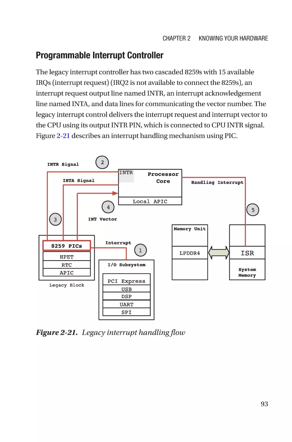
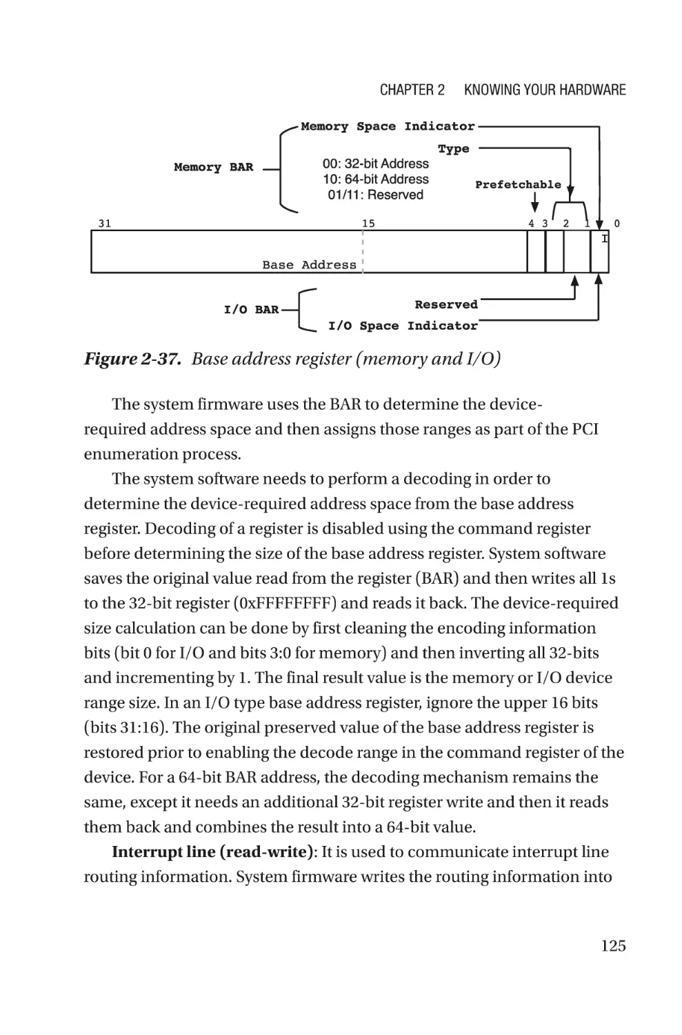
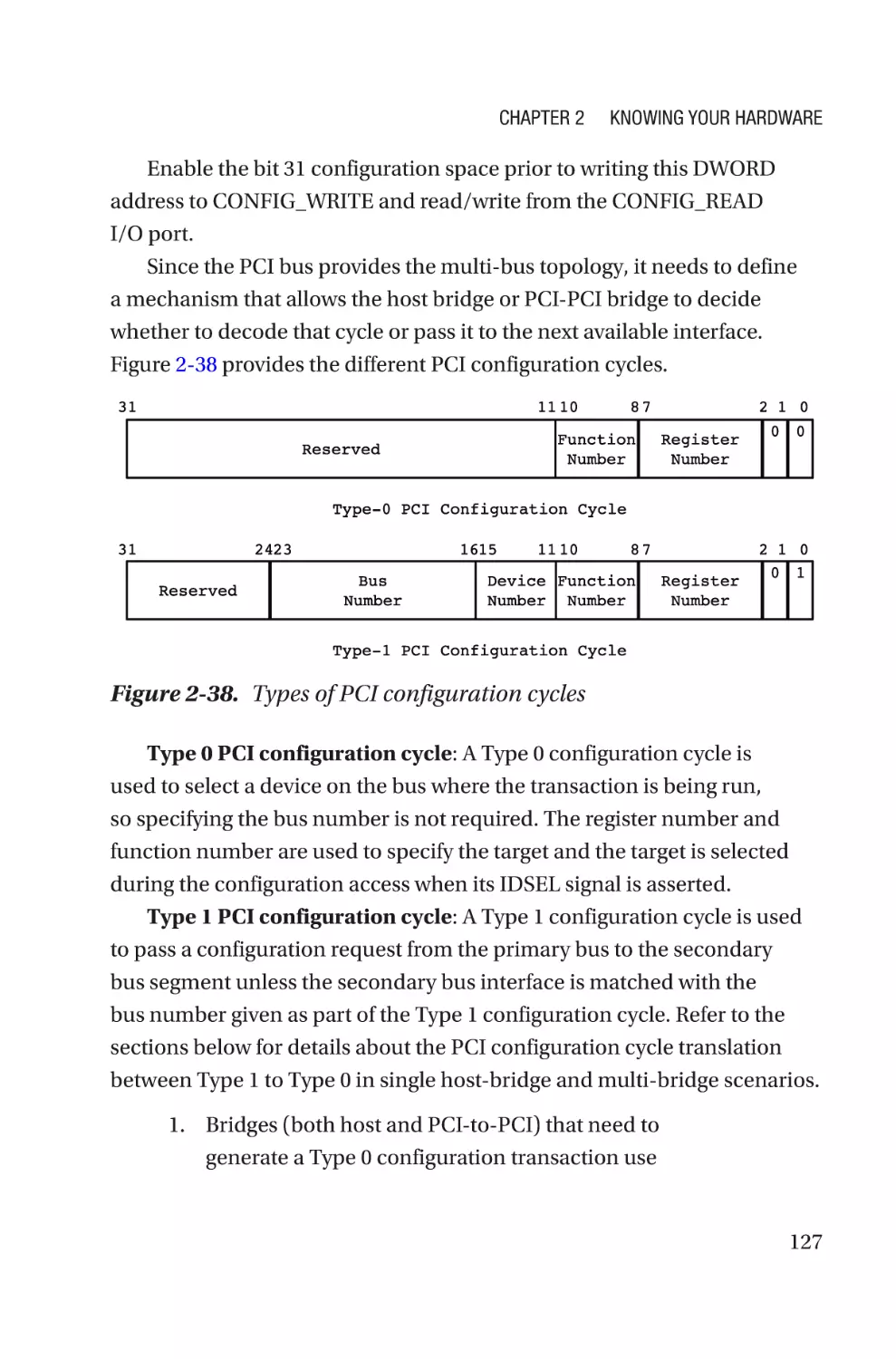
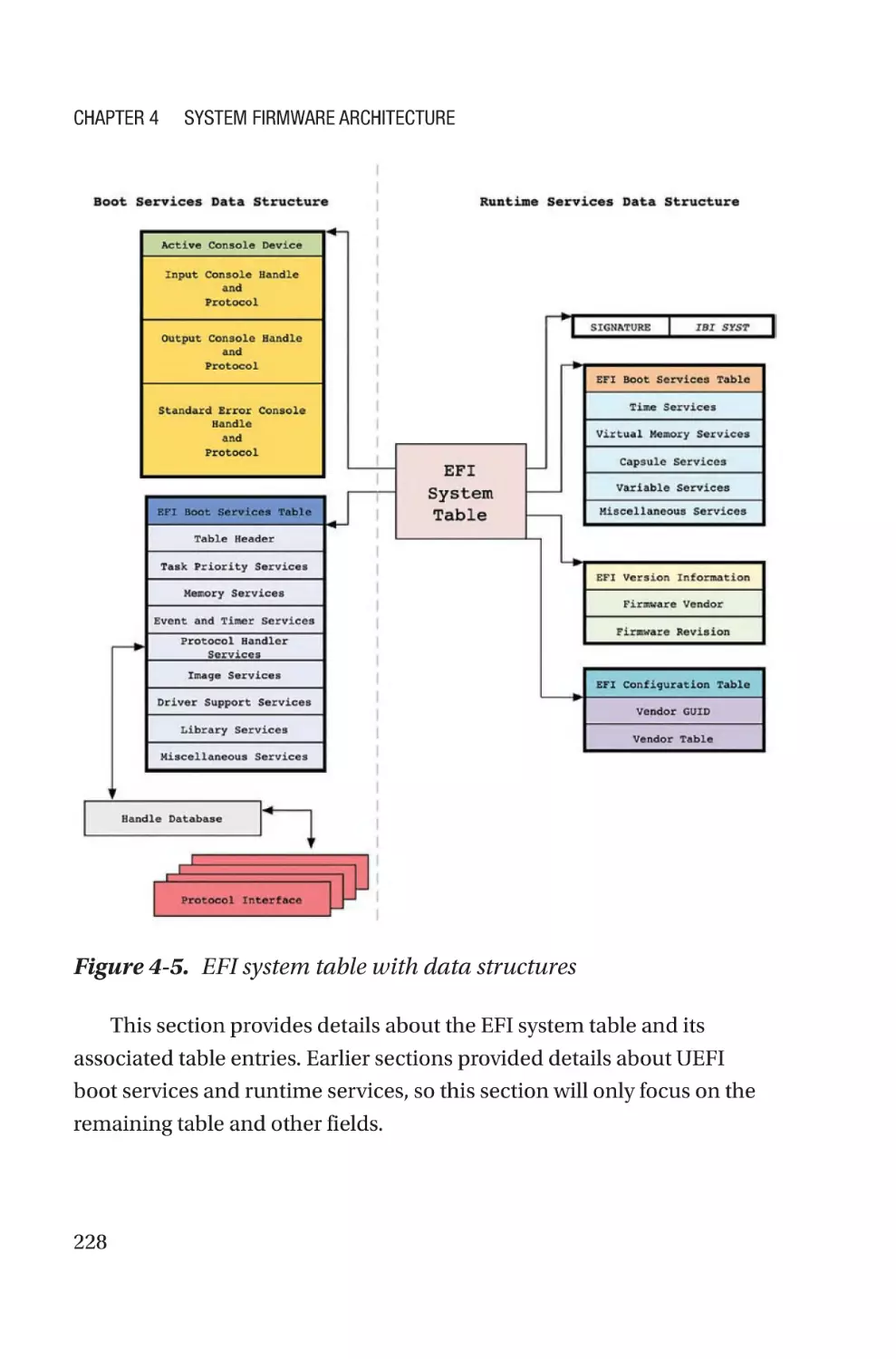
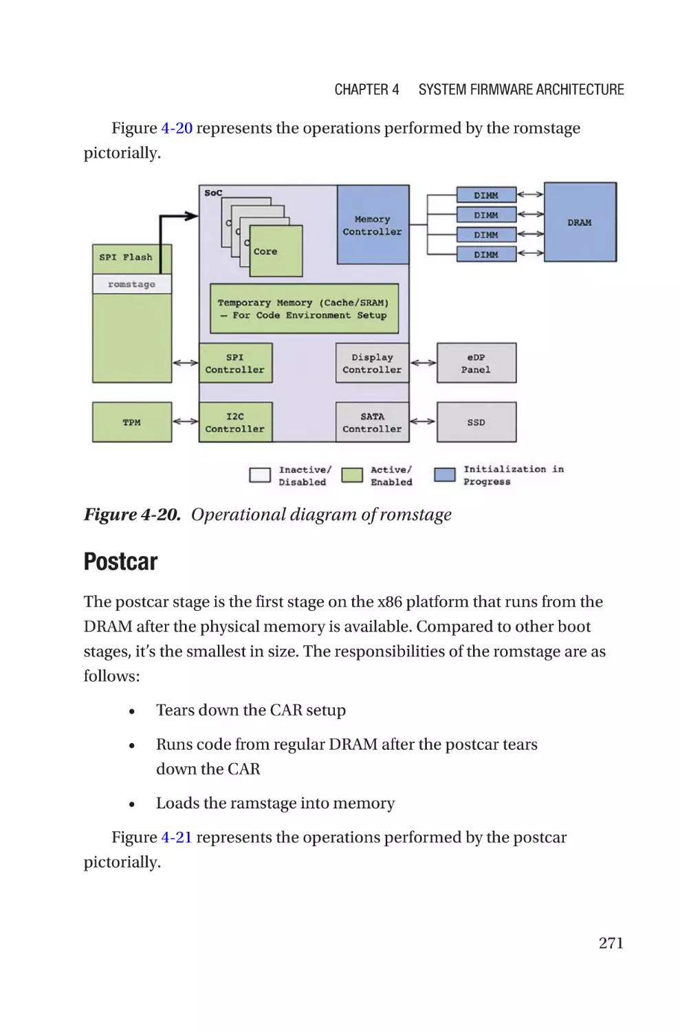
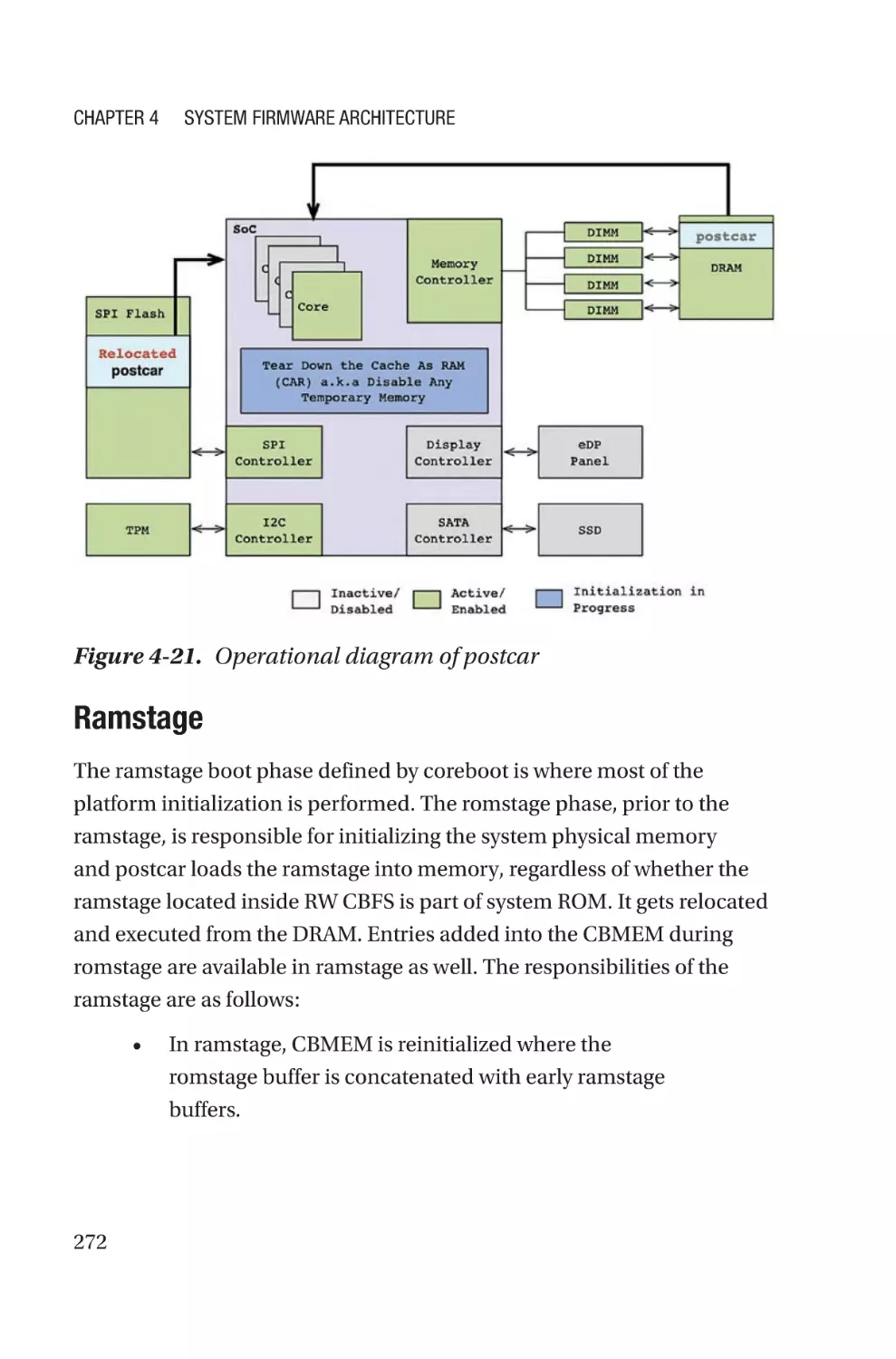
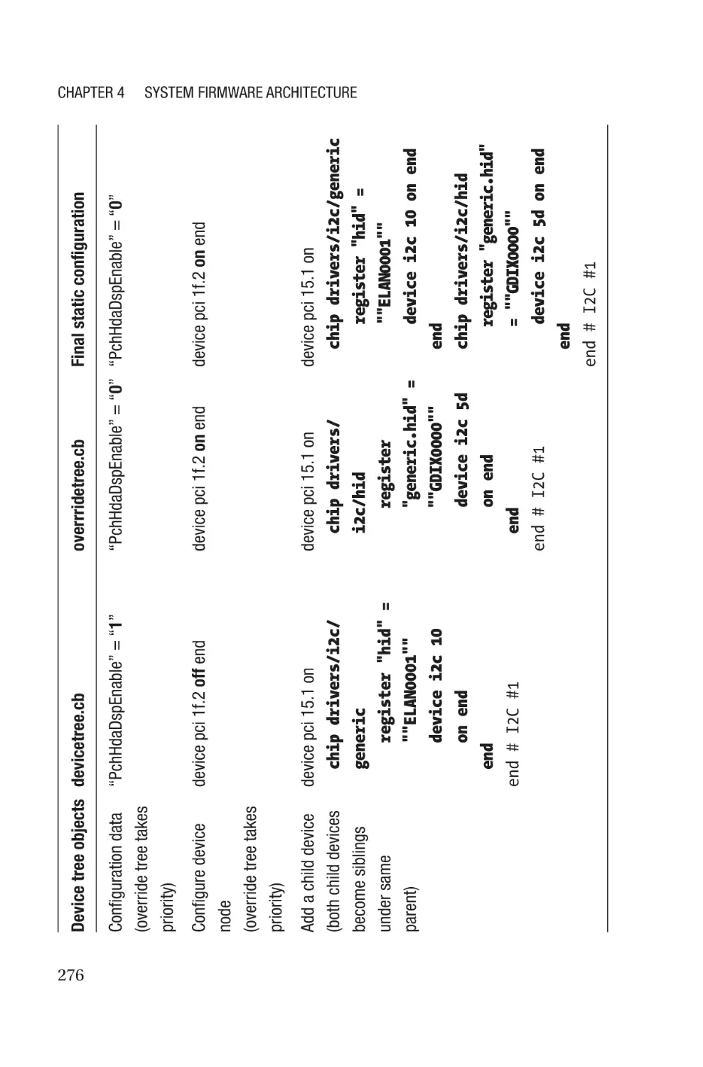
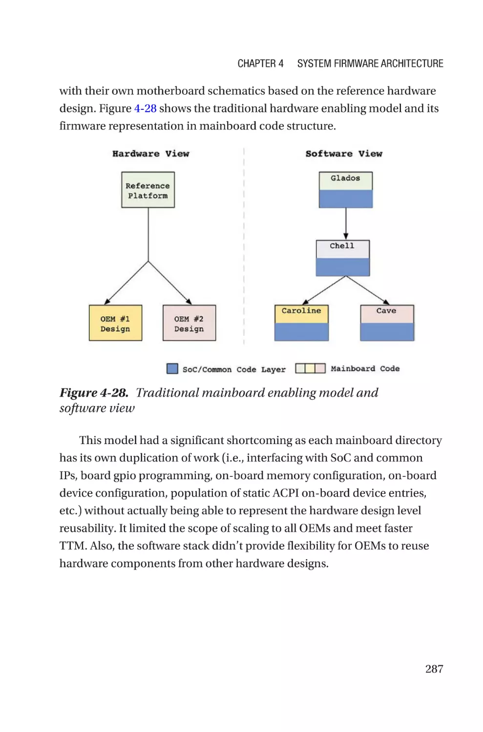
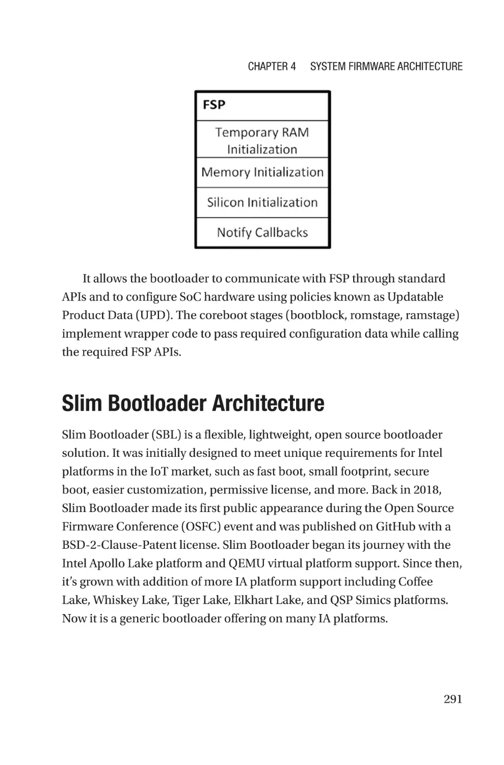
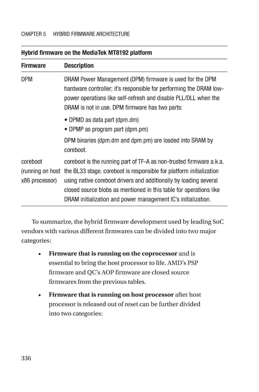
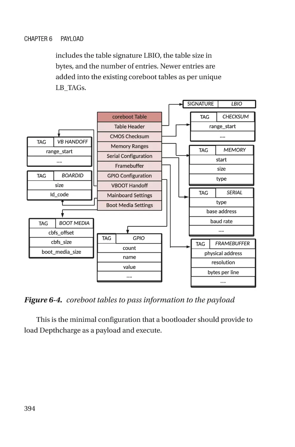
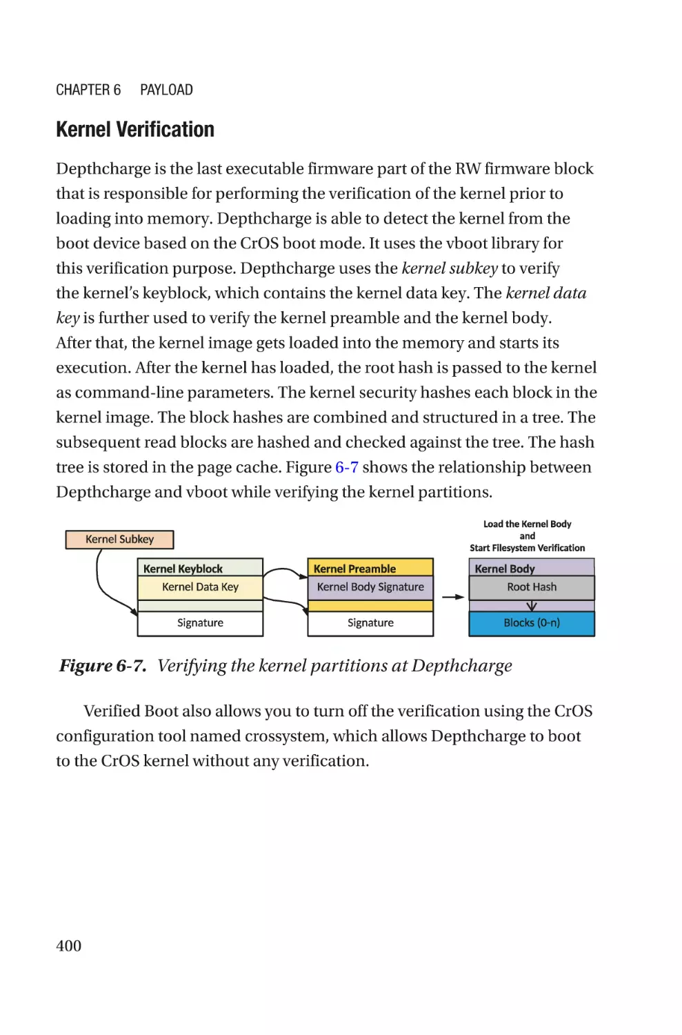
Text
System
Firmware
An Essential Guide to Open Source
and Embedded Solutions
—
Subrata Banik
Vincent Zimmer
System Firmware
An Essential Guide to Open
Source and Embedded
Solutions
Subrata Banik
Vincent Zimmer
System Firmware: An Essential Guide to Open Source and Embedded
Solutions
Subrata Banik
Bangalore, Karnataka, India
Vincent Zimmer
Tacoma, WA, USA
ISBN-13 (pbk): 978-1-4842-7938-0
https://doi.org/10.1007/978-1-4842-7939-7
ISBN-13 (electronic): 978-1-4842-7939-7
Copyright © 2022 by Subrata Banik and Vincent Zimmer
This work is subject to copyright. All rights are reserved by the Publisher, whether the whole or
part of the material is concerned, specifically the rights of translation, reprinting, reuse of
illustrations, recitation, broadcasting, reproduction on microfilms or in any other physical way,
and transmission or information storage and retrieval, electronic adaptation, computer software,
or by similar or dissimilar methodology now known or hereafter developed.
Trademarked names, logos, and images may appear in this book. Rather than use a trademark
symbol with every occurrence of a trademarked name, logo, or image we use the names, logos,
and images only in an editorial fashion and to the benefit of the trademark owner, with no
intention of infringement of the trademark.
The use in this publication of trade names, trademarks, service marks, and similar terms, even if
they are not identified as such, is not to be taken as an expression of opinion as to whether or not
they are subject to proprietary rights.
While the advice and information in this book are believed to be true and accurate at the date of
publication, neither the authors nor the editors nor the publisher can accept any legal
responsibility for any errors or omissions that may be made. The publisher makes no warranty,
express or implied, with respect to the material contained herein.
Managing Director, Apress Media LLC: Welmoed Spahr
Acquisitions Editor: Susan McDermott
Development Editor: Laura Berendson
Coordinating Editor: Jessica Vakili
Copy Editor: Mary Behr
Distributed to the book trade worldwide by Springer Science+Business Media New York, 1 NY
Plaza, New York, NY 10004. Phone 1-800-SPRINGER, fax (201) 348-4505, e-mail orders-ny@
springer-sbm.com, or visit www.springeronline.com. Apress Media, LLC is a California LLC and
the sole member (owner) is Springer Science + Business Media Finance Inc (SSBM Finance Inc).
SSBM Finance Inc is a Delaware corporation.
For information on translations, please e-mail booktranslations@springernature.com; for
reprint, paperback, or audio rights, please e-mail bookpermissions@springernature.com.
Apress titles may be purchased in bulk for academic, corporate, or promotional use. eBook
versions and licenses are also available for most titles. For more information, reference our Print
and eBook Bulk Sales web page at www.apress.com/bulk-sales.
Any source code or other supplementary material referenced by the author in this book is
available to readers on the GitHub repository: https://github.com/Apress/System-Firmware.
For more detailed information, please visit www.apress.com/source-code.
Printed on acid-free paper
Table of Contents
About the Authors��������������������������������������������������������������������������������xi
About the Technical Reviewers���������������������������������������������������������xiii
Foreword by Jonathan Zhang�������������������������������������������������������������xv
Preface����������������������������������������������������������������������������������������������xix
Acknowledgments�����������������������������������������������������������������������������xxi
Introduction�������������������������������������������������������������������������������������xxiii
Chapter 1: Introduction������������������������������������������������������������������������1
Lack of Open System Design��������������������������������������������������������������������������������3
Misinterpretation of Firmware Definition��������������������������������������������������������������4
Attract the Talent���������������������������������������������������������������������������������������������������5
The Importance of Programming Knowledge�������������������������������������������������������6
Specialized Education�������������������������������������������������������������������������������������������8
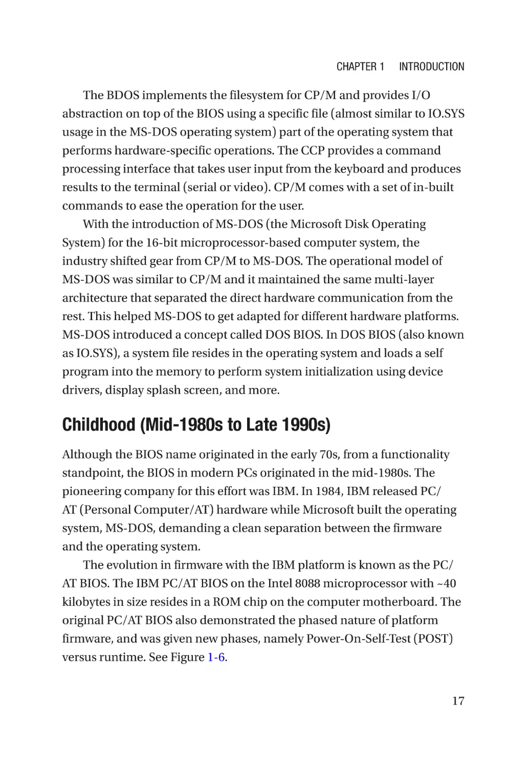
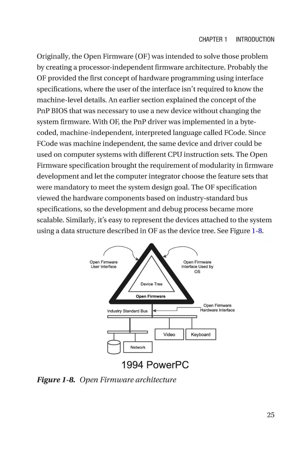
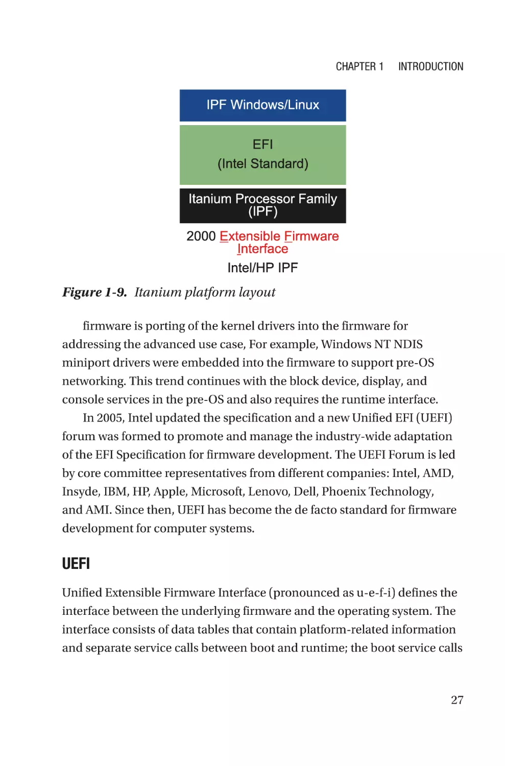
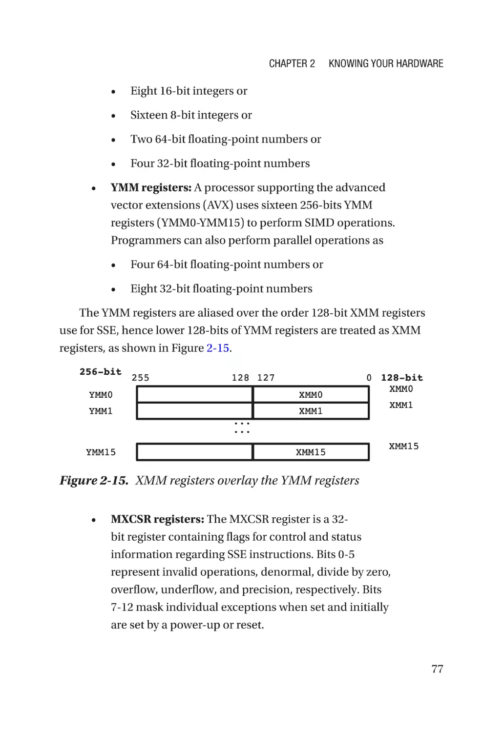
The Origin of Firmware����������������������������������������������������������������������������������10
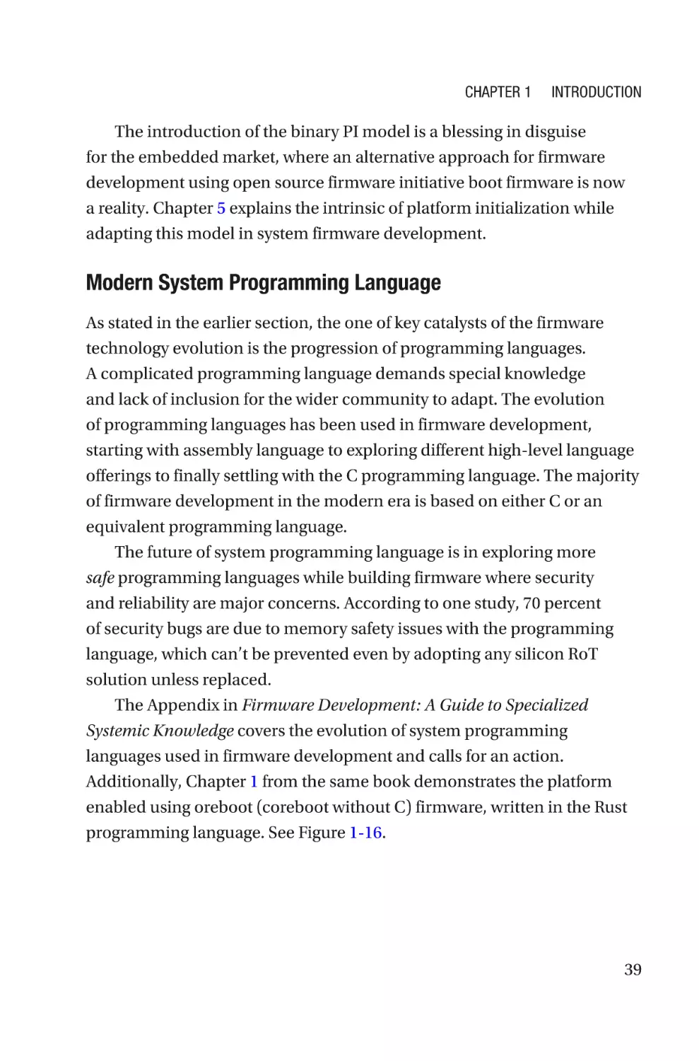
Firmware Evolution����������������������������������������������������������������������������������������14
Distinction Between Firmware and Software������������������������������������������������40
Introduction of Non-Host Firmware���������������������������������������������������������������41
Introduction to Device Firmware�������������������������������������������������������������������42
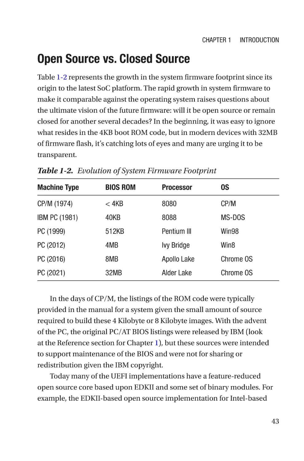
Open Source vs. Closed Source���������������������������������������������������������������������43
Summary�������������������������������������������������������������������������������������������������������44
iii
Table of Contents
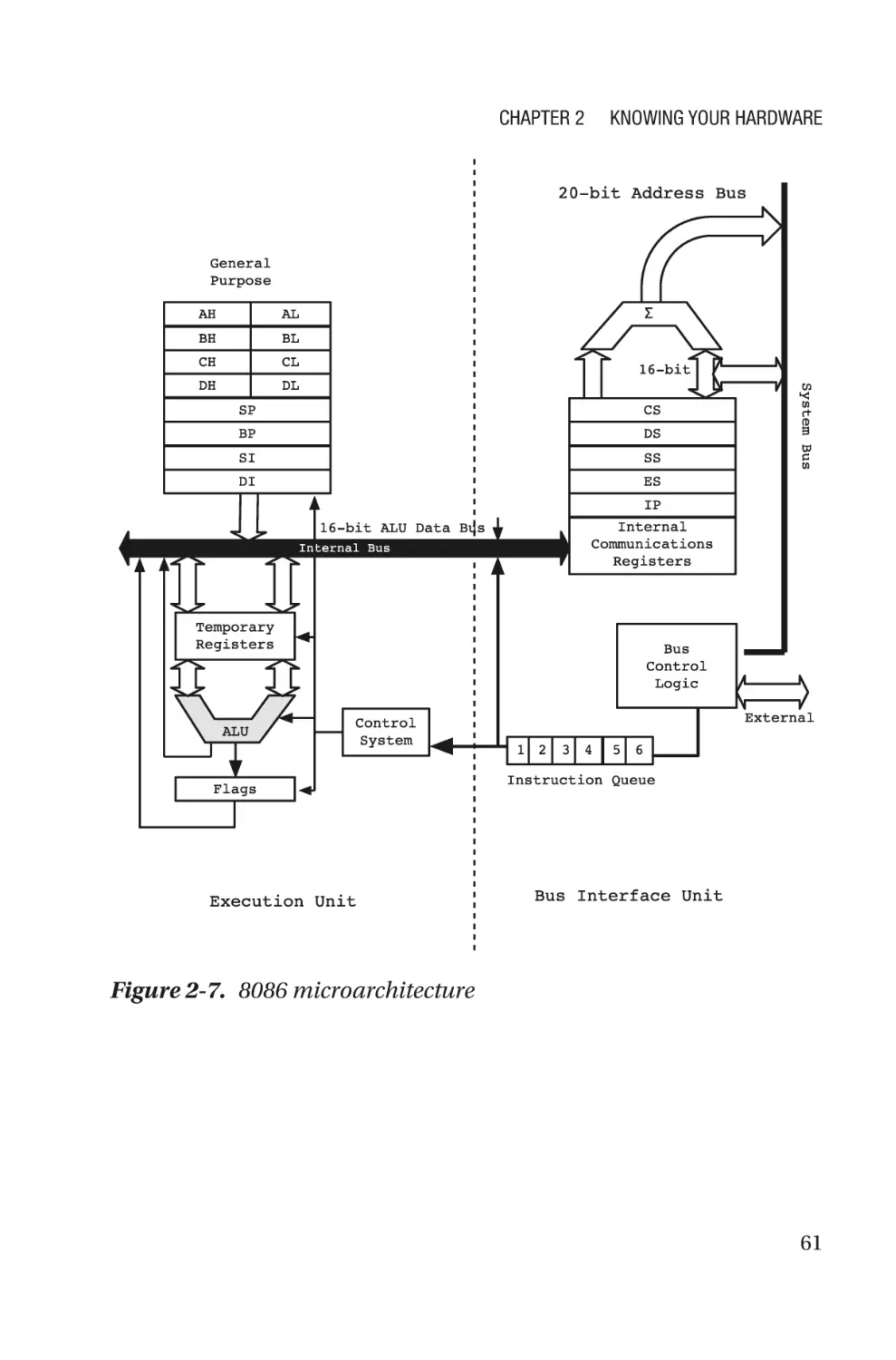
Chapter 2: Knowing Your Hardware���������������������������������������������������45
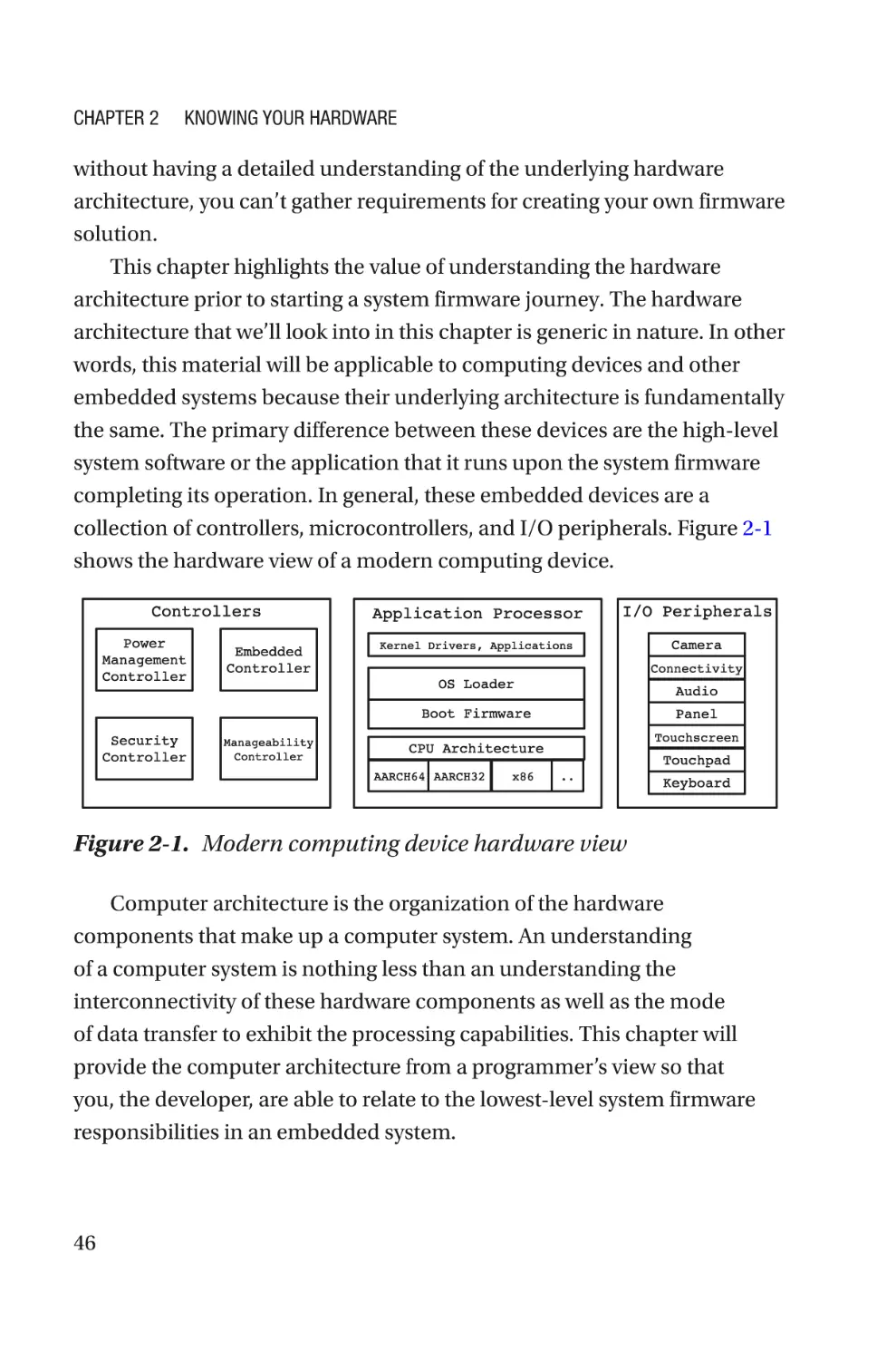
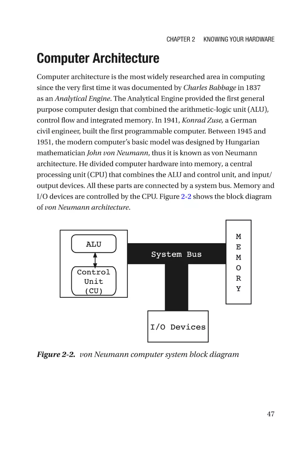
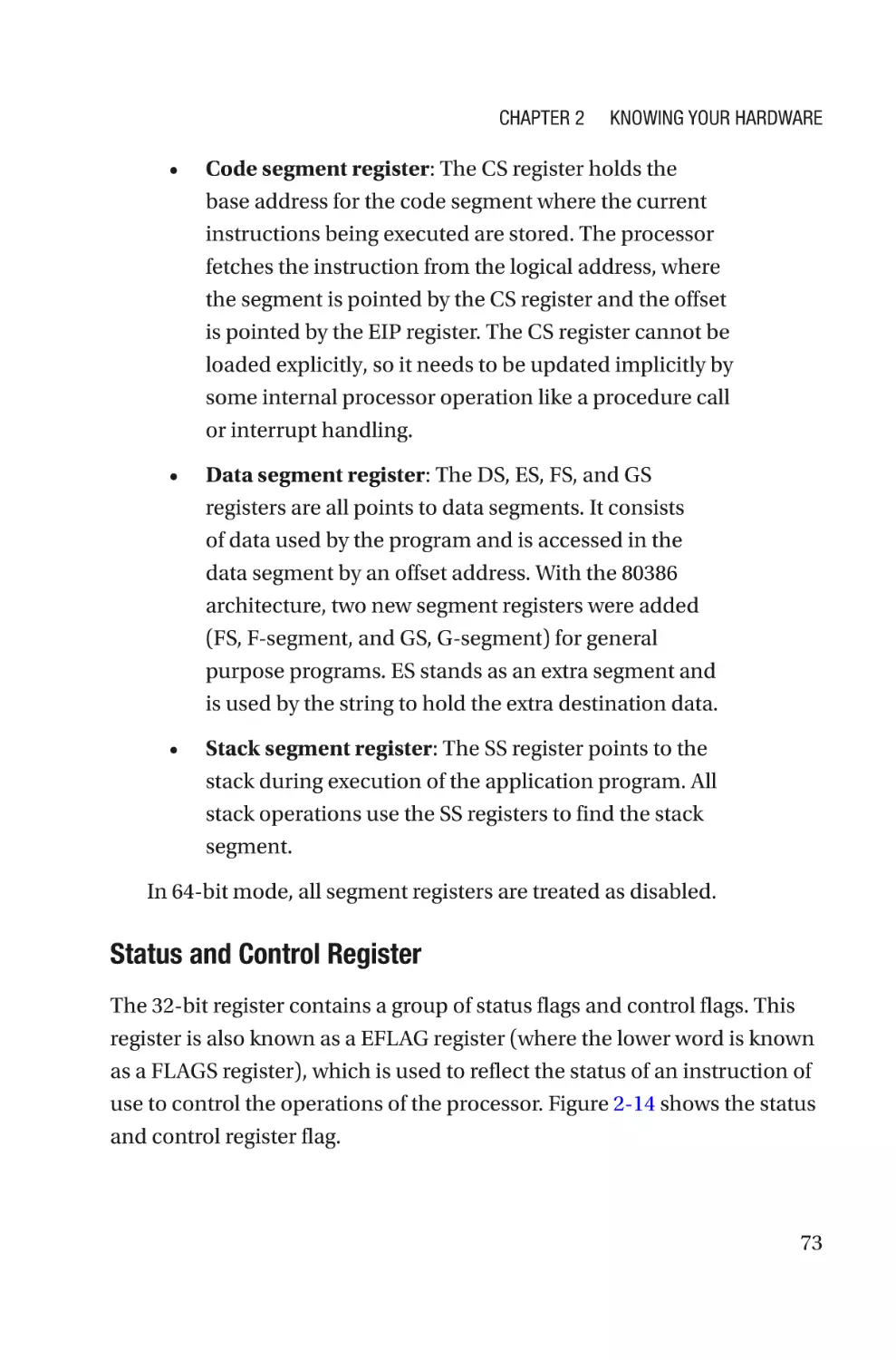
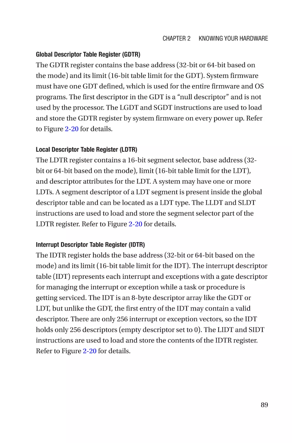
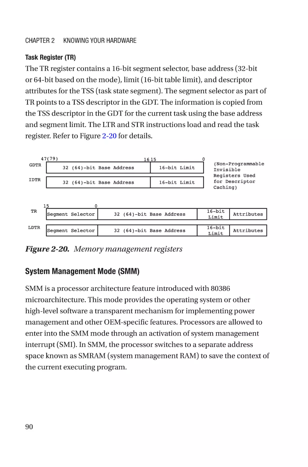
Computer Architecture����������������������������������������������������������������������������������������47
Instruction Set Architecture���������������������������������������������������������������������������50
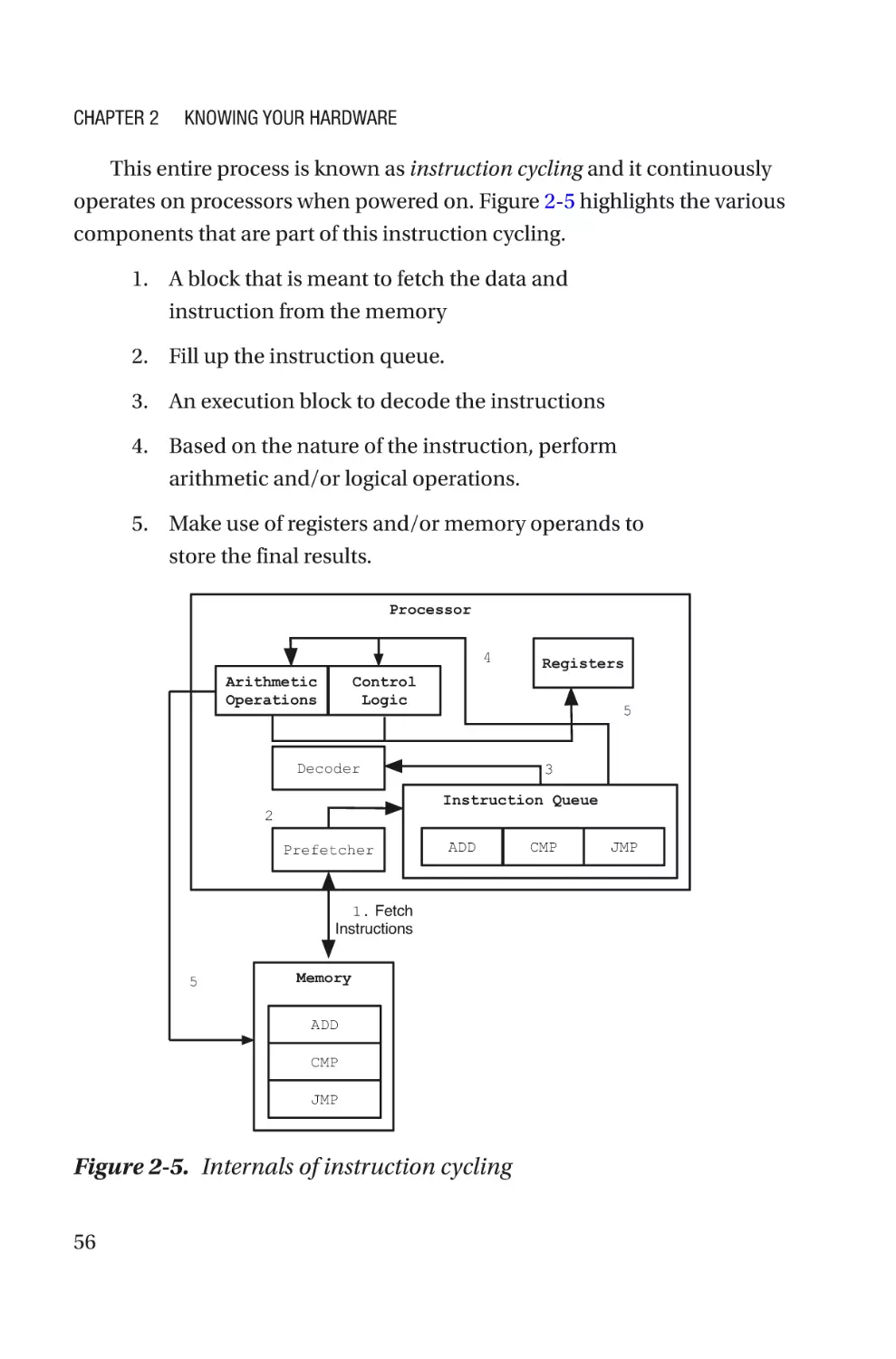
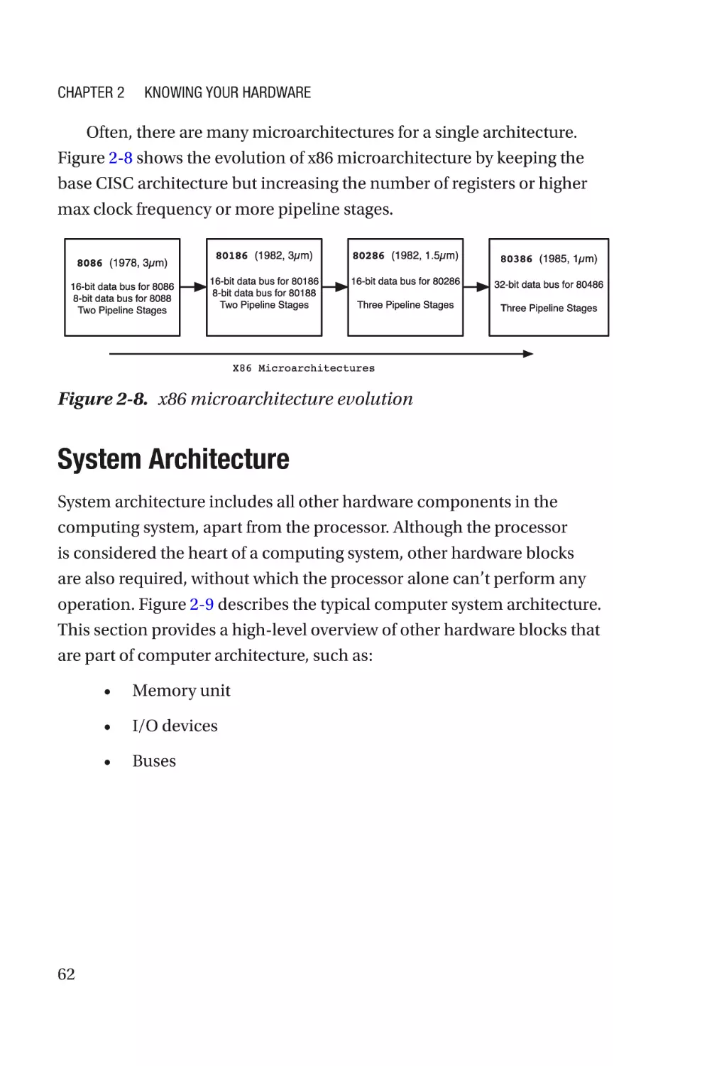
Microarchitecture������������������������������������������������������������������������������������������55
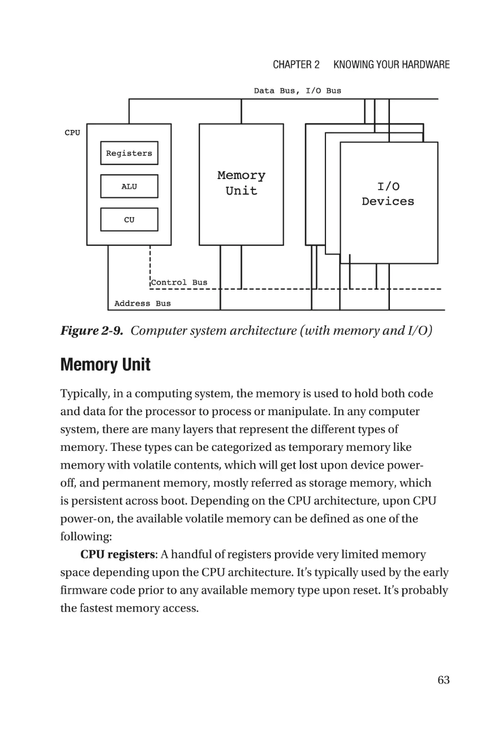
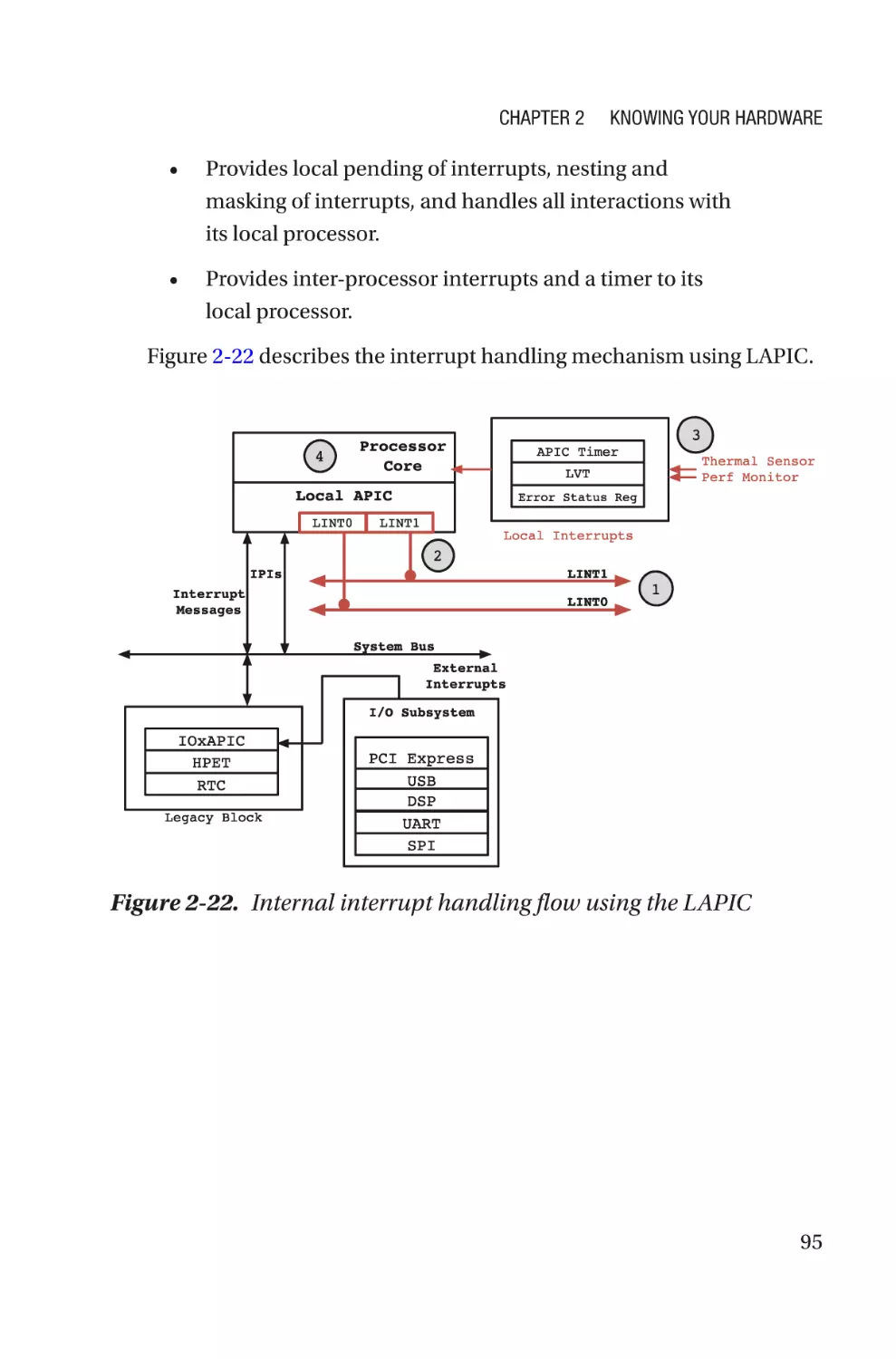
System Architecture��������������������������������������������������������������������������������������62
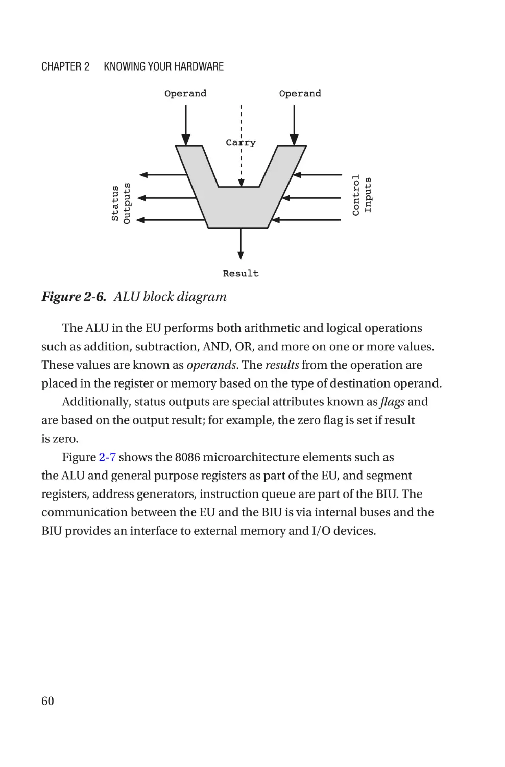
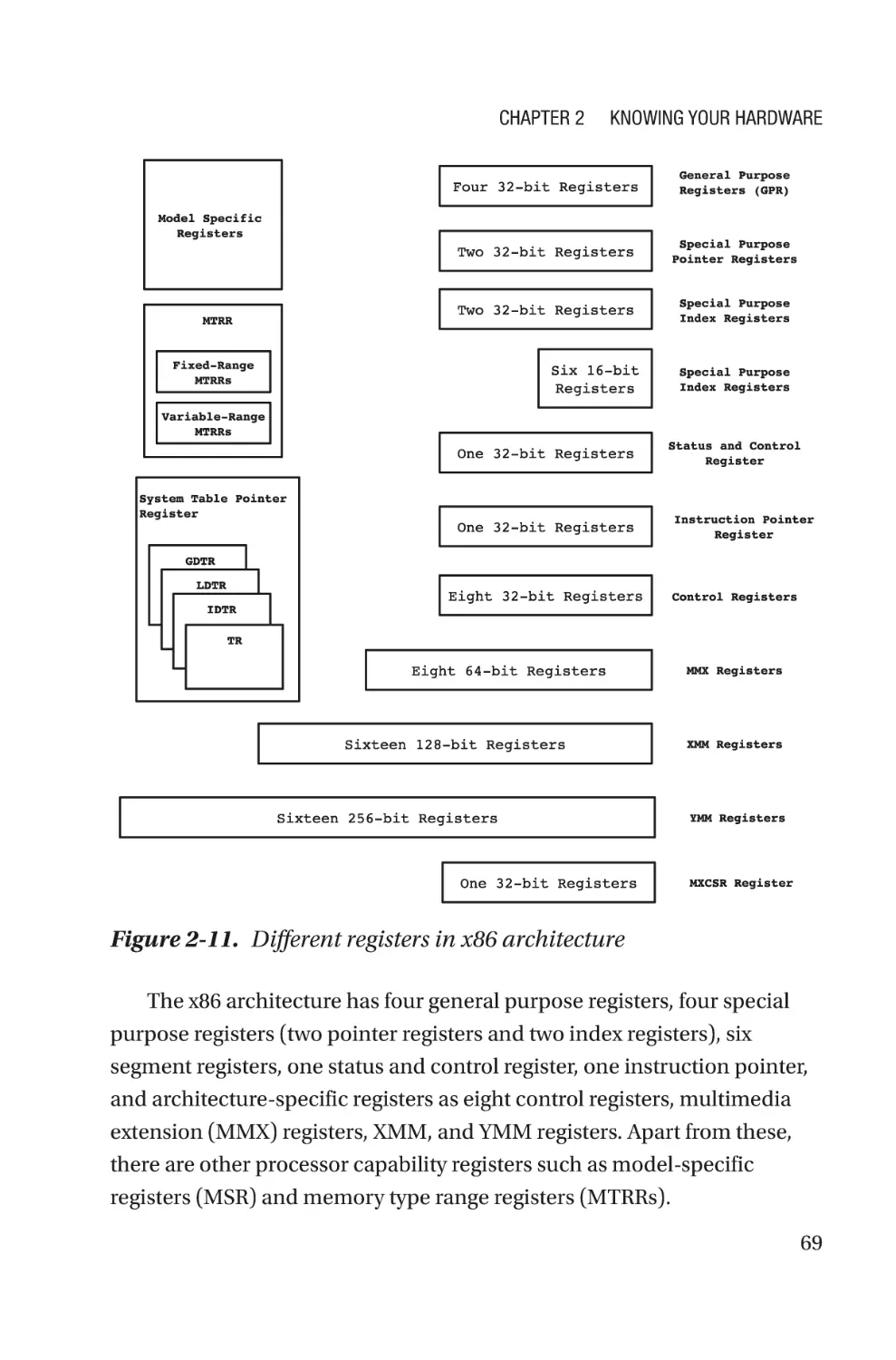
CPU Internals������������������������������������������������������������������������������������������������������68
Internals of x86 Processors���������������������������������������������������������������������������68
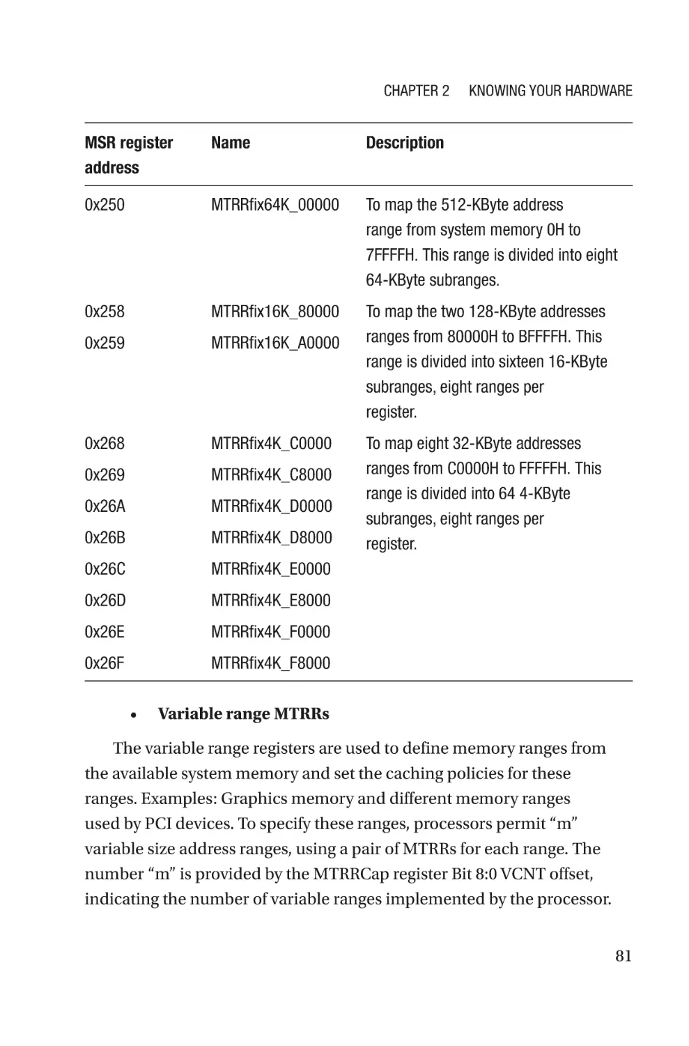
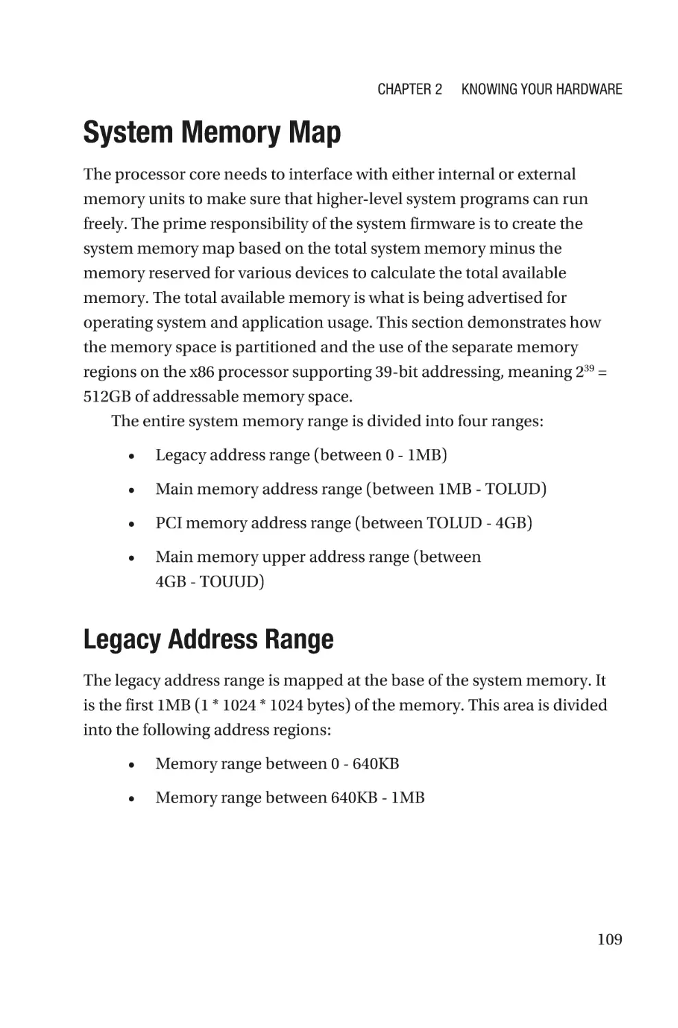
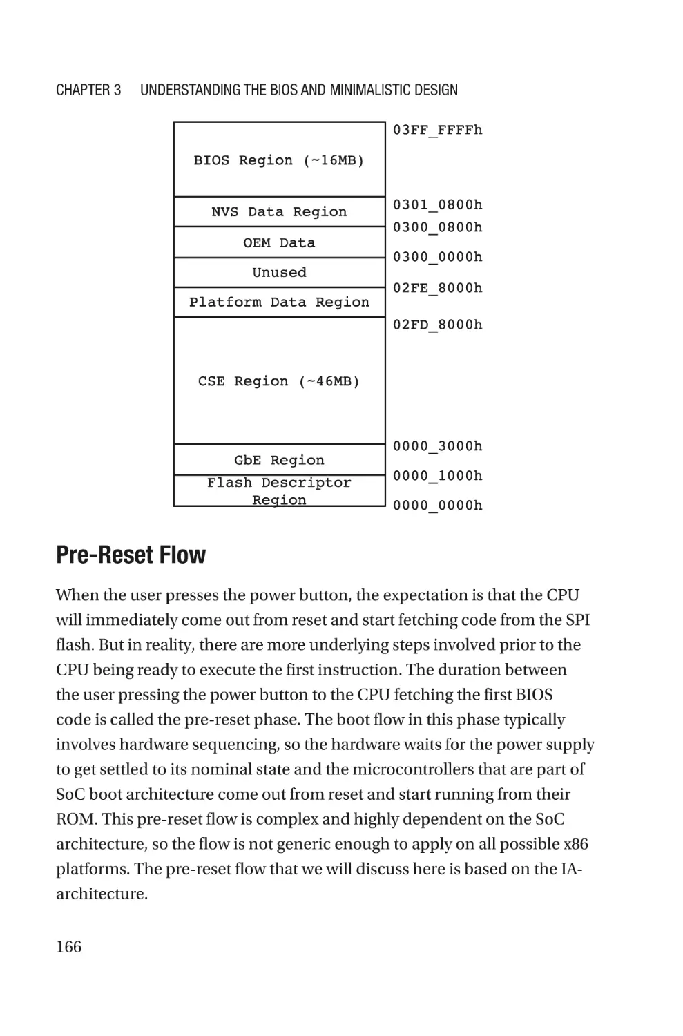
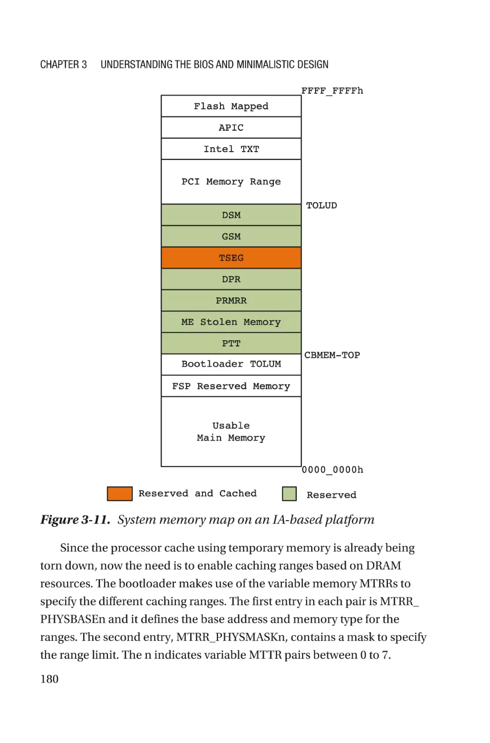
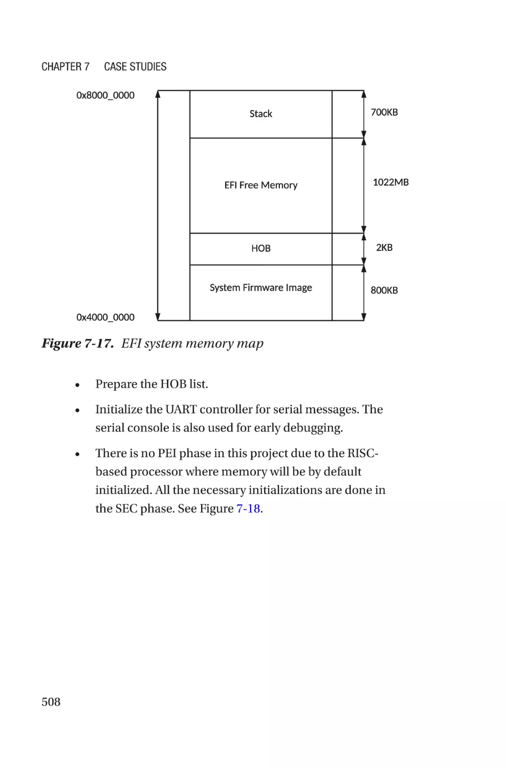
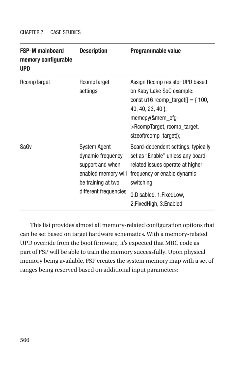
System Memory Map����������������������������������������������������������������������������������������109
Legacy Address Range��������������������������������������������������������������������������������109
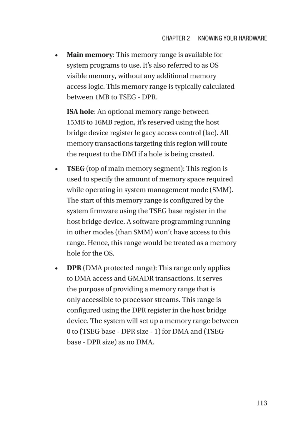
Main Memory Address Range����������������������������������������������������������������������112
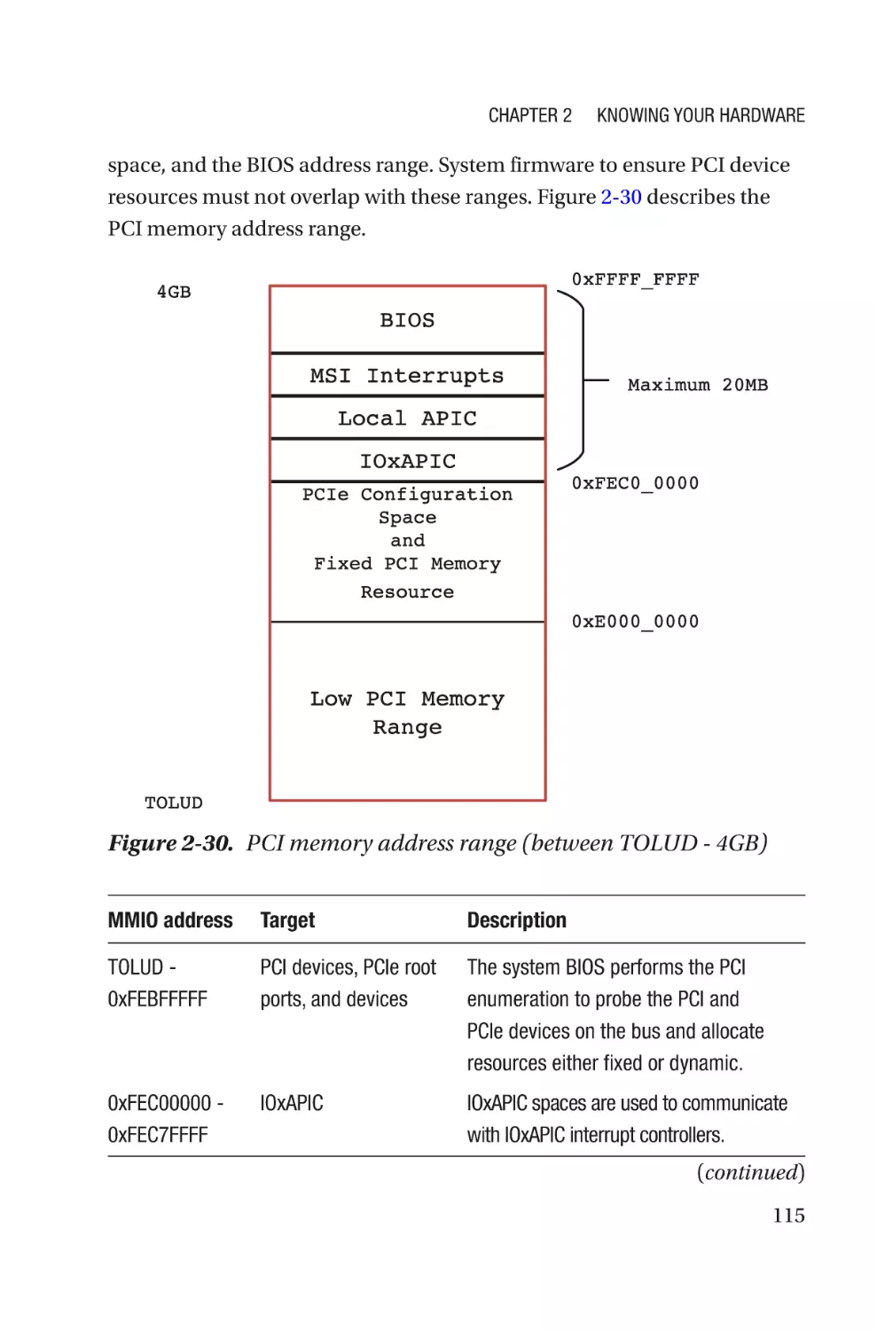
PCI Memory Address Range������������������������������������������������������������������������114
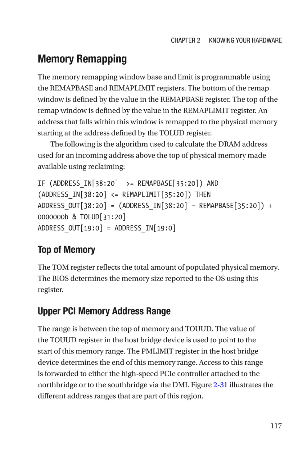
Main Memory Upper Address Range�����������������������������������������������������������116
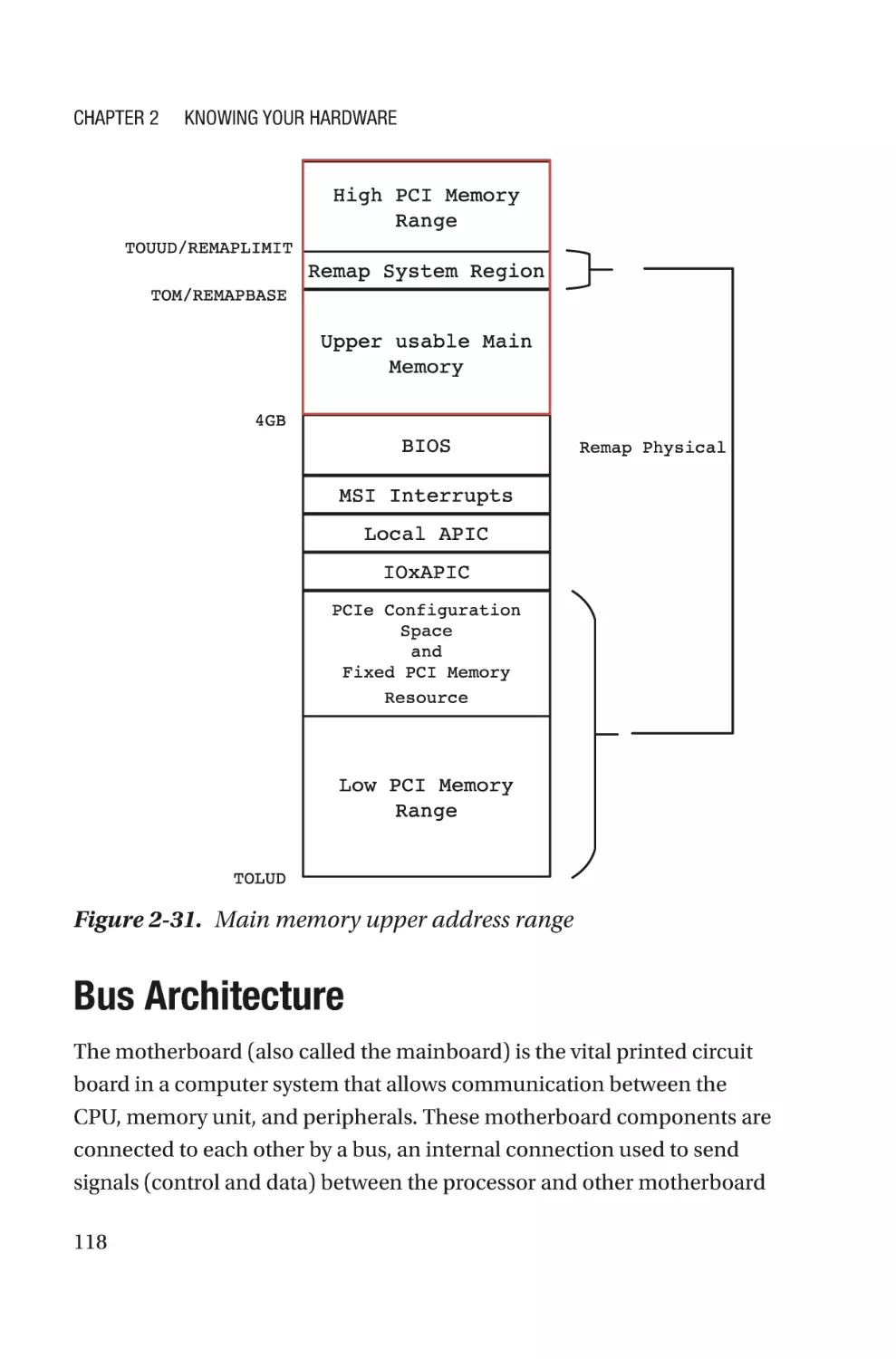
Bus Architecture������������������������������������������������������������������������������������������������118
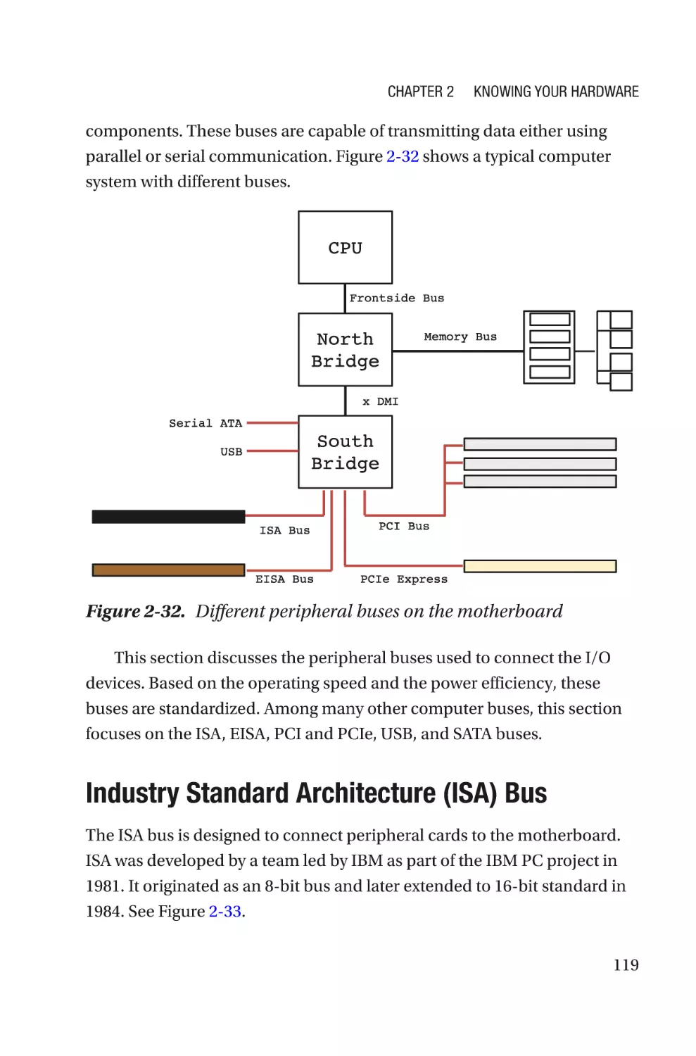
Industry Standard Architecture (ISA) Bus����������������������������������������������������119
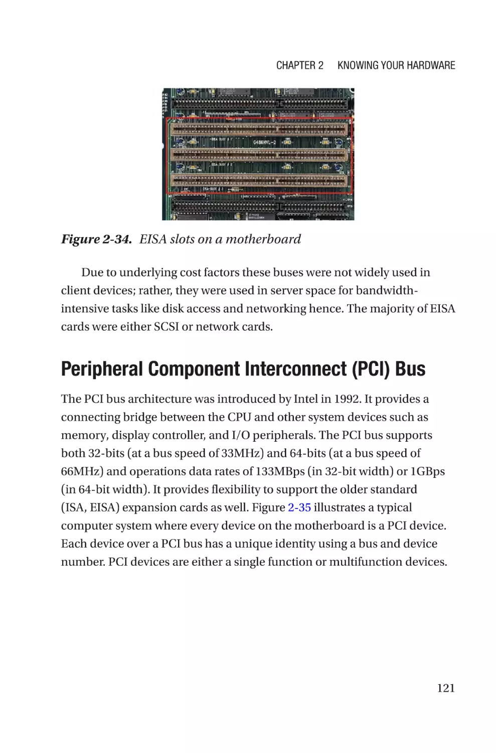
Extended Industry Standard Architecture (EISA) Bus����������������������������������120
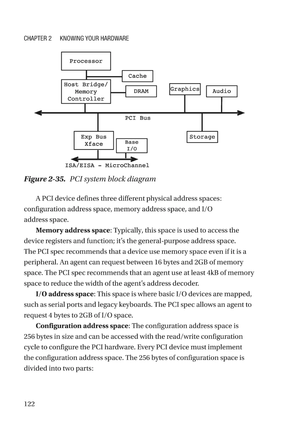
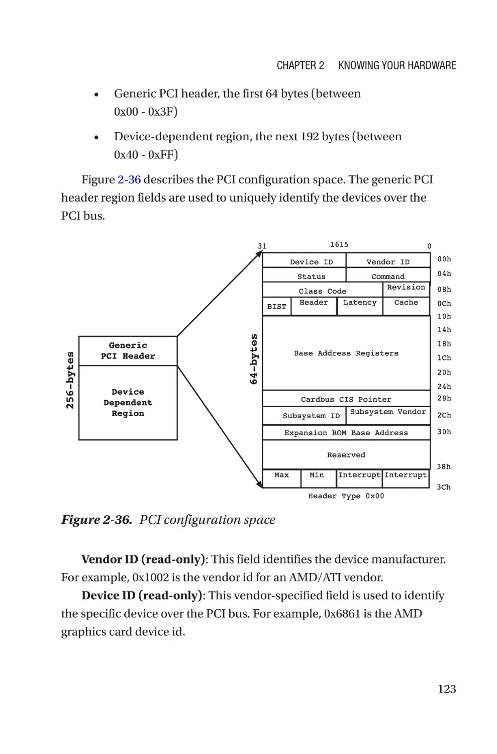
Peripheral Component Interconnect (PCI) Bus��������������������������������������������121
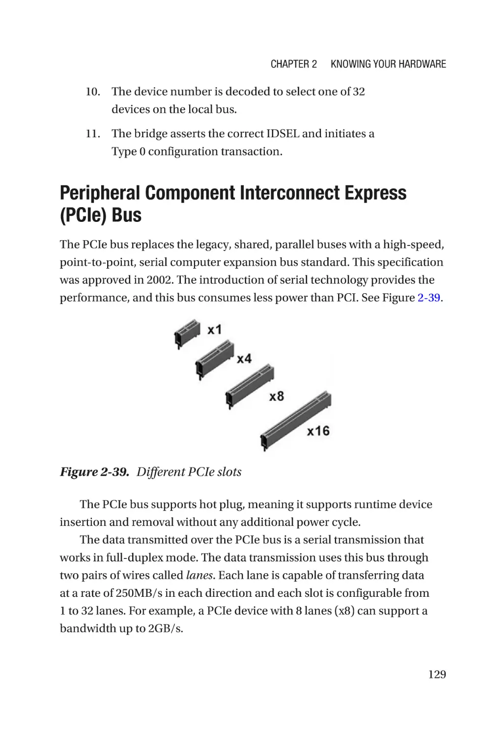
Peripheral Component Interconnect Express (PCIe) Bus�����������������������������129
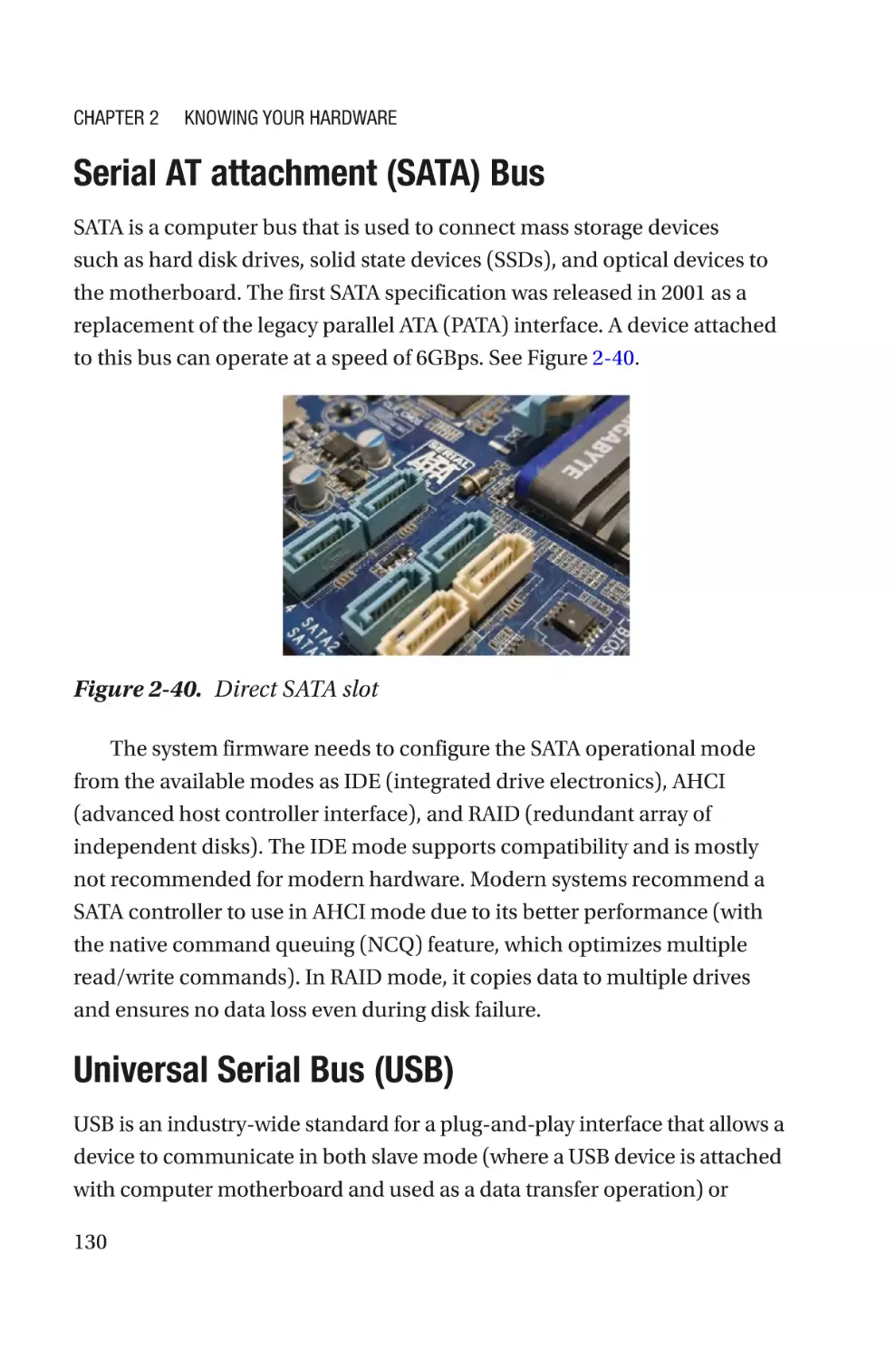
Serial AT attachment (SATA) Bus�����������������������������������������������������������������130
Universal Serial Bus (USB)���������������������������������������������������������������������������130
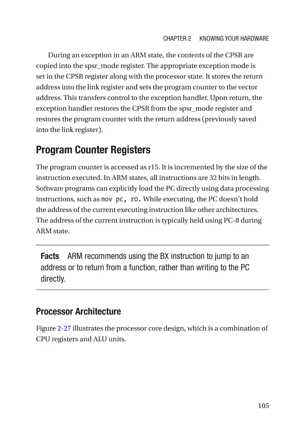
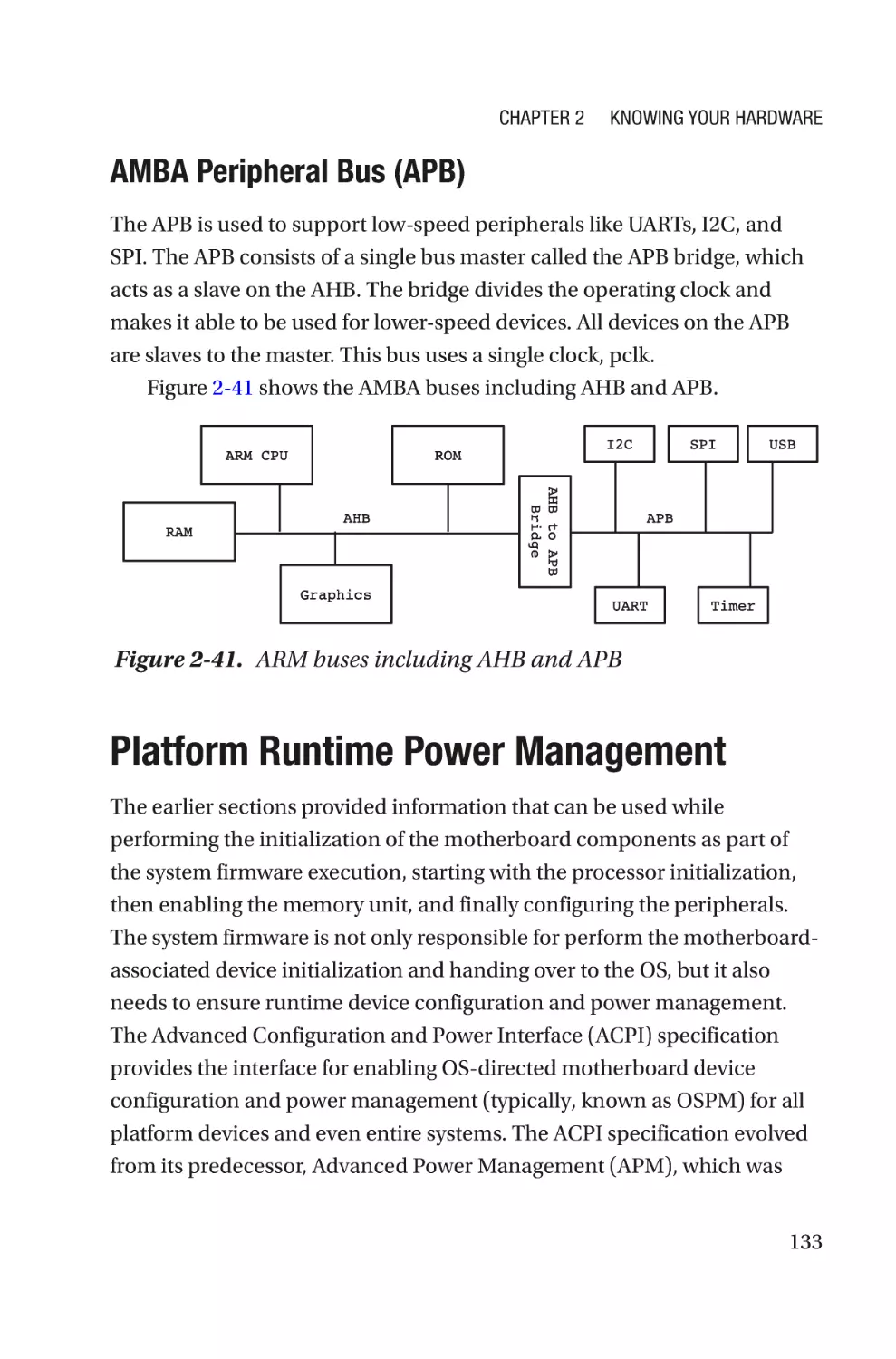
ARM Advanced Microcontroller Bus Architecture (AMBA)���������������������������132
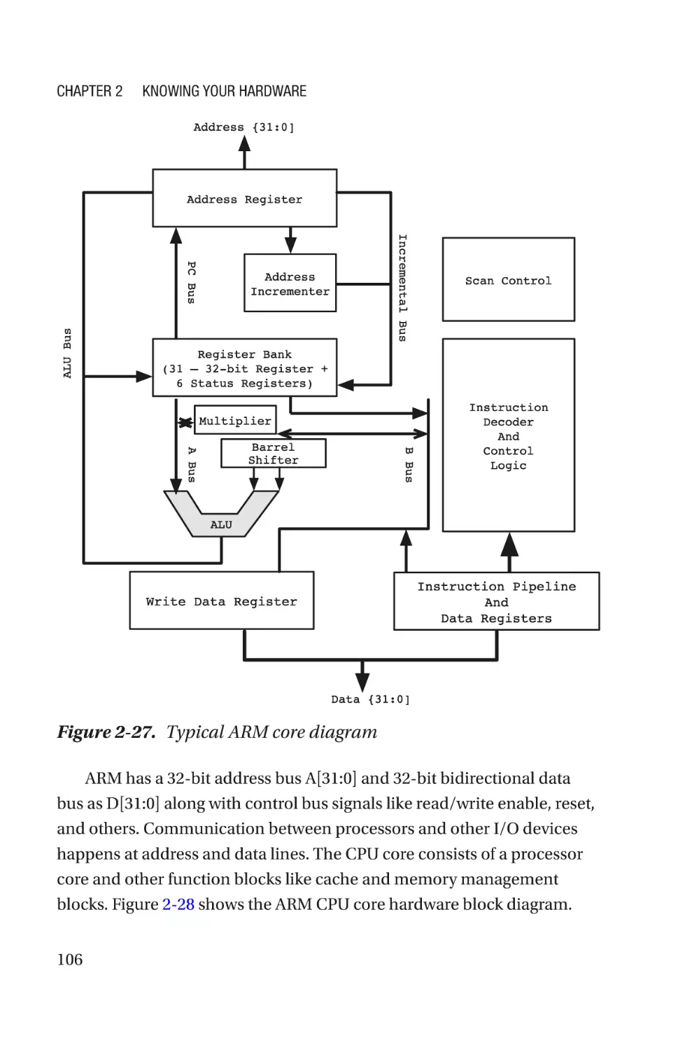
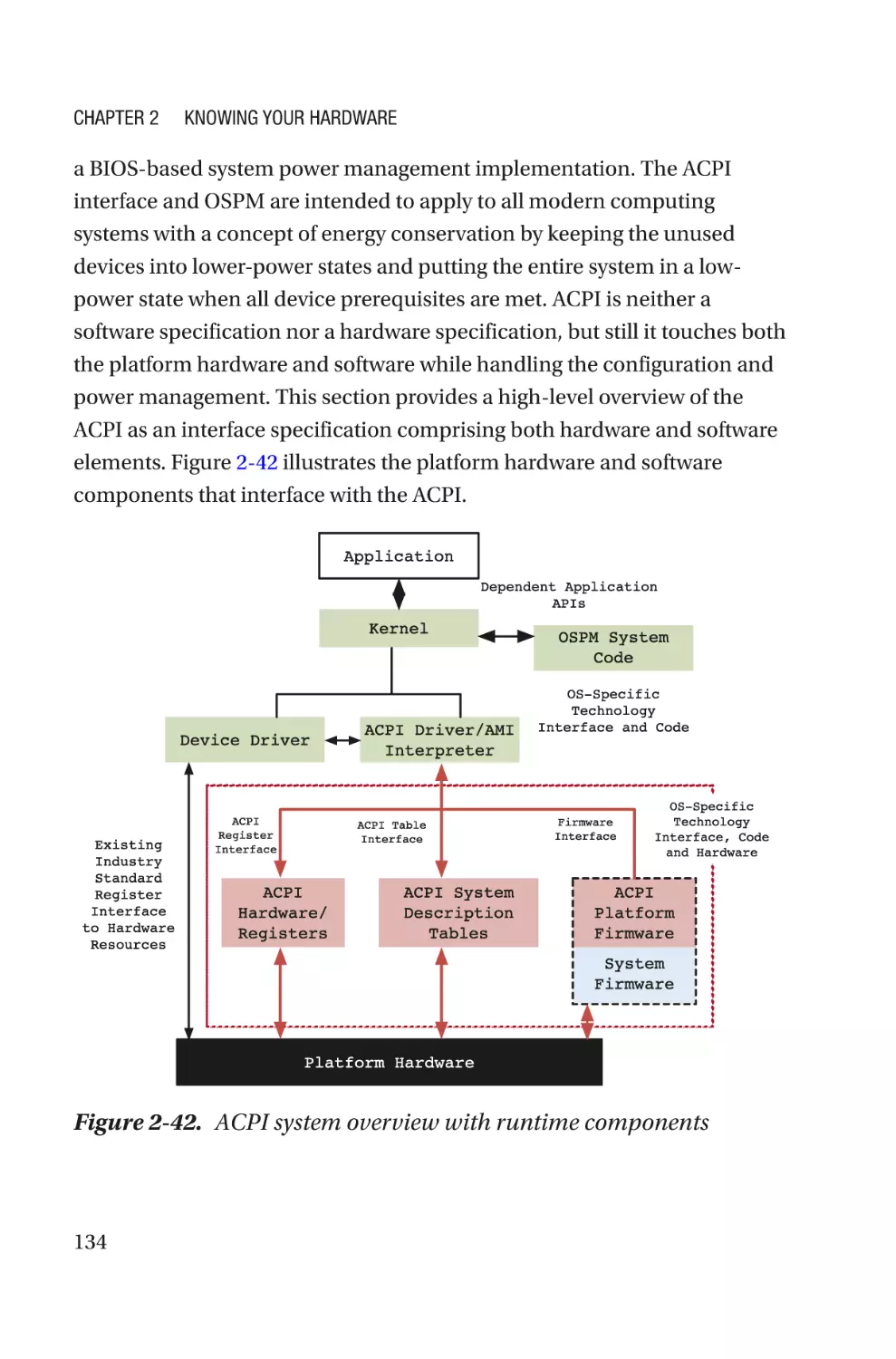
Platform Runtime Power Management�������������������������������������������������������������133
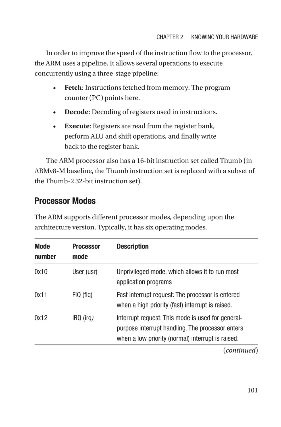
ACPI Hardware/Registers����������������������������������������������������������������������������135
ACPI System Description Tables������������������������������������������������������������������137
ACPI Platform Firmware������������������������������������������������������������������������������139
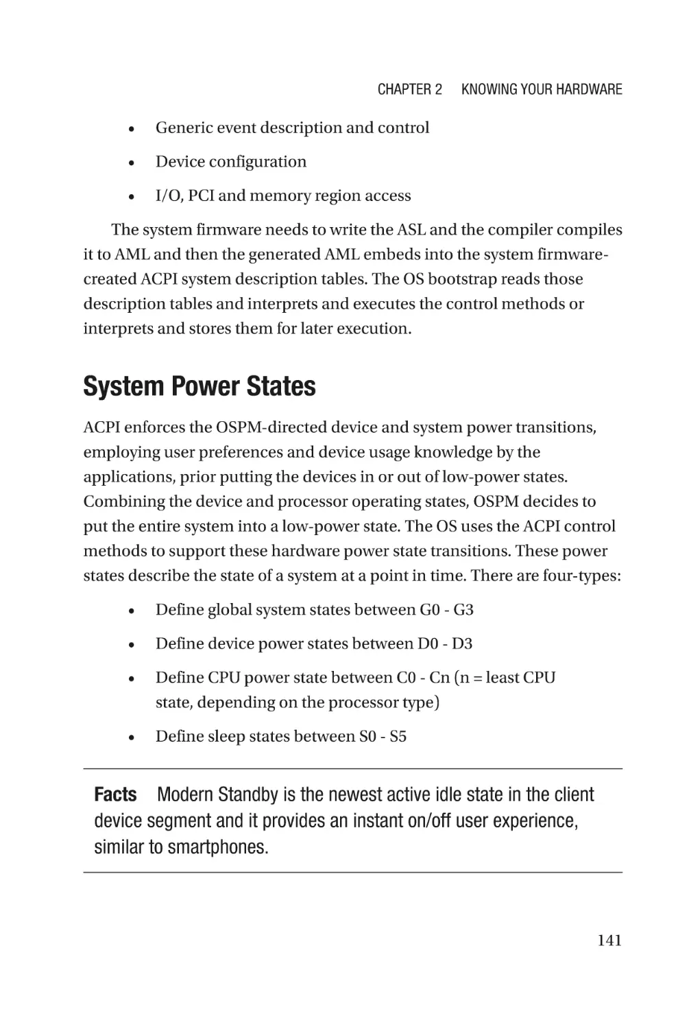
System Power States����������������������������������������������������������������������������������141
Summary����������������������������������������������������������������������������������������������������������142
iv
Table of Contents
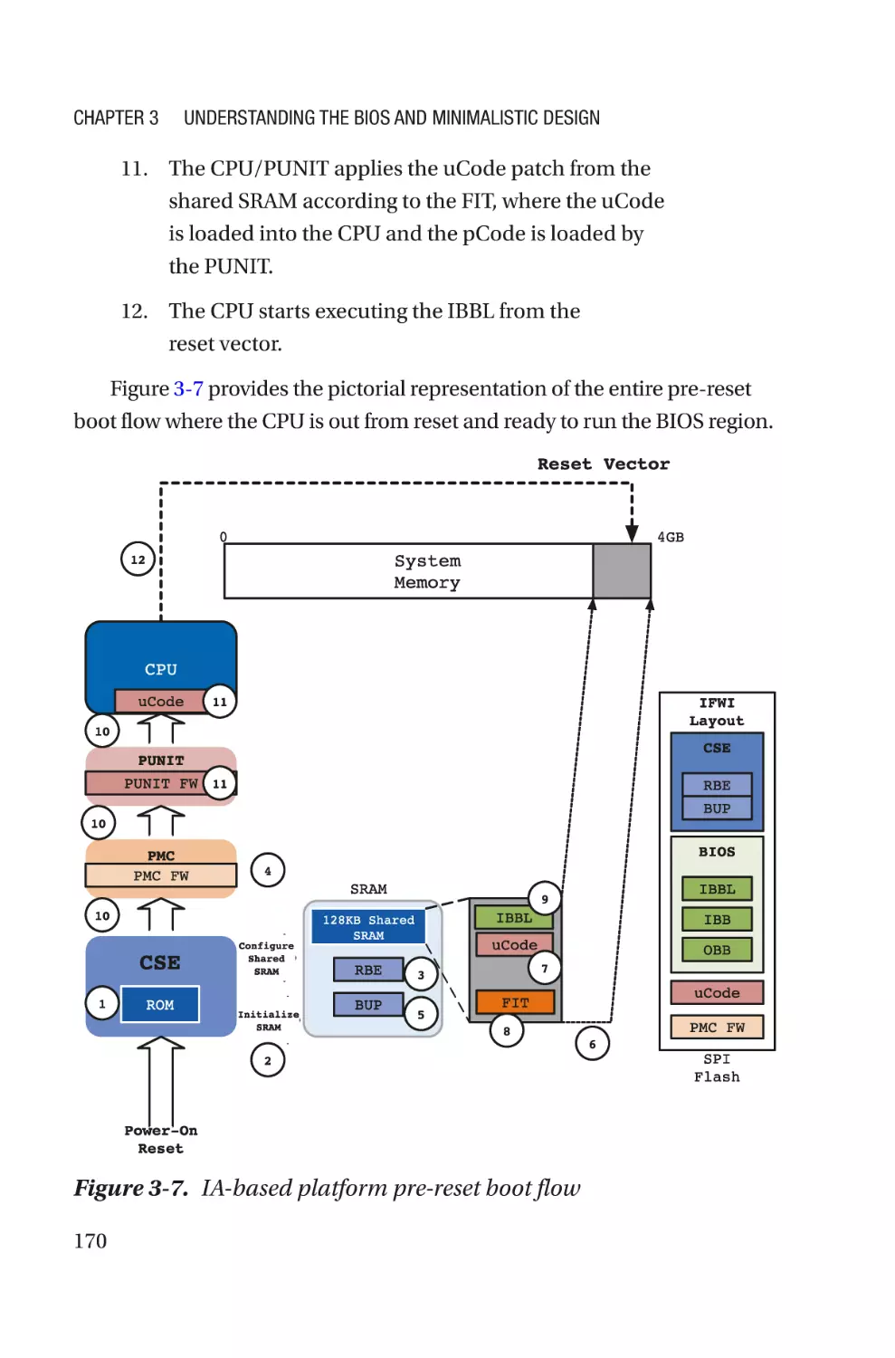
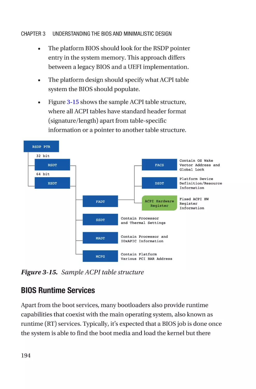
Chapter 3: Understanding the BIOS and Minimalistic Design�����������145
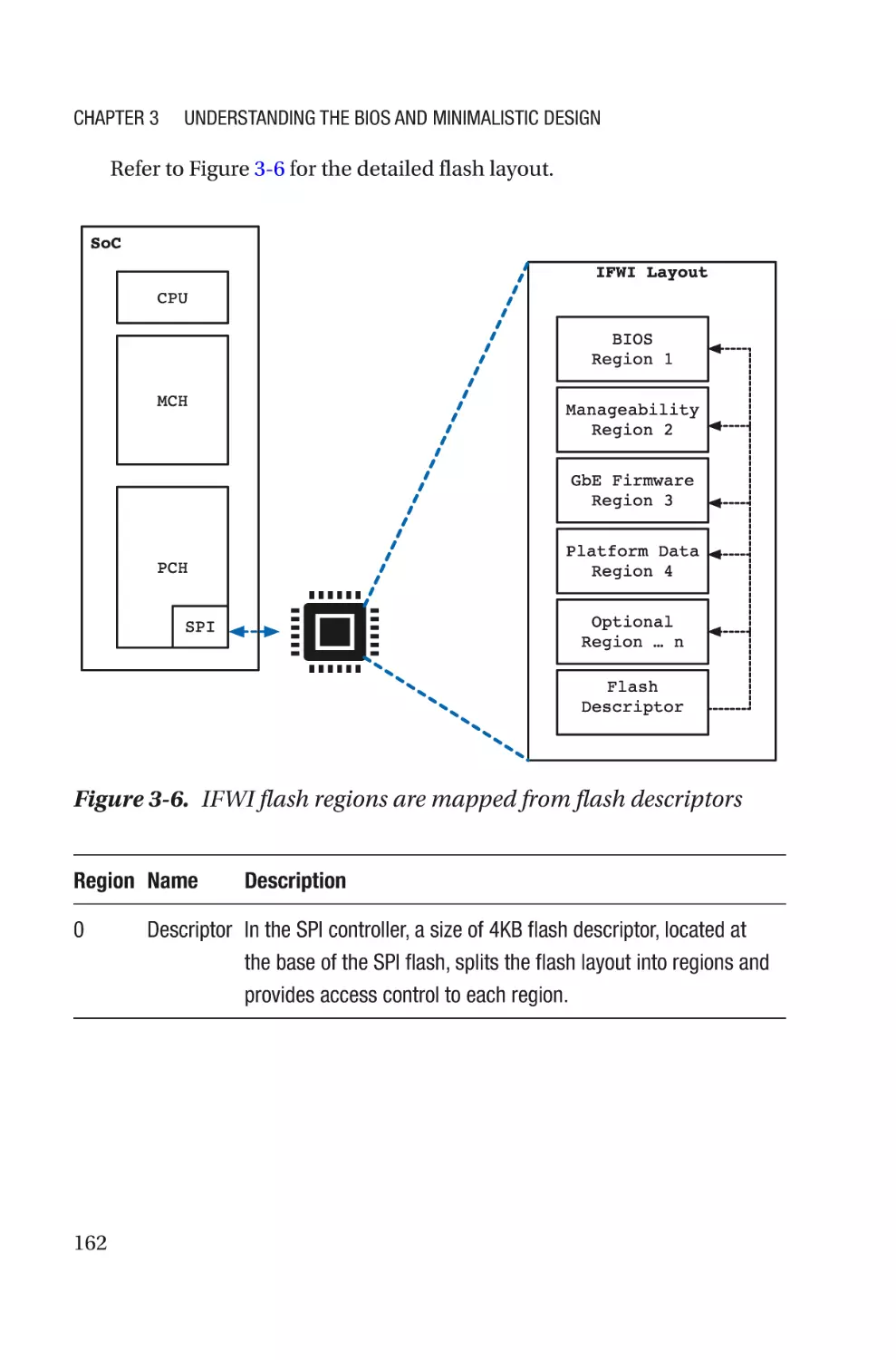
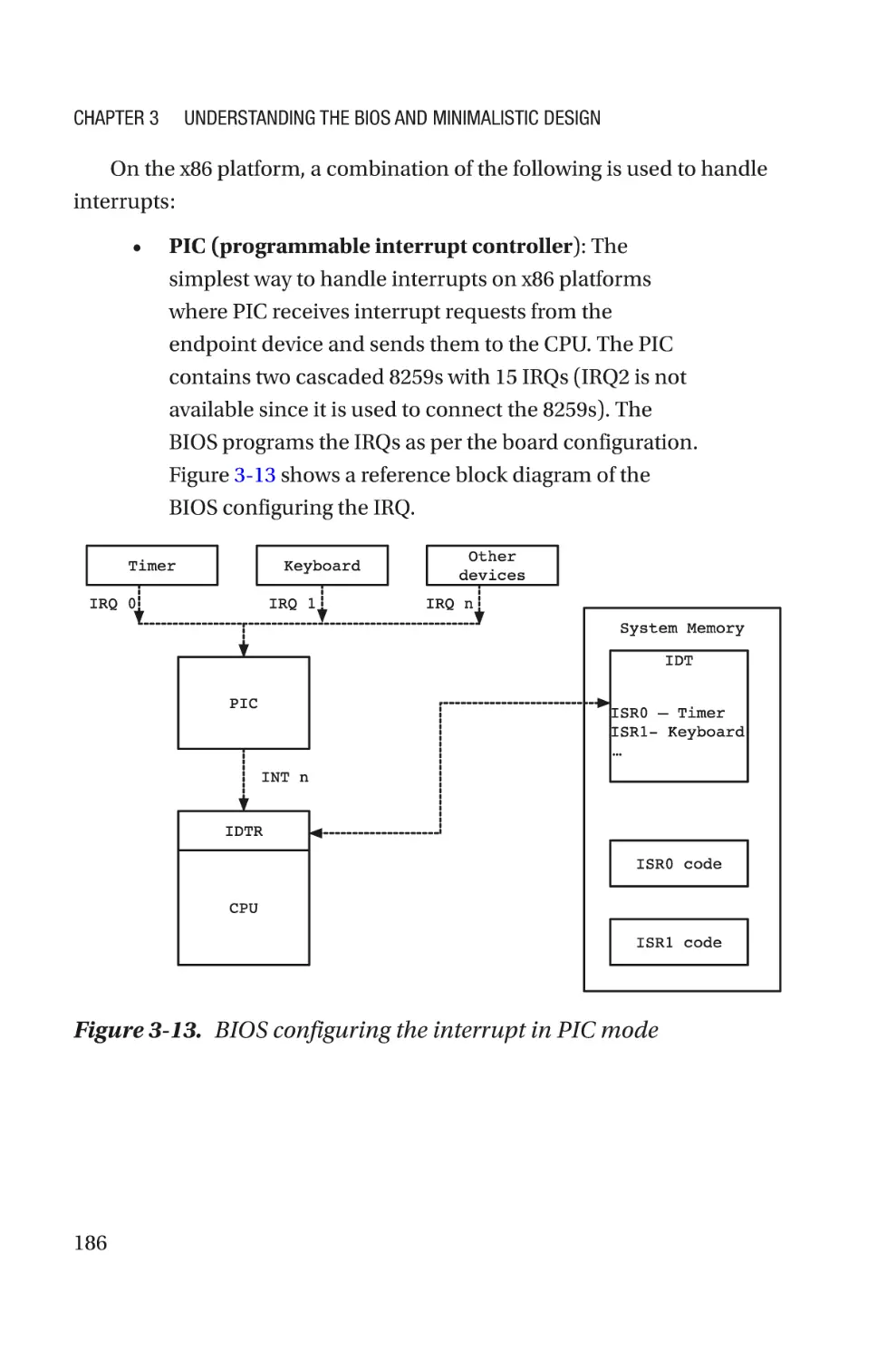
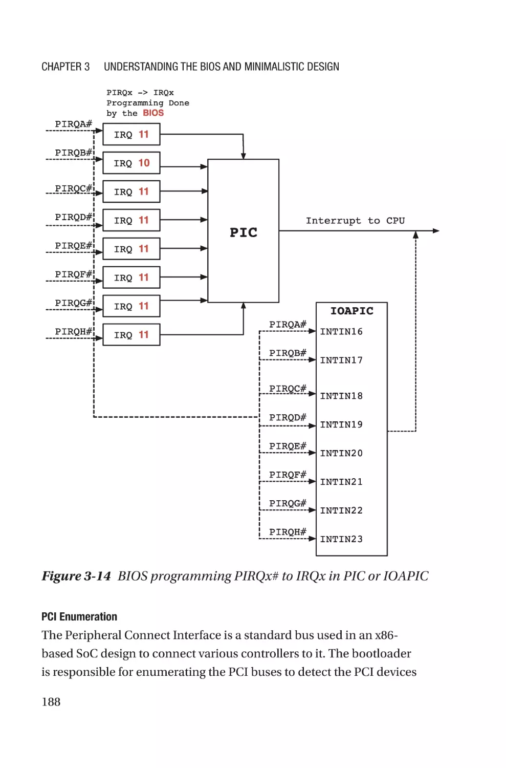
What Is the BIOS?���������������������������������������������������������������������������������������������146
Working Principle of BIOS����������������������������������������������������������������������������147
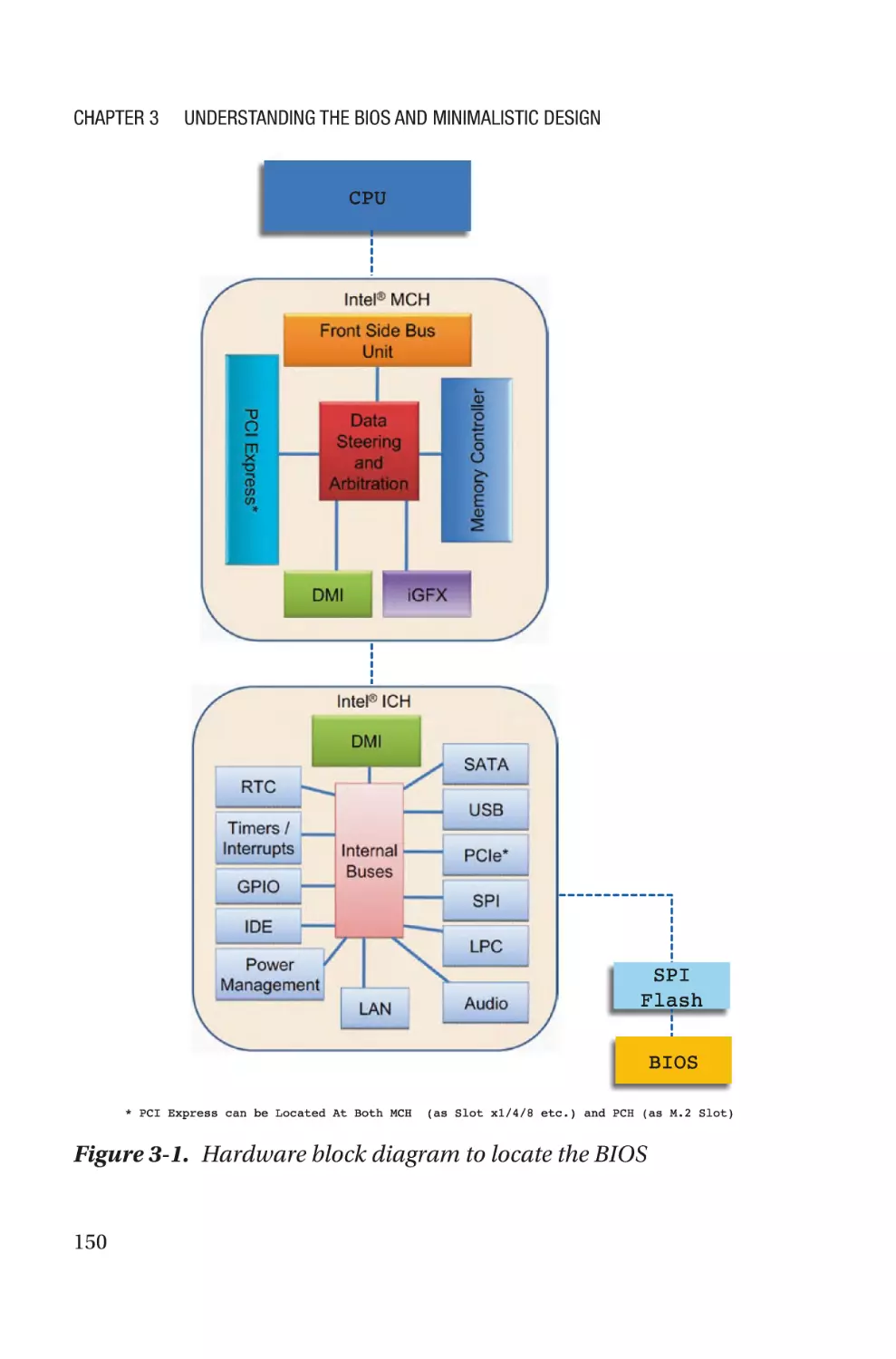
Where Does the BIOS Reside?���������������������������������������������������������������������149
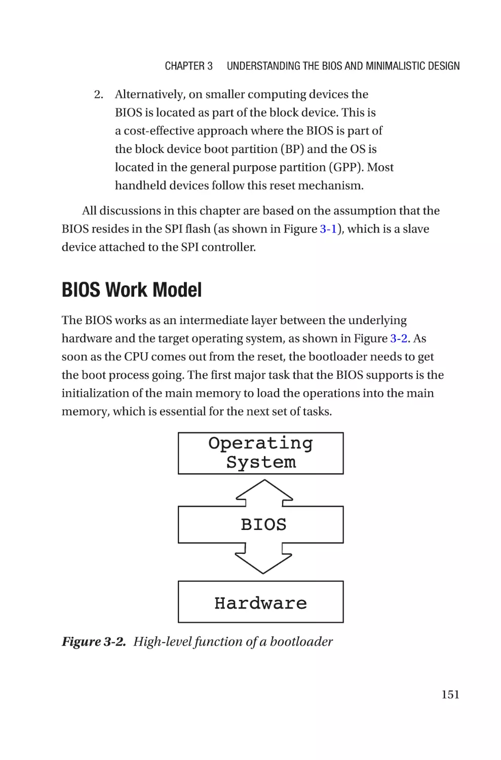
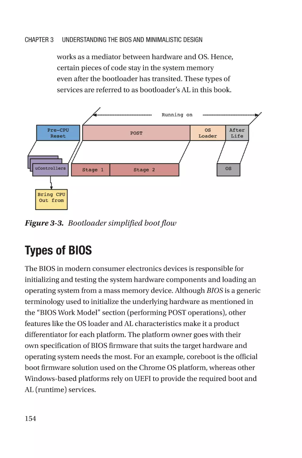
BIOS Work Model�����������������������������������������������������������������������������������������151
Types of BIOS�����������������������������������������������������������������������������������������������154
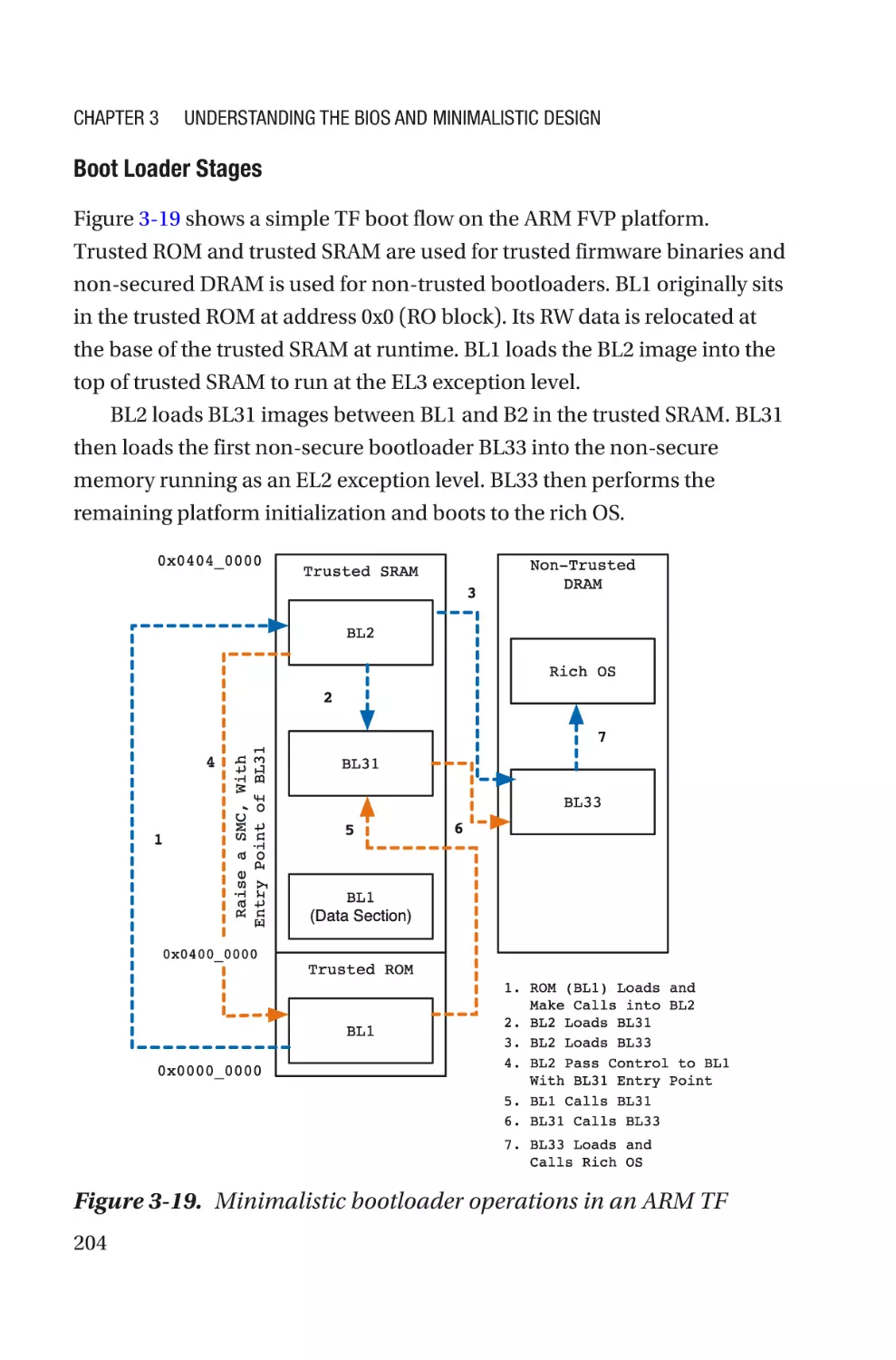
Designing a Minimalistic Bootloader����������������������������������������������������������������159
Minimalistic Bootloader Design on x86 Platform����������������������������������������160
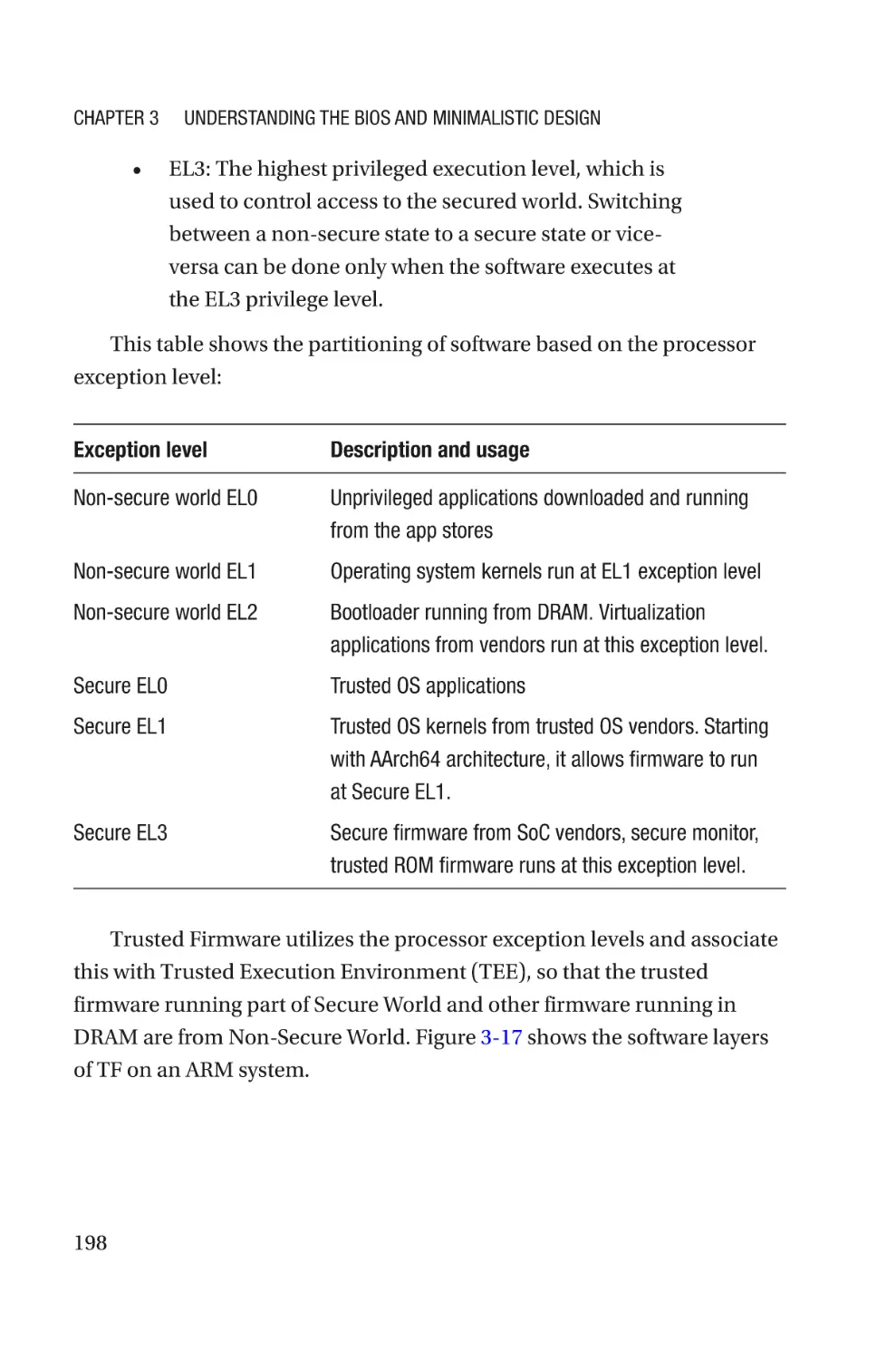
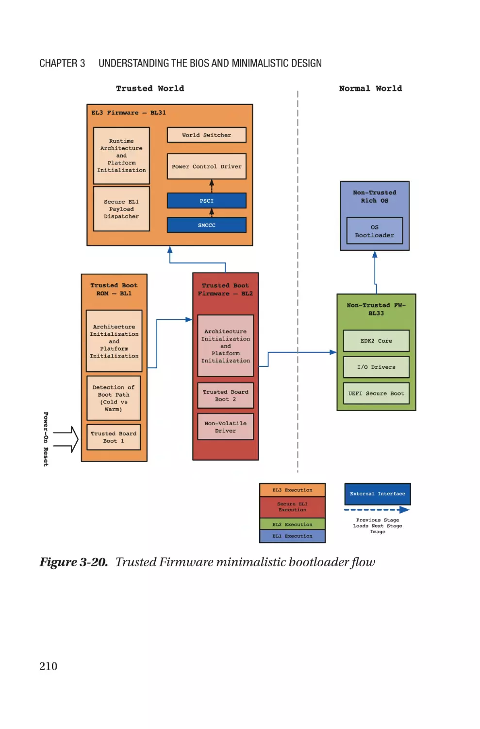
Minimalistic Bootloader Design on the ARM Platform���������������������������������197
Summary����������������������������������������������������������������������������������������������������������211
Chapter 4: System Firmware Architecture���������������������������������������213
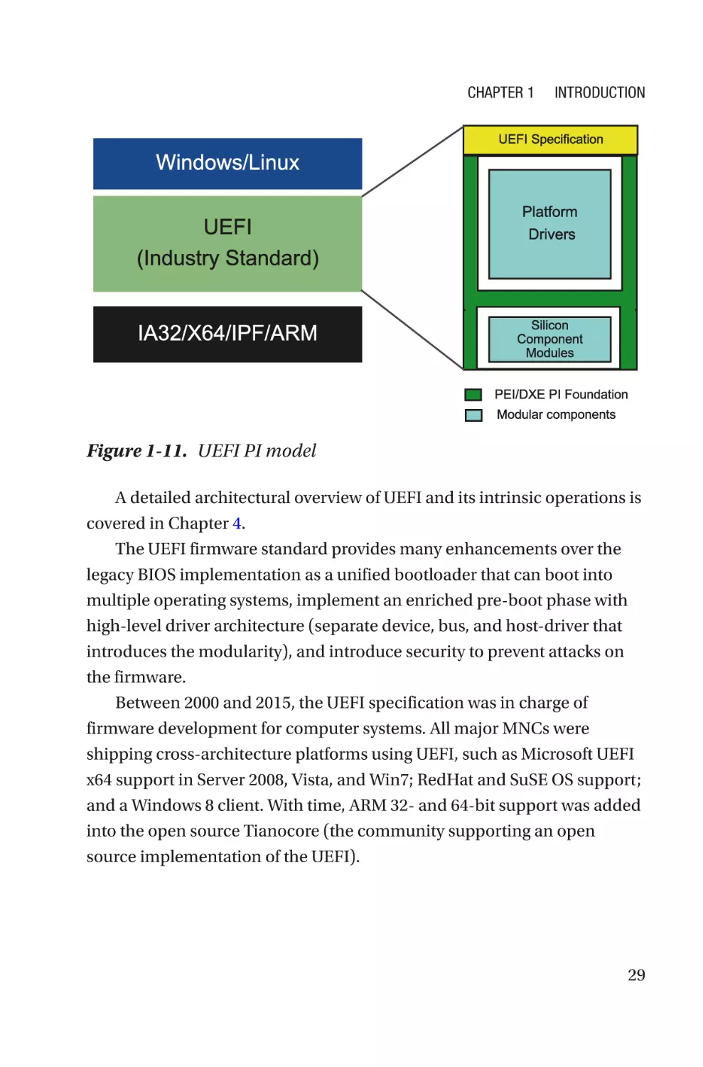
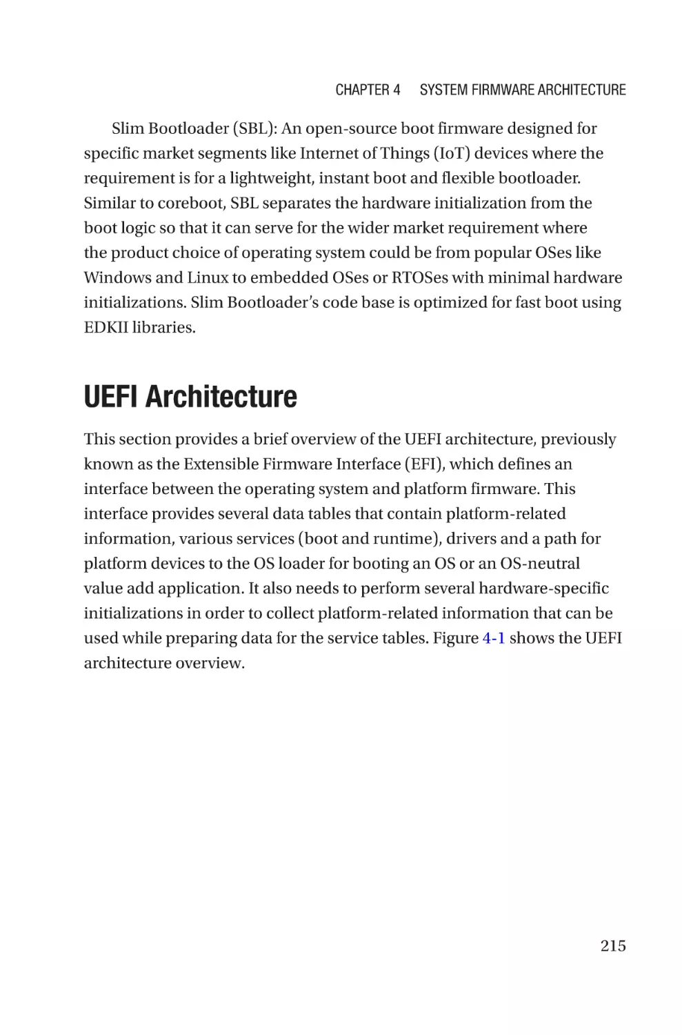
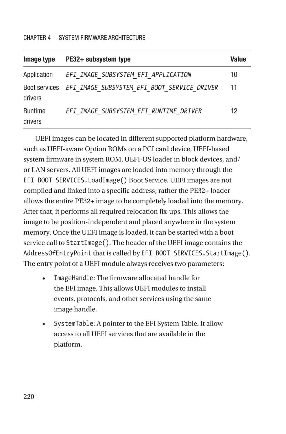
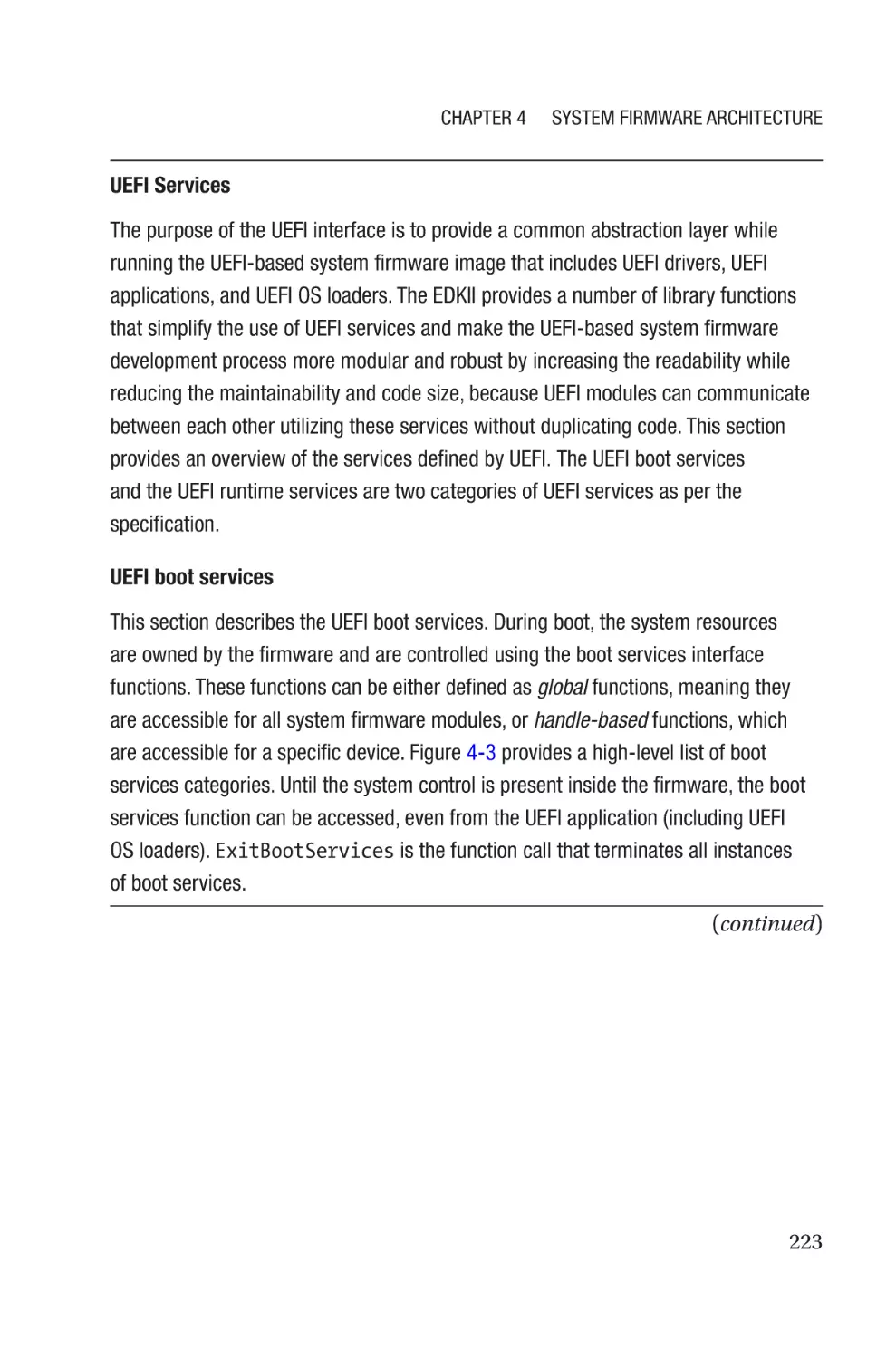
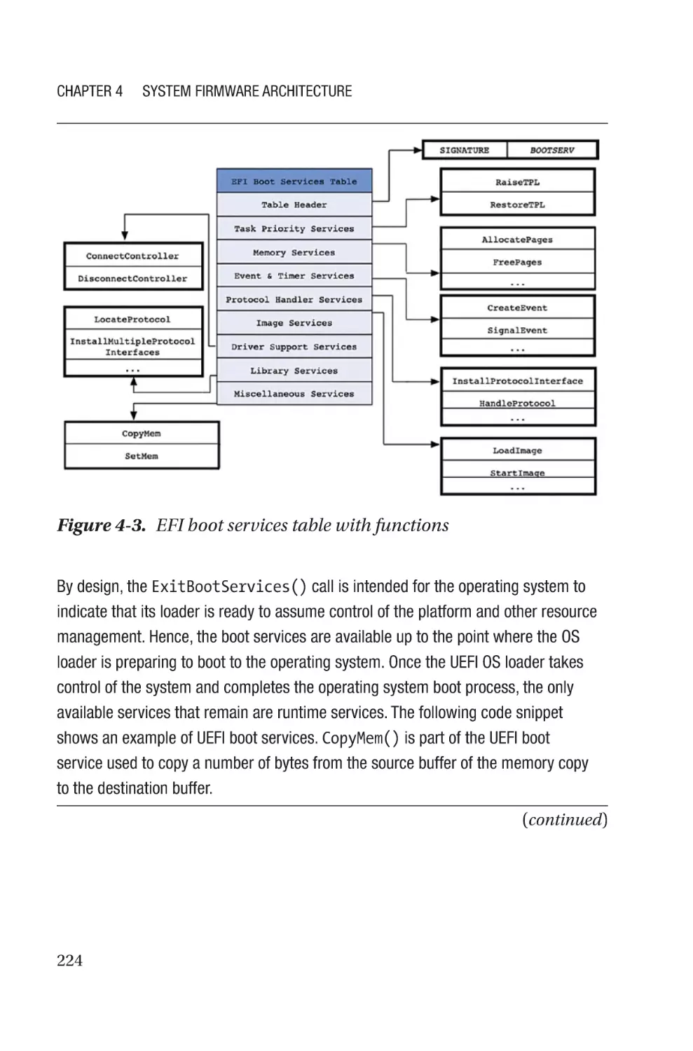
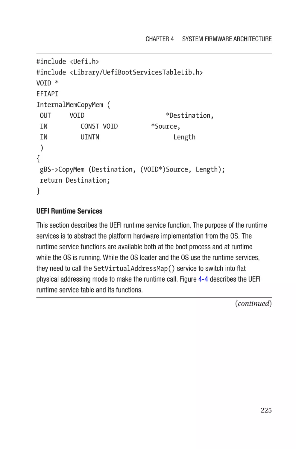
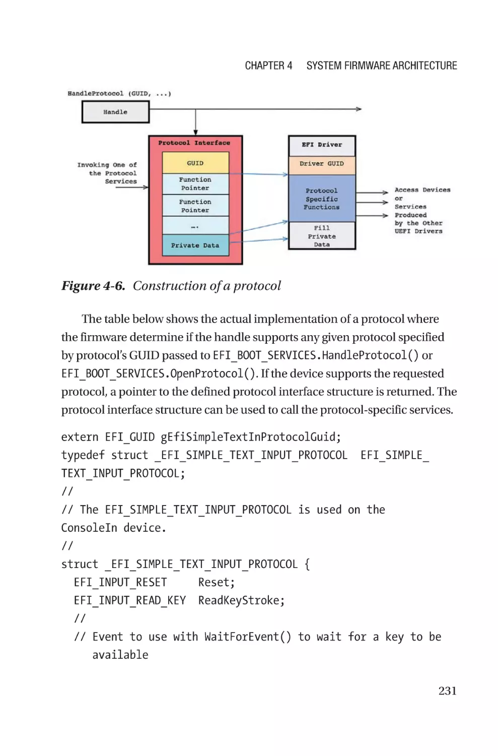
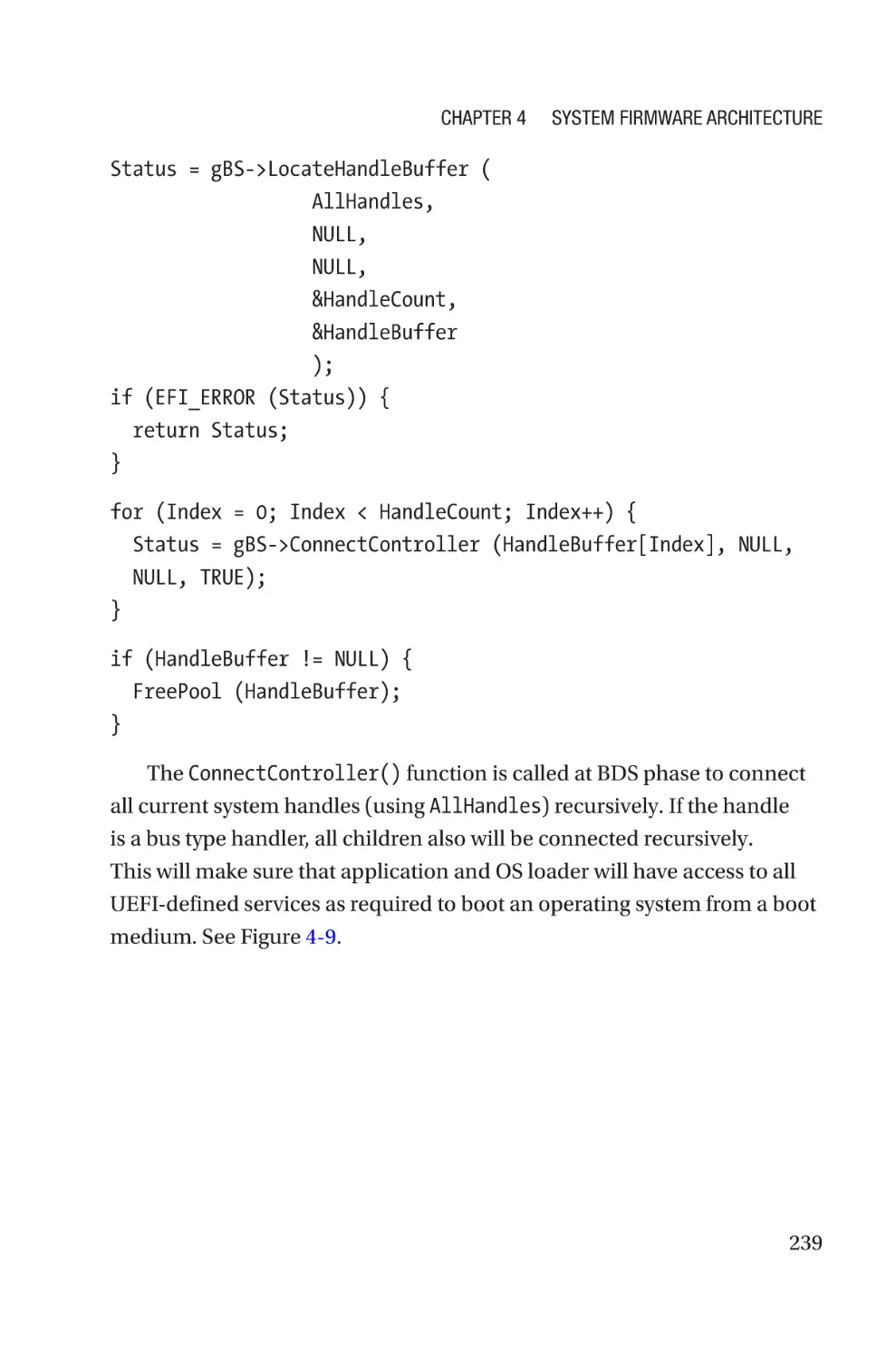
UEFI Architecture����������������������������������������������������������������������������������������������215
UEFI Specification����������������������������������������������������������������������������������������217
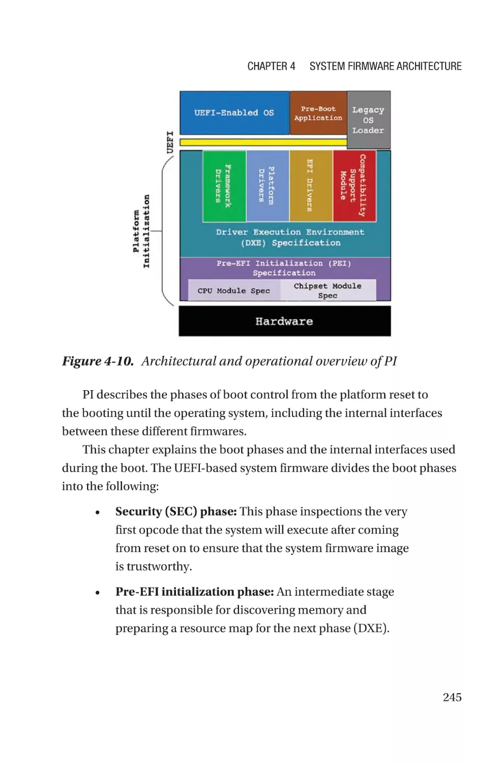
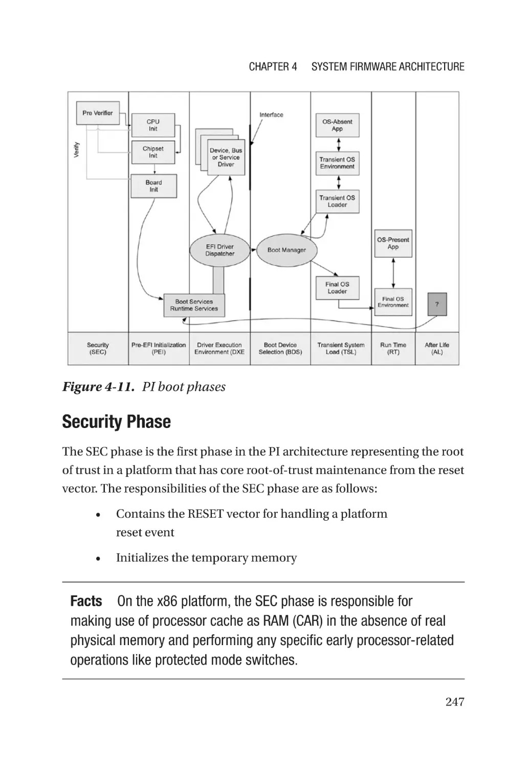
Platform Initialization Specification�������������������������������������������������������������244
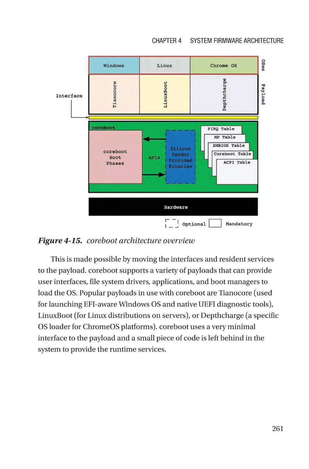
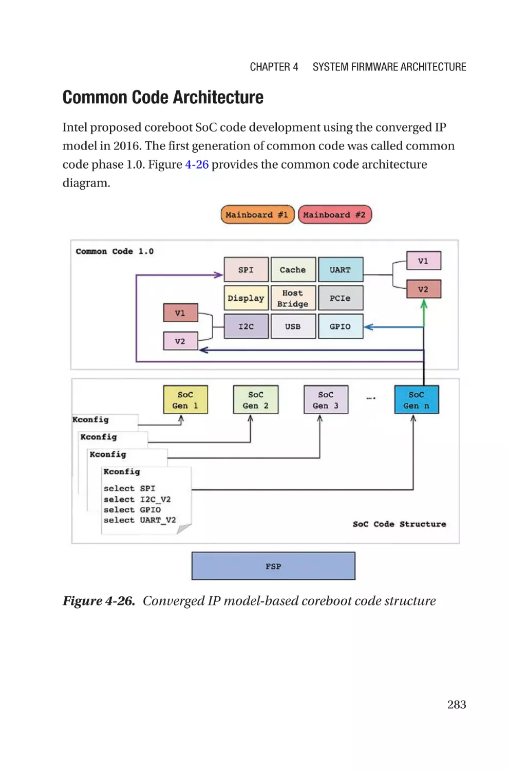
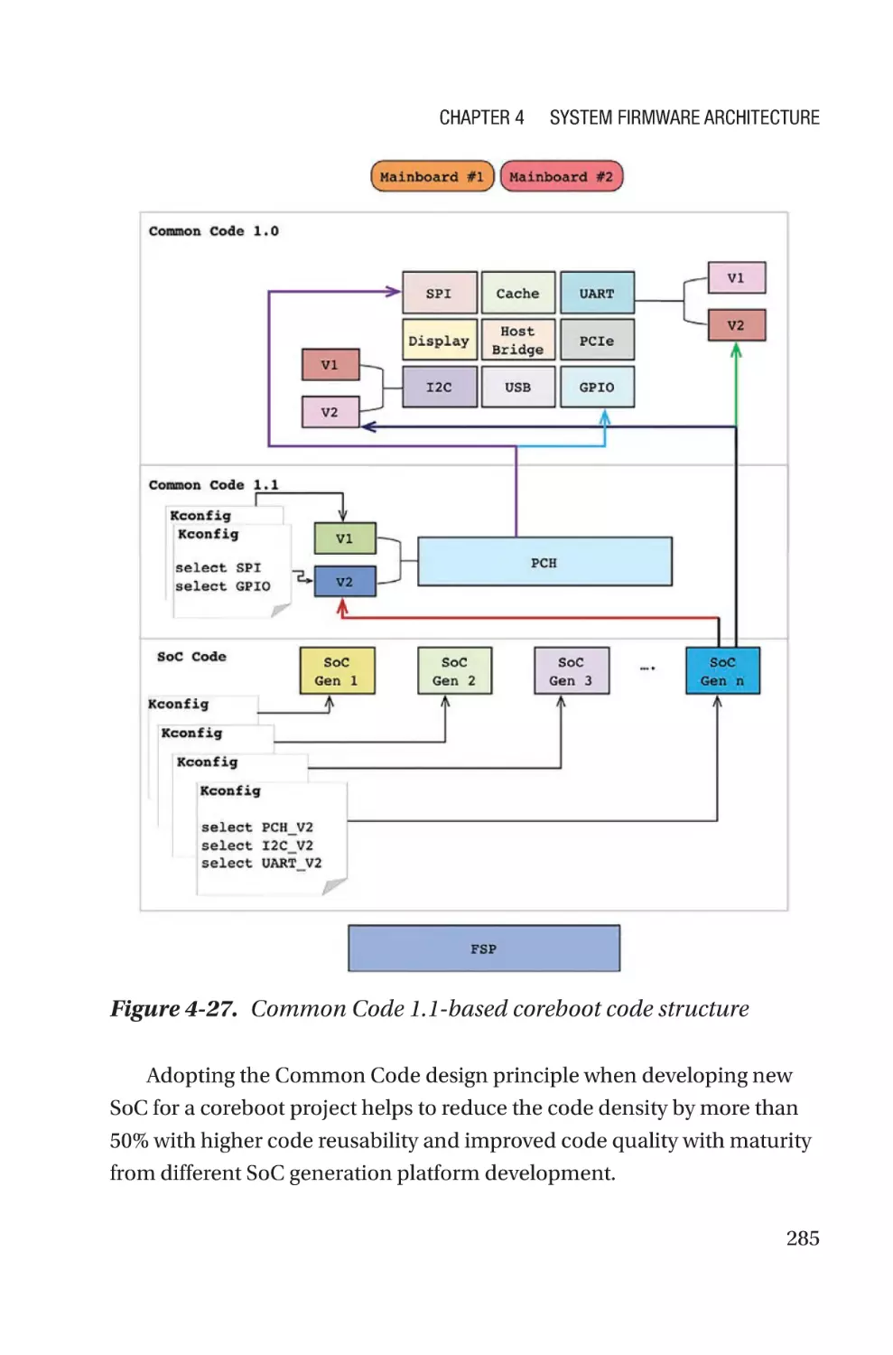
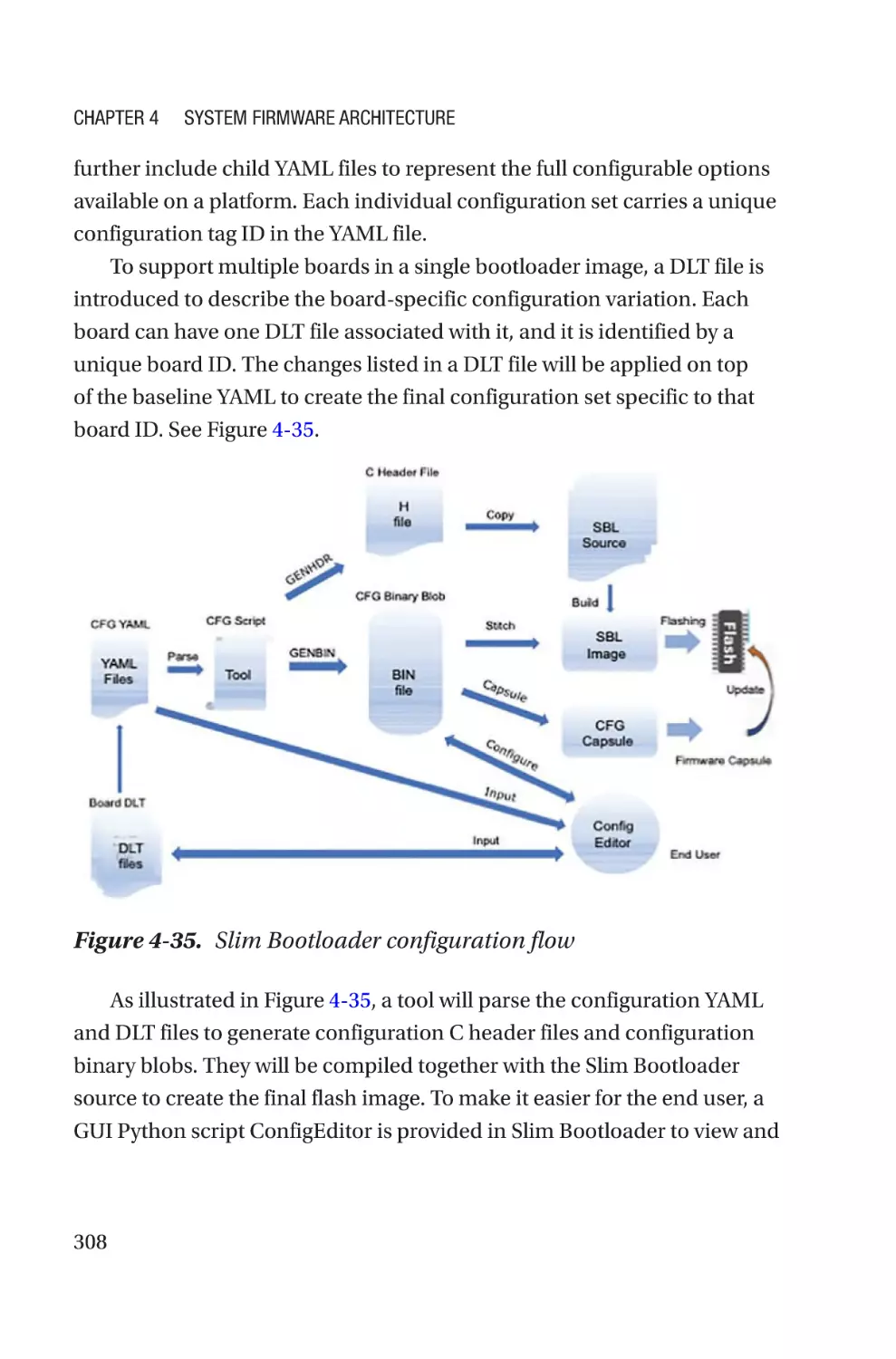
coreboot Architecture����������������������������������������������������������������������������������������260
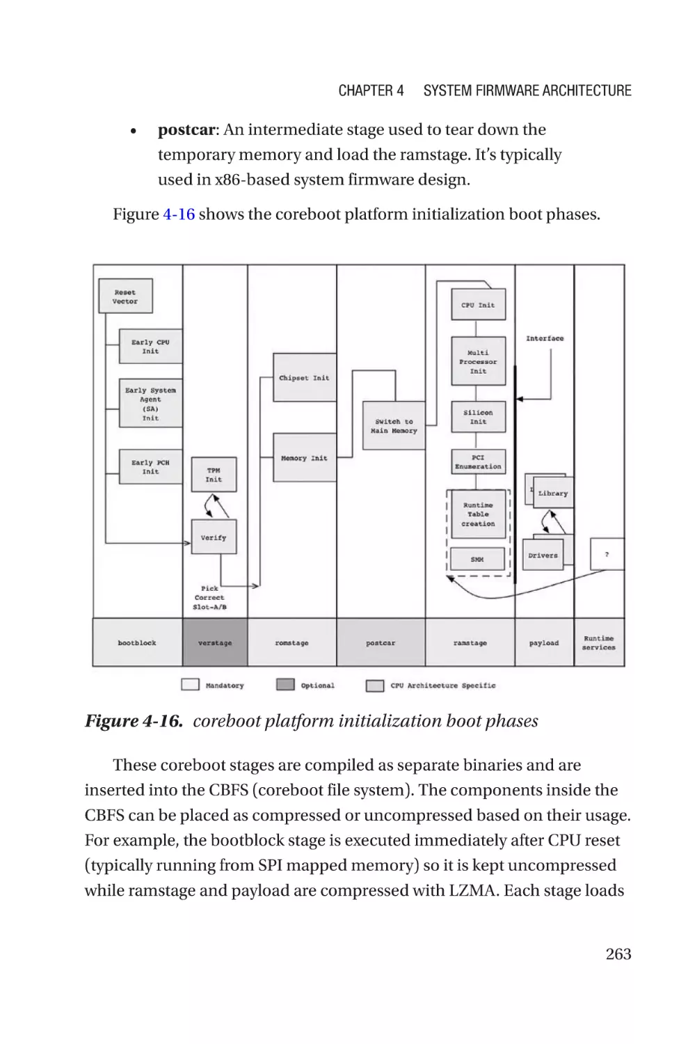
Platform Initialization����������������������������������������������������������������������������������262
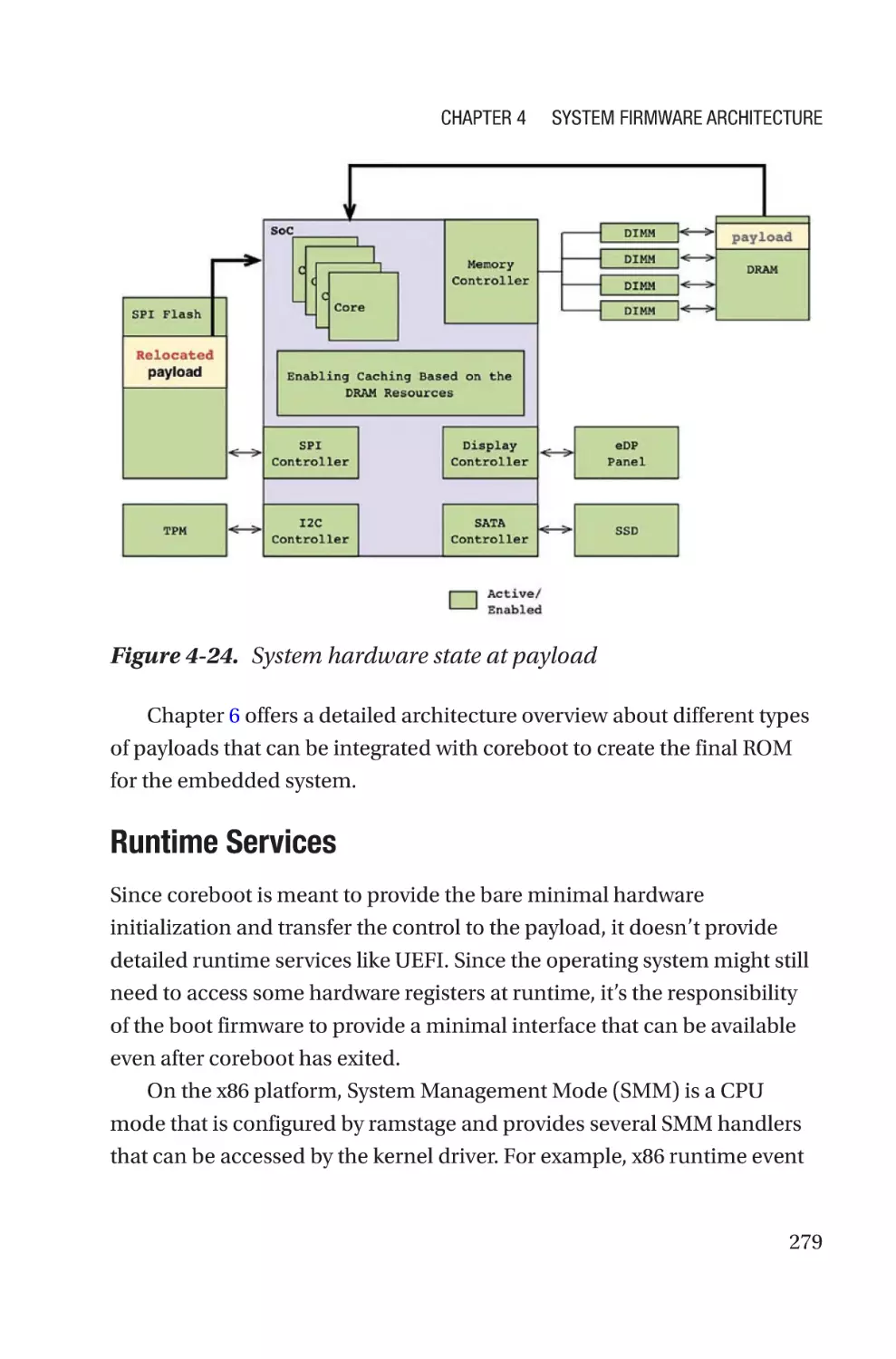
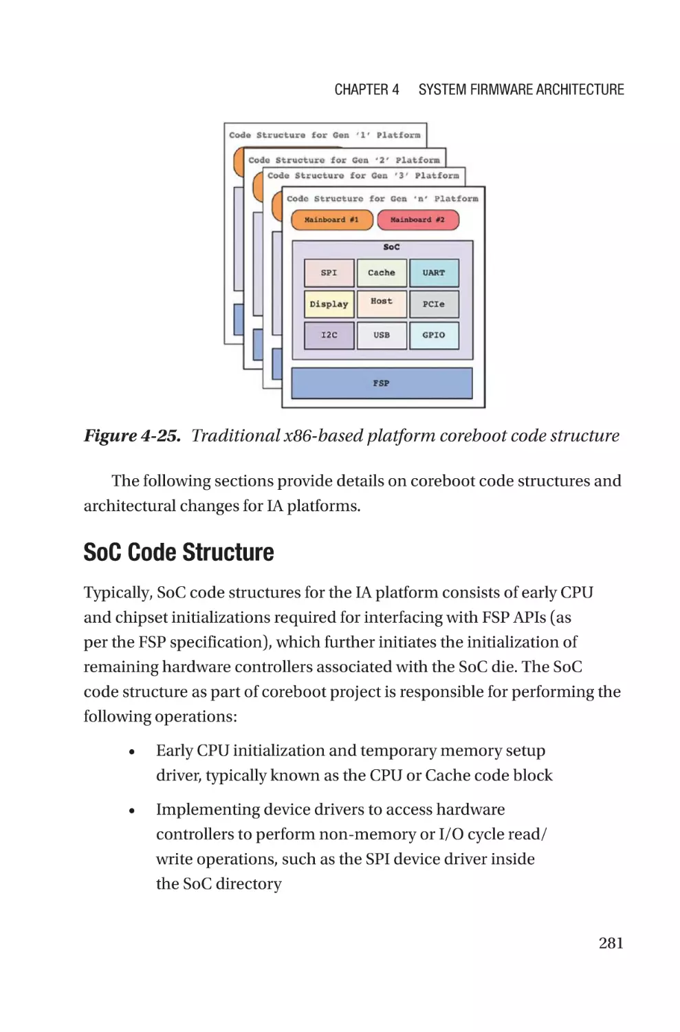
Source Tree Structure����������������������������������������������������������������������������������280
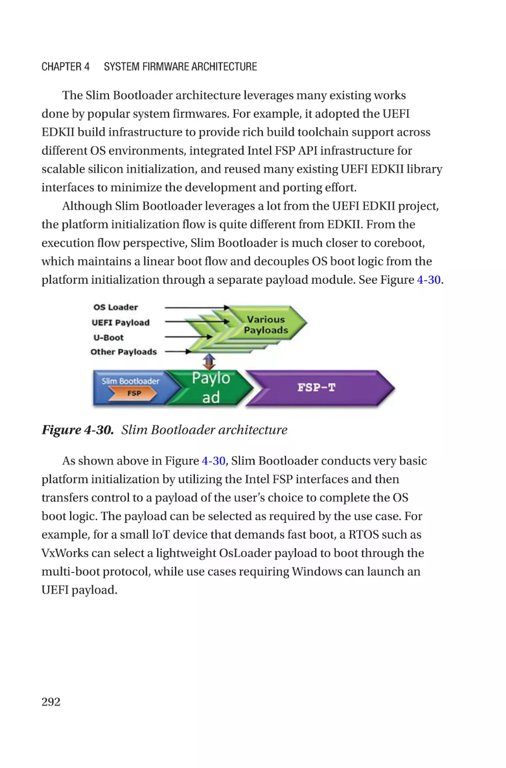
Slim Bootloader Architecture����������������������������������������������������������������������������291
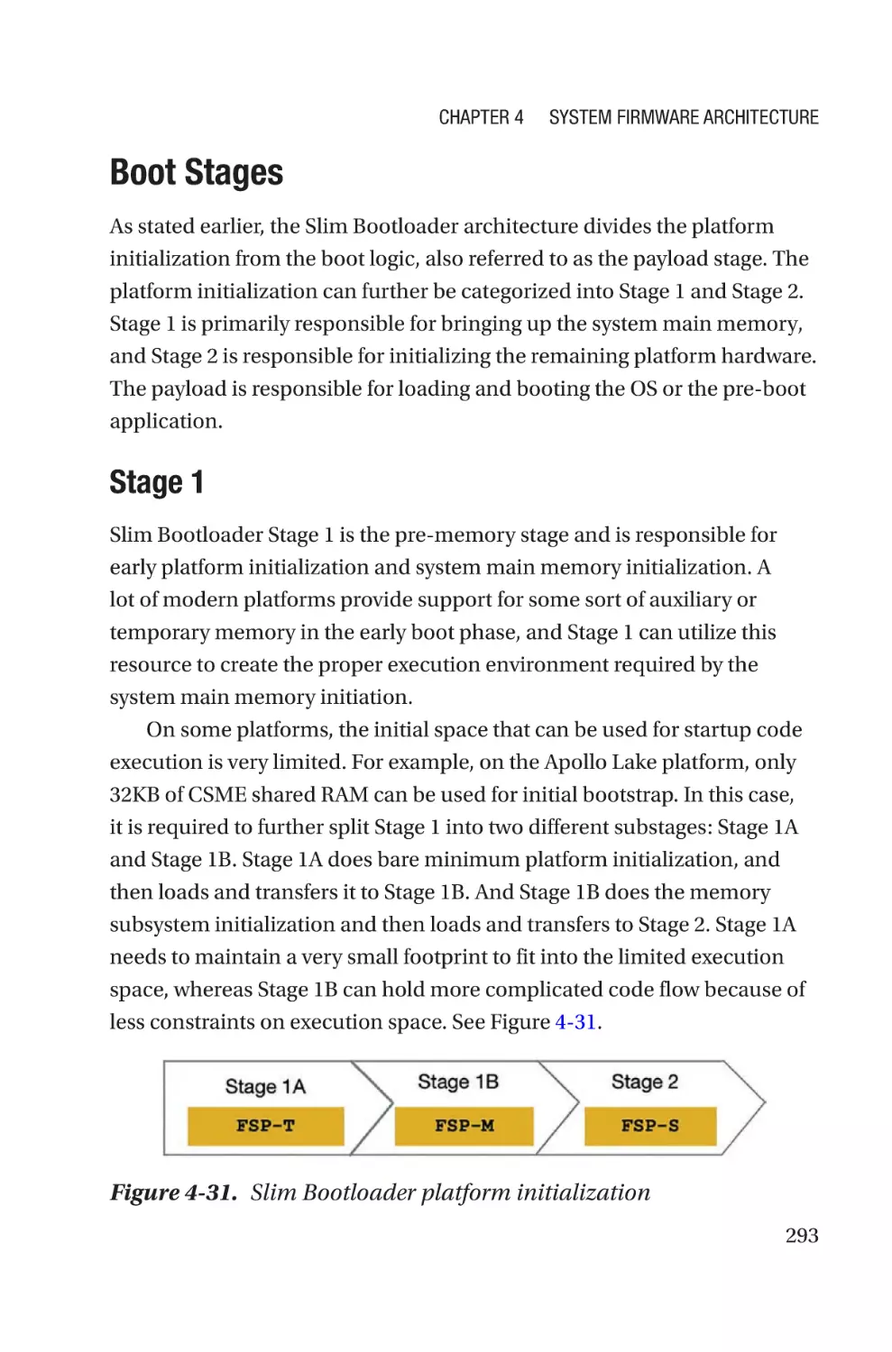
Boot Stages�������������������������������������������������������������������������������������������������293
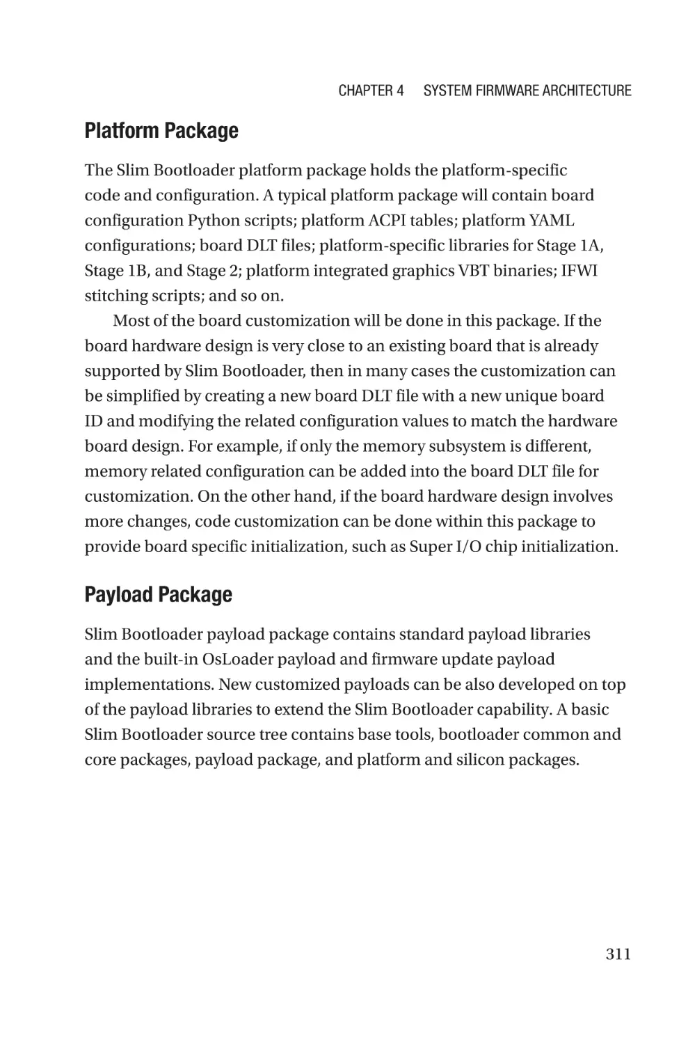
Summary����������������������������������������������������������������������������������������������������������312
Chapter 5: Hybrid Firmware Architecture����������������������������������������315
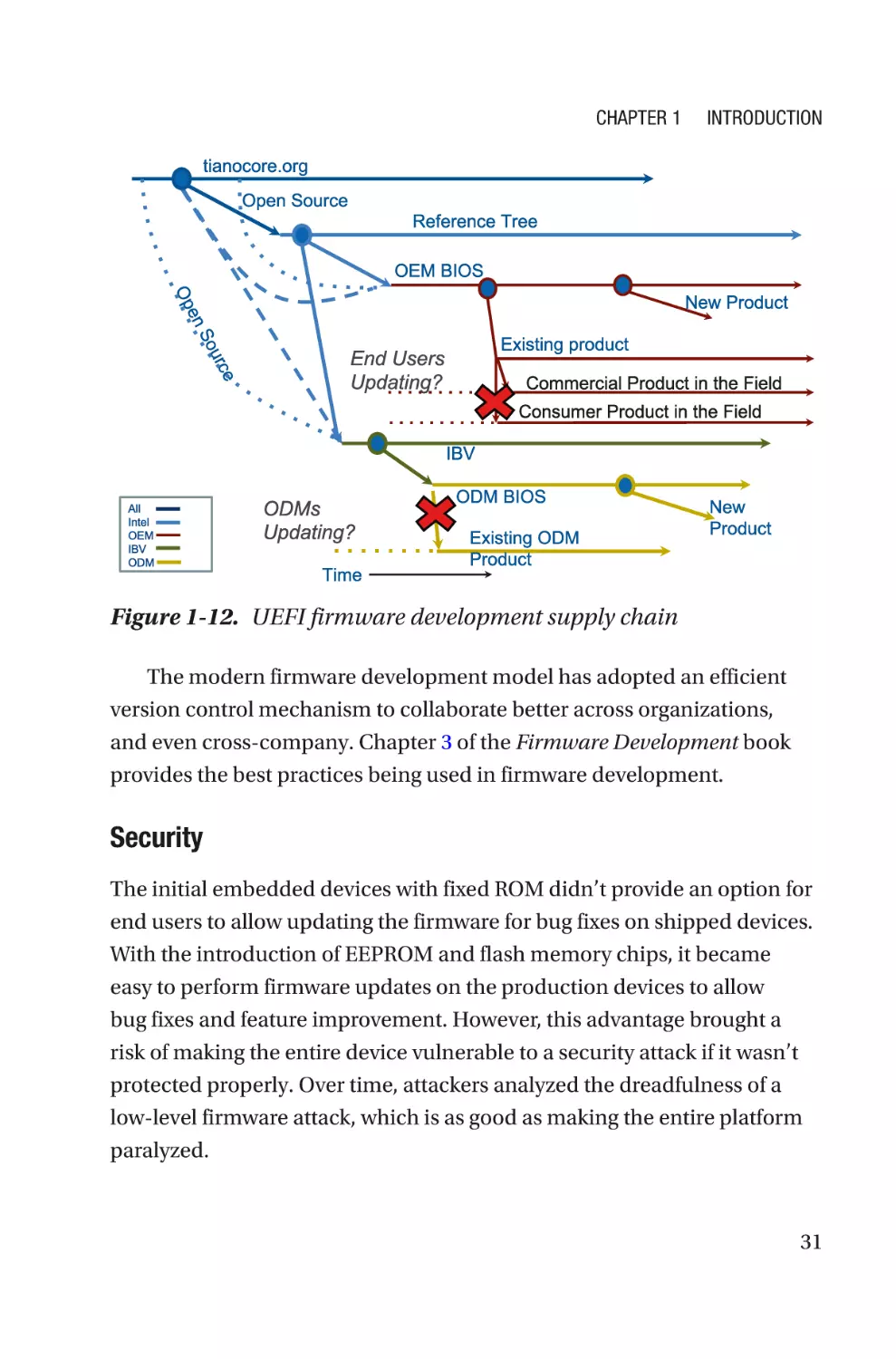
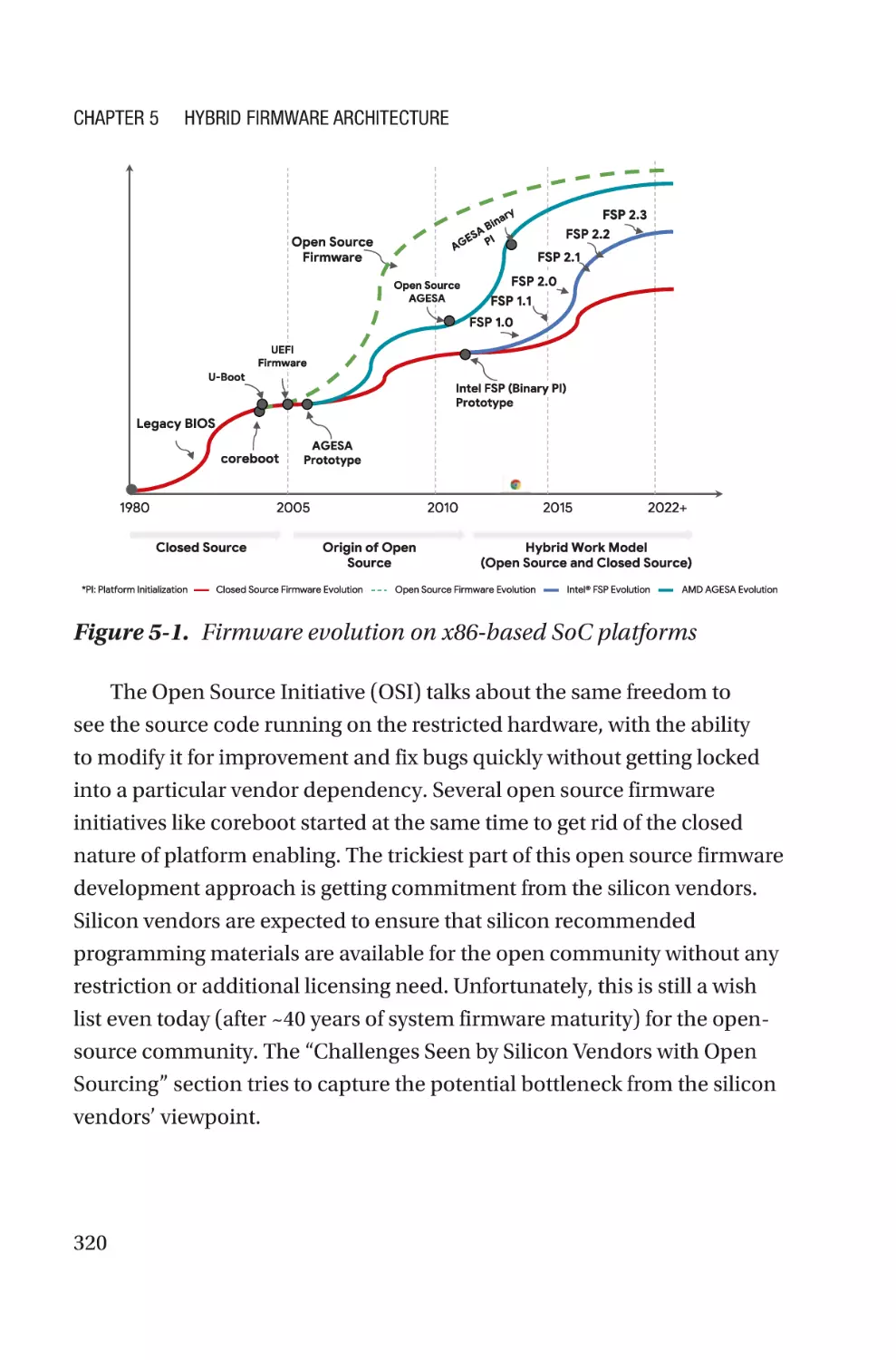
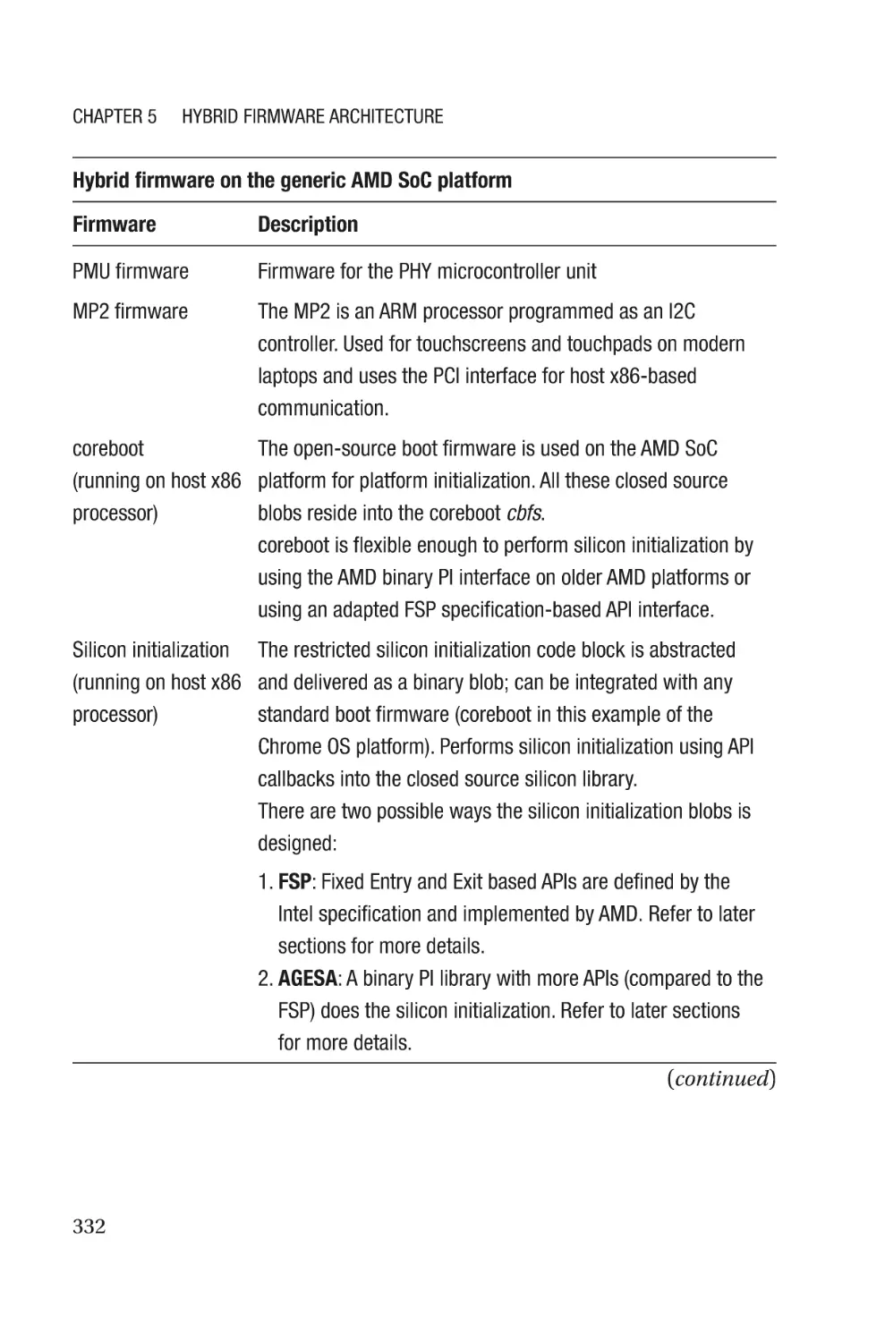
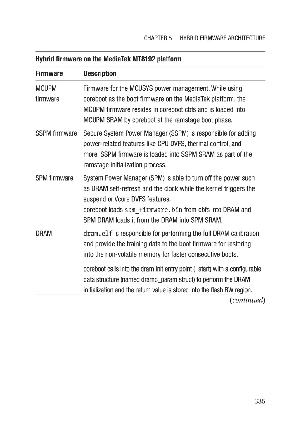
Understanding the System Firmware Development Model�������������������������������319
Generic��������������������������������������������������������������������������������������������������������321
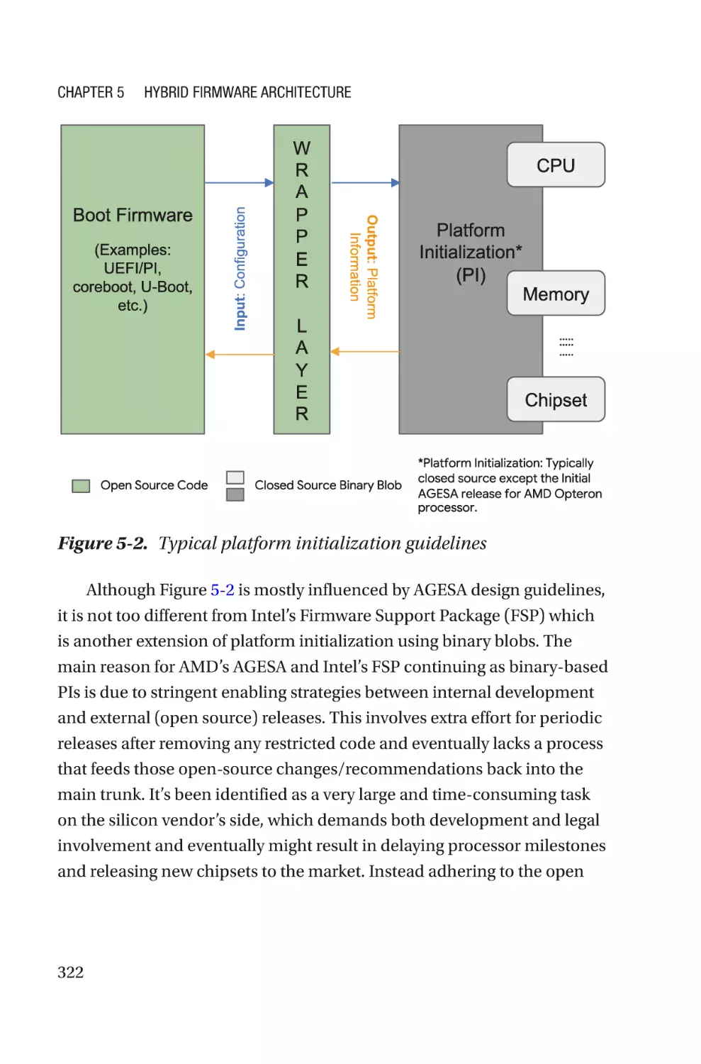
Platform Initialization (PI)����������������������������������������������������������������������������321
v
Table of Contents
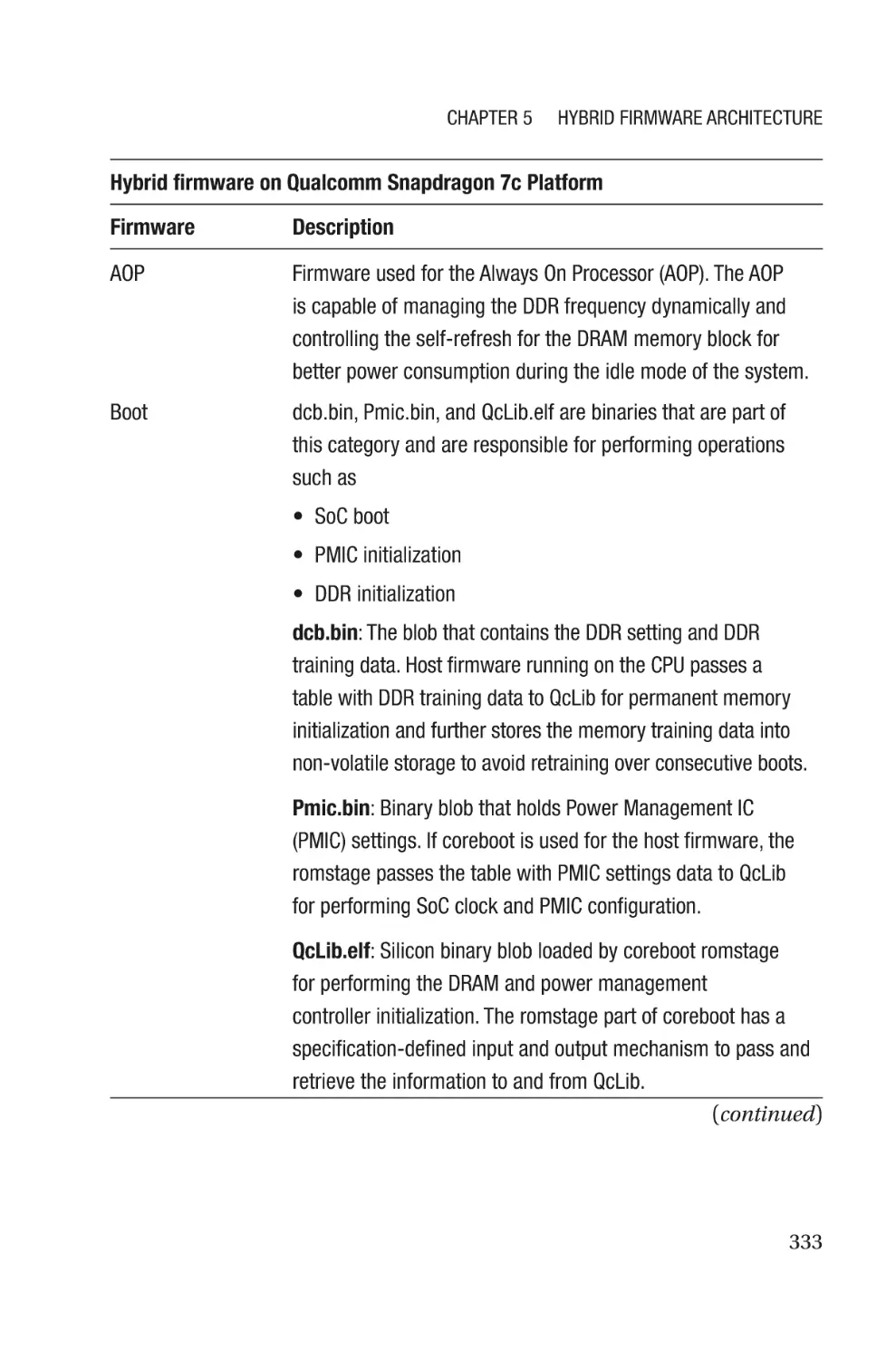
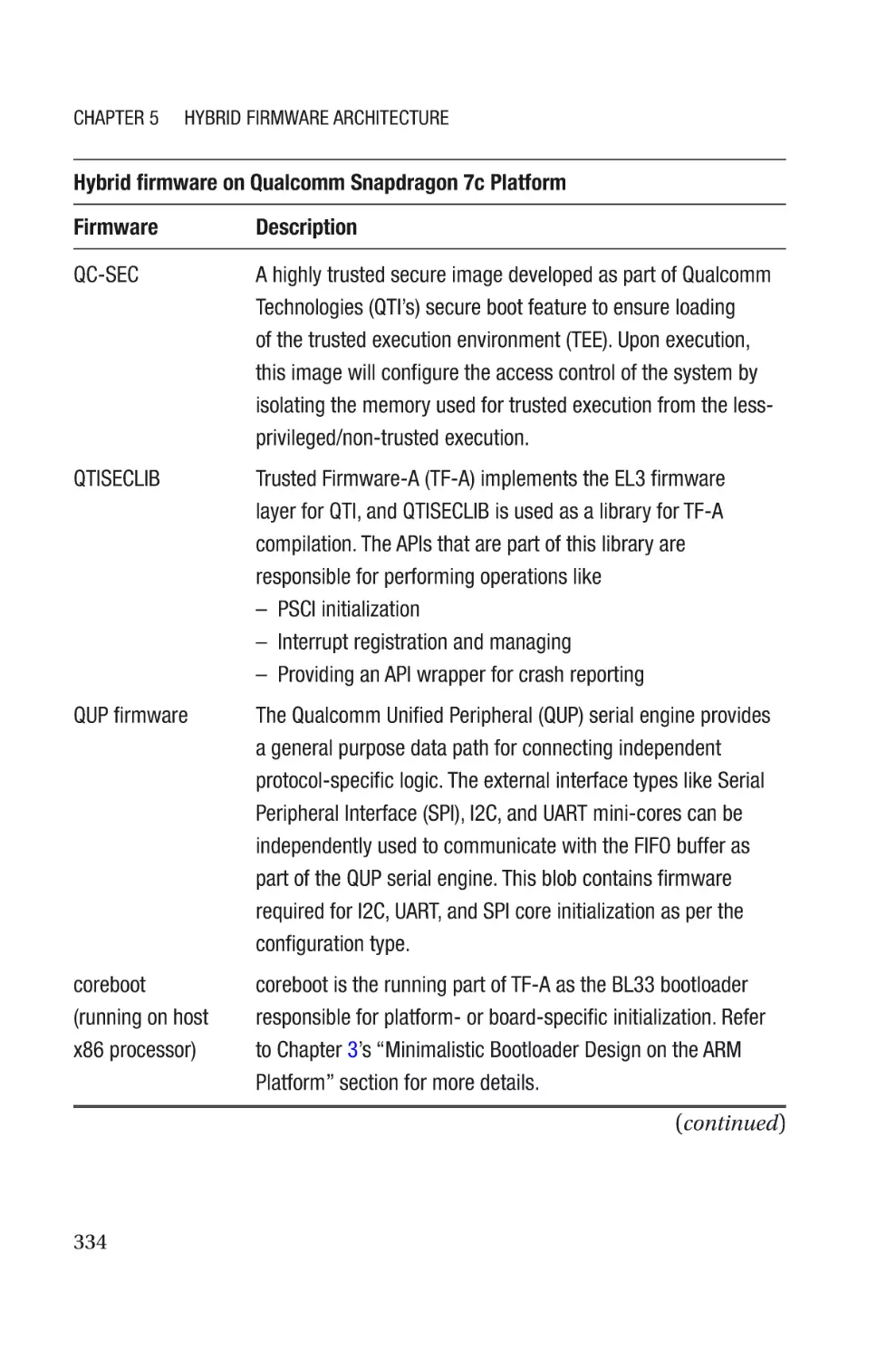
Understanding the System Firmware Supply Chain�����������������������������������������324
Platform Initialization����������������������������������������������������������������������������������324
Wrapper Layer���������������������������������������������������������������������������������������������325
Boot Firmware���������������������������������������������������������������������������������������������326
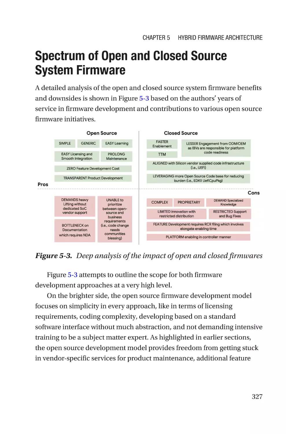
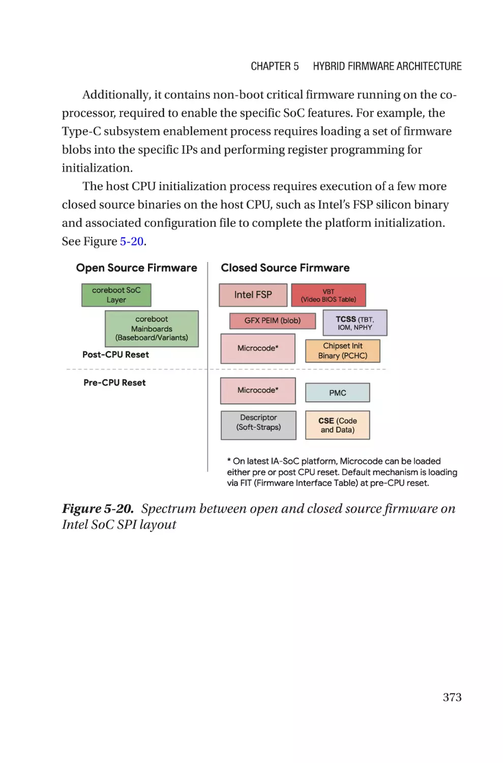
Spectrum of Open and Closed Source System Firmware���������������������������������327
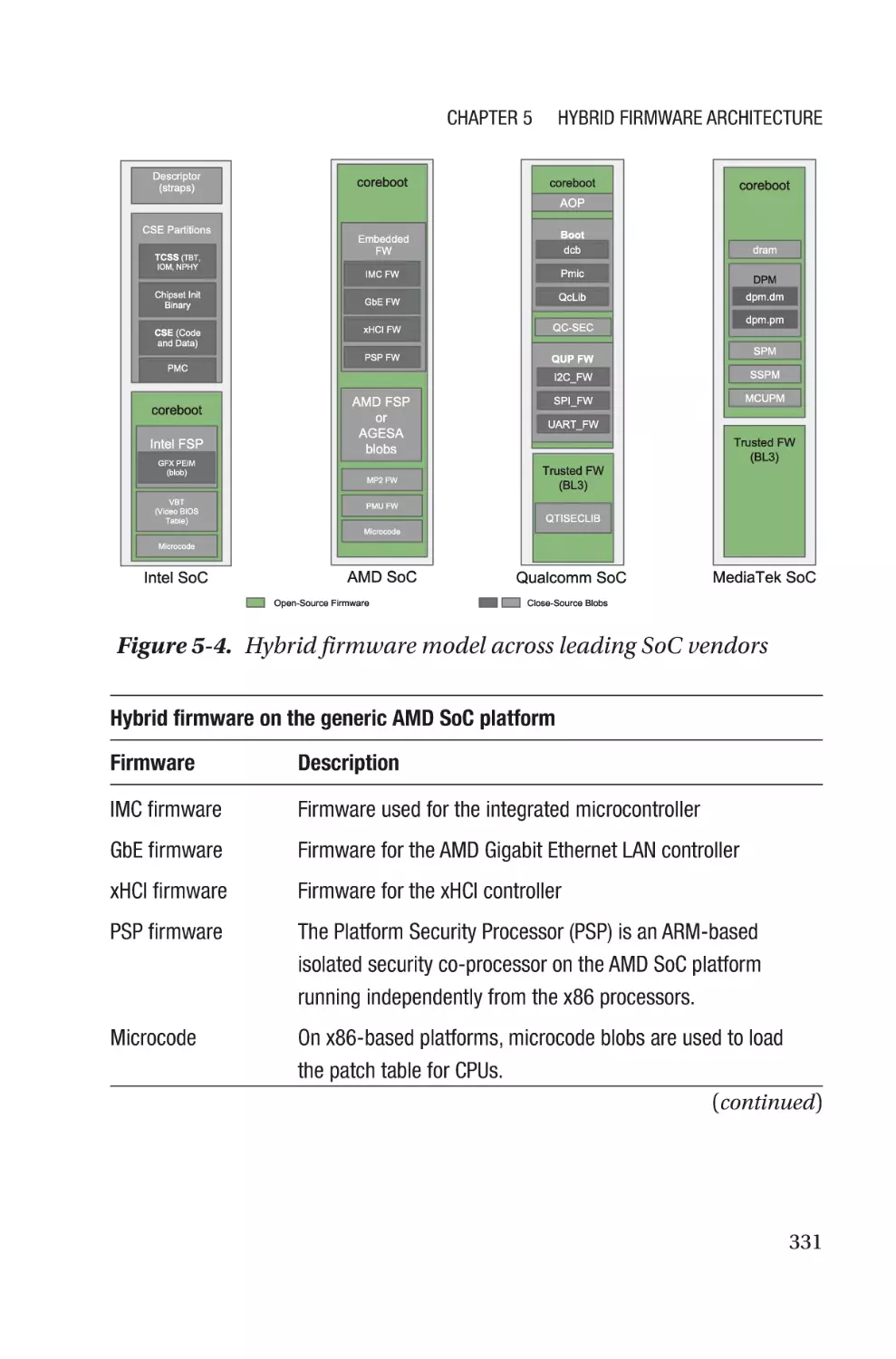
Current Industry Trends with Hybrid Firmware�������������������������������������������������330
Challenges Seen by Silicon Vendors with Open Sourcing���������������������������������337
Datasheet Dependency��������������������������������������������������������������������������������338
Third-Party IP Restrictions���������������������������������������������������������������������������339
Silicon Reference Code Development Without Compatibility����������������������339
Early Platform Enabling with Non-PRQ’ed Silicon���������������������������������������340
Distinguished Product Features������������������������������������������������������������������340
Limited Customer Demand��������������������������������������������������������������������������340
Closed-Source Mindset�������������������������������������������������������������������������������341
Documentation Is an Afterthought���������������������������������������������������������������342
Importance of a Specific System Firmware Architecture����������������������������342
Challenges Faced by the Open Community with Closed Sourcing��������������������343
Security�������������������������������������������������������������������������������������������������������343
Platform Enabling����������������������������������������������������������������������������������������344
Motivation Is Lagging����������������������������������������������������������������������������������344
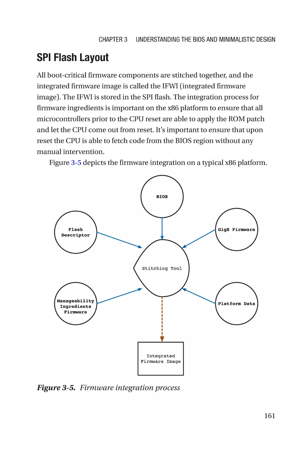
Hard to Debug����������������������������������������������������������������������������������������������344
Ungoverned Growth for Closed Source Blobs����������������������������������������������345
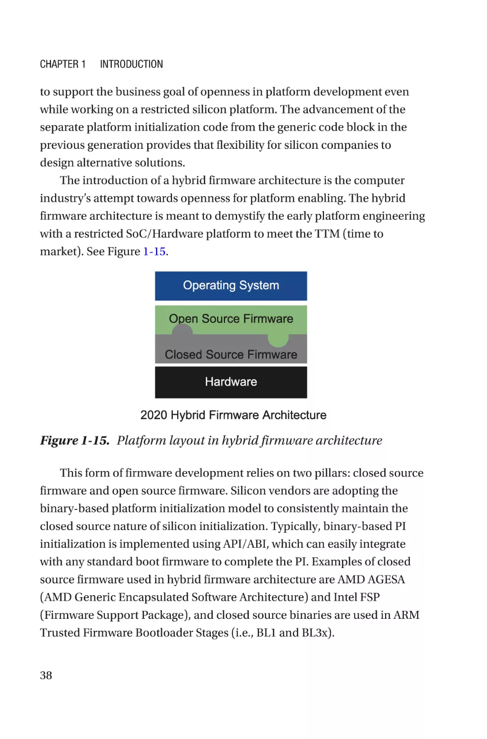
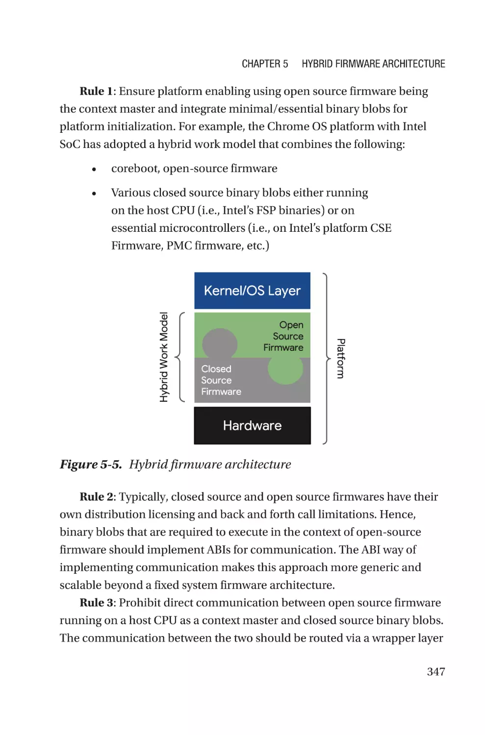
Hybrid Firmware Architecture���������������������������������������������������������������������������346
Ground Rules�����������������������������������������������������������������������������������������������346
Firmware Development Using Hybrid Firmware Architecture���������������������348
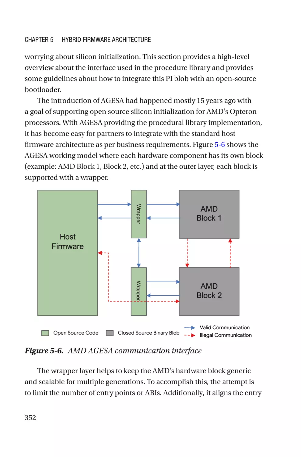
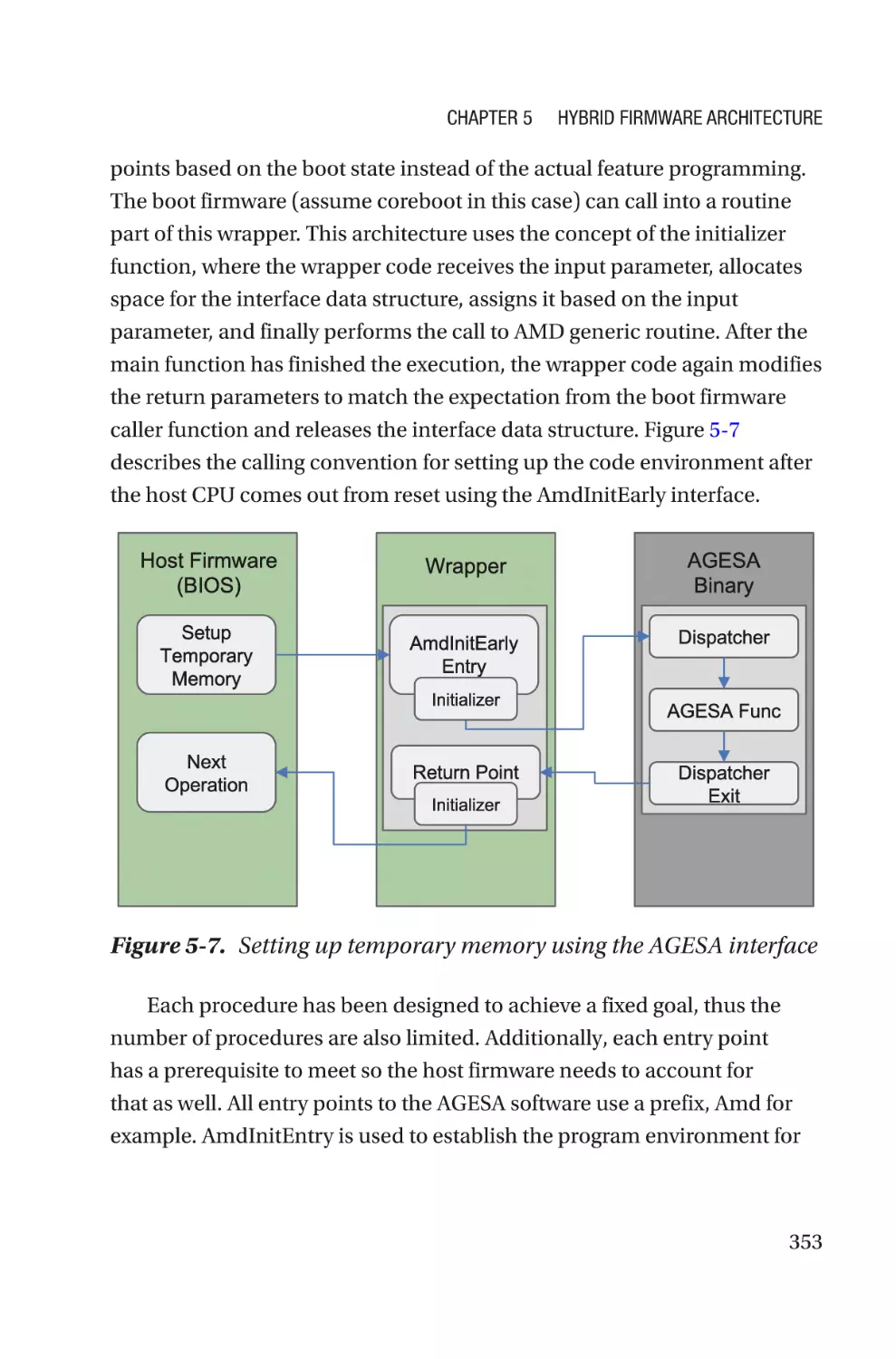
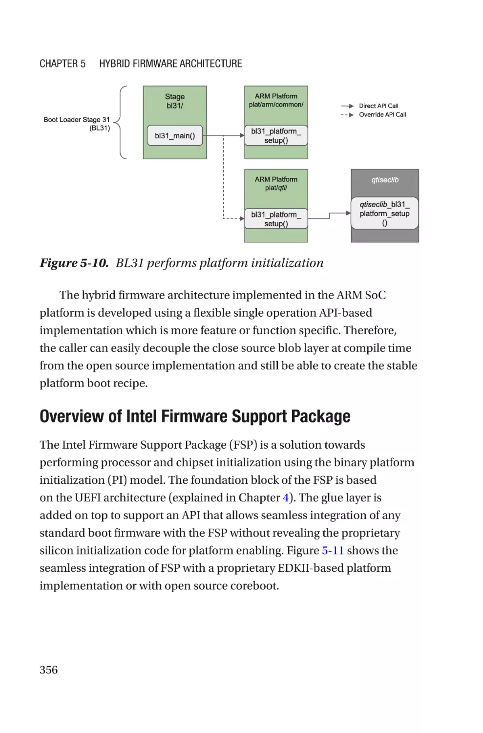
Conventional Closed Source Firmware in the Hybrid Work Model��������������351
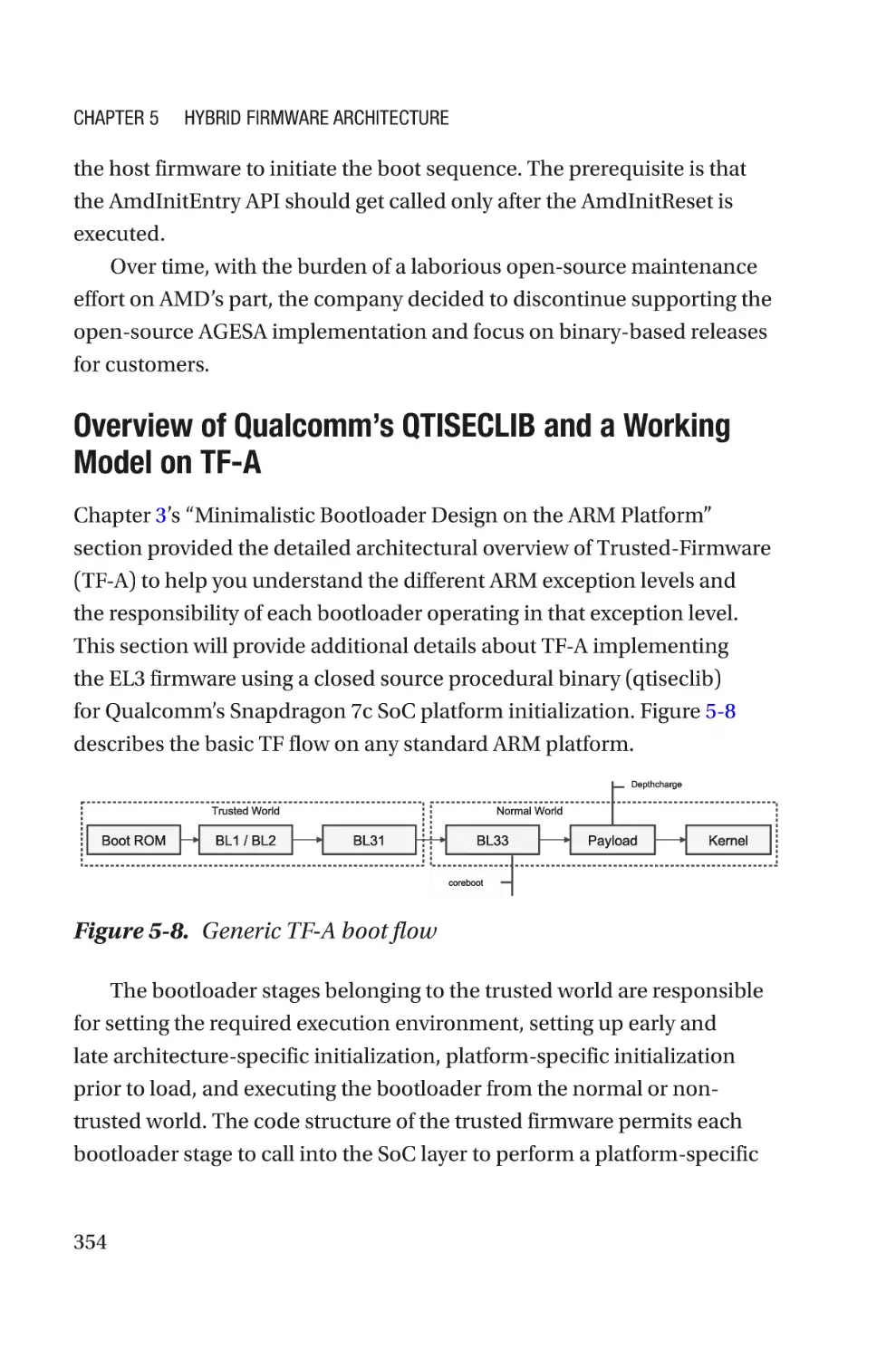
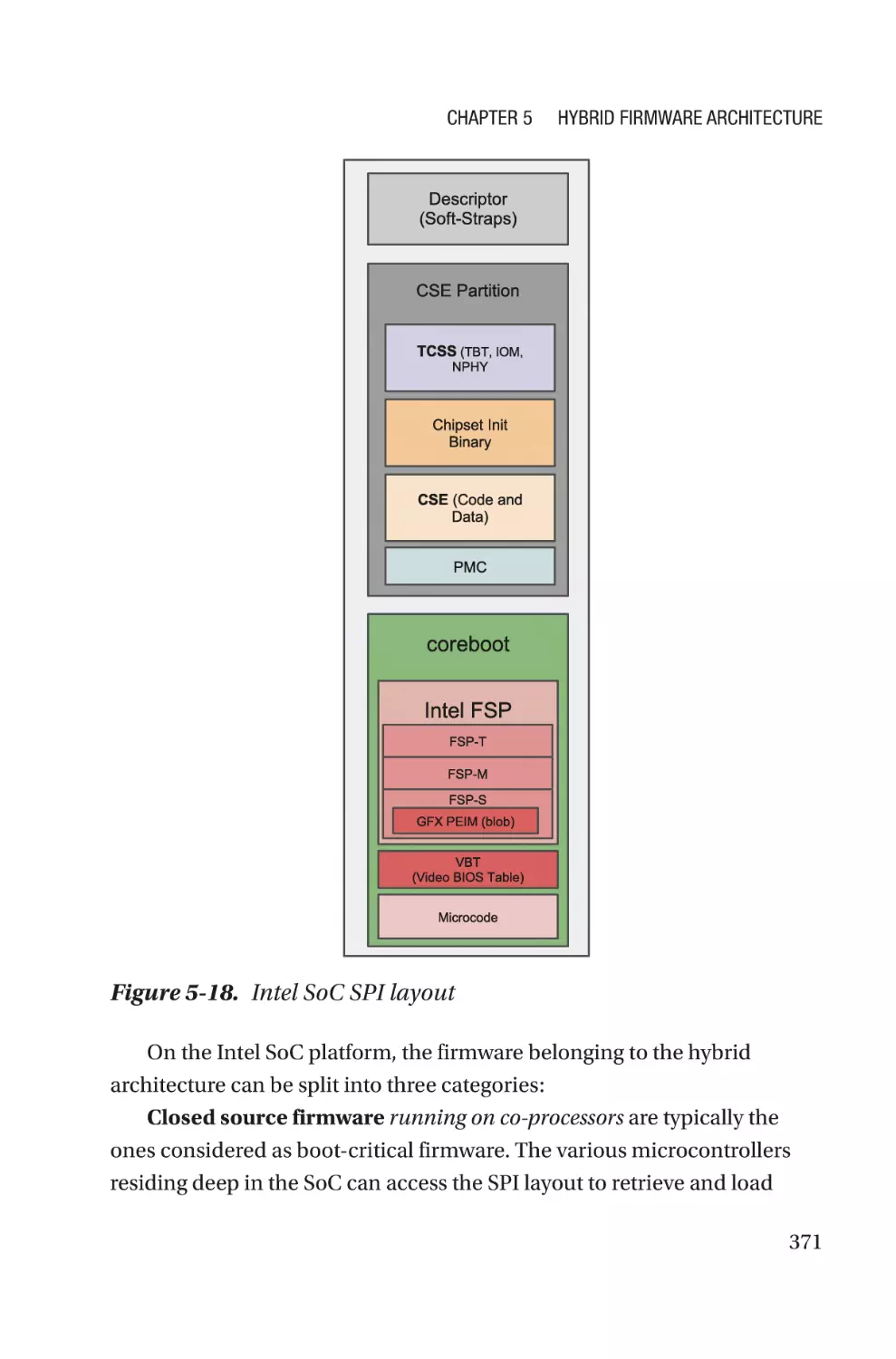
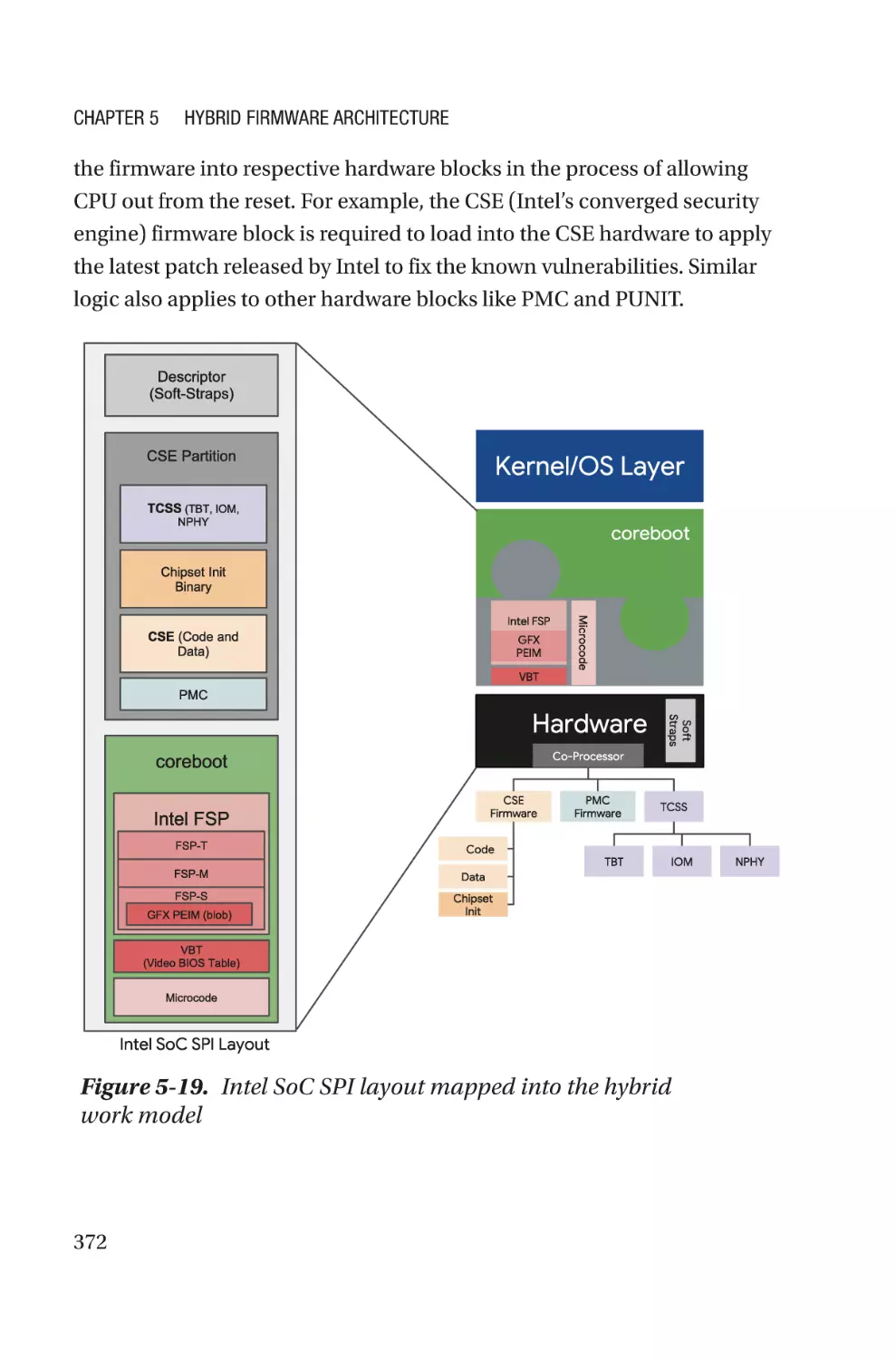
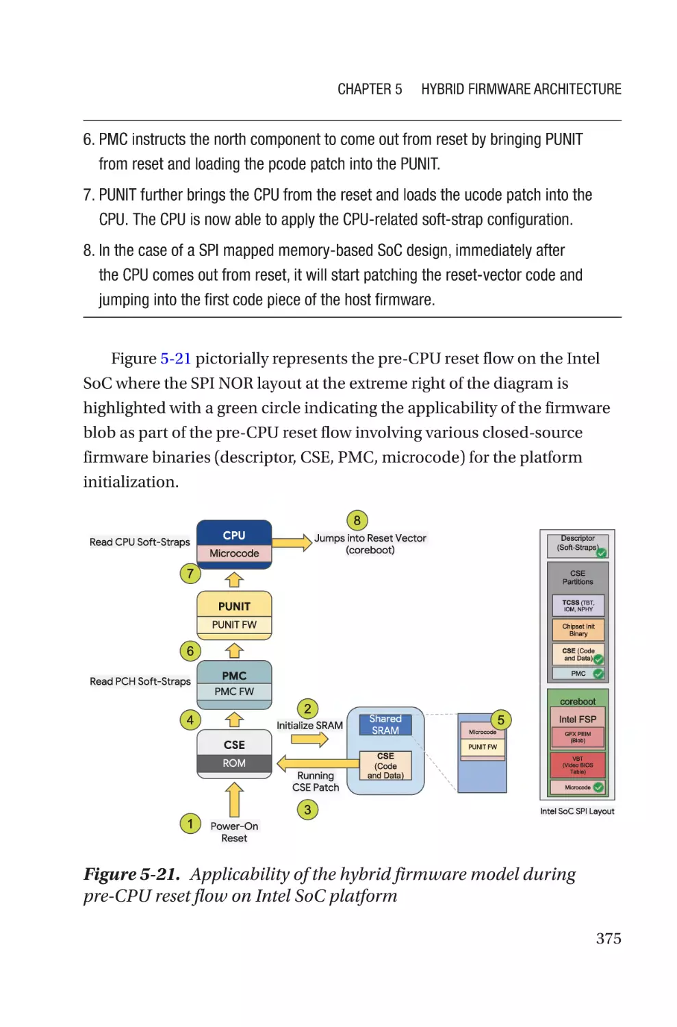
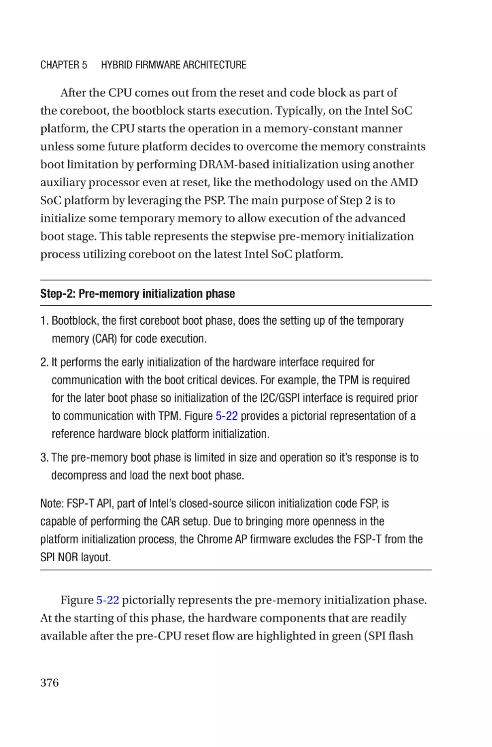
Application of Hybrid Firmware Architecture����������������������������������������������������369
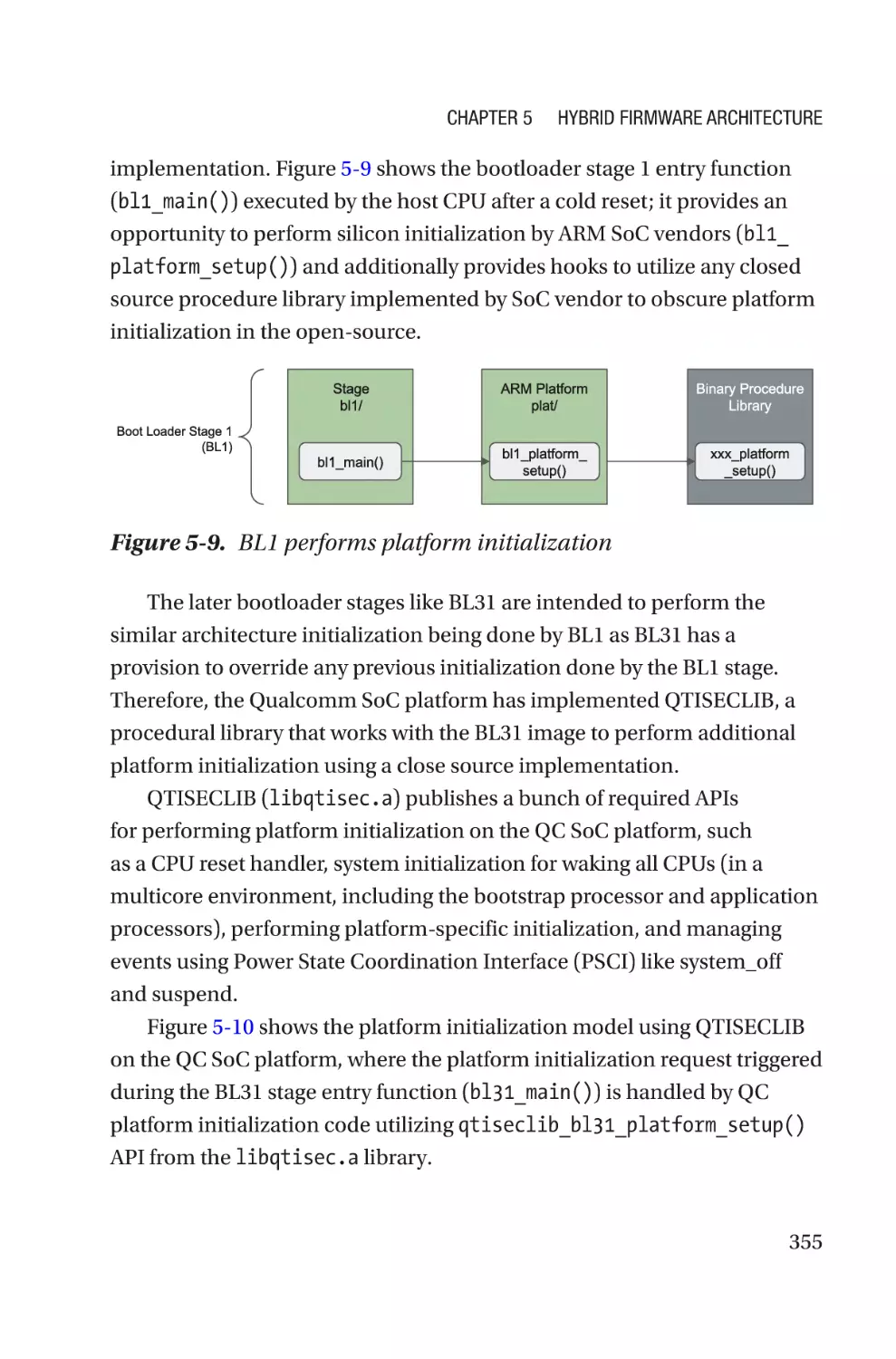
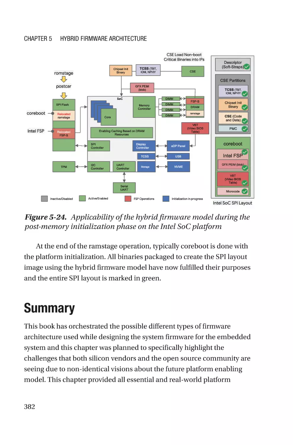
Summary����������������������������������������������������������������������������������������������������������382
vi
Table of Contents
Chapter 6: Payload���������������������������������������������������������������������������385
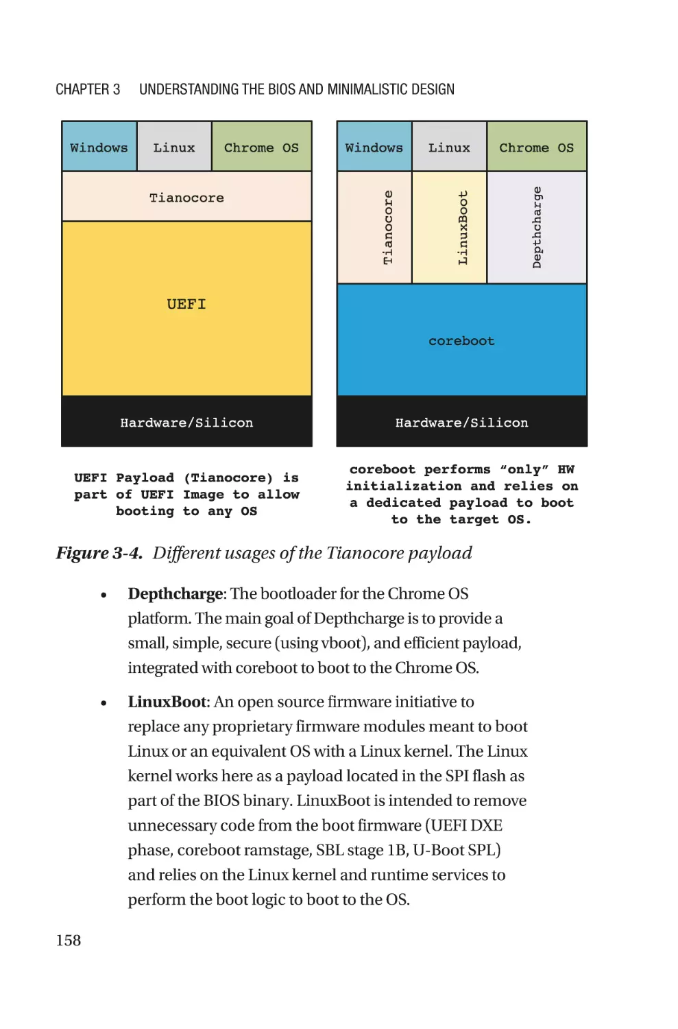
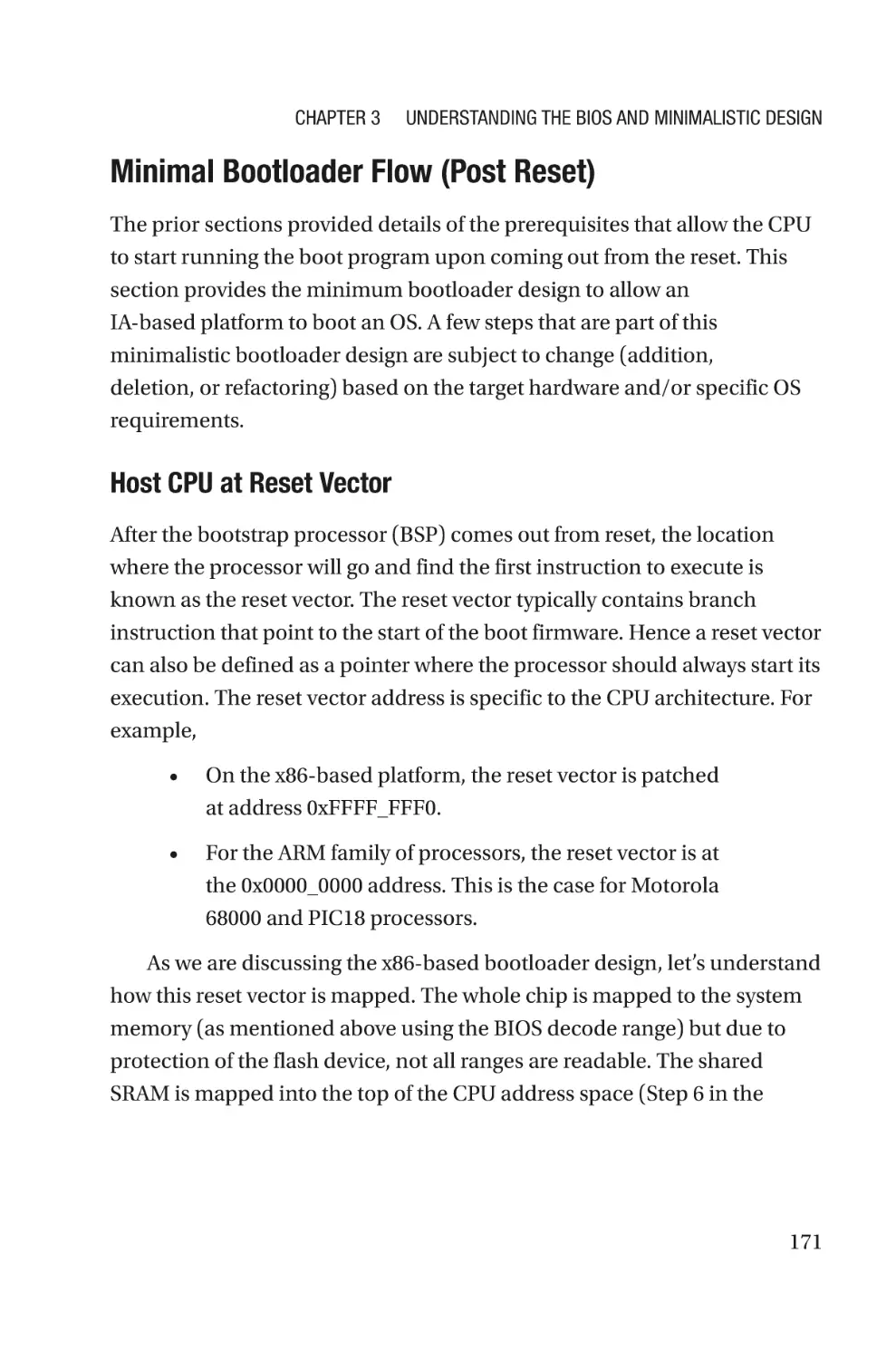
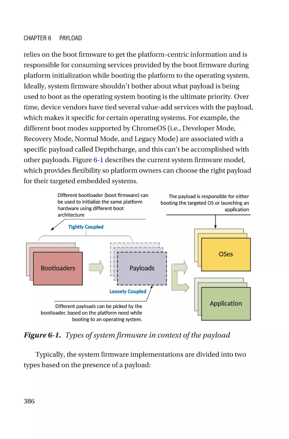
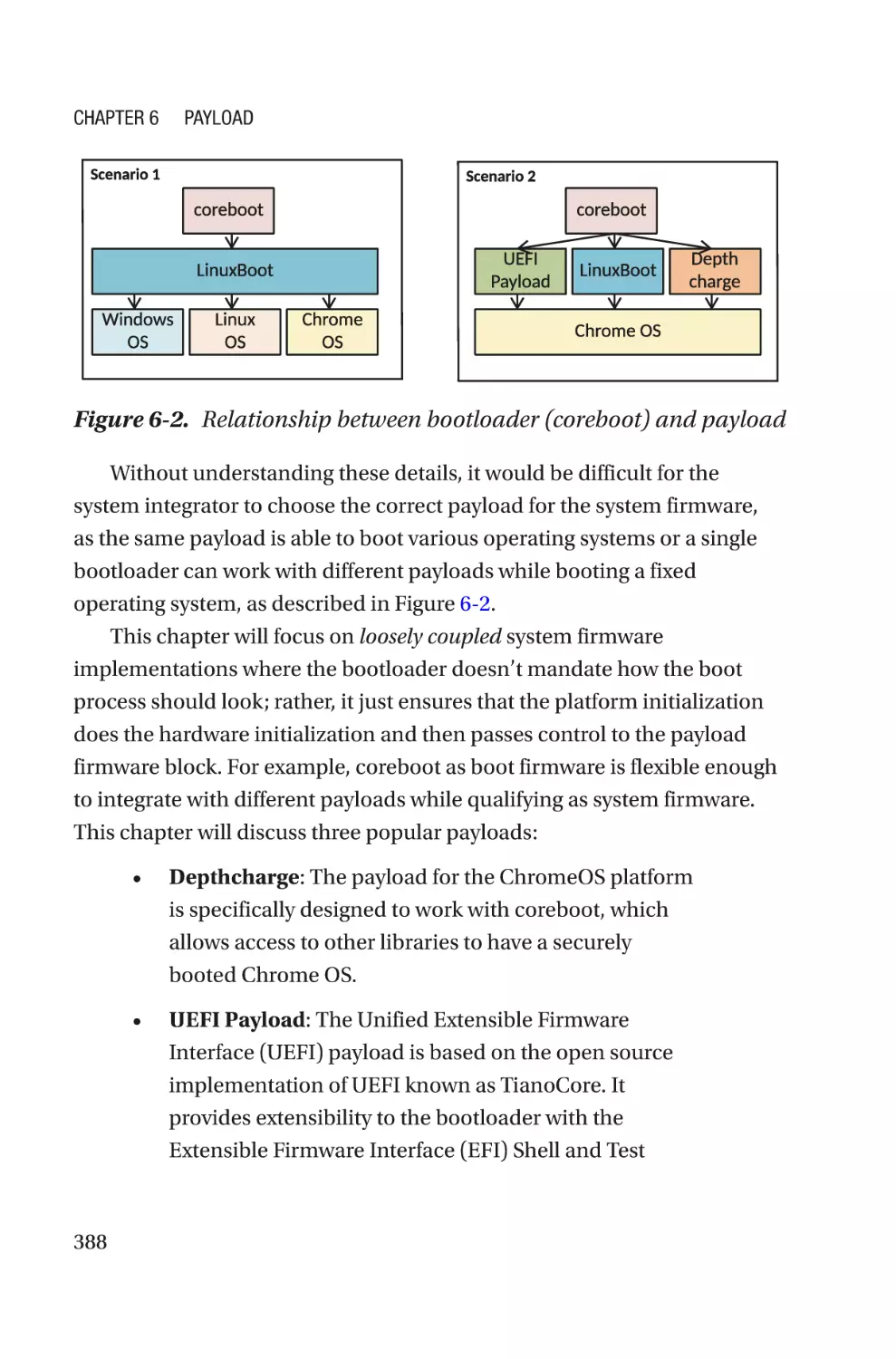
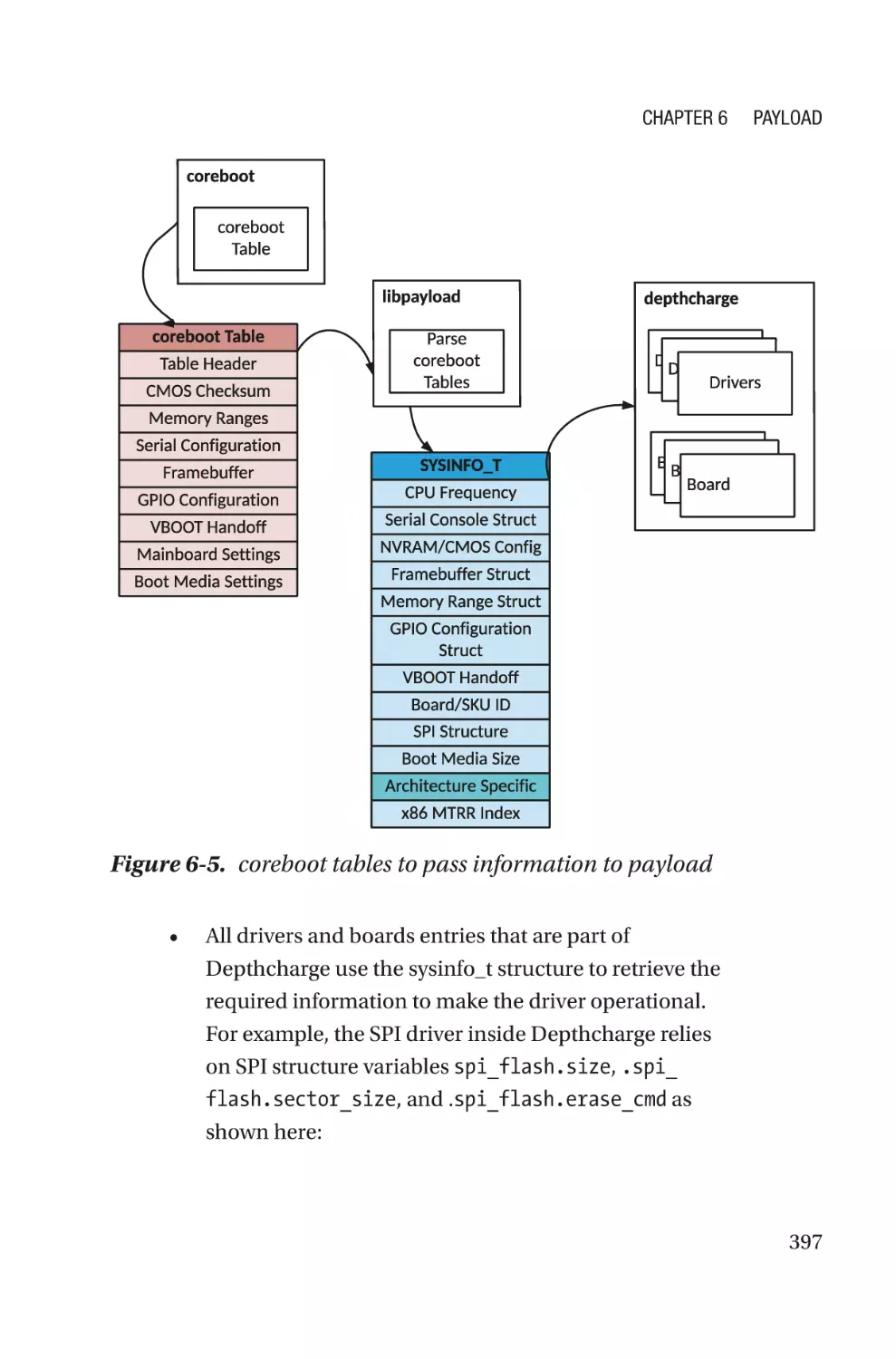
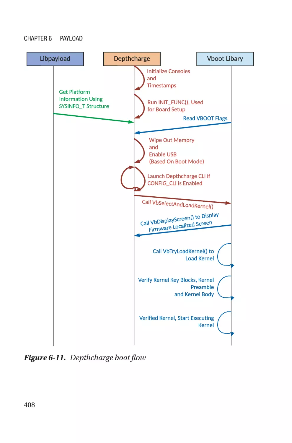
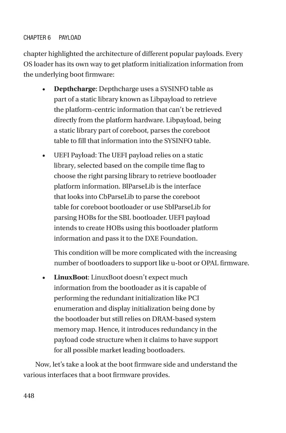
Depthcharge������������������������������������������������������������������������������������������������������390
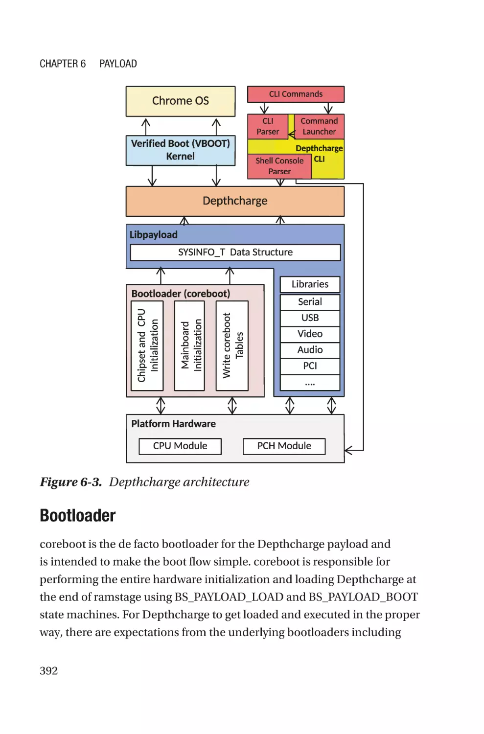
Depthcharge Architecture����������������������������������������������������������������������������391
Depthcharge Boot Flow�������������������������������������������������������������������������������407
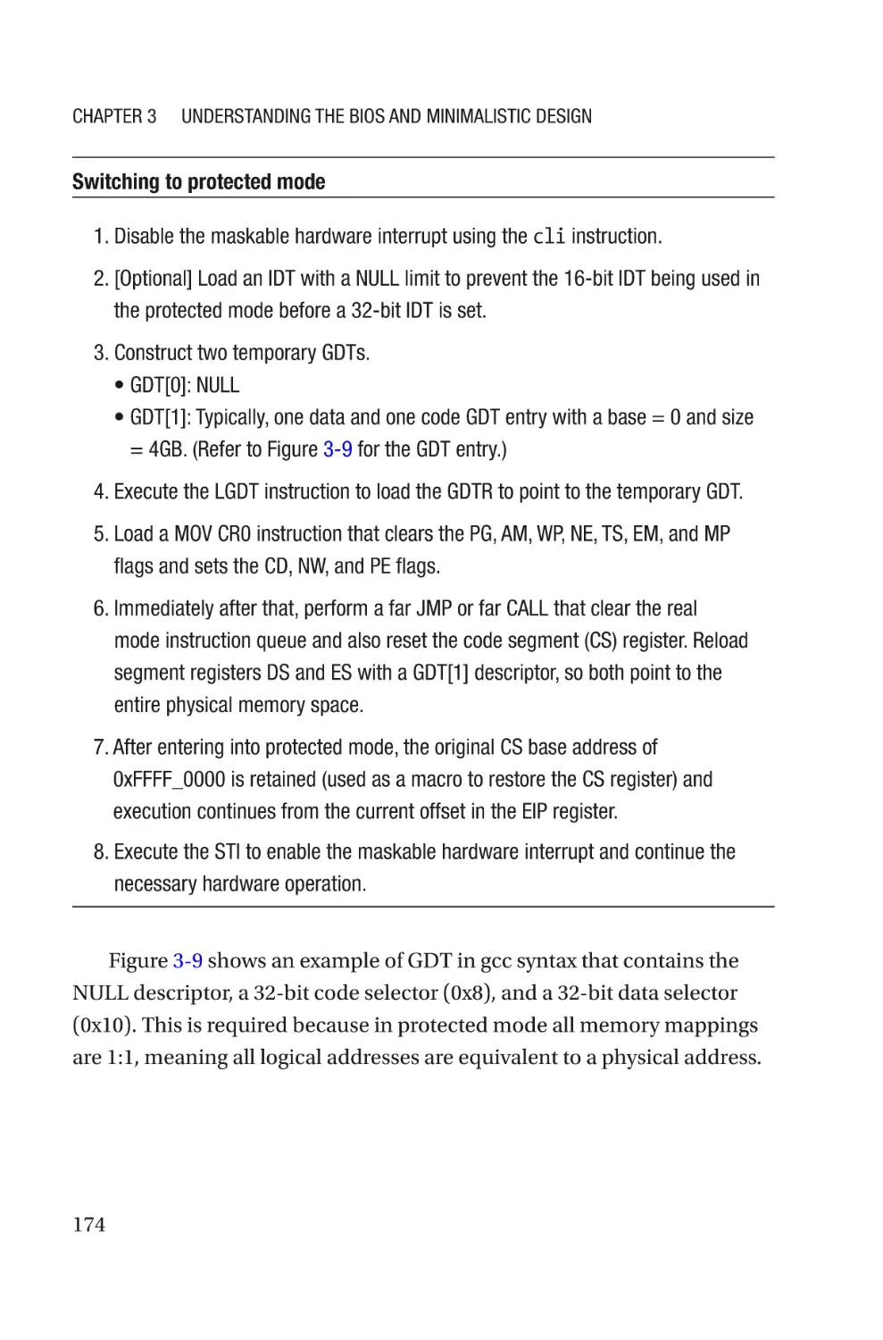
Depthcharge Code Structure�����������������������������������������������������������������������409
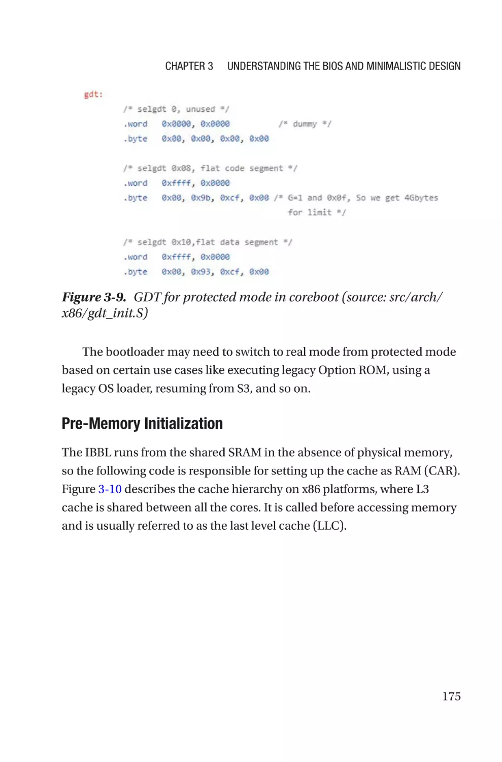
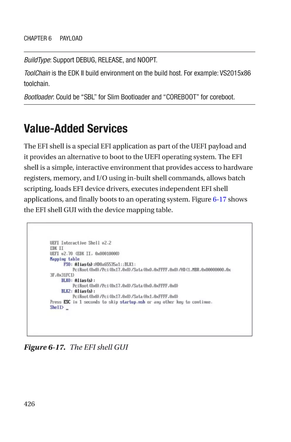
Value-Added Services���������������������������������������������������������������������������������411
UEFI Payload�����������������������������������������������������������������������������������������������������413
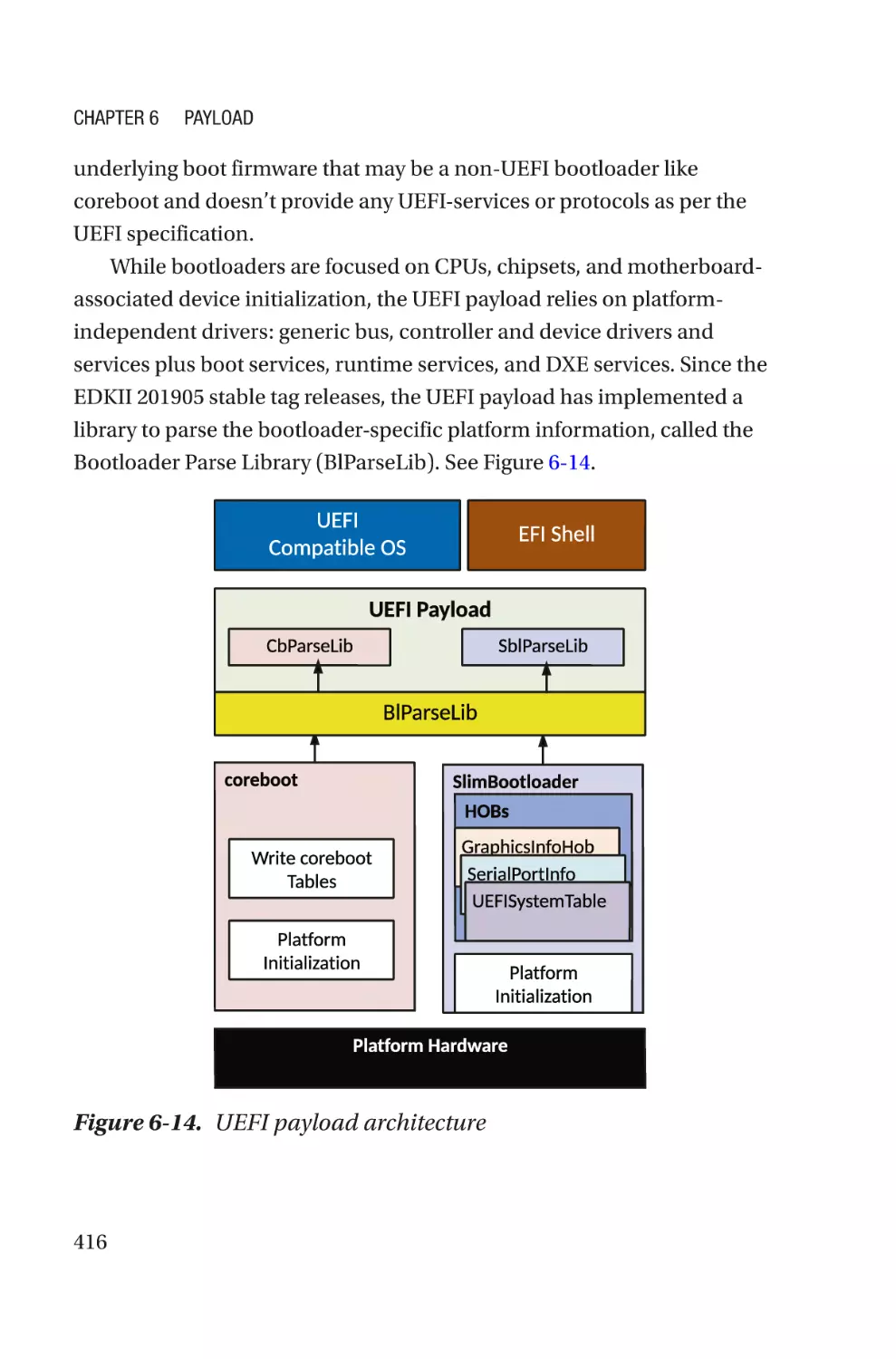
UEFI Payload Architecture���������������������������������������������������������������������������415
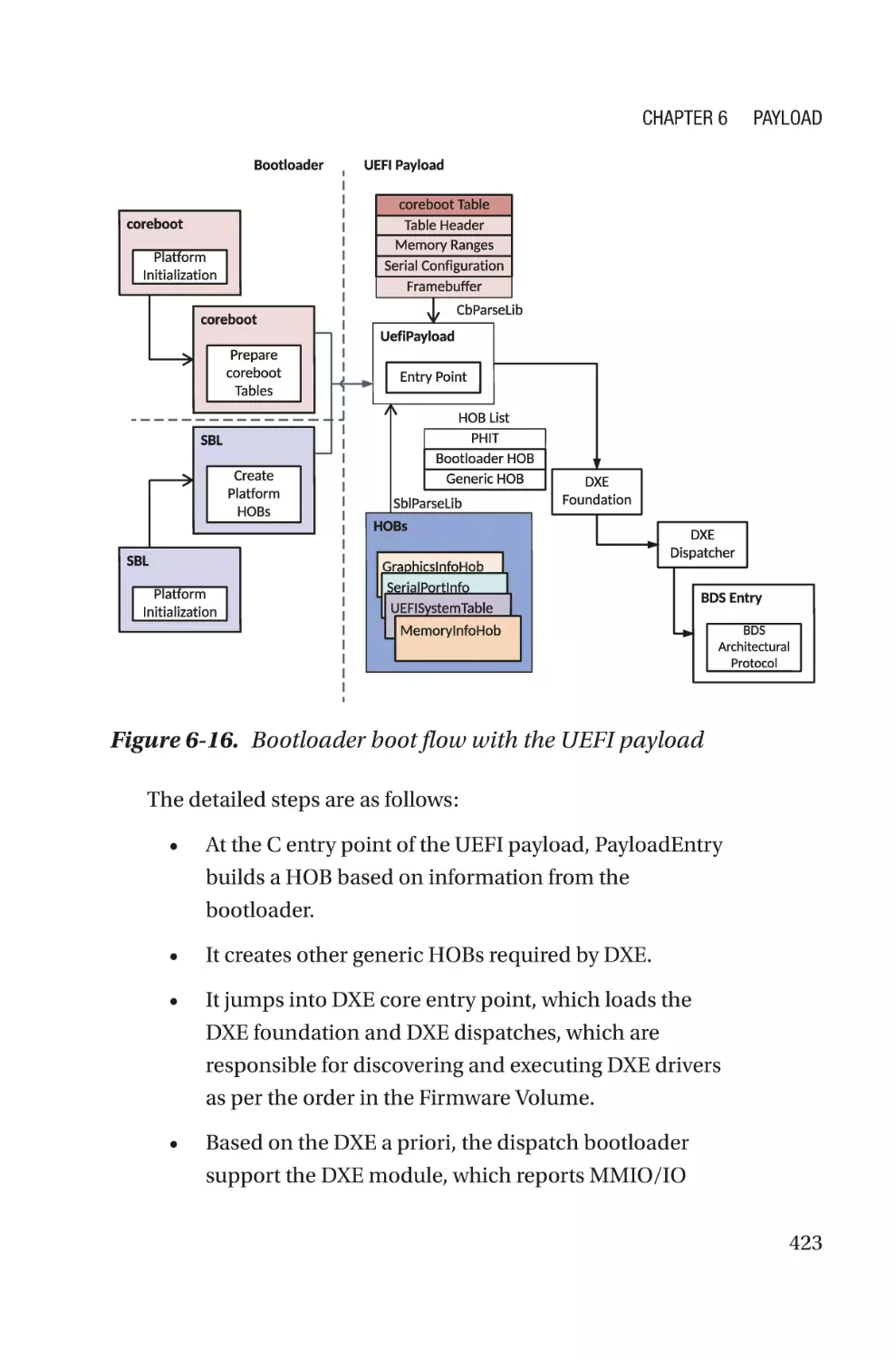
UEFI Payload Boot Flow�������������������������������������������������������������������������������422
UEFI Payload Code Structure�����������������������������������������������������������������������424
Value-Added Services���������������������������������������������������������������������������������426
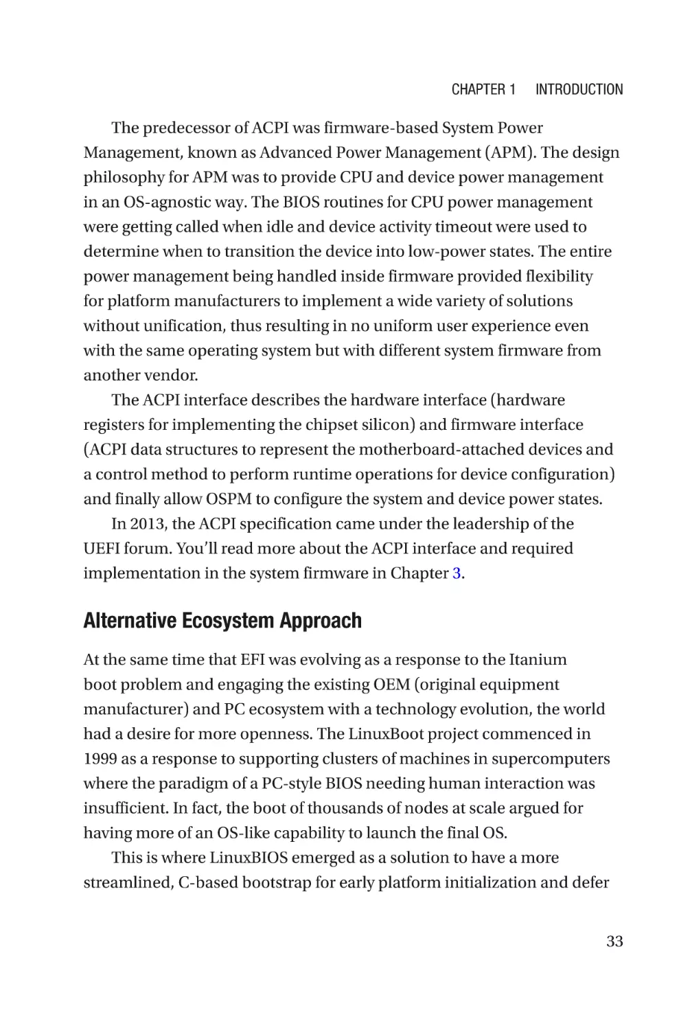
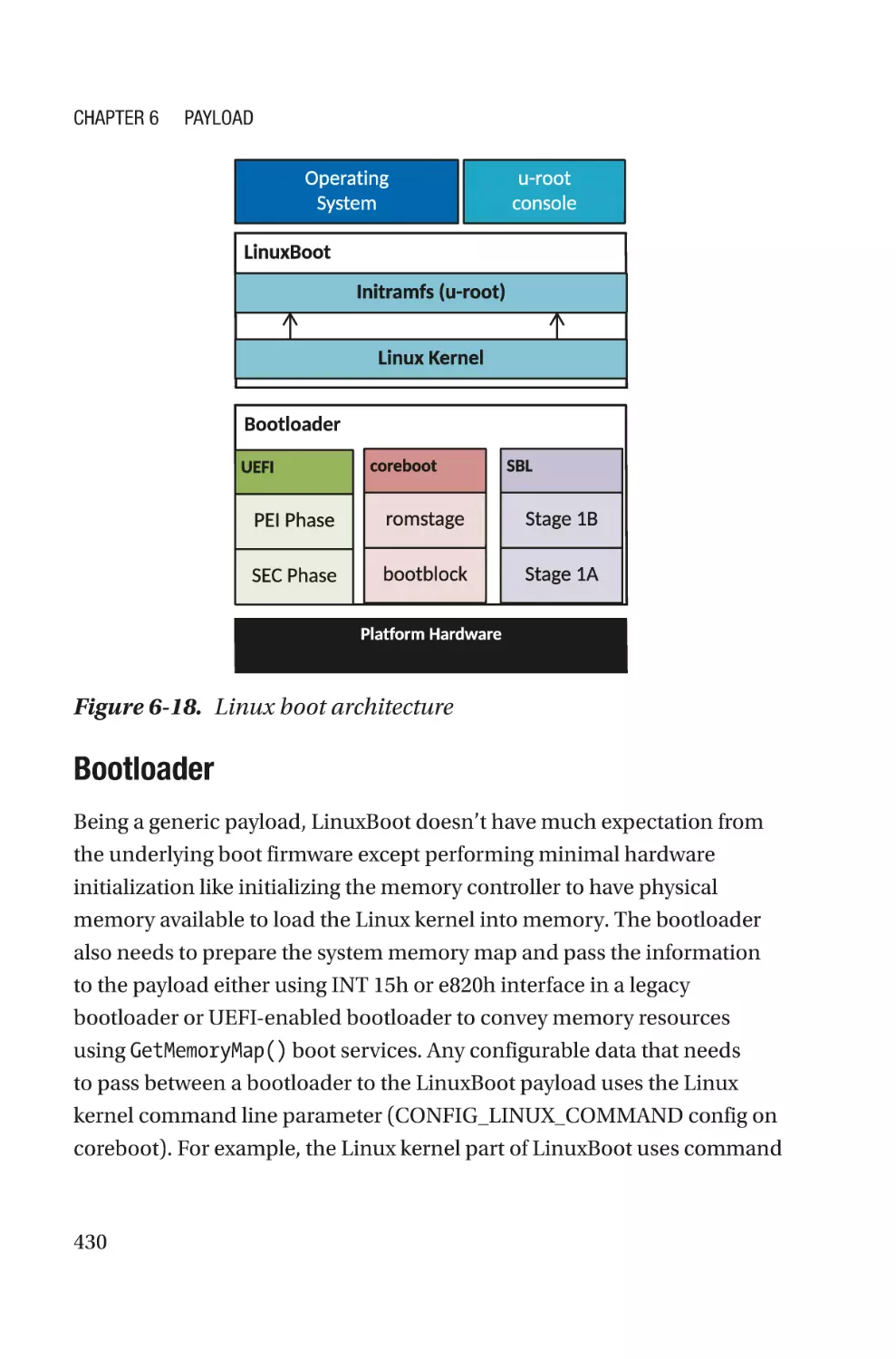
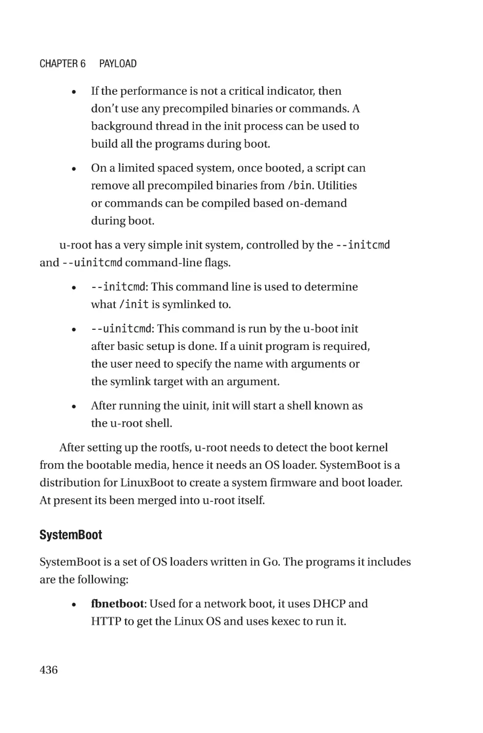
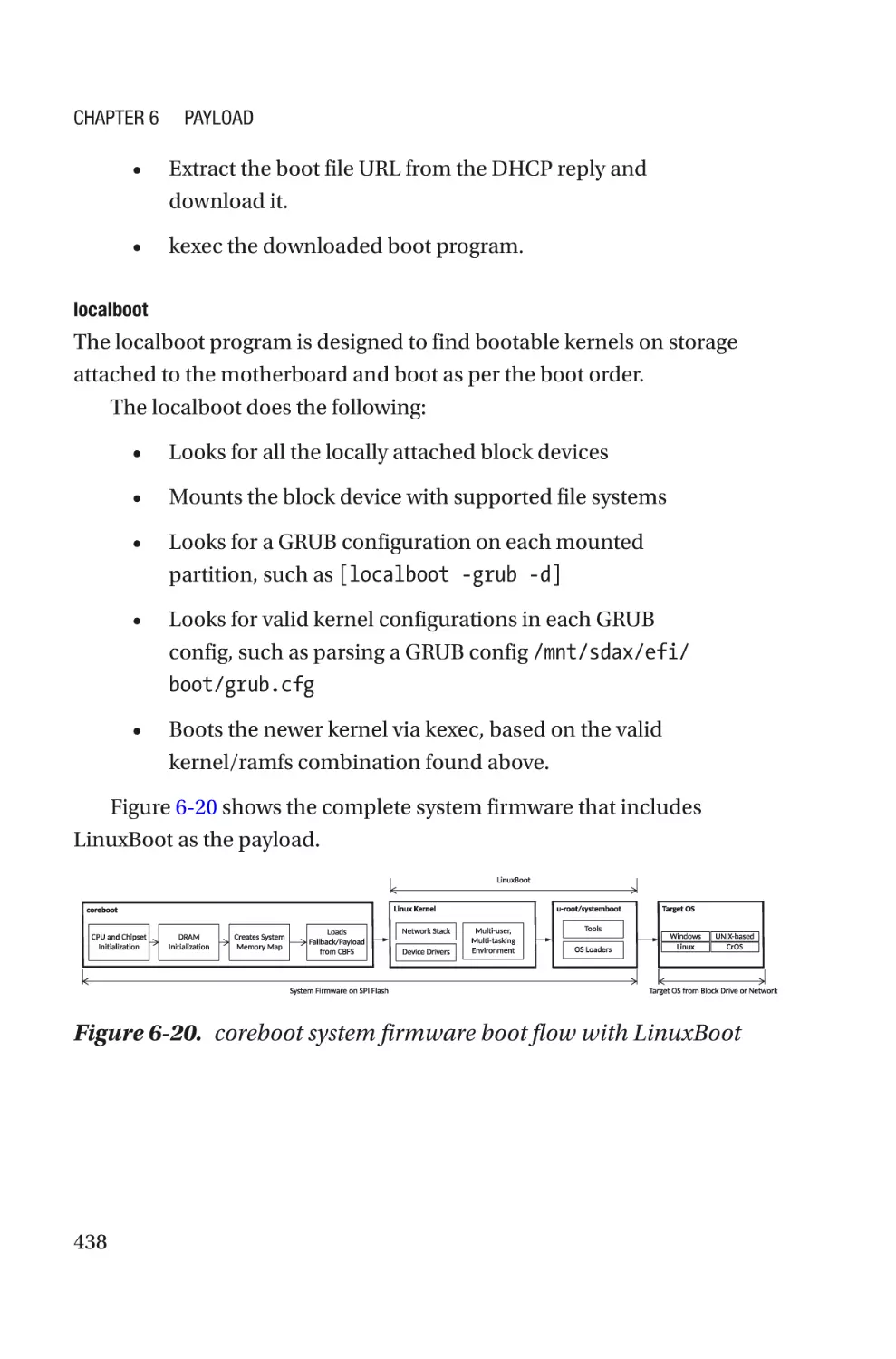
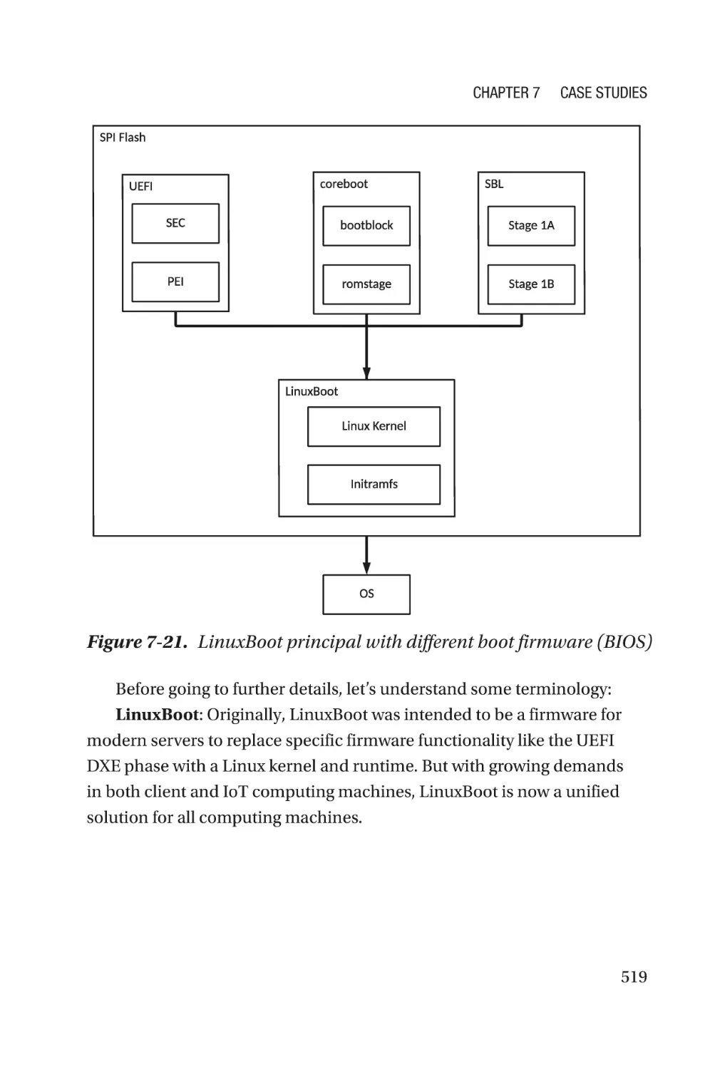
LinuxBoot����������������������������������������������������������������������������������������������������������427
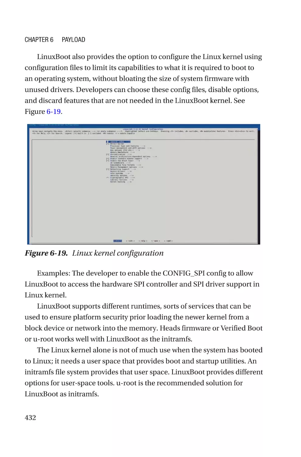
LinuxBoot Architecture��������������������������������������������������������������������������������429
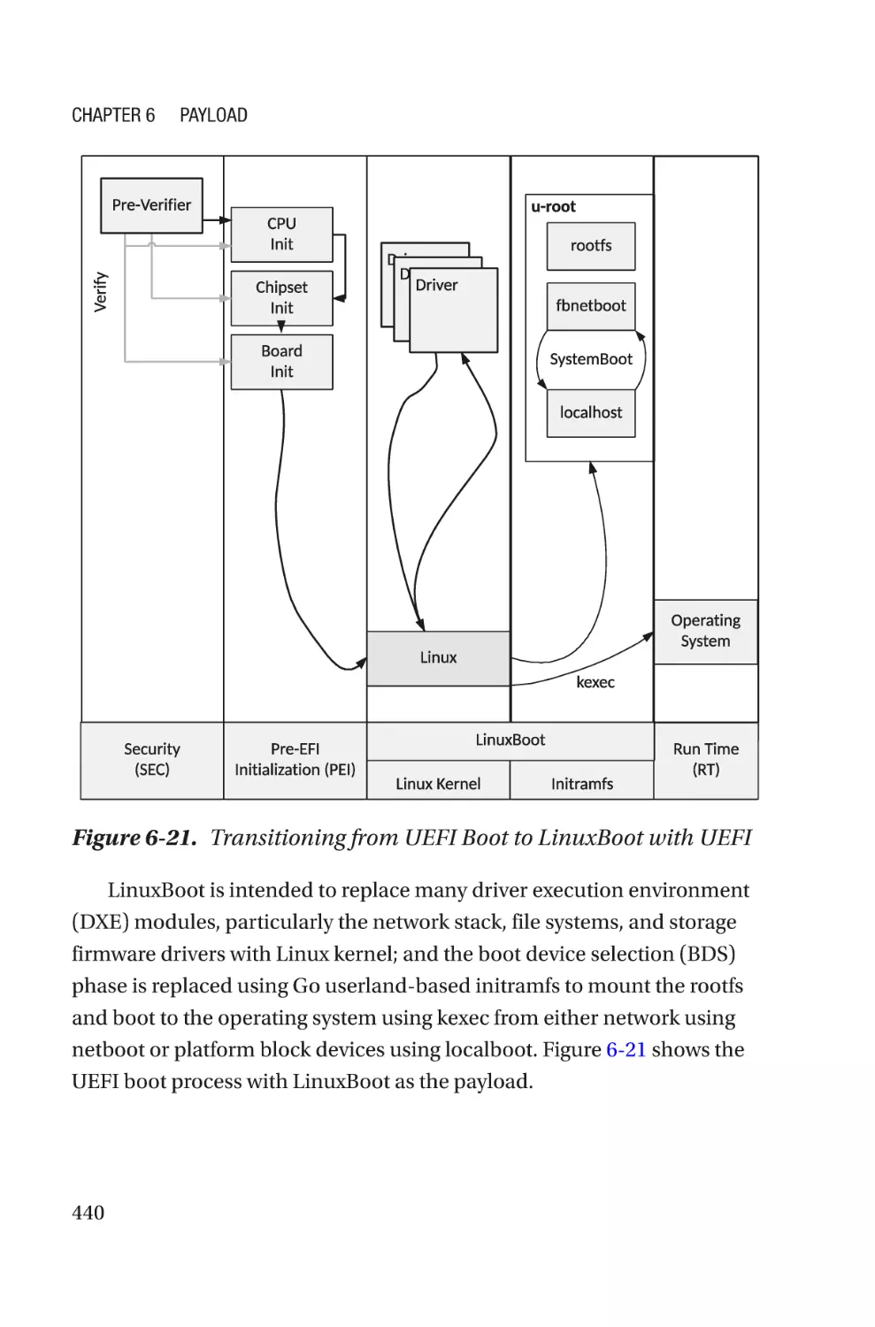
LinuxBoot Boot Flow������������������������������������������������������������������������������������439
LinuxBoot Code Structure����������������������������������������������������������������������������441
Value-Added Services���������������������������������������������������������������������������������443
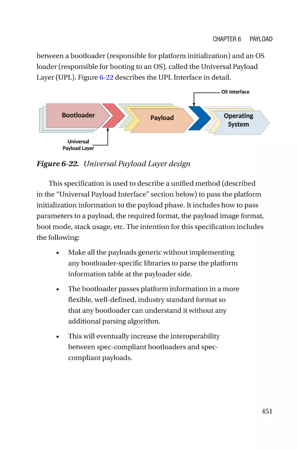
Universal Payload Layer (UPL)��������������������������������������������������������������������������447
Universal Payload Image Format�����������������������������������������������������������������452
Universal Payload Interface�������������������������������������������������������������������������455
Implementation of Universal Payload Layer������������������������������������������������458
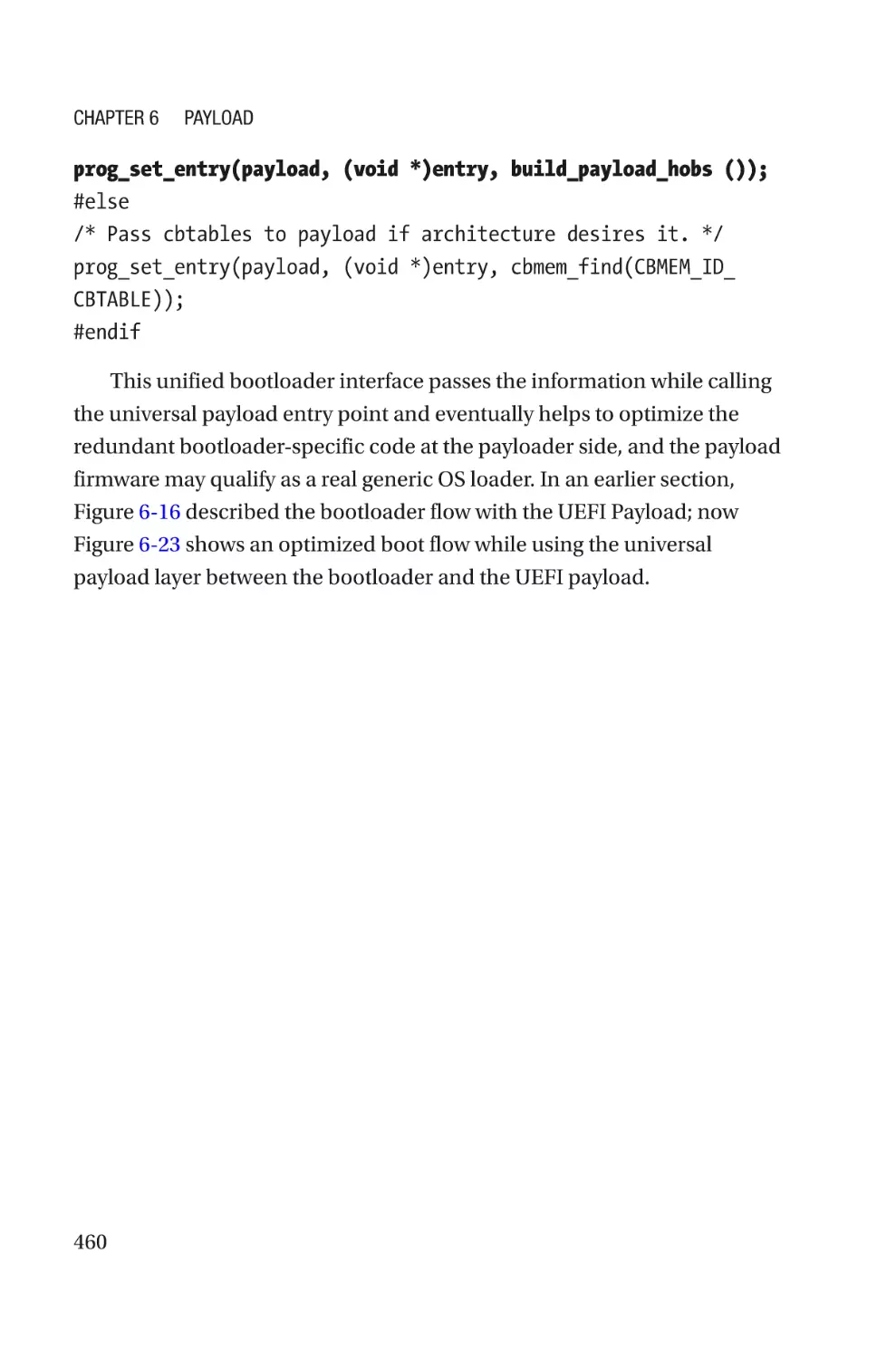
Summary����������������������������������������������������������������������������������������������������������461
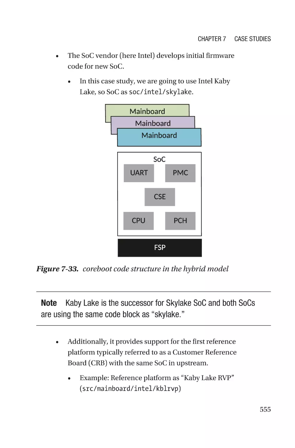
Chapter 7: Case Studies��������������������������������������������������������������������465
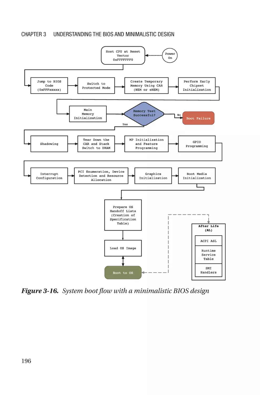
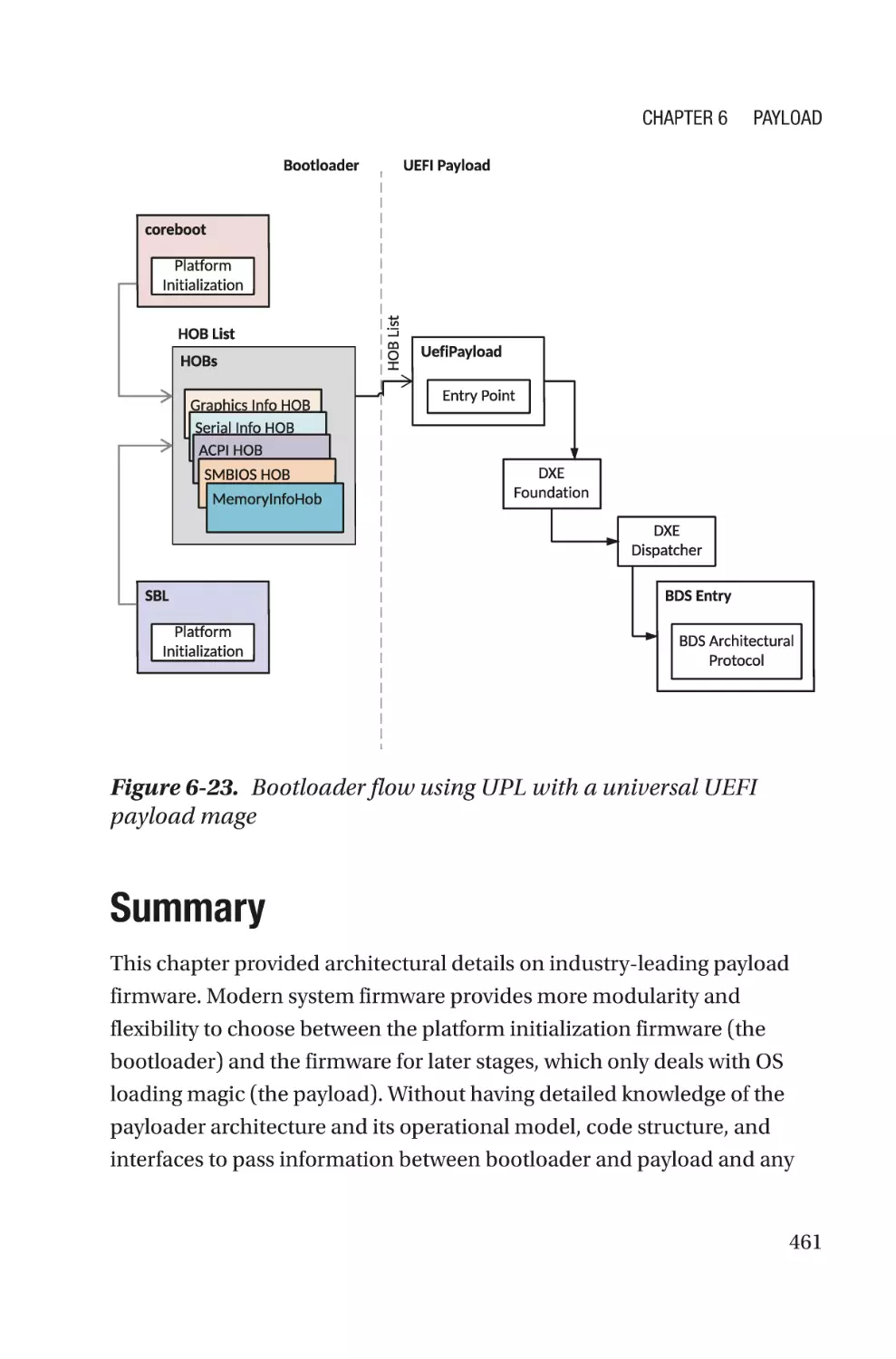
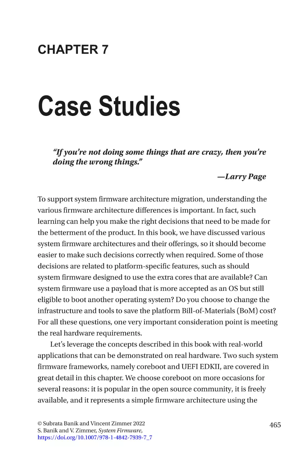
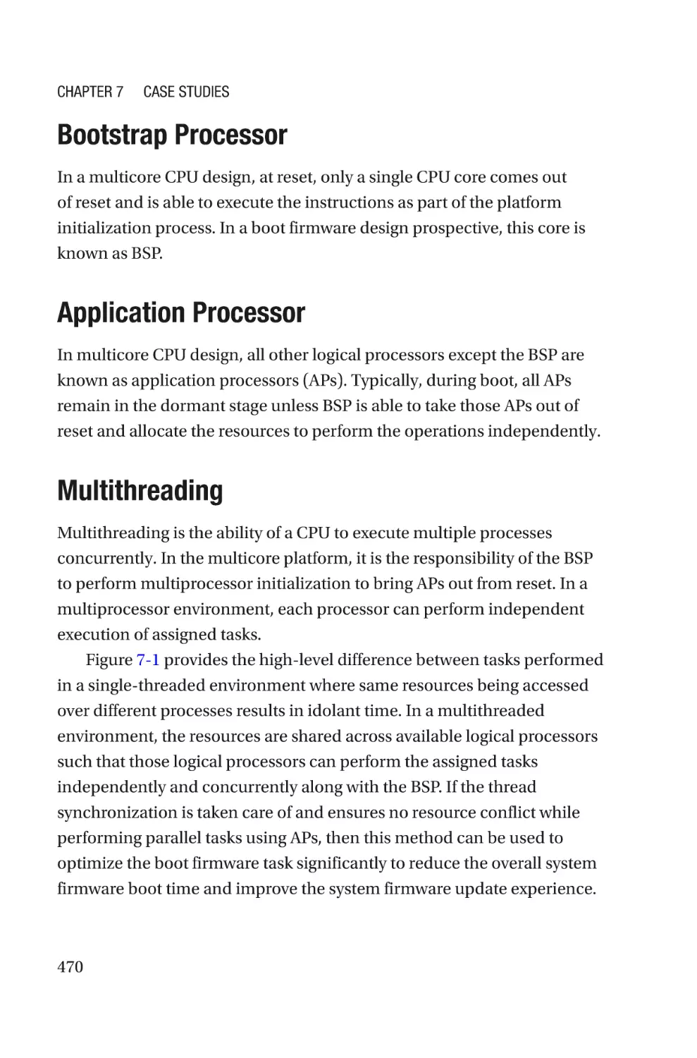
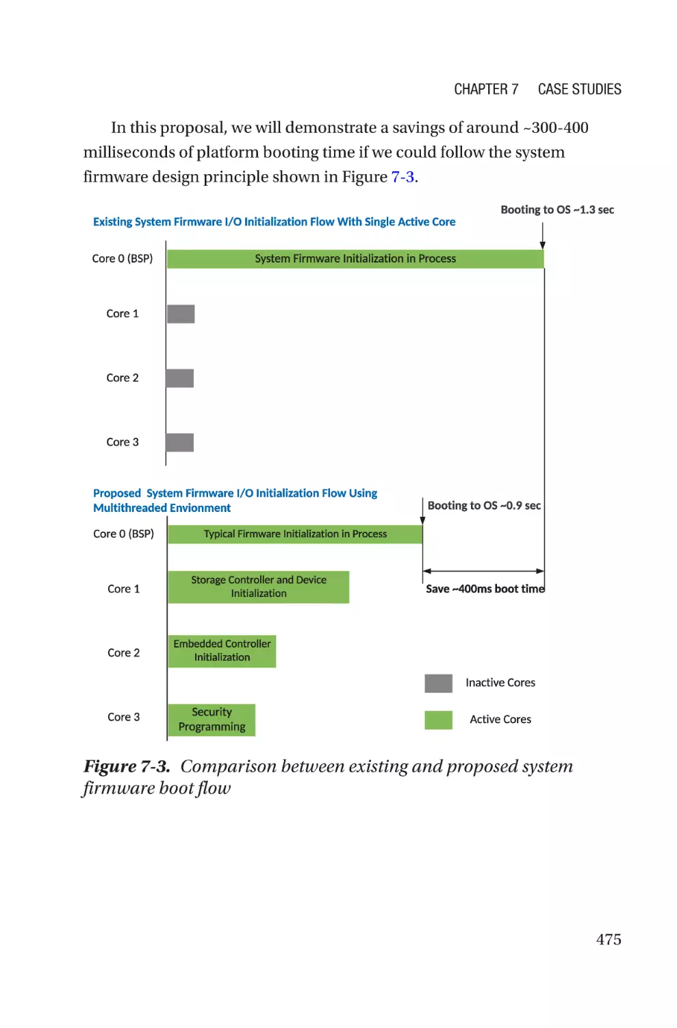
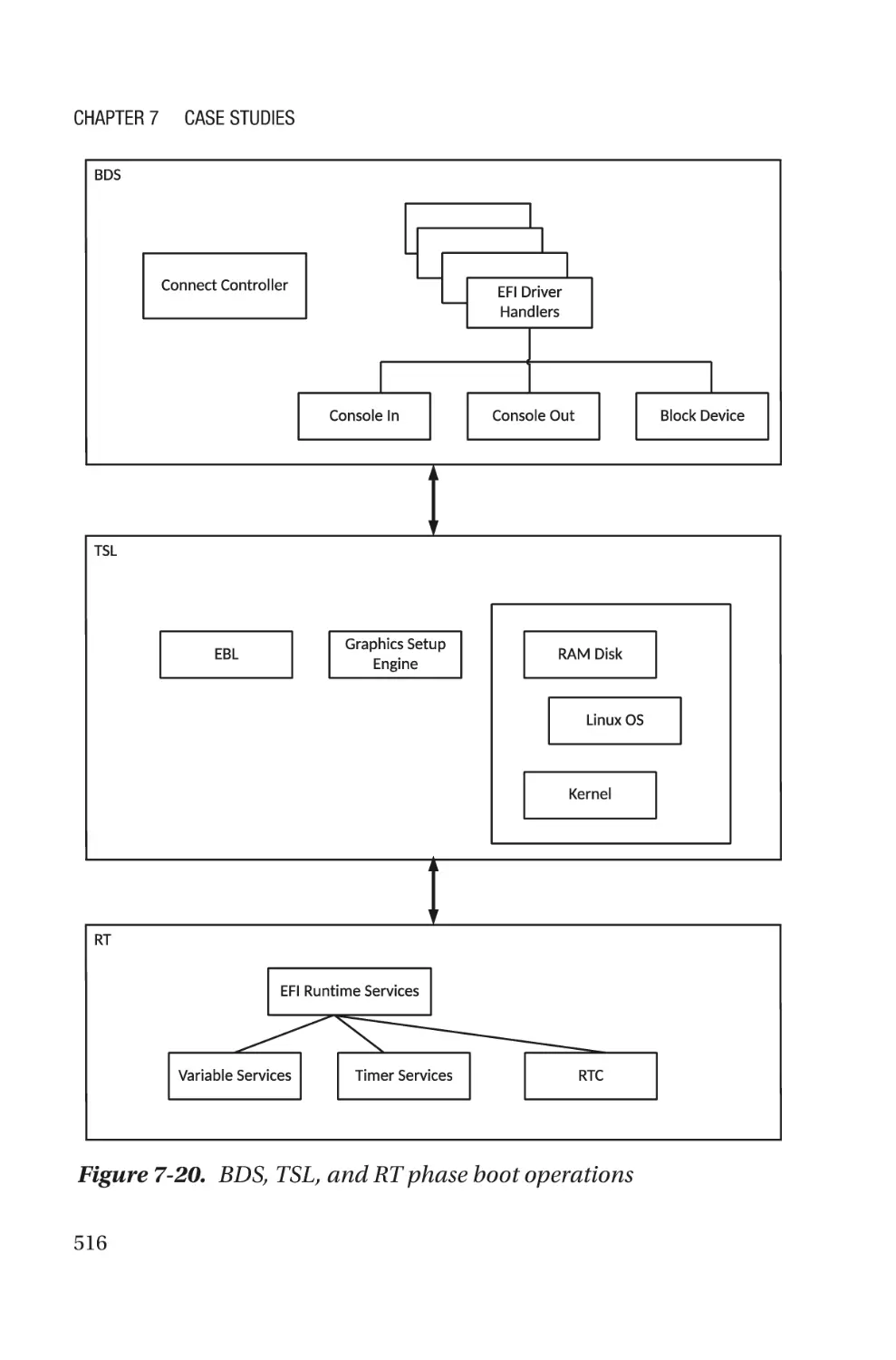
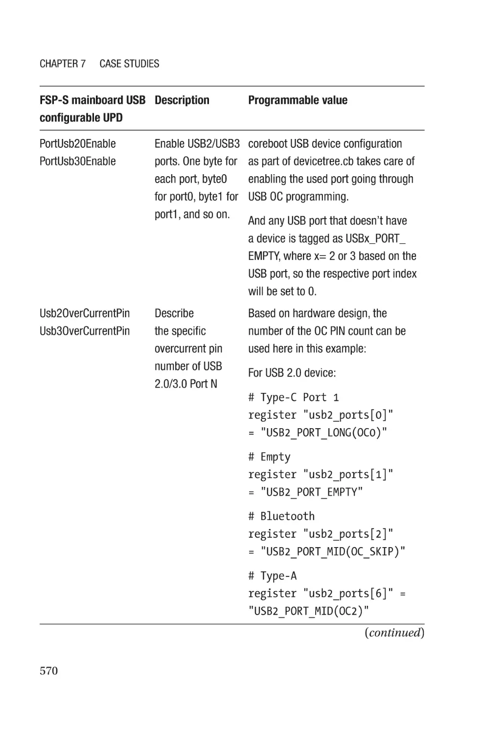
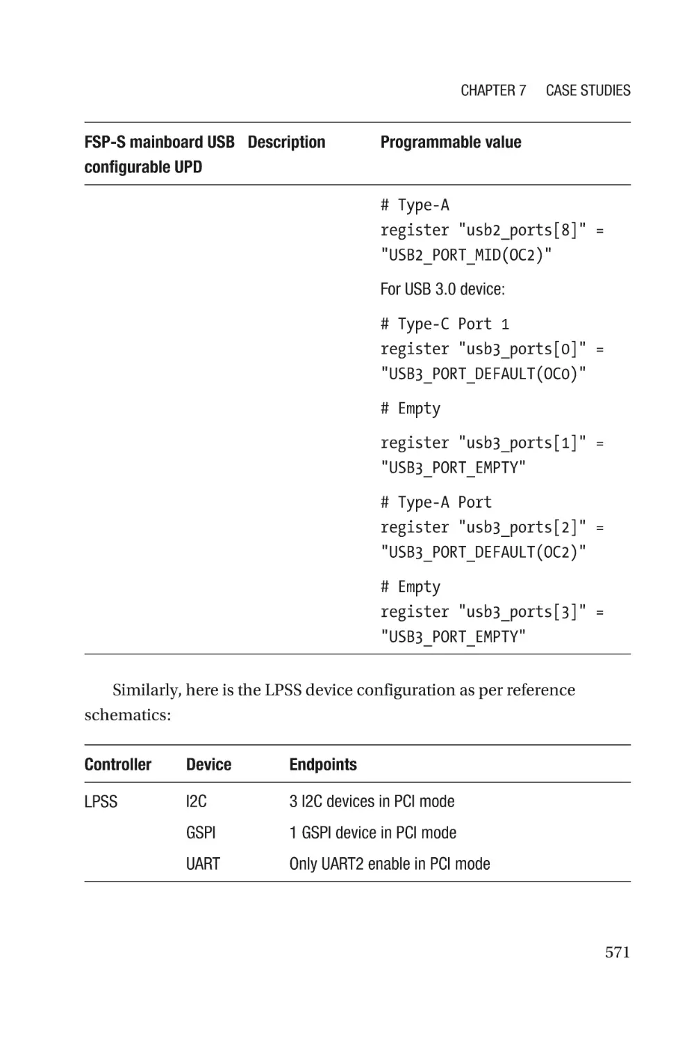
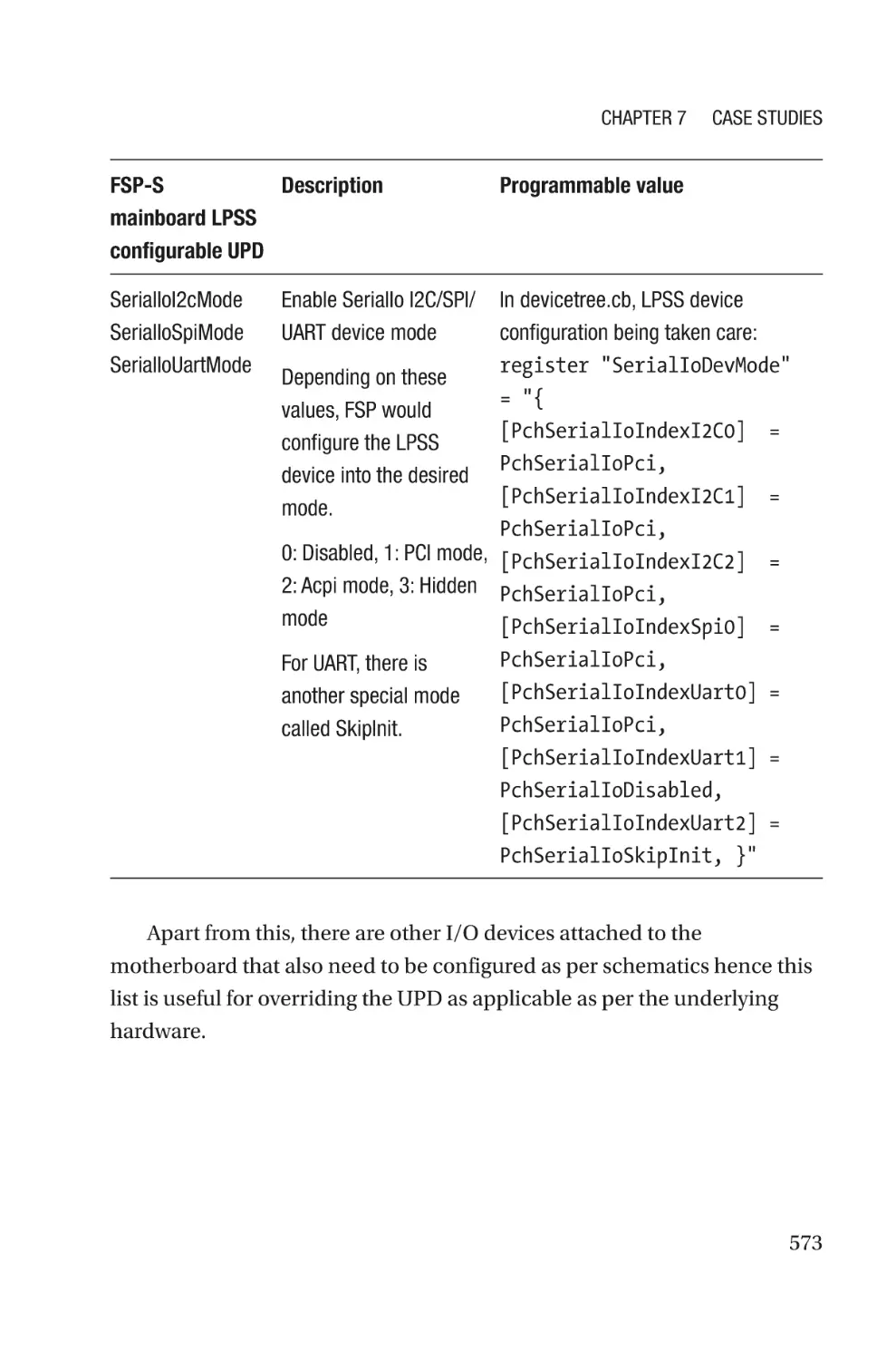
Reduce FW Booting Time Using Multi-Threaded Environment��������������������������467
coreboot������������������������������������������������������������������������������������������������������469
Bootstrap Processor������������������������������������������������������������������������������������470
Application Processor����������������������������������������������������������������������������������470
Multithreading���������������������������������������������������������������������������������������������470
ChromeOS����������������������������������������������������������������������������������������������������471
vii
Table of Contents
Crosh�����������������������������������������������������������������������������������������������������������471
Depthcharge������������������������������������������������������������������������������������������������471
Goal and Motivation�������������������������������������������������������������������������������������472
Implementation Schema�����������������������������������������������������������������������������472
Setting Up the Board�����������������������������������������������������������������������������������476
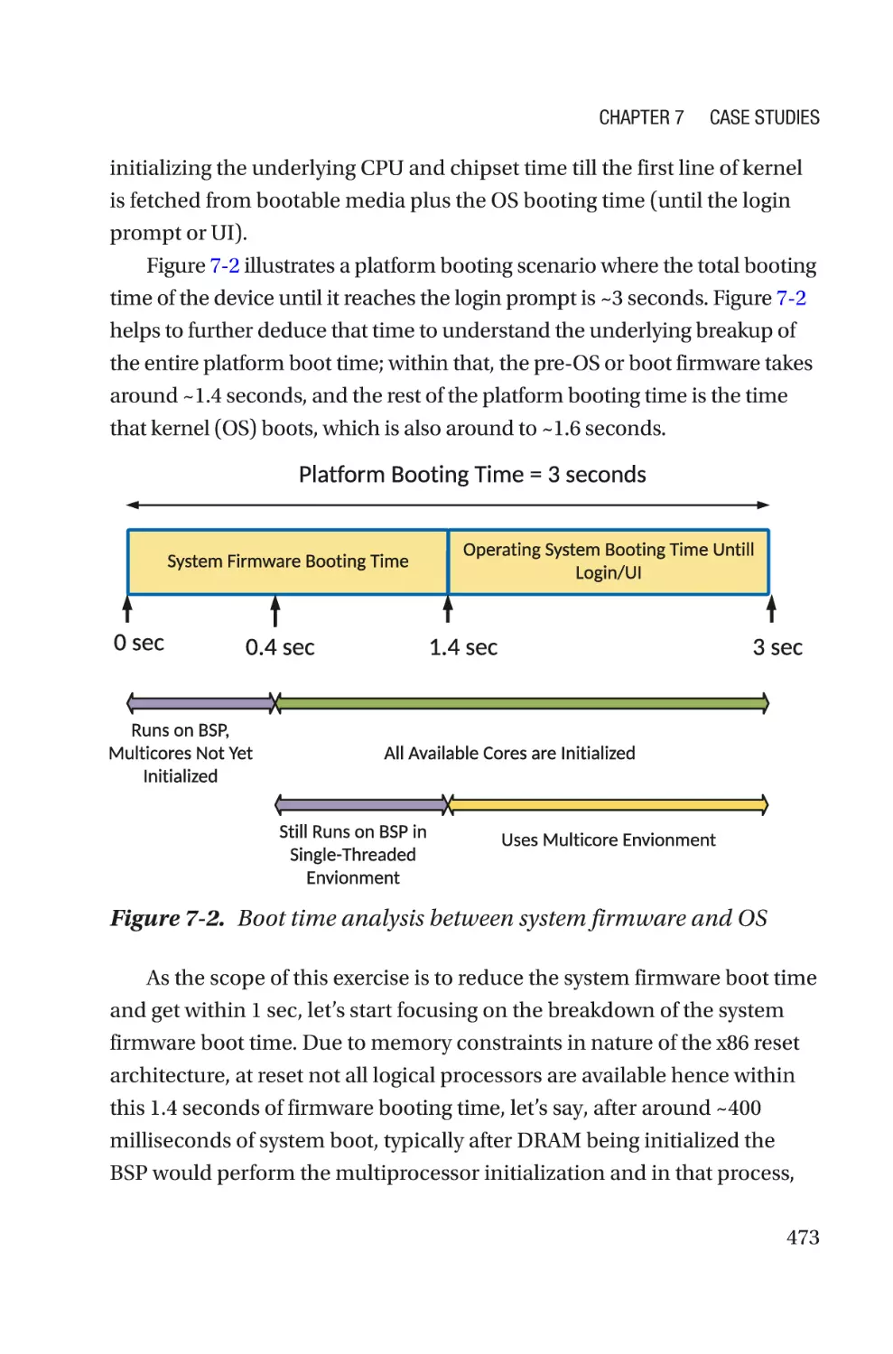
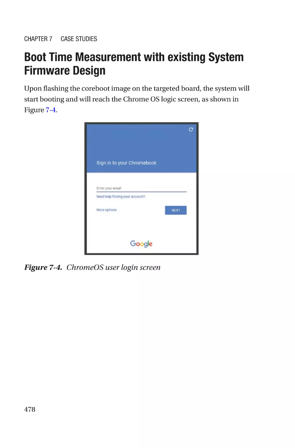
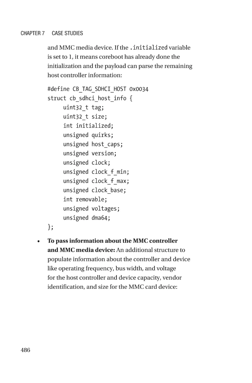
Boot Time Measurement with existing System Firmware Design���������������478
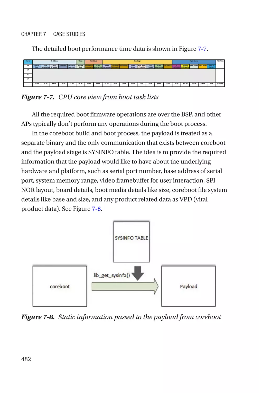
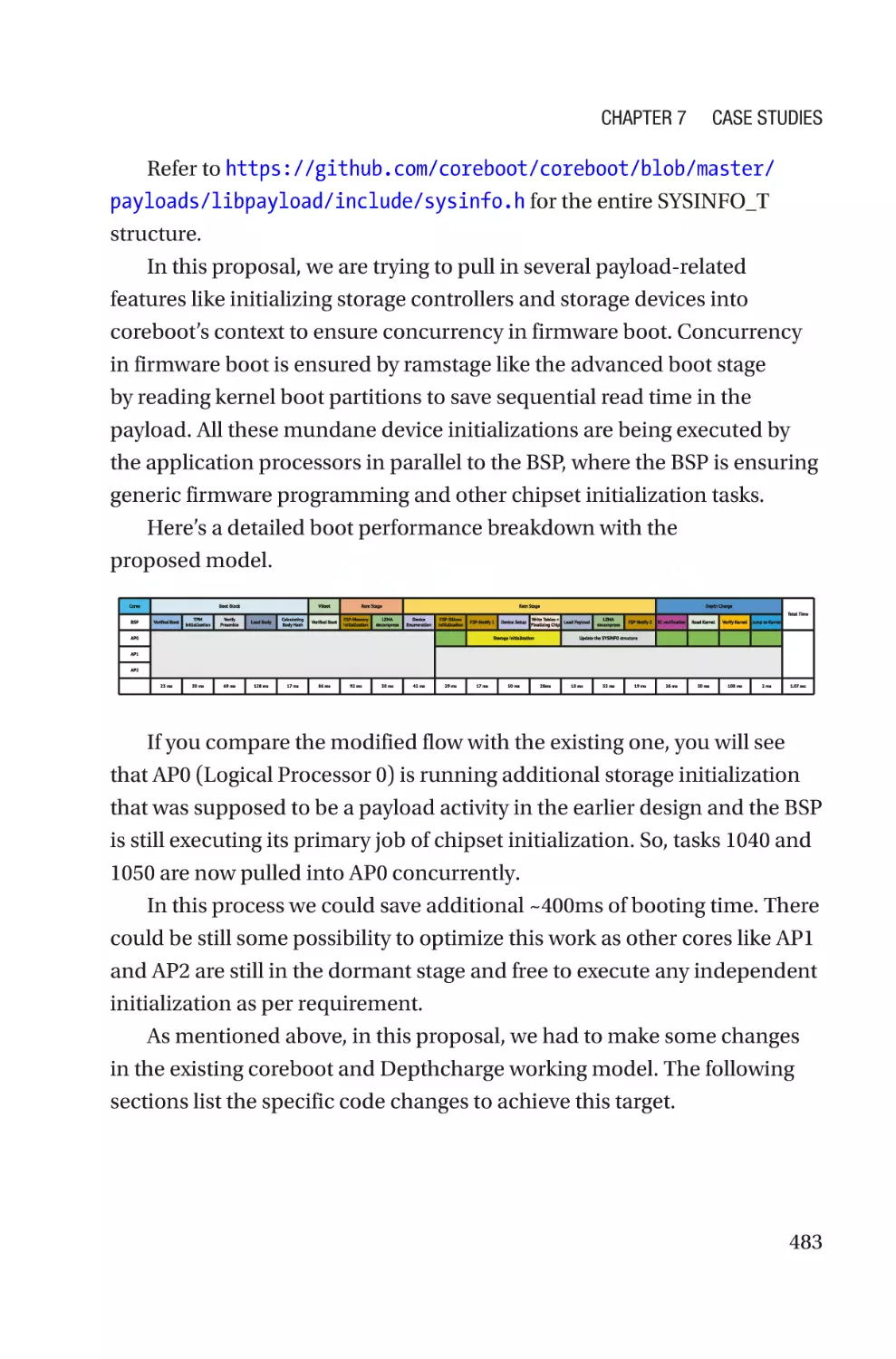
Detailed Implementation�����������������������������������������������������������������������������481
Firmware Boot Time Optimization for Capsule Update��������������������������������490
Firmware Boot Time Optimization Conclusion���������������������������������������������490
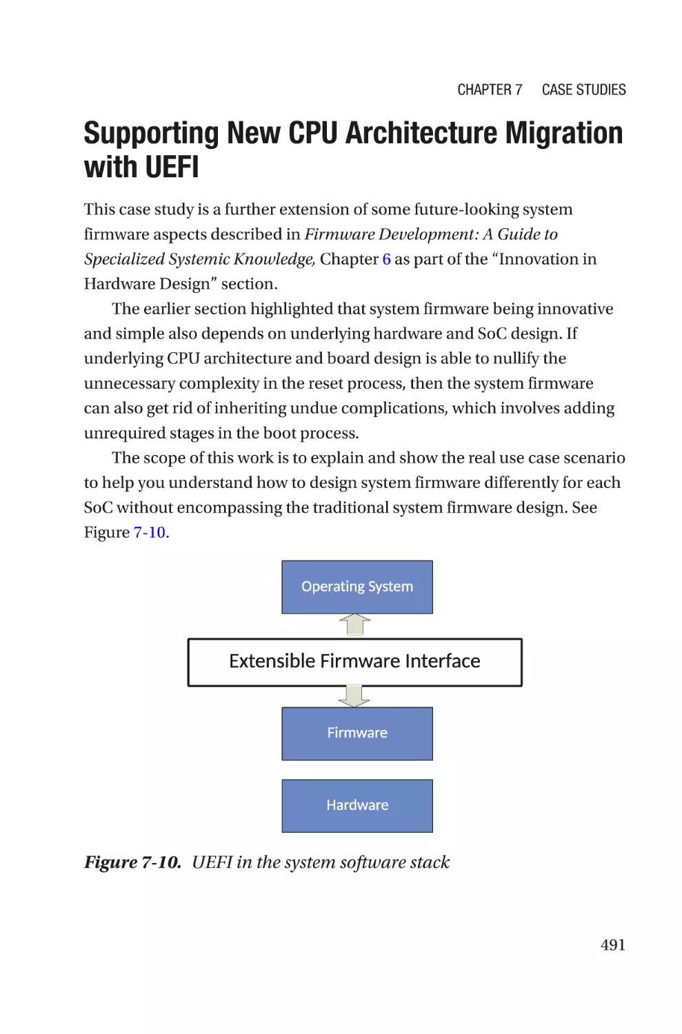
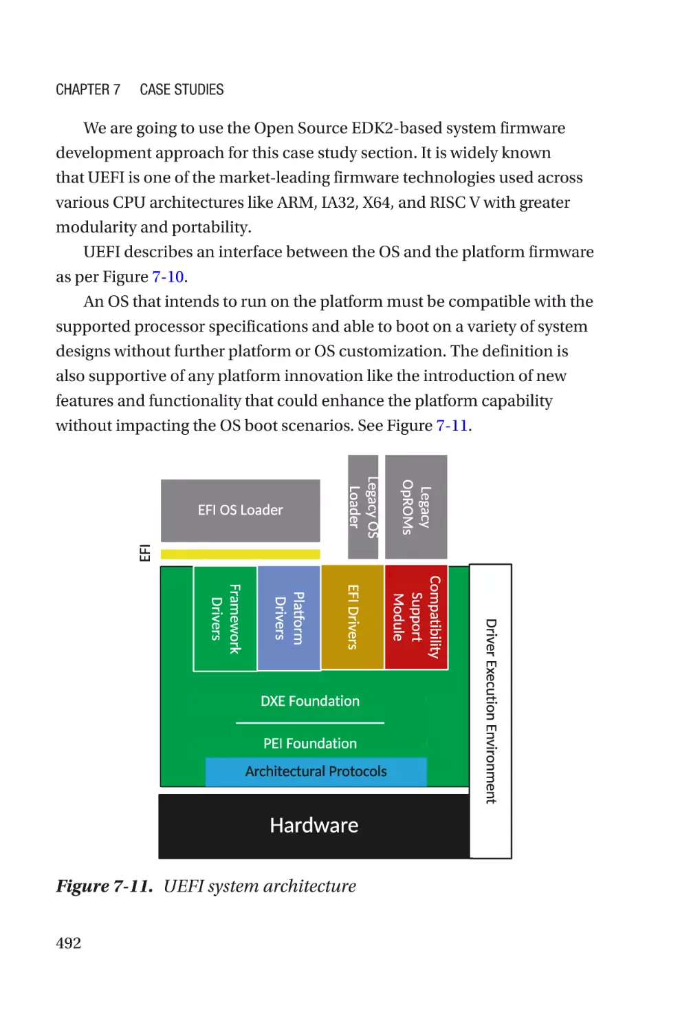
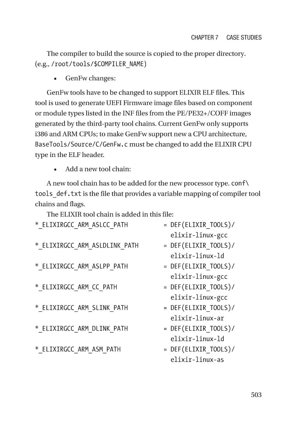
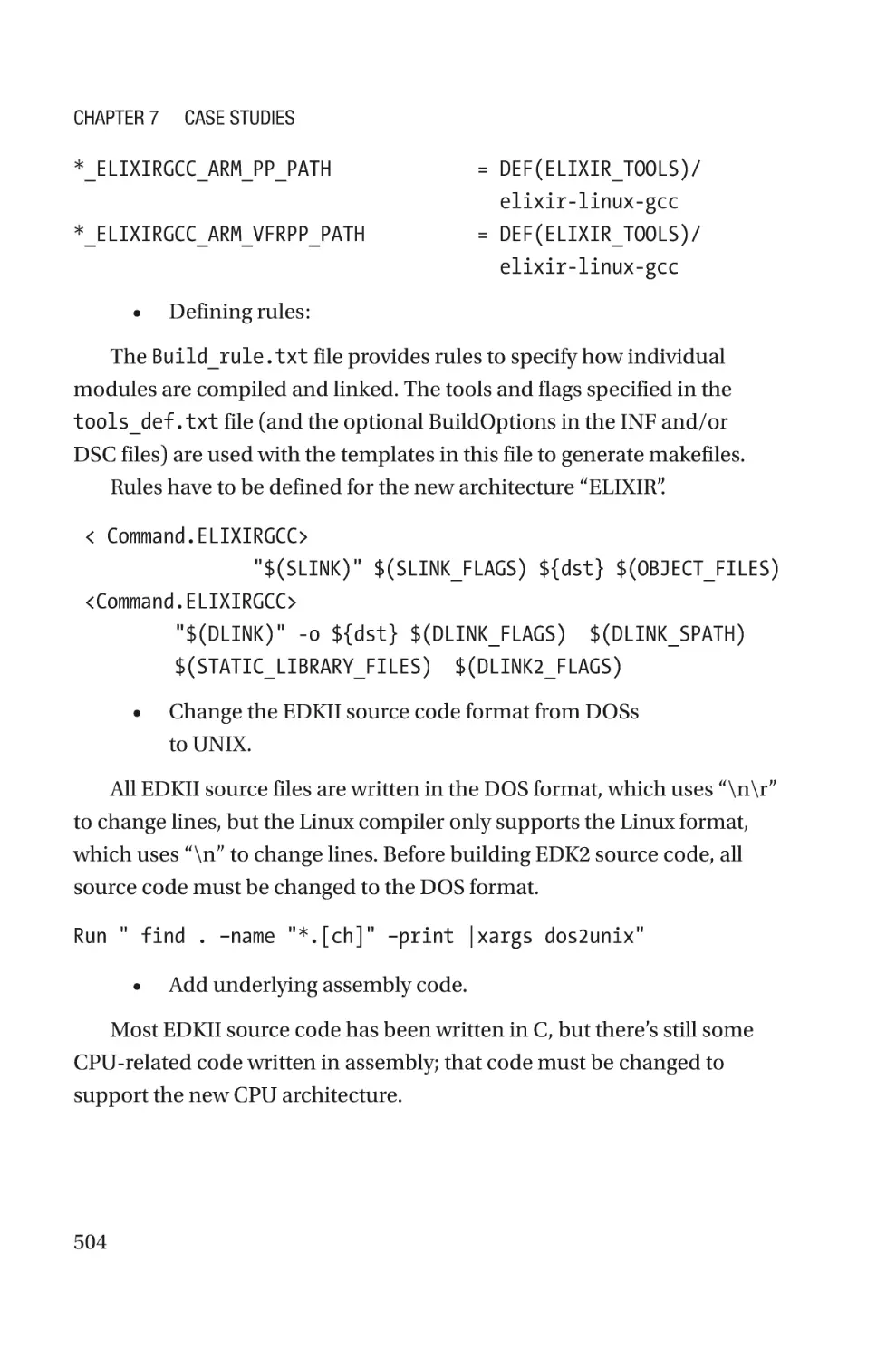
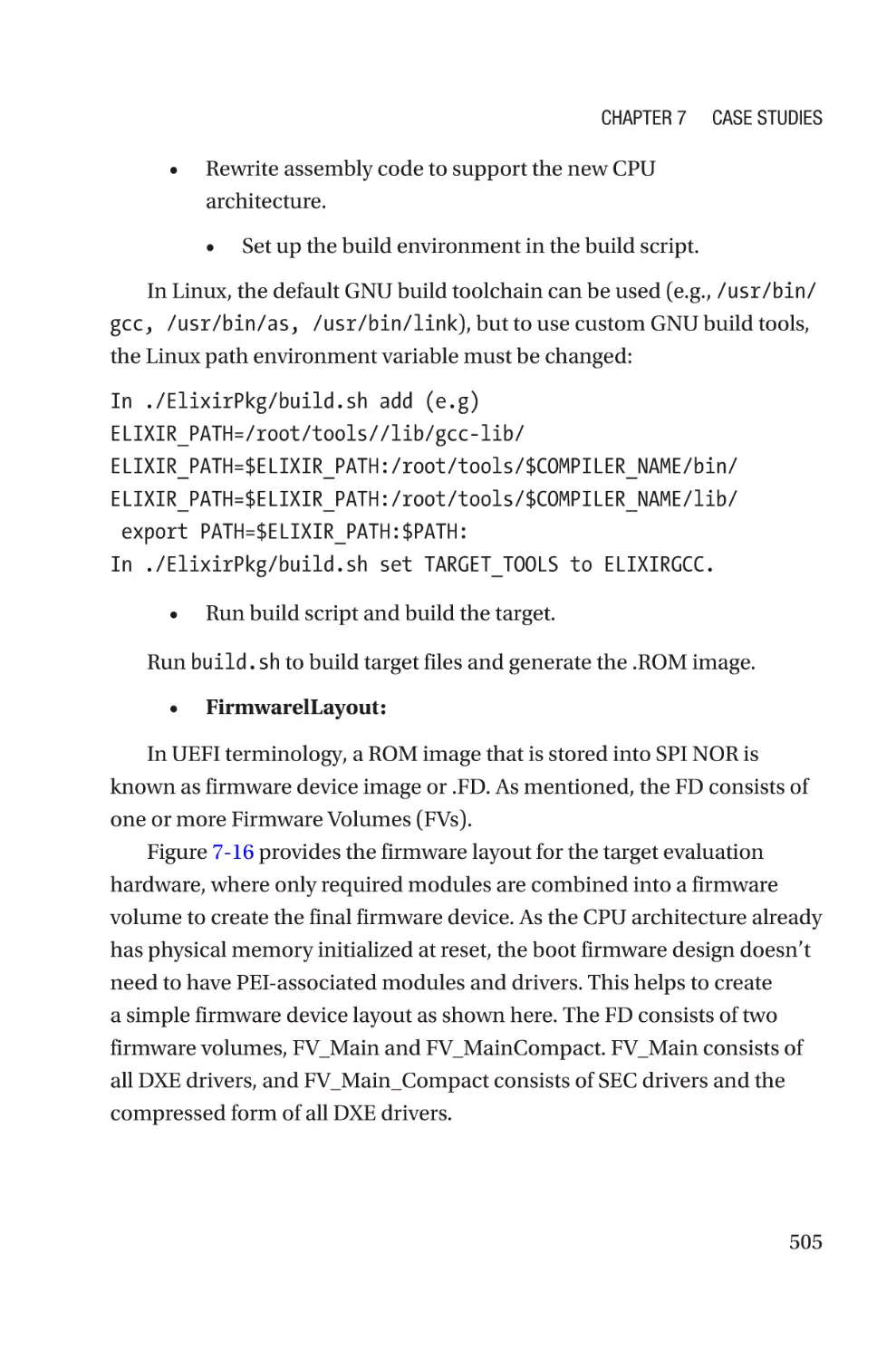
Supporting New CPU Architecture Migration with UEFI������������������������������������491
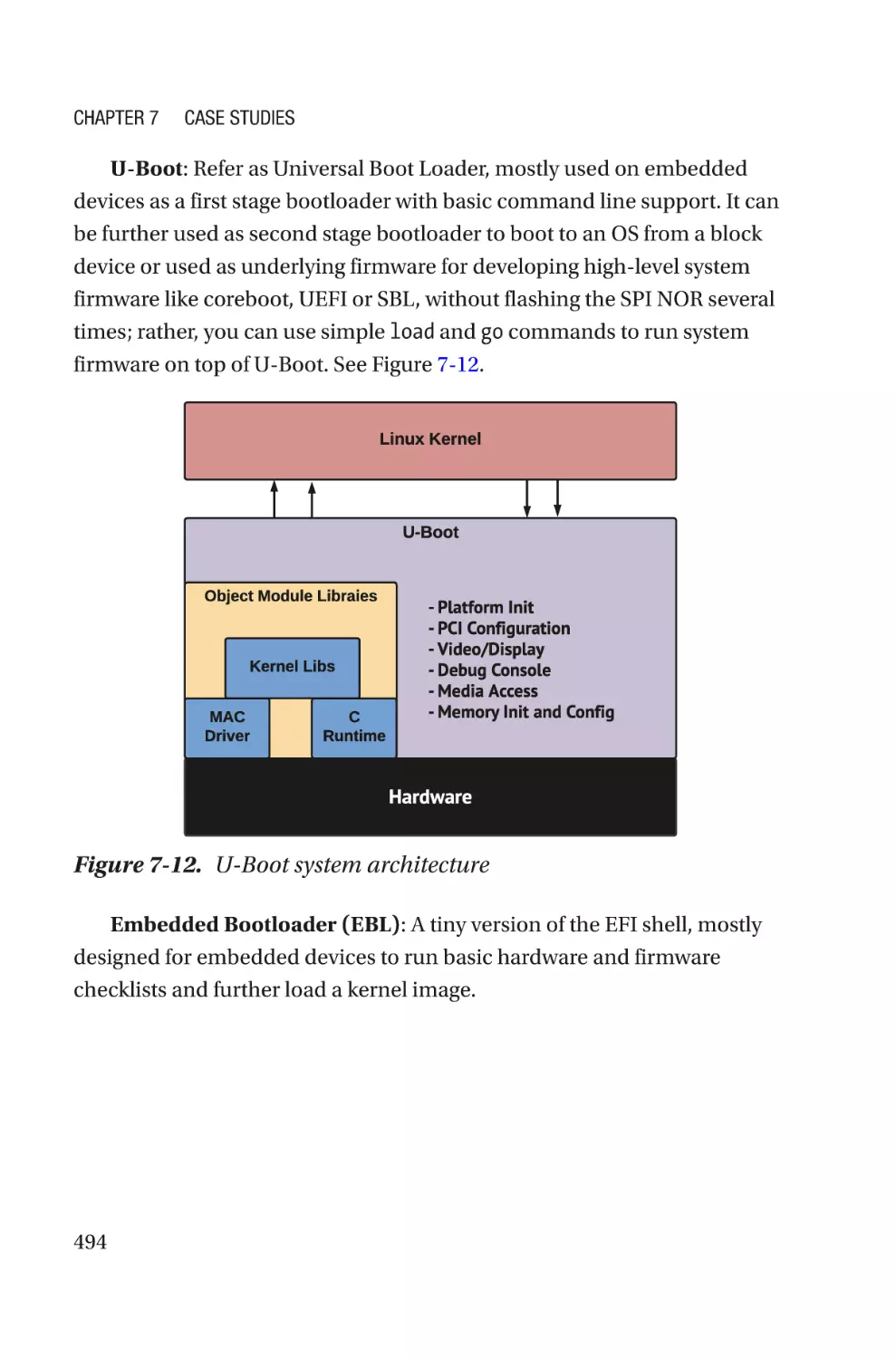
Goal and Motivation�������������������������������������������������������������������������������������497
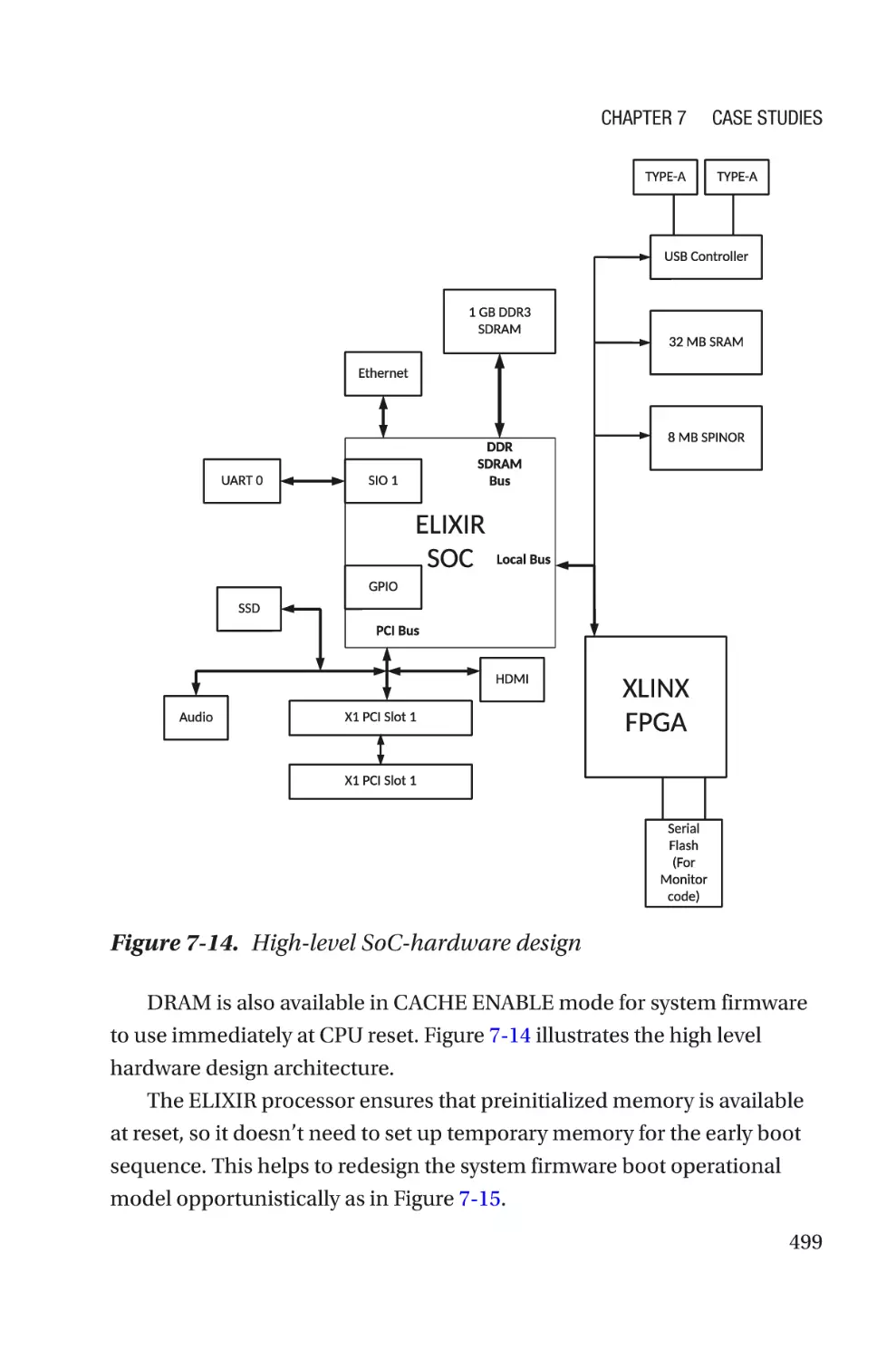
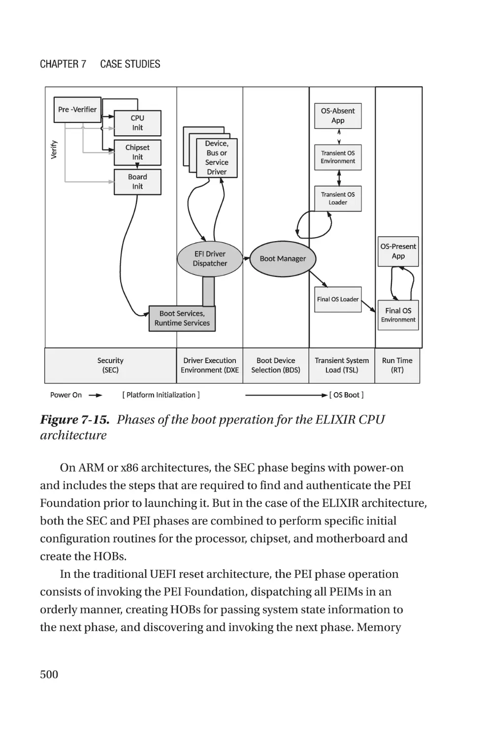
Implementation Schema�����������������������������������������������������������������������������498
Setting Up the Code Base����������������������������������������������������������������������������502
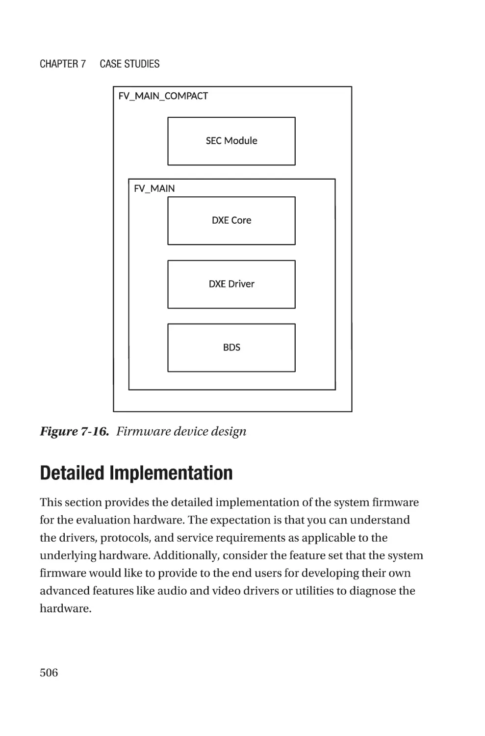
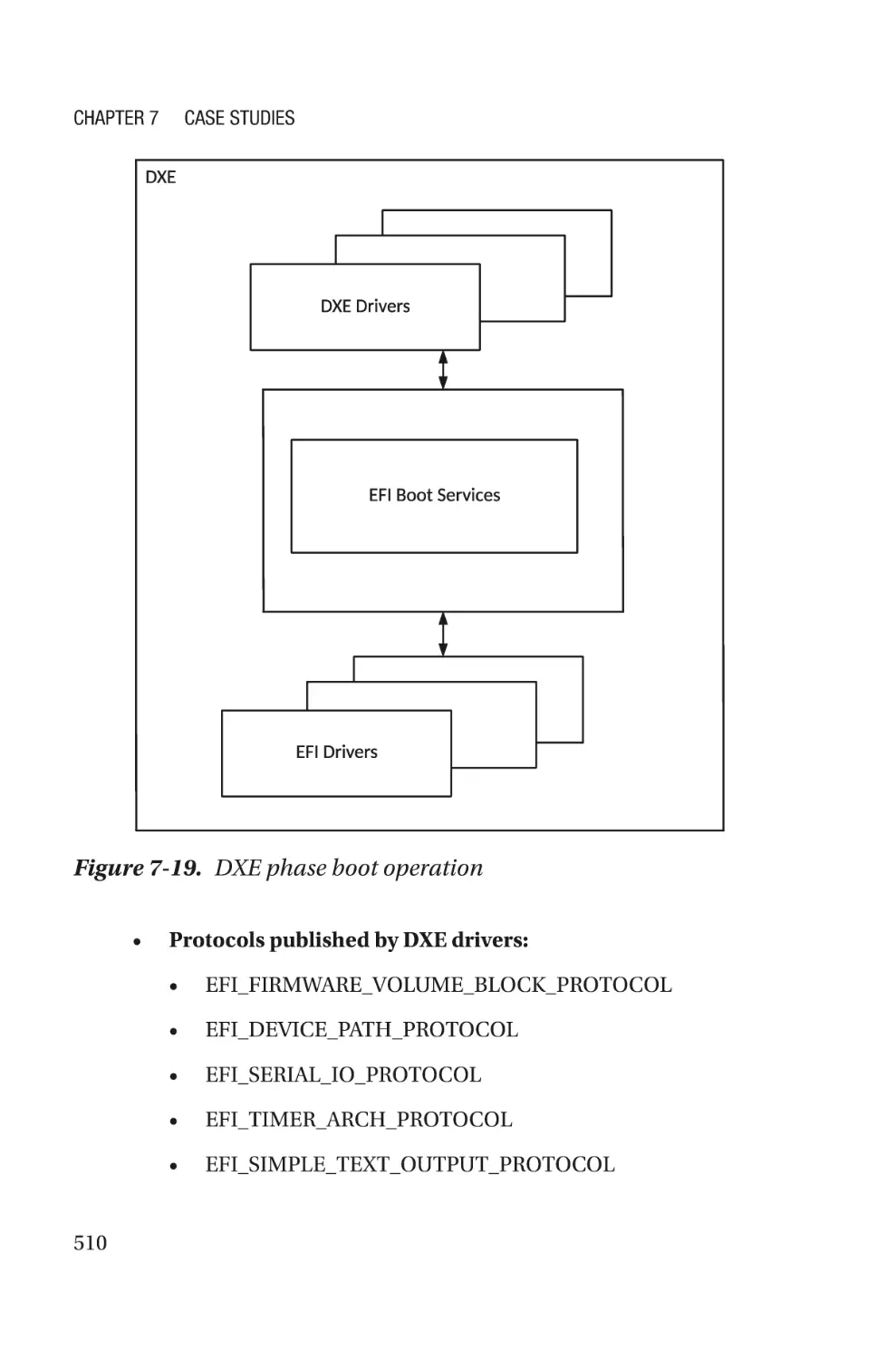
Detailed Implementation�����������������������������������������������������������������������������506
Porting a New CPU Architecture (Elixir) Conclusion�������������������������������������517
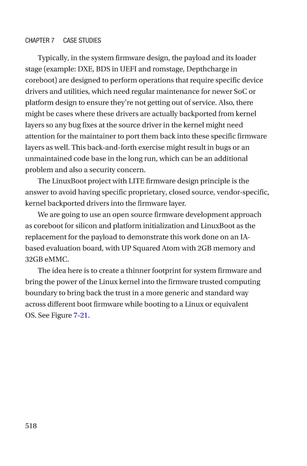
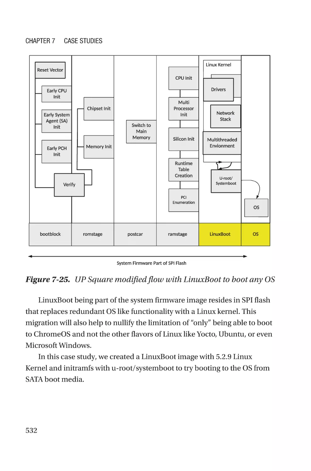
Reducing the System Firmware Boundary with LinuxBoot�������������������������������517
Goal and Motivation�������������������������������������������������������������������������������������522
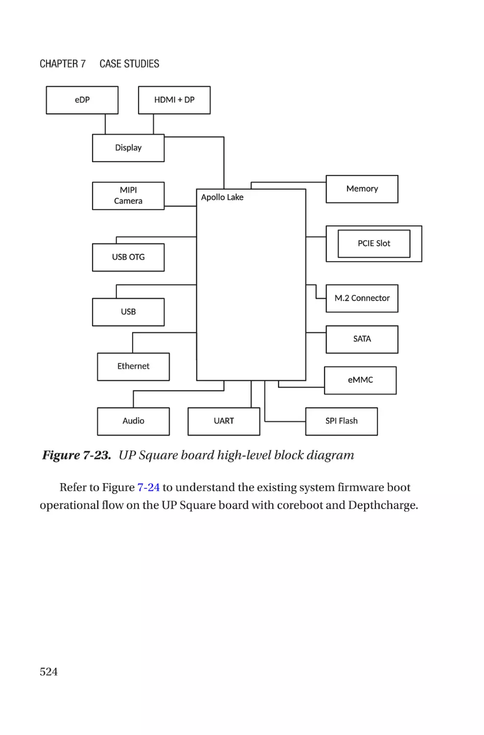
Implementation Schema�����������������������������������������������������������������������������523
Setting Up the Board�����������������������������������������������������������������������������������527
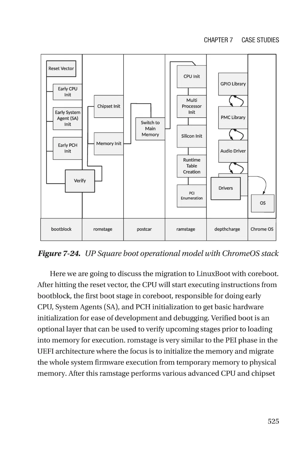
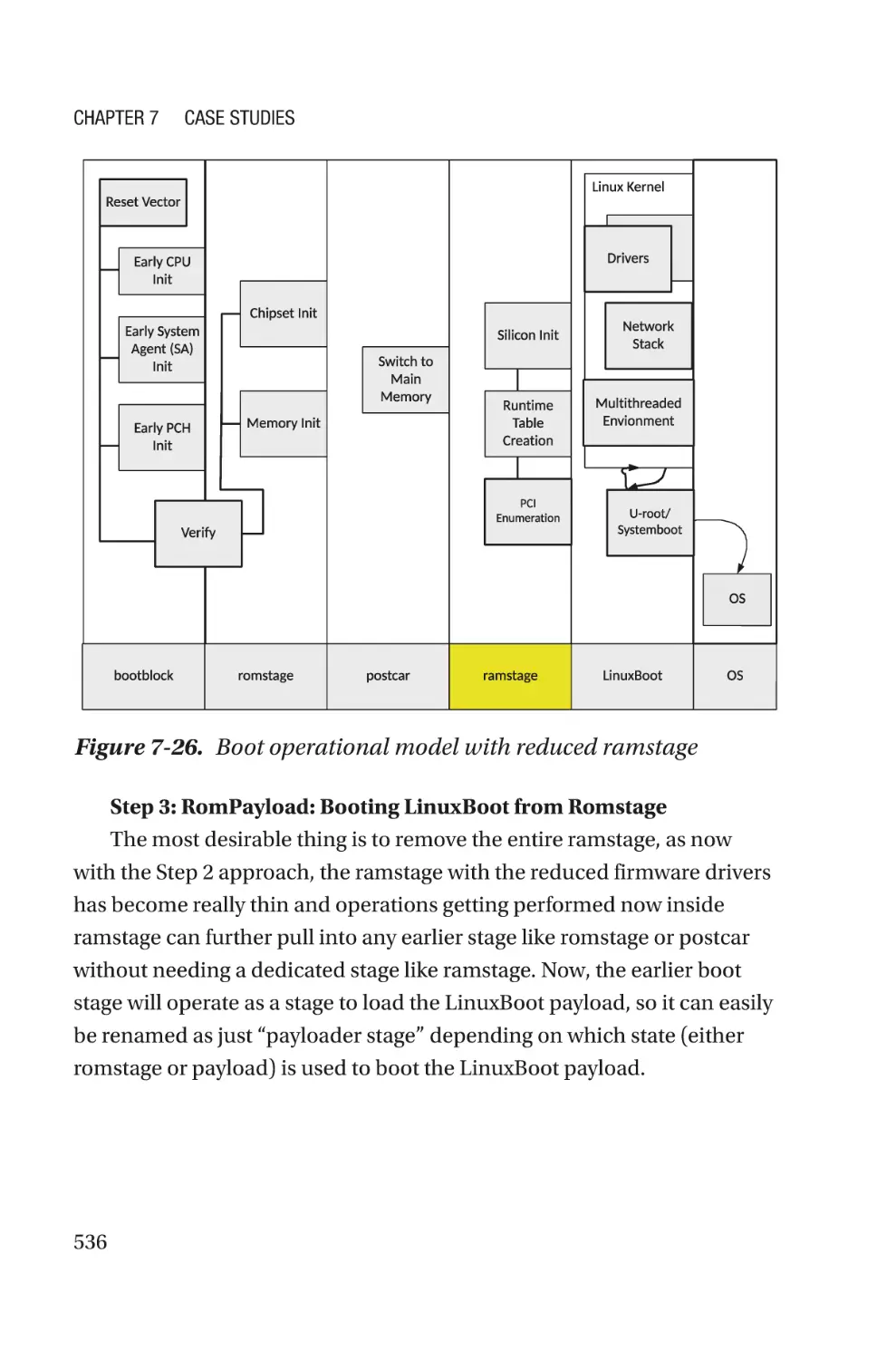
Detailed Implementation�����������������������������������������������������������������������������531
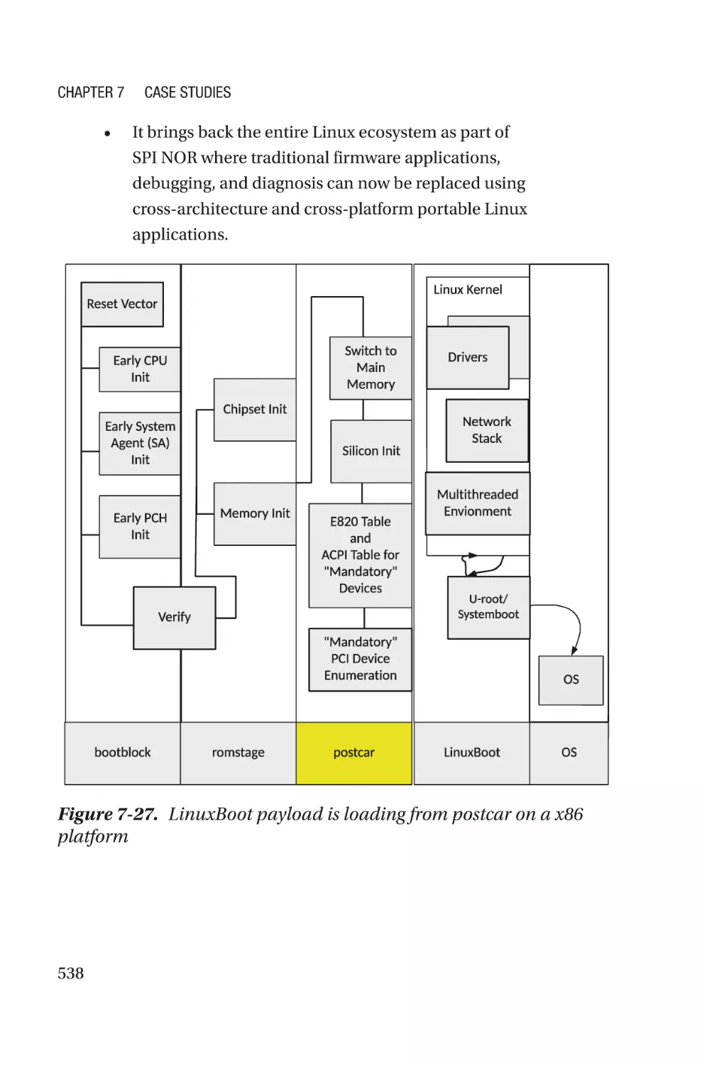
LinuxBoot Conclusion����������������������������������������������������������������������������������539
Adopting a Hybrid Firmware Development Model��������������������������������������������539
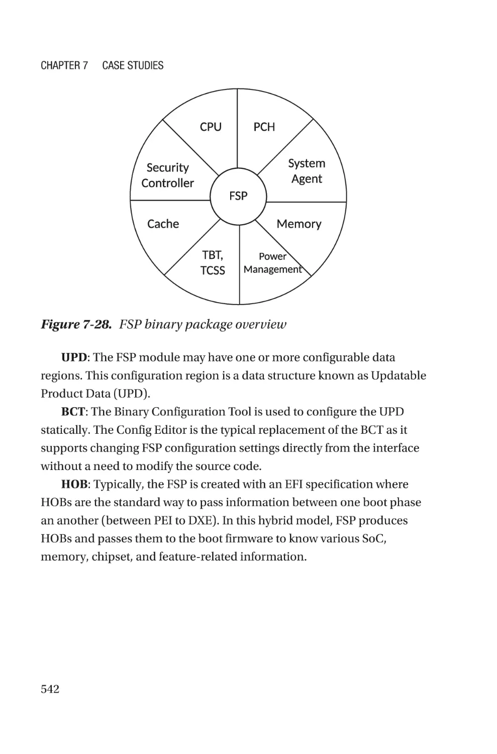
Goal and Motivation�������������������������������������������������������������������������������������543
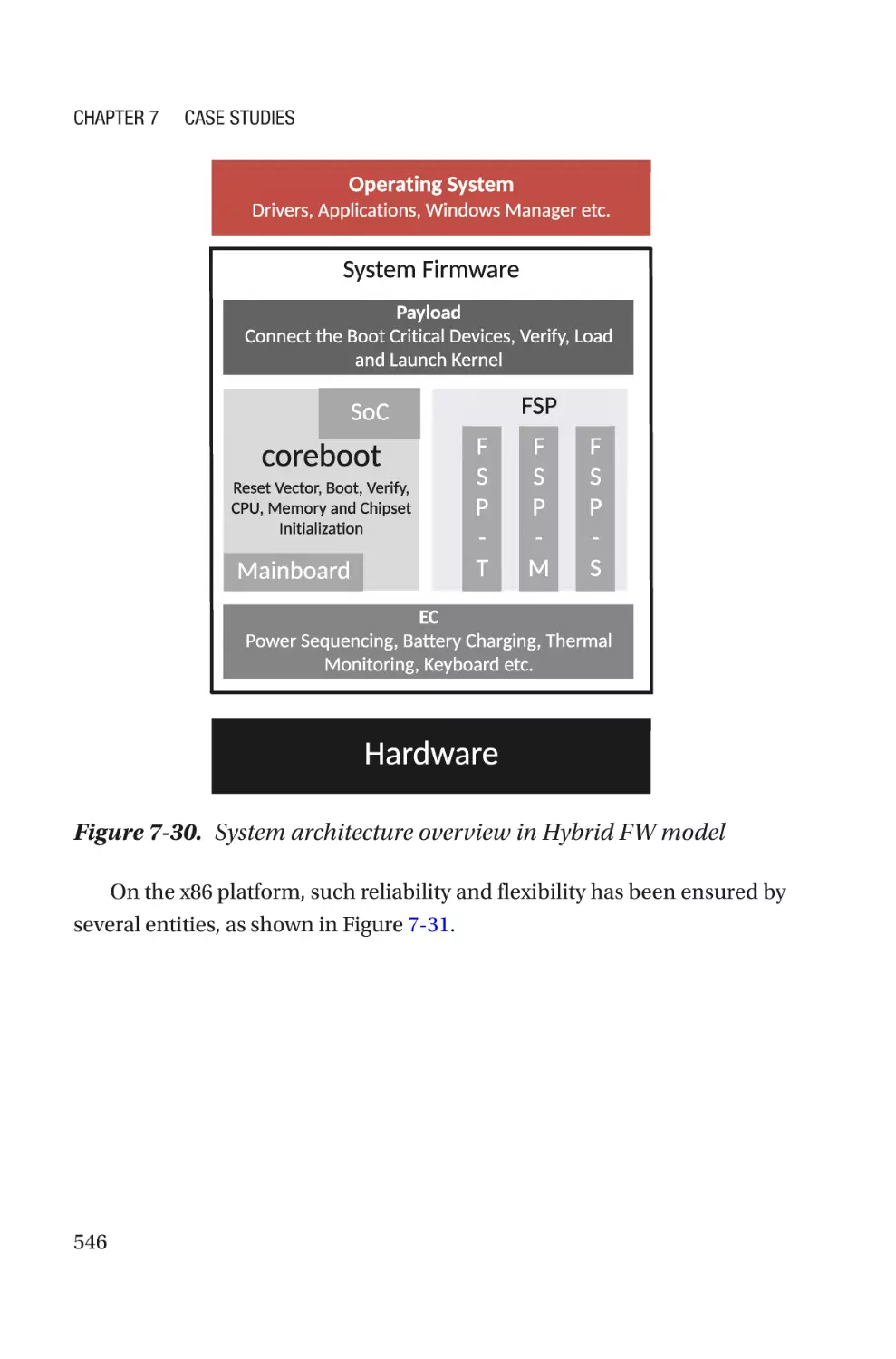
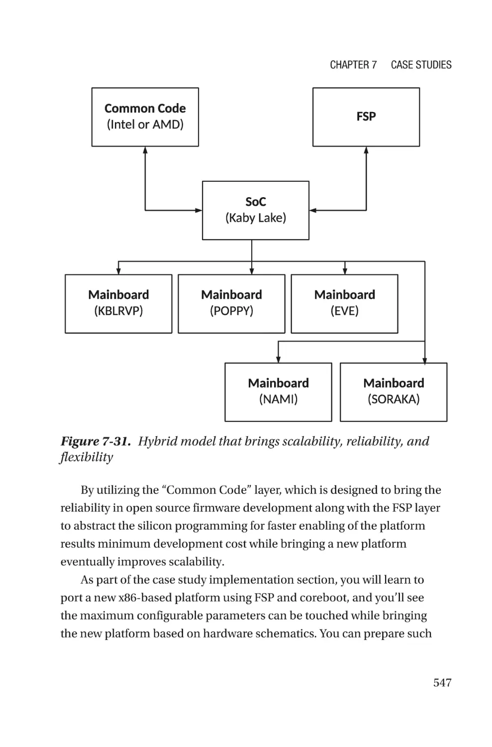
Implementation Schema�����������������������������������������������������������������������������543
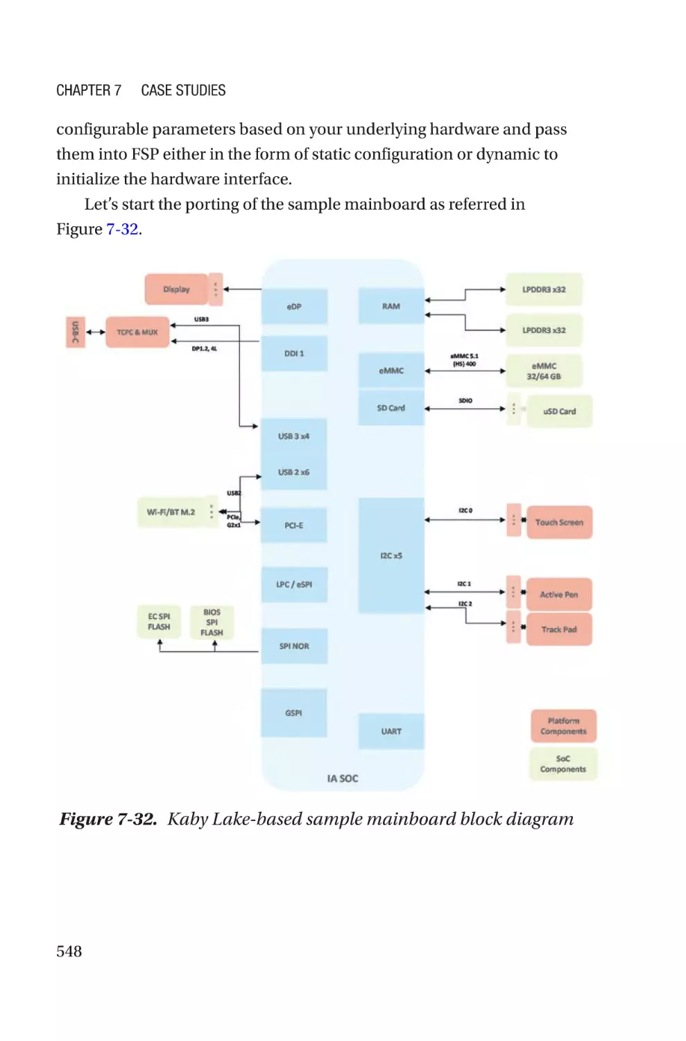
Setting Up the Board�����������������������������������������������������������������������������������550
Detailed Implementation�����������������������������������������������������������������������������554
Hybrid Firmware Development Model Conclusion���������������������������������������577
Summary����������������������������������������������������������������������������������������������������������577
viii
Table of Contents
Appendix A: Postcodes���������������������������������������������������������������������579
Appendix B: Data Types��������������������������������������������������������������������585
Glossary��������������������������������������������������������������������������������������������589
Reference������������������������������������������������������������������������������������������595
W
ebsites�����������������������������������������������������������������������������������������������������������595
References for the Chapter 1����������������������������������������������������������������������������598
Books�����������������������������������������������������������������������������������������������������������598
Conferences, Journals, and Papers�������������������������������������������������������������598
Specifications and Guidelines���������������������������������������������������������������������599
W
ebsites�����������������������������������������������������������������������������������������������������������599
References for Chapter 5����������������������������������������������������������������������������������601
Index�������������������������������������������������������������������������������������������������603
ix
About the Authors
Subrata Banik is a firmware engineer with
more than a decade in the computer industry.
He has acquired experience in system
firmware design, development, and debugging
across various firmware architectures like
UEFI, coreboot, and Slim Bootloader for x86
and ARM platforms. Subrata has profound
experience with platform enablement, which
had led to working on all leading PC makers’
products. Subrata is an active member of
open-source firmware (OSF) development
across different projects like coreboot, oreboot,
flashrom, and EDKII, where he is one of the leading contributors in open
firmware (coreboot) development. Subrata has received multiple US
patents and is very passionate about learning new technology and sharing
knowledge among enthusiast engineers. Subrata has presented technical
talks at industry events such as the Open Source Firmware conference,
Institute for Security and Technology, and Intel Developer Forum.
When not writing or working, he enjoys watching sports (especially
football) or spending time with his daughter. A fun fact about Subrata is he
is a strong believer in time travel.
You can chat with Subrata on Twitter at @abarjodi or at www.linkedin.
com/in/subrata-banik-268b3317/.
xi
About the Authors
Vincent Zimmer has been working on
embedded firmware for the last 30 years.
Vincent has contributed to or created firmware
spanning various firmware initiatives,
including the Extensible Firmware Interface,
where Vincent presently leads the Security
subteam in the UEFI Forum. Vincent has
co-authored various papers and books. He is
also a co-inventor on over 450 US patents.
xii
About the Technical Reviewers
Stefan Reinauer is a Staff Engineer in the
ChromeOS Group at Google Inc. He has been
working on open source firmware solutions
ever since he started the OpenBIOS project in
1997. He joined the LinuxBIOS project in 1999
and worked on the first x64 port for LinuxBIOS
in 2003. In 2005, Stefan founded coresystems
GmbH, the first company to ever provide
commercial support and development around
the coreboot project, working on ports to new chipsets and mainboards.
In 2008, Stefan took over maintainership of the LinuxBIOS project and
renamed it as coreboot. He was the original implementer of the project's
ACPI and SMM implementations. Since 2010, Stefan has lead the coreboot
efforts at Google and contributed significantly to what is the largest
coreboot deployment in the history of the project. He currently lives in the
San Francisco Bay area.
Zhixiong (Jonathan) Zhang has been working
on system software and firmware for the last
20 years. Jonathan is passionate at achieving
computer system solutions (such as CXL
memory solution) through holistic designs of
software/hardware, and of various software
components. He is thrilled at collaborating
with industry colleagues to form visions, and
make them into reality.
xiii
About the Technical Reviewers
Jonathan has been spearheading coreboot/LinuxBoot development
for servers based on Intel Xeon server processors, through multiple
generations from ground up. He initiated and has been leading an industry
coalition on this journey. Prior to Meta, he led UEFI/ATF development for
ARM servers and made it commercially viable from the ground up; he also
led UEFI and windows/Linux driver development for smart phones.
Jonathan is a frequent speaker on firmware/software topics at industry
conferences. He is an active participant of several industry standard
organizations (such as CXL forum, OCP, UEFI forum) and made a number
of specification changes.
xiv
Foreword by Jonathan Zhang
This book contains key aspects of an evolution that is about to happen for
system firmware (a.k.a. the BIOS). The last similar scale change in system
firmware happened in the late 90s, from BIOS to UEFI. While the birth
of the BIOS (e.g., the separation of system firmware from the operating
system) in the 70s led to the era of the PC, UEFI laid a solid foundation for
the success of computer desktops and servers, which is the foundation of
the modern Internet world.
Now, with the Internet moving toward cloud services and artificial
intelligence, will the innovation of UEFI continue to meet needs or will
there be an evolution in system firmware?
Thomas Khun described in his book The Structure of Science
Revolutions the concepts of paradigms and revolutions. These concepts
apply not only to scientific research but also to the computer industry. We
normally operate in a paradigm. A well-established paradigm is very useful
and powerful, and thus we tend to neglect stuff outside of the paradigm.
As time goes by, the anomalies pile up and then a paradigm shift happens,
which is called a revolution.
In the world of system firmware, the transition from BIOS to UEFI was
a revolution. Now the transition from UEFI to OSF (open system firmware)
will be another revolution. Even though there are several variants, a typical
OSF stack includes following components:
•
Silicon initialization binary. The silicon vendor
owns this.
•
coreboot. It does platform initialization. It adopts the
Linux kernel design philosophy and it has a Linux
kernel style development community/process.
xv
Foreword by Jonathan Zhang
•
LinuxBoot. As the bootloader, its main responsibility
is to find the target kernel/OS and jump-start it.
LinuxBoot has the Linux kernel as-is, and u-root as its
initramfs.
UEFI, as the current paradigm, is
•
Deployed in the majority of servers
•
Supported by most modern operating systems
•
Worked on by the majority of the system firmware
community
One anomaly is the shift to cloud computing. Hyperscalers need to
manage servers at scale, and in the meantime they often have feature
differentiation and shortened time to production (TTP) needs.
OSF allows hyperscalers to own the system firmware more easily, since
a smaller engineering team will be capable of developing and managing
it at scale, enabled by industry collaboration. With Linux playing an
instrumental role in OSF, Linux engineers are turned into system firmware
engineers, therefore system firmware can be managed at scale just like
Linux. In addition, new feature support and bug fixes in Linux can be
leveraged in system firmware directly, leading to improved stability and
reduced security vulnerability.
Another anomaly is the arrival of the computer architecture golden
age. David Patterson declared that, like the 1980s, the next decade will be
exciting for computer architects in academia and in industries. Not only
scientific research but also societal advancements (such as Web 3.0 and the
metaverse) demand exponential growth in computational power. On top of
that, the focus on computation is shifting from general purpose computing
to artificial intelligence workloads. However, Moore's Law is not supported
by chip process technological improvements alone any longer. All of these
changes require a new generation of server processors and server systems.
New technologies and design philosophies beyond the von Neumann
xvi
Foreword by Jonathan Zhang
architecture have been springing up. Other examples include heterogeneous
processor design enabled by chiplet and UCIe, and new interconnect
technologies such as CXL, to name a few. All of these new technologies
require timely development of system firmware as part of holistic solutions.
In the meantime, another event that happened in the industry was the
maturation of Linux into the de-facto standard of the OS industry. Linux
answers computer technology advancements gracefully and manages
versatility effectively. Why should we develop software for the same
technology twice–once for Linux, and another time for system firmware?
Why should we stabilize and harden software for the same technology
twice? Why should we require two vastly different skill sets for system
firmware engineers and kernel/OS engineers?
You might ask whether OSF is mature enough for prime time. This is
an important question. After all, technology alone is not good enough; we
see too many cases where a good technology does not gain traction in the
industry.
With over 10 years of technology accumulation, FSP (Firmware
Support Package) technology, as Intel’s silicon initialization binary,
matured. FSP is a Plan-Of-Record for Intel server processors, starting with
Intel’s Sapphire Rapids Scalable Processor. In addition, as part of Intel’s
OneAPI initiative, Vincent Zimmer coined Universal Scalable Firmware
(USF) architecture, which supports OSF.
On the other hand, coreboot has been shipped in hundreds of millions
of devices, notably chromebook, among other products. LinuxBoot has
been running at-scale at some of the world’s largest data centers.
Those components together, as open system firmware for servers,
have seen great progress in the last several years. In 2021, OCP (Open
Compute Project) accepted OSF for OCP DeltaLake server (based on Intel
Copper Lake Scalable Processor) and is available for the community. An
OCP community lab is being built to enable access to OCP gears, with
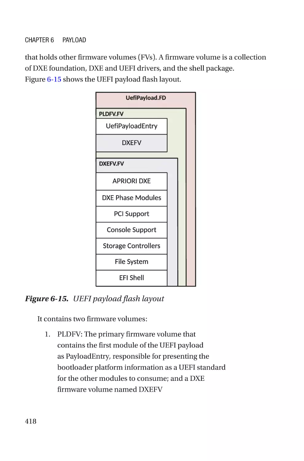
DeltaLake servers included, for the community. OSF is planned to be
deployed in production in ByteDance’s data centers.
xvii
Foreword by Jonathan Zhang
In addition to technology maturity, the OSF for servers also benefits
from a growing ecosystem and open source community. Subsequently,
a company can spend a minimum amount of resources to get OSF for
servers into production. The majority of system firmware features are
the same among the server developers, so why would they not work
together? In other words, some server developers may not want to hire 30
system firmware engineers; instead, they want to have 3 system firmware
engineers that work with partners and communities to achieve the results
traditionally done by 30 engineers.
coreboot and LinuxBoot are fully open source, and each participant
benefits from community resources for new features and bug fixes. Silicon
vendor company binary blobs are not open source (yet), but silicon vendor
companies have been allowing their customers to engineer the solutions
together. Such a new collaboration model is actually one of the key factors
that OSF for servers has been advancing at a fast pace in the last few years.
We are fortunate to have the firmware industry’s best minds to author
and review this book, to enable the industry to rethink system firmware.
Even though the groundwork has been going on for some years, the actual
paradigm shift has just begun. The benefits of such a paradigm shift to the
computer industry at large has just started to show up.
I hope you are as excited as we are to benefit from and contribute to
this paradigm shift. Some years later, once we live in a world where a new
processor (and/or technology) has system firmware support in a fraction
of the time that it takes today, where system firmware is not a black box to
owners and the computer industry at large, and where firmware engineers’
productivity has dramatically increased compared to today, we can
proudly say that we did it together!
xviii
Preface
Firmware is an essential part of any computing system, be it a device that
creates content like a personal computer, a workstation or consumer
electronics device like a smartphone, a smart home device, a wearable,
or a powerful server that stores user data. Similarly, a course on system
firmware is also an essential part of any computer-centric education for
the following reasons:
•
Firmware is capable of providing consistent behavior
across different architectures.
•
It empowers the system integrator with its flexible
nature to configure the hardware interface and also to
communicate with the operating system.
•
It is the key to optimizing the platform resources to
maximize power and performance efficiency.
•
We must try to avoid bugs or detects during product
development but providing workarounds or fixing
the bugs inside firmware is comparatively easier than
other layers because changing hardware is costly and
modifying operating systems is time consuming.
•
Firmware has the uniqueness to focus on security, both
SoC-based security and platform security.
Also, this field is undergoing rapid changes as underlying hardware
is more open now, more and more new computing devices are coming to
market to reduce redundant tasks or manual efforts, security is concern,
xix
Preface
and cost is key in product development, thus device manufacturers (ODM/
OEMs) are exploring opportunities to break the typical boundary of
developing system firmware for their products in a closed environment. In
this book, we ensure the fundamental concepts remain clear, so you can be
market ready with such a migration in technology.
We wrote this book as a text for readers like you who want to explore
the future of system firmware. The range of target audience could vary
between grade school students, to recent college graduates working
on developing firmware skill sets as per market needs, to embedded
firmware/software engineers migrating product development from
closed source firmware to open source firmware for product adaptation
needs. This book will benefit engineers working on various bootloaders
like open source firmware, UEFI, and Slim Bootloader development. As
prerequisites, we assume that you are familiar with basic programming
knowledge like assembly and C. The hardware topics required for
understanding firmware/BIOS are included in Chapter 3. For code
examples, we use predominantly C, with some pseudo code, but the idea
here is that you can still understand the code logic without a thorough
knowledge of a high-level programming language like UEFI.
The fundamental firmware design concepts covered in this book
are mostly applicable for all SoC architectures (i.e., x86, ARM, RISC-V,
etc.) with any platform design (i.e., personal computers, evaluation
boards, servers, etc.). Our aim is to present these concepts and design
principles in general without being tied to one particular architecture.
We will present a majority of examples with widely used architecture and
hardware references to make it a more real use case scenario. If a feature
or functionality doesn’t exist in all architecture and thus is specific to a SoC
architecture, we will state this explicitly.
xx
Acknowledgments
The system firmware journey from its origin to today’s modern
architecture and looking into the future is vast. It needs subject matter
experts to contribute and share their knowledge to complete this journey.
This book involved contributions from talented industry experts who we
are honored to work with, and they deserve acknowledgement.
We would like to thank Maurice Ma and Ravi P. Rangarajan for sharing
the Slim Bootloader (SBL) knowledge and architecture details as part of
Chapter 4. A special mention goes to Karthik Ramasubramanian, Shelley
Chen and Hung-Te Lin for their input on depicting the applicability of
hybrid firmware architecture on all leading SoC platforms as part of
Chapter 5.
Subrata thanks Vincent Zimmer, Ronald G. Minnich, and Stefan
Reinauer for their expertise and for making this venture enjoyable and
learnable. Above all, Subrata is thankful for his family, especially his wife,
Barnali, and daughter, Samriddhi, who were patient with many nights and
weekends consumed by this effort, and his parents, who influenced his
technical curiosity, which translated into book development.
Vincent thanks Subrata for the great collaboration on this project and
in other endeavors. Along with Subrata, he thanks collaborators across the
different communities, standards groups, and his employer.
xxi
Introduction
“The only way to be truly satisfied is to do what you believe
is great work.”
—Steve Jobs
The definition of system firmware changes over time. Typically, it starts
with no boot firmware for underlying hardware to modern computing
systems where system firmware is the product differentiator, due to the
level of optimization being put inside system firmware to allow configuring
hardware and establish the trusted communication between operating
system and hardware, and also at the same time provide electrifying
performance.
For example, the minimum expectation for an end user is to see
that the device is operational almost instantly by pressing the power
button or holding the device in hand or starting the ignition of the car
engine. Keeping the configurability of accessing underlying hardware, or
ensuring instant boot, the other key criteria for system firmware is that
it’s trustworthy. With firmware being the closest entity in system design,
it's easy to affect the hardware functionality and make it compromised. A
compromised system firmware is an ultimate risk for the entire system,
regardless of how secure the operating system may be. In the history of
system firmware or the boot firmware evolution process, only a small
group of people understand the background scene prior to booting to the
operating system.
CPU vendors were using a closed and controlled environment to make
sure that the platform bringing up the activity could be managed by those
key people, rather than opening such knowledge in a wider manner.
xxiii
Introduction
The downside of this closed-group-enabling model is that the entire
system firmware enabling and boot firmware development process
became a “secret art” where, willingly or unwillingly, the device
manufacturers had to reach such closed groups for their platform bring-up
activity. Eventually this resulted in several key issues:
•
ODM/OEMs had no control on their platform design
and had to rely on a third party to bring up their
platform.
•
CPU or SoC vendors “only” trusted a selective third
party for sharing the key knowledge to bring up their
processors or chipset.
•
They were unable to optimize the Bill of Material
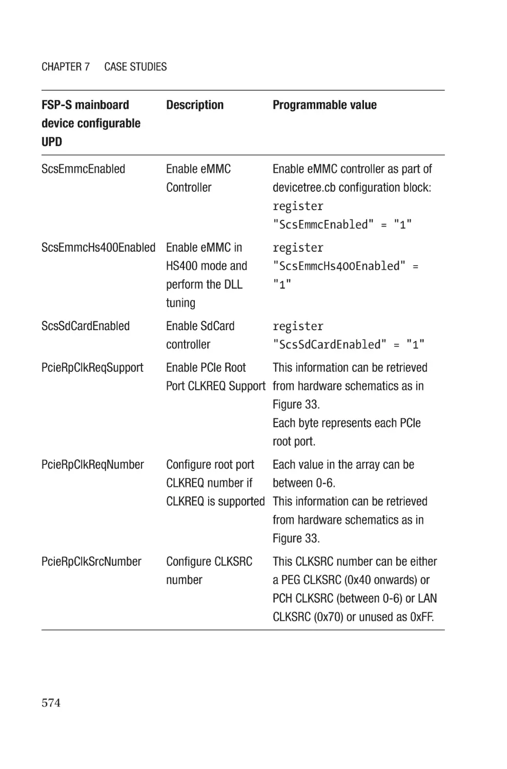
(BoM) cost, as a result of being dependent on thirdparty system firmware vendors, and they were unable
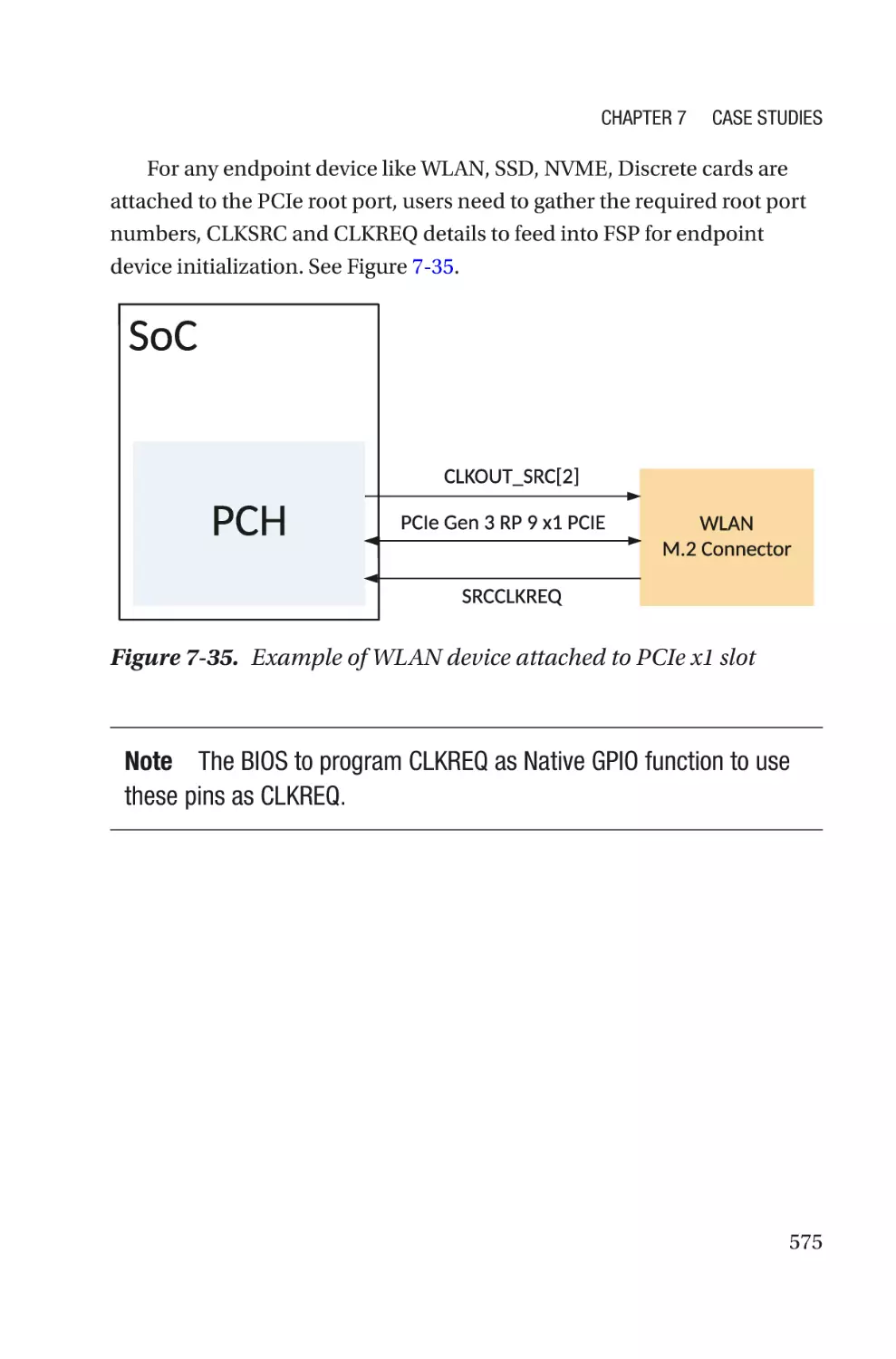
to utilize engineering resources on the ODM/OEM side
due to limited knowledge of the high-level proprietary
closed source system firmware.
•
They were unaware of SoC and/or platform security
because of third-party involvement and they had no
means to review the boot firmware code due to its
closed source nature.
To find an amicable way out here, the market looked for a transition
to a simpler, robust, transparency-enabling model of system firmware.
It's not possible for SoC vendors to still be able to control the platform
enabling model. In the present situation, there is more interest in knowing
what's happening behind the curtain of booting to the operating system to
define a transparent process in order to build a trustworthy system. There
is interest in knowing how to optimize the boot firmware flow, reduce its
boundaries, and make it more scalable for the operating system to leverage
xxiv
Introduction
the privileged mode that the system firmware belongs to while talking
to the hardware. This process might help to reduce the system boot time
requirement for exclusive hardware/firmware-centric communication.
This is quite an attractive period for system firmware developers
and companies who want to migrate their firmware development from
a closed source solution to open source, to minimize their development
costs, to bring transparency into product development process, and at the
same time, to ensure time to market for their new products. Therefore,
the key part here is choosing the right firmware solution as per their
product needs.
This introduction explains the general challenge of system firmware
migration and also describes what you can expect in the remainder of
this book.
Migration to Open Source System Firmware
The term migration is being used in this book to refer to the transition
of the existing firmware development model from closed source to open
source, or to adopt the open source firmware development model for the
new product development cycle.
This migration is not limited to porting the firmware alone; it’s also
an ecosystem change. For example, the program source code—whether
implemented based on closed source firmware or open source firmware—
is written with the capability of underlying hardware in mind. Therefore,
it is very important to keep in mind the required hardware capability to
develop the system firmware using an open source model is also expected
to be available to support this migration.
The repository to maintain the source code is also important to ensure
the real open source visibility, and to provide an opportunity for the
open source community to review the source code rather than limiting
the firmware development among few companies through peer review.
xxv
Introduction
Finally, there is the build infrastructure that is being used to stitch other
firmware ingredients (as applicable) with SoC architecture to qualify as
an integrated firmware image (IFWI). Typically, different SoC vendors use
their proprietary stitching tool for customization of IFWI ingredients as
per the product requirement. But for migration to open source firmware
development, it's expected to have a unified open source-friendly tool to
meet such requirements.
The important part in this whole open source migration is the system
firmware code development model. Over time, the platform-enabling
strategy has gone through a rapid transition. Even a few years back, SoC
vendors and device manufacturers were only considering a single entity
for boot firmware, typically Unified Extensible Firmware Interface (UEFI).
With an open source firmware development model, where more than one
entity is combined together to call it as system firmware, this assumption
won’t hold. At a high level, open source system firmware may consist of
two major components : boot firmware and payload.
There are several open source boot firmware options available to
perform the CPU and chipset initialization. Based on the nature of the
product and applicable market segment, device manufacturers choose the
right boot firmware. It might also be possible that boot firmware itself may
consist of several other associated firmware binaries that are restricted in
nature and not necessarily available in open source due to SoC vendors or
device manufacturer product requirements. This model is referred to as
hybrid and there are sections to explain the work model to support such
needs as well.
A boot firmware also needs to have a dedicated payload (typically, it
doesn’t have a payload integrated into it by default) to detect a special boot
signature to boot to the kernel from possible boot media. A payload can be
defined as another boot firmware, but in a generic manner, it doesn’t need
to perform specific CPU or chipset programming and is more architecture
neutral and platform independent. The major task for a payload is to
xxvi
Introduction
ensure booting to the operating system. Therefore, it’s preferable to have
a configurable option with boot firmware to choose the payload as per the
target operating system need.
Motivation for This Book
The PC industry is going through a transition where the typical device
manufacturers are willing to design their products in a more transparent
manner. There is significant interest in understanding the secretive
art behind booting to the operating system. This book highlights the
underlying ecosystem changes. It also makes system integrators aware of
the common challenges while migrating from a well-defined process to a
new, evolving, open source-based firmware development, to maintain or
improve the product quality and also to meet the time to market.
First, it’s important to understand the legacy of the system firmware—
its origin, architecture overview, and the reason why real-world firmware
development is expecting this migration—with case studies. Additionally,
this book provides an architectural overview of various popular boot
firmware options. Types of firmware discussed will include both closed
source and open source in nature, such as UEFI, coreboot, and Slim
Bootloader as well as their applicable market segments based on product
development and deployment requirements.
This book represents the journey of system firmware from its origin
to now. Also, it captures the evolution of system firmware from complex
and closed source to the modern firmware where it is still a hybrid
between closed and open source. Finally, it attempts to predict the market
transition about the future firmware model. This book tries to find the
most simplistic boot firmware solution, using the open source firmware
development. We deliver this information as a handbook to you so that you
know how to choose the right boot firmware for your products and develop
your own boot firmware using open source.
xxvii
Introduction
Who Is This Book For?
This book covers embedded system and firmware programming models.
Readers are expected to be comfortable with low-level programming
languages such as assembly and C. A few topics will require specific
knowledge of UEFI.
As this book will focus on open source firmware developments, the
target audience could vary between students interested in STEM topics,
to recent college graduates working on developing skill sets as per market
needs, to embedded firmware/software engineers migrating product
development from closed source firmware to open source firmware for
product adaptation needs.
Also, this book could be useful for engineers working in open source
firmware development. A few sections will require specific domain
knowledge like UEFI, as silicon vendors might be keen on using hybrid
work models.
You will learn the following while reading this book:
•
A comprehensive architecture overview of all market
standard and popular boot firmware (a.k.a. the BIOS,
the basic input and output system)
•
How to pick the correct BIOS for the required target
hardware
•
How to design a hybrid workflow model for the latest
chipset platform
•
Understanding various popular payload architectures
and offerings for embedded systems
•
xxviii
Picking the right payload for the boot firmware
solution to boot to the operating system
Introduction
•
Various case studies done on embedded systems
with different CPU architectures: x86 and ARM-based
solutions to optimize the system firmware boot time,
demonstrating the power of hardware innovation that
influences firmware design, usage of kernel features
in firmware trusted computing boundaries, and
understanding the product development cycle using
open source firmware development
O
verview
In general, this book is built with an assumption that you are reading
the chapters in sequence. Each chapter builds on a knowledge block
gained from earlier chapters. As the book progresses, you will apply this
knowledge.
Chapters can be divided into two categories: developing concepts and
applications. In concept chapters, you will learn about various aspects
such as hardware knowledge required prior to any system firmware
development, designing a minimal system firmware, and understanding
various different system firmware architectures and payloads. In the
application chapters, you’ll build a few applications using what you’ve
learned from the concepts chapters.
Starter: Chapter 1 provides the historical introduction about the boot
firmware and different solutions available like closed source boot firmware
and open source boot firmware. We will define the goals for you to create
your own open source boot firmware for target hardware.
Knowing your hardware: Chapter 2 provides a detailed understanding
of hardware interfaces that firmware needs to manage prior to booting to
an operating system. This is a very basic understanding section for system
boot firmware without which you really can’t make progress on your
system firmware journey.
xxix
Introduction
Understanding the BIOS and its minimalistic design: Chapter 3
provides details about the BIOS. It explains the basic characteristics that a
firmware has to have to call it a BIOS, as well as the minimum requirement
to design a boot firmware.
System firmware architecture: Chapter 4 provides architectural
details about popular or market leading system firmware along with
applicable market segments because of their characteristics. The idea here
is to understand the pros and cons of each offering.
Hybrid firmware architecture: Chapter 5 explains the ecosystem
balance with open source firmware development using minimum closed
source blobs. Open source boot firmware development has an enormous
dependency on SoC vendors for providing the documentation and
reference code for CPU, memory, and chipset initialization. This chapter
defines the hybrid firmware architecture, which is useful to build open
source firmware solutions when working with closed or restricted SoC
hardware platforms.
Payload: Chapter 6 explains the necessity of the payload for the boot
firmware. It provides architecture details of all popular payloads and
current offerings to help users to choose the correct payload for their
product.
Case studies: Chapter 7 covers a case study done on real hardware.
This real-life example will help you think through innovation while
designing your own open source boot firmware.
The Appendices include source code data types based on Chapter 7
and system firmware postcodes details. The Glossary and Index connect
back to the main topics.
xxx
CHAPTER 1
Introduction
“The beginning is always today.”
—Mary Wollstonecraft Shelley
A journey in life teaches us that the most important aspect of a journey
itself is not just reaching the destination, but rather ascribing importance
to the experience gathered during the journey. This book is written to
take readers through the amazing journey of firmware from its origin to
today, demonstrating its firmness even on modern electronic devices and
finally utilizing this opportunity to develop a specialized knowledge about
different types of firmware. In the history of computer architecture and
its evolution, the most underrated subject is firmware. The existence of
firmware is not known to end users. If any end user ever saw the firmware
screen, it was probably an awful day. Something might have been wrong
on the hardware side, so the end user started exploring the way to fix it and
“Here I come,” said the tiny firmware, which resides deep in the hardware.
The standard academic curriculum for the next set of engineers
silently ignores the importance of firmware. This creates an imbalance in
the embedded device ecosystem where recent college graduates are well
equipped with hardware knowledge (like transistors, microcontrollers, and
even microprocessors) and software knowledge (like a deep understanding
of application software, kernel operating model, artificial intelligence, and
machine learning) but are ignorant of an important piece in the jigsaw
puzzle: firmware. It’s a layer that stays closer to the hardware and brings it
© Subrata Banik and Vincent Zimmer 2022
S. Banik and V. Zimmer, System Firmware,
https://doi.org/10.1007/978-1-4842-7939-7_1
1
Chapter 1
Introduction
to life. It provides an easy interface to apply patches without any additional
cost of replacing or rebuilding the hardware. It’s also empowered enough to
orchestrate the entire platform to the operating system in a more abstract
manner to maintain the generic nature of operating systems. In the last two
decades, significant technological advancements in the embedded device
market have impacted our regular lifestyle, socio-economic status, and
more. These changes include the following examples: mobile phones are
no longer a luxury device (once limited to people who could afford them
20 years ago) and have rather become a necessity today as the definition
of entertainment has changed from limited shows airing on television
to unlimited content over global digital platforms readily available for
consumption via smart devices; popular video games are now equipped
with virtual reality to track the user’s motion and enable a real-world
gaming experience; personal computers are now within most everyone’s
affordability with reduced storage (memory and disk) and lower cost; the
pandemic added another dimension by necessitating digital education
for kids and demanding more powerful computing devices for work-fromhome experiences; and due to affordable and speedy internet services, new
internet users are growing rapidly. A recent study suggests that the global
embedded device market has seen a rapid revenue growth of ~$100 billion
in just the last six years. Applying Moore’s Law into it with the predictive
advancement of semiconductors, this eventually results in higher demand
for embedded systems and can easily predict the growth.
The alarming thing for the industry is that even though the demand
for embedded devices is increasing, the number of firmware engineers
has not. Over time, this might result in an imbalance where the embedded
firmware world won’t see fresh, incoming, talented engineers striving to
be part of this industry. Today, most computer system college graduates
are not even aware of the existence of the firmware world unless someone
explicitly mentions it. In the study of computer science and engineering,
the knowledge about firmware can be metaphorically presented as
the famous Platform 9¾ in J.K. Rowling’s novels. The whole world of
2
Chapter 1
Introduction
embedded firmware remains cloaked between the hardware and the
operating system and is secretly maintained by a privileged group hidden
from normal users’ eyes. Due to the rapid growth of the Internet of Things
in the last decade, there is a rise in the number of devices that need
firmware to become operational and to fulfill end users’ needs, such as
voice assistance, smart locks, and more. With the more complicated silicon
and sophisticated hardware designs, the underlying firmware that is
responsible to bring the platform to life is getting more complex over time.
Modern firmware development expects efficient system programming
knowledge to implement solutions, even considering the space and time
constraints. The non-volatile storage for keeping the firmware is limited,
so an optimal implementation is required to ensure platform enabling in
a time-efficient manner where the pressing of the power button starts the
device immediately or opening the laptop lid is enough to see the user
login without any forced delay in response.
Without any actionable improvement plan in place, there is no way
the current situation can be improved with time. The current embedded
industry needs to challenge the present education system and demand
more focused and practical education that will help to improve the quality
and also produce more ready engineers, those who are able to understand
the different firmware architecture, choose the right solution from the
lists of current offerings, or innovate one while designing and developing
firmware for embedded systems. This chapter presents some insights into
why traditional education of computer systems might have out-scoped the
importance of firmware study.
Lack of Open System Design
Since the origin of the computer, the separation between hardware and
software was not well known. Initially, the PC companies focused on
providing the complete solution, so the hardware and software layers were
3
Chapter 1
Introduction
very tightly coupled. Over time, this model started to become a bottleneck
for innovation in the hardware space (Refer to the “Origin of the Firmware”
section of this chapter). The open system design concept introduced
later in the computer evolution defines the layer approach in embedded
systems. Having a dedicated layer decoupled from the operating system
that touches the hardware eventually led to designing the operating system
more generically and in a hardware-neutral fashion. In this model, the
layer that touches the bare metal hardware stays close to the hardware
itself and allows for the opportunity to grow over time to support all future
hardware needs.
Due to the lack of open system design concepts, any study of
embedded devices today by default assumes a tightly coupled system
design, where a bunch of low-level device drivers are capable of providing
for the system programming. Unfortunately, that is not the case for most
embedded devices available today.
Misinterpretation of Firmware Definition
The most popular definition of firmware is found in IEEE 610.12-1990 and
it says “the combination of hardware device and computer instructions
and data that reside as read-only software on that device.” This definition
is largely correct for the early generations of electronic devices where
the users of the devices were limited (which translate into limited use-
case enablement), with minimum hardware components attached to
the motherboard, a simplistic microprocessor design, limited memory
designed to have fixed operations, when security was not a prevailing
concern, and when firmware updates and resilience requirements were
not even known to the industry at that time.
The scope of firmware in modern embedded devices is very broad.
The fundamental platform of stability and security relies heavily on
the trustworthiness of the firmware layer. The tiny and read-only terms
4
Chapter 1
Introduction
are often misleading when defining the actual scope of firmware in an
embedded system today.
A better definition of firmware that depicts its relevance in the
embedded system is as follows:
“Firmware: An essential piece of code that is responsible for performing
the underlying hardware initialization prior to handing over to the
operating system.”
A study of the embedded system and computer architecture wouldn’t
have ignored the value of an entity that is categorized as essential or
specialized knowledge in the academic world.
Facts NIST (National Institute of Standards and Technology) takes
a special interest in the platform (the collection of hardware and
firmware components of a computer system) firmware and publishes
resiliency guidelines that help organizations to better prepare against
potentially destructive security attacks, detect authorized changes,
and ensure secure recovery from attacks.
Additionally, this chapter will show possible path findings and share
an actionable improvement plan to support the growing embedded system
market needed to bring more quality to embedded firmware.
A
ttract the Talent
The best way to prevent firmware being a lost art in the future is by
attracting talented engineers who have a passion for contributing to
this embedded space. The best class of engineers are always looking
for specialization and advancement that not only helps to build their
resumes but also satisfies a craving for knowledge. Interest in cutting-edge
technologies related to the fields of artificial intelligence (AI), machine
5
Chapter 1
Introduction
learning (ML), and data science are well expected. It’s also important to
highlight that the value of studying embedded systems and firmware is
still relevant in modern times. The embedded system programming skill is
considered a top-10 high-paying job in the field of computers.
It is interesting to learn the history of how firmware has maintained
being value neutral to the end user over the last several decades since
its origin. It’s important for firmware engineers to keep it that way, as it
can become value negative when firmware is difficult to use, has security
issues, or isn’t performant. The inability to patch firmware on a system
with bug fixes or try to optimize the code, where the direct end user or
intermediate platform builder, fosters the potential for the space of closed
firmware to become ‘value negative.’ It can become value positive when
users are very concerned about firmware and often rely on the firmware
solutions. Over-dependency on firmware is also not a good indicator. Thus,
it’s an art to maintain the value of firmware in a platform that is close to
zero. To achieve this trend consistently in millions of devices year over year
definitely requires smart, focused, and talented engineers to get motivated
enough to accept and excel in the embedded firmware world.
The Importance of Programming Knowledge
The simplest way to represent the firmware is as a code block that is
responsible for setting or resetting a bunch of hardware registers. Over
time, this demand has evolved with additional requirements of being
optimized and efficient in operation. For example, a good firmware
programmer pays attention to not only setting or resetting a register bit but
also how optimally this operation can be done.
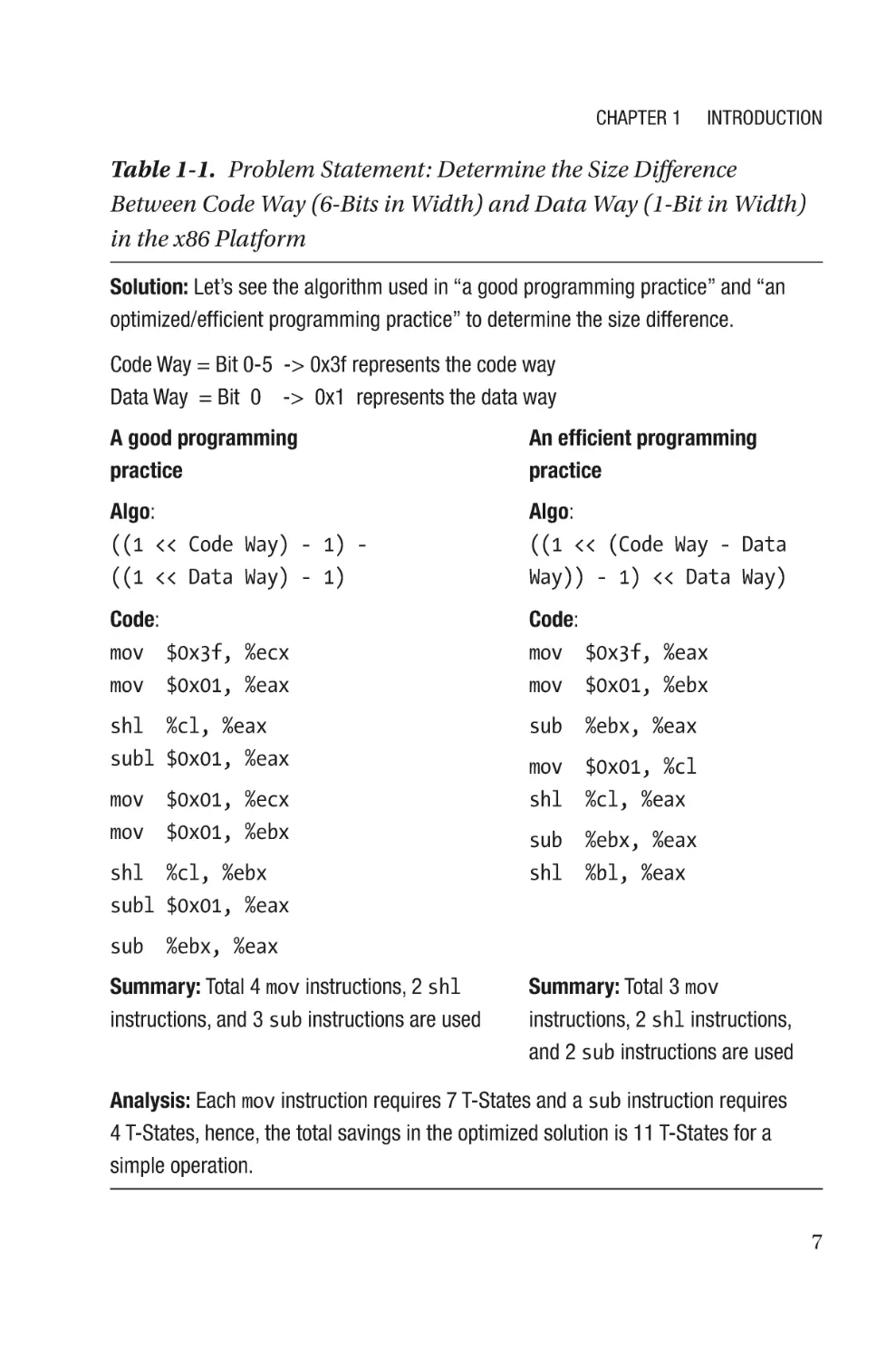
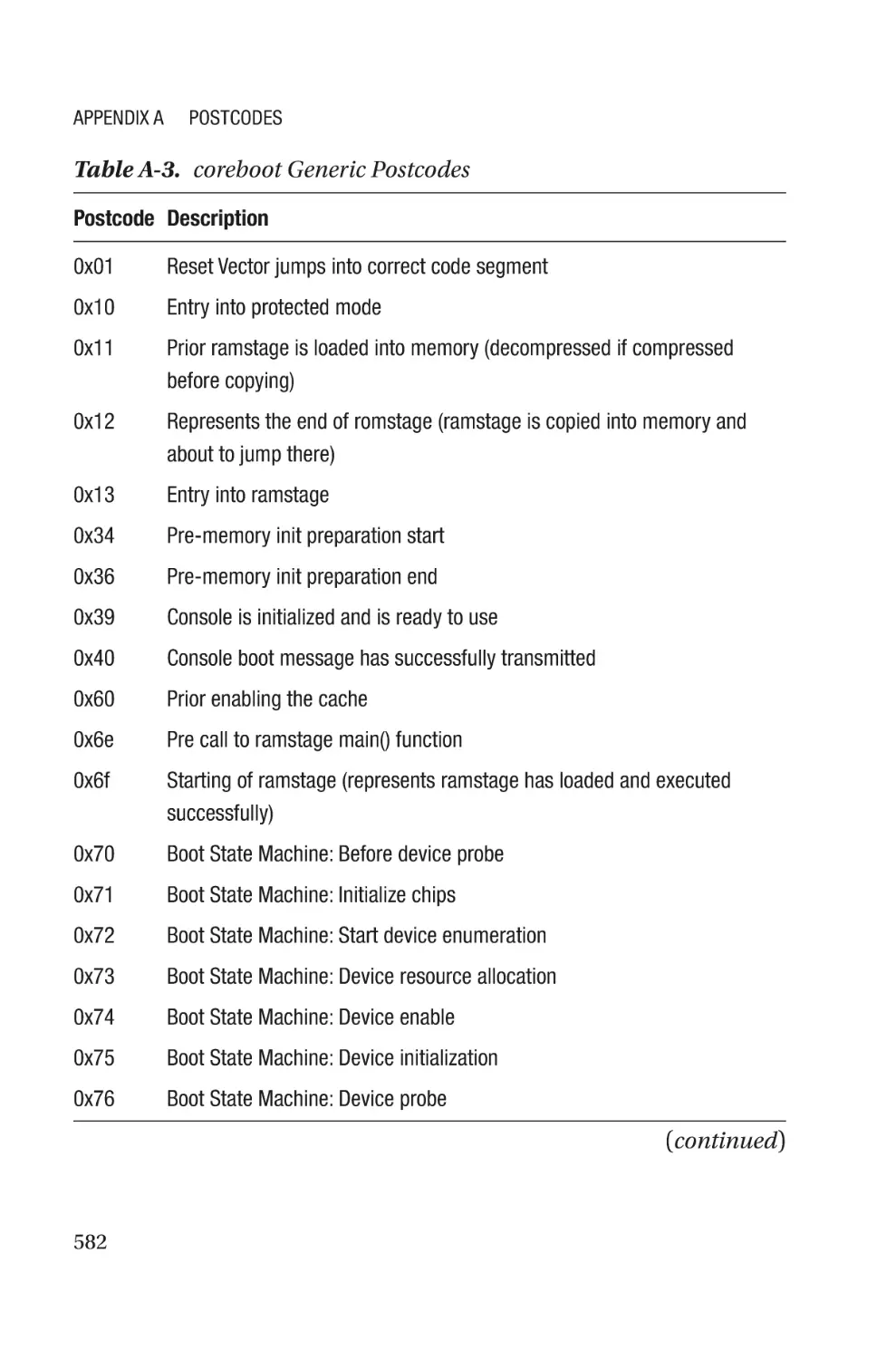
Table 1-1 describes a simple problem statement to help understand
why programming knowledge is important in embedded firmware.
6
Chapter 1
Introduction
Table 1-1. Problem Statement: Determine the Size Difference
Between Code Way (6-Bits in Width) and Data Way (1-Bit in Width)
in the x86 Platform
Solution: Let’s see the algorithm used in “a good programming practice” and “an
optimized/efficient programming practice” to determine the size difference.
Code Way = Bit 0-5 -> 0x3f represents the code way
Data Way = Bit 0 -> 0x1 represents the data way
A good programming
practice
An efficient programming
practice
Algo:
((1 << Code Way) - 1) ((1 << Data Way) - 1)
Algo:
((1 << (Code Way - Data
Way)) - 1) << Data Way)
Code:
mov $0x3f, %ecx
mov $0x01, %eax
Code:
mov $0x3f, %eax
mov $0x01, %ebx
shl %cl, %eax
subl $0x01, %eax
sub
%ebx, %eax
mov
shl
$0x01, %cl
%cl, %eax
sub
shl
%ebx, %eax
%bl, %eax
mov
mov
$0x01, %ecx
$0x01, %ebx
shl %cl, %ebx
subl $0x01, %eax
sub
%ebx, %eax
Summary: Total 4 mov instructions, 2 shl
instructions, and 3 sub instructions are used
Summary: Total 3 mov
instructions, 2 shl instructions,
and 2 sub instructions are used
Analysis: Each mov instruction requires 7 T-States and a sub instruction requires
4 T-States, hence, the total savings in the optimized solution is 11 T-States for a
simple operation.
7
Chapter 1
Introduction
This approach highlights the need for embedded firmware engineers
to have a deep knowledge of system programming. As per the current
industry trends, the firmware engineers are typically coming from an
electrical major background. A knowledge of electrical engineering would
help to understand the hardware components better, but the downside of
this background might be a lack in programming proficiency compared to
a computer science/engineering major candidate. Hence, it’s important
for a firmware engineer to have a good understanding of the hardware
along with being a prolific programmer. Unfortunately, the present
academic curriculum is not attuned for the embedded firmware industry
and requires special attention from the job-seeker to accomplish the goal.
Chapter 2 provides the essential cross architecture, processor-internal
knowledge that can streamline your understanding about hardware,
regardless of your backgrounds and it’s a prerequisite for understanding
the rest of the chapters.
S
pecialized Education
Many different fields of computer systems provide specialized training
and certification courses to support technical education for college grads,
allowing professionals to upgrade their domain knowledge and provide an
opportunity to learn about the new technology. For example, CCNA (Cisco
Certified Network Associate) certification certifies the skills and knowledge
in computer network fundamentals. OCA (Oracle Certified Associate) and
OCP (Oracle Certified Professional) certifications demonstrate high-level
skills in Java development.
Unfortunately, there are no specialized courses and opportunities
available to gain proficiency in embedded firmware. One of the biggest
reasons for such a shortcoming is due to lack of openness in the embedded
system development approach. Since the origin of firmware, the majority
of the firmware development and architectural innovation is limited to a
8
Chapter 1
Introduction
few companies. The firmware knowledge is confined to engineers working
for those companies and parties fortunate enough to receive that precious
training about hardware components, knowledge of system programming,
and getting used to the embedded system and firmware development
process. The downside is that it leads to engineers who only have focused
learning about a specific firmware architecture and who are thus unable
to explore or learn from the other offerings. At the same time, there is a
high chance that focus learning on a particular technology may become a
bottleneck towards being open enough to explore more opportunities and
unable to appreciate or leverage a potentially better design model than the
current approach.
This book is written with the intention of breaking that prohibition
about learning firmware. Our goal is to keep talented engineers in mind
and motivate them to learn essential knowledge about computer systems
and embedded devices to be able to thrive in the growing embedded
market. The learning of firmware architecture and development aspects
might help you to pick the correct system firmware from the lists that are
being presented as part of this book, when designing and building your
own firmware solutions for the targeted embedded system.
This chapter will further provide background information about
the origin of firmware and its evolution. Additionally, we will explain a
possible fork of the parallel firmware development approach in the last
several decades and show the current status. We want you to be aware of
the original necessity that inspired the invention of firmware and initiated
this journey.
The remaining section of this chapter is to set your expectations
for this book and also to refer to another book by us named Firmware
Development: A Guide to Specialized Systemic Knowledge. This book
provides the prerequisite knowledge to start with embedded firmware
learning, plus all necessary information about different types of firmware,
including underlying architectures, design assumptions, and applicable
user market. At the end of this book, you will have key information for
9
Chapter 1
Introduction
your firmware journey. The second book offers specialized firmware
development knowledge like understanding the other types of firmware
like non-host firmware, device firmware, and its architecture; the firmware
development concepts and applications using modern high-level
system programming languages; understanding the build and debug
infrastructure; creating a firmware security paradigm; and a deep dive into
the improvement opportunities for future firmware.
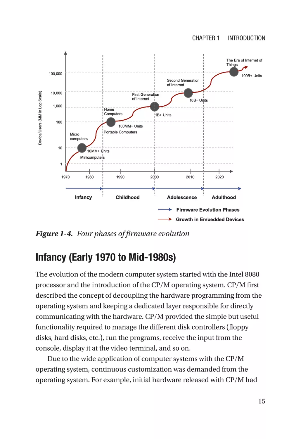
The Origin of Firmware
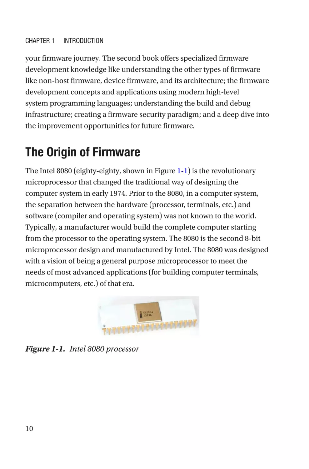
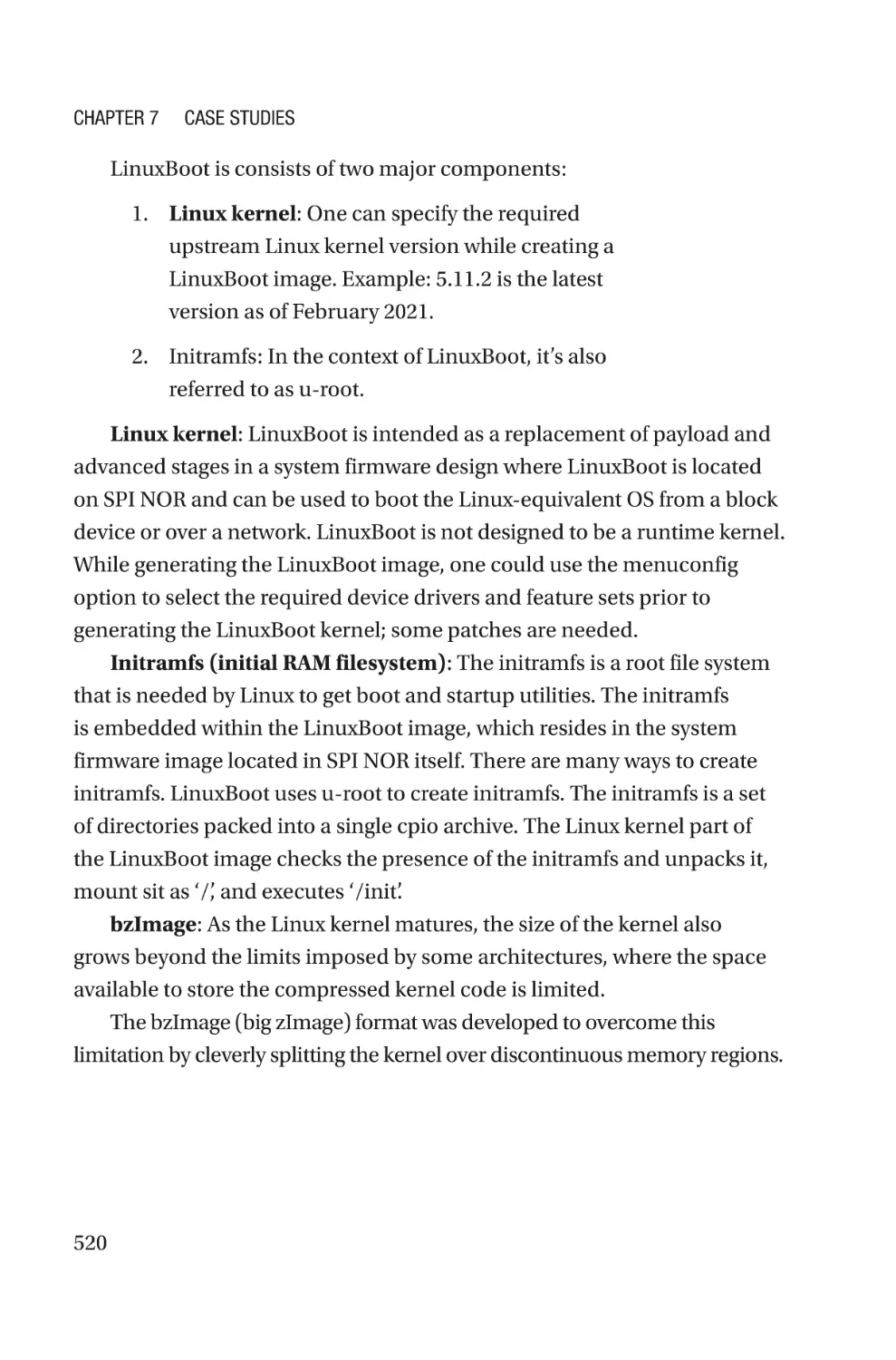
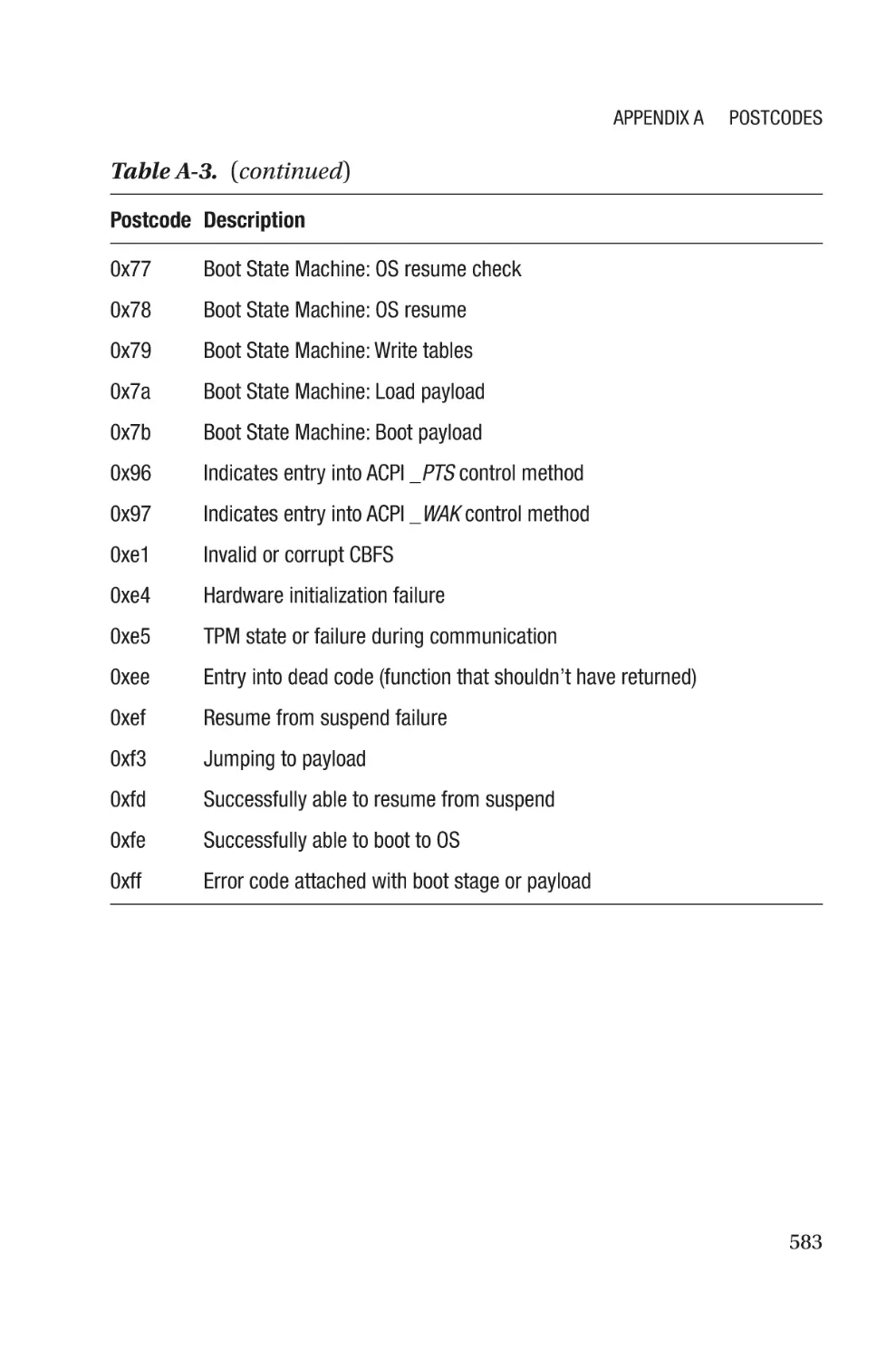
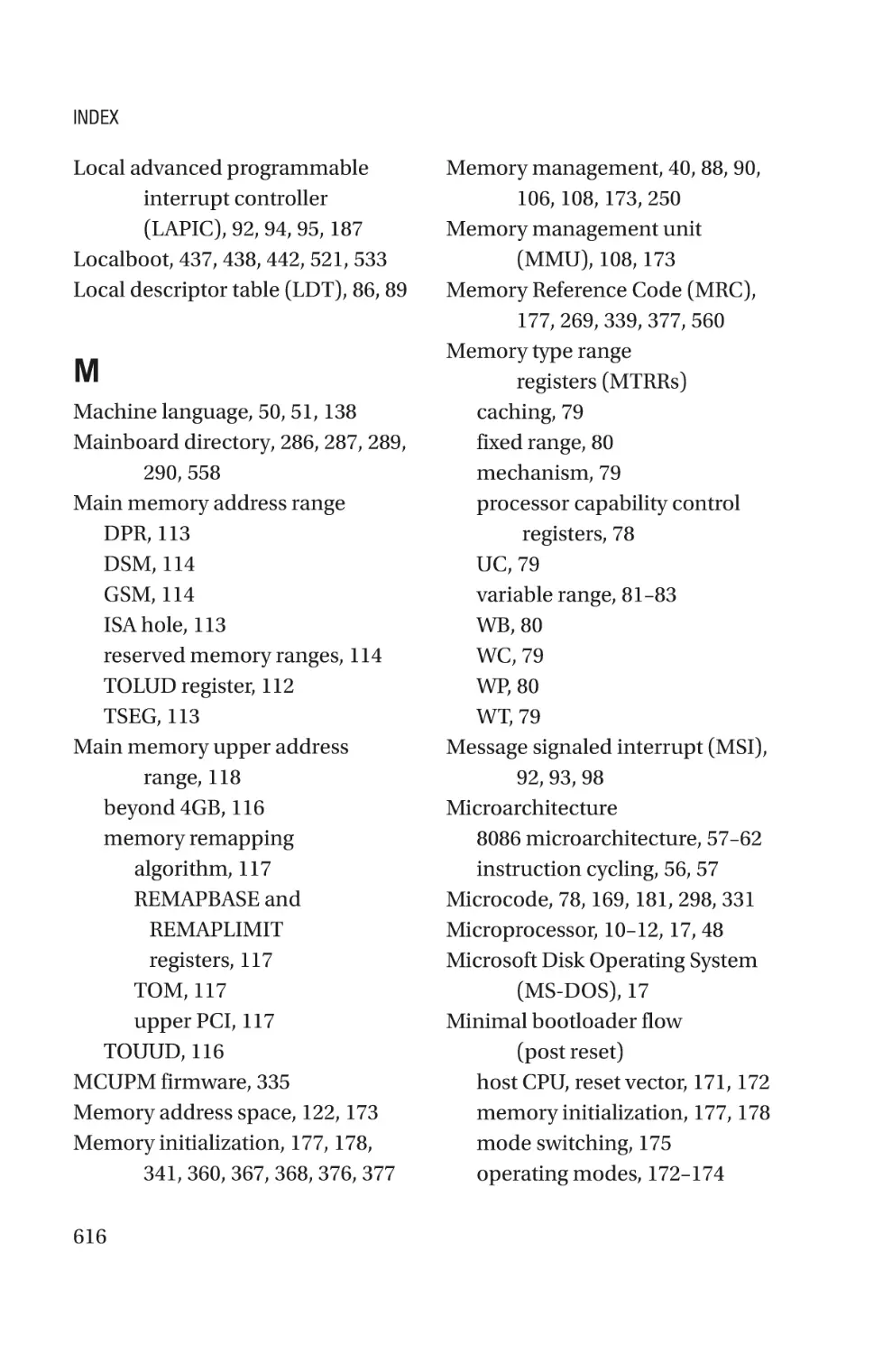
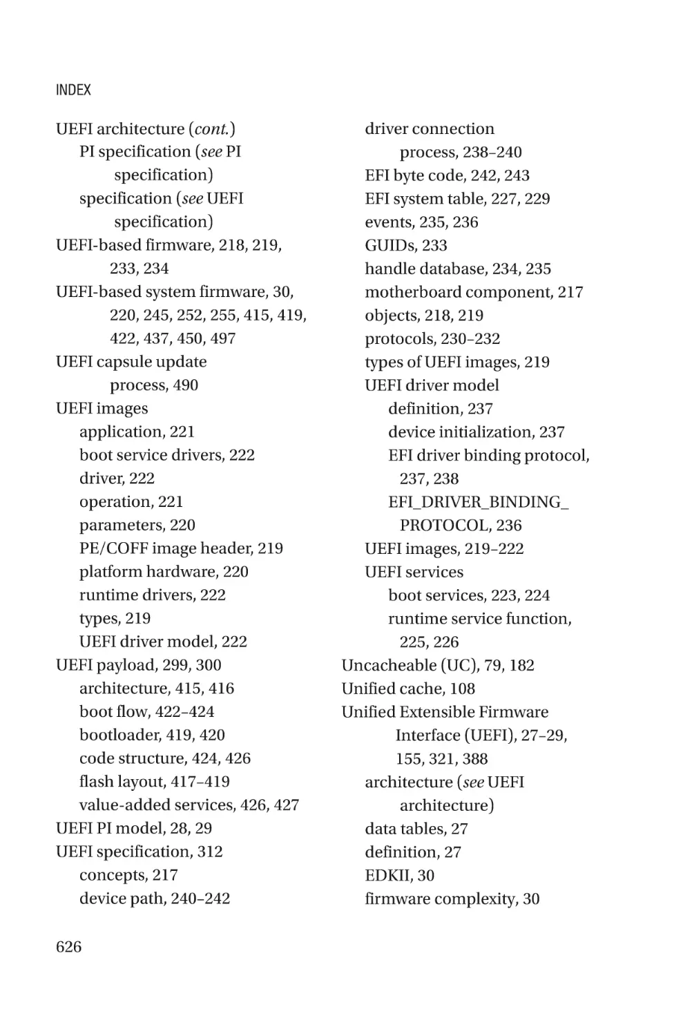
The Intel 8080 (eighty-eighty, shown in Figure 1-1) is the revolutionary
microprocessor that changed the traditional way of designing the
computer system in early 1974. Prior to the 8080, in a computer system,
the separation between the hardware (processor, terminals, etc.) and
software (compiler and operating system) was not known to the world.
Typically, a manufacturer would build the complete computer starting
from the processor to the operating system. The 8080 is the second 8-bit
microprocessor design and manufactured by Intel. The 8080 was designed
with a vision of being a general purpose microprocessor to meet the
needs of most advanced applications (for building computer terminals,
microcomputers, etc.) of that era.
Figure 1-1. Intel 8080 processor
10
Chapter 1
Introduction
Facts In 1987, an asteroid of Caussols’ main belt was named 8080
Intel to honor the revolutionary invention that changed the computer
industry.
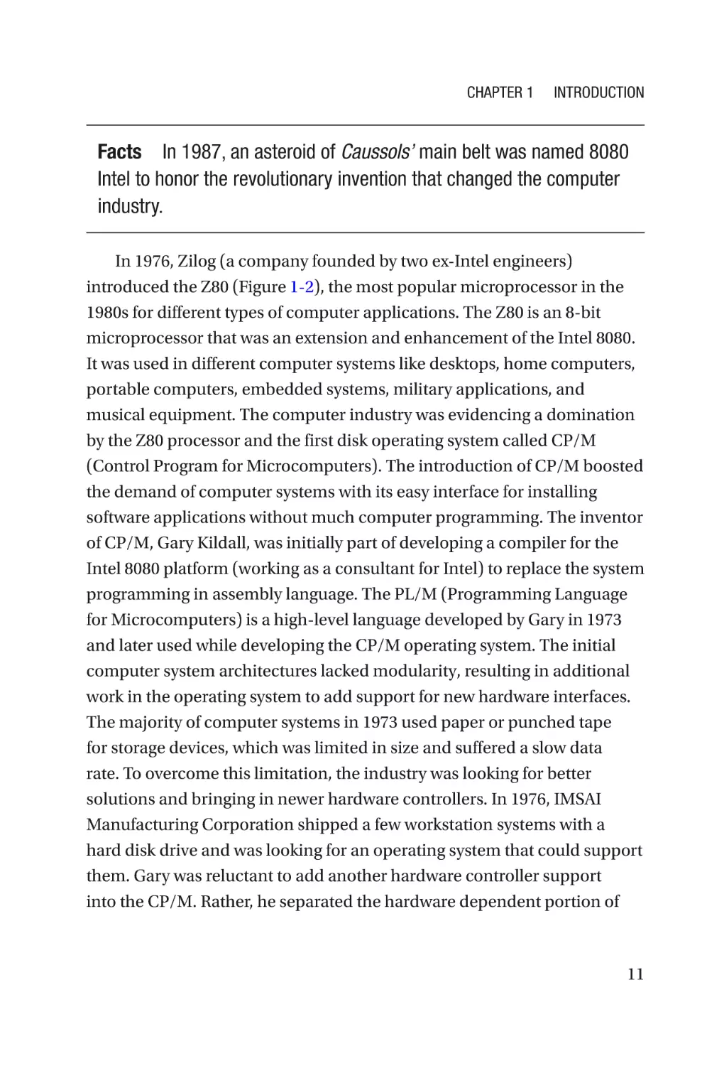
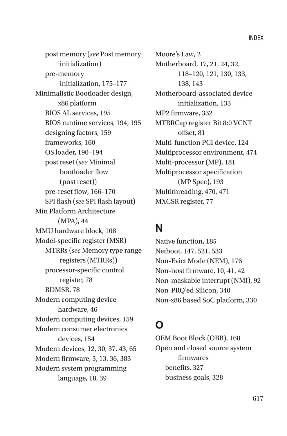
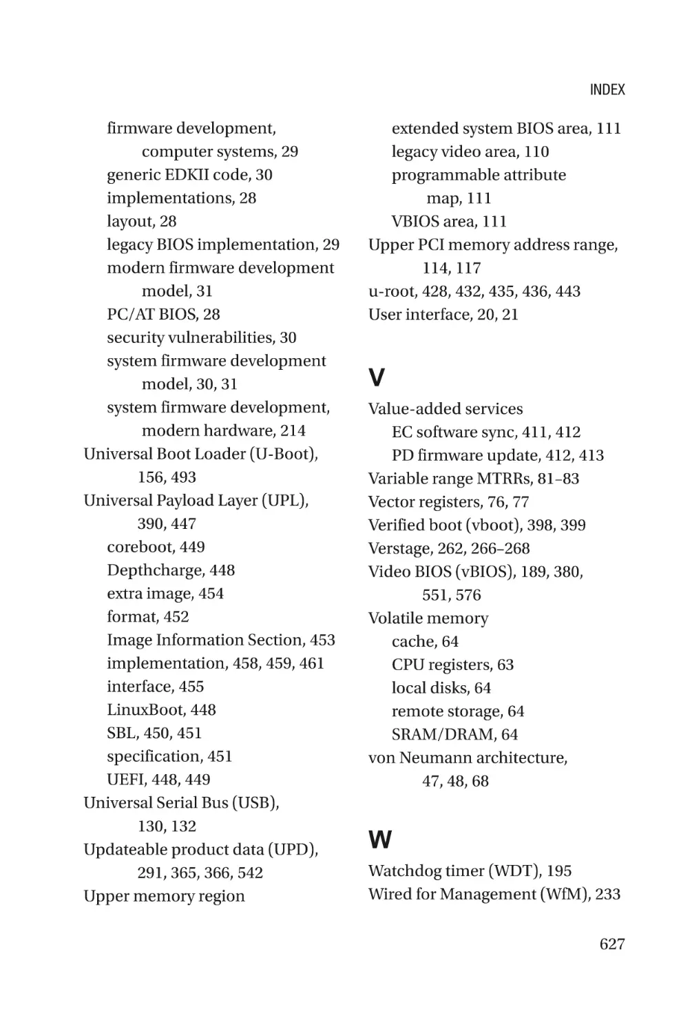
In 1976, Zilog (a company founded by two ex-Intel engineers)
introduced the Z80 (Figure 1-2), the most popular microprocessor in the
1980s for different types of computer applications. The Z80 is an 8-bit
microprocessor that was an extension and enhancement of the Intel 8080.
It was used in different computer systems like desktops, home computers,
portable computers, embedded systems, military applications, and
musical equipment. The computer industry was evidencing a domination
by the Z80 processor and the first disk operating system called CP/M
(Control Program for Microcomputers). The introduction of CP/M boosted
the demand of computer systems with its easy interface for installing
software applications without much computer programming. The inventor
of CP/M, Gary Kildall, was initially part of developing a compiler for the
Intel 8080 platform (working as a consultant for Intel) to replace the system
programming in assembly language. The PL/M (Programming Language
for Microcomputers) is a high-level language developed by Gary in 1973
and later used while developing the CP/M operating system. The initial
computer system architectures lacked modularity, resulting in additional
work in the operating system to add support for new hardware interfaces.
The majority of computer systems in 1973 used paper or punched tape
for storage devices, which was limited in size and suffered a slow data
rate. To overcome this limitation, the industry was looking for better
solutions and bringing in newer hardware controllers. In 1976, IMSAI
Manufacturing Corporation shipped a few workstation systems with a
hard disk drive and was looking for an operating system that could support
them. Gary was reluctant to add another hardware controller support
into the CP/M. Rather, he separated the hardware dependent portion of
11
Chapter 1
Introduction
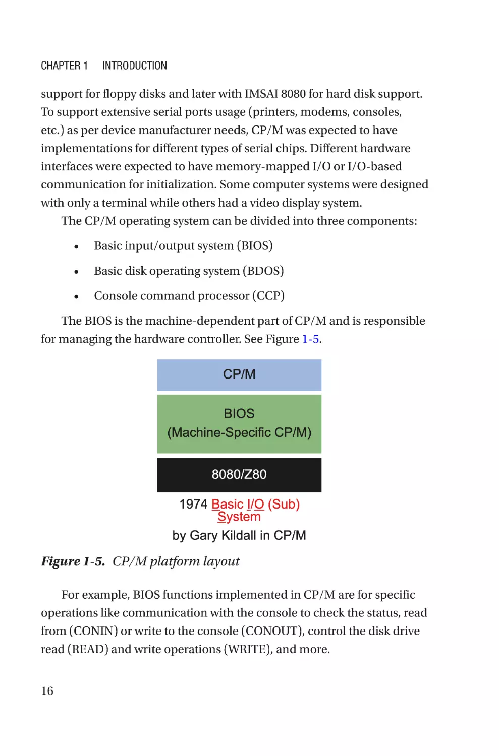
the CP/M and thus the notion of a basic I/O system (BIOS) evolved. In
8080- and Z80-based computer system with the CP/M operating system,
the machine-dependent code (a.k.a. the BIOS) is referred as a simple
bootloader that resides in the ROM (read-only memory) and manages to
perform the direct communication with the hardware and an additional
low-level hardware-specific file (often referred to as the hardware
abstraction layer in the modern operating system) part of the operating
system that interfaced with the system BIOS represented the philosophy of
firmware.
Figure 1-2. Zilog Z80 processor
Since its origin, the firmware on the embedded system has made a long
journey and has evolved several times in this process. The section about
firmware evolution will depict the journey of system firmware to help you
understand its applicability to modern devices.
Facts In 1983, Model 100 was the first notebook-style computer
that supported both the QWERTY keyboard and an LCD display.
The Model 100 was based on the Intel 8085 microprocessor and
supported ROM firmware-based platform booting. This was the last
Microsoft product that Bill Gates developed personally, and in one of
his interviews, he mentioned the nostalgia he has for the Model 100
project where he contributed significantly to the code development.
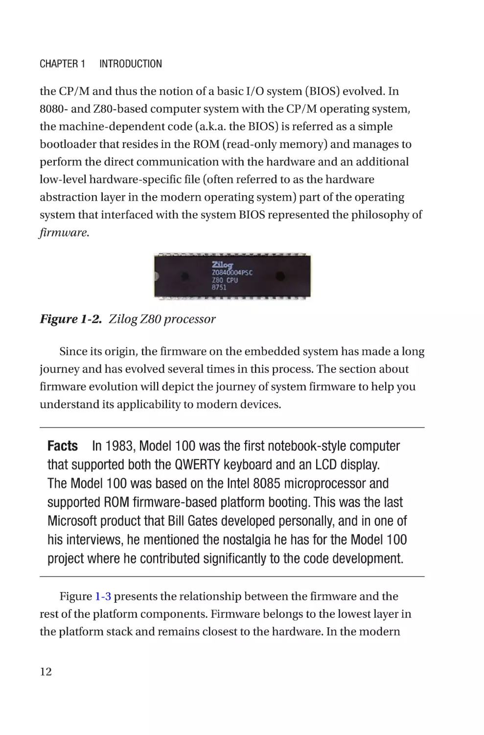
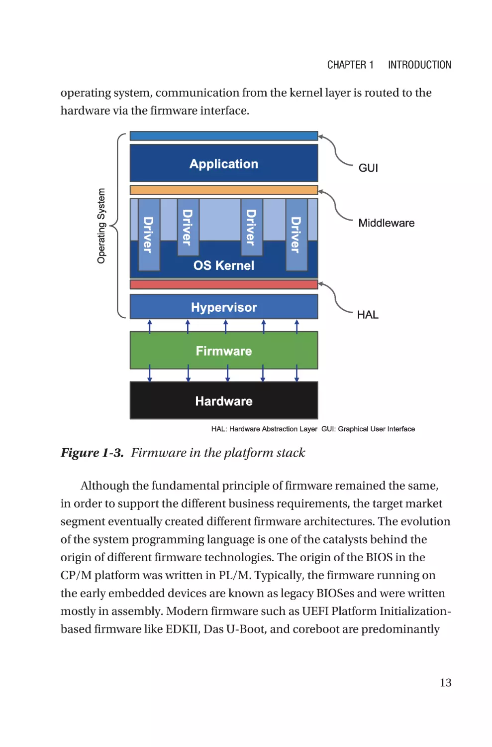
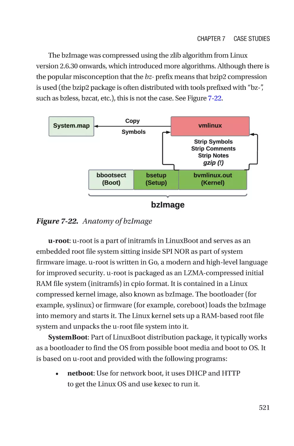
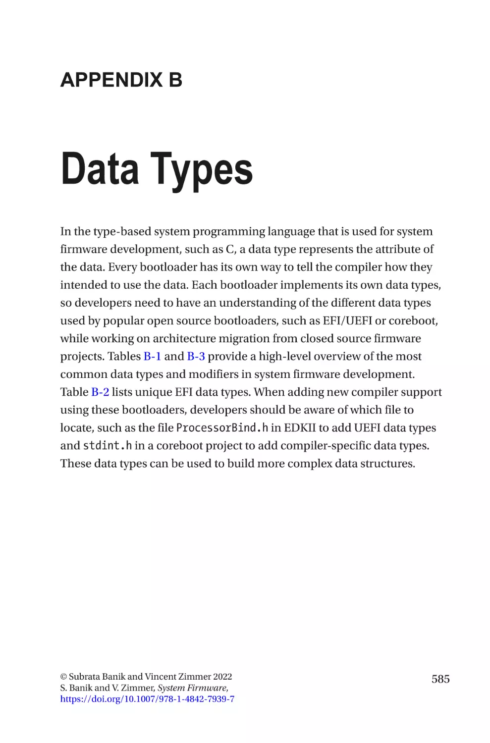
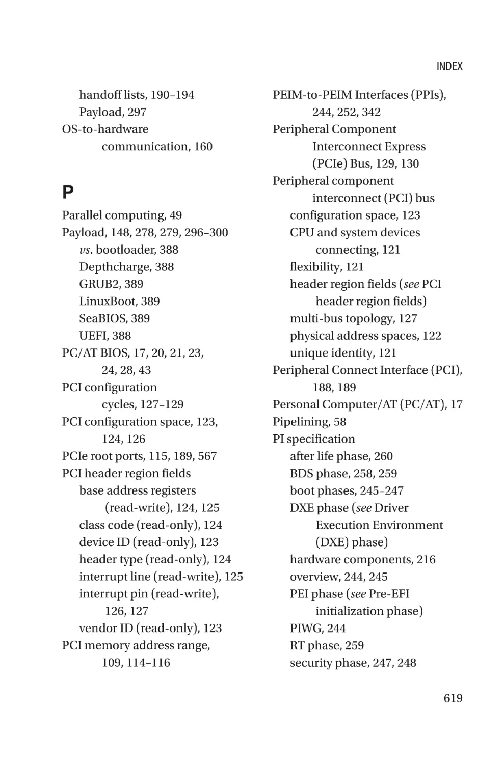
Figure 1-3 presents the relationship between the firmware and the
rest of the platform components. Firmware belongs to the lowest layer in
the platform stack and remains closest to the hardware. In the modern
12
Chapter 1
Introduction
operating system, communication from the kernel layer is routed to the
hardware via the firmware interface.
Figure 1-3. Firmware in the platform stack
Although the fundamental principle of firmware remained the same,
in order to support the different business requirements, the target market
segment eventually created different firmware architectures. The evolution
of the system programming language is one of the catalysts behind the
origin of different firmware technologies. The origin of the BIOS in the
CP/M platform was written in PL/M. Typically, the firmware running on
the early embedded devices are known as legacy BIOSes and were written
mostly in assembly. Modern firmware such as UEFI Platform Initialization-
based firmware like EDKII, Das U-Boot, and coreboot are predominantly
13
Chapter 1
Introduction
written in C with a small amount of assembly language code. This does
not imply that firmware is limited to the C programming language. In fact,
IEEE 1275 is written in Forth and the emergent firmware solution oreboot
(coreboot without C) is written in the Rust programming language. What
is important, though, is the functionality embodied in the firmware, the
flow, and the interfaces of the host firmware exposed to successive layers
of execution during the platform boot.
On the early platforms with Intel 8080 or Z80, the firmware was a tiny
code block that stored into the PROM (programmable read-only memory)
and performed the basic bootstrap operation. In later computer systems
with more complex processors and platforms, the ROM chip for storing the
firmware was replaced with flash memory. This provided easier ways to get
fixes or allow feature upgrades on the modern computer systems, even on
in-field devices.
F irmware Evolution
It’s been close to 50 years since the term basic I/O system was first
introduced by Gary Kildall and used in the CP/M based operating system
platform. In the last several decades, system firmware has evolved to keep
its interface still relevant with the innovation in hardware space and to
accommodate the different operating systems using a unified layer of
firmware. Figure 1-4 represents the growth in embedded devices over
decades and how it resonated into the firmware to satisfy the demand from
the next million units of devices. This section compares the evolution of
firmware to the human life cycle to illustrate the maturity that came with
the progression. A journey that started with a tiny read-only piece of code
has evolved into a proper hardware interface for performing the hardware
initialization and providing runtime services and has finally reached a
phase where the firmware needs to support advanced product features
(like security, resilience, etc.) to meet the modern electronic device needs.
14
Chapter 1
Introduction
Figure 1-4. Four phases of firmware evolution
Infancy (Early 1970 to Mid-1980s)
The evolution of the modern computer system started with the Intel 8080
processor and the introduction of the CP/M operating system. CP/M first
described the concept of decoupling the hardware programming from the
operating system and keeping a dedicated layer responsible for directly
communicating with the hardware. CP/M provided the simple but useful
functionality required to manage the different disk controllers (floppy
disks, hard disks, etc.), run the programs, receive the input from the
console, display it at the video terminal, and so on.
Due to the wide application of computer systems with the CP/M
operating system, continuous customization was demanded from the
operating system. For example, initial hardware released with CP/M had
15
Chapter 1
Introduction
support for floppy disks and later with IMSAI 8080 for hard disk support.
To support extensive serial ports usage (printers, modems, consoles,
etc.) as per device manufacturer needs, CP/M was expected to have
implementations for different types of serial chips. Different hardware
interfaces were expected to have memory-mapped I/O or I/O-based
communication for initialization. Some computer systems were designed
with only a terminal while others had a video display system.
The CP/M operating system can be divided into three components:
•
Basic input/output system (BIOS)
•
Basic disk operating system (BDOS)
•
Console command processor (CCP)
The BIOS is the machine-dependent part of CP/M and is responsible
for managing the hardware controller. See Figure 1-5.
Figure 1-5. CP/M platform layout
For example, BIOS functions implemented in CP/M are for specific
operations like communication with the console to check the status, read
from (CONIN) or write to the console (CONOUT), control the disk drive
read (READ) and write operations (WRITE), and more.
16
Chapter 1
Introduction
The BDOS implements the filesystem for CP/M and provides I/O
abstraction on top of the BIOS using a specific file (almost similar to IO.SYS
usage in the MS-DOS operating system) part of the operating system that
performs hardware-specific operations. The CCP provides a command
processing interface that takes user input from the keyboard and produces
results to the terminal (serial or video). CP/M comes with a set of in-built
commands to ease the operation for the user.
With the introduction of MS-DOS (the Microsoft Disk Operating
System) for the 16-bit microprocessor-based computer system, the
industry shifted gear from CP/M to MS-DOS. The operational model of
MS-DOS was similar to CP/M and it maintained the same multi-layer
architecture that separated the direct hardware communication from the
rest. This helped MS-DOS to get adapted for different hardware platforms.
MS-DOS introduced a concept called DOS BIOS. In DOS BIOS (also known
as IO.SYS), a system file resides in the operating system and loads a self
program into the memory to perform system initialization using device
drivers, display splash screen, and more.
Childhood (Mid-1980s to Late 1990s)
Although the BIOS name originated in the early 70s, from a functionality
standpoint, the BIOS in modern PCs originated in the mid-1980s. The
pioneering company for this effort was IBM. In 1984, IBM released PC/
AT (Personal Computer/AT) hardware while Microsoft built the operating
system, MS-DOS, demanding a clean separation between the firmware
and the operating system.
The evolution in firmware with the IBM platform is known as the PC/
AT BIOS. The IBM PC/AT BIOS on the Intel 8088 microprocessor with ~40
kilobytes in size resides in a ROM chip on the computer motherboard. The
original PC/AT BIOS also demonstrated the phased nature of platform
firmware, and was given new phases, namely Power-On-Self-Test (POST)
versus runtime. See Figure 1-6.
17
Chapter 1
Introduction
Figure 1-6. IBM PC/AT platform layout
A more detailed understanding of the IBM PC/AT platform and
firmware, which is the backbone for even the modern system firmware can
be found in Chapter 2, including interrupt handling, memory layout, CPU
internal operations, and the system bus architecture.
The POST (Power-On Self-Test)
The Power-On Self-Test is used to define a series of operations performed
by the BIOS after the processor becomes operational and the code block
is running from the ROM. After the limited hardware component gets
initialized, the BIOS loads the bootstrap loader (BSL) into the RAM
(random access memory) and executes it. The bootstrap loader uses the
bootstrap code to complete the boot from the disk drive. If it fails to boot
to the OS, at the end of the POST, it loads the ROM BASIC module for basic
I/O operations. After the platform power-on reset, the responsibility of the
POST operation ends by handing over to the bootstrap loader.
18
Chapter 1
Introduction
Starting with the Intel 8088 CPU platform, the responsibilities of
POST are
•
After the CPU comes out from the reset, it jumps into
the fixed memory mapped address 0xFFFF0 (20-bit
addressing), also known as reset-vector on x86-
based platforms. It contains a jmp instruction to start
execution of the Power-On Self-Test code.
•
Although the POST operation is highly platform
dependent, at the high level, it involves initialization
of the hardware components including the CPU and
physical memory (RAM), plus additional controllers
like the 8259 interrupt controller, 8237 DMA controller,
8253 timer, display controller, 8042 keyboard controller,
serial and parallel interface, and disk drives (floppy and
hard disk).
•
The POST operation is also responsible for creating
memory layout for applications to run as part of the
OS layer. Hence, the BIOS prepares the memory layout
table for keeping its essential data and code block for
internal usage and leaves a maximum of 640 kilobytes
of usable DRAM for the OS and its applications. This
simple memory reporting mechanism by the BIOS is
known as the BIOS data area (BDA).
Chapter 3 explains what a user should expect from the POST
operation. The minimalist nature of the POST operative is different
between architectures, so Chapter 3 outlines the differences in brief.
19
Chapter 1
Introduction
User Interface
The IBM PC/AT BIOS had first surmised the need for end users to know
the failure in the hardware initialization operation. The hardware was
sophisticated and it’s important to identify the failure or potential bad
hardware as part of the POST operation. One part of the initial user
interface implemented on the PC/AT was POST codes (2-bytes data, also
known as error codes), which appear either on the primary I/O port 80 or
video/serial console that represented the error status and the correctable
actions (if available). Error code 0x0003 signified CMOS Battery Low with
the corrective action being to continue booting or abort the boot to fix the
problem. Later, beep codes were a more meaningful way to draw the user’s
attention to a failure or to indicate the success If the computer failed the
POST, the computer generated different beep notations (between a short
beep or a long beep with a periodic interval) to inform the user about the
source of the problem. One short beep denoted the DRAM refresh failure.
Later, every BIOS vendor designed their own product-specific POST and
error codes for easy detecting of failures during POST. Appendix A list
common post codes and usages in computer systems.
In the mid-1990s, an advanced video/graphics user interface known as
the BIOS Setup Utility was developed; it was launched or controlled using
a specific key sequence. See Figure 1-7.
20
Chapter 1
Introduction
Figure 1-7. Aptio BIOS setup utility implemented by AMI
A user interface to allow configuration and remember user preference
wasn’t possible without having a place to store that information. IBM PC/
AT first introduced the idea of storing those configurations into the non-
volatile memory, later known as CMOS storage.
Chapter 2 of Firmware Development: A Guide to Specialized Systemic
Knowledge explains the need for configuration tools in the firmware
development approach and lists the different options available.
BIOS Services
The BIOS was responsible for performing the hardware initialization for
all controllers attached to the motherboard as part of the POST. The BIOS
implemented specific routines to perform the hardware components’
initialization, such as input and output devices, storage devices, and serial
ports. The PC/AT BIOS separated the platform initialization from the
runtime services. This section covers the additional services of the BIOS
leveraged by the OS and the platform.
21
Chapter 1
Introduction
BIOS Interrupt Call
The IBM platform leveraged BIOS interrupt calls to invoke the platform
hardware from the MS-DOS layer. Traditionally, the BIOS routines were
accessed by triggering the software interrupt. These BIOS interrupt calls
were used by the DOS internal operations and some application layers.
Such a mode of operation required high privilege. When software triggered
the BIOS interrupt, the CPU redirected the interrupt to the IVT (Interrupt
Vector Table) with the corresponding interrupt vector and a special routine
against that interrupt vector was executed to perform the requested
task. The INT instruction was used to trigger the software interrupt. This
included Int13h for disk access, Int10h for video access, and Int16h for
keyboard access. These Int-calls provided a service layer for both the OS
boot and OS runtime.
Plug and Play BIOS (PnP BIOS)
The Plug and Play BIOS Specification defined new functionality for the
system BIOS to be able to meet the computer system design goal with a
Plug and Play card. A PnP system BIOS played a vital role in helping to
manage the resources allocation for those card devices and ensured a
successful launch of the operating system. The PnP BIOS was responsible
for configuring Plug and Play cards during the POST. After the POST
process was complete, control of the Plug and Play device configuration
passed from the system BIOS to the OS. In order to make the Plug and Play
Card initialization process independent at the system firmware side, each
Plug and Play card was equipped with Option ROM, a newer standard for
the Plug and Play BIOS. The system firmware called into the Option ROM
to perform device initialization.
22
Chapter 1
Introduction
Bootstrap Loader
A bootstrap loader (BSL) is a special program that is responsible for
loading the operating system. At the end of the POST operation, BIOS
identifies an IPL (initial program load) device (floppy drives, hard drives,
CD-ROM drives, PnP cards, etc.) and is able to load and execute an
OS. BSL can identify all IPL devices in the system, prioritize them in the
order the user selects, and then sequentially go through each device and
attempt to boot.
Chapter 7 defines the purpose of having a separate bootstrap loader in
the system firmware architecture.
With the introduction of real and protected addressing mode for
the later CPU generations, the BIOS operations are also divided into
two categories: CBIOS (Compatibility BIOS) to maintain backward
compatibility with MS-DOS-like operating system, where all operations
are running in real mode, and ABIOS (Advanced BIOS), which provides a
new protected mode interface. This results in a significant change in the
operational model for the OS, which limits the direct BIOS interrupt calls
from the protected mode. In the 1990s, the BIOS provided more protected
mode interfaces to the operating systems, such as Advanced Power
Management (APM), e820, and MultiProcessor Specification (MPS).
The PC/AT BIOS became a de facto standard for computer systems
for a very long time. And given the lack of a redistributable open source
variant of the BIOS, various companies had to clean-room their own
instances. This led to the formation of independent BIOS vendors like
AMI, Award, System Soft, and Phoenix. Some of the large OEMs elected
to create their own clean-room BIOSes; one of the notable first examples
was Compaq.
This lack of openness and reuse led to incompatibilities over time,
resulting in bug wars between Houston and Austin regarding which of the
notable OEMs in those cities had the least bugs in their proprietary BIOS.
23
Chapter 1
Introduction
The PC/AT BIOS standard provided platform initialization and runtime
interface for operating system. The latter faced structural challenges in
the late 90s as the platform evolved beyond x86-CPU vendors (Intel and
AMD). Specifically, the Apple Macintosh and Sun used Motorola 68k and
Sparc CPUs, respectively. They could not use the x86 interrupt-calls as
their abstraction for booting.
Adolescence (2000 to 2015)
The most impactful era of the embedded industry started with the
revolution of the Internet in 2000. The PC industry has followed an
interesting arc with more numbers of users exploring the new side of
computing, resulting in improving the overall device-per-user ratio and
bringing new use case and platform requirements, so processors matured
to manage users’ advancements. Prevailing usage of firmware runtime
services by the operating system was another key motivation for further
evolution in the firmware space to define more rich solutions.
Open Firmware
With the introduction of open-system design in the 1970s and the origin
of firmware, the job of loading the operating system greatly involved
programming I/O components present in the motherboard. The
prerequisite of the platform booting to the OS is the advanced knowledge
of possible I/O devices from which the operating system may be loaded.
In different computer system applications like desktop computers, a new
bootable device may be added later to the system and the user would
expect its functionality. With rapid innovation in the hardware space
in the 1990s and more devices and users, it was impractical to roll out
different sets of system firmware to support new devices. Thus, to assist
the growth in the hardware/systems and maintain the generics of the
operating system, the firmware was rearchitected to allow abstracting
the hardware characteristics while presenting to the operating system.
24
Chapter 1
Introduction
Originally, the Open Firmware (OF) was intended to solve those problem
by creating a processor-independent firmware architecture. Probably the
OF provided the first concept of hardware programming using interface
specifications, where the user of the interface isn’t required to know the
machine-level details. An earlier section explained the concept of the
PnP BIOS that was necessary to use a new device without changing the
system firmware. With OF, the PnP driver was implemented in a byte-
coded, machine-independent, interpreted language called FCode. Since
FCode was machine independent, the same device and driver could be
used on computer systems with different CPU instruction sets. The Open
Firmware specification brought the requirement of modularity in firmware
development and let the computer integrator choose the feature sets that
were mandatory to meet the system design goal. The OF specification
viewed the hardware components based on industry-standard bus
specifications, so the development and debug process became more
scalable. Similarly, it’s easy to represent the devices attached to the system
using a data structure described in OF as the device tree. See Figure 1-8.
Figure 1-8. Open Firmware architecture
25
Chapter 1
Introduction
Companies like IBM, Sun, and Apple used Open Firmware for shipping
platforms. In the early days of Windows NT, Microsoft engineers wrote
the ARC (Advanced RISC Computing) boot firmware for non-x86-based
systems.
With the introduction of the 64-bit Itanium architecture from Intel,
the next generation of processor architecture needed a unified firmware
solution. There were nearly two possibilities between ARC or Open
Firmware. Initially, Open Firmware was considered as a solution for “how
to boot Itanium,” due to the fact the PowerPC booted Windows NT via
OF. Later, Intel introduced Extensible Firmware Interface (EFI) in 2000,
which was an outcome of the Intel Boot Initiative (IBI) program that began
in 1998.
EFI ended up looking more like ARC, with a similarity between
the ARC Firmware Function Vector and UEFI System Table, and both
supported booting from a FAT-formatted portion of the disk. OF does have
some advantages, especially for security. On the other hand, ARC muddied
platform definition details in the specification and it was also not clear if
ARC could be opened and extended. One interesting transition that was
introduced with the ARC firmware and also seen with EFI. See Figure 1-9.
26
Chapter 1
Introduction
Figure 1-9. Itanium platform layout
firmware is porting of the kernel drivers into the firmware for
addressing the advanced use case, For example, Windows NT NDIS
miniport drivers were embedded into the firmware to support pre-OS
networking. This trend continues with the block device, display, and
console services in the pre-OS and also requires the runtime interface.
In 2005, Intel updated the specification and a new Unified EFI (UEFI)
forum was formed to promote and manage the industry-wide adaptation
of the EFI Specification for firmware development. The UEFI Forum is led
by core committee representatives from different companies: Intel, AMD,
Insyde, IBM, HP, Apple, Microsoft, Lenovo, Dell, Phoenix Technology,
and AMI. Since then, UEFI has become the de facto standard for firmware
development for computer systems.
UEFI
Unified Extensible Firmware Interface (pronounced as u-e-f-i) defines the
interface between the underlying firmware and the operating system. The
interface consists of data tables that contain platform-related information
and separate service calls between boot and runtime; the boot service calls
27
Chapter 1
Introduction
are used to complete the POST operation and the operating system uses
the runtime service to access firmware routines.
UEFI is intended to replace the PC/AT BIOS (typically referred as the
legacy BIOS) INT-calls-based communication with sophisticated C callable
interfaces. The UEFI specification supports a machine-independent
architecture where processor bindings assist in setting up the machine
state on various CPU instruction set architectures (ISAs), commencing
with Itanium and IA-32 and subsequently including 32-bit ARM and 64-bit
ARM or Aarch64, along with 64-bit x86 or x64. See Figure 1-10.
Figure 1-10. UEFI platform layout
Underneath the UEFI interface there are many potential
implementations. One type of implementation is UEFI PI, or platform
initialization. The PI specification and code lives relative to the UEFI
interfaces and is divided into platform drivers and silicon component
modules. These modules contain executables for the early phase of
execution, or the Pre-EFI initialization (PEI), and the later Driver
Execution Environment (DXE) after memory has been initialized. The DXE
phase is responsible for both late platform initialization and the DXE core
driver provides the basic UEFI services. See Figure 1-11.
28
Chapter 1
Introduction
Figure 1-11. UEFI PI model
A detailed architectural overview of UEFI and its intrinsic operations is
covered in Chapter 4.
The UEFI firmware standard provides many enhancements over the
legacy BIOS implementation as a unified bootloader that can boot into
multiple operating systems, implement an enriched pre-boot phase with
high-level driver architecture (separate device, bus, and host-driver that
introduces the modularity), and introduce security to prevent attacks on
the firmware.
Between 2000 and 2015, the UEFI specification was in charge of
firmware development for computer systems. All major MNCs were
shipping cross-architecture platforms using UEFI, such as Microsoft UEFI
x64 support in Server 2008, Vista, and Win7; RedHat and SuSE OS support;
and a Windows 8 client. With time, ARM 32- and 64-bit support was added
into the open source Tianocore (the community supporting an open
source implementation of the UEFI).
29
Chapter 1
Introduction
One potential downside of this evolution, though, is fragmentation.
The original EFI sample from 1999 evolved into the EFI Developer Kit
(EDK) to include the firmware development framework and early PI
specifications, and has culminated in the EFI Developer Kit II (EDKII). The
EDKII code provides many of the class drivers and generic infrastructure
code with a permissive BSD style license, but the Tianocore project which
hosts EDKII does not have the full silicon initialization elements of the
PI code. In addition, given the permissive nature of the generic EDKII
code, many vendors take a downstream fork and add their own fixes and
modifications, which are rarely shared back with the community. This
raise the proprietary implementation of UEFI-based system firmware,
such as Aptio by American Megatrends (AMI) and InsydeH2O for server,
desktop, mobile, and embedded devices. Most implementations below
generic high-level code are still closed source.
The complexity of firmware increased as time progressed, as the code
base and standards needed to consider more modules and interfaces for
emergent I/O and memory buses (PCIe and USB standards evolved to
support improved speed in data transfer). This led to a lot of fragmentation
in the market where the products shipped were based upon this forest of
different branches from the silicon vendors, and the code went through
various hands, including independent bios vendors, OEMs, and ODMs.
Figure 1-12 shows the system firmware development model using
UEFI. Firmware vendors often do not rebase the firmware in the field
against the latest code or fixes, especially if the products are based upon
older branches. And many products do not release updates after the initial
product release. This lack of updates is not observable to end users since
the provenance of these various forks is not readily discernible. Thus, a
system may have out-of-date capabilities or known security vulnerabilities.
The traditional devices might have ignored such security vulnerabilities
but, knowing the attack surfaces on modern devices are shifted from
the OS and users to the firmware, emphasize the need for security in the
firmware.
30
Chapter 1
Introduction
Figure 1-12. UEFI firmware development supply chain
The modern firmware development model has adopted an efficient
version control mechanism to collaborate better across organizations,
and even cross-company. Chapter 3 of the Firmware Development book
provides the best practices being used in firmware development.
Security
The initial embedded devices with fixed ROM didn’t provide an option for
end users to allow updating the firmware for bug fixes on shipped devices.
With the introduction of EEPROM and flash memory chips, it became
easy to perform firmware updates on the production devices to allow
bug fixes and feature improvement. However, this advantage brought a
risk of making the entire device vulnerable to a security attack if it wasn’t
protected properly. Over time, attackers analyzed the dreadfulness of a
low-level firmware attack, which is as good as making the entire platform
paralyzed.
31
Chapter 1
Introduction
UEFI introduced Secure Boot to establish trust in the system firmware
by creating Trusted Computing Base (TCB). The idea was to implement
the smaller TCBs to verify the system firmware. Technology like Intel Boot
Guard uses keying material in fuses verifies the entire system firmware.
For example, on UEFI-based system firmware platforms, the Initial Boot
Block (IBB) block will only execute if it is the one from the manufacturer
(based on the fuse key matched). In addition, technology like a hardware
root of trust such as Boot Guard may be necessary but not sufficient for
the firmware to defend itself. Specifically, firmware may be composed of
hundreds of thousands of lines of codes. And given industry metrics such
as 1 defect per 1000 lines of code on average, the ability to potentially
exploit a vulnerability and get privilege escalation into the firmware is
non-zero.
Chapter 4 of Firmware Development: A Guide to Specialized Systemic
Knowledge describes the importance of system firmware being more
security compliant. Antivirus software is not enough to detect the presence
of rootkit or malware in the firmware.
ACPI
The Advanced Configuration and Power Interface (ACPI) specification was
developed to define a common industry standard for cross-architecture
platforms to manage the motherboard device configuration and power
management of the device and entire system. The ACPI specification
provides interfaces that support platform-agnostic, OS-directed
device configuration and power management. The key element in the
ACPI specification (evolved from its predecessor) is the OS-directed
configuration and power management (OSPM). The concept of ACPI
is suitable for all types of computer systems like desktops, services, and
mobile and embedded systems. The idea was to conserve energy by
transitioning unused devices and the overall system into a low-power state
when even possible.
32
Chapter 1
Introduction
The predecessor of ACPI was firmware-based System Power
Management, known as Advanced Power Management (APM). The design
philosophy for APM was to provide CPU and device power management
in an OS-agnostic way. The BIOS routines for CPU power management
were getting called when idle and device activity timeout were used to
determine when to transition the device into low-power states. The entire
power management being handled inside firmware provided flexibility
for platform manufacturers to implement a wide variety of solutions
without unification, thus resulting in no uniform user experience even
with the same operating system but with different system firmware from
another vendor.
The ACPI interface describes the hardware interface (hardware
registers for implementing the chipset silicon) and firmware interface
(ACPI data structures to represent the motherboard-attached devices and
a control method to perform runtime operations for device configuration)
and finally allow OSPM to configure the system and device power states.
In 2013, the ACPI specification came under the leadership of the
UEFI forum. You’ll read more about the ACPI interface and required
implementation in the system firmware in Chapter 3.
Alternative Ecosystem Approach
At the same time that EFI was evolving as a response to the Itanium
boot problem and engaging the existing OEM (original equipment
manufacturer) and PC ecosystem with a technology evolution, the world
had a desire for more openness. The LinuxBoot project commenced in
1999 as a response to supporting clusters of machines in supercomputers
where the paradigm of a PC-style BIOS needing human interaction was
insufficient. In fact, the boot of thousands of nodes at scale argued for
having more of an OS-like capability to launch the final OS.
This is where LinuxBIOS emerged as a solution to have a more
streamlined, C-based bootstrap for early platform initialization and defer
33
Chapter 1
Introduction
richer I/O services, akin to what UEFI provides in its single-threaded
programming model, to a payload. The payload could be any executive
software, but given the namesake of LinuxBIOS, this payload was
Linux. The rich set of capabilities of the Linux kernel were used in this
supercomputer use case, specifically the threaded network stack to boot
these machines at scale. See Figure 1-13.
Figure 1-13. LinuxBIOS platform layout
The other salient aspect of LinuxBIOS, which became the coreboot
project, was the community driver and a goal of maximal openness
from the beginning. Unlike the evolution of the UEFI ecosystem, which
introduced new technology to an existing supply chain of closed source
OEM and independent BIOS vendor copyrighted solutions, coreboot
fostered an environment of having the platform initialization, which is
broken into bootblock, romstage, and ramstage (vs. UEFI PI SEC, PEI, and
DXE) provided in GPLv2 open source. This copyleft license requires that
changes to code be provided back to the community.
One coreboot engineer responded to the question of why GPL for
firmware vs. the UEFI PI-based BSD license, with the following question:
“Why would someone want to hoard a bug fix, say for your hardware
initialization?” This shows in stark contrast the lack of end user value of
bug wars when, in fact, host firmware is largely value-neutral to end users.
34
Chapter 1
Introduction
And LinuxBIOS/coreboot were not alone. Although this community
and its infrastructure started on the richer x86 PC-like devices, it has
expanded to IBM Open Power and ARM. One hallmark of coreboot is
having a rich infrastructure for platform initialization, including x86
system management mode (SMM) and ACPI.
U-Boot from 2000 was another C-based host firmware initialization
technology. It has a much simpler software model that allows it to span
several hundred embedded class CPUs. It typically supports simpler
devices, whereas UEFI was built for a rich supply chain and shrink-wrap
OS interoperability working in tandem with ACPI. U-boot has a flattened
device tree and also has a tighter coupling with the OS, often necessitating
Linux kernel modifications to align with the specific U-boot instance.
In a larger sense, one can argue coreboot takes the PI aspect of UEFI
style firmware and opens it up. coreboot can comprehend UEFI today as a
payload, too.
A detailed architectural overview of coreboot and other bootloaders
is covered in Chapter 4. Additionally, Chapter 1 in Firmware Development
explains the extension of the firmware in a more advanced form in
the future.
Adulthood (the Modern Era of Firmware Since 2015)
From the beginning of the open system design aspect in the 1970s, the one
thing that has remained constant even with the evolution of the firmware
is the closed-source nature. Over time, an increasing number of embedded
devices are exposed to the Internet and vulnerabilities are being detected
on end user devices, raising questions about the fundamental rights of the
users. The security paradigm built at the operating system and application
level are not enough to ensure the trustworthiness of the platform where
the more privileged layer than the OS is still running unaudited code
35
Chapter 1
Introduction
as part of the firmware. Previous generations of firmware attempted to
become more comparable with the OS rather than being the essential unit
in this whole platform initialization.
Openness
Modern firmware is looking for more simplistic, essential, and bare
minimal hardware initialization prior to transferring control to the OS
loader or the OS itself. The firmware running on the embedded devices is
expected to be more mature to demonstrate the openness to witness more
transparency in the platform enabling. Asus’s Chromebook with Rockchip
RK3399 is a classic example of achieving the openness that the industry is
expecting from the matured firmware ecosystem. The typical bottleneck
for the firmware not being completely developed in open-source is the
first-party hardware restriction and third-party code running on the
restricted hardware. The next generation hardware design (including
processor and motherboard) is expected to be supportive enough to
ensure open sourcing and meeting business goals in parallel.
The computer industry is looking for more openness due to two major
reasons. The first is end user interest in knowing if the code block running
on the underlying hardware is really trustworthy, meaning users want to
know about configuration changes, bug fixes, and feature improvements
when accepting the firmware update. Secondly, the developer community
want freedom to fixing their own hardware without being beholden to the
original device vendor. The Open Source Firmware (OSF) initiative group
formed to support such a developer group and over time, it has been able
to connect with the business goal. For example, the platform adhering
to the Open Compute Project (OCP) is running various open-source
firmware code, including coreboot, the popular open system firmware.
Figure 1-14 shows the growth in coreboot firmware development in
year over year (YoY) time. The coreboot project receives an average 150
commits per day in 2021.
36
Chapter 1
Introduction
Figure 1-14. coreboot project commits trends in YoY
Security
The definition of security has evolved from the previous generation’s
embedded systems, where the manufacturer firmware implementation
was assumed to be trusted running on the target hardware. Modern
devices are more likely to rely on the hardware chip solution, which has
proven better compared to firmware-based security. With the introduction
of the OpenTitan project, the industry’s first open source silicon root of
trust (RoT), the future platform can envision an implementation that is
more transparent, trustworthy, and secure. The entire development model
of OpenTitan has actually neutralized the old claim of platform security,
which is “the less see the code, the better!”, to the current development
approach where it welcomes more eyes to inspect the code, evaluate it,
and contribute to the development.
Hybrid Firmware Architecture
Open Source Firmware development for product systems is not fully
mainstream even in this modern era of firmware development. The
restricted nature of design and development adopted by the processor
vendors is one major barrier of modern embedded devices for using
OSF solutions, although there is interest from different silicon vendors
37
Chapter 1
Introduction
to support the business goal of openness in platform development even
while working on a restricted silicon platform. The advancement of the
separate platform initialization code from the generic code block in the
previous generation provides that flexibility for silicon companies to
design alternative solutions.
The introduction of a hybrid firmware architecture is the computer
industry’s attempt towards openness for platform enabling. The hybrid
firmware architecture is meant to demystify the early platform engineering
with a restricted SoC/Hardware platform to meet the TTM (time to
market). See Figure 1-15.
Figure 1-15. Platform layout in hybrid firmware architecture
This form of firmware development relies on two pillars: closed source
firmware and open source firmware. Silicon vendors are adopting the
binary-based platform initialization model to consistently maintain the
closed source nature of silicon initialization. Typically, binary-based PI
initialization is implemented using API/ABI, which can easily integrate
with any standard boot firmware to complete the PI. Examples of closed
source firmware used in hybrid firmware architecture are AMD AGESA
(AMD Generic Encapsulated Software Architecture) and Intel FSP
(Firmware Support Package), and closed source binaries are used in ARM
Trusted Firmware Bootloader Stages (i.e., BL1 and BL3x).
38
Chapter 1
Introduction
The introduction of the binary PI model is a blessing in disguise
for the embedded market, where an alternative approach for firmware
development using open source firmware initiative boot firmware is now
a reality. Chapter 5 explains the intrinsic of platform initialization while
adapting this model in system firmware development.
Modern System Programming Language
As stated in the earlier section, the one of key catalysts of the firmware
technology evolution is the progression of programming languages.
A complicated programming language demands special knowledge
and lack of inclusion for the wider community to adapt. The evolution
of programming languages has been used in firmware development,
starting with assembly language to exploring different high-level language
offerings to finally settling with the C programming language. The majority
of firmware development in the modern era is based on either C or an
equivalent programming language.
The future of system programming language is in exploring more
safe programming languages while building firmware where security
and reliability are major concerns. According to one study, 70 percent
of security bugs are due to memory safety issues with the programming
language, which can’t be prevented even by adopting any silicon RoT
solution unless replaced.
The Appendix in Firmware Development: A Guide to Specialized
Systemic Knowledge covers the evolution of system programming
languages used in firmware development and calls for an action.
Additionally, Chapter 1 from the same book demonstrates the platform
enabled using oreboot (coreboot without C) firmware, written in the Rust
programming language. See Figure 1-16.
39
Chapter 1
Introduction
Figure 1-16. Next generation firmware
Distinction Between Firmware and Software
Although firmware is typically written in a higher-level language like C,
it often has special requirements. These requirements begin with the
environment. Specifically, firmware has a size constraint that is driven by
the small ROM size and small RAM size in microcontrollers, which only
have SRAM or cache that can be used before the DRAM is ready, a special
processor management mode size leveraging stolen system memory, and
limited stack and heap sizes.
Additional limitations include the Execution-In-Place (XIP) for the
early code block. Namely, some code executes in the ROM. One aspect of
this is the ROM code wherein some code has no writable global variable
in the DATA section. And for this early code, such as the UEFI Platform
Initialization PI, Slim Bootloader Stage1, and coreboot romstage, there is
no memory management, including no virtual memory, although page
tables may be used.
Beyond memory management, there are challenges with execution
isolation in early code flows. For example, ring separation might or might
not be available. As such, some firmware implementations just run
all code in supervisor mode. And although the hardware may contain
40
Chapter 1
Introduction
multiple CPU cores, multi-processing (MP) may or may not be enabled. In
fact, most implementations of host firmware execute services on a single
processor (known as bootstrap processor or BSP). Alongside MP, other
common capabilities like interrupts may be enabled, but only for usages
much simpler than that of operating systems. And unlike the operating
system, the firmware usually interacts directly with the hardware. Finally,
the firmware has its own executive infrastructure, such as a kernel and
loader, distinct from those found in high-level operating systems (HLOS)
like Windows or Linux or hypervisors.
Chapter 1 of Firmware Development: A Guide to Specialized Systemic
Knowledge provides the complete spectrum of firmware development on
embedded systems, which is majorly but not only limited to the system
firmware development alone. A study performed on the latest laptop
devices shows the presence of more than 16 different firmwares embedded
on the system.
Introduction of Non-Host Firmware
The host firmware, such as EDKII or coreboot, is not the only firmware
entity on the platform. A platform might have several other firmwares,
which are typically under the control of the platform manufacturer
including the baseboard management controller (BMC) on servers and
embedded controllers (EC) on client platforms. These devices typically
interact with the host firmware during the early phases of execution and
may, in fact, run prior to the host firmware since they can provide a RoT for
the host firmware or sequence the power capabilities of the platform.
These non-host firmware elements should be recorded by the host
firmware RoT for measurement, if possible, and these non-host elements
may have their RoT for updates and verifications proxied through the host.
In either case, these elements are part of the platform manufacturer’s TCB
typically and should not be exposed to arbitrary third-party updates.
41
Chapter 1
Introduction
Traditionally, these firmwares are also closed-source like the system
firmware over several decades, but the open-source initiative also applies
to these firmwares. The Open BMC project, Chrome EC project, and Open
Source Embedded Controller firmware development using Zephyr OS
are examples of open source non-host platforms available on the market.
Given the inclusion in the manufacturer’s TCB, following the security
practices for firmware development is key for having a robust product.
Chapter 1 in the Firmware Development book describes the firmware
development for BMC and embedded controllers using open source
firmware initiatives.
Introduction to Device Firmware
Beyond the manufacturer’s host firmware (sometimes known as the BIOS)
and non-host platforms (EC, BMC, etc.), the PCI card, USB devices, and
other components such as a complex programmable logic device (CPLD),
field-programmable gate array (FPGA), or digital signal processors (DSP)
on the system board may have their own firmware. In fact, a review of a
modern client platform noted 16 different firmware elements, and a server
example quoted a multiple of that figure.
There are some examples of device firmware, such as Open Sound
Firmware for programmable audio devices, but in general the device
firmware is opaque to and independent of the host firmware. As such,
there are protocols to query these devices for their state and add them to
security policy so that the host firmware can provide a holistic view of the
platform state to the HLOS.
And given that the device firmware reads in on the platform security
posture, construction of this firmware, just like the other non-host
firmware devices, is imperative for having a robust platform experience.
42
Chapter 1
Introduction
Open Source vs. Closed Source
Table 1-2 represents the growth in the system firmware footprint since its
origin to the latest SoC platform. The rapid growth in system firmware to
make it comparable against the operating system raises questions about
the ultimate vision of the future firmware: will it be open source or remain
closed for another several decades? In the beginning, it was easy to ignore
what resides in the 4KB boot ROM code, but in modern devices with 32MB
of firmware flash, it’s catching lots of eyes and many are urging it to be
transparent.
Table 1-2. Evolution of System Firmware Footprint
Machine Type
BIOS ROM
Processor
OS
CP/M (1974)
< 4KB
8080
CP/M
IBM PC (1981)
40KB
8088
MS-DOS
PC (1999)
512KB
Pentium III
Win98
PC (2012)
4MB
Ivy Bridge
Win8
PC (2016)
8MB
Apollo Lake
Chrome OS
PC (2021)
32MB
Alder Lake
Chrome OS
In the days of CP/M, the listings of the ROM code were typically
provided in the manual for a system given the small amount of source
required to build these 4 Kilobyte or 8 Kilobyte images. With the advent
of the PC, the original PC/AT BIOS listings were released by IBM (look
at the Reference section for Chapter 1), but these sources were intended
to support maintenance of the BIOS and were not for sharing or
redistribution given the IBM copyright.
Today many of the UEFI implementations have a feature-reduced
open source core based upon EDKII and some set of binary modules. For
example, the EDKII-based open source implementation for Intel-based
43
Chapter 1
Introduction
designs that reduce functionality at the platform layer is the Min Platform
Architecture (MPA) and the silicon modules are largely abstracted through
the Intel Firmware Support Package (FSP). ARM platforms have various
versions of open and closed with the ARM Trusted Firmware (TF-A),
and AMD has its source plus binary solution through the evolution of its
AGESA design.
Each of these designs has various merits that will get discussed
in several chapters of the book and challenges for the whole supply
chain, from the silicon supplier to the system board manufacturer to the
integrator to the enterprise or hyperscale, and finally its implication for the
end users.
S
ummary
This chapter described the various aspects of host firmware, including
its role in the platform. It provided a brief history of host firmware and its
contribution towards the evolution of different standards to overcome the
limitations of its previous generation, the distinction between host and
device firmware, the challenges of a diffuse supply chain, and finally the
need for open standards/solutions. This chapter is intended to provide
context and link between the subsequent chapters of the book and also
link to the other book about firmware development aspects. Hopefully, the
knowledge you got from this chapter and the rest of the chapters in this
book will motivate you to starting the journey with firmware and being
able to design your own firmware for target hardware.
44
CHAPTER 2
Knowing Your
Hardware
“Software comes from heaven when you have good
hardware.”
—Ken Olsen
This book is about designing your own system firmware for target
embedded devices. The system firmware is a piece of code that runs from
platform storage and is intended to perform the hardware initialization to
boot to an operating system or an embedded application. If you look into
your daily-used computing devices (laptop, desktop, and smartphone),
infotainment devices, and/or personal assistant devices, one thing that
makes these devices different from each other is their unique hardware
design. If you take a deeper look into these different devices, you will find
that the basic principles of operation are fundamentally the same across
all of them: upon the user pressing the power button, the device starts
its operation and within a short time it reaches the runtime/final system
software environment (OS or applications) so that the user can make use
of it. System firmware resides in the target hardware and starts while the
device is being powered on and remains operational until it transfers
control to the OS. The role of the system firmware is to abstract the
underlying hardware from regular users. But from a developer standpoint,
© Subrata Banik and Vincent Zimmer 2022
S. Banik and V. Zimmer, System Firmware,
https://doi.org/10.1007/978-1-4842-7939-7_2
45
Chapter 2
Knowing Your Hardware
without having a detailed understanding of the underlying hardware
architecture, you can’t gather requirements for creating your own firmware
solution.
This chapter highlights the value of understanding the hardware
architecture prior to starting a system firmware journey. The hardware
architecture that we’ll look into in this chapter is generic in nature. In other
words, this material will be applicable to computing devices and other
embedded systems because their underlying architecture is fundamentally
the same. The primary difference between these devices are the high-level
system software or the application that it runs upon the system firmware
completing its operation. In general, these embedded devices are a
collection of controllers, microcontrollers, and I/O peripherals. Figure 2-1
shows the hardware view of a modern computing device.
Figure 2-1. Modern computing device hardware view
Computer architecture is the organization of the hardware
components that make up a computer system. An understanding
of a computer system is nothing less than an understanding the
interconnectivity of these hardware components as well as the mode
of data transfer to exhibit the processing capabilities. This chapter will
provide the computer architecture from a programmer’s view so that
you, the developer, are able to relate to the lowest-level system firmware
responsibilities in an embedded system.
46
Chapter 2
Knowing Your Hardware
C
omputer Architecture
Computer architecture is the most widely researched area in computing
since the very first time it was documented by Charles Babbage in 1837
as an Analytical Engine. The Analytical Engine provided the first general
purpose computer design that combined the arithmetic-logic unit (ALU),
control flow and integrated memory. In 1941, Konrad Zuse, a German
civil engineer, built the first programmable computer. Between 1945 and
1951, the modern computer’s basic model was designed by Hungarian
mathematician John von Neumann, thus it is known as von Neumann
architecture. He divided computer hardware into memory, a central
processing unit (CPU) that combines the ALU and control unit, and input/
output devices. All these parts are connected by a system bus. Memory and
I/O devices are controlled by the CPU. Figure 2-2 shows the block diagram
of von Neumann architecture.
Figure 2-2. von Neumann computer system block diagram
47
Chapter 2
Knowing Your Hardware
Microprocessor is a term that is used widely in computer architecture;
it’s also known as a CPU. It combines processing logic and control logic
on a single integrated circuit. A microcontroller contains one or more
microprocessors along with in-built memory and programmable I/O
devices that are interconnected with bus architecture. On modern
computing devices, the system-on-chip (SoC) is a derivative of
microcontrollers that are attached with external memory devices. The
advantage of the von Neumann architecture is it’s the simplest design of
a control unit (CU) that gets data and instructions in the same way from a
memory location. Once a memory location is assigned to a processor and
if the value at that address is a number that the processor can execute, then
it’s an instruction, and if it is to be manipulated, then it’s the data. Due to
its simplistic design foundation, the von Neumann architecture is more
applicable for almost all modern computers with minor modifications,
such as desktop, laptops, and workstations. In contrast to von Neumann
architecture, in 1947, yet another computer architecture evolved at
Harvard University known as Harvard architecture. The main deviation
in this architecture in comparison to von Neumann architecture is, the
memory for data is separate from the memory for instruction. This means
that by using the Harvard architecture the processor can simultaneously
perform read instruction from memory and perform data read from and
write to the memory. Figure 2-3 shows the computer system block diagram
with the Harvard architecture.
48
Chapter 2
Knowing Your Hardware
Figure 2-3. Harvard architecture computer system block diagram
Since the CPU concurrently accesses two memory buses, this approach
allows parallel computing. The control unit for two buses makes it more
complicated and more expensive, hence it is more suitable for small,
embedded devices and digital signal processors.
This chapter will focus on discussing the embedded systems based on
von Neumann computer architecture. There are three main subcategories
of this computer architecture:
•
Instruction set architecture (ISA)
•
Microarchitecture
•
System architecture
49
Chapter 2
Knowing Your Hardware
Instruction Set Architecture
The previous section provided the basic building blocks of computer
architecture. The most important part of computer architecture is the
processor. It’s often referred to as the central processing unit. Everything
is built around the CPU. The CPU is capable of performing read and write
communication with the memory and I/O devices using the system bus.
Different CPU architectures have developed by configuring the
operational speed in which data is fetched, processed, and executed in
order to ensure better power or higher performance. Some processors are
optimized for higher performance, while others focus on improving the
system power consumption for longer battery life. Over time, based on
these principles many different CPU architectures have evolved, such as
ARM, x86, RISC-V, Power PC, MIPS, and SPARC.
The first step to understanding any CPU architecture is to learn its
language. Unlike a verbal language, in CPU architecture any meaningful
word that represents an operation is called an instruction. A complete
range of computer instructions forms an instruction set. These instructions
are different between different CPU architectures as instructions specify
the operations to perform and the operands to use. The operands can be
memory addresses, registers, or instructions. Although the instructions
are written in assembly language, which is still human readable, the
computer hardware can only understand the binaries (0s and 1s ) known
as machine language. Take a scenario of an ADD instruction using two
32-bit register operands. The first operand (destination operand), the
second operand (source operand), and store the result in the destination
operand (register). Figure 2-4 shows the encoding of this operation from
assembly language instructions to the machine code-readable format for
the processor.
50
Chapter 2
Knowing Your Hardware
Assembly Language Instruction that performs ADD ECX, EAX
Figure 2-4. Encoding of ADD assembly instruction into
machine code
After encoding, the machine language of instruction add ecx, eax
is 01h C1h in hexadecimal bytes as it appears in the memory in the
same order.
Although the instruction set of each CPU architecture is different, it’s
built upon the same basic principle of computer architecture, so almost all
architectures define the basic instruction sets such as memory, arithmetic,
and logical and control flow operations that operate on memory or
registers (I/O on x86 family processors has a separate space for accessing
the I/O devices).
51
Chapter 2
Knowing Your Hardware
Here is an example of common instruction sets in cross-architecture:
Data movement instructions
Operation
x86
ARM
Set a register to a 32-bit
fixed constant value
mov r32, imm32
imm32 = Immediate
DWORD Value
mov32 Rd, #constant
Rd= Destination Reg
#constant= Constant
32-bit Value
Copy data from a register
to a register
mov r32, r/m32
r32= DWORD GPP
register
mov Rd, Rn
Rn= Source Reg
ALU operations instructions
Operation
x86
ARM
Add the values of two
registers
add r32, r/m32
r/m32= A 32-bit
register or memory
operand
add Rd, Rn, Operand2
Operand2= Second
operand
Bitwise AND operations
and r32, r/m32
and Rd, Rn, Operand2
Control flow instructions
Operation
x86
ARM
Conditional branch
cmp r32, r/m32
cmp Rn, Operand2
Call a subroutine
call r/m32
bl destination
destination =
Relative expression
Return from a subroutine
Ret
bx lr
lr= Link Register
52
Chapter 2
Knowing Your Hardware
Privileged/system instructions
Operation
x86
ARM
Software interrupt
int
swi
C
ISC and RISC
Instruction Set Architecture (ISA) vocabulary can be divided into two
major categories:
•
•
Complex Instruction Set Computer (CISC)
•
Rich vocabulary
•
A single instruction performs more work.
Reduced Instruction Set Computer (RISC)
•
Small and reduced vocabulary
•
A single instruction performs less work.
The CISC processor architecture holds a smaller number of general
purpose registers but significantly larger instruction sets. The idea
behind the CISC processor is to do more operations via hardware and the
software does less work, which results in a single instruction in the CISC
processor being capable of performing 1,000 operations at once. This was
an advantage when developers used to write their program in assembly
language and external memory was costly and limited. So it made sense
to create a smaller program that took less space in memory and let each
instruction do more. This fundamental requirement of the CISC processor
makes the processor design complicated since it needed to support a large
and diverse instruction set. When external memory got cheaper and faster,
the advantages of CISC weren’t as great.
53
Chapter 2
Knowing Your Hardware
This thought gave birth to an alternative design named the RISC
processor architecture where the idea is to make the silicon design
simple and offload the complex instructions from silicon to the software
programming language. This allows RISC to have large numbers of register
sets, which eventually saves processors time when fetching data from
the slow-speed memory. With reduced-complexity instructions, decode
units also become smaller and simpler, which helps reduce the power
consumption of the processing unit. A simple integer multiplication
takes three cycles on a CISC processor whereas it might take only one
(or two based on memory operation) cycles on an RISC processor. Also,
the RISC processor uses a load-store model for memory access, which
means only load and store instructions can access memory. On CISC,
most instructions are allowed to directly operate on data in memory, but
on RISC processors, most of the instructions work on registers only, which
helps most of the instructions to complete in a single cycle. On an RISC
processor, any data must be moved from memory into registers before
being operated upon. With high-level programming language compilers,
developers no longer need to worry about writing more code and
compilers can make use of a more general purpose register set to optimize
the processor’s performance.
Take an example of performing the multiplication of two numbers from
a memory location and storing the results in another memory location using
CISC and RISC instructions. A single multiplication instruction can be
used on CISC to load two numbers from a memory location and perform
the actual multiplication operation and store the result into the destination
memory location. On a RISC processor, in the absence of complex
instructions, it divides the entire operations into three separate commands:
54
•
LOAD: Move these two data points from the memory
location into registers.
•
MULTIPLICATION: Perform the actual operation and
keep the result in the register.
Chapter 2
•
Knowing Your Hardware
STORE: Move the result from the register into the
memory location.
When you compare the underlying compiler generated code, you will
realize that the RISC processor needs more instructions to perform the
same operations. Also, the code size is bigger in RISC, but due to the fact
that each instruction takes only one cycle to complete, the entire operation
using either architecture takes the same number of cycles. So which ISA
is better, CISC or RISC ? The answer is mixed, as both offer benefits and
nowadays, there is a lot of mix-and-match between RISC and CISC-like
features in cross-architectures. The classic examples of CISC processors
are x86 architectures and Motorola 68xxx. RISC architecture examples
include the ARM, RISC-V, and PowerPC.
M
icroarchitecture
Microarchitecture is the term used in computing to explain how the ISA is
implemented in a particular processor. Instruction sets are like vocabulary
for a computing programming language, and microarchitecture ensures
how different components inside the processor are interconnected to
implement those instructions. The specific components like registers,
memories, ALU, EU, and others are arranged to form a processor called
the microarchitecture. The overall operation performed by the CPU can be
divided into three iterative loops:
•
Fetch an instruction from the memory (or I/O).
•
Decode the instruction.
•
•
Find the associated data that the instruction needs.
Execute the instruction.
•
Store the results
55
Chapter 2
Knowing Your Hardware
This entire process is known as instruction cycling and it continuously
operates on processors when powered on. Figure 2-5 highlights the various
components that are part of this instruction cycling.
1. A block that is meant to fetch the data and
instruction from the memory
2. Fill up the instruction queue.
3. An execution block to decode the instructions
4. Based on the nature of the instruction, perform
arithmetic and/or logical operations.
5. Make use of registers and/or memory operands to
store the final results.
Processor
Arithmetic
Operations
4
Control
Logic
5
Decoder
3
Instruction Queue
2
Prefetcher
ADD
1. Fetch
Instructions
5
Memory
ADD
CMP
JMP
Figure 2-5. Internals of instruction cycling
56
Registers
CMP
JMP
Chapter 2
Knowing Your Hardware
The internals of instruction cycling provide the requirement of several
hardware blocks that are essential for defining the microarchitecture of
any CPU architecture. Let’s take an example of basic x86 microarchitecture
to understand these hardware blocks in detail.
8 086 Microarchitecture
8086 and 8088 microprocessors are part of the first 8086 microarchitecture.
The 8086 is a 16-bit processor, which means it can read/write data from/
to memory and I/O either in word or byte format at a time. The internal
architecture of 8086 processors is divided into two units: the bus interface
unit (BIU) and the execution unit (EU). They are interdependent of each
other and they need additional hardware blocks as well. The following
sections provide more detailed descriptions of these units.
Bus Interface Unit
The BIU provides the interface to access the external memory and I/O
devices via the system bus. It is meant to perform the required data and
address transfer between the memory and I/O from the outside world and
fill up the instruction queue required for the execution unit. At a high level,
the BIU performs operations that include
•
Address generation circuit: Sends out physical
addresses for memory access
•
The BIU has an address generation circuit.
•
It generates the 20-bit physical address using a
segment and offset address as per the following
formula:
57
Chapter 2
Knowing Your Hardware
Physical 20 bit address = Segment Address * 10h + Offset Address
•
•
58
It fetches instructions from the memory and transfers
the data to and from the memory and I/O.
•
Bus Control Logic: The BCL as part of the BIU
generates all bus control signals like READ, WRITE
for memory and I/O accesses.
•
The BIU has four segment registers to hold the
addresses of instructions and data in memory. This
is used by the processor to address the memory
location. The instruction pointer register holds
the address of the next instruction that will get
executed by the EU.
Prefetch instruction queue: The BIU has an
instruction queue. The size of the instruction queue in
8086 is up to 6 bytes. The BIU fetches the instructions
and keep up to six instructions in the queue. In order
to increase the operational speed and avoid a delay
while the EU is executing those executions, the BIU
gets the next 6 bytes of the instruction and stores them
in the instruction queue. When the EU is done with
the previous instruction, it reads the next instruction
readily available in the queue, thus this process is
known as a prefetch instruction queue. Fetching the
next instruction while the current instruction is getting
executed by the EU is called pipelining and this results
in increased execution speed. This queue gets flushed
upon executing a branch instruction.
Chapter 2
Knowing Your Hardware
Execution Unit
The EU receives the instructions and data from the BIU, executes them,
and stores the results either in the general purpose registers or stores the
data in a memory location or I/O devices by passing the data back to the
BIU. The EU doesn’t have any way to communicate with system buses. At a
high level, EU performs the following operations:
•
Instruction register: The EU fetches an opcode from
the instruction queue into the instruction registers.
•
8086 has four 16-bit general purpose registers to
store immediate values during executions and four
special purpose registers (two pointer registers and
two index registers) and one flag/status register.
•
Instruction decoder: The decoder in the EU translates
fetched instructions into a series of operations and
sends the information to the control circuit for the
execution.
•
EU control system: The EU control system is a set of
gates that control the timings, passing of the data, and
other control inputs within the execution unit.
•
Arithmetic-logic unit (ALU): A control circuit
inside the EU unit is called the arithmetic-logic
unit. Figure 2-6 shows the control block diagram
of the ALU. The instructions that are executed by
the processor control the data flow between the
registers and the ALU using the ALU data bus. The
ALU is responsible for performing the arithmetic
manipulation of the data in the processor via the ALU’s
control inputs.
59
Chapter 2
Knowing Your Hardware
Figure 2-6. ALU block diagram
The ALU in the EU performs both arithmetic and logical operations
such as addition, subtraction, AND, OR, and more on one or more values.
These values are known as operands. The results from the operation are
placed in the register or memory based on the type of destination operand.
Additionally, status outputs are special attributes known as flags and
are based on the output result; for example, the zero flag is set if result
is zero.
Figure 2-7 shows the 8086 microarchitecture elements such as
the ALU and general purpose registers as part of the EU, and segment
registers, address generators, instruction queue are part of the BIU. The
communication between the EU and the BIU is via internal buses and the
BIU provides an interface to external memory and I/O devices.
60
Chapter 2
Knowing Your Hardware
Figure 2-7. 8086 microarchitecture
61
Chapter 2
Knowing Your Hardware
Often, there are many microarchitectures for a single architecture.
Figure 2-8 shows the evolution of x86 microarchitecture by keeping the
base CISC architecture but increasing the number of registers or higher
max clock frequency or more pipeline stages.
Figure 2-8. x86 microarchitecture evolution
S
ystem Architecture
System architecture includes all other hardware components in the
computing system, apart from the processor. Although the processor
is considered the heart of a computing system, other hardware blocks
are also required, without which the processor alone can’t perform any
operation. Figure 2-9 describes the typical computer system architecture.
This section provides a high-level overview of other hardware blocks that
are part of computer architecture, such as:
62
•
Memory unit
•
I/O devices
•
Buses
Chapter 2
Knowing Your Hardware
Figure 2-9. Computer system architecture (with memory and I/O)
M
emory Unit
Typically, in a computing system, the memory is used to hold both code
and data for the processor to process or manipulate. In any computer
system, there are many layers that represent the different types of
memory. These types can be categorized as temporary memory like
memory with volatile contents, which will get lost upon device poweroff, and permanent memory, mostly referred as storage memory, which
is persistent across boot. Depending on the CPU architecture, upon CPU
power-on, the available volatile memory can be defined as one of the
following:
CPU registers: A handful of registers provide very limited memory
space depending upon the CPU architecture. It’s typically used by the early
firmware code prior to any available memory type upon reset. It’s probably
the fastest memory access.
63
Chapter 2
Knowing Your Hardware
Cache: Depending on the CPU architecture, there may be different
levels of CPU cache available, which provides bigger memory space
compared to registers and might be sufficient to perform the early
hardware initialization using limited firmware code blocks. For example,
L1 cache holds cache lines retrieved from L2 cache, L2 cache holds cache
lines retrieved from LLC cache, and LLC cache holds cache lines retrieved
from the system memory. This provides comparatively faster access.
SRAM/DRAM: Different hardware designs are intended to overcome
the limitation of limited memory available post CPU reset using the
SRAM, pre-initialized memory available for firmware usage. DRAM, or the
main memory, provides the much bigger volatile storage for higher-level
applications. The memory access speed is lesser than cache but it’s much
cheaper.
The possible non-volatile memory types in the computer systems are
the following:
Local disks: The permanent storage part of the computer system,
possibly belonging to the I/O controller hub. It’s meant to provide the
higher memory space for keeping large software like the OS, system
applications, and others. It’s access time is much higher compared to the
main memory.
Remote storage: Typically referred to as cloud storage, storage space is
very high but provides the slowest memory access.
The order in which these memories are listed here is their actual
initialization order by system firmware first and later by the OS. The
memory units (the volatile memory outside the CPU) are connected with
the processor using three different buses: the address bus, data bus, and
control bus.
64
Chapter 2
Knowing Your Hardware
Facts Another widely used memory in computer systems is CMOS,
which is a low-power memory chip powered by a small battery
when the system is powered off to ensure that the stored data is
always preserved. It used to store boot configuration information
such as drive details, keyboard type, PCI bus slots configuration, and
passwords to restrict access to the system configuration window.
I /O Devices
A processor’s address space can contain devices other than the memory.
These devices are referred to as input/output devices (I/O). These devices
can be further categories into two types.
Legacy devices: The processor has access to these devices using
dedicated I/O mapped ports. Even processors can perform separate
instructions to read and write into these device spaces using an I/O bus.
Examples: Serial ports, parallel ports, PS2 keyboards
Modern devices: Today, a majority of I/O devices are attached to the
standard PCI bus (on x86) or the AMBA peripheral bus (APB on ARM).
The I/O functions are implemented in modern systems using memorymapped addressable peripheral registers. These devices can be accessed
using their memory-mapped registers. In a memory-mapped system, each
register appears as a memory location at a particular address. Examples:
USB, SATA, UART controllers
There are three different ways that data can be exchanged between the
processor and external I/O devices:
•
Programmed I/O: The data transfer is initiated based
on the execution of an I/O instruction. In this mode of
transfer, the CPU remains at an idle loop until the I/O
device is ready for the data transfer. This process wastes
lots of valuable CPU cycles.
65
Chapter 2
Knowing Your Hardware
•
Interrupt-initiated I/O: The external device triggers
an interrupt when it needs the dedicated service of
the processor for performing any data transfer. In this
mode, upon receiving the interrupt from an external
device, the processor will suspend its current task and
start executing the interrupt service routine (ISR).
•
Direct memory access (DMA): DMA allows the data to
be transferred between I/O devices and memory units
without the continuous involvement of the processor.
DMA is intended while performing a high-speed
transfer. This mode is known as direct memory access
because I/O devices can directly communicate with
each other using the memory buses without having
any dependencies of the CPU. Here the DMA controller
requests the processor to lease the system bus and
the processor informs the DMA controller that the
buses are available so that the DMA can take control of
the buses.
B
uses
Buses are the electrical signals that transfer the data from one part of the
computer system to another. A typical computer system usually contains
three bus types: address bus, data bus, and control bus. Additionally, the
CPU architecture that allows transferring the data between the CPU and
the I/O devices using programmed I/O has another bus called the I/O
bus. Figure 2-10 shows the connection between the memory unit and the
processor.
66
Chapter 2
Knowing Your Hardware
Figure 2-10. Bus connections between memory and processor
•
Address bus: Unidirectional bus that carries the
location information or address of the memory.
Depending on the n-bit address, the processor can
access up to 2n memory locations.
•
Data bus: This bus carries the data information that
needs to be read from or written to the memory.
Depending on the number of data lines, it limits the
maximum size of the data variable. For example, if
a data bus is 16 bits, then the maximum width of a
data variable is 16 bits. The direction of this bus is
dependent on the control bus.
•
Control bus: The bus that provides all the control
signals such as read or write operations to memory.
The control bus can also pass status information after
execution of the read/write operations like address
errors. The control bus is also bidirectional where
output signals are used for read, write, valid address,
and such and the input control lines are for reset, one
or more interrupt lines, and clock input.
67
Chapter 2
Knowing Your Hardware
C
PU Internals
Earlier sections provided basic computer architecture information and
the required hardware blocks for designing a computing system. Different
CPU architectures have implemented their own registers, ISAs, ALUs,
and control units for processing any instructions and communicating
with external memory units and/or I/O devices using a specific bus. This
section highlights the internals of different CPU architectures such as x86
and ARM.
Internals of x86 Processors
8086 is the first 16-bit microprocessor designed by Intel in 1978, which
gave rise to the x86 processor family. The x86 processor family is generally
classified as a von Neumann architecture machine. The 8086 has a 20-bit
address line (A0-A19), which means it can map up to 220 = 10,48,576 = 1MB
of memory. Out of this 20-bit address line, A0-A15 are coupled with the data
bus and A16-A19 are uniformly separated. As 8086 is a 16-bit processor,
it has a 16-bit (D0-D15) bidirectional data bus. 8086 microprocessors
perform fast operations compared to 8085 because of two separate engines,
called the BIU (bus interface unit) and the EU (execution unit). The BIU is
responsible for fetching the data from memory and I/O from the outside
world and filling up the 6-byte-long instruction queue. The EU fetches
instructions from the queue, decodes them, and executes operations.
Registers
The primary and internal data storage of the processor is known as a
register. Registers are used to hold the operands and data while running
an instruction. The size of a register is measured by the number of bits it
can hold. In an 8086 processor, the register width is 16 bits. The first 32-bit
registers were introduced with the 80386 microprocessor. Figure 2-11
shows the complete register list for x86 architecture.
68
Chapter 2
Knowing Your Hardware
Figure 2-11. Different registers in x86 architecture
The x86 architecture has four general purpose registers, four special
purpose registers (two pointer registers and two index registers), six
segment registers, one status and control register, one instruction pointer,
and architecture-specific registers as eight control registers, multimedia
extension (MMX) registers, XMM, and YMM registers. Apart from these,
there are other processor capability registers such as model-specific
registers (MSR) and memory type range registers (MTRRs).
69
Chapter 2
Knowing Your Hardware
General Purpose Registers (GPR)
The 32-bit general purpose registers are intended to provide the
following items:
•
Operands for arithmetic and logical operations
•
Operands to hold the memory address
•
EAX register: This register is also known as an
accumulator register. It works to hold the operands and
results for various arithmetic and logical operations.
•
EBX register: This register is used to hold the address
of the memory location. It’s also known as the base
register. Wide usage of this register is in segment mode
with a data segment register to hold the offset address.
•
ECX register: This register is referred to as a counter
register that holds the loop count during loop
instruction.
•
EDX register: This register is used to hold the upper 32bit values along with EAX during arithmetic operations
and point to the I/O port address for I/O operations. It’s
also known as a data register.
Special Purpose Registers (SPR)
Four special purpose registers are divided into two subcategories as
pointer registers (ESP, EBP) and index registers (ESI, EDI). The 32-bit
special purpose registers are intended to provide the following items:
70
•
Operands for address calculations
•
Special operands used for string instructions
Chapter 2
Knowing Your Hardware
•
Memory pointers
•
Stack pointers
•
ESP register: This register is used to point to the stack
top, also known as a stack pointer register (in the stack
segment register). It’s used during instructions like
push, pop, call, and ret.
•
EBP register: Base pointer registers contain the offset
address in the stack segment. This is used during base
addressing mode.
•
ESI register: This register is also known as a source
index register. It holds pointers to data in the segment
pointed by the data segment register, such as a source
pointer for string operations.
•
EDI register: Destination index register. It holds a
pointer to data (destination) in the segment pointed by
the extra segment register, such as a destination pointer
for string operations.
Figure 2-12 shows the alternate names and usage of both general
purpose and special purpose registers.
Figure 2-12. Alternative register names and usage
71
Chapter 2
Knowing Your Hardware
As shown in the figure, the 16-bit representation of these registers
used in the x86 architecture between 8086 and 80286 as AX, BX, CX, DX,
SP, BP, SI, and DI. Each of the lower two bytes of the 32-bit registers can
be referred to by the names of AH, BH, CH, and DH (the higher-order
byte between bits 15-8) and AL, BL, CL, and DL (for the lower-order byte
between bits 7-0).
In 64-bit mode, registers between EAX-EDI are referred to as RAX-EDI;
additionally, R8-R15 represents the eight new general purpose registers.
Segment Registers
The segment register is a special pointer that points to the segment
selectors. In order to access a particular segment in memory, the segment
selector for the segment must be present in that segment register. In x86
architecture, there are six 16-bit segment registers, which point to one of
three types of segments: code, data, and stack. Each segment register can
access 64KB of segments in memory. Figure 2-13 shows the use of different
segment registers.
Figure 2-13. Use of segment registers
72
Chapter 2
Knowing Your Hardware
•
Code segment register: The CS register holds the
base address for the code segment where the current
instructions being executed are stored. The processor
fetches the instruction from the logical address, where
the segment is pointed by the CS register and the offset
is pointed by the EIP register. The CS register cannot be
loaded explicitly, so it needs to be updated implicitly by
some internal processor operation like a procedure call
or interrupt handling.
•
Data segment register: The DS, ES, FS, and GS
registers are all points to data segments. It consists
of data used by the program and is accessed in the
data segment by an offset address. With the 80386
architecture, two new segment registers were added
(FS, F-segment, and GS, G-segment) for general
purpose programs. ES stands as an extra segment and
is used by the string to hold the extra destination data.
•
Stack segment register: The SS register points to the
stack during execution of the application program. All
stack operations use the SS registers to find the stack
segment.
In 64-bit mode, all segment registers are treated as disabled.
Status and Control Register
The 32-bit register contains a group of status flags and control flags. This
register is also known as a EFLAG register (where the lower word is known
as a FLAGS register), which is used to reflect the status of an instruction of
use to control the operations of the processor. Figure 2-14 shows the status
and control register flag.
73
Chapter 2
Knowing Your Hardware
Figure 2-14. Status and control flag (EFLAGS)
Status flag: Indicates the results of arithmetic and logical instructions
Bit definitions Descriptions
CF (bit 0)
Carry flag: Set if an arithmetic operation generates a carry or
a borrow out of the most significant bit of the result. This flag
indicates an overflow condition for arithmetic operations.
PF (bit 2)
Parity flag: Set if the least significant byte of the result contains an
even number of 1 bit.
AF (bit 4)
Auxiliary carry flag: Set if an arithmetic operation generates a
carry or a borrow out from lower nibble (D0-D3) to upper nibble
(D4-D7). This flag is used in binary-coded decimal (BCD) arithmetic.
ZF (bit 6)
Zero flag: Set to 1 when the result of arithmetic or logical operation
is zero; otherwise, it is set to 0.
SF (bit 7)
Sign flag: This flag holds the sign of the result. 0 indicates a
positive value and 1 indicates a negative value.
OF (bit 11)
Overflow flag: Set if the integer result is too large a positive
number or too small a negative
number (excluding the sign-bit) to fit in the destination operand.
74
Chapter 2
Knowing Your Hardware
Control flag: Controls the operations of the execution unit
Bit definitions
Descriptions
TF (bit 8)
Trap flag: Set to enable single-step mode for debugging (user to
execute one instruction at a time)
IF (bit 9)
Interrupt Flag: Controls the response of the processor to
maskable interrupt requests. Set to 1 for interrupt enabled
condition and set to 0 for interrupt disabled condition
DF (bit 10)
Direction Flag: Controls string instructions (MOVS, CMPS, LODS,
and STOS). Setting the DF flag causes the string instructions to
auto-decrement (to process strings from high addresses to low
addresses). Clearing the DF flag causes the string instructions
to auto-increment (process strings from low addresses to high
addresses).
In 64-bit mode, this register is known as RFLAGS but bits 32-63 are
reserved to 0.
Instruction Pointer Registers (IP)
EIP is the instruction pointer register that contains the offset in the current
code segment for the next instruction to get executed. This register is
advanced by one instruction while getting executed in linear order or it can
move back and forth by the number of instructions while executing branch
instructions, calling procedures, and such.
Control Registers (CR)
The control register is a set of 32-bit registers (CR0-CR7) used to change
or control the general behavior of a processor. The typical usage of these
registers is during processor addressing mode switch, page control, and
interrupt control. Each control register has several control flags that can be
75
Chapter 2
Knowing Your Hardware
set or reset based on software programming needs; for example, the CR0
bit 0 is PE (protected mode enable) and is set if the system is in protected
mode; otherwise the system remains in real mode.
In 64-bit mode, this register is 64 bits long and there are few more
control registers available. Additional general purpose registers include 32bit extensions to EAX called RAX, with similar extensions RBX, RCX, and
eight more 64-bit only registers R8 through R15.
Vector Registers
Vector registers hold data for vector processing done by SIMD (single
instruction, multiple data).
76
•
MMX registers: MMX is the first set of SIMD
instructions that defines eight 64-bit registers named
MM0-MM7. MMX registers can be used in different
ways (in eight 8-bit modes, four 16-bit modes, two 32bit modes, or one 64-bit mode) as operands for MMX
instructions. Programmers can also use these registers
as general purpose registers as per need.
•
XMM registers: XMM registers are introduced as part
of SSE (streaming SIMD extension) to overcome the
problem with MMX (where FPU and MMX are unable
to work at the same time). These are eight 128-bit
registers named XMM0-XMM7. Later with 64-bit mode,
a further eight registers XMM8-XMM15 were added.
Programming can either use these registers for 128bit arithmetic or floating-pointer operations or allow
parallel operations using
•
Two 64-bit integers or
•
Four 32-bit integers or
Chapter 2
•
•
Eight 16-bit integers or
•
Sixteen 8-bit integers or
•
Two 64-bit floating-point numbers or
•
Four 32-bit floating-point numbers
Knowing Your Hardware
YMM registers: A processor supporting the advanced
vector extensions (AVX) uses sixteen 256-bits YMM
registers (YMM0-YMM15) to perform SIMD operations.
Programmers can also perform parallel operations as
•
Four 64-bit floating-point numbers or
•
Eight 32-bit floating-point numbers
The YMM registers are aliased over the order 128-bit XMM registers
use for SSE, hence lower 128-bits of YMM registers are treated as XMM
registers, as shown in Figure 2-15.
Figure 2-15. XMM registers overlay the YMM registers
•
MXCSR registers: The MXCSR register is a 32bit register containing flags for control and status
information regarding SSE instructions. Bits 0-5
represent invalid operations, denormal, divide by zero,
overflow, underflow, and precision, respectively. Bits
7-12 mask individual exceptions when set and initially
are set by a power-up or reset.
77
Chapter 2
Knowing Your Hardware
Model-Specific Registers (MSR)
A model-specific register is a processor-specific control register used
in x86-architecture for processor-monitoring events, runtime machine
checks, to enable/disable certain CPU features, and for selecting memory
types for physical memory. The model-specific registers were introduced
with the Pentium processor (Pentium 4, Xeon P6 family), along with
CPUID instructions to determine which features are present on a
particular model. All MSRs can be accessed using RDMSR for reading
and writing with the WRMSR instructions. As MSRs and its bit-fields
have support for a finite range of processor families and models, it’s
recommended for programmers to make use of CPUID instruction with
leaf function 01h to query and determine model-specific availability of
MSRs. Many MSRs have existed between different processor generations
and even architectures hence known as architectural MSRs. These
“architectural MSRs” were given the prefix IA32_. For example:
Register
address
MSR name
Description
10h
IA32_TIME_STAMP_
COUNTER
Returns the current timestamp count
value
8Bh
IA32_BIOS_SIGN_ID
BIOS update signature (RO).
Returns the microcode update
signature following the execution of
CPUID.01H.
Memory Type Range Registers (MTRRs)
Memory type range registers are a set of processor capability control
registers used to optimize the memory operations for different memory
types such as ROM, RAM, frame buffer memory, and memory-mapped
I/O. MTRRs were introduced into the IA-32 architecture with the Pentium
78
Chapter 2
Knowing Your Hardware
Pro Processor. MTRRs are a type of MSRs that allow programmers to
specify the type of caching (no caching) in the system memory for selected
physical address ranges. The MTRR mechanism allows up to 96 memory
ranges to be defined in physical memory using a set of MSRs that helps to
specify the type of memory for each memory range. Here are the details of
different memory types:
Memory type: Uncacheable (UC)
Encoding in MTRR: 00h
Description: Specifying a system memory range with this type makes
the memory locations as non-cacheable. All reads and writes that appear
on the system bus are executed in program order without reordering. This
type of cache control is useful for memory-mapped I/O devices. When
applied on the physical memory, it greatly reduces processor performance.
Memory type: Write combining (WC)
Encoding in MTRR: 01h
Description: Specifying a system memory location with this type
makes the memory location as non-cacheable (same as the UC type).
Writes may be delayed and combined in the write combining buffer (WC
buffer) to reduce memory accesses. If the WC buffer is partially filled, the
writes may be delayed until the next occurrence of a serializing event, such
as an SFENCE or MFENCE instruction, CPUID execution, a read or write
to uncached memory, an interrupt occurrence, or a LOCK instruction
execution. This type of cache control is applicable for video frame buffers,
where regardless of the write order, it is important to update memory so
the written character is seen on the graphics display.
Memory type: Write-through (WT)
Encoding in MTRR: 04h
Description: Specifying a memory range with this type ensures that
writes and reads to and from system memory are cached. Reads come
from cache lines on cache hits; read misses cause cache fills. All writes are
written to a cache line (when possible) and through to system memory.
79
Chapter 2
Knowing Your Hardware
When writing through to memory, invalid cache lines are never filled, and
valid cache lines are either filled or invalidated.
Memory type: Write-protected (WP)
Encoding in MTRR: 05h
Description: Marking a system memory location with this type ensures
writes are propagated to the system bus and cause corresponding cache
lines on all processors on the bus to be invalidated. Reads come from
cache lines when possible, and read misses cause cache fills.
Memory type: Write-back (WB)
Encoding in MTRR: 06h
Description: All types of system memory accesses like writes and
reads to and from system memory are cached. Reads come from cache
lines on cache hits. Write misses cause cache line fills, and writes are
performed entirely in the cache, when possible. The write-back memory
type reduces bus traffic by eliminating many unnecessary writes to system
memory. Writes to a cache line are not immediately forwarded to system
memory; instead, they are accumulated in the cache. The modified cache
lines are written to system memory later, when a write-back operation is
performed. Write-back operations are triggered when cache lines need
to be deallocated, such as when new cache lines are being allocated in a
cache that is already full.
The memory ranges and the types of memory in each range are set by
groups of registers: the fixed range MTRRs and the variable range MTRRs.
These registers can be read and written using RDMSR and WRMSR
instructions.
•
Fixed range MTRRs
There are a total 11 fixed range registers of 64-bits each to map fixed
system memory ranges. Each fixed range register is divided into 8-bit fields
to specify the memory type for each of the subranges that the register
controls. Here is the list of fixed range registers:
80
Chapter 2
Knowing Your Hardware
MSR register
address
Name
Description
0x250
MTRRfix64K_00000
To map the 512-KByte address
range from system memory 0H to
7FFFFH. This range is divided into eight
64-KByte subranges.
0x258
MTRRfix16K_80000
0x259
MTRRfix16K_A0000
To map the two 128-KByte addresses
ranges from 80000H to BFFFFH. This
range is divided into sixteen 16-KByte
subranges, eight ranges per
register.
0x268
MTRRfix4K_C0000
0x269
MTRRfix4K_C8000
0x26A
MTRRfix4K_D0000
0x26B
MTRRfix4K_D8000
0x26C
MTRRfix4K_E0000
0x26D
MTRRfix4K_E8000
0x26E
MTRRfix4K_F0000
0x26F
MTRRfix4K_F8000
•
To map eight 32-KByte addresses
ranges from C0000H to FFFFFH. This
range is divided into 64 4-KByte
subranges, eight ranges per
register.
Variable range MTRRs
The variable range registers are used to define memory ranges from
the available system memory and set the caching policies for these
ranges. Examples: Graphics memory and different memory ranges
used by PCI devices. To specify these ranges, processors permit “m”
variable size address ranges, using a pair of MTRRs for each range. The
number “m” is provided by the MTRRCap register Bit 8:0 VCNT offset,
indicating the number of variable ranges implemented by the processor.
81
Chapter 2
Knowing Your Hardware
It’s recommended that system firmware read this register before creating
system memory using variable range registers.
It needs two register pairs to specify a memory range. The first register
is to define the base address and memory type for the range and the
second register contains the mask used to determine the address range.
MSR register
address
Name
Description
0x200
MTRRPhyBase0
Bit 7:0 specifies the memory type for the
range.
Specifies the base address of the address
range. This 24-bit value, in the case max
physical address is 36 bits, is extended by 12
bits at the low end to form the base address.
0x201
MTRRPhyMask0
Specifies a mask. The mask determines the
range of the region being mapped.
Bit 11 specifies the valid bit to enable this
register pair when set.
The last register pair to specify the variable memory range is
MTRRPhyBasen and MTRRPhyMaskn where n=m-1. Here is an example of
setting up the MTRR for a system with following assumptions (total system
memory is 4GB and variable MTTRs are 10).
82
•
64MB of system memory is mapped as write-back
memory (WB) for the highest system performance.
•
768MB of system memory is mapped as writeback memory for the PCI memory range and other
reserved ranges.
Chapter 2
Knowing Your Hardware
•
8MB of system memory is mapped as write-back
memory for system management mode base addresses.
•
256MB of the graphics card is mapped to writecombining memory (WC) beginning at address
A0000000H.
The following table settings for the MTRRs to have the proper mapping
of the system memory for this above configuration:
Registers
Base
Type
MTRRPhyBase0
0x0000000000000000 WB
MTRRPhyMask0 0x0000007fc0000000
MTRRPhyBase1
0x0000000040000000 WB
MTRRPhyMask1 0x0000007fe0000000
MTRRPhyBase2
0x0000000060000000 WB
MTRRPhyMask2 0x0000007ff0000000
MTRRPhyBase3
0x0000000070000000 WB
MTRRPhyMask3 0x0000007fff800000
MTRRPhyBase4
0x0000000070000000 WB
MTRRPhyMask4 0x0000007fff800000
MTRRPhyBase5
0x00000000a0000000
WC
MTRRPhyMask5 0x0000007ff0000000
MTRRPhyBase6
0x00000000b0000000 UC
MTRRPhyMask6 0x0000007ff0000000
MTRRPhyBase7
0x00000000c0000000
UC
MTRRPhyMask7 0x0000007fc0000000
83
Chapter 2
Knowing Your Hardware
Processor Modes
Upon reset, the x86 processor supports primarily three modes of
operations: real mode, protected mode, and system management mode.
There is one more special submode of protected mode known as virtual
8086 mode. Here are operational details of each mode.
Real Mode
All x86 processors come up in real mode after they are reset. This model
allows for executing the basic instruction set of the 8086 processor
(backward compatibility) in addition to a number of new features, such
as the ability to switch into other modes. It’s a 16-bit mode with 20-bit
address space offering no memory protection. That’s the reason this mode
is also known as real addressing mode. In real mode, only the first 1MB
(220) of memory can be addressed with the typical segment:offset logical
address. Each segment (segment registers are CS, DS, ES, SS, etc.) is 64K
bytes long (16-bit offset).
As an example, in real mode, if DS = 0x0008, then the data segment
begins at address (20-bit address) = DS * 0x10 = 0x0080 and its length is
64K bytes.
In real mode, the interrupt handling is through the interrupt vector
table (IVT).
Facts A 32-bit processor has a 36-bit address bus, which means
it can support up to 236 = 64GB of total memory, which can’t be
addressed in real mode but can be addressed in protected mode.
84
Chapter 2
Knowing Your Hardware
Interrupt Vector Table
In real mode, the maximum number of interrupts is 256, so the number
of vectors that can be stored in the interrupt vector table is 256. Each
interrupt vector entry in the IVT takes 4 bytes because each interrupt is a
4-byte real mode pointer (in the form of segment:offset, which represents
the address of a routine to be called, known as an interrupt service routine
or ISR, when the processor receives an interrupt, the first two bytes
represent the offset and next 2 bytes a segment). Hence, the bottom 1KB
(256 * 4 bytes = 1024 bytes) of system memory is devoted to the storage
of interrupt vectors. The IVT resides at a fixed location in conventional
memory (below 640KB) between addresses 0x0000:0x03FF. Figure 2-16 is
an example of interrupt handling using IVT with the below assumptions:
the Interrupt number is 0x10, a video BIOS interrupt used for display
related services
Figure 2-16. Demonstration of Int 10h interrupt handling
85
Chapter 2
Knowing Your Hardware
Protected Mode
Protected mode is the native state of the processor and it allows access
to all instructions and features. In protected mode, memory greater than
1MB can be accessed by the software. This mode provides a separate
memory area named segments; this segment size can be of variable
length (below or above 64KB). The processor prevents software programs
referencing memory outside its assigned segments. The segment registers
and offset address combined create the logical memory address in
protected mode, which is different compared to the real mode, although
the offset usage part of the logical memory calculation remains the same.
A 32-bit offset allows segments of up to 232 = 4GB in length. However,
the segment register contains a selector that selects a descriptor from a
descriptor table. The descriptor describes the memory segment’s location,
limits, and access rights.
Selectors: A segment selector is a 16-bit identifier that is used to select
a segment descriptor from a descriptor table that defines a segment. There
are two types of descriptor tables:
•
Global descriptor table (GDT): Contains segment
definitions that are applicable for all programs, also
known as system descriptors
•
Local descriptor table (LDT): Specific to an
application, also known as an application descriptor
Figure 2-17 shows the segment sector that holds a 13-bit index to select
a descriptor from one of 213 = 8192 descriptors available in a descriptor
table. The table indicator (TI) specifies the one of descriptor table to use
between GDT or LDT and requested privilege (RPL) specifies the privilege
level of selector.
86
Chapter 2
Knowing Your Hardware
Figure 2-17. Segment selector
Descriptors: A segment descriptor is a data structure as part of a
descriptor table (GDT or LDT) that provides the processor with the base
and limit of a segment, as well as access control and status information.
Each descriptor is 8 bytes long, so a descriptor table with an 8192
descriptor entry needs 8 * 8192 = 64KB of memory. It’s the responsibility of
the software program to create the descriptor table. Figure 2-18 illustrates
the general descriptor format for all types of segment descriptors.
Figure 2-18. Segment descriptors
The two important pieces of information are that the inside descriptor
is base (B31: B0) and indicates the starting location of the memory
segment and limit (L19:L0) contains the last offset address (between 1 and
1MB) inside the segment. The granularity (G) bit, if set, means the limit
value is multiplied by 4KB (the segment size is mapped anywhere between
4KB to 4GB).
87
Chapter 2
Knowing Your Hardware
For example, in protected mode, if the segment selector is 0x0010 =
0000 0000 0001 0000 that selects the descriptor 2 in the descriptor table.
Figure 2-19 describes how it is mapped to system memory.
Figure 2-19. Memory map using segment selection and descriptor
Facts In protected mode, control register CR4 bit 4 needs to be
enabled and 4M paging is needed to access the area between 4GB
and 64GB.
To control memory management, the processor provides four
memory-management registers as GDTR, LDTR, IDTR, and TR.
88
Chapter 2
Knowing Your Hardware
Global Descriptor Table Register (GDTR)
The GDTR register contains the base address (32-bit or 64-bit based on
the mode) and its limit (16-bit table limit for the GDT). System firmware
must have one GDT defined, which is used for the entire firmware and OS
programs. The first descriptor in the GDT is a “null descriptor” and is not
used by the processor. The LGDT and SGDT instructions are used to load
and store the GDTR register by system firmware on every power up. Refer
to Figure 2-20 for details.
Local Descriptor Table Register (LDTR)
The LDTR register contains a 16-bit segment selector, base address (32bit or 64-bit based on the mode), limit (16-bit table limit for the LDT),
and descriptor attributes for the LDT. A system may have one or more
LDTs. A segment descriptor of a LDT segment is present inside the global
descriptor table and can be located as a LDT type. The LLDT and SLDT
instructions are used to load and store the segment selector part of the
LDTR register. Refer to Figure 2-20 for details.
Interrupt Descriptor Table Register (IDTR)
The IDTR register holds the base address (32-bit or 64-bit based on the
mode) and its limit (16-bit table limit for the IDT). The interrupt descriptor
table (IDT) represents each interrupt and exceptions with a gate descriptor
for managing the interrupt or exception while a task or procedure is
getting serviced. The IDT is an 8-byte descriptor array like the GDT or
LDT, but unlike the GDT, the first entry of the IDT may contain a valid
descriptor. There are only 256 interrupt or exception vectors, so the IDT
holds only 256 descriptors (empty descriptor set to 0). The LIDT and SIDT
instructions are used to load and store the contents of the IDTR register.
Refer to Figure 2-20 for details.
89
Chapter 2
Knowing Your Hardware
Task Register (TR)
The TR register contains a 16-bit segment selector, base address (32-bit
or 64-bit based on the mode), limit (16-bit table limit), and descriptor
attributes for the TSS (task state segment). The segment selector as part of
TR points to a TSS descriptor in the GDT. The information is copied from
the TSS descriptor in the GDT for the current task using the base address
and segment limit. The LTR and STR instructions load and read the task
register. Refer to Figure 2-20 for details.
Figure 2-20. Memory management registers
System Management Mode (SMM)
SMM is a processor architecture feature introduced with 80386
microarchitecture. This mode provides the operating system or other
high-level software a transparent mechanism for implementing power
management and other OEM-specific features. Processors are allowed to
enter into the SMM mode through an activation of system management
interrupt (SMI). In SMM, the processor switches to a separate address
space known as SMRAM (system management RAM) to save the context of
the current executing program.
90
Chapter 2
Knowing Your Hardware
Virtual 8086 Mode
This mode is a sub operating mode of protected mode. In this mode,
processors are allowed to execute 8086 software in a protected and multitasking environment.
Interrupt
An interrupt is defined as an unexpected flow of control that affects the
current flow of execution and transfers the control to somewhere else that
depends upon the ISR. The routine that gets called up when the interrupt
is triggered is called the interrupt service routine (ISR). An interrupt is an
event that triggers the processor to jump from its current program counter
to a specific point in the code. This involves the processor saving its state
of execution and beginning execution of an interrupt handler. Hence, an
interrupt can also be referred to as a new program control that executes
and transfers control to the main program after complete execution of the
interrupt.
Interrupts are basically one of the foundational principles of computer
architecture. There are two types:
•
Software interrupts: Used as instructions as per ISA,
which causes a context switch to an interrupt handler.
Example: Used in BIOS routines.
•
Hardware interrupts: Implement a way to avoid a
processor’s idle cycles in a polling loop, waiting for I/O
devices to generate an event.
91
Chapter 2
Knowing Your Hardware
Earlier sections provided details about IVT and its calculation
mechanism based on the processor operating mode (real mode and
protected mode). Mainly interrupts can be classified into two categories :
•
NMI (non-maskable interrupt): Its priority is first and
it can’t be delayed.
•
INTR (interrupt request): A maskable interrupt that
can be delayed. The processor provides a control
mechanism to manage the interrupt servicing by the
processor core. The interrupt enable (IF) flag in the
EFLAGS register only affects the hardware interrupts.
Clearing the IF flag will not prevent the execution of
a trap or exception. The clear interrupt enable flag
instruction (cli) instruction clears the IF flag and
maskable hardware interrupts will not be handled. To
reenable the interrupts within a hardware interrupt
service routine, the set interrupt enable flag instruction
(sti) instruction explicitly turns them back on. int is an
assembly language instruction for x86 processors for
generating a software interrupt. It takes the interrupt
vector number formatted as a byte value as it supports
a maximum of 256 interrupt and exception vectors.
In general, interrupt events get generated by timer chips, keyboards, serial
ports, parallel ports, disk drives, the CMOS real-time clock, mice, sound cards,
and other peripheral devices to the processor through either programmable
interrupt controller (PIC) or 8259, local advanced programmable interrupt
controller (LAPIC), input/output advanced programmable interrupt
controller (I/OAPIC), or message signaled interrupt (MSI).
92
Chapter 2
Knowing Your Hardware
Programmable Interrupt Controller
The legacy interrupt controller has two cascaded 8259s with 15 available
IRQs (interrupt request) (IRQ2 is not available to connect the 8259s), an
interrupt request output line named INTR, an interrupt acknowledgement
line named INTA, and data lines for communicating the vector number. The
legacy interrupt control delivers the interrupt request and interrupt vector to
the CPU using its output INTR PIN, which is connected to CPU INTR signal.
Figure 2-21 describes an interrupt handling mechanism using PIC.
Figure 2-21. Legacy interrupt handling flow
93
Chapter 2
Knowing Your Hardware
Steps to handle an interrupt request from the I/O subsystem using the PIC
1. The I/O device has triggered an IRQ to the CPU. The IRQ signal is received by the
PIC. Example: A user pressing a key triggers an IRQ.
2. The PIC sends the interrupt request to the CPU using its INTR PIN.
3. Upon receiving the interrupt request, the CPU sends an interrupt
acknowledgement (INTA) to the PIC.
4. The PIC further sends the 8-bit interrupt vector to the CPU. Example: INT 9 is a
keyboard interrupt.
5. The CPU preserves its current state into the stack and fetches the corresponding
ISR from the interrupt vector table.
Advanced Programmable Interrupt Controller
The APIC is a more advanced interrupt controller than the legacy PIC. The
APIC is used for IRQ routing and sending interrupts between processors
in the multiprocessor systems. At the system level, APIC splits into two
parts: one residing in the CPU (called the local APIC or LAPIC) and the
other residing in the I/O subsystems (called the IOxAPIC). The LAPIC
and IOxAPIC communicate over system buses. This reduces the interrupt
latency over the standard interrupt controller.
Local Advanced Programmable Interrupt Controller
There is one LAPIC in each processor in the system. The LAPIC is capable
of receiving the interrupt from processor interrupt pins as internal sources
and from an external I/O APIC. Each LAPIC has a set of APIC registers in it
that control the delivery of the interrupts to the processor core. The local
APIC performs two primary functions for the processor:
94
Chapter 2
Knowing Your Hardware
•
Provides local pending of interrupts, nesting and
masking of interrupts, and handles all interactions with
its local processor.
•
Provides inter-processor interrupts and a timer to its
local processor.
Figure 2-22 describes the interrupt handling mechanism using LAPIC.
Figure 2-22. Internal interrupt handling flow using the LAPIC
95
Chapter 2
Knowing Your Hardware
Steps to handle interrupt request from internal sources using the LAPIC
1. The processor’s internal interrupt pins like LINT0/1, the APIC timer, the
performance-monitor counters, and the thermal sensors can trigger local
interrupts. Example: The LINT1 pin is going to be used as an NMI interrupt.
2. Upon receiving a signal from a local interrupt source, the LAPIC receives it.
3. The LAPIC creates the local vector table (LVT), a group of 32-bit APIC registers
that allow the software to specify the manner in which the local interrupts are
delivered to the processor core. Example: To implement a LVT LINT1 register for
an interrupt at LINT1 pin.
4. The LAPIC delivers the interrupt to the processor core using an interrupt delivery
protocol (e.g., the INTR/INTA/EOI protocol).
Facts The LAPIC can also receive an IRQ from the I/O APIC and
route it to the processor core using an interrupt message.
I/O Advanced Programmable Interrupt Controller
The IOxAPIC is used to receive the external interrupt from the associated
I/O devices and redirect them to the CPU in a more advanced manner
than the legacy PIC. In systems with multiple I/O subsystems, each
subsystem can have its own set of interrupts. Each interrupt pin is
individually programmable as either edge or level triggered. The interrupt
vector and interrupt steering information can be specified per interrupt.
The IOAPIC unit consists of a set of interrupt input signals, a 24-entry by
64-bit interrupt redirection table, programmable registers, and a message
unit for sending and receiving interrupt messages over the system bus.
Figure 2-23 describes the interrupt handling mechanism using the
IOxAPIC.
96
Chapter 2
Knowing Your Hardware
Figure 2-23. IOxAPIC interrupt handling flow
Steps to handle interrupt request from internal sources using the IOxAPIC
1. The I/O device triggers an interrupt to the IOxAPIC.
2. The IOxAPIC delivers the interrupt to the processor in the form of a 32-bit memory
write cycle with a known format for address and data as defined in the interrupt
message address and interrupt message data.
3. After this 32-bit memory write cycle is received by the processor, the CPU
preserves its current state into the stack and fetches a corresponding ISR from
the interrupt vector table.
97
Chapter 2
Knowing Your Hardware
Message Signaled Interrupt
The MSI is an alternative to traditional interrupts which rely on dedicated
pins to trigger an interrupt. PCIe devices that use MSIs trigger an
interrupt by writing a value to a particular memory address. Typically,
the bootloader does not use the MSI for interrupt handling. Figure 2-24
describes the interrupt handling mechanism using the MSI.
Figure 2-24. PCIe-MSI interrupt handling flow
Steps to handle interrupt request from internal sources using the MSI
1. PCIe devices generate MSI messages and write to the CPU.
2. The CPU preserves its current state into the stack and fetches the corresponding
ISR from the interrupt vector table.
98
Chapter 2
Knowing Your Hardware
Timers
In computer architecture, a timer is a device that is used for measuring and
signaling the end of time intervals. It’s also used for recording or indicating
the time. In software programming, a timer can be used to control the
sequence of an event or process. Computer systems usually have at least one
timer. Typically, the computer architecture provides two types of hardware
devices to help with time keeping: a real-time clock and a system timer.
Real-Time Clock
On the computer architecture, the real-time clock (RTC) provides a
nonvolatile device (CMOS) for storing the system time. The RTC continues
to keep track of time even when the system is off using a small battery
typically included on the system board. The RTC also has a timer that gets
used by system firmware.
System Timer
In computer programming, a system timer is an essential component. The
main idea behind a system timer in an architecture-agnostic manner is
to be able to trigger interrupts at a periodic rate. A system timer is often
configurable and used as a digital counter capable of incrementing or
decrementing and operating at fixed frequency. When the counter reaches
zero, it triggers an interrupt. On x86, the primary system timer is 8254, a
programmable interval timer (PIT).
The 8254 is a general purpose, multi-timing element that can be
treated as an array of I/O ports (0x40-0x43) in the system software. It’s also
used for accurate delay generation under software control.
The newer hardware also includes a HPET (high precision event
timer), which is an evolution of the PIT concept and is likely to be used by
operating systems, not by the bootloader. Other x86 time sources are the
local APIC timer and the processor’s time stamp counter (TSC).
99
Chapter 2
Knowing Your Hardware
Internals of ARM Processors
An ARM processor is one of the family members of a reduced instruction
set computer (RISC) architecture-based CPU developed by Advanced
RISC Machines (ARM). The first ARM design with a 32-bit processor was
the ARMv3 (the ARMv1 used a 32-bit internal structure but the address
space was limited to 26-bit, 226 = 64 MB of main memory).
Instruction Sets
Due to the RISC-architecture design the ARM processor follows a simple
ISA where the majority of instructions are executed in a single cycle so
that they can operate at higher speed. All instructions are 32 bits long. The
ARM instruction sets follow a load-store architecture:
100
•
Data processing instructions only act on registers.
•
All data processing instructions have the same
instruction format.
•
Combined ALU and shifter for high-speed bit
manipulation
•
First operand always register - Rn
•
Second operand is sent to the ALU via a barrel shifter.
The ARM doesn’t have support for shift instructions
hence it uses barrel shifter, a mechanism to perform
shift operations as part of other instructions.
For example, a left shift uses lsl #4 and multiplies by
power of two.
•
Limited direct memory access instruction with autoindexing addressing modes
Chapter 2
Knowing Your Hardware
In order to improve the speed of the instruction flow to the processor,
the ARM uses a pipeline. It allows several operations to execute
concurrently using a three-stage pipeline:
•
Fetch: Instructions fetched from memory. The program
counter (PC) points here.
•
Decode: Decoding of registers used in instructions.
•
Execute: Registers are read from the register bank,
perform ALU and shift operations, and finally write
back to the register bank.
The ARM processor also has a 16-bit instruction set called Thumb (in
ARMv8-M baseline, the Thumb instruction set is replaced with a subset of
the Thumb-2 32-bit instruction set).
Processor Modes
The ARM supports different processor modes, depending upon the
architecture version. Typically, it has six operating modes.
Mode
number
Processor
mode
Description
0x10
User (usr)
Unprivileged mode, which allows it to run most
application programs
0x11
FIQ (fiq)
Fast interrupt request: The processor is entered
when a high priority (fast) interrupt is raised.
0x12
IRQ (irq)
Interrupt request: This mode is used for generalpurpose interrupt handling. The processor enters
when a low priority (normal) interrupt is raised.
(continued)
101
Chapter 2
Knowing Your Hardware
Mode
number
Processor
mode
Description
0x13
Supervisor
(svc)
The processor enters on reset and when a software
interrupt instruction is executed.
0x17
Abort (abt)
This mode is used to handle memory access violations.
0x1B
Undefined
(und)
The processor enters into this mode when an
undefined instruction is executed.
Apart from these, there is an additional mode since ARMv4 has System
(sys), a privileged user mode.
Exception Levels
The processor supports different exception levels to ensure the firmware and/
or the software running on the application processor doesn’t have the same
level of access rights to be compliant with product security requirements.
For example, since the application processor powers on until reaching to the
user interface, it runs different types for firmware, middleware, software, and
finally applications, where each entity should be configured with its privilege
to access system resources. At the high level, this is the purpose of defining the
exception level so that an entity running at non-trusted privilege level doesn’t
have the capability to configure the system.
On the ARM architecture, the exception levels are referred to as
ELx, with x as a number between 0 and 3. The lowest level of privilege
is referred to as EL0 (or unprivileged level of execution) and EL3 is
considered as the highest privileged execution level. In a typical scenario,
the application code runs at EL0, a rich operating system runs at EL1, EL2
is used by a hypervisor, and EL3 is reserved for the low-level firmware
execution. Refer to the “Trusted Firmware” section in Chapter 3 for a more
detailed overview of ARM exception levels and communication between
nonsecure and secure worlds.
102
Chapter 2
Knowing Your Hardware
Registers
ARM has a total of 37 32-bit registers, which includes 30 general purpose
registers between r0-r15 and few others that are governed by the processor
mode, one dedicated program counter, one current program status register
(cpsr), and five saved program status registers (spsr) for privileged mode.
Figure 2-25 shows the ARM register organization.
Figure 2-25. ARM register organization based on processor mode
103
Chapter 2
Knowing Your Hardware
Each mode can access a particular set of registers (r0-r12) and r15,
r13-r15 are special registers, where r13 is the stack pointer, r14 is the link
register, and r15 is the program counter. Special instructions are required
to access CPSR and SPSR program status registers.
Program Status Registers
The processor has one CPSR and five SPSRs for exception handlers to use.
The program status registers contain the following:
•
Condition code flag: Holds information about the
most recently performed ALU operation
•
Interrupt disable: Controls the interrupt enable/
disable between irq and fiq
•
Mode: Defines the processor mode
Figure 2-26 shows the bit definitions of the program status registers.
Figure 2-26. ARM program status registers bit definitions
104
Chapter 2
Knowing Your Hardware
During an exception in an ARM state, the contents of the CPSR are
copied into the spsr_mode register. The appropriate exception mode is
set in the CPSR register along with the processor state. It stores the return
address into the link register and sets the program counter to the vector
address. This transfers control to the exception handler. Upon return, the
exception handler restores the CPSR from the spsr_mode register and
restores the program counter with the return address (previously saved
into the link register).
Program Counter Registers
The program counter is accessed as r15. It is incremented by the size of the
instruction executed. In ARM states, all instructions are 32 bits in length.
Software programs can explicitly load the PC directly using data processing
instructions, such as mov pc, r0. While executing, the PC doesn’t hold
the address of the current executing instruction like other architectures.
The address of the current instruction is typically held using PC-8 during
ARM state.
Facts ARM recommends using the BX instruction to jump to an
address or to return from a function, rather than writing to the PC
directly.
Processor Architecture
Figure 2-27 illustrates the processor core design, which is a combination of
CPU registers and ALU units.
105
Chapter 2
Knowing Your Hardware
Figure 2-27. Typical ARM core diagram
ARM has a 32-bit address bus A[31:0] and 32-bit bidirectional data
bus as D[31:0] along with control bus signals like read/write enable, reset,
and others. Communication between processors and other I/O devices
happens at address and data lines. The CPU core consists of a processor
core and other function blocks like cache and memory management
blocks. Figure 2-28 shows the ARM CPU core hardware block diagram.
106
Chapter 2
Knowing Your Hardware
Figure 2-28. ARM CPU core hardware block diagram
C
aches
A cache is a small, fast memory that holds the recently used memory
values. It’s part of the same chip as the processor and works based on the
property of locality, which means that the program tends to execute the
same instruction many times on the same data. Access to an item that is
present in the cache is called a hit and unavailability of that item in the
107
Chapter 2
Knowing Your Hardware
cache is known as a miss. An ARM processor can have one of the following
two organizations for the cache:
•
A unified cache: A single cache for both instructions
and data
•
Separate instruction and data cache: This is a
modified Harvard architecture, which allows a
dedicated instruction cache (ICache) and data cache
(DCache) and a write buffer.
Memory Management Unit
The memory management unit or MMU is responsible for translating all
CPU virtual addresses into physical addresses. Additionally, it controls the
memory accesses. A MMU hardware unit has the following functions:
•
Translation look-aside buffer (TLB): The TLB
contains a translated entry for the virtual address
and the access control logic to determine access if
permitted. If access is permitted, then MMU provides
an output physical address corresponding to the virtual
address; otherwise, MMU signals abort. The TLB-cache
holds 64 translated entities for the virtual address.
•
Control logic: This controls whether a program has
no-access, read-only, or read-write access to the
memory area. The level of access is also affected by the
processor operating mode (mode[4:0]).
The MMU hardware block is connected to the ARM memory bus
architecture (AMBA) interface, which provides a 32-bit address bus and
data bus to connect peripheral devices. Refer to the “Bus Architecture”
section for more details about the ARM memory bus architecture (AMBA).
108
Chapter 2
Knowing Your Hardware
System Memory Map
The processor core needs to interface with either internal or external
memory units to make sure that higher-level system programs can run
freely. The prime responsibility of the system firmware is to create the
system memory map based on the total system memory minus the
memory reserved for various devices to calculate the total available
memory. The total available memory is what is being advertised for
operating system and application usage. This section demonstrates how
the memory space is partitioned and the use of the separate memory
regions on the x86 processor supporting 39-bit addressing, meaning 239 =
512GB of addressable memory space.
The entire system memory range is divided into four ranges:
•
Legacy address range (between 0 - 1MB)
•
Main memory address range (between 1MB - TOLUD)
•
PCI memory address range (between TOLUD - 4GB)
•
Main memory upper address range (between
4GB - TOUUD)
Legacy Address Range
The legacy address range is mapped at the base of the system memory. It
is the first 1MB (1 * 1024 * 1024 bytes) of the memory. This area is divided
into the following address regions:
•
Memory range between 0 - 640KB
•
Memory range between 640KB - 1MB
109
Chapter 2
Knowing Your Hardware
Conventional Memory Range
System memory below 640KB is known as conventional memory, also
called base memory. It’s the first 640KB (640 * 1024 bytes) of the memory.
This memory region is segregated into the following parts:
Alignment type
Range
Size
Interrupt vector table
0x000 – 0x2FF
768 bytes
BIOS stack area
0x300 – 0x3FF
256 bytes
BIOS data area
0x400 – 0x4FF
256 bytes
Application memory area
0x500 – 0x9FFF
~638 kilobytes
Upper Memory Range
In legacy memory maps, the upper memory range refers to memory
between 640KB and 1024KB (0xA0000 - 0xFFFFF). The upper memory
region is divided into the following parts:
Alignment type
Range
Size
Legacy video area
0xA0000 – 0xBFFFF
128 kilobytes
VBIOS area
0xC0000 – 0xC7FFF
32 kilobytes
Expansion area
0xC8000 – 0xDFFFF
96 kilobytes
Extended system BIOS
0xE0000 – 0xEFFFF
64 kilobytes
BIOS/firmware
0xF0000 – 0xFFFFF
64 kilobytes
•
110
Legacy video area: The legacy 128KB VGA memory
range/frame buffer range is mapped between 0xA0000
to 0xBFFFF. This range can be further mapped into
video memory when used in graphics mode between
Chapter 2
Knowing Your Hardware
0xA0000 to 0xAFFFF. Memory range 0xB0000 - 0xB7FFF
is used to hold all text currently displayed on the screen
when video is in monochrome text mode; in color text
mode, memory range 0xB8000 - 0xBFFFF is used.
•
Programmable attribute map: The compatibility
memory range from 0xC0000 to 0xFFFFF is named
the programmable attribute map (PAM) memory
area. Each section has read enable and write enable
attributes. CPU registers between PAM0 to PAM6 are
used to map this configuration space.
•
VBIOS area: A dedicated address space for legacy
video option ROM, used to initialize the display and
provide display-related legacy services using int 10h.
•
Extended system BIOS area (0xE0000 - 0xEFFFF) and
system BIOS area (0xF0000 - 0xFFFFF) are usually
128KB long and are used to address the ROM. In some
cases, 0xE0000 address range can also be used for
option ROM execution.
Facts An option ROM is firmware usually residing on a plug-in card
(may also be present on the system board). It’s intended to isolate a
hardware device by providing an abstract interface that implements
device-specific functions. The optional ROM header holds the
signature 0x55,0xAA, followed by length of the initialization code and
a 4-byte option ROM initialization vector address.
111
Chapter 2
Knowing Your Hardware
Main Memory Address Range
The memory address range is extended from 1MB to the top of the
lower usable DRAM (TOLUD) that is permitted to be accessible by the
processor as per the TOLUD register. All memory access to this range by
the processor routes to the DRAM range unless specified by other memory
ranges (such as TSEG or video memory). Figure 2-29 shows the separation
of the main memory address range.
Figure 2-29. Main memory address range (between 1MB to TOLUD)
112
Chapter 2
•
Knowing Your Hardware
Main memory: This memory range is available for
system programs to use. It’s also referred to as OS
visible memory, without any additional memory
access logic. This memory range is typically calculated
between 1MB to TSEG - DPR.
ISA hole: An optional memory range between
15MB to 16MB region, it’s reserved using the host
bridge device register le gacy access control (lac). All
memory transactions targeting this region will route
the request to the DMI if a hole is being created.
•
TSEG (top of main memory segment): This region is
used to specify the amount of memory space required
while operating in system management mode (SMM).
The start of this memory range is configured by the
system firmware using the TSEG base register in the
host bridge device. A software programming running
in other modes (than SMM) won’t have access to this
range. Hence, this range would be treated as a memory
hole for the OS.
•
DPR (DMA protected range): This range only applies
to DMA access and GMADR transactions. It serves
the purpose of providing a memory range that is
only accessible to processor streams. This range is
configured using the DPR register in the host bridge
device. The system will set up a memory range between
0 to (TSEG base - DPR size - 1) for DMA and (TSEG
base - DPR size) as no DMA.
113
Chapter 2
•
Knowing Your Hardware
Reserved memory ranges: This memory range is
between (TSEG Base + TSEG limit) to TOLUD. It
combines various other device-specific reserved ranges
as the following:
•
Data of stolen memory (DSM): This range is used
to specify the base address of graphics data stolen
DRAM memory. This range is only available if
the internal graphics device is enabled. It acts as
graphics memory when an internal graphics device
is enabled. The BIOS determines the DSM base by
subtracting the graphics data stolen memory size
(the host bridge device register) from TOLUD.
•
GTT stolen memory (GSM): This range contains
the base address of stolen memory for the graphics
translation table (GTT) entries. This range is only
available if the internal graphics device is enabled.
The BIOS determines the GSM base by subtracting
the GTT graphics stolen memory size (the host
bridge device register) from the DSM base.
PCI Memory Address Range
This address range, from the top of low usable DRAM (TOLUD) to 4GB
is mapped to the DMI interface. There are a few exceptions for assigning
the resource to host the bridge device (i.e., PXPEPBAR, MCHBAR,
and DMIBAR and integrated graphics configurations like GMADR,
GTTMMADR, etc.). Some of the MMIO BARs may be mapped to the upper
PCI memory address range (above TOUUD). System firmware allocates
MMIO and/or IO resources to PCI devices belonging to this address range.
There are subranges within the PCI memory address range, mapped
between 4GB - 20MB for the APIC configuration space, the MSI interrupt
114
Chapter 2
Knowing Your Hardware
space, and the BIOS address range. System firmware to ensure PCI device
resources must not overlap with these ranges. Figure 2-30 describes the
PCI memory address range.
Figure 2-30. PCI memory address range (between TOLUD - 4GB)
MMIO address
Target
Description
TOLUD 0xFEBFFFFF
PCI devices, PCIe root
ports, and devices
The system BIOS performs the PCI
enumeration to probe the PCI and
PCIe devices on the bus and allocate
resources either fixed or dynamic.
0xFEC00000 0xFEC7FFFF
IOxAPIC
IOxAPIC spaces are used to communicate
with IOxAPIC interrupt controllers.
(continued)
115
Chapter 2
Knowing Your Hardware
MMIO address
Target
Description
0xFEC80000 0xFED00000
Local APIC
The local APIC registers are memory
mapped to this address.
Note: The mapped address is not fixed.
0xFEE00000 0xFEF00000
MSI interrupts
Any PCIe device or DMI device may
issue a memory write to 0FEEx_xxxxh.
This memory writes along with the
data to the processor as an interrupt
message transaction.
0xFF000000 0xFFFFFFFF
BIOS area
The processor begins execution from
the BIOS area after reset. This region is
positively decoded to DMI.
Main Memory Upper Address Range
Since the processor supports a 39-bit address, the main memory size
can be greater than 4GB. The main memory upper address range is used
to map system memory beyond 4GB to the top of upper usable DRAM
(TOUUD). To configure that TOM, the TOUUD and REMAPBASE/
REMAPLIMIT registers become relevant.
Top of Upper Usable DRAM
For physical memory greater than 4GB, the TOUUD register helps to
identify the address range in between the 4GB boundary and the total
amount of addressable DRAM. TOUUD reflects the top of the memory
minus the higher PCI memory range (and any other reserved range)
when remap is disable. If remap is enabled, then TOUUD points to the
REMAPLIMIT.
116
Chapter 2
Knowing Your Hardware
M
emory Remapping
The memory remapping window base and limit is programmable using
the REMAPBASE and REMAPLIMIT registers. The bottom of the remap
window is defined by the value in the REMAPBASE register. The top of the
remap window is defined by the value in the REMAPLIMIT register. An
address that falls within this window is remapped to the physical memory
starting at the address defined by the TOLUD register.
The following is the algorithm used to calculate the DRAM address
used for an incoming address above the top of physical memory made
available using reclaiming:
IF (ADDRESS_IN[38:20] >= REMAPBASE[35:20]) AND
(ADDRESS_IN[38:20] <= REMAPLIMIT[35:20]) THEN
ADDRESS_OUT[38:20] = (ADDRESS_IN[38:20] – REMAPBASE[35:20]) +
0000000b & TOLUD[31:20]
ADDRESS_OUT[19:0] = ADDRESS_IN[19:0]
Top of Memory
The TOM register reflects the total amount of populated physical memory.
The BIOS determines the memory size reported to the OS using this
register.
Upper PCI Memory Address Range
The range is between the top of memory and TOUUD. The value of
the TOUUD register in the host bridge device is used to point to the
start of this memory range. The PMLIMIT register in the host bridge
device determines the end of this memory range. Access to this range
is forwarded to either the high-speed PCIe controller attached to the
northbridge or to the southbridge via the DMI. Figure 2-31 illustrates the
different address ranges that are part of this region.
117
Chapter 2
Knowing Your Hardware
Figure 2-31. Main memory upper address range
B
us Architecture
The motherboard (also called the mainboard) is the vital printed circuit
board in a computer system that allows communication between the
CPU, memory unit, and peripherals. These motherboard components are
connected to each other by a bus, an internal connection used to send
signals (control and data) between the processor and other motherboard
118
Chapter 2
Knowing Your Hardware
components. These buses are capable of transmitting data either using
parallel or serial communication. Figure 2-32 shows a typical computer
system with different buses.
Figure 2-32. Different peripheral buses on the motherboard
This section discusses the peripheral buses used to connect the I/O
devices. Based on the operating speed and the power efficiency, these
buses are standardized. Among many other computer buses, this section
focuses on the ISA, EISA, PCI and PCIe, USB, and SATA buses.
Industry Standard Architecture (ISA) Bus
The ISA bus is designed to connect peripheral cards to the motherboard.
ISA was developed by a team led by IBM as part of the IBM PC project in
1981. It originated as an 8-bit bus and later extended to 16-bit standard in
1984. See Figure 2-33.
119
Chapter 2
Knowing Your Hardware
Figure 2-33. ISA slots on a motherboard
IBM used the original 8-bit version as a buffered interface to the
external bus of the Intel 8088 processor used in the original IBM PC. With
the introduction of Intel 80286 CPU, a 16-bit version of ISA was used on
IBM AT computers. The operating bus speed was 4.77MHz (with an 8-bit
bus) or 6/8MHz (with a 16-bit bus). The ISA bus on the motherboard
was eventually replaced due to the performance bottleneck and was
augmented with additional high-speed buses.
E xtended Industry Standard Architecture
(EISA) Bus
The EISA bus architecture was introduced in 1988. It extended the ISA
bus from 16 bits to 32 bits. The EISA extended the advanced technology
(AT) bus architecture that allowed more than one CPI to share the bus. It
also extended the bus mastering support to access 4GB of memory. The
EISA bus operated at a speed of 8.33MHz and transferred data at a rate of
32MBps. See Figure 2-34.
120
Chapter 2
Knowing Your Hardware
Figure 2-34. EISA slots on a motherboard
Due to underlying cost factors these buses were not widely used in
client devices; rather, they were used in server space for bandwidthintensive tasks like disk access and networking hence. The majority of EISA
cards were either SCSI or network cards.
Peripheral Component Interconnect (PCI) Bus
The PCI bus architecture was introduced by Intel in 1992. It provides a
connecting bridge between the CPU and other system devices such as
memory, display controller, and I/O peripherals. The PCI bus supports
both 32-bits (at a bus speed of 33MHz) and 64-bits (at a bus speed of
66MHz) and operations data rates of 133MBps (in 32-bit width) or 1GBps
(in 64-bit width). It provides flexibility to support the older standard
(ISA, EISA) expansion cards as well. Figure 2-35 illustrates a typical
computer system where every device on the motherboard is a PCI device.
Each device over a PCI bus has a unique identity using a bus and device
number. PCI devices are either a single function or multifunction devices.
121
Chapter 2
Knowing Your Hardware
Figure 2-35. PCI system block diagram
A PCI device defines three different physical address spaces:
configuration address space, memory address space, and I/O
address space.
Memory address space: Typically, this space is used to access the
device registers and function; it’s the general-purpose address space.
The PCI spec recommends that a device use memory space even if it is a
peripheral. An agent can request between 16 bytes and 2GB of memory
space. The PCI spec recommends that an agent use at least 4kB of memory
space to reduce the width of the agent’s address decoder.
I/O address space: This space is where basic I/O devices are mapped,
such as serial ports and legacy keyboards. The PCI spec allows an agent to
request 4 bytes to 2GB of I/O space.
Configuration address space: The configuration address space is
256 bytes in size and can be accessed with the read/write configuration
cycle to configure the PCI hardware. Every PCI device must implement
the configuration address space. The 256 bytes of configuration space is
divided into two parts:
122
Chapter 2
Knowing Your Hardware
•
Generic PCI header, the first 64 bytes (between
0x00 - 0x3F)
•
Device-dependent region, the next 192 bytes (between
0x40 - 0xFF)
Figure 2-36 describes the PCI configuration space. The generic PCI
header region fields are used to uniquely identify the devices over the
PCI bus.
Figure 2-36. PCI configuration space
Vendor ID (read-only): This field identifies the device manufacturer.
For example, 0x1002 is the vendor id for an AMD/ATI vendor.
Device ID (read-only): This vendor-specified field is used to identify
the specific device over the PCI bus. For example, 0x6861 is the AMD
graphics card device id.
123
Chapter 2
Knowing Your Hardware
Header type (read-only): This byte identifies the layout of the next
part of the generic header (beginning at byte 0x10 in the configuration
space) and also indicates if the device is a multi-function device. Value
0x00 between bits (6:0) specifies a generic device, value 0x01 specifies a
PCI-PCI bridge, and value 0x02 specifies a CareBus bridge. If bit 7 is 1, then
the device has multiple functions; otherwise, it’s a single function device.
In PCI bus topology, a function is a representation of a logical device.
If a package contains one function, it’s referred to as a single-function
PCI device, such as an integrated graphics device at bus 0, device 2, and
function 0. A package that contains two or more functions is referred to as
a multi-function PCI device, such as when several PCI devices like eSPI
(function 0), audio (function 3), Smbus (function 4), and SPI (function 5)
are attached to PCI bus 0, device 31. Each function has its own addressable
configuration space. The system firmware needs to ensure that system
resources (MMIO or I/O) assigned to one function do not conflict with the
resource assigned to the other devices.
Class code (read-only): This field is used to specify the generic
function of the device. In an integrated graphics device, the class code
indicates it is a display controller device.
Facts When reading a configuration space for a PCI device,
if it returns 0xFFFF for the Vendor Id and Device Id, it’s a
non-existent device.
There are other configurable (read-write) fields inside the PCI
configuration space that are used to access end-point devices and
configure those devices to communicate with the CPU using an interrupt.
Base address registers (read-write): The PCI device needs to
implement this register(s) to allow access to internal device registers of the
function either using memory or I/O accesses. The lowest bit field offset is
used to specify the type of access required. See Figure 2-37.
124
Chapter 2
Knowing Your Hardware
Figure 2-37. Base address register (memory and I/O)
The system firmware uses the BAR to determine the devicerequired address space and then assigns those ranges as part of the PCI
enumeration process.
The system software needs to perform a decoding in order to
determine the device-required address space from the base address
register. Decoding of a register is disabled using the command register
before determining the size of the base address register. System software
saves the original value read from the register (BAR) and then writes all 1s
to the 32-bit register (0xFFFFFFFF) and reads it back. The device-required
size calculation can be done by first cleaning the encoding information
bits (bit 0 for I/O and bits 3:0 for memory) and then inverting all 32-bits
and incrementing by 1. The final result value is the memory or I/O device
range size. In an I/O type base address register, ignore the upper 16 bits
(bits 31:16). The original preserved value of the base address register is
restored prior to enabling the decode range in the command register of the
device. For a 64-bit BAR address, the decoding mechanism remains the
same, except it needs an additional 32-bit register write and then it reads
them back and combines the result into a 64-bit value.
Interrupt line (read-write): It is used to communicate interrupt line
routing information. System firmware writes the routing information into
125
Chapter 2
Knowing Your Hardware
this register as it initializes and configures the system. The value in this
register indicates to which input of the system interrupt controller the
device’s interrupt pin is connected.
Interrupt pin (read-write): This field specifies which interrupt pin the
device uses between INTA# - INTD#. 0x00 means the device doesn’t use an
interrupt pin.
There are other configuration fields in the PCI configuration space, but
they are outside the scope of this chapter. The system software uses two
DWORD I/O locations as CONFIG_ADDRESS (0xcf8) and CONFIG_DATA
(0xcfc) to read and write the PCI configuration space. It needs bus, device,
function, and register to access the configuration space as the following:
•
Bus: An encoded value used to select buses between
1 - 256 in a system
•
Device: This field is used to select one of 32 devices on
a given bus.
•
Function: To select one of eight possible functions
(between function 0 - 7) on a multi-function device
•
Register: An encoded value (a byte width) is used
to select a DWORD in the configuration space of
the target.
Facts System software can use MMIO-based access as well to
read/write the PCI configuration space using the following formula
(for PCIe):
> PCIEXBAR + bus << 16 | device << 11 | function <<
8 | register
126
Chapter 2
Knowing Your Hardware
Enable the bit 31 configuration space prior to writing this DWORD
address to CONFIG_WRITE and read/write from the CONFIG_READ
I/O port.
Since the PCI bus provides the multi-bus topology, it needs to define
a mechanism that allows the host bridge or PCI-PCI bridge to decide
whether to decode that cycle or pass it to the next available interface.
Figure 2-38 provides the different PCI configuration cycles.
Figure 2-38. Types of PCI configuration cycles
Type 0 PCI configuration cycle: A Type 0 configuration cycle is
used to select a device on the bus where the transaction is being run,
so specifying the bus number is not required. The register number and
function number are used to specify the target and the target is selected
during the configuration access when its IDSEL signal is asserted.
Type 1 PCI configuration cycle: A Type 1 configuration cycle is used
to pass a configuration request from the primary bus to the secondary
bus segment unless the secondary bus interface is matched with the
bus number given as part of the Type 1 configuration cycle. Refer to the
sections below for details about the PCI configuration cycle translation
between Type 1 to Type 0 in single host-bridge and multi-bridge scenarios.
1. Bridges (both host and PCI-to-PCI) that need to
generate a Type 0 configuration transaction use
127
Chapter 2
Knowing Your Hardware
the device number to select which IDSEL to assert.
The function number is provided on bits (10:8) and
the register number is provided on bits (7:2). The
software must ensure bits (1:0) are “00” for a Type 0
configuration transaction.
2. A Type 0 configuration transaction is not propagated
beyond the local PCI bus and must be claimed by a
local device or terminated with master-abort.
3. If the target of a configuration transaction resides
on another bus (not the local bus), a Type 1
configuration transaction must be used.
4. All targets except PCI-to-PCI bridges ignore Type 1
configuration transactions.
5. PCI-to-PCI bridges decode the bus number field to
determine if the destination bus of the configuration
transaction resides behind the bridge.
a. If the bus number is not for a bus behind the bridge, the
transaction is ignored.
6. The bridge claims the transaction if the transaction
is to a bus behind the bridge.
7. If the bus number is not to the secondary bus of the
bridge, the transaction is simply passed through
unchanged.
8. If the bus number matches the secondary bus
number, the bridge converts the transaction into a
Type 0 configuration transaction.
9. The bridge changes bits (1:0) to “00” and passes bits
(10:2) through unchanged.
128
Chapter 2
Knowing Your Hardware
10. The device number is decoded to select one of 32
devices on the local bus.
11. The bridge asserts the correct IDSEL and initiates a
Type 0 configuration transaction.
eripheral Component Interconnect Express
P
(PCIe) Bus
The PCIe bus replaces the legacy, shared, parallel buses with a high-speed,
point-to-point, serial computer expansion bus standard. This specification
was approved in 2002. The introduction of serial technology provides the
performance, and this bus consumes less power than PCI. See Figure 2-39.
Figure 2-39. Different PCIe slots
The PCIe bus supports hot plug, meaning it supports runtime device
insertion and removal without any additional power cycle.
The data transmitted over the PCIe bus is a serial transmission that
works in full-duplex mode. The data transmission uses this bus through
two pairs of wires called lanes. Each lane is capable of transferring data
at a rate of 250MB/s in each direction and each slot is configurable from
1 to 32 lanes. For example, a PCIe device with 8 lanes (x8) can support a
bandwidth up to 2GB/s.
129
Chapter 2
Knowing Your Hardware
Serial AT attachment (SATA) Bus
SATA is a computer bus that is used to connect mass storage devices
such as hard disk drives, solid state devices (SSDs), and optical devices to
the motherboard. The first SATA specification was released in 2001 as a
replacement of the legacy parallel ATA (PATA) interface. A device attached
to this bus can operate at a speed of 6GBps. See Figure 2-40.
Figure 2-40. Direct SATA slot
The system firmware needs to configure the SATA operational mode
from the available modes as IDE (integrated drive electronics), AHCI
(advanced host controller interface), and RAID (redundant array of
independent disks). The IDE mode supports compatibility and is mostly
not recommended for modern hardware. Modern systems recommend a
SATA controller to use in AHCI mode due to its better performance (with
the native command queuing (NCQ) feature, which optimizes multiple
read/write commands). In RAID mode, it copies data to multiple drives
and ensures no data loss even during disk failure.
Universal Serial Bus (USB)
USB is an industry-wide standard for a plug-and-play interface that allows a
device to communicate in both slave mode (where a USB device is attached
with computer motherboard and used as a data transfer operation) or
130
Chapter 2
Knowing Your Hardware
even in master mode (where the host system is used to debug the target
system using the USB debug interface). Also, USB connectors are used for
charging other portable devices. The first USB specification was introduced
in 1996. Since then, the USB specification has evolved to the latest USB4
specification. Here are the high-level specification details:
USB specification Device types
Details
USB 1.x
Type-A, Type-B The port specification allows data transfer at
the rate of 1.5MBps for low speed and 12MBps
for full speed devices.
USB 2.0
Type-A/B,
Mini-A/B,
Micro-USB
cables and
connectors,
On-The-Go
(OTG)
This specification introduces a transfer rate
of maximum 480MBps, thus the name of high
speed USB. Additionally, this specification
makes it possible for two USB devices to
communicate with each other without any
additional USB host. A USB cable charging
specification is also introduced in this revision.
USB 3.x
Type-A/B,
Type-C
The USB 3.x specification provides improves
power management and transfer rate efficiency.
USB 3.0 is known as SuperSpeed USB, and it
supports up to 5.0GBps transfer rate. The USB
3.1 specification is known as SuperSpeed+
and it allows data transfer at a rate of 10GBps
using Gen 2 revision. The USB 3.2 specification
introduces transfer modes over a USB-C
connector with a data rate of 10 and 20GBps.
USB 4
Type-C
This specification is based on the Thunderbolt
3 protocol specification that supports up to
40GBps throughput. It supports backward
compatibility of USB specifications along with
DisplayPort and the PCI Express specification.
131
Chapter 2
Knowing Your Hardware
During system boot, when a peripheral device is attached via USB,
the system firmware needs to implement logic to detect the type of device
and automatically binds with an appropriate device driver to support data
transfer between the host system and device. The data transfer can occur
in any of four types.
Control transfer: This type of transfer is used to obtain the device
information and configure the device or control the device. Any transfer
that targets the default endpoint is called a control transfer.
Interrupt transfer: Devices that need a guaranteed response use this
type of transfer. Peripheral devices such as keyboard and mice use this
type of data transfer.
Isochronous transfer: This is for devices that operate at a fixed data
rate but might cause data loss without any interruption in transfer. For
example, audio and video data uses isochronous transfers.
Bulk transfer: Use this transfer mode for large amounts of data, such
as transferring files to a USB mass drive or from a printer or a scanner.
Except for low-speed endpoint USB devices, all other endpoint devices
support bulk transfer.
RM Advanced Microcontroller Bus
A
Architecture (AMBA)
The AMBA defines a multilevel busing system with a high-speed system
bus and lower-level peripheral bus. These two buses are linked via a bridge
that serves as the master to the peripheral bus-attached slave devices.
AMBA High-Speed Bus (AHB)
The AHB is used to connect high-speed peripherals and memory devices.
The AHB provides wider data bus configuration like 64/128/256/512/1024
bits. This bus provides separate read (HRDATA) and write
(HWDATA) buses.
132
Chapter 2
Knowing Your Hardware
AMBA Peripheral Bus (APB)
The APB is used to support low-speed peripherals like UARTs, I2C, and
SPI. The APB consists of a single bus master called the APB bridge, which
acts as a slave on the AHB. The bridge divides the operating clock and
makes it able to be used for lower-speed devices. All devices on the APB
are slaves to the master. This bus uses a single clock, pclk.
Figure 2-41 shows the AMBA buses including AHB and APB.
Figure 2-41. ARM buses including AHB and APB
Platform Runtime Power Management
The earlier sections provided information that can be used while
performing the initialization of the motherboard components as part of
the system firmware execution, starting with the processor initialization,
then enabling the memory unit, and finally configuring the peripherals.
The system firmware is not only responsible for perform the motherboardassociated device initialization and handing over to the OS, but it also
needs to ensure runtime device configuration and power management.
The Advanced Configuration and Power Interface (ACPI) specification
provides the interface for enabling OS-directed motherboard device
configuration and power management (typically, known as OSPM) for all
platform devices and even entire systems. The ACPI specification evolved
from its predecessor, Advanced Power Management (APM), which was
133
Chapter 2
Knowing Your Hardware
a BIOS-based system power management implementation. The ACPI
interface and OSPM are intended to apply to all modern computing
systems with a concept of energy conservation by keeping the unused
devices into lower-power states and putting the entire system in a lowpower state when all device prerequisites are met. ACPI is neither a
software specification nor a hardware specification, but still it touches both
the platform hardware and software while handling the configuration and
power management. This section provides a high-level overview of the
ACPI as an interface specification comprising both hardware and software
elements. Figure 2-42 illustrates the platform hardware and software
components that interface with the ACPI.
Figure 2-42. ACPI system overview with runtime components
134
Chapter 2
Knowing Your Hardware
There are three main components of the ACPI:
•
ACPI hardware/registers
•
ACPI system description tables
•
ACPI platform firmware
A
CPI Hardware/Registers
ACPI hardware/register components provide an interface that allows an
ACPI-compliant OS to access the ACPI-compliant hardware platform.
In this context, hardware is treated as a programming model that allows
read/write into dedicated chipset registers (memory or I/O mapped),
program sleep, or wake capabilities. ACPI classifies the hardware into two
categories: fixed and generic. Fixed hardware/registers need to follow
the ACPI specification while generic categories have flexibility in their
implementation.
F ixed Hardware/Register
ACPI defines a register-based interface for fixed hardware, for example
power management control and status register, timer register, and generalpurpose event registers to reduce operational latency. It allows the OSPM
to communicate with these registers directly without being dependent on
specific device drivers. This helps the OSPM to handle the wake process
without loading the entire OS. This table lists the fixed hardware register
blocks residing inside the ACPI system descriptor tables (the FADT has
specific pointers to the different fixed hardware register blocks used
by OSPM).
135
Chapter 2
Knowing Your Hardware
Registers
Register blocks
Register grouping
PM1a_STS
PM1a_EVT_BLK
PM1 Event Registers
PM1a_EN
PM1b_STS
PM1b_EVT_BLK
PM1b_EN
PM1a_CNT
PM1a_CNT_BLK
PM1 control registers
PM1b_CNT
PM1b_CNT_BLK
PM2_CNT
PM2_CNT_LEN
PM2 control register
PM_TMR
PM_TMR_BLK
PM timer register
P_CNT
P_BLK
Processor control registers
GPE0_BLK
General purpose event registers
P_LVL2
P_LVL3
GPE0_STS
GPE0_EN
GPE1_STS
GPE1_BLK
GPE1_EN
Each register block has one status and one control/enable register.
Each bit in these registers defines an event. Typically, system firmware
needs to configure the control/enable status and the status register
is hardware signaled. An event will trigger only when the equivalent
136
Chapter 2
Knowing Your Hardware
control and status bits are enabled. For example, the PM1Enable register
bit 8 represents the enablement of the power button, so when the user
presses the power button, the PM1Status register bit 8 will set to 1 and will
eventually trigger the power button event.
G
eneric Hardware/Register
The generic hardware model allows the registers to reside in one of
the following five address spaces. These registers can be accessed/
programmed using the ASL control method.
•
System IO
•
System memory
•
PCI address space
•
SMBUS
•
EC
A device’s generic hardware programming model is described
through an associated object in the ACPI namespace. Here is an example
of accessing the legacy IO port 80 as part of the ACPI control methods
(encoded in AML) :
OperationRegion (DEB0, SystemIO, 0x80, 1) // Port 80
Field (DEB0, ByteAcc,NoLock,Preserve)
{ DBG8, 8,} // 8-bit register space
ACPI System Description Tables
ACPI tables describe the interface to the hardware, some constraints to
the hardware, specifics for the fixed blocks of registers, and the address
of the register block. Many ACPI tables contain the definition blocks
implemented using a pseudo-code type of language, the interpretation
137
Chapter 2
Knowing Your Hardware
of which is performed by the OS. The pseudo-code language is known
as ACPI Machine Language (AML), generated from the ACPI Source
Language (ASL) part of the system firmware.
An ACPI table is initiated with a root system description pointer
(RSDP). During OS initialization, the OSPM must have an RSDP pointer
structure from the platform. The system firmware should look for a
RSDP pointer entry in the system memory. This approach is bootloader
implementation specific.
Facts With coreboot as the bootloader, the OSPM finds the RSDP
structure between memory space 0xE0000-0xFFFFF with the “RSD
PTR ” signature. On the UEFI-enabled system, the OSPM locates the
RSDP structure by locating the EFI Configuration Table within the EFI
System Table. The EFI Configuration Table consists of the ACPI x.x
specification GUID.
These ACPI tables must have ACPI definition blocks that include the
Differentiated System Description Table (DSDT) and the Secondary System
Description Table (SSDT) describing motherboard devices in a hierarchical
format known as the ACPI namespace. Each ACPI namespace has control
methods used by the OS while enumerating the device or by OSPM for
configuration and power management. The most common ACPI tables are
138
•
Root System Description Table (RSDT)
•
Extended System Description Table (XSDT)
•
Fixed ACPI Description Table (FADT)
•
Firmware ACPI Control Structure (FACS)
•
Differentiated System Description Table (DSDT)
•
Secondary System Description Table (SSDT)
Chapter 2
Knowing Your Hardware
ACPI Platform Firmware
Portions of the firmware that are compatible with the ACPI specifications
are known as ACPI platform firmware or ACPI BIOS. The ACPI BIOS can be
divided into two parts:
Pre-OS boot: Cook all ACPI tables, set up ACPI HW registers, and
initialize global non-volatile ACPI variables. Consider to be C coding.
Pre-Boot ACPI BIOS are general ACPI tables like FADT, CSRT, FPDT,
and MADT.
Post-OS boot: Prepare and populate the runtime code for OS drivers
and services to communicate with hardware. Establish an interface
between the OS and underlying hardware. Implemented using the ACPI
Source Language “ASL” coding (compiled version known as AML and
interpreted by the OSPM during boot). Post-boot ACPI BIOS is part of
DSDT and SSDT tables.
DSDT provides resources for the OS to enumerate platform devices and
also implement interfaces for sleep, wake, and some restart operations.
Let’s take an example of how the ACPI platform firmware handles sleep
state transition (between S0 to Sx, where x=3, as S3 or 5, as S5):
ACPI BIOS implementation of S0->Sx transition
The OSPM decides to place the system into a sleep state. Program SLP_TYPx and
SLP_EN.
The OSPM invokes the _TTS control methods to indicate the possible sleep state
that the system would like to transit to (1 - S1/ 2 - S2/ 3 - S3/ 4 - S4). (Optional)
The OSPM analyzes all devices capable of waking up the system and from which
sleep state. The _PRW named object under each device is examined, as well as the
power resource object it points to.
(continued)
139
Chapter 2
Knowing Your Hardware
ACPI BIOS implementation of S0->Sx transition
The OSPM places all devices into their respected Dx states using native drivers. If
the device is not wake-capable, then it is put into the D3 state.
The OSPM executes the _PTS control method, passing an argument that indicates
the targeted sleep state.
The OSPM saves any processor contexts other than the local processor into memory.
The OSPM writes the OS waking vectors into the FACS tables in memory.
The OSPM executes the _GTS control method, passing an argument that indicates
sleep state entered. (Optional)
The OSPM clears the WAK_STS register in the PM1a_STS/PM1b_STS FADT Table
register.
The OSPM saves the local processor context into memory.
The OSPM sets GPE enabled-registers to ensure that all appropriate wake
capabilities are properly programmed.
The OSPM writes SLP_TYPb with the SLP_EN bit into the PM1b_CNT register.
The OSPM loops on the WAK_STS register in PM1a_STS/PM1b_STS FADT table on a
periodic basis.
The system enters into the low-power state as specified.
ACPI Source Language Overview
The ACPI source language is intended to provide information and
mechanisms in form of definition blocks with operating system to perform
operations like
140
•
Resource allocation for devices
•
Power management control
Chapter 2
•
Generic event description and control
•
Device configuration
•
I/O, PCI and memory region access
Knowing Your Hardware
The system firmware needs to write the ASL and the compiler compiles
it to AML and then the generated AML embeds into the system firmwarecreated ACPI system description tables. The OS bootstrap reads those
description tables and interprets and executes the control methods or
interprets and stores them for later execution.
System Power States
ACPI enforces the OSPM-directed device and system power transitions,
employing user preferences and device usage knowledge by the
applications, prior putting the devices in or out of low-power states.
Combining the device and processor operating states, OSPM decides to
put the entire system into a low-power state. The OS uses the ACPI control
methods to support these hardware power state transitions. These power
states describe the state of a system at a point in time. There are four-types:
•
Define global system states between G0 - G3
•
Define device power states between D0 - D3
•
Define CPU power state between C0 - Cn (n = least CPU
state, depending on the processor type)
•
Define sleep states between S0 - S5
Facts Modern Standby is the newest active idle state in the client
device segment and it provides an instant on/off user experience,
similar to smartphones.
141
Chapter 2
Knowing Your Hardware
Figure 2-43 shows the relationship between different platform
component power states and their impacts over the entire system
power states.
Figure 2-43. System power states
S
ummary
This chapter started with computer architecture and provided an overview
of the basic computer design along with its subcategories as in instruction
set architecture (ISA), microarchitecture, and system architecture. While
discussing the ISA in detail, it also provided the different types of instruction
set architectures (i.e., CISC and RISC) and CPU internals based on those
two architectures and applications in x86 and ARM CPUs, which includes
registers, processor modes, interrupts, and processor architecture. There
were also detailed sections about the memory unit and various peripherals
142
Chapter 2
Knowing Your Hardware
communicating with the CPU using the different bus architectures and their
comparative benefits. Additionally, it provided the required knowledge
that a system firmware should have while transferring control to high-level
system software like the OS, as in a system memory map based on the
motherboard components, providing a runtime interface to manage the
device configuration, and power management at runtime.
The layout for this chapter was carefully designed to ensure that you
really do understand these basic hardware concepts well because several
components introduced here are going to be used repetitively in the rest of
the chapters in this book.
This chapter provided in-depth knowledge about the system hardware
and its internal components that you should possess prior to starting the
journey of system firmware. You may have started working on system
firmware or low-level device drivers for computing systems without
having much detailed knowledge about the domain, and it might take
several months or years of work exposure to understand the underlying
hardware and its native interfaces. Hence, this chapter has written with
immense care based on the real-work experiences of the authors to make
sure that, while reading this chapter, you will be able to understand it well,
connect several topics being discussed as part of this chapter, and use
this knowledge in next chapters, which cover the operation relationship
between system hardware and firmware.
143
CHAPTER 3
Understanding the
BIOS and Minimalistic
Design
“Simplicity is the ultimate sophistication.”
—Leonardo da Vinci
In the modern computing era, we are surrounded by many consumer
electronics devices. These devices have extended their boundary from
being computing “only” devices to “companion” devices, namely
devices that are used for daily needs including smart home aids, smart
appliances, and smart gadgets. From an end user’s standpoint, the device
is operational only after it is booted to its GUI and/or connected with the
network to operate in faceless mode (example: soft robotic devices) using
a remote or applications. The entire device bring-up process, starting
with the user pressing the device’s power button to the device getting
booted to the UI, remains unnoticed by its user. This process is responsible
for bringing the device to life after executing a series of complex CPU
initialization sequences, performing the physical memory (also known as
RAM) initialization to let applications use the main memory for improved
© Subrata Banik and Vincent Zimmer 2022
S. Banik and V. Zimmer, System Firmware,
https://doi.org/10.1007/978-1-4842-7939-7_3
145
Chapter 3
Understanding the BIOS and Minimalistic Design
efficiency, increasing the capabilities, and finally performing the chipset
initialization to boot the OS (Windows, Linux or one of its flavors, or
macOS) from the boot media.
The tiny piece of programming sequence that is responsible for such
operations is known as the BIOS. The BIOS resides in the target hardware
itself and is fetched by the processor upon coming out from the reset as
part of a power-on sequence.
There are many different types of firmware that exist based on the
underlying hardware requirements like system boot firmware, device
firmware, platform security firmware, and manageability firmware. Each
firmware has its minimum requirements to complete its assigned task to
initialize the underlying hardware and/or abstract the hardware to higher
level applications. This chapter will focus on the system boot firmware
and provide details about what a BIOS is, what basic characteristics
the firmware has to perform to qualify as a BIOS, and the minimum
requirements to design a BIOS.
This information will be helpful for you when you go to create your
own system firmware for a target embedded system. It won’t be possible
to do unless you understand the basic expectation from the BIOS. The
upcoming chapters will guide you in choosing the appropriate boot
firmware for the target hardware.
What Is the BIOS?
The BIOS, as the acronym suggests, is responsible for the basic input/
output system. The term BIOS is relevant with the word “boot.” Typically,
in computer terminology, the boot is referred to as bootstrapping, which is
the startup process that takes place automatically after a computer poweron without any manual input. Thus, a BIOS is known as a boot program
or boot sequence specially designed for such usage, where it starts its
execution by performing a bunch of instructions at the early boot phase in
the absence of physical memory and later performs a series of operations
146
Chapter 3
Understanding the BIOS and Minimalistic Design
to initialize the main memory where it can load dynamic libraries, install
several services for efficient boot usages, and finally initialize the boot
media (example: eMMC, SATA, SSD, NVMe, UFS, or USB) or boot from
a network (example: PXE boot or netboot) to load the OS and associated
drivers and applications.
The term bootloader can be used in many ways in computer
programming; in many cases, the bootloader is also referred to as a special
operating system software block (e.g., boot.efi as the EFI bootloader
to boot an EFI-aware OS; ARM Core Bootloader is typically used by
smartphone OSes) that is responsible for loading the operating system
from the block device into system memory. This chapter and Chapter 4
will use bootloader as semantics of booting, as in booting up an embedded
system. Hence in the context of this book, bootloader is used as a synonym
for the BIOS when it comes to initializing the CPU and hardware and still
relying on the OS loader to load and run the OS.
Working Principle of BIOS
As mentioned, the BIOS is the first executable piece of code run by the
processor after the user presses the power button. Thus, the boot firmware
needs to adhere to certain characteristics to qualify as a BIOS:
•
Self-supporting: A bootloader is a boot program for
bringing up the device without any user input, hence
the design principle needs to be self-supportive. Selfsupportive means that the bootloader is capable of
starting its execution from its residence. Typically, it’s
the reset vector (refer to later sections for details) which
is an address, where upon a reset, the processor goes
to find the first executable instruction. This address is
dependent on the target hardware architecture, and the
bootloader needs to get patched into this address. The
entire bootloader boot sequence is designed such that
147
Chapter 3
Understanding the BIOS and Minimalistic Design
it doesn’t depend on any user interaction to perform
the basic hardware initialization. All the boot phases
are part of the bootloader hardware initialization
process, which is written in such a way that it’s aware
of the prerequisites prior to starting execution of the
next phase. For an example, if the boot program is
dependent on the main memory, then the stage prior
to that will first ensure that the main memory is being
initialized and readily available.
148
•
Simple: The whole purpose of the bootloader is to
perform initialization of the underlying hardware. It
collects the most diverse hardware data and prepares
the device list while booting to higher-level software
like the OS. Post booting to the OS, the drivers and
applications can make use of the hardware without
knowing the exact programming details to initialize
the hardware interfaces. The expectation from the
boot program is a simple interface without any highlevel programming language due to the fact that the
bootloader starts its execution from a state where
RAM is not even available, and it needs a simple
robust mechanism during the boot phase to access the
hardware registers directly.
•
Boot: When the hardware initialization process is
complete, the bootloader will have a boot device
list prepared. Depending on the type of bootloader,
it can either decide to transfer the call to another
firmware called a payload or continue the same to find
the special boot signature (or boot record) from the
available boot devices to boot to the kernel. If it fails
to find the boot signature, an unsuccessful attempt to
Chapter 3
Understanding the BIOS and Minimalistic Design
boot to the OS would result in a recovery boot where
the device is dependent on booting from a removable
recovery media. If the bootloader and payload are
independent firmware binaries, it needs a standard
communication method to pass the hardware and
platform information to know the possible boot
devices.
The BIOS design aspect that this chapter is going to highlight is with
an assumption that the bootloader is only responsible for performing
the hardware initialization, preparing the boot device lists, and passing
that information to the payload. The payload is in charge of booting to an
operating system or equivalent to make use of the embedded system.
Where Does the BIOS Reside?
Based on the platform reset architecture, the BIOS can reside in two
different places:
1. The BIOS is stored in the flash memory (SPI NOR)
on the target motherboard hardware. This is the
widely used platform design where the SPI NOR is
used as firmware boot media. SPI NOR designates
the serial peripheral interconnect (SPI) bus upon
which the NOR flash is attached. NOR flash is
distinct from NAND in that it is memory mapped,
byte-addressable, bit and byte writable but only bulk
erasable, with the erase operation spanning either
an 8KiB or 64KiB section of the device. Typically,
on x86 platforms, the default reset architecture
supports the boot from SPI NOR. Figure 3-1 shows
the high-level block diagram of an IA-based
platform to highlight where the BIOS is located in
the hardware.
149
Chapter 3
Understanding the BIOS and Minimalistic Design
Figure 3-1. Hardware block diagram to locate the BIOS
150
Chapter 3
Understanding the BIOS and Minimalistic Design
2. Alternatively, on smaller computing devices the
BIOS is located as part of the block device. This is
a cost-effective approach where the BIOS is part of
the block device boot partition (BP) and the OS is
located in the general purpose partition (GPP). Most
handheld devices follow this reset mechanism.
All discussions in this chapter are based on the assumption that the
BIOS resides in the SPI flash (as shown in Figure 3-1), which is a slave
device attached to the SPI controller.
BIOS Work Model
The BIOS works as an intermediate layer between the underlying
hardware and the target operating system, as shown in Figure 3-2. As
soon as the CPU comes out from the reset, the bootloader needs to get
the boot process going. The first major task that the BIOS supports is the
initialization of the main memory to load the operations into the main
memory, which is essential for the next set of tasks.
Figure 3-2. High-level function of a bootloader
151
Chapter 3
Understanding the BIOS and Minimalistic Design
In the second step, the BIOS performs the chipset and CPU
initialization and loads the kernel or the high-level system software that
controls the devices through drivers. Apart from this, there is still some
work that the bootloader performs that remains unnoticed in the boot
process. Figure 3-3 provides the system simplified boot flow so you can
understand the bootloader work model. This boot flow includes
•
Pre-CPU reset: By definition, a bootloader is designed
to be self-supporting. Hence the firmware layout
as part of the SPI flash has to be explicit to point to
the required binaries (ROM patch) for associated
microcontrollers that take part in the prior CPU reset
activities. The final BIOS binary generation (described
in more detail as part of the “Stitching Tools” section
in Chapter 2 of Firmware Development: A Guide to
Specialized Systemic Knowledge) process needs to
ensure that upon the CPU release from reset it is able to
jump into an address where the bootloader is located.
Note In the most simplistic platform design, where no other
microcontrollers are involved prior to the CPU reset process, you
certainly can ignore the pre-CPU reset sections from the BIOS
work model.
•
152
POST (Power-on self-test): The boot program
responsible for performing the required hardware
initialization. Due to the size restriction where only
a limited portion of the SPI flash is memory mapped
and physical memory is not available, the bootloader
tasks can be divided into two major phases as Stage
1 (a.k.a. pre-memory phase) and Stage 2 (a.k.a. postmemory phase).
Chapter 3
Understanding the BIOS and Minimalistic Design
•
Stage 1: Typically, this is executed as a part of the
SPI mapped memory or part of the temporary
memory in the absence of the real main memory.
All modules that are part of Stage 1 are mapped
as eXecute-in-Place (XIP) where modules are
executed in a host address space where the SPI
flash is being mapped.
•
Stage 2: Main memory is initialized as part of Stage
1, and it loads Stage 2 into the memory. Stage 2 is
executed from main memory. It is responsible for
performing the hardware initialization, creating
the device lists, and passing the platform-centric
information to the OS loader/payload stage.
•
OS loader/payload: Depending on the type of
bootloader, the OS loader may or may not be part of the
bootloader program. Regardless of where the payload
is located, the bootloader passes a set of information
that is required for the OS loader to initialize an input,
an output device (optional to display some informative
text or take some special key sequence), and most
importantly the boot devices list to boot to the
OS. Chapter 6 describes the payload in more detail.
•
After Life (AL): Typically, in normal eyes the
bootloader is only responsible for performing the most
essential hardware initialization to boot to the OS and
its job ends once the OS loader hands over the control
to the boot manager. But that’s not the case anymore
with modern operating systems. As highlighted before
in the “BIOS Work Model” section, that bootloader
153
Chapter 3
Understanding the BIOS and Minimalistic Design
works as a mediator between hardware and OS. Hence,
certain pieces of code stay in the system memory
even after the bootloader has transited. These types of
services are referred to as bootloader’s AL in this book.
Figure 3-3. Bootloader simplified boot flow
T ypes of BIOS
The BIOS in modern consumer electronics devices is responsible for
initializing and testing the system hardware components and loading an
operating system from a mass memory device. Although BIOS is a generic
terminology used to initialize the underlying hardware as mentioned in
the “BIOS Work Model” section (performing POST operations), other
features like the OS loader and AL characteristics make it a product
differentiator for each platform. The platform owner goes with their
own specification of BIOS firmware that suits the target hardware and
operating system needs the most. For an example, coreboot is the official
boot firmware solution used on the Chrome OS platform, whereas other
Windows-based platforms rely on UEFI to provide the required boot and
AL (runtime) services.
154
Chapter 3
Understanding the BIOS and Minimalistic Design
Based on the wide usage model across client, servers, IoT, and
automotive platforms, there are different types of bootloaders:
•
coreboot: An extended firmware for embedded
platforms that is designed with the principle of
being open, secure, simple, and offering an instant
boot experience for its users. coreboot is an Open
Source Firmware (OSF) project that aims to provide
lightweight and lightning fast performance with
only the bare minimum hardware initialization to
load and run operating systems. In fact, coreboot
doesn’t by default come with any OS loader so it’s
just meant to perform the hardware initialization. It
needs a dedicated payload to load and run the target
operating system.
•
UEFI (Unified Extensible Firmware Interface): An
interface created to communicate between the OS
and platform firmware. It is a specification that is used
to write the firmware program that performs basic
hardware initialization (most similar to what’s done by
the traditional BIOS) to hand over the platform to its
operating system. There are other specifications as part
of UEFI that provide details on internal interfaces used
to communicate between different parts of the platform
firmware. UEFI has the OS visible interfaces in the
main UEFI specification and the underlying interfaces
in the platform initialization (PI) specification. There
are several reference implementations of UEFI and
PI, including the EFI Developer Kit II hosted on
tianocore. Tiano was the codename of the initiative that
created the precursor to PI, namely the Intel Platform
Innovation Framework for the Extensible Firmware
155
Chapter 3
Understanding the BIOS and Minimalistic Design
Interface, or “Framework” specifications, and the
original implementation known as the EFI Developer
Kit (EDK), which was the precursor to EDKII.
156
•
SBL (Slim Bootloader): An open-source boot
firmware build with the principle of being small, fast,
secure, extensible, and configurable running on Intel
x86 architecture. SBL is designed with the modular
approach by providing hardware initialization and then
launching a payload to boot to the OS. SBL leverages
the build system and library infrastructure of EDKII.
•
U-Boot (Universal Boot Loader): U-Boot is an open
source bootloader consisting of a first stage (where
U-Boot is responsible for configuring the memory
controller and performing the hardware configuration)
and a second stage (where it performs the required
operations to load an OS from the available device
lists) of a bootloader. Typically, it is used as a barebone bootloader for embedded systems or evaluation
hardware. It is available almost for all possible CPU
architectures (ARM, RISC-V, x86, etc.). U-boot also
has an implementation layer supporting UEFI that
is independent of the PI specification and EDKII
reference code.
•
Trusted Firmware: Provides an open source reference
implementation of secure world software for ARM
architecture. This specification allows SoC developers
and OEMs to implement their required bootloader
code by complying with the implementation
specification. The purpose of Trusted Firmware is to
create a foundation for trusted execution environments
Chapter 3
Understanding the BIOS and Minimalistic Design
(TEEs) on CPUs or secure processing environments
(SPEs) on microcontrollers where it reduces duplicate
efforts by adhering to standardizing on a single
implementation framework.
Chapter 4 will provide the detailed architecture overview of each boot
firmware type.
Some of these boot firmwares don’t have an OS loader integrated
by default so they need a dedicated payload to meet the OS loading
characteristics of a BIOS firmware. A few popular ones include
•
Tianocore: An open source implementation of the
UEFI payload that was developed using the EDKII
and PI specifications. coreboot only performs the
hardware initialization and then relies on the payload
to handle the boot logic. The Tianocore payload can
be integrated into the coreboot boot image; residing
in the SPI flash would load the UEFI-aware operating
system. Figure 3-4 shows the different usage models of
Tianocore as a payload.
157
Chapter 3
Understanding the BIOS and Minimalistic Design
Figure 3-4. Different usages of the Tianocore payload
158
•
Depthcharge: The bootloader for the Chrome OS
platform. The main goal of Depthcharge is to provide a
small, simple, secure (using vboot), and efficient payload,
integrated with coreboot to boot to the Chrome OS.
•
LinuxBoot: An open source firmware initiative to
replace any proprietary firmware modules meant to boot
Linux or an equivalent OS with a Linux kernel. The Linux
kernel works here as a payload located in the SPI flash as
part of the BIOS binary. LinuxBoot is intended to remove
unnecessary code from the boot firmware (UEFI DXE
phase, coreboot ramstage, SBL stage 1B, U-Boot SPL)
and relies on the Linux kernel and runtime services to
perform the boot logic to boot to the OS.
Chapter 3
Understanding the BIOS and Minimalistic Design
In modern computing devices, usage of the legacy BIOS has faded at
a rapid speed. The legacy BIOS had its own complexity in programming
the native hardware using assembly language or relying too much on
device-specific firmware like Option ROM (OpROM), which could increase
the attacking surface. Based on functionality, adaptability, and operating
speed, a platform owner decides which firmware to choose from the
available list of BIOS (boot firmware and OS loader) options to replace
the legacy BIOS concept like OpROM with a modular and driver-based
approach while initializing the hardware and booting to the OS.
Designing a Minimalistic Bootloader
It’s almost difficult for end users to differentiate the presence of the BIOS
from higher-level system software like operating systems, drivers, and
applications on a production system. It’s expected that end users and the
platform owners of the device only bother knowing about the details about
the system hardware and the capabilities of the operating system running
on the device. But it’s also important to understand the underlying
bootloader design as well for several reasons:
•
The underlying boot firmware (i.e., the BIOS) provides
consistent behavior across different architectures (e.g.,
ARM, x86, RISC V, etc.).
•
Firmware, being closest to the hardware, is meant to
provide better control of the platform.
•
It abstracts the underlying hardware by providing a
flexible interface to the OS.
159
Chapter 3
•
Understanding the BIOS and Minimalistic Design
Dealing with bugs: Working on a real hardware
platform increases the chances of working around
hardware or SoC defects. Firmware is close to hardware
and provides the lowest turnaround time to get the bug
fixed without altering the hardware or updating the
OS. Updating the BIOS is thus comparatively easier.
The above reasons should be enough to motivate you to understand
the underlying bootloader. Also, this book is committed to helping you
create your own system firmware and be able to boot the target embedded
systems. Prior to that, it’s important to understand the bootloader’s
minimum requirements and design schema.
The different types of BIOSes provide several different frameworks or
interfaces to ease the OS-to-hardware communication. But the underlying
working model is almost the same across different bootloaders. Hence
this section provides the minimalistic bootloader design with the required
sequence in which a typical BIOS performs all recommended hardware
initialization even on a cross-architecture platform.
Minimalistic Bootloader Design on x86 Platform
With growing customer demand for creating more performance-oriented
systems with a limited power envelope, it forces the SoC vendors to bring
more efficient microcontrollers into the SoC design along with the native
CPU. This makes the reset architecture even more complicated to ensure
that firmware running in these microcontrollers also gets periodic updates,
since they aren’t exempt from defects either. Hence the firmware image as
part of the SPI flash doesn’t just hold the BIOS region alone; rather it needs
to have ROM patch binaries for all possible microcontrollers that take part
into the SoC reset flow. Due to the fact that the bootloader design expects
it to be self-supporting, here is the list of items that you need to consider
when designing a minimalistic bootloader on x86 platform.
160
Chapter 3
Understanding the BIOS and Minimalistic Design
SPI Flash Layout
All boot-critical firmware components are stitched together, and the
integrated firmware image is called the IFWI (integrated firmware
image). The IFWI is stored in the SPI flash. The integration process for
firmware ingredients is important on the x86 platform to ensure that all
microcontrollers prior to the CPU reset are able to apply the ROM patch
and let the CPU come out from reset. It’s important to ensure that upon
reset the CPU is able to fetch code from the BIOS region without any
manual intervention.
Figure 3-5 depicts the firmware integration on a typical x86 platform.
Figure 3-5. Firmware integration process
161
Chapter 3
Understanding the BIOS and Minimalistic Design
Refer to Figure 3-6 for the detailed flash layout.
Figure 3-6. IFWI flash regions are mapped from flash descriptors
Region Name
0
162
Description
Descriptor In the SPI controller, a size of 4KB flash descriptor, located at
the base of the SPI flash, splits the flash layout into regions and
provides access control to each region.
Chapter 3
Understanding the BIOS and Minimalistic Design
Here are the flash descriptor region register details:
Flash Region 0 (flash descriptor) register
Bit range Default Access Description
30:16
0h
RO/V
Region limit (RL)
This specifies address bits 26:12 for the Region 0
limit. The value in this register is loaded from the
contents in the flash Descriptor.FLREG0 region limit.
14:0
0h
RO/V
Region base (RB)
This specifies address bits 26:12 for the Region 0
base. The value in this register is loaded from the
contents in the flash Descriptor.FLREG0 region base
Similarly, there are other flash region registers to describe the base and
limit for other flash regions as part of the IFWI image as below. The flash
controller must have a default region base of 0x7FFF and region limit to
0x0 within the flash controller in case the number of regions specified are
not in use.
Region Name
Register
Calculate base and limit
1
BIOS
Flash Region 1
(BIOS) register
2
Manageability
ingredients
Flash Region 2
(IFWI) register
3
GigE firmware
Flash Region 3
(GbE) register
4
Platform data
Flash Region 4
(platform data)
register
Region base (RB) = Flash
(Descriptor.FLREGx & 0x00000FFF )
<< 12
Region limit (RL) = Flash
(Descriptor.FLREGx & 0x0FFF0000 )
>> 4 | 0xFFF
x = Flash region index
163
Chapter 3
Understanding the BIOS and Minimalistic Design
Here are details about the other flash region sections as part of
the IFWI:
Region Name
Description
1
The BIOS region is at the top of the SPI flash so that this
region can be mapped into system memory. By default, all
x86 platforms map a maximum of 16MB of SPI flash at the
top of 4G in the host address space.
BIOS
This map is controlled by the BIOS Decode Enable register
either as part of LPC or SPI based on where SPI flash is
attached.
This register allows PCH to simply decode these ranges as
memory access when enabled for the SPI flash.
2
164
Bit
range
Default
value
Description
Bit 0
1h
Enables decoding of 1MB
of the following BIOS range:
0xFF00_0000 : 0xFF0F_FFFF
...
….
….
Bit 15
1h
Enables decoding of 1MB
of the following BIOS range:
0xFFF8_0000 : 0xFFFF_FFFF
Manageability This region is divided into two parts: initialization section
(code) and data region. The initialization section starts from
ingredients
the offset 4KB, covering the ROM patch. If the ROM patch
doesn’t exist, then the region size is 0. The data region is
followed by the code region.
(continued)
Chapter 3
Region Name
Understanding the BIOS and Minimalistic Design
Description
3
GbE firmware The GbE region and any optional flash regions will be added
as required into the SPI flash layout after the manageability
region and prior to BIOS region.
4
Platform data
The above sections provided detailed descriptions so you can
understand how to create a SPI flash layout and map the BIOS region
and several other boot-critical regions while creating an IFWI image, as
applicable based on the platform reset architecture. On x86 platforms,
the CPU reset is not guaranteed and the bootloader won’t be able to
perform its operation if you haven’t followed the proper recommendations
when creating the SPI flash layout. If you want to create your own system
firmware for x86-based embedded systems, the proper understanding of
these sections is important.
Take a look at the sample SPI flash layout (64MB) from a Xeon
processor-based server platform under the Cedar Island codename. The
BIOS region is placed at the top of the SPI flash as shown here:
FLASH@0xfc000000 64M {
SI_ALL@0x0 0x2fe8000 {
SI_DESC@0x0 0x1000
SI_GBE@0x1000 0x2000
SI_ME@0x3000 0x2fd5000
SI_PT@0x2fd8000 0x10000
}
FMAP@0x03000000 0x800
RW_MRC_CACHE@0x3000800 0x10000
COREBOOT(CBFS)@0x3010800
}
165
Chapter 3
Understanding the BIOS and Minimalistic Design
P
re-Reset Flow
When the user presses the power button, the expectation is that the CPU
will immediately come out from reset and start fetching code from the SPI
flash. But in reality, there are more underlying steps involved prior to the
CPU being ready to execute the first instruction. The duration between
the user pressing the power button to the CPU fetching the first BIOS
code is called the pre-reset phase. The boot flow in this phase typically
involves hardware sequencing, so the hardware waits for the power supply
to get settled to its nominal state and the microcontrollers that are part of
SoC boot architecture come out from reset and start running from their
ROM. This pre-reset flow is complex and highly dependent on the SoC
architecture, so the flow is not generic enough to apply on all possible x86
platforms. The pre-reset flow that we will discuss here is based on the IAarchitecture.
166
Chapter 3
Understanding the BIOS and Minimalistic Design
Prior to that, let’s understand the associated controllers and
microcontrollers that are part of this reset flow:
CSE (Converged Security Engine):
•
Intel Quark x86-based 32-bit CPU, 384KB SRAM, ROM
present.
•
First microcontroller active after power-on reset
•
Responsible for retrieving all firmware from the
SPI flash and verifying it prior to allowing other
microcontrollers to load their firmware.
•
CSE firmware has four different firmwares in it.
•
ROM: First piece of firmware code that runs after
reset, allows fetching and validating other CSE
bring up firmware from SPI flash.
•
RBE (ROM boot extension)
•
BUP (bring-up process): Responsible for
configuring the shared SRAM and loading the other
boot firmware into SRAM
•
Runtime: Micro kernel and runtime applications
PMC (Power Management Controller):
•
32-bit ARC controller, 64KB local instruction memory,
16KB local data memory, ROM present.
•
Responsible for platform-wide power management
during active and idle device states
•
PMC is also responsible for enhanced low power states
like S0ix
167
Chapter 3
Understanding the BIOS and Minimalistic Design
PUNIT:
•
8051 based microcontroller
•
Performs similar functionality as the PMC for the North
Complex IP block.
•
Determines the package C-states based on the system
idleness and latency tolerance reporting by the various
IP blocks on the North Complex
•
Communicates periodically with PMC to apply
comprehensive platform power management policies.
SPI Flash (BIOS region)
•
168
The BIOS on IA-based platforms is divided into
three blocks:
•
IBBL (Initial Boot Block Loader): This stage
runs from the shared static RAM (SRAM), which
is shared by the host CPU and the security
controller (i.e., CSE) and is mapped to the top of
the 4GB memory region. For example, in coreboot,
the bootblock acts as IBBL. For UEFI, it’s the
SEC phase.
•
IBB (Initial Boot Block): This stage is executed
from temporary memory known as cache as RAM
(CAR). For example, in coreboot, the romstage acts
as IBB. For UEFI, it’s the PEI phase.
•
OBB (OEM Boot Block): This stage is executed
from system DRAM. For example, in coreboot, the
ramstage and rest phases act as OBB. For UEFI, it’s
the DXE and rest phases.
Chapter 3
Understanding the BIOS and Minimalistic Design
Here is the pre-reset boot flow that involves these controllers, the
microcontrollers described above, and of course the host CPU:
1. Upon pressing the power button, the CSE comes out
from reset and the ROM starts its execution.
2. The CSE ROM sets up the CSE SRAM.
3. The CSE ROM authenticates and loads the RBE to
the SRAM.
4. The CSE RBE loads the PMC firmware to the SRAM
and the PMC consumes it.
5. The CSE RBE authenticates and loads the BUP to
the SRAM.
6. The CSE BUP configures the shared SRAM and
maps portions of the SRAM into the host CPU
address space.
7. The CSE BUP loads the uCode (microcode) patch to
shared SRAM.
[If Boot Guard is enabled, then the CSE can perform additional steps
to load the Key Manifest (KM) and Boot Policy Manifest (BPM) into the
SRAM as well. In this flow, we shall ignore this step.]
8. The CSE BUP creates the FIT (firmware interface
table) with
a. A pointer to uCode
b. A pointer to IBBL hash
9. The CSE BUP verifies and loads the IBBL.
10. It notifies the PMC and PUNIT to power up the
North Complex and CPU.
169
Chapter 3
Understanding the BIOS and Minimalistic Design
11. The CPU/PUNIT applies the uCode patch from the
shared SRAM according to the FIT, where the uCode
is loaded into the CPU and the pCode is loaded by
the PUNIT.
12. The CPU starts executing the IBBL from the
reset vector.
Figure 3-7 provides the pictorial representation of the entire pre-reset
boot flow where the CPU is out from reset and ready to run the BIOS region.
Figure 3-7. IA-based platform pre-reset boot flow
170
Chapter 3
Understanding the BIOS and Minimalistic Design
Minimal Bootloader Flow (Post Reset)
The prior sections provided details of the prerequisites that allow the CPU
to start running the boot program upon coming out from the reset. This
section provides the minimum bootloader design to allow an
IA-based platform to boot an OS. A few steps that are part of this
minimalistic bootloader design are subject to change (addition,
deletion, or refactoring) based on the target hardware and/or specific OS
requirements.
Host CPU at Reset Vector
After the bootstrap processor (BSP) comes out from reset, the location
where the processor will go and find the first instruction to execute is
known as the reset vector. The reset vector typically contains branch
instruction that point to the start of the boot firmware. Hence a reset vector
can also be defined as a pointer where the processor should always start its
execution. The reset vector address is specific to the CPU architecture. For
example,
•
On the x86-based platform, the reset vector is patched
at address 0xFFFF_FFF0.
•
For the ARM family of processors, the reset vector is at
the 0x0000_0000 address. This is the case for Motorola
68000 and PIC18 processors.
As we are discussing the x86-based bootloader design, let’s understand
how this reset vector is mapped. The whole chip is mapped to the system
memory (as mentioned above using the BIOS decode range) but due to
protection of the flash device, not all ranges are readable. The shared
SRAM is mapped into the top of the CPU address space (Step 6 in the
171
Chapter 3
Understanding the BIOS and Minimalistic Design
pre-reset flow). This access is located at the top of the SPI flash - 16 bytes
(i.e., the top of 4G (0xFFFF_FFFF) - 0x10 (16 bytes) = 0xFFFF_FFF0). The
IBBL is part of a shared SRAM executed from the reset vector. The code is
written in assembly as at this point no stack or cache as RAM is being set.
Figure 3-8 shows the typical IA system memory map at power-on.
Figure 3-8. Typical IA-based platform power-on memory map
Processor Operational Modes and Mode Switching
On the x86 processor, from the boot firmware and general purpose
operations standpoint, let’s discuss two widely used operating modes:
•
172
Real mode: Also known as real address mode. Upon
the CPU coming out from reset or with any hardware
reset, the processor starts operating in real mode. This
Chapter 3
Understanding the BIOS and Minimalistic Design
mode provides a 16-bit code execution mode and a 20bit segmented memory address space that can help to
access a total of 1MB of addressable memory.
In real mode, interrupts are handled using the
interrupt vector table (IVT).
•
Protected mode: Since the i386 processor, x86
architecture has added 32-bit native operating mode
support for processors to overcome the limitation
of maximum accessible memory up to 1MB in real
mode. This mode provides flexibility for system
firmware to access higher address memory and
still maintain backward compatibility based on the
operations needed.
In protected mode, the interrupt descriptor table
(IDT) is used to handle the interrupt and the global
descriptor table (GDT) is used to determine the
segment-based addressing.
After power-on, the BSP always starts in real mode. All processor
resources are reset. The memory management unit (MMU) and cache
are not yet available. The top 12-bit address line being asserted as high
allows access to the bootloader code directly from the SPI flash mapped
into below 1MB of memory (20-bit address as 0xFFFxx or physical address
0xFFFx_xxxx) in real mode. The BIOS will continue in this mode unless
it executes the first long jump; at that time, the processor will enter into
protected mode by following the recommended programming.
173
Chapter 3
Understanding the BIOS and Minimalistic Design
Switching to protected mode
1. Disable the maskable hardware interrupt using the cli instruction.
2. [Optional] Load an IDT with a NULL limit to prevent the 16-bit IDT being used in
the protected mode before a 32-bit IDT is set.
3. Construct two temporary GDTs.
• GDT[0]: NULL
• GDT[1]: Typically, one data and one code GDT entry with a base = 0 and size
= 4GB. (Refer to Figure 3-9 for the GDT entry.)
4. Execute the LGDT instruction to load the GDTR to point to the temporary GDT.
5. Load a MOV CR0 instruction that clears the PG, AM, WP, NE, TS, EM, and MP
flags and sets the CD, NW, and PE flags.
6. Immediately after that, perform a far JMP or far CALL that clear the real
mode instruction queue and also reset the code segment (CS) register. Reload
segment registers DS and ES with a GDT[1] descriptor, so both point to the
entire physical memory space.
7. After entering into protected mode, the original CS base address of
0xFFFF_0000 is retained (used as a macro to restore the CS register) and
execution continues from the current offset in the EIP register.
8. Execute the STI to enable the maskable hardware interrupt and continue the
necessary hardware operation.
Figure 3-9 shows an example of GDT in gcc syntax that contains the
NULL descriptor, a 32-bit code selector (0x8), and a 32-bit data selector
(0x10). This is required because in protected mode all memory mappings
are 1:1, meaning all logical addresses are equivalent to a physical address.
174
Chapter 3
Understanding the BIOS and Minimalistic Design
Figure 3-9. GDT for protected mode in coreboot (source: src/arch/
x86/gdt_init.S)
The bootloader may need to switch to real mode from protected mode
based on certain use cases like executing legacy Option ROM, using a
legacy OS loader, resuming from S3, and so on.
Pre-Memory Initialization
The IBBL runs from the shared SRAM in the absence of physical memory,
so the following code is responsible for setting up the cache as RAM (CAR).
Figure 3-10 describes the cache hierarchy on x86 platforms, where L3
cache is shared between all the cores. It is called before accessing memory
and is usually referred to as the last level cache (LLC).
175
Chapter 3
Understanding the BIOS and Minimalistic Design
Figure 3-10. Cache hierarchy on the x86 platform
NEM (Non-Evict Mode)
The boot code requires temporary memory in the absence of main
memory for setting up the stack that is required for a C program execution.
The BIOS implements a temporary memory by configuring the BSP cache
in non-evict mode. For many generations, NEM mode has run from the
LLC. Memory doesn’t exist, so all read/writes must be confined to the
cache; otherwise they’re lost. NEM has a strict requirement of maintaining
a 0.5MB buffer between the code and data sections. This makes the
bootloader’s job difficult where IBB doesn’t fit in the available LLC size.
To overcome this limitation, many bootloader designs use Cache
Allocation Technology (CAT), which provides a mechanism that ensures
data is always in the cache (minimum one way locked for data) while
code lines are replaced. This mechanism is also known as enhanced NEM
(eNEM), which allows bigger code blocks to run from the LLC.
176
Chapter 3
Understanding the BIOS and Minimalistic Design
Early Chipset Initialization
A few controllers are required to program during the early boot phases like
UART for enabling the serial console. This process requires programming
the PCI configuration space’s base address registers (BARs), enabling the
I/O and MMIO space. Depending on the chipset, there are prefetchers that
can be enabled at this point to speed up the data transfer from the flashed
mapped device. There may be other controllers that can be accessed
either over the PCI bus or memory mapped devices prior to memory
initialization.
Memory Initialization
Initialization of the memory controller is the key responsibility of the boot
firmware. This initialization process depends on the DRAM technology
and the capabilities of the memory controller. The memory controller
integrated inside the SoC provides an opportunity for the SoC vendors to
supply the memory reference code (MRC) and required documentation
to know the configurations allowed on a platform. At a high level, MRC
is developed based on the DRAM technology by following the JEDEC
initialization sequence. This involves running several training algorithms
in 32-bit protected mode by considering a few board configuration
parameters. PC-based memory configurations are based on dual
inline memory modules (DIMM). There is a very wide range of DIMM
configurations on embedded systems based on the module configuration
as soldered down/memory-down solutions or socketed memory solutions.
These configurations vary between the number of ranks, memory
controllers, runtime control of resistive compression (RCOMP), and delay
locked loop (DLL) capabilities. (Refer to Chapter 7’s “Adopting Hybrid
Firmware Development Model” section for details) These capabilities
allow the memory controller to change components such as the drive
strength to ensure flawless operation with temperature variations and with
aged hardware.
177
Chapter 3
Understanding the BIOS and Minimalistic Design
The majority of embedded systems are populated with soldered down
DIMMs on the motherboard so the BIOS doesn’t need to perform the
dynamic configuration; rather, the BIOS is specifically built for the target
configuration using the vendor-supplied serial presence detect (SPD)
data hard-coded as part of the BIOS. If the platform supports a socketed
memory module, then the DIMM configurations are read through a
special, tiny serial EEPROM chip. These chips contain specificationdefined information about the capabilities of the DRAM configuration
such as SPD data, which is readable through a SMBUS or an I2C interface.
It is also possible to provide hard-coded SPD data for EPROM-less devices
in case of socketed DIMM.
All this configuration data needs to be gathered as part of the memory
initialization process to feed into the MRC code in order to make main
memory available.
Post Memory Initialization
Today the firmware boundary is prolonged due to the fact that lots of IP
initializations and application processors initializations are dependent
on the main memory being initialized. For example, the basic foundation
block for security enforcement has to wait until the DRAM is available.
Once the main memory has been initialized, here is the minimum list of
operations being performed.
Memory Test
The idea here is to ensure the integrity of the main memory by writing
and reading back the test patterns (the most common ones are ZeroOne and Walking 1/0). This operation is done as part of MRC prior to
transferring the call into DRAM-based resources. For systems with fast
boot requirements, it doesn’t make sense to run this operation at all boot
paths (cold or warm boot).
178
Chapter 3
Understanding the BIOS and Minimalistic Design
Shadowing
In the absence of physical memory, the BIOS modules (IBBL and IBB) are
expected to run as part of XIP. This makes the boot process slower. Once
main memory is available, the BIOS performs a shadowing operation
of further modules from the SPI flash into DRAM-based memory. This
process requires the bootloader stages being built with relocation enabled
so that the program starts to execute from RAM.
Tear Down the CAR
While the BIOS is operating using the CAR as temporary memory, the data
and code stacks are part of the BSP cache. Now with main memory being
initialized, the need for the CAR is over, hence the need to tear down the
CAR. The stack must be set up before jumping into the main memory. The
stack top needs to get identified based on the main memory availability
after reserving the required memory range (refer to Figure 3-11). The stack
counts down, so the top of the stack must be placed with enough memory
to be allocated for the maximum stack.
179
Chapter 3
Understanding the BIOS and Minimalistic Design
Figure 3-11. System memory map on an IA-based platform
Since the processor cache using temporary memory is already being
torn down, now the need is to enable caching ranges based on DRAM
resources. The bootloader makes use of the variable memory MTRRs to
specify the different caching ranges. The first entry in each pair is MTRR_
PHYSBASEn and it defines the base address and memory type for the
ranges. The second entry, MTRR_PHYSMASKn, contains a mask to specify
the range limit. The n indicates variable MTTR pairs between 0 to 7.
180
Chapter 3
Understanding the BIOS and Minimalistic Design
MP (Multi-Processor) Initialization
In a typical CPU architecture, there is more than one logical processor
in it. As a result, the CPU initialization process is not only limited to the
BSP. The other logical processors available in a CPU architecture in case
of a multi-CPU core environment are known as application processors
(APs). It’s the responsibility of the BSP to bring the APs from the dormant
state and perform the initialization with identical features enabled for
the BSP. Before going to the AP initialization process, let’s understand the
underlying command used in this initialization process.
Startup Inter-Processor Interrupt (SIPI)
To wake up the other logical processors apart from the BSP, the BSP sends
a SIPI to each application processor, indicating the physical address from
which the APs should start executing. All APs start in real mode so this
address where APs will jump after reset must be below 1MB of memory
and be aligned on a 4-KB boundary.
The MP initialization can be divided into two major phases:
•
BSP initialization sequence, to let the APs out from
the reset
•
AP initialization sequence, to let the APs perform the
feature programming
BSP Initialization Sequence
The boot-strap code typically performs the following operations:
1. Initializes memory
2. Loads the microcode update into the processor
3. Initializes the MTRRs
4. Enables the caches
181
Chapter 3
Understanding the BIOS and Minimalistic Design
5. Loads start-up code for the AP to execute into a
4-KByte page in the lower 1MB of memory
6. Switches to protected mode and ensures that
the APIC address space is mapped to the strong
uncacheable (UC) memory type. Determines the
BSP’s APIC ID from the local APIC ID register
(default is 0).
7. Save the BSP used MSRs and MTRRs.
8. Performs the following operation to set up the BSP
to detect the presence of APs in the system and
the number of processors (within a finite duration,
minimally 10 milliseconds):
•
Sets the value of the COUNT variable to 1
•
In the AP BIOS initialization code, the AP
increments the COUNT variable to indicate its
presence. The finite duration while waiting for the
COUNT to be updated can be accomplished with
a timer. When the timer expires, the BSP checks
the value of the COUNT variable. If the timer
expires and the COUNT variable has not been
incremented, no APs are present or some error has
occurred.
9. Broadcasts an INIT-SIPI-SIPI sequence to the APs
to wake them up (newer AMD and Intel CPUs don’t
even need second SIPI and a delay between INIT
and the first SIPI) and initialize them. If the software
knows how many logical processors it expects to
wake up, it may choose to poll the COUNT variable.
182
Chapter 3
Understanding the BIOS and Minimalistic Design
If the expected processors show up before the 10
millisecond timer expires, the timer can be canceled
and skip to step 10.
10. Reads and evaluates the COUNT variable and
establishes a processor counts
11. If necessary, reconfigures the APIC and continues
with the remaining system diagnostics as
appropriate
AP Initialization Sequence
When an AP receives the INIT SIPI, it begins executing the BIOS AP
initialization code at the vector encoded in the SIPI.
The AP initialization code typically performs the following operations:
1. Waits on the BIOS initialization lock semaphore.
When control of the semaphore is attained,
initialization continues.
2. Loads the microcode update into the processor
3. Syncs the BSP MSRs and MTRRs
4. Enables the cache
5. Determines the AP’s APIC ID from the local APIC ID
register and adds it to the MP and ACPI tables and
optionally to the system configuration space in RAM
6. Initializes and configures the local APIC. Configures
the AP’s SMI execution environment. (Each AP and
the BSP must have a different SMBASE address.)
7. Increments the COUNT variable by 1
8. Releases the semaphore
183
Chapter 3
Understanding the BIOS and Minimalistic Design
9. Executes one of the following:
•
The CLI and HLT instructions (if MONITOR/
MWAIT is not supported), or
•
The CLI, MONITOR and MWAIT sequence to enter
a deep C-state
10. Waits for an INIT SIPI
Figure 3-12 provides a snapshot of the MP CPU feature programming
as part of IA-based platform using coreboot bootloader.
Figure 3-12. MP feature-enabling sequence (using coreboot on an
IA-based platform)
Late Chipset Initialization
The early chipset initialization is already being done in the pre-memory
phase. This stage performs the initialization of the remaining chipset
devices that take part in the payload or early kernel initialization process.
This list may widely vary between the underlying hardware and target OS
features. At a high level, the minimal operations in this phase are
184
•
General purpose I/O (GPIO) programming
•
Interrupt configuration
•
PCI enumeration
Chapter 3
Understanding the BIOS and Minimalistic Design
•
Graphics initialization
•
Boot media initialization (USB, SATA)
GPIO Programming
The GPIO controller is an elemental part of the SoC PCH. The GPIO
controller part of SoC may have one or more GPIO communities. Each
community consists of one or more GPIO groups, which consist of a number
of GPIO PINs. Several functionalities of each IP/device inside SoC can be
multiplexed to a particular I/O PIN. The configuration of the PINs must be
set prior to the use of the IP/device. This PIN can either be configured to be a
special function (typically known as a native function) or a general purpose
I/O PIN. If a PIN is configured as GPIO, then it’s direction can be configured
as input or output with respect to the SoC IP/device. For an example, UART
Rx and Tx PINs are programmed as native functions. The GPIO state may
be configured for PINs that are configured as outputs. It’s recommended
that developers refer to the board schematics to know the exact GPIO
configuration based on the target hardware.
Interrupt Configuration
Interrupts are like events and are used by endpoint devices to
communicate something to the CPU. For example, for user input on the
HID, in absence of an interrupt, the CPU would have had to poll all the
platform devices, resulting in wasting CPU time.
There are three types of interrupts:
•
Hardware interrupts: Interrupts coming from
hardware devices like a keyboard or timer
•
Software interrupts: Generated by the software int
instruction
•
Exceptions: Triggered by the CPU itself in response
to some erroneous conditions like “divide by zero”
and such
185
Chapter 3
Understanding the BIOS and Minimalistic Design
On the x86 platform, a combination of the following is used to handle
interrupts:
•
PIC (programmable interrupt controller): The
simplest way to handle interrupts on x86 platforms
where PIC receives interrupt requests from the
endpoint device and sends them to the CPU. The PIC
contains two cascaded 8259s with 15 IRQs (IRQ2 is not
available since it is used to connect the 8259s). The
BIOS programs the IRQs as per the board configuration.
Figure 3-13 shows a reference block diagram of the
BIOS configuring the IRQ.
Figure 3-13. BIOS configuring the interrupt in PIC mode
186
Chapter 3
Understanding the BIOS and Minimalistic Design
•
LAPIC (local advanced programmable interrupt
controller): APIC is a more advanced interrupt
controller than PIC. The APIC design is split into two
components: local components (LAPIC) integrated
into the processor and I/O APIC on a system bus.
There is one LAPIC in each processor in the system.
LAPICs may support up to 224 usable interrupt vectors.
Vector numbers 0 to 31, out of 0 to 255, are reserved for
exception handling by x86 processors.
•
IOxAPIC (input/output advanced programmable
interrupt controller): The IOxAPIC is present inside
the Integrated Controller HUB (ICH) or Platform
Controller Hub (PCH). The IOxAPIC has support for 24
interrupt lines. Each IRQ has an associated redirection
table entry that can be enabled/disabled and selects
the vector for the associated IRQ. Typically, the BIOS is
expected to program interrupts in IOxAPIC mode as it
provides the improved latency.
Refer to Figure 3-14 for the interrupt handling mechanism on x86based platforms. There are eight PIRQ pins named PIRQ[A#: H#] that
routed individual IRQs to the PIC and the PIC forwards the single interrupt
to the CPU based on the BIOS programming (GPIO IRQ Select; the valid
value is 14 or 15). Alternatively, ICH/PCH also connects those PIRQs to
eight individual IOxAPIC input pins.
187
Chapter 3
Understanding the BIOS and Minimalistic Design
Figure 3-14 BIOS programming PIRQx# to IRQx in PIC or IOAPIC
PCI Enumeration
The Peripheral Connect Interface is a standard bus used in an x86based SoC design to connect various controllers to it. The bootloader
is responsible for enumerating the PCI buses to detect the PCI devices
188
Chapter 3
Understanding the BIOS and Minimalistic Design
present and create the complete PCI device list. Later, it allocates the
DRAM-based resources to those PCI devices. The PCI enumeration is a
generic process that might take several milliseconds based on the number
of devices attached to the PCI bus and the speed at which the CPU is
operating. Most embedded systems have SoC internal devices attached
to Bus 0, hence a static PCI device list (similar to src/mainboard/google/
zork/variants/baseboard/devicetree_dalboz.cb) where the device
location (i.e., the bus) and function are known. Of course, there are
external devices sitting behind PCIe root ports which need an additional
child device enumeration. After discovering the entire PCI device list, the
BIOS needs to allocate and enable the resources, which includes
•
MMIO space
•
IRQ assignments as described in an earlier section
•
Locating the Option ROM (also known as expansion
ROM) and executing if available based on
platform need
A few of the PCI devices that are typically used in embedded
systems are the on-board graphics controller, USB controller, Serial ATA
(SATA), and SPI. The BIOS must ensure that these devices have resource
allocations for future use.
Graphics Initialization
Graphics initialization is considered as the sign of life for embedded
devices with displays attached. The BIOS detects the on-board graphics
controller or the off-board discrete graphics card on the PCIe root port.
Let’s limit this discussion up to the internal graphics controller. On legacy
platforms, the BIOS locates the expansion ROM inside the graphics
controller, also known as video BIOS (vBIOS) and executes it for display
initialization. Modern systems with UEFI rely on Graphics Output Protocol
(GOP), and open source firmware uses libgfxinit for graphics initialization
on embedded systems.
189
Chapter 3
Understanding the BIOS and Minimalistic Design
Boot Media Initialization
Typically boot device initialization is the responsibility of a payload
program. Boot firmware is responsible for detecting the boot devices over
the standard PCI bus and performing the resource allocation. The payload
has several device drivers for the required boot device: USB or SATA. With
USB, the payload needs to have the standard XHCI controller drivers and
USB bus drivers, followed by the USB device drivers. As USB is a generic
specification, the payload needs to have a mass storage driver to support
booting from the USB media.
Similarly, the boot firmware is expected to perform the SATA controller
mode setup prior to payload. Also, it implements the Port Mapping register
and Port X Enable (PxE) bit(s) of the Port Control and Status register
to enable the unused SATA ports based on runtime device detection.
Typically, on client segments, SATA controllers are expected to program in
AHCI (Advanced Host Controller Interface) mode while server platforms
configure the SATA controller in RAID mode.
Booting to the OS
The OS loader is responsible for managing the required communication
while booting to an OS. The boot firmware might need to provide different
sets of information based on the target OS (between a UEFI-aware OS
and a legacy OS). This section will limit the discussion to booting to a
legacy OS. While booting to a legacy OS, the OS bootloader is loaded into a
memory location below 1MB , so it switches into processor real mode and
jumps to the location. The following section specifies the expectation from
the boot firmware while booting to a legacy OS.
OS Handoff Lists
Here are the minimum requirements from a boot firmware while booting
to the OS and boot firmware to create several tables that the OS needs as
part of the post memory initialization process:
190
Chapter 3
Understanding the BIOS and Minimalistic Design
•
E820 table
•
Programmable interrupt routing (PIRQ) table
•
Multi-processor specification (MP) table
•
System management BIOS (SMBIOS) tables
•
Advanced configuration and power interface
(ACPI) tables
e820 Table
As discussed (Figure 3-11 as part of the post memory initialization), the
BIOS is responsible for defining the cacheable range and creating system
memory maps. It is also responsible for providing that system memory
map to the OS so that the OS is aware of what regions are actually available
to use and what all ranges are reserved. The ACPI specification describes
the entries in this table.
There are different ways to provide this information to the OS. For
example, an UEFI-aware OS relies on the EfiMemoryMap call from the
kernel to a real UEFI memory map. In a legacy OS, the most widely used
mechanism is to use real mode interrupt service 0x15, function 0xe8, subfunction 0x20 (hence its INT15, 0xe820), which the BIOS must implement.
The e820 table defines the following address range types:
e820 Type
Name
Description
1
RAM
This range is the available RAM usable by the
operating system.
2
Reserved
This range of addresses is in use or reserved by the
system and is not to be included in the allocatable
memory pool of the operating system’s memory
manager.
(continued)
191
Chapter 3
Understanding the BIOS and Minimalistic Design
e820 Type
Name
Description
3
ACPI
ACPI reclaim memory. This range is available RAM
usable by the OS after it reads the ACPI tables.
4
NVS
ACPI NVS memory. This range of addresses is in use
or reserved by the system and must not be used by
the operating system. This range is required to be
saved and restored across an NVS sleep.
5
Unusable
This range of addresses contains memory in which
errors have been detected. This range must not be
used by OSPM.
7
Persistent
memory
OSPM must comprehend this memory as having
non-volatile attributes and handling distinct from
conventional volatile memory.
With some bootloaders like coreboot, the e820 table has an entry of
type 16, which is unknown to the Linux kernel. coreboot marks the entire
cbmem as type 16 rather than attempting to mark the RAM as reserved.
Here is sample example of the e820 table from an x86-based platform:
BIOS-e820:
BIOS-e820:
BIOS-e820:
BIOS-e820:
BIOS-e820:
BIOS-e820:
BIOS-e820:
BIOS-e820:
BIOS-e820:
BIOS-e820:
BIOS-e820:
192
[mem
[mem
[mem
[mem
[mem
[mem
[mem
[mem
[mem
[mem
[mem
0x0000000000000000-0x000000000009ffff]
0x00000000000a0000-0x00000000000fffff]
0x0000000000100000-0x000000005bffffff]
0x000000005c000000-0x00000000707fffff]
0x00000000c0000000-0x00000000cfffffff]
0x00000000fc000000-0x00000000fc000fff]
0x00000000fd000000-0x00000000fe00ffff]
0x00000000fed10000-0x00000000fed17fff]
0x00000000fed80000-0x00000000fed83fff]
0x00000000feda0000-0x00000000feda1fff]
0x0000000100000000-0x000000048f7fffff]
usable
reserved
usable
reserved
reserved
reserved
reserved
reserved
reserved
reserved
usable
Chapter 3
Understanding the BIOS and Minimalistic Design
Programmable Interrupt Routing Table
The first PCI interrupt routing table provided by the x86 BIOS is the $PIR
table. This table describes how the PCI interrupt signals are connected to
input pins on a PIC. In addition, these details can be used by the operating
system to program the interrupt router directly.
Multiprocessor Specification Table
The multiprocessor specification table is required if a system has more
than one processor present. The signature of this table is _MP_. More
details can be found in the multiprocessor specification (MP Spec).
System Management BIOS Table
On booting the system, the BIOS will create the SMBIOS table with the
signature _SM_ and put it into the system memory. This table provides
information about the underlying system hardware and firmware and is
used by some OS-based applications. A popular consumer of SMBIOS
tables is the dmidecode command, which provides hardware-related
information such as processors, DIMM, BIOS, memory, and serial number.
Creation of ACPI Tables
ACPI defines an interface between the ACPI-compliant OS and platform
HW via the system BIOS to control core power and system management.
To provide HW vendor flexibility in choosing the implementation,
ACPI uses the concept of tables like system info, features, and other control
methods.
•
Describe the interfaces to the hardware
•
The ACPI table is initiated with the root system
description pointer (RSDP). During the OS
initialization, the OSPM must have an RSDP pointer
structure from the platform.
193
Chapter 3
Understanding the BIOS and Minimalistic Design
•
The platform BIOS should look for the RSDP pointer
entry in the system memory. This approach differs
between a legacy BIOS and a UEFI implementation.
•
The platform design should specify what ACPI table
system the BIOS should populate.
•
Figure 3-15 shows the sample ACPI table structure,
where all ACPI tables have standard header format
(signature/length) apart from table-specific
information or a pointer to another table structure.
Figure 3-15. Sample ACPI table structure
BIOS Runtime Services
Apart from the boot services, many bootloaders also provide runtime
capabilities that coexist with the main operating system, also known as
runtime (RT) services. Typically, it’s expected that a BIOS job is done once
the system is able to find the boot media and load the kernel but there
194
Chapter 3
Understanding the BIOS and Minimalistic Design
is certain access where the OS relies on the system BIOS. A widely used
application of a RT service is BIOS ASL (ACPI Source Language) code,
which is used by kernel devices and ACPI drivers. Apart from that, there
may be other services as part of the bootloader runtime service table, such
as get/set time, get/set wakeup time, access to the non-volatile memory
like SPI flash using a get/set variable, resetting the system, and more.
Another hidden but available AL service is usage of SMM triggered by
the System Management Interrupt (SMI). This allows accessing the SMI
handlers part of SMM memory written by the bootloader from the OS layer
with the highest privilege level.
BIOS AL Services
In the event that the main operating system crashes or issues a shutdown, there is a final set of capabilities known as After Life (AL) services.
Typically, it’s expected that the OS will shut down gracefully. In the
event of an OS panic or failure, a hardware watchdog timer (WDT)
may reinvoke the firmware, say the TCO SMI source. In this case, the
firmware can quiesce the hardware and create a firmware error log prior
to issuing a hard reset, such as an 0xCF9 write. Figure 3-16 shows a x86based embedded system boot flow with a minimalistic bootloader design
approach.
195
Chapter 3
Understanding the BIOS and Minimalistic Design
Figure 3-16. System boot flow with a minimalistic BIOS design
196
Chapter 3
Understanding the BIOS and Minimalistic Design
inimalistic Bootloader Design
M
on the ARM Platform
A bootloader design on the ARM platform is way different than what we
have discussed so far on the x86 platform. On the ARM platform, the
minimalist bootloader design needs to implement the Trusted Board
Boot (TBB) feature. The TBB feature allows the platform to be protected
from malicious firmware attack by implementing a chain of trust (CoT) at
each firmware level up to the normal world bootloader. Trusted Firmware
(TF) implements a subset of the TBB requirements for ARM reference
platforms. This section describes the minimalistic design of TF on the
ARM platform.
Trusted Firmware
The TBB sequence starts when the user presses the power button until
it transfers the control to firmware running as part of a normal world
bootloader in DRAM. The TF is a reference implementation of secure
world software for processors implementing both the A-Profile and
M-Profile of the ARM architecture. The TF for A-Profile ARM processors
is known as TF-A, and Trusted Firmware-M (TF-M) provides a reference
implementation of the platform requirements for ARM Cortex-M
processors. The scope of this section is limited to TF-A, an open source
implementation focusing on trusted boot including Exception Level 3
(EL3) code.
The ARM architecture defines four exception levels (EL0, EL1, EL2,
and EL3). These exception levels are associated with software execution
privileges.
•
EL0: The lowest privileged execution level, also referred
to as the unprivileged level of execution
197
Chapter 3
•
Understanding the BIOS and Minimalistic Design
EL3: The highest privileged execution level, which is
used to control access to the secured world. Switching
between a non-secure state to a secure state or viceversa can be done only when the software executes at
the EL3 privilege level.
This table shows the partitioning of software based on the processor
exception level:
Exception level
Description and usage
Non-secure world EL0
Unprivileged applications downloaded and running
from the app stores
Non-secure world EL1
Operating system kernels run at EL1 exception level
Non-secure world EL2
Bootloader running from DRAM. Virtualization
applications from vendors run at this exception level.
Secure EL0
Trusted OS applications
Secure EL1
Trusted OS kernels from trusted OS vendors. Starting
with AArch64 architecture, it allows firmware to run
at Secure EL1.
Secure EL3
Secure firmware from SoC vendors, secure monitor,
trusted ROM firmware runs at this exception level.
Trusted Firmware utilizes the processor exception levels and associate
this with Trusted Execution Environment (TEE), so that the trusted
firmware running part of Secure World and other firmware running in
DRAM are from Non-Secure World. Figure 3-17 shows the software layers
of TF on an ARM system.
198
Chapter 3
Understanding the BIOS and Minimalistic Design
Figure 3-17. Software/firmware layers of TF on an ARM system
In order to create a more scalable kernel image that can work on
all platforms, the ARM platform firmware is looking for a standard that
allows interaction with the hardware platform based on certain firmware
interfaces. Trusted Firmware has created some of these standards to make
this possible:
–– PSCI (Power State Coordination Interface)
–– SMC (Secure Monitor Call) Calling Convention
Power State Coordination Interface
This creates an API that can be used to perform device power management
by OS vendors for supervisory software working at different privilege
levels. The idea here is that when supervisory software running as part of
the non-secure world requests to manage the device power (i.e., power
off the system), the request context is transferred to the secure world
platform firmware, which might need to communicate with the trusted
OS. This interface is designed to provide a generic implementation that
199
Chapter 3
Understanding the BIOS and Minimalistic Design
allows rich OS, non-trusted firmware, trusted OSes, and secure firmware
to interoperate when power is being managed. This interface also allows
it to work along with other firmware tables (examples: ACPI and FDT
(Flattened Device Tree)). Figure 3-18 provides an example of a platform
shutdown request being managed with PSCI.
Figure 3-18. SYSTEM_OFF PSCI command from non-secure world
SMC Calling Convention
This defines a standard calling mechanism for the Secure Monitor Call
(SMC) instruction in the ARM architecture. In the ARM architecture,
synchronous control is transferred between the non-secure world to the
secure world through SMS exceptions. These calls may then be passed
on to a trusted OS in Secure EL1. It eases out the integration of several
software layers, such as a rich OS, virtualization application, trusted OS,
secure monitor, and system firmware.
200
Chapter 3
Understanding the BIOS and Minimalistic Design
TF Architecture
Based on the underlying ARM architecture (between 32-bit ARM processor
AArch32 and 64-bit ARM processor AArch64), the Trusted Firmware is
divided into five stages (in the order of execution):
Stage name
Firmware name
Applicable for
AArch32
Applicable for
AArch64
Boot Loader Stage Processor Trusted ROM
1 (BL1)
Yes
Yes
Boot Loader Stage Trusted Boot Firmware
2 (BL2)
Yes
Yes
Boot Loader Stage EL3 Runtime Firmware
3-1 (BL31)
No
Yes
Boot Loader Stage EL3 Runtime Firmware (for Yes
3-2 (BL32)
AArch32)
Secure EL1 Payload (for
AArch64)
Optional
Boot Loader Stage Non-Trusted Firmware
3-3 (BL33)
Yes
Yes
As part of the initialization process, these boot firmwares use different
memory regions for loading, verifying, and execution:
•
Regions are only accessible by the secure world
elements like ROM and trusted SRAM. There may be
some implementations that also use a region in the
DRAM as trusted DRAM only for secure operations.
•
Regions are accessible by both the non-secure and
secure world, such as non-trusted SRAM and DRAM.
201
Chapter 3
Understanding the BIOS and Minimalistic Design
Firmware Configuration
The Firmware Configuration Framework (FCONF) provides the flexibility
at each bootloader stage to allow for configuring the platform dynamically.
The bootloader stage can specify a firmware configuration file and/
or hardware configuration file that was previously hardcoded into the
firmware code. This framework uses the Flattened Device Tree (FDT)
format that is passed to the firmware during the bootloader load process.
These configuration files are
•
FW_CONFIG: The firmware configuration file that
holds platform configuration data shared across all
boot loader (BLx) images. The FW_CONFIG expects
a dtb_registry node with the information field like
the physical loading address of the configuration,
maximum size, and image id.
•
HW_CONFIG: The hardware configuration file that
can be shared by all bootloader stages and also by the
unsecured world rich OS
•
TB_FW_CONFIG: The Trusted Boot firmware
configuration file shared between BL1 and BL2 stages
•
SOC_FW_CONFIG: The SoC firmware configuration
file used by BL31
•
TOS_FW_CONFIG: The trusted OS firmware
configuration file used by the trusted OS (BL32)
•
NT_FW_CONFIG: The non-trusted firmware
configuration file used by the non-trusted
firmware (BL33)
Each bootloader stage can pass up to four arguments via registers
to the next stage. When dynamic configuration files are available, the
firmware configuration file is passed as the first argument and the generic
202
Chapter 3
Understanding the BIOS and Minimalistic Design
hardware configuration is passed as the next available argument for the
next bootloader stage. For example, FW_CONFIG is loaded by the BL1 and
then its address is passed in arg0 to BL2.
Firmware Image Package (FIP)
The FIP allows packing all possible bootloader images along with
configuration files and certificates for boot stage authentication into
a single archive that can be loaded by the TF from the non-volatile
platform storage (for FVP, it’s the SPI flash). This package also consists
of a dedicated driver (drivers/io/io_fip.c) to read data from a file in
the package. The FIP creation tool (tools/fiptool) can be used to pack
specified images into a binary package that can be loaded by the TF from
platform storage.
Firmware Authentication
Trusted Firmware has an authentication framework as part of the TCB
requirement that allows verification of all bootloader images. TF does this
by establishing a CoT using public-key cryptography standards (PKCS).
A CoT on the ARM platform relies on trusted components such as
•
A SHA-256 hash of the root of trusted public key
(ROTPK), stored inside the trusted root-key storage
register
•
The BL1 image running as part of the trusted ROM
The CoT certificates are categories as Key and Content. Key certificates
are used to verify public keys that have been used to sign content
certificates. Content certificates are used to store the hash of a bootloader
image. An image can be authenticated by calculating its hash (using
SHA-256 function) and matching it with the hash extracted from the
content certificate.
203
Chapter 3
Understanding the BIOS and Minimalistic Design
Boot Loader Stages
Figure 3-19 shows a simple TF boot flow on the ARM FVP platform.
Trusted ROM and trusted SRAM are used for trusted firmware binaries and
non-secured DRAM is used for non-trusted bootloaders. BL1 originally sits
in the trusted ROM at address 0x0 (RO block). Its RW data is relocated at
the base of the trusted SRAM at runtime. BL1 loads the BL2 image into the
top of trusted SRAM to run at the EL3 exception level.
BL2 loads BL31 images between BL1 and B2 in the trusted SRAM. BL31
then loads the first non-secure bootloader BL33 into the non-secure
memory running as an EL2 exception level. BL33 then performs the
remaining platform initialization and boots to the rich OS.
Figure 3-19. Minimalistic bootloader operations in an ARM TF
204
Chapter 3
Understanding the BIOS and Minimalistic Design
Here is the detailed description of each bootloader stage and its
minimal architecture:
Bootloader stage 1: The first stage of TF is designed to execute upon
a platform hitting the reset vector from the trusted ROM at EL3. The BL1
code starts at 0x0000_0000 in the FVP memory map. The Data section of
BL1 is placed inside a trusted SRAM base at address 0x0400_0000. The
operations performed by this stage are as follows:
•
Identify the boot path: Upon the CPU release from
reset, BL1 needs to perform a unique identification
to detect the boot path between the warm and cold
boot. This is a platform-specific implementation. For
example, the ARM FVP relies on a power controller to
distinguish between a cold and warm boot.
•
Set up exception vectors: BL1 sets up simple exception
vectors for both synchronous and asynchronous
exceptions.
•
MMU setup: BL1 sets up an EL3 memory translation
by creating page tables to cover the physical
address space.
•
Control register setup: BL1 performs enabling of
several control registers, which helps other bootloaders
running at different exception levels (for example,
instruction cache, intra-cluster coherency, use of
the HVC instruction from EL1, FIQ exceptions are
configured to be taken in EL3, etc.).
•
Platform initialization: BL1 performs the following
initialization:
•
Initialize the UART controller.
205
Chapter 3
Understanding the BIOS and Minimalistic Design
•
Determine the amount of trusted SRAM required to
load the next bootloader image (BL2).
•
Configure the platform storage to load the BL2
binary at a platform-specific base address.
•
Pass control to the BL2 image at Secure E1, starting
from its load address.
•
If the dynamic configuration file is available
(TB_FW_CONFIG), BL1 loads it to the
platform-defined address and makes it
available for BL2 via arg0.
Bootloader stage 2: BL2 performs the next level of Trusted Firmware
initialization that loads both secure and non-secure bootloader stages. BL2
runs from the Secure EL1. The operations performed by this stage are as
follows:
206
•
MMU setup: BL2 sets up a Secure EL1 memory
transition by creating page tables to cover the physical
address space in a similar way as BL1.
•
Platform initialization: BL2 performs the following
initialization:
•
BL2 calculates the limits of DRAM (main memory)
to determine whether there is enough space to load
the BL33 image.
•
BL2 uses a platform-defined base address to load
the BL31 image into trusted SRAM.
•
If the ARM architecture supports a BL32 image,
then BL2 is also responsible for loading BL32 into
trusted SRAM.
•
BL2 also initializes the UART controller.
Chapter 3
Understanding the BIOS and Minimalistic Design
•
Platform security is initialized to allow access to
controlled components. BL2 loads and verifies
the trusted key and other bootloader (BL3x) key
certificate.
•
BL2 loads the non-secured bootloader from nonvolatile storage into non-secured memory (DRAM).
The entry point address of the BL33 image is passed
to BL31 as BL2 relies on BL31 to pass control
to BL33.
•
BL2 raises an SMC to pass control back to BL1 with
a BL31 entry point. The exception is handled by the
SMC exception handler as part of BL1.
Bootloader stage 3-1: This image is loaded by BL2 and BL1
passes control to BL31 at EL3. BL31 executes from trusted SRAM. The
functionality perform by BL31 is as follows:
•
BL31 perform the similar architectural initialization
being done by BL1 as BL1 code was running from
the ROM, so BL31 allows an override of any previous
initialization done by BL1.
•
BL31 creates page tables to address the physical
address space and initializes the MMU.
•
BL31 overrides the exception vectors earlier populated
by BL1 with its own exception vector table.
•
Platform initialization: BL31 performs the following
initialization:
•
BL31 ensures that the required platform
initialization is done to help the non-secure world
bootloader and software run correctly.
207
Chapter 3
Understanding the BIOS and Minimalistic Design
•
BL31 is also responsible for executing the nonsecure world bootloader BL33 based on the
platform memory address populated by BL2.
•
BL31 also initializes the UART controller.
•
It initialize the generic interrupt controller.
•
It initialize the power controller device.
•
It initialize the runtime services of the software
and firmware running in the non-secure and
secure world at an exception level lower than
EL3 will request runtime services using the SMC
instruction. The EL3 runtime services framework
enables different service providers to easily
integrate their services into the final product
firmware. For an example, for power management
of the ARM system, PSCI is the interface used by
non-secure or secure world software.
Bootloader stage 3-3: BL2 loads the BL33 image into the non-secure
memory. BL33 is the first bootloader call outside the secure world, so
platform owners can decide to use any BIOS solution as BL33. BL33 images
can be any boot firmware like UEFI, coreboot, or U-Boot. BL31 initializes
the EL2 or EL1 processor context for a non-secure world cold boot,
ensuring that no secure state information finds its way into the non-secure
execution state. BL31 uses the entry point information provided by BL2 to
jump to the non-trusted firmware image (BL33) at the highest available
exception level (mostly EL2; if not available, then EL1). The functionality
perform by BL33 is as follows:
•
208
Platform initialization: BL33 performs the following
initialization:
Chapter 3
Understanding the BIOS and Minimalistic Design
•
As memory is available and initialized, it performs
the required set up for stack for running the C
programming code.
•
Initializes the UART controller for the serial console
•
Has a non-volatile driver to access the system
firmware
•
Sets up MMU for caching if BL33 is running from
non-secure SRAM.
•
Performs GPIO programming and moving
bootloader code from SRAM to DRAM (if not done
already)
•
Creates firmware code based on standard
specifications like ACPI and SMBIOS.
•
Performs boot device initialization and transfers
control to the OS bootloader as part of the nonsecure world
Figure 3-20 shows the Trusted Firmware boot flow which summarizes
all these different bootloaders’ minimalistic operational designs to
perform SoC and platform initialization in a secure manner and finally
boot to an OS.
209
Chapter 3
Understanding the BIOS and Minimalistic Design
Figure 3-20. Trusted Firmware minimalistic bootloader flow
210
Chapter 3
Understanding the BIOS and Minimalistic Design
S
ummary
This chapter captured the roles and responsibilities that a system
firmware needs to perform in order to be called a BIOS. We discussed
in detail the types of BIOSes and their working principles. Additionally,
this chapter revealed the minimalistic bootloader design across different
CPU architectures. The chapter also resolved the mystery of the system
initialization process prior to CPU reset (i.e., the pre-reset phase) and its
prerequisites, and provided a detailed understanding of reset and various
other boot and runtime operations made by the bootloader to ensure all
required hardware and platform components are initialized as part of the
bootloader execution. Having a minimal understanding of BIOS design in
cross-architecture will help you create your own system firmware based on
the target embedded system.
211
CHAPTER 4
System Firmware
Architecture
“God is in the details.”
—Mies van der Rohe
Architecture is a process that is used for developing a product. This
process includes planning, designing, and constructing. Similarly, the
firmware architecture represents the skeleton structure that a firmware
implementation will build upon. The primary idea behind system
firmware architecture is to design a minimalistic, robust, scalable, and
fast solution that can be applied across different computer systems and
embedded devices. Architecture demands a deeper knowledge of the
applied domain.
Hence, Chapter 2 provided adequate details about the motherboard
components (starting with processors and associated units like memory
and peripheral devices) and its interfaces (communication between these
motherboard components using various buses) while Chapter 3
covered the minimalistic system firmware design proposal based on
platform hardware knowledge. When creating system firmware for the
target embedded system, the developer needs to choose the right firmware
© Subrata Banik and Vincent Zimmer 2022
S. Banik and V. Zimmer, System Firmware,
https://doi.org/10.1007/978-1-4842-7939-7_4
213
Chapter 4
System Firmware Architecture
solution from the diverse lists of available bootloaders. Without knowing
the architecture of these bootloaders, it’s difficult for developers to choose
the correct system firmware for targeted hardware. This chapter will
provide details on system firmware architecture from a programming
environment perspective that involves understanding the boot phases,
the interface to the platform hardware, and passing information to the
operating systems.
Since this book is about open source firmware development, this
chapter will emphasize popular open source bootloader architecture.
Unified Extensible Firmware Interface (UEFI): UEFI is a
specification for developing system firmware on modern hardware. It’s an
interface between the firmware and the operating system. The primary
principle of UEFI architecture is to create a modular and scalable interface
that can be used as a unified framework (with minimal changes) for
different hardware platforms. This chapter will analyze UEFI architecture
in detail and its benefits over other bootloaders to guide you when to use
UEFI as a boot solution.
coreboot: coreboot is an alternative approach for designing boot
firmware solution with minimalistic, fast, and bare minimum hardware
programming to make the system usable and pass the control to the
suitable OS loader program (called the payload) for further booting to
the OS. Due to the fact that it performs minimal programming, it doesn’t
impose any high-level specification while implementing firmware, so
it’s more applicable for embedded systems where direct access to the
hardware is the minimum requirement. In this chapter, we will discuss the
coreboot programming model and the architectural changes being done
to make the firmware development process more modular and scalable
across different SoC platforms with higher testing integrity.
214
Chapter 4
System Firmware Architecture
Slim Bootloader (SBL): An open-source boot firmware designed for
specific market segments like Internet of Things (IoT) devices where the
requirement is for a lightweight, instant boot and flexible bootloader.
Similar to coreboot, SBL separates the hardware initialization from the
boot logic so that it can serve for the wider market requirement where
the product choice of operating system could be from popular OSes like
Windows and Linux to embedded OSes or RTOSes with minimal hardware
initializations. Slim Bootloader’s code base is optimized for fast boot using
EDKII libraries.
U
EFI Architecture
This section provides a brief overview of the UEFI architecture, previously
known as the Extensible Firmware Interface (EFI), which defines an
interface between the operating system and platform firmware. This
interface provides several data tables that contain platform-related
information, various services (boot and runtime), drivers and a path for
platform devices to the OS loader for booting an OS or an OS-neutral
value add application. It also needs to perform several hardware-specific
initializations in order to collect platform-related information that can be
used while preparing data for the service tables. Figure 4-1 shows the UEFI
architecture overview.
215
Chapter 4
System Firmware Architecture
Figure 4-1. UEFI architecture overview
At a high level, the UEFI architecture is divided into two parts.
UEFI: It’s a pure interface specification that is focused on booting or
passing information and control to the next layer, typically referred to as an
operating system loader. It’s also capable of providing OS runtime services.
All expectations from UEFI are part of the UEFI specification.
PI (Platform Initialization): Platform initialization focuses on
initializing the hardware components since the platform reset. It defines
the boot control being transferred from one phase to another phase
and interoperability between the firmware modules as part of platform
initialization. In fact, PI also implements the tables and services provided
by the UEFI specification. The PI specification is the evolution of Intel
Framework specifications, with additional capabilities.
216
Chapter 4
System Firmware Architecture
UEFI and PI are interdependent interfaces required to create the
system firmware using the UEFI architecture. UDK (the second generation
of the EFI Development Kit (EDK) is EDKII), the UEFI Development
Kit, is an open source project that provides the implementation of these
specifications. Hence, any system firmware developed using open source
EDKII should specify the underlying UEFI and PI specifications as well.
For example, the latest development (as of May 2021) can be referred to as
UEFI spec 2.9 and PI version 1.7.
U
EFI Specification
Typically, a motherboard component includes a processor, a memory
unit and various I/O devices and system firmware that is responsible for
perform the required initialization prior to transferring the control to the
OS loader. But as per the UEFI specification, it provides a programmatic
interface between the OS, add-in drivers, and system firmware. These
interfaces and services belonging to the UEFI specification are accessible
by the operating systems, high-level software, and pre-OS applications.
This section provide the architectural aspects of the interface. As per
UEFI specification 2.9, here are few key concepts of UEFI that you need to
understand:
•
Objects
•
UEFI images
•
EFI services
•
EFI system table
•
Protocols
•
Handling databases
•
Events
•
UEFI driver model
217
Chapter 4
System Firmware Architecture
•
Driver connection process
•
Device paths
•
EFI byte code (EBC)
Objects
Objects are the number of instances that UEFI-based firmware can
manage through various services. Figure 4-2 shows the various object
types of UEFI. The widely used objects are the following:
•
EFI system table
•
Handles
•
Protocols
•
Events
•
Memory
Figure 4-2. Objects managed by UEFI-based system firmware
218
Chapter 4
System Firmware Architecture
Here is an example of the UEFI firmware managing several objects.
The UEFI specification introduces the concept of object-oriented
thinking in system firmware programming, where each structure (handles,
protocol, events, etc.) is represented as an object in the central object
repository.
Status = gBS->InstallProtocolInterface (
&gImageHandle, // Handle Object
&gEfiShellProtocolGuid,
EFI_NATIVE_INTERFACE,
(VOID*)(&mShellProtocol) // Protocol Object
);
In the above example, the UEFI driver is installing a shell protocol
object, which is part of the handle database. The handle database is
composed of objects called handles and protocols; it’s also the central
repository for the objects maintained by the UEFI-based firmware.
There are some UEFI drivers that may access the environment variable
(depending on implementation, accessing stderr, stdin or stdout, etc.).
Also, some UEFI drivers may use the platform timers and counters.
U
EFI Images
This section describes the types of UEFI images, a set of files defined by
UEFI that contain executable code. All UEFI images contain a PE/COFF
image header, which follows the format defined by the Microsoft Portable
Executable and Common Object File Format Specification. The image
header contains information about the image type and processor type. The
executable code can be for IA32, IA64, x64, ARM, RISC-V, or generic EBC,
indicated by the machine code type field of the image. An UEFI image can
be from the following three image types:
219
Chapter 4
System Firmware Architecture
Image type
PE32+ subsystem type
Value
Application
EFI_IMAGE_SUBSYSTEM_EFI_APPLICATION
10
Boot services EFI_IMAGE_SUBSYSTEM_EFI_BOOT_SERVICE_DRIVER
drivers
11
Runtime
drivers
12
EFI_IMAGE_SUBSYSTEM_EFI_RUNTIME_DRIVER
UEFI images can be located in different supported platform hardware,
such as UEFI-aware Option ROMs on a PCI card device, UEFI-based
system firmware in system ROM, UEFI-OS loader in block devices, and/
or LAN servers. All UEFI images are loaded into memory through the
EFI_BOOT_SERVICES.LoadImage() Boot Service. UEFI images are not
compiled and linked into a specific address; rather the PE32+ loader
allows the entire PE32+ image to be completely loaded into the memory.
After that, it performs all required relocation fix-ups. This allows the
image to be position-independent and placed anywhere in the system
memory. Once the UEFI image is loaded, it can be started with a boot
service call to StartImage(). The header of the UEFI image contains the
AddressOfEntryPoint that is called by EFI_BOOT_SERVICES.StartImage().
The entry point of a UEFI module always receives two parameters:
220
•
ImageHandle: The firmware allocated handle for
the EFI image. This allows UEFI modules to install
events, protocols, and other services using the same
image handle.
•
SystemTable: A pointer to the EFI System Table. It allow
access to all UEFI services that are available in the
platform.
Chapter 4
System Firmware Architecture
Apart from that, the operation performed by the UEFI image at the
entry point varies depending on the type of the UEFI image and the
purpose for that module. For example, the SimpleTextInOutSerial driver
installs the EFI simple text input and output protocol at its entry point,
SimpleTextInOutEntryPoint.
This table describes the types of UEFI images:
Application
An UEFI image of type application can be loaded either from system memory or
non-volatile storage into the system memory by the boot manager or other UEFI
application. Upon loading into the system memory, the application will start its
execution at its entry point and automatically be unloaded from the memory when
the image returns from the entry point or calls the exit() boot service function.
The common examples of UEFI applications are the EFI Shell, the Flash updater
utility running from the EFI shell, and diagnostic utilities. It’s expected that none of
the application instances will be part of system memory upon its exit.
There is one special type of UEFI application called an OS loader. It calls EFI_
BOOT_SERVICES.ExitBootServices() to transfer the control to the operating
system after it ensures that all of the required OS infrastructure is ready. At this
stage, all boot time services will be eliminated, and the platform will have only
runtime services.
(continued)
221
Chapter 4
System Firmware Architecture
Drivers
An UEFI image of type driver can be loaded by the boot manager, UEFI core
firmware, or by other UEFI applications. The UEFI drivers behave differently from UEFI
applications after being loaded into the memory. Instances of UEFI drivers remain in
the system memory unless it returns an error. After the driver is returned or exited
from its entry point with success, it remains in memory and provides services to the
other drivers, applications, or the OS. At a high level, the services provided by the
drivers can be divided into two types: boot service drivers and runtime drivers.
Boot service drivers: The boot time drivers are loaded into memory by
allocating the code and data as a type of EfiBootServiceCode and
EfiBootServiceData. Hence, UEFI boot service drivers are terminated when
ExitBootServices() is called, and all memory resources consumed by the
UEFI boot service drivers are released.
Runtime drivers: The runtime drivers are loaded into memory by allocating the code
and data as a type of EfiRuntimeServiceCode and EfiRuntimeServiceData.
Hence, these types of memory are available even after the OS loader has taken
control of the platform when the boot service ExitBootServices() is called.
These services can be used by the runtime drivers while the operating system is
running. For example, all of the UEFI variable services are required for managing
multiple boot devices and security variables on the target systems.
Apart from these types, there are different types of drivers defined by the UEFI
specification as service drivers, initializing drivers, root bridge drivers, bus drivers, device
drivers, and hybrid drivers. The UEFI specification provides a special type of driver model
as UEFI driver model; the bus, device, and hybrid drivers belong to this category.
UEFI driver model: Drivers that follow the UEFI driver model described in the UEFI
specification aren’t allowed to touch the hardware or start the device-related services
at the entry point. Rather, at the entry point of a driver, it registers a set of services that
allow the driver to be started and stopped based on the platform initialization demand.
(continued)
222
Chapter 4
System Firmware Architecture
UEFI Services
The purpose of the UEFI interface is to provide a common abstraction layer while
running the UEFI-based system firmware image that includes UEFI drivers, UEFI
applications, and UEFI OS loaders. The EDKII provides a number of library functions
that simplify the use of UEFI services and make the UEFI-based system firmware
development process more modular and robust by increasing the readability while
reducing the maintainability and code size, because UEFI modules can communicate
between each other utilizing these services without duplicating code. This section
provides an overview of the services defined by UEFI. The UEFI boot services
and the UEFI runtime services are two categories of UEFI services as per the
specification.
UEFI boot services
This section describes the UEFI boot services. During boot, the system resources
are owned by the firmware and are controlled using the boot services interface
functions. These functions can be either defined as global functions, meaning they
are accessible for all system firmware modules, or handle-based functions, which
are accessible for a specific device. Figure 4-3 provides a high-level list of boot
services categories. Until the system control is present inside the firmware, the boot
services function can be accessed, even from the UEFI application (including UEFI
OS loaders). ExitBootServices is the function call that terminates all instances
of boot services.
(continued)
223
Chapter 4
System Firmware Architecture
Figure 4-3. EFI boot services table with functions
By design, the ExitBootServices() call is intended for the operating system to
indicate that its loader is ready to assume control of the platform and other resource
management. Hence, the boot services are available up to the point where the OS
loader is preparing to boot to the operating system. Once the UEFI OS loader takes
control of the system and completes the operating system boot process, the only
available services that remain are runtime services. The following code snippet
shows an example of UEFI boot services. CopyMem() is part of the UEFI boot
service used to copy a number of bytes from the source buffer of the memory copy
to the destination buffer.
(continued)
224
Chapter 4
System Firmware Architecture
#include <Uefi.h>
#include <Library/UefiBootServicesTableLib.h>
VOID *
EFIAPI
InternalMemCopyMem (
OUT
VOID
*Destination,
IN
CONST VOID
*Source,
IN
UINTN
Length
)
{
gBS->CopyMem (Destination, (VOID*)Source, Length);
return Destination;
}
UEFI Runtime Services
This section describes the UEFI runtime service function. The purpose of the runtime
services is to abstract the platform hardware implementation from the OS. The
runtime service functions are available both at the boot process and at runtime
while the OS is running. While the OS loader and the OS use the runtime services,
they need to call the SetVirtualAddressMap() service to switch into flat
physical addressing mode to make the runtime call. Figure 4-4 describes the UEFI
runtime service table and its functions.
(continued)
225
Chapter 4
System Firmware Architecture
Figure 4-4. EFI runtime services table with functions
All the memory used by the runtime services must be reserved to ensure that those
memory ranges are not being used by the OS. UEFI is responsible for defining the
hardware resources used by the runtime services, so the OS can synchronize with those
resources to make sure the OS never uses those resources while runtime service calls are
being made. The following code snippet shows an example of the UEFI runtime services.
ResetSystem() is part of the UEFI runtime service that allows a platform cold reset.
#include <Uefi.h>
#include <Library/UefiRuntimeServicesTableLib.h>
//
// Perform platform Cold Reset
//
VOID
EFIAPI
ResetCold (
VOID
)
{
gRT->ResetSystem (EfiResetCold, EFI_SUCCESS, 0, NULL);
}
226
Chapter 4
System Firmware Architecture
EFI System Table
UEFI uses the EFI system table, a very important data structure in
UEFI, which contains pointers to the runtime and boot services
table, configuration table, basic input and output console, and other
miscellaneous pointers. Figure 4-5 shows the definition of the EFI system
table. Prior to calling the EFI_BOOT_SERVICES.ExitBootServices()
function, all of the EFI system table fields remained valid. After an
operating system has taken control of the platform and with a call to
ExitBootServices(), only the Hdr, version information (FirmwareVendor,
FirmwareRevision), RuntimeServices, NumberOfTableEntries, and
ConfigurationTable fields remain valid.
227
Chapter 4
System Firmware Architecture
Figure 4-5. EFI system table with data structures
This section provides details about the EFI system table and its
associated table entries. Earlier sections provided details about UEFI
boot services and runtime services, so this section will only focus on the
remaining table and other fields.
228
Chapter 4
System Firmware Architecture
EFI configuration table: The ConfigurationTable field in the EFI
system table is a pointer to the system configuration tables. Each entry of
the table is described by the EFI_CONFIGURATION_TABLE structure. This
structure contains a set of GUID and table pointer pairs. A platform might
have more than one configuration table, so the NumberOfTableEntries
field holds the number of system configuration tables in the
ConfigurationTable buffer.
During the firmware boot, the UEFI firmware defines a number of
custom and industry standard configuration tables into the EFI system
table’s configuration table including the following:
•
EFI DXE services table: A table that holds the header
for the DXE service table and services used by the DXE
core like dispatcher and global coherency domain
services.
•
EFI_MEMORY_TYPE_INFORMATION: Provides the
EFI memory types as per the specification.
•
Industry standards define tables accessed as UEFI
configuration tables on UEFI-based systems including
•
EFI_ACPI_TABLE_GUID
•
SAL_SYSTEM_TABLE_GUID
•
SMBIOS_TABLE_GUID
Apart from that, the EFI system table holds the handle and protocol for
the active console input, output, and standard error console device.
Here is the sample code snippet to initialize the contents of the EFI
system table using the template:
EFI_SYSTEM_TABLE *gDxeCoreST = NULL;
//
// Allocate the EFI System Table
229
Chapter 4
System Firmware Architecture
// Use the templates to initialize the contents of the EFI
System Table
//
gDxeCoreST = AllocateRuntimeCopyPool (sizeof (EFI_SYSTEM_
TABLE), &mEfiSystemTableTemplate);
ASSERT (gDxeCoreST != NULL);
P
rotocols
The extensible and modular nature of UEFI has been built around the
protocols. The protocol is an agreement between UEFI drivers in order
to exchange information. It follows the producer and consumer model,
where one UEFI driver installs a variety of protocols using handles and any
consumer UEFI driver that want to use that information needs to pass the
unique identifier to retrieve the protocol interface structure. Each protocol
has a specification that includes the following:
•
A unique ID (GUID) that can help to identify the
protocol in the handle database
•
The protocol interface structure
•
The protocol services
The UEFI protocol is typically a combination of several function
pointers and data structures. Each protocol is associated with a unique
GUID, which can be also referred to as the protocol’s real name and
used to find the protocol in the handle database. Figure 4-6 shows the
construction of a protocol. The UEFI driver implements several protocolspecific functions and creates a structure that holds the pointers to
those protocol specific-functions and private, device-specific data. The
UEFI driver registers them with the boot service EFI_BOOT_SERVICES.
InstallProtocolInterface() using a handle.
230
Chapter 4
System Firmware Architecture
Figure 4-6. Construction of a protocol
The table below shows the actual implementation of a protocol where
the firmware determine if the handle supports any given protocol specified
by protocol’s GUID passed to EFI_BOOT_SERVICES.HandleProtocol() or
EFI_BOOT_SERVICES.OpenProtocol(). If the device supports the requested
protocol, a pointer to the defined protocol interface structure is returned. The
protocol interface structure can be used to call the protocol-specific services.
extern EFI_GUID gEfiSimpleTextInProtocolGuid;
typedef struct _EFI_SIMPLE_TEXT_INPUT_PROTOCOL EFI_SIMPLE_
TEXT_INPUT_PROTOCOL;
//
// The EFI_SIMPLE_TEXT_INPUT_PROTOCOL is used on the
ConsoleIn device.
//
struct _EFI_SIMPLE_TEXT_INPUT_PROTOCOL {
EFI_INPUT_RESET Reset;
EFI_INPUT_READ_KEY ReadKeyStroke;
//
// Event to use with WaitForEvent() to wait for a key to be
available
231
Chapter 4
System Firmware Architecture
//
EFI_EVENT WaitForKey;
};
EFI_STATUS Status;
EFI_HANDLE Handle;
EFI_SIMPLE_TEXT_INPUT_PROTOCOL *SimpleTextInput;
//
// Open the Simple Text Input Protocol BY_DRIVER.
//
Status = gBS->OpenProtocol (
Handle,
&gEfiSimpleTextInProtocolGuid,
(VOID **) &SimpleTextInput,
This->DriverBindingHandle,
Handle,
EFI_OPEN_PROTOCOL_BY_DRIVER
);
ASSERT ((Status == EFI_SUCCESS) || (Status == EFI_ALREADY_STARTED));
Here is a list of some widely used UEFI protocols defined by the
specification:
Protocol
Description
EFI_LOADED_IMAGE_PROTOCOL Provides information on the image
EFI_DEVICE_PATH_PROTOCOL
Provide the location information of the device
EFI_SIMPLE_TEXT_INPUT_
PROTOCOL
Protocol interface for devices that support
simple console text input
EFI_BLOCK_IO_PROTOCOL
Protocol interface for device that support block
I/O accesses
EFI_PCI_IO_PROTOCOL
Protocol to abstract memory, I/O, PCI configuration,
and DMA accesses to a PCI root bridge controller
232
Chapter 4
System Firmware Architecture
Globally Unique Identifier (GUIDs)
A unique identifier used in UEFI-based firmware is specified by a GUID, a
unique 128-bit number defined by the Wired for Management (WfM) 2.0
specification. Protocols are named using a GUID. The code snippet is a
GUID definition. Developers need to generate a GUID when creating an
image, protocol, or device as defined in UEFI.
//
// 128 bit buffer containing a unique identifier value.
//
typedef struct {
UINT32 Data1;
UINT16 Data2;
UINT16 Data3;
UINT8 Data4[8];
} EFI_GUID;
//
// The global ID for the Simple Text Input Protocol.
//
#define EFI_SIMPLE_TEXT_INPUT_PROTOCOL_GUID \
{ \
0x387477c1, 0x69c7, 0x11d2, {0x8e, 0x39, 0x0, 0xa0, 0xc9,
0x69, 0x72, 0x3b } \
}
Facts The GUIDGEN utility is used on Windows machines (or the
uuidgen command under Linux) to generate GUIDs. Other GUID
generation utilities may be found on the Internet.
233
Chapter 4
System Firmware Architecture
H
andle Database
The handle database contains objects called Handles and Protocols.
Handles are a collection of one or more protocols, and protocols are data
structures that consist of function pointers and data fields. During platform
initialization, the system firmware, UEFI modules, and UEFI applications
will create handles to register protocols to those handles. The handle
database can be accessed globally, meaning any UEFI module can install
a protocol on a handle, pass a handle identifier to check if it supports a
given protocol, and check if the device supports the device path protocol.
The handle database is built dynamically by calling the boot service
InstallProtocolInterface() function. It’s like the central repository for
the objects that are managed by the UEFI-based firmware. Each handle
is identified by a unique handle number, a key to an entry in the handle
database. Figure 4-7 shows the representation of the handle database.
Figure 4-7. Handle database
234
Chapter 4
System Firmware Architecture
Apart from handles and protocols, each protocol interface includes a
list of agents that are consuming the protocol interface. This information is
critical to ensure that UEFI drivers can safely start or stop any services on
a given handler. An agent can consist of an image handle, used to identify
the driver or application that is consuming the protocol interface, or a
controller handle, which identifies the controller that is consuming the
protocol interface.
E vents
As UEFI doesn’t support interrupts, it needs to provide an option for
developers who may want to use an interrupt driven driver model. Events
are the solution for that kind of usage. They’re objects that provide a
synchronous and asynchronous call back upon a particular occurrence.
The UEFI specification defined a bunch of boot services for managing
event, timer, and task priority at the preboot. A UEFI image allows
operations like create, close, signal, and wait for events; setting timers; and
raising and restoring task priority levels. The following three elements are
associated with every event:
•
The Task Priority Level (TPL) of an event
•
A notification function
•
A notification context
The notification function will execute based on its associated event
change in state (for a wait event, the function will notify whenever the
event is checked or waited upon) or being signaled (from the waiting
state to the signaled state). The notification context is passed into the
notification function each time the notification function gets executed. The
TPL is to define the priority in which the notification function is executed.
There are four TPL levels that are defined by these specifications:
235
Chapter 4
System Firmware Architecture
Task priority level
Values
Description
TPL_APPLICATION
4
The lowest priority level in which UEFI
images are executed
TPL_CALLBACK
8
Defined for most notified functions
TPL_NOTIFY
16
An intermediate priority level at which
most I/O operations are performed
TPL_HIGH_LEVEL
31
The highest priority level for any event to
operate
TPLs are used for the following purposes:
•
To define the priority between more than one event in
the signaled state at the same time. In these cases, the
notification function associated with higher priority
will be executed first.
•
To create locks to avoid multiple functions (one in
normal execution and one triggered by the event)
accessing the shared data structure at the same time
while getting executed. A lock can be created by
temporarily raising the task priority level to
TPL_HIGH_LEVEL.
UEFI Driver Model
Drivers that follow the UEFI driver model share the same characteristics of
EFI drivers and applications. However, the UEFI driver model allows more
control by the driver by separating the driver loading into memory from
its being operated on the host controller, bus, or endpoint device. UEFI
drivers that follow this model are registered with EFI_DRIVER_BINDING_
PROTOCOL on the driver’s image handle. These drivers are not allowed to
touch the controller at the entrypoint, so they install the driver binding
236
Chapter 4
System Firmware Architecture
protocol after loading the driver and exit successfully. Figure 4-8 shows the
driver initialization using the UEFI driver model.
Figure 4-8. Device initialization using the UEFI driver model
Later boot stages (discussed in the “Platform Initialization” section)
will make use of these handles to identify the best drivers for a controller.
The UEFI Driver Model defines the following two basic types of UEFI
boot time drivers: device drivers and bus drivers. A driver that has
characteristics of both a device driver and a bus driver is known as a hybrid
driver. Device drivers and bus drivers have distinguished operations to
perform at the Start() and Stop() services of the EFI_DRIVER_BINDING_
PROTOCOL.
EFI Driver Binding Protocol
This section provides a high-level overview of the EFI_DRIVER_BINDING_
PROTOCOL. All UEFI drivers that follow the UEFI Driver Model must install
at least one instance of this protocol at its entry point. This protocol
controls the behavior of the driver on the controller. It provides three
services to operate on a controller based on the given image handle:
237
Chapter 4
System Firmware Architecture
•
Supported: A service to test if a driver supports a given
controller. This service is called by the EFI boot service
ConnectController.
•
Start: If a controller is supported, then the driver will
start using the controller. Based on the type of driver,
it performs additional operations besides initializing
the controller and publishing the required protocols
for other drivers or applications to use. For example,
bus drivers create child handles for devices that are
visible on the bus, so a PCI bus driver may discover
and enumerate all PCI devices on the bus and create
handles for all child controllers in its first call to
Start().
•
Stop: Stops a controller using this driver. This service is
called by the EFI boot service DisconnectController.
Driver Connection Process
UEFI allows the extension of the platform firmware by loading the UEFI
drivers and UEFI applications. The driver connection process is performed
by the system firmware to make all the hardware controllers, buses, and
devices available for the boot manager for further booting to the OS
loader or the UEFI application. The EFI boot service EFI_BOOT_SERVICES.
ConnectController() is called with a given ControllerHandle to identify
the best driver for the controller.
EFI_STATUS Status;
UINTN HandleCount;
EFI_HANDLE *HandleBuffer;
UINTN Index;
238
Chapter 4
System Firmware Architecture
Status = gBS->LocateHandleBuffer (
AllHandles,
NULL,
NULL,
&HandleCount,
&HandleBuffer
);
if (EFI_ERROR (Status)) {
return Status;
}
for (Index = 0; Index < HandleCount; Index++) {
Status = gBS->ConnectController (HandleBuffer[Index], NULL,
NULL, TRUE);
}
if (HandleBuffer != NULL) {
FreePool (HandleBuffer);
}
The ConnectController() function is called at BDS phase to connect
all current system handles (using AllHandles) recursively. If the handle
is a bus type handler, all children also will be connected recursively.
This will make sure that application and OS loader will have access to all
UEFI-defined services as required to boot an operating system from a boot
medium. See Figure 4-9.
239
Chapter 4
System Firmware Architecture
Figure 4-9. UEFI-based system firmware connecting drivers
D
evice Paths
A device path is used to define the programmatic path to a device. It allows
us to determine the physical location of the device that the interfaces
are abstracting. EFI defines a protocol EFI_DEVICE_PATH_PROTOCOL that
is attached with a device handle, located in the handle database to help
system firmware include drivers, applications, and operating system
loaders to identify the hardware that the device handle represents. The
device path protocol provides a unique name for each physical device,
called a namespace. A device path is a data structure that is a collection of
one or more device path nodes, as shown in example below. The next table
shows an example of partition #1 of an IDE hard disk holding a boot target
attached to a PCI IDE controller attached to PCI root bridge #0.
240
Chapter 4
System Firmware Architecture
PCI Root Bridge #0 using a standard ACPI device path
Acpi (PNP0A03, 0)
A PCI IDE controller (Bus 0: Device 0x17: Function 0) is attached to the PCI Root
Bridge #0
Acpi (PNP0A03, 0)/Pci(17|0)
Device path for the IDE hard disk attached to the PCI IDE controller
Acpi (PNP0A03, 0)/Pci(17|0)/Ata (Primary, Master)
Initializing partition #1 of an ATA drive
Acpi (PNP0A03, 0)/Pci(17|0)/Ata (Primary, Master)/HD(Part1,
Sig00000000)
EFI OS loader located in partition #1 of an ATA drive
Acpi (PNP0A03, 0)/Pci(17|0)/Ata (Primary, Master)/HD(Part1,
Sig00000000)/"\EFI\Boot"/"OSLoader.efi"
A device path structure doesn’t contain any pointer hence its position
is independent. The UEFI specification defines six types of device path
nodes to describe device paths, shown below, and is terminated by a
special device path node called an end device path node.
241
Chapter 4
System Firmware Architecture
Type of device
path node
Description
Hardware
Describe the device that appears on industry-standard buses
that are directly accessible through processor memory or I/O
cycles. Example: devices on the buses like PCI
ACPI
Devices that are specified using HID, CID, and UID, meaning
they can’t be defined using standard bus terminologies.
Example: PCI root bridges
Messaging
Devices that belong to industry standard buses but can’t be
accessed using processor memory or I/O cycles. Example:
USB and ATA need dedicated bus protocol for communication
Media
Hard disk, CD-ROM, and file paths that support multiple
directory levels
BBS (BIOS boot
specification)
These device path nodes are used only in a platform that
supports BIOS INT services.
End of hardware
To mark the end of a device path
EFI Byte Code
This section defines EBC, a pseudo or virtual machine that can interpret
a predefined instruction set. EBC virtual machines can provide
platform- and processor-independent mechanism binaries. EBC Option
ROM images are architecture-independent and they are not limited
to a predetermined, fixed maximum size. EBC interpreters can be
implemented for any processor architecture. The advantages of EBC
are abstract and extensible design, processor independence, and OS
independence. EBC also facilitates the removal of legacy infrastructure
and provides exclusive use of EFI services such as Option ROM.
242
Chapter 4
System Firmware Architecture
The VM supports an EBC instruction set that performs data movement,
data manipulation, branching, and other miscellaneous operations typical
of a simple processor. The EBC virtual machine utilizes a simple register
set. There are two categories of VM registers: general purpose registers and
dedicated registers. All registers are 64-bits wide. There are eight generalpurpose registers (R0-R7), which are used by most EBC instructions to
manipulate or fetch data. Dedicated registers are the instruction pointer
(IP) and the flags (Flags) register. All EBC images are in the PE32+
format. A given EBC image must be executable on different platforms,
independent of whether it is a 32- or 64-bit processor.
UEFI defines the EFI_EBC_PROTOCOL protocol that allows execution
of EBC images. The code below shows the services provided by EFI_
EBC_PROTOCOL, which are typically loaded into Option ROMs. The image
loader will load the EBC image, perform standard relocations, and invoke
the CreateThunk() service to create a thunk for the EBC image’s entry
point. The entry point of an EBC image holds the EBC instructions, so it is
not directly executable by the native processor. Therefore, when an EBC
image is loaded, the loader must call the EbcCreateThunk service to get a
pointer to native code (thunk) that can be executed, which will invoke the
interpreter to begin execution at the original EBC entry point.
#define EFI_EBC_INTERPRETER_PROTOCOL_GUID \
{ \
0x13AC6DD1, 0x73D0, 0x11D4, {0xB0, 0x6B, 0x00, 0xAA, 0x00,
0xBD, 0x6D, 0xE7 } \
}
struct _EFI_EBC_PROTOCOL {
EFI_EBC_CREATE_THUNK CreateThunk;
EFI_EBC_UNLOAD_IMAGE UnloadImage;
EFI_EBC_REGISTER_ICACHE_FLUSH RegisterICacheFlush;
EFI_EBC_GET_VERSION GetVersion;
};
243
Chapter 4
System Firmware Architecture
Platform Initialization Specification
The PI Specification is another part of the specification published
by the Platform Initialization Working Group (PIWG) that describes
interoperability between firmware components from different providers.
This specification works in conjunction with the UEFI specification. The
contains of this specification can be divided into the following:
•
Core code and services required by the pre-EFI
initialization (PEI) phase
•
Core code and services required by the Driver
Execution Environment (DXE)
•
Basic PI firmware storage concepts include firmware
volumes, firmware file systems, PEI PEIM-toPEIM interfaces (PPIs) and DXE protocols, and
implementation of hand-off blocks (HOBs).
•
Management mode core interface
•
Standards
Figure 4-10 shows the architectural and operational overview of the PI
specification.
244
Chapter 4
System Firmware Architecture
Figure 4-10. Architectural and operational overview of PI
PI describes the phases of boot control from the platform reset to
the booting until the operating system, including the internal interfaces
between these different firmwares.
This chapter explains the boot phases and the internal interfaces used
during the boot. The UEFI-based system firmware divides the boot phases
into the following:
•
Security (SEC) phase: This phase inspections the very
first opcode that the system will execute after coming
from reset on to ensure that the system firmware image
is trustworthy.
•
Pre-EFI initialization phase: An intermediate stage
that is responsible for discovering memory and
preparing a resource map for the next phase (DXE).
245
Chapter 4
System Firmware Architecture
The early information gathered in this stage transits to
the DXE phase using the PEI-to-DXE handoff.
•
Driver execution environment (DXE) phase: This
phase is responsible for creating foundation code that
publishes a set of services and creates a dispatcher to
find and load the appropriate EFI drivers for the set of
devices.
•
Boot device selection (BDS) phase: The primary task
of this stage is to find and load the boot manager. This
component is responsible for determining the target
OS to boot.
•
Transient system load (TSL) phase: This phase allows
service interfaces to be available to OS loaders before
the platform is taken over completely by the OS kernel.
•
Run time (RT) phase: This phase provides a set of
drivers that remains operational even after OS has
taken the platform control.
•
After life (AL) phase: This phase is designed to allow
platform firmware to execute after the OS in the case
of voluntary or involuntary termination of the OS like
hardware failure or OS crashes.
Figure 4-11 shows the PI boot phases.
246
Chapter 4
System Firmware Architecture
Figure 4-11. PI boot phases
Security Phase
The SEC phase is the first phase in the PI architecture representing the root
of trust in a platform that has core root-of-trust maintenance from the reset
vector. The responsibilities of the SEC phase are as follows:
•
Contains the RESET vector for handling a platform
reset event
•
Initializes the temporary memory
Facts On the x86 platform, the SEC phase is responsible for
making use of processor cache as RAM (CAR) in the absence of real
physical memory and performing any specific early processor-related
operations like protected mode switches.
247
Chapter 4
System Firmware Architecture
•
Passing handoff information to the PEI foundation
•
Serves as the root of trust in the system
The SEC phase begins with power-on so it expects that the processor
has capabilities to produce some temporary memory, which might
be processor cache, system static RAM (SRAM), or a portion of the
DRAM mapped physical memory, and prior knowledge of the platform
configuration like where this temporary memory can be mapped. The SEC
phase is required to provide information to the PEI foundation including
the following:
•
The results of the processor built-in self-test (BIST)
•
Location of the boot firmware volume (BFV), from
where the SEC phase will discover and authenticate the
PEI foundation
•
Location and size of the temporary memory and
the stack
In addition to that, the SEC phase can provide a set of services like the
Security PPI and a Trusted Computing Group (TCG) PPI. These services
allow the Core Root-of-Trust Module (CRTM) to have the necessary
services to authenticate the PEI foundation, and the PEI foundation can
also reuse these services using PPI without reimplementation.
Pre-EFI Initialization Phase
The PEI phase of the PI architecture is invoked right after the SEC phase in
the boot flow. The PEI phase uses the temporary memory as a call stack to
dispatch the Pre-EFI Initialization Modules (PEIMs) and populate the PEI
services. The responsibilities of the PEI phase are the following:
248
Chapter 4
System Firmware Architecture
•
Provides a standardized method of loading and
invoking specific initial configuration routines for the
processor, chipset, and motherboard
•
Initializes the permanent memory
•
Initializes enough of the system, passes information in
form of HOBs, and allow instantiation of the DXE phase
•
Determines the system boot path in any machine
reset and recovers from corruption of the firmware
storage space
Typically, the PEI phase is intended to do the minimalist tasks listed
above to provide a stable base for follow-on phases. The PEI phase
provides a common framework that allows independent implementation
of initialization modules. Figure 4-13 shows the operational diagram of the
PEI phase. This framework consists of the following parts.
PEI Foundation
The processor architecture independent portable executable binary
responsible for performing these operations:
•
Dispatching the PEIMs using PEI Dispatcher
•
Determining the boot mode for ensuring fast
resume with minimal platform initialization through
firmware code
•
Initializing the permanent memory
•
Invoking the DXE loader
•
Providing a set of common core services used by
PEIMs, called PEI Services
•
Assisting PEIMs in communicating with each other
249
Chapter 4
System Firmware Architecture
PEI Services
A system table named the PEI Service Table (EFI_PEI_SERVICES) is
created by the PEI Foundation as part of PeiMain.c, which is a collection
of functions manifested by the PEI Foundation when the services’
initialization requirements are met. These services can be divided into
these classes:
Type of
services
Function
Description
PPI
InstallPpi,
ReInstallPpi,
LocatePpi,
NotifyPpi
Allows intermodule calls between
PEIMs and tracks using a database
maintained in temporary RAM
Boot mode
GetBootMode,
SetBootMode
To identify the platform reset scenarios
like S3, S5, normal mode
HOB
GetHobList,
CreateHob
Creates data structures called HOBs to
pass information between the PEI and
DXE phases
Firmware
volume
FfsFindNextVolume,
FfsFindNextFile, etc.
Finds PEIMs and other firmware files in
the firmware volumes.
PEI memory
InstallPeiMemory,
AllocatePages,
Copy/SetMem, etc.
Provides memory management
services for both temporary and
permanent memory
Status code
ReportStatusCode
Provides system firmware progress and
error codes (part of Appendix A)
Reset
ResetSystem
Allows resetting the system. Example:
warm, cold reset of the system
250
Chapter 4
System Firmware Architecture
In absence of physical memory, a pointer to the PEI Service Table
is passed as an argument of the PEIM’s entry point and also to part of
each PPI.
PEI Dispatcher
The PEI Dispatcher is a state machine implemented by the PEI
Foundation. Its job is to hand control the PEIMs in an orderly manner.
The PEI Dispatcher consists of a single phase. During the execution of this
phase, the PEI Foundation examines each file in the firmware volumes
that contain files of type PEIM. A dependency expression (TRUE or FALSE)
is code associated with each driver that describes the dependencies
that must be satisfied for that driver to run. It examines the dependency
expression (depex) within each firmware file to decide if a PEIM can
run. Once the dependency expression is evaluated to TRUE, the PEI
Foundation passes control to the PEIM with a true dependency expression.
The PEI dispatcher will exit after it has evaluated all of the PEIMs that are
part of the exposed firmware volume.
Pre-EFI Initialization Modules
PEIMs are specialized drivers that encapsulate processor, chipset, device,
or other platform-specific functionality. Due to the fact that PEI phase
is executed while minimal hardware resources are available, the PEI
phase provides mechanisms for PEIMs to locate and invoke interfaces to
communicate between other PEIMs or the PEI Foundation. These PEIMs
reside in ROM in either a compressed or uncompressed format depending
on the memory that it will operate on.
251
Chapter 4
System Firmware Architecture
PEIM-to-PEIM Interfaces (PPIs)
PEIMs communicate with each other using a structure called PEIM-toPEIM Interface. Each PPI is named using GUIDs to allow the independent
development and register a unique interface into the identifier database
without any naming collision. The PPIs are defined as structures that
contain functions and data. The PEIM must register a PPI into the PPI
database using InstallPpi() or ReInstallPpi() PEI services. A consumer
PEIM uses the LocatePpi() PEI service to access the interface. Based on
operations, PPIs can be divided into two types:
•
PPI services: A PEIM provides a function and/or data
for another PEIM to use using PPI services.
•
PPI notifications: A PEIM to register for a callback
when another PPI is registered with the PEI Foundation
Firmware Volumes (FVs)
PEIMs reside in Firmware Volumes. The Boot Firmware Volume (BFV)
contains the PEI Foundation and PEIMs. The PEI phase supports the
ability to have multiple firmware volumes.
Hand-Off Blocks (HOBs)
UEFI-based system firmware performs platform initialization as part of PEI
phase prior transferring the control to the DXE Foundation. The platform
information required to pass from the PEI phase to the DXE phase uses a
mechanism called a HOB. It’s a processor microarchitecture independent data
structure with a header and data section. The header definition is common for
all HOBs and allows any code using this definition to know two items:
252
•
The format of the data section
•
The total size of the HOB
Chapter 4
System Firmware Architecture
The sequential list of HOBs available in permanent memory is referred
to as the HOB list. The HOB list must contain at least one HOB named
the Phase Handoff Information Table (PHIT) HOB, the first HOB in the
HOB list that describes the information as physical memory used by
the PEI phase and the boot mode discovered during the PEI phase, and
one or more resource descriptor HOBs as per firmware need. Only PEI
components are allowed to make additions or changes to HOBs. Once
the HOB list is passed into DXE, it will be treated as read-only for DXE
components. Figure 4-12 describes the PEI-to-DXE handoff.
Figure 4-12. PEI-to-DXE handoff
253
Chapter 4
System Firmware Architecture
Dispatch of the DXE Foundation
After dispatching all PEIMs from the firmware volumes, the PEI dispatcher
job is complete and it invokes a special architectural PPI named DXE
Initial Program Load PPI (EFI_DXE_IPL_PPI) to discover and dispatch
the DXE Foundation and components that are needed to run the DXE
Foundation. The DXE IPL PPI passes the HOB list from PEI to the DXE
Foundation while it invokes the DXE Foundation. See Figure 4-13.
Figure 4-13. Operational diagram of the PEI phase
254
Chapter 4
System Firmware Architecture
Driver Execution Environment Phase
The DXE phase defined by UEFI-based system firmware is where the
majority of the platform initialization is performed. The PEI phase prior
to the DXE phase is responsible for initializing the permanent memory in
the platform so, regardless of the DXE phase being in the system ROM, it
gets loaded and executed from the physical memory. At the end of the PEI
phase, the system state information is passed to the DXE phase through
HOBs. The responsibilities of the DXE phase are as follows:
•
Initializes the processor, chipset, and platform
components and provides interfaces (as Boot Services,
Runtime Services and DXE Services) to the OS or UEFI
applications
•
The DXE and Boot Device Selection (BDS) phases work
together to establish consoles and attempt the booting
of the OS.
As per the DXE specification, the components in the DXE
phase include
•
DXE Foundation: The DXE Foundation produces a set
of UEFI Services.
•
DXE Dispatcher: The DXE Dispatcher is responsible
for discovering and executing DXE drivers as per the
order in the Firmware Volume.
•
A set of DXE drivers: The DXE drivers are responsible
for platform initialization and providing software
abstractions for console and boot devices.
These components work together to initialize the platform and provide
the services required to boot an OS.
255
Chapter 4
System Firmware Architecture
DXE Foundation
The DXE Foundation is a boot service image that produces the EFI system
table and the associated set of UEFI services: UEFI boot services, UEFI
runtime services, and DXE services. The DXE Dispatcher is also part of
DXE Foundation and is responsible for discovering and dispatching the
DXE drivers after resolving their dependency expression as they appear in
the Firmware Volumes. The DXE Foundation consumes the HOB list and
architectural protocols to provide the UEFI services.
The DXE Foundation only has dependency on the HOB list from
its previous operational state, hence instances of the prior phases can
be unloaded once the HOB list is passed to the DXE Foundation. The
DXE Foundation is a microarchitecture-neutral implementation that
is abstracted from the platform hardware through a set of architectural
protocol interfaces. The DXE Foundation is also responsible for
maintaining the Handle Database.
DXE Dispatcher
The DXE Dispatcher is one component of the DXE Foundation. The
firmware control is handed to the DXE Dispatcher after the DXE
Foundation is initialized. The DXE Dispatcher is responsible for loading
and invoking DXE drivers found in Firmware Volumes. The DXE
Dispatcher searches for drivers in the firmware volumes described by the
a priori file (optionally) and dependency expressions that are part of the
drivers. After the DXE drivers whose dependency expressions evaluate to
TRUE have been loaded and executed by the DXE Dispatcher, control is
transferred from the DXE Dispatcher to the BDS Architectural Protocol.
The BDS Architectural Protocol is responsible for establishing the console
devices and attempting the boot of the OS.
256
Chapter 4
System Firmware Architecture
DXE Drivers
We’ve already provided details about the DXE drivers and types. The
expectation for the DXE drivers is to perform the initialization of the
processor, chipset, and platform and to produce the DXE Architectural
Protocol and other protocol services used to abstract the platform
hardware.
DXE Architectural Protocols
The DXE Foundation is abstracted from the platform hardware through
a set of DXE Architectural Protocols. DXE drivers that are loaded from
firmware volumes produce the DXE Architectural Protocols, functions that
are consumed by DXE Foundation to produce the EFI boot services and
EFI runtime services. The early DXE drivers produce the DXE Architectural
Protocols, so the DXE Foundation can produce the full complement of EFI
boot services and EFI runtime services. Here are a few examples of DXE
Architectural Protocols:
BDS Architectural Protocols
Provides an entry point that the DXE Foundation can
call to transfer the control to the BDS phase
Variable Architectural
Protocols
Provides the services to read/write volatile
environment variables
Figure 4-14 shows the operational diagram of the DXE phase.
257
Chapter 4
System Firmware Architecture
Figure 4-14. Operational diagram of the DXE phase
Boot Device Selection Phase
The system firmware control is transferred to the BDS phase after DXE
Dispatcher has executed all the DXE drivers. The BDS Architecture
Protocol is discovered in the DXE phase and the control is transferred into
its entry point after these two conditions are met:
•
258
All of the DXE Architectural Protocols have been
registered in the handle database. This condition is
required for the DXE Foundation to produce the full
complement of EFI boot services and EFI runtime
services.
Chapter 4
•
System Firmware Architecture
The DXE Dispatcher does not have any more DXE
drivers to load and execute.
The BDS phase is responsible for establishing consoles (Console IN,
Console OUT, and Standard Error), enabling the boot devices required
to boot an OS and implementing the platform boot policies. If there is an
error in the BDS phase and it can’t make forward progress, it will reinvoke
the DXE Dispatcher (as shown in Figure 4-14).
Transient System Load Phase
The BDS phase is terminated when an OS loader is executed. The
Transient System Load (TSL) is primarily the OS vendor-provided EFI
application. The OS loader creates all required infrastructure for ensuring
the successful loading of an operating system. It calls the boot service
ExitBootServices() that frees up all of the boot service components and
those resources are not available for use by the operating system. At this
stage, the only available services are the runtime services and the firmware
enters into the Runtime (RT) phase.
R
untime Phase
The RT phase can coexist with the operating system being operational
and running. The system control now is with the platform OS. UEFI has a
limited set of runtime services (discussed earlier) that are available for the
OS to use. The most common runtime services are being used to perform
reset of the platform and the usage of the real-time clock. While the OS
uses the runtime services, it needs to call the SetVirtualAddressMap()
service to switch into flat physical addressing mode to make the
runtime call.
259
Chapter 4
System Firmware Architecture
After Life Phase
The BDS phase (via TSL) is terminated when the OS loader is executed
and the OS is successfully booted. At that stage, only a small set of UEFI
is left behind to support recovery from any catastrophic scenarios due to
hardware or OS failures. This is called the AL phase.
This summarizes the responsibility of the PI specification and the
interoperability between the UEFI and PI specifications combined the
system firmware architecture using UEFI. This section provided a brief
overview of all key terminologies used in the UEFI architecture and the
boot flow to understand where these concepts are applied.
c oreboot Architecture
This section provides a brief overview of coreboot, an open source
firmware project begun in 1999 (originally named as LinuxBIOS and later
renamed to coreboot in 2008) with a goal of creating system firmware
for embedded systems that can do the minimum hardware initialization
required to transfer control to an OS loader (payload) and run an operating
system. Figure 4-15 provides a coreboot architecture diagram to highlight
that coreboot design and development philosophy, which is different from
the UEFI architecture. Unlike the UEFI architecture, coreboot doesn’t
provide a separate specification for initializing platform components and
abstracting devices access through an interface to higher-level system
software. In fact, coreboot doesn’t provide any specification.
260
Chapter 4
System Firmware Architecture
Figure 4-15. coreboot architecture overview
This is made possible by moving the interfaces and resident services
to the payload. coreboot supports a variety of payloads that can provide
user interfaces, file system drivers, applications, and boot managers to
load the OS. Popular payloads in use with coreboot are Tianocore (used
for launching EFI-aware Windows OS and native UEFI diagnostic tools),
LinuxBoot (for Linux distributions on servers), or Depthcharge (a specific
OS loader for ChromeOS platforms). coreboot uses a very minimal
interface to the payload and a small piece of code is left behind in the
system to provide the runtime services.
261
Chapter 4
System Firmware Architecture
P
latform Initialization
This chapter explains the boot phases and internal interfaces used during
the boot. The coreboot system firmware divides the boot phases into the
following:
•
bootblock: The first boot stage upon platform reset,
it contains code for early processor initialization and
performs minimal initialization to load the next stage.
•
romstage: Typically, it’s responsible for performing
permanent memory initialization for the next stage to
use and early chipset initialization.
•
ramstage: The most complex hardware initialization
is performed by this stage, like multiprocessor
initialization on a multi-core platform, initializing
peripheral components, and creating the required
infrastructure to transfer the control to the payload.
•
payload: An OS loader program is separate from
coreboot and retrieves platform state information using
the coreboot interface. Also, it uses a static library named
libpayload, part of the coreboot project to get access
to SoC, platform device drivers required to boot to an
operating system. Chapter 6 provides details on payload.
Apart from that, there are two further stages (one is optional and one is
intermediate):
•
262
verstage: An optional stage in the coreboot project,
used to establish the trust in the system firmware boot
process. verstage is part of Read-Only Firmware block,
loaded by the bootblock to validate the Read-Write/
Updatable firmware section in the flash layout prior
loading in memory.
Chapter 4
•
System Firmware Architecture
postcar: An intermediate stage used to tear down the
temporary memory and load the ramstage. It’s typically
used in x86-based system firmware design.
Figure 4-16 shows the coreboot platform initialization boot phases.
Figure 4-16. coreboot platform initialization boot phases
These coreboot stages are compiled as separate binaries and are
inserted into the CBFS (coreboot file system). The components inside the
CBFS can be placed as compressed or uncompressed based on their usage.
For example, the bootblock stage is executed immediately after CPU reset
(typically running from SPI mapped memory) so it is kept uncompressed
while ramstage and payload are compressed with LZMA. Each stage loads
263
Chapter 4
System Firmware Architecture
the next stage at a given address (after decompressing if applicable). To
improve the boot performance, some stages are relocated and loaded into
permanent memory and also cached in CBMEM for faster resume.
CBFS: CBFS provides a mechanism that allows us to have the
independent blobs as part of the system ROM. It’s a data structure used to
store essential information about the ROM that can be used by both the
coreboot CBFS implementation while locating any blobs as well as utilities
while creating the final ROM image. Cbfstool is a utility for managing the
CBFS components during the final firmware image (.ROM) generation
process. CBFS components are placed in the ROM starting at the offset
data field in the cbfs_header data structure. Each CBFS component has
its own header that contains a magic field to identify the CBFS, len, type,
checksum and offset. Figure 4-17 shows the coreboot ROM layout of
ChromeOS platform that contains three cbfs as COREBOOT (RO) cbfs,
FW_MAIN_A (RW) cbfs, and FW_MAIN_B (RW) cbfs.
264
Chapter 4
System Firmware Architecture
Figure 4-17. CBFS layout
B
ootblock
The bootblock is the first stage of coreboot that is executed upon the
CPU coming out from reset. In the multicore processor scenario, the
bootblock code runs on the Boot Strap Processor (BSP) in a memory-
constrained manner in absence of real physical memory. Based on the
265
Chapter 4
System Firmware Architecture
CPU architecture, the bootblock code runs from either system static
RAM (SRAM) or a portion of the SPI that is memory mapped. Operations
performed by the bootblock phase include the following:
•
Processor-specific initialization as applicable. For
example, on the x86 platform, coreboot needs to
perform processor mode switch or set up MMU for
caching on the ARM platform.
•
Setting up the temporary ram (as Cache as RAM, a.k.a.
CAR) in absence of SRAM or if physical memory is not
yet available (CPU architecture-specific. In ARM TF
boot flow, coreboot is loaded into physical memory by
Trusted Boot Firmware, BL2) and configuring memory
and the interrupt access table
•
Preparing the environment to run C code, like setting
up the stack and heap and clearing memory for BSS
•
Early initialization of boot critical devices like the
power management controller and the event controller
to manage device wake capability and wake source, the
I/O decode range for enabling the early console, and
enabling caching for the memory mapped region to
speed up the access process
•
Decompressing (if applicable) and loading the next
stage. The bootblock loads the romstage or the verstage
if the system firmware has selected the verified boot.
Figure 4-18 represents the operations performed by the bootblock
stage pictorially.
266
Chapter 4
System Firmware Architecture
Figure 4-18. Operational diagram of the bootblock stage
V
erstage
The verstage represents the root of trust in a platform that has core root-oftrust maintenance in the read-only (RO) CBFS, a write-protect mechanism
to ensure this code block can’t get updated by the in-field firmware update
process. The responsibilities of the verstage are as follows:
•
The verstage provides a vb2_shared_data, used to
share data between vboot API calls. It holds various key
information like fw_slot, recovery_reason, and vb2_
context, another data structure that is used for firmware
verification.
•
The verstage installs a handle that is used to verify a file
before it’s loaded from CBFS or accessed.
•
This stage initializes the Trusted Platform Module
(TPM) so that the firmware can read and/or update
the key indexes for the keys used to sign the rewritable
267
Chapter 4
System Firmware Architecture
firmware and kernels. If this is a normal boot and
the TPM initialization fails, the system reboots into
recovery mode.
•
Upon successfully verifying the slot from the ReadWrite (RW) firmware block, it loads romstage from RW
CBFS and jumps to the romstage.
Figure 4-19 represents the operations performed by the verstage
pictorially.
Figure 4-19. Operational diagram of verstage
R
omstage
The romstage is the first stage invoked by the verified boot firmware from
the RW CBFS if verified boot is enabled, or this stage is invoked right after
the bootblock in the boot flow. This stage is executed from the temporary
memory and it performs DRAM initialization. The responsibilities of the
romstage are as follows:
268
Chapter 4
System Firmware Architecture
•
Performs early device initialization, such as PMIC,
SMBUS, the security controller part of SoC, and more
•
Initiates DRAM initialization. The DRAM initialization
process involves running SoC vendor-specific routines
that train the physical memory at different voltages
to ensure the device can be operable at different
frequencies and temperatures. Typically, either SoC
vendors provide the DRAM initialization code blocks
in the form of a proprietary binary to integrate with
coreboot or as Trusted Firmware, part of the SoC
binary that does the initialization of DRAM and loads
romstage into physical memory.
Facts On x86 platforms, SoC vendors provide the silicon
initialization code as part of reference code like FSP for Intel and
AGESA for AMD, although AMD has also started adopting the FSP
specification. The FSP specification provides an API named FSP-M
(M stands for Memory) which does memory reference code for doing
the DRAM initialization. Chapter 5 provides more details on the FSP
specification.
•
Creates CBMEM based on a Top of RAM DRAM base
minus the size of bootloader reserve range to save the
CBMEM header
CBMEM
CBMEM is a generic runtime storage interface for keeping the timestamp,
event log, boot console log redirected to memory, enabling stage caching
for faster resume, tables for ACPI, SMBIOS, MP, and more. This memory
269
Chapter 4
System Firmware Architecture
range is accessible for the rest of the boot phases and is available to the
operating system as reserved as part of the e820 table.
In-Memory Database (IMD)
IMD resides in the cbmem region for creating a dynamic cbmem
infrastructure. It allows cbmem to grow dynamically as things are added.
The IMD data structure has two regions: IMDR as a large region for the
IMD root pointer and small regions. These regions have their static size
allocation as per imd.h. It grows downwards in memory from the provided
upper limit and root size, so new allocation in IMD regions will always be
located below the last allocation region. Regions may be removed, but the
last one added is the only that can be removed.
Relocatable Modules (rmodules)
This concept is introduced to support relocation of the boot stage, like
modules that are supposed to get dispatched post memory and need more
space to create infrastructure code, so they are expected to relocate them
from SPI mapped memory into DRAM-based memory. For .elf files as part
of coreboot project, those that are supposed to get executed post physical
memory being initialized and not using SPI mapped memory, is using
rmodtool to generate position independent code and data block. cbfstool
is the tool used to parse and convert ELF type files to rmodules.
•
270
Romstage loads the next stage, postcar (if available),
into the DRAM and starts execution.
Chapter 4
System Firmware Architecture
Figure 4-20 represents the operations performed by the romstage
pictorially.
Figure 4-20. Operational diagram of romstage
P
ostcar
The postcar stage is the first stage on the x86 platform that runs from the
DRAM after the physical memory is available. Compared to other boot
stages, it’s the smallest in size. The responsibilities of the romstage are as
follows:
•
Tears down the CAR setup
•
Runs code from regular DRAM after the postcar tears
down the CAR
•
Loads the ramstage into memory
Figure 4-21 represents the operations performed by the postcar
pictorially.
271
Chapter 4
System Firmware Architecture
Figure 4-21. Operational diagram of postcar
R
amstage
The ramstage boot phase defined by coreboot is where most of the
platform initialization is performed. The romstage phase, prior to the
ramstage, is responsible for initializing the system physical memory
and postcar loads the ramstage into memory, regardless of whether the
ramstage located inside RW CBFS is part of system ROM. It gets relocated
and executed from the DRAM. Entries added into the CBMEM during
romstage are available in ramstage as well. The responsibilities of the
ramstage are as follows:
•
272
In ramstage, CBMEM is reinitialized where the
romstage buffer is concatenated with early ramstage
buffers.
Chapter 4
System Firmware Architecture
•
Performs multiprocessor initialization. The process
brings all available application processors (APs) out
from reset and allocates a dedicated stack to operate
independently.
•
Performs SMM relocation for each logical processor
and migrates the SMM handle from the default location
into the TSEG region
•
Advanced chipset initialization of all SoC associated
and third-party components. For example, display
initialization can be done using either an on-board
display controller or a discrete display card; silicon
reference code handles the on-board display controller
initialization whereas coreboot uses Option ROM or a
display driver to perform discrete display initialization.
Facts On x86 platforms, SoC vendors provide the reference
code binary (FSP) responsible for managing SoC-specific device
initialization with an API named FSP_S (S stands for Silicon).
Chapter 5 provides more details on the FSP specification.
•
Performs PCI enumeration, resource allocation,
enables the resource, and initializes the device. All
these tasks are performed using a boot state machine
and motherboard (or mainboard) configuration files,
called device trees.
Boot State Machine
At the entry point of ramstage (inside the main() function of the
lib/hardwaremain.c file), static boot entries are scheduled. A boot state
walker function is responsible for making a callback at state entry
273
Chapter 4
System Firmware Architecture
(BS_ON_ENTRY), executing a state function (using run_state()) to
complete the assigned task for that state, and making the final callback
at state exit (BS_ON_EXIT). The boot state machines are divided into the
following states and developers can associate any callbacks with these
state entry/exit events, similar to UEFI event handling.
Boot state
Description
BS_PRE_DEVICE
Before any device tree actions
take place
BS_DEV_INIT_CHIPS
Initializes all chips in the device
tree
Operations
dev->chips_ops->init()
BS_DEV_ENUMERATE Probes the device tree
dev->chips_ops>enable_dev()
dev->ops->enable()
dev->ops->scan_bus()
BS_DEV_RESOURCES Assigns resources to devices
dev->ops->read_
resources()
dev->ops->set_
resources()
BS_DEV_ENABLE
Device enable/disable
dev->ops->enable_
resources()
BS_DEV_INIT
Initializes the device
dev->ops->init()
BS_POST_DEVICE
Performs all device operations
dev->ops->final()
BS_OS_RESUME_
CHECK
Checks for OS resume to avoid
creation of additional runtime
tables
acpi_find_wakeup_
vector()
BS_OS_RESUME
Checks for OS resume
acpi_resume()
(continued)
274
Chapter 4
System Firmware Architecture
Boot state
Description
Operations
BS_WRITE_TABLES
Writes coreboot tables
dev->chip_ops->final()
BS_PAYLOAD_LOAD
Loads a payload into memory
payload_load()
BS_PAYLOAD_BOOT
Executes the loaded payload
payload_run()
Device tree
A device tree is a static data structure that describes the hardware layout
of the system, mostly used by ramstage-related operations (but available
for all boot phases) like PCI enumeration to probe the devices, dynamic
ACPI table generation, and such. It’s also used to configure the mainboard
components.
Facts The device tree used in coreboot is not related to the open
firmware device tree or the device tree blob (DTB) used to describe
platform hardware to the Linux Kernel.
The default device tree configuration for the mainboard is present
inside the baseboard directory devicetree.cb, which can be overwritten
using variant specific overridetree.cb. util/sconfig is the tool that is used
to compile the device tree files in a coreboot project to generate the static
device configuration (static.c). The firmware configuration table is also
part of the mainboard devicetree.cb file; it starts with a special token
as fw_config and terminates with end. This table provides device tree
examples and override rules.
275
276
device pci 1f.2 on end
device pci 1f.2 off end
device pci 15.1 on
chip drivers/i2c/
generic
register "hid" =
""ELAN0001""
device i2c 10
on end
end
end # I2C #1
Configure device
node
(override tree takes
priority)
Add a child device
(both child devices
become siblings
under same
parent)
device pci 15.1 on
device pci 15.1 on
chip drivers/
chip drivers/i2c/generic
r egister "hid" =
i2c/hid
register
""ELAN0001""
device i2c 10 on end
"generic.hid" =
end
""GDIX0000""
device i2c 5d chip drivers/i2c/hid
register "generic.hid"
on end
= ""GDIX0000""
end
device i2c 5d on end
end # I2C #1
end
end # I2C #1
device pci 1f.2 on end
“PchHdaDspEnable” = “0” “PchHdaDspEnable” = “0”
“PchHdaDspEnable” = “1”
Configuration data
(override tree takes
priority)
Final static configuration
overrridetree.cb
Device tree objects devicetree.cb
Chapter 4
System Firmware Architecture
Chapter 4
•
System Firmware Architecture
After it’s done with platform hardware initialization,
ramstage is also responsible for creating interface
tables to inform the payload or operating system,
including
•
Advanced Configuration and Power Interface
(ACPI) tables
•
System Management BIOS (SMBIOS) tables
•
coreboot tables
•
Device Tree Table updates (applicable for ARM)
Figure 4-22 describes table creation using the coreboot ramstage boot
stage machine.
Figure 4-22. Table creation using coreboot
•
Performs chipset lockdown and protects memory
reserved ranges
•
Loads payload from CBFS into memory and jumps to it
Figure 4-23 represents the operations performed by the ramstage
pictorially.
277
Chapter 4
System Firmware Architecture
Figure 4-23. Operational diagram of ramstage
P
ayload
The payload is a separate firmware block present inside coreboot CBFS
that is responsible for booting to an operating system. Libpayload is the
library for common payload functions and hardware drivers that allow
reading and parsing the various coreboot tables. Any information that
coreboot wants to pass to the payload is in the form of a SYSINFO table.
The SYSINFO table provides the required information that the payload
would like to have about the underlying hardware and platform, such as
serial port number, base address of the serial port, system memory range,
video framebuffer for user interaction, SPINOR layout, board details,
boot media details like size, coreboot file system details like base and size
and any product-related data as VPD (vital product data). Figure 4-24
represents the state of the platform hardware at the end of ramstage and
when control is with the payload.
278
Chapter 4
System Firmware Architecture
Figure 4-24. System hardware state at payload
Chapter 6 offers a detailed architecture overview about different types
of payloads that can be integrated with coreboot to create the final ROM
for the embedded system.
R
untime Services
Since coreboot is meant to provide the bare minimal hardware
initialization and transfer the control to the payload, it doesn’t provide
detailed runtime services like UEFI. Since the operating system might still
need to access some hardware registers at runtime, it’s the responsibility
of the boot firmware to provide a minimal interface that can be available
even after coreboot has exited.
On the x86 platform, System Management Mode (SMM) is a CPU
mode that is configured by ramstage and provides several SMM handlers
that can be accessed by the kernel driver. For example, x86 runtime event
279
Chapter 4
System Firmware Architecture
logging relies on SMI. Apart from that, Open Source Firmware Device Tree
Tables (on ARM), ACPI tables, and ACPI Source Language (ASL) objects
are used to access platform hardware at runtime.
Source Tree Structure
This section describes the code structure of coreboot projects. At a highlevel, the code structure can be split into the following parts as shown in
Figure 4-25:
280
•
SoC: This directory contains initialization code for SoC
intellectual property (IP) (also referred as on-board
hardware controllers) components.
•
Mainboard: Software representation of OEM/
reference hardware design, built based on underlying
SoC support
•
Architecture-specific and generic device drivers to
support SoC and mainboard code
•
Proprietary silicon initialization binary: SoC vendorprovided binary blobs that abstract all silicon-related
initialization using fewer APIs, called from coreboot,
to work with the latest chipsets in an open source
environment. On x86 platforms, SoC vendors provide
the silicon initialization code as part of reference code
like FSP for Intel and AGESA for AMD, although AMD
has also started adopting the FSP specification. Refer
to Chapter 5 to understand more about the proprietary
silicon blobs’ operational models and design
principles.
Chapter 4
System Firmware Architecture
Figure 4-25. Traditional x86-based platform coreboot code structure
The following sections provide details on coreboot code structures and
architectural changes for IA platforms.
SoC Code Structure
Typically, SoC code structures for the IA platform consists of early CPU
and chipset initializations required for interfacing with FSP APIs (as
per the FSP specification), which further initiates the initialization of
remaining hardware controllers associated with the SoC die. The SoC
code structure as part of coreboot project is responsible for performing the
following operations:
•
Early CPU initialization and temporary memory setup
driver, typically known as the CPU or Cache code block
•
Implementing device drivers to access hardware
controllers to perform non-memory or I/O cycle read/
write operations, such as the SPI device driver inside
the SoC directory
281
Chapter 4
System Firmware Architecture
•
Setting up devices prior to FSP, like TPM over I2C, the
UART controller for debugging, and such
•
Apart from that, SoC device setup that is not handled by
FSP like PCI enumeration, ACPI code for SoC devices,
and managing the GPIO controller and associated
GPIO communities
Figure 4-25 shows the number of SoC IP components that reside
inside the SoC directory. This is increasing due to more complex SoC
designs. Historically, the upstream coreboot code development started
for a new SoC by copying the generation ‘n’-1 SoC directory structure into
the ‘n’ SoC. It increases the redundancy in the IPs initialization code for
generation over generation SoC projects inside coreboot. Redundant code
across various SoC directories implies higher maintenance overhead for
reviewers and maintainers.
To solve this problem, latest IA-based platforms hosted in coreboot
follows the converged IP model (even AMD has adopted this code
development model for its latest SoCs) as it translates the actual hardware
development model into firmware that runs on the underlying hardware.
The coreboot code development using converged IP model is the exact
snapshot of the SoC design, where the same IP component is reused over
different SoCs with minor version changes, which is opaque to system
firmware while initializing that IP. This model brings a new code structure
into the upstream coreboot project named common code, a common
pool of IP libraries used by various SoC products belonging to the same
microarchitecture to create system firmware for the current SoC and even
applicable for future SoCs as well. The new code development model
makes the SoC code structure much simpler by utilizing common APIs
based on the different configurations.
282
Chapter 4
System Firmware Architecture
Common Code Architecture
Intel proposed coreboot SoC code development using the converged IP
model in 2016. The first generation of common code was called common
code phase 1.0. Figure 4-26 provides the common code architecture
diagram.
Figure 4-26. Converged IP model-based coreboot code structure
283
Chapter 4
System Firmware Architecture
With the common code phase 1.0 design, the SoC directory has a
dedicated Kconfig file that is used to maintain the IP versioning and SoC
specific overrides for the common code. For example, the GPIO common
block has all GPIO configuration logic and access mechanisms for the
hardware controller but the hardware register definitions and GPIO
community is different across different SoCs, so the SoC code structure
to have those register layers and boot stage-specific SoC information
alone required by common code block and mainboard to perform IP
initialization.
When the mainboard code tries to access a SoC code structure, it can
either make a direct call into a common code block or a respective SoC
call redirects it into common code APIs. The problem with the common
code 1.0 design is that the register layer residing in dedicated SoCs is now
looking redundant even with multiple SoC reuses of the same CPU core
and/or with incremental PCH. Common code 1.1 introduced a concept of
a common register layer across different SoCs to further optimize the SoC
code structure. See Figure 4-27.
Facts There is one more proposal named Common Code 2.0 to
create a common boot stage (i.e., bootblock, romstage, etc.) entry
and exit across different SoCs, which would further optimize the SoC
code structure and streamline the hardware initialization performed
by different SoCs.
284
Chapter 4
System Firmware Architecture
Figure 4-27. Common Code 1.1-based coreboot code structure
Adopting the Common Code design principle when developing new
SoC for a coreboot project helps to reduce the code density by more than
50% with higher code reusability and improved code quality with maturity
from different SoC generation platform development.
285
Chapter 4
System Firmware Architecture
Facts Prior to adopting the common code design, in 2016, the IASoC code density was 17.8K LOC. On the latest platform, it is around
~7K LOC.
Mainboard Code Structure
The Mainboard directory inside a coreboot project is built on SoC support
and common code, as mentioned in the prior sections. Typically, the
mainboard code structure is intended to provide the configuration
parameters to SoC and common code blocks. Regardless of the underlying
CPU architecture and without going deep into the motherboard design
details, a typical mainboard directory consists of files/sub-directories that
include the following:
Sample code structure
Descriptions
dsdt.asl, mainboard.asl
Static ACPI table entries for all motherboard
devices
*.fmd file
Flash layout file for platform
devicetree.cb
Platform configuration file that includes port and
peripherals
spd, romstage.c
On-board memory configuration
mainboard.c
Board-level callbacks
gpio.c
Mainboard GPIO configuration
In the traditional motherboard development approach, either the
SoC vendor or the platform owner (assume Google in the case of the
ChromeOS platform) provides the reference board hardware design that
is applied while designing the firmware. Later, OEMs/ODMs come up
286
Chapter 4
System Firmware Architecture
with their own motherboard schematics based on the reference hardware
design. Figure 4-28 shows the traditional hardware enabling model and its
firmware representation in mainboard code structure.
Figure 4-28. Traditional mainboard enabling model and
software view
This model had a significant shortcoming as each mainboard directory
has its own duplication of work (i.e., interfacing with SoC and common
IPs, board gpio programming, on-board memory configuration, on-board
device configuration, population of static ACPI on-board device entries,
etc.) without actually being able to represent the hardware design level
reusability. It limited the scope of scaling to all OEMs and meet faster
TTM. Also, the software stack didn’t provide flexibility for OEMs to reuse
hardware components from other hardware designs.
287
Chapter 4
System Firmware Architecture
To overcome this limitation, coreboot rearchitected the mainboard
code structure with introduction of the following.
Dynamic Generation of the ACPI Table
SoC and platform devices are described to an operating system using the
ACPI Differentiated System Description Table (DSDT), which is loaded
at boot, or in Secondary System Description Tables (SSDTs), which are
loaded at boot or loaded dynamically at runtime. In the traditional model,
platform device entries are typically static, so the DSDT was sufficient but
brought redundancy across different mainboards. Hence, SSDTs is used
to improve the modularity of the platform description by creating runtime
device nodes based on device tree properties. Generic driver code as part
of ramstage is responsible for creating those device nodes at runtime. This
table provides the code snippet to generate dynamic device nodes as part
of SSDT.
device pci 15.1 on
c hip drivers/i2c/
generic
1
r egister "hid" =
""ELAN0001"" 2
d evice i2c 10 on
end 3
end
end # I2C #1
288
1. Generic I2C driver used for device node creation
2. Describes the ACPI name object _HID as
Name(_HID, "ELAN0001")
3. Provides a I2C resource description as part of
_CRS with a slave address as 0x10
Name (_CRS, ResourceTemplate ()
{ I2cSerialBus (0x10,ControllerIn
itiated,1000000,AddressingMode7B
it,"\\_SB.PCI0.I2C1" )})
Chapter 4
System Firmware Architecture
Baseboard and Variant Structure
The baseboard and variant structure is introduced into the mainboard
directory to be able to represent the hardware enabling model into the
software stack as well.
Mainboard directory: The mainboard directory is the representation
of the reference hardware design, which acts as a base hardware schematic
for all OEMs design. Hence, it contains all common code shared by
different boards based on reference design. This directory contains
romstage.c, mainboard.c, chromeos.fmd, and more.
Baseboard: The baseboard represents the default hardware
configuration that is common across different OEMs designs but still can
be overridden by variants if required, such as the __weak implementation
of the GPIO configuration table, devicetree.cb, and on-board memory
configuration parameters like SPD.
Variants: A tiny code block that is an overlay on top of the baseboard
to specify pieces that are specific to the OEM design and different from
the default configuration provided by the baseboard, such as the GPIO
configuration table for the variant, memory configuration parameters,
and allowing the overriding default devicetree.cb using variant-specific
overridetree.cb with certain rules as explained in ramstage section.
Typically, the variant directory inside the coreboot mainboard is intended
to be maintained by the specific OEM as per their hardware design.
Figure 4-29 describes the current mainboard code structure which
optimizes the redundant code across different OEM mainboards.
289
Chapter 4
System Firmware Architecture
Figure 4-29. Current mainboard enabling model and software view
This new code structure has certain rules that make the current model
more scalable with more APIs and configurable parameters:
•
Variants can only access the code present within
the Mainboard directory. It allows overriding the
Baseboard code structure alone as applicable.
•
Mainboard code either accesses the Common
Code/Architecture/Generic libraries/drivers or SoC
directories.
•
Common Code calls SoC-specific overrides as
applicable.
Proprietary Silicon Initialization Binary
Chapter 5 provides the architecture specification of SoC vendor-provided
proprietary reference code binary that performs the initialization of on-die
components. Typically, an x86 platform uses such a binary model for SoC
initialization, called the FSP specification.
290
Chapter 4
System Firmware Architecture
It allows the bootloader to communicate with FSP through standard
APIs and to configure SoC hardware using policies known as Updatable
Product Data (UPD). The coreboot stages (bootblock, romstage, ramstage)
implement wrapper code to pass required configuration data while calling
the required FSP APIs.
Slim Bootloader Architecture
Slim Bootloader (SBL) is a flexible, lightweight, open source bootloader
solution. It was initially designed to meet unique requirements for Intel
platforms in the IoT market, such as fast boot, small footprint, secure
boot, easier customization, permissive license, and more. Back in 2018,
Slim Bootloader made its first public appearance during the Open Source
Firmware Conference (OSFC) event and was published on GitHub with a
BSD-2-Clause-Patent license. Slim Bootloader began its journey with the
Intel Apollo Lake platform and QEMU virtual platform support. Since then,
it’s grown with addition of more IA platform support including Coffee
Lake, Whiskey Lake, Tiger Lake, Elkhart Lake, and QSP Simics platforms.
Now it is a generic bootloader offering on many IA platforms.
291
Chapter 4
System Firmware Architecture
The Slim Bootloader architecture leverages many existing works
done by popular system firmwares. For example, it adopted the UEFI
EDKII build infrastructure to provide rich build toolchain support across
different OS environments, integrated Intel FSP API infrastructure for
scalable silicon initialization, and reused many existing UEFI EDKII library
interfaces to minimize the development and porting effort.
Although Slim Bootloader leverages a lot from the UEFI EDKII project,
the platform initialization flow is quite different from EDKII. From the
execution flow perspective, Slim Bootloader is much closer to coreboot,
which maintains a linear boot flow and decouples OS boot logic from the
platform initialization through a separate payload module. See Figure 4-30.
Figure 4-30. Slim Bootloader architecture
As shown above in Figure 4-30, Slim Bootloader conducts very basic
platform initialization by utilizing the Intel FSP interfaces and then
transfers control to a payload of the user’s choice to complete the OS
boot logic. The payload can be selected as required by the use case. For
example, for a small IoT device that demands fast boot, a RTOS such as
VxWorks can select a lightweight OsLoader payload to boot through the
multi-boot protocol, while use cases requiring Windows can launch an
UEFI payload.
292
Chapter 4
System Firmware Architecture
B
oot Stages
As stated earlier, the Slim Bootloader architecture divides the platform
initialization from the boot logic, also referred to as the payload stage. The
platform initialization can further be categorized into Stage 1 and Stage 2.
Stage 1 is primarily responsible for bringing up the system main memory,
and Stage 2 is responsible for initializing the remaining platform hardware.
The payload is responsible for loading and booting the OS or the pre-boot
application.
S
tage 1
Slim Bootloader Stage 1 is the pre-memory stage and is responsible for
early platform initialization and system main memory initialization. A
lot of modern platforms provide support for some sort of auxiliary or
temporary memory in the early boot phase, and Stage 1 can utilize this
resource to create the proper execution environment required by the
system main memory initiation.
On some platforms, the initial space that can be used for startup code
execution is very limited. For example, on the Apollo Lake platform, only
32KB of CSME shared RAM can be used for initial bootstrap. In this case,
it is required to further split Stage 1 into two different substages: Stage 1A
and Stage 1B. Stage 1A does bare minimum platform initialization, and
then loads and transfers it to Stage 1B. And Stage 1B does the memory
subsystem initialization and then loads and transfers to Stage 2. Stage 1A
needs to maintain a very small footprint to fit into the limited execution
space, whereas Stage 1B can hold more complicated code flow because of
less constraints on execution space. See Figure 4-31.
Figure 4-31. Slim Bootloader platform initialization
293
Chapter 4
System Firmware Architecture
Stage 1A
When coming out of reset, the processor may be in a very raw state and
may need very basic initialization before the rest of the platform can be
initialized. Stage 1A sets up the initial startup environment to support the
execution of the following stages. It performs the following initializations:
•
Initializes the processor and switches to 32-bit flat
mode or 64-bit long mode based on the desired
processor execution mode. When Stage 1A code starts
execution, there may not be a stack available and so
assembly language code may be used to avoid stack
dependency.
•
Sets up temporary memory for use as a temporary
stack. This is accomplished by interfacing with the Intel
FSP-T TempRamInit API
•
Switches to C programming
•
Establishes bootloader global data in the
temporary memory
•
Initializes debug device to enable early debug
message output
•
Loads Stage 1B into the desired location and then
transfers the control to Stage 1B.
Stage 1A code is assumed to be executed in place (XIP) from a readonly medium. Typically, it is flash or ROM, but it can also be shared
SRAM that the host CPU has no write access to, or a CPU cache region
that does not allow self-modifying. As such, any write to the data section,
such as global variables, should be avoided. In some special cases, after
the temporary memory is available, it might be desirable to move Stage
1A into the temporary memory for certain reasons. If such migration is
294
Chapter 4
System Firmware Architecture
required, Stage 1A will relocate itself into the new location and continue
the remaining execution flow from the new location.
Stage 1A includes the FSP-T binary component. FSP-T provides an
interface to help initialize the CPU cache as temporary memory.
Stage 1B
The primary purpose for Stage 1B is to bring up the system main memory
so that it has more resources to execute the remaining stages. It performs
the following initializations:
•
Early platform-specific initialization, such as
GPIO and SPI
•
Determines the desired boot mode
•
Detects the board ID
•
Loads and verifies platform configuration data
•
Initializes the main memory. This is accomplished by
interfacing with the Intel FSP-M FspMemoryInit API.
•
Switches the stack to system main memory and
migrates the bootloader global data from the temporary
memory to system main memory
•
Initializes cache for optimal performance. This is
accomplished by interfacing with the Intel FSP-M
TempRamExit API.
•
Loads Stage 2 into main memory, verifies, and then
transfers the control to the Stage 2 entry point
Since the temporary memory is available, Stage 1B can be executed
from either flash or temporary memory. To make the code generic for both
cases, similar to Stage 1A, any writes to the Stage 1B data section should be
avoided, even when Stage 1B is executed from the temporary memory.
295
Chapter 4
System Firmware Architecture
To reduce the image footprint on flash, Stage 1B can even be
compressed in flash and then decomposed into the temporary memory for
execution if the temporary memory size is sufficient.
Stage 1B includes the FSP-M binary component.
S
tage 2
Stage 2 is the post-memory stage and is responsible for the remaining
platform initialization including processor, chipset, PCI bus, I/O devices,
and ACPI. Stage 2 code is executed from system main memory and can be
compressed to reduce the footprint.
It performs the following initializations:
•
Completes the silicon initialization by interfacing with
the Intel FSP-S FspSiliconInit API
•
Saves non-volatile (NVS) data into flash
•
Multi-processor (MP) initialization
•
PCI enumeration and resource allocation
•
ACPI and SMBIOS initialization
•
Sends Intel FSP notifications by interfacing with the
Intel FSP-S FspNotifyPhase API
•
Prepares HOBs to pass the required platform
initialization information to the payload
•
Loads and jumps to the payload
Stage 2 includes the FSP-S binary component.
P
ayload
Slim Bootloader depends on payloads to perform OS booting logic
or any purpose-driven functionalities. In general, the payload can be
296
Chapter 4
System Firmware Architecture
implemented independent of specific platform hardware through the
abstracted platform interface. Slim Bootloader Stage 2 will construct the
required payload interfaces and pass them into the payload entry point as
a parameter.
Payload Interface
The Slim Bootloader payload interface adopts the HOB data structure
defined by the PI specification to abstract platform information. Each
HOB describes a piece of information associated with a specific platform
function block, and a list of HOBs provides overall platform information.
This HOB list is passed into the payload entry point for consumption.
In this way a payload can extract the required platform information to
standardize the hardware device initialization. It allows the exact same
payload binary to run on multiple different platforms.
Built-in Payloads
For convenience, Slim Bootloader provides two default built-in payloads:
OS Loader (OSLD) payload and Firmware Update (FWU) payload.
•
OS Loader Payload: The OSLD payload is primarily
used for customized OS boot flow. It implements Linux
boot protocol, multiboot protocol and also supports
loading and executing ELF and PECOFF images. It
provides a simple and fast path to boot Linux-based
OS, RTOS, hypervisor, or customized applications. It is
capable of booting from many different boot devices
including USB, NVMe, eMMC, SD, UFS, and SATA. It
supports different disk partitions (MBR, GPT), different
file systems (RAW, FAT, EXT2/3), as well as different
boot image formats (Multi-Boot, ELF, PECOFF, FV).
297
Chapter 4
System Firmware Architecture
Further, the OSLD payload provides a shell command
line interface to assist the debug.
•
Firmware Update Payload: The FWU payload
is primarily used for power fail safe fault-tolerant
system firmware updates. It can support ME/SPS
firmware updates in the flash ME region and a Slim
Bootloader component in the flash BIOS region, such
as microcode, configuration data blob, and external
payloads. The fault tolerance is provided through a
redundant boot partition mechanism. All boot-critical
firmware components have duplicated copies in boot
partitions. If one partition cannot boot after a firmware
update, it is possible to switch back to the other boot
partition that has not been updated yet and perform
recovery. The current firmware update state will
be stored in flash devices. If the firmware update is
interrupted for some reason, the next boot will resume
the update flow until it fully completes.
Figure 4-32 shows the firmware update high level flow in Slim
Bootloader.
298
Chapter 4
System Firmware Architecture
Figure 4-32. Slim Bootloader firmware update flow
External Payloads
There are many external payloads that can be integrated into Slim
Bootloader to provide specific functionality. The UEFI payload and Linux
payload are very popular external payloads for Slim Bootloader.
•
UEFI Payload: The UEFI payload provides a
UEFI specification compliant interface on top of a
299
Chapter 4
System Firmware Architecture
bootloader. It is built from the open source EDKII
project, and it extends the capability of a bootloader
to support many UEFI applications (UEFI Shell,
MemTest86, etc.) and UEFI-aware OSes (Windows,
Linux, etc.).
•
Linux Payload: The Linux payload uses the Linux
kernel itself to perform the tasks required by a payload.
Once the Linux payload is booted, it can be used as a
normal OS, or further load and launch the targeted OS
kernel using kexec. Slim Bootloader follows the Linux
boot protocol to prepare the required boot parameter
structures, load the kernel and InitRd images, and
finally transfer the control to the kernel entry point.
Beyond the UEFI payload and the Linux payload, many other payloads
can be used as required, such as the U-Boot payload and MicroPython
payload.
Multiple extremal payloads can coexist within a Slim Bootloader
image. This is done by packing multiple payload images into an Extended
Payload (EPLD) container component. The platform can select a proper
payload ID at runtime to determine which payload to boot for current flow.
For example, on many platforms Slim Bootloader provides the capability to
select the OS Loader payload or the UEFI payload using a GPIO input pin.
In summary, the Slim Bootloader payload architecture provides great
flexibility to customize the bootloader targeting very specific purposes by
leveraging lots of existing firmware solutions.
B
oot Flow
Slim Bootloader defines several standard boot modes to control different
boot paths. The primary supported boot modes are normal boot mode, S3
boot mode, S4 boot mode, and firmware update boot mode.
300
Chapter 4
System Firmware Architecture
Normal Boot Mode
The normal boot mode is the most common boot flow observed on a
platform boot. In this mode, Slim Bootloader will go through Stage 1A,
Stage 1B, Stage 2, and Payload to complete the boot. The detailed flow is
illustrated in Figure 4-33.
Figure 4-33. Slim Bootloader boot wlow
301
Chapter 4
System Firmware Architecture
To speed up the boot flow, the FSP might provide a faster path to
restore the memory controller state programmed on the full training path
if the memory configuration is not changed. If supported, Slim Bootloader
will save the MRC training data returned by FSP into a dedicated flash
region on the very first boot after flashing. On the following boots, the
saved training data will be loaded and fed back into FSP to enable fast
memory initialization. Slim Bootloader will compare the saved training
data with the one returned by FSP on every boot to see if the data needs to
be updated. If so, the new data will be written into flash and used for the
next boot.
S3 and S4 Boot Modes
Platform S3 and S4 boot flows defined by ACPI specification might need
special handling in boot firmware.
For the S3 boot path in Slim Bootloader, most of the early boot flows
are almost identical to the normal boot path except for the memory
initialization. When the S3 boot path is detected, the FSP will initialize the
memory in a special way such that the memory content can be preserved
across the S3 cycle.
The other difference starts from Stage 2 where the ACPI initialization
occurs. On the S3 boot path, the ACPI tables will not be constructed
or loaded again. Instead, it remembers the ACPI table memory range
populated on the normal boot path and reuses the same memory on the
S3 boot path. The S3 boot path does not hand over to payload like normal
boot path. Rather, it jumps into the waking vector provided by the ACPI
FADT table. All the required FSP and board notifications will be signaled
before jumping to the OS waking vector.
For S4 boot path, it is treated the same as normal boot flow on Slim
Bootloader. Slim Bootloader ensures the memory map is consistent across
S4 boot cycles.
302
Chapter 4
System Firmware Architecture
Firmware Update Boot Mode
Slim Bootloader provides a special boot path for firmware update. The
Firmware Update Boot Path is special in that the FWU payload is enforced
to launch when FWU mode is detected. It provides a platform opportunity
to recover the faulty firmware.
FWU mode can be triggered from Slim Bootloader Shell command
fwupdate or from OS through the ACPI and WMI interfaces. When the
FWU mode is activated, the firmware has higher privilege to access many
platform resources. For example, the flash device is not write-protected
yet, and many interfaces are not locked down either. As such, it is not
allowed to continue the normal boot flow when the system is in FWU boot
mode. A platform reboot must be issued to switch back to the normal boot
path after the FWU process is fully completed.
F lash Layout
SBL contains all critical boot components with redundant copy on boot
flash so that if one of them is corrupted due to a hardware defect or
firmware update process, Slim Bootloader is able to recover from the
second copy to boot, thus reducing the risk of bricking the board due to
failures.
Flash Map
Flash map is a data structure to describe the binary component layout
within a Slim Bootloader image. It contains a flash map header and a
component array. The header provides overall information for the image,
and each array entry describes the information for a specific component
including ID, offset, size, and attributes.
Slim Bootloader embeds the flash map structure into Stage 1A at a
fixed offset close to the end of the image. At the early Stage 1A, this flash
map structure is copied into the Slim Bootloader global data region located
303
Chapter 4
System Firmware Architecture
in the temporary memory. Then it can be further used to locate many
other components within the current boot partition.
The most seen Slim Bootloader component IDs are listed in this table:
ID
Component description
SG1A
Stage 1A
SG1B
Stage 1B
SG02
Stage 2
CNFG
External platform configuration data
UCOD
Microcode patch
MRCD
Memory training data
VARS
Variable data
KEYH
Hash store
PYLD
Default built-in payload
FWUP
Built-in firmware update payload
EPLD
Extended payload container
RSVD
Reserved
EMTY
Empty
Redundant Partitions
Slim Bootloader supports redundant flash partitions to improve the
robustness of the firmware boot flow. When a redundant flash partition is
used, the Slim Bootloader image can have redundant regions to hold the
boot critical components. In this way, if any boot critical component in
one partition is corrupted for any reason, the system can try to boot from
the other partition for recovery following a reboot.
304
Chapter 4
System Firmware Architecture
Slim Bootloader utilizes the flash top swap feature to support
redundant boot partitions. However, since the top swap size supported by
the silicon is very limited, the top swap region might not have sufficient
space to hold all required boot critical components. To address this, Slim
Bootloader introduces new extra redundant regions below the top swap
regions to manage redundancy.
Facts Top swap inverts an address on access to SPI and firmware
hub, so the processor believes it is fetching the alternate boot block
instead of the original boot-block. The size of the boot-block and
setting of this field must be determined by the BIOS developer. If this
is not set correctly, then the BIOS boot-block recovery mechanism
will not work.
In the sample redundant flash layout shown in Figure 4-34,
TOP_SWAP_A and TOP_SWAP_B are the top swap regions, and their size
should match the size supported by the silicon. Each region contains Stage
1A component. REDUNDANT_A and REDUNDANT_B are the extended
redundant regions and the size can be adjusted as needed. Each region
contains Stage 1B, Stage 2, configuration data, and a firmware update
payload. Together, TOP_SWAP_A and REDUNDANT_A in partition A
contain all of the critical components required for the firmware update
flow. TOP_SWAP_B and REDUNDANT_B in partition B contain a
secondary copy of those critical components. The other components in
NON_REDUNDANT region are not required on the recovery firmware
update flow. And NON_VOLATILE region is used to keep tracking the
firmware update states.
305
Chapter 4
System Firmware Architecture
Figure 4-34. Slim Bootloader flash layout with redundancy
306
Chapter 4
System Firmware Architecture
B
oard Configuration
To enable easier board customization, Slim Bootloader utilizes
configuration elements to manage the board variations. Configuration
elements can be further categorized into static configuration and dynamic
configuration.
Static configuration is build time knobs that can be used to control if
a certain option needs to be built into the final bootloader image or not.
Once configured, it is not possible to change it afterwards unless a new
image is built. Static configuration usually provides better image size
control since unused features can be easier stripped out for the image
build. On the contrary, dynamic configuration allows you to enable or
disable certain configuration knobs at boot time under certain conditions.
It provides better flexibility to allow the same code to dynamically adapt to
the current execution environment.
Static Configuration
Static configuration in Slim Bootloader is very similar to Kconfig used in
Linux kernel configuration. It provides configuration options used during
the build process, such as flash layout definition, board supporting, and
CPU feature set enabling.
There are many common static configuration options defined in
BootLoader.py at the root of the tree. It also provides the default values
for these options. A platform can override these default values in its
BoarcConfig.py located under the platform package.
Dynamic Configuration
Slim Bootloader adopted the YAML file format to describe dynamic
platform configurations, such as memory configuration, GPIO
configuration, and boot option configuration. All configuration options
are defined in a top level YAML file. And this top level YAML file can
307
Chapter 4
System Firmware Architecture
further include child YAML files to represent the full configurable options
available on a platform. Each individual configuration set carries a unique
configuration tag ID in the YAML file.
To support multiple boards in a single bootloader image, a DLT file is
introduced to describe the board-specific configuration variation. Each
board can have one DLT file associated with it, and it is identified by a
unique board ID. The changes listed in a DLT file will be applied on top
of the baseline YAML to create the final configuration set specific to that
board ID. See Figure 4-35.
Figure 4-35. Slim Bootloader configuration flow
As illustrated in Figure 4-35, a tool will parse the configuration YAML
and DLT files to generate configuration C header files and configuration
binary blobs. They will be compiled together with the Slim Bootloader
source to create the final flash image. To make it easier for the end user, a
GUI Python script ConfigEditor is provided in Slim Bootloader to view and
308
Chapter 4
System Firmware Architecture
modify the platform configuration options. The changed configuration
binary blob can be saved back into a DLT file for later use or used as input
to create the configuration capsule image. Through the firmware capsule
update process provided by FWU payload, the new configuration blob will
be updated into the flash at runtime. Eventually, the new configuration will
take effect from the following boot.
At the early boot stage (Stage 1B), the configuration binary blob will
be retrieved from flash and then loaded into memory for verification. If
it passes, this configuration data will be appended into a configuration
database in memory. This database will be the central place to provide
configuration information for Slim Bootloader. Platform code can use
a board ID and a configuration tag ID to uniquely find a configuration
option that is applicable for this board.
Source Tree Structure
The Slim Bootloader source tree structure is very similar to the open
sourced UEFI EDKII source tree. It groups modules along with required
libraries and definitions into packages. The tree structure alignment helps
the code reuse between the EDKII source and the Slim Bootloader source.
A basic Slim Bootloader source tree contains base tools, bootloader
common and core packages, payload package, and platform and silicon
packages.
Base Tools
Slim Bootloader base tools are directly adopted from the UEFI EDKII
project to provide an EDKII-compatible build infrastructure. As such, the
Slim Bootloader build process inherits the wide build toolchain support
including GCC, Microsoft Visual Studio, and Clang across multiple OS
environments including Windows and Linux.
309
Chapter 4
System Firmware Architecture
For Slim Bootloader, many unused base tools, such as VfrCompiler,
BrotliCompress, EfiRom, and so on, are stripped out to reduce the
number of the files required. On the other side, some new tool, such
as Lz4Comporess, is added to achieve faster image decompressing
performance while maintaining a very small footprint for the
decompression code itself.
Bootloader Common and Core Package
Slim Bootloader core and common packages are the central location for
the code that is shared across all platforms. The core package provides
primary stage execution flow, core libraries, and Python scripts used for
Slim Bootloader meta-file generation. The common package provides
generic libraries used for various purposes such as boot device access,
file system access, console input and output, crypto interfaces, and
decompression interfaces. Some of the common packages such as MdePkg
and IntelFsp2Pkg are located separately to maintain compatibility with the
EDKII source tree.
Many of these common and core libraries are ported directly from
EDKII MdePkg or MdeModulePkg with minor changes to remove the UEFI
and PI dependencies.
Silicon Package
The Slim Bootloader silicon package holds the silicon-specific source
code, binaries, and configurations. A typical silicon package contains Intel
FSP header files and binaries; microcode binaries; silicon-specific libraries
for Stage 1A, Stage 1B, and Stage 2; silicon IP-specific libraries such as
GPIO control, PCH access, HECI interface; and so on.
In general, silicon packages can be reused without changes if
the platform uses the same silicon. Most of the silicon initialization
customization is fully abstracted by the FSP UPD settings or platform
configuration data.
310
Chapter 4
System Firmware Architecture
Platform Package
The Slim Bootloader platform package holds the platform-specific
code and configuration. A typical platform package will contain board
configuration Python scripts; platform ACPI tables; platform YAML
configurations; board DLT files; platform-specific libraries for Stage 1A,
Stage 1B, and Stage 2; platform integrated graphics VBT binaries; IFWI
stitching scripts; and so on.
Most of the board customization will be done in this package. If the
board hardware design is very close to an existing board that is already
supported by Slim Bootloader, then in many cases the customization can
be simplified by creating a new board DLT file with a new unique board
ID and modifying the related configuration values to match the hardware
board design. For example, if only the memory subsystem is different,
memory related configuration can be added into the board DLT file for
customization. On the other hand, if the board hardware design involves
more changes, code customization can be done within this package to
provide board specific initialization, such as Super I/O chip initialization.
Payload Package
Slim Bootloader payload package contains standard payload libraries
and the built-in OsLoader payload and firmware update payload
implementations. New customized payloads can be also developed on top
of the payload libraries to extend the Slim Bootloader capability. A basic
Slim Bootloader source tree contains base tools, bootloader common and
core packages, payload package, and platform and silicon packages.
311
Chapter 4
System Firmware Architecture
S
ummary
This chapter provided a detailed architecture overview of UEFI, coreboot
and Slim Bootloader system firmwares. It should help you choose the
correct bootloader solution for your target hardware by understanding the
communication interface between high-level operating system and lowlevel platform hardware.
UEFI implements a robust specification to separate platform
initialization (PI Specification) from passing that information across
different firmware modules to an OS loader or an operating system (using
the UEFI Specification) and provides runtime services for OS drivers or
applications to use. Additionally, UEFI has ability to use large hard-drive
or boot partitions up to 8ZB (zettabytes, 8x270 bytes) and it provides a
pre-boot environment that allows running a diagnostics utility as an EFI
application.
coreboot is a minimal representation of system firmware that performs
mandatory hardware initializations required to pass the control to the
payload. coreboot has intentionally separated the platform initialization
from the interface required to communicate with the OS to ensure a
smaller footprint, instant boot, and lesser runtime service to meet security
requirements. This chapter also emphasizes the flexible code architecture
of coreboot that allows improvements over the time for providing better
scalability, making the platform more configurable, ease while porting new
SoC and/or mainboard using SoC common code model, and base-variant
code structure.
Slim Bootloader is a flexible, lightweight, open source bootloader
solution that is designed to meet unique requirements for the IoT market,
such as fast boot, small footprint, secure boot, and easier customization.
This chapter provided details to understand the SBL architecture,
boot flow, and required interface to communicate between modules
312
Chapter 4
System Firmware Architecture
and payload. Additionally, you explored the code structure and board
configuration so you can get involved in creating the system firmware
using SBL if it meets the platform design requirement.
Figure 4-36 shows a comparison between UEFI, coreboot and SBL
to help you understand that the working principle of system firmware
is typically the same as they all are focused on performing hardware
initialization and hand offs to the payload, but they have their own
specification which you need to consider when choosing one for target
embedded systems.
Figure 4-36. Comparison between SBL, UEFI, and coreboot
Chapter 2 provided platform hardware knowledge that you should
possess to start you journey on system firmware, Chapter 3 outlined what
is called a minimalistic system firmware requirement, and this chapter
provided the required knowledge on bootloader architecture that can be
used when implementing the system firmware. Chapter 7 has case studies
using these bootloader solutions to address unique platform requirements.
313
CHAPTER 5
Hybrid Firmware
Architecture
“People who are too fastidious towards the finite never
reach actuality, but linger in abstraction, and their light
dies away.”
—Hegel
Once upon a time, a difference between hardware and the software running
on the underlying hardware didn’t exist. The fundamental idea was to
improve the computing, ease the manual effort, and create more scalable
and economical solutions for wider adaptation. The initial computing
devices were meant for special usages. Users of those machines were
typically programmers or researchers, possibly belonging to well-funded
organizations where it was comparatively easy to maintain the device
costs and the additional cost of expensive software. It became challenging
when it came to the commercialization of computers where the hardware
cost itself was so high that it was tricky to additionally bear the cost for
expensive software. Different inventors developed the idea of making
computers more affordable for general users. The most well-received idea
was to slowly decouple the hardware and software to eventually bring
down the entire cost. In this process, many companies started developing
their own software solutions and distributing using different philosophies.
© Subrata Banik and Vincent Zimmer 2022
S. Banik and V. Zimmer, System Firmware,
https://doi.org/10.1007/978-1-4842-7939-7_5
315
Chapter 5
Hybrid Firmware Architecture
Within such a chaotic situation arose the free software movement. The
open source movement is one such fork from the free software movement,
which started in the late 1980s with the vision of non-proprietary software.
This movement emphasized the need for having free distribution of source
code used in production software. The term free software is used not to
define monetary freedom; rather, it focuses on bringing more open-source
code visibility from outside the group of specific software development
companies and provide the freedom in terms of modification to specify
what a user needs rather than forcing the user to settle with what a software
development company decides on behalf of the user.
Over time, the open source software movement has evolved and in the
modern era is posing questions about fundamental rights for users:
•
Open source is about empowering the users, allowing
the user to know what is running on the device when
accepting an automatic firmware or software update.
•
Typically, open source development is inclined more
towards defining the trust via transparency, whereas
with proprietary software there is always a fear of being
unethical or compromised due to its restricted nature.
Apart from meeting the basic fundamental rights for the users to
see, alter the source code, and reapply the changes on the underlying
hardware, the open source movement is also sensitive about the global
geopolitical issues and committed to providing freedom from getting
cornered by a supreme power to a relatively constrained nation.
Open source software has long been used by several government
agencies due to not only its availability as being free of cost but its
provision under a license that allows anyone to change, improve, and
extend the software without bothering about political treaties or alliances.
The advantage of this open source approach is to ensure continuous
support and development of the software by different parties if the
original developer or the parent company (rather, country) decides to stop
316
Chapter 5
Hybrid Firmware Architecture
supporting it during a crisis situation (due to consumers of the software
belonging to a non-treaty nation). There are more specific reasons for
government agencies to mandate the usage of open source including:
•
Trust: An open source development approach
with wider contributors across the globe naturally
brings more trust for a government agency to adopt
the solution rather than being developed within a
particular economic or technological ground.
•
Vendor-independent support: Typically, all forms
of proprietary software have defined maintenance
timelines. Post expiry of that timeline, the original
company might not be responsible for supporting bug
fixes, incremental feature development, and more.
Additionally, there is no guarantee that a vendor’s
business won’t get diluted over time. In such a case,
who is responsible for maintenance? It’s not always
feasible for government agencies to migrate to a newer
software infrastructure in such cases due compatibility,
security issues, and funding limitations.
Additionally, there might be some specific requirement
that each government agency might like to implement
(security features, etc.) which are not generic enough
for the public. Also, it’s not possible for technology
companies to support individual drops of the same
software across different users.
•
Security: Security is the biggest concern for
government agencies where proprietary software has
zero code visibility. So, it’s not possible to perform the
security audits. In the past, several security researchers
have proven the fact that proprietary software may
317
Chapter 5
Hybrid Firmware Architecture
contain known vulnerabilities, poor security, and
fragile encryption mechanisms. Without having access
to the source code, one can’t fix these and might expose
the platform to attackers.
Facts In recent years, government agencies are seeing more cyber
attacks. One such example is the Distributed DoS (Denial of Service)
attack on the Russian Defense Ministry on July 16, 2021. The attack
knocked the ministry’s website offline for around an hour before the
experts were able to rectify the issue and bring systems back online.
The open source software movement is more concerned about freedom
and ensuring trust with the known fact that software runs as part of the
System Protection Ring 0 to Ring 3. Ring 0 is considered as the most privileged
level where the kernel operates and Ring 3 is considered as the least
privileged for running applications or programs. Interestingly, underneath
the kernel layer there is the more privileged entity running in the form of
the system firmware, which is capable enough of directly accessing the bare
hardware without any abstraction. Another book from the same author,
named Specialized Systemic Knowledge, provides a detailed overview of the
security protection ring and components running part of it and presents the
necessity of security in the firmware layer. It is important to ensure the code
running as part of the firmware layer also has ample visibility in open source
and provides the freedom that the open source software movement envisions.
The German government is deeply supportive of engaging with open source
firmware for building custom hardware platforms.
318
Chapter 5
Hybrid Firmware Architecture
Chapter 1 shed light on the origin of system firmware and useful
background information about the firmware journey. This chapter will
highlight the state of modern system firmware and what bifurcation has
been done over a period of time to solve several challenges with either the
open source or proprietary firmware development models. Additionally,
we will introduce the hybrid firmware architecture, a way to balance the
open source firmware development ecosystem even with restricted CPU or
SoC architecture.
nderstanding the System Firmware
U
Development Model
Figure 5-1 illustrates the firmware evolution on the x86-based SoC
platform, which is the most widely used CPU/SoC architecture platform
for personal computers. Traditionally, firmware development on x86based platforms has been considered closed source since its origin. Early
days of platform enabling was considered using a legacy BIOS, which
lacked modularity and also demanded special programming knowledge.
These factors constrained the openness of system firmware at the origin
and push the entire firmware development under the cloak for a longer
period unless there was an initiative that demands the openness.
319
Chapter 5
Hybrid Firmware Architecture
Figure 5-1. Firmware evolution on x86-based SoC platforms
The Open Source Initiative (OSI) talks about the same freedom to
see the source code running on the restricted hardware, with the ability
to modify it for improvement and fix bugs quickly without getting locked
into a particular vendor dependency. Several open source firmware
initiatives like coreboot started at the same time to get rid of the closed
nature of platform enabling. The trickiest part of this open source firmware
development approach is getting commitment from the silicon vendors.
Silicon vendors are expected to ensure that silicon recommended
programming materials are available for the open community without any
restriction or additional licensing need. Unfortunately, this is still a wish
list even today (after ~40 years of system firmware maturity) for the opensource community. The “Challenges Seen by Silicon Vendors with Open
Sourcing” section tries to capture the potential bottleneck from the silicon
vendors’ viewpoint.
320
Chapter 5
Hybrid Firmware Architecture
With the introduction of Unified Extensible Firmware Interface (UEFI),
the entire platform enabling effort has been divided into two parts.
G
eneric
The core modules are responsible for providing the infrastructure for the
rest of the platform initialization needs. They are guided by the standard
specification and maintained by the industry-leading governing bodies.
Source codes are typically available for viewing but need specific licensing
for altering or extending them.
Platform Initialization (PI)
The actual source code responsible for hardware initialization is typically
considered as the most privileged code in terms of execution priority or
as a candidate qualified for restricted access. This further ensured that the
system firmware remained closed source for the next several decades until
a group of silicon firmware engineers innovated an alternative platform
initialization model utilizing APIs. These API-based platform initialization
designs have ensured seamless integration of silicon reference code with
different boot firmware architectures, such as boot firmware adhering to
the UEFI/PI specification, coreboot (earlier known as LinuxBIOS), or a
legacy BIOS. AMD Generic Encapsulated Software Architecture (AGESA)
is a great example; it was initially committed to deliver open source based
platform initialization for AMD’s Family 15h processors (known as AMD
Opteron). Figure 5-2 shows the principle design guideline for platform
initialization code to work seamlessly with any standard boot firmware.
321
Chapter 5
Hybrid Firmware Architecture
Figure 5-2. Typical platform initialization guidelines
Although Figure 5-2 is mostly influenced by AGESA design guidelines,
it is not too different from Intel’s Firmware Support Package (FSP) which
is another extension of platform initialization using binary blobs. The
main reason for AMD’s AGESA and Intel’s FSP continuing as binary-based
PIs is due to stringent enabling strategies between internal development
and external (open source) releases. This involves extra effort for periodic
releases after removing any restricted code and eventually lacks a process
that feeds those open-source changes/recommendations back into the
main trunk. It’s been identified as a very large and time-consuming task
on the silicon vendor’s side, which demands both development and legal
involvement and eventually might result in delaying processor milestones
and releasing new chipsets to the market. Instead adhering to the open
322
Chapter 5
Hybrid Firmware Architecture
source-based platform initialization model (as initially proposed), the
x86-based silicon vendors later adapted the binary PI which claims the
following benefits:
•
Tested and validated by silicon vendors prior to
customer and IBV (independent BIOS vendors)
integration
•
Intended to do heavy lifting on the silicon vendors’
side with trained silicon engineers and provide a better
interface for standard boot firmware integration
•
Provides well encapsulated, easy to integrate, and
customize binary PI blobs
•
Offers a defined release process that includes
documentation to understand the integration
responsibilities at the boot firmware side
•
Easy integration for silicon errata fixes at different
product life-cycles, without deeper understanding of
silicon operations
This approach of a binary-based PI is against the fundamental
principle of the open source movement, which doesn’t encourage getting
stuck with vendors providing the bug fixes or feature implementation.
Specifically, 2014 can be considered as the year for the alternative firmware
development approach for the Chrome OS platform, which demands more
freedom in platform enabling with open source firmware initiatives. Even
today it lacks any good real alternative approach by x86-based silicon
vendors that support open-source based firmware development for early
SoC platforms. The closed source binary PI model is a forced choice for the
Chrome OS platform to meet the business goals.
In summary, the firmware development model in last several decades
can be divided into three major parts. The closed source firmware
development is the case at the present with the majority of system
323
Chapter 5
Hybrid Firmware Architecture
firmware used for embedded devices. With the origin of open source,
the idea is to replace the proprietary firmware code with an open source
implementation, but unfortunately it lacks dedicated support from silicon
vendors. Finally, the hybrid work model is an attempted to balance the
open-source firmware development with a minimal, essential platform
initialization binary supplied by the silicon vendors. This chapter will
elaborate the design principles of various hybrid firmware architectures
with a demonstration of platform enabling using the hybrid work model.
nderstanding the System Firmware
U
Supply Chain
Typically, an open-source firmware development approach makes the
community more empowered and flexible enough to provide feature
enhancements or bug fixes as applicable. The traditional system firmware
development model is a kind of a dictatorship by the silicon vendors
to follow the ecosystem built for platform enabling. A deeper look into
Figure 5-2 will help you understand this ecosystem better with a proper
example. It consists of three major blocks: boot firmware, a wrapper layer,
and platform initialization. These blocks represent the supply chain used
for platform enabling.
P
latform Initialization
Typically, in the context of the system firmware development model,
platform initialization is a combination of both silicon initialization
and the targeted board initialization. But in this context, the platform
initialization term is used to represent the code block that is responsible
for silicon initialization alone and shared by silicon vendors.
In the traditional model (outside of an API-based binary model), the
sample code being used for silicon initialization is shared among IBVs
324
Chapter 5
Hybrid Firmware Architecture
for their code readiness (the underlying assumption in the platform
enablement model is that IBVs are responsible for the maintenance of the
system firmware (a.k.a. BIOS code) for OEM/ODMs). Every IBVs has their
own proprietary BIOS codebase to abstract the hardware initialization
and further provide APIs for other layers for utilization. Aptio (code name
for the proprietary BIOS solution developed by the American Megatrends
a.k.a. AMI) expects the additional porting of silicon vendor-provided
sample silicon initialization code to adhere to the Aptio infrastructure.
Similarly, the InsydeH2O UEFI firmware solution focuses on the
maximum utilization of a silicon vendor-provided sample package without
many modifications. Later the IBV BIOS code is further shared with
dedicated original equipment manufacturers (OEMs) and original design
manufacturers (ODMs) to add product-specific features like enabling
a pre-boot touch screen, on-screen keyboard, pre-boot connectivity,
launching a hardware diagnostic utility, and more. Finally, after adding the
boot firmware-specific layer, which focuses on the board configuration, the
OEM customized system firmware is used for platform enabling.
This process illustrates a continuous effort that runs typically bi-weekly
on the IBV/ODM/OEM side and starts with the silicon vendor releasing
sample silicon initialization reference code.
W
rapper Layer
Typically, the wrapper layer is considered as an open-source layer
that works as a transformation layer between the boot firmware and
the platform initialization binary blob in a hybrid work model. A good
example to understand the application of wrapper layer is the AGESA
wrapper implemented as part of an open source coreboot vendor code
implementation (https://github.com/coreboot/coreboot/tree/
master/src/vendorcode/amd/agesa). The vendor code calls a routine in
the wrapper and the wrapper code is responsible for modifying the input
parameters to meet the AGESA interface requirement to transfer the call
325
Chapter 5
Hybrid Firmware Architecture
further into AMD’s generic routine. Upon return, the wrapper code again
modifies the return parameters to meet the vendor code’s needs and
return to the caller. The direct communication between the boot firmware
and the PI layer is strictly prohibited. In the case of Intel’s FSP design,
several EDKII package modules work as wrapper layers. Specifically,
IntelFsp2Pkg is the one responsible for transferring the call into and from
the silicon initialization layer to and from the boot firmware layer.
B
oot Firmware
In the context of a hybrid work model, the boot firmware can be
considered using one of the open-source system firmware architectures.
Chapter 1 in Specialized Systemic Knowledge provides a detailed work
model using coreboot and EDKII Min-Platform as boot firmware for the
IA SoC platform. Typically, the responsibility of boot firmware in the
hybrid model is to provide configuration parameters as per the target
hardware prior to transferring the call into silicon vendor-provided binary
PI implementation and performing the specific hardware initialization
(outside the scope of silicon programming, like the BoM/peripheral
components initialization, like GPIO programming, etc.).
To summarize, the supply chain used on a traditional x86-based
platform enablement model demands too much manual porting and
this process might be erroneous due to more human involvement. The
modern platform-enabling model adopted by silicon vendors relies on
boot firmware-agnostic application binary interfaces (ABIs) like library
implementations (AGESA) from AMD or the firmware support package
(FSP) from Intel, rather relying on IBVs to prepare the codebase, distribute
among ODMs/OEMs, and finally provide bug fixes at each level.
326
Chapter 5
Hybrid Firmware Architecture
pectrum of Open and Closed Source
S
System Firmware
A detailed analysis of the open and closed source system firmware benefits
and downsides is shown in Figure 5-3 based on the authors’ years of
service in firmware development and contributions to various open source
firmware initiatives.
Figure 5-3. Deep analysis of the impact of open and closed firmwares
Figure 5-3 attempts to outline the scope for both firmware
development approaches at a very high level.
On the brighter side, the open source firmware development model
focuses on simplicity in every approach, like in terms of licensing
requirements, coding complexity, developing based on a standard
software interface without much abstraction, and not demanding intensive
training to be a subject matter expert. As highlighted in earlier sections,
the open source development model provides freedom from getting stuck
in vendor-specific services for product maintenance, additional feature
327
Chapter 5
Hybrid Firmware Architecture
enablement, fixing bugs, and more. Although the project development cost
(in terms of monetary value) is not pivotal for making the decision about
picking open or closed source firmware for product development, if that
is also a concern, then open source community projects are supportive
of being cost effective and transparent for product development. On
the other hand, the closed source firmware development model is more
focused on meeting business goals like the silicon time to market (TTM)
timeline. In order to meet those business goals, closed source firmware
often disregards the commitment towards the open source community.
The closed source model has existed over the last several decades, so
from the OEM side it is a proven success path for launching the product
year by year. The adaptation of a closed source model might also keep the
source code implementation aligned to the silicon vendor-supplied code
infrastructure. Even with the closed source-based firmware development
approach in last few years, there are some positive steps of reducing the
closed source burden by attempting feature development using open
source implementations. For example, Intel FSP adapted the open source
EDKII module UefiCpuPkg for multiprocessor initialization instead of
relying on closed source implementation.
On the flip side, using open source firmware development on a
restricted SoC platform demands significant heavy lifting without
dedicated commitment from the SoC vendors in terms of providing the
minimal documentation for silicon-recommended programming. If
the required documentation is available, there is no guarantee that the
documented programming steps are correct and that adhering to the
same will help to reach the desired goal. Often this documentation is
carried forward from the previous generation SoC platform without having
the actual hardware programming sequence captured. Often, updating
the document to match the actual programming recommendation is an
afterthought. Having an open source first model for firmware development
at times appears challenging when one needs to prioritize between
aligning community feedback and meeting business requirements, as
328
Chapter 5
Hybrid Firmware Architecture
there might be cases where a code change list (CL) is mandatory for
platform enabling but the community wants more documentation and
clarification, which needs alignment with SoC providers and other
internal stakeholders inside the silicon vendor. Closed source firmware
development has major bottleneck of not having basic code visibility,
a limited timeline for getting bug fixes, new feature implementation
subjected to internal alignment on the silicon vendor side, and finally a
single binary that serves all users requirements forces features on the user
even when the user is skeptical about the specific feature.
The idea behind the hybrid firmware development model is to benefit
from both (open and closed source) approaches and be flexible enough
to inherit only the positive side from either proposal. The hybrid firmware
approach tries to demystify firmware development on restricted SoC
platforms to meet the TTM. For example, the Intel SoC platform is not
supportive enough to ensure open source firmware (OSF) development
to meet the TTM. Ensure platform enabling using open-source firmware
with minimal/essential binary blobs in order to meet the silicon product
launch timeline. For example, the Chrome OS platform with Intel SoC has
adopted a hybrid work model that combines
•
coreboot, an open source firmware
•
And various closed source binary blobs running on
the host CPU (i.e., FSP) and essential microcontrollers
(i.e., CSE, PMC, etc.) to ensure the successful platform
enablement
The combination of open and closed source blobs remain constant
(with specific firmware binary name changes such as PSP instead CSE
firmware) while ensuring platform enablement using the AMD SoC for the
Chrome OS platform.
329
Chapter 5
Hybrid Firmware Architecture
urrent Industry Trends with Hybrid
C
Firmware
As highlighted in Figure 5-1 about the firmware evolution on x86-based
SoC platforms in the last several decades, the situation is indifferent even
for non-x86 based SoC platforms as well. At present, all leading silicon
vendors are reluctant to prioritize the silicon initialization using the open
source firmware initiative. This creates challenges for the business groups
(for Chrome OS devices) that are committed to the open source firmware
development to accept some kind of intermediate path to continue making
progress in platform initialization. Figure 5-4 exhibits the current industry
trends with hybrid firmware for the Chrome OS platform.
Although the ideal business goal is to develop firmware for APs
used in the Chrome OS platform using open source firmware initiatives,
Figure 5-4 is the ground reality with the different SoC platforms used in
Chrome OS devices. There are multiple closed source binary blobs being
integrated with open source coreboot (which is the primary boot firmware
for Chrome OS devices) to define the bootable recipe with those restricted
SoC platforms.
The tables provide a brief overview of how different closed source
binary blobs are used across AMD, Qualcomm, and MediaTek’s SoC
platform. Additional sections will demonstrate platform enabling using
hybrid firmware on Intel SoC platforms.
330
Chapter 5
Hybrid Firmware Architecture
Figure 5-4. Hybrid firmware model across leading SoC vendors
Hybrid firmware on the generic AMD SoC platform
Firmware
Description
IMC firmware
Firmware used for the integrated microcontroller
GbE firmware
Firmware for the AMD Gigabit Ethernet LAN controller
xHCI firmware
Firmware for the xHCI controller
PSP firmware
The Platform Security Processor (PSP) is an ARM-based
isolated security co-processor on the AMD SoC platform
running independently from the x86 processors.
Microcode
On x86-based platforms, microcode blobs are used to load
the patch table for CPUs.
(continued)
331
Chapter 5
Hybrid Firmware Architecture
Hybrid firmware on the generic AMD SoC platform
Firmware
Description
PMU firmware
Firmware for the PHY microcontroller unit
MP2 firmware
The MP2 is an ARM processor programmed as an I2C
controller. Used for touchscreens and touchpads on modern
laptops and uses the PCI interface for host x86-based
communication.
coreboot
The open-source boot firmware is used on the AMD SoC
(running on host x86 platform for platform initialization. All these closed source
blobs reside into the coreboot cbfs.
processor)
coreboot is flexible enough to perform silicon initialization by
using the AMD binary PI interface on older AMD platforms or
using an adapted FSP specification-based API interface.
Silicon initialization The restricted silicon initialization code block is abstracted
(running on host x86 and delivered as a binary blob; can be integrated with any
standard boot firmware (coreboot in this example of the
processor)
Chrome OS platform). Performs silicon initialization using API
callbacks into the closed source silicon library.
There are two possible ways the silicon initialization blobs is
designed:
1. FSP: Fixed Entry and Exit based APIs are defined by the
Intel specification and implemented by AMD. Refer to later
sections for more details.
2. AGESA: A binary PI library with more APIs (compared to the
FSP) does the silicon initialization. Refer to later sections
for more details.
(continued)
332
Chapter 5
Hybrid Firmware Architecture
Hybrid firmware on Qualcomm Snapdragon 7c Platform
Firmware
Description
AOP
Firmware used for the Always On Processor (AOP). The AOP
is capable of managing the DDR frequency dynamically and
controlling the self-refresh for the DRAM memory block for
better power consumption during the idle mode of the system.
Boot
dcb.bin, Pmic.bin, and QcLib.elf are binaries that are part of
this category and are responsible for performing operations
such as
• SoC boot
• PMIC initialization
• DDR initialization
dcb.bin: The blob that contains the DDR setting and DDR
training data. Host firmware running on the CPU passes a
table with DDR training data to QcLib for permanent memory
initialization and further stores the memory training data into
non-volatile storage to avoid retraining over consecutive boots.
Pmic.bin: Binary blob that holds Power Management IC
(PMIC) settings. If coreboot is used for the host firmware, the
romstage passes the table with PMIC settings data to QcLib
for performing SoC clock and PMIC configuration.
QcLib.elf: Silicon binary blob loaded by coreboot romstage
for performing the DRAM and power management
controller initialization. The romstage part of coreboot has a
specification-defined input and output mechanism to pass and
retrieve the information to and from QcLib.
(continued)
333
Chapter 5
Hybrid Firmware Architecture
Hybrid firmware on Qualcomm Snapdragon 7c Platform
Firmware
Description
QC-SEC
A highly trusted secure image developed as part of Qualcomm
Technologies (QTI’s) secure boot feature to ensure loading
of the trusted execution environment (TEE). Upon execution,
this image will configure the access control of the system by
isolating the memory used for trusted execution from the less-
privileged/non-trusted execution.
QTISECLIB
Trusted Firmware-A (TF-A) implements the EL3 firmware
layer for QTI, and QTISECLIB is used as a library for TF-A
compilation. The APIs that are part of this library are
responsible for performing operations like
– PSCI initialization
– Interrupt registration and managing
– Providing an API wrapper for crash reporting
QUP firmware
The Qualcomm Unified Peripheral (QUP) serial engine provides
a general purpose data path for connecting independent
protocol-specific logic. The external interface types like Serial
Peripheral Interface (SPI), I2C, and UART mini-cores can be
independently used to communicate with the FIFO buffer as
part of the QUP serial engine. This blob contains firmware
required for I2C, UART, and SPI core initialization as per the
configuration type.
coreboot
(running on host
x86 processor)
coreboot is the running part of TF-A as the BL33 bootloader
responsible for platform- or board-specific initialization. Refer
to Chapter 3’s “Minimalistic Bootloader Design on the ARM
Platform” section for more details.
(continued)
334
Chapter 5
Hybrid Firmware Architecture
Hybrid firmware on the MediaTek MT8192 platform
Firmware
Description
MCUPM
firmware
Firmware for the MCUSYS power management. While using
coreboot as the boot firmware on the MediaTek platform, the
MCUPM firmware resides in coreboot cbfs and is loaded into
MCUPM SRAM by coreboot at the ramstage boot phase.
SSPM firmware Secure System Power Manager (SSPM) is responsible for adding
power-related features like CPU DVFS, thermal control, and
more. SSPM firmware is loaded into SSPM SRAM as part of the
ramstage initialization process.
SPM firmware
System Power Manager (SPM) is able to turn off the power such
as DRAM self-refresh and the clock while the kernel triggers the
suspend or Vcore DVFS features.
coreboot loads spm_firmware.bin from cbfs into DRAM and
SPM DRAM loads it from the DRAM into SPM SRAM.
DRAM
dram.elf is responsible for performing the full DRAM calibration
and provide the training data to the boot firmware for restoring
into the non-volatile memory for faster consecutive boots.
coreboot calls into the dram init entry point (_start) with a configurable
data structure (named dramc_param struct) to perform the DRAM
initialization and the return value is stored into the flash RW region.
(continued)
335
Chapter 5
Hybrid Firmware Architecture
Hybrid firmware on the MediaTek MT8192 platform
Firmware
Description
DPM
DRAM Power Management (DPM) firmware is used for the DPM
hardware controller; it’s responsible for performing the DRAM lowpower operations like self-refresh and disable PLL/DLL when the
DRAM is not in use. DPM firmware has two parts:
• DPMD as data part (dpm.dm)
• DPMP as program part (dpm.pm)
DPM binaries (dpm.dm and dpm.pm) are loaded into SRAM by
coreboot.
coreboot
coreboot is the running part of TF-A as non-trusted firmware a.k.a.
(running on host the BL33 stage. coreboot is responsible for platform initialization
x86 processor) using native coreboot drivers and additionally by loading several
closed source blobs as mentioned in this table for operations like
DRAM initialization and power management IC’s initialization.
To summarize, the hybrid firmware development used by leading SoC
vendors with various different firmwares can be divided into two major
categories:
336
•
Firmware that is running on the coprocessor and is
essential to bring the host processor to life. AMD’s PSP
firmware and QC’s AOP firmware are closed source
firmwares from the previous tables.
•
Firmware that is running on host processor after host
processor is released out of reset can be further divided
into two categories:
Chapter 5
Hybrid Firmware Architecture
•
Firmware responsible for performing silicon
initialization and typically released as a closed
source binary blob with multiple APIs for
integration with other bootloaders. Examples:
AMD’s AGESA and QC’s QTISECLIB
•
The open-source firmware code running on the
host CPU, being the context master and often
calling into other restricted silicon blobs using
given APIs. For example, coreboot on the Chrome
OS platform seamlessly runs on both x86 and
ARM platforms and is able to manage platform
initialization using one or more closed source
binaries. Chapter 4 provides more details about
various open-source firmware architectures.
Later sections of this chapter provide a deep dive into the silicon
vendors’ supplied firmware that runs on the host processor for x86 and
ARM SoC platforms.
hallenges Seen by Silicon Vendors
C
with Open Sourcing
Since the historical past of platform enabling journeys the firmware
development model always remains closed and deeply controlled by
the silicon vendors. Silicon vendors typically rely on hardware partners
like OEMs/ODMs for building the reference hardware platform using
the silicon supplied by them and on software vendors like ISVs/IBVs to
develop the software and firmware using the same hardware components
and additionally provide support like bug fixes and maintenance. The
current platform enabling model demands more openness in this
traditional approach, which means challenges for silicon vendors to
revamp the enabling model.
337
Chapter 5
Hybrid Firmware Architecture
Based on several years of working experience in that closed-source
firmware development and enabling model at IBV and on the silicon
vendor side, here are some insights on the potential challenges for silicon
vendors regarding the demand for openness.
To simplify this discussion, this section will focus on listing challenges
seen by the silicon vendors in open-sourcing proprietary silicon
initialization code.
D
atasheet Dependency
System firmware programming can be defined as a simplistic process
where a bunch of chipset and CPU registers are programmed as per the
given guideline. Typically, the registers that get programmed by the silicon
reference code are not always documented as part of externally or publicly
available datasheets. Silicon engineers or the release owner may not be
sufficiently empowered to bring those required registers into the public
documentation first before fixing known bugs. Additionally, this may delay
program milestones with a dependency on external documentation with
every code change. Many of the registers programmed into the silicon
reference code are considered as “restricted secrets” based on the initial
attributes assigned by the silicon team. The potential reasons could be
register accesses over proprietary bus interface, interfacing with the power
management controller for better power savings, and more.
As per the open source programming model and reviewers’
expectations, all registers that are programmed by the silicon reference
code should get documented in the external datasheet with non-
restricted access.
338
Chapter 5
Hybrid Firmware Architecture
Third-Party IP Restrictions
Developing silicon reference code involves engaging with third-party IP
owners as well for integrating their components. Typically, this process
starts with third-party component owners sharing their reference code
under a specific license which forbids silicon vendors from redistribution.
For example, Memory Reference Code (MRC) shared by memory vendors
is prohibited from further distribution as part of silicon reference code.
Similarly, discrete GPU initialization code using third-party modules can’t
reside in the silicon reference code release. OEMs need to engage with
specific independent hardware vendors (IHVs) to make those reference
codes available.
ilicon Reference Code Development
S
Without Compatibility
Typically, silicon reference code is developed without ensuring backward
compatibility, which poses a challenge to determine the percentage of
code that is actually carried forward from the previous generation. Unless
a version control method for hardware registers is used in system firmware
programming, it’s hard to justify if all registers belonging to a newer
chipset are restricted and can’t have open source visibility. The fact behind
AMD’s aggressive open source silicon development plan with AGESA
didn’t last long due to a massive IP legal review on the codebase every
time before external release without any traceability of running additional
review only on newly added silicon code for specific CPU/SoC generation
incrementally rather than brute force method. The entire process became
expensive in terms of time and effort and caused problems on the business
side, like delaying the product shipment. Later AMD decided to only
support AGESA-based binary blobs for platform initialization.
339
Chapter 5
Hybrid Firmware Architecture
Early Platform Enabling with Non-PRQ’ed Silicon
Product Ready Quality (PRQ) is when a silicon is ready for shipment. In
the modern platform enabling model, the hardware and software vendors
have been engaging with silicon vendors since the first silicon power-time,
even cases for early platform bring up, partners are engaging with silicon
vendors during pre-silicon readiness using emulation models. In such cases,
working on non-PRQ silicon trends to have more workarounds and bug
fixes due to the nature of the engagement. The silicon team finds it hard to
implement workarounds for such early defects in the public domain (opensource). Additionally, there is a myth that demonstrating more silicon bugs
in the public domain before the product launch might impact the business
and make the shareholders concerned about the future product health. This
might eventually downgrade the company valuation in the open market.
Distinguished Product Features
Firmware is always closest to the hardware and is often used for reserved
engineering to get more insights into the underlying hardware. Any new
hardware interface developed as part of a silicon product would definitely
require firmware to initialize it. Early open-sourcing of silicon reference
code that includes any of distinguished product features might reveal an
advantage over the competition prior to the product launch.
Limited Customer Demand
Typically, platform enabling, customization, and support activity for
silicon vendors is still managed by IBVs. They predominantly use
proprietary closed source code for OEM/ODM platform development.
In current platform-enabling models across different operating systems
(Windows, Mac, Chrome, Android, Linux, etc.), the customer’s voice that
demands open-source-based silicon development is still very limited.
340
Chapter 5
Hybrid Firmware Architecture
From the business side, Google Chrome OS platforms are very keen on
having that freedom in platform development along with a very limited
group of companies like System76. Facebook (Meta) also shares the
vision of open source firmware for their server platforms. In general,
having an ecosystem that requires more open source visibility even with
silicon reference code would help silicon vendors think about possible
ways out. For example, the evolution of the closed source-based firmware
development model to the modern hybrid firmware model is the value
addition done by the voice, which demands more freedom. Both x86based silicon vendors adopted the same firmware support package (FSP)
specification for delivering the binary-based platform initialization blobs
for the open-source firmware integration.
C
losed-Source Mindset
Until and unless there is a specific business reason of making things
restricted or confidential, there is a thin line between what can be qualified
as closed source over open source. It’s a decision made by a few key
business folks with great power and the rest just adhere to the same. An
argument against this mindset could be a business decision that gets
redefined over a period of time and allows opportunity for rectification
is benefited the most rather than getting sucked into the history old
principle.
Looking at Intel’s FSP evolution on the core side of the business since
6th Generation of Core Processor, codename SkyLake till latest 12th
Generation Core Processor, codename Alder Lake, one argue could be
that, except the Memory Initialization blob (known as FSP-M and, deals
with memory technologies), others (FSP blobs for Silicon Initialization
and its associated call-backs) are good candidate for open source due to
its backward compatibility over last several generation of SoCs (and its
interface) and captured well as part of the external SoC programming
document.
341
Chapter 5
Hybrid Firmware Architecture
Documentation Is an Afterthought
The silicon reference code implemented by silicon vendors is not derived
from a single source document. Much of the code lacks supporting
documentation that justifies the flow inside the silicon reference code or
calls out the interdependency between various chipset initializations. A
good documentation that highlights the minimal silicon reference code
design could be a good starting point for the open-sourcing discussion.
Importance of a Specific System Firmware
Architecture
In an ideal scenario, a silicon vendor should just focus on developing and
releasing sample silicon programming code that is easy for the ecosystem
to accept and use for the product intercept. The highest priority should
be given to the business value rather than being affiliates with a particular
system firmware architecture for developing silicon reference code.
Take the example of Intel’s FSP development. The wrapper layer,
IntelFsp2Pkg, has been developed for FSP and is already available as part
of the open-source EDKII project. The rest of the FSP development is
tightly coupled with the UEFI PEI (pre-EFI initialization) phase. Multiple
PPIs (PEIM-to-PEIM interfaces), GUIDs (globally unique identifiers), and
HOBs (hand-off blocks) published by Intel’s FSP are outside of the FSP
specification and only get consumed by the UEFI platform code. A study
done using Intel’s core processor FSP codebase reveals that out of 21 PPIs
being published by FSP as part of the FSP-M and FSP-S blobs, only 5 are
used by the FSP module itself. So, the missing piece of the information
here is whether those unattended PPIs are being installed inside the scope
for silicon reference code and are mistakenly implemented inside FSP or
are meant for being consumed by entities outside FSP (i.e., UEFI platform
code). A UEFI platform-independent FSP development might have
broadened the scope for Intel’s FSP open source discussion.
342
Chapter 5
Hybrid Firmware Architecture
These are just a few high-level thoughts against the open-sourcing
discussion from the author’s den, without knowing about anything that
might actually prohibit the SoC vendors from getting into a more opensource friendly development model.
hallenges Faced by the Open Community
C
with Closed Sourcing
Looking at the evolution of the platform enabling model in the last
one decade, it’s important for silicon vendors to stay focused on the
open community feedback. It often appears that individuals who are
part of open communities also belong to the developer forum. For any
silicon vendor, it’s key to keep the developer community happy and stay
connected with them. Here is the summary of community feedback over
the last several years when the silicon vendors forced more closed sourced
binary blobs for platform initialization.
S
ecurity
The biggest challenge with the closed source binary model is lack of code
security audit opportunities. Additionally, there is no traceability about
incorporating security audit feedback into the firmware code base. The
code development is a manual process, and it is expected to have coding
defects. The industry average is about 10-20 defects per 1k LOC. In most of
cases, the defects that remain unreported are attributed to security threats.
It is possible to achieve zero defects in a product but that involves cost, so
the cheapest way to ensure quality is by allowing more eyes to review the
code. This is the bottleneck with the current silicon programming model.
343
Chapter 5
Hybrid Firmware Architecture
Facts NASA was able to achieve zero defects in their Space Shuttle
Flight Software development process, but at a cost of thousands of
dollars per line of code.
P
latform Enabling
With the current platform enabling model, every new platform power-on
requires some kind of support from the silicon vendors. Due to multiple
binary blob dependencies, it’s difficult to debug any issues that deal
with those restricted microcontrollers’ initializations. Such exclusive
dependency over silicon team representatives in platform enabling might
not be a very sustainable model even for silicon vendors as at times scaling
projects initiated by ODMs might run longer than the available support
window on the silicon side.
Motivation Is Lagging
The open source firmware community provides zero-cost consultation,
debug, bug fixes, and feature implementation. The only thing that the
community wants is support from silicon vendor engineering in terms
of getting the right documentation and/or code visibility without any
difficulty. Having limited or no commitment from silicon and hardware
vendors at times causes motivational issues for the open source
community.
H
ard to Debug
Debugging is an inevitable part of system firmware development. The
closed source approach prohibits the flexibility of source code-based
debugging on the hardware platform. It’s hard to detect failures if a closed
344
Chapter 5
Hybrid Firmware Architecture
source binary blob just stops booting. Chapter 4 of Firmware Development:
A Guide to Specialized Systemic Knowledge provides more details on
the debug methodology across different SoC architecture and hardware
platforms.
Additionally, the hybrid firmware model often limits the debuggability
due to non-uniform debug libraries between open and closed source
code bases. It’s the same with other report status libraries such as post
code and timestamps. For example, on hybrid firmware models on Intelbased platforms using coreboot open source boot firmware, one needs
to explicitly build FSP binaries in debug mode to get integrated into the
coreboot image. This is because Intel FSP and coreboot don’t share a
debug library even though both use the same hardware debug interface
like serial UART over CPU or PCH LPSS. Moreover, the open source
community might not have access to FSP debug binaries for fear of leaking
the silicon initialization flow.
Ungoverned Growth for Closed Source Blobs
Due to unaccountability and less governance to tap on the features that
went inside these closed source blobs and eventually rises the blobs
footprint, are real concerns for product integrators. Typically, developers
give more importance to enabling a new feature without bothering about
the implications for the platform in terms of increasing the boot media
size and a longer platform boot time. Additionally, the fuzzy responsibility
between the silicon vendor-provided PI binary and the open source boot
firmware creates unwanted duplication of work, resulting in a larger boot
media size. In a study done between Intel’s 6th generation core processor
and 11th generation core processor, the silicon reference binary blob size
increased by 2x times.
In summary, the open-source community sees this as the opportunity
for the silicon vendor not to limit the improved scope only to the process
and silicon technology used for building world-class products. A revamp
345
Chapter 5
Hybrid Firmware Architecture
in the platform enabling model is required to make it much easier and
scalable with time. The advocacy that this chapter is doing about defining
the hybrid firmware work model is to improve the ecosystem by offering
feedback from both sides (the silicon vendors and the open source
community), which needs to be considered when developing system
firmware for future platforms.
Hybrid Firmware Architecture
Earlier sections of this chapter emphasized the challenges that the
industry is facing with a goal of more code visibility for firmware
development. Unfortunately, at the same time, the business goals and the
restricted nature of the platform enabling model on the hardware side is
deferring that desire. The hybrid firmware architecture is an approach that
demystifies firmware development on restricted SoC and/or hardware
platforms. Figure 5-4 described the present industry platform enabling
model across leading SoC vendors and none of these approaches are
supportive enough to ensure open source firmware development to meet
the business goal of TTM.
This section provides a brief overview of the hybrid work model that
combines the various system firmware architectures explained as part of
the earlier chapters. The remaining sections highlight work-related details
to enable the platform using hybrid firmware architecture. Additionally,
a case study of a restricted SoC platform using this model will help
readers too. Prior to that, let’s understand a few ground rules that qualify a
firmware for getting into a hybrid firmware architecture.
G
round Rules
Figure 5-5 pictorially represents the hybrid firmware architecture with
some ground rules that ease the platform enabling.
346
Chapter 5
Hybrid Firmware Architecture
Rule 1: Ensure platform enabling using open source firmware being
the context master and integrate minimal/essential binary blobs for
platform initialization. For example, the Chrome OS platform with Intel
SoC has adopted a hybrid work model that combines the following:
•
coreboot, open-source firmware
•
Various closed source binary blobs either running
on the host CPU (i.e., Intel’s FSP binaries) or on
essential microcontrollers (i.e., on Intel’s platform CSE
Firmware, PMC firmware, etc.)
Figure 5-5. Hybrid firmware architecture
Rule 2: Typically, closed source and open source firmwares have their
own distribution licensing and back and forth call limitations. Hence,
binary blobs that are required to execute in the context of open-source
firmware should implement ABIs for communication. The ABI way of
implementing communication makes this approach more generic and
scalable beyond a fixed system firmware architecture.
Rule 3: Prohibit direct communication between open source firmware
running on a host CPU as a context master and closed source binary blobs.
The communication between the two should be routed via a wrapper layer
347
Chapter 5
Hybrid Firmware Architecture
as highlighted in Figure 5-2. The wrapper layer is responsible for receiving
the call from the external boot firmware (can be referred to as open-source
firmware) and translating the input parameters to route the call into
specific hardware blocks inside the closed source PI binary.
Rule 4: Allow redistribution of those close-source binaries without
any restriction. This will ensure that the open community engages in the
platform bring up with limited silicon vendor support.
Rule 5: Ensure every closed-source binary blob is equipped with
a header to retrieve its version information. Additionally, integrating a
closed binary into the code base requires descriptive information of the
support git bisect in the future for any critical issue debugging.
Although the open source community expects to have zero closed
source binary in firmware projects, knowing the limitations in the other
approach, as discussed in the earlier section, firmware development using
a hybrid firmware architecture is used on those restricted SoC platforms.
This section defines the ownership in the hybrid firmware development
model and their dependency over the platform enabling.
F irmware Development Using Hybrid
Firmware Architecture
Figure 5-5 shows the three major tiers of a platform: hardware layer,
firmware, and software layer.
Hardware layer: Typically remains closed source and consists of
different hardware control blocks.
Firmware layer: Running code to perform the hardware initialization
on the top of the hardware layer. This can either run open or closed
source firmware based on the actual hardware design on the host CPU or
coprocessors residing deep inside SoC.
348
Chapter 5
Hybrid Firmware Architecture
Software/kernel layer: The highest layer is the kernel, which relies
on the button layer for bringing the hardware controllers to life so the
applicable device driver can get loaded. It’s capable of holding the
firmware and loading it into the hardware controller using device driver.
The firmware layer belonging to hybrid firmware architecture used for
platform enabling can further be divided between firmwares used prior to
the main processor or host CPU reset and firmwares used post host CPU
reset for initialization of the platform components for ensuring booting to
software/kernel layer.
Types of firmware development in the hybrid work model
Pre-CPU reset
firmware
development
Any firmware that is essential for bringing the host processor out
from the reset belongs to this category. Typically, firmwares run
as part of a microcontroller and are released as a binary blob that
is considered closed source. In general, closed source blobs are
released by SoC vendors either using private GitHub repositories
or distributed over release portals. Examples: PSP firmware on the
AMD SoC platform, CSE firmware on Intel SoC platform
The open source firmware project coreboot has dedicated
submodules to support hosting these SoC vendor-provided
binaries.
Post-CPU
reset firmware
development
This type of firmware starts executing immediately after the
host CPU comes out from reset. Depending on the nature of the
platform initialization operation, it might require communication
between both open and closed source binaries using ABI. In
general, the communication takes place in the context of open
source coreboot being the initiator.
(continued)
349
Chapter 5
Hybrid Firmware Architecture
Types of firmware development in the hybrid work model
Let’s take an example of a coreboot project with the latest AMD
SoC platform. This firmware category can further split into three
subcategories with defined owners for development:
Silicon PI binaries: A closed source API-based implementation
is validated and released by a silicon vendor. In this example,
AMD can either provide FSP binaries or an AGESA PI blob for
integration with coreboot. The rest of the platform bring up code
has significant dependency over this piece of binary blob.
SoC layer inside coreboot that gets implemented around silicon
PI binaries and essential pieces of silicon initialization required
prior to calling into those ABI blobs. In general,, silicon team
engineers are also responsible for developing this code block in
open source. The completion of SoC code development depends
on both the SoC layer and associated silicon PI binary blobs.
The mainboard layer is developed utilizing the SoC code.
Typically, the expectation from this layer is to perform the
platform-specific initialization that is dependent on target
hardware. This includes board specific GPIO (general purpose
input/output) configuration, DRAM configuration, and
configuration of peripherals attached to the motherboard. In
the coreboot development model, the mainboard layer is a
combination of the baseboard (the base schematics used for the
mainboard design) and variants (one or more derived schematics
design based on the baseboard). ODM engineers take the lead in
the mainboard development.
350
Chapter 5
Hybrid Firmware Architecture
Submodules inside coreboot/ Description
third-party projects
Blobs
Various closed-source binaries for platform
initialization
amd_blobs
Proprietary blobs for AMD SoC
Fsp
Intel’s released FSP binaries and header files for
coreboot integration
qc_blobs
Blobs for the Qualcomm SoC platform
onventional Closed Source Firmware
C
in the Hybrid Work Model
This section will discuss briefly the post-CPU reset firmwares specifically
developed by silicon vendors and released as PI binaries in crossarchitecture platforms. The silicon vendor-provided binaries are
developed with the principle of maximizing reusability among different
boot firmwares to support the wider ecosystem. Additionally, all these
silicon vendor-supplied binaries are released to achieve a faster platform
bring up without bothering about silicon or hardware learning and paying
too much attention to the BIOS development guide or datasheets for the
implementation.
A brief overview about these conventional closed source firmwares will
help you understand the hybrid firmware architecture better.
Overview of AMD’s AGESA and Its Work Model
The AMD Generic Encapsulated Software Architecture (AGESA) is a
silicon initialization procedure library designed to enable AMD hardware
and software partners to seamlessly develop their features without
351
Chapter 5
Hybrid Firmware Architecture
worrying about silicon initialization. This section provides a high-level
overview about the interface used in the procedure library and provides
some guidelines about how to integrate this PI blob with an open-source
bootloader.
The introduction of AGESA had happened mostly 15 years ago with
a goal of supporting open source silicon initialization for AMD’s Opteron
processors. With AGESA providing the procedural library implementation,
it has become easy for partners to integrate with the standard host
firmware architecture as per business requirements. Figure 5-6 shows the
AGESA working model where each hardware component has its own block
(example: AMD Block 1, Block 2, etc.) and at the outer layer, each block is
supported with a wrapper.
Figure 5-6. AMD AGESA communication interface
The wrapper layer helps to keep the AMD’s hardware block generic
and scalable for multiple generations. To accomplish this, the attempt is
to limit the number of entry points or ABIs. Additionally, it aligns the entry
352
Chapter 5
Hybrid Firmware Architecture
points based on the boot state instead of the actual feature programming.
The boot firmware (assume coreboot in this case) can call into a routine
part of this wrapper. This architecture uses the concept of the initializer
function, where the wrapper code receives the input parameter, allocates
space for the interface data structure, assigns it based on the input
parameter, and finally performs the call to AMD generic routine. After the
main function has finished the execution, the wrapper code again modifies
the return parameters to match the expectation from the boot firmware
caller function and releases the interface data structure. Figure 5-7
describes the calling convention for setting up the code environment after
the host CPU comes out from reset using the AmdInitEarly interface.
Figure 5-7. Setting up temporary memory using the AGESA interface
Each procedure has been designed to achieve a fixed goal, thus the
number of procedures are also limited. Additionally, each entry point
has a prerequisite to meet so the host firmware needs to account for
that as well. All entry points to the AGESA software use a prefix, Amd for
example. AmdInitEntry is used to establish the program environment for
353
Chapter 5
Hybrid Firmware Architecture
the host firmware to initiate the boot sequence. The prerequisite is that
the AmdInitEntry API should get called only after the AmdInitReset is
executed.
Over time, with the burden of a laborious open-source maintenance
effort on AMD’s part, the company decided to discontinue supporting the
open-source AGESA implementation and focus on binary-based releases
for customers.
verview of Qualcomm’s QTISECLIB and a Working
O
Model on TF-A
Chapter 3’s “Minimalistic Bootloader Design on the ARM Platform”
section provided the detailed architectural overview of Trusted-Firmware
(TF-A) to help you understand the different ARM exception levels and
the responsibility of each bootloader operating in that exception level.
This section will provide additional details about TF-A implementing
the EL3 firmware using a closed source procedural binary (qtiseclib)
for Qualcomm’s Snapdragon 7c SoC platform initialization. Figure 5-8
describes the basic TF flow on any standard ARM platform.
Figure 5-8. Generic TF-A boot flow
The bootloader stages belonging to the trusted world are responsible
for setting the required execution environment, setting up early and
late architecture-specific initialization, platform-specific initialization
prior to load, and executing the bootloader from the normal or nontrusted world. The code structure of the trusted firmware permits each
bootloader stage to call into the SoC layer to perform a platform-specific
354
Chapter 5
Hybrid Firmware Architecture
implementation. Figure 5-9 shows the bootloader stage 1 entry function
(bl1_main()) executed by the host CPU after a cold reset; it provides an
opportunity to perform silicon initialization by ARM SoC vendors (bl1_
platform_setup()) and additionally provides hooks to utilize any closed
source procedure library implemented by SoC vendor to obscure platform
initialization in the open-source.
Figure 5-9. BL1 performs platform initialization
The later bootloader stages like BL31 are intended to perform the
similar architecture initialization being done by BL1 as BL31 has a
provision to override any previous initialization done by the BL1 stage.
Therefore, the Qualcomm SoC platform has implemented QTISECLIB, a
procedural library that works with the BL31 image to perform additional
platform initialization using a close source implementation.
QTISECLIB (libqtisec.a) publishes a bunch of required APIs
for performing platform initialization on the QC SoC platform, such
as a CPU reset handler, system initialization for waking all CPUs (in a
multicore environment, including the bootstrap processor and application
processors), performing platform-specific initialization, and managing
events using Power State Coordination Interface (PSCI) like system_off
and suspend.
Figure 5-10 shows the platform initialization model using QTISECLIB
on the QC SoC platform, where the platform initialization request triggered
during the BL31 stage entry function (bl31_main()) is handled by QC
platform initialization code utilizing qtiseclib_bl31_platform_setup()
API from the libqtisec.a library.
355
Chapter 5
Hybrid Firmware Architecture
Figure 5-10. BL31 performs platform initialization
The hybrid firmware architecture implemented in the ARM SoC
platform is developed using a flexible single operation API-based
implementation which is more feature or function specific. Therefore,
the caller can easily decouple the close source blob layer at compile time
from the open source implementation and still be able to create the stable
platform boot recipe.
Overview of Intel Firmware Support Package
The Intel Firmware Support Package (FSP) is a solution towards
performing processor and chipset initialization using the binary platform
initialization (PI) model. The foundation block of the FSP is based
on the UEFI architecture (explained in Chapter 4). The glue layer is
added on top to support an API that allows seamless integration of any
standard boot firmware with the FSP without revealing the proprietary
silicon initialization code for platform enabling. Figure 5-11 shows the
seamless integration of FSP with a proprietary EDKII-based platform
implementation or with open source coreboot.
356
Chapter 5
Hybrid Firmware Architecture
Figure 5-11. Intel FSP usage model
Compared to the other hybrid firmware architecture (as explained
in earlier sections, implemented by AMD and Qualcomm), Intel’s FSP
design philosophy is partly different. With other SoC vendors, binary
PI implementations running on the host CPU are developed with the
principle of a procedural binary, meaning the binary blob gets linked as
a library with the open source boot firmware and interface code allowing
transferring the call into the respective APIs. On the contrary, the FSP is
developed based on the UEFI design philosophy of having one or more
firmware volumes (FVs), which further consists of executable modules as
per the UEFI specification, as shown in Figure 5-12.
357
Chapter 5
Hybrid Firmware Architecture
Figure 5-12. Intel FSP producer/consumer model
Figure 5-12 shows the Intel FSP producer and consumer model where
EDKII, the open-source implementation of UEFI firmware, and UEFI
closed source platform initialization modules are represented as FSP
producer modules to build an FSP binary. In EDKII, there are two special
FSP-related packages. One is IntelFsp2Pkg, which is used to implement
underlying calling interface and another is PeiCore, which provides
the foundation layer for dispatching of the PEIM (pre-EFI initialization
modules) used to produce an FSP binary together with other EDKII silicon
packages. Chapter 4 presented the required knowledge to understand
the many different terminology inside FSP like hand-off blocks, firmware
volumes, and firmware files.
Figure 5-13 illustrates the underhood calling convention implemented
inside IntelFsp2Pkg. At the start of the program execution in the hybrid
firmware architecture, both the bootloader and the FSP set the program
358
Chapter 5
Hybrid Firmware Architecture
stack to maintain its own execution flow independently. The FSP stack
frame includes all general purpose registers, so that the FSP API can
perform the SetJump/LongJump-like operation to switch the context
between the original FSP API caller provided stack from the FSP’s
internal stack.
Figure 5-13. IntelFsp2Pkg handles context switching
The FSP architecture splits the stack and memory usages separately,
meaning the stack is used for normal program execution and the memory
is used to restore the context for a later stage to locate and use without
reinitialization. Prior to the FSP 2.1 specification in 2018, the expectation
for the bootloader is to maintain a separate stack for its own operation and
for FSP, this might add an extra stack requirement on the bootloader side.
To overcome this, with the FSP 2.1 specification, FSP recommends the
bootloader provide a single stack with a size requirement of the maximum
size for the FSP and the bootloader to execute.
Focusing back on Figure 5-12, the other side of the diagram
represents the consumer of the FSP. Figure 5-12 describes the FSP boot
flow where the operation performed by the FSP Producer is highlighted in
gray and the platform code that integrates the FSP binary and calls into is
359
Chapter 5
Hybrid Firmware Architecture
the FSP Consumer layer is represented in green. Although the FSP External
Architecture Specification (EAS) provides two different modes of operation
for FSP as the API mode and the dispatch mode (introduced with FSP 2.1
to facilitate the EDKII bootloaders), this section will focus on the API mode
to make it more relevant for users with an open-source bootloader with
a non-EDKII background (refer to Chapter 1 in Firmware Development
to understand the application of the FSP dispatch mode). The FSP EAS
describes the five major APIs to finish the silicon initialization for the Intel
SoC platform.
Figure 5-14 represents the evolution of FSP on the Intel platform in
the last decade. The FSP 1.x specification from 2014 defines FSP APIs with
a single monolithic FSP binary. Having a single monolithic FSP blob is
acceptable if the targeted boot media is SPI NOR, where the entire flash
region is memory mapped. With more embedded design scenarios with
NVMe/NAND flash-based booting, where the flash part can’t be mapped
during the system power on by default, a stepwise approach needs to
be adopted for platform initialization and that brings the requirement
of splitting a single monolithic silicon initialization blob like FSP into
multiple binaries.
360
•
Pre-memory initialization phase: Immediately
after the initial boot, it needs temporary memory
(either system SRAM or CPU cache) to start the code
execution.
•
Memory initialization phase: The memory
initialization code is loaded to the temporary memory
by the prior boot stage.
•
Post-memory initialization phase: The silicon
initialization code is loaded into the system DRAM by
the prior stage.
Chapter 5
Hybrid Firmware Architecture
The FSP 2.0 specification introduces such flexibility in the design to
support the boot media beyond just SPI NOR. Since then, the FSP supports
multiple binary components and allows flexibility at the boot firmware
to replace the proprietary blob implementation with open source native
drivers.
FSP binaries
Description
FSP-T
Entry point: TempRamInit
The FSP API is responsible for setting up the temporary memory
(a.k.a. cache-as-RAM (CAR)) setup on x86 and preparing the
execution environment.
Starting with the FSP 2.0 specification, the integration of
FSP-T is completely optional with coreboot. It relies on a native
open source CAR implementation rather than a proprietary
implementation using FSP.
FSP-M
Entry point: MemoryInit
Entry point: TempRamExit
MemoryInit is the most critical FSP API that sets up physical
memory for the rest of the platform usage. It supports migration
of program execution from temporary memory into physical
memory. Typically, it’s the first FSP API entry point that gets called
by coreboot (romstage).
The usage of the TempRamExit API is dependent over the
execution of the TempRamInit API. If a platform uses FSP-T for
temporary memory setup, then it needs to use the TempRamExit
API to tear down the temporary memory. On an x86-based
platform, the coreboot boot stage postcar is used to tear down
the temporary memory.
(continued)
361
Chapter 5
Hybrid Firmware Architecture
FSP binaries
Description
FSP-S
Entry point: SiliconInit
Entry point: MultiPhaseSiInit
Entry point: NotifyPhase
FSP-S is divided into multiple entry and exit points. Typically,
SiliconInit is responsible for performing the processor and chipset
initialization (apart from memory controller).
MultiPhaseSiInit is a newly added FSP API since the FSP 2.2
specification. It was introduced to perform any additional
programming prior to display initialization.
Additionally, FSP-S supports three notify phase callbacks
1. Post PCI enumeration
2. Ready to boot
3. End of firmware
to perform the silicon vendor-recommended lock configuration
and final programming of the hardware control block prior to
booting the payload/OS.
Figure 5-14 represents the journey of the Intel FSP specification and
provides more granular APIs based on functionality. This provides better
flexibility on the consumer side of the FSP to drop the unnecessary APIs
if an alternative method has been implemented by the boot firmware.
For example, coreboot used on Chrome AP firmware development never
stitched with FSP-T blob. Lately, an alternative coreboot native driver is
implemented to skip calling into the FSP-S Notify Phase APIs.
362
Chapter 5
Hybrid Firmware Architecture
Figure 5-14. Evolution of the Intel FSP specification
According to the FSP EAS, the integrator of the FSP binary should well
up to the below information:
•
FSP data structure: The FSP_INFO_HEADER structure
provides information about the FSP entry points,
configuration block, and more. This information can
be located in firmware section data, part of the first
firmware file in the FSP firmware volume. Figure 5-15
shows the FSP_INFO_HEADER layout.
363
Chapter 5
Hybrid Firmware Architecture
Figure 5-15. FSP_INFO_HEADER layout implement in IntelFsp2Pkg
In the FSP_INFO_HEADER, ImageBase is the pointer to the FSP binary
base address and Configuration Region (CgfRegion) is a pointer to the
configuration block inside each FSP component, as shown in Figure 5-16.
The FSP header also consists of the five API entry points (TempRamInit,
NotifyPhase, MemoryInit, TempRamExit, and Silicon Init). These entry
points will be invoked by the boot firmware as highlighted in Figure 5-17.
Each component of the FSP binary (i.e., FSP-T, FSP-M, and FSP-S) has its
own FSP_INFO_HEADER, code and configuration data region.
•
364
Configuration data region: The silicon initialization
modules reside inside the FSP firmware volumes
where the code block is responsible for performing the
platform initialization. These code blocks typically act
based on the policy information. In the UEFI firmware
architecture, the policy information is what is given by
Chapter 5
Hybrid Firmware Architecture
the user and can be updated from the UEFI BIOS Setup
Option. In the absence of the BIOS Setup Option like
a user interface with all system firmware architecture,
the configuration data region belonging to the FSP is
used to pass the policy information to silicon modules
for platform initialization, such as to specify the UART
number for serial debugging, enable or disable the
hardware interface, and more.
Figure 5-16. FSP Component logical view
Each FSP module (FSP-T, FSP-M, FSP-S) contains
its own configurable data region which will be
used by the consumer of the FSP during boot. This
configuration region is a data structure known as
updateable product data (UPD) and contains the
default parameters for the FSP initialization.
365
Chapter 5
Hybrid Firmware Architecture
The UPD parameters can be statically customized using
a separate YAML-based open-source configuration
utility known as the Config Editor (Refer to Chapter 2 of
Firmware Development for more details). The UPD data
can also be dynamically overridden by the bootloader at
runtime. In most cases, the default configuration as part
of the FSP configuration data region is the one taking
effect during the platform initialization as a silicon policy
unless overridden by the bootloader. The bootloader
can decide to implement the override using BIOS
Setup Page in the UEFI firmware or may need a direct
source code change for coreboot-like open-source boot
firmware. If the bootloader needs to update any of the
UPD parameters, it is recommended to copy the whole
UPD structure from the FSP component to memory,
update the parameters, and initialize the UPD pointer to
the address of the updated UPD structure. The FSP API
will then use this data structure instead of the default
configuration region data for the platform initialization.
Facts A session presented by the author as part of the Open Source
Firmware Conference 2021 called “MicroPython-based interactive
platform configuration for Coreboot” can be a possible solution to
provide a generic user interface to implement FSP UPD override
seamlessly on x86 platforms.
•
366
Silicon initialization: The main purpose of Intel’s FSP
is to develop an ecosystem with a binary-based silicon
initialization model to avoid running into a complex silicon
issue debugging and at the same time ensure meeting the
TTM. The closed source nature of silicon code modules
Chapter 5
Hybrid Firmware Architecture
inside the FSP are developed according to the Intel external
design specification (a.k.a. the EDS recommendation),
such as memory initialization, processor and coprocessors
bringing up code, and more. This piece of code only
requires updating to support newer SoC design.
Figure 5-17. Platform initialization boot flow using the FSP 2.2
specification
Generic code modules typically come from
open-source EDKII and are used for building the
silicon and platform code blocks. Examples: PEI
core, PCI bus
367
Chapter 5
Hybrid Firmware Architecture
The platform code is developed based on the actual
target hardware and the code pieces are mostly
board-centric initialization. Examples: GPIO
settings, ACPI table creation. Figure 5-17 highlights
the communication between the bootloader and
FSP using mandatory FSP APIs. This table presents
the detailed coreboot boot flow using the FSP 2.2
specification binary.
coreboot boot flow with FSP 2.2 blobs
coreboot owns the reset vector.
coreboot contains the real mode reset vector handler code.
Optionally, coreboot can call FSP-T for CAR setup and create the stack.
coreboot fills in the required UPDs before calling FSP-M for memory initialization.
On exit of FSP-M, coreboot tears down the CAR and does the required silicon
programming including filling up UPDs for FSP-S before calling FSP-S to initialize
the chipset.
If supported by the FSP, the bootloader enables multi-phase silicon initialization by
setting FSPS_ARCH_UPD.EnableMultiPhaseSiliconInit to a non-zero value.
On exit of FSP-S, coreboot performs PCI enumeration and resource allocation.
The bootloader calls the MultiPhaseSiInit() API with the
EnumMultiPhaseGetNumberOfPhases parameter to discover the number of silicon
initialization phases supported by the bootloader.
The bootloader must call the MultiPhaseSiInit() API with the
EnumMultiPhaseExecutePhase parameter n times, where n is the number of phases
returned previously. The bootloader may perform board-specific code in between
each phase as needed.
Finally, coreboot calls the NotifyPhase API from the proper boot stage before handing
over to payload.
368
Chapter 5
•
Hybrid Firmware Architecture
FSP output: The FSP architecture relies on the APIbased platform initialization using a single binary
solution that meets every platform’s purpose. The only
way to pass the specific information to FSP based on
target hardware is by using UPDs. Post FSP done with
silicon/hardware initialization, the FSP produces a
series of data structures known as HOBs to pass the
platform initialization information to the consumer of
the FSP. The expectation from the master bootloader is
to implement logic that parses those HOBs to consume
the platform information. For example, the bootloader
needs to parse the resource descriptor HOBs produced
by FSP-M to understand the system memory map.
The UEFI PI specification provides details about
implementing the HOB.
Application of Hybrid Firmware Architecture
Figure 5-5 from the earlier section of this chapter outlined the applicability
of the closed source firmware during platform bring up and also
highlighted that it’s not only limited to the firmware running on the host
CPU. Figure 5-4 presents the current industry trend where the boot media
holds firmware that must either run on the essential coprocessors or by
the host processor to meet the platform initialization goal before handing
off to the kernel. This section will demonstrate the application of hybrid
firmware architecture on Intel SoC-based Chrome OS platform enabling.
The section will help you understand the applicability of every closedsource binary blob that gets stitched to create the final boot recipe for the
Intel SoC. For the last several years, booting using SPI NOR has been the
de facto standard on the Chrome OS platform using Intel SoC. Typically,
Intel’s chipset supports multiple masters accessing the SPI flash. Due to
369
Chapter 5
Hybrid Firmware Architecture
the BoM configuration, the Chrome OS platform doesn’t use GbE (Gigabit
Ethernet) and uses a dedicated Chrome EC SPINOR, hence the SPI NOR
layout can be further simplified as illustrated in Figure 5-18 for the Chrome
OS platform.
Descriptor: A tiny binary file that holds pointers to the different flash
regions like the BIOS region and CSE region. It defines the access control
for the master accessing the other regions, various processor, and chipset
hardware interface control knobs known as soft-strap.
CSE partition: A region that holds several boot critical and non-boot
critical blobs expected to run by coprocessors to prepare the environment
for bringing the host CPU out from the reset and loading the required
firmware blob into a specific hardware controller (typically referred to
as IP) where the host CPU doesn’t have access to those hardware block
physical register space. Figure 5-19 represents the mapping between Intel
SoC SPI layout into the hybrid firmware architecture.
BIOS region (coreboot): The code block belonging to this region is
executed by the host processor immediately after coming out from the
reset. In the hybrid work model, the BIOS region is created after integrating
one or more closed source binaries. Figure 5-19 shows the mapping
between the Intel SoC SPI layout into the hybrid firmware architecture.
370
Chapter 5
Hybrid Firmware Architecture
Figure 5-18. Intel SoC SPI layout
On the Intel SoC platform, the firmware belonging to the hybrid
architecture can be split into three categories:
Closed source firmware running on co-processors are typically the
ones considered as boot-critical firmware. The various microcontrollers
residing deep in the SoC can access the SPI layout to retrieve and load
371
Chapter 5
Hybrid Firmware Architecture
the firmware into respective hardware blocks in the process of allowing
CPU out from the reset. For example, the CSE (Intel’s converged security
engine) firmware block is required to load into the CSE hardware to apply
the latest patch released by Intel to fix the known vulnerabilities. Similar
logic also applies to other hardware blocks like PMC and PUNIT.
Figure 5-19. Intel SoC SPI layout mapped into the hybrid
work model
372
Chapter 5
Hybrid Firmware Architecture
Additionally, it contains non-boot critical firmware running on the coprocessor, required to enable the specific SoC features. For example, the
Type-C subsystem enablement process requires loading a set of firmware
blobs into the specific IPs and performing register programming for
initialization.
The host CPU initialization process requires execution of a few more
closed source binaries on the host CPU, such as Intel’s FSP silicon binary
and associated configuration file to complete the platform initialization.
See Figure 5-20.
Figure 5-20. Spectrum between open and closed source firmware on
Intel SoC SPI layout
373
Chapter 5
Hybrid Firmware Architecture
On the Intel SoC platform, the open source firmware running on the
host CPU is really limited. In the hybrid work model adopted in Chrome,
the AP firmware development uses coreboot as the bootloader for calling
into the silicon initialization APIs. The idea behind adopting open source
firmware for the Chrome OS platform is to maintain the flexibility of using
an open-source firmware native driver implementation instead of calling
into the closed source APIs.
Figure 5-20 shows the spectrum of open and closed source firmware
for IA SoC platform binaries in consideration of firmware operational
mode between pre- and post-CPU reset.
This table shows the usage of closed source blobs during the pre-CPU
reset flow.
Step 1: Pre-CPU reset flow
1. With the platform power-on reset, the first hardware block that comes out from
reset is CSE (security controller on the Intel latest SoC platform) and the boot ROM
code inside CSE will start the ignition of the pre-CPU reset process.
2. The CSE boot ROM will initialize the CSE SRAM to load the binary blobs from the
SPI NOR into the SRAM and perform verification prior to execution.
3. The first patchable firmware copy that loads into the CSE SRAM is the CSE binary
(includes code and data) to apply the latest patch firmware running on top of the
boot ROM. CSE applies the updatable patch firmware to continue the operation
further.
4. CSE releases the PMC controller out from the reset and loads the PMC patch
firmware from SPI NOR into the CSE SRAM prior loading into the PMC hardware
block. It’s able to read and apply the PCH soft-strap configuration on the
hardware.
5. CSE utilizes the shared SRAM to load the microcode (that combines the ucode for
the CPU patch and pcode for the PUNIT patch).
(continued)
374
Chapter 5
Hybrid Firmware Architecture
6. PMC instructs the north component to come out from reset by bringing PUNIT
from reset and loading the pcode patch into the PUNIT.
7. PUNIT further brings the CPU from the reset and loads the ucode patch into the
CPU. The CPU is now able to apply the CPU-related soft-strap configuration.
8. In the case of a SPI mapped memory-based SoC design, immediately after
the CPU comes out from reset, it will start patching the reset-vector code and
jumping into the first code piece of the host firmware.
Figure 5-21 pictorially represents the pre-CPU reset flow on the Intel
SoC where the SPI NOR layout at the extreme right of the diagram is
highlighted with a green circle indicating the applicability of the firmware
blob as part of the pre-CPU reset flow involving various closed-source
firmware binaries (descriptor, CSE, PMC, microcode) for the platform
initialization.
Figure 5-21. Applicability of the hybrid firmware model during
pre-CPU reset flow on Intel SoC platform
375
Chapter 5
Hybrid Firmware Architecture
After the CPU comes out from the reset and code block as part of
the coreboot, the bootblock starts execution. Typically, on the Intel SoC
platform, the CPU starts the operation in a memory-constant manner
unless some future platform decides to overcome the memory constraints
boot limitation by performing DRAM-based initialization using another
auxiliary processor even at reset, like the methodology used on the AMD
SoC platform by leveraging the PSP. The main purpose of Step 2 is to
initialize some temporary memory to allow execution of the advanced
boot stage. This table represents the stepwise pre-memory initialization
process utilizing coreboot on the latest Intel SoC platform.
Step-2: Pre-memory initialization phase
1. Bootblock, the first coreboot boot phase, does the setting up of the temporary
memory (CAR) for code execution.
2. It performs the early initialization of the hardware interface required for
communication with the boot critical devices. For example, the TPM is required
for the later boot phase so initialization of the I2C/GSPI interface is required prior
to communication with TPM. Figure 5-22 provides a pictorial representation of a
reference hardware block platform initialization.
3. The pre-memory boot phase is limited in size and operation so it’s response is to
decompress and load the next boot phase.
Note: FSP-T API, part of Intel’s closed-source silicon initialization code FSP, is
capable of performing the CAR setup. Due to bringing more openness in the
platform initialization process, the Chrome AP firmware excludes the FSP-T from the
SPI NOR layout.
Figure 5-22 pictorially represents the pre-memory initialization phase.
At the starting of this phase, the hardware components that are readily
available after the pre-CPU reset flow are highlighted in green (SPI flash
376
Chapter 5
Hybrid Firmware Architecture
mapped memory, CSE, BSP running the host-firmware). The hardware
components colored gray still remain inactive or uninitialized and are
waiting for their execution changes. The components colored in blue
are getting initialized during this process. A special mention about the
exclusion of the FSP-TempRamInit API while working with coreboot on the
Chrome OS platform is highlighted in orange.
This phase of platform initialization runs using the BIOS/coreboot
region, without any closed-source binary blob. coreboot code is used
during this phase of platform initialization and is indicated in yellow to
represent the work-in-progress operations.
Figure 5-22. Applicability of the hybrid firmware model during
pre-memory initialization phase on the Intel SoC platform
Romstage, the boot phase as part of the coreboot, is responsible for
performing the physical memory initialization. This boot phase leverages
the silicon initialization FSP-MemoryInit (a.k.a. FSP-M) API to call
into the Memory Reference Code (MRC) code block for DRAM
377
Chapter 5
Hybrid Firmware Architecture
initialization. The only purpose of this phase is to allow the host firmware
to migrate into the physical memory-based execution. This table
represents the memory initialization steps utilizing the hybrid firmware
architecture on the latest Intel SoC platform.
Step 3: Memory initialization phase
1. Romstage, the first coreboot module, runs part of the updatable BIOS region.
It loads and executes the FSP-M binary blob part of the SPI NOR. Due to the
memory-restricted nature of the boot, FSP-M also gets XIP.
2. The silicon vendor-provided closed-source code block runs as part of the FSP-M
API and the primary task is to perform DRAM initialization.
3. The pre-memory boot phase is limited in size and operation so the response is
to decompress and load the next boot phase. Figure 5-23 provides a pictorial
representation of a reference hardware block platform initialization.
4. coreboot sets up the infrastructure (cbmem) based on the DRAM resources.
5. It perform the migration of the program execution environment into physical
memory.
Note: The MRC code running as part of the silicon reference binary blobs is typically
self-contained in terms of initializing the DRAM. The configuration information
that is passed between coreboot to FSP-M API uses UPDs like SPD data and other
memory settings. Refer to Chapter 7’s “Adopting Hybrid Firmware Development”
section to understand the detailed configuration parameters used for board
initialization.
Figure 5-23 pictorially represents the memory initialization phase. At
the start of this phase, the hardware components that are readily available
after the pre-memory initialization phase are highlighted in green (host
communication with I2C, SPI, UART, etc.). Hardware components
colored gray still remain inactive or uninitialized and are waiting for their
378
Chapter 5
Hybrid Firmware Architecture
execution changes. The components that are colored in blue are getting
initialized during this process. The memory controller(s) are getting
initialized during this process and ensure the availability of DRAM-based
resources for the advanced boot stage.
This phase of platform initialization runs using BIOS/coreboot
region, with major contributions from the closed-source binary blob.
coreboot code is used during this phase along with Intel FSP for platform
initialization and is indicated in yellow to represent the work-in-progress
operations.
Figure 5-23. Applicability of the hybrid firmware model during
memory initialization phase on the Intel SoC platform
This table lists the operation performed by the host firmware prior
to handing over either payload/boot to an operating system. Typically,
coreboot-like open-source boot firmware that inherently doesn’t include
the payload along with coreboot.rom is concerned about limiting the
usage of silicon initialization code prior handing off to payload.
379
Chapter 5
Hybrid Firmware Architecture
Step 4: Post-memory initialization phase
1. Ramstage, the coreboot module, is relocated into the DRAM and is responsible for
post-memory init operation. Ramstage starts by performing the multiprocessor
initialization using the open-source native driver in coreboot (developed using
Intel’s software developer manuals) to let all application processors come out
from the reset.
2. The FSP-S binary blob gets integrated with coreboot to perform the silicon
initialization. Figure 5-24 provides a pictorial representation of a reference
hardware block platform initialization.
3. The vcoreboot stage locates and loads the FSP-S binary blob into the main
memory. The FSP-SiliconInit API starts the execution.
4. FSP-S initiates remaining silicon initialization like graphics, storage, and type-c
subsystems.
5. There is a specific dependency on the CSE to load the non-boot critical binaries
for the silicon initialization prior to the FSP-S execution.
6. The CSE initiates loading of the TCSS firmwares (which combines the IOM, TBT/
USB4, and PHY firmware) into the respective hardware block after CSE SRAM
is used for performing the required verification prior to loading. The FSP-S API
performs the required TCSS configuration based on the platform policy, like the
USB port configuration.
7. Performing the high-speed IOs initialization by FSP-S depends on the required
binary extraction from the CSE binary. For example, the chipset binary a.k.a.
PCHC is extracted from the CSE partition and loaded into the physical layer.
8. The FSP-S relies on another PEIM module named Graphics PEIM (part of the
FSP-S blob) for pre-OS display initialization. The configuration file required by the
Graphics PEIM is known as video BIOS table (VBT) packed into the coreboot file
system (cbfs) to specify the display end-point configuration, resolution, and such.
(continued)
380
Chapter 5
Hybrid Firmware Architecture
Note: Silicon initialization modules running as part of the FSP-S binary blobs handle
all the chipset and processor initialization. The configuration information that is
passed between coreboot to FSP-S API uses UPDs like USB Over Current setting,
pointers to the VBT in the memory, enables/disables certain hardware interfaces,
and such. Refer to Chapter 7’s “Adopting Hybrid Firmware Development” section to
understand the detailed configuration parameters used for silicon initialization.
Figure 5-24 pictorially represents the post-memory initialization
phase. At the start of this phase, the hardware components that are readily
available after the memory initialization phase are highlighted in green
(the memory controller is now out from reset and the physical memory is
in use). There are no pending hardware component initializations after
this stage. The components that are colored in blue get initialized during
this process. The memory controller(s) get initialized during this process
as highlighted by the table.
This phase of platform initialization runs using BIOS/coreboot region,
with major contributions from the closed-source binary blob.
381
Chapter 5
Hybrid Firmware Architecture
Figure 5-24. Applicability of the hybrid firmware model during the
post-memory initialization phase on the Intel SoC platform
At the end of the ramstage operation, typically coreboot is done with
the platform initialization. All binaries packaged to create the SPI layout
image using the hybrid firmware model have now fulfilled their purposes
and the entire SPI layout is marked in green.
Summary
This book has orchestrated the possible different types of firmware
architecture used while designing the system firmware for the embedded
system and this chapter was planned to specifically highlight the
challenges that both silicon vendors and the open source community are
seeing due to non-identical visions about the future platform enabling
model. This chapter provided all essential and real-world platform
382
Chapter 5
Hybrid Firmware Architecture
enabling data that help to justify the need for adapting a hybrid firmware
development model (with minimal closed source blobs and maximizing
the platform enablement using open-source initiative firmware). Hybrid
firmware architecture is the most used approach in modern firmware
development to support restricted SoC platforms. Chrome AP firmware
development is expected to see more openness towards platform
enablement solutions but still adopt the hybrid model to balance out
the business in front of certain limitations in the current open-sourcing
approach from the SoC/hardware partners. All leading silicon vendors are
committed to ensuring platform initialization using closed source ABIbased models. This ABI-based model is flexible for a single binary to get
integrated even with non-EDKII bootloader to utilize the silicon reference
code for TTM readiness. The hybrid work model helps ensure scalability
by providing a single validated SoC binary across different OEMs/ODMs
and expects the configuration based on target hardware needs. The
understanding of the usefulness of each and every closed source blob
during platform initialization on Intel SoC platform eventually serves
the education purpose at the ODM sides and provides flexibility for the
enablement partners to configure the underlying firmware layer as per the
target platform needs.
There are several potential opportunities for improving the current
hybrid work model:
•
A potential analysis between the feature/functionality
against the applicability on the platform might help
to optimize the footprint for closed source binary.
For example, separating out the debug functionality
from the closed source based production blobs
might help to further optimize the SPINOR footprint.
Additionally, it might provide flexibility at the user
hand to choose between the feature and its size and
boot time implications even while working on a closed
source binary.
383
Chapter 5
Hybrid Firmware Architecture
•
A single binary solution from the silicon vendor can’t
be optimized enough to meet every different product’s
needs. Hence, required a compilation flag or binary level
utility to drop the unnecessary feature i.e., not applicable
on the targeted hardware to gain the SPINOR size,
improve the boot time, reduce the attack surface.
•
It’s a potential opportunity for the SoC vendors to
engage with the open community early during the
design phase to define an open-source roadmap that
helps everyone align with the single goal of more
openness in firmware development.
•
The hybrid model demands a more flexible platform
enabling utilities that define the openness in terms of
configuring the hardware interface by eliminating the source
code dependency. This would help to ensure more
engagement with the cross-functional team involved in the
platform enabling, like hardware engineers validating the
hardware interface, collaborating with silicon validation, and
ensuring firmware verification without code dependencies.
•
Finally, the opportunity to increase code sharing
between open- source and closed source firmware
development using a static library model might be
beneficial, such as a debug library on the hybrid model.
A deep study on the hybrid firmware architecture would help silicon
vendors to define a better work model in the future for platform enabling.
The expectation is to have zero or absolute essential binary blobs, which
are reduced in size, easy to configure, and flexible enough to build using
a software development kit (SDK), that would bring more code visibility
in public. Additionally, it would allow users to build and integrate the
essential binary blobs with pure open source boot firmware for creating
the system firmware for the targeted embedded system.
384
CHAPTER 6
Payload
“Journey of a thousand miles begins with a single step.”
—Lao-tzu
An aspiring journey towards booting an operating system starts with the
platform reaching a payload. A payload is a separate firmware block that
is architecture neutral and platform independent. It is responsible for
understanding the system state, preparing lists of boot devices that are
attached to the platform, looking for the boot manager (as per the priority)
to load, and executing the operating system. Hence, it’s also called an OS
loader. A payload may also be responsible for providing the first sign of
life indicator during a system firmware boot, as a payload can make use
of both platform input and output devices to show boot progress at the
display console or take some inputs (if required) to interact with the boot
manager (to alter the boot priority). Some payloads are also capable of
launching value-added services like pre-OS applications like diagnostics
utilities and the updater package to update the full boot flash alongside the
operating system at the end of a system firmware boot. The expectation
is that the payload will pass control to the OS after the pre-OS application
finishes execution. The entire system firmware functioning can be divided
into two major categories: ensuring all required platform hardware is
initialized and relevant system state information is gathered, and that this
information is passed to the payload so that the system can initiate booting
to an operating system. The payload is a unique piece of firmware that
© Subrata Banik and Vincent Zimmer 2022
S. Banik and V. Zimmer, System Firmware,
https://doi.org/10.1007/978-1-4842-7939-7_6
385
Chapter 6
Payload
relies on the boot firmware to get the platform-centric information and is
responsible for consuming services provided by the boot firmware during
platform initialization while booting the platform to the operating system.
Ideally, system firmware shouldn’t bother about what payload is being
used to boot as the operating system booting is the ultimate priority. Over
time, device vendors have tied several value-add services with the payload,
which makes it specific for certain operating systems. For example, the
different boot modes supported by ChromeOS (i.e., Developer Mode,
Recovery Mode, Normal Mode, and Legacy Mode) are associated with a
specific payload called Depthcharge, and this can’t be accomplished with
other payloads. Figure 6-1 describes the current system firmware model,
which provides flexibility so platform owners can choose the right payload
for their targeted embedded systems.
Figure 6-1. Types of system firmware in context of the payload
Typically, the system firmware implementations are divided into two
types based on the presence of a payload:
386
Chapter 6
Payload
Tightly coupled: The payload is an integral part of the system firmware
and can’t be detached or separated from the boot firmware. As a whole,
the boot firmware and the payload are used to qualify as a system firmware
and are used to boot the platform to the OS. Examples of system firmware
that contain a payload within the system stack are UEFI and U-Boot.
Loosely Coupled: The payloads are self-sufficient in nature, meaning
all required libraries for the payload to work are integrated in the payload
binary image itself. The bootloader is free to choose any such payload from
the available supported lists. The only information that is required to pass
between the boot firmware to the payload is through the standard data
structure. LinuxBoot and the Linux payload are examples of a payload that
belongs to this category. The tightly coupled system firmware can even be
used while booting the loosely coupled system firmware, such as the UEFI
payload and the U-Boot payload.
This book is committed to providing all relevant information
that you should have to build your own system firmware for targeted
embedded systems. The payload is the last piece of the firmware block
that completes the system firmware journey and lets the system boot
to an OS. Hence, this chapter will provide the architecture overview of
the boot flow of popular and open source friendly payloads and their
interfaces while communicating with the lower-level bootloader and
higher-level system software. Also, it will describe the value-add services
provided by each payload to make it exclusive while booting to a dedicated
operating system.
387
Chapter 6
Payload
Figure 6-2. Relationship between bootloader (coreboot) and payload
Without understanding these details, it would be difficult for the
system integrator to choose the correct payload for the system firmware,
as the same payload is able to boot various operating systems or a single
bootloader can work with different payloads while booting a fixed
operating system, as described in Figure 6-2.
This chapter will focus on loosely coupled system firmware
implementations where the bootloader doesn’t mandate how the boot
process should look; rather, it just ensures that the platform initialization
does the hardware initialization and then passes control to the payload
firmware block. For example, coreboot as boot firmware is flexible enough
to integrate with different payloads while qualifying as system firmware.
This chapter will discuss three popular payloads:
388
•
Depthcharge: The payload for the ChromeOS platform
is specifically designed to work with coreboot, which
allows access to other libraries to have a securely
booted Chrome OS.
•
UEFI Payload: The Unified Extensible Firmware
Interface (UEFI) payload is based on the open source
implementation of UEFI known as TianoCore. It
provides extensibility to the bootloader with the
Extensible Firmware Interface (EFI) Shell and Test
Chapter 6
Payload
Setup Engine (TSE) also known as Setup Page, allowing
you modifying the priority of the boot media listed by
the boot manager while booting the UEFI-aware OS. It’s
an integral part of the UEFI system firmware and the
most widely used by all bootloaders for different OSes
like Windows, Linux, and Android.
•
LinuxBoot: The concept of LinuxBoot is to reduce the
system firmware boundary and let the system boot
using Linux as a payload. In this approach, the boot
firmware loads the Linux kernel as the payload from the
boot storage (typically SPI NOR) and runs the initramfs
to find the OS from the possible boot media and boots
to the OS.
There are other popular payloads such as SeaBIOS and GRUB2, which
can be used with legacy bootloaders.
•
SeaBIOS: SeaBIOS is an open source implementation
of the x86 BIOS. It supports standard BIOS features and
interfaces provided by the BIOS. Presently, SeaBIOS is
either used as a payload for coreboot projects or is used
inside an QEMU emulator.
•
GRUB2: Grand Unified Bootloader 2 is the default open
source boot loader and boot manager for Ubuntu. It
is used to take control from the boot firmware, load
itself, load the Linux Kernel into memory, and execute.
GRUB2 has finished its job once the control reaches
the kernel. It can also work with coreboot projects as a
payload.
389
Chapter 6
Payload
And, providing a conceptual overview of Universal Payload Layer
(UPL), is used to solve the redundancy problem caused due to a single
bootloader being required to provide dedicated interfaces while
communicating with different payloads as shown in Figure 6-2 scenario 2.
D
epthcharge
Depthcharge is the default payload for booting the CrOS (Chromium OS/
Chrome OS) platforms. From Haswell onwards, all Chrome OS devices
use Depthcharge as a payload along with coreboot as the boot firmware,
replacing U-Boot entirely, which makes the boot process lighter. The
design principle of Depthcharge is thinner, simpler, and faster by doing the
minimalistic job as a payload to securely boot to CrOS.
390
•
Thinner: Compared to other payloads, Depthcharge
does the minimum job and relies on the bootloader for
doing PCI enumeration, enabling the device resources,
and such. It provides a very basic CLI to allow minimal
access to the CPU and chipset registers and memory for
pre-OS-related operations like debugging and running
commands.
•
Simpler: The Depthcharge payload provides a simple
architecture with very minimal communication with
the bootloader and doesn’t provide any runtime
services for Chrome OS to use. Hence, the attack
surface is less. The code structure is also simple, so
it’s easy to learn and maintain across different CrOS
platforms.
•
Faster: It has a reduced firmware boundary which
allows faster loading time into memory and also fast
execution time. As Depthcharge provides common
Chapter 6
Payload
drivers and architecture code, it also provides faster
enabling time while porting a new board.
•
Secure: The CrOS devices are very strict about the
security model and ensuring that these devices aren’t
compromised. It implements a verified boot (vboot)
layer that works with Depthcharge to make sure the
device boots to a verified and secured operating
system; otherwise, it triggers a recovery.
D
epthcharge Architecture
Like other payloads, Depthcharge is loaded by the bootloader at the
end of the platform initialization phase. It resides in the CBFS in an
uncompressed format and is loaded into memory by the bootloader and
then jumps into its main() function to start the execution.
It consists of several platform device drivers required to read the kernel
partitions from the boot device, a display driver for drawing localized
firmware screens, sound drivers for beeps (which is a CrOS accessibility
requirement), and value-add services like Depthcharge Shell.
Depthcharge uses two libraries: libpayload to access generic drivers
and retrieve information from the bootloader and verified boot (vboot) to
ensure a secure boot. Figure 6-3 shows the architecture of Depthcharge.
391
Chapter 6
Payload
Figure 6-3. Depthcharge architecture
B
ootloader
coreboot is the de facto bootloader for the Depthcharge payload and
is intended to make the boot flow simple. coreboot is responsible for
performing the entire hardware initialization and loading Depthcharge at
the end of ramstage using BS_PAYLOAD_LOAD and BS_PAYLOAD_BOOT
state machines. For Depthcharge to get loaded and executed in the proper
way, there are expectations from the underlying bootloaders including
392
Chapter 6
•
Allocating and enabling device resources: On x86
platforms, devices sitting behind the PCI and/or
PCIe buses require a special enumeration technique
to detect the device presence, allocate resources
dynamically, and enable access to device resources
using memory and/or I/O access. Depthcharge, being
lazy in device initialization (it doesn’t perform generic
PCI enumeration and relies on bootloader-enabling
devices), expects that all device resources are readily
available prior to control reaching the payload. Hence,
the bootloader ensures device resources are enabled
for those required to be operational in Depthcharge.
•
Preparing system memory layout: coreboot is
expected to load depthcharge.elf into the system
memory, hence coreboot reserves memory ranges
starting from TOLUD and marks the system-available
memory base and limit for allowing Depthcharge
to get loaded into the available system memory. It’s
done as part of the DRAM-based resource reservation
process. For example, on x86 platforms, the Host Bridge
resource allocation takes care of DRAM-based system
memory layout creation.
•
Writing coreboot tables: coreboot needs to create
tables to pass the platform-centric information to the
payload and to the loaded OS image. This information
is something that can’t be discovered by other means,
like querying the platform hardware directly. Figure 6-4
shows the coreboot tables, which are written into the
available system memory with a table header that
Payload
393
Chapter 6
Payload
includes the table signature LBIO, the table size in
bytes, and the number of entries. Newer entries are
added into the existing coreboot tables as per unique
LB_TAGs.
Figure 6-4. coreboot tables to pass information to the payload
This is the minimal configuration that a bootloader should provide to
load Depthcharge as a payload and execute.
394
Chapter 6
Payload
L ibpayload
Libpayload is a small, static library distributed under a BSD license and
intended to be used as a common function for coreboot payloads. It uses a
ncurses-based (new curses) implementation to provide an API that allows
it to communicate with payloads by passing parameters. This API is used
to pass an argument from the caller (coreboot) to the payload using the
API provided by the Libpayload. The calling application pushes on the
stack (as per the table below) the number of elements in the array (argc), a
pointer to the array (argv) and a magic number (0x12345678). The payload
first checks stack offset 0x04 for the magic number. If it is not present, then
the payload assumes that the caller did not pass any parameters (probably
because it was a legacy application). Failure to check for the magic
number could cause program failure too. After verifying the magic number
successfully, the payload can collect the other two elements and process
them accordingly.
Having Libpayload statically linked with Depthcharge helps to make
the Depthcharge platform independent and architecture neutral where
it doesn’t need to access the low-level code for I/O, common functions,
generic drivers, and such. The features provided by Libpayload include the
following:
•
A subset of libc functions, such as allocating or
deallocating the resources malloc/free, functions
for string operations like strcpy/strcat, console
functions like printf/getchar/putchar.
•
Various drivers for
•
USB stack: HID, mass storage, hubs
•
Serial consoles
•
Display consoles
•
CBMEM consoles
395
Chapter 6
Payload
•
NVRAM/CMOS access
•
LZMA compression
•
Storage drivers like SATA, eMMC, NVMe
Note Libpayload has another feature called a permissive BSD
license that allows for extracting data structures and content
ordinarily found in GPL-licensed code like coreboot into other
permissively licensed code bases, such as EDKII. This is how the UEFI
Payload Package in EDKII initially curated this content.
396
•
Reads and parses the coreboot table: At the C entry
point of Libpayload, it gathers the system information
using the lib_get_sysinfo() function. SYSINFO_T
is a data structure that contains both architectureindependent and architecture-specific information
that is required for the payload or going forward for
CrOS. Figure 6-5 shows the parsing of the coreboot
table between coreboot to Depthcharge using
Libpayload.
•
The sysinfo_t structure is created to store the
information after parsing the coreboot table. The
coreboot table works as an input for Libpayload and
retrieves the maximum table entries from the coreboot
table header. It parse the table entries to fill all relevant
information into sysinfo_t structure based on the
coreboot tag entry marked as CB_TAG_xxxx.
Chapter 6
Payload
Figure 6-5. coreboot tables to pass information to payload
•
All drivers and boards entries that are part of
Depthcharge use the sysinfo_t structure to retrieve the
required information to make the driver operational.
For example, the SPI driver inside Depthcharge relies
on SPI structure variables spi_flash.size, .spi_
flash.sector_size, and .spi_flash.erase_cmd as
shown here:
397
Chapter 6
Payload
SpiFlash *new_spi_flash(SpiOps *spi)
{
uint32_t rom_size = lib_sysinfo.spi_flash.size;
uint32_t sector_size = lib_sysinfo.spi_flash.
sector_size;
uint8_t erase_cmd = lib_sysinfo.spi_flash.
erase_cmd;
...
return flash;
}
V
erified Boot
The verified boot (vboot) ensures a secure computing platform for end
users. The security is kept inside the targeted hardware, also known as
Root of Trust (RoT). Verified boot works on the principle that it enforces
two sets of firmware blocks as Read-Only (RO) and Read-Write (RW).
The RO firmware block is part of SPI Flash, protected with hardware
write protection, and is considered as the platform Root of Trust. Once the
device RO firmware block is frozen, it can’t get updated in the field. The
verstage belonging to the coreboot boot flow is part of the RO firmware
block to initiate the firmware Verified Boot flow using the verified boot
library. The vboot layer uses public keys to verify other stages belong to the
RW firmware block. See Figure 6-6.
398
Chapter 6
Payload
Figure 6-6. Verified boot flow
It ensures a secure platform by executing only signed code. The RO
firmware verifies a signed RW firmware. (The RW firmware is an updatable
copy present inside the SPI Flash.) The RW firmware is further used
to verify the signed kernel using vboot handle prior to loading it into
memory. Failure to verify the kernel partition would trigger the platform
recovery.
Depthcharge communicates with the vboot library to ensure it can
validate the kernel boot partition based on the CrOS boot modes: Verified
Mode, Recovery Mode, Developer Mode, and Legacy Mode.
399
Chapter 6
Payload
Kernel Verification
Depthcharge is the last executable firmware part of the RW firmware block
that is responsible for performing the verification of the kernel prior to
loading into memory. Depthcharge is able to detect the kernel from the
boot device based on the CrOS boot mode. It uses the vboot library for
this verification purpose. Depthcharge uses the kernel subkey to verify
the kernel’s keyblock, which contains the kernel data key. The kernel data
key is further used to verify the kernel preamble and the kernel body.
After that, the kernel image gets loaded into the memory and starts its
execution. After the kernel has loaded, the root hash is passed to the kernel
as command-line parameters. The kernel security hashes each block in the
kernel image. The block hashes are combined and structured in a tree. The
subsequent read blocks are hashed and checked against the tree. The hash
tree is stored in the page cache. Figure 6-7 shows the relationship between
Depthcharge and vboot while verifying the kernel partitions.
Figure 6-7. Verifying the kernel partitions at Depthcharge
Verified Boot also allows you to turn off the verification using the CrOS
configuration tool named crossystem, which allows Depthcharge to boot
to the CrOS kernel without any verification.
400
Chapter 6
Payload
Handling Chrome OS Boot Modes
Chrome OS supports different boot modes that execute within
Depthcharge and in context to verified boot (vboot). It allows Depthcharge
to boot the operating system from different boot media (fixed or
removable) with different security levels such as verified and unverified.
Verified Mode
Verified mode enforces complete verification at both the firmware level
using VB_FIRMWARE and in the kernel scope using VB_KERNEL.
VB_FIRMWARE utilizes the Root of Trust burned inside the RO
firmware and verifies the RW firmware during the firmware boot path.
Similarly, Depthcharge verifies the VB_KERNEL either belongs to the
RW-A or the RW-B partition in the fixed boot media. In this mode, the
device tries to boot from the fixed boot media upon successful verification
of the GPT. Figure 6-8 shows the verified mode high-level boot flow. Failure
to verify the VB_FIRMWARE or VB_KERNEL block sets the boot mode to
recovery. A device is only allowed to boot using Google-signed Chrome OS
images in verified boot mode.
401
Chapter 6
Payload
Figure 6-8. Verified mode boot flow
Recovery Mode
A device can enter into recovery mode if any of the below conditions
are met:
402
•
Failure to verify either the VB_FIRMWARE or the VB_
KERNEL image
•
Hardware failure like a failure of the Platform Trusted
Module a.k.a. TPM or the embedded controller (EC)
Chapter 6
•
Payload
End user pressing the special key sequences of ESC +
REF + POWER (keyboard) or POWER + VOL-UP + VOLDOWN (tablet)
The recovery mode allows the system to only boot using the RO
firmware to the Google-signed Chrome OS image with a recovery key
from the recovery media like a USB or SD card. Depthcharge renders the
recovery firmware localized screen when the attached media doesn’t have
the valid recovery signed OS image present.
Figure 6-9. Recovery mode boot flow
403
Chapter 6
Payload
Figure 6-9 shows the recovery mode high-level boot flow. The
intention is to use the recovery mode to get the Chrome OS device back to
the trusted state or switch to the developer mode.
Developer Mode
Developer mode is a special mode that provides freedom to end users to
use the device to boot from internal or fixed storage, boot from removable
or external storage, turn off the kernel verification, or boot from a legacy
payload without voiding the warranty.
Depthcharge uses the developer mode firmware localized screen to
warn users that the verification is disable, booting from external media is
enabled, and booting using legacy payloads is enabled. To enter into this
mode, users need to verify the physical presence via the recovery mode
by pressing CTRL + D. Transitioning into developer mode from other
modes will erase device states like TPM and disk. The intent of this mode
is to allow more access to the hardware from the OS layer, like the root
shell provides access to more powerful tools and commands to override
the chipset registers or override the CrOS device security policies using
the crossystem tool. Figure 6-10 shows the override of the verified boot
policies, which allow Depthcharge to boot the Chrome OS from both
fixed and removable media in developer mode. It also allows booting the
Chrome OS in an untrusted manner. Additionally, developer mode allows
booting to other operating systems by using the compatible payloads in
legacy mode.
404
Chapter 6
Payload
Figure 6-10. Developer mode boot flow with security overrides
Legacy Mode
Legacy mode allows the device to boot using an alternate OS upon
launching a separate payload by pressing CTRL + L while Depthcharge
is booting in developer mode. Transitioning into this mode is possible
through a dedicated payload, residing in the RW_LEGACY region, known
as the secondary payload. A device supporting this mode must enable
crossystem configuration parameters as follows from developer mode:
#crossystem dev_boot_legacy=1
405
Chapter 6
Payload
The latest devices use the UEFI payload as an alternative payload for
booting the UEFI-aware OS or launching applications in this mode.
D
epthcharge Shell
The Depthcharge shell is a preboot environment to access the native
hardware to assist early development and easy debugging. The
Depthcharge shell provides a serial-based interactive console for running
the prebuilt commands instead of directly booting to the OS. Depthcharge
kconfig CONFIG_CLI must be selected while enabling this interactive
console. CONFIG_SYS_PROMPT kconfig is used to specify the console
prompt name; the default is dpch. At the C entry point of Depthcharge,
detect CLI kconfig is enabled and it launches the preboot environment.
The Depthcharge shell provides several built-in commands that do the
following:
•
Allow access to memory and I/O addresses at
different widths
•
Scan the PCI/PCIe tree and access the PCI
configuration space for devices
•
Render various firmware localized screens on display
•
Perform rudimentary tests on hardware controllers like
memory and display
•
Probe the storage devices and read blocks from
the device
Compared to other payloads, Depthcharge provides less flexibility
to allow running manufacturing tools, hardware independent debug, or
running firmware validation test suites at pre-OS due to unavailability of
the shell script and shell processor to allow running independent shell
applications.
406
Chapter 6
Payload
Depthcharge Boot Flow
Figure 6-11 describes the Depthcharge boot flow after coreboot has
loaded the Depthcharge binary from the CBFS into the memory and the
control jumps in the Depthcharge C entry point. Drivers and libraries
that are part of Depthcharge are able to access the Libpayload drivers and
libraries because it has been statically linked. During boot, Depthcharge
communicates with the vboot library to verify the OS kernel. The detailed
steps are as follows:
•
At the C entry point, Depthcharge initializes serial
consoles and the cbmem console and enables
timestamps.
407
Chapter 6
Payload
Figure 6-11. Depthcharge boot flow
408
Chapter 6
•
Run all initialization functions attached with the INIT_
FUNC(func_name) macro (generic and mainboard
specific) that are compiled in.
•
Generic drivers and mainboard-specific code retrieve
platform-centric information using sysinfo_t structure.
•
Wipe memory and enable USB if necessary while
booting in either developer or recovery mode, prior to
executing vboot functions.
•
Check if Depthcharge shell kconfig is enabled and
needs to launch the pre-OS environment.
•
Call vboot_select_and_load_kernel() to enter the
vboot library, which decides the boot mode (i.e.,
verified, recovery, developer, etc.).
•
Draw firmware localized screen over the display
console to notify the user about the boot mode.
•
Based on the boot mode, get the kernel image from the
block device, verify the kernel partition, load the kernel
into memory, and jump to the kernel image.
Payload
Depthcharge Code Structure
Depthcharge tries to be as lazy as possible, so it only does the operation
that is requested during the board setup. It doesn’t set up a device without
its being used. It focuses on booting to CrOS in a secured manner, so the
code structure is very basic and simple. Depthcharge code is distributed
under the GNU General Public License v2 (GPLv2) license to project
usage. This table provides the high-level overview of the Depthcharge code
structure.
409
Chapter 6
Payload
Directory Description
board
Contains board config settings, defined as defconfig. It’s used to select
the required generic drivers, specifying arch support, kernel format, and
any other drivers required by the board setup.
src/
arch
This directory contains architecture-specific code.
src/
board
This directory holds the board-specific setup code. Each reference
mainboard should have one entry here to provide the device lists
required to boot to CrOS. All variants of the reference mainboard
typically use the same Depthcharge target. For example, src/board/
reference_mainboard is enough to support all derivative designs of a
reference mainboard.
src/
boot
This directory holds code that supports booting the kernel.
src/
diag
This directory holds code for measuring the device health state.
src/
debug
The serial console-based Depthcharge shell and its associated
commands reside here.
src/
All types of drivers are used by Depthcharge for booting to the OS:
drivers generic drivers (bus, dma, flash, timer, video, and tpm) and SoC-specific
drivers (soc, gpio, etc.).
src/net This directory support the netboot feature using DHCP, TFTP.
src/
netboot
src/
vboot
410
This directory holds the interface to communicate with vboot.
Chapter 6
Payload
V
alue-Added Services
Apart from just booting to the operating system, Depthcharge also
provides some value-added services on the Chrome platform like ensuring
seamless firmware updates of platform-associated microcontrollers, like
the EC and the USB-C Power Delivery (PD) controller on latest devices.
EC Software Sync
The Chrome OS platform has two dedicated SPI flashes, one for the system
firmware that contains coreboot image, also known as the AP firmware,
and another for the EC firmware. All Chrome firmware parts of the SPI
flash have two regions: RO is write-protected and RW is updatable in the
field. It’s important to ensure that the AP firmware and the EC firmware
remain compatible through field upgrades. The in-field firmware updater
only updates the RW region on the AP SPI flash. The process that ensures
the seamless sync between the updated AP firmware and the EC RW
firmware is known as EC software sync. Figure 6-12 describes the EC
software sync process in detail.
•
The EC boots its RO firmware and powers on the AP.
•
The AP boots its RO firmware.
•
The AP verifies its RW firmware and jumps to it.
•
The EC computes a hash of its RW firmware.
•
The AP RW firmware contains a copy of the EC’s RW
firmware. At Depthcharge, the AP compares its hash
with the EC’s hash.
•
If they differ, the AP gives the EC the correct RW
firmware, which the EC writes to its flash.
•
The EC jumps to its RW firmware.
411
Chapter 6
Payload
Figure 6-12. EC software sync flow
PD Firmware Update
Type-C Port Controller (TCPC) chips in Chrome OS devices are
programmed with a firmware known as PD firmware. This firmware is field
updatable. Depthcharge performs updates to the PD firmware as part of
EC software sync. It requires configs that are enabled in Depthcharge:
•
412
Depthcharge needs to identify the TCPC chip based
on the EC-provided vendor id and product id of
the chip. Then Depthcharge needs to build with all
supported TCPC drivers that the platform supports,
such as CONFIG_DRIVER_EC_ANX3429 to support the
ANX3429 TCPC chip.
Chapter 6
•
Payload
CONFIG_CROS_EC_PROBE_AUX_FW_INFO is used
to get information about the TCPC chip and invokes
the appropriate TCPC chip driver to perform the
firmware update.
The PD firmware update is performed after the EC’s firmware is
updated and has jumped to the RW section successfully. The updatable
PD firmware image is part of the AP firmware RW-CBFS along with the
PD firmware hash. The PD firmware hash includes firmware version
information. At Depthcharge, the AP firmware requests the firmware
version from the TCPC chip. If the firmware version returned by the TCPC
chip differs from the firmware version built into the CBFS, the AP firmware
triggers the PD firmware update. The PD firmware update progress is
displayed using a Depthcharge firmware screen. Once the PD firmware
update is complete, the EC will reboot to RO so that the TCPC chips are
also reset.
U
EFI Payload
The UEFI payload is based on the open source EDKII project to allow
booting the UEFI OS or launching the UEFI value-added services. The
UEFI specification defines interfaces for firmware to become modular
(each module in EFI is defined using .inf) so that it can increase
interoperability and provides an interface for the operating system
to consume the firmware services. Loosely coupled system firmware
follows a modular design approach where the bootloader focuses on
the initializing hardware and separate firmware logic and the payload is
responsible for the OS boot logic. This separation of platform initialization
allows the bootloader to choose different payloads. The later boot logic
of the UEFI-system firmware can be used as a payload to allow coreboot
and Slim Bootloader-like non-UEFI bootloaders to even boot to an UEFIaware OS or launch EFI applications, making use of UEFI services. It
413
Chapter 6
Payload
increases the scope of a bootloader beyond its specific target platform
and/or operating system. The UEFI payload relies on the underlying boot
firmware to perform the SoC and mainboard device initialization and the
payload consumes the platform information, being architecture neutral
and hardware independent as much as possible. Figure 6-13 emphasizes
that UEFI payload doesn’t dictate how the platform firmware is built.
Also, it doesn’t have any prerequisites to implement by the underlying
boot firmware explicitly while loading the UEFI payload. Rather, the UEFI
payload provides its services and interfaces independently, which allows
an UEFI-aware OS to boot and consume the required services from the
underlying system firmware.
414
Chapter 6
Payload
Figure 6-13. Understanding the difference between UEFI-based
system firmware and the UEFI payload
UEFI Payload Architecture
Figure 6-13 shows the high-level architecture differences between the
UEFI-based system firmware and the UEFI payload. They both use the
same UEFI specification so the architecture implemented for the UEFI
payload is derived from what was discussed earlier in Chapter 4’s “UEFI
Architecture” section. This section is going to provide the UEFI payload
architecture overview and focus on how it is designed to interface with
415
Chapter 6
Payload
underlying boot firmware that may be a non-UEFI bootloader like
coreboot and doesn’t provide any UEFI-services or protocols as per the
UEFI specification.
While bootloaders are focused on CPUs, chipsets, and motherboardassociated device initialization, the UEFI payload relies on platformindependent drivers: generic bus, controller and device drivers and
services plus boot services, runtime services, and DXE services. Since the
EDKII 201905 stable tag releases, the UEFI payload has implemented a
library to parse the bootloader-specific platform information, called the
Bootloader Parse Library (BlParseLib). See Figure 6-14.
Figure 6-14. UEFI payload architecture
416
Chapter 6
Payload
The platform-specific information like memory map information,
framebuffer details, and console settings are retrieved by this library from
the bootloader (based on how it’s been implemented) to feed into the
UEFI Payload in generic way, as specified by the PI specification. It gets
the bootloader-specific information and builds HOBs for the UEFI payload
modules to consume.
Facts Prior to the EDKII 201905 stable release, the UEFI payload
had two dedicated packages for supporting coreboot as boot
firmware. CorebootModulePkg was used to parse the coreboot tables
and feed the data into the EFI system table, and CorebootPayloadPkg
contained firmware volumes that listed the modules required for
the UEFI payload to boot to the OS. Later, UefiPayloadPkg replaced
those two packages to make the UEFI payload implementation more
scalable and generic.
Figure 6-14 describes the architecture of UEFI payload. This next
section will cover the components that define the goal of booting to the
UEFI OS using the UEFI payload and bootloaders like SBL and coreboot.
UEFI Payload Flash Layout
The UEFI payload is an independent firmware binary that is injected into
coreboot CBFS as a payload to let coreboot provide a complete, open
source UEFI environment. The UefiPayloadPkg inside EDKII lists the
modules required to create the payload image. In the UEFI specification,
the FDF file lists the modules that go into the UEFI flash layout. The
UEFI payload firmware binary must contain all required libraries and
dispatchers that will execute when the bootloader copies the binary from
the SPI flash into the system memory. UefiPayload.fd is the flash layout
417
Chapter 6
Payload
that holds other firmware volumes (FVs). A firmware volume is a collection
of DXE foundation, DXE and UEFI drivers, and the shell package.
Figure 6-15 shows the UEFI payload flash layout.
Figure 6-15. UEFI payload flash layout
It contains two firmware volumes:
1. PLDFV: The primary firmware volume that
contains the first module of the UEFI payload
as PayloadEntry, responsible for presenting the
bootloader platform information as a UEFI standard
for the other modules to consume; and a DXE
firmware volume named DXEFV
418
Chapter 6
Payload
2. DXEFV: Firmware volume that contains the a priori
file for the UEFI infrastructure and bootloader
support, DXE foundation, generic DXE drivers that
produce DXE architecture protocols, generic bus
drivers, host controller drivers, device drivers, file
system driver, network driver, and value-added
EFI shell.
After a successful build, the payload image (UEFIPAYLOAD.fd) will be
generated inside the Build\UefiPayloadPkg directory.
Interface Between Bootloader and UEFI Payload
The UEFI-based system firmware implementation is divided into two
specifications, where the PI specification specifies the communication
between firmware modules to ensure all platform hardware is being
initialized and passes that information to a later stage (DXE) to create
services and populate interfaces for abstracting the underlying hardware
from the high-level system software. The UEFI payload is a generic boot
logic implementation of UEFI, so it can’t dictate how the bootloader
should pass the information to the UEFI payload. This leads to the
requirement of having a unified interface between the bootloader and the
UEFI payload for passing the bootloader platform information.
Bootloader
Different bootloaders have their own PI specifications and ways to create
the interface for passing information to the payload, which can’t be
standardized. This section covers the interface used by coreboot and SBL
to pass information to the payload as follows.
coreboot: As explained, the coreboot table is the way to pass control
to a payload or OS. It is an extensible data structure that provides the
information gathered by coreboot during the platform initialization phase.
419
Chapter 6
Payload
The following code describes the coreboot table header and every entry
in the boot environment list will correspond to a boot info record. Each
record has a type to indicate what it is for.
struct lb_header {
uint8_t signature[4]; /* LBIO */
uint32_t header_bytes;
uint32_t header_checksum;
uint32_t table_bytes;
uint32_t table_checksum;
uint32_t table_entries;
};
Slim Bootloader: SBL produces HOB data structures to pass
information about the platform like the memory map, graphics
information, and serial settings as part of the SBL Stage 2 Phase,
BuildExtraInfoHob(). It allows the UEFI payload to use the SBL without
any platform porting.
VOID *
EFIAPI
BuildExtraInfoHob (
IN STAGE2_PARAM *Stage2Param
)
{
// Update graphic info HOB
PlatformUpdateHobInfo (&gEfiGraphicsInfoHobGuid, GfxInfoHob);
// Update serial port hob
PlatformUpdateHobInfo (&gLoaderSerialPortInfoGuid,
SerialPortInfo);
....
}
420
Chapter 6
Payload
BlParseLib
To allow the UEFI payload to be a generic payload, the payload
implements the BlParseLib library based on the underlying bootloader
type. The BlParseLib library is defined using the UefiPayloadPkg.DSC file
as follows:
!if $(BOOTLOADER) == "COREBOOT"
BlParseLib|UefiPayloadPkg/Library/CbParseLib/CbParseLib.inf
!else
BlParseLib|UefiPayloadPkg/Library/SblParseLib/SblParseLib.inf
!endif
The UEFI payload entry point driver, UefiPayloadEntry.inf, includes
the BlParseLib library to retrieve bootloader platform information using
two separate library implementations:
CbParseLib: This library is used to retrieve coreboot table information
and create a HOB structure. The table usually resides in memory around
address 0x500 and has a library function to locate the coreboot table and
parse the coreboot records, required by the UEFI payload with a given
tag. Here is lists of coreboot records that the UEFI payload require for
later stages:
coreboot record tag Description
CB_TAG_MEMORY
To acquire the coreboot
memory table
CB_TAG_SERIAL
Gets the serial port information
CB_TAG_
FRAMEBUFFER
Finds the video framebuffer
information
The UEFI Payload retrieves the ACPI and SMBIOS tables from the
coreboot memory table based on the table signature.
421
Chapter 6
Payload
SblParseLib: Since SBL creates HOBs to pass the platform information
for UEFI payload, the library function retrieves the HobList pointer for SBL
to get all platform-specific HOBs. SblParseLib implements functions to
retrieve the data from the SBL GUIDed HOB. Here is lists of HOBs that the
UEFI payload require for its later stages:
GUIDed HOB
Description
gLoaderMemoryMapInfoGuid To acquire the coreboot memory table
gUefiSystemTableInfoGuid
Gets the ACPI and SMBIOS tables from the bootloader
gUefiSerialPortInfoGuid
Finds the serial port information
gEfiGraphicsInfoHobGuid
Finds the video framebuffer information
The UEFI payload builds HOBs based on the information from
BlParseLib.
UEFI Payload Boot Flow
The UEFI payload boot flow only focuses on creating the UEFI
infrastructure and services so that it can reuse most of the UEFI
specification and code for booting to a UEFI-aware OS or drop into the EFI
shell. The major difference between UEFI-based system firmware and the
UEFI payload is how the PI is implemented. The UEFI payload needs to
make sure it retrieves platform information from the bootloader so that it
can pass it in a more generic way to the DXE phase. Figure 6-16 describes
the bootloader flow with the UEFI payload.
422
Chapter 6
Payload
Figure 6-16. Bootloader boot flow with the UEFI payload
The detailed steps are as follows:
•
At the C entry point of the UEFI payload, PayloadEntry
builds a HOB based on information from the
bootloader.
•
It creates other generic HOBs required by DXE.
•
It jumps into DXE core entry point, which loads the
DXE foundation and DXE dispatches, which are
responsible for discovering and executing DXE drivers
as per the order in the Firmware Volume.
•
Based on the DXE a priori, the dispatch bootloader
support the DXE module, which reports MMIO/IO
423
Chapter 6
Payload
resources, installs ACPI and SMBIOS tables into UEFI
system table, and updates PCDs with information
retrieved from the bootloader HOB like framebuffer for
display (required for the Graphics Output Protocol).
•
The UEFI payload produces the EFI boot services and
EFI runtime services and a set of DXE architectural
protocols. After the DXE dispatcher has executed
all the DXE drivers, the BDS architecture protocol
is discovered in the DXE phase and the control is
transferred into the BDS entry point. The BDS phase
terminates once the OS loader has created all required
infrastructure for ensuring the successful loading of an
operating system.
UEFI Payload Code Structure
The UEFI payload is part of the open source EDKII Project, which
provides a modern, feature-rich payload environment for any bootloader.
As a payload, it provides an extensible firmware interface (EFI) shell to
bootloaders and allows for booting the UEFI OS. All UEFI payload content
uses a BSD-2-Clause Plus Patent License. This table provides the highlevel directory structure of the UEFI payload:
Directory
Description
UefiPayloadEntry
The first module in the UEFI payload flash layout, which
contains the assembly entry point, sets up the stack and
jumps into the C entry point, and performs operations
mentioned in the “Boot Flow” section. The module type
is SEC.
(continued)
424
Chapter 6
Payload
Directory
Description
Library/
CbParseLib
Library/
SblParseLib
The Bootloader Parse Library (BlParseLib) that holds the
parsing logic to retrieve bootloader platform information
Library/
AcpiTimerLib
Library/HobLib
Library/
PciHostBridgeLib
Library/
ResetSystemLib
Library/...
Generic libraries for payload uses, such as create, find HOB,
timer, reset platform, debug library, boot manager, host bridge,
etc.
Include
Header files required by the payload, such as Coreboot.h to
parse the coreboot table records
GraphicsOutputDxe Implements a generic GOP driver
BlSupportDxe
DXE driver to report MMIO/IO resources and extract SMBIOS
and ACPI tables from bootloader
ShellPkg
A value-added service, the shell application
To make the UEFI payload a generic payload, it needs to rely on the
build parameter to know the bootloader type to specify which bootloader
parsing library to use.
UEFI payload build command for an X64 build with a IA32 entry point
build -a IA32 -a X64 -p UefiPayloadPkg\UefiPayloadPkg.dsc -b BuildType -t
ToolChain -D BOOTLOADER=Bootloader
425
Chapter 6
Payload
BuildType: Support DEBUG, RELEASE, and NOOPT.
ToolChain is the EDK II build environment on the build host. For example: VS2015x86
toolchain.
Bootloader: Could be “SBL” for Slim Bootloader and “COREBOOT” for coreboot.
V
alue-Added Services
The EFI shell is a special EFI application as part of the UEFI payload and
it provides an alternative to boot to the UEFI operating system. The EFI
shell is a simple, interactive environment that provides access to hardware
registers, memory, and I/O using in-built shell commands, allows batch
scripting, loads EFI device drivers, executes independent EFI shell
applications, and finally boots to an operating system. Figure 6-17 shows
the EFI shell GUI with the device mapping table.
Figure 6-17. The EFI shell GUI
426
Chapter 6
Payload
The EFI shell supports three types of commands as described in
this table:
Type of
command
Description
These commands are integrated with the EFI shell core image and
In-built
commands are also called internal commands. These commands are useful for
early development, debugging, and general-purpose management.
Like any operating system command line interface, the EFI shell
has a consistent command line format. The command should be the
first argument, followed by options and parameters, all separated by
spaces. For example: help, cp, date, cd, reset, ver, time, load, etc.
External commands are a set of shell applications. External commands
External
commands are part of a file system, typically a storage device. Hence, prior to
running them, users need to first create a mapping between a userdefined name and a device using the map internal command. They can
execute those external commands under that file system.
Batch
scripts
The EFI shell defines a scripting language. This language provides
batch-script-only commands that allows execution of either internal
or external commands in a loop, conditional operation of commands,
data storage, and retrieval via environment variables. The scripting
language makes the UEFI shell unique.
L inuxBoot
The LinuxBoot project aims to replace hidden, proprietary, vendorsupplied complex firmware drivers running on the computer with a
Linux kernel and an initramfs. It’s intended to not reinvent the wheel by
implementing device drivers for firmware; rather, it saves development
time by utilizing device drivers from the Linux kernel and reduces the
427
Chapter 6
Payload
firmware attack surface by removing almost all functionality that is not
necessary to start the operating system. LinuxBoot is part of a system
firmware image that resides in the SPI Flash. It is a combination of the
Linux upstream kernel while the user-space initramfs image written with
Go language for system booting is known as u-root. Due to its modularity
and only performing operations required for system booting to the OS,
LinuxBoot can be used as a generic cross-architecture and cross-platform
portable payload with any traditional boot firmware. Although LinuxBoot
has been demonstrated on consumer computers, recently the paradigm
has shifted to modern servers as part of the open compute project.
LinuxBoot along with minimal boot firmware provides following benefits
over other system firmware:
428
•
Reliability: Increases reliability in boot by replacing
lightly-tested firmware drivers with mature,
well-tested Linux drivers used across different
computing scenarios like consumer electronics and
supercomputing systems.
•
Security: Reduces the firmware attack surface
by removing the code density from the “Ring 0”
bootloader. Brings the kernel into the Trusted
Computing Boundary (TCB) along with firmware so
that kernel security patches can apply to firmware
as well.
•
Flexibility: LinuxBoot is a generic payload and can
be used with any bootloader solutions, like coreboot,
U-Boot, OpenPower Abstraction Layer (OPAL),
SBL, and Trusted Firmware (TF). Can boot multiple
operating systems (Linux, Windows, Chrome, etc.).
Chapter 6
•
Performance: Provides improved boot time by
reducing the redundant firmware drivers with the
kernel (claimed 20x times faster). Integrating LinuxBoot
as a payload solution also reduces the system firmware
build time.
•
Customization: Allows customization of the initrd
runtime to support device driver needs as well as for
custom executables.
Payload
L inuxBoot Architecture
The goal of LinuxBoot is to reduce the role of firmware to ensure only
executing “bare-minimal” hardware initialization prior to booting into the
Linux kernel using kexec.
LinuxBoot, to be a true generic payload, does not state how the “bare
essentials” firmware prepares the hardware. It just relies on boot firmware
to load the flash-based Linux kernel into memory. Then, the Linux kernel
starts execution and runs a Go-based userland environment on the target
hardware. The LinuxBoot consists of three components:
•
Bootloader
•
Linux kernel
•
Initramfs
These components all make up one bundle and are stored in SPI flash.
See Figure 6-18.
429
Chapter 6
Payload
Figure 6-18. Linux boot architecture
B
ootloader
Being a generic payload, LinuxBoot doesn’t have much expectation from
the underlying boot firmware except performing minimal hardware
initialization like initializing the memory controller to have physical
memory available to load the Linux kernel into memory. The bootloader
also needs to prepare the system memory map and pass the information
to the payload either using INT 15h or e820h interface in a legacy
bootloader or UEFI-enabled bootloader to convey memory resources
using GetMemoryMap() boot services. Any configurable data that needs
to pass between a bootloader to the LinuxBoot payload uses the Linux
kernel command line parameter (CONFIG_LINUX_COMMAND config on
coreboot). For example, the Linux kernel part of LinuxBoot uses command
430
Chapter 6
Payload
line parameters to get the serial port information or get the IRQ routing
table information on x86 systems.
CONFIG_LINUX_COMMAND_LINE="loglevel=7 apic=debug show_
lapic=all irqpoll idle=nomwait earlyprintk=ttyS0,115200n8
console=ttyS0,115200n8 pci=biosirq"
Typically, different bootloaders contain device drivers and utilities
for advanced operations where fixing the bugs is a redundant task or can
be a source of security issues, which can be replaced using Linux drivers
and utilities part of LinuxBoot. Hence, LinuxBoot is aimed at replacing
advanced bootloader stages like DXE onwards from UEFI, ramstage in
coreboot, and Stage 2 in SBL with LinuxBoot payload.
L inux Kernel
LinuxBoot relies on the vendor-specific bootloader, which does the early
CPU, chipset, and board component initialization part, and replaces the
advanced bootloader phases of the boot process with a custom-built
Linux kernel that acts like an OS loader, which finds the target kernel from
the boot medium attached to the motherboard and invokes it via kexec.
kexec, referred to as the currenting running Linux kernel, allows booting
of a new kernel from the block device. This mechanism essentially skips
the bootloader stage and platform initialization performed by the system
firmware, and directly loads the new kernel into the main memory and
starts executing it. Memory contexts of the old kernel will get overridden by
the new kernel. Utilizing the power of the Linux kernel as a payload saves
the additional code in the firmware used for the PCI bus enumeration,
multiprocessor initialization, generic device initialization, and such.
LinuxBoot also limits the unnecessary use of a limited scripting
language in the EFI shell; rather it utilizes the power of shell scripting that
Linux provides for writing system initialization scripts.
431
Chapter 6
Payload
LinuxBoot also provides the option to configure the Linux kernel using
configuration files to limit its capabilities to what it is required to boot to
an operating system, without bloating the size of system firmware with
unused drivers. Developers can choose these config files, disable options,
and discard features that are not needed in the LinuxBoot kernel. See
Figure 6-19.
Figure 6-19. Linux kernel configuration
Examples: The developer to enable the CONFIG_SPI config to allow
LinuxBoot to access the hardware SPI controller and SPI driver support in
Linux kernel.
LinuxBoot supports different runtimes, sorts of services that can be
used to ensure platform security prior loading the newer kernel from a
block device or network into the memory. Heads firmware or Verified Boot
or u-root works well with LinuxBoot as the initramfs.
The Linux kernel alone is not of much use when the system has booted
to Linux; it needs a user space that provides boot and startup utilities. An
initramfs file system provides that user space. LinuxBoot provides different
options for user-space tools. u-root is the recommended solution for
LinuxBoot as initramfs.
432
Chapter 6
Payload
bzImage: As the Linux kernel matured, the size of the kernels
generated by users grew beyond the limits imposed by some architectures,
where the space available to store the compressed kernel code is limited.
The bzImage (big zImage) format was developed to overcome this
limitation by cleverly splitting the kernel over discontinuous memory
regions. The output LinuxBoot build process is a bzImage, which is
stitched with a bootloader to create the system firmware. During boot, the
bootloader loads the bzImage into memory and starts the kernel.
Initramfs (Initial RAM Filesystem)
Initramfs is the first root filesystem that the system has access to upon
booting to the Linux kernel. The purpose of an initramfs is to mount the
rootfs. The initramfs carries a complete set of directories that can be found
after mounting the rootfs. Initramfs is the solution introduced in the Linux
kernel 2.6 series. The key components inside the initramfs are
•
A single CPIO archive, which is extracted into rootfs
when the kernel boots up.
•
After extracting, the kernel checks to see if rootfs
contains a file named init, and, if found, mounts it as
‘/’ and runs '/init'. The init program is typically a
shell script that is responsible for locating and bringing
the real root device (if any available) and setting up the
system. If rootfs does not contain an init program
after the CPIO archive is extracted, the kernel will fall
through to the older code to locate and mount a root
partition, then exec some variant of /sbin/init out
of that.
There are different types of initramfs, and LinuxBoot is agnostic to
what initramfs is used with the kernel.
433
Chapter 6
•
Payload
u-root: u-root is a tiny userland binary, written in the
Go language, containing a set of programs and libraries
that are used to interact with the kernel. It contains a
toolset of standard Linux applications and commands.
u-root can create initramfs in two different modes:
•
Source-based mode: It contains Go toolchain
binaries and compiles the source code from
the shell to create the initramfs binary as in the
example below:
Download the required package to create u-root
1. go -u get github.com/u-root/u-root
2. go -u get github.com/systemboot/
systemboot/{uinit,localboot,netboot}
3. go get -u github.com/u-root/u-root/xcmds/
rush github.com/u-root/u-root/cmds/init
github.com/u-root/u-root/cmds/{ls,cat,date}
Build u-root
./u-root -build=bb core
github.com/systemboot/systemboot/localboot
github.com/systemboot/systemboot/netboot
github.com/systemboot/systemboot/uinit
•
Busybox (bb) mode: This is similar to the busybox
binary that comprises all the requested utilities.
u-root is a complete solution to start the final
operating system from the boot media by simply
executing its kernel using kexec.
434
Chapter 6
•
Payload
HEADS: A secure runtime that can be used as the
initramfs for LinuxBoot as well. This is a solution designed
to be secure even when an attacker has physical access
to the system. HEADS firmware utilizes the TPM-based
trusted hardware to protect against the firmware attacks.
This section will only focus on u-root as an initramfs.
u-root
The initramfs provided by u-root implements the toolchain needed to
securely boot the machine from either the network or localhost after
performing the required verification, communicating with different
internal boot-related components, and kexec-ing the next kernel. u-root
is an embedded root file system sitting inside SPI slash as part of the
system firmware image along with a Linux kernel. u-root is packaged as an
LZMA-compressed initial RAM file system (initramfs) in cpio format. It is
contained in a Linux compressed kernel image, also known as bzImage. The
bootloader (for example, syslinux) or firmware (for example, coreboot) loads
the bzImage into memory and starts it. The Linux kernel sets up a RAMbased root file system and unpacks the u-root file system into it. Unlike other
root file systems, which consist of multiple binaries, u-root only contains five
binaries: an init program and four Go-compiled binaries.
u-root is an open source project hosted on GitHub. The u-root image
is built out of the u-root source code. The Linux kernel starts an init
process during boot and it provides opportunity for u-root to start getting
executed. The init process for u-root sets up the key directories (/etc, /
proc, /dev, etc.), symlinks, and files. u-root provides flexibility to modify
the init program based on the use cases:
•
Typically, u-root takes 3 seconds to get to a shell, which
might not meet the fast boot requirement of embedded
systems like automotive. Hence, as an alternative, some
programs can be precompiled into /bin.
435
Chapter 6
Payload
•
If the performance is not a critical indicator, then
don’t use any precompiled binaries or commands. A
background thread in the init process can be used to
build all the programs during boot.
•
On a limited spaced system, once booted, a script can
remove all precompiled binaries from /bin. Utilities
or commands can be compiled based on-demand
during boot.
u-root has a very simple init system, controlled by the --initcmd
and --uinitcmd command-line flags.
•
--initcmd: This command line is used to determine
what /init is symlinked to.
•
--uinitcmd: This command is run by the u-boot init
after basic setup is done. If a uinit program is required,
the user need to specify the name with arguments or
the symlink target with an argument.
•
After running the uinit, init will start a shell known as
the u-root shell.
After setting up the rootfs, u-root needs to detect the boot kernel
from the bootable media, hence it needs an OS loader. SystemBoot is a
distribution for LinuxBoot to create a system firmware and boot loader.
At present its been merged into u-root itself.
SystemBoot
SystemBoot is a set of OS loaders written in Go. The programs it includes
are the following:
•
436
fbnetboot: Used for a network boot, it uses DHCP and
HTTP to get the Linux OS and uses kexec to run it.
Chapter 6
•
Payload
localboot: Used to find the local boot media (typically
SATA, NVME, eMMC, etc.) and the bootable kernel to
boot to OS.
systemboot is a wrapper around fbnetboot and localboot to perform
an iterative operation to attempt to boot from a network or a local boot
device. Use the -uinitcmd argument to the u-root build tool to make the
boot program appear similar to the BDS phase of the UEFI-based system
firmware.
Apart from these commands, there are commands like pxeboot and
boot, which are part of u-root.
•
pxeboot: Used for network boot, it uses DHCP and
HTTP or TFTP to get a boot configuration, which can
be parsed as PXELinux or iPXE configuration files to get
a boot program.
•
boot: Used to find the bootable kernel on a local disk,
show a menu, and boot to the OS. It supports GRUB,
syslinux, BootLoaderSpec and ESXi configurations.
All of these programs use kexec to boot.
fbnetboot
The fbnetboot client is responsible for configuring the network,
downloading a boot program, and kexec-ing it.
Here is a fbnetboot operation in DHCP mode:
•
Bring up the selected network interface (eth0 by
default).
•
Make a DHCPv6 transaction asking for the network
configuration, DNS, and a boot file URL.
•
Configure the interface based on the reply from DHCP.
437
Chapter 6
Payload
•
Extract the boot file URL from the DHCP reply and
download it.
•
kexec the downloaded boot program.
localboot
The localboot program is designed to find bootable kernels on storage
attached to the motherboard and boot as per the boot order.
The localboot does the following:
•
Looks for all the locally attached block devices
•
Mounts the block device with supported file systems
•
Looks for a GRUB configuration on each mounted
partition, such as [localboot -grub -d]
•
Looks for valid kernel configurations in each GRUB
config, such as parsing a GRUB config /mnt/sdax/efi/
boot/grub.cfg
•
Boots the newer kernel via kexec, based on the valid
kernel/ramfs combination found above.
Figure 6-20 shows the complete system firmware that includes
LinuxBoot as the payload.
Figure 6-20. coreboot system firmware boot flow with LinuxBoot
438
Chapter 6
Payload
LinuxBoot Boot Flow
This section provides the LinuxBoot boot process with UEFI boot firmware.
A UEFI-compliant system firmware resides in the SPI flash. Upon power
on reset, the security phase (SEC) and the pre-EFI initialization phase
(PEI) start execution from temporary memory and are responsible for
low-level platform hardware initialization, preparing the main memory.
and creating system memory map. Typically, after these two stages,
the remaining boot phases like DXE and BDS are executed from main
memory, where various drivers are used to boot the system to the OS. This
includes storage drivers, graphics drivers, and network drivers that are part
of the boot firmware.
439
Chapter 6
Payload
Figure 6-21. Transitioning from UEFI Boot to LinuxBoot with UEFI
LinuxBoot is intended to replace many driver execution environment
(DXE) modules, particularly the network stack, file systems, and storage
firmware drivers with Linux kernel; and the boot device selection (BDS)
phase is replaced using Go userland-based initramfs to mount the rootfs
and boot to the operating system using kexec from either network using
netboot or platform block devices using localboot. Figure 6-21 shows the
UEFI boot process with LinuxBoot as the payload.
440
Chapter 6
Payload
In this boot flow, LinuxBoot starts as a replacement of the traditional
DXE phase, resulting in most of the drivers not being loaded; instead, a
Linux kernel is loaded as a driver. This brings several advantages:
•
Running Linux at the earliest helps to reduce the attack
surface by receiving regular security packers and
bug fixes.
•
The Linux kernel and associated application utilities
provide a standardized and well-known programming
environment for developers rather than learning UEFI
capabilities.
•
Since LinuxBoot runs after the first two boot phases of
UEFI, it helps to reduce a large portion of SPI flash.
LinuxBoot Code Structure
LinuxBoot is a combination of a boot firmware, a Linux kernel, and an
initramfs file with enough tools to kexec the rest of the system; except the
first one, the others are part of a single LinuxBoot binary. This source code
is scattered into different GitHub projects:
•
linuxboot/linuxboot: The source code is distributed
under a GPLv2 license to replace the platform firmware
using Linux kernel.
•
u-root/u-root: A fully Go userland for the Linux kernel.
u-root is used to create a single binary rootfs containing
a busy-box like set of tools written in Go. The source
code is distributed under a BSD-3 Clause license.
441
Chapter 6
Payload
This table shows the source code structure of LinuxBoot:
linuxboot/linuxboot
Source directory Description
/bin
Directory that contains various tools like create-ffs, create-fv,
and extract-firmware to work on UEFI images
/boards
Specific targeted mainboard under a LinuxBoot project. Some of
these mainboards are part of an open compute project, where
DxeCore and SmmCore are replaced with the Linux kernel and
initramfs as UEFI modules.
/dxe
These are small DXE modules that help bootstrap the LinuxBoot
kernel.
/lib
A library used to parse GUIDs, generate EFI structs, etc.
Makefile
Required to build the LinuxBoot firmware image. This requires the
vendor firmware image, a Linux kernel, and an initrd.cpio.xz file.
This table shows the source code structure of u-root:
u-root/u-root
Source directory
Description
/cmds/boot
Go-based boot utilities like fbnetboot, localboot, pxeboot, and
systemboot for booting to the Linux kernel
/cmds/core
Set of u-root source files for basic commands like cat, dd, go.
etc. These tools are archived into a single package part of an
initramfs.
(continued)
442
Chapter 6
Payload
/pkg
/tools
The /pkg and /tools directory are where binaries for various
architecture/kernel combinations and compiler toolchain
binaries reside.
/integration
Various VM based tests for core u-root functionality are present
here: retrieving and kexec’ing Linux kernel, DHCP client tests,
and uinit tests.
/examples
Provides an example of a writing uinit using Go
/configs
Provides kernel configuration files, generic and architecture
specific
/docs
Documentation required to understand u-root
V
alue-Added Services
Every OS loader in modern system firmware has some sort of shell
capability. A shell has built-in commands, commands that don’t invoke
another program while executing; rather, a shell is able to recognize
them and execute, for example, a cd command. A shell may also support
running scripts from a file. Scripts are usually a simple sequence of
commands. These scripts are useful to define a program that is an
alternative to creating a new shell command in the absence of shell source
code. LinuxBoot provides a shell known as the u-root shell.
The u-root Shell
The U-root shell is a basic implementation of a shell that provides
fundamental features like read commands using a Go scanner package.
It can expand the command elements using the Go filepath package. And
it allows running those commands either standalone or by running shell
scripts. The u-root shell supports pipelines and IO redirection. It doesn’t
define its own scripting language; rather, it uses the Go compilers for
commands and creates shell scripts.
443
Chapter 6
Payload
This section describes the basic implementation of the u-root shell
built-in commands. The shell built-ins are defined by a name and a
function. The name is kept in a map and the map is searched for a
command name before looking in the file system. An init() function
is used to connect the built-in command to the map. It adds the name
and function to the map. The init() function is special because it gets
executed by Go when the program starts up. The following code provides
an example of the init() function and the built-in time command.
Setting up the code for `time` built-in:
// Synopsis:
// time CMD [ARG]...
// Package main is the 'root' of the package hierarchy for a
program.
// This code is part of the main program, not another package,
// and is declared as package main.
package main
// A Go source file list all the packages on which it has
a direct
// dependency.
import (
"fmt"
"os"
"os/exec"
"time"
)
// init() is an optional function. If init () is present
in a file,
// the Go compiler and runtime arrange for it to be called at
// program startup. It is therefore like a constructor.
444
Chapter 6
Payload
func init() {
addBuiltIn("time", runtime)
}
Actual “runtime” function that provides time in the u-root shell:
func printTime(label string, t time.Duration) {
fmt.Fprintf(os.Stderr, "%s %.03f\n", label, t.Seconds())
}
func runtime(c *Command) error {
var err error
start := time.Now()
if len(c.argv) > 0 {
c.cmd = c.argv[0]
c.argv = c.argv[1:]
c.args = c.args[1:]
// If we are in a builtin, then the lookup fails.
// The result of the failed lookup remains in
// c.Cmd and will make the start fail. We have to make
// a new Cmd.
...
err = runit(c)
}
realTime := time.Since(start)
printTime("real", realTime)
if c.ProcessState != nil {
printTime("user", c.ProcessState.UserTime())
printTime("sys", c.ProcessState.SystemTime())
}
return err
}
445
Chapter 6
Payload
During the LinuxBoot boot process, the init() function of the u-root.
go determines what /init is symlinked to and also checks symlink targets
and arguments for /bin/uinit. After running a uinit, init will start a shell
determined by the -defaultsh. The following code provides a snapshot of
the u-root shell running on QEMU x86_64 after the /init is successful.
cpio -ivt /tmp/initramfs.linux_amd64.cpio
# ...
# lrwxrwxrwx 0 root root 9 Nov 30 2018 init
-> bbin/init
qemu-system-x86_64 -kernel $KERNEL -initrd /tmp/initramfs.
linux_amd64.cpio -nographic -append "console=ttyS0"
# ...
# 2018/06/05 23:53:26 Welcome to u-root
# _
# _ _ _ ___ ___ | |__
# | | | |__| '_/ _ \ / _ \ | __|
# | |_| |__| | | (_) | (_) | |_
# \__,_| |_| \__/ \___/ \__|
#
# ~/>
At the u-root entry, if it fails to do proper init because of some
initialization failure, then the shell will start without a proper init as shown
in this example:
cpio -ivt /tmp/initramfs.linux_amd64.cpio
# ...
# lrwxrwxrwx 0 root root 9 Nov
30 2018 init ->
qemu-system-x86_64 -kernel $KERNEL -initrd /tmp/initramfs.
linux_amd64.cpio -nographic -append "console=ttyS0"
446
Chapter 6
Payload
# ...
# failed to put myself in foreground: ioctl: inappropriate
ioctl for device
# ~/>
Universal Payload Layer (UPL)
The definition of system firmware has evolved based on industry
requirements over the last few years. The silicon vendor decides what
should be the system firmware used on the target hardware built using
the specific silicon vendor-provided CPU or SoC. But with the increasing
demands of new features and the evolution of specific market needs (for
example,: automotive expects a system to boot to the kernel UI within
800ms after power-on, and a compliance guideline for an infotainment
system with a display is to show “splash” screen within one second of
bootup to allow user interaction within two seconds of bootup), a system
firmware specification designed for a server might not hold for automotive
use case. Hence, in the modern era of computing, device manufacturers
are looking for more custom solutions when building their system
firmware. For the same reason, all modern system firmware provides
flexibility to pick the bootloader that does the platform initialization and
the OS loader responsible for managing the boot logic separately. If you
take an example of designing system firmware for automotive systems, the
device manufacturer can choose to have Slim Bootloader for hardware
initialization and LinuxBoot as a payload to bring the early Linux kernel
for ease of configuration. Similarly, the mix and match between other boot
firmwares and payloads are possible while booting the system to an OS.
But the fundamental problem in these cases is the lack of a standard
interface that can be used on the bootloader side to pass the platform
initialization information to any payload seamlessly. Earlier sections of this
447
Chapter 6
Payload
chapter highlighted the architecture of different popular payloads. Every
OS loader has its own way to get platform initialization information from
the underlying boot firmware:
•
Depthcharge: Depthcharge uses a SYSINFO table as
part of a static library known as Libpayload to retrieve
the platform-centric information that can’t be retrieved
directly from the platform hardware. Libpayload, being
a static library part of coreboot, parses the coreboot
table to fill that information into the SYSINFO table.
•
UEFI Payload: The UEFI payload relies on a static
library, selected based on the compile time flag to
choose the right parsing library to retrieve bootloader
platform information. BlParseLib is the interface
that looks into CbParseLib to parse the coreboot
table for coreboot bootloader or use SblParseLib for
parsing HOBs for the SBL bootloader. UEFI payload
intends to create HOBs using this bootloader platform
information and pass it to the DXE Foundation.
This condition will be more complicated with the increasing
number of bootloaders to support like u-boot or OPAL firmware.
•
LinuxBoot: LinuxBoot doesn’t expect much
information from the bootloader as it is capable of
performing the redundant initialization like PCI
enumeration and display initialization being done by
the bootloader but still relies on DRAM-based system
memory map. Hence, it introduces redundancy in the
payload code structure when it claims to have support
for all possible market leading bootloaders.
Now, let’s take a look at the boot firmware side and understand the
various interfaces that a boot firmware provides.
448
Chapter 6
•
Payload
coreboot: coreboot, being the non-UEFI bootloader,
passes the platform information to downstream users
(payloads and/or operating systems) using coreboot
tables. The coreboot table is located in the memory
address at lower memory range 0x500, and when
the coreboot table is moved into the higher memory
address, it keeps a single sub table in lower memory,
which points to the real coreboot table.
Apart from the platform initialization information,
coreboot uses legacy INT 15h and e820h to pass the
memory map to the operating system. Also, coreboot
publishes tables for industry standard interfaces
like Advanced Configuration and Power Interface
(ACPI) and System Management BIOS (SMBIOS) or
architecture-specific data structures like device trees
for ARM to the OS as well.
•
UEFI: During the PEI phase of the UEFI boot process,
all platform-required information is created as HOBs.
This includes information like describing the physical
system memory, boot-strap processor (BSP) stack
information, and information regarding the firmware
devices and firmware volumes. The start of all these
HOBs is the Phase Handoff Information Table (PHIT)
HOB. At the end of the PEI phase, the DXE IPL PPI
passes the HOB list from PEI to the DXE Foundation
to retrieve the platform boot information and create a
system memory layout for creating UEFI service tables,
preparing the lists of DXE modules to begin dispatch,
and such.
449
Chapter 6
Payload
The UEFI-based system firmware relies on UEFI
interfaces like protocols to pass the information about
display framebuffers, input devices, and UEFI device
paths to find the OS loader inside the boot media to
boot to an OS.
Apart from these, UEFI also creates OS interfaces such
as ACPI tables, SMBIOS tables, and UEFI runtime
services as per the specification.
•
Slim Bootloader: SBL supports a loosely coupled
payload, so to pass the platform initialization
information, it creates HOB data structures and
provides the HOB list pointer to the payloads. SBL also
meets specifications for creating OS interfaces like
ACPI tables, SMBIOS tables, and such.
The comparative analysis between various boot firmwares helps to
understand that all boot firmwares are good to implement the interfaces
required to pass information to an operating system, whether it’s a system
memory map, a runtime interface like a ACPI table, or a UEFI-aware
operating system that expects runtime services. Bootloaders implement
OS interfaces properly because there are specifications or standards and
to qualify the product for productization, the system firmware vendor
needs to ensure it is meeting those specifications. When it comes to
system firmware, there is no standard specification to define the interfaces
between boot firmware and payloads. Over the last few years, there has
been lots of innovation in the system firmware area and this space is
rapidly growing. It’s high time to think about enforcing a standard so that
a smooth handshake can happen between boot firmware (bootloader)
and OS loader. This will help the industry to scale the system firmware
more efficiently than ever as the mix and match between bootloader and
payload solutions can be seamless. This specification defines an interface
450
Chapter 6
Payload
between a bootloader (responsible for platform initialization) and an OS
loader (responsible for booting to an OS), called the Universal Payload
Layer (UPL). Figure 6-22 describes the UPL Interface in detail.
Figure 6-22. Universal Payload Layer design
This specification is used to describe a unified method (described
in the “Universal Payload Interface” section below) to pass the platform
initialization information to the payload phase. It includes how to pass
parameters to a payload, the required format, the payload image format,
boot mode, stack usage, etc. The intention for this specification includes
the following:
•
Make all the payloads generic without implementing
any bootloader-specific libraries to parse the platform
information table at the payloader side.
•
The bootloader passes platform information in a more
flexible, well-defined, industry standard format so
that any bootloader can understand it without any
additional parsing algorithm.
•
This will eventually increase the interoperability
between spec-compliant bootloaders and speccompliant payloads.
451
Chapter 6
Payload
Universal Payload Image Format
A payload is a separate firmware binary that resides into the same SPI
flash where the bootloader resides. Being the primary boot firmware, it’s
the responsibility of the bootloader to locate the payload image into the
SPI flash (either into the firmware volume or cbfs) and then hash, verify,
load, and finally execute it. Due to the fact that different payloads are using
their own image format like Portable Executable (PE), Executable and
Linkable Format (ELF), Firmware Volume (FV), and RAW, it is challenging
for the bootloader to identify and support all these different payloader
image types.
The Universal Payload specification addresses this concern by
adopting a unified payload image format to facilitate the payload loading
process. This specification recommends reusing an existing format like ELF
as the common universal payload image format. The ELF format is flexible,
extensible, and cross-platform. It supports different endiannesses and
address sizes, so it does not exclude any particular CPU or instruction set
architecture. Many different operating systems on many different hardware
platforms have adopted this format.
A platform that supports more than one payload has a secondary
payload as part of the system firmware, such as the CrOS platform. The
secondary payload also resides in the same firmware file system along with
the primary payload, creating a problem for bootloaders to differentiate
a payload that supports a universal payload layer from a regular payload.
As the handshaking method between these two payloads are different, it
might be unable to detect a universal payload and might cause a system
hang while transferring control to the payload. To solve this problem, the
following section provides additional information as part of new defined
ELF section, as per the Universal Payload Specification.
452
Chapter 6
Payload
Universal Payload Image Information Section
The Universal Payload Image Information Section is a section inside the
ELF image to specify that the payload image adheres to Universal Payload
Specification. It’s a mandatory section inside an ELF image to retrieve
payload-specific information like payload version, payload ID, and such
prior to handing off control to the payload during the boot process. The
Universal Payload Information Section must include
•
Section name defined as ".upld_info"
•
Section aligned at 4-byte boundary within the
ELF image
•
Must contain a UNIVERSAL_PAYLOAD_INFO structure
within this section:
UNIVERSAL_PAYLOAD_INFO structure
Offset Size (in bytes)
Description
0
4
Signature: ‘PLDH’ is the identifier for the universal
payload info.
4
4
HeaderLength: Length of the structure in bytes
8
2
SpecRevision: Indicates the revision of this
specification:
Bit 7:0 - Minor Version
Bit 15:8 - Major Version
10
2
Reserved
(continued)
453
Chapter 6
Payload
UNIVERSAL_PAYLOAD_INFO structure
Offset Size (in bytes)
Description
12
4
Revision: Indicates the version of the payload binary:
Bit 7:0 - Build Number
Bit 15:8 - Revision
Bit 23:16 - Minor Version
Bit 31:24 - Major Version
16
4
Attribute: Bit field indicator of the payload image type:
Bit 0: Release Build, Bit 1: Debug Build. Others are
reserved.
20
4
Capability: Indicates the various capabilities of the
payload image, example: Bit 0: Support SMM rebase.
24
16
ProducerId: A NULL-terminated OEM-supplied string to
specify the vendors
40
16
ImageId: A NULL-terminated ASCII string that identifies
the payload name
Universal Payload Support Extra Image Section
A payload might need an extra image to proceed to the boot flow.
For example, a UEFI payload might need additional FV images or a
Linux payload might need an additional InitRd image. To meet such
requirements, it is expected that the bootloader will pass the additional
payload information while transferring control to the payload so that the
payload can consume these images later.
The Universal Payload Specification defines an optional section
for extra images. If this section exists during boot, the bootloader can
retrieve such information and create extra images into HOBs to pass the
information to the single universal payload ELF image.
454
Chapter 6
Payload
The Universal Payload Extra Section must include
•
A unique section name, defined as “.upld.*”. Here “*”
can be any ASCII string that is referred to as full section
name; the length should be less than 16 bytes.
•
The section is 4KB-page aligned.
•
This section contains the RAW extra image data.
Universal Payload Interface
The Universal Payload Interface is what the bootloader creates based on
the platform information it gathers and passes on to the OS loader while
transferring control. This proposed interface would replace the need to
have proprietary tables and equivalent parsing logic in the payloader
code to understand these critical pieces of information. Typically, this
information contains system memory information and memory ranges,
information about ACPI and SMBIOS tables, device tree structures, and
passes to the payload using a series of HOBs.
If the information is already present in industry-defined specifications
like ACPI, SMBIOS, or device trees, then payload can parse it to get the
required information. For the platform specification information that is
not defined in the standard tables, the bootloader should build multiple
HOBs and pass a HOB list pointer to the payload. The prototype of payload
entry point with universal payload layer (UPL) is defined as:
typedef
VOID
(*PAYLOAD_ENTRY) (
EFI_HOB_HANDOFF_INFO_TABLE *HobList
);
455
Chapter 6
Payload
Here is detailed HOB list that the bootloader needs to create to transfer
the platform initialization data from the bootloader to payloads:
HOB types
Description
Phase Handoff Info The bootloader reports the general state information through
Table(PHIT) HOB
the HOB following the EFI_HOB_HANDOFF_INFO_TABLE format.
CPU HOB
The bootloader reports the processor information to the payload
through the HOB following EFI_HOB_CPU; it contains the
address space and I/O space capabilities of the processor.
Resource
Descriptor HOB
The bootloader reports the system resources through the HOB
following the EFI_HOB_RESOURCE_DESCRIPTOR format.
For example, memory resources found by the bootloader report
using resource type EFI_RESOURCE_SYSTEM_MEMORY, and
reserved memory used by the bootloader is reported using
resource type EFI_RESOURCE_MEMORY_RESERVED.
I/O and MMIO resources use resource type EFI_RESOURCE_IO
and EFI_RESOURCE_MEMORY_MAPPED_IO to report using
HOB.
Memory
Allocation HOB
The bootloader reports the memory usages that exist outside
the HOB list through the HOB following the EFI_HOB_MEMORY_
ALLOCATION format.
Boot-Strap
Processor (BSP)
Stack Memory
Allocation HOB
The bootloader reports the initial stack prepared for
payload through the HOB following the EFI_HOB_MEMORY_
ALLOCATION_STACK format.
(continued)
456
Chapter 6
HOB types
Payload
Description
Memory Allocation The bootloader reports the payload memory location and entry
Module HOB
point through the HOB following the EFI_HOB_MEMORY_
ALLOCATION_MODULE format.
Graphics
Information HOB
The payload relying on the bootloader to initialize the graphics
device, so it expects the bootloader to report graphics-related
information like graphics mode, framebuffer, resolution,
etc. through EFI_PEI_GRAPHICS_INFO_HOB and EFI_PEI_
GRAPHICS_DEVICE_INFO_HOB.
ACPI Table HOB
The bootloader passes ACPI table information using GUIDed
type HOB, EFI_HOB_GUID_TYPE, so that the payload can get
the platform information from the ACPI table. The HOB data
structure contains pointers to the ACPI RSDP table.
SMBIOS Table HOB The bootloader might pass SMBIOS tables to the payload using
GUIDed type HOB. SmBiosEntryPoint points to the SMBIOS
table.
Device Tree HOB
The bootloader might pass device tree to the payload using
the HOB structure. DeviceTreeAddress points to the device tree
entry point.
Serial Information
HOB
Rather having back-and-forth calls between the bootloader and
payload to make use of bootloader serial debug port library,
the bootloader should pass serial debug port information
to the payload. It includes information like UseMmio, which
indicates type of serial port memory mapped or I/O mapped;
RegisterStride, which indicates the number of bytes between
registers; a DWORD field for BaudRate; and RegisterBase to
specify base address of serial port registers in MMIO or I/O
space.
457
Chapter 6
Payload
Implementation of Universal Payload Layer
This section provides the implementation of the Universal Payload
Specification using the coreboot bootloader with the UEFI universal
payload image booting on a x86-based platform. Typically, coreboot
supports a wide range of payloads to integrate with it. The bootloader
performs the following operations before transferring control to the
payload:
•
Initializes the processor and chipset using vendorspecific silicon implementation
•
The memory controller is initialized, and the system
memory layout is created.
•
All logical processors are out of reset, initialized, and
are patched with microcode.
•
Performs PCI enumeration and device resource (IO,
MMIO space) allocation
•
Initializes the graphics controller
Additionally, coreboot builds platform initialization information in the
form of HOBs at ramstage. The following code shows the implementation
details of bootloader building HOBs for a payload:
/* It will build HOBs based on information from bootloaders.*/
void *build_payload_hobs (void)
{
EFI_HOB_HANDOFF_INFO_TABLE *HobTable;
void *HobBase;
struct lb_header *header;
EFI_RESOURCE_ATTRIBUTE_TYPE ResourceAttribute;
458
Chapter 6
Payload
header = (struct lb_header *)cbmem_find(CBMEM_ID_CBTABLE);
HobBase = cbmem_add(CBMEM_ID_HOB_POINTER, 0x4000);
HobTable = HobTableInit(HobBase, 0x4000, HobBase, (u8 *)
HobBase + 0x40000);
build_gfx_info_hob (header);
build_serial_hob (header);
build_memory_hobs (header);
// Hard code for now
BuildCpuHob (36, 16);
build_acpi_hob ();
build_smbios_hob ();
// Report Local APIC range
ResourceAttribute = EFI_RESOURCE_ATTRIBUTE_PRESENT
|\ EFI_RESOURCE_ATTRIBUTE_INITIALIZED |\
EFI_RESOURCE_ATTRIBUTE_UNCACHEABLE |\ EFI_RESOURCE_
ATTRIBUTE_TESTED;
BuildResourceDescriptorHob (EFI_RESOURCE_MEMORY_MAPPED_IO,
ResourceAttribute, 0xFEC80000, SIZE_512KB);
BuildMemoryAllocationHob ( 0xFEC80000, SIZE_512KB,
EfiMemoryMappedIO);
return HobTable;
}
Typically, coreboot calls into the payload entry point with a pointer to
coreboot tables as an argument. With coreboot adhering to the Universal
Payload Specification, it passes the HOB lists pointer while calling the
universal payload image as follows:
#if CONFIG(UNIVERSAL_PAYLOAD_LAYER)
/* Pass Hoblist pointer to universal payload image. */
459
Chapter 6
Payload
prog_set_entry(payload, (void *)entry, build_payload_hobs ());
#else
/* Pass cbtables to payload if architecture desires it. */
prog_set_entry(payload, (void *)entry, cbmem_find(CBMEM_ID_
CBTABLE));
#endif
This unified bootloader interface passes the information while calling
the universal payload entry point and eventually helps to optimize the
redundant bootloader-specific code at the payloader side, and the payload
firmware may qualify as a real generic OS loader. In an earlier section,
Figure 6-16 described the bootloader flow with the UEFI Payload; now
Figure 6-23 shows an optimized boot flow while using the universal
payload layer between the bootloader and the UEFI payload.
460
Chapter 6
Payload
Figure 6-23. Bootloader flow using UPL with a universal UEFI
payload mage
S
ummary
This chapter provided architectural details on industry-leading payload
firmware. Modern system firmware provides more modularity and
flexibility to choose between the platform initialization firmware (the
bootloader) and the firmware for later stages, which only deals with OS
loading magic (the payload). Without having detailed knowledge of the
payloader architecture and its operational model, code structure, and
interfaces to pass information between bootloader and payload and any
461
Chapter 6
Payload
special value-added services, it’s unfeasible for developers to choose the
right payload firmware for the targeted operating system. Additionally, this
chapter provided the relationship between target hardware, the payload,
and final operating system to boot. Without considering these details, it’s
impractical to design a system firmware.
Typically, payload is the last stage prior loading an operating system,
hence any platform centric security, and interface to pass information to
underlying hardware can be obliged by the payload. Figure 6-24 offers a
comparison between all possible payloads and associated libraries to show
that all payload firmwares do the same job as an OS loader, but they have
their own specification which you need to consider while choosing either
one of them for target embedded systems.
Figure 6-24. Comparison between payload firmwares
Additionally, this chapter highlighted the problem of not having a
unified interface for passing the platform initialization information to
a payload without duplicating effort at both bootloader and payload
firmware. Having a proper interface specification such as Universal
Payload would help the bootloader to do less generic operations and only
focus on silicon initialization.
462
Chapter 6
Payload
Chapter 4 provided an architecture overview of system firmware in
the case of a loosely coupled system firmware, which allows you to choose
the payload as per your orchestration This chapter covered the required
knowledge on payloader architecture that can be used to complete the
system firmware journey and begin the journey towards high-level system
firmware. Chapter 7 covers studies using some of these payload solutions
integrated with bootloader to address unique platform requirements.
463
CHAPTER 7
Case Studies
“If you’re not doing some things that are crazy, then you’re
doing the wrong things.”
—Larry Page
To support system firmware architecture migration, understanding the
various firmware architecture differences is important. In fact, such
learning can help you make the right decisions that need to be made for
the betterment of the product. In this book, we have discussed various
system firmware architectures and their offerings, so it should become
easier to make such decisions correctly when required. Some of those
decisions are related to platform-specific features, such as should
system firmware designed to use the extra cores that are available? Can
system firmware use a payload that is more accepted as an OS but still
eligible to boot another operating system? Do you choose to change the
infrastructure and tools to save the platform Bill-of-Materials (BoM) cost?
For all these questions, one very important consideration point is meeting
the real hardware requirements.
Let’s leverage the concepts described in this book with real-world
applications that can be demonstrated on real hardware. Two such system
firmware frameworks, namely coreboot and UEFI EDKII, are covered in
great detail in this chapter. We choose coreboot on more occasions for
several reasons: it is popular in the open source community, it is freely
available, and it represents a simple firmware architecture using the
© Subrata Banik and Vincent Zimmer 2022
S. Banik and V. Zimmer, System Firmware,
https://doi.org/10.1007/978-1-4842-7939-7_7
465
Chapter 7
Case Studies
more popular C language. This gives a student of computer science and
engineering an opportunity to access, read, and modify system firmware
source code without running into any licensing issues.
We have also covered UEFI in great detail due to its popularity among
production systems. The majority of modern computing devices are still
running UEFI as system firmware, not only in personal computers, but also
in data centers and IoT devices as well. We will demonstrate a case study
using closed source system firmware as well to understand the design
and implementation with a different philosophy from coreboot, like open
source system firmware.
In addition, we briefly discuss other firmware ingredients that are
also in scope of system firmware such as payload, including LinuxBoot,
which has also defined its own market space in recent times and shows
great prospects to get used in more product segments in the future than its
present operational scope.
Finally, we provide a real-world example of a product development
cycle that combines both closed and open source firmware development,
typically referred to as a hybrid firmware development mode in this book.
This solution is more applicable for x86 platforms where the expectation
is to ensure all pieces of the firmware are open source, but still can
accept binary blobs for initializing the auxiliary processor and silicon
reference code.
This chapter offers a case study of various system firmware work
and some forward-looking initiatives in the firmware space described in
another book by the same authors named Firmware Development: A Guide
to Specialized Systemic Knowledge (see Chapter 6). All these case studies
are made based on different ARM and x86 processor-based platforms.
466
Chapter 7
Case Studies
educe FW Booting Time Using
R
Multi-Threaded Environment
This case study is a further extension of some future-looking system
firmware aspects described in Firmware Development: A Guide to
Specialized Systemic Knowledge, as part of the “Designing Multithreaded
System Firmware” section in Chapter 6.
In the modern world, where usage of IoT devices (like automotive and
navigation devices and home appliance devices) and client devices are
rapidly increasing, performance is a key measure. Users expect to see the
device operational as soon as they switch it on. It’s also a fact that all modern
day CPUs are multi-core processors in nature where more than one core is
available and these logical processors are equally capable of running tasks
in parallel to the BSP if the required resources are provided. But due to the
legacy system firmware design where basic platform initialization has been
handled by BSPs in a single-threaded environment without being bothered
about the modern CPU architecture with more logical processors.
Over time, due to an increase in complexity of computers, software
updates, and more I/O subsystems needed inside SoC or CPU architecture,
the hardware abstraction layer of the system firmware can’t maintain its
legacy. It must operate differently, sometimes a little smarter than the
traditional system firmware design. This means that system firmware
should adopt some good learning from operating systems and become a
little complicated in its operation to meet the customer expectation for
better user experience with faster boot to the OS, thereby providing an
instant-on experience.
The assumption of modern platform design is that the underlying
system firmware or boot firmware should not be aware of many advanced
SoC or CPU features, such as the multicore environment or heterogeneous
CPU architecture while booting to the OS. And these underlying hardware
capacities like multicore or heterogeneous CPUs can “only” be exercised in the
467
Chapter 7
Case Studies
OS/kernel layer and no scope beneath that layer. Hence initialization of I/Os,
which are independent in nature in terms of resources from each other, still
need to go through a sequential order during the firmware initialization phase.
This case study will nullify such assumptions by making use of such
key offerings of the CPU architecture in a pre-OS environment as needed
to perform the system firmware boot process efficiently.
1. This art proposes identifying key contexts for
concurrency with methods for concurrency and
synchronization between boot firmware and other
platform initialization entities for faster boot flow.
a. It’s possible to bring more than one logical processor out of
reset to run an operation concurrently based on the boot
mode like a firmware update.
b. It can perform basic hardware initialization without being
dependent on DRAM initialization (as on typical x86
platform, physical memory is not available on reset; the
exception is the latest AMD SoCs in x86 CPU architecture) in
low power mode or S5 charging to make a shorter firmware
boundary when booting to an OS is not a concern anymore.
2. Utilizing the power and performance efficiency of a
heterogeneous CPU architecture on boot scenarios.
a. Example: A firmware update which is exclusive case that
can’t perform at OS layer and today’s system firmware is
performing the traditional chipset/CPU initialization along
with FW update without being innovative in firmware design
to utilize the heterogenous CPUs to optimize the boot task
even if running on heterogeneous processor like Apple A1x
chip or Intel Lakefield on client segment.
3. More efficient usage of efficient CPUs and not only
encompassing the default boot processor.
468
Chapter 7
Case Studies
Rather than executing the entire platform initialization in sequential
order, all the independent resource initializations could have been done in
parallel using other available cores to utilize the multi-core architecture,
where all possible logical processors except the boot strap one remain in
dormant states during the entire system firmware phase. While the industry
is talks about advancement, progress in technology and new discoveries are
being made by bringing more cores to increase the processing capabilities.
The best high- and mid-entry segment CPUs are claiming to introduce
more cores and hyperthreading but are still lagging in exploring those
capabilities in the system firmware boundary when required to improve the
boot performance to quality for instant system boot.
This case study will describe how platform booting time can be
opportunistically optimized by executing independent initialization
of I/Os over parallel threads during the system firmware phase. It
also demonstrates the boot time improvement by performing early
initialization of storage devices over logical processors, so that the payload
can directly perform the required read operations from the block device
and boot to the OS without performing the read, followed by the load
operation in the payload to boot to the OS.
This section will focus on demonstrating the work on the open source
firmware development approach using Open Source BIOS (alias coreboot)
on an Intel-based Chrome platform.
Before entering into the detailed case study section, let’s go over some
terminology that is going to be used repeatedly.
c oreboot
coreboot, formerly known as LinuxBIOS, is a software project aimed
at replacing proprietary firmware (the BIOS or UEFI) found in most
computers with a lightweight firmware designed to perform only the
minimum number of tasks necessary to boot the platform. coreboot is also
known as open source BIOS.
469
Chapter 7
Case Studies
B
ootstrap Processor
In a multicore CPU design, at reset, only a single CPU core comes out
of reset and is able to execute the instructions as part of the platform
initialization process. In a boot firmware design prospective, this core is
known as BSP.
A
pplication Processor
In multicore CPU design, all other logical processors except the BSP are
known as application processors (APs). Typically, during boot, all APs
remain in the dormant stage unless BSP is able to take those APs out of
reset and allocate the resources to perform the operations independently.
M
ultithreading
Multithreading is the ability of a CPU to execute multiple processes
concurrently. In the multicore platform, it is the responsibility of the BSP
to perform multiprocessor initialization to bring APs out from reset. In a
multiprocessor environment, each processor can perform independent
execution of assigned tasks.
Figure 7-1 provides the high-level difference between tasks performed
in a single-threaded environment where same resources being accessed
over different processes results in idolant time. In a multithreaded
environment, the resources are shared across available logical processors
such that those logical processors can perform the assigned tasks
independently and concurrently along with the BSP. If the thread
synchronization is taken care of and ensures no resource conflict while
performing parallel tasks using APs, then this method can be used to
optimize the boot firmware task significantly to reduce the overall system
firmware boot time and improve the system firmware update experience.
470
Chapter 7
Case Studies
Figure 7-1. Resource utilization differences between single and
multithreaded processes
C
hromeOS
Chromium OS is an open-source project that aims to build an operating
system that provides a fast, simple, and more secure computing experience
for people who spend most of their time on the Web.
C
rosh
This is the homepage/documentation for the crosh, the Chromium OS
shell. If you‘re on a CrOS device right now, you should be able to launch
crosh by hitting Ctrl+Alt+T.
D
epthcharge
The official payload for the ChromeOS projects. Depthcharge is
responsible for performing the ChromeOS-specific operations required
prior to boot to OS and also act as bootloader for ChromeOS.
471
Chapter 7
Case Studies
G
oal and Motivation
Today coreboot is not only limited to enabling Chrome devices like
chromebooks. It has grown its adoptability among other end user
products, IoT, or even on servers.
On Chrome platforms, booting to the OS is a key measuring element.
Right now, there is a strict requirement of booting to the OS in less than
one second.
It is important to note that the complexity in platform design increases
generation over generation with the introduction of newer I/O subsystems
that could be discrete (graphic cards, storage) and plug and play (TBT,
USB4, storage). These I/O subsystems along with larger addressable
memory ranges consume more time for their initialization. The existing
legacy BIOS model lacks an advanced methodology that can be used to
balance the additional load in the boot process along with the effective
usage of system resources of newer platforms. Additionally, with the
introduction of the SoC design that comprehends independent IPs
provides an opportunity to improve system response time by running IP
initialization in parallel.
Additionally, in servers with 99.999% availability means 5 minutes
and 15 seconds or less of downtime in a year, so fast reboot is a key figure
of merit. For example, if the server cannot be online constantly, it should
reboot as quickly as possible. Given the potential terabytes of memory
to initialize and ECC syndromes to set, there are embarrassingly parallel
opportunities.
I mplementation Schema
For end users, after pressing the power button to something showing on
the screen of the devices where the user can interact is typically known
as platform bootup time. It mostly comprises the system firmware
472
Chapter 7
Case Studies
initializing the underlying CPU and chipset time till the first line of kernel
is fetched from bootable media plus the OS booting time (until the login
prompt or UI).
Figure 7-2 illustrates a platform booting scenario where the total booting
time of the device until it reaches the login prompt is ~3 seconds. Figure 7-2
helps to further deduce that time to understand the underlying breakup of
the entire platform boot time; within that, the pre-OS or boot firmware takes
around ~1.4 seconds, and the rest of the platform booting time is the time
that kernel (OS) boots, which is also around to ~1.6 seconds.
Figure 7-2. Boot time analysis between system firmware and OS
As the scope of this exercise is to reduce the system firmware boot time
and get within 1 sec, let’s start focusing on the breakdown of the system
firmware boot time. Due to memory constraints in nature of the x86 reset
architecture, at reset not all logical processors are available hence within
this 1.4 seconds of firmware booting time, let’s say, after around ~400
milliseconds of system boot, typically after DRAM being initialized the
BSP would perform the multiprocessor initialization and in that process,
473
Chapter 7
Case Studies
BSP will bring rest of the CPU cores (APs) into active state. Irrespective
of whether more than one logical processor is out of reset, traditionally,
boot firmware continues to operate in a single threaded environment, to
run all chipset initialization, authenticating other associated firmware
and loading prior execution works on the BSP (bootstrap processor, single
core) alone. See Figure 7-2.
The case study here is to implement a scheduler that uses the multicore environment even in the pre-OS phase instead of just running the
entire system firmware execution only using the BSP, although the rest
of cores are up. Here are examples of independent I/O initialization over
multiprocessor environment:
474
•
Storage device initialization: NVME, SSD, EMMC,
SATA, SD card, USB storage
•
Input and output device initialization: USB keyboard,
graphics device
•
Initialization of platform security components:
Platform Module (TPM) discrete solution, locking
down specific chipset registers
•
Communicating with other microcontrollers as part
of the boot process: Supporting EC sync, a special
communication to ensure EC firmware is running
the latest firmware and switches to the RW section
rather than remain in the RO firmware block in the
entire boot.
Chapter 7
Case Studies
In this proposal, we will demonstrate a savings of around ~300-400
milliseconds of platform booting time if we could follow the system
firmware design principle shown in Figure 7-3.
Figure 7-3. Comparison between existing and proposed system
firmware boot flow
475
Chapter 7
Case Studies
This case study demonstrated using an Intel SoC-based Chrome
device. Here are the reference hardware and firmware details:
•
CPU: Intel Core m3-7Y30 CPU (x86 CPU)
•
Number of cores: Quad Core CPU @2.6GHz
•
Peripherals attached:
•
•
Boot using SPI NOR
•
Output: Display over eDP
•
Boot Device: EMMC device
•
Other devices like connectivity, embedded
controller, TPM, audio
System firmware: coreboot 4.11
S
etting Up the Board
This section describes the process of adding a new platform (“board”) to
the existing firmware project, based on a reference design.
•
Download coreboot source code
1. Clone the latest coreboot code:
$ git clone https://review.coreboot.org/a/coreboot.git
cd coreboot
git submodule update --init --checkout
2. Place the associated blobs in appropriate locations.
476
Chapter 7
Case Studies
Note Consider the fact that the ucode and ME kit for Kaby Lake
SoC are available externally. Additionally, after product launch,
FSP binaries and required headers are available externally at
3rdparty/fsp/KabylakeFspBinPkg/.
•
Building coreboot for the board
1. Build the toolchain:
CPUS=$(nproc--ignore=1) make crossgcc-i386 iasl
2. Create coreboot .config.
The default options for this board should result in a
fully working image:
# echo "CONFIG_VENDOR_GOOGLE=y" > .config
# echo "CONFIG_BOARD_GOOGLE_SORAKA=y" >> .config
3. Build the image:
$ make # the image is generated as build/coreboot.rom
•
Flashing coreboot
Use the following mechanism to flash final coreboot.rom image on
the board.
Flashing mechanism on Chromebooks are via servo using flashrom
utility:
$ dut-control spi2_vref:pp3300 spi2_buf_en:on
spi2_buf_on_flex_en:on warm_reset:on
$ sudo flashrom -n -p ft2232_spi:type=servo-v2 -w <bios_image>
$ dut-control spi2_vref:off spi2_buf_en:off
spi2_buf_on_flex_en:off warm_reset:off
477
Chapter 7
Case Studies
oot Time Measurement with existing System
B
Firmware Design
Upon flashing the coreboot image on the targeted board, the system will
start booting and will reach the Chrome OS logic screen, as shown in
Figure 7-4.
Figure 7-4. ChromeOS user login screen
478
Chapter 7
Case Studies
After logging in as a user into ChromeOS, press CTRL + ALT + T to
launch crosh shell (command prompt/terminal), as shown in Figure 7-5.
Figure 7-5. Crosh shell
479
Chapter 7
Case Studies
Type the advance command cbmem -t at crosh to list the detailed
firmware booting time, as shown in Figure 7-6.
Figure 7-6. coreboot booting time (in reboot scenario) until
starting kernel
480
Chapter 7
Case Studies
Now let’s analyze the system firmware boot performance data as
shown in Figure 7-6. Listing the boot performance data in descending
order showed the most time consuming entries are 1040 and 1050.
1040:finished storage device initialization 1,81,229 (300,184)
1050:finished reading kernel from disk 1,280,169 (138,940)
These two entries together took around 440ms of total firmware boot
time. So, close to ~32% of the entire platform booting time is consumed by
storage initialization and reading the first partition of the kernel from the
storage drive alone.
D
etailed Implementation
This section will describe the implementation schema in detail to save an
additional ~440ms of firmware booting time as discussed in prior sections.
Earlier chapters provided the architecture details of coreboot and its
roles and responsibilities. Refer to Figure 4-16 for the coreboot boot flow
architecture. Primarily it has two major components:
•
coreboot: Does the entire chipset, CPU initialization,
PCI resource enumeration, and runtime table creation
•
Payload (Depthcharge): Payload for Chrome OS
to initialize the storage subsystem and read the OS
partition from storage device to boot to the OS
In the existing model, this entire firmware initialization takes place
using the BSP. Although right after DRAM is initialized and firmware has
switched its context from temporary memory to physical memory, at very
early “ramstage”, coreboot will perform CPU initialization to bring all
application processors (AP) out from reset. Since then till booting to OS,
those APs are available but in dormant state.
481
Chapter 7
Case Studies
The detailed boot performance time data is shown in Figure 7-7.
Figure 7-7. CPU core view from boot task lists
All the required boot firmware operations are over the BSP, and other
APs typically don’t perform any operations during the boot process.
In the coreboot build and boot process, the payload is treated as a
separate binary and the only communication that exists between coreboot
and the payload stage is SYSINFO table. The idea is to provide the required
information that the payload would like to have about the underlying
hardware and platform, such as serial port number, base address of serial
port, system memory range, video framebuffer for user interaction, SPI
NOR layout, board details, boot media details like size, coreboot file system
details like base and size, and any product related data as VPD (vital
product data). See Figure 7-8.
Figure 7-8. Static information passed to the payload from coreboot
482
Chapter 7
Case Studies
Refer to https://github.com/coreboot/coreboot/blob/master/
payloads/libpayload/include/sysinfo.h for the entire SYSINFO_T
structure.
In this proposal, we are trying to pull in several payload-related
features like initializing storage controllers and storage devices into
coreboot’s context to ensure concurrency in firmware boot. Concurrency
in firmware boot is ensured by ramstage like the advanced boot stage
by reading kernel boot partitions to save sequential read time in the
payload. All these mundane device initializations are being executed by
the application processors in parallel to the BSP, where the BSP is ensuring
generic firmware programming and other chipset initialization tasks.
Here’s a detailed boot performance breakdown with the
proposed model.
If you compare the modified flow with the existing one, you will see
that AP0 (Logical Processor 0) is running additional storage initialization
that was supposed to be a payload activity in the earlier design and the BSP
is still executing its primary job of chipset initialization. So, tasks 1040 and
1050 are now pulled into AP0 concurrently.
In this process we could save additional ~400ms of booting time. There
could be still some possibility to optimize this work as other cores like AP1
and AP2 are still in the dormant stage and free to execute any independent
initialization as per requirement.
As mentioned above, in this proposal, we had to make some changes
in the existing coreboot and Depthcharge working model. The following
sections list the specific code changes to achieve this target.
483
Chapter 7
Case Studies
Changes in Boot Firmware - coreboot
In existing models on the x86 architecture, most of the advanced chipset
initialization is handled by boot stage runs post-DRAM initialization
being done, hence ramstage is where majority of chipset initializations are
getting executed. The job responsibilities of ramstage are the following.
CPU multi-processor initialization: coreboot is responsible for
making multi-processor initialization as per Intel Software Developer
Manuals (SDM) guideline to take all possible APs out from reset. coreboot
has basic infrastructure to perform specific function execution over all APs
or a single AP based on APIC ID.
PCI enumeration: Additionally, ramstage is also responsible for
making resource allocation and enabling those resources for PCI devices.
As Depthcharge is a lazy payload that doesn’t have the ability to perform
the resource enabling hence, this is the must-have step for the payload to
ensure access of various boot devices and associated devices if any.
Hand-off to payload: Depthcharge being the specific payload
for chrome devices, it looks for coreboot to know certain information
about the platform. Any information that coreboot would like to pass
to Depthcharge will be in the form of a sysinfo table, as explained in
Figure 7-8.
In order to make early storage controller and device initialization
(SDHC controller and eMMC device) a part of ramstage using multithreaded environment, here is the list of changes that made it possible:
Add the API to let APs perform operations in parallel to BSP:
Typically, coreboot has support to perform a single operation iteratively
on multiple cores, but the idea here is to create a scheduler so that
independent tasks can be assigned to a logical processor based on
APIC ID.
484
Chapter 7
Case Studies
Create a common eMMC IP initialization block: This block will
perform eMMC storage controller and device initialization over an
application processor specified by the APIC ID. It’s prescribed to start
eMMC initialization as early as possible after the application processors
are available to execute any operation. Hence in this block, we are focusing
on three major tasks:
•
Assign a fixed MMIO base address for the eMMC
PCH controller to perform additional device-related
operations over the MMIO space
•
Initialize the SDHC controller
•
Initialize the media as in the card device
Make a fixed BAR assignment for the eMMC controller during PCI
enumeration: Since the PCI enumeration will continue over BSP and in
same time we will have eMMC controller and device initialization over AP
(based on the APIC ID), it’s important to ensure the MMIO base address
for the eMMC controller remains unchanged during PCI enumeration
as well.
Pass the SDHC controller and media information to the payload: So
far its payload to make storage controller initialization, so it never looks for
such data from coreboot, but in order to make eMMC early initialization
over APs to save boot time, it’s also important to let the payload know that
eMMC device is readily available to continue booting to the OS. Hence
required to create additional controller and media structure into the
SYSINFO table to pass from coreboot to payload.
Create new structure variables inside the SYSINFO table as follows:
•
To pass information about the SDHCI host: The
primary information that goes from coreboot to the
payload to notify the payload whether to perform
storage device initialization as part of the payload or
just use the additional structure for the MMC controller
485
Chapter 7
Case Studies
and MMC media device. If the .initialized variable
is set to 1, it means coreboot has already done the
initialization and the payload can parse the remaining
host controller information:
#define CB_TAG_SDHCI_HOST 0x0034
struct cb_sdhci_host_info {
uint32_t tag;
uint32_t size;
int initialized;
unsigned quirks;
unsigned host_caps;
unsigned version;
unsigned clock;
unsigned clock_f_min;
unsigned clock_f_max;
unsigned clock_base;
int removable;
unsigned voltages;
unsigned dma64;
};
•
486
To pass information about the MMC controller
and MMC media device: An additional structure to
populate information about the controller and device
like operating frequency, bus width, and voltage
for the host controller and device capacity, vendor
identification, and size for the MMC card device:
Chapter 7
Case Studies
Changes in Payload - Depthcharge
In the existing model, Depthcharge is where storage controller and media
device initializations take place.
Storage controller initialization: It requires to provide details about
the underlying hardware controller to which the block device is attached.
For example: eMMC card device is attached to the eMMC controller PCI
bus: device: function and required operational mode as HS400/HS200.
Storage media initialization: Additionally, it performs the required
initialization of storage media devices (here eMMC) to know the number
of blocks, section, and size information.
Boot from media to OS: Once the controller and device have been
initialized, it just reads the block from the eMMC device to boot to the OS.
As the storage controller and media devices have already been
initialized by coreboot during ramstage over APs, the boot firmware can
pass the design choice information to the payload as follows:
Skip SDHC and media initialization: Create a skip method by using
struct cb_sdhci_host_info.initialized = 1 to let Depthcharge know
that device is ready to use.
487
Chapter 7
Case Studies
Provide device configuration: As part of the sysinfo table, coreboot is
now able to pass required information about the controller and devices
to the payload using struct cb_mmc_media_info and struct
cb_mmc_ctrlr_info so that it can read the kernel partition directly from
the block device without bothering about reinitialization.
Final Boot-Time Measurement
Finally we are ready to create the new coreboot.rom that includes the
required coreboot and Depthcharge changes.
Let the system boot to the crosh shell after flashing the new
binary. Run the cbmem -t command from the shell to capture the boot
performance time, as shown in Figure 7-9.
488
Chapter 7
Case Studies
Figure 7-9. Final coreboot booting time (in reboot scenario) until
starting the kernel
489
Chapter 7
Case Studies
Now let’s analyze the system firmware boot performance data as
shown in Figure 7-8. It saves around ~440ms of firmware booting time in
this process. In specific details, boot performance data for task id 1040 and
1050 are now optimized as follows:
1040:finished storage device initialization 844, 228 (3,184)
1050:finished reading kernel from disk 875, 168 (30,940)
F irmware Boot Time Optimization for
Capsule Update
This responsiveness is even important on UEFI machines during an
update. For example, any parallelization during the UEFI capsule
update process (more details can be found at the reference section by
Intel Corporation presented during FOSDEM, slide 10) can improve
the user experience. This is because the capsule update process entails
reboots and suspends the user from being able to do useful work with
their device during the process. This use case is in addition to the value
of responsiveness for any system restart, too, as the user expectation of
electronic devices continues toward an “instant on” perception of the
hardware.
Firmware Boot Time Optimization Conclusion
Platform booting time is a critical performance indicator for modern
computing devices. This case study describes how to optimize platform
firmware booting time by performing independent I/O initialization
using multi-threaded environments. Although we have demonstrated
this concept using coreboot, this concept is equally relevant for the UEFI
BIOS as well due to the bottleneck of mundane speed device initialization
sequentially during boot. We also discussed the possibility of extending
this support over remaining APs in order to further optimize the boot time.
490
Chapter 7
Case Studies
upporting New CPU Architecture Migration
S
with UEFI
This case study is a further extension of some future-looking system
firmware aspects described in Firmware Development: A Guide to
Specialized Systemic Knowledge, Chapter 6 as part of the “Innovation in
Hardware Design” section.
The earlier section highlighted that system firmware being innovative
and simple also depends on underlying hardware and SoC design. If
underlying CPU architecture and board design is able to nullify the
unnecessary complexity in the reset process, then the system firmware
can also get rid of inheriting undue complications, which involves adding
unrequired stages in the boot process.
The scope of this work is to explain and show the real use case scenario
to help you understand how to design system firmware differently for each
SoC without encompassing the traditional system firmware design. See
Figure 7-10.
Figure 7-10. UEFI in the system software stack
491
Chapter 7
Case Studies
We are going to use the Open Source EDK2-based system firmware
development approach for this case study section. It is widely known
that UEFI is one of the market-leading firmware technologies used across
various CPU architectures like ARM, IA32, X64, and RISC V with greater
modularity and portability.
UEFI describes an interface between the OS and the platform firmware
as per Figure 7-10.
An OS that intends to run on the platform must be compatible with the
supported processor specifications and able to boot on a variety of system
designs without further platform or OS customization. The definition is
also supportive of any platform innovation like the introduction of new
features and functionality that could enhance the platform capability
without impacting the OS boot scenarios. See Figure 7-11.
Figure 7-11. UEFI system architecture
492
Chapter 7
Case Studies
UEFI comes with an inherent solid foundation of code written in C
along with an array of device drivers and debugging tools for various
platforms which are architecture neutral. Thus, successive generations of
products based on CISC and/or RISC CPU architecture can leverage the
pre-boot software investment from previous generations while isolating
any required changes to the EFI drivers.
As mentioned in the UEFI system architecture section as part of this
book, various boot stages in the UEFI architecture perform hardware
initialization as per underlying hardware requirements.
Before going into further details, let’s understand few keywords in
details as they are going to use repeatedly.
CISC: Complex Instruction Set Computer Architecture. The idea here
is that a single instruction can perform a number of low-level operations
like a load from memory, an arithmetic operation, or store or read
from memory, so multiple steps can be accommodated using a single
instruction.
RISC: Reduced Instruction Set Computer Architecture. The idea here
is to use simple commands that can be divided into several instructions
but operate within a single clock cycle.
Reset vector: A 32-bit address where the CPU will start fetching the
instruction post CPU reset. This address can be different between CISC
and RISC architectures and in most cases, this address is patchable using
monitor code.
Monitor code: A tiny firmware block that resides in permanent nonvolatile memory typically referred to as ROM. Mostly used to verify the
basic hardware interface at reset without complex or high-level system
firmware.
493
Chapter 7
Case Studies
U-Boot: Refer as Universal Boot Loader, mostly used on embedded
devices as a first stage bootloader with basic command line support. It can
be further used as second stage bootloader to boot to an OS from a block
device or used as underlying firmware for developing high-level system
firmware like coreboot, UEFI or SBL, without flashing the SPI NOR several
times; rather, you can use simple load and go commands to run system
firmware on top of U-Boot. See Figure 7-12.
Figure 7-12. U-Boot system architecture
Embedded Bootloader (EBL): A tiny version of the EFI shell, mostly
designed for embedded devices to run basic hardware and firmware
checklists and further load a kernel image.
494
Chapter 7
Case Studies
Refer to these sections for typical UEFI SoC-independent boot
architecture:
•
•
SEC (security) phase:
•
A phase that is designed to run without
decompression
•
Reset vector patched at 0th address
•
C stack setup using available SRAM
•
Jump into PEI core
PEI phase: Pre-EFI initialization phase
•
Performs early chipset initialization
•
Typically compressed in flash and needs
decompression
•
Started before memory initialized
•
Executes directly from SRAM mapped memory
•
Performs DRAM initialization
•
Reads chipset registers to know the boot mode to
skip certain chipset initialization on resume
•
Dispatches PEI modules
•
PEI modules communicate using PPI (PEI to PEI
interface)
•
Finally, jumps into DXE core (Figure 7-13)
495
Chapter 7
Case Studies
Figure 7-13. PEI phase internals
•
496
DXE phase: Driver execution environment phase
•
Executes out of physical memory
•
Typically compressed in SPI NOR and
loaded into main memory and runs after
decompression
•
Several DXE drivers for non-enumerable
hardware
•
CPU: Init, exceptions, MMU
•
Timer, RTC, platform reset
Chapter 7
•
•
Non-volatile data store for UEFI variables
•
UEFI status code for debug and error code
Case Studies
BDS phase: Boot dev select phase
•
Launches all UEFI drivers as applicable using bus
architecture
•
Locates boot critical devices to boot to OS
bootloader
This case study is going to nullify the legacy assumption made in
Figure 7-11 with the de facto UEFI-based system firmware architecture for
an evaluation board created using a new RISC-based CPU architecture.
G
oal and Motivation
The de facto standard for booting the evaluation or education board is
typically u-boot for booting into Linux OS. Due to the fact that platform
initialization done by a default boot loader in an embedded system
(u-boot in our scenario) contains the least modular, least architecture
and most custom components. Basic implementation done by the u-boot
bootloader contains only a “barebones” implementation of tools like
platform diagnostics, flash updates, and other libraries that are rarely
usable on future platforms and require higher maintenance. EFI/UEFI
serves a very important purpose, which is future upgradability and
maintainability as compared to u-boot-based embedded systems.
•
The aim is to develop EFI-aware system firmware for a
new CPU architecture with rich features of initializing
and configuring all peripherals during POST, EBL, and
graphical setup engine support.
•
Learning how to add support for new CPU architecture
in the EDKII build environment for choosing the target
compiler and assembler tools.
497
Chapter 7
Case Studies
•
Demonstrating system firmware development with
a SoC design where physical memory is initialized at
reset, thus the modularity in the EFI architecture is
used to reduce the conventional boot operation
•
As per the study, based on the required functionality to
enable the evaluation board, the UEFI ROM image size
is expected to be much less compared to the u-boot
ROM image size.
•
UEFI has a driver-based architecture and developers
can create each module independently. The UEFI
framework is strongly scalable and provides a set
of value-added features that can be added without
modifying the existing implementation.
I mplementation Schema
Figure 7-14 provides the high-level boot operational model of a
hypothetical (illustrated for educational purpose as part of this chapter)
RISC-based SoC architecture referred as ELIXIR in this case study. ELIXIR
has its own design innovation where it has pre-initialized memory (SRAM)
available at reset to innovate in firmware operation as well.
498
Chapter 7
Case Studies
Figure 7-14. High-level SoC-hardware design
DRAM is also available in CACHE ENABLE mode for system firmware
to use immediately at CPU reset. Figure 7-14 illustrates the high level
hardware design architecture.
The ELIXIR processor ensures that preinitialized memory is available
at reset, so it doesn’t need to set up temporary memory for the early boot
sequence. This helps to redesign the system firmware boot operational
model opportunistically as in Figure 7-15.
499
Chapter 7
Case Studies
Figure 7-15. Phases of the boot pperation for the ELIXIR CPU
architecture
On ARM or x86 architectures, the SEC phase begins with power-on
and includes the steps that are required to find and authenticate the PEI
Foundation prior to launching it. But in the case of the ELIXIR architecture,
both the SEC and PEI phases are combined to perform specific initial
configuration routines for the processor, chipset, and motherboard and
create the HOBs.
In the traditional UEFI reset architecture, the PEI phase operation
consists of invoking the PEI Foundation, dispatching all PEIMs in an
orderly manner, creating HOBs for passing system state information to
the next phase, and discovering and invoking the next phase. Memory
500
Chapter 7
Case Studies
discovery is an important architectural event during the PEI phase.
The PEI Foundation switches PEI stack usage from temporary RAM to
permanent system memory.
But in the case of the ELIXIR architecture, there is no need for a
dedicated PEI phase because memory is available in the initial stage itself.
Having a dedicated stage is costly for many reasons for system firmware
design architecture.
•
Firstly, creating stages like PEI requires additional
PEI foundations and modules, which would anyway
consume the SPI NOR.
•
Secondly, additional stages force an incremental effort
to locate the stage, hash the entire binary, verify and
load it into memory, and execute it.
For space and time boundary constraints, it’s better to avoid an
additional stage unless absolutely required.
The rest of the UEFI phases remain as is with required functionality to
perform the bare minimal hardware initialization and finally launch EBL
or the graphics setup page or launch Linux OS as per applicability.
This case study is made on an evaluation board with hypothetical
RISC-based CPU design where the memory is preinitialized at reset. Here
are the reference hardware and firmware details:
•
CPU: RISC-based 32-bit processor
•
Number of cores: Dual Core CPU @1GHz
•
Peripherals attached:
•
Boot using SPI NOR 8MB
•
Output: Display over HDMI
•
Boot Device: SSD
•
Debugging-aid: UART
501
Chapter 7
•
Case Studies
•
Memory: 32MB SRAM and 1GB DRR3 SDRAM
•
2 x1 PCI Slot
•
Audio controller and Codec
•
10/100 Phy Ethernet
•
2 Type-A USB port
System firmware: EFI (UEFI Specification 2.9)
Setting Up the Code Base
EDKII is the open source firmware development vehicle that has an
enhanced build environment compared to its predecessor, EDKI. EDKII is
flexible enough to choose the compiler and assembler tools. It also has a
provision to add support for building any new SoC architecture.
Here we will discuss adding support for new SoC architecture into
EDKII tool chain and set up the flash layout for ELIXIR.
The compiler for the ELIXIR processor is based on the Linux
operating system. EDKII already has support for IA32, IA64, IPF, and ARM
processors. The EDKII framework has a set of build configuration tools to
provide a flexible build process.
•
BUILD environment:
•
Setting environment variables:
The first variable to be set is WORKSPACE. This variable points to the
root directory of an EDKII directory tree. More than one development tree
can exist, and this environment variable is used to identify the current
working directory tree.
Another environment variable to be set is EDK_TOOLS_PATH. It points
to the directory containing the Bin directory for the BaseTools directory.
•
502
Setting ELIXIR tools chain in the EDKII build
environment:
Chapter 7
Case Studies
The compiler to build the source is copied to the proper directory.
(e.g., /root/tools/$COMPILER_NAME)
•
GenFw changes:
GenFw tools have to be changed to support ELIXIR ELF files. This
tool is used to generate UEFI Firmware image files based on component
or module types listed in the INF files from the PE/PE32+/COFF images
generated by the third-party tool chains. Current GenFw only supports
i386 and ARM CPUs; to make GenFw support new a CPU architecture,
BaseTools/Source/C/GenFw.c must be changed to add the ELIXIR CPU
type in the ELF header.
•
Add a new tool chain:
A new tool chain has to be added for the new processor type. conf\
tools_def.txt is the file that provides a variable mapping of compiler tool
chains and flags.
The ELIXIR tool chain is added in this file:
*_ELIXIRGCC_ARM_ASLCC_PATH = DEF(ELIXIR_TOOLS)/
elixir-linux-gcc
*_ELIXIRGCC_ARM_ASLDLINK_PATH = DEF(ELIXIR_TOOLS)/
elixir-linux-ld
*_ELIXIRGCC_ARM_ASLPP_PATH = DEF(ELIXIR_TOOLS)/
elixir-linux-gcc
*_ELIXIRGCC_ARM_CC_PATH = DEF(ELIXIR_TOOLS)/
elixir-linux-gcc
*_ELIXIRGCC_ARM_SLINK_PATH = DEF(ELIXIR_TOOLS)/
elixir-linux-ar
*_ELIXIRGCC_ARM_DLINK_PATH = DEF(ELIXIR_TOOLS)/
elixir-linux-ld
*_ELIXIRGCC_ARM_ASM_PATH = DEF(ELIXIR_TOOLS)/
elixir-linux-as
503
Chapter 7
Case Studies
*_ELIXIRGCC_ARM_PP_PATH = DEF(ELIXIR_TOOLS)/
elixir-linux-gcc
*_ELIXIRGCC_ARM_VFRPP_PATH = DEF(ELIXIR_TOOLS)/
elixir-linux-gcc
•
Defining rules:
The Build_rule.txt file provides rules to specify how individual
modules are compiled and linked. The tools and flags specified in the
tools_def.txt file (and the optional BuildOptions in the INF and/or
DSC files) are used with the templates in this file to generate makefiles.
Rules have to be defined for the new architecture “ELIXIR”.
< Command.ELIXIRGCC>
"$(SLINK)" $(SLINK_FLAGS) ${dst} $(OBJECT_FILES)
<Command.ELIXIRGCC>
"$(DLINK)" -o ${dst} $(DLINK_FLAGS) $(DLINK_SPATH)
$(STATIC_LIBRARY_FILES) $(DLINK2_FLAGS)
•
Change the EDKII source code format from DOSs
to UNIX.
All EDKII source files are written in the DOS format, which uses “\n\r”
to change lines, but the Linux compiler only supports the Linux format,
which uses “\n” to change lines. Before building EDK2 source code, all
source code must be changed to the DOS format.
Run " find . –name "*.[ch]" –print |xargs dos2unix"
•
Add underlying assembly code.
Most EDKII source code has been written in C, but there’s still some
CPU-related code written in assembly; that code must be changed to
support the new CPU architecture.
504
Chapter 7
•
Case Studies
Rewrite assembly code to support the new CPU
architecture.
•
Set up the build environment in the build script.
In Linux, the default GNU build toolchain can be used (e.g., /usr/bin/
gcc, /usr/bin/as, /usr/bin/link), but to use custom GNU build tools,
the Linux path environment variable must be changed:
In ./ElixirPkg/build.sh add (e.g)
ELIXIR_PATH=/root/tools//lib/gcc-lib/
ELIXIR_PATH=$ELIXIR_PATH:/root/tools/$COMPILER_NAME/bin/
ELIXIR_PATH=$ELIXIR_PATH:/root/tools/$COMPILER_NAME/lib/
export PATH=$ELIXIR_PATH:$PATH:
In ./ElixirPkg/build.sh set TARGET_TOOLS to ELIXIRGCC.
•
Run build script and build the target.
Run build.sh to build target files and generate the .ROM image.
•
FirmwarelLayout:
In UEFI terminology, a ROM image that is stored into SPI NOR is
known as firmware device image or .FD. As mentioned, the FD consists of
one or more Firmware Volumes (FVs).
Figure 7-16 provides the firmware layout for the target evaluation
hardware, where only required modules are combined into a firmware
volume to create the final firmware device. As the CPU architecture already
has physical memory initialized at reset, the boot firmware design doesn’t
need to have PEI-associated modules and drivers. This helps to create
a simple firmware device layout as shown here. The FD consists of two
firmware volumes, FV_Main and FV_MainCompact. FV_Main consists of
all DXE drivers, and FV_Main_Compact consists of SEC drivers and the
compressed form of all DXE drivers.
505
Chapter 7
Case Studies
Figure 7-16. Firmware device design
D
etailed Implementation
This section provides the detailed implementation of the system firmware
for the evaluation hardware. The expectation is that you can understand
the drivers, protocols, and service requirements as applicable to the
underlying hardware. Additionally, consider the feature set that the system
firmware would like to provide to the end users for developing their own
advanced features like audio and video drivers or utilities to diagnose the
hardware.
506
Chapter 7
Case Studies
Boot operational phases are
•
SEC (security) phase
•
DXE (driver execution environment) phase
•
BDS (boot device select) phase
•
TSL (transient system load) phase
•
RT (run time) phase
Details on the SEC Phase
•
1GB pre-initialized physical memory at reset. Starting
from DDR bank 0x4000_0000 to 0x8000_0000.
•
As pre-reset SPI NOR is already mapped to DDR bank
•
Reset vector mapped at 0x4000_0000 (patched using
monitor code)
•
As per Figure 7-16, the SEC module is packed
uncompressed so after setting up the required stack
based on available physical memory, the SEC phase
will start executing on its own.
•
Figure 7-17 provides a system memory map, which
typically gets created at the end of the PEI phase but
here due to memory availability, system firmware
creates the memory layout even in the SEC phase itself.
507
Chapter 7
Case Studies
Figure 7-17. EFI system memory map
508
•
Prepare the HOB list.
•
Initialize the UART controller for serial messages. The
serial console is also used for early debugging.
•
There is no PEI phase in this project due to the RISCbased processor where memory will be by default
initialized. All the necessary initializations are done in
the SEC phase. See Figure 7-18.
Chapter 7
Case Studies
Figure 7-18. SEC phase boot operation
Details on the DXE Phase
•
DXE drivers are compressed so SEC phases need to
uncompress and load into memory prior execution.
•
Figure 7-19 illustrate the boot operational model for
this stage, where DXE dispatches several DXE and
EFI drivers and publishes required services used in
later stages
509
Chapter 7
Case Studies
Figure 7-19. DXE phase boot operation
•
510
Protocols published by DXE drivers:
•
EFI_FIRMWARE_VOLUME_BLOCK_PROTOCOL
•
EFI_DEVICE_PATH_PROTOCOL
•
EFI_SERIAL_IO_PROTOCOL
•
EFI_TIMER_ARCH_PROTOCOL
•
EFI_SIMPLE_TEXT_OUTPUT_PROTOCOL
Chapter 7
•
•
EFI_HII_CONFIG_ROUTING_PROTOCOL
•
EFI_HII_CONFIG_ACCESS_PROTOCOL
•
EFI_HII_DATABASE_PROTOCOL
Case Studies
SPI flash library:
•
Base library to perform read, write, erase, and apply
protection for SPI NOR
•
System firmware would also be designed to keep a
configuration region mapped to SPI flash for storing
UEFI variable services for allowing configuration of
SoC interface and hardware capabilities using the
graphics setup engine.
•
Serial IO library: Used to initialize the UART over the
Super IO interface
•
Timer library: Configures the on-chip programmable
timers and enables the timer
•
XHCI host controller and USB bus driver:
•
Implemented as EFI driver
•
Installs host controller protocol for USB devices
•
Enumerates all USB ports to detect the device
presence and assign unique numbers to the device
available in ports
•
Establishes bus communication with the XHCI
controller
•
Installs USB BUS IO protocol for further
communication
511
Chapter 7
Case Studies
•
•
•
•
Device drivers for USB keyboard, Mice, and mass
storage:
•
Implemented as EFI driver
•
USB keyboard will install SimpleTextIn Protocol.
•
Installs SimplePointer protocol for USB mice
•
USB mass storage will publish BLOCK IO protocol
•
USB mass storage and keyboards will be working in
setup where all USB can be worked at EBL
IDE BUS driver and SATA controller:
•
Implemented as EFI driver
•
Responsible for communicating with the SATA
controller and initializing the channels and getting
the info.
•
IDE bus will install the IDE Bus Init Protocol for
further communication
•
SATA devices will be detected at both
setup and EBL
FileSystem driver:
•
512
Supports both high and low speed device
communication with XHCI controller using BUS
and HOST protocols
USB mass storage and SATA in IDE mode will
provide the features to boot to respective media,
in order to support the bootable media file system
driver that needs to be implemented.
Chapter 7
•
•
•
MBR partition supported
•
The file system only supported the English
language.
Case Studies
Network stack and PXE:
•
Implemented as EFI driver
•
Implements IP4 network stack based on all
standard network protocols
•
Creates a small client/server communication and
establishes the connection in order to support
diskless boot
•
Features supported in both setup and EBL
PCI Driver:
•
Implemented as DXE driver
•
Reads the PCI config for PCI devices, say VGA
and SATA
•
Fills the PCI I/O structure and publishes the PCI
I/O protocol for communication to PCI devices
Details on BDS, TSL, and RT Phases
•
BDS (boot device selection) phase:
•
In BDS phase, it will find out the CONSOLE
IN devices, CONSOLE OUT devices, and First
Boot device, and try to load the OS image from
that device.
•
All the UEFI drivers have been connected in this
phase via ConnectController.
513
Chapter 7
Case Studies
•
On failure to boot from the first boot device, it
enters into the next boot device until the last boot
device on the list.
•
In the absence of all bootable devices, it boots to
default EBL from the flash part.
•
EBL:
•
514
•
Embedded boot loader(EBL) which is a CLIbased environment almost similar to an
EFI shell.
•
A set of commands like Memmap and HOB need to
be implemented .
•
A special set of commands called “loads” and
“go” are required to replace the u-boot on such
evaluation boards to allow developers to create
their own firmware and/or drivers.
•
Upgrade the BIOS utility.
Setup customization:
•
Rich and configurable utility available after
POST for modifying the hardware interface and
capabilities.
•
Enable or disable a few peripheral components.
•
Boot to Inbuilt EBL.
Chapter 7
•
•
Case Studies
TSL (transient system load) phase:
•
It will load the OS from a bootable device.
•
As the target is to boot the Linux kernel, thus
RamDisk and bzImage are two necessary binary
images in the process to load the Linux kernel for
this evaluation board.
•
The kernel partition would mount the partitions
and create the basic file system where at the
minimum level “ls” would show the primary file
systems under root (/).
RT (run time) phase:
•
Although the control has been transferred to OS,
still a set of runtime services will be available,
which are provided during the system firmware
lifespan to access several features: RTC time (set
time/get time), timers, and variable services to
access NVRAM variables.
Figure 7-20 illustrates the boot operational model for this stage.
515
Chapter 7
Case Studies
Figure 7-20. BDS, TSL, and RT phase boot operations
516
Chapter 7
Case Studies
orting a New CPU Architecture (Elixir)
P
Conclusion
System firmware is meant to provide the abstraction of the hardware
layer to the OS like advanced system software and provide the basic
initialization of hardware. The system firmware architecture shouldn’t
create a bottleneck for designing such thinner firmware to solves the basic
purpose of booting the platform to the OS. This case study was done on an
evaluation board with a RISC CPU architecture so that you can see how to
add support for the new SoC architecture or associated compiler and tools
into a UEFI-like advanced system firmware in a step-by-step approach.
Also, you can specify all the required infrastructure changes to design
system firmware where innovation in SoC/hardware design would nullify
the legacy assumption of UEFI-like system firmware boot operation design
as well.
educing the System Firmware Boundary
R
with LinuxBoot
This case study is a further extension of some future-looking system
firmware aspects described in Firmware Development: A Guide to
Specialized Systemic Knowledge as part of the “Designing LITE Firmware”
section in Chapter 6.
Over time, several components of system firmware have grown out of
their traditional boundaries to support complex features, which makes
system firmware pretended more like an operating system than bare
minimum block to initialize the underlying hardware. The idea here is to
remove those complex layers from the system firmware and design a more
simplistic and open source friendly firmware for embedded systems.
517
Chapter 7
Case Studies
Typically, in the system firmware design, the payload and its loader
stage (example: DXE, BDS in UEFI and romstage, Depthcharge in
coreboot) are designed to perform operations that require specific device
drivers and utilities, which need regular maintenance for newer SoC or
platform design to ensure they’re not getting out of service. Also, there
might be cases where these drivers are actually backported from kernel
layers so any bug fixes at the source driver in the kernel might need
attention for the maintainer to port them back into these specific firmware
layers as well. This back-and-forth exercise might result in bugs or an
unmaintained code base in the long run, which can be an additional
problem and also a security concern.
The LinuxBoot project with LITE firmware design principle is the
answer to avoid having specific proprietary, closed source, vendor-specific,
kernel backported drivers into the firmware layer.
We are going to use an open source firmware development approach
as coreboot for silicon and platform initialization and LinuxBoot as the
replacement for the payload to demonstrate this work done on an IAbased evaluation board, with UP Squared Atom with 2GB memory and
32GB eMMC.
The idea here is to create a thinner footprint for system firmware and
bring the power of the Linux kernel into the firmware trusted computing
boundary to bring back the trust in a more generic and standard way
across different boot firmware while booting to a Linux or equivalent
OS. See Figure 7-21.
518
Chapter 7
Case Studies
Figure 7-21. LinuxBoot principal with different boot firmware (BIOS)
Before going to further details, let’s understand some terminology:
LinuxBoot: Originally, LinuxBoot was intended to be a firmware for
modern servers to replace specific firmware functionality like the UEFI
DXE phase with a Linux kernel and runtime. But with growing demands
in both client and IoT computing machines, LinuxBoot is now a unified
solution for all computing machines.
519
Chapter 7
Case Studies
LinuxBoot is consists of two major components:
1. Linux kernel: One can specify the required
upstream Linux kernel version while creating a
LinuxBoot image. Example: 5.11.2 is the latest
version as of February 2021.
2. Initramfs: In the context of LinuxBoot, it’s also
referred to as u-root.
Linux kernel: LinuxBoot is intended as a replacement of payload and
advanced stages in a system firmware design where LinuxBoot is located
on SPI NOR and can be used to boot the Linux-equivalent OS from a block
device or over a network. LinuxBoot is not designed to be a runtime kernel.
While generating the LinuxBoot image, one could use the menuconfig
option to select the required device drivers and feature sets prior to
generating the LinuxBoot kernel; some patches are needed.
Initramfs (initial RAM filesystem): The initramfs is a root file system
that is needed by Linux to get boot and startup utilities. The initramfs
is embedded within the LinuxBoot image, which resides in the system
firmware image located in SPI NOR itself. There are many ways to create
initramfs. LinuxBoot uses u-root to create initramfs. The initramfs is a set
of directories packed into a single cpio archive. The Linux kernel part of
the LinuxBoot image checks the presence of the initramfs and unpacks it,
mount sit as ‘/’, and executes ‘/init’.
bzImage: As the Linux kernel matures, the size of the kernel also
grows beyond the limits imposed by some architectures, where the space
available to store the compressed kernel code is limited.
The bzImage (big zImage) format was developed to overcome this
limitation by cleverly splitting the kernel over discontinuous memory regions.
520
Chapter 7
Case Studies
The bzImage was compressed using the zlib algorithm from Linux
version 2.6.30 onwards, which introduced more algorithms. Although there is
the popular misconception that the bz- prefix means that bzip2 compression
is used (the bzip2 package is often distributed with tools prefixed with “bz-”,
such as bzless, bzcat, etc.), this is not the case. See Figure 7-22.
Figure 7-22. Anatomy of bzImage
u-root: u-root is a part of initramfs in LinuxBoot and serves as an
embedded root file system sitting inside SPI NOR as part of system
firmware image. u-root is written in Go, a modern and high-level language
for improved security. u-root is packaged as an LZMA-compressed initial
RAM file system (initramfs) in cpio format. It is contained in a Linux
compressed kernel image, also known as bzImage. The bootloader (for
example, syslinux) or firmware (for example, coreboot) loads the bzImage
into memory and starts it. The Linux kernel sets up a RAM-based root file
system and unpacks the u-root file system into it.
SystemBoot: Part of LinuxBoot distribution package, it typically works
as a bootloader to find the OS from possible boot media and boot to OS. It
is based on u-root and provided with the following programs:
•
netboot: Use for network boot, it uses DHCP and HTTP
to get the Linux OS and use kexec to run it.
521
Chapter 7
Case Studies
•
localboot: Used to find the local boot media, typically
SATA, NVME, eMMC, etc. and bootable kernel to boot
to the OS.
•
uinit: A utility around netboot and localboot to
perform iterative operations to attempt to boot from a
network or local boot device.
G
oal and Motivation
The goal here is to reduce the complexity in system firmware design and
get rid of complex firmware drivers in the payload or its loading stages and
replace them with the maturity of Linux kernel and OS runtime services.
Typically, all boot firmware has their own preferred payload solutions
and implementations inside those payloads are not unified, so a bigger
portion of system firmware development is relying on adding new SoC or
platform support into a payload to ensure booting to the OS. Also, many
firmware drivers implement specific solutions to enable certain use case
scenarios. For example, the Google Chrome platform has a requirement of
implementing a boot beep solution to notify users in the absence of valid
OS partitions, and this implementation is in the Depthcharge payload,
which needs regular maintenance and requires porting for new platform
support. Having a Linux kernel equivalent solution sitting in SPI flash and
getting control prior to booting the OS to allow loading audio firmware
into controllers and using audio codecs to generate boot beep in a more
generic way.
The Linux kernel as part of LinuxBoot architecture is an unmodified
kernel along with the user-space initramfs created using Go tools for
system booting. It provides high modularity and is widely shareable across
different SoC or architecture.
522
Chapter 7
Case Studies
I mplementation Schema
This case study demonstrates the migration of an existing system firmware
development using open source coreboot and the Depthcharge payload
booting to ChromeOS on an Apollo lake-based UP square evaluation
platform by replacing the Depthcharge payload with more generic
LinuxBoot implementation.
The scope of booting various Linux and equivalent OSes is limited with
Depthcharge-like specific bootloaders. Also, the idea here is to reduce the
system firmware boundary by eliminating proprietary firmware drivers
and let the Linux boot kernel take care of OS-like features.
Figure 7-23 provides a high-level hardware block diagram for the UP
square board with an Atom processor.
523
Chapter 7
Case Studies
Figure 7-23. UP Square board high-level block diagram
Refer to Figure 7-24 to understand the existing system firmware boot
operational flow on the UP Square board with coreboot and Depthcharge.
524
Chapter 7
Case Studies
Figure 7-24. UP Square boot operational model with ChromeOS stack
Here we are going to discuss the migration to LinuxBoot with coreboot.
After hitting the reset vector, the CPU will start executing instructions from
bootblock, the first boot stage in coreboot, responsible for doing early
CPU, System Agents (SA), and PCH initialization to get basic hardware
initialization for ease of development and debugging. Verified boot is an
optional layer that can be used to verify upcoming stages prior to loading
into memory for execution. romstage is very similar to the PEI phase in the
UEFI architecture where the focus is to initialize the memory and migrate
the whole system firmware execution from temporary memory to physical
memory. After this ramstage performs various advanced CPU and chipset
525
Chapter 7
Case Studies
initialization followed by PCI enumeration, then the Depthcharge payload
stage begins where several firmware drivers perform OS-like operations
and finally pick the Chrome OS from boot media to boot to the OS.
The goal here is not to modify the mandatory and early phases like
bootblock and romstage, as the roles and responsibilities of these two
stages are tightly coupled with the underlying CPU and board. If LinuxBoot
could start right after the memory is initialized and the system firmware
has switched its context into physical memory, coreboot can perform the
basic initialization required to fetch LinuxBoot from SPI flash into memory
and start execution. By loading LinuxBoot right after romstage (or postcar,
i.e., the stage prior to ramstage), by replacing ramstage and Depthcharge,
it not only reduces the boot boundary but also reduces the SPI flash size
significantly by replacing those large firmware blocks.
Here are the reference hardware and firmware details:
•
CPU: Intel Atom E3940
•
Number of cores: Quad Core CPU @1.8GHz
•
Peripherals attached:
•
526
•
Boot using SPI NOR
•
Output: Display over eDP, HDMI
•
Boot device: SATA, eMMC
•
Debugging-aid: UART
•
Memory: 2GB LPDDR4
•
mPCIe slot
•
I2S audio controller and Codec
•
2 GbeLAN
•
2 Type-A USB 3.0
System Firmware: coreboot and LinuxBoot
Chapter 7
Case Studies
S
etting Up the Board
This section describes the process of building the UP squared board with
coreboot and a LinuxBoot payload.
•
Download coreboot source code:
1. Clone the latest coreboot code:
$ git clone https://review.coreboot.org/a/coreboot.git
cd coreboot
git submodule update --init --checkout
2. Place associated blobs in appropriate locations
Note Consider the fact that ucode and the ME kit for Apollo
Lake SoC are downloadable externally. FSP binaries and required
headers are also available externally at 3rdparty/fsp/
ApolloLakeFspBinPkg/.
•
Download the LinuxBoot source code and
building image:
•
Create initramfs
1. Download the Go package:
curl -O https://storage.googleapis.com/
golang/go1.11.8.linux-amd64.tar.gz
Note Download the package after knowing the latest version,
supported HOST machine mode, 32-bit or 64-bit, Windows or
Linux, etc.
527
Chapter 7
Case Studies
2. Decompress the downloaded Go package:
tar -xvf go1.11.1.linux-amd64.tar.gz
3. Move the package into /usr/local and modify the
permission:
sudo chown -R root:root ./go
sudo mv go /usr/local
4. Update the PATH and GOPATH:
export GOPATH=$HOME/go
export PATH=$PATH:/usr/local/go/bin:$GOPATH/bin
5. Download the required package to create u-root:
go -u get github.com/u-root/u-root
go -u get github.com/systemboot/systemboot/
{uinit,localboot,netboot}
go get -u github.com/u-root/u-root/xcmds/rush
github.com/u-root/u-root/cmds/init github.com/u-root/
u-root/cmds/{ls,cat,date}
6. Build u-root:
./u-root -build=bb core
github.com/systemboot/systemboot/localboot
github.com/systemboot/systemboot/netboot
github.com/systemboot/systemboot/uinit
7. At this stage, initramfs.linux_amd64.cpio would
be locate inside the /tmp directory.
Note The initramfs will be located in /tmp/ based on $platform
and $arch.
528
Chapter 7
Case Studies
8. Use XZ compression as required:
xz -C crc32 --lzma2=dict=512KiB
/tmp/initramfs.linux_amd64.cpio
9. After compression, the compressed image would
be located into the same /tmp directory in the
.xz format.
•
Creating LinuxBoot payload
1. Download the kernel:
wget https://mirrors.edge.kernel.org/pub/linux/kernel/
v5.x/linux-5.11.3.tar.xz
2. Decompress the kernel:
tar Jxf linux-5.11.3.tar.xz
3. Copy the config, update Initramfs path to
point at the initramfs created using previously
mentioned steps:
make menuconfig
4. Update the Initramfs path:
CONFIG_BLK_DEV_INITRD=y
CONFIG_INITRAMFS_SOURCE="/tmp/initramfs.linux_amd64.
cpio.xz"
CONFIG_RD_XZ=y
5. Update the command line parameter if required:
CONFIG_CMDLINE="earlyprintk=serial,ttyS0,57600
console=ttyS0,57600"
529
Chapter 7
Case Studies
•
Save and exit.
•
Make.
6. Finally, bzImage will get created in the arch/$ARCH/
boot/ directory.
•
Build coreboot for “Squared” board
1. Build toolchain:
CPUS=$(nproc--ignore=1) make crossgcc-i386 iasl
2. Create coreboot .config.
The default options for this board should result in a
fully working image:
# echo "CONFIG_VENDOR_UP=y" > .config
# echo "CONFIG_BOARD_UP_SQUARED=y" >> .config
3. Select LinuxBoot payload with cmd line if required:
CONFIG_PAYLOAD_LINUX=y
CONFIG_PAYLOAD_FILE= <PATH of bzImage>
CONFIG_LINUX_INITRD=""
CONFIG_PAYLOAD_OPTIONS=""
CONFIG_LINUX_COMMAND_LINE="loglevel=7 panic=0
earlyprintk=ttyS0,115200n8 console=ttyS0,115200n8"
4. Build image:
$ make # the image is generated as build/coreboot.rom
•
Flash coreboot
Follow this mechanism to flash final coreboot.rom image on the UP
Squared board. The flashing mechanism uses the flashrom utility.
$ flashrom -p <PROGRAMMER> -w build/coreboot.rom
530
Chapter 7
Case Studies
D
etailed Implementation
To adhere to the principle of designing LITE firmware for all computing
machines, this case study is focused on replacing complex kernelredundant functionality like the netboot driver, block device drivers, audio
drivers, and GPIO driver with newer SoC and platform in the firmware
space with a Linux kernel and userspace. The reason this idea is more
scalable is because we are going to use the upstream Linux kernel, which
already has support for any new SoC from CPU vendors and generic a
driver implementation like block device, netboot, and audio.
This is migrating a project development from coreboot with a specific
payload (Depthcharge) experience to use LinuxBoot so that the underlying
platform can run any flavor of the Linux runtime kernel without any
system firmware modification.
Here are the changes required to achieve this goal.
Step 1: Replace Depthcharge with the LinuxBoot payload
Depthcharge being the official payload used to boot the CrOS
(Chrome/Chromium OS) contains many vendor specific firmware drivers,
lacking in runtime configuration to a great extent in comparison to
Tianocore or LinuxBoot payload. Depthcharge being independent binary
in Chrome stack, results in redundant chipset initialization, requiring
additional patches to enable support for new SoC and board. Depthcharge
is another firmware block without any OS-level intelligence so it basically
increases the redundancy in the system firmware boot process on
embedded systems where boot time is critical and flash space is precious.
Figure 7-25 shows the migration in the system boot process, where
the items highlighted in yellow are components that are either reduced or
replaced with LinuxBoot.
531
Chapter 7
Case Studies
Figure 7-25. UP Square modified flow with LinuxBoot to boot any OS
LinuxBoot being part of the system firmware image resides in SPI flash
that replaces redundant OS like functionality with a Linux kernel. This
migration will also help to nullify the limitation of “only” being able to boot
to ChromeOS and not the other flavors of Linux like Yocto, Ubuntu, or even
Microsoft Windows.
In this case study, we created a LinuxBoot image with 5.2.9 Linux
Kernel and initramfs with u-root/systemboot to try booting to the OS from
SATA boot media.
532
Chapter 7
Case Studies
At the end of ramstage, when the boot state machine is done with the
execution of all available boot states, it loads the LinuxBoot payload from
cbfs and executes it. The control will transfer to the Linux kernel and the
user can verify the same using the sample log:
Jumping to boot code at 0x00040000(0x5bab8000)
CPU0: stack: 0x5bf49000 - 0x5bf4d000, lowest used address
0x5bf4a81c, stack used: 10212 bytes
Linux version 5.2.9 (gcc version 8.4.1 20200928 (Red Hat
8.4.1-1) (GCC)) #3 SMP Thu Feb 25 08:57:15 PST 2021
Command line: loglevel=7 earlyprintk=ttyS0,115200n8
console=ttyS0,115200n8
The Linux kernel will perform the early parsing of system firmware
provided system memory map, ACPI tables, PCI enumeration, and
multiprocessor initialization and wait for the init process. All Linux
systems start an init process on boot and in the case of LinuxBoot, it’s
u-root. The init for u-root sets up some basic directories, symlinks and
files. User can verify the execution of u-root when the /init process starts:
Run /init as init process
2018/06/05 23:52:47 Welcome to u-root!
Systemboot, a part of u-root, will now start running the uinit program
to find the bootable OS either using netboot or localboot to boot to the
OS. Systemboot also has its shell prompt for debugging any boot-related
issues. Users need to press CTRL-C within 5 seconds to drop into the shell.
533
Chapter 7
Case Studies
Once localboot is able to read the bootable partition and use Kexec,
systemboot will attempt to boot to the OS.
Decompressing Linux... Parsing ELF... Performing
relocations... done.
Booting the kernel.
[ 0.000000] Linux version 5.11.0-rc7 (Chromium OS
11.0_pre387436_p20200403-r4 clang version 11.0.0 (/var/
cache/chromeos-cache/distfiles/host/egit-src/llvm-project
c47f971694be0159ffddfee8a75ae515eba9839), LLD 11.0.0 (/var/
cache/chromeos-cache/distfiles/host/egit-src/llvm-project
c47f971694be0159ffddfee8a75ae515eba9839)) #52 SMP PREEMPT Mon
Mar 1 11:23:00 IST 2021
Developer Console
To return to the browser, press:
[ Ctrl ] and [ Alt ] and [ <- ] (F1)
To use this console, the developer mode switch must be engaged.
Doing so will destroy any saved data on the system.
In developer mode, it is possible to
- login and sudo as user 'chronos'
- require a password for sudo and login(*)
- disable power management behavior (screen dimming):
sudo initctl stop powerd
- install your own operating system image!
534
Chapter 7
Case Studies
* To set a password for 'chronos', run the following as root:
chromeos-setdevpasswd
If you are having trouble booting a self-signed kernel, you
may need to enable USB booting. To do so, run the following
as root:
enable_dev_usb_boot
Have fun and send patches!
localhost login:
Step 2: Remove “redundant” firmware operations from ramstage
Figure 7-26 shows the reduced ramstage where it deletes or replaces
many firmware drivers or modules as LinuxBoot is capable of doing those
operations without any firmware driver.
535
Chapter 7
Case Studies
Figure 7-26. Boot operational model with reduced ramstage
Step 3: RomPayload: Booting LinuxBoot from Romstage
The most desirable thing is to remove the entire ramstage, as now
with the Step 2 approach, the ramstage with the reduced firmware drivers
has become really thin and operations getting performed now inside
ramstage can further pull into any earlier stage like romstage or postcar
without needing a dedicated stage like ramstage. Now, the earlier boot
stage will operate as a stage to load the LinuxBoot payload, so it can easily
be renamed as just “payloader stage’’ depending on which state (either
romstage or payload) is used to boot the LinuxBoot payload.
536
Chapter 7
Case Studies
Note The oreboot boot architecture doesn’t have a stage like
ramstage for performing advanced chipset programming including
loading the payload. The stage that is responsible for loading the
payload is known as the payloader stage. This is the direct influence
based on the proof of concept being performed using LITE firmware
in the coreboot community and also presented as part of Open
Source Firmware Conference (OSFC) 2019 (https://2019.
osfc.io/talks/coreboot-lite-rampayload-and-
linuxboot.html).
As mentioned in Firmware Development: A Guide to Specialized
Systemic Knowledge in Chapter 6 in the “LITE Firmware Design Principle”
section, that early payloader stage can additionally perform platform-
specific minimum SoC and hardware initialization and creation of system
memory layout based on physical memory required to load the payload.
Figure 7-27 shows the benefits of using the LinuxBoot solution where
•
The Linux kernel helps to remove redundant firmware
initialization code blocks.
•
It makes system firmware simple with SoC and
platform-specific initialization rather than acting more
as an operating system.
•
It help to reduce platform boot time.
•
It reduces the firmware boundary by removing the
ramstage-like boot stage in coreboot and similarly it’s
possible to remove DXE in UEFI as well.
•
It provides a Go-based userland that is able to bring up
any user preferred kernel on the machine.
537
Chapter 7
•
Case Studies
It brings back the entire Linux ecosystem as part of
SPI NOR where traditional firmware applications,
debugging, and diagnosis can now be replaced using
cross-architecture and cross-platform portable Linux
applications.
Figure 7-27. LinuxBoot payload is loading from postcar on a x86
platform
538
Chapter 7
Case Studies
L inuxBoot Conclusion
This case study has shown a path forward to design system firmware with
more a scalable and universal payload that can be used to boot various
OS as needed. Also, it shares a working model between coreboot and
LinuxBoot using a LITE firmware design principle in order to make a
reduced system firmware boundary with improved responsiveness.
You can view this work as an opportunity to create such a solution
even in production firmware to improve productivity, where a driver
is written once and used across various system firmwares. Examples:
coreboot, u-boot, SBL, UEFI, ARM trusted firmware, OPAL without any
additional cost.
dopting a Hybrid Firmware
A
Development Model
This case study is a real-life application of a proposed work model
described in Chapter 5 as part of the hybrid work model to balance the
system firmware development ecosystem between an open source and
closed source approach.
As a theme of this book to cover the all possible system firmware
development approaches using an open source firmware development
model, it’s also a commitment to cover the challenges that the industry is
seeing in this migration of firmware or software development approach
from traditional closed source practices to more open-source-friendly
methods. Firmware is an integral part of system hardware and is designed
to abstract the underlying hardware to its upper layer system software
like OSes and/or applications, so it poses challenges to SoC vendors,
hardware designers, and device manufacturers to provide the required
documentation and reference source code for CPU, memory, chipset,
and IO initialization. Although the real desire to have an entire product
539
Chapter 7
Case Studies
development using an open source approach is not only limited to
firmware development, but also the SoC design specification, hardware
schematics, and layout availability in public repository.
There are some ongoing initiatives as part of Open Compute Project
(OCP) which aims to reinvent product development with an open source
vision for improved efficiency, flexibility, and scalability. Unfortunately, at
the present time, the majority of computing devices that we are evidencing
in our daily life belong to such a category where not all SoC vendors are
ready to adopt such open product development models due to multiple
reasons:
•
Comparative threat model: Many SoC or CPU design
companies invest in their R&D to innovate features that
can really be the product differentiator.
•
Protecting intellectual property (IP): Many times
for the first generation of a product, it’s really tough
to disclose a key feature without protecting the IP
part wisely.
•
Lack of understanding of open source development:
In many companies or organizations, the definition
of open source development is not clear and the
default assumption is that any source development
or hardware design inside a corporate boundary is
typically considered as a candidate for closed source
without a real assessment of the possibility of becoming
a part of an open source project.
Traditionally, SoC vendors share reference code or an early platform
bring up kit as part of a licensing agreement among a small enabling group
known as Independent BIOS Vendors (IBV). This closed source enabling
model prohibits a non-corporate person like a grad school student or a
540
Chapter 7
Case Studies
freelancer without a proper contract with a SoC vendor from learn the
tricks to bring a new platform or gain the required knowledge on system
firmware development.
In Chapter 5, we discussed in detail the possible way to avoid such
problems by introducing a model that we call the hybrid firmware
development model.
Presently, on x86 CPU architecture, the proprietary SoC initialization
code is distributed as part of a binary package along with required data
files to integrate with compliant boot firmware to create a system firmware
that can perform required CPU, chipset, and IO initialization along with
other platform-related features prior booting to OS.
The idea here is to make users understand the hybrid firmware
development model and integration process so that they can apply this
knowledge on their platform to configure the required knobs while
bringing up the platform.
For this demonstration, we are going to use coreboot with a closed
source binary provided by SoC vendors on an Intel powered Kaby Lakebased reference platform.
Before going to further details, here are some keywords.
FSP: The Firmware Support Package is a kit released by SoC vendors
that includes binary file(s), an integration guide, tools, and header(s).
FSP is a specification designed with a standard API interface to perform
silicon initialization and provide information back to the boot firmware
in the form of standard output structure. Figure 7-28 provides package
information about FSP.
541
Chapter 7
Case Studies
Figure 7-28. FSP binary package overview
UPD: The FSP module may have one or more configurable data
regions. This configuration region is a data structure known as Updatable
Product Data (UPD).
BCT: The Binary Configuration Tool is used to configure the UPD
statically. The Config Editor is the typical replacement of the BCT as it
supports changing FSP configuration settings directly from the interface
without a need to modify the source code.
HOB: Typically, the FSP is created with an EFI specification where
HOBs are the standard way to pass information between one boot phase
an another (between PEI to DXE). In this hybrid model, FSP produces
HOBs and passes them to the boot firmware to know various SoC,
memory, chipset, and feature-related information.
542
Chapter 7
Case Studies
G
oal and Motivation
The goal here is to understand the hybrid work model and integration
process, which is important knowledge for you to create your own system
firmware while working on the x86-based platform. This work is done
in such a way that you can understand the entire ecosystem involved in
bringing up a new platform using SoC vendor-provided FSP-like blobs.
One of the key motivations for a hybrid work model is the adaptation
of the latest chipset development using the Open Source Firmware
development model, where limited closed source blobs are still allowed.
Due to increasing customer demands, it has been seen that a platform
power on (PO) until product final shipment time has been drastically
reduced in the last few years. It’s challenging for the ecosystem partners to
be active at the same pace as SoC vendors to meet such aggressive product
timelines by adhering to so many SoC recommendations as part of silicon
specification, BIOS writer’s Guide (BWG), and such. Also, at the same
time, they need to protect the IP to mitigate the comparative threat model
in product design. To answer to such opens, on the x86 based platform,
silicon initialization code is now provided in the form of a royalty-free
binary with standard APIs to integrate with a wide range of boot firmware
solutions such as coreboot, SBL, and UEFI.
Platform owners can now almost be assured about silicon validation
coverage with FSP-like pre-validated silicon code and they just need to
focus on the platform bring up activity by knowing the configuration
parameters using the silicon capabilities.
I mplementation Schema
This case study demonstrates the real-world x86-based platform
porting using a hybrid work model where coreboot is used as a boot
firmware along with Intel FSP for performing the silicon recommended
programming in configurable fashion.
543
Chapter 7
Case Studies
Prior to the invention of FSP-like scalable IP encapsulated binary
models, the platform bring up activity was a complicated affair. Figure 7-29
explains the traditional platform enabling model without FSP.
Figure 7-29. Supply chain management of IA BIOS reference code
This traditional model was lacking in many ways. In the first place,
this model incurred unavoidable delays in the enabling process with so
many manual process at specific sites like IBVs and ODM/OEMs, which
increased the chances of human errors like missing implementations
of certain SoC recommendation steps in the platform BIOS resulting in
unexpected behavior, potential security holes, and such.
544
Chapter 7
Case Studies
In order to avoid such duplication and ensure a wider audience with
more pre-validated silicon code in the form of FSP for faster integration
with any boot firmware, even non-UEFI compliment ones like coreboot.
FSP being the passive silicon initialization code, relies a lot on the boot
firmware for its calling opportunities and prior to that, it’s also critical to
ensure all prerequisites are being met.
Figure 7-30 provides a system architecture overview of a hybrid
firmware development model where coreboot and FSP are an integral part
of hardware initialization process after ensuring the following:
•
Protect the SoC-developed new hardware IP and
associated code in open source.
•
Maintain a balance in the product development cycle
with majority of open source and very minimum
usage of blobs with partial and potential open
source candidate configuration parameters to allow
configuring the hardware interfaces using closed
source blobs.
•
Minimize the development cost among partners.
•
Ensure Time To Market (TTM) with higher confidence.
•
Increase reliability and flexibility in the process.
545
Chapter 7
Case Studies
Figure 7-30. System architecture overview in Hybrid FW model
On the x86 platform, such reliability and flexibility has been ensured by
several entities, as shown in Figure 7-31.
546
Chapter 7
Case Studies
Figure 7-31. Hybrid model that brings scalability, reliability, and
flexibility
By utilizing the “Common Code” layer, which is designed to bring the
reliability in open source firmware development along with the FSP layer
to abstract the silicon programming for faster enabling of the platform
results minimum development cost while bringing a new platform
eventually improves scalability.
As part of the case study implementation section, you will learn to
port a new x86-based platform using FSP and coreboot, and you’ll see
the maximum configurable parameters can be touched while bringing
the new platform based on hardware schematics. You can prepare such
547
Chapter 7
Case Studies
configurable parameters based on your underlying hardware and pass
them into FSP either in the form of static configuration or dynamic to
initialize the hardware interface.
Let’s start the porting of the sample mainboard as referred in
Figure 7-32.
Figure 7-32. Kaby Lake-based sample mainboard block diagram
548
Chapter 7
Case Studies
Here are the reference hardware and firmware details:
•
CPU: Intel 7th Generation Intel Core™ i3 Processors i3-7100E
•
Number of cores: Quad Core CPU @2.90GHz
•
Peripherals attached:
•
•
•
•
Dual Channel Hynix 4GB LPDDR3 Memory Down
solution
•
PCH UART2 for serial debug
•
USB device configuration
•
Two Type-A USB 2.0 at Port 6 and 8
•
One Type-C at USB Port 0
•
Bluetooth connected at USB 2.0 Port 3
•
One Type-A USB 3.0 at Port 2
LPSS device configuration
•
I2C0-2 Enable
•
GSPI0 Enable
•
UART2 Enable
Storage device configuration
•
EMMC Enable in HS400 mode
•
SD controller Enable
Connectivity device configuration
•
WIFI PCIE device at Root Port 9 with ClkSrc 2
System Firmware: coreboot and Intel Kaby Lake FSP
(specification 2.0)
549
Chapter 7
Case Studies
S
etting Up the Board
This section describes the process of building the Kaby Lake-based new
board with coreboot and Intel FSP.
•
Download Coreboot Source Code
1. Clone latest coreboot code:
$ git clone https://review.coreboot.org/a/coreboot.git
$ cd coreboot
$ git submodule update --init --checkout
2. Place associated blobs in appropriate locations
Note Consider the fact that all essential pre-x86 reset blobs are
distributed using Intel release portal a.k.a. RDC (Resource and
Design Center) link at www.intel.in/content/www/in/en/
design/resource-design-center.html. In this scenario, either
download the ucode and CSME external package for Kaby Lake SoC
from the RDC portal or decompress the IFWI (Intel Firmware Image
a.k.a. the final BIOS ROM) image from an existing device. The latter
one is the most widely used model for the open source developers
community working on Intel SoC platforms.
•
Download FSP binary and associated files
After the SoC product launch, SoC vendor
representatives normally upload the required
FSP kit into the https://github.com/intel/FSP
external repository for open source system firmware
development activities without being bottlenecked
to corporate accounts.
550
Chapter 7
Case Studies
1. Clone the latest FSP repository:
$ gh repo clone intel/FSP
2. Switch to the Kaby Lake FSP directory:
$ cd KabylakeFspBinPkg
This package contains the official release for Kaby Lake FSP as below:
Directory
structure
Contains
Docs
Repository to keep all documentation required to understand the
FSP release cadence, ingredients inside FSP, dependent binaries
like ucode, ME, VBT (Video BIOS Table), and the FSP integration
guide to know the recommended settings for the BIOS while
creating system firmware in the hybrid model
Include
All FSP binary-dependent header files are part of this directory.
• FspUpd.h => As master header
• FsptUpd.h => Configuration block for FSP-T
• FspmUpd.h => Configuration block for FSP-M
• FspsUpd.h => Configuration block for FSP-S
• MemInfoHob.h => To parse FSP provided Mem
Information Hob
Similarly, other headers to parse various FSP populated data
structures like SMBIOS Processor Information HOB, Cache
Information HOB, etc.
The number of headers inside the Include directory might differ
in different SoC FSP releases.
551
Chapter 7
Case Studies
Directory
structure
Contains
SampleCode/ As FSP is responsible for performing the display initialization using
the SoC-integrated display controller, the files inside this directory
Vbt
provide the configuration (vbt.bin) and boot setting file
(vbt.bsf) to modify the display end-point devices as per platform
design.
FSP Binary
The FSP specification is derived from the EFI specification so it
follows the output binary in the form of Firmware Device (.FD). Fsp.
fd is the final FSP binary, which internally might consist of one or
more associated binaries as per the FSP specification.
3. Split the FSP binary.
FSP is a standard specification that uses API
interfaces to control its execution in order to provide
modularity. The FSP binary can be divided into a
number of API interfaces using available tools as
part of the FSP repository.
Directory
structure
Contains
FSP/Tools
SplitFspBin.py is the tool part of open source Edk2 release
repository (Edk2/IntelFsp2Pkg/Tools) also checked into the
FSP release database and is responsible for splitting Fsp.fd into
multiple sub-binaries.
552
Chapter 7
Case Studies
Here is the command to use for this split operation:
$ python FSP/Tools/SplitFspBin.py split -f FSP/
KabylakeFspBinPkg/Fsp.fd
The output of SplitFspBin.py is three smaller
binaries:
•
Fsp_T.fd
•
Fsp_M.fd
•
Fsp_S.fd
4. Place FSP binaries and headers into coreboot code
After creating those required FSP binary files
and associated headers, let’s keep these files in
their designated directories prior to building the
mainboard.
Typically, CONFIG_FSP_HEADER_PATH Kconfig
is used to point to the path where FSP headers are
located. There could be multiple options to update
the FSP header path.
1. Use open source FSP repository directly as
3rdparty/fsp/KabylakeFspBinPkg/Include/.
2. Use the coreboot internal “vendorcode” repository
that also contains FSP header path as vendor code/
intel/fsp/fsp2_0/SkyKabyLake.
Note Typically, after FSP headers are available in an external
GitHub, there is a practice to remove the headers from the internal
repository to avoid duplication.
553
Chapter 7
Case Studies
3. Update the .config file to point to FSP header
Kconfig at any location from site-local as well.
Mainboard users also need to select CONFIG_ADD_FSP_BINARIES
Kconfig to add FSP binaries as required:
FSP Binary Kconfig
Path
FSP-T
CONFIG_FSP_T_FILE
If SoC users decide to use FSP-T, then they
need to provide PATH for Fsp_T.fd.
FSP-M
CONFIG_FSP_M_FILE
Mandatory FSP stage so users must
provide PATH for Fsp_M.fd
FSP-S
CONFIG_FSP_S_FILE
Mandatory FSP stage so users must
provide PATH for Fsp_S.fd
At this stage, users are now ready to select the required mainboard
Kconfig to start the coreboot build and generate final coreboot.rom to flash
on target hardware. The only missing piece in this system firmware hybrid
model that remains unknown to users is the knowledge of configuring the
FSP based on the underlying hardware. You will learn about that in the
detailed implementation section.
D
etailed Implementation
This section will provide the step-by-step approach for porting a
mainboard in a hybrid system firmware development model where users
might not have source code or the silicon reference code but have a deep
knowledge of required configuration knobs, would will help achieve the
platform being up activity with ease, which is also aligns with the goal of
FSP being introduced by SoC vendors.
Figure 7-33 shows the methodology behind creating the mainboard in
the hybrid work model.
554
Chapter 7
•
Case Studies
The SoC vendor (here Intel) develops initial firmware
code for new SoC.
•
In this case study, we are going to use Intel Kaby
Lake, so SoC as soc/intel/skylake.
Figure 7-33. coreboot code structure in the hybrid model
Note Kaby Lake is the successor for Skylake SoC and both SoCs
are using the same code block as “skylake.”
•
Additionally, it provides support for the first reference
platform typically referred to as a Customer Reference
Board (CRB) with the same SoC in upstream.
•
Example: Reference platform as “Kaby Lake RVP”
(src/mainboard/intel/kblrvp)
555
Chapter 7
•
Case Studies
This initial SoC code and support for reference
platforms helps device manufacturers (ODMs/OEMs)
to design based on a reference design and make use of
mainboard sample code.
•
Example: Multiple OEM designs are derived
out of baseboard as “poppy” (src/mainboard/
google/poppy).
Step 1: Create a mainboard directory
To port a new mainboard using the FSP specification, first you need to
create a mainboard directory inside a specific $VENDOR directory.
•
Example: ../coreboot/src/mainboard/$VENDOR. In
this case, the new mainboard would locate into the
intel directory since Intel is the vendor.
•
../coreboot/src/mainboard/intel
Let’s refer to the mainboard as $BOARD in this example where
Figure 7-34 explains the code tree structure used for development.
This entire mainboard structure can be further categorized into
several smaller buckets based on its usage towards initializing the SoC and
platform components.
In the scope of this case study, we are going to limit ourselves to FSP
related mainboard changes alone.
Here are FSP v2.0 related mainboard changes from Figure 7-34:
556
•
mainboard/intel/$BOARD/Kconfig
•
mainboard/intel/$BOARD/romstage.c
•
mainboard/intel/$BOARD/ramstage.c
•
mainboard/intel/$BOARD/devicetree.cb
Chapter 7
Case Studies
A firmware developer in a hybrid development model only needs to
bother with four files!
Figure 7-34. Tree structure of a sample mainboard with FSP spec 2.0
557
Chapter 7
Case Studies
Step 2: Configuring SoC capabilities as per target hardware
The purpose of the FSP binary is to abstract the underlying hardware
capabilities and provide configuration options as part of UPD to enable/
disable the required hardware interface.
As part of FSP specific 2.0, FSP has three major entry and exit points
which work based on UPD variables. Each FSP blob and supported header
has a dedicated configuration data region to let SoC or mainboard users
configure the hardware interface.
From the coreboot side, these UPDs can be classified into two parts:
•
UPDs need to be configured from SoC directories
(i.e., soc/intel/skylake)
•
Mainboard to configure FSP UPDs (i.e., mainboard/
intel/kblrvp)
We’re assuming there is already an underlying SoC directory as “Kaby
Lake” (using Sky Lake). So the focus would be only at mainboard side
porting with FSP v2.0.
Step 2.a: Enable the FSP v2.0 specification for the mainboard
Mainboard users can select the supported FSP specification in the
mainboard directory. This information is part of FSP integration guide
shared externally using https://github.com/intel/FSP/tree/master/
KabylakeFspBinPkg/Docs.
config BOARD_SPECIFIC_OPTIONS
def_bool y
select MAINBOARD_USES_FSP2_0
This enabling is done as part of the mainboard/intel/$BOARD/
Kconfig file.
Step 2.b : Configure FSP-T related UPDs
In general, FSP-T is designed to perform temporary memory (CAR)
setting up, which is part of SoC-related initialization and not many
configuration options are available for mainboard users.
558
Chapter 7
Case Studies
FSP-T mainboard
configurable UPD
Description
PcdSerialIoUartDebugEnable
If SoC users are relying on FSP-T to perform UART
initialization rather than native coreboot code
PcdSerialIoUartNumber
Mainboard users provide the Serial IO UART number
for debug. CONFIG_UART_FOR_CONSOLE is
assigned into this UPD.
There could be multiple methods to get a serial console enabled for
debugging on a mainboard based on the hardware design:
•
Using legacy UART: In the hardware design, CPU
UART is routed using legacy UART 0 (IO port 0x3f8) or
UART 1 (IO port 0x2f8).
•
Using PCH UART: Modern hardware expects a low
power debug interface hence utilizing PCH UART
capabilities. In this example, the underlying hardware
uses the PCH LPSS (Low Power Sub System) UART 0
controller for Serial IO.
•
Using UART over Super IO: In some cases, hardware
designers consider Super IO chips for enabling various
legacy devices together using the CPU interface to
minimize the cost.
Step 2.c: Configure FSP-M related UPDs
As the name suggests, FSP-M is primarily responsible for performing
the DRAM initialization and providing the system memory map after
curving out resources required for various traditional ranges like SMM,
display, CPU, and PCH related features.
559
Chapter 7
Case Studies
Memory-related configurations are like 3-way communication between
SoC vendors as Memory controller is being part of SoC, Memory vendors
as board design will use a memory card belonging to specific memory
technology and finally the firmware developer who gathers all these relevant
information together to perform the required memory initialization. The
Memory initialization process is a series of training algorithms designed as
part of Memory Reference Code (MRC). Previously as part of the platform
enabling model, memory vendors used to provide the memory reference
code in form of binary blobs and expected system firmware to integrate and
launch it as part of the memory initialization process. But presently, the
MRC being part of Silicon reference code aka. FSP and designed to work
seamlessly with all possible memory technology supported by the target
SoC design based on an easy configuration interface.
Memory devices can be attached differently based on the board design
and depending on that boot firmware needs to provide the memory
configuration parameter to FSP for initializing the target memory device.
There are two possible solutions that are applied while designing the
computing machines:
•
560
Socketed memory: A motherboard design has a
memory slot or socket for inserting the memory card
into the computer. Most desktop computers with DDR
type memory technology use this type of hardware
design. The benefit of this design solution is that users
can easily replace the existing DIMM with higher
capacity based on usage. In the majority of cases,
these memory modules are equipped with SPD (Serial
Presence Detect) which is accessible using SMBUS
or I2C interface to read information about memory
modules.
Chapter 7
Case Studies
In this operational mode, system firmware supports
complete automation while reading memory
module information over SMBUS based on slave
address.
•
Soldered memory: Typically, on laptops or
smartphones where device manufacturers don’t
support the upgrade of the memory system
after purchase, use this kind of hardware design
where DIMMs are soldered down directly on the
motherboard. In the majority of these cases, devices
don’t support reading SPD information on the fly;
rather, system firmware is equipped with relevant
memory module information and passes it to FSP for
initialization process. This type of hardware design is
also referred to as Memory Down RAM.
In this operational mode, system firmware
engineers are expected to get a static SPD data
file from the memory vendor as per the DIMM
part number.
In our example here, the board design has a dual channel Hynix 4GB
LPDDR3 memory down solution, so we expect to get the exact SPD hex
data file from the memory vendor.
561
Chapter 7
Case Studies
This table provide a description of the generic SPD hex data file.
Byte
Description
0
SPD device size
– SPD bytes used 128/SPD bytes total 256 (for LPDDR3)
– SPD bytes used 384/SPD bytes total 512 (for LPDDR4)
1
SPD revision (of JEDEC spec)
– 0x11 (Revision 1.1)
– 020 (Revision 2.0)
2
DRAM device type
– 0x0B (for DDR3)
– 0x10 (for LPDDR4)
– 0x11 (for LPDDR4x)
– 0xF1 (for LPDDR3)
3
Module type
4
SDRAM density and canks
5
SDRAM addressing
6
Module nominal voltage
7
SDRAM width
8
SDRAM bus width
9-35
Module timing parameters, CAS latency
36-116
Reserved
117-175
Module manufacturer information and specific data
176-255
Open for customer usage
256-319
Hybrid memory architecture-specific parameters (not for LPDDR3)
320-383
Module supplier’s data (not for LPDDR3)
562
Chapter 7
Case Studies
Apart from SPD information, here is the complete list of FSP-M UPDs
that boot firmware might need to configure based on board design:
FSP-M mainboard
memory configurable
UPD
Description
Programmable value
MemorySpdDataLen
SPD data length
0x100:256 Bytes, 0x200:512 Bytes
MemorySpdPtr00
Memory SPD Pointer Memory vendor to provide the
Channel 0 Dimm 0 SPD data (as explained in earlier
section)
Memory SPD Pointer
Channel 1 Dimm 0 Assign MemorySpdPtrXX UPD:
MemorySpdPtr10
MemorySpdPtr01
MemorySpdPtr11
SpdAddressTable[0]
SpdAddressTable[1]
SpdAddressTable[2]
SpdAddressTable[3]
Memory SPD Pointer mem_cfg->MemorySpdPtr00 =
Channel 0 Dimm 1 mainboard_get_spd_data(); /*
Function to read static SPD hex
Memory SPD Pointer
data from CBFS */
Channel 1 Dimm 1
mem_cfg->MemorySpdPtr10 =
mem_cfg->MemorySpdPtr00;
Similarly apply on other SPD
pointer UPDs as well.
Specify SPD
address table for
CH0D0/CH0D1/
CH1D0&CH1D1.
For socketed
memory design,
specify the SMBUS
address to read SPD
from SPD EEPROM.
0xA0
SPD address is a 7-bit address and
BIT 0 is for read/write. 0 for Read
and 1 for Write operation.
0xA2
0xA3
0xA4
(continued)
563
Chapter 7
Case Studies
FSP-M mainboard
memory configurable
UPD
Description
DqPinsInterleaved
Dqs Pins Interleaved Interleaving mode of DQ/DQS pins Setting
depends on board routing
DqByteMapCh0[12]
DqByteMapCh1[12]
Dq byte mapping
between CPU and
DRAM, Channel 0/1
Programmable value
The representation of this UPD as
[No. of Channel] [Iteration].
Example: No. of Channel is 2 and
Iteration is 12
This UPD represent which PI clocks
are getting used by what LPDDR
DQ Bytes (from CPU side)
DQByteMap[0] - ClkDQByteMap:
− If clock is per rank, program to
[0xFF, 0xFF]
− If clock is shared by 2 ranks,
program to [0xFF, 0] or [0, 0xFF]
− If clock is shared by 2 ranks but
does not go to all bytes, Entry[i]
defines which DQ bytes Group i
services
DQByteMap[1] - CmdNDQByteMap:
− [0] is CmdN/CAA and [1] is
CmdN/CAB
DQByteMap[2] - CmdSDQByteMap:
− [0] is CmdS/CAA and [1] is
CmdS/CAB
(continued)
564
Chapter 7
FSP-M mainboard
memory configurable
UPD
Description
Case Studies
Programmable value
DQByteMap[3] - CkeDQByteMap :
− 0] is CKE /CAA and [1] is CKE /
CAB, For DDR, DQByteMap
[3:1] = [0xFF, 0]
DQByteMap[4] - CtlDQByteMap :
Always program to [0xFF, 0] since
we have 1 CTL / rank
DQByteMap[5] - CmdVDQByteMap:
Always program to [0xFF, 0] since
we have 1 CA Vref
DqsMapCpu2DramCh0
DqsMapCpu2DramCh1
Set Dqs mapping
relationship between
CPU and DRAM,
Channel 0
The representation of this UPD as
[No. of Channel] [MAX_BYTES].
Example: No. of Channel is 2 and
Max Bytes is 8
This UPD represent LPDDR3 Map
from CPU DQS pins to SDRAM DQS
pins
Rcomp (Resistive
Indicates
Compensation) Resistor RcompResistor
settings
Assign Rcomp resistor UPD based
on Kaby Lake SoC example:
const u16 rcomp_resistor[] = {
200, 81, 162 };
memcpy(&mem_cfg>RcompResistor, rcomp_resistor,
sizeof(rcomp_resistor));
(continued)
565
Chapter 7
Case Studies
FSP-M mainboard
memory configurable
UPD
Description
Programmable value
RcompTarget
RcompTarget
settings
Assign Rcomp resistor UPD based
on Kaby Lake SoC example:
const u16 rcomp_target[] = { 100,
40, 40, 23, 40 };
memcpy(&mem_cfg>RcompTarget, rcomp_target,
sizeof(rcomp_target));
SaGv
System Agent
dynamic frequency
support and when
enabled memory will
be training at two
different frequencies
Board-dependent settings, typically
set as “Enable” unless any boardrelated issues operate at higher
frequency or enable dynamic
switching
0:Disabled, 1:FixedLow,
2:FixedHigh, 3:Enabled
This list provides almost all memory-related configuration options that
can be set based on target hardware schematics. With a memory-related
UPD override from the boot firmware, it’s expected that MRC code as
part of FSP will be able to train the memory successfully. Upon physical
memory being available, FSP creates the system memory map with a set of
ranges being reserved based on additional input parameters:
566
Chapter 7
FSP-M mainboard device Description
configurable UPD
PcieRpEnableMask
Case Studies
Programmable value
Enable PCIE Root Although it’s the boot firmware’s
Ports
responsibility of doing the PCIE
enumeration, FSP would like to
understand the PCIE Root Ports
(RP) being enabled in the early
boot process to read the attached
endpoint device to know the
maximum resource limit to curve
out such memory if it’s required.
Example: discrete graphics devices
attached to x8 PCH or CPU slot.
Typically this UPD is assigned after
parsing the PCI tree “ON” device tag
as part of the devicetree.cb file.
PcdSerialIoUartNumber
Select SerialIo
Uart Controller
for debug
It’s an additional responsibility of
FSP-M to perform initialization of
Serial IO UART due to the fact that
FSP-T is optional.
Mainboard users provide the Serial
IO UART number for debug.
CONFIG_UART_FOR_CONSOLE is
getting assigned into this UPD.
567
Chapter 7
Case Studies
With this, the system firmware in hybrid mode is almost ready to pass
the FSP-M stage seamlessly. This board configuration is done as part of the
following files:
•
mainboard/intel/$BOARD/romstage.c
•
mainboard/intel/$BOARD/devicetree.cb
Step 2.d: Configure FSP-S related UPDs
The remaining platform initialization (CPU feature initialization,
chipset registers and IO interfaces) are programmed as part of FSP-S API
being called from the boot firmware. As the CPU is capable of enabling the
same hardware controller using different an interface and relying on the
underlying hardware to design with a single interface (for example, the
audio controller can configure using HDA link, non-HDA I2S interface,
or modern soundwire), it’s the hardware design which enables a single
interface and responsibility of the system firmware to initialize the audio
controller in the desire mode.
FSP-S being the replacement for the silicon reference code to enable/
disable the hardware interface as per hardware design requirement with
easy to configure UPDs.
In this case study, we are using a reference schematic where a number
of IOs are attached with PCH. Hence, FSP-S is not only responsible to make
these devices functional but also to disable the unused hardware interfaces
for better power number during the active idle scenarios.
Let’s start with the USB device configuration as per reference
schematics.
568
Chapter 7
Controller
Device Endpoints
XHCI
USB
Case Studies
Two Type-A USB 2.0 at Port 6 and 8
One Type-C at USB Port 0
Bluetooth connected at USB2.0 Port 3
1 Type-C USB 3.0 at Port 2
The underlying SoC has 10 USB 2.0 ports and 4 USB 3.0 ports, out of
that only the listed above USB endpoints are exposed to the platform layer
hence system firmware is responsible for enabling these endpoint devices
and exposing the same capabilities to upper layer system software as well.
Typically, the USB configuration in system firmware has multiple
operations in it:
1. Ensure the USB Over Current (OC) Programming:
As per board schematics, there is an OC PIN
associated with every USB port and it is the
responsibility of the silicon reference code to ensure
the OC PIN is getting program correctly to avoid
damaging any USB ports or associated device to it.
2. Disable the unused USB ports: Turn off the port
power for unused USB ports.
3. Runtime interface: Provide information about the
USB port like location on board and the types of USB
device being connected to the kernel USB driver for
runtime managing the port power.
At present FSP-S is responsible for all sorts of boot services related to
communication with IP components using applicable UPD.
569
Chapter 7
Case Studies
FSP-S mainboard USB Description
configurable UPD
Programmable value
PortUsb20Enable
PortUsb30Enable
Enable USB2/USB3
ports. One byte for
each port, byte0
for port0, byte1 for
port1, and so on.
coreboot USB device configuration
as part of devicetree.cb takes care of
enabling the used port going through
USB OC programming.
Describe
the specific
overcurrent pin
number of USB
2.0/3.0 Port N
Based on hardware design, the
number of the OC PIN count can be
used here in this example:
Usb2OverCurrentPin
Usb3OverCurrentPin
And any USB port that doesn’t have
a device is tagged as USBx_PORT_
EMPTY, where x= 2 or 3 based on the
USB port, so the respective port index
will be set to 0.
For USB 2.0 device:
# Type-C Port 1
register "usb2_ports[0]"
= "USB2_PORT_LONG(OC0)"
# Empty
register "usb2_ports[1]"
= "USB2_PORT_EMPTY"
# Bluetooth
register "usb2_ports[2]"
= "USB2_PORT_MID(OC_SKIP)"
# Type-A
register "usb2_ports[6]" =
"USB2_PORT_MID(OC2)"
(continued)
570
Chapter 7
FSP-S mainboard USB Description
configurable UPD
Case Studies
Programmable value
# Type-A
register "usb2_ports[8]" =
"USB2_PORT_MID(OC2)"
For USB 3.0 device:
# Type-C Port 1
register "usb3_ports[0]" =
"USB3_PORT_DEFAULT(OC0)"
# Empty
register "usb3_ports[1]" =
"USB3_PORT_EMPTY"
# Type-A Port
register "usb3_ports[2]" =
"USB3_PORT_DEFAULT(OC2)"
# Empty
register "usb3_ports[3]" =
"USB3_PORT_EMPTY"
Similarly, here is the LPSS device configuration as per reference
schematics:
Controller
Device
Endpoints
LPSS
I2C
3 I2C devices in PCI mode
GSPI
1 GSPI device in PCI mode
UART
Only UART2 enable in PCI mode
571
Chapter 7
Case Studies
Platform devices like touch screens, trackpads, styluses, TPM chips,
and the kernel debug interface relying on LPSS controllers. These devices
can be configured into different modes based on the usage mode in system
firmware or OS. Here is list of different operating mode in general that can
be used for any LPSS device configuration as applicable:
Disable: The device is not required in the boot phase or after booting
to the OS so make use of sideband interface to disable that device. Note:
Once the device is disable as part of FSP initialization it can’t be enabled
without modifying the system firmware.
PCI mode: The device being configured to this mode is accessible
using PCI configuration read/write operations while in the pre-boot phase
and also after booting to the OS.
ACPI mode: Mostly used for higher level system software; in this
mode, the device is mapped to system memory and put into lower power
mode unless the kernel driver again brings back the device.
Hidden mode: The device is not completely disable but hidden from
PCI bus by padding the PCI device Device ID (DID )and Vendor ID (VID)
so that any high-level software or driver can’t access the device unless
it knows the Base Address Register (BAR) value for accessing the device
register’s space.
SkipInit mode: The device is already initialized by the boot firmware
and users don’t want to disturb the hardware initialization; rather they
want FSP to use the device as is if required. In this mode, FSP is not
initializing the device prior to use.
572
Chapter 7
FSP-S
Description
mainboard LPSS
configurable UPD
SerialIoI2cMode
SerialIoSpiMode
SerialIoUartMode
Case Studies
Programmable value
Enable SerialIo I2C/SPI/
UART device mode
In devicetree.cb, LPSS device
configuration being taken care:
register "SerialIoDevMode"
Depending on these
= "{
values, FSP would
[PchSerialIoIndexI2C0] =
configure the LPSS
PchSerialIoPci,
device into the desired
[PchSerialIoIndexI2C1] =
mode.
PchSerialIoPci,
0: Disabled, 1: PCI mode, [PchSerialIoIndexI2C2] =
2: Acpi mode, 3: Hidden PchSerialIoPci,
mode
[PchSerialIoIndexSpi0] =
PchSerialIoPci,
For UART, there is
[PchSerialIoIndexUart0] =
another special mode
PchSerialIoPci,
called SkipInit.
[PchSerialIoIndexUart1] =
PchSerialIoDisabled,
[PchSerialIoIndexUart2] =
PchSerialIoSkipInit, }"
Apart from this, there are other I/O devices attached to the
motherboard that also need to be configured as per schematics hence this
list is useful for overriding the UPD as applicable as per the underlying
hardware.
573
Chapter 7
Case Studies
FSP-S mainboard
device configurable
UPD
Description
Programmable value
ScsEmmcEnabled
Enable eMMC
Controller
Enable eMMC controller as part of
devicetree.cb configuration block:
register
"ScsEmmcEnabled" = "1"
ScsEmmcHs400Enabled Enable eMMC in
HS400 mode and
perform the DLL
tuning
register
"ScsEmmcHs400Enabled" =
"1"
ScsSdCardEnabled
Enable SdCard
controller
register
"ScsSdCardEnabled" = "1"
PcieRpClkReqSupport
Enable PCIe Root
This information can be retrieved
Port CLKREQ Support from hardware schematics as in
Figure 33.
Each byte represents each PCIe
root port.
PcieRpClkReqNumber
Configure root port Each value in the array can be
CLKREQ number if
between 0-6.
CLKREQ is supported This information can be retrieved
from hardware schematics as in
Figure 33.
PcieRpClkSrcNumber
Configure CLKSRC
number
574
This CLKSRC number can be either
a PEG CLKSRC (0x40 onwards) or
PCH CLKSRC (between 0-6) or LAN
CLKSRC (0x70) or unused as 0xFF.
Chapter 7
Case Studies
For any endpoint device like WLAN, SSD, NVME, Discrete cards are
attached to the PCIe root port, users need to gather the required root port
numbers, CLKSRC and CLKREQ details to feed into FSP for endpoint
device initialization. See Figure 7-35.
Figure 7-35. Example of WLAN device attached to PCIe x1 slot
Note The BIOS to program CLKREQ as Native GPIO function to use
these pins as CLKREQ.
575
Chapter 7
Case Studies
Apart from this list, there can be other useful UPDs as additional
devices are attached to the motherboard.
FSP-S
mainboard
device
configurable
UPD
Description
GraphicsConfigPtr Graphics configuration
pointer to VBT
Programmable value
Video BIOS Table (VBT) being part
of FSP external GitHub needs
additional configuration based on the
motherboard display endpoint device
attached.
BIOS to get VBT from CBFS and
update this UPD to let FSP allow
programming the onboard display
controller.
params->GraphicsConfigPtr =
(u32) vbt_get();
SataEnable
Enable SATA controller if
the board has provision
for M.2 slot for SATA or
direct SATA port
Enable SATA port and configure the
operating mode either as AHCI or
RAID mode.
At the exit of FSP-S and as control gets back into the boot firmware,
all required hardware interfaces are configured as per target hardware.
Now the BIOS performs the PCI enumeration and resource allocation,
followed by the creation of a runtime system memory map table for OS
consumption as part of E820 table, ACPI tables, SMBIOS tables, and tables
576
Chapter 7
Case Studies
required for payload to pass the boot critical information. coreboot calls
NotifyPhase (a subphase of FSP-S for any additional SoC recommended
lockdown and configuration typically independent of board config) prior
handing over to the payload.
Hybrid Firmware Development Model Conclusion
This case study provided a vision of the future system firmware scope
using widely used CPU architectures where the hybrid model is already
being adapted by leading SoC suppliers for various product segments,
such as AMD and Intel for their latest products. Due to the wider
acceptance of this model, this case study is different from the other case
studies presented in this chapter earlier because it provides the real
platform enabling knowledge that you can apply directly while working on
your product without much deviation.
S
ummary
This chapter provided extensive case studies with a thorough exercise in
analyzing the real-time requirements of various computing machines with
different application scope like evaluation engineering board, laptops,
and servers on a wide range of CPU architecture like x86 and ARM-based
system solutions.
These case studies are performed across various system firmware
frameworks like coreboot, UEFI, LinuxBoot, and FSP in order to
demonstrate that there is no need to stick with a specific firmware design
while supporting architecture migration or exploring an out-of-box
design approach in system firmware which eventually nullifies the legacy
assumptions.
577
Chapter 7
Case Studies
Adaptive multithreaded in a pre-boot environment is the future of
system firmware based on various use case limitations and scope of
improvement in modern computing systems.
Innovation in CPU architecture and platform design really helps to
reduce the firmware boundary, and this migration is also reflective to any
system firmware architecture.
The legacy of system firmware is being continued even in the modern
era where OSes are quite powerful enough to understand the underlying
hardware or able to communicate with native hardware directly. This
migration in system firmware architecture is a much needed step towards
designing LITE firmware.
Finally, in this competitive world where the open source firmware
model is also looking to find its permanent place in the mainstream
of firmware development across widely used CPU architecture based
products, the hybrid firmware development model is the answer towards
such adaptability questions.
The results shown from these case studies are optimistic that most
stringent real-time platform requirements can be addressed by open
source firmware solutions with ease. Thus, the open source firmware
solution can apply on any CPU architecture with a vision to design system
firmware with flexibility and reduced boundary to boot to the OS. The
open source firmware development with an FSP-like minimum binary
model is positioned to meet and potentially extend the support even on
latest chipsets from CPU vendors where the entire specification is not open
source friendly yet.
578
APPENDIX A
Postcodes
Postcodes are a sign of life on embedded systems. A postcode is typically
a small number that designates where in the startup of the firmware
or its “power on self test” the firmware has last reached. Typically, all
embedded devices are flashed with released versions of system firmware,
which means postcodes are the only possible way to detect any failures.
Depending on the endpoint, postcodes could be either 1 or 2 bytes in
width. Each system firmware uses its own implementation of postcodes to
report device boot state. Tables A-1 and A-2 list the postcodes used in the
FSP specification and Table A-3 lists coreboot as the boot firmware.
Table A-4 lists postcodes when coreboot and FSP work in hybrid mode.
© Subrata Banik and Vincent Zimmer 2022
S. Banik and V. Zimmer, System Firmware,
https://doi.org/10.1007/978-1-4842-7939-7
579
Appendix A
Postcodes
Table A-1. Generic FSP Postcodes
FSP API: TempRamInit
Postcode
Description
0x0000
TempRamInit API Entry
0x007F
TempRamInit API Exit
FSP API: FspMemoryInit
0xD800
FspMemoryInit API Entry
0xD87F
FspMemoryInit API Exit
0xDC00
Pre-Mem Entry
0xDC7F
Pre-Mem Exit
FSP API: TempRamExit
0xB800
TempRamExit API Entry
0xB87F
TempRamExit API Exit
FSP API: FspSiliconInit
0x9800
FspSiliconInit API Entry
0x987F
FspSiliconInit API Exit
0x9C00
Post-Mem Entry
0x9C7F
Post-Mem Exit
FSP API: NotifyPhase
580
0x6800
NotifyPhase API Entry
0x687F
NotifyPhase API Exit
Appendix A
Postcodes
Table A-2. Platform-Specific FSP Postcodes (Subject to Change)
Postcode
Description
0xDA00
Pre-Mem SaInit Entry
0xDA01
DeviceConfigurePreMem Start
0xDA06
Programming SA BARs
0xDA08
Install SA HOBs
0xDA10
Initializing DMI
0xDA50
Initializing Graphics
0xDB00
PCH API Entry
0x9A00
Post-Mem SaInit Entry
0x9A01
DeviceConfigure Start
0x9A03
Initializing Pei Display
0x9A05
CallPpiAndFillFrameBuffer
0x9A06
GraphicsPpiInit
0x9A07
GraphicsPpiGetMode
0x9A61
Set BIOS_RESET_CPL to indicate all configurations complete
0x9A63
GraphicsPmInit Start
0x9B01 - 0x980D
Post-Mem Device Configuration
0x9B40
Post-Mem OnEndOfPEI Entry
0x9B4F
Post-Mem OnEndOfPEI Exit
581
Appendix A
Postcodes
Table A-3. coreboot Generic Postcodes
Postcode Description
0x01
Reset Vector jumps into correct code segment
0x10
Entry into protected mode
0x11
Prior ramstage is loaded into memory (decompressed if compressed
before copying)
0x12
Represents the end of romstage (ramstage is copied into memory and
about to jump there)
0x13
Entry into ramstage
0x34
Pre-memory init preparation start
0x36
Pre-memory init preparation end
0x39
Console is initialized and is ready to use
0x40
Console boot message has successfully transmitted
0x60
Prior enabling the cache
0x6e
Pre call to ramstage main() function
0x6f
Starting of ramstage (represents ramstage has loaded and executed
successfully)
0x70
Boot State Machine: Before device probe
0x71
Boot State Machine: Initialize chips
0x72
Boot State Machine: Start device enumeration
0x73
Boot State Machine: Device resource allocation
0x74
Boot State Machine: Device enable
0x75
Boot State Machine: Device initialization
0x76
Boot State Machine: Device probe
(continued)
582
Appendix A
Postcodes
Table A-3. (continued)
Postcode Description
0x77
Boot State Machine: OS resume check
0x78
Boot State Machine: OS resume
0x79
Boot State Machine: Write tables
0x7a
Boot State Machine: Load payload
0x7b
Boot State Machine: Boot payload
0x96
Indicates entry into ACPI _PTS control method
0x97
Indicates entry into ACPI _WAK control method
0xe1
Invalid or corrupt CBFS
0xe4
Hardware initialization failure
0xe5
TPM state or failure during communication
0xee
Entry into dead code (function that shouldn’t have returned)
0xef
Resume from suspend failure
0xf3
Jumping to payload
0xfd
Successfully able to resume from suspend
0xfe
Successfully able to boot to OS
0xff
Error code attached with boot stage or payload
583
Appendix A
Postcodes
Table A-4. coreboot Postcodes with FSP in Hybrid Mode
584
0x88
Prior calling FSP Notify phase (End of Firmware)
0x89
After calling FSP Notify phase (End of Firmware)
0x90
Before calling FSP TempRamInit
0x91
Before calling FSP TempRamExit
0x92
Before calling FSP Memory Init
0x93
Before calling FSP Silicon Init
0x94
Before calling FSP Notify phase (after PCI
enumeration)
0x95
Before calling FSP Notify phase (ready to boot)
0x98
After calling FSP Memory Init
0x99
After calling FSP Silicon Init
0xa0
Before calling FSP Multiphase Silicon Init
0xa1
After calling FSP Multiphase Silicon Init
APPENDIX B
Data Types
In the type-based system programming language that is used for system
firmware development, such as C, a data type represents the attribute of
the data. Every bootloader has its own way to tell the compiler how they
intended to use the data. Each bootloader implements its own data types,
so developers need to have an understanding of the different data types
used by popular open source bootloaders, such as EFI/UEFI or coreboot,
while working on architecture migration from closed source firmware
projects. Tables B-1 and B-3 provide a high-level overview of the most
common data types and modifiers in system firmware development.
Table B-2 lists unique EFI data types. When adding new compiler support
using these bootloaders, developers should be aware of which file to
locate, such as the file ProcessorBind.h in EDKII to add UEFI data types
and stdint.h in a coreboot project to add compiler-specific data types.
These data types can be used to build more complex data structures.
© Subrata Banik and Vincent Zimmer 2022
S. Banik and V. Zimmer, System Firmware,
https://doi.org/10.1007/978-1-4842-7939-7
585
Appendix B
Data Types
Table B-1. Common EFI and coreboot Data Types
EFI
coreboot
Mnemonic Mnemonic
Description
BOOLEAN
bool
Logical Boolean
Size: 1-byte
Possible Values: 1 for TRUE/true, 0 for FALSE/false
INT8
int8_t
Signed 1-byte value
Min Value: 0x80
Max Value: 0x7F
UINT8
uint8_t
Unsigned 1-byte value
Max Value: 0xFF
INT16
int16_t
Signed 2-byte value
Min Value: 0x8000
Max Value: 0x7FFF
UINT16
uint16_t
Unsigned 2-byte value
Max Value: 0xFFFF
INT32
int32_t
Signed 4-byte value
Min Value: 0x8000_0000
Max Value: 0x7FFF_FFFF
UINT32
uint32_t
Unsigned 4-byte value
Max Value: 0xFFFF_FFFF
INT64
int64_t
Signed 8-byte value
Min Value: 0x80000000_00000000
Max Value: 0x7FFFFFFF_FFFFFFFF
UINT64
uint64_t
Unsigned 8-byte value
Max Value: 0xFFFFFFFF_FFFFFFFF
(continued)
586
Appendix B
Data Types
Table B-1. (continued)
EFI
coreboot
Mnemonic Mnemonic
Description
INTN
intmax_t
Signed n-byte value
n = 4 bytes on 32-bit and 8 bytes on 64-bit operations
UINTN
uintmax_t
Unsigned n-byte value
n = 4 bytes on 32-bit and 8 bytes on 64-bit operations
CHAR8
char
1-byte character
VOID
void
Undeclared type
When used in a function, referred as no return value
has the return type as void. Similarly no argument value
in function calls uses void argument. Using pointers
represents the address of an object, which can be cast
into any other data type.
Enumerated Type (Enum) Elements inside an enum are a signed value
Table B-2. Unique EFI Data Types
EFI
Mnemonic
Description
EFI_GUID
128-bit number that represents a global unique identifier. Any ppi,
protocol, device, instance, and image defined in UEFI should be
associated with an EFI_GUID type.
EFI_STATUS Represents an EFI status code in INTN type. This could be a
combination of success, failure, warning, and device states.
587
Appendix B
Data Types
Table B-3. Common EFI and coreboot Modifiers
EFI
Coreboot
Mnemonic
Description
CONST
DEVTREE_
CONST
This modifier associated with a data type makes the
data read only. This allows the compiler to enable
optimization to generate more efficient code.
STATIC
MAYBE_
STATIC_
NONZERO
Having a local scope while defined in a function and
defined as a variable increases its scope to lifetime
while the program is running.
VOLATILE
volatile
Defines a variable as volatile and tells the compiler that
it’s exempt from optimization because the value of the
variable may change without any action being taken
as part of the code. This data type should be used on
variables accessing the hardware device.
588
G
lossary
ACPI
Advanced Configuration and Power Interface
AL After Life; in the context of this book, any runtime service
that is part of system firmware is referred to as AL.
ALU Arithmetic-logic unit; a part of the CPU that performs
arithmetic and logical operations on the operands. It is
divided into two units, an arithmetic unit (AU) and a logic
unit (LU).
AMBA Advanced Microcontroller Bus Architecture
AP Application processor; typically, in a multicore
environment, any other processor cores apart from the
powered-on default processor are referred to as application
processors. Also, in embedded systems, application
processors are referred to as the core that runs the
bootstrap program.
APCB AMD PSP Control Block
ARM Advanced RISC Machine, formerly known as Acorn
RISC machine
ASL ACPI source language
BAR(s) Base Address Register(s); typically used to access the
device address space that is behind the host bus
BIOS Basic input/output system; in the context of this book, the
bootloader, boot firmware, and payload are all part of the
BIOS, which does the basic hardware initialization and
boot to OS.
BIU Bus Interface Unit
© Subrata Banik and Vincent Zimmer 2022
S. Banik and V. Zimmer, System Firmware,
https://doi.org/10.1007/978-1-4842-7939-7
589
GLOSSARY
BLx Boot Loader stages as part of Trusted Firmware; examples
are BL1, BL2, and BL3x
BSP Boot Strap Processor, which comes out from the power-on
reset and handles the platform initialization
CBFS CBFS is a scheme for managing independent blocks of data
as part of ROM. Though not a true filesystem, the style and
concepts are similar to the coreboot filesystem.
CCD Closed Case Debugging
CISC Complex instruction set computer architecture; the idea
here is that a single instruction can perform a number
of low-level operations like a load from memory or
an arithmetic operation that also stores or reads from
memory, hence multiple steps can be accommodated
using a single instruction.
coreboot An open sourced, extended firmware platform that
delivers a lightning fast and secure boot experience on
embedded systems
CPU Central processing unit
CSE Intel® Converged Security Engine
CU Control unit, a component of the CPU that directs
operations within the processor
DCI Intel® Direct Connect Interface
Depthcharge Depthcharge is responsible for performing the Chrome OSspecific operations required prior to boot to OS and also
act as bootloader for Chrome OS
DMI Direct Media Interface, a proprietary link between the
northbridge and southbridge on a computer motherboard
DSP Digital signal processors
e820 A legacy mechanism to pass the memory map from boot
firmware to the operating system
eNEM enhanced NEM (No-Evict Mode)
EBC EFI Byte Code
590
GLOSSARY
FSP Firmware Support Package, a specification designed with
standard API interface to perform silicon initialization and
provide information back to the boot firmware
GCC GNU Compiler Collection
GUID Globally unique identifier, a unique identifier used in UEFIbased firmware is specified by a GUID
HOB(s) Hand-off blocks; define a way to pass information between
different phases of types of boot firmware
Hybrid The term hybrid is used in the context of this book to define
a firmware development model that allows open-source
firmware development using limited SoC vendor provided
blobs, such as coreboot. A coreboot firmware project
accepts minimal boot critical SoC blobs integrated as part
of the ROM image.
ICH I/O controller hub; managed data communication between
the CPU and motherboard components
IDE An integrated development environment is used for
software development.
IMD In-memory database; an IMD resides in the cbmem region
for creating a dynamic cbmem infrastructure
IRQ Interrupt request
ISA Instruction Set Architecture, also used in bus specification
as Industry Standard Architecture
LinuxBoot LinuxBoot was intended to be a firmware for modern
servers that replaces specific firmware functionality like the
UEFI DXE phase with a Linux kernel and runtime.
MCH Intel® Memory Controller Hub
MIPS Microprocessor without interlocked pipeline stages, a part
of the RISC family
MMU Memory management unit, responsible for translating
all CPU virtual addresses into physical addresses and
additionally controlling memory accesses
591
GLOSSARY
Multithreading An environment that allows all possible processor
cores to operate at same time using dedicated code
and data stack without any coherency and resource
conflicts
No-eviction mode
NEM
Payload A separate firmware block that is responsible for
booting to the kernel
PCH Peripheral Controller Hub, the next generation to
ICH that controls certain data paths and support
functions used in conjunction with CPUs
Peripheral Component Interconnect
PCI
PCIe Peripheral Component Interconnect Express
Product
Development Phase Typically, an embedded system goes through
several phases starting from schematics design
to the product reaching shelves. These stages
are categories between Proto, Engineering
Validation Test (EVT), Design Validation Test
(DVT), Production Validation Test (PVT), and Mass
Production (MP).
PSP AMD Platform Security Processor, used to provide
the trusted execution environment
Reset Vector A 32-bit address where the CPU will start fetching
the instruction post CPU reset. This address can
be different between CISC and RISC architectures,
and in most cases, this address is patchable using
monitor code.
RISC Reduced instruction set computer architecture; the
idea here is to use simple commands that can be
divided into several instructions but operate within
a single clock cycle.
592
GLOSSARY
RISC-V An open source instruction set architecture based on the
RISC family
SA System agent, traditionally known as uncore. Defined as
a part of a microprocessor that is not in the core but still
closely connected to the core to achieve high performance.
SBL Slim Bootloader
SIMD Single instruction multiple data
SPARC Scalable Processor Architecture is a family member of
RISC, originally developed by Sun Microsystems.
TF Trusted Firmware, formerly known as ARM Trusted
Firmware
Tianocore An open source implementation of UEFI. In some cases, it’s
used as a payload with other bootloaders, such as coreboot
and SBL.
TLB Translation lookaside buffer, contains a translated entry
for the virtual address and the access control logic to
determine the access if permitted
TOLUD Top of lower usable DRAM
TOM Top of memory
TOUUD Top of upper usable DRAM
TSEG Top of the main memory segment; this region is used
to specify the amount of memory space required while
operating in System Management Mode (SMM).
UEFI Unified Extensible Firmware Interface
U-root Universal root, an open source project hosted on GitHub
UPD Updatable product data, a data structure that holds
configuration regions being part of FSP binary
x86 A family member of CISC. x86 is typically used to refer to
the 8086 processor family.
593
R
eference
W
ebsites
Coredna. What is Open Source Software?, Comparing Open Source
Software vs Closed Source Software (Introduction): www.coredna.com/
blogs/comparing-open-closed-source-software
Christian. Open-source-firmware-why-should-we-support-it,
Alternatives for the Basic Input Output System for server or client devices
(Introduction): https://hackernoon.com/open-source-firmware-whyshould-we-support-it-xqdy3bjg
Abhishek Pande. ARM Processor Modes, Understanding the ARM
Processor Operational Modes (Chapter 2): www.slideshare.net/abhi165/
arm-modes
John Catsoulis. Designing Embedded Hardware, Explore a preview
version of Designing Embedded Hardware (Chapter 2): www.oreilly.com/
library/view/designing-embedded-hardware/0596007558/ch01.html
GeeksforGeeks. I/O Interface (Interrupt and DMA Mode),
Understanding the method that is used to transfer information between
internal storage and external I/O devices is known as I/O interface
(Chapter 2): www.geeksforgeeks.org/io-interface-interruptdma-mode/
Deep Raj Bhujel. Functional Block Diagram of 8086 microprocessor,
A simple overview of 8086 microprocessor (Chapter 2): https://
deeprajbhujel.blogspot.com/2015/12/functional-block-diagramof-8086.html
© Subrata Banik and Vincent Zimmer 2022
S. Banik and V. Zimmer, System Firmware,
https://doi.org/10.1007/978-1-4842-7939-7
595
REFERENCE
Intel Corporation. Intel 64 and IA-32 Architectures Software Developer
Manuals, These manuals describe the architecture and programming
environment of the Intel 64 and IA-32 architectures (Chapter 2): www.
intel.com/content/www/us/en/developer/articles/technical/
intel-sdm.html
Alex Dzyoba. Basic X86 interrupts, Knowledge to initialIze x86
interrupts (Chapter 2): https://alex.dzyoba.com/blog/os-interrupts/
ARM Limited. Trusted Firmware Open Governance Project, The
reference implementation of Secure world software for Arm architectures
(Chapter 3): https://developer.arm.com/tools-and-software/opensource-software/firmware/trusted-firmware
Chromium OS. ARM Trusted Firmware Design, Understanding ARM
Trusted Firmware (Chapter 3): https://chromium.googlesource.com/
external/github.com/ARM-software/arm-trusted-firmware/+/v0.4rc1/docs/firmware-design.md
Brett Daniel. Giant List of Intel’s Advanced Technologies, Intel’s
processors are equipped with a multitude of technologies that can improve
the overall performance of your rugged server or workstation (Chapter 3):
www.trentonsystems.com/blog/giant-list-intel-advancedtechnologies
Science Direct. Reset Vector, By enabling the reset Vector-Catch feature
and resetting the system (Chapter 3): www.sciencedirect.com/topics/
engineering/reset-vector
Coreboot GitHub. Starting from scratch, This document to guide
about how to build coreboot (Chapter 4): https://doc.coreboot.org/
tutorial/part1.html
TrustedFirmware.org. Trusted Firmware-A Documentation, Trusted
Firmware-A (TF-A) provides a reference implementation of secure
world software for Arm SoCs (Chapter 4: https://trustedfirmware-a.
readthedocs.io/en/latest/
596
REFERENCE
Slim Bootloader. Slim Bootloader Project Documentation, Slim
Bootloader Open Source Project (version 1.0) documentation! (Chapter 4):
https://slimbootloader.github.io/index.html
PhoenixTS. UEFI-vs-Legacy-BIOS, UEFI vs Legacy BIOS Booting:
What’s the Difference? (Chapter 4): https://phoenixts.com/blog/
uefi-vs-legacy-bios/
David Morelo. Coreboot Versus UEFI, High level difference
between coreboot and UEFI (Chapter 4): https://linuxhint.com/
coreboot-vs-uefi/
Universal Scalable Firmware. Linux Payload, To build a basic Linux
payload conforming to universal payload standard (Chapter 6):
https://github.com/UniversalScalableFirmware/linuxpayload
Universal Scalable Firmware. Welcome to the Universal Scalable
Firmware project, Universal Scalable Firmware Specification (Chapter 6):
https://github.com/UniversalScalableFirmware
Tianocore. UEFI Payload for Coreboot Project, Understanding
Tianocore UefiPayloadPkg (Chapter 6): https://github.com/tianocore/
tianocore.github.io/wiki/Coreboot_UEFI_payload
Chromium OS Document. USB Type-C PD Firmware, Understanding
firmware update for TCPC chips (Chapter 6): https://chromium.
googlesource.com/chromiumos/docs/+/master/pd_firmware_update.md
LWN.net. LinuxBoot: Linux as firmware, Application for Linux
as Firmware (Chapter 6 and Chapter 7): https://lwn.net/
Articles/748586/
Coreboot GitHub. Starting from scratch, This document to guide
about how to build coreboot (Chapter 7): https://doc.coreboot.org/
tutorial/part1.html
Lowrisc. Open source silicon, Open silicon makes it easier to create
derivative designs and reduces time to market, while significantly lowering
the barriers to producing an SoC design (Chapter 7): www.lowrisc.org/
Subrata Banik and Barnali Sarkar, Intel Corporation. Reduce-firmwarebooting-time-whitepaper, Open Source Firmware Development Reduce
597
REFERENCE
Firmware Booting Time Using Multi-Threaded Environment (Chapter 7):
www.intel.com/content/dam/www/public/us/en/documents/
white-papers/reduce-firmware-booting-time-whitepaper.pdf
FOSDEM, Intel Corporation. Capsule Update and LVFS Improving
System Firmware Update (Chapter 7): https://archive.fosdem.
org/2020/schedule/event/firmware_culisfu/attachments/
slides/3709/export/events/attachments/firmware_culisfu/
slides/3709/FOSDEM_2020_Intel_Capsule_Update.pdf
R
eferences for the Chapter 1
B
ooks
[B-1] Jiming Sun, Vincent Zimmer, Marc Jones, Stefan Reinauer, Embedded
Firmware Solutions, Apress 2015.
[B-2] Vincent Zimmer, Michael Rothman, Suresh Marisetty, Beyond
BIOS: Developing with the Unified Extensible Firmware Interface, 3rd
edition, DeG, 2017.
[B-3] Vincent Zimmer, Michael Rothman, Robert Hale, UEFI: From
Reset Vector to Operating System, in Chapter 3 of Hardware-Dependent
Software, Springer, 2009.
[B-4] Sunil Cheruvu, Anil Kumar, Ned Smith, David M. Wheeler,
Demystifying Internet of Things Security, Apress, 2020.
Conferences, Journals, and Papers
[P-1] David Weston, “Hardening With Hardware”, in BlueHat 2018
https://github.com/microsoft/MSRC-Security-Research/blob/
master/presentations/2018_01_BlueHatIL/BlueHatIL18_Weston_
Hardening_With_Hardware.pdf
598
REFERENCE
[P-2] David Weston, “Advanced Windows Security”, in Platform Security
Summit 2019, www.platformsecuritysummit.com/2019/speaker/weston/
[P-3] Eclypsium, “Anatomy of a Firmware Attack”, 2019, https://
eclypsium.com/2019/12/20/anatomy-of-a-firmware-attack/
[P-4] Eclypsium, “FISMA compliance firmware security best practices”,
2019, https://eclypsium.com/2019/05/13/fisma-compliancefirmware-security-best-practices/
[P-5] NIST, “Hardware-Enabled Security for Server Platforms”, in NIST
whitepaper, 2020, available at https://nvlpubs.nist.gov/nistpubs/
CSWP/NIST.CSWP.04282020-draft.pdf
S
pecifications and Guidelines
[S-1] UEFI Organization, “UEFI Specification”, 2019, available at
www.uefi.org/
[S-2] UEFI Organization, “UEFI Platform Initialization Specification”,
2019, available at www.uefi.org/
[S-3] UEFI Organization, “ACPI Specification”, 2019, available at
www.uefi.org/
[S-4] PCI-SIG, “PCI Express Base Specification”, 2019,
https://pcisig.com/
[S-5] CXL Org, “Compute Express Link Specification”, 2019,
www.computeexpresslink.org/
W
ebsites
Tianocore. What is TianoCore?, TianoCore, the community supporting
an open source implementation of the Unified Extensible Firmware
Interface (UEFI): www.tianocore.org/
599
REFERENCE
Coreboot. Fast, secure and flexible OpenSource firmware, an open
source project that provides auditability and maximum control over
technology: www.coreboot.org/
Linuxboot. Linux as Firmware, LinuxBoot is a firmware for modern
servers that replaces specific firmware functionality like the UEFI DXE
phase with a Linux kernel and runtime: www.linuxboot.org
Slim Booloader. Slim Bootloader Project Documentation, Welcome
to Slim Bootloader Open Source Project (version 1.0) documentation!:
https://slimbootloader.github.io/
U-Boot. Das U-Boot -- the Universal Boot Loader, Welcome to the Wiki
area for cooperating on U-Boot development. www.denx.de/wiki/U-Boot
Intel. Intel Firmware Support Package (FSP), Intel Firmware Support
Package (Intel FSP) provides key programming information for initializing
Intel silicon and can be easily integrated into a boot loader of the
developer’s choice: www.intel.com/FSP
GitHub. Sound Open Firmware (SOF), Sound Open Firmware is an
open source community that provides an open source audio DSP firmware
and SDK for audio or signal processing on modern DSPs: https://
github.com/thesofproject
GitHub. Open Baseboard Management Controller (openbmc),
OpenBMC is a Linux distribution for management controllers used in
devices such as servers, top of rack switches or RAID appliances. https://
github.com/openbmc/openbmc
GitHub. Open Power, A place to collaborate on OpenPOWER firmware
related projects: https://github.com/open-power
IBM. Technical Reference for developing BIOS for IBM PC/AT
Platform: http://bitsavers.informatik.uni-stuttgart.de/pdf/ibm/
pc/at/6183355_PC_AT_Technical_Reference_Mar86.pdf
600
REFERENCE
R
eferences for Chapter 5
ACPI. Advanced Configuration and Power Interface, version 6.0, www.
uefi.org
BSF. Boot Setting File (BSF) Specification, https://firmware.intel.
com/sites/default/files/BSF_1_0.pdf
EDK2. UEFI Developer Kit, www.tianocore.org
EDKII specification. A set of specifications describe EDKII DEC/
INF/DSC/FDF file format, as well as EDKII BUILD. http://tianocore.
sourceforge.net/wiki/EDK_II_Specifications
FSP EAS. FSP External Architecture Specification, www.intel.com/
content/www/us/en/embedded/software/fsp/fsp-architecturespec-v2.html
FSP Consumer. Yao, Zimmer, Rangarajan, Ma, Estrada, Mudusuru,
A_Tour_Beyond_BIOS_Using_the_Intel_Firmware_Support_Package_with_
the_EFI_Developer_Kit_II_(FSP2.0), https://github.com/tianocore/
tianocore.github.io/wiki/EDK-II-white-papers
UEFI Book. Zimmer, et al, Beyond BIOS: Developing with the Unified
Extensible Firmware Interface, 2nd edition, Intel Press, January 2011
UEFI Overview. Zimmer, Rothman, Hale, “UEFI: From Reset Vector
to Operating System,” Chapter 3 of Hardware-Dependent Software,
Springer, 2009.
UEFI PI Specification. UEFI Platform Initialization (PI) Specifications,
volumes 1-5, Version 1.4, www.uefi.org
601
Index
A
ACPI BIOS
DSDT, 139
post-OS boot, 139
pre-OS boot, 139
ACPI fixed hardware/
register, 135–137
ACPI namespace, 138
ACPI platform firmware, see
ACPI BIOS
ACPI Source Language (ASL),
139–141, 195
ACPI specification, 133, 135, 139,
191, 302
ADD assembly instruction, 51
Address bus, 64, 66, 67, 84, 106, 108
Advanced Configuration and
Power Interface (ACPI),
32, 33, 133
components, 134, 135
hardware/register
ACPI-compliant hardware
platform, 135
fixed, 135–137
generic, 137
programming model, 135
OSPM enabling interface, 133
© Subrata Banik and Vincent Zimmer 2022
S. Banik and V. Zimmer, System Firmware,
https://doi.org/10.1007/978-1-4842-7939-7
platform firmware, 139–141
software specification, 134
system description
tables, 137–139
system power states, 141, 142
Advanced Power Management
(APM), 23, 33, 134
Advanced programmable interrupt
controller (APIC), 92,
94, 96, 187
Advanced RISC Machines
(ARM), 100
Advanced technology (AT), 120
Advanced vector extensions
(AVX), 77
After Life (AL), 153, 195, 246
ALU operations instructions, 52
Always On Processor (AOP), 333
AMBA High-Speed Bus (AHB), 132
AMBA Peripheral Bus
(APB), 65, 133
AMD Generic Encapsulated
Software Architecture
(AGESA), 321, 351–354
AmdInitEntry, 353, 354
AMD Opteron, 321
Analytical Engine, 47
603
INDEX
AP initialization sequence, 181,
183, 184
Application binary interfaces
(ABIs), 326
Application, hybrid firmware
architecture
BIOS region (coreboot), 370
booting, SPI NOR, 369
Chrome OS platform, 374
closed source blobs, pre-CPU
reset flow, 374
closed source firmware,
371, 372
CPU, 376
CSE partition, 370
current industry trend, 369
descriptor, 370
hardware components, 377
host CPU initialization
process, 373
Intel SoC platform, 371, 374
post-memory initialization
phase, 381, 382
pre-CPU reset flow, 375
pre-memory initialization
phase, 376–379
Intel SoC SPI layout, 370–372
memory controller(s), 379
non-boot critical firmware, 373
open vs. closed source
firmware, Intel SoC
SPI, 373
platform initialization, BIOS/
coreboot region, 377, 379
604
post-memory initialization
phase, 380
ramstage operation, 382
type-C subsystem enablement
process, 373
Application processors (APs), 178,
181, 470, 481, 483, 485
Architectural MSRs, 78
Arithmetic-logic unit (ALU), 47, 59
ARM Advanced Microcontroller
Bus Architecture
(AMBA), 132
ARM CPU core hardware block
diagram, 106, 107
ARM instruction sets, 100
ARM memory bus architecture
(AMBA), 108
ARM processor internals
cache, 107, 108
exception levels, 102
instruction sets, 100, 101
MMU, 108
processor core design, 105, 107
processor modes, 101, 102
program counter registers, 105
program status registers,
104, 105
registers, 103, 104
RISC architecture-based
CPU, 100
ARM Trusted Firmware (TF-A),
38, 44, 539
Assembly language, 11, 14, 39, 50,
51, 53, 90, 92, 159, 294
INDEX
B
Base Address Register (BAR),
177, 572
Baseboard management controller
(BMC), 41
Basic input/output system (BIOS),
12, 13, 16–23, 33, 42
boot, 146
characteristics
boot, 148, 149
self-supporting, 147, 148
simple, 148
definition, 146
firmware, 146
hardware block diagram, 150
operations, 147
platform reset architecture,
149, 151
programming, 187, 188
Binary-based PI, 38, 323
Binary Configuration Tool
(BCT), 542
Binary PI model, 39, 323
BIOS/coreboot region, 377,
379, 381
BIOS data area (BDA), 19
BIOS types
coreboot, 155
Slim Bootloader, 156
trusted firmware, 156
U-Boot, 156
UEFI, 155
BIOS work model
AL, 153
boot flow, 154
drivers, 152
high-level function, 151
intermediate layer, 151
OS loader/payload, 153
POST, 152, 153
pre-CPU reset, 152
BIOS writer’s Guide (BWG), 543
BlParseLib library, 421
Bootblock, 262, 263, 265–267
Boot device initialization, 190, 209
Boot device selection (BDS), 157,
201, 246, 258, 259, 440, 450,
497, 513
Boot firmware, 190, 248, 252, 266,
268, 279, 325, 326, 353
Boot firmware configuration (TB_
FW_CONFIG), 202
Booting, 147, 293, 296, 297, 345
Bootloader, 12, 29, 35, 147
Boot loader stages
ARM FVP platform, 204
exception level, 204
stage 1, 205, 206
stage 2, 206, 207
stage 3-1, 207, 208
stage 3-3, 208, 209
Boot operational phases, 507
Boot partition (BP), 151, 298, 304
Boot Policy Manifest (BPM), 169
Bootstrapping, 146
Bootstrap processor (BSP), 171,
265, 470
605
INDEX
BSP initialization
sequence, 181–183
Built-in payloads, 297, 298, 304
Build_rule.txt file, 504
Bulk transfer, 132
Bus architecture
AHB, 132
AMBA, 132
APB, 133
connections, 67
EISA bus, 120, 121
electrical signals, 66
ISA bus, 119, 120
motherboard components, 118
parallel/serial
communication, 119
PCI bus (see Peripheral
component interconnect
(PCI) bus)
PCIe bus, 129, 130
SATA, 130
types, 66
USB, 130, 132
Bus interface unit (BIU), 57, 68, 589
bzImage, 433, 435, 515, 520,
521, 530
C
Cache
fast memory, 107
hit and unavailability, 108
organizations, 108
Cache Allocation Technology
(CAT), 176
606
Cache as RAM (CAR), 168, 172,
175, 247, 266
Cache hierarchy, 175, 176
Cache memory, 64
CBMEM, 264, 269
CbParseLib, 421, 448
Central processing unit
(CPU), 47, 50
Chain of trust (CoT), 197
ChromeOS, login screen, 478
Chrome OS platform, 323, 329,
330, 374
Chromium OS, 471
CISC processor
architecture, 53
Clear interrupt enable flag
instruction (cli), 92
Closed-source binary blob, 348,
369, 377, 379, 381
Closed source firmware
development model, 323,
328, 384
Cloud storage, 64
Code segment register, 73
Common instruction sets, 52
Complex Instruction Set Computer
(CISC), 53, 54, 493
Computer architecture
Analytical Engine, 47
assembly language
instruction, 51
definition, 46
embedded systems, 49
Harvard architecture, 48, 49
Internals (see CPU internals)
INDEX
ISA, 50
microarchitecture, 55–62
microprocessor, 48
system architecture, 62–67
von Neumann architecture, 47
Computer industry, 11, 36, 38
Computing devices, 2, 45, 46, 151,
159, 315, 466, 490, 540
Configuration address space, 122
ConnectController() function, 239
Control bus, 64, 66, 67, 106
Control flow instructions, 52
Control logic, 108
Control Program for
Microcomputers (CP/M),
11–13, 15–17
Control register (CR), 75, 76
Control unit (CU), 48
Conventional closed source
firmware
AGESA, 351–354
AMD AGESA communication
interface, 352
BL1 performs platform
initialization, 355
BL31 performs platform
initialization, 356
FSP (see Intel Firmware Support
Package (FSP))
generic TF-A boot flow, 354
Qualcomm’s QTISECLIB,
TF-A, 354–356
silicon vendor-provided
binaries, 351
Conventional memory, 25, 85, 110
Converged Security Engine (CSE),
167, 372, 590
coreboot, 214, 312, 332, 469
booting time, 480
boot-time measurement,
488, 489
boot-time optimize, 490
BSP, 484
components, 481
CPU multi-processor, 484
Depthcharge, 487, 488
eMMC storage, 485
flash, 477
hand-off, 484
payload-related features, 483
PCI enumeration, 484
SDHC, 485
source code, 476
static information, 482
SYSINFO, 485, 486
task lists, 482
UEFI capsule update, 490
coreboot architecture, 35, 154, 155
design, 260
development philosophy, 260
in 1999, 260
overview, 261
payloads, 261
platform initialization
(see Coreboot platform
initialization boot phases)
proprietary silicon initialization
binary, 290, 291
607
INDEX
coreboot architecture (cont.)
source tree structure (see
coreboot code structures)
coreboot code structures
common code
architecture, 283–286
converged IP model-based, 283
mainboard, 280
baseboard and variant
structure, 289, 290
dynamic generation of ACPI
table, 288, 289
SoC support and common
code, 286
software view, 287, 290
traditional motherboard
development
approach, 286
SoC, 280–282
coreboot file system (CBFS),
263–265, 278
coreboot generic postcodes, 582
coreboot platform initialization
boot phases, 263
bootblock, 262, 263, 265–267
boot state machine, 273
CBFS, 263–265
device tree, 275–277
operational diagram, 278
payload, 262, 278, 279
postcar, 263, 271, 272
ramstage, 262, 272, 273, 275, 277
romstage, 262, 269, 270
runtime services, 279, 280
608
table creation, coreboot, 277
verstage, 262, 267, 268
Coreboot table, 275, 277, 278, 393,
394, 396, 417, 419
CP/M operating system, 11,
12, 15, 16
CPU architecture, 50
BDS phase, 497
code base, 502–504
DXE phase, 496
ELIXIR, 500, 501
firmware device design, 506
goal/motivation, 497, 498
implementation
schema, 498, 499
PEI phase, 495, 496
reasons, 501
RISC, 501
SEC phase, 495
software stack, 491
UEFI, 492
CPU internals
ARM processor
internals, 100–104
x86 processor (see x86 processor
internals)
CPU registers, 63, 105, 111, 338
Crosh shell, 471, 479
D
Data bus, 59, 66–68, 106, 108, 132
Data of stolen memory (DSM), 114
Data register, 70, 163
INDEX
Data segment register, 70, 71, 73
Datasheet dependency, 338, 339
Data types
common EFI, 586
unique EFI, 587
Depthcharge, 158, 471
architecture
bootloader, 392–394
libpayload, 395–397
boot flow, 407–409
code structure, 409
faster, 390
secure, 391
simpler, 390
thinner, 390
vboot, 398, 399
boot modes, 401–404
kernel verification, 400
shell, 406
Depthcharge shell, 391, 406,
409, 410
Developer mode, 386, 399, 404,
405, 534
Device firmware, 10, 42, 146
Device path, 218, 234, 240–242
Device tree, 275–277
Differentiated System Description
Table (DSDT), 138, 288
Direct memory access (DMA), 66
DMA protected range (SPR), 113
DRAM Power Management (DPM)
firmware, 336
Driver connection process,
238, 239
Driver execution environment
phase (DXE), 496
architectural protocols, 257
components, 255
definition, 255
device drivers, 512
dispatcher, 256
drivers, 257
dynamic configuration, 178
FileSystem driver, 512
foundation, 256
IDE BUS, 512
network stack, 513
operational diagram, 258
PCI, 513
protocols, 510, 511
responsibilities, 255
Dual inline memory modules
(DIMM), 177
DXE phase, 202, 206, 307, 309, 510
E
e820 table, 191, 192
Early chipset initialization, 177,
184, 262
EAX register, 70
EBP register, 71
EBX register, 70
ECX register, 70
EDI register, 71
EDX register, 70
EFI byte code (EBC), 242, 243
EFI Developer Kit (EDK), 156, 242
609
INDEX
EFI Developer Kit II (EDKII), 30
EFI driver binding protocol,
237, 238
EFI system table, 26, 138, 220,
227–229, 256, 417, 424
8086 Microarchitecture
BIU
address generation
circuit, 57
Bus Control Logic, 58
interface access, 57
prefetch instruction
queue, 58
elements, 60, 61
EU
ALU, 59
control system, 59
instruction decoder, 59
instruction register, 59
instructions and data, 59
evolution, 62
internal architecture, 57
16-bit processor, 57
ELIXIR processor, 499, 502
Embedded boot loader(EBL),
494, 514
Embedded controllers (EC), 41, 42,
402, 476
Embedded devices, 2, 3
eMMC storage, 485
enhanced NEM (eNEM), 176
ESI register, 71
ESP register, 71
EU control system, 59
610
Exception levels, 102
Executable and Linkable Format
(ELF), 452
Execution-In-Place (XIP), 40, 153
Execution unit (EU), 57
Extended Industry Standard
Architecture (EISA) Bus,
120, 121
Extensible Firmware Interface
(EFI), 26, 155, 215, 388, 424
External Architecture Specification
(EAS), 360
External payloads, 298–300
F
fbnetboot, 436, 437, 442
Firmware
architecture, 213
authentication, 203
cutting-edge technologies, 5
definition, 4, 5
device, 42
engineers, 5
global embedded device
market, 2
hardware, 1
Intel 8080 processor, 10
non-host, 41, 42
open source vs. closed
source, 43, 44
operating systems, 2
origin, 10–14
over-dependency, 6
INDEX
platform stack, 13
programming knowledge, 6–8
vs. software, 40, 41
specialized education, 8–10
technological advancements,
embedded device
market, 2
Zilog Z80 processor, 12
Firmware boot flow, 209, 304, 475
Firmware Configuration
Framework (FCONF),
202, 203
Firmware evolution
adolescence (2000 to 2015)
ACPI, 32, 33
alternative ecosystem
approach, 33–35
Itanium platform layout, 27
LinuxBIOS, 34
open firmware, 24–27
security, 31, 32
UEFI, 27–31
Adulthood (the modern era of
firmware since 2015)
closed-source nature, 35
coreboot project commits
trends, YoY, 37
hybrid firmware
architecture, 37–39
modern system
programming language, 39
next generation firmware, 40
openness, 36
security, 37
basic I/O system, 14
childhood (Mid-1980s to
Late 1990s)
BIOS interrupt calls, 22
BIOS services, 21
BIOS setup utility, 20, 21
IBM PC/AT platform, 18
IBM platform, 17
PnP BIOS, 22
POST (Power-On Self-
Test), 18, 19
user interface, 20, 21
CP/M platform, 16
footprint, 43
hardware space, 14
human life cycle, 14
IBM PC/AT platform, 18
infancy (Early 1970 to
Mid-1980s), 15–17
phases, 15
Firmware Image Package (FIP), 203
Firmware Support Package (FSP),
322, 326, 341, 356, 541, 542
Firmware Update Payload, 298
Firmware volumes (FVs), 252,
452, 505
Fixed range MTRRs, 80
Flags, 60, 73, 77
FLAGS register, 73, 243
Flash map, 173, 303, 304
Flattened Device Tree (FDT), 35,
200, 202
611
INDEX
FSP External Architecture
Specification (EAS), 35,
360, 601
FW_CONFIG, 202
FWU mode, 303
G
GbE firmware, 165, 331
General purpose partition (GPP), 151
General purpose registers (GPR),
53, 54, 59, 60, 69, 70, 72, 76,
103, 243
Generic FSP postcodes, 580
Global descriptor table (GDT),
86, 89, 173
Globally unique identifier
(GUIDs), 233
GPIO programming, 184, 185,
287, 326
Graphics initialization, 185, 189
Graphics Output Protocol (GOP),
189, 424
GTT stolen memory (GSM), 114
H
Handle database, 219, 230, 234, 235
Hand-Off Blocks (HOBs), 244,
252, 253
Hardware blocks, 57, 62, 68,
348, 372
Hardware configuration
(HW_CONFIG), 156, 202
612
Hardware interrupts, 91, 92, 185
Harvard architecture, 48, 49, 108
Higher-level system software, 159,
260, 387
High-level operating systems
(HLOS), 41
High-level system software, 46, 143,
152, 419
Host firmware, 41, 42, 333
Hybrid driver, 222, 237
Hybrid firmware architecture,
37–39, 347
ABI-based model, 383
application (see Application,
hybrid firmware
architecture)
business goals, 346
Chrome AP firmware
development, 383
conventional closed source
firmware (see Conventional
closed source firmware)
firmware development, 346
hardware layer, 348
layer, 348
software/kernel layer, 349
ground rules, 347, 348
modern firmware
development, 383
open community with closed
sourcing, challenges (see
Open community with
closed sourcing,
challenges)
INDEX
silicon vendors with open
sourcing (see Silicon
vendors, challenges)
supply chain (see System
firmware supply chain)
types of firmware
development, 349
Hybrid firmware development
model, 177, 348, 383, 541,
545, 577, 578
Hybrid firmware model
current industry trends, 330–337
generic AMD SoC platform, 331
Intel-based platforms, 345
leading SoC vendors, 331, 336
MediaTek MT8192
platform, 335
Qualcomm Snapdragon 7c
platform, 333
Hybrid work model, 324, 539
ACPI mode, 572
computing machines, 560
coreboot, 550, 555
FSP, 550, 553, 554, 558
goal/motivation, 543
hardware, 545, 558
hidden mode, 572
implementation schema, 543,
544, 546
LPSS device, 572
mainboard, 554, 556, 557
opportunities, 383, 384
PCI mode, 572
scalability/reliability/
flexibility, 547
SkipInit mode, 572
SoC vendors, 540–542, 554
SPD hex data file, 562
UPD, 558–560, 563, 566, 568
USB, 569
WLAN device, 575
I
IA-based platform, 149, 168,
170–172, 180, 184, 282
IBM PC/AT BIOS, 17, 20
IBM platform, 17, 22
IMC firmware, 331
Independent BIOS Vendors (IBV),
23, 30, 34, 50, 523, 540
Industry Standard Architecture
(ISA) Bus, 119, 120
init() function, 444, 446
Initial Boot Block (IBB), 32, 168
Initial Boot Block Loader
(IBBL), 168
In-memory database (IMD), 270, 591
Input/output advanced
programmable interrupt
controller (I/OAPIC), 92
Input/output (I/O) devices
DMA, 66
interrupt-initiated I/O, 66
legacy devices, 65
modern devices, 65
programmed I/O, 65
613
INDEX
Instruction, 50
cycling, 56
decoder, 59
pointer register, 58
register, 59
set, 50
Instruction Pointer Registers (IP), 75
Instruction Set Architecture (ISA),
50, 53, 142
Integrated firmware image
(IFWI), 161
Intel Boot Initiative (IBI)
program, 26
Intel Firmware Support Package
(FSP), 322
binaries, 360, 361
component logical view, 365
configuration data
region, 364–366
coreboot, 362
coreboot boot flow, FSP 2.2
specification binary, 368
data structure, 363
design philosophy, 357
EDKII, 358
evolution, 360, 363
FSP_INFO_HEADER,
ImageBase, 364
FSP_INFO_HEADER layout,
363, 364
glue layer, 356
IntelFsp2Pkg handles context
switching, 358, 359
output, 369
614
PeiCore, 358
PI, 356
producer/consumer model,
358, 359
silicon initialization, 366–368
stack, 359
2.0 specification, 361
UEFI design philosophy, 357
usage model, 357
Intel SoC-based Chrome device,
369, 476
Intel SoC platform, 371, 374–376,
377, 378, 382, 383
Internet of Things (IoT), 3, 215
Interrupt
APIC, 94
definition, 91
events, 92, 185
foundational principles, 91
INTR, 92
IOxAPIC, 96, 97
ISR, 91
LAPIC, 94, 95
MSI, 98
new program control, 91
NMI, 92
PIC, 93
types, 185
Interrupt descriptor table
(IDT), 89, 173
Interrupt enable (IF) flag, 92
Interrupt-initiated I/O, 66
Interrupt request (INTR),
92–94, 96, 97
INDEX
Interrupt service routine (ISR),
66, 85, 91
Interrupt transfer, 132
Interrupt vector table (IVT),
84, 85, 173
I/O address space, 122
I/O advanced programmable
interrupt controller
(IOxAPIC), 96, 97
Isochronous transfer, 132
J
JEDEC initialization sequence, 177
K
Kaby Lake-based new board, 550
Kaby Lake-based sample
mainboard, 548
Key Manifest (KM), 169
L
Last level cache (LLC), 64, 175, 176
Late chipset initialization
boot media initialization, 190
GPIO programming, 185
graphics initialization, 189
interrupts, 185–187
minimal operations, 184
PCI enumeration, 188, 189
Legacy access control (lac), 113
Legacy address range, 109
Legacy BIOS, 159, 194, 319,
321, 472
Legacy devices, 65, 559
Legacy mode, 386, 399, 404, 405
LinuxBIOS, 34, 321, 469
LinuxBoot, 158, 389, 427, 428, 518
advantages, 441
architecture, 429, 430
benefits, 537, 538
BIOS, 519
bootloader, 430, 431
bzImage, 520, 521
code structure, 441, 443
components, 520
Depthcharge, 531
DXE, 440
fbnetboot, 437
goal/motivation, 522
hardware, 526
implementation, 523–526
init process, 533
initramfs, 433–435, 520
kernel, 431–433, 520
localboot, 438, 439
OS, 532
ramstage, 535, 536
romstage, 536
squared board, 527–530
SystemBoot, 436, 437
u-root, 435, 436, 521
u-root shell, 446
Linux payload, 299, 300, 387, 454
LITE firmware, 517, 518, 531, 537,
539, 571, 578
615
INDEX
Local advanced programmable
interrupt controller
(LAPIC), 92, 94, 95, 187
Localboot, 437, 438, 442, 521, 533
Local descriptor table (LDT), 86, 89
M
Machine language, 50, 51, 138
Mainboard directory, 286, 287, 289,
290, 558
Main memory address range
DPR, 113
DSM, 114
GSM, 114
ISA hole, 113
reserved memory ranges, 114
TOLUD register, 112
TSEG, 113
Main memory upper address
range, 118
beyond 4GB, 116
memory remapping
algorithm, 117
REMAPBASE and
REMAPLIMIT
registers, 117
TOM, 117
upper PCI, 117
TOUUD, 116
MCUPM firmware, 335
Memory address space, 122, 173
Memory initialization, 177, 178,
341, 360, 367, 368, 376, 377
616
Memory management, 40, 88, 90,
106, 108, 173, 250
Memory management unit
(MMU), 108, 173
Memory Reference Code (MRC),
177, 269, 339, 377, 560
Memory type range
registers (MTRRs)
caching, 79
fixed range, 80
mechanism, 79
processor capability control
registers, 78
UC, 79
variable range, 81–83
WB, 80
WC, 79
WP, 80
WT, 79
Message signaled interrupt (MSI),
92, 93, 98
Microarchitecture
8086 microarchitecture, 57–62
instruction cycling, 56, 57
Microcode, 78, 169, 181, 298, 331
Microprocessor, 10–12, 17, 48
Microsoft Disk Operating System
(MS-DOS), 17
Minimal bootloader flow
(post reset)
host CPU, reset vector, 171, 172
memory initialization, 177, 178
mode switching, 175
operating modes, 172–174
INDEX
post memory (see Post memory
initialization)
pre-memory
initialization, 175–177
Minimalistic Bootloader design,
x86 platform
BIOS AL services, 195
BIOS runtime services, 194, 195
designing factors, 159
frameworks, 160
OS loader, 190–194
post reset (see Minimal
bootloader flow
(post reset))
pre-reset flow, 166–170
SPI flash (see SPI flash layout)
Min Platform Architecture
(MPA), 44
MMU hardware block, 108
Model-specific register (MSR)
MTRRs (see Memory type range
registers (MTRRs))
processor-specific control
register, 78
RDMSR, 78
Modern computing device
hardware, 46
Modern computing devices, 159
Modern consumer electronics
devices, 154
Modern devices, 12, 30, 37, 43, 65
Modern firmware, 3, 13, 36, 383
Modern system programming
language, 18, 39
Moore’s Law, 2
Motherboard, 17, 21, 24, 32,
118–120, 121, 130, 133,
138, 143
Motherboard-associated device
initialization, 133
MP2 firmware, 332
MTRRCap register Bit 8:0 VCNT
offset, 81
Multi-function PCI device, 124
Multiprocessor environment, 474
Multi-processor (MP), 181
Multiprocessor specification
(MP Spec), 193
Multithreading, 470, 471
MXCSR register, 77
N
Native function, 185
Netboot, 147, 521, 533
Non-Evict Mode (NEM), 176
Non-host firmware, 10, 41, 42
Non-maskable interrupt (NMI), 92
Non-PRQ’ed Silicon, 340
Non-x86 based SoC platform, 330
O
OEM Boot Block (OBB), 168
Open and closed source system
firmwares
benefits, 327
business goals, 328
617
INDEX
Open and closed source
system firmwares (cont.)
Chrome OS platform, 329
code change list (CL), 329
flip side, 328
hybrid firmware development
model, 329
impacts, 327
Intel SoC platform, 329
OEM, 328
project development cost, 328
simplicity, 327
Open community with closed
sourcing, challenges
hard to debug, 344, 345
motivational issues, 344
platform enabling model, 344
security, 343
silicon vendors, 343
ungoverned growth, closed
source blobs, 345, 346
Open Compute Project (OCP), 36,
428, 442, 540
Open firmware (OF), 24–27
Open-source-based silicon
development, 340
Open Source Firmware
development, 37, 214, 319,
320, 324, 327, 328, 330, 346,
466, 469, 502, 518, 539, 543,
547, 578
Open Source Firmware (OSF), 36,
155, 329
618
Open Source Initiative (OSI), 42,
320, 383
Open source software movement
advantage, 316
freedom and ensuring trust, 318
free software, 316
fundamental rights, 316
German government, 318
global geopolitical issues, 316
government agencies, 316
security, 317
specialized systemic
knowledge, 318
trust, 317
vendor-independent
support, 317
Open-system design, 3, 4, 24
OpenTitan, 37
Operands, 50, 56, 60, 68, 70, 76
Option ROM (OpROM), 22, 111, 159,
175, 189, 220, 242, 243, 273
OS-directed configuration and
power management
(OSPM), 32
OS handoff lists
ACPI table creation, 193
e820 Table, 191, 192
MP Spec table, 193
PIR table, 193
SMBIOS table, 193
OS loader
communication
management, 190
INDEX
handoff lists, 190–194
Payload, 297
OS-to-hardware
communication, 160
P
Parallel computing, 49
Payload, 148, 278, 279, 296–300
vs. bootloader, 388
Depthcharge, 388
GRUB2, 389
LinuxBoot, 389
SeaBIOS, 389
UEFI, 388
PC/AT BIOS, 17, 20, 21, 23,
24, 28, 43
PCI configuration
cycles, 127–129
PCI configuration space, 123,
124, 126
PCIe root ports, 115, 189, 567
PCI header region fields
base address registers
(read-write), 124, 125
class code (read-only), 124
device ID (read-only), 123
header type (read-only), 124
interrupt line (read-write), 125
interrupt pin (read-write),
126, 127
vendor ID (read-only), 123
PCI memory address range,
109, 114–116
PEIM-to-PEIM Interfaces (PPIs),
244, 252, 342
Peripheral Component
Interconnect Express
(PCIe) Bus, 129, 130
Peripheral component
interconnect (PCI) bus
configuration space, 123
CPU and system devices
connecting, 121
flexibility, 121
header region fields (see PCI
header region fields)
multi-bus topology, 127
physical address spaces, 122
unique identity, 121
Peripheral Connect Interface (PCI),
188, 189
Personal Computer/AT (PC/AT), 17
Pipelining, 58
PI specification
after life phase, 260
BDS phase, 258, 259
boot phases, 245–247
DXE phase (see Driver
Execution Environment
(DXE) phase)
hardware components, 216
overview, 244, 245
PEI phase (see Pre-EFI
initialization phase)
PIWG, 244
RT phase, 259
security phase, 247, 248
619
INDEX
PI specification (cont.)
transient system load phase, 259
UEFI specification, 216, 244
Platform bootup time, 472–474
Platform enabling model, 344, 346
Platform initialization (PI), 155,
321–325, 356
Platform Initialization Working
Group (PIWG), 244
Platform-specific FSP
postcodes, 581
Plug and Play BIOS (PnP BIOS), 22
PMU firmware, 332
Portable Executable (PE), 452
Port X Enable (PxE), 190
Postcar, 263, 271, 272, 361, 526,
536, 538
Postcodes, 579, 580, 582
Post memory initialization
foundation block, 178
late chipset
initialization, 184–190
memory test, 178
MP initialization, 181
shadowing, 179
SIPI, 181–184
tear down the CAR, 179, 180
Power Management Controller
(PMC), 167, 266, 333
Power-on self-test (POST), 17–19,
152, 153
Power State Coordination Interface
(PSCI), 199, 355
Pre-CPU reset, 152, 374–376
620
Pre-EFI Initialization Modules
(PEIMs), 248, 251, 358
Pre-EFI initialization phase, 245,
248, 342, 495
dispatcher, 251
DXE foundation dispatch, 254
foundation, 249
FVs, 252
HOBs, 252, 253
operational diagram, 254
PEIMs, 251
PEI-to-DXE handoff, 253
PI architecture, 248
PPIs, 252
responsibilities, 248
services, 250, 251
Prefetch instruction queue, 58
Pre-reset flow
boot flow, 166
controllers and
microcontrollers, 167–169
IA-architecture, 166
IA-based platforms, 170
IBB, 168
IBBL, 168
OBB, 168
Privileged/system instructions, 53
Processor modes
IVT, 85
protected mode, 86–88
real mode, 84
SMM, 90
Product Ready Quality (PRQ), 340
Program counter registers, 105
INDEX
Programmable interrupt controller
(PIC), 92–94, 96, 186, 187
Programmable interrupt routing
(PIR) table, 193
Programmable read-only memory
(PROM), 14
Programmed I/O, 65, 66
Programming Language for
Microcomputers
(PL/M), 11, 13
Program status registers, 103–105
Protected mode, 76, 84, 86–88, 173
PSP firmware, 331, 336, 349
Public-key cryptography standards
(PKCS), 203
PUNIT, 168, 169, 372
Q
QC-SEC, 334
QTISECLIB, 334, 337, 355
Qualcomm SoC platform, 351, 355
Qualcomm Unified Peripheral
(QUP), 334
QUP firmware, 334
R
Ramstage, 262, 335
coreboot, 272
responsibilities, 272, 273
Read-only memory (ROM), 12, 14
Real addressing mode, 84
Real mode, 23, 172, 368
Real-time clock (RTC), 92, 99, 259
Recovery mode, 268, 386, 399,
402, 403
Reduced Instruction Set Computer
(RISC), 53–55, 100, 493
Registers
CR, 75, 76
definition, 68
EFLAGS, 73, 75
GPR
EAX, 70
EBX, 70
ECX, 70
EDX, 70
IP, 75
MSR (see Model-specific
register (MSR))
segment register, 72, 73
size, 68
SPR, 70–72
vector registers, 76, 77
Relocatable Modules
(rmodules), 270
RISC processor, 54, 55
Romstage, 262
CBMEM, 269
IMD, 270
responsibilities, 268, 269
rmodules, 270, 271
Root system description pointer
(RSDP), 138, 193
RT (run time) phase, 507, 515
Runtime phase, 259
Runtime (RT) services, 194
621
INDEX
S
SblParseLib, 421, 422, 448
SeaBIOS, 389
Secondary System Description
Table (SSDT), 138, 288
SEC (security) phase, 495, 507–509
Secure Monitor Call (SMC), 200
Secure processing environments
(SPEs), 157
Security, 31, 32, 37, 317, 343
Security phase (SEC), 247, 248, 439
Segment descriptor, 86, 87, 89
Segment register, 58, 72, 73
Segments, 86
Segment selector, 86–88
Self-supportive, 147
Separate instruction and data
cache, 108
Serial AT attachment (SATA),
130, 189
Serial peripheral interconnect
(SPI), 149
Serial presence detect (SPD), 178
Shadowing, 179
Shared static RAM (SRAM), 168
Silicon reference code, 338,
339, 342
Silicon vendors, 38, 320, 322,
343, 384
hardware partners, 337
software vendors, 337
Silicon vendors, challenges
closed-source mindset, 341
622
datasheet dependency, 338, 339
distinguished product
features, 340
documentation, 342
Non-PRQ’ed silicon, 340
Intel’s FSP development, 342
limited customer demand,
340, 341
silicon reference code
development without
compatibility, 339
system firmware
architecture, 342
third-party ip restrictions, 339
UEFI platform-independent
FSP development, 342
Single instruction, multiple data
(SIMD), 76
Slim Bootloader (SBL) architecture,
156, 215, 293, 420
board customization
configuration flow, 308
dynamic, 307, 309
static, 307
boot flow, 301–303
boot stages
stage 1, 293–296
stage 2, 296
component IDs, 304
coreboot, 292
firmware update flow, 299
flash layout
flash map, 303, 304
INDEX
redundant
partitions, 304–306
Intel Apollo Lake platform, 291
Intel FSP interfaces, 292
Intel platforms, IoT market, 155,
291, 360
payloads
built-in, 297, 298
external, 299, 300
interface, 297
payload stage, 293
platform initialization, 293
QEMU virtual platform
support, 291
source tree structure
base tools, 309, 310
Bootloader common and
core package, 310
payload package, 311, 312
platform package, 311
silicon package,
310, 311
UEFI and coreboot
comparison, 313
UEFI EDKII project, 292
SoC architecture, 166, 319, 345,
498, 502, 517
SoC code structures, 281, 282
SoC firmware configuration (SOC_
FW_CONFIG), 202
Socketed memory, 177, 178,
560, 563
Software Developer Manuals
(SDM), 380, 484
Software development kit (SDK), 384
Software interrupts, 91, 185
Soldered memory, 561
Solid state devices (SSDs), 130
Source index register (ESI), 71
SPD hex data file, 561, 562
Special purpose registers (SPR),
59, 69–72
SPI flash, 151–153, 157
SPI flash layout
BIOS region, 165
firmware integration, 161
flash region registers, 163
IFWI, 162, 164
x86-based embedded
systems, 165
Xeon processor-based server
platform, 165
SPI NOR, 149, 360, 361,
369, 374–376
SPM firmware, 335
SRAM/DRAM, 64
SSPM firmware, 335
Stack segment register, 71, 73
Standard communication
method, 149
Startup inter-processor
interrupt (SIPI)
AP initialization sequence,
183, 184
APs, 181
BSP initialization
sequence, 181–183
Static configuration, 307, 548
623
INDEX
Status and control register
(EFLAGS), 69, 73–75
Stitching tools, 152
System Agents (SA), 525
System architecture
buses, 66, 67
hardware blocks, 62
I/O devices, 65, 66
memory unit, 63, 64
Systemboot, 436, 437, 442, 521, 533
System firmware, 386
computing systems, 134, 143
definition, 45
hardware architecture, 46
high-level system software, 46
loosely coupled, 387
target hardware, 45
tightly coupled, 387
System firmware
development model
closed source firmware
development, 323
generic, 321
hybrid work model, 324
legacy BIOS, 319
open source firmware
initiatives, 320
OSI, 320
PI, 321–324
silicon vendors, 320
typical platform initialization
guidelines, 322
x86-based SoC platform,
319, 320
624
System firmware execution,
133, 525
System firmware program, 219,
338, 339
System firmware supply chain
blocks, 324
boot firmware, 326
dictatorship by silicon
vendors, 324
open-source firmware
development
approach, 324
PI, 324, 325
wrapper layer, 325, 326
System initialization, 211
System Management BIOS
(SMBIOS), 193, 277
System management interrupt
(SMI), 90, 195
System management mode
(SMM), 90, 279
System management RAM
(SMRAM), 90
System memory map
legacy address range
conventional memory, 110
regions, 109
upper memory, 110
main memory address
range, 112–114
main memory upper address
range, 116, 117
PCI memory address range,
114, 115
INDEX
system firmware, 109
System memory range, 79, 80,
109, 482
System-on-chip (SoC), 48
System Power Manager (SPM), 335
System power states, 141, 142
System timer, 99
T
Table indicator (TI), 86
Target hardware architecture, 147
Task Priority Level (TPL), 235
Test Setup Engine (TSE), 388
TF architecture
ARM architecture, 201
boot loader stages, 204–209
FCONF, 202, 203
FIP, 203
firmware authentication, 203
initialization process, 201
Third-party IP restrictions, 339
32-bit registers, 50, 68, 72, 75, 103
Thumb instruction set, 101
Tianocore, 29, 30, 155, 157, 158,
261, 388, 531
Timers, 99, 219
Top of main memory segment
(TSEG), 113
Top of Memory (TOM), 117
Top of Upper Usable DRAM
(TOUUD), 116
Traditional x86-based platform
coreboot code structure, 281
Transient system load (TSL) phase,
259, 507, 515
Translation look-aside buffer
(TLB), 108
Trusted Board Boot (TBB), 197
Trusted Computing Base (TCB), 32
Trusted execution environments
(TEEs), 156, 198, 334, 592
Trusted Firmware-A (TF-A), 334
Trusted Firmware minimalistic
bootloader, 210
Trusted Firmware-M (TF-M), 197
Trusted Firmware (TF)
exception levels, 197, 198
PSCI, 199
SMC calling convention,
200, 201
TBB requirements, 197
TF-A, 197
TF-M, 197
Trusted-Firmware (TF-A), 354
Type 0 PCI configuration cycle, 127
Type 1 PCI configuration
cycle, 127–129
Type-C Port Controller (TCPC), 412
U
U-boot, 13, 35, 156, 158, 208,
300, 387
UEFI architecture
hardware-specific
initializations, 215
overview, 215, 216
625
INDEX
UEFI architecture (cont.)
PI specification (see PI
specification)
specification (see UEFI
specification)
UEFI-based firmware, 218, 219,
233, 234
UEFI-based system firmware, 30,
220, 245, 252, 255, 415, 419,
422, 437, 450, 497
UEFI capsule update
process, 490
UEFI images
application, 221
boot service drivers, 222
driver, 222
operation, 221
parameters, 220
PE/COFF image header, 219
platform hardware, 220
runtime drivers, 222
types, 219
UEFI driver model, 222
UEFI payload, 299, 300
architecture, 415, 416
boot flow, 422–424
bootloader, 419, 420
code structure, 424, 426
flash layout, 417–419
value-added services, 426, 427
UEFI PI model, 28, 29
UEFI specification, 312
concepts, 217
device path, 240–242
626
driver connection
process, 238–240
EFI byte code, 242, 243
EFI system table, 227, 229
events, 235, 236
GUIDs, 233
handle database, 234, 235
motherboard component, 217
objects, 218, 219
protocols, 230–232
types of UEFI images, 219
UEFI driver model
definition, 237
device initialization, 237
EFI driver binding protocol,
237, 238
EFI_DRIVER_BINDING_
PROTOCOL, 236
UEFI images, 219–222
UEFI services
boot services, 223, 224
runtime service function,
225, 226
Uncacheable (UC), 79, 182
Unified cache, 108
Unified Extensible Firmware
Interface (UEFI), 27–29,
155, 321, 388
architecture (see UEFI
architecture)
data tables, 27
definition, 27
EDKII, 30
firmware complexity, 30
INDEX
firmware development,
computer systems, 29
generic EDKII code, 30
implementations, 28
layout, 28
legacy BIOS implementation, 29
modern firmware development
model, 31
PC/AT BIOS, 28
security vulnerabilities, 30
system firmware development
model, 30, 31
system firmware development,
modern hardware, 214
Universal Boot Loader (U-Boot),
156, 493
Universal Payload Layer (UPL),
390, 447
coreboot, 449
Depthcharge, 448
extra image, 454
format, 452
Image Information Section, 453
implementation, 458, 459, 461
interface, 455
LinuxBoot, 448
SBL, 450, 451
specification, 451
UEFI, 448, 449
Universal Serial Bus (USB),
130, 132
Updateable product data (UPD),
291, 365, 366, 542
Upper memory region
extended system BIOS area, 111
legacy video area, 110
programmable attribute
map, 111
VBIOS area, 111
Upper PCI memory address range,
114, 117
u-root, 428, 432, 435, 436, 443
User interface, 20, 21
V
Value-added services
EC software sync, 411, 412
PD firmware update, 412, 413
Variable range MTRRs, 81–83
Vector registers, 76, 77
Verified boot (vboot), 398, 399
Verstage, 262, 266–268
Video BIOS (vBIOS), 189, 380,
551, 576
Volatile memory
cache, 64
CPU registers, 63
local disks, 64
remote storage, 64
SRAM/DRAM, 64
von Neumann architecture,
47, 48, 68
W
Watchdog timer (WDT), 195
Wired for Management (WfM), 233
627
INDEX
Wrapper layer, 324–326, 432
Write-back (WB), 80
Write combining (WC), 79
Write-protected (WP), 80
Write-through (WT), 79
X
x86-based silicon vendors, 323, 341
x86-based SoC platform, 319,
320, 330
x86 processor internals
16-bit (D0-D15) bidirectional
data bus, 68
BIU, 68
628
EU, 68
interrupt, 91, 92
modes (see Processor modes)
registers (see Registers)
RTC, 99
system timer, 99
timers, 99
von Neumann architecture
machine, 68
xHCI firmware, 331
XMM registers, 76, 77
Y, Z
YMM registers, 69, 77