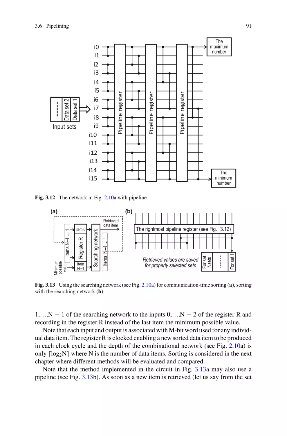
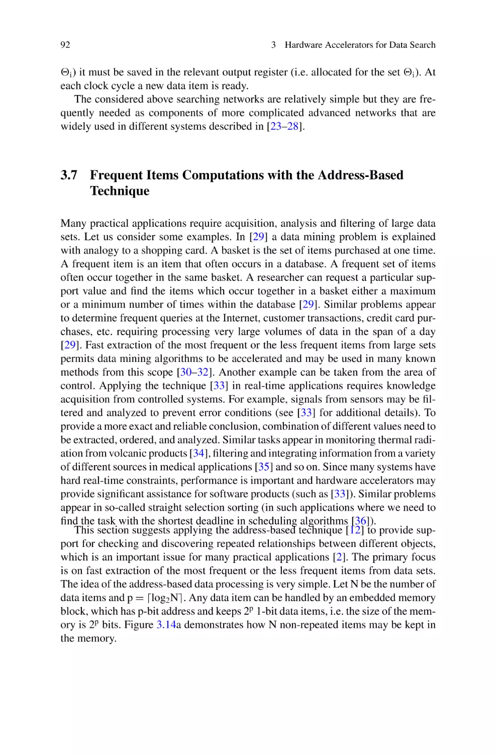
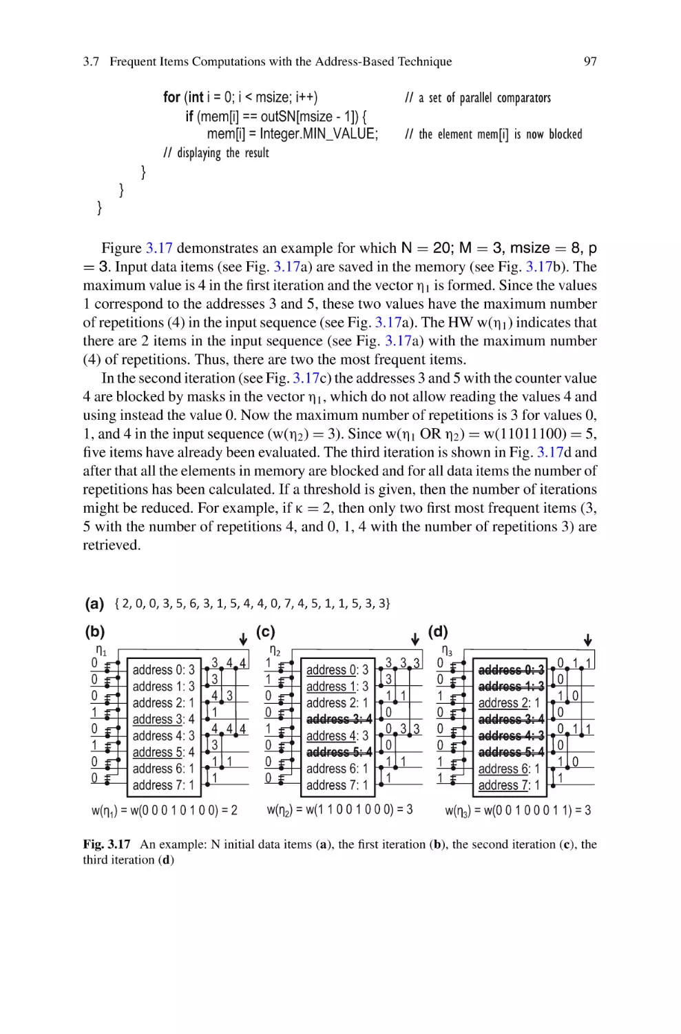
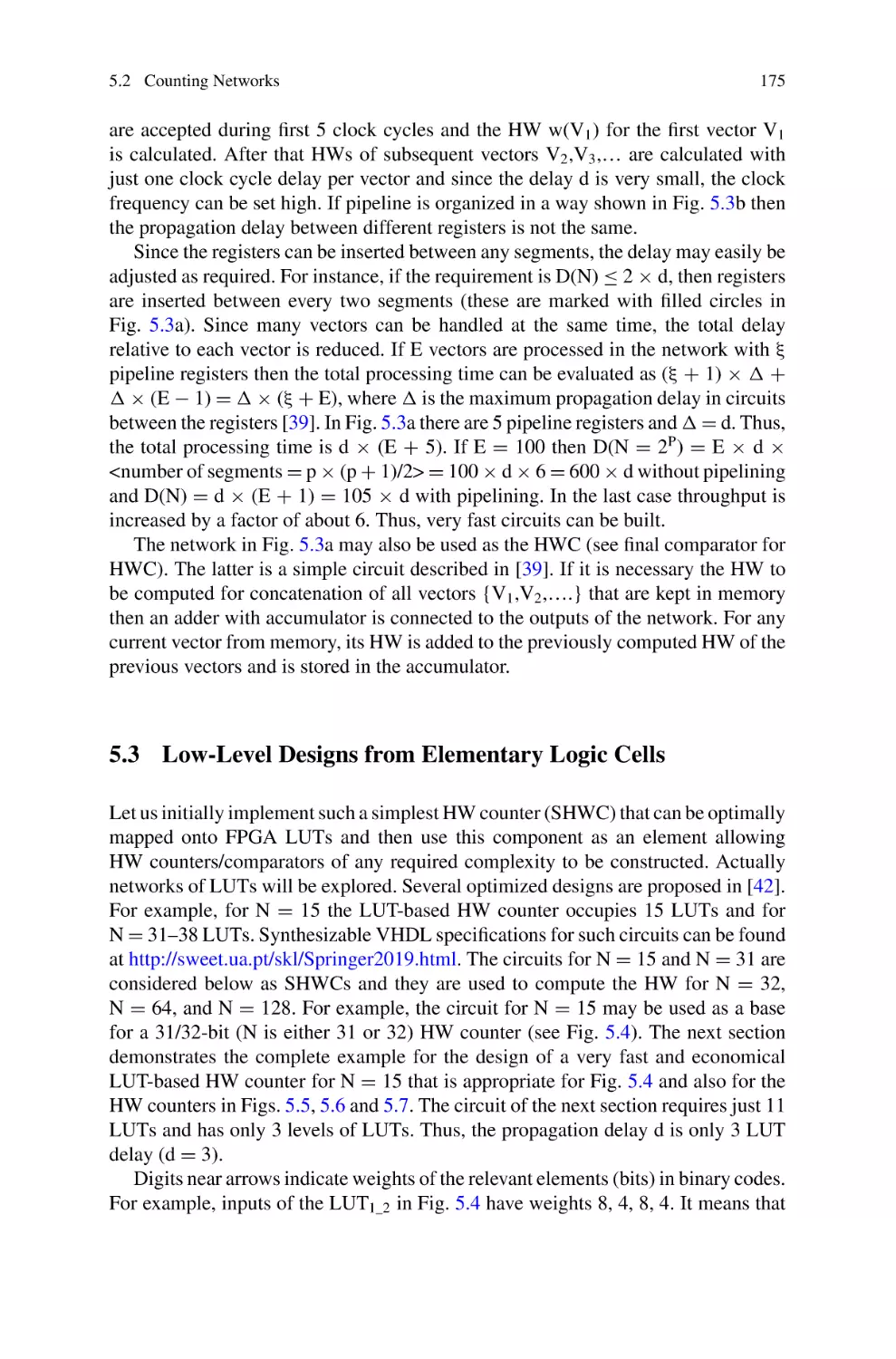
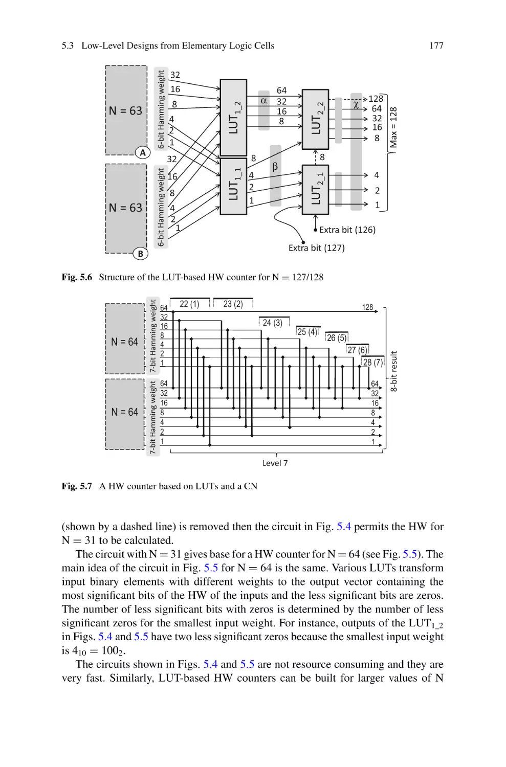
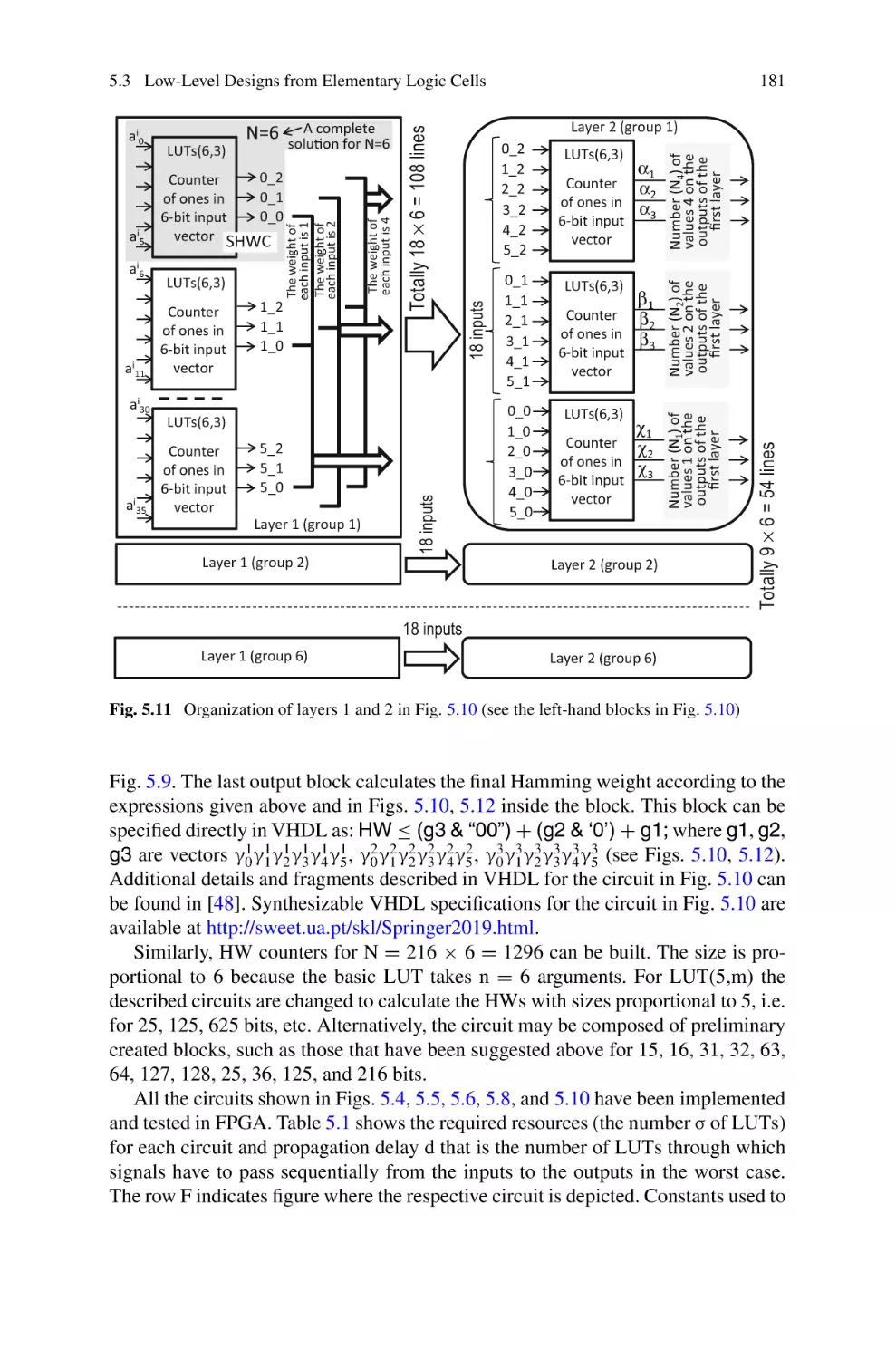
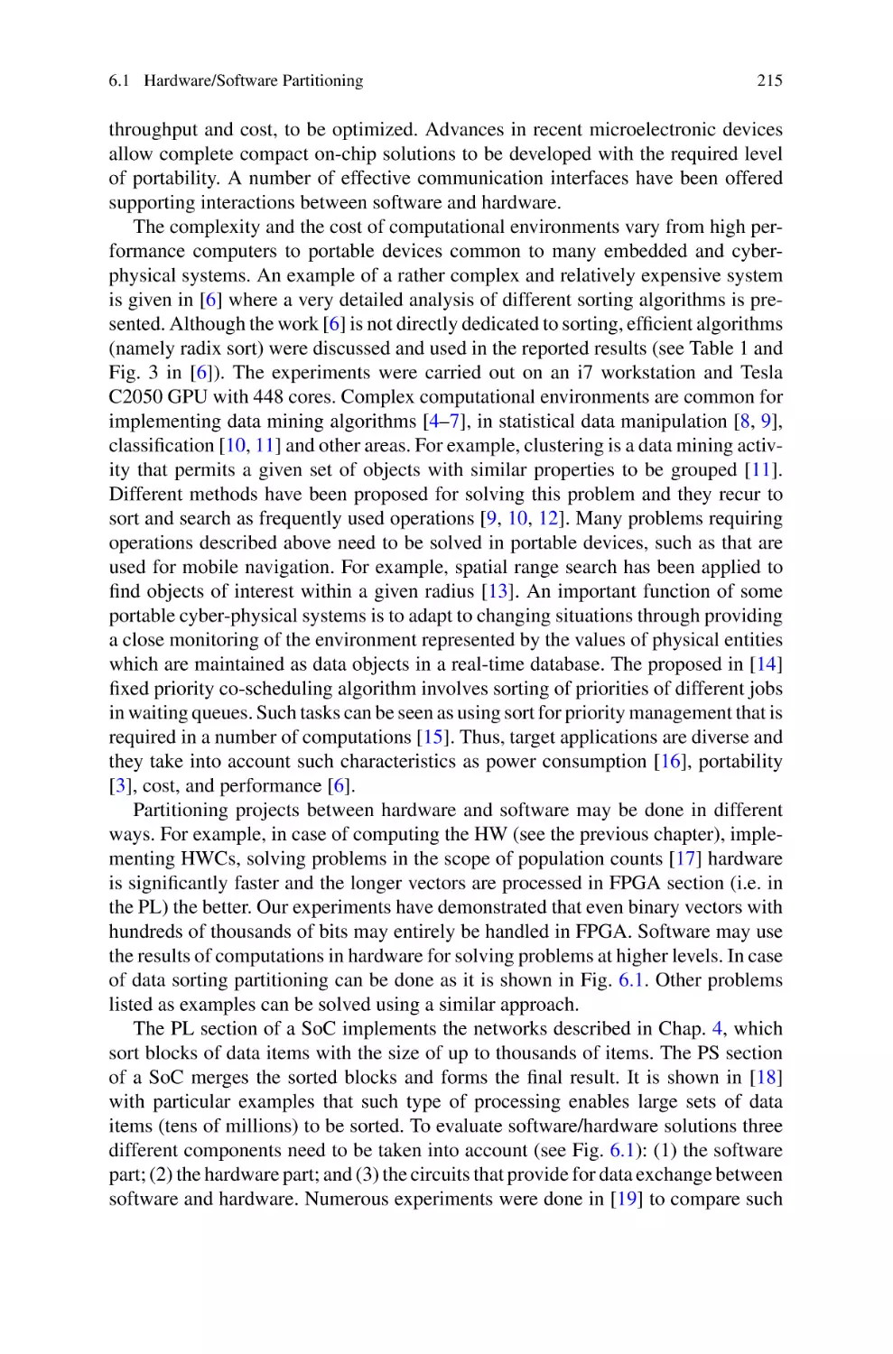
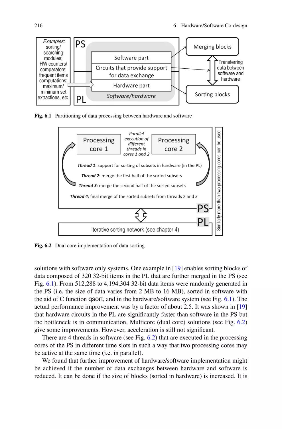
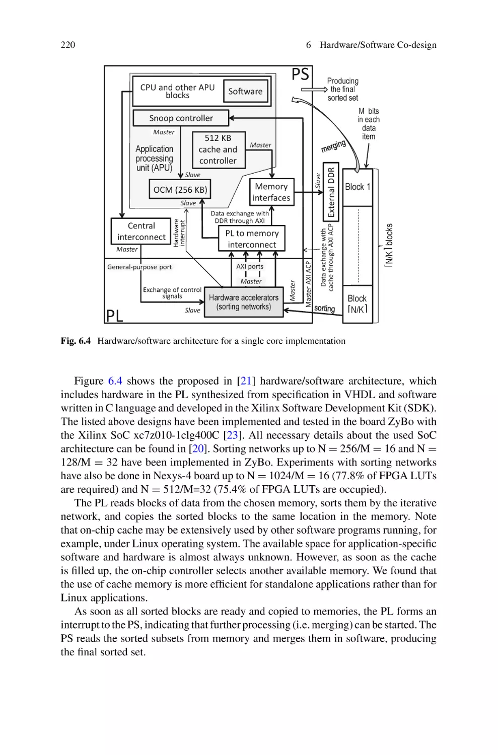
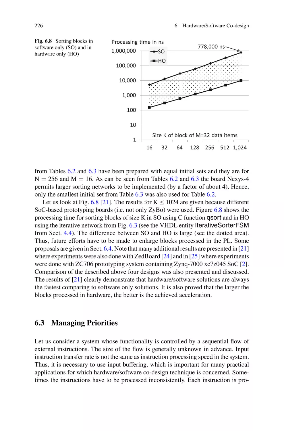
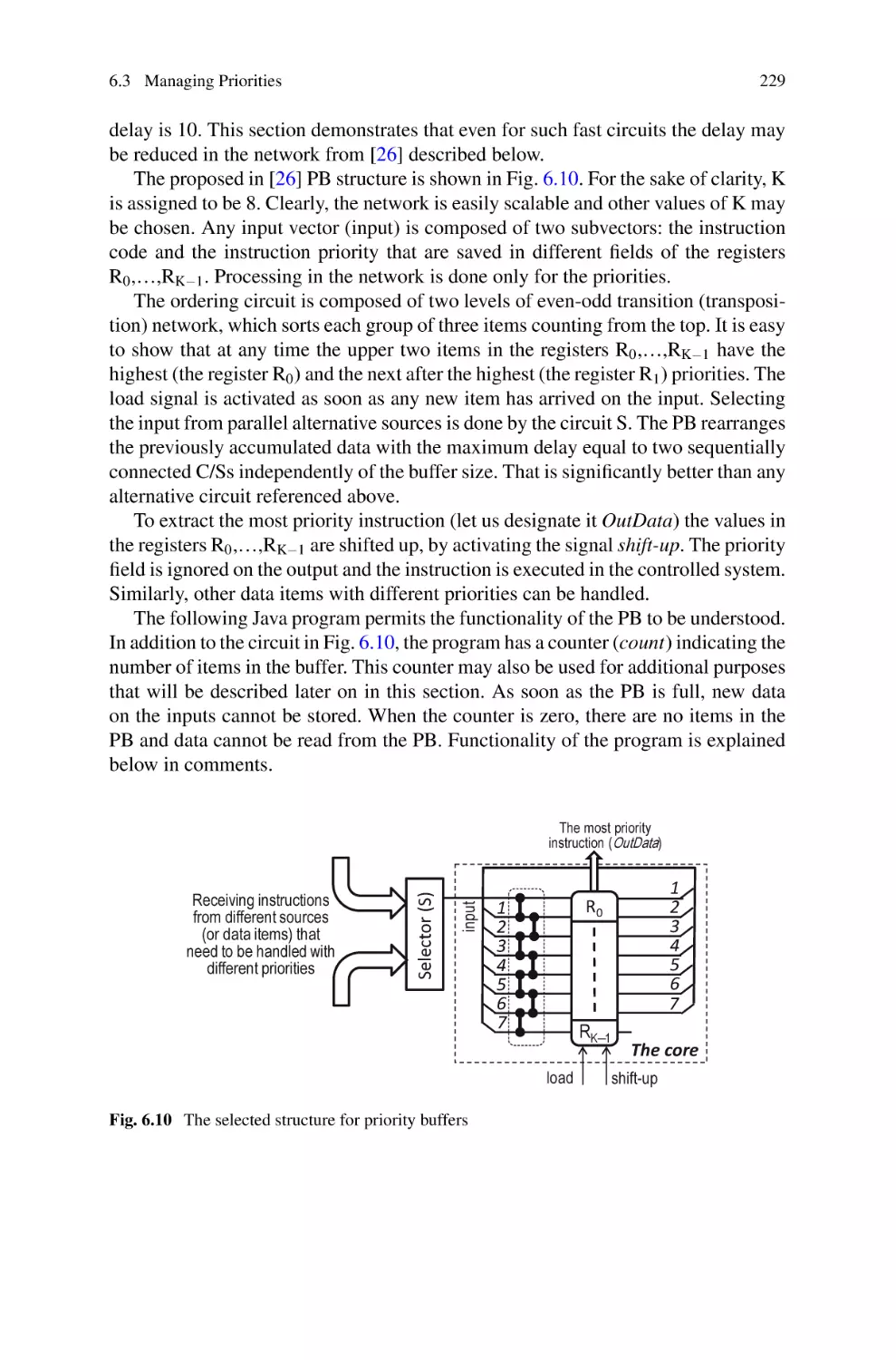
/


Text
Lecture Notes in Electrical Engineering 566
Iouliia Skliarova
Valery Sklyarov
FPGA-BASED
Hardware
Accelerators
Lecture Notes in Electrical Engineering
Volume 566
Series Editors
Leopoldo Angrisani, Department of Electrical and Information Technologies Engineering, University of Napoli
Federico II, Naples, Italy
Marco Arteaga, Departament de Control y Robótica, Universidad Nacional Autónoma de México, Coyoacán,
Mexico
Bijaya Ketan Panigrahi, Electrical Engineering, Indian Institute of Technology Delhi, New Delhi, Delhi, India
Samarjit Chakraborty, Fakultät für Elektrotechnik und Informationstechnik, TU München, Munich, Germany
Jiming Chen, Zhejiang University, Hangzhou, Zhejiang, China
Shanben Chen, Materials Science & Engineering, Shanghai Jiao Tong University, Shanghai, China
Tan Kay Chen, Department of Electrical and Computer Engineering, National University of Singapore,
Singapore, Singapore
Rüdiger Dillmann, Humanoids and Intelligent Systems Lab, Karlsruhe Institute for Technology, Karlsruhe,
Baden-Württemberg, Germany
Haibin Duan, Beijing University of Aeronautics and Astronautics, Beijing, China
Gianluigi Ferrari, Università di Parma, Parma, Italy
Manuel Ferre, Centre for Automation and Robotics CAR (UPM-CSIC), Universidad Politécnica de Madrid,
Madrid, Spain
Sandra Hirche, Department of Electrical Engineering and Information Science, Technische Universität
München, Munich, Germany
Faryar Jabbari, Department of Mechanical and Aerospace Engineering, University of California, Irvine, CA,
USA
Limin Jia, State Key Laboratory of Rail Traffic Control and Safety, Beijing Jiaotong University, Beijing, China
Janusz Kacprzyk, Systems Research Institute, Polish Academy of Sciences, Warsaw, Poland
Alaa Khamis, German University in Egypt El Tagamoa El Khames, New Cairo City, Egypt
Torsten Kroeger, Stanford University, Stanford, CA, USA
Qilian Liang, Department of Electrical Engineering, University of Texas at Arlington, Arlington, TX, USA
Ferran Martin, Departament d’Enginyeria Electrònica, Universitat Autònoma de Barcelona, Bellaterra,
Barcelona, Spain
Tan Cher Ming, College of Engineering, Nanyang Technological University, Singapore, Singapore
Wolfgang Minker, Institute of Information Technology, University of Ulm, Ulm, Germany
Pradeep Misra, Department of Electrical Engineering, Wright State University, Dayton, OH, USA
Sebastian Möller, Quality and Usability Lab, TU Berlin, Berlin, Germany
Subhas Mukhopadhyay, School of Engineering & Advanced Technology, Massey University,
Palmerston North, Manawatu-Wanganui, New Zealand
Cun-Zheng Ning, Electrical Engineering, Arizona State University, Tempe, AZ, USA
Toyoaki Nishida, Graduate School of Informatics, Kyoto University, Kyoto, Japan
Federica Pascucci, Dipartimento di Ingegneria, Università degli Studi “Roma Tre”, Rome, Italy
Yong Qin, State Key Laboratory of Rail Traffic Control and Safety, Beijing Jiaotong University, Beijing, China
Gan Woon Seng, School of Electrical & Electronic Engineering, Nanyang Technological University,
Singapore, Singapore
Joachim Speidel, Institute of Telecommunications, Universität Stuttgart, Stuttgart, Baden-Württemberg,
Germany
Germano Veiga, Campus da FEUP, INESC Porto, Porto, Portugal
Haitao Wu, Academy of Opto-electronics, Chinese Academy of Sciences, Beijing, China
Junjie James Zhang, Charlotte, NC, USA
The book series Lecture Notes in Electrical Engineering (LNEE) publishes the latest developments
in Electrical Engineering—quickly, informally and in high quality. While original research
reported in proceedings and monographs has traditionally formed the core of LNEE, we also
encourage authors to submit books devoted to supporting student education and professional
training in the various fields and applications areas of electrical engineering. The series cover
classical and emerging topics concerning:
•
•
•
•
•
•
•
•
•
•
•
•
Communication Engineering, Information Theory and Networks
Electronics Engineering and Microelectronics
Signal, Image and Speech Processing
Wireless and Mobile Communication
Circuits and Systems
Energy Systems, Power Electronics and Electrical Machines
Electro-optical Engineering
Instrumentation Engineering
Avionics Engineering
Control Systems
Internet-of-Things and Cybersecurity
Biomedical Devices, MEMS and NEMS
For general information about this book series, comments or suggestions, please contact leontina.
dicecco@springer.com.
To submit a proposal or request further information, please contact the Publishing Editor in
your country:
China
Jasmine Dou, Associate Editor (jasmine.dou@springer.com)
India
Swati Meherishi, Executive Editor (swati.meherishi@springer.com)
Aninda Bose, Senior Editor (aninda.bose@springer.com)
Japan
Takeyuki Yonezawa, Editorial Director (takeyuki.yonezawa@springer.com)
South Korea
Smith (Ahram) Chae, Editor (smith.chae@springer.com)
Southeast Asia
Ramesh Nath Premnath, Editor (ramesh.premnath@springer.com)
USA, Canada:
Michael Luby, Senior Editor (michael.luby@springer.com)
All other Countries:
Leontina Di Cecco, Senior Editor (leontina.dicecco@springer.com)
Christoph Baumann, Executive Editor (christoph.baumann@springer.com)
** Indexing: The books of this series are submitted to ISI Proceedings, EI-Compendex,
SCOPUS, MetaPress, Web of Science and Springerlink **
More information about this series at http://www.springer.com/series/7818
Iouliia Skliarova Valery Sklyarov
•
FPGA-BASED Hardware
Accelerators
123
Iouliia Skliarova
Department of Electronics
Telecommunications and Informatics
University of Aveiro
Aveiro, Portugal
Valery Sklyarov
Department of Electronics
Telecommunications and Informatics
University of Aveiro
Aveiro, Portugal
ISSN 1876-1100
ISSN 1876-1119 (electronic)
Lecture Notes in Electrical Engineering
ISBN 978-3-030-20720-5
ISBN 978-3-030-20721-2 (eBook)
https://doi.org/10.1007/978-3-030-20721-2
© Springer Nature Switzerland AG 2019
This work is subject to copyright. All rights are reserved by the Publisher, whether the whole or part
of the material is concerned, specifically the rights of translation, reprinting, reuse of illustrations,
recitation, broadcasting, reproduction on microfilms or in any other physical way, and transmission
or information storage and retrieval, electronic adaptation, computer software, or by similar or dissimilar
methodology now known or hereafter developed.
The use of general descriptive names, registered names, trademarks, service marks, etc. in this
publication does not imply, even in the absence of a specific statement, that such names are exempt from
the relevant protective laws and regulations and therefore free for general use.
The publisher, the authors and the editors are safe to assume that the advice and information in this
book are believed to be true and accurate at the date of publication. Neither the publisher nor the
authors or the editors give a warranty, expressed or implied, with respect to the material contained
herein or for any errors or omissions that may have been made. The publisher remains neutral with regard
to jurisdictional claims in published maps and institutional affiliations.
This Springer imprint is published by the registered company Springer Nature Switzerland AG
The registered company address is: Gewerbestrasse 11, 6330 Cham, Switzerland
Preface
Field-programmable gate arrays (FPGAs) were invented by Xilinx in 1985, i.e.,
about 35 years ago. Currently, they are part of heterogeneous computer platforms
that combine different types of processing systems with new generations of programmable logic. The influence of FPGAs on many directions in engineering is
growing continuously and rapidly. Forecasts suggest that the impact of FPGAs will
continue to expand, and the range of applications will increase considerably in
future. Recent field-configurable microchips incorporate scalar and vector
multi-core processing elements and reconfigurable logic appended with a number of
frequently used devices. FPGA-based systems can be specified, simulated, synthesized, and implemented in general-purpose computers by using dedicated integrated design environments. Experiments and explorations of such systems are
commonly based on prototyping boards that are linked to the design environment.
It is widely known that FPGAs can be applied efficiently in a vast variety of
engineering applications. One reason for this is that growing system complexity
makes it very difficult to ship designs without errors. Hence, it has become essential
to be able to fix errors after fabrication, and customizable devices, such as FPGAs,
make this much easier.
The complexity of contemporary chips is increasing exponentially with time,
and the number of available transistors is growing faster than the ability to design
meaningfully with them. This situation is a well-known design productivity gap,
which is increasing continuously. The extensive involvement of FPGAs in new
designs of circuits and systems and the need for better design productivity
undoubtedly require huge engineering resources, which are the major output of
technical universities. This book is intended to provide substantial assistance for
courses relating to the design and development of systems using FPGAs. Several
steps in the design process are discussed, including system modeling in software,
the retrieval of basic software functions, and the automatic mapping of these
functions to highly optimized hardware specifications. Finally, the synthesis and
implementation of circuits and systems is done in industrial computer-aided design
environments.
v
vi
Preface
FPGAs still operate at lower clock frequencies than general-purpose computers
and application-specific integrated circuits. The cost of the most advanced FPGA
devices is high, and cheaper FPGAs support clock frequencies that are much lower
than those in inexpensive computers that are used widely. One of the most
important applications of FPGAs is improving performance. Obviously, to achieve
acceleration with devices that are generally slower, parallelism needs to be applied
extensively and explaining how this can be achieved is the main target of this book.
Several types of hardware accelerators are studied and discussed in the context
of the following areas: (1) searching networks and their varieties, (2) sorting networks and a number of derived architectures, (3) counting networks, and (4) networks from lookup tables focusing on the rational decomposition of combinational
circuits. The benefits of the proposed methods and architectures are demonstrated
through examples from data processing and data mining, combinatorial searching,
encoding, as well as a number of other frequently required computations.
The following features set this book apart from others in the field:
1. The methodology discussed shows in detail how design ideas can be advanced
from rough modeling in software through to synthesizable hardware description
language specifications. Basic functions are retrieved from software and automatically transformed to core operational blocks in decompositions of the
developed circuits that are suggested.
2. Traditional highly parallel searching and sorting networks are combined with
other types of networks to allow complex combinational and sequential circuits
to be decomposed within regular reusable structures. Note that core components
of the network may be different from commonly used comparators/swappers.
3. Regular and easily scalable designs are described using a variety of networks
based on iterative hardware implementations. Relatively large highly parallel
segments of the developed circuit are reused iteratively, which allows the
number of core elements to be reduced dramatically, thus maximizing the
potential throughput with given hardware.
4. A number of synthesizable hardware description language specifications (in
VHDL) are provided that are ready to be tested and incorporated into practical
engineering designs. This can be an extremely valuable reference base for both
undergraduate and postgraduate university students. Many synthesizable VHDL
specifications are available online at http://sweet.ua.pt/skl/Springer2019.
The chapters in the book contain the following material:
Chapter 1 provides an introduction to reconfigurable devices (i.e., fieldprogrammable gate arrays and hardware programmable systems-on-chip), design
languages, methods, and tools that will be used in the book. The core reconfigurable
elements and the most common embedded blocks are briefly described, addressing
only those features that are needed in subsequent chapters. A number of simple
examples are given that are ready to be tested in FPGA-based prototyping boards,
two of which are briefly overviewed. Finally, the various types of networks that are
studied in the rest of the book are characterized in outline.
Preface
vii
Chapter 2 underlines that to compete with the existing alternative solutions (both
in hardware and in software), wide-level parallelism must be implemented in
FPGA-based circuits with small propagation delays. Several useful techniques are
discussed and analyzed, one example being the ratio between combinational and
sequential computations at different levels. Communication-time data processing is
introduced. Many supplementary components that are needed for hardware accelerators are described, implemented, and tested. Finally, different aspects of design
are discussed, and a range of useful examples are given.
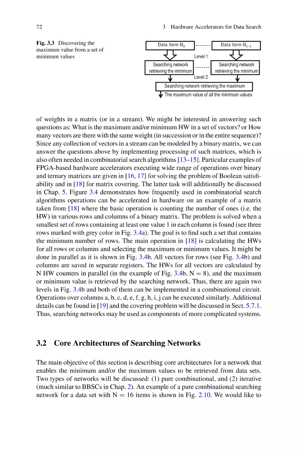
Chapter 3 is dedicated to searching networks. These allow extreme values in a
data set to be found, or items in a set that satisfy some predefined conditions or
limitations, indicated by given thresholds, to be identified. The simplest task discussed is retrieving the maximum and/or the minimum values or subsets from a data
set. More complicated procedures are described that permit the most frequently
occurring value/item to be found, or the retrieval of a set of the most frequent
values/items above a given threshold, or satisfying some other constraint. These
tasks can be solved for entire data sets, for intervals of data sets, or for specially
organized structures.
Chapter 4 studies sorting networks, with the emphasis on regular and easily
scalable structures that permit data to be sorted and a number of supplementary
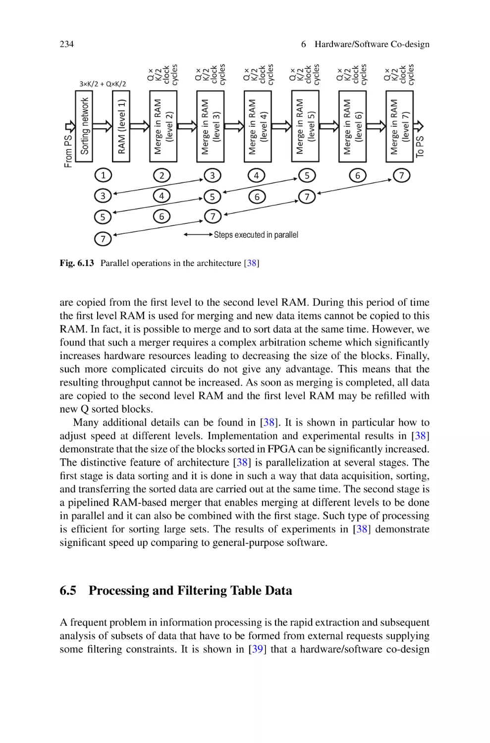
(derived) problems to be solved. Two core architectures are discussed: (1) an
iterative approach that is based on a highly parallel combinational sorting network
with minimal propagation delay, and (2) a communication-time architecture that
allows data to be processed as soon as a new item is received, thus minimizing
communication overhead. Several new problems are addressed, namely the retrieval
maximum and/or minimum sorted subsets, filtering, processing non-repeated items,
applying address-based techniques, and traditional pipelining together with the ring
pipeline that is introduced. Many examples are given and analyzed with complete
details.
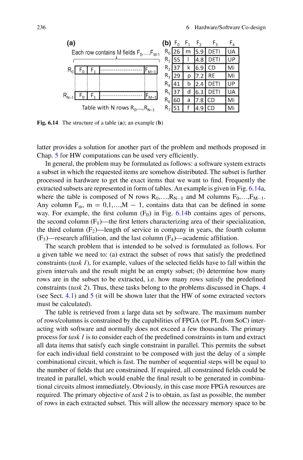
Chapter 5 identifies several computational problems that can be solved efficiently in FPGA-based hardware accelerators. Many of these involve the computation and comparison of Hamming weights. Three core methods are presented:
counting networks, low-level designs from elementary logic cells viewed as specially organized networks, and designs using arithmetical units involving FPGA
digital signal processing slices. Mixed solutions based on combining different
methods are also discussed. Many practical examples with synthesizable VHDL
code are given. Finally, the applicability of the proposed methods is demonstrated
using problems in combinatorial search, and data and information processing.
Chapter 6 concludes that for problems that allow a high level of parallelism to be
applied, hardware implementations are generally faster than software running in
general-purpose and application-specific computers. However, software is more
flexible and easily adaptable to potentially changing conditions and requirements.
Besides, on-chip hardware circuits introduce a number of constraints, primarily on
resources that limit the possible complexity of designs that can be implemented.
Thus, it makes sense to combine the flexibility, maintainability, and portability of
software with the speed and other capabilities of hardware, and this can be achieved
viii
Preface
in hardware/software co-design. Chapter 6 is dedicated to exploring these topics in
depth and discusses hardware/software partitioning, dedicated helpful blocks
(namely, priority buffers), hardware/software interaction, and some useful techniques that allow communication overhead to be reduced. A number of examples
are discussed.
The book can be used as the supporting material for university courses that
involve FPGA-based design, such as “Digital design,” “Computer architecture,”
“Embedded systems,” “Reconfigurable computing,” and “FPGA-based systems.” It
will also be helpful in engineering practice and research activity in areas where
FPGA-based circuits and systems are explored.
Aveiro, Portugal
Iouliia Skliarova
Valery Sklyarov
Conventions
1. VHDL/Java keywords are shown in bold font
2. VHDL/Java comments are shown in the following font:—this is a
comment
3. VHDL is not a case-sensitive language, and thus, UPPERCASE and lowercase
letters may be used interchangeably.
4. When a reference to a Java program is done, then the name of the relevant class
is pointed out. When a reference to a VHDL specification is done, then the name
of the relevant entity is indicated.
5. Java programs have been prepared as compact as possible. That is why many
required verifications (such as that are needed for files) have not been applied.
Besides, many input variables are declared as final constant values.
6. Xilinx Vivado 2018.3 has been used as the main design environment, but the
proposed specifications have been kept as platform-independent as possible.
Xilinx®, Artix®, Vivado®, and Zynq® are registered trademarks of Xilinx Inc.
Nexys-4 and ZyBo are trademarks of Digilent, Inc. Other product and company
names mentioned may be trademarks of their respective owners.
The research results reported in this book were supported by Portuguese
National Funds through the FCT—Foundation for Science and Technology, in the
context of the project UID/CEC/00127/2019.
ix
Contents
1 Reconfigurable Devices and Design Tools .
1.1 Introduction to Reconfigurable Devices
1.2 FPGA and SoC . . . . . . . . . . . . . . . . .
1.2.1 Logic Blocks . . . . . . . . . . . . . .
1.2.2 Memory Blocks . . . . . . . . . . . .
1.2.3 Signal Processing Slices . . . . . .
1.2.4 Systems-on-Chip . . . . . . . . . . .
1.3 Design and Prototyping . . . . . . . . . . . .
1.4 Design Methodology . . . . . . . . . . . . .
1.5 Problems Addressed . . . . . . . . . . . . . .
1.5.1 Searching Networks . . . . . . . . .
1.5.2 Sorting Networks . . . . . . . . . . .
1.5.3 Counting Networks . . . . . . . . .
1.5.4 LUT-Based Networks . . . . . . .
References . . . . . . . . . . . . . . . . . . . . . . . . .
.
.
.
.
.
.
.
.
.
.
.
.
.
.
.
.
.
.
.
.
.
.
.
.
.
.
.
.
.
.
.
.
.
.
.
.
.
.
.
.
.
.
.
.
.
.
.
.
.
.
.
.
.
.
.
.
.
.
.
.
.
.
.
.
.
.
.
.
.
.
.
.
.
.
.
.
.
.
.
.
.
.
.
.
.
.
.
.
.
.
.
.
.
.
.
.
.
.
.
.
.
.
.
.
.
.
.
.
.
.
.
.
.
.
.
.
.
.
.
.
.
.
.
.
.
.
.
.
.
.
.
.
.
.
.
.
.
.
.
.
.
.
.
.
.
.
.
.
.
.
.
.
.
.
.
.
.
.
.
.
.
.
.
.
.
.
.
.
.
.
.
.
.
.
.
.
.
.
.
.
.
.
.
.
.
.
.
.
.
.
.
.
.
.
.
.
.
.
.
.
.
.
.
.
.
.
.
.
.
.
.
.
.
.
.
.
.
.
.
.
.
.
.
.
.
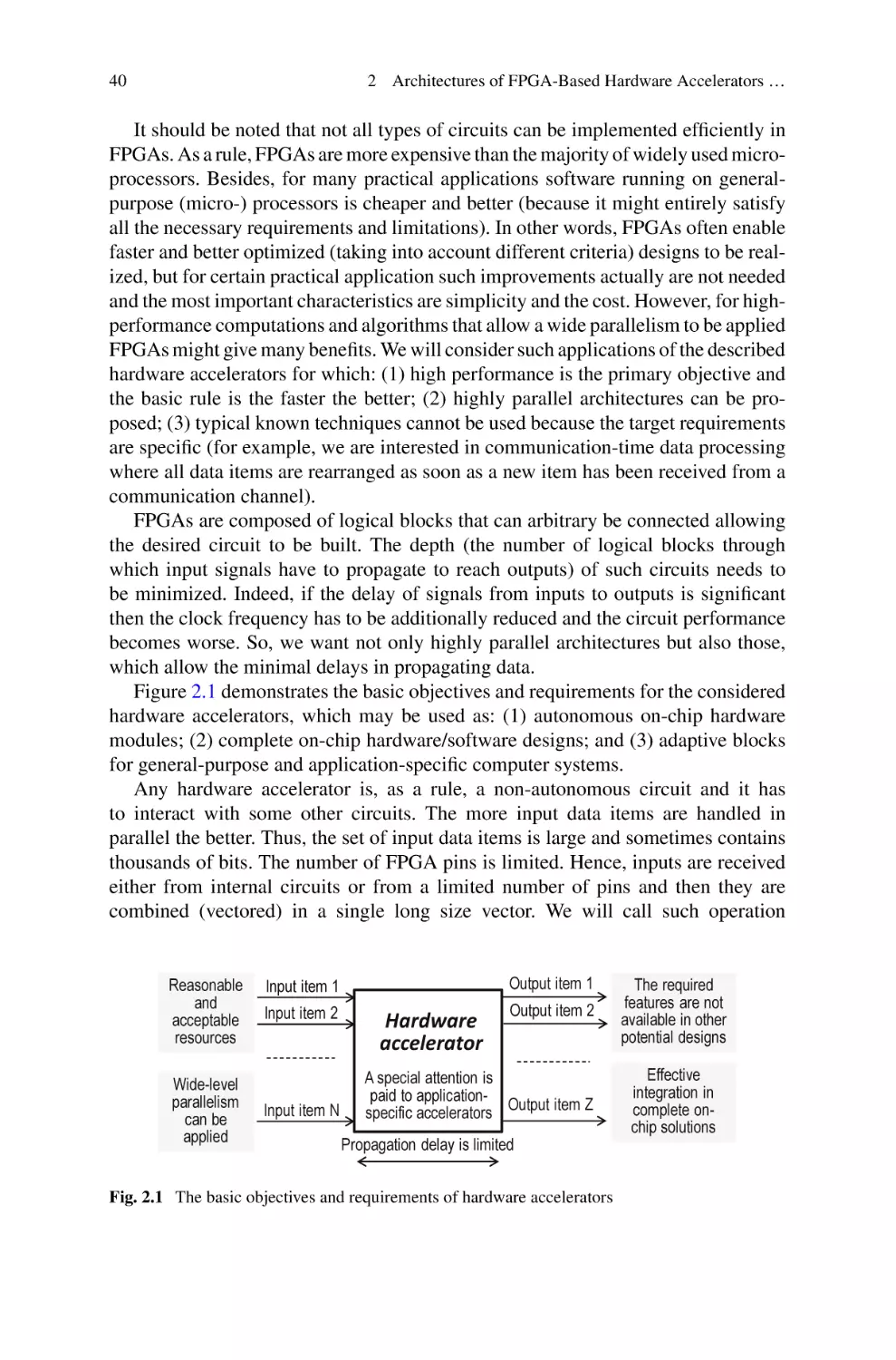
2 Architectures of FPGA-Based Hardware Accelerators
and Design Techniques . . . . . . . . . . . . . . . . . . . . . . . . . . . . . .
2.1 Why FPGA? . . . . . . . . . . . . . . . . . . . . . . . . . . . . . . . . . .
2.2 Combinational Versus Sequential Circuits . . . . . . . . . . . . .
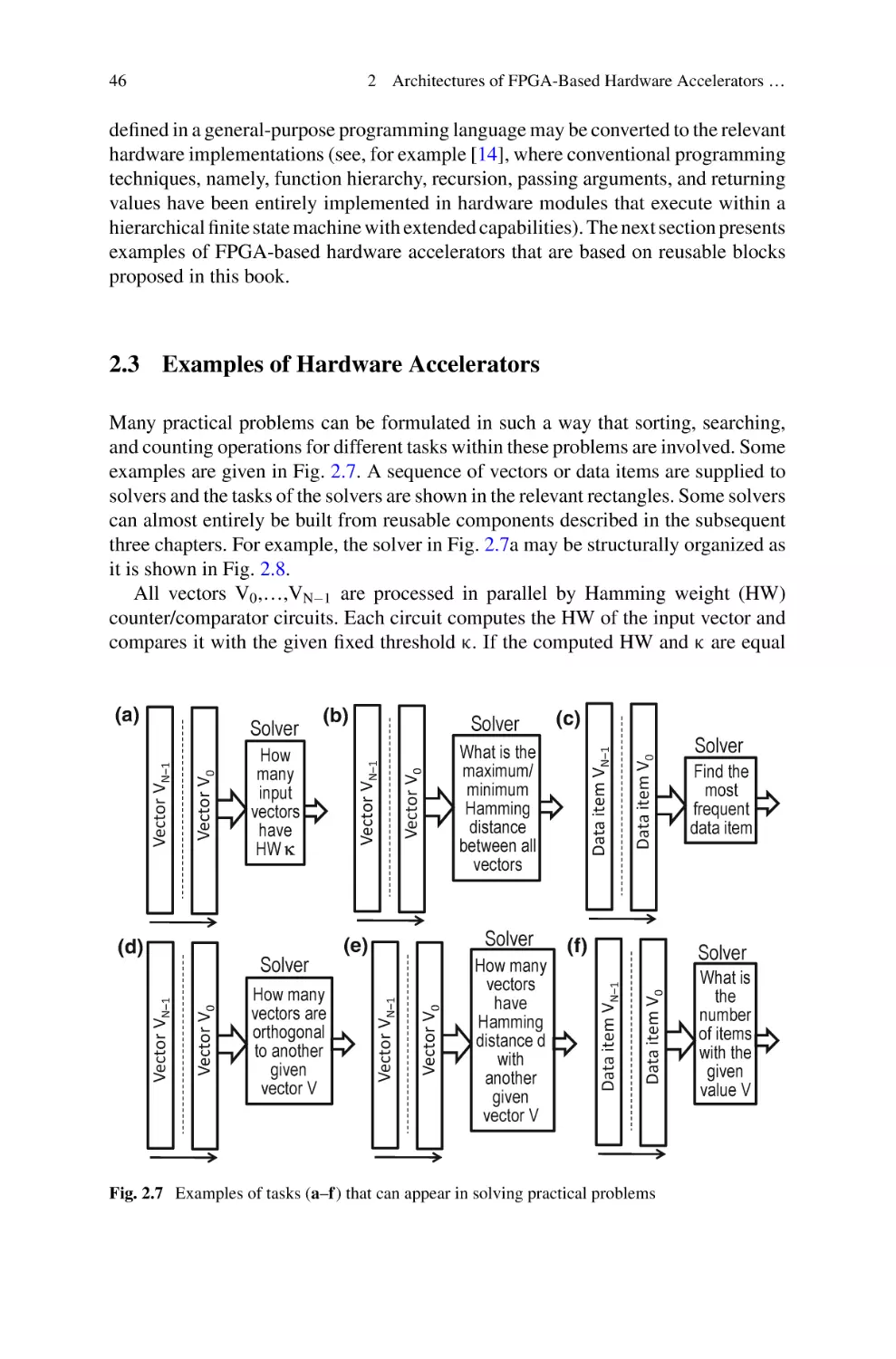
2.3 Examples of Hardware Accelerators . . . . . . . . . . . . . . . . .
2.4 Core Architectures of FPGA-Based Hardware Accelerators .
2.5 Design and Implementation of FPGA-Based Hardware
Accelerators . . . . . . . . . . . . . . . . . . . . . . . . . . . . . . . . . . .
2.6 Examples . . . . . . . . . . . . . . . . . . . . . . . . . . . . . . . . . . . . .
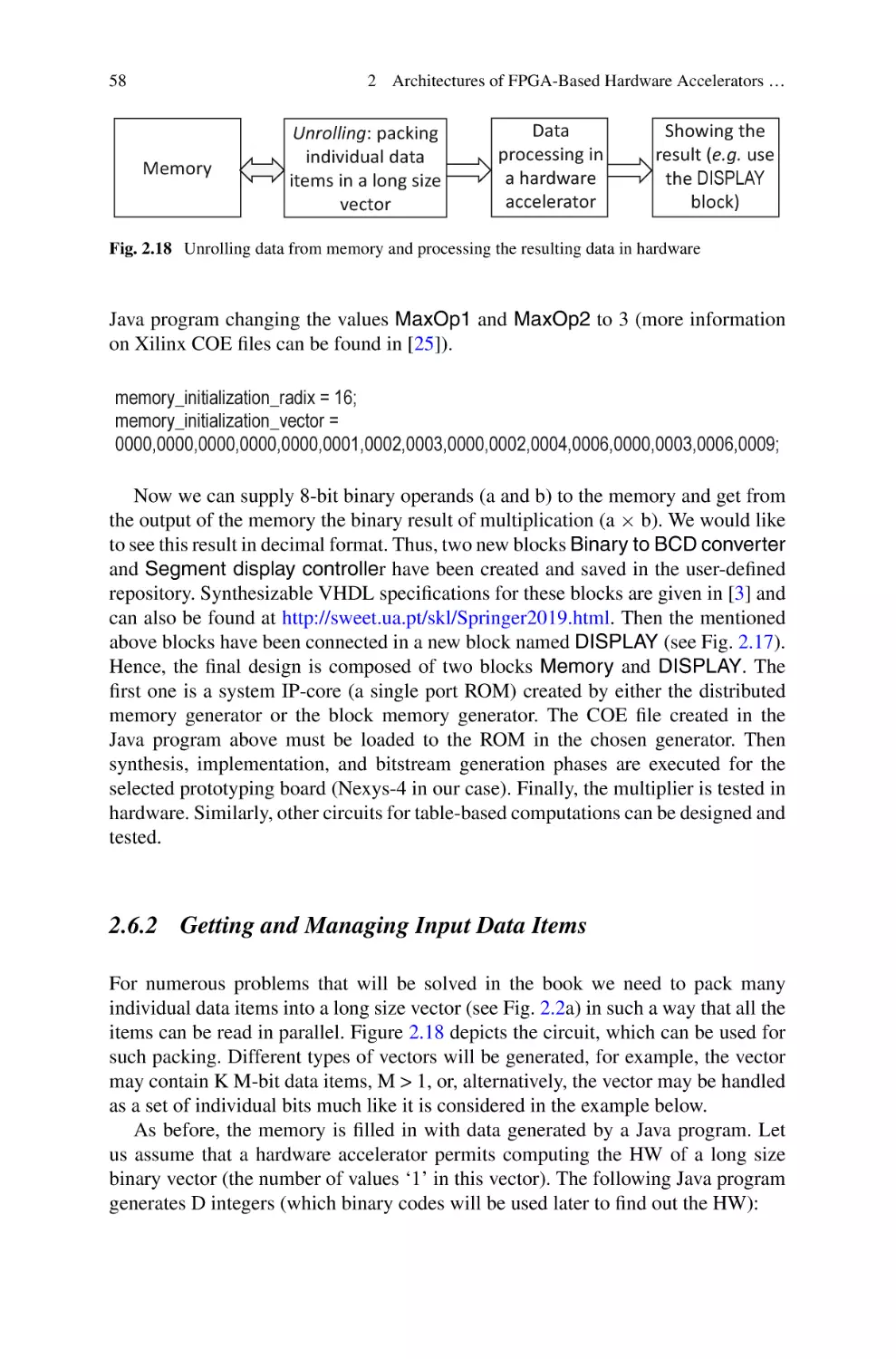
2.6.1 Table-Based Computations . . . . . . . . . . . . . . . . . . .
2.6.2 Getting and Managing Input Data Items . . . . . . . . .
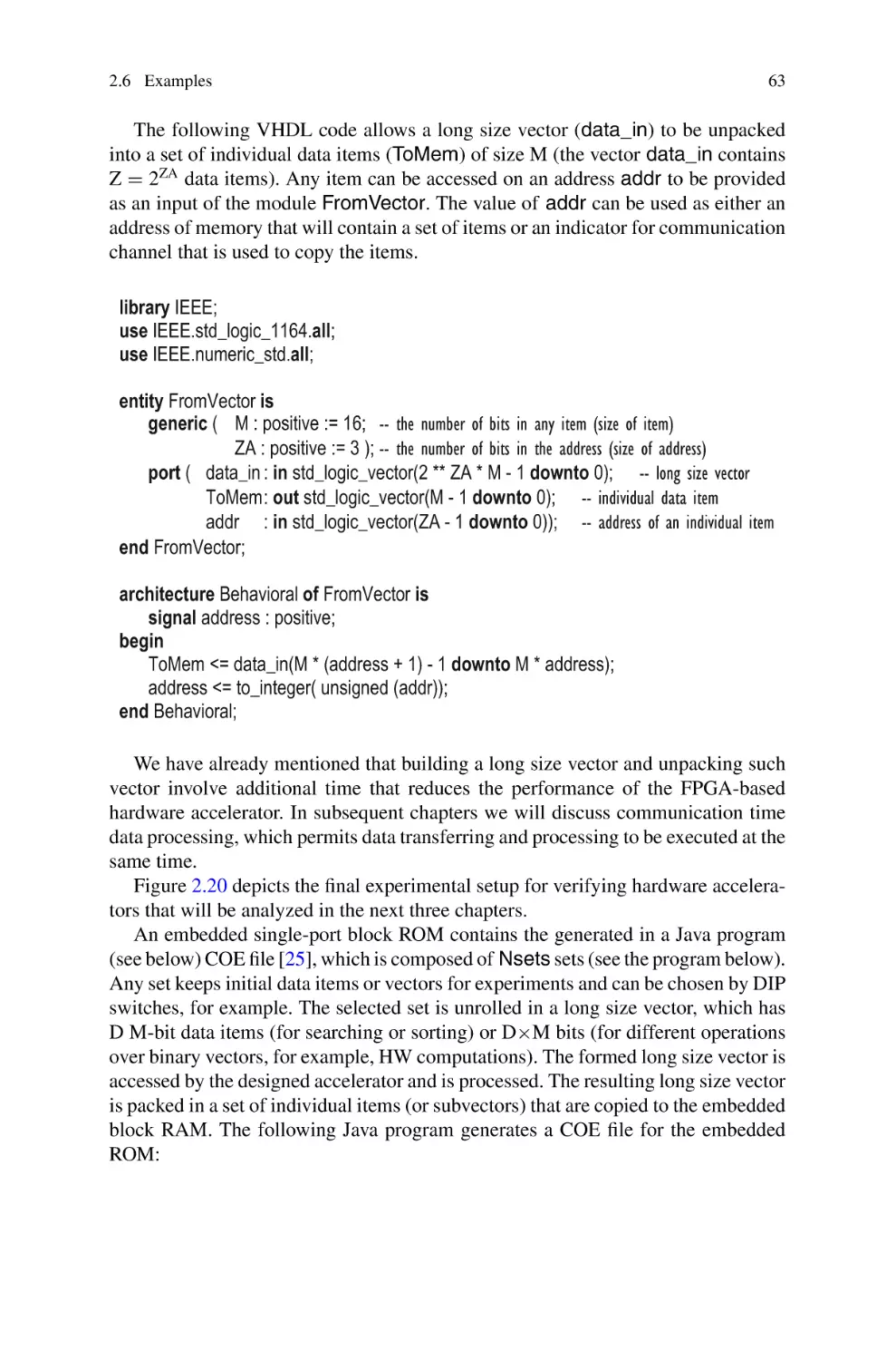
2.6.3 Getting and Managing Output Data Items . . . . . . . .
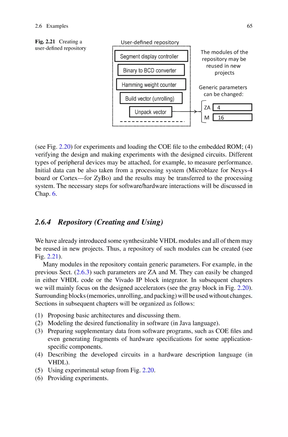
2.6.4 Repository (Creating and Using) . . . . . . . . . . . . . . .
References . . . . . . . . . . . . . . . . . . . . . . . . . . . . . . . . . . . . . . . .
.
.
.
.
.
.
.
.
.
.
.
.
.
.
.
.
.
.
.
.
.
.
.
.
.
.
.
.
.
.
.
.
.
.
.
.
.
.
.
.
.
.
.
.
.
.
.
.
.
.
.
.
.
.
.
.
.
.
.
.
.
.
.
.
.
.
.
.
.
.
.
.
.
.
.
1
1
2
3
6
9
13
15
18
27
28
29
33
34
36
.
.
.
.
.
.
.
.
.
.
.
.
.
.
.
.
.
.
.
.
.
.
.
.
.
39
39
42
46
48
.
.
.
.
.
.
.
.
.
.
.
.
.
.
.
.
.
.
.
.
.
.
.
.
.
.
.
.
.
.
.
.
.
.
.
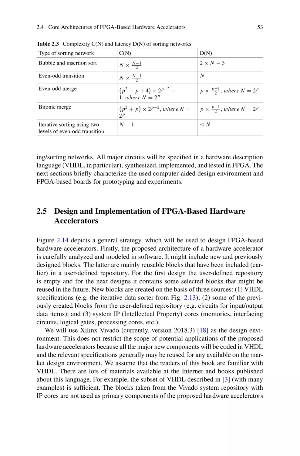
53
56
56
58
62
65
66
xi
xii
Contents
3 Hardware Accelerators for Data Search . . . . . . . . . . . . . . . . . .
3.1 Problem Definition . . . . . . . . . . . . . . . . . . . . . . . . . . . . . . .
3.2 Core Architectures of Searching Networks . . . . . . . . . . . . . .
3.3 Modeling Searching Networks in Software . . . . . . . . . . . . . .
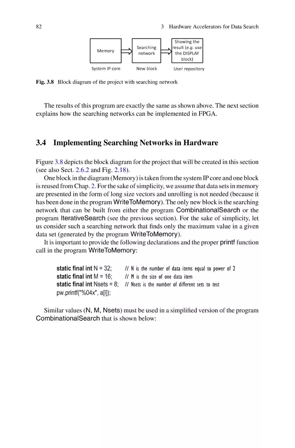
3.4 Implementing Searching Networks in Hardware . . . . . . . . . .
3.5 Search in Large Data Sets . . . . . . . . . . . . . . . . . . . . . . . . . .
3.6 Pipelining . . . . . . . . . . . . . . . . . . . . . . . . . . . . . . . . . . . . . .
3.7 Frequent Items Computations with the Address-Based
Technique . . . . . . . . . . . . . . . . . . . . . . . . . . . . . . . . . . . . .
3.8 Frequent Items Computations for a Set of Sorted Data Items
References . . . . . . . . . . . . . . . . . . . . . . . . . . . . . . . . . . . . . . . . .
4 Hardware Accelerators for Data Sort . . . . . . . . . . . . . . .
4.1 Problem Definition . . . . . . . . . . . . . . . . . . . . . . . . . .
4.2 Core Architectures of Sorting Networks . . . . . . . . . . .
4.3 Modeling Sorting Networks in Software . . . . . . . . . .
4.4 Implementing Sorting Networks in Hardware . . . . . . .
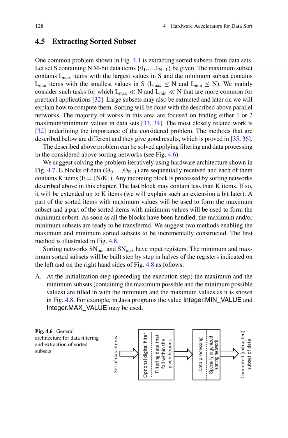
4.5 Extracting Sorted Subset . . . . . . . . . . . . . . . . . . . . . .
4.6 Modeling Networks for Data Extraction and Filtering
in Software . . . . . . . . . . . . . . . . . . . . . . . . . . . . . . .
4.7 Processing Non-repeated Values . . . . . . . . . . . . . . . .
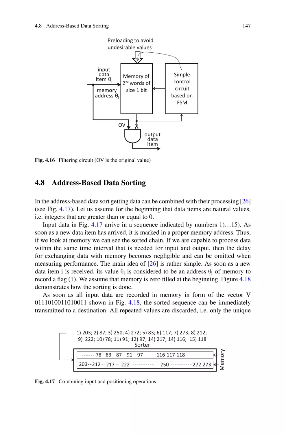
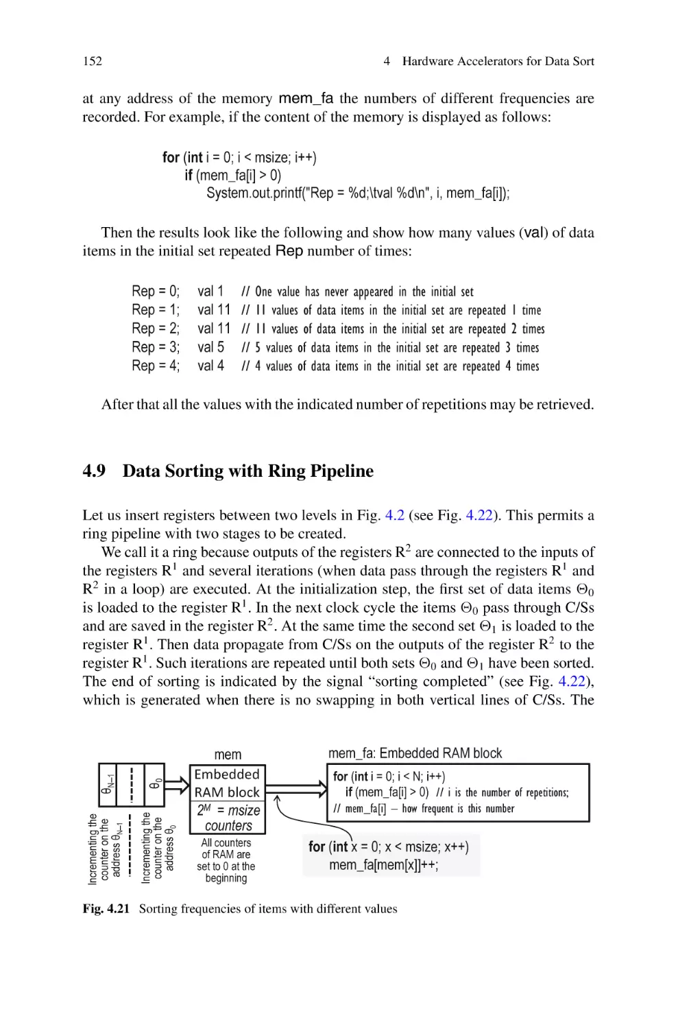
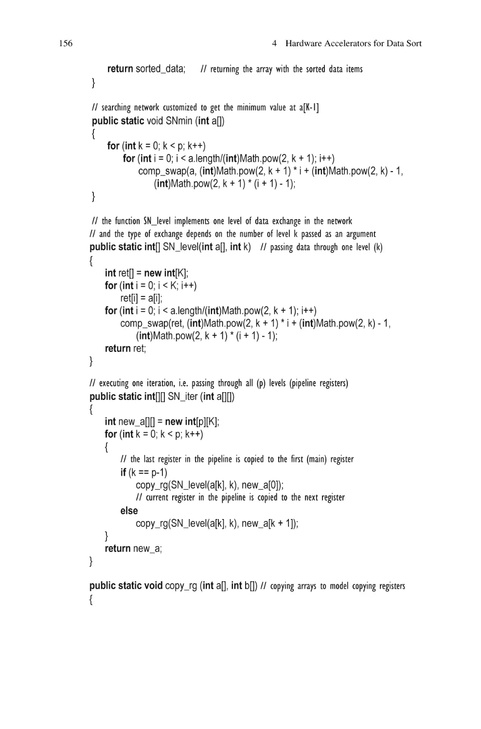
4.8 Address-Based Data Sorting . . . . . . . . . . . . . . . . . . .
4.9 Data Sorting with Ring Pipeline . . . . . . . . . . . . . . . .
References . . . . . . . . . . . . . . . . . . . . . . . . . . . . . . . . . . . .
.
.
.
.
.
.
.
.
.
.
.
.
.
.
.
.
.
.
.
.
.
.
.
.
.
.
.
.
69
69
72
78
82
86
90
....
92
....
98
. . . . 102
.
.
.
.
.
.
.
.
.
.
.
.
.
.
.
.
.
.
.
.
.
.
.
.
.
.
.
.
.
.
.
.
.
.
.
.
.
.
.
.
.
.
.
.
.
.
.
.
.
.
.
.
.
.
105
105
111
114
118
128
.
.
.
.
.
.
.
.
.
.
.
.
.
.
.
.
.
.
.
.
.
.
.
.
.
.
.
.
.
.
.
.
.
.
.
.
.
.
.
.
.
.
.
.
.
136
144
147
152
159
.
.
.
.
.
.
.
.
161
161
164
175
.
.
.
.
.
.
.
.
183
192
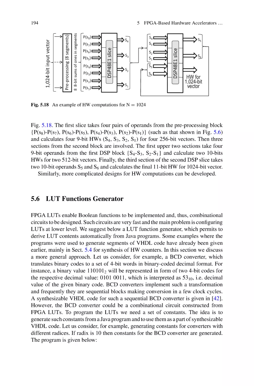
194
199
.
.
.
.
.
.
.
.
.
.
.
.
199
202
203
208
209
209
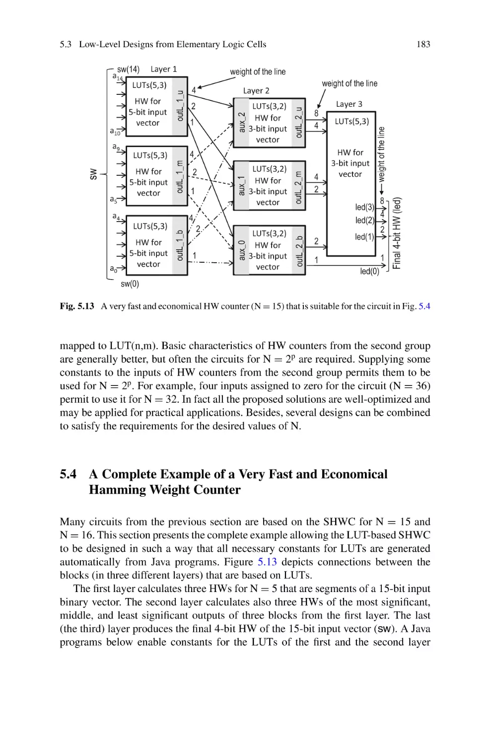
5 FPGA-Based Hardware Accelerators for Selected
Computational Problems . . . . . . . . . . . . . . . . . . . . . . . . . . . . . . . .
5.1 Introduction . . . . . . . . . . . . . . . . . . . . . . . . . . . . . . . . . . . . . .
5.2 Counting Networks . . . . . . . . . . . . . . . . . . . . . . . . . . . . . . . . .
5.3 Low-Level Designs from Elementary Logic Cells . . . . . . . . . . .
5.4 A Complete Example of a Very Fast and Economical Hamming
Weight Counter . . . . . . . . . . . . . . . . . . . . . . . . . . . . . . . . . . .
5.5 Using Arithmetical Units and Mixed Solutions . . . . . . . . . . . . .
5.6 LUT Functions Generator . . . . . . . . . . . . . . . . . . . . . . . . . . . .
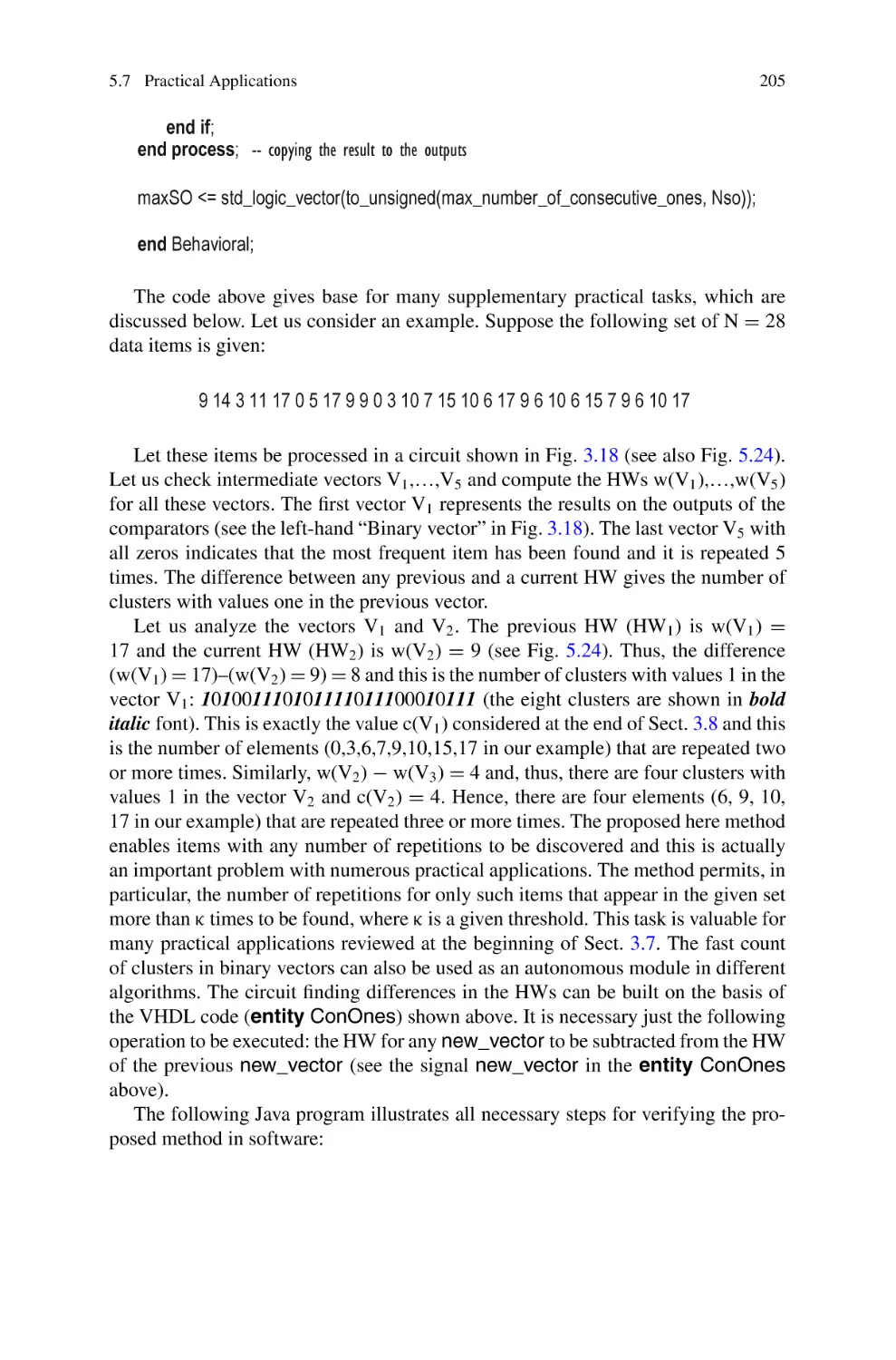
5.7 Practical Applications . . . . . . . . . . . . . . . . . . . . . . . . . . . . . . .
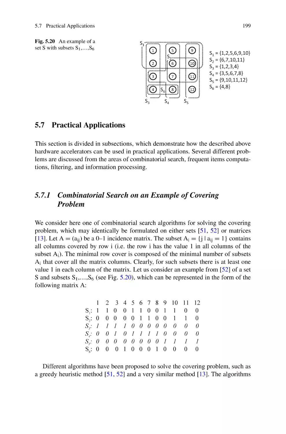
5.7.1 Combinatorial Search on an Example of Covering
Problem . . . . . . . . . . . . . . . . . . . . . . . . . . . . . . . . . . .
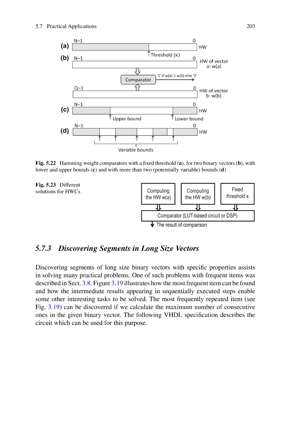
5.7.2 Hamming Weight Comparators . . . . . . . . . . . . . . . . . . .
5.7.3 Discovering Segments in Long Size Vectors . . . . . . . . .
5.7.4 Hamming Distance Computations . . . . . . . . . . . . . . . . .
5.7.5 Concluding Remarks . . . . . . . . . . . . . . . . . . . . . . . . . .
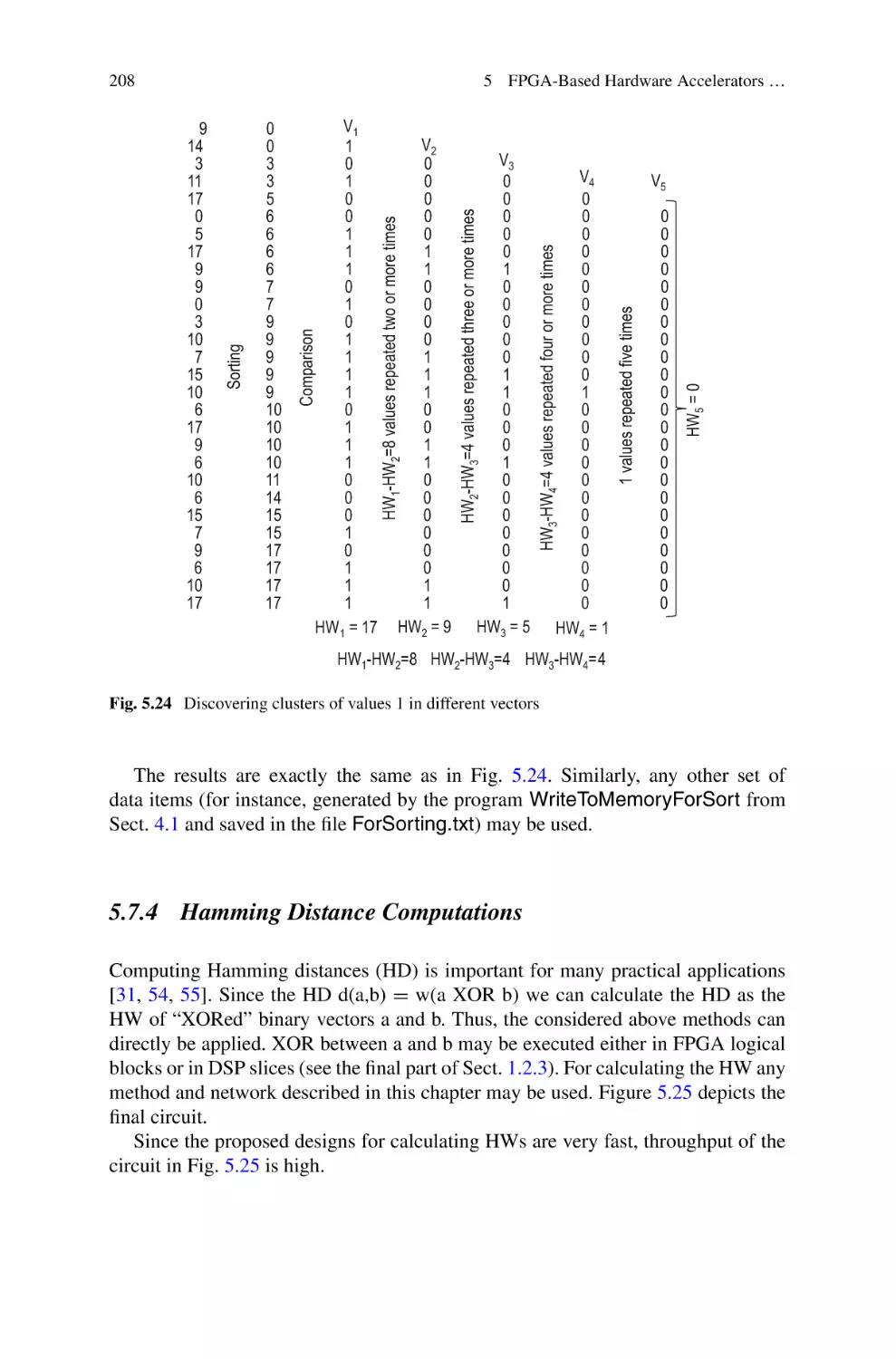
References . . . . . . . . . . . . . . . . . . . . . . . . . . . . . . . . . . . . . . . . . . .
Contents
6 Hardware/Software Co-design . . . . . . . . . . . . . . . . . .
6.1 Hardware/Software Partitioning . . . . . . . . . . . . . . .
6.2 An Example of Hardware/Software Co-design . . . .
6.3 Managing Priorities . . . . . . . . . . . . . . . . . . . . . . .
6.4 Managing Complexity (Hardware Versus Software)
6.5 Processing and Filtering Table Data . . . . . . . . . . . .
References . . . . . . . . . . . . . . . . . . . . . . . . . . . . . . . . . .
xiii
.
.
.
.
.
.
.
.
.
.
.
.
.
.
.
.
.
.
.
.
.
.
.
.
.
.
.
.
.
.
.
.
.
.
.
.
.
.
.
.
.
.
.
.
.
.
.
.
.
.
.
.
.
.
.
.
.
.
.
.
.
.
.
.
.
.
.
.
.
.
.
.
.
.
.
.
.
213
213
217
226
232
234
239
Index . . . . . . . . . . . . . . . . . . . . . . . . . . . . . . . . . . . . . . . . . . . . . . . . . . . . . . 243
Abbreviations
ACP
AI
ALU
APU
ARM
ASIC
ASSP
AXI
BBSC
BCD
BOOST
CA
CAD
CC
CLB
CN
COE
CPU
C/S
DDR
DIP
DSP
FIFO
FPGA
FR
FSM
GP
GPI
GPU
HD
Accelerator Coherency Port
Artificial Intelligence
Arithmetic and Logic Unit
Application Processing Unit
Advanced RISC Machine
Application-specific Integrated Circuit
Application-specific Standard Product
Advanced eXtensible Interface
Block-based Sequential Circuit
Binary-coded Decimal
BOolean Operation-based Screening and Testing
Comparator/Accumulator
Computer-aided Design
Combinational Circuit
Configurable Logic Block
Counting Network
Xilinx Coefficient
Central Processing Unit
Comparator/Swapper
Double Data Rate
Dual In-line Package
Digital Signal Processing
First-input First-output
Field-programmable Gate Array
Feedback Register
Finite State Machine
General-purpose
General-purpose Interface
Graphics Processing Unit
Hamming Distance
xv
xvi
HDL
HFSM
HP
HW
HWC
I/O
IP
LED
LSB
LUT
MSB
OB
OCM
OV
PB
PC
PCI
PL
POPCNT
PS
RAM
ROM
RTL
SAT
SC
SDK
SHWC
SN
SoC
SRAM
VCNT
VHDL
VHSIC
Abbreviations
Hardware Description Language
Hierarchical Finite State Machine
High Performance
Hamming Weight
Hamming Weight Comparator
Input/Output
Intellectual Property
Light-emitting Diode
Least Significant Bit
Lookup Table
Most Significant Bit
Output Block
On-chip Memory
Original Value
Priority Buffer
Personal Computer
Peripheral Component Interconnect
Programmable Logic
Population Count
Processing System
Random-access Memory
Read-only Memory
Register-transfer Level
Boolean Satisfiability
Sequential Circuit
Software Development Kit
Simplest Hamming Weight Counter
Searching/Sorting Network
System-on-chip
Static Random-access Memory
Vector Count set bits
VHSIC Hardware Description Language
Very High-speed Integrated Circuits
Chapter 1
Reconfigurable Devices and Design Tools
Abstract This chapter gives a short introduction to reconfigurable devices (FieldProgrammable Gate Arrays—FPGA and hardware programmable Systems-onChip—SoC), design languages, methods, and tools that will be used in the book.
The core reconfigurable elements and the most common embedded blocks are
briefly characterized. A generic design flow is discussed and some examples are
given that are ready to be tested in FPGA/SoC-based prototyping boards. All the
subsequent chapters of the book will follow the suggested design methodology that
includes: (1) proposing and evaluating basic architectures that are well suited for
hardware accelerators; (2) modeling the chosen architectures in software (in Java
language); (3) extracting the core components of future accelerators and generating
(in software) fragments for synthesizable hardware description language specifications; (4) mapping the software models to hardware designs; (5) synthesis, implementation, and verification of the accelerators in hardware. The first chapter gives
minimal necessary details and the background needed for the next chapters. All circuit specifications will be provided in VHDL. We will use Xilinx Vivado 2018.3 as
the main design environment but will try to keep the proposed circuit specifications
as platform independent as possible. An overview of the problems addressed in the
book is also done and an introduction to different kinds of network-based processing
is provided.
1.1 Introduction to Reconfigurable Devices
The first truly programmable logic devices that could be configured after manufacturing are Field-Programmable Gate Arrays (FPGAs). FPGAs have nowadays quite
impressive 35-years old history, showing evolution from relatively simple systems
with a few tens of modest configurable logic blocks and programmable interconnects up to extremely complex chips combining the reconfigurable logic blocks
and interconnects of traditional FPGA with embedded multi-core processors and
related peripherals, leading in this way to hardware programmable Systems-on-Chip
(SoC). One of the most-recently unveiled reconfigurable accelerator platform from
Xilinx, Versal, to be available by the end of 2019, integrates FPGA technology
© Springer Nature Switzerland AG 2019
I. Skliarova and V. Sklyarov, FPGA-BASED Hardware Accelerators,
Lecture Notes in Electrical Engineering 566,
https://doi.org/10.1007/978-3-030-20721-2_1
1
2
1 Reconfigurable Devices and Design Tools
with ARM CPU cores, Digital Signal Processing (DSP) and Artificial Intelligence
(AI) processing engines and is intended to be employed to process data-intensive
workloads running datacenters [1–3]. While the initial FPGA-based devices were
regarded as a more slow and less energy-efficient counterpart to custom chips, the
most recent and highly employed in industry products, such as Xilinx Virtex-7 [4]
and Altera (Intel) Stratix-V [5] families, provide significantly reduced power consumption, much increased speed, capacity and options for dynamic reconfiguration.
There is no doubt that influence of field-programmable devices on different engineering directions is growing continuously. Currently, FPGAs and SoCs are actively
employed in communication, consumer electronics, data processing, automotive, and
aerospace industries [6] and, in accordance with forecasts, the impact of FPGAs on
different development directions will continue to grow. This explains the need for a
large number of qualified engineers trained in effectively using the available on the
market reconfigurable devices.
One of the typical tasks frequently required is recurring to hardware accelerators
for data/information processing. In order to design and implement an efficient hardware accelerator, one must have a deep knowledge of the selected reconfigurable
device, design tools, and the respective processing algorithms. Within this book we
will restrict to using two popular prototyping boards: Nexys-4 [7] and ZyBo [8].
These include an FPGA from Artix-7 family [4] (Nexys-4) and a SoC from Zynq7000 family [9] (ZyBo), both from Xilinx. The two boards have been selected because
they are based on relatively recent devices and are considerably accessible for using
within academic environment.
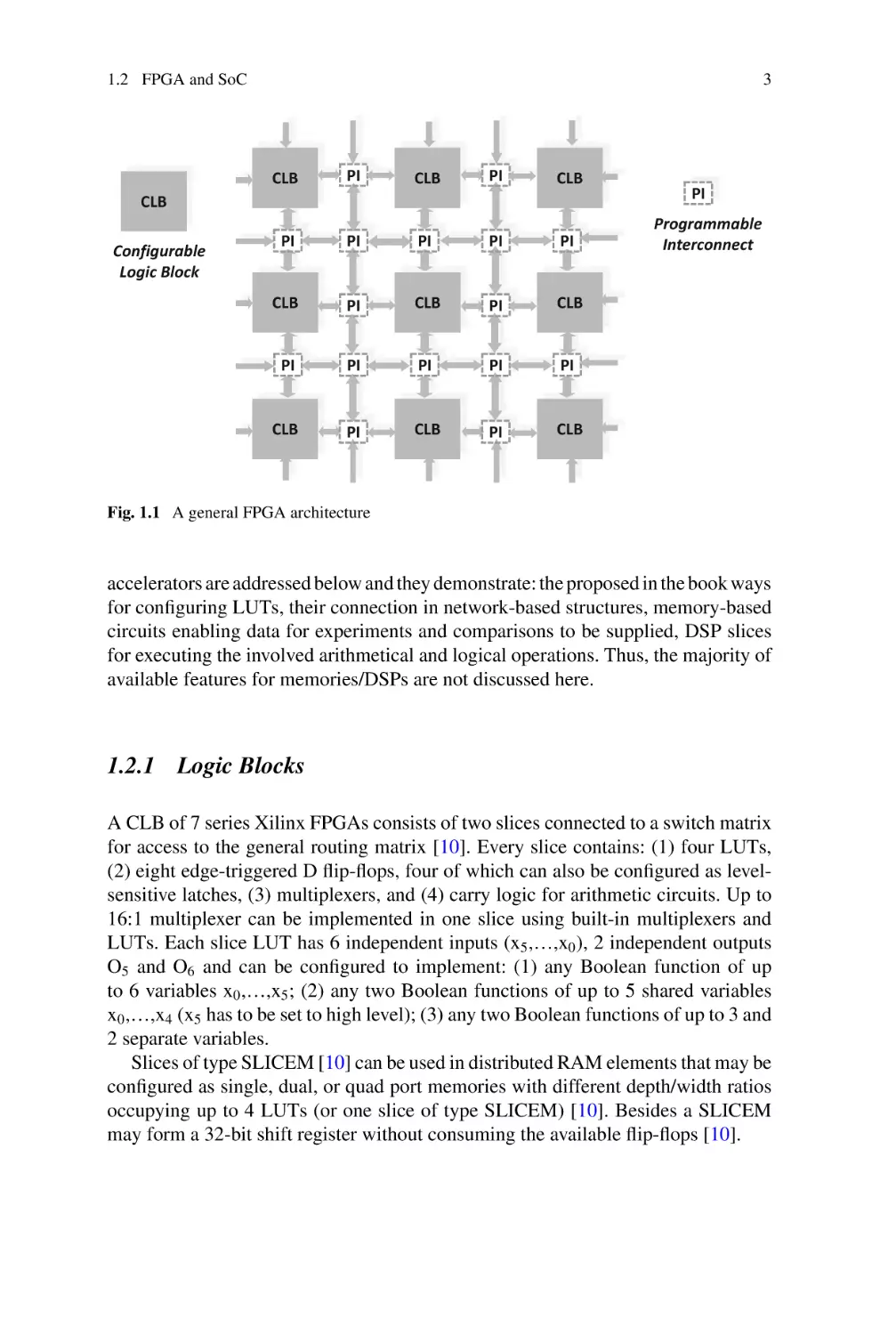
1.2 FPGA and SoC
FPGA is a programmable logic device which contains a large number of logic blocks
and incorporates a distributed interconnection structure. Both the functions of the
logic blocks and the internal interconnections can be configured and reconfigured for
solving particular problems through programming the relevant chip. In SRAM (Static
Random-Access Memory)-based FPGA devices programming is done by writing
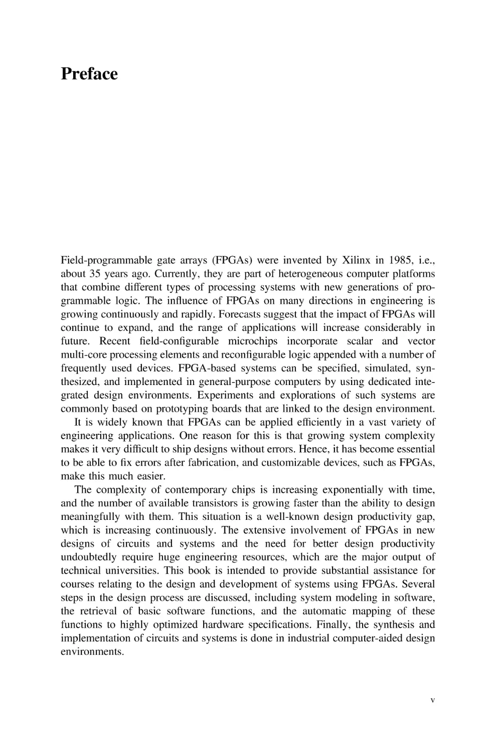
information to internal memory cells. A general structure of an FPGA is depicted in
Fig. 1.1. The architecture of logic blocks, interconnections and I/O (Input/Output)
blocks vary among different manufacturers and even within different families from
the same manufacturer.
Examples in this book are mainly based on 7 series FPGAs from Xilinx, the core
configurable logic blocks (CLB) of which contain look-up tables (LUTs), flip-flops,
and supplementary logic. A CLB consists of two slices and will be described in more
detail in Sect. 1.2.1. Two other blocks that are used in the book for prototyping are
memories and digital signal processing (DSP) slices that will be briefly characterized
in Sects. 1.2.2 and 1.2.3. There are many other components in FPGA but they are not
discussed here because the subsequent chapters do not use them. Besides, only such
features of the indicated above blocks that are needed for examples with hardware
1.2 FPGA and SoC
3
CLB
PI
CLB
PI
PI
PI
PI
PI
PI
CLB
PI
CLB
PI
CLB
PI
PI
PI
PI
PI
CLB
PI
CLB
PI
CLB
CLB
CLB
Configurable
Logic Block
PI
Programmable
Interconnect
Fig. 1.1 A general FPGA architecture
accelerators are addressed below and they demonstrate: the proposed in the book ways
for configuring LUTs, their connection in network-based structures, memory-based
circuits enabling data for experiments and comparisons to be supplied, DSP slices
for executing the involved arithmetical and logical operations. Thus, the majority of
available features for memories/DSPs are not discussed here.
1.2.1 Logic Blocks
A CLB of 7 series Xilinx FPGAs consists of two slices connected to a switch matrix
for access to the general routing matrix [10]. Every slice contains: (1) four LUTs,
(2) eight edge-triggered D flip-flops, four of which can also be configured as levelsensitive latches, (3) multiplexers, and (4) carry logic for arithmetic circuits. Up to
16:1 multiplexer can be implemented in one slice using built-in multiplexers and
LUTs. Each slice LUT has 6 independent inputs (x5 ,…,x0 ), 2 independent outputs
O5 and O6 and can be configured to implement: (1) any Boolean function of up
to 6 variables x0 ,…,x5 ; (2) any two Boolean functions of up to 5 shared variables
x0 ,…,x4 (x5 has to be set to high level); (3) any two Boolean functions of up to 3 and
2 separate variables.
Slices of type SLICEM [10] can be used in distributed RAM elements that may be
configured as single, dual, or quad port memories with different depth/width ratios
occupying up to 4 LUTs (or one slice of type SLICEM) [10]. Besides a SLICEM
may form a 32-bit shift register without consuming the available flip-flops [10].
4
1 Reconfigurable Devices and Design Tools
The propagation delay is independent of the function implemented in a LUT.
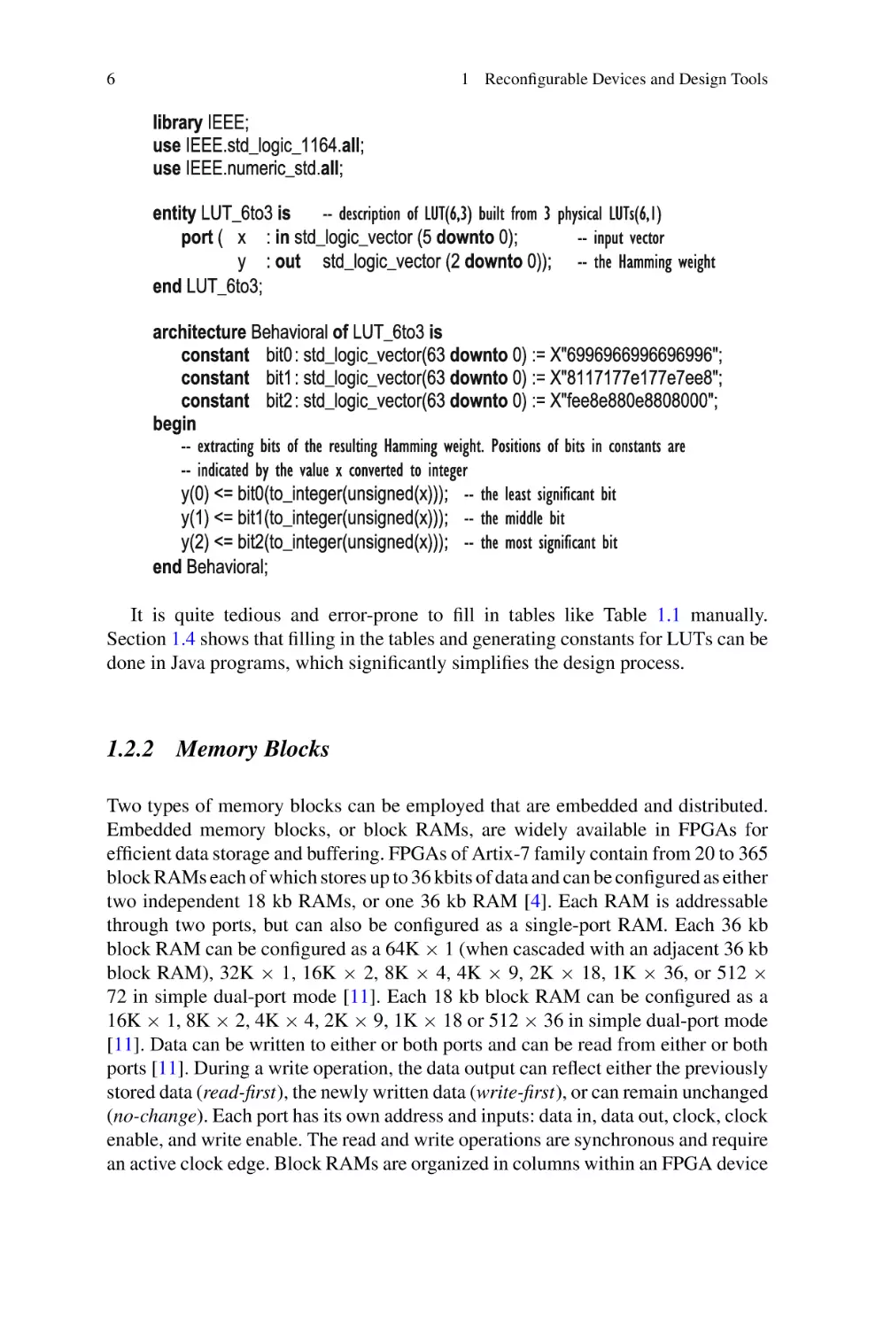
Therefore, LUTs can be used efficiently to solve data processing tasks. For example,
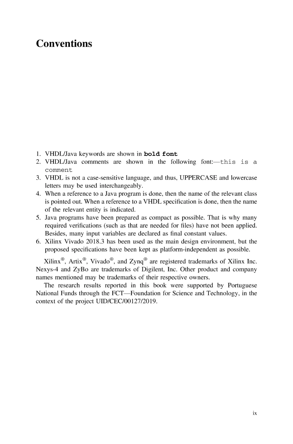
three LUTs(6,1), sharing common six inputs x5 ,…,x0 and having one output each
one, can be configured to determine the Hamming weight y2 y1 y0 of a 6-bit input
vector x5 ,…,x0 , as illustrated in Fig. 1.2 and Table 1.1. The Hamming weight (HW)
of a vector is the number of non-zero bits.
The LUTs can be configured through the use of constants, which may
be expressed in hexadecimal format, [X"6996966996696996" for y(0),
X"8117177e177e7ee8" for y(1), and X"fee8e880e8808000" for y(2)] derived
directly from Table 1.1 and explained with more detail in Fig. 1.3 for the output y(2).
The LUT-based circuit in Fig. 1.2 can be described in VHDL as follows, resulting
essentially in one logical LUT(6,3), composed of three physical LUTs(6,1):
Result:
y2y1y0 = 100
1
0
0
1
1
1
1
1
0
0
1
1
1
0
1
0
0
1
1
1
0
y2
y1
Hamming weight y2y1y0 of (x5x4x3x2x1x0)
Input vector
x5x4x3x2x1x0
Example:
x5x4x3x2x1x0=
100111
y0
Fig. 1.2 Configuring three LUTs(6,1) to calculate the Hamming weight y2 y1 y0 of a 6-bit input
vector x5 ,…,x0
1.2 FPGA and SoC
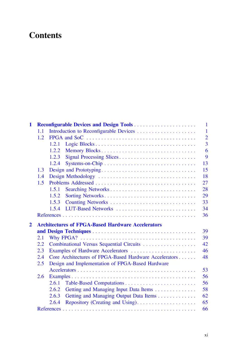
5
Table 1.1 Truth tables for configuring three LUTs(6,1) to calculate the Hamming weight y2 y1 y0
of a 6-bit input vector x5 ,…,x0
x5 x4 x3 x2 x1 x0
000000
000001
000010
000011
000100
000101
000110
000111
001000
001001
001010
001011
001100
001101
001110
001111
y2 y1 y0
000
001
001
010
001
010
010
011
001
010
010
011
010
011
011
100
x5 x4 x3 x2 x1 x0
010000
010001
010010
010011
010100
010101
010110
010111
011000
011001
011010
011011
011100
011101
011110
011111
y2 y1 y0
001
010
010
011
010
011
011
100
010
011
011
100
011
100
100
101
x5 x4 x3 x2 x1 x0
100000
100001
100010
100011
100100
100101
100110
100111
101000
101001
101010
101011
101100
101101
101110
101111
y2 y1 y0
001
010
010
011
010
011
011
100
010
011
011
100
011
100
100
101
x5 x4 x3 x2 x1 x0
110000
110001
110010
110011
110100
110101
110110
110111
111000
111001
111010
111011
111100
111101
111110
111111
0
0
0
8
0
8
8
e
0
8
8
e
8
e
e
f
X"fee8e880e8808000"
Fig. 1.3 Deriving the LUT contents X"fee8e880e8808000" for output y2
y2 y1 y0
010
011
011
100
011
100
100
101
011
100
100
101
100
101
101
110
6
1 Reconfigurable Devices and Design Tools
It is quite tedious and error-prone to fill in tables like Table 1.1 manually.
Section 1.4 shows that filling in the tables and generating constants for LUTs can be
done in Java programs, which significantly simplifies the design process.
1.2.2 Memory Blocks
Two types of memory blocks can be employed that are embedded and distributed.
Embedded memory blocks, or block RAMs, are widely available in FPGAs for
efficient data storage and buffering. FPGAs of Artix-7 family contain from 20 to 365
block RAMs each of which stores up to 36 kbits of data and can be configured as either
two independent 18 kb RAMs, or one 36 kb RAM [4]. Each RAM is addressable
through two ports, but can also be configured as a single-port RAM. Each 36 kb
block RAM can be configured as a 64K × 1 (when cascaded with an adjacent 36 kb
block RAM), 32K × 1, 16K × 2, 8K × 4, 4K × 9, 2K × 18, 1K × 36, or 512 ×
72 in simple dual-port mode [11]. Each 18 kb block RAM can be configured as a
16K × 1, 8K × 2, 4K × 4, 2K × 9, 1K × 18 or 512 × 36 in simple dual-port mode
[11]. Data can be written to either or both ports and can be read from either or both
ports [11]. During a write operation, the data output can reflect either the previously
stored data (read-first), the newly written data (write-first), or can remain unchanged
(no-change). Each port has its own address and inputs: data in, data out, clock, clock
enable, and write enable. The read and write operations are synchronous and require
an active clock edge. Block RAMs are organized in columns within an FPGA device
1.2 FPGA and SoC
7
and can be interconnected to create wider and deeper memory structures. It is possible
to specify block RAM characteristics and to initialize memory contents directly in
VHDL code. Besides, Intellectual Property (IP) core generator can also be used [12,
13].
Let us consider a simple example of specifying a parameterizable RAM, having
one port with synchronous read/write operation, in VHDL:
8
1 Reconfigurable Devices and Design Tools
The RAM has been parameterized with two generic constants: addrBusSize—for
specifying the RAM depth and dataBusSize—for specifying the RAM width. Both
read and write operations are synchronized with the same clock signal clk. The memory itself is specified as an array TMemory of NUM_WORDS words of dataBusSize bits. This VHDL specification follows read-first strategy, i.e. old content is read
before the new content is loaded.
Memory can be synthesized as either distributed ROM/RAM (constructed from
LUTs) or block RAM. Data is written synchronously into the RAM for both types.
Reading is done synchronously for block RAM and asynchronously for Distributed
RAM. By default, the synthesis tool selects which RAM to infer, based upon heuristics that give the best results for most designs and the result can be consulted in the
post-implementation resource utilization report. The designer can indicate explicitly
what type of RAM to infer by using VHDL attributes, such as ram_style/rom_style
attribute in Vivado [14]:
RAMs can be initialized in the following two ways: (1) specifying the RAM
initial contents directly in the VHDL source code (the code above illustrates how
to reset the initial RAM contents to 0), or (2) specifying the RAM initial contents
in an external data file [14]. In particular, data can be either read from raw text
files or uploaded from an initialization file of type COE [15]. A COE is a text
file indicating memory_initialization_radix (valid values are 2, 10, or 16) and memory_initialization_vector which contains values for each memory element. Any value
has to be written in radix defined by the memory_initialization_radix. The following
example presents a COE file specifying the initial contents for a RAM storing sixteen
8-bit vectors in hexadecimal system:
In Vivado memory can be initialized using memory generators in IP catalog. Any
file (like shown above) can be loaded and used as an initial set of data items that
are needed in examples of subsequent chapters. The following simple VHDL code
permits to read data from the file shown above and to display them:
1.2 FPGA and SoC
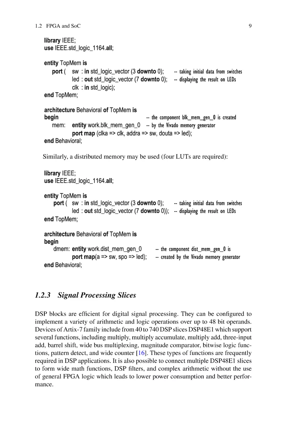
9
Similarly, a distributed memory may be used (four LUTs are required):
1.2.3 Signal Processing Slices
DSP blocks are efficient for digital signal processing. They can be configured to
implement a variety of arithmetic and logic operations over up to 48 bit operands.
Devices of Artix-7 family include from 40 to 740 DSP slices DSP48E1 which support
several functions, including multiply, multiply accumulate, multiply add, three-input
add, barrel shift, wide bus multiplexing, magnitude comparator, bitwise logic functions, pattern detect, and wide counter [16]. These types of functions are frequently
required in DSP applications. It is also possible to connect multiple DSP48E1 slices
to form wide math functions, DSP filters, and complex arithmetic without the use
of general FPGA logic which leads to lower power consumption and better performance.
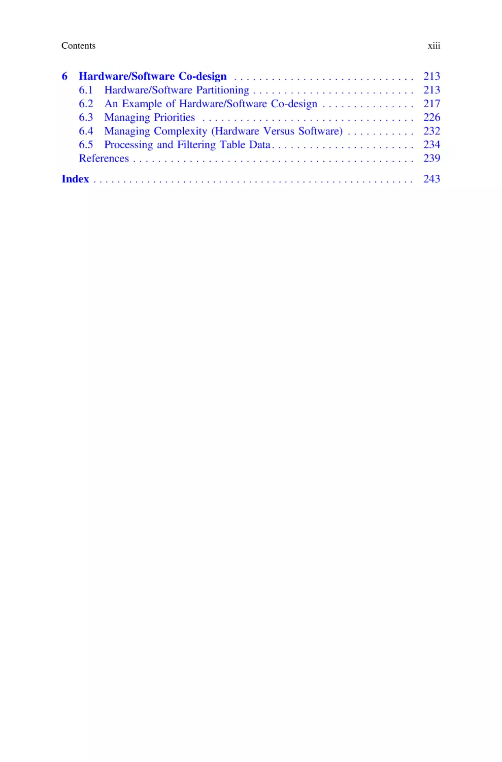
10
D
A
B
C
1 Reconfigurable Devices and Design Tools
25
30
18
48
Rg
A:B concatenated
Pre-adder
M
25
±
25
Rg
M
25
×
25
Rg
Rg
Rg
M
18
M
M
Rg
Rg
M
48
L
L: Bitwise logical
operations AND,
OR, NOT, NAND,
NOR, XOR, XNOR
M
18
+
-
Rg
M
48
P
=
bypass
Pattern
detect
48
Fig. 1.4 A simplified architecture of the DSP48E1 slice
Basically, the DSP48E1 slice contains a 25-bit input pre-adder followed by a
25 × 18 two’s complement multiplier and a 48-bit adder/subtracter/logic unit and
accumulator. A simplified architecture of the slice [16] is presented in Fig. 1.4, where
A, B, C, D are input operands and P is a 48-bit result. The slice DSP48E1 has several
mode inputs which permit to specify the desired functionality of the pre-adder (such
as whether the pre-adder realizes an addition operation, a subtraction operation, or is
disabled), the second-stage adder/subtracter/logic unit (controlling the selection of
the logic function in the DSP48E1 slice), and different pipelining options. DSP slices
are organized in vertical DSP columns and can be easily interconnected without the
use of general routing resources.
Subsequent chapters of the book will use only simple arithmetic and logic operations (such as a bitwise AND operation over 48 bit binary vectors [16]). The following
example demonstrates how to use a DSP slice as a simple adder:
1.2 FPGA and SoC
11
The following use of DSP slice might be helpful for Hamming weight comparators
(HWC) considered in Sect. 5.7.2.
DSP 48 macro is a Vivado IP core. It is configured for (D-A) operation with
CARRYOUT. The result of subtraction operation is not used and only the carry out
signal is needed. The first operand D is read from memory which was pre-loaded
with the COE file shown above. The second operand A is a threshold taken from
sw(11 downto 4). The first ‘0’ is concatenated because we only need operations
over positive numbers. The sizes of operands D and A for DSP were set to 9. A
single LED is ON if and only if the chosen from memory data item is greater than
the threshold. This is the exact operation that is needed for the HWC.
Different designs with embedded DSP slices are discussed in [17] (see Sect. 4.2
in [17]). The VHDL code below is based on the example with bitwise operations
(see page 154 in [17]) and it permits different logical bitwise operations to be tested.
48-bit binary vectors can be uploaded to memories (Dist_mem1 and Dist_mem2)
from preliminary created COE files. Particular memory words can be chosen by
12
1 Reconfigurable Devices and Design Tools
signals sw(3 downto 0) and sw(7 downto 4). Switches sw(12 downto 8) permit
different bitwise operations to be chosen (see examples in the comments below). The
result of the selected operation is shown on LEDs. For the sake of simplicity, just 16
less significant bits from memories are analyzed.
The presented VHDL code can be useful for Sects. 5.7.3, 5.7.4. The complete
synthesizable VHDL specifications with the code above can be found at http://sweet.
ua.pt/skl/Springer2019.html.
1.2 FPGA and SoC
13
1.2.4 Systems-on-Chip
This section provides an introduction to hardware programmable SoC-based designs
with the main focus on hardware accelerators discussed in the next chapters. A
system-on-chip (SoC) contains the necessary components (such as processing units,
peripheral interfaces, memory, clocking circuits, and input/output) for a complete
system. We will discuss in Chap. 6 different designs involving hardware and software
modules implemented within the Xilinx SoC architecture from the Zynq-7000 family
that combines the dual-core ARM Cortex MPCore-based processing system (PS) and
Xilinx programmable logic (PL) on the same microchip.
The interaction between the PS and the PL can be organized through the following
interfaces [18]:
• High-performance Advanced eXtensible Interface (AXI) optimized for high bandwidth access from the PL to external DDR memory and to dual-port on-chip
memory. There are totally four 32/64-bit ports available connecting the PL to the
memory.
• Four (two slave and two master) General-Purpose Interfaces (GPI) optimized for
access from the PL to the PS peripheral devices and from the PS to the PL registers.
• Accelerator Coherency Port (ACP) permitting a coherent access from the PL
(where hardware accelerators might be implemented) to the PS memory cache
enabling a low latency path between the PS and the PL.
Architectures and functionality of devices from the Zynq-7000 family are comprehensively described in [18]. Design with Zynq-7000 devices is supported by Xilinx
Vivado environment that permits configuration of hardware in the PL, linking the PL
with the PS, and development of software for the PS that interacts with hardware in
the PL.
Let us discuss potential applications of Xilinx Zynq-7000 devices for solving
problems described in the book and for co-design that enables the developed hardware circuits and systems to be linked with software running in the PS. Figure 1.5
demonstrates potential applications which enable large sets of data to be processed
in software with the aid of hardware accelerators. Additional details can be found in
[17]. Many design examples are given in [19].
The sets mentioned in Fig. 1.5 are either received from outside or may be preliminary created by the PS. The following steps can be applied:
• The PS divides the given set in such subsets that can be processed in the PL.
Suppose there are E such subsets with N items in each one.
• The values E, N, and the range of memory addresses are transferred to the PL and
the latter reads subsets from memory through internal high-performance interfaces,
handles data in each subset and copies the resulting subsets back to memory.
• As soon as some subsets are ready, the PL generates a dedicated interrupt that
informs the PS that certain subsets are already available in the memory and ready
for further processing.
• The PS processes the subsets from the PL making the final solution of the problem.
14
1 Reconfigurable Devices and Design Tools
The described in the book hardware accelerators can successfully be implemented
in the PL sections of a SoC (see Fig. 1.6).
Different types of hardware accelerators that will be discussed in the next chapters
are listed in rectangles on the left-hand side of Fig. 1.6. On the right-hand side of
Fig. 1.6 some potential practical applications are mentioned. Data, their characteristics (the number of items—N, the size of each item—M, the number of sets—E,
PS:
1. Dividing large
data sets in
subsets with
limited size and
copying the
subsets to
external memory
2. Operations with
the resulting
subsets from PL
PL:
DDR
memory:
1. Fast parallel
processing of data
items in each
subset and copying
the resulting
subsets to the
same memory
2. Request to copy
the resulting
subsets as soon as
they are ready
subset 1
subset E
interrupt
Fig. 1.5 Data processing in interacting software and hardware
PS
M N E
Data sets
Thresholds
Book-oriented IP cores
Searching networks and their
varieties
Potential
practical
applications:
Sorting networks and their
varieties
Data processing
Data mining
Data analytics
Combinatorial
search
Embedded systems
Bioinformatics
Cryptography
Coding
...
Extracting maximum/minimum
subsets
Methods applying address-based
techniques
Frequent items computations,
ordering, and extracting
Counting networks
Operations over binary vectors
and LUT-based networks
Filtering
PL
Fig. 1.6 Using the developed hardware accelerators in SoC and potential practical applications
1.2 FPGA and SoC
15
etc.), and potential thresholds are supplied to the PL, where the relevant hardware
accelerators are implemented. The results from the PL permit to solve the problem
in the PS operating with large blocks instead of individual items. This allows the
problems to be solved faster and more efficiently. The subsequent chapters describe
the listed in Fig. 1.6 blocks with all necessary details.
1.3 Design and Prototyping
There are a number of FPGA- and SoC-based prototyping boards available on the
market that simplify the process of FPGA configuration and provide support for
testing user circuits and systems in hardware. In experiments and examples of this
book two prototyping boards Nexys-4 [7] and ZyBo [8] are used and they are briefly
characterized below.
The Nexys-4 board manufactured by Digilent [7] contains one FPGA Artix-7
xc7a100t from 7 series of Xilinx [4]. Almost all examples in the next chapters have
been implemented and tested in this board. From the available onboard components,
the following have been used:
1.
2.
3.
4.
5.
100 MHz clock oscillator;
16 user LEDs;
5 user buttons;
16 slide switches;
Eight 7-segment displays.
The ZyBo prototyping board [8] contains as a core component the Zynq
xc7z010clg400 SoC [9] with the PL from Artix-7 family FPGA. Therefore, all the
examples of the book can directly be used and some of them have been tested in the
ZyBo.
Table 1.2 gives some details about Xilinx FPGAs available on the referenced
above boards. Here: Ns is the number of FPGA slices, NLUT is the number of FPGA
LUTs, Nff is the number of FPGA flip-flops, NDSP is the number of DSP slices, NBR is
the number of 36 kb block RAMs, Mkb is the size of embedded block RAM memory
in kb.
The simplified FPGA/PL design flow includes the following basic steps: (1) design
specification (design entry), (2) synthesis, (3) implementation, and (4) configuration
(programming) the device (i.e. FPGA/SoC). The design entry can be accomplished
Table 1.2 Characteristics of Xilinx FPGA/SoC in the Nexys-4 and ZyBo prototyping boards
Board
FPGA/SoC
Ns
NLUT
Nff
NDSP
NBR
Mkb
Nexys-4
xc7a100t
15,850
63,400
126,800
240
135
4,860
ZyBo
xc7z010
4,400
17,600
35,200
80
60
2,160
16
1 Reconfigurable Devices and Design Tools
with a variety of methods such as block-based design and specification with a hardware description language. Besides, a wide variety of intellectual property (IP) cores
is available and the whole design process can be reduced to the appropriate selection, integration and interconnection of the IPs. Moreover, synthesizable subsets of
high-level languages, such as C/C++, may be used quite efficiently to specify the
desired functionality. Such approaches permit the design abstraction level to be raised
resulting in reduced design cost.
During the synthesis phase the design entry is converted into a set of components
(such as LUTs, flip-flops, memories, DSP slices, etc.) resulting in an architecturespecific design netlist.
Then, at the implementation phase, logical elements from the netlist are mapped
to available physical components, placed in the device and connections between
these components are routed. The designer can influence this process by providing
physical and timing constraints to the computer-aided design (CAD) tool. The output
of this phase is a bitstream file that is used to configure the selected FPGA/SoC.
Alongside with these phases, different types of simulation and in-circuit tests can
be executed.
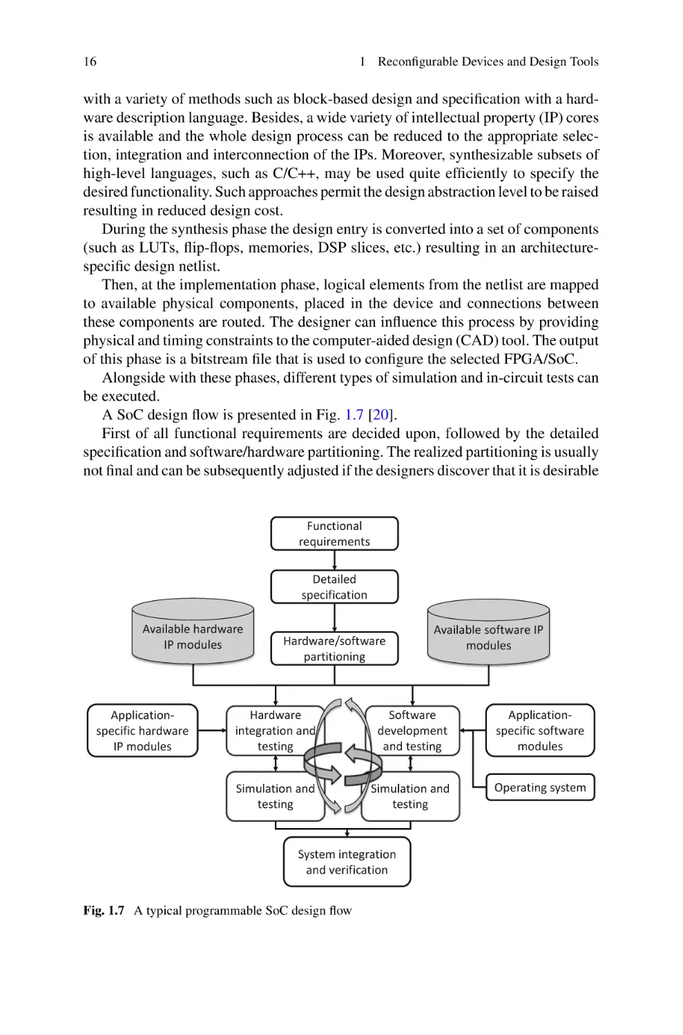
A SoC design flow is presented in Fig. 1.7 [20].
First of all functional requirements are decided upon, followed by the detailed
specification and software/hardware partitioning. The realized partitioning is usually
not final and can be subsequently adjusted if the designers discover that it is desirable
Functional
requirements
Detailed
specification
Available hardware
IP modules
Applicationspecific hardware
IP modules
Hardware/software
partitioning
Available software IP
modules
Hardware
integration and
testing
Software
development
and testing
Applicationspecific software
modules
Simulation and
testing
Simulation and
testing
Operating system
System integration
and verification
Fig. 1.7 A typical programmable SoC design flow
1.3 Design and Prototyping
17
to delegate certain software functions to hardware or vice-versa. Then development
and testing of both hardware and software is executed. The designers have at their
disposal libraries of pre-tested hardware and software IP modules to be reused.
If a specific hardware IP has to be developed, a variety of design methods may
be applied, such as register-transfer level (RTL) design with hardware description
languages (HDL) and specification in high level languages. The design specification
is further synthesized, tested and packaged to an IP to be integrated with other
modules. Afterwards verification of both hardware and software is required which
would frequently force the designers to go back to correct connections or functionality
of certain modules. Finally, the whole system is integrated and tested.
For the examples of this book Vivado 2018.3 design suite from Xilinx [12–14] has
been used for fulfilling all the design steps, from circuit specification to simulation,
synthesis, and implementation. Other CAD tools can also be involved in a similar
manner since the underlying ideas are exactly the same and just the relevant design
environments are different.
Specification is done in VHDL (Very high speed integrated circuit Hardware
Description Language), which is the only hardware description language used in
the book. Simulation can be executed at different levels including run-time with an
integrated logic analyzer. Software modules are developed in the Xilinx software
development kit with debugging capabilities.
It should be noted that not all VHDL specifications that have been used in the
book for Vivado can be synthesized in other CAD tools, such as Intel/Altera Quartus.
For example, many automatically generated VHDL fragments with constants for
configuring FPGA LUTs have these constants written in hexadecimal format (thus
specifying values whose number of bits is multiple of 4). However, the actually
needed number of bits may be smaller. For example, the following lines declare an
array with eight 2-bit constants:
If we use hexadecimal representation then the same array is declared as:
Hence, each constant actually has 4 bits from which just two less significant bits
are used. The majority of examples in the book are based on hexadecimal representation that is more compact. However, it might not be accepted by some CAD
tools, particularly Intel/Altera Quartus, if the actual number of bits is different from
the number of hexadecimal digits multiplied by 4. The next section of this chapter
explains changes that have to be done in the proposed programs to replace hexadecimal constants in generated files with binary constants.
18
1 Reconfigurable Devices and Design Tools
1.4 Design Methodology
This section describes the basic design methodology that is followed in the next chapters. At the beginning, the proposed architectures/structures and design methods are
analyzed and discussed with all necessary details. Mainly they rely on highly parallel networks that are not only traditional searching/sorting networks based on core
comparators/swappers (C/Ss) [21], but also networks with other types of elements.
One example of such structure is a counting network introduced in [22]. Then software models are suggested that do not replicate exactly operations in hardware (since
available parallelism is very limited) but permit the basic functionality and correctness of the executed operations to be roughly verified. Besides, the models enable all
indexed accesses to the proposed data structures to be evaluated and their correctness
to be checked. We will use Java language for modeling and any Java program in the
book will be referenced through the name of the class with the function main. At the
next step some selected functions from software models are automatically converted
to the relevant hardware specifications. For example, the network can be based on
such core elements as LUTs and a software function describes functionality of some
LUTs. After that a complete synthesizable hardware specification is prepared and
used as a design entry for a CAD tool where synthesis, implementation, and bitstream
generation are executed. Finally, the developed circuit is verified in hardware and all
necessary experiments are done.
Let us consider now simple examples. The following Java program permits the
contents of Table 1.1 to be generated automatically for a reasonable value of N.
1.4 Design Methodology
19
The program takes all possible vectors b of size N and calculates the HWs of b,
which are displayed in the following format:
The first column contains 6-bit (N = 6) vectors. The second column shows the
HW of the vector in binary format, and the last (third) column presents the HW of
the vector in decimal. Actually, Table 1.1 is constructed and displayed.
Even with a table data at hand, it is not practical to derive constants to fill in the
LUTs manually. The following Java program permits such constants to be generated
automatically:
20
1 Reconfigurable Devices and Design Tools
The program above generates the file Constants.txt with the following three
lines:
1.4 Design Methodology
21
If we compare these lines with the analogous lines in the VHDL code from
Sect. 1.2.1 (see entity LUT_6to3), we can see that they are exactly the same. Masks
in the line
are changed in such a way that permits the proper bit to be chosen, i.e. the least
significant bit (for mask 1), the middle bit (for mask 2), and the most significant bit
(for mask 4).
Several LUTs(6,1) can be cascaded to determine the Hamming weight of bigger
input vectors, having more than 6 bits. The program LutFileGenerator can build the
file Constants.txt for bigger correct values of N and ny. For example, if we change
the first lines as follows:
then new constants will be generated and saved in the file Constants.txt. They
can be copied to the following synthesizable VHDL code, which permits the HW of
a 16-bit (N = 16) binary vector to be calculated:
22
1 Reconfigurable Devices and Design Tools
Note that even the complete VHDL code above can be generated automatically
from a Java program but this is not a target of the book. The number of LUTs
synthesized in Vivado 2018.3 environment for the VHDL code above (N = 16) is 93
(and this is too many).
Let us look at the following VHDL code:
Even for such a trivial specification, the number of LUTs required for calculating
the HW for N = 16 is just 16, i.e. comparing to the previous example, less by a factor
of almost 5. However, the propagation delay is significant. It will be shown in Chap.
5 that HW counters can be optimized allowing both the number of components and
the propagation delay to be reduced considerably.
1.4 Design Methodology
23
Note that the constants X"6996966996696996", X"8117177e177e7ee8",
X"fee8e880e8808000" may be presented in form of an array, which might be easier to understand. Each element of the array would correspond to a row in Table 1.1
(i.e. the first element would be “000”, the next one—“001”, …, the last one—“110”).
Let us consider, for example constants for N = 3, m (number of LUT outputs) = 2.
For these constants the following array with eight 2-bit elements can be built:
Now a problem might appear that is explained at the end of the previous section
with exactly the same example. Elements of the array (from left to right) are the
HWs for digits 0 (HW = 0), 1 (HW = 1), 2 (HW = 1), 3 (HW = 2), 4 (HW = 1), 5
(HW = 2), 6 (HW = 2), and 7 (HW = 3). Hence, only two binary digits are required
but the hexadecimal constants have 4 binary digits (from which two less significant
are used). Thus, the following representation would be more clear: (b"00", b"01",
b"01", b"10", b"01", b"10", b"10", b"11"). Let as analyze the codes X"96" and
X"e8" above. If we write binary codes near the relevant hexadecimal digits:
then we can see that the codes (b"00", b"01", b"01", b"10", b"01", b"10", b"10",
b"11") are composed of the respective bit from the constant bit1 concatenated with
a bit with the same index from the constant bit0. If the number of LUT inputs is n
and the number of outputs is m, then the number of bits in the first (hexadecimal)
representation is always 2n and for any n > 1 hexadecimal constants contain the exact
number of binary digits. If we consider arrays then the number of bits in each array
element (constant) is m, which for the majority of the required configurations is
not divisible by four. The following Java program permits constants to be generated
correctly in form of an array:
24
1 Reconfigurable Devices and Design Tools
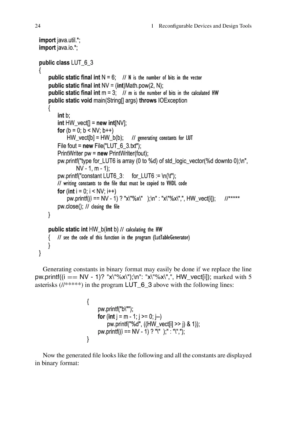
Generating constants in binary format may easily be done if we replace the line
pw.printf((i == NV - 1)? "x\"%x\");\n": "x\"%x\",", HW_vect[i]); marked with 5
asterisks (//*****) in the program LUT_6_3 above with the following lines:
Now the generated file looks like the following and all the constants are displayed
in binary format:
1.4 Design Methodology
25
The generated binary constants can be used like the following:
Similar changes can be done in other programs that are used to generate arrays
of constants. Let us consider one more example. Suppose a logical LUT(6,3) must
be used to find out the number of consecutive values 1 in a 6-bit binary vector. The
desired functionality may be modeled in the following Java program:
26
1 Reconfigurable Devices and Design Tools
The lines from the file ConOne.txt can now be copied to the following synthesizable VHDL code, which permits the maximum number of consecutive ones in 6-bit
binary vectors to be found:
1.4 Design Methodology
27
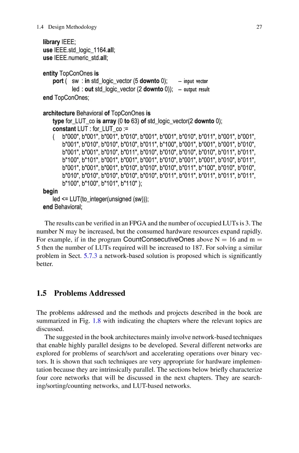
The results can be verified in an FPGA and the number of occupied LUTs is 3. The
number N may be increased, but the consumed hardware resources expand rapidly.
For example, if in the program CountConsecutiveOnes above N = 16 and m =
5 then the number of LUTs required will be increased to 187. For solving a similar
problem in Sect. 5.7.3 a network-based solution is proposed which is significantly
better.
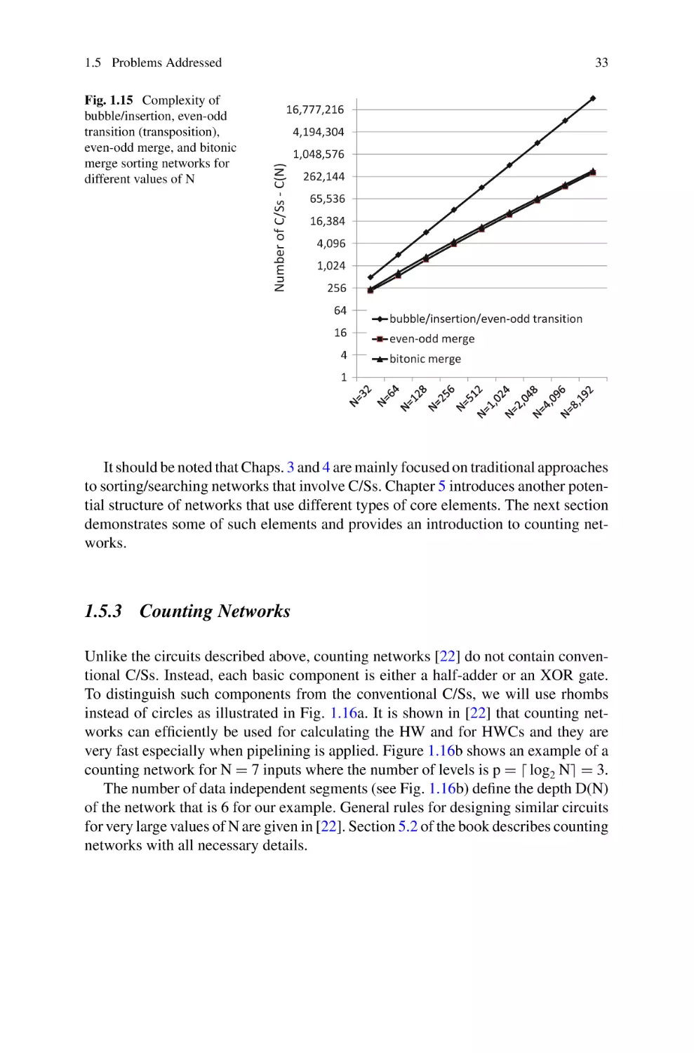
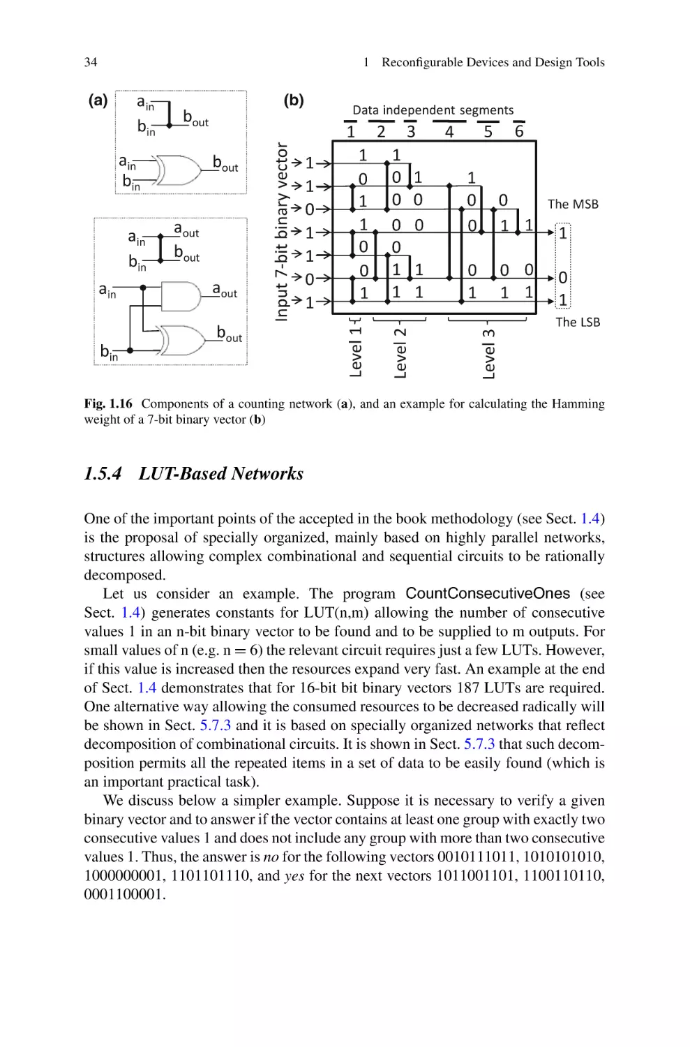
1.5 Problems Addressed
The problems addressed and the methods and projects described in the book are
summarized in Fig. 1.8 with indicating the chapters where the relevant topics are
discussed.
The suggested in the book architectures mainly involve network-based techniques
that enable highly parallel designs to be developed. Several different networks are
explored for problems of search/sort and accelerating operations over binary vectors. It is shown that such techniques are very appropriate for hardware implementation because they are intrinsically parallel. The sections below briefly characterize
four core networks that will be discussed in the next chapters. They are searching/sorting/counting networks, and LUT-based networks.
28
1 Reconfigurable Devices and Design Tools
1.5.1 Searching Networks
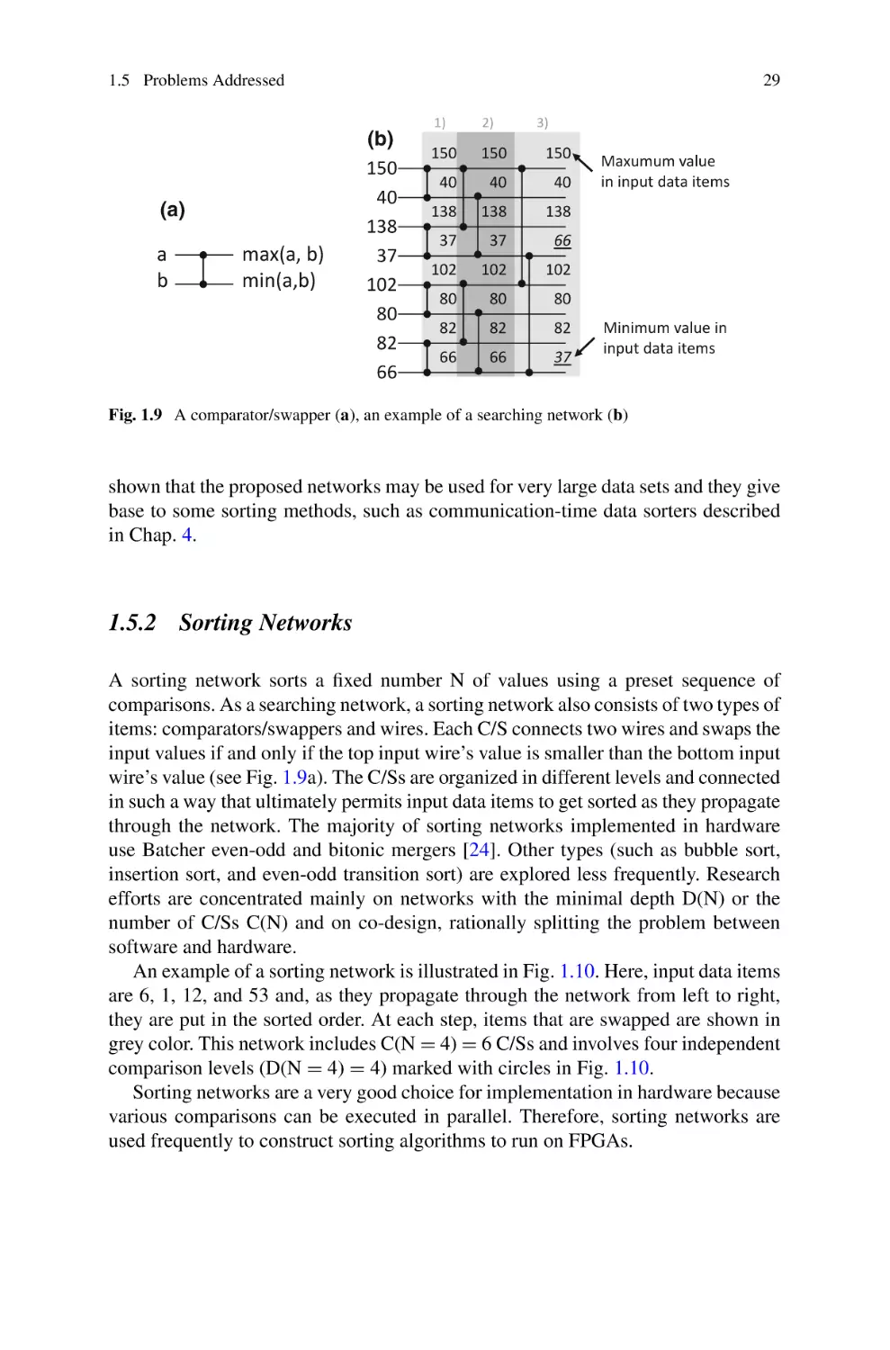
A searching network permits a maximum/minimum value in a set of N data items to be
found. The network can be constructed from C/Ss, each of which connects two wires
and swaps the input values if and only if the top input wire’s value is smaller than the
bottom input wire’s value (see Fig. 1.9a). The C/Ss are organized in different levels
and connected in such a way that permits: (1) finding maximum/minimum values in
pairs of inputs, (2) considering all minimum and all maximum values as two new
subsets and repeating the first point for each of them iteratively until the absolute
maximum and minimum are found. Actually, sorting networks may also be used for
data search, but we are interested in minimizing the number of C/Ss.
Searching networks are characterized by two primary parameters: the number of
C/Ss C(N) and the depth D(N), i.e. the minimal number of data dependent steps that
have to be executed one after another. An example of a searching network for N =
8 is depicted in Fig. 1.9b [23]. The input data 150, 40, 138, 37, 102, 80, 82, and 66
propagate through the network from left to right and the exchanged items at each
level are underlined. D(N) = log2 N = 3, thus searching is accomplished in 3
(log N)
steps, and the network requires C(N) = N + n=12 2n = 10 C/Ss. Different levels
are highlighted by distinct background colors.
Chapter 3 is dedicated to searching networks and gives all necessary details. Two
types of networks are proposed that are pure combinational and iterative where one
level of C/Ss is iteratively reused. Several modifications are discussed, for example,
fast extraction of the most frequent or the less frequent items from data sets. It is
General structure of hardware accelerators getting input data and managing the results
(chapter 2)
Hardware accelerators for data search and
solving some related problems: searching
networks (chapter 3)
Problems,
methods,
and projects
Hardware accelerators for data sort: sorting
networks and solving some related problems
(chapter 4)
Hamming weight counters/comparators and
hardware accelerators for combinatorial search;
automatic generation of VHDL blocks for
frequently used operations (chapter 5)
Hardware/software co-design (chapter 6)
Fig. 1.8 Problems addressed in the book
1.5 Problems Addressed
(a)
a
b
max(a, b)
min(a,b)
29
(b)
150
40
138
37
102
80
82
66
1)
2)
3)
150
150
150
40
40
40
138
138
138
37
37
66
102
102
102
80
80
80
82
82
82
66
66
37
Maxumum value
in input data items
Minimum value in
input data items
Fig. 1.9 A comparator/swapper (a), an example of a searching network (b)
shown that the proposed networks may be used for very large data sets and they give
base to some sorting methods, such as communication-time data sorters described
in Chap. 4.
1.5.2 Sorting Networks
A sorting network sorts a fixed number N of values using a preset sequence of
comparisons. As a searching network, a sorting network also consists of two types of
items: comparators/swappers and wires. Each C/S connects two wires and swaps the
input values if and only if the top input wire’s value is smaller than the bottom input
wire’s value (see Fig. 1.9a). The C/Ss are organized in different levels and connected
in such a way that ultimately permits input data items to get sorted as they propagate
through the network. The majority of sorting networks implemented in hardware
use Batcher even-odd and bitonic mergers [24]. Other types (such as bubble sort,
insertion sort, and even-odd transition sort) are explored less frequently. Research
efforts are concentrated mainly on networks with the minimal depth D(N) or the
number of C/Ss C(N) and on co-design, rationally splitting the problem between
software and hardware.
An example of a sorting network is illustrated in Fig. 1.10. Here, input data items
are 6, 1, 12, and 53 and, as they propagate through the network from left to right,
they are put in the sorted order. At each step, items that are swapped are shown in
grey color. This network includes C(N = 4) = 6 C/Ss and involves four independent
comparison levels (D(N = 4) = 4) marked with circles in Fig. 1.10.
Sorting networks are a very good choice for implementation in hardware because
various comparisons can be executed in parallel. Therefore, sorting networks are
used frequently to construct sorting algorithms to run on FPGAs.
30
1 Reconfigurable Devices and Design Tools
6
6
6
53
53
1
1
53
6
12
12
53
1
12
6
53
12
12
1
1
1
2
4
3
Fig. 1.10 An example of a sorting network
1)
150
40
138
37
102
80
82
66
2)
3)
4)
5)
6)
7)
150 150 150 150 150 150
150
150 150 150 150 150 150
40
138
138 138 138 138 138 138
102
102 102 102 102 102 102
80
80
82
82
82
82
82
82
138 138 138 138 138
138 40
40
40
37
37
102 40
37
102 102
8)
9)
10)
11)
12)
13)
102 102 102 37
80
40
82
80
80
80
80
80
80
80
80
80
80
37
82
40
66
66
66
66
66
66
82
82
82
82
82
37
66
40
40
40
40
40
40
66
66
66
66
66
66
37
37
37
37
37
37
37
All sorted
Fig. 1.11 An example of a bubble/insertion sorting network
An example of a bubble/insertion sorting network for N = 8 is given in Fig. 1.11.
Here, the input data are 150, 40, 138, 37, 102, 80, 82, and 66. Data items that get
swapped at each step are underlined in Fig. 1.11. D(N) = 2 × N − 3 = 13, thus
sorting is done in 13 steps, and the network requires C(N) = N × (N − 1)/2 = 28
C/Ss. Please note that the data happen to be sorted already at step 8 (see “All sorted”
mark in Fig. 1.11), but since the sorting network structure is fixed for any given value
of N, the sorting process continues through all the fixed 13 steps.
An example of an even-odd transition (transposition) sorting network for N = 8
and the same input data as in Fig. 1.11 is given in Fig. 1.12. D(N) = N = 8, thus
sorting is done in 8 steps, and the network requires the same number of C/Ss as in the
previous case: C(N) = N × (N − 1)/2 = 28. Once again the data get sorted earlier
than at the final step 8.
An example of even-odd merge sorting network for N = 8 and the same input
data as in Figs. 1.11 and 1.12 is given in Fig. 1.13. D(N = 2p ) = p × (p + 1)/2 =
6, thus sorting is done in 6 steps, and the network requires C(N = 2p ) = (p2 − p +
4) × 2p−2 − 1 = 19 comparators/swappers. As in the previous cases, data get sorted
earlier than at the final step 6.
1.5 Problems Addressed
31
1)
150
40
138
37
102
80
82
66
2)
3)
4)
5)
6)
7)
8)
150 150 150 150 150 150 150 150
40
138 138 138 138 138 138 138
138 40
37
102 102 102 102 102 102
102 40
82
82
82
82
82
102 37
82
40
80
80
80
80
80
82
37
80
40
66
66
66
82
80
80
37
66
40
40
40
66
66
66
66
37
37
37
37
4)
5)
6)
All sorted
Fig. 1.12 An example of an even-odd transition sorting network
1)
150
40
138
37
102
80
82
66
2)
3)
150
150 150
150
150
150
40
40
138
138
138
138
138
138 40
80
102
102
37
37
37
66
82
82
102
102 102
102
80
80
80
80
82
82
66
66
82
82
80
40
40
40
66
66
37
37
37
66
All sorted
Fig. 1.13 An example of an even-odd merge sorting network
The order of sorting (either descending or ascending) in the networks described
above may easily be changed through simple modifications in the C/Ss. In the examples above any C/S operates as follows: “if (a < b) then exchange a and b”. To
change the order of sorting the less than operation (<) must be changed to greater
than operation (>).
An example of a bitonic merge sorting network for N = 8 and the same input data
as in Figs. 1.11, 1.12 and 1.13 is presented in Fig. 1.14a. Bitonic merge networks use
a bit different C/Ss in which the arrow indicates the direction of movement of the
32
1 Reconfigurable Devices and Design Tools
1)
(a)
150
40
138
37
102
80
82
66
2)
3)
4)
5)
6)
150
150 150
150
150
150
40
138 138
138
138
138
37
37
40
82
82
102
138
40
37
102
102
82
102
66
66
66
66
80
80
80
80
80
80
66
66
102 82
40
40
40
82
82
37
37
37
102
(b)
a
b
min(a, b)
max(a,b)
a
b
max(a, b)
min(a,b)
All sorted
Fig. 1.14 An example of a bitonic merge sorting network (a), the used comparators/swappers (b)
Table 1.3 Complexity and latency of the considered sorting networks
C(N =
D(N)
2p )
Bubble/insertion Even-odd transition
Even-odd merge
Bitonic merge
N × (N − 1)/2
N × (N − 1)/2
(p2
– p + 4) ×
−1
(p2 + p) ×
2p–2
2×N−3
N
p × (p + 1)/2
2p–2
p × (p + 1)/2
greater data item (see Fig. 1.14b). D(N = 2p ) = p × (p + 1)/2 = 6, thus sorting is
done in 6 steps, and the network requires C(N = 2p ) = (p2 + p) × 2p–2 = 24 C/Ss. In
this example data get sorted only at the final step 6, but obviously this could happen
earlier.
The considered networks are scalable and can be adapted for different values of
N. Clearly, other types of designs may be proposed. A detailed analysis of potential
sorting networks is done in [21]. Expressions for the complexity and depth of the
described above sorting networks are presented in Table 1.3. Figure 1.15 shows the
complexity for different values of N. Even-odd and bitonic merge networks are the
fastest because they have the smallest depth D(N). For instance, to sort ~134 million
data items (227 ) just D(N) = 378 steps are required. But the consumed hardware
resources are huge. If N = 227 then 23,689,428,991 C/Ss are needed for the evenodd merge network, which clearly exceeds resources available even in the most
advanced FPGA.
Chapter 4 suggests alternative ways for implementing sorting networks in hardware that are based on iterative designs and a communication-time technique involving searching networks. Many related circuits, such as those for extracting the maximum/minimum subsets are presented. An efficient method that is called addressbased sorting is also discussed.
1.5 Problems Addressed
16,777,216
4,194,304
1,048,576
Number of C/Ss - C(N)
Fig. 1.15 Complexity of
bubble/insertion, even-odd
transition (transposition),
even-odd merge, and bitonic
merge sorting networks for
different values of N
33
262,144
65,536
16,384
4,096
1,024
256
64
16
4
bubble/insertion/even-odd transition
even-odd merge
bitonic merge
1
It should be noted that Chaps. 3 and 4 are mainly focused on traditional approaches
to sorting/searching networks that involve C/Ss. Chapter 5 introduces another potential structure of networks that use different types of core elements. The next section
demonstrates some of such elements and provides an introduction to counting networks.
1.5.3 Counting Networks
Unlike the circuits described above, counting networks [22] do not contain conventional C/Ss. Instead, each basic component is either a half-adder or an XOR gate.
To distinguish such components from the conventional C/Ss, we will use rhombs
instead of circles as illustrated in Fig. 1.16a. It is shown in [22] that counting networks can efficiently be used for calculating the HW and for HWCs and they are
very fast especially when pipelining is applied. Figure 1.16b shows an example of a
counting network for N = 7 inputs where the number of levels is p = log2 N = 3.
The number of data independent segments (see Fig. 1.16b) define the depth D(N)
of the network that is 6 for our example. General rules for designing similar circuits
for very large values of N are given in [22]. Section 5.2 of the book describes counting
networks with all necessary details.
34
1 Reconfigurable Devices and Design Tools
bin
2
bout
aout
bout
aout
bout
1
1
0
1
1
0
1
1
0
1
1
0
0
1
3
1
0
0
0
0
1
1
6
5
4
1
0
0
1
0
0
0
1 1
1
1
0
1
0 0
1 1
Level 3
ain
Data independent segments
1
Level 2
ain
bin
ain
bin
(b)
bout
Level 1
ain
bin
Input 7-bit binary vector
(a)
The MSB
1
0
1
The LSB
Fig. 1.16 Components of a counting network (a), and an example for calculating the Hamming
weight of a 7-bit binary vector (b)
1.5.4 LUT-Based Networks
One of the important points of the accepted in the book methodology (see Sect. 1.4)
is the proposal of specially organized, mainly based on highly parallel networks,
structures allowing complex combinational and sequential circuits to be rationally
decomposed.
Let us consider an example. The program CountConsecutiveOnes (see
Sect. 1.4) generates constants for LUT(n,m) allowing the number of consecutive
values 1 in an n-bit binary vector to be found and to be supplied to m outputs. For
small values of n (e.g. n = 6) the relevant circuit requires just a few LUTs. However,
if this value is increased then the resources expand very fast. An example at the end
of Sect. 1.4 demonstrates that for 16-bit bit binary vectors 187 LUTs are required.
One alternative way allowing the consumed resources to be decreased radically will
be shown in Sect. 5.7.3 and it is based on specially organized networks that reflect
decomposition of combinational circuits. It is shown in Sect. 5.7.3 that such decomposition permits all the repeated items in a set of data to be easily found (which is
an important practical task).
We discuss below a simpler example. Suppose it is necessary to verify a given
binary vector and to answer if the vector contains at least one group with exactly two
consecutive values 1 and does not include any group with more than two consecutive
values 1. Thus, the answer is no for the following vectors 0010111011, 1010101010,
1000000001, 1101101110, and yes for the next vectors 1011001101, 1100110110,
0001100001.
1.5 Problems Addressed
35
The proposed network-based solution is depicted in Fig. 1.17a. The circuit has
two levels composed of AND gates with two inputs each. AND operations are carried
out over all adjacent bits as it is demonstrated on examples (see Fig. 1.17b). If the
vector V1 on the outputs of the first level does not contain all zeros and the vector V2
on the outputs of the second level contains all zeros then the answer is yes, otherwise
the answer is no. Indeed, if there are at least two adjacent values 1 in the initial vector
V0 then at least one value 1 will appear in the vector V1 . If there are no clusters with
three or more consecutive values 1 then the vector V2 contains all zeros. Similarly, we
can test if the given vector V0 contains at least one group with exactly K consecutive
values of 1 and does not include any group with more than K consecutive values 1.
In this case the number of levels in Fig. 1.17a must be increased up to K and exactly
the same operations have to be performed over the vectors VK−1 and VK . Thus, the
answer is yes, if the vector VK−1 on the outputs of the level K − 1 does not contain
all zeros and the vector VK on the outputs of the level K contains all zeros, otherwise
the answer is no.
The following synthesizable VHDL code permits the proposed network for the
general case (where K consecutive values 1 are checked) to be described.
(a)
(b)
V0 0 0 1 0 1 1 1 0 1 1
V1 0 0 0 0 1 1 0 0 1
00001000
V2
Vector V2
Vector V1
AND operations
over adjacent bits
N-bit binary vector V0
AND operations
over adjacent bits
Level 2
Level 1
The answer is yes if the vector V 2
contains all zeros and the vector V1
does not contain all zeros
The answer is no
V0 1 0 1 1 0 0 1 1 0 1
V1 0 0 1 0 0 0 1 0 0
00000000
V2
The answer is yes
Fig. 1.17 Fast and economical solution for the described above task (a); two examples (b)
36
1 Reconfigurable Devices and Design Tools
The designed circuit is combinational. For N = 16 and K = 2 the network requires
9 LUTs, for N = 1000 and K = 2–670 LUTs, and for N = 1000 and K = 10–1415
LUTs. A similar approach may be used for solving different problems described in the
book. These problems are important for many areas, particularly for combinatorial
algorithms [25], coding and information processing [26].
References
1. Xilinx Press Releases (2018) Xilinx Unveils Versal: the first in a new category of platforms delivering rapid innovation with software programmability and scalable AI inference.
https://www.xilinx.com/news/press/2018/xilinx-unveils-versal-the-first-in-a-new-categoryof-platforms-delivering-rapid-innovation-with-software-programmability-and-scalable-aiinference.html. Accessed 6 Feb 2019
References
37
2. Xilinx Inc. (2018) Versal: the first Adaptive Compute Acceleration Platform (ACAP). White
paper: Versal ACAPs. https://www.xilinx.com/support/documentation/white_papers/wp505versal-acap.pdf. Accessed 24 Mar 2019
3. Xilinx Inc. (2018) Xilinx AI engines and their applications. White paper: AI
Engines. https://www.xilinx.com/support/documentation/white_papers/wp506-ai-engine.pdf.
Accessed 24 Mar 2019
4. Xilinx Inc. (2018) 7 series FPGAs data sheet: overview. https://www.xilinx.com/support/
documentation/data_sheets/ds180_7Series_Overview.pdf. Accessed 6 Feb 2019
5. Intel Corp. (2015) Stratix V device overview. https://www.intel.com/content/dam/www/
programmable/us/en/pdfs/literature/hb/stratix-v/stx5_51001.pdf. Accessed 6 Feb 2019
6. Gartner, Inc. (2018) Forecast overview: semiconductors, worldwide, 2018 update
7. Digilent Inc. (2016) Nexys-4™ reference manual. https://reference.digilentinc.com/_media/
reference/programmable-logic/nexys-4/nexys4_rm.pdf. Accessed 6 Feb 2019
8. Digilent Inc. (2017) ZYBO™ FPGA board reference manual. https://reference.digilentinc.
com/_media/reference/programmable-logic/zybo/zybo_rm.pdf. Accessed 6 Feb 2019
9. Xilinx Inc. (2018) Zynq-7000 SoC data sheet: overview. https://www.xilinx.com/support/
documentation/data_sheets/ds190-Zynq-7000-Overview.pdf. Accessed 6 Feb 2019
10. Xilinx Inc. (2016) 7 series FPGAs configurable logic block. https://www.xilinx.com/support/
documentation/user_guides/ug474_7Series_CLB.pdf. Accessed 6 Feb 2019
11. Xilinx Inc. (2019) 7 series FPGAs memory resources. https://www.xilinx.com/support/
documentation/user_guides/ug473_7Series_Memory_Resources.pdf. Accessed 6 Feb 2019
12. Xilinx Inc. (2018) Vivado design suite user guide. https://www.xilinx.com/support/
documentation/sw_manuals/xilinx2018_1/ug910-vivado-getting-started.pdf. Accessed 6 Feb
2019
13. Xilinx Inc. (2017) Vivado design suite. Designing with IP tutorial. https://www.xilinx.com/
support/documentation/sw_manuals/xilinx2017_1/ug939-vivado-designing-with-ip-tutorial.
pdf. Accessed 6 Feb 2019
14. Xilinx Inc. (2017) Vivado design suite user guide. Synthesis. https://www.xilinx.com/support/
documentation/sw_manuals/xilinx2017_1/ug901-vivado-synthesis.pdf Accessed 6 Feb 2019
15. Xilinx Inc. (2017) Vivado design suite PG058 block memory generator. https://www.xilinx.
com/support/documentation/ip_documentation/blk_mem_gen/v8_3/pg058-blk-mem-gen.
pdf. Accessed 17 Mar 2019
16. Xilinx Inc. (2018) 7 series DSP48E1 slice user guide. https://www.xilinx.com/support/
documentation/user_guides/ug479_7Series_DSP48E1.pdf Accessed 6 Feb 2019
17. Sklyarov V, Skliarova I, Barkalov A, Titarenko L (2014) Synthesis and optimization of FPGAbased systems. Springer, Switzerland
18. Xilinx Inc. (2018) Zynq-7000 all programmable SoC technical reference manual. https://www.
xilinx.com/support/documentation/user_guides/ug585-Zynq-7000-TRM.pdf. Accessed 6 Feb
2019
19. Sklyarov V, Skliarova I, Silva J, Rjabov A, Sudnitson A, Cardoso C (2014) Hardware/software
Co-design for programmable systems-on-chip. TUT Press
20. Skliarova I, Sklyarov V, Sudnitson A, Kruus M (2015) Integration of high-level synthesis to the
courses on reconfigurable digital systems. In: Proceedings of the 38th international conference
on information and communication technology, electronics and microelectronics—MIPRO’15,
Opatija, Croatia, May, 2015, pp 172–177
21. Knuth DE (2011) The art of computer programming. sorting and searching, 3rd edn. AddisonWesley, Massachusetts
22. Sklyarov V, Skliarova I (2015) Design and implementation of counting networks. Computing
97(6):557–577
23. Sklyarov V, Skliarova I (2013) Parallel processing in FPGA-based digital circuits and systems.
TUT Press, Tallinn
38
1 Reconfigurable Devices and Design Tools
24. Batcher KE (1968) Sorting networks and their applications. In: Proceedings of AFIPS spring
joint computer conference, USA (1968)
25. Reingold EM, Nievergelt J, Deo N (1977) Combinatorial algorithms. Theory and practice.
Prentice-Hall, Englewood Cliffs NJ
26. Yeung RW (2008) Information theory and network coding. Springer
Chapter 2
Architectures of FPGA-Based Hardware
Accelerators and Design Techniques
Abstract This chapter demonstrates distinctive features of FPGA-based hardware
accelerators. In order to compete with the existing alternative solutions (both in hardware and in software) a wide level parallelism must be implemented in circuits with
small propagation delays. For providing such characteristics several useful techniques are discussed and analyzed such as the ratio between combinational and
sequential computations at different levels. Individual data items are represented in
the form of long size input vectors that are processed concurrently in accelerators producing long size output vectors. Thus, pre- (conversion of individual items to long size
input vectors) and post- (conversion of long size output vectors to individual items)
processing operations have to be carried out. The technique of communication-time
data processing is introduced and its importance is underlined. Core network-based
architectures of hardware accelerators are discussed and the best architectures are
chosen for future consideration. Finally, different aspects of design and implementation of FPGA-based hardware accelerators are analyzed and three sources for the
designs are chosen that are synthesizable hardware description language specifications, the proposed reusable components, and intellectual property cores available
on the market. At the end of the chapter a few useful examples are presented in detail
and discussed.
2.1 Why FPGA?
Generally FPGAs operate at lower clock frequency than ASICs (Application-Specific
Integrated Circuits) and ASSPs (Application-Specific Standard Products) but they
can be customized and allow: (1) implementing wider parallelism in hardware; (2)
easily changing the size of data (such as operands in arithmetical expressions); (3)
experimenting with alternative (competitive) circuits, and many other distinctive features making them very attractive for both prototyping and new products. Nowadays
FPGAs can be used both as autonomous devices and as a part of more complicated
systems incorporating different types of processors, memories, interfaces, etc.
© Springer Nature Switzerland AG 2019
I. Skliarova and V. Sklyarov, FPGA-BASED Hardware Accelerators,
Lecture Notes in Electrical Engineering 566,
https://doi.org/10.1007/978-3-030-20721-2_2
39
40
2 Architectures of FPGA-Based Hardware Accelerators …
It should be noted that not all types of circuits can be implemented efficiently in
FPGAs. As a rule, FPGAs are more expensive than the majority of widely used microprocessors. Besides, for many practical applications software running on generalpurpose (micro-) processors is cheaper and better (because it might entirely satisfy
all the necessary requirements and limitations). In other words, FPGAs often enable
faster and better optimized (taking into account different criteria) designs to be realized, but for certain practical application such improvements actually are not needed
and the most important characteristics are simplicity and the cost. However, for highperformance computations and algorithms that allow a wide parallelism to be applied
FPGAs might give many benefits. We will consider such applications of the described
hardware accelerators for which: (1) high performance is the primary objective and
the basic rule is the faster the better; (2) highly parallel architectures can be proposed; (3) typical known techniques cannot be used because the target requirements
are specific (for example, we are interested in communication-time data processing
where all data items are rearranged as soon as a new item has been received from a
communication channel).
FPGAs are composed of logical blocks that can arbitrary be connected allowing
the desired circuit to be built. The depth (the number of logical blocks through
which input signals have to propagate to reach outputs) of such circuits needs to
be minimized. Indeed, if the delay of signals from inputs to outputs is significant
then the clock frequency has to be additionally reduced and the circuit performance
becomes worse. So, we want not only highly parallel architectures but also those,
which allow the minimal delays in propagating data.
Figure 2.1 demonstrates the basic objectives and requirements for the considered
hardware accelerators, which may be used as: (1) autonomous on-chip hardware
modules; (2) complete on-chip hardware/software designs; and (3) adaptive blocks
for general-purpose and application-specific computer systems.
Any hardware accelerator is, as a rule, a non-autonomous circuit and it has
to interact with some other circuits. The more input data items are handled in
parallel the better. Thus, the set of input data items is large and sometimes contains
thousands of bits. The number of FPGA pins is limited. Hence, inputs are received
either from internal circuits or from a limited number of pins and then they are
combined (vectored) in a single long size vector. We will call such operation
Reasonable
and
acceptable
resources
Wide-level
parallelism
can be
applied
Input item 1
Output item 1
Input item 2
Output item 2
Input item N
Hardware
accelerator
A special attention is
paid to applicationspecific accelerators Output item Z
Propagation delay is limited
Fig. 2.1 The basic objectives and requirements of hardware accelerators
The required
features are not
available in other
potential designs
Effective
integration in
complete onchip solutions
(b)
Output data item 1
Clock cycle 2
Output data item 2
Data in memory
or to a
communication
channel
Output data item Z
Output data item 2 Output data item 1
Output data item Z
Input data item 1
Input data item 2
Input data item N
Data in memory
or from a
communication
channel
Input data item 1
(a)
Input data item 2
41
Input data item N
2.1 Why FPGA?
Fig. 2.2 Building a vector from a set of individual input data items or unrolling (a) and building
individual output data items from the vector (b)
unrolling and it is demonstrated in Fig. 2.2a. Unrolling is frequently needed for
both handling data items from FPGA pins and from internal (i.e. implemented in
the FPGA) circuits. As a rule, such operation is executed sequentially requiring a
number of clock cycles (see Fig. 2.2). A similar operation is commonly involved to
build individual data items from a long size output vector composed of individual
output data items (see Fig. 2.2b). Additional clock cycles reduce performance of
accelerators and the number of such cycles needs to be minimized. One possible
way to increase the performance is an execution time data acquisition in such
a way that getting new sequential input data items is done in parallel with data
processing (of previously received and new data items) in hardware accelerators.
This is demonstrated in Fig. 2.3. Various methods that allow data acquisition and
processing to be parallelized will also be considered in this book. Three different
types of problems will be discussed: (1) data search (Chap. 3); (2) data sort
(Chap. 4); and (3) selected (mainly combinatorial) computations frequently needed
for different practical applications (Chap. 5). Some helpful design techniques (e.g.
automatic generation of synthesizable hardware description language fragments
from general-purpose programming languages) are also introduced and analyzed.
It is widely known that the most appropriate architectures for accelerating computations needed for the described above problems are based on parallel networks, such
as sorting networks [1–5], searching networks [3], counting networks [6], parallel
counters [7], and LUT-based networks [3]. A pipelining technique can be applied
42
2 Architectures of FPGA-Based Hardware Accelerators …
Input data item k
Input data item N
Data in memory
or from a
communication
channel
The same clock cycle for
transferring input data item
k and processing input
data items 1,…,k
Transferring
input data item k
Hardware
accelerator
Fig. 2.3 An example of the execution time data acquisition (communication-time data processing)
for parallel networks [3–5], and it is very efficient. The network can be either purely
combinational (non-sequential) or iterative with large highly parallel combinational
blocks [4, 8]. The latter allows the combinational delay in the circuit to be reduced.
The next section discusses design tradeoffs between them.
2.2 Combinational Versus Sequential Circuits
Implemented in FPGA circuits may be combinational and sequential. A combinational circuit (CC) does not have memory and, thus, output values of a CC depend
only on its current input values. A fundamental notion in a sequential circuit (SC) is
a state that depends not only on the current inputs but also on the functionality of the
SC in the past. Many examples of FPGA-based CC and SC (together with details) are
given in [3]. An important characteristic of any CC is the propagation delay that is the
time from getting input data to when the result on the outputs is ready to be taken.
Such a delay depends on the number of logical components through which input
signals propagate to the outputs. A general rule is the more levels of the components
the larger is the delay.
Let us consider an example. Suppose the CC in Fig. 2.4a must give an answer if
the number of values ‘1’ in an n-bit binary input vector x0 ,…,xn−1 is odd and in this
case y = 1, otherwise y = 0. Figure 2.4b and c depict potential circuits for the CC
for n = 8. An XOR gate represented in notation [3, 6] is shown in Fig. 2.4d. It is
clearly seen that logical functionality and the number of components in the circuits
in Fig. 2.4b and c are the same, but propagation delays are different.
A functionally equivalent SC can also be built (see an example in Fig. 2.5a).
Initially the SC copies the given input vector x0 ,…,xn−1 to a shift register and then
sequentially checks all the bits. The result y is sequentially formed in the feedback
flop-flop connected to the output of a single XOR gate.
Let us consider an example of the vector 11011101 (n = 8). Before the first shift
the flip-flop is reset to 0 and the rightmost bit of the vector force the value 1 (i.e.
1 XOR 0) on the input of the flip-flop, which changes its state to 1. After the first
2.2 Combinational Versus Sequential Circuits
43
x0
(b) x1
(a)
x0
x2
CC
xn‒1
x3
y
x4
x5
x6
(c) x0
x1
x2
x3
x4
x5
x6
x7
y
xi
xj
(d)
xi
xj
delay = 3
y
x7
delay = 7
xi
xj
xi
xj
Fig. 2.4 Example of a combinational circuit—CC (a); two different types of the CC with propagation delay 7 (b) and 3 (c); a simplified notation for an XOR gate (d)
x0
Shift register
y
Flip-flop
Any vector Vi (0≤i<N) is a
set of elements x0,…,xn‒1
Vector V0
xn‒1
(b)
x0
Vector VN‒1
(a) xn‒1
x0
x1
x2
x3
x4
x5
x6
x7
y
Flip-flop
Fig. 2.5 Example of a sequential circuit—SC (a); a block-based sequential circuit (BBSC) including a large size combinational core unit (b)
shift operation the upper input of the XOR gate is 0 and the state of the flip-flop is
not changed. After the second shift the state of the flip-flop becomes 0 because both
inputs of the XOR gate are 1. After 8 clock cycles the state of the flip-flop is 0 and
y = 0 saying that the number of values 1 in the input vector is even. Thus, the chosen
operation is completed in n clock cycles, but propagation delay in combinational part
is only 1, because input signals pass through just one XOR gate. Thus, it is often
questionable which implementation is indeed better from the point of view of the
required resources and latency, answering the question: “How long does the operation
take?” Frequently and especially for long size input vectors mixed implementations
(i.e. SCs including relatively large combinational blocks) might be the best from the
point of view of designer’s criteria. One example of the same circuit is depicted in
44
2 Architectures of FPGA-Based Hardware Accelerators …
Fig. 2.5b. An initial very long vector V is decomposed in N subvectors of size n. Any
subvector is handled by the CC and the set of subvectors is processed sequentially as
it is shown in Fig. 2.5b. Hence, finally we get three types of different implementations
even for our trivial example with a simple operation. For more complex operations
analogous solutions might be proposed and commonly it is rather difficult to answer
which solution is better for the given criteria, especially in FPGA-based circuits
because many additional constraints need to be taken into account. Frequently, only
prototyping and experiments permit this question to be properly answered.
Let us discuss now how different designs may be parallelized. Suppose a sum S
of N operands O0 ,…,ON−1 needs to be calculated: S = O0 + ··· + ON−1 . Figure 2.6
demonstrates three potential hardware implementations.
An adder in Fig. 2.6a takes operands O0 ,…,ON−1 sequentially and accumulates
the sum in a register involving N sequential steps. The CC in Fig. 2.6b computes
the sum S on a tree of adders, which may be done with the total delay equal to
log2 N delays of one adder. Figure 2.6c implements table-based computations in
a CC and the delay is undoubtedly the minimal (however, the required resources
are huge for practical cases). Hence, we can talk about a sequential implementation
in Fig. 2.6a and two combinational implementations in Figs. 2.6b and c. Besides,
much like Fig. 2.5b a block-based sequential circuit (BBSC) including a large size
combinational core unit may also be analyzed (such a technique is used in [8]).
Note that a BBSC is somewhere in the middle of two diametrically opposite design
approaches: (1) a completely combinational circuit when there is just one block;
and (2) a sequential circuit containing the simplest possible combinational element.
Thus, the same operation might be implemented differently and, in fact, generally
an infinite number of alternative solutions exist.
Two basic characteristics are important for FPGA-based circuits: (a) wide level
parallelism; and (b) small propagation delays in the circuits that implement wide
level parallelism. One more, although supplementary, but important characteristic is a high level of regularity of implemented circuits. Another crucial feature
is keeping (storing) data in such a way that is convenient for consequent processing.
Let us consider an example. An important operation in algorithms of combinatorial
(a)
ON‒1,…,O0
(c)
O0
ON‒1
(b)
S
Adder with
accumulator
CC
S
O0
O1
O2
O3
O0+O1
O2+O3
ON‒4 O +O
N‒4
N‒3
ON‒3
ON‒2 O +O
N‒2
N‒1
ON‒1
+
+
S
+
Fig. 2.6 Using an adder with accumulator (a); tree of adders (b); combinational circuit (c)
2.2 Combinational Versus Sequential Circuits
45
Table 2.1 Orthogonality operation between two 2-bit codes a and b
a
00
00
00
00
01
01
01
01
10
10
10
10
11
11
11
11
b
00
01
10
11
00
01
10
11
00
01
10
11
00
01
10
11
yort
0
0
0
1
0
0
0
0
0
0
0
0
1
0
0
0
search (such as the Boolean satisfiability or SAT) is checking for orthogonality and
intersection of pairs of vectors [3, 9]. For instance, orthogonality is defined in the
following general form:
yor t =
n−1
(ai xor bi );
i=0
where a and b are ternary vectors with 3 possible values of their elements: 1, 0,
and – (don’t care). Note that XOR operations that are used in the expression above
cannot be applied to ternary vectors and for such vectors special binary encoding
needs to be used. Suppose ternary components are encoded as follows: K(0) = 00;
K(1) = 11; and K(–) = 01 or 10. For the given 2-bit codes a and b orthogonality
operation is defined in Table 2.1.
In practical applications a very large number of long size ternary vectors need
to be processed [9] and checking for orthogonality of the vectors handling all their
elements in parallel might be beneficial for time critical applications. Thus, a circuit
similar to Fig. 2.6c is needed but the size of each operand is just 2 bits. The question
is how to construct such circuits.
There are many other problems that could be interesting and for which FPGAbased accelerators might be beneficial. In many practical applications an entire problem, such as the SAT (and also other problems discussed in Chap. 6), is solved
partially in software and partially in hardware [10]. Development of hardware frequently involves reusable blocks from which designs for solving different problems
can be composed much like a house is built from typical building modules. One
of the main objectives of this book is proposing such reusable (and generic) blocks
together with the design methods and architectures targeted to FPGA, which is done in
Chaps. 3–5. Another objective is to show how core (normally rather simple) components of FPGA-based accelerators can be generated automatically from relevant
descriptions (functions) in a general-purpose language (see, for example, Sect. 5.6).
The main attention is paid to sequential circuits including large combinational
blocks (i.e. BBSC) because fully combinational circuits require very large hardware resources and sequential circuits introduce considerable delays leading to performance degradation. So, we believe that optimal solutions are somewhere in the
middle.
Common models for SCs are finite state machine (FSM) and hierarchical FSM
(HFSM) [11]. Design methods for sequential (and parallel sequential) circuits from
FSM/HFSM models can be found in a number of publications (see, for example,
[3, 12, 13] with the relevant references). It is also known that functions that are
46
2 Architectures of FPGA-Based Hardware Accelerators …
defined in a general-purpose programming language may be converted to the relevant
hardware implementations (see, for example [14], where conventional programming
techniques, namely, function hierarchy, recursion, passing arguments, and returning
values have been entirely implemented in hardware modules that execute within a
hierarchical finite state machine with extended capabilities). The next section presents
examples of FPGA-based hardware accelerators that are based on reusable blocks
proposed in this book.
2.3 Examples of Hardware Accelerators
Many practical problems can be formulated in such a way that sorting, searching,
and counting operations for different tasks within these problems are involved. Some
examples are given in Fig. 2.7. A sequence of vectors or data items are supplied to
solvers and the tasks of the solvers are shown in the relevant rectangles. Some solvers
can almost entirely be built from reusable components described in the subsequent
three chapters. For example, the solver in Fig. 2.7a may be structurally organized as
it is shown in Fig. 2.8.
All vectors V0 ,…,VN−1 are processed in parallel by Hamming weight (HW)
counter/comparator circuits. Each circuit computes the HW of the input vector and
compares it with the given fixed threshold κ. If the computed HW and κ are equal
How many
vectors
have
Hamming
distance d
with
another
given
vector V
Data item V0
Data item VN‒1
(f)
Solver
Find the
most
frequent
data item
Solver
Data item V0
How many
vectors are
orthogonal
to another
given
vector V
What is the
maximum/
minimum
Hamming
distance
between all
vectors
Solver
(e)
(c)
Data item VN‒1
Vector V0
Vector VN‒1
Solver
Vector V0
How
many
input
vectors
have
HW
Solver
Vector V0
(d)
(b)
Vector VN‒1
Vector V0
Vector VN‒1
Solver
Vector VN‒1
(a)
Fig. 2.7 Examples of tasks (a–f) that can appear in solving practical problems
What is
the
number
of items
with the
given
value V
2.3 Examples of Hardware Accelerators
47
Vector V0
Vector VN‒1
HW counter/comparator
HW counter/comparator
HW counter
The result
Fig. 2.8 Possible implementation of the solver from Fig. 2.7a
Automatically generate code
for synthesis from the function
in a general-purpose language
Vector V0
n elements for checking
orthogonality between
the input and V
Vector VN‒1
V
n elements for checking
orthogonality between
the input and V
The result
HW counter
boolean test_ort (int v, int t)
{ return (( (v==0) & (t==0x3) ) | ( (v==0x3) & (t==0) ))
? true : false; } }
Fig. 2.9 Possible implementation of the solver from Fig. 2.7d
then the output is 1, otherwise the output is 0. The bottom HW counter calculates the
number of values 1 on its inputs and this is an answer to the question “How many
input vectors have HW κ?”
Some solvers might demand special elements. For example, the solver in Fig. 2.7d
requires an element, which checks for orthogonality (see Table 2.1) between all the
input vectors and V. If elements of ternary vectors are coded by 2-bit codes (see the
previous section), the solver may be structurally organized as it is shown in Fig. 2.9.
Ternary input vectors are supplied to blocks checking for orthogonality between
them and the given vector V. Each block contains n elements, which are modeled in
a general-purpose language (see, for example, Java function test_ort in Fig. 2.9 that
implements the functionality described by Table 2.1).
It will be shown in Sect. 5.6 that synthesizable hardware description language
specifications for combinational application-specific elements (such as for checking
orthogonality in Fig. 2.9) can be generated automatically from functions described
in a general-purpose language (such as test_ort in Fig. 2.9).
Analysis of different tasks (some of them are shown in Fig. 2.7) permits to conclude that searching, sorting, and counting procedures are often needed. Networkbased solutions are efficient for them. Although key elements of such networks are
48
2 Architectures of FPGA-Based Hardware Accelerators …
comparators/swappers (C/Ss), other types of elements (for example, [6]) can also be
used. Some of the elements are application-specific (i.e. non typical), but we suggest
to generate them automatically from specifications in a general-purpose language.
The networks can be completely combinational or, alternatively, completely sequential. However, BBSC solutions (sequential circuits with large highly parallel combinational blocks) permit a rational compromise between the consumed resources and
latency to be found. The next section briefly describes and characterizes different
networks. Chapters 3–5 are dedicated to all the required details, architectures, and
design methods.
We will use Java language for modeling the functionality of suggested circuits.
Java was chosen by the authors because our students are more familiar with this
language than with C/C++ at the moment when they start learning design of reconfigurable systems. Obviously, C/C++ programming languages might equally be used
(actually minimal modifications are required).
2.4 Core Architectures of FPGA-Based Hardware
Accelerators
The network based architecture for data search is shown in Fig. 2.10a (the number
of input data items N = 16). It is composed of C/Ss (see also Fig. 2.10b) which
check input operands a and b and transfer them to the outputs in such a way that
the upper value is always greater than or equal to the lower value. The architecture
is combinational and input values (such as that are shown on the left-hand side of
Fig. 2.10c) are passed through the C/Ss to the outputs involving just combinational
delays (see the right-hand side in Fig. 2.10c). All intermediate values appeared during
signal propagations are also shown in Fig. 2.10c. In fact, a binary tree is implemented
easily allowing the maximum (Max) and the minimum (Min) values of N input data
items to be found (see an example in Fig. 2.10c).
The levels are explicitly shown in Fig. 2.10. Each level contains just C/Ss that do
not have (within the level) any signal interdependency. Each level has a combinational delay that is equal to the combinational delay of one C/S. The number of
levels D(N) gives the combinational delay (or latency) of the network (4 * in our
example in Fig. 2.10). The complexity (the number of comparators/swappers C(N))
and latency (the number of levels) of the searching networks (for finding either one
value Min/Max or both values) are shown in Table 2.2 [15].
The next chapter will demonstrate implementation of the binary search network
and variations of this network for different types of practical applications. BBSCs
and pipelined solutions will also be discussed.
Sorting is a procedure that is needed in numerous computing systems [1]. For many
practical applications, sorting throughput is very important. The majority of sorting
2.4 Core Architectures of FPGA-Based Hardware Accelerators
(a)
(c) The maximum number = 89
The maximum number
i0
i1
i2
i3
i4
i5
i6
i7
i8
i9
i10
i11
i12
i13
i14
i15
49
35
(b)
a max(a,b)
b min(a,b)
- level 1
- level 2
- level 3
- level 4
The minimum number
87
89
89
35
27
53
27
35
87
53
53
27
27
87
87
89 89
88
88
88
89
34 34
6
6
10
6
6
34
50 50
50 50
34
34
34
50
11 11
11
12
10
10
10
15
13 15
12
12
14
13
15 13
14
14
10
6
12
15
The minimum number = 6
Fig. 2.10 Binary searching network (a), comparator/swapper and levels (b), an example (c)
networks implemented in hardware use Batcher even-odd and bitonic mergers [2, 16].
Research efforts are concentrated mainly on networks with a minimal depth D(N),
number C(N) of C/Ss, and on co-design, rationally splitting the problem between
software and hardware. A profound analysis of the networks [2, 16] is done in [3, 4,
15, 17] with many particular examples. It is concluded that sorting networks [2, 16]
can be implemented in FPGA only for a small number N of input data items while
practical applications require millions of such items to be processed.
Table 2.2 Complexity C(N)
and latency D(N) of the
searching networks
Type of searching
network
C(N)
Min or Max
log
2 N
Min and Max
simultaneously
log
2 N
D(N)
N /2n
log2 N
n=1
n=2
log
2 N
n=1
N /2n +
N /2n
log2 N
50
2 Architectures of FPGA-Based Hardware Accelerators …
N-item sorted set 1 N-item sorted set 2
N-item sorted set Z‒1 N-item sorted set Z
FPGA
Higher level system
Merge
Merge
Merge
Horizontal levels
Merge
Merge
Sorted set
Fig. 2.11 Merging the sorted in FPGA subsets in software of a higher level system
One general way is sorting relatively small subsets of larger sets in an FPGA and
then merging the subsets in software of a higher level system (see Fig. 2.11).
The initial set of data that is to be sorted is divided into Z subsets of N items.
Each subset is sorted in an FPGA with the aid of sorting networks. Merging is
executed as shown in Fig. 2.11 in a host system/processor that interacts with the
FPGA. Each horizontal level of merging permits the size of blocks to be doubled.
Thus, if N = 210 = 1024 and we would like to sort K = 220 = 1,048,576 items then
10 levels of mergers are needed (see Fig. 2.11). Clearly, the larger are the blocks
sorted in an FPGA the fewer merging is needed. Thus, we have to sort in hardware
as many data items as possible with such throughput that is similar to the throughput
of sorting networks. The networks [2, 16] involve significant propagation delays
through long combinational paths. Such delays are caused not only by C/Ss, but also
by multiplexers that have to be inserted and by interconnections. Hence, clock signals
with high frequency cannot be applied. Pipelining permits the clock frequency for
circuits to be increased because delays between registers in a pipeline are reduced. A
number of such solutions are described in [5]. However, once again, the complexity
of the circuits becomes the main limitation. The analysis presented in [3, 4] enables
to conclude the following:
(1) The known even-odd merge and bitonic merge circuits [2, 16] are theoretically
the fastest and they enable the highest throughput to be achieved if unlimited
resources are available. However, they are very resource consuming and can
only be used effectively in existing FPGAs for sorting small data sets.
(2) Pipelined solutions permit faster circuits than in point (1) to be designed. However, resource consumption is at least the same as in point (1), and in practice,
only very small data sets can be sorted.
(3) The existing even-odd merge and bitonic merge circuits are not very regular
(compared to the even-odd transition (transposition) networks [3], for example)
and thus the routing overhead may be significant. It is also clear that the larger
the value Z (the smaller value N for the same data set), the more data exchanges
51
J1
J0
The resul ng
(sorted) data
Memory
JN‒1
JN‒1
J0
J1
Saving the result
I0
IN‒1
Memory
Data processing
I1
I0
IN‒1
Ini al (unsorted) data
Unrolling data
I0,…,IN‒1 are N
data items
I1
2.4 Core Architectures of FPGA-Based Hardware Accelerators
Fig. 2.12 Pre- and post-processing for data sort
between the FPGA and the host system need to be involved, which additionally
reduces performance of hardware/software data sorters.
There is also another problem that might arise. As a rule, initial data and final
results are stored in conventional memories and each data item is kept at the relevant
address of the memory. The size of each data item (the number of bits) is always
limited. Suppose we would like to sort a set of K data items. Let us look at Fig. 2.12
where initial (unsorted) set is saved in memory and the resulting (sorted) set is
also saved in the memory. Parallel operations need to be applied to subsets of data
items, thus, at the beginning, initial data need to be unrolled (see Fig. 2.12 with
additional explanations in the previous section) and the sorted items need to be stored
in memory one by one (see Fig. 2.12). Hence pre- and post-processing operations
are involved and they: (1) sequentially read unsorted data items and save them in a
long size input register; and (2) copy the sorted data items from the long size output
vector to conventional memories. These operations undoubtedly involve significant
additional time. To reduce or even to avoid such time we have to be able to combine
reading/writing data items and their sorting. We will call such type of data sorters
communication-time data sorters.
Finally, the analysis presented in [3, 4, 15, 17] enables to conclude that BBSCs
with the basic architecture [4] permit a better compromise to be found between the
resources required and performance. The architecture [4] will be chosen as a base for
sorting networks with many variations and improvements described below. Besides,
communication-time data sorters will be discussed in detail and they enable data
acquisition and sorting to be executed in parallel in such a way that data sorting is
completed as soon as the last data item has been received.
Figure 2.13 depicts the basic iterative network for different sorting architectures
in the book. The core of the network is the circuit proposed in [4]. There are also
two additional registers Ri and Ro . The register Ri sequentially receives N data items
52
2 Architectures of FPGA-Based Hardware Accelerators …
Copying data to a host system for
subsequent merging
Output register Ro
Parallel copying
of sorted data
Register (R)
Parallel copying
of unsorted data
Input register Ri
Sequen al data acquisi on
from the source
Itera ve data sorter
Fig. 2.13 Sorting blocks with the iterative circuit from [4]
from the source (either from memory or a communication channel). Such N items
compose one block that can be entirely sorted in the network [4]. As soon as the
first block is received, all data items from this block are copied in parallel to the
register R and sorted in the iterative network from [4] with the maximum number of
clock cycles equal to N/2 [4]. At the same time data items from the next block are
received (copied from the source to the register Ri ). As soon as data items from the
first block are sorted they are copied in parallel to the output register Ro . After that the
second block is copied from the register Ri to the register R and sorted (see Fig. 2.13)
and the third block is being received from the source. At the same time the first sorted
block is copied from the register Ro to a host system for subsequent merging. Hence,
the first sorted block will be copied to the host system after acquisition of two blocks
from the source. Then data acquisition from the source, data sorting, and copying
data to the host system will be done in parallel. We can see from Fig. 2.13 that there
are just two sequential levels of C/Ss in the iterative data sorter [4]. Thus, the delay is
very small and we can apply high clock frequency (see also beginning of Sect. 6.2).
The results of [4] clearly demonstrate that such circuits are very efficient.
The complexity C(N) and the latency D(N) of different sorting networks are shown
in Table 2.3 [15]. Iterative sorting using two levels of even-odd transition network
[4] is shown in Fig. 2.13. In addition to the referenced above even-odd and bitonic
merge networks, bubble/insertion and even-odd transition (transposition) methods
[1, 3, 5] are included in Table 2.3.
Solving selected computational problems (Chap. 5) will be based on similar ideas.
Highly parallel networks with minimal depth (propagation delay) will be described.
Architectures for managing priorities (Sect. 6.3) are completely based on search-
2.4 Core Architectures of FPGA-Based Hardware Accelerators
53
Table 2.3 Complexity C(N) and latency D(N) of sorting networks
Type of sorting network
C(N)
D(N)
N −1
2
2× N −3
Bubble and insertion sort
N×
Even-odd transition
N × N 2−1
2
p − p + 4 × 2 p−2 −
1, wher e N = 2 p
2
p + p × 2 p−2 , wher e N =
2p
N
N −1
≤N
Even-odd merge
Bitonic merge
Iterative sorting using two
levels of even-odd transition
p×
p+1
2 , wher e
N = 2p
p×
p+1
2 , wher e
N = 2p
ing/sorting networks. All major circuits will be specified in a hardware description
language (VHDL, in particular), synthesized, implemented, and tested in FPGA. The
next sections briefly characterize the used computer-aided design environment and
FPGA-based boards for prototyping and experiments.
2.5 Design and Implementation of FPGA-Based Hardware
Accelerators
Figure 2.14 depicts a general strategy, which will be used to design FPGA-based
hardware accelerators. Firstly, the proposed architecture of a hardware accelerator
is carefully analyzed and modeled in software. It might include new and previously
designed blocks. The latter are mainly reusable blocks that have been included (earlier) in a user-defined repository. For the first design the user-defined repository
is empty and for the next designs it contains some selected blocks that might be
reused in the future. New blocks are created on the basis of three sources: (1) VHDL
specifications (e.g. the iterative data sorter from Fig. 2.13); (2) some of the previously created blocks from the user-defined repository (e.g. circuits for input/output
data items); and (3) system IP (Intellectual Property) cores (memories, interfacing
circuits, logical gates, processing cores, etc.).
We will use Xilinx Vivado (currently, version 2018.3) [18] as the design environment. This does not restrict the scope of potential applications of the proposed
hardware accelerators because all the major new components will be coded in VHDL
and the relevant specifications generally may be reused for any available on the market design environment. We assume that the readers of this book are familiar with
VHDL. There are lots of materials available at the Internet and books published
about this language. For example, the subset of VHDL described in [3] (with many
examples) is sufficient. The blocks taken from the Vivado system repository with
IP cores are not used as primary components of the proposed hardware accelerators
54
2 Architectures of FPGA-Based Hardware Accelerators …
and they are available in other design environments (although with some modifications). An integration of different blocks created with three mentioned above sources
(VHDL specification, user-defined repository, and system IP cores) will be done with
two methods: structural VHDL code (that might be reused, albeit with some modifications, in other design environments) and Vivado IP integrator. Finally, the steps
of synthesis, implementation, and FPGA bitstream generation are applied for the
selected prototyping system/board ready for verification and experiments. Different
steps of simulation and run-time debugging with the Vivado integrated logic analyzer
may also be carried out.
There are a number of FPGA-based prototyping boards available in the market
that simplify the process of FPGA configuration and provide support for testing user
circuits and systems in hardware. The examples in the book have been prepared
mainly for Nexys-4 board [19] and some projects for ZyBo board [20] manufactured
by Digilent that are briefly characterized in Sect. 1.3 and in [3, 21].
The main focus in the book is on hardware accelerators with minimal details
about getting input data and transferring the results. The necessary information can
be found in [21–24]. The main strategy for experiments and comparisons is explained
in Fig. 2.15.
Let us assume that we would like to compare the hardware accelerator for the
iterative data sorter [4] (see also Fig. 2.13) with sorting the same data in software (for
example, in Java programs running in a general-purpose computer). Java programs
generate initial data sets that are used for sorting data in software and in hardware
(in FPGA). Transferring data items to the FPGA-based hardware accelerators can
be done using different ways. We will copy them to embedded (to FPGA) memories
from COE files [25] (see Sect. 1.2.2) generated by Java programs. The same files
will be processed in Java programs to sort data in software, for example, with the aid
of the Arrays.sort(…) function. The time of sorting is measured and compared in
software and in hardware. A similar example for searching the maximum value in a
set of data is demonstrated in Fig. 2.16.
Hardware description
language (VHDL)
Architecture
of hardware
accelerator
User-defined
repository
System IP-cores
New blocks
of the
architecture
System IP or
VHDL
integrator
Reuse of previous blocks from a
repository
Final blockbased design
Synthesis and
implementation
Verification and
experiments
Fig. 2.14 A general strategy for the design, implementation, and test of hardware accelerators
2.5 Design and Implementation of FPGA-Based Hardware Accelerators
55
General-purpose (desktop) computer; so ware
programs described in a general-purpose language, for
example, Java
Compare to:
Hardware accelerator implemented in FPGA without
taking into account communica on overheads
General methodology:
Prepare ini al
data sets in
so ware (e.g.
Java) and save
them in files (e.g.
COE files for
Xilinx Vivado)
Read the files in
projects and use data
from them to solve
the problem with the
aid of the designed
FPGA-based
hardware accelerator
Measure the
performance and
compare the
results in
general-purpose
so ware and in
FPGA
Fig. 2.15 The main strategy for experiments and comparisons
Fig. 2.16 An example of experiments with an FPGA-based hardware accelerator implementing a
searching network
56
2 Architectures of FPGA-Based Hardware Accelerators …
The results are displayed in software (see the snapshot on the right-bottom corner
of Fig. 2.16) and in hardware (shown in onboard segment displays). You can see
from Fig. 2.16 that the values (65,208) are the same in both cases. Measuring time
in software is done with some Java functions. In FPGA we count the number of
clock cycles, multiply them by the clock period, and display the result in onboard
indicators. So, we can compare the performance. The next section gives some simple
but complete examples.
2.6 Examples
This section is divided in subsections and each subsection describes a simple example
that is not directly related to hardware accelerators but demonstrates how to create
a used-defined repository with auxiliary components that are useful for experiments
and comparisons. We begin with a trivial example explaining how to develop and
test table-based circuits for arithmetical computations.
2.6.1 Table-Based Computations
An example of a simple table for multiplication of two 2-bit operands (a and b)
is shown in Table 2.4 (only some potential values of the operands are included).
In practical applications all possible values of the operands a and b need to be
considered and, thus, if the sizes of operands a and b are s(a) and s(b) in bits then
the number of rows h in the table is 2s(a)+s(b) . For example, if s(a) = s(b) = 10 then
h = 220 . Let us use the concatenation of a and b (a&b) as the address of memory
and let us write in the memory to the address a&b the result of multiplication a ×
b. As soon as the operands are supplied to the memory the result will be produced
immediately with just a minimal delay. Dependently on the memory reading can
be either asynchronous (for example, in case of memory built from logical slices)
or synchronous involving either 1 or 2 clock cycles. In any case this is very fast
but requires very large memory blocks. Similarly, many other types of table-based
computations may be implemented.
Now we will demonstrate on this trivial example how to create a block-based
design and generate from a Java program a COE file used to fill in the chosen
memory. Figure 2.17 depicts the circuit, which we would like to implement.
The memory in Fig. 2.17 has to be loaded with the chosen COE file. Let us assume
that the operands are positive integers with the maximum value 255. The COE file
can be generated in the following Java program in which the operand sizes are generic
(defined as constants) and might easily be changed.
2.6 Examples
57
import java.util.*;
import java.io.*;
public class ROM_for_multiplication
{
static final int MaxOp1 = 255; // the maximum value for the first operand a
static final int MaxOp2 = 255; // the maximum value for the second operand b
public static void main (String args[]) throws IOException
{
File fout = new File("coe_for_multiplication.coe");
PrintWriter pw = new PrintWriter(fout);
pw.println("memory_initialization_radix = 16;");
pw.println("memory_initialization_vector = ");
for (int i = 0; i <= MaxOp1; i++)
for (int j = 0; j <= MaxOp1; j++)
pw.printf( (i == (MaxOp1)) && (j == (MaxOp2)) ? "%04x;" : "%04x,", i * j);
pw.println();
pw.close();
}
}
As a result, the file coe_for_multiplication.coe will be generated and saved.
Later on this file has to be copied to the chosen memory. As an example, you can
see below the COE file for 2-bit operands. It may easily be generated in the same
Address: a&b
Table 2.4 A simple table for
multiplication operation
Operand 1—a
Operand 2—b
The result—r
0
0
0
0
1
0
1
1
1
1
2
2
2
2
4
2
3
6
3
3
9
The result
Memory
User-defined repository: DISPLAY
r
Binary to BCD
converter
Onboard segment displays:
Fig. 2.17 Architecture of a table-based multiplier
Segment display
controller
58
2 Architectures of FPGA-Based Hardware Accelerators …
Memory
Unrolling: packing
individual data
items in a long size
vector
Data
processing in
a hardware
accelerator
Showing the
result (e.g. use
the DISPLAY
block)
Fig. 2.18 Unrolling data from memory and processing the resulting data in hardware
Java program changing the values MaxOp1 and MaxOp2 to 3 (more information
on Xilinx COE files can be found in [25]).
memory_initialization_radix = 16;
memory_initialization_vector =
0000,0000,0000,0000,0000,0001,0002,0003,0000,0002,0004,0006,0000,0003,0006,0009;
Now we can supply 8-bit binary operands (a and b) to the memory and get from
the output of the memory the binary result of multiplication (a × b). We would like
to see this result in decimal format. Thus, two new blocks Binary to BCD converter
and Segment display controller have been created and saved in the user-defined
repository. Synthesizable VHDL specifications for these blocks are given in [3] and
can also be found at http://sweet.ua.pt/skl/Springer2019.html. Then the mentioned
above blocks have been connected in a new block named DISPLAY (see Fig. 2.17).
Hence, the final design is composed of two blocks Memory and DISPLAY. The
first one is a system IP-core (a single port ROM) created by either the distributed
memory generator or the block memory generator. The COE file created in the
Java program above must be loaded to the ROM in the chosen generator. Then
synthesis, implementation, and bitstream generation phases are executed for the
selected prototyping board (Nexys-4 in our case). Finally, the multiplier is tested in
hardware. Similarly, other circuits for table-based computations can be designed and
tested.
2.6.2 Getting and Managing Input Data Items
For numerous problems that will be solved in the book we need to pack many
individual data items into a long size vector (see Fig. 2.2a) in such a way that all the
items can be read in parallel. Figure 2.18 depicts the circuit, which can be used for
such packing. Different types of vectors will be generated, for example, the vector
may contain K M-bit data items, M > 1, or, alternatively, the vector may be handled
as a set of individual bits much like it is considered in the example below.
As before, the memory is filled in with data generated by a Java program. Let
us assume that a hardware accelerator permits computing the HW of a long size
binary vector (the number of values ‘1’ in this vector). The following Java program
generates D integers (which binary codes will be used later to find out the HW):
2.6 Examples
import java.util.*; // see also the program WriteToMemoryForHW in section 5.4
import java.io.*;
public class Random_to_file
{
static Random rand = new Random();
static final int M = 32; // M is the size of one word
static final int D = 4; // D is the number of memory words
public static void main (String args[]) throws IOException
{
int a[] = new int[D]; // generated input data will be saved in this array
int HWsum = 0;
// the resulting Hamming weight
File fout = new File("ForHW32x4.coe");
PrintWriter pw = new PrintWriter(fout);
pw.println("memory_initialization_radix = 16;");
pw.println("memory_initialization_vector = ");
for (int d = 0; d < D; d++)
{
a[d] = rand.nextInt(Integer.MAX_VALUE);
pw.printf("%08x", a[d]);
pw.printf((d == D - 1) ? ";" : ",");
System.out.printf(" %08x", a[d]);
System.out.printf((d == D-1) ? ";" : ",");
HWsum += HW(a[d]); // the resulting Hamming weight
System.out.println();
pw.println();
}
System.out.printf("The total HW = %d\n",HWsum);
pw.close();
}
public static int HW(int item) // function computing the Hamming weight
{
int res = 0;
for (int n = 0; n < M; n++)
{
if ((item & 1) == 1)
res++;
item >>= 1;
}
System.out.printf("HW = %d", res);
return res;
}
}
59
60
2 Architectures of FPGA-Based Hardware Accelerators …
The size of each integer is predefined in the used computer and it is equal to 32
in our case. After executing the program the file ForHW32x4.coe will be generated
and saved on computer disk. An example of this file is shown below:
memory_initialization_radix = 16;
memory_initialization_vector =
36dccee2,
2eae37c4,
22ed498d,
71bee9a9;
The same generated numbers will be displayed on the screen and besides the HW
of each 32-bit vector (calculated by the function public static int HW(int item))
and the sum HWsum of these HWs will also be printed. An example for the saved
in the file ForHW32x4.coe data (see above) is shown below (the sum 69 is equal to
18 + 17 + 15 + 19):
36dccee2, HW = 18
2eae37c4, HW = 17
22ed498d, HW = 15
71bee9a9; HW = 19
The total HW = 69
Note that generation of full long size binary vectors (i.e. not divided in segments)
is done at the end of Sect. 5.4 (see the program WriteToMemoryForHW).
Unrolling (building a long size vector 36dccee22eae37c422ed498d71bee9a9)
is carried out in the following parameterized (with generic constants) VHDL code:
library IEEE;
use IEEE.std_logic_1164.all;
use IEEE.numeric_std.all;
entity Unroll_ROM is
generic ( data_width : positive := 32;
-- generic size of input items
address_bits : positive := 2); -- generic size of the address
port (clk
: in std_logic;
addr
: out std_logic_vector(address_bits - 1 downto 0);
data_in
: in std_logic_vector(data_width - 1 downto 0);
rst
: in std_logic;
data_out : out std_logic_vector(data_width * 2 ** address_bits - 1 downto 0);
completed : out std_logic);
end Unroll_ROM;
2.6 Examples
61
architecture Behavioral of Unroll_ROM is
type state_type is (init, copy, final);
signal C_S, N_S : state_type;
constant depth : positive := 2 ** address_bits;
signal addr_in, addr_in_N : natural range 0 to depth-1;
signal comp, comp_N : std_logic;
signal data_tmp, data_tmp_N
: std_logic_vector (data_width * 2 ** address_bits - 1 downto 0);
begin
process (clk)
begin
if (falling_edge(clk)) then
if (rst = '1') then
C_S
<= init;
addr_in
<= 0;
comp
<= '0';
data_tmp <= (others => '0');
else
C_S
<= N_S;
addr_in
<= addr_in_N;
comp
<= comp_N;
data_tmp <= data_tmp_N;
end if;
end if;
end process;
process (C_S, addr_in, data_in, data_tmp)
begin
N_S <= C_S;
addr_in_N <= addr_in;
comp_N <= '0';
data_tmp_N <= data_tmp;
case C_S is
when init =>
addr_in_N <= 0;
N_S <= copy;
when copy =>
data_tmp_N(data_width * (addr_in + 1) - 1 downto data_width * addr_in)
<= data_in;
if (addr_in = depth - 1) then
N_S <= final;
else
addr_in_N <= addr_in + 1;
N_S <= copy;
62
2 Architectures of FPGA-Based Hardware Accelerators …
end if;
when final =>
N_S <= final;
comp_N <= '1';
when others =>
N_S <= init;
end case;
end process;
data_out <= data_tmp;
addr <= std_logic_vector (to_unsigned (addr_in, address_bits) );
completed <= comp;
end Behavioral;
The code describes a finite state machine, which reads sequentially 2address_bits
data_width-bit words and builds data_width×2address_bits =128-bit vector (for the
default values of the generic constants) that is further processed in some of hardware
accelerators described in subsequent chapters. It is also easy to transfer data directly
to FPGA memories in run-time. Many examples of such type can be found in [21].
Besides, many sets of data can be generated in Java programs and they may be saved
in different segments of FPGA memory. Selecting a particular segment can be done
somehow on prototyping board (for example, using DIP switches). This permits
verification of computations for many sets of data to be done.
2.6.3 Getting and Managing Output Data Items
Unrolling: packing
individual data
items in a long size
vector
Fig. 2.19 Unpacking a long size binary vector
Data
processing in
a hardware
accelerator
long size
vector
Source of data
(a set of items)
long size
vector
When we solve problems like data sort (see Fig. 2.13) a long size input vector
containing unsorted data items is converted to a long size output vector containing
the sorted data items. We might want to save the resulting vector in memory as a set of
sorted items. Thus, we need implementing the circuit depicted in Fig. 2.2b allowing
converting a long size vector into a set of autonomous data items that compose the
vector (see Fig. 2.19).
Unpacking long
size vector into a
set of items
2.6 Examples
63
The following VHDL code allows a long size vector (data_in) to be unpacked
into a set of individual data items (ToMem) of size M (the vector data_in contains
Z = 2ZA data items). Any item can be accessed on an address addr to be provided
as an input of the module FromVector. The value of addr can be used as either an
address of memory that will contain a set of items or an indicator for communication
channel that is used to copy the items.
library IEEE;
use IEEE.std_logic_1164.all;
use IEEE.numeric_std.all;
entity FromVector is
generic ( M : positive := 16; -- the number of bits in any item (size of item)
ZA : positive := 3 ); -- the number of bits in the address (size of address)
port ( data_in : in std_logic_vector(2 ** ZA * M - 1 downto 0); -- long size vector
ToMem : out std_logic_vector(M - 1 downto 0); -- individual data item
addr : in std_logic_vector(ZA - 1 downto 0)); -- address of an individual item
end FromVector;
architecture Behavioral of FromVector is
signal address : positive;
begin
ToMem <= data_in(M * (address + 1) - 1 downto M * address);
address <= to_integer( unsigned (addr));
end Behavioral;
We have already mentioned that building a long size vector and unpacking such
vector involve additional time that reduces the performance of the FPGA-based
hardware accelerator. In subsequent chapters we will discuss communication time
data processing, which permits data transferring and processing to be executed at the
same time.
Figure 2.20 depicts the final experimental setup for verifying hardware accelerators that will be analyzed in the next three chapters.
An embedded single-port block ROM contains the generated in a Java program
(see below) COE file [25], which is composed of Nsets sets (see the program below).
Any set keeps initial data items or vectors for experiments and can be chosen by DIP
switches, for example. The selected set is unrolled in a long size vector, which has
D M-bit data items (for searching or sorting) or D×M bits (for different operations
over binary vectors, for example, HW computations). The formed long size vector is
accessed by the designed accelerator and is processed. The resulting long size vector
is packed in a set of individual items (or subvectors) that are copied to the embedded
block RAM. The following Java program generates a COE file for the embedded
ROM:
64
2 Architectures of FPGA-Based Hardware Accelerators …
import java.util.*;
import java.io.*;
public class GeneretingMultipleSetsReduced
{
static Random rand = new Random();
static final int M = 32; // M is the size of one data item/subvector
static final int D = 16; // D is the depth of memory
// the long vector has the size = M * D (for this example size =32 * 16 = 512 bits)
static final int Nsets = 8; // Nsets is the number of generated sets
public static void main (String args[]) throws IOException
{
int a[] = new int[D * Nsets];
// the size of all sets
File fout = new File("MultipleSets.coe"); // the name of the generated COE file
PrintWriter pw = new PrintWriter(fout);
pw.println("memory_initialization_radix = 16;"); // the first two lines
pw.println("memory_initialization_vector = "); // in the COE file
for (int e = 0; e < Nsets; e++)
// generating Nsets sets
for (int d = 0; d < D; d++)
{
a[d] = rand.nextInt(Integer.MAX_VALUE); // random number generation
pw.printf("%08x", a[d]);
// recording data in the file
pw.printf(((e == Nsets - 1) && (d == D - 1)) ? ";" : ",");
pw.println();
}
pw.close(); // closing the file
}
}
Thus, any designed FPGA-based accelerator can be tested using the following
steps: (1) preparing the user IP core from a synthesizable VHDL specification of the
circuit that is used as an FPGA-based accelerator; (2) generating a COE file for the
embedded ROM in the program above (or in a similar program); (3) connecting blocks
Embedded
ROM
ON
OFF
ON
Select set
Switches
Unrolling: packing
individual data
items in a long size
vector
long size
vector
Processing in the
FPGA accelerator
Embedded
RAM
Copying
the result
Unpacking long
size vector into a
set of items
long size
vector
Fig. 2.20 Experimental setup for working with FPGA-based hardware accelerators
2.6 Examples
Fig. 2.21 Creating a
user-defined repository
65
User-defined repository
Segment display controller
Binary to BCD converter
Hamming weight counter
Build vector (unrolling)
Unpack vector
The modules of the
repository may be
reused in new
projects
Generic parameters
can be changed:
ZA
4
M
16
(see Fig. 2.20) for experiments and loading the COE file to the embedded ROM; (4)
verifying the design and making experiments with the designed circuits. Different
types of peripheral devices may be attached, for example, to measure performance.
Initial data can be also taken from a processing system (Microblaze for Nexys-4
board or Cortex—for ZyBo) and the results may be transferred to the processing
system. The necessary steps for software/hardware interactions will be discussed in
Chap. 6.
2.6.4 Repository (Creating and Using)
We have already introduced some synthesizable VHDL modules and all of them may
be reused in new projects. Thus, a repository of such modules can be created (see
Fig. 2.21).
Many modules in the repository contain generic parameters. For example, in the
previous Sect. (2.6.3) such parameters are ZA and M. They can easily be changed
in either VHDL code or the Vivado IP block integrator. In subsequent chapters
we will mainly focus on the designed accelerators (see the gray block in Fig. 2.20).
Surrounding blocks (memories, unrolling, and packing) will be used without changes.
Sections in subsequent chapters will be organized as follows:
(1) Proposing basic architectures and discussing them.
(2) Modeling the desired functionality in software (in Java language).
(3) Preparing supplementary data from software programs, such as COE files and
even generating fragments of hardware specifications for some applicationspecific components.
(4) Describing the developed circuits in a hardware description language (in
VHDL).
(5) Using experimental setup from Fig. 2.20.
(6) Providing experiments.
66
2 Architectures of FPGA-Based Hardware Accelerators …
Note that repositories are very useful for engineering designs and for education. Often the complexity of the developed circuits and systems in universities is
significantly lower than the complexity of real engineering designs [24]. Modern
approaches to the design of digital systems enable such student projects’ complexity
to be increased meaningfully. Indeed, different methods and tools may be combined
efficiently within the same system, namely:
1. Circuits may be developed in a hardware description language at the beginning
of a course and included to the student repository for future use.
2. Memories and storage elements can automatically be generated and customized
using system repositories.
3. The developed digital circuits and systems may interact with software.
4. Combining different methods and tools listed above allows relatively complicated
systems to be developed within limited time.
Even simple (customizable through generic parameters) modules, described in
this chapter and placed to the repository (see Fig. 2.21), will be widely used in the
subsequent chapters of the book.
References
1. Knuth DE (2011) The art of computer programming. sorting and searching, 3rd edn. AddisonWesley, Massachusetts
2. Aj-Haj Baddar SW, Batcher KE (2011) Designing sorting networks. A new paradigm. Springer,
Berlin
3. Sklyarov V, Skliarova I, Barkalov A, Titarenko L (2014) Synthesis and optimization of FPGAbased systems. Springer, Berlin
4. Sklyarov V, Skliarova I (2014) High-performance implementation of regular and easily scalable
sorting networks on an FPGA. Microprocess Microsyst 38(5):470–484
5. Mueller R, Teubner J, Alonso G (2012) Sorting networks on FPGAs. Int J Very Large Data
Bases 21(1):1–23
6. Sklyarov V, Skliarova I (2015) Design and implementation of counting networks. Comput J
97(6):557–577
7. Parhami B (2009) Efficient Hamming weight comparators for binary vectors based on
accumulative and up/down parallel counters. IEEE Trans Circuits Syst—II Express Briefs
56(2):167–171
8. Zuluaga M, Milder P, Puschel M (2012) Computer generation of streaming sorting networks.
In: Proceedings of the 49th design automation conference, New York
9. Skliarova I, Ferrari AB (2004) Reconfigurable hardware SAT solvers: a survey of systems.
IEEE Trans Comput 53(11):1449–1461
10. Davis JD, Tan Z, Yu F, Zhang L (2008) A practical reconfigurable hardware accelerator for
Boolean satisfiability solvers. In: Proceedings of the 45th ACM/IEEE design automation conference—DAC’2008, Anaheim, California, USA, June 2008, pp 780–785
11. Sklyarov V (1999) Hierarchical finite-state machines and their use for digital control. IEEE
Trans VLSI Syst 7(2):222–228
12. Sklyarov V (2010) Synthesis of circuits and systems from hierarchical and parallel specifications. In: Proceedings of the 12th Biennial Baltic electronics conference – BEC’2010, Tallinn,
Estonia, Oct 2010, pp 389–392
References
67
13. Skliarova I, Sklyarov V, Sudnitson A (2012) Design of FPGA-based circuits using hierarchical
finite state machines. TUT Press
14. Sklyarov V, Skliarova I (2013) Hardware implementations of software programs based on
HFSM models. Int J Comput Electr Eng 39(7):2145–2160
15. Sklyarov V, Skliarova I (2017) Data processing in the firmware systems for logic control based
on search networks. Autom Remote Control 78(1):100–112
16. Batcher KE (1968) Sorting networks and their applications. In: Proceedings of AFIPS spring
joint computer conference, USA
17. Sklyarov V, Skliarova I, Rjabov A, Sudnitson A (2017) Fast iterative circuits and RAM-based
mergers to accelerate data sort in software/hardware systems. Proc Est Acad Sci 66(3):323–335
18. Xilinx Inc. (2018) Vivado design suite user guide. https://www.xilinx.com/support/
documentation/sw_manuals/xilinx2018_1/ug910-vivado-getting-started.pdf. Accessed 13 Feb
2019
19. Digilent Inc. (2016) Nexys-4TM reference manual. https://reference.digilentinc.com/_media/
reference/programmable-logic/nexys-4/nexys4_rm.pdf. Accessed 13 Feb 2019
20. Digilent Inc. (2017) ZYBO™ FPGA board reference manual. https://reference.digilentinc.
com/_media/reference/programmable-logic/zybo/zybo_rm.pdf. Accessed 13 Feb 2019
21. Sklyarov V, Skliarova I, Silva J, Rjabov A, Sudnitson A, Cardoso C (2014) Hardware/software
co-design for programmable systems-on-chip. TUT Press
22. Silva J, Sklyarov V, Skliarova I (2015) Comparison of on-chip communications in Zynq-7000
all programmable systems-on-chip. IEEE Embed Syst Lett 7(1):31–34
23. Sklyarov V, Skliarova I, Silva J, Sudnitson A (2015) Analysis and comparison of attainable
hardware acceleration in all programmable systems-on-chip. In: Proceedings of the Euromicro
conference on digital system design—Euromicro DSD’2015, Madeira, Portugal
24. Sklyarov V, Skliarova I (2016) Digital design: best practices and future trends. In: Proceedings
of the 15th Biennial Baltic electronics conference—BEC’2016, Tallinn, Estonia
25. Xilinx Inc. (2017) Vivado design suite PG058 block memory generator. https://www.xilinx.
com/support/documentation/ip_documentation/blk_mem_gen/v8_3/pg058-blk-mem-gen.
pdf. Accessed 17 Mar 2019
Chapter 3
Hardware Accelerators for Data Search
Abstract This chapter is dedicated to searching networks, which permit to find
extreme values in a set of data and to check if there are items satisfying some predefined conditions or limitations, indicated by given thresholds. The simplest task is
retrieving the maximum and/or the minimum values. More complicated procedures
permit the most frequent value/item to be found and a set of the most frequent values/items above a given threshold or satisfying some other constraint to be retrieved.
The described above tasks may be solved for entire data sets, for intervals of data
sets, or for specially organized structures, such as Boolean/ternary matrices. Different architectures are proposed that rely on: combinational and iterative searching
networks, address-based technique, and some others. They are modelled in software (using Java language) and implemented in FPGA on the basis of the design
technique described in the previous chapter. All necessary details for software and
the basic VHDL modules for FPGA are presented and discussed. Searching maximum/minimum items in very large data sets and pipelining are also overviewed. The
networks of this chapter will be used as components of more complicated systems
considered in subsequent chapters.
3.1 Problem Definition
Searching is needed in numerous computing systems [1]. Some examples are shown
in Fig. 3.1a and listed below:
(1) Retrieving from a given set items with the maximum and/or minimum values.
(2) Retrieving from a given set items with the maximum and/or minimum values
of given parameters, such as the Hamming weight (HW) of lines/columns of
binary/ternary matrices, the maximum and/or minimum difference in the HWs
in a given set of binary/ternary vectors, etc.
(3) Finding the most repeated items.
(4) Testing if in a given data set there are no repeated items, i.e. all values of the
items are unique.
(5) Ordering repeated items that satisfy some predefined conditions, for example
they must be repeated not less than a given threshold.
© Springer Nature Switzerland AG 2019
I. Skliarova and V. Sklyarov, FPGA-BASED Hardware Accelerators,
Lecture Notes in Electrical Engineering 566,
https://doi.org/10.1007/978-3-030-20721-2_3
69
70
3 Hardware Accelerators for Data Search
(a)
Finding the greatest minimum value in the intervals
Finding the smallest maximum value in the intervals
Interval 0
Dividing into intervals and
finding the minimum/maximum
values in each interval
Interval
Nsets‒1
Ordering
Finding the
Test if there are Finding the repeated
items maximum or
no items with the
most
satisfying
some
minimum
same value (i.e. repeated
line/column etc.
repeated items) item (items) predefined
conditions
in matrices
Finding the maximum and minimum values
(b)
Software
Acceleration
in hardware
based on
searching
A given set of data
Fig. 3.1 Common problems based on searching (a), interaction of software with hardware accelerators (b)
(6) Decomposing a given set in intervals 0,…,Nsets − 1 and solving the listed above
tasks in each separate interval.
(7) Finding extreme values in the set of intervals, for example, retrieving all minimum values in each interval and finding the maximum value among the retrieved
minimum values (finding the greatest minimum); similarly the smallest maximum can be requested to be found.
Note that searching for maximum/minimum values in a set of data items can be
done faster in software programs than in searching networks implemented in hardware. However, the main objective of hardwired searching networks is their internal
utilization (in an FPGA), i.e. they are needed as components of other circuits that are
faster in hardware than in software. Separating searching operations and their implementation in software would require many data exchanges between software and
hardware significantly increasing communication overhead. The considered design
technique permits the overall latency of a unit integrating searching and other circuits
to be reduced. Besides, communication-time searching networks are used in the next
chapter as a base for communication-time sorting, which is very efficient.
Note that the examples above have close relationship with data analytics, which
has been ranked as the top technologies priority [2]. One of the priority directions is
discovering significant patterns (such as a set of the most frequent items) that may
exist in the analyzed data sets. This is because identifying the hidden patterns enables
users to properly make the appropriate decision and action [2]. Thus, supporting the
ability to locate the repeating relationships between different objects is a challenge.
Review of different techniques and algorithms in the scope of frequent items mining
can be found in [2] with the relevant references. Many publications in this area are
dedicated to FPGA-based hardware accelerators [3–5].
For some applications locating maximum and minimum values needs to be done
after preprocessing steps. For example, it is necessary to find out the maximum
and/or the minimum Hamming distance (HD) between all given binary vectors (see
Fig. 2.7b). The HD d(a,b) between two vectors a and b is the number of elements with
71
Vector Vi …
3.1 Problem Definition
Vector V0
HW counter
Vector VN‒1
HW counter
R
Searching network
min
CAmin
minimum (HD)
compare and save the minimum
max
CAmax compare and save the maximum
maximum (HD)
Fig. 3.2 The proposed architecture allowing the problem in Fig. 2.7b to be solved
the same index that differ in both vectors. Certain applications that are fundamental
to information and computer science require HD to be calculated and analyzed for
either a couple of vectors or a set of vectors that are rows/columns of a binary matrix.
Computing the HD is needed when Hamming codes are used (see, for example, [6,
7]) and for many other practical applications reviewed in [8]. Since d(a,b) = w(a ⊕
b) we can calculate the HD as the HW of “XORed” arguments a and b.
Figure 3.2 demonstrates a feasible architecture enabling the problem indicated in
Fig. 2.7b to be solved.
Suppose input vectors V0 ,…,VN−1 are saved in an FPGA embedded memory
block. After that individual vectors V0 ,…,VN−1 are copied iteratively to the register
R. In every iteration the HDs between the vector Vi , saved in the R, and all other
vectors are calculated in parallel by N HW counters. Design of such counters will
be considered in Chap. 5 with all necessary details. A searching network is a fast
circuit described below which takes outputs from all the HW counters in parallel
and retrieves the maximum and minimum values, which are compared with the previously encountered maximum (see the comparator/accumulator CAmax in Fig. 3.2)
and minimum (see the block CAmin in Fig. 3.2) values. The blocks CAmax and CAmin
save the maximum and the minimum between the previous and the current values.
After N − 1 iterations the maximum and the minimum HD between all binary vectors
is computed (see outputs of the blocks CAmax and CAmin Fig. 3.2).
Finding extreme values in a set of intervals may be done by linked searching
networks that retrieve opposite values, for example first the minimum and then
the maximum for retrieving the maximum of all minimum values in all intervals.
Figure 3.3 depicts a circuit executing such an operation. There are two levels in the
circuit. The first level is composed of E searching networks retrieving minimum
values μ0 ,…,μE−1 from the corresponding sets 0 ,…,E−1 . A single searching network at the second level retrieves the maximum value from the minimum values
μ0 ,…,μE−1 . It will be shown in the next section that the circuit in Fig. 3.3 may be
entirely combinational involving many parallel operations. The circuit does not contain any storage at the levels 1 and 2. Similarly, the minimum of E maximum values
can be found.
Many research works (e.g. [9, 10]) and application problems (e.g. [11, 12]) necessitate not only counting and/or comparing HWs, but also analysis of the distribution
72
Fig. 3.3 Discovering the
maximum value from a set of
minimum values
3 Hardware Accelerators for Data Search
Data item Θ0
Data item ΘE‒1
Level 1
Searching network
retrieving the minimum
Searching network
retrieving the minimum
Level 2
Searching network retrieving the maximum
The maximum value of all the minimum values
of weights in a matrix (or in a stream). We might be interested in answering such
questions as: What is the maximum and/or minimum HW in a set of vectors? or How
many vectors are there with the same weight (in succession or in the entire sequence)?
Since any collection of vectors in a stream can be modeled by a binary matrix, we can
answer the questions above by implementing processing of such matrices, which is
also often needed in combinatorial search algorithms [13–15]. Particular examples of
FPGA-based hardware accelerators executing wide range of operations over binary
and ternary matrices are given in [16, 17] for solving the problem of Boolean satisfiability and in [18] for matrix covering. The latter task will additionally be discussed
in Chap. 5. Figure 3.4 demonstrates how frequently used in combinatorial search
algorithms operations can be accelerated in hardware on an example of a matrix
taken from [18] where the basic operation is counting the number of ones (i.e. the
HW) in various rows and columns of a binary matrix. The problem is solved when a
smallest set of rows containing at least one value 1 in each column is found (see three
rows marked with grey color in Fig. 3.4a). The goal is to find such a set that contains
the minimum number of rows. The main operation in [18] is calculating the HWs
for all rows or columns and selecting the maximum or minimum values. It might be
done in parallel as it is shown in Fig. 3.4b. All vectors for rows (see Fig. 3.4b) and
columns are saved in separate registers. The HWs for all vectors are calculated by
N HW counters in parallel (in the example of Fig. 3.4b, N = 8), and the maximum
or minimum value is retrieved by the searching network. Thus, there are again two
levels in Fig. 3.4b and both of them can be implemented in a combinational circuit.
Operations over columns a, b, c, d, e, f, g, h, i, j can be executed similarly. Additional
details can be found in [19] and the covering problem will be discussed in Sect. 5.7.1.
Thus, searching networks may be used as components of more complicated systems.
3.2 Core Architectures of Searching Networks
The main objective of this section is describing core architectures for a network that
enables the minimum and/or the maximum values to be retrieved from data sets.
Two types of networks will be discussed: (1) pure combinational, and (2) iterative
(much similar to BBSCs in Chap. 2). An example of a pure combinational searching
network for a data set with N = 16 items is shown in Fig. 2.10. We would like to
3.2 Core Architectures of Searching Networks
b
0
1
1
0
0
0
0
0
c
1
0
0
1
0
0
0
0
d
0
1
0
1
0
0
0
0
e
0
1
0
0
0
0
1
0
f
0
1
0
0
1
0
0
0
g
0
0
0
0
0
0
1
1
h
0
0
0
1
0
1
0
0
i
0
0
0
0
1
0
1
0
j
0
0
0
0
0
1
1
0
Separate registers
Level 1
V0
V1
V2
V3
V4
V5
V6
V7
(b)
a
1
1
0
0
0
0
0
0
Level 2
(a)
73
V0
V1
V2
V3
V4
V5
V6
V7
HW
HW
HW
HW
HW
HW
HW
HW
Searching network retrieving the maximum
and the minimum
The minimum row
The maximum row
Fig. 3.4 An example of a binary matrix from [18] (a), using a searching network to accelerate
operations over matrix rows and columns (b)
suggest a parameterized circuit that could be customized for any reasonable values
of N (the number of items) and M (the size in bits of an item).
At the beginning the proposed networks will be modeled and tested in software and
then implemented and tested in FPGA. Software will be developed in Java language
and hardware will be specified in VHDL. The core component of the considered
networks is a comparator/swapper (C/S) (see Fig. 2.10b), which will be described in
software and in hardware. In software the operation of a C/S is executed sequentially
(i.e. in several clock cycles). In hardware this operation is implemented in a pure
combinational circuit. An initial data set will be kept in an array of data items. For the
simplicity the elements of the array are chosen to be integers, but other types (reals,
characters, strings, etc.) can also be used. The following Java function describes the
operation of a C/S:
public static void comp_swap(int a[], int i, int j) // a is the initial array of data items
{
int tmp;
// operations > or >= can be used identically
if (a[i] > a[j]) // items of the array a are chosen through their indices
{
tmp = a[i]; // if a[i] > a[j] the items a[i] and a[j] are swapped
a[i] = a[j];
a[j] = tmp;
}
}
Many different ways can be used to describe the operation of a C/S in VHDL
and we will show below just one of them, which can be used directly in the VHDL
architecture:
Upper_Value <= a when a >= b else b; -- a and b are two data items
Lower_Value <= b when a >= b else a;
3 Hardware Accelerators for Data Search
a max(a,b)
b min(a,b)
(f)
a
b
(c)
(d)
a max(a,b) a min(a,b) a
b min(a,b) b max(a,b) b
(g)
a XOR b
a
b
(e)
=
(h)
a AND b
a
a=b b
a
b
a+b
(b)
and
(a)
or
74
a OR b
Fig. 3.5 A simplified graphical notation for a C/S where the greatest value is moved to the top line
(a, b), or to the bottom line (c), a comparator (d), one-bit half-adder (e), indicated logical operations:
XOR (f), AND (g), OR (h)
Let us agree that a is the upper input item and b is the bottom input item of the
associated C/S. When we compare two items like a ≥ b (a greater than or equal to b)
the upper result always contains the greatest value and bottom result—the smallest
value. Thus, finally the maximum value is retrieved from the upper line of the network
and the minimum value—from the bottom line of the network (see Fig. 2.10). In some
sections of the book in order to focus on maximum and minimum values of items on
outputs of C/Ss we will use together with the notation in Fig. 3.5a a similar notation
with an arrow line in Fig. 3.5b explicitly indicating the greatest value on the top line.
Likewise, Fig. 3.5c explicitly indicates that the greatest value is on the bottom line.
To simplify figures we also introduce graphical shapes for comparators, half
adders, and logical elements as it is shown in Fig. 3.5d–h. Note that in Fig. 3.5e–h
rhombs are drawn instead of circles in Fig. 3.5a–d. If “greater or equal” operation is
changed to “less or equal” operation as it is shown on an example below:
Upper_Value <= a when a <= b else b; -- a and b are handled data items
Lower_Value <= b when a <= b else a;
then the network in Fig. 2.10 moves the final maximum value to the bottom line
and the final minimum value—to the upper line.
The basic technique that will be used in subsequent sections of this chapter is
demonstrated in Fig. 3.6. The given searching network is described in software and
implemented in hardware (in FPGA). Sets of items (to search for the maximum and
the minimum) are randomly generated in software (see also Sects. 2.5, 2.6 in Chap. 2)
and saved in two files one of which is used in software and another (COE file)—in
hardware. Finally, the sets are processed in software and in hardware and the results
are compared.
The following Java program generates the mentioned above two files with the
same data items:
3.2 Core Architectures of Searching Networks
75
import java.util.*;
import java.io.*;
public class WriteToMemory
{
static final int N = 32;
// N is the number of data items equal to power of 2
static final int M = 16;
// M is the size of one data item
static final int Nsets = 8; // Nsets is the number of different sets
static Random rand = new Random();
public static void main(String[] args) throws IOException
{
int a[] = new int[N]; // a is the generated array of N data items
// the file data_proc.coe will be used in the hardware (FPGA-based) accelerator
File fout = new File("data_proc.coe");
// the file software.txt will be used in software
File fsoft = new File("software.txt");
PrintWriter pw = new PrintWriter(fout);
PrintWriter pws = new PrintWriter(fsoft);
pw.println("memory_initialization_radix = 16;");
pw.println("memory_initialization_vector = ");
for (int d = 0; d < Nsets; d++) // Nsets sets of data will be created
{
for (int x = 0; x < N; x++) // random data generation
a[x] = rand.nextInt((int)Math.pow(2, M) - 1);
for (int l=0; l<N; l++)
// the value 4 in the format 04x depends on M
{
pw.printf("%04x", a[l]); // writing generated data items to the files
pws.printf("%d ", a[l]); // data_proc.coe and software.txt
}
pw.printf((d == Nsets - 1) ? ";\n" : ",\n"); // line for data_proc.coe
}
pw.println();
pw.close();
// closing two files
pws.close();
}
Random generating
two files in Java
programs: a COE
file for FPGA and a
text file for networks
modeled in software
COE file
Data sets
are the
same
File for
software
Loading to FPGA
memory for hardware
networks
Hardware
accelerator
in FPGA
Use in the networks
modeled in software
The network
modeled in
software
Comparison of
the results and
experiments
}
Fig. 3.6 The basic technique for modeling and experiments with searching networks
76
3 Hardware Accelerators for Data Search
The first file (in the example above data_proc.coe) will be used in a hardware
(FPGA-based) accelerator. The second file (in the example above software.txt) will
be used in a Java program that models the searching network implemented in the
FPGA-based accelerator. Examples of these files for N = 4, M = 3, Nsets = 2
are shown below (the first one is data_proc.coe and the second—software.txt; the
data format in the program above was changed to pw.printf("%01x", a[l]); i.e. the
value %04x was replaced with %01x):
memory_initialization_radix = 16;
memory_initialization_vector =
1623,
1323;
16231323
Two sets of data items 1, 6, 2, 3 and 1, 3, 2, 3 are generated. Note that in the
first file (data_proc.coe) the items are presented in hexadecimal format and in the
second file (software.txt)—in decimal format. In the first file (data_proc.coe) data
have already been unrolled and each vector (such as 162316 ) contains 4 (N = 4) data
items. In the example above the contents of both files look similarly. However, if M
> 3 they might look differently, for example (M = 4):
memory_initialization_radix = 16;
memory_initialization_vector =
c82c,
95b6;
12 8 2 12 9 5 11 6
Here c16 = 1210 and b16 = 1110 . The values in both files are always the same.
For the considered example Nsets = 2 and two sets of data items will be generated.
In the first example they are 1, 6, 2, 3 and 1, 3, 2, 3 and in the second example
they are 12, 8, 2, 12, and 9, 5, 11, 6. In future we will store different subsets in
different segments of the same memory. Any segment can be activated, for example,
by DIP switches and, thus, experiments with different sets of data can be done in the
same hardware accelerator. A Java program that models the network for the hardware
accelerator will also handle different sets. So, the results can easily be checked and
compared.
We discuss below two architectures: a pure combinational (see Fig. 2.10 in the
previous chapter) and iterative (see Fig. 3.7a), where even N/2 outputs 0, 2, 4,…,14 are
connected with the upper N/2 inputs and odd N/2 outputs 1, 3, 5,…,15 are connected
with the lower N/2 inputs. Thus, outputs 0, 1, …, 15 depicted on the right-hand side
of Fig. 3.7a are fed back to the register R inputs in such a way that the upper input
line is connected with the output 0, the line below the upper line is connected with the
3.2 Core Architectures of Searching Networks
0
1
2
3
4
5
6
7
8
9
10
11
12
13
14
15
Outputs
0
2
4
6
8
10
12
14
1
3
5
7
9
11
13
15
The maximum number at
clock cycle ⎡log2N⎤
yegister y ( d = 16; the number of itera ons is 4)
Inputs
(a)
The minimum number at
clock cycle ⎡log2 N⎤
(b)
77
Change array
Change array
35
27
87
53
89
88
34
6
50
34
11
10
13
12
15
14
87
35
89
34
50
11
15
13
53
27
88
6
34
10
14
12
35
27
53
87
88
89
6
34
34
50
11
10
12
13
14
15
iteration 1
35
87
89
34
50
11
13
15
27
53
88
6
34
10
12
14
iteration 2
87
89
50
15
53
88
34
14
35
34
11
13
27
6
10
12
Change array
89 89
87 50
50 88
15 34
88 35
53 13
34 27
14 12
35 87
34 15
13 53
11 14
27 34
6 11
12 6
10 10
The maximum
number = 89
89
50
88
34
35
13
27
12
87
15
53
14
34
11
10
6
iteration 4
iteration 3
The minimum number = 6
Fig. 3.7 Iterative searching network (a), an example (b)
output 2, etc. If we compare the networks in Figs. 2.10 and 3.7a, we can see that any
level in Fig. 2.10 executes a similar operation to the respective iteration in Fig. 3.7a
(see also an example in Fig. 3.7b). Outputs after the first iteration in Fig. 3.7b are
exactly the same as outputs of the first level in Fig. 2.10. Subsequent iterations (after
the first) give similar results as the respective level in Fig. 2.10, but the values are
rearranged as described above. For example, the first 4 top values after the level 2 in
Fig. 2.10 are 87, 53, 35, 27. In Fig. 3.7b they appear in the top line 1, line 9, line 2
and line 10. In fact, intermediate values are not very important and the values that
appear in the upper line (35, 87, 89, 89) from left to right and in the bottom line (14,
12, 10, 6) are the same in both networks (see Figs. 2.10 and 3.7b) which implement
combinational and sequential binary search. For clarity the mentioned above values
are underlined in Fig. 3.7b, where any operation entitled “Change array” copies data
items from the outputs of the current iteration to the inputs for the next iteration.
In the iterative networks (see Fig. 3.7) the used hardware resources are reduced.
(log N−2) n
2 C/Ss whereas the circuit in
Indeed, the circuit in Fig. 2.10 requires N+ n=12
Fig. 3.7—N/2 C/Ss. Thus, the required hardware resources are decreased by a factor
of more than 2. For the circuits in Figs. 2.10 and 3.7 the resources in Fig. 3.7 have been
decreased by a factor of 2.75. The implementation in Fig. 3.7 is very regular, easily
scalable for any N, and does not involve complex interconnections. The minimum
and maximum values can be found in Tf clock cycles and Tf = log2 N. Indeed, at the
last iteration (Tf ) the results are already on the outputs of the C/Ss. Our experiments
have shown that throughput of the networks in Fig. 2.10 and 3.7 is almost the same.
The next section presents Java programs that model the circuits in Figs. 2.10 and
3.7.
78
3 Hardware Accelerators for Data Search
3.3 Modeling Searching Networks in Software
The first program models the network in Fig. 2.10. It reads data from the previously
created file (see the files software.txt in the previous section of this chapter), finds
the maximum and the minimum values for Nsets sets, and shows the results on a
monitor screen. It is important to use the same values N, M, Nsets for the program
below as for the program WriteToMemory given in the previous section of this
chapter.
import java.util.*;
import java.io.*;
public class CombinationalSearch
{
static final int N = 4;
// N must be the same as in the program WriteToMemory
static final int p = 2;
// p is the number of levels
static final int s[] = {1,2,4,8,16,32,64}; // an auxiliary array
// the variable M is not used in the program below but it is needed for hardware
static final int M = 4;
// M must be the same as in the program WriteToMemory
static final int Nsets = 8; // Nsets must be the same as in the program WriteToMemory
public static void main(String[] args) throws IOException
{
int a[] = new int[N], x = 0; // a is the generated array of N data items
File my_file = new File("software.txt");
Scanner read_from_file = new Scanner(my_file);
for (int d = 0; d < Nsets; d++)
{
while (read_from_file.hasNextInt())
{
System.out.println(a[x++] = read_from_file.nextInt());
if (x == N)
break;
}
SN(a);
x = 0;
System.out.printf("The maximum value = %d\n", a[a.length - 1]);
System.out.printf("The minimum value = %d\n", a[0]);
}
read_from_file.close();
// closing the file
}
3.3 Modeling Searching Networks in Software
79
public static void SN(int a[]) // function for the customizable searching network SN
{
for (int i = 0; i < a.length / 2; i++) // modeling the first level in Fig. 2.10
comp_swap(a, 2 * i, 2 * i + 1);
for (int k = 1; k < p; k++)
// modeling the remaining levels in Fig. 2.10
for (int i = 0; i < a.length / s[k + 1]; i++)
{
comp_swap(a, s[k + 1] * i + s[k] - 1, s[k + 1] * (i + 1) - 1);
comp_swap(a, s[k + 1] * i, s[k + 1] * (i + 1) - s[k]);
}
}
public static void comp_swap(int a[], int i, int j)
{ // see section 3.2
}
}
The auxiliary array s[] permits, in our opinion, to make the program better understandable. If we replace the function SN above with the function SN below, then the
array s[] can be removed from the program CombinationalSearch.
public static void SN(int a[]) // alternative function for the searching network
{
for (int i = 0; i < a.length / 2; i++)
comp_swap(a, 2 * i, 2 * i + 1);
for (int k = 1; k < p; k++)
for (int i = 0; i < a.length / (int)Math.pow(2, k + 1); i++)
{
comp_swap(a, (int)Math.pow(2, k + 1) * i + (int)Math.pow(2, k) - 1,
(int)Math.pow(2, k + 1) * (i + 1) - 1);
comp_swap(a, (int)Math.pow(2, k + 1) * i,
(int)Math.pow(2, k + 1) * (i + 1) - (int)Math.pow(2, k));
}
}
The program models parallel operations in hardware by sequentially executed
instructions. When we describe in VHDL a customizable searching network through
generic parameters, it is important to be sure that all necessary indexing is correct.
The software program permits to verify values of different indices much faster and
easier. Later on the same indices can be used in the VHDL code and this gives a
guaranty that indexing in hardware is correct. Clearly, all sequential operations in
the program above will be executed in combinational circuits that do not require
a clock signal (i.e. all these operations will be done concurrently). Although the
program above can be tested for large arrays, for the sake of simplicity we will show
80
3 Hardware Accelerators for Data Search
the results for the trivial example from Sect. 3.2 where two sets of data items 1, 6,
2, 3 and 1, 3, 2, 3 have been randomly generated:
1
6
2
3
The maximum value = 6
The minimum value = 1
1
3
2
3
The maximum value = 3
The minimum value = 1
The second program models the network in Fig. 3.7. It reads data from the previously created file (see different files software.txt in the previous section of this
chapter), finds the maximum and the minimum values for Nsets sets, and shows
the results on a monitor screen. Like before it is important to use the same values
N, M, Nsets for the program below as for the program WriteToMemory given in
Sect. 3.2.
import java.util.*;
import java.io.*;
public class IterativeSearch
{
static final int N = 4;
static final int p = 2;
// the variable M is not used in
static final int M = 4;
static final int Nsets = 2;
// N must be the same as in the program WriteToMemory
// p is the number of iterations in the iterative searching network
the program below but it is needed for hardware
// M must be the same as in the program WriteToMemory
// Nsets must be the same as in the program WriteToMemory
public static void main(String[] args) throws IOException
{
int a[] = new int[N], x = 0;
File my_file = new File("software.txt");
Scanner read_from_file = new Scanner(my_file);
for (int d = 0; d < Nsets; d++)
3.3 Modeling Searching Networks in Software
{
while (read_from_file.hasNextInt())
{
System.out.println(a[x++] = read_from_file.nextInt());
if (x == N)
break;
}
x = 0;
for (int k = 0; k < p; k++)
{
SN1(a);
a = change_array(a);
}
System.out.printf("The maximum value = %d\n", a[a.length - 1]);
System.out.printf("The minimum value = %d\n", a[0]);
}
read_from_file.close(); // closing the file
}
// this function changes the arrays as it is shown in Fig. 3.7a
public static int[] change_array (int a[])
{
int new_a[] = new int[a.length];
for (int j = 0, i = 0; j < a.length / 2; j++, i += 2)
new_a[j] = a[i];
for (int j = a.length / 2, i = 1; j < a.length; j++, i += 2)
new_a[j] = a[i];
return new_a;
}
public static void comp_swap(int a[], int i, int j) // see section 3.2
{ }
// this function models the network shown in Fig. 3.7a
public static void SN1(int a[])
{
int tmp;
for (int i = 0; i < a.length - 1; i += 2)
comp_swap(a, i, i + 1);
}
}
81
82
3 Hardware Accelerators for Data Search
Memory
Searching
network
Showing the
result (e.g. use
the DISPLAY
block)
System IP core
New block
User repository
Fig. 3.8 Block diagram of the project with searching network
The results of this program are exactly the same as shown above. The next section
explains how the searching networks can be implemented in FPGA.
3.4 Implementing Searching Networks in Hardware
Figure 3.8 depicts the block diagram for the project that will be created in this section
(see also Sect. 2.6.2 and Fig. 2.18).
One block in the diagram (Memory) is taken from the system IP core and one block
is reused from Chap. 2. For the sake of simplicity, we assume that data sets in memory
are presented in the form of long size vectors and unrolling is not needed (because it
has been done in the program WriteToMemory). The only new block is the searching
network that can be built from either the program CombinationalSearch or the
program IterativeSearch (see the previous section). For the sake of simplicity, let
us consider such a searching network that finds only the maximum value in a given
data set (generated by the program WriteToMemory).
It is important to provide the following declarations and the proper printf function
call in the program WriteToMemory:
static final int N = 32;
// N is the number of data items equal to power of 2
static final int M = 16;
// M is the size of one data item
static final int Nsets = 8; // Nsets is the number of different sets to test
pw.printf("%04x", a[l]);
Similar values (N, M, Nsets) must be used in a simplified version of the program
CombinationalSearch that is shown below:
3.4 Implementing Searching Networks in Hardware
import java.util.*;
import java.io.*;
public class CombinationalSearchMax
{
static final int N = 32;
// N must be the same as in the program WriteToMemory
static final int p = 5;
// p is the number of levels (if N=32 then p=5)
static final int M = 16;
// M must be the same as in the program WriteToMemory
static final int Nsets = 8; // Nsets must be the same as in the program WriteToMemory
public static void main(String[] args) throws IOException
{
int a[] = new int[N], x = 0;
File my_file = new File("software.txt");
Scanner read_from_file = new Scanner(my_file);
for (int d = 0; d < Nsets; d++)
{
while (read_from_file.hasNextInt())
{
a[x++] = read_from_file.nextInt();
if (x == N)
break;
}
SN(a);
x = 0;
System.out.printf("The maximum value = %d\n", a[a.length - 1]);
}
read_from_file.close();
// closing the file
}
// function for the customizable searching network SN to find just the maximum
public static void SN (int a[])
{
int tmp; // there are some lines in comments below showing how to convert Java
// statements to VHDL code (see lines below with comments "for VHDL")
// MyArr is an array holding N M-bit input vectors
for (int k = 0; k < p; k++)
for (int i = 0; i < a.length / (int)Math.pow(2, k + 1); i++)
// for VHDL: for i in 0 to N/(2**(k+1))-1 loop
// note that -1 is used because in Java the operation <
// is applied that is different from the operation <= (applied in VHDL)
if (a[(int)Math.pow(2, k + 1) * i + (int)Math.pow(2, k) - 1] >
83
84
3 Hardware Accelerators for Data Search
a[(int)Math.pow(2, k + 1) * (i + 1) - 1])
// for VHDL: if (MyAr(2 ** (k + 1) * i + (2 ** k) - 1) >
// MyAr(2 ** (k + 1) * i + 2 ** (k + 1) - 1)) then
{
tmp = a[(int)Math.pow(2, k + 1) * i + (int)Math.pow(2, k) - 1];
// for VHDL: tmp := MyAr(2 ** (k + 1) * i + (2 ** k) - 1);
a[(int)Math.pow(2, k + 1) * i + (int)Math.pow(2, k) - 1] =
a[(int)Math.pow(2, k + 1) * (i + 1) - 1];
// for VHDL: MyAr( 2 ** (k + 1) * i + (2 ** k) - 1) :=
// MyAr(2 ** (k + 1) * i + 2 ** (k + 1) - 1);
a[(int)Math.pow(2, k + 1) * (i + 1) - 1] = tmp;
// for VHDL: MyAr((2 ** (k + 1) * i + 2 ** (k + 1) - 1)) := tmp;
}
}
}
The results of the program above look like the following:
The maximum value = 63670
The maximum value = 64646
The maximum value = 64210
The maximum value = 65381
The maximum value = 59366
The maximum value = 64136
The maximum value = 63187
The maximum value = 59220
There are 8 sets in the file data_proc.coe generated by the program WriteToMemory and each set contains 32 (N = 32)16-bit data items (M = 16) packed in
vectors with N × M bits (i.e. 512 bits for our example). The program above displays
the maximum value for each of the sets. The Memory block (see Fig. 3.8) is a single
port ROM that is configured as 8 (sets) 512-bit words. Each word is a long size
512-bit vector containing 32 (N = 32) 16-bit data items (M = 16). Each set (from
8 available) can be used for a separate experiment and we assume that it is chosen
by DIP switches on the prototyping board.
The searching network has been described in VHDL code (constructed from the
Java function public static void SN (int a[])) as follows:
3.4 Implementing Searching Networks in Hardware
85
library IEEE;
use IEEE.std_logic_1164.all;
entity Max_circuit is
generic ( N : positive := 32;
M : positive := 16;
p : positive := 5);
port ( data_in
: in std_logic_vector(N * M - 1 downto 0); -- the value M is now used
max_value : out std_logic_vector(M - 1 downto 0));
end Max_circuit;
architecture Behavioral of Max_circuit is
type in_data is array (N - 1 downto 0) of std_logic_vector(M - 1 downto 0);
begin
max_f : process(data_in)
variable MyAr : in_data;
variable tmp : std_logic_vector(M - 1 downto 0);
begin
for i in N - 1 downto 0 loop
MyAr(i) := data_in(M * (i + 1)-1 downto M * i);
end loop;
for k in 0 to p - 1 loop
for i in 0 to N / (2 ** (k + 1)) - 1 loop
if (MyAr(2 ** (k + 1) * i + (2 ** k) - 1 ) >
MyAr(2 ** (k + 1) * i + 2 ** (k + 1) - 1)) then
tmp := MyAr(2 ** (k + 1) * i + (2 ** k) - 1);
MyAr(2 ** (k + 1) * i + (2 ** k) - 1) := MyAr(2 ** (k + 1) * i + 2 ** (k + 1) -1);
MyAr((2 ** (k + 1) * i + 2 ** (k + 1) - 1)) := tmp;
end if;
end loop;
end loop;
max_value <= MyAr(N - 1);
end process;
end Behavioral;
The entire circuit that contains all the blocks from Fig. 3.8 occupies in the FPGA of
Nexys-4 board 2% of look-up tables, 1% of flip-flops, and 6% of embedded memory
blocks. So, significantly more complicated searching networks can be implemented.
The network is combinational and for the generated sets data_proc.coe the results
are the same as shown above for the program CombinationalSearchMax.
A similar technique can be used for FPGA projects that implement functionality of
the programs CombinationalSearch and IterativeSearch permitting the maximum
and the minimum values to be found in parallel. Any project is customizable (generic)
3 Hardware Accelerators for Data Search
Rgmax
Data set 2
Data set 1
(a)
Input sets
Rgmin
The maximum number
Searching
network
The minimum number
(b)
8. The maximum value = 59220
7. The maximum value = 63187
6. The maximum value = 64136
5. The maximum value = 59366
4. The maximum value = 65381
3. The maximum value = 64210
2. The maximum value = 64646
1. The maximum value = 63670
86
Rgmax
1: 63670
2: 64646
4: 65381
The maximum
value
Fig. 3.9 Searching in large data sets (a), an example (b)
and, thus, different values of N and M can be explored. The program in Java may
also be customized for generating COE files for such values.
In the next section it is shown how the projects from this section can be used
for very large sets of data and how pipelining can be applied. Besides, a small
modification in the projects permits sorting data items to be done (see Sect. 3.6). The
described searching networks will also be taken as components of more complicated
projects and some of them (for frequent items computations) are discussed in the last
two sections (3.7 and 3.8).
3.5 Search in Large Data Sets
Combinational (Fig. 2.10) and iterative (Fig. 3.7) searching networks can be used
for processing large data sets as it is shown in Fig. 3.9a. As before, each data set
is presented in the form of a long size vector containing all data items. The sets
(1, 2,…, Nsets) are received sequentially and the maximum/minimum number is
found in each set. After processing any new set the maximum/minimum numbers
in this set are compared with the maximum/minimum numbers of all the previously
received sets kept in the registers Rgmax and Rgmin . If the new maximum/minimum
is greater/less than the values in the registers Rgmax /Rgmin , then the previous values
are replaced with the new values. After Nsets steps all the sets are processed and the
maximum/minimum values in all Nsets sets are found and stored in the registers
Rgmax /Rgmin . An example with searching just the maximum number is shown in
Fig. 3.9b (the same maximum values of 8 sets as in the previous section are used)
where the first maximum 63,670 has been replaced two times with new values 64,646
and 65,381 and the latter is the maximum value in all 8 sets.
The program below uses the combinational searching network (see Fig. 2.10) for
finding the maximum and the minimum numbers in large data sets generated and
saved in files.
3.5 Search in Large Data Sets
import java.util.*; // using the combinational searching network (see Fig. 2.10)
import java.io.*;
public class CombinationalSearchLargeSets
{
static final int N = 32;
// N must be the same as in the program WriteToMemory
static final int p = 5;
// p is the number of levels (if N = 32 then p = 5)
static final int M = 16;
// M must be the same as in the program WriteToMemory
static final int Nsets = 8; // Nsets must be the same as in the program WriteToMemory
public static void main(String[] args) throws IOException
{
int a[][] = new int[Nsets][N], x = 0; // a is Nsets sets of N * M-bit vectors
// max is the maximum and min is the minimum value in all Nsets sets
int max = 0, min = Integer.MAX_VALUE;
File my_file = new File("software.txt");
Scanner read_from_file = new Scanner(my_file);
for (int d = 0; d < Nsets; d++)
{
while (read_from_file.hasNextInt())
{
a[d][x++] = read_from_file.nextInt();
if (x == N)
break;
}
SN(a[d]);
x = 0;
max = ret_max(max, a[d][a[d].length-1]);
min = ret_min(min, a[d][0]);
System.out.printf("The maximum value = %d\n", a[d][a[d].length - 1]);
System.out.printf("The minimum value = %d\n", a[d][0]);
}
System.out.printf("-----------The maximum = %d\n", max);
System.out.printf("-----------The minimum = %d\n", min);
read_from_file.close(); // closing the file
}
public static void SN(int a[])
{ // see this function in section 3.3
}
87
88
3 Hardware Accelerators for Data Search
public static void comp_swap(int a[], int i, int j)
{ // see this function in section 3.2.
}
public static int ret_max(int i, int j)
{
if (i > j)
return i;
else
return j;
}
public static int ret_min(int i, int j)
{
if (i < j)
return i;
else
return j;
}
}
A similar program can be proposed for iterative searching networks. It is just
necessary to replace the function call SN(a[d]) in the code above with the following
lines:
for (int k = 0; k < p; k++)
{
SN1(a[d]);
a[d] = change_array(a[d]);
}
where the functions public static int[] change_array(int a[]) and public
static void SN1(inta[]) are defined in Sect. 3.3.
The programs above may easily be converted to FPGA projects for implementing
the circuits in Fig. 3.7a in hardware. The same technique as in the previous section
can be used. The input sets 1, 2,…, Nsets are received sequentially and search for
the maximum/minimum numbers is completed in Nsets steps. Each step is either
pure combinational (in the network depicted in Fig. 2.10) or iterative (in the network
depicted in Fig. 3.7).
Another useful method for search in large data sets is described in [20–22]. The
main idea of the circuit in Fig. 3.7 is the division of the initial set in each clock cycle
in two subsets in such a way that the first subset contains the maximum value and
the second subset contains the minimum value. In any iteration the maximum value
is moved to the top and the minimum value is moved to the bottom. After log2 N
clock cycles the maximum value will be copied to the upper line and the minimum
3.5 Search in Large Data Sets
89
Input set of data items
Data items:
N = 32
iteration 1
Minimum values from
the comparators above
Maximum values from
the comparators above
iteration 2
These values are not used and the respecƟve inputs can be reused
Minimum values from
the comparators above
Maximum values from
the comparators above
These values are not used
iteration 3
Maximum values from
the comparators above
Minimum values from
the comparators above
These values are not used
iteration 4
Maximum values from
the comparators above
Minimum values from
the comparators above
These values are not used
The minimum value
iteration 5
The maximum value
Fig. 3.10 An example of the searching network, which finds the maximum and the minimum values
in an input set of data items (N = 32, p = log2 N = 5)
value will be copied to the bottom line. It may be clearly seen in Fig. 3.7b. Let us
look at Fig. 3.10 where the iterative process is shown for a network with N = 32.
There are 5 iterations in the network and in each of them the previous subsets (i.e.
subsets from the outputs of the previous iteration) are divided in the subsets with
the minimum value (see the left-hand subsets) and with the maximum value (see the
right-hand subsets). Beginning from the second iteration any subset in the middle
is not needed for processing and may be reused. In the program IterativeSearch
(where the iterative searching network is described) at any second iteration additional
data items can be accepted to participate in the search. For example, the circuit where
additional data are copied at the second iteration is depicted in Fig. 3.11a. Figure 3.11b
gives an example for N = 8, p = log2 N = 3. Beginning from the second iteration
additional data subsets containing N/2 = 4 items can be loaded to the register R.
The initial set contains 8 items: 5, 72, 36, 41, 75, 18, 9, 30. At the first iteration the
larger values from each pair (5, 72), (36, 41), (75, 18), and (9, 30) (i.e. 72, 41, 75, 30)
will be loaded to the upper N/2 = 4 words of the register R and the smaller values
(i.e. 5, 36, 18, 9) will be loaded to the lower N/2 = 4 words of the register R. At the
second iteration the upper two values in the register R are 72 and 75 and the lower
two values are 5 and 9. The first two values include the maximum and the last two
values include the minimum. Thus, N/2 = 4 items in the middle can be replaced with
items from a new subset, for example: 2, 11, 87, 4. After subsequent two iterations a
new subset (for example, 85, 40, 50, 4) can be loaded, etc. If the second subset is the
last then in the iteration 5 the maximum (87) and the minimum (2) values from the
set {5, 72, 36, 41, 75, 18, 9, 30, 2, 11, 87, 4, 85, 40, 50, 4} will be found. Similarly,
very large data sets can be handled.
The program CombinationalSearchLargeSets describes the network in
Fig. 2.10, which possesses a larger propagation delay than the network in Fig. 3.7a.
90
3 Hardware Accelerators for Data Search
N/4 items
N‒5
N‒3
N‒1
Register R
Initial data
(b)
New porƟon
of data items
The
network
shown in
Fig. 3.7a
Minimum
value
New subset of
N/2 data items
0
2
4
Maximum
value
6, 8, and other even outputs
N/4 items
(a)
5
72
36
41
75
18
9
30
Clock cycles (iterations)
1)
72
41
75
30
5
36
18
9
2)
72
75
2
11
87
4
5
9
3)
75
11
87
9
72
2
4
5
4) 5)
75 87
87
2
3
2
85 40 50 4
N‒7, N‒9, and other odd outputs
Fig. 3.11 Using the circuit in Fig. 3.7a for large scale data sets (a), an example (b)
However for the network in Fig. 2.10 pipelining technique may be applied and it is
described in the next section.
3.6 Pipelining
The network in Fig. 2.10a with pipeline is shown in Fig. 3.12. Pipeline registers
are inserted between the levels of the network. Input sets are received similarly
to Fig. 3.9a. Large sets are divided into subsets 1,…,Nsets that are sent to the
network sequentially (see Fig. 3.9a). Outputs of intermediate levels are saved in the
registers. So, as soon as outputs of any level are saved, a new set can be transferred
to the inputs of this level. The maximum/minimum values for the first subset will
be found in log2 N clock cycles and any new subset will be processed after just
one additional clock cycle. Thus, the pipelined circuit is significantly faster. In the
network in Fig. 2.10a Nsets subsets are processed in Nsets clock cycles and in
the circuit in Fig. 3.12—in Nsets − 1 + log2 N clock cycles. So, the number of
clock cycles is larger and the difference is log2 N − 1. However, the clock period in
Fig. 2.10a is greater than (see details in Sect. 2.4) and in Fig. 3.12—greater than
/log2 N. Thus, the clock frequency for the circuit in Fig. 3.12 can be significantly
higher. Since flip-flops for the registers in Fig. 3.12 may be used from the same
FPGA slices as the logical elements for the network, the resources of the circuits in
Fig. 2.10a and in Fig. 3.12 are almost the same.
Note that the searching networks shown in Figs. 2.10a and 3.7 may also be used
for sorting. Let us look at Fig. 3.13a where an initial long size vector containing
all (unordered) data items (after unrolling) is saved in the register R. Each step
(executing in one clock cycle) enables the maximum (M-bit) value to be retrieved
from the vector (i.e. from the input data set). This value is extracted from the output
0 of the searching network (depicted in Fig. 2.10a). After that data are shifted up as
it is shown in Fig. 3.13a. This is done thanks to feedback copying items from outputs
3.6 Pipelining
91
Pipeline register
Pipeline register
Data set 2
Data set 1
Input sets
Pipeline register
The
maximum
number
i0
i1
i2
i3
i4
i5
i6
i7
i8
i9
i10
i11
i12
i13
i14
i15
The
minimum
number
Fig. 3.12 The network in Fig. 2.10a with pipeline
(b)
The rightmost pipeline register (see Fig. 3.12)
Retrieved values are saved
for properly selected sets
For set 1
item
N 1
Items N 1 … 1
Register R
item 0
Searching network
Minimum
possible
value
Items N 1 … 1
Retrieved
data item
For set
Nsets
(a)
Fig. 3.13 Using the searching network (see Fig. 2.10a) for communication-time sorting (a), sorting
with the searching network (b)
1,…,N − 1 of the searching network to the inputs 0,…,N − 2 of the register R and
recording in the register R instead of the last item the minimum possible value.
Note that each input and output is associated with M-bit word used for any individual data item. The register R is clocked enabling a new sorted data item to be produced
in each clock cycle and the depth of the combinational network (see Fig. 2.10a) is
only log2 N where N is the number of data items. Sorting is considered in the next
chapter where different methods will be evaluated and compared.
Note that the method implemented in the circuit in Fig. 3.13a may also use a
pipeline (see Fig. 3.13b). As soon as a new item is retrieved (let us say from the set
92
3 Hardware Accelerators for Data Search
i ) it must be saved in the relevant output register (i.e. allocated for the set i ). At
each clock cycle a new data item is ready.
The considered above searching networks are relatively simple but they are frequently needed as components of more complicated advanced networks that are
widely used in different systems described in [23–28].
3.7 Frequent Items Computations with the Address-Based
Technique
Many practical applications require acquisition, analysis and filtering of large data
sets. Let us consider some examples. In [29] a data mining problem is explained
with analogy to a shopping card. A basket is the set of items purchased at one time.
A frequent item is an item that often occurs in a database. A frequent set of items
often occur together in the same basket. A researcher can request a particular support value and find the items which occur together in a basket either a maximum
or a minimum number of times within the database [29]. Similar problems appear
to determine frequent queries at the Internet, customer transactions, credit card purchases, etc. requiring processing very large volumes of data in the span of a day
[29]. Fast extraction of the most frequent or the less frequent items from large sets
permits data mining algorithms to be accelerated and may be used in many known
methods from this scope [30–32]. Another example can be taken from the area of
control. Applying the technique [33] in real-time applications requires knowledge
acquisition from controlled systems. For example, signals from sensors may be filtered and analyzed to prevent error conditions (see [33] for additional details). To
provide a more exact and reliable conclusion, combination of different values need to
be extracted, ordered, and analyzed. Similar tasks appear in monitoring thermal radiation from volcanic products [34], filtering and integrating information from a variety
of different sources in medical applications [35] and so on. Since many systems have
hard real-time constraints, performance is important and hardware accelerators may
provide significant assistance for software products (such as [33]). Similar problems
appear in so-called straight selection sorting (in such applications where we need to
find the task with the shortest deadline in scheduling algorithms [36]).
This section suggests applying the address-based technique [12] to provide support for checking and discovering repeated relationships between different objects,
which is an important issue for many practical applications [2]. The primary focus
is on fast extraction of the most frequent or the less frequent items from data sets.
The idea of the address-based data processing is very simple. Let N be the number of
data items and p = log2 N. Any data item can be handled by an embedded memory
block, which has p-bit address and keeps 2p 1-bit data items, i.e. the size of the memory is 2p bits. Figure 3.14a demonstrates how N non-repeated items may be kept in
the memory.
3.7 Frequent Items Computations with the Address-Based Technique
θ0
Incrementing the counter
on the address θ0
The minimum/maximum value is the
minimum/maximum address where the
flag 1 is recorded
θN
All words of
RAM are set
to 0 at the
beginning
Incrementing the counter
on the address θN 1
θ0
Recording 1 on
the address θ0
θN
Recording 1 on
the address θN 1
Embedded
RAM block
1
(b)
1
(a)
93
Embedded
RAM block
N counters
All counters
of RAM are
set to 0 at the
beginning
Fig. 3.14 The address-based technique with individual bits (a) and with counters (b)
Initially all 2p 1-bit memory words are set to 0. As soon as a new data item θi
has arrived, a 1-bit memory word on the address θi is set to 1. Thus, the minimum
address on which the value 1 is recorded in the memory is the minimum data item and
the maximum address on which the value 1 is recorded is the maximum data item.
Repeated items may also be recognized and taken into account (see Fig. 3.14b). In
this case any memory word has more than one bit, which is considered to be a counter.
As soon as a new data item θi has arrived, the value written in the memory on the
address θi is incremented (i.e. the value 1 is added to the previously recorded value
in the counter). Hence, at any memory address θi the number of repetitions of value
θi is recorded. Besides, a threshold κ may be taken into account. The functionality
is the same as before while the value in the counter is less than κ. As soon as the
counter reaches the value κ, a special flag is set (for instance, a dedicated memory
bit is changed from 0 to 1) and the counter is set to 0 (by activating a reset signal).
Then only new repetitions are counted and finally only the items that are repeated
more than κ times are taken into account. The address-based technique may easily be
implemented in hardware and used in FPGA-based accelerators. Several important
for practical applications tasks can be solved, for example:
1. The embedded RAM block permits data in an input stream to be filtered in such
a way that only those items, which appear in the input stream more than κ times
(κ is a given threshold) are allowed to be included in the output stream. As soon
as any input item θi has arrived the counter on the address θi is incremented. If
the value in the counter is equal to κ then θi is allowed to be taken, otherwise θi
is ignored. This technique permits only items that appear more often that κ to be
transferred.
2. Save all data items from the input stream and carry out such operations as: (a)
find the most frequent item which is characterized by frequency ωmax (several
items might appear with the same frequency ωmax ); (b) answer the question “How
many items have the frequency ωmax ?”; (c) sort the items according to the number
of their appearances (1,2,…, ωmax or κ, κ + 1,…, ωmax ) in the input stream; (d)
answer the question “How many items have the frequency greater than or equal
to κ?”; (e) answer the question “How many items have the frequency within a
Parallel comparators
R
Long size vector
mem
Searching network
outSN
The most frequent item f
θ0
Embedded
RAM block
N counters
The most frequent items are
indicated by values 1 on
outputs of the comparators
Binary vector η
=
If output i is 1, then the item is one of the most frequent items
=
Fig. 3.16 The structure of
parallel comparators in
Fig. 3.15
θN
Fig. 3.15 Architecture
permitting the most frequent
item to be found (the names
mem and outSN will be used
in the Java program below)
Unrolling
3 Hardware Accelerators for Data Search
1
94
Parallel comparators
The most frequent item
Long size vector
Register R
given interval?”; (f) retrieve from the input stream data items with the desired
frequencies; (g) test if there are items with repeated values in the input stream,
etc.
Reasonability of solving the mentioned above tasks in hardware depends on many
factors and it is rather difficult to give exact recommendations. Instead, architectures
of potential circuits and methods of their design are introduced and discussed below.
The majority of the proposed solutions assume potential collaboration and interaction
of hardware and software. The emphasis is done on effective use of different parallel
schemes (networks, table-based modules, etc.) that have been and will be considered
in the book.
Figure 3.15 depicts architecture that enables the most frequent item in a data
set to be found. Suppose all the counters in the embedded block RAM have been
filled in (with item frequencies 0,1,2,…,ωmax ). Initially, data items from the counters
are mapped to a long size vector (see Sect. 2.1 and Fig. 2.2) that is saved in the
input register R of the searching network, which retrieves the maximum ωmax for
the most frequent item. The value ωmax is compared in parallel with all the elements
0,1,…,ωmax (counters extracted from the embedded RAM block) that compose the
long size vector in the register R. For those elements whose value is ωmax , the relevant
one-bit outputs of the comparators are 1 and all the remaining outputs are 0. If output
of the comparator σ is 1 then the address σ is one of the most frequent items. Clearly,
if there are several items with the same value ωmax then all of them are indicated
(they are the most frequent). Figure 3.16 shows the structure of parallel comparators.
They compare all outputs of the register R with the most frequent item ωmax . Note
that the graphical shape for comparators from Fig. 3.5d is used.
It is important that the formed by the comparators binary vector η (see Fig. 3.16)
is useful for several purposes. The HW w(ηmax ) is the number of different data items,
which have the same frequency ωmax . The vector ηmax can be used as a mask to block
the most frequent items and to find the next element ω2 for the second most frequent
item. Two ORed vectors ηmax and η2 formed for the elements with the values ωmax
3.7 Frequent Items Computations with the Address-Based Technique
95
and ω2 may be used similarly, i.e. the HW w(ηmax OR η2 ) is the number of different
data items, which have the frequency ωmax or ω2 . The vector (ηmax OR η2 ) can be
used as a mask to block two most frequent items and find the next element ω3 for the
third most frequent items, etc. The considered above searching networks and HW
counters that will be discussed in Chap. 5 are frequently involved.
The following Java program models the circuits depicted in Fig. 3.15 and 3.16.
Note that for the sake of clarity the program has many simplifications. For example,
much like to the previous sections many parallel operations in hardware (in FPGA)
are modeled by sequential operations.
import java.util.*;
public class AddressBasedFrequentItems
{
static final int N = 64; // N is the number of generated data items
static final int M = 5; // M is the size of one data item
// msize is the size of memory for address-based method
static final int msize = (int)Math.pow(2, M);
static final int p = 5; // p is the number of levels in the searching network
static Random rand = new Random();
public static void main(String[] args)
{
int[] mem = new int[msize]; // memory for address-based processing
int[] outSN;
// data on outputs of the searching network
clean(mem);
// cleaning the memory
for (int x = 0; x < N; x++)
// filling in the memory using the address-based technique
mem[rand.nextInt(msize)]++;
// outSN is an array with the results on outputs of the searching network
outSN = SN_fa(mem);
for (int i = 0; i < msize; i++) // a set of parallel comparators (see Fig. 3.15, 3.16)
if (mem[i] == outSN[msize - 1])
// displaying the result
System.out.printf("The most frequent item = %d;\trepeated %d times\n",
i, outSN[msize - 1]);
}
public static void clean (int m[]) // cleaning the array of integer values
{
for (int i = 0; i < m.length; i++)
m[i] = 0;
}
96
3 Hardware Accelerators for Data Search
public static int[] SN_fa (int a[]) // a slightly modified network from section 3.4
{
int tmp, ind1, ind2;
int[] insideSN = new int[msize]; // data on outputs of the searching network
for (int j = 0; j < msize; j++)
// forming and taking an input long size vector
insideSN[j] = a[j];
for (int k = 0; k < p; k++)
for (int i = 0; i < insideSN.length / (int)Math.pow(2, k + 1); i++)
{
ind1 = (int)Math.pow(2, k + 1) * i + (int)Math.pow(2, k) - 1;
ind2 = (int)Math.pow(2, k + 1) * (i + 1) - 1;
if (insideSN[ind1] > insideSN[ind2])
{
tmp = insideSN[ind1];
insideSN[ind1] = insideSN[ind2];
insideSN[ind2] = tmp;
}
}
return insideSN;
}
}
Note that the considered circuits may slightly be modified and this permits to
discover the number of repetitions for all items or to find only such items that are
repeated more than κ times where κ is a given threshold. Masks (binary vectors η) that
are formed permit the values (the counters in the long size vector) that have already
been taken into account to be blocked and this will be demonstrated on an example
below. If a threshold κ is given then only such repeated values are chosen that satisfy
the settled conditions. The following Java program is given as an example.
import java.util.*;
public class AddressBasedAllFrequentItems
{ // the same code lines as in the previous program
static final int threshold = 2; // the given threshold
public static void main(String[] args)
{ // the same code lines as in the previous program
for ( ; ; )
{
outSN = SN_fa(mem);
// comparing the current item with the threshold and repeating operations
if (outSN[msize - 1] <= threshold)
// if the defined conditions are satisfied
break;
3.7 Frequent Items Computations with the Address-Based Technique
97
// a set of parallel comparators
for (int i = 0; i < msize; i++)
if (mem[i] == outSN[msize - 1]) {
mem[i] = Integer.MIN_VALUE;
// displaying the result
// the element mem[i] is now blocked
}
}
}
Figure 3.17 demonstrates an example for which N = 20; M = 3, msize = 8, p
= 3. Input data items (see Fig. 3.17a) are saved in the memory (see Fig. 3.17b). The
maximum value is 4 in the first iteration and the vector η1 is formed. Since the values
1 correspond to the addresses 3 and 5, these two values have the maximum number
of repetitions (4) in the input sequence (see Fig. 3.17a). The HW w(η1 ) indicates that
there are 2 items in the input sequence (see Fig. 3.17a) with the maximum number
(4) of repetitions. Thus, there are two the most frequent items.
In the second iteration (see Fig. 3.17c) the addresses 3 and 5 with the counter value
4 are blocked by masks in the vector η1 , which do not allow reading the values 4 and
using instead the value 0. Now the maximum number of repetitions is 3 for values 0,
1, and 4 in the input sequence (w(η2 ) = 3). Since w(η1 OR η2 ) = w(11011100) = 5,
five items have already been evaluated. The third iteration is shown in Fig. 3.17d and
after that all the elements in memory are blocked and for all data items the number of
repetitions has been calculated. If a threshold is given, then the number of iterations
might be reduced. For example, if κ = 2, then only two first most frequent items (3,
5 with the number of repetitions 4, and 0, 1, 4 with the number of repetitions 3) are
retrieved.
(a) { 2, 0, 0, 3, 5, 6, 3, 1, 5, 4, 4, 0, 7, 4, 5, 1, 1, 5, 3, 3}
(b)
η1
0 =
0 =
0 =
1 =
0 =
1 =
0 =
0 =
(c)
address 0: 3
address 1: 3
address 2: 1
address 3: 4
address 4: 3
address 5: 4
address 6: 1
address 7: 1
3
3
4
1
4
3
1
1
4 4
3
4 4
1
w(η1) = w(0 0 0 1 0 1 0 0) = 2
η2
1 =
1 =
0 =
0 =
1 =
0 =
0 =
0 =
(d)
address 0: 3
address 1: 3
address 2: 1
address 3: 4
address 4: 3
address 5: 4
address 6: 1
address 7: 1
3
3
1
0
0
0
1
1
3 3
1
3 3
1
w(η2) = w(1 1 0 0 1 0 0 0) = 3
η3
0 =
0 =
1 =
0 =
0 =
0 =
1 =
1 =
address 0: 3
address 1: 3
address 2: 1
address 3: 4
address 4: 3
address 5: 4
address 6: 1
address 7: 1
0
0
1
0
0
0
1
1
1 1
0
1 1
0
w(η3) = w(0 0 1 0 0 0 1 1) = 3
Fig. 3.17 An example: N initial data items (a), the first iteration (b), the second iteration (c), the
third iteration (d)
98
3 Hardware Accelerators for Data Search
One question that might appear is how the vector ηi helps to extract particular
values from memory, for example, how for the given vector η1 = 00010100 (see
Fig. 3.17b) the values 3 and 5 can be retrieved. We found that the easiest way is to
get these values sequentially and only one comparator is sufficient for such purposes.
The maximum value from the upper output of the searching network (such as 4 in
Fig. 3.17b) is compared sequentially with all the counters kept in memory and if
the comparator detects equality then the address of the counter is retrieved as the
item that we look for. For all the retrieved items masks are set. Hence, in possible
subsequent iterations the retrieved items will not be retrieved once again.
For some practical application we would like to know if all items in the given set
have unique values. Clearly, that any set for which ωmax = 1 does not have repeated
items. If memory contains just individual bits (see Fig. 3.14a) then a data set does
not contain repeated items if the HW of all bits in the memory is equal to N. If the
HW is less than N then values of some items have been repeated.
The next section allows the most frequent item to be discovered when the described
above method cannot be applied due to some reasons, for example, if the size M of
data items is very large.
3.8 Frequent Items Computations for a Set of Sorted Data
Items
This section demonstrates a method introduced in [8] and also described in [20]
allowing the most frequent item in a set of preliminary sorted data items to be
discovered. Sorting may also be implemented in FPGA-based hardware accelerators
(see the next Chap. 4). Suppose we have a set of N sorted data items, which eventually
includes repeated items and we need the most frequently repeated item to be found.
One possible solution for this problem is shown in Fig. 3.18 where N − 1 parallel
comparators form a binary vector V. For comparators and gates graphical shapes from
Fig. 3.5d and g are used. The most frequently repeated item can be discovered if we
find the maximum number of consecutive ones in the vector and take the item from
any input of the comparators that forms the subvector with the maximum number of
consecutive ones.
The following Java program models all the steps involved.
3.8 Frequent Items Computations for a Set of Sorted Data Items
0
From outputs to inputs (Vtmp in the program)
Item 6
AND gates
Item 5
R
Elements of N-bit binary vector V
Item 4
From outputs to inputs (Vtmp in the program)
=
Item 3
and
Item N‒1
Item 2
and
Item 7
Item 1
and
(b)
=
=
=
=
=
=
=
Elements of N-bit binary vector V
Item 0
Binary vector
(a)
99
clock
Fig. 3.18 Architecture for the most frequent item computation in a given sorted set of data items
(a), copying the vector from the outputs of AND gates to the register R (b)
import java.util.*;
public class MostFrequentItemInSortedSet
{
static final int N = 64; // N is the number of generated data items
static final int M = 5; // M is the size of one data item
// generated items can be only of size M bits
static final int msize = (int)Math.pow(2, M);
static Random rand = new Random();
public static void main(String[] args)
{
int[] mem = new int[N];
// array for the generated data items
int[] V = new int[N];
// binary vector in the register R (see Fig. 3.18)
int[] Vtmp = new int[N];
// binary vector on outputs of AND gates (see Fig. 3.18)
int flag, nr = 0;
// flag indicates the completion of operation
for (int x = 0; x < N; x++)
// filling in the memory
mem[x] = rand.nextInt(msize - 1); // item 0,…,item N-1 in Fig. 3.18
Arrays.sort(mem);
// sorting the array
for (int i = 0; i < N - 1; i++)
// a set of parallel comparators (see Fig. 3.18),
if (mem[i] == mem[i + 1]) // which form a vector V
V[i]=1;
do
{
// iterations through AND gates
flag = 1;
nr++; // nr is the number of repetitions for the most frequent item
100
3 Hardware Accelerators for Data Search
for (int i = 0; i < N - 1; i++) // a set of AND gates (see Fig. 3.18)
if ((V[i] == 1) && (V[i + 1] == 1))
{
Vtmp[i] = 1;
flag = 0;
}
else
Vtmp[i] = 0;
Vtmp[N-1] = 0; // the bottom bit in Fig. 3.18 is 0
if (flag == 0) // copying to the register R if Vtmp does not contain all zeros
for (int i = 0; i < N - 1; i++)
V[i] = Vtmp[i];
} while (flag == 0); // complete the iterations when Vtmp contain all zeros
for (int i = 0; i < N - 1; i++)
if (V[i] == 1) // i values in the vector V indicate the most repeated items
System.out.printf("\nThe item is %d;\tThe number of repetitions = %d\n",
mem[i], nr+1);
}
}
Much like it was done in the previous section, the considered circuits may be
slightly modified and this permits to discover the number of repetitions for all the
items or to find only such items that are repeated more than κ times where κ is a
given threshold.
The binary vector that represents the result of comparison is saved in the feedback
register R. The right-hand circuit in Fig. 3.18 is reused iteratively in each subsequent
clock cycle. This forces any intermediate binary vector (Vtmp in the program above)
that is formed on the outputs of the AND gates to be stored in the register R. Hence,
any new clock cycle reduces the maximum number of consecutive ones Omax in
the vector by one and as soon as all outputs of the AND gates are set to 0 we can
conclude that Omax = ξ + 1, where ξ is the number of the last clock cycle (that is nr
in the program above). Indeed, when there are just values 1 separated by zeros in the
register R, all the outputs of the AND gates are set to 0 and an additional clock cycle
is not required to reach a conclusion. Indices of the values 1 in the register are the
indices (positions) of the items in the set of sorted items with Omax , i.e. these (one
or more) items are the most repeated. The feedback from the outputs of the AND
gates enables any intermediate binary vector to be stored in the register R. Not all
the gates are entirely logically reused. At the first step there are N − 1 active gates.
In each subsequent clock cycle the number of used gates is decremented because the
lower gate is blocked by 0 to be written to the bottom bit of the register R. In each
new clock cycle, this zero always propagates to an upper position and blocks another
gate. The circuit in Fig. 3.18 is very simple and fast. It is composed of just N − 1
AND gates, the register R, and minimal supplementary logic. Thus, the maximum
attainable clock frequency is high. The synthesizable VHDL code for components
of the circuit in Fig. 3.18 can be found in [20].
3.8 Frequent Items Computations for a Set of Sorted Data Items
3 iterations + 1 = 4 the
most repeated values
V
0
clock
0
0
V3
All zeros indicate the last step
R
0
0
0
0
0
0
0
0
0
0
0
0
0
0
0
0
0
0
0
Outputs of AND gates
0
0
0
0
0
0
0
1
0
0
0
0
R 0
0
1
V2 00
0
0
Third iteration with feedback
1
0
0
1
0
0
0
1
1
0
0
1
R 0
0
1
V1 10
0
0
The result
=
1
1
0
1
1
0
0
1
1
1
0
1
1
0
1
1
1
0
0
First iteration
=
Binary vector from the comparators
0 Item 0
0
0
7 1
1
1
2
3
3 3
3
3
14 4
4
4
5
5
5
5
5
6
7 Item 19
Second iteration with feedback
Elements of N-bit binary vector V in
different iterations: V V1, V1 V2, V2 V3
Consecutive ones
2
0
0
3
5
6
3
1
5
4
4
0
7
4
5
1
1
5
3
3
101
clock
Fig. 3.19 An example of the most frequent item computation in a given sorted set of data
Let us consider an example (see Fig. 3.19), where the same data as in Fig. 3.17a
are taken. At the beginning those items are sorted. Then the steps shown in Fig. 3.18
are applied. First, the binary vector from the comparators is produced. Then three
clocked iterations are executed that permit the binary vector from the comparators
and two subsequent vectors to be recorded. As soon as all outputs of AND gates are
zeros, the last vector saved in the register R is 0000000100000010000. The values 1
are recorded in positions 7 and 14. Thus, the most repeated items are 3 and 5, which
have the same positions. The number of repetitions for each of such items is 4 (see
Fig. 3.19). Therefore the results are the same as in Fig. 3.17b.
Note that the described method provides for additional interesting details. Let us
look at the vector V. The HW w(V) = 12 is the total number of repetitions of different
values. Indeed, 0, 1 and 4 are repeated twice, 3 and 5 are repeated three times, and
the total number of repetitions is 3 × 2+2 × 3 = 12. Let c(V) be the number of such
groups in the vector V each of which contains one or more consecutive one. For our
example c(V) = 5 and this is the number of elements (0,1,3,4,5) that are repeated
more than once. Similarly, other (intermediate) vectors V1 , V2 ,… may be examined.
w(V1 ) = 7 and c(V1 ) = 5 is the number of values that are repeated two and more
times. For our example in Fig. 3.19 w(V1 ) = 1 (for zero) + 1 (for one) + 2 (for three)
+ 1 (for four) + 2 (for five) = 7 and c(V1 ) indicates that the values 0, 1, 3, 4, and
5 are repeated two or more times. Finally, w(V2 ) = 2, and c(V2 ) = 2. The meaning
of these values may be explained analogically. Thus, the proposed method permits
102
3 Hardware Accelerators for Data Search
additional helpful details to be extracted. Synthesis of the circuit for calculating c
may be done with the aid of the methods that will be described in Sect. 5.7.3. Note
that data need be sorted before.
References
1. Cormen TH, Leiserson CE, Rivest RL, Stain C (2009) Introduction to algorithms, 3rd edn.
MIT Press, Cambridge
2. Chee CH, Jaafar J, Aziz IA, Hasan MH, Yeoh W (2018) Algorithms for frequent itemset mining:
a literature review. Artif Intell Rev
3. Yamamoto K, Ikebe M, Asai T, Motomura M (2016) FPGA-based stream processing for frequent itemset mining with incremental multiple hashes. Circuits Syst 7(10):3299–3309
4. Teubner J, Muller R, Alonso G (2011) Frequent item computation on a chip. IEEE Trans Knowl
Data Eng 23(8):1169–1181
5. Sun Y, Wang Z, Huang S, Wang L, Wang Y, Luo R, Yang H (2014) Accelerating frequent item
counting with FPGA. In: Proceedings of the 2014 ACM/SIGDA international symposium on
Field-Programmable Gate Arrays—FPGA’14, Monterey, CA, USA, Feb 2014, pp 109–112
6. Yin Z, Chang C, Zhang Y (2010) An information hiding scheme based on (7,4) Hamming code
oriented wet paper codes. Int J Innov Comput Inf Control 6(7):3121–4198
7. Lin RD, Chen TH, Huang CC, Lee WB, Chen WSE (2009) A secure image authentication
scheme with tampering proof and remedy based on Hamming code. Int J Innov Comput Inf
Control 5(9):2603–2618
8. Sklyarov V, Skliarova I (2013) Digital Hamming weight and distance analyzers for binary
vectors and matrices. Int J Innov Comput Inf Control 9(12):4825–4849
9. Vaishampayan VA (2012) Query matrices for retrieving binary vectors based on the Hamming
distance oracle. AT&T Labs-Research. Shannon Laboratory. http://arxiv.org/pdf/1202.2794v1.
pdf. Accessed 9 Mar 2019
10. Ma R, Cheng S (2011) The universality of generalized Hamming code for multiple sources.
IEEE Trans Commun 59(10):2641–2647
11. Bailey DG (2011) Design for embedded image processing on FPGAs. Wiley
12. Sklyarov V, Skliarova I, Mihhailov D, Sudnitson A (2011) Implementation in FPGA of addressbased data sorting. In: Proceedings of the 21st international conference on field programmable
logic and applications, Crete, Greece, 2011, pp 405–410
13. Reingold EM, Nievergelt J, Deo N (1977) Combinatorial algorithms. Theory and practice.
Prentice-Hall, Englewood Cliffs NJ
14. Zakrevskij A, Pottoson Y, Cheremisiniva L (2008) Combinatorial algorithms of discrete mathematics. TUT Press
15. Zakrevskii A (1981) Logical synthesis of cascade networks. Nauka
16. Skliarova I, Ferrari AB (2004) A software/reconfigurable hardware SAT solver. IEEE Trans
Very Large Scale Integr (VLSI) Syst 12(4):408–419
17. Skliarova I, Ferrari AB (2004) Reconfigurable hardware SAT solvers: a survey of systems.
IEEE Trans Comput 53(11):1449–1461
18. Skliarova I, Ferrari AB (2003) The design and implementation of a reconfigurable processor
for problems of combinatorial computation. J Syst Architect 49(4–6):211–226
19. Sklyarov V, Skliarova I (2013) Parallel processing in FPGA-based digital circuits and systems.
TUT Press
20. Sklyarov V, Skliarova I, Barkalov A, Titarenko L (2014) Synthesis and optimization of FPGAbased systems. Springer, Berlin
21. Sklyarov V, Skliarova I (2013) Fast regular circuits for network-based parallel data processing.
Adv Electr Comput Eng 13(4):47–50
References
103
22. Sklyarov V, Skliarova I, Utepbergenov I, Akhmediyarova A (2019) Hardware accelerators
for information processing in high-performance computing systems. Int J Innov Comput Inf
Control 15(1):321–335
23. Wang C (ed) (2018) High performance computing for big data. Methodologies and applications.
CLR Press by Taylor & Francis Group, London
24. Rouhani BD, Mirhoseini A, Songhori EM, Koushanfar F (2016) Automated real-time analysis
of streaming big and dense data on reconfigurable platforms. ACM Trans Reconfig Technol
Syst 10(1)
25. Gao Y, Huang S, Parameswaran A (2018) Navigating the data lake with datamaran: automatically extracting structure from log datasets. In: Proceedings of the 2018 international conference
on management of data—SIGMOD’18, Houston, TX, USA
26. Chen CLP, Zhang CY (2014) Data-intensive applications, challenges, techniques and technologies: a survey on big data. Inf Sci 275:314–347
27. Parhami B (2018) Computer architecture for big data. In: Sakr S, Zomaya A (eds) Encyclopedia
of big data technologies. Springer, Berlin
28. Chrysos G, Dagritzikos P, Papaefstathiou I, Dollas A (2013) HC-CART: A parallel system
implementation of data mining classification and regression tree (CART) algorithm on a multiFPGA system. ACM Trans Archit Code Optim 9(4):47:1–47:25
29. Baker ZK, Prasanna VK (2006) An architecture for efficient hardware data mining using reconfigurable computing systems. In: Proceedings of the 14th annual IEEE symposium on fieldprogrammable custom computing machines—FCCM’06, Napa, USA, April 2006, pp. 67–75
30. Sun S (2011) Analysis and acceleration of data mining algorithms on high performance reconfigurable computing platforms. Ph.D. thesis. Iowa State University. http://lib.dr.iastate.edu/cgi/
viewcontent.cgi?article=1421&context=etd. Accessed 9 Mar 2019
31. Wu X, Kumar V, Quinlan JR et al (2007) Top 10 algorithms in data mining. Knowl Inf Syst
14(1):1–37
32. Firdhous MFM (2010) Automating legal research through data mining. Int J Adv Comput Sci
Appl 1(6):9–16
33. Zmaranda D, Silaghi H, Gabor G, Vancea C (2013) Issues on applying knowledge-based
techniques in real-time control systems. Int J Comput Commun Control 8(1):166–175
34. Field L, Barnie T, Blundy J, Brooker RA, Keir D, Lewi E, Saunders K (2012) Integrated field,
satellite and petrological observations of the November 2010 eruption of Erta Ale. Bull Volc
74(10):2251–2271
35. Zhang W, Thurow K, Stoll R (2014) A knowledge-based telemonitoring platform for application
in remote healthcare. Int J Comput Commun Control 9(5):644–654
36. Verber D (2011) Hardware implementation of an earliest deadline first task scheduling algorithm. Informacije MIDEM 41(4):257–263
Chapter 4
Hardware Accelerators for Data Sort
Abstract This chapter is dedicated to sorting networks with regular and easily scalable structures, which permit data to be sorted and a number of supplementary problems to be solved. Two core architectures are discussed: (1) iterative that is based
on a highly parallel combinational sorting network with minimal propagation delay,
and (2) communication-time allowing data to be processed as soon as a new item is
received and, thus, minimizing communication overhead that is frequently pointed
out as the main bottleneck in system performance. The architectures are modeled in
software (using Java language) and implemented in FPGA. It is shown that sorting
is a base for many other data processing techniques, some of which have already
been discussed in Chap. 3. Several new problems that are important for practical
applications are highlighted, namely retrieving maximum and/or minimum sorted
subsets, filtering (making it possible a set of data with the desired characteristics to
be extracted), processing non-repeated items applying the address-based technique
that has already been used in the previous chapter, traditional pipelining together
with the introduced ring pipeline. The primary emphasis is on such important features as efficient pre-processing, uniformity of core components, rational combination of parallel, pipelined and sequential computations, and regularity of the circuits
and interconnections. Potential alternative solutions are demonstrated and discussed.
Many examples are given and analyzed with all necessary details.
4.1 Problem Definition
Sorting is needed in numerous computing systems [1] and it may be a base for many
other data processing algorithms. For example, it was used as an important step in
Sect. 3.8. Some other examples (that are based on sorting or might involve sorting)
are shown in Fig. 4.1a and listed below [2]:
(1) Extracting sorted maximum/minimum subsets from a given set.
(2) Filtering data, i.e. extracting subsets with values that are within the defined
limits or satisfy some characteristics.
(3) Dividing data items into intervals or subsets 0 ,…,E−1 and finding the minimum/maximum/average values in each subset, sorting each subset, or solving
some other problems partially described in the next point.
© Springer Nature Switzerland AG 2019
I. Skliarova and V. Sklyarov, FPGA-BASED Hardware Accelerators,
Lecture Notes in Electrical Engineering 566,
https://doi.org/10.1007/978-3-030-20721-2_4
105
106
4 Hardware Accelerators for Data Sort
(a)
(b)
The given set of data
Filtering
Interval 0
So ware
Dividing into intervals and
finding the minimum/maximum/
average values in each interval
Interval
Nsets‒1
Opera ons over intervals (subsets Θ0 ,…,ΘE‒1), such as union
(Θi U Θj), intersec on(Θi Θj), difference (Θi ‒ Θj), etc.
Sorted subset
The maximum
The minimum
between the given
sorted subset
sorted subset
maximum and
minimum values
Data sort
Removing
repeated items
Sta s cal data
manipula on
Communica on
me sor ng
FPGA-based
hardware
accelerators
for sor ng
Complete onchip solutions
Fig. 4.1 Common problems based on sorting (a), potential usage of hardware accelerators (b)
j (x: x ∈ i or
(4) Operations with the subsets
0 ,…,E−1 such as union i
j (x : x ∈ i and x ∈ j ), difference i − j
x ∈ j ), intersection i
(x : x ∈ i and x ∈ j ). Some other operations may also be considered, for
example, removing from a given subset all repeated or indicated items, etc.
(5) Locating and ordering repeating relationships between different objects, for
example ordering the most/less frequent items or items satisfying some other
criteria (this problem has already been partially discussed in Chap. 3).
(6) Removing all duplicated items from a given set.
(7) Multi-targeted sorting, i.e. ordering the same set by different criteria.
(8) Solving the problems indicated in points 1–7 above for matrices (for
rows/columns of matrices).
There are several types of potential systems for which operations indicated in
Fig. 4.1a are important and they are:
1. General-purpose and application-specific computers to accelerate software
through processing in hardware such operations that involve long time (i.e. timeconsuming operations). This permits, in particular, to free processing resources
and to use them for solving supplementary problems.
2. Cyber-physical or embedded systems where data are collected from (frequently
distributed) sensors. It is quite common to process data in real time, i.e. as soon
as any item is received from a sensor it has to be immediately and properly
positioned in a set of previously acquired data;
3. On-chip solutions that include both hardware and software parts. Accelerators are
often needed to speed up sorting in a very large number of applications beginning from simple computers and ending with complex multi-chip distributed
computing systems that can be found in such areas as medical instrumentation,
machine-tool control, communications, industrial networks, vehicles, agriculture, monitoring motorways, etc.
4.1 Problem Definition
107
Since the number of data items that have to be processed is growing rapidly
and continuously such operations become more and more time consuming. Thus,
speeding up is strongly required for many practical applications [3] and FPGA-based
hardware accelerators are very appropriate (see Fig. 4.1b).
Sorting and searching (see the previous chapter) can be executed in software only,
in hardware only, and in software/hardware interacting through high-performance
interfaces. Software only systems are implemented in single/multi-core processors
and recently very often in many-core GPUs (Graphics Processing Units). Hardware
only systems are probably the fastest but the number of processed data is very limited
which is not appropriate for many practical tasks. Software/hardware systems in
general and distributed systems in particular can be seen as a platform for elegant
and effective solutions in which the problem is decomposed in such a way that enables
optimizing different criteria, e.g. throughput (latency) and cost (resources). Advances
in recent microelectronic devices allow complete compact on-chip solutions to be
developed with the required level of portability. Thus, this technique is appropriate
for high-performance computing and for cyber-physical and embedded applications.
The complexity and the cost of computational environments vary from high performance computers to portable devices common to many embedded and cyberphysical systems. An example of a rather complex and relatively expensive system
is discussed in [4] where a very detailed analysis of different sorting algorithms is
presented. Although the work [4] is not directly dedicated to sorting, efficient algorithms (namely radix sort) were analyzed and used in the reported results (see Table 1
and Fig. 3 in [4]). The experiments were carried out on an i7 workstation and Tesla
C2050 GPU with 448 cores. Complex computational environments are common for
implementing data mining algorithms, in statistical data manipulation, classification, and other areas. For example, clustering is a data mining activity that permits
a given set of objects with similar properties to be grouped [5]. Different methods
have been proposed for solving this problem and they recur to sort and search as
frequently used operations. Many problems requiring fast data sort need to be solved
in portable devices, such as that are used for mobile navigation. For example, spatial
range search has been applied to find objects of interest within a given radius [6].
Fast sorting methods are used even in relatively-simple practical applications (see,
for example, [7]). Thus, targets are diverse.
To better satisfy up-to-date requirements for numerous practical applications fast
accelerators based on FPGAs (e.g. [8–14]), GPUs (e.g. [12, 15–19]) and multi-core
central-processing units—CPUs (e.g. [20, 21]), were profoundly investigated. The
latter can be explained by recent significant advances in the scope of high-density
and high-performance microelectronic devices becoming amazing competitors to
general-purpose systems for solving computationally intensive problems. The results
become especially promising if we can apply multiple simultaneously executing
operations. Two the most frequently investigated parallel sorters are based on sorting
[22, 23] and linear [9] networks. Sorting networks apparently were first explored in
1954 by P. N. Armstrong, R. J. Nelson, and D. G. O’Connor, which is supposed in
[1] (see also [24]).
108
4 Hardware Accelerators for Data Sort
A sorting network is a set of vertical lines composed of C/Ss transforming data to
change their locations in the input multi-item vector. The data propagate through the
lines (from left to right) until they are sorted. Three types of such networks are studied:
pure combinational, pipelined, and iterative (executing sequential operations over a
reusable relatively large combinational block). The linear networks (often referenced
as linear sorters [9]) take a sorted list and insert new incoming items in proper
positions. The method is the same as the insertion sort [1] and it assumes comparing
the new item with all the items in parallel and then insertion in the appropriate
position and shift of the existing elements in the entire multi-input vector. Additional
capabilities of parallelization are demonstrated in the proposed in [9] interleaved
linear sorter system. The main problem is applicability for large data sets (see, for
example, designs discussed in [9] that process just tens of items).
The majority of sorting networks implemented in hardware use Batcher even-odd
and bitonic mergers [22, 23]. Other types of networks are considered rarer (see,
for example, comb sort [25] in [13], bubble and insertion sort in [8], and even-odd
transition (transposition) sort in [15]). The research efforts are mainly concentrated
on networks with the minimal depth/number of C/Ss and on co-design, rationally
splitting the problem between software and hardware.
Sorting networks are frequently combined with other methods, examples of which
are merging of sorted sets [13, 14] and address-based sorting [26] using networks to
unfold positioned items.
It has already been mentioned that one of the fastest known parallel sorting methods is based on even-odd merge and bitonic merge networks [22, 23]. The depth D(N)
of a network that sorts N data item is the minimal number of steps S0 ,…,Sk ,…,SD(N)−1
that have to be executed one after another. This characteristic is important for both
pure combinational and sequential implementations. In the first case circuits operated at any step k use the results of the circuits from the previous steps 0,…,k − 1.
If we assume that propagation delays of all steps are equal then the total delay is
proportional to D(N). For sequential implementations D(N) determines the number
of sequentially executed steps (clock cycles) and, finally, throughput of the network.
If N is a power p of 2 (i.e. N = 2p ) then D(N = 2p ) = p × (p + 1)/2 for both the
indicated above networks which are very fast. Indeed, sorting of one million items
can be done in just 210 steps. However, there is another problem. The needed hardware resources are huge. Let us consider an even-odd merging network (that is less
resource consuming). The number of C/Ss for a such network is C(N = 2p ) = (p2 − p
+ 4) × 2p−2 − 1 (see Table 1.3). Thus, sorting one million items requires 100,663,295
C/Ss. Sequential implementation permits hardware resources to be reduced but there
is another problem. The number of memory transactions becomes very large. So,
210 steps is a good characteristic but it is not realizable in practice. The main idea of
this chapter is to find a good compromise between pure combinational parallel operations and sequential stages which contain the parallel operations. The emphasis is
done on such circuits that are as regular as possible avoiding redirecting data streams
based on multiplexing operations. This is because any multiplexer involves additional propagation delay and complicates interconnections. The latter might cause
additional propagation delays and so forth.
4.1 Problem Definition
109
A profound analysis of different sorting networks is done in [27] and the following conclusion is drawn. The even-odd merge and the bitonic merge networks
consume very large hardware resources and can only be implemented for processing a small number of items even in advanced FPGA devices. Furthermore, these
networks require complex interconnections involving numerous multiplexing operations that lead to excessive propagation delays. In contrast, very regular even-odd
transition networks with (one or) two sequentially reusable vertical lines of C/Ss (see
the iterative sorting network in Fig. 2.13) are more practical because they operate
with a higher clock frequency, provide sufficient throughput, and enable a significantly larger number of items to be sorted on the same microchip. Further, a pipeline
can be constructed and the number of vertical lines increased, allowing a compromise between performance and resources to be found. The emphasis in [27] is on
the ability to implement the circuits in commercially available FPGAs and on a
tradeoff between affordable hardware resources and attainable throughputs, taking
into account not only the network performance, but also the constraints imposed by
surrounding systems. Finally, the results of extensive experiments and comparisons
are presented in [27], which demonstrated advantages of the network from Fig. 2.13,
which can be used both autonomously and in combination with other popular sorting
methods, such as merge sort, address-based sort, quicksort, and radix sort. Thus, the
core architecture that is going to be discussed is illustrated in Fig. 2.13. A parameterized circuit that may be customized for any reasonable values N (the number of
items) and M (the size in bits of any item) is suggested and discussed below. Much
like in the previous chapter, at the beginning the networks are modeled and verified
in software and then implemented and tested in FPGA. Software will be developed
in Java language and hardware will be specified in VHDL. The core element of the
considered networks is a C/S (see Figs. 2.13 and 3.5), which will be described in
software and in hardware. In software the operation of a C/S is executed sequentially
(i.e. in several clock cycles). In hardware this operation is implemented in a pure
combinational circuit. The initial data set will be kept in an array of data items. For
the sake of simplicity, the elements of the array are chosen to be integers, but other
types (reals, characters, strings, etc.) can also be used. The following Java function
describes operation of the C/S, which is slightly different comparing to the previous
chapter (see Sect. 3.2):
public static boolean comp_swap(int a[], int i, int j)
{
int tmp;
if (a[i] > a[j])
{
tmp = a[i];
a[i] = a[j];
a[j] = tmp;
return true;
}
return false;
}
110
4 Hardware Accelerators for Data Sort
The returned value indicates whether the data items have been swapped. This is
needed to conclude that all data have already been sorted [27]. The basic technique
for modeling and experiments is shown in Fig. 3.6. In software two files with the
same data items are generated, which can be done in the following Java program:
import java.util.*;
import java.io.*;
public class WriteToMemoryForSort
{
static final int N = 64; // N is the number of data items
static final int M = 8; // M is the size of one data item
static Random rand = new Random();
public static void main(String[] args) throws IOException
{
int a[] = new int[N]; // a is the allocated array for N data items
// the file ForSorting.coe will be used in the hardware accelerator
File fout = new File("ForSorting.coe");
// the file SortInSoftware.txt will be used in software
File fsoft = new File("SortInSoftware.txt");
PrintWriter pw = new PrintWriter(fout);
PrintWriter pws = new PrintWriter(fsoft);
pw.println("memory_initialization_radix = 16;"); // for COE files
pw.println("memory_initialization_vector = "); // for COE files
for (int x = 0; x < N; x++)
// random data generation
a[x] = rand.nextInt((int)Math.pow(2,M)-1);
for (int i = 0; i < N - 1; i++)
// the value of 2 in the format 0x2 depends on M
{
pw.printf("%02x, ",a[i]);
// writing generated data items to the files
pws.printf("%d ",a[i]);
// ForSorting.coe and SortInSoftware.txt
}
pws.printf("%d ", a[N-1]);
pw.printf("%02x;\n", a[N-1]);
pw.println();
// this line is needed just for ForSorting.coe
pw.close(); pws.close();
// closing both files
}
}
The first file (in our example above ForSorting.coe) will be used in the hardware (FPGA-based) accelerator. The second file (in our example above SortInSoftware.txt) will be used in the Java program that models the sorting network that is
going to be implemented in the FPGA-based accelerator. Examples of these files
for N = 16, M = 8 are shown below (the first one is ForSorting.coe and the
second—SortInSoftware.txt):
4.1 Problem Definition
111
memory_initialization_radix = 16;
memory_initialization_vector =
ed, 77, 90, 38, 67, 6b, 62, 7d, 83, 42, 73, bc, 16, f7, 95, df;
237 119 144 56 103 107 98 125 131 66 115 188 22 247 149 223
The values in both files are always the same. In the first file they are written in
hexadecimal format and in the second file—in decimal format.
4.2 Core Architectures of Sorting Networks
The first architecture is iterative (see Fig. 2.13 in Chap. 2). The circuit requires a
significantly smaller number of C/Ss than the networks from [22, 23]. Many C/Ss
are active in parallel and reused in different iterations. There are N M-bit registers
R0 ,…,RN−1 in the iterative network (see Fig. 4.2). Unsorted input data are loaded
to the circuit through N M-bit lines θ0 ,…,θN−1 . For the fragment on the left-hand
side of Fig. 4.2, the number N of data items is even, but it may also be odd which
is shown on an example in the same Fig. 4.2. All operations in two vertical lines of
C/Ss (even α and odd β) are executed in one clock cycle. This implementation may
be unrolled to an even-odd transition network [15], but since pairs of vertical lines
in Fig. 4.2 are activated iteratively, the number of C/Ss is reduced compared to [15]
by a factor of N/2. Indeed, the circuit from [15] requires N × (N − 1)/2 C/Ss and the
circuit in Fig. 4.2—only N − 1 C/Ss. The circuit in [15] is combinational and the
circuit in Fig. 4.2 may require up to N iterations. The number N of iterations can be
reduced very similarly to [27]. Indeed, if beginning from the second iteration, there
is no data exchange in neither even nor odd C/Ss, then all data items are sorted. Note
that the network [15] has a long propagation delay from inputs to outputs. The circuit
in Fig. 4.2 can operate at a high clock frequency because it involves a delay of just
two C/Ss per iteration.
Let us look at the example shown in Fig. 4.2 (N = 11, M = 6). Initially, unsorted
data θ0 ,…,θ10 are copied to R0 ,…,R10 . There are 3 iterations and each of them is
forced by an active clock edge. There are 10 C/Ss in total. Rounded rectangles in
Fig. 4.2 indicate elements that are compared in parallel in each vertical line. Data are
sorted in 3 clock cycles and 3 < N = 11. Unrolled circuits from [15] would require 55
C/Ss with the total delay equal to the delay of N sequentially connected components
(C/Ss). The number of components can be additionally reduced if each of 6 lines is
activated sequentially. In this case sorting is completed in 6 clock cycles. In Sect. 4.4
we will present VHDL code for both types of sorting networks where either pairs of
vertical lines are active in parallel (the number of clock cycles for sorting in Fig. 4.2
is 3) or individual vertical lines are active in parallel (the number of clock cycles for
sorting in Fig. 4.2 is 6).
112
4 Hardware Accelerators for Data Sort
θN‒1
θ7
R7
θN‒1
RN‒1
α β
α
31
42
29
32
23
29
16
25
20
15
12
β
3
42 42
31 32
32 31
29 29
29 29
23 25
25 23
16 20
20 16
15 15
12 12
N M-bit sorted items θ0, … , θN‒1
θ7
θ6
R6
31
29
23
42
16
32
20
29
25
15
12
2
31
29
42
23
32
16
29
20
25
15
12
As soon as there is "no swapping"
the sor ng is completed
θ6
θ5
R5
β
α
odd
θ5
θ4
R4
29
31
16
23
42
20
25
32
29
12
15
1
31
29
23
16
42
20
32
25
29
12
15
even
θ4
θ3
R3
β
α
θ2
R2
odd
θ3
θ1
R1
sorted data
clock cycles (itera ons)
even
θ2
unsorted data
odd
N M-bit unsorted items θ0,…,θN‒1
θ1
θ0
R0
even
θ0
The same comparators are reused
The same comparators are reused
Fig. 4.2 An example of an iterative sorting network for the architecture shown in Fig. 2.13
We have already mentioned that the actual performance of sorting networks is
limited by the interfacing circuits that supply initial data and return the results.
Indeed, even for recent and advanced on-chip interaction methods, such as that are
used in hardware programmable Systems-on-Chip (SoC) [28], the communication
overheads do not allow the theoretical throughput to be achieved in practical designs
[29, 30] because data exchange between on-chip and onboard blocks involves delays
and the bottleneck is in communications. Thus, executing sorting operations as soon
as a new data item arrives might be useful and promising. We describe below highly
parallel networks that enable sorting to be done either entirely within the time required
for data transfers to and from the circuit or with a minimal addition time. We will
call such designs communication-time circuits.
The second architecture (see Fig. 4.3) enables communication-time sorting to be
done. It is based on the network for discovering the minimum and maximum values
described in the previous chapter (see Fig. 4.3a). It is composed of N M-bit registers
R0 ,…,RN−1 , and N − 1 C/Ss. For the sake of simplicity, N is assigned to be 16. Other
values may also be chosen. Arrows indicate that the larger value is moved up and the
smaller value is moved down (see Fig. 3.5b, c). Altering smaller and larger values
permits the order of sorting to be changed. Thus, either ascending or descending
sorting can be realized.
At the initialization step, all the registers R0 ,…,RN−1 are set to the minimum
possible value m for data items. This is controlled by the selection signals. For
the examples below we assume that this value is 0 (any other value may be chosen).
Data items are received sequentially from interfacing circuits through the multiplexer
Mux. Since all the registers are set to the minimum values, all input items with non-
4.2 Core Architectures of Sorting Networks
(a)
113
(b)
Input (unsorted) data
clock
c1 c2 c3 c4 c5 c6 c7 c8 c9 c10 c11 ………………..c16
0 0 0 0 0 0 0 0 0 0 0 0 0 0 0 1 1
0 0 0 0 0 0 0 0 0 0 0 0 0 0 1 1 11
0 0 0 0 0 0 0 0 0 0 0 0 0 1 11 11 15
0 0 0 0 0 0 0 0 0 0 0 0 1 1 11 15 6
0 0 0 0 0 0 0 0 0 0 0 1 1 11 15 19 21
0 0 0 0 0 0 0 0 0 0 1 1 11 15 19 21 19
0 0 0 0 0 0 0 0 0 1 1 11 15 19 21 49 49
0 0 0 0 0 0 0 0 1 1 11 15 19 21 49 6 49
0 0 0 0 0 0 0 1 11 19 21 21 49 49 49 50 50
0 0 0 0 0 0 1 11 19 21 19 49 21 49 50 49 49
0 0 0 0 0 1 49 49 49 49 49 50 50 50 55 55 55
0 0 0 0 1 49 11 19 21 11 50 19 49 55 49 49 62
0 0 0 1 49 50 55 55 55 55 55 62 62 62 73 73 73
0 0 1 49 50 55 50 50 50 50 62 55 55 73 62 62 74
0 55 55 55 55 62 62 62 62 62 74 74 74 74 74 74 83
0 0 0 0 0 0 0 0 0 0 0 0 0 0 0 0 1
R0,…,R15
83→6→49→73→49→15→74→1→21→19→11→62→50→49→1→55
Fig. 4.3 Communication-time data sorter for N = 16 (a), an example (b)
minimum values will be moved up and accommodated somehow in the registers
R0 ,…,RN−1 . Figure 4.3b demonstrates how N = 16 M-bit items are moved using
an example with data arriving in the following sequence: (1) 55; (2) 1; (3) 49; (4)
50; (5) 62; (6) 11; (7) 19; (8) 21; (9) 1; (10) 74; (11) 15; (12) 49; (13) 73; (14)
49; (15) 6; (16) 83. In the circuit in Fig. 4.3a all the C/Ss a,…,o operate in parallel
handling input data from the registers R0 ,…,RN−1 . Outputs of the circuit composed
of the C/Ss are written to the registers R0 ,…,RN−1 through feedback connections and
only the bottom output (marked as M-bit output) does not have a feedback. Note that
data may be received from any source (e.g. from memory) and accommodated in the
registers R0 ,…,RN−1 in N clock cycles indicated in Fig. 4.3b by symbols c1,…,c16
(N = 16). As soon as N unsorted data are received, the sorted result can be transmitted
immediately to the M-bit output as shown in Fig. 4.4.
Let us look at Fig. 4.3b. At each step, when a new item is received, the previously
accommodated in the registers R0 ,…,RN−1 items become partially sorted. This is
because the searching network (see the previous chapter) provides for necessary
data exchanges in the registers with the aid of C/Ss. Almost from the beginning of
transmitting the results (see Fig. 4.4) all other data items in the registers become
completely sorted (see the column shown in italic font and pointed in Fig. 4.4 by an
“up arrow” with the message “Data are sorted”). It is done after the clock cycle c2 (the
upper value 11 is the smallest and the bottom value 83 is the largest). This is because
the proposed network always moves the maximum value m to upper positions. Thus,
sorting is completed almost immediately after all input data have been received from
a single port. Hence, outputs can be delivered to the destination (e.g. to memory)
either through a single port as shown in Fig. 4.4 or through multiple ports using
additional multiplexers selecting groups of sorted items [31].
114
4 Hardware Accelerators for Data Sort
clock
c1 c2 c3 c4 c5 c6 c7 c8 c9 c10 c11 ………………..c16
1 11 11 15 19 21 49 49 49 50 55 62 73 74 83 m
11 6 15 19 21 49 49 49 50 55 62 73 74 83 m m
15 15 19 21 49 49 49 50 55 62 73 74 83 m m m
6 19 21 49 49 49 50 55 62 73 74 83 m m m m
21 21 49 49 49 50 55 62 73 74 83 m m m m m
19 49 49 49 50 55 62 73 74 83 m m m m m m
49 49 49 50 55 62 73 74 83 m m m m m m m
49 49 50 55 62 73 74 83 m m m m m m m m
50 50 55 62 73 74 83 m m m m m m m m m
49 55 62 73 74 83 m m m m m m m m m m
55 62 73 74 83 m m m m m m m m m m m
62 73 74 83 m m m m m m m m m m m m
73 74 83 m m m m m m m m m m m m m
74 83 m m m m m m m m m m m m m m
83 m m m m m m m m m m m m m m m
0 1 6 11 15 19 21 49 49 49 50 55 62 73 74 83
Mux
,…,R
R
0
15
Data are sorted
m s
Communicates the maximum value m
83→74→73→62→55→50→49→49→49→21→19→15 →11→6→1→1
Fig. 4.4 Transmitting the sorted data items from the communication-time data sorter
Complexity of the network in Fig. 4.3a can easily be estimated using formulae
from Table 2.2. The described circuits (Figs. 2.13, 4.2, and 4.3a) will give base for
solving common problems mentioned in Fig. 4.1. Some of them will be discussed in
the second part of this chapter.
4.3 Modeling Sorting Networks in Software
The first Java program models the network in Fig. 2.13 (see also Fig. 4.2). It reads
data from a previously created file (see files of type SortInSoftware.txt in the first
section of this chapter), sorts them, and shows the results on a monitor screen. It is
important to use the same values N, M for the program below as for the program
WriteToMemoryForSort given in the first section of this chapter.
4.3 Modeling Sorting Networks in Software
115
import java.util.*;
import java.io.*;
public class SortFromMemoryIter
{
static final int N = 64; // N is the number of data items
static final int M = 8; // M is the size of one data item
public static void main(String[] args) throws IOException
// a is an array for data items that will be filled in from the file "SortInSoftware.txt"
{
int a[] = new int[N], x=0, count = 0;
File my_file = new File("SortInSoftware.txt");
Scanner read_from_file = new Scanner(my_file);
// copying data items from the file "SortInSoftware.txt"
while (read_from_file.hasNextInt())
a[x++] = read_from_file.nextInt(); // x is the number of items (x is equal to N)
long time=System.nanoTime();
// activate the iterative sorter and terminate when all data are sorted
while (IterSort(a))
count++;
// count the number of iterations
long time_end=System.nanoTime(); // measure time if required
System.out.printf("measured time (in ns): %d\n", time_end-time);
for (int i = 0; i < N; i++)
// display the results
System.out.printf("%d\n", a[i]);
System.out.printf("\nNumber of clock cycles in hardware = %d\n", count);
read_from_file.close();
// close the file
}
public static boolean IterSort (int a[])
{
int tmp;
boolean swap = false;
for (int i = 0; i < a.length/2; i++)
// the line of even C/Ss
if (comp_swap(a, 2 * i, 2 * i + 1))
swap = true;
// true if there is at least one swap
for (int i = 0; i < a.length/2-1+a.length%2; i++) // the line of odd C/Ss
if (comp_swap(a, 2 * i + 1, 2 * i + 2))
swap = true; // true if there is at least one swap
return swap;
// true if there is at least one swapping or false otherwise
}
public static boolean comp_swap(int a[], int i, int j)
{ // see the C/S in section 4.1
}
}
The program terminates if there is no swapping in even or odd lines of C/Ss.
The number of clock cycles required by the respective hardware accelerator will
116
4 Hardware Accelerators for Data Sort
also be displayed. Besides, this program computes the time of execution in software
calling the function System.nanoTime(). This permits an approximate performance
comparison of software and hardware sorters to be done. To get the results shown in
Fig. 4.2 the following file SortInSoftware.txt can be used:
29 31 16 23 42 20 25 32 29 12 15
The second program models the network in Fig. 4.3a.
import java.util.*;
import java.io.*;
public class ComTimeDataSorter
{
static final int M = 8; // M is not used in the program but it is needed for hardware
static final int p = 8; // p is the number of levels in the network
public static final int N = (int)Math.pow(2, p); // N is the number of data items
public static void main(String[] args) throws IOException
{
int in_data[] = new int[N], x=0; // array allocated for input data items
int out_data[];
// array for output data items
File my_file = new File("SortInSoftware.txt");
Scanner read_from_file = new Scanner(my_file);
while (read_from_file.hasNextInt()) // reading data from the file SortInSoftware.txt
in_data[x++] = read_from_file.nextInt();
out_data = ComTimeSN(in_data); // getting the sorted array to print (to display)
print_array(out_data);
// printing (displaying) the sorted array
read_from_file.close();
// closing the file
}
public static int[] ComTimeSN (int in_array[]) // communication-time sorting network
{
int a[] = new int[N];
// intermediate array for the network
int sorted_data[] = new int[N];
for (int x = 0; x <= N-1; x++)
{
}
// getting input data items
a[N-1] = in_array[x];
// reading a new data item from the channel
// passing the new data through the combinational network
SNmin(a);
// rearranging data items in the network
// print_array(a);
// add this line to display the results step by step
4.3 Modeling Sorting Networks in Software
117
for (int x = 0; x < N; x++)
// transferring the sorted items to the output
{
sorted_data[x] = a[N - 1];
// getting a current (sorted) data item
a[N-1] = Integer.MAX_VALUE; // replace the taken item by the maximum value
SNmin(a);
// rearranging data items in the network
// print_array(a);
// add this line to display the results step by step
}
return sorted_data;
// returning the array with the sorted data items
} // the minimum value is at index 0 and the maximum value is at index N-1
public static void SNmin (int a[])
// using searching network to sort data
{
for (int k = 0; k < p; k++)
for (int i = 0; i < a.length/(int)Math.pow(2, k+1); i++)
comp_swap(a, (int)Math.pow(2, k+1) * i + (int)Math.pow(2, k) - 1,
(int)Math.pow(2, k + 1) * (i + 1) - 1);
}
public static void comp_swap (int a[], int i, int j) // C/S
{
int tmp;
// the line if (a[i] < a[j]) is changed comparing to the function
if (a[i] < a[j]) // in section 3.2: symbol ">" is replaced with "<"
{
tmp = a[i];
a[i] = a[j];
a[j] = tmp;
}
}
public static void print_array (int out_data[]) // function for displaying the array
{
for (int i = 0; i < out_data.length; i++)
{
System.out.printf("%5d; ", out_data[i]);
if (((i + 1) % 16) == 0)
System.out.println();
}
System.out.println();
}
}
To get the results shown in Figs. 4.3b and 4.4 the following file SortInSoftware.txt
can be used:
55 1 49 50 62 11 19 21 1 74 15 49 73 49 6 83
4 Hardware Accelerators for Data Sort
Memory
User repository
Unrolling: packing
individual data
items in a long size
vector
Unroll_ROM
Onboard segment displays:
New block
long size
vector
System IP core
Itera ve
sor ng
network
User repository
Packing long
size vector
into a set of
items
long size
vector
118
FromVector
User-defined repository: DISPLAY
Binary to BCD
Segment display
converter
controller
Binary to BCD converter
Segment display controller
Fig. 4.5 Block diagram of projects with iterative sorting networks
Data items from the first set {29, 31, 16, 23, 42, 20, 25, 32, 29, 12, 15} may
also be used but the result is: 0; 0; 0; 0; 0; 12; 15; 16; 20; 23; 25; 29; 31; 32; 42.
Sorting order is correct and the first five zeros appeared because the program assumes
2p data items (p = 4) and since N = 11 then 24 − N = 5 data items are assumed to be
zeros. One way is to skip the first 2p − N = 5 items retrieving only the remaining N =
11 items. The commented function print_array(a); enables to appreciate the results
step by step (much like they are shown in Figs. 4.3b and 4.4). For such experiments
we would recommend to use a smaller value than Integer.MAX_VALUE.
4.4 Implementing Sorting Networks in Hardware
Figure 4.5 depicts the block diagram for the projects that will be created in this
section.
One block in the diagram (Memory) is taken from the system IP core and four
blocks (Unroll_ROM, FromVector, Binary to BCD converter, and Segment display controller) are reused from Sect. 2.6. Note that VHDL specifications for the
latter two blocks (Binary to BCD converter and Segment display controller)
are available at http://sweet.ua.pt/skl/Springer2019.html. VHDL code for the block
Unroll_ROM can be found in Sect. 2.6.2 and VHDL code for the block FromVector—in Sect. 2.6.3. Initial (unsorted) data sets in Memory are presented in the form
of N data items of size M. The only new block is the iterative sorting network that
can be built from either the program SortFromMemoryIter or the program ComTimeDataSorter (see the previous section). The results of sorting may be shown on
onboard segment displays using different methods, for example, through reading any
item from memory with the sorted items by the respective address (in this case a new
memory block needs to be added to Fig. 4.5). Data items can also be read directly
from the vector. The sorted data may be displayed sequentially generating the proper
addresses with a low (visually appreciated) frequency, and so on. We can also create
4.4 Implementing Sorting Networks in Hardware
119
a (VHDL) block permitting the sorted data from the programs above (saved in COE
files) and the sorted data from projects running in FPGA to be compared. Since the
main focus is on hardware accelerators, the input/output is not our primary target and
generally any interaction of software and hardware may be organized (see Chap. 6).
The behavioral VHDL code below describes functionality of the iterative sorter
that is shown in Fig. 2.13 and is modeled in the program SortFromMemoryIter
presented in the previous section. All necessary details are given in the comments.
library IEEE;
use IEEE.std_logic_1164.all;
use IEEE.numeric_std.all;
entity IterS2levels is
-- iterative sorting network with architecture shown in Fig. 2.13
generic( N : positive := 4; -- the number of data items
M : positive := 4); -- the size of each data item
port ( clk
: in std_logic; -- system clock (100 MHz for Nexys-4)
reset
: in std_logic; -- reset
-- led - number of clock cycles used for iterative data sort in the network
led
: out std_logic_vector(7 downto 0);
data_in
: in std_logic_vector(N * M - 1 downto 0);
-- input data items
data_out : out std_logic_vector(N * M - 1 downto 0)); -- output data items
end entity IterS2levels;
architecture Behavioral of IterS2levels is
type state_type is (initial_state, iter, completed); -- enumeration type for FSM states
signal C_S, N_S : state_type; -- the current (C_S) and the next (N_S) FSM states
-- internal array that is used for variables in the process below
type in_data is array (N - 1 downto 0) of std_logic_vector(M - 1 downto 0);
-- the signals below permit the final iteration in the sorting network to be found
signal sorting_completed, N_sorting_completed : std_logic;
-- the signals below count the number of clock cycles in iterative sorting
signal counter, N_counter : natural range 0 to 2 * N - 1 := 0;
-- the signals below are used to store intermediate values of variables in the process
signal tm, tm_n : in_data;
begin
-- two processes below describe a finite state machine (FSM) for the iterative data sorter
process (clk) -- this is a sequential process describing the FSM registers (memory)
begin
120
4 Hardware Accelerators for Data Sort
if (rising_edge(clk)) then
if (reset = '1') then
C_S
<= initial_state;
sorting_completed <= '0';
counter
<= 0;
tm
<= (others => (others => '0'));
-- current signals are updated for the next iteration
else
C_S
<= N_S;
counter
<= N_counter;
sorting_completed <= N_sorting_completed;
tm
<= tm_n;
end if;
end if;
end process;
process (C_S, data_in, sorting_completed, counter, tm) -- this is a combinational process
variable MyAr : in_data; -- data set for internal operations in the network
variable tmp : std_logic_vector(M - 1 downto 0); -- temporary variable
begin
-- assignments of the next signals that may further be changed
N_S
<= C_S;
N_counter
<= counter;
N_sorting_completed <= sorting_completed;
tm_n
<= tm;
case C_S is
when initial_state =>
N_S <= iter; -- initialization of signals/variables in the initial state
N_sorting_completed <= '0';
N_counter <= 0;
-- getting individual items from the input long size vector
for i in N - 1 downto 0 loop
MyAr(i) := data_in(M * (i + 1) - 1 downto M * i);
end loop;
tm_n <= MyAr; -- saving the variable in between sequential state transitions
when iter => N_S <= iter; -- the main state for iterations in the sorting network
MyAr := tm;-- getting the variable from the signal recorded in memory
-- if there is no data swapping in the last iteration then the sorting is completed
-- otherwise the clock counter is incremented and the new iteration is executed
if (sorting_completed = '0') then
N_counter <= counter + 1;
N_sorting_completed <= '1';
for i in 0 to N / 2 - 1 loop -- the first vertical line of C/Ss operating in parallel
4.4 Implementing Sorting Networks in Hardware
121
if (MyAr(2 * i) < MyAr(2 * i + 1)) then
N_sorting_completed <= '0'; -- swapping is done and the next
tmp := MyAr(2 * i);
-- iteration is required
MyAr(2 * i) := MyAr(2 * i + 1);
MyAr(2 * i + 1) := tmp;
else
null;
end if;
end loop;
-- end of the loop for the first line of C/Ss
for i in 0 to N / 2 - 2 loop -- the second vertical line of C/Ss operating in parallel
if (MyAr(2 * i + 1) < MyAr(2 * i + 2)) then
N_sorting_completed <= '0'; -- swapping is done and the next
tmp := MyAr(2 * i + 1);
-- iteration is required
MyAr(2 * i + 1) := MyAr(2 * i + 2);
MyAr(2 * i + 2) := tmp;
else
null;
end if;
end loop;
-- end of the loop for the second line of C/Ss
tm_n <= MyAr;
-- saving the variable in between sequential state transitions
else N_S <= completed; -- there was no swapping
end if;
when completed =>
N_S <= completed;
-- the sorting is completed
for i in N - 1 downto 0 loop -- forming the output vector with the sorted items
data_out(M * (i + 1) - 1 downto M * i) <= tm(i);
end loop;
when others =>
N_S <= initial_state;
end case;
end process;
led <= std_logic_vector(to_unsigned(counter, 8)); -- passing the counter to LEDs
end Behavioral;
We can easily verify the results comparing the sorted data in software and in
hardware (in FPGA). The next VHDL code gives an alternative solution activating
even and odd vertical lines of parallel C/Ss in different clock cycles (the states even
and odd of FSM). This permits only one vertical line of C/Ss to be used in future
projects. Note that the code below is less commented because many lines are the
same as in the previous code. All new lines are commented.
122
library IEEE;
use IEEE.std_logic_1164.all;
use IEEE.numeric_std.all;
4 Hardware Accelerators for Data Sort
-- for N=64 and M=8 the number of used LUTs is 1,173
-- or 1.85 % of LUTs available in the FPGA of Nexys-4 board
entity IterativeSorterFSM is -- interface is the same as in the previous code
generic( N : positive := 4;
M : positive := 4);
port (
clk
: in std_logic;
reset
: in std_logic;
led
: out std_logic_vector(7 downto 0);
data_in
: in std_logic_vector(N * M - 1 downto 0);
data_out : out std_logic_vector(N * M - 1 downto 0));
end entity IterativeSorterFSM;
architecture Behavioral of IterativeSorterFSM is
-- now 4 states are needed instead of 3 states in the previous VHDL code
type state_type is (initial_state, even, odd, completed);
signal C_S, N_S : state_type;
type in_data is array (N - 1 downto 0) of std_logic_vector(M - 1 downto 0);
signal MyAr, N_MyAr : in_data; -- signals can be used here instead of variables
signal sorting_completed, N_sorting_completed : std_logic;
signal counter, N_counter : natural range 0 to 2 * N - 1 := 0;
-- the signals below allow even and odd vertical lines of C/Ss to be selected sequentially
signal even_odd_switcher, N_even_odd_switcher: std_logic;
begin
process (clk)
begin
if (rising_edge(clk)) then
if (reset = '1') then
C_S
<= initial_state;
even_odd_switcher <= '0';
counter
<= 0;
MyAr
<= (others => (others => '0'));
else
C_S
<= N_S;
MyAr
<= N_MyAr;
counter
<= N_counter;
sorting_completed <= N_sorting_completed;
even_odd_switcher<= N_even_odd_switcher;
end if;
end if;
end process;
4.4 Implementing Sorting Networks in Hardware
123
process (C_S, data_in, sorting_completed, counter, even_odd_switcher, MyAr)
begin
N_S
<= C_S;
N_MyAr
<= MyAr;
N_counter
<= counter;
N_even_odd_switcher <= even_odd_switcher;
N_sorting_completed <= sorting_completed;
case C_S is
when initial_state =>
-- initialization of signals and variables in the initial state
N_sorting_completed <= '0';
N_even_odd_switcher <= '0';
N_counter <= 0;
for i in N - 1 downto 0 loop -- getting individual items from the input vector
N_MyAr(i) <= data_in(M * (i + 1)-1 downto M * i);
end loop;
if (even_odd_switcher = '0') then
N_S <= even;
-- selecting even or odd lines
else
N_S <= odd;
end if;
when even =>
N_even_odd_switcher <= '1';
N_S <= odd;
-- even line is activated
if (sorting_completed = '0') then
N_counter <= counter + 1;
N_sorting_completed <= '1';
for i in 0 to N/2-1 loop
if (MyAr(2 * i) < MyAr(2 * i + 1)) then
N_sorting_completed <= '0';
N_MyAr(2 * i) <= MyAr(2 * i + 1);
N_MyAr(2 * i + 1) <= MyAr(2 * i);
else
null;
end if;
end loop;
else
N_S <= completed;
-- no swapping and the current iteration is the last
end if;
when odd =>
N_even_odd_switcher <= '0';
N_S <= even;
-- odd line is activated
if (sorting_completed = '0') then
N_counter <= counter + 1;
124
4 Hardware Accelerators for Data Sort
N_sorting_completed <= '1';
for i in 0 to N / 2 - 2 loop
if (MyAr(2 * i + 1) < MyAr(2 * i + 2)) then
N_sorting_completed <= '0';
N_MyAr(2 * i + 1) <= MyAr(2 * i + 2);
N_MyAr(2 * i + 2) <= MyAr(2 * i + 1);
else
null;
end if;
end loop;
else
N_S <= completed;
-- no swapping and the current iteration is the last
end if;
when completed =>
N_S <= completed;
when others =>
N_S <= initial_state;
end case;
end process;
process (MyAr)
begin
for i in N - 1 downto 0 loop -- forming the long size output vector with the sorted items
data_out(M * (i + 1)-1 downto M * i) <= MyAr(i);
end loop;
end process;
led <= std_logic_vector(to_unsigned(counter,8)); -- passing the counter to LEDs
end Behavioral;
The last VHDL code below includes the major part in structural VHDL and it also
describes functionality of the iterative sorter that is shown in Fig. 2.13. All necessary
details are given in the comments.
4.4 Implementing Sorting Networks in Hardware
125
library IEEE;
use IEEE.std_logic_1164.all;
use IEEE.numeric_std.all;
entity IS_Struc is -- interface is almost the same as in the previous code
generic( N : positive := 4;
-- N is the number of data items that is assumed to be even
M : positive := 4);
-- M is the size of each data item
port ( clk
: in std_logic; -- system clock 100 MHz
reset
: in std_logic; -- reset
-- the signal below is used to output the sorted data
btnD
: in std_logic; -- the sorted data are available for displaying
led
: out std_logic_vector(7 downto 0);
data_in
: in std_logic_vector(N * M - 1 downto 0);
-- input data items
data_out : out std_logic_vector(N * M - 1 downto 0)); -- output data items
end entity IS_Struc;
architecture Behavioral of IS_Struc is
type in_data is array (N - 1 downto 0) of std_logic_vector(M - 1 downto 0);
signal counter, N_counter : natural range 0 to 2 * N - 1 := 0;
-- the signals below are used for intermediate vectors on inputs and outputs in such a way that
-- data_in1 is the vector on inputs of the first line of C/Ss, data_out1 is the vector on outputs
-- of the first line of C/Ss, data_out2 is the vector on outputs of the second line of C/Ss
signal data_out1, data_out2, data_in1 : in_data;
component Comparator is -- structural component for the C/S
generic ( M : integer := 4);
port ( Op1
: in std_logic_vector(M - 1 downto 0);
Op2
: in std_logic_vector(M - 1 downto 0);
MaxValue : out std_logic_vector(M - 1 downto 0);
MinValue : out std_logic_vector(M - 1 downto 0));
end component Comparator;
-----
begin
process(clk) -- the process below executes iterations
begin
if (rising_edge(clk)) then
if (reset = '1') then -- initialization on reset
-- unpacking the long size vector into a set of individual data items
for i in N - 1 downto 0 loop
data_in1(i) <= data_in(M * (i + 1) - 1 downto M * i);
end loop;
the
the
the
the
first input operand
second operand
maximum output
minimum output
126
4 Hardware Accelerators for Data Sort
counter <= 0;
-- counter for clock cycles
elsif (btnD = '1') then
-- forming the output vector for the sorted data items
for i in N - 1 downto 0 loop
data_out(M * (i + 1) - 1 downto M * i) <= data_out2(i);
end loop;
else -- forcing the next iteration in the sorting network
-- the next iteration is required if at least one swapping is done
if (data_in1 /= data_out2) then
data_in1 <= data_out2; -- preparing data items for the next iteration
counter <= counter + 1; -- incrementing the clock counter
else
null;
-- completing the sort (data are sorted)
end if;
end if;
end if;
end process;
led <= std_logic_vector(to_unsigned(counter, 8)); -- passing the counter to LEDs
-- structural description of the even-odd transition iterative network
generate_even_comparators: -- generating the line of even comparators
for i in N / 2 - 1 downto 0 generate
EvenComp: entity work.Comparator
generic map (M => M)
port map (data_in1(i * 2), data_in1(i * 2 + 1), data_out1(i * 2),
data_out1(i * 2 + 1));
end generate generate_even_comparators;
generate_odd_comparators: -- generating the line of odd comparators
for i in N/2-2 downto 0 generate
OddComp: entity work.Comparator
generic map (M => M)
port map (data_out1(2 * i + 1), data_out1(2 * i + 2), data_out2(i * 2 + 1),
data_out2(i * 2 + 2));
end generate generate_odd_comparators;
-- copying the first and the last items from even comparators because they have not been transferred to
-- the inputs of odd comparators. Note that if N is odd then the lines below are different (see also Fig. 4.2)
data_out2(0) <= data_out1(0);
-- copying the first item
data_out2(N - 1) <= data_out1(N - 1);
-- copying the last item
end Behavioral;
4.4 Implementing Sorting Networks in Hardware
127
The C/S for the work library has the following VHDL code:
library IEEE;
use IEEE.std_logic_1164.all;
entity Comparator is -- see the component Comparator above
generic (M : positive := 4);
port(
Op1
: in std_logic_vector(M - 1 downto 0);
Op2
: in std_logic_vector(M - 1 downto 0);
MaxValue : out std_logic_vector(M - 1 downto 0);
MinValue : out std_logic_vector(M - 1 downto 0));
end Comparator;
architecture Behavioral of Comparator is
begin
process(Op1,Op2)
begin
-- swapping the items (operands) if required
if Op1 >= Op2 then
MaxValue <= Op1;
MinValue <= Op2;
else
MaxValue <= Op2;
MinValue <= Op1;
end if;
end process;
end Behavioral;
We compared the results in software and hardware. Sorting in software was done
with the aid of Java function Arrays.sort(a) in a desktop PC (with processor Intel
Core i7-4770 CPU @ 3.40 GHz). 1024 (N = 1024) 16-bit (M = 16) data items have
been sorted in a Java program and in the FPGA of Nexys-4 board operating at clock
frequency 100 MHz. The hardware accelerator based on the iterative sorting network
described by VHDL code IterativeSorterFSM (see above) was faster compared to
software by a factor of 40 (although the clock frequency of FPGA is significantly
lower). We measured only the speed of the circuit that processes a long size input vector with unsorted data items and builds a long size output vector with the sorted data
items. Unrolling was not taken into account. Further details will be given in Sect. 6.2
were software/hardware co-design is discussed and the entity IterativeSorterFSM
is used for Table 6.1 and Fig. 6.8.
The accelerator IterativeSorterFSM which sorts 128/512/1024 16-bit data items
with all necessary supplementary blocks shown in Fig. 4.5 occupies 6.7/38.5/77.8%
of LUTs and 0.37% of embedded memory blocks in the FPGA (available on Nexys-4
board). The VHDL code IterativeSorterFSM (customized for N = 1024 and M =
16) is available at http://sweet.ua.pt/skl/Springer2019.html.
128
4 Hardware Accelerators for Data Sort
4.5 Extracting Sorted Subset
One common problem shown in Fig. 4.1 is extracting sorted subsets from data sets.
Let set S containing N M-bit data items {θ1 ,…,θN−1 } be given. The maximum subset
contains Lmax items with the largest values in S and the minimum subset contains
Lmin items with the smallest values in S (Lmax ≤ N and Lmin ≤ N). We mainly
consider such tasks for which Lmax N and Lmin N that are more common for
practical applications [32]. Large subsets may also be extracted and later on we will
explain how to compute them. Sorting will be done with the described above parallel
networks. The majority of works in this area are focused on finding either 1 or 2
maximum/minimum values in data sets [33, 34]. The most closely related work is
[32] underlining the importance of the considered problem. The methods that are
described below are different and they give good results, which is proved in [35, 36].
The described above problem can be solved applying filtering and data processing
in the considered above sorting networks (see Fig. 4.6).
We suggest solving the problem iteratively using hardware architecture shown in
Fig. 4.7. E blocks of data (0 ,…,E−1 ) are sequentially received and each of them
contains K items (E = N/K). Any incoming block is processed by sorting networks
described above in this chapter. The last block may contain less than K items. If so,
it will be extended up to K items (we will explain such an extension a bit later). A
part of the sorted items with maximum values will be used to form the maximum
subset and a part of the sorted items with minimum values will be used to form the
minimum subset. As soon as all the blocks have been handled, the maximum and/or
minimum subsets are ready to be transferred. We suggest two methods enabling the
maximum and minimum sorted subsets to be incrementally constructed. The first
method is illustrated in Fig. 4.8.
Sorting networks SNmin and SNmax have input registers. The minimum and maximum sorted subsets will be built step by step in halves of the registers indicated on
the left and on the right hand sides of Fig. 4.8 as follows:
Computed (extracted)
subset of data
Specially organized
sorting network
Data processing
Filtering data that
fall within the
given bounds
Op onal digital filter
Fig. 4.6 General
architecture for data filtering
and extraction of sorted
subsets
Set of data items
A. At the initialization step (preceding the execution step) the maximum and the
minimum subsets (containing the maximum possible and the minimum possible
values) are filled in with the minimum and the maximum values as it is shown
in Fig. 4.8. For example, in Java programs the value Integer.MIN_VALUE and
Integer.MAX_VALUE may be used.
4.5 Extracting Sorted Subset
129
SN max
The maximum subset
Input data (K Mbit items)
Sequen ally received blocks
(Θ0,…,ΘE‒1) of data
Dedicated
register
Main
sor ng
network
(SN)
Processing individual
blocks with K M-bit
items each
SN min
The minimum subset
Fig. 4.7 Basic architecture to extract the maximum and the minimum sorted subsets from a data
set
SNmin input register
SNmin
Lmin
loading
loading
Lmin
Lmax
Main sor ng
network (SN)
The minimum subset
Lmax
Lmax
SNmax input register
SNmax
Lmax
feedback
L max M-bit items for the
rightmost segment
Lmin
Blocks of data
Loading the minimum
possible value only at
the ini aliza on step
Maximum values
Lmin
Minimum values
L min M-bit items for the
le most segment
feedback
Loading the maximum
possible value only at
the ini aliza on step
The maximum subset
Fig. 4.8 Extracting the maximum and minimum sorted subsets (the first method)
B. Blocks with data items are sequentially supplied to the inputs of the sorting
circuits located between the circuits which compute the maximum and the minimum subsets. All data items from one block are supplied in parallel. A new
block arrives only when all data items from the previous block are processed
(i.e. items, which satisfy criteria of the minimum go left and items, which satisfy
criteria of the maximum go right as it is shown in Fig. 4.8).
C. As soon as all the blocks 0 ,…,E−1 (in which the set S is decomposed) are
processed, the maximum and the minimum subsets are completely extracted.
Thus, the following steps are executed in Fig. 4.8:
(1) The first block 0 containing K M-bit data items is copied from an external
source (e.g. from memory) and becomes available on the inputs of the main SN.
(2) The block 0 is sorted in the main SN which can be done as described above.
(3) Lmax sorted items with maximum values are loaded in a half of the SNmax input
register as it is shown in Fig. 4.8. Lmin sorted items with minimum values are
loaded in a half of the SNmin input register as it is shown in Fig. 4.8.
130
4 Hardware Accelerators for Data Sort
(4) All the items are resorted by the relevant sorting networks SNmax and SNmin and
a new block 1 is copied from the external source and becomes available at the
inputs of the main SN.
(5) Such operations are repeated until all E–1 blocks are handled. The last block
may contain less than K items and it is processed slightly differently. As soon
as all E blocks have been transferred from the source to the accelerator and E −
1 blocks have been handled, the last block (if it is incomplete) is extended to K
items by copying the largest item from the created minimum sorted subset. Thus,
the last block becomes complete. Clearly, the largest item from the minimum
sorted subset cannot be moved again to the minimum subset and the last block
E−1 is handled similarly to the previous blocks 0 ,…,E−2 .
Let as look at an example in Fig. 4.9.
It is assumed that the minimum possible value of data items is 0 and the maximum
possible value is 99 (clearly, other values may also be chosen). At the first step (a)
input registers for SNmax and SNmin are initialized, and the first block of data 0 (0, 77,
12, 99, 3, 7, 52, 19, 40, 7) becomes available for the main SN. U indicates undefined
values. At the next step (b) the main SN sorts data and the input registers are updated
as it is shown by dashed fragments in Fig. 4.9. At step (c) a new block of data 1 (69,
92, 14, 69, 98, 28, 15, 10, 47, 16) becomes available. Note that loading the register
SNmin
h
99
98
92
81
80
51
43
42
Load
80
51
43
Symbol U
42
28 indicates an
17
undefined
15
value
10
10
10
Sort
15
10
10
10
7
3
3
0
Load
Fig. 4.9 An example of extracting sorted subsets using the first method
The maximum subset
e
f
g
99
99
99
98
98
98
92
92
92
77
77
81
69
81
77
69
77
77
52
63
63
40
39
39
Sort Load Sort
36
81
43
39
77
51
81
63
28
11
39
10
63
36
80
11
25
42
3
11
10
77
11
10
7
7
15
25
3
17
Load Sort Load
16
11
11
15
11
11
14
7
7
10
3
7
7
7
7
7
7
3
3
3
3
0
0
0
Sort Load Sort
The minimum subset
Main sor ng network (SN)
SNmax
a
b
c
d
99
0
0
99
77
0
0
77
52
0
0
52
40
0
0
40
98
U
99
0
92
U
77
0
69
U
52
0
69
U
40
0
Init Load Sort Load
0
98
99
69
77
92
77
92
12
69
52
14
99
69
40
69
3
47
19
98
7
28
12
28
52
16
7
15
19
15
7
10
40
14
3
47
7
10
0
16
Load Sort Load Sort
U
16
7
99
U
15
7
99
U
14
3
99
U
10
0
99
99
7
99
7
99
7
99
7
99
3
99
3
99
0
99
0
Init Load Sort Load
4.5 Extracting Sorted Subset
131
for the main SN can be done in parallel with sorting in the networks SNmax /SNmin .
After executing steps (a–h) the maximum and minimum sorted subsets are ready
(they are shown with grey background on the right-hand part of Fig. 4.9) and they
have been extracted from four blocks 0 ,…,3 of data. Note that at the last step h
new items are not added to the maximum and minimum subsets because all the items
in the last set are less than items in the maximum subset and greater than items in the
minimum subset. Clearly, this method enables the maximum and minimum sorted
subsets to be incrementally constructed for large data sets.
Note that copying minimum/maximum values to the SNmin /SNmax in Fig. 4.8 can
be avoided (see Fig. 4.10). In this case sorting is done in the network composed of
three segments shown in Fig. 4.7: SNmax , SN, and SNmin . At the first step, the first
K M-bit data items are sorted in the network which processes Lmax + K + Lmin
data items but the C/Ss linking the upper part (handling Lmax M-bit data items) and
the lower part (handling Lmin M-bit data items) are deactivated (i.e. the links with
the upper and bottom parts are broken). So, sorting is done only in the middle part
handling K M-bit items. As soon as the sorting is completed, the maximum subset
is copied to the upper part of the network and the minimum subset is copied to the
lower part of the network (see Fig. 4.10).
From the second step, all the C/S are properly linked, i.e. the sorting network
handles Lmax + K + Lmin items, but the feedback copying (see the first step and
Fig. 4.10) is disabled. Now for each new K M-bit items the maximum and the
minimum sorted subsets are appropriately corrected, i.e. new items may substitute
some previously selected items.
Let us look at the example shown in Fig. 4.11 for which: N = 20, K = 8, Lmax =
Lmin = 4 and two subsets 0 (0, 77, 12, 99, 3, 7, 52, 19, 40, 7) and 1 (69, 92, 14,
69,
98, 28, 15, 10, 47, 16) from the previous example are analyzed. The set S = 0 1
Lmax M-bit data items (from K M-bit data items) for ini aliza on at the beginning
L max×M
Input data
(K M-bit
data items)
L max M-bit data items
for the maximum
subset
M
M
M
M
Sor ng
network
Maximum
subset
Feedback copying
M
L min M-bit data items
for the minimum
subset
M
Minimum
subset
L min×M
Lmin M-bit data items (from K M-bit data items) for ini aliza on at the beginning
Fig. 4.10 A simplified architecture for extracting the minimum and the maximum subsets
4 Hardware Accelerators for Data Sort
Comparator may be
either enabled or disabled
Load Sort
Copy
99
77
52
19
40
7
69
92
14
69
98
28
12
7
3
0
99
98
92
77
69
69
52
40
28
19
14
12
7
7
3
0
Load Sort
Θ2
99
98
92
77
15
10
47
16
7
7
7
7
7
7
3
0
99
98
92
77
47
16
15
10
7
7
7
7
7
7
3
0
Load Sort
Maximum subset
99
77
52
19
99
77
52
19
Θ
12 1
7
3
0
12
7
3
0
- incomplete
U
U
U
U
99
77
52
19
12
7
3
0
U
U
U
U
Step 3
The maximum value
Θ0
U
U
U
U
0
77
12
99
3
7
52
19
U
U
U
U
- comparator is disabled (i.e. it is broken)
Feedback register (FR) L max
Lmin
K items
1
2
3
4
5
6
7
8
9
10
11
12
13
14
0
1
2
3
4
5
6
7
8
9
10
11
12
13
14
15
Step 2
Step 1
Itera ve sor ng network
Minimum subset
132
Fig. 4.11 Extracting sorted subsets using the first method with simplified architecture
is divided now into the following three new subsets: 0 = {0, 77, 12, 99, 3, 7, 52,
19}, 1 = {40, 7, 69, 92, 14, 69, 98, 28}, and 2 = {15, 10, 47, 16}, because for the
example in Fig. 4.11 K is chosen to be 8. The last subset 2 contains only 4 elements
and is incomplete. There are 3 steps in Fig. 4.11. At the first step, K (K = 8) items are
sorted and copied to the maximum and minimum subsets. Two C/Ss are disabled in
accordance with the explanations given above (breaking links of the middle section in
the sorting network with the upper and the lower sections). At the second step, all the
C/Ss are enabled and Lmax + K + Lmin items are sorted by the iterative network with
a feedback register (FR). It is easy to show that the maximum number of iterations
is (max(Lmax ,Lmin ) + K)/2 and since not all iterations are needed (see Sect. 4.2) this
number is almost always smaller. At the last (third) step, the incomplete subset 2
is extended to K items by copying the maximum value (7) from the minimum subset
{7, 7, 3, 0} to the positions of missing data (see Fig. 4.11). After sorting Lmax + K
+ Lmin items at the step 3 the final result is produced. It is the same as after the step
e in Fig. 4.9.
The idea of the second method is illustrated in Fig. 4.12 on the example from
Fig. 4.9 (with the same initial sets). At the initialization step SNmax and SNmin are
filled in with the minimum and maximum values which are assumed as before to
be 0 and 99. There are two additional fragments in Fig. 4.9 which contain circuits
from [37] (let us call them swapping networks). If these circuits are used for two
sorted subsets with equal sizes then it is guaranteed that the upper half outputs of
the network contain the largest values from the two sorted subsets and the lower half
outputs of the network contain the smallest values from the two sorted subsets. If
4.5 Extracting Sorted Subset
SNmin
c
d
e
99
99
99
77
98
98
92
92
92
98
77
81
Swap Sort Swap
98
36
81
92 Θ2 39
77
69
81
63
69
11
39
47
63
36
28
11
25
16
3
11
15
77
11
14
7
7
10
25
3
Sort Load Sort
7
7
3
7
7
7
3
3
3
0
0
0
Sort Swap
f
99
98
92
81
Sort
The maximum subset
0
77
12
99
3
7
52
19
40
7
b
99
77
52
40
Sort
69
92
14
69
98
28
15
10
47
16
Load
7
7
3
0
7
3
3
0
The minimum subset
Θ0
Main sor ng network (SN)
SNmax
a
0
40
0
52
0
77
0
99
Init
99
0
77
0 Θ1
52
0
40
0
19 swapping 19
12 networks 12
7
99
7
99
3
99
0
99
Sort
0
99
3
99
7
99
7
99
Init Swap Swap
133
Sort Swap Sort
Fig. 4.12 Extracting sorted subsets using the second method
we resort separately the upper and the lower parts then two sorted subsets will form
a single sorted set. In fact for the next step it is necessary to resort just items in the
maximum and minimum subsets.
Let us analyze the upper swapping network in Fig. 4.12 extracting the maximum
subset. At step (a) inputs of the network are the sorted subsets {0, 0, 0, 0} and {99, 77,
52, 40}. Thus, two new subsets {40, 52, 77, 99} and {0, 0, 0, 0} are created. Sorting
at step (b) enables the maximum sorted subset {99, 77, 52, 40} with four items to be
found on the outputs of SNmax . At step (c) inputs of the swapping network are the
sorted subsets {99, 77, 52, 40} and {98, 92, 69, 69}. Thus, the upper subset {99, 77,
92, 98} is formed. Sorting enables the new maximum sorted subset {99, 98, 92, 77}
to be built. At step (e) inputs of the swapping network are the sorted subsets {99,
98, 92, 77} and {81, 77, 63, 39}, so the new upper subset {99, 98, 92, 81} is built.
Sorting again will be done, but it is redundant. The final maximum sorted subset is
{99, 98, 92, 81} and it is the same as in Fig. 4.9. The lower swapping network in
Fig. 4.12 functions similarly and the minimum sorted subset {7, 3, 3, 0} is created.
It is also the same as in Fig. 4.9.
The second method involves an additional delay on the C/Ss of the swapping
network but eliminates copying (through feedbacks in Fig. 4.8) from the main SN to
SNmax and SNmin . For some tasks the maximum and minimum subsets may be large
and the available hardware resources become insufficient to implement the sorting
networks. In this case the method [35] of hardware/software interaction can be used.
134
4 Hardware Accelerators for Data Sort
For some practical applications only the maximum or the minimum subsets need
to be extracted. This task can be solved by removing the networks SNmin (for finding
only the maximum subset) or SNmax (for finding only the minimum subset).
One of the problems described in Sect. 4.1 is filtering. Suppose data items are
sent sequentially from a communication channel. Let for a given set S of sequentially
received data items Bu and Bl be the predefined upper (Bu ) and lower (Bl ) bounds.
We would like to use the described above circuits only for such data items ν that fall
within the bounds Bu and Bl , i.e. Bl ≤ ν ≤ Bu (or, possibly, Bl < ν < Bu ). Figure 4.13
depicts the architecture [35] that enables data items to be filtered at communication
time. There is an additional block on the upper input of the multiplexer MUX, which
takes a data item θk from the communication channel and executes the operation
indicated on the right-hand part of Fig. 4.13. If the counter is incremented, then
a new register is chosen to store θk . Otherwise, the signal WE (write enable) is
deasserted and a new item with a value that is out of the bounds Bu and Bl is not
recorded in the registers. Thus, only values that fall within the given bounds are
recorded and further processed.
Let us look at the same example from Fig. 4.11 for which we choose Bu = 90 and
Bl = 10 (see Fig. 4.14). At the first step incoming data items from the set S = {0,
77, 12, 99, 3, 7, 52, 19, 40, 7, 69, 92, 14, 69, 98, 28, 15, 10, 47, 16} have preliminary
been filtered, the values 0, 99, 3, 7, 92, and 98 (shown in bold font in the set S above)
have been removed (because they are either greater than Bu = 90 or less than Bl
= 10). Finally, two subsets 0 = {77, 12, 52, 19, 40, 69, 14, 69} and 1 = {28,
15, 10, 47, 16} are built. Since there are 5 items in 1 and K = 8, the subset 1 is
incomplete and it is handled similarly to Fig. 4.11. As can be seen from Fig. 4.14,
two steps are sufficient to extract the maximum {77, 69, 69, 52} and the minimum
{15, 14, 12, 10} subsets from the filtered set S. Similarly, filtering and computing
sorted subsets can be done for very large data sets.
The described above methods can be used for sorting relatively large data sets
in an FPGA, i.e. without interaction with a higher level system. Let max be the
maximum extracted subset and only such (i.e. the maximum) subset is built. Note
Bu and/or Bl
The maximum
item from the
minimum subset
up to the last
R0
increment
a er the last
Address
counter
(count)
K M-bit Input
registers
RK‒1
θk
MUX
θk
Register address
Fig. 4.13 Filtering input data items
K M-bit data items
to sor ng network
WE
(count = count+1, WE) when
Bl ≤ θk ≤ Bu else null;
If input value θk is within the
constraints Bu and Bl then
increment the address counter
and allow wri ng data
(ac vate the signal WE – write
enable). Otherwise deac vate
the signal WE and do not
increment the address counter.
4.5 Extracting Sorted Subset
135
Load Sort
Copy
θ1
77
69
69
52
28
15
10
47
16
40
40
40
40
19
14
12
77
69
69
52
47
40
40
40
40
28
19
16
15
14
12
10
Maximum subset
77
69
69
52
77
69
69
52
40
19
14
12
40
19
14
12
- incomplete
U
U
U
U
77
69
69
52
40
19
14
12
U
U
U
U
Minimum subset
θ0
U
U
U
U
77
12
52
19
40
69
14
69
U
U
U
U
The maximum value
Feedback register (FR) L max
L min
K
1
2
3
4
5
6
7
8
9
10
11
12
13
14
0
1
2
3
4
5
6
7
8
9
10
11
12
13
14
15
Step 2
Step 1
Itera ve sor ng network
Load Sort
Fig. 4.14 An example (filtering and computing subsets)
that data items in the extracted subset max are sorted (see Figs. 4.9, 4.11, 4.12, and
4.14). Let the extraction operation be iteratively repeated for such subsets of the set
S from which all the previously extracted maximum subsets are removed. It means
that after the first iteration new extraction of the maximum subset will be done for
the reduced set that is the difference: S − max . In each subsequent step the set S
will additionally be reduced. Finally, the initial set S will completely be sorted.
j
Since any new subset max is sorted (j is the number of iteration), the following
sequence of operations can be executed:
j
1. Extract the sorted subset max . At the beginning j = 1. Increment the value j if
this point (1) is executed once again.
j
j
2. Take the minimum value min(max ) from max and use this value as the
threshold or upper bound Bu for subsequent filtering.
3. Filter the set S and form the reduced set in such a way that:
j
(a) If any current item θi of S is greater than min(max ), remove θi from the set
S (because this value has already been extracted and included in the sorted
set);
j
(b) If any current item θi of S is equal to min(max ) then increment a specially
allocated counter. After all data items have been received compare the numj
j
j
ber of items min(max ) in max and add to max γ items with the value
j
j
min(max ) where γ = α − β, and α is the number of items min(max ) in
136
4 Hardware Accelerators for Data Sort
j
j
S and β is the number of items min(max ) in max . Then reset a counter
for processing new repeated items.
j
(c) If any current item θi of S is less than min(max ), leave this item (θi ) in
the set S (because θi has not been included yet in the result of sorting).
j
4. Append the extended subset max to the result of sorting. Apply operations
of points (1–4) to the reduced set S until this set is not empty. If the set S is
empty then all data items have been included in the result and, thus, have been
sorted.
The initial set S is saved in an embedded memory block. Then several iterations
are executed over all elements of S. The first iteration builds 1max which forms a
part of the result. Each the subsequent iteration j > 1 extends the number of sorted
data. Thus, at the first iteration the number of sorted items is greater (if there are
repeated items with the smallest value in the set 1max ) or equal to Lmax . At the
second iteration the number of sorted items is greater than or equal to 2 × Lmax .
The total number of iterations that enable all data items in the set S to be sorted
is less than or equal to N/Lmax . Similarly, sorting can be done using both the
maximum and the minimum extracted subsets. However, additional data copying for
incomplete subsets makes the sorter more complicated. Thus, working with just one
subset (either the maximum or the minimum) is less resource and time consuming.
Additional details about extracting just the maximum or the minimum subset will be
given in the next section.
The drawback of the described method is many memory readings, but on the other
hand relatively large data sets can be sorted in FPGA and communication overhead
is decreased. Besides, often it is not necessary all data to be sorted. For example,
when we have counters for the most frequent items we might need to retrieve them
up to the given threshold, and it may involve just a few iterations.
4.6 Modeling Networks for Data Extraction and Filtering
in Software
The first program models the network shown in Fig. 4.10 with possible filtering.
There are some cases that have to be handled specifically. The first case is when
there is only one subset (E = 1) with less than K data items. Such subset may be built
after filtering, for example. Let c be the number of data items in single incomplete
subset and c < K. Thus, K − c items are not used but they must contain values in
the network shown in Fig. 4.10. If non-used items are filled in with the absolute
minimum value, then we would not be able to build the minimum subset. If such
items are filled in with the absolute maximum value, then we would not be able
to build the maximum subset. Thus, specific values need to be used. The following
method is chosen. At the beginning, the non-used values are filled in with the absolute
minimum value. Then the set is sorted. Finally, the value with the index [K − L]
(L is the given number of maximum/minimum items) is copied to all the non-used
4.6 Modeling Networks for Data Extraction and Filtering in Software
137
items and resorting is done. It is guaranteed now that the maximum subset will not
be changed and the minimum subset will be properly created. A similar method is
applied to another case when the number of subsets is more than one but the last
subset is incomplete, i.e. it contains less than K items.
import java.util.*;
import java.io.*;
public class DataExtractionWithFiltering
{
static final int K = 20; // K is the number of data items in one subset (block)
static final int M = 10; // M is the size of one data item
// L is the number of items in extracted minimum and maximum subsets
static final int L = 8;
// E is the number of initial subsets (the total number of data items is E * K)
static final int E = 5;
// if Bu = Integer.MAX_VALUE and Bl = Integer.MIN_VALUE then the filter is OFF
static final int Bu = 250, Bl = 20; // bounds for filtering
public static void main(String[] args) throws IOException
// array a will sequentially receive subsets a[] of large data set
{
int a[][] = new int[E][K], x = 0, y = 0, c = 0, tmp, index = 0, block_size;
// array b is composed of the minimum subset, array a[], and the maximum subset
int b[] = new int[K + 2 * L];
File my_file = new File("ExtractingInSoftware.txt"); // extract data from this file
Scanner read_from_file = new Scanner(my_file);
while (read_from_file.hasNextInt())
// reading and filtering (if required)
{
}
tmp = read_from_file.nextInt();
if ((tmp <= Bu) && (tmp >= Bl))
{
a[y][x++] = tmp;
c++;
}
if (x == K)
{
x = 0;
y++;
}
// read new data item
// filtering
// c is the final number
138
4 Hardware Accelerators for Data Sort
block_size = (c > L) ? L : c;
// the size of block might be less than L
// index is equal to E for the number of data items K*E or less than E
index = (c == K * E) ? E : y;
// sorting the first K items to fill in the first maximum and minimum blocks (subsets)
while (IterSort(a[0])) ;
// iterate until all data have been sorted
if (y == 0)
// if there is just one (possibly incomplete) block (subset) a[0]
for (int i = 0; i < block_size; i++) // forming the maximum and minimum subsets
c];
block_size];
else
// there are more than K items
for (int i = 0; i < L; i++)
// forming the initial maximum and minimum subsets
L];
for (int j = 1; j < index; j++)
// handling all the remaining blocks
// filling in the middle part (allocated for new subsets) of the block (subset) b
for (int i = L; i < K + L; i++)
L];
// sorting the set b that includes three blocks
while (IterSort(b)) ;
// if there is the last incomplete block (subset) then fill it properly
if ((c > K) && (y == E - 1))
while (IterSort(a[y])) ; // sorting the last incomplete block
// filling in empty items (because the number of items is less than K)
for (int i = 0; i < K - c % K; i++)
// the value a[y][K - L] is the smallest in the set of items with maximum values
L];
// filling in the middle part (allocated for new subsets) of the block (subset) b
for (int i = L; i < K + L; i++)
L];
while (IterSort(b)) ;
// sorting the set b that includes three blocks
System.out.println("The minimum subset:"); // displaying the results
for (int i = 0; i < block_size; i++)
4.6 Modeling Networks for Data Extraction and Filtering in Software
139
System.out.println("\nThe maximum subset:");
for (int i = K + L; i < K + L + block_size; i++)
read_from_file.close();
// closing the file
public static boolean IterSort (int a[])
{ // the same function as in section 4.3
}
}
public static boolean comp_swap(int a[], int i, int j)
{ // the same function as in section 4.1
}
The file with source data items ExtractingInSoftware.txt containing all E subsets
can be generated in the program WriteToMemoryForExtractingData given below,
which is very similar to the program WriteToMemory described in Sect. 3.2. However, the program below does not generate COE files for hardware implementation.
The program DataExtractionWithFiltering shown above can be converted to the
corresponding VHDL code, but we are not going to demonstrate such a conversion
here and, thus, we do not need COE files.
import java.util.*;
import java.io.*;
public class WriteToMemoryForExtractingData
{
static final int K = 20;
// K is the number of data items
static final int M = 10;
// M is the size of one data item
// E is the number of initial subsets (the total number of data items is E * K)
static final int E = 5;
static Random rand = new Random();
public static void main(String[] args) throws IOException
{
int a[][] = new int[E][K]; // a is the generated array of E*K data items
File fsoft = new File("ExtractingInSoftware.txt"); // the file for software
PrintWriter pws = new PrintWriter(fsoft);
for (int y = 0; y < E; y++)
for (int x = 0; x < K; x++) // random data generation
a[y][x] = rand.nextInt((int)Math.pow(2, M) - 1);
for (int y = 0; y < E; y++) // for the file ExtractingInSoftware.txt
for (int x = 0; x < K; x++)
pws.printf("%d ",a[y][x]);
pws.close(); // closing the file
}
}
140
4 Hardware Accelerators for Data Sort
It should be noted that the program DataExtractionWithFiltering has been prepared in a way allowing operations in hardware to be modeled. The constants K, M,
L, E are used like generic parameters in VHDL. Thus, their values must be correct.
Otherwise, the program might give unpredictable results. The program can be tested
with the sets shown in Figs. 4.9, 4.11, 4.12, and 4.14. For example, the initial set in
Fig. 4.11 must be saved in a file as follows (this file can be used to extract data in
Fig. 4.11 or to filter and extract data in Fig. 4.14):
0 77 12 99 3 7 52 19 40 7 69 92 14 69 98 28 15 10 47 16
For some practical applications we need to find just subsets with either the maximum or the minimum values. In this case the problem can meaningfully be simplified.
Let us look at Fig. 4.15a. At the initialization stage, Lmax M-bit words of the FR are
filled in with the smallest possible value (such as zero or the minimal value for M-bit
data items). Then sorting is executed as before. Finally, the maximum subset will be
computed. For computing the minimum subsets the bottom part (see Fig. 4.15b) is
filled in with the largest possible value (such as the maximum value for M-bit data
items). After sorting in the network the minimum subset will be computed.
At the end of the previous section we mentioned that the described above methods
can be used for sorting relatively large data sets in FPGA. The networks shown in
Fig. 4.15 can be mapped to hardware much easier than the circuits allowing both subsets (the maximum and the minimum) to be found. That is why they were suggested to
be used at the end of the previous section. The program above DataExtractionWithFiltering is significantly simplified for implementing just one circuit from Fig. 4.15.
For example, for the circuit in Fig. 4.15a (which finds only the maximum subset) the
lines of function main below the line int a[][] = new int[E][K], x = 0, y = 0, c =
0, tmp, index = 0, block_size; are changed as follows:
(a)
(b)
This part of the network register is filled with
the smallest values at the beginning
M
L max
Maximum subset M
M bit
Input
subsets
M bit
Sor ng
M bit
Input
subsets
M bit
L min
Sor ng
network
M
Minimum subset M
network
This part of the network register is filled with
the largest values at the beginning
Fig. 4.15 Computing the maximum (a) and the minimum (b) subsets for a given set
4.6 Modeling Networks for Data Extraction and Filtering in Software
int b[] = new int[K + L];
File my_file = new File("ExtractingInSoftware.txt"); // extract data from this file
Scanner read_from_file = new Scanner(my_file);
while (read_from_file.hasNextInt()) // reading and filtering (if required)
tmp = read_from_file.nextInt();
// filtering
if ((tmp <= Bu) && (tmp >= Bl))
{
// read new data item
// c is the final number
if (x == K)
{
}
block_size = (c > L) ? L : c;
// the size of block might be less than L
// at the beginning the maximum subset contains only minimum values
for (int i = 0; i < L; i++)
b[K + i] = Integer.MIN_VALUE;
// remaining items in the incomplete subset are assigned the minimum value
for (int i = c; i < block_size; i++) // actual size of blocks can be less than L
a[E-1][i] = Integer.MIN_VALUE;
for (int z = 0; z < E; z++)
{
for (int i = 0; i < K; i++)
b[i] = a[z][i];
// copying the next subset
// sorting the set b that includes two blocks: array a[] and the maximum subset
while(IterSort(b)) ;
}
System.out.println("\nThe maximum subset:");
for (int i = K + L - block_size; i < K + L; i++) // displaying the results
System.out.printf("%d\n", b[i]);
read_from_file.close();
// closing the file
}
141
142
4 Hardware Accelerators for Data Sort
Only one line is changed in the upper part of the program DataExtractionWithFiltering that is: int b[] = new int[K + L]; because now the set b contains only the
maximum subset with indices b[K],…, b[K + L − 1]. Thus, the program DataExtractionWithFiltering may be significantly simplified if only the maximum subset
needs to be extracted. A similar simplification can be done if the program needs only
the minimum subset to be found.
The second program (UseOfSwappingNetwork) models the network shown in
Fig. 4.12. For the sake of clarity, we assume that all E subsets are complete and
there is no filtering. The problem with incomplete sets and filtering has already been
considered and explained in the previous program (DataExtractionWithFiltering).
Now there are exactly K × E items.
import java.util.*;
import java.io.*;
public class UseOfSwappingNetwork
{
// we assume here that all E subsets are complete and there is no filtering
static final int K = 20;
// K is the number of data items
static final int M = 10;
// M is the size of one data item
// L is the number of items in extracted minimum and maximum subsets
static final int L = 8;
// E is the number of initial subsets (the total number of data items is E * K)
static final int E = 5;
public static void main(String[] args) throws IOException
// allocated array (a) will sequentially receive subsets of a large data set
int a[][] = new int[E][K], x = 0, y = 0, flag = 0;
// (bmax) and (bmin) are the maximum and minimum subsets
int bmax[] = new int[L], bmin[] = new int[L];
File my_file = new File("ExtractingInSoftware.txt");
Scanner read_from_file = new Scanner(my_file);
while (read_from_file.hasNextInt()) // reading data items
4.6 Modeling Networks for Data Extraction and Filtering in Software
if (x == K)
{
}
maximum/minimum items
(IterSort(a[0])) ;
(int i = 0; i < L; i++)
(int j = 1; j < E; j++)
while (IterSort(a[j])) ;
SwappingNetwork(a[j], bmin, 0);
SwappingNetwork(bmax, a[j], 1);
while (IterSort(bmin)) ;
while (IterSort(bmax)) ;
// swapping for the minimum subset
// swapping for the maximum subset
// sorting the minimum subset
// sorting the maximum subset
}
System.out.println("The minimum subset:"); // displaying the results
for (int i = 0; i < L; i++)
System.out.printf("%d\n", bmin[i]);
System.out.println("\nThe maximum subset:");
for (int i = 0; i < L; i++)
System.out.printf("%d\n", bmax[i]);
read_from_file.close();
// closing the file
}
public static void SwappingNetwork (int b[], int a[], int flag) // swapping network
// if flag = 0 swapping the minimum subset, otherwise swapping the maximum subset
{
int tmp, ind = (flag == 0) ? 0 : K - L;
for (int i = 0, j = L - 1; i < j; i++, j--)
if (b[i] < a[j + ind])
{
tmp = b[i];
b[i] = a[j + ind];
a[j + ind] = tmp;
}
}
143
144
4 Hardware Accelerators for Data Sort
public static boolean IterSort (int a[])
{
} // the same function as in section 4.3
public static boolean comp_swap(int a[], int i, int j)
{
} // the same function as in section 4.1
}
The main objective of the programs DataExtractionWithFiltering and UseOfSwappingNetwork is to explain better the functionality of the circuits shown in
Figs. 4.10 and 4.12. Note that the considered sets may include data items with equal
values (i.e. repeated items). For some practical applications sorted sets must contain
just non-repeated values. Such a situation is considered in the next section.
4.7 Processing Non-repeated Values
In some practical applications it is necessary just non-repeated values to be handled,
i.e. each of such values has to be unique [38]. Let us consider, for instance, a set of
natural values: {8, 6, 11, 6, 5, 5, 5, 19, 11} and some of them (e.g. the values 5, 6
and 11) are repeated. Hence, the set of unique or non-repeated values is {8, 6, 11, 5,
19}. Besides filtering (see Sect. 4.1) may be applied and even some of non-repeated
values can also be discarded, i.e. they are not allowed to be taken for the subsequent
processing. For instance, in the given above set with unique values we may block
some interval, for example, the values greater than or equal to 5 and less than or
equal to 8. With such a requirement the set above is reduced to {11, 19}. In many
cases this task needs to be solved in real time, data processing has to be very fast and,
thus, hardware accelerators are necessary. We suggest below one possible solution
of this problem involving a procedure from the address-based data sorting proposed
in [26] (see also Sect. 3.7), where any value θi of data item i is considered to be a
memory address on which this memory contains a one-bit flag indicating whether the
value θi is new or has already been received. Let us assume that data items are taken
sequentially. It is shown below that the technique [26] permits very fast detection of
unique (non-repeated) items.
The objective of this section is to describe the proposed simple, but efficient
method that enables an input sequence to be filtered and the output sequence to be
formed in such a way that:
(1) All the source values of items are included in the output sequence just once. If
there are several items with the same value then just one of them is taken.
(2) All predefined and explicitly indicated values are removed from the output
sequence, i.e. filtering is applied.
The desired functionality is explained below on an example of modeling the circuit
in the following Java program, which generates a file with filtered and non-repeated
data items:
4.7 Processing Non-repeated Values
import java.util.*;
import java.io.*;
public class WriteToMemoryNonRepeated
{
static final int N = 256;
// N is the number of generated data items
static final int M = 10;
// M is the size of one data item
static Random rand = new Random();
final static boolean[] mask = new boolean[(int)Math.pow(2, M)];
// for this example Bl cannot be less than zero and Bu – greater than 2 in power M
static final int Bu = 800, Bl = 50; // borders for filtering
public static void main(String[] args) throws IOException
{
int a[] = new int[N];
// a is an array of N data items
int count = 0;
// count is the number of non-repeated items
clean();
// explicit clearing the array masks
File fsoft = new File("NonRepeatedItems.txt");
PrintWriter pws = new PrintWriter(fsoft);
// excluding values within the boundaries
for (int i = Bl; (i < Bu) && (i < (int)Math.pow(2, M)); i++)
block(i);
for (int x = 0; x < N; x++) // random data generation
a[x] = rand.nextInt((int)Math.pow(2, M) - 1);
for (int i = 0; i < N; i++)
// excluding repeated values
if (verify_rep(a[i]))
// count is an actual number of data items in the file NonRepeatedItems.txt
{
pws.printf("%d ", a[i]);
count++;
}
System.out.printf("The number of non-repeated values is %d\n", count);
pws.close();
// closing the file
}
public static boolean verify_rep (int check_me) // masking some values
{
if (mask[check_me])
return false;
else
mask[check_me] = true;
return true;
}
145
146
4 Hardware Accelerators for Data Sort
public static void clean ()
// cleaning the array of Boolean values
{
for (int i = 0; i < mask.length; i++)
mask[i] = false;
}
public static void block (int b)// masking the element b
{
mask[b] = true;
}
}
The program above generates randomly a set of integers that are stored in the
array a. An additional array mask with Boolean values is created. It is used much
like memory for sorting data in [26]. All the array elements are initially set to false
value by the function clean. The function block allows some undesirable values to
be discarded. As an example, we eliminated all the values greater than or equal to
Bl and less than Bu . The function verify_rep tests each incoming value θi and if
this value appears for the first time then on the address θi the value true is written,
otherwise the incoming value θi has either been blocked or already been processed
previously and, thus, the new value is discarded. In hardware implementation true
value is considered to be 1 and false value is considered to be 0.
The program creates a file NonRepeatedItems.txt, which contains only nonblocked and non-repeated values. This file may be used for any data processing, for
example for sorting.
Figure 4.16 demonstrates the proposed filtering circuit, which is very simple and
fast. The core of the circuit is memory that has 2M 1-bit words. If the value 1 is
written to an address θi then the value θi is blocked, i.e. it cannot be included in the
output sequence, and otherwise the value θi can be included in the output sequence.
A simple control circuit is an FSM, which preloads values 1 to the memory to such
addresses for which the corresponding values θi have to be discarded and sets the
value 1 for the first value θi in the input sequence. The bottom AND gate (a trivial
multiplexer) either allows (when on the address θi the flag 0 is stored) or not (when
on the address θi the flag 1 is stored) the value θi to be transmitted to the output.
The circuit in Fig. 4.16 is very fast. Preloading is executed only during the initialization phase. Data are received and the output is generated with the speed of access
to the memory.
Note that a trivial modification of the circuit in Fig. 4.16 enables data items to
be avoided if they fall in an interval of close values. Let us assume that any input
value of size M bits can be handled. If we take only the most significant M − k bits
as memory addresses in Fig. 4.16, then the interval is composed of 2k close values.
For example if k = 2 then the intervals are {0, 1, 2, 3}, {4, 5, 6, 7}, {8, 9, 10, 11},
etc. The value 1 in the memory written to the address θi for our example denotes that
one of the values θi 00 θi 01, θi 10, θi 11 has already arrived and, thus, any subsequent
value θi 00 θi 01, θi 10, θi 11 will be discarded.
4.8 Address-Based Data Sorting
147
Preloading to avoid
undesirable values
input
data
item θi
Simple
control
circuit
based on
FSM
Memory of
2M words of
memory
size 1 bit
address θi
OV
output
data
item
Fig. 4.16 Filtering circuit (OV is the original value)
4.8 Address-Based Data Sorting
In the address-based data sort getting data can be combined with their processing [26]
(see Fig. 4.17). Let us assume for the beginning that data items are natural values,
i.e. integers that are greater than or equal to 0.
Input data in Fig. 4.17 arrive in a sequence indicated by numbers 1)…15). As
soon as a new data item has arrived, it is marked in a proper memory address. Thus,
if we look at memory we can see the sorted chain. If we are capable to process data
within the same time interval that is needed for input and output, then the delay
for exchanging data with memory becomes negligible and can be omitted when
measuring performance. The main idea of [26] is rather simple. As soon as a new
data item i is received, its value θi is considered to be an address θi of memory to
record a flag (1). We assume that memory is zero filled at the beginning. Figure 4.18
demonstrates how the sorting is done.
As soon as all input data are recorded in memory in form of the vector V
0111010011010011 shown in Fig. 4.18, the sorted sequence can be immediately
transmitted to a destination. All repeated values are discarded, i.e. only the unique
1) 203; 2) 87; 3) 250; 4) 272; 5) 83; 6) 117; 7) 273; 8) 212;
9) 222; 10) 78; 11) 91; 12) 97; 14) 217; 14) 116; 15) 118
203 212
217
222
Fig. 4.17 Combining input and positioning operations
116 117 118
250
272 273
Memory
Sorter
78 83 87 91 97
148
4 Hardware Accelerators for Data Sort
Unsorted
data (input)
Memory
V
Sorted data:
1, 2, 3, 5, 8,
9, 11, 14, 15
2 8 11 1 3 5 9 15 11 14
1 1 1 1
0 addresses
M
1 1 1
1 1 2 one-bit
words
7 8 addresses 15
Can be divided in segments processed in parallel
Fig. 4.18 An example of the address-based data sort
and
011 (3)
Sor ng network
and
and
and
and
constant 101
101 (5)
1
constant 100
0
000
constant 011
011 (3)
1
constant 010
010 (2)
1
constant 001
001 (1)
1
constant 000
000
0
010 (2)
001 (1)
000 (0)
000 (0)
000 (0)
000 (0)
1 1 1
1 1
8
addresses 15
7
000
1 1 1 1
addresses
101 (5)
constant 110
0
and
0
segment 1
(b)
000
Take 4 values because HW = 4
0
and
constant 111
and
Hamming weight counter
HW = 4
0 11 1 0 1 0 0
(a)
V
1 111 (15)
1 110 (14)
1 011 (11)
1 001 (9)
1 000 (8)
0 101 (5)
0 011 (3)
0 010 (2)
0001 (1)
segment 0
Fig. 4.19 Retrieving the sorted items from a segment (a), all segments can be processed in parallel
and two of them are shown (b)
values are taken. The vector V = 0111010011010011 has to be converted to numeric
items and this can be done by a combinational circuit, thus, the delay is minimum.
Besides, the vector V can be fragmentized in such a way that fragments (segments)
are processed (converted to the respective numeric items) in parallel. Figure 4.19a
gives an example of conversion for the first segment V1 01110100 from Fig. 4.18
composed of 8 consecutive bits with indices 0,…,7. Clearly, other sizes (different
from 8) can be chosen. Eight bits (such as 01110100 from Fig. 4.18) are considered to be inputs of a combinational circuit that allows passing just such constants
that correspond to the values of 1 in the vector V1 . As a result, 4 sorted items are
produced. The second segment from Fig. 4.18 is handled similarly (see Fig. 4.19b).
The method is obviously simple and effective but there are some problems discussed
below.
First, the size of memory is large. Suppose, we need M-bit data to be sorted and
M = 32…64. Thus, the number of one-bit words becomes 232 …264 . Relying on the
4.8 Address-Based Data Sorting
149
Moore law we can expect cheaper and larger memory to become available on the
market but the required size (232 …264 ) is still huge.
Second, if we sort M-bit data, very often, the number of input items N is significantly less than 2M (N 2M ) especially for large values of M. Thus, we can expect
a huge number of empty positions in the memory space without data (some of such
holes are easily visible in Fig. 4.17).
To solve these problems different methods may be applied and one of them is
proposed in [26]. However, the size of memory still remains the main limitation of
the address-based sorting. Hence, this method is effective just for moderate values
of M. If the size M is limited then the number N of data items can be increased
significantly for FPGA-based hardware accelerators. For example, if M = 16 then
even in a simple FPGA a data sorter for N = 216 may easily be constructed. In this
case 64 kb embedded block RAM can be used as the memory (see Fig. 4.17). The
holes appeared in the RAM (see the second problem) can be eliminated with the aid
of the considered above sorting networks. The basic architecture of the data sorter
(which combines the address-based method and sorting networks) is depicted in
Fig. 4.20. A long size vector V from memory (see Fig. 4.17) is divided in segments
1,…,E. The number of items in all segments (except the last one) is equal to α and
α is a power of 2 (e.g. 32, 64, 128,…). The last segment possibly has less items than
α. Data items are also divided in segments 1 ,…,E and each of them is converted
by the combinational converter (see Fig. 4.19a). There is one additional circuit in
Fig. 4.20—HW, which permits to compute the Hamming weight of the vector Ve (e
= 1,…,E), which is equal to the number of values 1 in the respective vector and, thus,
to the number of data items that must be retrieved from the outputs of the associated
sorting network (see also Fig. 4.19a which illustrates all necessary details for one
segment). To reduce the resources, instead of E components (the control circuit, HW,
and the sorting network) just one of them may be used and it is sequentially connected
to the segments 1,…,E. In this case the performance of the data sorter will also be
decreased.
Sorted data may also be read sequentially directly from memory. In this case
all the addresses are scanned. Data items are taken as the values of addresses for
which the flag 1 is recorded in the memory. This technique is extremely simple and
the required resources are negligible but throughput depends of the number of data
items. If N is close to 2M then the circuit is fast because just two scans of memory
are needed: one to record flags in the memory and one (full) to read the sorted data
(i.e. the memory addresses pointing to positions where flags 1 are written). If N is
significantly less than 2M (N 2M ) then even for small number of data items one full
memory scan is still needed and throughput may be not good at all. However, different
acceleration methods can be used such as skipping memory segments that contain
only zero flags. The address-based technique is also useful when it is necessary
to extract sorted subsets between the defined maximum and minimum values (see
Sect. 4.1 and Fig. 4.1). In this case the memory is scanned only between the given
maximum and minimum addresses (values).
The program below demonstrates the functionality of the circuit in Fig. 4.20.
150
4 Hardware Accelerators for Data Sort
import java.util.*;
public class AddressBasedSortingNetwork
{
static final int N = 50000; // N is the number of randomly generated data items
static final int E = 256; // E is the number of segments
static final int M = 20;
// M is the size of one data item (in bits)
// msize is the size of memory for address-based sorting
static final int msize = (int)Math.pow(2, M);
static final int alpha = msize / E; // alpha is the size of one memory segment
static Random rand = new Random();
public static void main(String[] args)
{
boolean[] mem = new boolean[msize]; // memory for the address-based sorting
// HW - Hamming weight; total_nr - total number of items with non-repeated values
int HW = 0, total_nr = 0;
int a[] = new int[msize / E];
// a - array for data items within the current segment
clean(mem);
// cleaning the memory
for (int x = 0; x < N; x++)
// random data generation and filling in the memory
mem[rand.nextInt(msize - 1)] = true;
for (int e = E - 1; e >= 0; e--)
{
clean(a);
// cleaning the array (a)
for (int i = 0; i < msize / E; i++) // filling in the array a for the selected segment
if (mem[i + alpha * e])
{
a[i] = i + alpha * e;
HW++;
} // and counting the Hamming weight
total_nr += HW;
// calculating the total number of non-repeated data items
System.out.printf("Number of data items in segment %d: %d\n", e, HW);
while (IterSort(a)) ;
// sorting data items in the segment e
System.out.printf("Sorted data in segment: %d\n", e);
for (int i = 0; i < HW; i++)
// displaying the sorted items in the segment e
System.out.printf("%d\n", a[i]);
HW = 0;
// reset of HW for the next segment
} // completing the segment
System.out.printf("The total number of non-repeated items: %d\n", total_nr);
}
public static void clean (boolean m[])// cleaning the array of boolean values
{
4.8 Address-Based Data Sorting
}
151
for (int i = 0; i < m.length; i++)
m[i] = false;
public static void clean (int m[]) // cleaning the array of integer values
{
for (int i = 0; i < m.length; i++)
m[i] = 0;
}
public static boolean IterSort (int a[]) // iterative data sort
{ // the same function as in section 4.3
}
}
public static boolean comp_swap (int a[], int i, int j)
{ // the same function as in section 4.1 and only the next line is slightly changed
// if (a[i] < a[j])
}
Experiments with the program above make it easier to understand the functionality
of the circuit in Fig. 4.20, which rationally combines the address-based method
considered in [26] and iterative sorting networks described above.
Another useful application of address-based technique is ordering of frequencies
of data items (see Fig. 4.21).
Two blocks on the left-hand side are the same as in Fig. 3.14b where for any
item θi the value of the memory mem on the address θi is incremented and, thus,
any memory word (counter) written on the address θi is the number of repetitions
of the value θi . Then the memory mem is scanned and any output word (counter)
is considered as an address of another memory mem_fa (see Fig. 4.21), which is
also incremented as shown in Fig. 4.21 (see the line mem_fa[mem[x]]++;). Finally,
Θ1
V1
Long size vector V from memory
Segments of the vector
HW
Sorting network
The number of items,
which need to be taken
from the sorting network
Control circuit
Segment E
HW
The number of items,
which need to be taken
from the sorting network
Segment 1
VE
ΘE
Control circuit
Sorting network
Fig. 4.20 Data processing that combines the address-based method and sorting networks
152
4 Hardware Accelerators for Data Sort
at any address of the memory mem_fa the numbers of different frequencies are
recorded. For example, if the content of the memory is displayed as follows:
for (int i = 0; i < msize; i++)
if (mem_fa[i] > 0)
System.out.printf("Rep = %d;\tval %d\n", i, mem_fa[i]);
Then the results look like the following and show how many values (val) of data
items in the initial set repeated Rep number of times:
Rep = 0;
Rep = 1;
Rep = 2;
Rep = 3;
Rep = 4;
val 1
val 11
val 11
val 5
val 4
//
//
//
//
//
One value has never appeared in the initial set
11 values of data items in the initial set are repeated 1 time
11 values of data items in the initial set are repeated 2 times
5 values of data items in the initial set are repeated 3 times
4 values of data items in the initial set are repeated 4 times
After that all the values with the indicated number of repetitions may be retrieved.
4.9 Data Sorting with Ring Pipeline
θN
θ0
Incrementing the
counter on the
address θN 1
Incrementing the
counter on the
address θ0
1
Let us insert registers between two levels in Fig. 4.2 (see Fig. 4.22). This permits a
ring pipeline with two stages to be created.
We call it a ring because outputs of the registers R2 are connected to the inputs of
the registers R1 and several iterations (when data pass through the registers R1 and
R2 in a loop) are executed. At the initialization step, the first set of data items 0
is loaded to the register R1 . In the next clock cycle the items 0 pass through C/Ss
and are saved in the register R2 . At the same time the second set 1 is loaded to the
register R1 . Then data propagate from C/Ss on the outputs of the register R2 to the
register R1 . Such iterations are repeated until both sets 0 and 1 have been sorted.
The end of sorting is indicated by the signal “sorting completed” (see Fig. 4.22),
which is generated when there is no swapping in both vertical lines of C/Ss. The
mem
Embedded
RAM block
2M = msize
counters
All counters
of RAM are
set to 0 at the
beginning
mem_fa: Embedded RAM block
for (int i = 0; i < N; i++)
if (mem_fa[i] > 0) // i is the number of repetitions;
// mem_fa[i] – how frequent is this number
for (int x = 0; x < msize; x++)
mem_fa[mem[x]]++;
Fig. 4.21 Sorting frequencies of items with different values
4.9 Data Sorting with Ring Pipeline
θ1 θ1
θ2 θ2
θ3 θ3
θ4 θ4
θ θ5
5
θ6
θ7
θ6
θ7
θN‒1
R1
R2
R0
R0
R1
R1
R2
R2
R3
R4
R5
R6
R3
R4
R5
R6
R7
R7
RN‒1
RN‒1
θ0
θ0
θ1
θ1
θ2
θ2
θ3
θ3
θ4
θ4
θ5
θ5
θ6
θ6
θ7
θ7
θN‒1
and
Set Θ0: N M-bit unsorted items θ0,…,θN‒1
Set Θ1: N M-bit unsorted items θ0,…,θN‒1
θ0
θ0
153
sorting
completed
Fig. 4.22 Two-level iterative circuits with ring pipeline
maximum propagation delay through the combinational circuit is now just one level
of C/Ss and two sets with N items each can be sorted in N clock cycles at maximum
and actually faster thanks to the signal “sorting completed”.
Let us now discuss communication-time data sorters (see Sect. 4.2), for which a
ring pipeline can also be created [39]. Pipeline registers may be accommodated in
places indicated in Fig. 4.23 by dashed vertical lines R1 , R2 , and R3 , i.e. between the
C/Ss that are active at each level. Now the circuit in Fig. 4.23 may handle several
subsets with K items each (K = N/(p = log2 N )).
The primary K × M-bit register R1 and two new registers form a 3-stage ring
pipeline. The number of such stages for a general case is equal to p = log2 N
and the relevant circuit enables p sets with K M-bit elements to be processed. A
complete example with K = 4 and p = 2 is given in [39]. Sorting is done in parallel
with transmitting data and does not involve any additional delay.
Note that the circuit in Fig. 4.23 implements binary search and can easily be
cascaded as it is shown in Fig. 4.24, where S is the segment shown in Fig. 4.23. Now
there are 5 pipeline registers (p = log2 N = 5) that are the main register R1 , the
154
4 Hardware Accelerators for Data Sort
S
R0
a
K M-bit registers
A
M-bit
input
max
Mux
R3
R2
R1
b
e
c
g
d
RK‒1
clock
Altering comparators/
swappers from to
permits the order of
sor ng to be changed.
Thus, either ascending
or descending sor ng
can be done.
L0
f
L1
L2
M-bit output
combina onal path delay
Communicates either M-bit input vector or max – the maximum possible value
Fig. 4.23 Sorting network with ring pipeline (the registers R1 , R2 , R3 )
registers R2 and R3 in the segments S, and the registers R4 and R5 (see Fig. 4.24).
The circuit in Fig. 4.24 can sort 5 subsets (with K = 32 M-bit elements each one) in
K × p = 160 clock cycles and output the results also in K × p = 160 clock cycles
(at the end of this section it is shown that the number of clock cycles K × p may be
decreased). Note that getting data items through an M-bit channel requires 160 clock
cycles and as soon as the last item is received the sorted results can be transmitted
immediately. Similarly, networks with a ring pipeline can be built for larger values of
K. Since the network implements binary search, the number of C/Ss at the first level
(marked as L0 in Fig. 4.23) is equal to N/2. The number of C/Ss at each subsequent
level is changed as follows: N/22 ,…,N/2p . Hence, the total number C(N) of C/Ss
log N
is equal to: n=1 2 N/2n (see also Table 2.2). The number of levels in searching
networks without pipeline (that give the base) is p. So, the delay is p × Tcw (Tcw is
the delay of one C/S). Thus, any new input item can be received with the delay p
× Tcw required for transmitting input signals through p combinational levels. In the
proposed circuit with a ring pipeline any new input item can be received with the
delay Tcw , i.e. faster by a factor of p. Besides, since many subsets can be sorted by
the same circuit, the number of received items is increased by a factor of p.
The program below demonstrates the functionality of communication-time data
sorting with ring pipeline.
4.9 Data Sorting with Ring Pipeline
155
import java.util.*;
public class ComTimeDataSorterRing
{
static final int M = 10;
// M is the size of one data item (in bits)
static final int p = 8;
// p is the number of levels in the searching network
static final int K = (int)Math.pow(2, p); // K is the number of data items in each set
static Random rand = new Random();
public static void main(String[] args)
{ // the following declaration can be used for the example in [39]; p = 2 and M = 7
// int a[] = {36,116,101,42, 102, 62, 84,41};
int a[] = new int[K * p];
// initial set of data items transmitted through a channel
// this array (in_data) will sequentially receive data items from a channel
int in_data[][] = new int[p][K];
int out_data[];
// an array for output data items
for (int x = 0; x < K * p; x++)
// random generation of an initial data set
a[x] = rand.nextInt((int)Math.pow(2, M));
for (int j = 0; j < K * p; j++)
// executing iterations in the ring pipeline
{
in_data[0][K - 1] = a[j];
// getting a new data item from the generated set
in_data = SN_iter(in_data);
// a single iteration in the ring pipeline
// for (iint t = 0; t < p; t++) // all intermediate results (e.g. for [39]) can be tested
// print_array(in_data[t]);
// all intermediate results (e.g. for [39]) can be tested
}
for (int i = 0; i < p; i++)
// displaying p sorted sets
{
System.out.printf ("\n
S E T : %d\n", i);
out_data = Disp(in_data[i]); // getting the sorted set ( i ) to print (to display)
print_array(out_data);
// printing (displaying) the sorted set (array)
}
}
public static int[] Disp (int in_array[]) // display the results (form the array sorted_data
{
int sorted_data[] = new int[K]; // from data items kept in the network registers)
for (int x = 0; x < K; x++)
// transferring the sorted items to the output
{
SNmin(in_array);
// rearranging the array
sorted_data[x] = in_array[K - 1];
// getting the current (sorted) data item
in_array[K - 1] = Integer.MAX_VALUE; // replacing the retrieved item
}
// with the maximum value
156
4 Hardware Accelerators for Data Sort
return sorted_data;
// returning the array with the sorted data items
}
// searching network customized to get the minimum value at a[K-1]
public static void SNmin (int a[])
{
for (int k = 0; k < p; k++)
for (int i = 0; i < a.length/(int)Math.pow(2, k + 1); i++)
comp_swap(a, (int)Math.pow(2, k + 1) * i + (int)Math.pow(2, k) - 1,
(int)Math.pow(2, k + 1) * (i + 1) - 1);
}
// the function SN_level implements one level of data exchange in the network
// and the type of exchange depends on the number of level k passed as an argument
public static int[] SN_level(int a[], int k) // passing data through one level (k)
{
int ret[] = new int[K];
for (int i = 0; i < K; i++)
ret[i] = a[i];
for (int i = 0; i < a.length/(int)Math.pow(2, k + 1); i++)
comp_swap(ret, (int)Math.pow(2, k + 1) * i + (int)Math.pow(2, k) - 1,
(int)Math.pow(2, k + 1) * (i + 1) - 1);
return ret;
}
// executing one iteration, i.e. passing through all (p) levels (pipeline registers)
public static int[][] SN_iter (int a[][])
{
int new_a[][] = new int[p][K];
for (int k = 0; k < p; k++)
{
// the last register in the pipeline is copied to the first (main) register
if (k == p-1)
copy_rg(SN_level(a[k], k), new_a[0]);
// current register in the pipeline is copied to the next register
else
copy_rg(SN_level(a[k], k), new_a[k + 1]);
}
return new_a;
}
public static void copy_rg (int a[], int b[]) // copying arrays to model copying registers
{
4.9 Data Sorting with Ring Pipeline
}
157
for (int i = 0; i < K; i++)
b[i] = a[i];
public static void comp_swap (int a[], int i, int j) // C/S
{
int tmp;
if (a[i] < a[j])
// the same code as in section 3.2
}
public static void print_array (int out_data[])
{ // the same function as in section 4.3
}
}
M-bit
input
Mux
RK‒1
8 items
K M-bit registers
The main register
R4
R5
R2
R3
pipeline
registers
32 items
R0
8 items
R1
8 items
32 items
Fig. 4.24 An example of a
cascaded sorting network
(for K = 32) with ring
pipeline
8 items
Experiments with the program above make it easier to understand the functionality
of the circuits in Figs. 4.23 and 4.24. Many operations are executed sequentially in the
program above and similar operations are parallel in hardware. Thus, in hardware they
are significantly faster. It should also be noted that the number of pipeline registers
in the described network is always smaller than for any other solution used in sorting
networks because the number of propagation stages in the searching networks is
smaller (see Tables 2.2, 2.3 and compare, for instance, the number of stages 8 for the
described here network and 36 for the even-odd merge network for p = 8 and N =
256). Besides, the described networks enable data to be sorted during communication
time.
S
S
S
S
M-bit output
clock
max
Communicates either M-bit input vector or max
158
4 Hardware Accelerators for Data Sort
We have already mentioned in Sect. 4.2 (see also Fig. 4.4) that almost from the
beginning of transmitting the results (see Fig. 4.4) all other data items in the registers
become completely sorted (see the column shown in italic font and pointed in Fig. 4.4
by an “up arrow” with the message “Data are sorted”). It may easily be tested in the
function Disp, which can be modified as follows:
public static int[] Disp (int in_array[]) // display the results
{
int sorted_data[] = new int[K];
boolean test_sorted = true;
// to test if data have already been sorted
for (int x = 0; x < K; x++)
// transferring sorted items to the output
{
SNmin(in_array);
// rearranging the array
sorted_data[x] = in_array[K - 1]; // getting the current (sorted) data item
in_array[K - 1] = Integer.MAX_VALUE;
// the following lines permit to conclude that all data have already been sorted
if (test_sort(in_array) & test_sorted) // the code of this function is given below
{
System.out.printf ("sorted at step %d\n", x);
test_sorted = false;
}
}
return sorted_data; // returning the array with the sorted data items
}
// the function below tests if all data have already been sorted
public static boolean test_sort(int sorted_data[])
{
for (int z = 0; z < K - 1; z++)
if (sorted_data[z] <= sorted_data[z + 1])
continue;
else
return false; // not sorted yet
return true;
} // all data have been sorted
We found that the number of clock cycles to get all data items completely sorted
in any subset is less than p from the beginning of transferring the results. Thus, after
less than p clock cycles the sorted data may be retrieved from the pipeline registers
(see Figs. 4.23 and 4.24) applying shift operations (i.e. shifting items in all pipeline
registers and retrieving the sorted items from the subsets).
References
159
References
1. Knuth DE (2011) The art of computer programming. Sorting and searching, 3rd edn. AddisonWesley, Massachusetts
2. Sklyarov V, Rjabov A, Skliarova I, Sudnitson A (2016) High-performance information processing in distributed computing systems. Int J Innov Comput Inf Control 12(1):139–160
3. Sklyarov V, Skliarova I (2017) Parallel sort and search in distributed computer systems. In:
Proceedings of the international scientific and practical conference “computer science and
applied mathematics”, Almaty, Kazakhstan, Sept 2017, pp 86–105
4. Beliakov G, Johnstone M, Nahavandi S (2012) Computing of high breakdown regression
estimators without sorting on graphics processing units. Computing 94(5):433–447
5. Kovacs E, Ignat I (2007) Clustering with prototype entity selection compared with K-means.
J Control Eng Appl Inform 9(1):11–18
6. Al-Khalidi H, Taniar D, Safar M (2013) Approximate algorithms for static and continuous
range queries in mobile navigation. Computing 95(10–11):949–976
7. Ramíres BCL, Guzmán G, Alhalabi WS, Cruz-Cortés N, Torres-Ruiz M, Moreno M (2018)
On the usage of sorting networks to control greenhouse climatic factors. Int J Distrib Sensor
Netw 14(2)
8. Mueller R, Teubner J, Alonso G (2012) Sorting networks on FPGAs. Int J Very Large Data
Bases 21(1):1–23
9. Ortiz J, Andrews D (2010) A configurable high-throughput linear sorter system. In: Proceedings
of 2010 IEEE international symposium on parallel & distributed processing, Atlanta, USA, Apr
2010, pp 1–8
10. Zuluada M, Milder P, Puschel M (2012) Computer generation of streaming sorting networks.
In: Proceedings of the 49th design automation conference, San Francisco, June, 2012, pp
1245–1253
11. Greaves DJ, Singh S (2008) Kiwi: synthesis of FPGA circuits from parallel programs. In: Proceedings of the 16th IEEE international symposium on field-programmable custom computing
machines—FCCM’08, Palo Alto, USA, Apr 2008, pp 3–12
12. Chey S, Liz J, Sheaffery JW, Skadrony K, Lach J (2008) Accelerating compute-intensive
applications with GPUs and FPGAs. In: Proceedings of 2008 symposium on application specific
processors—SASP’08, Anaheim, CA, USA, June 2008, pp 101–107
13. Chamberlain RD, Ganesan N (2009) Sorting on architecturally diverse computer systems. In:
Proceedings of the 3rd international workshop on high-performance reconfigurable computing
technology and applications—HPRCTA’09, Portland, USA, Nov 2009, pp 39–46
14. Koch D, Torresen J (2011) FPGASort: a high performance sorting architecture exploiting
run-time reconfiguration on FPGAs for large problem sorting. In: Proceedings of the 19th
ACM/SIGDA international symposium on field programmable gate arrays—FPGA’11, New
York, USA, Feb–Mar 2011, pp 45–54
15. Kipfer P, Westermann R (2005) Improved GPU sorting. In: Pharr M, Fernando R
(eds) GPU gems 2: programming techniques for high-performance graphics and generalpurpose computation. Addison-Wesley. https://developer.nvidia.com/gpugems/GPUGems2/
gpugems2_chapter46.html. Accessed 23 Feb 2019
16. Gapannini G, Silvestri F, Baraglia R (2012) Sorting on GPU for large scale datasets: a thorough
comparison. Inf Process Manage 48(5):903–917
17. Ye X, Fan D, Lin W, Yuan N, Ienne P (2010) High performance comparison-based sorting
algorithm on many-core GPUs. In: Proceedings of 2010 IEEE international symposium on
parallel & distributed processing—IPDPS’10, Atlanta USA, Apr 2010, pp 1–10
18. Satish N, Harris M, Garland M (2009) Designing efficient sorting algorithms for many core
GPUs. In: Proceedings of IEEE international symposium on parallel & distributed processing—IPDPS’09, Rome, Italy, May 2009, pp 1–10
19. Cederman D, Tsigas P (2008) A practical quicksort algorithm for graphics processors. In: Proceedings of the 16th annual European symposium on algorithms—ESA’08, Karlsruhe, Germany, Sept 2008, pp 246–258
160
4 Hardware Accelerators for Data Sort
20. Grozea C, Bankovic Z, Laskov P (2010) FPGA vs. multi-core CPUs vs. GPUs. In: Keller R,
Kramer D, Weiss JP (eds) Facing the multicore-challenge. Springer, Berlin, pp 105–117
21. Edahiro M (2009) Parallelizing fundamental algorithms such as sorting on multi-core processors for EDA acceleration. In: Proceedings of the 18th Asia and South Pacific design automation
conference—ASP-DAC’09, Yokohama, Japan, Jan 2009, pp 230–233
22. Batcher KE (1968) Sorting networks and their applications. In: Proceedings of AFIPS spring
joint computer conference, USA
23. Aj-Haj Baddar SW, Batcher KE (2011) Designing sorting networks. A new paradigm. Springer,
Berlin
24. O’Connor DG, Nelson RJ (1962) Sorting system with N-line sorting switch.
US patent 3029413. http://patentimages.storage.googleapis.com/19/4e/8c/d8704ce03c9504/
US3029413.pdf. Accessed 10 Mar 2019
25. Lacey S, Box R (1991) A fast, easy sort: a novel enhancement makes a bubble sort into one of
the fastest sorting routines. Byte 16(4):315–320
26. Sklyarov V, Skliarova I, Mihhailov D, Sudnitson A (2011) Implementation in FPGA of addressbased data sorting. In: Proceedings of the 21st international conference on field programmable
logic and applications, Crete, Greece, 2011, pp 405–410
27. Sklyarov V, Skliarova I (2014) High-performance implementation of regular and easily scalable
sorting networks on an FPGA. Microprocess Microsyst 38(5):470–484
28. Xilinx, Inc. (2018) Zynq-7000 all programmable SoC technical reference manual. http://
www.xilinx.com/support/documentation/user_guides/ug585-Zynq-7000-TRM.pdf. Accessed
23 Feb 2019
29. Silva J, Sklyarov V, Skliarova I (2015) Comparison of On-chip communications in Zynq-7000
all programmable systems-on-chip. IEEE Embed Syst Lett 7(1):31–34
30. Sklyarov V, Skliarova I, Silva J, Sudnitson A (2015) Analysis and comparison of attainable
hardware acceleration in all programmable systems-on-chip. In: Proceedings of the Euromicro
conference on digital system design—Euromicro DSD”015, Madeira, Portugal, Aug 2015, pp
345–352
31. Sklyarov V, Skliarova I (2015) Hardware accelerators for data sort in all programmable systemson-chip. Adv Electr Comput Eng 15(4):9–16
32. Farmahini-Farahani A, Duwe HJ III, Schulte MJ, Compton K (2013) Modular design of highthroughput, low-latency sorting units. IEEE Trans Comput 62(7):1389–1402
33. Yuce B, Ugurdag HF, Goren S, Dundar G (2013) A fast circuit topology for finding the maximum of N k-bit numbers. In: Proceedings of the 21st symposium on computer arithmetic,
Austin, TX, USA, Apr 2013
34. Wey C, Shieh M, Lin S (2008) Algorithms of finding the first two minimum values and their
hardware implementation. IEEE Trans Circuits Syst I 55(11):3430–3437
35. Sklyarov V, Skliarova I, Rjabov A, Sudnitson A (2016) Computing sorted subsets for data processing in communicating software/hardware control systems. Int J Comput Commun Control
11(1):126–141
36. Sklyarov V, Skliarova I, Rjabov A, Sudnitson A (2015) Zynq-based system for extracting sorted
subsets from large data sets. Inf Midem J Microelectron Electron Compon Mater 45(2):142–152
37. Alekseev VE (1969) Sorting algorithms with minimum memory. Kibernetika 5(5):99–103
38. Skliarova I, Sklyarov V, Sudnitson A (2017) Fast processing of non-repeated values in hardware.
Elektron Elektrotech 23(3):74–77
39. Sklyarov V, Skliarova I, Sudnitson A (2016) Fast data sort based on searching networks with
ring pipeline. Electron Electr Eng 22(4):58–62
Chapter 5
FPGA-Based Hardware Accelerators
for Selected Computational Problems
Abstract This chapter is dedicated to several computational problems that can efficiently be solved in FPGA-based hardware accelerators. The base of them, which is
described in detail, is Hamming weight counting and comparison, which has many
practical applications. Three core methods are presented that are counting networks,
low-level designs from elementary logic cells, and designs using arithmetical units.
Mixed solutions that involve composition of different methods are also discussed.
Automatic generation of constants for look-up tables is suggested. Many practical
examples with synthesizable VHDL code are shown. Finally, applicability of the
proposed methods is demonstrated on some problems from the scope of combinatorial search (namely, matrix/set covering), frequent items computations, filtering, and
information processing.
5.1 Introduction
Popcount (which is a short for “population count”, also called Hamming weight) w(a)
of a binary vector a = {a0 ,…,aN−1 } is the number of bits with value ‘1’ in the vector,
which ranges from 0 to N [1]. The Hamming distance (HD) d(a,b) between two
binary vectors a and b is the number of corresponding elements that differ. Certain
applications that are fundamental to information and computer science require w(a)
and d(a,b) to be calculated and analyzed for either a single vector, or a set of vectors
that are rows/columns of a binary matrix. Such applications can be found in digital
signal processing [2], image [3] and data processing [4], encoding and error correction
[5], cryptography [6], combinatorial search [7], DNA computing [8], and many other
areas.
Hamming weight (HW) w(a) often needs to be compared with a fixed threshold
κ, or with HW w(b), where b = {b0 ,…,bQ−1 } is another binary vector and Q and
N may or may not be equal. Examples of applications where this can be the case
include digital filtering [9, 10], piecewise multivariate linear functions [11], pattern
matching/recognition [12], problem solving in Boolean space [13], combinatorial
search [14, 15], and encoding for data compression [16]. Many of these require HW
comparators with very high throughput. Streaming applications that are frequently
© Springer Nature Switzerland AG 2019
I. Skliarova and V. Sklyarov, FPGA-BASED Hardware Accelerators,
Lecture Notes in Electrical Engineering 566,
https://doi.org/10.1007/978-3-030-20721-2_5
161
162
5 FPGA-Based Hardware Accelerators …
used receive vectors sequentially, and the allowable delay between getting a vector
on inputs and outputting the result is limited. Thus, increased speed is always a major
requirement.
In recent years genetic data analysis has become a very important research area
and the size of data to be processed has been increased dramatically. For example, to
represent genotypes of 1000 individuals 37 GB array is created [17]. To store such
large arrays a huge memory is required. The compression of genotype data can be
done in succinct structures [18] with further analysis in such applications as BOOST
[19] and BiForce [20]. Succeeding advances in the use of succinct data structures
for genomic encoding are provided in [17]. The methods proposed in [17] intensively compute popcounts for very large data sets and it is underlined that further
performance increase can be possible in hardware accelerators of popcount algorithms. Similar problems arise in numerous bioinformatics applications such as
[17–24]. For instance, in [21] a HD filter for oligonucleotide probe candidate generation is built to select candidates below the given threshold. Similarity search is
widely used in chemical informatics to predict and optimize properties of existing
compounds [25, 26]. A fundamental problem is to find all the molecules whose fingerprints have Tanimoto similarity no less than a given value. It is shown in [27] that
solving this problem can be transformed to HD query. Many processing cores have
the relevant instructions, for instance, POPCNT (population count) [28] and VCNT
(Vector Count set bits) [29] are available for Intel and ARM Cortex microchips,
respectively. Operations (like POPCNT and VCNT) are needed in numerous applications and can be applied to very large sets of data (see, for example, [26]).
Popcount computations are widely requested in many other areas. Let us give a
few examples. To recognize identical web pages, Google uses SimHash to get a 64dimension vector for each web page. Two web pages are considered as near-duplicate
if their vectors are within HD 3 [10, 30]. Examples of other applications are digital
filtering [2], matrix analyzers [31], piecewise multivariate functions [11], pattern
matching/recognition [12], cryptography (finding the matching records) [32], and
many others.
For many practical applications (e.g. [13–15, 33, 34]) it is necessary not only
counting and/or comparing HWs, but also analysis of the distribution of weights in a
matrix. We might be interested in answering such questions as: What is the maximum
and/or minimum weight in a set of vectors [31]? How many vectors are there with
the same weight (in succession or in the entire sequence) [34]? What is the sorted
set of vectors [31]? Since any collection of vectors in a stream can be modeled by
a binary matrix, we can answer the questions above by implementing processing of
matrices in such a way that the weight of each incoming vector is: (a) determined
with the minimal achievable delay, and (b) temporarily stored in memory for further
processing.
Let’s consider another type of application, from combinatorial search. Many optimization algorithms in this context reduce to the covering problem [13]. Let a set
= {θ0 ,…,θE−1 } and its subsets 0 ,…,U−1 , for which 0 ∪…∪U−1 = be
given. The shortest (minimum) covering for the set is defined as the smallest
number of subsets for which their union is equal to . In [13] the set {0 ,…,U−1 }
5.1 Introduction
163
is represented by a binary matrix, the U rows of which correspond to the subsets
of the given set and the E columns—to the elements of the set . A value 1 in a
row u (0 ≤ u < U) and column e (0 ≤ e < E) indicates that the row u covers the
column e. The covering problem is solved if we can find the minimum number of
rows in which there is at least one value 1 in each column. It is known [15] that this
problem involves numerous procedures, such as counting the HW of binary vectors
that represent the rows and columns of the matrix, ordering the rows and columns,
and these operations are executed multiple times and are therefore time consuming
[35] so acceleration is greatly required.
Computing HD is needed in applications that use Hamming codes (see, for example, [36, 37]). However, since d(a,b) = w(a XOR b) we can calculate a HD as the
HW of “XORed” arguments a and b. The HW for a general vector (not necessarily
binary) is defined as the number of non-zero elements. Thus, all the methods outlined
above can be applied to any type of vector, such as [8], and the only difference is an
initial comparison-based operation that enables the input to be presented in the form
of a binary vector.
The first part of this chapter is dedicated to fast parallel application-specific systems that are targeted to FPGA and provide for the following:
(1) Finding the HW of a binary vector, or the HW of a set of binary vectors that
are rows/columns of a matrix. Clearly, the HD for binary vectors can also be
computed easily (see Sect. 5.7.4).
(2) Run-time processing of the HWs using the methods from the previous chapters,
such as searching and sorting.
Materials of the first part are mainly based on previous publications of the authors
[31, 34, 38–43] that are classified and systematized. The last part of this chapter
(Sect. 5.7) is dedicated to practical applications.
State-of-the-art HW comparators (HWCs) have been exhaustively studied in [1].
The charts presented (see Fig. 8 in [1]) compare the cost (i.e. the number of gates)
and the latency (i.e. the number of gate levels) for three selected methods, those of
Pedroni [9], Piestrak [44], and Parhami [1]. It is argued that the cost of the HWC
from [1] is the best for all values of N (N is the size of the given vector), while the
latency up to N = 64 is better for the method [44]. For N > 64 the method [1] again is
claimed to be the best. A thorough analysis of the known HWCs reported in publications permits to conclude the following: the existing methods mainly involve parallel
counters (i.e. circuits that execute combinational counting of HWs for given binary
vectors) and sorting networks or their varieties, such as [9, 45]. Note that the majority of HWCs are based on circuits that calculate HWs of individual vectors. Clearly,
the latter can be organized in matrices for streaming applications. Expressions for
cost and latency for different designs can be found in [1, 31]. Three subsequent sections describe three new designs for HW/HD computation and comparison. The first
design involves counting networks (CNs) [39] that are very regular, easily scalable,
and can be pipelined with negligible delays between pipeline registers. The second
design [31, 42, 43] is based on elementary logic cells that are FPGA LUTs providing better cost and latency for FPGA accelerators than the best briefly characterized
164
5 FPGA-Based Hardware Accelerators …
above alternatives [1, 9, 44, 45]. The third design [38, 40, 41] benefits from embedded to FPGAs arithmetical units, particularly digital signal processing (DSP) slices.
Section 5.6 describes LUT function generators which permit to derive LUT contents
automatically from Java programs. Finally, we discuss some practical applications
from the scope of combinatorial search and data processing. Many other types of
such applications can be found in [31].
5.2 Counting Networks
Unlike other approaches described in the previous two chapters, CNs do not contain conventional comparators/swappers. Instead, each basic component is either
a half-adder or an XOR gate. To distinguish such components from conventional
comparators/swappers we will use rhombs instead of circles and we will remove
such rhombs at any connection with a horizontal line if this line ends, i.e. if it does
not have further connections to the right (see also Fig. 3.5 in Sect. 3.2). Thus, a
component with two rhombs in a vertical line changes inputs to outputs as follows:
00 → 00; 01 → 01; 10 → 01; 11 → 10 (a half-adder). The component with just
one rhombs at the lower end changes inputs to outputs as follows: 00 → −0; 01
→ –1; 10 → –1; 11 → –0 (an XOR gate) and the most significant bit is ignored
because the upper horizontal line ends. Figure 5.1 shows an example of a CN for
N = 2p = 16 inputs where p is a non-negative integer and in the example p = 4. The
data independent segments of the network (see Fig. 5.1) are composed of vertical
lines that do not have any data dependency between them; thus they can be activated
concurrently and are characterized by a single one-component delay. Hence, the total
delay of the circuit in Fig. 5.1 is equal to 10. MSB is the most significant bit and
LSB is the least significant bit.
The levels of the network (each composed of one or more segments) in Fig. 5.1
calculate the HW of: 2-bit (level 1—segment 1); 4-bit (level 2—segments 2–3); 8bit (level 3—segments 4–6); 16-bit (level 4—segments 7–10) binary vectors. An
example with the input data 0110001101111101 is also shown in Fig. 5.1. Level 1
calculates the HW in eight 2-bit input vectors: 01, 10, 00, 11, 01, 11, 11, 01; level
2 calculates the HW in four 4-bit input vectors: 0110, 0011, 0111, 1101; level 3
calculates the HW in two 8-bit input vectors: 01100011, 01111101; and, finally,
level 4 calculates the HW in one 16-bit input vector: 0110001101111101 in which
there are ten values 1. Thus, the final result is 10102 (the binary code of 1010 ).
The circuit in Fig. 5.1 is very simple and fast. It is composed of just 42 trivial
components, which have negligible delay.
The network in Fig. 5.1 can be used for a HWC that takes the result on the output
of the network (such as that is shown in Fig. 5.1) and compares it with either a fixed
threshold κ, or with the result of another similar circuit. Thus, the problem description
is exactly the same as in [1] and a carry network from [1] can directly be used. It is
shown in [39] that a more simple and fast circuit can be designed from FPGA LUTs or
alternatively from embedded memory blocks. Since all memories (both distributed,
5.2 Counting Networks
165
Total delay
Data independent segments
1
0
0
0
0
1
0
1
0
0
1
0
0
1
0
0
0
6
0 0
0
1
1
0
1
1
0
0
1 1
1
1
1
0
0
1 1
0 0
1
0
0
6
0 0
0
1
0
0
1
0
0
0
1 1
1
1
0
0
0
0 0
0 0
0
0
3
0
3
0
Level 1 Level 2
5
4
5
4
Level 3
7
8
9
10
0
0
0
0
0
0
0
0
0
1
1
1
0
0
0
0
1
0
1
0
1
0
1
0
0
The MSB
1
Level 4
5-bit result
Input 16-bit binary vector
2
1
1
1
0
0
0
1
1
0
0
0
1
1
0
0
1
1
0
1
1
0
1
0
0
1
10 values 1 in
the input vector
2
1
1
0
1
1
1
1
1
0
The LSB
Fig. 5.1 A counting network for calculating the HW of a 16-bit binary vector
or LUT-based, and embedded) are run-time configurable, the circuits for HWCs are
not threshold-dependent (i.e. they may be dynamically customized for any value of
the threshold κ < N).
A simplified Java program below is given to test the functionality of the network in
Fig. 5.1. An initial 16-bit binary vector is generated randomly and the HW is obtained
in 5 most significant bits of the resulting vector a[Nseg] from the last (10th) data
independent segment. The vector a[0] receives the initial randomly generated vector.
Any vector a[i] is formed on the outputs of the segment i (see Fig. 5.1). After each
level (beginning from level 2) the number of horizontal lines is decreased. Thus, after
the level two the results are formed in four left groups of the vector a[3] with three
bits each; after the level 3 the results are formed in two left groups of the vector a[6]
with four bits each. After the level
4 the final result is produced. The number p of
levels for an N-input circuit is log2 N . The number of segments Nseg is p × (p +
1)/2. For Fig. 5.1 p = 4 and Nseg = 10. For the sake of clarity, the vectors have not
been packed in computer words and a complete integer has been used for storing just
one bit. This is because the program is given just to demonstrate operations of the
CN and it is not optimized at all. Besides, instead of some xor functions the function
add has been called. This permits the number of lines in the program to be reduced
but the result is the same.
166
5 FPGA-Based Hardware Accelerators …
import java.util.*;
public class CountNet
{
public static final int N = 16;
// N is the size of the vector
public static final int Nseg = 10;
// Nseg is the number of segments
static Random rand = new Random();
public static void main(String[] args)
// (a) keeps the initial vector (a[0]) and all the vectors generated on segments’ outputs
{
int a[][] = new int [Nseg + 1][N]; // a[i] vector generated on outputs of the segment i
for (int i = 0; i < N; i++)
// random generation of the initial vector
a[0][i] = rand.nextInt(2);
System.out.printf("Generated vector:\t"); // displaying the initial vector
for (int i = 0; i < N; i++)
System.out.printf("%d", a[0][i]);
System.out.println();
// functionality of level 1
for (int i = N / 2 - 1; i >= 0; i--)
add(a, i * 2, i * 2 + 1, 0, 1);
// outputs of level 1 and segment 1
// functionality of level 2
for (int k = N / 4 - 1; k >= 0; k--)
{
for (int i = 1; i >= 0; i--)
add(a, k * 4 + i, k * 4 + i + 2, 1, 2);
a[3][4 * k - k] = a[2][4 * k];
xor(a, k * 4 + 1, k * 4 + 2, k * 4 + 1 - k, 2, 3);
a[3][4 * k + 2 - k] = a[2][4 * k + 3];
}
// functionality of level 3
for (int k = N/8-1; k >= 0; k--)
{
for (int i = 2; i >= 0; i--)
add(a, k * 6 + i, k * 6 + i + 3, 3, 4);
a[6][6 * k - k - k] = a[4][6 * k];
a[6][6 * k + 3 - k - k] = a[4][6 * k + 5];
for (int i = 1; i >= 0; i--)
add(a, k * 6 + i + 1, k * 6 + i + 3, 4, 5);
a[6][6 * k + 2 - k - k] = a[5][6 * k + 4];
xor(a, 6 * k + 2, 6 * k + 3, 6 * k + 1 - k - k, 5, 6);
}
5.2 Counting Networks
167
// functionality of level 4
int k = 0;
for (int i = 3; i >= 0; i--)
add(a, k * 8 + i, k * 8 + i + 4, 6, 7);
a[10][10 * k / 2] = a[7][8 * k];
a[10][10 * k / 2 + 4] = a[7][8 * k + 7];
for (int i = 2; i >= 0; i--)
add(a, k * 8 + i + 1, k * 8 + i + 4, 7, 8);
a[10][10 * k / 2 + 3] = a[8][8 * k + 6];
for (int i = 1; i >= 0; i--)
add(a, k * 8 + i + 2, k * 8 + i + 4, 8, 9);
a[10][10 * k / 2 + 2] = a[9][8 * k + 5];
xor(a, 8 * k + 3, 8 * k + 4, 10 * k / 2 + 1, 9, 10);
}
System.out.printf("Hamming weight:\t\t");
for (int i = 0; i < N; i++)
System.out.printf("%d", a[Nseg][i]);
System.out.println();
// displaying the final result
public static void add(int a[][], int ind1, int ind2, int a1, int a2)
{
a[a2][ind1] = a[a1][ind1] & a[a1][ind2];
a[a2][ind2] = a[a1][ind1] ^ a[a1][ind2];
}
// half adder
public static void xor(int a[][],int ind1, int ind2, int ind4, int a1, int a2)
{
a[a2][ind4] = a[a1][ind1] ^ a[a1][ind2];
}
// XOR gate
}
The results of the program look like the following:
Generated vector: 1000111011111101
Hamming weight: 0101100000000000
The HW 010112 = 1110 for the vector with 11 bits with value 1 is shown in bold.
The program above permits a synthesizable VHDL code to be written. A structural
specification is given below. Similarly, a behavioral specification can be derived.
168
5 FPGA-Based Hardware Accelerators …
library IEEE; -- tested for the board Nexys-4
use IEEE.STD_LOGIC_1164.all;
entity CountingNetworkStruc is
generic ( N
: positive := 16;
Nseg : positive := 10);
port ( sw : in std_logic_vector(N - 1 downto 0); -- input vector
led : out std_logic_vector(4 downto 0)); -- the result on LEDs
end CountingNetworkStruc;
architecture Behavioral of CountingNetworkStruc is
type segments is array (Nseg + 1 downto 0) of std_logic_vector(N - 1 downto 0);
signal Rg_net : segments;
signal number_of_ones : std_logic_vector(4 downto 0); -- 5 bits are sufficient
begin
led <= number_of_ones;
Rg_net(0) <= sw;
-- the result to the onboard LEDs
-- the initial vector from dip switches
-- functionality of level 1
generate_adders_at_level1:
for i in N / 2 - 1 downto 0 generate
adder1 : entity work.Adder
port map (Rg_net(0)(i*2), Rg_net(0)(i*2 + 1), Rg_net(1)(i * 2), Rg_net(1)(i * 2 + 1));
end generate generate_adders_at_level1;
-- functionality of level 2
generate_adders_for_level2:
for k in N / 4 - 1 downto 0 generate
generate_adders_at_level2_G1:
for i in 1 downto 0 generate
adder2_G1 : entity work.Adder
port map (Rg_net(1)(k * 4 + i), Rg_net(1)(k * 4 + i + 2),
Rg_net(2)(k * 4 + i), Rg_net(2)(k * 4 + i + 2));
end generate generate_adders_at_level2_G1;
Rg_net(3)(4 * k - k) <= Rg_net(2)(4 * k);
adder2 : entity work.X_OR
port map (Rg_net(2)(4 * k + 1), Rg_net(2)(4 * k + 2), Rg_net(3)(4 * k + 1 - k));
Rg_net(3)(4 * k + 2 - k) <= Rg_net(2)(4 * k + 3);
end generate generate_adders_for_level2;
5.2 Counting Networks
169
-- functionality of level 3
generate_adders_for_level3:
for k in N / 8 - 1 downto 0 generate
generate_adders_at_level3_G1:
for i in 2 downto 0 generate
adder3_G1 : entity work.Adder
port map (Rg_net(3)(k * 6 + i), Rg_net(3)(k * 6 + i + 3),
Rg_net(4)(k * 6 + i), Rg_net(4)(k * 6 + i + 3));
end generate generate_adders_at_level3_G1;
Rg_net(6)(6 * k - k - k) <= Rg_net(4)(6 * k);
Rg_net(6)(6 * k + 3 - k - k) <= Rg_net(4)(6 * k + 5);
generate_adders_at_level3_G2:
for i in 1 downto 0 generate
adder3_G2 : entity work.Adder
port map (Rg_net(4)(k * 6 + i + 1), Rg_net(4)(k * 6 + i + 3),
Rg_net(5)(k * 6 + i + 1), Rg_net(5)(k * 6 + i + 3));
end generate generate_adders_at_level3_G2;
Rg_net(6)(6 * k + 2 - k - k) <= Rg_net(5)(6 * k + 4);
adder3 : entity work.X_OR
port map (Rg_net(5)(6 * k + 2), Rg_net(5)(6 * k + 3), Rg_net(6)(6 * k + 1 - k - k));
end generate generate_adders_for_level3;
-- functionality of level 4
generate_adders_for_level4:
for k in 0 downto 0 generate
generate_adders_at_level4_G1:
for i in 3 downto 0 generate
adder4_G1 : entity work.Adder
port map (Rg_net(6)(k * 8 + i), Rg_net(6)(k * 8 + i + 4),
Rg_net(7)(k * 8 + i), Rg_net(7)(k * 8 + i + 4));
end generate generate_adders_at_level4_G1;
Rg_net(10)(10 * k / 2) <= Rg_net(7)(8 * k);
Rg_net(10)(10 * k / 2 + 4) <= Rg_net(7)(8 * k + 7);
generate_adders_at_level4_G2:
for i in 2 downto 0 generate
adder4_G1 : entity work.Adder
port map (Rg_net(7)(k * 8 + i + 1), Rg_net(7)(k * 8 + i + 4),
Rg_net(8)(k * 8 + i + 1), Rg_net(8)(k * 8 + i + 4));
end generate generate_adders_at_level4_G2;
170
5 FPGA-Based Hardware Accelerators …
Rg_net(10)(10 * k / 2 + 3) <= Rg_net(8)(8 * k + 6);
generate_adders_at_level4_G3:
for i in 1 downto 0 generate
adder3_G2 : entity work.Adder
port map (Rg_net(8)(k * 8 + i + 2), Rg_net(8)(k * 8 + i + 4),
Rg_net(9)(k * 8 + i + 2), Rg_net(9)(k * 8 + i + 4));
end generate generate_adders_at_level4_G3;
Rg_net(10)(10 * k / 2 + 2) <= Rg_net(9)(8 * k + 5);
adder4 : entity work.X_OR
port map (Rg_net(9)(8 * k + 3), Rg_net(9)(8 * k + 4), Rg_net(10)(10 * k / 2 + 1));
end generate generate_adders_for_level4;
process (Rg_net(10)) -- process to display the result
begin
for i in 0 to 4 loop
number_of_ones(i) <= Rg_net(10)(4 - i);
end loop;
end process;
end Behavioral;
The two used components (half adder and X_OR) have been described as
follows:
library IEEE; -- half adder
use IEEE.STD_LOGIC_1164.all;
entity Adder is
port( A_in
B_in
A_out
B_out
end Adder;
: in std_logic;
: in std_logic;
: out std_logic;
: out std_logic);
architecture Behavioral of Adder is
begin
A_out <= A_in and B_in;
B_out <= A_in xor B_in;
end Behavioral;
-- two one-bit input operands
-- two one-bit output results
-- AND operation
-- XOR operation
5.2 Counting Networks
171
library IEEE; -- executing XOR operation
use IEEE.STD_LOGIC_1164.all;
entity X_OR is
port( A_in : in std_logic;
B_in : in std_logic;
B_out : out std_logic);
end X_OR;
-- two one-bit input operands
-- a single output operand
architecture Behavioral of X_OR is
begin
B_out <= A_in s B_in;
-- XOR operation
end Behavioral;
It is shown in [39] that CNs are scalable. Figure 5.2 depicts two subsequent levels
for the network in Fig. 5.1 (i.e. levels 5 and 6).
The program below permits any level of a CN to be described and tested. Characteristics of the network are also shown, namely: the delay of the network with the
assigned number of levels, number of elements for the chosen level, and the total
number of elements in the network that has a given number of levels.
13
16
15
17
18
19
20
Level 5
Fig. 5.2 Counting networks for levels 5 and 6 (N = 64)
Level 6
21
7-bit result
14
Total delay
12
5-bit results from 4 previous levels (20 lines totally)
11
172
5 FPGA-Based Hardware Accelerators …
import java.util.*;
public class Level
{
public static final int p = 10;
public static final int N = (int)Math.pow(2, p);
public static final int Nseg = p*(p + 1) / 2;
public static final int level = p;
static Random rand = new Random();
public static void main(String[] args)
{
int a[][] = new int [level+1][N+1];
System.out.printf("The delay of %d level network = %d\n", level, Nseg);
System.out.printf("Number of elements at level %d = %d\n", level,
level * (level + 1) / 2);
int total = 0;
for (int i = 1; i <= level; i++)
total += i * (i + 1) / 2 * N / (int)Math.pow(2, i);
System.out.printf("The total number of elements = %d\n", total);
for ( ; ; )
{ // testing if randomly generated operands are within the permitted range
for (int i = 0; i < N; i++)
a[0][i] = rand.nextInt(2);
// repeat generation if operands do not fall within the range
if (convert("Operand 1", a[0], level, 0, false) > (int)Math.pow(2, p - 1))
continue;
if (convert("Operand 2", a[0], level, level, false) > (int)Math.pow(2, p - 1))
continue;
break;
} // end of testing; the operands are now within the range
// operations within the level "level" (10 for this example)
for (int k = 0; k < p - 1; k++)
{
for (int j = 0; j < 2 * level; j++)
a[k + 1][j] = a[k][j];
for (int i = 2 * level - 1 - k, t = 0; i >= level; i--, t++)
add(a, i, level - 1 - t, k, k + 1);
}
for (int j = 0; j < 2 * level; j++)
a[p][j] = a[p - 1][j];
xor(a, p - 1, p, p - 1, p - 1, p);
System.out.printf("%d", a[p - 1][2 * level - 1]); // displaying the results
5.2 Counting Networks
}
173
for (int i = level - 1; i >= 0; i--)
System.out.printf("%d", a[p][i]);
System.out.println();
convert("Result", a[p], level, 0, true);
public static void add(int a[][], int ind1, int ind2, int a1, int a2)
{ // the same function as in the program (CountNet) above
}
public static void xor(int a[][], int ind1, int ind2, int ind4, int a1, int a2)
{ // the same function as in the program (CountNet) above
}
// supplementary function for code conversion
public static int convert(String s, int a[], int level, int index, boolean flag)
{
int result = 0;
for (int i = 0; i < level; i++)
if (a[i + index] == 1)
result += (int)Math.pow(2, i);
if (flag)
if (a[2 * level - 1] == 1)
result += (int)Math.pow(2, level);
System.out.printf("%s = %d\n", s, result);
return result;
}
}
The program permits to derive a synthesizable VHDL code for a CN of any
desirable complexity.
It is shown in [39] that the first segment at each level can be sequentially reused
within the level and this permits the number of components at each level to be reduced
block (such as that
significantly. The number CL of the elements in any individual
in Fig. 5.1) at level L of a combinational CN is: CL = Li=1 i = L × (L + 1)/2. For
example, the block at level 6 in Fig.
5.2 contains 21 elements. The number of levels
for an N-input CN is
p = log2 N . The total number C(N) of elements in the entire
p
network is: C(N) = i=1 Ci × N/2i . For instance, if N = 1024 then C(1024) = 4017
elements and some of them are circuits composed of just one XOR gate. The delay DL
of any level is: DL = L × d, where d is a delay of one basic element (such as a half adder
the entire CN (assuming that delays
or an XOR gate). The total delay D(N = 2p ) of
p
d of all elements are equal) is: D(N = 2p ) = i=1 i × d = d × (p × (p + 1)/2).
For instance, if N = 1024 then D(1024) = d × 55. Hence, CNs have the same
performance as sorting networks [46] with radically reduced complexity. Indeed,
C(1024) = 4017 for the CN and C(1024) = 24,063 for the even-odd merge sorting
network [46]. In contrast to another competitive design based on parallel counters [1],
174
5 FPGA-Based Hardware Accelerators …
Data independent segments
R5
1
1
1
0
1
0
0
0
V7
1
0
0
0
0
0
0
0
1
1
1
1
1
1
1
1
0
0
0
1
0
1
0
0
1
0
1
1
1
1
1
1
1
0
1
1
0
1
0
1
V6 V5 V4 V3 V2 V1
HW(V2)
0
0
1
1
1
1
0
0
R1 R2 R3 R4 R5
0
0
1
0
1
0
0
0
R l1
Threshold κ
Registers forming a pipeline
(c)
c
0
0
0
1
0
0
0
0
1
0
0
0
1
0
0
0
0
0
0
1
0
0
0
1
0
0
0
0
0
1
1
1
0
0
0
0
0
1
0
1
R l2
Level 3
Level 1 Level 2
(d)
1
1
1
1
1
1
1
1
V4
0
0
0
1
0
1
0
0
1
0
1
1
1
1
1
1
1
0
1
1
0
1
0
1
V3 V2 V1
Rl1 Rl2
0
0
0
1
0
1
0
0
0
0
1
1
1
0
0
0
output
R4
The maximal delay
is three segments
HW(V1)
R2 R3
(b) Registers forming a pipeline
6
5
4
Final comparator for HWC
R1
3
output
Memory holding E
(N-bit) input vectors
1 2
The Hamming weight
(a)
0
0
0
0
0
1
0
1
Fig. 5.3 Pipelined segments (a) and levels (b) for the CN with three levels, example for Fig. 5.3a
(c) and for Fig. 5.3b (d)
CNs do not involve a carry propagation chain needed for adders in [1]. Thus, the
delays are reduced.
There are several ways to improve performance of CNs. Pipeline registers may be
inserted between either data independent segments or levels of the network. Thus, a
pipeline is constructed and the circuit becomes sequential. In the first clock cycle an
input vector from memory is converted by the first segment/level and an intermediate
result is saved in the register R1 . In the next clock cycle the intermediate vector from
R1 is converted by the second segment/level and saved in R2 and at the same time
a new input vector from memory is converted by the first segment/level, and so
on. Thus, many vectors can be processed concurrently and throughput is increased.
Figure 5.3a/b show how pipeline registers can be inserted between segments/levels.
Figure 5.3c explains how input vectors V1 (arriving first), V2 ,…,V7 (arriving last)
propagate through the registers in Fig. 5.3a. Figure 5.3d explains how input vectors V1
(arriving first), V2 , V3 , V4 (arriving last) propagate through the registers in Fig. 5.3b.
The maximum delay between the registers in Fig. 5.3a is d and in Fig. 5.3b—L × d,
where d is the delay of one basic element (i.e. either a half-adder or an XOR), L is
the number of level. For example, at level 3 of Fig. 5.3b the delay is 3 × d.
Input vectors are read from input memory sequentially (see Fig. 5.3). In the
example in Fig. 5.3c the vector V1 is received first. Five first vectors (V1 ,…,V5 )
5.2 Counting Networks
175
are accepted during first 5 clock cycles and the HW w(V1 ) for the first vector V1
is calculated. After that HWs of subsequent vectors V2 ,V3 ,… are calculated with
just one clock cycle delay per vector and since the delay d is very small, the clock
frequency can be set high. If pipeline is organized in a way shown in Fig. 5.3b then
the propagation delay between different registers is not the same.
Since the registers can be inserted between any segments, the delay may easily be
adjusted as required. For instance, if the requirement is D(N) ≤ 2 × d, then registers
are inserted between every two segments (these are marked with filled circles in
Fig. 5.3a). Since many vectors can be handled at the same time, the total delay
relative to each vector is reduced. If E vectors are processed in the network with ξ
pipeline registers then the total processing time can be evaluated as (ξ + 1) × +
× (E − 1) = × (ξ + E), where is the maximum propagation delay in circuits
between the registers [39]. In Fig. 5.3a there are 5 pipeline registers and = d. Thus,
the total processing time is d × (E + 5). If E = 100 then D(N = 2P ) = E × d ×
<number of segments = p × (p + 1)/2> = 100 × d × 6 = 600 × d without pipelining
and D(N) = d × (E + 1) = 105 × d with pipelining. In the last case throughput is
increased by a factor of about 6. Thus, very fast circuits can be built.
The network in Fig. 5.3a may also be used as the HWC (see final comparator for
HWC). The latter is a simple circuit described in [39]. If it is necessary the HW to
be computed for concatenation of all vectors {V1 ,V2 ,….} that are kept in memory
then an adder with accumulator is connected to the outputs of the network. For any
current vector from memory, its HW is added to the previously computed HW of the
previous vectors and is stored in the accumulator.
5.3 Low-Level Designs from Elementary Logic Cells
Let us initially implement such a simplest HW counter (SHWC) that can be optimally
mapped onto FPGA LUTs and then use this component as an element allowing
HW counters/comparators of any required complexity to be constructed. Actually
networks of LUTs will be explored. Several optimized designs are proposed in [42].
For example, for N = 15 the LUT-based HW counter occupies 15 LUTs and for
N = 31–38 LUTs. Synthesizable VHDL specifications for such circuits can be found
at http://sweet.ua.pt/skl/Springer2019.html. The circuits for N = 15 and N = 31 are
considered below as SHWCs and they are used to compute the HW for N = 32,
N = 64, and N = 128. For example, the circuit for N = 15 may be used as a base
for a 31/32-bit (N is either 31 or 32) HW counter (see Fig. 5.4). The next section
demonstrates the complete example for the design of a very fast and economical
LUT-based HW counter for N = 15 that is appropriate for Fig. 5.4 and also for the
HW counters in Figs. 5.5, 5.6 and 5.7. The circuit of the next section requires just 11
LUTs and has only 3 levels of LUTs. Thus, the propagation delay d is only 3 LUT
delay (d = 3).
Digits near arrows indicate weights of the relevant elements (bits) in binary codes.
For example, inputs of the LUT1_2 in Fig. 5.4 have weights 8, 4, 8, 4. It means that
a14
a13
a1
a0
LUT-based
Hamming weight
counter for a 15bit binary vector
– the circuit from
the next secon
B
8
2
1
4
16
8 α
4
8
β
χ
LUT2_1
A
8
4
32
16
8
4
4
LUT1_1
a16
a15
LUT-based
Hamming weight
counter for a 15bit binary vector –
the circuit from the
next secon
4-bit Hamming weight
30-bit binary vector
a29
a28
LUT1_2
5 FPGA-Based Hardware Accelerators …
4-bit Hamming weight
176
2
1
2
1
Extra bit (a31)
Extra bit (a30)
N = 31
B
4
2
1
LUT1_2
8
16
8
4
32
16 α
8
4
8
β
2
1
4
LUT2_1
A
16
LUT1_1
N = 31
5-bit Hamming weight
Fig. 5.5 Structure of the
LUT-based HW counter for
N = 63/64
5-bit Hamming weight
Fig. 5.4 Structure of the LUT-based HW counter for N = 31/32
χ
64
32
16
8
4
2
1
Extra bit (63) Extra bit (62)
the binary value 1011 represents the following decimal value: 8 × 1 + 4 × 0 + 8 ×
1 + 4 × 1 = 20. Thus, the maximum value on the inputs of the LUT1_2 in Fig. 5.4 is
8 + 4+8 + 4 = 24. Any value on the inputs of the LUT1_2 can be coded by a 3-bit
vector (see the vector α in Fig. 5.4) indicating the number of values 4 on the inputs of
LUT1_2 . Indeed, the vector α contains the number of digits 4 (6 digits 4 at maximum
for our example). If, for instance, the value of the vector α is 101 then it represents
the number 20 (five digits 4). The vectors β and χ form outputs of the LUT2_1 and
external outputs of the circuit. Thus, we can compute the HW for N = 32. If bit 31
8
LUT1_1
6-bit Hamming weight
16
8
4
2
1
4
2
1
64
32
16
8
β
χ 128
64
32
16
8
LUT2_2
4
2
1
32
N = 63
α
Max = 128
A
8
LUT1_2
N = 63
32
16
177
8
4
LUT2_1
6-bit Hamming weight
5.3 Low-Level Designs from Elementary Logic Cells
2
1
Extra bit (126)
Extra bit (127)
B
N = 64
64
32
16
8
4
2
1
22 (1)
23 (2)
128
24 (3)
25 (4)
26 (5)
27 (6)
28 (7)
64
32
16
8
4
2
1
64
32
16
8
4
2
1
8-bit result
N = 64
7-bit Hamming weight 7-bit Hamming weight
Fig. 5.6 Structure of the LUT-based HW counter for N = 127/128
Level 7
Fig. 5.7 A HW counter based on LUTs and a CN
(shown by a dashed line) is removed then the circuit in Fig. 5.4 permits the HW for
N = 31 to be calculated.
The circuit with N = 31 gives base for a HW counter for N = 64 (see Fig. 5.5). The
main idea of the circuit in Fig. 5.5 for N = 64 is the same. Various LUTs transform
input binary elements with different weights to the output vector containing the
most significant bits of the HW of the inputs and the less significant bits are zeros.
The number of less significant bits with zeros is determined by the number of less
significant zeros for the smallest input weight. For instance, outputs of the LUT1_2
in Figs. 5.4 and 5.5 have two less significant zeros because the smallest input weight
is 410 = 1002 .
The circuits shown in Figs. 5.4 and 5.5 are not resource consuming and they are
very fast. Similarly, LUT-based HW counters can be built for larger values of N
178
5 FPGA-Based Hardware Accelerators …
(see, for example, a HW counter for N = 128 in Fig. 5.6). Now outputs of the
LUT1_2 in Fig. 5.6 have three less significant zeros because the smallest input weight
is 810 = 10002 . If we compare the considered LUT-based circuits and the CNs (see
the previous section) then we can conclude that the circuits described here (up to
N ≤ 128) are less resource consuming but in case of pipelined designs (which may
also be created for LUT-based circuits) CNs are faster. For N > 128 LUT-based
circuits may consume more resources. This is because the maximum number of n
for LUT(n,m) is currently 6 [47]. For larger values, LUT1_1 and LUT1_2 are built as
a tree of LUTs(n,m). Thus, hardware resources are increased. Note that LUT-based
designs may be combined with CNs and this permits a rational compromise between
resources and performance to be found. Figure 5.7 gives an example where two
circuits from Fig. 5.5 are connected to the level 7 of a CN, which finally calculates
the HW for N = 128.
Note that the CN operates in such a way that any of two operands from the previous
level cannot exceed 2k−1 , where k is the number of inputs for upper and bottom parts
of the network. That is why for our example in Fig. 5.7 the maximum value in each
of two 7-bit inputs of the network cannot be larger than 26 = 64. Thus, for the circuit
in Fig. 5.6 level 8 of a CN must be used.
The proposed in [31, 42] HW counters can also be taken as a base for processing
longer binary vectors. For example, the circuit in appendix B of [42] for N = 36
(which requires only 31 LUTs) may be used as a base for processing 216-bit (N =
216 = 6 × 36) binary vectors. Figure 5.8 depicts this circuit for N = 36 [42].
There are two layers in Fig. 5.8. All LUTs in any layer execute multiple logic
operations in parallel. For example, all LUTs(6, 3) of the first layer count the HW
for the 6-bit vectors on their inputs concurrently. Similarly, LUTs(6, 3) in the layer
2 output the results with just one LUT delay.
All LUT blocks are configured identically. Any block (i.e. SHWC)
counts the
HW of a 6-bit vector on the input and is composed of CSHWC = (log2 (n + 1)/m
physical LUTs(n,m). For the circuit in Fig. 5.8 we still need to implement the output
block that calculates the final HW. Figure 5.9 depicts a LUT-based solution for this
block from [42]. The circuit in Fig. 5.9 takes output signals α1 α2 α3 β1 β2 β3 χ1 χ2 χ3
from Fig. 5.8 and calculates the HW of the input vector a = ai0 , . . . ai35 . Digits near
arrow lines in Fig. 5.9 indicate weight of the respective signal. The output block is in
fact a multi-bit adder (with 2-bit carry signals ρ0 and ρ1 ), which adds the following
three vectors: (1) α1 α2 α3 shifted two bits left, (2) β1 β2 β3 shifted one bit left, and (3)
χ1 χ2 . This was done because the vector α1 α2 α3 contains the number N4 of values 4,
the vector β1 β2 β3 —the number N2 of values 2, and the vector χ1 χ2 χ— the number
N1 of values 1 (see Fig. 5.8). In the final HW the value α1 α2 α3 has to be multiplied by
4 (or shifted left two bits) and the value β1 β2 β3 has to be multiplied by 2 (or shifted
left one bit). Clearly, the value χ3 can be taken directly.
Synthesizable VHDL specifications for this circuit can be found at http://sweet.
ua.pt/skl/Springer2019.html. Additional details about the circuits in Figs. 5.4, 5.6,
5.7, 5.8 and 5.9 will be given in Sect. 5.6 where constants for the LUTs will be
generated automatically from Java programs.
5.3 Low-Level Designs from Elementary Logic Cells
LUTs(6,3)
Counter
of ones in
6-bit input
vector
1_2
1_1
1_0
LUTs(6,3)
ai35
0_1
1_1
2_1
3_1
4_1
5_1
0_0
1_0
2_0
3_0
4_0
5_0
ai30
Counter
of ones in
6-bit input
vector
5_2
5_1
5_0
LUTs(6,3)
α1
Counter α
2
of ones in α
3
6-bit input
vector
LUTs(6,3)
β1
χ1
Counter β
2
of ones in β
3
6-bit input
vector
LUTs(6,3)
Number (N4) of
values 4 on the
outputs of the
first layer
Layer 2
0_2
1_2
2_2
3_2
4_2
5_2
Number (N2) of
values 2 on the
outputs of the
first layer
ai11
0_2
Counter
0_1
of ones in
0_0
6-bit input
vector SHWC
A complete
soluon for N=6
Number (N1) of
values 1 on the
outputs of the
first layer
a i6
N=6
The weight of
each input is 4
a i5
Layer 1
LUTs(6,3)
The weight of
each input is 1
The weight of
each input is 2
a i0
179
Counter χ
2
of ones in χ
3
6-bit input
vector
Fig. 5.8 A LUT-based HW counter for N = 36
Fig. 5.9 The output block
that calculates the final HW
χ3 is the least
significant bit
χ3
α1 is the most
significant bit
χ2 χ1 β3 β2 α3
2 4 2 4 4
1
LSB γ0
β1 α2 α1
8 8 16
α 1 α 2 + β1
α3 0 + β2β3
Four
+ χ1χ2 = ρ 16 + ρ1ρ0 =
LUTs(5,2)
0
(γ
γ
γ
)
(ρ1ρ0γ2 γ1)
5 4 3
8
2
γ1
ρ1
4
γ2
Number of digits 2
8 16 32 MSB
γ3 γ4 γ5
Number of digits 8
Six circuits with ψ1 = 36 input lines (n = 6) from Fig. 5.8 can be connected with
the output block that permits a fast HW counter for N = 216 to be built (see Fig. 5.10).
The following general rules have been applied. The first layer outputs n = 6 groups
of segments in which N has been decomposed. As before n is the number of inputs
for the LUT-based circuit (i.e. n = 6 for our example). Thus, there are 6 circuits
depicted in Fig. 5.8 in the layers 1 and 2 of Fig. 5.10. The size ϕ1 of each vector
formed on the outputs of the LUT(6,ϕ1 )-based circuits is ϕ1 = (log2 (n + 1) (i.e.
3 for our example in Fig. 5.10). The second layer processes ψ1 × ϕ1 input signals
180
5 FPGA-Based Hardware Accelerators …
Compung the final result
216
inputs
Output
block
(OB)
27
lines
See the
circuit in
Fig. 5.9
6 outputs
Layer 4
γ3
+
+
γ1 0 0
γ2 0
γ3
HW
Hamming weight
γ1
6 outputs
See the
circuit in
Fig. 5.9
γ2
9 inputs
9 blocks with
LUT(6,m)
6 groups
9 lines in each group
54
lines
n=6
last
inputs
9 inputs
Layer 3
n=6
first
inputs
9 outputs
Circuit from Fig. 5.8
a215,…,a180
a71,…,a36
a0,…,a35
Layers 1, 2:
18
lines
Fig. 5.10 Basic structure of the LUT-based HW counter for N = 216
(i.e. 36 × 3 = 108, which is shown in Fig. 5.11) of the first layer and outputs n = 6
ψ2 -bit segments (see Figs. 5.8, 5.11, where ψ2 = 9) α1 α2 α3 β1 β2 β3 χ1 χ2 χ3 (totally
ψ2 × n = 54 lines) that are used as inputs of the layer 3 (see Fig. 5.12).
The size ϕ2
of each subvector (such as α1 α2 α3 , β1 β2 β3 , or χ1 χ2 χ3 ) is ϕ2 = ϕ1 = (log2 (n + 1)
(i.e. 3 for our example). The third layer processes ψ2 × n input signals of the second
layer (i.e. 9 × 6 = 54) and outputs ψ3 =(ψ2 × n)/n segments (i.e. 9 × 6/6 = 9
for our example) of size ϕ3 = ϕ2 = ϕ1 = (log2 (n + 1) = 3 (see Fig. 5.12). All the
components of the layers 1–3 are configured identically with LUT(6, 3) calculating
the HW of 6-bit binary vectors. The VHDL codes for this component are given in
Sect. 1.2.1 (see the entity LUT_6to3) and in Sect. 1.4 (see the entity LUT_6to3).
The referenced above codes are different but implement the same functionality.
Computing the final result is done in three circuits depicted in Fig. 5.9 connected
with the output block (see Figs. 5.10 and 5.12). Finally, the output block either
computes the HW of the input vector or forms the result of the comparison of two
binary vectors (that is not shown in Fig. 5.10). HW comparators will be discussed
in Sect. 5.7.2. The output block takes three 6-bit vectors γ01 γ11 γ21 γ31 γ41 γ51 (from the
upper block in Fig. 5.12), γ02 γ12 γ22 γ32 γ42 γ52 (from the middle block in Fig. 5.12), and
γ03 γ13 γ23 γ33 γ43 γ53 (from the bottom block in Fig. 5.12) and calculates the final HW as
follows: γ01 γ11 γ21 γ31 γ41 γ51 & “00” + γ02 γ12 γ22 γ32 γ42 γ52 & ‘0’ + γ03 γ13 γ23 γ33 γ43 γ53 .
Finally, we can say that for the circuit in Fig. 5.10 six left blocks (that receive
216-bit vector on the inputs) are taken from Fig. 5.8. They output a 54-bit vector
divided in 9 groups and bits from each group are handled by LUTs with n = 6 inputs
(see layer 3 in Fig. 5.10). The lines are decomposed in such a way that the upper
block handles the most significant bits from the six blocks of the layers 1–2 and
the bottom block handles the least significant bits from the six blocks of the layers
1–2. 27 outputs of the layer 3 are divided in 3 groups handled by three circuits from
ai30
ai35
Counter
of ones in
6-bit input
vector
5_2
5_1
5_0
Layer 1 (group 1)
18 inputs
LUTs(6,3)
Layer 1 (group 2)
0_0
1_0
2_0
3_0
4_0
5_0
LUTs(6,3)
LUTs(6,3)
Number (N4) of
values 4 on the
outputs of the
first layer
β1
χ1
Counter β
2
of ones in β
3
6-bit input
vector
Counter χ
2
of ones in χ
6-bit input 3
vector
Layer 2 (group 2)
Tot ally 9 × 6 = 54 lines
1_2
1_1
1_0
0_1
1_1
2_1
3_1
4_1
5_1
α1
Counter α
2
of ones in α
3
6-bit input
vector
Number (N2) of
values 2 on the
outputs of the
first layer
Counter
of ones in
6-bit input
vector
Layer 2 (group 1)
LUTs(6,3)
Number (N1) of
values 1 on the
outputs of the
first layer
ai11
LUTs(6,3)
181
0_2
1_2
2_2
3_2
4_2
5_2
18 inputs
a i6
0_2
Counter
0_1
of ones in
0_0
6-bit input
vector SHWC
A complete
soluon for N=6
The weight of
each input is 4
a i5
N=6
LUTs(6,3)
The weight of
each input is 1
The weight of
each input is 2
a i0
Totally 18 × 6 = 108 lines
5.3 Low-Level Designs from Elementary Logic Cells
18 inputs
Layer 1 (group 6)
Layer 2 (group 6)
Fig. 5.11 Organization of layers 1 and 2 in Fig. 5.10 (see the left-hand blocks in Fig. 5.10)
Fig. 5.9. The last output block calculates the final Hamming weight according to the
expressions given above and in Figs. 5.10, 5.12 inside the block. This block can be
specified directly in VHDL as: HW ≤ (g3 & “00”) + (g2 & ‘0’) + g1; where g1, g2,
g3 are vectors γ01 γ11 γ21 γ31 γ41 γ51 , γ02 γ12 γ22 γ32 γ42 γ52 , γ03 γ13 γ23 γ33 γ43 γ53 (see Figs. 5.10, 5.12).
Additional details and fragments described in VHDL for the circuit in Fig. 5.10 can
be found in [48]. Synthesizable VHDL specifications for the circuit in Fig. 5.10 are
available at http://sweet.ua.pt/skl/Springer2019.html.
Similarly, HW counters for N = 216 × 6 = 1296 can be built. The size is proportional to 6 because the basic LUT takes n = 6 arguments. For LUT(5,m) the
described circuits are changed to calculate the HWs with sizes proportional to 5, i.e.
for 25, 125, 625 bits, etc. Alternatively, the circuit may be composed of preliminary
created blocks, such as those that have been suggested above for 15, 16, 31, 32, 63,
64, 127, 128, 25, 36, 125, and 216 bits.
All the circuits shown in Figs. 5.4, 5.5, 5.6, 5.8, and 5.10 have been implemented
and tested in FPGA. Table 5.1 shows the required resources (the number σ of LUTs)
for each circuit and propagation delay d that is the number of LUTs through which
signals have to pass sequentially from the inputs to the outputs in the worst case.
The row F indicates figure where the respective circuit is depicted. Constants used to
5 FPGA-Based Hardware Accelerators …
The circuit from Fig. 5.9
Layer 2 (group 2)
Counting the least
significant bits
from the layer 2
(totally 6 inputs)
Layer 2 (group 6)
γ 15
γ 14
γ 13
γ12
γ11
γ10
Output
block
(OB)
+
+
γ1 0 0
γ2 0
γ3
The circuit from Fig. 5.9
Nine LUT-based
counters
27 outputs
Number (N2) of
values 2 on the
outputs of the
first layer
χ1
χ2
χ3
9 outputs
Number (N4) of
values 4 on the
outputs of the
first layer
β1
β2
β3
Layer 4
Counting the most
significant bits
from the layer 2
(totally 6 inputs)
Number (N1) of
values 1 on the
outputs of the
first layer
α1
α2
α3
Layer 3
54 lines
totally
Layer 2 (group 1)
γ 25
γ 24
HW
γ 23
γ 22 May also be
γ 21 used for HW
γ 20 comparators
The circuit from Fig. 5.9
182
γ 35
γ 34
γ 33
γ 32
γ 31
γ 30
Fig. 5.12 Organization of the layers 3 and 4 in Fig. 5.10
Table 5.1 Resources σ and propagation delays d for LUT-based circuits calculating HW for N-bit
binary vectors in figures indicated in the second row
N = 15
N = 16
N = 31
N = 32
N = 36
N = 63
N = 64
N = 127
N = 128
Figure
5.11
5.11
5.4
5.4
5.8
5.5
5.5
5.6
5.6
N = 216
5.10
σ
11
12
26
30
31
58
63
129
131
210
d
3
3
5
5
4
7
7
10
10
5+OB
configure the LUTs have been generated automatically from software. The next
section explains how it was done and presents many examples. Synthesis and implementations were done in the Xilinx Vivado environment. All VHDL codes are available at http://sweet.ua.pt/skl/Springer2019.html and may be downloaded and tested.
The resources were taken from the Vivado post-implementation reports. Propagation delays were checked in the Vivado elaborated design (schematic). The line
5+OB in Table 5.1 indicates that the delay is 5 LUT delays plus the delay of
the OB (see Fig. 5.12). This is because the OB has been synthesized from simple
VHDL expressions shown above. The circuits in Table 5.1 are divided in two groups.
The first group is comprised of HW counters for N ≈ 2p , p ≥ 4. The second group
includes HW counters for np , p ≥ 2, because the circuits are intended to be optimally
5.3 Low-Level Designs from Elementary Logic Cells
Layer 3
8
4
1
LUTs(3,2)
HW for
3-bit input
vector
outL_2_m
2
4
2
LUTs(3,2)
HW for
3-bit input
vector
2
HW for
5-bit input
vector
outL_1_b
4
LUTs(5,3)
2
1
LUTs(5,3)
HW for
3-bit input
vector
8
led(3)
4
led(2)
2
led(1)
1
1
led(0)
Final 4-bit HW (led)
outL_2_u
aux_2
1
LUTs(3,2)
HW for
3-bit input
vector
outL_2_b
a4
a0
2
aux_1
outL_1_m
sw
a5
weight of the line
Layer 2
4
LUTs(5,3)
HW for
5-bit input
vector
4
weight of the line
a9
weight of the line
aux_0
a10
HW for
5-bit input
vector
outL_1_u
sw(14) Layer 1
a14
LUTs(5,3)
183
sw(0)
Fig. 5.13 A very fast and economical HW counter (N = 15) that is suitable for the circuit in Fig. 5.4
mapped to LUT(n,m). Basic characteristics of HW counters from the second group
are generally better, but often the circuits for N = 2p are required. Supplying some
constants to the inputs of HW counters from the second group permits them to be
used for N = 2p . For example, four inputs assigned to zero for the circuit (N = 36)
permit to use it for N = 32. In fact all the proposed solutions are well-optimized and
may be applied for practical applications. Besides, several designs can be combined
to satisfy the requirements for the desired values of N.
5.4 A Complete Example of a Very Fast and Economical
Hamming Weight Counter
Many circuits from the previous section are based on the SHWC for N = 15 and
N = 16. This section presents the complete example allowing the LUT-based SHWC
to be designed in such a way that all necessary constants for LUTs are generated
automatically from Java programs. Figure 5.13 depicts connections between the
blocks (in three different layers) that are based on LUTs.
The first layer calculates three HWs for N = 5 that are segments of a 15-bit input
binary vector. The second layer calculates also three HWs of the most significant,
middle, and least significant outputs of three blocks from the first layer. The last
(the third) layer produces the final 4-bit HW of the 15-bit input vector (sw). A Java
programs below enable constants for the LUTs of the first and the second layer
184
5 FPGA-Based Hardware Accelerators …
to be automatically generated and saved in files LUT_5_3.txt and LUT_3_2.txt
accordingly.
import java.util.*;
import java.io.*;
public class LUT_5_3
{
// change N to 3 (N = 3) for the program generating LUT(3,2) at the second layer
public static final int N = 5;
// N is the number of bits in the vector
public static final int NV = (int)Math.pow(2, N);
// change m to 2 (m = 2) for the program generating LUT(3,2) at the second layer
public static final int m = 3;
// m is the number of bits in the calculated HW
public static void main(String[] args) throws IOException
{
int b;
// the array HW_vect for each index i contains the HW of index i
int HW_vect[] = new int[NV];
for (b = 0; b < NV; b++)
HW_vect[b] = HW_b(b); // generating constants for LUTs
File fout = new File("LUT_5_3.txt");
PrintWriter pw = new PrintWriter(fout);
pw.printf("type for_LUT5 is array (0 to %d) of std_logic_vector(%d downto 0);\n",
NV - 1, m - 1);
pw.printf("constant LUT5_3 : for_LUT5 := \n(\t");
// writing constants to the file
for (int i = 0; i < NV; i++)
pw.printf((i == NV - 1) ? "x\"%x\" );\n" : "x\"%x\",", HW_vect[i]);
pw.close(); // closing the file
}
}
public static int HW_b(int b) // calculating the HW
{ // see this function in the program LutTableGenerator (section 1.4)
}
The second program looks very similar. That is why just the function main is
presented below. Two changes (see the program above), namely N = 3 and m = 2
must also be done.
5.4 A Complete Example of a Very Fast and Economical Hamming Weight Counter
185
public static void main(String[] args) throws IOException
{
int b;
int HW_vect[] = new int[NV];
for (b = 0; b < NV; b++)
HW_vect[b] = HW_b(b);
File fout = new File("LUT_3_2.txt");
PrintWriter pw = new PrintWriter(fout);
// note that names and sizes have been slightly changed below
pw.printf("type for_LUT3 is array (0 to %d) of std_logic_vector(1 downto %d);\n",
NV - 1, m - 1);
pw.printf("constant LUT3_2 : for_LUT3 := \n(\t");
for (int i = 0; i < NV; i++)
pw.printf( (i == NV - 1) ? "x\"%x\" );\n" : "x\"%x\",", HW_vect[i]);
pw.close();
}
Note that the same program (LUT_5_3) above may be used for generating the
VHDL fragment for LUT(6, 3), widely used in the circuits depicted in Figs. 5.8,
5.10, 5.11 and 5.12. The respective Java program is given in Sect. 1.4.
The files LUT_5_3.txt and LUT_3_2.txt created in the programs above contain
lines of VHDL code for configuring the LUTs. For example, the file LUT_3_2.txt
includes the following lines:):
type for_LUT3 is array (0 to 7) of std_logic_vector(1 downto 0);
constant LUT3_2 : for_LUT3 := (x"0", x"1", x"1", x"2", x"1", x"2", x"2", x"3");
These lines permit three LUTs of the second layer (see Fig. 5.13) to be identically
configured and the lines have to be copied to the VHDL code, which will be shown
soon. The last Java program (given below) generates the file LUT_5_3output.txt
to configure a single LUT of the third layer. Inputs of the LUT have the following
weights (from top to bottom): 8, 4, 4, 2, 2 (see Fig. 5.13). The result on the outputs
of the LUT is the count of digits 2 in the HW.
186
5 FPGA-Based Hardware Accelerators …
import java.util.*;
import java.io.*;
public class LUT_5_3_output
{
public static final int N = 5; // N is the number of bits in the vector
public static final int NV = (int)Math.pow(2, N);
public static final int m = 3; // m is the number of bits in the result
public static void main(String[] args) throws IOException
{
File fout = new File("LUT_5_3output.txt");
PrintWriter pw = new PrintWriter(fout);
pw.printf("type for_LUT5O is array (0 to %d) of std_logic_vector(%d downto 0);\n",
NV - 1, m - 1);
pw.printf("constant LUT5_3output : for_LUT5O := \n(\t");
// writing constants to the file that is copied to VHDL code
for (int i = 0; i < NV; i++)
pw.printf( (i == NV - 1) ? "x\"%x\" );\n" : "x\"%x\",", LUT_out(i));
pw.close();
// closing the file
}
}
public static int LUT_out(int v) // generates the file to configure the output LUT
{
return (v & 0x1) + (v & 0x2) / 2 + (v & 0x4) / 2 + (v & 0x8) / 4 + (v & 0x10) / 4;
}
Let us check the function LUT_out, which generates constants to configure the
single LUT(5, 3) of the third layer. The weights of the LUT inputs are (from top to
bottom): 8, 4, 4, 2, 2 (see Fig. 5.13). This LUT permits the number of digits two to be
counted. Any expression in parentheses (see return statement of the Java function
LUT_out) permits the proper bit of a binary vector (representing the corresponding
integer value v) to be verified. For example, v&0x1 is equal to 1 when the least
significant bit of v is 1; v&0x2 is equal to 2 when next to the least significant bit is
1, etc. The value 1 in the bottom input of the output LUT (see Fig. 5.13) must add 2
to the HW. The first component (v&0x1) in the return statement permits the value
1 (meaning one value 2) to be added (if the least significant bit of v is 1). Similarly,
the second component (v&0x2)/2 adds 2 if the next to the least significant bit is 1.
Since the expression v&0x2 gives the value 2, the result is divided by 2. Finally, the
last component v&0x10 is not equal to zero if the most significant bit in 5 rightmost
bits of the binary vector v is 1. Since in this case the result is 0x10 and the weight of
the upper line is 8, the result 0x10 is divided by 4 to add 4 digits 2 (i.e. 8). Indeed,
if the most significant bit (i.e. v&0x10) is set, then the result is 0x10 = 1610 and
we have to add 8, i.e. 4 values of 2. This requires the result v&0x10 to be divided by
4. Similarly, other Java functions generating and saving in files constants for LUT-
5.4 A Complete Example of a Very Fast and Economical Hamming Weight Counter
187
based designs (see Figs. 5.4, 5.5, and 5.6) can be prepared (see also Sect. 5.6 below).
The lines of the generated file LUT_5_3output.txt have to be copied to VHDL code
that is shown below.
library IEEE;
use IEEE.std_logic_1164.all;
use IEEE.numeric_std.all;
entity LUTN15Top is
port ( sw
: in std_logic_vector (14 downto 0); -- input 15-bit binary vector
led
: out std_logic_vector (3 downto 0)); -- output 4-bit binary HW
end LUTN15Top;
architecture Behavioral of LUTN15Top is
-- the constants below were copied from the files generated by Java programs
type for_LUT5 is array (0 to 31) of std_logic_vector(2 downto 0);
constant LUT5_3 : for_LUT5 :=
(x"0",x"1",x"1",x"2",x"1",x"2",x"2",x"3",x"1",x"2",x"2",x"3",x"2",x"3",x"3",x"4",
x"1",x"2",x"2",x"3",x"2",x"3",x"3",x"4",x"2",x"3",x"3",x"4",x"3",x"4",x"4",x"5");
type for_LUT3 is array (0 to 7) of std_logic_vector(1 downto 0);
constant LUT3_2 : for_LUT3 := (x"0",x"1",x"1",x"2",x"1",x"2",x"2",x"3");
type for_LUT5O is array (0 to 31) of std_logic_vector(2 downto 0);
constant LUT5_3output : for_LUT5O :=
(x"0",x"1",x"1",x"2",x"2",x"3",x"3",x"4",x"2",x"3",x"3",x"4",x"4",x"5",x"5",x"6",
x"4",x"5",x"5",x"6",x"6",x"7",x"7",x"8",x"6",x"7",x"7",x"8",x"8",x"9",x"9",x"a");
-- outputs of upper LUT at the first layer
signal outL_1_u : std_logic_vector(2 downto 0);
-- outputs of middle LUT at the first layer
signal outL_1_m : std_logic_vector(2 downto 0);
-- outputs of bottom LUT at the first layer
signal outL_1_b : std_logic_vector(2 downto 0);
-- outputs of LUTs at the second layer
signal outL_2_u : std_logic_vector(1 downto 0); -- upper LUT
signal outL_2_m : std_logic_vector(1 downto 0); -- middle LUT
signal outL_2_b : std_logic_vector(1 downto 0); -- bottom LUT
signal aux_2 : std_logic_vector(2 downto 0);
signal aux_1 : std_logic_vector(2 downto 0);
signal aux_0 : std_logic_vector(2 downto 0);
begin
188
5 FPGA-Based Hardware Accelerators …
-- outputs for LUTs of the first layer
outL_1_u <= LUT5_3(to_integer(unsigned(sw(14 downto 10)))); -- u - upper
outL_1_m <= LUT5_3(to_integer(unsigned(sw(9 downto 5)))); -- m - middle
outL_1_b <= LUT5_3(to_integer(unsigned(sw(4 downto 0))));
-- b - bottom
aux_2 <= outL_1_u(2) & outL_1_m(2) & outL_1_b(2);
aux_1 <= outL_1_u(1) & outL_1_m(1) & outL_1_b(1);
aux_0 <= outL_1_u(0) & outL_1_m(0) & outL_1_b(0);
-- outputs for LUTs of the second layer
outL_2_u <= LUT3_2(to_integer(unsigned(aux_2)));
outL_2_m <= LUT3_2(to_integer(unsigned(aux_1)));
outL_2_b <= LUT3_2(to_integer(unsigned(aux_0)));
-- outputs for the final HW
led(3 downto 1) <= LUT5_3output(to_integer(
unsigned(outL_2_u & outL_2_m & outL_2_b(1))));
led(0) <= outL_2_b(0);
end Behavioral;
The code above describes all necessary connections in Fig. 5.13, which can easily
be verified. The names of signals in VHDL code are the same as shown in Fig. 5.13.
The results can be tested in the Nexys-4 prototyping board. Note that not all possible
5-bit codes can appear on the inputs of the LUT in the layer 3. Thus, 3 outputs of this
LUT are sufficient because the value on the outputs greater than 1112 (710 ) cannot
appear. Note that the circuit in Fig. 5.13 may easily be modified for N = 16. The
16th input can be added, for example, to the upper left LUT, which becomes now
LUT(6, 3). Constants for this LUT(6, 3) may be automatically generated in a slightly
modified program LUT_5_3 and all necessary changes were explained earlier in
this section (see also Sects. 1.2.1 and 1.4). An additional change is an extra output
of the LUT at the layer 3. This LUT now will have 4 outputs instead of 3. All other
connections are unchanged. The final circuit for N = 16 occupies 12 LUTs and has the
same propagation delay d = 3 as the circuit for N = 15. The Java program LUT_5_3
is used now for generating not only constants LUT(5, 3), but also (after modifications
explained above) constants for LUT(6, 3). Note, that the function LUT_out does not
require any change. The VHDL code for the circuit with N = 16 is available at http://
sweet.ua.pt/skl/Springer2019.html.
Other HW counters described in the previous section may also easily be implemented. Let us consider, for example, the circuit in Fig. 5.4 for N = 31. There are
three additional LUTs in Fig. 5.4: LUT1_1(5, 3), LUT1_2(4, 3), and LUT2_1(4, 3).
Note that for N = 31 only the inputs a0 ,…,a30 are taken and the extra bit a31 has been
removed. The new LUTs can be configured using the program LUT_5_3_output
(function LUT_out) with different return statements that are shown below:
return (v&0x1) + (v&0x2)/2 + (v&0x4)/2 + (v&0x8)/8 + (v&0x10)/8; // change for LUT1_1
return (v&0x1) + (v&0x2) + (v&0x4)/4 + (v&0x8)/4;
// change for LUT1_2
return (v&0x1) + (v&0x2)/2 + (v&0x4)/2 + (v&0x8)/2;
// change for LUT2_1
5.4 A Complete Example of a Very Fast and Economical Hamming Weight Counter
189
The VHDL code for the HW counter in Fig. 5.4 (N = 31) is available at http://
sweet.ua.pt/skl/Springer2019.html. The circuit occupies 26 LUTs and has the propagation delay d = 5. Similarly, other circuits described in this chapter can be implemented. For N = 32 the program LUT_5_3_output (function LUT_out) has the
following return statements (LUT1_2 is the same as before):
return (v&0x1) + (v&0x2)/2 + (v&0x4)/2 + (v&0x8)/8 + (v&0x10)/8 + (v&0x20)/32; // LUT1_1
return (v&0x1) + (v&0x2)/2 + (v&0x4)/2 + (v&0x8)/2 + (v&0x10)/8;
// LUT2_1
For N = 63 (see Fig. 5.5) the program LUT_5_3_output (function LUT_out)
has the following return statements:
return (v&0x1) + (v&0x2)/2 + (v&0x4)/2 + (v&0x8)/8 + (v&0x10)/8;
return (v&0x1) + (v&0x2) + (v&0x4) + (v&0x8)/8 + (v&0x10)/8 + (v&0x20)/8;
return (v&0x1) + (v&0x2)/2 + (v&0x4)/2 + (v&0x8)/2;
// LUT1_1
// LUT1_2
// LUT2_1
For N = 64 (see Fig. 5.5) the program LUT_5_3_output (function LUT_out)
has the following return statements (LUT1_2 is the same as before):
return (v&0x1)+(v&0x2)/2+(v&0x4)/4+(v&0x8)/4+(v&0x10)/16+(v&0x20)/16;
return (v&0x1)+(v&0x2)+(v&0x4)/4+(v&0x8)/4+(v&0x10)/4+(v&0x20)/4;
// LUT1_1
// LUT2_1
For N = 127 (see Fig. 5.6) the program LUT_5_3_output (function LUT_out)
has the following return statements:
return (v&0x1)+(v&0x2)+(v&0x4)+(v&0x8)/8+(v&0x10)/8+(v&0x20)/8;
// LUT1_1/ LUT1_2
return (v&0x1) + (v&0x2)/2 + (v&0x4)/2 + (v&0x8)/2;
// LUT2_1
return (v&0x1)+(v&0x2)/2+(v&0x4)/4+(v&0x8)/4+(v&0x10)/4+(v&0x20)/4; // LUT2_2
For N = 128 (see Fig. 5.6) the program LUT_5_3_output (function LUT_out)
has the following return statements (LUT1_1, LUT1_2, and LUT2_2 are the same
as for N = 127):
return (v&0x1) + (v&0x2)/2 + (v&0x4)/4 + (v&0x8)/4 + (v&0x10)/4;
// LUT2_1
Finally, the generated constants have to be included in the VHDL code.
Figure 5.14 shows how different experiments have been organized.
LUT-based HW counters are combinational circuits decomposed in blocks in such
a way that each block can optimally be mapped to one or several LUTs. Several (more
than one LUTs) are used in the HW circuits when the number of inputs (i.e. the number
of arguments for the LUT) is sufficient, but the number of outputs (i.e. the number of
Boolean functions) is insufficient. Thus, any block is either individual LUT or a set
of LUTs. Tables to configure the LUTs are built in software in such a way that the
190
5 FPGA-Based Hardware Accelerators …
Fig. 5.14 Organization of
experiments with LUT based
circuits
Random
generation of
COE files and
testing the
expected results
(computing the
Hamming weights
in software – in
Java programs)
Generating
fragments of
VHDL in Java
programs
Comparison
of the results
Single port
embedded ROM
Loading
COE file with many sets
of long size vectors
Experiments in
FPGA with sets
of long size
vectors
Synthesizable VHDL specification of LUTbased Hamming weight counters (and
comparators, if required)
generated in software fragments can be copied to the VHDL code (much like it was
done before). Long size binary vectors are also generated randomly in software and
saved in COE files [49], which are loaded to ROM/RAM that are embedded to FPGA.
Integration of the ROM (keeping a relatively large set of long size binary vectors)
and the developed LUT-based circuits (calculating the HWs of these vectors) is done
in the Xilinx Vivado IP integrator or directly in VHDL. The results are compared
with the results in software, the resources and the delays are evaluated. The COE
files that contain a set of long size binary vectors can be generated in the following
Java program:
import java.util.*;
import java.io.*;
public class WriteToMemoryForHW
{
static final int K = 4;
// K is the number of subvectors
// E is the total number of different long size vectors
static final int E = 32;
// E is the number of vectors
static final int Nsub = 32;
// the size of subvector
static final int N = K * Nsub; // the size of one vector N is K * Nsub
static Random rand = new Random();
public static void main(String[] args) throws IOException
{
int a[][] = new int[E][K];
// a is the generated array of E data items
int HW = 0;
// HW is the Hamming weight
File fsoft = new File("HWvectors.coe");
// the file for FPGA ROM
PrintWriter pw = new PrintWriter(fsoft);
pw.println("memory_initialization_radix = 16;");
pw.println("memory_initialization_vector = ");
for (int y = 0; y < E / 2; y++)
// random data generation
for (int x = 0; x < K; x++)
// for the first half of a set of vectors
a[y][x] = rand.nextInt((int)Math.pow(2, Nsub));
5.4 A Complete Example of a Very Fast and Economical Hamming Weight Counter
// the next lines generate vectors with HWs close to maximum and to minimum
for (int y = E/2; y < E-1; y++)
{
if (y < E - E / 4)
a[y][0] = Integer.MAX_VALUE;
else
for (int x = 1; x < K; x++)
a[y][x] = 200;
for (int x = 1; x < K; x++)
// random data generation
a[y][x] -= rand.nextInt(200);
for (int x = 0; x < K; x++)
{
a[E - 1][x] = 0xFFFFFFFF;
a[E - 2][x] = 0;
}
}
// the next lines fill in the file HWvectors.coe
for (int y = 0; y < E; y++)
{
HW = 0;
for (int x = 0; x < K; x++)
{
pw.printf("%08x", a[y][x]);
HW += HW_b(a[y][x]);
}
pw.printf( (y == E - 1) ? ";" : ",");
}
// the next lines display the generated vectors with the relevant HW
// in decimal and hexadecimal formats
for (int y = 0; y < E; y++)
{
HW = 0;
System.out.printf("Vector = ");
for (int x = 0; x < K; x++)
{
System.out.printf("%08x", a[y][x]);
HW += HW_b(a[y][x]);
}
System.out.printf("\t\tHW = %d (%x)\n", HW, HW);
}
pw.close(); // closing the file
}
}
public static int HW_b(int b) // calculating the HW
{ // see this function in the program LutTableGenerator (section 1.4)
}
191
192
5 FPGA-Based Hardware Accelerators …
5.5 Using Arithmetical Units and Mixed Solutions
Arithmetical units are often utilized to compute the HW of binary vectors and to build
HWCs [1]. Many FPGAs include digital signal processing (DSP) slices which permit
different arithmetical operations to be executed. Since such slices are embedded to
FPGA we can consume them without any additional cost. The main idea of methods
[40, 41] is the use of DSP arithmetic and logic unit (ALU) in such a way that permits
a tree of adders to be built in different sections of the same ALU taking into account
that the sum of two n-bit operands cannot contain more than n + 1 bits. Thus, the
ALU can be fragmented in a way shown in Fig. 5.15 for a 16-bit binary vector
initially represented in form of eight 2-bit subvectors (shown on the left-hand side
of Fig. 5.15). Firstly, two bits in each of the eight pairs are added. The result of each
sum is a maximum of 2 bits, with possible values 00 (i.e. 0 + 0), 01 (i.e. 0 + 1 or
1 + 0), and 10 (i.e. 1 + 1). The addition is done in eight 2-bit ALU segments, as
shown in Figs. 5.15 and 5.16.
The described method permits quite complex HW counters to be implemented
with moderate resources. For example, the circuit in Fig. 5.15 requires just one
DSP48E1 slice (from Xilinx 7th series FPGA) and can be verified using the synthesizable VHDL code given in [41, 42] (and also available at http://sweet.ua.pt/
skl/Springer2019.html). A DSP-based circuit for N = 32 can be built using the
One DSP48E1 slice
16-bit input vector
Eight 2-bit sums each with
the maximum value 10 2 =210
Four 3-bit sums each with
the maximum value 100 2 =4 10
4-bit sums (maximum
value: 1000 2=810 )
The first stage (addions)
The second stage (addions)
The third stage
The 4th stage
Eight 2-bit sums each with
the maximum value 102 =210
Four 3-bit sums each with
the maximum value 100 2 =410
4-bit sums (maximum
value: 1000 2=810 )
5-bit final HW
2-bit ALU segments
3-bit ALU segments
4-bit ALU segments
5-bit ALU segment
Fig. 5.15 Computing the HW of a 16-bit binary vector using one DSP slice
Two 1-bit
operands
2-bit
result
2-bit ALU
segment
Two 2-bit
operands
0
0
3-bit ALU
segment
Two 4-bit
operands
Two 3-bit
operands
4-bit
result
0
3-bit
result
0
0
4-bit ALU
segment
5-bit
final
result
0
0
0
5-bit ALU
segment
0
Some inputs are constants 0 shown in Italic
Fig. 5.16 ALU segments to implement tree-based additions at different stages in Fig. 5.15
41 outputs
for results
The second
16-bit vector
for the
second DSP
HW counter
for N=16
Unused
secon
6-bit
HW for
N=32
HW counter
for N=16
41 outputs
for results
The first
16-bit
vector for
the first
DSP
41×2 inputs
for HW
Fig. 5.17 DSP-based HW
counter for N = 32
(additional details can be
found in Fig. 4.11 in [42])
193
41×2 inputs
for HW
5.5 Using Arithmetical Units and Mixed Solutions
5-bit
HW for
N=16
component in Fig. 5.15 in a way shown in Fig. 5.17. Two such components compute the HW for the first and for the second 16-bit subvectors of the 32-bit vector.
After that a part of DSP slices is still vacant and can be used for adding two 5-bit
input operands keeping the HW for the first and for the second 16-bit vectors. Thus,
these two operands can be added producing the 6-bit HW for the 32-bit vector. Note
that additional materials (including topics about HWCs) can be found in [41, 42].
In [42] synthesizable VHDL specifications are given for DSP-based HW counters
and comparators for N = 32 and N = 64. Similarly, HW counters may be built
for larger values of N. We found that when we need HW for very long vectors to be
found then good results can be obtained in a composition of pre- and post-processing
blocks, where for pre-processing the circuits described in Sects. 5.2–5.4 are used and
post-processing is done in embedded DSP slices [38]. This is because LUT-based
circuits and CNs are the fastest and less resource consuming solutions comparing to
the existing alternatives for small and moderate size binary vectors (see examples
from the previous three sections).
Sequentially connected sections of DSP-blocks have larger delays. However, in
case of large size vectors (e.g. containing millions of bits) DSP-based post-processing
becomes more economical and the number of sequentially connected sections turns
out to be quite reasonable (comparing to the circuits from the previous three sections).
Numerous experiments [38, 41, 42] have demonstrated that a compromise between
the number of logical and DSP slices can be found dependently on:
(1) Utilization of logical/DSP slices for other circuits implemented on the same
FPGA (i.e. the unneeded for other circuits FPGA resources can be employed
for HW computations).
(2) Optimal use of available resources in such a way that allows the largest (required)
vectors to be processed in a chosen microchip.
Let us consider an example for N = 1024 that is illustrated in Fig. 5.18. Single
instruction, multiple data feature allows the 48-bit logic unit in the DSP slice [50]
to be split into four smaller 12-bit sections (with carry out signal per section). The
internal carry propagation between the sections is blocked to ensure independent
operations. The described above feature enables only two DSP slices to be used in
P(s6)
P(s5)
P(s4)
P(s3)
P(s2)
P(s1)
S4
S4
S3
S3
S2
S1
S2
S1
S5
S6
S5
DSP48E1 slice
P(s8)
P(s7)
DSP48E1 slice
8 8-bit sums of ones in segments
Pre-processing (8 segments)
5 FPGA-Based Hardware Accelerators …
1,024-bit input vector
194
S6
HW for
1,024-bit
vector
Fig. 5.18 An example of HW computations for N = 1024
Fig. 5.18. The first slice takes four pairs of operands from the pre-processing block
{P(s8 )-P(s7 ), P(s6 )-P(s5 ), P(s4 )-P(s3 ), P(s2 )-P(s1 )} (such as that shown in Fig. 5.6)
and calculates four 9-bit HWs (S4 , S3 , S2 , S1 ) for four 256-bit vectors. Then three
sections from the second block are involved. The first upper two sections take four
9-bit operands from the first DSP block {S4 -S3 , S2 -S1 } and calculate two 10-bits
HWs for two 512-bit vectors. Finally, the third section of the second DSP slice takes
two 10-bit operands S5 and S6 and calculates the final 11-bit HW for 1024-bit vector.
Similarly, more complicated designs for HW computations can be developed.
5.6 LUT Functions Generator
FPGA LUTs enable Boolean functions to be implemented and, thus, combinational
circuits to be designed. Such circuits are very fast and the main problem is configuring
LUTs at lower level. We suggest below a LUT function generator, which permits to
derive LUT contents automatically from Java programs. Some examples where the
programs were used to generate segments of VHDL code have already been given
earlier, mainly in Sect. 5.4 for synthesis of HW counters. In this section we discuss
a more general approach. Let us consider, for example, a BCD converter, which
translates binary codes to a set of 4-bit words in binary-coded decimal format. For
instance, a binary value 1101012 will be represented in form of two 4-bit codes for
the respective decimal value: 0101 0011, which is interpreted as 5310 , i.e. decimal
value of the given binary code. BCD converters implement such a transformation
and frequently they are sequential blocks making conversion in a few clock cycles.
A synthesizable VHDL code for such a sequential BCD converter is given in [42].
However, the BCD converter could be a combinational circuit constructed from
FPGA LUTs. To program the LUTs we need a set of constants. The idea is to
generate such constants from a Java program and to use them as a part of synthesizable
VHDL code. Let us consider, for example, generating constants for converters with
different radices. If radix is 10 then constants for the BCD converter are generated.
The program is given below:
5.6 LUT Functions Generator
195
import java.util.*;
import java.io.*;
public class LUTconstants
{
public static final int N = 8;
// N is the number of bits in a given binary vector
public static final int NV = (int)Math.pow(2, N); // number of different vectors
public static final int m = 3;
// number of 4-bit digits in the result
public static final int radix = 10; // given radix
public static void main(String[] args) throws IOException
{
File fout = new File("LUT_const.txt");
// file LUT_const.txt will be generated
PrintWriter pw = new PrintWriter(fout);
pw.printf("type for_BCD is array (0 to %d) of std_logic_vector(%d downto 0);",
NV - 1, 4 * m - 1);
// generating the VHDL code
pw.printf("\nconstant BCD : for_BCD := \n(\t");
// generating the VHDL code
for (int i = 0; i < NV; i++)
{
pw.printf("x\""); // generating constants
for (int j = 0; j < m; j++)
pw.printf("%x", BCD_const(i, m)[j]);
pw.printf( (i == NV - 1) ? "\" );\n" : "\", ");
}
pw.close();
// closing the file
}
}
// calculate constants for the converter
public static int[] BCD_const(int binary, int number_digits)
{
int set_of_hex[] = new int[number_digits]; // the set of constants for one value
for (int i = number_digits - 1; i >= 0; i--) // converting to the given radix
{
set_of_hex[i] = binary % radix;
binary /= radix;
}
return set_of_hex;
// returning the set of constants
}
Let us change for the simplicity the values at the beginning of the program as
follows: N = 4; m = 2. The following file LUT_const.txt will automatically be
generated:
196
5 FPGA-Based Hardware Accelerators …
type for_BCD is array (0 to 15) of std_logic_vector(7 downto 0);
constant BCD : for_BCD :=
( x"00", x"01", x"02", x"03", x"04", x"05", x"06", x"07", x"08", x"09",
x"10", x"11", x"12", x"13", x"14", x"15" );
It is a fragment of VHDL code with the reserved words shown in bold font. This
fragment can be copied to the section of a VHDL file between the reserved words
architecture and begin and this will be shown on an example below.
Let us change the initial values N and m given in the program above to N = 8
and m = 3. Now we can design a combinational (LUT-based) circuit which converts
8-bit binary values to BCD. The program generates the following lines:
type for_BCD is array (0 to 255) of std_logic_vector(11 downto 0);
constant BCD : for_BCD :=
( x"000", x"001", x"002", x"003", x"004", x"005", x"006", x"007", …
which have to be copied to the VHDL code as it is shown below:
library IEEE;
use IEEE.std_logic_1164.all;
use IEEE.numeric_std.all;
entity T_BCD is
port ( sw
led
: in std_logic_vector (7 downto 0);
-- sw is a given input vector
: out std_logic_vector (11 downto 0)); -- LEDs show three 4-bit
-- vectors of the result
end T_BCD;
architecture Behavioral of T_BCD is
-- the lines generated in the Java program are copied here
type for_BCD is array (0 to 255) of std_logic_vector(11 downto 0);
constant BCD : for_BCD :=
( x"000", x"001", x"002", x"003", x"004", x"005", …
-- the line above is partially shown; it must be entirely copied from the file LUT_const.txt
begin
led <= BCD(to_integer(unsigned(sw)));
end Behavioral;
Now we can add constraints and synthesize the circuit (for instance, in Vivado
environment for Nexys-4 board). Input binary vectors can be entered through DIP
switches and the result is displayed on LEDs. According to the Vivado implementation report the circuit occupies just 13 FPGA LUTs.
Similarly, other kinds of combinational converters (in particular, with different
radices—radix) can be designed and tested. Such a technique may be used for many
5.6 LUT Functions Generator
Layer 2 in Fig. 5.8
Number (N2) of
values 2 on the
outputs of the
first layer
Number (N1) of
values 1 on the
outputs of the
first layer
χ3 is the χ3 χ2 χ1
least
significant
bit
β3 β2 β1
χ2 χ1 β3 β2 α 3
χ3
LUT2_4
2 4 2 4 4
1
Number (N4) of
values 4 on the
outputs of the
first layer
α3 α2 α1
β1 α 2 α 1
8 8 16
α
α
α 3 0 + β 2β 3
1 2 + β1
+ χ1χ2 = ρ 16 + ρ1ρ0 =
0
(γ5 γ4 γ3)
(ρ1ρ0γ2 γ1)
8
2
γ1
LSB γ0
ρ1
4
γ2
Number of digits 2
α1 is the
most
significant
bit
LUT8_16_32
Fig. 5.19 Functionality of
the output block for Fig. 5.8
in Sect. 5.3
197
8 16 32 MSB
γ3 γ4 γ5
Number of digits 8
types of LUT-based combinational circuits. Note, that even complete synthesizable
VHDL code (like that is shown above) can be generated from programs.
There are some LUT-based circuits given in Sect. 5.3. It is not always clear how to
fill in the LUTs. Some examples were given in Sect. 5.4. We consider below additional
examples and generate constants for LUTs from programs. Let us look at Fig. 5.9.
There are two LUTs (LUT2_4 and LUT8_16_32) in the output circuit, which are
connected with the previous layer as it is additionally shown in Fig. 5.19. In the
name of each LUT the weights of outputs that form the result are explicitly indicated.
Java functionLUT2_4 below (see also Sect. 5.4) describes the exact functionality of
LUT2_4.
public static int LUT2_4(int vect)
{ return (vect&0x1) + (vect&0x2) + (vect&0x4)/4 + (vect&0x8)/4 + (vect&0x10)/8; }
The exact functionality of LUT8_16_32 is:
public static int LUT8_16_32(int vect)
{ return (vect&0x1) + (vect&0x2)/2 + (vect&0x4)/2 + (vect&0x8)/8 + (vect&0x10)/8; }
The following program generates constants for the first and the second LUTs:
198
5 FPGA-Based Hardware Accelerators …
import java.util.*;
import java.io.*;
public class OutputCircuit
{
public static final int N = 5; // N is the number of LUT inputs
// NV is the number of different N-bit binary vectors
public static final int NV = (int)Math.pow(2, N);
public static void main(String[] args) throws IOException
{
File fout = new File("LUT.txt"); // file LUT.txt will be generated
PrintWriter pw = new PrintWriter(fout);
// for LUT2_4 the same name LUTs1 as in [42] is used to simplify the comparison
pw.printf("type for_LUT is array (0 to %d) of std_logic_vector(3 downto 0);\n",
NV - 1);
pw.printf("constant LUTs1 : for_LUT := \n(\t");
// generating constants LUTs1 for LUT2_4
for (int i = 0; i < NV; i++)
pw.printf( (i == NV - 1) ? "x\"%x\" );\n" : "x\"%x\",", LUT2_4(i));
// for LUT8_16_32 the name LUTs2 from [42] is used to simplify the comparison
pw.printf("constant LUTs2 : for_LUT := \n(\t");
// generating constants LUTs2 for the LUT8_16_32
for (int i = 0; i < NV; i++)
pw.printf( (i == NV - 1) ? "x\"%x\" );" : "x\"%x\",", LUT8_16_32(i));
pw.close();
// closing the file
}
// the considered above functions LUT2_4 and LUT8_16_32
}
The program creates the file LUT.txt with the following lines, which can be copied
to the synthesizable VHDL specification:
type for_LUT is array (0 to 31) of std_logic_vector(3 downto 0);
constant LUTs1 : for_LUT :=
(x"0",x"1",x"2",x"3",x"1",x"2",x"3",x"4",x"2",x"3",x"4",x"5",x"3",x"4",x"5",x"6",
x"2",x"3",x"4",x"5",x"3",x"4",x"5",x"6",x"4",x"5",x"6",x"7",x"5",x"6",x"7",x"8");
constant LUTs2 : for_LUT :=
(x"0",x"1",x"1",x"2",x"2",x"3",x"3",x"4",x"1",x"2",x"2",x"3",x"3",x"4",x"4",x"5",
x"2",x"3",x"3",x"4",x"4",x"5",x"5",x"6",x"3",x"4",x"4",x"5",x"5",x"6",x"6",x"7");
Note that these lines are exactly the same as in the VHDL code of the entire circuit
for N = 36 in [42] (see p. 423 in [42]). The technique considered here may also be
used effectively for other types of digital devices decomposed on LUTs, such as
coders/decoders, multi-level combinational circuits, finite state machines [42], etc.
5.7 Practical Applications
199
Fig. 5.20 An example of a
set S with subsets S1 ,…,S6
S1
1
5
9
S2
2
6
10
3
7
11
8
12
S6
4
S3
S1 = {1,2,5,6,9,10}
S2 = {6,7,10,11}
S3 = {1,2,3,4}
S4 = {3,5,6,7,8}
S5 = {9,10,11,12}
S6 = {4,8}
S5
S4
5.7 Practical Applications
This section is divided in subsections, which demonstrate how the described above
hardware accelerators can be used in practical applications. Several different problems are discussed from the areas of combinatorial search, frequent items computations, filtering, and information processing.
5.7.1 Combinatorial Search on an Example of Covering
Problem
We consider here one of combinatorial search algorithms for solving the covering
problem, which may identically be formulated on either sets [51, 52] or matrices
[13]. Let A = (aij ) be a 0–1 incidence matrix. The subset Ai = {j | aij = 1} contains
all columns covered by row i (i.e. the row i has the value 1 in all columns of the
subset Ai ). The minimal row cover is composed of the minimal number of subsets
Ai that cover all the matrix columns. Clearly, for such subsets there is at least one
value 1 in each column of the matrix. Let us consider an example from [52] of a set
S and subsets S1 ,…,S6 (see Fig. 5.20), which can be represented in the form of the
following matrix A:
S1 :
S2 :
S3:
S4:
S5:
S6:
1
1
0
1
0
0
0
2
1
0
1
0
0
0
3
0
0
1
1
0
0
4
0
0
1
0
0
1
5
1
0
0
1
0
0
6
1
1
0
1
0
0
7
0
1
0
1
0
0
8
0
0
0
1
0
1
9
1
0
0
0
1
0
10
1
1
0
0
1
0
11
0
1
0
0
1
0
12
0
0
0
0
1
0
Different algorithms have been proposed to solve the covering problem, such as
a greedy heuristic method [51, 52] and a very similar method [13]. The algorithms
200
5 FPGA-Based Hardware Accelerators …
may equally be applied to either sets or matrices and any of such models can be
chosen because they are directly convertible to each other.
We consider below a slightly modified method from [13] that is applied to binary
matrices (like A in the example above) and the matrix from Fig. 5.20 [52] will be
used to illustrate the steps of the chosen method that are the following:
(1) Finding the column Cmin with the minimum HW. If there are many columns
with the same (minimum) HW, selecting such one for which the maximum row
is larger, where the maximum row contains value 1 in the considered column
and has the maximum number of ones.
(2) If HW = 0 then the desired covering does not exist, otherwise from the set of
rows containing ones in the column Cmin finding and including in the covering
the row Rmax with the maximum HW.
(3) Removing the row Rmax and all the columns from the matrix that contain ones
in the row Rmax . If there are no columns then the covering is found otherwise
go to step (1).
Let us apply the steps (1–3) to the matrix A above:
(1)
(2)
(3)
(1)
(2)
(3)
(1)
(2)
(3)
The column 12 is chosen.
The row S5 is included in the covering.
The row S5 and the columns 9,10,11,12 are removed from the matrix.
The remaining columns contain the following number of ones: 2,2,2,2,2,3,2, 2.
The column 3 is selected because for this column the row S4 has the maximum
HW equal to 5.
The row S4 is chosen and included in the covering.
The row S4 and the columns 3, 5, 6, 7, 8 are removed from the matrix.
The remaining matrix contains rows S1 , S2 , S3 , S6 and columns 1, 2, 4 with the
following HWs: 2, 2, 2. The column 1 is chosen.
The row S3 is selected and included in the covering.
After removing the row S3 the covering is found and it includes the rows S3 , S4 ,
S5 shown in italic font in the matrix in Fig. 5.20. The minimum covering is the
same as in [52] that was found with a different algorithm.
We consider below the proposed in [34] architecture executing the described
above steps. At the beginning the given matrix is unrolled in such a way that all its
rows and columns are saved in separate registers. Now all rows and columns can be
accessed and processed in parallel. Figure 5.21 demonstrates the unrolled matrix A.
HW counters compute HWs for all the rows/columns in parallel using the circuits
described in the previous sections, which are very fast.
The MIN column and MAX row circuits permit to find out the minimal column
Cmin and the maximum row Rmax and the methods from Chap. 3 are used.
In accordance with the proposals [34] the matrix is unrolled only once and any
reduced matrix is formed by masking previously selected rows and columns. One
select register and two mask registers (one for rows and another one for columns)
shown in Fig. 5.21 are additionally allocated and involved. The select register is filled
in with all zeros at the beginning of the step (1) and after the step (1) it indicates
Registers for
matrix columns
5.7 Practical Applications
0
0
201
Select register for the rows
0
0
0
Mask register for the rows
0
0
0
000000001111
110011001100 000001100110
S5
S2
S1
1
0
HW
counter
HW
counter
HW
counter
1 1
0
0
0
HW counter
MAX row
1
0
1 2
0
0
0
0
0
0
0
0 12
0
1
0
HW counter
The maximum row
HW counter
Registers for matrix rows
Mask register for
the columns
0
1
0 11
0
1
0
0
0
000100010000
S5
MIN
column
The minimum column
HW counter
The matrix A:
HW counter
Fig. 5.21 Architecture of the accelerator for solving the matrix covering problem on an example
of the unrolled matrix A
by values 1 those rows that have to be chosen by the selected column (i.e. such
rows that have 1 value in the selected column). The mask registers are filled in with
zeros at the beginning of the algorithm and they block (by values 1) those rows and
columns that have been removed from the matrix in each iteration. For example, the
select register contains the value 000010 after the first step in the example above.
The mask registers after the first iteration in the example are set to 000000001111
for the columns and 000010 for the rows. After the second iteration they are updated
as 001011111111 for the columns and 000110 for the rows.
The architecture depicted in Fig. 5.21 has been implemented and tested. The
results are shown in [34]. The covering problem was solved partially in software
and partially in hardware of a SoC from Xilinx Zynq-7000 family [53]. Two of
the described above accelerators (for searching maximum/minimum values and for
computing the HW) were used in the hardware circuit.
Software in the processing system (PS) of a SoC is responsible for the following
steps:
(1) Generating the matrix, unrolling it, and saving in external memory as a set of
rows and a set of columns.
202
5 FPGA-Based Hardware Accelerators …
(2) As soon as Cmin is found, the FPGA (that is in on-chip programmable logic
section) generates an interrupt of type a. The PS receives the Cmin and sets the
select register in the FPGA communicating through general-purpose ports [53].
(3) As soon as Rmax is found, the FPGA generates an interrupt of type b. The PS
receives the Rmax and sets the mask registers in the FPGA through generalpurpose ports [53].
(4) At any iteration it is checked if the solution is found or if it does not exist. If the
solution is found it is indicated by the PS and the search is completed.
Hardware in the FPGA (in that section of a SoC that contains programmable logic
and interacts with the PS) implements the architecture in Fig. 5.21 and is responsible
for the following steps:
(1) Getting the unrolled matrix and saving the rows and columns in registers as it
is shown in Fig. 5.21.
(2) Getting from the PS select/mask vectors and setting/updating the select and the
mask registers.
(3) Finding out the value Cmin at each iteration and as soon as the value of Cmin is
ready, generating the interrupt of type a.
(4) Finding out the value Rmax at any iteration and as soon as the value of Rmax is
ready, generating the interrupt of type b.
The experiments in [34] demonstrated valuable acceleration. The covering is
found significantly faster than in software. The acceleration comparing with the PS
only is by a factor ranging from 30 to 50 and comparing with desktop computer—by
a factor ranging from 5 to 10.
5.7.2 Hamming Weight Comparators
Certain applications require HW w(a) of vector a = {a0 ,…,aN−1 } to be compared
with a fixed threshold κ (see Fig. 5.22a) or with HW w(b) of another binary vector
b = {b0 ,…,bQ−1 } (see Fig. 5.22b). The sizes Q and N can be either equal or different.
Many practical applications need to process data within the given upper and lower
bounds [31]. In the simplest case there are two thresholds: one for upper and another
one for lower bounds (see Fig. 5.22c). In a more complicated case there are several
variable bounds (see Fig. 5.22d).
Many different types of HWCs have been proposed that are reviewed in [1]. An
analysis of the results [1] demonstrates that the main problem is computing the
HWs while the comparison may be done easily. After the HW has been computed
using either a circuit suggested in [1], an embedded DSP slice (see an example in
Sect. 1.2.3), or a simple comparator can be used as it is shown in Fig. 5.23.
Calculating the HW for the vectors a and b can be done in highly optimized
circuits described in Sects. 5.2–5.5. Fixed thresholds (or values for variable bounds)
may be transmitted from a higher level system or embedded processor. Thus, HW
comparisons can easily be implemented.
5.7 Practical Applications
(a)
203
0
N‒1
HW
Threshold (κ)
(b) N‒1
Comparator
(c)
HW of vector
a: w(a)
'1' if w(a) ≥ w(b) else '0'
Q‒1
0 HW of vector
b: w(b)
N‒1
0
HW
Upper bound
(d)
0
Lower bound
0
HW
N‒1
Variable bounds
Fig. 5.22 Hamming weight comparators with a fixed threshold (a), for two binary vectors (b), with
lower and upper bounds (c) and with more than two (potentially variable) bounds (d)
Fig. 5.23 Different
solutions for HWCs
Computing
the HW w(a)
Computing
the HW w(b)
Fixed
threshold κ
Comparator (LUT-based circuit or DSP)
The result of comparison
5.7.3 Discovering Segments in Long Size Vectors
Discovering segments of long size binary vectors with specific properties assists
in solving many practical problems. One of such problems with frequent items was
described in Sect. 3.8. Figure 3.19 illustrates how the most frequent item can be found
and how the intermediate results appearing in sequentially executed steps enable
some other interesting tasks to be solved. The most frequently repeated item (see
Fig. 3.19) can be discovered if we calculate the maximum number of consecutive
ones in the given binary vector. The following VHDL specification describes the
circuit which can be used for this purpose.
204
5 FPGA-Based Hardware Accelerators …
library IEEE;
use IEEE.std_logic_1164.all;
use IEEE.numeric_std.all;
entity ConOnes is
generic ( N
Nso
port ( clk
in_v
maxSO
end ConOnes;
-- this code was tested in Nexys-4 board
: integer := 16; -- number of bits in binary vector
: integer := 5); -- number of bits in the result
: in std_logic; -- system clock
: in std_logic_vector(N - 1 downto 0);
-- binary vector
: out std_logic_vector(Nso - 1 downto 0)); -- the result
architecture Behavioral of ConOnes is
signal max_number_of_consecutive_ones: natural range 0 to N;
signal max_number : natural range 0 to N;
signal vector_with_ones, new_vector : std_logic_vector(N - 1 downto 0);
signal Reg : std_logic_vector(N - 1 downto 0);
begin
process (Reg)
begin
-- AND operations (see Fig. 3.18)
for i in 0 to N - 2 loop
new_vector(i) <= Reg(i) and Reg(i + 1);
end loop;
new_vector(N - 1) <= '0'; -- the bottom bit is always zero (see Fig. 3.19)
end process;
process(clk)
begin
if rising_edge(clk) then
if (to_integer(unsigned(in_v)) = 0) then -- if the vector is 0 then there are no ones
max_number_of_consecutive_ones <= 0;
else
-- see iterations in Fig. 3.19
Reg <= in_v; -- Reg gets the initial vector and keeps all intermediate results
max_number <= 1;
-- iterations are repeated until the vector is zero
if (to_integer(unsigned(new_vector)) /= 0) then
Reg <= new_vector;
-- see iterations in Fig. 3.19
max_number <= max_number + 1;
else -- below the final maximum number of consecutive ones is found
max_number_of_consecutive_ones <= max_number;
end if;
end if;
5.7 Practical Applications
205
end if;
end process; -- copying the result to the outputs
maxSO <= std_logic_vector(to_unsigned(max_number_of_consecutive_ones, Nso));
end Behavioral;
The code above gives base for many supplementary practical tasks, which are
discussed below. Let us consider an example. Suppose the following set of N = 28
data items is given:
9 14 3 11 17 0 5 17 9 9 0 3 10 7 15 10 6 17 9 6 10 6 15 7 9 6 10 17
Let these items be processed in a circuit shown in Fig. 3.18 (see also Fig. 5.24).
Let us check intermediate vectors V1 ,…,V5 and compute the HWs w(V1 ),…,w(V5 )
for all these vectors. The first vector V1 represents the results on the outputs of the
comparators (see the left-hand “Binary vector” in Fig. 3.18). The last vector V5 with
all zeros indicates that the most frequent item has been found and it is repeated 5
times. The difference between any previous and a current HW gives the number of
clusters with values one in the previous vector.
Let us analyze the vectors V1 and V2 . The previous HW (HW1 ) is w(V1 ) =
17 and the current HW (HW2 ) is w(V2 ) = 9 (see Fig. 5.24). Thus, the difference
(w(V1 ) = 17)–(w(V2 ) = 9) = 8 and this is the number of clusters with values 1 in the
vector V1 : 101001110101111011100010111 (the eight clusters are shown in bold
italic font). This is exactly the value c(V1 ) considered at the end of Sect. 3.8 and this
is the number of elements (0,3,6,7,9,10,15,17 in our example) that are repeated two
or more times. Similarly, w(V2 ) − w(V3 ) = 4 and, thus, there are four clusters with
values 1 in the vector V2 and c(V2 ) = 4. Hence, there are four elements (6, 9, 10,
17 in our example) that are repeated three or more times. The proposed here method
enables items with any number of repetitions to be discovered and this is actually
an important problem with numerous practical applications. The method permits, in
particular, the number of repetitions for only such items that appear in the given set
more than κ times to be found, where κ is a given threshold. This task is valuable for
many practical applications reviewed at the beginning of Sect. 3.7. The fast count
of clusters in binary vectors can also be used as an autonomous module in different
algorithms. The circuit finding differences in the HWs can be built on the basis of
the VHDL code (entity ConOnes) shown above. It is necessary just the following
operation to be executed: the HW for any new_vector to be subtracted from the HW
of the previous new_vector (see the signal new_vector in the entity ConOnes
above).
The following Java program illustrates all necessary steps for verifying the proposed method in software:
206
5 FPGA-Based Hardware Accelerators …
import java.util.*;
import java.io.*;
public class CountingRepeated
{
static final int N = 28; // N is the number of data items
static final int M = 5; // M is the size of one data item
public static void main(String[] args) throws IOException
{
int mem[] = new int[N], x = 0, HWprev = 0; // HWprev is the HW of a previous vector
int[] V = new int[N];
// binary vector in the register R (see Fig. 3.18)
int[] Vtmp = new int[N]; // binary vector on outputs of AND gates (see Fig. 3.18)
int flag, nr = 0;
// flag indicates the completion of operation
int nt = 0;
// nt indicates which number of repetitions is analyzed
// data items may be copied from any previously generated file
File my_file = new File("ForSorting.txt");
Scanner read_from_file = new Scanner(my_file);
while (read_from_file.hasNextInt()) // reading data items from the file
{
mem[x++] = read_from_file.nextInt();
if (x == N)
break;
}
x = 0;
// up to N items can be taken
read_from_file.close();
// closing the file
Arrays.sort(mem);
// sorting the array (any sorter can be used)
for (int i = 0; i < N - 1; i++)
// a set of parallel comparators (see Fig. 3.18),
if (mem[i] == mem[i + 1]) // which form a vector V
V[i] = 1;
System.out.printf("V1 = ");
// displaying the result on the comparators outputs
for (int i = 0; i < N - 1; i++)
// (see Fig. 3.18)
System.out.printf("%d", V[i]);
System.out.printf(";\tHW(V1) = %d\n", HW_b(V));
do
{ // iterations through AND gates
flag = 1;
nr++; // nr is the number of repetitions for the most frequent item
for (int i = 0; i < N - 1; i++) // a set of AND gates (see Fig. 3.18)
if ((V[i] == 1) && (V[i + 1] == 1))
{
Vtmp[i] = 1;
5.7 Practical Applications
207
flag = 0;
}
else
Vtmp[i] = 0;
Vtmp[N - 1] = 0;
// the bottom bit in Fig.3.18 is 0
if (nt > 0)
{ // difference is calculated beginning only from the second vector
for (int i = 0; i < N - 1; i++) // displaying intermediate vectors (see Fig. 5.24)
System.out.printf("%d", V[i]);
System.out.printf(" HW = %d", HW_b(V)); // displaying the HW (Fig. 5.24)
System.out.printf(";
%d values repeated %d or more \n",
HWprev - HW_b(V), ++nt);
HWprev = HW_b(V);
}
else
{
nt++;
HWprev = HW_b(V);
}
if (flag == 0)
// copying to the register R if Vtmp does not contain all zeros
for (int i = 0; i < N - 1; i++)
V[i] = Vtmp[i];
} while (flag == 0);
// complete the iterations when Vtmp contains all zeros
for (int i = 0; i < N - 1; i++)
if (V[i] == 1)
// i values in the vector V indicate the most repeated items
System.out.printf
("The most repeated item is %d;\tthe number of repetitions is %d\n", mem[i], nr + 1);
}
public static int HW_b(int V[]) // calculating the HW for vector the V
{
int HW = 0;
for (int i = 0; i < N; i++)
// for each bit with the value 1 the HW is incremented
if (V[i] == 1)
HW++;
// verifying the value (V[i] can be either 0 or 1)
return HW;
// returning the HW
}
}
The program gives the following results for the initial data from Fig. 5.24:
V1 = 101001110101111011100010111; HW(V1) = 17
000001100001110011000000110 HW = 9 8 values repeated 2 or more times
000000000001000000000000000 HW = 5 4 values repeated 3 or more times
000000000000000000000000000 HW = 1 4 values repeated 4 or more times
The most repeated item is 9; the number of repetitions is 5
5 FPGA-Based Hardware Accelerators …
V5
0
0
0
0
0
0
0
0
0
0
0
0
0
0
0
0
0
0
0
0
0
0
0
HW5 = 0
V4
0
0
0
0
0
0
0
0
0
0
0
1
0
0
0
0
0
0
0
0
0
0
0
0
HW4 = 1
1 values repeated five times
V3
0
0
0
0
0
1
0
0
0
0
0
1
1
0
0
0
1
0
0
0
0
0
0
0
1
HW3 = 5
HW3-HW4=4 values repeated four or more times
V2
0
0
0
0
0
1
1
0
0
0
0
1
1
1
0
0
1
1
0
0
0
0
0
0
1
1
HW2 = 9
HW2-HW3=4 values repeated three or more times
V1
1
0
1
0
0
1
1
1
0
1
0
1
1
1
1
0
1
1
1
0
0
0
1
0
1
1
1
HW 1 = 17
HW1-HW2=8 values repeated two or more times
0
0
3
3
5
6
6
6
6
7
7
9
9
9
9
9
10
10
10
10
11
14
15
15
17
17
17
17
Comparison
9
14
3
11
17
0
5
17
9
9
0
3
10
7
15
10
6
17
9
6
10
6
15
7
9
6
10
17
Sorting
208
HW1-HW2=8 HW2-HW3=4 HW3-HW4=4
Fig. 5.24 Discovering clusters of values 1 in different vectors
The results are exactly the same as in Fig. 5.24. Similarly, any other set of
data items (for instance, generated by the program WriteToMemoryForSort from
Sect. 4.1 and saved in the file ForSorting.txt) may be used.
5.7.4 Hamming Distance Computations
Computing Hamming distances (HD) is important for many practical applications
[31, 54, 55]. Since the HD d(a,b) = w(a XOR b) we can calculate the HD as the
HW of “XORed” binary vectors a and b. Thus, the considered above methods can
directly be applied. XOR between a and b may be executed either in FPGA logical
blocks or in DSP slices (see the final part of Sect. 1.2.3). For calculating the HW any
method and network described in this chapter may be used. Figure 5.25 depicts the
final circuit.
Since the proposed designs for calculating HWs are very fast, throughput of the
circuit in Fig. 5.25 is high.
5.7 Practical Applications
Fig. 5.25 The circuit for
computing the Hamming
distance between two binary
vectors
209
Binary vector a
d(a,b)
Binary vector b
a XOR b
HW
5.7.5 Concluding Remarks
Numerous other practical applications [e.g. 54–57] may benefit from the described
in the book highly parallel hardware accelerators and many such applications are
considered in referenced below publications. The proposed method permits LUT
contents to be generated from Java programs based on specification of the desired
functionality in software. Thus, new fast hardware blocks may be designed easier
because they may be carefully tested in software and then automatically retrieved
and converted to hardware description language specifications.
In the previous Chaps. (2–4) the described here HW counters have already been
frequently used. In Chap. 2a, solving the problem in Fig. 2.7a required frequent
computations of HWs and comparison of the HWs with the given fixed-threshold
κ (see Fig. 2.8). To solve the problem explained in Fig. 2.7b HW counters are also
regularly involved (see Fig. 3.2). They are also needed for frequent items computations (see Sect. 3.7), address-based sorting (see Fig. 4.20), and many other practical
applications. The hardware accelerators described in Chaps. 3–5 assist in solving
numerous tasks of data and information processing, data mining and analytics [56],
in computer architectures for big data [57], and so on. The presented results can be
used in both high-performance multilevel structures: (FPGA)-(on-chip processors)(general-purpose computers) interacting through high-performance interfaces, such
as PCI and AXI (details are given in [58]), and on-chip solutions for different types of
cyber-physical and embedded systems that require acceleration of time-consuming
or frequently used operations. Some examples can be found in [58].
References
1. Parhami B (2009) Efficient Hamming weight comparators for binary vectors based on accumulative and up/down parallel counters. IEEE Trans Circuits Syst II Express Briefs 56(2):167–171
2. Wendt PD, Coyle EJ, Gallagher NC (1986) Stack filters. IEEE Trans Acoust Speech Signal
Process 34(4):898–908
3. Qin C, Chang CC, Tsou PL (2012) Perceptual image hashing based on the error diffusion
halftone mechanism. Int J Innov Comput Inf Control 8(9):6161–6172
4. Sklyarov V, Skliarova I (2012) Data processing in FPGA-based systems. Tutorial. In: Proceedings of the 6th international conference on application of information and communication
technologies—AICT, Tbilisi, Georgia, Oct 2012, pp 291–295
5. Yang S, Yeung RW, Ngai CK (2011) Refined coding bounds and code constructions for coherent
network error correction. IEEE Trans Inf Theory 57(3):1409–1424
6. Ngai CK, Yeung RW, Zhang Z (2011) Network generalized Hamming weight. IEEE Trans Inf
Theory 57(2):1136–1143
210
5 FPGA-Based Hardware Accelerators …
7. Skliarova I, Ferrari AB (2004) Reconfigurable hardware SAT solvers: a survey of systems.
IEEE Trans Comput 53(11):1449–1461
8. Milenkovic O, Kashyap N (2005) On the design of codes for DNA computing. In: Proceedings of the 2005 international conference on coding and cryptography—WCC’2005, Bergen,
Norway, Mar 2005, pp 100–119
9. Pedroni V (2004) Compact Hamming-comparator-based rank order filter for digital VLSI and
FPGA implementations. In: Proceedings of the IEEE international symposium on circuits and
systems—ISCAS’2004, Vancouver, BC, Canada, May 2004, pp 585–588
10. Chen K (1989) Bit-serial realizations of a class of nonlinear filters based on positive Boolean
functions. IEEE Trans Circuits Syst 36(6):785–794
11. Storace M, Poggi T (2011) Digital architectures realizing piecewise-linear multivariate functions: two FPGA implementations. Int J Circuit Theory Appl 39(1):1–15
12. Barral C, Coron JS, Naccache D (2004) Externalized fingerprint matching. In: Proceedings of
the 1st international conference on biometric authentication—ICBA’2004, Hong Kong, July
2004, pp 309–315
13. Zakrevskij A, Pottoson Y, Cheremisiniva L (2008) Combinatorial algorithms of discrete mathematics. TUT Press
14. Skliarova I, Ferrari AB (2004) A software/reconfigurable hardware SAT solver. IEEE Trans
Very Large Scale Integr (VLSI) Syst 12(4):408–419
15. Skliarova I, Ferrari AB (2003) The design and implementation of a reconfigurable processor
for problems of combinatorial computation. J Syst Archit. Special Issue on Reconfigurable
Systems 49(4–6):211–226 (2003)
16. Knuth DE (2011) The art of computer programming. Sorting and searching, 3rd edn. AddisonWesley, Massachusetts
17. Putnam PP, Zhang G, Wilsey PA (2013) A comparison study of succinct data structures for use
in GWAS. BMC Bioinformatics 14:369
18. Jacobson G (1989) Space-efficient static trees and graphs. In: Proceedings of the 30th annual
symposium on foundations of computer science—SFCS’89, USA, Oct–Nov 1989, pp 549–554
19. Wan X, Yang C, Yang Q, Xue H, Fan X, Tang NLS, Yu W (2010) BOOST: a fast approach
to detecting gene-gene interactions in genome-wide case-control studies. Am J Hum Genet
87(3):325–340
20. Gyenesei A, Moody J, Laiho A, Semple CAM, Haley CS, Wei WH (2012) BiForce Toolbox:
powerful high-throughput computational analysis of gene–gene interactions in genome-wide
association studies. Nucleic Acids Res 40(W1):628–632
21. Hafemeister C, Krause R, Schliep A (2011) Selecting oligonucleotide probes for wholegenome tiling arrays with a cross-hybridization potential. IEEE/ACM Trans Comput Biol
Bioinf 8(6):1642–1652
22. Milenkovic O, Kashyap N (2006) On the design of codes for DNA computing. In: Ytrehus O
(ed) Coding and cryptography. Springer, Berlin
23. Bolger AM, Lohse M, Usadel B (2014) Trimmomatic: a flexible trimmer for illumina sequence
data. Bioinformatics 30(15):2114–2120
24. Wu TD, Nacu S (2010) Fast and SNP-tolerant detection of complex variants and splicing in
short reads. Bioinformatics 26(7):873–881
25. Nasr R, Vernica R, Li C, Baldi P (2010) Speeding up chemical searches using the inverted
index: the convergence of chemoinformatics and text search methods. J Chem Inf Model
52(4):891–900
26. Dalke Scientific Software, LLC (2011) Faster population counts. http://dalkescientific.com/
writings/diary/archive/2011/11/02/faster_popcount_update.html. Accessed 26 Feb 2019
27. Zhang X, Qin J, Wang W, Sun Y, Lu J (2013) HmSearch: an efficient hamming distance query
processing algorithm. In: Proceedings of the 25th international conference on scientific and
statistical database management—SSDBM’2013, Baltimore, USA, July 2013
28. Intel, Corp. (2007) Intel® SSE4 programming reference. http://www.info.univ-angers.fr/pub/
richer/ens/l3info/ao/intel_sse4.pdf. Accessed 26 Feb 2019
References
211
29. ARM Ltd. (2013) NEON™ Version: 1.0 programmer’s guide. http://infocenter.arm.com/help/
index.jsp?topic=/com.arm.doc.den0018a/index.html. Accessed 26 Feb 2019
30. Manku GS, Jain A, Sarma AD (2007) Detecting near-duplicates for web crawling. In: Proceedings of the 16th international world wide web conference, Banff, Canada, May 2007, pp
141–150
31. Sklyarov V, Skliarova I (2013) Digital Hamming weight and distance analyzers for binary
vectors and matrices. Int J Innov Comput Inf Control 9(12):4825–4849
32. Zhang B, Cheng R, Zhang F (2014) Secure Hamming distance based record linkage with
malicious adversaries. Comput Electr Eng 40(6):1906–1916
33. Baranov S (1994) Logic synthesis for control automata. Kluwer Academic Publishers, USA
34. Sklyarov V, Skliarova I, Rjabov A, Sudnitson A (2014) Fast matrix covering in all programmable systems-on-chip. Electron Electr Eng 20(5):150–153
35. Gu J, Purdom PW, Franco J, Wah BW (1997) Algorithms for the satisfiability (SAT) problem:
a survey. DIMACS Ser Discrete Math Theor Comput Sci 35:19–151
36. Yin Z, Chang C, Zhang Y (2010) An information hiding scheme based on (4, 7) Hamming
code oriented wet paper codes. Int J Innov Comput Inf Control 6(7):3121–4198
37. Lin RD, Chen TH, Huang CC, Lee WB, Chen WSE (2009) A secure image authentication
scheme with tampering proof and remedy based on Hamming code. Int J Innov Comput Inf
Control 5(9):2603–2618
38. Sklyarov V, Skliarova I, Silva J (2016) On-chip reconfigurable hardware accelerators for popcount computations. Int J Reconfig Comput 2016:8972065
39. Sklyarov V, Skliarova I (2015) Design and implementation of counting networks. Computing
97(6):557–577
40. Sklyarov V, Skliarova I (2015) Multi-core DSP-based vector set bits counters/comparators. J
Signal Process Syst 80(3):309–322
41. Sklyarov V, Skliarova I (2014) Hamming weight counters and comparators based on embedded
DSP blocks for implementation in FPGA. Adv Electr Comput Eng 14(2):63–68
42. Sklyarov V, Skliarova I, Barkalov A, Titarenko L (2014) Synthesis and optimization of FPGAbased systems. Springer, Switzerland
43. Sklyarov V, Skliarova I, Silva J, Rjabov A, Sudnitson A, Cardoso C (2014) Hardware/software
co-design for programmable systems-on-chip. TUT Press, Tallinn
44. Piestrak SJ (2007) Efficient Hamming weight comparators of binary vectors. Electron Lett
43(11):611–612
45. Pedroni VA (2003) Compact fixed-threshold and two-vector Hamming comparators. Electron
Lett 39(24):1705–1706
46. Aj-Haj Baddar SW, Batcher KE (2011) Designing sorting Networks. A new paradigm. Springer,
Berlin
47. Xilinx Inc. (2016) 7 Series FPGAs configurable logic block. https://www.xilinx.com/support/
documentation/user_guides/ug474_7Series_CLB.pdf. Accessed 26 Feb 2019
48. Sklyarov V, Skliarova I (2013) Parallel processing in FPGA-based digital circuits and systems.
TUT Press
49. Xilinx Inc. (2017) Vivado design suite PG058 block memory generator. https://www.xilinx.
com/support/documentation/ip_documentation/blk_mem_gen/v8_3/pg058-blk-mem-gen.
pdf. Accessed 17 Mar 2019
50. Xilinx Inc. (2018) 7 series DSP48E1 slice user guide. https://www.xilinx.com/support/
documentation/user_guides/ug479_7Series_DSP48E1.pdf. Accessed 26 Feb 2019
51. Rosen KH, Michaels JG, Gross JL, Grossman JW, Shier DR (2000) Handbook of discrete and
combinatorial mathematics. CRC Press
52. Cormen TH, Leiserson CE, Rivest RL, Stain C (2009) Introduction to algorithms, 3rd edn.
MIT Press, Cambridge
53. Xilinx Inc. (2018) Zynq-7000 SoC data sheet: overview. https://www.xilinx.com/support/
documentation/data_sheets/ds190-Zynq-7000-Overview.pdf Accessed 26 Feb 2019
54. Reingold EM, Nievergelt J, Deo N (1977) Combinatorial algorithms. Theory and practice.
Prentice-Hall
212
5 FPGA-Based Hardware Accelerators …
55. Yeung RW (2008) Information theory and network coding. Springer, Berlin
56. Chee CH, Jaafar J, Aziz IA, Hasan MH, Yeoh W (2018) Algorithms for frequent itemset mining:
a literature review. Artif Intell Rev
57. Parhami B (2018) Computer architecture for big data. In: Sakr S, Zomaya A (eds) Encyclopedia
of Big data technologies. Springer, Berlin
58. Sklyarov V, Rjabov A, Skliarova I, Sudnitson A (2016) High-performance information processing in distributed computing systems. Int J Innov Comput Inf Control 12(1):139–160
Chapter 6
Hardware/Software Co-design
Abstract For those problems allowing high-level parallelism to be applied, hardware implementations are generally faster than relevant software running in generalpurpose and application-specific computers. However, software is more flexible and
easily adaptable to potentially changing conditions and requirements. Besides, onchip hardware circuits set a number of constraints, primarily on resources that limit
the complexity of implemented designs. For example, searching and sorting networks
can be mapped to commercial FPGAs for data sets not exceeding a few thousands of
items. Usually, software enables designers/programmers to cope with the complexity
of the developed products much easier than hardware. Thus, it is reasonable flexibility and maintainability of software to be rationally combined with the speed and other
capabilities of hardware, which can be achieved in hardware/software co-design. This
chapter is devoted to the relevant topics and discusses hardware/software partitioning,
dedicated helpful blocks (namely, priority buffers), hardware/software interaction,
and some useful methods allowing communication overhead to be reduced. A number of examples with systems-on-chip that combine software running in a processing
system and hardware implemented in a programmable logic (in FPGA section) are
given and discussed.
6.1 Hardware/Software Partitioning
Combining capabilities of software and reconfigurable hardware permits many
characteristics of developed applications to be improved. The earliest work in this
direction was done at the University of California at Los Angeles [1]. The idea was
to create fixed + variable structure computer and to augment a standard processor by
an array of reconfigurable logic assuming that this logic can execute tasks faster and
more efficiently. Such combination of flexibility of software and speed of hardware
was considered as a new way to evolve higher performance computing from any
general-purpose computer. The level of technology in 1959–1960 was not sufficient
for this method to be put in practice. Today modern on-chip architectures enable the
ideas from [1] to be realized in a wide scope of engineering designs and some of
them are discussed below.
© Springer Nature Switzerland AG 2019
I. Skliarova and V. Sklyarov, FPGA-BASED Hardware Accelerators,
Lecture Notes in Electrical Engineering 566,
https://doi.org/10.1007/978-3-030-20721-2_6
213
214
6 Hardware/Software Co-design
We will consider designs involving hardware and software modules implemented
in the Xilinx System-on-Chip—SoC architecture from Zynq-7000 family that combines a dual-core ARM Cortex MPCore-based processing system (PS) and Xilinx
programmable logic (PL) on the same microchip [2]. The basic reason for choosing
a software/hardware platform based on Zynq-7000 SoC is that ARM has become the
standard embedded processing architecture for about anything that is not a PC [3].
Newer more advanced microchips, such as Ultra scale multiprocessor SoCs, combine
a quad-core 64-bit ARM Cortex-A53 application processor, a 32-bit ARM CortexR5 real time processor, and an ARM Mali-400 MP graphics processor together with
16 nm logic on a single chip [4]. This permits advanced portable systems on a single
microchip possessing computational resources comparable with that of PC (desktop
computer) and with significantly lower power consumption to be developed. Easily
scalable designs (such as that have been described in the previous chapters) can be
implemented in currently available and future microchips that are faster, have more
advanced resources, and consume less power.
The considered in the previous chapters hardware accelerators execute frequent
operations required in many computational systems [5]. Since the number of data
items that have to be processed is growing rapidly and continuously such operations
become more and more time consuming. Thus, acceleration is strongly required for
many practical applications. The type and structure of accelerators depend on what
we would like to achieve. There are several types of potential systems for which the
mentioned above operations are important and they are:
(1) Cyber-physical or embedded systems where data are collected from (distributed)
sensors. It is quite common to process data in real time, i.e. as soon as an item
is received from a sensor it has to be immediately and properly positioned in a
set of previously acquired data.
(2) On-chip solutions that include both hardware and software parts. Hardware
accelerators are often needed in very large number of applications beginning
from relatively simple computers and ending with complex multi-chip distributed systems that can be found in such areas as medical instrumentation,
machine-tool control, communications, industrial networks, etc.
(3) General-purpose and application-specific computers to accelerate software
through redirecting to hardware such operations that involve long time. Since
accelerators might operate in parallel with some other operations, this permits to
free processing resources and to use them for solving supplementary problems.
Computational operations may be executed in software only, in hardware only,
and in hardware/software interacting through high-performance interfaces. Software
only systems are implemented in single/multi-core processors and recently very often
in many-core GPU (Graphics Processing Units). Improvements for such systems
may be provided with hardware accelerators. Hardware only systems are probably
the fastest but the number of processed data is limited which is not appropriate
for many practical tasks. Software/hardware systems in general and distributed systems in particular can be seen as a platform for elegant and effective solutions in
which a problem is decomposed in such a way that enables different criteria, namely,
6.1 Hardware/Software Partitioning
215
throughput and cost, to be optimized. Advances in recent microelectronic devices
allow complete compact on-chip solutions to be developed with the required level
of portability. A number of effective communication interfaces have been offered
supporting interactions between software and hardware.
The complexity and the cost of computational environments vary from high performance computers to portable devices common to many embedded and cyberphysical systems. An example of a rather complex and relatively expensive system
is given in [6] where a very detailed analysis of different sorting algorithms is presented. Although the work [6] is not directly dedicated to sorting, efficient algorithms
(namely radix sort) were discussed and used in the reported results (see Table 1 and
Fig. 3 in [6]). The experiments were carried out on an i7 workstation and Tesla
C2050 GPU with 448 cores. Complex computational environments are common for
implementing data mining algorithms [4–7], in statistical data manipulation [8, 9],
classification [10, 11] and other areas. For example, clustering is a data mining activity that permits a given set of objects with similar properties to be grouped [11].
Different methods have been proposed for solving this problem and they recur to
sort and search as frequently used operations [9, 10, 12]. Many problems requiring
operations described above need to be solved in portable devices, such as that are
used for mobile navigation. For example, spatial range search has been applied to
find objects of interest within a given radius [13]. An important function of some
portable cyber-physical systems is to adapt to changing situations through providing
a close monitoring of the environment represented by the values of physical entities
which are maintained as data objects in a real-time database. The proposed in [14]
fixed priority co-scheduling algorithm involves sorting of priorities of different jobs
in waiting queues. Such tasks can be seen as using sort for priority management that is
required in a number of computations [15]. Thus, target applications are diverse and
they take into account such characteristics as power consumption [16], portability
[3], cost, and performance [6].
Partitioning projects between hardware and software may be done in different
ways. For example, in case of computing the HW (see the previous chapter), implementing HWCs, solving problems in the scope of population counts [17] hardware
is significantly faster and the longer vectors are processed in FPGA section (i.e. in
the PL) the better. Our experiments have demonstrated that even binary vectors with
hundreds of thousands of bits may entirely be handled in FPGA. Software may use
the results of computations in hardware for solving problems at higher levels. In case
of data sorting partitioning can be done as it is shown in Fig. 6.1. Other problems
listed as examples can be solved using a similar approach.
The PL section of a SoC implements the networks described in Chap. 4, which
sort blocks of data items with the size of up to thousands of items. The PS section
of a SoC merges the sorted blocks and forms the final result. It is shown in [18]
with particular examples that such type of processing enables large sets of data
items (tens of millions) to be sorted. To evaluate software/hardware solutions three
different components need to be taken into account (see Fig. 6.1): (1) the software
part; (2) the hardware part; and (3) the circuits that provide for data exchange between
software and hardware. Numerous experiments were done in [19] to compare such
216
Examples :
sorting/
searching
modules;
HW counters/
comparators;
frequent items
computations;
maximum/
minimum set
extractions, etc.
6 Hardware/Software Co-design
PS
Merging blocks
So ware part
Transferring
data between
software and
hardware
Circuits that provide support
for data exchange
Hardware part
PL
Sor ng blocks
So ware/hardware
Processing
core 1
Parallel
execu on of
different
threads in
cores 1 and 2
Processing
core 2
Thread 1: support for sor ng of subsets in hardware (in the PL)
Thread 2: merge the first half of the sorted subsets
Thread 3: merge the second half of the sorted subsets
Thread 4: final merge of the sorted subsets from threads 2 and 3
Iterative sorting network (see chapter 4)
PS
PL
Similarly more than two processing cores can be used
Fig. 6.1 Partitioning of data processing between hardware and software
Fig. 6.2 Dual core implementation of data sorting
solutions with software only systems. One example in [19] enables sorting blocks of
data composed of 320 32-bit items in the PL that are further merged in the PS (see
Fig. 6.1). From 512,288 to 4,194,304 32-bit data items were randomly generated in
the PS (i.e. the size of data varies from 2 MB to 16 MB), sorted in software with
the aid of C function qsort, and in the hardware/software system (see Fig. 6.1). The
actual performance improvement was by a factor of about 2.5. It was shown in [19]
that hardware circuits in the PL are significantly faster than software in the PS but
the bottleneck is in communication. Multicore (dual core) solutions (see Fig. 6.2)
give some improvements. However, acceleration is still not significant.
There are 4 threads in software (see Fig. 6.2) that are executed in the processing
cores of the PS in different time slots in such a way that two processing cores may
be active at the same time (i.e. in parallel).
We found that further improvement of hardware/software implementation might
be achieved if the number of data exchanges between hardware and software is
reduced. It can be done if the size of blocks (sorted in hardware) is increased. It is
6.1 Hardware/Software Partitioning
217
feasible if, for example, merging is partially done in hardware. Section 6.4 discusses
such kind of merging using RAM blocks embedded to FPGA. Another potential way
is the use of address-based technique (see Sects. 3.7, 4.8). If this method is applicable
then millions of data items can easily be processed in an FPGA (in PL section).
Interactions between the ARM-based PS and PL are supported by nine on-chip
Advanced eXtensible Interfaces (AXI): four 32-bit General-Purpose (GP) ports, four
32/64-bit high performance (HP) ports, and one 64-bit Accelerator Coherency Port
(ACP) [20]. The detailed analysis and comparison of different interfaces for hardware/software communications in Zynq-7000 devices are done in [18]. It is shown in
particular that for transferring a small number of data items between the PS and PL
on-chip GP ports can be used more efficiently than other available interfaces. It is also
proved experimentally that large volumes of data can be more efficiently transferred
from/to memories to/from the PL through HP interfaces: AXI HP and AXI ACP. In
all the designs [18] memories are slaves and either the PL or the processor in the PS
is the master. To increase performance, data from memories may be requested to be
cacheable.
Many practical projects demonstrating interaction of software running in the PS
with hardware in the PL are given in [18]. They are used for sorting, searching and
HW computations. The described here methods (see Chaps. 3–5) permit the results
of [18] for accelerating in hardware to be additionally improved. The next section
presents a complete example.
6.2 An Example of Hardware/Software Co-design
The section overviews the methods of [21] where several examples of SoC designs
are presented and the results of experiments are reported. All the designs can use
hardware accelerators described in Chap. 4.
Figure 6.3 outlines the basic structure of the considered hardware accelerator
for data sorting. The core component is an iterative network (the entity IterativeSorterFSM from Sect. 4.4). The same C/Ss may be reused for even and odd
levels and switching between the levels is controlled by a finite state machine (FSM)
that is implemented in the entity IterativeSorterFSM (see Sect. 4.4). The primary
idea of the considered in [21] architecture is enabling data transfers and sorting in
parallel, which is important for hardware/software interactions.
Let N be the number of items that have to be sorted and K be the number of items
in one sorting block. The maximum delay from the beginning of source data transfer
to the end of the result transfer is N/K × K + 2 × K = (N/K + 2) × K [21].
Indeed, K clock cycles are needed to transfer the initial block of data from memory
to the input register, K clock cycles—to transfer the sorted block of data from the
output register to memory, and K clock cycles (at maximum) for sorting each block
in the iterative network. Comparison/swapping is done for all K data items in parallel
and we need K iterations at maximum. Beginning from the second block, sorting is
done in parallel with data transfer to the input register. Thus, receiving input items
218
6 Hardware/Software Co-design
Zynq SoC
PL
Fig. 6.3 Basic architecture of the hardware accelerator for data sorting
3
RK 1 RK
2
M
RK
Output
register
for K Mbit items
Registers
M
K data items
in parallel
RK 1 RK
2
R 1 R0
2
RK 1 RK
K data items
in parallel
M
R1 R0
Iterative sorting
network
M
Input
register
for K Mbit items
Output to
HP AXI port
Odd C/Ss
Even C/Ss
Input from
HP AXI port
R3 R2 R1 R0
and sorting require K clock cycles. As soon as K items are sorted, they are copied in
parallel to the output register. Hence, 2 × K clock cycles are needed to prepare the
first sorted block in the output register. In subsequent K clock cycles: (a) K data items
are transferred to the input register, (b) K previously transferred data items are sorted
in the network, and (c) K previously sorted data items are transferred from the output
register to the PS (memory). These three operations (a), (b), and (c) are executed at
the same time, i.e. in parallel. Transferring K data items from memory to the sorter
needs K clock cycles. Transferring K data items from the sorter to memory needs also
K clock cycles. Therefore, if sorting can be done even without any delay, then only
the data transfer requires N + K clock cycles. Indeed, K clock cycles are needed to
get the first block and subsequent blocks can be received in parallel with transferring
the results. The design in Fig. 6.3 is indeed fast, which can be easily checked through
experiments with the given in Sect. 4.4 synthesizable VHDL specifications.
Architecture in Fig. 6.3 (with the entity IterativeSorterFSM from Sect. 4.4)
enables data in the network to be processed with the maximum speed of data transfer.
This can be done thanks to the minimal delay in the C/Ss. Indeed, all signals propagate
through only one level of C/Ss at different (even and odd) iterations. Let us look at
the registers R0 ,…,RK−1 shown in the iterative sorting network in Fig. 6.3 (see also
signals N_MyAr, MyAr in the entity IterativeSorterFSM from Sect. 4.4). There are
two states even and odd in which different registers (even-odd and odd-even) are
connected to the C/Ss (see registers in Fig. 6.3). Thus, the delay is equal to the delay
of just one C/S. It is shown at the end of Sect. 4.4 that fast parallel sorting (of up
to 1024 16-bit or 512 32-bit data items) can be realized in relatively cheap FPGAs.
Sorting large data sets is done by merging the sorted blocks (in which the given large
set is decomposed) in software.
6.2 An Example of Hardware/Software Co-design
219
Some additional improvements can be done taking into account a possibility to
transfer 64 bits in parallel where individual data items can be packed in one AXI
word, enabling the number of data transfers to be reduced. If M = 32 then 2 items can
be packed in one word. In this case the iterative networks with two vertical lines of
C/Ss [22] (see Fig. 2.13) may be used directly, which enable sorting to be done in K/2
clock cycles at maximum (instead of K clock cycles in Fig. 6.3). Each method has
advantages and disadvantages. For the method in Fig. 2.13, the maximum number
of data items (that can be processed in the PL) is reduced compared to Fig. 6.3, and
the delay in the iterative network is increased (because signals propagate through
two levels of C/Ss). This does not allow the maximum clock frequency for the PL
to be used. Hence, the speed of transfers is decreased. However, the number of
data transfers (when we pack 2 items in one AXI word) is also decreased and this
is an advantage because communication overhead is reduced. These two methods
are compared in [21]. Transferring 2 × 32 bit items can also be practical for the
architecture in Fig. 6.3 using FIFOs on inputs and outputs. Although there is no
speed-up in data processing in the PL, communication overheads are reduced by a
factor of 2 and a shared memory (DDR/OCM—on-chip memory) can be used by the
PS for solving other problems in parallel.
Four designs for solving the sorting problem have been analyzed in [21] and they
are:
(1) A single core implementation where software in the PS and hardware in the PL
operate sequentially.
(2) A single core implementation where software in the PS and hardware in the PL
operate in parallel. It is shown in [21] that PS and PL frequently share the same
memory, which may lead to performance degradation.
(3) A dual-core implementation where software in the dual-core PS and hardware
in the PL operate sequentially.
(4) A multi-core implementation where software in the dual-core PS and hardware
in the PL operate in parallel allowing the highest level of parallelism to be
achieved for the selected microchips.
Designs (3) and (4) permit merge operations in the PS to be parallelized in different
cores. Designs (2) and (4) permit merge operations [22] to be executed in the PS
concurrently with sorting blocks in the PL. Access to memories can be done in lite
and burst modes. The latter is faster [19], especially for transferring large data sets.
Note that higher parallelism requires more sophisticated interactions between the
processing units that execute parallel operations. Besides, the used memories often
have to be shared between the processing units. Potentialities for SoC standalone
applications are limited and applications running under operating systems (such as
Linux) involve additional delays caused by the relevant processes of the operating
systems. Furthermore, the programs allocate memory spaces and the size of available
memory for data sorters is reduced. Consequently, more constraints are introduced.
So, the results of the designs listed above need to be carefully evaluated and compared
and they cannot be predicted in advance.
220
6 Hardware/Software Co-design
PS
Producing
the final
sorted set
So ware
M bits
in each
data
item
Snoop controller
Data exchange with
DDR through AXI
AXI ports
General-purpose port
Master
Exchange of control
signals
PL
Slave
Hardware accelerators
(sorting networks)
Master AXI ACP
PL to memory
interconnect
Block 1
[ N/K blocks
Memory
interfaces
[
Master
Hardware
interrupt
Slave
Slave
Slave
OCM (256 KB)
Central
interconnect
Master
External DDR
512 KB
cache and
controller
Master
Application
processing
unit (APU)
Data exchange with
cache through AXI ACP
Master
Block
[ N/K
[
CPU and other APU
blocks
Fig. 6.4 Hardware/software architecture for a single core implementation
Figure 6.4 shows the proposed in [21] hardware/software architecture, which
includes hardware in the PL synthesized from specification in VHDL and software
written in C language and developed in the Xilinx Software Development Kit (SDK).
The listed above designs have been implemented and tested in the board ZyBo with
the Xilinx SoC xc7z010-1clg400C [23]. All necessary details about the used SoC
architecture can be found in [20]. Sorting networks up to N = 256/M = 16 and N =
128/M = 32 have been implemented in ZyBo. Experiments with sorting networks
have also be done in Nexys-4 board up to N = 1024/M = 16 (77.8% of FPGA LUTs
are required) and N = 512/M=32 (75.4% of FPGA LUTs are occupied).
The PL reads blocks of data from the chosen memory, sorts them by the iterative
network, and copies the sorted blocks to the same location in the memory. Note
that on-chip cache may be extensively used by other software programs running, for
example, under Linux operating system. The available space for application-specific
software and hardware is almost always unknown. However, as soon as the cache
is filled up, the on-chip controller selects another available memory. We found that
the use of cache memory is more efficient for standalone applications rather than for
Linux applications.
As soon as all sorted blocks are ready and copied to memories, the PL forms an
interrupt to the PS, indicating that further processing (i.e. merging) can be started. The
PS reads the sorted subsets from memory and merges them in software, producing
the final sorted set.
6.2 An Example of Hardware/Software Co-design
PS
Hardware in the PL
So ware in the PS
Interaction with
hardware including
interrupt handler
Merging two blocks
or two sets of the
previously merged
blocks in one core
Sorted blocks
from memory
to the PS ( )
PL
Running in parallel
Merged blocks
from the PS to
memory ( )
GP port
interrupt
Generating
an interrupt
when the
first two
blocks are
sorted and
ready
Control unit (based on FSM)
Fig. 6.5 Hardware/software
architecture for single core
implementation with parallel
operations in the PS and PL
221
Iterative
sorting
network for
blocks with K
items (see
chapter 4)
Data transfer
through AXI
ACP port
Unsorted blocks
from memory to
the PL ( )
Sorted blocks
from the PL to
memory ( )
DDR/OCM/cache memory
Figure 6.5 depicts the proposed in [21] hardware/software architecture of a single
core implementation with parallel operations. N/K blocks with up to K M-bit data
items are copied from the chosen memory to the PL, sorted, and the sorted blocks
are transferred back to the memory. As soon as the first two blocks are sorted and
transferred, the PL generates an interrupt, indicating that the first two blocks can be
merged in software of the PS. Further merging in software and sorting the remaining
blocks in hardware are done in parallel. The number of currently sorted blocks is
periodically updated through a GP port. As soon as the PS finishes merging, it checks
the number of newly available blocks from the PL through a GP port. If a new pair
of blocks is available, a new merge operation is started, otherwise either a merge of
the previously merged blocks is initiated (if such blocks are ready) or software is
suspended until blocks for merging from the PL become available. The latter situation
(although supported) actually never occurs because hardware is faster than software
even taking into account the communication overheads.
Thus, the PS and the PL run in parallel until the final result of sorting is produced.
Memories may be shared but such sharing is minimized through potential invocation
of different memories (DDR, OCM and cache). Sorting of blocks in the PL is finished
much earlier than merging the sorted blocks in the PS.
A dual-core project running under Linux is described in [21]. Hardware for the
project is the same as in the previous implementations. There are 4 threads in software
(see Fig. 6.2) executed in the processing cores of the PS such that two processing
cores may be active at the same time (i.e. in parallel). The first thread is responsible
for preparing unsorted subsets in memory for the PL and getting sorted subsets from
memory. After sorting in the PL is completed, N/K sorted subsets are ready for the
PS and they are divided into two halves. The second and the third threads activate
the functions (halfMerger) that merge the first and the second halves of the sorted
222
PS
Hardware in the PL
So ware in the PS
Interaction with
hardware including
interrupt handler
Merging
Merging two blocks
two blocks in the
in the first second
core
core
Final merging in any
single core
Sorted blocks
from memory
to the PS ( )
PL
Running in parallel
Merged blocks
from the PS to
memory ( )
GP port
interrupt
Generating
an interrupt
when the
first two
blocks are
sorted and
ready
Control unit (based on FSM)
Fig. 6.6 Hardware/software
architecture for multi-core
implementation with parallel
operations in the PS and PL
6 Hardware/Software Co-design
Iterative
sorting
network for
blocks with K
items (see
chapter 4)
Data transfer
through AXI
ACP port
Unsorted blocks
from memory to
the PL ( )
Sorted blocks
from the PL to
memory ( )
DDR/OCM/cache memory
subsets, creating two large blocks of data that are further merged in the function
finalMerger activated in the last (fourth) thread. Two functions halfMerger may run
in different cores in parallel. Multiple threads are managed by the operating system.
In this type of implementation, hardware and software operate sequentially, i.e. at
the beginning software is suspended, waiting until all the blocks have been sorted
in hardware. Dual-core implementation with parallel operations is slightly different.
Figure 6.6 shows hardware/software architecture developed in [21].
N/K blocks with up to K M-bit data items are copied from the chosen memory
to the PL, sorted, and the sorted subsets are transferred back to the memory. As
soon as the first two blocks are sorted and transferred, the PL generates an interrupt,
indicating that the first two blocks can be merged in software of the PS running in
one core. At the beginning, software running in the second core checks availability
of the sorted blocks through a GP port. As soon as such blocks are available, merging
is started in parallel with merging in the first core. Subsequent operations are similar
to those described above, i.e. as soon as any core finishes merging, it checks the
number of newly available blocks from the PL through a GP port. If a new pair of
blocks is available, a new merge operation is started, otherwise either a merge of
the previously merged blocks is initiated or software is suspended until blocks for
merging become available. Thus, software in two cores of the PS and hardware in
the PL may run in parallel until the final result of sorting is produced.
The results of experiments with different designs are given in [21]. The number of
data items in the initial (unsorted) set varies from K (i.e. from the size of one block)
to N = 33,554,432 (i.e. up to more than 33 million of 32-bit data items). Figure 6.7
shows the organization of experiments.
A multi-level computing system (desktop PC–PS–PL) has been used. Initial
unsorted data are either generated randomly in software of the PS with the aid of C
6.2 An Example of Hardware/Software Co-design
223
language rand function or prepared in the host PC (desktop computer). In the last
case, data may be randomly generated by rand or other functions (such as that used
above in Java programs) or copied from benchmarks. Sorting is done completely
in a SoC. The results are verified in software (desktop PC or the PS). The same
data can also be used in COE files for data processing in autonomous FPGA-based
boards such as Nexys-4 (see the left-hand part of Fig. 6.7). Thus, different types of
experiments may be carried out.
Software applications have been created and uploaded to the PS memory from
SDK. Interactions are done through the SDK console window. An example of interactions is given in [21]. The measurements included all the involved communication
overheads. For all the experiments, AXI ACP port was used for transferring blocks
between the PL and memories.
Table 6.1 presents the results of experiments that permit communication overheads
to be estimated [21]. We consider standalone applications and the following three
types of data sorters:
Generating unsorted data items
and verification of the results
Using the same files for
hardware only sorting networks
COE files
Embedded
ROM/RAM
Host PC
Input files
Interfaces
Getting unsorted data
from the host PC
Verifying
the results
Software
developed
in SDK
Measurements
and support for
experiments
Experiments with sorting
networks from section 4.4 in
Nexys-4 prototyping board
Output files
Processing in
software of the
host PC
Verifying the results
in the host PC
Hardware
developed
in Vivado
PS
Merging blocks
PL
Iterative network
Fig. 6.7 The experimental setup
Table 6.1 The results of
experiments with one block
of K 32-bit data items
The size of blocks K →
32
64
128
SO (μs)
12.9
29.4
52.2
HS (μs)
2.7
3.6
5.6
HO (μs)
≤0.32
≤0.64
≤1.28
Acc with CO (A_CO)
4.8
8.2
9.3
Acc without CO (A)
40.3
45.9
51.7
224
6 Hardware/Software Co-design
(1) Software only sorters (see the row SO) where sorting is completely done in
software of the PS by C language qsort function. Initial data are taken from
memory and the sorted data are saved in the same memory.
(2) Hardware only sorters (see the row HO) where sorting is completely done in
hardware of the PL without transmitting data items between the PS and PL.
Initial data are taken from the PL registers and the sorted data are saved in the
PL registers. It is assumed that data items in the registers are ready before sorting
and the results are not copied to anywhere. This case does not reflect reality but
it is useful because it permits potentialities of hardware to be estimated. The
entity IterativeSorterFSM from Sect. 4.4 was used for the experiments.
(3) Hardware/software sorters (see the row HS) where unsorted blocks are copied
from memory to the PL in AXI ACP burst mode and the sorted blocks are copied
from the PL to memory in AXI ACP burst mode. The PS participates only in data
transfers and does not execute merging. This case permits sorting in hardware
plus communication overheads to be evaluated. The memory is shared between
the PS and PL. The entity IterativeSorterFSM from Sect. 4.4 was used for the
experiments.
The rows Acc with CO (A_CO) and Acc without CO (A) show acceleration
of HS and HO sorters compared to SO sorters (i.e. communication overheads—CO
are either taken, in the row A_CO, or not taken, in the row A, into account). The
clock frequency of the PS is 650 MHz. The clock frequency for the PL was set to
100 MHz. The values in the rows SO and HS in Table 6.1 are average times spent
for sorting 10 instances of randomly generated data. From the results in Table 6.1
we can conclude the following:
(1) Communication time (for data transfer between the PS and PL) is significantly
larger than the time for processing data in the PL by iterative networks. This is
easily seen comparing values in the rows HS and HO and taking into account
that no merging (or additional sorting operations) is done in software for the
considered examples. Clearly, communication overhead is equal to HS time
minus HO time. For example, for K = 32, interactions between the PL and
memory for ZyBo require additional time that is equal to 2.7 − 0.32 μs (at
maximum) ≈ 2.4 μs. So, using faster but significantly more resource consuming
sorting networks does not make any sense. Indeed, any additional acceleration
in hardware (allowing the value 0.32 μs in the example above to be reduced)
does not permit overall performance of HS sorters to be increased.
(2) The row Acc without CO (A) makes sense only for evaluating hardware capabilities but the results in this row are not very important for practical applications
requiring sorting large data sets because data items have to be transferred to/from
internal registers and the experiments have shown that it takes significantly more
time than sorting in the PL. Sorting larger data sets entirely in FPGA is possible
but only in advanced devices.
(3) The row Acc with CO (A_CO) shows the actual acceleration in SoC. It is clearly
seen that the larger the size of the blocks, the higher is the acceleration. Taking
into account the results of point (1), we can conclude that better acceleration
6.2 An Example of Hardware/Software Co-design
225
can be achieved by increasing the block size. Please note that comparison of
the hardware accelerators is done here with software running in the PS of SoC,
i.e. this is not the same as used in Sect. 4.4 (where comparison was done with
a desktop PC).
Note, that ZyBo has one of the less advanced Zynq-7000 SoCs xc7z010-1clg400c
[23]. Tables 6.2 and 6.3 compare characteristics of different sorters implemented in
the PL of ZyBo and in the FPGA of Nexys-4 board (that was often used before this
chapter). The entity IterativeSorterFSM from Sect. 4.4 has been implemented and
tested in both boards.
The projects for Table 6.3 have exactly the same structure as shown in Fig. 2.20
(see Sect. 2.6.3). This means that resources for unrolling and unpacking modules
depicted in Fig. 2.20 are also included in the number σ of the used LUTs. Besides,
all the components (except memory) from Fig. 2.17 (see Sect. 2.6.1) are also included
in the number σ of LUTs and they permit to appreciate the results on segment displays
that can show any particular sorted item selecting the address of the embedded RAM
(see Fig. 2.20) by on-board switches. The number of used clock cycles (allowing
sorting time t to be obtained) is shown on LEDs. Note that the board ZyBo does not
have similar peripheral elements as Nexys-4. To provide analogous conditions for
the experiments external segment displays were connected through Pmod headers
[23] of ZyBo and different segments of a smaller number of LEDs (only 4 LEDs
are available in ZyBo) and switches (only 4 switches are available in ZyBo) are
selected by on-board buttons. Thus, all necessary schematic modules are the same
for both boards. The number of necessary clock cycles depends on the initial data
set. For example, if the initial set contains already sorted data (from the largest to the
smallest) then the number of used clock cycles is just one. For unsorted data items
the maximum number of clock cycles is equal to N. If initial data are the same for
both boards then the number of clock cycles is also the same. Only two examples
Table 6.2 The number σ of used LUTs with percentage from the total number of available LUTs
and the time t required for sorting N data items of size M in ZyBo board
N = 64
N = 128
N = 128
N = 256
M
32
16
32
16
σ
3915 (22.2%)
4137 (23.5%)
10,661 (60.6%)
10,451 (59.4%)
t (μs)
0.6
1.26
1.26
2.35
Table 6.3 The number σ of used LUTs with percentage from the total number of available LUTs
and the time t required for sorting N data items of size M in Nexys-4 board
N = 256
N = 256
N = 512
N = 512
N = 1024
M
16
32
16
32
16
σ
10,375
(16.4%)
20,467
(32.3%)
24,416
(38.5%)
47,818
(75.4%)
49,323
(77.8%)
t (μs)
2.35
2.45
4.85
5
9.8
226
Fig. 6.8 Sorting blocks in
software only (SO) and in
hardware only (HO)
6 Hardware/Software Co-design
Processing me in ns
1,000,000
SO
778,000 ns
HO
100,000
10,000
1,000
100
10
1
Size K of block of M=32 data items
16
32
64
128 256 512 1,024
from Tables 6.2 and 6.3 have been prepared with equal initial sets and they are for
N = 256 and M = 16. As can be seen from Tables 6.2 and 6.3 the board Nexys-4
permits larger sorting networks to be implemented (by a factor of about 4). Hence,
only the smallest initial set from Table 6.3 was also used for Table 6.2.
Let us look at Fig. 6.8 [21]. The results for K ≤ 1024 are given because different
SoC-based prototyping boards (i.e. not only ZyBo) were used. Figure 6.8 shows the
processing time for sorting blocks of size K in SO using C function qsort and in HO
using the iterative network from Fig. 6.3 (see the VHDL entity IterativeSorterFSM
from Sect. 4.4). The difference between SO and HO is large (see the dotted area).
Thus, future efforts have to be made to enlarge blocks processed in the PL. Some
proposals are given in Sect. 6.4. Note that many additional results are presented in [21]
where experiments were also done with ZedBoard [24] and in [25] where experiments
were done with ZC706 prototyping system containing Zynq-7000 xc7z045 SoC [2].
Comparison of the described above four designs was also presented and discussed.
The results of [21] clearly demonstrate that hardware/software solutions are always
the fastest comparing to software only solutions. It is also proved that the larger the
blocks processed in hardware, the better is the achieved acceleration.
6.3 Managing Priorities
Let us consider a system whose functionality is controlled by a sequential flow of
external instructions. The size of the flow is generally unknown in advance. Input
instruction transfer rate is not the same as instruction processing speed in the system.
Thus, it is necessary to use input buffering, which is important for many practical
applications for which hardware/software co-design technique is concerned. Sometimes the instructions have to be processed inconsistently. Each instruction is pro-
6.3 Managing Priorities
227
vided with additional field(s) indicating priority or some other details required for
the proper selection of the instruction. A priority buffer (a priority queue) is a device
storing incoming (sequential) flow of instructions (or other data) and allowing outputs to be selectively extracted from the supplied incoming data [15]. The following
list demonstrates some selectivity rules:
(1) Each instruction (data) is provided with an extra field indicating the priority
of the instruction. The selection has to be able to extract instruction with the
highest priority.
(2) The system has to be able to remove from the buffer all the instructions that are
no longer required.
(3) The system has to be able to check if a particular instruction is in the buffer.
Any incoming instruction occupies (allocates) the buffer memory. Any removed
instruction has to free the previously allocated memory. Buffers of such type are
required for numerous practical applications [15, 26] and they may be used in communicating hardware/software systems. For example, in [27] a priority buffer (PB)
stores pulse height analyzer events. Real-time embedded systems [28] employ a
priority preemptive scheduling in which each process is given a particular priority
(a small integer) when the system is designed. At any time, the system executes the
highest-priority process. One of the proposals of [29] was to create a smart agent scanning and selecting data according to their priority. Similar tasks frequently appear
in cyber-physical systems that include medical devices, aerospace, transportation
vehicles and intelligent highways, defense and robotics, process control, factory
automation, building and environmental management [30] and refer to the integration of computations with physical processes [31] influencing each other. A number
of cyber-physical systems for different application areas are described in [30–33]. Let
us consider one of them from [33]. A typical adaptive cruise control and collision
avoidance system receives periodic inputs from such sensors as radar, lidar (light
identification detection and ranging), and cameras and then processes the data to
extract necessary information. Each sensor might be assigned a priority and the system executes the respective operations according to the assigned priorities to decide
how much acceleration or deceleration is required and sends commands to actuators
making the appropriate actions. Since this is a time-critical functionality, the endto-end latency from sensing to actuation must be bounded. The application domains
define different requirements for cyber-physical systems. For example, for such areas
as space, railways and telecommunications (the main domain of [34]) support for
function/procedure calls, remote message passing through interaction middleware,
data access, events and signals are sufficient to cover virtually all needs [34]. Timecritical functionality that is common for high-performance computational systems
significantly restricts the end-to-end latency. For example, any higher priority event
that needs to be handled in a computational system may generate an interrupt. In
case if there are many events (appeared either sequentially or in parallel) with some
assigned priorities they have to be somehow ordered in order to be able at any time
to select the most important event from which an interrupt must occur. Independently of application domains, the majority of cyber-physical systems process data
228
6 Hardware/Software Co-design
(received from sensors or computational devices) and implement control functions
sending commands to actuators or processors. Note that the accumulated data can be
of different types and the specific of applicability of the buffer can also vary. However, the basic operations and general functionality of the buffer is very similar to
the described above. The used architectures and design methods are also diverse and
they are mainly targeted to implementation in software. Many of them are based on
sort and shift algorithms [35]. Two operations are important for the PB: (1) interrupts
that enable to react, and (2) devices that properly select the most important events
taking into account the last request and the available history. The latter function is
directly supported by PBs that are frequently needed in scheduling algorithms. They
receive instructions from different sources and output instructions with the highest
priorities (see Fig. 6.9). Much like [28] each instruction is assigned a priority (an
integer). At any time, the PB has to output the highest-priority instruction. Detecting
such an instruction involves internal processing that might be sequential and combinational. In the first case, the delay is determined by the number of the required clock
cycles and the maximum allowed clock frequency. In the second case, combinational
circuits involve a delay that depends on the number of combinational levels through
which input signals propagate until producing the required result. The main objective
of this section is to provide the minimal possible delay in the PB from an incoming
event to making the decision which event needs to be handled.
An analysis of known publications has shown that three primary methods may
be used to design a PB [26] that are based on: (a) manipulating binary trees [15]
that are built and re-built in a specially organized memory, (b) sorting networks (see
Chap. 4), and (c) searching networks (see Chap. 3). Such three methods are briefly
described and analyzed below. The PB proposed in [15] is created in memory that
keeps a binary tree. The latter is constructed dynamically much like it is done in
[36] for data sort. Instructions are kept in the tree in accordance with their priorities.
In order to find the most priority instruction it is necessary to traverse the tree and
this involves sequential processes, with the number of clock cycles equal to the
number of instructions in the buffer in the worst case. Thus, the delay is significant.
Sorting networks permit incoming instructions to be ordered based on their priorities.
Thus, the most priority instruction can easily be chosen. However, requirements for
real-time processing necessitate reordering items as soon as a new item has arrived.
Searching networks allow the maximum value to be found on the basis of a binary
combinational network. A PB constructed on the basis of such networks is one of the
best. Indeed, the maximum delay is log2 K where K is the size of the PB (number
of instructions that can be kept in the PB). For example, for K = 1024 the maximum
Fig. 6.9 Basic structure of a
priority buffer
Receiving instructions
from different sources
(or data items) that
need to be handled with
different priorities
Priority
buffer
(PB)
Retrieving an
instruction or data
item with the
highest priority
6.3 Managing Priorities
229
delay is 10. This section demonstrates that even for such fast circuits the delay may
be reduced in the network from [26] described below.
The proposed in [26] PB structure is shown in Fig. 6.10. For the sake of clarity, K
is assigned to be 8. Clearly, the network is easily scalable and other values of K may
be chosen. Any input vector (input) is composed of two subvectors: the instruction
code and the instruction priority that are saved in different fields of the registers
R0 ,…,RK−1 . Processing in the network is done only for the priorities.
The ordering circuit is composed of two levels of even-odd transition (transposition) network, which sorts each group of three items counting from the top. It is easy
to show that at any time the upper two items in the registers R0 ,…,RK−1 have the
highest (the register R0 ) and the next after the highest (the register R1 ) priorities. The
load signal is activated as soon as any new item has arrived on the input. Selecting
the input from parallel alternative sources is done by the circuit S. The PB rearranges
the previously accumulated data with the maximum delay equal to two sequentially
connected C/Ss independently of the buffer size. That is significantly better than any
alternative circuit referenced above.
To extract the most priority instruction (let us designate it OutData) the values in
the registers R0 ,…,RK−1 are shifted up, by activating the signal shift-up. The priority
field is ignored on the output and the instruction is executed in the controlled system.
Similarly, other data items with different priorities can be handled.
The following Java program permits the functionality of the PB to be understood.
In addition to the circuit in Fig. 6.10, the program has a counter (count) indicating the
number of items in the buffer. This counter may also be used for additional purposes
that will be described later on in this section. As soon as the PB is full, new data
on the inputs cannot be stored. When the counter is zero, there are no items in the
PB and data cannot be read from the PB. Functionality of the program is explained
below in comments.
input
Receiving instructions
from different sources
(or data items) that
need to be handled with
different priorities
Selector (S)
The most priority
instruction (OutData)
RK
load
Fig. 6.10 The selected structure for priority buffers
1
2
3
4
5
6
7
R0
1
2
3
4
5
6
7
1
The core
shift-up
230
6 Hardware/Software Co-design
import java.util.*;
public class priority_buffer
{
static Scanner sc = new Scanner(System.in);
static final int K = 16;
// the size of the buffer K is a power of 2
static final int howManyTimes = 16; // the number of steps with the priority buffer
public static void main(String[] args)
{
int flag = 0, count = 0; // if flag = 1 this indicates data extraction
int a[] = new int [K]; // basic array (current values in the register)
int b[] = new int [K]; // feedback array
for (int t = 0; t < howManyTimes; t++)
{
for (int k = 0; k < K / 2; k++)
// the first (even) level of the network below
comp_swap(a, k * 2, k * 2 + 1);
for (int k = 0; k < K / 2 - 1; k++) // the second (odd) level of the network below
comp_swap(a, k * 2 + 1, k * 2 + 2);
for (int k = 0; k < K / 2; k++)
// printing the values of the register
System.out.printf("%d %d \n", a[k * 2], a[k * 2 + 1]);
System.out.println("Extract data: 1, any other number: do not extract data");
flag = sc.nextInt();
// extracting data item below if the flag is 1
if (flag == 1)
if (count == 0)
System.out.println("The buffer is empty");
else
{
count--;
System.out.printf("extracted item = %d\n", shift(a));
}
// requesting the next data item to the buffer below
System.out.println("Input data? Any negative data in case of no input");
b[0] = sc.nextInt();
// the next item is inserted to the buffer (if it is not negative)
if (b[0] >= 0)
{
count++;
for (int i = 0; i < K-1; i++)
6.3 Managing Priorities
231
b[i+1] = a[i]; // creating the feedback
// updating the register below
for (int i = 0; i < K; i++)
a[i] = b[i];
}
}
// repeat the requested number (howManyTimes)
}
// the function comp_swap compares two values and swaps them if necessary
public static void comp_swap(int[] a, int i, int j)
{ //see the function comp_swap in ComTimeDataSorter in section 4.3
}
}
// the function shift extracts the most priority data from the register
// and shifts the remaining values in the register
public static int shift(int[] a)
{
int OutData = a[0];
for (int i = 0; i < K-1; i++)
a[i] = a[i+1];
a[K - 1] = 0;
return OutData;
}
The program has an easily understandable interface and may be used for different
experiments and evaluations. Note that it executes sequentially operations that are
run in parallel in hardware. Experiments done in [26] have demonstrated that the
circuit in Fig. 6.10 is simple and fast.
Note that the network in Fig. 6.10 can also be used for communication-time data
sort [26]. Incoming data arrive to the input shown in Fig. 6.10. This permits to
accumulate sequentially arriving input data in the registers R0 ,…,RK−1 and output
the sorted data (also sequentially) as soon as they are needed. Thus, sorting is done at
run time, i.e. as soon as a new item is loaded to the registers R0 ,…,RK−1 , the sorted
sequence that includes the new item and all the previously received items may be
produced. The correctness can easily be checked with the aid of the given above Java
program. The counter (not shown in Fig. 6.10 and similar to the variable count in the
program above) indicates the number of items in the registers R0 ,…,RK−1 allowing
creating additional signals common to buffer-based structures, such as showing the
number of available (free) positions (registers) in the buffer, verifying if the buffer
is full (or empty), etc. Similar additional signals may also be introduced for the PB
in Fig. 6.10. It is important that the circuit (see Fig. 6.10) is fully scalable.
232
6 Hardware/Software Co-design
6.4 Managing Complexity (Hardware Versus Software)
Section 6.2 concludes that the larger the blocks processed in hardware, the better
acceleration can be achieved and it was proved in [21]. Since the size of the described
above networks must be constrained when they are intended to be implemented in
FPGA (in PL) we have to be able to either modify the (sorting) algorithms or execute
in hardware some of software functions, such as merging.
Note that advances in microelectronic devices have dissolved the boundary
between software and hardware. Many problems described in the book can be solved
in hardware more efficiently than in software but available resources still remain a
very important factor limiting applicability of FPGAs without interactions with software (i.e. without the help from software) [22]. Modern microchips contain processing cores and programmable logic enabling configurable internal interactions. Thus,
the boundary becomes indeed fuzzy allowing different methods to be applied. Faster
hardware circuits that enable significantly greater parallelism to be achieved have
encouraged recent research efforts into high-performance computation in electronic
systems. Not all problems may efficiently be parallelized and mapped to FPGA (to
PL) and they are solved in software much more efficiently than in hardware. Actually
a compromise between software and hardware is chosen in practical situations by
system designers. This book does not give recommendations but suggests some methods and architectures that might be helpful. It has been proved that for such methods
and architectures hardware designs are better than alternative software implementations. It is known that functions that are defined in a general-purpose programming
language may be converted to hardware implementations and there are many proposals for such a conversion, for example [37], where conventional programming
techniques namely function hierarchy, recursion, passing arguments, and returning
values have been entirely implemented in hardware modules that execute within a
hierarchical finite state machine with extended capabilities.
We mentioned above that FPGAs are more advantageous when a high level parallelism can be applied. In Sect. 6.2 highly parallel networks have already been
mapped to programmable logic but we need communication overheads to be reduced.
We found that merging in embedded RAM-blocks can be seen as a reasonable way
because it permits significantly larger blocks to be sorted with minimal consumption
of logic FPGA resources. Of course, alternative algorithms may be evaluated but our
choice is focused on partial merging in hardware.
Three stages of data processing are proposed in [38] and they are data sorting in
hardware (in FPGA), partial merging of preliminary sorted blocks in hardware (in
FPGA), and final merging relatively large subsets (i.e. blocks produced at the second
stage and received from the FPGA) in general-purpose software. This section presents
just the main ideas of hardware implementation allowing significantly larger blocks
to be sorted in FPGA (in the PL section of SoC). The detailed description can be found
in [38]. Merging is done with the aid of embedded dual-port block RAMs available
in FPGA and SoC. Input data items are received through the first port and outputs
for subsequent merging are taken through the second port. Figure 6.11 shows one
6.4 Managing Complexity (Hardware Versus Software)
233
The first block RAM
The second
ports
The second block RAM
Merging
The first ports
Address counter
Copying
the result
For merging
larger blocks
Block RAM
Address counter
Q×K sorted items
After each merging
the sorted set is
doubled comparing
with the previous level
The size of
Q × K/2
one sorted
clock One block RAM of level G block is
cycles
2G‒1×K =
Q×K
Address
counters
Sorted set is doubled
Address
counters
Merging
Pipeline is
constructed from
block RAMs
Merging
The size of
one sorted
block is 4×K
The size of
one sorted
block is 2×K
Merging
Sorted set is doubled
Address
counters
Q/4 × K×4/2
= Q × K/2
Q/4 block RAM of level 3
clock cycles
Q is the number of blocks
Q/2×K×2/2
= Q × K/2 Q/2 block RAM of level 2
clock cycles
Sorted set is doubled
Merging
The size of
one sorted
block is K
Q block RAM of level 1
Address
counters
Q×
K/2
clock
cycles
Data items from the sorting network
Fig. 6.11 Simple merging of two sorted blocks
Pipeline
Fig. 6.12 Pipelined merging with embedded block RAM
level of merging. Input data (for merging) come from two embedded block RAMs,
merged, and copied to a new embedded block RAM. There are two address counters
for each input RAM. At the beginning they are set to 0. Two data items are read and
compared. If the item is selected from the first RAM then the address counter of the
first RAM is incremented, otherwise (i.e. the item is selected from the second RAM)
the address counter of the second RAM is incremented. Two blocks are merged in
2 × K clock cycles (K is the size of one block). Different types of parallel merging
have been verified and compared. We found that the best result (i.e. obtained in the
fastest and less resource consuming circuit) is produced in a RAM-based circuit
depicted in Fig. 6.12 that is controlled by a simple finite state machine.
Architecture in Fig. 6.12 permits many sets with Q blocks (each block contains
K M-bit data items) to be sorted in pipeline in a way that is shown in Fig. 6.13. Equal
numbers enclosed in circles (at the bottom) indicate steps executed in parallel. As
soon as data are copied to the first level RAM, merging is started and sorted data
Q×
K/2
clock
cycles
Q×
K/2
clock
cycles
Q×
K/2
clock
cycles
Q×
K/2
clock
cycles
Q×
K/2
clock
cycles
Merge in RAM
(level 3)
Merge in RAM
(level 4)
Merge in RAM
(level 5)
Merge in RAM
(level 6)
Merge in RAM
(level 7)
1
2
3
4
5
3
4
5
6
7
5
6
7
RAM (level 1)
Sorting network
From PS
3×K/2 + Q×K/2
7
6
To PS
Q×
K/2
clock
cycles
6 Hardware/Software Co-design
Merge in RAM
(level 2)
234
7
Steps executed in parallel
Fig. 6.13 Parallel operations in the architecture [38]
are copied from the first level to the second level RAM. During this period of time
the first level RAM is used for merging and new data items cannot be copied to this
RAM. In fact, it is possible to merge and to sort data at the same time. However, we
found that such a merger requires a complex arbitration scheme which significantly
increases hardware resources leading to decreasing the size of the blocks. Finally,
such more complicated circuits do not give any advantage. This means that the
resulting throughput cannot be increased. As soon as merging is completed, all data
are copied to the second level RAM and the first level RAM may be refilled with
new Q sorted blocks.
Many additional details can be found in [38]. It is shown in particular how to
adjust speed at different levels. Implementation and experimental results in [38]
demonstrate that the size of the blocks sorted in FPGA can be significantly increased.
The distinctive feature of architecture [38] is parallelization at several stages. The
first stage is data sorting and it is done in such a way that data acquisition, sorting,
and transferring the sorted data are carried out at the same time. The second stage is
a pipelined RAM-based merger that enables merging at different levels to be done
in parallel and it can also be combined with the first stage. Such type of processing
is efficient for sorting large sets. The results of experiments in [38] demonstrate
significant speed up comparing to general-purpose software.
6.5 Processing and Filtering Table Data
A frequent problem in information processing is the rapid extraction and subsequent
analysis of subsets of data that have to be formed from external requests supplying
some filtering constraints. It is shown in [39] that a hardware/software co-design
6.5 Processing and Filtering Table Data
235
technique is helpful for such type of processing and the proposed hardware accelerators (namely, for computation of HW) can efficiently be used. The subsets are
composed of items that more or less (i.e. not exactly) satisfy the desired requirements and further improvement is needed to find elements that meet the constraints.
The methods and circuits described below enable accelerating operations on the subsets and extracting data in such a way that: (a) the number of items that meet the
requirements exactly is determined, and (b) all such items are extracted. The problem is divided in two parts that are solved in software and in hardware accelerators
correspondingly. The first part is the extraction of subsets from large data sets and
this is done either in a general-purpose computer or in embedded to SoC processors.
The second part, which is the main target of this section, is the manipulation and
analysis of subsets (tables) in the proposed in the book hardware accelerators.
Engineering and scientific applications have become more data intensive [40]
requiring emerging high-performance interactive frameworks. An example is a
MapReduce programming model that permits clusters of data sets to be generated
and processed with the aid of parallel distributed algorithms. There are two basic procedures for this model that are map and reduce. The first procedure filters (extracts
subsets) and sorts inputs. The second one executes a reduction phase assuring that all
outputs of the map operation that share the same feature (key) are shown. Clustering
is a division of the original set into subsets of objects that have a high degree of
similarity in the same subset (cluster). Objects in different clusters have sharp distinctions [40]. Thus, the extraction of subsets of a set of data that satisfy a given set
of characteristics can be seen as a common problem. For example, we might accumulate records about university students and then search for subsets of the records
that have a specific set of features, such as falling within a specific age interval, having average grades, and a particular background. Similar problems arise with search
engines such as those used on the Internet where the number of items in the initial
collection and in an extracted subset may be large. When these engines are used in
real-time systems that are time-critical, the search must be as fast as possible. To
increase the effectiveness of such information processing, attention is often focused
on high-performance hardware accelerators [41], for which reconfigurable technology offers many advantages [42]. Examples of the criteria for the search problem
are given in [43] that rationally combine flexibility of software and the speed of
hardware. Many other practical cases are shown in [44] with an extensive list of the
relevant references. It is underlined in [40] that for the majority of such cases using
hardware accelerators running in parallel with software is very effective. Thus, solving many problems from this area may efficiently be done with hardware accelerators
described in Chaps. 3–5. The feature that distinguishes the results [39] from similar
works (such as [40]) is that a combination of multiple criteria is applied in a single
search. The suggested method evaluates many criteria in parallel so it is fast.
The two major innovations of [39] are: (1) proposing two variants of fast circuits
that enable data for which at least one of the given constraints is not satisfied to
be masked (this provides a solution for one part of the problem being considered);
(2) taking a binary vector with the masks and parallel computation of its HW. The
236
6 Hardware/Software Co-design
(a)
(b) F0 F1 F2
Each row contains M fields F0,…,FM-1 R0
R1
R2
F
F
F
R0 0 1
M‒1
R3
R4
R5
FM‒1
RN‒1 F0 F1
R6
R7
Table with N rows R0,…,RN‒1
F3
26 m 5.9 DETI
55 l 4.8 DETI
37 k 6.9 CD
29 p 7.2 RE
41 b 2.4 DETI
37 d 6.3 DETI
60 a 7.8 CD
51 f 4.9 CD
F4
UA
UP
Mi
Mi
UP
UA
Mi
Mi
Fig. 6.14 The structure of a table (a); an example (b)
latter provides a solution for another part of the problem and methods proposed in
Chap. 5 for HW computations can be used very efficiently.
In general, the problem may be formulated as follows: a software system extracts
a subset in which the requested items are somehow distributed. The subset is further
processed in hardware to get the exact items that we want to find. Frequently the
extracted subsets are represented in form of tables. An example is given in Fig. 6.14a,
where the table is composed of N rows R0 ,…,RN−1 and M columns F0 ,…,FM−1 .
Any column Fm , m = 0,1,…,M − 1, contains data that can be defined in some
way. For example, the first column (F0 ) in Fig. 6.14b contains ages of persons,
the second column (F1 )—the first letters characterizing area of their specialization,
the third column (F2 )—length of service in company in years, the fourth column
(F3 )—research affiliation, and the last column (F4 )—academic affiliation.
The search problem that is intended to be solved is formulated as follows. For
a given table we need to: (a) extract the subset of rows that satisfy the predefined
constraints (task 1), for example, values of the selected fields have to fall within the
given intervals and the result might be an empty subset; (b) determine how many
rows are in the subset to be extracted, i.e. how many rows satisfy the predefined
constraints (task 2). Thus, these tasks belong to the problems discussed in Chaps. 4
(see Sect. 4.1) and 5 (it will be shown later that the HW of some extracted vectors
must be calculated).
The table is retrieved from a large data set by software. The maximum number
of rows/columns is constrained by the capabilities of FPGA (or PL from SoC) interacting with software and normally does not exceed a few thousands. The primary
process for task 1 is to consider each of the predefined constraints in turn and extract
all data items that satisfy each single constraint in parallel. This permits the subset
for each individual field constraint to be composed with just the delay of a simple
combinational circuit, which is fast. The number of sequential steps will be equal to
the number of fields that are constrained. If required, all constrained fields could be
treated in parallel, which would enable the final result to be generated in combinational circuits almost immediately. Obviously, in this case more FPGA resources are
required. The primary objective of task 2 is to obtain, as fast as possible, the number
of rows in each extracted subset. This will allow the necessary memory space to be
6.5 Processing and Filtering Table Data
237
MUXN‒1
FM‒1
C
RN‒1
U0
Filtering
MUX0
O0
U0
Set the Rg to all values
1 at the beginning
HW (chapter 5) gives the
solution of the task 2
F0
1
Computation of Hamming Weight (HW)
FM-1…..F0
1
N-bit register (Rg)
FM‒1
UN
Constraints
F0
Select field
R0
UN
ON‒1
AND opera on
Filtering
Fig. 6.15 The basic architecture
allocated in parallel in software. Note that different subsets are built for different
predefined constraints.
It is shown in [39] that the formulated search problem may be solved efficiently
in a hardware accelerator.
Figure 6.15 depicts the basic architecture proposed in [39].
Multiplexers MUX0 ,…,MUXN−1 select the fields F0 ,…,FM−1 sequentially in such
a way that at the beginning all the fields F0 are selected, then all the fields F1 are
selected, and so on. Thus, N rows (see Fig. 6.14a) are processed in parallel by applying
the constraint(s) to the current field. The blocks Filtering are combinational and each
of them has one binary output. If the value of the field falls within the indicated range
then the output is ‘1’, otherwise the output is ‘0’. The remaining part of the circuit
operates as follows:
(1) The N-bit register Rg contains all ones initially (U0 = ··· = UN−1 = 1).
(2) At each step, one field (selected by the multiplexers) in all the rows is processed.
The value in the register Rg is formed as an AND operation between the previous
value in the register (U0 ,…,UN−1 ) and the vector O0 ,…,ON−1 on the outputs of
the blocks Filtering.
(3) After the last field has been processed, the vector (U0 ,…,UN−1 ) in the register
Rg is a mask for rows that have to be selected, which gives the solution for task
1.
Computing the HW in the register Rg gives the solution of the task 2 and the
methods described in Chap. 5 may be applied.
Figure 6.16 shows an example of extracting data from the table in Fig. 6.14b with
constraints described in the lines (a),…,(e) (see Fig. 6.16). The result is ready after
5 clock cycles in which the fields F0 ,…,F4 are selected sequentially.
The first step is shown in column (a) where an AND operation is performed
between the vector {U0 ,…,UN−1 } with all values ‘1’ and the vector {O0 ,…,ON−1 }
on the outputs of the blocks Filtering that is “10110100”. Thus, only rows with
6 Hardware/Software Co-design
R0
R1
R2
R3
R4
R5
R6
R7
F0 F1
26 m
55 l
37 k
29 p
41 b
37 d
60 a
51 f
F2
5.9
4.8
6.9
7.2
2.4
6.3
7.8
4.9
F3
DETI
DETI
CD
RE
DETI
DETI
CD
CD
F3
F0 F1 F2
R2 37 k 6.9 CD
F4
UA
UP
Mi
Mi
UP
UA
Mi
Mi
F4
Mi
(a)
AND
1 0
1 0
1 1
1 0
1 1
1 1
1 0
1 1
(b)
AND
0 1
0 1
1 1
0 0
1 0
1 1
0 0
1 1
(c)
AND
0 1
0 1
1 1
0 0
0 0
1 1
0 0
1 1
(d)
AND
0 0
0 0
1 1
0 0
0 0
1 0
0 1
1 1
F3
F0 F1 F2
R7 51 f 4.9 CD
(e)
AND
0 0
0 0
1 1
0 1
0 0
0 0
0 1
1 1
HW = 2
238
0
0
1
0
0
0
0
1
R0
R1
R2
R3
R4
R5
R6
R7
F4
Mi
Fig. 6.16 An example
the values less than 55 and greater than 30 (constraint a in Fig. 6.16) are selected.
The subsequent steps (b), (c), (d), (e) construct the final vector {U0 ,…,UN−1 } =
“10000100” that identifies the two rows R2 and R7 that are shown on the right-hand
side of Fig. 6.16. The HW of the vector “10000100” is 2, which is the number of
rows extracted. The blocks Filtering are built using the methods described in the
previous chapters. The proposed circuit executes many operations in parallel and the
processing time is proportional to M, where M is the number of fields (five for our
example).
It should be noted that some operations are still sequential. Let us look at Fig. 6.15.
Any individual field Fm in all rows is processed in parallel. However, different fields
are still treated sequentially. Duplicating the block C (see Fig. 6.15) with the multiplexers MUX0 ,…,MUXN−1 for each field F0 ,…,FM−1 permits a fully combinational
circuit to be constructed that does not involve sequential operations and all fields in
all rows are processed in parallel. We found that although such a solution is possible,
the hardware resources required will be increased significantly and in practice they
are increased by more than a factor of M. In addition, all the rows have to be saved in
internal registers, i.e. embedded memory blocks cannot be used. Thus, the completely
combinational solution may be considered just for very fast circuits with a limited
value of M. In [39] the main emphasis is on the sequential architecture. The number
of sequential steps can vary from 0 (with more hardware resources), with all fields
processed in parallel, to M, when all fields are processed sequentially. Generally, a
reasonable compromise between the resources and the latency can be found. Indeed,
to improve performance more than one (but not all) field may be handled in parallel.
There are also many supplementary problems that need to be solved over the
extracted data, such as sorting, or some other types of data processing for which the
6.5 Processing and Filtering Table Data
239
proposed hardware accelerators may efficiently be used. Thus, the technique [39] can
easily be combined with the proposed methods making it possible a large number of
additional, very efficient solutions for the considered problems, to be found. Some
examples from [39] are: (1) extracting the maximum/minimum (sorted) subsets from
the given set, (2) extracting subsets with such values that fall within an interval
bounded by the given maximum and minimum, (3) finding the most repeated value
or a set of most repeated values, (4) computing medians, etc.
We believe that in future applicability of high-performance FPGA-based accelerators will be extended. For example, the importance and complexity of big data [45]
forces computer engineers to seek new solutions for processing them. Processing
speed still continues to rise exponentially while memory bandwidth increases at a
much slower rate [46]. Working with big data requires huge storage, extensive processing capability, and high-performance communications for data exchange [46].
It is explicitly stated in [45] that based on previous knowledge we need to introduce
new techniques for data manipulation, analysis, and mining [45]. Hardware acceleration with FPGA and SoC is very efficient and it is used for data sorting/mining [47,
48], data manipulation/extraction [49], processing large graphs [50], etc. Many other
comprehensive examples, together with the relevant references, are given in [46].
The majority of the applications referenced above rely on software at a higher level
for manipulating huge volumes of data, and use hardware at a lower level when the
number of data items is limited. This is done because even the most advanced FPGAs
are not capable of handling big data, but they are able to significantly accelerate
lower-level (local) tasks. For example, some very interesting experiments for Bing
search page ranking acceleration were presented by Microsoft Corporation in [51],
where the target production latency and the typical average throughput in softwareonly mode have been normalized to 1.0. It is shown that with a single local FPGA,
throughput can be increased by a factor of 2.25. The work [51] concludes that “with
the configurable clouds design reconfigurable logic becomes a first-class resource
in the datacenter and over time may even be running more computational work than
the datacenter’s CPUs”.
References
1. Estrin G (1960) Organization of computer systems—the fixed plus variable structure computer.
In: Proceedings of western joint IRE-AIEE-ACM computer conference, New York, pp 33–40
2. Xilinx Inc. (2018) Zynq-7000 SoC data sheet: overview. https://www.xilinx.com/support/
documentation/data_sheets/ds190-Zynq-7000-Overview.pdf. Accessed 2 Mar 2019
3. Santarini M (2014) Products, profits proliferate on Zynq SoC platforms. XCell J 88:8–15
4. Santarini M (2015) Xilinx 16 nm UltraScale+ devices yield 2-5X performance/watt advantage.
XCell J 90:8–15
5. Sklyarov V, Skliarova I (2017) Parallel sort and search in distributed computer systems. In:
Proceedings of the international scientific and practical conference “computer science and
applied mathematics”, Almaty, Kazakhstan, Sept 2017, pp 86–105
6. Beliakov G, Johnstone M, Nahavandi S (2012) Computing of high breakdown regression
estimators without sorting on graphics processing units. Computing 94(5):433–447
240
6 Hardware/Software Co-design
7. Baker ZK, Prasanna VK (2006) An architecture for efficient hardware data mining using reconfigurable computing systems. In: Proceedings of the 14th annual IEEE symposium on fieldprogrammable custom computing machines—FCCM’06, Napa, USA, Apr 2006, pp 67–75
8. Sun S, Zambreno J (2011) Design and analysis of a reconfigurable platform for frequent pattern
mining. IEEE Trans Parallel Distrib Syst 22(9):1497–1505
9. Sun S (2011) Analysis and acceleration of data mining algorithms on high performance reconfigurable computing platforms. Ph.D. thesis. Iowa State University. http://lib.dr.iastate.edu/cgi/
viewcontent.cgi?article=1421&context=etd. Accessed 2 Mar 2019
10. Wu X, Kumar V, Quinlan JR et al (2007) Top 10 algorithms in data mining. Knowl Inf Syst
14(1):1–37
11. Salter-Townshend M, White A, Gollini I, Murphy TB (2012) Review of statistical network
analysis: models, algorithms, and software. Stat Anal Data Mining 5(4):243–264
12. Firdhous MF (2010) Automating legal research through data mining. Int J Adv Comput Sci
Appl 1(6):9–16
13. Al-Khalidi H, Taniar D, Safar M (2013) Approximate algorithms for static and continuous
range queries in mobile navigation. Computing 95(10–11):949–976
14. Wang JT, Lam KY, Han S, Son SH, Mok AK (2013) An effective fixed priority co-scheduling
algorithm for periodic update and application transactions. Computing 95(10–11):993–1018
15. Sklyarov V, Skliarova I (2009) Modeling, design, and implementation of a priority buffer for
embedded systems. In: Proceedings of the 7th Asian control conference—ASCC’2009, Hong
Kong, Aug 2009, pp 9–14
16. Shuja J, Madani SA, Bilal K, Hayat K, Khan SU, Sarwar S (2012) Energy-efficient data centers.
Computing 94(12):973–994
17. Dalke Scientific Software LLC (2011) Faster population counts. http://dalkescientific.com/
writings/diary/archive/2011/11/02/faster_popcount_update.html. Accessed 2 Mar 2019
18. Sklyarov V, Skliarova I, Silva J, Rjabov A, Sudnitson A, Cardoso C (2014) Hardware/software
co-design for programmable systems-on-chip. TUT Press
19. Silva J, Sklyarov V, Skliarova I (2015) Comparison of on-chip communications in Zynq-7000
all programmable systems-on-chip. IEEE Embed Syst Lett 7(1):31–34
20. Xilinx Inc. (2018) Zynq-7000 all programmable SoC technical reference manual. https://
www.xilinx.com/support/documentation/user_guides/ug585-Zynq-7000-TRM.pdf. Accessed
28 Feb 2019
21. Sklyarov V, Skliarova I, Silva J (2016) Software/hardware solutions for information processing
in all programmable systems-on-chip. J Control Eng Appl Inform 18(3):109–120
22. Sklyarov V, Skliarova I, Barkalov A, Titarenko L (2014) Synthesis and optimization of FPGAbased systems. Springer, Switzerland
23. Digilent Inc. (2017) ZYBO™ FPGA board reference manual. https://reference.digilentinc.
com/_media/reference/programmable-logic/zybo/zybo_rm.pdf. Accessed 28 Feb 2019
24. Avnet Inc. (2014) ZedBoard (Zynq™ evaluation and development) hardware user’s
guide. http://www.zedboard.org/sites/default/files/documentations/ZedBoard_HW_UG_v2_
2.pdf. Accessed 2 Mar 2019
25. Rjabov A, Sklyarov V, Skliarova I, Sudnitson A (2015) Processing sorted subsets in a multilevel reconfigurable computing system. Electron Electr Eng 21(2):30–33
26. Sklyarov V, Skliarova I (2017) Network-based priority buffer. In: Proceedings of the 5th international conference on electrical engineering—ICEE’2017, Boumerdes, Algeria, Oct 2017, pp
1–4
27. Mewaldt RA, Cohen CMS, Cook WR et al (2008) The low-energy telescope (LET) and SEP
central electronics for the STEREO mission. Space Sci Rev 136(1–4):285–362
28. Edwards SA (2003) Design languages for embedded systems. Computer science technical
report CUCS-009-03, Columbia University
29. Sun HT (2007) First failure data capture in embedded system. In: Proceedings of IEEE international conference on electro/information technology, Chicago, USA, May 2007, pp 183–187
30. Rajkumar R, Lee I, Sha L, Stankovic J (2010) Cyber-physical systems: the next computing
revolution. In: Proceedings of the 47th ACM/IEEE design automation conference, Anaheim,
California, USA, June 2010, pp 731–736
References
241
31. Lee EA, Seshia SA (2016) Introduction to embedded systems—a cyber-physical systems
approach. MIT Press
32. Jensen JC, Lee EA, Seshia SA (2015) An introductory lab in embedded and cyber-physical
systems v.1.70. http://leeseshia.org/lab. Accessed 2 Mar 2019
33. Vipin K, Shreejith S, Fahmy SA, Easwaran A (2014) Mapping time-critical safety-critical cyber
physical systems to hybrid FPGAs. In: Proceedings of the 2nd IEEE international conference
on cyber-physical systems, networks, and applications, Hong Kong, Aug 2014, pp 31–36
34. Panunzio M, Vardanega T (2014) An architectural approach with separation of concerns to
address extra-functional requirements in the development of embedded real-time software
systems. J Syst Architect 60(9):770–781
35. Pietrzyk PA, Shaoutnew A (1991) Message based priority buffer insertion ring protocol. Electron Lett 27(23):2106–2108
36. Kernighan BW, Ritchie DM (1988) The C programming language, Prentice Hall
37. Sklyarov V, Skliarova I (2013) Hardware implementations of software programs based on
HFSM models. Comput Electr Eng 39(7):2145–2160
38. Sklyarov V, Skliarova I, Rjabov A, Sudnitson A (2017) Fast iterative circuits and RAM-based
mergers to accelerate data sort in software/hardware systems. Proc Est Acad Sci 66(3):323–335
39. Sklyarov V, Skliarova I, Utepbergenov I, Akhmediyarova A (2019) Hardware accelerators
for information processing in high-performance computing systems. Int J Innov Comput Inf
Control 15(1):321–335
40. Wang C (ed) (2018) High performance computing for big data. Methodologies and applications.
CLR Press by Taylor & Francis Group, London
41. Chen R, Prasanna VK (2016) Accelerating equi-join on a CPU-FPGA heterogeneous platform.
In: Proceedings of the 24th IEEE annual international symposium on field-programmable
custom computing machines, Washington, DC, USA, pp 212–219
42. Rouhani BD, Mirhoseini A, Songhori EM, Koushanfar F (2016) Automated real-time analysis
of streaming big and dense data on reconfigurable platforms. ACM Trans Reconfig Technol
Syst 10(1):art. 8
43. Sklyarov V, Skliarova I, Rjabov A, Sudnitson A (2016) Computing sorted subsets for data processing in communicating software/hardware control systems. Int J Comput Commun Control
11(1):126–141
44. Gao Y, Huang S, Parameswaran A (2018) Navigating the data lake with datamaran: automatically extracting structure from log datasets. In: Proceedings of the 2018 international conference
on management of data—SIGMOD’18, Houston, TX, USA, June 2018, pp 943–958
45. Chen CLP, Zhang CY (2014) Data-intensive applications, challenges, techniques and technologies: a survey on big data. Inf Sci 275(10):314–347
46. Parhami B (2018) Computer architecture for big data. In: Sakr S, Zomaya A (eds) Encyclopedia
of big data technologies. Springer, Berlin
47. Chen R, Prasanna VK (2017) Computer generation of high throughput and memory efficient
sorting designs on FPGA. IEEE Trans Parallel Distrib Syst 28(11):3100–3113
48. Chrysos G, Dagritzikos P, Papaefstathiou I, Dollas A (2013) HC-CART: a parallel system
implementation of data mining classification and regression tree (CART) algorithm on a multiFPGA system. ACM Trans Archit Code Optim 9(4):47:1–47:25
49. Sklyarov V, Rjabov A, Skliarova I, Sudnitson A (2016) High-performance information processing in distributed computing systems. Int J Innov Comput Inf Control 12(1):139–160
50. Lee J, Kim H, Yoo S, Choi K, Hofstee HP, Nam GJ, Nutter MR, Jamsek D, Extra V (2017)
Boosting graph processing near storage with a coherent accelerator. Proc VLDB Endow
10(12):1706–1717
51. Caulfield AM, Chung ES, Putnam A et al (2016) A cloud-scale acceleration architecture. In:
Proceedings of the 49th IEEE/ACM international symposium on microarchitecture - MICRO,
Taipei, Taiwan, Dec 2016, pp 1–13
Index
A
Address-based technique, 149
B
Binary vector
clusters, 205, 208
Block-Based Sequential Circuit (BBSC), 43,
44
C
COE files, 8, 56, 60
Combinational BCD converter, 194
Combinational Circuit (CC), 42
Combinatorial search, 72
Communication-time
processing, 40, 42
sorting, 51, 90, 111, 152
Comparator/swapper, 48, 73, 74
Complexity and latency for
counting networks, 173–175
searching networks, 48, 78
sorting networks, 32, 52
Configurable logic blocks, 2
Constants generated for
6-bit HW counter, 25
16-bit HW counter, 21
counting consecutive ones, 26
Counting networks, 33, 164, 178
pipelined, 174
D
Design flow for
FPGA, 15
hardware accelerators, 53
SoC, 16
Design methodology, 18
Digital Signal Processing (DSP), 9
bitwise operations, 11
HW comparator, 11
simple adder, 10
Distributed RAM, 3, 8
E
Embedded block RAM, 6
Experiments (setup), 53–55, 63, 189, 190
Extracting subsets, 128
F
Filtering, 134
Frequent items
address-based technique, 92, 151
computations, 44, 92, 98, 203
with threshold, 93, 205
G
Generated files for
hardware, 58, 74, 76
software, 58, 74, 76
Generating constants (binary), 24
Generating constants for
LUT(6,3), 4, 25
LUTs for HW counters, 188
Generating files with binary vectors, 58, 190
H
Hamming distance, 46, 70, 71, 161, 163, 208
Hamming weight counter, 4, 161
for 1,024-bit binary vectors, 194
for 127/128-bit binary vectors, 178
for 15-bit binary vectors, 183
© Springer Nature Switzerland AG 2019
I. Skliarova and V. Sklyarov, FPGA-BASED Hardware Accelerators,
Lecture Notes in Electrical Engineering 566,
https://doi.org/10.1007/978-3-030-20721-2
243
244
Hamming weight counter (cont.)
for 16-bit binary vectors, 188, 192
for 216-bit binary vectors, 180
for 31/32-bit binary vectors, 175, 193
for 36-bit binary vectors, 178
for 63/64-bit binary vectors, 177, 193
for millions of bits, 193
Hardware accelerators, 14
Hardware only system, 214, 224
Hardware/software interaction, 13, 107
Hardware/software partitioning, 215
Hardware/software sorting, 219
Hardware/software system, 214, 216
Hexadecimal vs. binary constants, 17
HW comparator, 11, 161, 163, 164, 175, 202
I
Indexing (from software to hardware), 79
Intervals of close values, 146
J
Java functions
change_array (swapping network), 81
comp_swap (comparator/swapper), 73,
110
Disp (testing sorted), 155, 158
HW_b (HW calculating), 19
IterSort (iterative network), 115
print_array (displaying an array), 116
SN (searching network), 79
Java programs
AddressBasedAllFrequentItems, 96
AddressBasedFrequentItems, 95
AddressBasedSortingNetwork, 150
CombinationalSearch, 78
CombinationalSearchLargeSets, 87
CombinationalSearchMax, 83
ComTimeDataSorter, 116
ComTimeDataSorterRing, 155
ConOnes, 204
CountConsecutiveOnes, 25
CountingRepeated, 206
CountNet, 166
DataExtractionWithFiltering, 137
GeneretingMultipleSetsReduced, 63
IterativeSearch, 80
Level, 171
LUT_5_3, 184
LUT_5_3_output, 186
LUT_6_3, 24
LUTconstants, 195
LutFileGenerator, 20
LutTableGenerator, 18
MostFrequentItemInSortedSet, 99
Index
OutputCircuit, 198
priority_buffer, 230
Random_to_file, 58
ROM_for_multiplication, 56
SortFromMemoryIter, 115
UseOfSwappingNetwork, 142
WriteToMemory, 75
WriteToMemoryForExtractingData, 139
WriteToMemoryForHW, 190
WriteToMemoryForSort, 110
WriteToMemoryNonRepeated, 145
L
Look-up table, 2, 3
LUT-based networks, 34, 41, 175
LUT functions generator, 194
M
Matrix/set covering, 72, 162, 199
Merging in RAM-blocks, 232
Merging in software, 50
Multi-core sorting, 216, 219
Multi-level system, 222
O
Operations over matrices, 72
Orthogonality and intersection, 45
P
Pipelining, 90
Popcount computations, 161, 162
Pre- and post-processing, 51
Priority buffer, 227
Problems addressed, 27
Propagation delay, 40, 42, 50, 181
Prototyping boards, 15
PS-PL interaction, 217
R
Relationship between constants, 23
Repeated items, 205
Repeating relationships, 70, 92, 106
Repository, 65
Ring pipeline, 152
S
Searching networks, 28, 49, 71
combinational, 72, 73, 76, 77, 85, 108
iterative, 77, 88, 89, 108, 111
pipelined, 108
Segments of vectors, 60, 203
Sequential circuit, 42
Simplest HW counter, 175, 178
Simplified notations, 74
Index
Slice (FPGA), 2, 3
Software only system, 214, 224
Sorting networks, 29, 49, 51, 108
bitonic merge, 32, 49, 50, 108
bubble/insertion, 30, 108
complexity and latency, 32, 53, 107
even-odd merge, 31, 50, 53, 108
even-odd transition, 31, 50, 108
merging, 108
Swapping network, 132
T
Table-based computations, 56
U
Unpacking a vector, 62, 63
Unrolling operation, 41, 58
V
VHDL entity
Adder, 170
Binary to BCD converter, 58
Comparator, 126
245
ConOnes, 204
CountingNetworkStruc, 168
DISPLAY, 58
Exact_K_ConsGenIP, 36
FromVector, 63
HWCounter, 22
IS_Struc, 125
IterativeSorterFSM, 122
IterS2levels, 119
LUT_6to3, 6, 25
LUT_16to5, 21
LUTN15Top, 187
Max_circuit, 85
RAM_SWR, 7
Segment display controller, 58
T_BCD, 196
Test_bitwise_with_DSP, 12
TopConOnes, 27
TopDSP, 10
TopMem, 8
Unroll_ROM, 60
X_OR, 168