


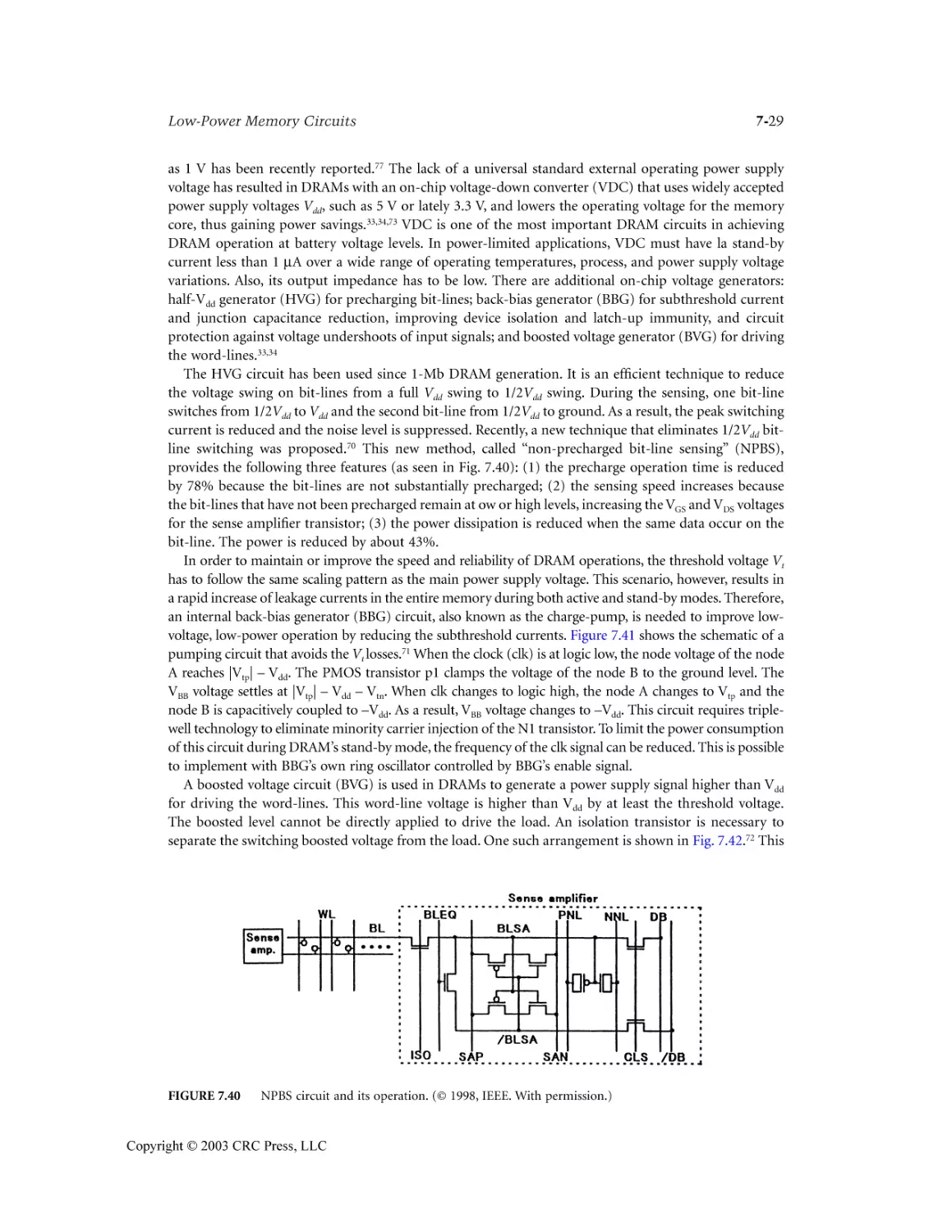


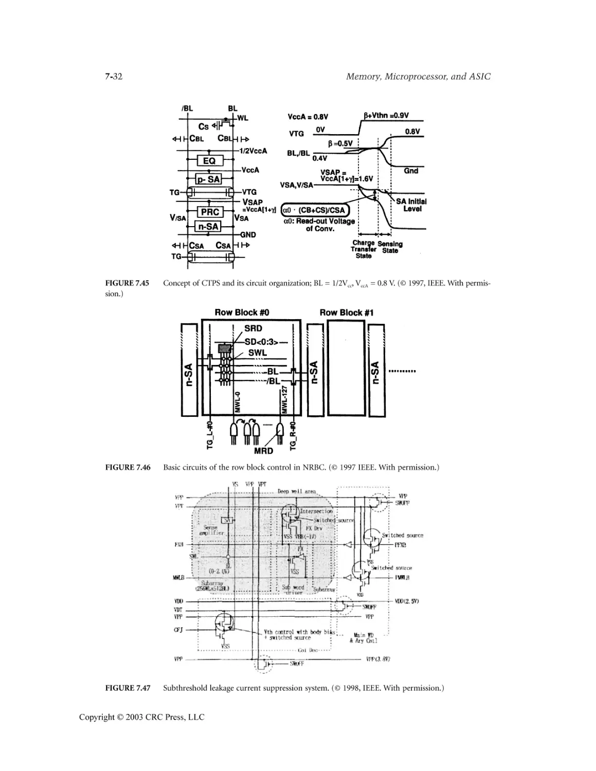

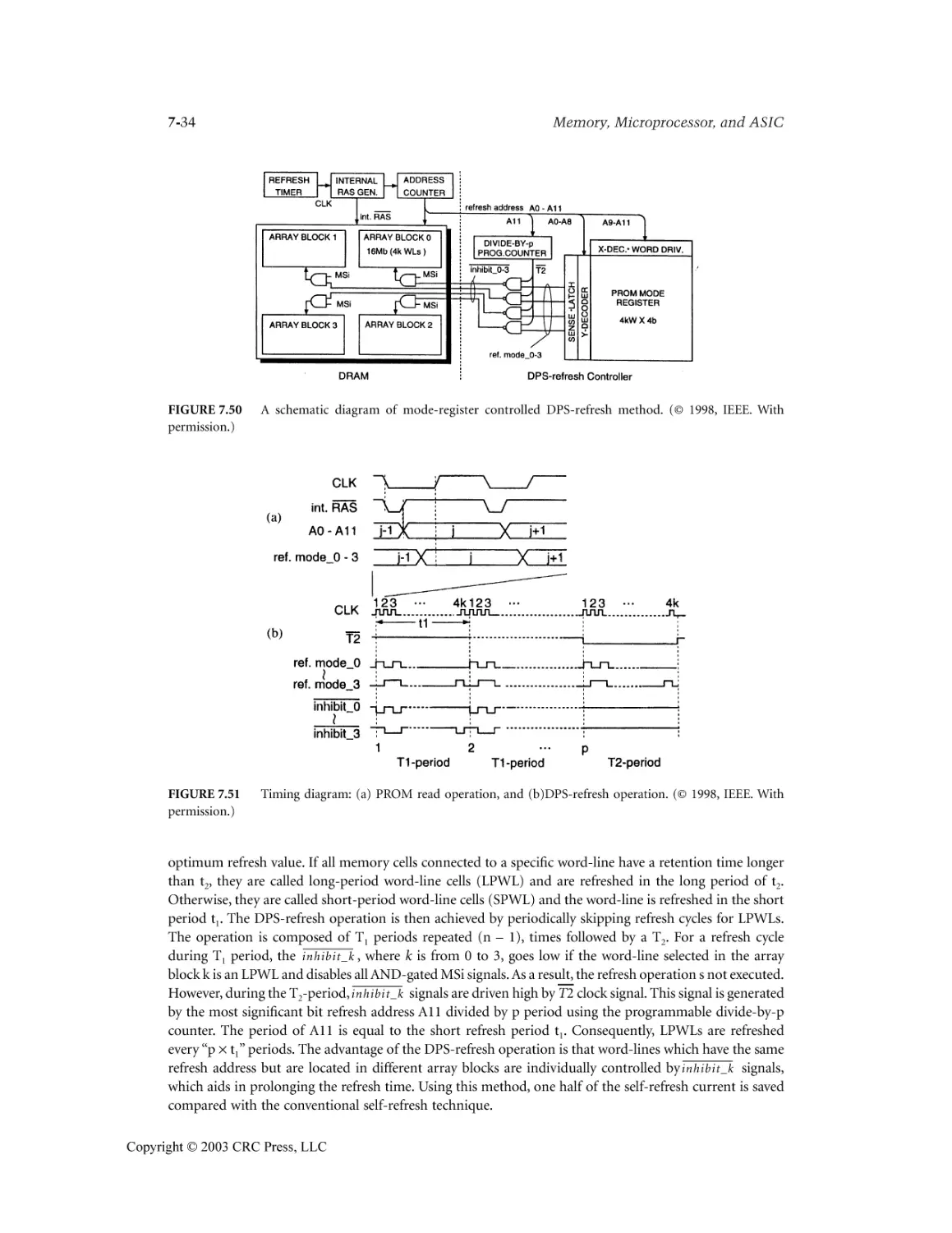
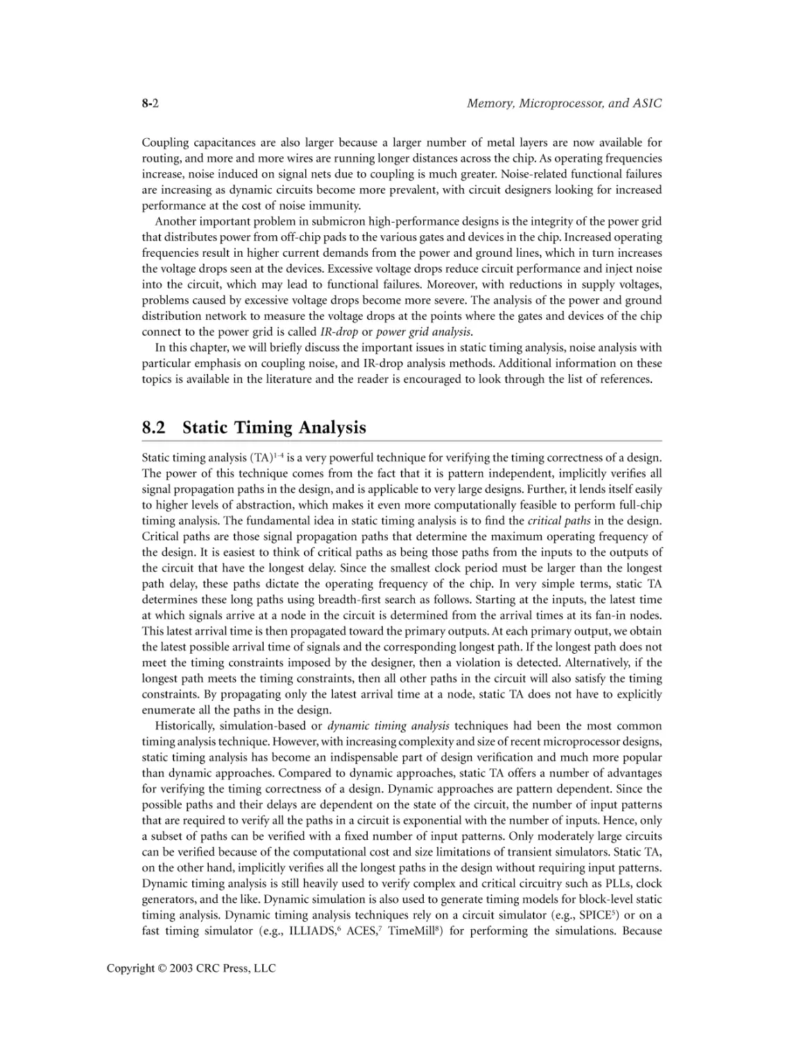


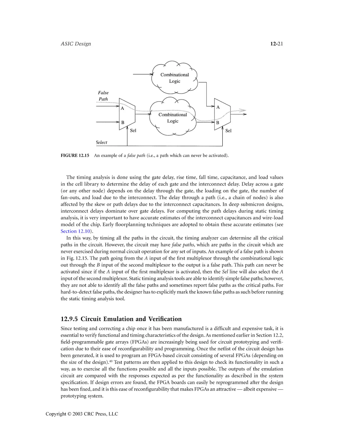
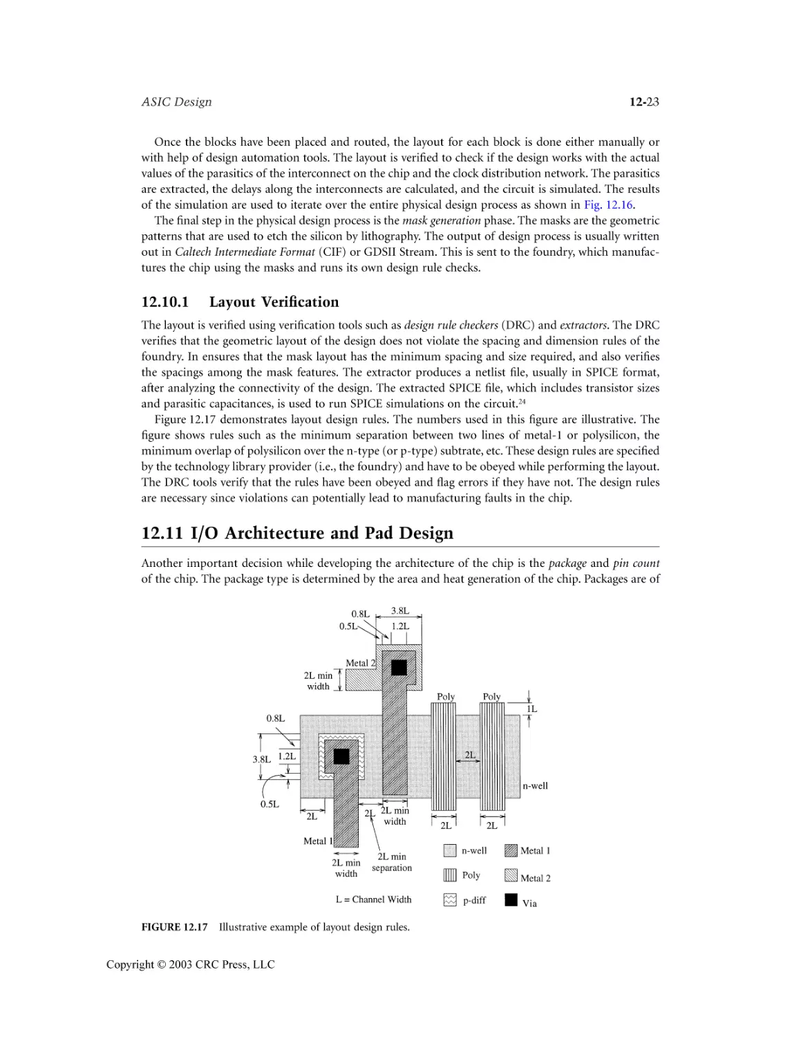


Author: Wai Kai Chen
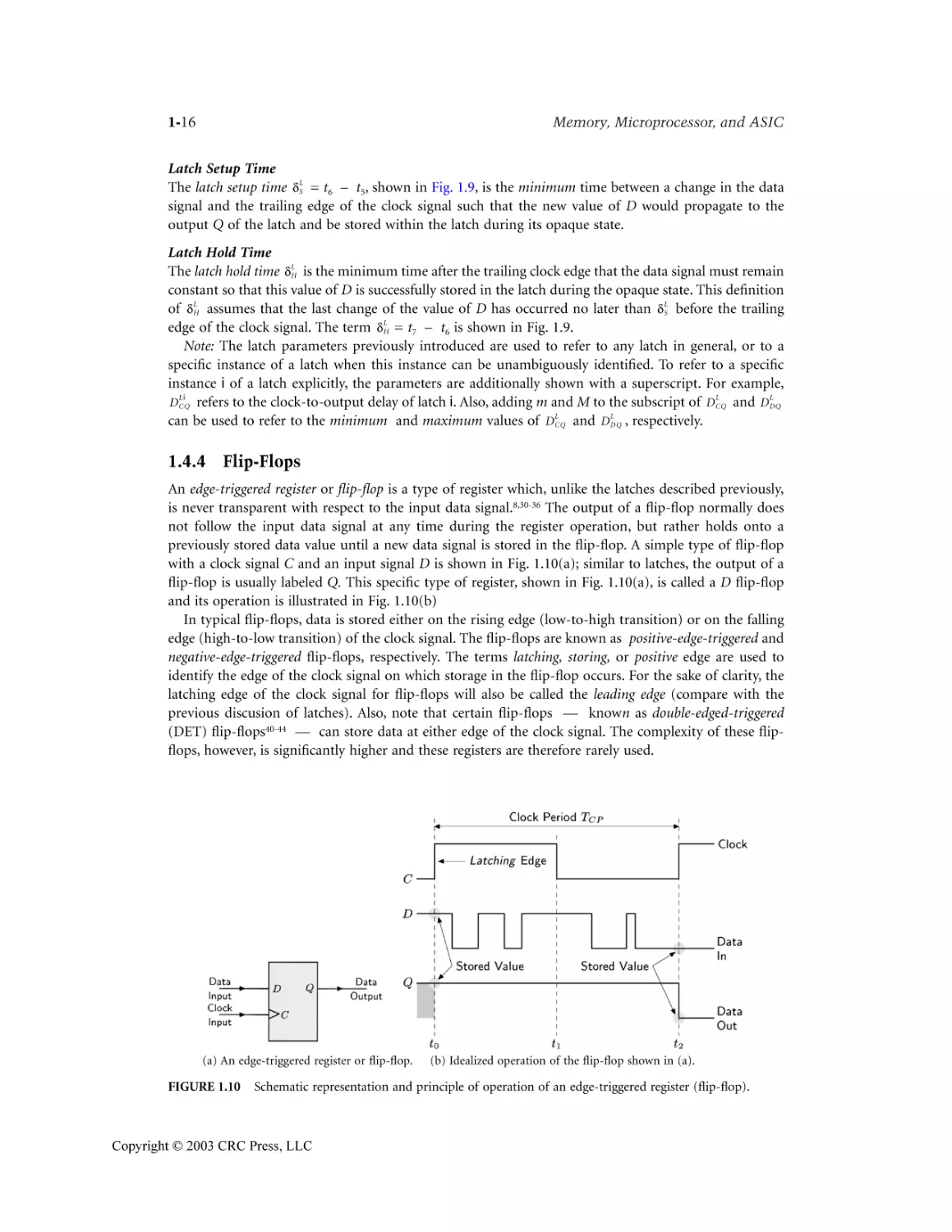
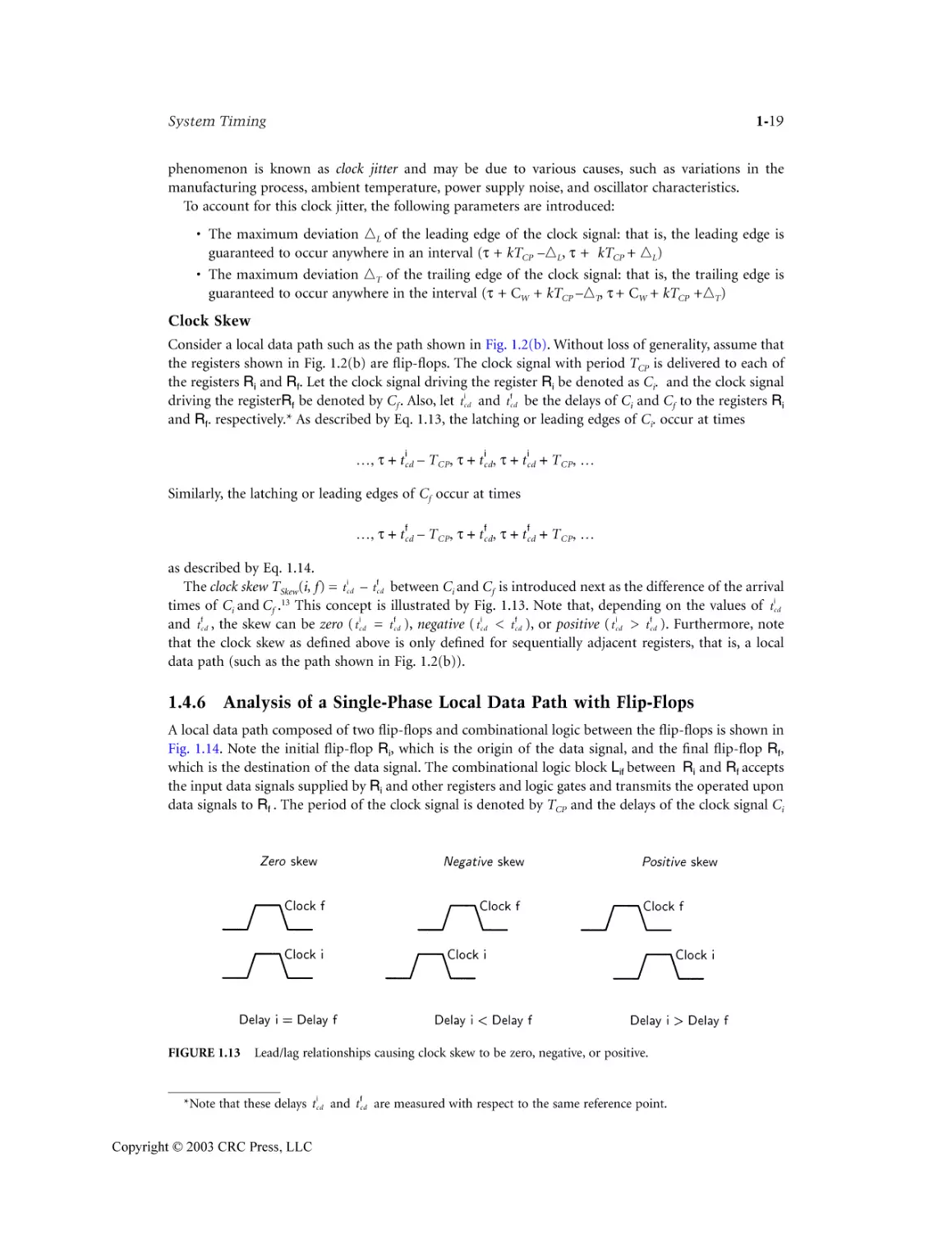
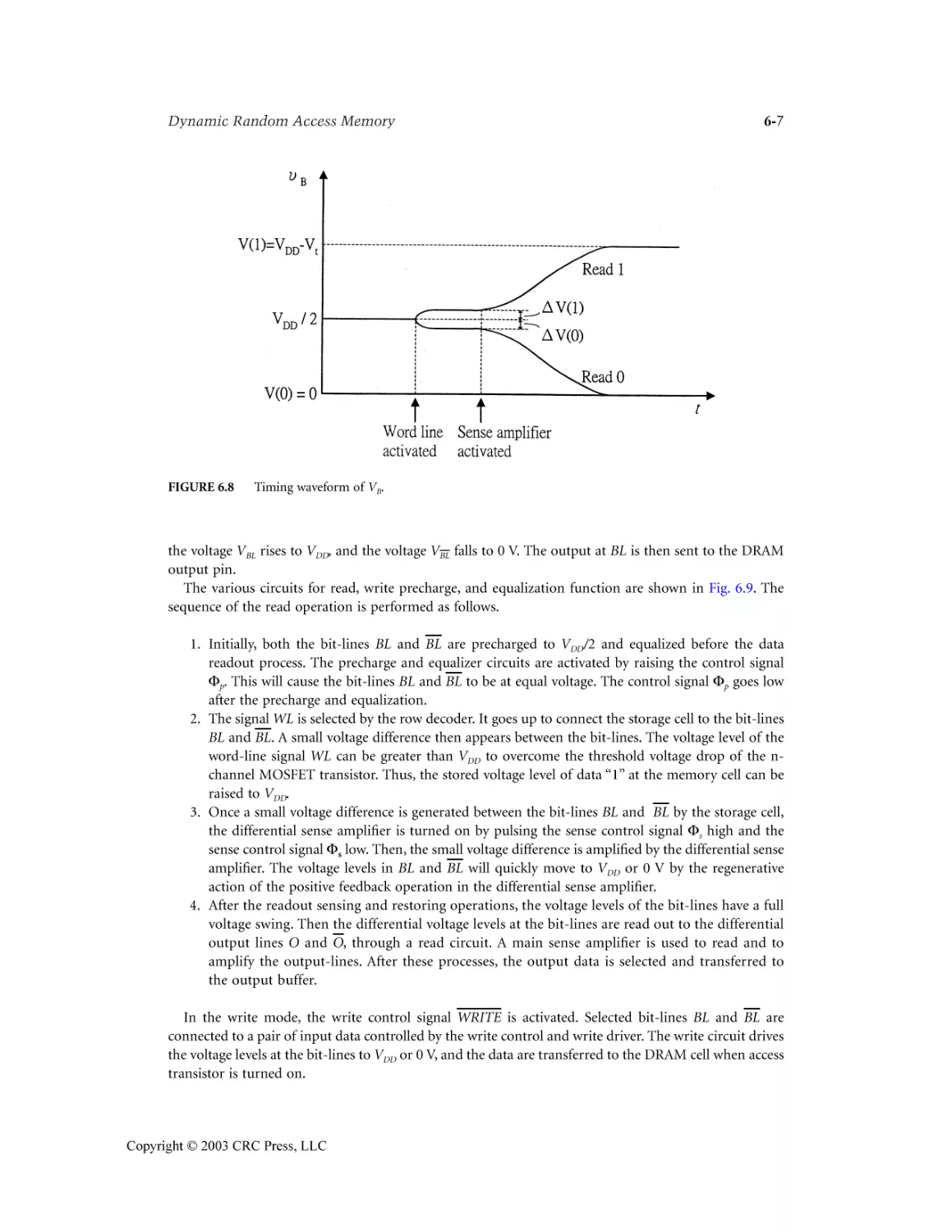
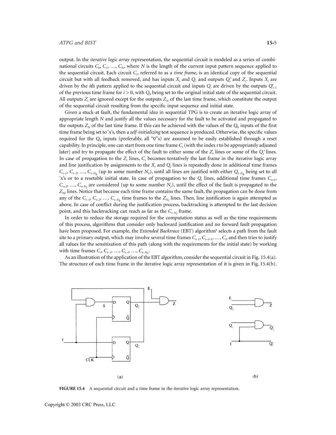
Tags: integrated circuits synthesis arithmetic circuits fpga asic embedded systems digital design hardware synthesis electronic circuits hardware development
ISBN: 0-8493-1737-1
Year: 2003


MEMORY,
MICROPROCESSOR,
and ASIC
Copyright © 2003 CRC Press, LLC
MEMORY,
MICROPROCESSOR,
and ASIC
Editor-in-Chief
Wai-Kai Chen
C RC P R E S S
Boca Raton London New York Washington, D.C.
Copyright © 2003 CRC Press, LLC
1737_FM Page iv Thursday, February 6, 2003 11:36 AM
The material from this book was first published in The VLSI Handbook, CRC Press, 2000.
Library of Congress Cataloging-in-Publication Data
Memory, microprocessor, and ASIC / Wai-Kai Chen, editor-in-chief.
p. cm. -- (Principles and applications in engineering ; 7)
Includes bibliographical references and index.
ISBN 0-8493-1737-1 (alk. paper)
1. Semiconductor storage devices. 2. Microprocessors 3. Application specific integrated
circuits. 4. Integrated circuits--Very large scale integration. I. Chen, Wai-Kai, 1936- II
Series
TK7895.M4V57 2003
621.38¢5--dc21
2002042927
This book contains information obtained from authentic and highly regarded sources. Reprinted material is quoted with
permission, and sources are indicated. A wide variety of references are listed. Reasonable efforts have been made to publish
reliable data and information, but the authors and the publisher cannot assume responsibility for the validity of all materials
or for the consequences of their use.
Neither this book nor any part may be reproduced or transmitted in any form or by any means, electronic or mechanical,
including photocopying, microfilming, and recording, or by any information storage or retrieval system, without prior
permission in writing from the publisher.
All rights reserved. Authorization to photocopy items for internal or personal use, or the personal or internal use of specific
clients, may be granted by CRC Press LLC, provided that $1.50 per page photocopied is paid directly to Copyright Clearance
Center, 222 Rosewood Drive, Danvers, MA 01923 USA The fee code for users of the Transactional Reporting Service is
ISBN 0-8493-1737-1/03/$0.00+$1.50. The fee is subject to change without notice. For organizations that have been granted
a photocopy license by the CCC, a separate system of payment has been arranged.
The consent of CRC Press LLC does not extend to copying for general distribution, for promotion, for creating new works,
or for resale. Specific permission must be obtained in writing from CRC Press LLC for such copying.
Direct all inquiries to CRC Press LLC, 2000 N.W. Corporate Blvd., Boca Raton, Florida 33431.
Trademark Notice: Product or corporate names may be trademarks or registered trademarks, and are used only for
identification and explanation, without intent to infringe.
Visit the CRC Press Web site at www.crcpress.com
© 2003 by CRC Press LLC
No claim to original U.S. Government works
International Standard Book Number 0-8493-1737-1
Library of Congress Card Number 2002042927
Printed in the United States of America 1 2 3 4 5 6 7 8 9 0
Printed on acid-free paper
Copyright © 2003 CRC Press, LLC
1737_FM Page v Thursday, February 6, 2003 11:36 AM
Preface
The purpose of Memory, Microprocessor, and ASIC is to provide in a single volume a comprehensive
reference work covering the broad spectrum of memory, registers, system timing, microprocessor design,
verification and architecture, ASIC design, and test and testability. The book is written and developed
for practicing electrical engineers and computer scientists in industry, government, and academia. The
goal is to provide the most up-to-date information in the field.
Over the years, the fundamentals of the field have evolved to include a wide range of topics and a
broad range of practice. To encompass such a wide range of knowledge, the book focuses on the key
concepts, models, and equations that enable the design engineer to analyze, design, and predict the
behavior of large-scale systems. While design formulas and tables are listed, emphasis is placed on the
key concepts and theories underlying the processes.
The book stresses the fundamental theory behind professional applications. In order to do so, it is
reinforced with frequent examples. Extensive development of theory and details of proofs have been
omitted. The reader is assumed to have a certain degree of sophistication and experience. However, brief
reviews of theories, principles, and mathematics of some subject areas are given. These reviews have been
done concisely, with perception.
The compilation of this book would not have been possible without the dedication and efforts of Bing
J. Sheu, Steve M. Kang and Nick Kanopoulos, and, above all, the contributing authors. I wish to thank
them all.
Wai-Kai Chen
v
Copyright © 2003 CRC Press, LLC
1737_FM Page vii Thursday, February 6, 2003 11:36 AM
Editor-in-Chief
Wai-Kai Chen, Professor and Head Emeritus of the Department of
Electrical Engineering and Computer Science at the University of
Illinois at Chicago. He is now serving as Academic Vice President at
International Technological University. He received his B.S. and M.S.
in electrical engineering at Ohio University, where he was later recognized as a Distinguished Professor. He earned his Ph.D. in electrical
engineering at University of Illinois at Urbana/Champaign.
Professor Chen has extensive experience in education and industry
and is very active professionally in the fields of circuits and systems.
He has served as visiting professor at Purdue University, University
of Hawaii at Manoa, and Chuo University in Tokyo, Japan. He was
editor of the IEEE Transactions on Circuits and Systems, Series I and
II, president of the IEEE Circuits and Systems Society and is the
founding editor and editor-in-chief of the Journal of Circuits, Systems
and Computers. He received the Lester R. Ford Award from the Mathematical Association of America, the Alexander von Humboldt Award from Germany, the JSPS Fellowship
Award from Japan Society for the Promotion of Science, the Ohio University Alumni Medal of Merit for
Distinguished Achievement in Engineering Education, the Senior University Scholar Award and the 2000
Faculty Research Award form the University of Illinois at Chicago, and the Distinguished Alumnus Award
from the University of Illinois at Urbana/Champaign. He is the recipient of the Golden Jubilee Medal,
the Education Award, and the Meritorious Service Award from IEEE Circuits and Systems Society, and the
Third Millennium Medal from the IEEE. He has also received more than dozen honorary professorship
awards from major institutions in China.
A fellow of the Institute of Electrical and Electronics Engineers and the American Association for the
Advancement of Science, Professor Chen is widely known in the profession for his Applied Graph Theory
(North-Holland), Theory and Design of Broadband Matching Networks (Pergamon Press), Active Network
and Feedback Amplifier Theory (McGraw-Hill), Linear Networks and Systems (Brooks/Cole), Passive and
Active Filters: Theory and Implements (John Wiley & Sons), Theory of Nets: Flows in Networks (WileyInterscience), and The Circuits and Filters Handbook and The VLSI Handbook (CRC Press).
vii
Copyright © 2003 CRC Press, LLC
1737_FM Page ix Thursday, February 6, 2003 11:36 AM
Contributors
David Blaauw
Charles Ching-Hsiang Hsu
Motorola, Inc.
Austin, Texas
National Tsing-Hua University
Hsinchu, Taiwan
Kuo-Hsing Cheng
Jen-Sheng Hwang
Tamkang University
Tamsui, Taipei Hsien, Taiwan
National Science Council
Hsinchu, Taiwan
Amy Hsiu-Fen Chou
Wen-mei W. Hwu
National Tsing-Hua University
Hsinchu, Taiwan
University of Illinois
Urbana, Illinois
Daniel A. Connors
Vikram Iyengar
University of Illinois
Urbana, Illinois
University of Illinois
Urbana, Illinois
Abhijit Dharchoudhury
Dimitri Kagaris
Motorola, Inc.
Austin, Texas
Southern Illinois University
Carbondale, Illinois
Eby G. Friedman
Nick Kanopoulos
University of Rochester
Rochester, New York
Stantanu Ganguly
Intel Corporation
Austin, Texas
Rajesh K. Gupta
University of California
Irvine, California
Sumit Gupta
University of California
Irvine, California
Atmel Multimedia and
Communications
Morrisville, North Carolina
Tanay Karnik
Intel Corporation
Hillsboro, Oregon
Ivan S. Kourtev
University of Pittsburgh
Pittsburgh, Pennsylvania
Frank Ruei-Ling Lin
National Tsing-Hua University
Hsinchu, Taiwan
ix
Copyright © 2003 CRC Press, LLC
1737_FM Page x Thursday, February 6, 2003 11:36 AM
John W. Lockwood
Yuh-Kuang Tseng
Washington University
St. Louis, Missouri
Industrial Research and
Technology Institute
Chutung, Hsinchu, Taiwan
Martin Margala
University of Alberta
Edmonton, Alberta, Canada
Chung-Yu Wu
National Chiao Tung University
Hsinchu, Taiwan
Elizabeth M. Rudnick
University of Illinois
Urbana, Illinois
Rick Shih-Jye Shen
National Tsing-Hua University
Hsinchu, Taiwan
Spyros Tragoudas
Southern Illinois University
Carbondale, Illinois
x
Copyright © 2003 CRC Press, LLC
Evans Ching-Song Yang
National Tsing-Hua University
Hsinchu, Taiwan
1737_FM Page xi Thursday, February 6, 2003 11:36 AM
Contents
1
System Timing Ivan S. Kourtev and Eby G. Friedman
1.1 Introduction .........................................................................................................................1-1
1.2 Synchronous VLSI Systems ..................................................................................................1-3
1.3 Synchronous Timing and Clock Distribution Networks .....................................................1-5
1.4 Timing Properties of Synchronous Storage Elements ........................................................1-13
1.5 A Final Note ........................................................................................................................1-27
1.6 Glossary of Terms ................................................................................................................1-27
References ......................................................................................................................................1-29
2
ROM/PROM/EPROM Jen-Sheng Hwang
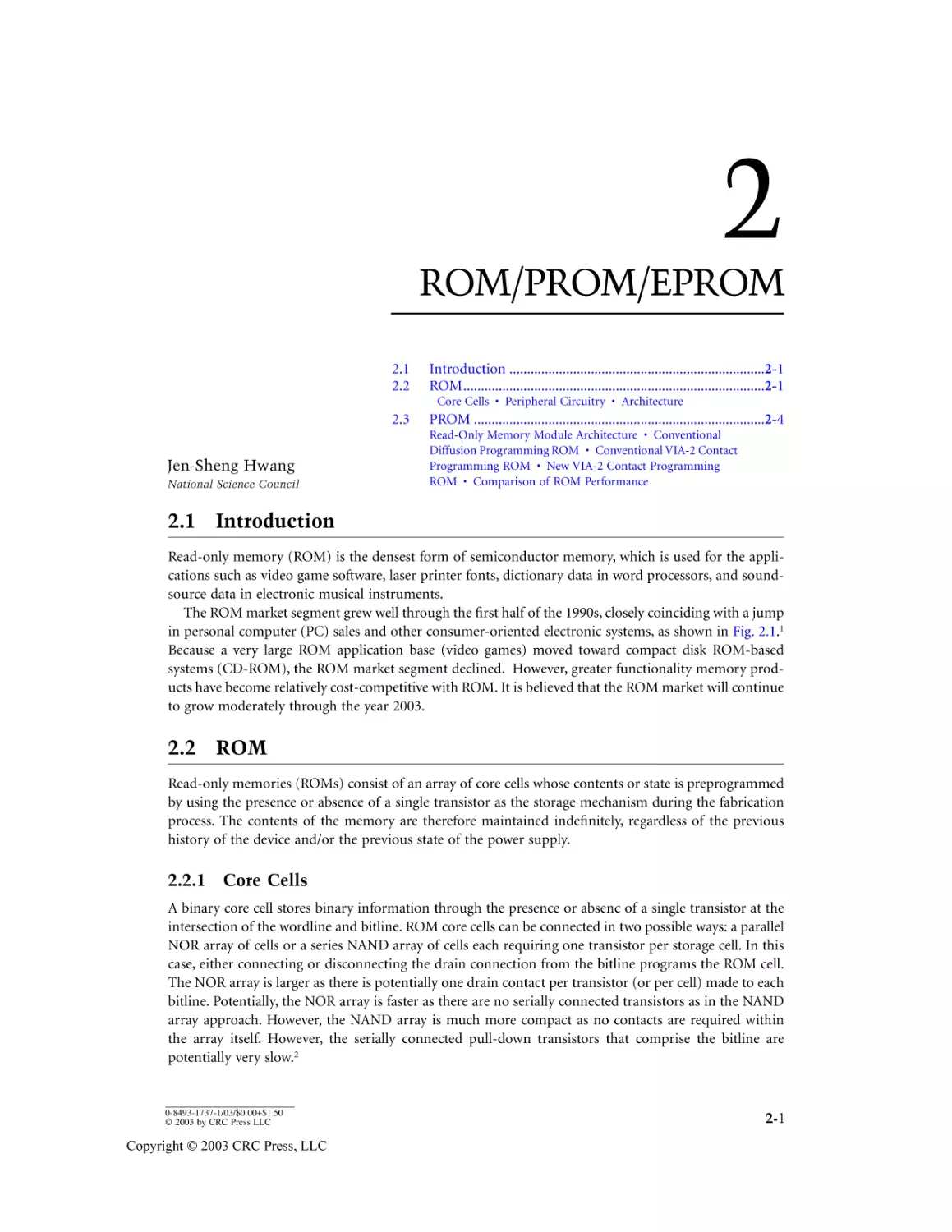
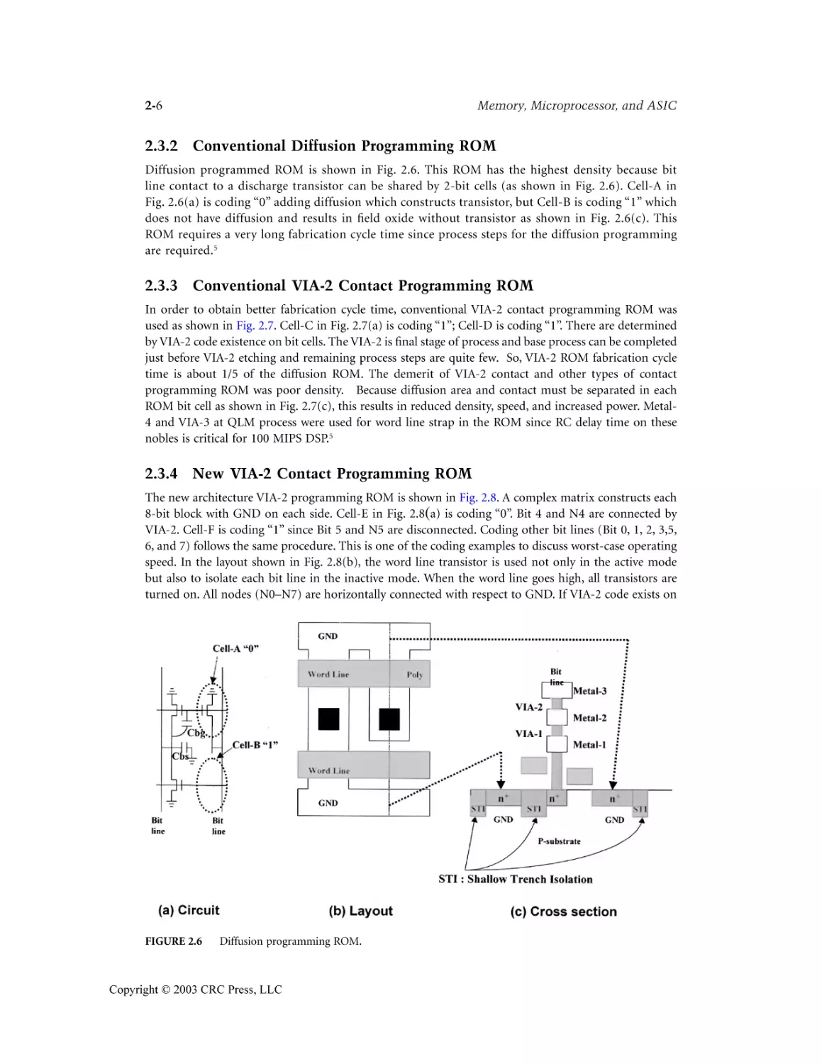
2.1 Introduction .........................................................................................................................2-1
2.2 ROM .....................................................................................................................................2-1
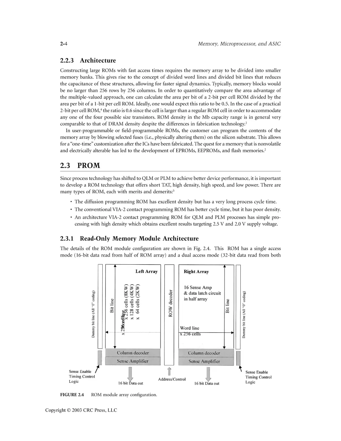
2.3 PROM ...................................................................................................................................2-4
References ........................................................................................................................................2-9
3
SRAM Yuh-Kuang Tseng
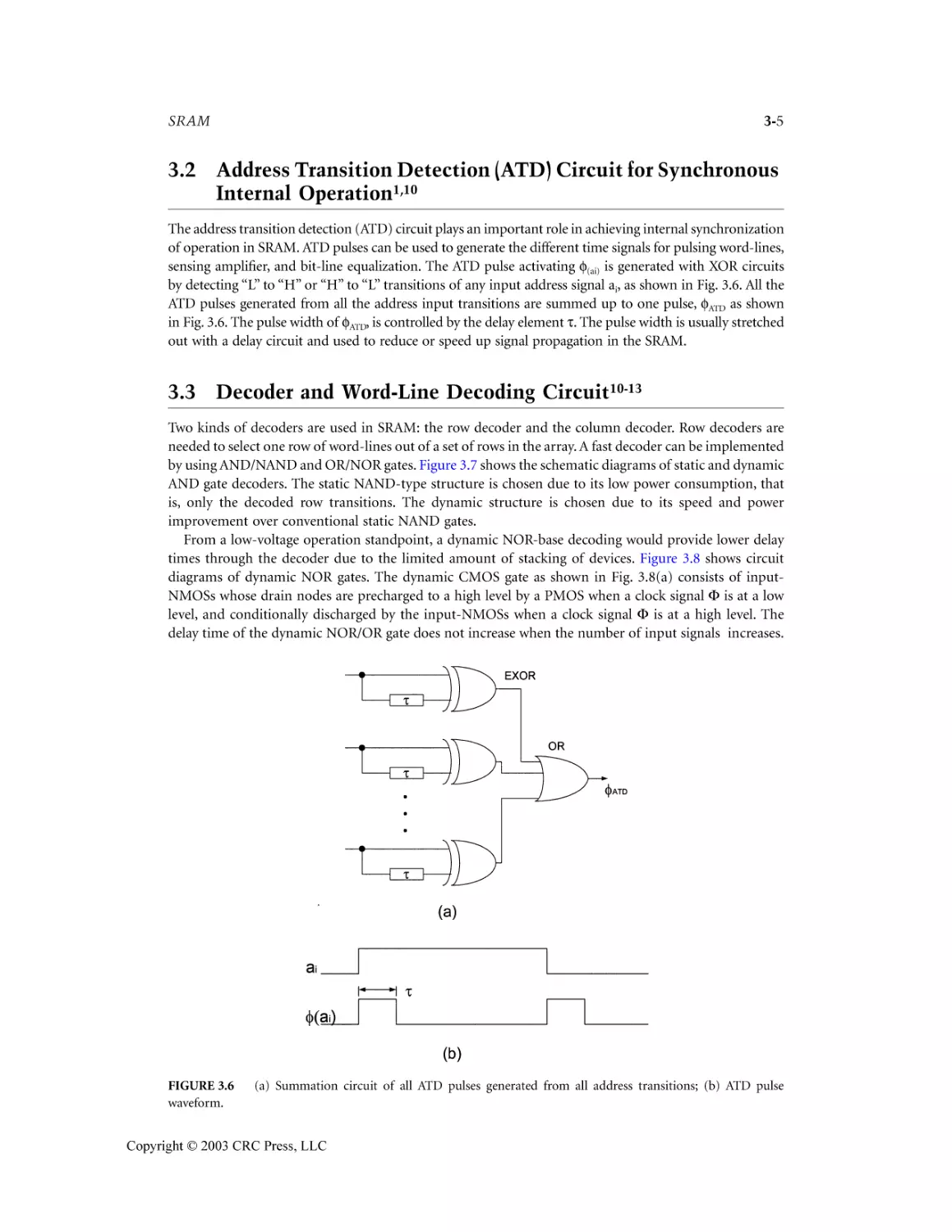
3.1 Read/Write Operation ..........................................................................................................3-1
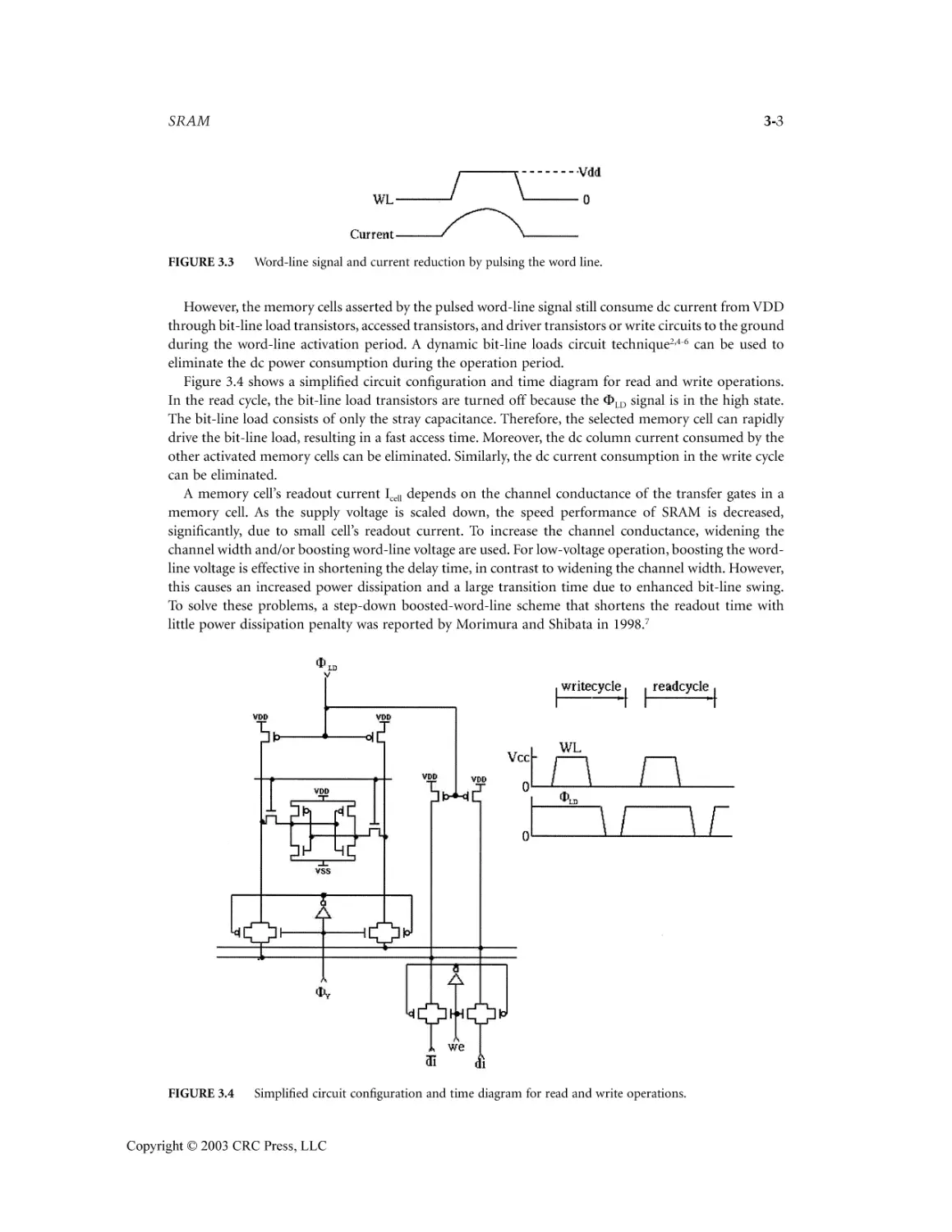
3.2 Address Transition Detection (ATD) Circuit for Synchronous Internal Operation ...........3-5
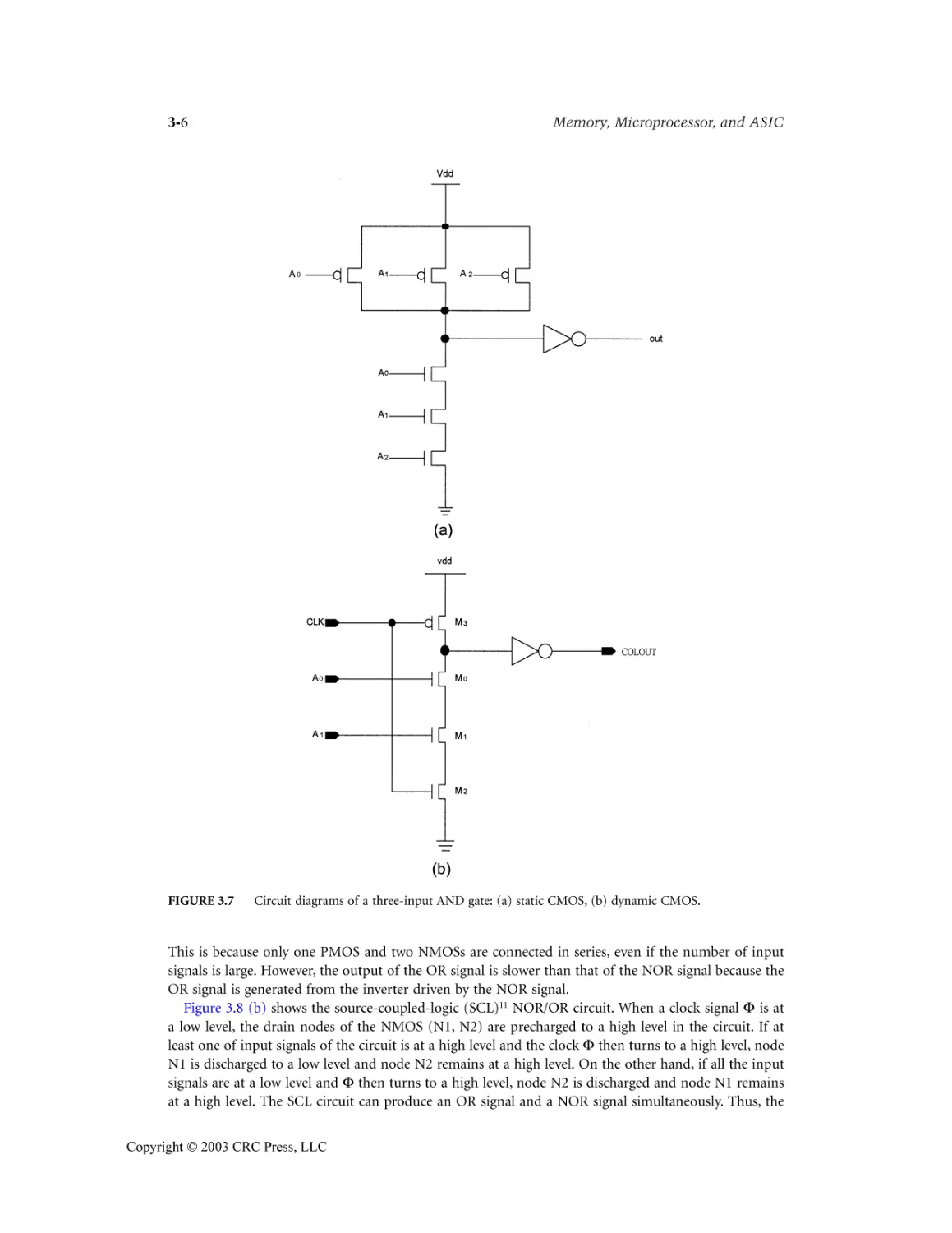
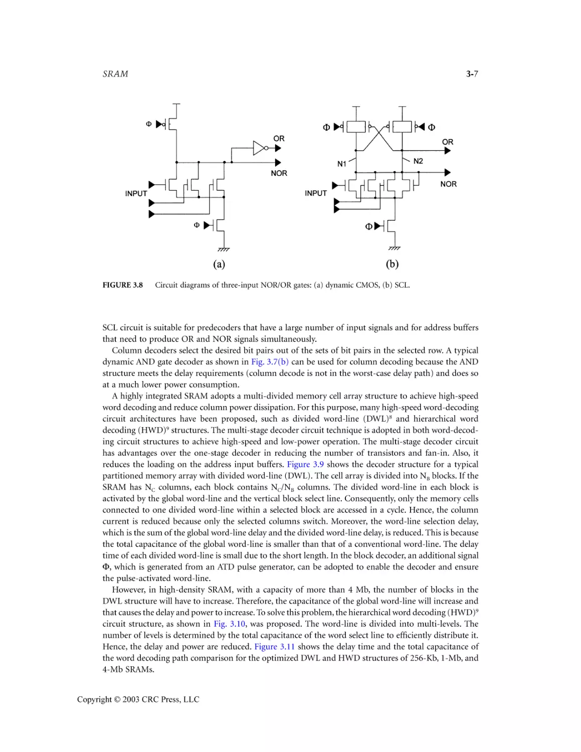
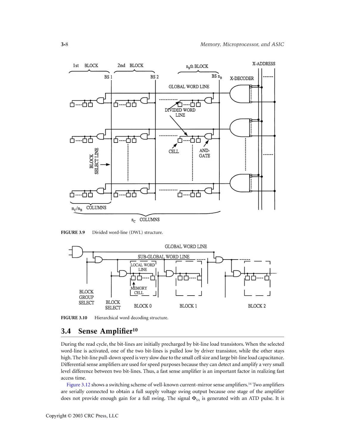
3.3 Decoder and Word-Line Decoding Circuit .........................................................................3-5
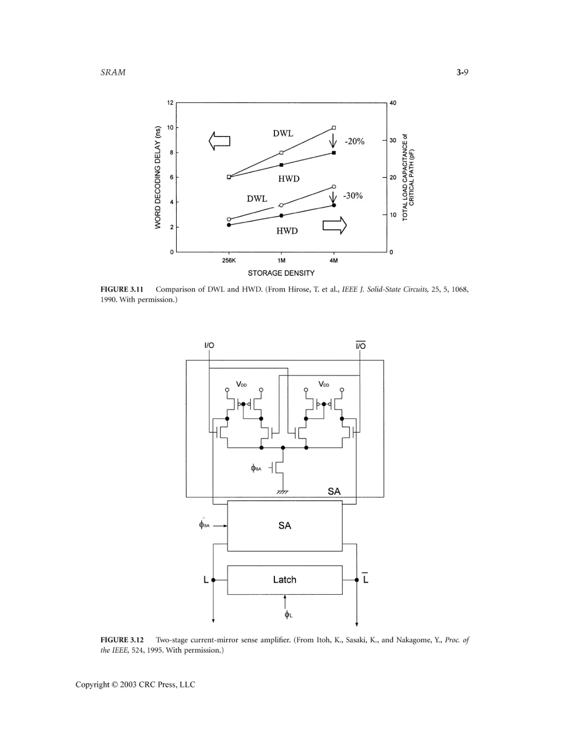
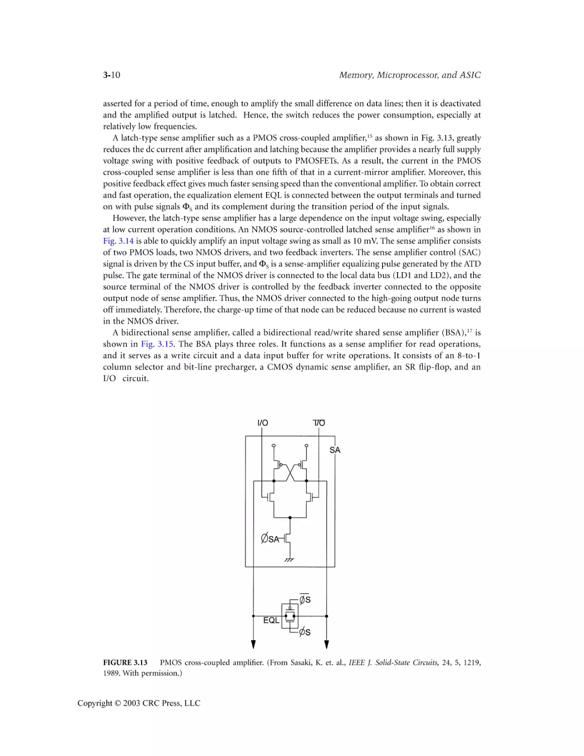
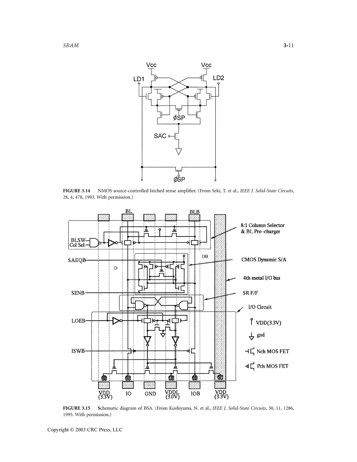
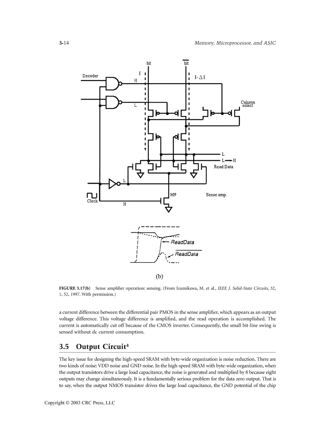
3.4 Sense Amplifier .....................................................................................................................3-8
3.5 Output Circuit .....................................................................................................................3-14
References ......................................................................................................................................3-16
4
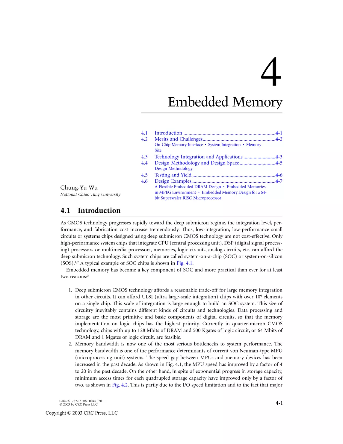
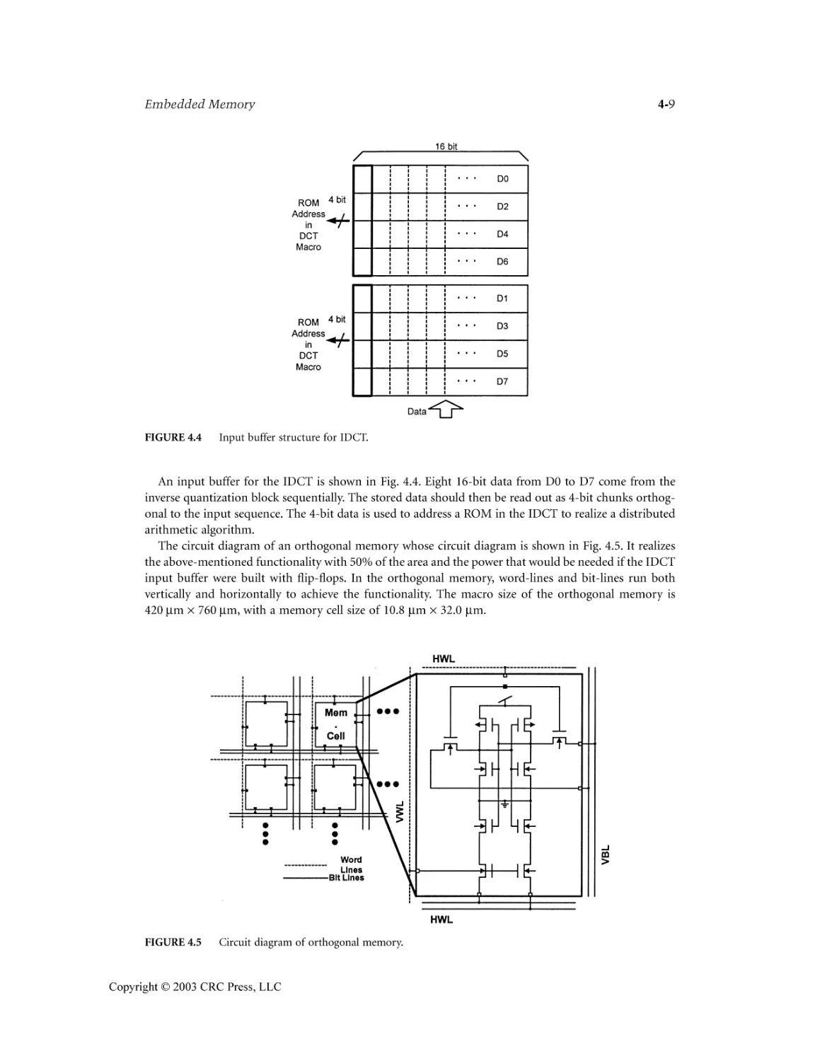
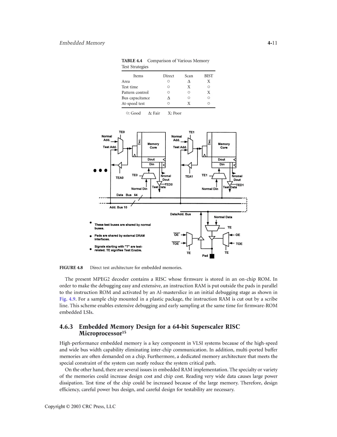
Embedded Memory Chung-Yu Wu
4.1 Introduction .........................................................................................................................4-1
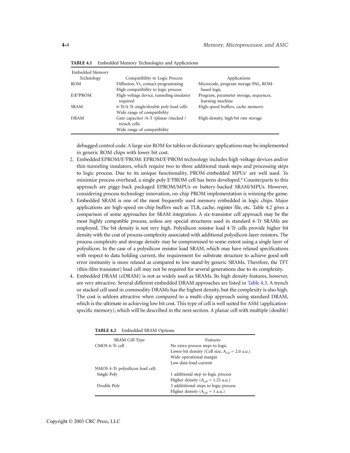
4.2 Merits and Challenges ...........................................................................................................4-2
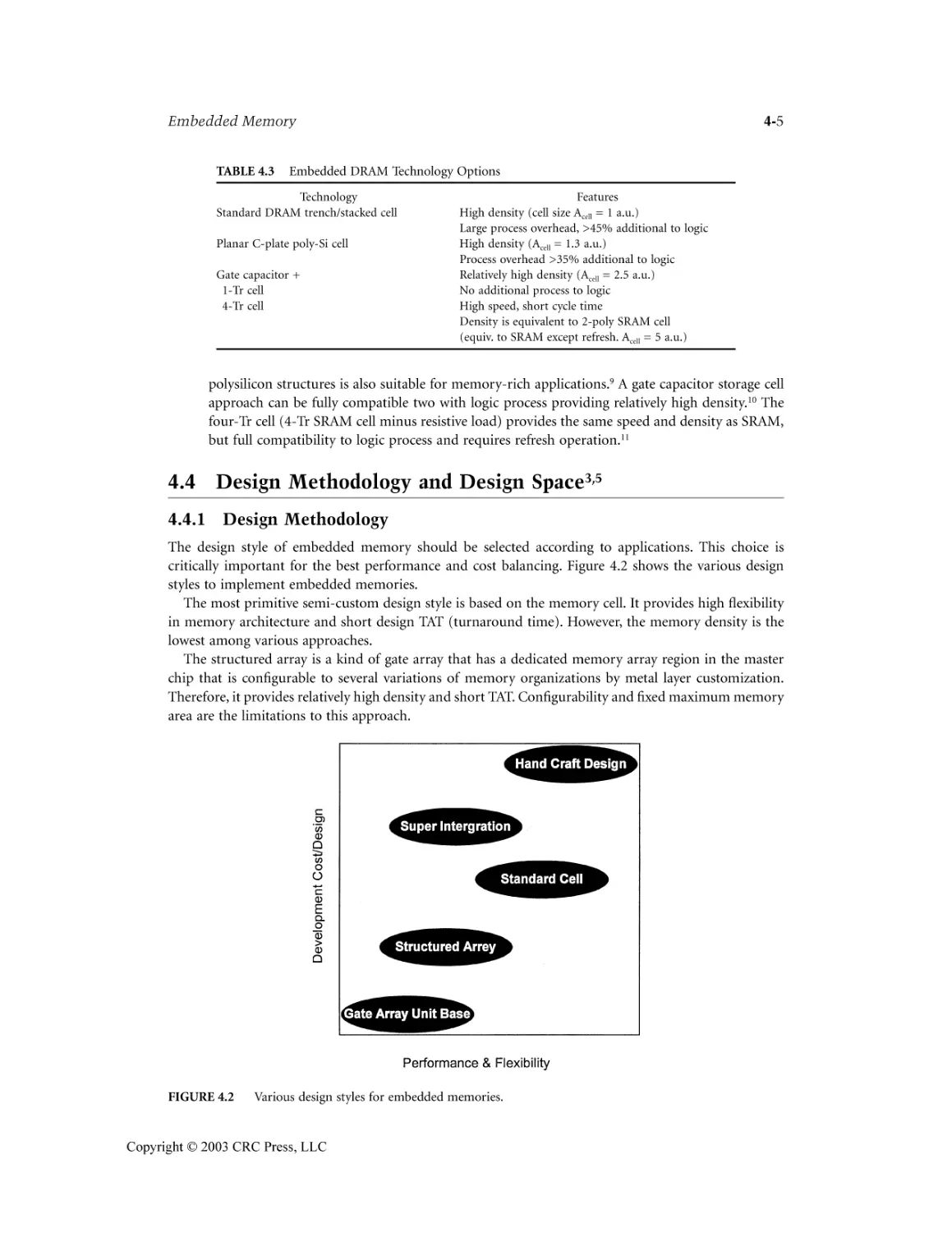
4.3 Technology Integration and Applications ............................................................................4-3
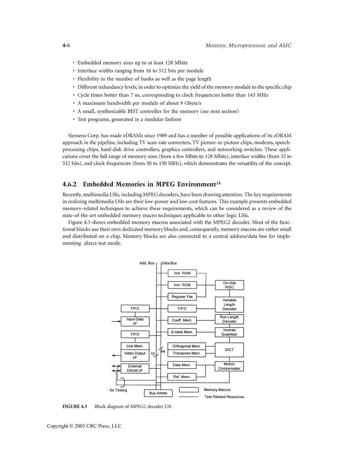
4.4 Design Methodology and Design Space ................................................................................4-5
4.5 Testing and Yield ...................................................................................................................4-6
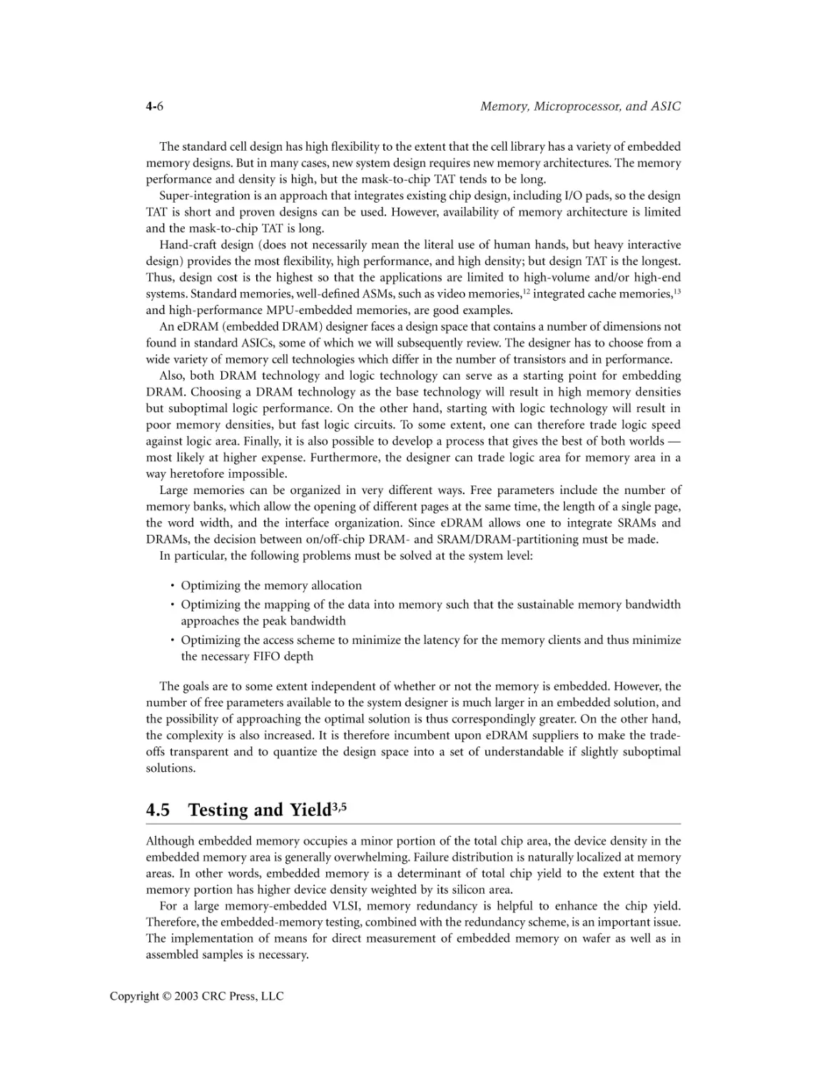
4.6 Design Examples ...................................................................................................................4-7
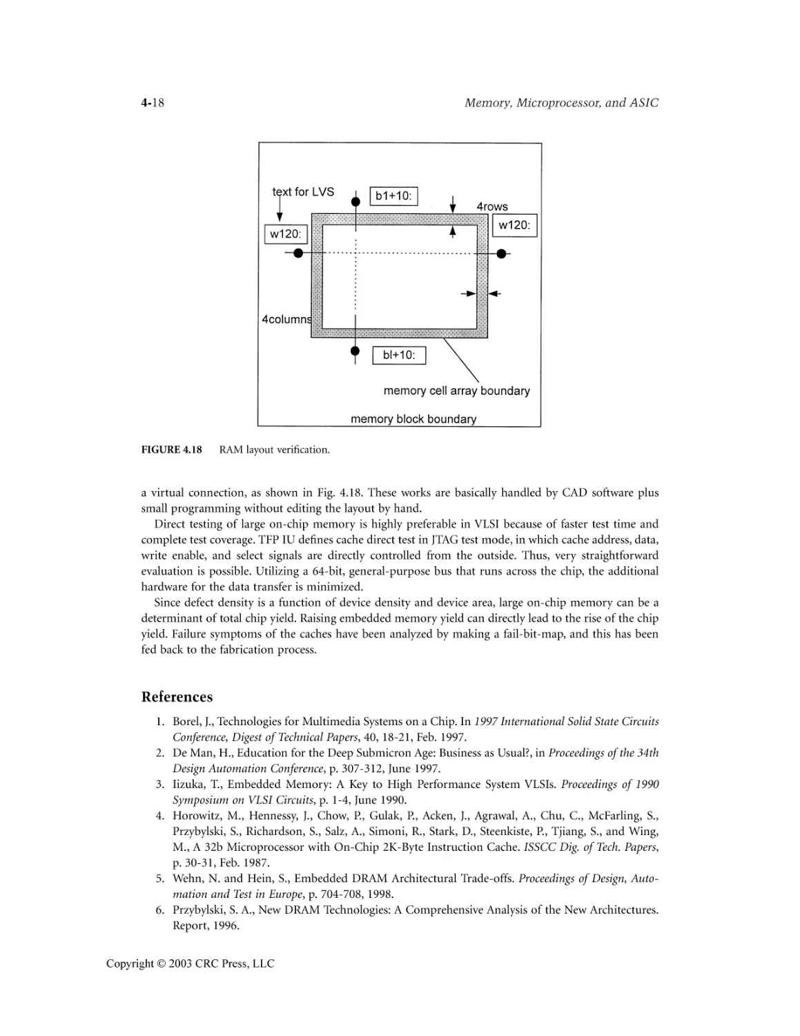
References ......................................................................................................................................4-18
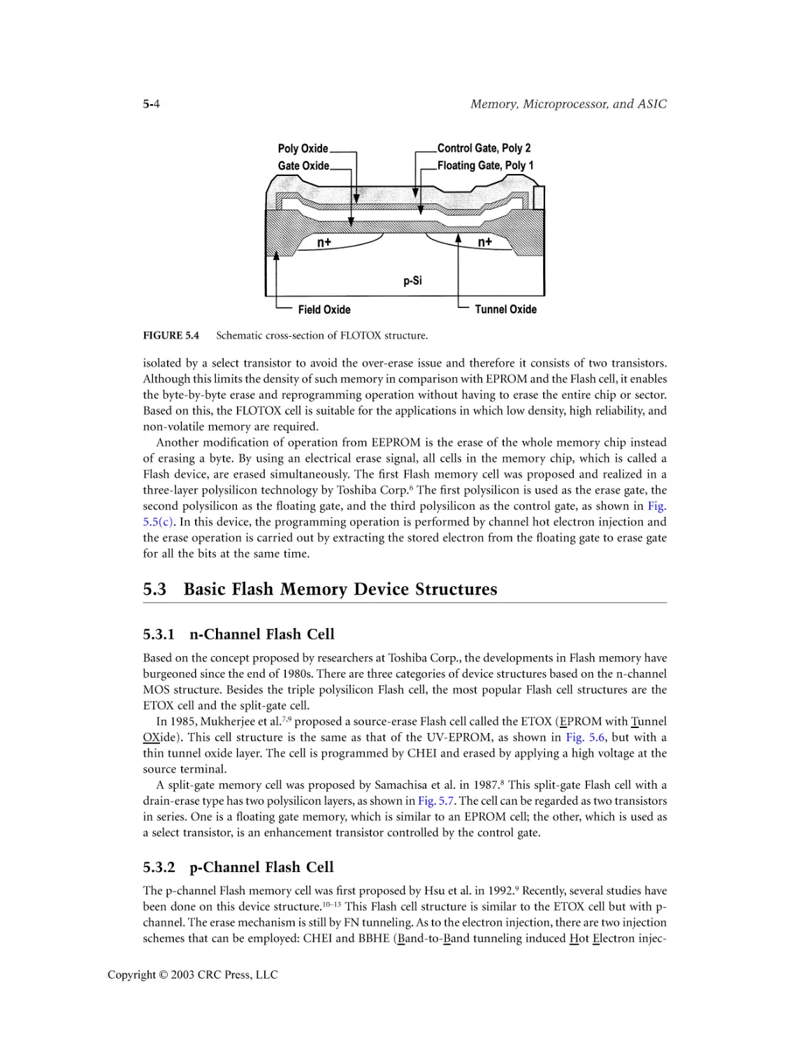
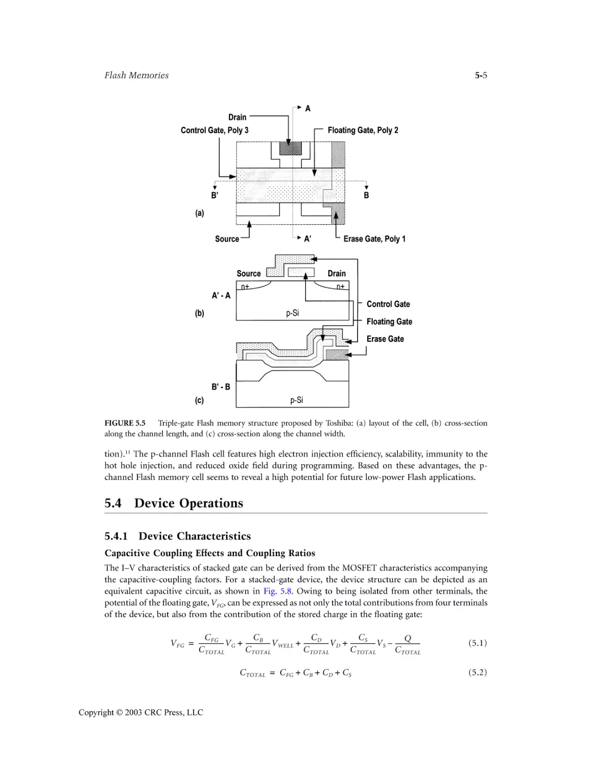
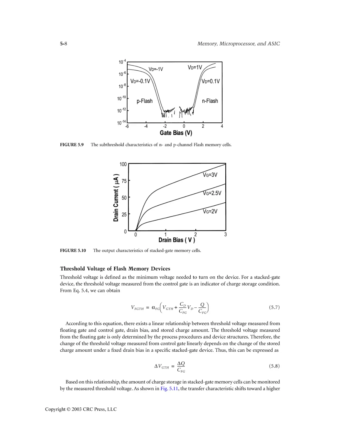
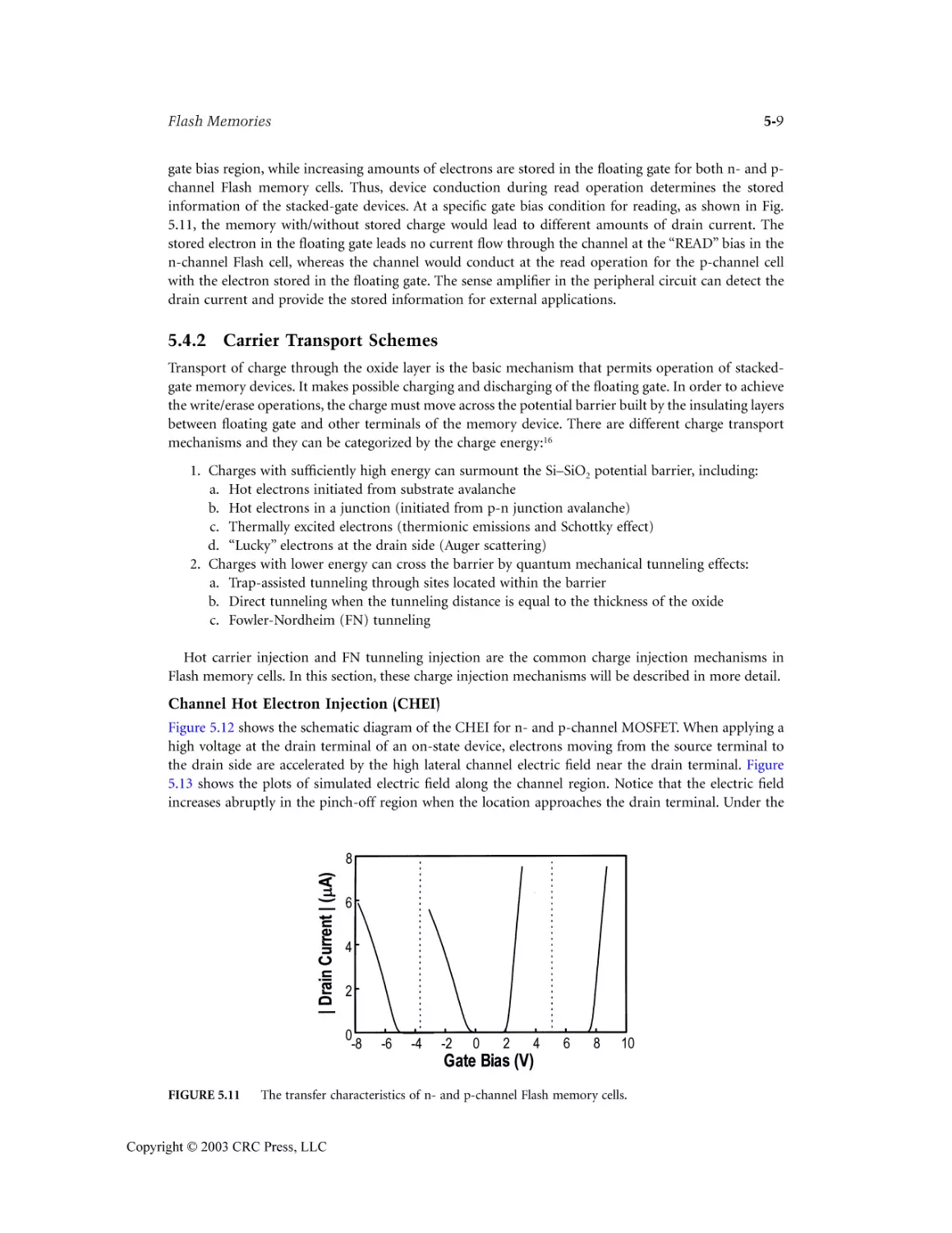
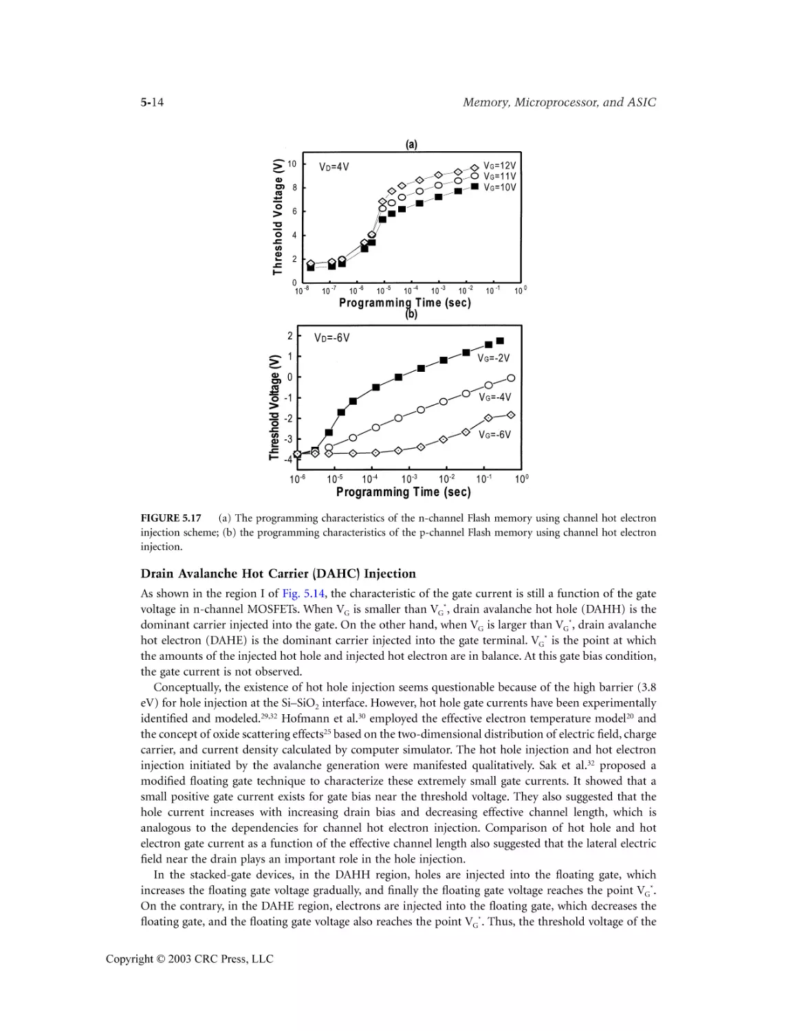
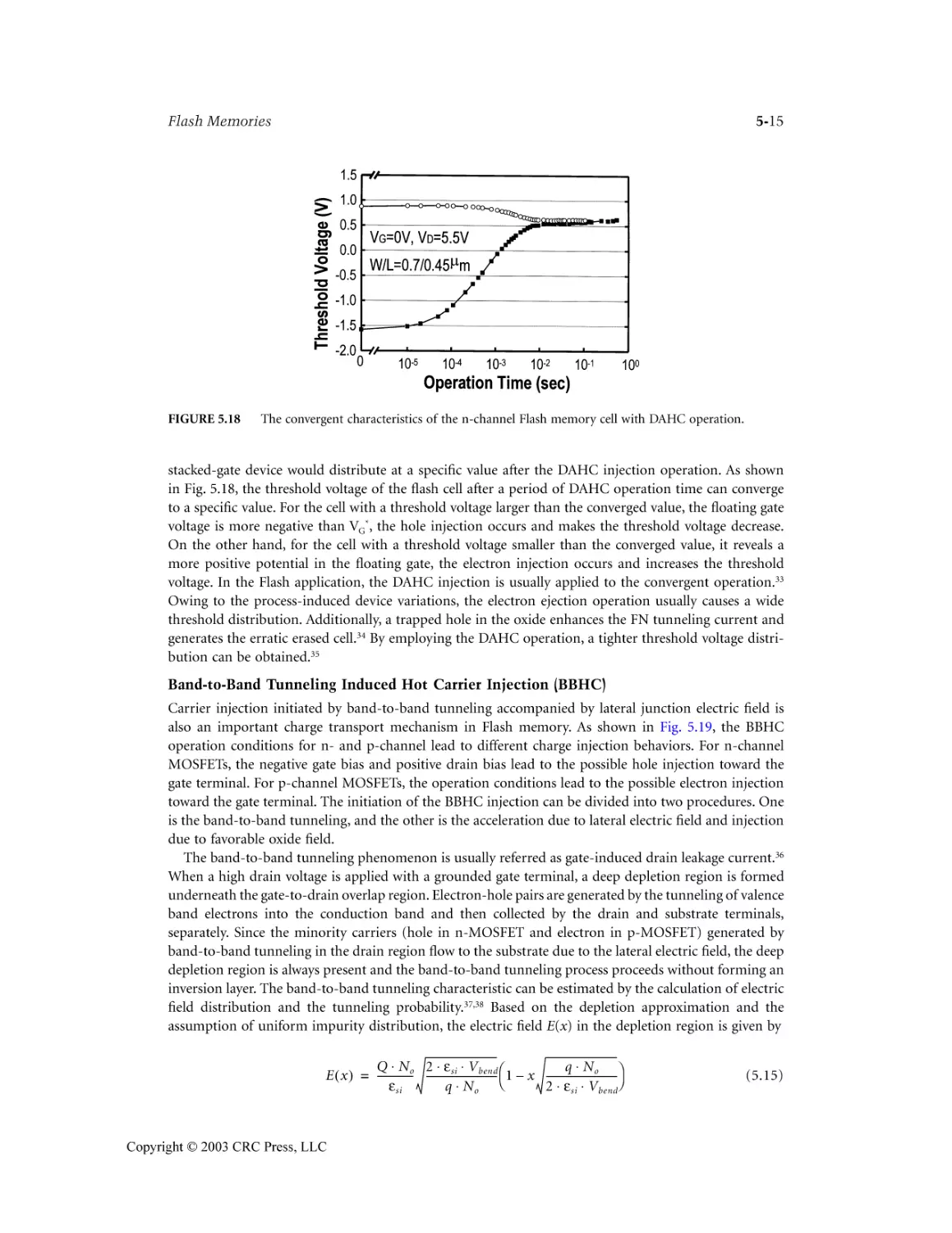
5
Flash Memories Rick Shih-Jye Shen, Frank Ruei-Ling Lin, Amy Hsiu-Fen Chou,
Evans Ching-Song Yang , and Charles Ching-Hsiang Hsu
5.1 Introduction .........................................................................................................................5-1
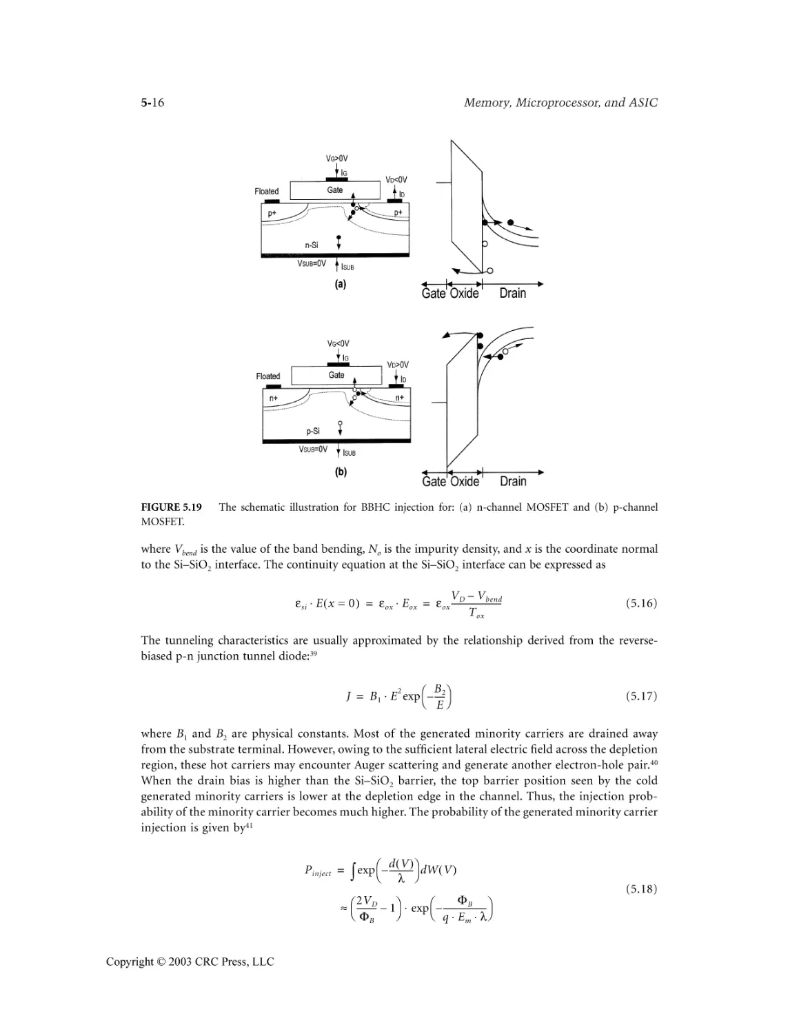
5.2 Review of Stacked-Gate Non-Volatile Memory ..................................................................5-1
xi
Copyright © 2003 CRC Press, LLC
1737_FM Page xii Thursday, February 6, 2003 11:36 AM
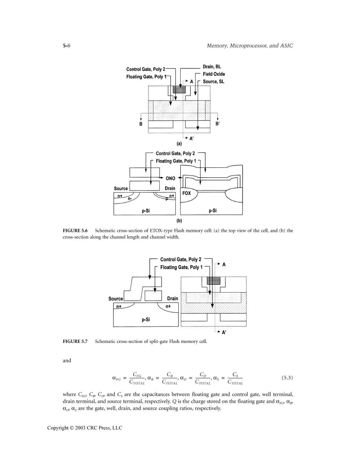
5.3 Basic Flash Memory Device Structures ................................................................................5-4
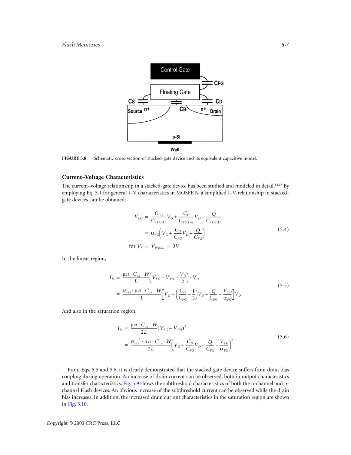
5.4 Device Operations .................................................................................................................5-5
5.5 Variations of Device Structure ...........................................................................................5-20
5.6 Flash Memory Array Structures .........................................................................................5-23
5.7 Evolution of Flash Memory Technology ............................................................................5-24
5.8 Flash Memory System .........................................................................................................5-26
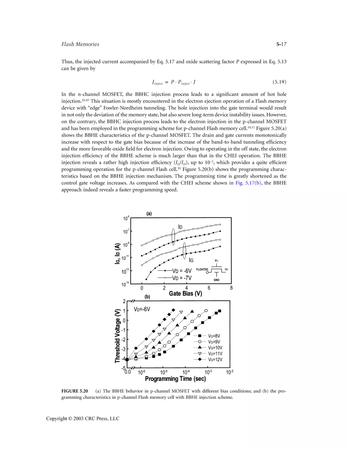
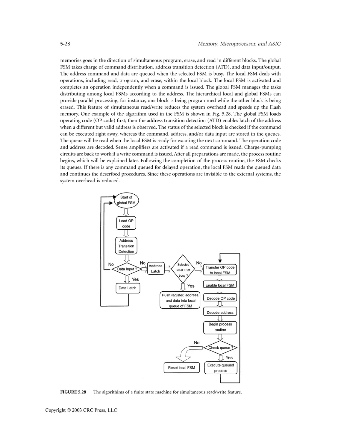
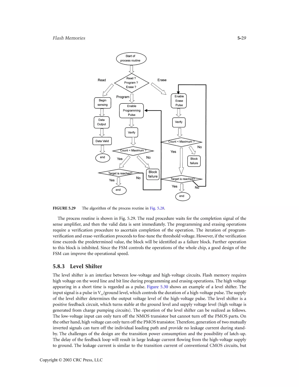
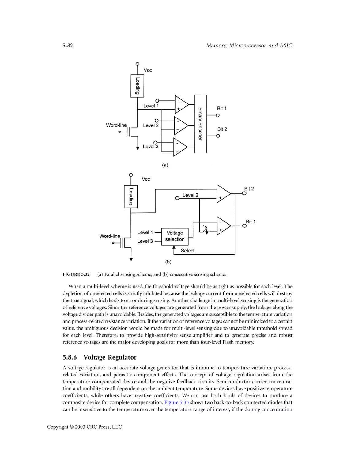
References ......................................................................................................................................5-35
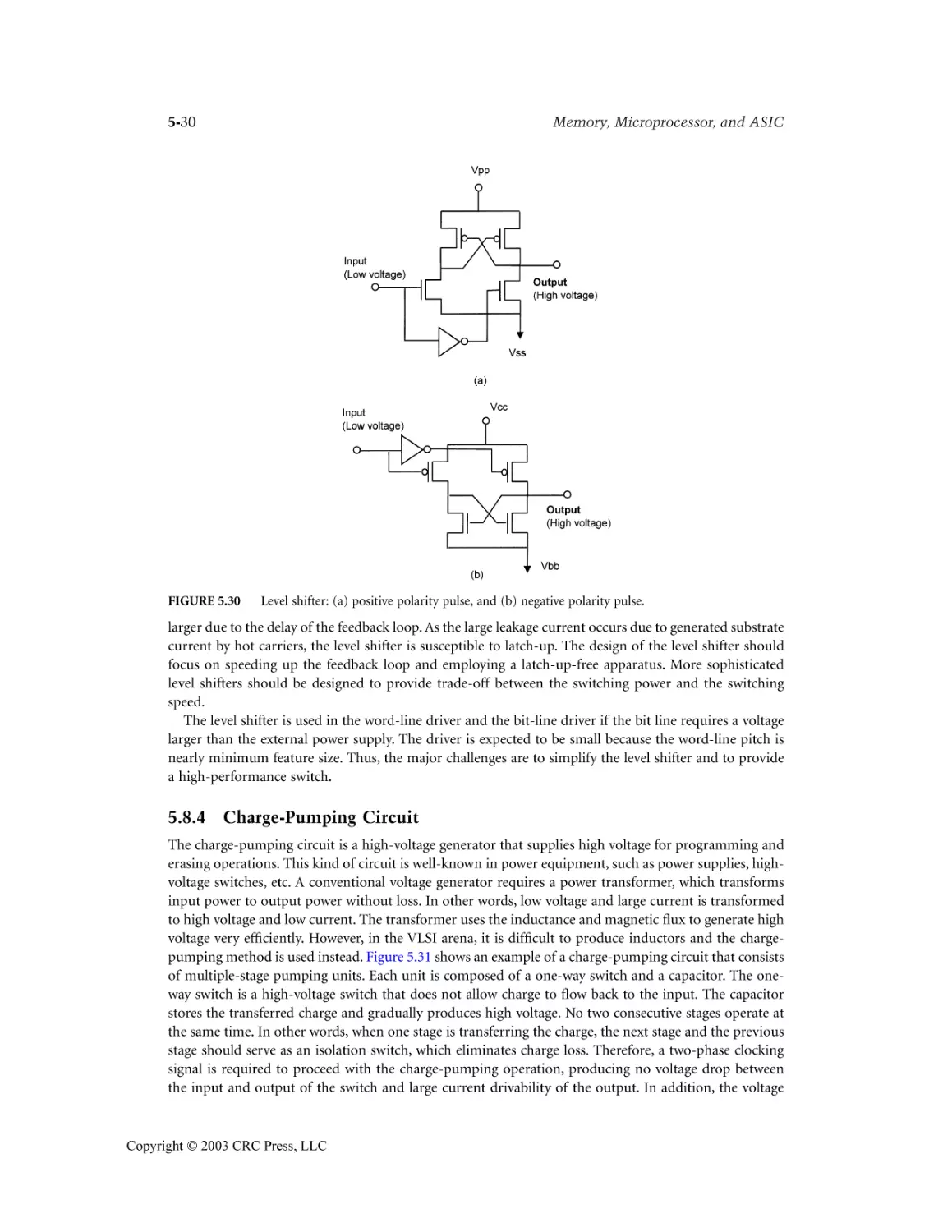
6
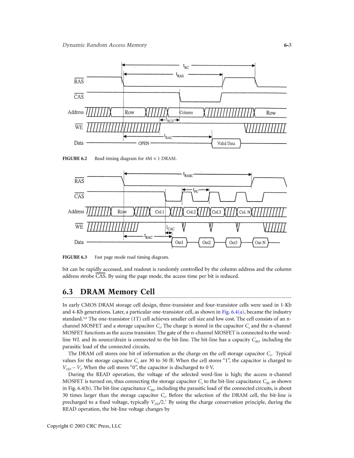
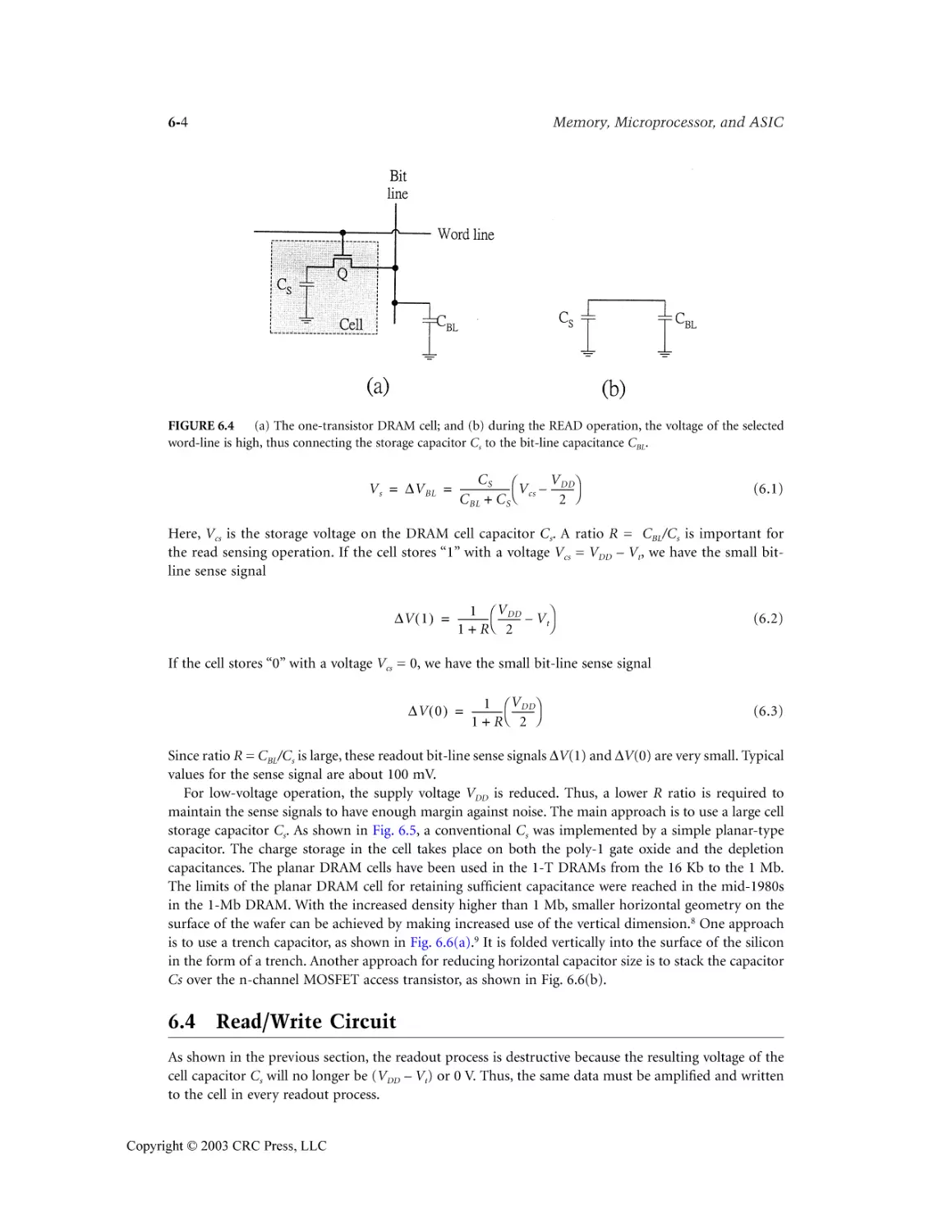
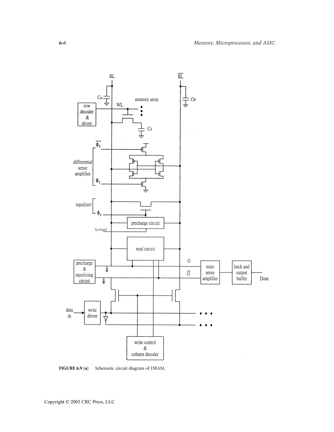
Dynamic Random Access Memory Kuo-Hsing Cheng
6.1 Introduction .........................................................................................................................6-1
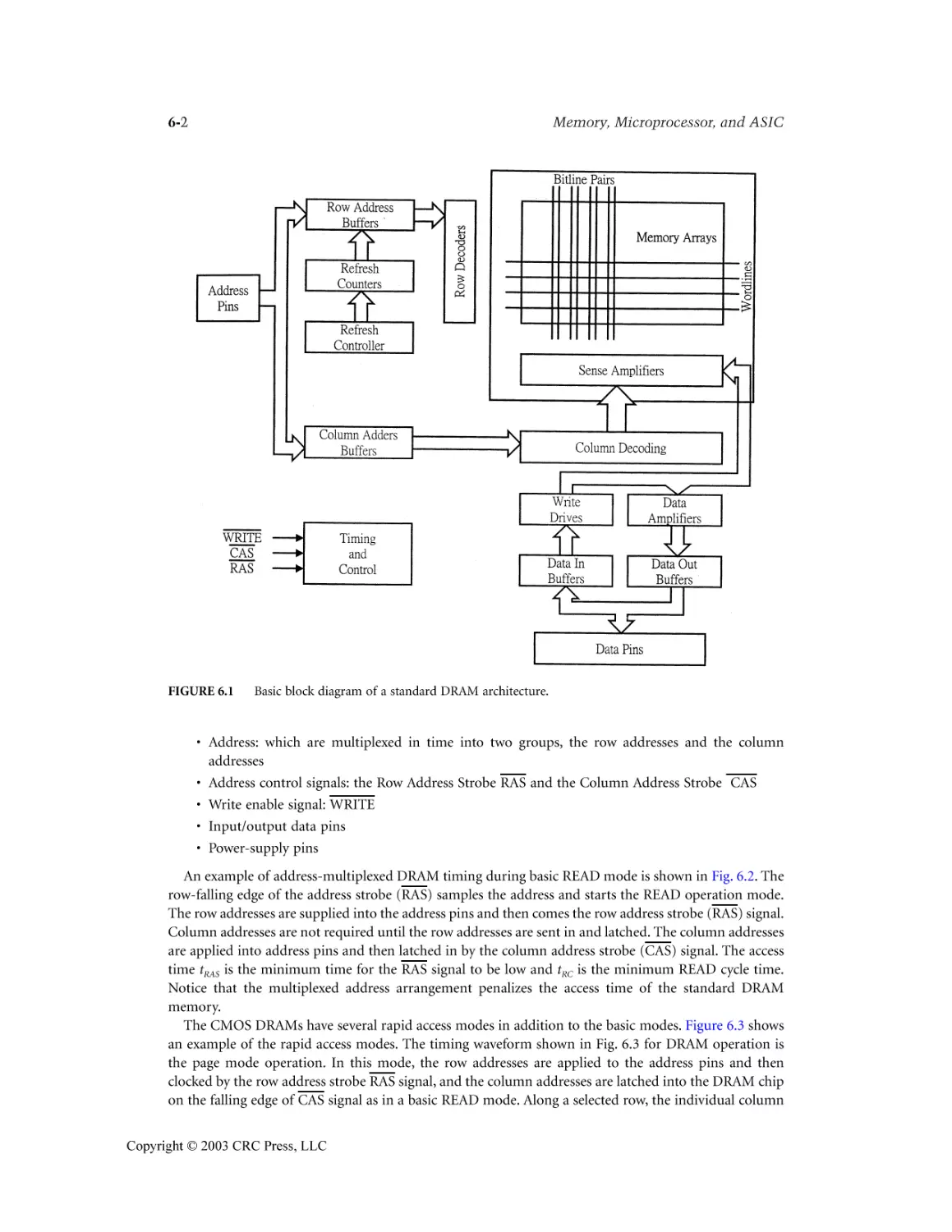
6.2 Basic DRAM Architecture .....................................................................................................6-1
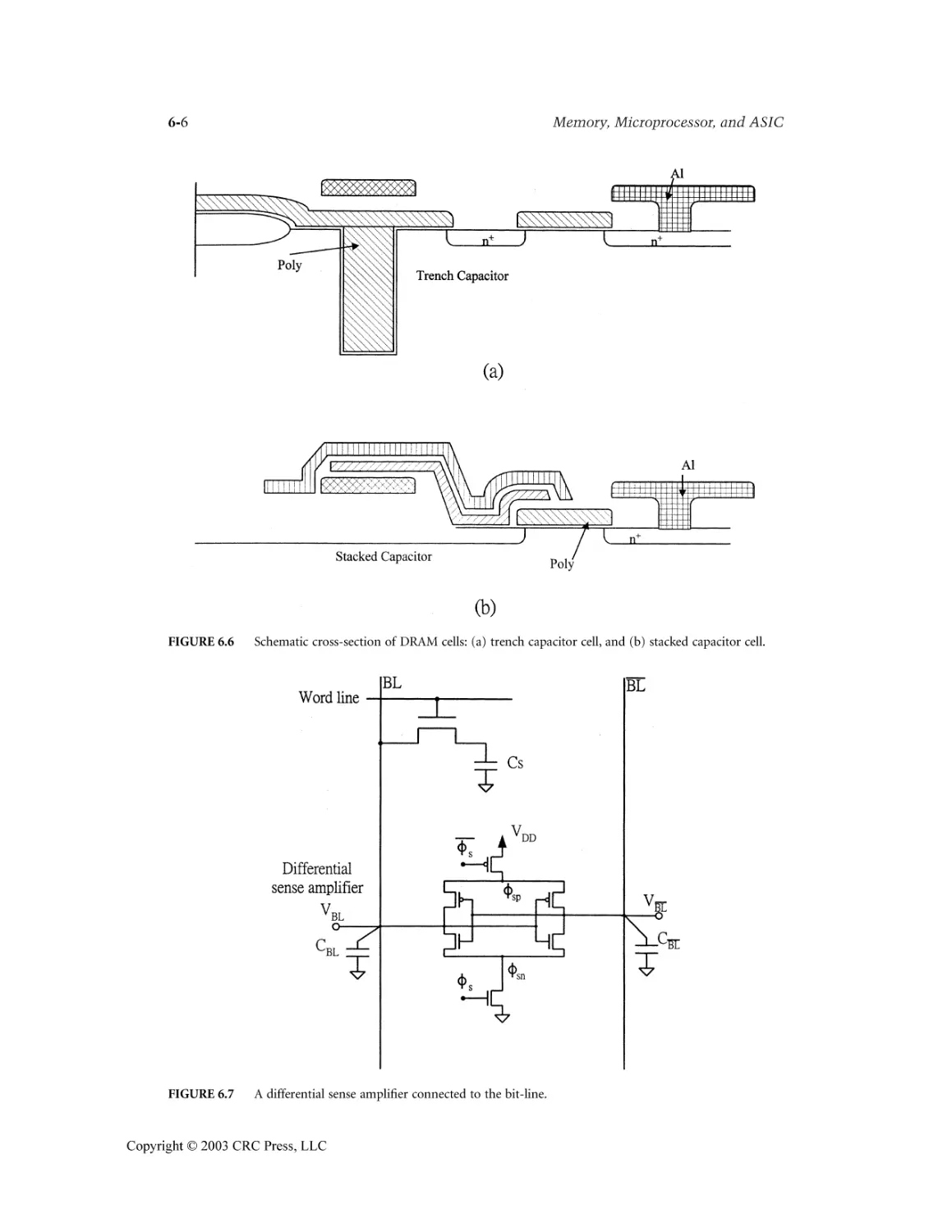
6.3 DRAM Memory Cell ............................................................................................................6-3
6.4 Read/Write Circuit ...............................................................................................................6-4
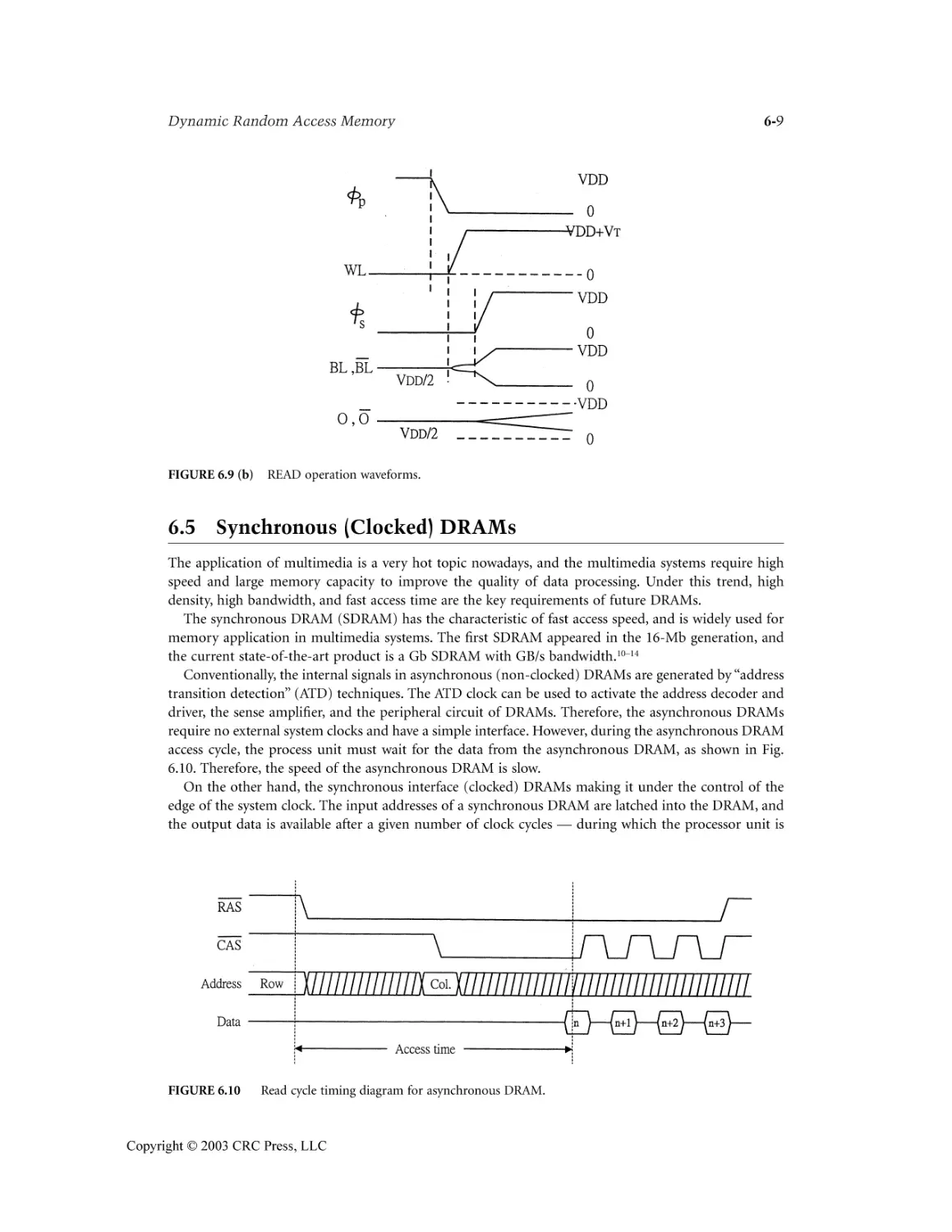
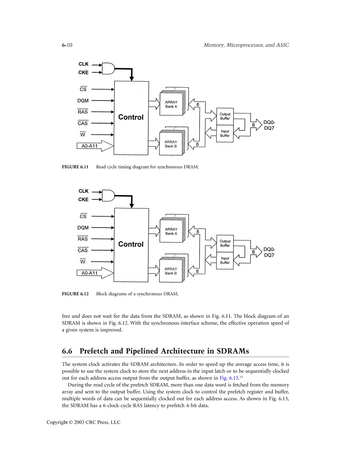
6.5 Synchronous (Clocked) DRAMs...........................................................................................6-9
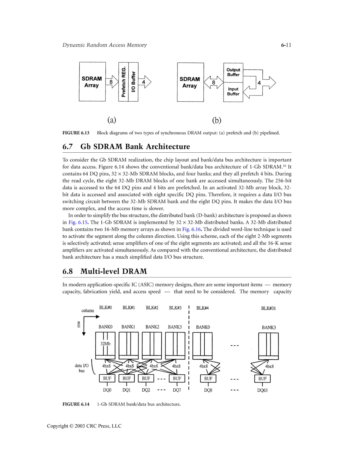
6.6 Prefetch and Pipelined Architecture in SDRAMs ..............................................................6-10
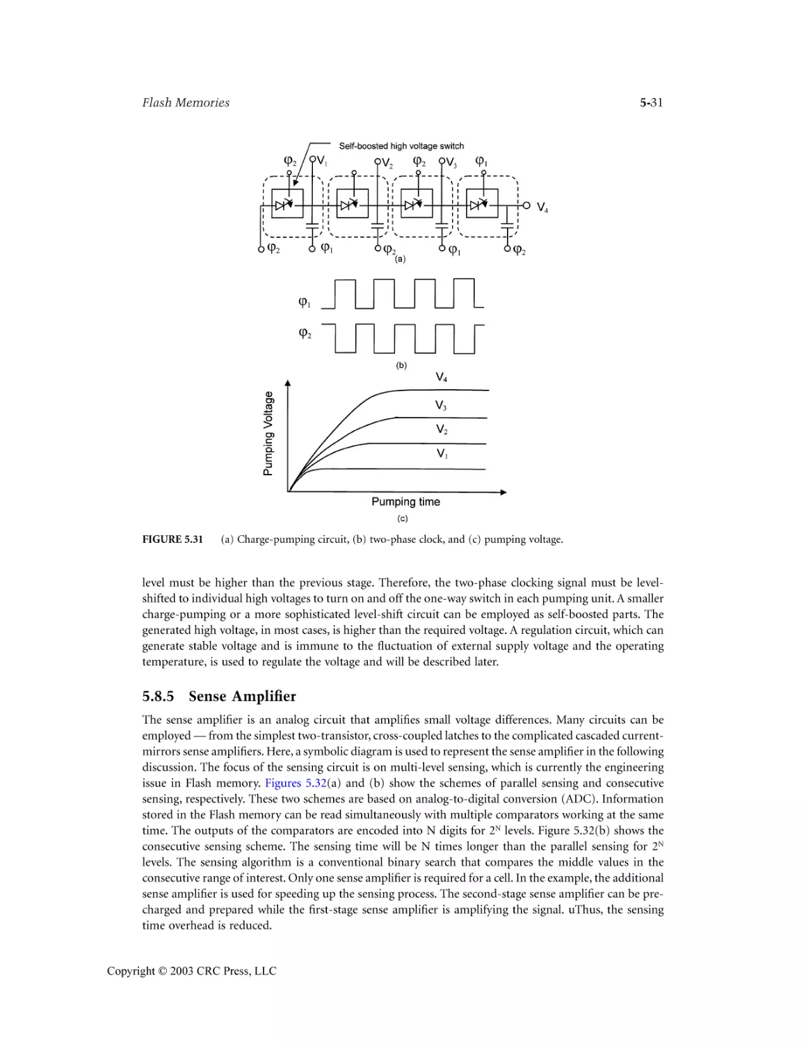
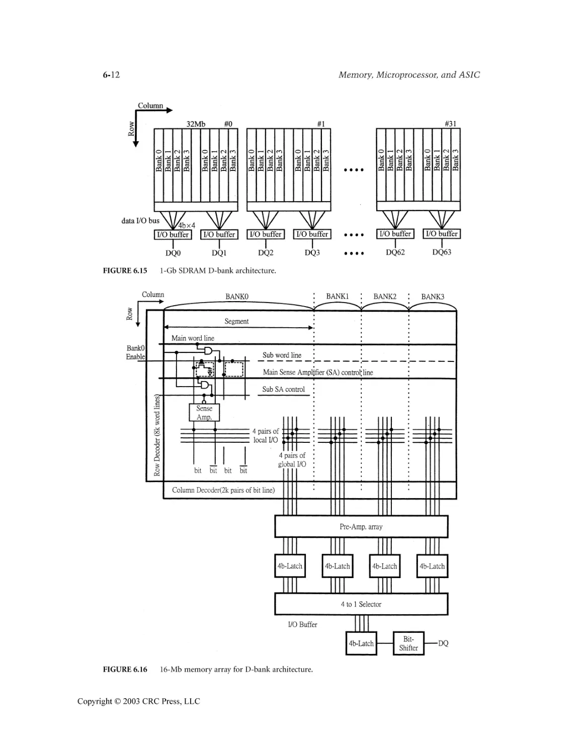
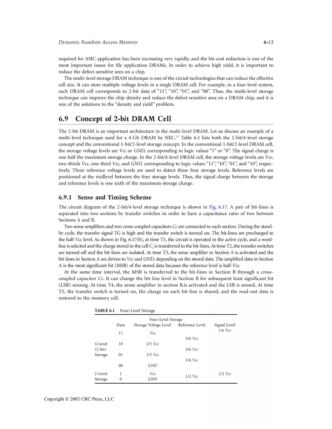
6.7 Gb SDRAM Bank Architecture ..........................................................................................6-11
6.8 Multi-level DRAM ..............................................................................................................6-11
6.9 Concept of 2-bit DRAM Cell ..............................................................................................6-13
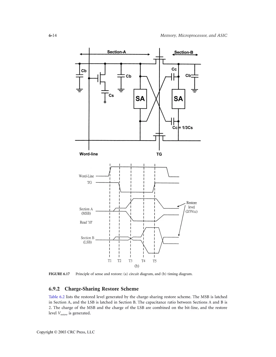
References ......................................................................................................................................6-15
7
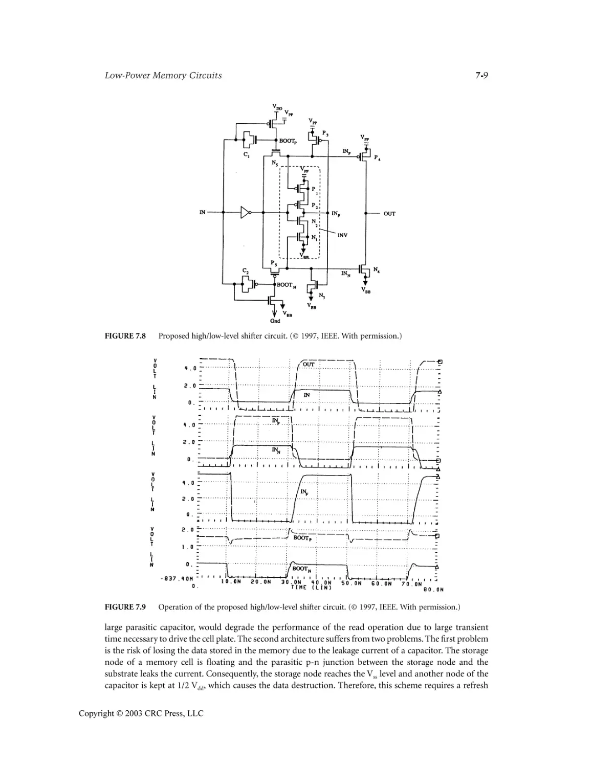
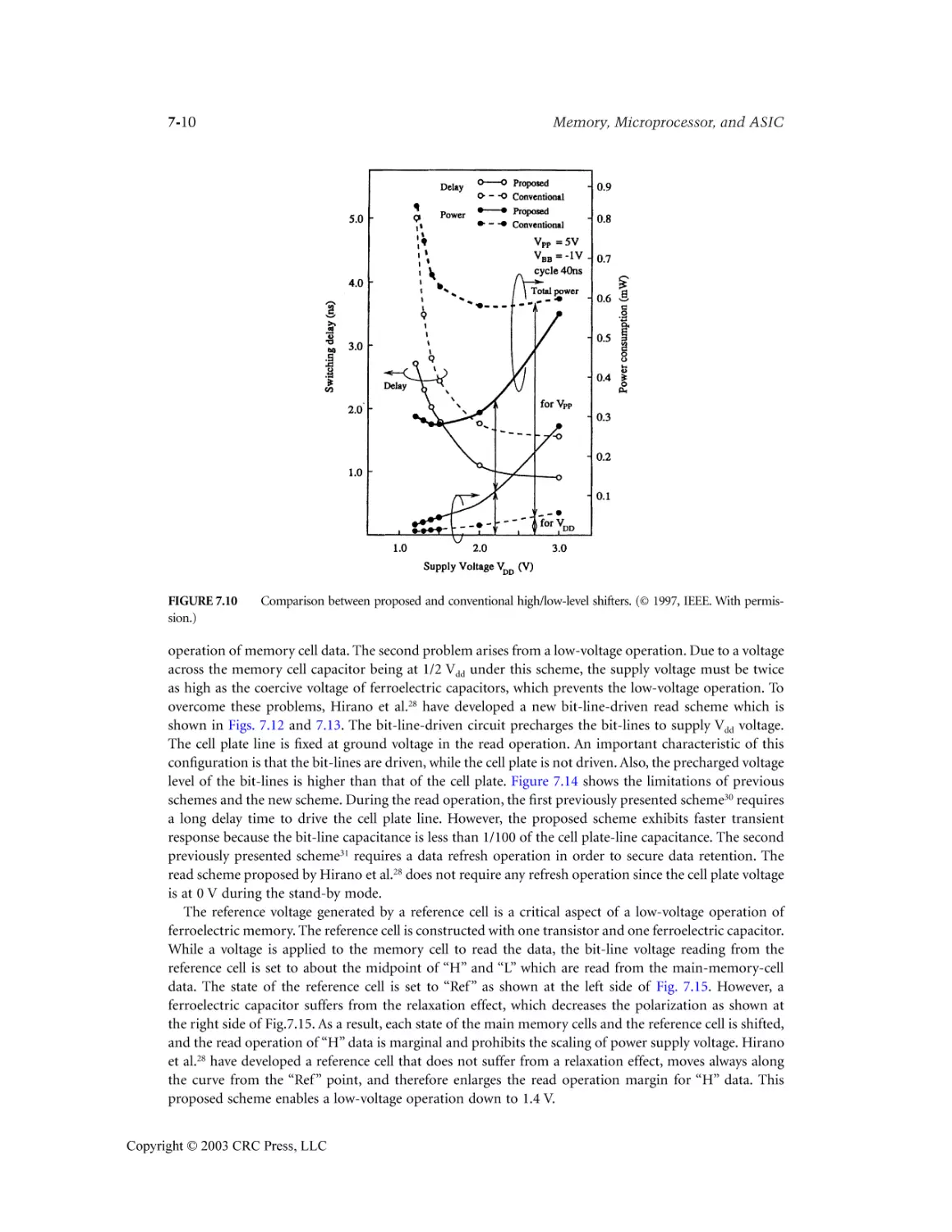
Low-Power Memory Circuits Martin Margala
8
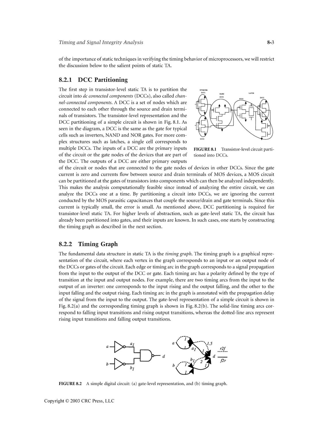
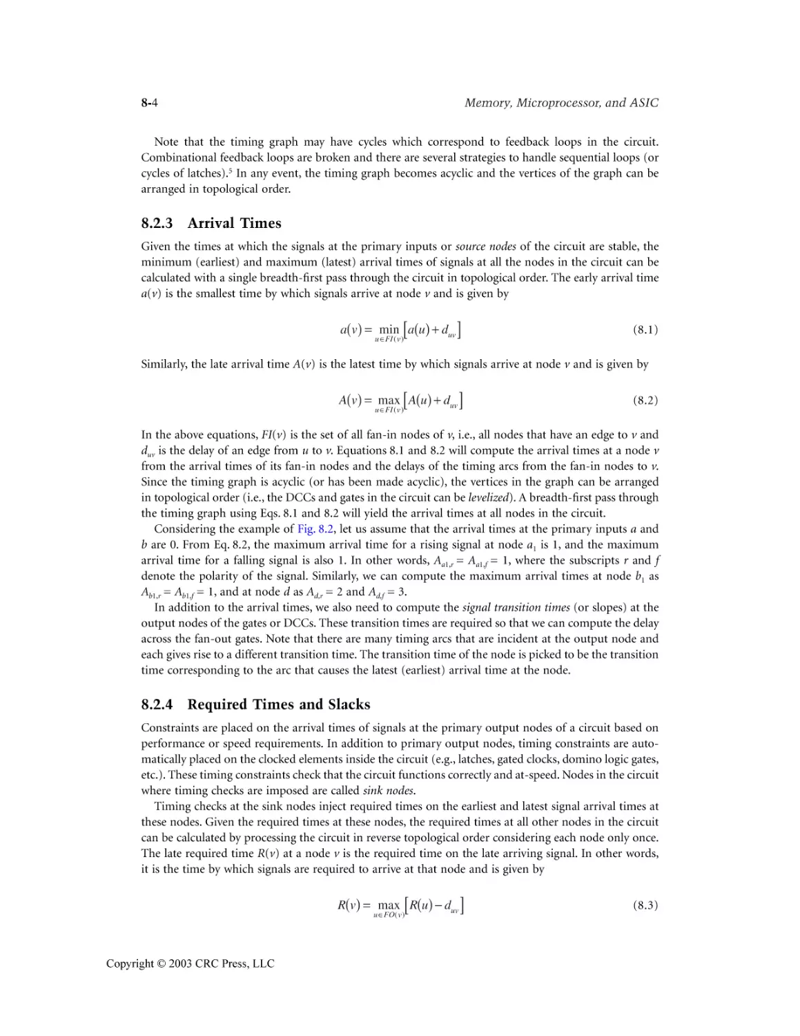
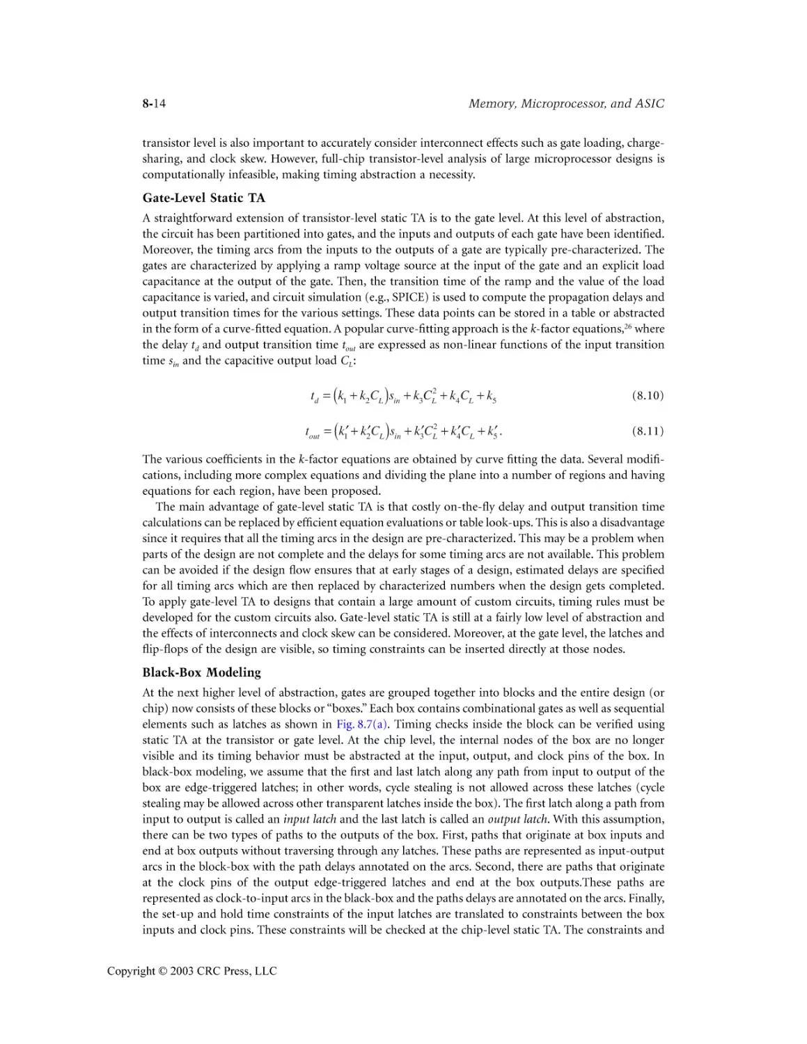
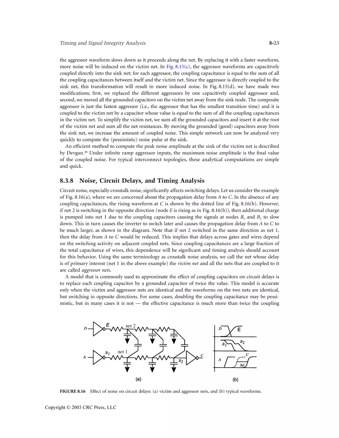
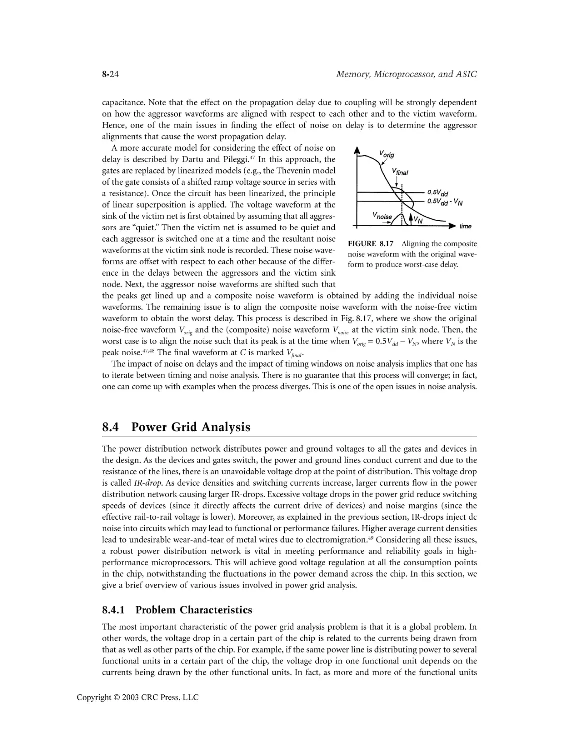
Timing and Signal Integrity Analysis Abhijit Dharchoudhury, David Blaauw, and
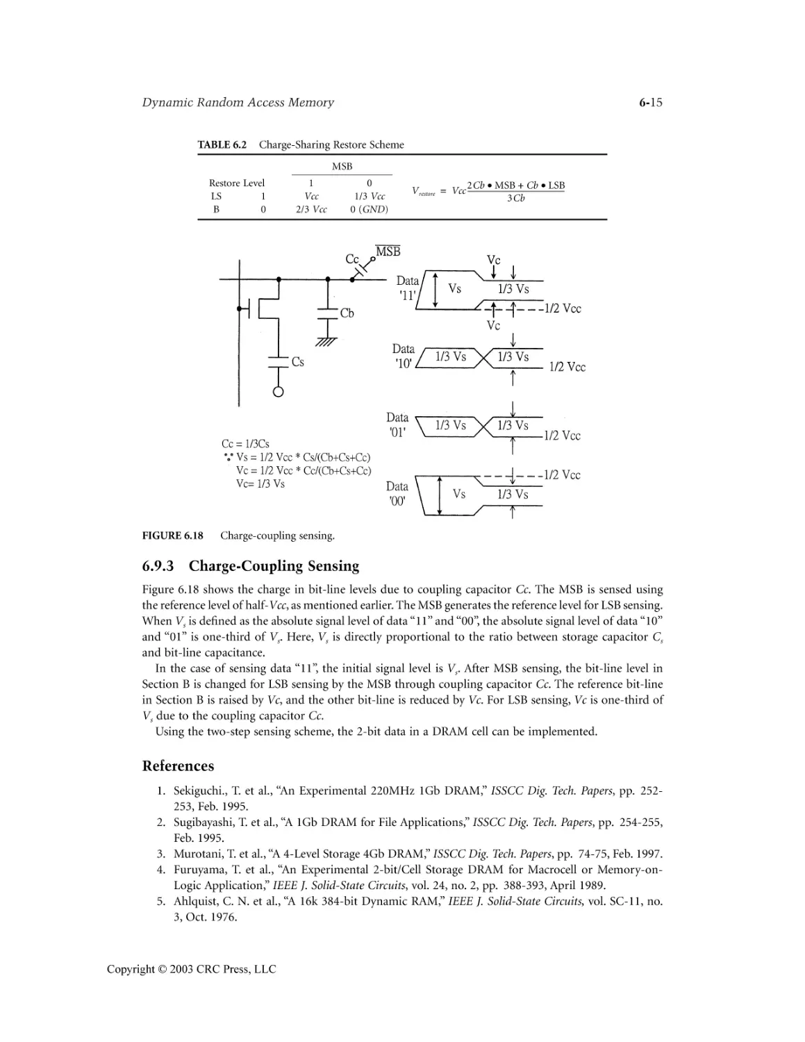
Stantanu Ganguly
8.1 Introduction .........................................................................................................................8-1
8.2 Static Timing Analysis ..........................................................................................................8-2
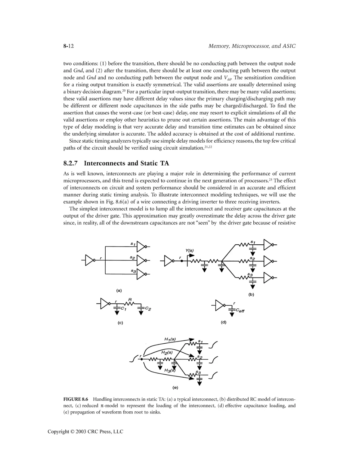
8.3 Noise Analysis .....................................................................................................................8-16
8.4 Power Grid Analysis ...........................................................................................................8-24
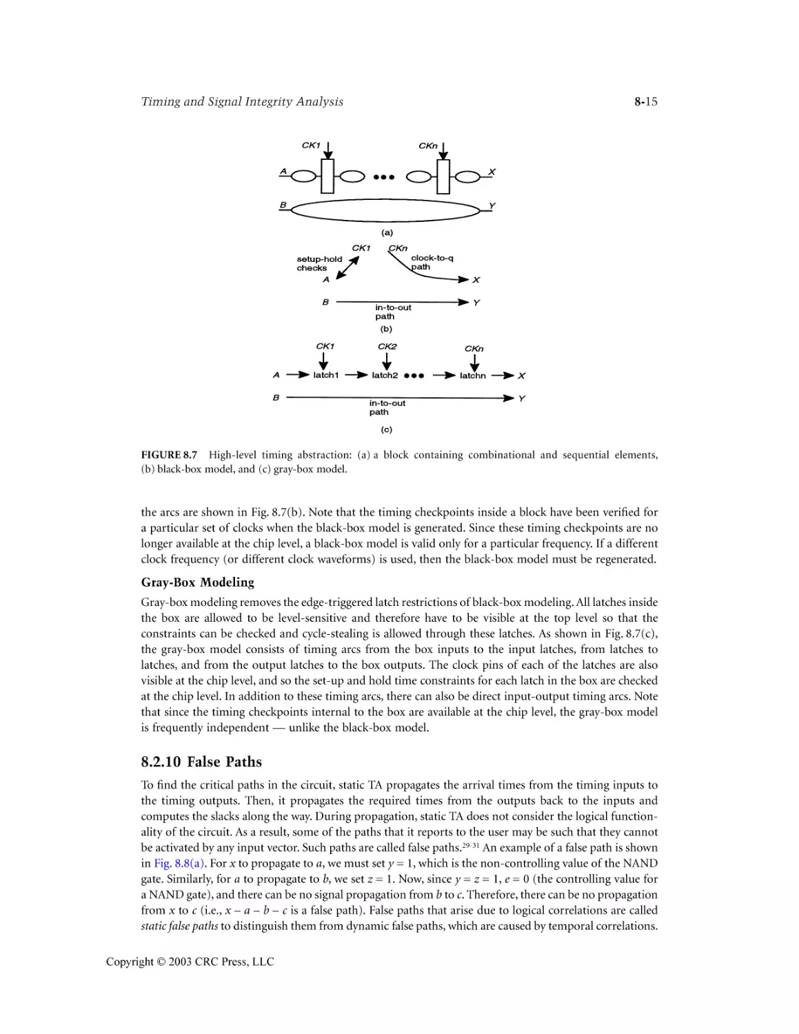
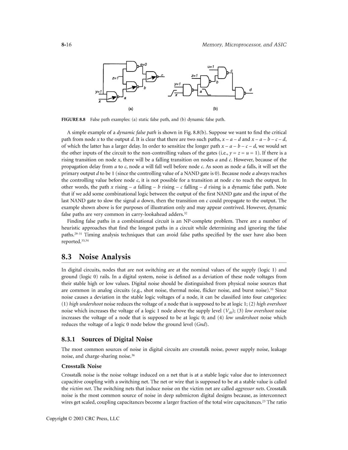
9
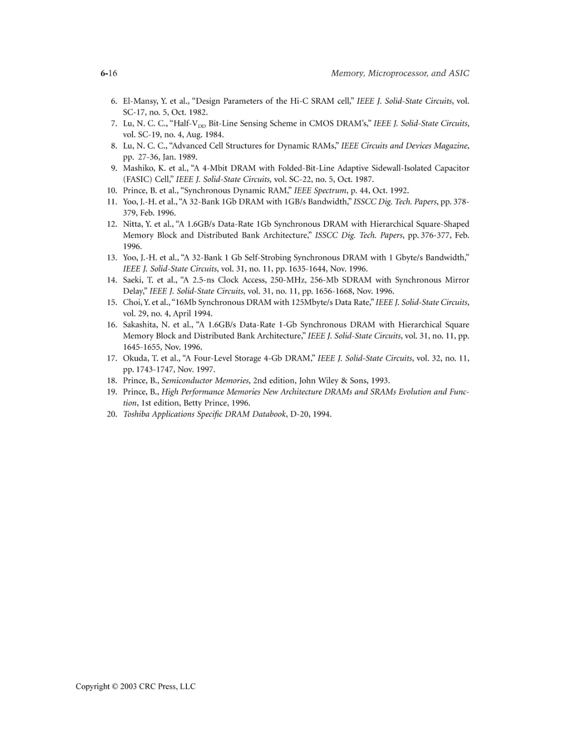
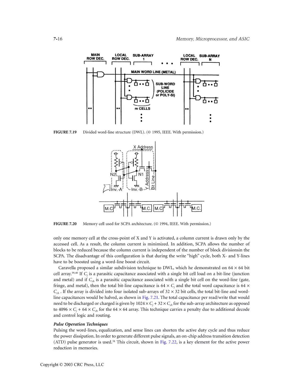
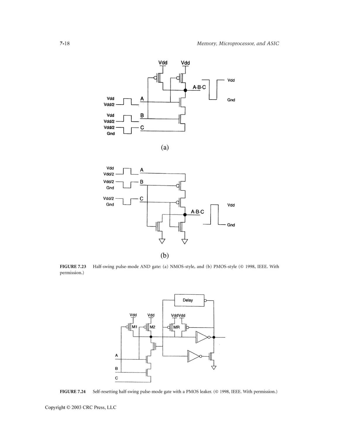
7.1 Introduction .........................................................................................................................7-1
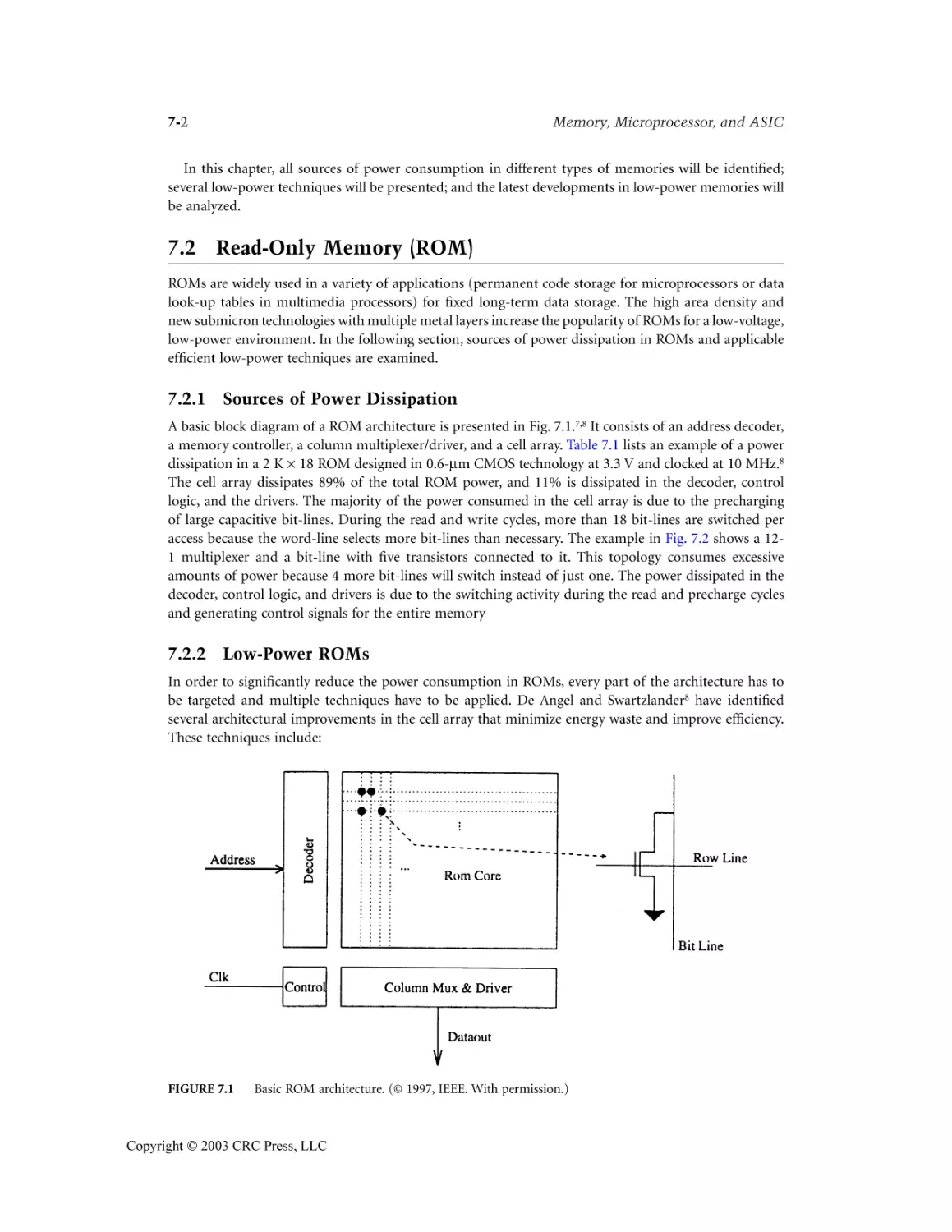
7.2 Read-Only Memory (ROM) .................................................................................................7-2
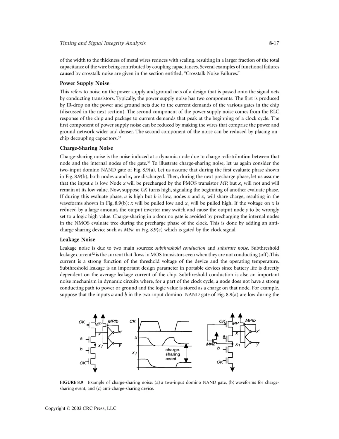
7.3 Flash Memory .......................................................................................................................7-4
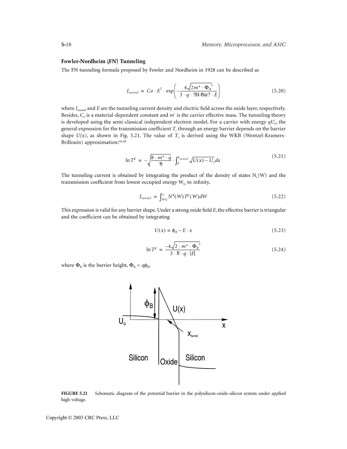
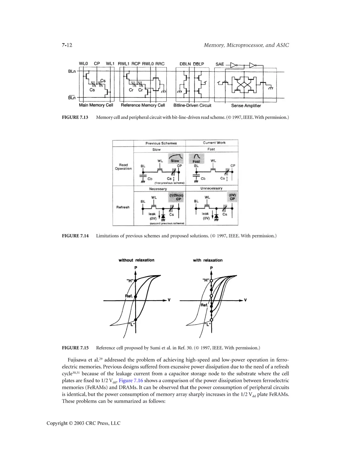
7.4 Ferroelectric Memory (FeRAM) ..........................................................................................7-8
7.5 Static Random-Access Memory (SRAM) ...........................................................................7-13
7.6 Dynamic Random-Access Memory (DRAM) ....................................................................7-25
7.7 Conclusion ..........................................................................................................................7-35
References ......................................................................................................................................7-35
Microprocessor Design Verification Vikram Iyengar and Elizabeth M. Rudnick
9.1
9.2
9.3
9.4
9.5
9.6
9.7
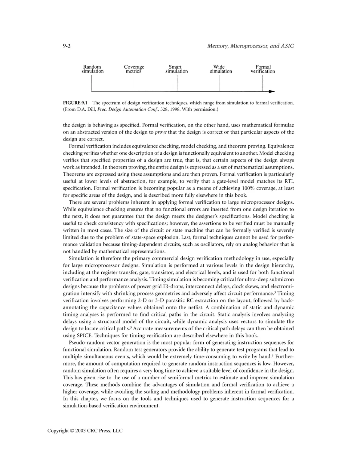
Introduction .........................................................................................................................9-1
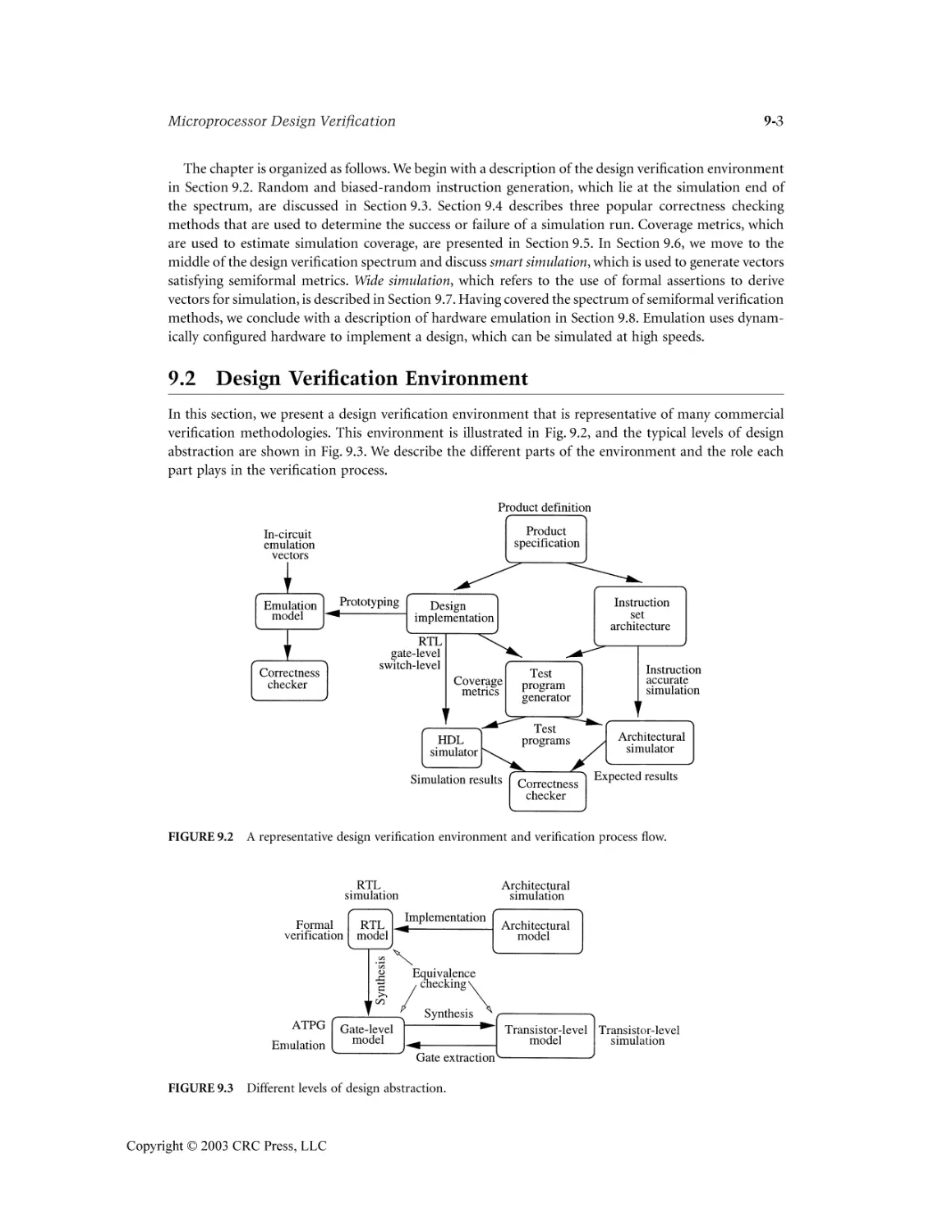
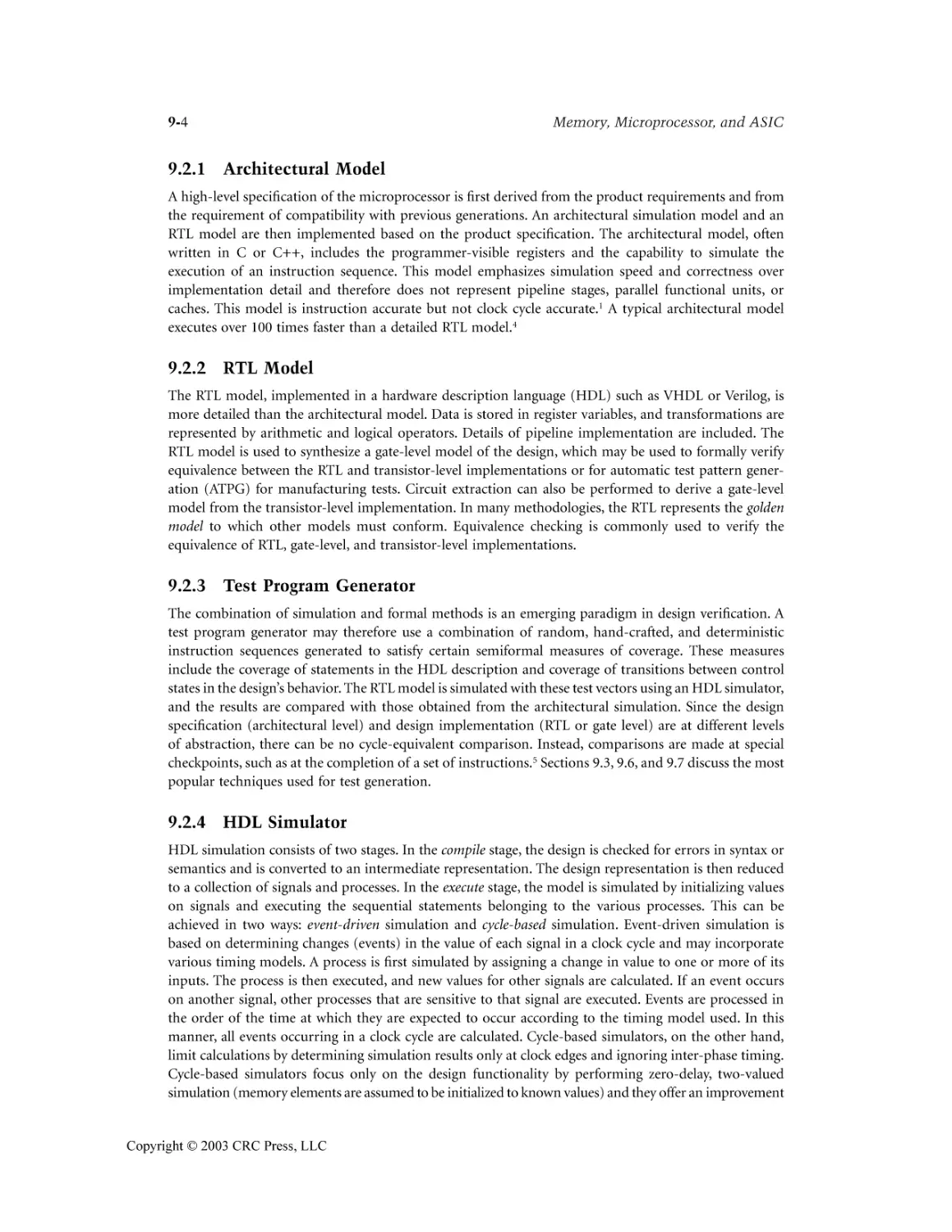
Design Verification Environment ........................................................................................9-3
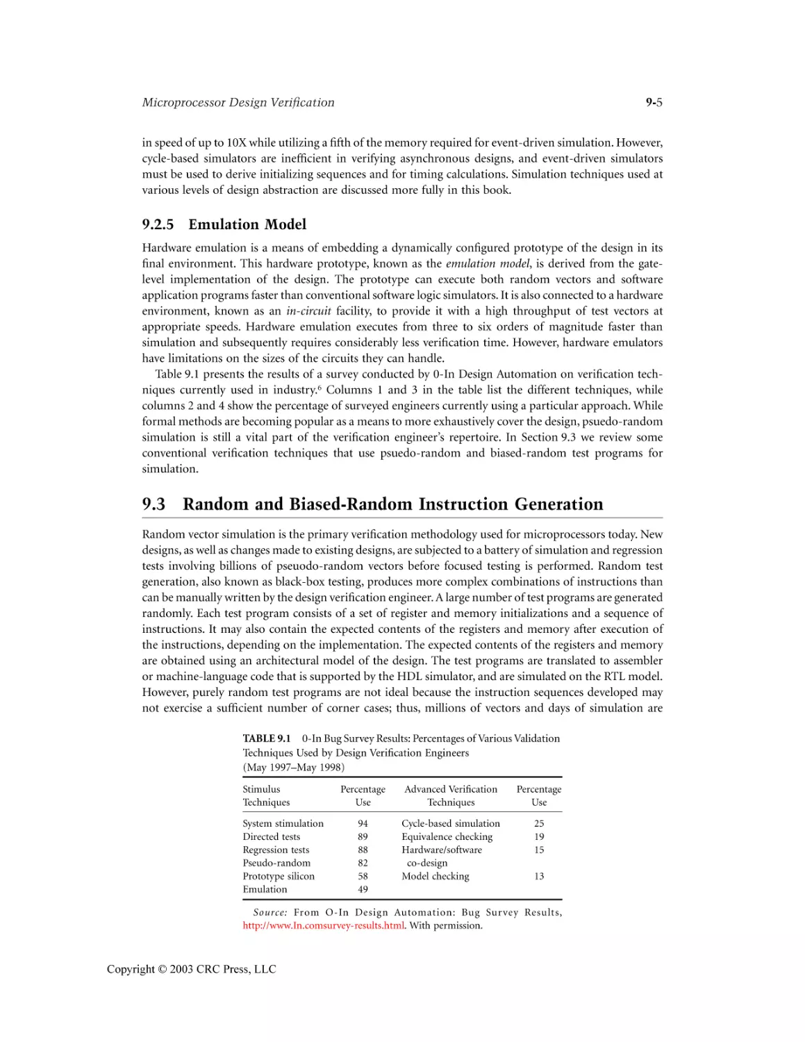
Random and Biased-Random Instruction Generation .......................................................9-5
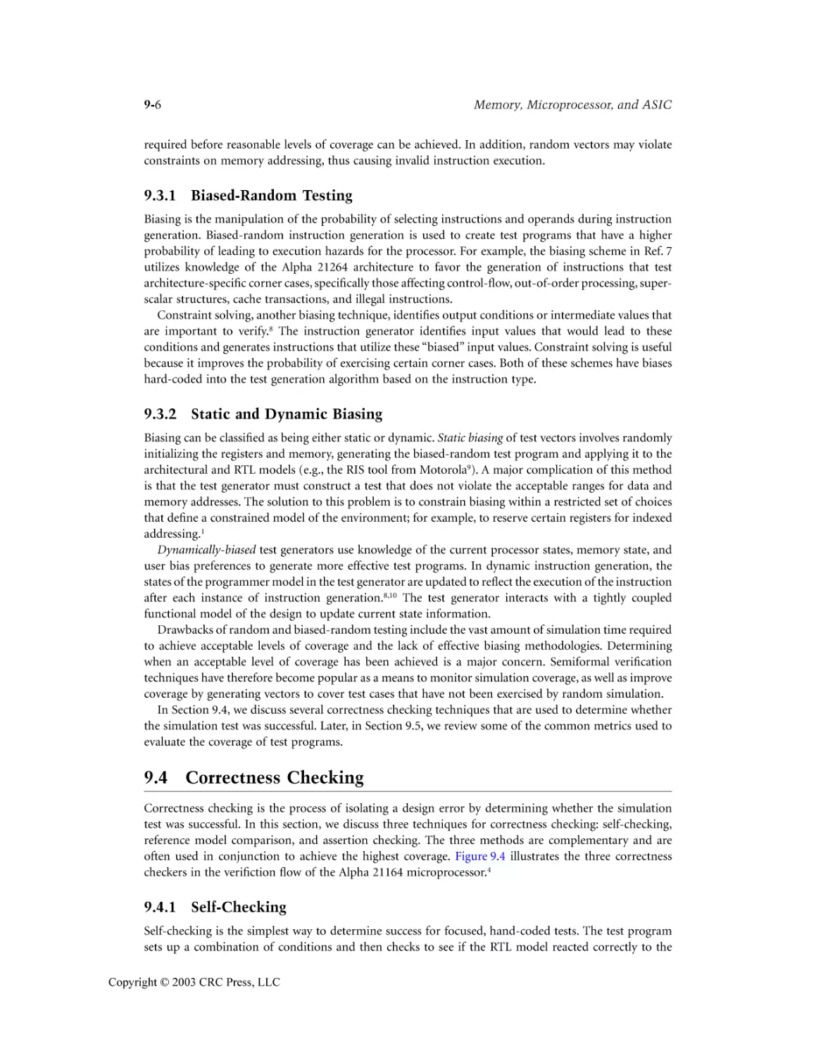
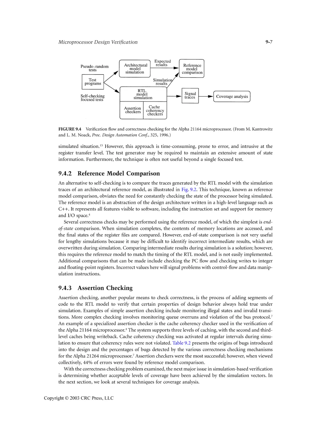
Correctness Checking ...........................................................................................................9-6
Coverage Metrics ...................................................................................................................9-8
Smart Simulation ................................................................................................................9-10
Wide Simulation .................................................................................................................9-12
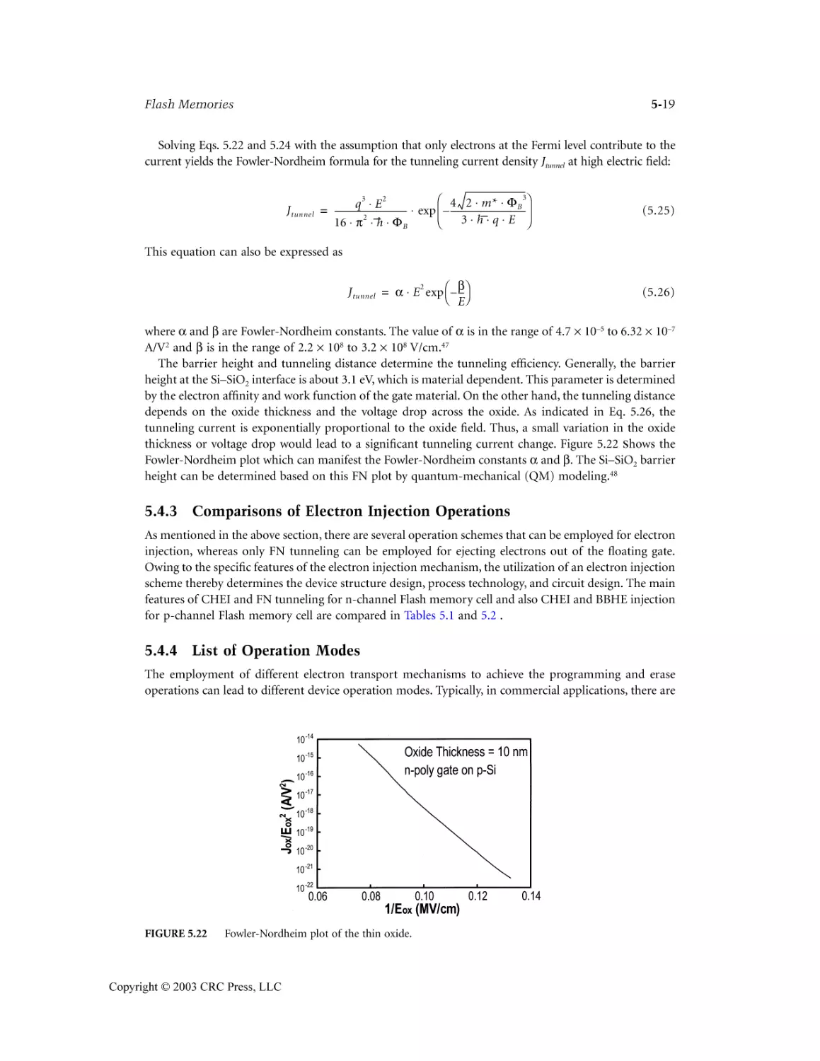
xii
Copyright © 2003 CRC Press, LLC
1737_FM Page xiii Thursday, February 6, 2003 11:36 AM
9.8 Emulation ............................................................................................................................. 9-13
9.9 Conclusion ............................................................................................................................ 9-14
References ......................................................................................................................................9-15
10
Microprocessor Layout Method Tanay Karnik
11
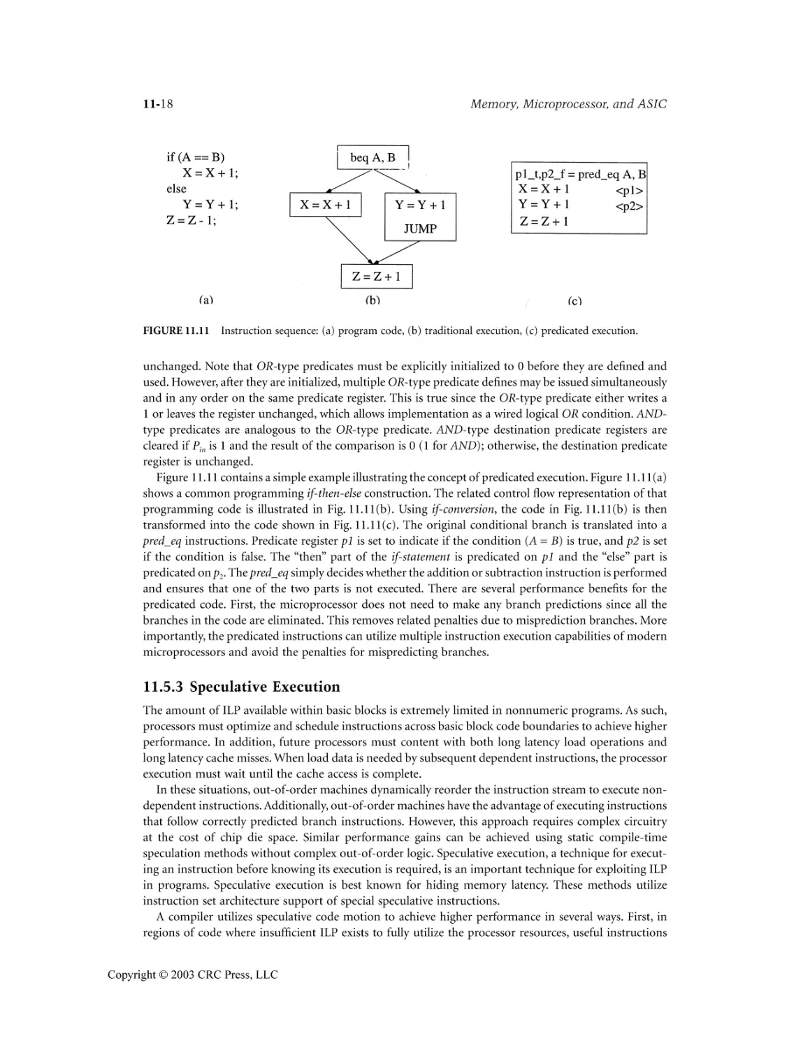
Architecture Daniel A. Connors and Wen-mei W. Hwu
12
ASIC Design Sumit Gupta and Rajesh K. Gupta
13
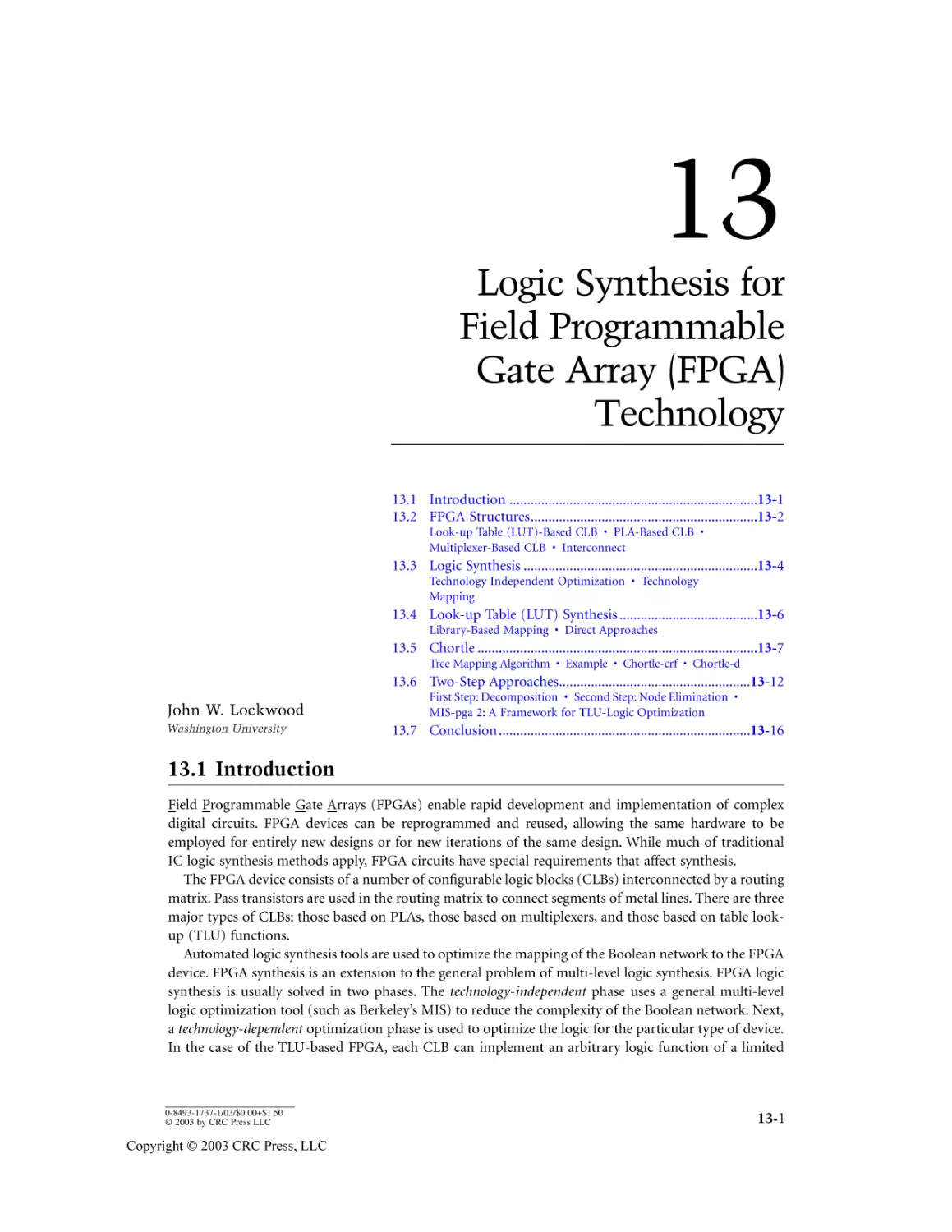
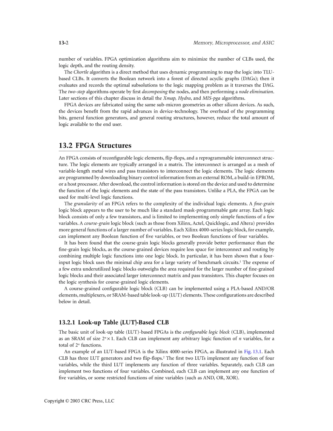
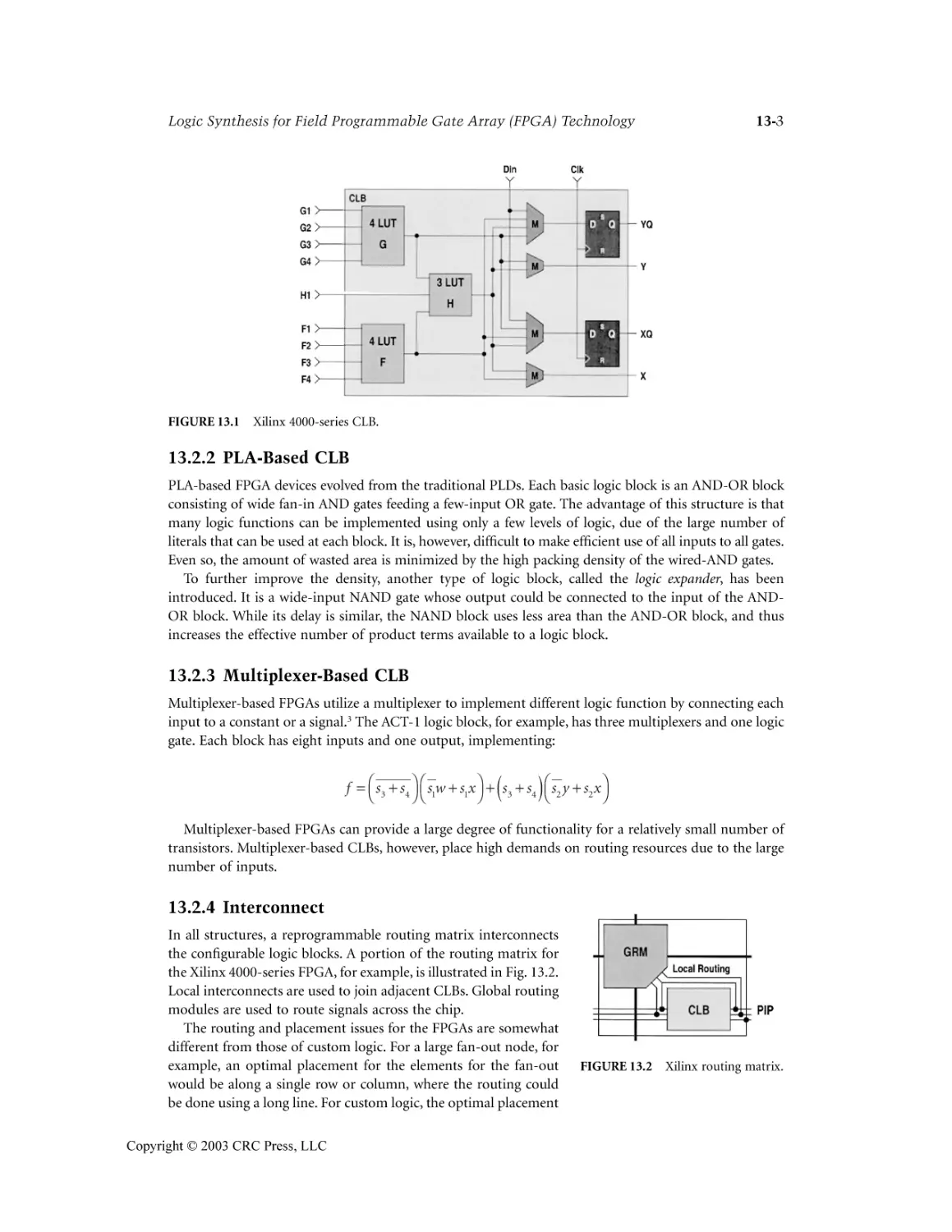
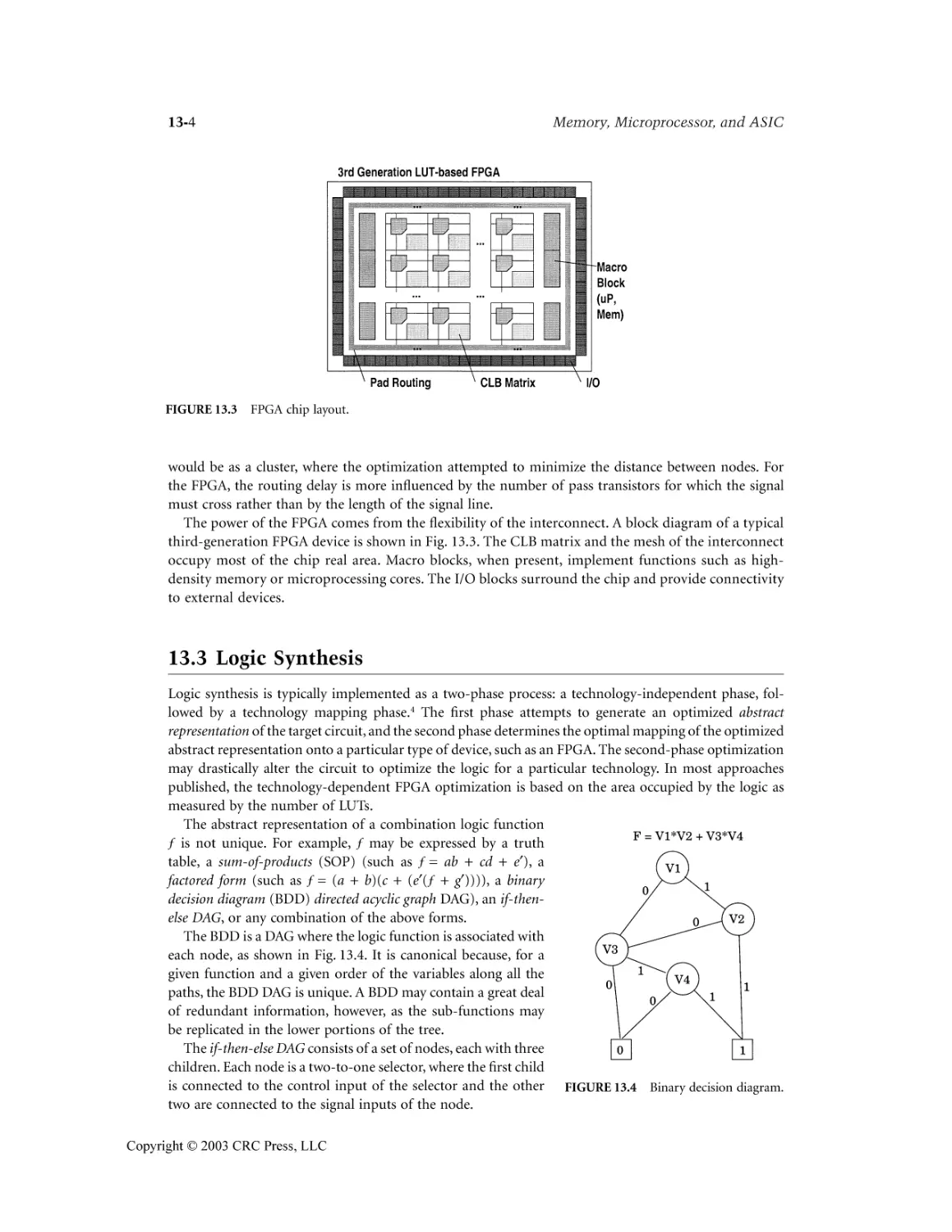
Logic Synthesis for Field Programmable Gate Array (FPGA) Technology
10.1 Introduction ........................................................................................................................ 10-1
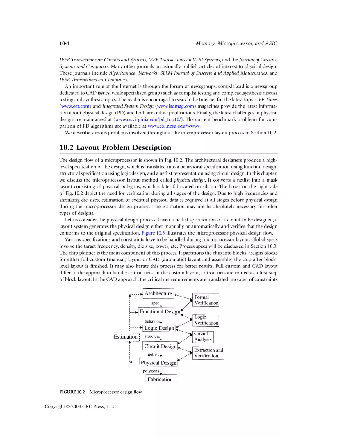
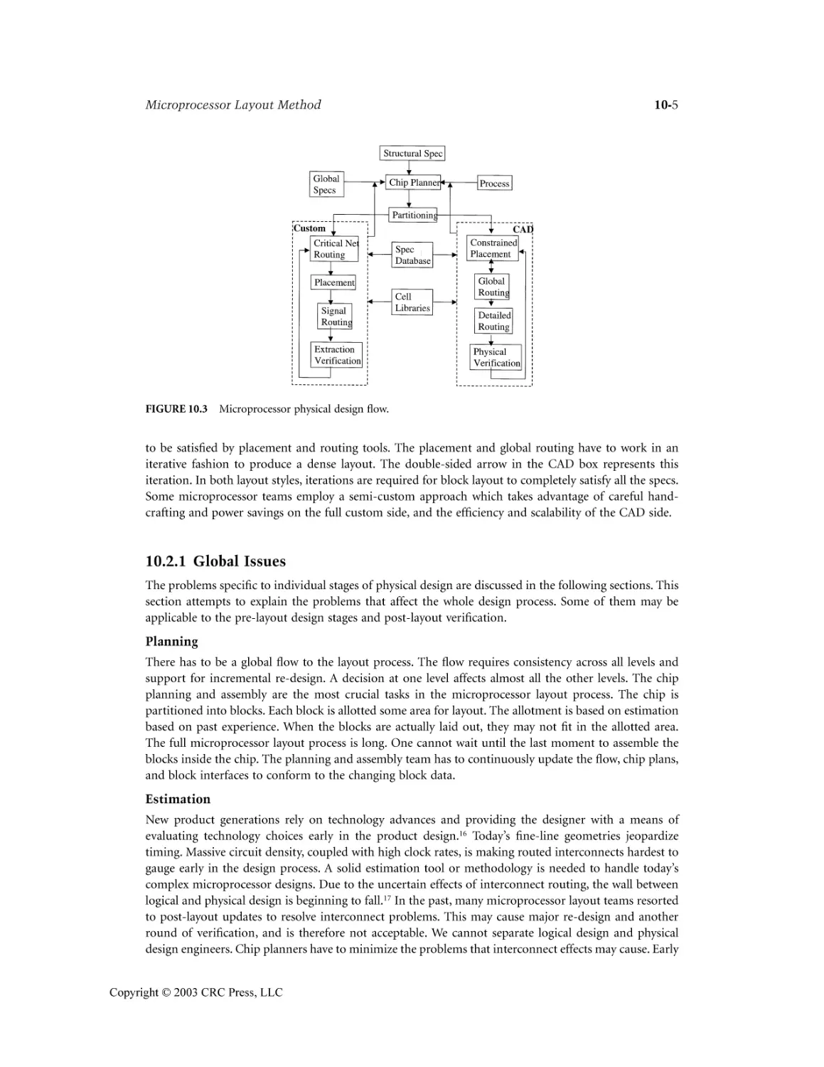
10.2 Layout Problem Description .............................................................................................. 10-4
10.3 Manufacturing ..................................................................................................................... 10-7
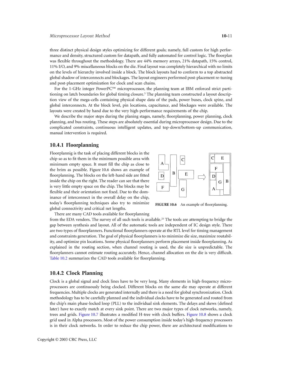
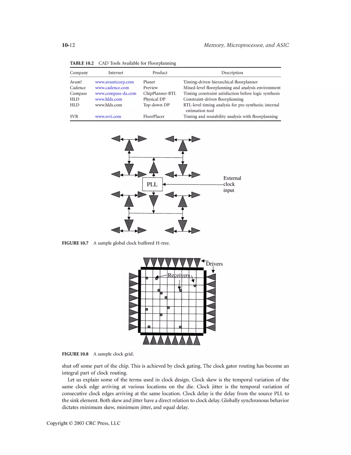
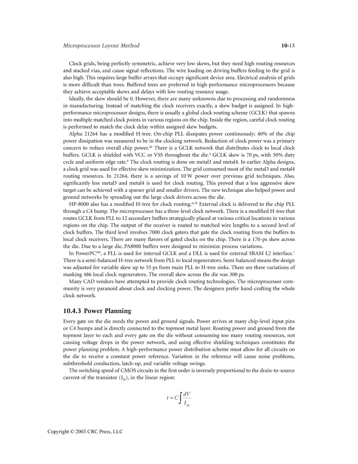
10.4 Chip Planning .................................................................................................................... 10-10
References ....................................................................................................................................10-27
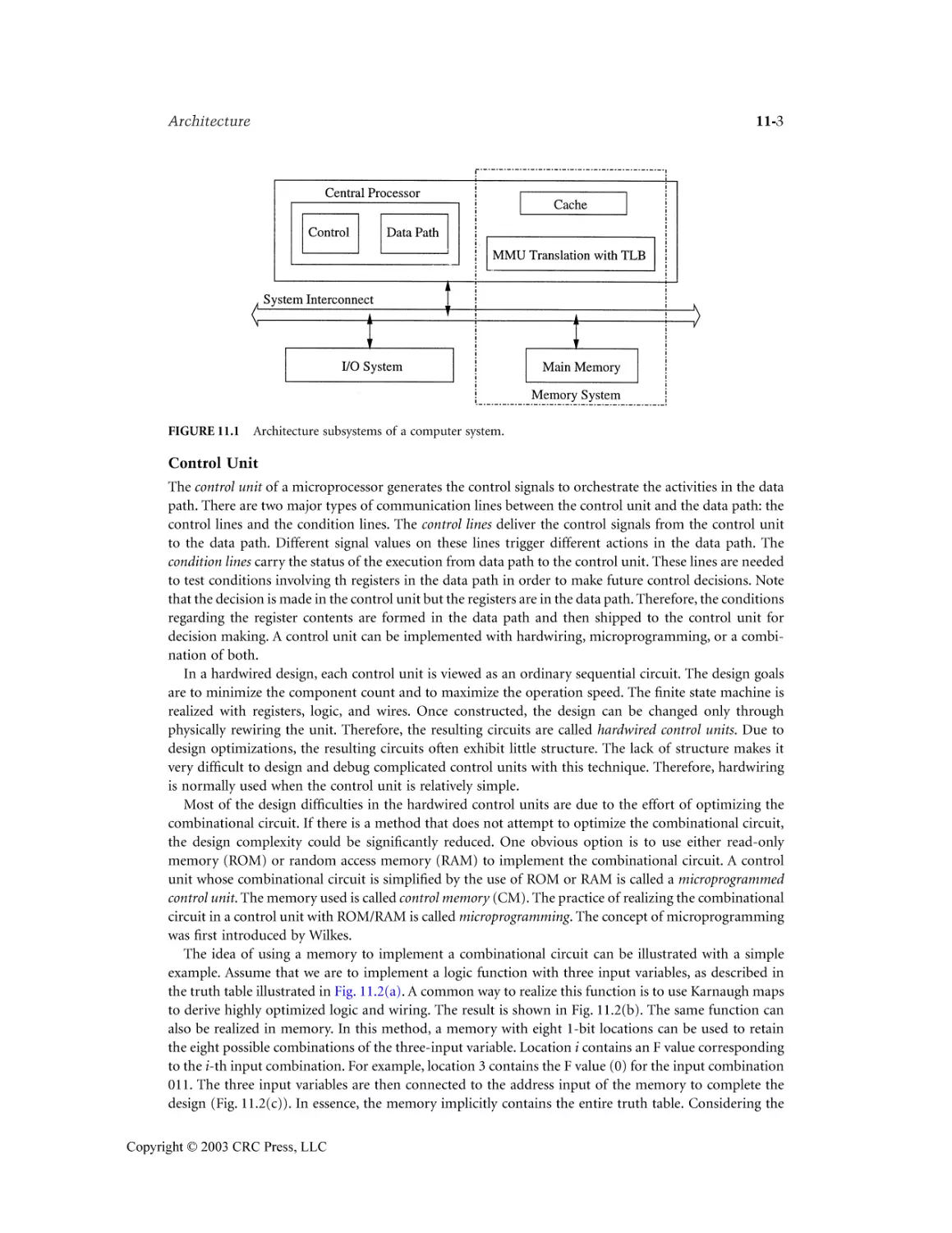
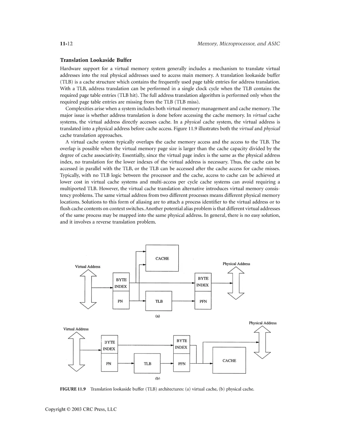
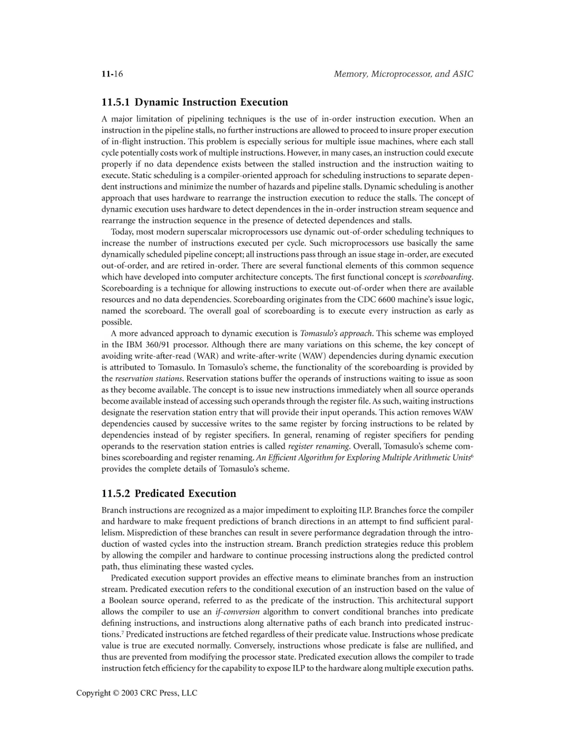
11.1 Introduction .......................................................................................................................11-1
11.2 Types of Microprocessors.................................................................................................... 11-1
11.3 Major Components of a Microprocessor .......................................................................... 11-2
11.4 Instruction Set Architecture ............................................................................................. 11-14
11.5 Instruction-Level Parallelism ........................................................................................... 11-15
11.6 Industry Trends ................................................................................................................. 11-19
References ....................................................................................................................................11-21
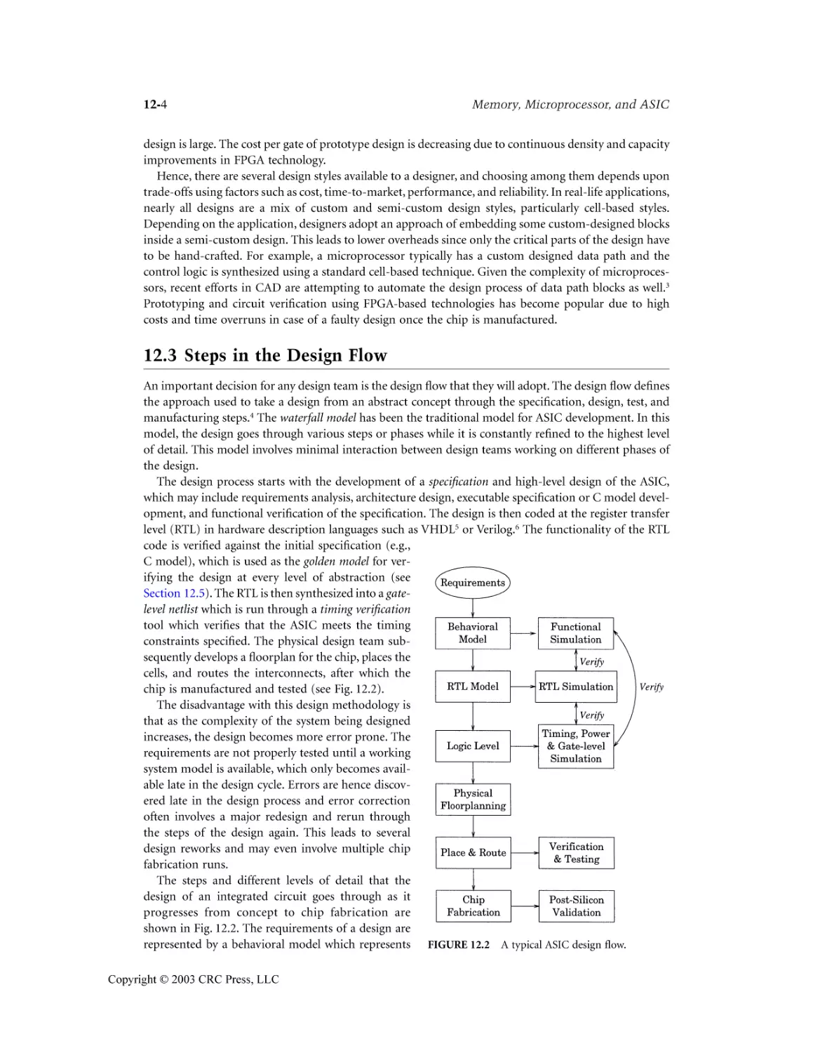
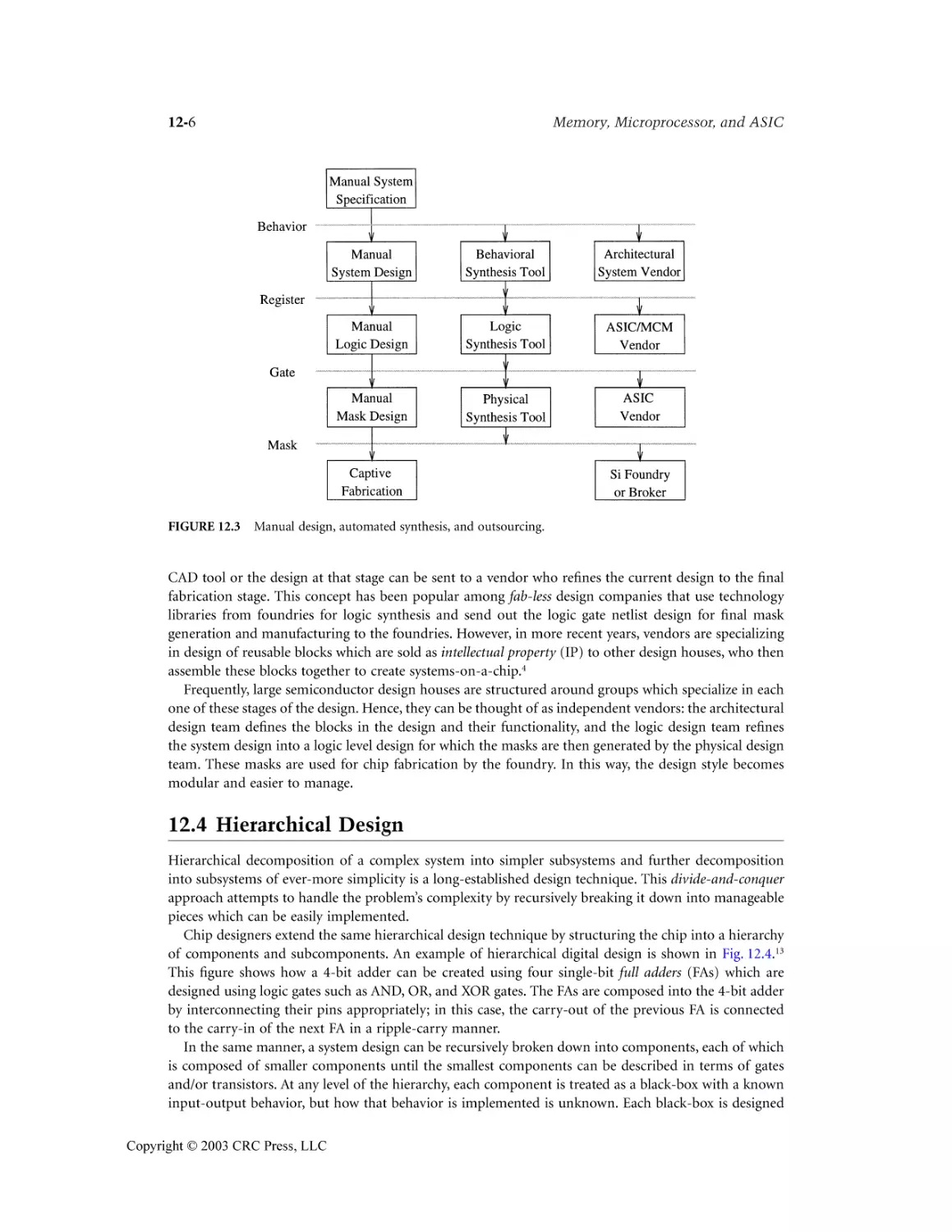
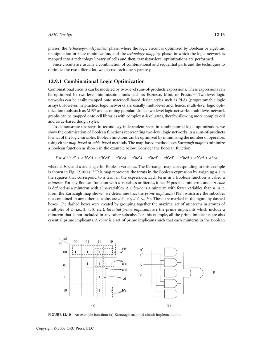
12.1 Introduction ........................................................................................................................ 12-1
12.2 Design Styles ........................................................................................................................ 12-2
12.3 Steps in the Design Flow ..................................................................................................... 12-4
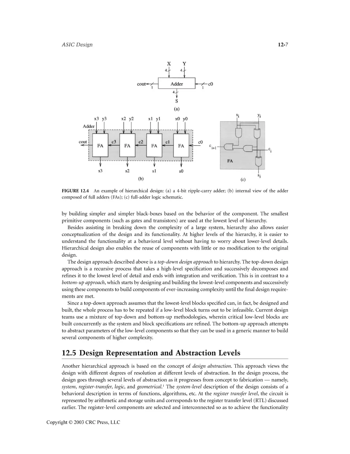
12.4 Hierarchical Design.............................................................................................................. 12-6
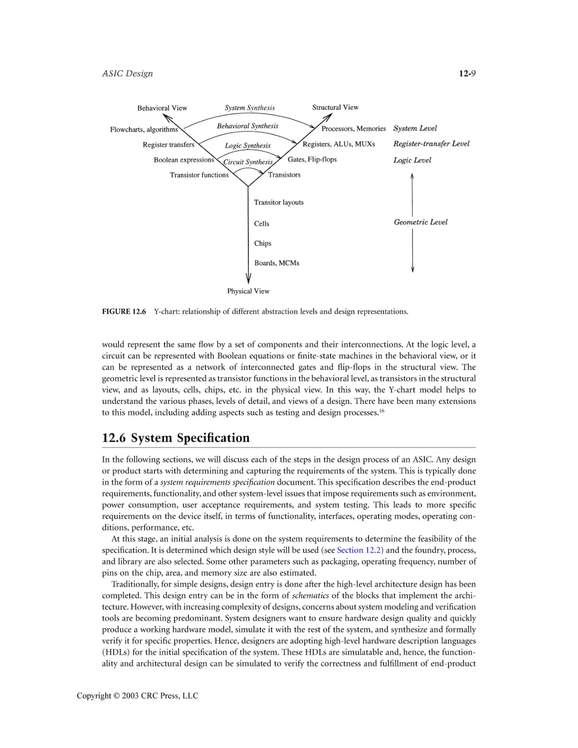
12.5 Design Representation and Abstraction Levels .................................................................. 12-7
12.6 System Specification ............................................................................................................ 12-9
12.7 Specification Simulation and Verification ....................................................................... 12-10
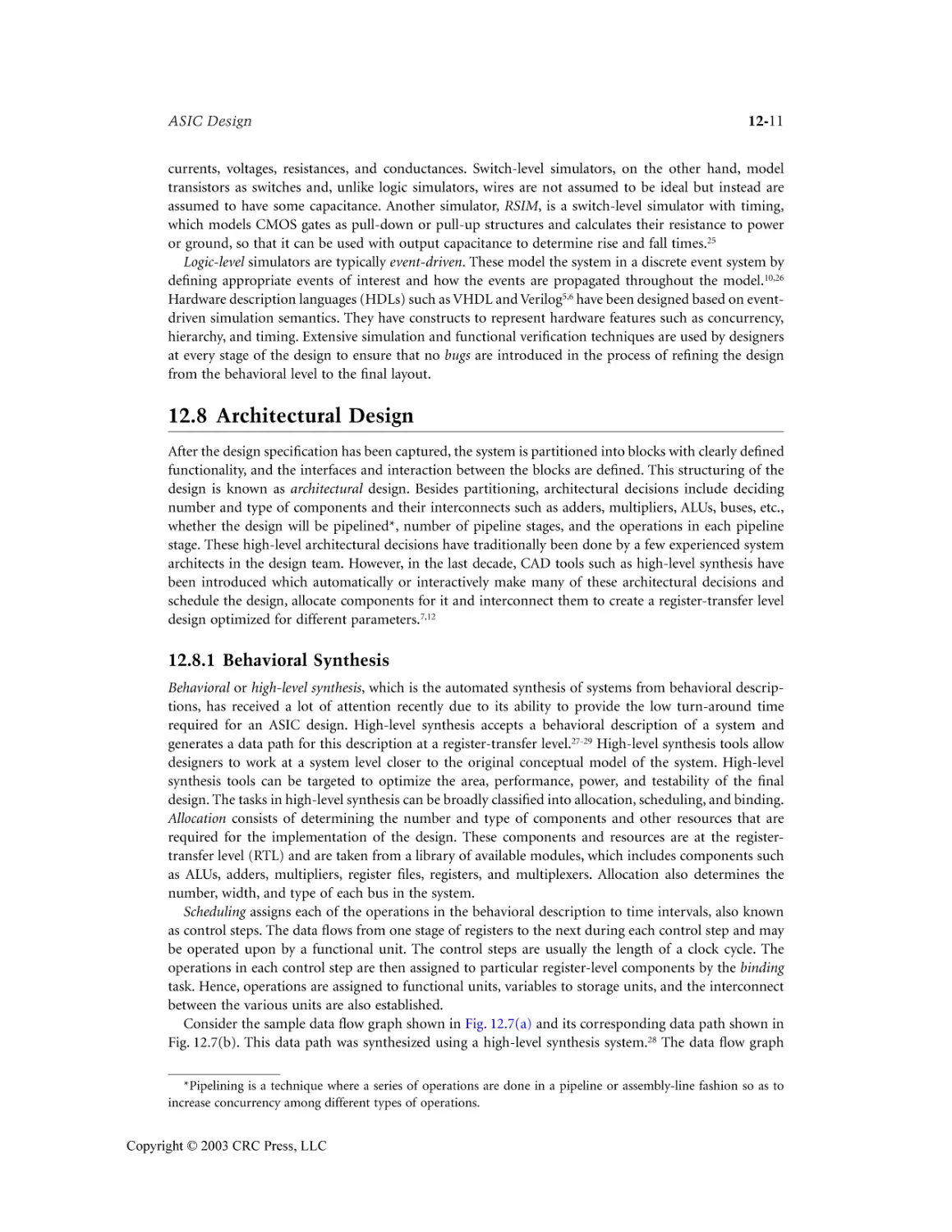
12.8 Architectural Design ......................................................................................................... 12-11
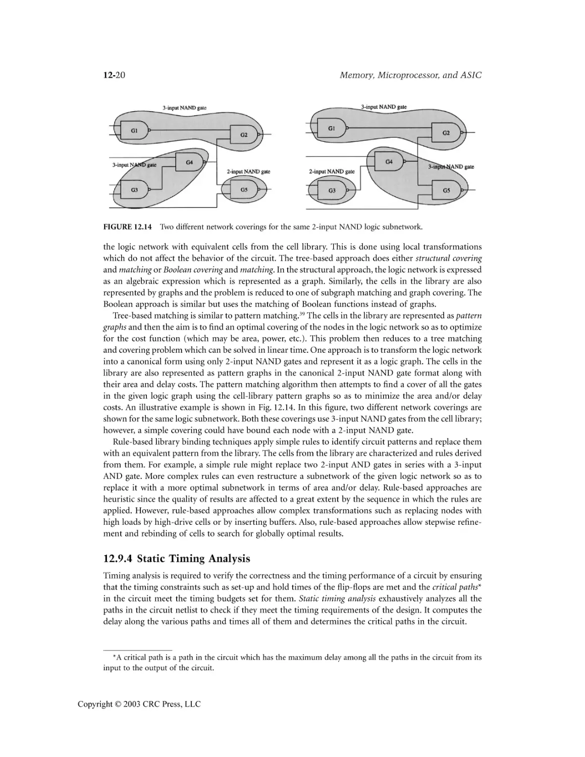
12.9 Logic Synthesis .................................................................................................................. 12-14
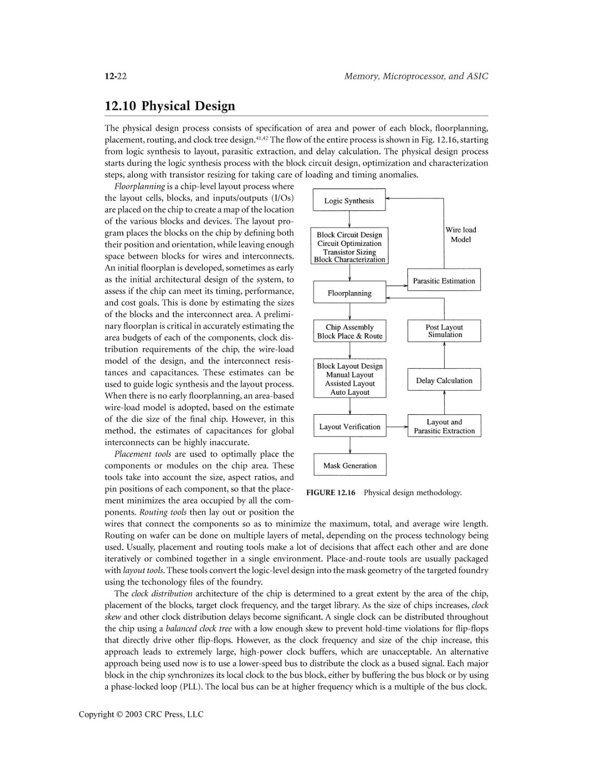
12.10 Physical Design................................................................................................................... 12-22
12.11 I/O Architecture and Pad Design ..................................................................................... 12-23
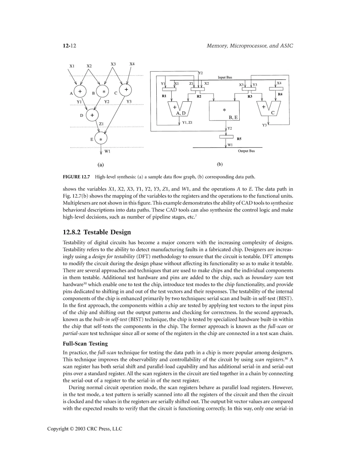
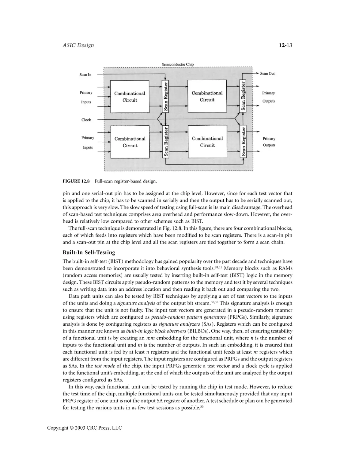
12.12 Tests after Manufacturing ................................................................................................. 12-24
12.13 High-Performance ASIC Design ...................................................................................... 12-24
12.14 Low Power Issues .............................................................................................................. 12-25
12.15 Reuse of Semiconductor Blocks ....................................................................................... 12-26
12.16 Conclusion ......................................................................................................................... 12-26
References ....................................................................................................................................12-27
John
13.1
13.2
13.3
13.4
W. Lockwood
Introduction ........................................................................................................................
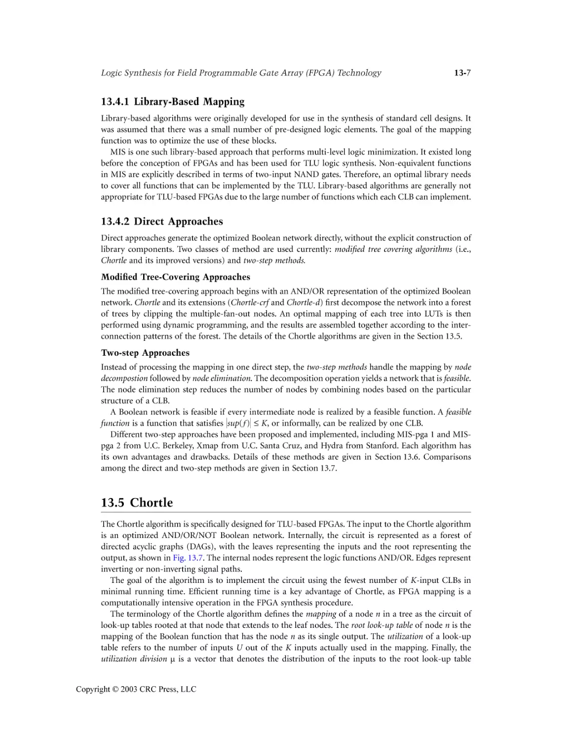
FPGA Structures ..................................................................................................................
Logic Synthesis ....................................................................................................................
Look-up Table (LUT) Synthesis .........................................................................................
13-1
13-2
13-4
13-6
xiii
Copyright © 2003 CRC Press, LLC
1737_FM Page xiv Thursday, February 6, 2003 11:36 AM
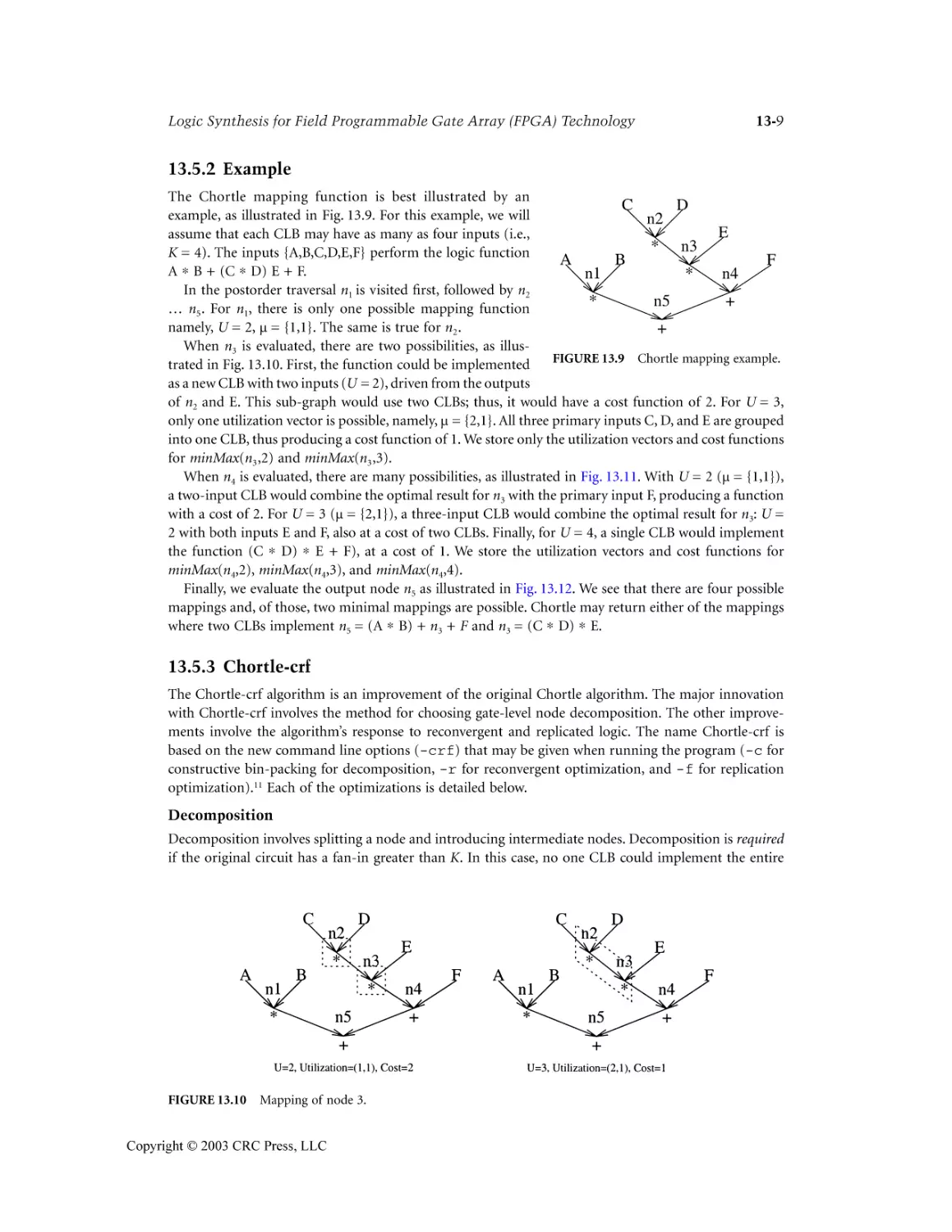
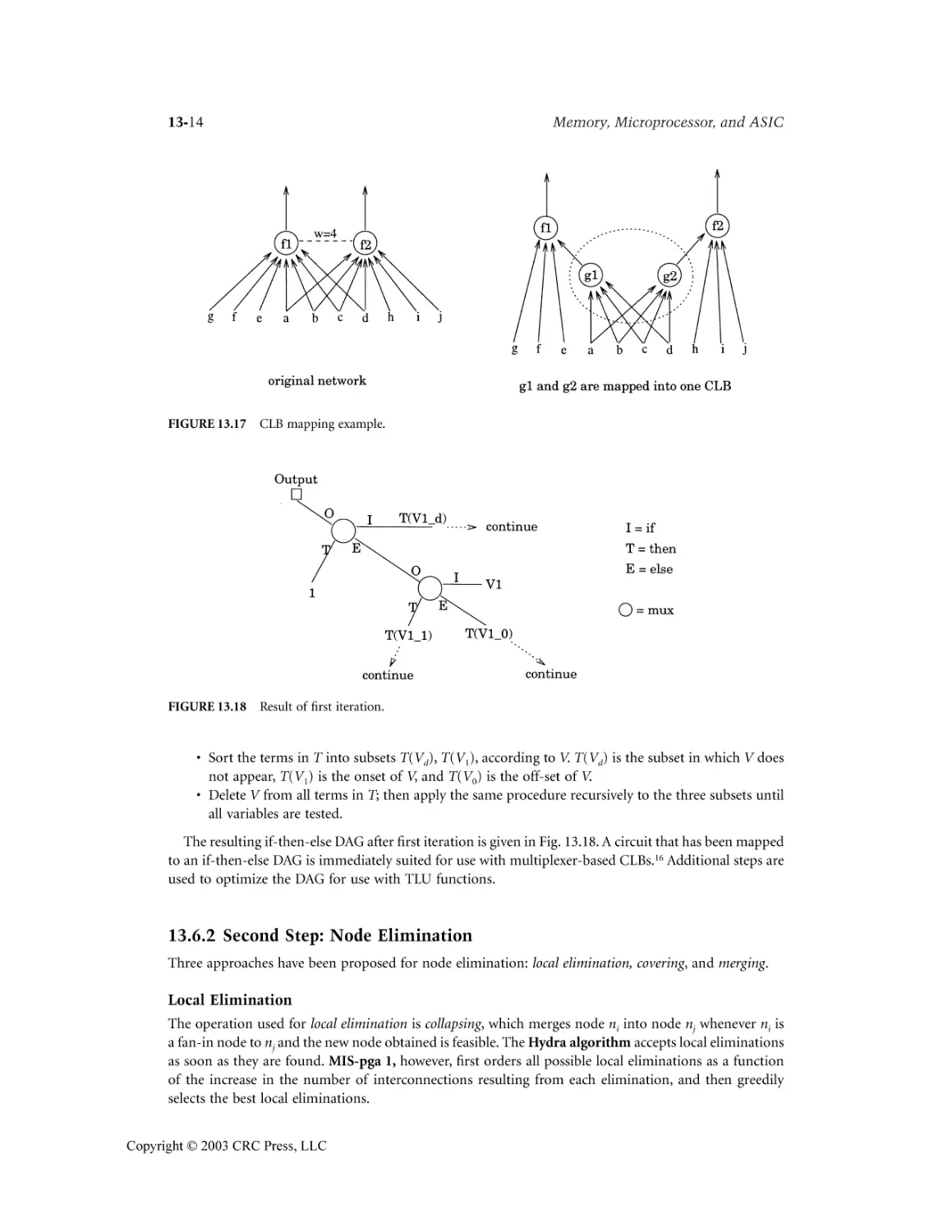
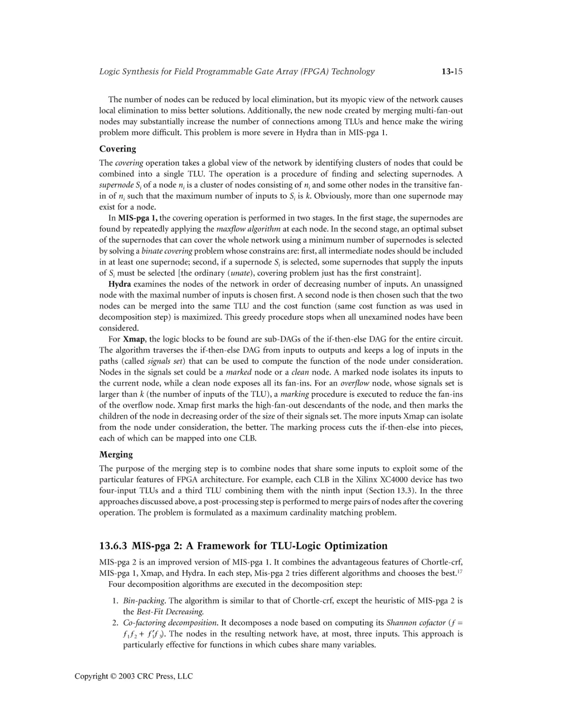
13.5 Chortle .................................................................................................................................13-7
13.6 Two-Step Approaches ......................................................................................................13-12
13.7 Conclusion ........................................................................................................................13-16
References ....................................................................................................................................13-16
14
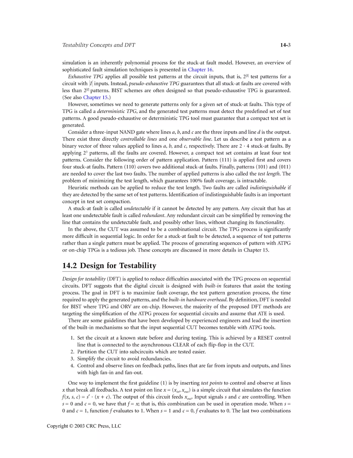
Testability Concepts and DFT Nick Kanopoulos
14.1 Introduction: Basic Concepts .............................................................................................14-1
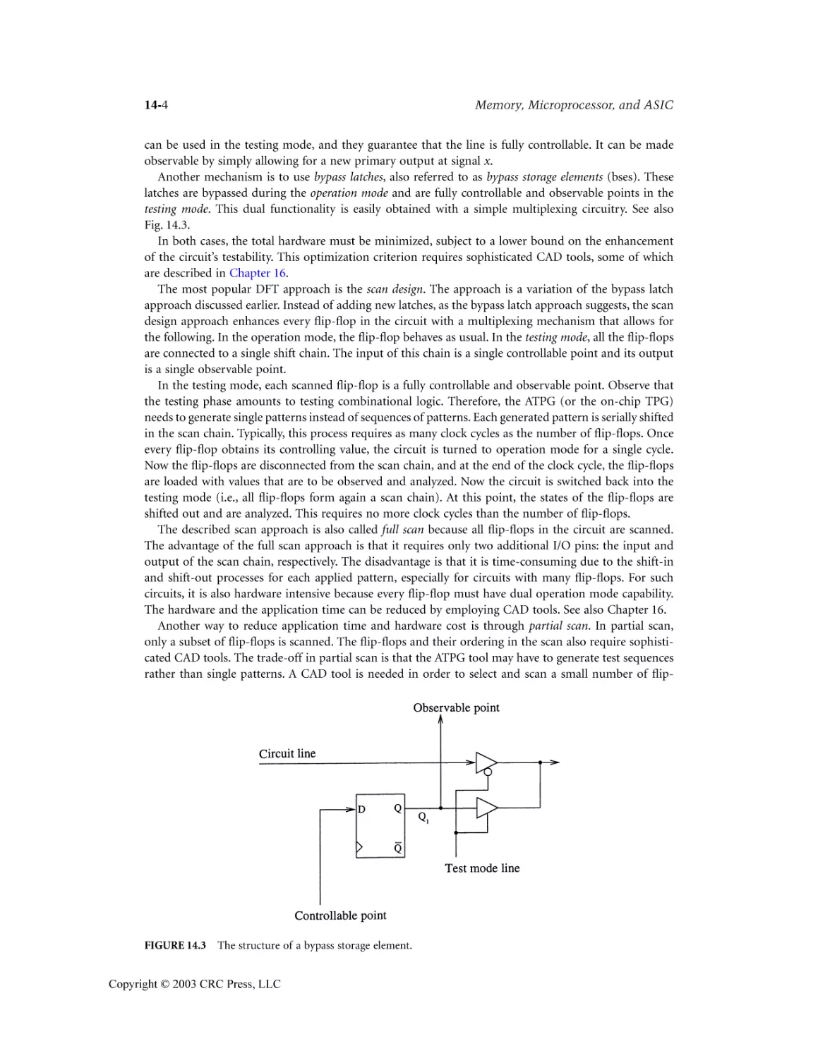
14.2 Design for Testability ..........................................................................................................14-3
References ......................................................................................................................................14-5
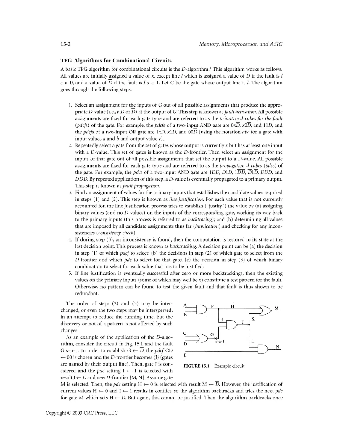
15
ATPG and BIST Dimitri Kagaris
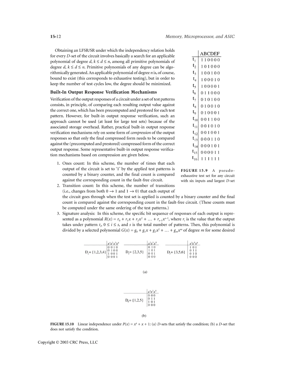
15.1 Automatic Test Pattern Generation ...................................................................................15-1
15.2 Built-In Self-Test ................................................................................................................15-8
References ....................................................................................................................................15-14
16
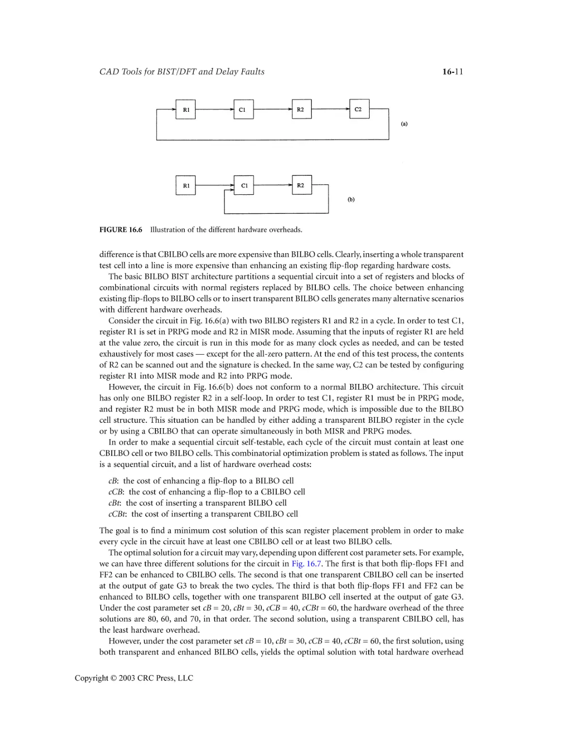
CAD Tools for BIST/DFT and Delay Faults Spyros Tragoudas
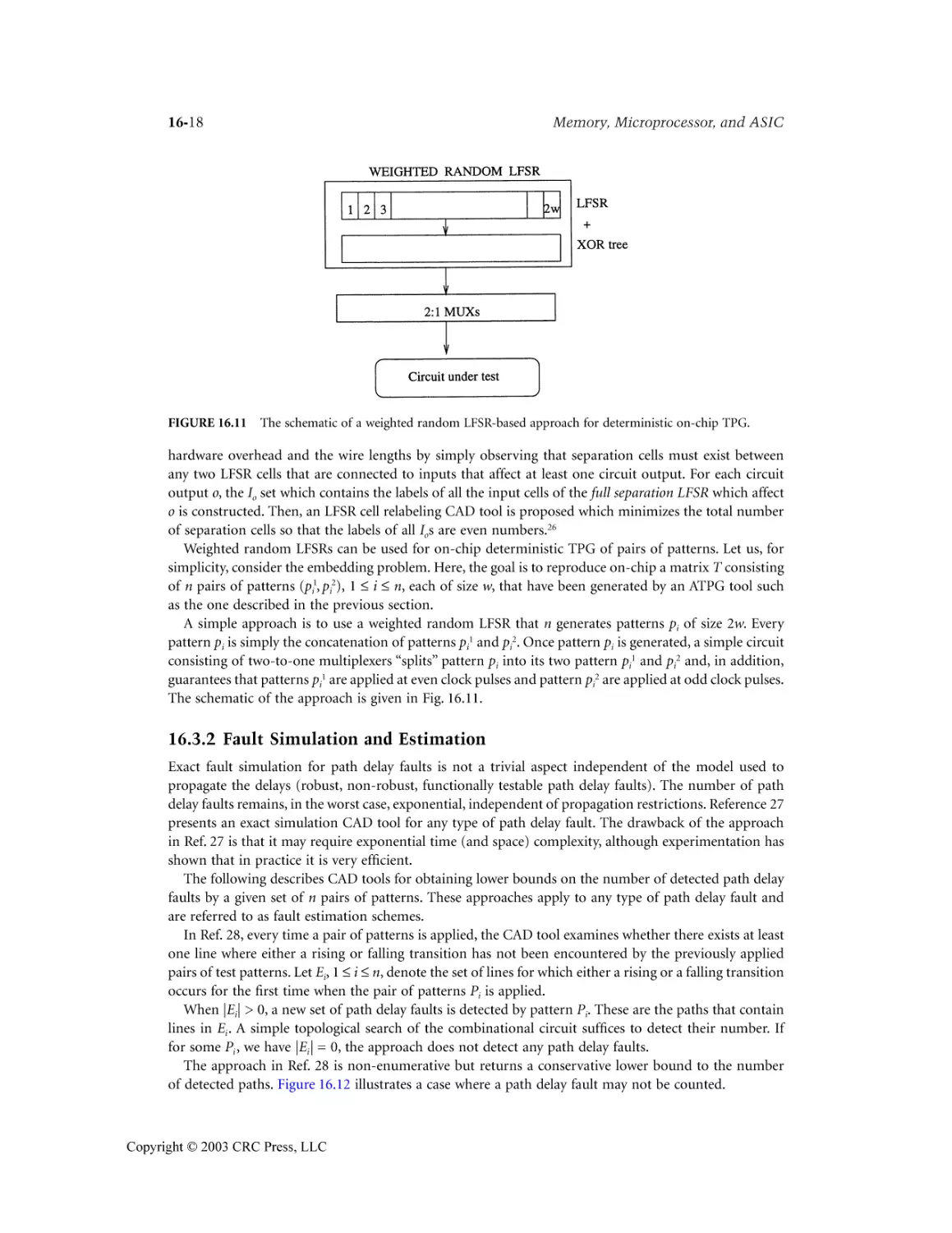
16.1 Introduction .......................................................................................................................16-1
16.2 CAD for Stuck-At Faults ....................................................................................................16-1
16.3 CAD for Path Delays ........................................................................................................16-14
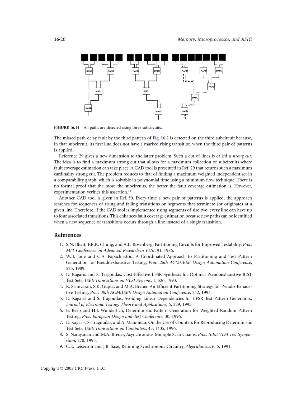
References ....................................................................................................................................16-20
xiv
Copyright © 2003 CRC Press, LLC
1737_CH01 Page 1 Wednesday, January 22, 2003 9:17 AM
1
System Timing
1.1
1.2
Introduction ........................................................................1-1
Synchronous VLSI Systems.................................................1-3
General Overview • Advantages and Drawbacks of
Synchronous Systems
1.3
Synchronous Timing and Clock
Distribution Networks ........................................................1-5
Background • Definitions and Notation • Clock
Scheduling • Structure of the Clock Distribution Network
1.4
Common Storage Elements • Storage
Elements • Latches • Flip-Flops • The Clock
Signal • Analysis of a Single-Phase Local Data Path with FlipFlops • Analysis of a Single-Phase Local Data Path with
Latches
Ivan S. Kourtev
University of Pittsburgh
Eby G. Friedman
Timing Properties of Synchronous
Storage Elements ...............................................................1-13
1.5
1.6
A Final Note ......................................................................1-27
Glossary of Terms..............................................................1-27
University of Rochester
1.1 Introduction
The concept of data or information processing arises in a variety of fields. Understanding the principles
behind this concept is fundamental to computer design, communications, manufacturing process control,
biomedical engineering, and an increasingly large number of other areas of technology and science. It is
impossible to imagine modern life without computers for generating, analyzing, and retrieving large
amounts of information, as well as communicating information to end users regardless of their location.
Technologies for designing and building microelectronics-based computational equipment have been
steadily advancing ever since the first commercial discrete integrated circuits were introduced* in the late
1950s.1 As predicted by Moore’s law in the 1960s,2 integrated circuit (IC) density has been doubling
approximately every 18 months, and this doubling in size has been accompanied by a similar exponential
increase in circuit speed (or, more precisely, clock frequency). These trends of steadily increasing circuit
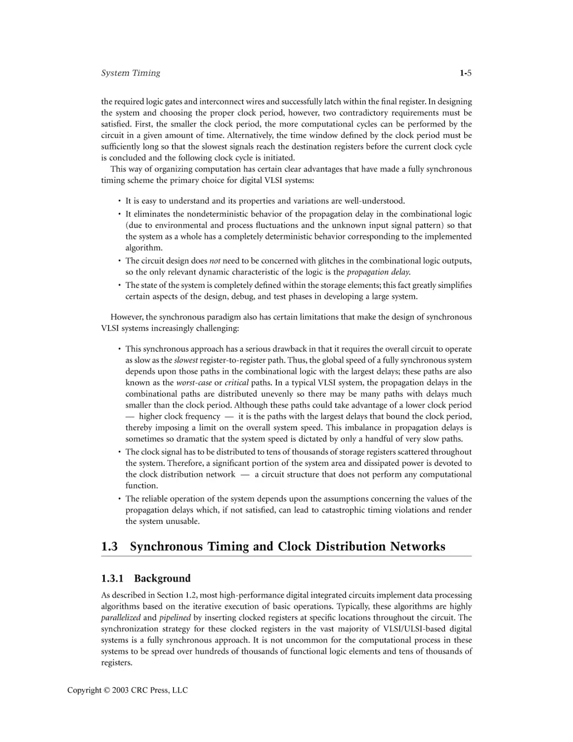
size and clock frequency are illustrated in Fig. 1.1(a) and (b), respectively. As a result of this amazing
revolution in semiconductor technology, it is not unusual for modern integrated circuits to contain over
ten million switching elements (i.e., transistors) packed into a chip area as large as 500 mm2.3-5 This truly
exceptional technological capability is due to advances in both design methodologies and physical manufacturing technologies. Research and experience demonstrate that this trend of exponentially increasing
integrated circuit computational power will continue into the foreseeable future.
Integrated circuit performance is typically characterized6 by the speed of operation, the available circuit
functionality, and the power consumption, and there are multiple factors which directly affect these
*Monolthic integrated circuits (ICs) were introduced in the 1960s.
0-8493-1737-1/03/$0.00+$1.50
© 2003 by CRC Press LLC
Copyright © 2003 CRC Press, LLC
1-1
1737_CH01 Page 2 Wednesday, January 22, 2003 9:17 AM
1-2
Memory, Microprocessor, and ASIC
(a) Evolution of the number of transistors per integrated circuit; and (b) Evolution of clock frequency.
FIGURE 1.1
Moore’s law: exponential increase in circuit integration and clock frequency. (From Rabaey, J. M.,
Digital Integrated Circuits: A Design Perspective, Prentice Hall, Inc., 1995.)
performance characteristics. While each of these factors is significant, on the technological side, increased
circuit performance has been largely achieved by the following approaches:
• Reduction in feature size (technology scaling); that is, the capability of manufacturing physically
smaller and faster device structures
• Increase in chip area, permitting a larger number of circuits and therefore greater on-chip functionality
• Advances in packaging technology, permitting the increasing volume of data traffic between an
integrated circuit and its environment as well as the efficient removal of heat created during circuit
operation
The most complex integrated circuits are referred to as VLSI circuits, where the term “VLSI” stands
for Very Large-Scale Integration. This term describes the complexity of modern integrated circuits
consisting of hundreds of thousands to many millions of active transistor elements. Presently, the leading
integrated circuit manufacturers have a technological capability for the mass production of VLSI circuits
with feature sizes as small as 0.12 mm.7 These sub-1/2-micrometer technologies are identified with the
term deep submicrometer (DSM) since the minimum feature size is well below the one micrometer mark.
As these dramatic advances in fabricating technologies take place, integrated circuit performance is
often limited by effects closely related to the very reasons behind these advances, such as small geometry
interconnect structures. Circuit performance has become strongly dependent and limited by electrical
issues that are particularly significant in deep submicrometer integrated circuits. Signal delay and related
waveform effects are among those phenomena that have a great impact on high-performance integrated
circuit design methodologies and the resulting system implementation. In the case of fully synchronous
VLSI systems, these effects have the potential to create catastrophic failures due to the limited time
available for signal propagation among gates.
Synchronous systems in general are reviewed in Section 1.2, followed by a more detailed description
of these systems and the related timing constraints in Section 1.3. The timing properties of the storage
elements are discussed in Section 1.4 closing with an appendix containing a glossary of the many terms
used throughout this chapter.
Copyright © 2003 CRC Press, LLC
1737_CH01 Page 3 Wednesday, January 22, 2003 9:17 AM
System Timing
1-3
1.2 Synchronous VLSI Systems
1.2.1 General Overview
Typically, a digital VLSI system performs a complex computational algorithm, such as a Fast Fourier
Transform or a RISC* architecture microprocessor. Although modern VLSI systems contain a large
number of components, these systems normally employ only a limited number of different kinds of logic
elements or logic gates. Each logic element accepts certain input signals and computes an output signal
to be used by other logic elements. At the logic level of abstraction, a VLSI system is a network of tens
of thousands or more logic gates whose terminals are interconnected by wires in order to implement the
target algorithm.
The switching variables acting as inputs and outputs of a logic gate in a VLSI system are represented
by tangible physical qualities,** while a number of these devices are interconnected to yield the desired
function of each logic gate. The specifiics of the physical characteristics are collectively summarized with
the term “technology” which encompasses such detail as the type and behavior of the devices that can be
built, the number and sequence of the manufacturing steps, and the impedance of the different interconnect materials used. Today, several technologies make possible the implementation of high-performance
VLSI systems — these are best exemplified by CMOS, bipolar, BiCMOS, and gallium arsenide.2,8 CMOS
technology in particular exhibits many desirable performance characteristics, such as low power consumption, high density, ease of design, and reasonable to excellent speed. Due to these excellent performance
characteristics, CMOS technology has become the dominant VLSI technology used today.
The design of a digital VLSI system may require a great deal of effort in order to consider a broad
range of architectural and logic issues; that is, choosing the appropriate gates and interconnections among
these gates to achieve the required circuit function. No design is complete, however, without considering
the dynamic (or transient) characteristics of the signal propagation, or, alternatively, the changing behavior of signals within time. Every computation performed by a switching circuit involves multiple signal
transitions between logic states and requires a finite amount of time to complete. The voltage at every
circuit node must reach a specific value for the computation to be completed. Therefore, state-of-theart integrated circuit design is largely centered around the difficult task of predicting and properly
interpreting signal waveform shapes at various points in a circuit.
In a typical VLSI system, millions of signal transitions determine the individual gate delays and the
overall speed of the system. Some of these signal transitions can be executed concurrently, while others
must be executed in a strict sequential order.9 The sequential occurrence of the latter operations — or
signal transition events — must be properly coordinated in time so that logically correct system operation
is guaranteed and its results are reliable (in the sense that these results can be repeated). This coordination
is known as synchronization and is critical to ensuring that any pair of logical operations in a circuit with
a precedence relationship proceed in the proper order. In modern digital integrated circuits, synchronization is achieved at all stages of system design and system operation by a variety of techniques, known
as a timing discipline or timing scheme.8,10-12 With few exceptions, these circuits are based on a fully
synchronous timing scheme, specifically developed to cope with the finite speed required by the physical
signals to propagate through the system.
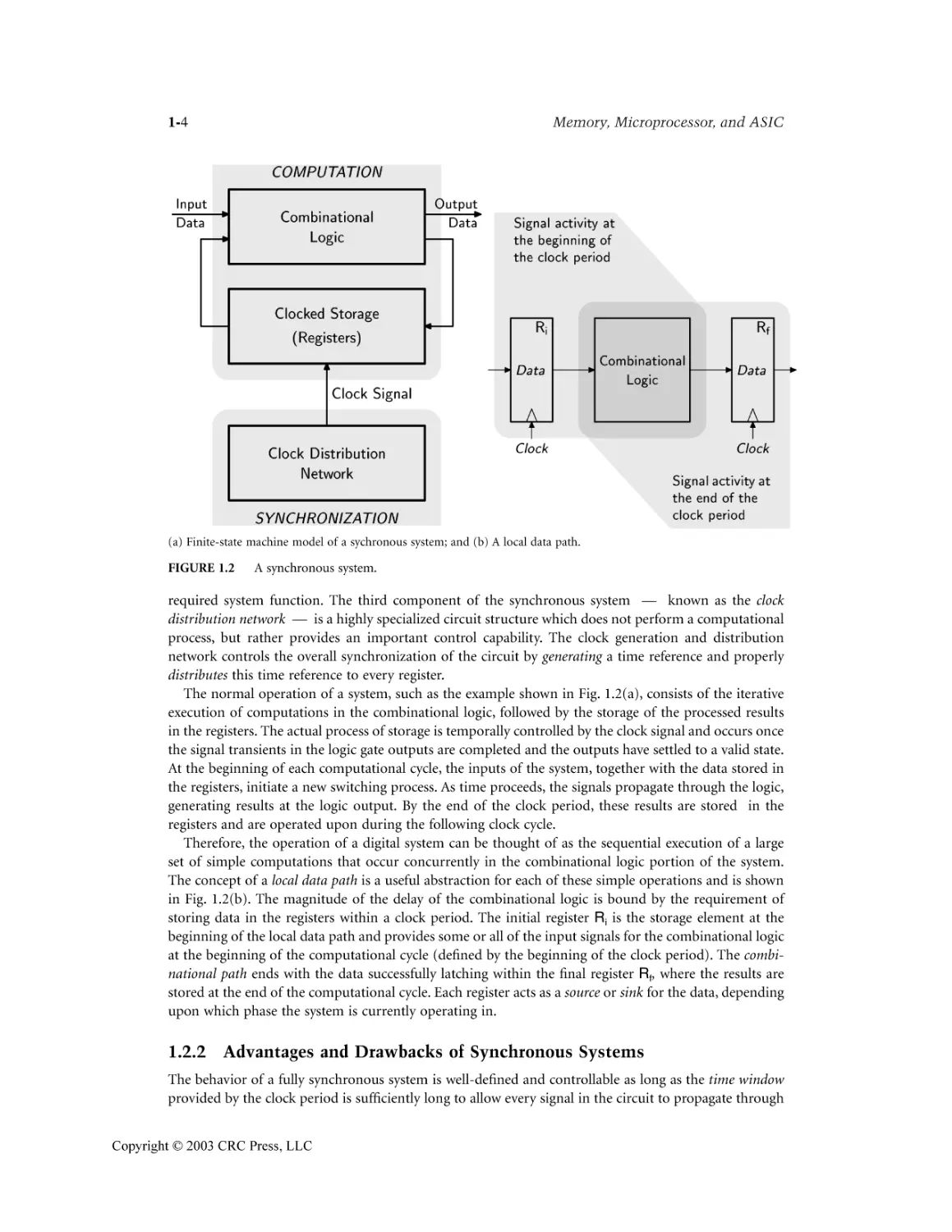
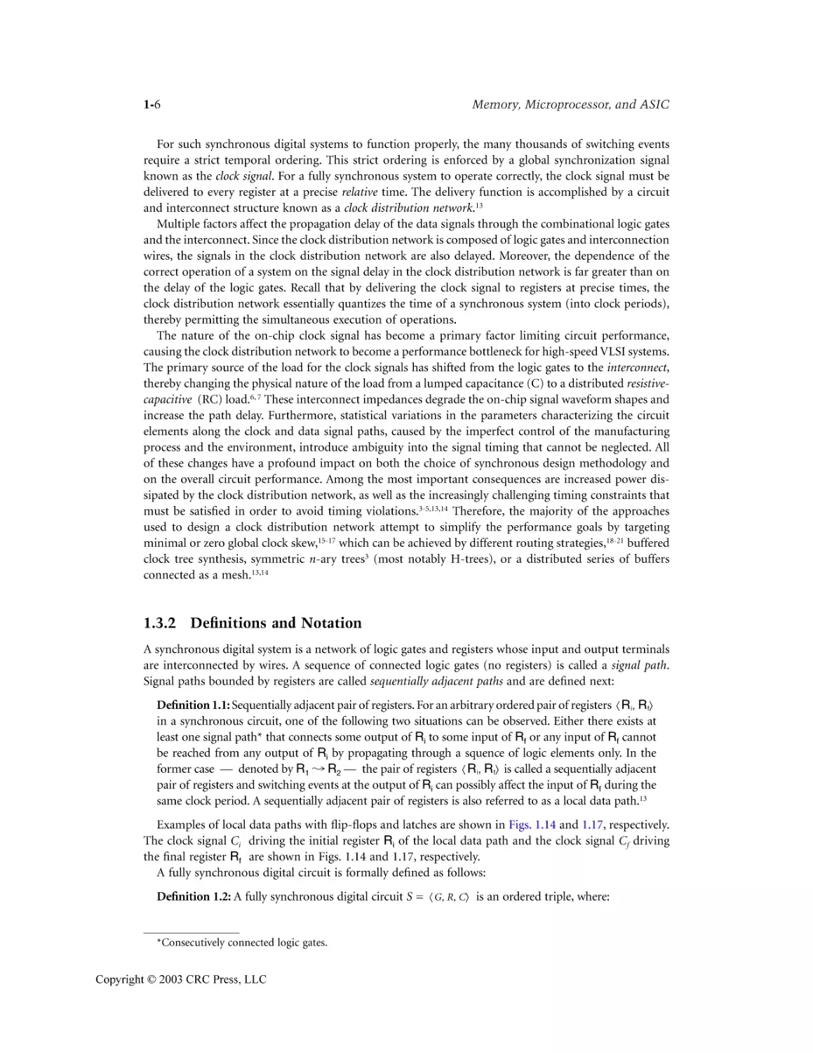
An example of a fully synchronous system is shown in Fig. 1.2(a). As illustrated in Fig. 1.2(a), there
are three recognizable components in this system. The first component — the logic gates, collectively
referred to as the combinational logic — provides the range of operations that a system executes. The
second component — the clocked storage elements or simply the registers — are elements that store
the results of the logical operations. Together, the combinational logic and registers constitute the
computational portion of the synchronous system and are interconnected in a way that implements the
*RISC = Reduced Instruction Set Computer.
**Such quantities as the electical voltages and currents in the electronic devices.
Copyright © 2003 CRC Press, LLC
1737_CH01 Page 4 Wednesday, January 22, 2003 9:17 AM
1-4
Memory, Microprocessor, and ASIC
(a) Finite-state machine model of a sychronous system; and (b) A local data path.
FIGURE 1.2
A synchronous system.
required system function. The third component of the synchronous system — known as the clock
distribution network — is a highly specialized circuit structure which does not perform a computational
process, but rather provides an important control capability. The clock generation and distribution
network controls the overall synchronization of the circuit by generating a time reference and properly
distributes this time reference to every register.
The normal operation of a system, such as the example shown in Fig. 1.2(a), consists of the iterative
execution of computations in the combinational logic, followed by the storage of the processed results
in the registers. The actual process of storage is temporally controlled by the clock signal and occurs once
the signal transients in the logic gate outputs are completed and the outputs have settled to a valid state.
At the beginning of each computational cycle, the inputs of the system, together with the data stored in
the registers, initiate a new switching process. As time proceeds, the signals propagate through the logic,
generating results at the logic output. By the end of the clock period, these results are stored in the
registers and are operated upon during the following clock cycle.
Therefore, the operation of a digital system can be thought of as the sequential execution of a large
set of simple computations that occur concurrently in the combinational logic portion of the system.
The concept of a local data path is a useful abstraction for each of these simple operations and is shown
in Fig. 1.2(b). The magnitude of the delay of the combinational logic is bound by the requirement of
storing data in the registers within a clock period. The initial register Ri is the storage element at the
beginning of the local data path and provides some or all of the input signals for the combinational logic
at the beginning of the computational cycle (defined by the beginning of the clock period). The combinational path ends with the data successfully latching within the final register Rf, where the results are
stored at the end of the computational cycle. Each register acts as a source or sink for the data, depending
upon which phase the system is currently operating in.
1.2.2 Advantages and Drawbacks of Synchronous Systems
The behavior of a fully synchronous system is well-defined and controllable as long as the time window
provided by the clock period is sufficiently long to allow every signal in the circuit to propagate through
Copyright © 2003 CRC Press, LLC
1737_CH01 Page 5 Wednesday, January 22, 2003 9:17 AM
System Timing
1-5
the required logic gates and interconnect wires and successfully latch within the final register. In designing
the system and choosing the proper clock period, however, two contradictory requirements must be
satisfied. First, the smaller the clock period, the more computational cycles can be performed by the
circuit in a given amount of time. Alternatively, the time window defined by the clock period must be
sufficiently long so that the slowest signals reach the destination registers before the current clock cycle
is concluded and the following clock cycle is initiated.
This way of organizing computation has certain clear advantages that have made a fully synchronous
timing scheme the primary choice for digital VLSI systems:
• It is easy to understand and its properties and variations are well-understood.
• It eliminates the nondeterministic behavior of the propagation delay in the combinational logic
(due to environmental and process fluctuations and the unknown input signal pattern) so that
the system as a whole has a completely deterministic behavior corresponding to the implemented
algorithm.
• The circuit design does not need to be concerned with glitches in the combinational logic outputs,
so the only relevant dynamic characteristic of the logic is the propagation delay.
• The state of the system is completely defined within the storage elements; this fact greatly simplifies
certain aspects of the design, debug, and test phases in developing a large system.
However, the synchronous paradigm also has certain limitations that make the design of synchronous
VLSI systems increasingly challenging:
• This synchronous approach has a serious drawback in that it requires the overall circuit to operate
as slow as the slowest register-to-register path. Thus, the global speed of a fully synchronous system
depends upon those paths in the combinational logic with the largest delays; these paths are also
known as the worst-case or critical paths. In a typical VLSI system, the propagation delays in the
combinational paths are distributed unevenly so there may be many paths with delays much
smaller than the clock period. Although these paths could take advantage of a lower clock period
— higher clock frequency — it is the paths with the largest delays that bound the clock period,
thereby imposing a limit on the overall system speed. This imbalance in propagation delays is
sometimes so dramatic that the system speed is dictated by only a handful of very slow paths.
• The clock signal has to be distributed to tens of thousands of storage registers scattered throughout
the system. Therefore, a significant portion of the system area and dissipated power is devoted to
the clock distribution network — a circuit structure that does not perform any computational
function.
• The reliable operation of the system depends upon the assumptions concerning the values of the
propagation delays which, if not satisfied, can lead to catastrophic timing violations and render
the system unusable.
1.3 Synchronous Timing and Clock Distribution Networks
1.3.1 Background
As described in Section 1.2, most high-performance digital integrated circuits implement data processing
algorithms based on the iterative execution of basic operations. Typically, these algorithms are highly
parallelized and pipelined by inserting clocked registers at specific locations throughout the circuit. The
synchronization strategy for these clocked registers in the vast majority of VLSI/ULSI-based digital
systems is a fully synchronous approach. It is not uncommon for the computational process in these
systems to be spread over hundreds of thousands of functional logic elements and tens of thousands of
registers.
Copyright © 2003 CRC Press, LLC
1737_CH01 Page 6 Wednesday, January 22, 2003 9:17 AM
1-6
Memory, Microprocessor, and ASIC
For such synchronous digital systems to function properly, the many thousands of switching events
require a strict temporal ordering. This strict ordering is enforced by a global synchronization signal
known as the clock signal. For a fully synchronous system to operate correctly, the clock signal must be
delivered to every register at a precise relative time. The delivery function is accomplished by a circuit
and interconnect structure known as a clock distribution network.13
Multiple factors affect the propagation delay of the data signals through the combinational logic gates
and the interconnect. Since the clock distribution network is composed of logic gates and interconnection
wires, the signals in the clock distribution network are also delayed. Moreover, the dependence of the
correct operation of a system on the signal delay in the clock distribution network is far greater than on
the delay of the logic gates. Recall that by delivering the clock signal to registers at precise times, the
clock distribution network essentially quantizes the time of a synchronous system (into clock periods),
thereby permitting the simultaneous execution of operations.
The nature of the on-chip clock signal has become a primary factor limiting circuit performance,
causing the clock distribution network to become a performance bottleneck for high-speed VLSI systems.
The primary source of the load for the clock signals has shifted from the logic gates to the interconnect,
thereby changing the physical nature of the load from a lumped capacitance (C) to a distributed resistivecapacitive (RC) load.6, 7 These interconnect impedances degrade the on-chip signal waveform shapes and
increase the path delay. Furthermore, statistical variations in the parameters characterizing the circuit
elements along the clock and data signal paths, caused by the imperfect control of the manufacturing
process and the environment, introduce ambiguity into the signal timing that cannot be neglected. All
of these changes have a profound impact on both the choice of synchronous design methodology and
on the overall circuit performance. Among the most important consequences are increased power dissipated by the clock distribution network, as well as the increasingly challenging timing constraints that
must be satisfied in order to avoid timing violations.3-5,13,14 Therefore, the majority of the approaches
used to design a clock distribution network attempt to simplify the performance goals by targeting
minimal or zero global clock skew,15-17 which can be achieved by different routing strategies,18-21 buffered
clock tree synthesis, symmetric n-ary trees3 (most notably H-trees), or a distributed series of buffers
connected as a mesh.13,14
1.3.2 Definitions and Notation
A synchronous digital system is a network of logic gates and registers whose input and output terminals
are interconnected by wires. A sequence of connected logic gates (no registers) is called a signal path.
Signal paths bounded by registers are called sequentially adjacent paths and are defined next:
Definition 1.1: Sequentially adjacent pair of registers. For an arbitrary ordered pair of registers · R i, R fÒ
in a synchronous circuit, one of the following two situations can be observed. Either there exists at
least one signal path* that connects some output of Ri to some input of Rf or any input of Rf cannot
be reached from any output of Ri by propagating through a squence of logic elements only. In the
former case — denoted by R1 R2 — the pair of registers · R i, R fÒ is called a sequentially adjacent
pair of registers and switching events at the output of Ri can possibly affect the input of Rf during the
same clock period. A sequentially adjacent pair of registers is also referred to as a local data path.13
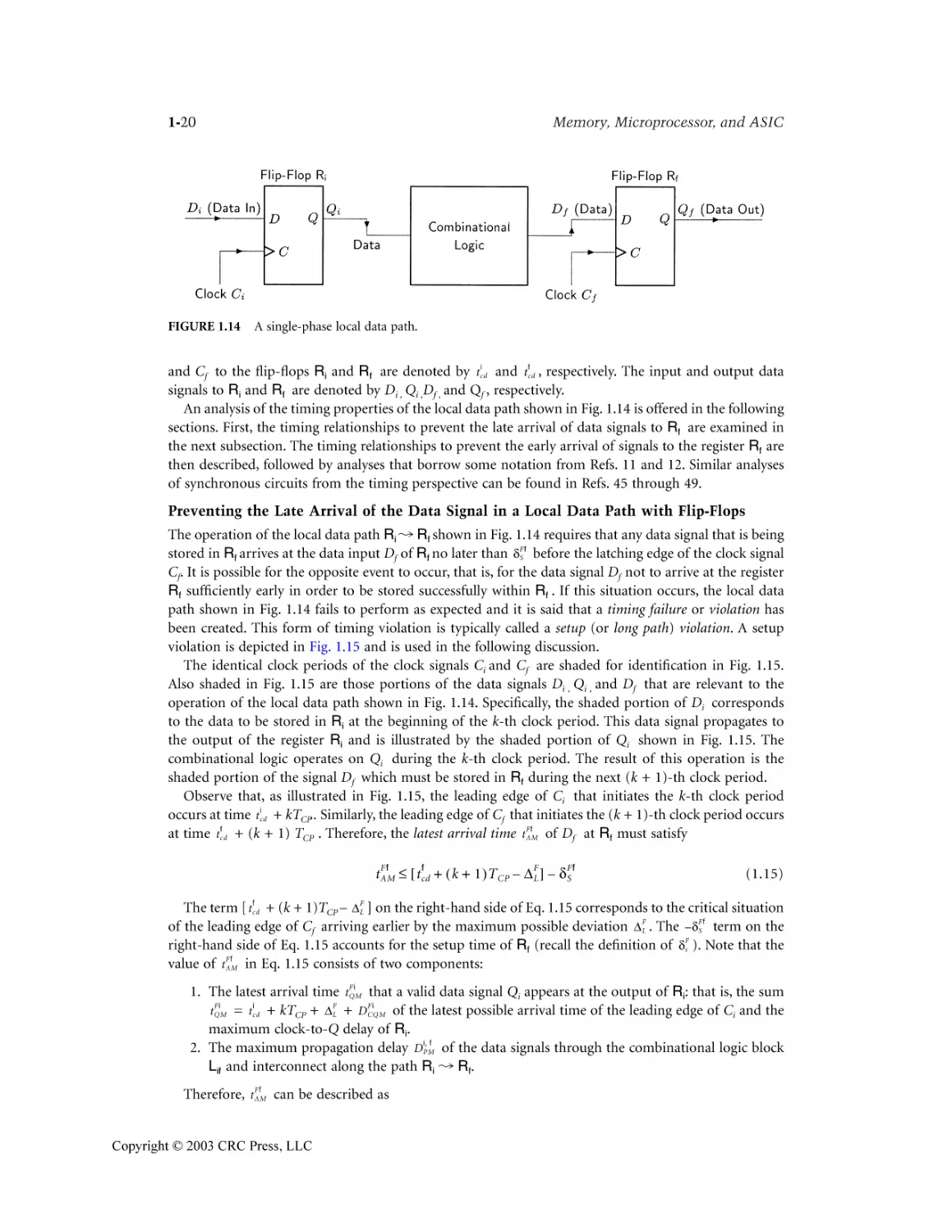
Examples of local data paths with flip-flops and latches are shown in Figs. 1.14 and 1.17, respectively.
The clock signal Ci driving the initial register Ri of the local data path and the clock signal Cf driving
the final register Rf are shown in Figs. 1.14 and 1.17, respectively.
A fully synchronous digital circuit is formally defined as follows:
Definition 1.2: A fully synchronous digital circuit S = · G, R, CÒ is an ordered triple, where:
*Consecutively connected logic gates.
Copyright © 2003 CRC Press, LLC
1737_CH01 Page 7 Wednesday, January 22, 2003 9:17 AM
1-7
System Timing
∑ G = {g1, g2, …, gM} is the set of all combinational logic gates,
∑ R = {R1, R2, …, RN} is the set of all registers, and
∑ C = ||ci ¥ j||N ¥ N is a matrix describing the connectivity of G where for every element Ci,j of C
Ï0, if (Ri R j )
ci, j = Ì
Rj )
Ó1, if (Ri
Note that in a fully synchronous digital system there are no purely combinational signal cycles; that is,
it is impossible to reach the input of any logic gate gk by starting at the same gate and going through a
sequence of combinational logic gates only.13,22
Graph Model of a Fully Synchronous Digital Circuit
Certain properties of a synchronous digital circuit may be better understood by analyzing a graph model
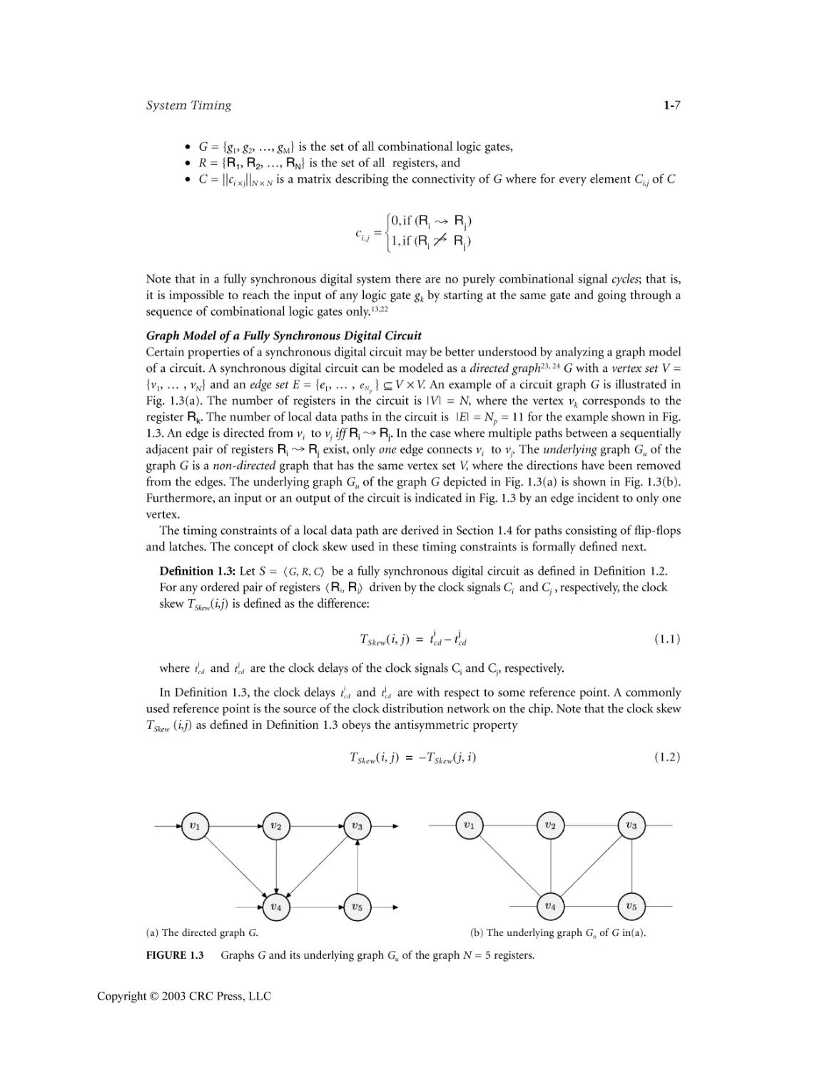
of a circuit. A synchronous digital circuit can be modeled as a directed graph23, 24 G with a vertex set V =
{v1, … , vN} and an edge set E = {e1, … , e Np } Õ V ¥ V. An example of a circuit graph G is illustrated in
Fig. 1.3(a). The number of registers in the circuit is V = N, where the vertex vk corresponds to the
register Rk. The number of local data paths in the circuit is E = Np = 11 for the example shown in Fig.
1.3. An edge is directed from vi to vj iff Ri Rj. In the case where multiple paths between a sequentially
adjacent pair of registers Ri Rj exist, only one edge connects vi to vj. The underlying graph Gu of the
graph G is a non-directed graph that has the same vertex set V, where the directions have been removed
from the edges. The underlying graph Gu of the graph G depicted in Fig. 1.3(a) is shown in Fig. 1.3(b).
Furthermore, an input or an output of the circuit is indicated in Fig. 1.3 by an edge incident to only one
vertex.
The timing constraints of a local data path are derived in Section 1.4 for paths consisting of flip-flops
and latches. The concept of clock skew used in these timing constraints is formally defined next.
Definition 1.3: Let S = · G, R, CÒ be a fully synchronous digital circuit as defined in Definition 1.2.
For any ordered pair of registers · R i, R jÒ driven by the clock signals Ci and Cj , respectively, the clock
skew TSkew(i,j) is defined as the difference:
i
j
T Skew ( i, j ) = t cd – t cd
(1.1)
where t icd and t cdj are the clock delays of the clock signals Ci and Cj, respectively.
In Definition 1.3, the clock delays t icd and t cdj are with respect to some reference point. A commonly
used reference point is the source of the clock distribution network on the chip. Note that the clock skew
TSkew (i,j) as defined in Definition 1.3 obeys the antisymmetric property
T Skew ( i, j ) = – T Skew ( j, i )
(a) The directed graph G.
FIGURE 1.3
(b) The underlying graph Gu of G in(a).
Graphs G and its underlying graph Gu of the graph N = 5 registers.
Copyright © 2003 CRC Press, LLC
(1.2)
1737_CH01 Page 8 Wednesday, January 22, 2003 9:17 AM
1-8
Memory, Microprocessor, and ASIC
The clock skew TSkew (i,j) as defined in Definition 1.3 is a component in the timing constraints of a local
data path (see inequalities 1.19, 1.24, 1.34, 1.35, and 1.40). Therefore, clock skew is defined and is only
of practical use for sequentially-adjacent registers Ri and Rj* (i.e., only for local data paths).
The following substitutions are introduced for notational convenience:
Definition 1.4: Let S = · G, R, CÒ be a fully synchronous digital circuit where the registers Ri, Rf Œ R
i, f
and Ri Rf. The long path delay D̂ PM of the local data path Ri Rf is defined as
Fi
i, f
Ff
F
Ï ( D CQM + D PM + d S + 2D L ), if R i, R f are flip flops
i, f
D̂ PM = Ì
i, f
Lf
L
L
Ó ( D Li
CQM + D PM + d S + D L + D T ), if R i, R f are latches
(1.3)
Similarly, the short delay D̂ Pm of the local data path Ri Rf is defined as
i, f
i, f
Fi
Ff
F
Ï ( D Pm + D CQ – d H – 2D L ), if R i, R f are flip flops
i, f
D̂ Pm = Ì
Lf
L
L
i, f
Ó ( D Li
CQm + D Pm – d H – D L – D T ), if R i, R f are latches
(1.4)
For example, using the notations described in Definition 1.4, the timing constraints of a local data
path Ri Rf with flip-flops (Eqs. 1.19 and 1.24) become
i, f
T Skew ( i, f ) £ T CP – D̂ PM
i, f
– D̂ Pm £ T Skew ( i, f )
(1.5)
(1.6)
For a local data path Ri Rf consisting of the flip-flows Ri and Rf, the setup and hold time violations
are avoided if Eqs. 1.5 and 1.6, respectively, are satisfied.
The clock skew TSkew(i, f) for a local data path Ri Rf can be either positive or negative, as illustrated
in Figs. 1.15 and 1.16, respectively. Negative clock skew may be used to effectively speed up a local data
path Ri Rf by allowing an additional TSkew(i, f) amount of time for the signal to propagate from Ri to
Rf. However, excessive negative skew may create a hold time violation, thereby creating a lower bound
on TSkew(i, f) as described by Eq. 1.6. A hold time violation is a clock hazard or a race condition, also
known as double clocking.13,25 Similarly, positive clock skew effectively decreases the clock period TCP by
TSkew(i, f), thereby limiting the maximum clock frequency.** In this case, a clocking hazard known as
zero clocking may be created.13,25
1.3.3 Clock Scheduling
Examining the constraints of Eqs. 1.5 and 1.6 reveals a procedure for preventing clock hazards. Assuming
Eq. 1.5 is not satisfied, a suitably large value of TCP can be chosen to satisfy constraint Eq. 1.5 and prevent
zero clocking. Also note that, unlike Eq. 1.5, Eq. 1.6 is independent of TCP. Therefore, TCP cannot be
varied to correct a double clocking hazard, but rather a redesign of the clock distribution network may
be required.17
Both double and zero clocking hazards can be eliminated if two simple choices characterizing a fully
synchronous digital circuit are made. Specifically, if equal values are chosen for all clock delays, then the
clock skew TSkew(i, f) = 0 for each local data path Ri Rf,
i
f
" · R i, R fÒ :t cd = t cd fi T Skew ( i, f ) = 0
(1.7)
*Note that technically, however, TSkew(i, j) can be calculated for any ordered pair of registers · R i, R jÒ .
**Positive clock skew may also be thought of as increasing the path delay. In either case, positive clock skew TSkew
> 0 makes it more difficult to satisfy Eq. 1.5.
Copyright © 2003 CRC Press, LLC
1737_CH01 Page 9 Wednesday, January 22, 2003 9:17 AM
1-9
System Timing
Therefore, Eqs. 1.5 and 1.6 become
i
i, f
f
T Skew ( i, f ) = t cd – t cd = 0 £ T CP – D̂ PM
i, f
i
f
– D̂ Pm £ 0 = T Skew ( i, f ) = t cd – t cd
(1.8)
(1.9)
Note that Eq. 1.8 can be satisfied for each local data path Ri Rf in a circuit if a sufficiently large
i, f
value — larger than the greatest value D̂ PM in a circuit — is chosen for TCP. Furthermore, Eq. 1.9 can
i, f
be satisfield across an entire circuit if it can be ensured that D̂ Pm ≥ 0 for each local data path Ri Rf in
the circuit. The timing constraint Eqs. 1.8 and 1.9 can be satisfield since choosing a sufficiently large
i, f
clock period TCP is always possible and D̂ Pm is positive for a properly designed local data path Ri Rf.
The application of this zero clock skew methodology (Eqs. 1.7, 1.8, and 1.9) has been central to the
design of fully synchronous digital circuits for decades.13,26 By requiring the clock signal to arrive at each
register Rj with approximately the same delay t cdj ,* these design methods have become known as zero
clock skew methods.
As shown by previous research,13,15-17,27-29 both double and zero clocking hazards may be removed from
a synchronous digital circuit even when the clock skew is non-zero; that is, TSkew(i, f) π 0 for some (or
all) local data paths Ri Rf. As long as Eqs. 1.5 and 1.6 are satisfied, a synchronous digital system can
operate reliably with non-zero clock skews, permitting the system to operate at higher clock frequencies
while removing all race conditions.
The vector column of clock delays TCD = [ t 1cd , t 2cd , …]T is called a clock schedule.13,25 If TCD is chosen
such that Eqs. 1.5 and 1.6 are satisfied for every local data path Ri Rf, TCD is called a consistent clock
schedule. A clock schedule that satisfies Eq. 1.7 is called a trivial clock schedule. Note that a trivial clock
schedule TCD implies global zero clock skew since for any i and f, t icd = t fcd , and thus, TSkew(i, f) = 0.
Fishburn25 first suggested an algorithm for computing a consistent clock schedule that is non-trivial.
Furthermore, Fishburn showed25 that by exploiting negative and positive clock skew within the local data
paths Ri Rf, a circuit can operate with a clock period TCP less than the clock period achievable by a
trivial (or zero skew) clock schedule that satisfies the conditions specified by Eqs. 1.5 and 1.6. In fact,
Fishburn25 determined an optimal clock schedule by applying linear programming techniques to solve
for TCD so as to satisfy Eqs. 1.5 and 1.6 while minimizing the objective function Fobjective = TCP.
The process of determining a consistent clock schedule TCD can be considered as the mathematical
problem of minimizing the clock period TCP under the constraints Eqs. 1.5 and 1.6. However, there are
important practical issues to consider before a clock schedule can be properly implemented. A clock
distribution network must be synthesized such that the clock signal is delivered to each register with the
proper delay so as to satisfy the clock skew schedule TCD. Furthermore, this clock distribution network
must be constructed so as to minimize the deleterious effects of interconnect impedances and process
parameter variations on the implemented clock schedule. Synthesizing the clock distribution network
typically consists of determining a topology for the network, together with the circuit design and physical
layout of the buffers and interconnect within the clock distribution network.13
1.3.4 Structure of the Clock Distribution Network
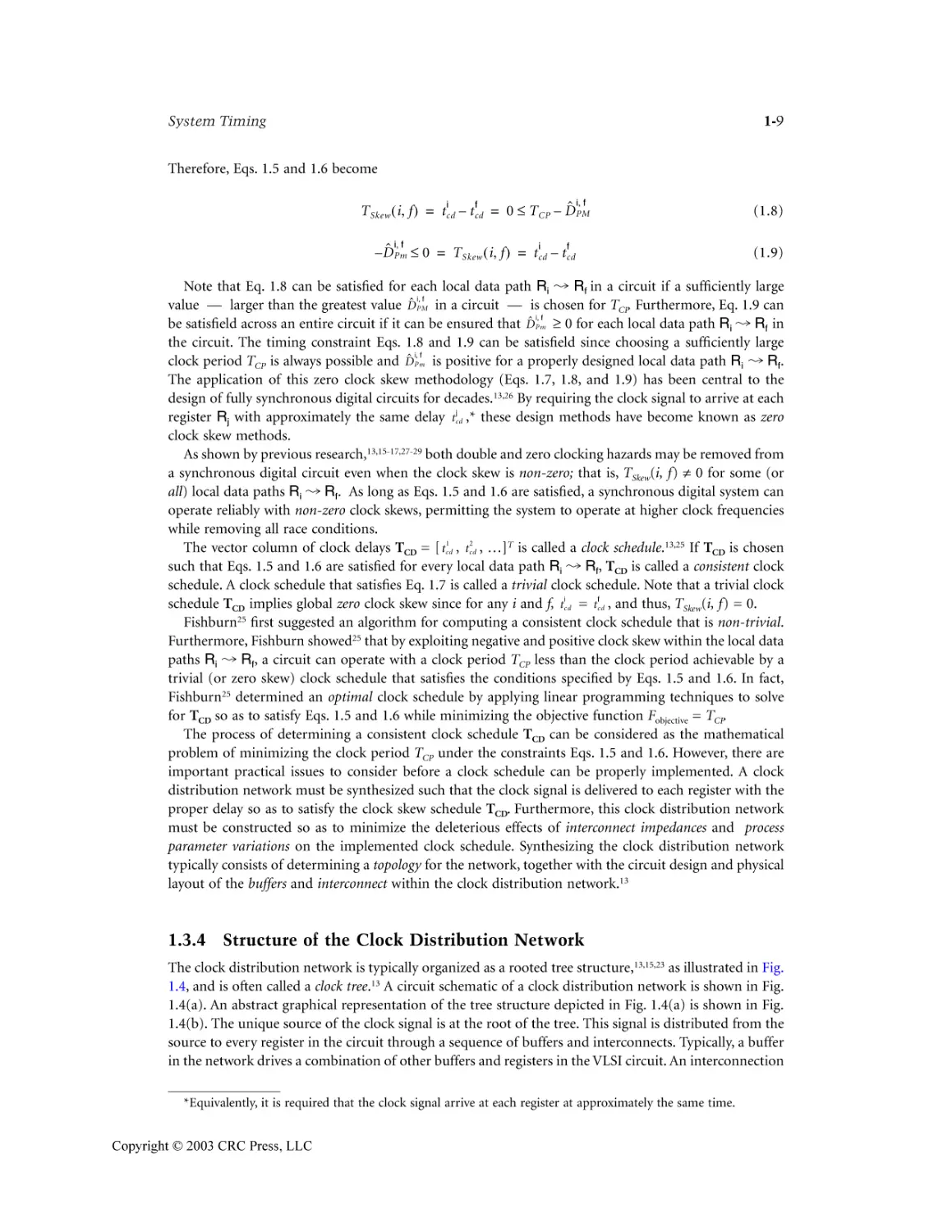
The clock distribution network is typically organized as a rooted tree structure,13,15,23 as illustrated in Fig.
1.4, and is often called a clock tree.13 A circuit schematic of a clock distribution network is shown in Fig.
1.4(a). An abstract graphical representation of the tree structure depicted in Fig. 1.4(a) is shown in Fig.
1.4(b). The unique source of the clock signal is at the root of the tree. This signal is distributed from the
source to every register in the circuit through a sequence of buffers and interconnects. Typically, a buffer
in the network drives a combination of other buffers and registers in the VLSI circuit. An interconnection
*Equivalently, it is required that the clock signal arrive at each register at approximately the same time.
Copyright © 2003 CRC Press, LLC
1737_CH01 Page 10 Wednesday, January 22, 2003 9:17 AM
1-10
Memory, Microprocessor, and ASIC
(a) Circuit structure of the clock distribution network.
FIGURE 1.4
(b) Clock tree structure that corresponds to the
circuit shown in (a).
Tree structure of a clock distribution network.
network of wires connects the output of the driving buffer to the inputs of these driven buffers and
registers. An internal node of the tree corresponds to a buffer, and a leaf node of the tree corresponds to
a register. There are N leaves* in the clock tree labeled F1 through FN, where leaf Fj corresponds to register
Rj. A clock tree topology that implements a given clock schedule TCD must enforce a clock skew TSkew(i,
f) for each local data path Ri Rf of the circuit in order to ensure that both Eqs. 1.5 and 1.6 are satisfied.
This topology, however, can be affected by three important issues relating to the operation of a fully
synchronous digital system.
Linear Dependency of the Clock Skews
An important corollary related to the conservation property13 of clock skew is that there is a linear
dependency among the clock skews of a global data path that form a cycle in the underlying graph of the
circuit. Specifically, if v0, e1, v1π v0, …, vk – 1, ek, vk ∫ v0 is a cycle in the underlying graph of the circuit, then
0
1
1
2
0 = [ t cd – t cd ] + [ t cd – t cd ] + º
(1.10)
k–1
=
 TSkew ( i, i + 1 )
i=0
The property described by Eq. 1.10 is illustrated in Fig. 1.3 for the undirected cycle v1, v4, v3, v2, v1.
Note that
1
4
4
3
3
2
2
1
0 = ( t cd – t cd ) + ( t cd – t cd ) + ( t cd – t cd ) + ( t cd – t cd )
= T Skew ( 1, 4 ) + T Skew ( 4, 3 ) + T Skew ( 3, 2 ) + T Skew ( 2, 1 )
(1.11)
The importance of this property is that Eq. 1.10 describes the inherent correlation among certain clock
skews within a circuit. Therefore, these correlated clock skews cannot be optimized independently of each
other. Returning to Fig. 1.3, note that it is not necessary that a directed cycle exists in the directed graph
G of a circuit for Eq. 1.10 to hold. For example, v2, v3, v4 is not a cycle in the directed circuit graph G
in Fig. 1.3(a) but v2, v3, v4 is a cycle in the undirected circuit graph Gu in Fig. 1.3(b). In addition, TSkew(2,
3) + TSkew(3, 4) + TSkew(4, 2) = 0; that is, the skews TSkew(2, 3), TSkew(3, 4), and TSkew(4, 2) are linearly
dependent. A maximum of (V – 1) = (N – 1) clock skews can be chosen independently of each other
in a circuit, which is easily proven by considering a spanning tree of the underlying circuit graph Gu.23,24
Any spanning tree of Gu will contain (N – 1) edges — each edge corresponding to a local data path
— and the addition of any other edge of Gu will form a cycle such that Eq. 1.10 holds for this cycle.
Note, for example, that for the circuit modeled by the graph shown in Fig. 1.3, four independent clock
skews can be chosen such that the remaining three clock skews can be expressed in terms of the
independent clock skews.
*The number of registers N in the circuit.
Copyright © 2003 CRC Press, LLC
1737_CH01 Page 11 Wednesday, January 22, 2003 9:17 AM
System Timing
1-11
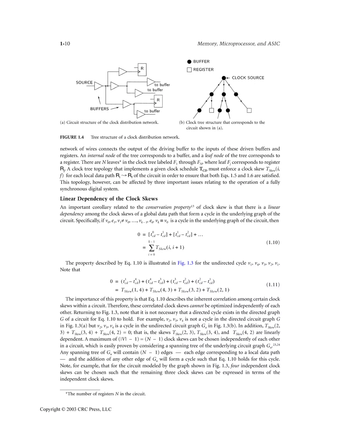
FIGURE 1.5
The permissible range of the clock skew of a local data path Ri Rf. A timing violation exists if
i, f
i, f
TSkew(i, f) œ [– D̂ Pm , TCP – D̂ PM ].
Permissible Ranges
Previous research17,29 has indicated that tight control over the clock skews rather than the clock delays is
necessary for the circuit to operate reliably. The relationships in Eqs. 1.5 and 1.6 are used in Ref. 29 to
determine a permissible range of the allowed clock skew for each local data path. The concept of a
permissible range for the clock skew TSkew(i, f) of a local data path Ri Rf is illustrated in Fig. 1.5. When
i, f
i, f
TSkew(i, f) Œ [– D̂ Pm , TCP – D̂ PM ] — as shown in Fig. 1.5 — Eqs. 1.5 and 1.6 are satisfied. The clock
i, f
skew TSkew(i, f) is not permitted to be in either the interval (–•, – D̂ Pm ) because a race condition will be
i, f
created or the interval (TCP – D̂ PM ,+ •) because the minimum clock period will be limited.
Also note that the reliability of the circuit is related to the probability of a timing violation occurring
for any local data path Ri Rf. Therefore, the reliability of any local data path Ri Rf of the circuit
(and therefore of the entire circuit) is increased in two ways:
1. By choosing the clock skew TSkew(i, f) for a local data path as far as possible from the borders of
i, f
i, f
the interval [– D̂ Pm , TCP – D̂ PM ], that is, by (ideally) positioning the clock skew TSkew(i, f) in the
i, f
i, f
middle of the permissible range, that is, TSkew(i, f) = 1/2 [TCP – ( D̂ PM + D̂ Pm )]
i, f
i, f
2. By increasing the width TCP – ( D̂ PM – D̂ Pm ) of the permissible range of the local data path Ri Rf
Due to the linear dependence of the clock skews shown previously, however, it is not possible to build a
typical circuit such that for each local data path Ri Rf, the clock skew TSkew(i, f) is in the middle of
the permissible range.
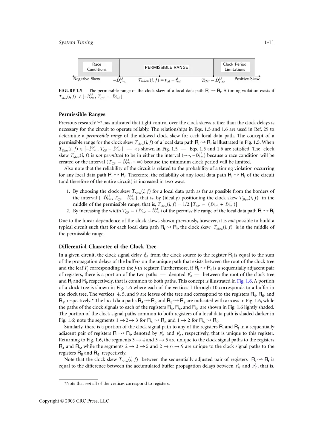
Differential Character of the Clock Tree
In a given circuit, the clock signal delay t cdj from the clock source to the register Rj is equal to the sum
of the propagation delays of the buffers on the unique path that exists between the root of the clock tree
and the leaf Fj corresponding to the j-th register. Furthermore, if Ri Rf is a sequentially adjacent pair
of registers, there is a portion of the two paths — denoted P *if — between the root of the clock tree
and Ri and Rf, respectively, that is common to both paths. This concept is illustrated in Fig. 1.6. A portion
of a clock tree is shown in Fig. 1.6 where each of the vertices 1 through 10 corresponds to a buffer in
the clock tree. The vertices 4, 5, and 9 are leaves of the tree and correspond to the registers R4, R5, and
R9, respectively.* The local data paths R4 R5 and R5 R9 are indicated with arrows in Fig. 1.6, while
the paths of the clock signals to each of the registers R4, R5, and R9 are shown in Fig. 1.6 lightly shaded.
The portion of the clock signal paths common to both registers of a local data path is shaded darker in
Fig. 1.6; note the segments 1 Æ 2 Æ 3 for R4 R5 and 1 Æ 2 for R5 R9.
Similarly, there is a portion of the clock signal path to any of the registers Ri and Rf in a sequentially
adjacent pair of registers Ri Rf, denoted by P iif and P fif , respectively, that is unique to this register.
Returning to Fig. 1.6, the segments 3 Æ 4 and 3 Æ 5 are unique to the clock signal paths to the registers
R4 and R5, while the segments 2 Æ 3 Æ 5 and 2 Æ 6 Æ 9 are unique to the clock signal paths to the
registers R5 and R9, respectively.
Note that the clock skew TSkew(i, f) between the sequentially adjusted pair of registers Ri Rf is
equal to the difference between the accumulated buffer propagation delays between P iif and P fif , that is,
*Note that not all of the vertices correspond to registers.
Copyright © 2003 CRC Press, LLC
1737_CH01 Page 12 Wednesday, January 22, 2003 9:17 AM
1-12
Memory, Microprocessor, and ASIC
FIGURE 1.6
Illustration of the differential nature of the clock tree.
TSkew(i, f) = Delay ( P iif ) – Delay ( P fif ). Therefore, any variations of circuit parameters over P *if will not
affect the value of the clock skew TSkew(i, f). For the example shown in Fig. 1.6, TSkew (4,5) = Delay ( P 44, 5 )
– Delay ( P 54, 5 ) and TSkew (5,9) = Delay ( P 55, 9 ) – Delay ( P 95, 9 ).
The differential feature of the clock tree suggests an approach for minimizing the effects of process
parameter variations on the correct operation of the circuit. To illustrate this approach, each branch p
Æ q of the clock tree shown in Fig. 1.6 is labeled with two numbers: tp,q > 0 is the intended delay of the
branch and ep,q ≥ 3 0 is the maximum error (deviation) of this delay.* In other words, the actual delay
of the branch p Æ q is in the interval [tp,q – ep,q, tp,q + ep,q]. With this notation, the target clock skew
values for the local data paths R4 R5 and R5 R9 are shown in the middle column in Table 1.1. The
bounds of the actual clock skew values for the local data paths R4 R5 and R5 R9 (considering the
e variations) are shown in the right-most column in Table 1.1.
As the results in Table 1.1 demonstrate, it is advantageous to maximize P *if for any local data path Ri
Rf with a relatively narrow permissible range, such that the parameter variations on P *if do not affect
i, f
i, f
TSkew(i, f). Similarly, when the permissible range [– D̂ Pm , TCP – D̂ PM ] is wider, P *if may be permitted to
be only a small franction of the total path from the root to Ri and Rf, respectively. Future research work
will explore this approach of synthesizing a clock tree based on choosing a tree structure which restricts
the possible variations of those local data paths with narrow permissible ranges, and tolerates larger delay
variations for those local data paths with wider permissible ranges.
TABLE 1.1 Target and Actual Values of the Clock Skews for the Local Data Paths R4 R5
and R5 R9 Shown in Fig. 1.6
TSkew(4, 5)
TSkew(5, 9)
Target Skew
t3, 4 – t3, 5
t2, 3 + t3, 5 – t2, 6 – t6, 9
Actual Skew Bounds
t3, 4 – t3, 5 ± (e3, 4 + e3, 4)
t2, 3 + t3, 5 – t2, 6 – t6, 9 ± (e2, 3 + e3, 5 + e2, 6 + e6, 9)
*The deviation e is due to parameter variations during circuit manufacturing as well as to environmnetal conditions during operation of the circuit.
Copyright © 2003 CRC Press, LLC
1737_CH01 Page 13 Wednesday, January 22, 2003 9:17 AM
System Timing
1-13
1.4 Timing Properties of Synchronous Storage Elements
1.4.1 Common Storage Elements
The general structure and principles of operation of a fully synchronous digital VLSI system were
described in Section 1.2. In this section, the timing constraints due to the combinational logic and the
storage elements within a synchronous system are reviewed. The clock distribution network provides the
time reference for the storage elements — or registers — thereby enforcing the required logical order
of operations. This time reference consists of one or more clock signals that are delivered to each and
every register within the integrated circuit. These clock signals control the order of computational events
by controlling the exact times the register data inputs are sampled.
The data signals are inevitably delayed as these signals propagate through the logic gates and along
interconnections within the local data paths. These propagation delays can be evaluated within a certain
accuracy and used to derive timing relationships among signals in a circuit. In this section, the properties
of commonly used types of registers and their local timing relationships for different types of local data
paths are described. After discussing registers in general in the next subsection, the properties of levelsensitive registers (latches) and the significant timing parameters of these registers are reviewed. Edgesensitive registers (flip-flops) and their timing parameters are also analyzed. Properties and definitions
related to the clock distribution network are reviewed, and finally, the mathematical foundation for
analyzing timing violations in both flip-flops and latches is discussed.
1.4.2 Storage Elements
The storage elements (registers) encountered throughout VLSI systems vary widely in their function and
temporal relationships. Independent of these differences, however, all storage elements share a common
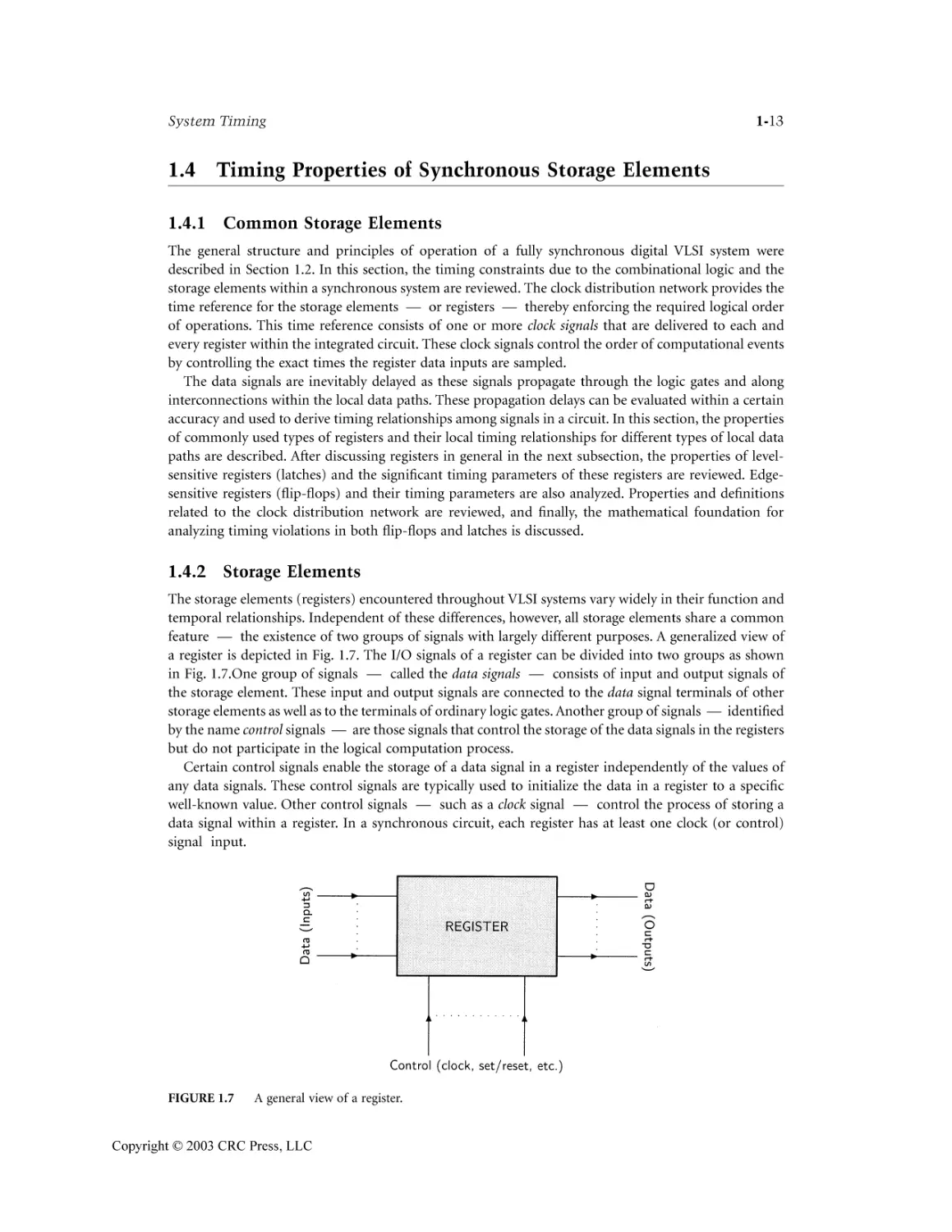
feature — the existence of two groups of signals with largely different purposes. A generalized view of
a register is depicted in Fig. 1.7. The I/O signals of a register can be divided into two groups as shown
in Fig. 1.7.One group of signals — called the data signals — consists of input and output signals of
the storage element. These input and output signals are connected to the data signal terminals of other
storage elements as well as to the terminals of ordinary logic gates. Another group of signals — identified
by the name control signals — are those signals that control the storage of the data signals in the registers
but do not participate in the logical computation process.
Certain control signals enable the storage of a data signal in a register independently of the values of
any data signals. These control signals are typically used to initialize the data in a register to a specific
well-known value. Other control signals — such as a clock signal — control the process of storing a
data signal within a register. In a synchronous circuit, each register has at least one clock (or control)
signal input.
FIGURE 1.7
A general view of a register.
Copyright © 2003 CRC Press, LLC
1737_CH01 Page 14 Wednesday, January 22, 2003 9:17 AM
1-14
Memory, Microprocessor, and ASIC
The two major groups of storage elements (registers) are considered in the following sections based
on the type of relationship that exists among the data and clock signals of these elements. In latches, it
is the specific value or level of a control signal* that determines the data storage process. Therefore,
latches are also called level-sensitive registers. In contrast to latches, a data signal is stored in flip-flops as
controlled by an edge of a control signal. For that reason, flip-flops are also called edge-triggered registers.
The timing properties of latches and flip-flops are described in detail in the following two sections.
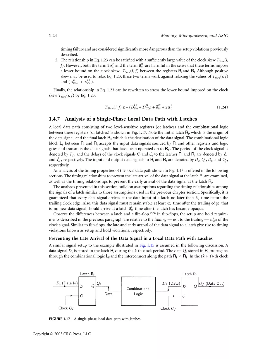
1.4.3 Latches
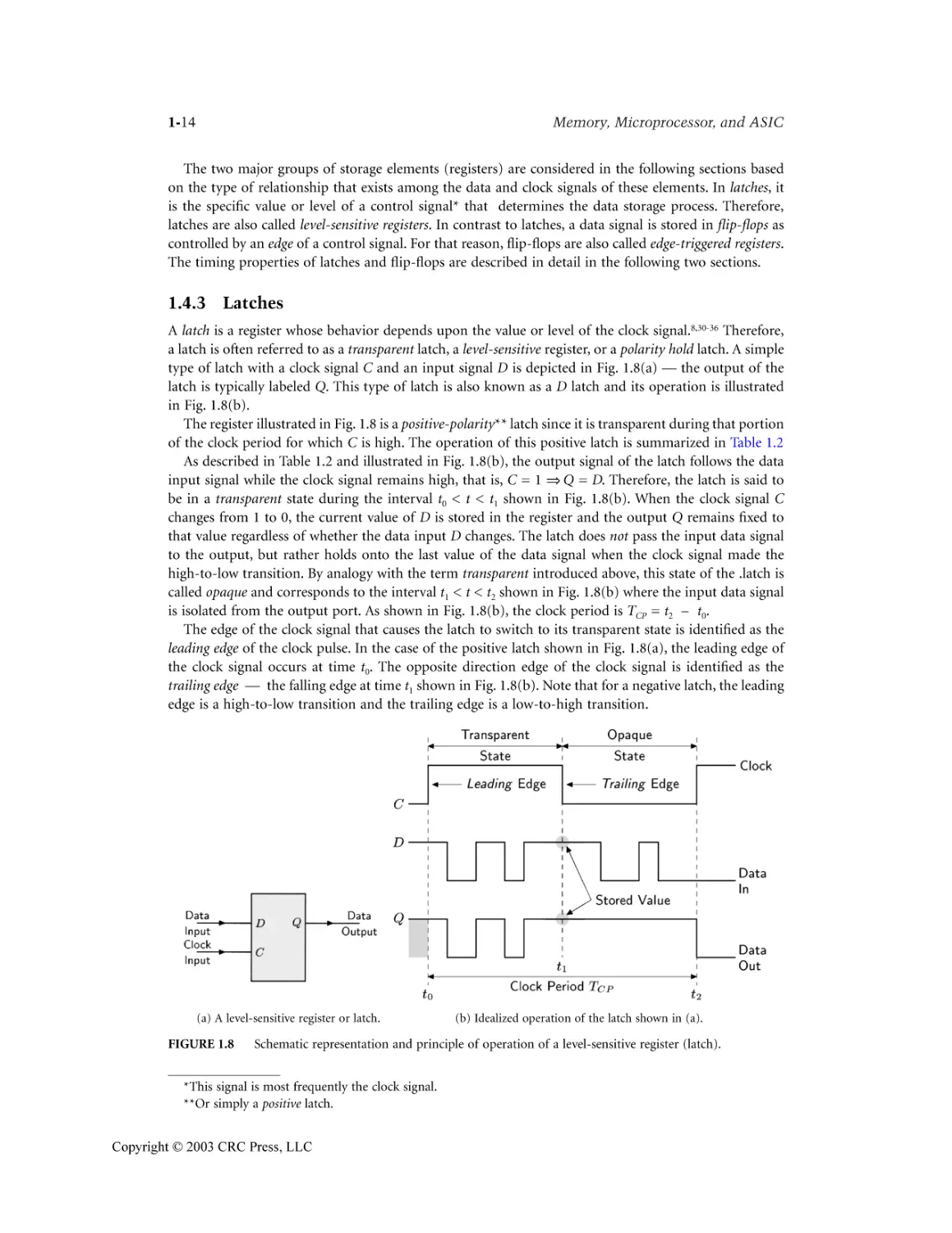
A latch is a register whose behavior depends upon the value or level of the clock signal.8,30-36 Therefore,
a latch is often referred to as a transparent latch, a level-sensitive register, or a polarity hold latch. A simple
type of latch with a clock signal C and an input signal D is depicted in Fig. 1.8(a) — the output of the
latch is typically labeled Q. This type of latch is also known as a D latch and its operation is illustrated
in Fig. 1.8(b).
The register illustrated in Fig. 1.8 is a positive-polarity** latch since it is transparent during that portion
of the clock period for which C is high. The operation of this positive latch is summarized in Table 1.2
As described in Table 1.2 and illustrated in Fig. 1.8(b), the output signal of the latch follows the data
input signal while the clock signal remains high, that is, C = 1 fi Q = D. Therefore, the latch is said to
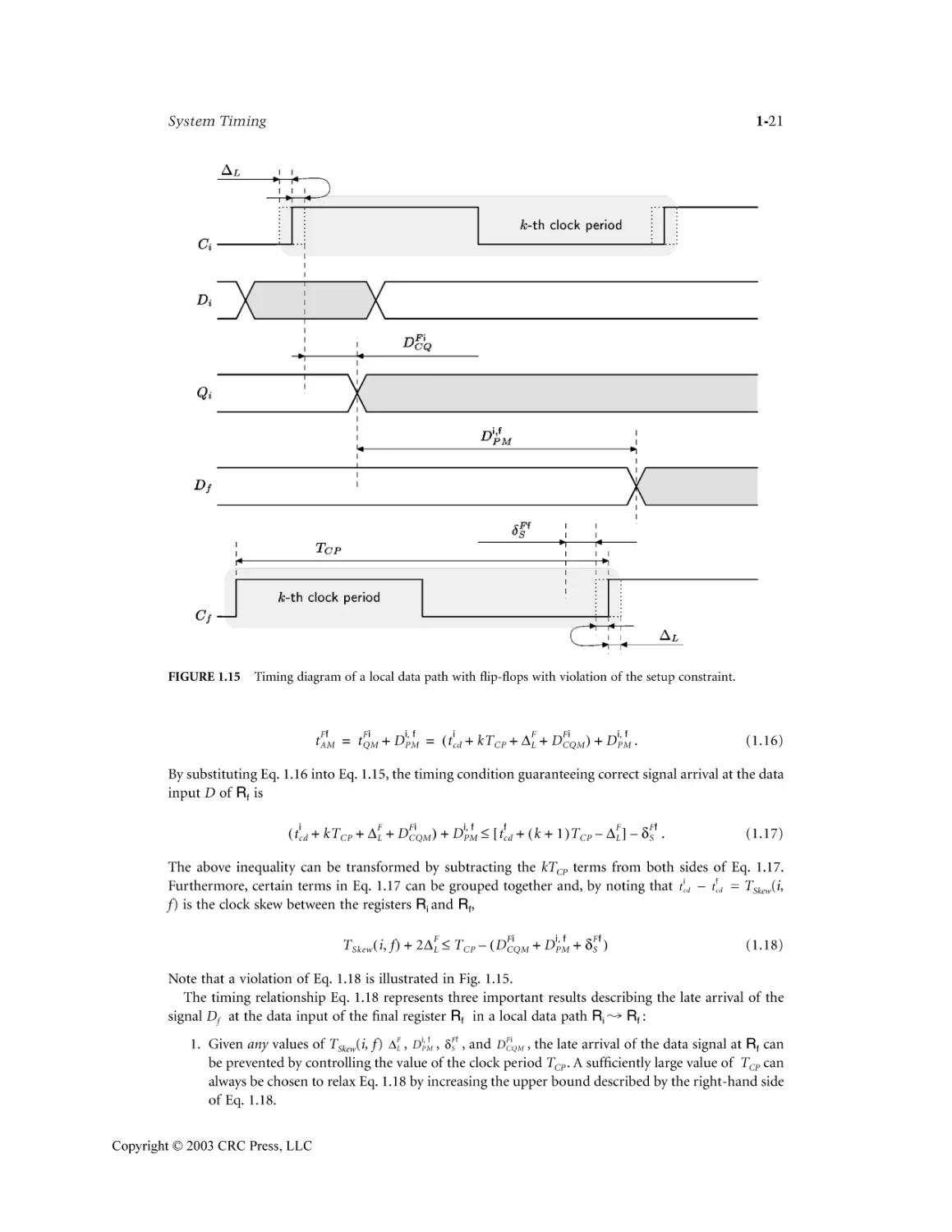
be in a transparent state during the interval t0 < t < t1 shown in Fig. 1.8(b). When the clock signal C
changes from 1 to 0, the current value of D is stored in the register and the output Q remains fixed to
that value regardless of whether the data input D changes. The latch does not pass the input data signal
to the output, but rather holds onto the last value of the data signal when the clock signal made the
high-to-low transition. By analogy with the term transparent introduced above, this state of the .latch is
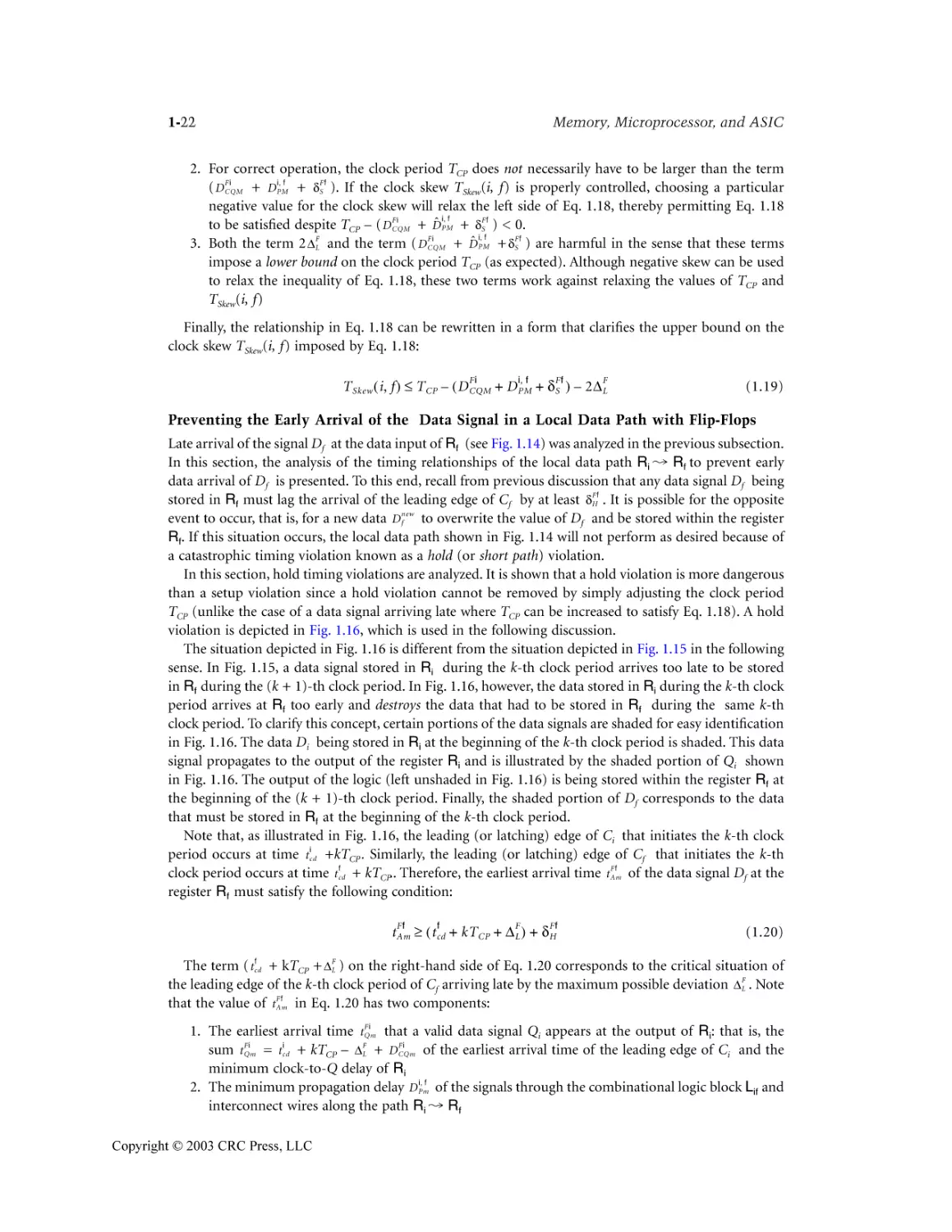
called opaque and corresponds to the interval t1 < t < t2 shown in Fig. 1.8(b) where the input data signal
is isolated from the output port. As shown in Fig. 1.8(b), the clock period is TCP = t2 – t0.
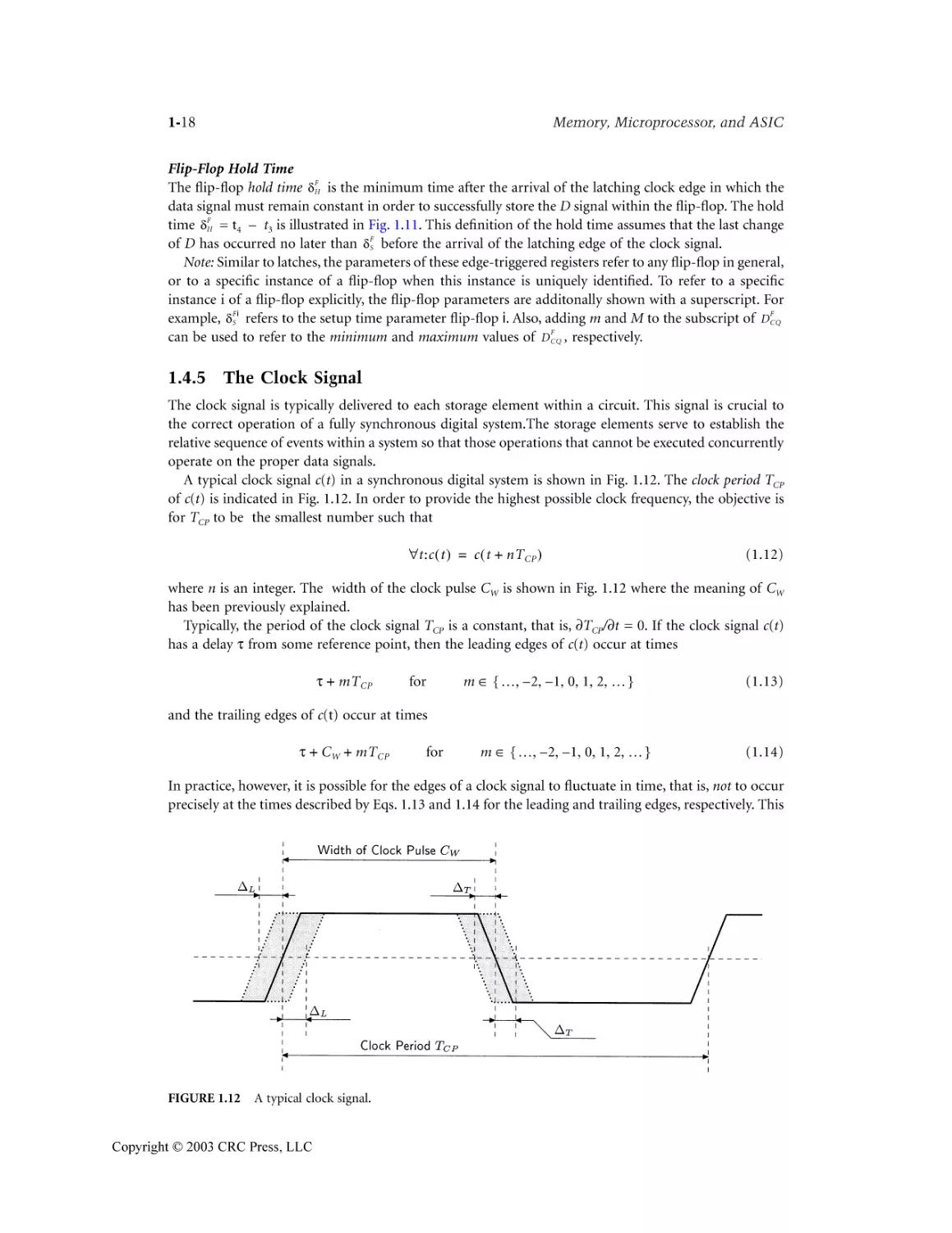
The edge of the clock signal that causes the latch to switch to its transparent state is identified as the
leading edge of the clock pulse. In the case of the positive latch shown in Fig. 1.8(a), the leading edge of
the clock signal occurs at time t0. The opposite direction edge of the clock signal is identified as the
trailing edge — the falling edge at time t1 shown in Fig. 1.8(b). Note that for a negative latch, the leading
edge is a high-to-low transition and the trailing edge is a low-to-high transition.
(a) A level-sensitive register or latch.
FIGURE 1.8
(b) Idealized operation of the latch shown in (a).
Schematic representation and principle of operation of a level-sensitive register (latch).
*This signal is most frequently the clock signal.
**Or simply a positive latch.
Copyright © 2003 CRC Press, LLC
1737_CH01 Page 15 Wednesday, January 22, 2003 9:17 AM
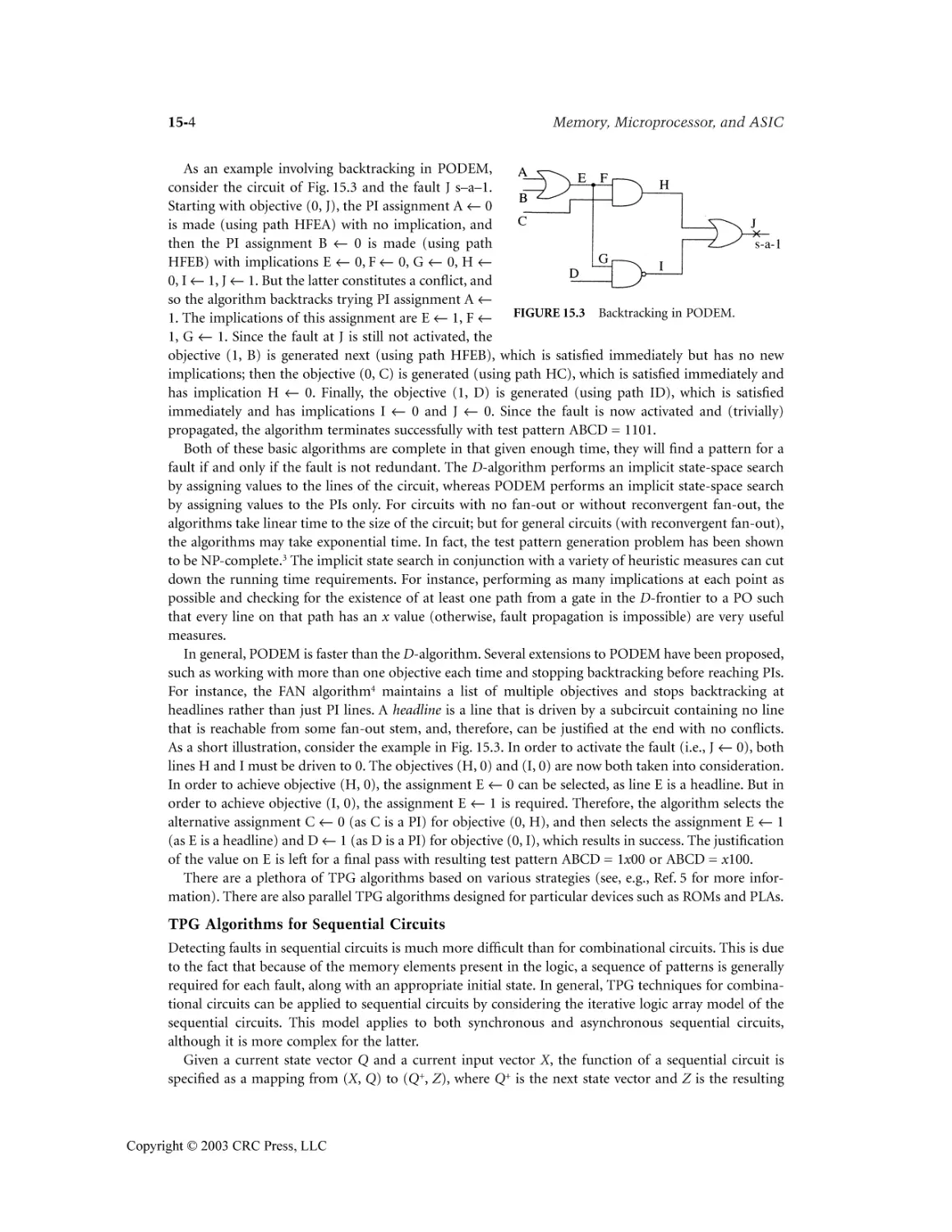
1-15
System Timing
TABLE 1.2
Operation of the Positive-Polarity D Latch
Clock
Output
State
High
Low
Passes input
Maintains output
Transparent
Opaque
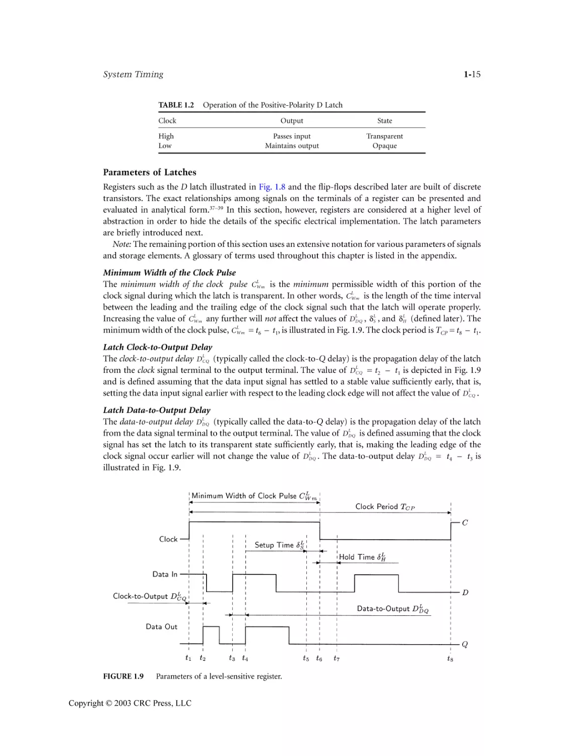
Parameters of Latches
Registers such as the D latch illustrated in Fig. 1.8 and the flip-flops described later are built of discrete
transistors. The exact relationships among signals on the terminals of a register can be presented and
evaluated in analytical form.37–39 In this section, however, registers are considered at a higher level of
abstraction in order to hide the details of the specific electrical implementation. The latch parameters
are briefly introduced next.
Note: The remaining portion of this section uses an extensive notation for various parameters of signals
and storage elements. A glossary of terms used throughout this chapter is listed in the appendix.
Minimum Width of the Clock Pulse
The minimum width of the clock pulse C LWm is the minimum permissible width of this portion of the
clock signal during which the latch is transparent. In other words, C LWm is the length of the time interval
between the leading and the trailing edge of the clock signal such that the latch will operate properly.
Increasing the value of C LWm any further will not affect the values of D LDQ , d LS , and d LH (defined later). The
minimum width of the clock pulse, C LWm = t6 – t1, is illustrated in Fig. 1.9. The clock period is TCP = t8 – t1.
Latch Clock-to-Output Delay
The clock-to-output delay D LCQ (typically called the clock-to-Q delay) is the propagation delay of the latch
from the clock signal terminal to the output terminal. The value of D LCQ = t2 – t1 is depicted in Fig. 1.9
and is defined assuming that the data input signal has settled to a stable value sufficiently early, that is,
setting the data input signal earlier with respect to the leading clock edge will not affect the value of D LCQ .
Latch Data-to-Output Delay
The data-to-output delay D LDQ (typically called the data-to-Q delay) is the propagation delay of the latch
from the data signal terminal to the output terminal. The value of D LDQ is defined assuming that the clock
signal has set the latch to its transparent state sufficiently early, that is, making the leading edge of the
clock signal occur earlier will not change the value of D LDQ . The data-to-output delay D LDQ = t4 – t3 is
illustrated in Fig. 1.9.
FIGURE 1.9
Parameters of a level-sensitive register.
Copyright © 2003 CRC Press, LLC
1737_CH01 Page 16 Wednesday, January 22, 2003 9:17 AM
1-16
Memory, Microprocessor, and ASIC
Latch Setup Time
The latch setup time d LS = t6 – t5, shown in Fig. 1.9, is the minimum time between a change in the data
signal and the trailing edge of the clock signal such that the new value of D would propagate to the
output Q of the latch and be stored within the latch during its opaque state.
Latch Hold Time
The latch hold time d LH is the minimum time after the trailing clock edge that the data signal must remain
constant so that this value of D is successfully stored in the latch during the opaque state. This definition
of d LH assumes that the last change of the value of D has occurred no later than d LS before the trailing
edge of the clock signal. The term d LH = t7 – t6 is shown in Fig. 1.9.
Note: The latch parameters previously introduced are used to refer to any latch in general, or to a
specific instance of a latch when this instance can be unambiguously identified. To refer to a specific
instance i of a latch explicitly, the parameters are additionally shown with a superscript. For example,
Li
L
L
D CQ refers to the clock-to-output delay of latch i. Also, adding m and M to the subscript of D CQ and D DQ
L
L
can be used to refer to the minimum and maximum values of D CQ and D DQ , respectively.
1.4.4 Flip-Flops
An edge-triggered register or flip-flop is a type of register which, unlike the latches described previously,
is never transparent with respect to the input data signal.8,30-36 The output of a flip-flop normally does
not follow the input data signal at any time during the register operation, but rather holds onto a
previously stored data value until a new data signal is stored in the flip-flop. A simple type of flip-flop
with a clock signal C and an input signal D is shown in Fig. 1.10(a); similar to latches, the output of a
flip-flop is usually labeled Q. This specific type of register, shown in Fig. 1.10(a), is called a D flip-flop
and its operation is illustrated in Fig. 1.10(b)
In typical flip-flops, data is stored either on the rising edge (low-to-high transition) or on the falling
edge (high-to-low transition) of the clock signal. The flip-flops are known as positive-edge-triggered and
negative-edge-triggered flip-flops, respectively. The terms latching, storing, or positive edge are used to
identify the edge of the clock signal on which storage in the flip-flop occurs. For the sake of clarity, the
latching edge of the clock signal for flip-flops will also be called the leading edge (compare with the
previous discusion of latches). Also, note that certain flip-flops — known as double-edged-triggered
(DET) flip-flops40-44 — can store data at either edge of the clock signal. The complexity of these flipflops, however, is significantly higher and these registers are therefore rarely used.
(a) An edge-triggered register or flip-flop.
FIGURE 1.10
(b) Idealized operation of the flip-flop shown in (a).
Schematic representation and principle of operation of an edge-triggered register (flip-flop).
Copyright © 2003 CRC Press, LLC
1737_CH01 Page 17 Wednesday, January 22, 2003 9:17 AM
System Timing
1-17
As shown in the timing diagram in Fig. 1.10(b), the output of the flip-flop remains unchanged most
of the time, regardless of the transitions in the data signal. Only values of the data signal in the vicinity
of the storing edge of the clock signal can affect the output of the flip-flop. Therefore, changes in the
output will only be observed when the currently stored data has a logic value x, and the storing edge of
the clock signal occurs while the input data signal has a logic value of x.
Parameters of Flip-Flops
The significant timing parameters of an edge-triggered register are similar to those of latches and are
presented next. These parameters are illustrated in Fig. 1.11.
Minimum Width of the Clock Pulse
The minimum width of the clock pulse C FWm is the minimum permissible width of the time interval between
the latching edge and the non-latching edge of the clock signal. The minimum width of the clock pulse
F
C Wm = t6 – t3 is shown in Fig. 1.11 and is defined as the minimum interval between the latching and
non-latching edges of the clock pulse such that the flip-flop will operate correctly. Further increasing
F
F
F
C Wm will not affect the values of the setup time d S and hold time d H (defined later). The clock period
TCP = t6 – t1 is also shown in Fig. 1.11.
Flip-Flop Clock-to-Output Delay
As shown in Fig. 1.11, the clock-to-output delay D FCQ of the flip-flop is D FCQ = t5 – t3. This propagation
delay parameter — typically called the clock-to-Q delay — is the propagation delay from the clock
signal terminal to the output terminal. The value of D FCQ is defined assuming that the data input signal
has settled to a stable value sufficiently early, that is, setting the data input any earlier with respect to the
latching clock edge will not affect the value of D FCQ .
Flip-Flop Setup Time
The flip-flop setup time d FS is shown in Fig. 1.11 — d FS = t3 – t2. The parameter d FS is defined as the
minimum time between a change in the data signal and the latching edge of the clock signal such that
the new value of D propagates to the output Q of the flip-flop and is successfully latched within the
flip-flop.
FIGURE 1.11
Parameters of an edge-triggered register.
Copyright © 2003 CRC Press, LLC
1737_CH01 Page 18 Wednesday, January 22, 2003 9:17 AM
1-18
Memory, Microprocessor, and ASIC
Flip-Flop Hold Time
The flip-flop hold time d FH is the minimum time after the arrival of the latching clock edge in which the
data signal must remain constant in order to successfully store the D signal within the flip-flop. The hold
time d FH = t4 – t3 is illustrated in Fig. 1.11. This definition of the hold time assumes that the last change
of D has occurred no later than d FS before the arrival of the latching edge of the clock signal.
Note: Similar to latches, the parameters of these edge-triggered registers refer to any flip-flop in general,
or to a specific instance of a flip-flop when this instance is uniquely identified. To refer to a specific
instance i of a flip-flop explicitly, the flip-flop parameters are additonally shown with a superscript. For
example, d FS i refers to the setup time parameter flip-flop i. Also, adding m and M to the subscript of D FCQ
can be used to refer to the minimum and maximum values of D FCQ , respectively.
1.4.5 The Clock Signal
The clock signal is typically delivered to each storage element within a circuit. This signal is crucial to
the correct operation of a fully synchronous digital system.The storage elements serve to establish the
relative sequence of events within a system so that those operations that cannot be executed concurrently
operate on the proper data signals.
A typical clock signal c(t) in a synchronous digital system is shown in Fig. 1.12. The clock period TCP
of c(t) is indicated in Fig. 1.12. In order to provide the highest possible clock frequency, the objective is
for TCP to be the smallest number such that
"t:c ( t ) = c ( t + nT CP )
(1.12)
where n is an integer. The width of the clock pulse CW is shown in Fig. 1.12 where the meaning of CW
has been previously explained.
Typically, the period of the clock signal TCP is a constant, that is, ∂TCP/∂t = 0. If the clock signal c(t)
has a delay t from some reference point, then the leading edges of c(t) occur at times
t + mT CP
for
m Œ { º, – 2, – 1, 0, 1, 2, º }
(1.13)
and the trailing edges of c(t) occur at times
t + C W + mT CP
for
m Œ { º, – 2, – 1, 0, 1, 2, º }
(1.14)
In practice, however, it is possible for the edges of a clock signal to fluctuate in time, that is, not to occur
precisely at the times described by Eqs. 1.13 and 1.14 for the leading and trailing edges, respectively. This
FIGURE 1.12
A typical clock signal.
Copyright © 2003 CRC Press, LLC
1737_CH01 Page 19 Wednesday, January 22, 2003 9:17 AM
1-19
System Timing
phenomenon is known as clock jitter and may be due to various causes, such as variations in the
manufacturing process, ambient temperature, power supply noise, and oscillator characteristics.
To account for this clock jitter, the following parameters are introduced:
• The maximum deviation L of the leading edge of the clock signal: that is, the leading edge is
guaranteed to occur anywhere in an interval (t + kTCP –L, t + kTCP + L)
• The maximum deviation T of the trailing edge of the clock signal: that is, the trailing edge is
guaranteed to occur anywhere in the interval (t + CW + kTCP –T, t + CW + kTCP +T)
Clock Skew
Consider a local data path such as the path shown in Fig. 1.2(b). Without loss of generality, assume that
the registers shown in Fig. 1.2(b) are flip-flops. The clock signal with period TCP is delivered to each of
the registers Ri and Rf. Let the clock signal driving the register Ri be denoted as Ci. and the clock signal
driving the registerRf be denoted by Cf . Also, let t icd and t fcd be the delays of Ci and Cf to the registers Ri
and Rf. respectively.* As described by Eq. 1.13, the latching or leading edges of Ci. occur at times
i
i
i
º, t + t cd – T CP, t + t cd, t + t cd + T CP, º
Similarly, the latching or leading edges of Cf occur at times
f
f
f
º, t + t cd – T CP, t + t cd, t + t cd + T CP, º
as described by Eq. 1.14.
The clock skew TSkew(i, f) = t icd – t fcd between Ci and Cf is introduced next as the difference of the arrival
times of Ci and Cf .13 This concept is illustrated by Fig. 1.13. Note that, depending on the values of t icd
and t fcd , the skew can be zero ( t icd = t fcd ), negative ( t icd < t fcd ), or positive ( t icd > t fcd ). Furthermore, note
that the clock skew as defined above is only defined for sequentially adjacent registers, that is, a local
data path (such as the path shown in Fig. 1.2(b)).
1.4.6 Analysis of a Single-Phase Local Data Path with Flip-Flops
A local data path composed of two flip-flops and combinational logic between the flip-flops is shown in
Fig. 1.14. Note the initial flip-flop Ri, which is the origin of the data signal, and the final flip-flop Rf,
which is the destination of the data signal. The combinational logic block Lif between Ri and Rf accepts
the input data signals supplied by Ri and other registers and logic gates and transmits the operated upon
data signals to Rf . The period of the clock signal is denoted by TCP and the delays of the clock signal Ci
FIGURE 1.13
Lead/lag relationships causing clock skew to be zero, negative, or positive.
i
f
*Note that these delays t cd and t cd are measured with respect to the same reference point.
Copyright © 2003 CRC Press, LLC
1737_CH01 Page 20 Wednesday, January 22, 2003 9:17 AM
1-20
FIGURE 1.14
Memory, Microprocessor, and ASIC
A single-phase local data path.
and Cf to the flip-flops Ri and Rf are denoted by t icd and t fcd , respectively. The input and output data
signals to Ri and Rf are denoted by Di , Qi ,Df , and Qf , respectively.
An analysis of the timing properties of the local data path shown in Fig. 1.14 is offered in the following
sections. First, the timing relationships to prevent the late arrival of data signals to Rf are examined in
the next subsection. The timing relationships to prevent the early arrival of signals to the register Rf are
then described, followed by analyses that borrow some notation from Refs. 11 and 12. Similar analyses
of synchronous circuits from the timing perspective can be found in Refs. 45 through 49.
Preventing the Late Arrival of the Data Signal in a Local Data Path with Flip-Flops
The operation of the local data path Ri Rf shown in Fig. 1.14 requires that any data signal that is being
stored in Rf arrives at the data input Df of Rf no later than d FfS before the latching edge of the clock signal
Cf. It is possible for the opposite event to occur, that is, for the data signal Df not to arrive at the register
Rf sufficiently early in order to be stored successfully within Rf . If this situation occurs, the local data
path shown in Fig. 1.14 fails to perform as expected and it is said that a timing failure or violation has
been created. This form of timing violation is typically called a setup (or long path) violation. A setup
violation is depicted in Fig. 1.15 and is used in the following discussion.
The identical clock periods of the clock signals Ci and Cf are shaded for identification in Fig. 1.15.
Also shaded in Fig. 1.15 are those portions of the data signals Di , Qi , and Df that are relevant to the
operation of the local data path shown in Fig. 1.14. Specifically, the shaded portion of Di corresponds
to the data to be stored in Ri at the beginning of the k-th clock period. This data signal propagates to
the output of the register Ri and is illustrated by the shaded portion of Qi shown in Fig. 1.15. The
combinational logic operates on Qi during the k-th clock period. The result of this operation is the
shaded portion of the signal Df which must be stored in Rf during the next (k + 1)-th clock period.
Observe that, as illustrated in Fig. 1.15, the leading edge of Ci that initiates the k-th clock period
occurs at time t icd + kTCP.. Similarly, the leading edge of Cf that initiates the (k + 1)-th clock period occurs
at time t fcd + (k + 1) TCP . Therefore, the latest arrival time t FfAM of Df at Rf must satisfy
Ff
f
F
Ff
t AM £ [ t cd + ( k + 1 )T CP – D L ] – d S
(1.15)
The term [ t fcd + (k + 1)TCP – D FL ] on the right-hand side of Eq. 1.15 corresponds to the critical situation
of the leading edge of Cf arriving earlier by the maximum possible deviation D FL . The – d FS f term on the
right-hand side of Eq. 1.15 accounts for the setup time of Rf (recall the definition of d Fs ). Note that the
f
value of t FAM
in Eq. 1.15 consists of two components:
i
1. The latest arrival time t FQM
that a valid data signal Qi appears at the output of Ri: that is, the sum
Fi
F
Fi
i
t QM = t cd + kTCP + D L + D CQM of the latest possible arrival time of the leading edge of Ci and the
maximum clock-to-Q delay of Ri.
,f
2. The maximum propagation delay D iPM
of the data signals through the combinational logic block
Lif and interconnect along the path Ri Rf.
f
Therefore, t FAM
can be described as
Copyright © 2003 CRC Press, LLC
1737_CH01 Page 21 Wednesday, January 22, 2003 9:17 AM
1-21
System Timing
FIGURE 1.15
Timing diagram of a local data path with flip-flops with violation of the setup constraint.
Ff
Fi
i, f
i
F
Fi
i, f
t AM = t QM + D PM = ( t cd + kT CP + D L + D CQM ) + D PM .
(1.16)
By substituting Eq. 1.16 into Eq. 1.15, the timing condition guaranteeing correct signal arrival at the data
input D of Rf is
i
F
Fi
i, f
f
F
Ff
( t cd + kT CP + D L + D CQM ) + D PM £ [ t cd + ( k + 1 )T CP – D L ] – d S .
(1.17)
The above inequality can be transformed by subtracting the kTCP terms from both sides of Eq. 1.17.
Furthermore, certain terms in Eq. 1.17 can be grouped together and, by noting that t icd – t fcd = TSkew(i,
f) is the clock skew between the registers Ri and Rf,
F
Fi
i, f
Ff
T Skew ( i, f ) + 2D L £ T CP – ( D CQM + D PM + d S )
(1.18)
Note that a violation of Eq. 1.18 is illustrated in Fig. 1.15.
The timing relationship Eq. 1.18 represents three important results describing the late arrival of the
signal Df at the data input of the final register Rf in a local data path Ri Rf :
,f
i
1. Given any values of TSkew(i, f) D FL , D iPM
, d FS f , and D FCQM
, the late arrival of the data signal at Rf can
be prevented by controlling the value of the clock period TCP . A sufficiently large value of TCP can
always be chosen to relax Eq. 1.18 by increasing the upper bound described by the right-hand side
of Eq. 1.18.
Copyright © 2003 CRC Press, LLC
1737_CH01 Page 22 Wednesday, January 22, 2003 9:17 AM
1-22
Memory, Microprocessor, and ASIC
2. For correct operation, the clock period TCP does not necessarily have to be larger than the term
i
,f
( D FCQM
+ D iPM
+ d FS f ). If the clock skew TSkew(i, f) is properly controlled, choosing a particular
negative value for the clock skew will relax the left side of Eq. 1.18, thereby permitting Eq. 1.18
i, f
i
+ D̂ PM + d FS f ) < 0.
to be satisfied despite TCP – ( D FCQM
i, f
F
Fi
3. Both the term 2 D L and the term ( D CQM + D̂ PM + d FS f ) are harmful in the sense that these terms
impose a lower bound on the clock period TCP (as expected). Although negative skew can be used
to relax the inequality of Eq. 1.18, these two terms work against relaxing the values of TCP and
TSkew(i, f)
Finally, the relationship in Eq. 1.18 can be rewritten in a form that clarifies the upper bound on the
clock skew TSkew(i, f) imposed by Eq. 1.18:
Fi
i, f
Ff
F
T Skew ( i, f ) £ T CP – ( D CQM + D PM + d S ) – 2D L
(1.19)
Preventing the Early Arrival of the Data Signal in a Local Data Path with Flip-Flops
Late arrival of the signal Df at the data input of Rf (see Fig. 1.14) was analyzed in the previous subsection.
In this section, the analysis of the timing relationships of the local data path Ri Rf to prevent early
data arrival of Df is presented. To this end, recall from previous discussion that any data signal Df being
stored in Rf must lag the arrival of the leading edge of Cf by at least d FHf . It is possible for the opposite
event to occur, that is, for a new data D new
to overwrite the value of Df and be stored within the register
f
Rf. If this situation occurs, the local data path shown in Fig. 1.14 will not perform as desired because of
a catastrophic timing violation known as a hold (or short path) violation.
In this section, hold timing violations are analyzed. It is shown that a hold violation is more dangerous
than a setup violation since a hold violation cannot be removed by simply adjusting the clock period
TCP (unlike the case of a data signal arriving late where TCP can be increased to satisfy Eq. 1.18). A hold
violation is depicted in Fig. 1.16, which is used in the following discussion.
The situation depicted in Fig. 1.16 is different from the situation depicted in Fig. 1.15 in the following
sense. In Fig. 1.15, a data signal stored in Ri during the k-th clock period arrives too late to be stored
in Rf during the (k + 1)-th clock period. In Fig. 1.16, however, the data stored in Ri during the k-th clock
period arrives at Rf too early and destroys the data that had to be stored in Rf during the same k-th
clock period. To clarify this concept, certain portions of the data signals are shaded for easy identification
in Fig. 1.16. The data Di being stored in Ri at the beginning of the k-th clock period is shaded. This data
signal propagates to the output of the register Ri and is illustrated by the shaded portion of Qi shown
in Fig. 1.16. The output of the logic (left unshaded in Fig. 1.16) is being stored within the register Rf at
the beginning of the (k + 1)-th clock period. Finally, the shaded portion of Df corresponds to the data
that must be stored in Rf at the beginning of the k-th clock period.
Note that, as illustrated in Fig. 1.16, the leading (or latching) edge of Ci that initiates the k-th clock
period occurs at time t icd +kTCP . Similarly, the leading (or latching) edge of Cf that initiates the k-th
clock period occurs at time t fcd + kTCP.. Therefore, the earliest arrival time t FAmf of the data signal Df at the
register Rf must satisfy the following condition:
Ff
f
F
Ff
t Am ≥ ( t cd + kT CP + D L ) + d H
(1.20)
The term ( t fcd + kTCP + D FL ) on the right-hand side of Eq. 1.20 corresponds to the critical situation of
the leading edge of the k-th clock period of Cf arriving late by the maximum possible deviation D FL . Note
that the value of t FAmf in Eq. 1.20 has two components:
1. The earliest arrival time t FQmi that a valid data signal Qi appears at the output of Ri: that is, the
i
of the earliest arrival time of the leading edge of Ci and the
sum t FQmi = t icd + kTCP – D FL + D FCQm
minimum clock-to-Q delay of Ri
,f
2. The minimum propagation delay D iPm
of the signals through the combinational logic block Lif and
interconnect wires along the path Ri Rf
Copyright © 2003 CRC Press, LLC
1737_CH01 Page 23 Wednesday, January 22, 2003 9:17 AM
1-23
System Timing
FIGURE 1.16
Timing diagram of a local data path with flip-flops with a violation of the hold constraint.
Therefore, t FAmf can be described as
Ff
Ff
i, f
i
Fi
F
i, f
t Am = t Qm + D Pm = ( t cd + kT CP – D L + D CQM ) + D Pm
(1.21)
By substituting Eq. 1.21 into Eq. 1.20, the timing condition that guarantees that Df does not arrive too
early at Rf is
i
F
Fi
i, f
f
F
Ff
( t cd + kT CP – D L + D CQm ) + D Pm ≥ ( t cd + kT CP + D L ) + d H
(1.22)
The inequality Eq. 1.22 can be further simplified by regrouping terms and noting that t icd – t fcd =
TSkew(i, f) is the clock skew between the registers Ri and Rf:
F
Fi
i, f
Ff
T Skew ( i, f ) – 2D L ≥ – ( D CQm + D Pm ) + d H
(1.23)
Recall that a violation of Eq. 1.23 is illustrated in Fig. 1.16.
The timing relationship described by Eq. 1.23 provides certain important facts describing the early
arrival of the signal Df at the data input of the final register Rf of a local data path:
1. Unlike Eq. 1.18, the inequality Eq. 1.23 does not depend on the clock period TCP . Therefore, a
violation of Eq. 1.23 cannot be corrected by simply manipulating the value of TCP . A synchronous
digital system with hold violations is non-functional, while a system with setup violations will
still operate correctly at a reduced speed.* For this reason, hold violations result in catastrophic
*Increasing the clock period TCP in order to satisfy Eq. 1.18 is equivalent to reducing the frequency of the clock
signal.
Copyright © 2003 CRC Press, LLC
1737_CH01 Page 24 Wednesday, January 22, 2003 9:17 AM
1-24
Memory, Microprocessor, and ASIC
timing failure and are considered significantly more dangerous than the setup violations previously
described.
2. The relationship in Eq. 1.23 can be satisfied with a sufficiently large value of the clock skew TSkew(i,
f). However, both the term 2 D FL and the term d FHf are harmful in the sense that these terms impose
a lower bound on the clock skew TSkew(i, f) between the registers Ri and Rf. Although positive
skew may be used to relax Eq. 1.23, these two terms work against relaxing the values of TSkew(i, f)
i
,f
and ( D FCQm
+ D iPm
).
Finally, the relationship in Eq. 1.23 can be rewritten to stress the lower bound imposed on the clock
skew TSkew(i, f) by Eq. 1.23:
i, f
Fi
Ff
F
T Skew ( i, f ) ≥ – ( D Pm + D CQ ) + d H + 2D L
(1.24)
1.4.7 Analysis of a Single-Phase Local Data Path with Latches
A local data path consisting of two level-sensitive registers (or latches) and the combinational logic
between these registers (or latches) is shown in Fig. 1.17. Note the initial latch Ri, which is the origin of
the data signal, and the final latch Rf, which is the destination of the data signal. The combinational logic
block Lif between Ri and Rf accepts the input data signals sourced by Ri and other registers and logic
gates and transmits the data signals that have been operated on to Rf . The period of the clock signal is
denoted by TCP and the delays of the clock signals Ci and Cf to the latches Ri and Rf are denoted by t icd
and t fcd , respectively. The input and output data signals to Ri and Rf are denoted by Di , Qi , Df , and Qf ,
respectively.
An analysis of the timing properties of the local data path shown in Fig. 1.17 is offered in the following
sections. The timing relationships to prevent the late arrival of the data signal at the latch Rf are examined,
as well as the timing relationships to prevent the early arrival of the data signal at the latch Rf.
The analyses presented in this section build on assumptions regarding the timing relationships among
the signals of a latch similar to those assumptions used in the previous chapter section. Specifically, it is
guaranteed that every data signal arrives at the data input of a latch no later than d LS time before the
trailing clock edge. Also, this data signal must remain stable at least d LH time after the trailing edge, that
is, no new data signal should arrive at a latch d LH time after the latch has become opaque.
Observe the differences between a latch and a flip-flop.45,50 In flip-flops, the setup and hold requirements described in the previous paragraph are relative to the leading — not to the trailing — edge of the
clock signal. Similar to flip-flops, the late and early arrival of the data signal to a latch give rise to timing
violations known as setup and hold violations, respectively.
Preventing the Late Arrival of the Data Signal in a Local Data Path with Latches
A similar signal setup to the example illustrated in Fig. 1.15 is assumed in the following discussion. A
data signal Di, is stored in the latch Ri during the k-th clock period. The data Qi, stored in Ri propagates
through the combinational logic Lif and the interconnect along the path Ri Rf . In the (k + 1)-th clock
FIGURE 1.17
A single-phase local data path with latches.
Copyright © 2003 CRC Press, LLC
1737_CH01 Page 25 Wednesday, January 22, 2003 9:17 AM
1-25
System Timing
period, the result Df of the computation in Lif is stored within the latch Rf . The signal Df must arrive at
least d LS time before the trailing edge of Cf in the (k + 1)-th clock period.
f
Similar to the discussion presented in the previous section, the latest arrival time t LAM
of Df at the D
input of Rf must satisfy
Lf
f
L
Lf
L
t AM £ [ t cd + ( k + 1 )T CP + C Wm – D T ] – d S
(1.25)
Note the difference between Eqs. 1.25 and 1.15. In Eq. 1.15, the first term on the right-hand side is [ t fcd
+ (k + 1) TCP – D FL ], while in Eq. 1.25, the first term on the right-hand side has an additional term C LWm .
The addition of C LWm corresponds to the concept that, unlike flip-flops, a data signal is stored in a latch,
shown in Fig. 1.17, at the trailing edge of the clock signal (the C LWm term). Similar to the case of flipflops, the term [ t fcd + (k + 1) TCP + C LWm – D LT ] on the right-hand side of Eq. 1.25 corresponds to the
critical situation of the trailing edge of the clock signal Cf arriving earlier by the maximum possible
deviation D LT .
f
Observe that the value of t LAM
in Eq. 1.25 consists of two components:
i
1. The latest arrival time t LQM
when a valid data signal Qi appears at the output of the latch Ri,
2. The maximum signal propagation delay through the combinational logic block Lif and the interconnect along the path Ri Rf
Therefore, t LAMf can be described as
Lf
i, f
Li
(1.26)
t AM = D PM + t QM
However, unlike the situation of flip-flops discussed previously, the term t LQmi on the right-hand side of
i
depends
Eq. 1.26 is not the sum of the delays through the register Ri. The reason is that the value of t LQM
on whether the signal Di arrived before or during the transparent state of Ri in the k-th clock period.
Therefore, the value of t LQmi in Eq. 1.26 is the greater of the following two quantities:
Li
Li
Li
i
Li
L
t QM = max [ ( t AM + D DQM ), ( t cd + kT CP + D L + D CQM ) ]
(1.27)
There are two terms on the right-hand side of Eq. 1.27:
i
i
1. The term ( t LAM
+ D LDQM
) corresponds to the situation in which Di arrives at Ri after the leading
edge of the k-th clock period.
i
) corresponds to the situation in which Di arrives at Ri before
2. The term ( t icd + kTCP + D LL + D LCQM
the leading edge of the k-th clock pulse arrives.
f
By substituting Eq. 1.27 into Eq. 1.26, the latest time of arrival t LAM
is:
Lf
i, f
Li
Li
i
Li
(1.28)
D PM + max [ ( t AM + D DQM ), ( t cd + kT CP + D L + D CQM ) ]
L
L
Lf
f
£ [ t cd + ( k + 1 )T CP + C Wm – D T ] – d S
(1.29)
L
t AM = D PM + max [ ( t AM + D DQM ), ( t cd + kT CP + D L + D CQM ) ]
which is in turn substituted into Eq. 1.25 to obtain
i, f
Li
Li
i
L
Li
Equation Eq. 1.29 is an expression for the inequality that must be satisfied in order to prevent the late
arrival of a data signal at the data input D of the register Rf. By satisfying Eq. 1.29, setup violations in
the local data path with latches shown in Fig. 1.17 are avoided. For a circuit to operate correctly, Eq. 1.29
must be enforced for any local data path Ri Rf consisting of the latches Ri and Rf.
Copyright © 2003 CRC Press, LLC
1737_CH01 Page 26 Wednesday, January 22, 2003 9:17 AM
1-26
Memory, Microprocessor, and ASIC
The max operation in Eq. 1.29 creates a mathematically difficult situation since it is unknown which
of the quantities under the max operation is greater. To overcome this obstacle, this max operation can
be split into two conditions:
i, f
Li
Li
f
L
Lf
L
D PM + ( t AM + D DQM ) £ [ t cd + ( k + 1 )T CP + C Wm – D T ] – d S
i, f
i
Li
L
f
L
L
(1.30)
Lf
D PM + ( t cd + kT CP + D L + D CQM ) £ [ t cd + ( k + 1 )T CP + C Wm – D T ] – d S
(1.31)
Taking into account that the clock skew TSkew(i, f) = t icd – t fcd , Eqs. 1.30 and 1.31 can be rewritten as
i, f
Li
Li
f
L
Lf
(1.32)
i, f
Lf
(1.33)
L
D PM + ( t AM + D DQM ) £ [ t cd + ( k + 1 )T CP + C Wm – D T ] – d S
L
L
Li
L
T Skew ( i, f ) + ( D L + D T ) £ ( T CP + C Wm ) – ( D CQM + D PM + d S )
Equation 1.33 can be rewritten in a form that clarifies the upper bound on the clock skew TSkew(i, f)
imposed by Eq. 1.33:
i, f
Li
Li
f
Lf
(1.34)
T Skew ( i, f ) £ ( T CP + C Wm – D L – D T ) – ( D CQM + D PM + d S )
(1.35)
L
L
D PM + ( t AM + D DQM ) £ [ t cd + ( k + 1 )T CP + C Wm – D T ] – d S
L
L
Li
L
i, f
Lf
Preventing the Early Arrival of the Data Signal in a Local Data Path with Latches
A similar signal setup to the example illustrated in Fig. 1.16 is assumed in the discussion presented in
this section. Recall the difference between the late arrival of a data signal at Rf and the early arrival of a
data signal at Rf. In the former case, the data signal stored in the latch Ri during the k-th clock period
arrives too late to be stored in the latch Rf during the (k + 1)-th clock period. In the latter case, the data
signal stored in the latch Ri during the k-th clock period propagates to the latch Rf too early and overwrites
the data signal that was already stored in the latch Rf during the same k-th clock period.
In order for the proper data signal to be successfully latched within Rf during the k-th clock period,
there should not be any changes in the signal Df until at least the hold time after the arrival of the storing
(trailing) edge of the clock signal Cf . Therefore, the earliest arrival time t LAmf of the data signal Df at the
register Rf must satisfy the following condition:
Lf
f
L
L
Lf
t Am ≥ ( t cd + kT CP + C Wm + D T ) + d H
(1.36)
The term ( t fcd + kTCP + C LWm + D LT ) on the right-hand side of Eq. 1.36 corresponds to the critical
situation of the trailing edge of the k-th clock period of the clock signal Cf arriving late by the maxiumum
possible deviation D LT . Note that the value of t LAmf in Eq. 1.36 consists of two components:
1. The earliest arrival time t LQmi that a valid data signal Qi appears at the output of the latch Ri: that
i
of the earliest arrival time of the leading edge of the
is, the sum t LQmi = t icd + kTCP – D LL + D LCQm
i
of Rf
clock signal Ci and the minimum clock-to-Q delay D LCQm
i, f
2. The minimum propagation delay D Pm of the signal through the combinational logic Lif and the
interconnect along the path Ri Rf
Therefore, t LAmf can be described as
Lf
Li
i, f
i
L
Li
i, f
t Am = t Qm + D Pm = ( t cd + kT CP – D L + D CQm ) + D Pm
(1.37)
By substituting Eq. 1.37 into Eq. 1.36, the timing condition guaranteeing that Df does not arrive too
early at the latch Rf is
Copyright © 2003 CRC Press, LLC
1737_CH01 Page 27 Wednesday, January 22, 2003 9:17 AM
1-27
System Timing
i
L
Li
i, f
f
L
L
Lf
( t cd + kT CP – D L + D CQm ) + D Pm ≥ ( t cd + kT CP + C Wm + D T ) + d H
(1.38)
The inequality Eq. 1.38 can be further simplified by reorganizing the terms and noting that t icd – t fcd
= TSkew(i, f) is the clock skew between the registers Ri and Rf:
L
L
Li
i, f
Lf
T Skew ( i, f ) – ( D L + D T ) ≥ – ( D CQm + D Pm ) + d H
(1.39)
The timing relationship described by Eq. 1.39 represents two important results describing the early
arrival of the signal Df at the data input of the final latch Rf of a local data path:
1. The relationship in Eq. 1.39 does not depend on the value of the clock period TCP.. Therefore, if
a hold timing violation in a synchronous system has occurred,* this timing violation is catastrophic.
2. The relationship in Eq. 1.39 can be satisfied with a sufficiently large value of the clock skew TSkew(i,
f). Furthermore, both the term ( D LL + D LT ) and the term d LHf are harmful in the sense that these
terms impose a lower bound on the clock skew TSkew(i, f) between the latches Ri and Rf. Although
positive skew TSkew(i, f) > 0 can be used to relax Eq. 1.39, these two terms make it difficult to
i
,f
+ D iPm
).
satisfy the inequality in Eq. 1.39 for specific values of TSkew(i, f) and ( D LCQm
Furthermore, Eq. 1.39 can be rewritten to emphasize the lower bound on the clock skew TSkew(i, f)
imposed by Eq. 1.39:
L
L
Li
i, f
Lf
T Skew ( i, f ) ≥ ( D L + D T ) – ( D CQm + D Pm ) + d H
(1.40)
1.5 A Final Note
The properties of registers and local data paths were described in this chapter. Specifically, the timing
relationships to prevent setup and hold timing violations in a local data path consisting of two positive
edge-triggered flip-flops were analyzed. The timing relationships to prevent setup and hold timing
violations in a local data path consisting of two positive-polarity latches were also analyzed.
In a fully synchronous digital VLSI system, however, it is possible to encounter types of local data
paths different from those circuits analyzed in this chapter. For example, a local data path may begin
with a positive-polarity, edge-sensitive register Ri, and end with a negative-polarity, edge-sensitive register
Rf. It is also possible that different types of registers are used; for example, a register with more than one
data input. In each individual case, the analyses described in this chapter illustrate the general methodology used to derive the proper timing relationships specific to that system. Furthermore, note that for
a given system, the timing relationships that must be satisfied for the system to operate correctly — such
as Eqs. 1.19, 1.24, 1.34, 1.35, and 1.40 — are collectively referred to as the overall timing constraints of
the synchronous digital system.13,51–55
1.6
Glossary of Terms
The following notations are used in this chapter.
1. Clock Signal Parameters
TCP:
The clock period of a circuit
DL :
The tolerance of the leading edge of any clock signal
DT :
The tolerance of the trailing edge of any clock signal
*As described by the inequality Eq. 1.39 not being satisfied.
Copyright © 2003 CRC Press, LLC
1737_CH01 Page 28 Wednesday, January 22, 2003 9:17 AM
1-28
Memory, Microprocessor, and ASIC
DL :
L
The tolerance of the leading edge of a clock signal driving a latch
L
The tolerance of the trailing edge of a clock signal driving a latch
DL :
F
The tolerance of the leading edge of a clock signal driving a flip-flop
F
T
The tolerance of the trailing edge of a clock signal driving a flip-flop
L
The minimum width of the clock signal in a circuit with latches
F
The minimum width of the clock signal in a circuit with flip-flops
DT :
D :
C Wm :
C Wm :
2. Latch Parameters
L
D CQ :
D
Li
CQ
D
L
CQm
The clock-to-output delay of a latch
The clock-to-output delay of the latch Ri
:
:
Li
D CQm :
The minimum clock-to-output delay of a latch
The minimum clock-to-output delay of the latch Ri
D
L
CQM
:
The maximum clock-to-output delay of a latch
D
Li
CQM
:
The maximum clock-to-output delay of the latch Ri
D
L
DQ
:
The data-to-output delay of a latch
D
Li
DQ
:
The data-to-output delay of the latch Ri
D
L
DQm
:
The minimum data-to-output delay of a latch
D
Li
DQm
:
The minimum data-to-output delay of the latch Ri
D
L
DQM
:
The maximum data-to-output delay of a latch
Li
D DQM :
The maximum data-to-output delay of the latch Ri
L
S
The setup time of a latch
Li
S
The setup time of the latch Ri
L
H
The hold time of a latch
Li
H
The hold time of the latch Ri
d :
d :
d :
d :
t
L
AM
:
The latest arrival time of the data signal at the data input of a latch
t
Li
AM
:
The latest arrival time of the data signal at the data input of the latch Ri
t
L
Am
:
The earliest arrival time of the data signal at the data input of a latch
Li
The earliest arrival time of the data signal at the data input of the latch Ri
t Am :
t
L
QM
:
The latest arrival time of the data signal at the data output of a latch
t
Li
QM
:
The latest arrival time of the data signal at the data output of the latch Ri
t
L
Qm
:
The earliest arrival time of the data signal at the data output of a latch
t
Li
Qm
:
The earliest arrival time of the data signal at the data output of the latch Ri
3. Flip-flop Parameters
F
D CQ :
The clock-to-output delay of a latch
D
Fi
CQ
D
F
CQm
:
The minimum clock-to-output delay of a flip-flop
D
Fi
CQm
:
The minimum clock-to-output delay of the flip-flop Ri
D
F
CQM
:
The maximum clock-to-output delay of a flip-flop
D
Fi
CQM
:
The maximum clock-to-output delay of the flip-flop Ri
The clock-to-output delay of the latch Ri
:
Copyright © 2003 CRC Press, LLC
1737_CH01 Page 29 Wednesday, January 22, 2003 9:17 AM
System Timing
F
The setup time of a flip-flop
Fi
S
The setup time of the flip-flop Ri
F
H
The hold time of a flip-flop
Fi
H
The hold time of the flip-flop Ri
dS :
d :
d :
d :
t
F
AM
:
The latest arrival time of the data signal at the data input of a flip-flop
t
Fi
AM
:
The latest arrival time of the data signal at the data input of the flip-flop Ri
t
F
Am
:
The earliest arival time of the data signal at the data input of a flip-flop
Fi
t Am :
1-29
The earliest arrival time of the data signal at the data input of the flip-flop Ri
t
F
QM
:
The latest arrival time of the data signal at the data output of a flip-flop
t
Fi
QM
:
The latest arival time of the data signal at the data output of the flip-flop Ri
t
F
Qm
:
The earliest arrival time of the data signal at the data output of a flip-flop
t
Fi
Qm
:
The earliest arrival time of the data signal at the data output of the flip-flop Ri
4. Local Data Path Parameters
R i ?RightArrow-? R f : A local data path from register Ri to register Rf exists
R i ?RightArrow-? R f : A local data path from register Ri to register Rf does not exist
References
1. Kilby, J. S., “Invention of the Integrated Circuit,” IEEE Transactions on Electron Devices, vol. ED23, pp. 648-654, July 1976.
2. Rabaey, J. M., Digital Integrated Circuits: A Design Perspective. Prentice Hall, Inc., Upper Saddle
River, NJ, 1995.
3. Gaddis, N. and Lotz, J., “A 64-b Quad-Issue CMOS RISC Microprocessor,” IEEE Journal of SolidState Circuits, vol. SC-31, pp. 1697-1702, Nov. 1996.
4. Gronowski, P. E. et al., “A 433-MHz 64-bit Quad-Issue RISC Microprocessor,” IEEE Journal of
Solid-State Circuits, vol. SC-31, pp. 1687-1696, Nov. 1996.
5. Vasseghi, N., Yeager, K., Sarto, E., and Seddighnezhad, M., “200-Mhz Superscalar RISC Microprocessor,” IEEE Journal of Solid-State Circuits, vol. SC-31, pp. 1675-1686, Nov. 1996.
6. Bakoglu, H. B., Circuits, Interconnections, and Packaging for VLSI. Addison-Wesley Publishing
Company, Reading, MA, 1990.
7. Bothra, S., Rogers, B., Kellam, M., and Osburn, C. M., “Analysis of the Effects of Scaling on
Interconnect Delay in ULSI Circuits,” IEEE Transactions on Electron Devices, vol. ED-40, pp. 591597, Mar. 1993.
8. Weste, N. W. and Eshraghian, K., Principles of CMOS VLSI Design: A Systems Perspective. AddisonWesley Publishing Company, Reading, MA, 2nd ed., 1992.
9. Mead, C. and Conway, L., Introduction to VLSI Systems. Addison-Wesley Publishing Company,
Reading, MA, 1980.
10. Anceau, F., “ASynchronous Approach for Clocking VLSI Systems,” IEEE Journal of Solid-State
Circuits, vol. SC-17, pp. 51-56, Feb. 1982.
11. Afghani M. and Svensson, C., “A Unified Clocking Scheme for VLSI Systems,” IEEE Journal of Solid
State Circuits, vol. SC-25, pp. 225-233, Feb. 1990.
12. Unger, S. H. and Tan, C-J., “Clocking Schemes for High-Speed Digital Systems,” IEEE Transactions
on Computers, vol. C.-35, pp. 880-895, Oct. 1986.
13. Friedman, E. G., Clock Distribution Networks in VLSI Circuits and Systems. IEEE Press, 1995.
14. Bowhill, W. J. et al., “Circuit Implementation of a 300-MHz 64-bit Second-generation CMOS Alpha
CPU,” Digital Technial Journal, vol. 7, no. 1, pp. 100-118, 1995.
Copyright © 2003 CRC Press, LLC
1737_CH01 Page 30 Wednesday, January 22, 2003 9:17 AM
1-30
Memory, Microprocessor, and ASIC
15. Neves, J. L. and Friedman, E. G., “Topological Design of Clock Distribution Networks Based on
Non-Zero Clock Skew Specification,” Proceedings of the 36th IEEE Midwest Symposium on Circuits
and Systems, pp. 468-11, Aug. 1993.
16. Xi, J. G. and Dai, W. W.-M., “Useful-Skew Clock Routing With Gate Sizing for Low Power Design,”
Proceedings of the 33rd ACM/IEEE Design Automation Conference, pp. 383-388, June 1996.
17. Neves, J. L. and Friedman, E. G., “Design Methodology for Synthesizing Clock Distribution Networks Exploiting Non-Zero Localized Clock Skew,” IEEE Transactions on Very Large Scale Integration (VLSI) Systems, vol. VLSI-4, pp. 286-291, June 1996.
18. Jackson, M. A. B., Srinivasan, A., and Kuh, E. S., “Clock Routing for High-Performance ICs,”
Proceedings of the 27th ACM/IEEE Design Automation Conference, pp. 573-579, June 1990.
19. Tsay, R.-S., “An Exact Zero-Skew Clock Routing Algorithm,” IEEE Transactions on Computer-Aided
Design of Integrated Circuits and Systems, vol. CAD-12, pp. 242-249, Feb. 1993.
20. Chou, N.-C. and Cheng, C.-K., “On General Zero-Skew Clock New Construction,” IEEE Transactions on Very Large Scale Integration (VLSI) Systems, vol. VLSI-3, pp. 141-146, Mar. 1995.
21. Ito, N., Sugiyama, H., and Konno, T., “ChipPRISM: Clock Routing and Timing Analysis for HighPerformance CMOS VLSI Chips,” Fujitsu Scientific and Technical Jornal, vol. 31, pp. 180-187, Dec.
1995.
22. Leiserson, C. E. and Saxe, J. B., “A Mixed-Integer Linear Programming Problem Which Is Efficiently
Solvable,” Journal of Algorithms, vol. 9, pp. 114-128, Mar. 1988.
23. Cormen, T. H., Leiserson, C. E., and Rivest, R. L., Introduction to Algorithms. MIT Press, 1989.
24. West, D. B., Introduction to Graph Theory. Prentice Hall, Upper Saddle River, NJ, 1996.
25. Fishburn, J. P., “Clock Skew Optimization,” IEEE Transactions on Computers, vol. C-39, pp. 945951, July 1990.
26. Lee, T.-C. and Kong, J., “The New Line in IC Design,” IEEE Spectrum, pp. 52-58, Mar. 1997.
27. Friedman, E. G., “The Application of Localized Clock Distribution Design to Improving the
Performance of Retimed Sequential Circuits,” Proceedings of the IEEE Asia-Pacific Conference on
Circuits and Systems, pp. 12-17, Dec. 1992.
28. Kourtev, I. S. and Friedman, E. G., “Simultaneous Clock Scheduling and Buffered Clock Tree
Synthesis,” Proceedings of the IEEE International Symposium on Circuits and Systems, pp. 1812-1815,
June 1997.
29. Neves, J. L. and Friedman, E. G., “Optimal Clock Skew Scheduling Tolerant to Process Variations,”
Proceedings of the 33rd ACM/IEEE Design Automation Conference, pp. 623-628, June 1996.
30. Glasser, L. A. and Dobberpuhl, D. W., The Design and Analysis of VLSI Circuits. Addison-Wesley
Publishing Company, Reading, MA, 1985.
31. Uyemura, J. P., Circuit Design for CMOS VLSI. Kluwer Academic Publishers, 1992.
32. Kang, S. M. and Leblebici, Y., CMOS Digital Integrated Circuits: Analysis and Design. The McGrawHill Companies, Inc., New York, 1996.
33. Sedra, A. S. and Smith, K. C., Microelectronic Circuits. Oxford University Press, 4th ed., 1997.
34. Kohavi, Z., Switching and Finite Automata Theory. McGraw-Hill Book Company, New York, 2nd
ed., 1978.
35. Mano, M. M. and Kime, C. R., Logic and Computer Design Fundamentals. Prentice-Hall, Inc., 1997.
36. Wolf, W., Modern VLSI Design: A Systems Approach. Prentice Hall, Upper Saddle River, NJ, 1994.
37. Kacprzak, T. and Albicki, A., “Analysis of Metastable Operation in RS CMOS Flip-Flops,” IEEE
Journal of Solid-State Circuits, vol. SC-22, pp. 57-64, Feb. 1987.
38. Jackson, T. A. and Albicki, A., “Analysis of Metastable Operation in D Latches,” IEEE Transactions
on Circuits and Systems — I: Fundamental Theory and Applications, vol. CAS I-36, pp. 1392-1404,
Nov. 1989.
39. Friedman, E. G., “Latching Characteristics of a CMOS Bistable Register,” IEEE Transactions on
Circuits and Systems — I: Fundamental Theory and Applications, vol. CAS I-40, pp. 902-908, Dec.
1993.
Copyright © 2003 CRC Press, LLC
1737_CH01 Page 31 Wednesday, January 22, 2003 9:17 AM
System Timing
1-31
40. Unger, S. H., “Double-Edge-Triggered Flip-Flops,” IEEE Transactions on Computers, vol. C-30, pp.
41-451, June 1981.
41. Lu, S.-L., “A Novel CMOS Implementation of Double-Edge-Triggered D-Flip-Flops,” IEEE Journal
of Solid State Circuits, vol. SC-25, pp. 1008-1010, Aug. 1990.
42. Afghani, M. and Yuan, J., “Double-Edge-Triggered D-Flip-Flops for High-Speed CMOS Circuits,”
IEEE Journal of Solid State Circuits, vol. SC-26, pp. 1168-1170, Aug. 1991.
43. Hossain, R., Wronski, L., and Albicki, A., “Double Edge Triggered Devices: Speed and Power
Constraints,” Proceedings of the 1996 IEEE International Symposium on Circuits and Systems, vol.
3, pp. 1491-1494, 1993.
44. Blair, G. M., “Low-Power Double-Edge Triggered Flip-Flop,” Electronics Letters, vol. 33, pp. 84581, May 1997.
45. Lin, I., Ludwig, J. A., and Eng, K., “Analyzing Cycle Stealing on Synchronous Circuits with LevelSensitive Latches,” Proceedings of the 29th ACM/IEEE Design Automation Conference, pp. 393-398,
June 1992.
46. Lee, J. fuw, Tang, D. T., and Wong, C. K., “A Timing Analysis Algorithm for Circuits with LevelSensitive Latches,” IEEE Transactions on Computer-Aided Design, vol. CAD-15, pp. 535-543, May
1996.
47. Szymanski, T. G., “Computing Optimal Clock Schedules,” Proceedings of the 29th ACM/IEEE Design
Automation Conference, pp. 399-404, June 1992.
48. Dagenais, M. R. and Rumin, N. C., “On the Calculation of Optimal Clocking Parameters in
Synchronous Circuits with Level-Sensitive Latches,” IEEE Transactions on Computer-Aided Design,
vol. CAD-8, pp. 268-278, Mar. 1989.
49. Sakallah, K. A., Mudge, T. N., and Olukotun, O. A., “checkTc and minTc: Timing Verification and
Optimal Clocking of Synchronous Digital Circuits,” Proceedings of the IEEE/ACM International
Conference on Computer-Aided Design, pp. 552-555, Nov. 1990.
50. Sakallah, K. A., Mudge, T. N., and Olukotun, O. A., “Analysis and Design of Latch-Controlled
Synchronous Digital Circuits,” IEEE Transactions on Computer-Aided Design, vol. CAD-11, pp. 322333, Mar. 1992.
51. Kourtev, I. S. and Friedman, E. G., “Topological Synthesis of Clock Trees with Non-Zero Clock
Skew,” Proceedings of the 1997 ACM/IEEE International Workshop on Timing Issues in the Specification and Design of Digital Systems, pp. 158-163, Dec. 1997.
52. Kourtev, I. S. and Friedman, E. G., “Topological Synthesis of Clock Trees for VLSI-Based DSP
Systems,” Proceedings of the IEEE Workshop on Signal Processing Systems, pp. 151-162, Nov. 1997.
53. Kourtev, I. S. and Friedman, E. G., “Integrated Circuit Signal Delay,” Encyclopedia of Electrical and
Electronics Engineering. Wiley Publishing Company, vol. 10, pp. 378-392, 1999.
54. Neves, J. L. and Friedman, E. G., “Synthesizing Distributed Clock Trees for High Performance
ASICs,” Proceedings of the IEEE ASIC Conference, pp. 126-129, Sept. 1994.
55. Neves, J. L. and Friedman, E. G., “Buffered Clock Tree Synthesis with Optimal Clock Skew Scheduling for Reduced Sensitivity to Process Parameter Variations,” Proceedings of the ACM/SIGDA
International Workshop on Timing Issues in the Specification and Synthesis of Digital Systems, pp.
131-141, Nov. 1995.
56. Deokar, R. R. and Sapatnekar, S. S., “A Fresh Look at Retiming via Clock Skew Optimization,”
Proceedings of the 32nd ACM/IEEE Design Automation Conference, pp. 310-315, June 1995.
Copyright © 2003 CRC Press, LLC
1737 Book Page 1 Tuesday, January 21, 2003 4:05 PM
2
ROM/PROM/EPROM
2.1
2.2
Introduction ........................................................................2-1
ROM.....................................................................................2-1
2.3
PROM ..................................................................................2-4
Core Cells • Peripheral Circuitry • Architecture
Jen-Sheng Hwang
National Science Council
Read-Only Memory Module Architecture • Conventional
Diffusion Programming ROM • Conventional VIA-2 Contact
Programming ROM • New VIA-2 Contact Programming
ROM • Comparison of ROM Performance
2.1 Introduction
Read-only memory (ROM) is the densest form of semiconductor memory, which is used for the applications such as video game software, laser printer fonts, dictionary data in word processors, and soundsource data in electronic musical instruments.
The ROM market segment grew well through the first half of the 1990s, closely coinciding with a jump
in personal computer (PC) sales and other consumer-oriented electronic systems, as shown in Fig. 2.1.1
Because a very large ROM application base (video games) moved toward compact disk ROM-based
systems (CD-ROM), the ROM market segment declined. However, greater functionality memory products have become relatively cost-competitive with ROM. It is believed that the ROM market will continue
to grow moderately through the year 2003.
2.2 ROM
Read-only memories (ROMs) consist of an array of core cells whose contents or state is preprogrammed
by using the presence or absence of a single transistor as the storage mechanism during the fabrication
process. The contents of the memory are therefore maintained indefinitely, regardless of the previous
history of the device and/or the previous state of the power supply.
2.2.1 Core Cells
A binary core cell stores binary information through the presence or absenc of a single transistor at the
intersection of the wordline and bitline. ROM core cells can be connected in two possible ways: a parallel
NOR array of cells or a series NAND array of cells each requiring one transistor per storage cell. In this
case, either connecting or disconnecting the drain connection from the bitline programs the ROM cell.
The NOR array is larger as there is potentially one drain contact per transistor (or per cell) made to each
bitline. Potentially, the NOR array is faster as there are no serially connected transistors as in the NAND
array approach. However, the NAND array is much more compact as no contacts are required within
the array itself. However, the serially connected pull-down transistors that comprise the bitline are
potentially very slow.2
0-8493-1737-1/03/$0.00+$1.50
© 2003 by CRC Press LLC
Copyright © 2003 CRC Press, LLC
2-1
1737 Book Page 2 Tuesday, January 21, 2003 4:05 PM
2-2
FIGURE 2.1
Memory, Microprocessor, and ASIC
The ROM market growth and forecast.
Encoding multiple-valued data in the memory array involves a one-to-one mapping of logic value to
transistor characteristics at each memory location and can be implemented in two ways:
(i) Adjust the width-to-length (W/L) ratios of the transistors in the core cells of the memory array, or
(ii) Adjust the threshold voltage of the transistors in the core cells of the memory array.3
The first technique works on the principle that the W/L ratio of a transistor determines the amount of
current that can flow through the device (i.e., the transconductance). This current can be measured to
determine the size of the device at the selected location and hence the logic value stored at this location.
In order to store 2 bits per cell, one would use one of four discrete transistor sizes. Intel Corp. used this
technique in the early 1980s to implement high-density look-up tables in its i8087 math co-processor.
Motorola Inc. also introduced a four-state ROM cell with an unusual transistor geometry that had variable
W/L devices. The conceptual electrical schematic of the memory cell, along with the surrounding peripheral circuitry, is shown in Fig. 2.2.2
2.2.2 Peripheral Circuitry
The four states in a 2-bit per cell ROM are four distinct current levels. There are two primary techniques
to determine which of the four possible current levels an addressed cell generates. One technique
compares the current generated by a selected memory cell against three reference cells using three separate
sense amplifiers. The reference cells are transistors with W/L ratios that fall in between the four possible
standard transistor sizes found in the memory array as illustrated in Fig. 2.3.2
The approach is essentially a 2-bit flash analog-to-digital (A/D) converter. An alternate method for
reading a two-bit per cell device is to compute the time it takes for a linearly rising voltage to match the
output voltage of the cell. This time interval then can be mapped to the equivalent 2-bit binary code
corresponding to the memory contents.
Copyright © 2003 CRC Press, LLC
1737 Book Page 3 Tuesday, January 21, 2003 4:05 PM
ROM/PROM/EPROM
FIGURE 2.2
Geometry-variable multiple-valued NOR ROM.
FIGURE 2.3
ROM sense amplifier.
Copyright © 2003 CRC Press, LLC
2-3
1737 Book Page 4 Tuesday, January 21, 2003 4:05 PM
2-4
Memory, Microprocessor, and ASIC
2.2.3 Architecture
Constructing large ROMs with fast access times requires the memory array to be divided into smaller
memory banks. This gives rise to the concept of divided word lines and divided bit lines that reduces
the capacitance of these structures, allowing for faster signal dynamics. Typically, memory blocks would
be no larger than 256 rows by 256 columns. In order to quantitatively compare the area advantage of
the multiple-valued approach, one can calculate the area per bit of a 2-bit per cell ROM divided by the
area per bit of a 1-bit per cell ROM. Ideally, one would expect this ratio to be 0.5. In the case of a practical
2-bit per cell ROM,4 the ratio is 0.6 since the cell is larger than a regular ROM cell in order to accommodate
any one of the four possible size transistors. ROM density in the Mb capacity range is in general very
comparable to that of DRAM density despite the differences in fabrication technology.2
In user-programmable or field-programmable ROMs, the customer can program the contents of the
memory array by blowing selected fuses (i.e., physically altering them) on the silicon substrate. This allows
for a “one-time” customization after the ICs have been fabricated. The quest for a memory that is nonvolatile
and electrically alterable has led to the development of EPROMs, EEPROMs, and flash memories.2
2.3 PROM
Since process technology has shifted to QLM or PLM to achieve better device performance, it is important
to develop a ROM technology that offers short TAT, high density, high speed, and low power. There are
many types of ROM, each with merits and demerits:5
• The diffusion programming ROM has excellent density but has a very long process cycle time.
• The conventional VIA-2 contact programming ROM has better cycle time, but it has poor density.
• An architecture VIA-2 contact programming ROM for QLM and PLM processes has simple processing with high density which obtains excellent results targeting 2.5 V and 2.0 V supply voltage.
2.3.1 Read-Only Memory Module Architecture
The details of the ROM module configuration are shown in Fig. 2.4. This ROM has a single access
mode (16-bit data read from half of ROM array) and a dual access mode (32-bit data read from both
FIGURE 2.4
ROM module array configuration.
Copyright © 2003 CRC Press, LLC
1737 Book Page 5 Tuesday, January 21, 2003 4:05 PM
ROM/PROM/EPROM
FIGURE 2.5
2-5
Detail of low power selective bit line precharge and sense amplifier circuits.
ROM arrays) with external address and control signals. One block in the array contains 16-bit lines and
is connected to a sense amplifier circuit as shown in Fig. 2.5. In the decoder, only one bit line in 16 bits
is selected and precharged by P1 and T1.5
16 bits in half array at a single access mode or 32 bits in a dual access mode are dynamically
precharged to VDD level. Dl is a pul-down transistor to keep unselected bit lines at ground level. The
speed of the ROM will be limited by bit line discharge time in the worst-case ROM coding. When
connection exists on all of bit lines vertically, total parasitic capacitance Cbs on the bit line by Ndiffusions and Cbg will be a maximum. Tills situation is shown in Fig. 2.6a. In the 8KW ROM, 256
bit cells are in the vertical direction, resulting in 256 times of cell bit line capacitance. In this case,
discharge time from VDD to GND level is about 6 to 8 ns at VDD = 1.66 V and depends on ROM
programming type such as diffusion or VIA-2. Short circuit currents in the sense amplifier circuits
arc avoided by using a delayed enable signal (Sense Enable). There are dummy bit lines on both sides
of the array, as indicated in Fig 2.4. This line contains “0”s on all 256 cells and has the longest discharge
time. It is used to generate timing for a delayed enable signal that activates the sense amplifier circuits.
These circuits were used for all types of ROM to provide a fair comparison of the performance of each
type of ROM.5
Copyright © 2003 CRC Press, LLC
1737 Book Page 6 Tuesday, January 21, 2003 4:05 PM
2-6
Memory, Microprocessor, and ASIC
2.3.2 Conventional Diffusion Programming ROM
Diffusion programmed ROM is shown in Fig. 2.6. This ROM has the highest density because bit
line contact to a discharge transistor can be shared by 2-bit cells (as shown in Fig. 2.6). Cell-A in
Fig. 2.6(a) is coding “0” adding diffusion which constructs transistor, but Cell-B is coding “1” which
does not have diffusion and results in field oxide without transistor as shown in Fig. 2.6(c). This
ROM requires a very long fabrication cycle time since process steps for the diffusion programming
are required.5
2.3.3 Conventional VIA-2 Contact Programming ROM
In order to obtain better fabrication cycle time, conventional VIA-2 contact programming ROM was
used as shown in Fig. 2.7. Cell-C in Fig. 2.7(a) is coding “1”; Cell-D is coding “1”. There are determined
by VIA-2 code existence on bit cells. The VIA-2 is final stage of process and base process can be completed
just before VIA-2 etching and remaining process steps are quite few. So, VIA-2 ROM fabrication cycle
time is about 1/5 of the diffusion ROM. The demerit of VIA-2 contact and other types of contact
programming ROM was poor density. Because diffusion area and contact must be separated in each
ROM bit cell as shown in Fig. 2.7(c), this results in reduced density, speed, and increased power. Metal4 and VIA-3 at QLM process were used for word line strap in the ROM since RC delay time on these
nobles is critical for 100 MIPS DSP.5
2.3.4 New VIA-2 Contact Programming ROM
The new architecture VIA-2 programming ROM is shown in Fig. 2.8. A complex matrix constructs each
8-bit block with GND on each side. Cell-E in Fig. 2.8(a) is coding “0”. Bit 4 and N4 are connected by
VIA-2. Cell-F is coding “1” since Bit 5 and N5 are disconnected. Coding other bit lines (Bit 0, 1, 2, 3,5,
6, and 7) follows the same procedure. This is one of the coding examples to discuss worst-case operating
speed. In the layout shown in Fig. 2.8(b), the word line transistor is used not only in the active mode
but also to isolate each bit line in the inactive mode. When the word line goes high, all transistors are
turned on. All nodes (N0–N7) are horizontally connected with respect to GND. If VIA-2 code exists on
FIGURE 2.6
Diffusion programming ROM.
Copyright © 2003 CRC Press, LLC
1737 Book Page 7 Tuesday, January 21, 2003 4:05 PM
ROM/PROM/EPROM
FIGURE 2.7
Conventional VIA-2 programming ROM.
FIGURE 2.8
New VIA-2 programming ROM.
Copyright © 2003 CRC Press, LLC
2-7
1737 Book Page 8 Tuesday, January 21, 2003 4:05 PM
2-8
Memory, Microprocessor, and ASIC
all or some nodes (N0–N7) in the horizontal direction, the discharge time of bit lines is very short since
this ROM uses a selective bit fine precharge method.5
Figure 2.9 shows timing chart of each key signal and when Bit 4 is accessed, for example, only this
line will be precharged during the precharge phase. However, all other bit lines are pulled down to
GND by Dl transistors as shown in Fig. 2.4. When VIA-2 code exists like N4 and Bit 4, this line will
be discharged. But if it does not exist, this line will stay at VDD level dynamically, as described during
the word line active phase, which is shown in Fig. 2.9. After this operation, valid data appears on the
data out node of data latch circuits.5
In order to evaluate worst-case speed, no VIA-2 coding on horizontal bit cell was used since transistor
series resistance at active mode will be maximum with respect to GND. However, in this situation, charge
sharing effects and lower transistor resistance during the word line active mode allow fast discharge of
bit lines despite the increased parasitic capacitance on bit line to 1.9 times. This is because all other nodes
(N0–N7) will stay at GND dynamically. The capacitance ratio between bit line (Cb) and all nodes except
N4 (Cn) was about 20:1. A fast voltage drop could be obtained by charge sharing at the initial stage of
bit line discharging. About five voltage drop could be obtained on an 8KW configuration through the
charge sharing path shown in Fig. 2.9(c). With this phenomenon, the full level discharging was mainly
determined by complex transistor RC network connected to GND as shown in Fig. 2.8(a). This new
ROM has much wider transistor width than conventional ROMs and much smaller speed degradation
due to process deviations, because conventional ROMs typically use the minimum allowable transistor
size to achieve higher density and are more sensitive due to process variations.5
FIGURE 2.9
Timing chart of new VIA-2 programming ROM.
Copyright © 2003 CRC Press, LLC
1737 Book Page 9 Tuesday, January 21, 2003 4:05 PM
2-9
ROM/PROM/EPROM
2.3.5 Comparison of ROM Performance
The performance comparison of each type of ROM is listed in Table 2.1. An 8KW ROM module area
ratio was indicated using same array configuration, and peripheral circuits with layout optimization to
achieve fair comparison. The conventional VIA-2 ROM was 20% bigger than diffusion ROM, but the
new VIA-2 ROM was only 4% bigger. The TAT ratio (days for processing) was reduced to 0.2 due to
final stage of process steps. SPICE simulations were performed to evaluate each ROM performance
considering low voltage applications. The DSP targets 2.5 V and 2.0 V supply voltage as chip specification
with low voltage comer at 2.3 V and 1.8 V, respectively. However, a lower voltage was used in SPICE
simulations for speed evaluation to account for the expected 7.5 supply voltage reduction due to the IR
drop from the external supply voltage on the DSP chip. Based on this assumption, VDD = 2.13 V and
VDD = 1.66 V were used for speed evaluation. The speed of the new VIA-2 ROM was optimized at 1.66
V to get over 100 MHz and demonstrated 106 MHz operation at VDD = 1.66 V, 125 dc (based on typical
process models). Additionally, 149 MHz at VDD = 2.13 V, 125 dc was demonstrated with the typical
model and 123 MHz using the slow model. This is a relatively small deviation induced by changes in
process parameters such as width reduction of the transistors. By using the fast model, operation at 294
MHz was demonstrated without any timing problems. This means the new ROM has very high productivity with even three sigma of process deviation and a wide range of voltages and temperatures.5
TABLE 2.1
Comparison of ROM Performance
Comparison Item
8KW (Area ratio)
TAT (Day ratio)
Speed @ 2.13 V,
125 dc. Weak.
Speed @ 2.13 V,
125 dc. Typical.
Speed @ 2.81 V,
–40 dc. Strong.
Speed @ 1.66 V.
125 dc. Typical.
Power @ 2.81 V,–40dc.
Strong. 100 MHz.
(16-bit single access)
Power @ 2.81 V @ 40 dc.
Strong. 100 MHz.
(32-bit dual access)
Diffusion ROM
1.0
1.0
Conventional VIA-2 ROM
1.2
0.2
New VIA-2 ROM
1.04
0.2
83 MHz
86 MHz
123 MHz
166 MHz
98M Hz
149 MHz
277 MHz
179 MHz
294 MHz
103 MHz
75 MHz
106 MHz
15.6 mW
19.3 mW
2 UrnW
29.6 mW
37.1 mW
401 mW
Performance was measured with worst coding (all coding “1” ).
References
1. Karls, J., Status 1999: A Report on the Integrated Circuit Industry, Integrated Circuit Engineering
Corporation, 1999.
2. Gulak, P. G., A Review of Multiple-Valued Memory Technology, IEEE International Symposium on
Multi-valued Logic, 1998.
3. Rich, D. A., A Survey of Multi Valued Memories, IEEE Trans. on Comput., vol. C-35, no. 2, pp.
99–106, Feb. 1986.
4. Prince, B., Semiconductor Memories, 2nd ed., John Wiley & Sons Ltd., New York, 1991.
5. Takahashi, H., Muramatsu, S., and Itoigawa, M., A New Contact Programming ROM Architecture
for Digital Signal Processor, Symposium on VLSI Circuits, 1998.
Copyright © 2003 CRC Press, LLC
1737 Book Page 1 Tuesday, January 21, 2003 4:05 PM
3
SRAM
3.1
3.2
Yuh-Kuang Tseng
Industrial Research
and Technology Institute
3.1
3.3
3.4
3.5
Read/Write Operation.........................................................3-1
Address Transition Detection (ATD) Circuit
for Synchronous Internal Operation .................................3-5
Decoder and Word-Line Decoding Circuit .......................3-5
Sense Amplifier....................................................................3-8
Output Circuit................................................................. 3-14
Read/Write Operation
Figure 3.1 shows a simplified readout circuit for an SRAM. The circuit has static bit-line loads composed
of pull-up PMOS devices M1 and M2. The bit-lines are pulled up to VDD by bit-line load transistors
M1 and M2. During the read cycle, one word-line is selected. The bit line BL is discharged to a level
determined by the bit-line load transistor M1, the accessed transistor N1, and the driver transistor N2
as shown in Fig. 3.1(b). At this time, all selected memory cells consume a dc column current flowing
through the bit-line load transistors, accessed transistors, and driver transistors. This current flow
increases the operating power and decreases the access speed of the memory.
Figure 3.2 shows a simplified circuit diagram for SRAM write operation. During the write cycle, the
input data and its complement are placed on the bit-lines. Then the word-line is activated. This will force
the memory cell to flip into the state represented on the bit-lines, whereas the new data is stored in the
memory cell. The write operation can be described as follows. Consider that a high voltage level and a
low voltage level are stored in both node 1 and node 2, respectively. If the data is to be written into the
cell, then node 1 becomes low and node 2 becomes high. During this write cycle, a dc current will flow
from VDD through bit-line load transistor M1 and write circuits to ground. This extra dc current flow
in the write cycle increases the power consumption and degrades the write speed performance. Moreover,
in the tail portion of the write cycle, if data 0 has been written into node 1 as shown in Fig. 3.2, the turnon word-line transistor N1 and driver transistor N2 form a discharge circuit path to discharge the bitline voltage. Thus, the write recovery time is increased. In high-speed SRAM, write recovery time is an
important component of the write cycle time. It is defined as the time necessary to recover from the
write cycle to the read state after the WE signal is disabled.1 During the write recovery period, the selected
cell is in the quasi-read condition,2 which consumes dc current, as in the case of the read cycle.
Based on the above discussion, the dc current problems that occur in the read and write cycles should
be overcome to reduce power dissipation and improve speed performance. Some solutions for the dc
current problems of conventional SRAM will be described. During the active mode (read cycle or write
cycle), the word-line is activated, and all selected columns consume a dc current. Thus, the word-line
activation duration should be shortened to reduce the power consumption and improve speed performance during the active mode. This is possible by using the Address Transition Detection (ATD)
technique3 to generate the pulsed word-line signal with enough time to achieve the read and write
operations, as shown in Fig. 3.3.
0-8493-1737-1/03/$0.00+$1.50
© 2003 by CRC Press LLC
Copyright © 2003 CRC Press, LLC
3-1
1737 Book Page 2 Tuesday, January 21, 2003 4:05 PM
3-2
Memory, Microprocessor, and ASIC
FIGURE 3.1
(a) Simplified readout circuit for an SRAM; (b) signal waveform.
FIGURE 3.2
Simplified circuit diagram for SRAM write operations.
Copyright © 2003 CRC Press, LLC
1737 Book Page 3 Tuesday, January 21, 2003 4:05 PM
3-3
SRAM
FIGURE 3.3
Word-line signal and current reduction by pulsing the word line.
However, the memory cells asserted by the pulsed word-line signal still consume dc current from VDD
through bit-line load transistors, accessed transistors, and driver transistors or write circuits to the ground
during the word-line activation period. A dynamic bit-line loads circuit technique2,4-6 can be used to
eliminate the dc power consumption during the operation period.
Figure 3.4 shows a simplified circuit configuration and time diagram for read and write operations.
In the read cycle, the bit-line load transistors are turned off because the FLD signal is in the high state.
The bit-line load consists of only the stray capacitance. Therefore, the selected memory cell can rapidly
drive the bit-line load, resulting in a fast access time. Moreover, the dc column current consumed by the
other activated memory cells can be eliminated. Similarly, the dc current consumption in the write cycle
can be eliminated.
A memory cell’s readout current Icell depends on the channel conductance of the transfer gates in a
memory cell. As the supply voltage is scaled down, the speed performance of SRAM is decreased,
significantly, due to small cell’s readout current. To increase the channel conductance, widening the
channel width and/or boosting word-line voltage are used. For low-voltage operation, boosting the wordline voltage is effective in shortening the delay time, in contrast to widening the channel width. However,
this causes an increased power dissipation and a large transition time due to enhanced bit-line swing.
To solve these problems, a step-down boosted-word-line scheme that shortens the readout time with
little power dissipation penalty was reported by Morimura and Shibata in 1998.7
FIGURE 3.4
Simplified circuit configuration and time diagram for read and write operations.
Copyright © 2003 CRC Press, LLC
1737_CH03 Page 4 Thursday, February 6, 2003 11:38 AM
3-4
Memory, Microprocessor, and ASIC
The concept of this scheme is shown in Fig. 3.5(b), in contrast to the conventional full-boosted-wordline scheme in Fig. 3.5(a). The step-down boosted-word-line scheme also boosts the selected word-line,
but the boosted period is restricted only at the beginning of memory cell access. This enables the sensing
operation to start early, by fast bit-line transition. During the sensing period of bit-line signals, the wordline potential is stepped down to the supply voltage to suppress the power dissipation; the reduced bitline signals are sufficient to read out data by current sensing, and the reduced bit-line swing is effective
in shortening the bit-line transition time in the next read cycle (Fig. 3.5(c)). As a result, fast readout is
accomplished with little dissipation penalty (Fig. 3.5(d)).
The step-down boosted-word-line scheme is also used in data writing. In the writing cycle, the
proposed scheme is just as effective in reducing the memory-cell current because the memory cells
unselected by column-address signals consume the same power as in the read cycle. The boosted wordline voltage shortens the time for writing data because it increases the channel conductance of the access
transistor in the selected memory cells. The writing recovery operation starts after the word-line voltage
is stepped down. Reducing the memory cell’s current accelerates the recovery operation of lower bitlines. So, a shorter recovery time than that of the conventional full-boosted-word-line scheme is obtained.
Other circuit techniques for dc column current reduction, such as divided word-line (DWL)8 and
hierarchical word decoding (HWD)9 structures will be described in the following sections.
FIGURE 3.5
Step-down boosted-word-line scheme: (a) conventional boosted word-line, (b) step-down boosted
word-line, (c) bit-line transition, and (d) current consumption of a selected memory cell.
Copyright © 2003 CRC Press, LLC
1737 Book Page 5 Tuesday, January 21, 2003 4:05 PM
3-5
SRAM
3.2 Address Transition Detection (ATD) Circuit for Synchronous
Internal Operation1,10
The address transition detection (ATD) circuit plays an important role in achieving internal synchronization
of operation in SRAM. ATD pulses can be used to generate the different time signals for pulsing word-lines,
sensing amplifier, and bit-line equalization. The ATD pulse activating f(ai) is generated with XOR circuits
by detecting “L” to “H” or “H” to “L” transitions of any input address signal ai, as shown in Fig. 3.6. All the
ATD pulses generated from all the address input transitions are summed up to one pulse, fATD as shown
in Fig. 3.6. The pulse width of fATD, is controlled by the delay element t. The pulse width is usually stretched
out with a delay circuit and used to reduce or speed up signal propagation in the SRAM.
3.3 Decoder and Word-Line Decoding Circuit10-13
Two kinds of decoders are used in SRAM: the row decoder and the column decoder. Row decoders are
needed to select one row of word-lines out of a set of rows in the array. A fast decoder can be implemented
by using AND/NAND and OR/NOR gates. Figure 3.7 shows the schematic diagrams of static and dynamic
AND gate decoders. The static NAND-type structure is chosen due to its low power consumption, that
is, only the decoded row transitions. The dynamic structure is chosen due to its speed and power
improvement over conventional static NAND gates.
From a low-voltage operation standpoint, a dynamic NOR-base decoding would provide lower delay
times through the decoder due to the limited amount of stacking of devices. Figure 3.8 shows circuit
diagrams of dynamic NOR gates. The dynamic CMOS gate as shown in Fig. 3.8(a) consists of inputNMOSs whose drain nodes are precharged to a high level by a PMOS when a clock signal F is at a low
level, and conditionally discharged by the input-NMOSs when a clock signal F is at a high level. The
delay time of the dynamic NOR/OR gate does not increase when the number of input signals increases.
FIGURE 3.6
waveform.
(a) Summation circuit of all ATD pulses generated from all address transitions; (b) ATD pulse
Copyright © 2003 CRC Press, LLC
1737 Book Page 6 Tuesday, January 21, 2003 4:05 PM
3-6
FIGURE 3.7
Memory, Microprocessor, and ASIC
Circuit diagrams of a three-input AND gate: (a) static CMOS, (b) dynamic CMOS.
This is because only one PMOS and two NMOSs are connected in series, even if the number of input
signals is large. However, the output of the OR signal is slower than that of the NOR signal because the
OR signal is generated from the inverter driven by the NOR signal.
Figure 3.8 (b) shows the source-coupled-logic (SCL)11 NOR/OR circuit. When a clock signal F is at
a low level, the drain nodes of the NMOS (N1, N2) are precharged to a high level in the circuit. If at
least one of input signals of the circuit is at a high level and the clock F then turns to a high level, node
N1 is discharged to a low level and node N2 remains at a high level. On the other hand, if all the input
signals are at a low level and F then turns to a high level, node N2 is discharged and node N1 remains
at a high level. The SCL circuit can produce an OR signal and a NOR signal simultaneously. Thus, the
Copyright © 2003 CRC Press, LLC
1737 Book Page 7 Tuesday, January 21, 2003 4:05 PM
3-7
SRAM
FIGURE 3.8
Circuit diagrams of three-input NOR/OR gates: (a) dynamic CMOS, (b) SCL.
SCL circuit is suitable for predecoders that have a large number of input signals and for address buffers
that need to produce OR and NOR signals simultaneously.
Column decoders select the desired bit pairs out of the sets of bit pairs in the selected row. A typical
dynamic AND gate decoder as shown in Fig. 3.7(b) can be used for column decoding because the AND
structure meets the delay requirements (column decode is not in the worst-case delay path) and does so
at a much lower power consumption.
A highly integrated SRAM adopts a multi-divided memory cell array structure to achieve high-speed
word decoding and reduce column power dissipation. For this purpose, many high-speed word-decoding
circuit architectures have been proposed, such as divided word-line (DWL)8 and hierarchical word
decoding (HWD)9 structures. The multi-stage decoder circuit technique is adopted in both word-decoding circuit structures to achieve high-speed and low-power operation. The multi-stage decoder circuit
has advantages over the one-stage decoder in reducing the number of transistors and fan-in. Also, it
reduces the loading on the address input buffers. Figure 3.9 shows the decoder structure for a typical
partitioned memory array with divided word-line (DWL). The cell array is divided into NB blocks. If the
SRAM has NC columns, each block contains NC/NB columns. The divided word-line in each block is
activated by the global word-line and the vertical block select line. Consequently, only the memory cells
connected to one divided word-line within a selected block are accessed in a cycle. Hence, the column
current is reduced because only the selected columns switch. Moreover, the word-line selection delay,
which is the sum of the global word-line delay and the divided word-line delay, is reduced. This is because
the total capacitance of the global word-line is smaller than that of a conventional word-line. The delay
time of each divided word-line is small due to the short length. In the block decoder, an additional signal
F, which is generated from an ATD pulse generator, can be adopted to enable the decoder and ensure
the pulse-activated word-line.
However, in high-density SRAM, with a capacity of more than 4 Mb, the number of blocks in the
DWL structure will have to increase. Therefore, the capacitance of the global word-line will increase and
that causes the delay and power to increase. To solve this problem, the hierarchical word decoding (HWD)9
circuit structure, as shown in Fig. 3.10, was proposed. The word-line is divided into multi-levels. The
number of levels is determined by the total capacitance of the word select line to efficiently distribute it.
Hence, the delay and power are reduced. Figure 3.11 shows the delay time and the total capacitance of
the word decoding path comparison for the optimized DWL and HWD structures of 256-Kb, 1-Mb, and
4-Mb SRAMs.
Copyright © 2003 CRC Press, LLC
1737 Book Page 8 Tuesday, January 21, 2003 4:05 PM
3-8
FIGURE 3.9
FIGURE 3.10
Memory, Microprocessor, and ASIC
Divided word-line (DWL) structure.
Hierarchical word decoding structure.
3.4 Sense Amplifier10
During the read cycle, the bit-lines are initially precharged by bit-line load transistors. When the selected
word-line is activated, one of the two bit-lines is pulled low by driver transistor, while the other stays
high. The bit-line pull-down speed is very slow due to the small cell size and large bit-line load capacitance.
Differential sense amplifiers are used for speed purposes because they can detect and amplify a very small
level difference between two bit-lines. Thus, a fast sense amplifier is an important factor in realizing fast
access time.
Figure 3.12 shows a switching scheme of well-known current-mirror sense amplifiers.14 Two amplifiers
are serially connected to obtain a full supply voltage swing output because one stage of the amplifier
does not provide enough gain for a full swing. The signal FSA is generated with an ATD pulse. It is
Copyright © 2003 CRC Press, LLC
1737 Book Page 9 Tuesday, January 21, 2003 4:05 PM
SRAM
3-9
FIGURE 3.11
Comparison of DWL and HWD. (From Hirose, T. et al., IEEE J. Solid-State Circuits, 25, 5, 1068,
1990. With permission.)
FIGURE 3.12
Two-stage current-mirror sense amplifier. (From Itoh, K., Sasaki, K., and Nakagome, Y., Proc. of
the IEEE, 524, 1995. With permission.)
Copyright © 2003 CRC Press, LLC
1737 Book Page 10 Tuesday, January 21, 2003 4:05 PM
3-10
Memory, Microprocessor, and ASIC
asserted for a period of time, enough to amplify the small difference on data lines; then it is deactivated
and the amplified output is latched. Hence, the switch reduces the power consumption, especially at
relatively low frequencies.
A latch-type sense amplifier such as a PMOS cross-coupled amplifier,15 as shown in Fig. 3.13, greatly
reduces the dc current after amplification and latching because the amplifier provides a nearly full supply
voltage swing with positive feedback of outputs to PMOSFETs. As a result, the current in the PMOS
cross-coupled sense amplifier is less than one fifth of that in a current-mirror amplifier. Moreover, this
positive feedback effect gives much faster sensing speed than the conventional amplifier. To obtain correct
and fast operation, the equalization element EQL is connected between the output terminals and turned
on with pulse signals FS and its complement during the transition period of the input signals.
However, the latch-type sense amplifier has a large dependence on the input voltage swing, especially
at low current operation conditions. An NMOS source-controlled latched sense amplifier16 as shown in
Fig. 3.14 is able to quickly amplify an input voltage swing as small as 10 mV. The sense amplifier consists
of two PMOS loads, two NMOS drivers, and two feedback inverters. The sense amplifier control (SAC)
signal is driven by the CS input buffer, and FS is a sense-amplifier equalizing pulse generated by the ATD
pulse. The gate terminal of the NMOS driver is connected to the local data bus (LD1 and LD2), and the
source terminal of the NMOS driver is controlled by the feedback inverter connected to the opposite
output node of sense amplifier. Thus, the NMOS driver connected to the high-going output node turns
off immediately. Therefore, the charge-up time of that node can be reduced because no current is wasted
in the NMOS driver.
A bidirectional sense amplifier, called a bidirectional read/write shared sense amplifier (BSA),17 is
shown in Fig. 3.15. The BSA plays three roles. It functions as a sense amplifier for read operations,
and it serves as a write circuit and a data input buffer for write operations. It consists of an 8-to-1
column selector and bit-line precharger, a CMOS dynamic sense amplifier, an SR flip-flop, and an
I/O circuit.
FIGURE 3.13
PMOS cross-coupled amplifier. (From Sasaki, K. et. al., IEEE J. Solid-State Circuits, 24, 5, 1219,
1989. With permission.)
Copyright © 2003 CRC Press, LLC
1737 Book Page 11 Tuesday, January 21, 2003 4:05 PM
SRAM
3-11
FIGURE 3.14
NMOS source-controlled latched sense amplifier. (From Seki, T. et al., IEEE J. Solid-State Circuits,
28, 4, 478, 1993. With permission.)
FIGURE 3.15
Schematic diagram of BSA. (From Kushiyama, N. et al., IEEE J. Solid-State Circuits, 30, 11, 1286,
1995. With permission.)
Copyright © 2003 CRC Press, LLC
1737 Book Page 12 Tuesday, January 21, 2003 4:05 PM
3-12
Memory, Microprocessor, and ASIC
Eight bit-line pairs are connected to a CMOS dynamic sense amplifier through CMOS transfer gates.
The BLSW signal is used to select a column and to precharge bit-lines. When the BLSW signal is high,
one of eight bit-line pairs is connected to the sense amplifier. When the BLSW signal is low, all bit-line
pairs are precharged to VDD level. The SAEQB signal controls the sense amplifier equalization. When
the SAEQB signal is low, sense nodes D and DB are equalized and precharged to the VDD level. The
SENB signal activates the CMOS dynamic sense amplifier. The SR flip-flop holds the result. The output
circuit consists of four p-channel transistors. If the result is high, I/O is connected to VDD (3.3 V) and
IOB is connected to VDD (3 V) through p-channel devices. VDDL is a 3-V power supply provided
externally. The I/O pair is connected to the sense amplifier through p-channel transfer gates controlled
by ISWB. During write operations, ISWB falls to connect the I/O pair to the sense amplifier.
Figure 3.16 shows operational waveforms of the BSA. At the beginning of the read operations, after
some intrinsic delay from the rising edge of the SACLK, data from the selected cell is read onto the bitline pair. At the same time, the BLSW and the SAEQB rise. One of the eight CMOS transfer gates is
turned on, the bit-line pair is connected to sense nodes D and DB, and precharging of the CMOS sense
amplifier and bit-line pair is terminated. After the signal on the bit-line pair signal is sufficiently developed, the BLSW falls to disconnect the bit-line pair from the sense nodes D and DB. At the same time,
the SENB falls to activate the sense amplifier. After the differential output data is latched onto the SR
flip-flop, the SAEQB falls to start the equalization of the bit-line pair and the CMOS sense amplifier.
At the beginning of the write operations, after some delay from the rising edge of SACLK, the ISWB
signal falls, and the differential I/O pair is directly connected to the sense amplifier through p-channel
FIGURE 3.16
Operational waveforms of the BSA. (From Kushiyama, N. et al., IEEE J. Solid-State Circuits, 30, 11,
1286, 1995. With permission.)
Copyright © 2003 CRC Press, LLC
1737 Book Page 13 Tuesday, January 21, 2003 4:05 PM
SRAM
3-13
transfer gates. After the signals D and DB are sufficiently developed, ISWB turns off the p-channel transfer
gates to disconnect the sense amplifier from the I/O pair. At the same time, the SENB falls to sense the
data, and BLSW rise to connect the sense amplifier to the bit-line pair. After the data is written into the
selected memory cell, SAEQB and BLSW fall to start equalization of the bit-line pair and the CMOS
sense amplifier.
Conventional sense amplifiers operate incorrectly when threshold voltage deviation is larger than bitline swing, a current-sensing sense amplifier proposed by Izumikawa et al. in 1997 can continue to operate
normally.18 Figure 3.17 illustrates the sense amplifier operations. Bit-lines are always charged up to VDD
through load PMOSFETs. When memory cells are selected with a word-line, the voltage difference in a
bit-line pair appears (Fig. 3.17(a)). During this period, all column-select PMOSFETs are off, and no dc
current flows in the sense amplifier. The sense amplifier differential outputs, referred to as ReadData, are
equalized at ground level through pull-down NMOSFETs M7 and M8.
After a 40-mV difference appears in a bit-line pair, power switch M9 of the sense amplifier and one
column-select pair of PMOSFETs are set to on (Fig. 3.17(b)). The difference in bit-line voltages causes
FIGURE 3.17(a) Sense amplifier operation: before sensing. (From Izumikawa, M. et al., IEEE J. Solid-State Circuits,
32, 1, 52, 1997. With permission.)
Copyright © 2003 CRC Press, LLC
1737 Book Page 14 Tuesday, January 21, 2003 4:05 PM
3-14
Memory, Microprocessor, and ASIC
FIGURE 3.17(b) Sense amplifier operation: sensing. (From Izumikawa, M. et al., IEEE J. Solid-State Circuits, 32,
1, 52, 1997. With permission.)
a current difference between the differential pair PMOS in the sense amplifier, which appears as an output
voltage difference. This voltage difference is amplified, and the read operation is accomplished. The
current is automatically cut off because of the CMOS inverter. Consequently, the small bit-line swing is
sensed without dc current consumption.
3.5 Output Circuit4
The key issue for designing the high-speed SRAM with byte-wide organization is noise reduction. There are
two kinds of noise: VDD noise and GND noise. In the high-speed SRAM with byte-wide organization, when
the output transistors drive a large load capacitance, the noise is generated and multiplied by 8 because eight
outputs may change simultaneously. It is a fundamentally serious problem for the data zero output. That is
to say, when the output NMOS transistor drives the large load capacitance, the GND potential of the chip
Copyright © 2003 CRC Press, LLC
1737 Book Page 15 Tuesday, January 21, 2003 4:05 PM
SRAM
3-15
FIGURE 3.18
Noise-reduction output circuit. (From Izumikawa, M. et al., IEEE J. Solid-State Circuits, 32, 1, 52,
1997. With permission.)
FIGURE 3.19
Waveforms of noise-reduction output circuit (solid line) and conventional output circuit: (a) gate
bias, (b) data output, and (c) GND bounce. (From Miyaji, F. et al., IEEE Solid-State Circuits, 24, 5, 1213, 1989. With
permission.)
Copyright © 2003 CRC Press, LLC
1737 Book Page 16 Tuesday, January 21, 2003 4:05 PM
3-16
Memory, Microprocessor, and ASIC
goes up because of the peak current and the parasitic inductance of the GND line. Therefore, the address
buffer and the ATD circuit are influenced by the GND bounce, and unnecessary signals are generated.
Figure 3.18 shows a noise-reduction output circuit. The waveforms of the noise-reduction output
circuit and conventional output circuit are shown in Fig. 3.19. In the conventional circuit, nodes A
and B are connected directly as shown in Fig. 3.18. Its operation and characteristics are shown by the
dotted lines in Fig. 3.18. Due to the high-speed driving of transistor M4, the GND potential goes up,
and the valid data is delayed by the output ringing. A new noise-reduction output circuit consists of
one PMOS transistor, two NMOS transistors, one NAND gate, and the delay part ( its characteristics
are shown by the solid lines in Fig. 3.19). The operation of this circuit is explained as follows. The
control signals CE and OE are at high level and signal WE is at low level in the read operation. When
the data zero output of logical high level is transferred to node C, transistor M1 is cut off, and M2
raises node A to the middle level. Therefore, the peak current that flows into the GND line through
transistor M4 is reduced to less than one half that of the conventional circuit because M4 is driven by
the middle level. After a 5-ns delay from the beginning of the middle level, transistor M3 raises node
A to the VDD level. As a result, the conductance of M4 becomes maximum, but the peak current is
small because of the low output voltage. Therefore, the increase of GND potential is small, and the
output ringing does not appear.
References
1. Bellaouar, A. and Elmasry, M. I., Low-Power Digital VLSI Design Circuit and Systems, Kluwer
Academic Publishers, 1995.
2. Ishibashi, K. et al., “A 1-V TFT-Load SRAM Using a Two-Step Word-Voltage Method,” IEEE J.
Solid-State Circuits, vol. 27, no. 11, pp. 1519-1524, Nov. 1992.
3. Chen, C.-W. et al., “A Fast 32KX8 CMOS Static RAM with Address Transition Detection,” IEEE J.
Solid-State Circuits, vol. SC-22, no. 4, pp. 533-537, Aug. 1987.
4. Miyaji, F. et al., “A 25-ns 4-Mbit CMOS SRAM with Dynamic Bit-Line Loads,” IEEE J. Solid-State
Circuits, vol. 24, no. 5, pp.1213-1217, Oct. 1989.
5. Matsumiya, M. et al., “A 15-ns 16-Mb CMOS SRAM with Interdigitated Bit-Line Architecture,”
IEEE J. Solid-State Circuits, vol. 27, no. 11, pp. 1497-1502, Nov. 1992.
6. Mizuno, H. and Nagano, T., “Driving Source-Line Cell Architecture for Sub-1V High-Speed LowPower Applications,” IEEE J. Solid-State Circuits, no. 4, pp. 552-557, Apr. 1996.
7. Morimura, H. and Shibata, N., “A Step-Down Boosted-Wordline Scheme for 1-V Battery-Operated
Fast SRAM’s,” IEEE J. Solid-State Circuits, no. 8, pp. 1220-1227, Aug. 1998.
8. Yoshimito, M. et al., “A Divided Word-Line Structure in the Static RAM and Its Application to a
64 K Full CMOS RAM,” IEEE J. Solid-State Circuits, vol. SC-18, no. 5, pp. 479-485, Oct. 1983.
9. Hirose, T. et al., “A 20-ns 4-Mb CMOS SRAM with Hierarchical Word Decoding Architecture,”
IEEE J. Solid-State Circuits, vol. 25, no. 5, pp. 1068-1074, Oct. 1990.
10. Itoh, K., Sasaki, K., and Nakagome, Y., “Trends in Low-Power RAM Circuit Technologies,” Proceedings of the IEEE, pp. 524-543, Apr. 1995.
11. Nambu, H. et al., “A 1.8-ns Access, 550-MHz, 4.5-Mb CMOS SRAM,” IEEE J. Solid-State Circuits,
vol. 33, no. 11, pp. 1650-1657, Nov. 1998.
12. Cararella, J. S., “A Low Voltage SRAM for Embedded Applications,” IEEE J. Solid-State Circuits,
vol. 32, no. 3, pp. 428-432, Mar. 1997.
13. Prince, B., Semiconductor Memories: A Handbook of Design, Manufacture, and Application, 2nd
edition, John Wiley & Sons, 1991.
14. Minato, O. et al., “A 20-ns 64 K CMOS RAM,” in ISSCC Dig. Tech. Papers, pp. 222-223, Feb. 1984.
15. Sasaki, K., et al., “A 9-ns 1-Mbit CMOS SRAM,” IEEE J. Solid-State Circuits, vol. 24, no. 5, pp.
1219-1224, Oct. 1989.
16. Seki, T. et al., “A 6-ns 1-Mb CMOS SRAM with Latched Sense Amplifier,” IEEE J. Solid-State
Circuits, vol. 28, no. 4, pp. 478-482, Apr. 1993.
Copyright © 2003 CRC Press, LLC
1737 Book Page 17 Tuesday, January 21, 2003 4:05 PM
SRAM
3-17
17. Kushiyama, N. et al., “An Experimental 295 MHz CMOS 4K X 256 SRAM Using Bidirectional
Read/Write Shared Sense Amps and Self-Timed Pulse Word-Line Drivers,” IEEE J. Solid-State
Circuits, vol. 30, no. 11, pp. 1286-1290, Nov. 1995.
18. Izumikawa, M. et al., “A 0.25-mm CMOS 0.9-V 100M-Hz DSP Core,” IEEE J. Solid-State Circuits,
vol. 32, no. 1, pp. 52-60, Jan. 1997.
Copyright © 2003 CRC Press, LLC
1737 Book Page 1 Tuesday, January 21, 2003 4:05 PM
4
Embedded Memory
4.1
4.2
Introduction ........................................................................4-1
Merits and Challenges.........................................................4-2
On-Chip Memory Interface • System Integration • Memory
Size
4.3
4.4
Technology Integration and Applications .........................4-3
Design Methodology and Design Space............................4-5
4.5
4.6
Testing and Yield .................................................................4-6
Design Examples .................................................................4-7
Design Methodology
Chung-Yu Wu
National Chiao Tung University
A Flexible Embedded DRAM Design • Embedded Memories
in MPEG Environment • Embedded Memory Design for a 64bit Superscaler RISC Microprocessor
4.1 Introduction
As CMOS technology progresses rapidly toward the deep submicron regime, the integration level, performance, and fabrication cost increase tremendously. Thus, low-integration, low-performance small
circuits or systems chips designed using deep submicron CMOS technology are not cost-effective. Only
high-performance system chips that integrate CPU (central processing unit), DSP (digital signal processing) processors or multimedia processors, memories, logic circuits, analog circuits, etc. can afford the
deep submicron technology. Such system chips are called system-on-a-chip (SOC) or system-on-silicon
(SOS).1,2 A typical example of SOC chips is shown in Fig. 4.1.
Embedded memory has become a key component of SOC and more practical than ever for at least
two reasons:3
1. Deep submicron CMOS technology affords a reasonable trade-off for large memory integration
in other circuits. It can afford ULSI (ultra large-scale integration) chips with over 109 elements
on a single chip. This scale of integration is large enough to build an SOC system. This size of
circuitry inevitably contains different kinds of circuits and technologies. Data processing and
storage are the most primitive and basic components of digital circuits, so that the memory
implementation on logic chips has the highest priority. Currently in quarter-micron CMOS
technology, chips with up to 128 Mbits of DRAM and 500 Kgates of logic circuit, or 64 Mbits of
DRAM and 1 Mgates of logic circuit, are feasible.
2. Memory bandwidth is now one of the most serious bottlenecks to system performance. The
memory bandwidth is one of the performance determinants of current von Neuman-type MPU
(microprocessing unit) systems. The speed gap between MPUs and memory devices has been
increased in the past decade. As shown in Fig. 4.1, the MPU speed has improved by a factor of 4
to 20 in the past decade. On the other hand, in spite of exponential progress in storage capacity,
minimum access times for each quadrupled storage capacity have improved only by a factor of
two, as shown in Fig. 4.2. This is partly due to the I/O speed limitation and to the fact that major
0-8493-1737-1/03/$0.00+$1.50
© 2003 by CRC Press LLC
Copyright © 2003 CRC Press, LLC
4-1
1737 Book Page 2 Tuesday, January 21, 2003 4:05 PM
4-2
Memory, Microprocessor, and ASIC
FIGURE 4.1
An example of system-on-a-chip (SOC).
efforts in semiconductor memory development have focused on density and bit cost improvements. This speed gap creates a strong demand for memory integration with MPU on the same
chip. In fact, many MPUs with cycle times better than 60 ns have on-chip memories. The new
trend in MPUs, (i.e., RISC architecture) is another driving force for embedded memory, especially
for cache applications.4 RISC architecture is strongly dependent on memory bandwidth, so that
high-performance, non-ECL-based RISC MPUs with more than 25 to 50 MHz operation must
be equipped with embedded cache on the chip.
4.2 Merits and Challenges
The main characteristics of embedded memories can be summarized as follows.5
4.2.1 On-Chip Memory Interface
Advantages include:
1. Replacing off-chip drivers with smaller on-chip drivers can reduce power consumption significantly, as large board wire capacitive loads are avoided. For instance, consider a system which
needs a 4-Gbyte/s bandwidth and a bus width of 256 bits. A memory system built with discrete
SDRAMs (16-bit interface at 100 MHz) would require about 10 times the power of an embedded
DRAM with an internal 256-bit interface.
2. Embedded memories can achieve much higher fill frequencies,6 which is defined as the bandwidth
(in Mbit/s) divided by the memory size in Mbit (i.e., the fill frequency is the number of times per
second a given memory can be completely filled with new data), than discrete memories. This is
because the on-chip interface can be up to 512 bits wide, whereas discrete memories are limited
to 16 to 64 bits. Continuing the above example, it is possible to make a 4-Mbit embedded DRAM
with a 256-bit interface. In contrast, it would take 16 discrete 4-Mbit chips (256 K¥16) to achieve
the same width, so the granularity of such a discrete system is 64 Mbits. But the application may
only call for, say, 8 Mbits of memory.
3. As interface wire lengths can be optimized for application in embedded memories, lower propagation times and thus higher speeds are possible. In addition, noise immunity is enhanced.
Challenges and disadvantages include:
Copyright © 2003 CRC Press, LLC
1737 Book Page 3 Tuesday, January 21, 2003 4:05 PM
Embedded Memory
4-3
1. Although the power consumption per system decreases, the power consumption per chip may
increase. Therefore, junction temperature may increase and memory retention time may decrease.
However, it should be noted that memories are usually low-power devices.
2. Some sort of minimal external interface is still needed in order to test the embedded memory.
The hybrid chip is neither a memory nor a logic chip. Should it be tested on a memory or logic
tester, or on both?
4.2.2 System Integration
Advantages include:
1. Higher system integration saves board space, packages, and pins, and yields better form factors.
2. Pad-limited design may be transformed into non-pad-limited by choosing an embedded solution.
3. Better speed scalability, along with CMOS technology scaling.
Challenges and disadvantages include:
1. More expensive packages may be needed. Also, memories and logic circuits require different power
supplies. Currently, the DRAM power supply (2.5 V) is less than the logic power supply (3.3 V),
but this situation will reverse in the future due to the back-biasing problem in DRAMs.
2. The embedded memory process adds another technology for which libraries must be developed
and characterized, macros must be ported, and design flows must be tuned.
3. Memory transistors are optimized for low leakage currents, yielding low transistor performance,
whereas logic transistors are optimized for high saturation currents, yielding high leakage currents.
If a compromise is not acceptable, expensive extra manufacturing steps must be added.
4. Memory processes have fewer layers of metal than do logic circuit processes. Layers can be added
at the expense of fabrication cost.
5. Memory fabs are optimized for large-volume production of identical products, for high-capacity
utilization, and for high yield. Logic fabs, while sharing these goals, are slanted toward lower batch
sizes and faster turnaround time.
4.2.3 Memory Size
The advantage is that:
• Memory size can be customized and memory architecture can be optimized for dedicated
applications.
Challenges and disadvantages include:
• On the other hand, the system designer must know the exact memory requirement at the time of
design. Later extensions are not possible, as there is no external memory interface. From the
customer’s point of view, the memory component goes from a commodity to a highly specialized
part that may command premium pricing. As memory fabrication processes are quite different,
second-sourcing problems abound.
4.3 Technology Integration and Applications3,5
The memory technologies for embedded memories have a wide variation — from ROM to RAM — as
listed in Table 4.1.3 In choosing these technologies, one of the most important figure of merits is the
compatibility to logic process.
1. Embedded ROM: ROM technology has the highest compatibility to logic process. However, its
application is rather limited. PLA, or ROM-based logic design, is a well-used but rather special
case of embedded ROM category. Other applications are limited to storage for microcode or wellCopyright © 2003 CRC Press, LLC
1737 Book Page 4 Tuesday, January 21, 2003 4:05 PM
4-4
Memory, Microprocessor, and ASIC
TABLE 4.1
Embedded Memory Technologies and Applications
Embedded Memory
Technology
ROM
E/E2PROM
SRAM
DRAM
Compatibility to Logic Process
Diffusion, Vt, contact programming
High compatibility to logic process
High-voltage device, tunneling insulator
required
6-Tr/4-Tr single/double poly load cells
Wide range of compatibility
Gate capacitor /4-T /planar /stacked /
trench cells
Wide range of compatibility
Applications
Microcode, program storage PAL, ROMbased logic
Program, parameter storage, sequencer,
learning machine
High-speed buffers, cache memory
High-density, high bit rate storage
debugged control code. A large size ROM for tables or dictionary applications may be implemented
in generic ROM chips with lower bit cost.
2. Embedded EPROM/E2PROM: EPROM/E2PROM technology includes high-voltage devices and/or
thin tunneling insulators, which require two to three additional mask steps and processing steps
to logic process. Due to its unique functionality, PROM-embedded MPUs7 are well used. To
minimize process overhead, a single poly E2PROM cell has been developed.8 Counterparts to this
approach are piggy-back packaged EPROM/MPUs or battery-backed SRAM/MPUs. However,
considering process technology innovation, on-chip PROM implementation is winning the game.
3. Embedded SRAM is one of the most frequently used memory embedded in logic chips. Major
applications are high-speed on-chip buffers such as TLB, cache, register file, etc. Table 4.2 gives a
comparison of some approaches for SRAM integration. A six-transistor cell approach may be the
most highly compatible process, unless any special structures used in standard 6-Tr SRAMs are
employed. The bit density is not very high. Polysilicon resistor load 4-Tr cells provide higher bit
density with the cost of process complexity associated with additional polysilicon-layer resistors. The
process complexity and storage density may be compromised to some extent using a single layer of
polysilicon. In the case of a polysilicon resistor load SRAM, which may have relaxed specifications
with respect to data holding current, the requirement for substrate structure to achieve good soft
error immunity is more relaxed as compared to low stand-by generic SRAMs. Therefore, the TFT
(thin-film transistor) load cell may not be required for several generations due to its complexity.
4. Embedded DRAM (eDRAM) is not as widely used as SRAMs. Its high density features, however,
are very attractive. Several different embedded DRAM approaches are listed in Table 4.3. A trench
or stacked cell used in commodity DRAMs has the highest density, but the complexity is also high.
The cost is seldom attractive when compared to a multi-chip approach using standard DRAM,
which is the ultimate in achieving low bit cost. This type of cell is well suited for ASM (applicationspecific memory), which will be described in the next section. A planar cell with multiple (double)
TABLE 4.2
Embedded SRAM Options
SRAM Cell Type
CMOS 6-Tr cell
NMOS 4-Tr polysilicon load cell:
Single Poly
Double Poly
Copyright © 2003 CRC Press, LLC
Features
No extra process steps to logic
Lower bit density (Cell size, Acell = 2.0 a.u.)
Wide operational margin
Low data-load current
1 additional step to logic process
Higher density (Acell = 1.25 a.u.)
3 addititional steps to logic process
Higher density (Acell = 1 a.u.)
1737 Book Page 5 Tuesday, January 21, 2003 4:05 PM
4-5
Embedded Memory
TABLE 4.3
Embedded DRAM Technology Options
Technology
Standard DRAM trench/stacked cell
Planar C-plate poly-Si cell
Gate capacitor +
1-Tr cell
4-Tr cell
Features
High density (cell size Acell = 1 a.u.)
Large process overhead, >45% additional to logic
High density (Acell = 1.3 a.u.)
Process overhead >35% additional to logic
Relatively high density (Acell = 2.5 a.u.)
No additional process to logic
High speed, short cycle time
Density is equivalent to 2-poly SRAM cell
(equiv. to SRAM except refresh. Acell = 5 a.u.)
polysilicon structures is also suitable for memory-rich applications.9 A gate capacitor storage cell
approach can be fully compatible two with logic process providing relatively high density.10 The
four-Tr cell (4-Tr SRAM cell minus resistive load) provides the same speed and density as SRAM,
but full compatibility to logic process and requires refresh operation.11
4.4 Design Methodology and Design Space3,5
4.4.1 Design Methodology
The design style of embedded memory should be selected according to applications. This choice is
critically important for the best performance and cost balancing. Figure 4.2 shows the various design
styles to implement embedded memories.
The most primitive semi-custom design style is based on the memory cell. It provides high flexibility
in memory architecture and short design TAT (turnaround time). However, the memory density is the
lowest among various approaches.
The structured array is a kind of gate array that has a dedicated memory array region in the master
chip that is configurable to several variations of memory organizations by metal layer customization.
Therefore, it provides relatively high density and short TAT. Configurability and fixed maximum memory
area are the limitations to this approach.
FIGURE 4.2
Various design styles for embedded memories.
Copyright © 2003 CRC Press, LLC
1737 Book Page 6 Tuesday, January 21, 2003 4:05 PM
4-6
Memory, Microprocessor, and ASIC
The standard cell design has high flexibility to the extent that the cell library has a variety of embedded
memory designs. But in many cases, new system design requires new memory architectures. The memory
performance and density is high, but the mask-to-chip TAT tends to be long.
Super-integration is an approach that integrates existing chip design, including I/O pads, so the design
TAT is short and proven designs can be used. However, availability of memory architecture is limited
and the mask-to-chip TAT is long.
Hand-craft design (does not necessarily mean the literal use of human hands, but heavy interactive
design) provides the most flexibility, high performance, and high density; but design TAT is the longest.
Thus, design cost is the highest so that the applications are limited to high-volume and/or high-end
systems. Standard memories, well-defined ASMs, such as video memories,12 integrated cache memories,13
and high-performance MPU-embedded memories, are good examples.
An eDRAM (embedded DRAM) designer faces a design space that contains a number of dimensions not
found in standard ASICs, some of which we will subsequently review. The designer has to choose from a
wide variety of memory cell technologies which differ in the number of transistors and in performance.
Also, both DRAM technology and logic technology can serve as a starting point for embedding
DRAM. Choosing a DRAM technology as the base technology will result in high memory densities
but suboptimal logic performance. On the other hand, starting with logic technology will result in
poor memory densities, but fast logic circuits. To some extent, one can therefore trade logic speed
against logic area. Finally, it is also possible to develop a process that gives the best of both worlds —
most likely at higher expense. Furthermore, the designer can trade logic area for memory area in a
way heretofore impossible.
Large memories can be organized in very different ways. Free parameters include the number of
memory banks, which allow the opening of different pages at the same time, the length of a single page,
the word width, and the interface organization. Since eDRAM allows one to integrate SRAMs and
DRAMs, the decision between on/off-chip DRAM- and SRAM/DRAM-partitioning must be made.
In particular, the following problems must be solved at the system level:
• Optimizing the memory allocation
• Optimizing the mapping of the data into memory such that the sustainable memory bandwidth
approaches the peak bandwidth
• Optimizing the access scheme to minimize the latency for the memory clients and thus minimize
the necessary FIFO depth
The goals are to some extent independent of whether or not the memory is embedded. However, the
number of free parameters available to the system designer is much larger in an embedded solution, and
the possibility of approaching the optimal solution is thus correspondingly greater. On the other hand,
the complexity is also increased. It is therefore incumbent upon eDRAM suppliers to make the tradeoffs transparent and to quantize the design space into a set of understandable if slightly suboptimal
solutions.
4.5 Testing and Yield3,5
Although embedded memory occupies a minor portion of the total chip area, the device density in the
embedded memory area is generally overwhelming. Failure distribution is naturally localized at memory
areas. In other words, embedded memory is a determinant of total chip yield to the extent that the
memory portion has higher device density weighted by its silicon area.
For a large memory-embedded VLSI, memory redundancy is helpful to enhance the chip yield.
Therefore, the embedded-memory testing, combined with the redundancy scheme, is an important issue.
The implementation of means for direct measurement of embedded memory on wafer as well as in
assembled samples is necessary.
Copyright © 2003 CRC Press, LLC
1737 Book Page 7 Tuesday, January 21, 2003 4:05 PM
Embedded Memory
4-7
In addition to off-chip measurement, on-chip measurement circuitry is essential for accurate AC
evaluation and debugging. Testing DRAMs is very different from testing logic. In the following, the main
points of notice are discussed.
• The fault models of DRAMs explicitly tested for are much richer. They include bit-line and wordline failures, crosstalk, retention time failures, etc.
• The test patterns and test equipment are highly specialized and complex. As DRAM test programs
include a lot of waiting, DRAM test times are quite high, and test costs are a significant fraction
of total cost.
• As DRAMs include redundancy, the order of testing is: (1) pre-fuse testing, (2) fuse blowing, (3)
post-fuse testing. There are thus two wafer-level tests.
The implication on eDRAMs is that a high degree of parallelism is required in order to reduce test
costs. This necessitates on-chip manipulation and compression of test data in order to reduce the offchip interface width. For instance, Siemens Corp. offers a synthesizable test controller supporting algorithmic test pattern generation (ATPG) and expected-value comparison [partial built-in self test (BIST)].
Another important aspect of eDRAM testing is the target quality and reliability. If eDRAM is used for
graphics applications, occasional “soft” problems, such as too short retention time of a few cells, are
much more acceptable than if eDRAM is used for program data. The test concept should take this costreduction potential into account, ideally in conjunction with the redundancy concept.
A final aspect is that a number of business models are common in eDRAM, from foundry business
to ASIC-type business. The test concept should thus support testing the memory, either from a logic
tester or a memory tester, so that the customer can do memory testing on his logic tester if required.
4.6 Design Examples
Three examples of embedded memory designs are described. The first one is a flexible embedded DRAM
design from Siemens Corp.5 The second one is the embedded memories in MPEG environment from
Toshiba Corp.14 The last one is the embedded memory design for a 64-bit superscaler RISC microprocessor from Toshiba Corp. and Silicon Graphics, Inc.15
4.6.1 A Flexible Embedded DRAM Design5
There is an increasing gap between processor and DRAM speed: processor performance increases by 60%
per year in contrast to only a 10% improvement in the DRAM core. Deep cache structures are used to
alleviate this problem, albeit at the cost of increased latency, which limits the performance of many
applications. Merging a microprocessor with DRAM can reduce the latency by a factor of 5 to 10, increase
the bandwidth by a factor of 50 to 100, and improve the energy efficiency by a factor of 2 to 4.16
Developing memory is a time-consuming task and cannot be compared with a high-level based
logic design methodology which allows fast design cycles. Thus, a flexible memory concept is a
prerequisite for a successful application of eDRAM. Its purpose is to allow fast construction of
application-specific memory blocks that are customized in terms of bandwidth, word width, memory
size, and the number of memory banks, while guaranteeing first-time-right designs accompanied by
all views, test programs, etc.
A powerful eDRAM approach that permits fast and safe development of embedded memory modules
is described. The concept, developed by Siemens Corp. for its customers, uses a 0.24-mm technology
based on its 64/256 Mbit SDRAM process.5 Key features of the approach include:
• Two building-block sizes, 256 Kbit and 1 Mbit; memory modules with these granularities can
be constructed
• Large memory modules, from 8 to 16 Mbit upwards, achieving an area efficiency of about
1 Mbit/mm2
Copyright © 2003 CRC Press, LLC
1737 Book Page 8 Tuesday, January 21, 2003 4:05 PM
4-8
Memory, Microprocessor, and ASIC
•
•
•
•
•
•
•
•
Embedded memory sizes up to at least 128 Mbits
Interface widths ranging from 16 to 512 bits per module
Flexibility in the number of banks as well as the page length
Different redundancy levels, in order to optimize the yield of the memory module to the specific chip
Cycle times better than 7 ns, corresponding to clock frequencies better than 143 MHz
A maximum bandwidth per module of about 9 Gbyte/s
A small, synthesizable BIST controller for the memory (see next section)
Test programs, generated in a modular fashion
Siemens Corp. has made eDRAMs since 1989 and has a number of possible applications of its eDRAM
approach in the pipeline, including TV scan-rate converters, TV picture-in-picture chips, modems, speechprocessing chips, hard-disk drive controllers, graphics controllers, and networking switches. These applications cover the full range of memory sizes (from a few Mbits to 128 Mbits), interface widths (from 32 to
512 bits), and clock frequencies (from 50 to 150 MHz), which demonstrates the versatility of the concept.
4.6.2 Embedded Memories in MPEG Environment14
Recently, multimedia LSIs, including MPEG decoders, have been drawing attention. The key requirements
in realizing multimedia LSIs are their low-power and low-cost features. This example presents embedded
memory-related techniques to achieve these requirements, which can be considered as a review of the
state-of-the-art embedded memory macro techniques applicable to other logic LSIs.
Figure 4.3 shows embedded memory macros associated with the MPEG2 decoder. Most of the functional blocks use their own dedicated memory blocks and, consequently, memory macros are rather small
and distributed on a chip. Memory blocks are also connected to a central address/data bus for implementing direct test mode.
FIGURE 4.3
Block diagram of MPEG2 decoder LSI.
Copyright © 2003 CRC Press, LLC
1737 Book Page 9 Tuesday, January 21, 2003 4:05 PM
Embedded Memory
FIGURE 4.4
4-9
Input buffer structure for IDCT.
An input buffer for the IDCT is shown in Fig. 4.4. Eight 16-bit data from D0 to D7 come from the
inverse quantization block sequentially. The stored data should then be read out as 4-bit chunks orthogonal to the input sequence. The 4-bit data is used to address a ROM in the IDCT to realize a distributed
arithmetic algorithm.
The circuit diagram of an orthogonal memory whose circuit diagram is shown in Fig. 4.5. It realizes
the above-mentioned functionality with 50% of the area and the power that would be needed if the IDCT
input buffer were built with flip-flops. In the orthogonal memory, word-lines and bit-lines run both
vertically and horizontally to achieve the functionality. The macro size of the orthogonal memory is
420 mm ¥ 760 mm, with a memory cell size of 10.8 mm ¥ 32.0 mm.
FIGURE 4.5
Circuit diagram of orthogonal memory.
Copyright © 2003 CRC Press, LLC
1737 Book Page 10 Tuesday, January 21, 2003 4:05 PM
4-10
Memory, Microprocessor, and ASIC
FIFOs and other dual-port memories are designed using a single-port RAM operated twice in one
clock cycle to reduce area, as shown in Fig. 4.6. A dual-port memory cell is twice as large as a singleport memory cell.
All memory blocks are synchronous self-timed macros and contain address pipeline latches. Otherwise,
the timing design needs more time, since the lengths of the interconnections between latches and a
decoder vary from bit to bit. Memory power management is carried out using a Memory Macro Enable
signal when a memory macro is not accessed, which reduces the total memory power to 60%.
Flip-flop (F/F) is one of the memory elements in logic LSIs. Since digital video LSIs tend to employ
several thousand F/Fs on a chip, the design of the F/F is crucial for small area and low power. The
optimized F/F with hold capability is shown in Fig. 4.7. Due to the optimized smaller transistor sizes,
especially for clock input transistors, and a minimized layout accomodating a multiplexer and a D-F/F
in one cell, 40% smaller power and area are realized compared with a normal ASIC F/F.
Establishing full testability of on-chip memories without much overhead is another important issue.
Table 4.4 compares three on-chip memory test strategies: a built-in self-test (BIST), a scan test, and a
direct test. The direct test mode, where all memories can be directly accessed from outside in a test mode,
is implemented because of its inherent small area. In a test mode, DRAM interface pads are turned into
test pins and can access to each memory block through internal buses, as shown in Figs. 4.3 and 4.8.
FIGURE 4.6
Realizing dual-port memory with a single-port memory (FIFO case).
FIGURE 4.7
Optimized flip-flop.
Copyright © 2003 CRC Press, LLC
1737 Book Page 11 Tuesday, January 21, 2003 4:05 PM
4-11
Embedded Memory
TABLE 4.4 Comparison of Various Memory
Test Strategies
Items
Area
Test time
Pattern control
Bus capacitance
At-speed test
: Good
FIGURE 4.8
D: Fair
Direct
D
Scan
D
X
X
BIST
X
X
X: Poor
Direct test architecture for embedded memories.
The present MPEG2 decoder contains a RISC whose firmware is stored in an on-chip ROM. In
order to make the debugging easy and extensive, an instruction RAM is put outside the pads in parallel
to the instruction ROM and activated by an Al-masterslice in an initial debugging stage as shown in
Fig. 4.9. For a sample chip mounted in a plastic package, the instruction RAM is cut out by a scribe
line. This scheme enables extensive debugging and early sampling at the same time for firmware-ROM
embedded LSIs.
4.6.3 Embedded Memory Design for a 64-bit Superscaler RISC
Microprocessor15
High-performance embedded memory is a key component in VLSI systems because of the high-speed
and wide bus width capability eliminating inter-chip communication. In addition, multi-ported buffer
memories are often demanded on a chip. Furthermore, a dedicated memory architecture that meets the
special constraint of the system can neatly reduce the system critical path.
On the other hand, there are several issues in embedded RAM implementation. The specialty or variety
of the memories could increase design cost and chip cost. Reading very wide data causes large power
dissipation. Test time of the chip could be increased because of the large memory. Therefore, design
efficiency, careful power bus design, and careful design for testability are necessary.
Copyright © 2003 CRC Press, LLC
1737 Book Page 12 Tuesday, January 21, 2003 4:05 PM
4-12
FIGURE 4.9
Memory, Microprocessor, and ASIC
Instruction RAM masterslice for code debugging.
TFP is a high-speed and highly concurrent 64-bit superscaler RISC microprocessor, which can issue
up to four instructions per cycle.17,18 Very wide bandwidth of on-chip caches is vital in this architecture.
The design of the embedded RAMs, especially on caches and TLB, is reported.
The TFP integer unit (IU) chip implements two integer ALU pipelines and two load/store pipelines.
The block diagram is shown in Fig. 4.10. A five-stage pipeline is shown in Fig. 4.11. In the TFP IU chip,
RAM blocks occupy a dominant part of the real estate. The die size is 17.3 mm ¥ 17.3 mm. In addition
to other caches, TLB, and register file, the chip also includes two buffer queues: SAQ (store address queue)
and FPQ (floating point queue). Seventy-one percent of all overall 2.6 million transistors are used for
memory cells. Transistor counts of each block are listed in Table 4.5.
The first generation of TFP chip was fabricated using Toshiba’s high-speed 0.8 mm CMOS technology:
double poly-Si, triple metal, and triple well. A deep n-well was used in PLL and cache cell arrays in order
to decouple these circuits from the noisy substrate or power line of the CMOS logic part. The chip
operates up to 75 MHz at 3.1 V and 70°C, and the peak performance reaches 300 MIPS.
Features of each embedded memory are summarized in Table 4.6. Instruction, branch, and data caches
are direct mapped because of the faster access time. High-resistive poly-Si load cells are used for these
caches since the packing density is crucial for the performance.
FIGURE 4.10
Block diagram of TFP IU.
Copyright © 2003 CRC Press, LLC
1737 Book Page 13 Tuesday, January 21, 2003 4:05 PM
4-13
Embedded Memory
FIGURE 4.11
TFP IU pipelining.
TABLE 4.5
Transistor Counts
Block
Cache, TLB memory cell
RegFile, FPQ, SAQ memory cells
Custom block without memory cell
Random blocks
Total
Transistor Count
1,761,040
106,624
209,218
250,621
2,627,503
Ratio (%)
67.02
4.06
19.38
9.54
100.00
Instruction cache (ICACHE) is 16 KB of virtual address memory. It provides four instructions (128
bits wide) per cycle. Branch cache (BCACHE) contains branch target address with one flag bit to indicate
a predicted branch. BCACHE contains 1-K entries and is virtually indexed in parallel with ICACHE.
Data cache (DCACHE) is 16 KB, dual ported, and supports two independent memory instructions
(two loads, or one load and one store) per cycle. Total memory bandwidth of ICACHE and DCACHE
reaches 2.4 GB/s at 75 MHz. Floating point load/store data bypass DCACHE and go directly to bigger
external global cache.17,19 DCACHE is virtually indexed and physically tagged.
TLB is dual ported, three-set-associative memory containing 384 entries. A unique address comparison
scheme is employed here, which will be described in the following section. It supports several different
page sizes, ranging from 4 KB to 16 MB. TLB is indexed by low-order 7 bits of virtual page number
(VPN). The index is hashed by exclusive-OR with a low-order ASID (address space identifier) so that
many processes can coexist in TLB at one time.
Since several different RAMs are used in TFP chips, the design efficiency is important. Consistent
circuit schemes are used for each of the caches and TLB RAMs. Layout is started from the block that has
the tightest area restriction, and the created layout modules are exported to other blocks with small
modification.
The basic block diagram of cache blocks is shown in Fig. 4.12, and the timing diagram is shown in
Fig. 4.13. Unlike a register file or other smaller queue buffers, these blocks employ dual-railed bit-lines.
To achieve 75-MHz operation in the worst-case condition, it should operate at 110 MHz under typical
conditions. In this targeted 9-ns cycle time, address generation is done about 3 ns before the end of the
cycle, as shown in Fig. 4.11. To take advantage of this big address setup time, address is received by
transparent latch: TLAT_N (transparent while clock is low) instead of flip-flop. Thus, decode is started
Copyright © 2003 CRC Press, LLC
1737 Book Page 14 Tuesday, January 21, 2003 4:05 PM
4-14
Memory, Microprocessor, and ASIC
TABLE 4.6
Summary of Embedded RAM Features
Block
Instruction cache
(ICACHE)
Feature
16 KB, direct mapped
32 B line size
Vitually addressed
4 instructions per cycle
Cell Size
Hi-R cell
6.75 mm ¥ 9 mm
Branch Cache
(BCACHE)
1 K entries, direct mapped
Hi-R cell
6.75 mm ¥ 9 mm
Data cache
2-ported, 16 KB, direct mapped
32 B line size
Virtually indexed and physically tagged
Write through
One valid bit for 32 b word
4-ported (2 read, 2 write)
34.3mm ¥ 18.9mm
Hi-R cell
12.6 mm ¥ 9.45 mm
TLB
3 sets, 384 entries
2-ported
Index is hashed by ASID
Supported page size:
4K, 8K, 16K, 64K, 1M, 4M, 16M
CMOS cell
21.2 mm ¥13.7 mm
Register file
64 b ¥ 32 entries
13-ported (9 read, 4 write)
CMOS cell
59.5 mm ¥ 42.8 mm
Floating point queue
(FPQ)
Dispatches 4 floating-point instructions per cycle
3-ported (2 read, 1 write)
16 entries
16.1 mm ¥ 40.7 mm
Store address queue
(SAQ)
Content addressable
3-ported
(1 read, 1 write, 1 compare)
32 entries, 2 banked
CMOS cell
35.1 mm ¥ 17.1 mm
Valid RAM
(VRAM)
FIGURE 4.12
Basic RAM block diagram.
Copyright © 2003 CRC Press, LLC
CMOS cell
1737 Book Page 15 Tuesday, January 21, 2003 4:05 PM
Embedded Memory
FIGURE 4.13
4-15
RAM timing diagram.
as soon as address generation is done and is finished before the end of the cycle. Another transparent
latch — TLAT_P (transparent while clock is high) — is placed after the sense amplifier and it holds read
data while the clock is low.
Word-line (WL) is enabled while clock is high. Since the decode is already finished, WL can be driven
to “high” as fast as possible. The sense amplifier is enabled (SAE) with a certain delay after the wordline. The paired current-mirror sense amplifier is chosen since it provides good performance without
overly strict SAE timing. Bit-line is precharged and equalized while the clock is low. The clock-to-data
delay of DCACHE, which is the biggest array, is 3.7 ns under typical conditions: clock-to-WL is 0.9 ns
and WL-to-data is 2.8 ns. Since on-chip PLL provides 50% duty clock, timing pulses such as SAE or WE
(write enable) are created from system clock by delaying the positive edge and negative edge appropriately.
As both word-line and sense amplifier are enabled in just half the time of one cycle, the current
dissipation is reduced by half. However, the power dissipation and current spike are still an issue because
the read/write data width is extremely large. Robust power bus matrix is applied in the cache and TLB
blocks so that the dc voltage drop at the worst place is limited to 60 mV inside the block.
From a minimum cycle time viewpoint, write is more critical than read because write needs bigger
bit-line swing, and the bit-line must be precharged before the next read. To speed up precharge time,
precharge circuitry is placed on both the top and bottom of the bit-line. In addition, the write circuitry
dedicated to cache-refill is placed on the top side of DCACHE and ICACHE to minimize the wire delay
of the write data from input pad. Write data bypass selector is implemented so that the write data is
available as read data in the same cycle with no timing penalty.
Virtual to physical address translation and following cache hit check are almost always one of the
critical paths in a microprocessor. This is because the cache tag comparison has to wait for the VTLB
(RAM that contains virtual address tag) search operation and the following physical address selection
from PTLB (RAM that contains physical address).20 A timing example of the conventional scheme is
shown in Fig. 4.14. In TFP, the DCACHE tag is directly compared with all the three sets of PTLB data
in parallel — which are merely candidates of physical address at this stage — without waiting for the
VTLB hit results. The block diagram and timing are shown in Figs. 4.15 and 4.16. By the time this hit
check of the cache tag is done, VTLB hit results are just ready and they select the PTLB hit result
immediately. The “ePmatch” signal in Fig. 4.16 is the overall cache hit result. Although three times more
comparators are needed, this scheme saves about 2.8 ns as compared to the conventional one.
Copyright © 2003 CRC Press, LLC
1737 Book Page 16 Tuesday, January 21, 2003 4:05 PM
4-16
Memory, Microprocessor, and ASIC
FIGURE 4.14
Conventional physical cache hit check.
FIGURE 4.15
TFP physical cache hit check.
In TLB, sense amplifiers of each port are separately placed on the top and bottom of the array to
mitigate the tight layout pitch of the circuit. A large amount of wire creates problems around VTLB,
PTLB, and DTAG (DCACHE tag RAM) from both layout and critical path viewpoints. This was solved
by piling them to build a data path (APATH: Address Data Path) by making the most of the metal-3
vertical interconnection. Although this metal-3 signal line runs over TLB arrays in parallel with the metal1 bit-line, the TLB access time is not degraded since horizontal metal-2 word-line shields the bit-line
from the coupling noise. The data fields of three sets are scrambled to make the data path design tidy;
39-bit (in VTLB) and 28-bit (in PTLB) comparators of each set consist of optimized AND-tree. WiredOR type comparators are rejected because a longer wired-OR node in this array configuration would
have a speed penalty.
Copyright © 2003 CRC Press, LLC
1737_CH04 Page 17 Thursday, February 6, 2003 11:39 AM
Embedded Memory
FIGURE 4.16
4-17
Block diagram of TLB and DTAG.
As TFP supports different page sizes, VPN and PFN (page frame number) fields change, depending
on the page size. The index and comparison field of TLB are thus made selectable by control signals.
32-bit DCACHE data are qualified by one valid bit. A valid bit needs the read-modify-write operation
based on the cache hit results. However, this is not realized in one cycle access because of tight timing.
Therefore, two write ports are added to valid bit and write access is moved to the next cycle: the W-stage.
The write data bypass selector is essential here to avoid data hazards.
To minimize the hardware overhead of the VRAM (valid bit RAM) row decoder, two schemes are
applied. First, row decoders of read ports are shared with DCACHE by pitch-matching one VRAM cell
height with two DCACHE cells. Second, write word-line drivers are made of shift registers that have read
word-lines as inputs. The schematic is shown in Fig. 4.17.
Although the best way to verify the whole chip layout is to do DRC (design rule check) and LVS (layout
versus schematic) check that includes all sections and the chip, it was not possible in TFP since the
transistor count is too large for CAD tools to handle. Thus, it was necessary to exclude a large part of
the memory cells from the verification flow. To avoid possible mistakes around the boundary of the
memory cell array, a few rows and columns were sometimes retained on each of the four sides of a cell
array. In the case when this breaks signal continuity, text is added on the top level of the layout to make
FIGURE 4.17
VRAM row decoder.
Copyright © 2003 CRC Press, LLC
1737 Book Page 18 Tuesday, January 21, 2003 4:05 PM
4-18
FIGURE 4.18
Memory, Microprocessor, and ASIC
RAM layout verification.
a virtual connection, as shown in Fig. 4.18. These works are basically handled by CAD software plus
small programming without editing the layout by hand.
Direct testing of large on-chip memory is highly preferable in VLSI because of faster test time and
complete test coverage. TFP IU defines cache direct test in JTAG test mode, in which cache address, data,
write enable, and select signals are directly controlled from the outside. Thus, very straightforward
evaluation is possible. Utilizing a 64-bit, general-purpose bus that runs across the chip, the additional
hardware for the data transfer is minimized.
Since defect density is a function of device density and device area, large on-chip memory can be a
determinant of total chip yield. Raising embedded memory yield can directly lead to the rise of the chip
yield. Failure symptoms of the caches have been analyzed by making a fail-bit-map, and this has been
fed back to the fabrication process.
References
1. Borel, J., Technologies for Multimedia Systems on a Chip. In 1997 International Solid State Circuits
Conference, Digest of Technical Papers, 40, 18-21, Feb. 1997.
2. De Man, H., Education for the Deep Submicron Age: Business as Usual?, in Proceedings of the 34th
Design Automation Conference, p. 307-312, June 1997.
3. Iizuka, T., Embedded Memory: A Key to High Performance System VLSIs. Proceedings of 1990
Symposium on VLSI Circuits, p. 1-4, June 1990.
4. Horowitz, M., Hennessy, J., Chow, P., Gulak, P., Acken, J., Agrawal, A., Chu, C., McFarling, S.,
Przybylski, S., Richardson, S., Salz, A., Simoni, R., Stark, D., Steenkiste, P., Tjiang, S., and Wing,
M., A 32b Microprocessor with On-Chip 2K-Byte Instruction Cache. ISSCC Dig. of Tech. Papers,
p. 30-31, Feb. 1987.
5. Wehn, N. and Hein, S., Embedded DRAM Architectural Trade-offs. Proceedings of Design, Automation and Test in Europe, p. 704-708, 1998.
6. Przybylski, S. A., New DRAM Technologies: A Comprehensive Analysis of the New Architectures.
Report, 1996.
Copyright © 2003 CRC Press, LLC
1737 Book Page 19 Tuesday, January 21, 2003 4:05 PM
Embedded Memory
4-19
7. Wada, Y., Maruyama, T., Chida, M., Takeda, S., Shinada, K., Sekiguchi, K., Suzuki, Y., Kanzaki, K.,
Wada, M., and Yoshikawa, M., A 1.7-Volt Operating CMOS 64 KBit E2PROM. Symp. on VLSI Circ.,
Kyoto, Dig. of Tech. Papers, p. 41-42, May 1989.
8. Matsukawa, M., Morita, S., Shinada, K., Miyamoto, J., Tsujimoto, J., Iizuka, T., and Nozawa, H.,
A High Density Single Poly Si Structure EEPROM with LB (Lowered Barrier Height) Oxide for
VLSI’s. Symp. on VLSI Technology, Dig. of Tech. Papers, p. 100-101, 1985.
9. Sawada, K., Sakurai, T., Nogami, K., Iizuka, T., Uchino, Y., Tanaka, Y., Kobayashi, T., Kawagai, K.,
Ban, E., Shiotari, Y., Itabashi, Y., and Kohyama, S., A 72K CMOS Channelless Gate Array with
Embedded 1Mbit Dynamic RAM. IEEE CICC, Proc. 20.3.1, May 1988.
10. Archer, D., Deverell, D., Fox, F., Gronowski, P., Jain, A., Leary, M., Olesin, A., Persels, S.,
Rubinfeld, P., Schmacher, D., Supnik, B., and Thrush, T., A 32b CMOS Microprocessor with
On-Chip Instruction and Data Caching and Memory Management. ISSCC Digest of Technical
Papers, p. 32-33; Feb. 1987.
11. Beyers, J. W., Dohse, L. J., Fucetola, J. P., Kochis, R. L., Lob, C. G., Taylor, G. L., and Zeller, E. R.,
A 32b VLSI CPU Chip. ISSCC Digest of Technical Papers, p. 104-105, Feb. 1981.
12. Ishimoto, S., Nagami, A., Watanabe, H., Kiyono, J., Hirakawa, N., Okuyama, Y., Hosokawa, F., and
Tokushige, K., 256K Dual Port Memory. ISSCC Digest of Technical Papers, p. 38-39, Feb. 1985.
13. Sakurai, T., Nogami, K., Sawada, K., Shirotori, T., Takayanagi, T., Iizuka, T., Maeda, T., Matsunaga,
J., Fuji, H., Maeguchi, K., Kobayashi, K., Ando, T., Hayakashi, Y., and Sato, K., A Circuit Design
of 32Kbyte Integrated Cache Memory. 1988 Symp. on VLSI Circuits, p. 45-46, Aug. 1988.
14. Otomo, G., Hara, H., Oto, T., Seta, K., Kitagaki, K., Ishiwata, S., Michinaka, S., Shimazawa, T.,
Matsui, M., Demura, T., Koyama, M., Watanabe, Y., Sano, F., Chiba, A., Matsuda, K., and Sakurai,
T., Special Memory and Embedded Memory Macros in MPEG Environment. Proceedings of IEEE
1995 Custom Integrated Circuits Conference, p. 139-142, 1995.
15. Takayanagi, T., Sawada, K., Sakurai, T., Parameswar, Y., Tanaka, S., Ikumi, N., Nagamatsu, M.,
Kondo, Y., Minagawa, K., Brennan, J., Hsu, P., Rodman, P., Bratt, J., Scanlon, J., Tang, M., Joshi,
C., and Nofal, M., Embedded Memory Design for a Four Issue Superscaler RISC Microprocessor.
Proceedings of IEEE 1994 Custom Integrated Circuits Conference, p. 585-590, 1994.
16. Patterson, D. et al. Intelligent RAM (IRAM): Chips that Remember and Compute. In 1997 International Solid State Circuits Conference, Digest of Technical Papers, 40, 224-225, February 1997.
17. Hsu, P., Silicon Graphics TFP Micro-Supercomputer Chip Set. Hot Chips V Symposium Record, p.
8.3.1-8.3.9, Aug. 1993.
18. Ikumi, N. et al., A 300 MIPS, 300 MFLOPS Four-Issue CMOS Superscaler Microprocessor. ISSCC
94 Digest of Technical Papers, Feb. 1994.
19. Unekawa, Y. et al., A 110 MHz/1Mbit Synchronous TagRAM. 1993 Symposium on VLSI Circuits
Digest of Technical Papers, p. 15-16, May 1993.
20. Takayanagi, T. et al., 2.6 Gbyte/sec Cache/TLB Macro for High-Performance RISC Processor.
Proceedings of CICC’91, p. 10.21.1-10.2.4, May 1991.
Copyright © 2003 CRC Press, LLC
1737_CH05 Page 1 Thursday, February 6, 2003 11:39 AM
5
Flash Memories
5.1
5.2
5.3
Introduction ........................................................................5-1
Review of Stacked-Gate Non-Volatile Memory ................5-1
Basic Flash Memory Device Structures .............................5-4
5.4
Device Operations...............................................................5-5
n-Channel Flash Cell • p-Channel Flash Cell
Device Characteristics • Carrier Transport
Schemes • Comparisons of Electron Injection
Operations • List of Operation Modes
Rick Shih-Jye Shen
National Tsing-Hua University
Frank Ruei-Ling Lin
5.5
CHEI Enhancement • FN Tunneling
Enhancement • Improvement of Gate Coupling Ratio
National Tsing-Hua University
Amy Hsiu-Fen Chou
National Tsing-Hua University
Evans Ching-Song Yang
National Tsing-Hua University
Charles Ching-Hsiang Hsu
National Tsing-Hua University
Variations of Device Structure .........................................5-20
5.6
Flash Memory Array Structures.......................................5-23
5.7
5.8
Evolution of Flash Memory Technology .........................5-24
Flash Memory System.......................................................5-26
NOR-Type Array • AND-Type Families • NAND-Type Array
Applications and Configurations • Finite State
Machine • Level Shifter • Charge-Pumping Circuit • Sense
Amplifier • Voltage Regulator • Y-Gating • Page
Buffer • Block Register • Summary
5.1 Introduction
In past decades, owing to process simplicity, stacked-gate memory devices have become the mainstream
in the non-volatile memory market. This chapter is divided into seven sections to review the evolution
of stacked-gate memory, device operation, device structures, memory array architectures, and flash
memory system. In Section 5.2, a short historical review of stacked-gate memory device and the current
flash device are described. Following this, the current–voltage characteristics, charge injection/ejection
mechanisms, and the write/erase configurations are mentioned in detail. Based on the descriptions of
device operation, some modifications in the memory device structure to improve performance are
addressed in Section 5.4. Following the introductions of single memory device cells, descriptions of the
memory array architectures are employed in Section 5.6 to facilitate the understanding of device operation. In Section 5.7, a table lists the history of flash memory development over the past decade. Finally,
Section 5.8 is dedicated to the issues related to implementation of a flash memory system.
5.2 Review of Stacked-Gate Non-Volatile Memory
The concept of a memory device with a floating gate was first proposed by Kahng and Sze in 1967.1 The
suggested device structure was started from a basic MOS structure. As shown in Fig. 5.1, the insulator in
the conventional MOS structure was replaced with a thin oxide layer (I1), an isolated metal layer (M1), and
a thick oxide layer (I2). These stacked oxide and metal layers led to the so-called MIMIS structure. In this
0-8493-1737-1/03/$0.00+$1.50
© 2003 by CRC Press LLC
Copyright © 2003 CRC Press, LLC
5-1
1737_CH05 Page 2 Thursday, February 6, 2003 11:39 AM
5-2
FIGURE 5.1
Memory, Microprocessor, and ASIC
Schematic cross-section of MIMIS structure.
device structure, the first insulator layer I1 had to be thin enough to allow electrons injected into the floating
gate M1. Besides, the second insulator layer I2 is required to be thick enough to avoid the loss of stored
charge during charge injection operation. During electron injection operation, a high electric field (~10
MV/cm) enables the electron tunneling through I1 directly, and the injected electrons are captured in the
floating gate and thus change the I–V characteristics. On the other hand, a negative voltage is applied at
the external gate to remove the stored electrons during the discharge operation by the same direct tunneling
mechanism. Owing to the very thin oxide layer I1, the defects in the oxide and the back tunneling phenomena
lead to a poor charge retention capability. However, this MIMIS structure demonstrated, for the first time,
the possibility of implementation of non-volatile memory device based on the MOS structure.
After MIMIS was invented, several improvements were proposed to enhance the performance of
MIMIS. One was the utilization of dielectric material with a large amount of electron-trapping centers
as a replacement of the floating metal gate.2,3 The injected electrons would be trapped in the bulk and
also at the interface traps in the dielectric material, such as silicon nitride (Si3N4), Al2O3, and Ta2O5. The
device structure with these insulating layers as electron storage node was referred as a charge trapping
device. Another solution to improve the oxide quality and charge retention capability was the increase
of the thickness of the tunnel dielectric I1. This device structure based on the MIMIS structure but with
a thicker insulating layer was also referred as a floating gate device.
In the initial development period, the charge trapping devices had several advantages compared with
floating gate devices. They allowed high density, good write/erase endurance capability, and fast programming/erase time. However, the main obstacle for the wide application of charge trapping devices
was the poorer charge retention capability than in floating gate devices. On the other hand, the floating
gate devices showed a major drawback of not being electrically erasable. Therefore, the erase operation
had to be preceded by the time-consuming UV-irradiation process. However, the floating gate devices
had been applied successfully because of the following advantages and improvements. First, the floating
gate devices were compatible with the standard double polysilicon NMOS process and then became
compatible with CMOS process after minor modification. Second, an excellent charge retention capability
was obtained because of the thicker gate oxide. Besides, the thicker oxide leads to a relieved gate disturbance issue. Furthermore, the development of the electrical erase operation technique during the 1980s
made the write/erase operation easier and more efficient. Based on these reasons, most commercial nonvolatile memory companies focused their research efforts on the floating gate devices. Therefore, floating
gate devices have become the mainstream product in the non-volatile market.
A high operation voltage is unavoidable when the thickness of oxide I1 increases in MIMIS structure.
Thus, another way to achieve electron injection was necessary to make the injection operation more
efficient. In 1971, the introduction of a memory element with avalanche injection scheme was demonstrated.4 This first operating floating gate device — named Floating gate Avalanche injection MOS
(FAMOS), as shown in Fig. 5.2 — was a p-channel MOSFET in which no electrical contact was made
to the silicon gate. The injection operation of the FAMOS memory structure is initiated by avalanche
Copyright © 2003 CRC Press, LLC
1737_CH05 Page 3 Thursday, February 6, 2003 11:39 AM
Flash Memories
FIGURE 5.2
5-3
Schematic cross-section of FAMOS structure.
phenomena in the drain region underneath the gate. The electron-hole pair generation is caused by
applying a high reversed bias at the drain/substrate junction. Some of generated electrons drift toward
the floating gate by the positive oxide field which is induced by the capacitive coupling between floating
gate and drain. However, the inefficient injection process was the major drawback in this device structure.
In order to improve the injection efficiency, the Stacked-gate Avalanche injection MOS (SAMOS)
with an external gate was proposed, as shown in Fig. 5.3. Owing to the additional gate bias, the
programming speed was improved by an increased drift velocity of electrons in the oxide and the field
induced energy barrier lowering at the Si–SiO2 interface. Besides, by employing this control gate, the
electrical erase operation became possible by building up a high electric field across the inter-polysilicon dielectric.
All the stacked-gate devices mentioned above are p-channel devices, which utilize the avalanche
injection scheme. However, if a smaller access time is required for the read operation, n-channel devices
are necessary because of higher channel carrier mobility. Since the avalanche injection in an n-channel
device is based on hole injection, other injection mechanisms are required for n-channel stacked-gate
memory cells. There are two major injection schemes for the n-channel memory cell. One is channel
hot electron injection (CHEI) and the other one is high electric field (Fowler-Nordheim, FN) tunneling
mechanism. These two operation schemes lead to different device structures. The memory devices using
the CHEI scheme allow a thicker gate oxide, whereas the memory devices using the FN tunneling scheme
require thinner oxide. In 1980, researchers at Intel Corp. proposed the FLOTOX (FLOating gate Tunnel
OXide) device, as shown in Fig. 5.4, in which the electrons are injected into and ejected from the floating
gate through a high-quality thin oxide region outside the channel region.5 The FLOTOX cell must be
FIGURE 5.3
Schematic cross-section of p-channel SAMOS structure.
Copyright © 2003 CRC Press, LLC
1737_CH05 Page 4 Thursday, February 6, 2003 11:39 AM
5-4
FIGURE 5.4
Memory, Microprocessor, and ASIC
Schematic cross-section of FLOTOX structure.
isolated by a select transistor to avoid the over-erase issue and therefore it consists of two transistors.
Although this limits the density of such memory in comparison with EPROM and the Flash cell, it enables
the byte-by-byte erase and reprogramming operation without having to erase the entire chip or sector.
Based on this, the FLOTOX cell is suitable for the applications in which low density, high reliability, and
non-volatile memory are required.
Another modification of operation from EEPROM is the erase of the whole memory chip instead
of erasing a byte. By using an electrical erase signal, all cells in the memory chip, which is called a
Flash device, are erased simultaneously. The first Flash memory cell was proposed and realized in a
three-layer polysilicon technology by Toshiba Corp.6 The first polysilicon is used as the erase gate, the
second polysilicon as the floating gate, and the third polysilicon as the control gate, as shown in Fig.
5.5(c). In this device, the programming operation is performed by channel hot electron injection and
the erase operation is carried out by extracting the stored electron from the floating gate to erase gate
for all the bits at the same time.
5.3 Basic Flash Memory Device Structures
5.3.1 n-Channel Flash Cell
Based on the concept proposed by researchers at Toshiba Corp., the developments in Flash memory have
burgeoned since the end of 1980s. There are three categories of device structures based on the n-channel
MOS structure. Besides the triple polysilicon Flash cell, the most popular Flash cell structures are the
ETOX cell and the split-gate cell.
In 1985, Mukherjee et al.7,9 proposed a source-erase Flash cell called the ETOX (EPROM with Tunnel
OXide). This cell structure is the same as that of the UV-EPROM, as shown in Fig. 5.6, but with a
thin tunnel oxide layer. The cell is programmed by CHEI and erased by applying a high voltage at the
source terminal.
A split-gate memory cell was proposed by Samachisa et al. in 1987.8 This split-gate Flash cell with a
drain-erase type has two polysilicon layers, as shown in Fig. 5.7. The cell can be regarded as two transistors
in series. One is a floating gate memory, which is similar to an EPROM cell; the other, which is used as
a select transistor, is an enhancement transistor controlled by the control gate.
5.3.2 p-Channel Flash Cell
The p-channel Flash memory cell was first proposed by Hsu et al. in 1992.9 Recently, several studies have
been done on this device structure.10–13 This Flash cell structure is similar to the ETOX cell but with pchannel. The erase mechanism is still by FN tunneling. As to the electron injection, there are two injection
schemes that can be employed: CHEI and BBHE (Band-to-Band tunneling induced Hot Electron injecCopyright © 2003 CRC Press, LLC
1737_CH05 Page 5 Thursday, February 6, 2003 11:39 AM
5-5
Flash Memories
FIGURE 5.5
Triple-gate Flash memory structure proposed by Toshiba: (a) layout of the cell, (b) cross-section
along the channel length, and (c) cross-section along the channel width.
tion).11 The p-channel Flash cell features high electron injection efficiency, scalability, immunity to the
hot hole injection, and reduced oxide field during programming. Based on these advantages, the pchannel Flash memory cell seems to reveal a high potential for future low-power Flash applications.
5.4 Device Operations
5.4.1 Device Characteristics
Capacitive Coupling Effects and Coupling Ratios
The I–V characteristics of stacked gate can be derived from the MOSFET characteristics accompanying
the capacitive-coupling factors. For a stacked-gate device, the device structure can be depicted as an
equivalent capacitive circuit, as shown in Fig. 5.8. Owing to being isolated from other terminals, the
potential of the floating gate, VFG, can be expressed as not only the total contributions from four terminals
of the device, but also from the contribution of the stored charge in the floating gate:
C FG
CB
CD
CS
Q
-V G + ---------------V WELL + ---------------V D + ---------------V S – --------------V FG = --------------C TOTAL
C TOTAL
C TOTAL
C TOTAL
C TOTAL
(5.1)
C TOTAL = C FG + C B + C D + C S
(5.2)
Copyright © 2003 CRC Press, LLC
1737_CH05 Page 6 Thursday, February 6, 2003 11:39 AM
5-6
Memory, Microprocessor, and ASIC
FIGURE 5.6
Schematic cross-section of ETOX-type Flash memory cell: (a) the top view of the cell, and (b) the
cross-section along the channel length and channel width.
FIGURE 5.7
Schematic cross-section of split-gate Flash memory cell.
and
C FG
CB
CD
CS
-, a B = ---------------, a D = ---------------, a S = --------------a FG = --------------C TOTAL
C TOTAL
C TOTAL
C TOTAL
(5.3)
where CFG, CB, CD, and CS are the capacitances between floating gate and control gate, well terminal,
drain terminal, and source terminal, respectively. Q is the charge stored on the floating gate and aFG, aB,
aD, aS are the gate, well, drain, and source coupling ratios, respectively.
Copyright © 2003 CRC Press, LLC
1737_CH05 Page 7 Thursday, February 6, 2003 11:39 AM
5-7
Flash Memories
FIGURE 5.8
Schematic cross-section of stacked-gate device and its equivalent capacitive model.
Current–Voltage Characteristics
The current–voltage relationship in a stacked-gate device has been studied and modeled in detail.14,15 By
employing Eq. 5.1 for general I–V characteristics in MOSFETs, a simplified I–V relationship in stackedgate devices can be obtained:
C FG
CD
Q
-V G + ---------------V D – --------------V FG = --------------C TOTAL
C TOTAL
C TOTAL
CD
Qˆ
= a FG Ê V G + --------V
D – --------¯
Ë
C FG
C FG
(5.4)
for V S = V WELL = 0V
In the linear region,
mn ◊ C ox ◊ W Ê
V
- V FG – V TH – ------Dˆ ◊ V D
I D = ---------------------------Ë
L
2¯
a FG ◊ mn ◊ C ox ◊ W
C D 1ˆ
Q V TH
- V G + Ê -------– -- V – -------- – -------= ----------------------------------------- V
Ë C FG 2¯ D C FG a FG D
L
(5.5)
And also in the saturation region,
mn ◊ C ox ◊ W
2
- ( V FG – V TH )
I D = ---------------------------2L
2
CD
a FG ◊ mn ◊ C ox ◊ W Ê
Q V THˆ 2
- V G + --------V
= ------------------------------------------D – -------- – ---------¯
Ë
2L
C FG
C FG a FG
(5.6)
From Eqs. 5.5 and 5.6, it is clearly demonstrated that the stacked-gate device suffers from drain bias
coupling during operation. An increase of drain current can be observed, both in output characteristics
and transfer characteristics. Fig. 5.9 shows the subthreshold characteristics of both the n-channel and pchannel Flash devices. An obvious increase of the subthreshold current can be observed while the drain
bias increases. In addition, the increased drain current characteristics in the saturation region are shown
in Fig. 5.10.
Copyright © 2003 CRC Press, LLC
1737_CH05 Page 8 Thursday, February 6, 2003 11:39 AM
5-8
FIGURE 5.9
FIGURE 5.10
Memory, Microprocessor, and ASIC
The subthreshold characteristics of n- and p-channel Flash memory cells.
The output characteristics of stacked-gate memory cells.
Threshold Voltage of Flash Memory Devices
Threshold voltage is defined as the minimum voltage needed to turn on the device. For a stacked-gate
device, the threshold voltage measured from the control gate is an indicator of charge storage condition.
From Eq. 5.4, we can obtain
CD
Qˆ
V FGTH = a FG Ê V GTH + --------V
D – --------¯
Ë
C FG
C FG
(5.7)
According to this equation, there exists a linear relationship between threshold voltage measured from
floating gate and control gate, drain bias, and stored charge amount. The threshold voltage measured
from the floating gate is only determined by the process procedures and device structures. Therefore, the
change of the threshold voltage measured from control gate linearly depends on the change of the stored
charge amount under a fixed drain bias in a specific stacked-gate device. Thus, this can be expressed as
DQ
DV GTH = -------C FG
(5.8)
Based on this relationship, the amount of charge storage in stacked-gate memory cells can be monitored
by the measured threshold voltage. As shown in Fig. 5.11, the transfer characteristic shifts toward a higher
Copyright © 2003 CRC Press, LLC
1737_CH05 Page 9 Thursday, February 6, 2003 11:39 AM
Flash Memories
5-9
gate bias region, while increasing amounts of electrons are stored in the floating gate for both n- and pchannel Flash memory cells. Thus, device conduction during read operation determines the stored
information of the stacked-gate devices. At a specific gate bias condition for reading, as shown in Fig.
5.11, the memory with/without stored charge would lead to different amounts of drain current. The
stored electron in the floating gate leads no current flow through the channel at the “READ” bias in the
n-channel Flash cell, whereas the channel would conduct at the read operation for the p-channel cell
with the electron stored in the floating gate. The sense amplifier in the peripheral circuit can detect the
drain current and provide the stored information for external applications.
5.4.2 Carrier Transport Schemes
Transport of charge through the oxide layer is the basic mechanism that permits operation of stackedgate memory devices. It makes possible charging and discharging of the floating gate. In order to achieve
the write/erase operations, the charge must move across the potential barrier built by the insulating layers
between floating gate and other terminals of the memory device. There are different charge transport
mechanisms and they can be categorized by the charge energy:16
1. Charges with sufficiently high energy can surmount the Si–SiO2 potential barrier, including:
a. Hot electrons initiated from substrate avalanche
b. Hot electrons in a junction (initiated from p-n junction avalanche)
c. Thermally excited electrons (thermionic emissions and Schottky effect)
d. “Lucky” electrons at the drain side (Auger scattering)
2. Charges with lower energy can cross the barrier by quantum mechanical tunneling effects:
a. Trap-assisted tunneling through sites located within the barrier
b. Direct tunneling when the tunneling distance is equal to the thickness of the oxide
c. Fowler-Nordheim (FN) tunneling
Hot carrier injection and FN tunneling injection are the common charge injection mechanisms in
Flash memory cells. In this section, these charge injection mechanisms will be described in more detail.
Channel Hot Electron Injection (CHEI)
Figure 5.12 shows the schematic diagram of the CHEI for n- and p-channel MOSFET. When applying a
high voltage at the drain terminal of an on-state device, electrons moving from the source terminal to
the drain side are accelerated by the high lateral channel electric field near the drain terminal. Figure
5.13 shows the plots of simulated electric field along the channel region. Notice that the electric field
increases abruptly in the pinch-off region when the location approaches the drain terminal. Under the
FIGURE 5.11
The transfer characteristics of n- and p-channel Flash memory cells.
Copyright © 2003 CRC Press, LLC
1737_CH05 Page 10 Thursday, February 6, 2003 11:39 AM
5-10
Memory, Microprocessor, and ASIC
FIGURE 5.12
MOSFET.
Schematic illustration of the channel hot carrier effect in (a) n-channel MOSFET and (b) p-channel
FIGURE 5.13
Simulated electric field along the channel in the n-channel MOSFET.
oxide field, which is favorable for attracting electrons, part of the heated electrons gain enough energy
to surmount the Si–SiO2 potential barrier and inject into the gate terminal.
Figure 5.14 shows the qualitative plot of gate current characteristic for n-channel MOSFETs. For the
gate bias in the region “I”, a quite small gate current can be characterized. In this subthreshold region,
the carrier injection mainly originates from the avalanche injection, which will be discussed in the next
section. In region II, the channel conducts and the channel current increases as the gate bias increases
Copyright © 2003 CRC Press, LLC
1737_CH05 Page 11 Thursday, February 6, 2003 11:39 AM
Flash Memories
FIGURE 5.14
5-11
Schematic gate current behavior in n-channel MOSFET.
and thus the gate current induced by CHEI increases. As the gate bias increases further, the gate current
peaks at a high gate bias. Following the peak value of the gate current, the decreasing gate current is
mainly caused by the decrease of the lateral electric field, as illustrated in region III.
On the other hand, the measured gate current characteristic in p-channel MOSFETs is shown in Fig.
5.15. Owing to the large potential barrier and short mean free path, the hot hole generated and accelerated
in the channel cannot gain enough energy to surmount the oxide barrier. Thus, electron current initiated
by channel hot electrons is still the dominant component of gate current in the p-channel MOSFET.17,18
Besides, the gate current peaks at a lower gate bias in a p-channel MOSFET and has a larger peak value
than that in an n-channel MOSFET. In larger gate bias regions, the gate current is dominated by hole
injection, which may be caused by the oxide field favoring the injection of the conducting holes into the
gate terminal.19
In the 1980s, there were several approaches to describe the channel hot electron injection into the gate
terminal. Takeda et al.20 modeled the gate current in n-channel MOSFETs as thermionic emission from
the heated electron gas over the Si–SiO2 potential barrier. This thermionic gate current model, referred
as the “effective electron temperature model,” assumes that the heated electrons become an electron gas
with a Maxwellian distribution with an effective temperature Te(x). The temperature Te(x) depends on
the electric field and the location in the channel. The gate current is given by
FIGURE 5.15
The gate current behavior of p-channel MOSFET measured from the threshold voltage shift of the
stacked-gate structure.
Copyright © 2003 CRC Press, LLC
1737_CH05 Page 12 Thursday, February 6, 2003 11:39 AM
5-12
Memory, Microprocessor, and ASIC
kT e ˆ 1 § 2
FB ˆ
d
◊ exp Ê – ----------- ◊ exp Ê – --ˆ
J G = q ◊ n S ◊ Ê ------------Ë l¯
Ë k ◊ T e¯
Ë 2pm*¯
(5.9)
where ns is the surface electron density, k is the Boltzmann constant, m* is the effective electron mass,
FB is the Si–SiO2 potential barrier, d is the distance of the electron from the interface at Te(x), and l is
the mean free path. The last term in Eq. 5.9 accounts for the probability of energy loss due to the collision
while the electron moves toward the Si–SiO2 interface.
Another gate current model, the lucky electron model, is based on the assumption that an electron is
injected into oxide by obtaining enough energy from the lateral channel electric field without suffering
any collision. The lucky electron approach for hot electron injection was originated by Shockley21 and
Verway et al.,22 who applied it in the study of substrate hot electron injection in MOSFETs and subsequently refined and verified by Ning et al.23 Hu modified the substrate lucky electron injection model
and applied it to CHEI in MOSFETs.24 In this model, there are three probabilities to describe the physical
mechanism responsible for CHEI gate current.25 They are (1) the probability of a hot electron to gain
enough kinetic energy and normal momentum, (2) the probability of not suffering any inelastic collision
during transport to the Si–SiO2 interface, and (3) the probability of not suffering collision in oxide imagepotential well. Thus, the gate current originated from CHEI is given by
IG =
L
( P1 ◊ P2 ◊ P3 )
dx
Ú0 ID ----------------------------lr
(5.10)
where ID is the channel current, L is the channel length, and lr is the redirection scattering mean free
path. P1 is the probability that an electron can gain the energy equals the energy barrier under the channel
electric field E without suffering optical phonon scattering and can be expressed as
F
P 1 = exp Ê – ------Bˆ
Ë El¯
(5.11)
where l is the mean free path for optical phonon scattering. P2 is the probability of not suffering any
inelastic collision during transport to the Si–SiO2 interface and can be expressed as
Ê yˆ
•
Úy = 0 n ( y ) ◊ exp Ë – --l-¯ dy
P 2 = ----------------------------------------------------•
n
(
y
)
d
y
Ú
(5.12)
y =0
The last probability factor is the scattering in the oxide image-potential well. P3 can be expressed as:26
y
P 3 = exp Ê – ------o-ˆ
Ë l ox¯
(5.13)
Ong et al. modified the lucky electron model to analyze the hot electron injection effects in p-channel
MOSFETs.27,28 Based on Eq. 5.10 and substituting substrate current (ISUB) for drain current (ID), the gate
current in p-channel MOSFETs can be expressed as
IG =
y=L
( P1 ◊ P2 ◊ P3 )
dy
Úy = 0 ISUB ----------------------------lr
(5.14)
After describing the channel hot electron injection mechanisms, the charge injection characteristics
based on the CHEI scheme are discussed. First, the output characteristics (ID–VD) of a memory cell are
taken into account. The output characteristic of a stacked-gate device can be regarded as an injection
Copyright © 2003 CRC Press, LLC
1737_CH05 Page 13 Thursday, February 6, 2003 11:39 AM
Flash Memories
5-13
indicator to examine the effects of channel hot electron injection under different device operation
conditions and device structures. The output characteristics of the n-channel Flash memory under a
high gate bias are shown in Fig. 5.16(a). The drain current rolls off at a lower drain bias as the channel
length of the device decreases. This indicates obviously that the channel length reduction results in the
increase of the lateral channel electric field and therefore the enhancement of hot electron injection. As
the electron injection initiates, the stored electrons retard the conduction of the channel and the device
is gradually turned off owing to the continuous electron injection. On the contrary, the output characteristics in the p-channel Flash memory, as shown in Fig. 5.16(b), reveal a quite different I–V behavior
after electron injection. Owing to the reduction of threshold voltage after electron injection, the enhancement of further channel conduction can be observed as the drain bias increases.
Second, the programming characteristics of the n- and p-channel Flash memory are demonstrated.
Figure 5.17(a) shows the gate bias effects on the CHEI programming characteristics in an n-channel
Flash memory cell. The threshold voltage increases as the electron injection process prolongs and then
saturates at different values for different gate biases. On the other hand, Fig. 5.17(b) shows the CHEI
programming characteristics in a p-channel Flash memory cell. Compared with the n-channel cell, the
programming characteristic in the p-channel Flash cell reveals a large dependence on the gate bias
condition. This is mainly caused by the CHEI that distributes within a narrower gate bias condition. The
gate current in the p-MOSFET peaks at lower gate bias and decreases steeply when the gate bias becomes
more negative. Therefore, the injected electrons during programming accompanied by the control gate
bias lead to a more negative floating gate potential and the programming behavior is quite different at
different gate bias conditions.
FIGURE 5.16
(a) The output characteristics of the n-channel Flash memory at high gate bias, and (b) the output
characteristics of the p-channel Flash memory at high gate bias.
Copyright © 2003 CRC Press, LLC
1737_CH05 Page 14 Thursday, February 6, 2003 11:39 AM
5-14
Memory, Microprocessor, and ASIC
FIGURE 5.17
(a) The programming characteristics of the n-channel Flash memory using channel hot electron
injection scheme; (b) the programming characteristics of the p-channel Flash memory using channel hot electron
injection.
Drain Avalanche Hot Carrier (DAHC) Injection
As shown in the region I of Fig. 5.14, the characteristic of the gate current is still a function of the gate
voltage in n-channel MOSFETs. When VG is smaller than VG*, drain avalanche hot hole (DAHH) is the
dominant carrier injected into the gate. On the other hand, when VG is larger than VG*, drain avalanche
hot electron (DAHE) is the dominant carrier injected into the gate terminal. VG* is the point at which
the amounts of the injected hot hole and injected hot electron are in balance. At this gate bias condition,
the gate current is not observed.
Conceptually, the existence of hot hole injection seems questionable because of the high barrier (3.8
eV) for hole injection at the Si–SiO2 interface. However, hot hole gate currents have been experimentally
identified and modeled.29,32 Hofmann et al.30 employed the effective electron temperature model20 and
the concept of oxide scattering effects25 based on the two-dimensional distribution of electric field, charge
carrier, and current density calculated by computer simulator. The hot hole injection and hot electron
injection initiated by the avalanche generation were manifested qualitatively. Sak et al.32 proposed a
modified floating gate technique to characterize these extremely small gate currents. It showed that a
small positive gate current exists for gate bias near the threshold voltage. They also suggested that the
hole current increases with increasing drain bias and decreasing effective channel length, which is
analogous to the dependencies for channel hot electron injection. Comparison of hot hole and hot
electron gate current as a function of the effective channel length also suggested that the lateral electric
field near the drain plays an important role in the hole injection.
In the stacked-gate devices, in the DAHH region, holes are injected into the floating gate, which
increases the floating gate voltage gradually, and finally the floating gate voltage reaches the point VG*.
On the contrary, in the DAHE region, electrons are injected into the floating gate, which decreases the
floating gate, and the floating gate voltage also reaches the point VG*. Thus, the threshold voltage of the
Copyright © 2003 CRC Press, LLC
1737_CH05 Page 15 Thursday, February 6, 2003 11:39 AM
5-15
Flash Memories
FIGURE 5.18
The convergent characteristics of the n-channel Flash memory cell with DAHC operation.
stacked-gate device would distribute at a specific value after the DAHC injection operation. As shown
in Fig. 5.18, the threshold voltage of the flash cell after a period of DAHC operation time can converge
to a specific value. For the cell with a threshold voltage larger than the converged value, the floating gate
voltage is more negative than VG*, the hole injection occurs and makes the threshold voltage decrease.
On the other hand, for the cell with a threshold voltage smaller than the converged value, it reveals a
more positive potential in the floating gate, the electron injection occurs and increases the threshold
voltage. In the Flash application, the DAHC injection is usually applied to the convergent operation.33
Owing to the process-induced device variations, the electron ejection operation usually causes a wide
threshold distribution. Additionally, a trapped hole in the oxide enhances the FN tunneling current and
generates the erratic erased cell.34 By employing the DAHC operation, a tighter threshold voltage distribution can be obtained.35
Band-to-Band Tunneling Induced Hot Carrier Injection (BBHC)
Carrier injection initiated by band-to-band tunneling accompanied by lateral junction electric field is
also an important charge transport mechanism in Flash memory. As shown in Fig. 5.19, the BBHC
operation conditions for n- and p-channel lead to different charge injection behaviors. For n-channel
MOSFETs, the negative gate bias and positive drain bias lead to the possible hole injection toward the
gate terminal. For p-channel MOSFETs, the operation conditions lead to the possible electron injection
toward the gate terminal. The initiation of the BBHC injection can be divided into two procedures. One
is the band-to-band tunneling, and the other is the acceleration due to lateral electric field and injection
due to favorable oxide field.
The band-to-band tunneling phenomenon is usually referred as gate-induced drain leakage current.36
When a high drain voltage is applied with a grounded gate terminal, a deep depletion region is formed
underneath the gate-to-drain overlap region. Electron-hole pairs are generated by the tunneling of valence
band electrons into the conduction band and then collected by the drain and substrate terminals,
separately. Since the minority carriers (hole in n-MOSFET and electron in p-MOSFET) generated by
band-to-band tunneling in the drain region flow to the substrate due to the lateral electric field, the deep
depletion region is always present and the band-to-band tunneling process proceeds without forming an
inversion layer. The band-to-band tunneling characteristic can be estimated by the calculation of electric
field distribution and the tunneling probability.37,38 Based on the depletion approximation and the
assumption of uniform impurity distribution, the electric field E(x) in the depletion region is given by
Q ◊ N 2 ◊ e si ◊ V bend Ê
q ◊ No ˆ
E ( x ) = ---------------o ---------------------------- 1 – x ---------------------------Ë
e si
q ◊ No
2 ◊ e si ◊ V bend¯
Copyright © 2003 CRC Press, LLC
(5.15)
1737_CH05 Page 16 Thursday, February 6, 2003 11:39 AM
5-16
FIGURE 5.19
MOSFET.
Memory, Microprocessor, and ASIC
The schematic illustration for BBHC injection for: (a) n-channel MOSFET and (b) p-channel
where Vbend is the value of the band bending, No is the impurity density, and x is the coordinate normal
to the Si–SiO2 interface. The continuity equation at the Si–SiO2 interface can be expressed as
V D – V bend
e si ◊ E ( x = 0 ) = e ox ◊ E ox = e ox -----------------------T ox
(5.16)
The tunneling characteristics are usually approximated by the relationship derived from the reversebiased p-n junction tunnel diode:39
B
2
J = B 1 ◊ E exp Ê – -----2ˆ
Ë E¯
(5.17)
where B1 and B2 are physical constants. Most of the generated minority carriers are drained away
from the substrate terminal. However, owing to the sufficient lateral electric field across the depletion
region, these hot carriers may encounter Auger scattering and generate another electron-hole pair.40
When the drain bias is higher than the Si–SiO2 barrier, the top barrier position seen by the cold
generated minority carriers is lower at the depletion edge in the channel. Thus, the injection probability of the minority carrier becomes much higher. The probability of the generated minority carrier
injection is given by41
P inject =
Ê d ( V )ˆ
- dW ( V )
Ú exp Ë – ----------l ¯
2V
FB ˆ
ª Ê ---------D- – 1ˆ ◊ exp Ê – -------------------Ë FB
¯
Ë q ◊ E m ◊ l¯
Copyright © 2003 CRC Press, LLC
(5.18)
1737_CH05 Page 17 Thursday, February 6, 2003 11:39 AM
5-17
Flash Memories
Thus, the injected current accompanied by Eq. 5.17 and oxide scattering factor P expressed in Eq. 5.13
can be given by
J inject = P ◊ P inject ◊ J
(5.19)
In the n-channel MOSFET, the BBHC injection process leads to a significant amount of hot hole
injection.42,43 This situation is mostly encountered in the electron ejection operation of a Flash memory
device with “edge” Fowler-Nordheim tunneling. The hole injection into the gate terminal would result
in not only the deviation of the memory state, but also severe long-term device instability issues. However,
on the contrary, the BBHC injection process leads to the electron injection in the p-channel MOSFET
and has been employed in the programming scheme for p-channel Flash memory cell.10,11 Figure 5.20(a)
shows the BBHE characteristics of the p-channel MOSFET. The drain and gate currents monotonically
increase with respect to the gate bias because of the increase of the band-to-band tunneling efficiency
and the more favorable oxide field for electron injection. Owing to operating in the off state, the electron
injection efficiency of the BBHE scheme is much larger than that in the CHEI operation. The BBHE
injection reveals a rather high injection efficiency (IG/ID), up to 10–2, which provides a quite efficient
programming operation for the p-channel Flash cell.10 Figure 5.20(b) shows the programming characteristics based on the BBHE injection mechanism. The programming time is greatly shortened as the
control gate voltage increases. As compared with the CHEI scheme shown in Fig. 5.17(b), the BBHE
approach indeed reveals a faster programming speed.
FIGURE 5.20
(a) The BBHE behavior in p-channel MOSFET with different bias conditions; and (b) the programming characteristics in p-channel Flash memory cell with BBHE injection scheme.
Copyright © 2003 CRC Press, LLC
1737_CH05 Page 18 Thursday, February 6, 2003 11:39 AM
5-18
Memory, Microprocessor, and ASIC
Fowler-Nordheim (FN) Tunneling
The FN tunneling formula proposed by Fowler and Nordheim in 1928 can be described as
Ê 4 2m* ◊ F B 3 ˆ
2
J tunnel = Co ◊ E ◊ exp Á – ----------------------------------------˜
Ë 3 ◊ q ◊ ?H-bar? ◊ E¯
(5.20)
where Jtunnel and E are the tunneling current density and electric field across the oxide layer, respectively.
Besides, Co is a material-dependent constant and m* is the carrier effective mass. The tunneling theory
is developed using the semi-classical independent electron model. For a carrier with energy qUo, the
general expression for the transmission coefficient Tc through an energy barrier depends on the barrier
shape U(x), as shown in Fig. 5.21. The value of Tc is derived using the WKB (Wentzel-KramersBrillouin) approximation:44,46
8 ◊ m* ◊ q X
ln T c = – ---------------------- ◊ Ú0 tunnel U ( x ) – U o dx
h
(5.21)
The tunneling current is obtained by integrating the product of the density of states Nc(W) and the
transmission coefficient from lowest occupied energy WG to infinity,
J tunnel =
•
ÚWG N
c( W )Tc ( W ) dW
(5.22)
This expression is valid for any barrier shape. Under a strong oxide field E, the effective barrier is triangular
and the coefficient can be obtained by integrating
U ( x ) = fB – E ◊ x
(5.23)
3
– 4 2 ◊ m* ◊ F B
ln T c = -------------------------------------3◊h◊q◊ E
(5.24)
where FB is the barrier height, FB = qfB.
FIGURE 5.21
high voltage.
Schematic diagram of the potential barrier in the polysilicon-oxide-silicon system under applied
Copyright © 2003 CRC Press, LLC
1737_CH05 Page 19 Thursday, February 6, 2003 11:39 AM
5-19
Flash Memories
Solving Eqs. 5.22 and 5.24 with the assumption that only electrons at the Fermi level contribute to the
current yields the Fowler-Nordheim formula for the tunneling current density Jtunnel at high electric field:
3
2
Ê 4 2 ◊ m* ◊ F B 3ˆ
q ◊E
◊
exp
J tunnel = --------------------------------Á – -----------------------------------˜
2
Ë 3◊h◊q◊E ¯
16 ◊ p ◊ h ◊ F B
(5.25)
This equation can also be expressed as
2
b
J tunnel = a ◊ E exp Ê – ---ˆ
Ë E¯
(5.26)
where a and b are Fowler-Nordheim constants. The value of a is in the range of 4.7 ¥ 10–5 to 6.32 ¥ 10–7
A/V2 and b is in the range of 2.2 ¥ 108 to 3.2 ¥ 108 V/cm.47
The barrier height and tunneling distance determine the tunneling efficiency. Generally, the barrier
height at the Si–SiO2 interface is about 3.1 eV, which is material dependent. This parameter is determined
by the electron affinity and work function of the gate material. On the other hand, the tunneling distance
depends on the oxide thickness and the voltage drop across the oxide. As indicated in Eq. 5.26, the
tunneling current is exponentially proportional to the oxide field. Thus, a small variation in the oxide
thickness or voltage drop would lead to a significant tunneling current change. Figure 5.22 shows the
Fowler-Nordheim plot which can manifest the Fowler-Nordheim constants a and b. The Si–SiO2 barrier
height can be determined based on this FN plot by quantum-mechanical (QM) modeling.48
5.4.3 Comparisons of Electron Injection Operations
As mentioned in the above section, there are several operation schemes that can be employed for electron
injection, whereas only FN tunneling can be employed for ejecting electrons out of the floating gate.
Owing to the specific features of the electron injection mechanism, the utilization of an electron injection
scheme thereby determines the device structure design, process technology, and circuit design. The main
features of CHEI and FN tunneling for n-channel Flash memory cell and also CHEI and BBHE injection
for p-channel Flash memory cell are compared in Tables 5.1 and 5.2 .
5.4.4 List of Operation Modes
The employment of different electron transport mechanisms to achieve the programming and erase
operations can lead to different device operation modes. Typically, in commercial applications, there are
FIGURE 5.22
Fowler-Nordheim plot of the thin oxide.
Copyright © 2003 CRC Press, LLC
1737_CH05 Page 20 Thursday, February 6, 2003 11:39 AM
5-20
Memory, Microprocessor, and ASIC
TABLE 5.1 Comparisons of Fowler-Nordheim Tunneling and Channel Hot
Electron Injection as Programming Scheme for Stacked-Gate Devices
FN Tunneling Injection Scheme
Low power consumption
∑ Single external power supply
High oxide field
∑ Thinner oxide thickness required
∑ Higher trap generation rate
∑ More severe read disturbance issue
∑ Highly technological problem
Slower programming speed
CHEI Scheme
High power consumption
∑ Complicated circuitry technique
Low oxide field
∑ Oxide can be thicker
∑ Higher oxide integrity
∑ Low read disturbance issue
Faster programming speed
TABLE 5.2 Comparisons of Band-to-Band Tunneling Induced Hot Electron Injection
and Channel Hot Electron Injection as Programming Scheme for Stacked-Gate Devices
Power consumption
Injection efficiency
Programming speed
Electron injection window
Oxide field
BBHE Injection Scheme
Lower
Higher
Faster
Wider
Higher
CHEI Scheme
Higher
Lower
Slower
Narrower
Lower
three different operation modes for n-channel Flash cells and two different operation modes for p-channel
Flash cells. In the n-channel cell, as shown in Fig. 5.23, the write/erase operation modes include: (1)
programming operation with CHEI and erase operation with FN tunneling ejection at source or drain
side,6–8,49–61 as shown in Fig. 5.23(a), usually referred as NOR-type operation mode; (2) programming
operation with FN tunneling ejection at drain side and erase operation with FN tunneling injection
through channel region,62–70 as shown in Fig. 5.23(b), usually referred as AND-type operation mode; and
(3) programming and erase operations with FN tunneling injection/ejection through channel region,71–78
usually referred as NAND-type operation mode. As to the p-channel cell, as shown in Fig. 5.24, the
write/erase operation modes include: (1) programming operation with CHEI at drain side and erase
operation with FN tunneling ejection through channel region,9 as shown in Fig. 5.24(a); and (2) programming operation with BBHE at drain side and erase operation with FN tunneling injection through
channel region,10,11 as shown in Fig. 5.24(b).
These operation modes not only lead to different device structures but also different memory array
architectures. The main purpose of utilizing various device structures for different operation modes is
based on the consideration of the operation efficiency, reliability requirements, and fabrication procedures. In addition, the operation modes and device structures determine, and also are determined by,
the memory array architectures. In the following sections, the general improvements of the Flash device
structures and the array architectures for specific operation modes are described.
5.5 Variations of Device Structure
5.5.1 CHEI Enhancement
As mentioned above, alternative operation modes are proposed to achieve pervasive purposes and various
features, which are approached either by CHEI or FN tunneling injection. Furthermore, it is indicated
that over 90% of Flash memory product ever shipped are the CHEI-based Flash memory devices.79 With
the major manufacturers’ competition, many innovations and efforts are dedicated to improve the
performance and reliability of CHEI schemes.50,53,56,57,61,80–83 As described in Eq. 5.11, an increase in the
electric field can enhance the probability of the electrons gaining enough energy. Therefore, the major
approach to improve the channel hot electron injection efficiency is to enhance the electric field near the
Copyright © 2003 CRC Press, LLC
1737_CH05 Page 21 Thursday, February 6, 2003 11:39 AM
Flash Memories
5-21
FIGURE 5.23
Different n-channel Flash write/erase operations: (a) programmming operation with CHEI at drain
side and erase operation with FN tunneling ejection at source side; (b) programming operation with FN tunneling
ejection at drain side and erase operation with tunneling injection through channel region; and (c) programming
and erase operations with FN tunneling injection/ejection through channel region.
drain side. One of the structure modifications is utilizing the large-angle implanted p-pocket (LAP)
around the drain to improve the programming speed.56,57,60,83 LAP has also been used to enhance the
punch-through immunity for scaling down capability.50,53 As demonstrated in Fig. 5.13, the device with
LAP has a twofold maximum electric field of that in the device without LAP structure. According to our
previous report,83 additionally, the LAP cell with proper process design can satisfy the cell performance
requirements such as read current and punch-through resistance and also reliable long-term charge
retention. Besides, the utilization of the p-pocket implantation can achieve the low-voltage operation
and feasible scaling-down capability simultaneously.
5.5.2 FN Tunneling Enhancement
From the standpoint of power consumption, the programming/erase operation based on the FN tunneling
mechanism is unavoidable because of the low current during operation. As the dimension of Flash
memory continues scaling down, in order to lower the operation voltage, a thinner tunnel oxide is needed.
However, it is difficult to scale down the oxide thickness further due to reliability concerns. There are
two ways to overcome this issue. One method is to raise the tunneling efficiency by employing a layer
of electron injector on top of the tunnel oxide. Another method is to improve the gate coupling ratio of
the memory cell without changing the properties of the insulator between the floating gate and well.
Copyright © 2003 CRC Press, LLC
1737_CH05 Page 22 Thursday, February 6, 2003 11:39 AM
5-22
Memory, Microprocessor, and ASIC
FIGURE 5.24
Different p-channel Flash write/erase operations: (a) programming operation with CHEI at drain
side and erase operation with FN tunneling ejection through channel region; and (b) programming operation with
BBHE at drain side and erase operation with FN tunneling injection through channel region.
The electron injectors on the top of the tunnel oxide enhance the electric field locally and thus the
tunneling efficiency is improved. Therefore, the onset of tunneling behavior takes place at a lower operation
voltage. There are two materials used as electron injectors: polyoxide layer84 and silicon-rich oxide (SRO)
layer.85 The surface roughness of the polyoxide is the main feature for electron injectors. However, owing
to the properties of the polyoxide, the electron trapping during write/erase operation limits the application
for Flash memory cells. On the other hand, the oxide layer containing excess silicon exhibits lower charge
trapping and larger charge-to-breakdown characteristics. These silicon components in the SRO layer form
tiny silicon islands. The high tunneling efficiency is caused by the electric field enhancement of these silicon
islands. Lin et al.47 reported that the Flash cell with SRO layer can achieve the write/erase capability up to
106 cycles. However, the charge retentivity of the Flash memory cell with electron injector layers would be
poorer than the conventional memory cell because the charge loss is also aggravated by the enhancement
of the SRO layer. Thus, the stacked-gate device with SRO layer was also proposed as a volatile memory cell
which can feature a longer refresh time than that in the conventional DRAM cell.86
5.5.3 Improvement of Gate Coupling Ratio
Another way to reduce the operation voltage is to increase the gate coupling ratio of the memory cell.
From the description in the Section 5.4, the floating gate potential can be increased with an increased
gate coupling ratio, through an enlarged inter-polysilicon capacitance. For the sake of obtaining a large
interpoly capacitance, it is indispensable to reduce the interpoly dielectric thickness or increase the
interpoly capacitor area. However, the reduced interpoly dielectric thickness would lead to charge loss
during long-term operation. Therefore, a proper structure modification without increasing the effective
cell size is necessary to increase the interpoly capacitance. It was proposed to put an extended floating
gate layer over the bit-line region by employing two steps of polysilicon layer deposition.68,87 Such device
structure with memory array modifications would achieve a smaller effective cell size and a high coupling
ratio (up to 0.8). Shirai et al.88 proposed a process modification to increase the effective area on the top
surface of the floating gate layer. This modified process, which forms a hemispherical-grained (HSG)
polysilicon layer, can achieve a high capacitive coupling ratio (up to 0.8). However, the charge retentivity
would be a major concern in considering the material as the electric injector.
Copyright © 2003 CRC Press, LLC
1737_CH05 Page 23 Thursday, February 6, 2003 11:39 AM
Flash Memories
5-23
5.6 Flash Memory Array Structures
5.6.1 NOR-Type Array
In general, most of the Flash memory array, as shown in Fig. 5.25(a), is the NOR-type array.49–61 In this
array structure, two neighboring memory cells share a bit-line contact and a common source line.
Therefore, half the drain contact size and half the source line width is occupied in the unit memory cell.
Since the memory cell is connected to the bit line directly, the NOR-type array features random access
and lower series resistance characteristics. The NOR-type array can be operated in a larger read current
and thus a faster read operation speed. However, the drawback of the NOR-type array is the large cell
area per unit cell. In order to maintain the advantages in a NOR-type array and also reduce the cell size,
there were several efforts to improve the array architectures. The major improvement in the NOR-type
array is the elimination of bit-line contacts — the employment of buried bit-line configuration.52 This
concept evolves from the contactless EPROM proposed by Texas Instruments Inc. in 1986.89 By using
this contactless bit-line concept, the memory cell has a 34% size reduction.
FIGURE 5.25
(a) Schematic top view and cross-section of the NOR-type Flash memory array; and (b) schematic
top view and cross-section of the NAND-type Flash memory array.
Copyright © 2003 CRC Press, LLC
1737_CH05 Page 24 Thursday, February 6, 2003 11:39 AM
5-24
Memory, Microprocessor, and ASIC
5.6.2 AND-Type Families
Another modification of the NOR-type array accompanied by a different operation mode is the AND-type
array. In the NOR-type array, the CHEI is used as the electron injection scheme. However, owing to the
considerations of power consumption and series resistance contributed by the buried bit line/source, both
the programming and erase operations utilize FN tunneling to eliminate the above concerns. Some improvements and modifications based on the NOR-type array have been proposed, including DIvided-bitline NOR
(DINOR) proposed by Mitsubishi Corp.,65,68 Contactless NOR (AND) proposed by Hitachi Corp.,64,66
Asymmetrical Contactless Transistor (ACT) cell by Sharp Corp.,69 and Dual String NOR (DuSNOR) by
Samsung Corp.70 and Macronix, Inc.67 The DINOR architecture employs the main bit-line and sub-bit-line
configuration to reduce the disturbance issue during FN programming. The AND and DuSNOR structures
consist of strings of memory cells with n+ buried source and bit lines. String-select and ground-select
transistors are attached to the bit and source lines, respectively. In the DuSNOR structure, a smaller cell
size can be realized because every two adjacent cell strings share a source line. Although a smaller cell size
can be obtained utilizing the buried bit line and source line, the resistance of the buried diffusion line would
degrade the read performance. The read operation consideration will be the dominant factor in determining
the size of a memory string in the AND and DuSNOR structures.
5.6.3 NAND-Type Array
In order to realize a smaller Flash memory cell, the NAND structure was proposed in 1987.90 As shown
in Fig. 5.25(b), the memory cells are arranged in series. It was reported that the cell size of the NAND
structure is only 44% of that in the NOR-type array under the same design rules. The operation
mechanisms of a single memory cell in the NAND architecture is the same as NOR and AND architectures.
However, the programming and read operations are more complex. Besides, the read operation speed is
lower than that in the NOR-type structure because a number of memory cells are connected in series.
Originally, the NAND structure was operated with CHEI programming and FN tunneling through
the channel region.90 Later on, edge FN ejection at drain side was employed.62,63 However, owing to
reliability concerns, operations utilizing the bipolarity write/erase scheme were then proposed to reduce
the oxide damage.71–78 Owing to the memory cells in the NAND structure being operated by FN write
and erase, in order to improve the FN operation efficiency and reduce the operation voltage, the booster
plate technology on the NAND structure was proposed by Samsung Corp.77
5.7 Evolution of Flash Memory Technology
In this section, as in Table 5.3, the development of device structures, process technology, and array
architectures for Flash memory are listed by date. The burgeoning development in Flash memory devices
reveals a prospective future.
TABLE 5.3
Year
1984
1985
1986
1987
1987
1987
1988
1988
1988
1988
1988
1989
The Development of the Flash Memory
Technology
Flash memory (2 mm, 64 mm2)
Source-side erase type Flash (1.5 mm, 25 mm2, 512 Kb)
Source-side injection (SI-EPROM)
Drain-erase type Flash, split-gate device (128 Kb)
NAND structure E2PROM (1 mm, 6.43 mm2, 512 Kb)
Source-side erase Flash (0.8 mm, 9.3 mm2)
ETOX-type Flash (1.5 mm, 36 mm2, 256 Kb)
NAND E2PROM (1 mm, 9.3 mm2, 4 Mb)
NAND E2PROM (1 mm, 12.9 mm2, 4 Mb)
Poly-poly erase Flash (1.2 mm, 18 mm2)
Contactless Flash (1.5 mm, 40.5 mm2)
Negative gate erase
Copyright © 2003 CRC Press, LLC
Affiliation
Toshiba (Japan)
EXCL (USA)
UC Berkley (USA)
Seeq, UC Berkley (USA)
Toshiba (Japan)
Hitachi (Japan)
Intel (USA)
Toshiba (Japan)
Toshiba (Japan)
WSI (USA)
TI (USA)
AMD (USA)
Ref.
6
7
49
8
90
50
91
62
63
92
93
94
1737_CH05 Page 25 Thursday, February 6, 2003 11:39 AM
5-25
Flash Memories
TABLE 5.3 (continued)
The Development of the Flash Memory
1989
1989
1989
1990
1990
1990
1990
1990
1990
1990
1991
1991
1991
1991
1991
1991
1991
1992
1992
1992
1992
1992
1993
1993
1993
1993
1994
1994
1994
1994
1994
1994
1995
1995
1995
1995
1995
1995
ETOX-type Flash (1 mm, 15.2 mm2, 1 Mb)
Sidewall Flash (1 mm, 14 mm2)
Punch-through-erase
Well-erase, bipolarity W/E operation
NAND, new self-aligned patterning (0.6 mm, 2.3 mm2)
Contactless Flash, ACEE (0.8 mm, 8.6 mm2, 4 Mb)
FACE cell (0.8 mm, 4.48 mm2)
Negative gate erase (0.6 mm, 3.6 mm2, 16 Mb)
Tunnel diode-based contactless Flash
p-Pocket EPROM cell (0.6 mm, 16 Mb)
SAS process
PB-FACE cell (0.8 mm, 4.16 mm2)
Burst-pulse erase (0.6 mm, 3.6 mm2)
SSW-DSA cell (0.4 mm, 1.5 mm2, 64 Mb)
Sector erase (0.6 mm, 3.42 mm2, 16 Mb)
Self-convergence erase
Virtual ground, auxiliary gate (0.5 mm, 2.59 mm2)
AND cell (0.4 mm, 1.28 mm2, 64 Mb)
DINOR array (0.5 mm, 2.88 mm2, 16 Mb)
2-Step erase method
Buried source side injection
p-Channel Flash cell with SRO layer
HiCR cell (0.4 mm, 1.5 mm2, 64 Mb)
3-D sidewall Flash
Asymmetrical offset S/D DINOR (0.5 mm, 1.0 mm2)
NAND E2PROM (0.4 mm, 1.13 mm2, 64 Mb)
Self-convergent method
Substrate hot electron (SHE) erase
Dual-bit split-gate (DSG) cell (multi-level cell)
SA-STI NAND E2PROM (0.35 mm, 0.67 mm2, 256 Mb)
SST cell
AND cell (0.25 mm, 0.4 mm2, 256 Mb)
Multi-level NAND EEPROM
Convergence erase scheme
DuSNOR array (0.5 mm, 1.6 mm2)
CISEI programming scheme
SAHF cell (0.3 mm, 0.54 mm2, 256 Mb)
P-Flash with BBHE scheme (0.4 mm)
Intel (USA)
Toshiba (Japan)
Toshiba (Japan)
Toshiba (Japan)
Toshiba (Japan)
TI (USA)
Intel (USA)
Mitsubishi (Japan)
TI (USA)
Toshiba (Japan)
Intel (USA)
Intel (USA)
NEC (Japan)
NEC (Japan)
Hitachi (Japan)
Toshiba (Japan)
Sharp (Japan)
Hitachi (Japan)
Mitsubishi (Japan)
NEC (Japan)
TI (USA)
IBM (USA)
NEC (Japan)
Philip, Stanford (USA)
Mitsubishi (Japan)
Toshiba (Japan)
Motorola (USA)
Mitsubishi (Japan)
Hyundai (Korea)
Toshiba (Japan)
SST (USA)
Hitachi (Japan)
Toshiba (Japan)
UT, AMD (USA)
Samsung (Korea)
AT&T, Lucent (USA)
NEC (Japan)
Mitsubishi (Japan)
1995
1995
1995
1995
1995
1996
1996
1996
1996
1997
1997
1997
1997
1997
1997
1997
1997
1997
ACT cell (0.3 mm, 0.39 mm2)
Multi-level with self-convergence scheme
Multi-level SWATT NAND cell (0.35 mm, 0.67 mm2)
SCIHE injection scheme
Alternating word-line voltage pulse
Self-limiting programming p-Flash
High-speed NAND (HS-NAND) (2 mm2, 16 Mb)
Booster plate NAND (0.5 mm, 32 Mb)
Shared bit line NAND (256 Mb)
F-Cell
NAND with STI (256 Mb)
Shallow groove isolation (SGI)
Word-line self-boosting NAND
SPIN cell
Booster line technology for NAND
AMG array
High k interpoly dielectric
Self-convergent operation for p-Flash
Sharp (Japan)
National (USA)
Toshiba (Japan)
AMD (USA)
NKK (Japan)
Mitsubishi (Japan)
Samsung (Korea)
Samsung (Korea)
Samsung (Korea)
SGS-Thomson (France)
Toshiba (Japan)
Hitachi (Japan)
Samsung (Korea)
Motorola (USA)
Samsung (Korea)
WSI (USA)
Lucent (USA)
NTHU (ROC)
Copyright © 2003 CRC Press, LLC
95
51
96
71, 72
97
98
52
54
99
53
100
101
56
57
64
33, 35
59
66
65
102
60
9
87
103
68
74
104
105
106
75
124
107
108
109
70
110
88
10
continued
69
111
112
113
114
11
76
77
115
116
117
118
119
120
121
122
123
12
1737_CH05 Page 26 Thursday, February 6, 2003 11:39 AM
5-26
Memory, Microprocessor, and ASIC
5.8 Flash Memory System
5.8.1 Applications and Configurations
Flash memory is a single-transistor memory with floating gate for storing charges. Since 1985, the
mass production of Flash memory has shared the market of non-volatile memory. The advantages of
high density and electrical erasable operation make Flash memory an indispensable memory in the
applications of programmable systems, such as network hubs, modems, PC BIOS, microprocessorbased systems, etc. Recently, image cameras and voice recorders have adopted Flash memory as the
storage media. These applications require battery operation, which cannot afford large power consumption. Flash memory, a true non-volatile memory, is very suitable for these portable applications
because stand-by power is not necessary.
In the interest of portable systems, the specification requirements of Flash memory include some
special features that other memories (e.g., DRAM, SRAM) do not have; for example, multiple internal
voltages with single external power supply, power-down during stand-by, direct execution, simultaneous erase of multiple blocks, simultaneous re-program/erase of different blocks, precise regulation
of internal voltage, and embedded program/erase algorithms to control threshold voltage. Since 1995,
an emerging need of Flash memory is to increase the density by doubling the number of bits per cell.
The charge stored in the floating gate is controlled precisely to provide multi-level threshold voltages.
The information stored in each cell can be 00, 01, 10, or 11. Using multi-level storage can decrease
the cost per bit tremendously. The multi-level Flash memories have two additional requirements: (1)
fast sensing of multi-level information, and (2) high-speed multi-level programming. Since the
memory cell characteristics would be degraded after cycling, which leads to fluctuation of programmed states, fast sensing and fast programming are challenged by the variation of threshold
voltage in each level.
Another development is analog storage of Flash memory, which is feasible for image storage and
voice record. The threshold voltage can be varied continuously between the maximum and minimum
values to meet the analog requirements. Analog storage is suitable for recording the information that
can tolerate distortion between the storing information and the restored information (e.g., image and
speech data).
Before exploring the system design of Flash memory, the major differences between Flash memory
and other digital memory, such as SRAM and DRAM, should be clarified. First, multiple sets of voltages
are required in Flash memory for programming, erase, and read operations. The high-voltage related
circuit is a unique feature that differs from other memories (e.g., DRAM, SRAM). Second, the characteristics of Flash memory cell are degrading because of stress by programming and erasing. The
control of an accurate threshold voltage by an internal finite state machine is the special function that
Flash memory must have. In addition to the mentioned features, address decoding, sense amplifier,
and I/O driver are all required in Flash memory. The system of Flash memory, as a result, can be
regarded as a simplified mixed-signal product that employs digital and analog design concepts.
Figure 5.26 shows the block diagram of Flash memory. The word-line driver, bit-line driver, and
source-line driver control the memory array. The word-line driver is high-voltage circuitry, which
includes a logic X-decoder and level shifter. The interface between the bit-line driver and the memory
array is the Y-gating. Along the bit-line direction, the sense amplifier and data input/output buffer
are in charge of reading and temporary storage of data. The high-voltage parts include chargepumping and voltage regulation circuitry. The generated high voltage is used to proceed with programming and erasing operations. Behind the X-decoder, the address buffer catches the address.
Finally, a finite state machine, which executes the operation code, dictates the operations of the
system. The heart of the finite state machine is the clocking circuit, which also feeds the clock to a
two-phase generator for charge-pumping circuits. In the following sections, the functions of each
block will be discussed in detail.
Copyright © 2003 CRC Press, LLC
1737_CH05 Page 27 Thursday, February 6, 2003 11:39 AM
Flash Memories
FIGURE 5.26
5-27
Block diagram of the Flash memory system.
5.8.2 Finite State Machine
A finite state machine (FSM) is a control unit that processes commands and operation algorithms. Figure
5.27(a) demonstrates an example of an FSM. Figure 5.27(b) shows the details of an FSM. The command
logic unit is an AND-OR-based logic unit that generates next-state codes, while the state register latches
the current state. The current state is related to the previous state and input state. State transitions follow
the designated state diagram or state table that describe the functionality to translate state codes into
controlling signals that are required by other circuits in the memory. The tendency to develop Flash
FIGURE 5.27
state machine.
(a) The hierarchical architecture of a finite state machine; and (b) the block diagram of a finite
Copyright © 2003 CRC Press, LLC
1737_CH05 Page 28 Thursday, February 6, 2003 11:39 AM
5-28
Memory, Microprocessor, and ASIC
memories goes in the direction of simultaneous program, erase, and read in different blocks. The global
FSM takes charge of command distribution, address transition detection (ATD), and data input/output.
The address command and data are queued when the selected FSM is busy. The local FSM deals with
operations, including read, program, and erase, within the local block. The local FSM is activated and
completes an operation independently when a command is issued. The global FSM manages the tasks
distributing among local FSMs according to the address. The hierarchical local and global FSMs can
provide parallel processing; for instance, one block is being programmed while the other block is being
erased. This feature of simultaneous read/write reduces the system overhead and speeds up the Flash
memory. One example of the algorithm used in the FSM is shown in Fig. 5.28. The global FSM loads
operating code (OP code) first; then the address transition detection (ATD) enables latch of the address
when a different but valid address is observed. The status of the selected block is checked if the command
can be executed right away, whereas the command, address, and/or data input are stored in the queues.
The queue will be read when the local FSM is ready for excuting the next command. The operation code
and address are decoded. Sense amplifiers are activated if a read command is issued. Charge-pumping
circuits are back to work if a write command is issued. After all preparations are made, the process routine
begins, which will be explained later. Following the completion of the process routine, the FSM checks
its queues. If there is any command queued for delayed operation, the local FSM reads the queued data
and continues the described procedures. Since these operations are invisible to the external systems, the
system overhead is reduced.
FIGURE 5.28
The algorithims of a finite state machine for simultaneous read/write feature.
Copyright © 2003 CRC Press, LLC
1737_CH05 Page 29 Thursday, February 6, 2003 11:39 AM
Flash Memories
FIGURE 5.29
5-29
The algorithm of the process routine in Fig. 5.28.
The process routine is shown in Fig. 5.29. The read procedure waits for the completion signal of the
sense amplifier, and then the valid data is sent immediately. The programming and erasing operations
require a verification procedure to ascertain completion of the operation. The iteration of programverification and erase-verification proceeds to fine-tune the threshold voltage. However, if the verification
time exceeds the predetermined value, the block will be identified as a failure block. Further operation
to this block is inhibited. Since the FSM controls the operations of the whole chip, a good design of the
FSM can improve the operational speed.
5.8.3 Level Shifter
The level shifter is an interface between low-voltage and high-voltage circuits. Flash memory requires
high voltage on the word line and bit line during programming and erasing operations. The high voltage
appearing in a short time is regarded as a pulse. Figure 5.30 shows an example of a level shifter. The
input signal is a pulse in Vcc/ground level, which controls the duration of a high-voltage pulse. The supply
of the level shifter determines the output voltage level of the high-voltage pulse. The level shifter is a
positive feedback circuit, which turns stable at the ground level and supply voltage level (high voltage is
generated from charge pumping circuits). The operation of the level shifter can be realized as follows.
The low-voltage input can only turn off the NMOS transistor but cannot turn off the PMOS parts. On
the other hand, high voltage can only turn off the PMOS transistor. Therefore, generation of two mutually
inverted signals can turn off the individual loading path and provide no leakage current during standby. The challenges of the design are the transition power consumption and the possibility of latch-up.
The delay of the feedback loop will result in large leakage current flowing from the high-voltage supply
to ground. The leakage current is similar to the transition current of conventional CMOS circuits, but
Copyright © 2003 CRC Press, LLC
1737_CH05 Page 30 Thursday, February 6, 2003 11:39 AM
5-30
FIGURE 5.30
Memory, Microprocessor, and ASIC
Level shifter: (a) positive polarity pulse, and (b) negative polarity pulse.
larger due to the delay of the feedback loop. As the large leakage current occurs due to generated substrate
current by hot carriers, the level shifter is susceptible to latch-up. The design of the level shifter should
focus on speeding up the feedback loop and employing a latch-up-free apparatus. More sophisticated
level shifters should be designed to provide trade-off between the switching power and the switching
speed.
The level shifter is used in the word-line driver and the bit-line driver if the bit line requires a voltage
larger than the external power supply. The driver is expected to be small because the word-line pitch is
nearly minimum feature size. Thus, the major challenges are to simplify the level shifter and to provide
a high-performance switch.
5.8.4 Charge-Pumping Circuit
The charge-pumping circuit is a high-voltage generator that supplies high voltage for programming and
erasing operations. This kind of circuit is well-known in power equipment, such as power supplies, highvoltage switches, etc. A conventional voltage generator requires a power transformer, which transforms
input power to output power without loss. In other words, low voltage and large current is transformed
to high voltage and low current. The transformer uses the inductance and magnetic flux to generate high
voltage very efficiently. However, in the VLSI arena, it is difficult to produce inductors and the chargepumping method is used instead. Figure 5.31 shows an example of a charge-pumping circuit that consists
of multiple-stage pumping units. Each unit is composed of a one-way switch and a capacitor. The oneway switch is a high-voltage switch that does not allow charge to flow back to the input. The capacitor
stores the transferred charge and gradually produces high voltage. No two consecutive stages operate at
the same time. In other words, when one stage is transferring the charge, the next stage and the previous
stage should serve as an isolation switch, which eliminates charge loss. Therefore, a two-phase clocking
signal is required to proceed with the charge-pumping operation, producing no voltage drop between
the input and output of the switch and large current drivability of the output. In addition, the voltage
Copyright © 2003 CRC Press, LLC
1737_CH05 Page 31 Thursday, February 6, 2003 11:39 AM
Flash Memories
FIGURE 5.31
5-31
(a) Charge-pumping circuit, (b) two-phase clock, and (c) pumping voltage.
level must be higher than the previous stage. Therefore, the two-phase clocking signal must be levelshifted to individual high voltages to turn on and off the one-way switch in each pumping unit. A smaller
charge-pumping or a more sophisticated level-shift circuit can be employed as self-boosted parts. The
generated high voltage, in most cases, is higher than the required voltage. A regulation circuit, which can
generate stable voltage and is immune to the fluctuation of external supply voltage and the operating
temperature, is used to regulate the voltage and will be described later.
5.8.5 Sense Amplifier
The sense amplifier is an analog circuit that amplifies small voltage differences. Many circuits can be
employed — from the simplest two-transistor, cross-coupled latches to the complicated cascaded currentmirrors sense amplifiers. Here, a symbolic diagram is used to represent the sense amplifier in the following
discussion. The focus of the sensing circuit is on multi-level sensing, which is currently the engineering
issue in Flash memory. Figures 5.32(a) and (b) show the schemes of parallel sensing and consecutive
sensing, respectively. These two schemes are based on analog-to-digital conversion (ADC). Information
stored in the Flash memory can be read simultaneously with multiple comparators working at the same
time. The outputs of the comparators are encoded into N digits for 2N levels. Figure 5.32(b) shows the
consecutive sensing scheme. The sensing time will be N times longer than the parallel sensing for 2N
levels. The sensing algorithm is a conventional binary search that compares the middle values in the
consecutive range of interest. Only one sense amplifier is required for a cell. In the example, the additional
sense amplifier is used for speeding up the sensing process. The second-stage sense amplifier can be precharged and prepared while the first-stage sense amplifier is amplifying the signal. uThus, the sensing
time overhead is reduced.
Copyright © 2003 CRC Press, LLC
1737_CH05 Page 32 Thursday, February 6, 2003 11:39 AM
5-32
FIGURE 5.32
Memory, Microprocessor, and ASIC
(a) Parallel sensing scheme, and (b) consecutive sensing scheme.
When a multi-level scheme is used, the threshold voltage should be as tight as possible for each level. The
depletion of unselected cells is strictly inhibited because the leakage current from unselected cells will destroy
the true signal, which leads to error during sensing. Another challenge in multi-level sensing is the generation
of reference voltages. Since the reference voltages are generated from the power supply, the leakage along the
voltage divider path is unavoidable. Besides, the generated voltages are susceptible to the temperature variation
and process-related resistance variation. If the variation of reference voltages cannot be minimized to a certain
value, the ambiguous decision would be made for multi-level sensing due to unavoidable threshold spread
for each level. Therefore, to provide high-sensitivity sense amplifier and to generate precise and robust
reference voltages are the major developing goals for more than four-level Flash memory.
5.8.6 Voltage Regulator
A voltage regulator is an accurate voltage generator that is immune to temperature variation, processrelated variation, and parasitic component effects. The concept of voltage regulation arises from the
temperature-compensated device and the negative feedback circuits. Semiconductor carrier concentration and mobility are all dependent on the ambient temperature. Some devices have positive temperature
coefficients, while others have negative coefficients. We can use both kinds of devices to produce a
composite device for complete compensation. Figure 5.33 shows two back-to-back connected diodes that
can be insensitive to the temperature over the temperature range of interest, if the doping concentration
Copyright © 2003 CRC Press, LLC
1737_CH05 Page 33 Thursday, February 6, 2003 11:39 AM
Flash Memories
5-33
FIGURE 5.33
(a) Back-to-back connected temperature-compensated dual diodes; and (b) the characteristics of
a diode as a function of temperature.
FIGURE 5.34
Voltage regulation block diagram.
is properly designed. The forward-bias diode is negatively sensitive to temperature: the higher the
temperature, the lower the cut-in voltage. On the other hand, the reverse-bias diode shows a reverse
characteristic in the breakdown voltage. When connecting the two diodes and optimizing the diode
characteristics, the regulated voltage can be insensitive to temperature. Nevertheless, the generated voltage
is usually not what we want. A feedback loop, as shown in Fig. 5.34, is needed to generate precise
programming and erasing voltage. The charge-pumping output voltage and drivability are functions of
the two-phase clocking frequency. The pumping voltage can be scaled to be compared with the precise
voltage generator to provide a feedback signal for the clocking circuit whose frequency can be varied.
With the feedback loop, the generated voltage can be insensitive to temperature. Whatever the desired
output voltage is, the structure can be applied in general to produce temperature-insensitive voltage.
5.8.7 Y-Gating
Y-gating is the decoding path of bit lines. The bit-line pitch is as small as the minimum feature size. One
register and one sense amplifier per bit line is difficult to achieve. Y-gating serves as a switch that makes
multiple bit lines share one latch and one sense amplifier. Two approaches — indirect decoding and
direct decoding — used as the Y-gating are shown in Figs. 5.35(a) and (b), respectively. Regarding the
indirect decoding, if 2N bit lines are decoded using one-to-two decoding unit, cascaded stages are required
with N decoding control lines. However, when the direct decoding schemes is used, 2N bit lines require
2N decoding lines to establish a one-to-2N decoding network, and the pre-decoder is required to generate
the decoding signal. The area penalty of indirect decoding is reduced but the voltage drop along the
decoding path is of concern. To avoid the voltage drop, a boosted decoding line should be used to
Copyright © 2003 CRC Press, LLC
1737_CH05 Page 34 Thursday, February 6, 2003 11:39 AM
5-34
FIGURE 5.35
Memory, Microprocessor, and ASIC
(a) Indirect decoding, and (b) direct decoding.
overcome the threshold voltage of the passing transistor. Another approach to eliminate voltage drop is
the employment of a CMOS transfer gate. However, the area penalty arises again due to well-to-well
isolation. Since Flash memory is very sensitive to the drain voltage, boosted decoding control lines,
together with the indirect decoding scheme, are suggested.
5.8.8 Page Buffer
A page buffer is static memory (SRAM-like memory) that serves as temporary storage of input data. The
page buffer also serves as temporary storage of read data. With the page buffer, Flash memory can increase
its throughput or bandwidth during programming and read, because external devices can talk to the
page buffer in a very short time without waiting for the slow programming of Flash memory. After the
input data is transferred to the page buffer, the Flash memory begins programming and external devices
can do other tasks. The page size should be carefully designed according to the applications. The larger
the page size, the more data can be transferred into Flash memory without having to wait for the
completion of programming. However, the area penalty limits the page size. There exists a proper design
of page buffer for the application of interest.
Copyright © 2003 CRC Press, LLC
1737_CH05 Page 35 Thursday, February 6, 2003 11:39 AM
Flash Memories
5-35
5.8.9 Block Register
The block register stores the information about the individual block. The information includes failure
of the block, write inhibit, read inhibit, executable operation, etc., according to the applications of interest.
Some blocks, especially the boot block, are write-inhibited after first programming. This prevents virus
injection in some applications, such as PC BIOS. The block registers are also Flash memory cells for
storing block information, which will not disappear after power-off. When the local FSM is working on
a certain block, the first thing is to check the status of the block by reading the register. If the block is
identified as a failure block, no further operation can be made in this block.
5.8.10 Summary
Flash memory is a system with mixed analog and digital systems. The analog circuits include voltagegeneration circuits, analog-to-digital converter circuits, sense amplifier circuits, and level-shifter circuits.
These circuits require excellent functionality but small area consumption. The complicated analog designs
in the pure-analog circuit do not meet the requirements of Flash memory, which requires large array
efficiency, large memory density, and large storage volume. Therefore, the design of these analog circuits
tends toward reduced design and qualified function. On the other hand, the digital parts of Flash memory
are not as complicated as those digital circuits used in pure digital signal process circuits. Therefore, the
mixed analog and digital Flash memory system can be implemented in a simplified way. Furthermore,
Flash memory is a memory cell-based system. All the functions of the circuits are designed according to
the characteristics of the memory cell. Once the cell structure of a memory differs, it will result in a
completely different system design.
References
1. Kahng, D. and Sze, S. M., A floating gate and its application to memory devices, Bell Syst. Tech. J.,
vol. 46, p. 1283, 1967.
2. Frohman-Bentchlowsky, D., An integrated metal-nitride-oxide-silicon (MNOS) memory, IEDM
Tech. Dig., 1968.
3. Pao, H. C and O’Connel, M., Appl. Phys. Lett., no. 12, p. 260, 1968.
4. Frohman-Bentchlowsky, D., A fully decoded 2048-bit electrically programmable FAMOS read only
memory, IEEE J. Solid-State Circuits, vol. SC-6, no. 5, p. 301, 1971.
5. Johnson, W., Perlegos, G., Renninger, A., Kuhn, G., and Ranganath, T., A 16k bit electrically erasable
non-volatile memory, Tech. Dig. IEEE ISSCC, p. 152, 1980.
6. Masuoka, F., Asano, M., Iwahashi, H., Komuro, T., and Tanaka, S., A new Flash EEPROM cell using
triple polysilicon technology, IEDM Tech. Dig., p. 464, 1984.
7. Mukherjee, S., Chang, T., Pang, R., Knecht, M., and Hu, D., A single transistor EEPROM cell and
its implementation in a 512K CMOS EEPROM, IEDM Tech. Dig., p. 616, 1985.
8. Samachisa, G., Su, C.-S., Kao, Y.-S., Smarandoiu, G., Wang, C. Y.-M., Wong, T., and Hu, C., A
128K Flash EEPROM using double-polysilicon technology, IEEE J. Solid-State Circuits, vol. SC-22,
no. 5, p. 676, 1987.
9. Hsu, C. C.-H., Acovic, A., Dori, L., Wu, B., Lii, T., Quinlan, D., DiMaria, D., Taur, Y., Wordeman,
M., and Ning, T., A high speed, low power p-channel Flash EEPROM using silicon rich oxide as
tunneling dielectric, Ext. Abstract of 1992 SSDM, p. 140, 1992.
10. Ohnakado, T., Mitsunaga, K., Nunoshita, M., Onoda, H., Sakakibara, K., Tsuji, N., Ajika, N.,
Hatanaka, M., and Miyoshi, H., Novel electron injection method using band-to-band tunneling
induced hot electron (BBHE) for Flash memory with p-channel cell, IEDM Tech. Dig., p. 279, 1995.
11. Ohnakado, T., Takada, H., Hayashi, K., Sugahara, K., Satoh, S., and Abe, H., Novel self-limiting
program scheme utilizing n-channel select transistors in p-channel DINOR Flash memory, IEDM
Tech. Dig., 1996.
Copyright © 2003 CRC Press, LLC
1737_CH05 Page 36 Thursday, February 6, 2003 11:39 AM
5-36
Memory, Microprocessor, and ASIC
12. Shen, S.-J., Yang, C.-S., Wang, Y.-S., and Hsu, C. C.-H., Novel self-convergent programming scheme
for multi-level p-channel Flash memory, IEDM Tech. Dig., p. 287, 1997.
13. Chung, S. S., Kuo, S. N., Yih, C. M., and Chao, T. S., Performance and reliability evaluations of pchannel Flash memories with different programming schemes, IEDM Tech. Dig., 1997.
14. Wang, S. T., On the I-V characteristics of floating gate MOS transistors, IEEE Trans. Electron Devices,
vol. ED-26, no. 9, p. 1292, 1979.
15. Liong, L. C. and Liu, P.-C., A theoretical model for the current-voltage characteristics of a floating
gate EEPROM cell, IEEE Trans. Electron Devices, vol. ED-40, no. 1, p. 146, 1993.
16. Manthey, J. T., Degradation of Thin Silicon Dioxide Films and EEPROM Cells, Ph.D. dissertation,
1990.
17. Ng, K. K. and Taylor, G. W., Effects of hot-carrier trapping in n and p channel MOSFETs, IEEE
Trans. Electron Devices, vol. ED-30, p. 871, 1983.
18. Selmi, L., Sangiorgi, E., Bez, R., and Ricco, B., Measurement of the hot hole injection probability
from Si into SiO2 in p-MOSFETs, IEDM Tech. Dig., p. 333, 1993.
19. Tang, Y., Kim, D. M., Lee, Y.-H., and Sabi, B., Unified characterization of two-region gate bias
stress in submicronmeter p-channel MOSFET’s, IEEE Electron Device Lett., vol. EDL-11, no. 5, p.
203, 1990.
20. Takeda, E., Kume, H., Toyabe, T., and Asai, S., Submicrometer MOSFET structure for minimizing
hot carrier generation, IEEE Trans. Electron Devices, vol. ED-29, p. 611, 1982.
21. Shockley, W., Problems related to p-n junction in silicon, Solid-State Electron., vol. 2, p. 35, 1961.
22. Verwey, J. F., Kramer, R. P., and de Maagt B. J., Mean free path of hot electrons at the surface of
boron-doped silicon, J. Appl. Phys., vol. 46, p. 2612, 1975.
23. Ning, T. H., Osburn, C. M., and Yu, H. N., Emission probability of hot electrons from silicon into
silicon dioxide, J. Appl. Phys., vol. 48, p. 286, 1977.
24. Hu, C., Lucky-electron model of hot-electron emission, IEDM Tech. Dig., p. 22, 1979.
25. Tam, S., Ko, P.-K., and Hu, C., Lucky-electron model of channel hot electron injection in MOSFET’s, IEEE Trans. Electron Devices, vol. ED-31, p. 1116, 1984.
26. Berglung, C. N. and Powell, R. J., Photoinjection into SiO2. Electron scattering in the image force
potential well, J. Appl. Phys., vol. 42, p. 573, 1971.
27. Ong, T.-C., Ko, P. K., and Hu, C., Modeling of substrate current in p-MOSFET’s, IEEE Electron
Device Lett., vol. EDL-8, no. 9, p. 413, 1987.
28. Ong, T.-C., Seki, K., Ko, P. K., and Hu, C., P-MOSFET gate current and device degradation, Proc.
IEEE/IRPS, p. 178, 1989.
29. Takeda, E., Suzuki, N., and Hagiwara, T., Device performance degradation due to hot carrier
injection at energies below the Si-SiO2 energy barrier, IEDM Tech. Dig., p. 396, 1983.
30. Hofmann, K. R., Werner, C., Weber, W., and Dorda, G., Hot-electron and hole emission effects in
short n-channel MOSFET’s, IEEE Trans. Electron Devices, vol. ED-32, no. 3, p. 691, 1985.
31. Nissan-Cohen, Y., A novel floating-gate method for measurement of ultra-low hole and electron
gate currents in MOS transistors, IEEE Electron Device Lett., vol. EDL-7, no. 10, p. 561, 1986.
32. Sak, N. S., Hereans, P. L., Hove, L. V. D., Maes, H. E., DeKeersmaecker, R. F., and Declerck, G. J.,
Observation of hot-hole injection in NMOS transistors using a modified floating gate technique,
IEEE Trans. Electron Devices, vol. ED-33, no. 10, p. 1529, 1986.
33. Yamada, S., Suzuki, T., Obi, E., Oshikiri, M., Naruke, K., and Wada, M., A self-convergence erasing
scheme for a simple stacked gate Flash EEPROM, IEDM Tech. Dig., p. 307, 1991.
34. Ong, T. C., Fazio, A., Mielke, N., Pan, S., Righos, N., Atwood, G., and Lai, S., Erratic erase in ETOX
Flash memory array, Proc. Symp. on VLSI Technology, p. 83, 1993.
35. Yamada, S., Yamane, T., Amemiya, K., and Naruke, K., A self-convergence erase for NOR Flash
EEPROM using avalanche hot carrier injection, IEEE Trans. Electron Devices, vol. ED-43, no. 11,
p. 1937, 1996.
36. Chen, J., Chan, T. Y., Chen, I. C., Ko, P. K., and Hu, C., Subbreakdown drain leakage current in
MOSFET, IEEE Electron Device Lett., vol. EDL-8, no. 11, p. 515, 1987.
Copyright © 2003 CRC Press, LLC
1737_CH05 Page 37 Thursday, February 6, 2003 11:39 AM
Flash Memories
5-37
37. Chan, T. Y., Chen, J., Ko, P. K., and Hu, C., The impact of gate-induced drain leakage on MOSFET
scaling, IEDM Tech. Dig., p. 718, 1987.
38. Shrota, R., Endoh, T., Momodomi, M., Nakayama, R., Inoue, S., Kirisawa, R., and Masuoka, F.,
An accurate model of sub-breakdown due to band-to-band tunneling and its application, IEDM
Tech. Dig., p. 26, 1988.
39. Chang, C. and Lien, J., Corner-field induced drain leakage in thin oxide MOSFET’s, IEDM Tech.
Dig., p. 714, 1987.
40. Chen, I.-C., Coleman, D. J., and Teng, C. W., Gate current injection initiated by electron band-toband tunneling in MOS devices, IEEE Electron Device Lett., vol. EDL-10, no. 7, p. 297, 1989.
41. Yoshikawa, K., Mori, S., Sakagami, E., Ohshima, Y., Kaneko, Y., and Arai, N., Lucky-hole injection
induced by band-to-band tunneling leakage in stacked gate transistor, IEDM Tech. Dig., p. 577,
1990.
42. Haddad, S., Chang, C., Swanminathan, B., and Lien, J., Degradation due to hole trapping in Flash
memory cells, IEEE Electron Device Lett., vol. EDL-10, no. 3, p. 117, 1989.
43. Igura, Y., Matsuoka, H., and Takeda, E., New device degradation due to Cold carrier created by
band-to-band tunneling, IEEE Electron Device Lett., vol. 10, no. 5, p. 227, 1989.
44. Lenzlinger, M. and Snow, E. H., Fowler-Nordheim tunneling into thermally grown SiO2, J. Appl.
Phys., vol. 40, no. 1, p. 278, 1969.
45. Weinberg, Z. A., On tunneling in MOS structure, J. Appl. Phys., vol. 53, p. 5052, 1982.
46. Ricco, B. and Fischetti, M. V., Temperature dependence of the currents in silicon dioxide in the
high field tunneling regime, J. Appl. Phys., vol. 55, p. 4322, 1984.
47. Lin, C. J., Enhanced Tunneling Model and Characteristics of Silicon Rich Oxide Flash Memory,
Ph.D. dissertation, 1996.
48. Olivo, P., Sune, J., and Ricco, B., Determination of the Si-SiO2 barrier height from the FowlerNordheim plot, IEEE Electron Device Lett., vol. EDL-12, no. 11, p. 620, 1991.
49. Wu, A. T., Chan, T. Y., Ko, P. K., and Hu, C., A source-side injection erasable programmable readonly-memory (SI-EPROM) device, IEEE Electron Device Lett., vol. EDL-7, no. 9, p. 540, 1986.
50. Kume, H., Yamamoto, H., Adachi, T., Hagiwara, T., Komori, K., Nishimoto, T., Koike, A., Meguro,
S., Hayashida, T., and Tsukada, T., A Flash-erase EEPROM cell with an asymmetric source and
drain structure, IEDM Tech. Dig., p. 560, 1987.
51. Naruke, K., Yamada, S., Obi, E., Taguchi, S., and Wada, M., A new Flash-erase EEPROM cell with
a side-wall select-gate on its source side, IEDM Tech. Dig., p. 603, 1989.
52. Woo, B. J., Ong, T. C., Fazio, A., Park, C., Atwood, D., Holler, M., Tam, S., and Lai, S., A novel
memory cell using Flash array contact-less EPROM (FACE) technology, IEDM Tech. Dig., p. 91,
1990.
53. Ohshima, Y., Mori, S., Kaneko, Y., Sakagami, E., Arai, N., Hosokawa, N., and Yoshikawa, K., Process
and device technologies for 16M bit EPROM’s with large-tilt-angle implanted p-pocket cell, IEDM
Tech. Dig., p. 95, 1990.
54. Ajika, N., Obi, M., Arima, H., Matsukawa, T., and Tsubouchi, N., A 5 volt only 16M bit Flash
EEPROM cell with a simple stacked gate structure, IEDM Tech. Dig., p. 115, 1990.
55. Manos, P. and Hart, C., A self-aligned EPROM structure with superior data retention, IEEE Electron
Device Lett., vol. EDL-11, no. 7, p. 309, 1990.
56. Kodama, N., Saitoh, K., Shirai, H., Okazawa, T., and Hokari, Y., A 5V only 16M bit Flash EEPROM
cell using highly reliable write/erase technologies, Proc. Symp. on VLSI Technology, p. 75, 1991.
57. Kodama, N., Oyama, K., Shirai, H., Saitoh, K., Okazawa, T., and Hokari, Y., A symmetrical side
wall (SSW)-DSA cell for a 64-M bit Flash memory, IEDM Tech. Dig., p. 303, 1991.
58. Liu, D. K. Y., Kaya, C., Wong, M., Paterson, J., and Shah, P., Optimization of a source-side-injection
FAMOS cell for Flash EPROM application, IEDM Tech. Dig., p. 315, 1991.
59. Yamauchi, Y., Tanaka, K., Shibayama, H., and Miyake, R., A 5V-only virtual ground Flash cell with
an auxiliary gate for high density and high speed application, IEDM Tech. Dig., p. 319, 1991.
Copyright © 2003 CRC Press, LLC
1737_CH05 Page 38 Thursday, February 6, 2003 11:39 AM
5-38
Memory, Microprocessor, and ASIC
60. Kaya, C., Liu, D. K. Y., Paterson, J., and Shah, P., Buried source-side injection (BSSI) for Flash
EPROM programming, IEEE Electron Device Lett., vol. EDL-13, no. 9, p. 465, 1992.
61. Yoshikawa, K., Sakagami, E., Mori, S., Arai, N., Narita, K., Yamaguchi, Y., Ohshima, Y., and Naruke,
K., A 3.3V operation nonvolatile memory cell technology, Proc. Symp. on VLSI Technology, p. 40,
1992.
62. Shirota, R., Itoh, Y., Nakayama, R., Momodomi, M., Inoue, S., Kirisawa, R., et al., A new NAND
cell for ultra high density 5V-only EEPROM’s, Proc. Symp. on VLSI Technology, p. 33, 1988.
63. Momodomi, M., Kirisawa, R., Nakayama, R., Aritome, S., Endoh, T., Itoh, T., et al., New device
technologies for 5V-only 4Mb EEPROM with NAND structure cell, IEDM Tech. Dig., p. 412, 1988.
64. Kume, H., Tanaka, T., Adachi, T., Miyamoto, N., Saeki, S., Ohji, Y., et al., A 3.42 mm2 Flash memory
cell technology conformable to a sector erase, Proc. Symp. on VLSI Technology, p. 77, 1991.
65. Onoda, H., Kunori, Y., Kobayashi, S., Ohi, M., Fukumoto, A., Ajika, N., and Miyoshi, H., A novel
cell structure suitable for a 3 volt operation, sector erase Flash memory, IEDM Tech. Dig., p. 599, 1992.
66. Kume, H., Kato, M., Adachi, T., Tanaka, T., Sasaki, T., and Okazaki, T., A 1.28 mm2 contactless
memory cell technology for a 3V-only 64M bit EEPROM, IEDM Tech. Dig., p. 991, 1992.
67. Method for Manufacturing a Contact-Less Floating Gate Transistor, U.S. Patent 5453391, 1993.
68. Ohi, M., Fukumoto, A., Kunori, Y., Onoda, H., Ajika, N., Hatanaka, M., and Miyoshi, H., An
asymmetrical offset source/drain structure for virtual ground array Flash memory with DINOR
operation, Proc. Symp. on VLSI Technology, p. 57, 1993.
69. Yamauchi, Y., Yoshimi, M., Sato, S., Tabuchi, H., Takenaka, N., and Sakiyam, K., A new cell structure
for sub-quarter micron high density Flash memory, IEDM Tech. Dig., p. 267, 1995.
70. Kim, K. S., Kim, J. Y., Yoo, J. W., Choi, Y. B., Kim, M. K., Nam, B. Y., et al., A novel dual string
NOR (DuSNOR) memory cell technology scalable to the 256M bit and 1G bit Flash memory,
IEDM Tech. Dig., p. 263, 1995.
71. Kirisawa, R., Aritome, S., Nakayama, R., Endoh, T., Shirota, R., and Masuoka, F., A NAND structures cell with a new programming technology for highly reliable 5V-only Flash EEPROM, Proc.
Symp. on VLSI Technology, p. 129, 1990.
72. Aritome, S., Kirisawa, R., Endoh, T., Nakayama, R., Shirota, R., Sakui, K., Ohuchi, K., and Masuoka,
F., Extended data retention characteristics after more than 104 write and erase cycles in EEPROM’s,
Proc. IEEE/IRPS, p. 259, 1990.
73. Endoh, T., Iizuka, H., Aritome, S., Shirota, R., and Masuoka, F., New write/erase operation technology for Flash EEPROM cells to improve the read disturb characteristics, IEDM Tech. Dig., p.
603, 1992.
74. Aritome, S., Hatakeyama, K., Endoh, T., Yamaguchi, T., Shuto, S., Iizuka, H., et al., A 1.13 mm2
memory cell technology for reliable 3.3V 64M NAND EEPROM’s, Ext. Abstract of 1993 SSDM, p.
446, 1993.
75. Aritome, S., Satoh, S., Maruyama, T., Watanabe, H., Shuto, S., Hermink, G. J., Shirota, R., Watanabe,
S., and Masuoka, F., A 0.67 mm2 self-aligned shallow trench isolation cell (SA-STI cell) for 3V-only
256M bit NAND EEPROM’s, IEDM Tech. Dig., p. 61, 1994.
76. Kim, D. J., Choi, J. D., Kim, J. Oh, H. K., and Ahn, S. T., and Kwon, O.H., Process integration for
the high speed NAND Flash memory cell, Proc. Symp. on VLSI Technology, p. 236, 1996.
77. Choi, J. D., Kim, D. J., Jang, D. S., Kim, J., Kim, H. S., Shin, W. C., Ahn, S. T., and Kwon, O. H.,
A novel booster plate technology in high density NAND Flash memories for voltage scaling down
and zero program disturbance, Proc. Symp. on VLSI Technology, p. 238, 1996.
78. Entoh, T., Shimizu, K., Iizuka, H., and Masuoka, F., A new write/erase method to improve the read
disturb characteristics based on the decay phenomena of the stress induced leakage current for
Flash memories, IEEE Trans. Electron Device, vol. ED-45, no. 1, p. 98, 1998.
79. Lai, S. K., NVRAM technology, NOR Flash design and multi-level Flash, IEDM NVRAM Technology
and Application Short Course, 1995.
Copyright © 2003 CRC Press, LLC
1737_CH05 Page 39 Thursday, February 6, 2003 11:39 AM
Flash Memories
5-39
80. Yamada, S., Hiura, Y., Yamane, T., Amemiya, K., Ohshima, Y., and Yoshikawa, K., Degradation
mechanism of Flash EEPROM programming after programming/erase cycles, IEDM Tech. Dig., p.
23, 1993.
81. Cappelletti, P., Bez, R., Cantarelli, D., and Fratin, L., Failure mechanisms of Flash cell in program/erase cycling, IEDM Tech. Dig., p. 291, 1994.
82. Liu, Y. C., Guo, J.-C., Chang, K. L., Huang, C. I., Wang, W. T., Chang, A., and Shone, F., Bitline
stress effects on Flash EPROM cells after program/erase cycling, IEEE Nonvolatile Semiconductor
Memory Workshop, 1997.
83. Shen, S.-J., Chen, H.-M., Lin, C.-J., Chen, H.-H., Hong, G., and Hsu, C. C.-H., Performance and
reliability trade-off of large-tilted-angle implant p-pocket (LAP) on stacked-gate memory devices,
Japan. J. Appl. Phys., vol. 36, part 1, no. 7A, p. 4289, 1997.
84. DiMaria, D. J., Dong, D. W., Pesavento, F. L., Lam, C., and Brorson, B. D., Enhanced conduction
and minimized charge trapping in electrically alterable read-only memories using off-stoichiometric silicon dioxide films, J. Appl. Phys., vol. 55, p. 300, 1984.
85. Lin, C.-J., Hsu, C. C.-H., Chen, H.-H., Hong, G., and Lu, L. S., Enhanced tunneling characteristics
of PECVD silicon-rich-oxide (SRO) for the application in low voltage Flash EEPROM, IEEE Trans.
Electron Device, vol. ED-43, no. 11, p. 2021, 1996.
86. Shen, S.-J., Lin C.-J., and Hsu, C. C.-H, Ultra fast write speed, long refresh time, low FN power
operated volatile memory cell with stacked nanocrystalline Si film, IEDM Tech. Dig., p. 515, 1996.
87. Hisamune, Y. S., Kanamori, K., Kubota, T., Suzuki, Y., Tsukiji, M., Hasegawa, E., et al., A high
capacitive-coupling ratio (HiCR) cell for 3V-only 64 M bit and future Flash memories, IEDM Tech.
Dig., p. 19, 1993.
88. Shirai, H., Kubota, T., Honma, I., Watanabe, H., Ono, H., and Okazawa, T., A 0.54 mm2 self-aligned,
HSG floating gate cell (SAHF cell) for 256M bit Flash memories, IEDM Tech. Dig., p. 653, 1995.
89. Esquivel, J., Mitchel, A., Paterson, J., Riemenschnieder, B., Tieglaar, H., et al., High density contactless, self aligned EPROM cell array technology, IEDM Tech. Dig., p. 592, 1986.
90. Masuoka, F., Momodomi, M., Iwata, Y., and Shirota, R., New ultra high density EPROM and Flash
EEPROM with NAND structure cell, IEDM Tech. Dig., p. 552, 1987.
91. Kynett, V. N., Baker, A., Fandrich, M. L., Hoekstra, G. P., Jungroth, O., Hreifels, J. A., et al., An insystem re-programmable 32K ¥ 8 CMOS Flash memory, IEEE J. Solid Stat., vol. SC-23, no. 5, p.
1157, 1988.
92. Kazerounian, R., Ali, S., Ma, Y., and Eitan, B., A 5 volt high density poly-poly erase Flash EPROM
cell, IEDM Tech. Dig., p. 436, 1988.
93. Gill, M., Cleavelin, R., Lin, S., D’Arrigo, I., Santin, G., Shah, P., et al., A 5-volt contactless 256K
bit Flash EEPROM technology, IEDM Tech. Dig., p. 428, 1988.
94. Flash EEPROM Array with Negative Gate Voltage Erase Operation, U.S. Patent 5077691, filed: 1989.
95. Kynett, V. N., Fandrich, M. L., Anderson, J., Dix, P., Jungroth, O., Hreifels, J. A., et al., A 90ns onemillion erase/program cycle 1Mbit Flash memory, IEEE J. Solid-State Circuits., vol. SC-24, no. 5,
p. 1259, 1989.
96. Endoh, T., Shirota, R., Tanaka, Y., Nakayama, R., Kirisawa, R., Aritome, S., and Masuoka, F., New
design technology for EEPROM memory cells with 10 million write/erase cycling endurance, IEDM
Tech. Dig., p. 599, 1989.
97. Shirota, R., Nakayama, R., Kirisawa, R., Momodomi, M., Sakui, K., Itoh, Y., et al., A 2.3 mm2
memory cell structure for 16M bit NAND EEPROM’s, IEDM Tech. Dig., p. 103, 1990.
98. Riemenschneider, B., Esquivel, A. L., Paterson, J., Gill, M., Lin, S., Schreck, J., et al., A process
technology for a 5-volt only 4M bit Flash EEPROM with an 8.6 mm2 cell, Proc. Symp. on VLSI
Technology, p. 125, 1990.
99. Gill, M., Cleavelin, R., Lin, S., Middendorf, M., Nguyen, A., Wong, J., et al., A novel sub-lithographic
tunnel diode based 5V-only Flash memory, IEDM Tech.Dig., p. 119, 1990.
100. Self-Aligned Source Process and Apparatus, U.S. Patent 5103274, filed: 1991.
Copyright © 2003 CRC Press, LLC
1737_CH05 Page 40 Thursday, February 6, 2003 11:39 AM
5-40
Memory, Microprocessor, and ASIC
101. Woo, B. J., Ong, T. C., and Lai, S., A poly-buffered FACE technology for high density Flash
memories, Proc. Symp. on VLSI Technology, p. 73, 1991.
102. Oyama, K., Shirai, H., Kodama, N., Kanamori, K., Saitoh, K., et al., A novel erasing technology
for 3.3V Flash memory with 64 Mb capacity and beyond, IEDM Tech. Dig., p. 607, 1992.
103. Pein, H. and Plummer, J. D., A 3-D side-wall Flash EPROM cell and memory array, IEEE Electron
Device Lett., vol. EDL-14, no. 8, p. 415, 1993.
104. Dhum, D. P., Swift, C. T., Higman, J. M., Taylor, W. J., Chang, K. T., Chang, K. M., and Yeargain,
J. R., A novel band-to-band tunneling induced convergence mechanism for low current, high
density Flash EEPROM applications, IEDM Tech. Dig., p. 41, 1994.
105. Tsuji, N., Ajika, N., Yuzuriha, K., Kunori, Y., Hatanaka, M., and Miyoshi, H., New erase scheme
for DINOR Flash memory enhancing erase/write cycling endurance characteristics, IEDM Tech.
Dig., p. 53, 1994.
106. Ma. Y., Pang, C. S., Chang, K. T., Tsao, S. C., Frayer, J. E., Kim, T., Jo, K., Kim, J., Choi, I., and
Park, H., A dual-bit split-gate EEPROM (DSG) cell in contactless array for single Vcc high density
Flash memories, IEDM Tech. Dig., p. 57, 1994.
107. Kato, M., Adachi, T., Tanaka, T., Sato, A., Kobayashi, T., Sudo, Y., et al., A 0.4 mm self-aligned
contactless memory cell technology suitable for 256M bit Flash memory, IEDM Tech. Dig., p. 921,
1994.
108. Hemink, G. J., Tanaka, T., Endoh, T., Aritome, S., and Shirota, R., Fast and accurate programming
method for multi-level NAND EEPROM’s, Proc. Symp. on VLSI Technology, p. 129, 1995.
109. Hu, C.-Y., Kencke, D. L., Banerjee, S. K., Richart, R., Bandyopadhyay, B., Moore, B., Ibok, E., and
Garg, S., A convergence scheme for over-erased Flash EEPROM’s using substrate-bias-enhanced
hot electron injection, IEEE Electron Device Lett., vol. EDL-16, no. 11, p. 500, 1995.
110. Bude, J. D., Frommer, A., Pinto, M. R., and Weber, G. R., EEPROM/Flash sub 3.0V drain-source
bias hot carrier writing, IEDM Tech. Dig., p. 989, 1995.
111. Chi, M. H and Bergemont, A., Multi-level Flash/EPROM memories: new self-convergent programming methods for low-voltage applications, IEDM Tech. Dig., p. 271, 1995.
112. Aritome, S., Takeuchi, Y., Sato, S., Watanabe, H., Shimizu, K., Hemink, G., and Shirota, R., A novel
side-wall transistor cell (SWATT cell) for multi-level NAND EEPROMs, IEDM Tech. Dig., p. 275,
1995.
113. Hu, C.-Y., Kencke, D. L., Banerjee, S. K., Richart, R., Bandyopadhyay, B., Moore, B., Ibok, E., and
Garg, S., Substrate-current-induced hot electron (SCIHE) injection: a new convergence scheme
for Flash memory, IEDM Tech. Dig., p. 283, 1995.
114. Gotou, H., New operation mode for stacked gate Flash memory cell, IEEE Electron Device Lett.,
vol. EDL-16, no. 3, p. 121, 1995.
115. Shin, W. C., Choi, J. D., Kim, D. J., Kim, J., Kim, H. S., Mang, K. M., et al., A new shared bit line
NAND cell technology for the 256Mb Flash memory with 12V programming, IEDM Tech. Dig.,
p. 173, 1996.
116. Papadas, C., Guillaumot, B., and Cialdella, B., A novel pseudo-floating-gate Flash EEPROM device
(-cell), IEEE Electron Device Lett., vol. EDL-18, no. 7, p. 319, 1997.
117. Shimizu, K., Narita, K., Watanabe, H., Kamiya, E., Takeuchi, Y., Yaegashi, T., Aritome, S., and
Watanabe, T., A novel high-density 5F2 NAND STI cell technology suitable for 256Mbit and 1Gbit
Flash memories, IEDM Tech. Dig., p. 271, 1997.
118. Kobayashi, T., Matsuzaki, N., Sato, A., Katayama, A., Kurata, H., Miura, A., Mine, T., Goto, Y., et
al., A 0.24 mm2 cell process with 0.18 mm width isolation and 3-D interpoly dielectric films for
1Gb Flash memories, IEDM Tech. Dig., p. 275, 1997.
119. Choi, J. D., Lee, D. G., Kim, D. J., Cho, S. S., Kim, H. S., Shin, C. H., and Ahn, S. T., A triple
polysilicon stacked Flash memory cell with wordline self-boosting programming, IEDM Tech. Dig.,
p. 283, 1997.
Copyright © 2003 CRC Press, LLC
1737_CH05 Page 41 Thursday, February 6, 2003 11:39 AM
Flash Memories
5-41
120. Chen, W.-M., Swift, C., Roberts, D., Forbes, K., Higman, J., Maiti, B., Paulson, W., and Chang, K.T., A novel flash memory device with split gate source side injection and ONO charge storage stack
(SPIN), Proc. Symp. on VLSI Technology, p. 63, 1997.
121. Kim, H. S., Choi, J. D., Kim, J., Shin, W. C., Kim, D. J., Mang, K. M., and Ahn, S. T., Fast parallel
programming of multi-level NAND Flash memory cells using the booster-line technology, Proc.
Symp. on VLSI Technology, p. 65, 1997.
122. Roy, A., Kazerounian, R., Irani, R., Prabhakar, V., Nguyen, S., Slezak, Y., et al., A new Flash
architecture with a 5.8l2 scalable AMG Flash cell, Proc. Symp. on VLSI Technology, p. 67, 1997.
123. Lee, W.-H., Clemens, J. T., Keller, R. C., and Manchanda, L., A novel high K interpoly dielectric
(IPD) Al2O3 for low voltage/high speed Flash memories: erasing in msec at 3.3V, Proc. Symp. on
VLSI Technology, p. 117, 1997.
124. Kianian, S. et al., A novel 3-volt-only, small sector erase, high density Flash EEPROM, Proc. Symp.
on VLSI Tech., p. 71, 1994.
Copyright © 2003 CRC Press, LLC
1737 Book Page 1 Tuesday, January 21, 2003 4:05 PM
6
Dynamic Random
Access Memory
6.1
6.2
6.3
6.4
6.5
6.6
6.7
6.8
6.9
Kuo-Hsing Cheng
Tamkang University
Introduction ........................................................................6-1
Basic DRAM Architecture ..................................................6-1
DRAM Memory Cell...........................................................6-3
Read/Write Circuit ..............................................................6-4
Synchronous (Clocked) DRAMs........................................6-9
Prefetch and Pipelined Architecture in SDRAMs...........6-10
Gb SDRAM Bank Architecture ........................................6-11
Multi-level DRAM.............................................................6-11
Concept of 2-bit DRAM Cell ...........................................6-13
Sense and Timing Scheme • Charge-Sharing Restore
Scheme • Charge-Coupling Sensing
6.1 Introduction
The first dynamic RAM (DRAM) was proposed in 1970 with a capacity of 1 Kb. Since then, DRAMs
have been the major driving force behind VLSI technology development. The density and performance
of DRAMs have increased at a very fast pace. In fact, the densities of DRAMs have quadrupled about
every three years.
The first experimental Gb DRAM was proposed in 19951,2 and remains commercially available in 2000.
However, multi-level storage DRAM techniques are used to improve the chip density and to reduce the
defect-sensitive area on a DRAM chip.3,4 The developments in VLSI technology have produced DRAMs
that realize a cheaper cost per bit compared with other types of memories.
6.2 Basic DRAM Architecture
The basic block diagram of a standard DRAM architecture is shown in Fig. 6.1. Unlike SRAM, the
addresses on the standard DRAM memory are multiplexed into two groups to reduce the address input
pin counts and to improve the cost-effectiveness of packaging. Although the number of address input
pin counts can be reduced by half using the multiplexed address scheme on the standard DRAM memory,
the timing control of the standard DRAM memory becomes more complex and the operation speed is
reduced. For high-speed DRAM applications, separate address input pins can be used to reduce the
timing control complexity and to improve the operation speed.
In general, the address transition detector (ATD) circuit is not needed in a DRAM memory. DRAM
controller provides Row Address Strobe (RAS) and Column Address Strobe (CAS) to latch in the row
addresses and the column addresses. As shown in Fig. 6.1, the pins of a standard DRAM are:
0-8493-1737-1/03/$0.00+$1.50
© 2003 by CRC Press LLC
Copyright © 2003 CRC Press, LLC
6-1
1737 Book Page 2 Tuesday, January 21, 2003 4:05 PM
6-2
Memory, Microprocessor, and ASIC
FIGURE 6.1
Basic block diagram of a standard DRAM architecture.
• Address: which are multiplexed in time into two groups, the row addresses and the column
addresses
• Address control signals: the Row Address Strobe RAS and the Column Address Strobe CAS
• Write enable signal: WRITE
• Input/output data pins
• Power-supply pins
An example of address-multiplexed DRAM timing during basic READ mode is shown in Fig. 6.2. The
row-falling edge of the address strobe (RAS) samples the address and starts the READ operation mode.
The row addresses are supplied into the address pins and then comes the row address strobe (RAS) signal.
Column addresses are not required until the row addresses are sent in and latched. The column addresses
are applied into address pins and then latched in by the column address strobe (CAS) signal. The access
time tRAS is the minimum time for the RAS signal to be low and tRC is the minimum READ cycle time.
Notice that the multiplexed address arrangement penalizes the access time of the standard DRAM
memory.
The CMOS DRAMs have several rapid access modes in addition to the basic modes. Figure 6.3 shows
an example of the rapid access modes. The timing waveform shown in Fig. 6.3 for DRAM operation is
the page mode operation. In this mode, the row addresses are applied to the address pins and then
clocked by the row address strobe RAS signal, and the column addresses are latched into the DRAM chip
on the falling edge of CAS signal as in a basic READ mode. Along a selected row, the individual column
Copyright © 2003 CRC Press, LLC
1737 Book Page 3 Tuesday, January 21, 2003 4:05 PM
Dynamic Random Access Memory
FIGURE 6.2
Read timing diagram for 4M ¥ 1 DRAM.
FIGURE 6.3
Fast page mode read timing diagram.
6-3
bit can be rapidly accessed, and readout is randomly controlled by the column address and the column
address strobe CAS. By using the page mode, the access time per bit is reduced.
6.3 DRAM Memory Cell
In early CMOS DRAM storage cell design, three-transistor and four-transistor cells were used in 1-Kb
and 4-Kb generations. Later, a particular one-transistor cell, as shown in Fig. 6.4(a), became the industry
standard.5,6 The one-transistor (1T) cell achieves smaller cell size and low cost. The cell consists of an nchannel MOSFET and a storage capacitor Cs. The charge is stored in the capacitor Cs and the n-channel
MOSFET functions as the access transistor. The gate of the n-channel MOSFET is connected to the wordline WL and its source/drain is connected to the bit-line. The bit-line has a capacity CBL, including the
parasitic load of the connected circuits.
The DRAM cell stores one bit of information as the charge on the cell storage capacitor Cs. Typical
values for the storage capacitor Cs are 30 to 50 fF. When the cell stores “1”, the capacitor is charged to
VDD – Vt. When the cell stores “0”, the capacitor is discharged to 0 V.
During the READ operation, the voltage of the selected word-line is high; the access n-channel
MOSFET is turned on, thus connecting the storage capacitor Cs to the bit-line capacitance CBL as shown
in Fig. 6.4(b). The bit-line capacitance CBL, including the parasitic load of the connected circuits, is about
30 times larger than the storage capacitor Cs. Before the selection of the DRAM cell, the bit-line is
precharged to a fixed voltage, typically VDD/2.7 By using the charge conservation principle, during the
READ operation, the bit-line voltage changes by
Copyright © 2003 CRC Press, LLC
1737 Book Page 4 Tuesday, January 21, 2003 4:05 PM
6-4
Memory, Microprocessor, and ASIC
FIGURE 6.4
(a) The one-transistor DRAM cell; and (b) during the READ operation, the voltage of the selected
word-line is high, thus connecting the storage capacitor Cs to the bit-line capacitance CBL.
CS Ê
V DDˆ
- V cs – -------V s = DV BL = ------------------C BL + C S Ë
2 ¯
(6.1)
Here, Vcs is the storage voltage on the DRAM cell capacitor Cs. A ratio R = CBL/Cs is important for
the read sensing operation. If the cell stores “1” with a voltage Vcs = VDD – Vt, we have the small bitline sense signal
1 V DD
- – V tˆ
DV ( 1 ) = ------------ Ê -------¯
1 + RË 2
(6.2)
If the cell stores “0” with a voltage Vcs = 0, we have the small bit-line sense signal
1 V DDˆ
DV ( 0 ) = ------------ Ê -------1 + RË 2 ¯
(6.3)
Since ratio R = CBL/Cs is large, these readout bit-line sense signals DV(1) and DV(0) are very small. Typical
values for the sense signal are about 100 mV.
For low-voltage operation, the supply voltage VDD is reduced. Thus, a lower R ratio is required to
maintain the sense signals to have enough margin against noise. The main approach is to use a large cell
storage capacitor Cs. As shown in Fig. 6.5, a conventional Cs was implemented by a simple planar-type
capacitor. The charge storage in the cell takes place on both the poly-1 gate oxide and the depletion
capacitances. The planar DRAM cells have been used in the 1-T DRAMs from the 16 Kb to the 1 Mb.
The limits of the planar DRAM cell for retaining sufficient capacitance were reached in the mid-1980s
in the 1-Mb DRAM. With the increased density higher than 1 Mb, smaller horizontal geometry on the
surface of the wafer can be achieved by making increased use of the vertical dimension.8 One approach
is to use a trench capacitor, as shown in Fig. 6.6(a).9 It is folded vertically into the surface of the silicon
in the form of a trench. Another approach for reducing horizontal capacitor size is to stack the capacitor
Cs over the n-channel MOSFET access transistor, as shown in Fig. 6.6(b).
6.4 Read/Write Circuit
As shown in the previous section, the readout process is destructive because the resulting voltage of the
cell capacitor Cs will no longer be (VDD – Vt) or 0 V. Thus, the same data must be amplified and written
to the cell in every readout process.
Copyright © 2003 CRC Press, LLC
1737 Book Page 5 Tuesday, January 21, 2003 4:05 PM
Dynamic Random Access Memory
FIGURE 6.5
6-5
Structural innovations of planar DRAM cells.
Next to the storage cells, a sense amplifier with positive feedback structure, as shown in Fig. 6.7, is the
most important component in a memory chip to amplify the small readout signal in the readout process.
The input and output nodes of the differential positive feedback sense amplifier are connected to the
bit-lines BL and BL. The small readout signal appearing between BL and BL is detected by the differential
sense amplifier and amplified to a full-voltage swing at BL and BL. For example, if the DRAM memory
cell in BL has a stored data “1”, then a small positive voltage DV(1) will be generated and added to the
bit-line BL voltage after the readout process. The voltage in the bit-line BL will be DV(1) + VDD/2. In the
same time, the bit-line BL will keep its previous precharged voltage level, which is precharged to VDD/2.
Thus, the small positive voltage DV(1) appears between BL and BL, with VBL higher than VBL, immediately
after the readout process. It is amplified by the differential sense amplifier. The waveforms of VB before
and after activating the sense amplifier are shown in Fig. 6.8. After the sensing and restoring operations,
Copyright © 2003 CRC Press, LLC
1737 Book Page 6 Tuesday, January 21, 2003 4:05 PM
6-6
Memory, Microprocessor, and ASIC
FIGURE 6.6
Schematic cross-section of DRAM cells: (a) trench capacitor cell, and (b) stacked capacitor cell.
FIGURE 6.7
A differential sense amplifier connected to the bit-line.
Copyright © 2003 CRC Press, LLC
1737 Book Page 7 Tuesday, January 21, 2003 4:05 PM
Dynamic Random Access Memory
FIGURE 6.8
6-7
Timing waveform of VB.
the voltage VBL rises to VDD, and the voltage VBL falls to 0 V. The output at BL is then sent to the DRAM
output pin.
The various circuits for read, write precharge, and equalization function are shown in Fig. 6.9. The
sequence of the read operation is performed as follows.
1. Initially, both the bit-lines BL and BL are precharged to VDD/2 and equalized before the data
readout process. The precharge and equalizer circuits are activated by raising the control signal
Fp. This will cause the bit-lines BL and BL to be at equal voltage. The control signal Fp goes low
after the precharge and equalization.
2. The signal WL is selected by the row decoder. It goes up to connect the storage cell to the bit-lines
BL and BL. A small voltage difference then appears between the bit-lines. The voltage level of the
word-line signal WL can be greater than VDD to overcome the threshold voltage drop of the nchannel MOSFET transistor. Thus, the stored voltage level of data “1” at the memory cell can be
raised to VDD.
3. Once a small voltage difference is generated between the bit-lines BL and BL by the storage cell,
the differential sense amplifier is turned on by pulsing the sense control signal Fs high and the
sense control signal Fs low. Then, the small voltage difference is amplified by the differential sense
amplifier. The voltage levels in BL and BL will quickly move to VDD or 0 V by the regenerative
action of the positive feedback operation in the differential sense amplifier.
4. After the readout sensing and restoring operations, the voltage levels of the bit-lines have a full
voltage swing. Then the differential voltage levels at the bit-lines are read out to the differential
output lines O and O, through a read circuit. A main sense amplifier is used to read and to
amplify the output-lines. After these processes, the output data is selected and transferred to
the output buffer.
In the write mode, the write control signal WRITE is activated. Selected bit-lines BL and BL are
connected to a pair of input data controlled by the write control and write driver. The write circuit drives
the voltage levels at the bit-lines to VDD or 0 V, and the data are transferred to the DRAM cell when access
transistor is turned on.
Copyright © 2003 CRC Press, LLC
1737 Book Page 8 Tuesday, January 21, 2003 4:05 PM
6-8
FIGURE 6.9 (a)
Memory, Microprocessor, and ASIC
Schematic circuit diagram of DRAM.
Copyright © 2003 CRC Press, LLC
1737 Book Page 9 Tuesday, January 21, 2003 4:05 PM
Dynamic Random Access Memory
FIGURE 6.9 (b)
6-9
READ operation waveforms.
6.5 Synchronous (Clocked) DRAMs
The application of multimedia is a very hot topic nowadays, and the multimedia systems require high
speed and large memory capacity to improve the quality of data processing. Under this trend, high
density, high bandwidth, and fast access time are the key requirements of future DRAMs.
The synchronous DRAM (SDRAM) has the characteristic of fast access speed, and is widely used for
memory application in multimedia systems. The first SDRAM appeared in the 16-Mb generation, and
the current state-of-the-art product is a Gb SDRAM with GB/s bandwidth.10–14
Conventionally, the internal signals in asynchronous (non-clocked) DRAMs are generated by “address
transition detection” (ATD) techniques. The ATD clock can be used to activate the address decoder and
driver, the sense amplifier, and the peripheral circuit of DRAMs. Therefore, the asynchronous DRAMs
require no external system clocks and have a simple interface. However, during the asynchronous DRAM
access cycle, the process unit must wait for the data from the asynchronous DRAM, as shown in Fig.
6.10. Therefore, the speed of the asynchronous DRAM is slow.
On the other hand, the synchronous interface (clocked) DRAMs making it under the control of the
edge of the system clock. The input addresses of a synchronous DRAM are latched into the DRAM, and
the output data is available after a given number of clock cycles — during which the processor unit is
FIGURE 6.10
Read cycle timing diagram for asynchronous DRAM.
Copyright © 2003 CRC Press, LLC
1737 Book Page 10 Tuesday, January 21, 2003 4:05 PM
6-10
Memory, Microprocessor, and ASIC
FIGURE 6.11
Read cycle timing diagram for synchronous DRAM.
FIGURE 6.12
Block diagrams of a synchronous DRAM.
free and does not wait for the data from the SDRAM, as shown in Fig. 6.11. The block diagram of an
SDRAM is shown in Fig. 6.12. With the synchronous interface scheme, the effective operation speed of
a given system is improved.
6.6 Prefetch and Pipelined Architecture in SDRAMs
The system clock activates the SDRAM architecture. In order to speed up the average access time, it is
possible to use the system clock to store the next address in the input latch or to be sequentially clocked
out for each address access output from the output buffer, as shown in Fig. 6.13.15
During the read cycle of the prefetch SDRAM, more than one data word is fetched from the memory
array and sent to the output buffer. Using the system clock to control the prefetch register and buffer,
multiple words of data can be sequentially clocked out for each address access. As shown in Fig. 6.13,
the SDRAM has a 6-clock-cycle RAS latency to prefetch 4-bit data.
Copyright © 2003 CRC Press, LLC
1737 Book Page 11 Tuesday, January 21, 2003 4:05 PM
Dynamic Random Access Memory
FIGURE 6.13
6-11
Block diagrams of two types of synchronous DRAM output: (a) prefetch and (b) pipelined.
6.7 Gb SDRAM Bank Architecture
To consider the Gb SDRAM realization, the chip layout and bank/data bus architecture is important
for data access. Figure 6.14 shows the conventional bank/data bus architecture of 1-Gb SDRAM.16 It
contains 64 DQ pins, 32 ¥ 32-Mb SDRAM blocks, and four banks; and they all prefetch 4 bits. During
the read cycle, the eight 32-Mb DRAM blocks of one bank are accessed simultaneously. The 256-bit
data is accessed to the 64 DQ pins and 4 bits are prefetched. In an activated 32-Mb array block, 32bit data is accessed and associated with eight specific DQ pins. Therefore, it requires a data I/O bus
switching circuit between the 32-Mb SDRAM bank and the eight DQ pins. It makes the data I/O bus
more complex, and the access time is slower.
In order to simplify the bus structure, the distributed bank (D-bank) architecture is proposed as shown
in Fig. 6.15. The 1-Gb SDRAM is implemented by 32 ¥ 32-Mb distributed banks. A 32-Mb distributed
bank contains two 16-Mb memory arrays as shown in Fig. 6.16. The divided word-line technique is used
to activate the segment along the column direction. Using this scheme, each of the eight 2-Mb segments
is selectively activated; sense amplifiers of one of the eight segments are activated; and all the 16-K sense
amplifiers are activated simultaneously. As compared with the conventional architecture, the distributed
bank architecture has a much simplified data I/O bus structure.
6.8 Multi-level DRAM
In modern application-specific IC (ASIC) memory designs, there are some important items — memory
capacity, fabrication yield, and access speed — that need to be considered. The memory capacity
FIGURE 6.14
1-Gb SDRAM bank/data bus architecture.
Copyright © 2003 CRC Press, LLC
1737 Book Page 12 Tuesday, January 21, 2003 4:05 PM
6-12
Memory, Microprocessor, and ASIC
FIGURE 6.15
1-Gb SDRAM D-bank architecture.
FIGURE 6.16
16-Mb memory array for D-bank architecture.
Copyright © 2003 CRC Press, LLC
1737 Book Page 13 Tuesday, January 21, 2003 4:05 PM
6-13
Dynamic Random Access Memory
required for ASIC application has been increasing very rapidly, and the bit-cost reduction is one of the
most important issues for file application DRAMs. In order to achieve high yield, it is important to
reduce the defect-sensitive area on a chip.
The multi-level storage DRAM technique is one of the circuit technologies that can reduce the effective
cell size. It can store multiple voltage levels in a single DRAM cell. For example, in a four-level system,
each DRAM cell corresponds to 2-bit data of “11”, “10”, “01”, and “00”. Thus, the multi-level storage
technique can improve the chip density and reduce the defect-sensitive area on a DRAM chip, and it is
one of the solutions to the “density and yield” problem.
6.9 Concept of 2-bit DRAM Cell
The 2-bit DRAM is an important architecture in the multi-level DRAM. Let us discuss an example of a
multi-level technique used for a 4-Gb DRAM by NEC.17 Table 6.1 lists both the 2-bit/4-level storage
concept and the conventional 1-bit/2-level storage concept. In the conventional 1-bit/2-level DRAM cell,
the storage voltage levels are Vcc or GND, corresponding to logic values “1” or “0”. The signal charge is
one half the maximum storage charge. In the 2-bit/4-level DRAM cell, the storage voltage levels are Vcc,
two-thirds Vcc, one-third Vcc, and GND, corresponding to logic values “11”, “10”, “01”, and “10”, respectively. Three reference voltage levels are used to detect these four storage levels. Reference levels are
positioned at the midlevel between the four storage levels. Thus, the signal charge between the storage
and reference levels is one sixth of the maximum storage charge.
6.9.1 Sense and Timing Scheme
The circuit diagram of the 2-bit/4-level storage technique is shown in Fig. 6.17. A pair of bit-lines is
separated into two sections by transfer switches in order to have a capacitance ratio of two between
Sections A and B.
Two sense amplifiers and two cross-coupled capacitors Cc are connected to each section. During the standby cycle, the transfer signal TG is high and the transfer switch is turned on. The bit-lines are precharged to
the half-Vcc level. As shown in Fig. 6.17(b), at time T1, the circuit is operated in the active cycle, and a wordline is selected and the charge stored in the cell Cs is transferred to the bit-lines. At time T2, the transfer switches
are turned off and the bit-lines are isolated. At time T3, the sense amplifier in Section A is activated and the
bit-lines in Section A are driven to Vcc and GND, depending on the stored data. The amplified data in Section
A is the most significant bit (MSB) of the stored data because the reference level is half-Vcc.
At the same time interval, the MSB is transferred to the bit-lines in Section B through a crosscoupled capacitor Cc. It can change the bit-line level in Section B for subsequent least significant bit
(LSB) sensing. At time T4, the sense amplifier in section B.is activated and the LSB is sensed. At time
T5, the transfer switch is turned on, the charge on each bit-line is shared, and the read-out data is
restored to the memory cell.
TABLE 6.1
Four-Level Storage
Data
Four-Level Storage
Storage Voltage Level
Reference Level
11
Vcc
10
2/3 Vcc
01
1/3 Vcc
00
GND
1
0
Vcc
GND
Signal Level
1/6 Vcc
5/6 Vcc
4-Level
(2-bit)
Storage
3/6 Vcc
1/6 Vcc
2-Level
Storage
Copyright © 2003 CRC Press, LLC
1/2 Vcc
1/2 Vcc
1737 Book Page 14 Tuesday, January 21, 2003 4:05 PM
6-14
FIGURE 6.17
Memory, Microprocessor, and ASIC
Principle of sense and restore: (a) circuit diagram, and (b) timing diagram.
6.9.2 Charge-Sharing Restore Scheme
Table 6.2 lists the restored level generated by the charge-sharing restore scheme. The MSB is latched
in Section A, and the LSB is latched in Section B. The capacitance ratio between Sections A and B is
2. The charge of the MSB and the charge of the LSB are combined on the bit-line, and the restore
level Vrestore is generated.
Copyright © 2003 CRC Press, LLC
1737 Book Page 15 Tuesday, January 21, 2003 4:05 PM
6-15
Dynamic Random Access Memory
TABLE 6.2
Charge-Sharing Restore Scheme
MSB
Restore Level
LS
1
B
0
FIGURE 6.18
1
Vcc
2/3 Vcc
0
1/3 Vcc
0 (GND)
2Cb ∑ MSB + Cb ∑ LSB
V restore = Vcc ------------------------------------------------------3Cb
Charge-coupling sensing.
6.9.3 Charge-Coupling Sensing
Figure 6.18 shows the charge in bit-line levels due to coupling capacitor Cc. The MSB is sensed using
the reference level of half-Vcc, as mentioned earlier. The MSB generates the reference level for LSB sensing.
When Vs is defined as the absolute signal level of data “11” and “00”, the absolute signal level of data “10”
and “01” is one-third of Vs. Here, Vs is directly proportional to the ratio between storage capacitor Cs
and bit-line capacitance.
In the case of sensing data “11”, the initial signal level is Vs. After MSB sensing, the bit-line level in
Section B is changed for LSB sensing by the MSB through coupling capacitor Cc. The reference bit-line
in Section B is raised by Vc, and the other bit-line is reduced by Vc. For LSB sensing, Vc is one-third of
Vs due to the coupling capacitor Cc.
Using the two-step sensing scheme, the 2-bit data in a DRAM cell can be implemented.
References
1. Sekiguchi., T. et al., “An Experimental 220MHz 1Gb DRAM,” ISSCC Dig. Tech. Papers, pp. 252253, Feb. 1995.
2. Sugibayashi, T. et al., “A 1Gb DRAM for File Applications,” ISSCC Dig. Tech. Papers, pp. 254-255,
Feb. 1995.
3. Murotani, T. et al., “A 4-Level Storage 4Gb DRAM,” ISSCC Dig. Tech. Papers, pp. 74-75, Feb. 1997.
4. Furuyama, T. et al., “An Experimental 2-bit/Cell Storage DRAM for Macrocell or Memory-onLogic Application,” IEEE J. Solid-State Circuits, vol. 24, no. 2, pp. 388-393, April 1989.
5. Ahlquist, C. N. et al., “A 16k 384-bit Dynamic RAM,” IEEE J. Solid-State Circuits, vol. SC-11, no.
3, Oct. 1976.
Copyright © 2003 CRC Press, LLC
1737 Book Page 16 Tuesday, January 21, 2003 4:05 PM
6-16
Memory, Microprocessor, and ASIC
6. El-Mansy, Y. et al., “Design Parameters of the Hi-C SRAM cell,” IEEE J. Solid-State Circuits, vol.
SC-17, no. 5, Oct. 1982.
7. Lu, N. C. C., “Half-VDD Bit-Line Sensing Scheme in CMOS DRAM’s,” IEEE J. Solid-State Circuits,
vol. SC-19, no. 4, Aug. 1984.
8. Lu, N. C. C., “Advanced Cell Structures for Dynamic RAMs,” IEEE Circuits and Devices Magazine,
pp. 27-36, Jan. 1989.
9. Mashiko, K. et al., “A 4-Mbit DRAM with Folded-Bit-Line Adaptive Sidewall-Isolated Capacitor
(FASIC) Cell,” IEEE J. Solid-State Circuits, vol. SC-22, no. 5, Oct. 1987.
10. Prince, B. et al., “Synchronous Dynamic RAM,” IEEE Spectrum, p. 44, Oct. 1992.
11. Yoo, J.-H. et al., “A 32-Bank 1Gb DRAM with 1GB/s Bandwidth,” ISSCC Dig. Tech. Papers, pp. 378379, Feb. 1996.
12. Nitta, Y. et al., “A 1.6GB/s Data-Rate 1Gb Synchronous DRAM with Hierarchical Square-Shaped
Memory Block and Distributed Bank Architecture,” ISSCC Dig. Tech. Papers, pp. 376-377, Feb.
1996.
13. Yoo, J.-H. et al., “A 32-Bank 1 Gb Self-Strobing Synchronous DRAM with 1 Gbyte/s Bandwidth,”
IEEE J. Solid-State Circuits, vol. 31, no. 11, pp. 1635-1644, Nov. 1996.
14. Saeki, T. et al., “A 2.5-ns Clock Access, 250-MHz, 256-Mb SDRAM with Synchronous Mirror
Delay,” IEEE J. Solid-State Circuits, vol. 31, no. 11, pp. 1656-1668, Nov. 1996.
15. Choi, Y. et al., “16Mb Synchronous DRAM with 125Mbyte/s Data Rate,” IEEE J. Solid-State Circuits,
vol. 29, no. 4, April 1994.
16. Sakashita, N. et al., “A 1.6GB/s Data-Rate 1-Gb Synchronous DRAM with Hierarchical Square
Memory Block and Distributed Bank Architecture,” IEEE J. Solid-State Circuits, vol. 31, no. 11, pp.
1645-1655, Nov. 1996.
17. Okuda, T. et al., “A Four-Level Storage 4-Gb DRAM,” IEEE J. Solid-State Circuits, vol. 32, no. 11,
pp. 1743-1747, Nov. 1997.
18. Prince, B., Semiconductor Memories, 2nd edition, John Wiley & Sons, 1993.
19. Prince, B., High Performance Memories New Architecture DRAMs and SRAMs Evolution and Function, 1st edition, Betty Prince, 1996.
20. Toshiba Applications Specific DRAM Databook, D-20, 1994.
Copyright © 2003 CRC Press, LLC
1737 Book Page 1 Tuesday, January 21, 2003 4:05 PM
7
Low-Power Memory
Circuits
7.1
7.2
Introduction ........................................................................7-1
Read-Only Memory (ROM)...............................................7-2
7.3
Flash Memory......................................................................7-4
Sources of Power Dissipation • Low-Power ROMs
Low-Power Circuit Techniques for Flash Memories
7.4
7.5
Ferroelectric Memory (FeRAM) ........................................7-8
Static Random-Access Memory (SRAM) ........................7-14
7.6
Dynamic Random-Access Memory (DRAM) .................7-25
7.7
Conclusion .........................................................................7-35
Low-Power SRAMs
Martin Margala
University of Alberta
Low-Power DRAM Circuits
7.1 Introduction
In recent years, rapid development in VLSI fabrication has led to decreased device geometries and increased
transistor densities of integrated circuits, and circuits with high complexities and very high frequencies have
started to emerge. Such circuits consume an excessive amount of power and generate an increased amount
of heat. Circuits with excessive power dissipation are more susceptible to run-time failures and present serious
reliability problems. Increased temperature from high-power processors tends to exacerbate several silicon
failure mechanisms. Every 10°C increase in operating temperature approximately doubles a component’s
failure rate. Increasingly expensive packaging and cooling strategies are required as chip power increases.1,2
Due to these concerns, circuit designers are realizing the importance of limiting power consumption and
improving energy efficiency at all levels of design. The second driving force behind the low-power design
phenomenon is a growing class of personal computing devices, such as portable desktops, digital pens, audioand video-based multimedia products, and wireless communications and imaging systems, such as personal
digital assistants, personal communicators, and smart cards. These devices and systems demand high-speed,
high-throughput computations, complex functionalities, and often real-time processing capabilities.3,4 The
performance of these devices is limited by the size, weight, and lifetime of batteries. Serious reliability problems,
increased design costs, and battery-operated applications have prompted the IC design community to look more
aggressively for new approaches and methodologies that produce more power-efficient designs, which means
significant reductions in power consumption for the same level of performance.
Memory circuits form an integral part of every system design as dynamic RAMs, static RAMs, ferroelectric
RAMs, ROMs, or Flash memories significantly contribute to system-level power consumption. Two examples
of recently presented reduced-power processors show that 43% and 50.3%, respectively, of the total system
power consumption is attributed to memory circuits.5,6 Therefore, reducing the power dissipation in memories can significantly improve the system power-efficiency, performance, reliability, and overall costs.
0-8493-1737-1/03/$0.00+$1.50
© 2003 by CRC Press LLC
Copyright © 2003 CRC Press, LLC
7-1
1737 Book Page 2 Tuesday, January 21, 2003 4:05 PM
7-2
Memory, Microprocessor, and ASIC
In this chapter, all sources of power consumption in different types of memories will be identified;
several low-power techniques will be presented; and the latest developments in low-power memories will
be analyzed.
7.2 Read-Only Memory (ROM)
ROMs are widely used in a variety of applications (permanent code storage for microprocessors or data
look-up tables in multimedia processors) for fixed long-term data storage. The high area density and
new submicron technologies with multiple metal layers increase the popularity of ROMs for a low-voltage,
low-power environment. In the following section, sources of power dissipation in ROMs and applicable
efficient low-power techniques are examined.
7.2.1 Sources of Power Dissipation
A basic block diagram of a ROM architecture is presented in Fig. 7.1.7,8 It consists of an address decoder,
a memory controller, a column multiplexer/driver, and a cell array. Table 7.1 lists an example of a power
dissipation in a 2 K ¥ 18 ROM designed in 0.6-mm CMOS technology at 3.3 V and clocked at 10 MHz.8
The cell array dissipates 89% of the total ROM power, and 11% is dissipated in the decoder, control
logic, and the drivers. The majority of the power consumed in the cell array is due to the precharging
of large capacitive bit-lines. During the read and write cycles, more than 18 bit-lines are switched per
access because the word-line selects more bit-lines than necessary. The example in Fig. 7.2 shows a 121 multiplexer and a bit-line with five transistors connected to it. This topology consumes excessive
amounts of power because 4 more bit-lines will switch instead of just one. The power dissipated in the
decoder, control logic, and drivers is due to the switching activity during the read and precharge cycles
and generating control signals for the entire memory
7.2.2 Low-Power ROMs
In order to significantly reduce the power consumption in ROMs, every part of the architecture has to
be targeted and multiple techniques have to be applied. De Angel and Swartzlander8 have identified
several architectural improvements in the cell array that minimize energy waste and improve efficiency.
These techniques include:
FIGURE 7.1
Basic ROM architecture. (© 1997, IEEE. With permission.)
Copyright © 2003 CRC Press, LLC
1737 Book Page 3 Tuesday, January 21, 2003 4:05 PM
7-3
Low-Power Memory Circuits
TABLE 7.1
Power Dissipation ROM 2 K ¥ 18
Block **
Decoder
ROM core
Control
Drivers
Power (mW)
0.06
2.24
0.18
0.05
Percentage (%)
2.1
89
7.2
1.7
(Source: © 1997, IEEE. With permission.)
FIGURE 7.2
•
•
•
•
•
•
•
•
•
ROM bit-lines. (© 1997, IEEE. With permission.)
Hierarchical word-line
Selective precharging
Minimization of non-zero terms
Inverted ROM core(s)
Row(s) inversion
Sign magnitude encoding
Sign magnitude and inverted block
Difference encoding
Smaller cell arrays
All of these methods result in a reduction of the capacitance and/or switching activity of bit- and
row-lines. A hierarchical word-line approach divides memory into separate blocks and runs the block
word-line in one layer and a global word-line in another layer. As a result, only the bit cells of the
desired block are accessed. A selective precharging method addresses the problem of activating multiple
bit-lines, although only a single memory location is being accessed. By using this method, only those
bit-lines that are being accessed are precharged. The hardware overhead for implementing this function
is minimal. A minimization of non-zero terms reduces the total capacitance of bit- and row-lines because
zero-terms do not switch bit-lines. This also reduces the number of transistors in the memory core.
An inverted ROM applies to a memory with a large number of 1s. In this case, the entire ROM array
could be inverted and the final data will be inverted back in the output driver circuitry. Consequently,
the number of transistors and the capacitance of bit- and row-lines are reduced. An inverted row
method also minimizes non-zero terms, but on a row-by-row basis. This type of encoding requires an
extra bit (MSB) that indicates whether or not a particular row is encoded. A sign and magnitude
encoding is used to store negative numbers. This method also minimizes the number of 1s in the
memory. However, a two’s complement conversion is required when data is retrieved from the memory.
A sign and magnitude and an inverted block is a combination of the two techniques described previously.
A difference encoding can be used to reduce the size of the cell array. In applications where a ROM is
accessed sequentially and the data read from one address does not change significantly from the
Copyright © 2003 CRC Press, LLC
1737 Book Page 4 Tuesday, January 21, 2003 4:05 PM
7-4
Memory, Microprocessor, and ASIC
following address, the memory core can store the difference between these two entries instead of the
entire value. The disadvantage is a need for an additional adder circuit to calculate the original value.
In applications where different bit sizes of data are needed, smaller memory arrays are useful to
implement. If stored in a single memory array, its bit size is determined by the largest number. However,
most of the bit positions in smaller numbers are occupied by non-zero values that would increase the
bit-line and row-line capacitance. Therefore, by grouping the data to smaller memory arrays according
to their size, significant savings in power can be achieved.
On the circuit level, powerful techniques that minimize the power dissipation can be applied. The
most common technique is reducing the power supply voltage to approximately Vdd ª 2Vt in a correlation
with the architectural-based scaling. In this region of operation, the CMOS circuits achieve the maximum
power efficiency.9,10 This results in large power savings because the power supply is a quadratic term in
a well-known dynamic power equation. In addition, the static power and short-circuit power are also
reduced. It is important that all the transistors in the decoder, control logic, and driver block be sized
properly for low-power, low-voltage operation. Rabaey and Pedram9 have shown that the ideal low-power
sizing is when Cd = CL/2, where Cd is the total parasitic capacitance from driving transistors and CL is
the total load capacitance of a particular circuit node. By applying this method to every circuit node, a
maximum power efficiency can be achieved. Third, different logic styles should be explored for the
implementation of the decoder, control logic, and drivers. Some alternative logic styles are superior to
standard CMOS for low-power, low-voltage operation.11,12 Fourth, by reducing the voltage swing of the
bit-lines, significant reduction in switching power can be obtained. One way of implementing this
technique is to use NMOS precharge transistors. The bit-lines are then precharged to Vdd – Vt. A fifth
method can be applied in cases when the same location is accessed repeatedly.8 In this case, a circuit
called a voltage keeper can be used to store past history and avoid transitions in the data bus and adder
(if sign and magnitude is implemented). The sixth method involves limiting short-circuit dissipation
during address decoding and in the control logic and drivers. This can be achieved by careful design of
individual logic circuits.
7.3 Flash Memory
In recent years, flash memories have become one of the fastest growing segments of semiconductor
memories.13,14 Flash memories are used in a broad range of applications, such as modems, networking
equipment, PC BIOS, disk drives, digital cameras, and various new microcontrollers for leading-edge
embedded applications. They are primarily used for permanent mass data storage. With the rapidly
emerging area of portable computing and mobile telecommunications, the demand for low-power,
low-voltage flash memories increases. Under such conditions, flash memories must employ low-power
tunneling mechanisms for both write and erase operations, thinner tunneling dielectrics, and on-chip
voltage pumps.
7.3.1 Low-Power Circuit Techniques for Flash Memories
In order to prolong the battery life in mobile devices, significant reductions of power consumption in
all electronic components have to be achieved. One of the fundamental and most effective methods is a
reduction in power supply voltage. This method has also been observed in Flash memories. Designs with
a 3.3-V power supply, as opposed to the traditional 5-V power supply, have been reported.15–20 In addition,
multi-level architectures that lower the cost per bit, increase memory density, and improve energy
efficiency per bit, have emerged.17,20 Kawahara et al.22 and Otsuka and Horowitz23 have identified major
bottlenecks when designing Flash memories for low-power, low-voltage operation and proposed suitable
technologies and techniques for deep sub-micron, sub-2V power supply Flash memory design. Due to
its construction, a Flash memory requires high voltage levels for program and erase operations, often
exceeding 10 V (Vpp). The core circuitry that operates at these voltage levels cannot be as aggressively
scaled as the peripheral circuitry that operates with standard Vdd. Peripheral devices are designed to
Copyright © 2003 CRC Press, LLC
1737 Book Page 5 Tuesday, January 21, 2003 4:05 PM
7-5
Low-Power Memory Circuits
TABLE 7.2
Transistor Parameters
Vdd transistor
Channel length
Oxide thickness
Threshold voltage
nmos
0.6 mm
10 nm
0.4 V
pmos
1.2 mm
Vpp transistor
nmos
pmos
22.3 nm
0.79 V
0.97 V
Source: © 1997, IEEE. With permission.
improve the power and performance of the chip, whereas core devices are designed to improve the read
performance. Parameters such as the channel length, the oxide thickness, the threshold voltage, and the
breakdown voltage must be adjusted to withstand high voltages. Technologies that allow two different
transistor environments on the same substrate must be used. An example of transistor parameters in a
multi-transistor process is given in Table 7.2.
Technologies reaching deep sub-micron levels — 0.25 mm and lower — can experience three major
problems (summarized in Fig. 7.3): (1) layout of the peripheral circuits due to a scaled Flash memory
cell; (2) an accurate voltage generation for the memory cells to provide the required threshold voltage
and narrow deviation; and (3) deviations in dielectric film characteristics caused by large numbers of
memory cells. Kawahara et al.22 have proposed several circuit enhancements that address these problems.
They proposed a sensing circuit with a relaxed layout pitch, bit-line clamped sensing multiplex, and
intermittent burst data transfer for a three times feature-size pitch. They also proposed a low-power
dynamic bandgap generator with voltage boosted by using triple-well bipolar transistors and voltagedoubler charge pumping, for accurate generation of 10 to 20 V that operate at Vdd under 2.5 V. They
demonstrated these improvements on a 128-Mb experimental chip fabricated using 0.25-mm technology.
On the circuit level, three problems have been identified by Otsuka and Horowitz:23 (1) interface
between peripheral and core circuitry; (2) sense circuitry and operation margin; and (3) internal high
voltage generation.
FIGURE 7.3
Quarter-micron flash memory. (© 1996, IEEE. With permission.)
Copyright © 2003 CRC Press, LLC
1737 Book Page 6 Tuesday, January 21, 2003 4:05 PM
7-6
Memory, Microprocessor, and ASIC
During program and erase modes, the core circuits are driven with higher voltage than the peripheral
circuits. This voltage is higher than Vdd in order to achieve good read performance. Therefore, a levelshifter circuit is necessary to interface between the peripheral and core circuitry. However, when a
standard power supply (Vdd) is scaled to 1.5 V and lower, the threshold voltage of Vpp transistors will
become comparable to one half of Vdd or less, which results in significant delay and poor operation
margin of the level shifter and, consequently, degrades the read performance. A level shifter is necessary
for the row decoder, column selection, and source selection circuit. Since the inputs to the level shifters
switch while Vpp is at the read Vpp level, the performance of the level shifter needs to be optimized only
for a read operation. In addition to a standard erase scheme, Flash memories utilizing a negative-gate
erase or program scheme have been reported.15,19 These schemes utilize a single voltage supply that results
in lower power consumption. The level shifters in these Flash memories have to shift a signal from Vdd
to Vpp and from Gnd to Vbb. Conventional level shifters suffer from delay degradation and increased
power consumption when driven with low power supply voltage. There are several reasons attributed to
these effects. First, at low Vdd (1.5 V), the threshold voltage of Vpp transistors is close to half the power
supply voltage, which results in an insufficient gate swing to drive the pull-down transistors as shown in
Fig. 7.4. This also reduces the operation margin of these shifters for the threshold voltage fluctuation of
the Vpp transistor. Second, a rapid increase in power consumption at Vdd under 1.5 V is due to dc current
leakage through Vpp to Gnd during the transient switching. At 1.5 V, 28% of the total power consumption
of Vpp is due to dc current leakage. Two signal shifting schemes have been proposed: one for a standard
flash memory and another for a negative-gate erase or program Flash memories. The first proposed
design is shown in Fig. 7.5. This high-level shifter uses a bootstrapping switch to overcome the degradation
due to a low input gate swing and improves the current driving capability of both pull-down drivers. It
also improves the switching delay and the power consumption at 1.5 V because the bootstrapping reduces
FIGURE 7.4
Conventional high-level shifter circuits with (a) feedback pMOS and (b) cross-coupled pMOS.
(© 1997, IEEE. With permission.)
Copyright © 2003 CRC Press, LLC
1737 Book Page 7 Tuesday, January 21, 2003 4:05 PM
Low-Power Memory Circuits
FIGURE 7.5
7-7
A high-level shifter circuit with bootstrapping switch. (© 1997, IEEE. With permission.)
the dc current leakage during the transient switching. Consequently, the bootstrapping technique
increases the operation margin. The layout overhead from the bootstrapping circuit, capacitors, and an
isolated n-well is negligible compared to the total chip area because it is used only as the interface between
the peripheral circuitry and the core circuitry. Figure 7.6 shows the operation of the proposed high-level
shifter, and Fig. 7.7 illustrates the switching delay and the power consumption versus the power supply
FIGURE 7.6
Operation of the proposed high-level shifter circuit. (© 1997, IEEE. With permission.)
Copyright © 2003 CRC Press, LLC
1737 Book Page 8 Tuesday, January 21, 2003 4:05 PM
7-8
FIGURE 7.7
sion.)
Memory, Microprocessor, and ASIC
Comparison between proposed and conventional high-level shifters. (© 1997, IEEE. With permis-
voltage of the conventional design and the proposed design. The second proposed design, shown in Fig.
7.8, is a high/low-level shifter that also utilizes a bootstrapping mechanism to improve the switching
speed, reduce dc current leakage, and improve operation margin. The operation of the proposed shifter
is illustrated in Fig. 7.9. At 1.5 V, the power consumption decreases by 40% compared to a conventional
two-stage high/low-level shifter, as shown in Fig. 7.10. The proposed level shifter does not require an
isolated n-well and therefore the circuit is suitable for a tight-pitch design and a conventional well layout.
In addition to the more efficient level-shift scheme, Otsuka and Horowitz23 also addressed the problem
of sensing under very low power supply voltages (1.5 V) and proposed a new self-bias bit-line sensing
method that reduces the delay’s dependence on bit-line capacitance and achieves a 19-ns reduction of
the sense delay at low voltages. This enhances the power efficiency of the chip.
On a system level, Tanzawa et al.25 proposed an on-chip error correcting circuit (ECC) with only 2%
layout overhead. By moving the ECC from off-chip to on-chip, 522-Byte temporary buffers that are
required for conventional ECC and occupy a large part of ECC area, have been eliminated. As a result,
the area of ECC circuit has been reduced by a factor of 25. The on-chip ECC has been optimized, which
resulted in an improved power-efficiency by a factor of two.
7.4 Ferroelectric Memory (FeRAM)
Ferroelectric memory combines the advantages of a non-volatile Flash memory and the density and
speed of a DRAM memory. Advances in low-voltage, low-power design toward mobile computing
applications have been seen in the literature.28,29 Hirano et al.28 reported a new 1-transistor/1-capacitor
nonvolatile ferroelectric memory architecture that operates at 2 V with 100-ns access time. They achieved
these results using two new improvements: a bit-line-driven read scheme and a non-relaxation reference
cell. In previous ferroelectric architectures, either a cell-plate-driven or non-cell-plate driven read scheme,
as shown in Figs. 7.11(a) and (b), was used.30,31 Although the first architecture could operate at low supply
voltages, the large capacitance of the cell plate, which connects to many ferroelectric capacitors and a
Copyright © 2003 CRC Press, LLC
1737 Book Page 9 Tuesday, January 21, 2003 4:05 PM
Low-Power Memory Circuits
FIGURE 7.8
Proposed high/low-level shifter circuit. (© 1997, IEEE. With permission.)
FIGURE 7.9
Operation of the proposed high/low-level shifter circuit. (© 1997, IEEE. With permission.)
7-9
large parasitic capacitor, would degrade the performance of the read operation due to large transient
time necessary to drive the cell plate. The second architecture suffers from two problems. The first problem
is the risk of losing the data stored in the memory due to the leakage current of a capacitor. The storage
node of a memory cell is floating and the parasitic p-n junction between the storage node and the
substrate leaks the current. Consequently, the storage node reaches the Vss level and another node of the
capacitor is kept at 1/2 Vdd, which causes the data destruction. Therefore, this scheme requires a refresh
Copyright © 2003 CRC Press, LLC
1737 Book Page 10 Tuesday, January 21, 2003 4:05 PM
7-10
FIGURE 7.10
sion.)
Memory, Microprocessor, and ASIC
Comparison between proposed and conventional high/low-level shifters. (© 1997, IEEE. With permis-
operation of memory cell data. The second problem arises from a low-voltage operation. Due to a voltage
across the memory cell capacitor being at 1/2 Vdd under this scheme, the supply voltage must be twice
as high as the coercive voltage of ferroelectric capacitors, which prevents the low-voltage operation. To
overcome these problems, Hirano et al.28 have developed a new bit-line-driven read scheme which is
shown in Figs. 7.12 and 7.13. The bit-line-driven circuit precharges the bit-lines to supply Vdd voltage.
The cell plate line is fixed at ground voltage in the read operation. An important characteristic of this
configuration is that the bit-lines are driven, while the cell plate is not driven. Also, the precharged voltage
level of the bit-lines is higher than that of the cell plate. Figure 7.14 shows the limitations of previous
schemes and the new scheme. During the read operation, the first previously presented scheme30 requires
a long delay time to drive the cell plate line. However, the proposed scheme exhibits faster transient
response because the bit-line capacitance is less than 1/100 of the cell plate-line capacitance. The second
previously presented scheme31 requires a data refresh operation in order to secure data retention. The
read scheme proposed by Hirano et al.28 does not require any refresh operation since the cell plate voltage
is at 0 V during the stand-by mode.
The reference voltage generated by a reference cell is a critical aspect of a low-voltage operation of
ferroelectric memory. The reference cell is constructed with one transistor and one ferroelectric capacitor.
While a voltage is applied to the memory cell to read the data, the bit-line voltage reading from the
reference cell is set to about the midpoint of “H” and “L” which are read from the main-memory-cell
data. The state of the reference cell is set to “Ref ” as shown at the left side of Fig. 7.15. However, a
ferroelectric capacitor suffers from the relaxation effect, which decreases the polarization as shown at
the right side of Fig.7.15. As a result, each state of the main memory cells and the reference cell is shifted,
and the read operation of “H” data is marginal and prohibits the scaling of power supply voltage. Hirano
et al.28 have developed a reference cell that does not suffer from a relaxation effect, moves always along
the curve from the “Ref ” point, and therefore enlarges the read operation margin for “H” data. This
proposed scheme enables a low-voltage operation down to 1.4 V.
Copyright © 2003 CRC Press, LLC
1737 Book Page 11 Tuesday, January 21, 2003 4:05 PM
Low-Power Memory Circuits
7-11
FIGURE 7.11
permission.)
(a) Cell-plate-driven read scheme, and (b) non-cell-plate-driven read scheme. (© 1997, IEEE. With
FIGURE 7.12
Memory cell array architecture. (© 1997, IEEE. With permission.)
Copyright © 2003 CRC Press, LLC
1737 Book Page 12 Tuesday, January 21, 2003 4:05 PM
7-12
Memory, Microprocessor, and ASIC
FIGURE 7.13
Memory cell and peripheral circuit with bit-line-driven read scheme. (© 1997, IEEE. With permission.)
FIGURE 7.14
Limitations of previous schemes and proposed solutions. (© 1997, IEEE. With permission.)
FIGURE 7.15
Reference cell proposed by Sumi et al. in Ref. 30. (© 1997, IEEE. With permission.)
Fujisawa et al.29 addressed the problem of achieving high-speed and low-power operation in ferroelectric memories. Previous designs suffered from excessive power dissipation due to the need of a refresh
cycle30,31 because of the leakage current from a capacitor storage node to the substrate where the cell
plates are fixed to 1/2 Vdd. Figure 7.16 shows a comparison of the power dissipation between ferroelectric
memories (FeRAMs) and DRAMs. It can be observed that the power consumption of peripheral circuits
is identical, but the power consumption of memory array sharply increases in the 1/2 Vdd plate FeRAMs.
These problems can be summarized as follows:
Copyright © 2003 CRC Press, LLC
1737 Book Page 13 Tuesday, January 21, 2003 4:05 PM
Low-Power Memory Circuits
FIGURE 7.16
permission.)
7-13
Comparison of the power dissipation between FeRAMs and DRAMs. (© 1997, IEEE. With
• The memory cell capacitance is large and therefore the capacitance of the data-line needs to be
set larger in order to increase the signal voltage of non-volatile data.
• The non-volatile data cannot be read by the 1/2 Vdd subdata-line precharge technique because the
cell plate is set to 1/2 Vdd. Therefore, the data-line is precharged to Vdd or Gnd.
When the memory cell density rises, the number of activated data-lines increases. This increases power
dissipation of the array. A selective subdata-line activation technique as shown in Fig. 7.17, which was
proposed by Hamamoto et al., overcomes this problem. However, its access time is slower compared to
all-subdataline activation because the selective subdataline activation requires a preparation time. Therefore, neither of these two techniques can simultaneously achieve low-power and high-speed operation.
Fujisawa et al.29 demonstrated a low-power high-speed FeRAM operation using an improved chargeshare modified (CSM) precharge-level architecture. The new CSM architecture solves the problems of
slow access speed and high power dissipation. This architecture incorporates two features that reduce
the sensing period, as shown in Fig. 7.18. The first feature is the charge-sharing between the parasitic
capacitance of the main data-line (MDL) and the subdata-line (SDL). During the stand-by mode, all
SDLs and MDLs are precharged to 1/2 Vdd and Vdd, respectively. During the read operation, the precharge
circuits are all cut off from the data-lines (time t0). After the y-selection signal (YS) is activated (time
t1), the charge in the parasitic capacitance of the MDL (Cmdl) is transferred to the selected parasitic
capacitance of the SDL (Csdl) and the selected SDL potential is raised by charge-sharing. As a result, the
voltage is applied only to a memory cell intersecting selected word-line (WL) and YS. The second feature
FIGURE 7.17
Low power dissipation techniques. (© 1997, IEEE. With permission.)
Copyright © 2003 CRC Press, LLC
1737 Book Page 14 Tuesday, January 21, 2003 4:05 PM
7-14
Memory, Microprocessor, and ASIC
FIGURE 7.18
Principle of the CSM architecture. (© 1997, IEEE. With permission.)
is a simultaneous activation of WL and YS without causing a loss of the readout voltage. During the
write operation, only data of the selected memory cell is written, whereas all the other memory cells keep
their non-volatile data.
Consequently, the power dissipation does not increase during this operation. The writing period is
equal to the sensing period because WL and YS can also be activated simultaneously in the write cycle.
7.5 Static Random-Access Memory (SRAM)
SRAMs have experienced a very rapid development of low-power, low-voltage memory design during
recent years due to an increased demand for notebooks, laptops, hand-held communication devices, and
IC memory cards. Table 7.3 summarizes some of the latest experimental SRAMs for very low-voltage
and low-power operation
In this section, active and passive sources of power dissipation in SRAMs will be discussed and common
low-power techniques will be analyzed.
7.5.1 Low-Power SRAMs
Sources of SRAM Power
There are different sources of active and stand-by (data retention) power present in SRAMs. The active
power is the sum of the power consumed by the following components:
TABLE 7.3
Low-Power SRAMs Performance Comparison
Memory Size (Ref.)
4 Kb (40)
4 Kb (40)
32 Kb (44)
32 Kb (48)
32 Kb (49)
32 Kb (42)
32 Kb (55)
256 Kb (53)
1 Mb (50)
1 Mb (52)
4.5 Mb (51)
7.5 Mb (47)
7.5 Mb (58)
Copyright © 2003 CRC Press, LLC
Power Supply
0.9 V
1.6 V
1V
1V
1V
1V
1V
1.4 V
1V
0.8 V
1.8 V
3.3 V
3.3 V
CMOS
Technology
0.6 mm
0.6 mm
0.35 mm
0.35 mm
0.25 mm
0.25 mm
0.25 mm
0.4 mm
0.5 mm
0.35 mm
0.25 mm
0.6 mm
0.8 mm
Access Time
39 ns
12 ns
17 ns
11.8 ns
7.3 ns
—
7 ns
60 ns
74 ns
10 ns
1.8 ns
6 ns
18 ns
Power Dissipation
18 mW @ 1 MHz
64 mW @ 1 MHz
5 mW @ 50 MHz
3 mW @ 10 MHz
0.9 mW @ 100 MHz
0.9 mW @ 100 MHz
3.9 mW @ 100 MHz
3.6 mW @ 5 MHz
1 mW @ 10 MHz
5 mW @ 100 MHz
2.8 W @ 550 MHz
8.42 mW @ 50 MHz
4.8 mW @ 20 MHz
1737 Book Page 15 Tuesday, January 21, 2003 4:05 PM
7-15
Low-Power Memory Circuits
•
•
•
•
Decoders
Memory array.
Sense amplifiers
Periphery (I/O circuitry, write circuitry, etc.) circuits
The total active power of an SRAM with m ¥ n array of cells can be summarized by the expression9,33,34:
P active = ( mi active + m ( n – 1 )i leak + ( n + m )fC DE V INT + mi DC Dtf + C PT V INT f + I DCP )V dd
(7.1)
where iactive is the effective current of selected cells, ileak is the effective data retention current of the
unselected memory cells, CDE is the output node capacitance of each decoder, VINT is the internal power
supply voltage, iDC is the dc current consumed during the read operation, Dt is the activation time of the
dc current consuming parts (i.e., sense amplifiers), f is the operating frequency, CPT is the total capacitance
of the CMOS logic and the driving circuits in the periphery, and IDCP is the total static (dc) or quasistatic current of the periphery. Major sources of IDCP are column circuitry and differential amplifiers on
the I/O lines.
The stand-by power of an SRAM has a major source represented by ileakmn because the static current
from other sources is negligibly small (sense amplifiers are disabled during this mode). Therefore, the
total stand-by power can be expressed as:
Pstandby = mnileak ¥ Vdd
(7.2)
Techniques for Low-Power Operation
In order to significantly reduce the power consumption in SRAMs, all contributors to the total power
must be targeted. The most efficient techniques used in recent memories are:
• Capacitance reduction of word-lines and the number of cells connected to them, data-lines, I/O
lines, and decoders
• DC current reduction using new pulse operation techniques for word-lines, periphery, circuits,
and sense amplifiers
• AC current reduction using new decoding techniques (i.e., multi-stage static CMOS decoding)
• Operating voltage reduction
• Leakage current reduction (in active and stand-by mode) utilizing multiple threshold voltage (MTCMOS) or variable threshold voltage technologies (VT-CMOS)
Capacitance Reduction
The largest capacitive elements in a memory are word-lines, bit-lines, and data-lines, each with a number
of cells connected to them. Therefore, reducing the size of these lines can have a significant impact on
power consumption reduction. A common technique often used in large memories is called Divided
Word Line (DWL), which adopts a two-stage hierarchical row decoder structure as shown in Fig. 7.19.34
The number of sub-word-lines connected to one main word-line in the data-line direction is generally
four, substituting the area of a main row decoder with the area of a local row decoder. DWL features
two-step decoding for selecting one word-line, greatly reducing the capacitance of the address lines to a
row decoder and the word-line RC delay.
A single bit-line cross-point cell activation (SCPA) architecture reduces the power further by improving
the DWL technique.36 The architecture enables the smallest column current possible without increasing
the block division of the cell array, thus reducing the decoder area and the memory core area. The cell
architecture is shown in Fig. 7.20. The Y-address controls the access transistors and the X-address. Since
Copyright © 2003 CRC Press, LLC
1737 Book Page 16 Tuesday, January 21, 2003 4:05 PM
7-16
Memory, Microprocessor, and ASIC
FIGURE 7.19
Divided word-line structure (DWL). (© 1995, IEEE. With permission.)
FIGURE 7.20
Memory cell used for SCPA architecture. (© 1994, IEEE. With permission.)
only one memory cell at the cross-point of X and Y is activated, a column current is drawn only by the
accessed cell. As a result, the column current is minimized. In addition, SCPA allows the number of
blocks to be reduced because the column current is independent of the number of block divisionsin the
SCPA. The disadvantage of this configuration is that during the write “high” cycle, both X- and Y-lines
have to be boosted using a word-line boost circuit.
Caravella proposed a similar subdivision technique to DWL, which he demonstrated on 64 ¥ 64 bit
cell array.39,40 If Cj is a parasitic capacitance associated with a single bit cell load on a bit-line (junction
and metal) and if Cch is a parasitic capacitance associated with a single bit cell on the word-line (gate,
fringe, and metal), then the total bit-line capacitance is 64 ¥ Cj and the total word capacitance is 64 ¥
Cch . If the array is divided into four isolated sub-arrays of 32 ¥ 32 bit cells, the total bit-line and wordline capacitances would be halved, as shown in Fig. 7.21. The total capacitance per read/write that would
need to be discharged or charged is given by 1024 ¥ Cj + 32 ¥ Cch for the sub-array architecture as opposed
to 4096 ¥ Cj + 64 ¥ Cch for the 64 ¥ 64 array. This technique carries a penalty due to additional decode
and control logic and routing.
Pulse Operation Techniques
Pulsing the word-lines, equalization, and sense lines can shorten the active duty cycle and thus reduce
the power dissipation. In order to generate different pulse signals, an on-chip address transition detection
(ATD) pulse generator is used.34 This circuit, shown in Fig. 7.22, is a key element for the active power
reduction in memories.
Copyright © 2003 CRC Press, LLC
1737 Book Page 17 Tuesday, January 21, 2003 4:05 PM
Low-Power Memory Circuits
FIGURE 7.21
7-17
Memory architecture. (© 1997, IEEE. With permission.)
FIGURE 7.22
Address transition detection circuits: (a) and (b) ATD pulse generators; (c) ATD pulse waveforms;
and (d) a summation circuit of all ATD pulses generated from all address transitions. (© 1995, IEEE. With permission.)
An ATD generator consists of delay circuits (i.e., inverter chains) and an XOR circuit. The ATD circuit
generates a f(ai) pulse every time it detects an “L”-to-“H” or “H”-to-“L” transition on the input address
signal ai. Then, all ATD-generated pulses from all address transitions are summed through an OR gate
to a single pulse fATD. This final pulse is usually stretched out with a delay circuit to generate different
pulses needed in the SRAM and used to reduce power or speed up a signal propagation.
Pulsed operation techniques are also used to reduce power consumption by reducing the signal swing
on high-capacitance predecode lines, write-bus-lines, and bit-lines without sacrificing the performance.37,42,49 These techniques target the power that is consumed during write and decode operations.
Most of the power savings comes from operating the bit-lines from Vdd/2 rather than Vdd. This approach
is based on the new half-swing pulse-mode gate family. Figure 7.23 shows a half-swing pulse-mode AND
gate. The principle of the operation is in a merger of a voltage-level converter with a logical AND. A
positive half-swing (transitions from a rest state Vdd/2 to Vdd and back to Vdd/2) and a negative half-swing
(transitions from a rest state Vdd/2 to Gnd and back to Vdd/2) combined with the receiver-gate logic style
result in a full gate overdrive with negligible effects of the low-swing inputs on the performance of the
receiver. This structure is combined with a self-resetting circuitry and a PMOS leaker to improve the
noise margin and the speed of the output reset transition, as shown in Figure 7.24.
Copyright © 2003 CRC Press, LLC
1737 Book Page 18 Tuesday, January 21, 2003 4:05 PM
7-18
Memory, Microprocessor, and ASIC
FIGURE 7.23
permission.)
Half-swing pulse-mode AND gate: (a) NMOS-style, and (b) PMOS-style (© 1998, IEEE. With
FIGURE 7.24
Self-resetting half-swing pulse-mode gate with a PMOS leaker. (© 1998, IEEE. With permission.)
Copyright © 2003 CRC Press, LLC
1737 Book Page 19 Tuesday, January 21, 2003 4:05 PM
Low-Power Memory Circuits
7-19
Both negative and positive half-swing pulses can reduce the power consumption further by using a
charge recycling. The charge used to produce the assert transition of a positive pulse can also be used to
produce the reset transition of a negative pulse. If the capacitances of positive and negative pulses match,
then no current would be drawn from the Vdd/2 power supply (Vdd/2 voltage is generated by an on-chip
voltage converter). Combining the half-swing pulse-mode logic with the charge recycling techniques,
75% of the power on high-capacitance lines can be saved.49
AC Current Reduction
One of the circuit techniques that reduces AC current in memories is multi-stage decoding. It is
common that fast static CMOS decoders are based on OR/NOR and AND/NAND architectures.
Figure 7.25 shows one example of a row decoder for a three-bit address. The input buffers drive the
interconnect capacitance of the address line and also the input capacitance of the NAND gates. By
using a two-stage decode architecture, the number of transistors, fanin and the loading on the
address input buffers are reduced, as shown in Fig. 7.26. As a result, both speed and power are
optimized. The signal fx, generated by the ATD pulse generator, enables the decoder and secures
pulse-activated word-line.
Operating Voltage Reduction and Low-Power Sensing Techniques
Operating voltage reduction is the most powerful method for power conservation. Power supply voltage
reductions down to 1 V35,42,44,46,48–50,55 and below40,52,53 have been reported. This aggressively scaled environment requires news skills in new fast-speed and low-power sensing schemes. A charge-transfer sense
amplifying scheme combined with a dual-Vt CMOS circuit achieves a fast sensing speed and a very low
power dissipation at 1 V power supply.44,55 At this voltage level, the “roll-off ” on threshold voltage versus
gate length, the shortest gate length causes the Vth mismatch between the pair of MOSFETs in the
differential sense amplifier. Figure 7.27 shows the schematic of a charge-transfer sense amplifier. The
charge-transfer (CT) transistors perform the sensing and act as a cross-couple latch. For the read
operation, the supply voltage of the sense amplifiers changes from 1 V to 1.5 V by p-MOSFETs. The
threshold voltage mismatch between two CTs is completely compensated because CTs themselves form
FIGURE 7.25
A row decoder for a 3-bit address.
Copyright © 2003 CRC Press, LLC
1737 Book Page 20 Tuesday, January 21, 2003 4:05 PM
7-20
Memory, Microprocessor, and ASIC
a + b : number of bits for row decoding.
FIGURE 7.26
A two-stage decoder architecture.
FIGURE 7.27
Charge-transfer sense amplifier. (© 1998 IEEE. With permission.)
a latch. Consequently, the bit-line precharge time, before the word-line pulse, can be omitted due to
improved sensitivity. The cycle time is shortened because all clock timing signals in read operation are
completed within the width of the word-line pulse.
Another method is the step-down, boosted-word-line scheme combined with current-sensing amplification. Boosting a selected word-line voltage shortens the bit-line delay before the stored data is sensed.
The power consumption is reduced during the word-line selection using a stepping down technique of
selected world-line potential.46 However, this causes an increased power dissipation and a large transition
time due to enhanced bit-line swing. The operation of this scheme is shown in Figure 7.28. After the
selected word-line is boosted, it is restricted to only a short period at the beginning of the memory-cell
access. This enables an early sensing operation. When the bit-lines are sensed, the word-line potential is
reduced to the supply voltage level to suppress the power dissipation. Reduced signals on the bit-lines
are sufficient to complete the read cycle with the current sensing. A fast read operation is obtained with
Copyright © 2003 CRC Press, LLC
1737 Book Page 21 Tuesday, January 21, 2003 4:05 PM
Low-Power Memory Circuits
7-21
FIGURE 7.28
Step-down, boosted-word-line scheme: (a) conventional, (b) step-down boosted word-line, (c) bitline transition, and (d) current consumption of a selected memory cell. (© 1998 IEEE. With permission.)
little power penalty. The step-down boosting method is also used for write operation. The circuit diagram
of this method is shown in Fig. 7.29. Word drivers are connected to the boosted-pulse generator via
switches S1 and S2. These switches separate the parasitic capacitance CB from the boosted line, thus
reducing its capacitance. NMOS transistors are more suitable for implementing these switches because
they do not require a level-shift circuit. Transistor Q1 is used for the stepping-down function. During
the boost, the gate electrode is set to Vdd. If the word-line charge exceeds Vdd + |Vtp|, then Q1 (|Vtp| is a
threshold voltage of Q1) turns on and the word-line is clamped. After the stepping-down process, fSEL
switches low and Q1 guarantees Vdd voltage on the word-line.
An efficient method for reducing the AC power of bit-lines and data-lines is to use the current-mode
read and write operations based on new current-based circuit techniques.47,56,57 Wang et al. proposed a
new SRAM cell that supports current-mode operations with very small voltage swings on bit-lines and
datalines. A fully current-mode technique consumes only 30% of the power consumed by a previous
current-read-only design. Very small voltage swings on bit-lines and data-lines lead to a significant
reduction of ac power. The new memory cell has seven transistors, as shown in Fig. 7.30. The additional
transistor Meq clears the content of the memory cell prior to the write operation. It performs the cell
equalization. This transistor is turned off during the read operation so it does not disrupt the normal
operation. An n-type current conveyor is inserted between the data input cell and the memory cell in
order to perform a current-mode write operation, which is a complementary way to read. The equalization transistor is sized to be as large as possible to improve fast equalization speed, but not to increase
the cell size. After suitable sizing, the new seven-transistor cell is 4.3% smaller than its six-transistor
counterpart, as illustrated in Fig. 7.31.
Another new current-mode sense amplifier for 1.5-V power supply was proposed by Wang and Lee.57
The new circuit overcomes the problems of a conventional sense amplifier with pattern dependency by
implementing a modified current conveyor. A pattern-dependency problem limits the scaling of the
operating voltage. Also, the circuit does not consume any DC power because it is constructed as a
Copyright © 2003 CRC Press, LLC
1737 Book Page 22 Tuesday, January 21, 2003 4:05 PM
7-22
Memory, Microprocessor, and ASIC
FIGURE 7.29
Circuit schematic of step-down boosted word-line method. (© 1998 IEEE. With permission.)
FIGURE 7.30
New seven-transistor SRAM memory cell. (© 1998, IEEE. With permission.)
complementary device. As a result, the power consumption is reduced by 61 to 94% compared with a
conventional design. The circuit structure of the modified current conveyor is similar to a conventional
current conveyor design. However, an extra PMOS transistor Mp7, as seen in Fig. 7.32, is used. The
transistor is controlled by RX signal (a complement of CS). After every read cycle, transistor Mp7 is
turned on and equalizes nodes RXP and RXN, which eliminates any residual differential voltage between
these two nodes (limitation in conventional designs).
Leakage Current Reduction
In order to effectively reduce the dynamic power consumption, the threshold voltage is reduced along
with the operating voltage. However, low threshold voltages increase the leakage current during both
active and stand-by modes. The fundamental method for a leakage current reduction is a dual-Vth or a
variable-Vth circuit technique. An example of one such technique is shown in Fig. 7.33.44,55 Here, high
Vth MOS transistors are utilized to reduce the leakage current during stand-by mode. As the supply
voltage for the word decoder (g) is lowered to 1 V, all transistors forming the decoder are low Vth to
retain high performance. The leakage currents during the stand-by mode are substantially reduced by a
Copyright © 2003 CRC Press, LLC
1737 Book Page 23 Tuesday, January 21, 2003 4:05 PM
Low-Power Memory Circuits
7-23
FIGURE 7.31
SRAM cell layout: (a) 6T cell, and (b) new 7T cell. (© 1998, IEEE. With permission.)
FIGURE 7.32
SRAM read circuitry with the new current-mode sense amplifier. (© 1998, IEEE. With permission.)
cut-off switch (SWP, SWN). SWN consists of a high Vth transistor, and SWP consists of a low Vth transistor.
Both switches are controlled by a 1.5-V signal. Hence, the SWN gains considerable conductivity. SWP
can be quickly cut off because of the reverse-biasing. The operating voltage of the local decoder (w) is
boosted to 1.5 V. The high operating voltage gives sufficient drivability even to high Vth transistors.
This technique belongs to schemes that use dynamic boosting of the power supply voltage and wordlines. However, in these schemes, the gate voltage of MOSFETs is often raised to more than 1.4 V, although
the operating voltage is 0.8 V. This creates reliability problems.
Copyright © 2003 CRC Press, LLC
1737 Book Page 24 Tuesday, January 21, 2003 4:05 PM
7-24
Memory, Microprocessor, and ASIC
FIGURE 7.33
Dual Vth CMOS circuit scheme. (© 1998, IEEE. With permission.)
FIGURE 7.34
permission.)
Dynamic leakage cut-off scheme: (a) circuit schematic and (b) its operation. (© 1998, IEEE. With
Kawaguchi et al.54 introduced a new technique — a dynamic leakage cut-off (DLC) scheme. Operation
waveforms are shown in Fig. 7.34. A dynamic change of n-well and p-well bias voltages to Vdd and Vss,
respectively, for selected memory cells is the key feature of this architecture. At the same time, the nonselected memory cells are biased with ~2Vdd for VNWELL, and ~–Vdd for VPWELL. After this, the Vth of the
selected cells becomes low, which aids in high drive. Thus, a fast operation is executed. On the other
hand, the Vth of the unselected memory cells is high enough to achieve low subthreshold current
consumption. This technique is similar to the Variable Threshold CMOS (VT CMOS) technique; however,
the difference is in the synchronization signal of the well bias. While in VT CMOS, the well bias is
synchronized with a stand-by signal, and the DLC technique is synchronized with the word-line signal.
Nii et al.48 improved the MT-CMOS technique further and proposed the Auto-Backgate Controlled
(ABC) MT-CMOS method. The ABC MT-CMOS reduces significantly the leakage current during the
“sleep” mode. The circuit diagram of this method is shown in Fig. 7.35. Transistors Q1–Q4 are highthreshold devices that act as switches to cut off the leakage current. The internal circuitry is designed
Copyright © 2003 CRC Press, LLC
1737 Book Page 25 Tuesday, January 21, 2003 4:05 PM
Low-Power Memory Circuits
FIGURE 7.35
7-25
A schematic diagram of ABC-MT-CMOS circuit. (© 1998, IEEE. With permission.)
with low-Vt devices. During the active mode, signal SL is pulled low and SL is pulled high. Q1, Q2, and
Q3 turn on, Q4 turns off, and virtual power supply VVDD and the substrate bias BP become 1 V. During
the sleep mode, signal SL is pulled high, SL is pulled low, and Q1, Q2, and Q3 turn off, whereas Q4 turns
on and BP becomes 3.3 V. The leakage current that flows from Vdd2 to ground through D1, and D2
determines voltages Vd1, Vd2, and Vm. Vd1 is a bias between the source and the substrate of the PMOS
transistors, Vd2 is a bias of the NMOS transistors, and Vm is a voltage between the virtual power line
VVDD and the virtual ground VGND. The leakage current is reduced to 20 pA/cell.
7.6 Dynamic Random-Access Memory (DRAM)
Similar to all previous types of memories, DRAM has undergone a remarkable development toward
higher access speed, higher density, and reduced power.34,61–64 As for reducing power, a variety of techniques targeting various sources of power in DRAMs have been reported. In this section, sources of
power consumption will be discussed and then several methods for the reduction of active and data
retention power in DRAMs will be described.
7.6.1 Low-Power DRAM Circuits
Sources of DRAM Power
The total power dissipated in a DRAM has two components: the active power and the data retention
power. Major contributors to the active power are: decoders (row and column), memory array, sense
amplifier, DC current dissipation of other circuits (a refresh circuitry, a substrate back-bias generator, a
boosted level generator, a voltage reference circuit, a half-Vdd generator and a voltage down converter),
and remaining periphery circuits (main sense amplifier, I/O buffers, write circuitry, etc). The total active
power can be described as:
P active = [ ( mC D DV D + C PT V INT )f + I DCP ]V dd
(7.3)
where CD is the data-line capacitance, DVD is the data-line voltage swing (0.5 Vdd), m is the number of
cells connected to the activated data-line, CPT is the capacitance of the periphery circuits, VINT is the
internal supply voltage, and IDCP is the static current.
The total data retention power is given as:
Copyright © 2003 CRC Press, LLC
1737 Book Page 26 Tuesday, January 21, 2003 4:05 PM
7-26
Memory, Microprocessor, and ASIC
P retention =
= [ ( mC D DV D + C PT V INT ) ( n § t REF ) + I DCP ]V dd
(7.4)
where n is the number of words that require refresh and 1/tREF is the frequency of the refresh operation
(current).
Techniques for Low-Power Operation
To reduce power consumption during both modes of DRAM operation, many circuit techniques can be
applied, including:
• Capacitance reduction, especially of data-lines, word-lines, and shared I/O, using partial activation
of multi-divided data-lines and partial activation of multi-divided word-lines
• Lowering of external and internal voltages
• DC power reduction of peripheral circuits during the active mode by using static CMOS decoders,
pulse techniques, and ATD circuit, similar to SRAMs
• Refresh power reduction (in addition to capacitance reduction and operating voltages reduction,
which are also applicable to the refresh mode, decreasing the frequency of refresh cycle or decreasing the number of words n that require refresh affects the total refresh power)
• AC and DC power reduction of circuits such as a voltage down converter (VDC), a half-voltage
generator (HVG), a boosted voltage generator (BVG), and a back-bias generator (BBG)
Capacitance Reduction
Charging and discharging large data- and word-lines contribute to large amounts of dissipated power in
a DRAM.34,64 Therefore, minimizing the capacitance of these lines can accomplish significant gains in
power savings. There are two fundamental methods used to reduce capacitance in DRAMs: partial
activation of multi-divided data-line and partial activation of multi-divided word-line. The concept of
both techniques is shown in Figs. 7.36 and 7.37.
The foundation of partial activation of multi-divided data-line (Fig. 7.36) is in reducing the number
of memory cells connected to an active data-line, thus reducing its capacitance CD. The data-lines are
divided into small sections with shared I/O circuitry and a sense amplifier. By sharing these resources,
further reduction of CD is achieved. The partial activation is performed by activating only one sense
amplifier along the data-line. The principle of the partial activation of multi-divided word-line (see Fig.
7.37) is very similar to that of SRAMs. A single word-line is divided into several ones by the subword-
FIGURE 7.36
Multi-divided data-line architecture. (© 1995, IEEE. With permission.)
Copyright © 2003 CRC Press, LLC
1737 Book Page 27 Tuesday, January 21, 2003 4:05 PM
Low-Power Memory Circuits
FIGURE 7.37
7-27
Hierarchical word-line architecture. (© 1995, IEEE. With permission.)
line drivers (SWL). Every SWL has to be selected by the main word-line (MWL) and the row select line
signal (RX). Thus, only a partial word-line will be activated.
A similar method, called a hierarchical decoding scheme with dynamic CMOS series logic predecoder,
has been proposed for synchronous DRAMs (SDRAMs).65,66 This method targets the power losses in the
peripheral region of the memory. This power is consumed due to the large capacitive loading of the datalines, the address-lines, and the predecoder lines. The scheme is shown in Fig. 7.38. The hierarchical
decoder uses predecoded signal lines where the redundancy circuits are connected directly from the global
lines. This results in a reduced capacitive loading and a 50% reduction in the number of bus lines (column
FIGURE 7.38
A decoding scheme with the hierarchical predecoded row signal and global signals shared with
redundancy. (© 1998, IEEE. With permission.)
Copyright © 2003 CRC Press, LLC
1737 Book Page 28 Tuesday, January 21, 2003 4:05 PM
7-28
Memory, Microprocessor, and ASIC
and row decoders). This circuit technique can be combined with a design of a small-swing single-address
driver with a dynamic predecoder.65,66 This scheme allows a reduction of 23 address lines. The schematic
diagram of this circuit is shown in Fig. 7.39. Also, the scheme achieves a small swing in address lines
with a short pulse-driven pull-up transistor with a level holder of half-VINT power. The pull-up for the
reduced swing bus line is achieved with a short pulse and its width brings the bus signal close to the
small swing voltage (VINTL).
DC Current Reduction
During the active mode, most of the DC power in DRAMs and SDRAMs is consumed by the periphery
circuits and I/O lines. The decoding and pulsed operation techniques based on an ATD circuit and similar
to those for SRAMs can be applied. In order to minimize power consumption of I/O lines in SDRAMs,
two circuit techniques have been proposed.68 As for the first technique, the extended small-swing read
operation (DVI/O = ±200 mV), the small-swing data paths (local I/O and global I/O) are extended up to
the output buffer stages through main I/O (MIO) lines (see Fig. 7.39). Shared current sense amplifiers
(I/O sense amplifiers) also reduce power consumption. In the secondtechnique, the single I/O line driving
write operation halves the operating current of long global I/O lines and main I/O lines. By combining
these two methods, as much as 30% of total peripheral power can be saved.
Another power-saving method for low-power SDRAMs is based on a new cell-operating concept.69
When the operating voltage of the memory array is scaled to 1.8 V for 1-Gb SDRAMs, the performance
significantly degrades due to the following factors. First, the sensing speed decreases due to the noticeable
threshold voltage of source-floated transistors. Second, a triple-pumping circuit may be required to
increase the power of boosted word-lines (relatively high Vpp). The concept of the proposed method is
that the bit-lines are precharged to ground level (Vss). The word-line reset voltage is –0.5 V (as compared
with 1/2 Vdd in conventional schemes) so that a cell leakage current can be prevented while lowering the
threshold voltage of pass transistors. This eliminates word-line boosting because the triple-boosting
circuit is no longer required.
Operating Voltages Reduction
Lowering external and internal operating voltages is considered an important technique for achieving
significant savings of power. In both active and stand-by modes, voltages from different sources, such as
Vdd, VINT, or DVD, as described in Eqs. 7.3 and 7.4, largely contribute to a total power consumption. Over
the last decade, a trend in the reduction of the external power supply voltage Vdd for DRAMs has been
observed, sliding from 12 V down to 3.3, 2.5, and 1.2 V.66,67,69,76,79 An experimental circuit with Vdd as low
FIGURE 7.39
Block diagram of I/O datapath.(© 1996, IEEE. With permission.)
Copyright © 2003 CRC Press, LLC
1737 Book Page 29 Tuesday, January 21, 2003 4:05 PM
Low-Power Memory Circuits
7-29
as 1 V has been recently reported.77 The lack of a universal standard external operating power supply
voltage has resulted in DRAMs with an on-chip voltage-down converter (VDC) that uses widely accepted
power supply voltages Vdd, such as 5 V or lately 3.3 V, and lowers the operating voltage for the memory
core, thus gaining power savings.33,34,73 VDC is one of the most important DRAM circuits in achieving
DRAM operation at battery voltage levels. In power-limited applications, VDC must have la stand-by
current less than 1 mA over a wide range of operating temperatures, process, and power supply voltage
variations. Also, its output impedance has to be low. There are additional on-chip voltage generators:
half-Vdd generator (HVG) for precharging bit-lines; back-bias generator (BBG) for subthreshold current
and junction capacitance reduction, improving device isolation and latch-up immunity, and circuit
protection against voltage undershoots of input signals; and boosted voltage generator (BVG) for driving
the word-lines.33,34
The HVG circuit has been used since 1-Mb DRAM generation. It is an efficient technique to reduce
the voltage swing on bit-lines from a full Vdd swing to 1/2Vdd swing. During the sensing, one bit-line
switches from 1/2Vdd to Vdd and the second bit-line from 1/2Vdd to ground. As a result, the peak switching
current is reduced and the noise level is suppressed. Recently, a new technique that eliminates 1/2Vdd bitline switching was proposed.70 This new method, called “non-precharged bit-line sensing” (NPBS),
provides the following three features (as seen in Fig. 7.40): (1) the precharge operation time is reduced
by 78% because the bit-lines are not substantially precharged; (2) the sensing speed increases because
the bit-lines that have not been precharged remain at ow or high levels, increasing the VGS and VDS voltages
for the sense amplifier transistor; (3) the power dissipation is reduced when the same data occur on the
bit-line. The power is reduced by about 43%.
In order to maintain or improve the speed and reliability of DRAM operations, the threshold voltage Vt
has to follow the same scaling pattern as the main power supply voltage. This scenario, however, results in
a rapid increase of leakage currents in the entire memory during both active and stand-by modes. Therefore,
an internal back-bias generator (BBG) circuit, also known as the charge-pump, is needed to improve lowvoltage, low-power operation by reducing the subthreshold currents. Figure 7.41 shows the schematic of a
pumping circuit that avoids the Vt losses.71 When the clock (clk) is at logic low, the node voltage of the node
A reaches |Vtp| – Vdd. The PMOS transistor p1 clamps the voltage of the node B to the ground level. The
VBB voltage settles at |Vtp| – Vdd – Vtn. When clk changes to logic high, the node A changes to Vtp and the
node B is capacitively coupled to –Vdd. As a result, VBB voltage changes to –Vdd. This circuit requires triplewell technology to eliminate minority carrier injection of the N1 transistor. To limit the power consumption
of this circuit during DRAM’s stand-by mode, the frequency of the clk signal can be reduced. This is possible
to implement with BBG’s own ring oscillator controlled by BBG’s enable signal.
A boosted voltage circuit (BVG) is used in DRAMs to generate a power supply signal higher than Vdd
for driving the word-lines. This word-line voltage is higher than Vdd by at least the threshold voltage.
The boosted level cannot be directly applied to drive the load. An isolation transistor is necessary to
separate the switching boosted voltage from the load. One such arrangement is shown in Fig. 7.42.72 This
FIGURE 7.40
NPBS circuit and its operation. (© 1998, IEEE. With permission.)
Copyright © 2003 CRC Press, LLC
1737 Book Page 30 Tuesday, January 21, 2003 4:05 PM
7-30
Memory, Microprocessor, and ASIC
FIGURE 7.41
Low-voltage pumping circuit.
FIGURE 7.42
Boosted voltage generator. (© 1991, IEEE. With permission.)
particular circuit generates an output of 2Vdd. Voltage scaling has no effect on its performance and,
therefore, it is suitable for Vdd reduction down to sub-1V levels.
Leakage Current Reduction and Data-Retention Power
The key limitation in achieving battery (1 V) or solar cell (0.5 V) operation will be the subthreshold
power consumption that will dominate both active and stand-by DRAM modes. In this subsection, circuit
techniques that drastically reduce leakage and data-retention power will be described.
Several methods that address the exponentially increasing threshold voltage in rapidly scaled technologies have been proposed. One such method, a well-driving scheme, uses a dynamic Vt by driving the
well (see Fig. 7.43).64,74 Thus, the threshold voltage is higher during the stand-by mode than in the active
mode. The advantage of this method is a fast operation in the active mode and a leakage current
suppression in the stand-by mode.
To reduce the subthreshold currents in various DRAM voltage generators, a self-off-time detector
circuit could be used.75 It automatically evaluates the optimal off-time interval and controls the dynamic
ON/OFF switching ratio of power-dissipation circuits such as level detectors. This method is directly
applicable to any on-chip voltage generator or self-refresh circuit. The block diagram of this architecture
is shown in Fig. 7.44.
A charge-transfer presensing scheme (CTPS) with 1/2Vcc bit-line precharge and a nonreset block
control scheme (NRBC) reduces the data-retention current by 75%.76 The principle of the CTPS technique
Copyright © 2003 CRC Press, LLC
1737 Book Page 31 Tuesday, January 21, 2003 4:05 PM
Low-Power Memory Circuits
7-31
FIGURE 7.43
Low-voltage well-driving scheme. (© 1995, IEEE. With permission.)
FIGURE 7.44
Block diagram of BBG circuit using the self-off-time detector. (© 1997, IEEE. With permission.)
is shown in Fig. 7.45. The sense amplifier SA and the bit-line BL are separated by the transfer-gate TG.
The bit-line is precharged to 1/2VccA (power supply voltage for the array) and the sense amplifier node
is precharged to a voltage higher than VccA. When TG is at a low level, the word-line WL is activated and
the data from the memory cell MC is transferred to the bit-line BL. A small voltage change appears on
the bit-line pair. Then, the TG voltage is set to the voltage for the charge-transfer condition, and the
charge of SA node is transferred to the bit-line. The transfer is complete when the bit-line voltage reaches
VTG – Vtn. After that, a large variation of the readout voltage appears on the SA pair.
The CTSP technique reduces the active array current and prolongs the data-retention time. The dataretention power can be reduced further by the nonreset row block control scheme (NRBC), which is
used to reduce the charge/discharge number of row block control circuits to 1/128 of the conventional
method. The NRBC architecture is shown in Fig. 7.46. NRBC is a divided word-line structure where one
subword-line (SWL) in the selected row block is activated if one main word-line (MWL) and one of four
subdecode signals (SD0~3) are activated in this row block. Also, the transfer-gates TG_L and TG_R are
activated at both sides of this row block. After the data-retention mode is set, SD and TG signals do not
swing fully at every cycle but only every 128 cycles for activating the same row block. As a result, the row
control current is reduced by 70% compared with the conventional scheme.
Another effective method for leakage current reduction is the subthreshold leakage current suppression
system (SCSS), shown in Fig. 7.47.78 The method features high drivability (Ids) and low-Vt transistors. The
Copyright © 2003 CRC Press, LLC
1737 Book Page 32 Tuesday, January 21, 2003 4:05 PM
7-32
Memory, Microprocessor, and ASIC
FIGURE 7.45
sion.)
Concept of CTPS and its circuit organization; BL = 1/2Vcc, VccA = 0.8 V. (© 1997, IEEE. With permis-
FIGURE 7.46
Basic circuits of the row block control in NRBC. (© 1997 IEEE. With permission.)
FIGURE 7.47
Subthreshold leakage current suppression system. (© 1998, IEEE. With permission.)
Copyright © 2003 CRC Press, LLC
1737 Book Page 33 Tuesday, January 21, 2003 4:05 PM
Low-Power Memory Circuits
FIGURE 7.48
7-33
Principle of the negative voltage word-line technique. (© 1997, IEEE. With permission.)
principle of this method is reducing the active mode leakage current with a body bias control and reducing
the stand-by mode current by body bias and switched-source impedance. PMOS transistors use the boosted
word-line voltage as a body bias, whereas NMOS transistors use memory cell substrate voltage as a body
bias. In addition to leakage suppression techniques, extending the refresh time can also significantly reduce
power consumption during the stand-by mode, as shown in Eq. 7.4.67,80,81 The refresh time is determined
from the time needed for the stored charge in the memory cell to keep enough margin against leakage at
high temperature. In order to achieve long refresh characteristics for a low-voltage operation, a negative
word-line method can be applied.67 Figure 7.48 shows the concept of this method. A negative gate-source
voltage Vgs is applied, which decreases the subthreshold current of the MC transistor and provides a noisefree dynamic refresh. It also enables the shallow back-bias voltage Vbb that reduces the electrical field
between the storage node and the p-well region under the memory cell and results in a small junction
leakage current. This achieves longer static refresh time. Figure 7.49 shows an example of the negative
voltage word-line driver. Dual-period self-refresh (DPS-refresh) scheme is a method that can extend the
refresh time by four to six times.80 The principle of the DPS-refresh scheme is shown in Fig. 7.50 and the
corresponding timing diagram in Fig. 7.51. The key concept is to use two different internal self-refresh
periods. All word-lines are separated into two groups according to retention test data that is stored in a
PROM mode register implemented in the chip periphery. The short period t1 corresponds to a conventional
self-refresh period determined by the minimum retention time in a chip. The long period t2 is set to the
FIGURE 7.49
Negative voltage word-line driver. (© 1997, IEEE. With permission.)
Copyright © 2003 CRC Press, LLC
1737 Book Page 34 Tuesday, January 21, 2003 4:05 PM
7-34
Memory, Microprocessor, and ASIC
FIGURE 7.50
permission.)
A schematic diagram of mode-register controlled DPS-refresh method. (© 1998, IEEE. With
FIGURE 7.51
permission.)
Timing diagram: (a) PROM read operation, and (b)DPS-refresh operation. (© 1998, IEEE. With
optimum refresh value. If all memory cells connected to a specific word-line have a retention time longer
than t2, they are called long-period word-line cells (LPWL) and are refreshed in the long period of t2.
Otherwise, they are called short-period word-line cells (SPWL) and the word-line is refreshed in the short
period t1. The DPS-refresh operation is then achieved by periodically skipping refresh cycles for LPWLs.
The operation is composed of T1 periods repeated (n – 1), times followed by a T2. For a refresh cycle
during T1 period, the inhibit_k , where k is from 0 to 3, goes low if the word-line selected in the array
block k is an LPWL and disables all AND-gated MSi signals. As a result, the refresh operation s not executed.
However, during the T2-period, inhibit_k signals are driven high by T2 clock signal. This signal is generated
by the most significant bit refresh address A11 divided by p period using the programmable divide-by-p
counter. The period of A11 is equal to the short refresh period t1. Consequently, LPWLs are refreshed
every “p ¥ t1” periods. The advantage of the DPS-refresh operation is that word-lines which have the same
refresh address but are located in different array blocks are individually controlled by inhibit_k signals,
which aids in prolonging the refresh time. Using this method, one half of the self-refresh current is saved
compared with the conventional self-refresh technique.
Copyright © 2003 CRC Press, LLC
1737 Book Page 35 Tuesday, January 21, 2003 4:05 PM
Low-Power Memory Circuits
7-35
7.7 Conclusion
In this chapter, the latest developments in low-power circuit techniques and methods for ROMs, Flash
memories, FeRAMs, SRAMs, and DRAMs were described. All major sources of power dissipation in these
memories were analyzed. Key techniques for drastic reduction of power consumption were identified.
These are: capacitance reduction, very low operating voltages, DC and AC current reduction, and suppression of leakage currents. Many of the reviewed techniques are applicable to other applications such
as ASICs, DSPs, etc. Battery and solar-cell operation requires an operating voltage environment in sub1V area. These conditions demand new design approaches and more sophisticated concepts to retain
high device reliability. Experimental circuits operating at these voltage levels slowly start to emerge in all
types of memories. However, there is no universal solution for any of these designs, and many challenges
still await memory designers.
References
1. Pivin, D., “Pick the Right Package for Your Next ASIC Design,” EDN, vol. 39, no. 3, pp. 91–108,
Feb. 3, 1994.
2. Small, C., “Shrinking Devices Put the Squeeze on System Packaging,” EDN, vol. 39, no. 4, pp.
41–46, Feb. 17, 1994.
3. Manners, D., “Portables Prompt Low-Power Chips,” Electronics Weekly, no. 1574, p. 22, Nov. 13,
1991.
4. Mayer, J., “Designers Heed the Portable Mandate,” EDN, vol. 37, no. 20, pp. 65–68, Nov. 5, 1992.
5. Stephany, R. et al., “A 200MHz 32b 0.5W CMOS RISC Microprocessor,” in ISSCC Digest of Technical
Papers, pp. 15.5-1 to 15.5-2, Feb. 1998.
6. Igura, H. et al., “An 800MOPS 100mW 1.5V Parallel DSP for Mobile Multimedia Processing,” in
ISSCC Digest of Technical Papers, pp. 18.3-1 to 18.3-2, Feb. 1998.
7. Sharma, A. K., Semiconductor Memories — Technology, Testing and Reliability, IEEE Press, 1997.
8. de Angel, E. and Swartzlander, E. E. Jr., “Survey of Low Power Techniques for ROMs,” in Proceedings
of ISLPED’97, pp. 7–11, Aug. 1997.
9. Rabaey, J. and Pedram, M., Editors, Low-Power Methodologies, Kluwer Academic Publishers, 1996.
10. Margala, M. and Durdle, N. G., “Noncomplementary BiCMOS Logic and CMOS Logic Styles for
Low-Voltage Low-Power Operation — A Comparative Study,” IEEE Journal of Solid-State Circuits,
vol. 33, no. 10, pp. 1580–1585, Oct. 1998.
11. Margala, M. and Durdle, N. G., “1.2 V Full-Swing BiNMOS Logic Gate,” Microelectronics Journal,
vol. 29, no. 7, pp. 421–429, Jul. 1998.
12. Margala, M. and Durdle, N. G., “Low-Power 4-2 Compressor Circuits,” International Journal of
Electronics, vol. 85, no. 2, pp. 165–176, Aug. 1998.
13. Grossman, S., “Future Trends in Flash Memories,” in Proceedings of MTDT’96, pp. 2–3, Aug. 1996.
14. Verma, R., “Flash Memory Quality and Reliability Issues,” in Proceedings of MTDT’96, pp. 32–36,
Aug. 1996.
15. Ohkawa, M. et al., “A 98 mm2 Die Size 3.3-V 64-Mb Flash Memory with FN-NOR Type FourLevel Cell,” IEEE Journal of Solid-State Circuits, vol. 31, no. 11, pp. 1584–1589, Nov. 1996.
16. Kim, J.-K. et al., “A 120-mm2 64-Mb NAND Flash Memory Achieving 180 ns/Byte Effective Program
Speed,” IEEE Journal of Solid-State Circuits, vol. 32, no. 5, pp. 670–679, May 1997.
17. Jung, T.-S. et al., “A 117-mm2 3.3-V Only 128-Mb Multilevel NAND Flash Memory for Mass Storage
Applications,” IEEE Journal of Solid-State Circuits, vol. 31, no. 11, pp. 1575–1583, Nov. 1996.
18. Hiraki, M. et al., “A 3.3V 90 MHz Flash Memory Module Embedded in a 32b RISC Microcontroller,”
in Advanced Program of ISSCC’99, p. 17, Nov. 1998.
19. Atsumi, S. et al. ,"A 3.3 V-only 16 Mb Flash Memory with row-decoding scheme,” in ISSCC Digest
of Technical Papers, pp. 42–43, Feb. 1996.
Copyright © 2003 CRC Press, LLC
1737 Book Page 36 Tuesday, January 21, 2003 4:05 PM
7-36
Memory, Microprocessor, and ASIC
20. Takeuchi, K. et al., “A Multipage Cell Architecture for High-Speed Programming Multilevel NAND
Flash Memories,” IEEE Journal Solid-State Circuits, vol. 33, no. 8, pp. 1228–1238, Aug. 1998.
21. Takeuchi, K. et al., “A Negative Vth Cell Architecture for Highly Scalable, Excellently Noise Immune
and Highly Reliable NAND Flash Memories,” in Digest of Technical Papers of Symposium on VLSI
Circuits, pp. 234–235, Jun. 1998.
22. Kawahara, T. et al., “Bit-Line Clamped Sensing Multiplex and Accurate High Voltage Generator
for Quarter-Micron Flash Memories,” IEEE Journal of Solid-State Circuits, vol. 31, no. 11, pp.
1590–1600, Nov. 1996.
23. Otsuka, N. and Horowitz, M., “Circuit Techniques for 1.5-V Power Supply Flash Memory,” IEEE
Journal of Solid-State Circuits, vol. 32, no. 8, pp. 1217–1230, Aug. 1997.
24. Mihara, M. et al., “A 29 mm2 1.8V-Only 16 Mb DINOR Flash Memory with Gate-Protected PolyDiode Charge Pump,” in Advanced Program of ISSCC’99, p. 17, Nov. 1998.
25. Tanzawa, T. et al., “A Compact On-Chip ECC for Low Cost Flash Memories,” IEEE Journal of SolidState Circuits, vol. 32, no. 5, pp. 662–669, May 1997.
26. Nozoe, A. et al., “A 256Mb Multilevel Flash Memory with 2MB/s Program Rate for Mass Storage
Application,” in Advanced Program of ISSCC’99, p. 17, Nov. 1998.
27. Imamiya, K. et al., “A 130 mm2 256Mb NAND Flash with Shallow Trench Isolation Technology,”
in Advanced Program of ISSCC’99, p. 17, Nov. 1998.
28. Hirano, H. et al., “2-V/100ns 1T/1C Nonvolatile Ferroelectric Memory Architecture with BitlineDriven Read Scheme and Nonrelaxation Reference Cell,” IEEE Journal of Solid-State Circuits, vol.
32, no. 5, pp. 649–654, May 1997.
29. Fujisawa, H. et al., “The Charge-Share Modified (CSM) Precharge-Level Architecture for HighSpeed and Low-Power Ferroelectric Memory,” IEEE Journal of Solid-State Circuits, vol. 32, no. 5,
pp. 655–661, May 1997.
30. Sumi, T. et al., “A 256Kb nonvolatile ferroelectric memory at 3 V and 100 ns,” in ISSCC Digest of
Technical Papers, pp. 268–269, Feb. 1994.
31. Koike, H. et al., “A 60-ns 1-Mb Nonvolatile Ferroelectric Memory with a Nondriven Cell Plate Line
Write/Read Scheme,” IEEE Journal of Solid-State Circuits, vol. 31, no. 11, pp. 1625–1634, Nov. 1996.
32. Womack, R. et al., “A 16-kb ferroelectric nonvolatile memory with a bit parallel architecture,” in
ISSCC Digest of Technical Papers, pp. 242–243, Feb. 1989.
33. Bellaouar, A. and Elmasry, M. I., Low-Power Digital VLSI Design, Circuits and Systems, Kluwer
Academic Publishers, 1996.
34. Itoh, K. et al., “Trends in Low-Power RAM Circuit Technologies,” Proceedings of the IEEE, pp.
524–543, Apr. 1995.
35. Morimura, H. and Shibata, N., “A 1-V 1-Mb SRAM for Portable Equipment,” in Proceedings of
ISLPED’96, pp. 61–66, Aug. 1996.
36. Ukita, M. et al., “A Single Bitline Cross-Point Cell Activation (SCPA) Architecture for Ultra Low
Power SRAMs,” in ISSCC Digest of Technical Papers, pp. 252–253, Feb. 1994.
37. Amrutur, B. S. and Horowitz, M. A., “Techniques to Reduce Power in Fast Wide Memories,” in
Proceedings of SLPE’94, pp. 92–93, 1994.
38. Toyoshima, H. et al., “A 6-ns, 1.5-V, 4-Mb BiCMOS SRAM,” IEEE Journal of Solid-State Circuits,
vol. 31, no. 11, pp. 1610–1617, Nov. 1996.
39. Caravella, J. S., “A 0.9 V, 4 K SRAM for Embedded Applications,” in Proceedings of CICC, pp.
119–122, May 1996.
40. Caravella, J. S., “A Low Voltage SRAM for Embedded Applications,” IEEE Journal of Solid-State
Circuits, vol. 32, no. 3, pp. 428–432, Mar. 1997.
41. Haraguchi, Y. et al., “A Hierarchical Sensing Scheme (HSS) of High-Density and Low-Voltage Operation SRAMs,” in Digest of Technical Papers of Symposium on VLSI Circuits, pp. 79–80, Jun. 1997.
42. Mori, T. et al., “A 1V 0.9 mW at 100 MHz 2k¥16b SRAM utilizing a Half-Swing Pulsed- Decoder
and Write-Bus Architecture in 0.25 mm Dual-Vt CMOS,” in ISSCC Digest of Technical Papers, pp.
22.4-1 to 22.4-2, Feb. 1998.
Copyright © 2003 CRC Press, LLC
1737 Book Page 37 Tuesday, January 21, 2003 4:05 PM
Low-Power Memory Circuits
7-37
43. Kuang, J. B. et al., “SRAM Bitline Circuits on PD SOI: Advantages and Concerns,” IEEE Journal of
Solid-State Circuits, vol. 32, no. 6, pp. 837–843, June 1997.
44. Kawashima, S. et al., “A Charge-Transfer Amplifier and an Encoded-Bus Architecture for LowPower SRAM’s,” IEEE Journal of Solid-State Circuits, vol. 33, no. 5, pp. 793–799, May 1998.
45. Amrutur, B. S. and Horowitz, M. A., “A Replica Technique for Wordline and Sense Control in LowPower SRAM’s,” IEEE Journal of Solid-State Circuits, vol. 33, no. 8, pp. 1208–1219, Aug. 1998.
46. Morimura, H. and Shibata, N., “A Step-Down Boosted-Wordline Scheme for 1-V Battery Operated
Fast SRAM’s,” IEEE Journal of Solid-State Circuits, vol. 33, no. 8, pp. 1220–1227, Aug. 1998.
47. Wang, J.-S. et al., “Low-Power Embedded SRAM Macros with Current-Mode Read/Write Operations,” in Proceedings of ISLPED, pp. 282–287, Aug. 1998.
48. Nii, K. et al., “A Low Power SRAM Using Auto-Backgate-Controlled MT-CMOS,” in Proceedings
of ISLPED, pp. 293–298, Aug. 1998.
49. Mai, K. W. et al., “Low-Power SRAM Design Using Half-Swing Pulse-Mode Techniques,” IEEE
Journal of Solid-State Circuits, vol. 33, no. 11, pp. 1659–1671, Nov. 1998.
50. Sato, H. et al., “A 5-MHz, 3.6mW, 1.4-V SRAM with Nonboosted, Vertical Bipolar Bit-Line Contact
Memory Cell,” IEEE Journal of Solid-State Circuits, vol. 33, no. 11, pp. 1672–1681, Nov. 1998.
51. Nambu, H. et al., “A 1.8-ns Access, 550-MHz, 4.5-Mb CMOS SRAM,” IEEE Journal of Solid-State
Circuits, vol. 33, no. 11, pp. 1650–1658, Nov. 1998.
52. Yamauchi, H. et al., “A 0.8V/100MHz/sub-5mW-Operated Mega-bit SRAM Cell Architecture with
Charge-Recycle Offset-Source Driving (OSD) Scheme,” in Digest of Technical Papers of Symposium
on VLSI Circuits, pp. 126–127, June 1996.
53. Itoh, K. et al., “A Deep Sub-V, Single Power-Supply SRAM Cell with Multi-Vt Boosted Storage
Node and Dynamic Load,” in Digest of Technical Papers of Symposium on VLSI Circuits, pp. 132–133,
June 1996.
54. Kawaguchi, H. et al., “Dynamic Leakage Cut-off Scheme for Low-Voltage SRAM’s,” in Digest of
Technical Papers of Symposium on VLSI Circuits, pp. 140–141, June 1998.
55. Fukushi, I. et al., “A Low-Power SRAM Using Improved Charge Transfer Sense Amplifiers and a
Dual-Vth CMOS Circuit Scheme,” in Digest of Technical Papers of Symposium on VLSI Circuits, pp.
142–143, June 1998.
56. Khellah, M. and Elmasry, M. I., “Circuit Techniques for High-Speed and Low-Power Multi-Port
SRAMS,” in Proceedings of ASIC, pp. 157–161, Sept. 1998.
57. Wang, J.-S. and Lee, H.Y., “A New Current-Mode Sense Amplifier for Low-Voltage Low- Power
SRAM Design,” in Proceedings of ASIC, pp. 163–167, Sept. 1998.
58. Shultz, K. J. et al., “Low-Supply-Noise Low-Power Embedded Modular SRAM,” IEE ProceedingsCircuits, Devices and Systems, vol. 143, no. 2, pp. 73–82, Apr. 1996.
59. van der Wagt, P. et al., “RTD/HFET Low Standby Power SRAM Gain Cell,” Texas Instruments
Research Web-site, 4 pages, 1997.
60. Greason, J. et al., “A 4.5 Megabit, 560MHz, 4.5GByte/s High Bandwidth SRAM,” in Digest of
Technical Papers of Symposium on VLSI Circuits, pp. 15–16, June 1997.
61. Aoki, M. and Itoh, K., “Low-Voltage and Low-Power ULSI Circuit Techniques,” IEICE Transactions
on Electronics, vol. E77-C, no. 8, pp. 1351–1360, Aug. 1994.
62. Suzuki, T. et al., “High-Speed Circuit Techniques for Battery-Operated 16 MBit CMOS DRAM,”
IEICE Transactions on Electronics, vol. E77-C, no. 8, pp. 1334–1342, Aug. 1994.
63. Lee, K. et al., “Low-Voltage, High-Speed Circuit Designs for Gigabit DRAM’s,” IEEE Journal of
Solid-State Circuits, vol. 32, no. 5, pp. 642–648, May 1997.
64. Itoh, K. et al., “Limitations and Challenges of Multigigabit DRAM Chip Design,” IEEE Journal of
Solid-State Circuits, vol. 32, no. 5, pp. 624–634, May 1997.
65. Lee, K.-C. et al., “A 1GBit SDRAM with an Independent Sub-Array Controlled Scheme and a
Hierarchical Decoding Scheme,” in Digest of Technical Papers of Symposium on VLSI Circuits, pp.
103–104, June 1997.
Copyright © 2003 CRC Press, LLC
1737 Book Page 38 Tuesday, January 21, 2003 4:05 PM
7-38
Memory, Microprocessor, and ASIC
66. Lee, K. et al., “A 1GBit SDRAM with an Independent Sub-Array Controlled Scheme and a Hierarchical Decoding Scheme,” IEEE Journal of Solid-State Circuits, vol. 33, no. 5, pp. 779–786, May
1998.
67. Tsuruda, T. et al., “High-Speed/High-Bandwidth Design Methodologies for On-Chip DRAM Core
Multimedia System LSI’s,” IEEE Journal of Solid-State Circuits, vol. 32, no. 3, pp. 477–482, Mar. 1997.
68. Joo, J.-H. et al., “A 32-Bank 1 Gb Self-Strobing Synchronous DRAM with 1 GByte/s Bandwidth,”
IEEE Journal of Solid-State Circuits, vol. 31, no. 11, pp. 1635–11644, Nov. 1996.
69. Eto, S. et al., “A 1-Gb SDRAM with Ground-Level Precharged Bit Line and Nonboosted 2.1-V
Word Line,” IEEE Journal of Solid-State Circuits, vol. 33, no. 11, pp. 1697–1702, Nov. 1998.
70. Kato, Y. et al., “Non-Precharged Bit-Line Sensing Scheme for High-Speed Low-Power DRAMs,” in
Digest of Technical Papers of Symposium on VLSI Circuits, pp. 16–17, June 1998.
71. Tsikikawa, Y. et al., “An Efficient Back-Bias Generator with Hybrid Pumping Circuit for 1.5V
DRAMs,” in Digest of Technical Papers of Symposium on VLSI Circuits, pp. 85–86, May 1993.
72. Nakagome, Y. et al., “An Experimental 1.5-V 64-Mb DRAM,” IEEE Journal of Solid-State Circuits,
vol. 26, no. 4, pp. 465–471, Apr. 1991.
73. Tanaka, H. et al., “A Precise On-Chip Voltage Generator for a Giga-Scale DRAM with a Negative
Word-Line Scheme,” in Digest of Technical Papers of Symposium on VLSI Circuits, pp. 94–95, June
1998.
74. Seta, K. et al., “50% Active Power Saving without Speed Degradation Using Standby Power Reduction (SPA) Circuit,” in ISSCC Digest of Technical Papers, pp. 318–319, Feb. 1995.
75. Song, H. J., “A Self-Off-Time Detector for Reducing Standby Current of DRAM,” IEEE Journal of
Solid-State Circuits, vol. 32, no. 10, pp. 1535–1542, Oct. 1997.
76. Tsukude, M. et al., “A 1.2- to 3.3-V Wide Voltage-Range/Low-Power DRAM with a Charge-Transfer
Presensing Scheme,” IEEE Journal of Solid-State Circuits, vol. 32, no. 11, pp. 1721–1727, Nov. 1997.
77. Shimomura, K. et al., “A 1-V 46-ns 16-Mb SOI-DRAM with Body Control Technique,” IEEE Journal
of Solid-State Circuits, vol. 32, no. 11, pp. 1712–1720, Nov. 1997.
78. Hasegawa, M. et al., “A 256 Mb SDRAM with Subthreshold Leakage Current Suppression,” in
ISSCC Digest of Technical Papers, pp. 5.5-1 to 5.5-2, Feb. 1998.
79. Okudi, T. and Murotani, T., “A Four-Level Storage 4-Gb DRAM,” IEEE Journal of Solid-State
Circuits, vol. 32, no. 11, pp. 1743–1747, Nov. 1997.
80. Idei, Y. et al., “Dual-Period Self-Refresh Scheme for Low-Power DRAM’s with On-Chip PROM
Mode Register,” IEEE Journal of Solid-State Circuits, vol. 33, no. 2, pp. 253–259, Feb. 1998.
81. Tanizaki, T. et al., “Practical Low Power Design Architecture for 256 Mb DRAM,” in Proceedings
of ESSCIRC’97, pp. 188–191, Sept. 1997.
82. Hamanoto, T. et al., “400-MHz Random Column Operating SDRAM Techniques with Self-Skew
Compensation,” IEEE Journal of Solid-State Circuits, vol. 33, no. 5, pp. 770–778, May 1998.
Copyright © 2003 CRC Press, LLC
1737 Book Page 1 Tuesday, January 21, 2003 4:05 PM
8
Timing and Signal
Integrity Analysis
8.1
8.2
Introduction ........................................................................8-1
Static Timing Analysis.........................................................8-2
DCC Partitioning • Timing Graph • Arrival Times •
Required Times and Slacks • Clocked Circuits • TransistorLevel Delay Modeling • Interconnects and State TA • Process
Variations and Static TA • Timing Abstraction • False Paths
8.3
Sources of Digital Noise • Crosstalk Noise Failures • Modeling
of Interconnect and Gates for Noise Analysis • Input and
Output Noise Models • Linear Circuit Analysis • Interaction
with Timing Analysis • Fast Noise Calculation Techniques •
Noise, Circuit Delays, and Timing Analysis
Abhijit Dharchoudhury
Motorola, Inc.
David Blaauw
Motorola, Inc.
Stantanu Ganguly
Intel Corp.
Noise Analysis....................................................................8-16
8.4
Power Grid Analysis ..........................................................8-24
Problem Characteristics • Power Grid Modeling • Block
Current Signatures • Matrix Solution Techniques • Exploiting
Hierarchy
8.1 Introduction
Microprocessors are rapidly moving into deep submicron dimensions, gigahertz clock frequencies, and
transistor counts in excess of 10 million transistors. This trend is being fueled by the ever-increasing
demand for more powerful computers on one side and by rapid advances in process technology, architecture, and circuit design on the other side. At these small dimensions and high speeds, timing and signal
integrity analyses play a critical role in ensuring that designs meet their performance and reliability goals.
Timing analysis is one of the most important verification steps in the design of a microprocessor
because it ensures that the chip is meeting speed requirements. Timing analysis of multi-million transistor
microprocessors is a very challenging task. This task is made even more challenging because in the deep
submicron regime, transistor-level and interconnect-centric analyses become vital. Therefore, timing
analysis must satisfy the two conflicting requirements of accurate low-level analysis (so that deep submicron designs can be handled) and efficient high-level abstraction (so that large designs can be handled).
The term signal integrity typically refers to analyses that check that signals to not assume unintended
values due to circuit noise. Circuit noise is a broad term that applies to phenomena caused by unintended
circuit behavior such as unintentional coupling between signals, degradation of voltage levels due to
leakage currents and power supply voltage drops, etc. Circuit noise does not encompass physical noise
effects (e.g., thermal noise) or manufacturing faults (e.g., stuck-at faults). Signal integrity is also becoming
a very critical verification task. Among the various signal integrity-related issues, noise induced by
coupling between adjacent wires is perhaps the most important one. With the scaling of process technologies, coupling capacitances between wires are become a larger fraction of the total wire capacitances.
0-8493-1737-1/03/$0.00+$1.50
© 2003 by CRC Press LLC
Copyright © 2003 CRC Press, LLC
8-1
1737 Book Page 2 Tuesday, January 21, 2003 4:05 PM
8-2
Memory, Microprocessor, and ASIC
Coupling capacitances are also larger because a larger number of metal layers are now available for
routing, and more and more wires are running longer distances across the chip. As operating frequencies
increase, noise induced on signal nets due to coupling is much greater. Noise-related functional failures
are increasing as dynamic circuits become more prevalent, with circuit designers looking for increased
performance at the cost of noise immunity.
Another important problem in submicron high-performance designs is the integrity of the power grid
that distributes power from off-chip pads to the various gates and devices in the chip. Increased operating
frequencies result in higher current demands from the power and ground lines, which in turn increases
the voltage drops seen at the devices. Excessive voltage drops reduce circuit performance and inject noise
into the circuit, which may lead to functional failures. Moreover, with reductions in supply voltages,
problems caused by excessive voltage drops become more severe. The analysis of the power and ground
distribution network to measure the voltage drops at the points where the gates and devices of the chip
connect to the power grid is called IR-drop or power grid analysis.
In this chapter, we will briefly discuss the important issues in static timing analysis, noise analysis with
particular emphasis on coupling noise, and IR-drop analysis methods. Additional information on these
topics is available in the literature and the reader is encouraged to look through the list of references.
8.2 Static Timing Analysis
Static timing analysis (TA)1-4 is a very powerful technique for verifying the timing correctness of a design.
The power of this technique comes from the fact that it is pattern independent, implicitly verifies all
signal propagation paths in the design, and is applicable to very large designs. Further, it lends itself easily
to higher levels of abstraction, which makes it even more computationally feasible to perform full-chip
timing analysis. The fundamental idea in static timing analysis is to find the critical paths in the design.
Critical paths are those signal propagation paths that determine the maximum operating frequency of
the design. It is easiest to think of critical paths as being those paths from the inputs to the outputs of
the circuit that have the longest delay. Since the smallest clock period must be larger than the longest
path delay, these paths dictate the operating frequency of the chip. In very simple terms, static TA
determines these long paths using breadth-first search as follows. Starting at the inputs, the latest time
at which signals arrive at a node in the circuit is determined from the arrival times at its fan-in nodes.
This latest arrival time is then propagated toward the primary outputs. At each primary output, we obtain
the latest possible arrival time of signals and the corresponding longest path. If the longest path does not
meet the timing constraints imposed by the designer, then a violation is detected. Alternatively, if the
longest path meets the timing constraints, then all other paths in the circuit will also satisfy the timing
constraints. By propagating only the latest arrival time at a node, static TA does not have to explicitly
enumerate all the paths in the design.
Historically, simulation-based or dynamic timing analysis techniques had been the most common
timing analysis technique. However, with increasing complexity and size of recent microprocessor designs,
static timing analysis has become an indispensable part of design verification and much more popular
than dynamic approaches. Compared to dynamic approaches, static TA offers a number of advantages
for verifying the timing correctness of a design. Dynamic approaches are pattern dependent. Since the
possible paths and their delays are dependent on the state of the circuit, the number of input patterns
that are required to verify all the paths in a circuit is exponential with the number of inputs. Hence, only
a subset of paths can be verified with a fixed number of input patterns. Only moderately large circuits
can be verified because of the computational cost and size limitations of transient simulators. Static TA,
on the other hand, implicitly verifies all the longest paths in the design without requiring input patterns.
Dynamic timing analysis is still heavily used to verify complex and critical circuitry such as PLLs, clock
generators, and the like. Dynamic simulation is also used to generate timing models for block-level static
timing analysis. Dynamic timing analysis techniques rely on a circuit simulator (e.g., SPICE5) or on a
fast timing simulator (e.g., ILLIADS,6 ACES,7 TimeMill8) for performing the simulations. Because
Copyright © 2003 CRC Press, LLC
1737 Book Page 3 Tuesday, January 21, 2003 4:05 PM
Timing and Signal Integrity Analysis
8-3
of the importance of static techniques in verifying the timing behavior of microprocessors, we will restrict
the discussion below to the salient points of static TA.
8.2.1 DCC Partitioning
The first step in transistor-level static TA is to partition the
circuit into dc connected components (DCCs), also called channel-connected components. A DCC is a set of nodes which are
connected to each other through the source and drain terminals of transistors. The transistor-level representation and the
DCC partitioning of a simple circuit is shown in Fig. 8.1. As
seen in the diagram, a DCC is the same as the gate for typical
cells such as inverters, NAND and NOR gates. For more complex structures such as latches, a single cell corresponds to
multiple DCCs. The inputs of a DCC are the primary inputs FIGURE 8.1 Transistor-level circuit partiof the circuit or the gate nodes of the devices that are part of tioned into DCCs.
the DCC. The outputs of a DCC are either primary outputs
of the circuit or nodes that are connected to the gate nodes of devices in other DCCs. Since the gate
current is zero and currents flow between source and drain terminals of MOS devices, a MOS circuit
can be partitioned at the gates of transistors into components which can then be analyzed independently.
This makes the analysis computationally feasible since instead of analyzing the entire circuit, we can
analyze the DCCs one at a time. By partitioning a circuit into DCCs, we are ignoring the current
conducted by the MOS parasitic capacitances that couple the source/drain and gate terminals. Since this
current is typically small, the error is small. As mentioned above, DCC partitioning is required for
transistor-level static TA. For higher levels of abstraction, such as gate-level static TA, the circuit has
already been partitioned into gates, and their inputs are known. In such cases, one starts by constructing
the timing graph as described in the next section.
8.2.2 Timing Graph
The fundamental data structure in static TA is the timing graph. The timing graph is a graphical representation of the circuit, where each vertex in the graph corresponds to an input or an output node of
the DCCs or gates of the circuit. Each edge or timing arc in the graph corresponds to a signal propagation
from the input to the output of the DCC or gate. Each timing arc has a polarity defined by the type of
transition at the input and output nodes. For example, there are two timing arcs from the input to the
output of an inverter: one corresponds to the input rising and the output falling, and the other to the
input falling and the output rising. Each timing arc in the graph is annotated with the propagation delay
of the signal from the input to the output. The gate-level representation of a simple circuit is shown in
Fig. 8.2(a) and the corresponding timing graph is shown in Fig. 8.2(b). The solid-line timing arcs correspond to falling input transitions and rising output transitions, whereas the dotted-line arcs represent
rising input transitions and falling output transitions.
FIGURE 8.2
A simple digital circuit: (a) gate-level representation, and (b) timing graph.
Copyright © 2003 CRC Press, LLC
1737 Book Page 4 Tuesday, January 21, 2003 4:05 PM
8-4
Memory, Microprocessor, and ASIC
Note that the timing graph may have cycles which correspond to feedback loops in the circuit.
Combinational feedback loops are broken and there are several strategies to handle sequential loops (or
cycles of latches).5 In any event, the timing graph becomes acyclic and the vertices of the graph can be
arranged in topological order.
8.2.3 Arrival Times
Given the times at which the signals at the primary inputs or source nodes of the circuit are stable, the
minimum (earliest) and maximum (latest) arrival times of signals at all the nodes in the circuit can be
calculated with a single breadth-first pass through the circuit in topological order. The early arrival time
a(v) is the smallest time by which signals arrive at node v and is given by
[
a(v) = min a(u) + duv
u ŒFI ( v )
]
(8.1)
Similarly, the late arrival time A(v) is the latest time by which signals arrive at node v and is given by
[
A(v) = max A(u) + duv
u ŒFI ( v )
]
(8.2)
In the above equations, FI(v) is the set of all fan-in nodes of v, i.e., all nodes that have an edge to v and
duv is the delay of an edge from u to v. Equations 8.1 and 8.2 will compute the arrival times at a node v
from the arrival times of its fan-in nodes and the delays of the timing arcs from the fan-in nodes to v.
Since the timing graph is acyclic (or has been made acyclic), the vertices in the graph can be arranged
in topological order (i.e., the DCCs and gates in the circuit can be levelized). A breadth-first pass through
the timing graph using Eqs. 8.1 and 8.2 will yield the arrival times at all nodes in the circuit.
Considering the example of Fig. 8.2, let us assume that the arrival times at the primary inputs a and
b are 0. From Eq. 8.2, the maximum arrival time for a rising signal at node a1 is 1, and the maximum
arrival time for a falling signal is also 1. In other words, Aa1,r = Aa1,f = 1, where the subscripts r and f
denote the polarity of the signal. Similarly, we can compute the maximum arrival times at node b1 as
Ab1,r = Ab1,f = 1, and at node d as Ad,r = 2 and Ad,f = 3.
In addition to the arrival times, we also need to compute the signal transition times (or slopes) at the
output nodes of the gates or DCCs. These transition times are required so that we can compute the delay
across the fan-out gates. Note that there are many timing arcs that are incident at the output node and
each gives rise to a different transition time. The transition time of the node is picked to be the transition
time corresponding to the arc that causes the latest (earliest) arrival time at the node.
8.2.4 Required Times and Slacks
Constraints are placed on the arrival times of signals at the primary output nodes of a circuit based on
performance or speed requirements. In addition to primary output nodes, timing constraints are automatically placed on the clocked elements inside the circuit (e.g., latches, gated clocks, domino logic gates,
etc.). These timing constraints check that the circuit functions correctly and at-speed. Nodes in the circuit
where timing checks are imposed are called sink nodes.
Timing checks at the sink nodes inject required times on the earliest and latest signal arrival times at
these nodes. Given the required times at these nodes, the required times at all other nodes in the circuit
can be calculated by processing the circuit in reverse topological order considering each node only once.
The late required time R(v) at a node v is the required time on the late arriving signal. In other words,
it is the time by which signals are required to arrive at that node and is given by
[
R(v) = max R(u) - duv
u ŒFO( v )
Copyright © 2003 CRC Press, LLC
]
(8.3)
1737 Book Page 5 Tuesday, January 21, 2003 4:05 PM
8-5
Timing and Signal Integrity Analysis
Similarly, the early required time r(v) is the required time on the early arriving signal. In other words,
it is the time after which signals are required to arrive at node v and is given by
[
r(v) = min r(u) - duv
u ŒFO( v )
]
(8.4)
In these equations, FO(v) is the set of fan-out nodes of v (i.e., the nodes to which there is a timing arc
from node v) and duv is the delay of the timing arc from node u to node v. Note that R(v) is the time
before which a signal must arrive at a node, whereas r(v) is the time after which the signal must arrive.
The difference between the late arrival time and the late required time at a node v is defined as the
late slack at that node and is given by
Sl (v) = R(v) - A(v)
(8.5)
Similarly, the early slack at node v is defined by
Se (v) = a(v) - r(v)
(8.6)
Note that the late and early slacks have been defined in such a way that a negative value denotes a
constraint violation. The overall slack at a node is the smaller of the early and late slacks; that is,
S(v) = min Sl (v), Se (v)
(8.7)
Slacks can be calculated in the backward traversal along with the required times. If the slacks at all nodes
in the circuit are positive, then the circuit does not violate any timing constraint. The nodes with the
smallest slack value are called critical nodes. The most critical path is the sequence of critical nodes that
connect the source and sink nodes.
Continuing with the example of Fig. 8.2, let the maximum required time at the output node d be 1.
Then, the late required time for a rising signal at node a1 is Ra1,r = –0.5 since the delay of the rising-tofalling timing arc from a1 to d is 1.5. Similarly, the late required time for a falling signal at node a1 is
Ra1,f = Rd,r – 1 = 0. The required times at the other nodes in the circuit can be calculated to be: Rb1,r =
–1, Rb1,f = 0, Ra,r = –1, Ra,f = –1.5, Rb,r = –1, and Rb,f = –2. The slack at each node is the difference between
the required time and the arrival time and are as follows: Sd,r = –1.5, Sd,f = –2, Sa1,r = –1.5, Sa1,f = –1, Sb1,r =
–2, Sb1,f = –1, Sa,r = –1, Sa,f = –1.5, Sb,r = –1, and Sb,f = –2. Thus, the critical path in this circuit is b falling —
b1 rising — d falling, and the circuit slack is –2.
8.2.5 Clocked Circuits
As mentioned earlier, combinational circuits have timing checks imposed only at the circuit primary
outputs. However, for circuits containing clocked elements such as latches, flip-flops, gated clocks,
domino/precharge logic, etc., timing checks must also be enforced at various internal nodes in the circuit
to ensure that the circuit operates correctly and at-speed. In circuits containing clocked elements, a
separate recognition step is required to detect the clocked elements and to insert constraints. There are
two main techniques for detecting clocked elements: pattern recognition and clock propagation.
In pattern recognition-based approaches, commonly used sequential elements are recognized using
simple topological rules. For example. back-to-back inverters in the netlist are often an indication of a
latch. For more complex topologies, the detection is accomplished using templates supplied by the user.
Portions of a circuit are typically recognized in the graph of the original circuit by employing subgraph
isomorphism algorithms.9 Once a subcircuit has been recognized, timing constraints are automatically
inserted. Another application of pattern-based subcircuit recognition is to determine logical relationships
between signals. For example, in pass-gate multiplexors, the data select lines are typically one-hot. This
relationship cannot be obtained from the transistor-level circuit representation without recognizing the
Copyright © 2003 CRC Press, LLC
1737 Book Page 6 Tuesday, January 21, 2003 4:05 PM
8-6
Memory, Microprocessor, and ASIC
subcircuit and imposing the logical relationships for that subcircuit. The logical relationship can then
be used by timing analysis tools. However, purely pattern recognition-based approaches can be restrictive
and may necessitate a large number of templates from the user for proper functioning.
In clock propagation-based approaches, the recognition is performed automatically by propagating
clock signals along the timing graph and determining how these clock signals interact with data signals
at various nodes in the circuit. The primary input clocks are identified by the user and are marked as
(simple) clock nodes. Starting from the primary clock inputs and traversing the timing arcs in the timing
graph, the type of the nodes is determined based on simple rules. These rules are illustrated in Fig. 8.3,
where we show the transistor-level subcircuits and the corresponding timing subgraphs for some common
sequential elements.
FIGURE 8.3 Sequential element detection: (a) simple clock, (b) gated clock, (c) merged clock, (d) latch node, and
(e) footed and footless domino gates. Broken arcs are shown as dotted lines. Each arc is marked with the type of
output transition(s) it can cause (e.g., R/F: rise and fall, R: rise only, and F: fall only).
Copyright © 2003 CRC Press, LLC
1737 Book Page 7 Tuesday, January 21, 2003 4:05 PM
Timing and Signal Integrity Analysis
8-7
• A node that has only one clock signal incident on it and no feedback is classified as a simple clock
node (Fig. 8.3(a)).
• A node that has one clock and one or more data signals incident on it, but no feedback, is classified
as a gated clock node (Fig. 8.3(b)).
• A node that has multiple clock signals (and zero or more data signals) incident on it and no
feedback is classified as a merged clock node (Fig. 8.3(c)).
• A node that has at least one clock and zero or more data signals incident on it and has a feedback
of length two (i.e., back-to-back timing arcs) is classified as a latch node (Fig. 8.3(d)). The other
node in the two-node feedback is called the latch output node. A latch node is of type data. The
timing arc(s) from the latch output node to the latch is (are) broken.
Latches can be of two types: level-sensitive and edge-triggered. To distinguish between edge-triggered and level-sensitive latches, various rules may be applied. These rules are usually designspecific and will not be discussed here. It is assumed that all latches are level-sensitive unless the
user has marked certain latches to be edge-triggered.
• Note that the domino gates of Fig. 8.3(e) also satisfy the conditions for a latch node. For a latch
node, both data and clock signals cause rising and falling transitions at the latch node. For domino
gates, data inputs a and b cause only falling transitions at the domino node x. This condition can
be used to distinguish domino nodes from latch nodes. Footed and footless domino gates can be
distinguished from each other by looking at the clock transitions on the domino node. Since the
footed gate has the clocked nMOS transistor at the “foot” of the evaluate tree, the clock signal at
CK causes both rising and falling transitions at node x. In the footless domino gate, CK causes
only a rising transition at node x.
Clock propagation stops when a node has been classified as a data node. This type of detection can be
easily performed with a simple breadth-first search on the timing graph.
Once the sequential elements have been recognized, timing constraints must be inserted to ensure that
the circuit functions correctly and at-speed.10 These are described below and illustrated in Figs. 8.4 and 8.5.
• Simple clocks: In this case, no timing checks are necessary. The arrival times and slopes at the
simple clock node are obtained just as in normal data node.
• Gated clocks: The basic purpose of a gated clock is to enable or disable clock transitions at the
input of the gate from propagating to the output of the gate. This is done by setting the value of
the data input. For example, in the gated clock of Fig. 8.3(b), setting the data input to 1 will allow
the clock waveform to propagate to the output, whereas setting the data input to 0 will disable
transitions at the gate output. To make sure that this is indeed the behavior of the gated clock,
the timing constraints should be such that transitions at the data input node(s) do not create
transitions at the output node. For the gated NAND clock of Fig. 8.3(b), we have to ensure that
the data can transition (high or low) only when the clock is low, i.e., data can transition after the
clock turns low (short path constraint) and before the clock turns high (long path constraint).
This is shown in Fig. 8.4(a). In addition to imposing this timing constraint, we also break the
timing arc from the data node to the gated clock node since data transitions cannot create output
clock transitions.
• Merged clocks: Merged clocks are difficult to handle in static TA since the output clock waveform
may have a different clock period compared to the input clocks. Moreover, the output clock
waveform depends on the logical operation performed by the gate. To avoid these problems, static
TA tools typically ask the user to provide the waveform at the merged clock node and the merged
clock node is treated as a (simple) clock input node with that waveform. Users can obtain the clock
waveform at the merged clock node by using dynamic simulation with the input clock waveforms.
• Edge-triggered latches: An edge-triggered latch has two types of constraints: set-up constraint and
hold constraint. The set-up constraint requires that the data input node should be ready (i.e., the
rising and falling signals should have stabilized) before the latch turns on. In the latch shown in
Fig. 8.3(d), the latch is turned on by the rising edge of the clock. Hence, the data should arrive
Copyright © 2003 CRC Press, LLC
1737 Book Page 8 Tuesday, January 21, 2003 4:05 PM
8-8
Memory, Microprocessor, and ASIC
FIGURE 8.4 Timing constraints and timing graph modifications for sequential elements: (a) gated clock, (b) edgetriggered latch, and (c) level-sensitive latch. Broken arcs are shown as dotted lines.
some time before the rising edge of the clock (this time margin is typically referred to as the setup time of the latch). This constraint imposes a required time on the latest (or maximum) arrival
time at the data input of the latch and is therefore a long path constraint. This is shown in
Fig. 8.4(b). The hold constraint ensures that data meant for the current clock cycle does not
accidentally appear during the on-phase of the previous clock cycle. Looking at Fig. 8.4(b), this
implies that the data should appear some time after the falling edge of the clock (this time margin
is called the hold time of the latch). The hold time imposes a required time on the early (or
minimum) arrival time at the data input node and is therefore a short path constraint. As the
name implies, in edge-triggered latches, the on-edge of the clock causes data to be stored in the
latch (i.e., causes transitions at the latch node). Since the data input is ready before the clock turns
on, the latest arrival time at the latch node will be determined only by the clock signal. To make
sure that this is indeed the behavior of the latch, the timing arc from the data input node to the
latch node is broken, as shown in Fig. 8.4(b). One additional set of timing constraints is imposed
for an edge-triggered latch. Since data is stored at the latch (or latch output) node, we must ensure
that the data gets stored before the latch turns off. In other words, signals should arrive at the
latch output node before the off-edge of the clock.
• Level-sensitive latches: In the case of level-sensitive latches, the data need not be ready before the
latch turns on, as is the case for edge-triggered latches. In fact, the data can arrive after the onedge of the clock — this is called cycle stealing or time borrowing. The only constraint in this case
is that the data gets latched before the clock turns off. Hence, the set-up constraint for a levelsensitive latch is that signals should arrive at the latch output node (not the latch node itself)
before the falling edge of the clock, as shown in Fig. 8.4(c). The hold constraint is the same as
Copyright © 2003 CRC Press, LLC
1737 Book Page 9 Tuesday, January 21, 2003 4:05 PM
Timing and Signal Integrity Analysis
8-9
FIGURE 8.5 Domino circuit: (a) block diagram, and (b) clock waveforms and precharge and evaluate constraints.
Note precharge implies the phase of operation (clock); the signals are falling.
before; it ensures that data meant for the current clock cycle arrives only after the latch was turned
off in the previous clock cycle. This is also shown in Fig. 8.4(c). Since the latest arriving signal at
the latch node may come from either the data or the clock node, timing arcs are not broken for
a level-sensitive latch. Since data can flow through the latch, level-sensitive latches are also referred
to as transparent latches.
• Domino gates: Domino circuits have two distinct phases of operation: precharge and evaluate.11
Looking at the domino gate of Fig. 8.3(e), we see that in the precharge phase, the clock signal is
low and the domino node x is precharged to a high value and the output node y is pre-discharged
to a low value. During the evaluate phase, the clock is high and if the values of the gate inputs
establish a path to ground, domino node x is discharged and output node y turns high. The
difference between footed and footless domino gates is the clocked nMOS transistor at the “foot”
of the nMOS evaluate tree. To demonstrate the timing constraints imposed on domino circuits,
consider the domino circuit block diagram and the clock waveforms shown in Fig. 8.5. The footed
domino blocks are labeled FD1 and FD2, and the footless blocks are labeled FLD1 and FLD2.
From Fig. 8.5(b), note that all three clocks have the same period 2T, but the falling edge of CK2
is 0.25T after the falling edge of CK1 which in turn is 0.5T after the falling edge of CK0. Therefore,
the precharge phase for FD1 and FD2 is T, for FLD1 is 0.5T, and for FLD2 is 0.25T. The various
timing constraints for domino circuits are illustrated in Fig. 8.5 and discussed below.
1. We want the output O to evaluate (rise) before the clock starts falling and to precharge (fall)
before the clock starts rising.
Copyright © 2003 CRC Press, LLC
1737 Book Page 10 Tuesday, January 21, 2003 4:05 PM
8-10
Memory, Microprocessor, and ASIC
2. Consider node N1, which is an output of FD1 and an input of FD2. N1 starts precharging
(falling) when CK0 falls, and the constraint on it is that it should finish precharging before
CK0 starts rising.
3. Next, consider node N2, which is an input to FLD1 clocked by CK1. Since this block is footless,
N2 should be low during the precharge phase to avoid short-circuit current. N2 starts precharging (falling) when CK0 starts falling and should finish falling before CK1 starts falling.
Note that the falling edges of CK0 and CK1 are 0.5T apart, and the precharge constraint is on
the late or maximum arrival time of N2 (long path constraint). Also, N2 should start rising
only after CK1 has finished rising. This is a constraint on the early or minimum arrival time
of N2 (short path constraint). In this example, N2 starts rising with the rising edge of CK0
and, since all the clock waveforms rise at the same time, the short path constraint will be
satisfied trivially.
4. Finally, consider node N3. Since N3 is an input of FLD2, it must satisfy the short-circuit current
constraints. N3 starts precharging (falling) when CK1 starts falling and it should fall completely
before CK2 starts falling. Since the two clock edges are 0.25T apart, the precharge constraint
on N3 is tighter than the one on N2. As before, the short path constraint on N3 is satisfied
trivially.
The above discussion highlights the various types of timing constraints that must be automatically
inserted by the static TA tool.
Note that each relative timing constraint between two signals is actually composed of two constraints.
For example, if signal d must rise before clock CK rises, then (1) there is a required time on the late or
maximum rising arrival time at node d (i.e., Ad,r < ACK,r), and (2) there is a required time on the early or
minimum rising arrival time at the clock node CK (i.e., aCK,r < ad,r). There is one other point to be noted.
Set-up and hold constraints are fundamentally different in nature. If a hold constraint is violated, then
the circuit will not function at any frequency. In other words, hold constraints are functional constraints.
Set-up constraints, on the other hand, are performance constraints. If a set-up constraint is violated, the
circuit will not function at the specified frequency, but it will function at a lower frequency (lower speed
of operation). For domino circuits, precharge constraints are functional constraints, whereas evaluate
constraints are performance constraints.
8.2.6 Transistor-Level Delay Modeling
In transistor-level static TA, delays of timing arcs have to be computed on-the-fly using transistor-level
delay estimation techniques. There are many different transistor-level delay models which provide different trade-offs between speed and accuracy. Before reviewing some of the more popular delay models,
we define some notations. We will refer to the delay of a timing arc as being its propagation delay (i.e.,
the time difference between the output and the input completing half their transitions). For a falling
output, the fall times is defined as the time to transition from 90% to 10% of the swing; similarly, for a
rising output, the rise time is defined as the time to transition from 10% to 90% of the swing. The
transition time at the output of the timing arc is defined to be either the rise time or the fall time. In
many of the delay models discussed below, the transition time at the input of a timing arc is required to
find the delay across the timing arc. At any node in the circuit, there is a transition time corresponding
to each timing arc that is incident on that node. Since for long path static TA, we find the latest arriving
signal at a node and propagate that arrival time forward, the transition time at a node is defined to be
the output transition time of the timing arc which produced the latest arrival time at the node. Similarly,
for short path analysis, we find the transition time as the output transition time of the timing arc that
produced the earliest arrival time at the node.
Analytical closed-form formulae for the delay and output transition times are useful for static TA
because of their efficiency. One such model was proposed in Hedenstierna and Jeppson,12 where the
propagation delay across an inverter is expressed as a function of the input transition time sin, the output
Copyright © 2003 CRC Press, LLC
1737 Book Page 11 Tuesday, January 21, 2003 4:05 PM
8-11
Timing and Signal Integrity Analysis
load CL, and the size and threshold voltages of the NMOS and PMOS transistors. For example, the inverter
delay for a rising input and falling output is given by
td = k0
CL
+ s (k + k V )
bn in 1 2 tn
(8.8)
where bn is the NMOS transconductance (proportional to the width of the device), Vtn is the NMOS
threshold voltage, and k0, k1, and k2 are constants. The formula for the rising delay is the same, with
PMOS device parameters being used. The output transition time is considered to be a multiple of the
propagation delay and can be calibrated to a particular technology. More accurate analytical formulae
for the propagation delay and output transition time for an inverter gate have been reported in the
literature.13,14 These methods consider more complex circuit behavior such as short-circuit current (both
NMOS and PMOS transistors in the inverter are conducting) and the effect of MOS parasitic capacitances
that directly couple the input and outputs of the inverter. More accurate models of the drain current
and parasitic capacitances of the transistor are also used. The main shortcoming of all these delay models
is that they are based on an inverter primitive; therefore, arbitrary CMOS gates seen in the circuit must
be mapped to an equivalent inverter.15 This process often introduces large errors.
A simpler delay model is based on replacing transistors by linear resistances and using closed-form
expressions to compute propagation delays.16,17 The first step in this type of delay modeling is to determine
the charging/discharging path from the power supply rail to the output node that contains the switching
transistor. Next, each transistor along this path is modeled as an effective resistance and the MOS diffusion
capacitances are modeled as lumped capacitances at the transistor source and drain terminals. Finally,
the Elmore time constant18 of the path is obtained by starting at the power supply rail and adding the
product of each transistor resistance and the sum of all downstream capacitances between the transistor
and the output node. The accuracy of this method is largely dependent on the accuracy of the effective
resistance and capacitance models. The effective resistance of a MOS transistor is a function of its width,
the input transition time, and the output capacitance load. It is also a function of the position of the
transistor in the charging/discharging path. The position variable can have three values: trigger (when
the input at the gate of the transistor is switching), blocking (when the transistor is not switching and it
lies between the trigger and the output node), and support (when the transistor is not switching and lies
between the trigger and the power supply rail). The simplest way to incorporate these effects into the
resistance model is to create a table of the resistance values (using circuit simulation) for various values
of the transistor width, the input transition, and the output load. During delay modeling, the resistance
value of a transistor is obtained by interpolation from the calibration table. Since the position is a discrete
variable, a different table must be stored for each position variable. The effective MOS parasitic capacitances are functions of the transistor width and can also be modeled using a table look-up approach.
The main drawbacks of this approach are the lack of accuracy in modeling a transistor as a linear resistance
and capacitance, as well as not considering the effect of parallel charging/discharging paths and complementary paths. In our experience, this approach typically gives 10–20% accuracy with respect to SPICE
for standard gates (inverters, NANDs, NORs, etc.); for complex gates, the error can be greater. These
methods do not compute the transition time or slope at the output of the DCC. The transition time at
the output node is considered to be a multiple of the propagation delay. Note that the propagation delay
across a gate can be negative; this is the case, for example, if there is a slow transition at the input of a
strong but lightly loaded gate. As a result, the transition time would become negative, giving a large error
compared to the correct value.
Yet another method of modeling the delay from an input to an output of a DCC (or gate) is based on
running a circuit simulator such as SPICE,5 or a fast timing simulator such as ILLIADS6 or ACES.7 Since
the waveform at the switching input is known, the main challenge in this method is to determine the
assertions (whether an input should be set to a high or low value) for the side inputs which gives rise to
a transition at the output of the DCC.19 For example, let us consider a rising transition at the input
causing a falling transition at the output. In this case, a valid assertion is one that satisfies the following
Copyright © 2003 CRC Press, LLC
1737 Book Page 12 Tuesday, January 21, 2003 4:05 PM
8-12
Memory, Microprocessor, and ASIC
two conditions: (1) before the transition, there should be no conducting path between the output node
and Gnd, and (2) after the transition, there should be at least one conducting path between the output
node and Gnd and no conducting path between the output node and Vdd. The sensitization condition
for a rising output transition is exactly symmetrical. The valid assertions are usually determined using
a binary decision diagram.20 For a particular input-output transition, there may be many valid assertions;
these valid assertions may have different delay values since the primary charging/discharging path may
be different or different node capacitances in the side paths may be charged/discharged. To find the
assertion that causes the worst-case (or best-case) delay, one may resort to explicit simulations of all the
valid assertions or employ other heuristics to prune out certain assertions. The main advantage of this
type of delay modeling is that very accurate delay and transition time estimates can be obtained since
the underlying simulator is accurate. The added accuracy is obtained at the cost of additional runtime.
Since static timing analyzers typically use simple delay models for efficiency reasons, the top few critical
paths of the circuit should be verified using circuit simulation.21,22
8.2.7 Interconnects and Static TA
As is well known, interconnects are playing a major role in determining the performance of current
microprocessors, and this trend is expected to continue in the next generation of processors.23 The effect
of interconnects on circuit and system performance should be considered in an accurate and efficient
manner during static timing analysis. To illustrate interconnect modeling techniques, we will use the
example shown in Fig. 8.6(a) of a wire connecting a driving inverter to three receiving inverters.
The simplest interconnect model is to lump all the interconnect and receiver gate capacitances at the
output of the driver gate. This approximation may greatly overestimate the delay across the driver gate
since, in reality, all of the downstream capacitances are not “seen” by the driver gate because of resistive
FIGURE 8.6 Handling interconnects in static TA: (a) a typical interconnect, (b) distributed RC model of interconnect, (c) reduced p-model to represent the loading of the interconnect, (d) effective capacitance loading, and
(e) propagation of waveform from root to sinks.
Copyright © 2003 CRC Press, LLC
1737 Book Page 13 Tuesday, January 21, 2003 4:05 PM
Timing and Signal Integrity Analysis
8-13
shielding due to line resistances. A more accurate model of the wire as a distributed RC line is shown in
Fig. 8.6(b). This is the wire model output by most commercial RC extraction tools. In Fig. 8.6(b), node
r is called the root of the interconnect and is driven by the driver gate, and the other end points of the
wire at the inputs of the receiver gate are called sinks of the interconnect and are labeled s1, s2, and s3.
Interconnects have two main effects: (1) the interconnect resistance and capacitance determines the
effective load seen by the driving gate and therefore its delay, and (2) due to non-zero wire resistances,
there is a non-zero delay from the root to the sinks of the interconnect — this is called the time-of-flight
delay.
To model the effect of the interconnect on the driver delay, we first replace the metal wire with a
p-model load as shown in Fig. 8.6(c).24 This is done by finding the first three moments of the admittance
Y(s) of the interconnect at node r. It can be shown that the admittance is given by Y(s) = m1s + m2s2 +
ˆ = s(C + C ) – s2RC2 + s3R2C3 + º,
m3s3 + º. Next, we obtain the admittance of the p-load as Y(s)
2
2
1
2
where R, C1, and C2 are the parameters of the p-load model. To obtain the parameters of the p-load, we
equate the first three moments of Y(s) and Ŷ(s). This gives us the following equations for the parameters
of the p-load model:
C2 =
m2
m2
m22
, C1 = m1 - 2 , and R = - 33
m3
m3
m2
(8.9)
Now, if we are using a transistor-level delay model or a pre-characterized gate-level delay model that
can only handle purely capacitive loading and not p-model loads, we have to determine an effective
capacitance Ceff that will accurately model the p-load. The basic idea of this method25,26 is to equate the
average current drawn by the p-model load to the average current drawn by the Ceff load. Since the
average current drawn by any load is dependent on the transition time at the output of the gate and the
transition time is itself a function of the load, we have to iterate to converge to the correct value of Ceff .
Once the effective capacitance has been obtained, the delay across the driver gate and the waveform at
node r can be obtained.
The waveform at the root node is then propagated to the sink nodes s1, s2, s3 across the transfer functions
H1(s), H2(s), and H3(s), respectively. This procedure is illustrated in Fig. 8.6(e). If the driver waveform
can be simplified as a ramp, the output waveforms at the sink nodes can be computed easily using
reduced-order modeling techniques like AWE27 and the time-of-flight delay between the root node and
the sink nodes can be calculated.
8.2.8 Process Variations and Static TA
Unavoidable variations and disturbances present in IC manufacturing processes cause variations in device
parameters and circuit performances. Moreover, variations in the environmental conditions (of such
parameters as temperature, supply voltages, etc.) also cause variations in circuit performances.28 As a
result, static TA should consider the effect of process and environmental variations. Typically, statistical
process and environmental variations are considered by performing analysis at two process corners: bestcase corner and worst-case corner. These process corners are typically represented as different device
model parameter sets, and as the name implies, are for the fastest and slowest devices. For gate-level
static TA, gate characterization is first performed at these two corners yielding two different gate delay
models. Then, static TA is performed with the best-case and worst-case gate delay models. Long path
constraints (e.g., latch set-up and performance or speech constraints) are checked with the worst-case
models and short path constraints (e.g., latch hold constraints) are checked with the best-case models.
8.2.9 Timing Abstraction
Transistor-level timing analysis is very important in high-performance microprocessor design and verification since a large part of the design is hand-crafted and cannot be pre-characterized. Analysis at the
Copyright © 2003 CRC Press, LLC
1737 Book Page 14 Tuesday, January 21, 2003 4:05 PM
8-14
Memory, Microprocessor, and ASIC
transistor level is also important to accurately consider interconnect effects such as gate loading, chargesharing, and clock skew. However, full-chip transistor-level analysis of large microprocessor designs is
computationally infeasible, making timing abstraction a necessity.
Gate-Level Static TA
A straightforward extension of transistor-level static TA is to the gate level. At this level of abstraction,
the circuit has been partitioned into gates, and the inputs and outputs of each gate have been identified.
Moreover, the timing arcs from the inputs to the outputs of a gate are typically pre-characterized. The
gates are characterized by applying a ramp voltage source at the input of the gate and an explicit load
capacitance at the output of the gate. Then, the transition time of the ramp and the value of the load
capacitance is varied, and circuit simulation (e.g., SPICE) is used to compute the propagation delays and
output transition times for the various settings. These data points can be stored in a table or abstracted
in the form of a curve-fitted equation. A popular curve-fitting approach is the k-factor equations,26 where
the delay td and output transition time tout are expressed as non-linear functions of the input transition
time sin and the capacitive output load CL :
td = (k1 + k2CL )sin + k3CL2 + k4CL + k5
(8.10)
tout = (k1¢ + k2¢CL )sin + k3¢CL2 + k4¢CL + k5¢ .
(8.11)
The various coefficients in the k-factor equations are obtained by curve fitting the data. Several modifications, including more complex equations and dividing the plane into a number of regions and having
equations for each region, have been proposed.
The main advantage of gate-level static TA is that costly on-the-fly delay and output transition time
calculations can be replaced by efficient equation evaluations or table look-ups. This is also a disadvantage
since it requires that all the timing arcs in the design are pre-characterized. This may be a problem when
parts of the design are not complete and the delays for some timing arcs are not available. This problem
can be avoided if the design flow ensures that at early stages of a design, estimated delays are specified
for all timing arcs which are then replaced by characterized numbers when the design gets completed.
To apply gate-level TA to designs that contain a large amount of custom circuits, timing rules must be
developed for the custom circuits also. Gate-level static TA is still at a fairly low level of abstraction and
the effects of interconnects and clock skew can be considered. Moreover, at the gate level, the latches and
flip-flops of the design are visible, so timing constraints can be inserted directly at those nodes.
Black-Box Modeling
At the next higher level of abstraction, gates are grouped together into blocks and the entire design (or
chip) now consists of these blocks or “boxes.” Each box contains combinational gates as well as sequential
elements such as latches as shown in Fig. 8.7(a). Timing checks inside the block can be verified using
static TA at the transistor or gate level. At the chip level, the internal nodes of the box are no longer
visible and its timing behavior must be abstracted at the input, output, and clock pins of the box. In
black-box modeling, we assume that the first and last latch along any path from input to output of the
box are edge-triggered latches; in other words, cycle stealing is not allowed across these latches (cycle
stealing may be allowed across other transparent latches inside the box). The first latch along a path from
input to output is called an input latch and the last latch is called an output latch. With this assumption,
there can be two types of paths to the outputs of the box. First, paths that originate at box inputs and
end at box outputs without traversing through any latches. These paths are represented as input-output
arcs in the block-box with the path delays annotated on the arcs. Second, there are paths that originate
at the clock pins of the output edge-triggered latches and end at the box outputs.These paths are
represented as clock-to-input arcs in the black-box and the paths delays are annotated on the arcs. Finally,
the set-up and hold time constraints of the input latches are translated to constraints between the box
inputs and clock pins. These constraints will be checked at the chip-level static TA. The constraints and
Copyright © 2003 CRC Press, LLC
1737 Book Page 15 Tuesday, January 21, 2003 4:05 PM
Timing and Signal Integrity Analysis
8-15
FIGURE 8.7 High-level timing abstraction: (a) a block containing combinational and sequential elements,
(b) black-box model, and (c) gray-box model.
the arcs are shown in Fig. 8.7(b). Note that the timing checkpoints inside a block have been verified for
a particular set of clocks when the black-box model is generated. Since these timing checkpoints are no
longer available at the chip level, a black-box model is valid only for a particular frequency. If a different
clock frequency (or different clock waveforms) is used, then the black-box model must be regenerated.
Gray-Box Modeling
Gray-box modeling removes the edge-triggered latch restrictions of black-box modeling. All latches inside
the box are allowed to be level-sensitive and therefore have to be visible at the top level so that the
constraints can be checked and cycle-stealing is allowed through these latches. As shown in Fig. 8.7(c),
the gray-box model consists of timing arcs from the box inputs to the input latches, from latches to
latches, and from the output latches to the box outputs. The clock pins of each of the latches are also
visible at the chip level, and so the set-up and hold time constraints for each latch in the box are checked
at the chip level. In addition to these timing arcs, there can also be direct input-output timing arcs. Note
that since the timing checkpoints internal to the box are available at the chip level, the gray-box model
is frequently independent — unlike the black-box model.
8.2.10 False Paths
To find the critical paths in the circuit, static TA propagates the arrival times from the timing inputs to
the timing outputs. Then, it propagates the required times from the outputs back to the inputs and
computes the slacks along the way. During propagation, static TA does not consider the logical functionality of the circuit. As a result, some of the paths that it reports to the user may be such that they cannot
be activated by any input vector. Such paths are called false paths.29-31 An example of a false path is shown
in Fig. 8.8(a). For x to propagate to a, we must set y = 1, which is the non-controlling value of the NAND
gate. Similarly, for a to propagate to b, we set z = 1. Now, since y = z = 1, e = 0 (the controlling value for
a NAND gate), and there can be no signal propagation from b to c. Therefore, there can be no propagation
from x to c (i.e., x – a – b – c is a false path). False paths that arise due to logical correlations are called
static false paths to distinguish them from dynamic false paths, which are caused by temporal correlations.
Copyright © 2003 CRC Press, LLC
1737 Book Page 16 Tuesday, January 21, 2003 4:05 PM
8-16
FIGURE 8.8
Memory, Microprocessor, and ASIC
False path examples: (a) static false path, and (b) dynamic false path.
A simple example of a dynamic false path is shown in Fig. 8.8(b). Suppose we want to find the critical
path from node x to the output d. It is clear that there are two such paths, x – a – d and x – a – b – c – d,
of which the latter has a larger delay. In order to sensitize the longer path x – a – b – c – d, we would set
the other inputs of the circuit to the non-controlling values of the gates (i.e., y = z = u = 1). If there is a
rising transition on node x, there will be a falling transition on nodes a and c. However, because of the
propagation delay from a to c, node a will fall well before node c. As soon as node a falls, it will set the
primary output d to be 1 (since the controlling value of a NAND gate is 0). Because node a always reaches
the controlling value before node c, it is not possible for a transition at node c to reach the output. In
other words, the path x rising – a falling – b rising – c falling – d rising is a dynamic false path. Note
that if we add some combinational logic between the output of the first NAND gate and the input of the
last NAND gate to slow the signal a down, then the transition on c could propagate to the output. The
example shown above is for purposes of illustration only and may appear contrived. However, dynamic
false paths are very common in carry-lookahead adders.32
Finding false paths in a combinational circuit is an NP-complete problem. There are a number of
heuristic approaches that find the longest paths in a circuit while determining and ignoring the false
paths.29-31 Timing analysis techniques that can avoid false paths specified by the user have also been
reported.33,34
8.3 Noise Analysis
In digital circuits, nodes that are not switching are at the nominal values of the supply (logic 1) and
ground (logic 0) rails. In a digital system, noise is defined as a deviation of these node voltages from
their stable high or low values. Digital noise should be distinguished from physical noise sources that
are common in analog circuits (e.g., shot noise, thermal noise, flicker noise, and burst noise).35 Since
noise causes a deviation in the stable logic voltages of a node, it can be classified into four categories:
(1) high undershoot noise reduces the voltage of a node that is supposed to be at logic 1; (2) high overshoot
noise which increases the voltage of a logic 1 node above the supply level (Vdd); (3) low overshoot noise
increases the voltage of a node that is supposed to be at logic 0; and (4) low undershoot noise which
reduces the voltage of a logic 0 node below the ground level (Gnd).
8.3.1 Sources of Digital Noise
The most common sources of noise in digital circuits are crosstalk noise, power supply noise, leakage
noise, and charge-sharing noise.36
Crosstalk Noise
Crosstalk noise is the noise voltage induced on a net that is at a stable logic value due to interconnect
capacitive coupling with a switching net. The net or wire that is supposed to be at a stable value is called
the victim net. The switching nets that induce noise on the victim net are called aggressor nets. Crosstalk
noise is the most common source of noise in deep submicron digital designs because, as interconnect
wires get scaled, coupling capacitances become a larger fraction of the total wire capacitances.23 The ratio
Copyright © 2003 CRC Press, LLC
1737 Book Page 17 Tuesday, January 21, 2003 4:05 PM
Timing and Signal Integrity Analysis
8-17
of the width to the thickness of metal wires reduces with scaling, resulting in a larger fraction of the total
capacitance of the wire being contributed by coupling capacitances. Several examples of functional failures
caused by crosstalk noise are given in the section entitled, “Crosstalk Noise Failures.”
Power Supply Noise
This refers to noise on the power supply and ground nets of a design that is passed onto the signal nets
by conducting transistors. Typically, the power supply noise has two components. The first is produced
by IR-drop on the power and ground nets due to the current demands of the various gates in the chip
(discussed in the next section). The second component of the power supply noise comes from the RLC
response of the chip and package to current demands that peak at the beginning of a clock cycle. The
first component of power supply noise can be reduced by making the wires that comprise the power and
ground network wider and denser. The second component of the noise can be reduced by placing onchip decoupling capacitors.37
Charge-Sharing Noise
Charge-sharing noise is the noise induced at a dynamic node due to charge redistribution between that
node and the internal nodes of the gate.32 To illustrate charge-sharing noise, let us again consider the
two-input domino NAND gate of Fig. 8.9(a). Let us assume that during the first evaluate phase shown
in Fig. 8.9(b), both nodes x and x1 are discharged. Then, during the next precharge phase, let us assume
that the input a is low. Node x will be precharged by the PMOS transistor MP, but x1 will not and will
remain at its low value. Now, suppose CK turns high, signaling the beginning of another evaluate phase.
If during this evaluate phase, a is high but b is low, nodes x and x1 will share charge, resulting in the
waveforms shown in Fig. 8.9(b): x will be pulled low and x1 will be pulled high. If the voltage on x is
reduced by a large amount, the output inverter may switch and cause the output node y to be wrongly
set to a logic high value. Charge-sharing in a domino gate is avoided by precharging the internal nodes
in the NMOS evaluate tree during the precharge phase of the clock. This is done by adding an anticharge sharing device such as MNc in Fig. 8.9(c) which is gated by the clock signal.
Leakage Noise
Leakage noise is due to two main sources: subthreshold conduction and substrate noise. Subthreshold
leakage current32 is the current that flows in MOS transistors even when they are not conducting (off).This
current is a strong function of the threshold voltage of the device and the operating temperature.
Subthreshold leakage is an important design parameter in portable devices since battery life is directly
dependent on the average leakage current of the chip. Subthreshold conduction is also an important
noise mechanism in dynamic circuits where, for a part of the clock cycle, a node does not have a strong
conducting path to power or ground and the logic value is stored as a charge on that node. For example,
suppose that the inputs a and b in the two-input domino NAND gate of Fig. 8.9(a) are low during the
FIGURE 8.9 Example of charge-sharing noise: (a) a two-input domino NAND gate, (b) waveforms for chargesharing event, and (c) anti-charge-sharing device.
Copyright © 2003 CRC Press, LLC
1737 Book Page 18 Tuesday, January 21, 2003 4:05 PM
8-18
Memory, Microprocessor, and ASIC
evaluate phase of the clock. Due to subthreshold leakage current in the NMOS evaluate transistors, the
charge on node x may be drained away, leading to a degradation in its voltage and a wrong value at the
output node y. The purpose of the half latch device MPfb is to replenish the charge that may be lost due
to the leakage current.
Another source of leakage noise is minority carrier back injection into the substrate due to bootstrapping. In the context of mixed analog-digital designs, this is often referred to as substrate noise.38 Substrate
noise is often reduced by having guard bands, which are diffusion regions around the active region of a
transistor tied to supply voltages so that the minority carriers can be collected.
8.3.2 Crosstalk Noise Failures
In this section, we provide some examples of functional failures caused by crosstalk noise. Functional
failures result when induced noise voltages cause an erroneous state to be stored at a memory element
(e.g., at a latch node or a dynamic node). Consider the simple latch circuit of Fig. 8.10(a) and let us
assume that the data input d is a stable high value and the latch l has a stable low value. If the net
corresponding to node d is coupled to another net e and there is a high to low transition on net e, net
d will be pulled low. When e has finished switching, d will be pulled back to a high value by the PMOS
transistor driving net d and the noise on d will dissipate. Thus, the transition on net e will cause a noise
pulse on d. If the amplitude of this noise pulse is large enough, the latch node l will be pulled high.
Depending on the conditions under which the noise is injected, it may or may not cause a wrong value
to be stored at the latch node. For example, let us consider the situation depicted in Fig. 8.10(b), where
FIGURE 8.10 Crosstalk noise-induced functional failures: (a) latch circuit; (b) high undershoot noise on d does
not cause functional failure in (b) but does cause failure in (c); (d) same latch circuit with noise induced on an
internal node; and (e) low undershoot noise causing a failure.
Copyright © 2003 CRC Press, LLC
1737 Book Page 19 Tuesday, January 21, 2003 4:05 PM
Timing and Signal Integrity Analysis
8-19
CK is high and the latch is open. If the noise pulse on d appears near the middle of the clock phase, then
the latch node will be pulled high; but as the noise on d dissipates, latch node l will return to its correct
value because the latch is open. However, if the noise pulse on d appears near the end of the clock phase
as shown in Fig. 8.10(c), the latch may turn off before the noise on d dissipates, the latch node may not
recover, and a wrong value will be stored. A similar unrecoverable error may occur if noise appears on
the clock net turning the latch on when it was meant to be off. This might cause a wrong value to be
latched.
Now let us consider the latch circuit of Fig. 8.10(d), where the wire between the input inverter and
the pass gate of the latch is long and subject to coupling capacitances. Suppose the latch is turned off
(CK is low), the data input is high so that the node d¢ is low, and a high value is stored at the latch node.
If net e transitions from a high to a low value, a low undershoot noise will be introduced on d¢. If this
noise is sufficiently large, the NMOS pass transistor will turn on even through its gate voltage is zero
(since its gate-source voltage will become greater than its threshold voltage). This will discharge the latch
node l, resulting in a functional failure.
In order to push performance, domino circuits are becoming more and more prevalent.88 These circuits
trade performance for noise immunity and are susceptible to functional noise failures. A noise-related
functional failure in domino circuits is shown in Fig. 8.11. Again, let us consider the two-input domino
NAND gate shown in Fig. 8.11(a). Let us assume that during the evaluate phase, a is held to a low value
by the driving inverter, but b is high. Then, x should remain charged and y should remain low. If an
unrelated net d switches high, and there is sufficient coupling between signals a and d, then a low
overshoot noise pulse will be induced on node a. If the pulse is large enough, a path to ground will be
created and node x will be discharged. As shown in Fig. 8.11(b), this will erroneously set the output node
of the domino gate to a high value. When the noise on a dissipates, it will return to a low value, but x
and y are not able to recover from the noise event, causing a functional failure.
As the examples above demonstrate, functional failures due to digital noise cause circuits to malfunction. Noise analysis is becoming an important failure mechanism in deep submicron designs
because of several technology and design trends. First, larger die sizes and greater functionality in
modern chips result in longer wires, which makes the circuit more susceptible to coupling noise.
Second, scaling of interconnect geometries has resulted in increased coupling between adjacent wire.23
Third, the drive for faster performance has increased the use of faster non-restoring logic families such
as domino logic. These circuit families have faster switching speeds at the expense of reduced noise
immunity. False switching events at the inputs of these gates are catastrophic since precharged nodes
may be discharged and these nodes cannot recover their original state when the noise dissipates. Fourth,
lower supply voltage levels reduce the magnitudes of the noise margins of circuits. Finally, in state-ofthe-art microprocessors, many functional units located in different parts of the chip are operating in
parallel and this causes a lot of switching activity in long wires that run across different parts of the
chip. All of these factors make noise analysis a very important task to verify the proper functioning
of digital designs.
FIGURE 8.11 Functional failure in domino gates: (a) two-input NAND gate, and (b) voltage waveforms when input
noise causes a functional failure.
Copyright © 2003 CRC Press, LLC
1737 Book Page 20 Tuesday, January 21, 2003 4:05 PM
8-20
Memory, Microprocessor, and ASIC
8.3.3 Modeling of Interconnect and Gates for Noise Analysis
Let us consider the example of Fig. 8.12(a) where three wires are running in parallel and are capacitively
coupled to each other. Suppose that we are interested in finding the noise that is induced on the middle
net by the adjacent nets switching. The middle net is called the victim net and the two neighboring nets
are called aggressors. Consider the situation when the victim net is held to a stable logic zero value by
the victim driver and both the aggressor nets are switching high. Due to the coupling between the nets,
a low overshoot noise will be induced on the victim net as shown in Fig. 8.12(a). If the noise pulse is
large and wide enough, the victim receiver may switch and cause a wrong value at the output of the
inverter.
The circuit-level models for this system are explained below and shown in Fig. 8.12(b).
1. The (net) complex consisting of the victim and aggressor nets is modeled as a coupled distributed
RC network. The coupled RC lines are typically output by a parasitic extraction tool.
2. The non-linear victim driver is holding the victim net to a stable value. We model the non-linear
driver as a linear holding resistance. For example, if the victim driver holds the output to logic 0
(logic 1), we determine an effective NMOS (PMOS) resistance. The value of the holding resistance
for a gate can be obtained by pre-characterization using SPICE.
3. The aggressor driver is modeled as a Thevenin voltage source in series with a switching resistance.
The Thevenin voltage source is modeled as a shifted ramp, where the ramp starts switching at
time t0 and the transition time is Dt. The switching resistance is denoted by Rs .
4. The victim receiver is modeled as a capacitor of value equal to the input capacitance of the gate
These models convert the non-linear circuit into a linear circuit. The multiple sources in this linear
circuit can now be analyzed using linear superposition. For each aggressor, we get a noise pulse at
the sink(s) of the victim net, while shorting the other aggressors. These noise pulses have different
amplitudes and widths; the amplitude and width of the composite noise waveform is obtained by
aligning these noise pulses so that their peaks line up. This is a conservative assumption to simulate
the worst-case noise situation..
FIGURE 8.12 (a) A noise pulse induced on the victim net by capacitive coupling to adjacent aggressor nets, and
(b) linearized model for analysis.
Copyright © 2003 CRC Press, LLC
1737 Book Page 21 Tuesday, January 21, 2003 4:05 PM
Timing and Signal Integrity Analysis
8-21
8.3.4 Input and Output Noise Models
As mentioned earlier, noise creates circuit failures when it propagates to a charge-storage node and causes a wrong value to be
stored at the node. Propagating noise across non-linear gates39
makes the noise analysis problem complex. In this discussion,
a more conservative simple model will be discussed. With each
input terminal of a victim receiver gate, we associate a noise
rejection curve.40 This is a curve of the noise amplitude versus
the noise width that produces a predefined amount of noise at
the output. If we assume a triangular noise pulse at the input FIGURE 8.13 A typical noise rejection
curve.
of the victim receiver, the noise rejection curve defines the
amplitude-width combination that produces a fixed amount of
noise at the output of the receiver. A sample noise rejection curve is shown in Fig. 8.13. As the width
becomes very large, the noise amplitude tends toward the dc noise margin of the gate. Due to the
lowpass nature of a digital gate, very sharp noise pulses are filtered out and do not cause any appreciable
noise at the output. When the noise pulse at the sink(s) of the victim net have been obtained, the
pulse amplitude and width are compared against the noise rejection curve to determine if a noise
failure occurs.
Since we do not propagate noise across gates, noise injected into the victim net at the output of the
victim driver must model the maximum amount of noise that may be produced at the output of a gate.
The output noise model is a dc noise that is equal to the predefined amount of output noise that was
used to determine the input noise rejection curve above. Contributions from other dc noise sources such
as IR-drop noise may be added to the output noise. If we assume that there is no resistive dc path to
ground, this output noise appears unchanged at the sink(s) of the victim net.
8.3.5 Linear Circuit Analysis
The linear circuit that models the net complex to be analyzed can be quite large since the victim and
aggressor nets are modeled as a large number of RC segments and the victim net can be coupled to many
aggressor nets. Moreover, there are a large number of nets to be analyzed. Since general circuit simulation
tools such as SPICE can be extremely time-consuming for these networks, fast linear circuit simulation
tools such as RICE41 can be used to solve these large net complexes. RICE uses reduced-order modeling
and asymptotic waveform evaluation (AWE) techniques27 to speed up the analysis while maintaining
sufficient accuracy. Techniques that overcome the stability problems in AWE, such as Pade via Lancszos
(PVL),42 Arnoldi-based techniques,43 congruence transform-based techniques (PACT),44 or combinations
(PRIMA),45 have been proposed recently.
8.3.6 Interaction with Timing Analysis
Calculation of crosstalk noise interacts tightly with timing analysis since timing analysis lets us determine which of the aggressor nets can switch at the same time. This reduces the pessimism of assuming
that for a victim net, all the nets it is coupled to can switch simultaneously and induce noise on it.
Timing analysis defines timing windows by the earliest and latest arrival times for all signals. This is
shown in Fig. 8.14 for three aggressors A1, A2, and A3 of a particular victim net of interest. Based
upon these timing windows, we can define five different scenarios for noise analysis where different
aggressors can switch simultaneously. For example, in interval T1, only A1 can switch; in T2, A1, and
A2 can switch; in T3, only A2 can switch; and so on. Note that in this case, all three aggressors can
never switch at the same time. Without considering the timing windows provided by timing analysis,
we would have overestimated the noise by assuming that all three aggressors could switch at the same
time.
Copyright © 2003 CRC Press, LLC
1737 Book Page 22 Tuesday, January 21, 2003 4:05 PM
8-22
FIGURE 8.14
Memory, Microprocessor, and ASIC
Effect of timing windows on aggressor selection for noise analysis.
8.3.7 Fast Noise Calculation Techniques
Any state-of-the-art microprocessors will have many nets to be analyzed, but typically only a small fraction
of the nets will be susceptible to noise problems. This motivates the use of extremely fast techniques that
provably overestimate the noise at the sinks of a net. If a net passes the noise test under this quick analysis,
then it does not need to be analyzed any further; if a net fails the noise test, then it can be analyzed using
more accurate techniques. In this sense, these fast techniques can be considered to be noise filters. If these
noise filters produce sufficiently accurate noise estimates, then the expectation is that a large number of
nets would be screened out quickly. This combination of fast and detailed analysis techniques would
therefore speed up the overall analysis process significantly. Note that noise filters must be provably
pessimistic and that multiple noise filters with less and less pessimism can be used one after the other
to successively screen out nets.
Let us consider the net complex shown in Fig. 8.15(a), where we have modeled the net as distributed
RC lines, the victim driver as a linear holding resistance, and the aggressors as voltage ramps and linear
resistances. The grounded capacitances of the victim net is denoted as Cgv , and the coupling capacitances
to the two aggressors are denoted as Cc1 and Cc2. In Figs. 8.15(b-d), we show the steps through which we
can obtain a circuit which will provide a provably pessimistic estimate of the noise waveform. In
Fig. 8.15(b), we have removed the resistances of the aggressor nets. This is pessimistic because, in reality,
FIGURE 8.15 Noise filters: (a) original net complex with distributed RC models for aggressors and victims,
(b) aggressor lines have only coupling capacitances to victim, (c) aggressors are directly coupled to sink of victim,
and (d) single (strongest) aggressor and all grounded capacitors of victim moved away from sink.
Copyright © 2003 CRC Press, LLC
1737 Book Page 23 Tuesday, January 21, 2003 4:05 PM
Timing and Signal Integrity Analysis
8-23
the aggressor waveform slows down as it proceeds along the net. By replacing it with a faster waveform,
more noise will be induced on the victim net. In Fig. 8.15(c), the aggressor waveforms are capacitively
coupled directly into the sink net; for each aggressor, the coupling capacitance is equal to the sum of all
the coupling capacitances between itself and the victim net. Since the aggressor is directly coupled to the
sink net, this transformation will result in more induced noise. In Fig. 8.15(d), we have made two
modifications; first, we replaced the different aggressors by one capacitively coupled aggressor and,
second, we moved all the grounded capacitors on the victim net away from the sink node. The composite
aggressor is just the fastest aggressor (i.e., the aggressor that has the smallest transition time) and it is
coupled to the victim net by a capacitor whose value is equal to the sum of all the coupling capacitances
in the victim net. To simplify the victim net, we sum all the grounded capacitors and insert it at the root
of the victim net and sum all the net resistances. By moving the grounded (good) capacitors away from
the sink net, we increase the amount of coupled noise. This simple network can now be analyzed very
quickly to compute the (pessimistic) noise pulse at the sink.
An efficient method to compute the peak noise amplitude at the sink of the victim net is described
by Devgan.46 Under infinite ramp aggressor inputs, the maximum noise amplitude is the final value
of the coupled noise. For typical interconnect topologies, these analytical computations are simple
and quick.
8.3.8 Noise, Circuit Delays, and Timing Analysis
Circuit noise, especially crosstalk noise, significantly affects switching delays. Let us consider the example
of Fig. 8.16(a), where we are concerned about the propagation delay from A to C. In the absence of any
coupling capacitances, the rising waveform at C is shown by the dotted line of Fig. 8.16(b). However,
if net 2 is switching in the opposite direction (node E is rising as in Fig. 8.16(b)), then additional charge
is pumped into net 1 due to the coupling capacitors causing the signals at nodes B1 and B2 to slow
down. This in turn causes the inverter to switch later and causes the propagation delay from A to C to
be much larger, as shown in the diagram. Note that if net 2 switched in the same direction as net 1,
then the delay from A to C would be reduced. This implies that delays across gates and wires depend
on the switching activity on adjacent coupled nets. Since coupling capacitances are a large fraction of
the total capacitance of wires, this dependence will be significant and timing analysis should account
for this behavior. Using the same terminology as crosstalk noise analysis, we call the net whose delay
is of primary interest (net 1 in the above example) the victim net and all the nets that are coupled to it
are called aggressor nets.
A model that is commonly used to approximate the effect of coupling capacitors on circuit delays is
to replace each coupling capacitor by a grounded capacitor of twice the value. This model is accurate
only when the victim and aggressor nets are identical and the waveforms on the two nets are identical,
but switching in opposite directions. For some cases, doubling the coupling capacitance may be pessimistic, but in many cases it is not — the effective capacitance is much more than twice the coupling
FIGURE 8.16
Effect of noise on circuit delays: (a) victim and aggressor nets, and (b) typical waveforms.
Copyright © 2003 CRC Press, LLC
1737 Book Page 24 Tuesday, January 21, 2003 4:05 PM
8-24
Memory, Microprocessor, and ASIC
capacitance. Note that the effect on the propagation delay due to coupling will be strongly dependent
on how the aggressor waveforms are aligned with respect to each other and to the victim waveform.
Hence, one of the main issues in finding the effect of noise on delay is to determine the aggressor
alignments that cause the worst propagation delay.
A more accurate model for considering the effect of noise on
delay is described by Dartu and Pileggi.47 In this approach, the
gates are replaced by linearized models (e.g., the Thevenin model
of the gate consists of a shifted ramp voltage source in series with
a resistance). Once the circuit has been linearized, the principle
of linear superposition is applied. The voltage waveform at the
sink of the victim net is first obtained by assuming that all aggressors are “quiet.” Then the victim net is assumed to be quiet and
each aggressor is switched one at a time and the resultant noise
FIGURE 8.17 Aligning the composite
waveforms at the victim sink node is recorded. These noise wave- noise waveform with the original waveforms are offset with respect to each other because of the differ- form to produce worst-case delay.
ence in the delays between the aggressors and the victim sink
node. Next, the aggressor noise waveforms are shifted such that
the peaks get lined up and a composite noise waveform is obtained by adding the individual noise
waveforms. The remaining issue is to align the composite noise waveform with the noise-free victim
waveform to obtain the worst delay. This process is described in Fig. 8.17, where we show the original
noise-free waveform Vorig and the (composite) noise waveform Vnoise at the victim sink node. Then, the
worst case is to align the noise such that its peak is at the time when Vorig = 0.5Vdd – VN , where VN is the
peak noise.47,48 The final waveform at C is marked Vfinal .
The impact of noise on delays and the impact of timing windows on noise analysis implies that one has
to iterate between timing and noise analysis. There is no guarantee that this process will converge; in fact,
one can come up with examples when the process diverges. This is one of the open issues in noise analysis.
8.4 Power Grid Analysis
The power distribution network distributes power and ground voltages to all the gates and devices in
the design. As the devices and gates switch, the power and ground lines conduct current and due to the
resistance of the lines, there is an unavoidable voltage drop at the point of distribution. This voltage drop
is called IR-drop. As device densities and switching currents increase, larger currents flow in the power
distribution network causing larger IR-drops. Excessive voltage drops in the power grid reduce switching
speeds of devices (since it directly affects the current drive of devices) and noise margins (since the
effective rail-to-rail voltage is lower). Moreover, as explained in the previous section, IR-drops inject dc
noise into circuits which may lead to functional or performance failures. Higher average current densities
lead to undesirable wear-and-tear of metal wires due to electromigration.49 Considering all these issues,
a robust power distribution network is vital in meeting performance and reliability goals in highperformance microprocessors. This will achieve good voltage regulation at all the consumption points
in the chip, notwithstanding the fluctuations in the power demand across the chip. In this section, we
give a brief overview of various issues involved in power grid analysis.
8.4.1 Problem Characteristics
The most important characteristic of the power grid analysis problem is that it is a global problem. In
other words, the voltage drop in a certain part of the chip is related to the currents being drawn from
that as well as other parts of the chip. For example, if the same power line is distributing power to several
functional units in a certain part of the chip, the voltage drop in one functional unit depends on the
currents being drawn by the other functional units. In fact, as more and more of the functional units
Copyright © 2003 CRC Press, LLC
1737 Book Page 25 Tuesday, January 21, 2003 4:05 PM
Timing and Signal Integrity Analysis
8-25
switch together, the IR-drop in all the functional units will increase because the current supply demand
on the power line is more.
Since IR-drop analysis is a global problem and since power distribution networks are typically very
large, a critical issue is the large size of the network. For a state-of-the-art microprocessor, the number
of nodes in the power grid is on the order of millions. An accurate IR-drop analysis would simulate the
non-linear devices in the chip, together with the non-ideal power grid, making the size of the network
even more unmanageable. In order to keep IR-drop analysis computationally feasible, the simulation is
done in two steps. First, the non-linear devices are simulated assuming perfect supply voltages, and the
power and ground currents drawn by the devices are recorded (these are called current signatures). Next,
these devices are modeled as independent time-varying current sources for simulating the power grid
and the voltage drops at the consumption points (where transistors are connected to power and ground
rails) are measured. Since voltage drops are typically less than 10% of the power supply voltage, the error
incurred by ignoring the interaction between the device currents and the actual supply voltage is usually
small. The linear power and ground network is still very large and hierarchy has to be exploited to reduce
the size of the analyzed network. Hierarchy will be discussed in more detail later.
Yet another characteristic of the IR-drop analysis problem is that it is dependent on the activity in the
chip, which in turn is dependent on the vectors that are supplied. An important problem in IR-drop analysis
is to determine what this input pattern should be. For IR-drop analysis, patterns that produce maximum
instantaneous currents are required. This topic has been addressed by a few papers,50-52 but will not be
discussed here. However, the fact that vectors are important means that transient analysis of the power grid
is required. Since each solution of the network is expensive and since many simulations are necessary,
dynamic IR-drop analysis is very expensive. The speed and memory issues related to linear system solution
techniques become important in the context of transient analysis. An important issue in transient analysis
is related to the capacitances (both parasitic and intentional decoupling) in the power grid. Since capacitors
prevent instantaneous changes in node voltages, IR-drop analysis without considering capacitors will be
more pessimistic. A pessimistic analysis can be done by ignoring all power grid capacitances, but a more
accurate analysis with capacitances may require additional computation time for solving the network.
Yet another issue is raised by the vector dependence. As mentioned earlier, the non-linear simulation
to determine the currents drawn from the power grid is done separately (from the linear network) using
the supplied vectors. Since the number of transistors in the whole chip is huge, simultaneous simulation
of the whole chip may be infeasible because of limitations in non-linear transient simulation tools (e.g.,
SPICE or fast timing simulators). This necessitates partitioning the chip into blocks (typically corresponds
to functional units, like floating point unit, integer unit, etc.) and performing the simulation one block
at a time. In order to preserve the correlation among the different blocks, the blocks must be simulated
with the same underlying set of chip-wide vectors. To determine the vectors for a block, a logic simulation
of the chip is done, and the signals at the inputs of the block are monitored and used as inputs for the
block simulation.
Since dynamic IR-drop analysis is typically expensive (especially since many vectors are required),
techniques to reduce the number of simulations are often used. A commonly used technique is to
compress the current signatures from the different clock cycles into a single cycle. The easiest way to
accomplish this is to find the maximum envelope of the multi-cycle current signature. To find the
maximum envelope over N cycles, the single-cycle current signature is computed using
isc (t ) = max iorig (t + kT ) , 1 £ k £ N , 0 £ t £ T
(8.12)
where isc (t) is the single-cycle, iorig (t) is the original current signature, and T is the clock period. Since
this method does not preserve the correlation among different current sources (sinks), it may be overly
pessimistic.
A final characteristic of IR-drop analysis is related to the way in which the analysis is typically done.
Typically, the analysis is done at the very last stages of the design when the layout of the power network
is available. However, IR-drop problems that could be revealed at this stage are very expensive or even
Copyright © 2003 CRC Press, LLC
1737 Book Page 26 Tuesday, January 21, 2003 4:05 PM
8-26
Memory, Microprocessor, and ASIC
impossible to fix. IR-drop analysis that is applicable to all stages of a microprocessor design has been
addressed by Dharchoudhury et al.53
8.4.2 Power Grid Modeling
The power and ground grids can be extracted by a parasitic extractor to obtain an R-only or an RC
network. Extraction implies that the layout of the power grid is available. To insert the transistor current
sources at the proper nodes in the power grid, the extractor should preserve the names and locations of
transistors. Power grid capacitances come from metal wire capacitances (coupling and grounded), device
capacitances, and decoupling capacitors inserted in the power grid to reduce voltage fluctuations. Several
interesting issues are raised in the modeling of power grid capacitances. The power or ground net is
coupled to other signal nets and since these nets are switching, the effective grounded capacitance is
difficult to compute. The same is true for capacitances of MOS devices connected to the power grid.
Making the problem worse, the MOS capacitances are voltage dependent. These issues have not been
completely addressed as yet. Typically, one resorts to worst-case analysis by ignoring coupling capacitances
to signal nets and MOS device capacitances, but considering only the grounded capacitances of the power
grid and the decoupling capacitors.
There are three other issues related to power grid modeling. First, for electromigration purposes, via
arrays should be extracted as resistance arrays so that current crowding can be modeled. Electromigration
problems are primarily seen in the vias and if the via array is modeled as a single resistance, such problems
could be masked. Second, the inductance of the package pins also creates a voltage drop in the power
grid. This drop is created by the time-varying current in the pins (v = Ldi/dt). This effect is typically
handled by adding a fixed amount of drop on top of the on-chip IR-drop estimate. Third, a word of
caution about network reduction or crunching. Most commercial extraction tools have options to reduce
the size of an extracted network. This reduction is typically performed using reduced-order modeling
techniques with interconnect delay being the target. This reduction is intended for signal nets and is
done so that errors in the interconnect delay are kept below a certain threshold. For IR-drop analysis,
such crunching should not be done since we are not interested in the delay. Moreover, during the
reduction the nodes at which transistors hook up to the power grid could be removed.
8.4.3 Block Current Signatures
As mentioned above, accurate modeling of the current signatures of the devices that are connected to
the power grid is important. At a certain point in the design cycle of a microprocessor, different blocks
may be at different stages of completion. This implies that multiple current signature models should be
available so that all the blocks in the design can be modeled at various stages in the design.53
The most accurate model is to provide transient current signatures for all the devices that are connected
to the supply or ground grid. This assumes that the transistor-level representation of the entire block is
available. The transient current signatures are obtained by transistor-level simulation (typically with a
fast transient simulator) with user-specified input vectors. As mentioned earlier, in order to maintain
correlation with other blocks, the input vectors for each block must be derived from a common chipwide input vector set. At the chip level, the vectors are usually hot loops (i.e., the vectors try to turn on
as many blocks as possible). The block-level inputs for the transistor-level simulation are obtained by
monitoring the signal values at the block inputs during a logic simulation of the entire chip with the hot
loop vectors.
At the other end of the spectrum, the least accurate current model for a block is an area-based dc current
signature. This is employed at early stages of analysis when the block design is not complete. The average
current consumption per unit area of the block can be computed from the average power consumption
specification for the chip and the normal supply voltage value. Since the peak current can be larger than
the average current, some multiple of the average per-unit-area current is multiplied by the block area
to compute the current consumption for the block.
Copyright © 2003 CRC Press, LLC
1737 Book Page 27 Tuesday, January 21, 2003 4:05 PM
Timing and Signal Integrity Analysis
8-27
An intermediate current model can be derived from a full-chip gate-level power estimation tool. Given
a set of input vectors, this tool computes the average power consumed by each block over a cycle. From
the average power consumption, an average current can be computed for each cycle. Again, to account
for the difference between the peak and average currents, the average current can be multiplied by a
constant factor. Hence, one obtains a multi-cycle dc current signature for the block in this model.
8.4.4 Matrix Solution Techniques
The large size of power grids places very stringent demands on the linear system solver, making it the
most important part of an IR-drop analysis tool. The power grids in typical state-of-the-art microprocessors usually contain multiple layers of metal (processes with up to six layers of metal are currently
available) and the grid is usually designed as a mesh. Therefore, the network cannot usually be reduced
significantly using a tree-link type of transformation. In older-generation microprocessors, the power
network was often “routed” and therefore more amenable to tree-link type reductions. In networks of
this type, significant reduction in the size can typically be obtained.54
In general, matrix solution techniques can be categorized into two major types: direct and iterative.55
The size and structure of the conductance matrix of the power grid is important in determining the type
of linear solution technique that should be used. Typically, the power grid contains millions of nodes,
but the conductance matrix is very sparse (typically, less than five entries per row or column of the
matrix). Since it is a conductance matrix, the matrix will also be symmetric positive definite — for a
purely resistive grid, the conductance matrix may be ill-conditioned.
Iterative solution techniques apply well to sparse systems, but their convergence can be slowed down
by ill-conditioning. Convergence can usually be improved by applying pre-conditioners. Another important advantage of iterative methods is that they do not suffer from size limitations as much as direct
techniques. Iterative techniques usually need to store the sparse matrix and a few iteration vectors during
the solution. The disadvantage of iterative techniques is in transient solution. If constant time steps are
used during transient simulation, the conductance matrix remains the same from one time point to
another and only the right-hand-side vector changes. Iterative techniques depend on the right-hand side
and so a fresh solution is required for each time point during transient simulation. The solution from
previous time points cannot be reused. The most widely used iterative solution technique for IR-drop
analysis is the conjugate gradient solution technique. Typically, a pre-conditioner such as incomplete
Cholesky pre-conditioning is also used in conjunction with the conjugate gradient scheme.
Direct techniques rely on first factoring the matrix and then using these factors with the right-handside vector to find the solution. Since the matrix is symmetric positive definite, one can apply specialized
direct techniques such as Cholesky factorization. The main advantage of direct techniques in the context
of IR-drop analysis is in transient analysis. As explained earlier, transient simulation with constant time
steps will result in the linear solution of a fixed matrix. Direct techniques can factor this matrix once
and the factors can be reused with different right-hand-side vectors to give some efficiency. The main
disadvantage of direct techniques is memory usage to store the factors of the conductance matrix.
Although the conductance matrix is sparse, its factors are not and this means that the memory usage
will be O(n2), where n is the size of the matrix.
8.4.5 Exploiting Hierarchy
From the discussions above, it is clear that IR-drop analysis of large microprocessor designs can be limited
by size restrictions. The most effective way to reduce the size is to exploit the hierarchy in the design. In
this discussion, we will assume a two-level hierarchy consisting of the chip and its constituent blocks.
This hierarchy in the blocks also partitions the entire power distribution grid into two parts: the global
grid and the intra-block grid. The global grid distributes power from the chip pads to tap points in the
various blocks (these are called block ports) and the intra-block grid distributes power from these tap
points to the transistors in the block. This partitioning allows us to apply hierarchical analysis. First, the
Copyright © 2003 CRC Press, LLC
1737 Book Page 28 Tuesday, January 21, 2003 4:05 PM
8-28
Memory, Microprocessor, and ASIC
intra-block power grid can be analyzed to find the voltages at the transistor tap points. This analysis
assumes that the voltages at the block ports are equal to ideal supply (Vdd ) or ground (0). The intrablock analysis must also determine a macromodel for the block which is then used for analyzing the
global grid. A block admittance macromodel will consist of a current source at each port and an
admittance matrix relating the currents and voltages among the ports. The size of the admittance matrix
will be equal to the number of ports and each entry will model the effect of the voltage at one port to
the current at some other port. In other words, the off-diagonal entries in the admittance matrix will
model current redistribution between the ports of the block. Note that, in general, the admittance matrix
will be dense and have p2 entries if p is the number of ports. If n is the number of nodes in the intrablock grid, this block would have contributed a sparse submatrix of size n to the global grid during flat
analysis. For hierarchical analysis, this block contributes a dense submatrix of size p. If p << n, hierarchical
analysis will be more efficient than a flat analysis, both in terms of computational time and memory usage.
For exact equivalence with flat analysis, the admittance between every pair of ports must be modeled,
resulting in a dense admittance matrix for the block. This will reduce the sparsity of the global conductance matrix and adversely affect solution speed. However, if a block is large, the effective resistance
between two ports that are far away will be very large and so the corresponding entry in the admittance
matrix can be zeroed with very little loss in accuracy. In fact, the simplest block model will consist of
current sources at the ports and a diagonal admittance matrix. For chip-level analysis, the error from
this assumption can be kept small if the blocks themselves are small. There is one other source of error
in hierarchical analysis and that is the dependence of the block currents on the port voltages. Again, if
the voltage drops to the blocks are small (as it will be in a well-designed grid), the error due to this
assumption will be small.
References
1. R.B. Hitchcock, G.L. Smith, and D.D. Cheng, Timing analysis of computer hardware, IBM J. Res.
Develop., 26(1), 100-105, Jan. 1982.
2. N.P. Jouppi, Timing analysis and performance improvement of MOS VLSI designs, IEEE Trans.
Computer-Aided Design, 6(4), 650-665, July 1987.
3. K.A. Sakallah, T.N. Mudge, and O.A. Olukotun, checkTc and minTc: Timing verification and
optimal clocking of synchronous digital circuits, Proc. IEEE Intl. Conf. Computer-Aided Design,
pp. 552-555, Nov. 1990.
4. T. Burks, K.A. Sakallah, and T.N. Mudge, Critical paths in circuits with level-sensitive latches, IEEE
Trans. Very Large Scale Integration Systems, 3(2), 273-291, June 1995.
5. L.W. Nagel, SPICE 2: A computer program to simulate semiconductor circuits, Technical Report
ERL-M520, Univ. of California, Berkeley, May 1975.
6. Y.H. Shih, Y. Leblebici, and S.M. Kang, ILLIADS: A fast timing and reliability simulator for digital
MOS circuits, IEEE Trans. Computer-Aided Design, pp. 1387-1402, Sept. 1993.
7. A. Devgan and R.A. Rohrer, Adaptively controlled explicit simulation, IEEE Trans. Computer-Aided
Design, pp. 746-762, June 1994.
8. TimeMill Reference Manual, Epic Design Technology, 1996.
9. Generalized recognition of gates, Bull Worldwide Information Systems, Sept. 1994.
10. N. Weste and K. Eshragian, Principles of CMOS VLSI Design, Addison-Wesley, 1990.
11. A. Dharchoudhury, D. Blaauw, J. Norton, S. Pullela, and J. Dunning, Transistor-level sizing and
timing verification of domino circuits in the PowerPC™ microprocessor, Proc. Intl. Conf. Computer
Design, pp. 143-148, 1997.
12. N. Hedenstierna and K.O. Jeppson, CMOS circuit speed and buffer optimization, IEEE Trans.
Computer-Aided Design, 6(2), 270-281, Mar. 1987.
13. T. Sakurai and A.R. Newton, Alpha-power law MOSFET model and its applications to CMOS
inverter delay and other formulas, IEEE J. Solid-State Circuits, 25(2), 584-594, April 1990.
Copyright © 2003 CRC Press, LLC
1737 Book Page 29 Tuesday, January 21, 2003 4:05 PM
Timing and Signal Integrity Analysis
8-29
14. A.I. Kayssi, K.A. Sakallah, and T.M. Burks, Analytical transient response of CMOS inverters, IEEE
Trans. Circuits. Syst., 39(1), 42-45, Jan. 1992.
15. A. Nabavi-Lishi and N.C. Rumin, Inverter models of CMOS gates for supply current and delay
evaluation, IEEE Trans. Computer-Aided Design, 13(10), 1271-1279, Oct. 1994.
16. J. Rubinstein, P. Penfield, and M.A. Horowitz, Signal delay in RC tree networks, IEEE Trans.
Computer-Aided Design, 2(3), 202-211, July 1983.
17. J. Cherry, Pearl: A CMOS timing analyzer, Proc. ACM/IEEE Design Automation Conf., pp. 148-153,
1988.
18. W.C. Elmore, The transient response of damped linear networks with particular regard to broadband amplifiers, J. Applied Physics, 19(1), 55-63, Jan. 1948.
19. T. Burkes and R.E. Mains, Incorporating signal dependencies into static transistor-level delay
calculation, Proc. TAU 97, pp. 110-119, Dec. 1997.
20. R. Bryant, Graph-based algorithms for boolean function manipulation, IEEE Trans. Computers,
35(8), 677-691, Aug. 1986.
21. M. Desai and Y.T. Yen, A systematic technique for verifying critical path delays in a 300 MHz Alpha
CPU design using circuit simulation, Proc. Design Automation Conf., pp. 125-130, 1996.
22. S. Savithri, D. Blaauw, and A. Dharchoudhury, A three tier assertion technique for SPICE verification of transistor-level timing analysis, Proc. Intl. VLSI’99, Jan. 1999.
23. H. Bakoglu, Circuits, Interconnection and Packaging for VLSI, Addison-Wesley, Reading, MA, 1990.
24. P.R. O’Brien and T.L. Savarino, Modeling the driving point characteristics of resistive interconnect
for accurate delay estimation, Proc. IEEE Intl. Conf. Computer-Aided Design, pp. 512-515, Nov. 1989.
25. J. Qian, S. Pullela, and L.T. Pillage, Modeling the effective capacitance for the RC interconnect of
CMOS gates, IEEE Trans. Computer-Aided Design, pp. 1526-1555, Dec. 1994.
26. F. Dartu, N. Menezes, J. Qian, and L.T. Pileggi, A gate-delay model for high-speed CMOS circuits,
Proc. ACM/IEEE Design Automation Conf., 1994.
27. L.T. Pillage and R.A. Rohrer, Asymptotic waveform evaluation for timing analysis, IEEE Trans.
Computer-Aided Design, 9, 352-366, April 1990.
28. J.C. Zhang and M.A. Styblinski, Yield and Variability Optimization of Integrated Circuits, Kluwer
Academic, Boston, 1995.
29. D.H.C. Du, S.H.C. Yen, and S. Ghanta, On the general false path problem in timing analysis, Proc.
Design Automation Conf., pp. 555-560, 1989.
30. P.C. McGeer and R.K. Brayton, Efficient algorithms for computing the longest viable path in a
combinational network, Proc. Design Automation Conf., pp. 561-567, 1989.
31. Y. Kukimoto, W. Gost, A. Saldanha, and R. Brayton, Approximate timing analysis of combinational
circuits under the XBD0 model, Proc. ACM/IEEE Conf. Computer-Aided Design, pp. 176-181, 1997.
32. M. Shoji, CMOS Digital Circuit Technology, Prentice-Hall, Englewood Cliffs, NJ, 1988.
33. K.P. Belkhale and A.J. Seuss, Timing analysis with known false sub graphs, Proc. ACM/IEEE Intl.
Conf. Computer-Aided Design, pp. 736-740, Nov. 1995.
34. D. Blaauw and T. Edwards, Generating false path free timing graphs for circuit optimization, Proc.
TAU99, March 1999.
35. D.A. Hodges and H.G. Jackson, Analysis and Design of Digital Integrated Circuits, McGraw-Hill,
New York, 1988.
36. K.L. Sheppard and V. Narayanan, Noise in deep submicron digital design, Proc. ACM/IEEE Design
Automation Conf., pp. 524-531, 1996.
37. H.C. Chen, Minimizing chip-level simultaneous switching noise for high-performance microprocessor design, Proc. IEEE Intl. Symp. Circuits Syst., 4, 544-547, 1996.
38. P.K. Su, M.J. Loinaz, S. Masui, and B.A. Wooley, Experimental results and modeling techniques for
substrate noise in mixed-signal integrated circuits, IEEE J. Solid-State Circuits, 28(4), 420-430, 1993.
39. K.L. Sheppard, V. Narayana, P.C. Elmendorf, and G. Zheng, Global harmony: Coupled noise
analysis for full-chip RC interconnect networks, Proc. Intl. Conf. Computer-Aided Design,
pp. 139-146, 1997.
Copyright © 2003 CRC Press, LLC
1737 Book Page 30 Tuesday, January 21, 2003 4:05 PM
8-30
Memory, Microprocessor, and ASIC
40. J. Lohstroh, Static and dynamic noise margins of logic circuits, IEEE J. Solid-State Circuits, SC-14,
591-598, June 1979.
41. C.L. Ratzlaff, N. Gopal, and L.T. Pillage, RICE: Rapid interconnect circuit evaluator, IEEE Trans.
Computer-Aided Design, 13(6), 763-776, 1994.
42. P. Feldman and R.W. Freund, Efficient linear circuit analysis by Pade approximation via the Lanczos
process, IEEE Trans. Computer-Aided Design, 14(5), 639-649, May 1995.
43. L.M. Elfadel and D.D. Ling, Block rational Arnoldi algorithm for multipoint passive model-order
reduction of multiport RLC networks, Proc. IEEE/ACM Intl. Conf. Computer-Aided Design,
pp. 66-71, Nov. 1997.
44. K.J. Kerns, I.L. Wemple, and A.T. Yang, Stable and efficient reduction of substrate model networks
using congruence transforms, Proc. IEEE/ACM Intl. Conf. Computer-Aided Design, pp. 207-214,
1995.
45. A. Odabasioglu, M. Celik, and L.T. Pileggi, PRIMA: Passive reduced-order interconnect macromodeling algorithm, Proc. Intl. Conf. Computer-Aided Design, pp. 58-65, 1997.
46. A. Devgan, Efficient coupled noise estimation for on-chip interconnects, Proc. IEEE Intl. Conf.
Computer-Aided Design, pp. 147-151, Nov. 1997.
47. F. Dartu and L.T. Pileggi, Calculating worst-case gate delays due to dominant capacitance coupling,
Proc. ACM/IEEE Design Automation Conf., pp. 46-51, June 1997.
48. P. Gross, R. Arunachalam, K. Rajgopal, and L.T. Pileggi, Determination of worst-case aggressor
alignment for delay calculation, Proc. Intl. Conf. Computer-Aided Design, pp. 212-219, Nov. 1998.
49. J.R. Black, Electromigration failure modes in aluminum metalization for semiconductor devices,
Proc. IEEE, pp. 1587-1594, Sept. 1969.
50. S. Chowdhury and J.S. Barkatullah, Estimation of maximum currents in MOS IC logic circuits,
IEEE Trans. Computer-Aided Design, 9(6), 642-654, June 1990.
51. H. Kriplani, F. Najm, and I. Hajj, Pattern independent maximum current estimation in power and
ground buses of CMOS VLSI circuits, IEEE Trans. Computer-Aided Design, 14(8), 998-1012, Aug.
1995.
52. A. Krstic and K.T. Cheng, Vector generation for maximum instantaneous current through supply
lines for CMOS circuits, Proc. ACM/IEEE Design Automation Conf., pp. 383-388, 1997.
53. A. Dharchoudhury, R. Panda, D. Blaauw, R. Vaidyanathan, B. Tutuianu, and D. Bearden, Design
and analysis of power distribution networks in Power PC™ microprocessors, Proc. ACM/IEEE
Design Automation Conf., pp. 738-743, 1998.
54. D. Stark, Analysis of power supply networks in VLSI circuits, Research Report 91/3, Western
Research Lab, Digital Equipment Corp., Apr. 1991.
55. G. Golub and C. Van Loan, Matrix Computations, Johns Hopkins Univ. Press, Baltimore, MD, 1989.
Copyright © 2003 CRC Press, LLC
1737 Book Page 1 Wednesday, January 22, 2003 8:19 AM
9
Microprocessor
Design Verification
9.1
9.2
Introduction ........................................................................9-1
Design Verification Environment.......................................9-3
Architectural Model • RTL Model • Test Program
Generator • HDL Simulator • Emulation Model
9.3
Random and Biased-Random Instruction
Generation ...........................................................................9-5
Biased-Random Testing • Static and Dynamic Biasing
9.4
Correctness Checking .........................................................9-6
Self-Checking • Reference Model Comparison • Assertion
Checking
9.5
Coverage Metrics.................................................................9-8
HDL Metrics • Manufacturing Fault Models • Sequence and
Case Analysis • State Machine Coverage
9.6
Smart Simulation ..............................................................9-10
Hazard-Pattern Enumeration • ATPG • State and Transition
Traversal
9.7
Partitioning FSM Variables • Deriving Simulation Tests from
Assertions
Vikram Iyengar
University of Illinois at UrbanaChampaign
9.8
Emulation ..........................................................................9-13
Pre-configuration • Full-Chip Configuration • Testbed and
In-Circuit Emulation
Elizabeth M. Rudnick
University of Illinois at UrbanaChampaign
Wide Simulation................................................................9-12
9.9
Conclusion .........................................................................9-14
Performance Validation • Design for Verification
9.1 Introduction
The task of verifying that a microprocessor implementation conforms to its specification across various
levels of design hierarchy is a major part of the microprocessor design process. Design verification is a
complex process which involves a number of levels of abstraction (e.g., architectural, RTL, and gate),
several aspects of design (e.g., timing, speed, functionality, and power), as well as different design styles.1
With the high complexity of present-day microprocessors, the percentage of the design cycle time required
for verification is often greater than 50%.
The increasing complexity of designs has led to a number of approaches being used for verification.
Simulation and formal verification are widely recognized as being at opposite ends of the design verification spectrum, as shown in Fig. 9.1.2 Simulation is the process of stimulating a software model of the
design in an enviornment that models the actual hardware system. The values of internal and output
signals are obtained for a given set of inputs and are compared with expected results to determine whether
0-8493-1737-1/03/$0.00+$1.50
© 2003 by CRC Press LLC
Copyright © 2003 CRC Press, LLC
9-1
1737 Book Page 2 Wednesday, January 22, 2003 8:19 AM
9-2
Memory, Microprocessor, and ASIC
FIGURE 9.1 The spectrum of design verification techniques, which range from simulation to formal verification.
(From D.A. Dill, Proc. Design Automation Conf., 328, 1998. With permission.)
the design is behaving as specified. Formal verification, on the other hand, uses mathematical formulae
on an abstracted version of the design to prove that the design is correct or that particular aspects of the
design are correct.
Formal verification includes equivalence checking, model checking, and theorem proving. Equivalence
checking verifies whether one description of a design is functionally equivalent to another. Model checking
verifies that specified properties of a design are true, that is, that certain aspects of the design always
work as intended. In theorem proving, the entire design is expressed as a set of mathematical assumptions.
Theorems are expressed using these assumptions and are then proven. Formal verification is particularly
useful at lower levels of abstraction, for example, to verify that a gate-level model matches its RTL
specification. Formal verification is becoming popular as a means of achieving 100% coverage, at least
for specific areas of the design, and is described more fully elsewhere in this book.
There are several problems inherent in applying formal verification to large microprocessor designs.
While equivalence checking ensures that no functional errors are inserted from one design iteration to
the next, it does not guarantee that the design meets the designer’s specifications. Model checking is
useful to check consistency with specifications; however, the assertions to be verified must be manually
written in most cases. The size of the circuit or state machine that can be formally verified is severely
limited due to the problem of state-space explosion. Last, formal techniques cannot be used for performance validation because timing-dependent circuits, such as oscillators, rely on analog behavior that is
not handled by mathematical representations.
Simulation is therefore the primary commercial design verification methodology in use, especially
for large microprocessor designs. Simulation is performed at various levels in the design hierarchy,
including at the register transfer, gate, transistor, and electrical levels, and is used for both functional
verification and performance analysis. Timing simulation is becoming critical for ultra-deep submicron
designs because the problems of power grid IR-drops, interconnect delays, clock skews, and electromigration intensify with shrinking process geometries and adversely affect circuit performance.3 Timing
verification involves performing 2-D or 3-D parasitic RC extraction on the layout, followed by backannotating the capacitance values obtained onto the netlist. A combination of static and dynamic
timing analyses is performed to find critical paths in the circuit. Static analysis involves analyzing
delays using a structural model of the circuit, while dynamic analysis uses vectors to simulate the
design to locate critical paths.3 Accurate measurements of the critical path delays can then be obtained
using SPICE. Techniques for timing verification are described elsewhere in this book.
Pseudo-random vector generation is the most popular form of generating instruction sequences for
functional simulation. Random test generators provide the ability to generate test programs that lead to
multiple simultaneous events, which would be extremely time-consuming to write by hand.4 Furthermore, the amount of computation required to generate random instruction sequences is low. However,
random simulation often requires a very long time to achieve a suitable level of confidence in the design.
This has given rise to the use of a number of semiformal metrics to estimate and improve simulation
coverage. These methods combine the advantages of simulation and formal verification to achieve a
higher coverage, while avoiding the scaling and methodology problems inherent in formal verification.
In this chapter, we focus on the tools and techniques used to generate instruction sequences for a
simulation-based verification environment.
Copyright © 2003 CRC Press, LLC
1737 Book Page 3 Wednesday, January 22, 2003 8:19 AM
Microprocessor Design Verification
9-3
The chapter is organized as follows. We begin with a description of the design verification environment
in Section 9.2. Random and biased-random instruction generation, which lie at the simulation end of
the spectrum, are discussed in Section 9.3. Section 9.4 describes three popular correctness checking
methods that are used to determine the success or failure of a simulation run. Coverage metrics, which
are used to estimate simulation coverage, are presented in Section 9.5. In Section 9.6, we move to the
middle of the design verification spectrum and discuss smart simulation, which is used to generate vectors
satisfying semiformal metrics. Wide simulation, which refers to the use of formal assertions to derive
vectors for simulation, is described in Section 9.7. Having covered the spectrum of semiformal verification
methods, we conclude with a description of hardware emulation in Section 9.8. Emulation uses dynamically configured hardware to implement a design, which can be simulated at high speeds.
9.2 Design Verification Environment
In this section, we present a design verification environment that is representative of many commercial
verification methodologies. This environment is illustrated in Fig. 9.2, and the typical levels of design
abstraction are shown in Fig. 9.3. We describe the different parts of the environment and the role each
part plays in the verification process.
FIGURE 9.2
A representative design verification environment and verification process flow.
FIGURE 9.3
Different levels of design abstraction.
Copyright © 2003 CRC Press, LLC
1737 Book Page 4 Wednesday, January 22, 2003 8:19 AM
9-4
Memory, Microprocessor, and ASIC
9.2.1 Architectural Model
A high-level specification of the microprocessor is first derived from the product requirements and from
the requirement of compatibility with previous generations. An architectural simulation model and an
RTL model are then implemented based on the product specification. The architectural model, often
written in C or C++, includes the programmer-visible registers and the capability to simulate the
execution of an instruction sequence. This model emphasizes simulation speed and correctness over
implementation detail and therefore does not represent pipeline stages, parallel functional units, or
caches. This model is instruction accurate but not clock cycle accurate.1 A typical architectural model
executes over 100 times faster than a detailed RTL model.4
9.2.2 RTL Model
The RTL model, implemented in a hardware description language (HDL) such as VHDL or Verilog, is
more detailed than the architectural model. Data is stored in register variables, and transformations are
represented by arithmetic and logical operators. Details of pipeline implementation are included. The
RTL model is used to synthesize a gate-level model of the design, which may be used to formally verify
equivalence between the RTL and transistor-level implementations or for automatic test pattern generation (ATPG) for manufacturing tests. Circuit extraction can also be performed to derive a gate-level
model from the transistor-level implementation. In many methodologies, the RTL represents the golden
model to which other models must conform. Equivalence checking is commonly used to verify the
equivalence of RTL, gate-level, and transistor-level implementations.
9.2.3 Test Program Generator
The combination of simulation and formal methods is an emerging paradigm in design verification. A
test program generator may therefore use a combination of random, hand-crafted, and deterministic
instruction sequences generated to satisfy certain semiformal measures of coverage. These measures
include the coverage of statements in the HDL description and coverage of transitions between control
states in the design’s behavior. The RTL model is simulated with these test vectors using an HDL simulator,
and the results are compared with those obtained from the architectural simulation. Since the design
specification (architectural level) and design implementation (RTL or gate level) are at different levels
of abstraction, there can be no cycle-equivalent comparison. Instead, comparisons are made at special
checkpoints, such as at the completion of a set of instructions.5 Sections 9.3, 9.6, and 9.7 discuss the most
popular techniques used for test generation.
9.2.4 HDL Simulator
HDL simulation consists of two stages. In the compile stage, the design is checked for errors in syntax or
semantics and is converted to an intermediate representation. The design representation is then reduced
to a collection of signals and processes. In the execute stage, the model is simulated by initializing values
on signals and executing the sequential statements belonging to the various processes. This can be
achieved in two ways: event-driven simulation and cycle-based simulation. Event-driven simulation is
based on determining changes (events) in the value of each signal in a clock cycle and may incorporate
various timing models. A process is first simulated by assigning a change in value to one or more of its
inputs. The process is then executed, and new values for other signals are calculated. If an event occurs
on another signal, other processes that are sensitive to that signal are executed. Events are processed in
the order of the time at which they are expected to occur according to the timing model used. In this
manner, all events occurring in a clock cycle are calculated. Cycle-based simulators, on the other hand,
limit calculations by determining simulation results only at clock edges and ignoring inter-phase timing.
Cycle-based simulators focus only on the design functionality by performing zero-delay, two-valued
simulation (memory elements are assumed to be initialized to known values) and they offer an improvement
Copyright © 2003 CRC Press, LLC
1737 Book Page 5 Wednesday, January 22, 2003 8:19 AM
9-5
Microprocessor Design Verification
in speed of up to 10X while utilizing a fifth of the memory required for event-driven simulation. However,
cycle-based simulators are inefficient in verifying asynchronous designs, and event-driven simulators
must be used to derive initializing sequences and for timing calculations. Simulation techniques used at
various levels of design abstraction are discussed more fully in this book.
9.2.5 Emulation Model
Hardware emulation is a means of embedding a dynamically configured prototype of the design in its
final environment. This hardware prototype, known as the emulation model, is derived from the gatelevel implementation of the design. The prototype can execute both random vectors and software
application programs faster than conventional software logic simulators. It is also connected to a hardware
environment, known as an in-circuit facility, to provide it with a high throughput of test vectors at
appropriate speeds. Hardware emulation executes from three to six orders of magnitude faster than
simulation and subsequently requires considerably less verification time. However, hardware emulators
have limitations on the sizes of the circuits they can handle.
Table 9.1 presents the results of a survey conducted by 0-In Design Automation on verification techniques currently used in industry.6 Columns 1 and 3 in the table list the different techniques, while
columns 2 and 4 show the percentage of surveyed engineers currently using a particular approach. While
formal methods are becoming popular as a means to more exhaustively cover the design, psuedo-random
simulation is still a vital part of the verification engineer’s repertoire. In Section 9.3 we review some
conventional verification techniques that use psuedo-random and biased-random test programs for
simulation.
9.3 Random and Biased-Random Instruction Generation
Random vector simulation is the primary verification methodology used for microprocessors today. New
designs, as well as changes made to existing designs, are subjected to a battery of simulation and regression
tests involving billions of pseuodo-random vectors before focused testing is performed. Random test
generation, also known as black-box testing, produces more complex combinations of instructions than
can be manually written by the design verification engineer. A large number of test programs are generated
randomly. Each test program consists of a set of register and memory initializations and a sequence of
instructions. It may also contain the expected contents of the registers and memory after execution of
the instructions, depending on the implementation. The expected contents of the registers and memory
are obtained using an architectural model of the design. The test programs are translated to assembler
or machine-language code that is supported by the HDL simulator, and are simulated on the RTL model.
However, purely random test programs are not ideal because the instruction sequences developed may
not exercise a sufficient number of corner cases; thus, millions of vectors and days of simulation are
TABLE 9.1 0-In Bug Survey Results: Percentages of Various Validation
Techniques Used by Design Verification Engineers
(May 1997–May 1998)
Stimulus
Techniques
System stimulation
Directed tests
Regression tests
Pseudo-random
Prototype silicon
Emulation
Percentage
Use
Advanced Verification
Techniques
Percentage
Use
94
89
88
82
58
49
Cycle-based simulation
Equivalence checking
Hardware/software
co-design
Model checking
25
19
15
13
Source: From O-In Design Automation: Bug Survey Results,
http://www.In.comsurvey-results.html. With permission.
Copyright © 2003 CRC Press, LLC
1737 Book Page 6 Wednesday, January 22, 2003 8:19 AM
9-6
Memory, Microprocessor, and ASIC
required before reasonable levels of coverage can be achieved. In addition, random vectors may violate
constraints on memory addressing, thus causing invalid instruction execution.
9.3.1 Biased-Random Testing
Biasing is the manipulation of the probability of selecting instructions and operands during instruction
generation. Biased-random instruction generation is used to create test programs that have a higher
probability of leading to execution hazards for the processor. For example, the biasing scheme in Ref. 7
utilizes knowledge of the Alpha 21264 architecture to favor the generation of instructions that test
architecture-specific corner cases, specifically those affecting control-flow, out-of-order processing, superscalar structures, cache transactions, and illegal instructions.
Constraint solving, another biasing technique, identifies output conditions or intermediate values that
are important to verify.8 The instruction generator identifies input values that would lead to these
conditions and generates instructions that utilize these “biased” input values. Constraint solving is useful
because it improves the probability of exercising certain corner cases. Both of these schemes have biases
hard-coded into the test generation algorithm based on the instruction type.
9.3.2 Static and Dynamic Biasing
Biasing can be classified as being either static or dynamic. Static biasing of test vectors involves randomly
initializing the registers and memory, generating the biased-random test program and applying it to the
architectural and RTL models (e.g., the RIS tool from Motorola9). A major complication of this method
is that the test generator must construct a test that does not violate the acceptable ranges for data and
memory addresses. The solution to this problem is to constrain biasing within a restricted set of choices
that define a constrained model of the environment; for example, to reserve certain registers for indexed
addressing.1
Dynamically-biased test generators use knowledge of the current processor states, memory state, and
user bias preferences to generate more effective test programs. In dynamic instruction generation, the
states of the programmer model in the test generator are updated to reflect the execution of the instruction
after each instance of instruction generation.8,10 The test generator interacts with a tightly coupled
functional model of the design to update current state information.
Drawbacks of random and biased-random testing include the vast amount of simulation time required
to achieve acceptable levels of coverage and the lack of effective biasing methodologies. Determining
when an acceptable level of coverage has been achieved is a major concern. Semiformal verification
techniques have therefore become popular as a means to monitor simulation coverage, as well as improve
coverage by generating vectors to cover test cases that have not been exercised by random simulation.
In Section 9.4, we discuss several correctness checking techniques that are used to determine whether
the simulation test was successful. Later, in Section 9.5, we review some of the common metrics used to
evaluate the coverage of test programs.
9.4 Correctness Checking
Correctness checking is the process of isolating a design error by determining whether the simulation
test was successful. In this section, we discuss three techniques for correctness checking: self-checking,
reference model comparison, and assertion checking. The three methods are complementary and are
often used in conjunction to achieve the highest coverage. Figure 9.4 illustrates the three correctness
checkers in the verifiction flow of the Alpha 21164 microprocessor.4
9.4.1 Self-Checking
Self-checking is the simplest way to determine success for focused, hand-coded tests. The test program
sets up a combination of conditions and then checks to see if the RTL model reacted correctly to the
Copyright © 2003 CRC Press, LLC
1737 Book Page 7 Wednesday, January 22, 2003 8:19 AM
Microprocessor Design Verification
9-7
FIGURE 9.4 Verification flow and correctness checking for the Alpha 21164 microprocessor. (From M. Kantrowitz
and L. M. Noack, Proc. Design Automation Conf., 325, 1996.)
simulated situation.15 However, this approach is time-consuming, prone to error, and intrusive at the
register transfer level. The test generator may be required to maintain an extensive amount of state
information. Furthermore, the technique is often not useful beyond a single focused test.
9.4.2 Reference Model Comparison
An alternative to self-checking is to compare the traces generated by the RTL model with the simulation
traces of an architectural reference model, as illustrated in Fig. 9.2. This technique, known as reference
model comparison, obviates the need for constantly checking the state of the processor being simulated.
The reference model is an abstraction of the design architecture written in a high-level language such as
C++. It represents all features visible to software, including the instruction set and support for memory
and I/O space.4
Several correctness checks may be performed using the reference model, of which the simplest is endof-state comparison. When simulation completes, the contents of memory locations are accessed, and
the final states of the register files are compared. However, end-of-state comparison is not very useful
for lengthy simulations because it may be difficult to identify incorrect intermediate results, which are
overwritten during simulation. Comparing intermediate results during simulation is a solution; however,
this requires the reference model to match the timing of the RTL model, and is not easily implemented.
Additional comparisons that can be made include checking the PC flow and checking writes to integer
and floating-point registers. Incorrect values here will signal problems with control-flow and data manipulation instructions.
9.4.3 Assertion Checking
Assertion checking, another popular means to check correctness, is the process of adding segments of
code to the RTL model to verify that certain properties of design behavior always hold true under
simulation. Examples of simple assertion checking include monitoring illegal states and invalid transitions. More complex checking involves monitoring queue overruns and violation of the bus protocol.7
An example of a specialized assertion checker is the cache coherency checker used in the verification of
the Alpha 21164 microprocessor.4 The system supports three levels of caching, with the second and thirdlevel caches being writeback. Cache coherency checking was activated at regular intervals during simulation to ensure that coherency rules were not violated. Table 9.2 presents the origins of bugs introduced
into the design and the percentages of bugs detected by the various correctness checking mechanisms
for the Alpha 21264 microprocessor.7 Assertion checkers were the most successful; however, when viewed
collectively, 44% of errors were found by reference model comparison.
With the correctness checking problem examined, the next major issue in simulation-based verification
is determining whether acceptable levels of coverage have been achieved by the simulation vectors. In
the next section, we look at several techniques for coverage analysis.
Copyright © 2003 CRC Press, LLC
1737 Book Page 8 Wednesday, January 22, 2003 8:19 AM
9-8
Memory, Microprocessor, and ASIC
TABLE 9.2 Effectiveness of Correctness Checks Used in the Verification
of the Alpha 21264 Microprocessor
Origin of Bug
Implementation error
Programming mistake
Matching model
to schematics
Architectural conception
Other
Bugs
Introducea
78%
9%
5%
3%
5%
Correctness Checker
Bugs
Detecteda
Assertion checker
Register miscompare
Simulation “no progress”
PC miscompare
Memory state miscompare
Manual inspection
Self-checking test
Cache coherency check
SAVES check
25%
22%
15%
14%
8%
6%
5%
3%
2%
a Percentage of total design erros.
Source: From RS. Taylor et al., Proc. Design Automation Conf., 638, 1998. With
permission.
9.5 Coverage Metrics
Coverage analysis provides information on how thoroughly a design has been exercised during simulation.
Coverage metrics are used to evaluate the effectiveness of random simulation vectors, as well as guide
the generation of deterministic tests. A number of coverage metrics have been proposed, and verification
engineers often use a variety of metrics simultaneously to determine test completeness. The simplest
metrics used are based on the HDL description of the design. Examples are statement coverage, conditional branch coverage, toggle coverage, and path coverage.2,4
9.5.1 HDL Metrics
Statement coverage determines the number of statements in the HDL description that are executed.
Conditional branch coverage metrics compute the number of conditional expressions that are toggled
during simulation. Each of the important conditional expressions (e.g., if and case statements) is
assigned to a monitored variable. If the variable is assigned to both 0 and 1 during simulation, both
paths of the conditional branch are considered activated. Toggle coverage is the ratio of the number of
signals that experienced 1-to-0 and 0-to-1 transitions during simulation, to the total number of effective
signals. The number of effective signals is adjusted to include only those that can possibly be toggled
in the fault-free model. Another recently proposed HDL metric is based on error observability at the
primary outputs of the design.12 Observability is computed by tagging variables during simulation and
checking whether the tags are propagated to the outputs. A tag calculus, similar to that of the Dalgorithm used for ATPG, is introduced. Coverage is measured as the percentage of tags visible at the
design outputs. The method provides a stricter measure of coverage than does HDL-line coverage.
However, while HDL-based metrics are useful, they are generally not effective measures of whether logic
is being functionally exercised.
9.5.2 Manufacturing Fault Models
A second class of coverage metrics is based on manufacturing fault models.13,14 These metrics characterize
a class of design errors analogous to faults in hardware testing and measure coverage through fault
simulation. Logic design errors, such as gate substitution, missing gates, and extra inverters, are injected
randomly into the design. The design is then simulated using a stuck-at fault simulator. This approach
has been used for measuring the coverage of ATPG tests for embedded arrays in microprocessors. ATPG
is the process of automatically generating test patterns for manufacturing tests and is typically performed
Copyright © 2003 CRC Press, LLC
1737 Book Page 9 Wednesday, January 22, 2003 8:19 AM
9-9
Microprocessor Design Verification
at the gate level. The problems with using manufacturing fault models to estimate coverage are that fault
simulation is often computationally intensive, and faults introduced during the manufacturing process
do not always model design errors.
9.5.3 Sequence and Case Analysis
Other metrics widely used in industry include sequence analysis, occurrence analysis, and case analysis.4,7
Sequence analysis monitors sequences of events during simulation, for example, request-acknowledge
sequences, interrupt assertions, and traps. Occurrence analysis determines the presence of one-time events,
such as a carry-out being generated for every bit in an adder. The absence of such an event could signal
a failure. Finally, case analysis consists of collecting and studying simulation statistics, such as exerciser
type, cycles simulated, issue rate, and instruction types.7
9.5.4 State Machine Coverage
A more formal way to evaluate coverage is to look at an abstraction of the design in the form of a finite
state machine (FSM).5,15–17 The control logic of the design is extracted as an FSM, which has a smaller
state space than the original design but which exhibits the design’s control behavior. Coverage is typically
estimated by the fraction of different states reached by the FSM or the fraction of state transitions exercised
during simulation. FSM coverage metrics are also used to generate test programs with high coverage, as
described in Section 9.6. Binary decision diagrams (BDDs), borrowed from formal verification, are used
to describe and traverse the implementation state space. A BDD is a way of efficiently representing a set
of binary-valued decisions (scalar Boolean functions) in the form of a tree or directed acyclic graph.
A method of transforming the high-level description of the circuit into a reduced FSM that has far
fewer states than the original design, is proposed in Ref. 15. Simulation coverage is estimated by relating
the fraction of transitions in the state graph traversed by this reduced FSM, to the number of HDL
statements exercised in the high-level description.
More recently, Moundanos et al.17 have described the extraction of the control logic of the design from
its HDL description. The control logic is extracted in the form of an FSM, which represents the control
space of the entire circuit. The vectors whose coverage is to be evaluated are simulated on the FSM.
Simulation coverage is estimated by the following two ratios:
(
)
Number of states visited
Total number of reachable states
(
)
Number of transitions visited
Total number of reachable transitions
State coverage metric SCM =
Transition coverage metric TCM =
A similar approach to evaluating coverage is used in Ref. 16. Since only a subset of state variables
directly controls the datapath, the non-controlling independent state variables are removed from the
state graph of the FSM. This reduced state graph is called a control event graph, and each reachable state
is a control event. Coverage is evaluated in terms of the number of control events visited and the number
of transitions exercised in the control event graph.
Further along the spectrum toward formal verification lie techniques dubbed “smart simulation,”2
which not only evaluate coverage of the given vectors, but also generate new functional tests using coverage
metrics. In Section 9.6, we discuss several such techniques that use semiformal coverage metrics to derive
simulation vectors. We begin with techniques based on identifying hazard patterns and later discuss more
formal methods that use state machine coverage.
Copyright © 2003 CRC Press, LLC
1737 Book Page 10 Wednesday, January 22, 2003 8:19 AM
9-10
Memory, Microprocessor, and ASIC
9.6 Smart Simulation
Deterministic or smart simulation uses vectors that cover a certain aspect of the design’s behavior using
details of its implementation. We first describe ad hoc techniques, such as hazard-pattern enumeration,
which target specific blocks in the processor, and then describe more general techniques aimed at verifying
the entire chip.
9.6.1 Hazard-Pattern Enumeration
Ad hoc techniques typically target a specific block in the design, such as a pipeline18,19 or cache controller.20
Errors in the pipeline mechanism represent only a small fraction of the total errors. In a study undertaken
in Ref. 19, it was shown that only 2.79% of the total errors in a commercial 32-bit CPU design were
related to the pipeline interlock controller. However, these errors are widely acknowledged as being the
hardest to detect and are therefore targeted by ad hoc methods.
Pipeline hazards are situations that prevent the next instruction from executing in its designated clock
cycle. These are classified as structural hazards, data hazards, and control hazards. Structural hazards
occur when two instructions in different pipeline stages attempt to access the same physical resource
simultaneously. Data hazards are of three types: read-after-write (RAW), write-after-write (WAW), and
write-after-read (WAR) hazards. The most common are RAW hazards, in which the second instruction
attempts to read the result of the first instruction before it is written. Control hazards are treated as RAW
hazards in the program counter (PC). An algorithm that enumerates all the structural, data, and control
hazard patterns for each common resource in the pipeline is presented in Ref. 18. Test programs that
include all the patterns that can cause the pipeline to stall are then generated.
Lee and Siewiorek19 define the set of state variables read by an instruction as its read state and the set
written by the instruction as its write state. A conflict exists between two instructions if at least one of
them is a write and the intersection of their read/write or write/write states is not empty. A dependency
graph is constructed with nodes representing all the possible read/write instructions and edges (or
dependency arcs) representing conflicts between instructions. Test programs are generated to cover all
the dependency arcs in the graph, and the dependency arc coverage is calculated.
In Ref. 20, a cache controller is verified using a model of the memory hierarchy, a set of cache coherence
protocols, and enumeration capabilities to generate test programs for the design.
The problem inherent in ad hoc techniques is that pipeline behavior after the detection of a hazard is
usually not considered.21 Test cases reachable only after a hazard has occurred are therefore not covered.
We next discuss more general test generation techniques, which are applicable to a larger part of the
design.
9.6.2 ATPG
An important class of verification techniques is based on the use of test programs generated by ATPG
tools. Coverage is measured as the fraction of design errors detected. These methods have been used in
industry to verify the equivalence between the gate-level and transistor-level models; for example, in the
verification of PowerPC™ arrays.13,14 In this approach, a gate-level model is created from the transistorlevel implementation, and tests generated at the gate level are simulated at the transistor level to verify
equivalence. However, these techniques, while effective at lower levels of abstraction, do not provide a
good measure of the extent to which the design has been exercised.
9.6.3 State and Transition Traversal
Tests generated by traversing the design’s state space work on the principle that verification will be close to
complete if the processor either visits all the states or exercises all the transitions of its state graph during
simulation.15,17,20 Since memory limitations make it impossible to examine the state graph of the entire
design, the design behavior is usually abstracted in the form of a reduced state graph. Test sequences are
Copyright © 2003 CRC Press, LLC
1737 Book Page 11 Wednesday, January 22, 2003 8:19 AM
Microprocessor Design Verification
9-11
FIGURE 9.5 Verification flow for a representative state machine traversal technique. (From R. C. Ho and M. A.
Horowitz, Proc. Int. Conf. on Computer Aided Design, 146, 1996. With permission.)
then generated which cause this reduced FSM to exercise all the transitions. Figure 9.5 illustrates the
verification flow for this technique. The first step is to extract the control logic of the design in the form of
an FSM. The datapath is usually not considered because most designs have datapaths of substantial size,
which can lead to an unmanageable state space. Furthermore, errors in the datapath usually result from
incorrect implementation — not incorrect design — and can be easily tested by conventional simulation.17
A method to extract the control logic of the design in the form of an FSM can be found in Ref. 17.
This is illustrated in Fig. 9.6. The data variables in the design are made nondeterministic by including
them in the set of primary inputs to the FSM. Since the datapath is to be excluded from consideration,
the inputs to the data variables are excluded. This is represented by the dotted lines in Fig. 9.6. The
support set of the primary outputs and control state variables is now determined in terms of the primary
inputs, control state variables, and data variables. This support set forms the new set of primary inputs
to the FSM. Data variables that are not a part of the support set are excluded from the FSM. In this
manner, the effect of the data variables on the control flow is taken into account, even though the data
registers are abstracted.
After the FSM has been extracted, state enumeration is performed to determine the reachable states,
and a state graph which details the behavior of the FSM is generated. Since coverage is typically evaluated
by the number of states visited or the number of transitions exercised, a state or transition tour of the
state graph is found. A state (transition) tour of a directed state graph is a sequence of transitions that
traverses every state (transition) at least once. Several polynomial-time algorithms have been developed
for finding transition tours in nonsymmetric, strongly connected graphs, since this problem (the Chinese
FIGURE 9.6 Extraction of the control flow machine. (From D. Moundanos, J. A. Abraham, and Y. V. Hoskote, IEEE
Trans. on Computers, 47, 1, 2, 1998. With permission.)
Copyright © 2003 CRC Press, LLC
1737 Book Page 12 Wednesday, January 22, 2003 8:19 AM
9-12
Memory, Microprocessor, and ASIC
Postman problem) is frequently encountered in protocal conformance testing.22 The transition tour is
translated into an instruction sequence which will cause the FSM to exercise all transtions.
Cheng and Krishnakumar15 use exhaustive coverage of the reduced FSM to generate test programs
guaranteeing that all statements in the original HDL representation are exercised. A test generation
technique based on visiting all states in the state graph is presented in Ref. 21. Test cases are developed
based on enumerating hazard patterns in the pipeline and are translated into sequences of states in the
state graph. Simulation vectors that satisfy all test cases are generated. A more general transition-traversal
technique is given in Ref. 22. A translator is used to convert the HDL representation to a set of interacting
FSMs. A full state enumeration of the FSMs is performed to find all reachable states from reset. This
produces a complete state graph, which is used to generate vectors that cause the processor to take a
transition tour.
Finally, several classes of processors for which transition coverage is effective are identified in Ref. 5.
The authors demonstrate that under a given set of conditions, transition tours of the state graph can be
used to completely validate a large class of processors.
State-space explosion is currently a key problem in computing state machine coverage. As designs get
larger and considerably more complex, the maximum size of the state machine that can be handled is
the major limiting factor in the use of formal methods. However, research is currently being undertaken
to deal with state explosion, and we foresee an increasing use of formal coverage metrics in the future.
9.7 Wide Simulation
Near the formal end of the verification spectrum, wide simulation is performed by representing the FSM
behavior as a set of transitions between valid control states and symbolically representing large sets of
states in relatively few simulations. Assertions covering all the transitions in the state graph are written
and are used to derive vectors for simulation.
9.7.1 Partitioning FSM Variables
The authors in Ref. 23 first focus on specific parts of the design by partitioning the FSM variables into
three sets — coverage Co, ignore Ig, and care CA — based on their respective importance. Using these
sets, the number of transitions in the graph that need to be exercised can be reduced.
For example, a state in the FSM is viewed as the 3-tuple {X, Y, Z}, where X ΠCo, Y ΠIg, and Z ΠCa.
Two transitions, T1((X1Y1Z1), (X2Y2 Z2)) and T2 ((X3Y3 Z3), (X4Y4 Z4)), which differ in the value of a coverage
variable, are distinct and require separate tests; for example, if X1 π X3 or X2 π X4, then T1 and T2 require
different tests. However, two transitions that differ only in the value of an ignore variable are equivalent.
Therefore, if X1 = X3, X2 = X4, Z1 = Z3, and Z2, = Z4, then T1, T2 are equivalent and a vector that tests T1
will also test T2 . Finally, two transitions that differ in the value of a care variable do not necessarily require
different tests.23
In this manner, the state graph is represented as the set of all valid transitions T, of which only a few
must be exercised, based on the equivalence relations. Next, formal assertions are written for each
transition. An assertion is a temporal logic expression of the form antecedent Æ consequent, where both
antecedent and consequent can consist of complex logical expressions.13 The first step in the test generation process is to choose a valid transition T1(v,v¢) Œ T and write an assertion of the form state(v) Æ
next(–state(v¢)), which means that if the FSM is in state v, then the next state cannot be v¢.
9.7.2 Deriving Simulation Tests from Assertions
A model checker can be used to generate sequences of input vectors which satisfies the assertion.23 A
model checker is a formal verification tool that is used to either prove that a certain property is satisfied
by the system or generate a counterexample to show that the property does not always hold true. The
model checker reports that the assertion state(v) Æ next(–state(v¢)) is false and that the transition is
Copyright © 2003 CRC Press, LLC
1737 Book Page 13 Wednesday, January 22, 2003 8:19 AM
Microprocessor Design Verification
9-13
indeed valid. The model checker also outputs a symbolic sequence of states and input patterns which
lead to state v. This symbolic (high-level) sequence of patterns is then translated into a simulation vector
sequence and is used to verify the design. The transition T1 and all transitions equivalent to T1 are removed
from T, and the process is repeated.23
Wang and Abadir13,14 use tools to automatically generate formal assertions for PowerPC™ arrays from
the RTL model. Symbolic trajectory evaluation, a descendant of symbolic simulation, is used to formally
prove that all assertions are true. After the design has been formally verified, simulation vectors are
derived from the assertions and are used for simulating the design. The methods used to derive these
vectors are as follows. The symbolic values used in the antecedent of each assertion are replaced with a
set of vectors based on each condition specified in the consequent. First, symbolic address comparison
expressions are replaced with address marching sequences (e.g., to test large decoders). Next, symbolic
data comparison expressions are replaced with data marching sequences (e.g., in testing comparators).
Stand-alone symbolic values representing sets of states or input patterns are replaced with random vectors.
Assertion decision trees are constructed and tests are generated to cover all branches (e.g., in testing
control logic). Finally, control signal decision trees are constructed in order to generate tests that cover
abnormal functional space.13
We have now reached the “formal” end of our discussion on verification techniques, which range from
random simulation to semiformal verification. Formal verification, which uses mathematical formulae
to prove correctness, is described by Levitan. In Section 9.8, we describe emulation, which is a means to
implement a design using programmable hardware, with performance several orders of magnitude faster
than conventional software simulators. Emulation has become popular as a means to test a processor
against real-world application programs, which are impossibly slow to run using simulation.
9.8 Emulation
The fundamental difference between simulation and emulation is that simulation models the design in
software on a general-purpose host computer, while emulation actually implements the design using
dynamically configured hardware. Emulation, performed in addition to simulation has several advantages. It provides up to six orders of magnitude improvement in execution performance and enables
several tests that are too complex to simulate to be performed prior to tapeout. These include power-on
self-tests, operating system boots, and running software applications (e.g., Open Windows).24 Finally,
emulation reduces the number of silicon iterations that are needed to arrive at the final design, because
errors caught by emulation can be corrected before committing the design to silicon.
9.8.1 Pre-configuration
The emulation process consists of four major phases: pre-configuration, configuration, testbed preparation, and in-circuit emulation (ICE).24 In the pre-configuration phase, the different components of the
design are assembled and converted into a representation that is supported by the emulation vendor. For
example, in the K5 emulation, each custom library cell was expressed in terms of primitives that could
be mapped to a field-programmable gate array (FPGA).25 An FPGA is a simple programmable logic
device that allows users to implement multi-level logic. Several thousand FPGAs must be connected
together to prototype a complex microprocessor. Once the cell libraries have been translated, the various
gate-level netlists are converted to a format acceptable to the configuration software. This can be complicated because the netlists obtained from standard-cell and datapath designers are often in a variety of
formats.24
There is often no FPGA equivalent for complex transistor-level megacells, which are commonly used
in full custom processors. Gate-level emulation models for megacells must therefore be created. These
gate-level blocks are implemented in the programmable hardware and are verified against simulation
vectors to ensure that each module performs correctly according to the simulation model.
Copyright © 2003 CRC Press, LLC
1737 Book Page 14 Wednesday, January 22, 2003 8:19 AM
9-14
Memory, Microprocessor, and ASIC
9.8.2 Full-Chip Configuration
In this phase, the design netlists and libraries are combined with control and specification files and
downloaded to program the emulation hardware. In the first stage of configuration, the netlists are parsed
for semantic analysis and logic optimization.24 The design is then partitioned into a number of logic
board modules (LBMs) in order to satisfy the logic and pin constraints of each LBM. The logic assigned
to each LBM is flattened, checked for timing and connectivity and further partitioned into clusters to
allow the mapping of each cluster to an individual FPGA.25 Finally, the interconnections between the
LBMs are established and the design is downloaded to the emulator.
9.8.3 Testbed and In-circuit Emulation
The testbed is the hardware environment in which the design to be emulated will finally operate. This
consists of the target ICE board, logic analyzer, and supporting laboratory equipment.24 The target ICE
board contains PROM sockets, I/O ports, and headers for the logic analyzer probes.
Verification takes place in two modes: the simulation mode and ICE. In the simulation mode, the
emulator is operated as a fast simulator. Software is used to simulate the bus master and other hardware
devices, and the entire simulation test suite is run to validate the emulation model.25 An external monitor
and logic analyzer are used to study results at internal nodes and determine success. In the ICE mode,
the emulator pins are connected to the actual hardware (application) environment. Initially, diagnostic
tests are run to verify the hardware interface. Finally, application software provides the emulation model
with billions of vectors for high-speed functional verification.
In Section 9.9, we conclude our discussion on design verification and review some of the areas of
current research.
9.9 Conclusion
Microprocessor design teams use a combination of simulation and formal verification to verify pre-silicon
designs. Simulation is the primary verification methodology in use, since formal methods are applicable
mainly to well-defined parts of the RTL or gate-level implementation. The key problem in using formal
verification for large designs is the unmanageable state space.
Simulation typically involves the application of a large number of psuedo-random or biased-random
vectors in the expectation of exercising a large portion of the design’s functionality. However, random
instruction generation does not always lead to certain highly improbable (corner case) sequences, which
are the most likely to cause hazards during execution. This has led to the use of a number of semiformal
methods, which use knowledge-derived from formal verification techniques to more fully cover the design
behavior. For example, techniques based on HDL statement coverage ensure that all statements in the
HDL representation of the design are executed at least once. At a more formal level, a state graph of the
design’s functionality is extracted from the HDL description, and formal techniques are used to derive
test sequences that exercise all transitions between control states. Finally, formal methods based on the
use of temporal logic assertions and symbolic simulation can be used to automatically generate simulation
vectors. We next describe some current directions of research in verification.
9.9.1 Performance Validation
With an increasing sophistication in the art of functional validation, ensuring the lack of performance
bugs in microprocessors has become the next focus of verifiction. The fundamental hurdle to automating
performance validation for microprocessors is the lack of formalism in the specification of error-free
pipeline execution semantics.26 Current validation techniques rely on focused, handwritten test cases with
expert inspection of the output. In Ref. 26, analytical models are used to generate a controlled class of
test sequences with golden signatures. These are used to test for defects in latency, bandwidth, and resource
size coded into the processor model. However, increasing the coverage to include complex, contextCopyright © 2003 CRC Press, LLC
1737 Book Page 15 Wednesday, January 22, 2003 8:19 AM
Microprocessor Design Verification
9-15
sensitive parameter faults and generating more elaborate tests to cover the cache hierarchy and pipeline
paths remain open problems.
9.9.2 Design for Verification
Design for verification (DFV) is the new buzzword in microprocessor verification today. With the costs
of verification becoming prohibitive, verification engineers are increasingly looking to designers for
easy-to-verify designs. One way to accomplish DFV is to borrow ideas from design for testability (DFT),
which is commonly used to make manufacturing testing easier. Partitioning the design into a number
of modules and verifying each module separately is one such popular DFT technique. DFV can also be
accomplished by adding extra modes to the design behavior, in order to suppress features such as outof-order execution during simulation. Finally, a formal level of abstraction, which expresses the microarchitecture in a formal language that is amenable to assertion checking, would be an invaluable aid to
formal verification.
References
1. C. Pixley, N. Strader, W. Bruce, J. Park, M. Kaufmann, K. Shultz, M. Burns, J. Kumar, J. Yuan, and
J. Nguyen, Commercial design verification: Methodology and tools, Proc. Int. Test Conf., pp. 839,
1996.
2. D.A. Dill, What’s between simulation and formal verification?, Proc. Design Automation Conf.,
pp. 328-329, 1998.
3. R. Saleh, D. Overhauser, and S. Taylor, Full-chip verification of UDSM designs, Proc. Int. Conf. on
Computer-Aided Design, pp. 254, 1998.
4. M. Kantrowitz and L.M. Noack, I’m done simulating; now what? Verification coverage analysis
and correctness checking of the DECchip 21164 Alpha microprocessor, Proc. Design Automation
Conf., pp. 325, 1996.
5. A. Gupta, S. Malik, and P. Ashar, Toward formalizing a validation methodology using simulation
coverage, Proc. Design Automation Conf., pp. 740, 1997.
6. 0-In Design Automation: Bug Survey Results, http://www.In.comsurvey_results.html.
7. S. Taylor, M. Quinn, D. Brown, N. Dohm, S. Hildebrandt, J. Huggins, and C. Ramey, Functional
verification of a multiple-issue, out-of-order, superscalar alpha processor — The Alpha 21264
microprocessor, Proc. Design Automation Conf., pp. 638, 1998.
8. A. Chandra, V. Iyengar, D. Jameson, R. Jawalekar, I. Nair, B. Rosen, M. Mullen, J. Yoon, R. Armoni,
D. Geist, and Y. Wolfsthal, AVPGEN – A test generator for architecture verification, IEEE Trans.
on Very Large Scale Integrated Systems, vol. 3, no. 2, pp. 188, June 1995.
9. J. Freeman, R. Duerden, C. Taylor, and M. Miller, The 68060 microprocessor function design and
verification methodology, Proc. On-Chip Systems Design Conf., pp. 10-1, 1995.
10. A. Aharon, A. Bar-David, B. Dorfman, E. Gofman, M. Leibowitz, and V. Schwartzburd, Verification
of the IBM RISC system/6000 by a dynamic biased pseudo-random test program generator, IBM
Systems Journal, vol. 30, no. 4, pp. 527, 1991.
11. A. Hosseini, D. Mavroidis, and P. Konas, Code generation and analysis for the functional verification
of microprocessors, Proc. Design Automation Conf., pp. 305, 1996.
12. F. Fallah and S. Devadas, OCCOM: Efficient computation of observability-based code coverage
metrics for functional verification, Proc. Design Automation Conf., pp. 152, 1998.
13. L.-C. Wang and M.S. Abadir, A new validation methodology combining test and formal verification
for PowerPC™ microprocessor arrays, Proc. Int. Test Conf., pp. 954, 1997.
14. L.-C. Wang and M.S. Abadir, Measuring the effectiveness of various design validation approaches
for PowerPC™ microprocessor arrays, Proc. Design in Automation and Test Europe, pp. 273, 1998.
15. K.-T. Cheng and A.S. Krishnakumar, Automatic functional test generation using the extended finite
state machine model, Proc. Design Automation Conf., pp. 86, 1993.
Copyright © 2003 CRC Press, LLC
1737 Book Page 16 Wednesday, January 22, 2003 8:19 AM
9-16
Memory, Microprocessor, and ASIC
16. R.C. Ho and M.A. Horowitz, Validation coverage analysis for complex digital designs, Proc. Int.
Conf. on Computer Aided Design, pp. 146, 1996.
17. D. Moundanos, J.A. Abraham, and Y.V. Hoskote, Abstraction techniques for validation coverage
analysis and test generation, IEEE Trans. on Computers, vol. 47, no. 1, pp. 2, Jan. 1998.
18. H. Iwashita, T. Nakata, and F. Hirose, Integrated design and test assistance for pipeline controllers,
IEICE Trans. on Information and Systems, vol. E76-D, no. 7, pp. 747, 1993.
19. D.C. Lee and D.P. Siewiorek, Functional test generation for pipelined computer implementations,
Proc. Int. Symp. on Fault-Tolerant Computing, pp. 60, 1991.
20. B. O’Krafka, S. Mandyam, J. Kreulen, R. Raghavan, A. Saha, and N. Malik, MTPG: A portable test
generator for cache-coherent multiprocessors, Proc. Phoenix Conf. on Computers and Communications, pp. 38, 1995.
21. H. Iwashita, S. Kowatari, T. Nakata, and F. Hirose, Automatic test program generation for pipelined
processors, Proc. Int. Conf. on Computer-Aided Design, pp. 580, 1994.
22. R.C. Ho, C.H. Yang, M.A. Horowitz, and D.A. Dill, Architecture validation for processors, Proc.
Int. Symp. on Computer Architecture, pp. 404, 1995.
23. D. Geist, M. Farkas, A. Landver, Y. Lichtenstein, S. Ur, and Y. Wolfsthal, Coverage-directed test
generation using symbolic techniques, Proc. Int. Test Conf., pp. 143, 1996.
24. J. Gateley et al., UltraSPARC™-I emulation, Proc. Design Automation Conf., pp. 13, 1995.
25. G. Ganapathy, R. Narayan, G. Jorden, D. Fernandez, M. Wang, and J. Nishimura, Hardware
emulation for functional verification of K5, Proc. Design Automation Conf., pp. 315, 1996.
26. P. Bose, Performance test case generation for microprocessors, Proc. VLSI Test Symp., pp. 54, 1998.
Copyright © 2003 CRC Press, LLC
1737_CH10 Page 1 Thursday, February 6, 2003 11:44 AM
10
Microprocessor
Layout Method
10.1 Introduction ......................................................................10-1
CAD Perspective • Internet Resources
10.2 Layout Problem Description ............................................10-4
Global Issues • Explanation of Terms
10.3 Manufacturing...................................................................10-7
Packaging • Technology Process
10.4 Chip Planning..................................................................10-10
Floorplanning • Clock Planning • Power Planning • Bus
Routing • Cell Libraries • Block-Level Layout • Physical
Verification
Tanay Karnik
Intel Corporation
10.1 Introduction
This chapter presents various concepts and strategies employed to generate a layout of a high-performance, general-purpose microprocessor. The layout process involves generating a physical view of the
microprocessor that is ready for manufacturing in a fabrication facility (fab) subject to a given target
frequency. The layout of a microprocessor differs from ASIC layout because of the size of the problem,
complexity of today’s superscalar architectures, convergence of various design styles, the planning of large
team activities, and the complex nature of various, sometimes conflicting, constraints.
In June 1979, Intel introduced the first 8-bit microprocessor with 29,000 transistors on the chip with
8-MHz operating frequency.1 Since then, the complexity of microprocessors has been closely following
Moore’s law, which states that the number of transistors in a microprocessor will double every 18 months.2
The number of execution units in the microprocessor is also increasing with generations. The increasing
die size poses a layout challenge with every generation. The challenge is further augmented by the everincreasing frequency targets for microprocessors. Today’s microprocessors are marching toward the GHz
frequency regime with more than 10 million transistors on a die. Table 10.1 includes some statistics of
today’s leading microprocessors*:
TABLE 10.1
Manufacturer
Compaq
IBM
HP
Sun
Intel
Microprocessor Statistics
Part Name
# Transistors
(millions)
Frequency
(MHz)
Die Size
(mm2)
Technology
(µm)
Alpha 21264
PowerPC
PA-8000
UltraSparc-I
Pentium II
15.2
6.35
3.8
5.2
7.5
600
250
250
167
450
314
66.5
338
315
118
0.35
0.3
0.5
0.5
0.25
*The reader may refer to Refs. 3 through 10 for further details about these processors.
0-8493-1737-1/03/$0.00+$1.50
© 2003 by CRC Press LLC
Copyright © 2003 CRC Press, LLC
10-1
1737_CH10 Page 2 Thursday, February 6, 2003 11:44 AM
10-2
FIGURE 10.1
Memory, Microprocessor, and ASIC
Chip micrographs: (a) Compaq Alpha 21264; (b) HP PA-8000.
In order to understand the magnitude of the problem of laying out a high-performance microprocessor,
refer to the sample chip micrographs in Fig. 10.1. Various architectural modules, such as functional
blocks, datapath blocks, memories, memory management units, etc., are physically separated on the die.
There are many layout challenges apparent in this figure. The floorplanning of various blocks on the
chip to minimize chip-level global routing is done before the layout of the individual blocks is available.
The floorplanning has to fit the blocks together to minimize chip area and satisfy the global timing
constraints. The floorplanning problem is explained in Section 10.4.1 (Floorplanning). As there are
millions of devices on the die, routing power and ground signals to each gate involves careful planning.
The power routing problem is described in Section 10.4.2 (Clock Planning). The microprocessor is
designed for a particular frequency target. There are three key steps to high performance. The first step
involves designing a high-performance circuit family, the second one involves design of fast storage
elements, and the third is to construct a clock distribution scheme with minimum skew. Many elements
need to be clocked to achieve synchronization at the target frequency. Routing the global clock signal
exactly from an initial generator point to all of these elements within the given delay and skew budgets
is a hard task. Section 10.4.3 (Power Planning) includes the description of clock planning and routing
problems. There are various signal buses routed inside the chip running among chip I/Os and blocks. A
64-bit datapath bus is a common need in today’s high-performance architectures, but routing that wide
a bus in the presence of various other critical signals is very demanding, as explained in Section 10.4.4
(Bus Routing).
The problems identified by looking at the chip micrographs are just a glimpse of a laborious layout
process. Before any task related to layout begins, the manufacturing techniques need to be stabilized and
the requirements have to be modeled as simple design rules to be strictly obeyed during the entire design
process. The manufacturing constraints are caused by the underlying process technology (Section 10.3.2,
Technology Process) or packaging (Section 10.3.1, Packaging).
Another set of decisions to be taken before the layout process involves the circuit style(s) to be used
during the microprocessor design. Examples of such styles include full custom, semi-custom, and automatic layout. They are described in Section 10.2. The circuit styles represent circuit layout styles, but
there is an orthogonal issue to them, namely, circuit family style. The examples of circuit families include
static CMOS, domino, differential, cascode, etc. The circuit family styles are carefully studied for the
Copyright © 2003 CRC Press, LLC
1737_CH10 Page 3 Thursday, February 6, 2003 11:44 AM
Microprocessor Layout Method
10-3
underlying manufacturing process technology and ready-to-use cell libraries are developed to be used
during the block layout. The library generation is illustrated in Section 10.4.5.
Major layout effort is required for the layout of functional blocks. The layout of individual blocks is
usually done by parallel teams. The complex problem size prompts partitioning inside the block and
reusability across blocks. Cell libraries as well as shared mega-cells help expedite the process. Wellestablished methodologies exist in various microprocessor design companies. Block-level layout is usually
done hierarchically. The steps for block-level layout involve partitioning, placement, routing, and compaction. They are detailed in Section 10.4.6.
10.1.1 CAD Perspective
The complexity of microprocessor design is growing, but there is no proportional growth in design team
sizes. Historically, many tasks during the microprocessor layout were carefully hand-crafted. The reasons
were twofold. The size of the problem was much smaller than what we face today. The second reason
was that computer-aided design (CAD) was not mature. Many CAD vendors today are offering fast and
accurate tools to automatically perform various tasks such as floorplanning, noise analysis, timing
analysis, placement, and routing. This computerization has enabled large circuit design and fast turnaround times. References to various CAD tools with their capabilities have been added throughout this
chapter.
CAD tools do not solve all of the problems during the microprocessor layout process. The regular
blocks, like datapath, still need to be laid out manually with careful management of timing budgets.
Designers cannot just throw the netlist over the wall to CAD to somehow generate a physical design.
Manual effort and tools have to work interactively. Budgeting, constraints, connectivity, and interconnect
parasitics should be shared across all levels and styles. Tools from different vendors are not easily
interoperable due to a lack of standardization. The layout process may have proprietary methodology or
technology parameters that are not available to the vendors. Many microprocessor manufacturers have
their own internal CAD teams to integrate the outside tools into the flow or develop specific point tools
internally. This chapter attempts to explain the advantages as well as shortcomings of CAD for physical
layout.
Invaluable information about physical design automation and related algorithms is provided in Refs. 11
and 12. These two textbooks cover a wide range of problems and solutions from the CAD perspective.
They also include detailed analyses of various CAD algorithms. The reader is encouraged to refer to
Refs. 13 to 15 for a deeper understanding of digital design and layout.
10.1.2 Internet Resources
The Internet is bringing the world together with information exchange. Physical design of microprocessors is a widely discussed topic on the Internet. The following Web sites are a good resource for advanced
learning of this field.
The key conference for physical design is the International Symposium on Physical Design (ISPD),
held annually in April. The most prominent conference in the electronic design automation (EDA)
community is the ACM/IEEE Design Automation Conference (DAC), (www.dac.com). The conference
features an exhibit program consisting of the latest design tools from leading companies in design
automation. Other related conferences are the International Conference on Computer Aided Design
(ICCAD) (www.iccad.com), IEEE International Symposium on Circuits and Systems (ISCAS)
(www.iscas.nps.navy.mil), International Conference on Computer Design (ICCD), IEEE Midwest Symposium on Circuits and Systems (MSCAS), IEEE Great Lakes Symposium on VLSI (GLSVLS)
(www.eecs.umich.edu/glsvlsi), European Design Automation Conference (EDAC), International Conference on VLSI Design (vcapp.csee.usf.edu/vlsi99/), and Microprocessor Forum. Several journals dedicated
to the field of VLSI design automation include broad coverage of all topics in physical design. They are
IEEE Transactions on CAD of Circuits and Systems (akebono.stanford.edu/users/nanni/tcad), Integration,
Copyright © 2003 CRC Press, LLC
1737_CH10 Page 4 Thursday, February 6, 2003 11:44 AM
10-4
Memory, Microprocessor, and ASIC
IEEE Transactions on Circuits and Systems, IEEE Transactions on VLSI Systems, and the Journal of Circuits,
Systems and Computers. Many other journals occasionally publish articles of interest to physical design.
These journals include Algorithmica, Networks, SIAM Journal of Discrete and Applied Mathematics, and
IEEE Transactions on Computers.
An important role of the Internet is through the forum of newsgroups. comp.lsi.cad is a newsgroup
dedicated to CAD issues, while specialized groups such as comp.lsi.testing and comp.cad.synthesis discuss
testing and synthesis topics. The reader is encouraged to search the Internet for the latest topics. EE Times
(www.eet.com) and Integrated System Design (www.isdmag.com) magazines provide the latest information about physical design (PD) and both are online publications. Finally, the latest challenges in physical
design are maintained at (www.cs.virginia.edu/pd_top10/). The current benchmark problems for comparison of PD algorithms are available at www.cbl.ncsu.edu/www/.
We describe various problems involved throughout the microprocessor layout process in Section 10.2.
10.2 Layout Problem Description
The design flow of a microprocessor is shown in Fig. 10.2. The architectural designers produce a highlevel specification of the design, which is translated into a behavioral specification using function design,
structural specification using logic design, and a netlist representation using circuit design. In this chapter,
we discuss the microprocessor layout method called physical design. It converts a netlist into a mask
layout consisting of physical polygons, which is later fabricated on silicon. The boxes on the right side
of Fig. 10.2 depict the need for verification during all stages of the design. Due to high frequencies and
shrinking die sizes, estimation of eventual physical data is required at all stages before physical design
during the microprocessor design process. The estimation may not be absolutely necessary for other
types of designs.
Let us consider the physical design process. Given a netlist specification of a circuit to be designed, a
layout system generates the physical design either manually or automatically and verifies that the design
conforms to the original specification. Figure 10.3 illustrates the microprocessor physical design flow.
Various specifications and constraints have to be handled during microprocessor layout. Global specs
involve the target frequency, density, die size, power, etc. Process specs will be discussed in Section 10.3.
The chip planner is the main component of this process. It partitions the chip into blocks, assigns blocks
for either full custom (manual) layout or CAD (automatic) layout and assembles the chip after blocklevel layout is finished. It may also iterate this process for better results. Full custom and CAD layout
differ in the approach to handle critical nets. In the custom layout, critical nets are routed as a first step
of block layout. In the CAD approach, the critical net requirements are translated into a set of constraints
FIGURE 10.2
Microprocessor design flow.
Copyright © 2003 CRC Press, LLC
1737_CH10 Page 5 Thursday, February 6, 2003 11:44 AM
Microprocessor Layout Method
FIGURE 10.3
10-5
Microprocessor physical design flow.
to be satisfied by placement and routing tools. The placement and global routing have to work in an
iterative fashion to produce a dense layout. The double-sided arrow in the CAD box represents this
iteration. In both layout styles, iterations are required for block layout to completely satisfy all the specs.
Some microprocessor teams employ a semi-custom approach which takes advantage of careful handcrafting and power savings on the full custom side, and the efficiency and scalability of the CAD side.
10.2.1 Global Issues
The problems specific to individual stages of physical design are discussed in the following sections. This
section attempts to explain the problems that affect the whole design process. Some of them may be
applicable to the pre-layout design stages and post-layout verification.
Planning
There has to be a global flow to the layout process. The flow requires consistency across all levels and
support for incremental re-design. A decision at one level affects almost all the other levels. The chip
planning and assembly are the most crucial tasks in the microprocessor layout process. The chip is
partitioned into blocks. Each block is allotted some area for layout. The allotment is based on estimation
based on past experience. When the blocks are actually laid out, they may not fit in the allotted area.
The full microprocessor layout process is long. One cannot wait until the last moment to assemble the
blocks inside the chip. The planning and assembly team has to continuously update the flow, chip plans,
and block interfaces to conform to the changing block data.
Estimation
New product generations rely on technology advances and providing the designer with a means of
evaluating technology choices early in the product design.16 Today’s fine-line geometries jeopardize
timing. Massive circuit density, coupled with high clock rates, is making routed interconnects hardest to
gauge early in the design process. A solid estimation tool or methodology is needed to handle today’s
complex microprocessor designs. Due to the uncertain effects of interconnect routing, the wall between
logical and physical design is beginning to fall.17 In the past, many microprocessor layout teams resorted
to post-layout updates to resolve interconnect problems. This may cause major re-design and another
round of verification, and is therefore not acceptable. We cannot separate logical design and physical
design engineers. Chip planners have to minimize the problems that interconnect effects may cause. Early
Copyright © 2003 CRC Press, LLC
1737_CH10 Page 6 Thursday, February 6, 2003 11:44 AM
10-6
Memory, Microprocessor, and ASIC
estimation of placement, signal integrity, and power analysis information is required at the floorplanning
stage even before the structural netlist is available.
Changing Specifications
Microprocessor design is a long process. It is driven by market conditions, which may change during the
course of the design. So, architectural specs may be updated during the design. During physical design,
the decisions taken during the early stages of the design may prove to be wrong. Some blocks may have
added functionalities or new circuit families, which may need more area. The global abstract available
to block-level designers may continuously change, depending on sibling blocks and global specs. Hence,
the layout process has to be very flexible. Flexibility may be realized at the expense of performance,
density, or area — but it is well worth it.
Die Shrinks and Compactions
The easiest way to achieve better performance is process shrinks. Optical shrinks are used to convert a
die from one process to a finer process. Some more engineering is required to make the microprocessor
work for the new process. A reduction in feature size from 0.50 µm to 0.35 µm results in an increase of
approximately 60% more devices on a similarly sized die.3 Layouts designed for a manufacturing process
should be scalable to finer geometries. The decisions taken during layout should not prohibit further
feature shrinks.
Scalability
CAD algorithms implemented in automatic layout tools must be applicable to large sizes. The same tools
must be useful across generations of microprocessor. Training the designers on an entirely new set of
CAD tools for every generation is impractical. The data representation inside the tools should be symbolic
so that the process numbers can be updated without a major change in tools.
10.2.2 Explanation of Terms
There are many terms related to microprocessor layout used in the following sections. The definitions
and explanation of those terms are provided in this section.
Capacitance: A time-varying voltage across two parallel metal segments exhibits capacitance. The
voltage (v) and current (i) relation across a capacitor (C) is:
i=C
dv
dt
Closely spaced unconnected metal wires in layout can have significant cross-capacitance. Capacitance is very significant at 0.5-µm process and beyond.18
Inductance: A time-varying current in a wire loop exhibits inductance. If the current through a power
grid or large signal buses changes rapidly, this can have inductive effects on adjacent metal wires.
The voltage (v) and current (i) relation across an inductor (L) is:
v=L
di
dt
Inductance is not a local phenomenon like capacitance.
Parasitics: The shrinking technology and increasing frequencies are causing analog physical behavior
in digital microprocessors.19 The electrical parameters associated with final physical routes are
called interconnect parasitics. The parasitic effects in the metal routes on the final silicon need to
be estimated in the early phases of the design.
Copyright © 2003 CRC Press, LLC
1737_CH10 Page 7 Thursday, February 6, 2003 11:44 AM
10-7
Microprocessor Layout Method
Design rules: The process specification is captured in an easy-to-use set of rules called design rules.
Spacing: If there is enough spacing between metal wires, they do not exhibit cross-capacitance.
Minimum metal spacing is a part of the design rules.
Shielding: The power signal is routed on a wide metal line and does not have time-varying properties.
In order to reduce external effects like cross-capacitance on a critical metal wire, it is routed
between or next to a power wire. This technique is called shielding.
Electromigration: Also known as metal migration, it results from a conductor carrying too much
current. The result is a change in conductor dimensions, causing high resistive spots and eventual
failure. Aluminum is the most commonly used metal in microprocessors. Its current density
(current per width) threshold for electromigration is:
2
mA
mm
10.3 Manufacturing
Manufacturing involves taking the drawn physical layout and fabricating it on silicon. A detailed description of fabrication processes is beyond the scope of this book. Elaborate descriptions of the fabrication
process can be found in Refs. 11 and 13. The reader may be curious as to why manufacturing has to be
discussed before the layout process. The reality is that all of the stages in the layout flow need a clear
specification of the manufacturing technology. So, the packaging specs and design rules must be ready
before the physical design starts.
In this section, we present a brief overview of chip packaging and the technology process. The reader
is advised to understand the assessment of manufacturing decisions (see Ref. 16). There is a delicate
balancing of the system requirements and the implementation technology. New product generation relies
on technology advances and providing the designer with a means of evaluating technology choices early
in the product design.
10.3.1 Packaging
ICs are packaged into ceramic or plastic carriers usually in the form of a pin grid array (PGA) in which
pins are organized in several concentric rectangular rows. These days, PGAs have been replaced by surfacemount assemblies such as ball grid arrays (BGAs) in which an array of solder balls connects the package
to the board. There is definitely a performance loss due to the delays inside the package. In many
microprocessors, naked dies are directly attached to the boards. There are two major methods of attaching
naked dies. In wire bonding, I/O pads on the edge of the die are routed to the board. The active side of
the die faces away from the board and the I/Os of the die lie on the periphery (peripheral I/Os). The
other die attachment, control collapsed chip connection (C4) is a direct connection of die I/Os and the
board. The I/O pins are distributed over the die and a solder ball is placed over each I/O pad (areal I/Os).
The die is flipped and attached to the board. The technology is called C4 flip-chip. Figure 10.4 provides
an abstract view of the two styles.
There is a discussion about practical issues related to packaging available in Ref. 20. According to the
Semiconductor Industry Association’s (SIA) roadmap, there should be 600 I/Os per package in 2507 rows,
7 µm package lines/space, 37.5 µm via size, and 37.5 µm landing pad size by the year 1999. The SIA
roadmap lists the following parameters that affect routing density for the design of packaging parameters:
• Number of I/Os: This is a function of die size and planned die shrinks. The off-chip connectivity
requires more pins.
• Number of rows: The number of rows of terminals inside the package.
• Array shape: Pitch of the array, style of the array (i.e., full array, open at center, only peripheral).
Copyright © 2003 CRC Press, LLC
1737_CH10 Page 8 Thursday, February 6, 2003 11:44 AM
10-8
Memory, Microprocessor, and ASIC
FIGURE 10.4
Die attachment styles.
• Power delivery: If the power and ground pins are located in the middle, the distribution can be
made with fewer routing resources and more open area is available for signals, but then the power
cannot be used for shielding the critical signals.
• Cost of package: This includes the material, processing cost, and yield considerations. The current
trend in packaging indicates a package with 1500 I/O on the horizon and there are plans for 2000 I/Os.
There is a gradual trend toward the increased use of areal I/Os. In the peripheral method, the I/Os on
the perimeter are fanned out until the routing metal pitch is large enough for the chip package and board
to handle it. There may be high inductance in the wire bonding. Inductance causes current time delay
at switching, slow rise time, and ground bounce in which the ground plane moves away from 0 V, noise,
and timing problems. These effects have to be handled during a careful layout of various critical signals.
Silicon array attachments and plastic array packages are required for high I/O densities and power
distribution. In microprocessors, the packaging technology has to be improvised because of the growth
in bus widths, additional metal layers, less current capacity per wire, more power to be distributed over
the die, and the growing number of data and control lines due to bus widths. The number of I/Os has
exceeded the wire bonding capacity. Additionally, there is a limit to how much a die can be shrunk in
the wire bonding method. High operating frequencies, low supply voltage, and high current requirements
manifest themselves into a difficult power distribution across the whole die. There are assembly issues
with fine pitches for wire bonds. Hence, the microprocessor manufacturers are employing C4 flip-chip
technologies. Areal packages reduce the routing inside the die but need more routing on the board.
The effect of area packaging is evident in today’s CAD tools.21 The floorplanner has to plan for areal
pads and placement of I/O buffers. Area interconnect facilitates high I/O counts, shorter interconnect
rates, smaller power rails, and better thermal conductivity. There is a need for an automatic area pad
planner to optimize thousands of tightly spaced pads. A separate area pad router is also desired. The
possible locations for I/O buffers should be communicated top-down to the placement tool and the
placement info should be fed back to the I/O pad router. After the block level layout is complete and the
chip is assembled, the area pad router should connect the power pads to inner block-level power rails.
Let us discuss some industry microprocessor packaging specs. The packaging of DEC/Compaq’s Alpha
21264 has 587 pins.4 This microprocessor contains distributed on-chip decoupling capacitors (decap) as
well as a 1-µm package decap. There are 144-bit (128-bit data, 16-bit ECC) secondary cache data interfaces
and 72-bit system data interfaces. Cache and system data pins are interleaved for efficient multiplexing.
The vias have to arrayed orthogonal to the current flow. HP’s PA-8000 has a flip-chip package, which
enables low resistance, less inductance, and larger off-chip cache support. There are 704 I/O signals and
1200 power and ground bumps in the 1085-pin package. Each package pin fans out to multiple bumps.6
Copyright © 2003 CRC Press, LLC
1737_CH10 Page 9 Thursday, February 6, 2003 11:44 AM
Microprocessor Layout Method
10-9
PowerPC™ has a 255-pin CBGA with C4 technology.7 431 C4’s are distributed around the periphery.
There are 104 VDD and GND internal C4’s. The C4 placement is done for optimal L2 cache interface.
There is a debate about moving from high-cost ceramic to low-cost plastic packaging. Ceramic ball
grid arrays suffer from 50% propagation speed degradation due to high dielectric constant (10). There
is a trend to move toward plastic. However, ceramic is advantageous in thermal conductivity and it
supports high I/O flip-chip packaging.
10.3.2 Technology Process
The whole microprocessor layout is driven by the underlying technology process. The process engineers
decide the materials for dielectric, doping, isolation, metal, via, etc. and design the physical properties
of various lithographic layers. There has to be close cooperation between layout designers and process
engineers. Early process information and timely updates of technology parameters are provided to the
design teams, and a feedback about the effect of parameters on layout is provided to the process teams.
Major process features are managed throughout the design process. This way, a design can be better
optimized for process, and future scaling issues can be uncovered.
The main process features that affect a layout engineer are metal width, pitch and spacing specs, via
specs, and I/O locations. Figure 10.5(a) shows a sample multi-layer routing inside a chip. Whenever two
metal rails on adjacent layers have to be connected, a via needs to be dropped between them.
Figure 10.5(b) illustrates how a via is placed. The via specs include the type of a via (stacked, staggered),
coverage of via (landed, unlanded, point, bar, arrayed), bottom layer enclosure, top layer enclosure, and
the via width. In today’s microprocessors, there is a need for metal planarization. Some manufacturers
are actually adding planarization metal layers between the usual metal layers for fabrication as well as
shielding. Aluminum was the most common metal for fabrication. IBM has been successful in getting
copper to work instead of aluminum. The results show a 30% decrease in interconnect delay.
The process designers perform what-if analyses and design sensitivity studies of all of the process
parameters on the basis of early description of the chip with major datapath and bus modeling, net
constraints, topology, routing, and coupled noise inside the package. The circuit speed is inversely
proportional to the physical scale factor. Aggressive process scaling makes manufacturing difficult. On
the other hand, slack in the parameters may cause the die size to increase. We have listed some of the
process numbers in today’s leading microprocessors in this section. The feature sizes are getting very
small and many unknown physical effects have started showing up.22 The processes are so complicated
to correctly obey during the design, an abstraction called design rules is generated for the layout engineers.
Design rules are constraints imposed on the geometry or topology of layouts and are derived from basic
physics of circuit operation such as electromigration, current carrying capacity, junction breakdown, or
punch-through, and limits on fabrication such as minimum widths, spacing requirements, misalignments
FIGURE 10.5
A view of (a) multi-layer routing and (b) a simple via.
Copyright © 2003 CRC Press, LLC
1737_CH10 Page 10 Thursday, February 6, 2003 11:44 AM
10-10
Memory, Microprocessor, and ASIC
during processing, and planarization. The rules reflect a compromise between fully exploiting the fabrication process and producing a robust design on target.5
As feature sizes are decreasing, optical lithography will need to be replaced with deep-UV, x-ray, or
electron beam techniques for features sizes below 0.15 µm.20 It was feared that quantum effects would
start showing up below 0.1 µm. However, IBM has successfully fabricated a 0.08-µm chip in the laboratory
without seeing quantum effects. Another physical limit may be the thickness of the gate oxide. The
thickness has dropped to a few atoms. It is soon going to hit a fundamental quantum limit.
Alpha 21264 has 0.35-µm feature size, 0.25-µm effective channel length, and 6-nm gate oxide. It has
four metal layers with two reference planes. All metal layers are AlCu. Their width/pitches are 0.62/1.225,
0.62/1.225, 1.53/2.8, and 1.53/2.8 µm, respectively.4 Two thick aluminum planes are added to the process
in order to avoid cycle-to-cycle current variations. There is a ground reference plane between metal2 and
metal3, and a VDD reference plane above metal4. Nearly the entire die is available for power distribution
due to the reference planes. The planes also avoid inductive and capacitive coupling.8
PowerPC™ has 0.3-µm feature size, 0.18-µm effective channel length, 5-nm gate oxide thickness, and
a five-layer process with tungsten local interconnect and tungsten vias.7 The metal widths/pitches are
0.56/0.98, 0.63/1.26, 0.63/1.26, 0.63/1.26, and 1.89/3.78 µm, respectively.
HP-8000 has 0.5-µm feature size and 0.29-µm effective channel length.6 There is a heavy investment
in the process design for future scaling of interconnect and devices. There are five metal layers, the bottom
two for local fine routing, metal3 and metal4 for global low resistive routing, and metal5 reserved for
power and clock. The author could not find published detailed metal specs for this microprocessor.
Intel Pentium II is fabricated with a 0.25-µm CMOS four-layer process.23 The metal width/pitches are
0.40/1.44, .64/1.36, .64/1.44, and 1.04/2.28 µm, respectively. The two lower metal layers are usually used
in block-level layout, metal3 is primarily used for global routing, and metal4 is used for top-level chip
power routing.
10.4 Chip Planning
As explained in Section 10.2, chip planning is the master step during the layout of a microprocessor.
During the early stages of design, the planning team has to assign area, routing, and timing budgets to
individual blocks on the basis of some estimation methods. Top-down constraints are imposed on the
individual blocks. During the block layout, continuous bottom-up feedback to the planner is necessary
in order to validate or update the imposed constraints and budgets. Once all the blocks have been laid
out and their accurate physical information is available, the chip planning team has to assemble the full
chip layout subject to the architectural and process specs.
Chip planning involves partitioning the microprocessor into blocks. The finite state machines are
considered random control logic and partitioned into automatically synthesizable blocks. Regular structures like arrays, memories, and datapath require careful signal routing and pitch matching. They have
to be partitioned into modular and regular blocks that can be laid out using full-custom or semi-custom
techniques.
IBM adopted a two-level hierarchical approach for the G4 processor.24 They identified groups of
10,000 to 20,000 non-array transistors as macros. Macros were individually laid out by parallel teams.
The macro layouts were simplified and abstracted for floorplanning, place and route, and global extraction. The shapes of individual blocks varied during the design process. The chip planner performed the
layouts for global interconnects and physical design of the entire chip. The global environment was
abstracted down to the block level. A representation of global wires was added overlaying a block. That
included global timing at block interfaces, arrival times with phase tags at primary inputs (PI), required
times with phase tags at primary outputs (PO), PI resistances, and PO capacitances. Capacitive loading
at the outputs was based on preliminary floorplan analysis. Each block was allowed sufficient wiring and
cell area. The control logic was synthesized with a high-performance standard cell library; datapaths were
designed with semi-custom macros. Caches, memory management unit (MMU) arrays, branch unit
arrays, phase-locked loop (PLL), and delay-locked loop (DLL) were all full-custom layouts.7 There were
Copyright © 2003 CRC Press, LLC
1737_CH10 Page 11 Thursday, February 6, 2003 11:44 AM
Microprocessor Layout Method
10-11
three distinct physical design styles optimizing for different goals; namely, full custom for high performance and density, structured custom for datapath, and fully automated for control logic. The floorplan
was flexible throughout the methodology. There are 44% memory arrays, 21% datapath, 15% control,
11% I/O, and 9% miscellaneous blocks on the die. Final layout was completely hierarchical with no limits
on the levels of hierarchy involved inside a block. The block layouts had to conform to a top abstracted
global shadow of interconnects and blockages. The layout engineers performed post-placement re-tuning
and post-placement optimization for clock and scan chains.
For the 1-GHz integer PowerPC™ microprocessor, the planning team at IBM enforced strict partitioning on latch boundaries for global timing closure.5 The planning team constructed a layout description view of the mega-cells containing physical shape data of the pads, power buses, clock spine, and
global interconnects. At the block level, pin locations, capacitance, and blockages were available. The
layouts were created by hand due to the very high-performance requirements of the chip.
We describe the major steps during the planing stages, namely, floorplanning, power planning, clock
planning, and bus routing. These steps are absolutely essential during microprocessor design. Due to the
complicated constraints, continuous intelligent updates, and top-down/bottom-up communication,
manual intervention is required.
10.4.1 Floorplanning
Floorplannig is the task of placing different blocks in the
chip so as to fit them in the minimum possible area with
minimum empty space. It must fill the chip as close to
the brim as possible. Figure 10.6 shows an example of
floorplanning. The blocks on the left-hand side are fitted
inside the chip on the right. The reader can see that there
is very little empty space on the chip. The blocks may be
flexible and their orientation not fixed. Due to the dominance of interconnect in the overall delay on the chip,
today’s floorplanning techniques also try to minimize FIGURE 10.6 An example of floorplanning.
global connectivity and critical net lengths.
There are many CAD tools available for floorplanning
from the EDA vendors. The survey of all such tools is available.25 The tools are attempting to bridge the
gap between synthesis and layout. All of the automatic tools are independent of IC design style. There
are two types of floorplanners. Functional floorplanners operate at the RTL level for timing management
and constraints generation. The goal of physical floorplanners is to minimize die size, maximize routability, and optimize pin locations. Some physical floorplanners perform placement inside floorplanning. As
explained in the routing section, when channel routing is used, the die size is unpredictable. The
floorplanners cannot estimate routing accurately. Hence, channel allocation on the die is very difficult.
Table 10.2 summarizes the CAD tools available for floorplanning.
10.4.2 Clock Planning
Clock is a global signal and clock lines have to be very long. Many elements in high-frequency microprocessors are continuously being clocked. Different blocks on the same die may operate at different
frequencies. Multiple clocks are generated internally and there is a need for global synchronization. Clock
methodology has to be carefully planned and the individual clocks have to be generated and routed from
the chip’s main phase-locked loop (PLL) to the individual sink elements. The delays and skews (defined
later) have to exactly match at every sink point. There are two major types of clock networks, namely,
trees and grids. Figure 10.7 illustrates a modified H-tree with clock buffers. Figure 10.8 shows a clock
grid used in Alpha processors. Most of the power consumption inside today’s high-frequency processors
is in their clock networks. In order to reduce the chip power, there are architectural modifications to
Copyright © 2003 CRC Press, LLC
1737_CH10 Page 12 Thursday, February 6, 2003 11:44 AM
10-12
Memory, Microprocessor, and ASIC
TABLE 10.2
CAD Tools Available for Floorplanning
Company
Internet
Product
Description
Avant!
Cadence
Compass
HLD
HLD
www.avanticorp.com
www.cadence.com
www.compass-da.com
www.hlds.com
www.hlds.com
Planet
Preview
ChipPlanner-RTL
Physical DP
Top-down DP
SVR
www.svri.com
FloorPlacer
Timing-driven hierarchical floorplanner
Mixed-level floorplanning and analysis environment
Timing constraint satisfaction before logic synthesis
Constraint-driven floorplanning
RTL-level timing analysis for pre-synthesis; internal
estimation tool
Timing and routability analysis with floorplanning
FIGURE 10.7
A sample global clock buffered H-tree.
FIGURE 10.8
A sample clock grid.
shut off some part of the chip. This is achieved by clock gating. The clock gator routing has become an
integral part of clock routing.
Let us explain some of the terms used in clock design. Clock skew is the temporal variation of the
same clock edge arriving at various locations on the die. Clock jitter is the temporal variation of
consecutive clock edges arriving at the same location. Clock delay is the delay from the source PLL to
the sink element. Both skew and jitter have a direct relation to clock delay. Globally synchronous behavior
dictates minimum skew, minimum jitter, and equal delay.
Copyright © 2003 CRC Press, LLC
1737_CH10 Page 13 Thursday, February 6, 2003 11:44 AM
10-13
Microprocessor Layout Method
Clock grids, being perfectly symmetric, achieve very low skews, but they need high routing resources
and stacked vias, and cause signal reflections. The wire loading on driving buffers feeding to the grid is
also high. This requires large buffer arrays that occupy significant device area. Electrical analysis of grids
is more difficult than trees. Buffered trees are preferred in high-performance microprocessors because
they achieve acceptable skews and delays with low routing resource usage.
Ideally, the skew should be 0. However, there are many unknowns due to processing and randomness
in manufacturing. Instead of matching the clock receivers exactly, a skew budget is assigned. In highperformance microprocessor designs, there is usually a global clock routing scheme (GCLK) that spawns
into multiple matched clock points in various regions on the chip. Inside the region, careful clock routing
is performed to match the clock delay within assigned skew budgets.
Alpha 21264 has a modified H-tree. On-chip PLL dissipates power continuously; 40% of the chip
power dissipation was measured to be in the clocking network. Reduction of clock power was a primary
concern to reduce overall chip power.26 There is a GCLK network that distributes clock to local clock
buffers. GCLK is shielded with VCC or VSS throughout the die.4 GCLK skew is 70 ps, with 50% duty
cycle and uniform edge rate.8 The clock routing is done on metal3 and metal4. In earlier Alpha designs,
a clock grid was used for effective skew minimization. The grid consumed most of the metal3 and metal4
routing resources. In 21264, there is a savings of 10 W power over previous grid techniques. Also,
significantly less metal3 and metal4 is used for clock routing. This proved that a less aggressive skew
target can be achieved with a sparser grid and smaller drivers. The new technique also helped power and
ground networks by spreading out the large clock drivers across the die.
HP-8000 also has a modified H-tree for clock routing.6,18 External clock is delivered to the chip PLL
through a C4 bump. The microprocessor has a three-level clock network. There is a modified H-tree that
routes GCLK from PLL to 12 secondary buffers strategically placed at various critical locations in various
regions on the chip. The output of the receiver is routed to matched wire lengths to a second level of
clock buffers. The third level involves 7000 clock gators that gate the clock routing from the buffers to
local clock receivers. There are many flavors of gated clocks on the chip. There is a 170-ps skew across
the die. Due to a large die, PA8000 buffers were designed to minimize process variations.
In PowerPC™, a PLL is used for internal GCLK and a DLL is used for external SRAM L2 interface.7
There is a semi-balanced H-tree network from PLL to local regenerators. Semi-balanced means the design
was adjusted for variable skew up to 55 ps from main PLL to H-tree sinks. There are three variations of
masking 486 local clock regenerators. The overall skew across the die was 300 ps.
Many CAD vendors have attempted to provide clock routing technologies. The microprocessor community is very paranoid about clock and clocking power. The designers prefer hand-crafting the whole
clock network.
10.4.3 Power Planning
Every gate on the die needs the power and ground signals. Power arrives at many chip-level input pins
or C4 bumps and is directly connected to the topmost metal layer. Routing power and ground from the
topmost layer to each and every gate on the die without consuming too many routing resources, not
causing voltage drops in the power network, and using effective shielding techniques constitutes the
power planning problem. A high-performance power distribution scheme must allow for all circuits on
the die to receive a constant power reference. Variation in the reference will cause noise problems,
subthreshold conduction, latch-up, and variable voltage swings.
The switching speed of CMOS circuits in the first order is inversely proportional to the drain-to-source
current of the transistor (Ids), in the linear region:
t =C
Copyright © 2003 CRC Press, LLC
dV
ÚI
ds
1737_CH10 Page 14 Thursday, February 6, 2003 11:44 AM
10-14
Memory, Microprocessor, and ASIC
where C is the loading capacitance, V is the output voltage, and t is the switching delay. Ids, in turn,
depends on the IR-drop (Vdrop) as:
(
I ds µ V gs - Vt - Vdrop
)
where Vgs is the gate to source voltage and Vt is the threshold voltage of the MOS transistor. Therefore,
achieving the highest switching speed requires distributing the power network from the pads at the
periphery of the die or C4 bumps to the sources of the transistors with minimal IR drop due to routing.
The problem of reducing Vdrop is modeled in terms of minimum allowable voltage at the source and the
difference between Vdd and Vss acceptable at the sinks. All physical stages from pads to pins have to be
considered. Some losses, like tolerance of the power supply, the tester guardband, and power drop in the
package, are out of the designer’s control. The remaining IR-drop budget is divided among global and
local power meshes.
The designers at Motorola have provided a nice overview of power routing in Ref. 27. Their design of
PowerPC™ power grid continued across all design stages. A robust grid design was required to handle
the possible switching and large current flow into the power and ground networks. Voltage drops in
power grid cause noise, degrading performance, high average current densities, and undesirable wearing
of metal. The problem was to design a grid achieving perfect voltage regulation at all demand points on
the chip, irrespective of switching activities and using minimum metal layers. The PowerPC™ processor
family has a hierarchy of five or six metal layers for power distribution. Structure, size, and layout of the
power grid had to be done early in the design phase in the presence of many unknowns and insufficient
data. The variability continued until the end of design cycle. All commercial tools depend on post-layout
power grid analysis after the physical data is available. One cannot change the power plan at that stage
because too much is at stake toward the end. Hence, Motorola designers used power analysis tools at
every stage. They generated applicable constant models for every stage. There are millions of demand
points in a typical microprocessor. One cannot simulate all non-linear devices with a non-ideal power
grid. Therefore, the approach was as follows. They simulated non-linear devices with fixed power,
converted all devices to current sources, and then analyzed the power grid. There was still a large linear
system to handle. So, a hierarchical approach was used. Before the floorplaning stage, the locations of
clean VCC/GND pads and power grid widths/pitches were decided on the basis of design rules and via
styles (point or bar vias). After the floorplan was fixed, all blocks were given block power service terminals.
Wires that connect global power to block power were also modeled in the service terminals. Power was
routed inside the blocks and PowerMill simulations were used for validation.
Alpha 21264 operates at a high frequency and has a large die as listed in Table 10.1. The large die and
high frequency lead to high power supply currents. This has a serious effect on power, clock, and ground
networks.3,4 Power dissipation was the sole factor limiting chip complexity and size; 198 out of 587 chiplevel pins are VDD and VSS pins. Supply current has doubled during every generation of Alpha microprocessor. Hence, a very complex power distribution was required. In order to meet very large cycle-tocycle current variations, two thick low-resistance aluminum planes were added to the process.8 One plane
was placed between metal2 and metal3 connected to VSS, and the other above the topmost metal4
connected to VDD. Nearly the entire die area was available for power distribution. This helped in inductive
and capacitive decoupling, reduced on-chip crosstalk, and presented excellent current returns paths for
analysis and minimized inductive noise.
UltraSPARC-I™ has 288 power and ground pins out of 520.9 The methodology involved an early
identification of excessive voltage drop points and seamless integration of power distribution and CAD
tools. Correct-by-construction power grid design was done throughout the design cycle. The power
networks were designed for cell libraries and functional blocks. They were reliability-driven designs before
mask generation. This enabled efficient distribution of the Vdd and Vss networks on a large die. Minimization of area overhead, as well as IR drop for power distribution, was considered throughout the
design cycle. Parts of power distribution network are incorporated into the standard cell library layouts.
Copyright © 2003 CRC Press, LLC
1737_CH10 Page 15 Thursday, February 6, 2003 11:44 AM
Microprocessor Layout Method
10-15
CAD tools were used for the composition of standard cell and datapath with correct-by-construction
power interconnections. The methodology was designed to be scalable to future generations. Estimation
and budgeting of IR-drops was done across the chip. Metal4 was the only over-the-block routing layer.
It was used for routing power from peripheral I/O pads to individual functional units. It was the primary
means of distributing power. The power distribution should not constrain the floorplan. Hence, two
meshes were laid out: a top-down global mesh and an in-cell local mesh. This enabled block movement
during placement because they have only local mesh. As long as the local power mesh crosses the global
mesh, the power can be distributed inside the block. Metal3 local power routes have to be orthogonal to
global metal4 power. The direction of metal1 and metal2 do not matter. The global chip is divided into
two parts. In part 1, metal3 was vertical and metal4 was horizontal. The opposite directions were selected
for the second part. A block could be moved half the die distance because of two types of regions for
power on the chip. The power grid on three metal layers with interconnections, number of vias, and via
types was simulated using HSPICE to determine the widths, spacings, and number of vias of the power
grid. Vias had to be arrayed orthogonal to the current flow. There was a 90-mV IR-drop from M3-M4
via to the source of a cell. Additional problems existed because the metal2 width is fixed in UltraSPARC™.
Up to a certain drive strength, the metal2 power rail was 2.5 µm. Beyond that, additional rail of 1 µm
was added. The locations of clock receivers changed throughout the design process. They had to be shifted
to align power.
10.4.4 Bus Routing
The author considers bus routing a critical problem and it needs the same attention as power or clock
routing. The problem arises due to today’s superscalar, large bit-width microprocessor architectures. The
chip planners design the clock and power plans and floorplan the chip very efficiently to minimize empty
space on the die, but leave limited routing resources on the top layers to route busses. There is a simple
analogy to understand this problem. Whenever a city is being planned, the roads are constructed before
the individual buildings. In microprocessor layout, buses must be planned before the blocks are laid out.
A bus, by nature, is bi-directional and must have matching characteristics at all data bits. There should
be a matching RC delay viewed from both ends. It connects a wide datapath to another. If it is routed
straight from one datapath block to another, then the characteristics match; but it is not always feasible
on the die to achieve straight routes. Whenever there is a directional change, via delay comes into picture.
The delays due to via and uneven lengths for all the bit-lines in the bus cause a mismatch across the bits
of the bus. Figure 10.9 depicts a simple technique called bus interleaving, employed in today’s microprocessors, to achieve matching lengths.
The problems do not end there. Bus interleaving may match the lengths across the bit-widths, but it
does not guarantee matching environment for all the bit-lines. Crosstalk due to adjacent layers or buses
may cause mismatch among the bit-lines. In differential circuits, very low voltage buses are routed with
long routing lengths. Alpha designers had to carefully route low swing buses in 21264 to minimize all
differential noise effects.3 These types of buses need shielding to protect the low-voltage signals. If all bits
in a bus switch simultaneously, large current variations inject inductive noise into the neighboring signal
lines. Hence, other signals also need to be shielded from active buses.
FIGURE 10.9
Bus interleaving.
Copyright © 2003 CRC Press, LLC
1737_CH10 Page 16 Thursday, February 6, 2003 11:44 AM
10-16
Memory, Microprocessor, and ASIC
10.4.5 Cell Libraries
A major step toward high performance is the availability of a fast ready-to-use circuit library. Due to
large and complex circuit sizes, transistor-level layout is formidable. All microprocessor teams design a
family of logic gates to perform certain logic operations. These gates become the bottom level units in
the netlist hierarchy. They serve as a level of abstraction higher than a basic transistor. Predefined logic
functions help in automatic synthesis. The gates may differ in their circuit family, logic functions, drive
strength, power consumption, internal layout, placement of cell interface ports, power rails, etc. The
number of different cells available in the design libraries can be as high as 2000. The libraries offer the
most common predefined building blocks of logic and low-level analog and I/O functions. Complex
designs require multiple libraries. The libraries enable fast time to market, aid synthesis in logic minimization, and provide an efficient representation of logic in hardware description languages.
Block-level layout tools support cell-based layout. They need the cells to be of a certain height and
perform fast row-based layout. The block-level layout tools are very mature and fast. Many microprocessor design teams design their libraries to be directly usable by block-level layout tools. There are
many CAD tools available for cell designs and cell-based block designs. The most common approach
is to develop a different library for each process and migrate the design to match the library. Processspecific libraries lead to small die size with high performance. There are tools available on the market
for automatic process porting, but the portability across processes causes performance and area
degradation.
Microprocessor manufacturers have their in-house libraries designed and optimized for proprietary
processes. The cell libraries have to be designed concurrently with the process design and they must be
ready before the block-level design begins. The libraries for datapath and control can differ in styles, size,
and routing resource utilization. As datapath is considered crucial to a microprocessor, datapath libraries
may not support porosity, but the control logic library has to provide porosity for neighboring datapath
cells to use some of its routing resources. Thus, datapath libraries are designed for higher performance
than control. In UltraSPARC-I™ processor, the design team at Sun Microsystems used separate standard
cells for datapath and control.9
In this section, we present various layout aspects of cell library design. The reader is requested to refer
to Refs. 13-15 for circuit aspects of libraries.
Circuit Family
The most common circuit family is CMOS. They are very popular because of the static nature. It is a
fully restored logic in which output either sets at Vdd or Vss. The rise and fall times are of the same
order. This family has almost zero static power dissipation. The main advantage in layout is its symmetric
nature, nice separation of n and p transistors, and ability to produce regular layouts. Figure 10.10 shows
a three-input CMOS NOR library cell.
The other popular circuit family in high-performance microprocessors is that of dynamic circuits. The
inputs feed into the n-stack and not the p-stack. There is a precharge p-transistor and a smaller keeper
p-transistor in the p-stack. So, the number of transistors in p-stack is exactly 2. The dynamic circuits
need careful analysis and verification, but allow wide OR structures, less fan-in and fan-out capacitance.
The switching point is determined by the nMos threshold and there is no crossover current during output
transition. As there is less loading on the inputs, this circuit family is very fast. As one can see in Fig. 10.10,
the area occupied by the p-stack is very large compared to the n-stack in static CMOS. Domino logic
families have a significant area advantage over static if the same static netlist can be synthesized in
monotonic domino gates. However, layout of domino gates is not trivial. Every gate needs a clock routed
to it. As the family does not support fully restoring logic, the domino gate output needs to be shielded
from external noise sources. Additional circuitry may be required to avoid charge-sharing and noise
problems.
Other circuit families include BiCMOS, in which bipolar transistors are used for high speed and CMOS
transistors are used for low-power, high-density gates; differential cascode voltage switch logic (DVSL),
Copyright © 2003 CRC Press, LLC
1737_CH10 Page 17 Thursday, February 6, 2003 11:44 AM
Microprocessor Layout Method
FIGURE 10.10
10-17
A three-input CMOS NOR layout.
in which differential output logic uses positive feedback for speed-up; differential split-level logic (DSL),
in which load is used to reduce output voltage swing; and pass transistor logic (PTL), in which complex
logic such as muxing is easily supported.
Cell Layout Architecture
There are various issues involved in deciding how a cell should be laid out. Let us look at some of the issues.
Cell height: If row-based block layout tools are going to be used, then the cells should be designed to
have standard heights. This approach also helps in placement during full-custom layout. Basically,
constraining one dimension (height) enables better optimization for the other one (width). However, snapping to a particular height may cause unnecessary waste of active transistor area for cells
with small drive strengths.
Diffusion orientation: Manufacturing may cause some variation in cell geometries. In order to achieve
consistent variations across all transistors inside a cell, process technology may dictate fixed
orientation of transistors.
Metal usage: Cells are part of a larger block. They should allow block-level over-the-cell routing.
Guidelines for strict metal usage must be followed while laying out cells. Some cell guidelines may
force single-metal usage inside the cell.
Power: Cells must adhere to the block-level power grid. They should either instantiate power pins
internally and include the power pins in the interface view, or should enable block-level power
routing by abutment. In UltraSPARC-I™, there was a clear separation of metal usage between
datapath and control standard cells. The power in control was distributed on horizontal metal1
with adjacent cells abutting the rails. Metal2 was only used to connect metal1 to metal3 power.
Metal2 power hook-up could have been longer for better power delivery, but it would consume
routing resources. The datapath library had vertical metal2 abutting for power and it was directly
connected to metal3 power grid.9
Copyright © 2003 CRC Press, LLC
1737_CH10 Page 18 Thursday, February 6, 2003 11:44 AM
10-18
Memory, Microprocessor, and ASIC
Cell abstraction: Internal layout details of a cell are not required at the block level. Cells should be
abstracted to provide a simplified view of interface pins (ports), power pins, and metal obstructions. Design guidelines may have requirements for coherent cell abstract views. Multiple cell
families may differ in their internal layout, but there may be a need for generating consistent
abstract views for easy placement and routing.
Port placement: If channel routers are used, then interface ports must lie at the cell boundaries. For
area routers, the ports can be either at the boundary or at internal locations where there is enough
space to drop a via from a higher metal layer passing over the cell.
Gridding: All geometries inside the cell must lie on the manufacturing grid. Some automatic tools
may enforce gridding for cell abstracts. In that case, the interface ports must be on a layout routing
grid dictated by the tools.
Special requirements: These can include family-specific constraints. A domino cell may need specific
clock placement; a different logic cell may need strict layout matching for differential signals, etc.
Stretchability: Consider two versions of the CMOS NOR3 gate as shown in Fig. 10.11. As we can see,
the widths of the transistors changed, but the overall layout looks very similar. This is the idea
behind stretchability and soft libraries. Generate new cells from a basic cell, depending on the
drive strength required. In the G4 processor, the IBM design team used a continuously tunable,
parameterized standard cell library with logic functions chosen for performance.24 The cells were
available in discrete levels or sizes. The rules were continuously tunable. Parameterization was
done for delay, not size. They also had a parameterized domino library. Beta and gain tuning
enabled delay optimization during placement, even after initial placement. Changes due to actual
routing were handled as engineering change orders (ECOs). The cell layouts were generated from
soft libraries. The automatic generator concentrated on simple static cells. The most complex cell
was a 2¥2 AO/OA. The soft library also allowed customization of cell images. The cell generator
generated a standard set of sizes, which were selected and used over the entire chip. This approach
loses the cell library notion. So, the layout was completely flattened. Some cells were also nonparameterized. Schematics were generated on the basis of tuned library and flattened layout. This
basically led to a block-level mega-cell just like a standard cell.
Characterization: As we mentioned before, circuit aspects of cell design are out of the scope of this
section. However, we briefly explain characterization of the cell because it impacts layout. The
detailed electrical parasitics of cell layout are extracted and the behavior of each library cell is
FIGURE 10.11
Cell stretching.
Copyright © 2003 CRC Press, LLC
1737_CH10 Page 19 Thursday, February 6, 2003 11:44 AM
Microprocessor Layout Method
10-19
individually characterized over a range of output loads and input rise/fall times. The parameters
tracked during this process are propagation delay, output rise/fall times, and peak/average current.
The characterization can be represented as a closed-form equation of input rise/fall times, output
loading, and device characteristics inside the cell. Another popular method involves generating
look-up table models for the equations. The tables need interpolation methods. Using the process
data and electromigration limits, the width of signal/supply rails and minimum number of contacts
were determined in UltraSPARC-I™. These values are formulated as a set of layout verification
rules for post-layout checks.9 In the PowerPC microprocessor, all custom circuits and library
elements were simulated over various process corners and operating conditions to guarantee
reliable operation, sufficient design margin, and sufficient scalability.7
Mega-cells: Today’s superscalar microprocessors have regular and modular architectures. Not only
standard cells, but large layout blocks such as clock drivers, ROMs, and ALUs can also be repeated
at several locations on the die. Mega-cells is a concept that generalizes standard cells to a larger
size. This automatically converts logic function to a datapath function. Automatic layout is not
recommended for mega-cells because of the internal irregularity. Layout optimization of a megacell is done by full-custom technique, which is time-consuming; but if it is used multiple times
on the die, the effort pays off.
Cell Synthesis
As mentioned earlier in this section, there are CAD vendors supporting library generation tools. Cadabra
(www.cadabratech.com) is a leading vendor in this area with its CLASSIC tool suite. Another notable
vendor tool is Tempest-Cell from Sycon Design Inc. (www.sycon-design.com). A very good overview of
such tools and external library vendors is available in Ref. 28. The idea of external libraries originated
from IC databooks. In the past, ready-to-use ICs were available from various vendors with fully detailed
electrical characteristics. Now, the same concept is applied to cell libraries, which are not ICs, but readyto-use layouts that can be included in bigger circuits. The libraries are designed specific to a particular
process and gate family, but they can be ported to other architectures. Automatic process migration tools
are available on the market. Complex combinational and sequential functions are available in the libraries
with varying electrical characteristics comprising of strengths, fan-out, load matching, timing, power,
area attributes, and different views. The library vendors also provide synthesis tools that work with logic
design teams and enable usage of new cells.
10.4.6 Block-Level Layout
A block is a physically and logically separated circuit inside a microprocessor that performs a specific
arithmetic, logic, storage, or control function. Roughly speaking, a full-custom technique is used for
layout of regular structures, like arrays and datapath, whereas automatic tools are used for random control
logic consisting of finite state machines. Block-level layout is a very thoroughly researched and mature
area. The author has biased the presentation in this section toward automation and CAD tools. Fullcustom techniques accept more constraints but approximately follow the same methodology.
Block-level layout needs careful tracking of all pieces.29 Due to its hierarchical nature, strict signal and
net naming conventions must be followed. The blocks’ interface view may be a little fuzzy. Where does
a block design end? At the output pin of the current block or at the input pin of the block it is feeding
to? There may be some logic that cannot be classified into any of the types and it is not large enough to
be considered a separate block of its own. Such logic is called glue logic. Glue logic at the chip level may
actually be tightly coupled to lower-level gates. It needs physical proximity to the lower level. Every block
may be required to include some part of such glue logic during layout.
In IBM’s G4 microprocessor, custom layout was used for dataflow stacks and arrays. A semi-custom
cell-based technique was used for control logic.24 Capacitive loading at the block outputs was based on
preliminary floorplan analysis. During the early phase of the design, layout-dependent device models
were used for block-level optimization. For UltraSPARC™, layout of mega-cells and memory cells was
Copyright © 2003 CRC Press, LLC
1737_CH10 Page 20 Thursday, February 6, 2003 11:44 AM
10-20
TABLE 10.3
Memory, Microprocessor, and ASIC
Currently Available Block-Level Tools
Company
Internet
Tool
Block Type
Arcadia Design
Systems
Avant! Corp.
www.arcadiadesign.com
Mustang
Datapath
www.avanticorp.com
Apollo
Cadence
www.cadence.com
Silicon Ensemble
Cadence
Duet Technologies
www.cadence.com
www.duettech.com
IC Craftsman
Epoch
Control,
mega-blocks
Control,
mega-blocks
All
Control
Everest Design
Automation
Gambit Automated
Design
Mentor Graphics
Corp.
Snaketech, Inc.
Stanza Systems, Inc.
www.everest-da.com
www.gambit.com
(Under
development)
Grandmaster
www.mentorg.com
IC Station
www.snaketech.com
www.stanzas.com
Cellsnake
PolarSLE
Control,
mega-blocks
Control
All
Sycon Design, Inc.
www.sycon-design.com
Tempest-Cell
All
Tanner EDA
www.tanner.com
Tanner Tools Pro
Control
Timberwolf
Systems, Inc.
www.twolf.com
TimberWolf
Control
Control
Control
Description
Regularity extraction and
placement
All path timing-driven place
and route
Timing-driven place and route
Detailed routing
Placement and timing-driven
routing
Interconnect design, physical
floorplannig, gridless routing
Parallel processing-based place
and route
Cell-based place and route
For cell-based ICs
Custom layout editor with
router
Layout synthesis, structured
custom style or block-level
place and route
Editing, placement, routing,
simulation
Placement, global routing,
detailed routing
done in parallel with RTL design.30 Initial layout iterations were performed with estimated area and
boundaries. There were concurrent chip and block-level designs as well as concurrent datapath and
standard cell designs. The concurrency yielded faster turn-around time for logical-physical design iterations. Critical net routing and detailed routing was done after the block-level layout iterations converged.
A survey of CAD tools available on the market for block-level layout is included in Table 10.3. The
author presents various steps in the block-level layout process in the following sections. Constraints
associated with different block types are also included in the individual sections, wherever applicable.
Placement
The chip planner partitions the circuit into different blocks. Each block consists of a netlist of standard
cells or subblocks, whose physical and electrical characteristics are known. For the sake of simplicity, let
us only consider a netlist of cells inside the block. The area occupied by each block can be estimated and
the number of block-level I/Os (pins) required by each block is known. During the placement step, all
of the movable pins of the block and internal cells are positioned on the layout surface, in such fashion
that no two cells are overlapping and enough space is left for interconnection among the cells.
Figure 10.12 illustrates an example placement of a netlist. The numbers next to the pins of the cells
on the left side specify the nets they are connected to. The placement problem is stated as follows: given
an electrical circuit consisting of cells, and a netlist interconnecting terminals on these cells and on the
periphery of the block itself, construct a layout indicating positions of these blocks such that all the nets
can be routed and the total layout area of the block is minimized. For high-performance microprocessors,
an alternative objective is chosen where the placement is optimized to minimize the total delay of the
circuit by minimizing lengths of all critical paths subject to a fixed block area constraint. In full-custom
style, the placement problem is a packing problem where cells of different sizes and shapes are packed
inside the block area.
Copyright © 2003 CRC Press, LLC
1737_CH10 Page 21 Thursday, February 6, 2003 11:44 AM
Microprocessor Layout Method
FIGURE 10.12
10-21
Example of placement.
Various factors affect the decisions taken during placement. We discuss some of the factors. All
microprocessor designers may face many additional constraints due to the circuit families, types of
libraries, layout methodology, and schedule.
Shape of the cells: In automatic placement tools, the cell are assumed to be rectangular. If the real cell
is not rectangular, it may be snapped to an overlapping rectangle. The snapping tends to increase
block area. Cells may be flexible and different aspect ratios may be available for each cell. Rowbased placement approaches also need standardized height for all the cells.
Routing considerations: All of the tools and algorithms for placement are routing driven. Their
objective is to estimate routing lengths and congestions at the placement stage and avoid
unroutability. The cells have to be spaced to allow routing completion. If over-the-cell (OTC)
routes are used, then the spacing may be avoided.
Performance: For high-performance circuits, critical nets must be routed within their timing budgets.
The placement tool has to operate with a fast and accurate timing analyzer to evaluate various
decisions taken during placement. This approach is called performance-driven placement. It forces
cells connected to critical nets to be placed very close to each other, which may leave less space
for routing that critical net.
Packaging: When the circuit is operational, all cells generate heat. The heat dissipated should be
uniform over the entire layout surface of the block. The high power-consuming cells will have
to be spaced apart. This approach may directly conflict with performance-driven placement.
C4 bumps and power grids may cause some restrictions on allowable locations for some of the
cells.
Pre-placed cells: In some cases, the locations of some cells may be fixed or a region may be specified for
their placement. For instance, a block-level clock buffer must be at the exact location specified by
the clock planner to achieve minimum skew. The placement approach must follow these restrictions.
Special considerations: In microprocessor designs, the placement methodology may be expected to
place and sometimes reorder the scan chain. Parts of blocks may be allowed to overlap. Blocklevel pins may be ordered but not fixed. If the routing plan separates chip and block-level routing
layers, there may be areal block-level I/Os in the middle of the layout area.
The CAD algorithms for placement have been thoroughly studied over many decades. The algorithms
are classified into simulated annealing-based, partitioning-based, genetic algorithm-based, and mathematical programming-based approaches. All of these algorithms have been extended to performancedriven techniques for microprocessor layouts. For an in-depth analysis of these algorithms, please refer
to Refs. 11 and 12.
Copyright © 2003 CRC Press, LLC
1737_CH10 Page 22 Thursday, February 6, 2003 11:44 AM
10-22
Memory, Microprocessor, and ASIC
Global Routing
The placement step determines the exact locations of cells and pins. The nets connecting to those pins
have to be routed. The input at a general routing stage consists of a netlist, timing budgets for critical
nets, full placement information, and the routing resource specs. Routing resources include available
metal layers with obstructions/porosity and their specs include RC delay per unit length on each metal
layer and RC delay for each type of via. The objective of routing a block in a microprocessor is to achieve
routing completion and timing convergence. In other words, the net loads presented by the final routes
must be within the timing budgets. In microprocessor layout, routing also involves special treatment for
clock nets, power, and ground lines.
The layout area of the block can be divided into smaller regions. They may be the open spaces not
occupied by the cells. These open spaces are called channels. If the routing is only allowed in the open
spaces, it is called a channel routing problem. Due to multiple layers available for routing and areal I/Os,
over-the-cell routing has become popular. The approach where the whole region is considered for routing
with pins lying anywhere in the layout area is called area routing.
Traditionally, the routing problem is divided into two phases. The first phase is called global routing
and generates an approximate route for each net. It assigns a list of routing regions to each net without
specifying the actual geometric layout of wires. The second phase, called detailed routing, will be discussed
in the next subsection.
Global routing consists of three phases: region definition, region assignment, and pin assignment.
During definition, the regions are decided by partitioning the routing space into different regions.
Each region has a capacity, which means the maximum number of nets that can pass through that
region on a layer in a direction. The routing capacity of a region is a function of design rules and wire
geometries. During the second phase, nets or parts of the nets are assigned to various regions,
depending on the current occupancy and the net criticality. This phase identifies a sequence of regions
through which a net will be routed. Once the region assignment is done, pins are assigned at the
boundary of the regions so that the detailed routing can proceed on each region independently. As
long as the pins are fixed at the region boundaries, the whole layout area will be fully connected by
abutment.
There is a slight difference between full-custom and automatic layout styles for global routing. In full
custom, since regions can be expanded, some violations of region capacities is allowed. However, too
many violations may enforce a re-placement.
Some of the factors affecting the decisions taken at global routing are:
Block I/O: Location of block I/Os and their distribution along the periphery may affect region
definitions. Areal I/Os need special considerations because they may not lie at a region boundary.
Nets: Multi-terminal nets need special consideration during global routing. There is a different class
of algorithms to handle such nets.
Pre-routes: There may be pre-routed nets, like clock, already occupying region capacities. A completely
unconnected bus may be passing through the block. Such pre-routes have to be correctly modeled
in the region definition.
Performance: Critical nets may have a length and via bound. The number of vias must be minimized
for such nets. Critical nets may also need shielding, so they have to be routed next to a power route.
Some nets may have spacing requirements with respect to other nets. Some nets may be wider than
others, and the region occupancy must include the extra resources required for wide routes.
Detailed router: The type and style of detailed routing affects the decisions taken during the global
routing. The detailed router may be a channel router, for which pins must be placed on the opposite
sides of the region. In some cases, the detailed router may need information about via bounds
from the global router.
Global routing is typically studied as a graph problem. There are three types of graph models to
represent regions and their capacities, namely, the grid graph model, the checker board model, and the
Copyright © 2003 CRC Press, LLC
1737_CH10 Page 23 Thursday, February 6, 2003 11:44 AM
Microprocessor Layout Method
10-23
channel intersection graph model. For two terminal nets, there are three types of global routing algorithms: maze routing, line-probe, and shortest path based. For multi-terminal routing, Steiner tree-based
approaches are very popular. There are some mathematical formulations for global routing; however,
they provide solutions on small blocks only.
Detailed Routing
Global routing uses the original net information and separates the routing problem into a set of restricted
region routing problems. A routing region can be a channel (pins on opposite sides), a 2-D switchbox
(pins on all sides in 2-D), or a 3-D switchbox (pins on all faces in 3-D). The detailed router places the
actual wire segments within the regions, thus completing the required connection between the cells.
There is a limited scope for the regions to expand into other regions. A detailed router has to intelligently
order the regions to be routed, depending on the occupancy and criticality. Factors affecting detailed
routing are:
Metal layers: Traditionally, two or three routing layers were available at the block-level detailed routing.
There are numerous techniques published for two- or three-layer detailed routing. Today’s microprocessors consist of four or five metal layers. The number of layers is likely to increase to ten in
the near future. A detailed router should fully utilize the available layers. Their widths, spacing,
pitch, and electrical requirements must be obeyed. Obstructions must be handled on all metal
layers.
Via: The via count is of major concern in detailed routing and must be minimized to improve
performance and area. Vias impact manufacturability, cause RC delays, signal reflections, and
transmission line effects. They also make post-layout compaction difficult.
Nets: Traditionally, a multi-terminal net is decomposed into a set of two terminal nets for ease of
routing. Current approaches handle multi-terminal nets directly. Variable-width nets need special
attention during detailed routing. In high-performance designs, nets may also be tapered; that is,
the same routing segment of a net may have variable widths. The detailed router should support
tapering. Due to the criticality, some nets may be required to be routed across all the regions
before the rest of the nets. This breaks the paradigm for sequential region routing, unless such
nets are modeled as pre-routes.
Region specs: Depending on the type of the region, pins may be located at various boundaries or
faces. Regions may be flexible to some extent. However, the detailed router must try not to exceed
the region bounds.
Gridding: A detailed router may assume wire gridding, implying that the pitch of wires on any metal
layer is considered fixed. All pins in the regions and on the cell are on the routing grid specified
by the detailed router. The layout area can be modeled as an array of grid points. Hence, the
routing is very fast. Gridding hinders routing with variable-width variable spacing of metal layers.
It can be accomplished at the cost of area. Hence, non-gridded routers are used in microprocessors
for critical net routing.
Until the process technology advanced to the point when over-the-cell (OTC) routing became feasible,
channel routing was the most popular area of research for CAD. The channel routing approaches are
classified into algorithms for a single layer, a single row, two layers, and three layers. Multi-layer channel
routing algorithms have also been published. Channel routing approaches can also be extended to
switchboxes. The switchbox routing is not guaranteed to complete. A rip-up and re-route utility is added
to the detailed routers for switchboxes.
Let us understand some of the routing tools and methodologies followed internally by various microprocessor companies. IBM developed a grid-based router to connect blocks together.5 For the G4 processor, they employed two strategies. In the first method, chip-level routing was performed without any
blockages from the block level.24 Then, the block level routes tap the chip-level shadows appropriately.
This approach was used only where wiring resources were limited. In the alternative method, the wiring
tracks were divided between chip and block level. The negative image of each level was available at the
Copyright © 2003 CRC Press, LLC
1737_CH10 Page 24 Thursday, February 6, 2003 11:44 AM
10-24
Memory, Microprocessor, and ASIC
other level. Pre-routes were also supported. The second method enables parallel routing effort while the
first enables efficient use of wiring resources. Long routes were split at appropriate places and buffers
(repeaters) were placed to minimize delays.
In HP’s PA-8000, the block router is really pushing the limits of technology. It achieves high routing
completion, supports multi-width wires, optimizes the ratio of wire area/block area, has a fast turnaround time, and strictly follows a rigid placement model.31 The router was originally a channel router
with blocks and channels, but it was modified for multiple layers. The placement of C4 I/O bumps is
fixed. Changes in locations of bumps may cause alpha-particle emission. Hence, metal5 was not
included with other layers during automatic routing. Routing channels were not expandable, but they
could be moved. An electrical model of the block I/Os was supplied to the router. The area routing
problem was converted to channels with blockages so that an in-house channel router could be used.
L-shaped blocks were cut into two rectangular blocks, but intelligent port placement and constraints
bound them together so that the same block router was used. In earlier HP processors, the ports were
at the block boundary. In PA-8000, over-the-block (OTB) routing was supported. Blocks were considered black-boxes at the chip level and no internals were supplied to the router; however, an abstract
virtual grid model of each block was available. The grid model enabled the lowest cost path of a global
net to traverse through any region over a block. The router minimized jogging and distributed
unavoidable jogs to reduce congestion. A sophisticated net flow optimizer was developed for obstacles,
ports inside the block, jog allocation, and optimal exit points to avoid jogging. A density estimator
was used for close estimation of detailed routing. It had port models and net characteristics for multiterminal net routing. The topology of ports and obstacles was negotiated between the chip and block
layouts. The OTB router supported variable widths and spacing. A graph theoretic approach was used
to allocate trunks in channels with obstacles. The routers did not support crosstalk or delay modeling.
When these violations occurred, jog insertion and wrong-side segmenting was employed. The router
always finished routing under constrained placement and reported spacing problems.
Compaction
The original idea behind compaction was to improve layout productivity. The designers were free to
explore alternative layout strategies and generate a topological design without geometrical details. The
compaction tool was expected to produce a correct geometrical design from the topological design that
completely satisfied all of the design rules of the manufacturing process.32 The approaches employing
hierarchical compaction helped in chip planning and assembly because the compactors had flexibility to
choose interconnections, abutment, routing area, etc.
Today, compactors are used to minimize layout area after detailed routing. They are used as automatic
tools or layout aids. Due to excessive area allotment by the chip planner, sub-optimal layout algorithms,
or local optimization of internal layout, some vacant space is present in the block layout area. The goal
of compaction is to minimize layout without violating design rules, without significant changes to the
existing layout topology, and without violating the designer specified constraints.11 The main idea is to
reduce the space between features as much as possible without violating spacing design rules. Compaction
can also be used when scaling down a design to a new set of process rules. The features can be regenerated
to the new process spec and the empty area around the features can be recovered using compaction.12
A compactor needs three things: the initial layout representation, technology information, and a
compaction strategy. The same approach can be applied to full-custom and automatic layout styles
because there is no apparent difference between the three inputs generated by both styles.
The initial layout is represented as a constraint graph or a virtual grid. The former represents
connection and separation rules as linear inequalities, which can be modeled as a weighted directed
graph. A separation constraint leads to one inequality, while a connection constraint leads to two.
Shadow propagation and scanlines are two examples of techniques to generate constraint graphs. The
latter representation requires that each component be attached to a grid line on the layout grid. The
minimum distance between grid lines is the maximum separation required between any two features
occupying the grid lines. This representation leads to very fast and simple algorithms, but does not
Copyright © 2003 CRC Press, LLC
1737_CH10 Page 25 Thursday, February 6, 2003 11:44 AM
Microprocessor Layout Method
10-25
produce as good results as the constraint graph representation. All compactors allow the designers to
specify additional constraints specific to a circuit.
The most popular strategy is 1-D compaction. The layout is compacted along the x-direction, followed
by a compaction in the y-direction. Longest path or network flow methods are commonly used for 1-D
compaction. As the full 2-D view is not available, the results may be inferior to 2-D strategy. The reader
should note that the 2-D compaction problem is proven to be NP-complete. The 2-D problem is solved
by an integer linear programming technique, whose complexity is exponential. So the 2-D approach is
impractical even for moderate-sized circuits. There are 1½-D approaches employing zone refinement
techniques, but they change the original topology of the layout.
Hierarchical compaction strategies are used to compact a full chip or large blocks. In this approach,
hierarchical input representation is generated at each level of the hierarchy from the bottom up. Initially,
leaf-level individual blocks or subblocks are compacted and then layout of group of blocks is compacted.
Finally, a flat level compactor can also be used for generating a compact cell library.
CAD Tools
Surveys of the latest CAD tools for block-level layout are available in Refs. 25 and 33. The routers are
classified into three stages. Stage 1 routing means point-to-point single-width routing without any
electrical info; stage 2 means routing with geometric data and design rules; and stage 3 means interconnect
RC aware routing. All tools interact with the floorplan. They consider length, timing, routability, and
use automatic cell padding to minimize congestion. Some tools also perform scan chain reordering.
Placement with estimated global routing is a very common feature. The tools are very mature and widely
used. However, some physical design problems stem less from the technical challenge than from the lack
of industry standards. Except for GDSII, there are no standard data formats. One cannot easily represent
block boundaries, dimensions, ports, channel locations, connection points, open spaces for OTC across
all the tools. Microprocessor layout teams go through strenuous processes to integrate point tools from
various vendors to work as a common tool suite.
There are three types of constraint-driven routing tools: channel routing, area routing, and hybrid
routing. In channel routing, the die size is unknown. Hence, it forces an additional floorplanning iteration.
Area routers try to finish routing even if they violate design rules.
The major vendor for block-level placement and routing tools is Cadence (www.cadence.com). It is
supplying fundamentally new engines. There is a new timing-driven flow with no need to re-synthesize.
Buffer optimization is done during placement. It will soon include an extraction capability and analysis
of crosstalk, electromigration, and hot electron effects. The new Warp router eliminates clock skew.
Cadence also supplies a detailed router, IC Craftsman, capable of shape-based routing. It is a stage 3
router. The Warp router will have the same capability soon. Currently available block-level layout tools
are presented in Table 10.3. The reader should note that all of the automatic tools also support manual
editing, so they can be used as layout editors for full custom techniques.
10.4.7 Physical Verification
Let us re-visit the physical design flow described earlier. The chip planner partitions the chip into blocks,
the blocks are floorplanned, critical signals are routed, the blocks are laid out, and finally the chip is
assembled. A large database of polygons representing the physical features inside the chip is generated.
The chip layout represented in the database must be verified against the high-level architectural goals of
the microprocessor, such as frequency, power, manufactuarability, etc. Post-silicon debug is an expensive
process. In some cases, editing the manufactured die may be impossible. Physical verification is the last,
but very important step during microprocessor layout method. If a serious design rule or timing violation
is observed, the entire layout process may have to be re-visited, followed by re-verification.
The reader may be aware of commonly used terms during physical verification: post-layout performance verification (PLPV), design rule checking (DRC), electrical rule checking (ERC), and layout
verification system (LVS). ERC and PLPV involve extracting the layout in the form of electrical elements
Copyright © 2003 CRC Press, LLC
1737_CH10 Page 26 Thursday, February 6, 2003 11:44 AM
10-26
Memory, Microprocessor, and ASIC
and analyzing the electrical representation of the circuit by simulation methods. Some CAD vendors
and microprocessor design teams are investing in new tools to reveal the full effects of a circuit’s
parasitic coupling, delays, degradation, signal integrity, crosstalk, IR-drops, hot spots from thermal
build-up, charge accumulation, electromigration, etc. Simulation and electrical analysis is beyond the
scope of this chapter.
There are two types of design rules checked during DRC. The first type are composition rules, which
describe how to construct components and wires from the layers that can be fabricated. The other type
are spacing rules, which describe how far apart objects in the layout must be for them to be reliably
built.32 Adherence to both types is required during DRC. The rules are checked by expanding the
components and wires into rectangles as specified by their design rule views.
Due to the confidential nature of manufacturing processes, the exact details of the verification methods
are proprietary to the microprocessor manufacturers. There is a significant gap between silicon capabilities
and CAD tools on the market.29 The high-performance requirements need verification to be done at
greater levels of detail and accuracy. Due to the large number of transistors in a microprocessor, there is
an explosion of layout data. To solve this problem, verification should provide a close interaction between
front-end design and back-end layout. It should be able to operate on approximate data available at
various stages of the layout to identify potential problems related to power, signal integrity, electromigration, electromagnetic interference, reliability, and thermal effects.
The challenges involved in physical verification and available vendor tools for automatic verification
are presented in Ref. 33. These tools are modified inside the microprocessor design teams to conform
to the confidential manufacturing and architectural specification. The basic problem suffered by all
tools is too much data from accurate physical analysis. In a typical microprocessor, there may be
500,000 nets, which lead to 21 million coupling capacitors and 2.5 million resistances. Hence, fast
and accurate verification is a problem. The number of parasitic effects and circuit data is growing
with every microprocessor generation. Unless efficient physical verification tools are available, overengineering will continue to compensate for the uncertainty in final parasitics. Process shrinks are
causing more layers, more interconnect, 3-D capacitive effects, and even inductive effects. The lack
of efficient verification tools prohibits further feature shrinks. Verification has to be a complex set of
algorithms handling large data. There is a need for incremental and hierarchical systems that have
new parasitic extractors, circuits analyzers, and optimizers. Some microprocessor layout designers
have employed automatic updates of routed edges, non-uniform etching, and remedies for the antenna
effect.
Let us discuss some verification approaches followed by leading microprocessor manufacturers. Alpha
21264 included very high-speed circuits and the layout was full-custom.8 It needed careful and detailed
post-layout electrical verification. No CAD tools capable of handling this were available. Therefore, an
internally developed simulator was used. It is non-logic; that is, it checks timing behavior, electrical
hazards, reliability, charge sharing, IR noise, interconnect capacitance, noise-induced minority carrier
injection, circuit topology violations, dynamic nodes, latches, stack height minimization, leaker usage,
fan-in-fan-out restrictions, wireability, beta ratios, races, edge rates, and delays.
The verification for the G4 microprocessor at IBM was divided between chip level and block level.24
The modeling had three levels of accuracy: namely, statistical, Steiner, and detailed RC. Pathmill* was
used for timing analysis. The verification tool extracted and analyzed the layout and inserted decoupling
capacitors, wide wires, and repeaters automatically. If a full-chip long net was found not to meet its
timing, a repeater had to be inserted on the net. IBM observed a problem with the repeater insertion
methodology. What if the die does not have a space at the location of the repeater to be inserted? Some
space had to be deliberately created for this problem.
In UltraSPARC-I™, the power network was extensively verified using an internal tool called PGRID.9
The block-level layout was translated into a schematic model for the chip-level verification. The voltages
*A tool from Synopsys.
Copyright © 2003 CRC Press, LLC
1737_CH10 Page 27 Thursday, February 6, 2003 11:44 AM
Microprocessor Layout Method
10-27
at four corners of a block were extracted from HSPICE runs. Finally, a graphical error map for electromigration and IR-drop violations was generated at all levels of the layout.
References
1. T. Jamil, Fifth-generation microprocessors, IEEE Potentials, 15(5), 33, Dec. 1996-Jan. 1997.
2. R.N. Noyce, Microelectronics, Scientific American, 237(3), 65, Sept. 1977.
3. M.K. Gowan, L.L. Biro, and D.B. Jackson, Power considerations in the design of the Alpha 21264
microprocessor, Proceedings of Design Automation Conference, pp. 726-731, 1998.
4. M. Matson et al., Circuit Implementation of a 600 MHz superscalar RISC microprocessor, ICCD
98, pp. 104-110, 1998.
5. S. Posluszny et al., Design methodology for a 1.0 GHz microprocessor, ICCD, pp. 17-23, 1998.
6. A. Kumar, The HP PA-8000 RISC CPU, IEEE Micro., 17, 27, 1997.
7. G. Gerosa, A 250 MHz 5-W PowerPC microprocessor with on-chip L2 cache controller, IEEE
Journal of Solid State Circuits, 32, 11, 1997.
8. Gronowski et al., High-performance microprocessor design, IEEE Journal of Solid-State Circuits,
33(5), 676, 1998.
9. A. Dala, L. Lev, and S. Mitra, Design of an efficient power distribution network for the UltraSPARCI™ microprocessor, Proceedings of ICCD, pp. 118-123, 1995.
10. K. Diefendorff, K7 Challenges Intel. Microprocessor Report, 12, Oct. 26, 1998.
11. N. Sherwani, Algorithms for VLSI Physical Design Automation, 2nd ed., Kluwer Academic Publishers,
1995.
12. S.M. Sait and H. Youssef, VLSI Physical Design Automation Theory and Practice, McGraw-Hill, 1995.
13. N.H.E. Weste and K. Eshraghian, Principles of CMOS VLSI Design — A Systems Perspective, 2nd ed.,
Addison-Wesley, 1993.
14. S.M. Kang and Y. Leblebici, CMOS Digital Integrated Circuits Analysis and Design, McGraw-Hill,
1996.
15. R.J. Baker, H.W. Li, and D.E. Boyce, CMOS Circuit Design, Layout and Simulation, IEEE Press, 1998.
16. D.P. LaPotin, Early assessment of design, packaging and technology tradeoffs, International Journal
of High Speed Electronics, 2(4), 209, 1991.
17. G. Bassak, Focus Report: IC physical design tools, Integrated System Design Magazine, Nov. 1998.
18. P.J. Dorweiler, F.E. Moore, D.D. Josephson, and G.T. Colon-Bonet, Design methodologies and
circuit design tradeoffs for the HP PA 8000 processor, Hewlett-Packard Journal, 48, 16, Aug. 1997.
19. E. Malavasi, E. Charbon, E. Feit, and A. Sangiovanni-Vincentelli, Automation of IC layout with
analog constraints, IEEE Transactions on CAD, 15, 923, Aug. 1996.
20. D. Trobough, IC design drives array packages, Integrated System Design Magazine, Aug. 1998.
21. Farbarik et al., CAD tools for area-distributed I/O pad packaging, Proceedings of 1997 IEEE MultiChip Module Conference, pp. 125-129, 1997.
22. B.T. Preas and M.J. Lorenzetti, Physical design automation of VLSI Systems, Introduction to Physical
Design Automation, Benjamin Cummings, Menlo Park, CA, 1988.
23. N. Sherwani, Panel Discussion, International Symposium on Physical Design, Monterey, CA, Apr.
1998.
24. K.L. Sheperd et al., Design methodology for the high performance G4 S/390 microprocessor,
ICCAD, pp. 232-240, 1997.
25. [Schultz 97].
26. H. Fair and D. Bailey, Clocking design and analysis for a 600 MHz alpha microprocessor, ISSCC
Digest of Technical Papers, pp. 398-399, Feb. 1998.
Copyright © 2003 CRC Press, LLC
1737_CH10 Page 28 Thursday, February 6, 2003 11:44 AM
10-28
Memory, Microprocessor, and ASIC
27. A. Dharchoudhury, R. Panda, D. Blauuw, and R. Vaidyanathan, Design and analysis of power
distribution networks in PowerPC microprocessors, Proceedings of Design Automation Conference,
pp. 738-743, 1998.
28. R.T. Maniwa, Focus report: design libraries, Integrated System Design Magazine, Aug. 1997.
29. T. Maniwa, Physical verification: challenges and problems for new designs, Integrated System Design
Magazine, Nov. 1998.
30. A. Cao et al., CAD Methodology for the design of UltraSPARC-I™ microprocessor at Sun Microsystems, Inc., Proceedings of 32nd Design Automation Conference, pp. 19-22, 1995.
31. J.C. Fong, H.K. Chan, and M.D. Kruckenberg, Solving IC interconnect routing for an advanced
PA-RISC processor, Hewlett-Packard Journal, 48(4), 40, Aug. 1997.
32. W.J. Wolf and A.E. Dunlop, Symbolic layout and compaction, Chapter 6 in Physical Design Automation of VLSI Systems, Benjamin Cummings, Menlo Park, CA, 1988.
33. G. Bassak, Focus report: physical verification tools, Integrated System Design Magazine, Feb. 1998.
Copyright © 2003 CRC Press, LLC
1737 Book Page 1 Wednesday, January 22, 2003 8:19 AM
11
Architecture
11.1 Introduction ......................................................................11-1
11.2 Types of Microprocessors .................................................11-1
11.3 Major Components of a Microprocessor ........................11-2
Central Processor • Memory Subsystem • System
Interconnection
Daniel A. Connors
University of Illinois at UrbanaChampaign
Wen-mei W. Hwu
University of Illinois at UrbanaChampaign
11.4 Instruction Set Architecture ...........................................11-14
11.5 Instruction-Level Parallelism..........................................11-15
Dynamic Instruction Execution • Predicated Execution •
Speculative Execution
11.6 Industry Trends ...............................................................11-19
Computer Microprocessor Trends • Embedded
Microprocessor Trends • Microprocessor Market Trends
11.1 Introduction
The microprocessor industry is divided into the computer and embedded sectors. Both computer and
embedded microprocessors share aspects of computer design, instruction set architecture, organization,
and hardware. The term “computer architecture” is used to describe these fundamental aspects and, more
directly, refers to the hardware components in a computer system and the flow of data and control
information among them. In this chapter, various types of microprocessors will be described, fundamental architecture mechanisms relevant in the operation of all microprocessors will be presented, and
microprocessor industry trends discussed.
11.2 Types of Microprocessors
Computer microprocessors are designed for use as the central processing units (CPU) of computer
systems such as personal computers, workstations, servers, and supercomputers. Although microprocessors started as humble programmable controllers in the early 1970s, virtually all computer systems built
in the 1990s use microprocessors as their central processing units. The dominating architecture in the
computer microprocessor domain today is the Intel 32-bit architecture, also known as IA-32 or X86.
Other high-profile architectures in the computer microprocessor domain include Compaq-Digital Alpha,
HP PA-RISC, Sun Microsystems SPARC, IBM/Motorola PowerPC, and MIPS.
Embedded microprocessors are increasingly used in consumer and telecommunications products to
satisfy the demands for quality and functionality. Major product areas that require embedded microprocessors include digital TV, digital cameras, network switches, high-speed modems, digital cellular phones,
video games, laser printers, and automobiles. Future improvements in energy consumption, fabrication
cost, and performance will further enable new applications such as the hearing aid. Many experts expect
that embedded microprocessors will form the fastest-growing sector of the semiconductor business in
the next decade.1
0-8493-1737-1/03/$0.00+$1.50
© 2003 by CRC Press LLC
Copyright © 2003 CRC Press, LLC
11-1
1737 Book Page 2 Wednesday, January 22, 2003 8:19 AM
11-2
Memory, Microprocessor, and ASIC
Embedded microprocessors have been categorized into DSP processors and embedded CPUs due to
historic reasons. DSP processors have been designed and marketed as special-purpose devices that are
mostly programmed by hand to perform digital signal processing computations. A recent trend in the
DSP market is to use compilers to alleviate the need for tedious hand-coding in DSP development. Another
recent trend in the DSP market is toward integrating a DSP processor core with application-specific logic
to form a single-chip solution. This approach is enabled by the fast-increasing chip density technology.
The major benefit is reduced system cost and energy consumption. Two general types of DSP cores are
available to application developers today. Foundry-captive DSP cores and related application-specific logic
design services are provided by major semiconductor vendors such as Texas Instruments, Lucent Technologies, and SGS-Thompson to application developers who commit to their fabrication lines. A very large
volume commitment is usually required to use the design service. Licensable DSP cores are provided by
small to medium design houses to application developers who want to be able to choose fabrication lines.
There are several ways that the needs of embedded computing differ from those of more traditional
general-purpose systems. Constraints on the code size, weight, and power consumption place stringent
requirements on embedded processors and the software they execute. Also, constraints rooted in realtime requirements are often a significant consideration in many embedded systems. Furthermore, cost
is a severe constraint on embedded processors.
Embedded CPUs are used in products where the computation involved resembles that of generalpurpose applications and operating systems. Embedded CPUs have been traditionally derived from outof-date computer microprocessors. They often reuse the compiler and related software support developed
for their computer cousins. Recycling the microprocessor design and compiler software minimizes engineering cost. A trend in the embedded CPU domain is similar to that in the DSP domain: to provide
embedded CPU cores and application-specific logic design services to form single-chip solutions. For
example, MIPs customized its embedded CPU core for use in Nintendo64, in return for engineering fees
and royalty streams. ARM, NEC, and Hitachi offer similar products and services. Due to an increasing
need to perform DSP computation in consumer and telecommunication products, an increasing number
of embedded CPUs have extensions to enable more effective DSP computation.
Contrary to the different constraints and product markets, both computer and embedded microprocessors share traditional elements of computer architecture. These main elements will be described.
Additionally, over the past decade, substantial research has gone into the design of microprocessors
embodying parallelism at the instruction level, as well as aggressive compiler optimization and analysis
techniques for harnessing this opportunity. Much of this effort has since been validated through the
proliferation of mainstream general-purpose computers based on these technologies. Nevertheless, growing demand for high performance in embedded computing systems is creating new opportunities to
leverage these techniques in application-specific domains. The research of Instruction-Level Parallelism
(ILP) has developed a distinct architecture methodology referred to as Explicitly Parallel Instruction
Computing (EPIC) technology. Overall, these techniques represent fundamental substantial changes in
computer architecture.
11.3 Major Components of a Microprocessor
The main hardware of a microprocessor system can be divided into sections according to their functionalities. A popular approach is to divide a system into four subsystems: the central processor, the memory
subsystem, the input/output (I/O) subsystem, and the system interconnection. Figure 11.1 shows the
connection between these subsystems. The main components and characteristics of these subsystems will
be described.
11.3.1 Central Processor
A modern microprocessor’s central processor system can typically be further divided into control, data
path, pipelining, and branch prediction hardware.
Copyright © 2003 CRC Press, LLC
1737 Book Page 3 Wednesday, January 22, 2003 8:19 AM
11-3
Architecture
FIGURE 11.1
Architecture subsystems of a computer system.
Control Unit
The control unit of a microprocessor generates the control signals to orchestrate the activities in the data
path. There are two major types of communication lines between the control unit and the data path: the
control lines and the condition lines. The control lines deliver the control signals from the control unit
to the data path. Different signal values on these lines trigger different actions in the data path. The
condition lines carry the status of the execution from data path to the control unit. These lines are needed
to test conditions involving th registers in the data path in order to make future control decisions. Note
that the decision is made in the control unit but the registers are in the data path. Therefore, the conditions
regarding the register contents are formed in the data path and then shipped to the control unit for
decision making. A control unit can be implemented with hardwiring, microprogramming, or a combination of both.
In a hardwired design, each control unit is viewed as an ordinary sequential circuit. The design goals
are to minimize the component count and to maximize the operation speed. The finite state machine is
realized with registers, logic, and wires. Once constructed, the design can be changed only through
physically rewiring the unit. Therefore, the resulting circuits are called hardwired control units. Due to
design optimizations, the resulting circuits often exhibit little structure. The lack of structure makes it
very difficult to design and debug complicated control units with this technique. Therefore, hardwiring
is normally used when the control unit is relatively simple.
Most of the design difficulties in the hardwired control units are due to the effort of optimizing the
combinational circuit. If there is a method that does not attempt to optimize the combinational circuit,
the design complexity could be significantly reduced. One obvious option is to use either read-only
memory (ROM) or random access memory (RAM) to implement the combinational circuit. A control
unit whose combinational circuit is simplified by the use of ROM or RAM is called a microprogrammed
control unit. The memory used is called control memory (CM). The practice of realizing the combinational
circuit in a control unit with ROM/RAM is called microprogramming. The concept of microprogramming
was first introduced by Wilkes.
The idea of using a memory to implement a combinational circuit can be illustrated with a simple
example. Assume that we are to implement a logic function with three input variables, as described in
the truth table illustrated in Fig. 11.2(a). A common way to realize this function is to use Karnaugh maps
to derive highly optimized logic and wiring. The result is shown in Fig. 11.2(b). The same function can
also be realized in memory. In this method, a memory with eight 1-bit locations can be used to retain
the eight possible combinations of the three-input variable. Location i contains an F value corresponding
to the i-th input combination. For example, location 3 contains the F value (0) for the input combination
011. The three input variables are then connected to the address input of the memory to complete the
design (Fig. 11.2(c)). In essence, the memory implicitly contains the entire truth table. Considering the
Copyright © 2003 CRC Press, LLC
1737 Book Page 4 Wednesday, January 22, 2003 8:19 AM
11-4
Memory, Microprocessor, and ASIC
FIGURE 11.2
Using memory to simplify logic design: (a) Karnaugh map, (b) logic, (c) memory.
FIGURE 11.3
Basic model of microprogrammed control units.
decoding logic and storage cells involved in an 8¥1 memory, it is obvious that the memory approach
uses a lot more hardware components than the Karnaugh map approach. However, the design is much
simpler in the memory approach.
Figure 11.3 illustrates the general model of a microprogrammed control unit. Each control memory
location consists of an address field and some control fields. The address field plus the next address logic
implements the combinational circuit for generating the next state value. The control fields implement
the combinational circuit for generating the control signal. Both the control memory and the next address
logic will be studied in detail in this section. The state register/counter has been renamed the Control
Memory Address Register (CMAR) for an obvious reason: the contents of the register are used as the address
input to the control memory. An important insight is that the CMAR stores the state of the control unit.
Data Path
The data path of a microprocessor contains the main arithmetic and logic execution units required to
execute instructions. Designing the data path involves analyzing the function(s) to be performed, then
specifying a set of hardware registers to hold the computation state, and designing computation steps to
transform the contents of these registers into the final result. In general, the functions to be performed
will be divided into steps, each of which can be done with a reasonable amount of logic in one clock
cycle. Each step brings the contents of the registers closer to the final result. The data path must be
equipped with a sufficient amount of hardware to allow these computation steps in one clock cycle. The
data path of a typical microprocessor contains integer and floating-point register files, ten or more
Copyright © 2003 CRC Press, LLC
1737 Book Page 5 Wednesday, January 22, 2003 8:19 AM
11-5
Architecture
functional units for computation and memory access, and pipeline registers. One must understand the
concept of pipelining in order to understand the data paths of today’s microprocessors.
Pipelining
In the 1970s, only supercomputers and mainframe computers were pipelined. Today, most commercial
microprocessors are pipelined. In fact, pipelining has been a major reason why microprocessors today
outperform supercomputers built less than 10 years ago. Pipelining is a technique to coordinate parallel
processing of operations.2 This technique has been used in assembly lines of major industries for more
than a century. The idea is to have a line of workers specializing in different pieces of work required to
finish a product. A conveying belt carries each product through the line of workers. Each worker will do
a small piece of work on each product. Each product is finished after it is processed by all the workers
in the assembly line.
The obvious advantage of pipelining is to allow one worker to immediately start working on a new
product after finishing the work on a current product. The same methodology is applied to instruction
processing in microprocessors. Figure 11.4(a) shows an example five-stage pipeline dividing instruction
execution into Fetch (F), Decode (D), Execute (E), Memory (M), and Write-back (W) operations, each
requiring various stage-specific logic. Between each stage is a stage register (SR) used to hold the
instruction information necessary to control the instruction. A very basic principle of pipelining is that
the work performed by each stage must take about the same amount of time. Otherwise, the efficiency
will be significantly reduced because one stage becomes a bottleneck of the entire pipeline. Similarly, the
time duration of the slowest pipeline stage determines the overall clock frequency of the processor. Due
to this constraint and the characteristics of memory speeds, the five-stage pipeline model often requires
some of the principle five stages to be divided into smaller stages. For instance, the memory stage may
be divided into three stages, allowing memory accesses to be pipelined and the overall processor clock
speed to be a function of a fraction of the memory access latency.
FIGURE 11.4
Pipeline architecture: (a) machine, (b) overlapping instructions.
Copyright © 2003 CRC Press, LLC
1737 Book Page 6 Wednesday, January 22, 2003 8:19 AM
11-6
Memory, Microprocessor, and ASIC
The time required to finish N instructions in a pipeline with K stages can be calculated. Assume a
cycle time of T for the overall instruction completion, and an equal T/K processing delay at each stage.
With a pipeline scheme, the first instruction completes the pipeline after T, and there will be a new
instruction out of the pipeline per stage delay T/K. Therefore, the delays of executing N instructions with
and without pipelining, respectively, are:
( )
T* N
(11.1)
( )(
)
T + T k * N -1
(11.2)
There is an initial delay in the pipeline execution model before each stage has operations to execute.
The initial delay is usually called pipeline start-up delay (P), and is equal to total execution time of one
instruction. The speed-up of a pipelined machine relative to a non-pipelined machine is calculated as:
P*N
(
)
P + N -1
(11.3)
When N is much larger than the number of pipestages P, the ideal speed-up approaches P. This is an
intuitive result since there are P parts of the machine working in parallel, allowing the execution to go
about P times faster in ideal conditions.
The overlap of sequential instructions in a processor pipeline is shown in Fig. 11.4(b). The instruction
pipeline becomes full after the pipeline delay of P = 5 cycles. Although the pipeline configuration executes
operations in each stage of the processor, two important mechanisms are constructed to ensure correct
functional operation between dependent instructions in the presence of data hazards. Data hazards occur
when instructions in the pipeline generate results that are necessary for later instructions that are already
started in the pipeline. In the pipeline configuration of Fig. 11.4(a), register operands are initially retrieved
during the decode stage. However, the execute and memory stage can define register operands and contain
the correct current value but are not able to update the register file until the later write-back execution
stage. Forwarding (or bypassing) is the action of retrieving the correct operand value for an executing
instruction between the initial register file access and any pending instruction’s register file updates.
Interlocking is the action of stalling an operation in the pipeline when conditions cause necessary register
operand results to be delayed. It is necessary to stall early stages of the machine so that the correct results
are used, and the machine does not proceed with incorrect values for source operands. The primary
causes of delay in pipeline execution are initiated due to instruction fetch delay and memory latency.
Branch Prediction
Branch instructions pose serious problems for pipelined processors by causing hardware to fetch and
execute instructions until the branch instructions are completed. Executing incorrect instructions can
result in severe performance degradation through the introduction of wasted cycles into the instruction
stream.
There are several methods for dealing with pipeline stalls caused by branch instructions. The simplest
performance scheme handles branches by treating every branch as either taken or not-taken. This treatment can be set for every branch or determined by the branch opcode. The designation allows the pipeline
to continue to fetch instructions as if the branch was a normal instruction. However, the fetched instruction
may need to be discarded and the instruction fetch restarted when the branch outcome is incorrect.
Delayed branching is another scheme which treats the set of sequential instructions following a branch
as delay slots. The delay-slot instructions are executed whether or not the branch instruction is taken.
Limitations on delayed branches are caused by the compiler and program characteristics being unable
to support numerous instructions that execute independent of the branch direction. Improvements have
Copyright © 2003 CRC Press, LLC
1737 Book Page 7 Wednesday, January 22, 2003 8:19 AM
11-7
Architecture
FIGURE 11.5
Branch prediction.
been introduced to provide nullifying branches, which include a predicted direction for the branch. When
the prediction is incorrect, the delay-slot instructions are nullified.
A more modern approach to reducing branch penalties uses hardware to dynamically predict the
outcome of a branch. Branch prediction strategies reduce overall branch penalties by allowing the
hardware to continue processing instructions along the predicted control path, thus eliminating wasted
cycles. Efficient execution can be maintained while branch targets are correctly predicted. However, a
large performance penalty is incurred when a branch is mispredicted. The branch target buffer is a cache
structure that is accessed in parallel with the instruction fetch. It records the past history of branch
instructions so that a prediction can be made while the branch is fetched again. This prediction method
adapts the branch prediction to the runtime program behavior, generating a high prediction accuracy.
The target addresses of the branch is also saved in the buffer so that the target instruction can be fetched
immediately if a branch is predicted taken.
Several methodologies of branch target prediction have been constructed.3 Figure 11.5 illustrates
several general branch prediction schemes. The most common implementation retains history information for each branch as shown in Fig. 11.5(a). The history includes the previous branch directions for
making predictions on future branch directions. The simplest history is last-taken, which uses 1 bit to
recall whether the branch condition was taken or not taken. A more effective branch predictor uses a 2bit saturating state history counter to determine the future branch outcome similar to Fig. 11.5(b). Two
bits rather than one bit allows each branch to be tagged as strongly or weakly taken or not taken. Every
correct prediction reinforces the prediction, while an incorrect prediction weakens it. It takes two consecutive mispredictions to reverse the direction (whether taken or not taken) of the prediction.
Recently, more complex two-level adaptive branch prediction schemes have been built which use two
levels of branch history to make predictions, as shown in Fig. 11.5(c). The first level is the branch outcome
history of the last branches encountered. The second level is the branch behavior for the last occurrences
of a specific pattern of branch histories. There are alternative ways of constructing both levels of adaptive
branch prediction schemes; the mechanisms can contain information that is either based on individual
branches, groups (set-based), and all (global). Individual formation contains the branch history for each
branch instruction. Set-based information groups branches according to their instruction address, thereby
forming sets of branch history. Global information uses a global history containing all branch outcomes.
The second level containing branch behaviors can also be constructed using any of the three types. In
general, the first-level branch history pattern is used as an index into the second-level branch history.
11.3.2 Memory Subsystem
The memory system serves as a repository of information in a microprocessor system. The processing
unit retrieves information stored in memory, operates on the information, and returns new information
Copyright © 2003 CRC Press, LLC
1737 Book Page 8 Wednesday, January 22, 2003 8:19 AM
11-8
Memory, Microprocessor, and ASIC
back to memory. The memory system is constructed of basic semiconductor DRAM units called modules
or banks.
There are several properties of memory, including speed, capacity, and cost, that play an important
role in the overall system performance. The speed of a memory system is the key performance parameter
in the design of the microprocessor system. The latency (L) of the memory is defined as the time delay
from when the processor first requests data from memory until the processor receives the data. Bandwidth
is defined as the rate which information can be transferred from the memory system. Memory bandwidth
and latency are related to the number of outstanding requests (R) that the memory system can service:
BW =
L
R
(11.4)
Bandwidth plays an important role in keeping the processor busy with work. However, technology
trade-offs to optimize latency and improve bandwidth often conflict with the need to increase the capacity
and reduce the cost of the memory system.
Cache Memory
Cache memory, or simply cache, is a small, fast memory constructed using semiconductor SRAM. In
modern computer systems, there is usually a hierarchy of cache memories. The top-level cache is closest
to the processor and the bottom level is closest to the main memory. Each higher level cache is about
5 to 10 times faster than the next level. The purpose of a cache hierarchy is to satisfy most of the processor
memory accesses in one or a small number of clock cycles. The top-level cache is often split into an
instruction cache and a data cache to allow the processor to perform simultaneous accesses for instructions and data. Cache memories were first used in the IBM mainframe computers in the 1960s. Since
1985, cache memories have become a standard feature for virtually all microprocessors.
Cache memories exploit the principle of locality of reference. This principle dictates that some memory
locations are referenced more frequently than others, based on two program properties. Spatial locality
is the property that an access to a memory location increases the probability that the nearby memory
location will also be accessed. Spatial locality is predominantly based on sequential access to program
code and structured data. Temporal locality is the property that access to a memory location greatly
increases the probability that the same location will be accessed in the near future. Together, the two
properties ensure that most memory references will be satisfied by the cache memory.
There are several different cache memory designs: direct-mapped, fully associative, and set-associative.
Figure 11.6 illustrates the two basic schemes of cache memory: direct-mapped and set-associative. Directmapped cache, shown in Fig. 11.6(a), allows each memory block to have one place to reside within a
cache. Fully associative cache, shown in Fig. 11.6(b), allows a block to be placed anywhere in the cache.
Set associative cache restricts a block to a limited set of places in the cache.
Cache misses are said to occur when the data requested does not reside in any of the possible cache
locations. Misses in caches can be classified into three categories: conflict, compulsory, and capacity.
Conflict misses are misses that would not occur for fully associative caches with least recently used (LRU)
replacement. Compulsory misses are misses required in cache memories for initially referencing a memory location. Capacity misses occur when the cache size is not sufficient to contain data between
references. Complete cache miss definitions are provided in Ref. 4.
Unlike memory system properties, the latency in cache memories is not fixed and depends on the
delay and frequency of cache misses. A performance metric that accounts for the penalty of cache misses
is effective latency. Effective latency depends on the two possible latencies: hit latency (LHIT), the latency
experienced for accessing data residing in the cache, and miss latency (LMISS), the latency experienced
when accessing data not residing in the cache. Effective latency also depends on the hit rate (H), the
percentage of memory accesses that are hits in the cache, and the miss rate (M or 1 – H), the percentage
of memory accesses that miss in the cache. Effective latency in a cache system is calculated as:
Copyright © 2003 CRC Press, LLC
1737 Book Page 9 Wednesday, January 22, 2003 8:19 AM
11-9
Architecture
FIGURE 11.6
Cache memory: (a) direct-mapped design, (b) two-way set-associative design.
(
Leffective = LHIT * H + LMISS * 1 - H
)
(11.5)
In addition to the base cache design and size issues, there are several other cache parameters that affect
the overall cache performance and miss rate in a system. The main memory update method indicates
when the main memory will be updated by store operations. In write-through cache, each write is
immediately reflected to the main memory. In write-back cache, the writes are reflected to the main
memory only when the respective cache block is replaced. Cache block allocation is another parameter
and designates whether the cache block is allocated on writes or reads. Last, block replacement algorithms
for associative structures can be designed in various ways to extract additional cache performance. These
include least recently used (LRU), least frequently used (LFU), random, and first-in, first-out (FIFO).
These cache management strategies attempt to exploit the properties of locality. Spatial locality is
exploited by deciding which memory block is placed in cache, and temporal locality is exploited by
deciding which cache block is replaced. Traditionally, when cache service misses, they would block all
new requests. However, non-blocking cache can be designed to service multiple miss requests simultaneously, thus alleviating delay in accessing memory data.
In addition to the multiple levels of cache hierarchy, additional memory buffers can be used to
improve cache performance. Two such buffers are a streaming/prefetch buffer and a victim cache.2
Figure 11.7 illustrates the relation of the streaming buffer and victim cache to the primary cache of a
memory system. A streaming buffer is used as a prefetching mechanism for cache misses. When a cache
miss occurs, the streaming buffer begins prefetching successive lines starting at the miss target. A victim
cache is typically a small, fully associative cache loaded only with cache lines that are removed from
the primary cache. In the case of a miss in the primary cache, the victim cache may hold additional
data. The use of a victim cache can improve performance by reducing the number of conflict misses.
Figure 11.7 illustrates how cache accesses are processed through the streaming buffer into the primary
cache on cache requests, and from the primary cache through the victim cache to the secondary level
of memory on cache misses.
Overall, cache memory is constructed to hold the most important portions of memory. Techniques
using either hardware or software can be used to select which portions of main memory to store in cache.
However, cache performance is strongly influenced by program behavior and numerous hardware design
alternatives.
Copyright © 2003 CRC Press, LLC
1737 Book Page 10 Wednesday, January 22, 2003 8:19 AM
11-10
FIGURE 11.7
Memory, Microprocessor, and ASIC
Advanced cache memory system.
Virtual Memory
Cache memory illustrated the principle that the memory address of data can be separate from a particular
storage location. Similar address abstractions exist in the two-level memory hierarchy of main memory
and disk storage. An address generated by a program is called a virtual address, which needs to be
translated into a physical address or location in main memory. Virtual memory management is a mechanism which provides the programmers with a simple, uniform method to access both main and secondary memories. With virtual memory management, the programmers are given a virtual space to hold
all the instructions and data. The virtual space is organized as a linear array of locations. Each location
has an address for convenient access. Instructions and data have to be stored somewhere in the real
system; these virtual space locations must correspond to some physical locations in the main and
secondary memory. Virtual memory management assigns (or maps) the virtual space locations into the
main and secondary memory locations. The mapping of virtual space locations to the main and secondary
memory is managed by the virtual memory management. The programmers are not concerned with the
mapping.
The most popular memory management scheme today is demand paging virtual memory management, where each virtual space is divided into pages indexed by the page number (PN). Each page consists
of several consecutive locations in the virtual space indexed by the page index (PI). The number of
locations in each page is an important system design parameter called page size. Page size is usually
defined as a power of two so that the virtual space can be divided into an integer number of pages. Pages
are the basic unit of virtual memory management. If any location in a page is assigned to the main
memory, the other locations in that page are also assigned to the main memory. This reduces the size of
the mapping information.
The part of the secondary memory to accommodate pages of the virtual space is called the swap space.
Both the main memory and the swap space are divided into page frames. Each page frame can host a
page of the virtual space. If a page is mapped into the main memory, it is also hosted by a page frame
in the main memory. The mapping record in the virtual memory management keeps track of the
association between pages and page frames.
When a virtual space location is requested, the virtual memory management looks up the mapping
record. If the mapping record shows that the page containing requested virtual space location is in main
memory, the management performs the access without any further complication. Otherwise, a secondary
memory access has to be performed. Accessing the secondary memory is usually a complicated task and
is usually performed as an operating system service. In order to access a piece of information stored in
the secondary memory, an operating system service usually has to be requested to transfer the information
into the main memory. This also applies to virtual memory management. When a page is mapped into
the secondary memory, the virtual memory management has to request a service in the operating system
Copyright © 2003 CRC Press, LLC
1737 Book Page 11 Wednesday, January 22, 2003 8:19 AM
11-11
Architecture
FIGURE 11.8
Virtual memory translation.
to transfer the requested virtual space location into the main memory, update its mapping record, and
then perform the access. The operating system service thus performed is called the page fault handler.
The core process of virtual memory management is a memory access algorithm. A one-level virtual
address translation algorithm is illustrated in Fig. 11.8. At the start of the translation, the memory access
algorithm receives a virtual address in a memory address register (MAR), looks up the mapping record,
requests an operating system service to transfer the required page if necessary, and performs the main
memory access. The mapping is recorded in a data structure called the Page Table located in main memory
at a designated location marked by the page table base register (PTBR).
The page table index and the PTBR form the physical address (PAPTE) of the respective page table
entry. Each PTE keeps track of the mapping of a page in the virtual space. It includes two fields: a hit/miss
bit and a page frame number. If the hit/miss (H/M) bit is set (hit), the corresponding page is in main
memory. In this case, the page frame hosting the requested page is pointed to by the page frame number
(PFN). The final physical address (PAD) of the requested data is then formed using the PFN and PI. The
data is returned and placed in the memory buffer register (MBR) and the processor is informed of the
completed memory access. Otherwise (miss), a secondary memory access has to be performed. In this
case, the page frame number should be ignored. The fault handler has to be invoked to access the
secondary memory. The hardware component that performs the address translation algorithm is called
the memory management unit (MMU).
The complexity of the algorithm depends on the mapping structure. A very simple mapping structure
is used in this section to focus on the basic principles of the memory access algorithms. However, more
complex two-level schemes are often used due to the size of the virtual address space. The size of the
page table designated may be quite large for a range of main memory sizes. As such, it becomes necessary
to map portions of page table into a second page table. In such designs, only the second-level page table
is stored in a reserved region of main memory, while the first page table is mapped just like the data in
the virtual spaces. There are also requirements for such designs in a multiprogramming system, where
there are multiple processes active at the same time. Each processor has its own virtual space and therefore
its own page table. As a result, these systems need to keep multiple page tables at the same time. It usually
take too much main memory to accommodate all the active page tables. Again, the natural solution to
this problem is to provide other levels of mapping.
Copyright © 2003 CRC Press, LLC
1737 Book Page 12 Wednesday, January 22, 2003 8:19 AM
11-12
Memory, Microprocessor, and ASIC
Translation Lookaside Buffer
Hardware support for a virtual memory system generally includes a mechanism to translate virtual
addresses into the real physical addresses used to access main memory. A translation lookaside buffer
(TLB) is a cache structure which contains the frequently used page table entries for address translation.
With a TLB, address translation can be performed in a single clock cycle when the TLB contains the
required page table entries (TLB hit). The full address translation algorithm is performed only when the
required page table entries are missing from the TLB (TLB miss).
Complexities arise when a system includes both virtual memory management and cache memory. The
major issue is whether address translation is done before accessing the cache memory. In virtual cache
systems, the virtual address directly accesses cache. In a physical cache system, the virtual address is
translated into a physical address before cache access. Figure 11.9 illustrates both the virtual and physical
cache translation approaches.
A virtual cache system typically overlaps the cache memory access and the access to the TLB. The
overlap is possible when the virtual memory page size is larger than the cache capacity divided by the
degree of cache associativity. Essentially, since the virtual page index is the same as the physical address
index, no translation for the lower indexes of the virtual address is necessary. Thus, the cache can be
accessed in parallel with the TLB, or the TLB can be accessed after the cache access for cache misses.
Typically, with no TLB logic between the processor and the cache, access to cache can be achieved at
lower cost in virtual cache systems and multi-access per cycle cache systems can avoid requiring a
multiported TLB. However, the virtual cache translation alternative introduces virtual memory consistency problems. The same virtual address from two different processes means different physical memory
locations. Solutions to this form of aliasing are to attach a process identifier to the virtual address or to
flush cache contents on context switches. Another potential alias problem is that different virtual addresses
of the same process may be mapped into the same physical address. In general, there is no easy solution,
and it involves a reverse translation problem.
FIGURE 11.9
Translation lookaside buffer (TLB) architectures: (a) virtual cache, (b) physical cache.
Copyright © 2003 CRC Press, LLC
1737 Book Page 13 Wednesday, January 22, 2003 8:19 AM
Architecture
11-13
Physical cache designs are not always limited by the delay of the TLB and cache access. In general,
there are two solutions to allow large physical cache design. The first solution, employed by companies
with past commitments to page size, is to increase the set associativity of cache. This allows the cache
index portion of the address to be used immediately by the cache in parallel with virtual address
translation. However, large set associativity is very difficult to implement in a cost-effective manner. The
second solution, employed by companies without past commitment, is to use a larger page size. The
cache can be accessed in parallel with the TLB access similar to the other solution. In this solution, there
are fewer address indexes that are translated through the TLB, potentially reducing the overall delay. With
larger page sizes, virtual caches do not have advantage over physical caches in terms of access time.
11.3.3 Input/Output Subsystem
The input/output (I/O) subsystem transfers data between the internal components (CPU and main
memory) and the external devices (disks, terminals, printers, keyboards, scanners).
Peripheral Controllers
The CPU usually controls the I/O subsystem by reading from and writing into the I/O (control) registers.
There are two popular approaches for allowing the CPU to access these I/O registers: I/O instructions
and memory-mapped I/O. In an I/O instruction approach, special instructions are added to the instruction set to access I/O status flags, control registers, and data buffer registers. In a memory-mapped I/O
approach, the control registers, the status flags, and the data buffer registers are mapped as physical
memory locations. Due to the increasing availability of chip area and pins, microprocessors are increasingly
including peripheral controllers on-chip. This trend is especially clear for embedded microprocessors.
Direct Memory Access Controller
A DMA controller is a peripheral controller that can directly drive the address lines of the system bus.
The data is directly moved from the data buffer to the main memory, rather than from data buffer to a
CPU register, then from CPU register to main memory.
11.3.4 System Interconnection
System interconnection is the facilities that allow the components within a computer system to communicate with each other. There are numerous logical organizations of these system interconnect facilities.
Dedicated links or point-to-point connections enable dedicated communication between components. There are different system interconnection configurations based on the connectivity of the system
components. A complete connection configuration, requiring N · (N – 1)/2 links, is created when there
is one link between every possible pair of components. A hypercube configuration assigns a unique ntuple {1,0} as the coordinate of each component and constructs a link between components whose
coordinates differ only in one dimension, requiring N · log N links. A mesh connection arranges the
system components into an N-dimensional array and has connections between immediate neighbors,
requiring 2 · N links.
Switching networks are a group of switches that determine the existence of communication links
among components. A cross-bar network is considered the most general form of switching network and
uses a N ¥ M two-dimensional array of switches to provide an arbitrary connection between N components on one side to M components on another side using N · M switches and N + M links. Another
switching network is the multistage network, which employs multiple stages of shuffle networks to provide
a permutation connection pattern between N components on each side by using N · log N switches and
N · log N links.
Shared buses are single links which connect all components to all other components and are the most
popular connection structure. The sharing of buses among the components of a system requires several
Copyright © 2003 CRC Press, LLC
1737 Book Page 14 Wednesday, January 22, 2003 8:19 AM
11-14
Memory, Microprocessor, and ASIC
aspects of bus control. First, there is a distinction between bus masters, the units controlling bus transfers
(CPU, DMA, IOP) and bus slaves, and the other units (memory, programmed I/O interface).
Bus interfacing and bus addressing are the means to connect and disconnect units on the bus. Bus
arbitration is the process of granting the bus resource to one of the requesters. Arbitration typically uses
a selection scheme similar to interrupts; however, there are more fixed methods of establishing selection.
Fixed-priority arbitration gives every requester a fixed priority, and round-robin ensures every requester
the most favorable at one point in time. Bus timing refers to the method of communication among the
system units and can be classified as either synchronous or asynchronous. Synchronous bus timing uses
a shared clock that defines the time other bus signals change and stabilize. Clock sharing by all units
allows the bus to be monitored at agreed time intervals and action taken accordingly. However, the
synchronous system bus must operate at the speed of the slowest component. Asynchronous bus timing
allows units to use different clocks, but the lack of a shared clock makes it necessary to use extra signals
to determine the validity of bus signals.
11.4 Instruction Set Architecture
There are several elements that characterize an instruction set architecture, including word size, instruction encoding, and architecture model.
Word Size
Programs often differ in the size of data they prefer to manipulate. Word processing programs operate
on 8-bit or 16-bit data that corresponds to characters in text documents. Many applications require 32-bit
integer data to avoid frequent overflow in arithmetic calculation. Scientific computation often requires
64-bit floating-point data to achieve the desired accuracy. Operating systems and databases may require
64-bit integer data to represent a very large name space with integers. As a result, the processors are
usually designed to access multiple-byte data from memory systems. This is a well-known source of
complexity in microprocessor design.
The endian convention specifies the numbering of bytes with a memory word. In the little endian
convention, the least significant byte in a word is numbered byte 0. The number increases as the positions
increase in significance. The DEC VAX and X86 architectures follow the little endian convention. In the
big endian convention, the most significant byte in a word is numbered 0. The number decreases as the
positions decrease in significance. The IBM 360/370, HP PA-RISC, Sun SPARC, and Motorola 680X0
architectures follow the big endian convention. The difference usually manifests itself when users try to
transfer binary files between machines using different endian conventions.
Instruction Encoding
Instruction encoding plays an important role in the code density and performance of microprocessors.
Traditionally, the cost of memory capacity was the determining factor in designing either a fixed-length
or variable-length instruction set. Fixed-length instruction encoding assigns the same encoding size to
all instructions. Fixed-length encoding is generally a characteristic of modern microprocessors and the
product of the increasing advancements in memory capacity.
Variable-length instruction set is the term used to describe the style of instruction encoding that uses
different instructions lengths according to addressing modes of operands. Common addressing modes
included either register or methods of indexing memory. Figure 11.10 illustrates two potential designs
found in modern use of decoding variable-length instructions. The first alternative, in Fig. 11.10(a),
involves an additional instruction decode stage in the original pipeline design. In this model, the first
stage is used to determine instruction lengths and steer the instructions to the second stage, where the
actual instruction decoding is performed. The second alternative, in Fig. 11.10(b), involves pre-decoding
and marking instruction lengths in the instruction cache. This design methodology has been effectively
used in decoding X86 variable instructions.5 The primary advantage of this scheme is the simplification
of the number of decode stages in the pipeline design. However, the method requires a larger instruction
cache structure for holding the resolved instruction information.
Copyright © 2003 CRC Press, LLC
1737 Book Page 15 Wednesday, January 22, 2003 8:19 AM
11-15
Architecture
FIGURE 11.10
Variable-sized instruction decoding: (a) staging, (b) pre-decoding.
Architecture Model
Several instruction set architecture models have existed over the past three decades of computing. First,
complex instruction set computers (CISC) characterized designs with variable instruction formats,
numerous memory addressing modes, and large numbers of instruction types. The original CISC philosophy was to create instructions sets that resembled high-level programming languages in an effort to
simplify compiler technology. In addition, the design constraint of small memory capacity also led to
the development of CISC. The two primary architecture examples of the CISC model are the Digital
VAX and Intel X86 architecture families.
Reduced instruction set computers (RISC) gained favor with the philosophy of uniform instruction
lengths, load-store instruction sets, limited addressing modes, and reduced number of operation types.
RISC concepts allow the microarchitecture design of machines to be more easily pipelined, reducing the
processor clock cycle frequency and the overall speed of a machine. The RISC concept resulted from
improvements in programming languages, compiler technology, and memory size. The HP PA-RISC,
Sun SPARC, IBM Power PC, MIPS, and DEC Alpha machines are examples of RISC architectures.
Architecture models allowing multiple instructions to issue in a clock cycle are very long instruction
word (VLIW). VLIWs issue a fixed number of operations conveyed as a single long instruction and place
the responsibility of creating the parallel instruction packet on the compiler. Early VLIW processors
suffered from code expansion due to instructions. Examples of VLIW technology are the Multiflow Trace
and Cydrome Cydra machines. Explicitly parallel instruction computing (EPIC) is similar in concept to
VLIW in that both use the compiler to explicitly group instructions for parallel execution. In fact, many
of the ideas for EPIC architectures come from previous RISC and VLIW machines. In general, the EPIC
concept solves the excessive code expansion and scalability problems associated with VLIW models by
not completely eliminating its functionality. Also, the trend of compiler-controlled architecture mechanisms are generally considered part of the EPIC-style architecture domain. The Intel IA-64, Philips
Trimedia, and Texas Instruments ‘C6X are examples of EPIC machines.
11.5 Instruction-Level Parallelism
Modern processors are being designed with the ability to execute many parallel operations at the instruction level. Such processors are said to exploit instruction-level parallelism (ILP). Exploiting ILP is
recognized as a new fundamental architecture concept in improving microprocessor performance, and
there are a wide range of architecture techniques that define how an architecture can exploit ILP.
Copyright © 2003 CRC Press, LLC
1737 Book Page 16 Wednesday, January 22, 2003 8:19 AM
11-16
Memory, Microprocessor, and ASIC
11.5.1 Dynamic Instruction Execution
A major limitation of pipelining techniques is the use of in-order instruction execution. When an
instruction in the pipeline stalls, no further instructions are allowed to proceed to insure proper execution
of in-flight instruction. This problem is especially serious for multiple issue machines, where each stall
cycle potentially costs work of multiple instructions. However, in many cases, an instruction could execute
properly if no data dependence exists between the stalled instruction and the instruction waiting to
execute. Static scheduling is a compiler-oriented approach for scheduling instructions to separate dependent instructions and minimize the number of hazards and pipeline stalls. Dynamic scheduling is another
approach that uses hardware to rearrange the instruction execution to reduce the stalls. The concept of
dynamic execution uses hardware to detect dependences in the in-order instruction stream sequence and
rearrange the instruction sequence in the presence of detected dependences and stalls.
Today, most modern superscalar microprocessors use dynamic out-of-order scheduling techniques to
increase the number of instructions executed per cycle. Such microprocessors use basically the same
dynamically scheduled pipeline concept; all instructions pass through an issue stage in-order, are executed
out-of-order, and are retired in-order. There are several functional elements of this common sequence
which have developed into computer architecture concepts. The first functional concept is scoreboarding.
Scoreboarding is a technique for allowing instructions to execute out-of-order when there are available
resources and no data dependencies. Scoreboarding originates from the CDC 6600 machine’s issue logic,
named the scoreboard. The overall goal of scoreboarding is to execute every instruction as early as
possible.
A more advanced approach to dynamic execution is Tomasulo’s approach. This scheme was employed
in the IBM 360/91 processor. Although there are many variations on this scheme, the key concept of
avoiding write-after-read (WAR) and write-after-write (WAW) dependencies during dynamic execution
is attributed to Tomasulo. In Tomasulo’s scheme, the functionality of the scoreboarding is provided by
the reservation stations. Reservation stations buffer the operands of instructions waiting to issue as soon
as they become available. The concept is to issue new instructions immediately when all source operands
become available instead of accessing such operands through the register file. As such, waiting instructions
designate the reservation station entry that will provide their input operands. This action removes WAW
dependencies caused by successive writes to the same register by forcing instructions to be related by
dependencies instead of by register specifiers. In general, renaming of register specifiers for pending
operands to the reservation station entries is called register renaming. Overall, Tomasulo’s scheme combines scoreboarding and register renaming. An Efficient Algorithm for Exploring Multiple Arithmetic Units6
provides the complete details of Tomasulo’s scheme.
11.5.2 Predicated Execution
Branch instructions are recognized as a major impediment to exploiting ILP. Branches force the compiler
and hardware to make frequent predictions of branch directions in an attempt to find sufficient parallelism. Misprediction of these branches can result in severe performance degradation through the introduction of wasted cycles into the instruction stream. Branch prediction strategies reduce this problem
by allowing the compiler and hardware to continue processing instructions along the predicted control
path, thus eliminating these wasted cycles.
Predicated execution support provides an effective means to eliminate branches from an instruction
stream. Predicated execution refers to the conditional execution of an instruction based on the value of
a Boolean source operand, referred to as the predicate of the instruction. This architectural support
allows the compiler to use an if-conversion algorithm to convert conditional branches into predicate
defining instructions, and instructions along alternative paths of each branch into predicated instructions.7 Predicated instructions are fetched regardless of their predicate value. Instructions whose predicate
value is true are executed normally. Conversely, instructions whose predicate is false are nullified, and
thus are prevented from modifying the processor state. Predicated execution allows the compiler to trade
instruction fetch efficiency for the capability to expose ILP to the hardware along multiple execution paths.
Copyright © 2003 CRC Press, LLC
1737 Book Page 17 Wednesday, January 22, 2003 8:19 AM
11-17
Architecture
Predicated execution offers the opportunity to improve branch handling in microprocessors. Eliminating
frequently mispredicted branches may lead to a substantial reduction in branch prediction misses. As a
result, the performance penalties associated with the eliminated branches are removed. Eliminating branches
also reduces the need to handle multiple branches per cycle for wide-issue processors. Finally, predicated
execution provides an efficient interface for the compiler to expose multiple execution paths to the hardware.
Without compiler support, the cost of maintaining multiple execution paths in hardware grows rapidly.
The essence of predicated execution is the ability to suppress the modification of the processor state
based upon some execution condition. Full predication cleanly supports this through a combination of
instruction set and microarchitecture extensions. These extensions can be classified as a support for
suppression of execution and expression of condition. The result of the condition which determines if
an instruction should modify state is stored in a set of 1-bit registers. These registers are collectively
referred to as the predicate register file. The values in the predicate register file are associated with each
instruction in the extended instruction set through the use of an additional source operand. This operand
specifies which predicate register will determine whether the operation should modify processor state.
If the value in the specified register is 1, or true, the instruction is executed normally; if the value is 0,
or false, the instruction is suppressed.
Predicate register values may be set using predicate define instructions. The predicate define semantics
used are those of the HPL Playdoh architecture.8 There is a predicate define instruction for each comparison opcode in the original instruction set. The major difference with conventional comparison
instructions is that these predicate defines have up to two destination registers and that their destination
registers are predicate registers. The instruction format of a predicate define is shown below.
pred_<cmp> Pout1<type> , Pout2<type> , src1, src2 (P in)
This instruction assigns values to Pout1 and Pout2 according to a comparison of src1 and src2 specified
by < cmp> . The comparison <cmp> can be: equal (eq), not equal (ne), greater than (gt), etc. A predicate
<type> is specified for each destination predicate. Predicate defining instructions are also predicated, as
specified by Pin .
The predicate <type> determines the value written to the destination predicate register based upon
the result of the comparison and of the input predicate, Pin . For each combination of comparison result
and Pin , one of three actions may be performed on the destination predicate: it can write 1, write 0, or
leave it unchanged. There are six predicate types which are particularly useful: the unconditional (U),
OR, and AND type predicates and their complements. Table 11.1 contains the truth table for these
predicate definition types.
Unconditional destination predicate registers are always defined, regardless of the value of Pin and the
result of the comparison. If the value of Pin is 1, the result of the comparison is placed in the predicate
register (or its compliment for U). Otherwise, a 0 is written to the predicate register. Unconditional
predicates are utilized for blocks which are executed based on a single condition.
The OR-type predicates are useful when execution of a block can be enabled by multiple conditions,
such as logical AND (&&) and OR (||) constructs in C. OR-type destination predicate registers are set if
Pin is 1 and the result of the comparison is 1 (0 for OR); otherwise, the destination predicate register is
TABLE 11.1
Predicate Definition Truth Table
Pout
—
Pin
Comparison
U
U
OR
OR
AND
AND
0
0
1
1
0
1
0
1
0
0
0
1
0
0
1
0
—
—
—
1
—
—
1
—
—
—
0
—
—
—
—
0
Copyright © 2003 CRC Press, LLC
1737 Book Page 18 Wednesday, January 22, 2003 8:19 AM
11-18
FIGURE 11.11
Memory, Microprocessor, and ASIC
Instruction sequence: (a) program code, (b) traditional execution, (c) predicated execution.
unchanged. Note that OR-type predicates must be explicitly initialized to 0 before they are defined and
used. However, after they are initialized, multiple OR-type predicate defines may be issued simultaneously
and in any order on the same predicate register. This is true since the OR-type predicate either writes a
1 or leaves the register unchanged, which allows implementation as a wired logical OR condition. ANDtype predicates are analogous to the OR-type predicate. AND-type destination predicate registers are
cleared if Pin is 1 and the result of the comparison is 0 (1 for AND); otherwise, the destination predicate
register is unchanged.
Figure 11.11 contains a simple example illustrating the concept of predicated execution. Figure 11.11(a)
shows a common programming if-then-else construction. The related control flow representation of that
programming code is illustrated in Fig. 11.11(b). Using if-conversion, the code in Fig. 11.11(b) is then
transformed into the code shown in Fig. 11.11(c). The original conditional branch is translated into a
pred_eq instructions. Predicate register p1 is set to indicate if the condition (A = B) is true, and p2 is set
if the condition is false. The “then” part of the if-statement is predicated on p1 and the “else” part is
predicated on p2. The pred_eq simply decides whether the addition or subtraction instruction is performed
and ensures that one of the two parts is not executed. There are several performance benefits for the
predicated code. First, the microprocessor does not need to make any branch predictions since all the
branches in the code are eliminated. This removes related penalties due to misprediction branches. More
importantly, the predicated instructions can utilize multiple instruction execution capabilities of modern
microprocessors and avoid the penalties for mispredicting branches.
11.5.3 Speculative Execution
The amount of ILP available within basic blocks is extremely limited in nonnumeric programs. As such,
processors must optimize and schedule instructions across basic block code boundaries to achieve higher
performance. In addition, future processors must content with both long latency load operations and
long latency cache misses. When load data is needed by subsequent dependent instructions, the processor
execution must wait until the cache access is complete.
In these situations, out-of-order machines dynamically reorder the instruction stream to execute nondependent instructions. Additionally, out-of-order machines have the advantage of executing instructions
that follow correctly predicted branch instructions. However, this approach requires complex circuitry
at the cost of chip die space. Similar performance gains can be achieved using static compile-time
speculation methods without complex out-of-order logic. Speculative execution, a technique for executing an instruction before knowing its execution is required, is an important technique for exploiting ILP
in programs. Speculative execution is best known for hiding memory latency. These methods utilize
instruction set architecture support of special speculative instructions.
A compiler utilizes speculative code motion to achieve higher performance in several ways. First, in
regions of code where insufficient ILP exists to fully utilize the processor resources, useful instructions
Copyright © 2003 CRC Press, LLC
1737 Book Page 19 Wednesday, January 22, 2003 8:19 AM
11-19
Architecture
FIGURE 11.12
Instruction sequence: (a) traditional execution, (b) speculative execution.
may be executed. Second, instructions at the beginning of long dependence chains may be executed early
to reduce the computation’s critical path. Finally, long latency instructions may be initiated early to
overlap their execution with other useful operations. Figure 11.12 illustrates a simple example of code
before and after a speculative compile-time transformation is performed to execute a load instruction
above a conditional branch.
Figure 11.12(a) shows how the branch instruction and its implied control flow define a control
dependence that restricts the load operation from being scheduled earlier in the code. Cache miss latencies
would halt the processor unless out-of-order execution mechanisms were used. However, with speculation
support, Fig. 11.12(b) can be used to hide the latency of the load operation.
The solution requires the load to be speculative or nonfaulting. A speculative load will not signal an
exception for faults such as address alignment or address space access errors. Essentially, the load is
considered silent for these occurrences. The additional check instruction in Fig. 11.12(b) enables these
signals to be detected when the original execution does reach the original location of the load. When the
other path of branch’s execution is taken, such silent signals are meaningless and can be ignored. Using
this mechanism, the load can be placed above all existing control dependences, providing the compiler
with the ability to hide load latency. Details of compiler speculation can be found in Ref. 9.
11.6 Industry Trends
The microprocessor industry is one of the fastest moving industries today. Healthy demands from the
marketplace have stimulated strong competition, which in turn resulted in great technical innovations.
11.6.1 Computer Microprocessor Trends
The current trends of computer microprocessors include deep pipelining, high clock frequency, wide
instruction issue, speculative and out-of-order execution, predicated execution, natural data types, large
on-chip caches, floating point capabilities, and multiprocessor support. In the area of pipelining, the Intel
Pentium II processor is pipelined approximated twice as deeply as its predecessor Pentium. The deep
pipeline has allowed the clock Pentium II processor to run at a much higher clock frequency than Pentium.
In the area of wide instruction issue, the Pentium II processor can decode and issue up to three X86
instructions per clock cycle, compared to the two-instruction issue bandwidth of Pentium. Pentium II
has dedicated a very significant amount of chip area to Branch Target Buffer, Reservation Station, and
Reorder Buffer to support speculative and out-of-order execution. These structures together allow the
Pentium II processor to perform much more aggressive speculative and out-of-order execution than
Pentium. In particular, Pentium II can coordinate the execution of up to 40 X86 instructions, which is
several times larger than Pentium.
Copyright © 2003 CRC Press, LLC
1737 Book Page 20 Wednesday, January 22, 2003 8:19 AM
11-20
Memory, Microprocessor, and ASIC
In the area of predicated execution, Pentium II supports a conditional move instruction that was not
available in Pentium. This trend is furthered by the next-generation IA-64 architecture where all instructions
can be conditionally executed under the control of predicate registers. This ability will allow future
microprocessors to execute control-intensive programs much faster than their predecessors.
In the area of data types, the MMX instructions from Intel have become a standard feature of all
X86 microprocessors today. These instructions take advantage of the fact that multimedia data items are
typically represented with a smaller number of bits (8 to 16 bits) than the width of an integer data path
today (32 to 64 bits). Based on an observation, the same operation is often repeated on all data items in
multimedia applications, the architects of MMX specify that each MMX instruction performs the same
operation on several multimedia data items packed into one integer word. This allows each MMX
instruction to process several data items simultaneously to achieve significant speed-up in targeted
applications. In 1998, AMD proposed the 3DNow! instructions to address the performance needs of 3-D
graphics applications. The 3DNow! instructions are designed based on the concept that 3-D graphics
data items are often represented in single precision floating-point format and they do not require the
sophisticated rounding and exception handling capabilities specified in the IEEE Standard format. Thus,
one can pack two graphics floating-point data into one double-precision floating-point register for more
efficient floating-point processing of graphics applications. Note that MMX and 3DNow! are similar in
concepts applied to integer and floating-point domains.
In the area of large on-chip caches, the popular strategies used in computer microprocessors are either
to enlarge the first-level caches or to incorporate second-level and sometimes third-level caches on-chip.
For example, the AMD K7 microprocessor has a 64-KB first-level instruction cache and a 64-KB firstlevel data cache. These first-level caches are significantly larger than those found in the previous generations. For another example, the Intel Celeron microprocessor has a 128-KB second-level combined
instruction and data cache. These large caches are enabled by the increased chip density that allows many
more transistors on the chip. The Compaq Alpha 21364 microprocessor has both: a 64-KB first-level
instruction cache, a 64-KB first-level data cache, and a 1.5-MB second-level combined cache.
In the area of floating-point capabilities, computer microprocessors in general have much stronger
floating-point performance than their predecessors. For example, the Intel Pentium II processor achieves
several times the floating-point performance improvements of the Pentium processor. For another
example, most RISC microprocessors now have floating-point performances that rival supercomputer
CPUs built just a few years ago.
Due to the increasing demand of multiprocessor enterprise computing servers, many computer microprocessors now seamlessly support cache coherence protocols. For example, the AMD K7 microprocessor
provides direct support for seamless multiprocessor operation when multiple K7 microprocessors are
connected to a system bus. This capability was not available in its predecessor, the AMD K6.
11.6.2 Embedded Microprocessor Trends
There are three clear trends in embedded microprocessors. The first trend is to integrate a DSP core with
an embedded CPU/controller core. Embedded applications increasingly require DSP functionalities such
as data encoding in disk drives and signal equalization for wireless communications. These functionalities
enhance the quality of services of their end computer products. At the 1998 Embedded Microprocessor Forum,
ARM, Hitachi, and Siemens all announced products with both DSP and embedded microprocessors.10
Three approaches exist in the integration of DSP and embedded CPUs. One approach is to simply
have two separate units placed on a single chip. The advantage of this approach is that it simplifies the
development of the microprocessor. The two units are usually taken from existing designs. The software
development tools can be directly taken from each unit’s respective software support environments. The
disadvantage is that the application developer needs to deal with two independent hardware units and
two software development environments. This usually complicates software development and verification.
An alternative approach to integrating DSP and embedded CPUs is to add the DSP as a co-processor
of the CPU. This CPU fetches all instructions and forwards the DSP instructions to the co-processor.
Copyright © 2003 CRC Press, LLC
1737 Book Page 21 Wednesday, January 22, 2003 8:19 AM
Architecture
11-21
The hardware design is more complicated than the first approach due to the need to more closely interface
the two units, especially in the area of memory accesses. The software development environment also
needs to be modified to support the co-processor interaction model. The advantage is that the software
developers now deal with a much more coherent environment.
The third approach to integrating DSP and embedded CPUs is to add DSP instructions to a CPU
instruction set architecture. This usually requires brand-new designs to implement the fully integrated
instruction set architecture.
The second trend in embedded microprocessors is to support the development of single-chip
solutions for large-volume markets. Many embedded microprocessor vendors offer designs that can
be licensed and incorporated into a larger chip design that includes the desired input/output peripheral
devices and Application-Specific Integrated Circuit (ASIC) design. This paradigm is referred to as
system-on-a-chip design. A microprocessor that is designed to function in such a system is often
referred to as a licensable core.
The third major trend in embedded microprocessors is aggressive adoption of high-performance
techniques. Traditionally, embedded microprocessors are slow to adopt high-performance architecture
and implementation techniques. They also tend to reuse software development tools such as compilers
from the computer microprocessor domain. However, due to the rapid increase of required performance
in embedded markets, the embedded microprocessor vendors are now making fast moves in adopting
high-performance techniques. This trend is especially clear in the DSP microprocessors. Texas Instruments, Motorola/Lucent, and Analog Devices have all announced aggressive EPIC DSP microprocessors
to be shipped before the Intel/HP IA-64 EPIC microprocessors.
11.6.3 Microprocessor Market Trends
Readers who are interested in market trends for microprocessors are referred to Microprocessor Report, a
periodical publication by MicroDesign Resources (www.MDRonline.com). In every issue, there is a summary of microarchitecture features, physical characteristics, availability, and pricing of microprocessors.
References
1. J. Turley, RISC volume gains but 68K still reigns, Microprocessor Report, vol. 12, pp. 14-18, Jan. 1998.
2. J.L. Hennessy and D.A. Patterson, Computer Architecture A Quantitative Approach, Morgan Kaufman, San Francisco, CA, 1990.
3. J.E. Smith, A study of branch prediction strategies, Proceedings of the 8th International Symposium
on Computer Architecture, pp. 135-14, May 1981.
4. W.W. Hwu and T.M. Conte, The susceptibility of programs to context switching, IEEE Transactions
on Computers, vol. C-43, pp. 993-1003, Sept. 1994.
5. L. Gwennap, Klamath extends P6 family, Microprocessor Report, Vol. 1, pp. 1-9, February 1997.
6. R.M. Tomasulo, An efficient algorithm for exploiting multiple arithmetic units, IBM Journal of
Research and Development, vol. 11, pp. 25-33, Jan. 1967.
7. J.R. Allen et al., Conversion of control dependence to data dependence, Proceedings of the 10th
ACM Symposium on Principles of Programming Languages, pp. 177-189, Jan. 1983.
8. V. Kathail, M.S. Schlansker, and B.R. Rau, HPL PlayDoh architecture specification: Version 1.0,
Tech. Rep. HPL-93-80, Hewlett-Packard Laboratories, Palo Alto, CA, Feb. 1994.
9. S.A. Mahlke et al., Sentinel scheduling: A model for compiler-controlled speculative execution,
ACM Transactions on Computer Systems, vol. 11, Nov. 1993.
10. Embedded Microprocessor Forum (San Jose, CA), Oct. 1998.
Copyright © 2003 CRC Press, LLC
1737_CH12 Page 1 Tuesday, January 28, 2003 10:28 AM
12
ASIC Design
12.1
12.2
12.3
12.4
12.5
12.6
12.7
12.8
Introduction ....................................................................12-1
Design Styles....................................................................12-2
Steps in the Design Flow ................................................12-4
Hierarchical Design.........................................................12-6
Design Representation and Abstraction Levels.............12-7
System Specification........................................................12-9
Specification Simulation and Verification...................12-10
Architectural Design .....................................................12-11
12.9
Logic Synthesis ..............................................................12-14
Behavioral Synthesis • Testable Design
Combinational Logic Optimization • Sequential Logic
Optimization • Technology Mapping • Static Timing
Analysis • Circuit Emulation and Verification
12.10 Physical Design..............................................................12-22
Layout Verification
Sumit Gupta
University of California at Irvine
Rajesh K. Gupta
University of California at Irvine
12.11
12.12
12.13
12.14
12.15
12.16
I/O Architecture and Pad Design.................................12-23
Tests after Manufacturing.............................................12-24
High-Performance ASIC Design..................................12-24
Low Power Issues ..........................................................12-25
Reuse of Semiconductor Blocks...................................12-26
Conclusion.....................................................................12-26
12.1 Introduction
Microelectronic technology has matured considerably in the past few decades. Systems which until the
start of the decade required a printed circuit board for implementation are now being developed on a
single chip. These systems-on-a-chip (SOCs) are becoming a reality due to vast improvements in chip
fabrication and process technology. A key component in SOC and other semiconductor chips are Application-Specific Integrated Circuits (ASICs). These are specialized circuit blocks or entire chips which are
designed specifically for a given application or an application domain. For instance, a video decoder
circuit may be implemented as an ASIC chip to be used inside a personal computer product or in a range
of multimedia appliances. Due to the custom nature of these designs, it is often possible to squeeze in
more functionality under performance requirements — while reducing system size, power, heat, and
cost — than possible with standard IC parts. Due to cost and performance advantages, ASICs and
semiconductor chips with ASIC blocks are used in a wide range of products, from consumer electronics
to space applications.
Traditionally, the design of ASICs has been a long and tedious process because of the different steps
in the design process. It has also been an expensive process due to the costs associated with ASIC
manufacturing for all but applications requiring more than tens of thousands of IC parts. Lately, the
0-8493-1737-1/03/$0.00+$1.50
© 2003 by CRC Press LLC
Copyright © 2003 CRC Press, LLC
12-1
1737_CH12 Page 2 Tuesday, January 28, 2003 10:28 AM
12-2
Memory, Microprocessor, and ASIC
situation has been changing in favor of increased use of ASIC parts, in part helped by robust design
methodologies and increased use of automated circuit synthesis tools. These tools allow designers to go
from high-level design descriptions, all the way to final chip layouts and mask generation for the
fabrication process. These developments, coupled with an increasing market for semiconductor chips in
nearly all every-day devices, have led to a spur in the demand for ASICs and chips which have ASICs in
them.
ASIC design and manufacturing span a broad range of activities, which includes product conceptualization, design and synthesis, verification, and testing. Once the product requirements have been
finalized, a high-level design is done from which the circuit is synthesized or successively refined to the
lowest level of detail. The design has to be verified for functionality and correctness at each stage of the
process to ensure that no errors are introduced and the product requirements are met. Testing here refers
to manufacturing test, which involves determining if the chip has no manufacturing defects. This is a
challenging problem since it is difficult to control and observe internal wires in a manufactured chip and
it is virtually impossible to repair the manufactured chips. At the same time, volume manufacturing of
semiconductors requires that the product be tested in a very short time (usually less than a second).
Hence, we need to develop a test methodology which allows us to check if a given chip is functional in
the shortest possible amount of time. In this chapter, we focus on ASIC design issues and their relationship
to other ASIC aspects, such as testability, power optimization, etc. We concentrate on the design flow,
methodology, synthesis, and physical issues, and relate these to the computer-aided design (CAD) tools
available.
The rest of this chapter is organized in the following manner. Section 12.2 introduces the notion of a
design style and the ASIC design methodologies. Section 12.3 outlines the steps in the design process
followed by a discussion of the role of hierarchy and design abstractions in the ASIC design process.
Following sections on architectural design, logic synthesis, and physical design give examples to demonstrate the key ideas. We elucidate the availability and the use of appropriate CAD tools at various steps
of the ASIC design.
12.2 Design Styles
ASIC design starts with an initial concept of the required IC part. Early in this product conceptualization
phase, it is important to decide the design style that will be most suitable for the design and validation
of the eventual ASIC chip. A design style refers to a broad method of designing circuits which uses specific
techniques and technologies for the design implementation and validation. In particular, a design style
determines the specific design steps and the use of library parts for the ASIC part. Design styles are
determined, in part, by the economic viability of the design, as determined by trade-offs between
performance, pricing, and production volume. For some applications, such as defense systems and space
applications, although the volume is low, the cost is of little concern due to the time criticality of the
application and the requirements of high performance and reliability. For applications such as consumer
electronics, the high volume can offset high production costs.
Design styles are broadly classified into custom and semi-custom designs.1 Custom designs, as the name
suggests, involve the complete design to be hand-crafted so as to optimize the circuit for performance
and/or area for a given application. Although this is an expensive design style in terms of effort and cost,
it leads to high-quality circuits for which the cost can be amortized over a large volume production.
The semi-custom design style limits the circuit primitives and uses predesigned blocks which cannot
be further fine-tuned. These predesigned primitive blocks are usually optimized, well-designed, and wellcharacterized, and ultimately help raise the level of abstraction in the design. This design style leads to
reduced design times and facilitates easier development of CAD tools for design and optimization. These
CAD tools allow the designer to choose among the various available primitive blocks and interconnect
them to achieve the design functionality and performance. Semi-custom design styles are becoming the
norm due to increasing design complexity. At the current level of circuit complexity, the loss in quality
by using a semi-custom design style is often very small compared to a custom design style.
Copyright © 2003 CRC Press, LLC
1737_CH12 Page 3 Tuesday, January 28, 2003 10:28 AM
12-3
ASIC Design
FIGURE 12.1
Classification of custom and semi-custom design styles.
Semi-custom designs can be classified into two major classes: cell-based design and array-based design,
which can further be further subdivided into subclasses as shown in Fig. 12.1.1 Cell-based designs use
libraries of predesigned cells or cell generators, which can synthesize cell layouts given their functional
description. The predesigned cells can be characterized and optimized for the various process technologies
that the library targets.
Cell-based designs can be based on standard-cell design, in which basic primitive cells are designed
once and, thereafter, are available in a library for each process technology or foundry used. Each cell in
the library is parameterized in terms of area, delay, and power. These libraries have to be updated whenever
the foundry technology changes. CAD tools can then be used to map the design to the cells available in
the library in a step known as technology mapping or library binding. Once the cells are selected, they are
placed and wired together.
Another cell-based design style uses cell generators to synthesize primitive building blocks which can
be used for macro-cell-based design (see Fig. 12.1). These generators have traditionally been used for the
automatic synthesis of memories and programmable logic arrays (PLAs), although recently module
generators have been used to generated complex datapath components such as multipliers.2 Module
generators for macro-cell generation are parameterizable, that is, they can be used to generate different
instances of a module such as a 8 ¥ 8 and a 16 ¥ 8 multiplier.
In contrast to cell-based designs, array-based designs use a prefabricated matrix of non-connected
components known as sites. These sites are wired together to create the circuit required. Array-based
circuits can either be pre-diffused or pre-wired, also known as mask programmable and field programmable
gate arrays, respectively (MPGAs and FPGAs). In MPGAs, wafers consisting of arrays of unwired sites
are manufactured and then the sites are programmed by connecting them with wires, via different routing
layers during the chip fabrication process. There are several types of these pre-diffused arrays, such as
gate arrays, sea-of-gates, and compacted arrays (see Fig. 12.1).
Unlike MPGAs, pre-wired gate arrays or FPGAs are programmed outside the semiconductor foundry.
FPGAs consist of programmable arrays of modules implementing generic logic. In the anti-fuse type of
FPGAs, wires can be connected by programming the anti-fuses in the array. Anti-fuses are open-circuit
devices that become a short-circuit when an appropriate current is applied to them. In this way, the
circuit design required can be achieved by connecting the logic module inputs appropriately by programming the anti-fuses. On the other hand, memory-based FPGAs store the information about the interconnection and configuration of the various generic logic modules in memory elements inside the array.
The use of FPGAs is becoming more and more popular as the capacity of the arrays and their
performance are improving. At present, they are used extensively for circuit prototyping and verification.
Their relative ease of design and customization leads to low cost and time overheads. However, FPGA is
still an expensive technology since the number of gate arrays required to implement a moderately complex
Copyright © 2003 CRC Press, LLC
1737_CH12 Page 4 Tuesday, January 28, 2003 10:28 AM
12-4
Memory, Microprocessor, and ASIC
design is large. The cost per gate of prototype design is decreasing due to continuous density and capacity
improvements in FPGA technology.
Hence, there are several design styles available to a designer, and choosing among them depends upon
trade-offs using factors such as cost, time-to-market, performance, and reliability. In real-life applications,
nearly all designs are a mix of custom and semi-custom design styles, particularly cell-based styles.
Depending on the application, designers adopt an approach of embedding some custom-designed blocks
inside a semi-custom design. This leads to lower overheads since only the critical parts of the design have
to be hand-crafted. For example, a microprocessor typically has a custom designed data path and the
control logic is synthesized using a standard cell-based technique. Given the complexity of microprocessors, recent efforts in CAD are attempting to automate the design process of data path blocks as well.3
Prototyping and circuit verification using FPGA-based technologies has become popular due to high
costs and time overruns in case of a faulty design once the chip is manufactured.
12.3 Steps in the Design Flow
An important decision for any design team is the design flow that they will adopt. The design flow defines
the approach used to take a design from an abstract concept through the specification, design, test, and
manufacturing steps.4 The waterfall model has been the traditional model for ASIC development. In this
model, the design goes through various steps or phases while it is constantly refined to the highest level
of detail. This model involves minimal interaction between design teams working on different phases of
the design.
The design process starts with the development of a specification and high-level design of the ASIC,
which may include requirements analysis, architecture design, executable specification or C model development, and functional verification of the specification. The design is then coded at the register transfer
level (RTL) in hardware description languages such as VHDL5 or Verilog.6 The functionality of the RTL
code is verified against the initial specification (e.g.,
C model), which is used as the golden model for verifying the design at every level of abstraction (see
Section 12.5). The RTL is then synthesized into a gatelevel netlist which is run through a timing verification
tool which verifies that the ASIC meets the timing
constraints specified. The physical design team subsequently develops a floorplan for the chip, places the
cells, and routes the interconnects, after which the
chip is manufactured and tested (see Fig. 12.2).
The disadvantage with this design methodology is
that as the complexity of the system being designed
increases, the design becomes more error prone. The
requirements are not properly tested until a working
system model is available, which only becomes available late in the design cycle. Errors are hence discovered late in the design process and error correction
often involves a major redesign and rerun through
the steps of the design again. This leads to several
design reworks and may even involve multiple chip
fabrication runs.
The steps and different levels of detail that the
design of an integrated circuit goes through as it
progresses from concept to chip fabrication are
shown in Fig. 12.2. The requirements of a design are
represented by a behavioral model which represents FIGURE 12.2 A typical ASIC design flow.
Copyright © 2003 CRC Press, LLC
1737_CH12 Page 5 Tuesday, January 28, 2003 10:28 AM
ASIC Design
12-5
the functions the design must implement with the timing, area, power, testing, etc. constraints. This
behavioral model is usually captured in the form of an executable functional specification in a language
such as C (or C++). This functional specification is simulated for a wide set of inputs to verify that all
the requirements and functionalities are met.
For instance, when developing a new microprocessor, after the initial architectural design, the design
team develops an instruction set architecture. This involves making decisions on issues such as the number
of pipeline stages, width of the data path, size of the register file, number and type of components in the
data path, etc. An instruction set simulator is then developed so that the range of applications being
targeted (or a representative set) can be simulated on the processor simulator. This verifies that the
processor can run the application or a benchmark suite within the required timing performance. The
simulator also verifies that the high-level design is correct and attempts to identify data and pipeline
hazards in the data path architecture. The feedback from the simulator may be used to refine the
instruction set of the processor.
The functional specification (or behavioral model) is converted into a register transfer level (RTL)
model, either manually or by using a behavioral or high-level synthesis tool.7 This RTL model uses
register-level components like adders, multipliers, registers, multiplexors, etc. to represent the structural
model of the design with the components and their interconnections. This RTL model is simulated,
typically using event-driven simulation (see Section 12.7) to verify the functionality and coarse-level
timing performance of the model. The tested and verified software functional model is used as the golden
model to compare the results against. The RTL model is then refined to the logic gate level using logic
synthesis tools which implement the components with gates or combination of gates, usually using a
cell-library-based methodology. The gate-level netlist undergoes the most extensive simulation. Besides
functionality, other constraints such as timing and power are also analyzed. Static timing analysis tools
are used to analyze the timing performance of the circuit and identify critical paths in the design. The
gate-level netlist is then converted into a physical layout, by floorplanning the chip area, placement of
the cells, and routing of the interconnects. The layout is used to generate the set of masks* required for
chip fabrication.
Logic synthesis is a design methodology for the synthesis and optimization of gate-level logic circuits.
Before the advent of logic synthesis, ASIC designers used a capture-and-simulate design methodology.8
In this methodology, a team of design architects starts with the requirements for the product and produces
a rough block diagram of the chip architecture. This architecture is then refined to ensure completeness
and functionality and then given to a team of logic and layout designers who use logic and circuit
schematic design tools to capture the design and each of its functional blocks and their interconnections.
Layout, placement, and routing tools are then used to map this schematic into the technology library or
to another custom or semi-custom design style.
However, the development of logic synthesis in the last decade has raised the ante to a describe-andsynthesize methodology. Designs are specified in hardware description languages (HDL) such as VHDL5
and Verilog,6 using Boolean equations and finite-state machine descriptions or diagrams, in a technologyindependent form. Logic synthesis tools are then used to synthesize these Boolean equations and finitestate machine descriptions into functional units and control units, respectively.9-11
Behavioral or high-level synthesis tools work at a higher level of abstraction and use programs, algorithms, and dataflow graphs as inputs to describe the behavior of the system and synthesize the processors,
memories, and ASICs from them.7,12 They assist in making decisions that have been the domain of chip
architects and have been based mostly on experience and engineering intuition.
The relationship of the ASIC design flow, synthesis methodologies, and CAD tools is shown in Fig. 12.3.
This figure shows how the design can go from behavior to register to gate to mask level via several paths
which may be manual or automated or may involve sourcing out to another vendor. Hence, at any stage
of the design, the design refinement step can either be performed manually or with the help of a synthesis
*Masks are the geometric patterns used to etch the cells and interconnects onto the silicon wafer to fabricate the
chip.
Copyright © 2003 CRC Press, LLC
1737_CH12 Page 6 Tuesday, January 28, 2003 10:28 AM
12-6
FIGURE 12.3
Memory, Microprocessor, and ASIC
Manual design, automated synthesis, and outsourcing.
CAD tool or the design at that stage can be sent to a vendor who refines the current design to the final
fabrication stage. This concept has been popular among fab-less design companies that use technology
libraries from foundries for logic synthesis and send out the logic gate netlist design for final mask
generation and manufacturing to the foundries. However, in more recent years, vendors are specializing
in design of reusable blocks which are sold as intellectual property (IP) to other design houses, who then
assemble these blocks together to create systems-on-a-chip.4
Frequently, large semiconductor design houses are structured around groups which specialize in each
one of these stages of the design. Hence, they can be thought of as independent vendors: the architectural
design team defines the blocks in the design and their functionality, and the logic design team refines
the system design into a logic level design for which the masks are then generated by the physical design
team. These masks are used for chip fabrication by the foundry. In this way, the design style becomes
modular and easier to manage.
12.4 Hierarchical Design
Hierarchical decomposition of a complex system into simpler subsystems and further decomposition
into subsystems of ever-more simplicity is a long-established design technique. This divide-and-conquer
approach attempts to handle the problem’s complexity by recursively breaking it down into manageable
pieces which can be easily implemented.
Chip designers extend the same hierarchical design technique by structuring the chip into a hierarchy
of components and subcomponents. An example of hierarchical digital design is shown in Fig. 12.4.13
This figure shows how a 4-bit adder can be created using four single-bit full adders (FAs) which are
designed using logic gates such as AND, OR, and XOR gates. The FAs are composed into the 4-bit adder
by interconnecting their pins appropriately; in this case, the carry-out of the previous FA is connected
to the carry-in of the next FA in a ripple-carry manner.
In the same manner, a system design can be recursively broken down into components, each of which
is composed of smaller components until the smallest components can be described in terms of gates
and/or transistors. At any level of the hierarchy, each component is treated as a black-box with a known
input-output behavior, but how that behavior is implemented is unknown. Each black-box is designed
Copyright © 2003 CRC Press, LLC
1737_CH12 Page 7 Tuesday, January 28, 2003 10:28 AM
ASIC Design
12-7
FIGURE 12.4 An example of hierarchical design: (a) a 4-bit ripple-carry adder; (b) internal view of the adder
composed of full adders (FAs); (c) full-adder logic schematic.
by building simpler and simpler black-boxes based on the behavior of the component. The smallest
primitive components (such as gates and transistors) are used at the lowest level of hierarchy.
Besides assisting in breaking down the complexity of a large system, hierarchy also allows easier
conceptualization of the design and its functionality. At higher levels of the hierarchy, it is easier to
understand the functionality at a behavioral level without having to worry about lower-level details.
Hierarchical design also enables the reuse of components with little or no modification to the original
design.
The design approach described above is a top-down design approach to hierarchy. The top-down design
approach is a recursive process that takes a high-level specification and successively decomposes and
refines it to the lowest level of detail and ends with integration and verification. This is in contrast to a
bottom-up approach, which starts by designing and building the lowest-level components and successively
using these components to build components of ever-increasing complexity until the final design requirements are met.
Since a top-down approach assumes that the lowest-level blocks specified can, in fact, be designed and
built, the whole process has to be repeated if a low-level block turns out to be infeasible. Current design
teams use a mixture of top-down and bottom-up methodologies, wherein critical low-level blocks are
built concurrently as the system and block specifications are refined. The bottom-up approach attempts
to abstract parameters of the low-level components so that they can be used in a generic manner to build
several components of higher complexity.
12.5 Design Representation and Abstraction Levels
Another hierarchical approach is based on the concept of design abstraction. This approach views the
design with different degrees of resolution at different levels of abstraction. In the design process, the
design goes through several levels of abstraction as it progresses from concept to fabrication — namely,
system, register-transfer, logic, and geometrical.1 The system-level description of the design consists of a
behavioral description in terms of functions, algorithms, etc. At the register transfer level, the circuit is
represented by arithmetic and storage units and corresponds to the register transfer level (RTL) discussed
earlier. The register-level components are selected and interconnected so as to achieve the functionality
Copyright © 2003 CRC Press, LLC
1737_CH12 Page 8 Tuesday, January 28, 2003 10:28 AM
12-8
Memory, Microprocessor, and ASIC
FIGURE 12.5 Simplified ASIC design flow: the progress of the design from the behavior to mask level and the
synthesis processes and steps involved.
of the design. The logic level describes the circuit in terms of logic gates and flip-flops and the behavior
of the system can be described in terms of a set of logic functions. These logic components are represented
at the geometric level by a layout of the cells and transistors using geometric masks.
These levels of abstraction can be further understood with the help of the simplified ASIC design flow
shown in Fig. 12.5.14 This figure shows behavior as the initial abstraction level which represents the system
level functionality of the design. The register-transfer level comprises components and their interconnections and, for more complex systems, may also comprise standard components such as ROMs (read-only
memory), ASICs, etc. The logic level corresponds to the gate level representation and the set of masks of
the physical layout of the chip correspond to the geometric level.
This figure also shows the synthesis processes and the steps involved in each process. These synthesis
processes help refine the design from one level of detail to the next finer level of detail. These synthesis
processes are known as behavioral synthesis, logic synthesis, and physical synthesis, and each of these
synthesis processes are discussed in detail in later sections. It is possible to go from one level of detail to
the next by following the steps within the synthesis process, either manually or with the help of CAD tools.
The circuit can also be viewed at different levels of design detail as the design progresses from concept
to fabrication. These different design representations or views are differentiated by the type of information
that they capture. These representations can be classified as behavioral, structural, and physical.8 In a
behavioral representation, only the functional behavior of the system is described and the design is treated
as a black-box. A structural representation refines the design by adding information about the components
in the system and their interconnection. The detailed physical characteristics of the components are
specified in the physical representation, including the placement and routing information.
The relationships between the different abstraction levels and design representations or views is
captured by the Y-chart shown in Fig. 12.6.15 This chart shows how the same design at the system level
can have a behavioral view and a structural view. Whereas the behavioral view would conceptualize the
design in terms of flowcharts and algorithms, the structural view would represent the design in terms of
processors, memories, and other logic blocks. Similarly, the behavioral view at the register-transfer level
would represent the register transfer flow by a set of behavioral statements, whereas the structural view
Copyright © 2003 CRC Press, LLC
1737_CH12 Page 9 Tuesday, January 28, 2003 10:28 AM
12-9
ASIC Design
FIGURE 12.6
Y-chart: relationship of different abstraction levels and design representations.
would represent the same flow by a set of components and their interconnections. At the logic level, a
circuit can be represented with Boolean equations or finite-state machines in the behavioral view, or it
can be represented as a network of interconnected gates and flip-flops in the structural view. The
geometric level is represented as transistor functions in the behavioral level, as transistors in the structural
view, and as layouts, cells, chips, etc. in the physical view. In this way, the Y-chart model helps to
understand the various phases, levels of detail, and views of a design. There have been many extensions
to this model, including adding aspects such as testing and design processes.16
12.6 System Specification
In the following sections, we will discuss each of the steps in the design process of an ASIC. Any design
or product starts with determining and capturing the requirements of the system. This is typically done
in the form of a system requirements specification document. This specification describes the end-product
requirements, functionality, and other system-level issues that impose requirements such as environment,
power consumption, user acceptance requirements, and system testing. This leads to more specific
requirements on the device itself, in terms of functionality, interfaces, operating modes, operating conditions, performance, etc.
At this stage, an initial analysis is done on the system requirements to determine the feasibility of the
specification. It is determined which design style will be used (see Section 12.2) and the foundry, process,
and library are also selected. Some other parameters such as packaging, operating frequency, number of
pins on the chip, area, and memory size are also estimated.
Traditionally, for simple designs, design entry is done after the high-level architecture design has been
completed. This design entry can be in the form of schematics of the blocks that implement the architecture. However, with increasing complexity of designs, concerns about system modeling and verification
tools are becoming predominant. System designers want to ensure hardware design quality and quickly
produce a working hardware model, simulate it with the rest of the system, and synthesize and formally
verify it for specific properties. Hence, designers are adopting high-level hardware description languages
(HDLs) for the initial specification of the system. These HDLs are simulatable and, hence, the functionality and architectural design can be simulated to verify the correctness and fulfillment of end-product
Copyright © 2003 CRC Press, LLC
1737_CH12 Page 10 Tuesday, January 28, 2003 10:28 AM
12-10
Memory, Microprocessor, and ASIC
requirements. In present ASIC design methodologies used in the industry, HDLs are typically used to
capture designs at a register-transfer level and logic synthesis tools are then used to synthesize the design.
However, recently the use of executable specifications for capturing system requirements is becoming
popular, as proposed in the Specify-Explore-Refine (SER) methodology for system design.8 After this
specify phase, the explore phase consists of evaluating various different system components to implement
the system functionality within the design constraints specified. The specification is updated with the
design decisions made during the exploration phase in the refine phase. This methodology leads to a
better understanding of the system functionality at a very early stage in the process. An executable
specification is particularly useful to validate the product functionality and correctness and for the
automatic verification of various design properties. Executable specifications can be easily simulated and
the same model can be used for synthesis. Current design methodologies produce functional verification
models in C or C++ and these are then thrown away and the design is manually entered again for the
design tools.
The selection of a language to capture the system specification is an area of active research. The language
must be easy to understand and program, and must be able to capture all the system’s characteristics
besides having the support of CAD tools which can synthesize the design from the specification. Many
languages have been used to capture system descriptions, including VHDL,5 Verilog,6 HardwareC,17
Statecharts,18 Silage,19 Esterel,20 and SpecSyn.21 More recently, there has been a move toward the use of
programming languages for digital design due to their ability to easily express executable behaviors and
allow quick hardware modeling and simulation and also due to system designers’ familiarity with generalpurpose, high-level programming languages such as C and C++.22
These languages have raised the level of abstraction at which the designer specifies the design to being
closer to the conceptual model. The conceptual behavioral design can then be partitioned and structured
and components can be allocated. In this manner, the design progresses from a purely functional
specification to a structural implementation in a series of steps known as refinement. This methodology
leads to lower design times, more efficient exploration of a larger design space, and lower re-design time.
12.7 Specification Simulation and Verification
Once a design has been captured in a hardware description language or a schematic capture tool, the
functionality of the specification needs to be verified. The most popular technique for design verification
is simulation, in which a set of input values are applied to the design and the output values are compared
to the expected output values. Simulation is used at every stage of the design process and at various levels
of design description: behavioral, functional, logic, circuit, and switch.
Formal verification tools attempt to do equivalence checks between different stages of a design.
Currently, in the industry, once the requirements of a design have been finalized, a functional specification
is captured by a software model of the design in C or C++, which also models other design properties
and architectural decisions. This software model is extensively simulated to verify that the design meets
the system requirements and to verify the correctness of the architectural design. Often, a C or C++
model is used as the golden model against which the hardware model is verified at every stage of the
design. The functional specification is translated (usually manually) into a structural RTL description,
and their outputs are compared by simulation to verify that their functionality is equivalent. This is
typically done by applying a set of input patterns to both the models and comparing their outputs on a
cycle-by-cycle basis. As the design is further refined from RTL to logic level to physical layout, at each
stage, the circuit is simulated to verify functional correctness and some other design properties, such as
timing and area constraints.
The simulations of the RTL, logic, and physical level descriptions are done by different kind of
simulators.23 Logic-level simulators simulate the circuit at the logic gate level and are used extensively to
verify the functional correctness of the design. Circuit-level simulation, which is the most accurate
simulation technique, operates at a circuit level. The SPICE program is the foremost circuit simulation
and analysis tool.24 SPICE simulates the circuit by solving the matrix differential equations for circuit
Copyright © 2003 CRC Press, LLC
1737_CH12 Page 11 Tuesday, January 28, 2003 10:28 AM
ASIC Design
12-11
currents, voltages, resistances, and conductances. Switch-level simulators, on the other hand, model
transistors as switches and, unlike logic simulators, wires are not assumed to be ideal but instead are
assumed to have some capacitance. Another simulator, RSIM, is a switch-level simulator with timing,
which models CMOS gates as pull-down or pull-up structures and calculates their resistance to power
or ground, so that it can be used with output capacitance to determine rise and fall times.25
Logic-level simulators are typically event-driven. These model the system in a discrete event system by
defining appropriate events of interest and how the events are propagated throughout the model.10,26
Hardware description languages (HDLs) such as VHDL and Verilog5,6 have been designed based on eventdriven simulation semantics. They have constructs to represent hardware features such as concurrency,
hierarchy, and timing. Extensive simulation and functional verification techniques are used by designers
at every stage of the design to ensure that no bugs are introduced in the process of refining the design
from the behavioral level to the final layout.
12.8 Architectural Design
After the design specification has been captured, the system is partitioned into blocks with clearly defined
functionality, and the interfaces and interaction between the blocks are defined. This structuring of the
design is known as architectural design. Besides partitioning, architectural decisions include deciding
number and type of components and their interconnects such as adders, multipliers, ALUs, buses, etc.,
whether the design will be pipelined*, number of pipeline stages, and the operations in each pipeline
stage. These high-level architectural decisions have traditionally been done by a few experienced system
architects in the design team. However, in the last decade, CAD tools such as high-level synthesis have
been introduced which automatically or interactively make many of these architectural decisions and
schedule the design, allocate components for it and interconnect them to create a register-transfer level
design optimized for different parameters.7,12
12.8.1 Behavioral Synthesis
Behavioral or high-level synthesis, which is the automated synthesis of systems from behavioral descriptions, has received a lot of attention recently due to its ability to provide the low turn-around time
required for an ASIC design. High-level synthesis accepts a behavioral description of a system and
generates a data path for this description at a register-transfer level.27-29 High-level synthesis tools allow
designers to work at a system level closer to the original conceptual model of the system. High-level
synthesis tools can be targeted to optimize the area, performance, power, and testability of the final
design. The tasks in high-level synthesis can be broadly classified into allocation, scheduling, and binding.
Allocation consists of determining the number and type of components and other resources that are
required for the implementation of the design. These components and resources are at the registertransfer level (RTL) and are taken from a library of available modules, which includes components such
as ALUs, adders, multipliers, register files, registers, and multiplexers. Allocation also determines the
number, width, and type of each bus in the system.
Scheduling assigns each of the operations in the behavioral description to time intervals, also known
as control steps. The data flows from one stage of registers to the next during each control step and may
be operated upon by a functional unit. The control steps are usually the length of a clock cycle. The
operations in each control step are then assigned to particular register-level components by the binding
task. Hence, operations are assigned to functional units, variables to storage units, and the interconnect
between the various units are also established.
Consider the sample data flow graph shown in Fig. 12.7(a) and its corresponding data path shown in
Fig. 12.7(b). This data path was synthesized using a high-level synthesis system.28 The data flow graph
*Pipelining is a technique where a series of operations are done in a pipeline or assembly-line fashion so as to
increase concurrency among different types of operations.
Copyright © 2003 CRC Press, LLC
1737_CH12 Page 12 Tuesday, January 28, 2003 10:28 AM
12-12
FIGURE 12.7
Memory, Microprocessor, and ASIC
High-level synthesis: (a) a sample data flow graph, (b) corresponding data path.
shows the variables X1, X2, X3, Y1, Y2, Y3, Z1, and W1, and the operations A to E. The data path in
Fig. 12.7(b) shows the mapping of the variables to the registers and the operations to the functional units.
Multiplexers are not shown in this figure. This example demonstrates the ability of CAD tools to synthesize
behavioral descriptions into data paths. These CAD tools can also synthesize the control logic and make
high-level decisions, such as number of pipeline stages, etc.7
12.8.2 Testable Design
Testability of digital circuits has become a major concern with the increasing complexity of designs.
Testability refers to the ability to detect manufacturing faults in a fabricated chip. Designers are increasingly using a design for testability (DFT) methodology to ensure that the circuit is testable. DFT attempts
to modify the circuit during the design phase without affecting its functionality so as to make it testable.
There are several approaches and techniques that are used to make chips and the individual components
in them testable. Additional test hardware and pins are added to the chip, such as boundary scan test
hardware30 which enable one to test the chip, introduce test modes to the chip functionality, and provide
pins dedicated to shifting in and out of the test vectors and their responses. The testability of the internal
components of the chip is enhanced primarily by two techniques: serial scan and built-in self-test (BIST).
In the first approach, the components within a chip are tested by applying test vectors to the input pins
of the chip and shifting out the output patterns and checking for correctness. In the second approach,
known as the built-in self-test (BIST) technique, the chip is tested by specialized hardware built-in within
the chip that self-tests the components in the chip. The former approach is known as the full-scan or
partial-scan test technique since all or some of the registers in the chip are connected in a test scan chain.
Full-Scan Testing
In practice, the full-scan technique for testing the data path in a chip is more popular among designers.
This technique improves the observability and controllability of the circuit by using scan registers.30 A
scan register has both serial shift and parallel-load capability and has additional serial-in and serial-out
pins over a standard register. All the scan registers in the circuit are tied together in a chain by connecting
the serial-out of a register to the serial-in of the next register.
During normal circuit operation mode, the scan registers behave as parallel load registers. However,
in the test mode, a test pattern is serially scanned into all the registers of the circuit and then the circuit
is clocked and the values in the registers are serially shifted out. The output bit vector values are compared
with the expected results to verify that the circuit is functioning correctly. In this way, only one serial-in
Copyright © 2003 CRC Press, LLC
1737_CH12 Page 13 Tuesday, January 28, 2003 10:28 AM
12-13
ASIC Design
FIGURE 12.8
Full-scan register-based design.
pin and one serial-out pin has to be assigned at the chip level. However, since for each test vector that
is applied to the chip, it has to be scanned in serially and then the output has to be serially scanned out,
this approach is very slow. The slow speed of testing using full-scan is its main disadvantage. The overhead
of scan-based test techniques comprises area overhead and performance slow-down. However, the overhead is relatively low compared to other schemes such as BIST.
The full-scan technique is demonstrated in Fig. 12.8. In this figure, there are four combinational blocks,
each of which feeds into registers which have been modified to be scan registers. There is a scan-in pin
and a scan-out pin at the chip level and all the scan registers are tied together to form a scan chain.
Built-In Self-Testing
The built-in self-test (BIST) methodology has gained popularity over the past decade and techniques have
been demonstrated to incorporate it into behavioral synthesis tools.28,31 Memory blocks such as RAMs
(random access memories) are usually tested by inserting built-in self-test (BIST) logic in the memory
design. These BIST circuits apply pseudo-random patterns to the memory and test it by several techniques
such as writing data into an address location and then reading it back out and comparing the two.
Data path units can also be tested by BIST techniques by applying a set of test vectors to the inputs
of the units and doing a signature analysis of the output bit stream.30,32 This signature analysis is enough
to ensure that the unit is not faulty. The input test vectors are generated in a pseudo-random manner
using registers which are configured as pseudo-random pattern generators (PRPGs). Similarly, signature
analysis is done by configuring registers as signature analyzers (SAs). Registers which can be configured
in this manner are known as built-in logic block observers (BILBOs). One way, then, of ensuring testability
of a functional unit is by creating an n:m embedding for the functional unit, where n is the number of
inputs to the functional unit and m is the number of outputs. In such an embedding, it is ensured that
each functional unit is fed by at least n registers and the functional unit feeds at least m registers which
are different from the input registers. The input registers are configured as PRPGs and the output registers
as SAs. In the test mode of the chip, the input PRPGs generate a test vector and a clock cycle is applied
to the functional unit’s embedding, at the end of which the outputs of the unit are analyzed by the output
registers configured as SAs.
In this way, each functional unit can be tested by running the chip in test mode. However, to reduce
the test time of the chip, multiple functional units can be tested simultaneously provided that any input
PRPG register of one unit is not the output SA register of another. A test schedule or plan can be generated
for testing the various units in as few test sessions as possible.33
Copyright © 2003 CRC Press, LLC
1737_CH12 Page 14 Tuesday, January 28, 2003 10:28 AM
12-14
FIGURE 12.9
Memory, Microprocessor, and ASIC
Built-in self-test (BIST)-based testable data path for sample data flow graph.
Consider the example of the data path of the sample data flow graph shown earlier in Fig. 12.7(b). In
this figure, the multiplier module is part of a 2-1 embedding consisting of registers R2, R3, and R5. In
the test mode, R2 and R3 are configured as pseudo-random test pattern generators, whereas R5 is
configured as a signature register. However, both the adders cannot be part of a 2-1 embedding since
their outputs are stored in the same registers as their inputs. By adding a register R6 (shown dotted in
Fig. 12.9) at the output of the left adder, we can make this adder testable since it becomes part of a 2-1
embedding consisting of input registers R1 and R2 and output register R6. The other adder can be made
testable by changing the binding of variables to registers such that Z1 is mapped to R3 and Y3 is mapped
to R2, along with the necessary changes in the interconnect. If the modified embedding is used, the
second adder will be the part of a 2-1 embedding which consists of input registers R3 and R4 and output
register R2. The modified testable data path is shown in Fig. 12.9. There are several other ways that this
circuit can be modified to make it testable.
Some of the main challenges in this BIST-based methodology for testing data path units are ensuring
that each functional unit is part of an n:m embedding while at the same time converting as few registers
into BILBOs (since these are more expensive in terms of area) and generating an efficient test schedule
such that the total test time is minimum.
Although in this section we have attempted to introduce the issues in testability and design for
testability, it is by no means a complete picture of the field of testing. Several test issues such as delay
faults, mixed-signal test, partial scan have not been discussed. There are several techniques and test styles
which can be adopted, depending on the characteristics of the system under design.
12.9 Logic Synthesis
Logic synthesis deals with the synthesis and optimization of circuits at the logic gate level.9,34-36 Digital
circuits typically have sequential and combinational components. These can be specified by finite-state
machines, state transition diagrams or tables, Boolean equations, schematic diagrams, or HDL descriptions. Finite-state machine representations are optimized by state minimization and encoding, and
Boolean functions are optimized either by two-level optimization techniques which are exact or by
heuristic multi-level optimization techniques.
Logic synthesis includes a range of optimizations and techniques like state machine optimization,
multi-level logic optimization, retiming, re-synthesis, technology mapping, or post-layout transistor
sizing. The optimization steps are selected and ordered according to the chosen optimization metric,
whether it may be area, speed, power, or a trade-off between these. These steps are divided into two
Copyright © 2003 CRC Press, LLC
1737_CH12 Page 15 Tuesday, January 28, 2003 10:28 AM
12-15
ASIC Design
phases: the technology-independent phase, where the logic circuit is optimized by Boolean or algebraic
manipulation or state minimization, and the technology-mapping phase, in which the logic network is
mapped into a technology library of cells and then, transistor-level optimizations are performed.
Since circuits are usually a combination of combinational and sequential parts and the techniques to
optimize the two differ a lot, we discuss each one separately.
12.9.1 Combinational Logic Optimization
Combinational circuits can be modeled by two-level sum-of-products expressions. These expressions can
be optimized by two-level minimization tools such as Espresso, Mini, or Presto.1,37 Two-level logic
networks can be easily mapped onto macrocell-based design styles such as PLAs (programmable logic
arrays). However, in practice, logic networks are usually multi-level and, hence, multi-level logic optimization tools such as MIS38 are becoming popular. Unlike two-level logic networks, multi-level network
graphs can be mapped onto cell libraries with complex n-level gates, thereby allowing more complex cell
and array-based design styles.
To demonstrate the steps in technology-independent steps in combinatorial logic optimization, we
show the optimization of Boolean functions representing two-level logic networks in a sum-of-products
format of the logic variables. Boolean functions can be optimized by minimizing the number of operators
using either map-based or table-based methods. The map-based method uses Karnaugh maps to minimize
a Boolean function as shown in the example below. Consider the Boolean function:
F = a¢b¢c¢d¢ + a¢b¢c¢d + a¢b¢cd¢ + a¢b¢cd + a¢bc¢d + a¢bcd¢ + ab¢cd¢ + a¢bcd + ab¢cd + abcd
where a, b, c, and d are single-bit Boolean variables. The Karnaugh map corresponding to this example
is shown in Fig. 12.10(a).13 This map represents the terms in the Boolean expression by assigning a 1 in
the squares that correspond to a term in the expression. Each term in a Boolean function is called a
minterm. For any Boolean function with n-variables or literals, it has 2n possible minterms and a n-cube
is defined as a minterm with all n-variables. A subcube is a minterm with fewer variables than n in it.
From the Karnaugh map shown, we determine that the prime implicants (PIs), which are the subcubes
not contained in any other subcube, are a¢b¢, a¢c, a¢d, cd, b¢c. These are marked in the figure by dashed
boxes. The dashed boxes were created by grouping together the maximal set of minterms in groups of
multiples of 2 (i.e., 2, 4, 8, etc.). Essential prime implicants are the prime implicants which include a
minterm that is not included in any other subcube. For this example, all the prime implicants are also
essential prime implicants. A cover is a set of prime implicants such that each minterm in the Boolean
FIGURE 12.10
An example function: (a) Karnaugh map, (b) circuit implementation.
Copyright © 2003 CRC Press, LLC
1737_CH12 Page 16 Tuesday, January 28, 2003 10:28 AM
12-16
Memory, Microprocessor, and ASIC
function is contained in at least one prime implicant. A minimal cover is a selection of the minimum
number of prime implicants that form a cover over all the minterms in the function. For this example,
a minimal cover is a¢b¢, a¢c, a¢d, cd, b¢c. Hence, the reduced Boolean function is:
F = a¢b¢ + a¢c + a¢d + cd + b¢c
The circuit corresponding to this function is shown in Fig. 12.10(b). The 5-input OR gate at the end of
the circuit can be implemented by splitting it into several 2-input OR gates.
The same minimization can be done using tabular methods such as the Quine-McCluskey method.13
This method represents the same information in tables which then reduce the minterms by iteratively
finding subcubes with fewer variables. The reader is referred to standard texts on digital design for further
discussion on this method.
The Karnaugh map shown in Fig. 12.10(a) conceptually demonstrates the combinational logic optimization process. However, in practice, two-level optimizers such as Espresso are used for logic optimization. Espresso uses an expand-irredundant-reduce iterative algorithm to reduce the size of the given
Boolean function.37 A n-variable function can be represented by a set of points in n-dimensional space.
The function then has an on-set, which is the set of points for which the function’s value is 1; an off-set,
which is the set of points for which the function’s value is 0; and a don’t-care or dc-set, which is the set
of points for which the function’s value is don’t care. The basic Espresso algorithm first expands each
cube in the on-set to make it as large as possible, without covering a point in the off-set (points in the
dc-set may be covered). Then, for points covered by several cubes, the smaller cubes are removed in favor
of the larger covering cubes in the irredundant step. Finally, the cubes are reduced so as to minimize the
variables in the cubes.
The example and strategies discussed above demonstrate the two-level optimization methodology. The
final circuit implementation for the example, (see Fig. 12.10(b)) has two stages of logic. However, cell
libraries used to map the gates in the logic circuit to the gates available from the foundry usually have
more complex gates which are a combination of several gates such as AND-OR, OR-AND, or NOR-AND
gates. To fully utilize these cell libraries, multi-level logic optimization techniques are used. These techniques are not restricted to two-level logic networks but instead deal with multiple-level logic circuits.
This provides the necessary flexibility required to map the logic network to complex cells in the technology
library, hence optimizing area and delay. However, multi-level optimization techniques are not exact,
i.e., only heuristics exist for modeling and optimizing multiple-level networks. For further discussion on
this subject, the reader is referred to Ref. 1.
12.9.2 Sequential Logic Optimization
Sequential circuits are usually represented by a finite-state machine (FSM) model. This consists of a
combinational circuit and a set of registers as shown in Fig. 12.11. The model has a set of inputs, I, a set
of outputs O, the state S, and a clock signal. The clock signal defines the clock cycle, which is a time
FIGURE 12.11
Finite-state machine model.
Copyright © 2003 CRC Press, LLC
1737_CH12 Page 17 Tuesday, January 28, 2003 10:28 AM
ASIC Design
12-17
interval in which the combinational circuit analyzes the inputs and the state to calculate the outputs and
the next state. At every clock cycle, the data computed by the combinational circuit is stored in the
registers along with other state and control information.
A finite-state machine (FSM) is defined by the quintuple <S,I,O, f,h> where S, I, and O are the set of
states, inputs, and outputs, respectively, and f and h represent the next state and output calculation
functions. The next state function f can be represented as f :S ¥ I Æ S and the output function h can be
either represented as h:S ¥ I Æ O or as h:S Æ O, depending on whether the finite-state machine is
implemented as a Mealy machine or a Moore machine. In the Mealy machine, the output function is
dependent on the inputs and the state, whereas in the Moore machine the output is state based only.
In a sequential circuit represented by an FSM, the set of states, inputs, and outputs, S, I, and O,
correspond to k flip-flops, Q0, …, Qk–1; n input signals, I0, …, In–1; and m output signals, O0, …, Om–1.
Each of these correspond to a single bit in the implementation. The finite-state machine model is usually
represented using state transition diagrams or state tables.1,13 State transition diagrams are mainly optimized by state minimization and state encoding (explained in the next subsection).
Let us first discuss an example to demonstrate the design of sequential circuits. Consider the example
of a modulo-4 counter shown in Fig. 12.12. Figure 12.12(a) shows the finite-state machine transition
graph for the counter. The counter counts from 0 to 3 back to 0 whenever the count signal C is 1. When
the count signal C is 0, the counter stays in the same state. The counter outputs the count Z at each clock
cycle. Hence, the state transition graph has four states S0 to S3 corresponding to the count states 0 to 3.
There is a transition from one state to the next if C = 1 and the output Z is the count at that time. If
C = 0, the state does not change and the output Z is the same as when entering the state. The states S0
to S3 have been encoded as 00, 01, 11, 10, respectively. This is an example of an input-based or Mealytype FSM.
FIGURE 12.12 Sequential circuit example: modulo-4 counter (a) FSM for counter, (b) circuit for the counter,
(c) state transition table, (d) next state Karnaugh map, (e) output Karnaugh map.
Copyright © 2003 CRC Press, LLC
1737_CH12 Page 18 Tuesday, January 28, 2003 10:28 AM
12-18
Memory, Microprocessor, and ASIC
The information from the FSM can be captured in a state transition table as shown in Fig. 12.12(c).
In this figure, the present and the next states are shown using their encoding and are marked by bit
variables Q1 Q0 and D1 D0, respectively. The output Z is a two-bit variable Z1 Z0 which goes from 0 to 3
(or 00 to 11). The Karnaugh maps corresponding to the next state and the output bit vectors are shown
in Figs. 12.12(d) and 12.12(e), respectively. The maximal coverings for all the bits in the next state
variables and the output variable are shown in these Karnaugh maps by dotted boxes. Note that although
the Karnaugh Maps for D1 D0 and Z1 Z0 have been grouped together, their coverings and optimizations
are independent. From these coverings, we get the following reduced Boolean equations for the bit
variables:
D1 = Q1C + Q0C
D0 = Q0C + Q1C
Z1 = Q1C + Q0C
Z 0 = Q1Q0C + Q1Q0C + Q1Q0C + Q1Q0C
The circuit diagram corresponding to these equations is shown in Fig. 12.12(b). The circuit has two
D-flip-flops which correspond to the two-bit variables in the state, and the combinational part has been
implemented using simple AND, OR, and NOT gates. Note that, in this example, the state minimization
and encoding steps are assumed to have already been done.
State Minimization and Encoding
State minimization aims at reducing the number of machine states used to represent an FSM. Since the
minimum number of bits required to encode n states is [log2n], reducing the number of states can lead
to a reduced number of bits and, hence, flip-flops required to encode the states. It also leads to fewer
transitions, fewer logic gates, and fewer inputs per gate. These reductions not only lead to lower area
cost but also speed up the design and reduce the power consumption.
State minimization can be done by finding equivalent states and by using don’t-care information to
remove states. Two states are equivalent if and only if, for every input, both the states produce the same
output and the corresponding next states are equivalent.
Consider the example state transition graph shown in Fig. 12.13(a). The state transition table corresponding to this graph is shown in Fig. 12.13(c). State minimization can be done in two steps. The first
step is finding the states with the same outputs for the same inputs. We group these states such that states
in the same group have the same output for each input. This is shown in Fig. 12.13(d). There are three
groups u0, u1, and u2 which, respectively, give output 1, 0, and 0 when the input 0 is applied and give
output 1, 0, and 1 when the input 1 is applied. In the next step, we compare the next states for each state
in a group for all inputs. If the next state for two states within a group is in the same group, then the
two states are considered equivalent. In this example, we find the states s0 and s2 in the group u0 are
equivalent since all the next states of these two states are in the same group. Hence, these two states can
be combined into one state and the minimized state transition table is shown in Fig. 12.13(e). The
corresponding minimized state transition graph for the example is shown in Fig. 12.13(b). Note that the
transition from s1 to u0 is denoted as X/0 since for all inputs, when in state s1, the next state is u0 and
the output is 0.
After the states have been minimized, state encoding is performed to assign a binary representation to
the states of the finite-state machine. In the example shown earlier in Fig. 12.13(b), the minimized state
transition graph has four states, whereas the original state transition graph had five states (see
Fig. 12.13(a)). Hence, whereas it would have taken 3 bits to encode the five states in the original FSM,
the reduced FSM requires only 2 bits for the encoding. Fewer encoding bits implies fewer flip-flops in
the circuit and, hence, reduced area and increased speed of the final design. There are several other
encoding methodologies, such as gray encoding, NRZ encoding, etc., which are used to reduce circuit
switching, bus switching, etc.1
Copyright © 2003 CRC Press, LLC
1737_CH12 Page 19 Tuesday, January 28, 2003 10:28 AM
12-19
ASIC Design
(c)
(d)
(e)
FIGURE 12.13 An example of state minimization: (a) original state transition graph, (b) minimized state transition
graph, (c) original state transition table, (d) states grouped based on their outputs, (e) minimized state transition table.
12.9.3 Technology Mapping
Technology mapping forms the link between logic synthesis and physical design. After logic synthesis, a
circuit-level schematic or netlist of the design is created using a vendor-independent logic library. This
library has elements such as low-level gates, flip-flops, latches, and at times, multiplexers, counters, and
adders. The schematic entry tool then generates a netlist of the elements with their interconnections.
Typically, a netlist translator along with a vendor-specific library are used to replace the vendor-independent generic elements and generate the netlist in a particular vendor’s netlist format. This allows the
schematic entry or netlist generation to be independent of the vendor-specific library.
The process of transforming the generic cell-based logic network into a vendor library-specific network
is known as library binding or technology mapping. This step allows us to retarget the same design to
different technologies and implementation styles. The library contains a set of parameterized logic cells.
These cells may be primitive or a combination of a set of cells to produce a commonly used functionality
such as adders, shifters, etc. Typically, the cell library vendor provides different libraries optimized for
area, performance, power, and/or testability.
Each cell in the vendor library contains a physical layout of the cell, its timing model (delay characteristics and capacitances on each input), a wire load model, a behavioral model (VHDL/Verilog model),
circuit schematic, cell icon (for schematic tools), and for bigger cells, its routing and testing strategy.
CAD tools use the timing characteristics to analyze the circuit and determine the capacitances at each
node in the netlist, and use the delay formulas along with the timing characteristics of each element to
compute the delays for each node. Wiring capacitances are included by estimating a wire-load model
initially and then later using the back-annotation information from the floorplanning and place-androute tools (see Section 12.10).
Cell-Library Binding
Cell-library binding is the process of transforming the set of Boolean equations or the Boolean network
into a logic gate network with the gates in the cell library. Cell-library binding approaches are classified
into two types: rule-based and tree-based approaches. Rule-based approaches iteratively replace parts of
Copyright © 2003 CRC Press, LLC
1737_CH12 Page 20 Tuesday, January 28, 2003 10:28 AM
12-20
FIGURE 12.14
Memory, Microprocessor, and ASIC
Two different network coverings for the same 2-input NAND logic subnetwork.
the logic network with equivalent cells from the cell library. This is done using local transformations
which do not affect the behavior of the circuit. The tree-based approach does either structural covering
and matching or Boolean covering and matching. In the structural approach, the logic network is expressed
as an algebraic expression which is represented as a graph. Similarly, the cells in the library are also
represented by graphs and the problem is reduced to one of subgraph matching and graph covering. The
Boolean approach is similar but uses the matching of Boolean functions instead of graphs.
Tree-based matching is similar to pattern matching.39 The cells in the library are represented as pattern
graphs and then the aim is to find an optimal covering of the nodes in the logic network so as to optimize
for the cost function (which may be area, power, etc.). This problem then reduces to a tree matching
and covering problem which can be solved in linear time. One approach is to transform the logic network
into a canonical form using only 2-input NAND gates and represent it as a logic graph. The cells in the
library are also represented as pattern graphs in the canonical 2-input NAND gate format along with
their area and delay costs. The pattern matching algorithm then attempts to find a cover of all the gates
in the given logic graph using the cell-library pattern graphs so as to minimize the area and/or delay
costs. An illustrative example is shown in Fig. 12.14. In this figure, two different network coverings are
shown for the same logic subnetwork. Both these coverings use 3-input NAND gates from the cell library;
however, a simple covering could have bound each node with a 2-input NAND gate.
Rule-based library binding techniques apply simple rules to identify circuit patterns and replace them
with an equivalent pattern from the library. The cells from the library are characterized and rules derived
from them. For example, a simple rule might replace two 2-input AND gates in series with a 3-input
AND gate. More complex rules can even restructure a subnetwork of the given logic network so as to
replace it with a more optimal subnetwork in terms of area and/or delay. Rule-based approaches are
heuristic since the quality of results are affected to a great extent by the sequence in which the rules are
applied. However, rule-based approaches allow complex transformations such as replacing nodes with
high loads by high-drive cells or by inserting buffers. Also, rule-based approaches allow stepwise refinement and rebinding of cells to search for globally optimal results.
12.9.4 Static Timing Analysis
Timing analysis is required to verify the correctness and the timing performance of a circuit by ensuring
that the timing constraints such as set-up and hold times of the flip-flops are met and the critical paths*
in the circuit meet the timing budgets set for them. Static timing analysis exhaustively analyzes all the
paths in the circuit netlist to check if they meet the timing requirements of the design. It computes the
delay along the various paths and times all of them and determines the critical paths in the circuit.
*A critical path is a path in the circuit which has the maximum delay among all the paths in the circuit from its
input to the output of the circuit.
Copyright © 2003 CRC Press, LLC
1737_CH12 Page 21 Thursday, February 6, 2003 11:50 AM
12-21
ASIC Design
FIGURE 12.15
An example of a false path (i.e., a path which can never be activated).
The timing analysis is done using the gate delay, rise time, fall time, capacitance, and load values
in the cell library to determine the delay of each gate and the interconnect delay. Delay across a gate
(or any other node) depends on the delay through the gate, the loading on the gate, the number of
fan-outs, and load due to the interconnect. The delay through a path (i.e., a chain of nodes) is also
affected by the skew or path delays due to the interconnect capacitances. In deep submicron designs,
interconnect delays dominate over gate delays. For computing the path delays during static timing
analysis, it is very important to have accurate estimates of the interconnect capacitances and wire-load
model of the chip. Early floorplanning techniques are adopted to obtain these accurate estimates (see
Section 12.10).
In this way, by timing all the paths in the circuit, the timing analyzer can determine all the critical
paths in the circuit. However, the circuit may have false paths, which are paths in the circuit which are
never exercised during normal circuit operation for any set of inputs. An example of a false path is shown
in Fig. 12.15. The path going from the A input of the first multiplexor through the combinational logic
out through the B input of the second multiplexor to the output is a false path. This path can never be
activated since if the A input of the first multiplexor is activated, then the Sel line will also select the A
input of the second multiplexor. Static timing analysis tools are able to identify simple false paths; however,
they are not able to identify all the false paths and sometimes report false paths as the critical paths. For
hard-to-detect false paths, the designer has to explicitly mark the known false paths as such before running
the static timing analysis tool.
12.9.5 Circuit Emulation and Verification
Since testing and correcting a chip once it has been manufactured is a difficult and expensive task, it is
essential to verify functional and timing characteristics of the design. As mentioned earlier in Section 12.2,
field-programmable gate arrays (FPGAs) are increasingly being used for circuit prototyping and verification due to their ease of reconfigurability and programming. Once the netlist of the circuit design has
been generated, it is used to program an FPGA-based circuit consisting of several FPGAs (depending on
the size of the design).40 Test patterns are then applied to this design to check its functionality in such a
way, as to exercise all the functions possible and all the inputs possible. The outputs of the emulation
circuit are compared with the responses expected as per the functionality as described in the system
specification. If design errors are found, the FPGA boards can easily be reprogrammed after the design
has been fixed, and it is this ease of reconfigurability that makes FPGAs an attractive — albeit expensive —
prototyping system.
Copyright © 2003 CRC Press, LLC
1737_CH12 Page 22 Tuesday, January 28, 2003 10:28 AM
12-22
Memory, Microprocessor, and ASIC
12.10 Physical Design
The physical design process consists of specification of area and power of each block, floorplanning,
placement, routing, and clock tree design.41,42 The flow of the entire process is shown in Fig. 12.16, starting
from logic synthesis to layout, parasitic extraction, and delay calculation. The physical design process
starts during the logic synthesis process with the block circuit design, optimization and characterization
steps, along with transistor resizing for taking care of loading and timing anomalies.
Floorplanning is a chip-level layout process where
the layout cells, blocks, and inputs/outputs (I/Os)
are placed on the chip to create a map of the location
of the various blocks and devices. The layout program places the blocks on the chip by defining both
their position and orientation, while leaving enough
space between blocks for wires and interconnects.
An initial floorplan is developed, sometimes as early
as the initial architectural design of the system, to
assess if the chip can meet its timing, performance,
and cost goals. This is done by estimating the sizes
of the blocks and the interconnect area. A preliminary floorplan is critical in accurately estimating the
area budgets of each of the components, clock distribution requirements of the chip, the wire-load
model of the design, and the interconnect resistances and capacitances. These estimates can be
used to guide logic synthesis and the layout process.
When there is no early floorplanning, an area-based
wire-load model is adopted, based on the estimate
of the die size of the final chip. However, in this
method, the estimates of capacitances for global
interconnects can be highly inaccurate.
Placement tools are used to optimally place the
components or modules on the chip area. These
tools take into account the size, aspect ratios, and
pin positions of each component, so that the place- FIGURE 12.16 Physical design methodology.
ment minimizes the area occupied by all the components. Routing tools then lay out or position the
wires that connect the components so as to minimize the maximum, total, and average wire length.
Routing on wafer can be done on multiple layers of metal, depending on the process technology being
used. Usually, placement and routing tools make a lot of decisions that affect each other and are done
iteratively or combined together in a single environment. Place-and-route tools are usually packaged
with layout tools. These tools convert the logic-level design into the mask geometry of the targeted foundry
using the techonology files of the foundry.
The clock distribution architecture of the chip is determined to a great extent by the area of the chip,
placement of the blocks, target clock frequency, and the target library. As the size of chips increases, clock
skew and other clock distribution delays become significant. A single clock can be distributed throughout
the chip using a balanced clock tree with a low enough skew to prevent hold-time violations for flip-flops
that directly drive other flip-flops. However, as the clock frequency and size of the chip increase, this
approach leads to extremely large, high-power clock buffers, which are unacceptable. An alternative
approach being used now is to use a lower-speed bus to distribute the clock as a bused signal. Each major
block in the chip synchronizes its local clock to the bus block, either by buffering the bus block or by using
a phase-locked loop (PLL). The local bus can be at higher frequency which is a multiple of the bus clock.
Copyright © 2003 CRC Press, LLC
1737_CH12 Page 23 Thursday, February 6, 2003 11:50 AM
12-23
ASIC Design
Once the blocks have been placed and routed, the layout for each block is done either manually or
with help of design automation tools. The layout is verified to check if the design works with the actual
values of the parasitics of the interconnect on the chip and the clock distribution network. The parasitics
are extracted, the delays along the interconnects are calculated, and the circuit is simulated. The results
of the simulation are used to iterate over the entire physical design process as shown in Fig. 12.16.
The final step in the physical design process is the mask generation phase. The masks are the geometric
patterns that are used to etch the silicon by lithography. The output of design process is usually written
out in Caltech Intermediate Format (CIF) or GDSII Stream. This is sent to the foundry, which manufactures the chip using the masks and runs its own design rule checks.
12.10.1
Layout Verification
The layout is verified using verification tools such as design rule checkers (DRC) and extractors. The DRC
verifies that the geometric layout of the design does not violate the spacing and dimension rules of the
foundry. In ensures that the mask layout has the minimum spacing and size required, and also verifies
the spacings among the mask features. The extractor produces a netlist file, usually in SPICE format,
after analyzing the connectivity of the design. The extracted SPICE file, which includes transistor sizes
and parasitic capacitances, is used to run SPICE simulations on the circuit.24
Figure 12.17 demonstrates layout design rules. The numbers used in this figure are illustrative. The
figure shows rules such as the minimum separation between two lines of metal-1 or polysilicon, the
minimum overlap of polysilicon over the n-type (or p-type) subtrate, etc. These design rules are specified
by the technology library provider (i.e., the foundry) and have to be obeyed while performing the layout.
The DRC tools verify that the rules have been obeyed and flag errors if they have not. The design rules
are necessary since violations can potentially lead to manufacturing faults in the chip.
12.11 I/O Architecture and Pad Design
Another important decision while developing the architecture of the chip is the package and pin count
of the chip. The package type is determined by the area and heat generation of the chip. Packages are of
FIGURE 12.17
Illustrative example of layout design rules.
Copyright © 2003 CRC Press, LLC
1737_CH12 Page 24 Tuesday, January 28, 2003 10:28 AM
12-24
Memory, Microprocessor, and ASIC
various types such as plastic or ceramic, and each one has a different number of pins and different layout
of pins in the chips.43 Hence, the pin count is also determined at the same time as the package and is
estimated during the initial architecture design.
Pads are the interface between the pins on the outside of the chip and the inputs and outputs in the
digital circuits within the chip. Pads are usually distributed around the edge of the chip or, in recent
packaging schemes, across the entire chip face. Each pad has an associated input or output circuitry
which provides the necessary drive current required. Hence, each pad has Vd d and Vs s (i.e., positive and
negative voltage) wires running through it. The number of pads and corresponding pins dedicated to
Vd d and Vs s depends on how much current the chip draws and the power it consumes.
12.12 Tests after Manufacturing
There are several types of defects that can be introduced by the manufacturing process, such as stuck-at
faults, delay faults, etc.30 Hence, after the chip has been fabricated, it is tested extensively to find the faulty
ones from the batch. By far one of the most expensive phases in the production of an integrated circuit,
testing is done by applying test patterns to the unit being tested and comparing the unit’s responses with
the expected outputs for a working unit. Automatic test pattern generation (ATPG) tools use the description of the circuit to derive the sequence of the test vectors which exercise as many paths in the design
as possible and test for the faults that may occur.30
Manufacturing tests aim at finding several different types of faults based on which they can be broadly
classified into functional tests, diagnostic tests, and parametric tests.44 Functional tests are simple tests
which determine if a chip is functional or not and, hence, are also known as go/no go tests. Diagnostic
tests are more involved since they aim at debugging the manufactured chip to determine which component
in the chip has failed and possibly locate the fault within the component. This test is important to locate
a manufacturing fault which is causing a large percentage of manufactured chips to fail. Parameteric tests
check for clock skew, delay faults, noise margins, clock frequencies, etc. in the range of working conditions,
such as supply voltage and temperature, for which the chip is supposed to function.
However, it is very difficult to create a set of test patterns that test for all the potential faults in the
circuit. Recent developments have led to design methodologies which aim to improve the testability of
the circuit while it is being designed. In this way, it is possible to design a circuit so that a set of test
patterns can be generated which tests for all possible faults in the circuit. A detailed discussion on testing
and testing methodologies is beyond the scope of this chapter.
12.13 High-Performance ASIC Design
The main optimization goal of ASIC chips is usually area. However, in a lot of mission-critical designs, speed
is of foremost concern. Such high-performance designs require special design methodologies. A lot of design
teams adopt a completely hand-crafted design methodology for these chips. However, it is recommended to
use standard logic synthesis tools to make one pass over the design and the components in the chip, so as to
at least get an estimate of the speed and area of the components. Since CAD tools are able to explore a much
larger design space, they often can generate fairly optimal designs which come close to meeting the speed
constraints of the design team. The design team can then take these components and hand-tune them to
improve their speed. Common methods used are transistor resizing and transistor reodering.
Although most of the datapath blocks can be synthesized using standard cell libraries, there are always
situations where a component is on the critical path. These critical blocks are typically completely handcrafted. Alternatively, although most of the chip may be in CMOS technology, designers may choose
faster technologies for the custom-crafted components and, hence, adopt a mixed technology methodology for the chip. Dynamic and dual-rail logic are popular as high-speed design styles, although their
power consumption is much higher. In dynamic logic, all the nodes are precharged and typically require
less number of transistors than static circuits and, hence, switch faster than CMOS circuits. However,
Copyright © 2003 CRC Press, LLC
1737_CH12 Page 25 Tuesday, January 28, 2003 10:28 AM
12-25
ASIC Design
these circuits are more power hungry since there is more switching activity and each node has to be
precharged. Dual-rail logic has, as the name implies, two rails of signals, one being the complement of
the other. The main disadvantage with this type of design is that it leads to reduced current drives,
especially at reduced voltages. However, recent technologies such as the differential current switch logic
(DCSL) family have high-speed and low-power operations.45
Another factor often overlooked by designers is the fact that in most companies, technology libraries
are designed so as to be optimum in terms of area (i.e., all the cells in the library have been handcrafted so as to have the least area). However, there is always an area-speed tradeoff, and if a design
is more speed critical and system architects are willing to throw some more area at the chip in order
to improve speed, then the designers should request speed optimized technology libraries from the
physical design team or foundry, as the case may be. This does not necessarily mean that all the cells
in the library have to be redesigned to make them faster, but instead, only critical cells such as registers,
full adders, or other components which are being used in components which are on the critical path,
can be optimized.
12.14 Low Power Issues
The demand for portable semiconductor devices has fueled the need for more power-efficient semiconductor designs since the battery life on these portable devices is limited. This has led to the
development of several power estimation and minimization design techniques. A considerable amount
of this work is is focused on circuit-level power savings by modifying circuits and circuit design
techniques to introduce low-power modes.46-48 Several synthesis tools11 also incorporate power estimation as part of their cost functions. In general, power management and savings have become a very
important issue in IC design.
Power dissipation in CMOS circuits arises from switching or dynamic power due to the switching
current, short-circuit current when both n-channel and p-channel transistors are momentarily on during
switching, and leakage current during static operation. Of these, the main source of power consumption
in CMOS gates is the switching current or dynamic power. The average power consumption of a CMOS
gate due to the switching current is given by:
P = aC LVdd2 f
(12.1)
where f is the system clock frequency, Vdd is the supply voltage, CL is the load capacitance, and a is the
switching activity (i.e., the probability of a 0 Æ 1 transition during a clock cycle). Some of the high-level
strategies for reducing power consumption that can be deduced from this expression include:
• Activity-based component shutdown: Shut down the component during periods of inactivity by
either shutting the clock (f = 0) or shutting the power supply (Vdd = 0). This can be done when
it is known that a component will not be used in a clock cycle, by either gating the clock or gating
the power supply or asserting a disable on the component’s enable input (if any).
2
• Supply voltage reduction: Operate at the lowest possible supply voltage (since P = a Vdd ). Many
chips which are embedded in portable devices adopt this methodology since the battery life of a
portable device is limited. However, trade-offs are made with other factors such as speed, noise
margins, etc.
• Switching activity reduction: Architectural changes to restructure the computation, communication, or memory for example to reduce the switching activity, a. By far, this has been the area of
most research which has led to methods for achieving fewer transitions, especially on interconnect
and memory.
Recent work on system-level power shutdown and use of low-power modes has shown that significant
savings can be achieved by considering high-level system inactivity and usage information.49-51
Copyright © 2003 CRC Press, LLC
1737_CH12 Page 26 Tuesday, January 28, 2003 10:28 AM
12-26
Memory, Microprocessor, and ASIC
12.15 Reuse of Semiconductor Blocks
In the past few years, the reuse of semiconductor functional blocks has become popular. High-level functional blocks such as signal-processing functions, input/output interface devices, audio/video compression
and decompression functions, etc. are being designed once and reused in several designs. These blocks are
also known as cores and several companies specializing in developing these cores are selling them as
intellectual property (IP).52 These cores are designed with clear, well-defined and well-documented interfaces
so that they can be integrated into system designs easily. The resulting system-on-a-chip (SOC) uses several
of these cores and sometimes a microprocessor core to implement a complex system targeted at, say,
multimedia processing. This is akin to the use of software component libraries in software design.
This core reuse methodology has created a new set of challenges for ASIC design.4,53 Frequently, while
integrating the cores, a significant amount of “glue logic” is required to tie in the varied integration
requirements of the cores. This glue logic effects system verification detrimentally, since the cores have
to be tested and verified with the glue logic. Testing a chip with several cores is an open research problem.
A methodology has to be developed that allows core access and isolation during scan-based testing.
The industry is moving toward defining modular design styles and standard interface templates for
cores so that they can easily be plugged-in to a system and parameterizable features can be included or
deleted depending on the design requirements. Bus and interconnect standards are also being developed,
which will allow minimal glue logic to incorporate cores. New core test strategies are being developed
to facilitate test and verification of cores and their interaction with other cores in the system.
This system-on-a-chip technology is driving the next step in the evolution of semiconductor design
and development of CAD tools. Design teams are re-learning the way designs are conceived and created,
so as to allow reuse. The bus interface standardization efforts will eliminate glue logic and, hence, the
performance overheads due to glue logic. These standardizations will allow the development of CAD
tools which will make the use of cores as easy as a standard cell library and core integration tools as
interactive as circuit schematic tools of today.
12.16 Conclusion
As advances in semiconductor technology continue to provide the ability to put more on silicon with
increasing circuit densities and performance, the ASIC design methodology is evolving to higher levels
of system specification and an increasing use of CAD tools to automate the design process. Increasing
complexity has also led to the proliferation of language-based approaches for digital design. More recently,
programming languages are being used for system design due to their ability to quickly model and
simulate digital system designs and the familiarity they enjoy with designers.22 The use of high-level
programming languages for hardware modeling also helps in the semiconductor block reuse methodology. At a lower level of abstraction, logic synthesis tools have matured to the extent that they are
indispensible for large, complex designs. The linking of the physical design and logic synthesis is becoming
important and popular since the effectiveness and accuracy of logic synthesis is impacted to a great extent
by the feedback and parasitic information provided by floorplanning tools.
Behavioral synthesis methodologies are fast becoming available which allow the synthesis of high-level
functional descriptions of systems in C-based languages. These tools attempt to raise the abstraction level
and design entry level close to the conceptualization level. These high-level synthesis tools allow a more
complete and efficient exploration of the design space which cannot be done effectively manually. They
remove the onus from “experienced” system designers to tried and proven methodologies.
Additionally, the ever-increasing demands for semiconductor devices in all aspects of everyday life is
fueling the development of better and faster design turn-around tools and methodologies. Logic design
productivity is increasing due to the availability of new tools and methodologies such as emulators and
prototyping environments, cycle simulators, hardware accelerators, formal verification tools, system-ona-chip methodologies etc. The need for devices which are portable is prompting more power efficient
design and power estimation methodologies. Increasingly complex interactions between physical aspects
Copyright © 2003 CRC Press, LLC
1737_CH12 Page 27 Tuesday, January 28, 2003 10:28 AM
ASIC Design
12-27
and higher levels of the design are causing a tighter integration of the various levels of design from highlevel synthesis to logic design to physical design. Finally, better development styles are being adopted
which allow fast prototyping of a system and involve more interaction between the various design teams
working on different levels of the design.
References
1. G. De Micheli, Synthesis and Optimization of Digital Circuits, McGraw-Hill, New York, 1994.
2. Synopsys Module Compiler, http://www.synopsys.com/products/datapath/datapath.html.
3. A. Chowdhary, S. Kale, P. Saripella, N.K. Sehgal, and R.K. Gupta, A general approach for regularity
extraction in datapath circuits, International Conference on Computer-Aided Design, 1998.
4. M. Keating and P. Bricaud, Reuse Methodology Manual for System-on-a-Chip Designs, Kluwer
Academic, 1998.
5. IEEE Standard, VHDL Language Reference Manual, 1988.
6. D. Thomas and P. Moorby, The Verilog Hardware Description Language, Kluwer Academic, 1991.
7. Synopsys Behavioral Compiler, http://www.synopsys.com/products/beh_syn/beh_syn.html.
8. D. Gajski, S. Narayan, L. Ramachandran, F. Vahid, and P. Fung, System design methodologies:
aiming at the 100 h design cycle, IEEE Transactions on (VLSI) Systems, vol. 4, no. 1, March 1996.
9. S. Devadas, A. Ghosh, and K. Keutzer, Logic Synthesis, McGraw-Hill, New York, 1994.
10. C.H. Roth Jr., Digital Systems Design Using VHDL, PWS Publishing, 1998.
11. Synopsys Design Compiler, http://www.synopsys.com/products/logic/logic.html.
12. D.D. Gajski and L. Ramachandran, Introduction to high-level synthesis, IEEE Design Test Comput.,
winter 1994.
13. D.D. Gajski, Principles of Digital Design, Prentice Hall, Englewood Cliffs, NJ, 1997.
14. S. Malik, private communication.
15. D.D. Gajski and R.H. Kuhn, Guest editor’s Introduction: New VLSI tools, IEEE Computer, Dec.
1983.
16. A. Jantsch, A. Hemani, and S. Kumar, The Rugby Model: A Conceptual Frame for the Study of
Modeling, Analysis and Synthesis Concepts of Electronic Systems, Design, Automation and Test in
Europe, 1999.
17. D. Ku and G. De Micheli, HardwareC — a language for hardware design, Stanford Univ. Tech.
Rep. CSL-TR-90-419, 1988.
18. D. Harel, Statecharts: A visual formalism for complex systems, Sci. Comput. Programming, 8, 1987.
19. P. Hilfinger and J. Rabaey, Anatomy of a Silicon Compiler, Kluwer Academic, 1992.
20. N. Halbwachs, Synchronous Programming of Reactive Systems, Kluwer Academic, 1993.
21. F. Vahid, S. Narayan, and D.D. Gajski, SpecCharts: A VHDL frontend for embedded systems, IEEE
Trans. Computer-Aided Design, vol. 14, pp. 694-706, 1995.
22. R.K. Gupta and S.Y. Liao, Using a programming language for digital system design, IEEE Design
and Test of Computers, Apr. 1997.
23. N. Weste and K. Eshraghian, Principles of CMOS VLSI Design: A Systems Perspective, AddisonWesley, 1994.
24. L.W. Nagel, SPICE2: a computer program to simulate semiconductor circuits, Memo ERL-M520,
Dept. Electrical Engineering and Computer Science, University of California, Berkeley, 1975.
25. C. Terman, Timing simulation for large digital MOS circuits, Advances in Computer-Aided Engineering Design, vol. 1, JAI Press, 1984.
26. Z. Navabi, VHDL: Analysis and Modeling of Digital Systems, McGraw-Hill, New York, 1993.
27. R. Camposano and W. Wolf, High Level VLSI Synthesis, Kluwer Academic, 1991.
28. C.P. Ravikumar, S. Gupta, and A. Jajoo, Synthesis of testable RTL designs using adaptive simulated
annealing algorithm, Eleventh International Conference on VLSI Design, 1998, India.
29. D.D. Gajski, N.D. Dutt, C.-H. Wu Allen, and Steve Y.-L. Lin, High-Level Synthesis: Introduction to
Chip and System Design, Kluwer Academic, 1992.
Copyright © 2003 CRC Press, LLC
1737_CH12 Page 28 Tuesday, January 28, 2003 10:28 AM
12-28
Memory, Microprocessor, and ASIC
30. M. Abramovici, M.A. Breuer, and A.D. Friedman, Digital Systems Testing and Testable Design,
Computer Science Press, 1990.
31. V.D. Agrawal, C.R. Kime, and K.K. Saluja, A tutorial on built-in self-test, Part 1. Principles, Part
2. Applications, IEEE Design & Test of Computers, 10, March/June 1993.
32. L. Avra, Allocation and Assignment in High-Level Synthesis for Self-Testable Data Paths, Proceedings
of International Test Conference, pp. 463–472, 1991.
33. S.-P. Lin, C. Njinda, and M. Breuer, Generating a family of testable designs using the BILBO
methodology, Journal of Electronic Testing: Theory and Applications, pp. 71-89, 1993.
34. R.H. Katz, Contemporary Logic Design, Benjamin/Cummings Publishing, 1994.
35. G.D. Hachtel and F. Somenzi, Logic Synthesis and Verification Algorithms, Kluwer Academic, 1996.
36. E.J. McCluskey, Logic Design Principles, Prentice-Hall, Englewood Cliffs, NJ, 1986.
37. R.K. Brayton, C. McMullen, G.D. Hachtel, and A. Sangiovanni-Vincentelli, Logic Minimization
Algorithms for VLSI Synthesis, Kluwer Academic, 1984.
38. R.K. Brayton, R. Rudell, A. Sangiovanni-Vincentelli, and A. Wang, MIS: a multiple-level logic
optimization system, IEEE Transactions on CAD/ICAS, CAD-6, Nov. 1987.
39. K. Keutzer, DAGON: Technology Binding and Local Optimization by DAG Matching, Proceedings
of the Design Automation Conference, 1987.
40. Quickturn Emulation Tools, http://www.quickturn.com/.
41. B. Preas and M. Lorenzetti, Physical Design Automation of VLSI Systems, Benjamin Cummings
Publishing, 1988.
42. S.M. Sait and H. Youssef, VLSI Physical Design Automation, IEEE Press, 1995.
43. W. Wolf, Modern VLSI Design: Systems on Silicon, Prentice Hall, Englewood Cliffs, NJ, 1998.
44. J.M. Rabaey, Digital Integrated Circuits: A Design Perspective, Prentice Hall, Englewood Cliffs, NJ,
1996.
45. D. Somasekhar and K. Roy, Differential current switch logic: a low power DCVS logic family,
European Solid-State Circuits Conference, 1995.
46. F.N. Najm, A survey of power estimation techniques in VLSI circuits, IEEE Transactions on Very
Large Scale Integration (VLSI) Systems, Dec. 1994.
47. M. Pedram, Power Minimization in IC Design: Principles and Applications, ACM Transactions on
Design Automation of Electronic Systems, Jan. 1996.
48. L. Benini and G. De Micheli, Dynamic Power Management: Design Techniques and CAD Tools,
Kluwer Academic, 1997.
49. M.B. Srivastava, A.P. Chandrakasan, and R.W. Broderson, Predictive system shutdown and other
architectural techniques for energy efficient programmable computation, IEEE Transactions on Very
Large Scale Integration (VLSI) Systems, Mar. 1996.
50. G.A. Paleologo, L. Benini, A. Bogliolo, and G. De Micheli, Policy optimization for dynamic power
management, Proc. of 35th Design Automation Conference, June 1998.
51. D. Ramanathan, S. Irani, and R.K. Gupta, Online power management algorithms for embedded
systems, submitted for publication.
52. Y. Zorian and R.K. Gupta, Introduction to core-based design, IEEE Design and Test of Computers,
Oct. 1997.
53. J.J. Engel et al., Design methodology for IBM ASIC products, IBM Journal of Research and Development, 40, (no. 4), IBM, July 1996.
Copyright © 2003 CRC Press, LLC
1737 Book Page 1 Wednesday, January 22, 2003 8:19 AM
13
Logic Synthesis for
Field Programmable
Gate Array (FPGA)
Technology
13.1 Introduction ......................................................................13-1
13.2 FPGA Structures................................................................13-2
Look-up Table (LUT)-Based CLB • PLA-Based CLB •
Multiplexer-Based CLB • Interconnect
13.3 Logic Synthesis ..................................................................13-4
Technology Independent Optimization • Technology
Mapping
13.4 Look-up Table (LUT) Synthesis .......................................13-6
Library-Based Mapping • Direct Approaches
13.5 Chortle ...............................................................................13-7
Tree Mapping Algorithm • Example • Chortle-crf • Chortle-d
13.6 Two-Step Approaches......................................................13-12
John W. Lockwood
Washington University
First Step: Decomposition • Second Step: Node Elimination •
MIS-pga 2: A Framework for TLU-Logic Optimization
13.7 Conclusion .......................................................................13-16
13.1 Introduction
Field Programmable Gate Arrays (FPGAs) enable rapid development and implementation of complex
digital circuits. FPGA devices can be reprogrammed and reused, allowing the same hardware to be
employed for entirely new designs or for new iterations of the same design. While much of traditional
IC logic synthesis methods apply, FPGA circuits have special requirements that affect synthesis.
The FPGA device consists of a number of configurable logic blocks (CLBs) interconnected by a routing
matrix. Pass transistors are used in the routing matrix to connect segments of metal lines. There are three
major types of CLBs: those based on PLAs, those based on multiplexers, and those based on table lookup (TLU) functions.
Automated logic synthesis tools are used to optimize the mapping of the Boolean network to the FPGA
device. FPGA synthesis is an extension to the general problem of multi-level logic synthesis. FPGA logic
synthesis is usually solved in two phases. The technology-independent phase uses a general multi-level
logic optimization tool (such as Berkeley’s MIS) to reduce the complexity of the Boolean network. Next,
a technology-dependent optimization phase is used to optimize the logic for the particular type of device.
In the case of the TLU-based FPGA, each CLB can implement an arbitrary logic function of a limited
0-8493-1737-1/03/$0.00+$1.50
© 2003 by CRC Press LLC
Copyright © 2003 CRC Press, LLC
13-1
1737_CH13 Page 2 Thursday, February 6, 2003 11:51 AM
13-2
Memory, Microprocessor, and ASIC
number of variables. FPGA optimization algorithms aim to minimize the number of CLBs used, the
logic depth, and the routing density.
The Chortle algorithm is a direct method that uses dynamic programming to map the logic into TLUbased CLBs. It converts the Boolean network into a forest of directed acyclic graphs (DAGs); then it
evaluates and records the optimal subsolutions to the logic mapping problem as it traverses the DAG.
The two-step algorithms operate by first decomposing the nodes, and then performing a node elimination.
Later sections of this chapter discuss in detail the Xmap, Hydra, and MIS-pga algorithms.
FPGA devices are fabricated using the same sub-micron geometries as other silicon devices. As such,
the devices benefit from the rapid advances in device-technology. The overhead of the programming
bits, general function generators, and general routing structures, however, reduce the total amount of
logic available to the end user.
13.2 FPGA Structures
An FPGA consists of reconfigurable logic elements, flip-flops, and a reprogrammable interconnect structure. The logic elements are typically arranged in a matrix. The interconnect is arranged as a mesh of
variable-length metal wires and pass transistors to interconnect the logic elements. The logic elements
are programmed by downloading binary control information from an external ROM, a build-in EPROM,
or a host processor. After download, the control information is stored on the device and used to determine
the function of the logic elements and the state of the pass transistors. Unlike a PLA, the FPGA can be
used for multi-level logic functions.
The granularity of an FPGA refers to the complexity of the individual logic elements. A fine-grain
logic block appears to the user to be much like a standard mask-programmable gate array. Each logic
block consists of only a few transistors, and is limited to implementing only simple functions of a few
variables. A course-grain logic block (such as those from Xilinx, Actel, Quicklogic, and Altera) provides
more general functions of a larger number of variables. Each Xilinx 4000-series logic block, for example,
can implement any Boolean function of five variables, or two Boolean functions of four variables.
It has been found that the course-grain logic blocks generally provide better performance than the
fine-grain logic blocks, as the course-grained devices require less space for interconnect and routing by
combining multiple logic functions into one logic block. In particular, it has been shown that a fourinput logic block uses the minimal chip area for a large variety of benchmark circuits.1 The expense of
a few extra underutilized logic blocks outweighs the area required for the larger number of fine-grained
logic blocks and their associated larger interconnect matrix and pass transistors. This chapter focuses on
the logic synthesis for course-grained logic elements.
A course-grained configurable logic block (CLB) can be implemented using a PLA-based AND/OR
elements, multiplexers, or SRAM-based table look-up (LUT) elements. These configurations are described
below in detail.
13.2.1 Look-up Table (LUT)-Based CLB
The basic unit of look-up table (LUT)-based FPGAs is the configurable logic block (CLB), implemented
as an SRAM of size 2n ¥ 1. Each CLB can implement any arbitrary logic function of n variables, for a
total of 2n functions.
An example of an LUT-based FPGA is the Xilinx 4000-series FPGA, as illustrated in Fig. 13.1. Each
CLB has three LUT generators and two flip-flops.2 The first two LUTs implement any function of four
variables, while the third LUT implements any function of three variables. Separately, each CLB can
implement two functions of four variables. Combined, each CLB can implement any one function of
five variables, or some restricted functions of nine variables (such as AND, OR, XOR).
Copyright © 2003 CRC Press, LLC
1737 Book Page 3 Wednesday, January 22, 2003 8:19 AM
Logic Synthesis for Field Programmable Gate Array (FPGA) Technology
FIGURE 13.1
13-3
Xilinx 4000-series CLB.
13.2.2 PLA-Based CLB
PLA-based FPGA devices evolved from the traditional PLDs. Each basic logic block is an AND-OR block
consisting of wide fan-in AND gates feeding a few-input OR gate. The advantage of this structure is that
many logic functions can be implemented using only a few levels of logic, due of the large number of
literals that can be used at each block. It is, however, difficult to make efficient use of all inputs to all gates.
Even so, the amount of wasted area is minimized by the high packing density of the wired-AND gates.
To further improve the density, another type of logic block, called the logic expander, has been
introduced. It is a wide-input NAND gate whose output could be connected to the input of the ANDOR block. While its delay is similar, the NAND block uses less area than the AND-OR block, and thus
increases the effective number of product terms available to a logic block.
13.2.3 Multiplexer-Based CLB
Multiplexer-based FPGAs utilize a multiplexer to implement different logic function by connecting each
input to a constant or a signal.3 The ACT-1 logic block, for example, has three multiplexers and one logic
gate. Each block has eight inputs and one output, implementing:
(
)
f = ÊË s3 + s4 ˆ¯ ÊË s1w + s1x ˆ¯ + s3 + s4 ÊË s2 y + s2 x ˆ¯
Multiplexer-based FPGAs can provide a large degree of functionality for a relatively small number of
transistors. Multiplexer-based CLBs, however, place high demands on routing resources due to the large
number of inputs.
13.2.4 Interconnect
In all structures, a reprogrammable routing matrix interconnects
the configurable logic blocks. A portion of the routing matrix for
the Xilinx 4000-series FPGA, for example, is illustrated in Fig. 13.2.
Local interconnects are used to join adjacent CLBs. Global routing
modules are used to route signals across the chip.
The routing and placement issues for the FPGAs are somewhat
different from those of custom logic. For a large fan-out node, for
example, an optimal placement for the elements for the fan-out
would be along a single row or column, where the routing could
be done using a long line. For custom logic, the optimal placement
Copyright © 2003 CRC Press, LLC
FIGURE 13.2
Xilinx routing matrix.
1737 Book Page 4 Wednesday, January 22, 2003 8:19 AM
13-4
FIGURE 13.3
Memory, Microprocessor, and ASIC
FPGA chip layout.
would be as a cluster, where the optimization attempted to minimize the distance between nodes. For
the FPGA, the routing delay is more influenced by the number of pass transistors for which the signal
must cross rather than by the length of the signal line.
The power of the FPGA comes from the flexibility of the interconnect. A block diagram of a typical
third-generation FPGA device is shown in Fig. 13.3. The CLB matrix and the mesh of the interconnect
occupy most of the chip real area. Macro blocks, when present, implement functions such as highdensity memory or microprocessing cores. The I/O blocks surround the chip and provide connectivity
to external devices.
13.3 Logic Synthesis
Logic synthesis is typically implemented as a two-phase process: a technology-independent phase, followed by a technology mapping phase.4 The first phase attempts to generate an optimized abstract
representation of the target circuit, and the second phase determines the optimal mapping of the optimized
abstract representation onto a particular type of device, such as an FPGA. The second-phase optimization
may drastically alter the circuit to optimize the logic for a particular technology. In most approaches
published, the technology-dependent FPGA optimization is based on the area occupied by the logic as
measured by the number of LUTs.
The abstract representation of a combination logic function
ƒ is not unique. For example, ƒ may be expressed by a truth
table, a sum-of-products (SOP) (such as ƒ = ab + cd + e¢), a
factored form (such as ƒ = (a + b)(c + (e¢(ƒ + g¢)))), a binary
decision diagram (BDD) directed acyclic graph DAG), an if-thenelse DAG, or any combination of the above forms.
The BDD is a DAG where the logic function is associated with
each node, as shown in Fig. 13.4. It is canonical because, for a
given function and a given order of the variables along all the
paths, the BDD DAG is unique. A BDD may contain a great deal
of redundant information, however, as the sub-functions may
be replicated in the lower portions of the tree.
The if-then-else DAG consists of a set of nodes, each with three
children. Each node is a two-to-one selector, where the first child
is connected to the control input of the selector and the other FIGURE 13.4 Binary decision diagram.
two are connected to the signal inputs of the node.
Copyright © 2003 CRC Press, LLC
1737 Book Page 5 Wednesday, January 22, 2003 8:19 AM
Logic Synthesis for Field Programmable Gate Array (FPGA) Technology
FIGURE 13.5
13-5
An example of Boolean network.
13.3.1 Technology-Independent Optimization
In the technology-independent synthesis phase, the combinational logic function is represented by the
Boolean network, as illustrated in Fig. 13.5. The nodes of the network are initially general nodes, which
can represent any arbitrary logic function. During optimization, these nodes are usually mapped from
the general form to a generic form, which only consists of AND, OR, and NOT logic nodes.4 At the end
of first synthesis phase, the complexity and number of nodes of the Boolean network has been reduced.
Two classes of operations — network restructuring and node minimization — are used to optimize the
network. Network restructuring operations modify the structure of the Boolean network by introducing
new nodes, eliminating others, and adding and removing arcs. Node minimization simplifies the logic
equations associated with nodes.5
Restructuring Operations
Decomposition reduces the support of the function F (denoted as sup(F)). The support of the function
refers to the set of variables that F explicitly depends on. The cardinality of a function (denoted by sup(F))
represents the number of variables that F explicitly depends on.
Factoring is used to transform the SOP form of a logic function into a factored form. Substitution
expresses one given logic function in terms of another. Elimination merges a subfunction G into the
function F so that F is expressed only in terms of its fan-in nodes of F and G (not in terms of G itself).
The efficiency of the restructuring operations depends on finding a suitable divisor P to factor the
function, that is, given functions F, choose a divisor P, and find the functions Q and R such that F = PQ+R.
The number of possible divisors is hopelessly large; thus, an effective procedure is required to restrict the
searching subspace for good divisors. The Brayton and McMullen kernel matching technique is used.
The kernels of a function F are the set of expressions K(F) = {g g à D(F), where g is cube-free and
D(F) are the primary divisors.
A cube is a logic function given by the product of literals. A cube of a function F is a cube whose onset does not have vertices in the off-set of F (e.g., if F = ab(c + d), ab is a cube of F). An expression F is
cube-free if no cube divides the expression evenly.6 For example, F = ab + c is cube-free, while F = ab + ac
is not cube-free. Finally, the primary divisors of F are the set of expression D(F) = F/C C is a cube.7
Kernel functions can be computed effectively by several fast algorithms. Based on the kernel functions
extracted, the restructuring operations can generate acceptable results usually within a reasonable amount
of time.4 Speed/quality trade-offs are still needed, however, as is the case with MIS, which is a multi-level
logic synthesis system.8
Node Minimization
Node minimization attempts to reduce the complexity of a given network by using Boolean minimization
techniques on its nodes.
A two-level logic minimization with consideration of the don’t-care inputs and outputs can be used to
minimize the nodes in the circuit. Two types of don’t-care sets — satisfiability don’t care (SDC) and
Copyright © 2003 CRC Press, LLC
1737 Book Page 6 Wednesday, January 22, 2003 8:19 AM
13-6
Memory, Microprocessor, and ASIC
observability don’t care (ODC) — are used in the two-level minimizer. The SCD set represents combinations of input variables that can never occur because of the structure of the network itself, while the ODC
set represents combinations of variables that will never be observed at outputs. If the ODCs and SDCs
are too large, a practical running time can only be achieved by using a limited subset of ODCs and SDCs.8
Another technique is to use a tautology checker to determine if two Boolean networks are equivalent,
by taking XNOR of their corresponding primary outputs.9 A node is first tentatively simplified by deleting
either variables or cubes. If the result of tautology check is 1 (equivalent), then this deletion is performed.
As with the first method, an exhaustive search is usually not possible because of the computational cost
of the tautology check.
13.3.2 Technology Mapping
Taking the special characteristics of a particular FPGA device into account, the technology mapping
phase attempts to realize the Boolean network using a minimal number of CLBs. Synthesis algorithms
fall into two main categories: algorithmic approaches and rule-based techniques.
By expressing the optimized AND/OR/NOT network as a subject graph (a network of two-input NAND
gates) and a library of potential mappings as a pattern graphs, the first approach converts the mapping
problem to a covering problem with the goal of finding the minimum-cost cover of the subject graph by
the pattern graphs. The problem is NP-hard; thus, heuristics must be used. If the network to be mapped
is a tree, an optimal heuristic method has been found. It is inspired by Aho et al.’s work on optimizing
compilers. If the Boolean network is not a tree, a step of decomposition into forest of trees is performed;
then the mapping problem is solved as a tree-covering-by-tree problem, using the proven optimal heuristic.
The rule-based technique traverses the Boolean network and replaces subnetworks with patterns in
the library when a match is found. It is slow compared to the first method, but can generate better results.
Mixed approaches, which include a perform tree-covering step followed by a rule-based clean-up step,
are the current trend in industry.
13.4 Look-up Table (LUT) Synthesis
The existing approaches to synthesize FPGAs based on look-up tables (LUTs) are summarized in Fig. 13.6.
Beginning with an optimized AND/OR/NOT Boolean network generated by a general-purpose multilevel logic minimizer, such as MIS-II, these algorithms attempt to minimize the number of LUTs needed
to realize the logic network.
FIGURE 13.6
Approaches to synthesize FPGAs based on LUTs.
Copyright © 2003 CRC Press, LLC
1737 Book Page 7 Wednesday, January 22, 2003 8:19 AM
Logic Synthesis for Field Programmable Gate Array (FPGA) Technology
13-7
13.4.1 Library-Based Mapping
Library-based algorithms were originally developed for use in the synthesis of standard cell designs. It
was assumed that there was a small number of pre-designed logic elements. The goal of the mapping
function was to optimize the use of these blocks.
MIS is one such library-based approach that performs multi-level logic minimization. It existed long
before the conception of FPGAs and has been used for TLU logic synthesis. Non-equivalent functions
in MIS are explicitly described in terms of two-input NAND gates. Therefore, an optimal library needs
to cover all functions that can be implemented by the TLU. Library-based algorithms are generally not
appropriate for TLU-based FPGAs due to the large number of functions which each CLB can implement.
13.4.2 Direct Approaches
Direct approaches generate the optimized Boolean network directly, without the explicit construction of
library components. Two classes of method are used currently: modified tree covering algorithms (i.e.,
Chortle and its improved versions) and two-step methods.
Modified Tree-Covering Approaches
The modified tree-covering approach begins with an AND/OR representation of the optimized Boolean
network. Chortle and its extensions (Chortle-crf and Chortle-d) first decompose the network into a forest
of trees by clipping the multiple-fan-out nodes. An optimal mapping of each tree into LUTs is then
performed using dynamic programming, and the results are assembled together according to the interconnection patterns of the forest. The details of the Chortle algorithms are given in the Section 13.5.
Two-step Approaches
Instead of processing the mapping in one direct step, the two-step methods handle the mapping by node
decompostion followed by node elimination. The decomposition operation yields a network that is feasible.
The node elimination step reduces the number of nodes by combining nodes based on the particular
structure of a CLB.
A Boolean network is feasible if every intermediate node is realized by a feasible function. A feasible
function is a function that satisfies sup(ƒ) £ K, or informally, can be realized by one CLB.
Different two-step approaches have been proposed and implemented, including MIS-pga 1 and MISpga 2 from U.C. Berkeley, Xmap from U.C. Santa Cruz, and Hydra from Stanford. Each algorithm has
its own advantages and drawbacks. Details of these methods are given in Section 13.6. Comparisons
among the direct and two-step methods are given in Section 13.7.
13.5 Chortle
The Chortle algorithm is specifically designed for TLU-based FPGAs. The input to the Chortle algorithm
is an optimized AND/OR/NOT Boolean network. Internally, the circuit is represented as a forest of
directed acyclic graphs (DAGs), with the leaves representing the inputs and the root representing the
output, as shown in Fig. 13.7. The internal nodes represent the logic functions AND/OR. Edges represent
inverting or non-inverting signal paths.
The goal of the algorithm is to implement the circuit using the fewest number of K-input CLBs in
minimal running time. Efficient running time is a key advantage of Chortle, as FPGA mapping is a
computationally intensive operation in the FPGA synthesis procedure.
The terminology of the Chortle algorithm defines the mapping of a node n in a tree as the circuit of
look-up tables rooted at that node that extends to the leaf nodes. The root look-up table of node n is the
mapping of the Boolean function that has the node n as its single output. The utilization of a look-up
table refers to the number of inputs U out of the K inputs actually used in the mapping. Finally, the
utilization division µ is a vector that denotes the distribution of the inputs to the root look-up table
Copyright © 2003 CRC Press, LLC
1737 Book Page 8 Wednesday, January 22, 2003 8:19 AM
13-8
Memory, Microprocessor, and ASIC
FIGURE 13.7
Boolean network and DAG representation.
FIGURE 13.8
Forest of fan-out-free trees.
among subtrees. For example, a utilization vector of µ = {2,1} would refer to a table look-up function
that has two of the K inputs from the left logic subtree and one input from the right subtree.
13.5.1 Tree Mapping Algorithm
The first step of the Chortle algorithm is to convert the input graph to forest of fan-out-free trees, where
each logic function has exactly one output. As illustrated in Fig. 13.8, node n has a fan-out degree of
two; thus, two new nodes n1 and n2 are created that implement the same Boolean equation of node n.
Each subtree is then evaluated independently.
Chortle uses a postorder traversal of each DAG to determine the mapping of each node. The logic
functions connecting the inputs (leaves) are processed first; the logic functions connecting those functions
are processed next, and so on until reaching the output node (root).
Chortle’s tree mapping algorithm is based on dynamic programming. Chortle computes and records
the solution to all subproblems, proceeding from the smallest to the largest subproblem, avoiding
recomputation of the smaller subproblems. The subproblem refers to computation of the minimum-cost
mapping function of the node n in the tree. For each node ni, the subproblem minMap(ni ,U) is solved
for each value of U, ranging from 2 … K (U = K refers to a look-up function that is fully utilized, while
U = 2 refers to a TLU with only two inputs).
In general, for the same value of U, multiple utilization vectors µ(u1, u2, …, uƒ ) are possible, such that
ƒi=1 ui = U. The utilization vector determines how many inputs are to be used from each of the previous
optimal subsolutions. Chortle examines each possible mapping function to determine this node’s minimum-cost mapping function, cost(minMap(n,U)). For each value of U Œ {2 … K}, the utilization division
of the minimum-cost mapping function is recorded.10
Copyright © 2003 CRC Press, LLC
1737_CH13 Page 9 Thursday, February 6, 2003 11:52 AM
Logic Synthesis for Field Programmable Gate Array (FPGA) Technology
13-9
13.5.2 Example
The Chortle mapping function is best illustrated by an
example, as illustrated in Fig. 13.9. For this example, we will
assume that each CLB may have as many as four inputs (i.e.,
K = 4). The inputs {A,B,C,D,E,F} perform the logic function
A * B + (C * D) E + F.
In the postorder traversal n1 is visited first, followed by n2
… n5 . For n1, there is only one possible mapping function
namely, U = 2, µ = {1,1}. The same is true for n2 .
When n3 is evaluated, there are two possibilities, as illusFIGURE 13.9 Chortle mapping example.
trated in Fig. 13.10. First, the function could be implemented
as a new CLB with two inputs (U = 2), driven from the outputs
of n2 and E. This sub-graph would use two CLBs; thus, it would have a cost function of 2. For U = 3,
only one utilization vector is possible, namely, µ = {2,1}. All three primary inputs C, D, and E are grouped
into one CLB, thus producing a cost function of 1. We store only the utilization vectors and cost functions
for minMax(n3 ,2) and minMax(n3 ,3).
When n4 is evaluated, there are many possibilities, as illustrated in Fig. 13.11. With U = 2 (µ = {1,1}),
a two-input CLB would combine the optimal result for n3 with the primary input F, producing a function
with a cost of 2. For U = 3 (µ = {2,1}), a three-input CLB would combine the optimal result for n3: U =
2 with both inputs E and F, also at a cost of two CLBs. Finally, for U = 4, a single CLB would implement
the function (C * D) * E + F), at a cost of 1. We store the utilization vectors and cost functions for
minMax(n4,2), minMax(n4,3), and minMax(n4,4).
Finally, we evaluate the output node n5 as illustrated in Fig. 13.12. We see that there are four possible
mappings and, of those, two minimal mappings are possible. Chortle may return either of the mappings
where two CLBs implement n5 = (A * B) + n3 + F and n3 = (C * D) * E.
13.5.3 Chortle-crf
The Chortle-crf algorithm is an improvement of the original Chortle algorithm. The major innovation
with Chortle-crf involves the method for choosing gate-level node decomposition. The other improvements involve the algorithm’s response to reconvergent and replicated logic. The name Chortle-crf is
based on the new command line options (-crf) that may be given when running the program (-c for
constructive bin-packing for decomposition, -r for reconvergent optimization, and -f for replication
optimization).11 Each of the optimizations is detailed below.
Decomposition
Decomposition involves splitting a node and introducing intermediate nodes. Decomposition is required
if the original circuit has a fan-in greater than K. In this case, no one CLB could implement the entire
FIGURE 13.10
Mapping of node 3.
Copyright © 2003 CRC Press, LLC
1737 Book Page 10 Wednesday, January 22, 2003 8:19 AM
13-10
Memory, Microprocessor, and ASIC
FIGURE 13.11
Mapping of node 4.
FIGURE 13.12
Mapping of node 5.
FIGURE 13.13
Decomposition example.
Copyright © 2003 CRC Press, LLC
1737 Book Page 11 Wednesday, January 22, 2003 8:19 AM
Logic Synthesis for Field Programmable Gate Array (FPGA) Technology
FIGURE 13.14
13-11
Reconvergent logic example.
function. In general, the decomposition of a node may yield a circuit that uses fewer CLBs. Consider,
for example, implementations with four-input CLBs (K = 4) of the circuit shown in Fig. 13.13. Without
decomposition, the output node forces the sub-optimal use of the first two function generators (i.e.,
A * B and C * D are implemented as individual CLBs). With decomposition, however, the output node
OR gate is decomposed to form a new node, which implements the function (A * B) + (C * D), which
can be implemented in one CLB.
The original Chortle algorithm used an exhaustive search of all possible decompositions to find the
optimal decomposition for the subcircuit, causing the running time at a node to increase exponentially
as the fan-in increased. As a heuristic within the original Chortle algorithm, nodes would be arbitrarily
split if the fan-in to a node exceeded 10, allowing each subfunction to be computed in a reasonable
amount of time. If a node was split, however, the solution was no longer guaranteed to be optimal.
The improved Chortle-crf algorithm uses first-fit-decreasing bin packing algorithm to solve the decomposition problem. Large fan-in nodes are decomposed into smaller subnodes with smaller fan-in. Next,
the look-up tables for the input functions are bin-packed into CLBs. A look-up table with k inputs is
merged into the first CLB that has at least K – k unused inputs remaining. A new CLB is generated, if
needed, to accommodate the k inputs.
Reconvergent Logic
Reconvergent logic occurs when a signal is split into multiple function generators, and then those output
signals merge at another generator. An example of reconvergent logic is shown in Fig. 13.14. When the
XOR gate was converted to a SOP format by the technology-independent minimization phase, two AND
gates and an OR gate were generated. Both AND gates share the same inputs. If the total number of
distinct inputs is less than the size of the CLB, it is possible to map these functions into one CLB. The
Chortle-crf algorithm finds all local reconvergent paths and then examines the effect of merging those
signals into one CLB.
Replicated Logic
For multi-output logic circuits, there are cases when logic duplication uses fewer CLBs than logic that
uses subterms generated by a shared CLB. Figure 13.15 shows an example of a six-input circuit with two
outputs. One product term is shared for both functions ƒ and g. Without replication, the subfunction
implemented by the middle AND gate would be implemented as one CLB, as well as the subfunctions
for ƒ and g. In this case, however, the middle AND gate can be replicated and mapped into both function
generators, thus allowing the entire circuit to be implemented using two CLBs, rather than three.
When a circuit has a fan-out greater than one, Chortle may implement the node explicitly or implicitly.
For an explicit node, the subfunction is generated by a dedicated CLB, and this output signal is treated
as an input to the rest of the logic. For an implicit node, the logic is replicated for each fan-out subcircuit.
The algorithm computes the cost of the circuit, both with replication and without. Logic replication is
chosen if this reduces the number of CLBs used to implement the circuit.
Copyright © 2003 CRC Press, LLC
1737 Book Page 12 Wednesday, January 22, 2003 8:19 AM
13-12
FIGURE 13.15
Memory, Microprocessor, and ASIC
Replicated logic example.
13.5.4 Chortle-d
The primary goal of Chortle-d is to reduce the depth of the logic (i.e., the largest number of CLBs for
any signal path through combinational logic).12 By minimizing the longest paths, it is possible to increase
the frequency at which the circuit can operate. Chortle-d is an enhancement of the Chortle-crf algorithm.
Chortle-d, however, may use more look-up tables than Chortle-crf to implement a circuit with a shorter
depth.
The Chortle-d algorithm separates logic into strata. Each stratum contains logic at the same depth.
When nodes are decomposed, the outputs of the tables with the deepest stratum are connected to those
at the next level. Chortle-d also employs logic replication, where possible. Replication often reduces the
depth of the logic, as illustrated in Fig. 13.15.
The depth optimization is only applied to the critical paths in the circuit. The algorithm first minimizes
depth for the entire circuit to determine the maximum target depth. Next, the Chortle-crf algorithm is
employed to find a circuit that has minimum area. For paths in the area-optimized circuit that exceed
the target depth, depth-minimization decomposition is performed. This has the effect of equalizing the
delay throuth the circuit.
It was found that for the 20 circuits in the MCNC logic synthesis benchmark, the chortle-d algorithm
constructed circuits with 35% fewer logic levels, but at the expense of 59% more look-up tables.
13.6 Two-Step Approaches
As with Chortle, the two-step methods start with an optimized network in which the number of literals
is minimized. The network is decomposed to be feasible in the first step; then the number of nodes is
reduced in the second step. If the given network is already feasible, the first step is skipped.
13.6.1 First Step: Decomposition
For a given FPGA device, with a k-input TLU, all nodes of the network with more than k inputs must
be decomposed. Different methods decompose the network in different ways.
MIS-pga 1
MIS-pga 1 was developed at Berkeley for FPGA synthesis, as an extension of MIS-II. It uses two algorithms, kernel decomposition and Roth-Karp decomposition, to decompose the infeasible nodes separately;
then it selects the better result.
Kernel decomposition decomposes an infeasible node ni by extracting a kernel function ki and splitting
ni based on ki and its residue ri . The residue ri , of a kernel ki , of a function F is the expression for F with
a new variable substituted for all occurrences of ki in F; for example, if F = x1x2 + x1x3, then ki = x2 + x3,
and ri = x1ki. As there may be more than one kernel function that exists for a node, a cost function is
Copyright © 2003 CRC Press, LLC
1737 Book Page 13 Wednesday, January 22, 2003 8:19 AM
Logic Synthesis for Field Programmable Gate Array (FPGA) Technology
FIGURE 13.16
13-13
Example of kernel decomposition.
associated with each kernel: cost(ki) = sup(ki) I sup(ri). The kernel with minimum cost is chosen. A
kernel decomposition is illustrated in Fig. 13.16.
Splitting infeasible nodes by kernel functions minimizes the number of new edges generated. Therefore,
the considerations of wiring resources and logic area are integrated together. This procedure is applied
recursively until all nodes are feasible. If no kernels can be extracted for a node, an AND-OR decomposition is applied.
Roth-Karp decomposition is based on the classical decomposition of Ashenhurst and Curtis.13 Instead
of building a decomposition chart whose size grows exponentially, as it does with the original method,
a compact cover representation of the on-set and the off-set of the function is used. The Roth-Karp
algorithm avoids the expensive computation of the best solution by accepting the first bound set. As with
kernel decomposition, the AND/OR decomposition is used as a last resort.
Hydra Decomposition
The Hydra algorithm, developed at Stanford University, is designed specifically for two-output TLU
FPGAs.14 Decomposition in Hydra is performed in three stages. The first and third stages are AND-OR
decompositions, while the second stage is a simple-disjoint decomposition, which is defined as the following:
Given a function F and its support S, with F = G(H(Sa), Sb), where Sa, Sb Õ S and Sa U Sb = S; If Sa I
Sb = 0, then G is a disjoint decomposition of F.
The first stage is executed only if the number of inputs to the nodes in the given network is larger
than a given threshold. Without performing the first stage, the efficiency of the second stage would be
reduced. The last stage is applied only if the resulting network is still infeasible.
In the second stage, the algorithm searches for all the function pairs that have common variables and
then applies the simple-disjoint decomposition on them. As a result, two CLBs with the same fan-ins
can be merged into one two-output CLB. The rationale is illustrated in Fig. 13.17.
A weighted graph G(V,E,W) that represents the shared-variable relationship is constructed based on
the given Boolean network. In the G(V,E,W), V is the node set corresponding to that of the Boolean
network; edge, eij à E, exists for any pair of nodes {vi , vj} à V if they share variables; and weight wij à W,
is the number of variables shared correspondingly. Edges are first sorted by weight and then traversed
in decreasing order to check for simple-disjoint decomposition. A cost function, which is the linear
combination of the number of the shared inputs and the total number of variables in the extracted
functions, is computed to decide whether or not to accept a certain simple decomposition.
Xmap Decomposition
The Xmap decomposes the infeasible network by converting the SOP form from MIS-II to an if-thenelse DAG representation.15 The terms of the SOP network are collected in a set T; then, variables are
sorted in decreasing order of the frequency of their appearance in T; finally, the if-then-else DAG is
formed by the following recursive function:
• Let V be the most frequently used variable in the current set T.
Copyright © 2003 CRC Press, LLC
1737 Book Page 14 Wednesday, January 22, 2003 8:19 AM
13-14
Memory, Microprocessor, and ASIC
FIGURE 13.17
CLB mapping example.
FIGURE 13.18
Result of first iteration.
• Sort the terms in T into subsets T(Vd), T(V1), according to V. T(Vd) is the subset in which V does
not appear, T(V1) is the onset of V, and T(V0) is the off-set of V.
• Delete V from all terms in T; then apply the same procedure recursively to the three subsets until
all variables are tested.
The resulting if-then-else DAG after first iteration is given in Fig. 13.18. A circuit that has been mapped
to an if-then-else DAG is immediately suited for use with multiplexer-based CLBs.16 Additional steps are
used to optimize the DAG for use with TLU functions.
13.6.2 Second Step: Node Elimination
Three approaches have been proposed for node elimination: local elimination, covering, and merging.
Local Elimination
The operation used for local elimination is collapsing, which merges node ni into node nj whenever ni is
a fan-in node to nj and the new node obtained is feasible. The Hydra algorithm accepts local eliminations
as soon as they are found. MIS-pga 1, however, first orders all possible local eliminations as a function
of the increase in the number of interconnections resulting from each elimination, and then greedily
selects the best local eliminations.
Copyright © 2003 CRC Press, LLC
1737 Book Page 15 Wednesday, January 22, 2003 8:19 AM
Logic Synthesis for Field Programmable Gate Array (FPGA) Technology
13-15
The number of nodes can be reduced by local elimination, but its myopic view of the network causes
local elimination to miss better solutions. Additionally, the new node created by merging multi-fan-out
nodes may substantially increase the number of connections among TLUs and hence make the wiring
problem more difficult. This problem is more severe in Hydra than in MIS-pga 1.
Covering
The covering operation takes a global view of the network by identifying clusters of nodes that could be
combined into a single TLU. The operation is a procedure of finding and selecting supernodes. A
supernode Si of a node ni is a cluster of nodes consisting of ni and some other nodes in the transitive fanin of ni such that the maximum number of inputs to Si is k. Obviously, more than one supernode may
exist for a node.
In MIS-pga 1, the covering operation is performed in two stages. In the first stage, the supernodes are
found by repeatedly applying the maxflow algorithm at each node. In the second stage, an optimal subset
of the supernodes that can cover the whole network using a minimum number of supernodes is selected
by solving a binate covering problem whose constrains are: first, all intermediate nodes should be included
in at least one supernode; second, if a supernode Si is selected, some supernodes that supply the inputs
of Si must be selected [the ordinary (unate), covering problem just has the first constraint].
Hydra examines the nodes of the network in order of decreasing number of inputs. An unassigned
node with the maximal number of inputs is chosen first. A second node is then chosen such that the two
nodes can be merged into the same TLU and the cost function (same cost function as was used in
decomposition step) is maximized. This greedy procedure stops when all unexamined nodes have been
considered.
For Xmap, the logic blocks to be found are sub-DAGs of the if-then-else DAG for the entire circuit.
The algorithm traverses the if-then-else DAG from inputs to outputs and keeps a log of inputs in the
paths (called signals set) that can be used to compute the function of the node under consideration.
Nodes in the signals set could be a marked node or a clean node. A marked node isolates its inputs to
the current node, while a clean node exposes all its fan-ins. For an overflow node, whose signals set is
larger than k (the number of inputs of the TLU), a marking procedure is executed to reduce the fan-ins
of the overflow node. Xmap first marks the high-fan-out descendants of the node, and then marks the
children of the node in decreasing order of the size of their signals set. The more inputs Xmap can isolate
from the node under consideration, the better. The marking process cuts the if-then-else into pieces,
each of which can be mapped into one CLB.
Merging
The purpose of the merging step is to combine nodes that share some inputs to exploit some of the
particular features of FPGA architecture. For example, each CLB in the Xilinx XC4000 device has two
four-input TLUs and a third TLU combining them with the ninth input (Section 13.3). In the three
approaches discussed above, a post-processing step is performed to merge pairs of nodes after the covering
operation. The problem is formulated as a maximum cardinality matching problem.
13.6.3 MIS-pga 2: A Framework for TLU-Logic Optimization
MIS-pga 2 is an improved version of MIS-pga 1. It combines the advantageous features of Chortle-crf,
MIS-pga 1, Xmap, and Hydra. In each step, Mis-pga 2 tries different algorithms and chooses the best.17
Four decomposition algorithms are executed in the decomposition step:
1. Bin-packing. The algorithm is similar to that of Chortle-crf, except the heuristic of MIS-pga 2 is
the Best-Fit Decreasing.
2. Co-factoring decomposition. It decomposes a node based on computing its Shannon cofactor (ƒ =
ƒ1 ƒ2 + ƒ¢1ƒ 3). The nodes in the resulting network have, at most, three inputs. This approach is
particularly effective for functions in which cubes share many variables.
Copyright © 2003 CRC Press, LLC
1737 Book Page 16 Wednesday, January 22, 2003 8:19 AM
13-16
Memory, Microprocessor, and ASIC
3. AND/OR decomposition. It can always find a feasible network, but is usually not a good network
for the node elimination step. Therefore, it is used as the last resort.
4. Disjoint decomposition. Unlike Hydra, this method is used on a node-by-node basis. When it is
used as a preprocessing stage for the bin-packing approach, a locally optimal decomposition can
be found.
MIS-pga 2 interweaves some operations of the two-step methods. For example, the local elimination
operation is applied to the original infeasible network as well as to the decomposed, feasible network.
This same operation is referred to as partial collapse when applied before decomposition. Unlike MISpga 1, which separates the covering and the merging operations, these two operations are combined
together to solve a single, binate covering problem.
Because MIS-pga 2 does a more exhaustive decomposition phase, and because the combined covering/merging phase has a more global view of the circuit, MIS-pga 2 results are almost always superior
to those of Chortle-crf, MIS-pga 1, Hydra, and Xmap. For the same reason, MIS-pga 2 is relatively slow,
as compared to the other algorithms.
13.7 Conclusion
By understanding how FPGA logic is synthesized, hardware designers can make the best use of their
software development tools to implement complex, high-performance circuits. Synthesis of FPGA logic
devices combines the algorithms of Chortle and its extensions, Xmap, Hydra, MIS-pga 1, and MIS-pga 2.
Each of these methods starts with an optimized Boolean network and then maps the logic into the
configurable logic blocks of a field-programmable gate array circuit. Because the optimal covering
problem is NP-hard, heuristic approaches must balance between the optimality of the solution and the
running time of the optimizer. Understanding this trade-off is the key to rapidly prototyping logic using
FPGA technology.
References
1. J. Rose, A.E. Gamal, and A. Sangiovanni-Vincentelli, Architecture of field-programmable gate
arrays, Proceedings of the IEEE, vol. 81, pp. 1013-1029, July 1993.
2. Xilinx, Inc., The Programmable Logic Data Book, 1993.
3. ACTEL, FPGA Data Book and Design Guide, 1994.
4. A. Sangiovanni-Vincentelli, A.E. Gamal, and J. Rose, Synthesis methods for field programmable
gate arrays, Proceedings of the IEEE, vol. 81, pp. 1057-1083, July 1993.
5. R.K. Brayton, G.D. Hachtel, and A. Sangiovanni-Vincentelli, Multilevel logic synthesis, Proceedings
of the IEEE, vol. 78, pp. 264-300, Feb. 1990.
6. R. Brayton, R. Rudell, A. Sangiovanni-Vincentelli, and A. Wang, Multi-level logic optimization and
the rectangular covering problem, IEEE International Conference on Computer-Aided Design, (Santa
Clara, CA), pp. 62-65, 1987.
7. R. Murgai, Y. Nishizaki, N. Shenoy, R.K. Brayton, and A. Sangiovanni-Vincentelli, Logic synthesis
for programmable gate arrays, ACM/IEEE Design Automation Conference, (Orlando, FL),
pp. 620-625, 1990.
8. R.K. Brayton, R. Rudell, A. Sangiovanni-Vincentelli, and A.R. Wang, MIS: A multiple-level logic
optimization system, IEEE Transactions on Computer-Aided Design, vol. CAD-6, pp. 1062-1081,
November 1987.
9. D. Bostick, G.D. Hachtel, R. Jacoby, M.R. Lightner, P. Moceyunas, C.R. Morrison, and D. Ravenscroft, The boulder optimal logic design system, IEEE International Conference on Computer-Aided
Design, (Santa Clara, CA), pp. 62-69, 1987.
Copyright © 2003 CRC Press, LLC
1737 Book Page 17 Wednesday, January 22, 2003 8:19 AM
Logic Synthesis for Field Programmable Gate Array (FPGA) Technology
13-17
10. R.J. Francis, J. Rose, and K. Chung, Chortle: A technology mapping program for look-up tablebased field programmable gate arrays, ACM/IEEE Design Automation Conference, (Orlando, FL),
pp. 613-619, 1990.
11. R.J. Francis, J. Rose, and Z. Vranesic, Chortle-crf: Fast technology mapping for look-up table-based
FPGAs, ACM/IEEE Design Automation Conference, (San Francisco, CA), pp. 227-233, 1991.
12. R.J. Francis, J. Rose, and Z. Vranesic, Technology mapping of look-up table-based FPGAs for performance, IEEE International Conference on Computer-Aided Design, (Santa Clara, CA), pp. 568-575,
1991.
13. T. Luba, M. Markowski, and B. Zbierzchowski, Logic decomposition for programmable gate arrays,
Euro ASIC ‘92, pp. 19-24, 1992.
14. D. Filo, J.C.-Y. Yang, F. Mailhot, and G.D. Micheli, Technology mapping for a two-output RAMbased field programmable gate array, European Design Automation Conference, pp. 534-538, 1991.
15. K. Karplus, Xmap: a technology mapper for table-lookup field programmable gate arrays,
ACM/IEEE Design Automation Conference, (San Francisco, CA), pp. 240-243, 1991.
16. R. Murgai, R.K. Brayton, and A. Sangiovanni-Vincentelli, An improved systhesis algorithm for
multiplexer-based pga’s ACM/IEEE Design Automation Conference, (Anaheim, CA), pp. 380-386,
1992.
17. R. Murgai, N. Shenoy, R.K. Brayton, and A. Sangiovanni-Vincentelli, Improved logic synthesis
algorithms for table look up architectures, IEEE International Conference on Computer-Aided
Design, (Santa Clara, CA), pp. 564-567, 1991.
Copyright © 2003 CRC Press, LLC
1737 Book Page 1 Wednesday, January 22, 2003 8:19 AM
14
Testability Concepts
and DFT
Nick Kanopoulos
Atmel, Multimedia and
Communications
14.1 Introduction: Basic Concepts ...........................................14-1
14.2 Design for Testability ........................................................14-3
14.1 Introduction: Basic Concepts
Physical faults or design errors may alter the behavior of a digital circuit. Design errors are tackled by
redesigning the circuit, whereas physical errors can be reduced by determining appropriate operating
conditions.1,2
There are many sources of physical faults: improper interconnections between parts, improper assembly, missing parts, and erroneous parts may occur while the circuit is being manufactured. After manufacturing, the circuit may fail due to excessive heat dissipation or for mechanical reasons associated with
corrosions and, in general, bad maintenance. Short-circuit faults are those due to connections of signal
lines that must be disconnected. In addition, disconnecting lines that must be connected may cause opencircuit faults.1,3
Failures in the operation of digital circuits are addressed in the testing process, which is abstracted in
Fig. 14.1. Typically, the testing process determines the presence of faults. The circuit being tested is often
called the circuit under test (CUT). Errors are detected by applying test patterns on the inputs of the CUT
and analyzing the responses on its outputs. A test pattern is typically a vector of 0 and 1, and every bit
corresponds to an input of the CUT. A test pattern is generated by a test pattern generator (TPG) tool.
The responses are analyzed using an output response verification (ORV) tool. The ORV tool is a comparator
circuit.
The testing process is done periodically during the circuit’s life span. It is initially done after fabrication
and while the CUT is still at the wafer. Testing is also done when it is removed from the wafer, and later
it is tested as part of a printed circuit board (PCB).
Testing is done either at the transistor level or at the logical level. We are considering here logical-level
testing for which TPG and ORV are concerned with binary values, that is, the signals are binary values.
The components are gates and flip-flops (or latches). We do not consider parametric testing, which
analyzes waveforms at the transistor level. A circuit C = (V,E) is considered as a collection V of components
and E lines. Figure 14.2 depicts a combinational circuit at the logic level. The components represent gates.
The integer value on each circuit line indicates its label. The circuit inputs are lines 1, 2, 3, 6, 7, 23, and 24.
The test patterns may be precomputed by a pattern generator program, often referred to as an automatic
test pattern generator (ATPG). The goal in an ATPG program is to quickly compute a small set of test
patterns that detect all faults. The design of ATPG tools is a difficult task. Once the patterns are generated,
they are stored in the memory of an automatic test equipment (ATE) mechanism that applies the test
patterns and analyzes the responses using the ORV tool. In order for the ATE tools to test PCBs or
complex digital systems, they must be controlled by computer programs.
0-8493-1737-1/03/$0.00+$1.50
© 2003 by CRC Press LLC
Copyright © 2003 CRC Press, LLC
14-1
1737 Book Page 2 Wednesday, January 22, 2003 8:19 AM
14-2
Memory, Microprocessor, and ASIC
FIGURE 14.1
The testing process.
FIGURE 14.2
A circuit at the logic level.
ATE equipment is often very expensive. Thus, some circuits are designed so that they can test themselves. This concept is called built-in self-testing (BIST). In BIST, the TPG and ORV tools are on-chip
and the concern is twofold: accuracy and hardware cost. Chapter 15 reviews popular ATPG tools and
BIST mechanisms. Furthermore, the complexity of current application-specific integrated circuits (ASICs)
has led to the development of sophisticated CAD tools that automate the design of BIST mechanisms.
Such tools are presented in Chapter 16.
The testing process requires fault models that precisely define the behavior of the (logic-level) circuit.
The standard model for logical-level testing is the stuck-at fault model. This model associates two types
of faults for each line l of the circuit: the stuck-at 0 fault and the stuck-at 1 fault. The stuck-at 0 fault
assumes that line l is permanently stuck at the logic value 0. Similarly, the stuck-at 1 assumes it is stuck
at 1. The single stuck-at fault model assumes that only one such fault is present at a time. Under the
single stuck-at fault model, a circuit with E lines can have at most 2 · E faults. Although the stuck-at
fault model appears to be simplistic, it has been shown to be very effective, and a set of patterns that
detect all single stuck-at faults covers most (physical) faults as well.
However, the stuck-at fault model is of limited use to faults associated with delays in the operation of
the CUT. Such faults are called delay faults. Although it has been shown that testing for delay faults can
be theoretically reduced to testing for stuck-at faults in an auxiliary circuit, the size of the latter circuit
is prohibitively large. Instead, an alternative fault model, the path delay fault model, is applied successfully.
The path delay fault model is postponed until Chapter 16.
In order for a test pattern to detect a stuck-at fault on line l, it must guarantee that the complementary
logic value is applied on l. In addition, it must apply an appropriate logic value to each of the other lines
in the circuit so that the erroneous behavior of the circuit at line l is propagated all the way to an output
line. This way, the fault is observed and detected. The problem of generating a test pattern that detects
a given stuck-at fault is an intractable problem, that is, it requires algorithms whose worst-case complexity
it exponential to O(V + E), the size of the input circuit. ATPG algorithms for the stuck-at fault model
are described in Chapter 15. They are very efficient, and require seconds per stuck-at fault, even for very
large circuits.
The stuck-at fault model is easy to use, involves only 2 · E faults, and requires at most 2 · E test
patterns. Once a pattern is applied by the ATE equipment, a process called fault simulation is performed
in order to determine how many faults are detected by the applied test pattern. A key measure of the
effectiveness of a set of test patterns is its fault coverage. This is defined as the percentage of faults detected
by the set of patterns.
Fault simulation is needed in order to determine the fault coverage of a set of test patterns. Fault
simulation is important in testing with ATE as well as in the design of the on-chip test mechanisms. Fault
Copyright © 2003 CRC Press, LLC
1737 Book Page 3 Wednesday, January 22, 2003 8:19 AM
Testability Concepts and DFT
14-3
simulation is an inherently polynomial process for the stuck-at fault model. However, an overview of
sophisticated fault simulation techniques is presented in Chapter 16.
Exhaustive TPG applies all possible test patterns at the circuit inputs, that is, 2|I| test patterns for a
circuit with I inputs. Instead, pseudo-exhaustive TPG guarantees that all stuck-at faults are covered with
less than 2|I| patterns. BIST schemes are often designed so that pseudo-exhaustive TPG is guaranteed.
(See also Chapter 15.)
However, sometimes we need to generate patterns only for a given set of stuck-at faults. This type of
TPG is called a deterministic TPG, and the generated test patterns must detect the predefined set of test
patterns. A good pseudo-exhaustive or deterministic TPG tool must guarantee that a compact test set is
generated.
Consider a three-input NAND gate where lines a, b, and c are the three inputs and line d is the output.
There exist three directly controllable lines and one observable line. Let us describe a test pattern as a
binary vector of three values applied to lines a, b, and c, respectively. There are 2 · 4 stuck-at faults. By
applying 23 patterns, all the faults are covered. However, a compact test set contains at least four test
patterns. Consider the following order of pattern application. Pattern (111) is applied first and covers
four stuck-at faults. Pattern (110) covers two additional stuck-at faults. Finally, patterns (101) and (011)
are needed to cover the last two faults. The number of applied patterns is also called the test length. The
problem of minimizing the test length, which guarantees 100% fault coverage, is intractable.
Heuristic methods can be applied to reduce the test length. Two faults are called indistinguishable if
they are detected by the same set of test patterns. Identification of indistinguishable faults is an important
concept in test set compaction.
A stuck-at fault is called undetectable if it cannot be detected by any pattern. Any circuit that has at
least one undetectable fault is called redundant. Any redundant circuit can be simplified by removing the
line that contains the undetectable fault, and possibly other lines, without changing its functionality.
In the above, the CUT was assumed to be a combinational circuit. The TPG process is significantly
more difficult in sequential logic. In order for a stuck-at fault to be detected, a sequence of test patterns
rather than a single pattern must be applied. The process of generating sequences of pattern with ATPG
or on-chip TPGs is a tedious job. These concepts are discussed in more details in Chapter 15.
14.2 Design for Testability
Design for testability (DFT) is applied to reduce difficulties associated with the TPG process on sequential
circuits. DFT suggests that the digital circuit is designed with built-in features that assist the testing
process. The goal in DFT is to maximize fault coverage, the test pattern generation process, the time
required to apply the generated patterns, and the built-in hardware overhead. By definition, DFT is needed
for BIST where TPG and ORV are on-chip. However, the majority of the proposed DFT methods are
targeting the simplification of the ATPG process for sequential circuits and assume that ATE is used.
There are some guidelines that have been developed by experienced engineers and lead the insertion
of the built-in mechanisms so that the input sequential CUT becomes testable with ATPG tools.
1. Set the circuit at a known state before and during testing. This is achieved by a RESET control
line that is connected to the asynchronous CLEAR of each flip-flop in the CUT.
2. Partition the CUT into subcircuits which are tested easier.
3. Simplify the circuit to avoid redundancies.
4. Control and observe lines on feedback paths, lines that are far from inputs and outputs, and lines
with high fan-in and fan-out.
One way to implement the first guideline (1) is by inserting test points to control and observe at lines
x that break all feedbacks. A test point on line x = (xin, xout) is a simple circuit that simulates the function
f (x, s, c) = s¢ · (x + c). The output of this circuit feeds xout. Input signals s and c are controlling. When
s = 0 and c = 0, we have that f = x; that is, this combination can be used in operation mode. When s =
0 and c = 1, function f evaluates to 1. When s = 1 and c = 0, f evaluates to 0. The last two combinations
Copyright © 2003 CRC Press, LLC
1737 Book Page 4 Wednesday, January 22, 2003 8:19 AM
14-4
Memory, Microprocessor, and ASIC
can be used in the testing mode, and they guarantee that the line is fully controllable. It can be made
observable by simply allowing for a new primary output at signal x.
Another mechanism is to use bypass latches, also referred to as bypass storage elements (bses). These
latches are bypassed during the operation mode and are fully controllable and observable points in the
testing mode. This dual functionality is easily obtained with a simple multiplexing circuitry. See also
Fig. 14.3.
In both cases, the total hardware must be minimized, subject to a lower bound on the enhancement
of the circuit’s testability. This optimization criterion requires sophisticated CAD tools, some of which
are described in Chapter 16.
The most popular DFT approach is the scan design. The approach is a variation of the bypass latch
approach discussed earlier. Instead of adding new latches, as the bypass latch approach suggests, the scan
design approach enhances every flip-flop in the circuit with a multiplexing mechanism that allows for
the following. In the operation mode, the flip-flop behaves as usual. In the testing mode, all the flip-flops
are connected to a single shift chain. The input of this chain is a single controllable point and its output
is a single observable point.
In the testing mode, each scanned flip-flop is a fully controllable and observable point. Observe that
the testing phase amounts to testing combinational logic. Therefore, the ATPG (or the on-chip TPG)
needs to generate single patterns instead of sequences of patterns. Each generated pattern is serially shifted
in the scan chain. Typically, this process requires as many clock cycles as the number of flip-flops. Once
every flip-flop obtains its controlling value, the circuit is turned to operation mode for a single cycle.
Now the flip-flops are disconnected from the scan chain, and at the end of the clock cycle, the flip-flops
are loaded with values that are to be observed and analyzed. Now the circuit is switched back into the
testing mode (i.e., all flip-flops form again a scan chain). At this point, the states of the flip-flops are
shifted out and are analyzed. This requires no more clock cycles than the number of flip-flops.
The described scan approach is also called full scan because all flip-flops in the circuit are scanned.
The advantage of the full scan approach is that it requires only two additional I/O pins: the input and
output of the scan chain, respectively. The disadvantage is that it is time-consuming due to the shift-in
and shift-out processes for each applied pattern, especially for circuits with many flip-flops. For such
circuits, it is also hardware intensive because every flip-flop must have dual operation mode capability.
The hardware and the application time can be reduced by employing CAD tools. See also Chapter 16.
Another way to reduce application time and hardware cost is through partial scan. In partial scan,
only a subset of flip-flops is scanned. The flip-flops and their ordering in the scan also require sophisticated CAD tools. The trade-off in partial scan is that the ATPG tool may have to generate test sequences
rather than single patterns. A CAD tool is needed in order to select and scan a small number of flip-
FIGURE 14.3
The structure of a bypass storage element.
Copyright © 2003 CRC Press, LLC
1737 Book Page 5 Wednesday, January 22, 2003 8:19 AM
Testability Concepts and DFT
14-5
flops. This guarantees low hardware overhead and low application time. The flip-flop selection must also
guarantee an upper bound on the length of any generated test sequence. This simplifies the task of the
ATPG tool and has an impact on the test application time.
References
1. M. Abramovici, M.A. Breuer, and A.D. Friedman, Digital Systems Testing and Testable Design,
Computer Science Press, New York, 1990.
2. J.P. Hayes, Introduction to Digital Logic Design, Addison-Wesley, Boston, 1993.
3. P.H. Bardell, W.H. McAnney, and J. Savir, Built-In Test for VLSI: Pseudorandom Techniques, John
Wiley & Sons, New York, 1987.
Copyright © 2003 CRC Press, LLC
1737_CH15 Page 1 Tuesday, January 28, 2003 10:31 AM
15
ATPG and BIST
15.1 Automatic Test Pattern Generation .................................15-1
Dimitri Kagaris
Southern Illinois University
TPG Algorithms • Other ATPG Aspects
15.2 Built-In Self-Test ...............................................................15-8
Online BIST • Offline BIST
15.1 Automatic Test Pattern Generation
Automatic test pattern generation (ATPG) refers in general to the set of algorithmic techniques for
obtaining a set of test patterns that detects possible faulty behavior of a circuit after its fabrication. Faults
during fabrication can affect the functional correctness of the circuit (functional faults) and its timing
performance (delay faults). In this chapter, we deal only with functional faults. The physical faults in a
circuit (such as breaks, opens, technology-specific faults) have to be modeled as logical faults (like “stuckat” and “bridging” faults) in order to reduce the required complexity of ATPG. The most common fault
model used in practice is the stuck-at model, where lines in a gate-level or register-transfer-level description of a circuit are assumed to be set permanently to a “1” or “0” value in the presence of a fault. An
additional restriction is that the modeled faults cause only one line in the circuit to have a stuck-at value
(single stuck-at fault model). Patterns generated under this model have been shown in practice to cover
many of the unmodeled faults as well.
Given a list of stuck-at faults of interest, the primary goal of ATPG is to generate a test pattern for
each of these faults, and additionally to keep the overall number of test patterns generated as small as
possible. The latter is required for reducing the time/cost of applying the test patterns to the circuit. In
this section, we describe basic test pattern generation (TPG) algorithms for finding a test pattern given
a stuck-at fault, and other aspects of the ATPG process for facilitating the task of TPG algorithms and
reducing the number of generated test patterns.
15.1.1 TPG Algorithms
Given a target fault of line l being stuck at value v, denoted by l s–a–v, a TPG algorithm attempts to
–
generate a pattern such that (1) the pattern brings l to have a value v (fault activation) and (2) the same
pattern carries over the effect of the fault to a primary output (fault propagation). A path from line l to
a primary output along each line of which the effect of the fault is carried over is called a sensitized path.
The case of a line having a value of “1” in the correct circuit and a value of “0” in the circuit under
the fault l s–a–v is denoted by the symbol D and, similarly, the opposite case is denoted by D. Given the
symbols D and D, the basic Boolean operations AND, OR, NOT can be extended in a straightforward
manner. For example, AND (1, D) = D, AND(1, D) = D, AND(0, D) = 0, AND(0, D) = 0, AND(x, D) =
x, AND(x, D) = x (where x denotes the don’t-care case), etc.
0-8493-1737-1/03/$0.00+$1.50
© 2003 by CRC Press LLC
Copyright © 2003 CRC Press, LLC
15-1
1737_CH15 Page 2 Tuesday, January 28, 2003 10:31 AM
15-2
Memory, Microprocessor, and ASIC
TPG Algorithms for Combinational Circuits
A basic TPG algorithm for combinational circuits is the D-algorithm.1 This algorithm works as follows.
All values are initially assigned a value of x, except line l which is assigned a value of D if the fault is l
s–a–0, and a value of D if the fault is l s–a–1. Let G be the gate whose output line is l. The algorithm
goes through the following steps:
1. Select an assignment for the inputs of G out of all possible assignments that produce the appropriate D-value (i.e., a D or D) at the output of G. This step is known as fault activation. All possible
assignments are fixed for each gate type and are referred to as the primitive d-cubes for the fault
(pdcfs) of the gate. For example, the pdcfs of a two-input AND gate are 0xD, x0D, and 11D, and
the pdcfs of a two-input OR gate are 1xD, x1D, and 00D (using the notation abc for a gate with
input values a and b and output value c).
2. Repeatedly select a gate from the set of gates whose output is currently x but has at least one input
with a D-value. This set of gates is known as the D-frontier. Then select an assignment for the
inputs of that gate out of all possible assignments that set the output to a D-value. All possible
assignments are fixed for each gate type and are referred to as the propagation d-cubes (pdcs) of
the gate. For example, the pdcs of a two-input AND gate are 1DD, D1D, 1DD, D1D, DDD, and
DDD. By repeated application of this step, a D-value is eventually propagated to a primary output.
This step is known as fault propagation.
3. Find an assignment of values for the primary inputs that establishes the candidate values required
in steps (1) and (2). This step is known as line justification. For each value that is not currently
accounted for, the line justification process tries to establish (“justify”) the value by (a) assigning
binary values (and no D-values) on the inputs of the corresponding gate, working its way back
to the primary inputs (this process is referred to as backtracing); and (b) determining all values
that are imposed by all candidate assignments thus far (implication) and checking for any inconsistencies (consistency check).
4. If during step (3), an inconsistency is found, then the computation is restored to its state at the
last decision point. This process is known as backtracking. A decision point can be (a) the decision
in step (1) of which pdcf to select; (b) the decisions in step (2) of which gate to select from the
D-frontier and which pdc to select for that gate; (c) the decision in step (3) of which binary
combination to select for each value that has to be justified.
5. If line justification is eventually successful after zero or more backtrackings, then the existing
values on the primary inputs (some of which may well be x) constitute a test pattern for the fault.
Otherwise, no pattern can be found to test the given fault and that fault is thus shown to be
redundant.
The order of steps (2) and (3) may be interchanged, or even the two steps may be interspersed,
in an attempt to reduce the running time, but the
discovery or not of a pattern is not affected by such
changes.
As an example of the application of the D-algorithm, consider the circuit in Fig. 15.1 and the fault
G s–a–1. In order to establish G ¨ D, the pdcf CD
¨ 00 is chosen and the D-frontier becomes {J} (gates
are named by their output line). Then, gate J is conFIGURE 15.1 Example circuit.
sidered and the pdc setting I ¨ 1 is selected with
result J ¨ D and new D-frontier {M, N}. Assume gate
M is selected. Then, the pdc setting H ¨ 0 is selected with result M ¨ D. However, the justification of
current values H ¨ 0 and I ¨ 1 results in conflict, so the algorithm backtracks and tries the next pdc
for gate M which sets H ¨ D. But again, this cannot be justified. Then the algorithm backtracks once
Copyright © 2003 CRC Press, LLC
1737_CH15 Page 3 Tuesday, January 28, 2003 10:31 AM
ATPG and BIST
15-3
more and selects gate N from the D-frontier. Then the assignment
E ¨ 1 is made, which results in N ¨ D. Since the values E ¨ 1
and I ¨ 1 can now be justified without conflict, the algorithm
terminates successfully, returning test pattern ABCDE = 11001.
As another example, consider the circuit in Fig. 15.2 and the
fault B s–a–1. In order to establish B ¨ D, the assignment B ¨
0 is made and the D-frontier becomes {F, G}. Assume that gate F
is selected. In order to propagate the fault to line H, the pdc setting FIGURE 15.2 Multipath sensitization.
A ¨ 1 is selected and the pdc of gate H setting G ¨ 0 is tried.
But this results in conflict, as B (and E) are required to be 0. Then
the algorithm backtracks and tries the next available pdc of H which sets G ¨ D. This value can now be
justified by setting C ¨ 1, with resulting test pattern ABC = 101. A similar thing happens if gate G is
selected from the original D-frontier. That is, in this example, the algorithm had to sensitize two paths
simultaneously from the fault site to a PO in order to detect the fault. This is referred to as multipath
sensitization, but its need rarely arises in practice. To reduce computational time, examination of pdcs
involving more than one input being set to D (or D) is often omitted.
Another basic TPG algorithm is PODEM.2 The PODEM algorithm also uses the five-valued logic (0,
1, x, D, D), and works as follows. Initially, all lines are assigned a value of x except line l, which is assigned
a value of D if the fault is l s–a–0, and a value of D if the fault is l s–a–1. The algorithm at each step tries
to satisfy an objective (v, l), defined as a desired value v at a line l by making assignments only to primary
inputs (PIs), one PI at a time. The mapping of an objective to a single PI value is done heuristically, as
–
explained below. The initial objective is (v, l), assuming that the examined fault is l s–a–v. Then the
algorithm computes all implications of the current pattern of values assigned to PIs. If the effect of the
fault is propagated to a primary output (PO), the algorithm terminates with success. If a conflict occurs
and the fault cannot be activated or cannot be propagated to a PO, then the algorithm backtracks to the
previous decision point, which is the last assignment to a PI. If no conflict occurs but the fault has not
been activated or not been propagated to a PO because the currently implied values on the lines involved
are x, then the algorithm continues with the same objective (v, l) if the fault is still not activated, or with
–
an objective (c, l¢) if the fault has been activated but not propagated, where l¢ is an input line of a gate
from the D-frontier that has currently assigned a value of x on it, and c is the controlling value of that gate.
The determination of which single PI to select and which value to assign to it given an objective (v, l)
is done heuristically (in the worst case, at random). A simple heuristic is to select a path from line l to
–
a PI such that every line of the path except l has an x value on it, and assign to that PI the value v (v) if
the total number of inverting gates (i.e., NOT, NAND, NOR) along that path is even (odd). In addition,
concerning the selection of a gate from the D-frontier, a simple heuristic is to select the gate that is closest
to a PO. As an example of the application of PODEM, consider the circuit of Fig. 15.1 and the fault G
s–a–1. The initial objective is (0, G). The chosen PI assignment is C ¨ 1, and this has no implications.
The objective remains the same, with chosen PI assignment D ¨ 0 and implications G ¨ D. The
D-frontier becomes {J} and the next objective is (1, I). This results in PI assignments A ¨ 1 and B ¨ 1
with implications F ¨1, H ¨ 1, I ¨ 1, M ¨ 0, J ¨ D, K ¨ D, L ¨ D, and new D-frontier {N}. The
next objective is (1, E), which is immediately satisfied and has implication N ¨ D. So, the algorithm
returns successfully with test pattern ABCDE = 11001.
In the example of Fig. 15.2, PODEM works as follows. The original objective is (0, B). With PI
assignment B ¨ 0, the D-frontier becomes {F, G}. Assuming gate F is selected, the next objective is (1, A),
which is immediately satisfied with resulting implication F ¨ D and new D-frontier {G, H}. Given that
gate H is selected as closer to the output, the next objective is (0, G), which leads to the PI assignment
C ¨ 1 with implications G ¨ D and H ¨ D. That is, the resulting test pattern is ABC = 101. Notice
that although the implied value for G was D while the objective generated was (1, G), this is not considered
a conflict, since the goal of any objective is only to lead to a PI assignment that activates and propagates
the fault to a PO.
Copyright © 2003 CRC Press, LLC
1737_CH15 Page 4 Tuesday, January 28, 2003 10:31 AM
15-4
Memory, Microprocessor, and ASIC
As an example involving backtracking in PODEM,
consider the circuit of Fig. 15.3 and the fault J s–a–1.
Starting with objective (0, J), the PI assignment A ¨ 0
is made (using path HFEA) with no implication, and
then the PI assignment B ¨ 0 is made (using path
HFEB) with implications E ¨ 0, F ¨ 0, G ¨ 0, H ¨
0, I ¨ 1, J ¨ 1. But the latter constitutes a conflict, and
so the algorithm backtracks trying PI assignment A ¨
1. The implications of this assignment are E ¨ 1, F ¨ FIGURE 15.3 Backtracking in PODEM.
1, G ¨ 1. Since the fault at J is still not activated, the
objective (1, B) is generated next (using path HFEB), which is satisfied immediately but has no new
implications; then the objective (0, C) is generated (using path HC), which is satisfied immediately and
has implication H ¨ 0. Finally, the objective (1, D) is generated (using path ID), which is satisfied
immediately and has implications I ¨ 0 and J ¨ 0. Since the fault is now activated and (trivially)
propagated, the algorithm terminates successfully with test pattern ABCD = 1101.
Both of these basic algorithms are complete in that given enough time, they will find a pattern for a
fault if and only if the fault is not redundant. The D-algorithm performs an implicit state-space search
by assigning values to the lines of the circuit, whereas PODEM performs an implicit state-space search
by assigning values to the PIs only. For circuits with no fan-out or without reconvergent fan-out, the
algorithms take linear time to the size of the circuit; but for general circuits (with reconvergent fan-out),
the algorithms may take exponential time. In fact, the test pattern generation problem has been shown
to be NP-complete.3 The implicit state search in conjunction with a variety of heuristic measures can cut
down the running time requirements. For instance, performing as many implications at each point as
possible and checking for the existence of at least one path from a gate in the D-frontier to a PO such
that every line on that path has an x value (otherwise, fault propagation is impossible) are very useful
measures.
In general, PODEM is faster than the D-algorithm. Several extensions to PODEM have been proposed,
such as working with more than one objective each time and stopping backtracking before reaching PIs.
For instance, the FAN algorithm4 maintains a list of multiple objectives and stops backtracking at
headlines rather than just PI lines. A headline is a line that is driven by a subcircuit containing no line
that is reachable from some fan-out stem, and, therefore, can be justified at the end with no conflicts.
As a short illustration, consider the example in Fig. 15.3. In order to activate the fault (i.e., J ¨ 0), both
lines H and I must be driven to 0. The objectives (H, 0) and (I, 0) are now both taken into consideration.
In order to achieve objective (H, 0), the assignment E ¨ 0 can be selected, as line E is a headline. But in
order to achieve objective (I, 0), the assignment E ¨ 1 is required. Therefore, the algorithm selects the
alternative assignment C ¨ 0 (as C is a PI) for objective (0, H), and then selects the assignment E ¨ 1
(as E is a headline) and D ¨ 1 (as D is a PI) for objective (0, I), which results in success. The justification
of the value on E is left for a final pass with resulting test pattern ABCD = 1x00 or ABCD = x100.
There are a plethora of TPG algorithms based on various strategies (see, e.g., Ref. 5 for more information). There are also parallel TPG algorithms designed for particular devices such as ROMs and PLAs.
TPG Algorithms for Sequential Circuits
Detecting faults in sequential circuits is much more difficult than for combinational circuits. This is due
to the fact that because of the memory elements present in the logic, a sequence of patterns is generally
required for each fault, along with an appropriate initial state. In general, TPG techniques for combinational circuits can be applied to sequential circuits by considering the iterative logic array model of the
sequential circuits. This model applies to both synchronous and asynchronous sequential circuits,
although it is more complex for the latter.
Given a current state vector Q and a current input vector X, the function of a sequential circuit is
specified as a mapping from (X, Q) to (Q+, Z), where Q+ is the next state vector and Z is the resulting
Copyright © 2003 CRC Press, LLC
1737_CH15 Page 5 Tuesday, January 28, 2003 10:31 AM
ATPG and BIST
15-5
output. In the iterative logic array representation, the sequential circuit is modeled as a series of combinational circuits C0, C1, º, CN , where N is the length of the current input pattern sequence applied to
the sequential circuit. Each circuit Ci , referred to as a time frame, is an identical copy of the sequential
circuit but with all feedback removed, and has inputs Xi and Qi and outputs Qi+ and Zi . Inputs Xi are
driven by the ith pattern applied to the sequential circuit and inputs Qi are driven by the outputs Q+i–1
of the previous time frame for i > 0, with Q0 being set to the original initial state of the sequential circuit.
All outputs Zi are ignored except for the outputs ZN of the last time frame, which constitute the output
of the sequential circuit resulting from the specific input sequence and initial state.
Given a stuck-at fault, the fundamental idea in sequential TPG is to create an iterative logic array of
appropriate length N and justify all the values necessary for the fault to be activated and propagated to
the outputs ZN of the last time frame. If this can be achieved with the values of the Q0 inputs of the first
time frame being set to ‘x’s, then a self-initializing test sequence is produced. Otherwise, the specific values
required for the Q0 inputs (preferably, all “0”s) are assumed to be easily established through a reset
capability. In principle, one can start from one time frame Ct (with the index t to be appropriately adjusted
later) and try to propagate the effect of the fault to either some of the Zt lines or some of the Qt+ lines.
In case of propagation to the Zt lines, Ct becomes tentatively the last frame in the iterative logic array
and line justification by assignments to the Xt and Qt lines is repeatedly done in additional time frames
Ct–1, Ct–2, º, Ct–Nb (up to some number Nb), until all lines are justified with either Qt–Nb being set to all
‘x’s or to a resetable initial state. In case of propagation to the Qt lines, additional time frames Ct+1,
Ct+2, º, Ct+Nf are considered (up to some number Nf ), until the effect of the fault is propagated to the
ZNf lines. Notice that because each time frame contains the same fault, the propagation can be done from
any of the Ct–1, Ct–2, º, Ct–Nb time frames to the ZNf lines. Then, line justification is again attempted as
above. In case of conflict during the justification process, backtracking is attempted to the last decision
point, and this backtracking can reach as far as the Ct–Nf frame.
In order to reduce the storage required for the computation status as well as the time requirements
of this process, algorithms that consider only backward justification and no forward fault propagation
have been proposed. For example, the Extended Backtrace (EBT) algorithm6 selects a path from the fault
site to a primary output, which may involve several time frames Ct–1, Ct–i+1, º, Ct, and then tries to justify
all values for the sensitization of this path (along with the requirements for the initial state) by working
with time frames Ct, Ct–1, º, Ct–i, º, Ct–Nb .
As an illustration of the application of the EBT algorithm, consider the sequential circuit in Fig. 15.4(a).
The structure of each time frame in the iterative logic array representation of it is given in Fig. 15.4(b).
FIGURE 15.4
A sequential circuit and a time frame in the iterative logic array representation.
Copyright © 2003 CRC Press, LLC
1737_CH15 Page 6 Tuesday, January 28, 2003 10:31 AM
15-6
Memory, Microprocessor, and ASIC
Consider the fault S s–a–0. The EBT algorithm selects the path SQ2Z to propagate the fault. This path
involves two time frames, as the value of line S is the value of line Q2 before one clock cycle (by definition
of the D-type flip-flop). Considering the index of the last frame to be t and following the structure of
each time frame (Fig. 15.4(b)), the path actually comprises the lines Z[t], Q2[t], Q+2[t–1]. In order to sensitize
this path, line E[t] must be set to 1. Now, in order to activate the fault at line S, which is identified with
Q+2[t–1], lines I[t–1] and Q1[t–1] must be set to 1. Assuming a self-initializing sequence is sought, further
justification needs to be made for the value Q1[t–1], which is equal to the value of line Q+1[t–2] in an additional
time frame indexed by t – 2. Since Q+1[t–2] is set directly by I[t–2], the search is over and the self-initializing
sequence (first pattern first) is IE = (1x, 1x, x1).
15.1.2 Other ATPG Aspects
There are several components in the ATPG process that are centered around the TPG algorithm and can
be viewed as preprocessing or postprocessing steps to it.
Given a list of target faults on which the TPG algorithm is to work on, some very useful preprocessing
steps include the following:
1. Fault collapsing: For a circuit with n lines in total, there are 2n possible stuck-at faults to consider.
Fault collapsing reduces this initial number by taking advantage of equivalence and dominance
relations among faults. Two faults are said to be functionally equivalent if all patterns that detect
the one detect also the other. Given a set of functionally equivalent faults, only one fault from that
set has to be considered for test generation. A fault f1 is said to dominate a fault f2 if all patterns
that detect f2 detect also f1 and there is at least one pattern that detects f1 but not f2. Then only f2
needs to be considered for test generation. It can be shown that the fault s–a–(c ≈ i) on the output
of a gate is functionally equivalent to the fault s–a–c on any of the gate inputs and that the fault
–
–
s–a–(c ≈ i) on the output of a gate dominates the fault s–a– c on any of the gate inputs, where c
is the controlling value of the gate and i is 1 (0) if the gate is inverting (non-inverting). As an
example, using these relations on the circuit of Fig. 15.1, we obtain that (F–s–0, A–s–0, B–s–0),
(G–s–1, C–s–1, D–s–1), (J–s–1, G–s–0, I–s–0), (M–s–0, H–s–1, K–s–1), (N–s–0, E–s–0, L–s–0)
are functionally equivalent sets of faults, and that F–s–1 dominates A–s–1 and B–s–1, G–s–0
dominates C–s–0 and D–s–0, J–s–0 dominates G–s–1 and I–s–1, M–s–1 dominates H–s–0 and
K–s–0, and N–s–1 dominates E–s–1 and L–s–1. Given these relations, only the set of faults {A–s–1,
B–s–1, C–s–0, D–s–0, G–s–1, I–s–1 H–s–0, K–s–0, E–s–1, L–s–1, F–s–0, M–s–0, N–s–0} need be
considered; the number of target stuck-at faults is reduced from 28 to 13.
2. Removal of randomly testable faults: A very simple way of eliminating faults from a target fault list
is to generate test patterns at random and verify, by fault simulation, which target faults (if any)
each generated pattern detects. The generation of such patterns is done by a pseudorandom method,
that is, an algorithmic method whose behavior under specific statistical criteria seems close to
random. Eliminating all faults by pseudorandom test pattern generation generally requires a very
large number of patterns. For instance, under the assumption of uniform input distribution and
independent test pattern generation, the smallest number of patterns to detect with probability
ln(P )
Ps a fault whose detection probability is d is N = ÈÍ ln(1 -s d) ùú . In general, faults with small detection
Î
û
probability are referred to as randomly untestable or hard-to-detect faults, whereas faults with high
detection probability are referred to as randomly testable or easy-to-detect faults. For example, in
a circuit consisting of a single k-input AND gate with output line l, the fault l s–a–0 is a hard-todetect fault as only one out of 2k patterns can detect it, whereas the fault l s–a–1 is an easy-todetect fault as 2k – 1 out of 2k patterns can detect it. In practice, an acceptable number of
pseudorandom test patterns are generated and simulated in order to drop many easy-to-detect
faults from the target fault list, with all remaining faults given over to a deterministic (as opposed
to pseudorandom) TPG tool, in case a complete test is desired.
Copyright © 2003 CRC Press, LLC
1737_CH15 Page 7 Tuesday, January 28, 2003 10:31 AM
ATPG and BIST
15-7
3. Removal of faults identified by critical path tracing: A critical path under an input pattern t is a
path from a primary input or internal line to a primary output such that if there is a change in
the value under t of any line in the path, the PO also changes (in other words, input pattern t can
–
serve as a test pattern for each fault l s–a– v, where l is any line of the path and v is the value of
that line under t). Critical path tracing is a technique for systematically identifying critical paths
in a circuit. Starting from an assigned value to a PO (a PO line always constitutes a critical subpath),
it works its way back to the PIs trying to extend current critical subpaths. The extension however
cannot be done safely through stems of reconvergent fan-out. Given a gate whose output is the
beginning of a current critical subpath, the method assigns only one input of the gate to a value
–
c or all inputs of the gate to value c in order to justify the output value, where c is the critical value
of the gate. In both cases, longer critical subpaths are created that can be developed further
recursively. Once the PIs are reached and all non-critical values are justified, all corresponding
faults on lines in critical paths are covered by the resulting input pattern, and so these faults can
be dropped from the initial fault list. Some critical paths for the circuit of Fig. 15.3 are shown in
Fig. 15.5. Notice that stem E in Fig. 15.5(a) is not critical (as found by separate fault simulation),
whereas stem E in Fig. 15.5(b) actually turns out to be critical. Critical path tracing can also be
viewed as a fault-independent (in contrast to fault-driven) deterministic TPG algorithm that is
generally faster but may not cover all possible detectable faults or prove that a fault is undetectable.
A basic postprocessing step after test patterns have been generated by an ATPG technique is compaction.
Compaction attempts to reduce the number of patterns by taking advantage of any x values in the patterns
generated. The basic step is to merge two patterns which do not have conflicting values in any bit position.
For example, in Fig. 15.6(a), we can compact patterns t1, t2 and t3, t4 to obtain the test set in Fig. 15.6(b),
which cannot be compacted further. However, we can also compact patterns t2, t3, t4 and t1, t5 to obtain
the test set in Fig. 15.6(c), which is smaller than that of Fig. 15.6(b). In general, finding a compacted test
set of minimum size is an NP-hard problem, but efficient heuristics exist to solve the problem satisfactorily. Compaction can also be done simultaneously with test pattern generation in order to better exploit
FIGURE 15.5
Some critical paths (shown in bold) found by critical path tracing.
Copyright © 2003 CRC Press, LLC
1737_CH15 Page 8 Tuesday, January 28, 2003 10:31 AM
15-8
FIGURE 15.6
Memory, Microprocessor, and ASIC
Compaction of test patterns.
the x values as soon as they are generated. This is referred to as dynamic compaction (in contrast to static
compaction), and its basic idea is to assign appropriately any x values in the last generated pattern in
order to obtain test patterns for additional faults.
15.2 Built-In Self-Test
In order to make the testing of a VLSI circuit easier, several design-for-testability criteria can be taken
into account along with the other “traditional” design criteria of cost, delay, area, power, etc. For example,
transforming a sequential circuit into combinational parts by linking in a “test mode” all its flip-flops
into a shift register so that patterns to initialize the flip-flops can be easily loaded and responses can be
observed is a common design-for-testability technique known as full-scan. Built-in self-test (BIST) is an
ultimate design-for-testability technique in which extra circuitry is introduced on-chip in order to provide
test patterns to the original circuit and verify its output responses. The aim is to provide a faster and
more economic alternative to external testing. The difficulty in the BIST approach is the discovery of
schemes which have very low hardware overhead and provide the required test quality in order to justify
their inclusion on-chip.
15.2.1 Online BIST
A special form of BIST is the design of self-checking circuits in which no explicit test patterns are provided,
but the operation of the circuit is tested online by identifying any invalid output responses (i.e., responses
that can never occur under fault-free operation). If, however, there is a fault that can cause a valid response
to be changed into another valid response, then that fault cannot be detected. The identification of faulty
behavior is done by a special built-in circuit called checker. For example, in a k: 2k decoder, a checker can
check if exactly one of the 2k output lines has a value 1 each time. If the number of 1s in the output
pattern is 0 or more than 1, then an error is detected. If, however, a fault in the decoder causes an input
pattern to assert only one output line but not the correct one, then the fault cannot be detected by such
a checker. In general, the design of self-checking circuits is based on coding theory. The checker has to
encode all output responses of the circuit under fault-free operation in order to distinguish between valid
and invalid responses. For example, using the single-bit parity code, a checker can compute the parity
of the actual response of the circuit for the current input, compute also the parity of the (known) correct
output response corresponding to that input, and compare the two parities.
Faults in the checker can beat the purpose of fault detection in the original circuit. However, the
assumption is that the logic of the checker is much simpler than the circuit it checks and therefore can
be tested far more easily. Research on the design of self-checking checkers seeks to minimize the logic that
is not self-testable.
15.2.2 Offline BIST
In a general offline BIST scheme, test pattern generation and application, as well as output response
verification, are done by built-in mechanisms while the circuit operates in a test mode.
Copyright © 2003 CRC Press, LLC
1737_CH15 Page 9 Tuesday, January 28, 2003 10:31 AM
ATPG and BIST
FIGURE 15.7
15-9
LFSR configurations.
Built-in TPG Mechanisms
Mechanisms that have been considered for built-in test pattern generation and application include readonly memories, counters, cellular automata, and linear feedback shift registers (LFSRs). Of these mechanisms, LFSRs offer the most flexibility and have received the most attention. A linear feedback shift
register (LFSR) consists of a series of flip-flops connected in a circular structure by means of exclusiveOR (XOR) gates. The two basic types of an LFSR are shown in Fig. 15.7(a) and Fig. 15.7(b).
The structure in Fig. 15.7(a) uses the XOR gates externally, while the structure in Fig. 15.7(b) uses the
XOR gates internally. The connections of the flip-flops to the XOR gates are fixed for a basic n-bit LFSR
and are specified by the values ci, 1 £ i £ n, where ci = 1 denotes a connection and ci = 0 denotes no
connection. The specific pattern of ci values is conveniently represented as a polynomial P(x) = 1 +
Sni=1 cixi over the field of elements mod 2 and is referred to as the characteristic polynomial of the LFSR.
i
(The representation can also be done by the polynomial Pr(x) = xn + Sn–1
i=1 cn–ix , which is referred to as
the reciprocal polynomial of P(x).) Given an initial state, an LFSR cycles through a sequence of states as
determined by its characteristic polynomial. For particular characteristic polynomials known as primitive
polynomials, the corresponding sequence of states has the maximum possible length (that is, 2n – 1, since
the all-0 state will cause the LFSR to cycle through it continuously). A primitive polynomial of degree n
has the property that the smallest value k such that xkmodP(x) = 1 is k = 2n – 1. Primitive polynomials
exist for every degree and a list of them can be found in Ref. 7.
An example of a specific LFSR with characteristic polynomial P(x) = x4 + x + 1, along with the sequence
of the resulting states, is given in Fig. 15.8(a) for the external-XOR type and in Fig. 15.8(b) for the
internal-XOR type. Although the properties of interest to most BIST applications are the same for the
two LFSR types, an external-XOR type LFSR may be slower due to the multiple-level XOR logic. (Notice
also that the stae of the external-XOR type LFSR at cycle i (starting from i = 0) is exactly the pattern
x¢modP(x).)
There are three basic schemes for the design of a built-in test pattern generator: (1) deterministic,
(2) pseudorandom, and (3) pseudo-exhaustive.
Copyright © 2003 CRC Press, LLC
1737_CH15 Page 10 Tuesday, January 28, 2003 10:31 AM
15-10
FIGURE 15.8
Memory, Microprocessor, and ASIC
LFSRs with (a) characteristic polynomial P(x) = x4 + x + 1 and (b) resulting sequences.
In deterministic TPG, a set of patterns for a list of target faults obtained by a TPG algorithm (after any
postprocessing, like compaction) are “embedded” in a TPG mechanism. The obvious solution is to use
a read-only memory (ROM) for this purpose, but this is applicable only for very small test sets. An
alternative simple solution is to use a binary counter or an LFSR of length w (where w is the test pattern
length) that starts from an initial state si and cycles through until it reaches another state sj so that all
the desired patterns appear somewhere between states si and sj, with each intermediate state constituting
a required or not required pattern. The problem here is to find (if at all) a pair of states si, sj in the
sequence produced by the underlying mechanism such that the absolute distance between si and sj is
acceptably smaller than 2w, in order to keep the number of testing cycles acceptably low.
In pseudorandom built-in TPG, an LFSR is typically used as a pseudorandom generator, which cycles
through a subsequence of l states, each state constituting a pseudorandom pattern, where l is again
acceptably low. Such a sequence is analyzed by fault simulation in order to determine its fault coverage
(defined as the ratio of the number of faults that the patterns in the sequence detected over the number
of all detectable faults of interest). In general, very long subsequences are needed to achieve an acceptable
level of fault coverage. An enhancement of this idea is to use weighted random LFSRs. These include extra
logic in order to change the bit probabilities in the states that the LFSR generates. For example, by having
bit i of each test pattern be the output of an AND gate driven by two LFSR bits, the probability of having
a ‘1’ in bit i is the product of the probabilities of having a ‘1’ in those LFSR bits.
In pseudo-exhaustive built-in TPG, the goal is to reduce the testing of the circuit to the testing of
appropriate subcircuits of it such that each subcircuit depends on a small number of primary inputs,
then apply all possible patterns to each of these subcircuits. The benefits of an exhaustive test set is that
no test pattern generation or fault simulation is needed and that the generated patterns guarantee that
all detectable faults that do not induce sequential behavior are detected. In order for pseudo-exhaustive
TPG to achieve the benefits of exhaustive testing without taking prohibitive time, particular relations
must hold between the primary outputs (POs) and the primary inputs (PIs) on which they depend. If
Copyright © 2003 CRC Press, LLC
1737_CH15 Page 11 Tuesday, January 28, 2003 10:31 AM
ATPG and BIST
15-11
such relations do not hold, they may be imposed upon the circuit through design-for-testability
techniques.
In general, there are many pseudo-exhaustive test sets that can be obtained for a given circuit. The
goal in pseudo-exhaustive built-in TPG is to find and embed a pseudo-exhaustive test set that offers the
best trade-off in hardware implementation cost and testing time.
As a simple example of how a pseudo-exhaustive test set can be obtained, consider a circuit with n
inputs and one output fed by a two-input gate whose inputs are driven in turn by two disjoint subcircuits.
Then, that output can be tested pseudo-exhaustively by 2n1 + 2n2 + 1 patterns instead of 2n, where n1 and
n2 are the numbers of the (disjoint) primary inputs that drive the two subcircuits. The first 2n1 of these
patterns contain a constant subpattern (consisting of n2 bits) required to sensitize the paths from the first
subcircuit to the output; the next 2n2 of these patterns contain a constant subpattern (consisting of n1 bits)
required to sensitize the paths from the second subcircuit to the output; and the last pattern is required
to provide both inputs of the gate with the controlling value of the gate. This pseudo-exhaustive test set
could be generated on-chip by using, for instance, a counter and some extra storage for the constant
subpatterns, but such pseudo-exhaustive test sets can be impractical to implement in large circuits.
Obtaining suitable pseudo-exhaustive test sets for built-in implementation is based on the consideration of the subsets of PIs on which each PO depends. Let us call such a set a D-set. All D-sets must be
smaller than the number n of PIs; otherwise, pseudo-exhaustive testing is not applicable. A general
preprocessing step for pseudo-exhaustive TPG is to identify groups of PIs that never appear together in
a D-set. All PIs in such a group can share the same test signal for the pseudo-exhaustive testing. In this
way, the number of test signals is reduced from n to n¢, with an immediate reduction of the test time
from 2n to 2n¢. Minimizing the value of n¢ is an NP-hard problem, but efficient heuristics exist to reduce
it in practice.
Pseudo-exhaustive test sets can be obtained by considering only the size k < n of the maximum D-set
in a circuit and ignoring the structure of the D-sets as well as their number (i.e., such pseudo-exhaustive
test sets are good for any n-input circuit with no output being dependent on more than k inputs). For
example, it has been shown8 that a test set that comprises all binary patterns containing w1 ‘1’s, all binary
patterns containing w2 ‘1’s, etc., up to wi ‘1’s, where w1, w2, º, wi are all the solutions of the equation
w = c mod(n – k + 1), for some constant c £ n – k, constitute a pseudo-exhaustive test set. For instance,
if n = 6 and k = 3, the set of all patterns with 0 or 4 ‘1’s (corresponding to c = 0), the set of all patterns
with 1 or 5 ‘1’s (corresponding to c = 2), the set of all patterns with 2 or 6 ‘1’s (corresponding to c = 2),
the set of all patterns with 3 ‘1’s (corresponding to c = 3) constitute pseudo-exhaustive test sets that can
be applied to any circuit with n inputs and maximum D-set size k. The structure of one of these sets
(corresponding to c = 2) is given in Fig. 15.9. The generation of such a set of patterns can be done using
constant-weight counters, which produce a sequence of states with the same constant number of ‘1’s in
each. The
disadvantages of this approach are the size of the test set which, although not 2n, is still large
n
ʪ 2 ˆ
, and the hardware overhead required for the implementation of a constant-weight counter.
Ë n - k + 1¯
Better solutions may be obtained by considering the particular structure of each D-set. A very
important mechanism in this regard is the Extended LFSR. An Extended LFSR (also known as
LFSR/SR) is a shift register (SR) of n cells whose initial k cells are configured into an LFSR with
a characteristic polynomial of degree k. Let P(x) be that characteristic polynomial. It has been
shown (see, e.g., Ref. 9) that the successive states of such an LFSR/SR test exhaustively a D-set
D = {d_1, d_2, º, d_s}, s = |D| (the di elements denote the indices of the cells that drive the circuit
inputs), if an only if the set of vectors x d1modP(x), x d2modP(x), º, x dsmodP(x) are linearly independent. If this relation holds for every D-set, then the corresponding test sequence tests the
circuit pseudo-exhaustively in time 2k (after the initialization of the LFSR and SR parts of the
LFSR/SR). As an example, consider the D-sets D1 = {1, 2, 3, 4}, D2 = {2, 3, 5}, D3 = {3, 5, 6}. All
these D-sets satisfy the above relation under primitive polynomial P(x) = x 4 + x + 1 (see
Fig. 15.10(a)). However, if a D-set D4 = {1, 2, 5} were also present, that D-set could no more be
tested pseudo-exhaustively, as its corresponding vectors are linearly dependent (see Fig. 15.10(b)).
Copyright © 2003 CRC Press, LLC
1737_CH15 Page 12 Tuesday, January 28, 2003 10:31 AM
15-12
Memory, Microprocessor, and ASIC
Obtaining an LFSR/SR under which the independency relation holds
for every D-set of the circuit involves basically a search for an applicable
polynomial of degree d, k £ d £ n, among all primitive polynomials of
degree d, k £ d £ n. Primitive polynomials of any degree can be algorithmically generated. An applicable polynomial of degree n is, of course,
bound to exist (this corresponds to exhaustive testing), but in order to
keep the number of test cycles low, the degree should be minimized.
Built-In Output Response Verification Mechanisms
Verification of the output responses of a circuit under a set of test patterns
consists, in principle, of comparing each resulting output value against
the correct one, which has been precomputed and prestored for each test
pattern. However, for built-in output response verification, such an
approach cannot be used (at least for large test sets) because of the
associated storage overhead. Rather, practical built-in output response
verification mechanisms rely on some form of compression of the output
responses so that only the final compressed form needs to be compared
against the (precomputed and prestored) compressed form of the correct
output response. Some representative built-in output response verification mechanisms based on compression are given below.
1. Ones count: In this scheme, the number of times that each
output of the circuit is set to ‘1’ by the applied test patterns is F I G U R E 1 5 . 9 A p s e u d o counted by a binary counter, and the final count is compared exhaustive test set for any circuit
against the corresponding count in the fault-free circuit.
with six inputs and largest D-set
2. Transition count: In this scheme, the number of transitions
(i.e., changes from both 0 Æ 1 and 1 Æ 0) that each output of
the circuit goes through when the test set is applied is counted by a binary counter and the final
count is compared against the corresponding count in the fault-free circuit. (These counts must
be computed under the same ordering of the test patterns.)
3. Signature analysis: In this scheme, the specific bit sequence of responses of each output is represented as a polynomial R(x) = r0 + r1 x + r2 x 2 + º + rs–1 x s–1, where ri is the value that the output
takes under pattern ti, 0 £ i £ s, and s is the total number of patterns. Then, this polynomial is
divided by a selected polynomial G(x) = g0 + g1 x + g2 x2 + º + gm xm of degree m for some desired
FIGURE 15.10 Linear independence under P(x) = x4 + x + 1: (a) D-sets that satisfy the condition; (b) a D-set that
does not satisfy the condition.
Copyright © 2003 CRC Press, LLC
1737_CH15 Page 13 Tuesday, January 28, 2003 10:31 AM
ATPG and BIST
FIGURE 15.11
15-13
(a) Structure for division by x4 + x + 1; (b) general structure of an MISR.
value m, and the remainder of this division (referred to as signature) is compared against the
remainder of the division by G(x) of the corresponding fault-free response C(x) = c0 + c1 x +
c2 x 2 + º + cs–1 x s–1. Such a division is done efficiently in hardware by an LFSR structure such as
that in Fig. 15.11(a). In practice, the responses of all outputs are handled together by an extension
of the division circuit, known as multiple-input signature register (MISR). The general form of a
MISR is shown in Fig. 15.11(b).
In all compression techniques, it is possible for the compressed forms of a faulty response and the
correct one to be the same. This is known as aliasing or fault masking. For example, the effect of aliasing
in ‘1’s count output response verification is that faults that cause the overall number of ‘1’s in each output
to be the same as in the fault-free circuit are not going to be detected after compression, although the
appropriate test patterns for their detection have been applied. In general, signature analysis offers a very
small probability of aliasing. This is due to the fact that an erroneous response R(x) = C(x) = E(x), where
E(x) represents the error pattern (and addition is done mod 2), will produce the same signature as the
correct response C(x) and only if E(x) is be a multiple of the selected polynomial G(x).
BIST Architectures
BIST strategies for systems composed of combinational logic blocks and registers generally rely on partial
modifications of the register structure of the system in order to economize on the cost of the required
mechanisms for TPG and output response verification. For example, in the built-in logic block observer
(BILBO) scheme,10 each register that provides input to a combinational block and receives the output of
Copyright © 2003 CRC Press, LLC
1737_CH15 Page 14 Tuesday, January 28, 2003 10:31 AM
15-14
FIGURE 15.12
Memory, Microprocessor, and ASIC
BILBO structure for a 4-bit register.
another combinational block is transformed into a multipurpose structure that can act as an LFSR (for
test pattern generation), as an MISR (for output response verification), as a shift register (for scan chain
configurations), and also as a normal register. An implementation of the BILBO structure for a 4-bit
register is shown in Fig. 15.12. In this example, the characteristic polynomial for the LFSR and MISR is
P(x) = x4 + x + 1.
By setting B1B2 B3 = 001, the structure acts like an LFSR. By setting B1B2 B3 = 101, the structure acts
like an MISR. By setting B1B2 B3 = 000, the structure acts like a shift register (with serial input SI and
serial output SO). By setting B1B2 B3 = 11x, the structure acts like a normal register; and by setting B1B2 B3 =
01x, the register can be cleared.
As two more representatives of system BIST architectures, we mention here the STUMPS scheme,11
where each combinational block is interfaced to a scan path and each scan path is fed by one cell of the
same LFSR and feeds one cell of the same MISR, and the LOCST scheme,12 where there is a single
boundary scan chain for inputs and a single boundary scan chain for outputs, with an initial portion of
the input chain configured as an LFSR and a final portion of the output chain configured as an MISR.
References
1. J.P. Roth, W.G. Bouricious, and P.R. Schneider, Programmed algorithms to compute tests to detect
and distinguish between failures in logic circuits, IEEE Trans. Electronic Computers, 16, 567, 1967.
2. P. Goel, An implicit enumeration algorithm to generate tests for combinational logic circuits, IEEE
Trans. Computers, 30, 215, 1981.
3. M.R. Garey and D.S. Johnson, Computers and Intractability – A Guide to the Theory of NPCompleteness, W.H. Freeman and Co., New York, 1979.
4. H. Fujiwara and T. Shimono, On the acceleration of test generation algorithms, IEEE Trans.
Computers, 32, 1137, 1983.
5. M. Abramovici, M.A. Breuer, and A.D. Friedman, Digital Systems Testing and Testable Design,
Computer Science Press, New York, 1990.
6. R.A. Marlett, EBT: A comprehensive test generation technique for highly sequential circuits, Proc.
15th Design Automation Conf., 335, 1978.
7. W.W. Peterson and E.J. Weldon, Jr., Error-Correcting Codes, MIT Press, Cambridge, MA, 1972.
8. D.T. Tang, and L.S. Woo, Exhaustive test pattern generation with constant weight vectors, IEEE
Trans. Computers, 32, 1145, 1983.
9. Z. Barzilai, Coppersmith, D., and Rosenberg, A.L., Exhaustive generation of bit patterns with
applications to VLSI testing, IEEE Trans. Computers, 32, 190, 1983.
10. B. Koenemann, J. Mucha, and G. Zwiehoff, Built-in test for complex digital integrated circuits,
IEEE J. Solid State Circuits, 15, 315, 1980.
11. P.H. Bardell and W.H. McAnney, Parallel pseudorandom sequences for built-in test, in Proc. Int.
Test. Conf., 302, 1984.
12. J. LeBlanc, LOCST: A built-in self-test technique, IEEE Design and Test of Computers, 1, 42, 1984.
Copyright © 2003 CRC Press, LLC
1737_CH16 Page 1 Thursday, February 6, 2003 11:55 AM
16
CAD Tools
for BIST/DFT
and Delay Faults
16.1 Introduction ......................................................................16-1
16.2 CAD for Stuck-At Faults ..................................................16-1
Synthesis of BIST Schemes for Combinational Logic • DFT
and BIST for Sequential Logic • Fault Simulation
Spyros Tragoudas
16.3 CAD for Path Delays.......................................................16-14
Southern Illinois University
CAD Tools for TPG • Fault Simulation and Estimation
16.1 Introduction
This chapter describes computer-aided design (CAD) tools and methodologies for improved design for
testability (DFT), built-in self-test (BIST) mechanisms, and fault simulation. Section 16.2 presents CAD
tools for the traditional stuck-at fault model which was examined in Chapters 14 and 15. Section 16.3
describes a fault model suitable for delay faults — the path delay fault model. The number of path delay
faults in a circuit may be a non-polynomial quantity. Thus, this fault model requires sophisticated CAD
tools not only for BIST and DFT, but also for ATPG and fault simulation.
16.2 CAD for Stuck-At Faults
In the traditional stuck-at model, each line in the circuit is associated to at most two faults: a stuck-at 0
and a stuck-at 1 fault. We distinguish between combinational and sequential circuits. In the former case,
computer-aided design (CAD) tools target efficient synthesis of BIST schemes. The testing of sequential
circuits is by far a more difficult problem and must be assisted by DFT techniques. The most popular
DFT approach is the scan design. The following subsections present CAD tools for combinational logic
and sequential logic, and then a review of advances in fault simulation.
16.2.1 Synthesis of BIST Schemes for Combinational Logic
The Pseudo-exhaustive Approach
In the pseudo-exhaustive approach, patterns are generated pseudorandomly and target all possible faults.
A common circuit preprocessing routine for CAD tools is called circuit segmentation.
The idea in circuit segmentation is to insert a small number of storage elements in the circuit. These
elements are bypassed in operation mode — that is, they function as wires — but in testing mode, they
are part of the BIST mechanism. Due to their dual functionality, they are called bypass storage elements
(bses). The hardware overhead of a bse amounts to that of a flip-flop and a two-to-one multiplexer. Each
0-8493-1737-1/03/$0.00+$1.50
© 2003 by CRC Press LLC
Copyright © 2003 CRC Press, LLC
16-1
1737_CH16 Page 2 Thursday, February 6, 2003 11:55 AM
16-2
FIGURE 16.1
Memory, Microprocessor, and ASIC
An observable point that depends on four controllable points.
bse is a controllable as well as an observable point, and must be inserted so that every observable point
(primary output or bse) depends on at most k controllable points (primary inputs or bses), where k is
an input parameter not larger than 25. This way, no more than 2k patterns are needed to pseudoexhaustively test the circuit.
The circuit segmentation problem is modeled as a combinational minimization problem. The objective
function is to minimize the number of inserted bses so that each observable point depends on at most
k controllable points. The problem is NP-hard in general.1 However, efficient CAD tools have been
proposed.2-4 In Ref. 2, the bse insertion tool minimizes the hardware overhead using a greedy methodology.
The CAD tool in Ref. 3 uses iterative improvement, and the one in Ref. 4 the concept of articulation points.
When the test pattern generation (TPG) is an LFSR/SR with a characteristic polynomial P(x) with
period P, P ≥ 2k – 1, bse insertion must be guided by a sophisticated CAD tools which guarantees that
the P different patterns that are generated by the LFSR/SR suffice to test the circuit pseudo-exhaustively.
This in turn implies that each observable point which depends on at most k controllable points must
receive 2k – 1 patterns. (The all-zero input pattern is excluded because it cannot be generated by the
LFSR/SR.) The example below illustrates the problem.
Example 1
Consider the LFSR/SR of Fig. 16.1, which has seven cells. In this case, the total number of primary inputs
and inserted bses is seven. Consider a consecutive labeling of the LFSR/SR cells in the range [1…7], where
the left-most element takes label 1. Assume that an observable point o in the circuit depends on elements
1, 2, 3, and 5 of the LFSR/SR. In this case, k ≥ 4, and the input dependency of o is represented by the
set Io = {1, 2, 3, 5}.
Let the characteristic polynomial of the LFSR/SR be P(x) = x4 + x + 1. This is a primitive polynomial
and its period P is P = 24 – 1 = 15. We list in Table 16.1 the patterns generated by P(x) when the initial
seed is 00010.
Any seed besides 00000 will return 24 – 1 different patterns. Although 15
TABLE 16.1
different patterns have been generated, the observable point o will receive the
set of subpatterns projected by columns 1, 2, 3, and 5 of the above matrix. In
0
0
0
1
0
1
0
0
0
1
particular, o will receive patterns in Table 16.2.
1
1
0
0
0
Although 15 different patterns have been generated by P(x), point o receives
1
1
1
0
0
only eight different patterns. This happens because there exists at least one linear
1
1
1
1
0
1
2
3
5
combination in the set {x , x , x , x }, the set of monomials of o, which is divided
0
1
1
1
1
by P(x). In particular, the linear combination x5 + x2 + 1 is divisible by P(x). If
1
0
1
1
1
0
1
0
1
1
no linear combination is divisible by P(x), then o will receive as many different
1
0
1
0
1
patterns as the period of the characteristic polynomial P(x).
1
1
0
1
0
For each linear combination in some set Io which is divisible by the characteristic
0
1
1
0
1
polynomial P(x), we say that a linear dependency occurs. Avoiding linear depen0
0
1
1
0
dencies in the set Io sets is a fundamental problem in pseudo-exhaustive built-in
1
0
0
1
1
0
1
0
0
1
TPG. The following describes CAD tools for avoiding linear dependencies.
0
0
1
0
0
The approach in Ref. 3 proposes that the elements of the LFSR/SR (inserted
bses plus primary inputs) are assigned appropriate labels in the LFSR/SR. It has
Copyright © 2003 CRC Press, LLC
1737_CH16 Page 3 Thursday, February 6, 2003 11:55 AM
CAD Tools for BIST/DFT and Delay Faults
16-3
been easily shown that no linear combination in some Io is divisible by P(x) if the
TABLE 16.2
largest label in Io and the smallest label in Io differ by less than k units.3 We call this
0
0
0
0
property the k-distance property in set Io. Reference 3 presents a coordinated scheme
1
0
0
1
that segments the circuit with bse insertion, and labels all the LFSR/SR cells so that
1
1
0
0
the k-distance property is satisfied for each set Io .
1
1
1
0
It is an NP-hard problem to minimize the number of inserted bses subject to the
1
1
1
0
0
1
1
1
above constraints. This problem contains a special case the traditional circuit seg1
0
1
1
mentation problem. Furthermore, Ref. 3 shows that it is NP-complete to decide
0
1
0
1
whether an appropriate LFSR/SR cell labeling exists so that k-distance property is
1
0
1
1
satisfied for each set Io without considering the circuit segmentation problem, that
1
1
0
0
is, after bses have been inserted so that for each set Io it holds that |Io| £ k. However,
0
1
1
1
0
0
1
0
Ref. 3 presents an efficient heuristic for the k-distance property problem. It is reduced
1
0
0
1
to the bandwidth minimization problem on graphs for which many efficient poly0
1
0
1
nomial time heuristics have been proposed.
0
0
1
0
The outline of the CAD tool in Ref. 3 is as follows. Initially, bses are inserted so
that for each set Io , we have that |Io| £ k. Then, a bandwidth-based heuristic determines whether all sets Io could satisfy the k-distance property. For each Io that violates the k-distance
property, a modification is proposed by recursively applying a greedy bse insertion scheme, which is
illustrated in Fig. 16.2.
The primary inputs (or inserted bses) are labeled in the range [1…6], as shown in the Fig. 16.2. Assume
that the characteristic polynomial is P(x) = x4 + x + 1, i.e., k = 4. Under the given labeling, sets Ie and Id
satisfy the k-distance property but set Ig violates it. In this case, the tool finds the closest front of
predecessors of g that violate the k-distance property. This is node f. New bses are inserted on the incoming
edges if f. (The tool may attempt to insert bses on a subset of the incoming edges.) These bses are assigned
labels 7, 8. In addition, 4 is relabeled to 6, and 6 to 4. This way, Ig satisfies the k-distance requirement.
The CAD tool can also be executed so that instead of examining the k-distance, it examines instead
if each set Io has at least one linear dependency. In this case, it finds the closest front of predecessors that
contain some linear dependency, and inserts bses on their incoming edges. This approach increases the
time performance without significant savings in the hardware overhead.
The reason that primitive polynomials are traditionally selected as characteristic polynomials of
LFSR/SRs is that they have large period P. However, any polynomial could serve as a characteristic
polynomial of the LFSR/SR as long as its period P is no less than 2k – 1. If P is less than 2k – 1, then no
set Io with |Io| = k can be tested pseudo-exhaustively.
A desirable characteristic polynomial would be one that has large period P and whose multiples obey
a given pattern which we could try to avoid when relabeling the cells of the LFSR/SR so that appropriate
Io sets are formed. This is the idea of the CAD tool in Ref. 5.
FIGURE 16.2
Enforcing the k-distance property with bse insertion.
Copyright © 2003 CRC Press, LLC
1737_CH16 Page 4 Thursday, February 6, 2003 11:55 AM
16-4
Memory, Microprocessor, and ASIC
In particular, Ref. 5 proposes that the characteristic polynomial is a product P(x) = P1(x) · P2(x) of
two polynomials. P1(x) is a primitive polynomial of degree k which guarantees that the period of the
characteristic polynomial P(x) is at least 2k – 1. P2(x) is the polynomial x d + x d–1 + x d–2 + º + x1 + x0,
whose degree d is determined by the CAD tool. P2(x) is called a consecutive polynomial of degree d. The
CAD tool determines which primitive polynomial of degree d will be implemented in P(x).
The multiples of consecutive polynomials have a given structure. Consider an Io = {i1, i2, º, ik} and
I¢o = {i¢1, i¢2, º, i¢k¢} Õ Ik . Ref. 5 shows that there is no linear combination in set I¢o if the parity of all
remainders of each i¢j Œ I¢o modulo d-1 is either even or odd. In more detail, the algorithm groups all
i¢j whose remainder modulo d-1 is x under list Lx, and then checks the parity of the list Lx. There are d
lists labeled L0 through Ld–1. If not all list parities agree, then there is no linear combination in I¢o. (If a
list Lx is empty, it has even parity.) The example below illustrates the approach.
Example 2
Let Io = {27, 16, 5, 3, 1} and P2(x) = x4 + x3 + x2 + x + 1. Lists L3, L2, L1, and L0 are constructed, and their
parities are examined. Set Io contains linear dependencies because in subset I¢o = {27, 3}, there are even
parities in all lists. In particular, list L3 has two elements and all the remaining lists are empty.
However, there are no linear independencies in the subset I¢o = {16, 3, 1}. In this case, L0, L1, and L3
have exactly one element each, and L2 is empty. Therefore, there is no subset of I¢o where all Li, 0 £ i £
3 have the same parity.
The performance of the approach in Ref. 5 is affected by the relative order of the LFSR/SR cells. Given
a consecutive polynomial of degree d, one LFSR/SR cell labeling may give linear dependencies in some
Io whereas an appropriate relabeling may guarantee that no linear dependencies occur in any set Io .
Reference 5 shows that it is an NP-complete problem to determine whether a relabeling exists so that no
linear dependencies occur in any set Io .
The idea of Ref. 5 is to label the LFSR/SR cells so that a small fraction of linear dependencies exist
in each set Io . In particular, for each set Io , the approach returns a large subset I ¢o with no linear
dependencies with respect to polynomial P2(x). This is promise for pseudorandom built-in TPG. The
objective is relaxed so that each set Io receives many different test patterns. Experimentation in Ref. 5
shows that the smaller the fraction of linear dependencies in a set, the larger fraction of different
patterns will receive. Also observe that many linear dependencies can be filtered out by the primitive
polynomial P1(x).
A final approach for avoiding linear dependencies was proposed in Ref. 4. The idea is also to find a
maximal subset I¢o of each Io where no linear dependencies occur. The maximality of I¢o is defined with
respect to linear independencies, that is, I¢o cannot be further expanded by adding another label a without
introducing some linear dependencies. It is then proposed that cell a receives another label a¢ (as small
as possible) which guarantees that there are no linear dependencies in I¢o » {a}. This may cause many
“dummy” cells in the LFSR/SR (i.e., labels that do not belong to any Io). Such dummy cells are subsequently removed by inserting XOR gates.
The Deterministic Approach
In this section we discuss BIST schemes for deterministic test pattern generation, where the generated
patterns target a given list of faults. An initial set T of test patterns is traditionally part of the input
instance. Set T has been generated by an ATPG tool and detects all the random resistant faults in the
circuit.
The goal in deterministic BIST is to consult T and, within a short period of time, generate patterns
on-chip which detect all random pattern resistant faults. The BIST scheme may be reproduced by a subset
of the patterns in T as well as patterns not in T. If all the patterns of T are to be reproduced on-chip,
then the mechanism is also called a test set embedding scheme. (In this case, only the patterns of T need
to be reproduced on-chip.) The objective in test set embedding schemes is well defined, but the reproduction time or the hardware overhead may be less when we do not insist that all the patterns of T are
reproduced on-chip.
Copyright © 2003 CRC Press, LLC
1737_CH16 Page 5 Thursday, February 6, 2003 11:55 AM
CAD Tools for BIST/DFT and Delay Faults
FIGURE 16.3
16-5
The schematic of a weighted random LFSR.
A very popular method for deterministic on-chip TPG is to use weighted random LFSRs. A weighted
random LFSR consists of a simple LFSR/SR and a tree of XOR gates, which is inserted between the cells
of the LFSR/SR and the inputs of the circuit under test, as Fig. 16.3 indicates. The tree of XOR gates
guarantees that the test patterns applied to the circuit inputs are weighted with appropriate signal
probabilities (probability of logic “1”).
The idea is to weigh random test patterns with non-uniform probability distributions in order to
improve detectability of random pattern resistant faults. The test patterns in T assist in assigning weights.
The signal probability of an input is also referred to as the weight associated with that input. The collection
of weights on all inputs of a circuit is called a weight set. Once a weight set has been calculated, the XOR
tree of the weighted LFSR is constructed.
Many weighted random LFSR synthesis schemes have been proposed in the literature. Their syntheses
mainly focuses on determining the weight set, thus the structure of the XOR tree. Recent approaches
consider multiple weight sets. In Ref. 6, it has been shown that patterns with small Hamming distance
are easier to be reproduced by the same weight set. This observation forms the basis of the approach
which works in sessions.
A session starts by generating a weight set for a subset T¢ of patterns T with small Hamming distance
from a given centroid pattern in the subset. Subsequently, the XOR tree is constructed and a characteristic
polynomial is selected which guarantees high fault coverage. Next, fault simulation is applied and it is
determined how many faults remain undetected. If there are still undetected faults, an automatic test
pattern generator (ATPG) is activated, and a new set of patterns T is determined for the next session;
otherwise, the CAD tool terminates.
For the test set embedding problem, weighted random LFSRs are not the only alternative. Binary
counters may turn out to be a powerful BIST structure that requires very little hardware overhead.
However, their design (synthesis) must be supported by sophisticated CAD tools that quickly and
accurately determine the amount of time needed for the counter to reproduce a test matrix T on-chip.
Such a CAD tool is described in Ref. 7, and recommends whether a counter may be suitable for the test
embedding problem on a given circuit. The CAD tool in Ref. 7 designs a counter which reproduces T
within a number of clock cycles that is within a constant factor from the smallest possible by a binary
counter.
Consider a test matrix T of four patterns, consisting of eight
TABLE 16.3
columns, labeled 1 through 8. (The circuit under test has eight
1
0
1
0
1
1
0
1
inputs.) A simple binary counter requires 125 clock cycles to repro1
0
1
1
1
1
0
1
duce these four patterns in a straightforward manner. The counter
1
0
1
0
1
1
1
1
is seeded with the fourth pattern and incrementally will reach the
0
1
0
0
0
0
0
0
second pattern, which is the largest, after 125 cycles. Instead, the
Copyright © 2003 CRC Press, LLC
1737_CH16 Page 6 Thursday, February 6, 2003 11:55 AM
16-6
Memory, Microprocessor, and ASIC
CAD tool in Ref. 7 synthesizes the counter so that only four clock cycles are needed for reproducing onchip these four patterns.
The idea is that matrix T can be manipulated appropriately. The following operations are allowed on T:
• Any constant columns (with all 0 or all 1) can be eliminated since ground and power wires can
be connected to the respective inputs.
• Merging of any two complimentary columns. This operation is allowed because the same counter
cell (enhanced flip-flop) has two states Q and Q ¢. Thus, it can produce (over successive clock
cycles) a column as well as its complement.
• Many identical columns (and respective complementary) can be merged into a single column
since the output of a single counter cell can fan-out to many circuit inputs. However, due to delay
considerations we do not allow more than a given number f of identical columns to be merged.
Bound f is an input parameter in the CAD tool.
• Columns can be permuted. This corresponds to reordering of the counter cells.
• Any column can be replaced by its complementary column.
These five operations can be applied on T in order to reduce the number of clock cycles needed for
reproducing it. The first three operations can be applied easily in a preprocessing step. In the presence
of column permutation, the problem of minimizing the number of required clock cycles is NP-hard. In
practice, the last two operations drastically reduce the reproduction time. The impact of column permutation is shown in the example in Table 16.4.
The matrix on the left needs 125 cycles to be reproduced on-chip. The column permutation shown
to the right reduces the reproduction time to only four cycles.
The idea of the counter synthesis CAD tool is to place as many identical columns as possible as the
rightmost columns of the matrix. This set of columns can be preceded by a complementary column, if
one exists. Otherwise, the first of the identical columns is complemented. The remaining columns are
permuted so that a special condition is enforced, if possible.
The example in Table 16.5 illustrates the described algorithm. Consider matrix T given in Table 16.5.
Assume that f = 1, that is, no fan-out stems are required. The columns are permuted as given in Table 16.6.
The leading (rightmost) four columns are three identical columns and a complementary column to them.
These four leading columns partition the vectors into two parts. Part 1 consists of the first two vectors
with prefix 0111. Part 2 contains the remaining vectors. Consider the subvectors of both parts in the
partition, induced when removing the leading columns. This set of subvectors (each has 8 bits) will
determine the relative order of the remaining columns of T.
TABLE 16.4
1
1
1
0
0
0
0
1
1
1
1
0
0
1
0
0
1
1
1
0
1
1
1
0
0
0
1
0
1
1
1
0
0
0
0
1
1
1
1
0
1
1
1
0
1
1
1
0
1
1
1
0
1
1
1
0
TABLE 16.5
1
1
0
1
1
0
Copyright © 2003 CRC Press, LLC
0
1
1
1
1
0
0
0
1
0
0
1
0
1
0
1
0
0
0
1
0
1
0
1
1
0
0
0
0
1
1
1
0
1
1
0
0
0
1
1
1
1
1
1
0
0
0
0
1
1
0
0
0
0
1
1
0
0
0
0
1
1
0
1
1
1
0
0
0
0
0
0
1
0
1737_CH16 Page 7 Thursday, February 6, 2003 11:55 AM
16-7
CAD Tools for BIST/DFT and Delay Faults
TABLE 16.6
0
0
1
1
1
1
1
1
0
0
0
0
1
1
0
0
0
0
1
1
0
0
0
0
1
1
0
1
1
1
1
1
0
1
1
0
1
1
0
1
1
0
0
0
1
0
0
1
1
0
0
0
0
1
0
1
1
1
1
0
0
1
0
1
0
0
0
1
0
1
0
1
The unassigned eight columns are permuted and complemented (if necessary) so that the smallest
subvector in part 1 is not smaller than the largest subvector in part 2. We call this conduction the low
order condition. The column permutation in Table 16.6 satisfies the low order condition. In this example,
no column needs to be complemented in order for the low order condition to be satisfied.
The CAD tool in Ref. 7 determines in polynomial time whether the columns can be permuted or
complemented so that the low order condition is satisfied. If it is satisfied, it is shown that the amount
of required clock cycles for reproducing T is within a factor of two from the minimum possible. This
also holds when the low order condition cannot be satisfied.
A test matrix T may contain don’t-cares. Don’t-cares are assigned so that we maximize the number
of identical columns in T. This problem is shown to be NP-hard.7 However, an assignment that maximizes
the number of identical columns is guided by efficient heuristics for the maximum independent set
problem on a graph G = (V, E), which is constructed in the following way.
For each column c of T, there exists a node vc ΠV. In addition, there exists an edge between a pair of
nodes if and only if there exists at least one column where one of the two columns has 1 and the other
has 0. In other words, there exists an edge if and only if there is no don’t-care assignment that makes
the respective columns identical. Clearly, G = (V, E) has an independent set of size k if and only if there
exists a don’t-care assignment that makes the respective columns of T identical. The operation of this
CAD tool is illustrated in the example below.
Example 3
Consider matrix T with don’t-cares and columns labeled
c1 through c6 in Table 16.7. In graph G = (V, E) of
Fig. 16.4, node i corresponds to column ci, 1 £ i £ 6.
Nodes 3, 4, 5, and 6 are independent. The matrix to the
left below shows the don’t-care assignment on columns
c3, c4 , c5 , and c6 . The don’t-care assignment on the
remaining columns (c1 and c2) is done as follows. First,
it is attempted to find a don’t-care assignment that
makes either c1 or c2 complementary to the set of identical columns {c3, c4 , c5 , c6 }. Column c2 satisfies this condition. Then, columns c2, c3, c4, c5 and c6 are assigned to
the leftmost positions of T. As described earlier, the test FIGURE 16.4 Graph construction with the
patterns of T are now assigned in two parts. Part 1 has don't-care assignment.
patterns 1 and 3, and part 2 has patterns 2 and 4. The
don’t-cares of column c1 are assigned so that the low order condition is satisfied. The resulting don’tcare assignment and column permutation is shown in the matrix to the right in Table 16.8.
TABLE 16.7
c1
0
x
1
0
c2
0
1
x
x
c3
1
0
x
x
TABLE 16.8
c4
x
0
1
x
c5
1
x
x
0
Copyright © 2003 CRC Press, LLC
c6
1
0
x
x
0
x
1
0
0
1
x
x
1
0
1
0
1
0
1
0
1
0
1
0
1
0
1
0
0
1
0
1
1
0
1
0
1
0
1
0
1
0
1
0
1
0
1
0
0
0
1
0
1737_CH16 Page 8 Thursday, February 6, 2003 11:55 AM
16-8
Memory, Microprocessor, and ASIC
Extensions of the CAD tool involve partitioning of the patterns into submatrices where some or all of
the above-mentioned operations are applied independently. For example, the columns of one submatrix
can be permuted in a completely different way from the columns of another submatirx. Trade-offs
between hardware overhead and reproduction time have been analyzed among different variations
(extensions) of the CAD tools. The trade-offs are determined by the subset of operations that can be
applied independently in each submatrix. The larger the set, the higher the hardware overhead is.
16.2.2 DFT and BIST for Sequential Logic
CAD Tools for Scan Designs
In the full scan design, all the flip-flops in the circuit must be scanned and inserted in the scan chain.
The hardware overhead is large and the test application time is lengthy for circuits with a large number
of flip-flops. Test application time can be drastically reduced by an appropriate reordering of the cells in
the scan chain. This cell reordering problem has been formulated as a combinatorial optimization
problem which is shown to be NP-hard. However, an efficient CAD tool for determining an efficient cell
reordering is presented in Ref. 8.
One useful approach for reducing both of the above costs is to resynthesize the circuit by repositioning
its flip-flops so that their number is minimized while the functionality of the design is preserved. We
describe such a circuit resynthesis scheme.
Let us consider the circuit graph G = (V, E) of the circuit, where each node v ΠV is either an
input/output port or a combinational module. Each edge (u, v) ΠE is assigned a weight ff(u, v) equal
to the number of flip-flops on it. Reference 9 has shown that flip-flops can be repositioned without
changing the functionality of the circuit as follows.
Let IO denote the set of input/output ports. The flip-flop repositioning problem amounts to assigning
r() values to each node in V so that
()
r (u) = r (v ) £ f f (u, v ), "(u, v ) ŒE
r v = 0, "v ΠIO
(16.1)
Once an r() value is assigned to each node at I/O port, the new number of flip-flops on each edge (u, v)
is computed using the formula
( )
( ) () ()
f fnew u, v = f f u, v + r u - r v
(16.2)
The set of constraints in Eq. 16.1 is a set of difference constraints and forms a special case of linear
programming which can be solved in polynomial time using Bellman–Ford shortest path calculations.
The described resynthesis scenario is also referred to as retiming because flip-flop repositionings may
affect the clock period.
The above set of difference constraints has an infinite number of solutions. Thus, there exists an infinite
number of circuit designs with an equivalent functionality. One can benefit from these alternative designs,
and resynthesis can be done in order to optimize certain objective functions. In full scan, the objective
is to minimize the total number of flip-flops. The latter quantity is precisely
f f (u, v )
Â
( )
new
u, v
which can be rewritten (using Eq. 16.2) as
Copyright © 2003 CRC Press, LLC
1737_CH16 Page 9 Thursday, February 6, 2003 11:55 AM
16-9
CAD Tools for BIST/DFT and Delay Faults
 ( f f (u,v ) + r(u) - r(v )) =  f f (u,v ) +  (r(u) - r(v ))
(u, v )
(u, v )
(16.3)
(u, v )
Since the first term in Eq. 16.3 is an invariant, the goal is to find r() values that minimize Â(u,v)(r(u) –
r(v)) subject to the constraints in Eq. 16.1. This special case of integer linear programming is polynomially
solvable using min-cost flow techniques.9 Once the r() values are computed, Eq. 16.2 is applied to determine where the flip-flops will be repositioned. The resulting circuit has minimum number of flip-flops.9
Although full scan is widely used by the industry, its hardware overhead is often prohibitive. An alternative
approach for scan designs is the structural partial scan approach where a minimum cardinality subset of the
flip-flops must be scanned so that every cycle contains at least one scanned flip-flop. This is an NP-hard
problem. Reference 10 has shown that minimizing the number of flip-flops subject to some constraints
additional to Eq. 16.1 turns out to be a beneficial approach for structural partial scan. The idea here is that
minimizing the number of flip-flops amounts to maximizing the average number of cycles per flip-flop. This
leads to efficient heuristics for selecting a small number of flip-flops for breaking all cycles.
Other resynthesis schemes that reposition the flip-flops in order to reduce the partial scan overhead
have been proposed in Refs. 11 and 12. Both schemes initially identify a set of lines L that forms a low
cardinality solution for partial scan. L may have lines without flip-flops. Thus, the flip-flops must be
repositioned so each line of L has a flip-flop which is then scanned.
Another important goal in partial scan is to minimize the sequential depth of the scanned circuit. This
is defined as the maximum number of flip-flops along any path in the scanned circuit whose endpoints
are either controllable or observable. The sequential depth of a scanned circuit is a very important quantity
because it affects the upper bound on the length of the test sequences which need to be applied in order
to detect the stuck-at faults. Since the scanned circuit is acyclic, the sequential depth can be determined
in polynomial time by a simple topological graph traversal.
Figure 16.5 below illustrates the concept of the sequential depth. Cycles denote I/O ports, oval nodes
represent combinational modules, solid square nodes indicate unscanned flip-flops, and empty square
nodes are scanned flip-flops. The sequential depth of the circuit graph to the left is 2. The figure to the
right shows an equivalent circuit where the sequential depth has been reduced to 1. In this figure, the
unscanned (solid flip-flops) have been repositioned, while the scanned flip-flops remain at the original
positions so that the scanned circuit is guaranteed to be acyclic. Flip-flop repositioning is done subject
to the constraints in Eq. 16.1 so that the functionality of the design is preserved.
Let F be the set of observable/controllable points in the scanned circuit. Let F(u, v) denote the
maximum number of unscanned flip-flops between u and v, u, v Œ F, and E¢ denote the set of edges in
the scanned sequential graph that have a scanned flip-flop. Ref. 10 proves that the sequential depth is at
most k if and only if there exists a set of r() values that satisfy the following set of inequalities:
() () ( )
r (v ) - r (u) £ k - F (u, v ), "u, v ŒF
r u - r v = 0, " u, v ŒE ¢
FIGURE 16.5
The impact of flip-flop repositioning on the sequential depth.
Copyright © 2003 CRC Press, LLC
(16.4)
1737_CH16 Page 10 Thursday, February 6, 2003 11:55 AM
16-10
Memory, Microprocessor, and ASIC
A simple hierarchy search can then be applied in order to find the smallest sequential depth that can be
obtained with flip-flop repositioning.
A final objective in partial scan is to be able to balance the scanned circuit. In a balanced circuit, all
paths between any pair of combinational modules have the same number of flip-flops. It has been shown
that the TPG process for a balanced circuit reduces to TPG for combinational logic.13 It has been proposed
to balance a circuit by enhancing already existing flip-flops in the circuit and then bypassing them during
testing mode.13 A multiplexing circuitry needs to be associates with each selected flip-flop. Minimizing
the multiplexer-related hardware overhead amounts to minimizing the number of selected flip-flops,
which is an NP-hard problem.13
The natural question is whether flip-flop repositioning may help in balancing a circuit with less
hardware overhead. Unfortunately, it has been shown that it cannot. It can however assist in inserting
the minimum possible bses in order for the circuit to be balanced. Each inserted bse element is bypassed
during operation mode but acts as a delay element in testing mode.
The algorithm consists of two steps. In the first step, bses are greedily inserted so that the scanned
circuit becomes balanced. Subsequently, the number of the inserted bses is minimized by repositioning
the inserted elements.
This is a variation of the approach that was described earlier for minimizing the number of flip-flops
in a circuit. Bses are treated as flip-flops, but for every edge (u, v) with original circuit flip-flops, the set
of constraints in Eq. 16.1 is enhanced with the additional constraint r(u) – r(v) = 0. This ensures that
the flip-flops of the circuit will not be repositioned.
The correctness of the approach relies on the property that any flip-flop repositioning on a balanced
circuit always maintains the balancing property. This can be easily shown as follows.
In an already balanced circuit, the number of flip-flops on any path pi(u, v) between any combinational
nodes u, v has a number of flip-flops c(u, v). When u and v are not adjacent nodes but the endpoints of
a path p with two or more lines, a telescoping summation using Eq. 16.2 can be applied on the edges of
the path to show that ffnew p(u, v), the number of flip-flops on p after retiming, is
( ) ( ) () ()
f fnew p u, v = c u, v + r u - r v
Observe now that quantity ffnew p(u, v) is independent of the actual path p(u, v), and remains invariant
as long as we have a path between nodes u and v. This argument holds for all pairs of combinational
nodes u, v. Thus, the circuit remains balanced after repositioning the flip-flops.
Test application time is a complex issue for designs that have been resynthesized for improved partial
scan. Test sequences that have been precomputed for the circuit prior to its resynthesis cannot any more
be applied to the resynthesized circuit. However, Ref. 14 shows that one can apply such recomputed test
sequences after an initializing sequence of patterns brings the circuit to a given state s. State s guarantees
that the precomputed patterns can be applied.
On-Chip Schemes for Sequential Logic
Many CAD tools have been proposed in the literature for automating the design of BIST on-chip schemes
for sequential logic. The first CAD tool of this section considers LFSR-based pseudo-exhaustive BIST.
Then, a deterministic scheme that uses Cellular Automata is presented.
A popular LFSR-based approach for pseudorandom built-in self-test (BIST) of sequential logic proposes to enhance the scanned flip-flops of the circuit into either Built-In Logic-Block Observation (BILBO)
cells or Concurrent Built-In Logic-Block Observation (CBILBO) cells. Additional BILBO cells and CBILBO
cells that are transparent in normal mode can also be inserted into arbitrary lines in sequential circuits.
The approach uses pseudorandom pattern generators (PRPGs) and multiple-input signature registers
(MISRs).
There are two important differences between BILBO and CBILBO cells. (For the detailed structure of
BILBO and CBILBO cells, see Ref. 15.) First, in testing mode, a CBILBO cell operates both in the PRPG
mode and the MISR mode, while a BILBO cell only can operate in one of the two modes. The second
Copyright © 2003 CRC Press, LLC
1737_CH16 Page 11 Thursday, February 6, 2003 11:55 AM
CAD Tools for BIST/DFT and Delay Faults
FIGURE 16.6
16-11
Illustration of the different hardware overheads.
difference is that CBILBO cells are more expensive than BILBO cells. Clearly, inserting a whole transparent
test cell into a line is more expensive than enhancing an existing flip-flop regarding hardware costs.
The basic BILBO BIST architecture partitions a sequential circuit into a set of registers and blocks of
combinational circuits with normal registers replaced by BILBO cells. The choice between enhancing
existing flip-flops to BILBO cells or to insert transparent BILBO cells generates many alternative scenarios
with different hardware overheads.
Consider the circuit in Fig. 16.6(a) with two BILBO registers R1 and R2 in a cycle. In order to test C1,
register R1 is set in PRPG mode and R2 in MISR mode. Assuming that the inputs of register R1 are held
at the value zero, the circuit is run in this mode for as many clock cycles as needed, and can be tested
exhaustively for most cases — except for the all-zero pattern. At the end of this test process, the contents
of R2 can be scanned out and the signature is checked. In the same way, C2 can be tested by configuring
register R1 into MISR mode and R2 into PRPG mode.
However, the circuit in Fig. 16.6(b) does not conform to a normal BILBO architecture. This circuit
has only one BILBO register R2 in a self-loop. In order to test C1, register R1 must be in PRPG mode,
and register R2 must be in both MISR mode and PRPG mode, which is impossible due to the BILBO
cell structure. This situation can be handled by either adding a transparent BILBO register in the cycle
or by using a CBILBO that can operate simultaneously in both MISR and PRPG modes.
In order to make a sequential circuit self-testable, each cycle of the circuit must contain at least one
CBILBO cell or two BILBO cells. This combinatorial optimization problem is stated as follows. The input
is a sequential circuit, and a list of hardware overhead costs:
cB: the cost of enhancing a flip-flop to a BILBO cell
cCB: the cost of enhancing a flip-flop to a CBILBO cell
cBt: the cost of inserting a transparent BILBO cell
cCBt: the cost of inserting a transparent CBILBO cell
The goal is to find a minimum cost solution of this scan register placement problem in order to make
every cycle in the circuit have at least one CBILBO cell or at least two BILBO cells.
The optimal solution for a circuit may vary, depending upon different cost parameter sets. For example,
we can have three different solutions for the circuit in Fig. 16.7. The first is that both flip-flops FF1 and
FF2 can be enhanced to CBILBO cells. The second is that one transparent CBILBO cell can be inserted
at the output of gate G3 to break the two cycles. The third is that both flip-flops FF1 and FF2 can be
enhanced to BILBO cells, together with one transparent BILBO cell inserted at the output of gate G3.
Under the cost parameter set cB = 20, cBt = 30, cCB = 40, cCBt = 60, the hardware overhead of the three
solutions are 80, 60, and 70, in that order. The second solution, using a transparent CBILBO cell, has
the least hardware overhead.
However, under the cost parameter set cB = 10, cBt = 30, cCB = 40, cCBt = 60, the first solution, using
both transparent and enhanced BILBO cells, yields the optimal solution with total hardware overhead
Copyright © 2003 CRC Press, LLC
1737_CH16 Page 12 Thursday, February 6, 2003 11:55 AM
16-12
FIGURE 16.7
Memory, Microprocessor, and ASIC
The solution depends on the cost parameter set.
of 50. Although a CBILBO cell is more expensive than a BILBO cell, and a transparent cell is more
expensive than an enhanced one, in some situations using CBILBO cells and transparent test cells may
be beneficial to the hardware overhead.
For this difficult combinatorial problem, Ref. 16 presents a CAD tool that finds the optimal hardware
overhead using a branch and bound approach. The worst-case time complexity of the CAD tool is
exponential and, in many instances, its time response is prohibitive. For this reason, Ref. 16 proposes an
alternative branch and bound CAD tool that terminates the search whenever solutions close to the optimal
are found. Although time complexity still remains exponential, the results reported in Ref. 16 show that
branch and bound techniques are promising.
The remainder of this section presents a CAD tool for embedding test sequences on-chip. Checking
for stuck-at faults in sequential logic requires the application of a sequence of test patterns to set the
values of some flip-flops along with those values required for fault justification/propagation. Therefore,
it is imperative that all test patterns in each test sequence are applied in the specified order. Cellular automata
(CA) have been proposed as a TPG mechanism to achieve this goal, the advantage being mainly that
they are a finite-state machine (FSM) with a very regular structure.
References 17 and 18 propose that hybrid CAs are used for embedding test sequences on-chip. Hybrid
CAs consist of a series of flip-flops fi1 £ n. The next state fi+ of flip-flop i is a function Fi of the present
states of fi–1, fi , and fi+1. (We call them the 3-neighborhood CAs.) For the computation of fi+ and fn+, the
missing neighbors are considered to be constant 0. A straightforward implementation of function Fi is
by an 8-to-1 multiplexer.
Consider a p ¥ w test matrix T comprising p ordered test vectors. The CAD tool in Ref. 18 presents a
systematic methodology for this embedding problem. First, we give some definitions.18
Given a sequence of three columns (XL, X, XR), each row i, 1 £ i £ p – 1, is associated to a template
i
ti = ÈÍx L
x i x iR ù .
i +1
úû
x
Î
(No template is associated with the last row p). Let H(ti) denote the upper part [xiL xi xiR]
of ti and let L(ti) denote the lower part, [xi+1].
Given a sequence of columns (XL, X, XR), two templates ti and tj , 1 £ i, j £ p – 1, are conflicting if and
only if it happens that H(ti) = H(tj) and L(ti) π L(tj). A sequence of three columns (XL, X, XR) is a valid
triplet if and only if there are no conflicting templates. This is imperative in order to have a properly
defined Fi function for the corresponding CA cell that will generate column X of the test matrix, if column
X is assigned between columns XL and XR in the CA cell ordering. If a valid triple cannot be formed from
test matrix columns, a so-called “link column” must be introduced (corresponding to an extra CA cell)
so as to make a valid triplet.
The goal in the studied on-chip embedding problem by a hybrid CA is to introduce the minimum
number of link columns (extra CA cells) so as to generate the whole sequence. The CAD tool in Ref. 18
tackles this problem by a systematic procedure that uses shift-up columns. Given a column X = (x1, x2,
ˆ = (x 1, x 2, º, x p,d)tr, where d is a don’t-care. Given a
º, xp)tr, the shift-up column of X is the column X
ˆ
column X, the sequence of columns (XL, X, X) is a valid triplet for any column XL .
Moreover, given two columns A and B of the test matrix, a shifting sequence from A to B to be a
sequence of columns (A, L0, L1, L2, º, Lj , B) such that L0 = Â, Li = Lˆ i–1, 1 £ i £ j, and (Lj–1, Lj , B), is a
valid triplet. A shifting sequence is always a valid sequence.
Copyright © 2003 CRC Press, LLC
1737_CH16 Page 13 Thursday, February 6, 2003 11:55 AM
CAD Tools for BIST/DFT and Delay Faults
16-13
The important property of a shifting sequence (A, L0 , L1, L2 , º, Lj , B) is that column A can be preceded
by any other column X in a CA ordering, with the resulting sequence (X, A, L0, L1, L2 , º, Lj , B) being
still valid. That is, for any two columns A and B of the test matrix, column B can always be placed after
column A with some intervening link columns without regard to what column is placed before A. Given
any two columns A and B of the test matrix, the goal of the CAD tool in Ref. 18 is to find a shifting
sequence (A, L0, L1, º, LjAB , B) of minimum length. This minimum number (denoted by mAB) can be
found by successive shift-ups of L0 = Â until a valid triplet ending with column B is formed.
Given an ordered test matrix T, the CAD tool in Ref. 18 reduces the problem of finding short length
test shifting sequences to that of computing a Traveling Salesman (TS) solution on an auxiliary graph.
Experimental results reported in Ref. 18 show that this hybrid CA-based approach is promising.
16.2.3 Fault Simulation
Explicit fault simulation is needed whenever the test patterns are generated using an ATPG tool. Fault
simulation is needed in scan designs when an ATPG tool is used for TPG. Fault simulation procedures
may also be used in the design of deterministic on-chip TPG schemes. On the other hand, pseudoexhaustive/pseudorandom BIST schemes mainly use compression techniques for detecting whether the
circuit is faulty. Compression techniques were covered in Chapter 15.15
This section reviews CAD tools proposed for fault simulation of stuck-at faults in single-output combinational logic. For a more extensive discussion on the subject, we refer the reader to Ref. 15 (Chapter 5).
The simplest form of simulation is called single-fault propagation. After a test pattern is simulated, the
stuck-at faults are inserted one after the other. The values of every faulty circuitry are compared with
the error-free values. A faulty value needs to be propagated from the line where the fault occurs. The
propagation process continues line-by-line, in a topological search manner, until there is no faulty value
that differs from the respective good one. If the latter condition is not satisfied, the fault is detected.
In an alternative approach, called parallel-fault propagation, the goal is to simulate n test patterns in
parallel using n-bit memory. Gates are evaluated using Boolean instructions operating on n-bit operands.
The problem with this type of simulation is that events may occur only in a subset of the n patterns
while at a gate. If one average a fraction of gates have events on their inputs in one test pattern, the
parallel simulator will simulate 1/a more gates than an event-driven simulator. Since n patterns are
simulated in parallel, the approach is more efficient when n ≥ 1/a, and the speed-up is n · a. Single and
parallel fault propagation are combined efficiently in a CAD tool proposed in Ref. 19.
Another approach for fault simulation is the critical path tracing approach.20 For every test pattern, the
approach first simulates the fault-free circuit and then determines the detected faults by determining
which lines have critical values. A line has critical value 0 (1) in pattern t if and only if test pattern t
detects the fault stuck-at 0 (1) at the line. Therefore, finding the lines that are critical in pattern t amounts
to finding the stuck-at faults that are detected by t.
Critical lines are found by backtracking from the primary outputs. Such a backtracking process
determines paths of critical lines that are called critical paths. The process of generating critical paths
uses the concept of sensitive inputs of a gate with two or more inputs (for a test pattern t). This is
determined easily: if only input l has the controlling value of a gate, then it is sensitive. On the other
hand, if all the inputs of a gate have noncontrolling value, then they are all sensitive. There is no other
condition for labeling some input line of a gate as sensitive. Thus, the sensitive inputs of a gate can be
identified during the fault-free simulation of the circuit.
The operation of the critical path tracing algorithm is based on the observation that when a gate
output is critical, then all its sensitive inputs are critical. On fan-out free circuits, critical path tracing is
a simple traversal that applies recursively to the above observation. The situation is more complicated
when there exist reconvergent fan-outs. This is illustrated in Fig. 16.8.
In Fig. 16.8(a), starting from g, we determine critical lines g, e, b, and c1 as critical, in that order. In
order to determine whether c is critical, we need additional analysis. The effects of the fault stuck-at 0
on line c propagate on reconvergent paths with different parities which cancel each other when they
Copyright © 2003 CRC Press, LLC
1737_CH16 Page 14 Thursday, February 6, 2003 11:55 AM
16-14
FIGURE 16.8
Memory, Microprocessor, and ASIC
The solution depends on the cost parameter set.
reconverge at gate g. This is called self-masking. Self-masking does not occur at Fig. 16.8(b) because the
fault propagation from c2 does not reach the reconvergent point. In Fig. 16.8(b), c is critical.
Therefore, the problem is to determine whether self-masking occurs or not at the stem of the circuit.
Let 0 (1) be the value of a stem l under test t. A solution is to explicitly simulate the fault stuck-at 1 (0)
on l, and if t detects this fault, then l is marked as critical.
Instead, the CAD tool uses bottlenecks in the propagation of faults that are called capture lines. Let a
be a line with topological level tla, sensitized to stuck-at fault f with a pattern t. If every path sensitized
to f either goes through a or does not reach any other line with greater topological level greater than tla ,
then a is a capture line of f under pattern t. Such a line is common to all paths on which the effects of
f can propagate to the primary output under pattern t.
The capture lines of a fault form a transitive chain. Therefore, a test t detects fault f if and only if all
the capture lines of f under test pattern t are critical in t. Thus, in order to determine whether a stem is
critical, the CAD tool does not propagate the effects of the fault step up to the primary output; it only
propagates the fault effects up to the capture line that is closest to the stem.
16.3 CAD for Path Delays
16.3.1 CAD Tools for TPG
Fault Models and Nonenumerative ATPG
In the path delay fault problem, defects cause the propagation time along paths in the circuit under test
to exceed the clock period. We assume here a fully scanned circuit where path delays are examined in
combinational logic. A path delay fault is any path where either a rising (0 Æ 1) or falling (1 Æ 0)
transition occurs on every line in the path. Therefore, for every physical path in the circuit, there exist
two path delay faults. The first path delay fault is associated with a rising transition on the first line in
the path. The second path delay fault is associated with a falling transition on the first line in the path.
In order to detect path delay faults, pairs of patterns must be applied rather than single test patterns.
One of the conditions that can be imposed on the tests for path delay faults is the robust condition.
Robust tests guarantee the detection of the targeted path delay faults independent of any delays in the
Copyright © 2003 CRC Press, LLC
1737_CH16 Page 15 Thursday, February 6, 2003 11:55 AM
16-15
CAD Tools for BIST/DFT and Delay Faults
TABLE 16.9
Requirements for Robust Propagation
Output Transition
gate
AND
OR
NAND
NOR
0Æ1
1Æ0
Any number of inputs
Single input
Single input
Any number of inputs
Single input
Any number of inputs
Any number of inputs
Single input
rest of the circuit. Table 16.9 lists the conditions for robust propagation of path delay faults in a circuit
containing AND, OR, NAND, and NOR gates.
Thus, when the output of a AND gate has been assigned, rising transition multiple inputs are allowed
to have rising transitions because rising transitions for an AND gate are transitions from a controlling
value (cv) to a noncontrolling value (ncv). If, on the other hand, the output of an AND gate has a falling
transition (ncv Æ cv), then only one input is allowed to have an ncv Æ cv transition in order to satisfy
the robustness.
Some definitions are necessary before we describe additional path delay fault families. Given a path
delay fault p and a gate g on the p, the on-input of g with respect to path p is the input of g that is also
on p. All other inputs of g are called off-inputs of g with respect to path p.
Robust path delay faults are a subset of the non-robust path delay faults. A non-robust test vector
satisfies the conditions: (1) a transition is launched at the primary input of the target path, and (2) all
off-inputs of the target path settle to non-controlling values under the second pattern in the vector. A
robust test vector must satisfy the conditions of the non-robust tests, and whenever the transition at an
on-input line a is cv Æ ncv, each off-input of a is steady at ncv. The target faults detected by robust test
vectors are called robustly testable, and are a subset of the target faults that are detected by non-robust
test vectors. The target faults that are not robust testable and are detected by non-robust test vectors are
called non-robustly testable. Non-robust test vectors cannot guarantee the detection of the target fault in
the presence of other delay faults.
Functionally sensitizable test vectors allow for faults to be detected in the presence of multiple path
delays. They detect a set of faults that is a superset of those detected by non-robust test vectors. A target
fault is functionally testable (FT) if there is at least one gate with one or more off-inputs with ncv Æ ncv
transition, where all of its off-inputs with ncv Æ cv transition are also delayed while its remaining offinputs satisfy the conditions for non-robust test vectors. We say that each such gate satisfies the functionally
testable (FT) condition. It has been shown that FT faults have better probability to be detected when the
maximum off-input slack (or, simply, slack) is a small integer. (The slack of an off-input is defined as
the difference between the stable time of the on-input signal and the stable time of the off-input signal.)
Faults that are not detected by functionally sensitizable test vectors are called functionally unsensitizable.
Table 16.10 summarizes the above-mentioned off-input conditions.21
Other classifications of path delay faults have been recently proposed in the literature, but they are
not presented here.22,23 Systematic path delay fault classification is very important when considering test
pattern generation. For example, test pattern generation for robust path delay faults does not need to
consider actual delays on the gates. However, delays have to be considered when generating pairs of
TABLE 16.10 Off-Input Signals for Two Input Gates
and Fault Classification
cv Æ ncv
ncv Æ cv
Stable ncv
Stable cv
Copyright © 2003 CRC Press, LLC
Off-Input Transition
On-Input Transition
Robust
Funct. unsensitizable
Robust
Funct. unsensitizable
Non-robustly testable
Functionally testable
Robust
Funct. unsensitizable
1737_CH16 Page 16 Thursday, February 6, 2003 11:55 AM
16-16
Memory, Microprocessor, and ASIC
patterns for non-robust and functionally testable faults. For the latter fault family, the generator must
take into consideration that they are multiple faults, and that the slack is an important parameter for
their detection.
The conventional approach for generating test patterns for path delay faults is a modification of the
test pattern generation for stuck-at faults. It consists of a two-phase loop, each loop iteration resulting
in a generated pair of patterns. Initially, transitions are assigned on the lines of path P. This is called the
path sensitization phase. Then, a modified ATPG for stuck-at faults is executed twice. The first time, a
test pattern must be generated so that every line of the selected path delay fault receives its initial transition
value. The second execution of the modified ATPG generates another pattern, which assigns the final
transition value on every line on the path. This is called the line justification phase.
The problem with this conventional approach is that the repeat loop will be executed as many times
as the number of path delay faults, which is an exponential quantity to the size of the circuit. More
explicitly, the difficulty of the path delay fault model is that the number of targeted faults is exponential;
therefore we cannot afford to generate pairs of test patterns that detect one fault at a time.
Any practical ATPG tool must be able to generate a polynomial number of test patterns. Thus, in the
case of path delay faults, the two-phase loop must be modified as follows. The first phase must be able
to sensitize multiple paths. The second phase must be able to justify the assigned line transitions of as
many sensitized paths as possible.
The goal in a nonenumerative ATPG is to generate a pair of patterns that sensitizes and justifies the
transitions on all the lines of a subcircuit. Clearly, the average number of paths in each examined subcircuit
must be an exponential quantity when the number of paths in the circuit is exponential. Thus, a necessary
condition for the path sensitization phase is to generate, on average, subgraphs with large size.
The ATPG tools described in this section generate pairs of test patterns for robust path delay faults.24,25
Both tools target an efficient path sensitization phase. A necessary condition for the paths of a subcircuit
to be simultaneously sensitized is to be structurally compatible with respect to the parity (on the number
of inverters) between any two reconvergent nodes in the subcircuit. This concept is illustrated in Fig. 16.9.
Consider the circuit on the top portion of Fig. 16.9. The subgraph induced by the thick edges consists
of two structurally compatible paths. These two paths share two OR gates. The two subpaths that share
the same OR gate endpoints have even parity.
FIGURE 16.9
A graph consisting of structurally compatible paths.
Copyright © 2003 CRC Press, LLC
1737_CH16 Page 17 Thursday, February 6, 2003 11:55 AM
CAD Tools for BIST/DFT and Delay Faults
16-17
Any graph that constrains structurally compatible graphs is called a structurally compatible (SG) graph.
The tools in Refs. 24 and 25 consider a special case of SG graphs with a single primary input and a single
primary output. We call such an SG graph a primary compatible SG graph (PCG graph).
For the same pair of primary input and output nodes in the circuit, there may be many different PCG
graphs, which are called sibling PCG graphs. Sibling PCG graphs contain mutually incompatible paths.
The subgraph induced by the thick edges on the bottom portion of Fig. 16.9 shows a PCG that is sibling
to the one on the top portion. This graph also contains two paths (the ones induced by the thick edges).
The ATPG tool in Ref. 25 generates large sibling PCGs for every pair of primary input and output
nodes in the circuit. The size of each returned PCG is measured in terms of the number of structurally
compatible paths that satisfy the requirements for robust propagation described earlier. Experimentation
in Ref. 25 shows that the line justification phase satisfies the constraints along paths in a manner proportional to the size of the graph returned by the multiple path sensitization phase.
Given a pair of primary input and primary output nodes, Ref. 25 constructs large sibling PCGs as
follows. Initially, a small number of lines in the circuit are removed so that the subcircuit between the
selected primary inputs and outputs is a series-parallel graph. A polynomial time algorithm is applied
on the series-parallel graph which finds the maximum number of structurally compatible paths that
satisfy the conditions for robust propagation. An intermediate tree structure is maintained, which helps
extract many such large sibling PCGs for the same pair of primary input and output nodes. Finally, many
previously deleted edges are inserted so that the size of the sibling PCGs is increased further by considering
paths that do not necessarily belong on the previously constructed series-parallel graph.
Once a pair of patterns is generated by the ATPG tool in Ref. 25, fault simulation must be done so
that the number of robust paths detected by the generated pair of patterns can be determined. The fault
simulation problem for the path delay fault model is not as easy as for the stuck-at model. The difficulty
relies on the fact that the number of path delay faults is not necessarily a polynomial quantity.
Each generated pair of patterns by the CAD tool in Ref. 25 targets robust path delay faults in a particular
sibling PCG. It may, however, detect robust path delay faults in the portion of the circuit outside the
targeted PCG. This complicates the fault simulation process. Thus, Ref. 25 suggests that faults are simulated
only within the current PCG in which case a simple topological graph traversal suffices to detect them.
On-Chip TPG Aspects
Many recent on-chip TPG schemes have been recently proposed for generating pairs of patterns. They
are classified as either pseudo-exhaustive/pseudorandom or deterministic.
A pseudo-exhaustive scheme for generating pairs of patterns on-chip is proposed in Ref. 26. The
method is based on a simple LFSR that has 2 · w cells for a circuit with w inputs. Every other LFSR cell
is connected to a circuit input. In particular, all the LFSR cells at even positions are connected to circuit
inputs, and the remaining LFSR cells are used for “destroying” the shift dependency of the contents in
the LFSR cells at even positions. The cells at odd positions are also called separation cells. Since the
contents of the latter cells are independent, the scheme can generate all the possible two-input patterns.
The schematic of the approach is given in Fig. 16.10.
Such an LFSR scheme is called a full-input separation LFSR.26 It requires a significant hardware overhead
and long wire feedback connections. A CAD tool is presented in Ref. 26 that reduces the size of the
FIGURE 16.10
The schematic of an LFSR-based scheme for pseudo-exhaustive on-chip TPG.
Copyright © 2003 CRC Press, LLC
1737_CH16 Page 18 Thursday, February 6, 2003 11:55 AM
16-18
FIGURE 16.11
Memory, Microprocessor, and ASIC
The schematic of a weighted random LFSR-based approach for deterministic on-chip TPG.
hardware overhead and the wire lengths by simply observing that separation cells must exist between
any two LFSR cells that are connected to inputs that affect at least one circuit output. For each circuit
output o, the Io set which contains the labels of all the input cells of the full separation LFSR which affect
o is constructed. Then, an LFSR cell relabeling CAD tool is proposed which minimizes the total number
of separation cells so that the labels of all Ios are even numbers.26
Weighted random LFSRs can be used for on-chip deterministic TPG of pairs of patterns. Let us, for
simplicity, consider the embedding problem. Here, the goal is to reproduce on-chip a matrix T consisting
of n pairs of patterns (pi1, pi2), 1 £ i £ n, each of size w, that have been generated by an ATPG tool such
as the one described in the previous section.
A simple approach is to use a weighted random LFSR that n generates patterns pi of size 2w. Every
pattern pi is simply the concatenation of patterns pi1 and pi2. Once pattern pi is generated, a simple circuit
consisting of two-to-one multiplexers “splits” pattern pi into its two pattern pi1 and pi2 and, in addition,
guarantees that patterns pi1 are applied at even clock pulses and pattern pi2 are applied at odd clock pulses.
The schematic of the approach is given in Fig. 16.11.
16.3.2 Fault Simulation and Estimation
Exact fault simulation for path delay faults is not a trivial aspect independent of the model used to
propagate the delays (robust, non-robust, functionally testable path delay faults). The number of path
delay faults remains, in the worst case, exponential, independent of propagation restrictions. Reference 27
presents an exact simulation CAD tool for any type of path delay fault. The drawback of the approach
in Ref. 27 is that it may require exponential time (and space) complexity, although experimentation has
shown that in practice it is very efficient.
The following describes CAD tools for obtaining lower bounds on the number of detected path delay
faults by a given set of n pairs of patterns. These approaches apply to any type of path delay fault and
are referred to as fault estimation schemes.
In Ref. 28, every time a pair of patterns is applied, the CAD tool examines whether there exists at least
one line where either a rising or falling transition has not been encountered by the previously applied
pairs of test patterns. Let Ei, 1 £ i £ n, denote the set of lines for which either a rising or a falling transition
occurs for the first time when the pair of patterns Pi is applied.
When |Ei| > 0, a new set of path delay faults is detected by pattern Pi. These are the paths that contain
lines in Ei . A simple topological search of the combinational circuit suffices to detect their number. If
for some Pi , we have |Ei | = 0, the approach does not detect any path delay faults.
The approach in Ref. 28 is non-enumerative but returns a conservative lower bound to the number
of detected paths. Figure 16.12 illustrates a case where a path delay fault may not be counted.
Copyright © 2003 CRC Press, LLC
1737_CH16 Page 19 Thursday, February 6, 2003 11:55 AM
CAD Tools for BIST/DFT and Delay Faults
FIGURE 16.12
16-19
An undetected path delay fault.
Assume that the path delay faults in all three patterns start with a rising transition. Furthermore,
assume that the first pair of patterns detects path delay faults along all the paths of the subgraph which
is covered by thick edges. Let the second pair of patterns detect path delay faults on all the paths of the
subgraph covered by dotted edges, and let the dashed path indicate a path delay fault detected by the
third pair of patterns. Clearly, the latter path delay fault cannot be detected by the approach in Ref. 28.
For this reason, Ref. 28 suggests that fault simulation is done by virtually partitioning the circuit into
subcircuits. The subcircuits should contain disjoint paths. One implementation for such a partitioning
scheme is to consider lines that are independent in the sense that there is no physical path in the circuit
that contains any two selected lines. Once a line is selected, we form a subcircuit that consists of all lines
that depend on the selected line. In addition, the selected lines must form a cut separating the inputs
from the outputs so that every physical path. This way, every path delay fault belongs to exactly one
subcircuit. Figure 16.13 below shows three selected lines (the thick lines) of the circuit in Fig. 16.12 that
are independent and also separate the inputs from the outputs.
Figure 16.14 contains the subcircuits corresponding to these lines. The first pattern detects path delay
faults in the first two subcircuits, and the second pattern detects path delay faults in the third subcircuit.
FIGURE 16.13
Three independent lines that form a cut.
Copyright © 2003 CRC Press, LLC
1737_CH16 Page 20 Thursday, February 6, 2003 11:55 AM
16-20
FIGURE 16.14
Memory, Microprocessor, and ASIC
All paths are detected using three subcircuits.
The missed path delay fault by the third pattern of Fig. 16.2 is detected on the third subcircuit because,
in that subcircuit, its first line does not have a marked rising transition when the third pair of patterns
is applied.
Reference 29 gives a new dimension to the latter problem. Such a cut of lines is called a strong cut.
The idea is to find a maximum strong cut that allows for a maximum collection of subcircuits where
fault coverage estimation can take place. A CAD tool is presented in Ref. 29 that returns such a maximum
cardinality strong cut. The problem reduces to that of finding a maximum weighted independent set in
a comparability graph, which is solvable in polynomial time using a minimum flow technique. There is
no formal proof that the more the subcircuits, the better the fault coverage estimation is. However,
experimentation verifies this assertion.29
Another CAD tool is given in Ref. 30. Every time a new pair of patterns is applied, the approach
searches for sequences of rising and falling transitions on segments that terminate (or originate) at a
given line. Therefore, if the CAD tool is implemented using segments of size two, every line can have up
to four associated transitions. This enhances fault coverage estimation because new paths can be identified
when a new sequence of transitions occurs through a line instead of a single transition.
References
1. S.N. Bhatt, F.R.K. Chung, and A.L. Rosenberg, Partitioning Circuits for Improved Testability, Proc.
MIT Conference on Advanced Research in VLSI, 91, 1986.
2. W.B. Jone and C.A. Papachristou, A Coordinated Approach to Partitioning and Test Pattern
Generation for Pseudoexhaustive Testing, Proc. 26th ACM/IEEE Design Automation Conference,
525, 1989.
3. D. Kagaris and S. Tragoudas, Cost-Effective LFSR Synthesis for Optimal Pseudoexhaustive BIST
Test Sets, IEEE Transactions on VLSI Systems, 1, 526, 1993.
4. R. Srinivasan, S.K. Gupta, and M.A. Breuer, An Efficient Partitioning Strategy for Pseudo-Exhaustive Testing, Proc. 30th ACM/IEEE Design Automation Conference, 242, 1993.
5. D. Kagaris and S. Tragoudas, Avoiding Linear Dependencies for LFSR Test Pattern Generators,
Journal of Electronic Testing: Theory and Applications, 6, 229, 1995.
6. B. Reeb and H.J. Wunderlich, Deterministic Pattern Generation for Weighted Random Pattern
Testing, Proc. European Design and Test Conference, 30, 1996.
7. D. Kagaris, S. Tragoudas, and A. Majumdar, On the Use of Counters for Reproducing Deterministic
Test Sets, IEEE Transactions on Computers, 45, 1405, 1996.
8. S. Narayanan and M.A. Breuer, Asynchronous Multiple Scan Chains, Proc. IEEE VLSI Test Symposium, 270, 1995.
9. C.E. Leiserson and J.B. Saxe, Retiming Synchronous Circuitry, Algorithmica, 6, 5, 1991.
Copyright © 2003 CRC Press, LLC
1737_CH16 Page 21 Thursday, February 6, 2003 11:55 AM
CAD Tools for BIST/DFT and Delay Faults
16-21
10. D. Kagaris and S. Tragoudas, Retiming-based Partial Scan, IEEE Transactions on Computers, 45, 74,
1996.
11. S.T. Chakradhar and S. Dey, Resynthesis and Retiming for Optimum Partial Scan, Proc. 31st Design
Automation Conference, 87, 1994.
12. P. Pan and C.L. Liu, Partial Scan with Preselected Scan Signals, Proc. 32nd Design Automation
Conference, 189, 1995.
13. R. Gupta, R. Gupta, and M.A. Breuer, The BALLAST Methodology for Structured Partial Scan
Design, IEEE Transactions on Computers, 39, 538, 1990.
14. A. El-Maleh, T. Marchok, J. Rajski, and W. Maly, On Test Set Preservation of Retimed Circuits,
Proc. 32nd ACM/IEEE Design Automation Conference, 341, 1995.
15. M. Abramovici, M.A. Breuer, and A.D. Friedman, Digital Systems Testing and Testable Design,
Computer Science Press, 1990.
16. A.P. Stroele and H.-J. Wunderlich, Test Register Insertion with Minimum Hardware Cost, Proc.
International Conference on Computer-Aided Design, 95, 1995.
17. S. Boubezari and B. Kaminska, A Deterministic Built-In Self-Test Generator Based on Cellular
Automata Structures, IEEE Transactions on Computers, 44, 805, 1995.
18. D. Kagaris and S. Tragoudas, Cellular Automata for Generating Deterministic Test Sequences, Proc.
European Design and Test Conference, 77, 1997.
19. J.A. Waicukauski, E.B. Eichelberger, D.O. Florlenza, E. Lindbloom, and T. McCarthy, Fault Simulation for Structured VLSI, VLSI Systems Design, 6, 20, 1985.
20. M. Abramovici, P.R. Menon, and D.T. Miller, Critical Path Tracing: An Alternative to Fault Simulation, IEEE Design and Test of Computers, 1, 83, 1984.
21. K.-T. Cheng and H.-C. Chen, Delay Testing for Robust Untestable Faults, Proc. International Test
Conference, 954, 1993.
22. W.K. Lam, A Saldhana, R.K. Brayton, and A.L. Sangiovanni-Vincentelli, Delay Fault Coverage and
Performance Tradeoffs, Proc. Design Automation Conference, 446, 1993.
23. M.A. Gharaybeh, M.L. Bushnell, and V.D. Agrawal, Classification and Test Generation for PathDelay Faults Using Stuck-Fault Tests, Proc. International Test Conference, 139, 1995.
24. I. Pomeranz, S.M. Reddy, and P. Uppalui, NEST: An Nonenumerative Test Generation Method for
Path Delay Faults in Combinational Circuits, IEEE Transactions on CAD, 14, 1505, 1995.
25. D. Karayiannis and S. Tragoudas, ATPD: An Automatic Test Pattern Generator for Path Delay
Faults, Proc. International Test Conference, 443, 1996.
26. J. Savir, Delay Test Generation: A Hardware Perspective, Journal of Electronic Testing: Theory and
Applications, 10, 245, 1997.
27. M.A. Gharaybeh, M.L. Bushnell, and V.D. Agrawal, An Exact Non-Enumerative Fault Simulator
for Path-Delay Faults, Proc. International Test Conference, 276, 1996.
28. I. Pomeranz and S.M. Reddy, An Efficient Nonenumerative Method to Estimate the Path Delay
Fault Coverage in Combinational Circuits, IEEE Transactions on Computer-Aided Design, 13, 240,
1994.
29. D. Kagaris, S. Tragoudas, and D. Karayiannis, Improved Nonenumerative Path Delay Fault Coverage
Estimation Based on Optimal Polynomial Time Algorithms, IEEE Transactions on Computer-Aided
Design, 3, 309, 1997.
30. K. Heragu, V.D. Agrawal, M.L. Bushnell, and J.H. Patel, Improving a Nonenumerative Method to
Estimate Path Delay Fault Coverage, IEEE Transactions on Computer-Aided Design, 7, 759, 1997.
Copyright © 2003 CRC Press, LLC