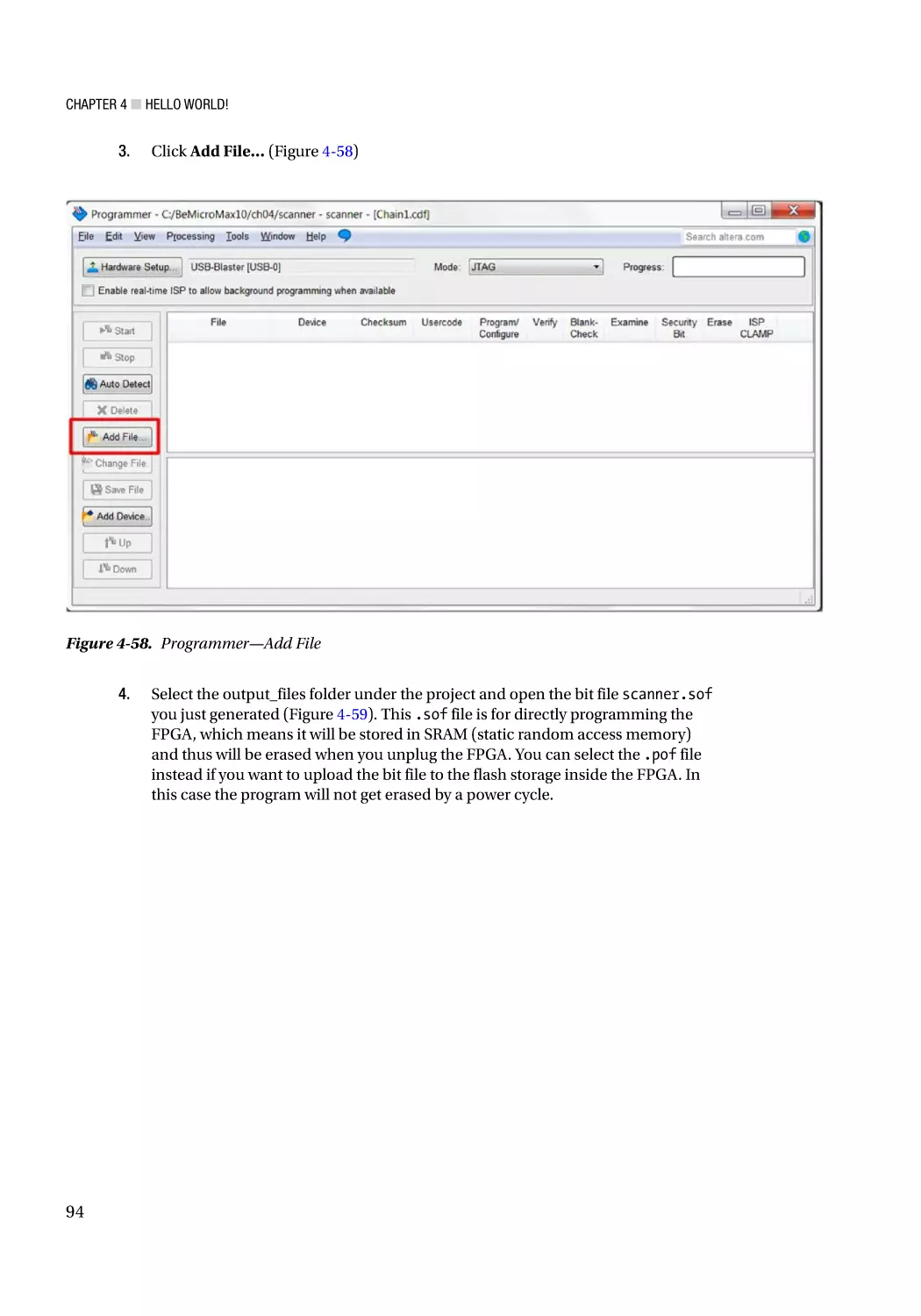
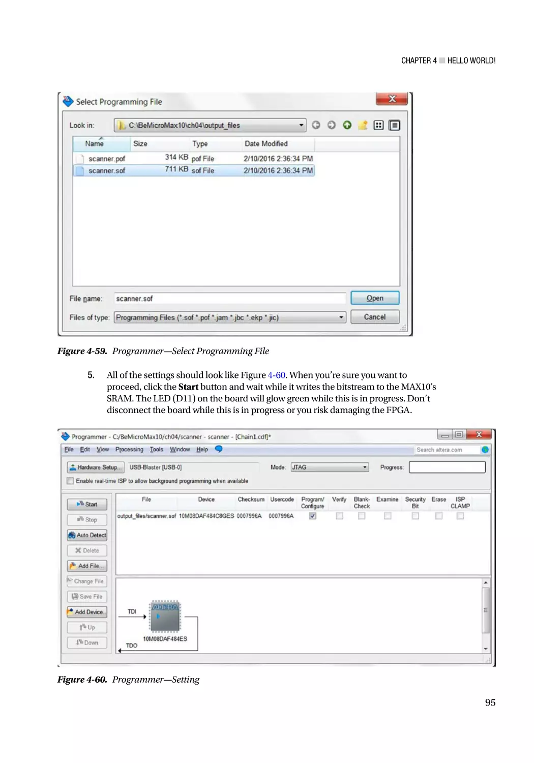
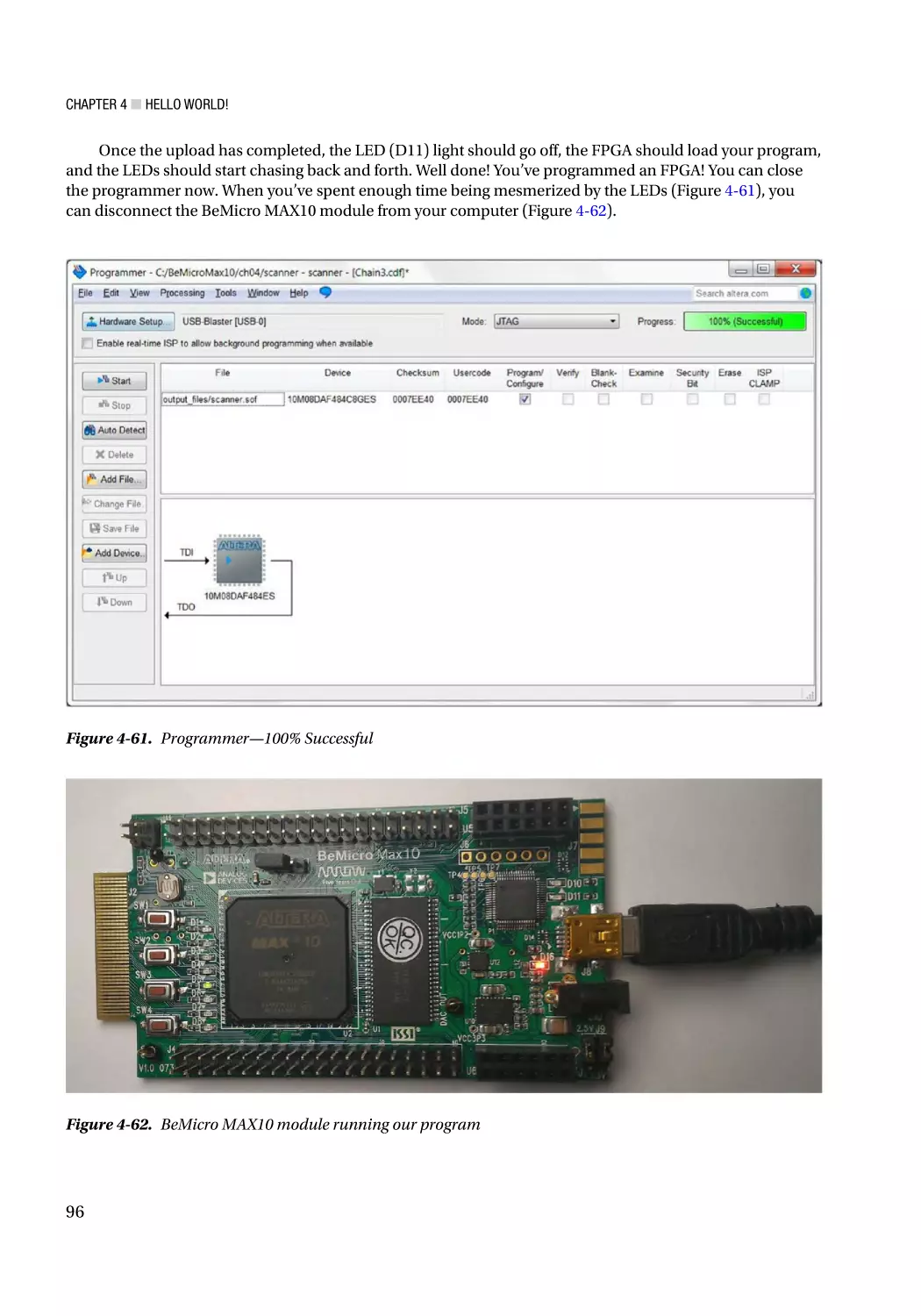
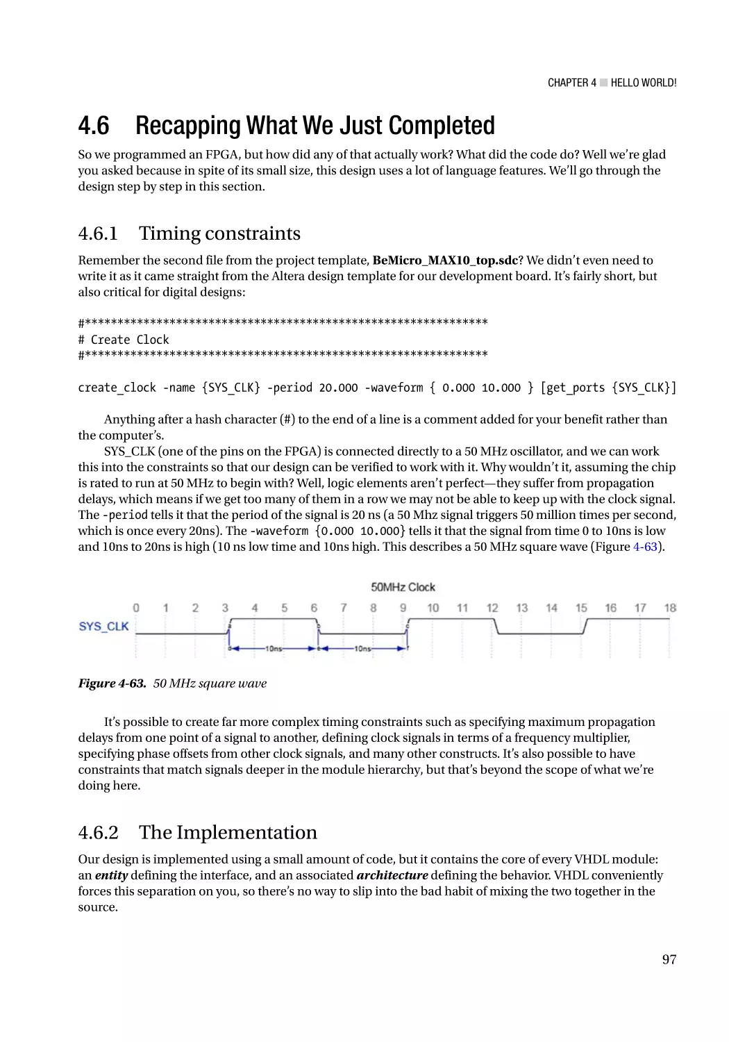
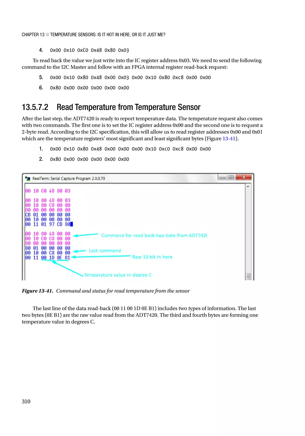
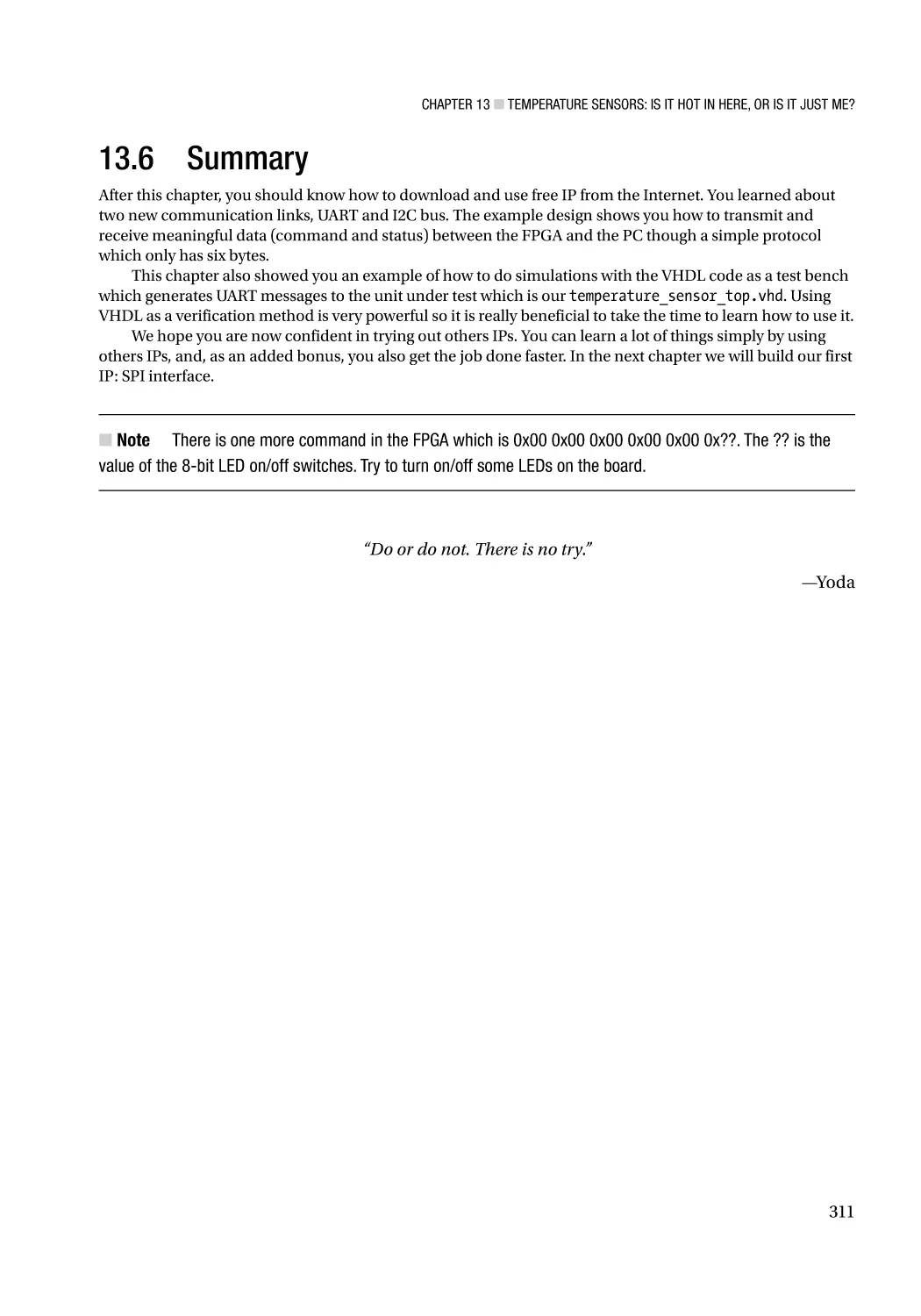
/


Text
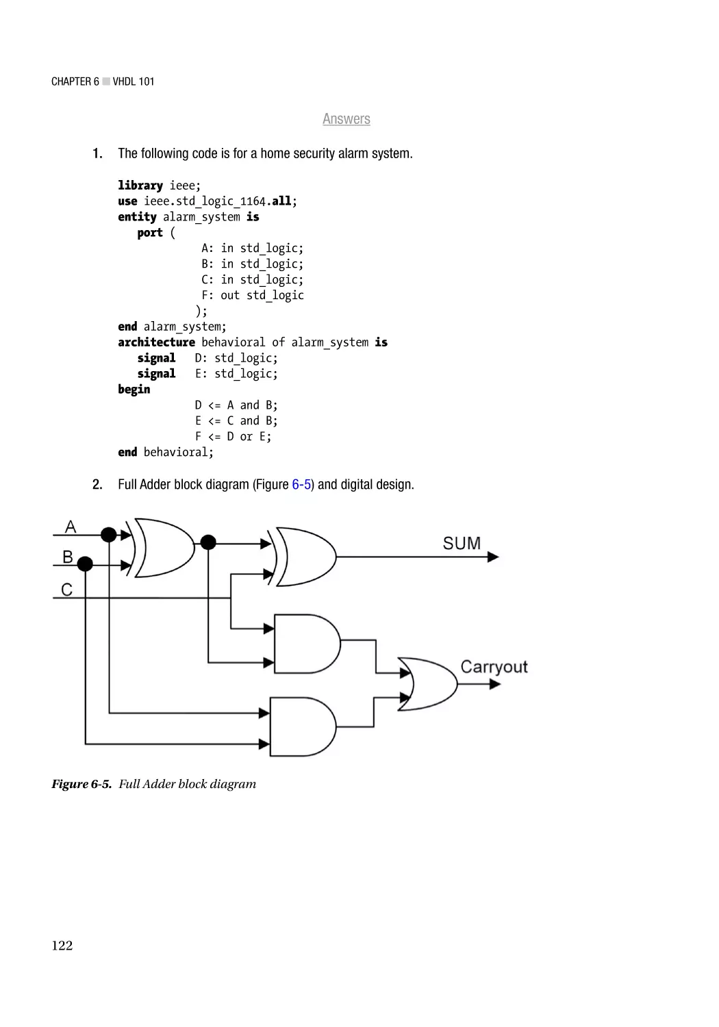
TECHNOLOGY IN AC TION™
Beginning FPGA:
Programming
Metal
Your brain on hardware
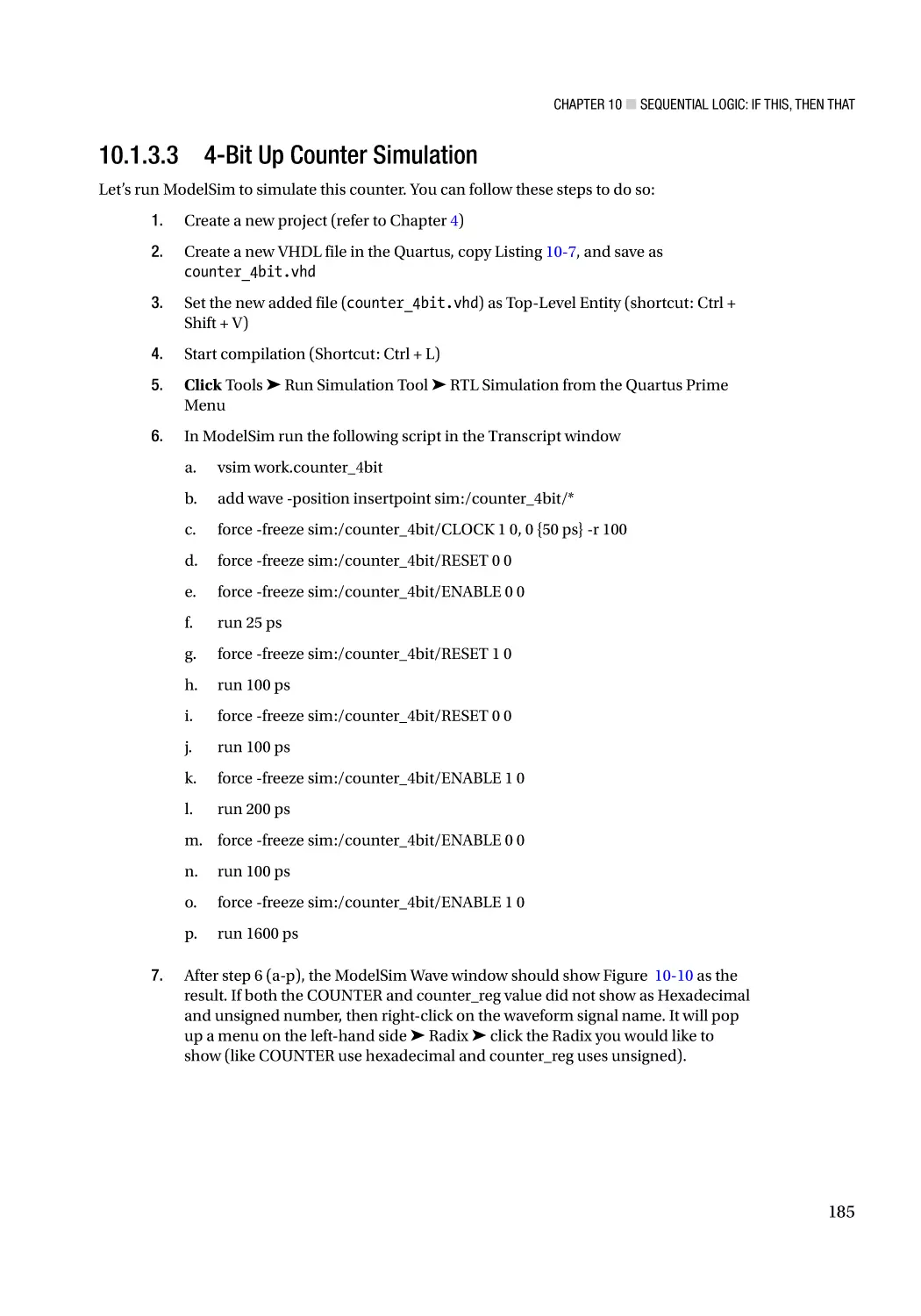
—
Aiken Pang
Peter Membrey
Beginning FPGA:
Programming Metal
Your brain on hardware
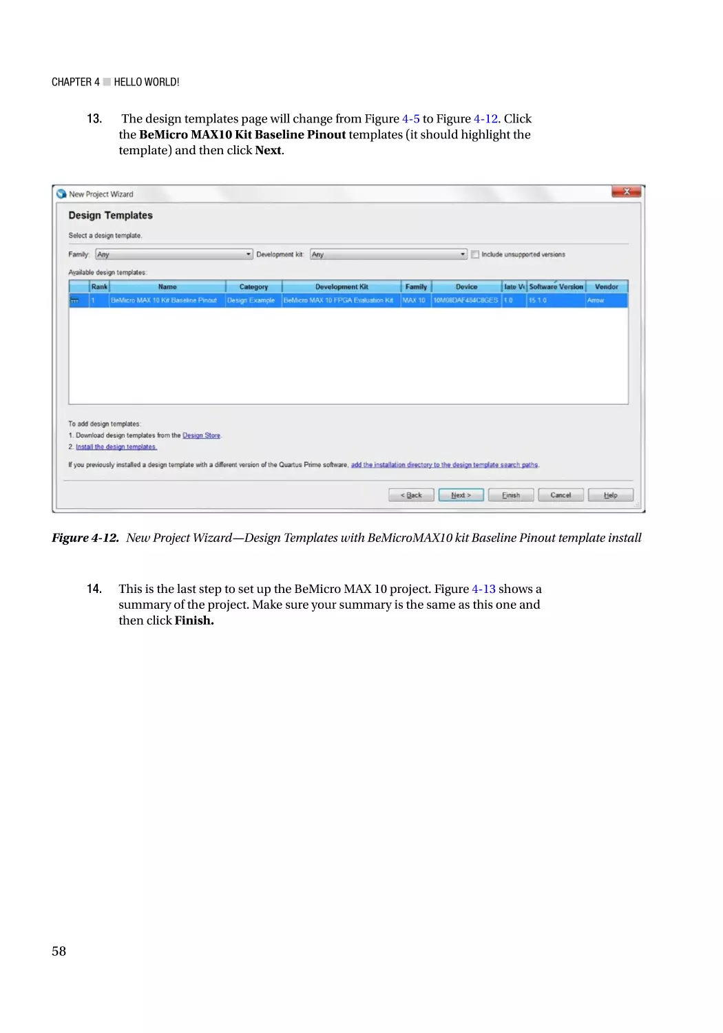
Aiken Pang
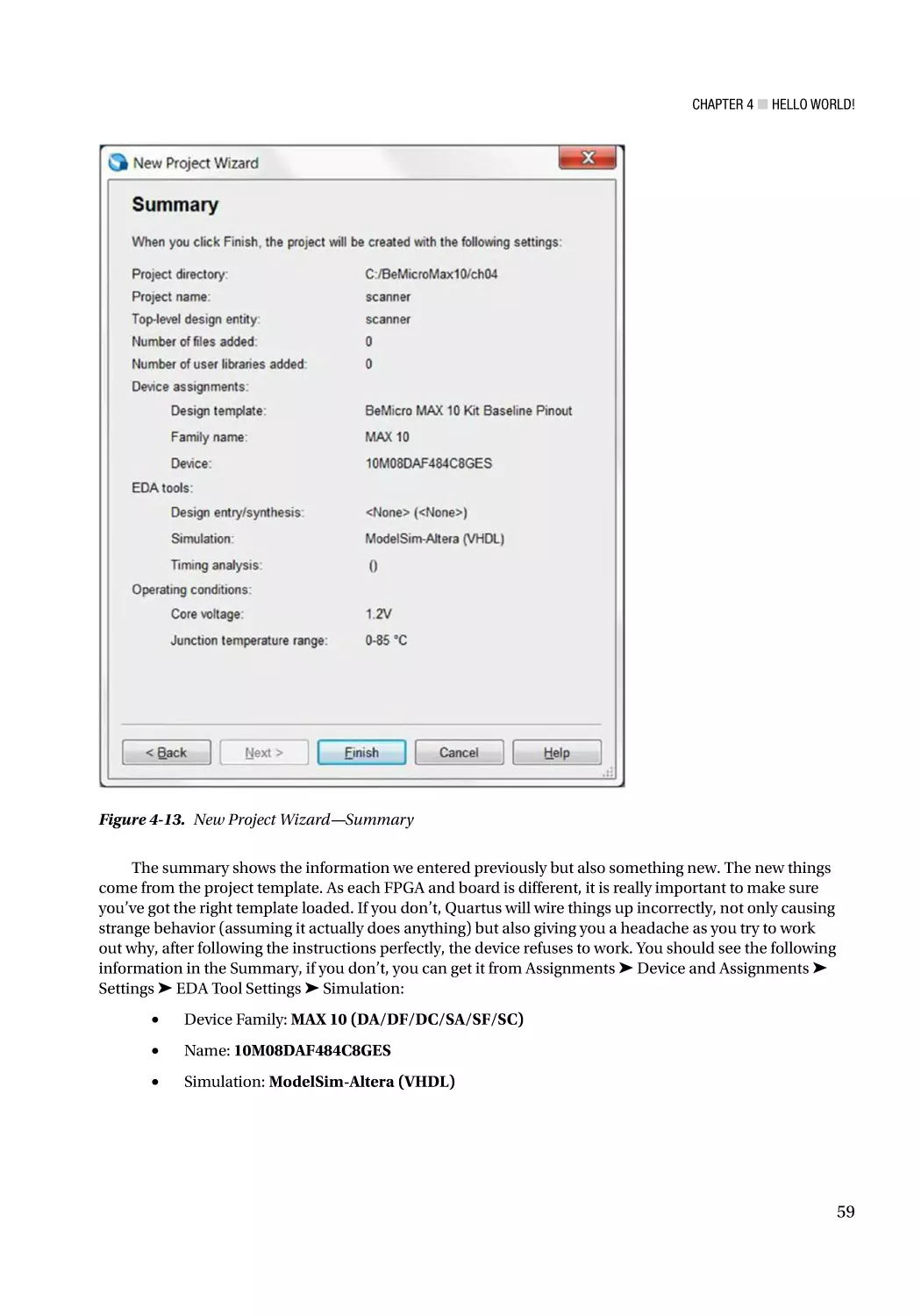
Peter Membrey
Beginning FPGA: Programming Metal: Your Brain on Hardware
Aiken Pang Peter Membrey
Chelmsford, Massachusetts
Lai Chi Kok, Kowloon, Hong Kong
USA China
ISBN-13 (pbk): 978-1-4302-6247-3
DOI 10.1007/978-1-4302-6248-0
ISBN-13 (electronic): 978-1-4302-6248-0
Library of Congress Control Number: 2016962137
Copyright © 2017 by Aiken Pang and Peter Membrey
This work is subject to copyright. All rights are reserved by the Publisher, whether the whole or part of the
material is concerned, specifically the rights of translation, reprinting, reuse of illustrations, recitation,
broadcasting, reproduction on microfilms or in any other physical way, and transmission or information
storage and retrieval, electronic adaptation, computer software, or by similar or dissimilar methodology now
known or hereafter developed.
Trademarked names, logos, and images may appear in this book. Rather than use a trademark symbol with
every occurrence of a trademarked name, logo, or image we use the names, logos, and images only in an
editorial fashion and to the benefit of the trademark owner, with no intention of infringement of the trademark.
The use in this publication of trade names, trademarks, service marks, and similar terms, even if they are
not identified as such, is not to be taken as an expression of opinion as to whether or not they are subject to
proprietary rights.
While the advice and information in this book are believed to be true and accurate at the date of publication,
neither the authors nor the editors nor the publisher can accept any legal responsibility for any errors or
omissions that may be made. The publisher makes no warranty, express or implied, with respect to the
material contained herein.
Managing Director: Welmoed Spahr
Lead Editor: Natalie Pao
Technical Reviewer: Brendan Horan
Editorial Board: Steve Anglin, Pramila Balan, Laura Berendson, Aaron Black, Louise Corrigan,
Jonathan Gennick, Robert Hutchinson, Celestin Suresh John, Nikhil Karkal, James Markham,
Susan McDermott, Matthew Moodie, Natalie Pao, Gwenan Spearing
Coordinating Editor: Jessica Vakili
Copy Editor: Lori Jacobs
Compositor: SPi Global
Indexer: SPi Global
Artist: SPi Global
Distributed to the book trade worldwide by Springer Science+Business Media New York,
233 Spring Street, 6th Floor, New York, NY 10013. Phone 1-800-SPRINGER, fax (201) 348-4505, e-mail
orders-ny@springer-sbm.com, or visit www.springeronline.com. Apress Media, LLC is a California LLC
and the sole member (owner) is Springer Science + Business Media Finance Inc (SSBM Finance Inc). SSBM
Finance Inc is a Delaware corporation.
For information on translations, please e-mail rights@apress.com, or visit www.apress.com.
Apress and friends of ED books may be purchased in bulk for academic, corporate, or promotional use.
eBook versions and licenses are also available for most titles. For more information, reference our Special
Bulk Sales–eBook Licensing web page at www.apress.com/bulk-sales.
Any source code or other supplementary materials referenced by the author in this text are available to
readers at www.apress.com. For detailed information about how to locate your book’s source code, go to
www.apress.com/source-code/. Readers can also access source code at SpringerLink in the Supplementary
Material section for each chapter.
Printed on acid-free paper
Contents at a Glance
About the Authors�������������������������������������������������������������������������������������������������� xiii
About the Technical Reviewer���������������������������������������������������������������������������������xv
■Part
■
I: Getting Started with FPGA������������������������������������������������������� 1
■Chapter
■
1: What Is an FPGA and What Can It Do?������������������������������������������������� 3
■Chapter
■
2: Our Weapon of Choice ����������������������������������������������������������������������� 13
■Chapter
■
3: Lock and Load������������������������������������������������������������������������������������ 23
■Chapter
■
4: Hello World!��������������������������������������������������������������������������������������� 47
■Part
■
II: Time Out for Theory������������������������������������������������������������ 105
■Chapter
■
5: FPGA Development Timeline������������������������������������������������������������ 107
■Chapter
■
6: VHDL 101������������������������������������������������������������������������������������������ 117
■Chapter
■
7: Number Theory for FPGAs���������������������������������������������������������������� 125
■Chapter
■
8: Telling the Truth: Boolean Algebra and Truth Tables������������������������ 137
■Chapter
■
9: Simplifying Boolean Algebra for FPGA��������������������������������������������� 159
■Chapter
■
10: Sequential Logic: IF This, THEN That���������������������������������������������� 171
■Chapter
■
11: Combinatorial Logic: Putting It All Together on the FPGA�������������� 191
■Part
■
III: Let’s Make Something!������������������������������������������������������ 219
■Chapter
■
12: Light Sensors: Turning a Laser Pointer into a Hi-Tech Tripwire ���� 221
■Chapter
■
13: Temperature Sensors: Is It Hot in Here, or Is It Just Me?�������������� 267
■Chapter
■
14: How Fast Can You Run? Ask the Accelerometer!��������������������������� 313
iii
■ Contents at a Glance
■■Part IV: Taking It Further: Talking to the Raspberry Pi and
LED Displays����������������������������������������������������������������������������������� 345
■Chapter
■
15: Two-Way Communications with Your Raspberry Pi: SPI���������������� 347
■Chapter
■
16: Up in Lights: How to Drive LED Segment Displays������������������������� 367
Index��������������������������������������������������������������������������������������������������������������������� 381
iv
Contents
About the Authors�������������������������������������������������������������������������������������������������� xiii
About the Technical Reviewer���������������������������������������������������������������������������������xv
■Part
■
I: Getting Started with FPGA������������������������������������������������������� 1
■Chapter
■
1: What Is an FPGA and What Can It Do?������������������������������������������������� 3
1.1 Field-Programmable����������������������������������������������������������������������������������������������� 4
1.1.1 Configuration Technology����������������������������������������������������������������������������������������������������������� 4
1.2 Gates = Logic���������������������������������������������������������������������������������������������������������� 5
1.2.1 The Basic Gate Design Block No. 1: Logic Element�������������������������������������������������������������������� 5
1.2.2 The Basic Gate Design Block No. 2: Configurable IO Block�������������������������������������������������������� 8
1.2.3 The Basic Gate Design Block No. 3: Internal RAM���������������������������������������������������������������������� 8
1.3 Arrays Have Many Connections������������������������������������������������������������������������������� 8
1.4 What Can It Do?������������������������������������������������������������������������������������������������������� 9
1.5 It Can Get the Job Done Fast!�������������������������������������������������������������������������������� 10
1.6 FPGA vs. Processor����������������������������������������������������������������������������������������������� 11
1.7 Summary��������������������������������������������������������������������������������������������������������������� 12
■Chapter
■
2: Our Weapon of Choice ����������������������������������������������������������������������� 13
2.1 What Weapons (FPGAs) Are Available�������������������������������������������������������������������� 13
2.2 The BeMicro Max 10: Our Weapon of Choice�������������������������������������������������������� 14
2.2.1 The Master: Altera MAX 10 FPGA���������������������������������������������������������������������������������������������� 15
2.2.2 The Emissaries: BeMicro MAX 10 Board Features ������������������������������������������������������������������� 17
v
■ Contents
2.3 Other Tools������������������������������������������������������������������������������������������������������������ 18
2.3.1 The Place to Connect Everything: The Breadboard������������������������������������������������������������������� 19
2.3.2 Making the Invisible Visible: The Multi-meter�������������������������������������������������������������������������� 20
2.4 Wrap-up���������������������������������������������������������������������������������������������������������������� 21
■Chapter
■
3: Lock and Load������������������������������������������������������������������������������������ 23
3.1 Getting the Development Toolchain Up and Running�������������������������������������������� 23
3.2 Downloading Altera Tools�������������������������������������������������������������������������������������� 24
3.2.1 Altera Toolchains���������������������������������������������������������������������������������������������������������������������� 25
3.2.2 Create an Altera Account���������������������������������������������������������������������������������������������������������� 25
3.2.3 Download the Altera Toolchains����������������������������������������������������������������������������������������������� 26
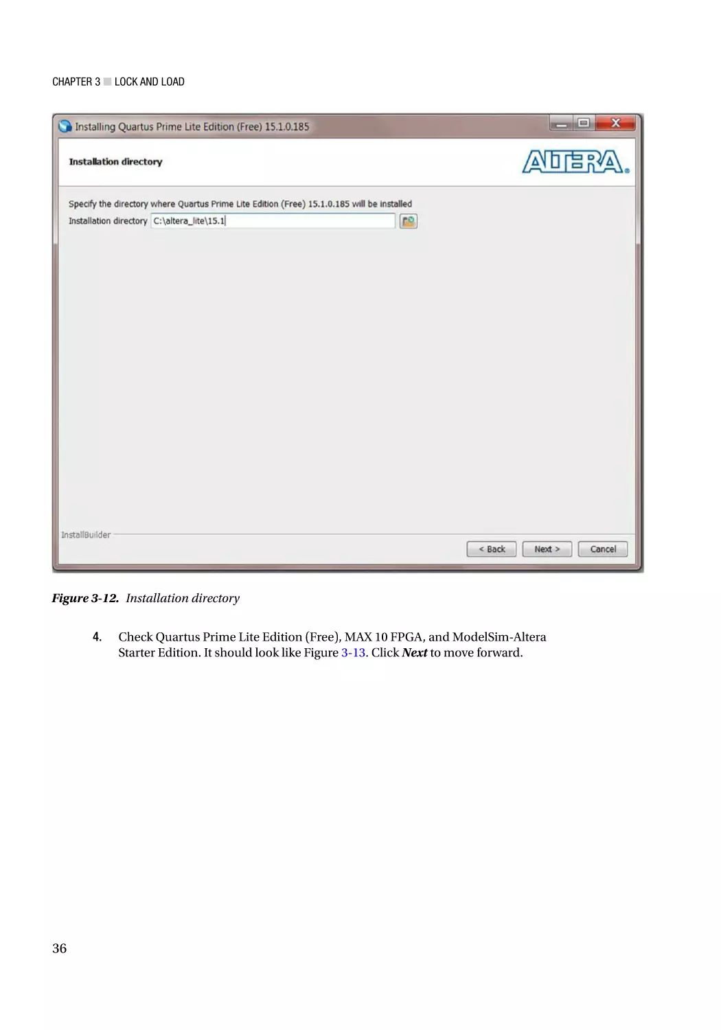
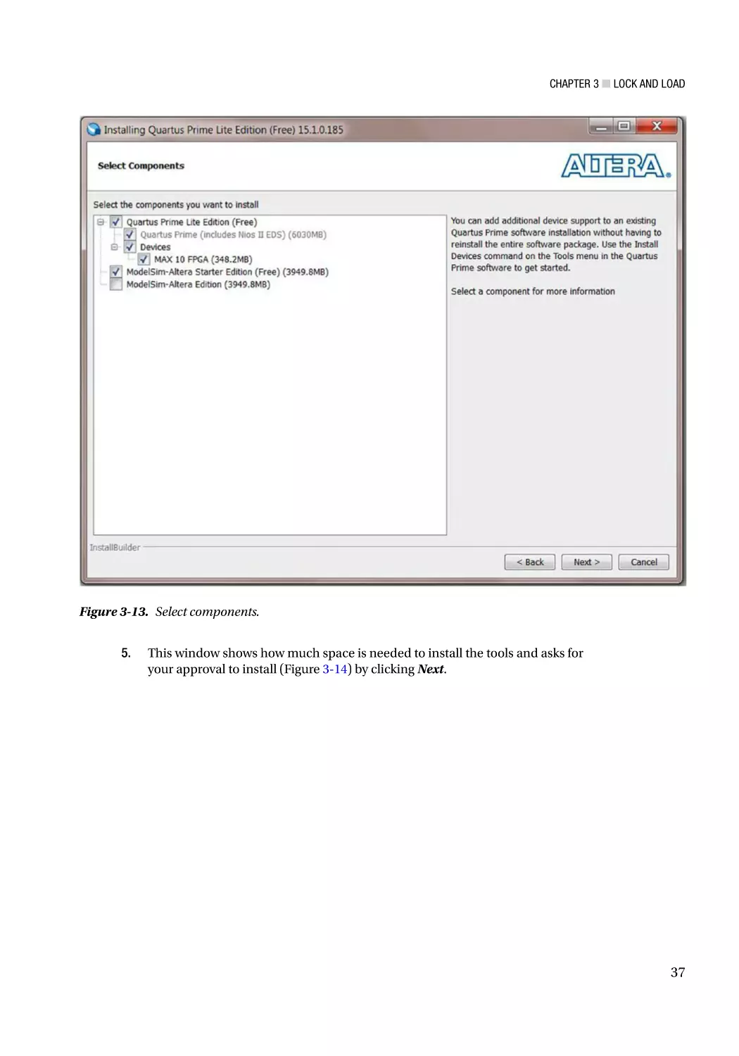
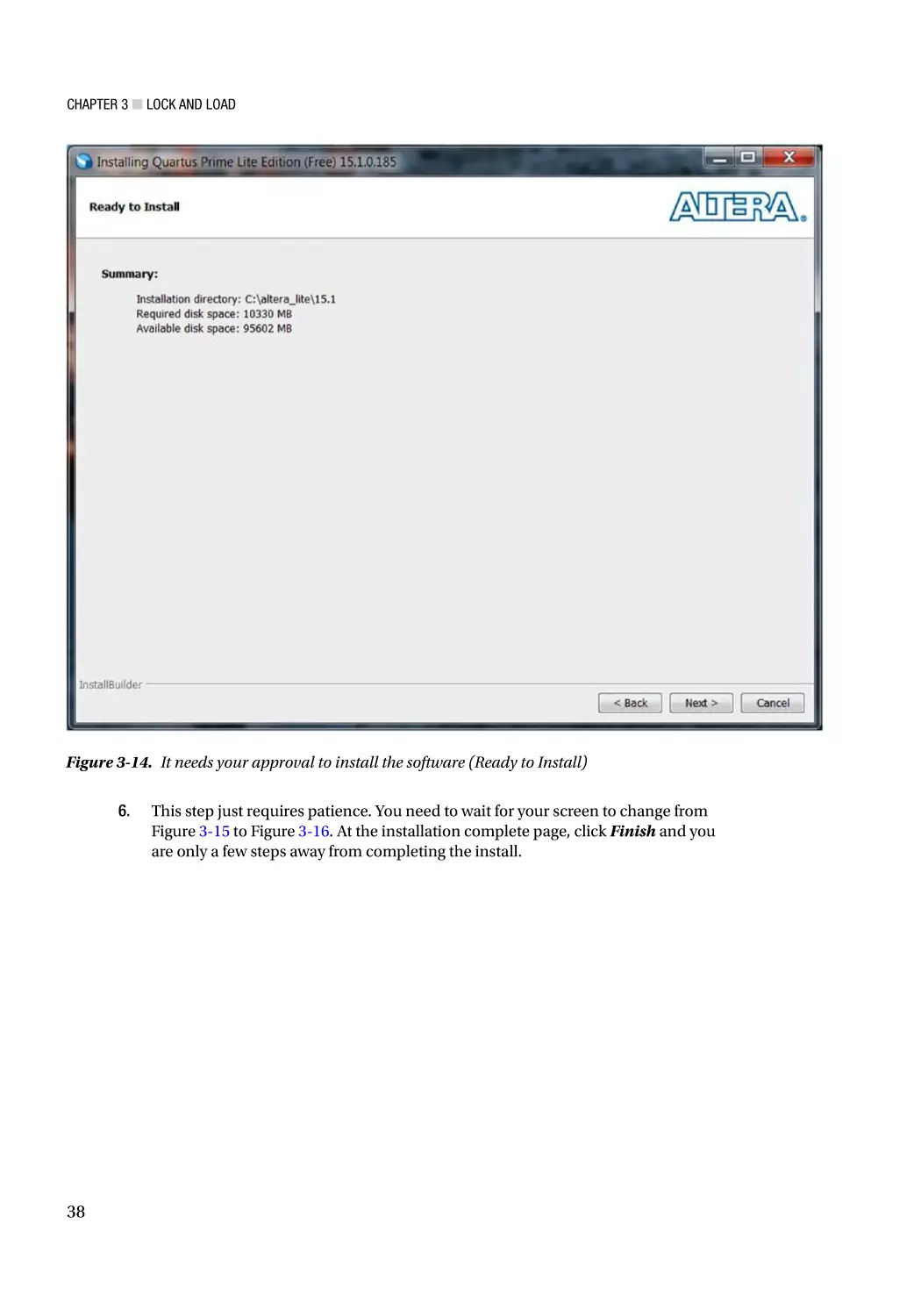
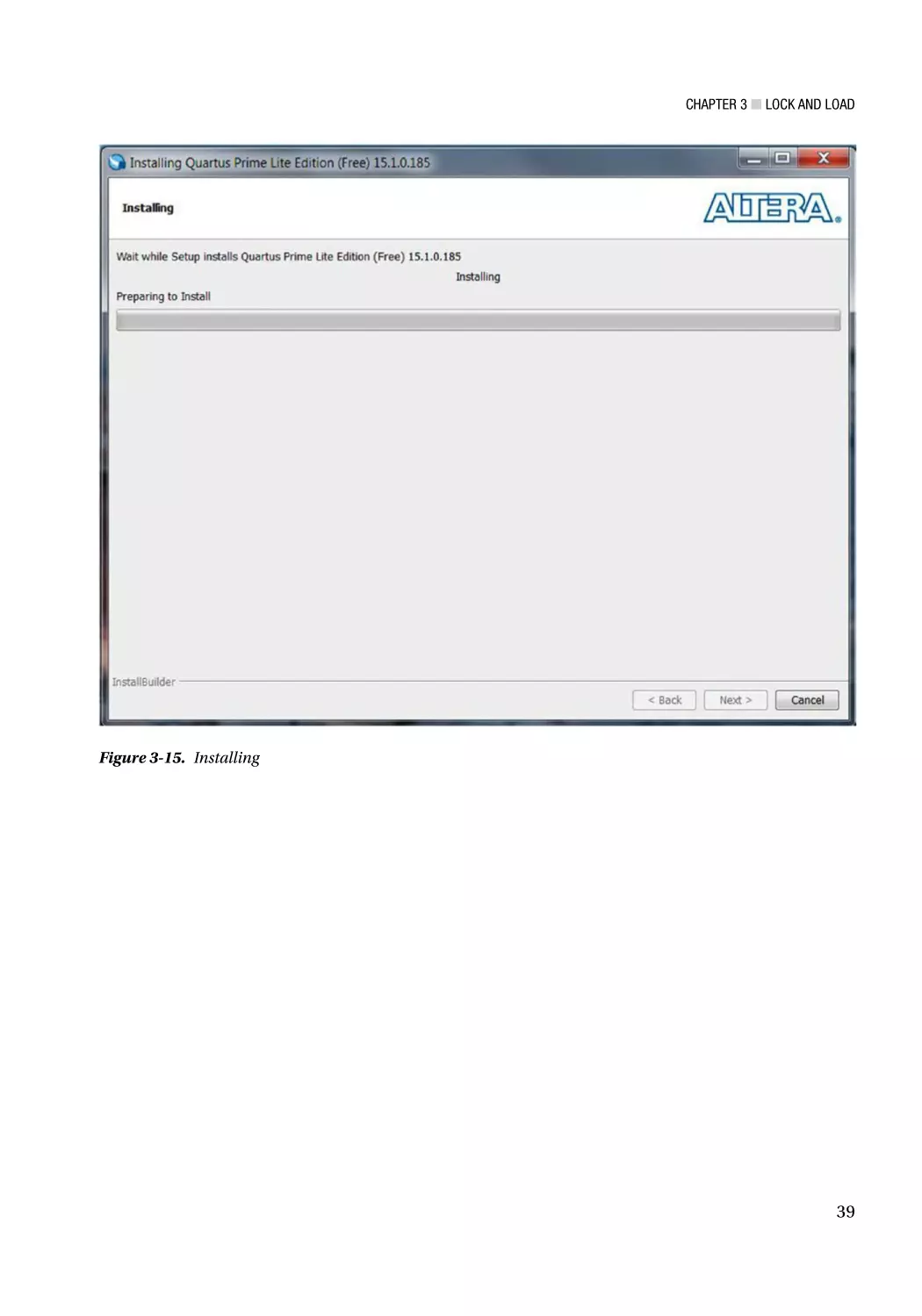
3.3 Install Altera Quartus Prime Lite Edition���������������������������������������������������������������� 33
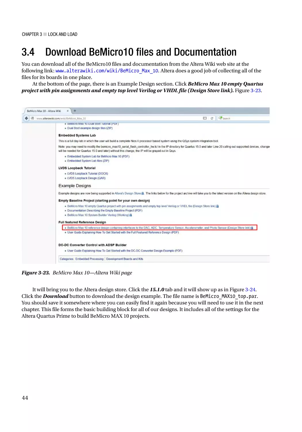
3.4 Download BeMicro10 files and Documentation���������������������������������������������������� 44
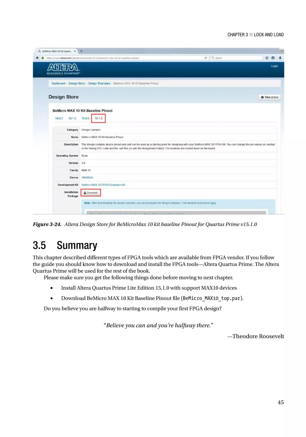
3.5 Summary��������������������������������������������������������������������������������������������������������������� 45
■Chapter
■
4: Hello World!��������������������������������������������������������������������������������������� 47
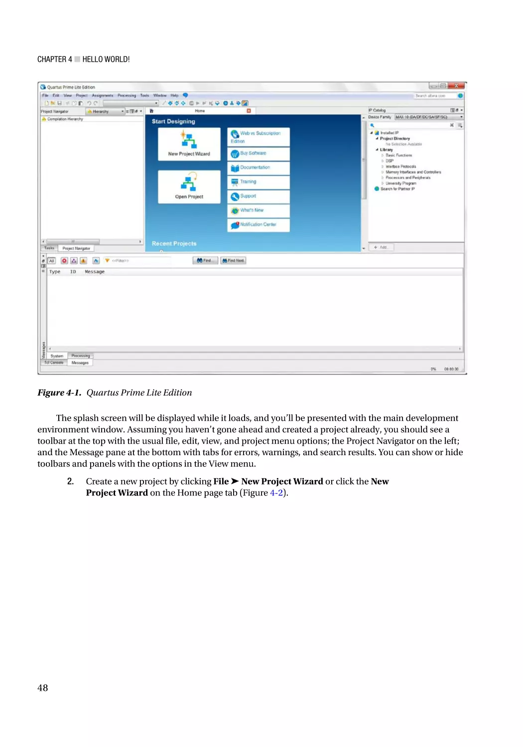
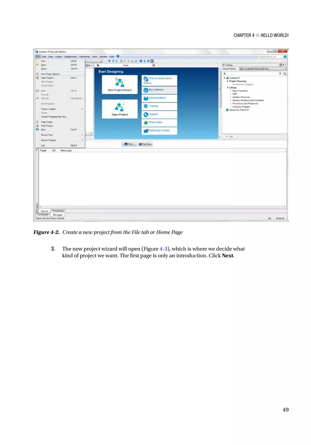
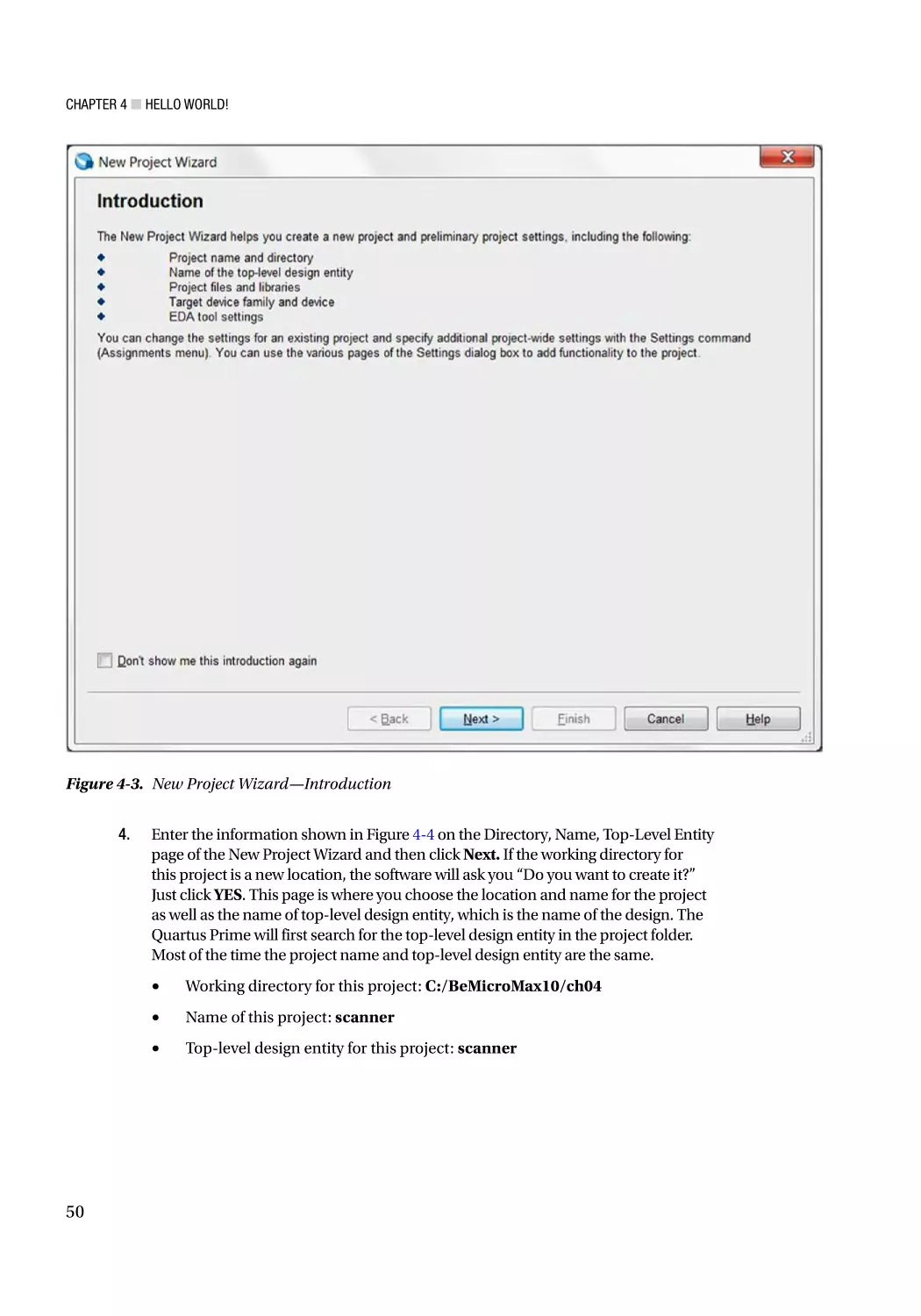
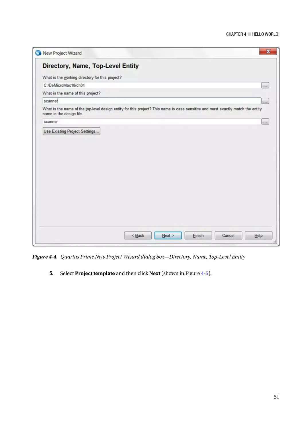
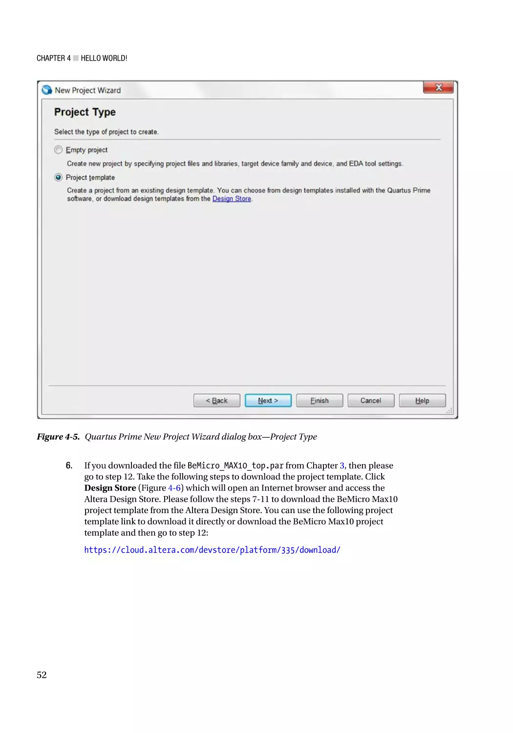
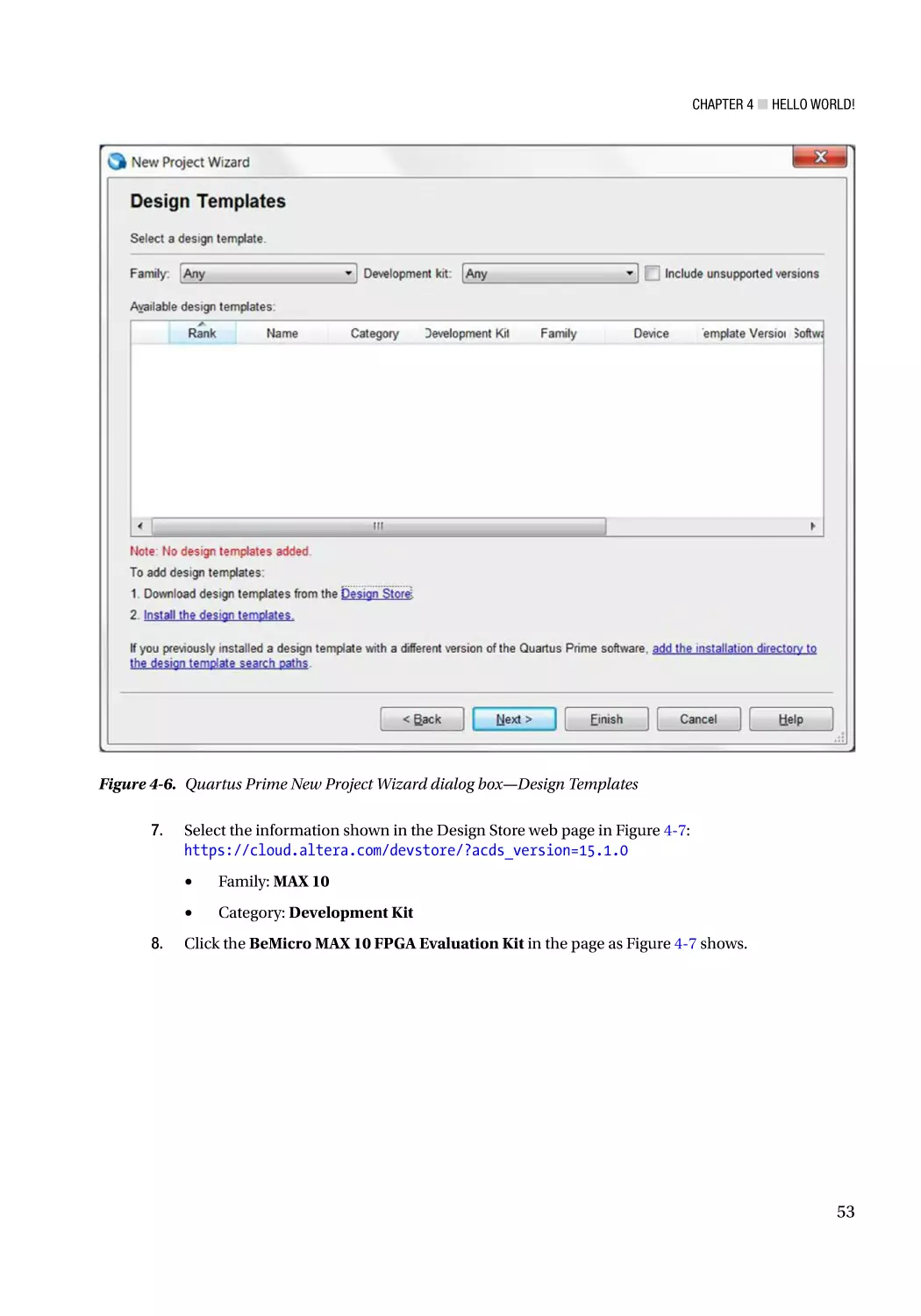
4.1 Launch Quartus Prime and Create a New Project������������������������������������������������� 47
4.2 Write Code������������������������������������������������������������������������������������������������������������� 61
4.3 Implement Design������������������������������������������������������������������������������������������������� 69
4.4 Simulate Design���������������������������������������������������������������������������������������������������� 75
4.5 Burn It!������������������������������������������������������������������������������������������������������������������ 89
4.5.1 Install USB Blaster Driver��������������������������������������������������������������������������������������������������������� 89
4.5.2 Program Design������������������������������������������������������������������������������������������������������������������������ 92
4.6 Recapping What We Just Completed�������������������������������������������������������������������� 97
4.6.1 Timing constraints�������������������������������������������������������������������������������������������������������������������� 97
4.6.2 The Implementation������������������������������������������������������������������������������������������������������������������ 97
4.6.3 The Test Bench����������������������������������������������������������������������������������������������������������������������� 101
4.7 Summary������������������������������������������������������������������������������������������������������������� 103
4.7.1 But I Don’t have a Mercury Module!��������������������������������������������������������������������������������������� 103
vi
■ Contents
■Part
■
II: Time Out for Theory������������������������������������������������������������ 105
■Chapter
■
5: FPGA Development Timeline������������������������������������������������������������ 107
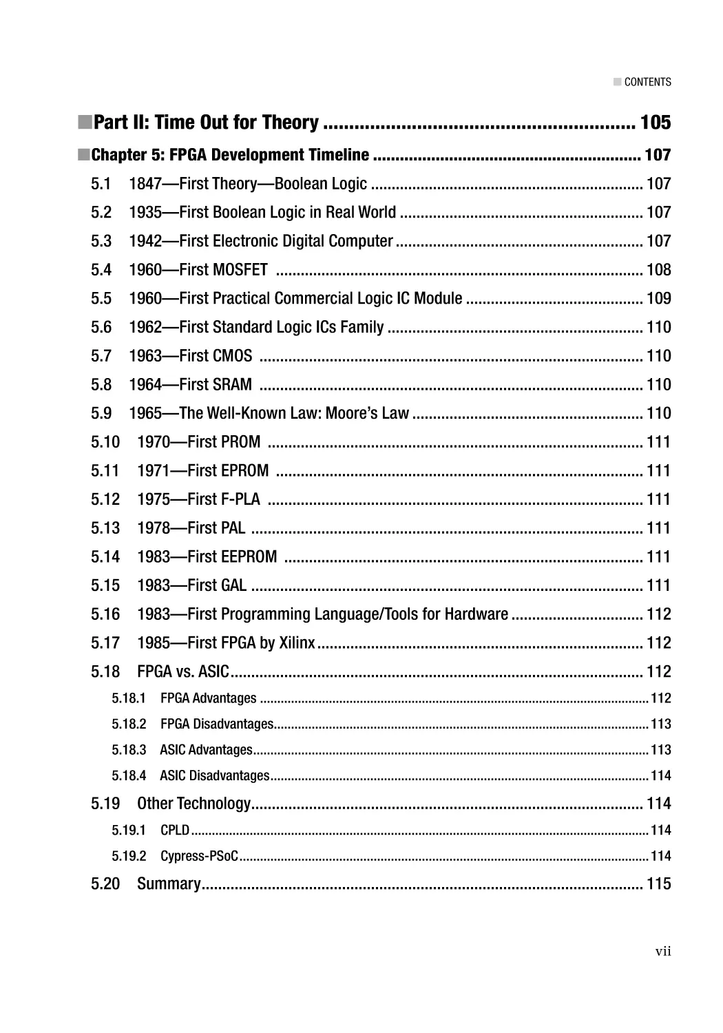
5.1 1847—First Theory—Boolean Logic������������������������������������������������������������������ 107
5.2 1935—First Boolean Logic in Real World����������������������������������������������������������� 107
5.3 1942—First Electronic Digital Computer������������������������������������������������������������ 107
5.4 1960—First MOSFET ����������������������������������������������������������������������������������������� 108
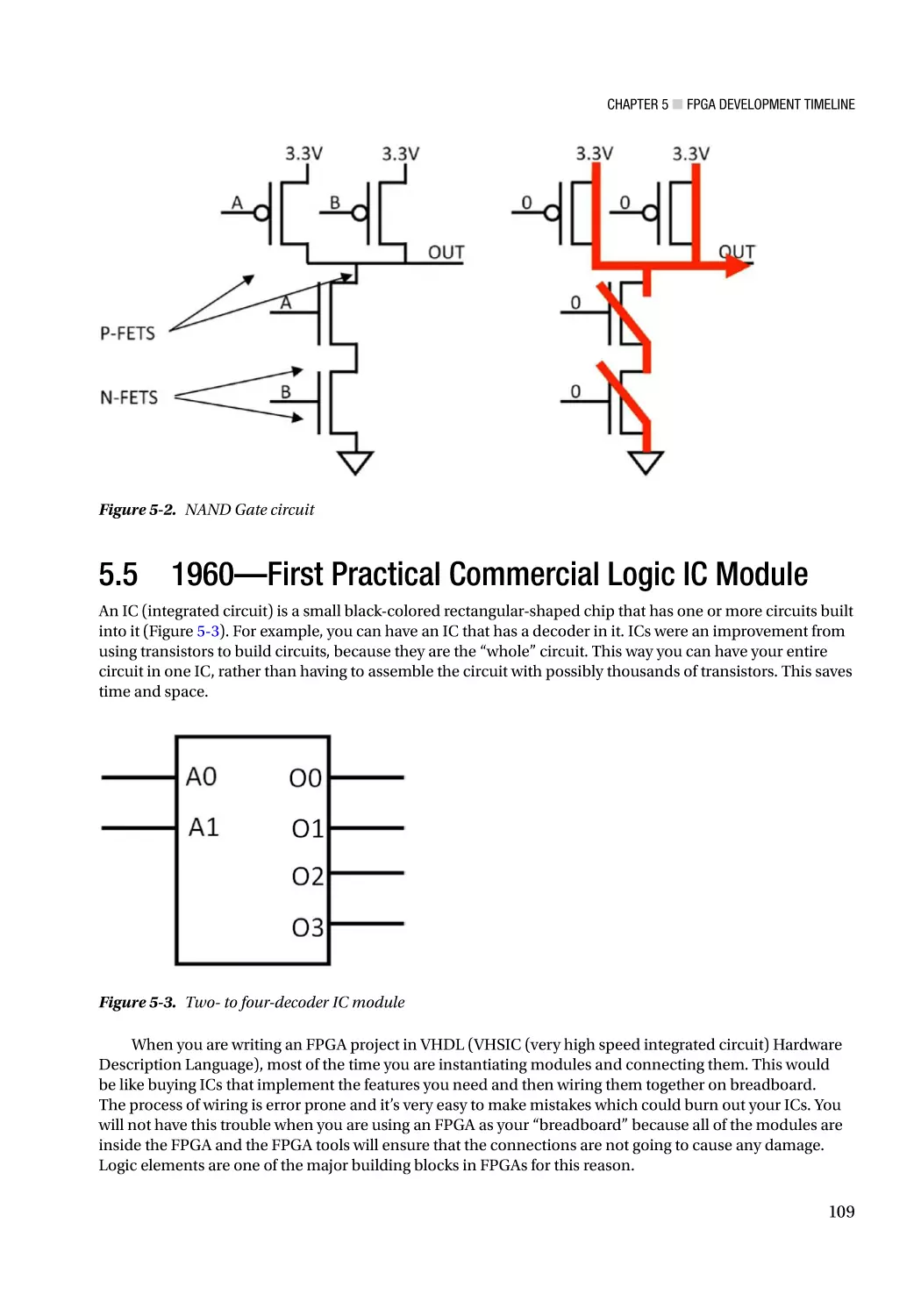
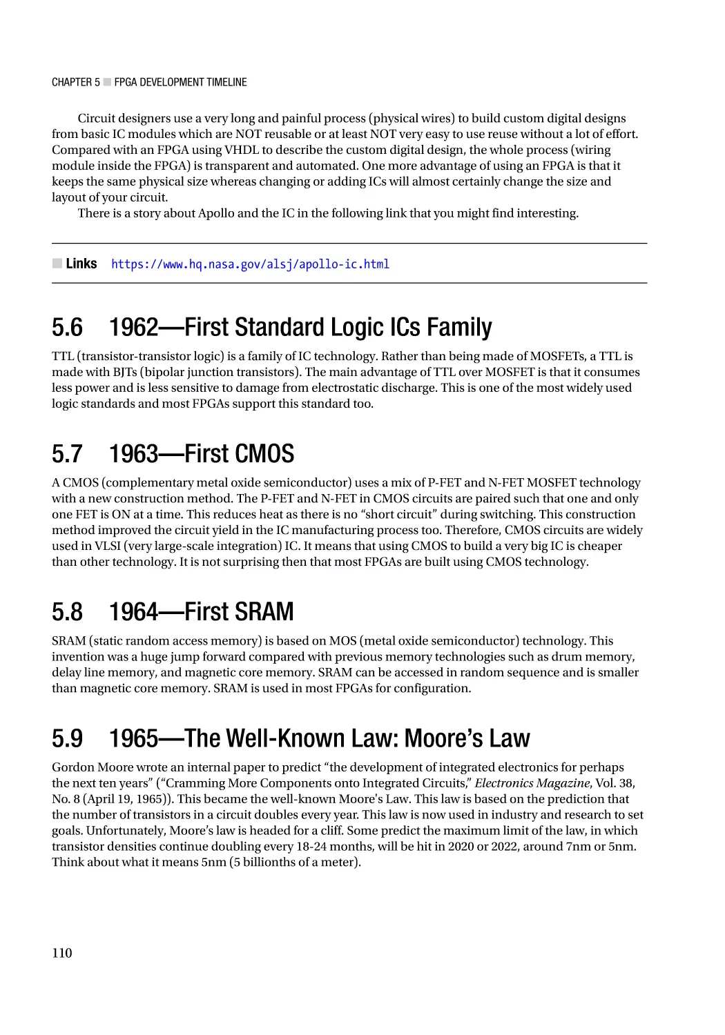
5.5 1960—First Practical Commercial Logic IC Module������������������������������������������� 109
5.6 1962—First Standard Logic ICs Family�������������������������������������������������������������� 110
5.7 1963—First CMOS ��������������������������������������������������������������������������������������������� 110
5.8 1964—First SRAM ��������������������������������������������������������������������������������������������� 110
5.9 1965—The Well-Known Law: Moore’s Law�������������������������������������������������������� 110
5.10 1970—First PROM ������������������������������������������������������������������������������������������� 111
5.11 1971—First EPROM ����������������������������������������������������������������������������������������� 111
5.12 1975—First F-PLA ������������������������������������������������������������������������������������������� 111
5.13 1978—First PAL ����������������������������������������������������������������������������������������������� 111
5.14 1983—First EEPROM ��������������������������������������������������������������������������������������� 111
5.15 1983—First GAL ����������������������������������������������������������������������������������������������� 111
5.16 1983—First Programming Language/Tools for Hardware�������������������������������� 112
5.17 1985—First FPGA by Xilinx������������������������������������������������������������������������������� 112
5.18 FPGA vs. ASIC���������������������������������������������������������������������������������������������������� 112
5.18.1 FPGA Advantages����������������������������������������������������������������������������������������������������������������� 112
5.18.2 FPGA Disadvantages������������������������������������������������������������������������������������������������������������� 113
5.18.3 ASIC Advantages������������������������������������������������������������������������������������������������������������������� 113
5.18.4 ASIC Disadvantages�������������������������������������������������������������������������������������������������������������� 114
5.19 Other Technology����������������������������������������������������������������������������������������������� 114
5.19.1 CPLD������������������������������������������������������������������������������������������������������������������������������������� 114
5.19.2 Cypress-PSoC����������������������������������������������������������������������������������������������������������������������� 114
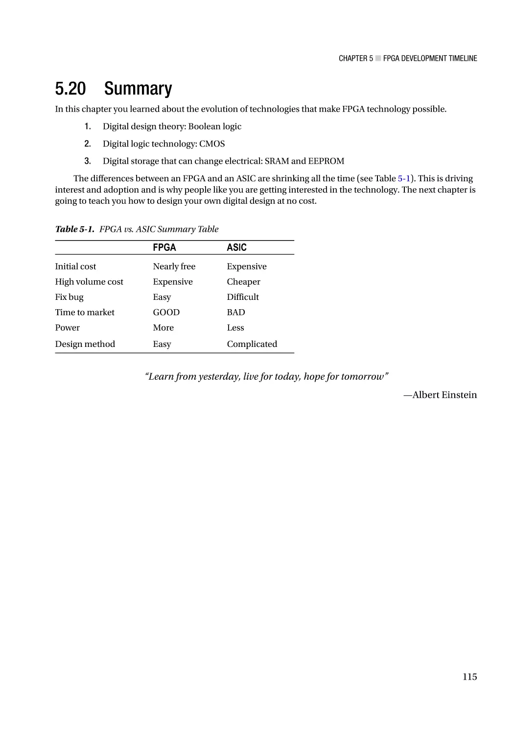
5.20 Summary����������������������������������������������������������������������������������������������������������� 115
vii
■ Contents
■Chapter
■
6: VHDL 101������������������������������������������������������������������������������������������ 117
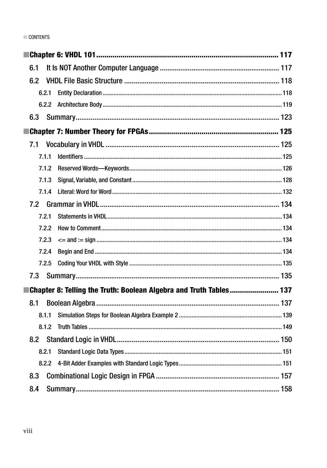
6.1 It Is NOT Another Computer Language���������������������������������������������������������������� 117
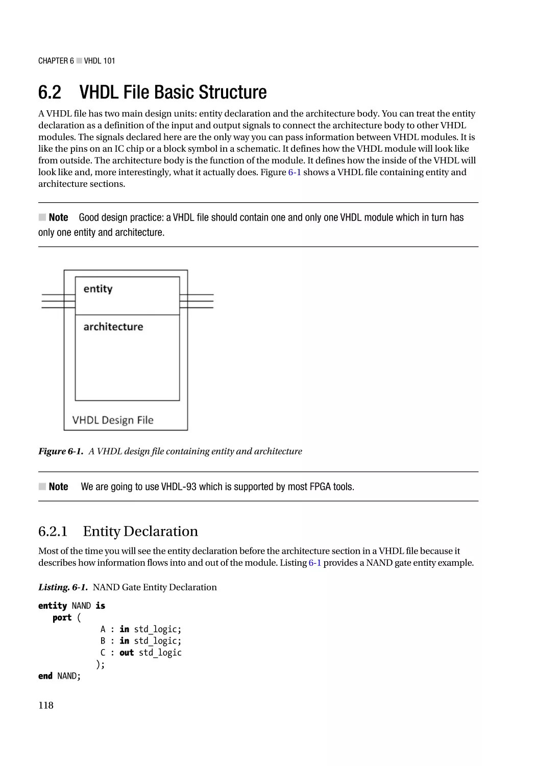
6.2 VHDL File Basic Structure����������������������������������������������������������������������������������� 118
6.2.1 Entity Declaration������������������������������������������������������������������������������������������������������������������� 118
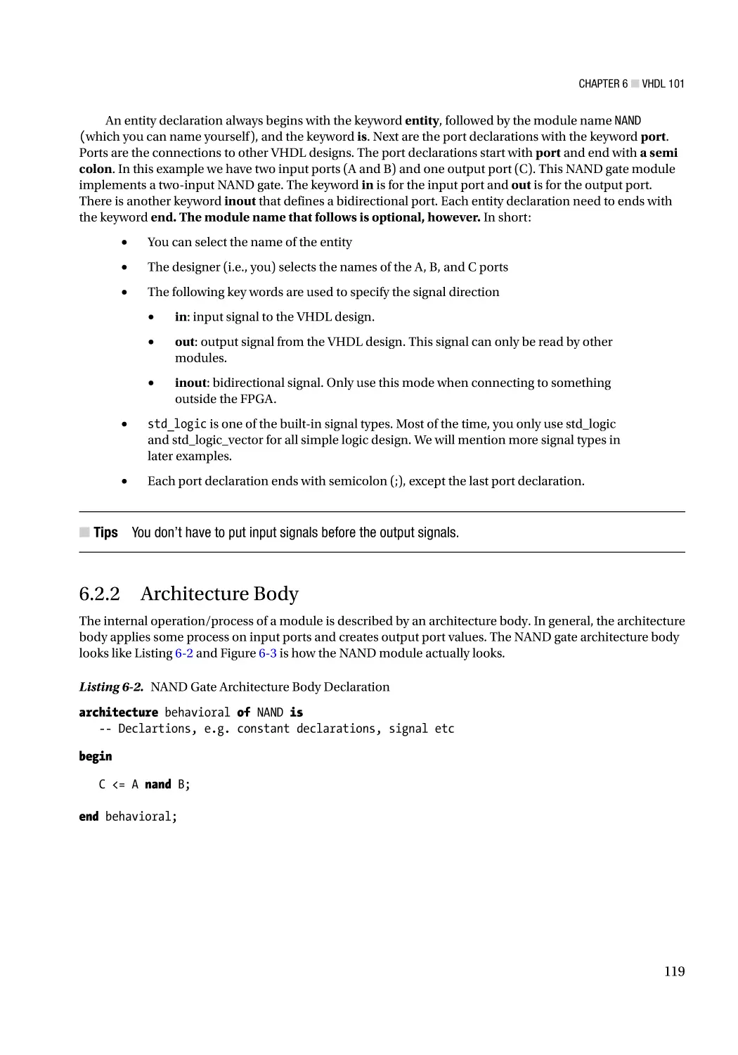
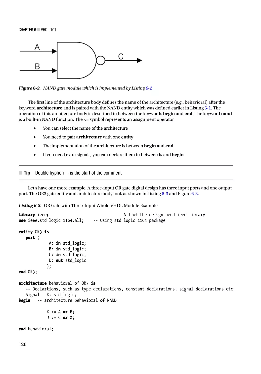
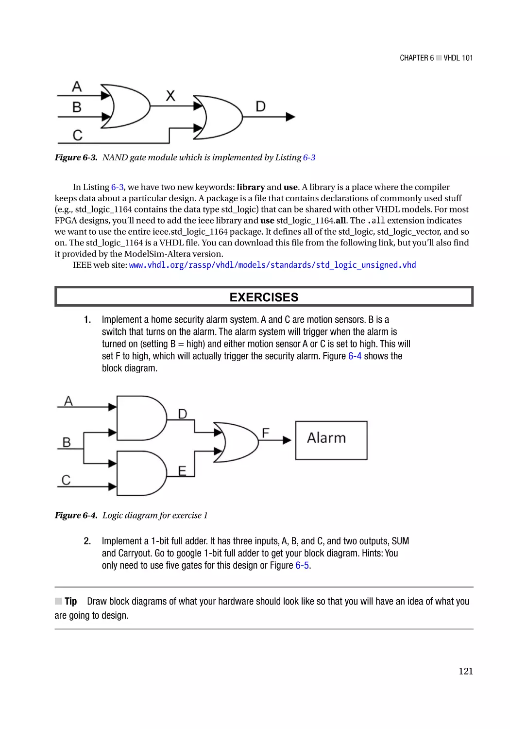
6.2.2 Architecture Body������������������������������������������������������������������������������������������������������������������� 119
6.3 Summary������������������������������������������������������������������������������������������������������������� 123
■Chapter
■
7: Number Theory for FPGAs���������������������������������������������������������������� 125
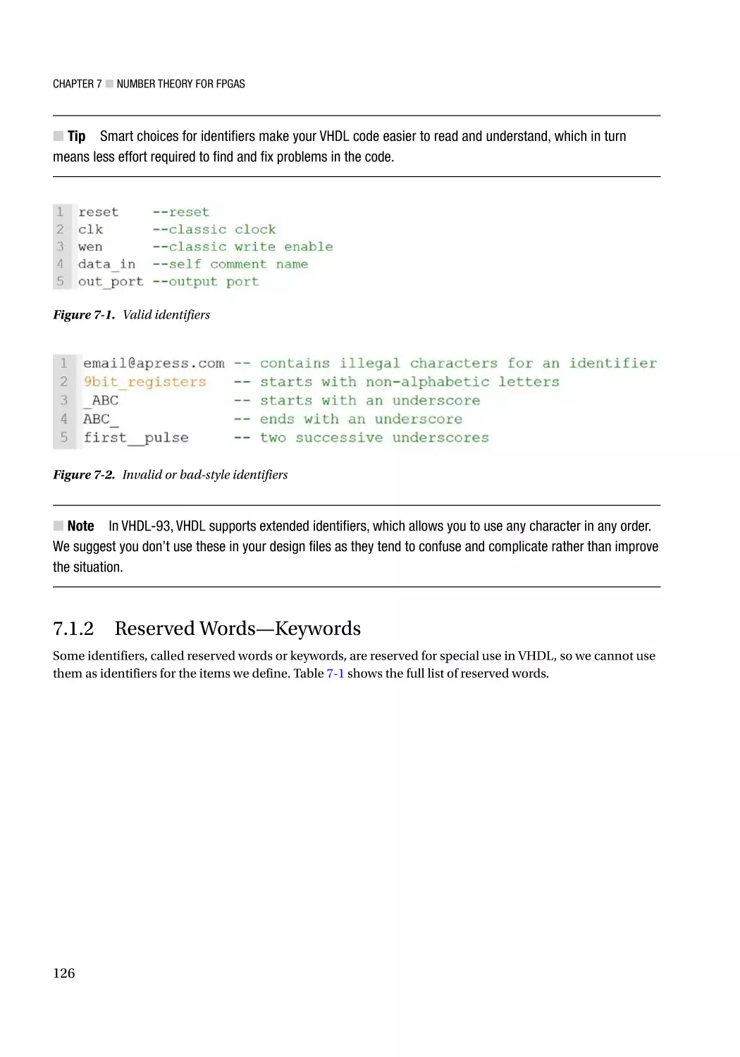
7.1 Vocabulary in VHDL��������������������������������������������������������������������������������������������� 125
7.1.1 Identifiers������������������������������������������������������������������������������������������������������������������������������� 125
7.1.2 Reserved Words—Keywords�������������������������������������������������������������������������������������������������� 126
7.1.3 Signal, Variable, and Constant������������������������������������������������������������������������������������������������ 128
7.1.4 Literal: Word for Word������������������������������������������������������������������������������������������������������������� 132
7.2 Grammar in VHDL������������������������������������������������������������������������������������������������ 134
7.2.1 Statements in VHDL���������������������������������������������������������������������������������������������������������������� 134
7.2.2 How to Comment�������������������������������������������������������������������������������������������������������������������� 134
7.2.3 <= and := sign����������������������������������������������������������������������������������������������������������������������� 134
7.2.4 Begin and End������������������������������������������������������������������������������������������������������������������������ 134
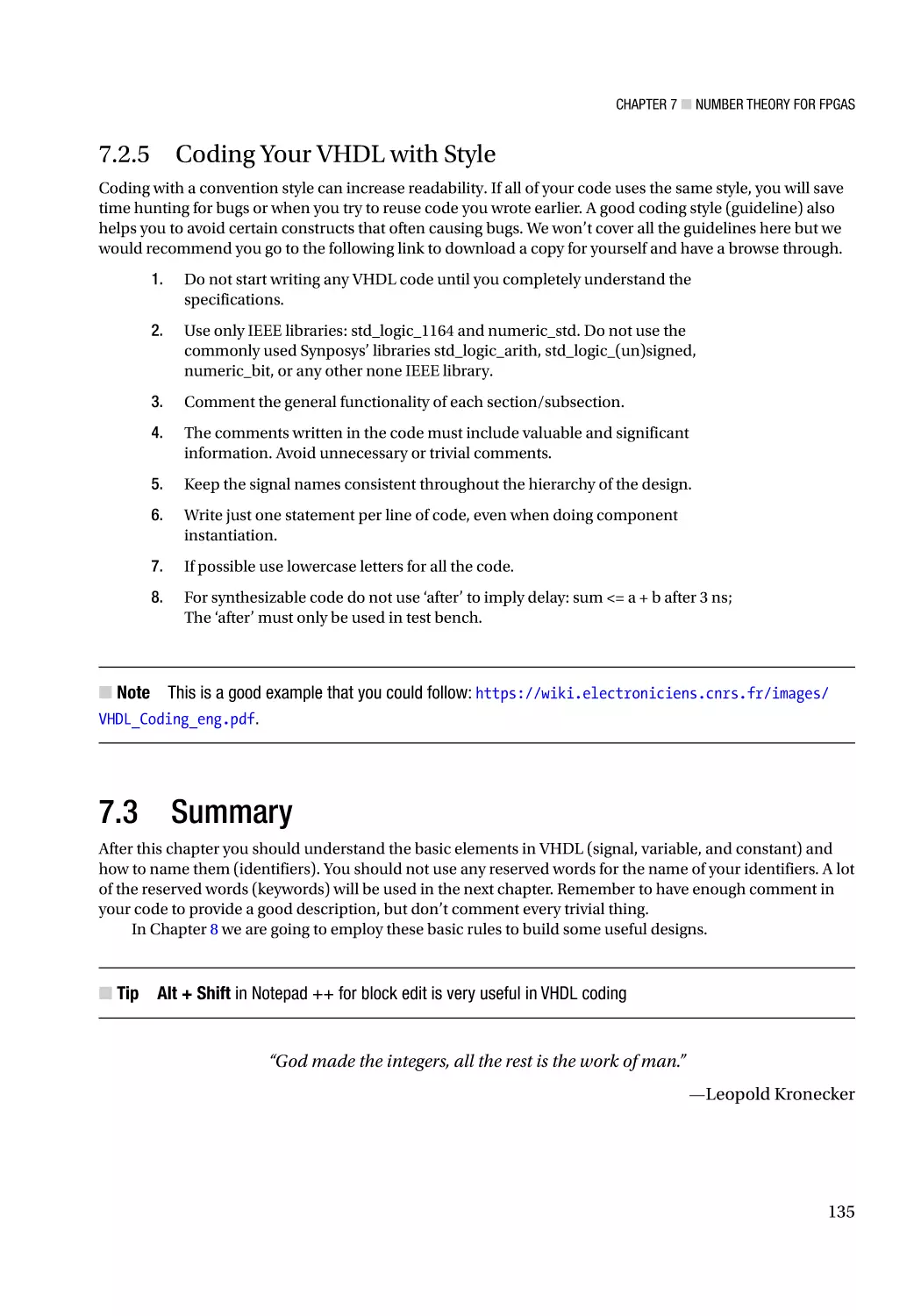
7.2.5 Coding Your VHDL with Style�������������������������������������������������������������������������������������������������� 135
7.3 Summary������������������������������������������������������������������������������������������������������������� 135
■Chapter
■
8: Telling the Truth: Boolean Algebra and Truth Tables������������������������ 137
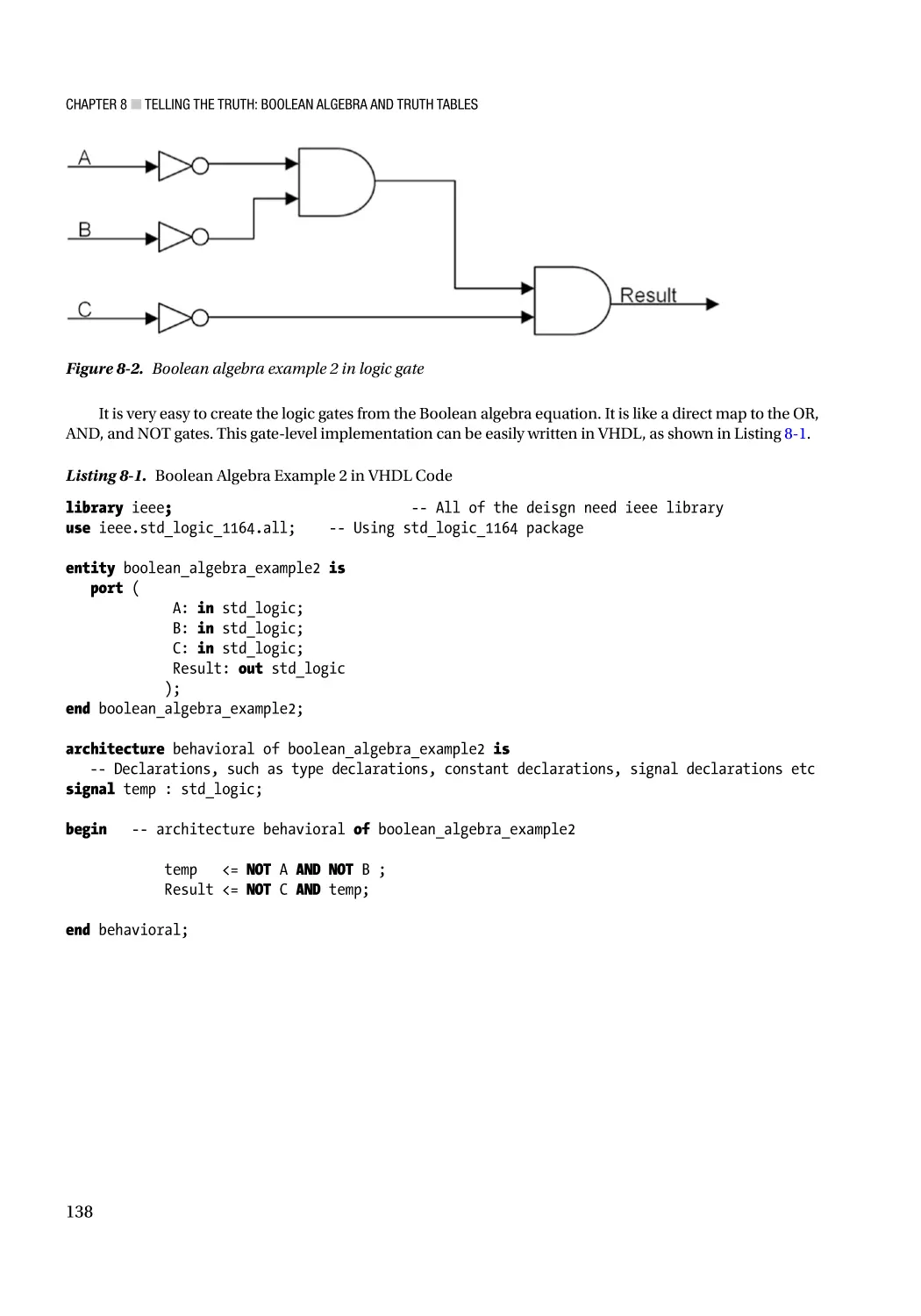
8.1 Boolean Algebra�������������������������������������������������������������������������������������������������� 137
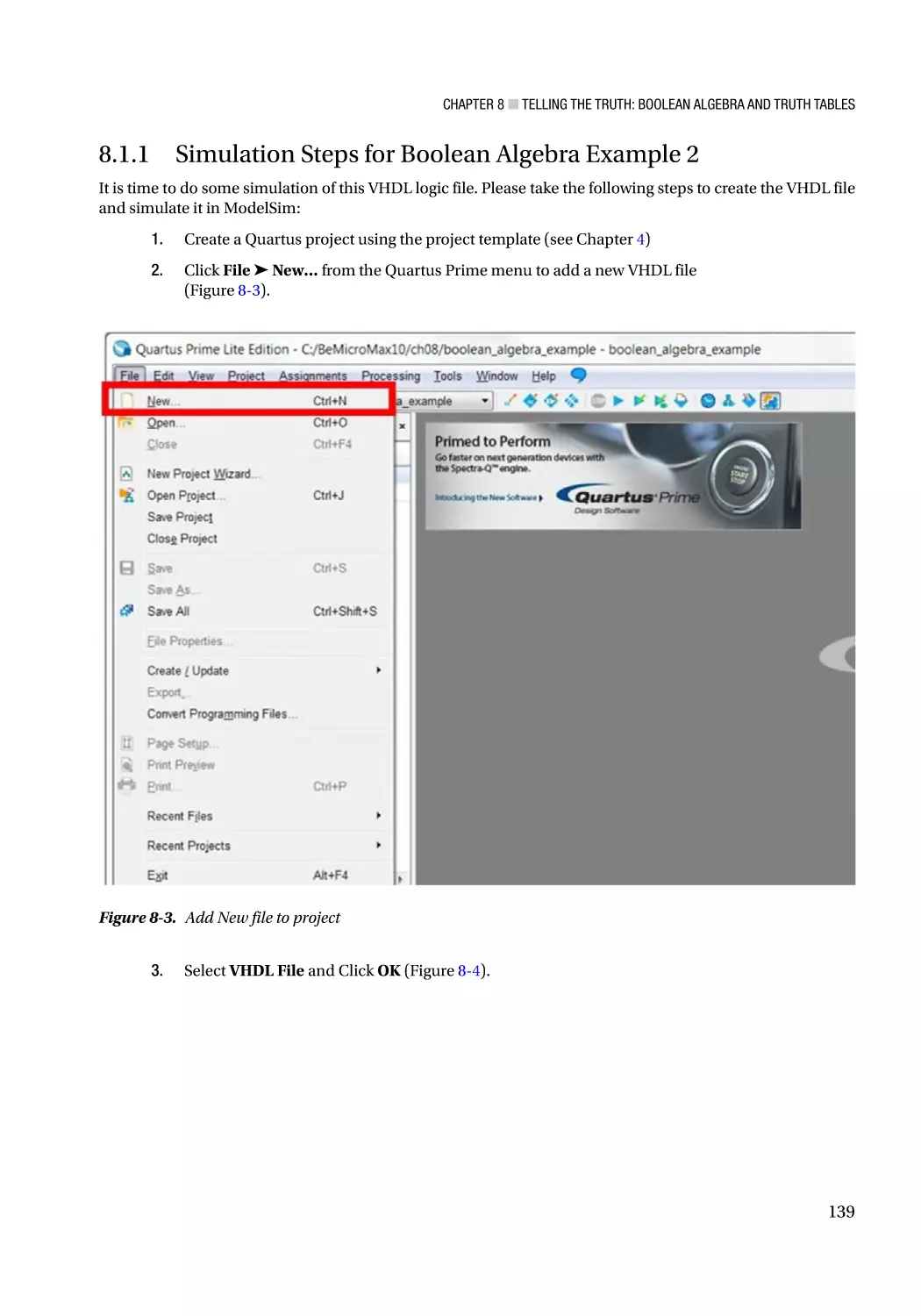
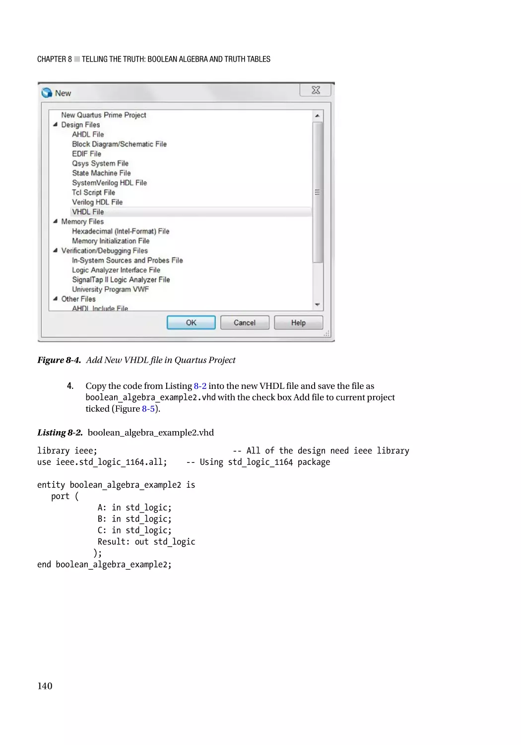
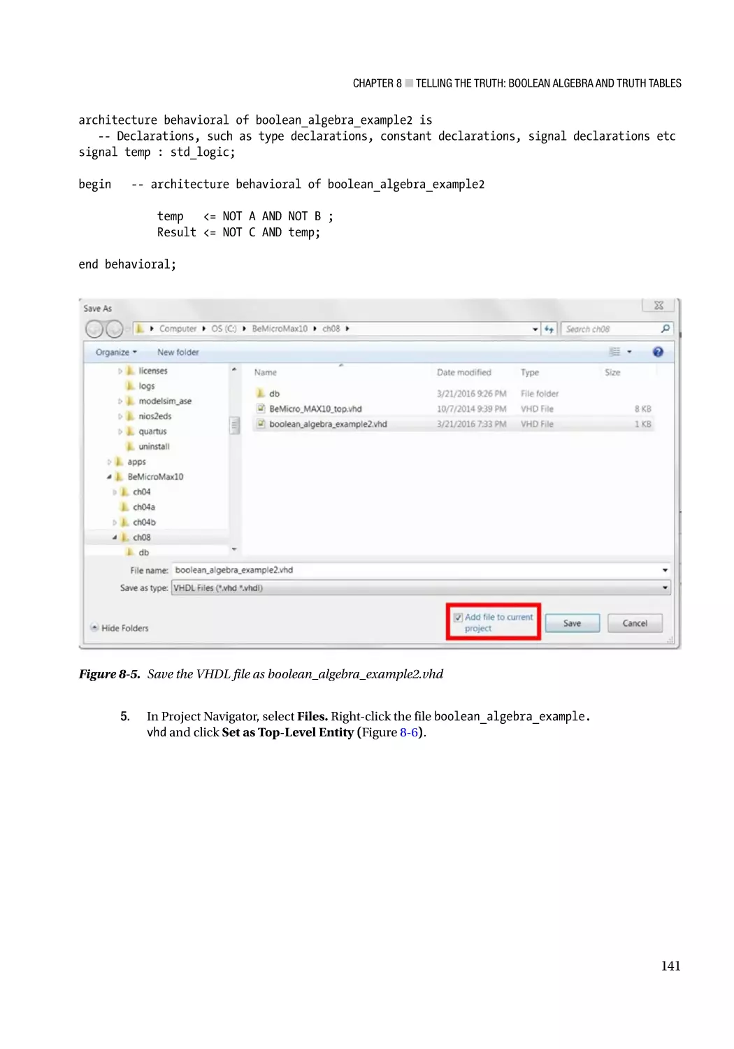
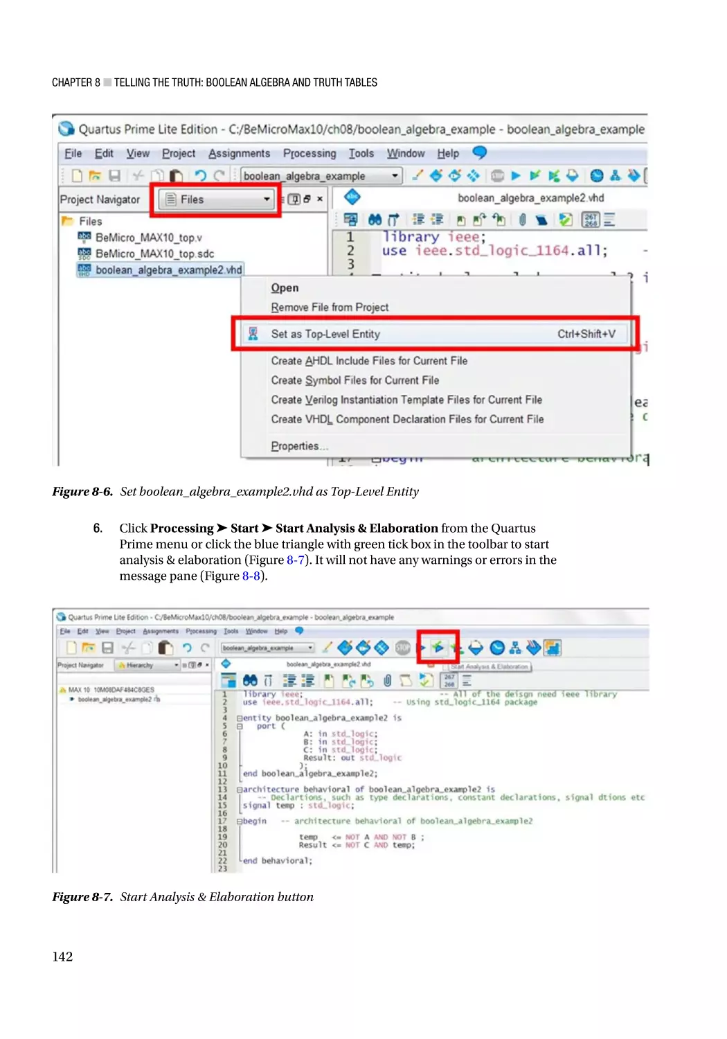
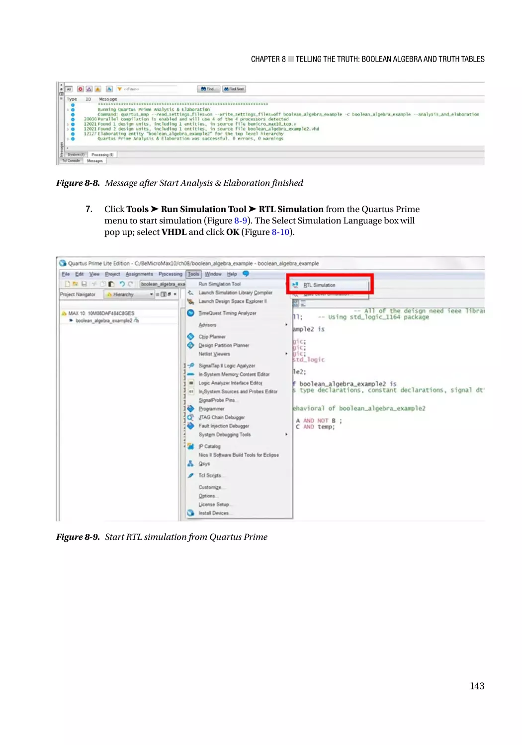
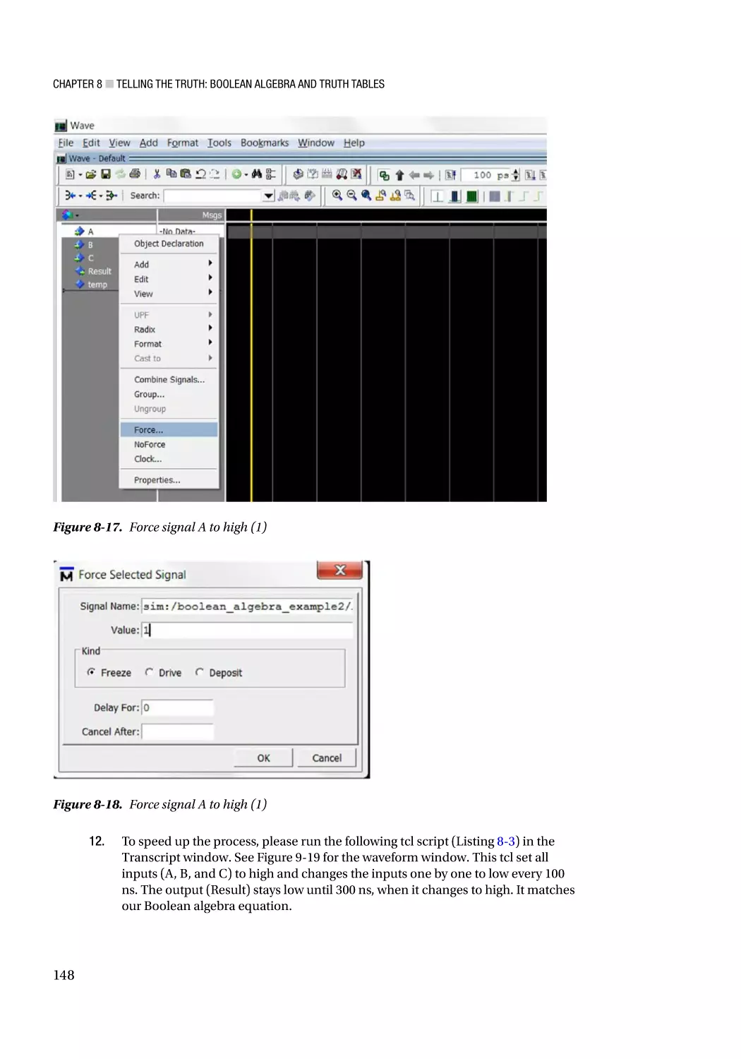
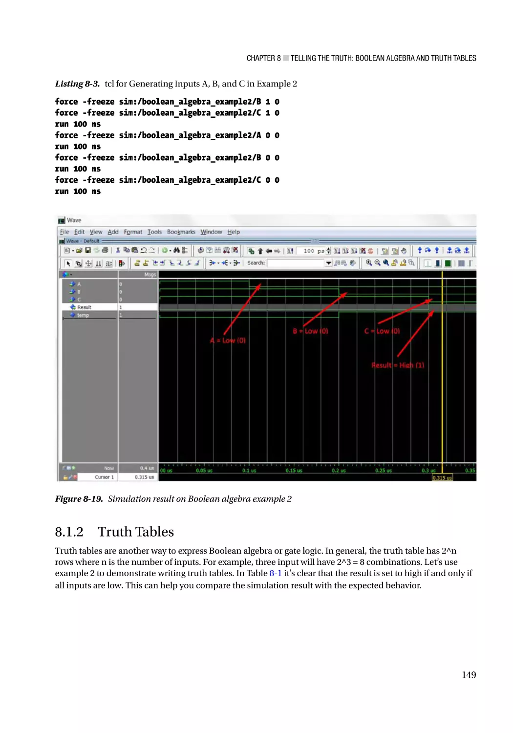
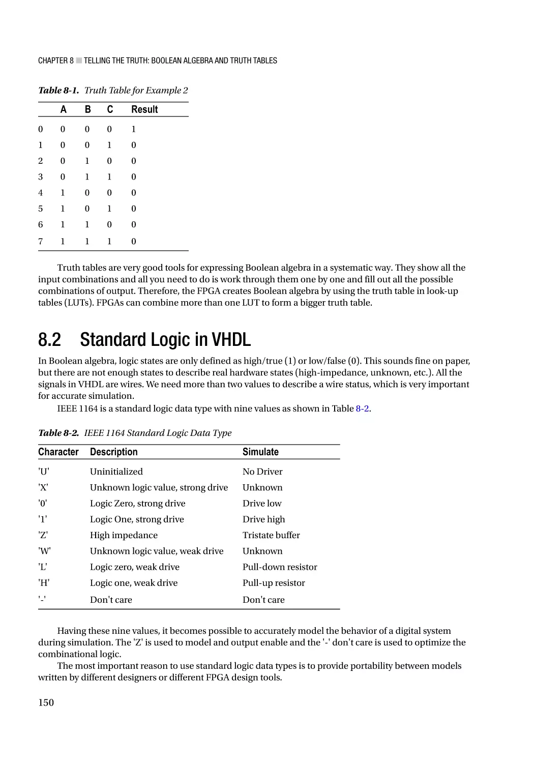
8.1.1 Simulation Steps for Boolean Algebra Example 2������������������������������������������������������������������ 139
8.1.2 Truth Tables���������������������������������������������������������������������������������������������������������������������������� 149
8.2 Standard Logic in VHDL��������������������������������������������������������������������������������������� 150
8.2.1 Standard Logic Data Types����������������������������������������������������������������������������������������������������� 151
8.2.2 4-Bit Adder Examples with Standard Logic Types������������������������������������������������������������������ 151
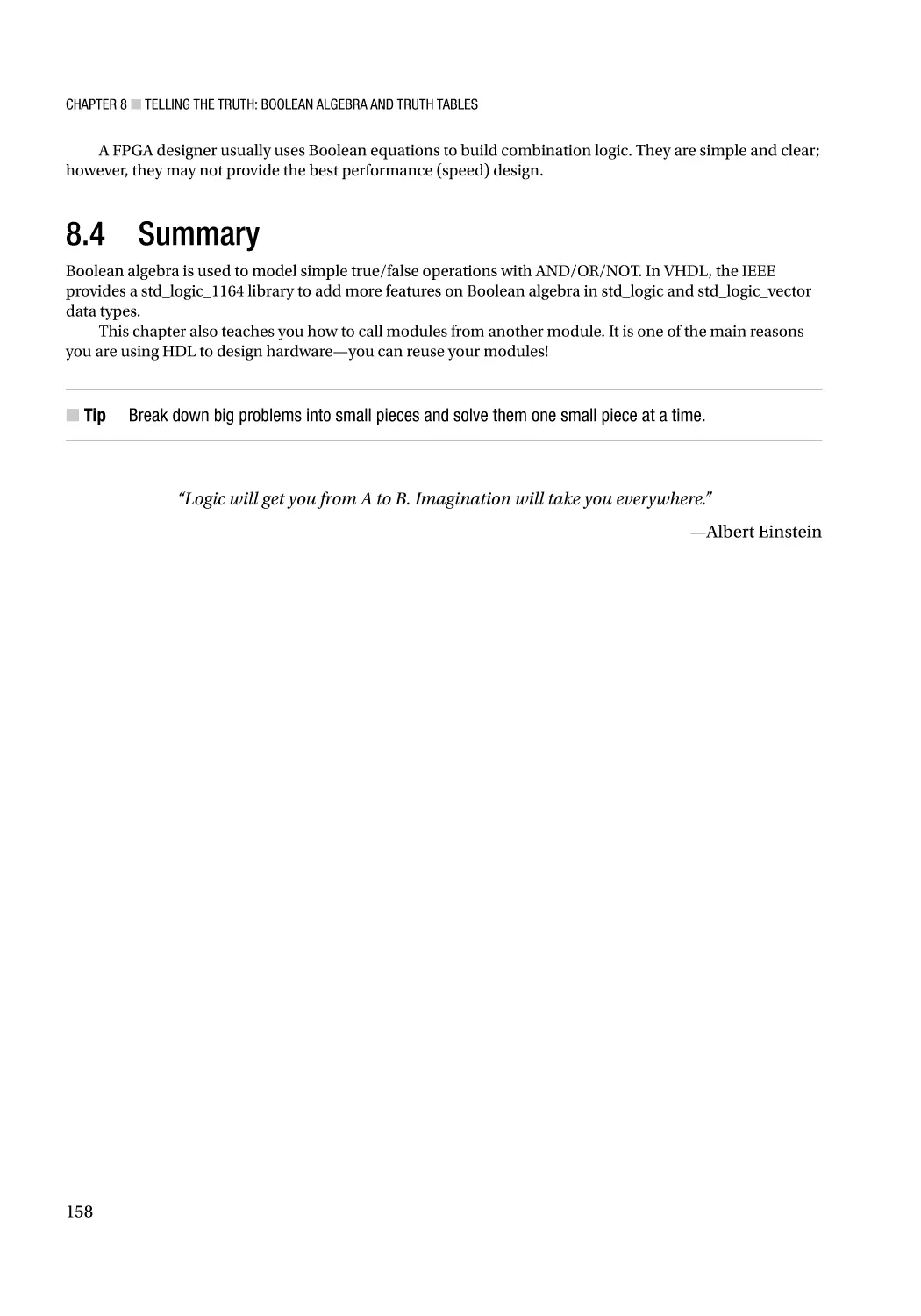
8.3 Combinational Logic Design in FPGA������������������������������������������������������������������ 157
8.4 Summary������������������������������������������������������������������������������������������������������������� 158
viii
■ Contents
■Chapter
■
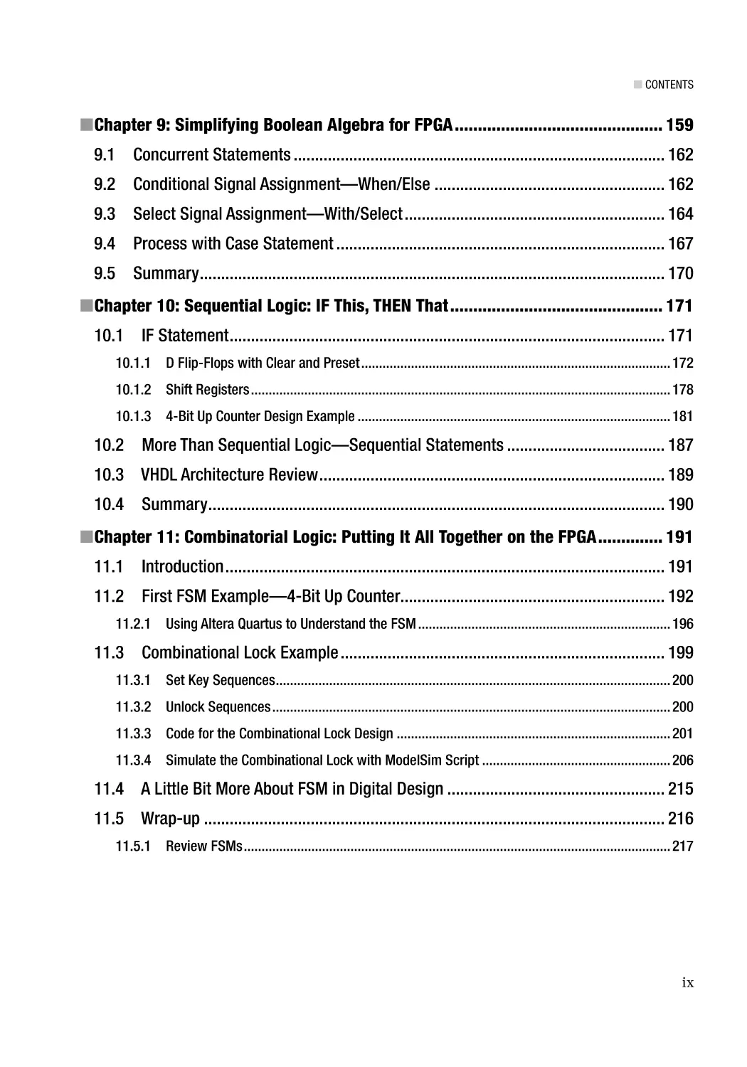
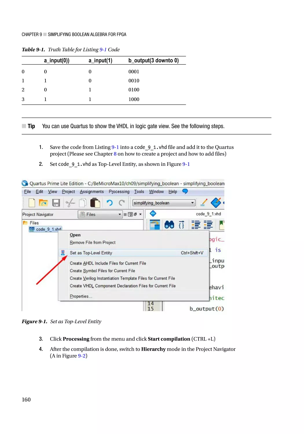
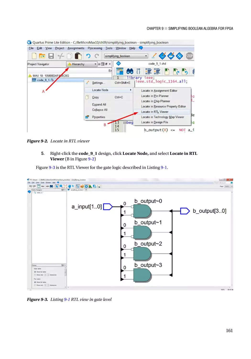
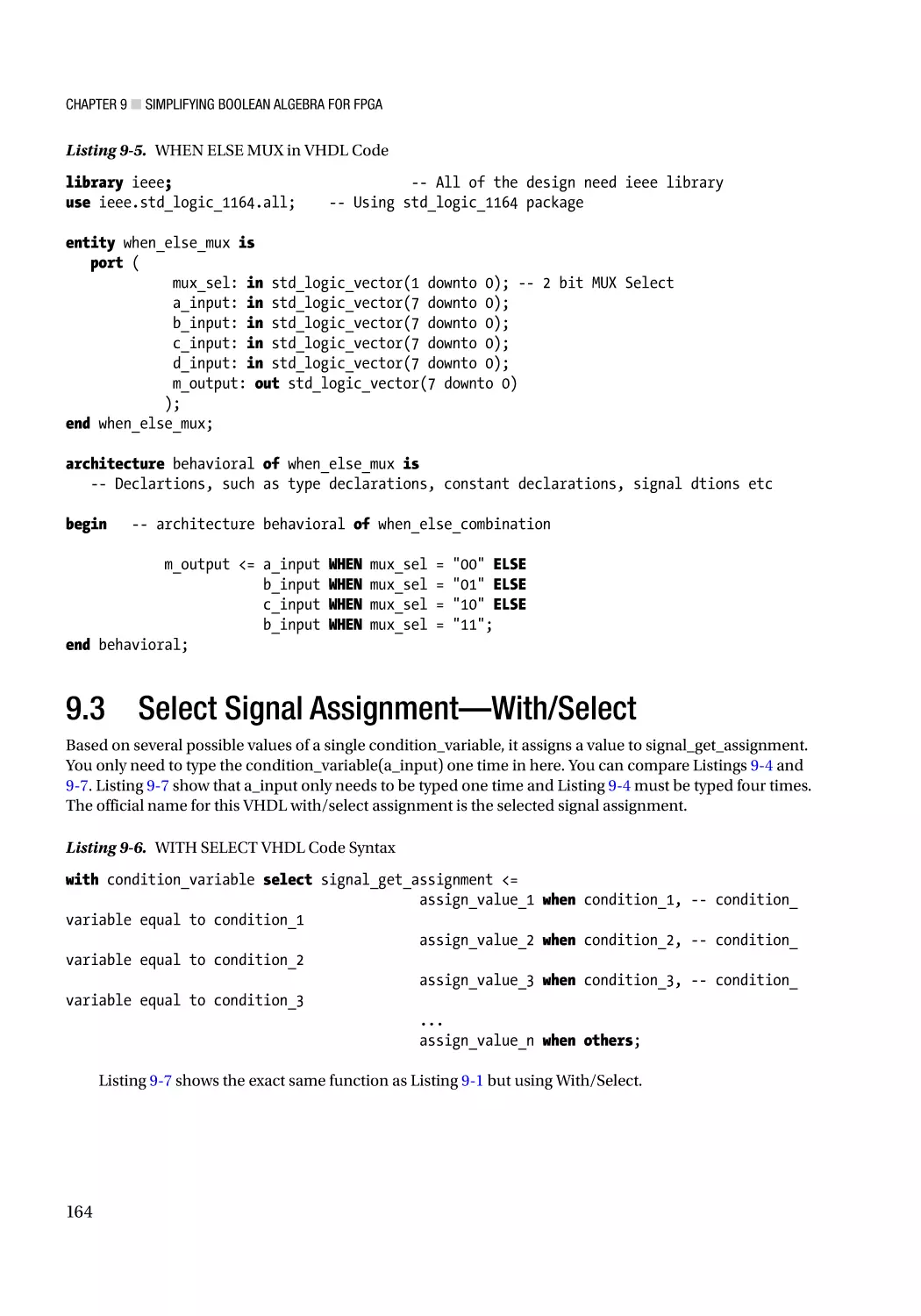
9: Simplifying Boolean Algebra for FPGA��������������������������������������������� 159
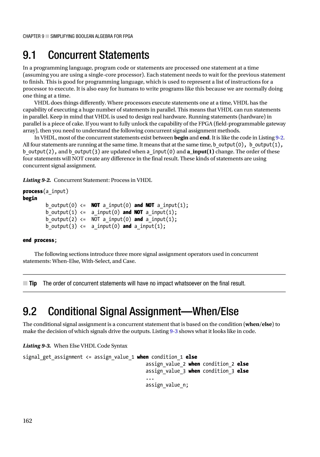
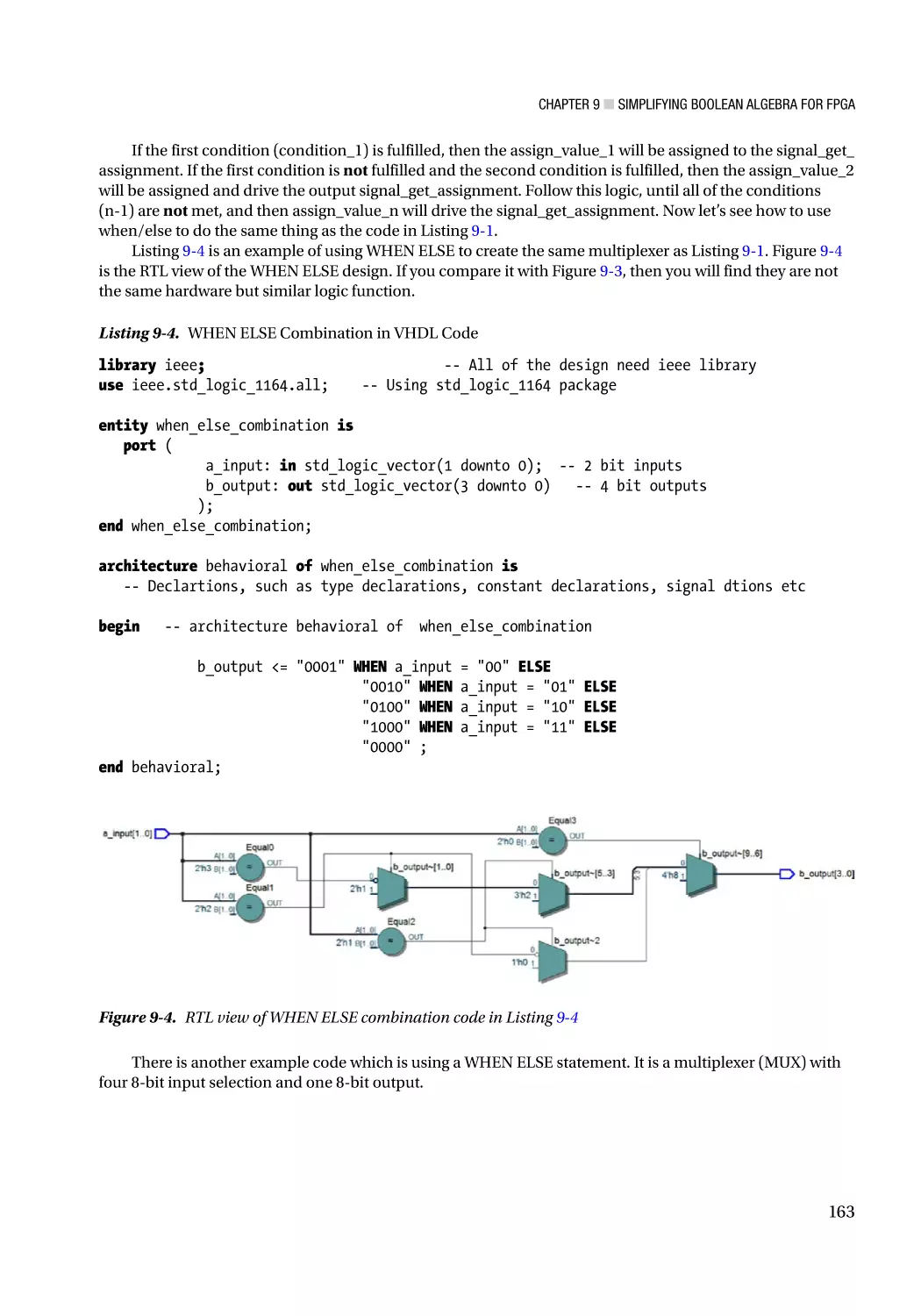
9.1 Concurrent Statements��������������������������������������������������������������������������������������� 162
9.2 Conditional Signal Assignment—When/Else������������������������������������������������������ 162
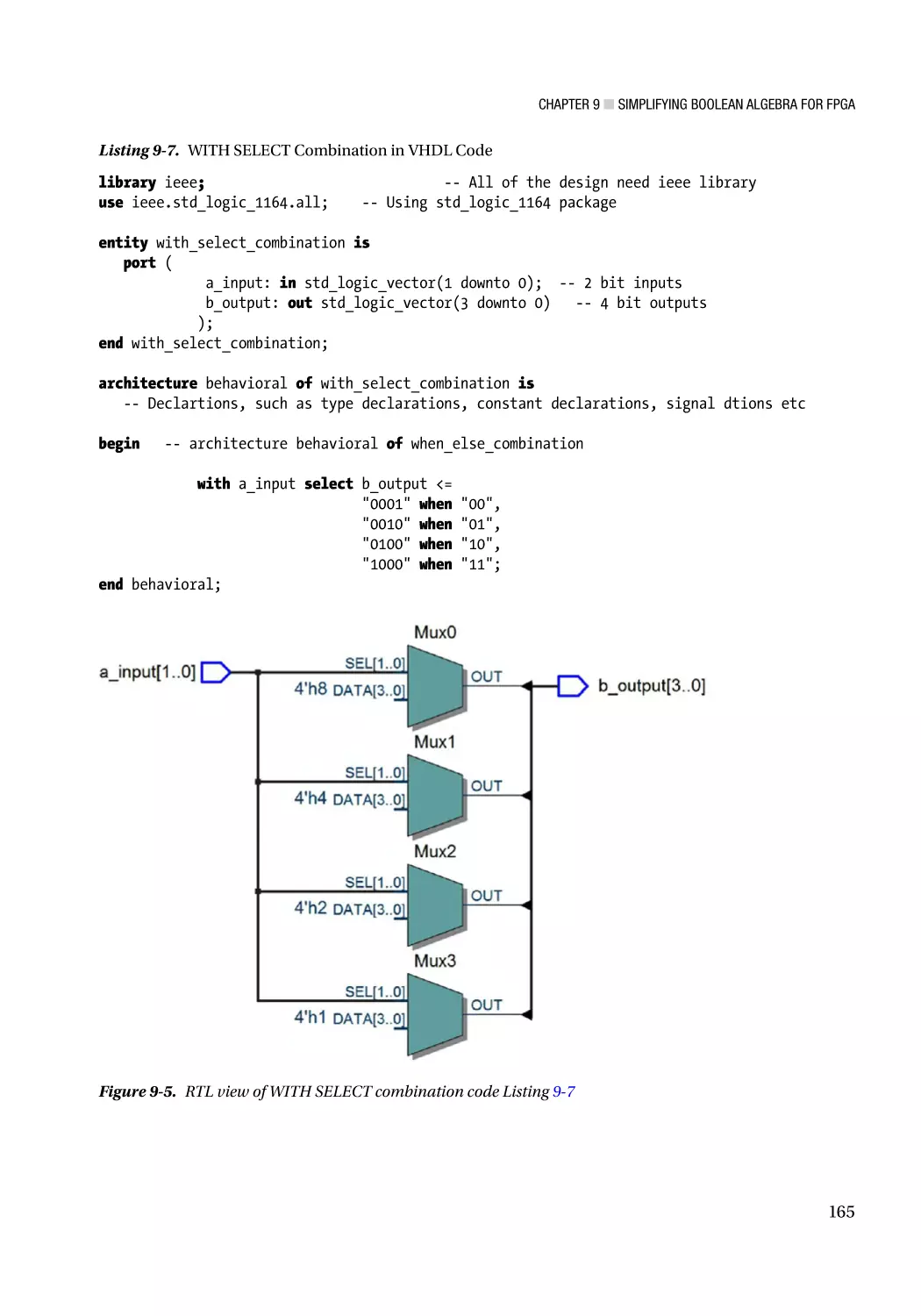
9.3 Select Signal Assignment—With/Select������������������������������������������������������������� 164
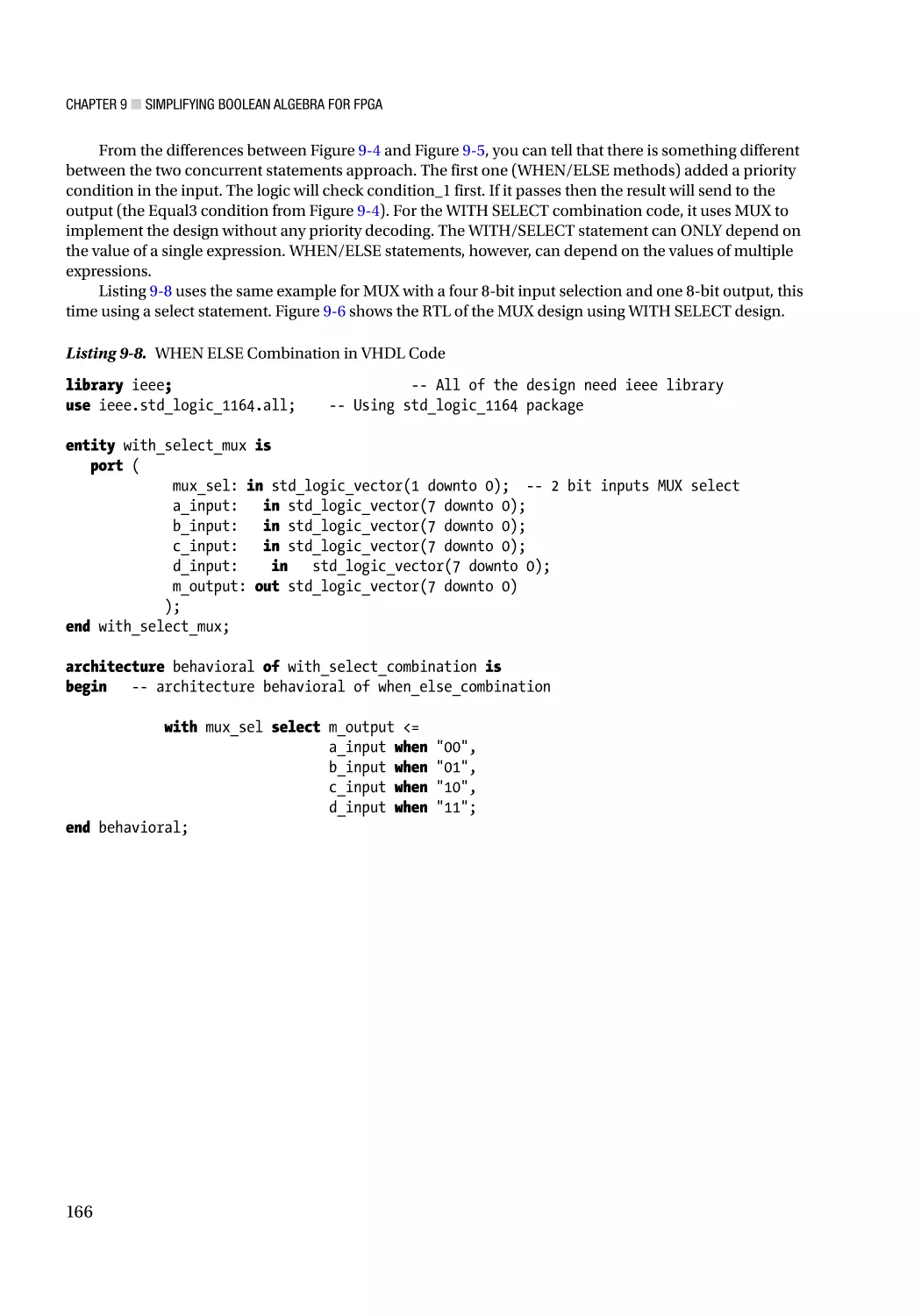
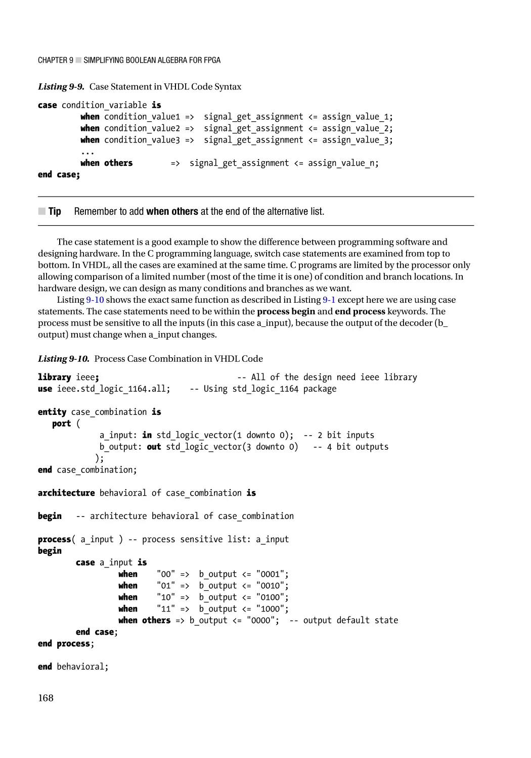
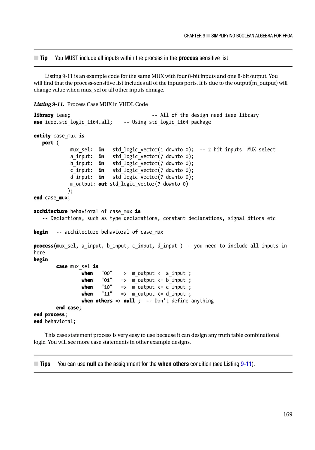
9.4 Process with Case Statement����������������������������������������������������������������������������� 167
9.5 Summary������������������������������������������������������������������������������������������������������������� 170
■Chapter
■
10: Sequential Logic: IF This, THEN That���������������������������������������������� 171
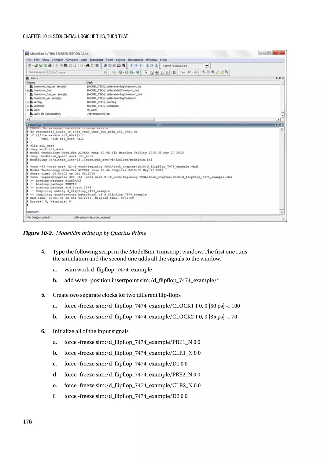
10.1 IF Statement������������������������������������������������������������������������������������������������������ 171
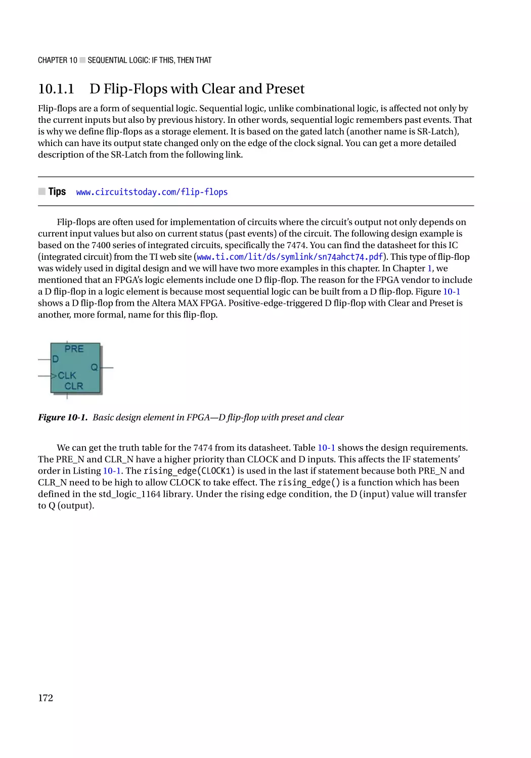
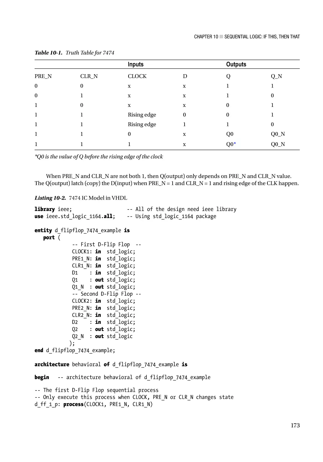
10.1.1 D Flip-Flops with Clear and Preset��������������������������������������������������������������������������������������� 172
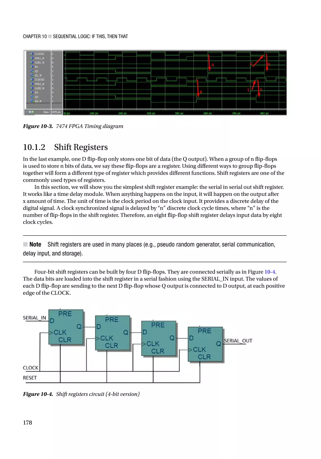
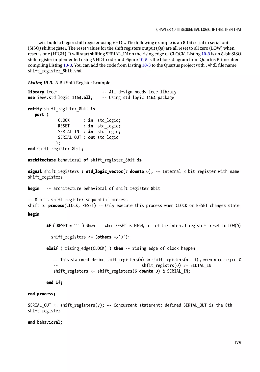
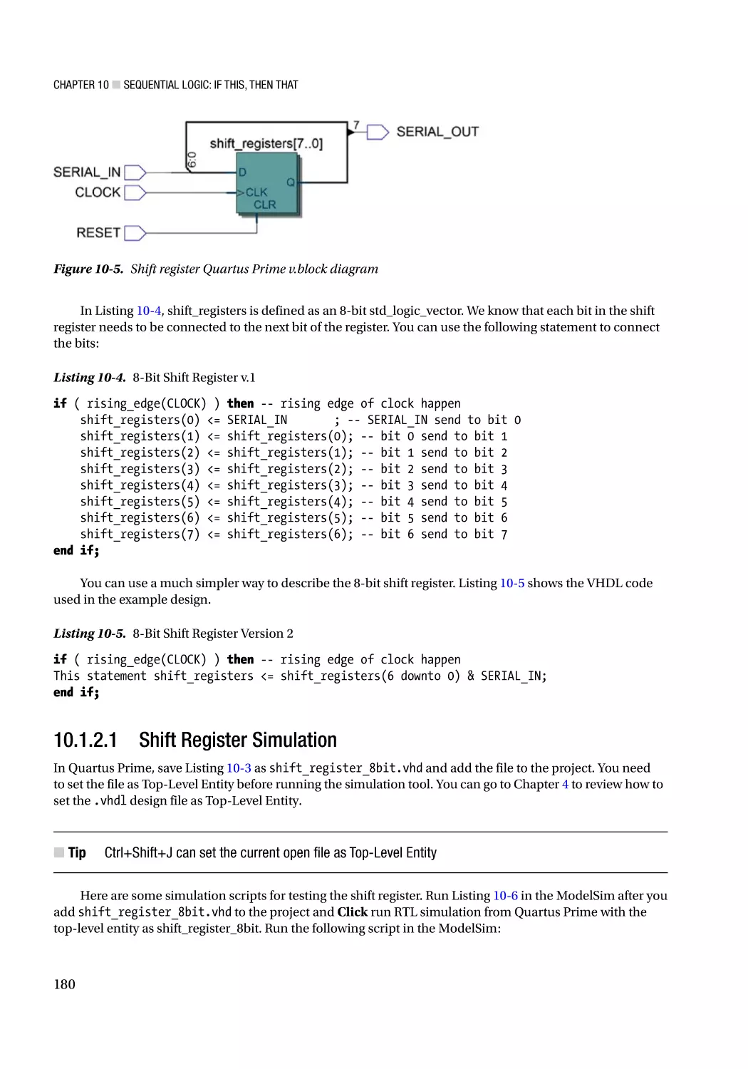
10.1.2 Shift Registers���������������������������������������������������������������������������������������������������������������������� 178
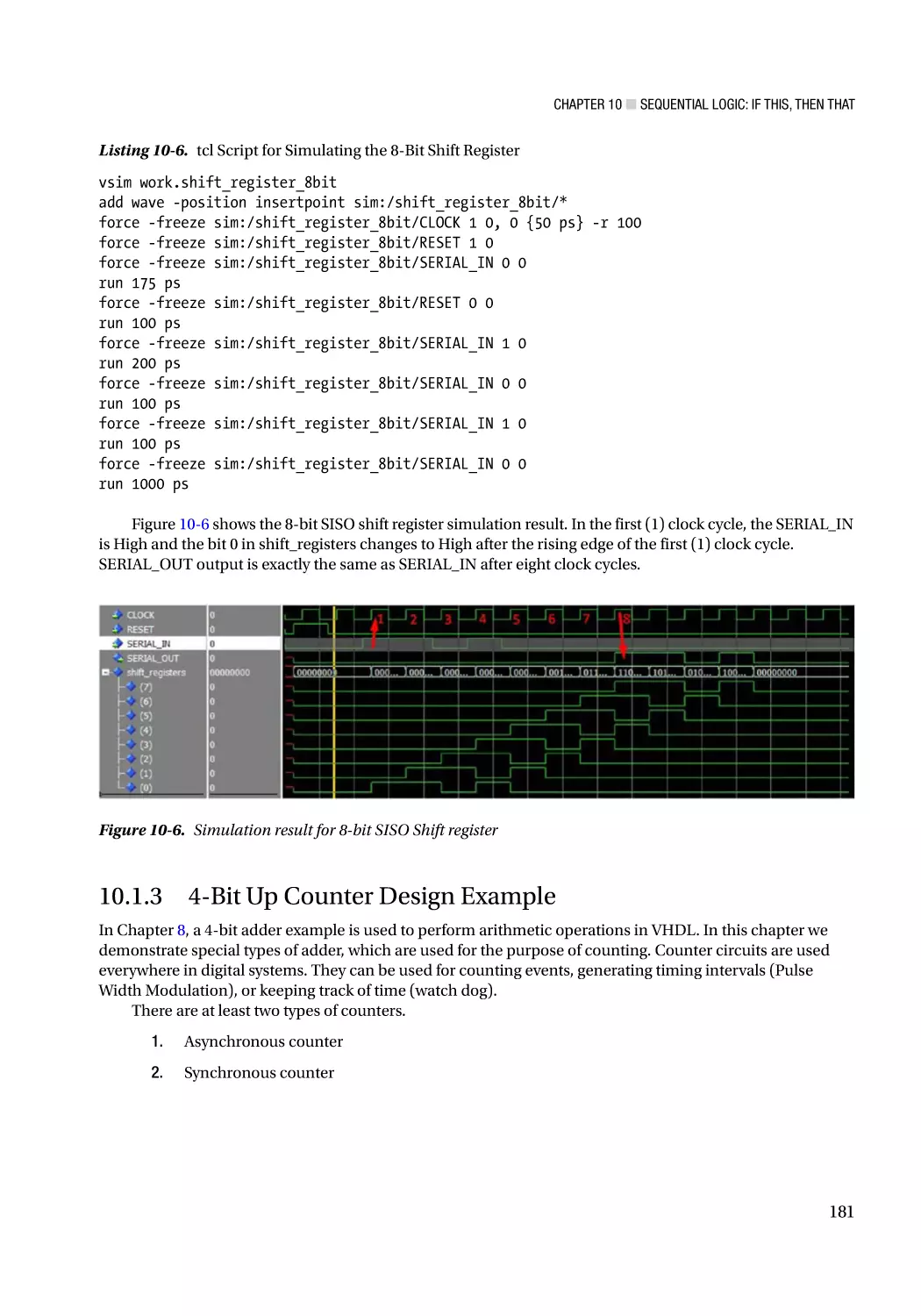
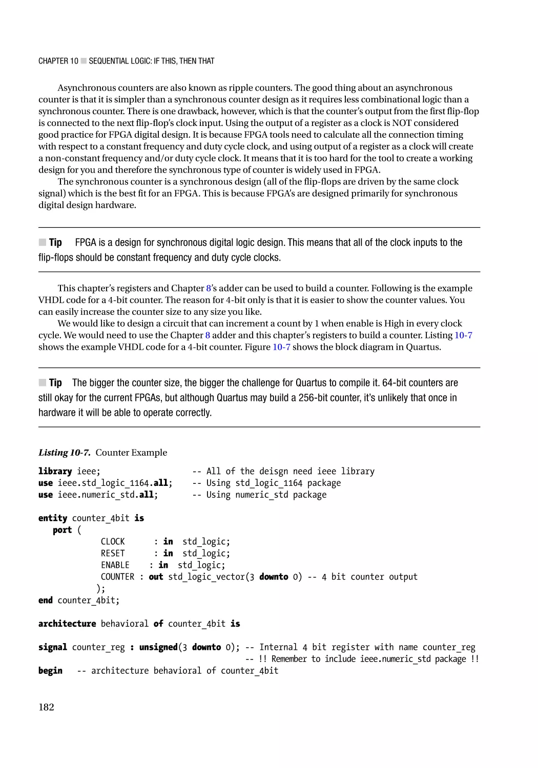
10.1.3 4-Bit Up Counter Design Example���������������������������������������������������������������������������������������� 181
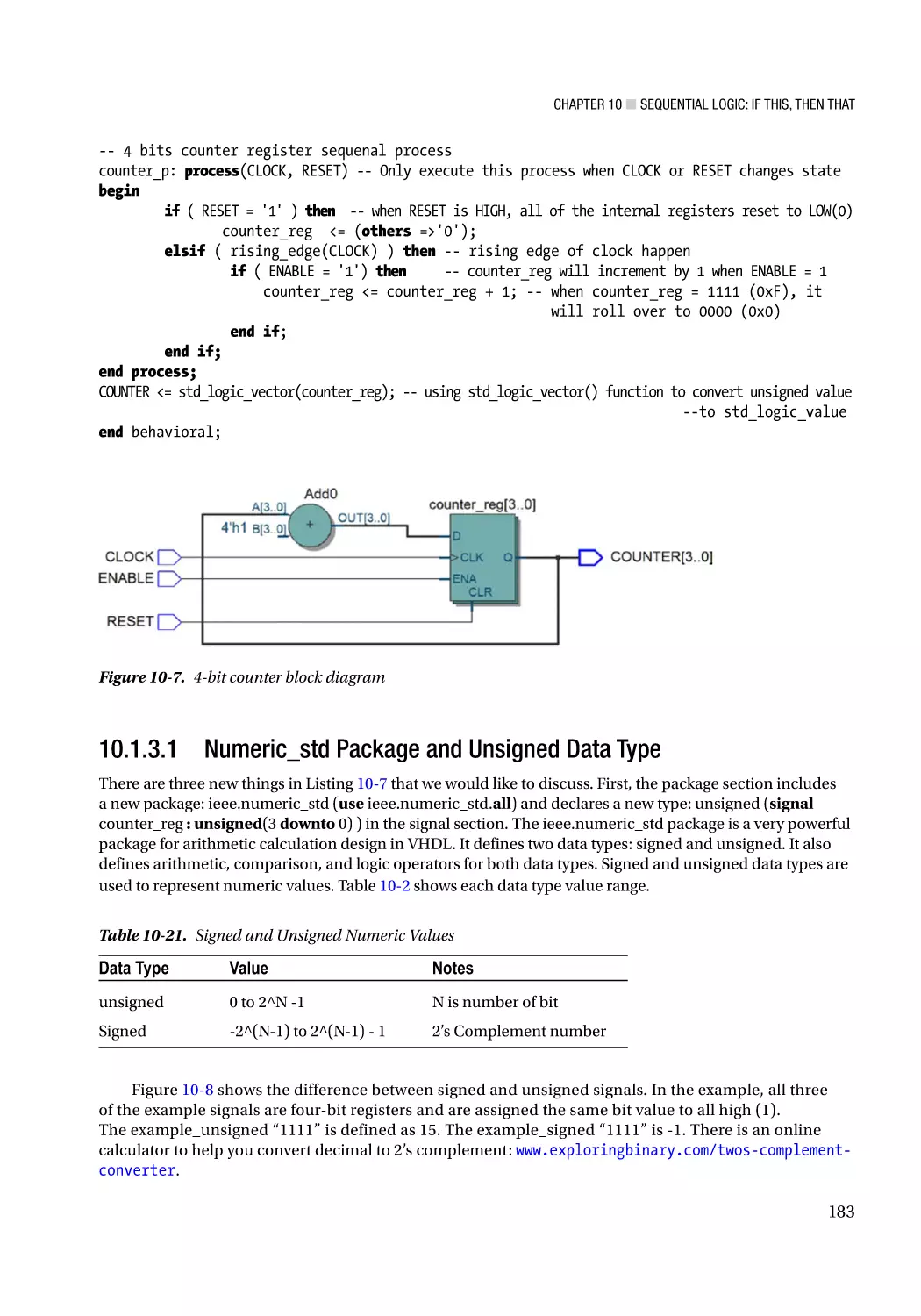
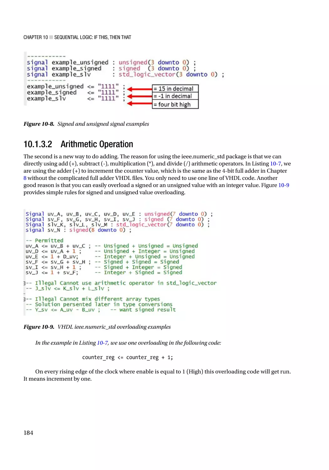
10.2 More Than Sequential Logic—Sequential Statements������������������������������������� 187
10.3 VHDL Architecture Review��������������������������������������������������������������������������������� 189
10.4 Summary����������������������������������������������������������������������������������������������������������� 190
■Chapter
■
11: Combinatorial Logic: Putting It All Together on the FPGA�������������� 191
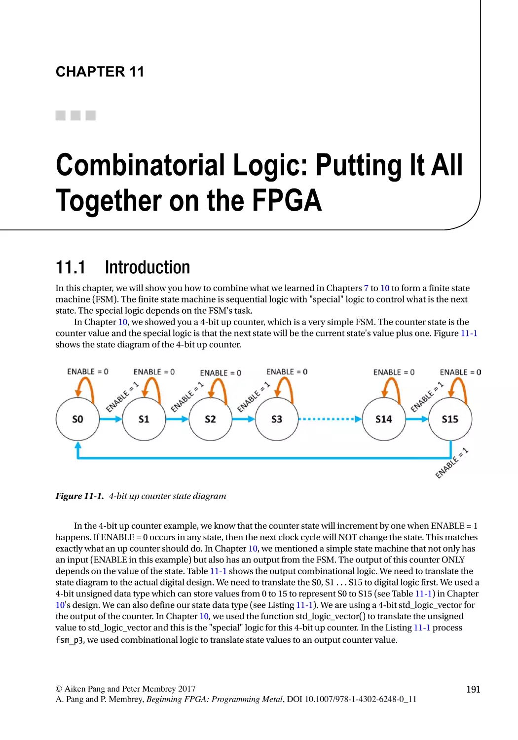
11.1 Introduction������������������������������������������������������������������������������������������������������� 191
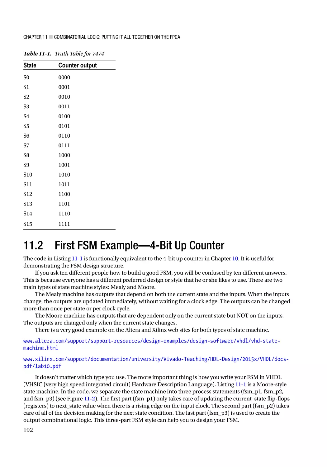
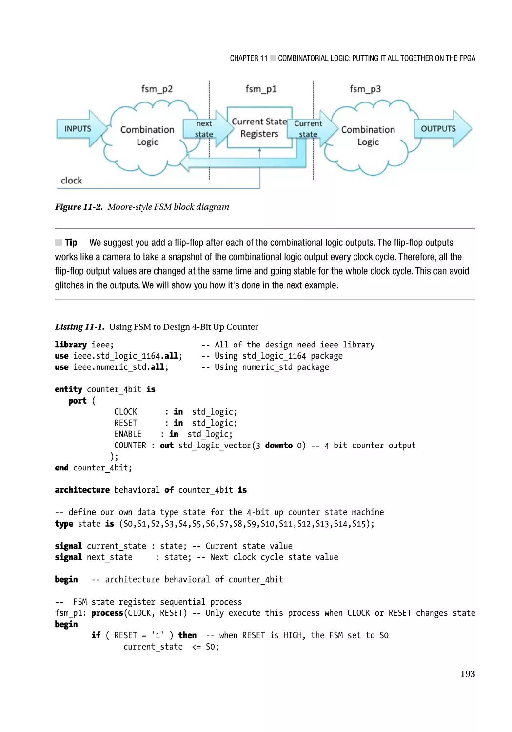
11.2 First FSM Example—4-Bit Up Counter������������������������������������������������������������� 192
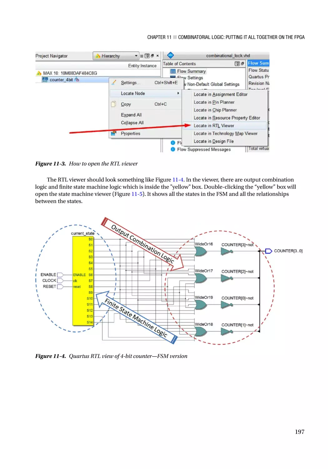
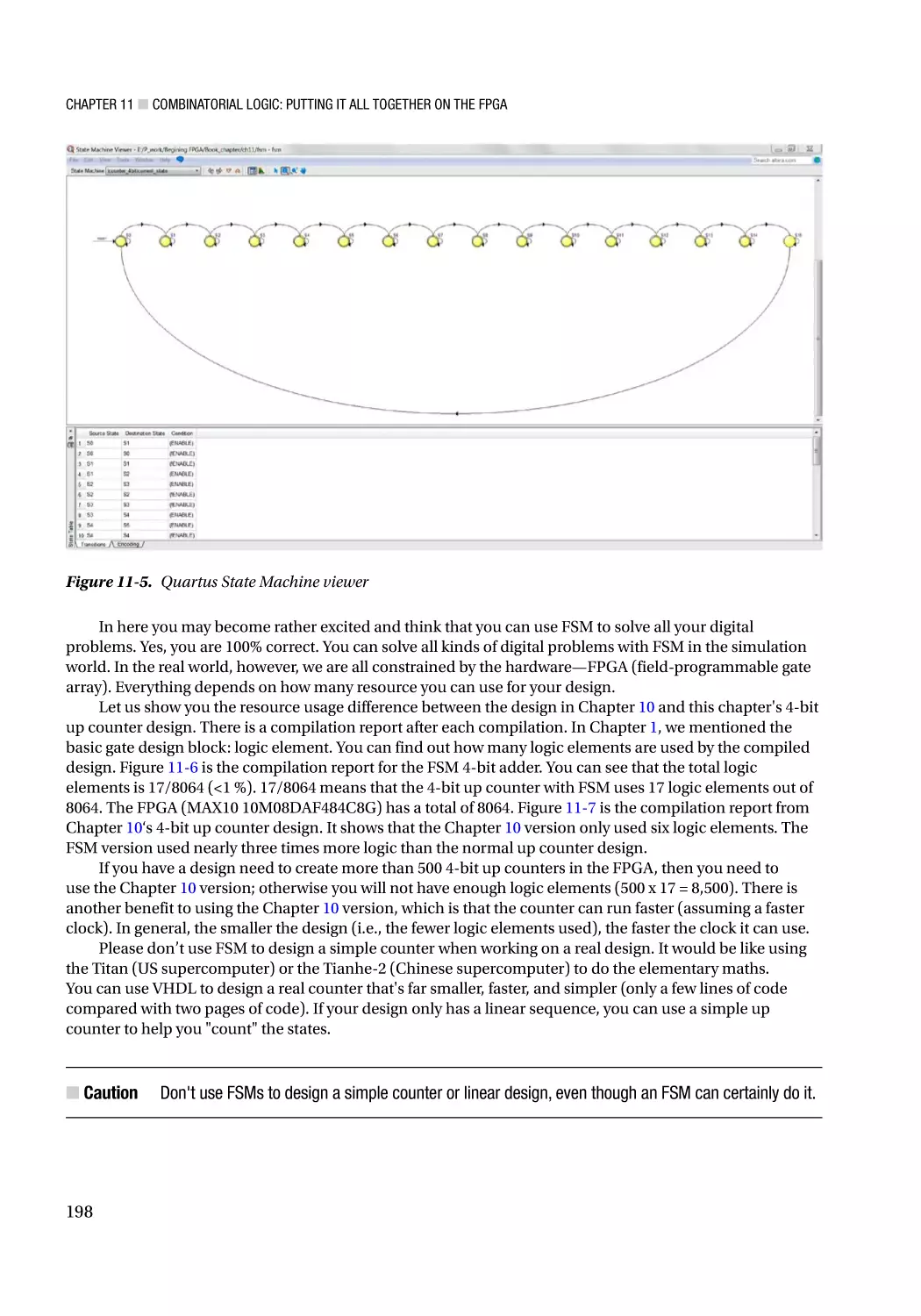
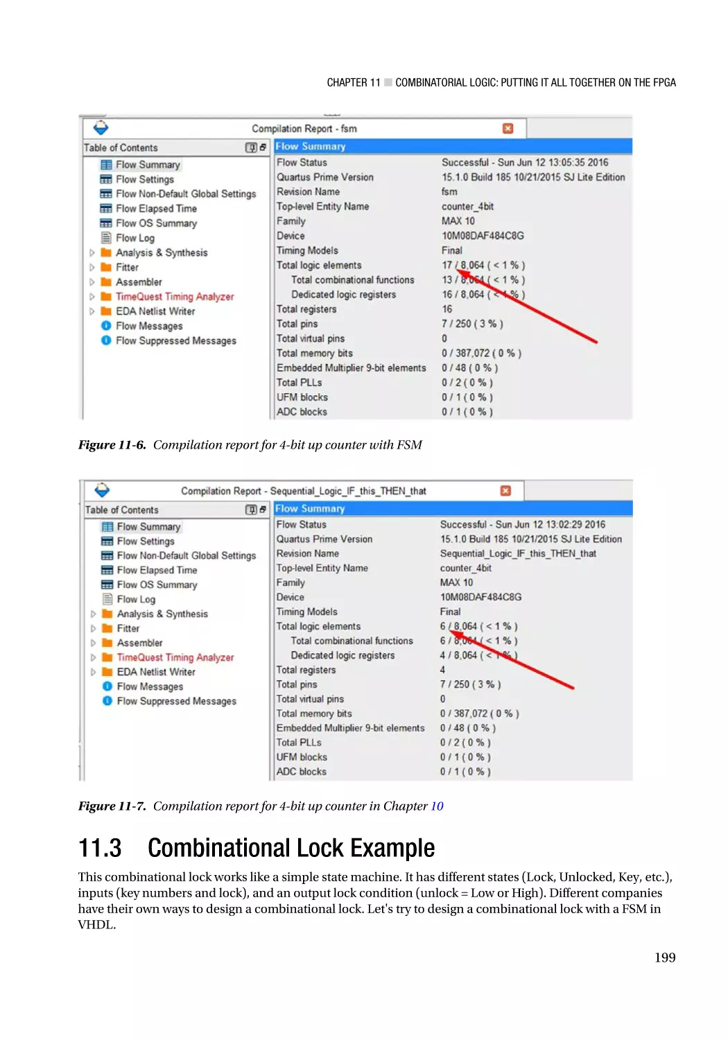
11.2.1 Using Altera Quartus to Understand the FSM����������������������������������������������������������������������� 196
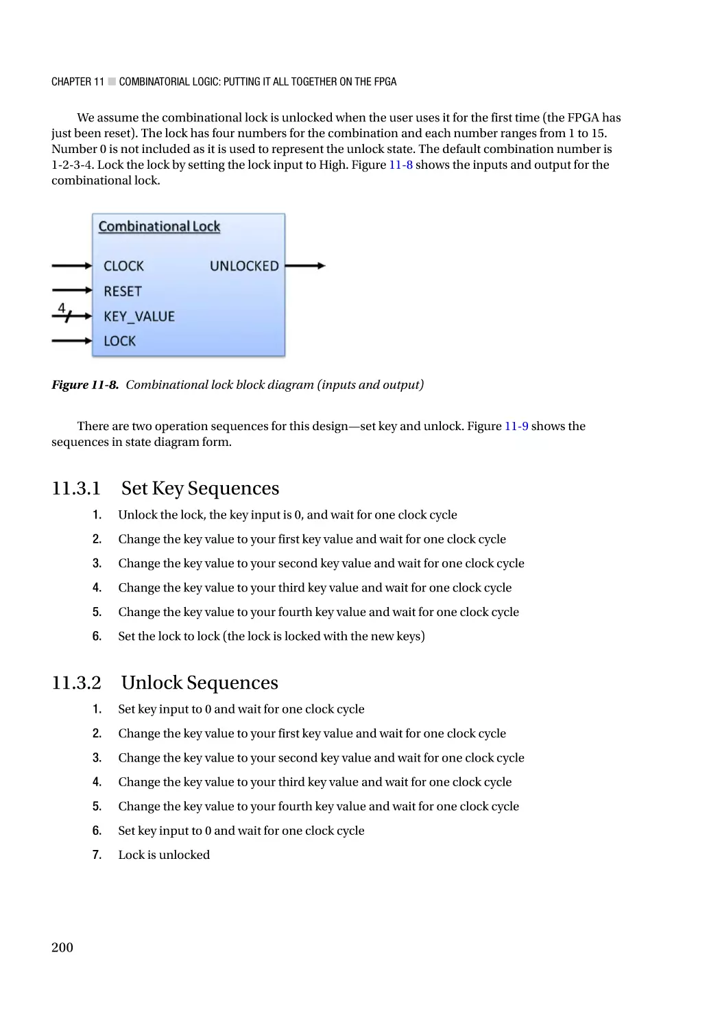
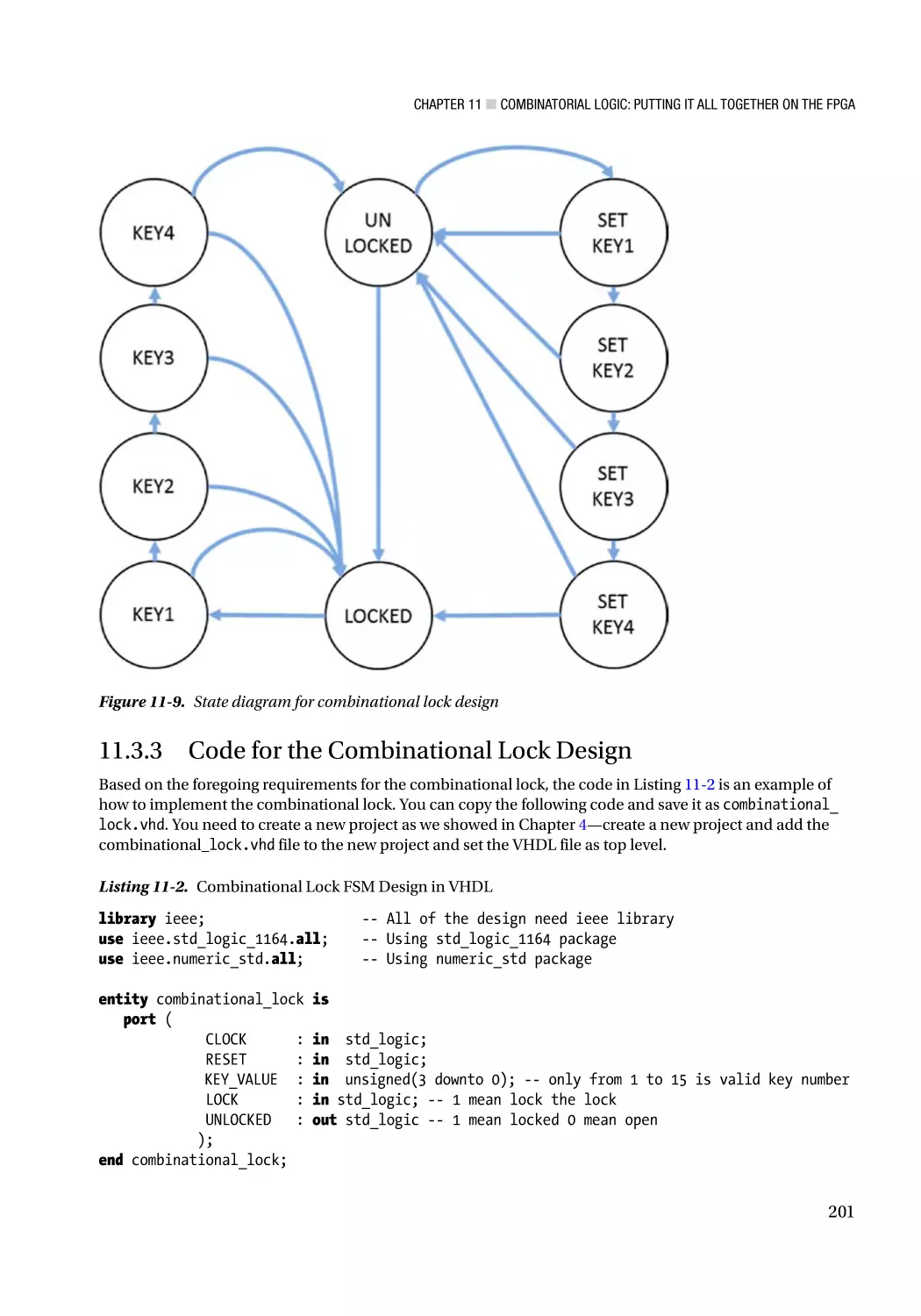
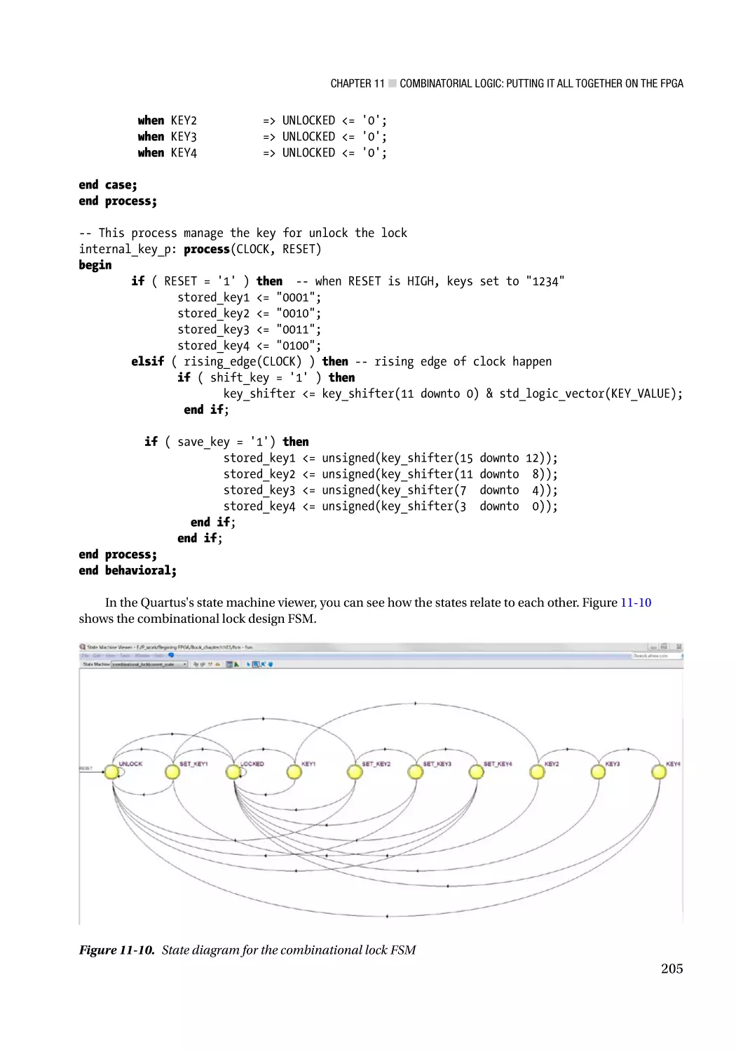
11.3 Combinational Lock Example���������������������������������������������������������������������������� 199
11.3.1 Set Key Sequences��������������������������������������������������������������������������������������������������������������� 200
11.3.2 Unlock Sequences���������������������������������������������������������������������������������������������������������������� 200
11.3.3 Code for the Combinational Lock Design����������������������������������������������������������������������������� 201
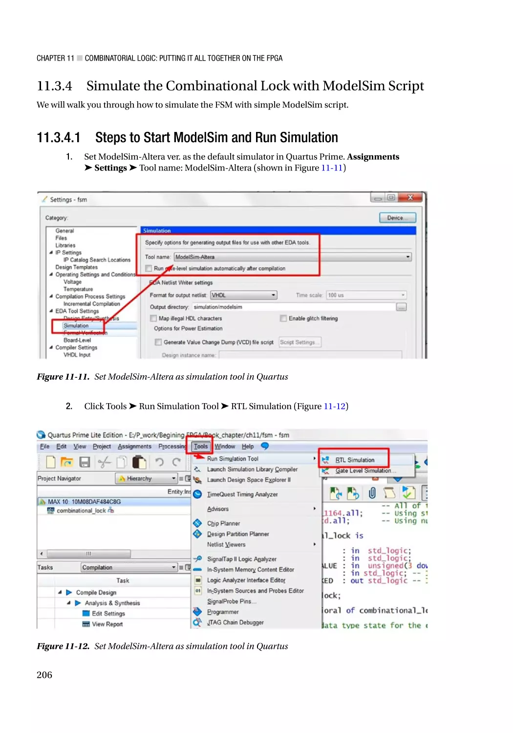
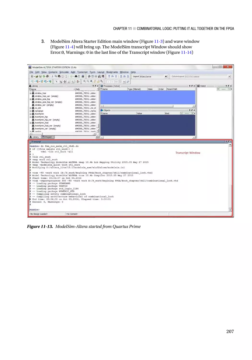
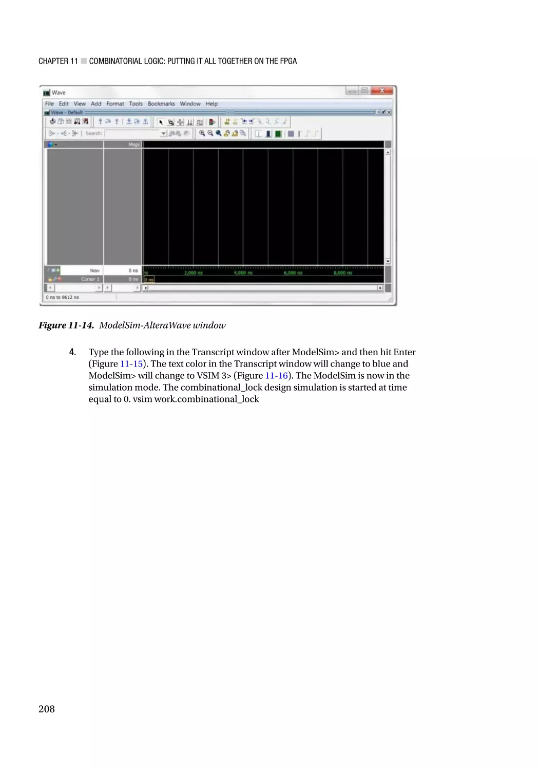
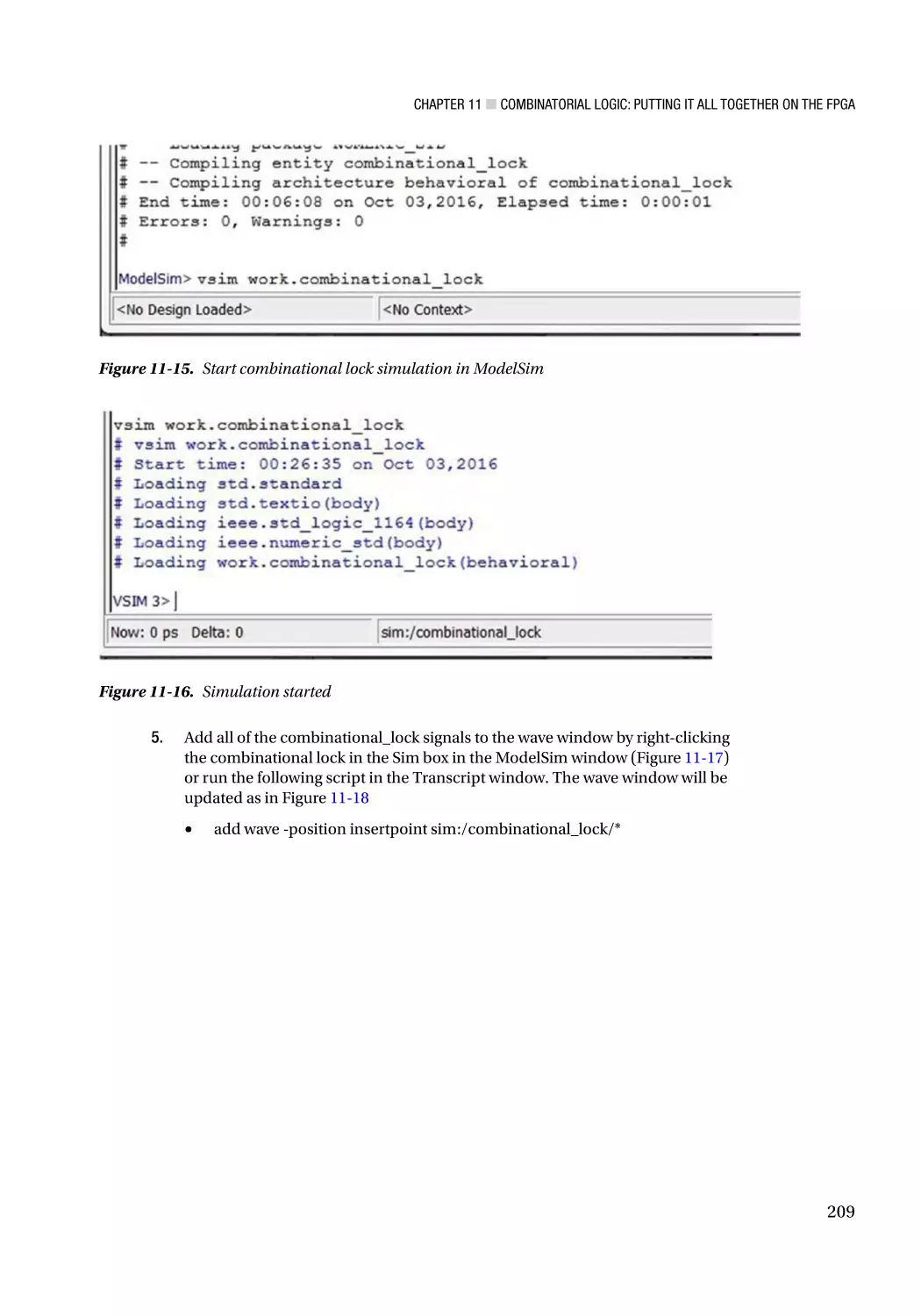
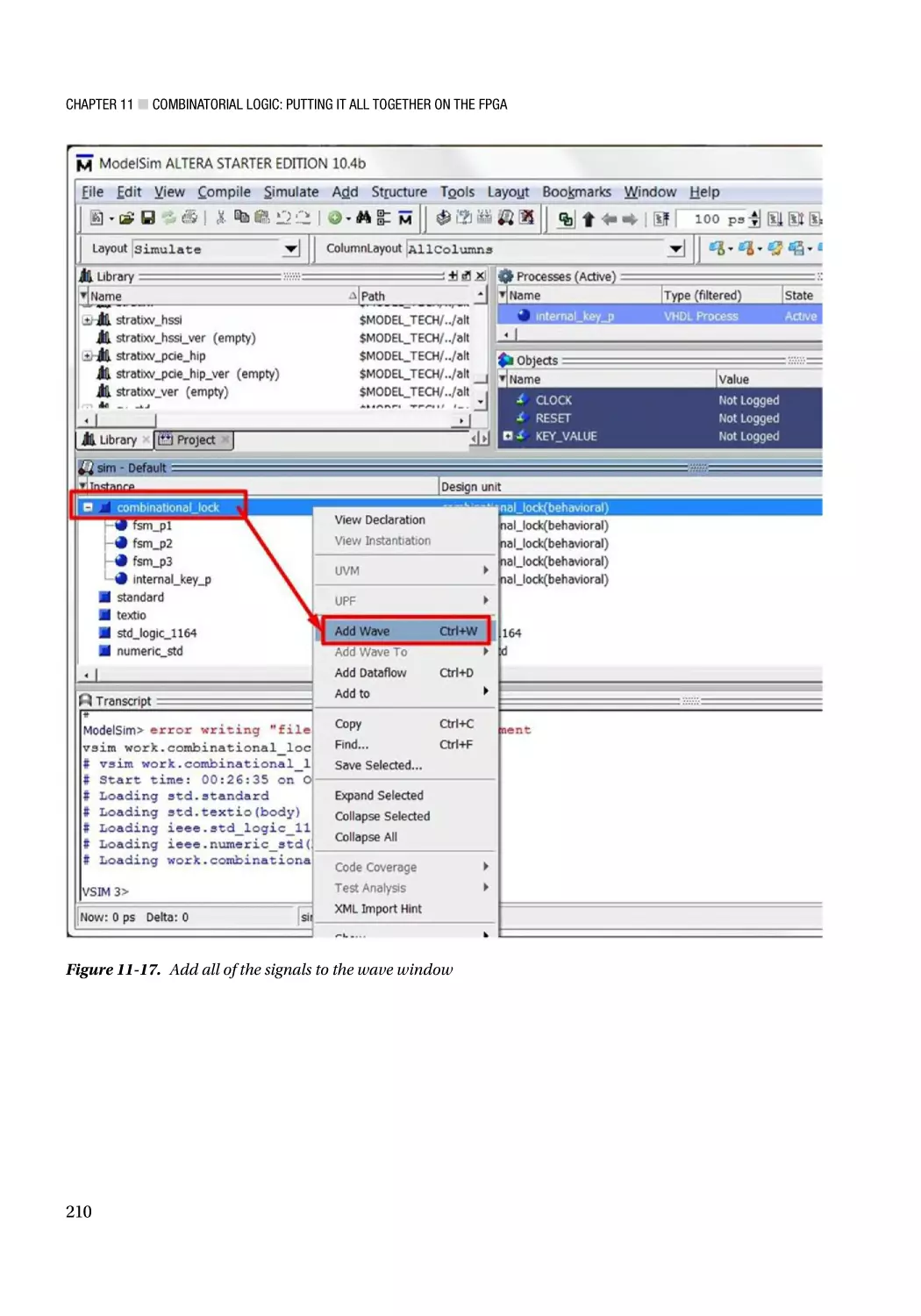
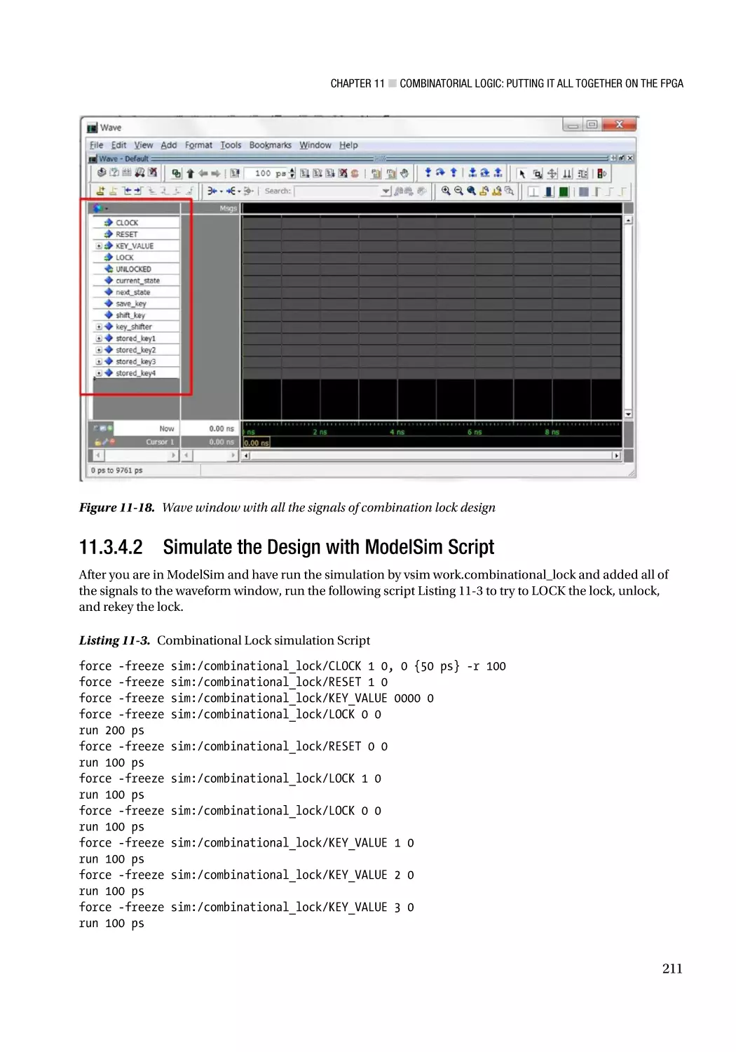
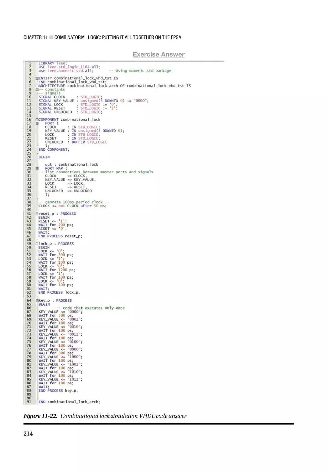
11.3.4 Simulate the Combinational Lock with ModelSim Script����������������������������������������������������� 206
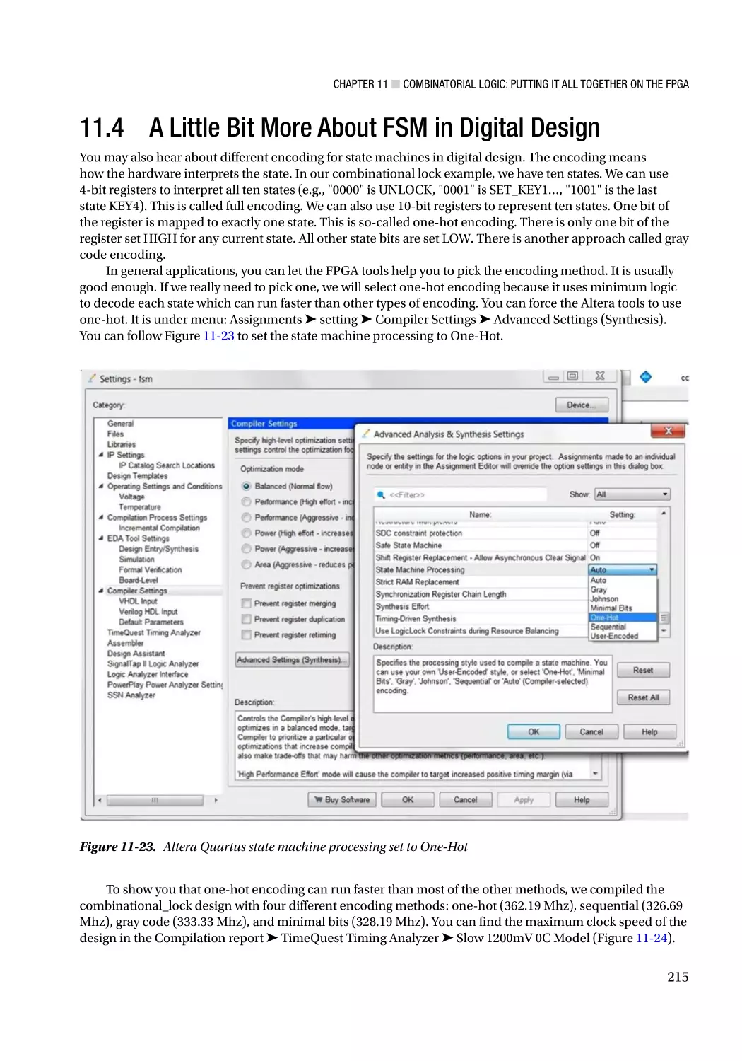
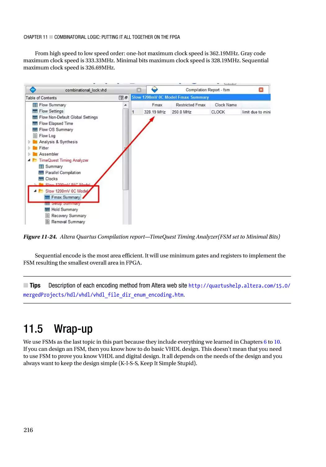
11.4 A Little Bit More About FSM in Digital Design��������������������������������������������������� 215
11.5 Wrap-up������������������������������������������������������������������������������������������������������������ 216
11.5.1 Review FSMs������������������������������������������������������������������������������������������������������������������������ 217
ix
■ Contents
■Part
■
III: Let’s Make Something!������������������������������������������������������ 219
■Chapter
■
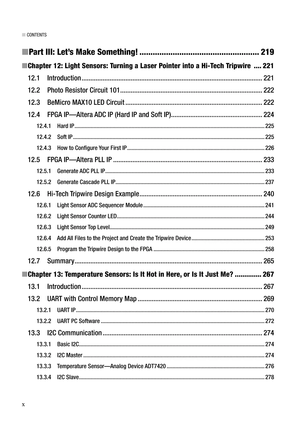
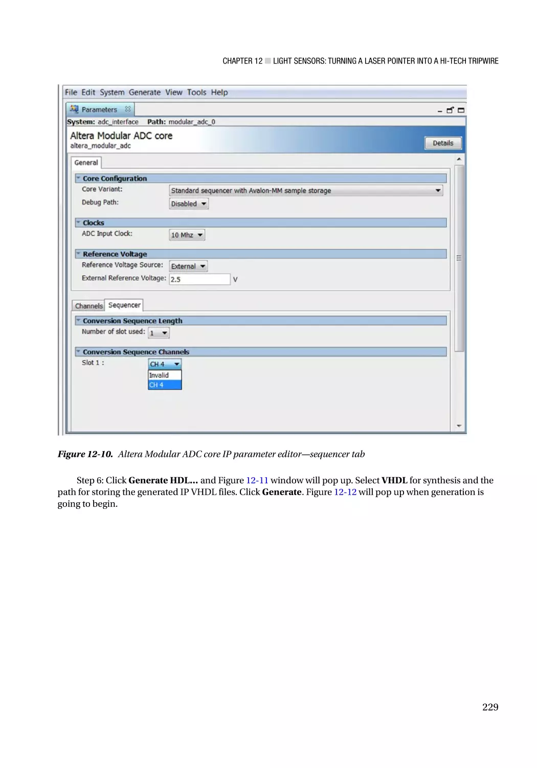
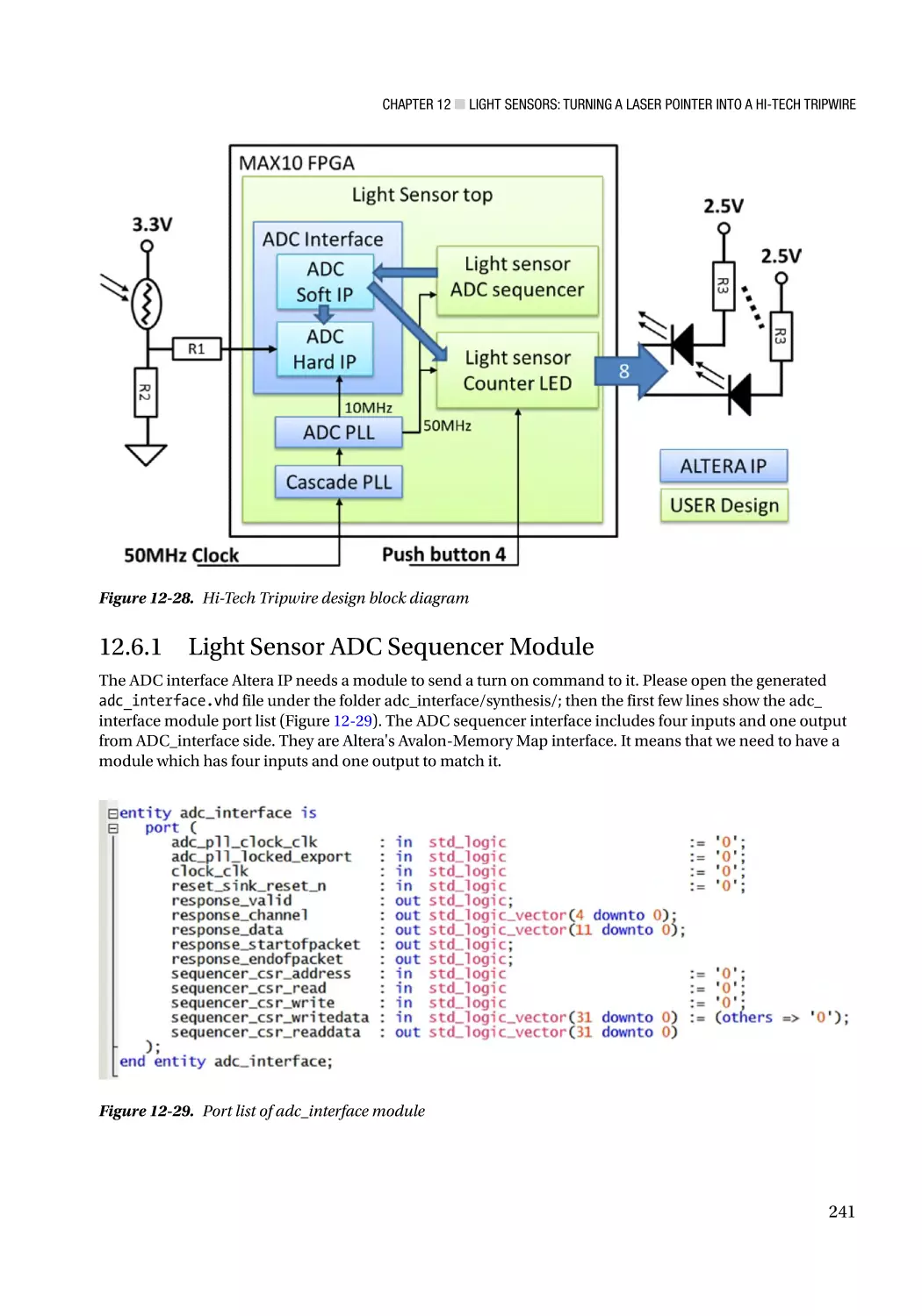
12: Light Sensors: Turning a Laser Pointer into a Hi-Tech Tripwire ���� 221
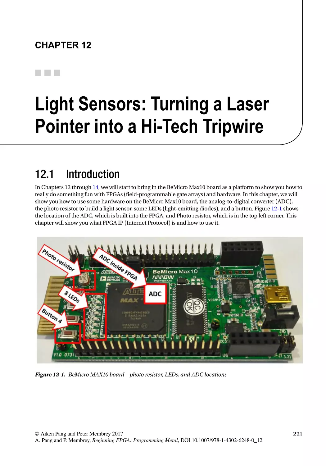
12.1 Introduction������������������������������������������������������������������������������������������������������� 221
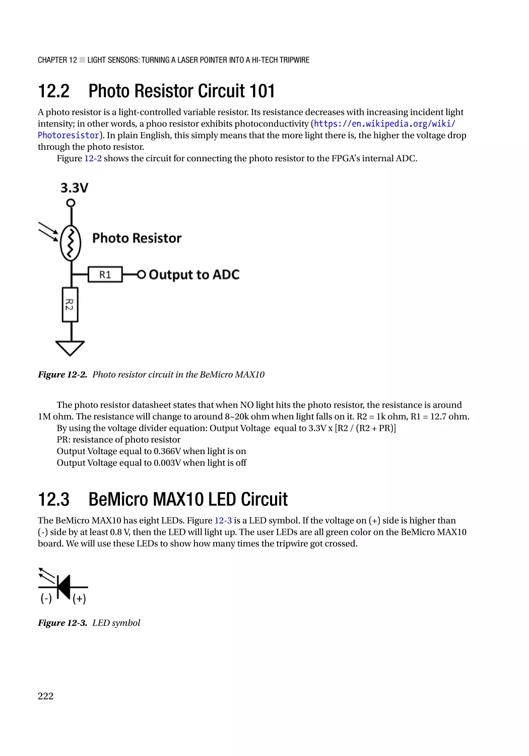
12.2 Photo Resistor Circuit 101��������������������������������������������������������������������������������� 222
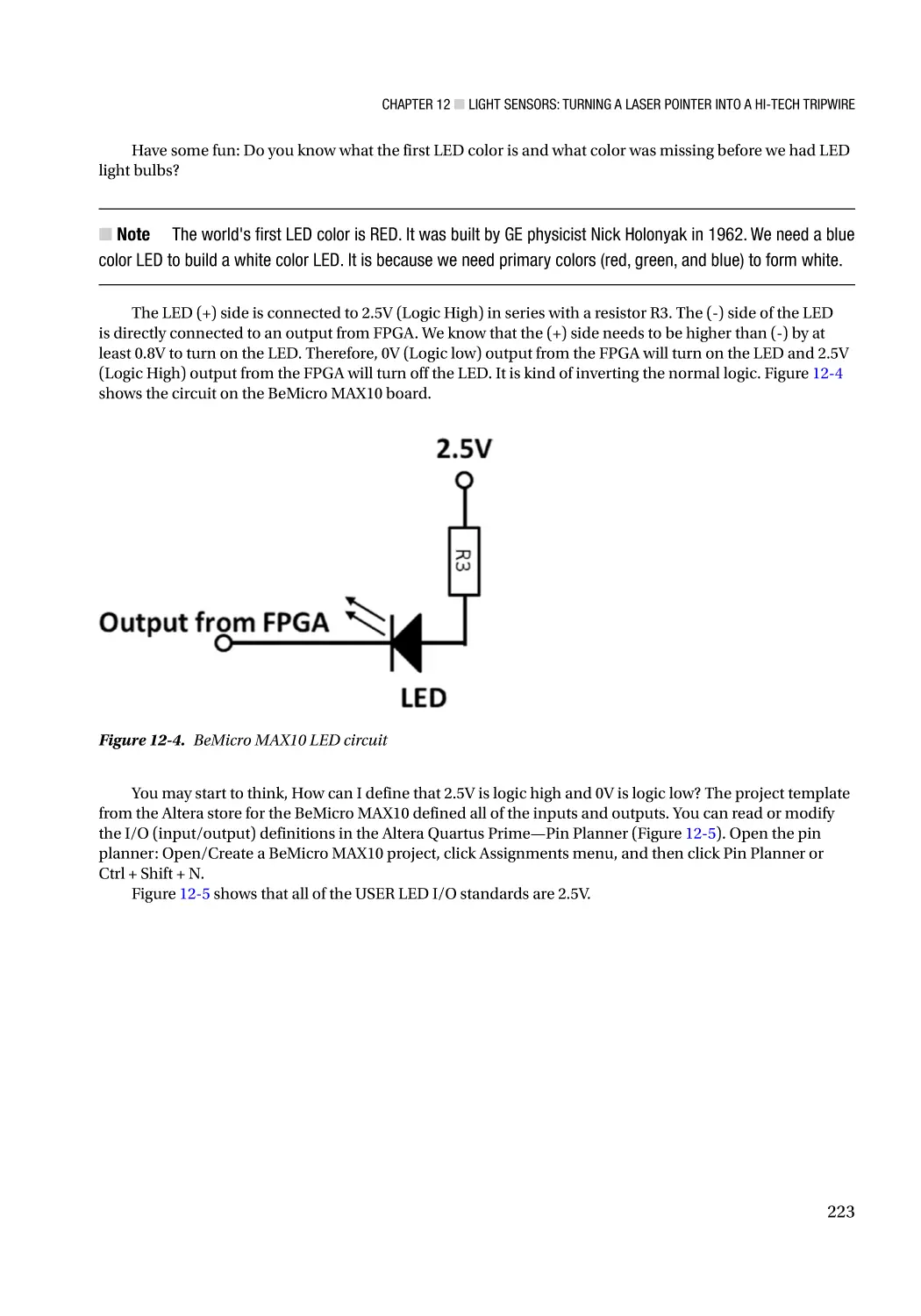
12.3 BeMicro MAX10 LED Circuit������������������������������������������������������������������������������ 222
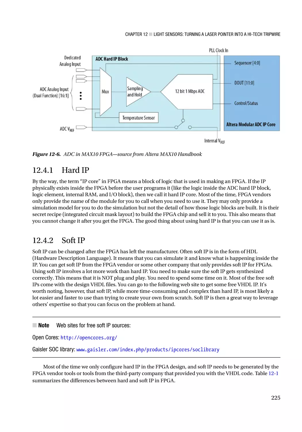
12.4 FPGA IP—Altera ADC IP (Hard IP and Soft IP)��������������������������������������������������� 224
12.4.1 Hard IP���������������������������������������������������������������������������������������������������������������������������������� 225
12.4.2 Soft IP����������������������������������������������������������������������������������������������������������������������������������� 225
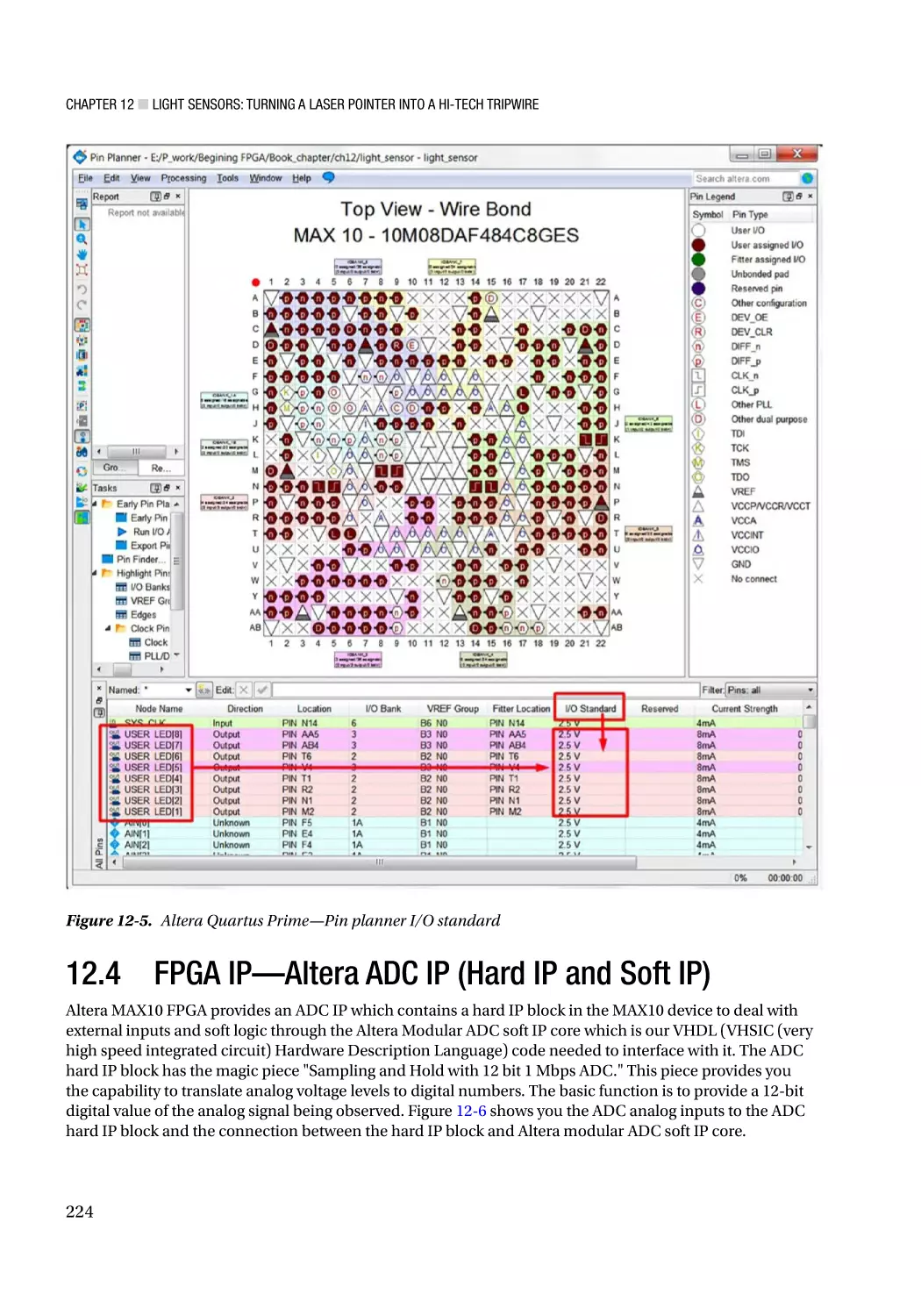
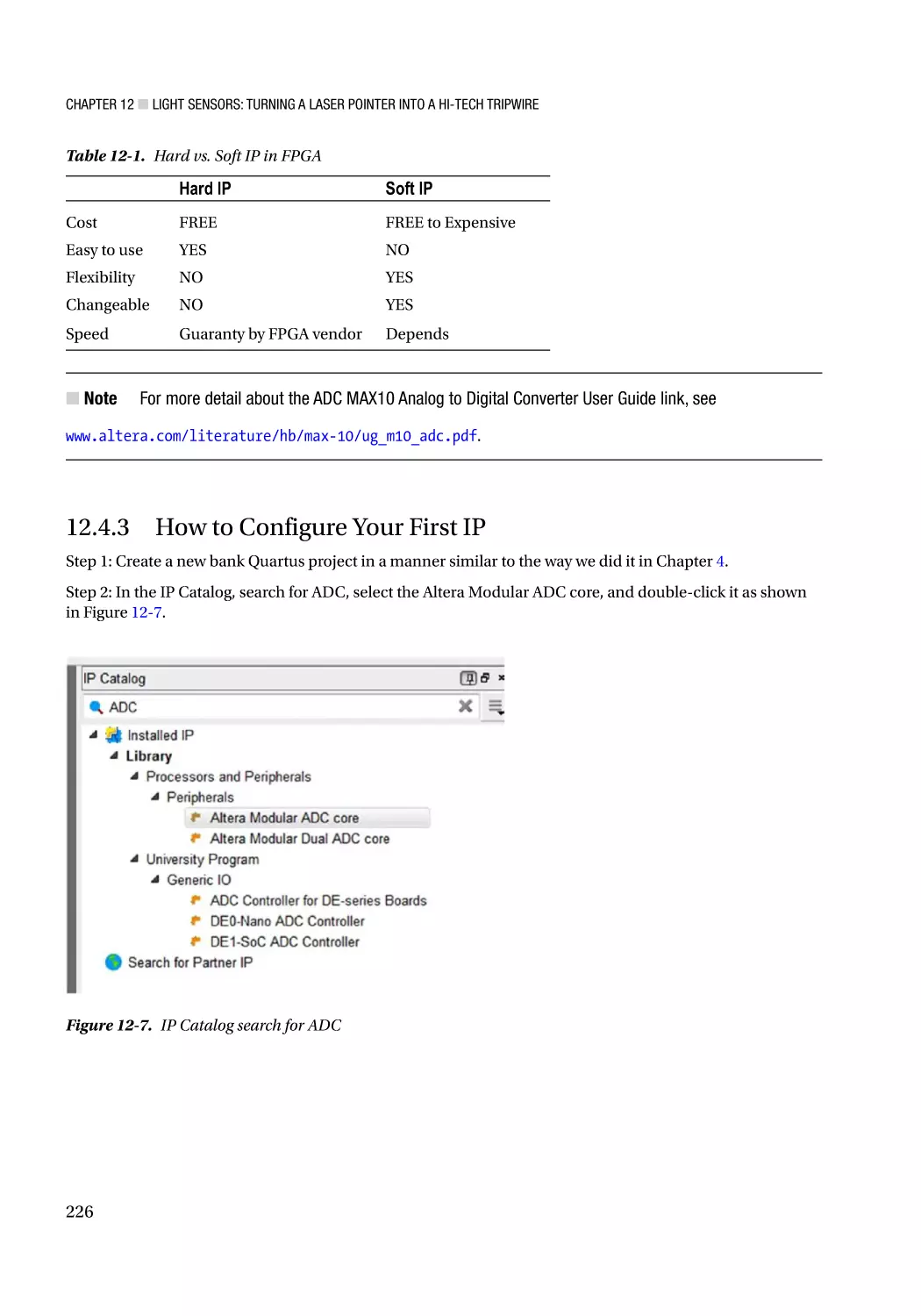
12.4.3 How to Configure Your First IP���������������������������������������������������������������������������������������������� 226
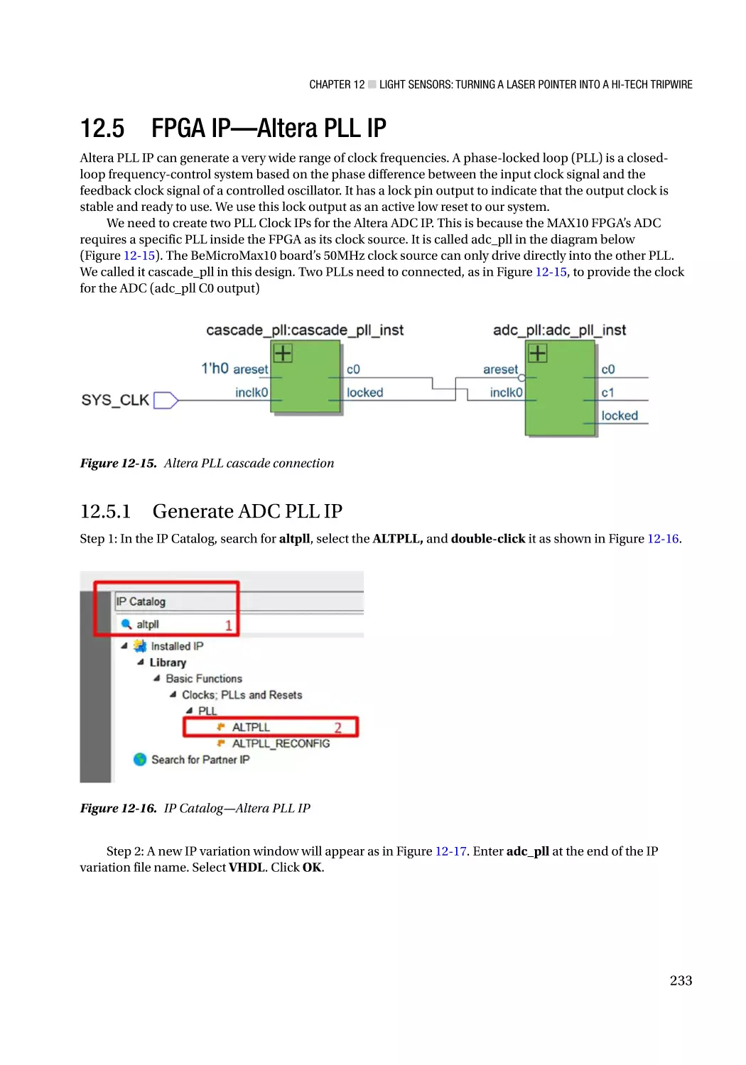
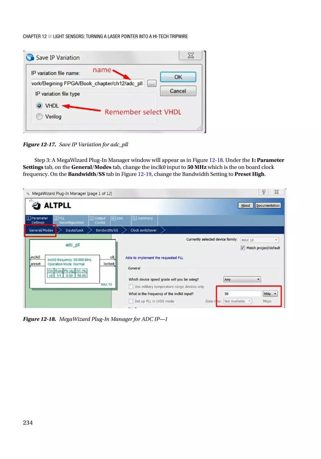
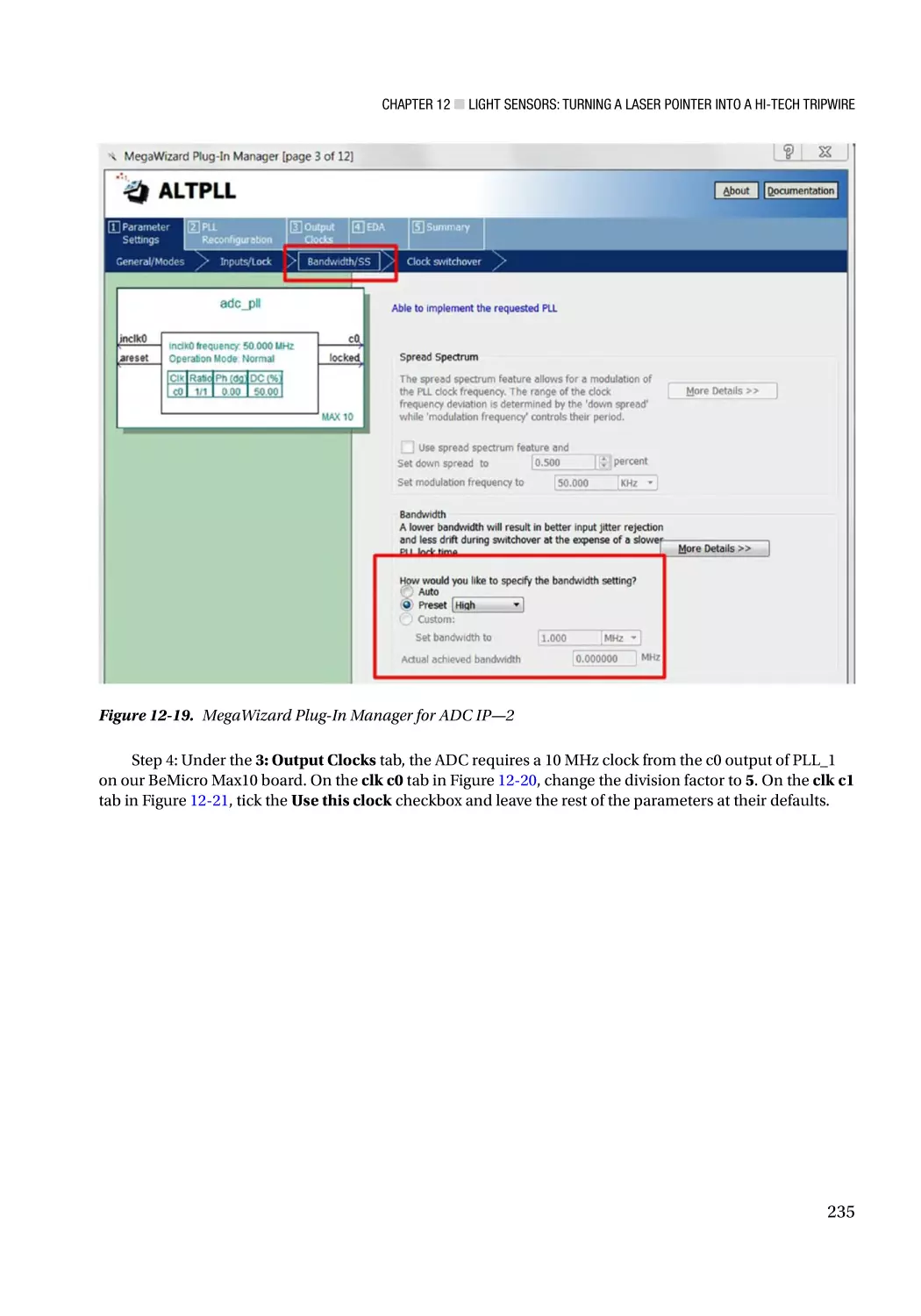
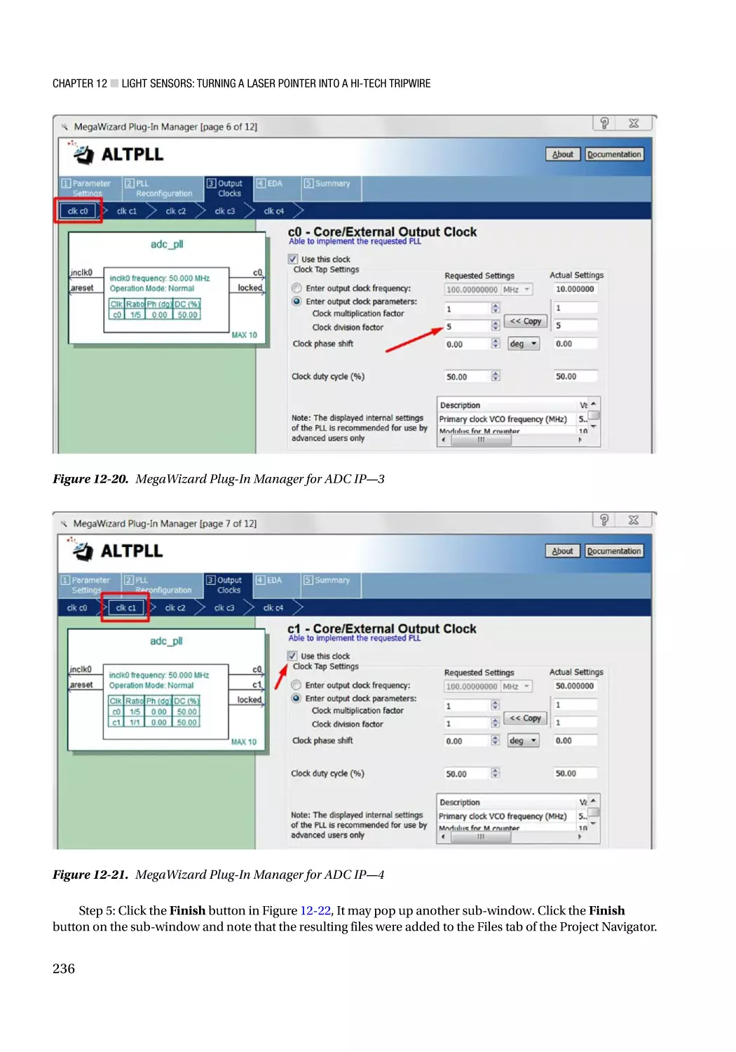
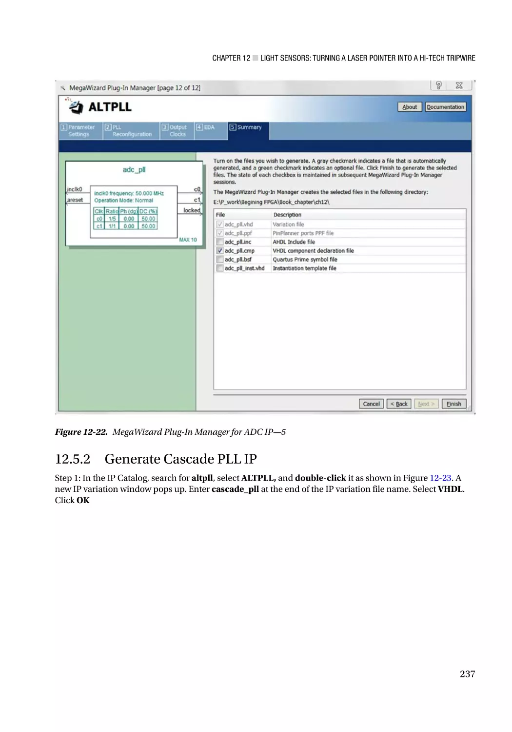
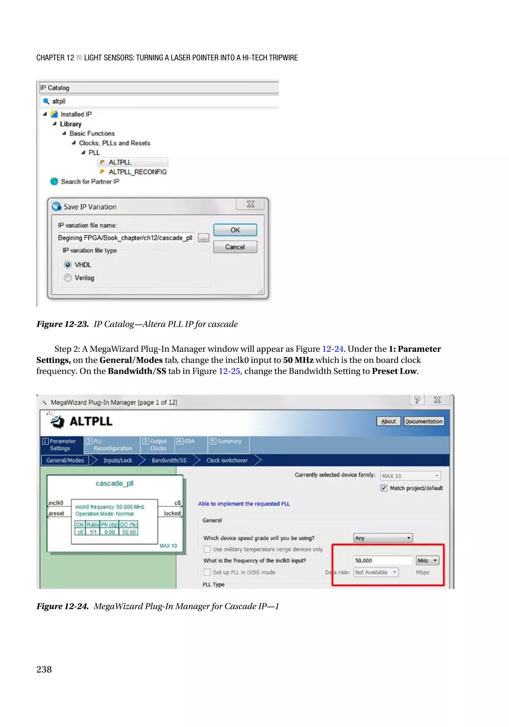
12.5 FPGA IP—Altera PLL IP������������������������������������������������������������������������������������� 233
12.5.1 Generate ADC PLL IP������������������������������������������������������������������������������������������������������������� 233
12.5.2 Generate Cascade PLL IP������������������������������������������������������������������������������������������������������ 237
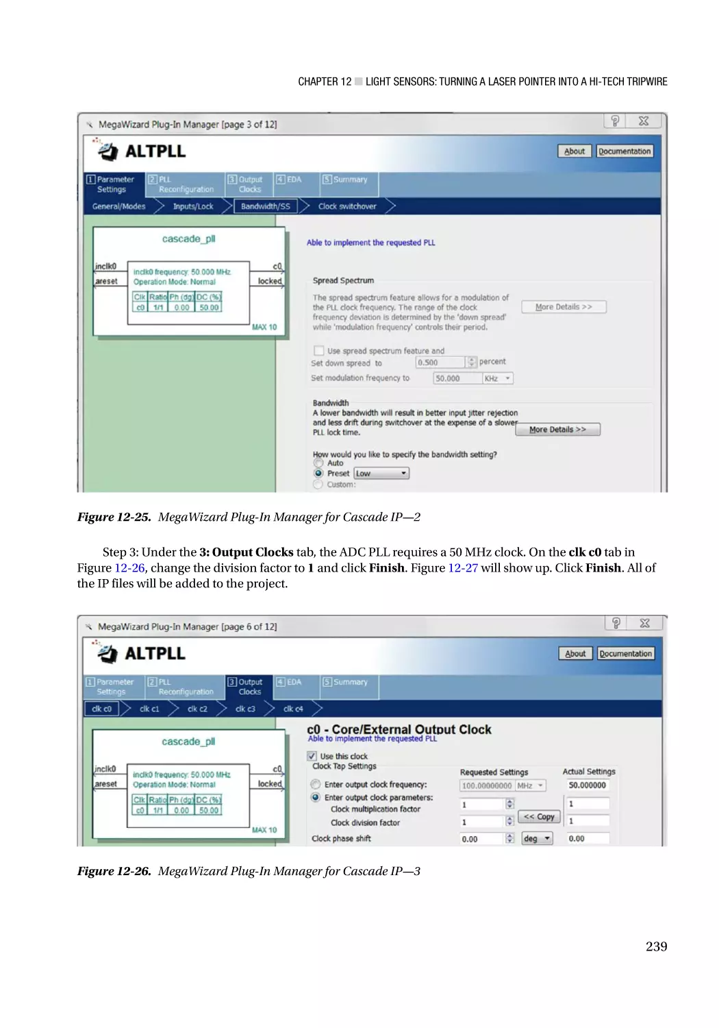
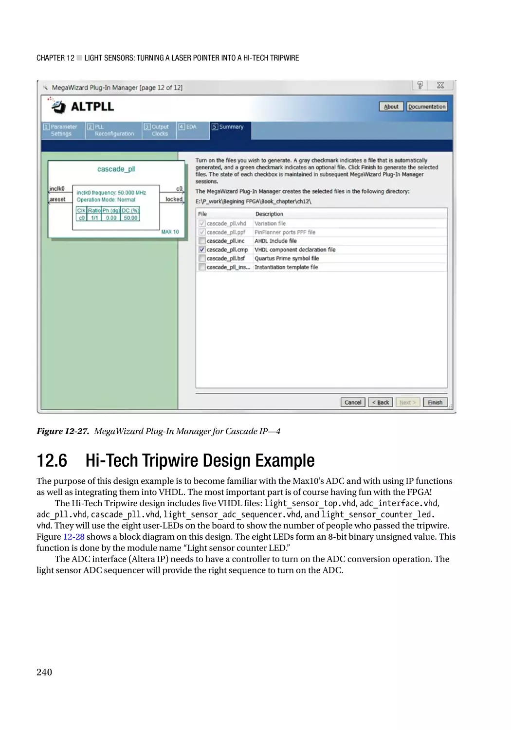
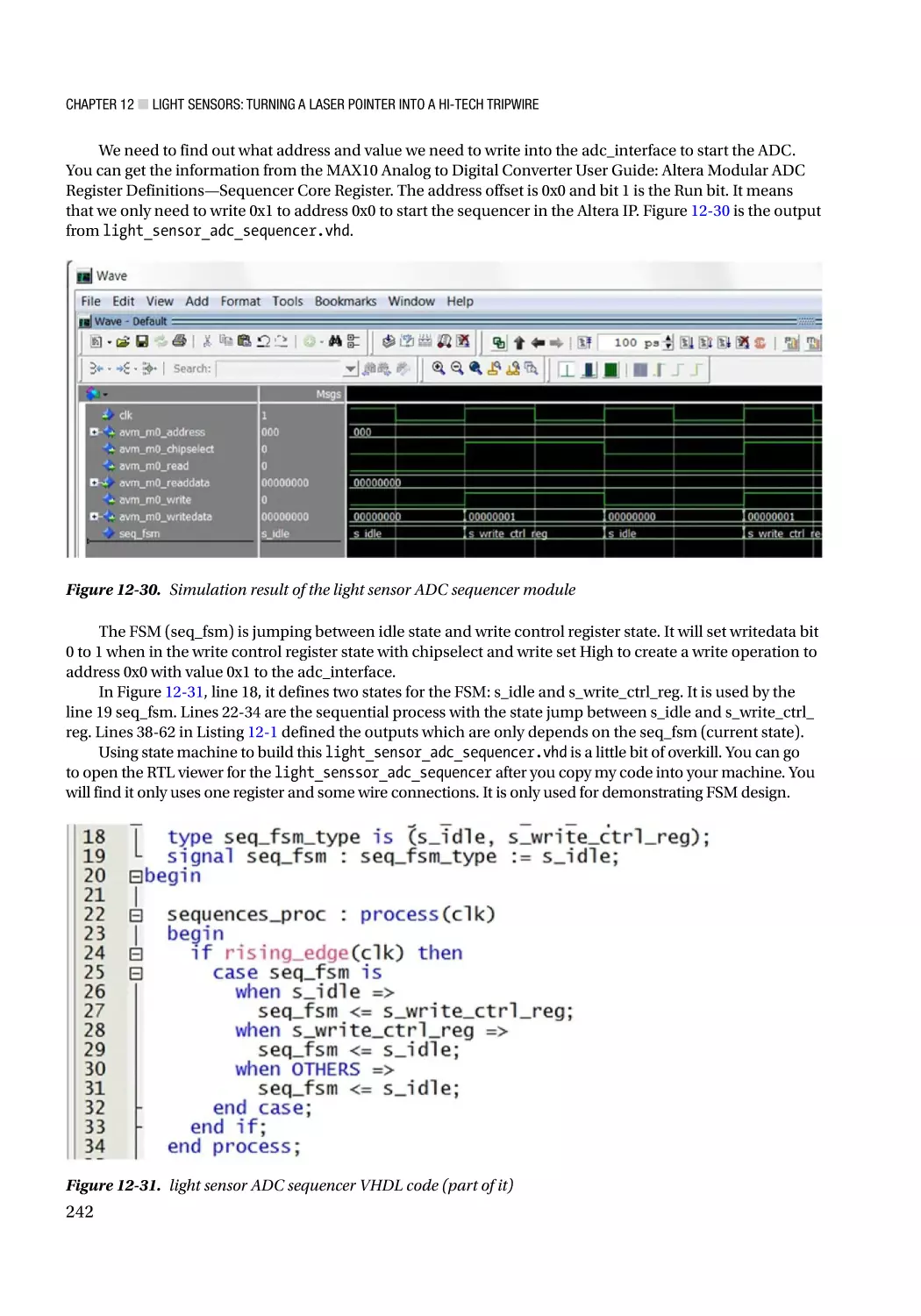
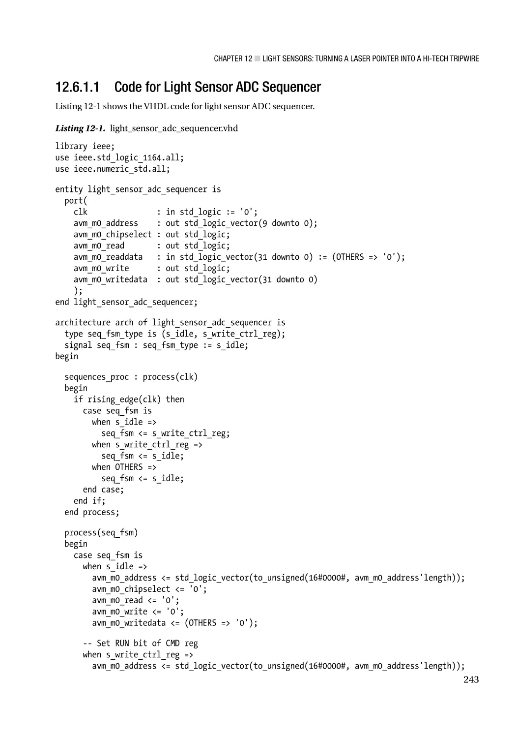
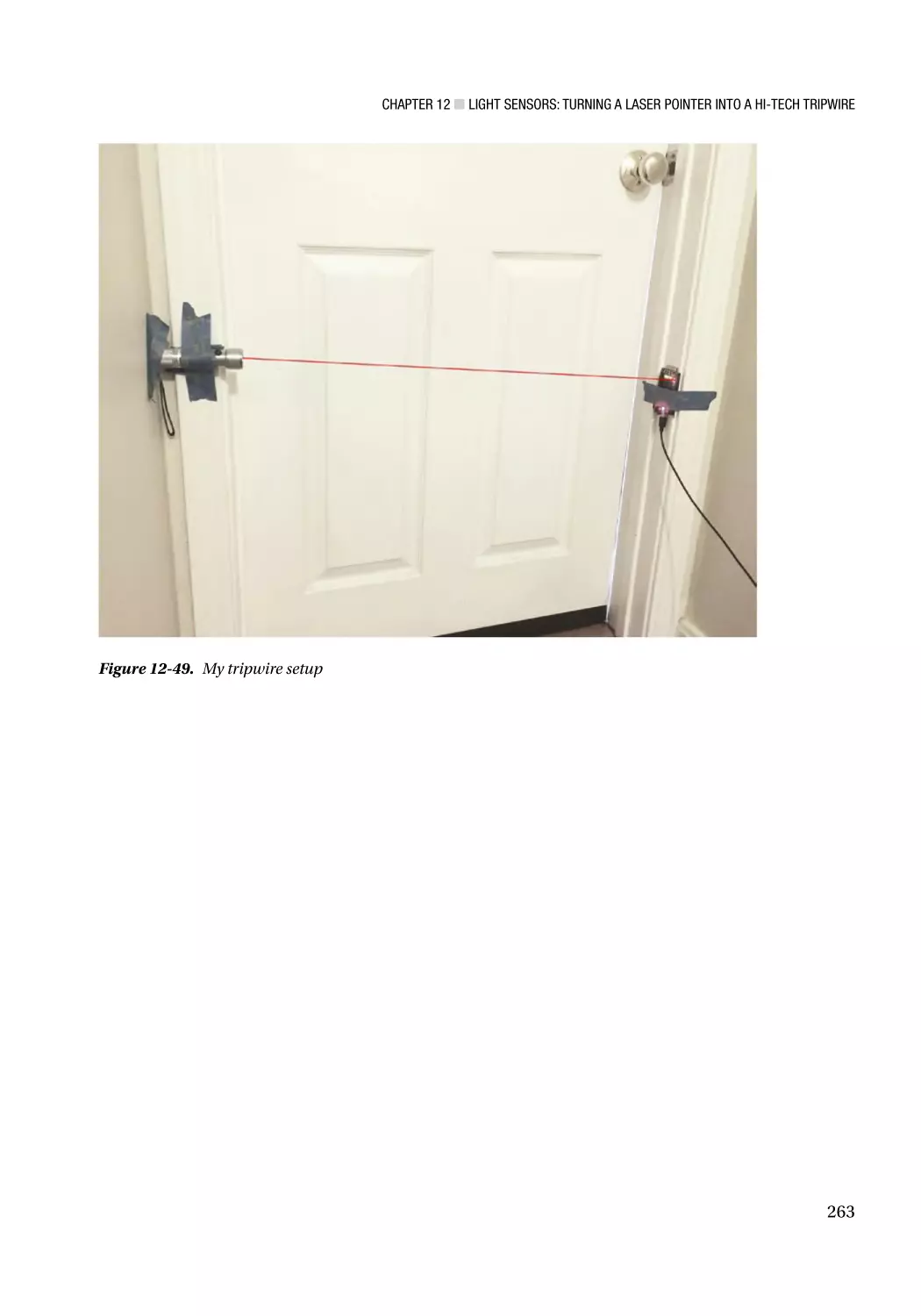
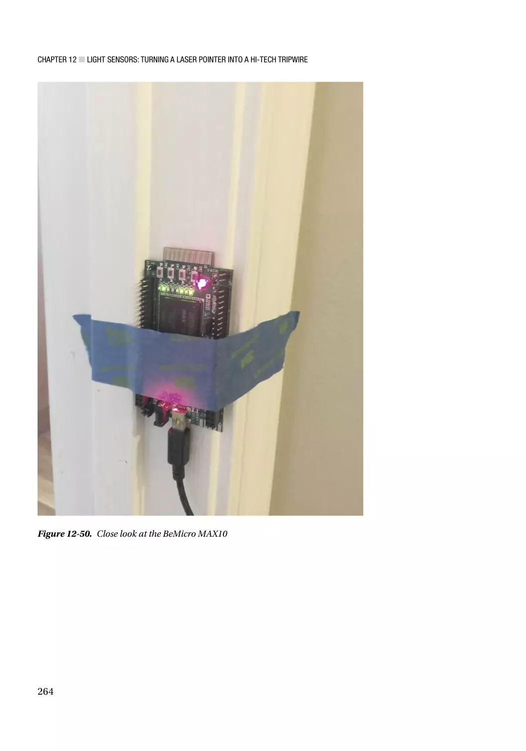
12.6 Hi-Tech Tripwire Design Example���������������������������������������������������������������������� 240
12.6.1 Light Sensor ADC Sequencer Module����������������������������������������������������������������������������������� 241
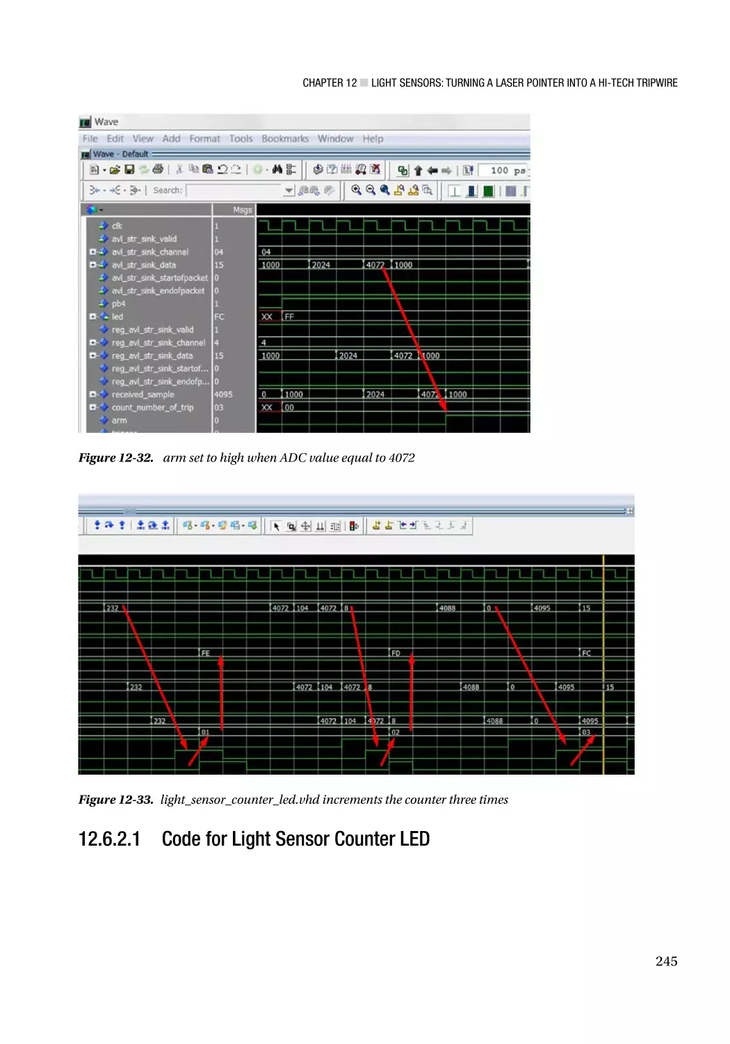
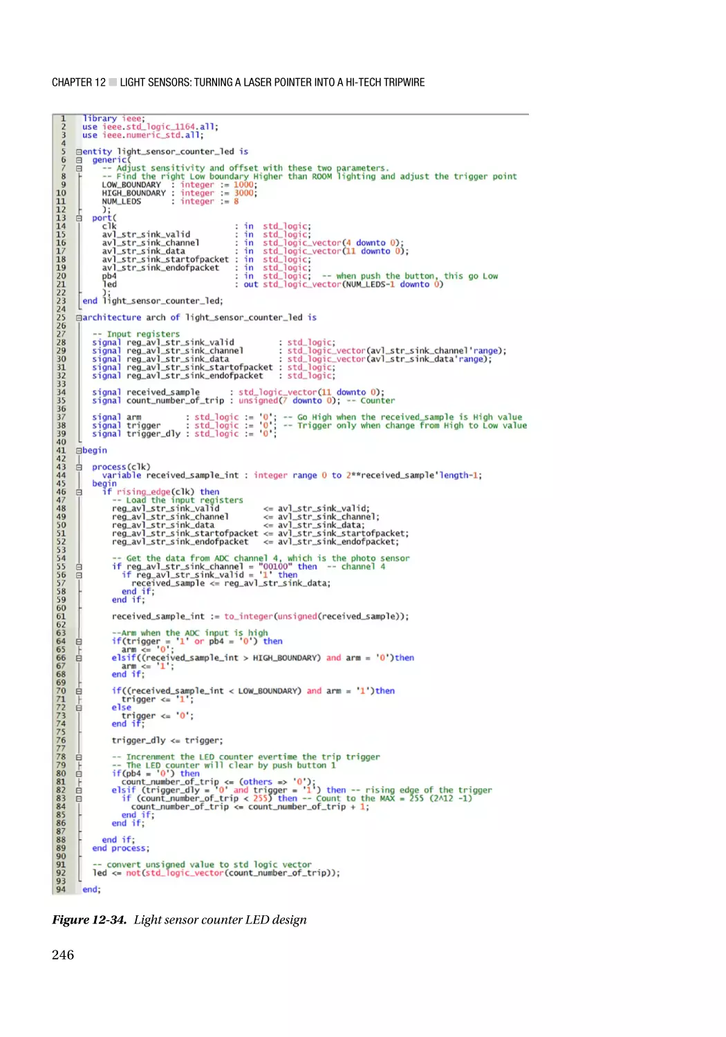
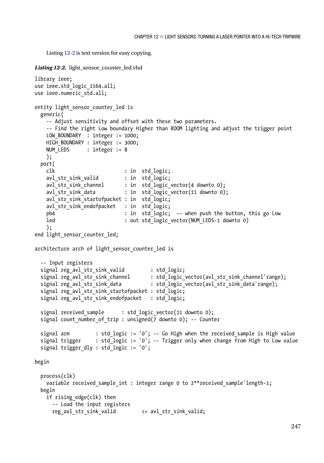
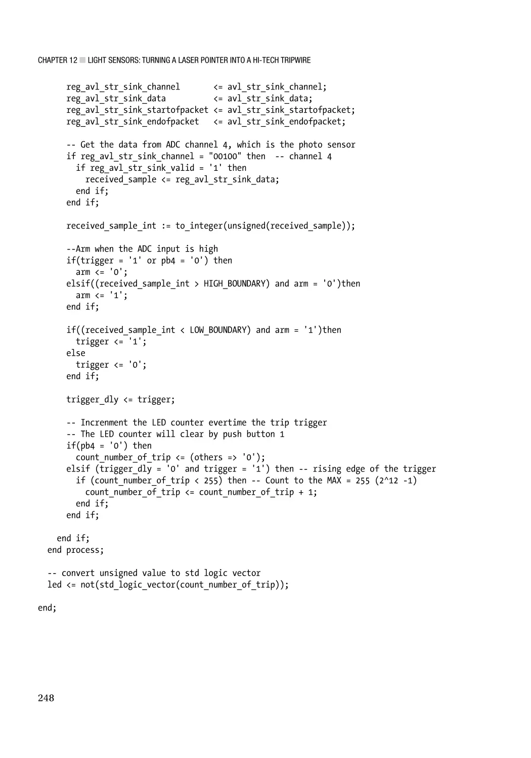
12.6.2 Light Sensor Counter LED����������������������������������������������������������������������������������������������������� 244
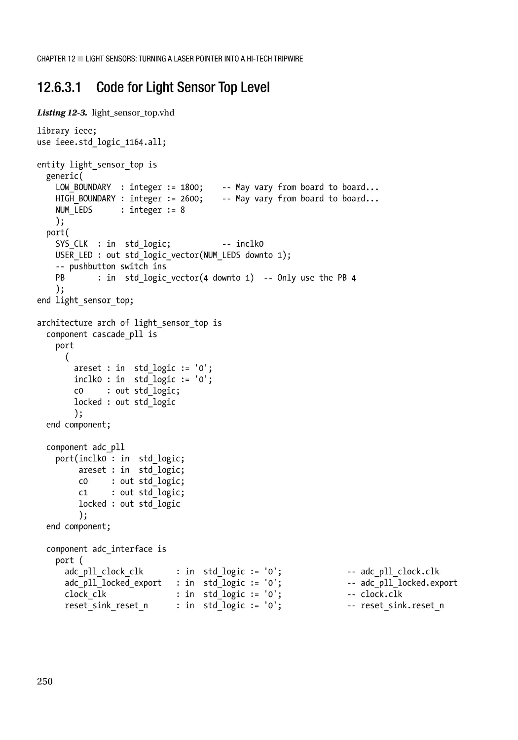
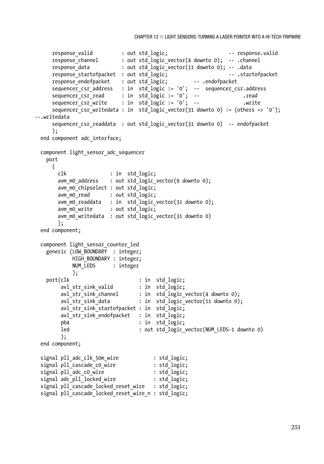
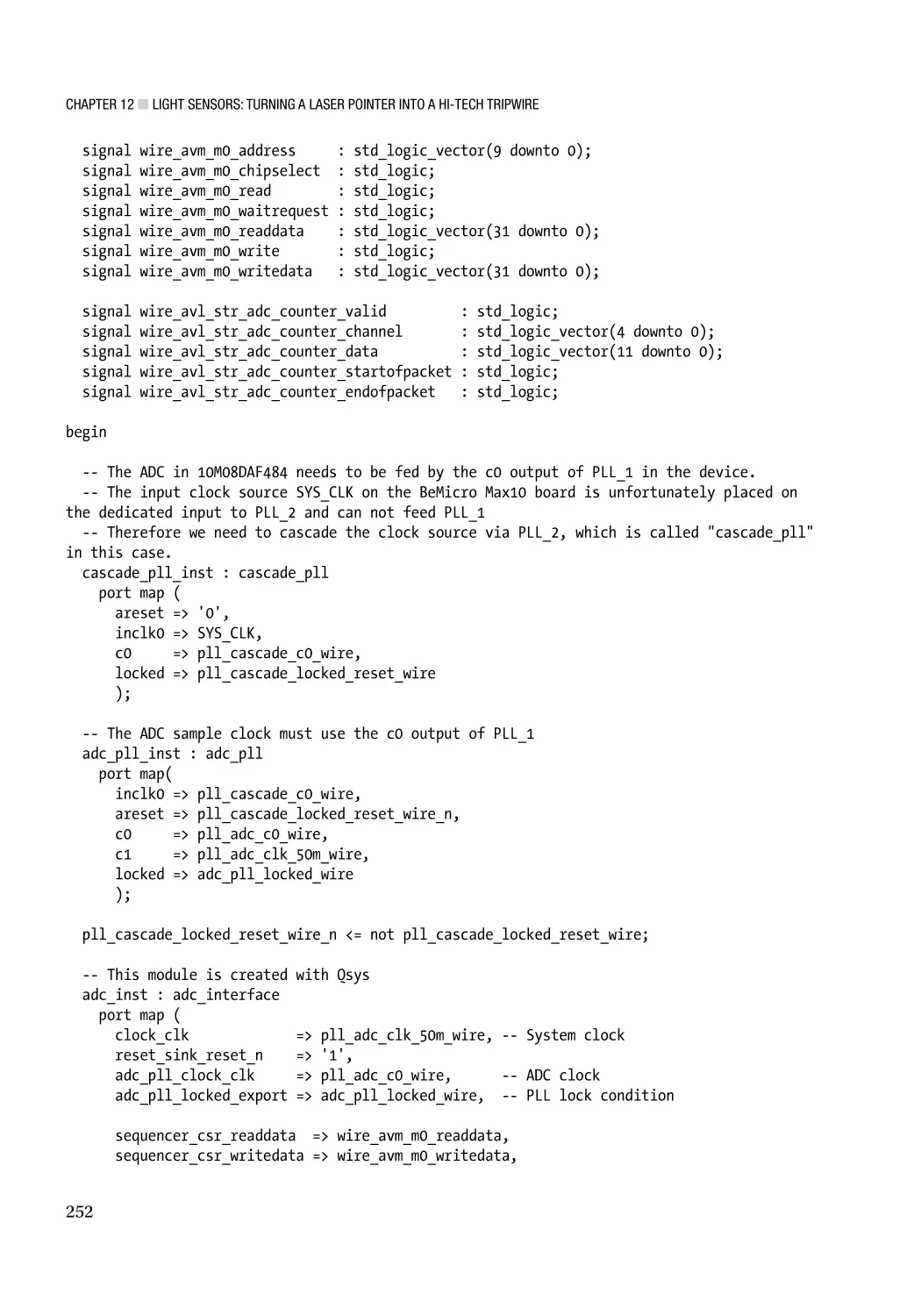
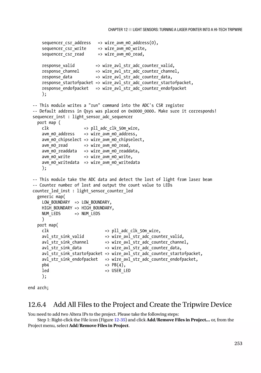
12.6.3 Light Sensor Top Level��������������������������������������������������������������������������������������������������������� 249
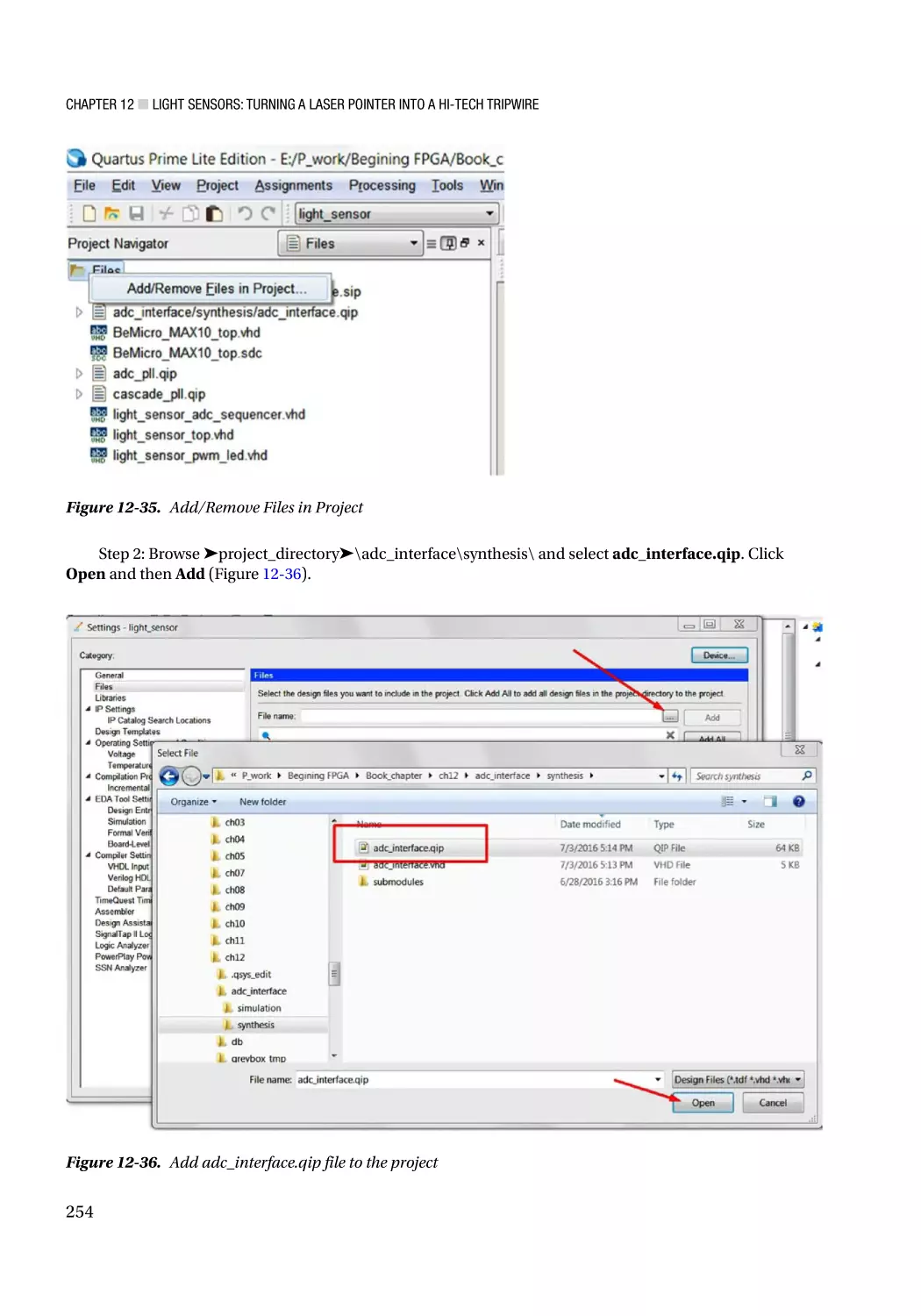
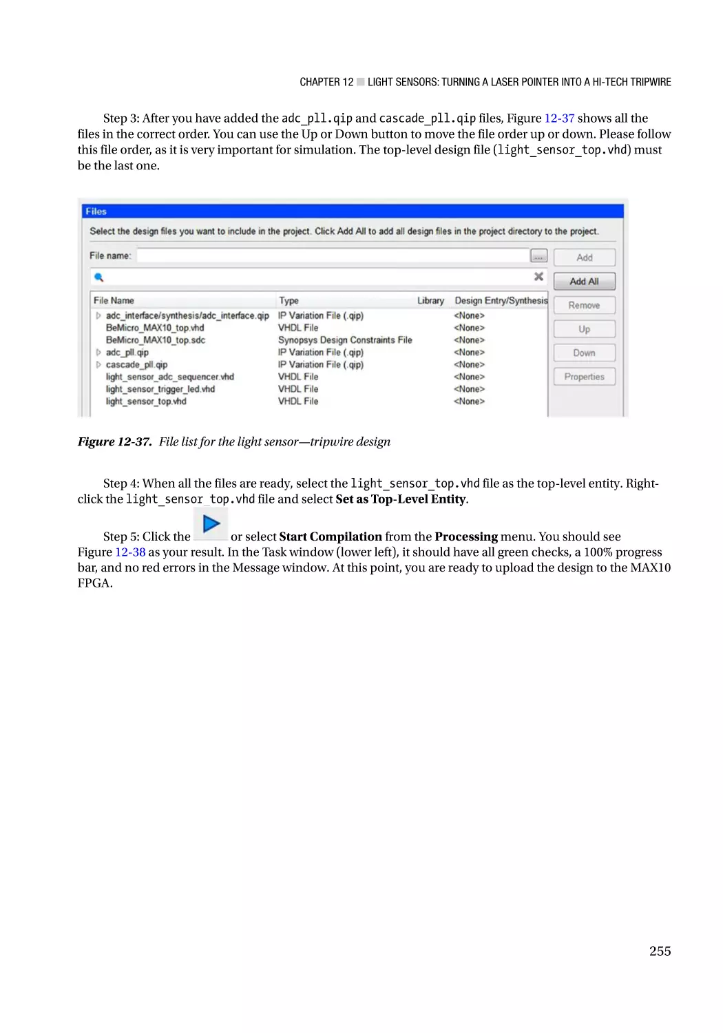
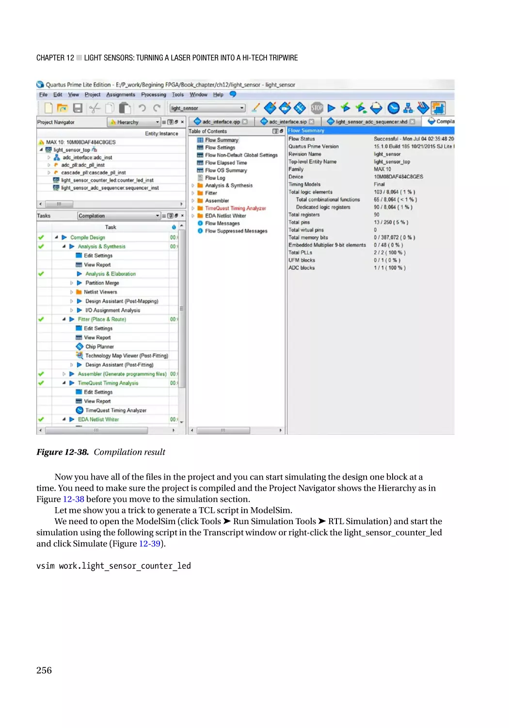
12.6.4 Add All Files to the Project and Create the Tripwire Device�������������������������������������������������� 253
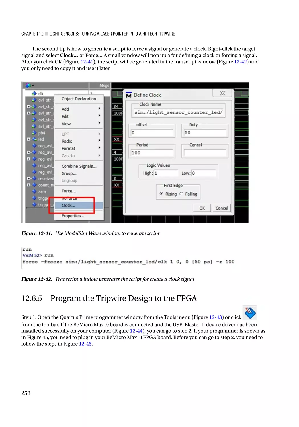
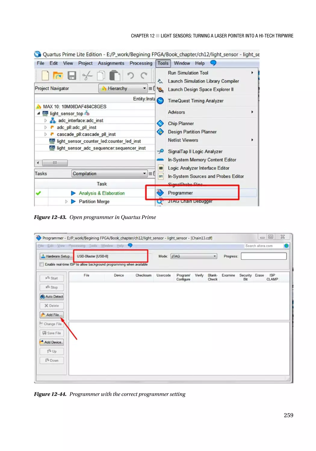
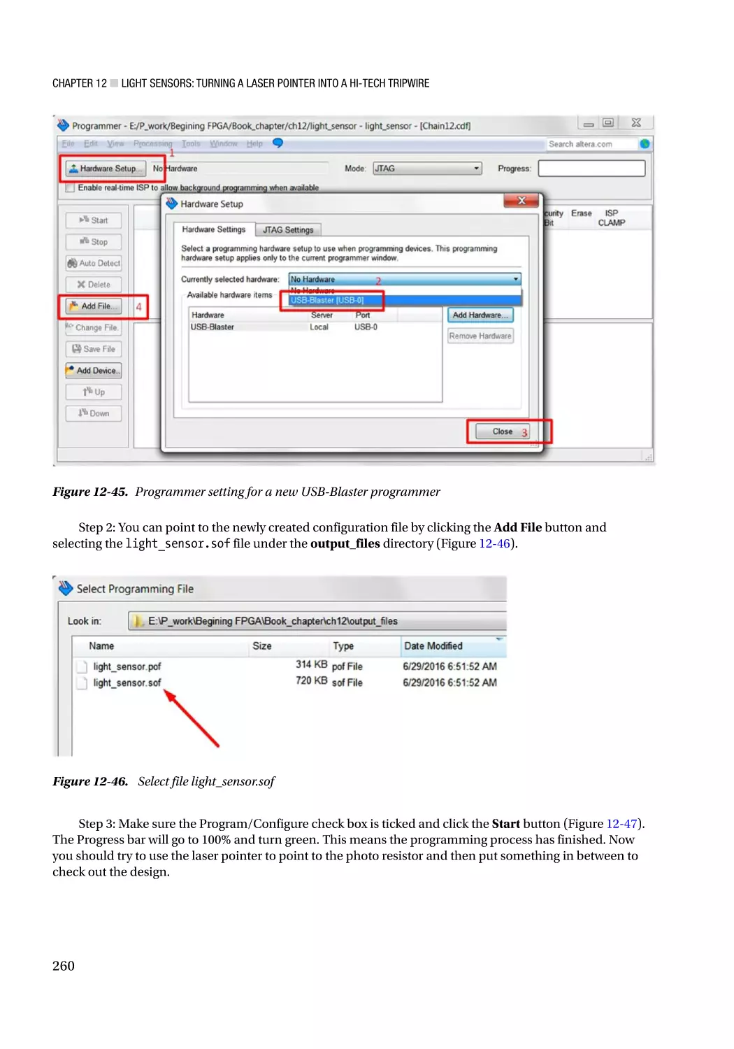
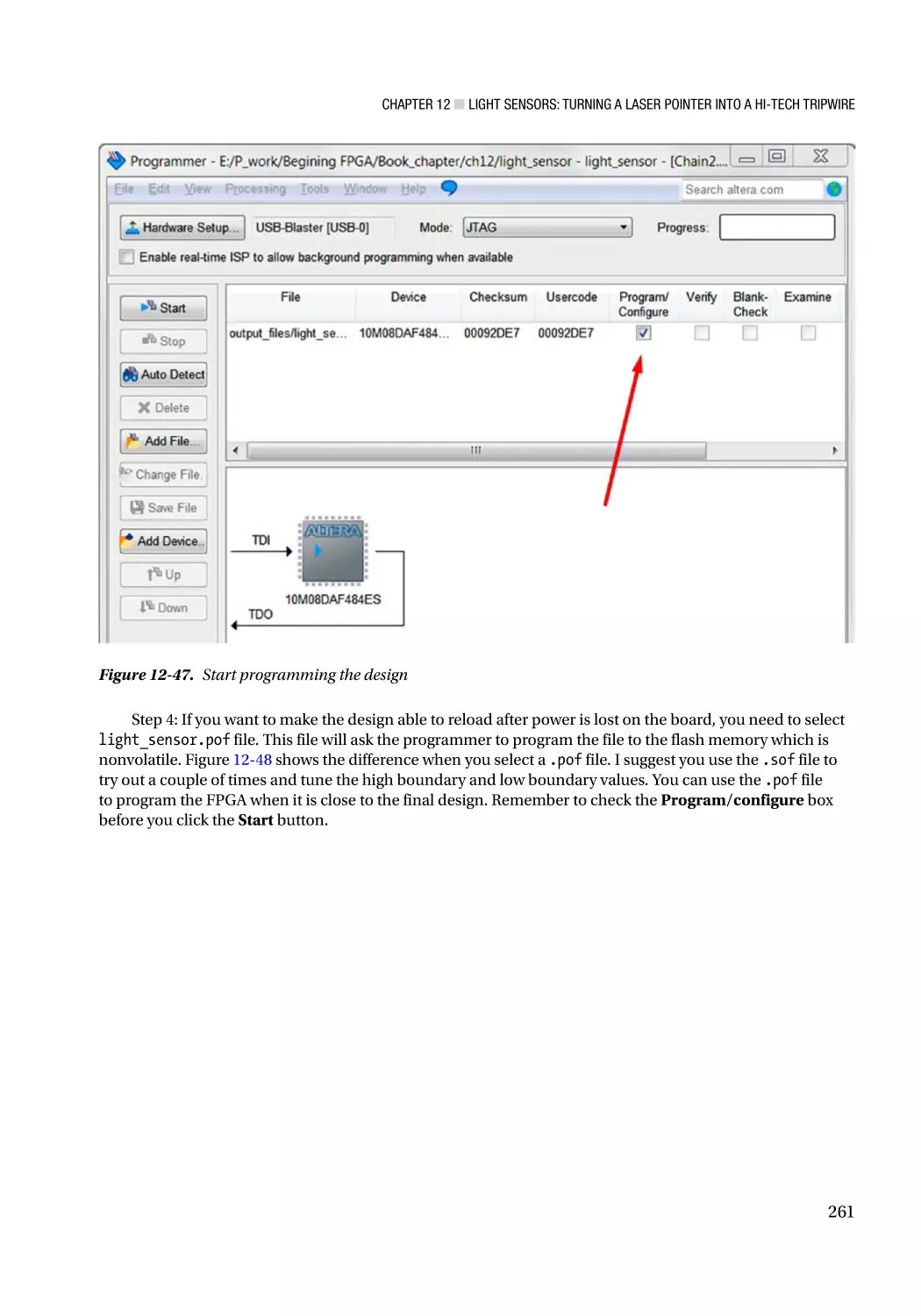
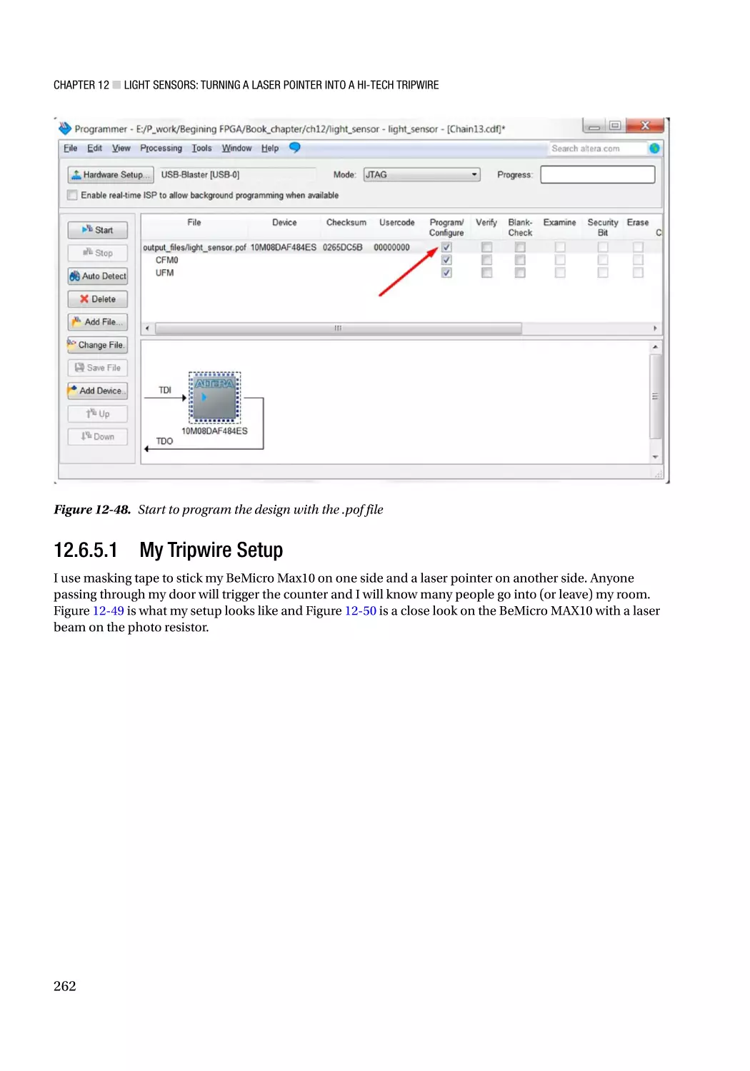
12.6.5 Program the Tripwire Design to the FPGA���������������������������������������������������������������������������� 258
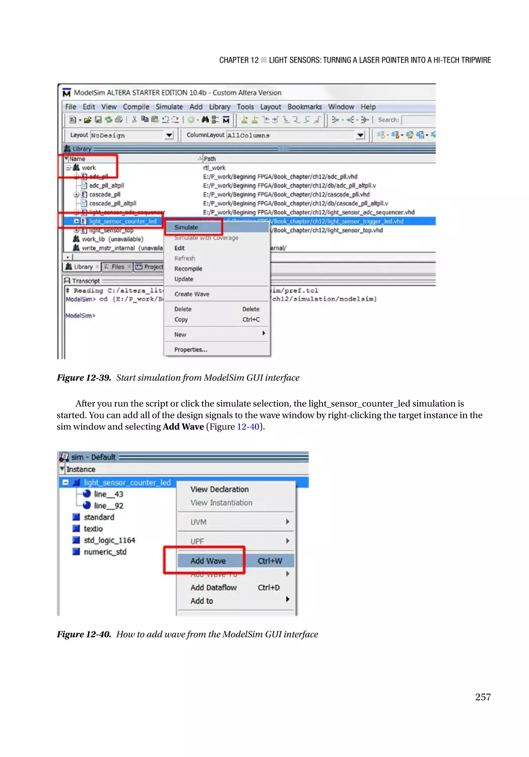
12.7 Summary����������������������������������������������������������������������������������������������������������� 265
■Chapter
■
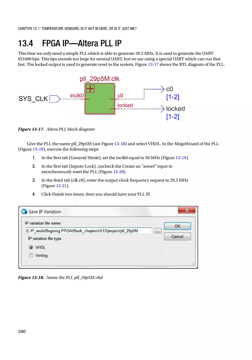
13: Temperature Sensors: Is It Hot in Here, or Is It Just Me?�������������� 267
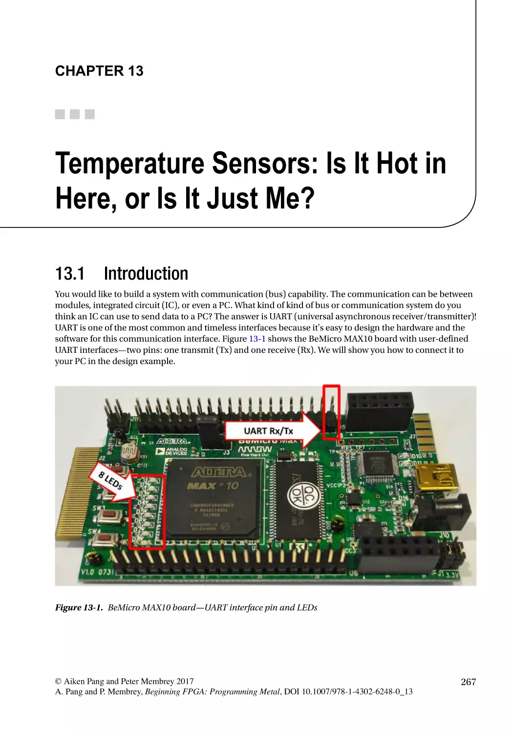
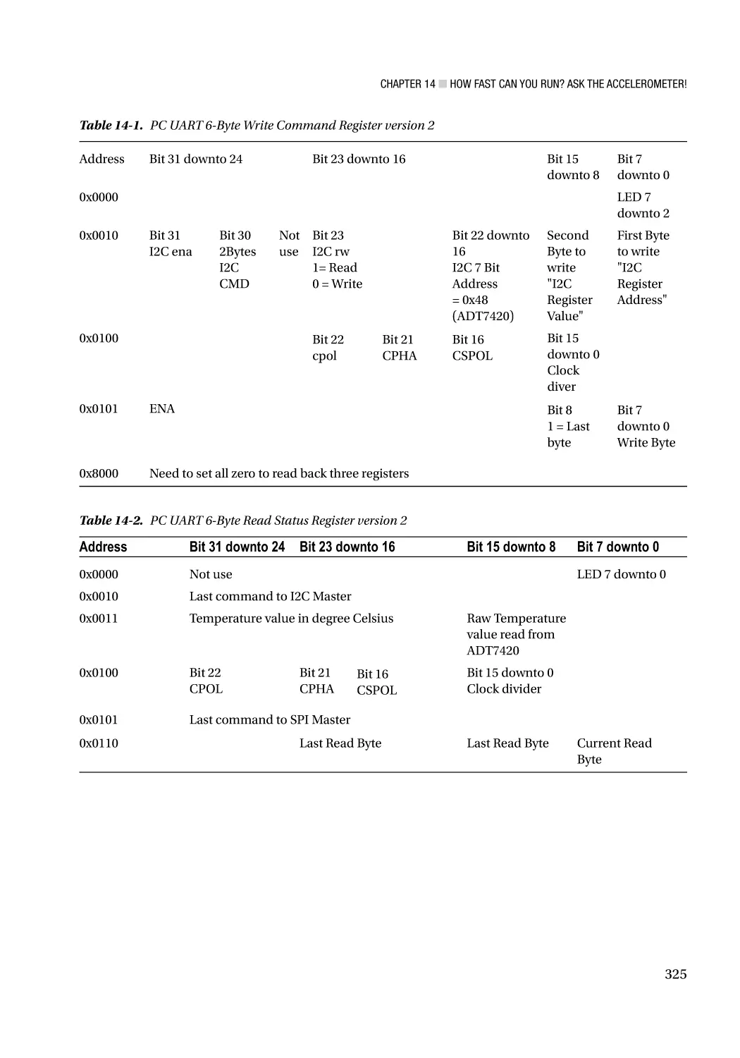
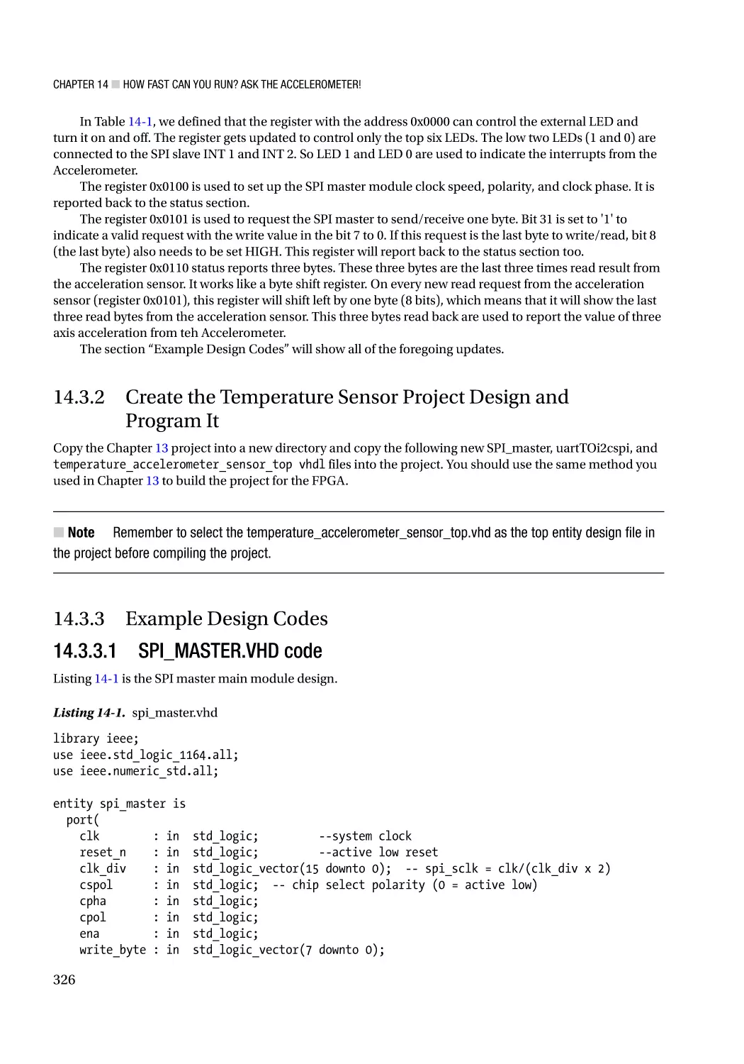
13.1 Introduction������������������������������������������������������������������������������������������������������� 267
13.2 UART with Control Memory Map����������������������������������������������������������������������� 269
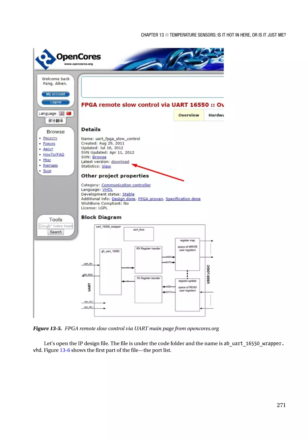
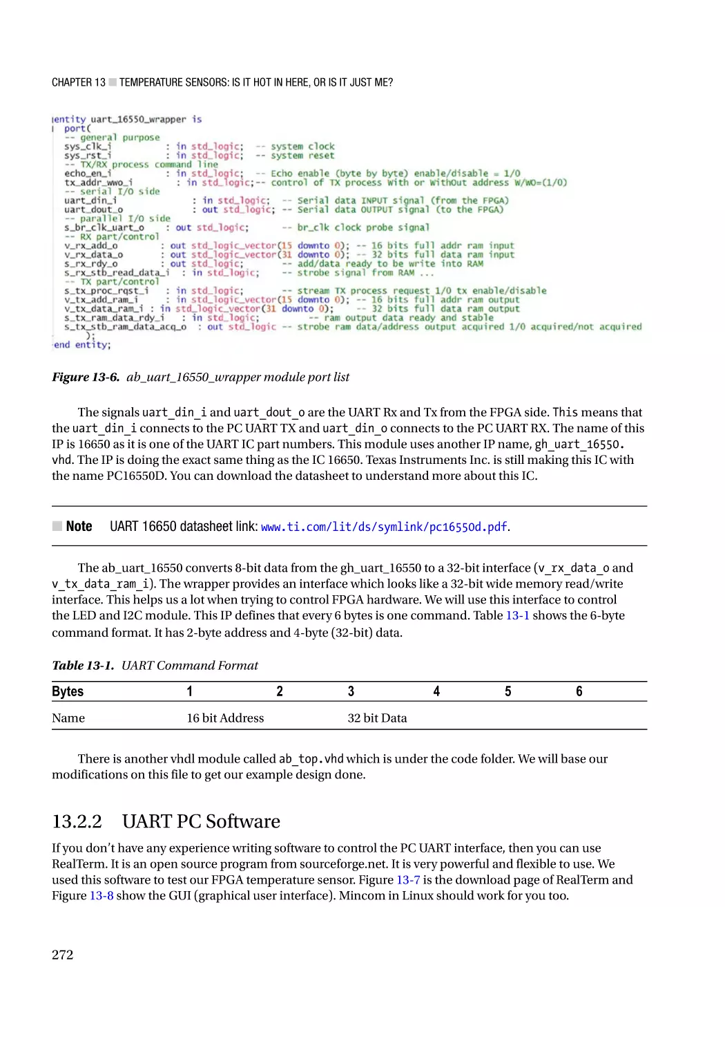
13.2.1 UART IP��������������������������������������������������������������������������������������������������������������������������������� 270
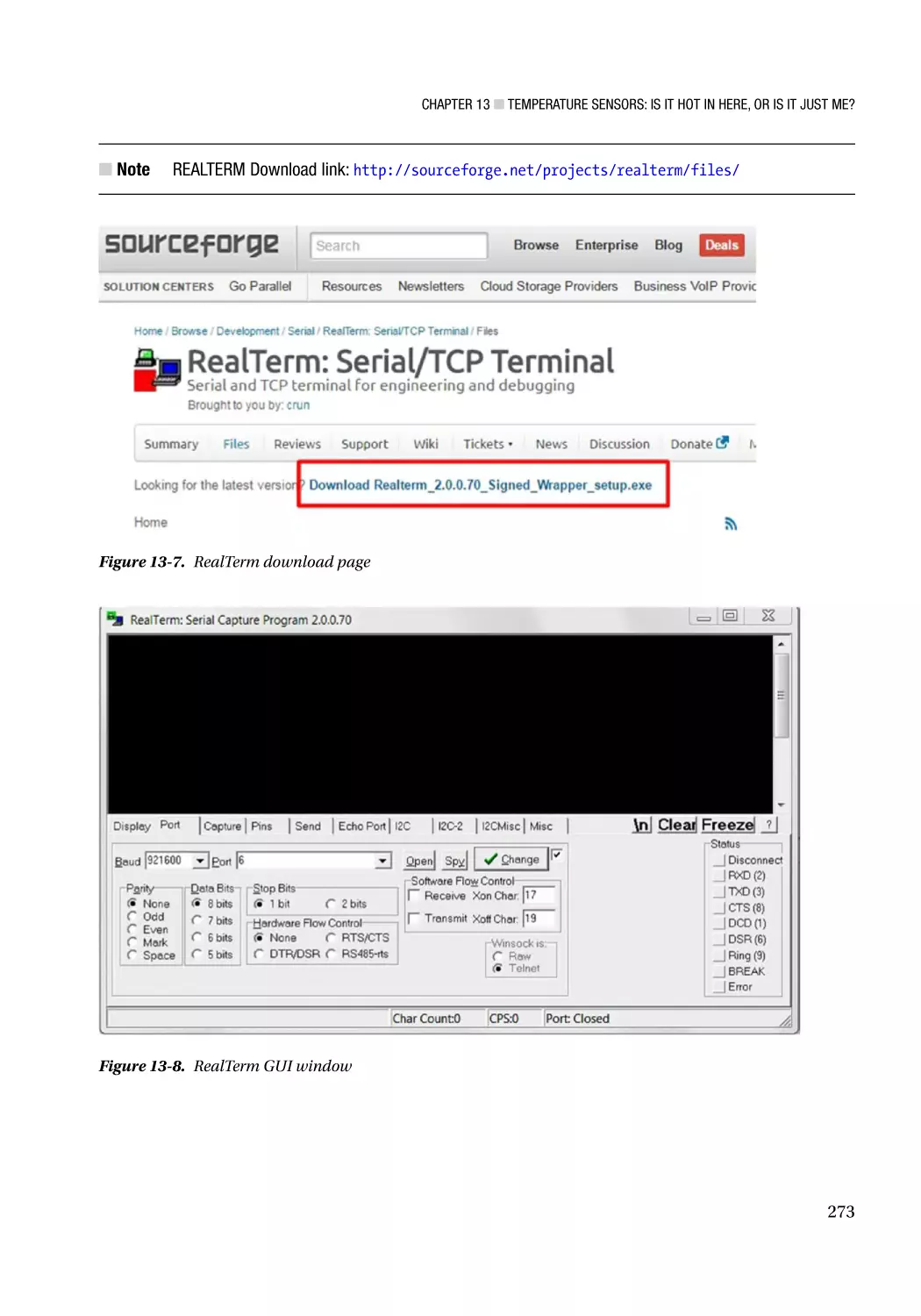
13.2.2 UART PC Software���������������������������������������������������������������������������������������������������������������� 272
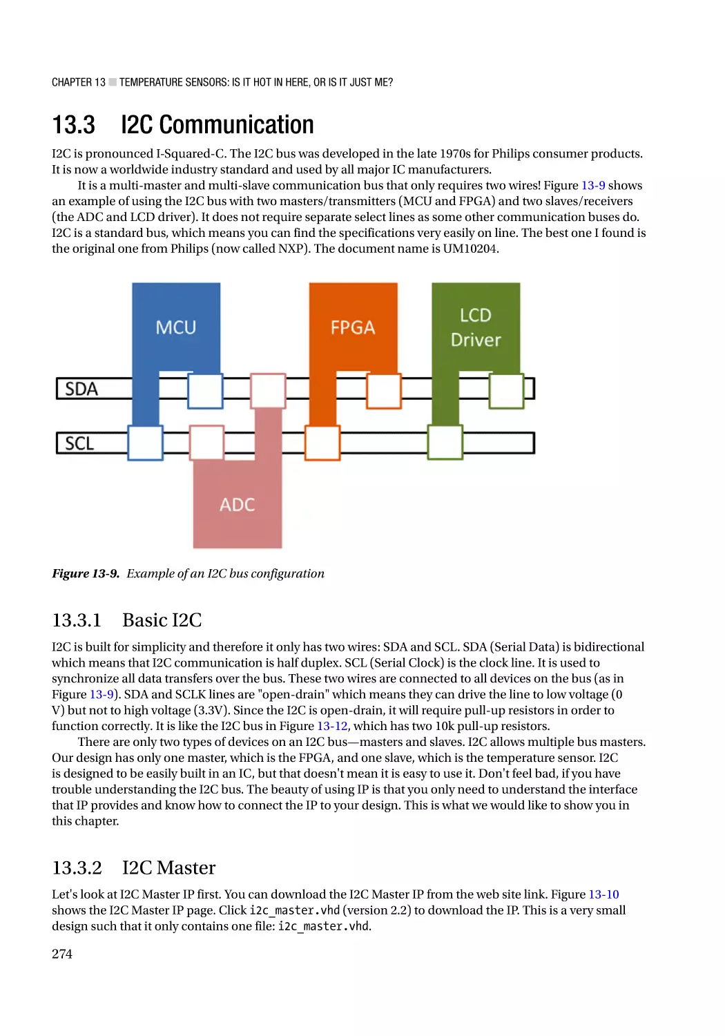
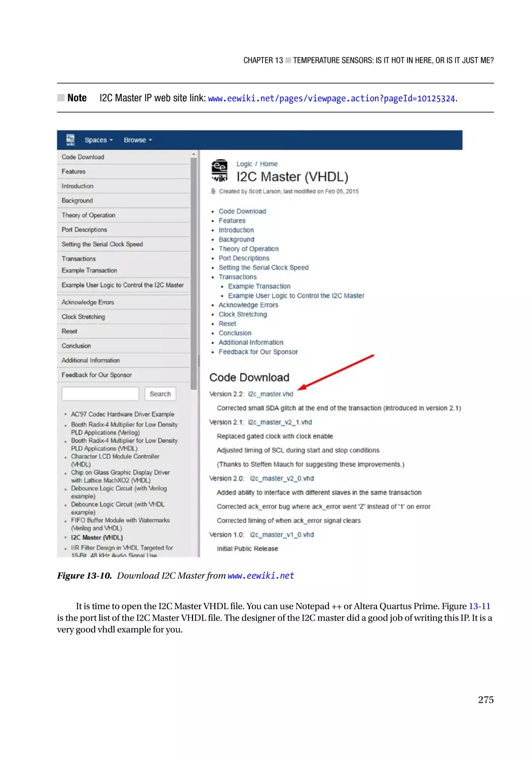
13.3 I2C Communication������������������������������������������������������������������������������������������� 274
13.3.1 Basic I2C������������������������������������������������������������������������������������������������������������������������������� 274
13.3.2 I2C Master���������������������������������������������������������������������������������������������������������������������������� 274
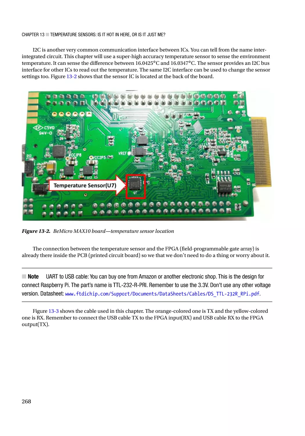
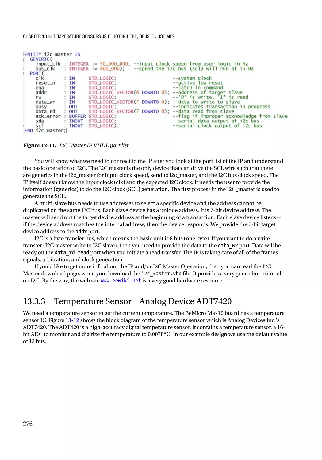
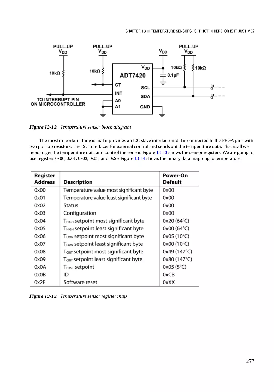
13.3.3 Temperature Sensor—Analog Device ADT7420������������������������������������������������������������������� 276
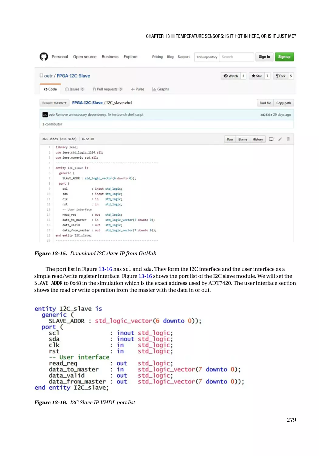
13.3.4 I2C Slave������������������������������������������������������������������������������������������������������������������������������� 278
x
■ Contents
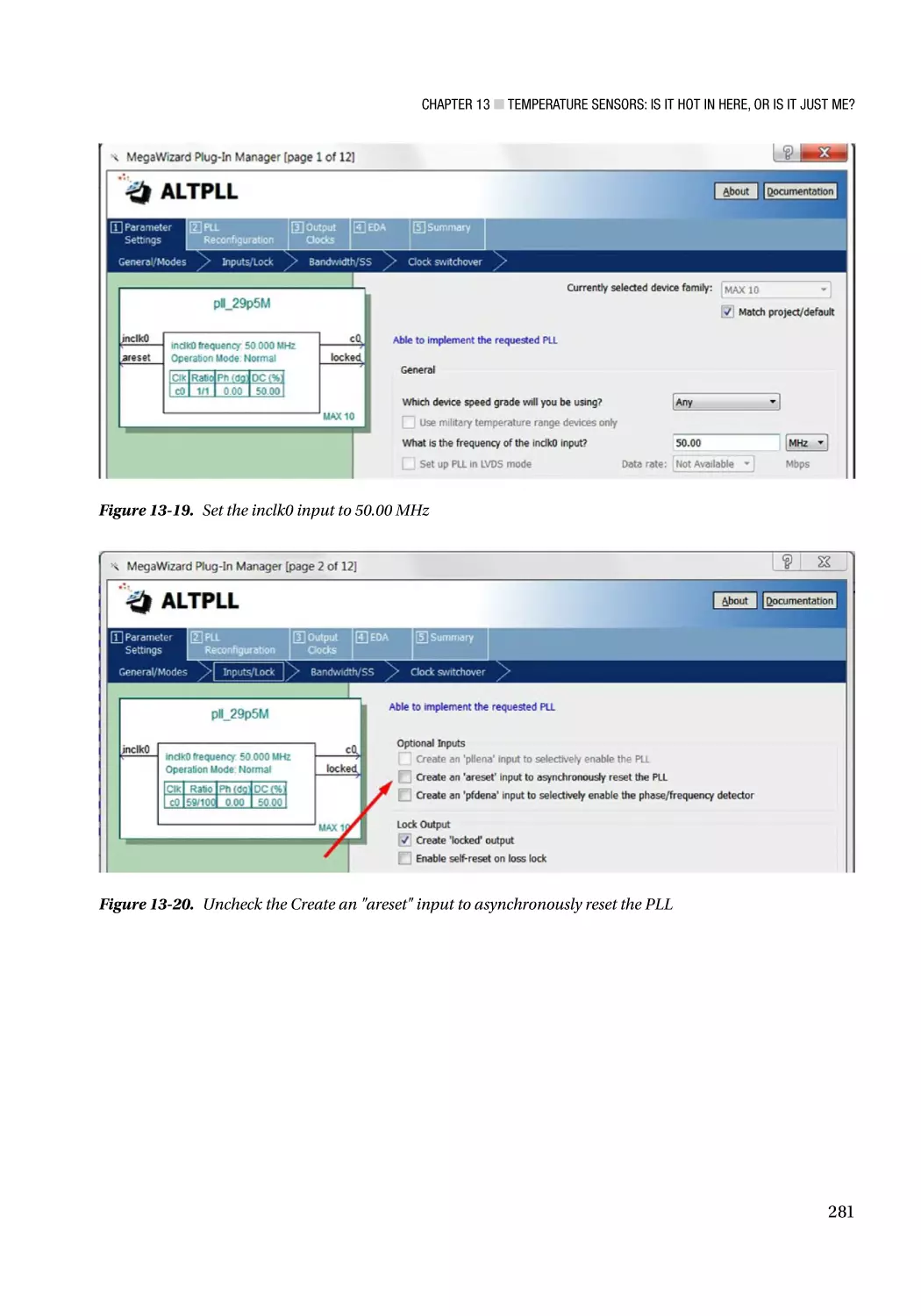
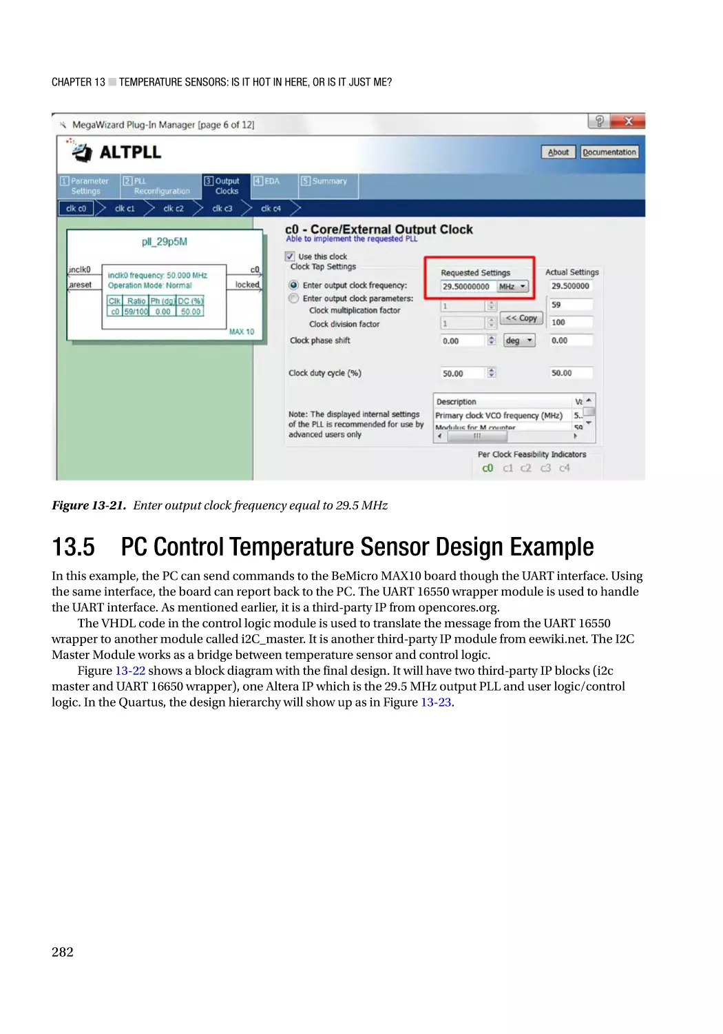
13.4 FPGA IP—Altera PLL IP������������������������������������������������������������������������������������� 280
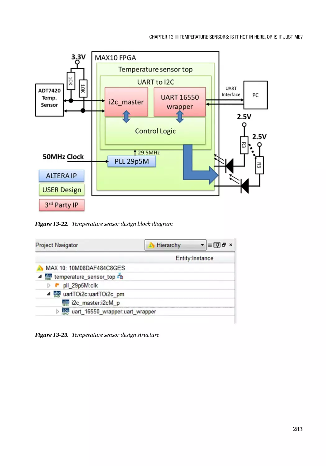
13.5 PC Control Temperature Sensor Design Example���������������������������������������������� 282
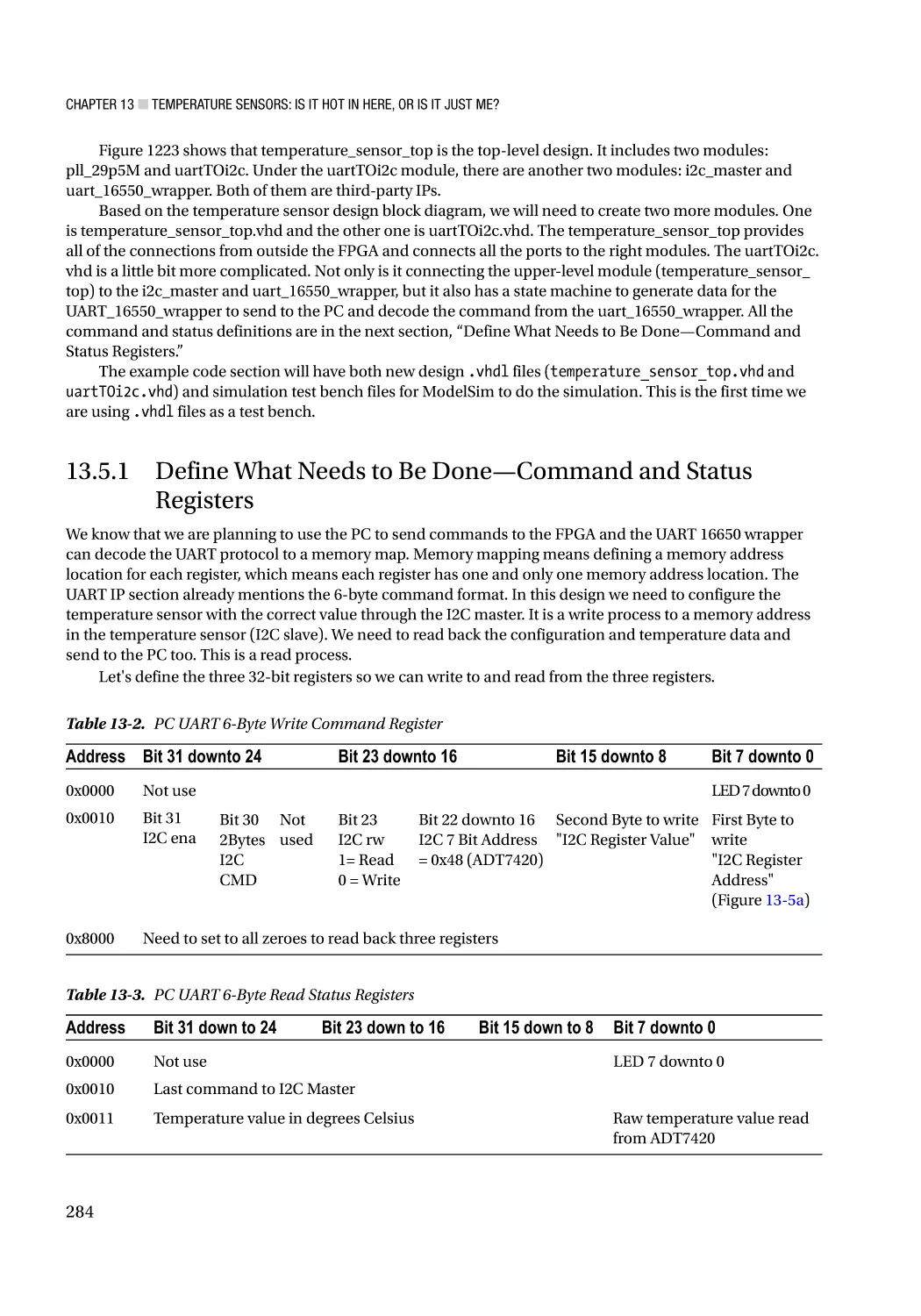
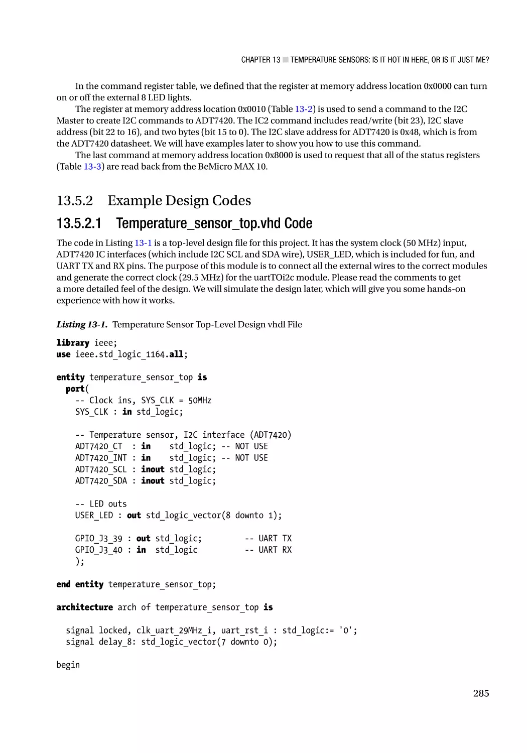
13.5.1 Define What Needs to Be Done—Command and Status Registers�������������������������������������� 284
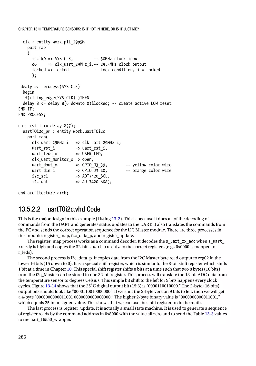
13.5.2 Example Design Codes��������������������������������������������������������������������������������������������������������� 285
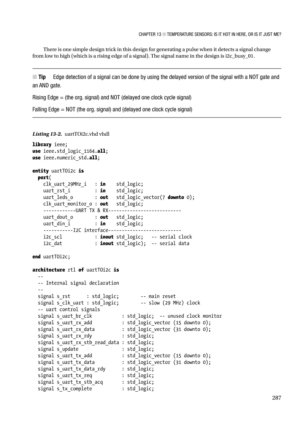
13.5.3 Example Simulation Codes��������������������������������������������������������������������������������������������������� 292
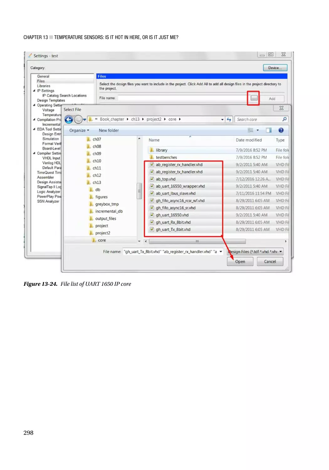
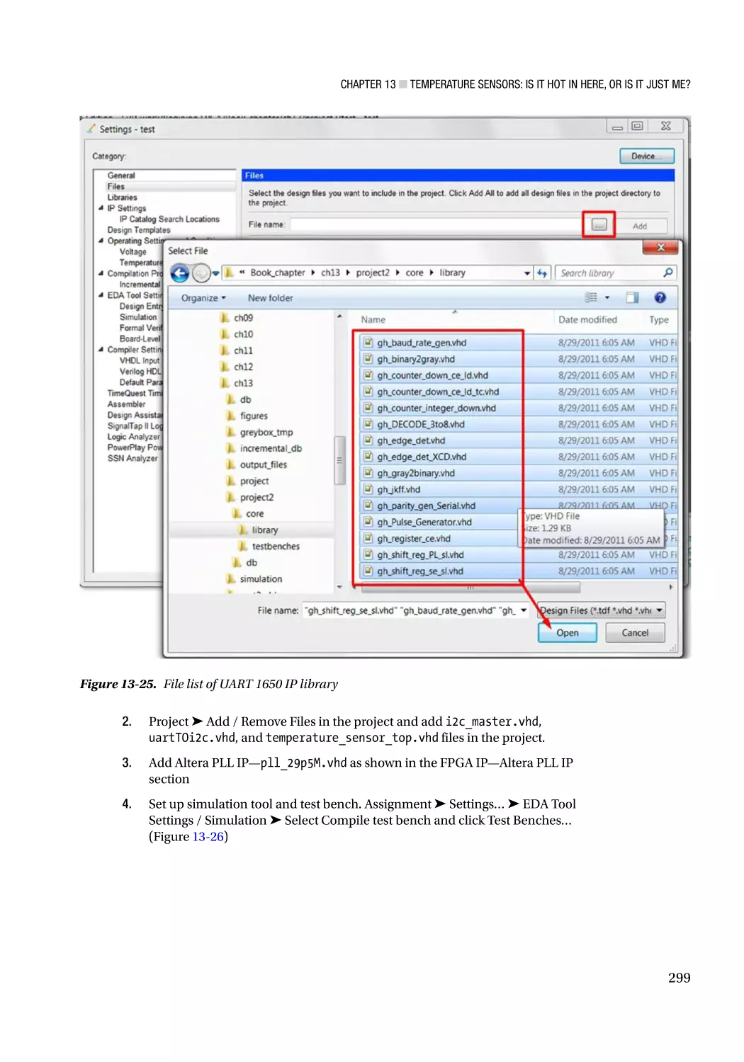
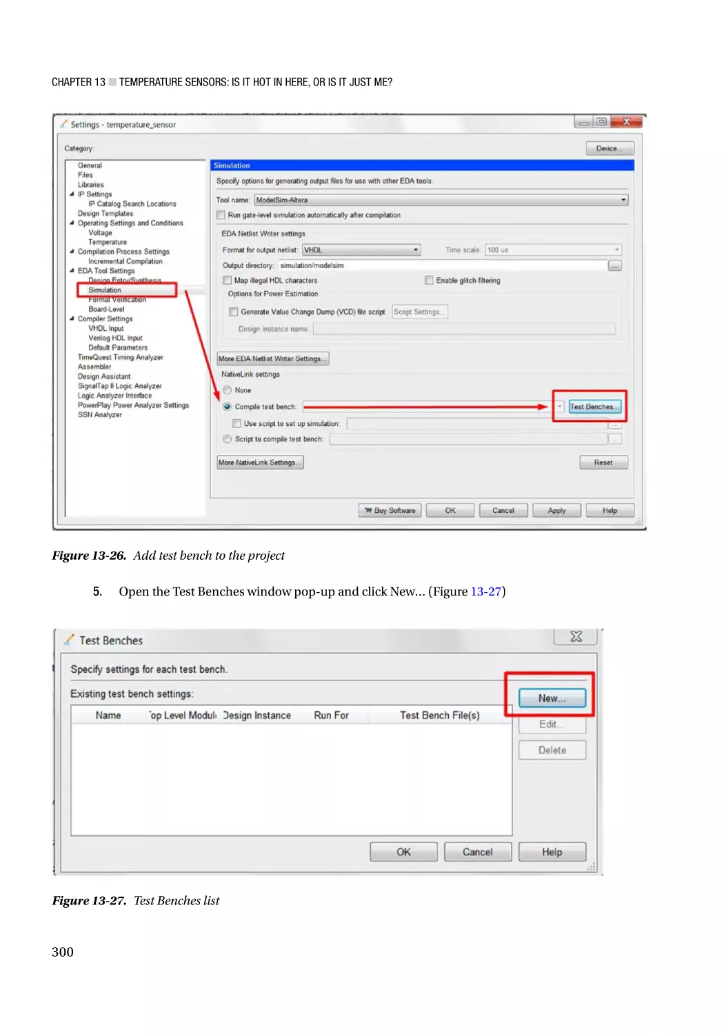
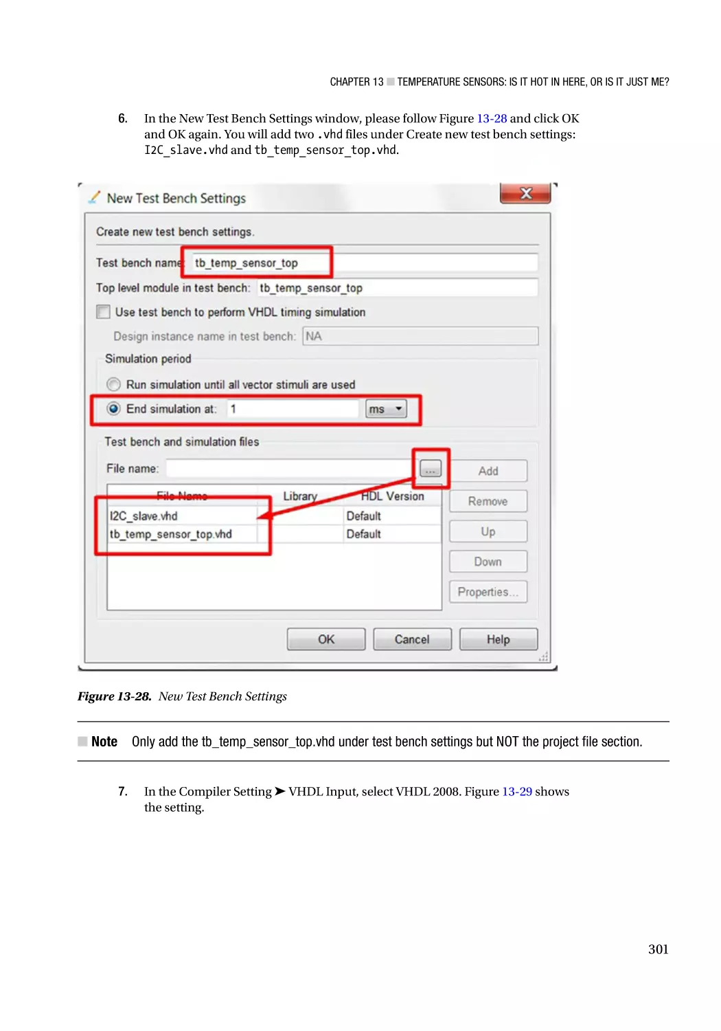
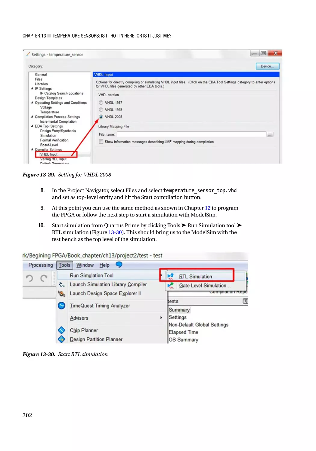
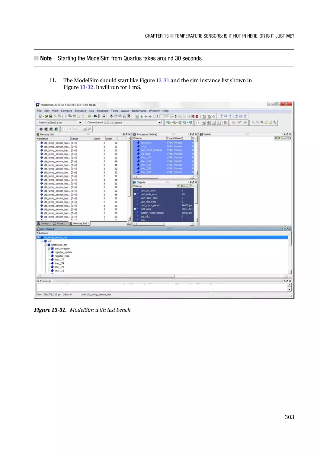
13.5.4 Create Temperature Sensor Project Design and Program It������������������������������������������������� 297
13.5.5 Hardware Setup for the Temperature Sensor Project Design����������������������������������������������� 305
13.5.6 UART Software Setup—RealTerm���������������������������������������������������������������������������������������� 305
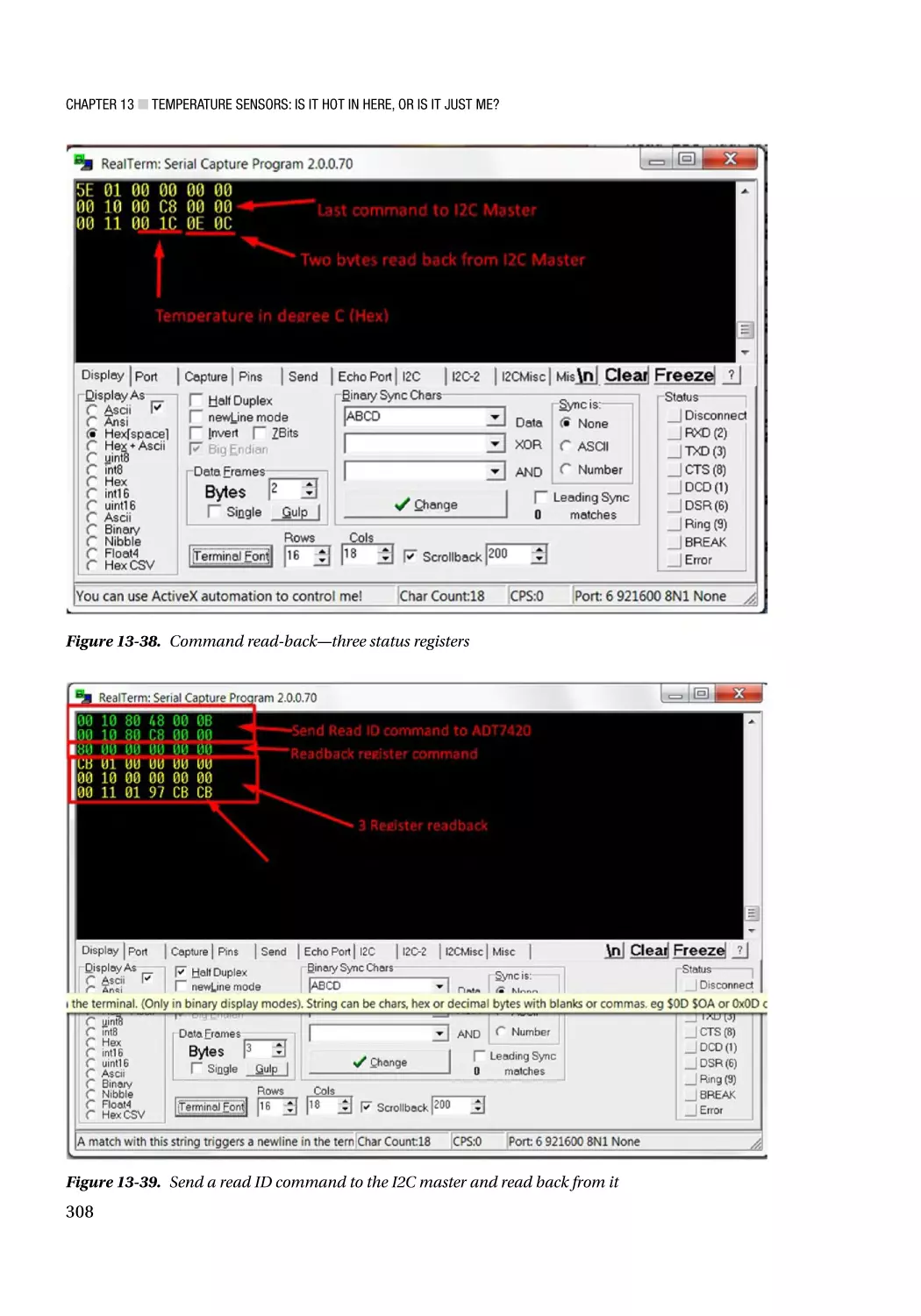
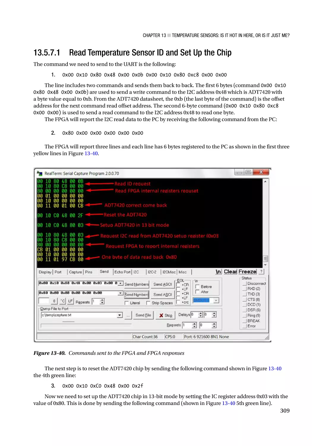
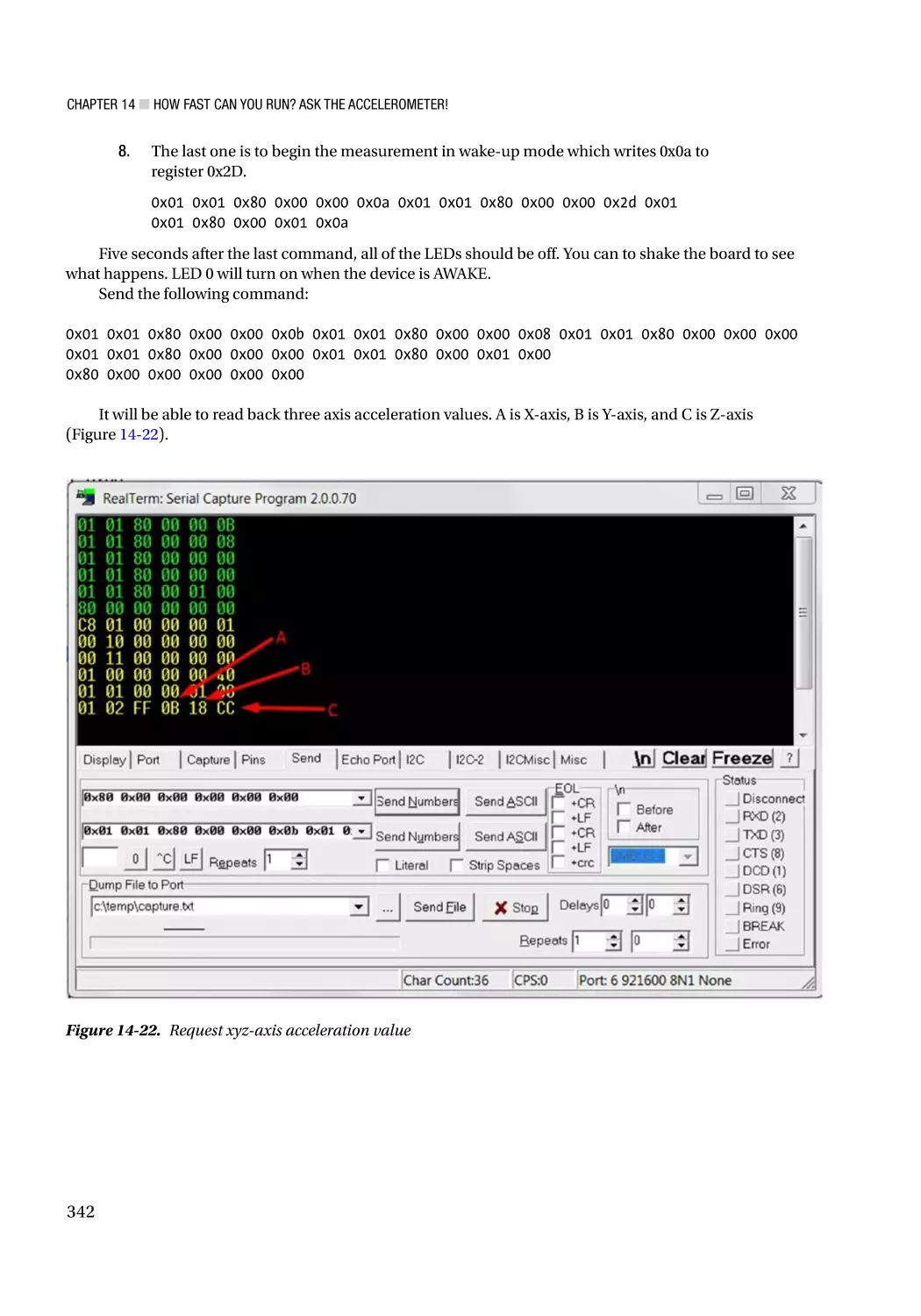
13.5.7 Command Your FPGA to Read the Temperature�������������������������������������������������������������������� 307
13.6 Summary����������������������������������������������������������������������������������������������������������� 311
■Chapter
■
14: How Fast Can You Run? Ask the Accelerometer!��������������������������� 313
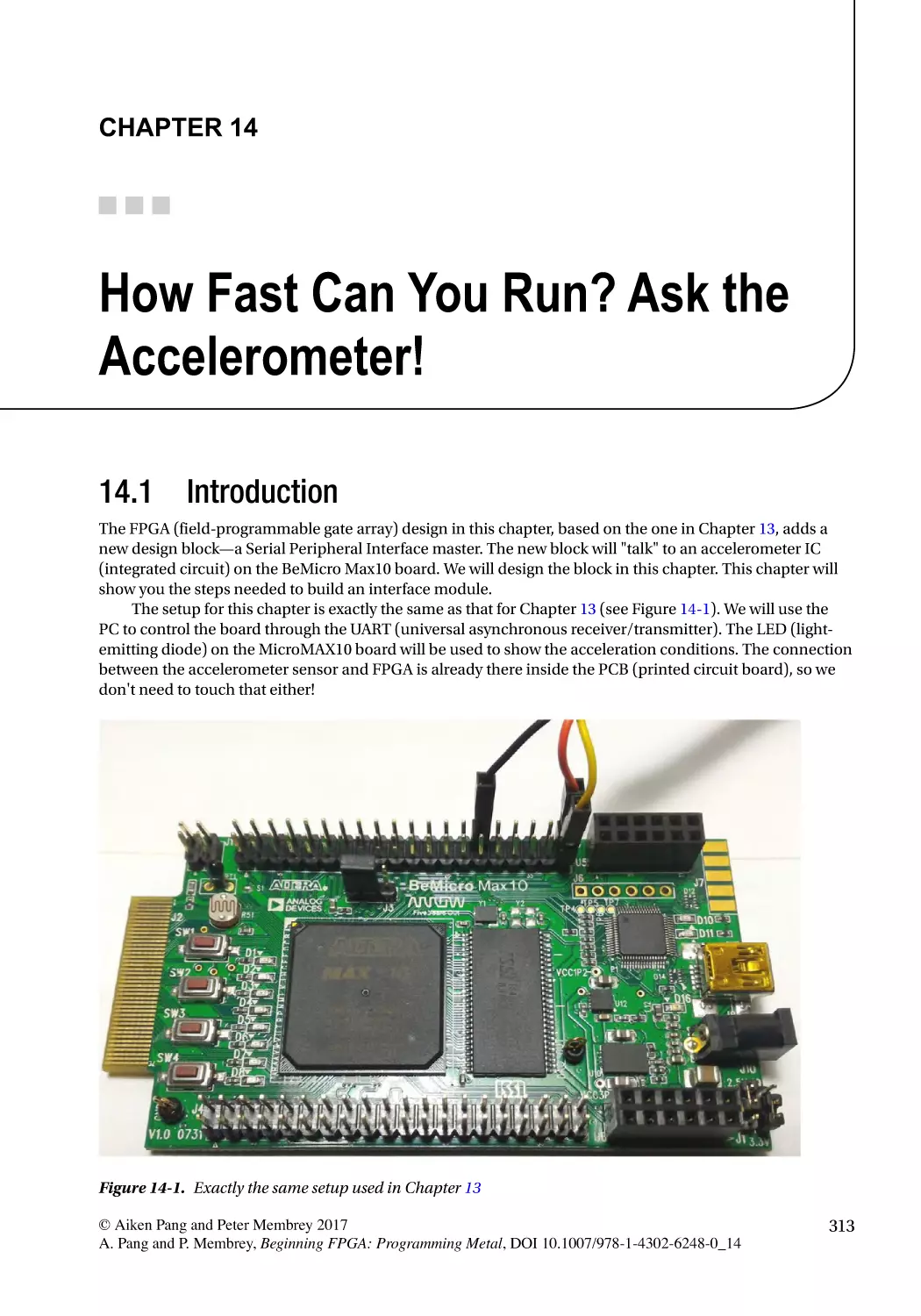
14.1 Introduction������������������������������������������������������������������������������������������������������� 313
14.2 Steps to Build Your First Interface Module ������������������������������������������������������� 314
14.2.1 Understanding the SPI���������������������������������������������������������������������������������������������������������� 314
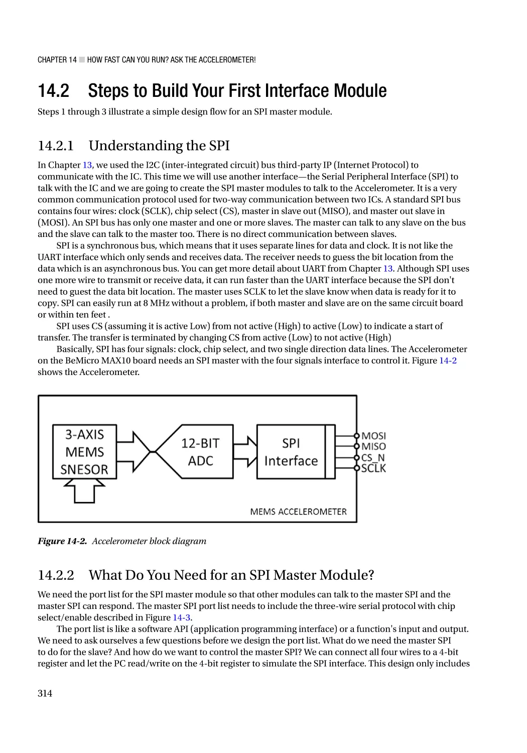
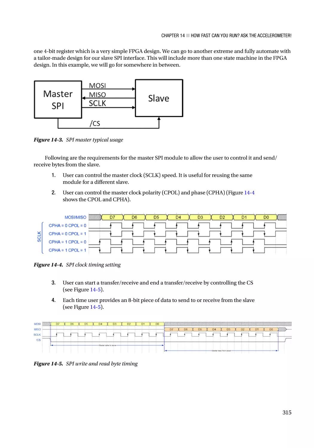
14.2.2 What Do You Need for an SPI Master Module?��������������������������������������������������������������������� 314
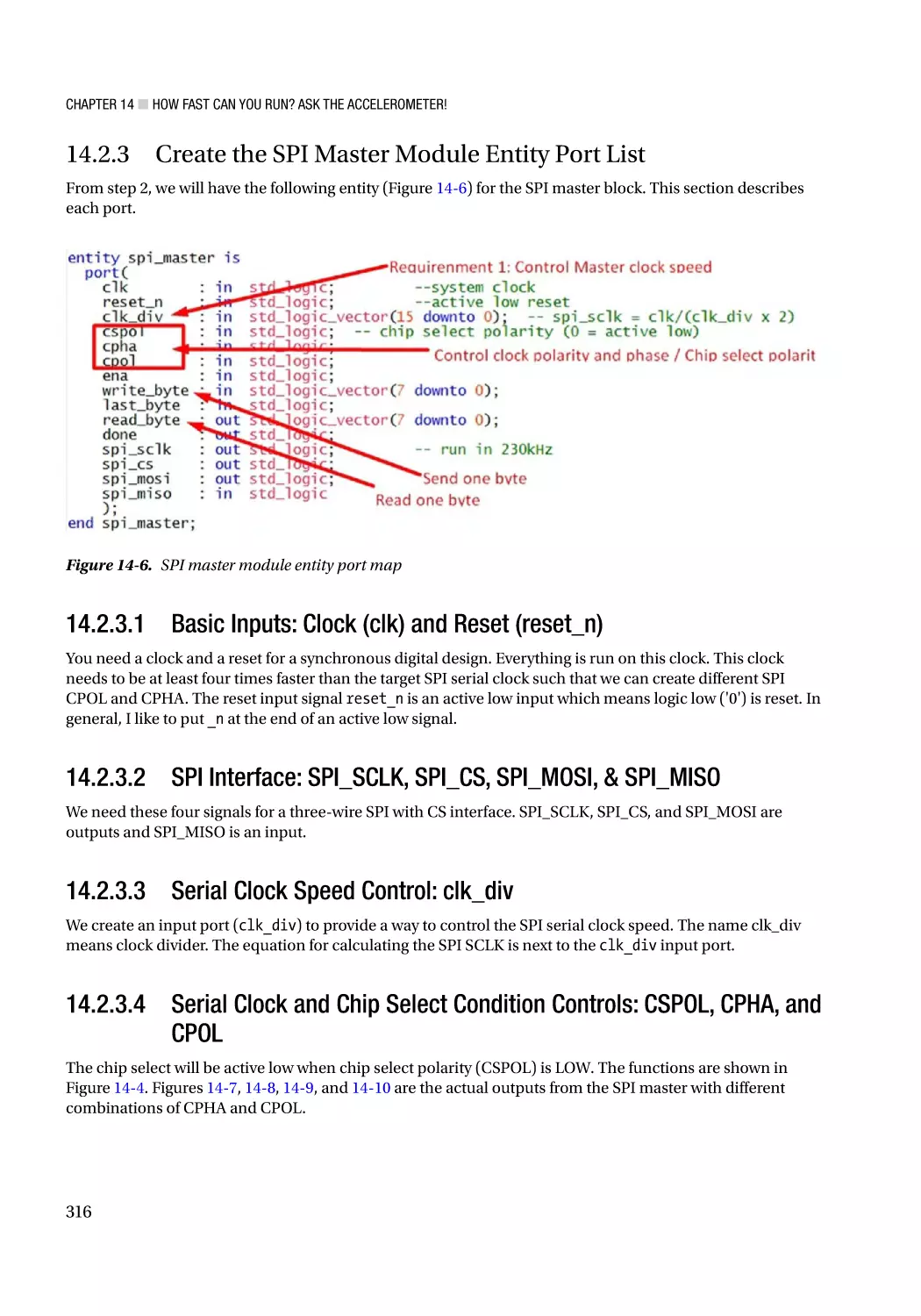
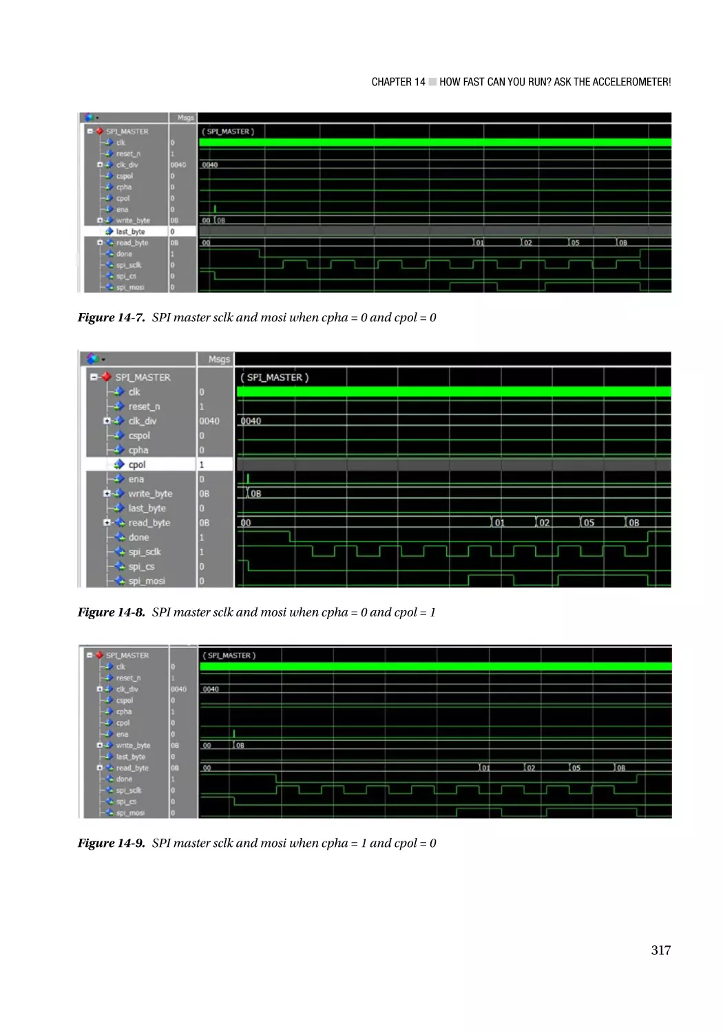
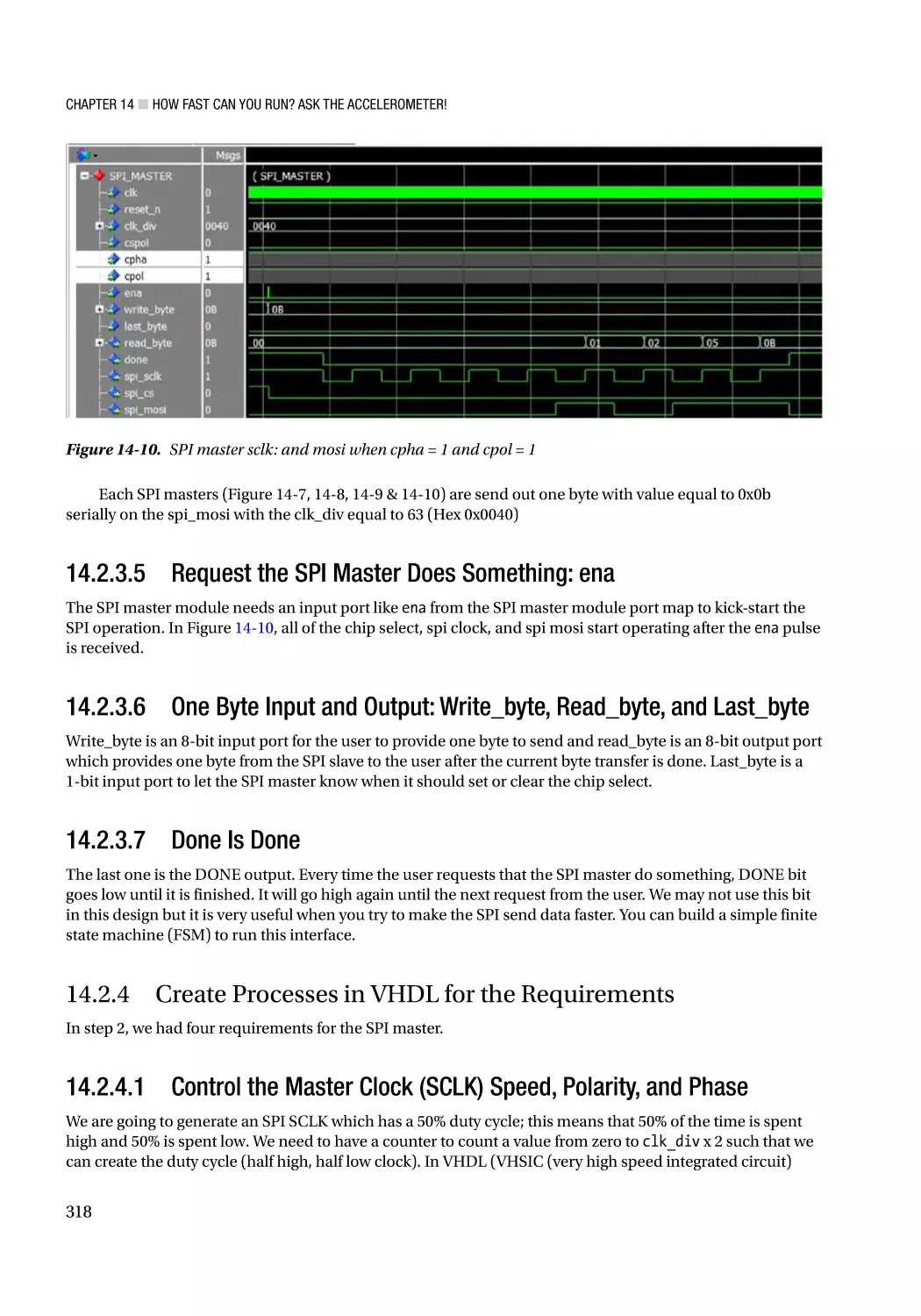
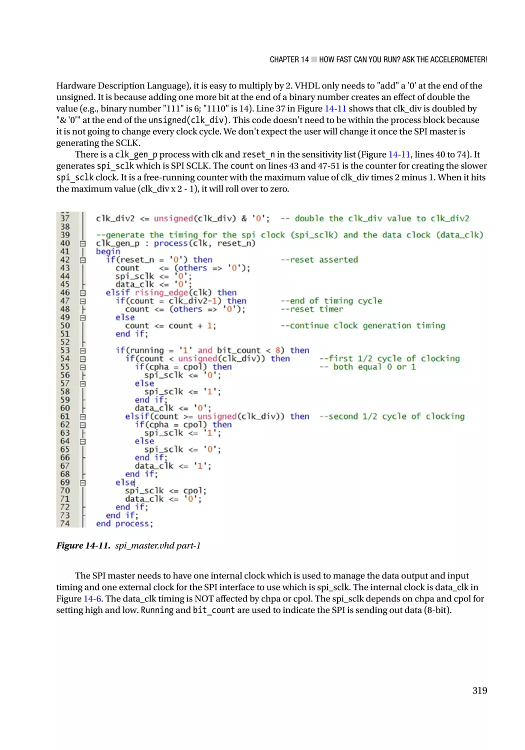
14.2.3 Create the SPI Master Module Entity Port List���������������������������������������������������������������������� 316
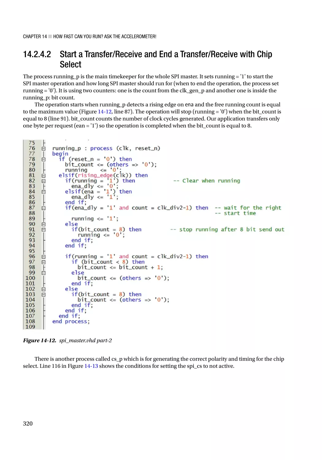
14.2.4 Create Processes in VHDL for the Requirements������������������������������������������������������������������ 318
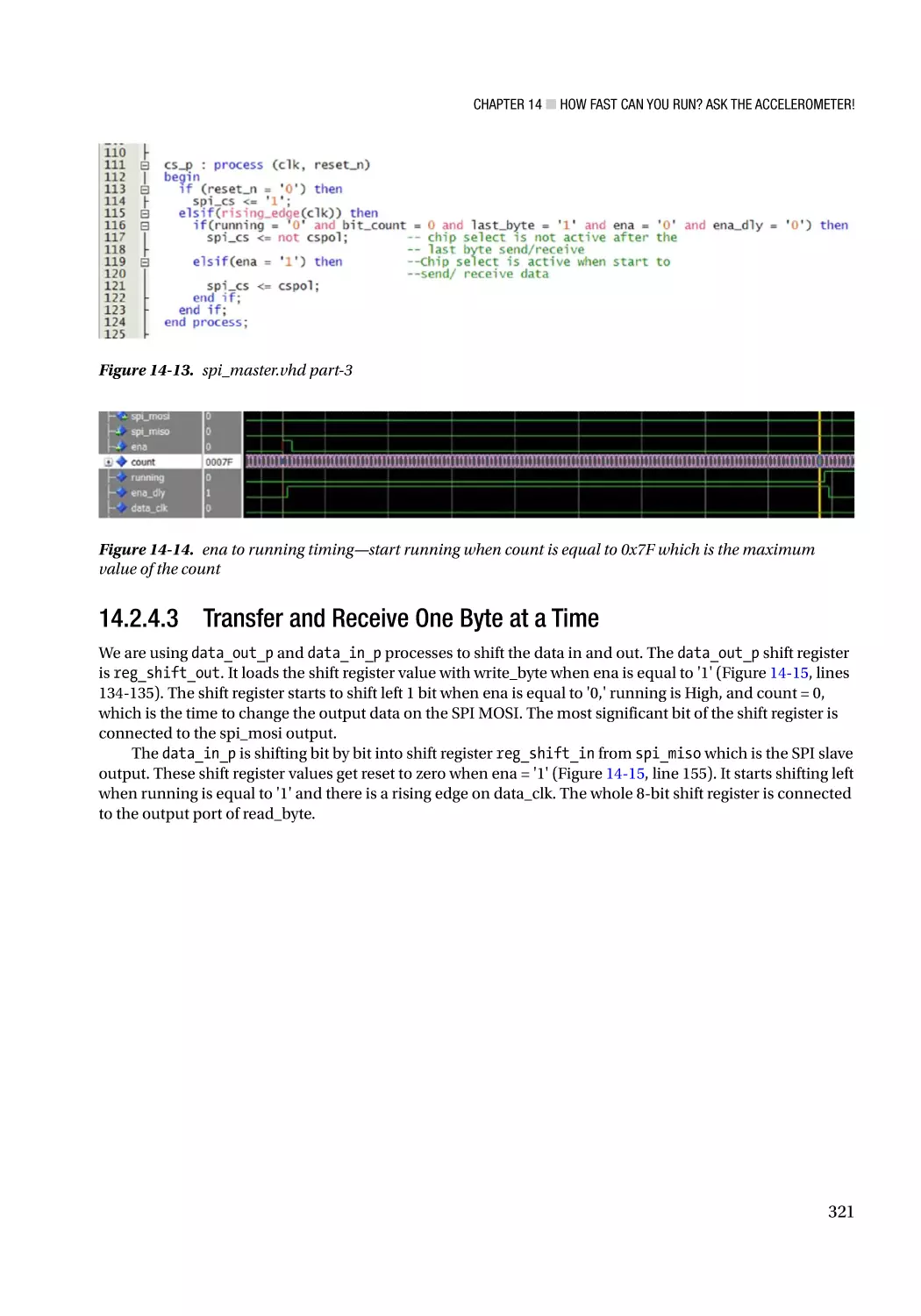
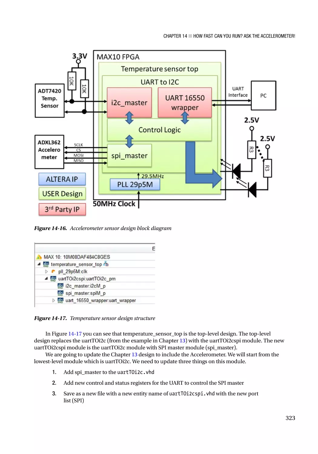
14.3 PC Control Accelerometer Sensor Design Example������������������������������������������� 322
14.3.1 Add New Command and Status Registers���������������������������������������������������������������������������� 324
14.3.2 Create the Temperature Sensor Project Design and Program It������������������������������������������� 326
14.3.3 Example Design Codes��������������������������������������������������������������������������������������������������������� 326
14.3.4 Hardware Setup for the Accelerator Sensor Project Design������������������������������������������������� 338
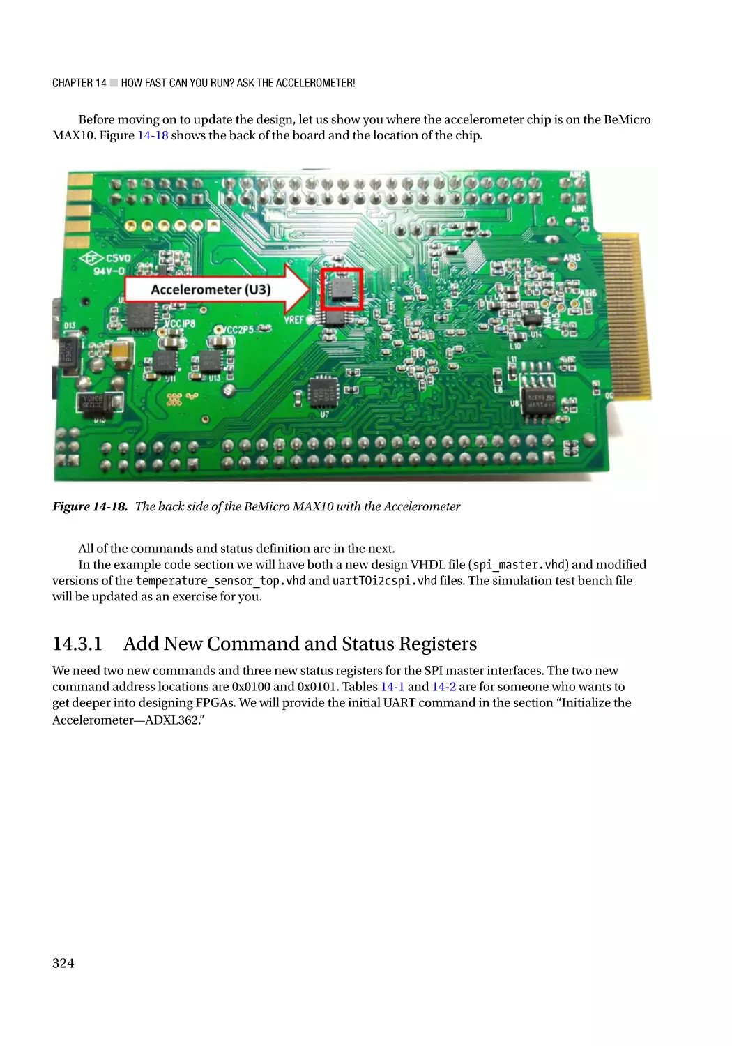
14.3.5 Initialize the Accelerometer—ADXL362������������������������������������������������������������������������������� 338
14.4 Summary����������������������������������������������������������������������������������������������������������� 343
■■Part IV: Taking It Further: Talking to the Raspberry Pi and
LED Displays����������������������������������������������������������������������������������� 345
■Chapter
■
15: Two-Way Communications with Your Raspberry Pi: SPI���������������� 347
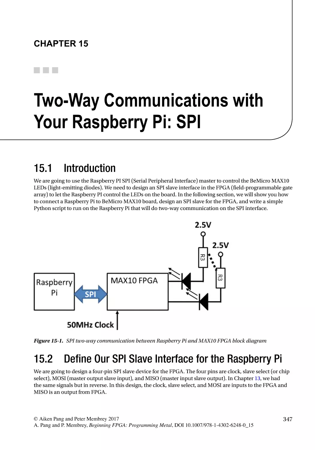
15.1 Introduction������������������������������������������������������������������������������������������������������� 347
15.2 Define Our SPI Slave Interface for the Raspberry Pi����������������������������������������� 347
xi
■ Contents
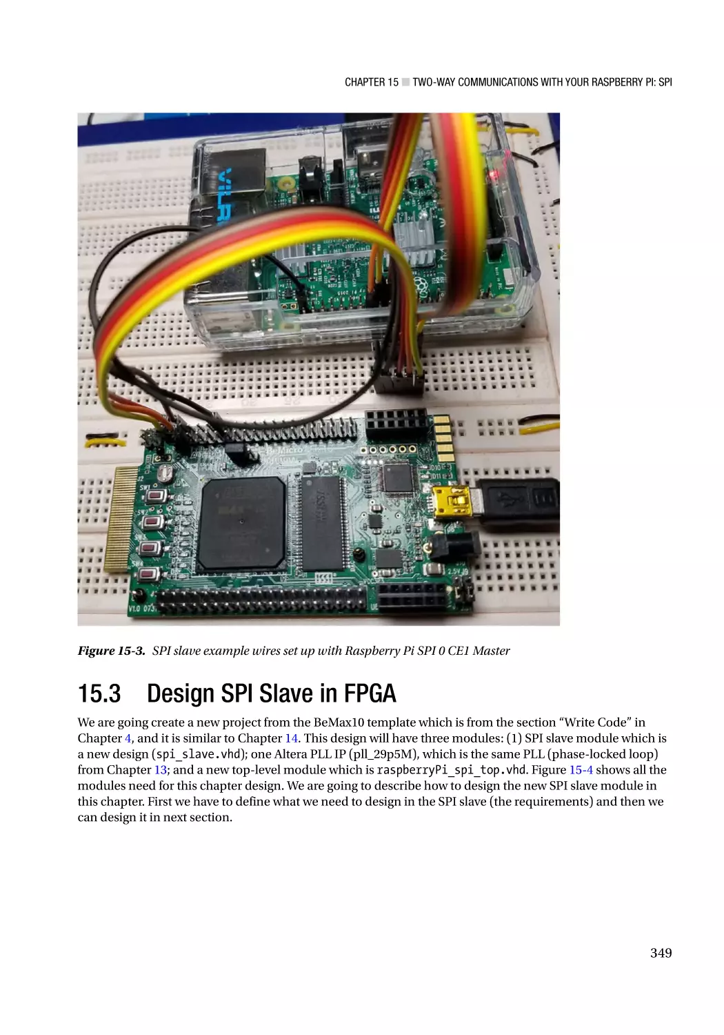
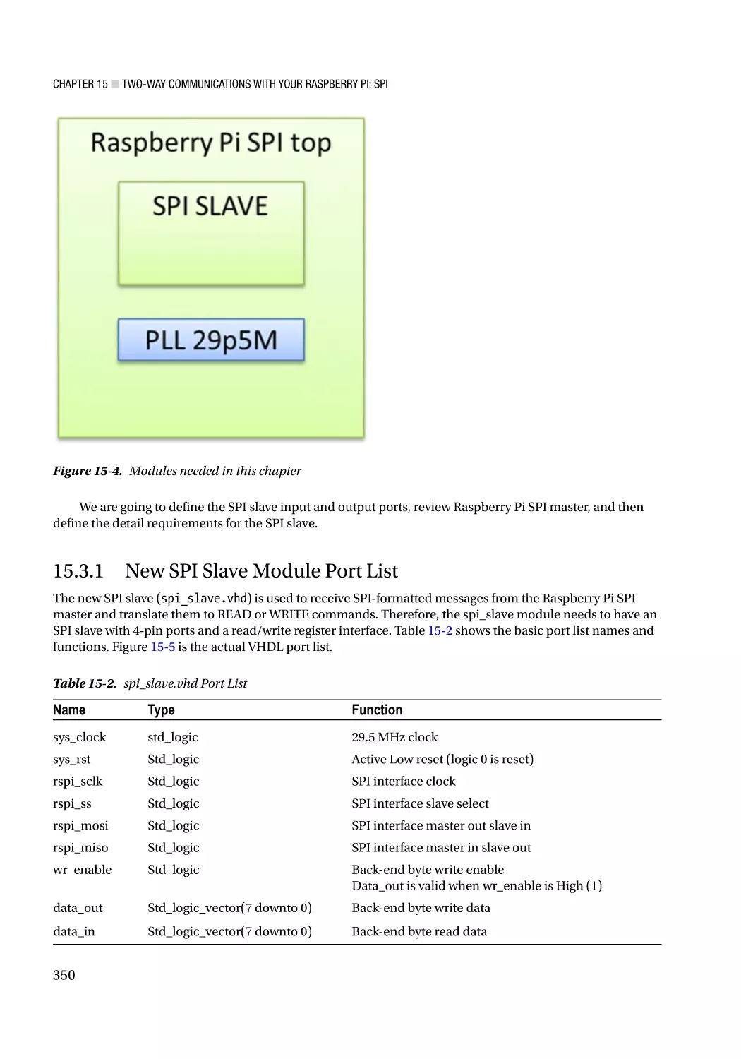
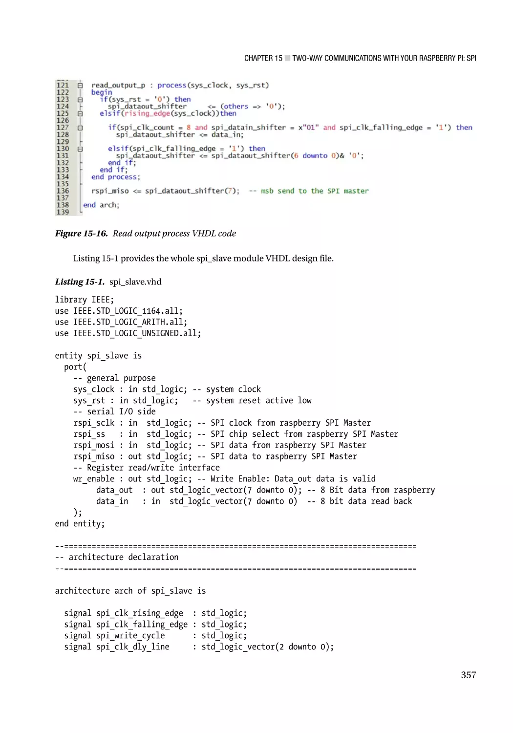
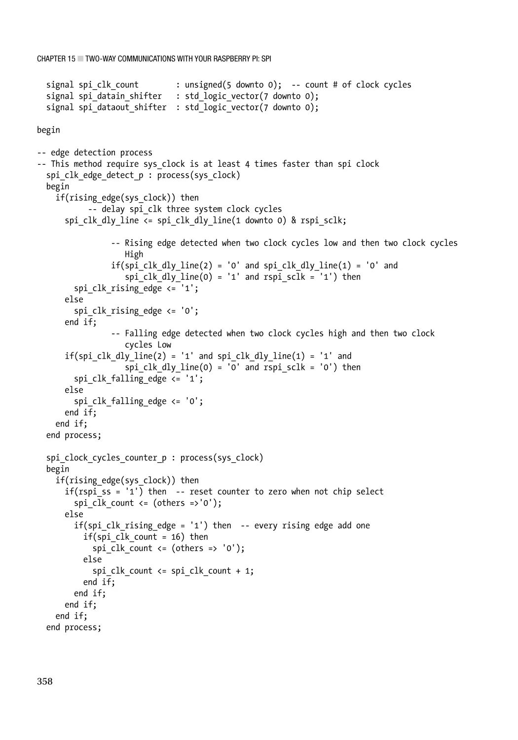
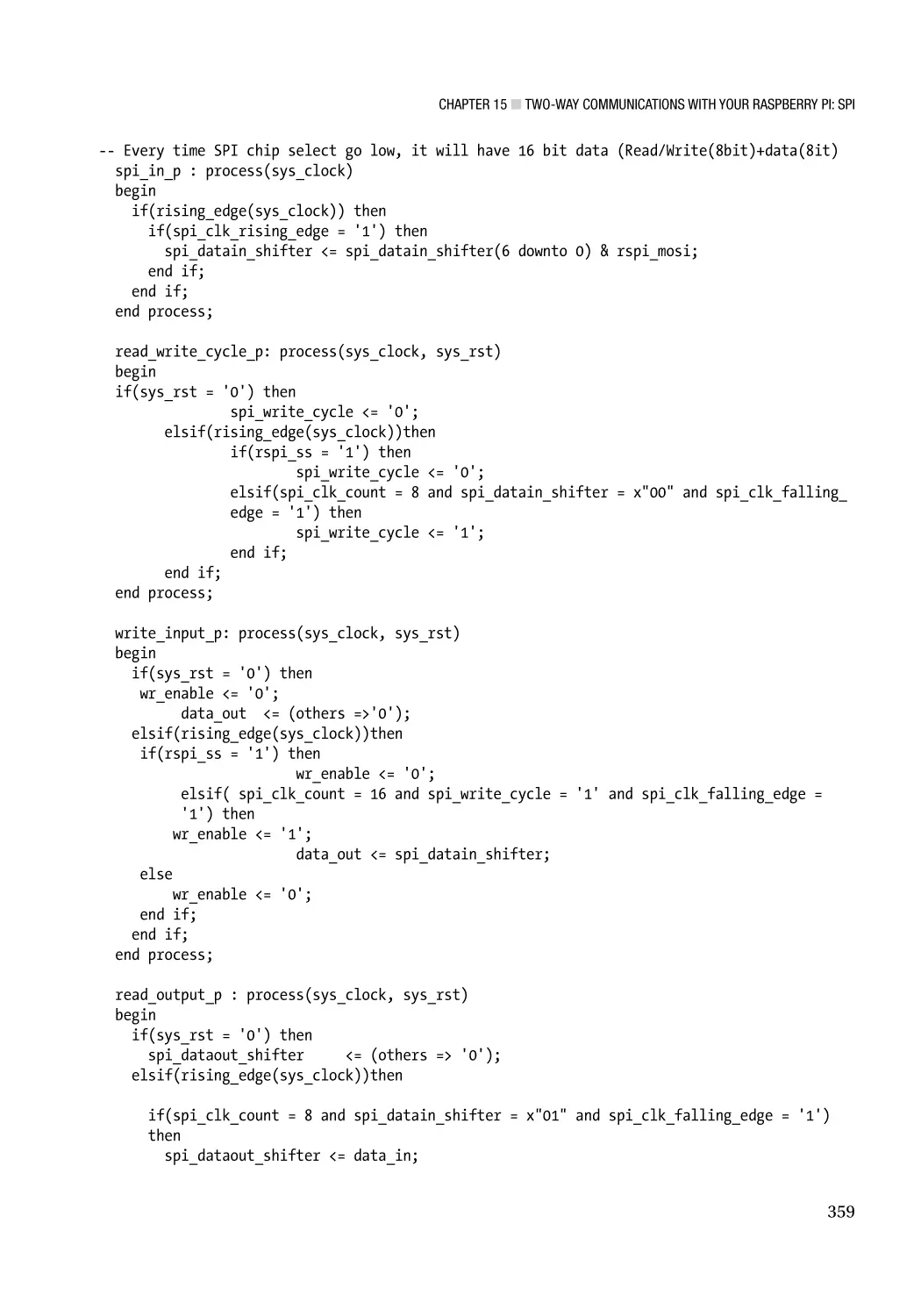
15.3 Design SPI Slave in FPGA���������������������������������������������������������������������������������� 349
15.3.1 New SPI Slave Module Port List������������������������������������������������������������������������������������������� 350
15.3.2 Raspberry Pi SPI Master 0 Default Setting and Data Format����������������������������������������������� 351
15.3.3 Writing VHDL for the SPI Slave��������������������������������������������������������������������������������������������� 352
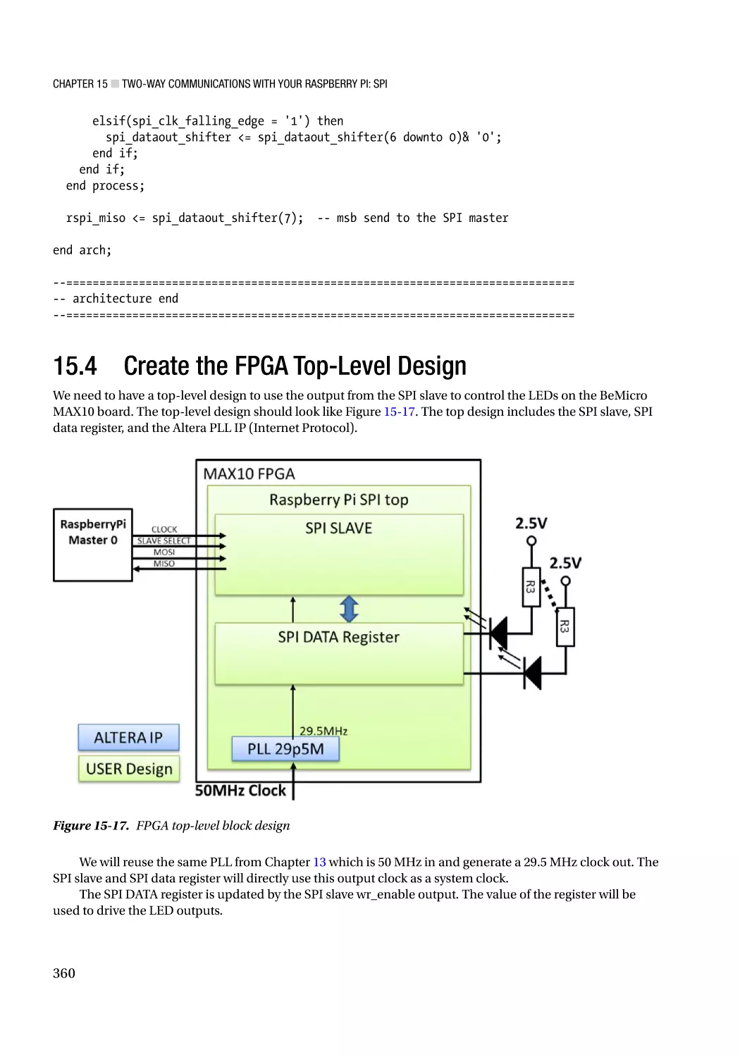
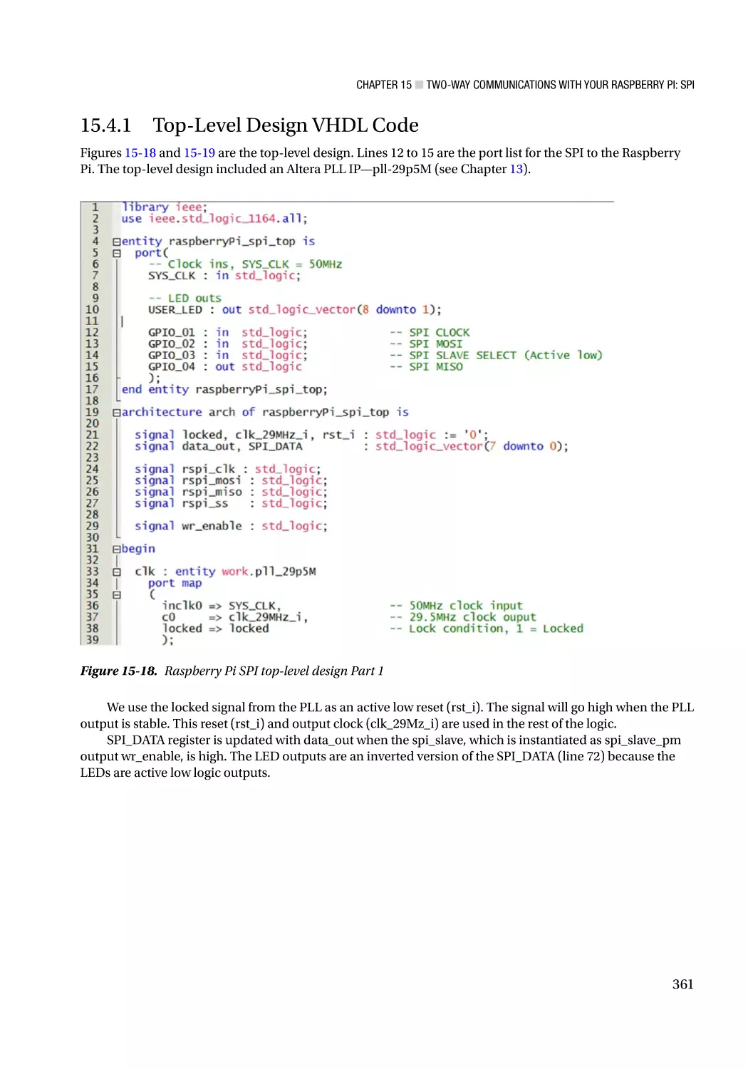
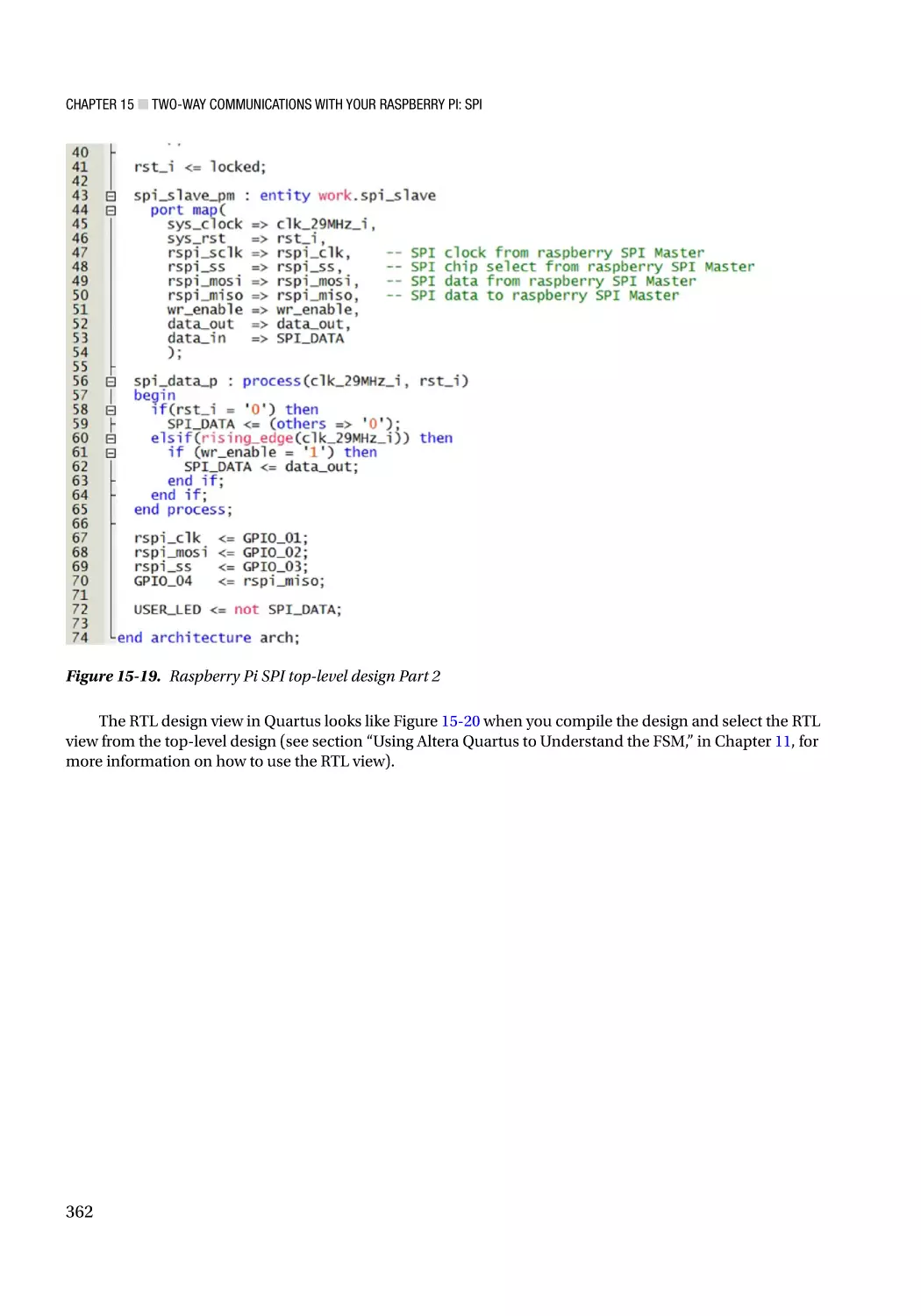
15.4 Create the FPGA Top-Level Design�������������������������������������������������������������������� 360
15.4.1 Top-Level Design VHDL Code������������������������������������������������������������������������������������������������ 361
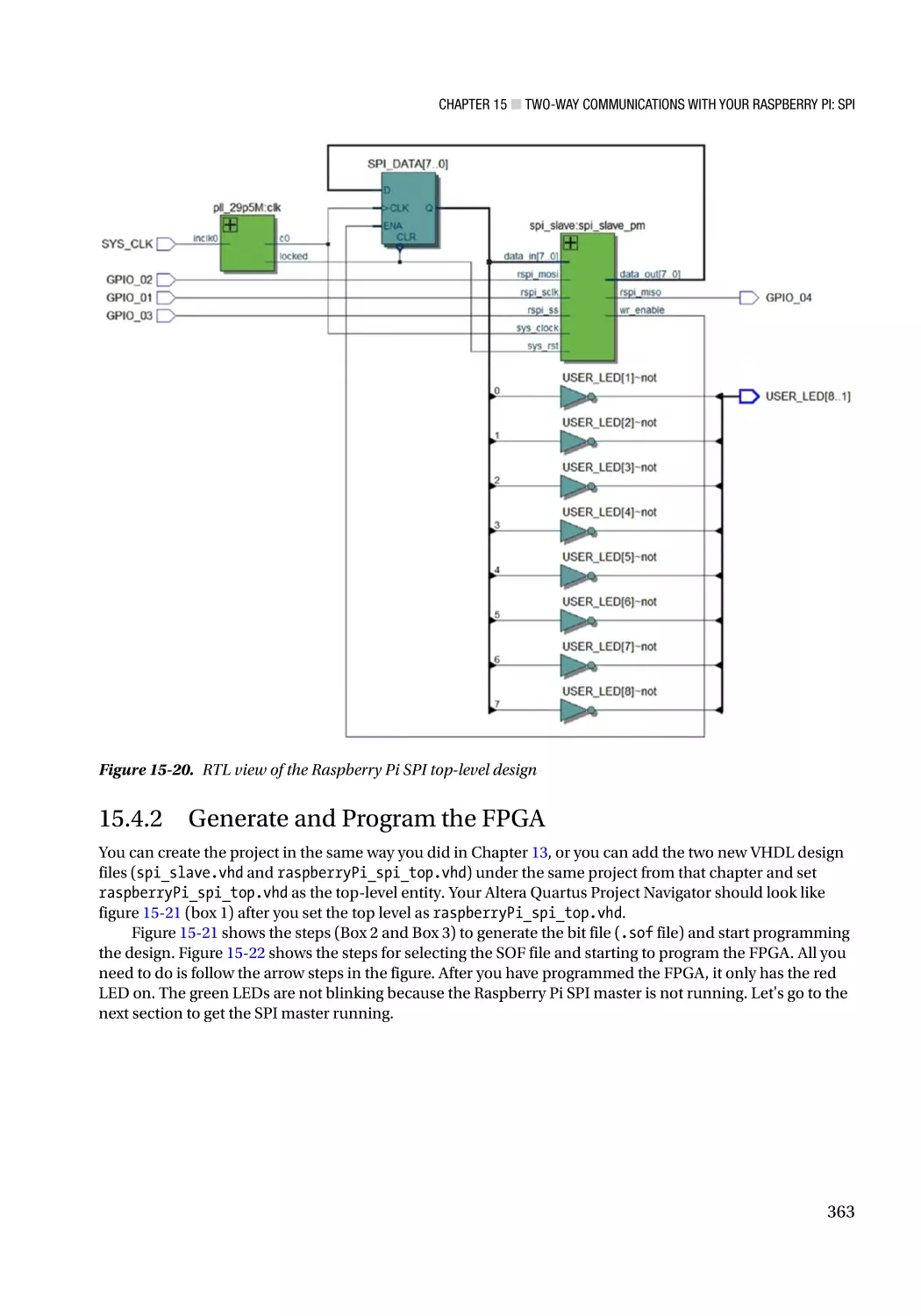
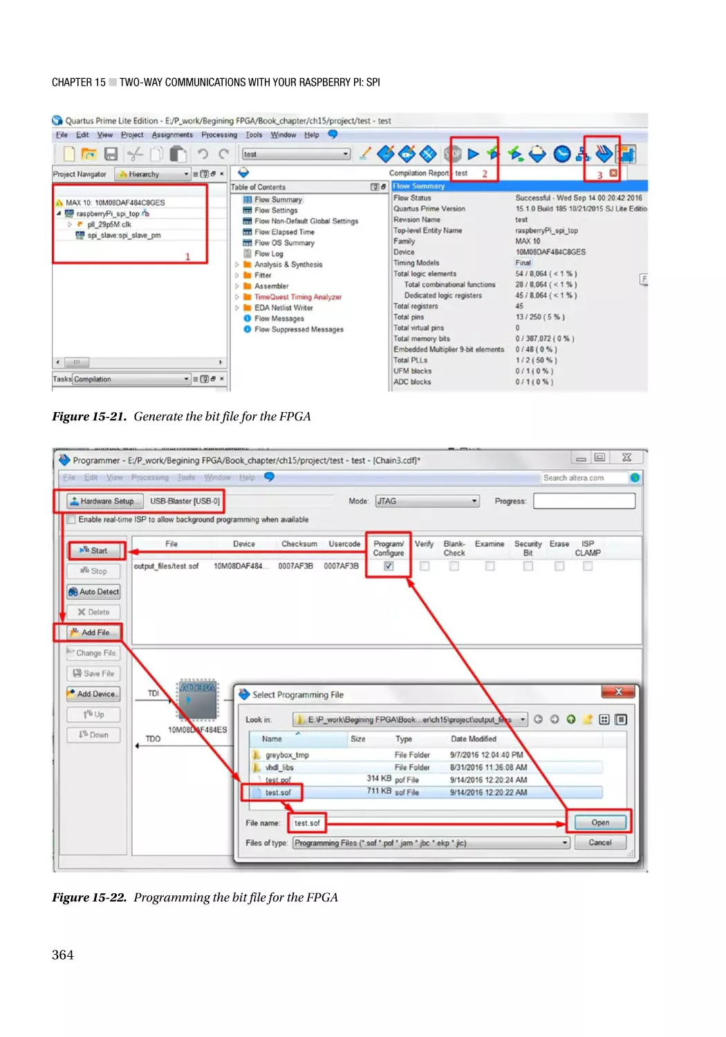
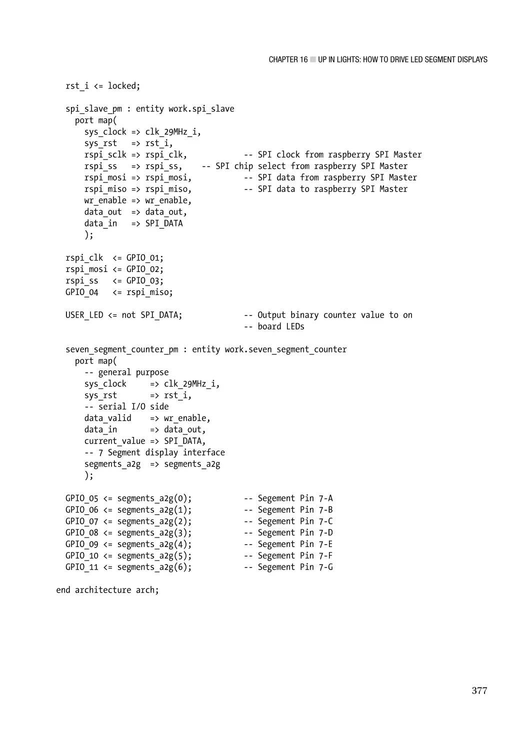
15.4.2 Generate and Program the FPGA������������������������������������������������������������������������������������������ 363
15.5 How to Use Raspberry Pi SPI Master Interface ������������������������������������������������ 365
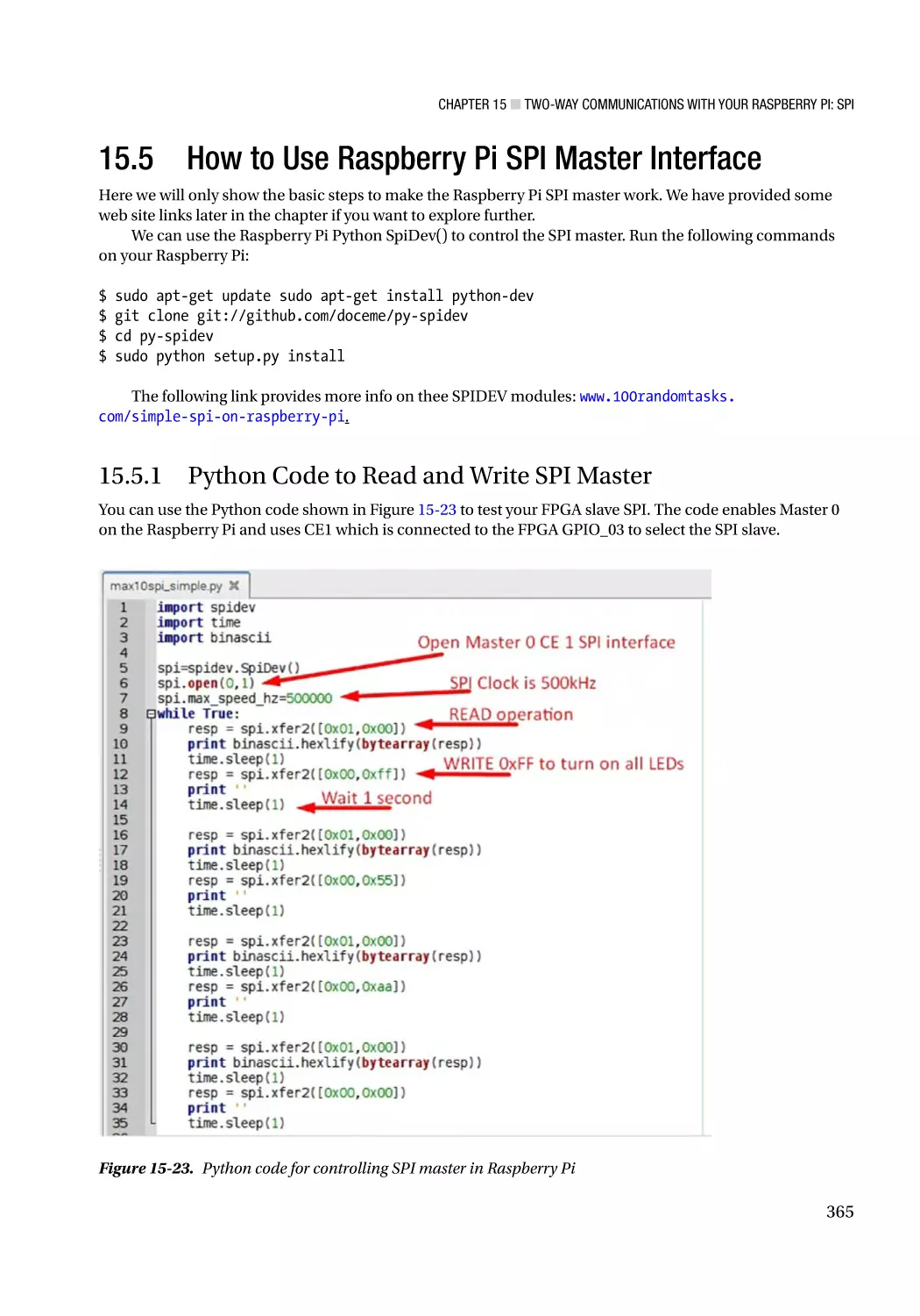
15.5.1 Python Code to Read and Write SPI Master�������������������������������������������������������������������������� 365
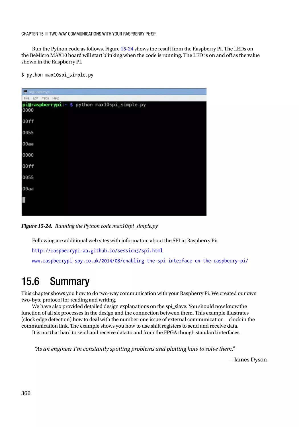
15.6 Summary����������������������������������������������������������������������������������������������������������� 366
■Chapter
■
16: Up in Lights: How to Drive LED Segment Displays������������������������� 367
16.1 Introduction������������������������������������������������������������������������������������������������������� 367
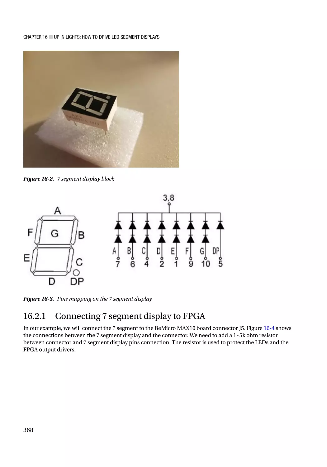
16.2 How to drive a 7 segment display��������������������������������������������������������������������� 367
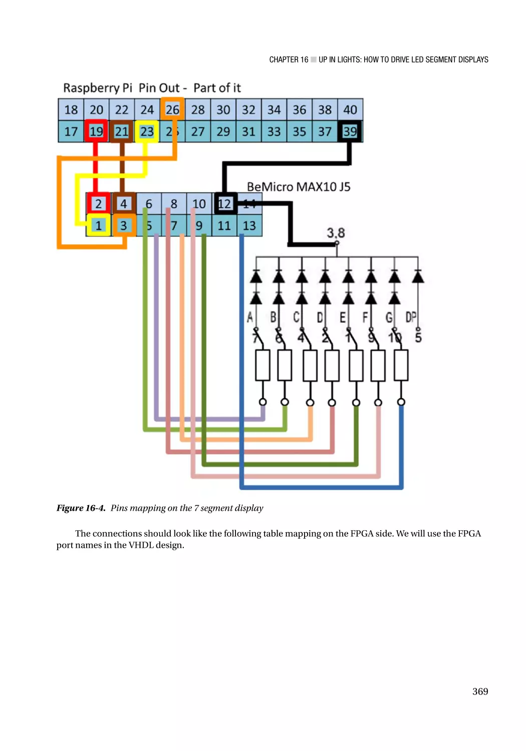
16.2.1 Connecting 7 segment display to FPGA�������������������������������������������������������������������������������� 368
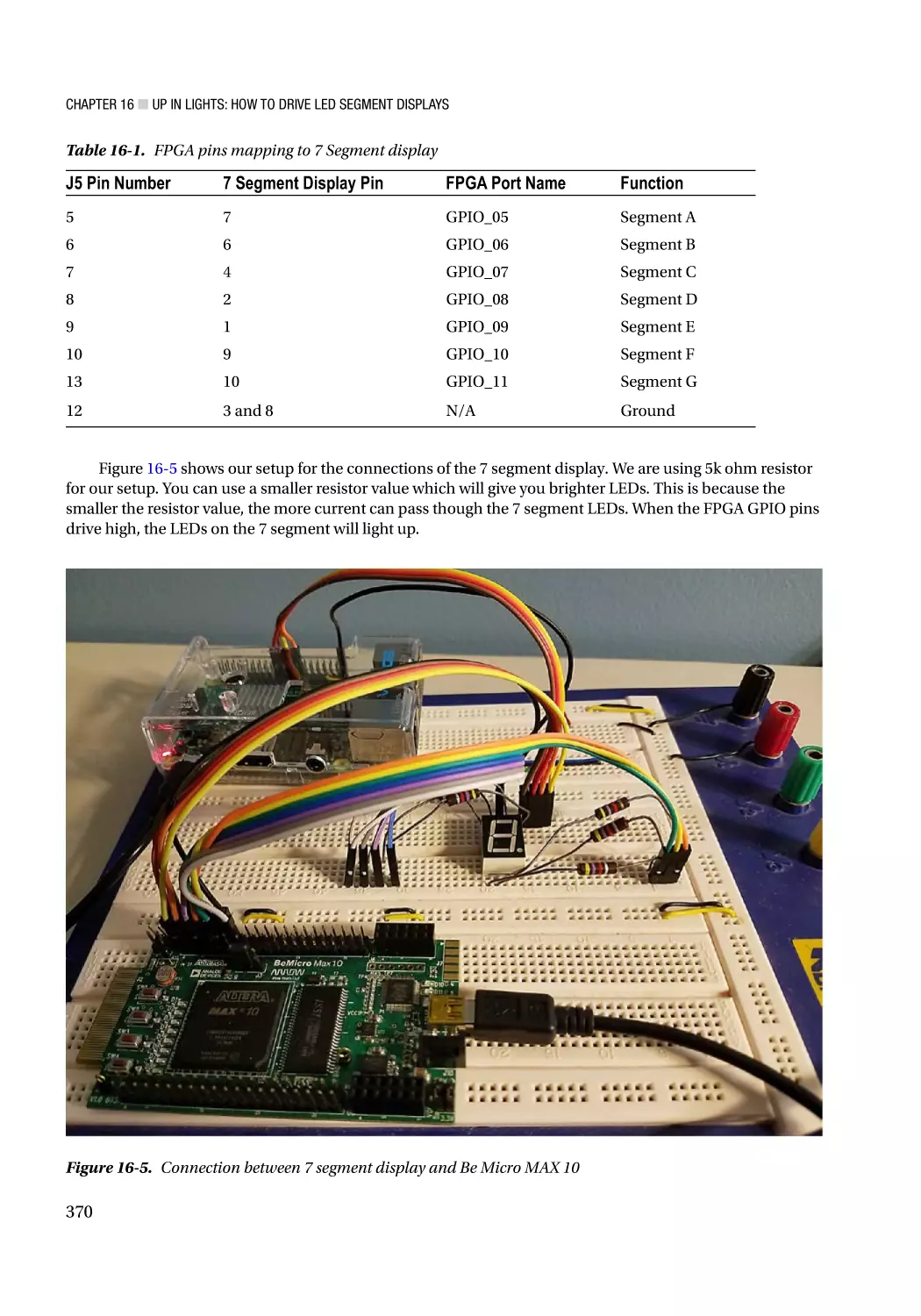
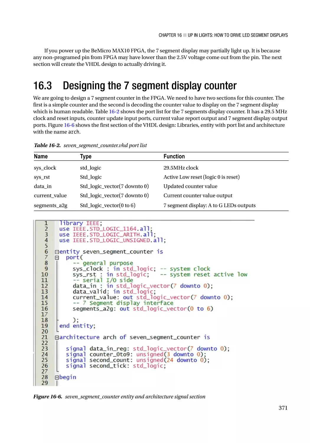
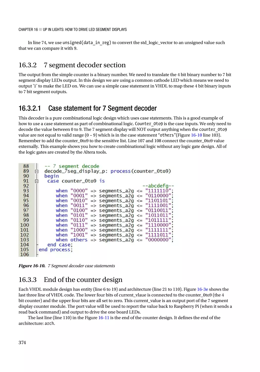
16.3 Designing the 7 segment display counter��������������������������������������������������������� 371
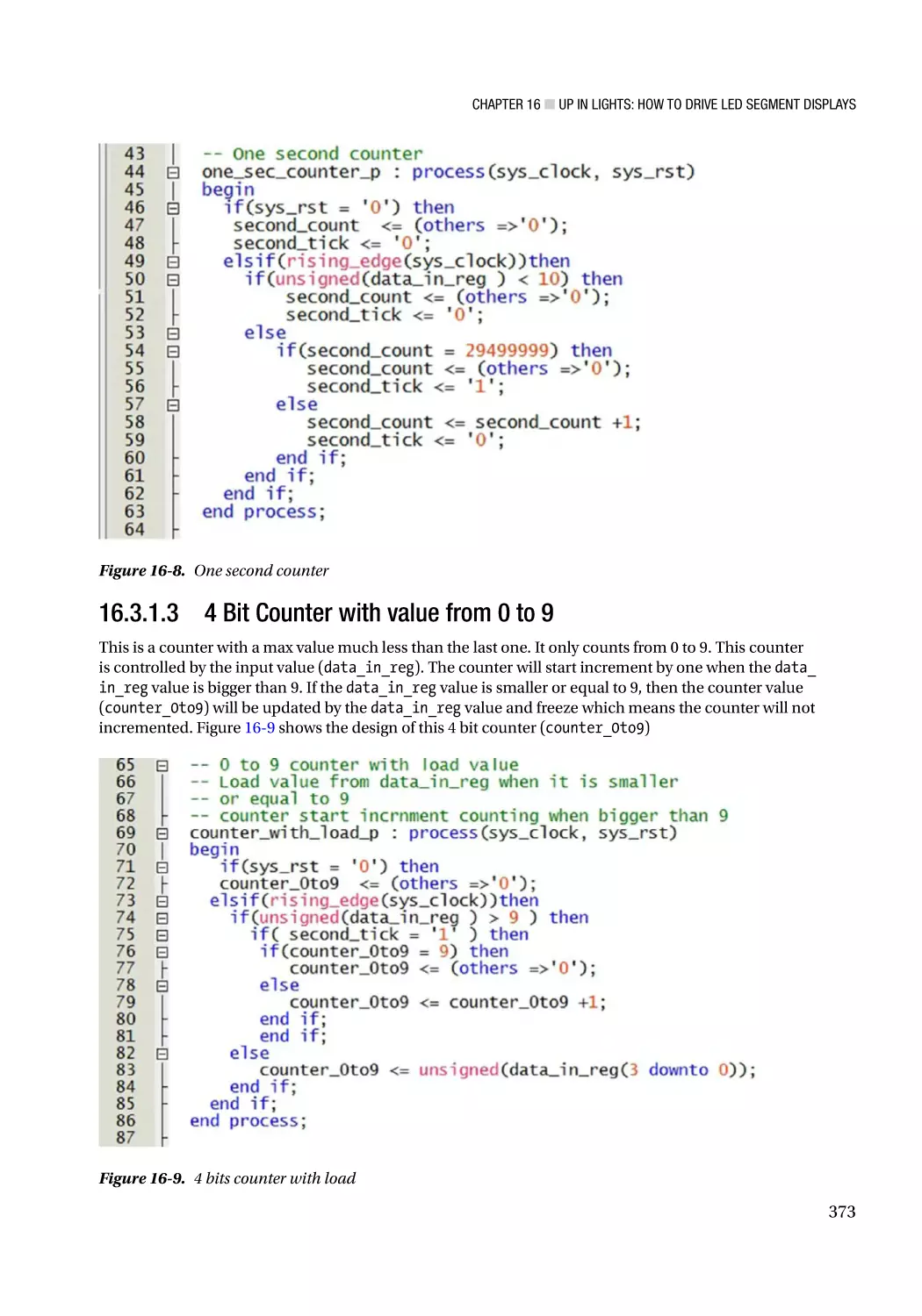
16.3.1 Simple counter design section��������������������������������������������������������������������������������������������� 372
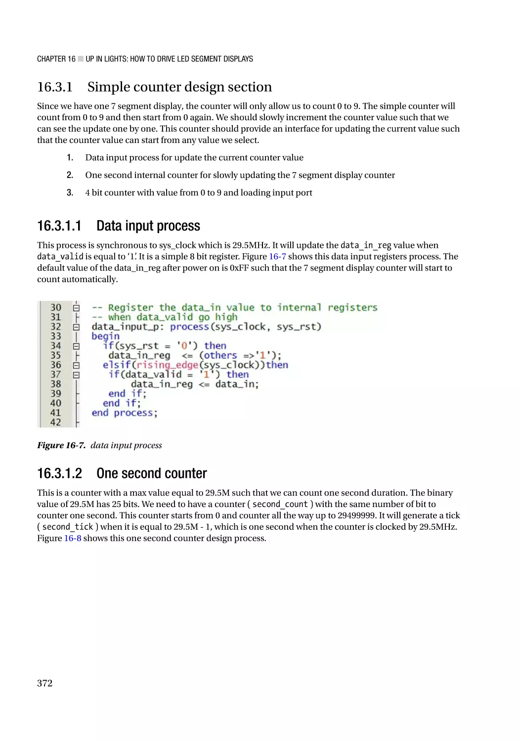
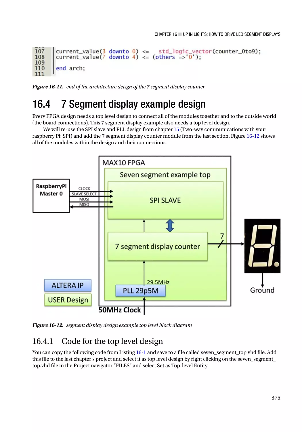
16.3.2 7 segment decoder section�������������������������������������������������������������������������������������������������� 374
16.3.3 End of the counter design���������������������������������������������������������������������������������������������������� 374
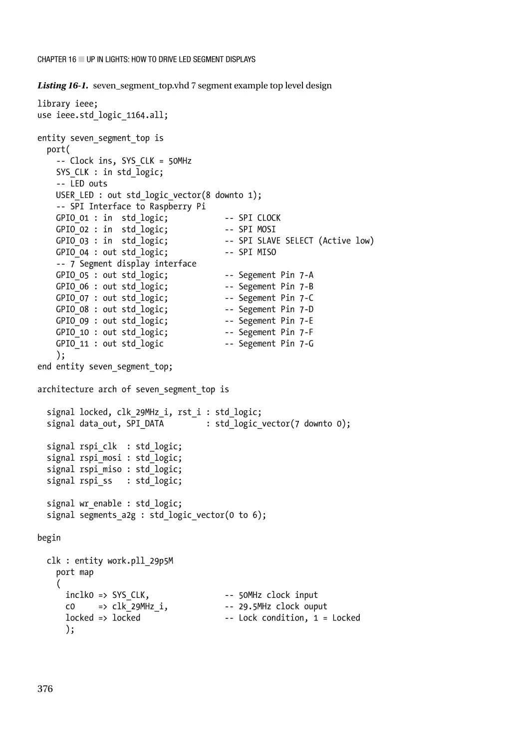
16.4 7 Segment display example design������������������������������������������������������������������ 375
16.4.1 Code for the top level design������������������������������������������������������������������������������������������������ 375
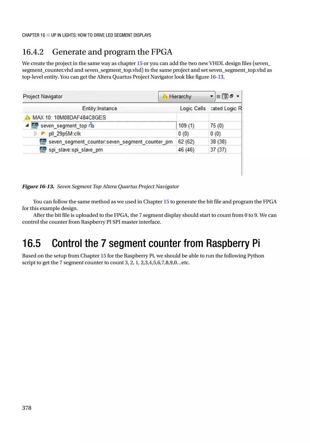
16.4.2 Generate and program the FPGA������������������������������������������������������������������������������������������ 378
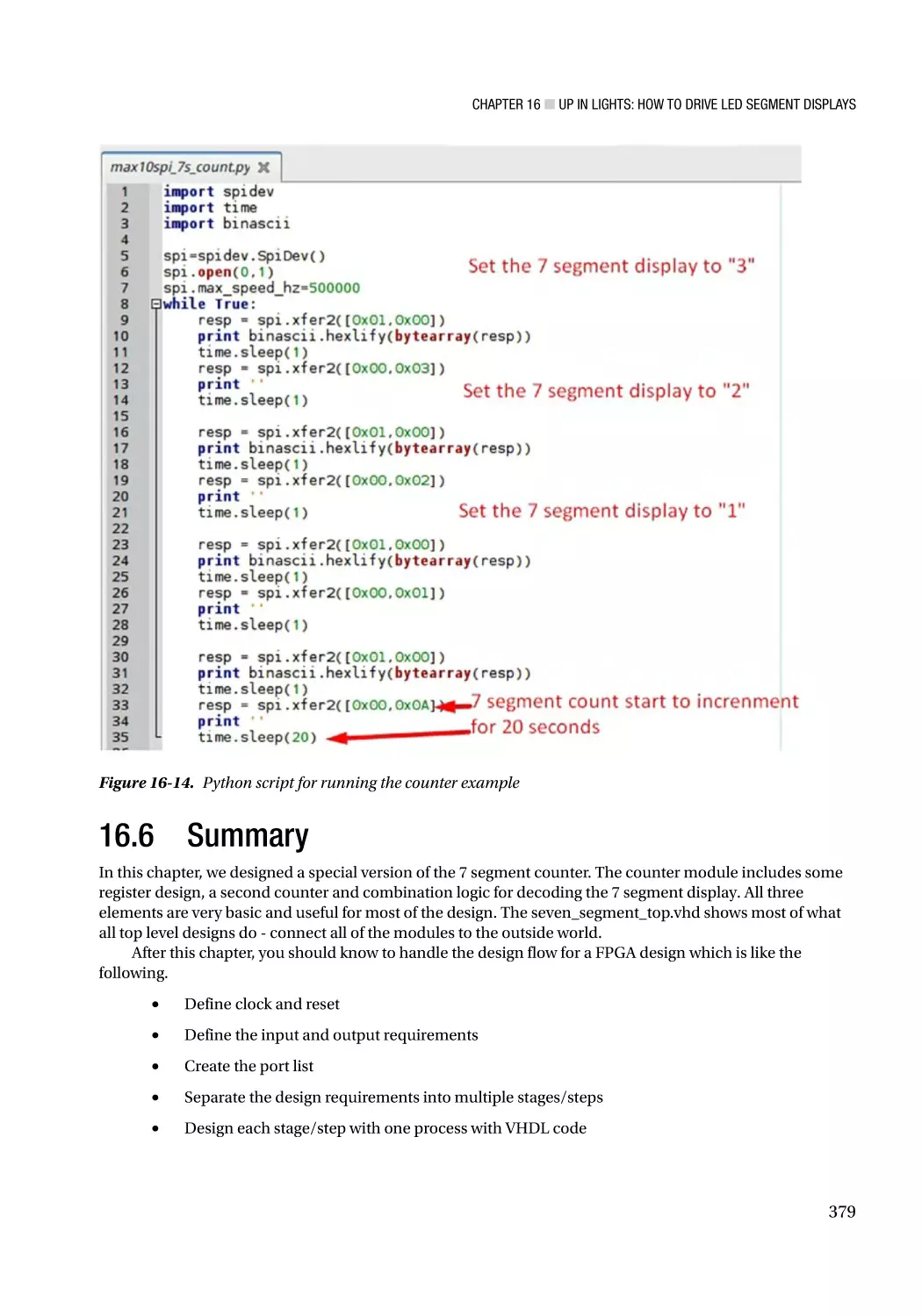
16.5 Control the 7 segment counter from Raspberry Pi�������������������������������������������� 378
16.6 Summary����������������������������������������������������������������������������������������������������������� 379
Index��������������������������������������������������������������������������������������������������������������������� 381
xii
About the Authors
Aiken Pang was born in Hong Kong in the early 1980s just in time for the
home micro-computer revolution. He developed an interest in computers
after finding an Apple IIe at his uncle’s home; he installed a TV card and
a floppy drive and loaded his first game (Pacman) by himself at the age
of 10. Since then he has self-taught himself a number of programming
languages and built his own computers from scratch.
Aiken followed his passion for computing into more formal studies
and holds a BEng in Electronics Engineering and an MSc in Computer
Engineering from Hong Kong Polytechnic University and the University of
Massachusetts at Lowell, respectively. He has been using VHDL (VHSIC (very
high speed integrated circuit) Hardware Description Language) to design
hardware in FPGAs (field-programmable gate arrays) for more than ten years.
He lives in the United States with his wife France and their
daughter Mayah.
Hailing from the UK, Peter Membrey has worked for Red Hat, holds a RHCE certification, and has worked
and taught at a number of educational institutions since the beginning of his career. He knows what Linux
users like and need and hopes that CentOS will get the kudos it deserves. He lives in Hong Kong and is
teaching and consulting on all matters having to do with Linux Enterprise networking, while studying for his
master’s degree.
xiii
About the Technical Reviewer
Brendan Horan is a hardware fanatic, with a full high rack of all types
of machine architectures in his home. He has more than 10 years of
experience working with large UNIX systems and tuning the underlying
hardware for optimal performance and stability. Brendan's love for all
forms of hardware has helped him throughout his IT career, from fixing
laptops to tuning servers and their hardware in order to suit the needs
of high-availability designs and ultra low-latency applications. Brendan
takes pride in the Open Source Movement and is happy to say that every
computer in his house is powered by open source technology. He resides
in Hong Kong with his wife, Vikki, who continues daily to teach him more
Cantonese.
xv
PART I
Getting Started with FPGA
CHAPTER 1
What Is an FPGA and
What Can It Do?
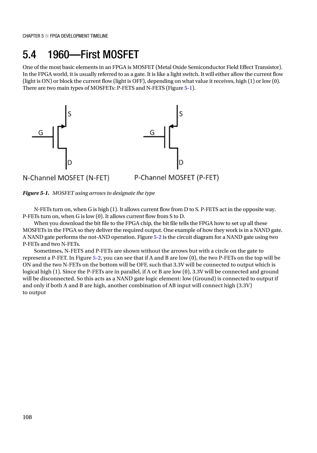
Field-programmable gate arrays (FPGA) are a special type of integrated circuits (ICs) or chip that can be
programmed in the field after manufacture and has three basic building blocks: logic gates, flip-flops +
memories, and wires. In this chapter we will quickly review what FPGA is and some of the things it can do.
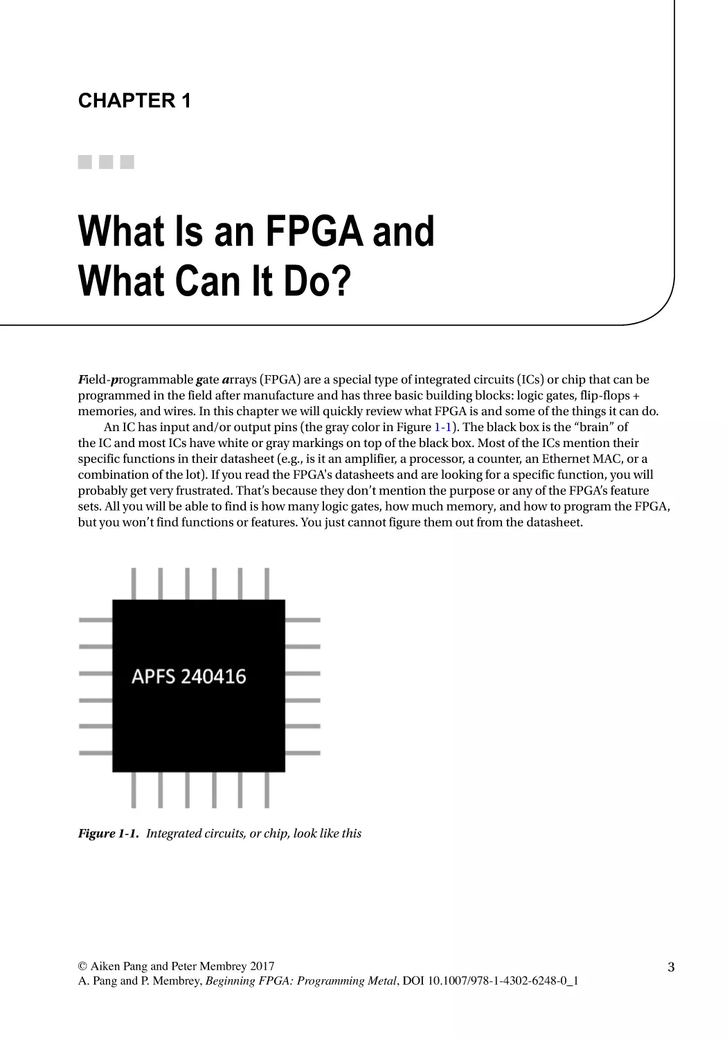
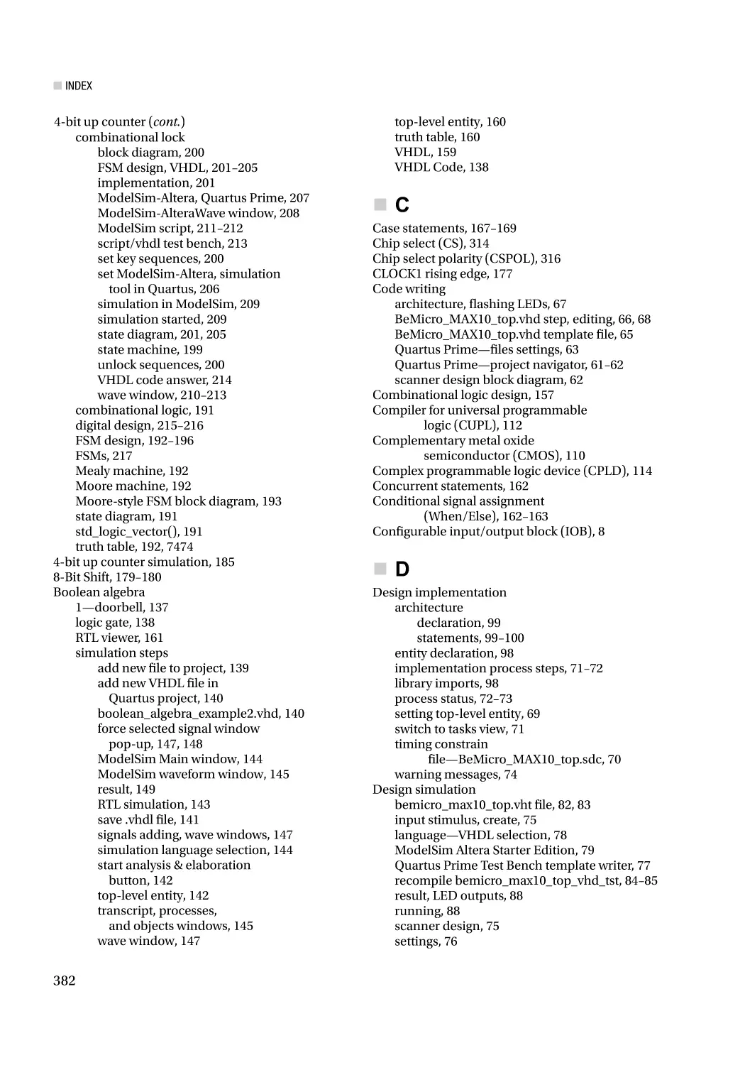
An IC has input and/or output pins (the gray color in Figure 1-1). The black box is the “brain” of
the IC and most ICs have white or gray markings on top of the black box. Most of the ICs mention their
specific functions in their datasheet (e.g., is it an amplifier, a processor, a counter, an Ethernet MAC, or a
combination of the lot). If you read the FPGA's datasheets and are looking for a specific function, you will
probably get very frustrated. That’s because they don’t mention the purpose or any of the FPGA’s feature
sets. All you will be able to find is how many logic gates, how much memory, and how to program the FPGA,
but you won’t find functions or features. You just cannot figure them out from the datasheet.
Figure 1-1. Integrated circuits, or chip, look like this
© Aiken Pang and Peter Membrey 2017
A. Pang and P. Membrey, Beginning FPGA: Programming Metal, DOI 10.1007/978-1-4302-6248-0_1
3
Chapter 1 ■ What Is an FPGA and What Can It Do?
FPGAs allow designers to modify their designs very late in the design cycle —even after the end product
has been manufactured and deployed in the field. Sound familiar? It should sound a lot like Windows updates
or Android/Apple phone software updates. That's one of the most powerful and compelling features of
an FPGA but please don’t treat FPGA design as a software programming exercise for a microcontroller or
processor. An FPGA is not a processor with software. It is an amazing device that allows the average person to
create his or her very own digital circuit. You are designing a hardware digital circuit when you are creating an
FPGA design. You are going to use a hardware description language (which, incidentally, is used by Intel CPU
chip designers too) to design your FPGA. This is a very important concept. We will provide more details when
we are putting together some example designs in the later chapters. In the following sections we’ll provide a
little bit more detail about field-programmable, gates, and arrays and what they can do.
1.1 Field-Programmable
The most valuable FPGA feature is that the end user can program or configure it within seconds. This means
that the end user can change the hardware design in the FPGA chip quickly and at will. For example, the
FPGA can change from temperature sensor to LED (light-emitting diode) driver within a few seconds. This
means that FPGAs are useful for rapid product development and prototyping. This field-programmable
magic is done by a configuration file, often called a bit file which is created by a designer (you). Once loaded,
the FPGA will behave like the digital circuit you designed!
1.1.1 Configuration Technology
Table 1-1 lists the three types of configuration technologies: static random access memory (SRAM), flash
memory, and antifuse.
Table 1-1. Different Types of Configuration Technology
SRAM
Flash
Antifuse
Achronix
YES
--
--
Altera
YES
--
--
Lattice
YES
--
--
Microsemi
--
YES
YES
Xilinx
YES
--
--
Most of the FPGA vendors are using SRAM technology. It is fast and small, and it offers unlimited
reprogrammability. One of the drawbacks though is that the FPGA needs time to reload the entire design
into SRAM every time you power up the FPGA. This approach also takes more power.
Flash and antifuse technologies are non-volatile (meaning that they can retain data even if the power is
turned off ) so that they provide the benefit of “instant on” without needing to reload the FPGA bit file every
time we power up the FPGA or the system. They also draw less power than the SRAM approach.
Antifuse technology can only be programmed once and can’t match the performance of SRAM
technology. The only reasons to use an antifuse technology FPGA today is due to its super high reliability
and security.
4
Chapter 1 ■ What Is an FPGA and What Can It Do?
■■Tips The world’s largest and most powerful particle accelerator—Large Hadron Collider (LHC)—uses
antifuse FPGAs to implement radiation protection digital circuits.
This book focuses on SRAM technology because it is the most common technology and is the easiest to
program. Most of the SRAM-based FPGAs have an external EEPROM (electrically erasable programmable
read-only memory) for storing the bit file, similar to how a computer stores programs on disk. All you need
to do is “burn” your bit file into the EERPOM and the FPGA will autoload the bit file from the EEPROM when
it powers up.
1.2 Gates = Logic
The gate is the most basic element in digital logic and is more formally known as a logic gate. All modern
digital designs are based on CMOS (complementary metal oxide semiconductor) logic gates. To support
complex digital designs, FPGAs contain tens of thousands, hundreds of thousands, or even more individual
logic elements which are built by logic gates.
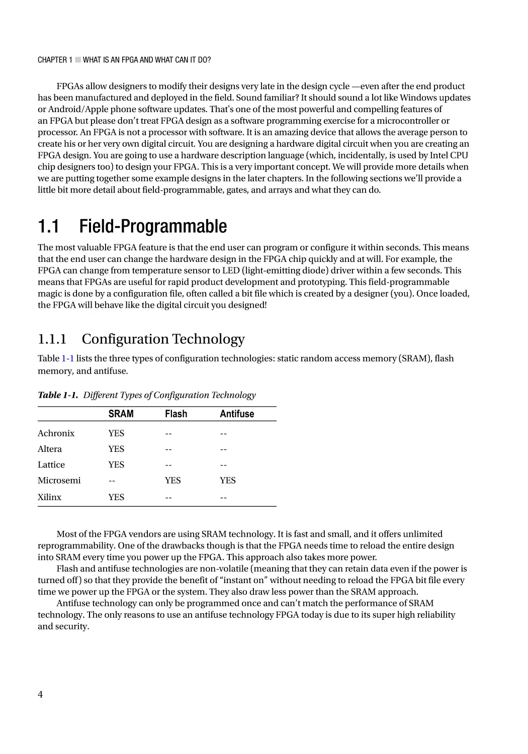
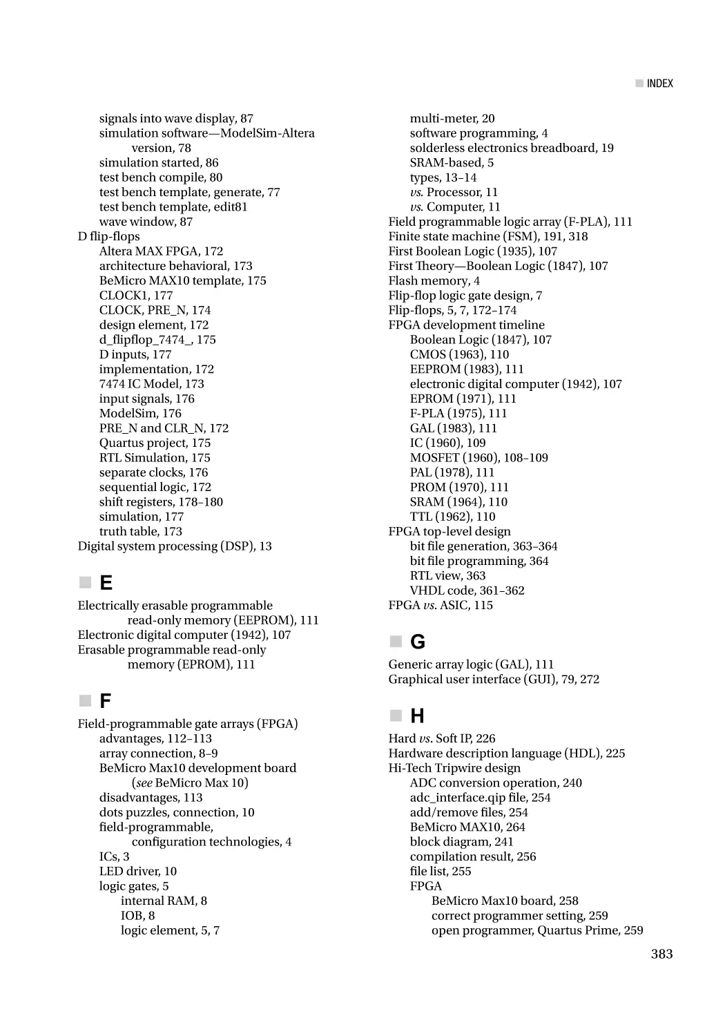
1.2.1 The Basic Gate Design Block No. 1: Logic Element
The logic element (LE) is one of the smallest elements in FPGA design. It basically consists of a look-up table
(LUT), flip-flop, and multiplexer (which we will cover shortly). FPGAs are used extensively for compute
problems that can benefit from parallel computing architectures—for example, cleaning up images being
received from an image sensor, local processing on image pixels, and computing difference vectors in H.264
compression. LEs can form any complex or even simple digital function inside the FPGA. Figure 1-2 shows
the basic configurable logic elements. Although different FPGA venders have their own LE designs, they are
very similar to the one shown in Figure 1-2. Most of the inputs to a LE are connected to the LUT and followed
with a flip-flop (register). The output of the LE is selected by a multiplexer (MUX). The LUT and MUX are the
major configurable blocks in the LE. Don’t worry, this will all make sense after you read the next section.
Figure 1-2. Basic configurable LEs
5
Chapter 1 ■ What Is an FPGA and What Can It Do?
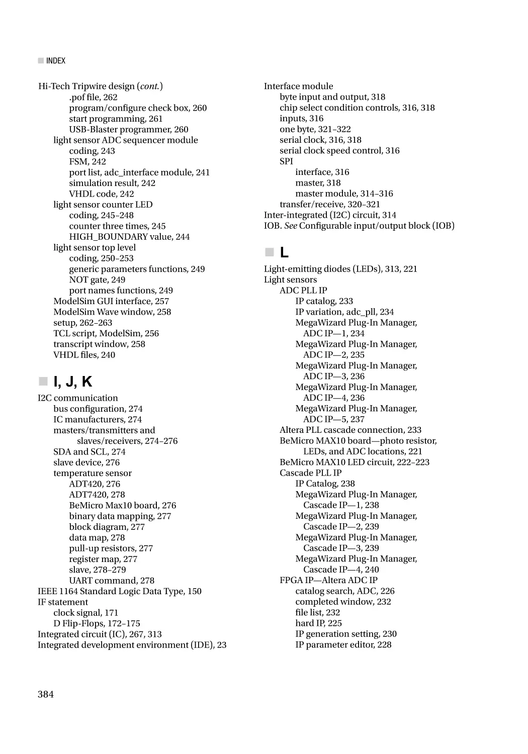
1.2.1.1 The Magic Block: LUT
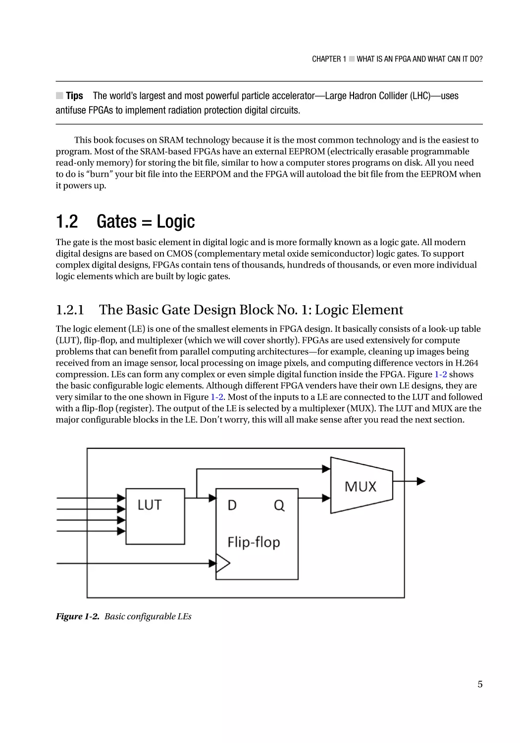
The LUT is basically just a small amount of read-only memory. A four-input, one output LUT, can generate
any four-input Boolean function (AND/OR/XOR/NOT) (Figure 1-2). We will provide more details on
Boolean function in Chapters 8 and 9. When you configure the FPGA, the contents of the LUT will be
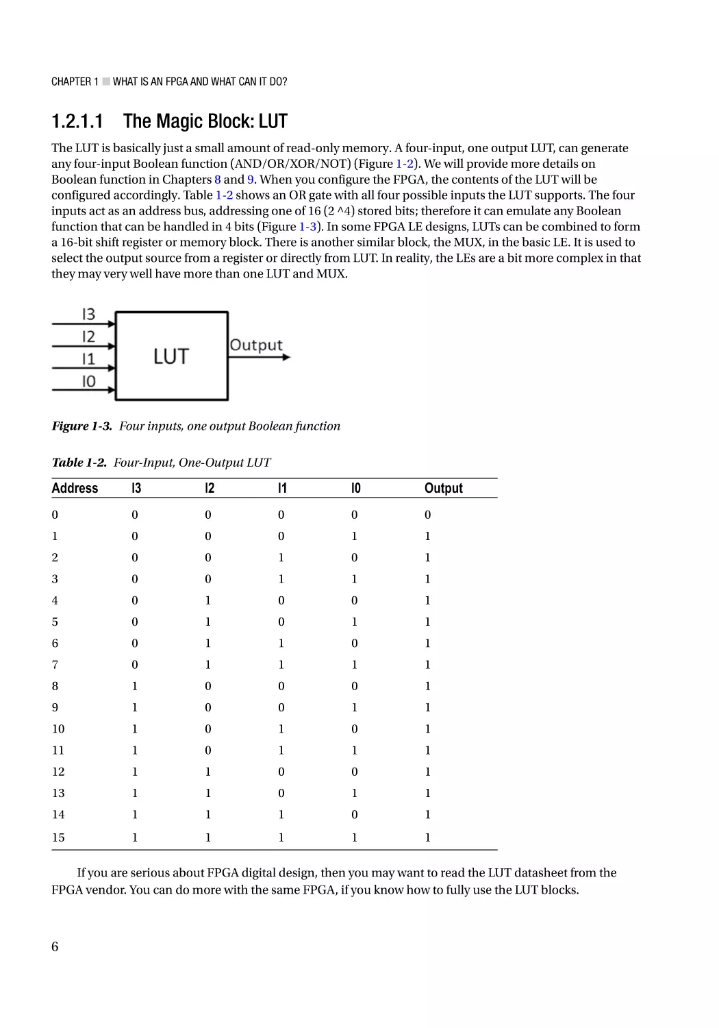
configured accordingly. Table 1-2 shows an OR gate with all four possible inputs the LUT supports. The four
inputs act as an address bus, addressing one of 16 (2 ^4) stored bits; therefore it can emulate any Boolean
function that can be handled in 4 bits (Figure 1-3). In some FPGA LE designs, LUTs can be combined to form
a 16-bit shift register or memory block. There is another similar block, the MUX, in the basic LE. It is used to
select the output source from a register or directly from LUT. In reality, the LEs are a bit more complex in that
they may very well have more than one LUT and MUX.
Figure 1-3. Four inputs, one output Boolean function
Table 1-2. Four-Input, One-Output LUT
Address
I3
I2
I1
I0
Output
0
0
0
0
0
0
1
0
0
0
1
1
2
0
0
1
0
1
3
0
0
1
1
1
4
0
1
0
0
1
5
0
1
0
1
1
6
0
1
1
0
1
7
0
1
1
1
1
8
1
0
0
0
1
9
1
0
0
1
1
10
1
0
1
0
1
11
1
0
1
1
1
12
1
1
0
0
1
13
1
1
0
1
1
14
1
1
1
0
1
15
1
1
1
1
1
If you are serious about FPGA digital design, then you may want to read the LUT datasheet from the
FPGA vendor. You can do more with the same FPGA, if you know how to fully use the LUT blocks.
6
Chapter 1 ■ What Is an FPGA and What Can It Do?
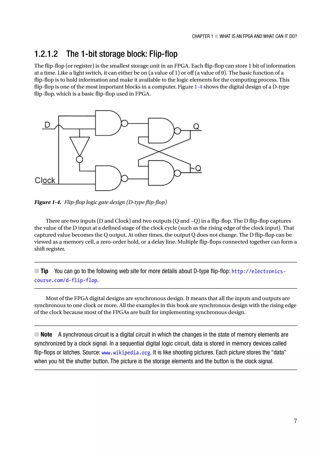
1.2.1.2 The 1-bit storage block: Flip-flop
The flip-flop (or register) is the smallest storage unit in an FPGA. Each flip-flop can store 1 bit of information
at a time. Like a light switch, it can either be on (a value of 1) or off (a value of 0). The basic function of a
flip-flop is to hold information and make it available to the logic elements for the computing process. This
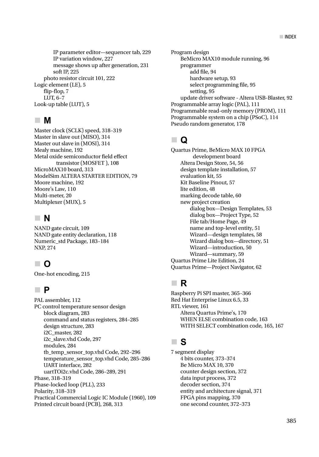
flip-flop is one of the most important blocks in a computer. Figure 1-4 shows the digital design of a D-type
flip-flop, which is a basic flip-flop used in FPGA.
Figure 1-4. Flip-flop logic gate design (D-type flip-flop)
There are two inputs (D and Clock) and two outputs (Q and ~Q) in a flip-flop. The D flip-flop captures
the value of the D input at a defined stage of the clock cycle (such as the rising edge of the clock input). That
captured value becomes the Q output. At other times, the output Q does not change. The D flip-flop can be
viewed as a memory cell, a zero-order hold, or a delay line. Multiple flip-flops connected together can form a
shift register.
■■Tip You can go to the following web site for more details about D-type flip-flop: http://electronicscourse.com/d-flip-flop.
Most of the FPGA digital designs are synchronous design. It means that all the inputs and outputs are
synchronous to one clock or more. All the examples in this book are synchronous design with the rising edge
of the clock because most of the FPGAs are built for implementing synchronous design.
■■Note A synchronous circuit is a digital circuit in which the changes in the state of memory elements are
synchronized by a clock signal. In a sequential digital logic circuit, data is stored in memory devices called
flip-flops or latches. Source: www.wikipedia.org. It is like shooting pictures. Each picture stores the “data”
when you hit the shutter button. The picture is the storage elements and the button is the clock signal.
7
Chapter 1 ■ What Is an FPGA and What Can It Do?
1.2.2 The Basic Gate Design Block No. 2: Configurable IO Block
Another basic logic design element is configurable input/output block (IOB). It is used to connect the LE to
the outside world. It can be configured as an input or output, as b-directional, or not connected. The IOB
can support different types of electrical input/output (I/O) specifications (e.g., TTL logic, 3.3V CMOS, and
PCIe) and add internal pull-up or pull-down resisters. Remember to select the correct I/O specification. It
is because different specifications have different driving strength (voltage and current) and most of the time
they are not compatible. The worst is overload the FPGA IO and break the FPGA.
The latest FPGA IOB can support bandwidth higher than 10 Gbps. Some FPGAs even have direct optical
input and output physical connections (Source: www.altera.com/content/dam/altera-www/global/en_US/
pdfs/literature/wp/wp-01161-optical-fpga.pdf). Chapter 12 provides a detailed discussion on how to
use IOBs.
1.2.3 The Basic Gate Design Block No. 3: Internal RAM
The internal RAM (random access memory) block is another configurable unit in the FPGA. The main
configuration parameter is number of read/write ports. You can read and write the same memory with
different locations at the same time. It is like one instruction to read and write on the same physical memory
with different address. Can you think of a use case of this type of configuration (read and write at the same
time/clock cycle)? One possibility is FIFO (first in, first out memory) which is used to pass data from module
A to module B. There is an FPGA vendor that puts DRAM (dynamic random access memory) (which is the
one you’ll find in your computer because of its density—it can pack more bits into the same physical size)
inside the FPGA and allows the rest of the logic to access it directly. Some FPGA vendors put flash memory
(which is a non-volatile memory such as you’d find in a memory card or USB stick) into their FPGA. If your
application needs non-volatile memory, then an FPGA with built-in flash memory would be a good fit for
you. In Parts 3 and 4, we will show how to configure internal RAM.
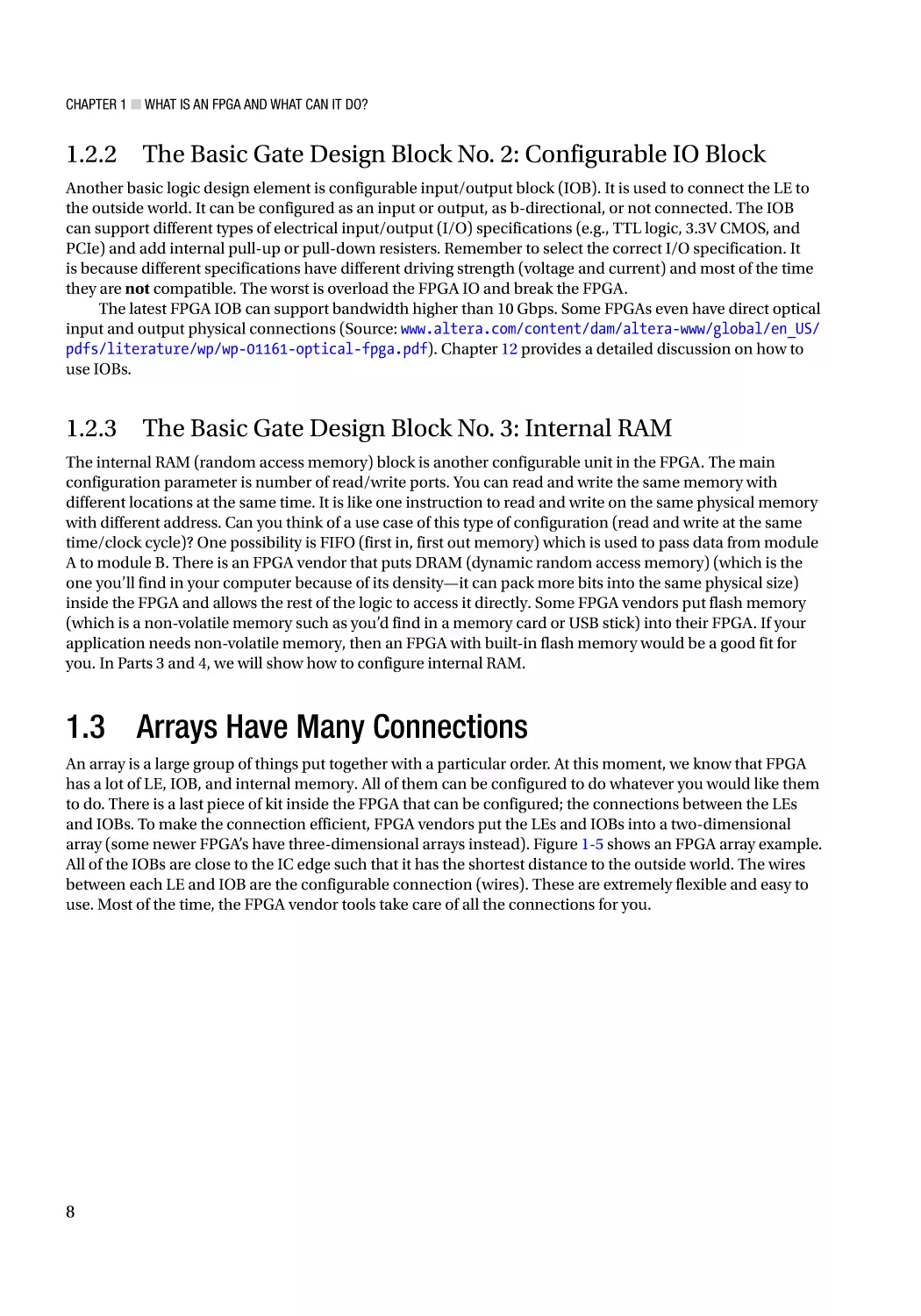
1.3 Arrays Have Many Connections
An array is a large group of things put together with a particular order. At this moment, we know that FPGA
has a lot of LE, IOB, and internal memory. All of them can be configured to do whatever you would like them
to do. There is a last piece of kit inside the FPGA that can be configured; the connections between the LEs
and IOBs. To make the connection efficient, FPGA vendors put the LEs and IOBs into a two-dimensional
array (some newer FPGA’s have three-dimensional arrays instead). Figure 1-5 shows an FPGA array example.
All of the IOBs are close to the IC edge such that it has the shortest distance to the outside world. The wires
between each LE and IOB are the configurable connection (wires). These are extremely flexible and easy to
use. Most of the time, the FPGA vendor tools take care of all the connections for you.
8
Chapter 1 ■ What Is an FPGA and What Can It Do?
Figure 1-5. Gate array
Digital logic theory: If you have enough NAND gates then you can build anything that you want. In
an ideal world we don’t need to have complicated LE blocks. All we need to have are NAND gates and
connections in between.
In the real world: The routing between NAND gates will very quickly run out of room to finish even
a simple job. Traditional FPGAs are optimized for more complex configurable logic element blocks
with a relatively limited number of interconnections between them. Today, FPGAs have added more
interconnections by using 3D arrays. These 3D arrays are stacked like multiple chips with connections
between chips.
Keep in mind: It is possible to run out of connections between LEs and IOB and thus fail to generate a
viable FPGA design.
1.4 What Can It Do?
Generally speaking, all the FPGA does is generate ones (3.3 V) and zeroes (0 V) which means it can do
everything or nothing. That doesn’t sound terribly impressive does it? However, you need to ask the
right question in order to get the right answer. The right question is, “What you want it to do?” The more
you do, the more it can do for you! Think of the FPGA as a piece of clay. You can mold that clay into any
number of shapes, make a plate, make a statue, or make a tiny house. Its potential is limited only by your
imagination, and that’s also true of an FPGA—it has the capability to take on practically any function you
can imagine!
9
Chapter 1 ■ What Is an FPGA and What Can It Do?
It is very difficult to design your own chip completely from scratch. The big difference between an
FPGA and every other chip you can buy on the market is that an FPGA doesn't actually do anything. It
has no intended function when you buy it. It is not like a microcontroller that has a defined function or a
generic process ready to run software. An FPGA gives you the ultimate in flexibility, allowing you to design
anything you can imagine in the digital domain. If you want to turn your FPGA into an 8051 microcontroller,
you can do it. You can configure your FPGA to be a custom LED driver for 1,000 LEDs, a 100 PWM (Pulse
Width Modulator), or a universal asynchronous receiver/transmitter (UART or COM port) device, which is a
common computer interface. However, just because it can be done with an FPGA does not mean that it will
necessarily be easy to do so.
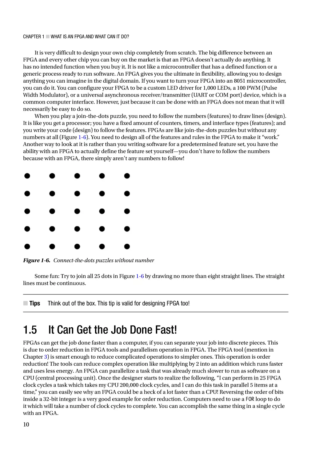
When you play a join-the-dots puzzle, you need to follow the numbers (features) to draw lines (design).
It is like you get a processor; you have a fixed amount of counters, timers, and interface types (features); and
you write your code (design) to follow the features. FPGAs are like join-the-dots puzzles but without any
numbers at all (Figure 1-6). You need to design all of the features and rules in the FPGA to make it “work.”
Another way to look at it is rather than you writing software for a predetermined feature set, you have the
ability with an FPGA to actually define the feature set yourself—you don’t have to follow the numbers
because with an FPGA, there simply aren’t any numbers to follow!
Figure 1-6. Connect-the-dots puzzles without number
Some fun: Try to join all 25 dots in Figure 1-6 by drawing no more than eight straight lines. The straight
lines must be continuous.
■■Tips
Think out of the box. This tip is valid for designing FPGA too!
1.5 It Can Get the Job Done Fast!
FPGAs can get the job done faster than a computer, if you can separate your job into discrete pieces. This
is due to order reduction in FPGA tools and parallelism operation in FPGA. The FPGA tool (mention in
Chapter 3) is smart enough to reduce complicated operations to simpler ones. This operation is order
reduction! The tools can reduce complex operation like multiplying by 2 into an addition which runs faster
and uses less energy. An FPGA can parallelize a task that was already much slower to run as software on a
CPU (central processing unit). Once the designer starts to realize the following, “I can perform in 25 FPGA
clock cycles a task which takes my CPU 200,000 clock cycles, and I can do this task in parallel 5 items at a
time,” you can easily see why an FPGA could be a heck of a lot faster than a CPU! Reversing the order of bits
inside a 32-bit integer is a very good example for order reduction. Computers need to use a FOR loop to do
it which will take a number of clock cycles to complete. You can accomplish the same thing in a single cycle
with an FPGA.
10
Chapter 1 ■ What Is an FPGA and What Can It Do?
Data flow into and out of the FPGA is expandable too! So you can send a lot of data to an FPGA to get
more jobs done at the same time. Image, video, and Ethernet packet processing all need this kind of high
bandwidth data flow.
For example, suppose you want to do some processing work on an image, and let’s say you want
to rotate it. Let’s also say that it takes one second to do this, and you have 10,000 images to do. A single
processor would take nearly three hours to process this workload. Of course, modern CPUs are multicore, so
let’s be generous and assume we have eight cores at our disposal. Now we can do the same work in just over
20 minutes. With the FPGA, though, we might have our “image processing” unit, and maybe 500 of those fit
on a single FPGA. If we could keep those units full of data, we’d complete our task in only 20 seconds. If we
also consider that it is now being processed in hardware rather than software, we could say that it only takes
half a second to process an image, dropping our total time down to ten seconds. Okay, this example is a bit
contrived and there are plenty of ifs, buts, and maybes, but it gives you an idea of the power of an FPGA.
1.6 FPGA vs. Processor
The major difference between a processor and an FPGA is that an FPGA doesn’t have a permanent hardware
configuration; on the contrary, it is configurable according to the end-user needs. However, processors have
a permanent hardware configuration which means that all the transistors, registers, interface structures,
and all of the connections are permanent. A processor can only do predefined tasks (accumulation,
multiplication, I/O switch, etc.). Designers make the processor do these tasks “in a consecutive manner” by
using software, in accordance with their own functions.
Hardware configuration in the FPGA is not fixed so it is defined by the end user. Although logic
elements are fixed in FPGA, functions they achieve and the interconnections between them are controlled
by the user. So tasks that FPGAs can do are not predefined. You can have the task done according to the
written hardware description language (HDL) code "in parallel," which means concurrently. The capability
of parallel processing is one of the most important features that separates FPGAs from processors and makes
them superior in many areas.
Processors are generally more useful for repetitive control of specific circuits. For example, using an FPGA
for simple functions such as turning on or off a device from a computer may be overkill. This process can easily
done with many conventional microcontrollers. However, FPGA solutions are more reasonable, if you want to
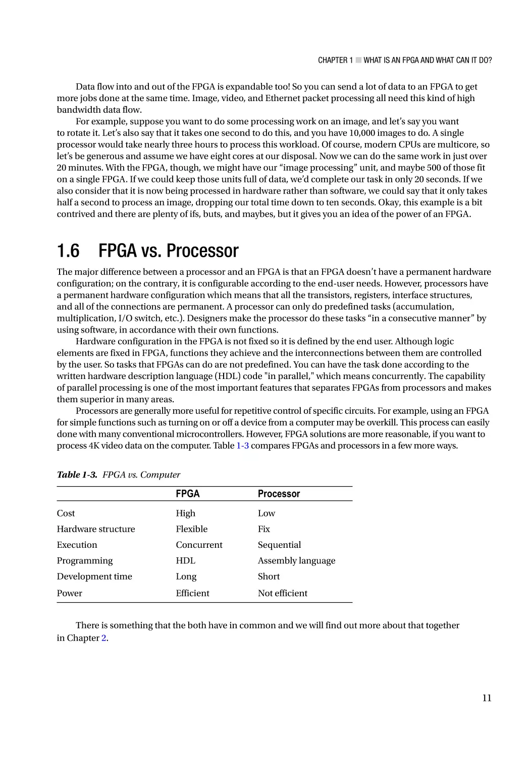
process 4K video data on the computer. Table 1-3 compares FPGAs and processors in a few more ways.
Table 1-3. FPGA vs. Computer
FPGA
Processor
Cost
High
Low
Hardware structure
Flexible
Fix
Execution
Concurrent
Sequential
Programming
HDL
Assembly language
Development time
Long
Short
Power
Efficient
Not efficient
There is something that the both have in common and we will find out more about that together
in Chapter 2.
11
Chapter 1 ■ What Is an FPGA and What Can It Do?
1.7 Summary
Field-programmable gate arrays have three basic building blocks.
1.
Logic gates
2.
Flip-flops + memories
3.
Wires
FPGAs can do many things, or they can do nothing, with these three building blocks. It all depends
on you. You need to design the hardware structure to handle the task you want. FPGAs can concurrently
process your tasks and this is the main difference between FPGA and a processor. Chapters 2, 3, and 4 will
get you ready to design real digital logic.
In Chapter 2, you will get hands on with the hardware platform we will be using.
In Chapter 3, you will install FPGA digital design environment software.
In Chapter 4, you will create your first digital design in the FPGA world!
As you work your way through this book (Part 2 and Part 3), you will create a number of design blocks;
each block can be reused. Each block is like LEGO, you can reuse all the blocks you create in other designs.
“Nothing will work unless you do.”
—Maya AngelouElectronic supplementary material The online version of this chapter (doi:10.1007/978-14302-6248-0_1) contains supplementary material, which is available to authorized users.
12
CHAPTER 2
Our Weapon of Choice
This chapter will briefly review the various FPGAs (field-programmable gate arrays) available and then
examine the features of BeMicro MAX 10 board, which is what we are using throughout the book.
Finally, we introduce some tools for simple hardware projects. You will find that they are very useful for
this book and for your hardware projects.
2.1 What Weapons (FPGAs) Are Available
You may think FPGAs are expensive things. This was true ten years ago, but right now, you can always find
a FPGA fit for your budget and application. A quick browse on one FPGA manufacturer’s web sites turns up
more than five differently named FPGAs. This is similar to browsing Intel’s web site where you’ll find a wide
range of processors available: Celeron, Pentium, Core, Atom, Xeon, and Itanium. All this choice is great, but
what does it really mean for you? Well, just like you need the right processor for a particular job, you’ll also
need the right FPGA. Don’t worry, though, our job is to get you up to speed so that you’ll be able to navigate
through all the choices with ease.
Most of the FPGA companies don't have that much support for people who are just getting started, so
let’s begin with a quick look at the different types of FPGAs you can get your hands on:
In general, FPGA manufacturers provide three types of FPGA:
1.
The Aircraft Carrier—System on Chip (SoC): This one comes with pretty much
everything onboard (FPGA chip). SoC means that the FPGA has a central
processor unit (CPU) and many standard interfaces built-in. An ARM core is one
the most common processor designs that you’ll find in SoC FPGAs. Because it
comes with all these features, a SoC can be used to quickly develop prototypes
and they tend to have a lot of custom interfaces wrapped around a CPU for which
existing software is already written. This type of FPGA is best suited for your
need for software flexibility and hardware speed. One of the hottest examples is
Advanced Driver Assistance Systems (ADAS). It is a system to help the car driver
in the driving process. The system should improve car and road safety. All of
the autopilot cars (Google self-driving car, Telsa Autopilot system, and Volvo’s
IntelliSafe Autopilot) have ADAS.
2.
The Laser Cannon—High End: It provides high-density computational power and
super high-speed digital interfaces in one go. The computational power comes
from a specially designed logic element(LE) which is digital signal processing(DSP)
blocks that we discussed in the first chapter. One of the super high-speed digital
interfaces available is PCIe Gen 3 (close to 8GBs per second. It can transfer one and
a half DVDs within seconds). This type of FPGA is designed for consuming a lot of
digital data. For example, High-Performance Computing (HPC), Optical Transport
Networks, and Software Define Radio are using this type of FPGA.
© Aiken Pang and Peter Membrey 2017
A. Pang and P. Membrey, Beginning FPGA: Programming Metal, DOI 10.1007/978-1-4302-6248-0_2
13
Chapter 2 ■ Our Weapon of Choice
3.
The Pocket Knife—Low End: It provides the most cost-effective solution for a
general digital interface. This type of FPGA is like a sea of gates which has only
basic elements (logic, memory, and clocks). Anything you can think of using
logic gate to design, you can finish with this type of FPGA. This type of FPGA is
like an 8051 MCU, which has all you need to do basic things. This type of FPGA is
best suited for consumer products, low-cost prototyping, and education.
Table 2-1 shows the FPGA names from different FPGA manufacturers. You can use this table to narrow
down what FPGA may suit your next project FPGA need.
Table 2-1. Different Types of FPGA's Name List
FPGA
SoC
High End
Low End
Achronix
N/A
Speedster 22i
N/A
Altera
Stratix SoC
Stratix/ Arria
Max 10 (used in BeMicro Max 10)
Micorsemi
Smart Fusion 2
N/A
IGLOO 2
Lattice
N/A
ECP/Lattice
iCE40 / MachXO
Xilinx
Zynq
Virtex
Spartan-6
If you’re hoping you can simply search for the name of the FPGA and find just the development kit
you’re looking for, you’re probably going to get lost very quickly. The problem is that there are literally
thousands of different combinations out there ranging in cost from hundreds to tens of thousands of dollars.
Often just looking at the description between two parts, it isn’t even obvious why one is five times the price
of the other. Once you get a few projects under your belt, you will welcome this bounty of choice—but for
now, how do you even know where to start?
That’s where the BeMicro Max10 development board comes in: it is small, practical, and reasonably
priced. It’s powerful enough for you to do a lot of different things and it includes enough hardware built
in to start building projects with practical real-world applications straight away. Every component is
representative of what you’ll find in industry. This board puts you on equal footing with the big boys, but
without the big cost.
In subsequent sections we’ll look at the BeMicro Max 10 and the other tools you’ll need in this book.
■■Tips
Please go to the following web site to order your BeMicro Max10 development board:
http://www.arrow.com/bemicromax10.
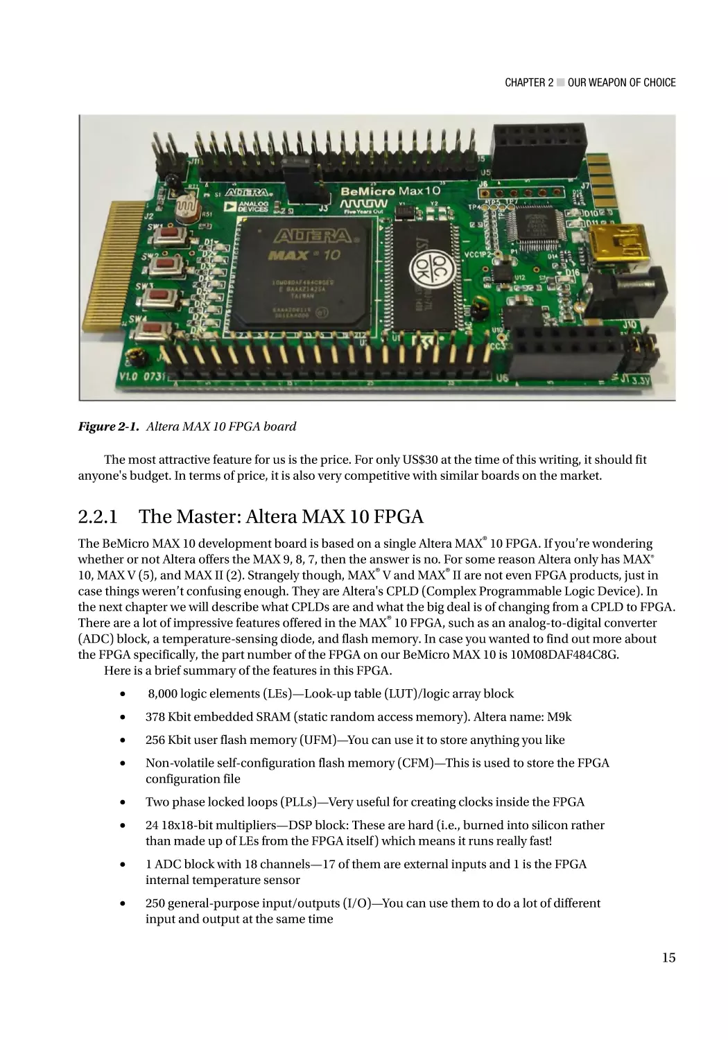
2.2 The BeMicro Max 10: Our Weapon of Choice
The BeMicro MAX 10 development board is developed by Arrow. The purpose of this board is to
demonstrate any many of the MAX 10 features as possible. Arrow’s web site says it best: “A compact and
low-cost hardware evaluation platform for a broad range of embedded applications.” This makes it a great
fit for our purposes. Figure 2-1 shows the BeMicro Max 10.
14
Chapter 2 ■ Our Weapon of Choice
Figure 2-1. Altera MAX 10 FPGA board
The most attractive feature for us is the price. For only US$30 at the time of this writing, it should fit
anyone's budget. In terms of price, it is also very competitive with similar boards on the market.
2.2.1 The Master: Altera MAX 10 FPGA
The BeMicro MAX 10 development board is based on a single Altera MAX® 10 FPGA. If you’re wondering
whether or not Altera offers the MAX 9, 8, 7, then the answer is no. For some reason Altera only has MAX®
10, MAX V (5), and MAX II (2). Strangely though, MAX® V and MAX® II are not even FPGA products, just in
case things weren’t confusing enough. They are Altera's CPLD (Complex Programmable Logic Device). In
the next chapter we will describe what CPLDs are and what the big deal is of changing from a CPLD to FPGA.
There are a lot of impressive features offered in the MAX® 10 FPGA, such as an analog-to-digital converter
(ADC) block, a temperature-sensing diode, and flash memory. In case you wanted to find out more about
the FPGA specifically, the part number of the FPGA on our BeMicro MAX 10 is 10M08DAF484C8G.
Here is a brief summary of the features in this FPGA.
•
8,000 logic elements (LEs)—Look-up table (LUT)/logic array block
•
378 Kbit embedded SRAM (static random access memory). Altera name: M9k
•
256 Kbit user flash memory (UFM)—You can use it to store anything you like
•
Non-volatile self-configuration flash memory (CFM)—This is used to store the FPGA
configuration file
•
Two phase locked loops (PLLs)—Very useful for creating clocks inside the FPGA
•
24 18x18-bit multipliers—DSP block: These are hard (i.e., burned into silicon rather
than made up of LEs from the FPGA itself ) which means it runs really fast!
•
1 ADC block with 18 channels—17 of them are external inputs and 1 is the FPGA
internal temperature sensor
•
250 general-purpose input/outputs (I/O)—You can use them to do a lot of different
input and output at the same time
15
Chapter 2 ■ Our Weapon of Choice
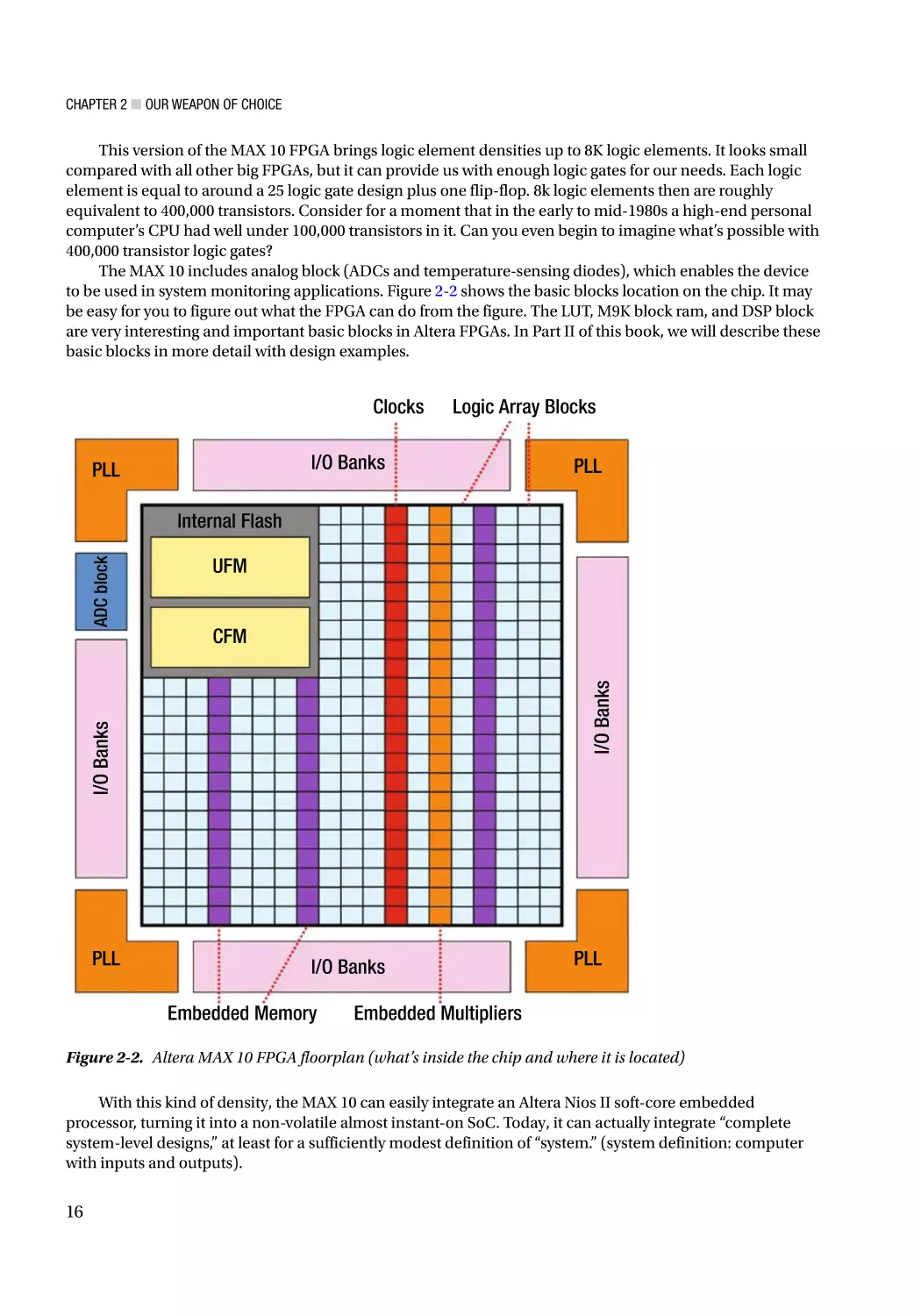
This version of the MAX 10 FPGA brings logic element densities up to 8K logic elements. It looks small
compared with all other big FPGAs, but it can provide us with enough logic gates for our needs. Each logic
element is equal to around a 25 logic gate design plus one flip-flop. 8k logic elements then are roughly
equivalent to 400,000 transistors. Consider for a moment that in the early to mid-1980s a high-end personal
computer’s CPU had well under 100,000 transistors in it. Can you even begin to imagine what’s possible with
400,000 transistor logic gates?
The MAX 10 includes analog block (ADCs and temperature-sensing diodes), which enables the device
to be used in system monitoring applications. Figure 2-2 shows the basic blocks location on the chip. It may
be easy for you to figure out what the FPGA can do from the figure. The LUT, M9K block ram, and DSP block
are very interesting and important basic blocks in Altera FPGAs. In Part II of this book, we will describe these
basic blocks in more detail with design examples.
Clocks
PLL
Logic Array Blocks
I/O Banks
PLL
I/O Banks
PLL
UFM
I/O Banks
CFM
I/O Banks
ADC block
Internal Flash
PLL
Embedded Memory
Embedded Multipliers
Figure 2-2. Altera MAX 10 FPGA floorplan (what’s inside the chip and where it is located)
With this kind of density, the MAX 10 can easily integrate an Altera Nios II soft-core embedded
processor, turning it into a non-volatile almost instant-on SoC. Today, it can actually integrate “complete
system-level designs,” at least for a sufficiently modest definition of “system.” (system definition: computer
with inputs and outputs).
16
Chapter 2 ■ Our Weapon of Choice
2.2.2 The Emissaries: BeMicro MAX 10 Board Features
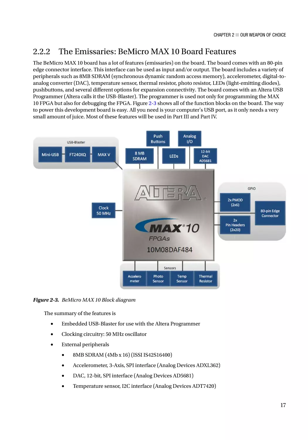
The BeMicro MAX 10 board has a lot of features (emissaries) on the board. The board comes with an 80-pin
edge connector interface. This interface can be used as input and/or output. The board includes a variety of
peripherals such as 8MB SDRAM (synchronous dynamic random access memory), accelerometer, digital-toanalog converter (DAC), temperature sensor, thermal resistor, photo resistor, LEDs (light-emitting diodes),
pushbuttons, and several different options for expansion connectivity. The board comes with an Altera USB
Programmer (Altera calls it the USB-Blaster). The programmer is used not only for programming the MAX
10 FPGA but also for debugging the FPGA. Figure 2-3 shows all of the function blocks on the board. The way
to power this development board is easy. All you need is your computer's USB port, as it only needs a very
small amount of juice. Most of these features will be used in Part III and Part IV.
Figure 2-3. BeMicro MAX 10 Block diagram
The summary of the features is
•
Embedded USB-Blaster for use with the Altera Programmer
•
Clocking circuitry: 50 MHz oscillator
•
External peripherals
•
8MB SDRAM (4Mb x 16) (ISSI IS42S16400)
•
Accelerometer, 3-Axis, SPI interface (Analog Devices ADXL362)
•
DAC, 12-bit, SPI interface (Analog Devices AD5681)
•
Temperature sensor, I2C interface (Analog Devices ADT7420)
17
Chapter 2 ■ Our Weapon of Choice
•
•
•
Thermal resistor
•
Photo resistor
General user input or output
•
8 user LEDs
•
2 user Pushbuttons
Expansion connectivity
•
Two 6-pin PMOD expansion headers
•
Two 40-pin prototyping headers which provide access to 64 digital I/O
•
One 6-pin analog input header
•
One 80-pin BeMicro card edge connector
■■History The first SoC integrated circuit (IC) was a digital watch. It integrated a timekeeping circuit and LCD
driver transistors on to a single Intel 5810 CMOS chip in 1974. Source: http://www.computerhistory.org/
semiconductor/timeline/1974-digital-watch-is-first-system-on-chip-integrated-circuit-52.html.
It’s excellent for getting started and learning the basics, but at the same time it’s ready to be the core
of something big. We understand that you may have very good reasons to use another development board.
Although the projects in this book are tailored for the BeMicro MAX 10, most of the example designs we use
are standard and are applicable to any FPGA. However, if you have the BeMicro MAX 10, you will benefit of
being able to follow explicit step-by-step instructions and won’t have to worry about converting or adapting
those instructions, which causes problems all by themselves.
We do take advantage of the on-board peripherals including the LEDs and ADC, and we use the
MAX 10’s block RAM for storing data in some projects. If your development board has different on-board
peripherals, you can either connect the same device(s) externally or replace the relevant parts of the code
with equivalents for the on-board peripherals you have. It’s a bit harder to adapt to different internal FPGA
features, so it’s best to choose a development board based on an FPGA from the MAX 10 family if you want to
follow along when we’re using the block RAM.
■■Tips The most updated information about BeMicro MAX 10 is in this Altera Wiki web site:
http://www.alterawiki.com/wiki/BeMicro_Max_10.
2.3 Other Tools
I know the BeMicro MAX 10 module is self-contained, and you can start programming it with no other
components, but limiting yourself to eight LEDs as outputs and four buttons as an input is rather restrictive.
It’s far more fun to hook up your FPGA to the real world. We won’t be doing any hard-core electrical
engineering—it’s all going to be pretty basic stuff—and I don’t expect you’ll want to set up a workshop, but
you will need a few essential tools to get the job done. You may even already have some of them already.
18
Chapter 2 ■ Our Weapon of Choice
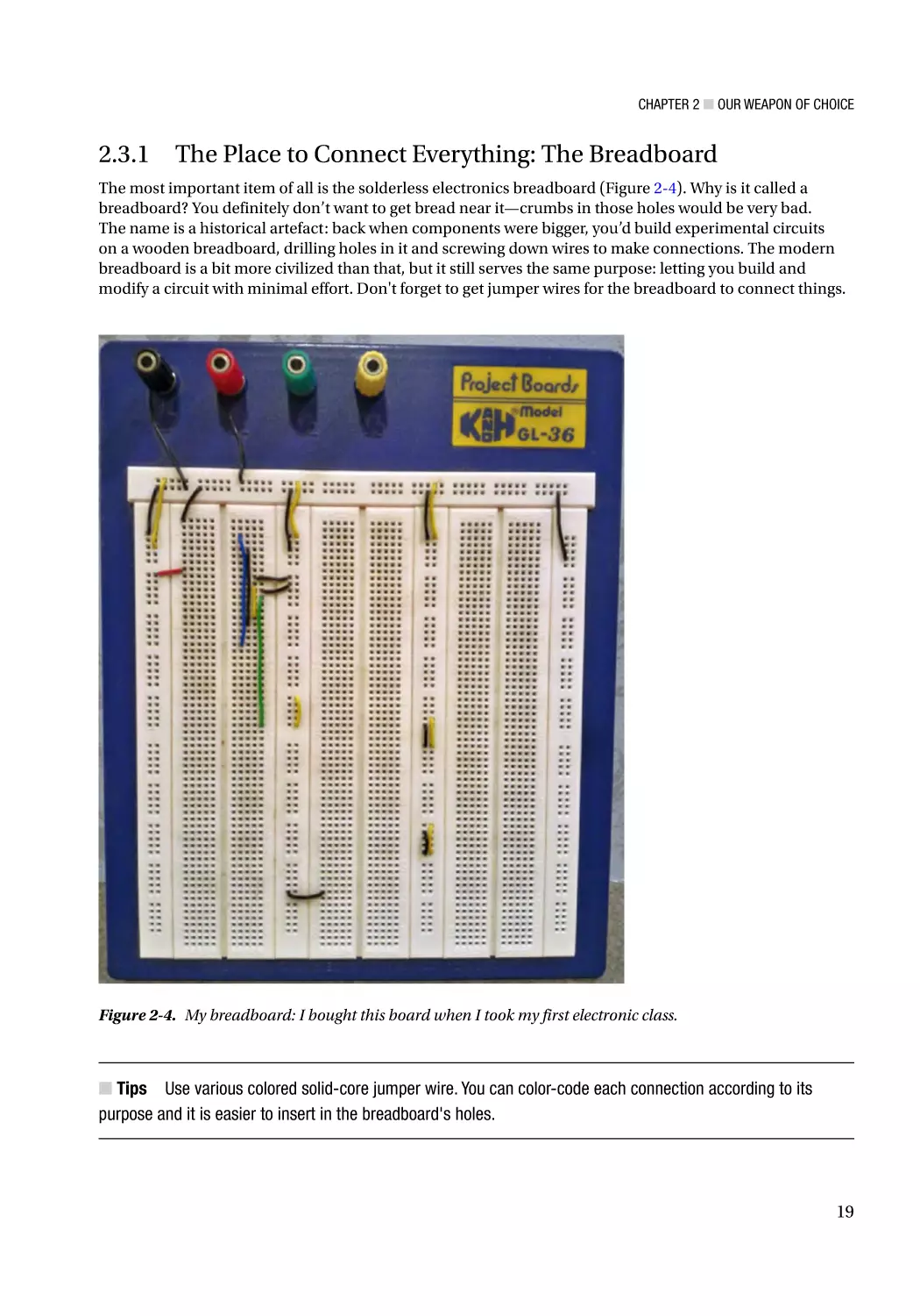
2.3.1 The Place to Connect Everything: The Breadboard
The most important item of all is the solderless electronics breadboard (Figure 2-4). Why is it called a
breadboard? You definitely don’t want to get bread near it—crumbs in those holes would be very bad.
The name is a historical artefact: back when components were bigger, you’d build experimental circuits
on a wooden breadboard, drilling holes in it and screwing down wires to make connections. The modern
breadboard is a bit more civilized than that, but it still serves the same purpose: letting you build and
modify a circuit with minimal effort. Don't forget to get jumper wires for the breadboard to connect things.
Figure 2-4. My breadboard: I bought this board when I took my first electronic class.
■■Tips Use various colored solid-core jumper wire. You can color-code each connection according to its
purpose and it is easier to insert in the breadboard's holes.
19
Chapter 2 ■ Our Weapon of Choice
2.3.2 Making the Invisible Visible: The Multi-meter
A proper multi-meter for regular use around the home or electronic work can be had for less than $20. More
expensive meters do not necessarily have more features. They give greater accuracy for professional work,
and they are more rugged in their construction and durability. We only need the multi-meter to measure
DC voltage, DC current, and resistance in this book's project. Any cheap multi-meter (Figure 2-5) will be
accurate enough for all the projects in this book, so don’t feel forced to pay more for something that comes
with a calibration certificate too.
Figure 2-5. My cheap multi-meter
20
Chapter 2 ■ Our Weapon of Choice
2.4 Wrap-up
This chapter briefly presented the features of the BeMicro MAX 10 board—one of the common development
boards—and the MAX 10 FPGA. We provided links to some of the key online documentation and to the wiki
forum. I recommend you download the MAX 10 FPGA user guide collection from the Altera MAX 10 support
page (www.altera.com/products/fpga/max-series/max-10/support.html). Please don't read through
the whole user guide, as it has more than 500 pages. It is for reference only. The preparation for hardware is
done; next comes software!
“People who are really serious about software should make their own hardware.”
—Alan Curtis Kay
21
CHAPTER 3
Lock and Load
Before you can begin writing VHDL (VHSIC Hardware Description Language) code for the FPGA
(field-programmable gate array), you'll need a few items. To begin with, you'll need an FPGA board
(e.g., the “MAX10” FPGA board, which we described in the Chapter 2) and development tools from the FPGA
vendor. In this chapter we will walk you through how to download and install the toolchain in Windows.
3.1 Getting the Development Toolchain Up and Running
Nowadays, most of the FPGA companies provide three editions of their development toolchain: free edition,
paid edition, and some form of pro edition. Table 3-1 lists them by brand.
Table 3-1. FPGA Brands
Altera
Xilinx
Microsemi
Free edition
Quartus Prime Lite Edition
Vivado HL WebPACK
Libero Gold
Paid edition
Quartus Prime Standard Edition
Vivado HL Design Suite
Libero Standalone
Paid more edition
Quartus Prime Pro Edition
Vivado HL System Edition
Libero Platinum
Every few years, the companies' marketing departments need to come up with new names for their new
products. The development toolchain gets updated to a new version every year or so, which means it is a new
product. In 2015, the new name for the Altera toolchain is Quartus Prime. Previously it was known as Quartus
II. This shouldn’t pose any problems for you though, just remember to download at least version number 15.1.
Altera Quartus Prime Lite edition (free edition) is all you need to use in this book. It is Altera's integrated
development environment (IDE). The Quartus Prime Lite includes tools for creating and simulating the
FPGA design, compiling (Synthesis + Place & Route) your design, and actually programming the FPGA. With
this Lite edition, you can use Altera's industrial quality toolchain and development environment for free. The
trade-off is that it will only work with the smaller devices and it will take longer to compile. Happily this isn’t
really an issue for us as by current standards, small means that it can build a microprocessor with memory
and some interfaces (e.g., UARTs (universal asynchronous receiver/transmitter) and general-purpose input/
output) which is still pretty powerful. When Altera says small, it means the MAX® series, Cyclone® series and
Arria® II series. Altera’s bigger (and thus more powerful) FPGAs are the Stratix® series and Arria 10. One of the
reasons we picked the BeMicro 10 FPGA board was that the BeMicro10's FPGA (MAX 10) fits into the small
category and thus we can use the toolchain for free. The Quartus Prime Lite Edition supports 64-bit Linux
and Windows. When we wrote this book, the latest version of Quartus Prime Lite was v15.1.0. Ideally you
should download the same version we are using, but if there is a newer version available, just be aware that
there might be some differences between our instructions and what you see on your screen.
© Aiken Pang and Peter Membrey 2017
A. Pang and P. Membrey, Beginning FPGA: Programming Metal, DOI 10.1007/978-1-4302-6248-0_3
23
Chapter 3 ■ Lock and Load
The Quartus Prime Lite Edition includes the following features that we will use in this book:
•
Design—VHDL editor, Altera IPs (MegaCore IP Library), synthesizer, and fitter
•
Simulation—ModelSim®-Altera Starter Edition
•
Debug—SignalTap II Logic Analyzer (Built-in logic analyzer)
•
Programmer—Quartus Prime Programmer
So you’ve got your development board and you’re ready to build stuff, but you’re not quite sure how to
set up your tools? Or, maybe you’ve ordered the development board and you want to get everything set up so
you’re ready to play as soon as it arrives? Well, don’t worry if you feel overwhelmed or confused by the Altera
web site, it’s not the easiest to navigate. The next section will guide you through downloading and installing
Quartus Prime Lite edition.
■■Note The required toolchain depends on the exact FPGA you are targeting. Altera Quartus Prime Lite edition
supports the MAX 10 family of FPGAs, including the device used in BeMicro 10. If you are planning to use a
different development board, please ensure you can obtain a toolchain that supports it for an affordable price
before you commit to the board.
3.2 Downloading Altera Tools
You'll need an Internet connection and a web browser to begin the download from the Altera web site
(www.altera.com).
To get access to the latest and greatest from Altera, you'll need to create a myAltera Account. To create
your myAltera account, just go to Altera web site at. That will bring you to a page similar to the one shown in
Figure 3-1. Then follow the steps outlined in the next few sections.
Figure 3-1. Altera web site front page
24
Chapter 3 ■ Lock and Load
3.2.1 Altera Toolchains
Let’s talk about what we are going to download from the Altera web site before we start the download
process. (It may take you few hours to finish.) There are at least three files you are going to download.
•
Quartus Prime (IDE + programmer) is the basic tool that you are going to use in
this book.
•
MAX10 FPGA design support file. Quartus Prime needs this file in order to support
BeMicro10's MAX 10 FPGA board.
•
ModelSim-Altera Starter edition software supports functional simulation for Altera
devices. ModelSim simulator is the most popular choice for FPGA design simulation.
The version we get from Altera has a 10,000 executable line limitation and is ideal for
simulating smaller FPGA designs like the designs covered in this book.
3.2.2 Create an Altera Account
1.
After you arrive at the Altera web site (www.altera.com), click MYALTERA in the
top right-hand corner. You'll be given the option of either myAltera Sign in or
Don't have an account?. Since you don't have a myAltera account yet, enter
your e-mail address in the Don't have an account? section and click Register
(Figure 3-2).
Figure 3-2. myAltera Sign In
25
Chapter 3 ■ Lock and Load
2.
You should then receive an e-mail containing a link to complete the registration
process after submitting the form. Click the activation link in the e-mail to prove
that you weren’t providing a fake e-mail address, and you should be good to go.
If you’re signed in now, you should see WELCOME, “Your Name,” and Sign Out
links at the top of each Altera page where you previously saw the MYALTERA
tab (Figure 3-3). At this point your myAltera account should ready to download
Quarts® Prime Lite edition.
3.
If you aren’t signed in, click the MYALTERA, and enter the login details you
chose a moment ago, and click Sign In.
4.
Once you’re sure you’re signed in, follow the steps in the next section to
download the Altera toolchain.
3.2.3 Download the Altera Toolchains
1.
Once you are logged in to the Altera web site with your account, click MENU on
the top menu. Figure 3-3 shows the login page. There will be a pop-up window as
Figure 3-4. Click the top SUPPORT and click Downloads.
Figure 3-3. myAltera Home page after login
26
Chapter 3 ■ Lock and Load
Figure 3-4. Pop-up window for downloading the tools
2.
You'll be taken to the Quartus Prime edition’s selection page. All you need to do
is click Version 15.1 and click Lite Edition on the right-hand side (Figure 3-5). Or
you can use this link (http://dl.altera.com/15.1/?edition=lite) to directly
access the download page for the lite edition.
27
Chapter 3 ■ Lock and Load
Figure 3-5. Altera Downloads selection
3.
28
I suggest you download everything: click the Combined Files tab which is shown
in Figure 3-6. If you have trouble downloading as one big file, then click the
Individual Files tab which is shown in Figure 3-7. Regardless of which method
you choose, you must select release version 15.1. Be sure to download the same
version we are using.
Chapter 3 ■ Lock and Load
Figure 3-6. Altera Quartus Prime Lite Edition selection page—Combined Files with Akamai DLM3
Download Manager
29
Chapter 3 ■ Lock and Load
Figure 3-7. Altera Quartus Prime Lite Edition selection page—Individual Files with Akamai DLM3
Download Manager
30
Chapter 3 ■ Lock and Load
■■Tips Altera isn't limited to a single version. You can install newly released versions after you install 15.1
without having to uninstall it. Keep in mind, though, that it will take up to another 13GB of space. It’s also
possible to use the Akamai DLM3 Download Manager in a Window machine to download the Linux version.
3.2.3.1 Download Select Checklist
Before you click the Download Selected Files button, please double-check that you are using the same
selection as the following list:
•
Select release: 15.1
•
Operating system: Windows
•
Download method: Akamai DLM3 Download Manager (probably faster)/Direct Download
•
For Individual Files tab selection: you need to download the following things
•
Quartus Prime (includes Nios II EDS)
•
ModelSim-Altera Edition (includes starter edition)
•
MAX 10 FPGA devices support
31
Chapter 3 ■ Lock and Load
4.
If everything looks good, then click Download Selected Files either in the
Individual Files tab or the Combined Files tab. After you pick a download
location and save, the download manager opens and begins the file download
process (Figure 3-8). If you cannot use the download manager, select Direct
Download and click the download arrow next to each file (Figure 3-9). You may
ask for login to myAltera again in this step.
■■Tip Select the location storage that can handle files bigger than 4GB (e.g., NTFS). It allows you to move the
.tar file easily after you’ve finished the download.
Figure 3-8. Akamai DLM3 Download Manager—Windows only
32
Chapter 3 ■ Lock and Load
Figure 3-9. Altera Quartus Prime Lite Edition selection page—Combined Files with Direct Download
3.3 Install Altera Quartus Prime Lite Edition
Once you’ve gotten your hands on the Quartus Lite setup files, you can start to install them on your
development machine. The process is fairly similar for Windows and Linux, so we describe Windows here.
Make sure you have enough disk space for the installation—a full installation of the Altera tools consumes
over 13GB.
If you’re installing on Windows, you’ll need the 64-bit version of Windows 7, Windows 8.1, or Windows
Server 2008, preferably with the latest service pack and security updates. You’ll need administrator access to
install the software, and an Internet connection and web browser to obtain a license. The screenshots of the
Windows installation process are captured on Windows 7.
If you prefer Linux, Altera only supports the use of their products on Red Hat Enterprise Linux 5.10
and Red Hat Enterprise Linux 6.5. If you aren’t using one of these officially supported distributions, don’t
despair: the tools work pretty well on any modern Linux distribution, you just might need to do some
tweaking to get it to work.
33
Chapter 3 ■ Lock and Load
1.
For the individual files method: if you are using Windows, run the file
QuartusLiteSetup-<version>-windows.exe. For the combined file method, you
must unzip the .tar file to extract the installation files. Examples of unzipping
tools: WinZip, 7-zip, or WinRAR. You need to unzip the files on the same
directory and run Setup.bat. Both ways will bring you to the Setup Wizard as in
Figure 3-10. Just click Next.
Figure 3-10. Installing Quartus Prime Lite Edition (Free)
2.
34
Click “I accept the agreement” and then click Next (Figure 3-11).
Chapter 3 ■ Lock and Load
Figure 3-11. License Agreement
3.
Select the installation location for the giant (>10GB) Quartus Prime Lite edition
and click Next (Figure 3-12).
■■Tips You can install the Quartus Prime Lite on your external hard drive to save space from your
C:\, although of course this will mean you need your external drive handy if you want to use it.
35
Chapter 3 ■ Lock and Load
Figure 3-12. Installation directory
4.
36
Check Quartus Prime Lite Edition (Free), MAX 10 FPGA, and ModelSim-Altera
Starter Edition. It should look like Figure 3-13. Click Next to move forward.
Chapter 3 ■ Lock and Load
Figure 3-13. Select components.
5.
This window shows how much space is needed to install the tools and asks for
your approval to install (Figure 3-14) by clicking Next.
37
Chapter 3 ■ Lock and Load
Figure 3-14. It needs your approval to install the software (Ready to Install)
6.
38
This step just requires patience. You need to wait for your screen to change from
Figure 3-15 to Figure 3-16. At the installation complete page, click Finish and you
are only a few steps away from completing the install.
Chapter 3 ■ Lock and Load
Figure 3-15. Installing
39
Chapter 3 ■ Lock and Load
Figure 3-16. Quartus Prime Lite installation complete
7.
40
Click Next on the Device Driver Installation Wizard (Figure 3-17) and Click
Finish after it completes the installation (Figure 3-18). This step installs the
Altera programmer, USB Blaster II, to your machine. You’ll need this to copy your
designs to the FPGA.
Chapter 3 ■ Lock and Load
Figure 3-17. Programmer Driver Installation Wizard
Figure 3-18. Completing the programmer driver installation
41
Chapter 3 ■ Lock and Load
8.
In order to use the free edition, you need to enable sending TalkBack data to Altera
(Figure 3-19). Check Enable sending TalkBack data to Altera and Click OK.
Figure 3-19. Quartus Prime TalkBack
9.
Select Run the Quartus Prime software and click OK in Figure 3-20. It means
that you selected the Lite edition. The Lite edition doesn't need any software
license to run it.
Figure 3-20. Quartus Prime 15.1 Lite Edition licensing options
42
Chapter 3 ■ Lock and Load
10.
Quartus Prime Lite Edition should be brought up in front of you, as in Figure 3-21.
If it isn’t, you can bring it up from your Start menu. In the Start menu, Quartus
Prime 15.1 is your entry point. You should able to find it as in in Figure 3-22.
Figure 3-21. Quartus Prime Lite Edition
Figure 3-22. Windows Start menu
We finally have the Altera toolchain and development environment installed. In the next chapter, I will
describe how to use the Quartus Prime Lite Edition.
43
Chapter 3 ■ Lock and Load
3.4 Download BeMicro10 files and Documentation
You can download all of the BeMicro10 files and documentation from the Altera Wiki web site at the
following link: www.alterawiki.com/wiki/BeMicro_Max_10. Altera does a good job of collecting all of the
files for its boards in one place.
At the bottom of the page, there is an Example Design section. Click BeMicro Max 10 empty Quartus
project with pin assignments and empty top level Verilog or VHDL file (Design Store link). Figure 3-23.
Figure 3-23. BeMicro Max 10—Altera Wiki page
It will bring you to the Altera design store. Click the 15.1.0 tab and it will show up as in Figure 3-24.
Click the Download button to download the design example. The file name is BeMicro_MAX10_top.par.
You should save it somewhere where you can easily find it again because you will need to use it in the next
chapter. This file forms the basic building block for all of our designs. It includes all of the settings for the
Altera Quartus Prime to build BeMicro MAX 10 projects.
44
Chapter 3 ■ Lock and Load
Figure 3-24. Altera Design Store for BeMicroMax 10 kit baseline Pinout for Quartus Prime v15.1.0
3.5 Summary
This chapter described different types of FPGA tools which are available from FPGA vendor. If you follow
the guide you should know how to download and install the FPGA tools—Altera Quartus Prime. The Altera
Quartus Prime will be used for the rest of the book.
Please make sure you get the following things done before moving to next chapter.
•
Install Altera Quartus Prime Lite Edition 15.1.0 with support MAX10 devices
•
Download BeMicro MAX 10 Kit Baseline Pinout file (BeMicro_MAX10_top.par).
Do you believe you are halfway to starting to compile your first FPGA design?
“Believe you can and you're halfway there.”
—Theodore Roosevelt
45
CHAPTER 4
Hello World!
What do Knight Rider’s KITT and Battlestar Galactica’s Cylons have in common? That’s right: undeniably
awesome scanning LEDs (light-emitting diodes)! Now that we’re set up, we’ll recreate this on our
development board. We’ll go through the steps pretty quickly and then go back and take a look at how
we got there in more detail. At this point we’re still unfamiliar with the development environment, so
the mechanics of each step are covered here. Don’t worry, though, you only have to learn to do this stuff
once, and I won’t be telling you which button to click in every project. The basic steps are writing the code,
simulating it to check that it does what we expect, and loading it on to the FPGA board.
Specifically, our example entails the following design steps:
1.
Launch Quartus Prime and create a new project
2.
Write code
3.
Implement design
4.
Simulate design
5.
Burn it!
4.1 Launch Quartus Prime and Create a New Project
In this section you’ll use Altera Quartus Prime to create a new project for your BeMicro MAX 10 FPGA
development board. You will do this step multiple times in this book when you walk through all the
examples in this book.
1.
Click Start ➤ All Programs ➤ Altera 15.1.x.xxx Lite Edition ➤ Quartus Prime
Lite Edition 15.1.x.xxx ➤ Quartus Prime 15.1, or click the shortcut on your
desktop. The Quartus Prime Lite Edition will open. The first time you open
Quartus Prime, it look like Figure 4-1.
© Aiken Pang and Peter Membrey 2017
A. Pang and P. Membrey, Beginning FPGA: Programming Metal, DOI 10.1007/978-1-4302-6248-0_4
47
Chapter 4 ■ Hello World!
Figure 4-1. Quartus Prime Lite Edition
The splash screen will be displayed while it loads, and you’ll be presented with the main development
environment window. Assuming you haven’t gone ahead and created a project already, you should see a
toolbar at the top with the usual file, edit, view, and project menu options; the Project Navigator on the left;
and the Message pane at the bottom with tabs for errors, warnings, and search results. You can show or hide
toolbars and panels with the options in the View menu.
2.
48
Create a new project by clicking File ➤ New Project Wizard or click the New
Project Wizard on the Home page tab (Figure 4-2).
Chapter 4 ■ Hello World!
Figure 4-2. Create a new project from the File tab or Home Page
3.
The new project wizard will open (Figure 4-3), which is where we decide what
kind of project we want. The first page is only an introduction. Click Next.
49
Chapter 4 ■ Hello World!
Figure 4-3. New Project Wizard—Introduction
4.
50
Enter the information shown in Figure 4-4 on the Directory, Name, Top-Level Entity
page of the New Project Wizard and then click Next. If the working directory for
this project is a new location, the software will ask you “Do you want to create it?”
Just click YES. This page is where you choose the location and name for the project
as well as the name of top-level design entity, which is the name of the design. The
Quartus Prime will first search for the top-level design entity in the project folder.
Most of the time the project name and top-level design entity are the same.
•
Working directory for this project: C:/BeMicroMax10/ch04
•
Name of this project: scanner
•
Top-level design entity for this project: scanner
Chapter 4 ■ Hello World!
Figure 4-4. Quartus Prime New Project Wizard dialog box—Directory, Name, Top-Level Entity
5.
Select Project template and then click Next (shown in Figure 4-5).
51
Chapter 4 ■ Hello World!
Figure 4-5. Quartus Prime New Project Wizard dialog box—Project Type
6.
If you downloaded the file BeMicro_MAX10_top.par from Chapter 3, then please
go to step 12. Take the following steps to download the project template. Click
Design Store (Figure 4-6) which will open an Internet browser and access the
Altera Design Store. Please follow the steps 7-11 to download the BeMicro Max10
project template from the Altera Design Store. You can use the following project
template link to download it directly or download the BeMicro Max10 project
template and then go to step 12:
https://cloud.altera.com/devstore/platform/335/download/
52
Chapter 4 ■ Hello World!
Figure 4-6. Quartus Prime New Project Wizard dialog box—Design Templates
7.
8.
Select the information shown in the Design Store web page in Figure 4-7:
https://cloud.altera.com/devstore/?acds_version=15.1.0
•
Family: MAX 10
•
Category: Development Kit
Click the BeMicro MAX 10 FPGA Evaluation Kit in the page as Figure 4-7 shows.
53
Chapter 4 ■ Hello World!
Figure 4-7. Altera Design Store with selected Family: MAX10 and Category: Development Kit
9.
54
Click View all design examples in the page as shown in Figure 4-8.
Chapter 4 ■ Hello World!
Figure 4-8. Altera Design Store—BeMicro MAX 10 FPGA Evaluation kit
10.
Select the Category shown in the design examples page. It will look like Figure 4-9.
Look for the name: BeMicro MAX 10 Kit Baseline Pinout and then click the
name to bring you to our final destination.
•
Category: Design Example
55
Chapter 4 ■ Hello World!
Figure 4-9. Altera Design Store—Category: Design Example: BeMicro MAX10 Kit Baseline Pinout
11.
56
Click Download on the BeMicro MAX 10 Kit Baseline Pinout page (Figure 4-10).
The file name is BeMicro_MAX10_top.par. Go to the next step.
Chapter 4 ■ Hello World!
Figure 4-10. Altera Design Store—BeMicro MAX 10 Kit Baseline Pinout
12.
Click Install the design template in the New Project Wizard—Design Templates.
Enter the location of the BeMicro_MAX10_top.par and click OK (Figure 4-11).
•
Design template file: <Location you store the file>\BeMicro_MAX10_top.par
•
Destination directory: no need to change.
Figure 4-11. Design Template installation
57
Chapter 4 ■ Hello World!
13.
The design templates page will change from Figure 4-5 to Figure 4-12. Click
the BeMicro MAX10 Kit Baseline Pinout templates (it should highlight the
template) and then click Next.
Figure 4-12. New Project Wizard—Design Templates with BeMicroMAX10 kit Baseline Pinout template install
14.
58
This is the last step to set up the BeMicro MAX 10 project. Figure 4-13 shows a
summary of the project. Make sure your summary is the same as this one and
then click Finish.
Chapter 4 ■ Hello World!
Figure 4-13. New Project Wizard—Summary
The summary shows the information we entered previously but also something new. The new things
come from the project template. As each FPGA and board is different, it is really important to make sure
you’ve got the right template loaded. If you don’t, Quartus will wire things up incorrectly, not only causing
strange behavior (assuming it actually does anything) but also giving you a headache as you try to work
out why, after following the instructions perfectly, the device refuses to work. You should see the following
information in the Summary, if you don’t, you can get it from Assignments ➤ Device and Assignments ➤
Settings ➤ EDA Tool Settings ➤ Simulation:
•
Device Family: MAX 10 (DA/DF/DC/SA/SF/SC)
•
Name: 10M08DAF484C8GES
•
Simulation: ModelSim-Altera (VHDL)
59
Chapter 4 ■ Hello World!
Again, it’s important to get this right: if you don’t, Quartus Prime won’t know what the true capabilities
of the device are, and you’re likely to end up with a bitstream that won’t even work if you try uploading it.
You can read most of the necessary information on the physical device itself, although you’ll probably need
good light and maybe even a magnifying glass to make out the lettering. After some squinting, I determined
that mine says “ALTERA® MAX®10 10M08DAF484C8GES” on top. You can find full information on what this
means in Altera’s datasheet, but I’ll go over how to decode the bits we care about here.
Figure 4-14. MAX 10 device marking decode table from Altera MAX10 datasheet
Altera provides a cheat sheet (Figure 4-14) from its datasheet.
60
•
10M: MAX 10
•
08: 8K logic elements
•
DA: Dual Supply - analog and flash features with RSI option
•
F: Fine Line BGA (FBPA). It is one of the package type
•
484: 484 pins, Package size is 23mm x 23 mm
•
C: Commercial temperature range (0° C to 85° C)
Chapter 4 ■ Hello World!
•
8: Slowest speed grade
•
G: RoHS6
•
ES: Engineering sample. That's why the BeMicroMAx10 only sale for $30
We’re showing you this here because it’s good practice to know and understand the equipment
you’re actually using, especially if you decide to go it alone and build your systems. However, if you don’t
understand everything here, don’t worry about it.
4.2 Write Code
Now that you’ve got a project open, you should see the Project Navigator panel on the left (Figure 4-15). The
top left shows your project hierarchy (default) with a choice of five views: Hierarchy, Files, Design Unit, IP
Components, and Revisions. The Hierarchy view shows how everything fits together; the Files view shows all
the files included in the project, which is usually a superset of the Hierarchy. In this example we will only use
these two views.
Figure 4-15. Quartus Prime—Project Navigator
This design example will be a stand-alone flashing LED without any user inputs. The design block
diagram will look like Figure 4-16. The only input is clock and the outputs are eight LED drivers.
61
Chapter 4 ■ Hello World!
Figure 4-16. Scanner design block diagram
1.
The first thing to do is add a BeMicro MAX10 vhdl template file. Click Project ➤
Add/Remove Files in Project… from the Quartus Prime menu to open the Files
Setting dialog box. It should look like Figure 4-17.
Figure 4-17. Quartus Prime—Project Navigator
2.
62
In the Files Setting dialog box, you will see there are two files name (see Figure 4-18).
•
BeMicro_MAX10_top.v: Verilog HDL file. We will need to replace this file with
VHDL file which is provided by the template.
•
BeMicro_MAX10_top.sdc: Synopsys Design Constraints file. The Quartus
needs this file to know about our development board (e.g., How fast the clock
run on this board).
Chapter 4 ■ Hello World!
3.
Select BeMicro_MAX10_top.v and then click Remove. Enter BeMicro_MAX10_
top.vhd in File Name box and then click Add (Figure 4-18). Click Apply. The
completed File Settings should look like Figure 4-19. It has two files. The first one
is BeMicro_MAX10_top.vhd. The second one is BeMicro_MAX10_top.sdc. If the
files are included correctly, then click OK (Figure 4-19).
■■Tips .vhd, .vhdl are the file extensions used by VHDL. As .vhd is the most common one, we will use .vhd
for all the design files used in this book.
Figure 4-18. Quartus Prime—Files Settings
63
Chapter 4 ■ Hello World!
Figure 4-19. Quartus Prime—Files Settings Completed
4.
64
Double-click BeMicro_MAX10_top in the Project Navigator. It will open the
BeMicro_MAX10_top.vhd file in the middle of Quartus Prime (Figure 4-20).
Chapter 4 ■ Hello World!
Figure 4-20. Open BeMicro_MAX10_top.vhd template file
5.
The following steps are going to modify this BeMicro_MAX10_top.vhd file
(read the following Tips before you start to modify):
a.
Delete all the lines from 23 to 70 and 73 to 213.
b.
Delete the semicolon at the end of the USER_LED : out std_logic_
vector(8 downto 1).
■■Tips Back up the BeMicro_MAX10_top.vhd file before you start to modify it. Alternatively, you can recreate
the project to get the original .vhdl file back. We will use this backup filter in later chapters.
c.
Add this USE ieee.numeric_std.all; on line 18. It should look like
Figure 4-21.
65
Chapter 4 ■ Hello World!
Figure 4-21. Editing BeMicro_MAX10_top.vhd steps a-c finished
Before we go to the next step, let’s see what we have in this template file. What you see here (Figure 4-21)
is a basic VHDL template which can be used as a starting point for you. Best practice is to only have a single
entity (Figure 4-21 line 19) per .vhd file. An entity is the basic unit of a VHDL design. An entity has a name
and a well-defined interface/port (lines 20-25), so it can be instantiated and hooked up to stuff. It also has
an architecture (line 29) that defines what it does.
The entity name (in our example it’s BeMicro_MAX10_top) usually matches the file name. Entity names
must be valid VHDL identifiers and must be unique within a project. What’s a valid VHDL identifier? It’s a
string of characters starting with a letter and containing only letters, numbers, and/or underscores. VHDL
identifiers are case insensitive, so BeMicro and bEmICRO are the same from the toolchain’s point of view.
MAX10 is a valid identifier, but 10MAX isn’t because it doesn’t start with a letter. The architecture name also
has to be a valid VHDL identifier, but its value isn’t really important as it’s local to the entity. You generally
use it to indicate the level of abstraction in your implementation. I tend to call it rtl (register-transfer level)
from force of habit, but anything sensible will do (the template uses arch as shorthand for architecture).
The template also defined the input and output ports. Our only input (line 22) is a 50 MHz clock signal
(not a clock that tells you the time, a clock that just ticks 50 million times a second), and our outputs (line 24)
are eight lines driving LEDs.
There are a few things you should be able to pick up about the language just by looking at the template file:
Anything after -- (two hyphens) until the end of the line is a comment and is ignored by the toolchain.
The syntax is vaguely reminiscent of Pascal with English-like keywords, parentheses for grouping; and
semicolons as statement terminators, and it’s relatively insensitive to whitespace (spaces, tabs and line
breaks).
d.
66
All we really need to do in this step is populate the empty architecture with
our desired behavior—flashing the LEDs in turn. Fill in the blanks to make it
look like Listing 4-1.
Chapter 4 ■ Hello World!
Listing 4-1. Architecture for Flashing LEDs in Turn Behavior VHDL Code
architecture arch of BeMicro_MAX10_top is
signal divider_counter : unsigned(23 downto 0) := (others =>'0');
signal state
: unsigned(3 downto 0) := (others =>'0');
signal scanningLED
: std_logic_vector(8 downto 1);
begin
divider_p: process (SYS_CLK)
begin
if (rising_edge(SYS_CLK)) then
if (divider_counter = to_unsigned(9999999,24)) then
divider_counter <= (others =>'0');
if (state = to_unsigned(14,4)) then
state <= to_unsigned(1,4);
else
state <= state + 1;
end if;
else
divider_counter <= divider_counter + 1;
state <= state;
end if;
end if;
end process;
led_driver_p: process (state)
begin
case to_integer(state) is
when 1
=> scanningLED <= "10000000";
when 2|14
=> scanningLED <= "01000000";
when 3|13
=> scanningLED <= "00100000";
when 4|12
=> scanningLED <= "00010000";
when 5|11
=> scanningLED <= "00001000";
when 6|10
=> scanningLED <= "00000100";
when 7|9
=> scanningLED <= "00000010";
when 8
=> scanningLED <= "00000001";
when others => scanningLED <= "00000000";
end case;
end process;
USER_LED <= not scanningLED;
end architecture arch;
The finished architecture should look like Figure 4-22.
67
Chapter 4 ■ Hello World!
Figure 4-22. Editing BeMicro_MAX10_top.vhd step d finished
68
Chapter 4 ■ Hello World!
4.3 Implement Design
Don’t worry if the VHDL code doesn’t make sense to you yet; all will be shown in good time. For now, save
the BeMicro_MAX10_top.vhd file and tell Quartus Prime to try to implement it. You can do the following to
implement the design:
1.
Click Hierarchy and select Files in the Project Navigator tab. In Files mode, the
project navigator will show you all the files in the project.
2.
Right-click the BeMicro_MAX10_top.vhd file and click Set as Top-Level Entity
from the context menu (Figure 4-23). This step is very important to ensure
that Quartus Prime picks the right entity (vhdl file) as the top-level file. This is
because Quartus Prime will start to implement the design from the top-level
entity. Sometimes people refer to this as the top module—the top of the design
hierarchy, where submodules are instantiated and linked together (conceptually
similar to the main function in a C program).
Figure 4-23. Setting top-level entity
69
Chapter 4 ■ Hello World!
3.
Double-click the BeMicro_MAX10_top.sdc file which is the timing file for this
project. Add # in the beginning of line 14 which comments out an unused
USER_CLK and adds derive_clock_uncertainty on line 32 (Figure 4-24). This
step can eliminate false warnings from Quartus Prime in the compile time.
Figure 4-24. Timing constraint file—BeMicro_MAX10_top.sdc
4.
70
Click the Task tab to switch to the Tasks view. It will look like Figure 4-25.
Chapter 4 ■ Hello World!
Figure 4-25. Switch to Tasks view.
5.
To start the implementation process, you can use any of the following methods.
Figure 4-26 highlights the locations.
•
Click Processing ➤ Start Compilation
•
Press keyboard <Ctrl> + L
•
Click the blue “play” triangle icon in the icon bar below the menu bar
71
Chapter 4 ■ Hello World!
Figure 4-26. How to start the implementation of the design
Quartus Prime will change to Figure 4-27 to show the implementation status. The Compilation report
tab will show up in the middle of Quartus Prime. The task list on the left-hand side will start to show each
task status and its finish time. The Stop icon will “light” up and will allow you to stop the process. In the
lower right corner, it will show 100% when it has finished doing the implementation. It may take a while to
map the logic onto the target device and generate timing data. This process should not take more than
15 minutes for this project as it’s a simple design. The time it takes is related to both the complexity of your
design and the specs of the computer you’re using to build it.
72
Chapter 4 ■ Hello World!
Figure 4-27. Implement Design in process
When you see six green ticks show up on the left-hand side of each of the tasks in the Tasks view,
Quartus Prime has successfully completed the implementation. You should also see “100%” in the lower
right corner. Figure 4-28 shows what it should look like. Please spend some time reading the Compilation
report even if you don’t fully understand it at this stage. It shows that the Scanner design used 53 logic
elements and 9 pins.
You may have found some warnings in your report. It is OK to have some warnings when building this
example. (Figure 4-28 shows that my project has three warnings). Let have a look at the warnings by clicking
the yellow warning triangle in Figure 4-29. It shows only warning in the message windows. The first warning
(ID: 292013) is because we are using the free Quartus Prime version. The second and third warnings are a result
of a lot of unused input and output pins which are removed from the design by Write code section step 5a.
73
Chapter 4 ■ Hello World!
Figure 4-28. Implement Finished with warnings
Figure 4-29. Warning messages are OK to have.
74
Chapter 4 ■ Hello World!
We should not have any critical warning like Timing requirements not met. This critical warning is
due to bad, wrong, or incomplete design. If you get a timing requirements not met warning, you should
review your design files.
Congratulations! You’ve compiled your first VHDL design! The next step is to work out whether it
actually works.
4.4 Simulate Design
Once you have completed the hardware design entry, you may want to simulate your design on a PC to gain
confidence that it works exactly as expected before pushing it to your FPGA. Simulation requires a form of
input stimulus and then the FPGA simulator software can determine the corresponding outputs. Design
simulation is important because we can quickly test our designs under different circumstances, which would
either be time-consuming or impossible to test on real hardware.
Altera provides us with industry standard software for simulating and analyzing designs. The name of
the tool is ModelSim. As the name suggests, it allows you to simulate your model/design.
There are two ways to create input stimulus:
•
Tcl Script in ModelSim (easy)
•
Using a test bench (a bit harder but more flexible)
We will pick the harder method for this example, although we will do it with Quartus Prime’s help.
Let's go build a test bench and run the simulation for our scanner design.
1.
Click Assignments ➤ Settings ➤ EDA Tools Settings\Simulation to open the
simulation settings window. Your setting should look like Figure 4-30.
•
Tool name: ModelSim-Altera
•
Output directory: simulation/modelsim
•
NativeLink settings: None
75
Chapter 4 ■ Hello World!
Figure 4-30. Simulation settings
2.
76
Create the test bench template: Click Processing ➤ Start ➤ Start Test Bench
Template Writer from the Quartus Prime menu (Figure 4-31). The test bench
template writer is based on your top-level entity module and uses information
from that file to generate a test bench for it. It will show the location of the test
bench file in the processing message tab (Figure 4-32).
Chapter 4 ■ Hello World!
Figure 4-31. Quartus Prime Test Bench template writer
■■Tips Each module (entity) should have its own test bench to simulate the module. Each module needs
to be simulated before it can be connected to other modules. This can save you a huge amount of time when
debugging your design later. It also acts like a kind of safeguard for your design.
Figure 4-32. Generated test bench template and the location of the file show in Processing Message tab
3.
Click Tools ➤ Run Simulation ➤ RTL Simulation to open ModelSim
(Simulation software). It is like Figure 4-33. The first time you run it in a project,
it will ask you to select the simulation language. Select VHDL and click OK
(Figure 4-34).
77
Chapter 4 ■ Hello World!
Figure 4-33. Start the Simulation software—ModelSim-Altera version
Figure 4-34. Select simulation language—VHDL
4.
ModelSim ALTERA STARTER EDITION should open (Figure 4-35). In the transcript,
you should find the last line is ModelSim➤. Enter the following Tcl command and
hit Enter. Once completed you should see Figure 4-36 in the Transcript log.
•
78
vcom -reportprogress 300 -work BeMicro_MAX10_top.vht
Chapter 4 ■ Hello World!
Figure 4-35. ModelSim ALTERA STARTER EDITION
Figure 4-36. ModelSim ALTERA STARTER EDITION
5.
You can compile your test bench using the graphical user interface (GUI) too.
Click Compile ➤ Compile… from the menu (Figure 4-37). It will open the
Compile Source Files dialog. Make sure your settings are the same as shown in
Figure 4-38, Select BeMicro_MAX10_top.vht and then click the Compile icon.
Step 4 and step 5 both compile the test bench file BeMicro_MAX10_top.vht into
the work library. Click Done to leave the dialog.
79
Chapter 4 ■ Hello World!
Figure 4-37. Compile test bench from the GUI
Figure 4-38. Compile test bench from the GUI
80
Chapter 4 ■ Hello World!
6.
Remember that the test bench is only a template. Let’s open it and do some
editing. In the top left corner in the Library pane, click the “+” icon next to the
work icon. You will see two names as follows:
•
bemicro_max10_top: this is our scanner LED design module
•
bemicro_max10_top_vhd_tst: this is the test bench
Right-click the bemicro_max10_top_vhd_tst, and click Edit (Figure 4-39). This
will open an editor as per Figure 4-40.
Figure 4-39. Edit test bench template
81
Chapter 4 ■ Hello World!
■■Tips Quartus Prime and ModelSim both provide VHDL file editors. There are other good VHDL file editors
that you can try. For example, you can try Notepad ++ or Emacs with VHDL mode.
Figure 4-40. Edit bemicro_max10_top.vht file
82
Chapter 4 ■ Hello World!
Have a quick look through the code, and see if any of it looks familiar. Don’t worry if it still doesn’t make
much sense. One thing that might stand out is that it looks like a different person wrote this template—a lot
of reserved words (highlighted in red) that were lowercase in the implementation template are uppercase
here (reserved words, like identifiers, are case-insensitive in VHDL). In any case, kudos to whomever it was,
because they’ve managed to almost magically produce a perfect test case for us. Anything that saves us time
and helps us to avoid writing the same boilerplate code over and over again is a definite win for us.
7.
Edit the test bench and change the following things. The file should look like
Figure 4-41 when you’re done. Remember to save the file. Click File ➤ Save.
•
At the end of line 36: Add := '0';
•
Add a new line after line 50: Add SYS_CLK <= not SYS_CLK after 10 ns;
Figure 4-41. bemicro_max10_top.vht file completed
83
Chapter 4 ■ Hello World!
8.
Right-click the bemicro_max10_top_vhd_tst, and click Recompile (Figure 4-42).
This will recompile the test bench again. Once completed you should see
Figure 4-36 in the Transcript log.
Figure 4-42. Recompile bemicro_max10_top_vhd_tst
9.
84
Click Simulate ➤ Start Simulation… in the ModelSim menu. It will open the
Start Simulation dialog (Figure 4-43).
Chapter 4 ■ Hello World!
Figure 4-43. Recompile bemicro_max10_top_vhd_tst
10.
Click the “+” icon next to the work icon, select bemicro_max10_top_vhd_tst,
click the black triangle in the resolution box and select ns. All the settings should
look like those in Figure 4-44 within the red box. Click OK to start simulation.
The simulation will look like Figure 4-45.
Figure 4-44. Recompile bemicro_max10_top_vhd_tst
85
Chapter 4 ■ Hello World!
There are two important boxes in the simulation: Sim-Default and Objects. Sim-Default shows the
design structure relations. The Object box displays the object inside the selected (in the sim-Default)
module. Figure 4-45 shows that we selected the test bench module (bemicro_max10_top_vhd_tst) and the
object box show two objects: SYS_CLK and USER_LED.
Figure 4-45. Simulation started
11.
Right-click the Instance :i1 or Design unit: bemicro_max10_top(arch), and
click Add Wave. Figure 4-46 shows the location. It will pop up a Wave window
like Figure 4-47. You can also trigger it by entering the following script in the
Transcript box:
•
86
add wave sim:/bemicro_max10_top_vhd_tst/i1/*
Chapter 4 ■ Hello World!
Figure 4-46. Add all the signals into a Wave display
Figure 4-47. Wave window
87
Chapter 4 ■ Hello World!
12.
Enter the following command in Transcript window and hit enter (Figure 4-48). You
can switch to the Wave window to look at the output. Expand the scanningLED
bus in the main area of the window (click the “+” next to it to make it “-”) so
you can see the LED outputs plotted individually. After doing this, wait for the
simulation to complete. Depending on how fast your computer is, this may be a
good time for a coffee break.
•
run 7000 ms
Figure 4-48. Run the simulation for seven seconds
Once the simulation is complete and the simulation time stops counting, click View ➤ Zoom ➤ Zoom
Full in the Wave window menu. Assuming everything went well, you should see that it’s illuminating each of
the LEDs in sequence, first in one direction and then going back the other way (Figure 4-49). Pat yourself on
the back, and close ModelSim for now (unless you want to do some exploring to find out what else it can do).
There’s no need to save anything here—we didn’t do anything particularly interesting. However, if it doesn’t
look right, it’s time to go back and look for problems in the code. There isn’t very much of it, so it shouldn’t
be too hard to spot the problem.
Figure 4-49. Simulation result showing LED outputs activated in sequence
88
Chapter 4 ■ Hello World!
4.5 Burn It!
Now that we’re satisfied that our design works in principle, it’s time for the moment of truth: running it on
real hardware!
4.5.1 Install USB Blaster Driver
You only need to run these steps one time. If you already installed the driver then go the Program Design
section.
1.
Connect your BeMicro MAX 10 kit to your PC using the provided mini-USB cable.
2.
The Installing device driver software pop-up dialog box appears (Figure 4-50).
Figure 4-50. Windows tries to find a driver for you
3.
The Windows driver installation will NOT find a driver. Click Close (Figure 4-51).
Figure 4-51. Device driver software was not successfully installed
1.
Launch the Windows Device Manager by clicking the Windows Start button and
selecting Control Panel then double-clicking the Device Manager icon.
2.
Right-click the USB-Blaster which will be listed under Other Devices and select
Update Driver Software… (Figure 4-52).
89
Chapter 4 ■ Hello World!
Figure 4-52. Device Manager
3.
90
Do not search automatically. Instead select Browse my computer for driver
software (Figure 4-53).
Chapter 4 ■ Hello World!
Figure 4-53. Device manager
4.
When you are prompted to insert the disc that came with your USB-Blaster,
select “I don't have a disc. Show me other options.”
5.
Select Browse my computer for driver software (advanced) when you see that
Windows couldn't find the driver software for your device dialog box.
6.
Click Browse, and browse to the C:\altera_lite\15.1\quartus\drivers\usbblaster directory. Note: Do not select the x32 or x64 directories. Click OK. Select
the Include subfolders option, and click Next (Figure 4-54).
Figure 4-54. Update Driver Software - Altera USB-Blaster
91
Chapter 4 ■ Hello World!
7.
If you are prompted that Windows can't verify the publisher of this driver
software, select Install this driver software anyway in the Window Security dialog
box. The installation wizard guides you through the installation process. When
the software for this device has been successfully installed and the dialog box
appears, click Close.
4.5.2 Program Design
This is the last step to put your first FPGA design into the real world-hardware!
1.
Back in Quartus Prime, switch to the Task tab. Check that the Assembler
(Generate programming files) task has a green check next to it (If there isn’t a
green tick, then double-click the Assembler and it should run and change to
a green tick after it finishes) as Figure 4-55 and double-click Program Device
(Open Programmer) to open the Altera programmer (Figure 4-55).
Figure 4-55. Open Altera USB-Blaster Programmer
Quartus Prime will grind away for a while as it turns our design into a bitstream
suitable for loading onto your FPGA. This takes the form of a file with the
filename extension .sof in the project folder. You can find out some interesting
statistics about the design, including its utilization of FPGA resources, in the
Compilation Report. Unsurprisingly, we’re using less than 1% of what the chip
has to offer, and our design meets all timing constraints.
2.
92
Click the Hardware Setup… icon in the Programmer (Figure 4-56). In the
Hardware Setup dialog select USB-Blaster [USB-0] and click Close (Figure 4-57).
Chapter 4 ■ Hello World!
Figure 4-56. Programmer
Figure 4-57. Programmer—Hardware setup
93
Chapter 4 ■ Hello World!
3.
Click Add File… (Figure 4-58)
Figure 4-58. Programmer—Add File
4.
94
Select the output_files folder under the project and open the bit file scanner.sof
you just generated (Figure 4-59). This .sof file is for directly programming the
FPGA, which means it will be stored in SRAM (static random access memory)
and thus will be erased when you unplug the FPGA. You can select the .pof file
instead if you want to upload the bit file to the flash storage inside the FPGA. In
this case the program will not get erased by a power cycle.
Chapter 4 ■ Hello World!
Figure 4-59. Programmer—Select Programming File
5.
All of the settings should look like Figure 4-60. When you’re sure you want to
proceed, click the Start button and wait while it writes the bitstream to the MAX10’s
SRAM. The LED (D11) on the board will glow green while this is in progress. Don’t
disconnect the board while this is in progress or you risk damaging the FPGA.
Figure 4-60. Programmer—Setting
95
Chapter 4 ■ Hello World!
Once the upload has completed, the LED (D11) light should go off, the FPGA should load your program,
and the LEDs should start chasing back and forth. Well done! You’ve programmed an FPGA! You can close
the programmer now. When you’ve spent enough time being mesmerized by the LEDs (Figure 4-61), you
can disconnect the BeMicro MAX10 module from your computer (Figure 4-62).
Figure 4-61. Programmer—100% Successful
Figure 4-62. BeMicro MAX10 module running our program
96
Chapter 4 ■ Hello World!
4.6 Recapping What We Just Completed
So we programmed an FPGA, but how did any of that actually work? What did the code do? Well we’re glad
you asked because in spite of its small size, this design uses a lot of language features. We’ll go through the
design step by step in this section.
4.6.1 Timing constraints
Remember the second file from the project template, BeMicro_MAX10_top.sdc? We didn’t even need to
write it as it came straight from the Altera design template for our development board. It’s fairly short, but
also critical for digital designs:
#**************************************************************
# Create Clock
#**************************************************************
create_clock -name {SYS_CLK} -period 20.000 -waveform { 0.000 10.000 } [get_ports {SYS_CLK}]
Anything after a hash character (#) to the end of a line is a comment added for your benefit rather than
the computer’s.
SYS_CLK (one of the pins on the FPGA) is connected directly to a 50 MHz oscillator, and we can work
this into the constraints so that our design can be verified to work with it. Why wouldn’t it, assuming the chip
is rated to run at 50 MHz to begin with? Well, logic elements aren’t perfect—they suffer from propagation
delays, which means if we get too many of them in a row we may not be able to keep up with the clock signal.
The -period tells it that the period of the signal is 20 ns (a 50 Mhz signal triggers 50 million times per second,
which is once every 20ns). The -waveform {0.000 10.000} tells it that the signal from time 0 to 10ns is low
and 10ns to 20ns is high (10 ns low time and 10ns high. This describes a 50 MHz square wave (Figure 4-63).
Figure 4-63. 50 MHz square wave
It’s possible to create far more complex timing constraints such as specifying maximum propagation
delays from one point of a signal to another, defining clock signals in terms of a frequency multiplier,
specifying phase offsets from other clock signals, and many other constructs. It’s also possible to have
constraints that match signals deeper in the module hierarchy, but that’s beyond the scope of what we’re
doing here.
4.6.2 The Implementation
Our design is implemented using a small amount of code, but it contains the core of every VHDL module:
an entity defining the interface, and an associated architecture defining the behavior. VHDL conveniently
forces this separation on you, so there’s no way to slip into the bad habit of mixing the two together in the
source.
97
Chapter 4 ■ Hello World!
4.6.2.1 Library Imports
Before we even get to the entity declaration, there are a couple of lines that tell the synthesizer to import a
library:
library IEEE;
use IEEE.STD_LOGIC_1164.ALL;
use IEEE.NUMERIC_STD.ALL;
Libraries need to be made visible before they can be used, and that’s what the library statement
does—in this case we want to make the IEEE library visible to our module. (Two special libraries, std and
work, are visible by default, but all other libraries must be made visible explicitly.) A library is made up of
packages, and you can make their contents visible with the use statement. We want to make everything from
the STD_LOGIC_1164 and NUMERIC_STD packages in the IEEE library visible. Why do we need a library in
such a simple module? Well, VHDL has a basic BIT type built into the language, but the IEEE1164 standard
defines more comprehensive logic called STD_LOGIC, which provides features such as high-impedance,
indeterminate, and weak states, IEEE (Institute of Electrical and Electronics Engineers) standard numeric
types, and arithmetic functions for use with synthesis tools. This is similar to including “stdio.h” in a C
application—it’s not technically required, but practically every program you write is going to need it.
4.6.2.2 The Entity Declaration
The entity declaration defines the inputs and outputs of the module (Listing 4-2). The stuff here is all you
have access to when you instantiate the module, and the sole means for the module to communicate with
the outside world.
Listing 4-2. VHDL Entity Declaration
entity BeMicro_MAX10_top is
port(
-- Clock ins, SYS_CLK = 50MHz, USER_CLK = 24MHz
SYS_CLK : in std_logic;
-- LED outs
USER_LED : out std_logic_vector(8 downto 1)
);
end entity BeMicro_MAX10_top;
An entity may define a port containing input and output signals and/or a generic declaration for
parameters that supply static values to instantiations of the module. In this simple example, we have a port
containing an input and an output. Signals within a port definition take the form of a name, a literal colon (:),
the direction, and the data type. Some data types require additional parameters. Semicolons separate
signals, and the port definition itself is terminated with a semicolon.
The first signal, SYS_CLK, is a single logic line input: the direction in and the data type STD_LOGIC should
be fairly obvious. The USER_LED signal is an eight-bit output bus. There’s a STD_LOGIC_VECTOR (8 downto 1)
type that represents a one-dimensional bit array with eight elements (from 8 to 1).
There is one other possible signal direction which is used for bidirectional communication lines: inout.
Note that when you close blocks of code with an end statement, you need to indicate what you’re
closing. This can help you follow where you are if you’re looking at the end of some deeply nested blocks. It’s
a bit inconsistent about whether you need to close things using the name or the type of block, but it’s still not
a bad idea. The example shows both types of block (entity) and name (BeMicro_MAX10_top).
98
Chapter 4 ■ Hello World!
4.6.2.3 The Architecture
The architecture is divided into two distinct parts: declarations and statements. This is another example
of VHDL’s strict enforcement of a particular structure. It’s rather inflexible, but it also makes it easy to find
things, which is extremely valuable when working with code that someone else has written.
4.6.2.3.1 Declaration
Let’s start with the declarations—they come between the architecture statement and the begin statement
that introduces the statements themselves (Listing 4-3).
Listing 4-3. VHDL Architecture Declarations
architecture arch of BeMicro_MAX10_top is
signal divider_counter : unsigned(23 downto 0) := (others =>'0');
signal state
: unsigned(3 downto 0) := (others =>'0');
signal scanningLED
: std_logic_vector(8 downto 1);
begin
Declarations can comprise all kinds of things, including type definitions, constant values, and
subcomponents. Here we declare just two internal unsigned signals. Wait a moment, unsigned? Maybe you
watched that episode of Futurama where the robot Bender has a nightmare about the number 2: digital
electronics only ever deal with zeroes and ones! Well you’re right—the FPGA can’t directly represent an
unsigned number. But the beauty of the modern VHDL synthesizer is that it allows us to use certain highlevel abstractions and then let the tools worry about how to implement them on the chip. Signals are only
visible inside the architecture, and they can be used for internal state, intermediate values, communication
between submodules, debugging values for simulation, or anything else you can think of. They’re roughly
equivalent to a C++ member variable. Remember, though, these abstractions are a convenience for us
developers and do not have a one-to-one equivalent in hardware.
The basic form of a signal declaration is the signal keyword followed by a name, a literal colon (:), the
data type, and optionally the initialization operator (=), and an initial value, terminated by a semicolon (;).
Two of our signals here are unsigned—we specify a precise number of bits to define the range of the number.
We initialize both of the signals to zero.
4.6.2.3.2 Statements
The actual statements that define the behavior of our architecture come between the begin and end
statements. First we have a process block (Listing 4-4).
Listing 4-4. divider_p Process
divider_p: process (SYS_CLK) -- Sensitivity list
begin
if (rising_edge(SYS_CLK)) then -- function call: rising_edges()
if (divider_counter = to_unsigned(9999999,24)) then
divider_counter <= (others =>'0');
if (state = to_unsigned(14,4)) then
state <= to_unsigned(1,4); -- assignment
else
state <= state + 1; -- adder
end if;
99
Chapter 4 ■ Hello World!
else
divider_counter <= divider_counter + 1; -- adder
state <= state;
end if;
end if;
end process;
The purpose of this process is pretty simple: the clock source ticks 50 million times per second, which
is way too fast to see, so we need to divide it down to something much slower. We do this by counting up to
9,999,999 and then starting over at zero. So, including the zero, there are ten million values, which means
we’ll complete a cycle five times a second (50 million divided by 10 million is 5). Additionally, each time we
start again from zero we move to the next state, or if we’re already in the final state 14, we start again at 1.
When we get down to the nuts and bolts of how it works, a process block is a container for sequential
code. The statements within a process block appear to execute in the order they’re written when a specified
signal changes state (in practice they’re actually executed all at once when a trigger event occurs, but
you write the code as though it’s executed sequentially). Statements outside process blocks constitute
concurrent code, and they execute all together all the time. The kinds of statements allowed in sequential and
concurrent code aren’t quite the same—some things only work in one or the other, while others are valid in
both contexts.
The process is named divider here so it can be referred to, but this is not strictly necessary—you
can create an anonymous process by omitting the name and colon. The part in parentheses following the
process keyword is the sensitivity list: this is where you list the signals that your process needs to react to.
This process only reacts to changes in the SYS_CLK input (if your process is sensitive to multiple signals, list
them all here separated by commas).
Let’s pull apart the first if statement. Straight away we can see that the logical operators are English
words, they have lower precedence than comparison operators, the equality operator is a single equals
sign (=), and outer parentheses aren’t required around the condition because it’s terminated with the then
keyword. More subtly, rising_edge(SYS_CLK) is an example of function call. SYS_CLK is an input to the
function rising_edge(). The function will output high when the SYS_CLK change from '0' (low) to '1' (high).
We won’t have to wait long—this happens 50 million times every second.
The remaining if statements are pretty straightforward—they just check signals for particular values.
Some of them have corresponding else clauses that are evaluated if the condition is false. The other
statements are assignments: <= (left angle bracket, equals) is the assignment operator, and assigns the value
on the right to the signal on the left. We can conveniently do arithmetic on unsigned values (there are a
couple of additions in there).
The remaining thing to note here is that VHDL code must be unambiguous. The synthesizer must be
in no doubt as the expected state of any signal after code is executed. If you don’t want to change a value,
you can assign it to itself, as we do when we want to preserve the value of the state signal near the end of
the process block (this isn’t strictly necessary in sequential code—it’s assumed you want a signal’s value
preserved if you don’t assign to it). If you don’t care what the value of a signal is under certain circumstances,
you have to make this explicit (you can use the value '-' for STD_LOGIC signals, and the synthesizer will
choose a value that minimizes the device utilization).
We finish up with a case statement for obtaining the LED outputs sequences from the state signal
(Listing 4-5).
Listing 4-5. Case Statement
led_driver_p: process (state) --Sensitivity list
begin
case to_integer(state) is -- case selection
when 1
=> scanningLED <= "10000000";
when 2|14
=> scanningLED <= "01000000";
100
Chapter 4 ■ Hello World!
when
when
when
when
when
when
when
end case;
end process;
3|13
4|12
5|11
6|10
7|9
8
others
=>
=>
=>
=>
=>
=>
=>
scanningLED
scanningLED
scanningLED
scanningLED
scanningLED
scanningLED
scanningLED
<=
<=
<=
<=
<=
<=
<=
"00100000";
"00010000";
"00001000";
"00000100";
"00000010";
"00000001";
"00000000"; --Another cases fall into this section
Remember this is in a concurrent context, so it runs all the time. Any time the state signal changes the
LED outputs will change accordingly. The case statement lets us translate from one signal to another using
arbitrary tables. There are more than 14 possible output values from state; some of them are mapped to two
multiple input values using the | (pipe) operator. Choices are separated with commas, and the statement
is terminated with a semicolon. I’ve organized it with one choice per line, but you can jam it all one line, or
divide it up some other way if you like—that’s the beauty of whitespace-insensitive languages.
Note that, like everything else in VHDL, a case statement must be completely unambiguous. Every
possible input must be mapped to a corresponding output. In this case our input signal is only restricted
by the unsigned definition so there are a large number of possible values that you don’t want to handle
individually. You can make the last choice when others and it will catch any value that isn’t handled
explicitly.
There’s one other thing we can learn by examining this statement: values for STD_LOGIC_VECTOR signals
are represented with sequences of characters surrounded by double quotes ("). You use the same characters
you would use for STD_LOGIC values, but you need as many of them as there are bits in the vector. The order
corresponds to the order used when you declared the signal (MSB first if you used downto, or LSB first if you
used to).
The last statement in the code is a concurrent signal assignment. It assigns logical NOT the value of
scanningLED to USER_LED. It is because the USER_LED (the onboard LEDs) is active low logic which
means logic 0 will turn on the LEDs. USER_LED and scanningLED need to be the same data type
(std_logic_vector(8 downto 1)).
USER_LED <= not scanningLED;
4.6.3 The Test Bench
Despite being generated automatically for the most part, the simulation test bench includes some interesting
code. Our implementation was so simple that the simulation test bench is actually more complex than our
actual design. Let’s pull it apart and see what we find.
4.6.3.1 The Empty Entity
Like every module, the test bench must declare an entity defining its externally visible interface. It’s only
for simulation purposes, so we can work with internal signals alone, and there’s no need for any inputs and
outputs. Thus the entity has no port or generic definition. This is as simple as it can get:
ENTITY BeMicro_MAX10_top_vhd_tst IS
END BeMicro_MAX10_top_vhd_tst;
101
Chapter 4 ■ Hello World!
4.6.3.2 Declarations
Now this looks a bit more interesting—the test bench has to declare the module under test as a component
so it can be instantiated (Listing 4-6).
Listing 4-6. Declare Signals and Component
-- signals
SIGNAL SYS_CLK : STD_LOGIC := ‘0’;
SIGNAL USER_LED : STD_LOGIC_VECTOR(8 DOWNTO 1);
COMPONENT BeMicro_MAX10_top
PORT (
SYS_CLK : IN STD_LOGIC;
USER_LED : OUT STD_LOGIC_VECTOR(8 DOWNTO 1)
);
END COMPONENT;
The component declaration is a lot like the module’s entity declaration, with an equivalent port definition.
There are two internal signals declared, with names and types that match the signals in the port of the
component that we plan to test. Note that the USER_LED signal is not initialized—it’s unnecessary as it’s
going to be connected to the output of the unit under test.
4.6.3.3 Statements
In Listing 4-7 we get to see an actual submodule instantiation, and some convenient simulation code that
would have no chance of actually being synthesized and run on physical hardware.
Listing 4-7. Test Bench Statements
i1 : BeMicro_MAX10_top
PORT MAP (
-- list connections between master ports and signals
SYS_CLK => SYS_CLK, -- The LEFT one is Port signal, the RIGHT one is Local signal
USER_LED => USER_LED -- => is a mapper
);
-- Add in a free running clock of 50MHz / 20 nS cycles
SYS_CLK <= not SYS_CLK after 10 ns; -- this one work in simulation
init : PROCESS
-- variable declarations
BEGIN
-- code that executes only once
WAIT;
END PROCESS init;
always : PROCESS
-- optional sensitivity list
-- (
)
-- variable declarations
BEGIN
-- code executes for every event on sensitivity list
WAIT;
END PROCESS always;
102
Chapter 4 ■ Hello World!
The first part is possibly the most interesting. This is an instantiation of the scanner component
called i1 (short for instance one). Inside the parentheses, the submodule’s input/output port signals are
connected, or “mapped,” to signals in this architecture. The fact that the local signals are named exactly the
same way as the signals in the component’s port definition doesn’t promote clarity here, so you’ll have to
take my word for how this works. The name of the port signal of the component being instantiated goes on
the left of the mapping operator => and the name of the local signal it’s being connected to goes on the right.
Yes, => (equals, right angle bracket) is the mapping operator, used for associating or connecting things.
Next up we have a concurrent statement that definitely wouldn’t work in an implementation module. The
first part is a normal logic gate design which is OK for both simulation and design. The after keyword generates
delays between each time assignment. As convenient as it would be, there is no hardware component that truly
generates arbitrary delays, so as soon as you use an after statement, you’re restricting your code to running
in simulation. However, it’s a very useful tool for building a test bench: NOT the current SYS_CLK, wait for half
the SYS_CLK period, NOT the current SYS_CLK, wait for another half SYS_CLK period and repeat forever. This
generates a square wave at the clock frequency, which is the perfect input for testing our design.
The last two processes, init and always, would be where we’d generate other inputs for testing our
design. It uses wait statements to generate arbitrary delays. Note the final wait statement with no duration
specified—this will wait forever, preventing the process from repeating. Our design has no inputs apart from
the clock signal, so we didn’t have to write anything clever here.
The 10ns is a built-in time type which represents a time interval. You give time signals a numeric value
with a unit (valid units are fs, ps, ns, us, ms, sec, min, and hr). The time type is rather abstract, and using
it is likely to result in your module only working under simulation. This obviously isn’t a problem for a
simulation test bench, but you should probably not use time signals in your implementation. The value of
10ns is chosen to correspond to the actual clock half period on our development board.
4.7 Summary
That wraps up the Hello World! project. While it’s simple on the surface, there’s a lot going on. We’ve actually seen
most of the core concepts of VHDL in action. Where you go next depends on what you want to learn: you can read
up on some background and theory in Part II, or jump straight into the projects in Part III of this book.
4.7.1 But I Don’t have a Mercury Module!
If you’re using a different development board, don’t despair. All the code here is standard VHDL, which can
be synthesized for and run on just about any FPGA, and even some CPLDs (Complex Programmable Logic
Devices). You’ll have to make the following adjustments to the process:
•
When creating the project, choose your FPGA rather than mine (this is good advice
even if you have a BeMicro MAX10—they could change the exact model of FPGA
used at some point).
•
Use an appropriate timing constraint (.sdc) file for your development board.
•
Make the names of the signals in the top module match the names of the clock input
and LEDs outputs on your development board.
•
Adjust the number 99999999 proportionally if the clock frequency on your board isn’t 50 MHz.
•
Adjust the 10 ns value in the test bench to match the half period of your clock source
(the name may be different if your clock input constraint is named differently).
•
Follow the instructions that came with your board for uploading the bitstream file.
“For the things we have to learn before we can do them, we learn by doing them.”
—Aristotle, the Nicomachean Ethics
103
PART II
Time Out for Theory
CHAPTER 5
FPGA Development Timeline
We’ve picked some of the important inventions from the history of electronics world to share with you. These
inventions all contributed in some way to modern FPGA (field-programmable gate array) development.
5.1 1847—First Theory—Boolean Logic
With just three operations (AND, OR, and NOT) you can perform all the logic functions for the basic building
blocks, not just for an FPGA but all forms of digital computing. If you’d like to know about Boolean logic,
you can google Mathematical Analysis of Logic by George Boole (1815-1864) (Macmillan, Barclay, and
Macmillan, 1847). Today we also refer to this as Boolean algebra, which as we mentioned previously is the
foundation of all digital logic. If you love math, I suggest you take a look at this book.
5.2 1935—First Boolean Logic in Real World
Decades later, Boole's concepts finally got someone attention. Claude Shannon (1916-2001) used
electromechanical relays to build a Boolean algebra logic circuit. You will use logic gates to build Boolean
algebra logic circuits in your FPGA.
5.3 1942—First Electronic Digital Computer
The first vacuum tube (in the 1940s, vacuum tube meant electronic) digital computer was called ABC (the
Atanasoff-Berry computer). It was built with more than 300 vacuum tubes and could compute complex
algebraic equations. This is the first machine implemented that followed the three key concepts that every
modern computer and FPGA digital design relies on.
•
All calculations are done using electronics (vacuum tubes) rather than mechanical
implementations.
•
Binary digits (0 and 1) represent all numbers and data.
•
Memory and computation are separated.
A lot of FPGAs are used to compute a specific math model like filtering in digital signal processing (DSP).
© Aiken Pang and Peter Membrey 2017
A. Pang and P. Membrey, Beginning FPGA: Programming Metal, DOI 10.1007/978-1-4302-6248-0_5
107
Chapter 5 ■ FPGA Development Timeline
5.4 1960—First MOSFET
One of the most basic elements in an FPGA is MOSFET (Metal Oxide Semiconductor Field Effect Transistor).
In the FPGA world, it is usually referred to as a gate. It is like a light switch. It will either allow the current flow
(light is ON) or block the current flow (light is OFF), depending on what value it receives, high (1) or low (0).
There are two main types of MOSFETs: P-FETS and N-FETS (Figure 5-1).
Figure 5-1. MOSFET using arrows to designate the type
N-FETs turn on, when G is high (1). It allows current flow from D to S. P-FETS act in the opposite way.
P-FETs turn on, when G is low (0). It allows current flow from S to D.
When you download the bit file to the FPGA chip, the bit file tells the FPGA how to set up all these
MOSFETs in the FPGA so they deliver the required output. One example of how they work is in a NAND gate.
A NAND gate performs the not-AND operation. Figure 5-2 is the circuit diagram for a NAND gate using two
P-FETs and two N-FETs.
Sometimes, N-FETS and P-FETs are shown without the arrows but with a circle on the gate to
represent a P-FET. In Figure 5-2, you can see that if A and B are low (0), the two P-FETs on the top will be
ON and the two N-FETs on the bottom will be OFF, such that 3.3V will be connected to output which is
logical high (1). Since the P-FETs are in parallel, if A or B are low (0), 3.3V will be connected and ground
will be disconnected. So this acts as a NAND gate logic element: low (Ground) is connected to output if
and only if both A and B are high, another combination of AB input will connect high (3.3V)
to output
108
Chapter 5 ■ FPGA Development Timeline
Figure 5-2. NAND Gate circuit
5.5 1960—First Practical Commercial Logic IC Module
An IC (integrated circuit) is a small black-colored rectangular-shaped chip that has one or more circuits built
into it (Figure 5-3). For example, you can have an IC that has a decoder in it. ICs were an improvement from
using transistors to build circuits, because they are the “whole” circuit. This way you can have your entire
circuit in one IC, rather than having to assemble the circuit with possibly thousands of transistors. This saves
time and space.
Figure 5-3. Two- to four-decoder IC module
When you are writing an FPGA project in VHDL (VHSIC (very high speed integrated circuit) Hardware
Description Language), most of the time you are instantiating modules and connecting them. This would
be like buying ICs that implement the features you need and then wiring them together on breadboard.
The process of wiring is error prone and it’s very easy to make mistakes which could burn out your ICs. You
will not have this trouble when you are using an FPGA as your “breadboard” because all of the modules are
inside the FPGA and the FPGA tools will ensure that the connections are not going to cause any damage.
Logic elements are one of the major building blocks in FPGAs for this reason.
109
Chapter 5 ■ FPGA Development Timeline
Circuit designers use a very long and painful process (physical wires) to build custom digital designs
from basic IC modules which are NOT reusable or at least NOT very easy to use reuse without a lot of effort.
Compared with an FPGA using VHDL to describe the custom digital design, the whole process (wiring
module inside the FPGA) is transparent and automated. One more advantage of using an FPGA is that it
keeps the same physical size whereas changing or adding ICs will almost certainly change the size and
layout of your circuit.
There is a story about Apollo and the IC in the following link that you might find interesting.
■■Links https://www.hq.nasa.gov/alsj/apollo-ic.html
5.6 1962—First Standard Logic ICs Family
TTL (transistor-transistor logic) is a family of IC technology. Rather than being made of MOSFETs, a TTL is
made with BJTs (bipolar junction transistors). The main advantage of TTL over MOSFET is that it consumes
less power and is less sensitive to damage from electrostatic discharge. This is one of the most widely used
logic standards and most FPGAs support this standard too.
5.7 1963—First CMOS
A CMOS (complementary metal oxide semiconductor) uses a mix of P-FET and N-FET MOSFET technology
with a new construction method. The P-FET and N-FET in CMOS circuits are paired such that one and only
one FET is ON at a time. This reduces heat as there is no “short circuit” during switching. This construction
method improved the circuit yield in the IC manufacturing process too. Therefore, CMOS circuits are widely
used in VLSI (very large-scale integration) IC. It means that using CMOS to build a very big IC is cheaper
than other technology. It is not surprising then that most FPGAs are built using CMOS technology.
5.8 1964—First SRAM
SRAM (static random access memory) is based on MOS (metal oxide semiconductor) technology. This
invention was a huge jump forward compared with previous memory technologies such as drum memory,
delay line memory, and magnetic core memory. SRAM can be accessed in random sequence and is smaller
than magnetic core memory. SRAM is used in most FPGAs for configuration.
5.9 1965—The Well-Known Law: Moore’s Law
Gordon Moore wrote an internal paper to predict “the development of integrated electronics for perhaps
the next ten years” (“Cramming More Components onto Integrated Circuits,” Electronics Magazine, Vol. 38,
No. 8 (April 19, 1965)). This became the well-known Moore's Law. This law is based on the prediction that
the number of transistors in a circuit doubles every year. This law is now used in industry and research to set
goals. Unfortunately, Moore’s law is headed for a cliff. Some predict the maximum limit of the law, in which
transistor densities continue doubling every 18-24 months, will be hit in 2020 or 2022, around 7nm or 5nm.
Think about what it means 5nm (5 billionths of a meter).
110
Chapter 5 ■ FPGA Development Timeline
5.10 1970—First PROM
PROM (programmable read-only memory) was one of the first types of programmable memory. A user
could “burn” the one-time programmable fuse in the PROM to program it. Although PROM was a huge
step in programmable technology, there was still improvement to be made, as it wasn’t reprogrammable.
Once you “burn” the PROM, it cannot be changed. There are some FPGAs that use this technology as it can
sometimes be a feature to ensure that the FPGA is not changed after being programmed.
5.11 1971—First EPROM
EPROM (erasable programmable read-only memory) was the second step in programmable memory, in that
it could be erased and reprogrammed. To erase an EPROM, you had to bring your EPROM to tanning bed,
switch on the UV light, and let it directly shine on the EPROM. This kind of erasing method is clearly not very
user friendly.
5.12 1975—First F-PLA
An F-PLA (field programmable logic array) is based on the SUM-OF-PRODUCT form of PROM technology.
F-PLA includes a circuit block called a programmable AND gates array and a circuit block called a
programmable OR gates array. The F-PLA connected these two blocks to produce a desired output. With this
programmable logic you could directly implement POS (product of sums—OR gates and then AND gates)
and SOP (sum of products—AND gates then OR gates) in F-PLA. POS and SOP are now only used in teaching
tools. POS and SOP are only capable of implementing simple programmable logic like PLA, but they don’t
come close to the needed complexity for FPGAs.
5.13 1978—First PAL
PAL (programmable array logic) is similar to PLA; however, rather than having two programmable array, it
instead has a fixed OR gates array and a programmable AND gates array. Although this only allows PAL to
form SOP logic, it can operate faster and cheaper than PLA. Both PAL and PLA are using PROM technology,
which means they can be programmed only once.
5.14 1983—First EEPROM
EEPROM (electrically erasable programmable read-only memory) provides a much more user-friendly
approach than an EPROM. You don't need to expose the memory under the UV light to erase it. It is the first
piece of memory that can be read and write/erase electronically. Erasing an EPROM will erase the entire
chip, although you can erase one byte at a time if you wanted to. However, there is a limit on how many times
you can reprogram an EEPROM.
5.15 1983—First GAL
GAL stands for generic array logic. Lattice Semiconductor significantly improved the PAL design by making
the chips electronically programmable. GALs combine EEPROM and CMOS technology to create a
high-speed (at least for 1983), low-power logic device.
111
Chapter 5 ■ FPGA Development Timeline
5.16 1983—First Programming Language/Tools for
Hardware
PALASM (PAL assembler) was the first compiler to convert Boolean equations into a “fuse map” file for PAL.
CUPL (compiler for universal programmable logic) was the first design tool that supported multiple
programmable logic device families.
ABEL (Advanced Boolean Expression Language) was the first hardware description language. It
included truth table and combinational equation support as well as the ability to describe a state machine.
This language is now owned by Xilinx, one of the most famous FPGA companies.
5.17 1985—First FPGA by Xilinx
Finally in 1985, the first FPGA, the XC2064 was shipped! It offered only 800 gates. At that time, you still
needed to use a schematic based method to design your FPGA.
5.18 FPGA vs. ASIC
The difference between FPGAs and ASICs (application-specific integrated circuits) primarily come down to
$money$, tools, performance, and design flexibility. They each have their own pros and cons. However, the
latest developments in the FPGA area are reducing the benefits of ASICs. That's why you see more and more
consumer electronic products using FPGA.
5.18.1 FPGA Advantages
•
•
Faster time to market
•
Don't need to have layout, masks, or other manufacturing steps for an FPGA
design. Off-the-shelf FPGAs are available and you just need to upload your bit
file (which is generated by VHDL) to your FPGA and you’re done!
•
FPGA synthesis is much easier than ASIC. FPGA is like using LEGO to build a
castle and ASIC is like using sand to build it.
•
Shorter design cycle. This is because the FPGA software can handle a lot of the
placement and routing. Modern FPGA design software removes the complex
and time-consuming floor planning, timing analysis, placement, and routing
from the designer.
•
Reusability of the FPGA is the main advantage. Prototypes of the design can be
implemented on FPGAs, which could then be verified to closely replicate how
an ASIC would behave. If the design has faults, you just change the HDL code,
generate a new bitstream, program the FPGA, and test it again. Modern FPGAs
are reconfigurable both partially and on the fly.
Cheaper to start
•
112
No NRE (non-recurring engineering costs): This cost is typically related with an
ASIC design. There is nothing for FPGA. FPGA tools are cheap or free. We are
already using the free one free from Altera. To get started with ASICs you need
to commit a large amount of NRE and the tools are expensive—very expensive.
Chapter 5 ■ FPGA Development Timeline
•
•
More predictable development cost: The FPGA design flow eliminates potential
respins of the wafer for the project since the design logic is already synthesized
and verified in FPGA device.
•
If you are going to make less than 500 boards, then using FPGAs is much
cheaper. It isn't worth making an ASIC for small runs.
Faster and cheaper
•
•
Field reprogram ability: a new design can be uploaded remotely, instantly.
FPGAs can be reprogrammed in a snap while an ASIC can take more than
$60,000 and at least four to six weeks to make the same changes. Then, of
course, you need to ship the new ASIC and physically upgrade the device.
Buy one get N free!
•
Unlike ASICs, FPGAs have special hardware such as block RAM, clock modules,
Ethernet MACs, memories and high-speed I/O, and embedded CPU built in,
which can be used to get better performance. High-end FPGAs usually come with
phase-locked loops, low-voltage differential signal (LVDS), hardware multipliers
for DSPs and microprocessor cores (e.g., Power PC (hardcore), and Microblaze
(softcore) in Xilinx and ARM (hardcore) and Nios (softcore) in Altera). There are
FPGAs available today that come with built-in ADC (analog-to-digital converter)!
Using all these features, designers can build a system on a chip.
5.18.2 FPGA Disadvantages
•
Eat too much power!
•
•
One size fit all, or doesn’t fit at all
•
•
FPGA’s consume more power than ASICs. You don't have that much control
over the power optimization. This is where ASIC wins the race!
You have to use the resources available in the FPGA. Thus FPGA limits the
design size.
No one uses FPGAs to build cell phones
•
FPGA are only good for low-quantity production. As quantity increases, the cost
per product increases compared to the ASIC implementation.
5.18.3 ASIC Advantages
•
Cheaper
•
•
Lower unit costs: For very high-volume designs the cost comes out to be much
less. It can be cheaper than implementing the design using FPGA, at least when
you have the appropriate volume of units.
Faster
•
ASICs are faster than FPGAs: ASICs gives design flexibility. This gives a lot of
opportunity for speed optimization.
113
Chapter 5 ■ FPGA Development Timeline
•
Lower
•
•
Lower in power: ASICs can be optimized for low-power requirements. There
are several low-power techniques such as power gating and clock gating that
are available to achieve the power target. This is where FPGAs can’t compete.
Can you imagine a cell phone which has to be charged after every call? Lowpower ASICs help extended battery life, which is of course critical for embedded
battery-powered devices.
Mix and match
•
You can implement analog circuits and mixed signal designs in ASIC. This is
generally not possible in FPGA.
5.18.4 ASIC Disadvantages
•
Time to market
•
•
Complex design issues:
•
•
ASICs can take a year or more to design. A good way to shorten the
development time is to make prototypes using FPGAs and then switch to an
ASIC.
With ASICs you need to take into account and take care in designing for
manufacturability issues, signal integrity issues, and many more. With FPGAs
you don't have to deal with these because ASIC designers have already taken
care of it. (Don't forget an FPGA is an IC and thus was designed by ASIC design
engineer!!)
Expensive tools
•
ASIC design tools are very expensive. You need to spend a huge amount of NRE.
5.19 Other Technology
5.19.1 CPLD
CPLD (complex programmable logic device) is something between an FPGA and a PAL. CPLD has a lot of
PAL and connects them with an array of connections. CPLD purely provide gates. It has another name—SEA
of Gates. The biggest difference between CPLD and most FPGAs is the presence of non-volatile memory in
CPLD. The MAX10 FPGA in the BeMicro Max10 board has non-volatile memory (flash) too!
5.19.2 Cypress-PSoC
PSoC (programmable system on a chip) architecture contains programmable analog and digital blocks, a
CPU, and programmable routing and interconnects. With this technology, Cypress tries to bring everything
into one chip. The programmable analog is really cool in that you can program an operational amplifier to
be a voltage follower or a voltage diver. You don't need to breadboard the analog circuit anymore.
114
Chapter 5 ■ FPGA Development Timeline
5.20 Summary
In this chapter you learned about the evolution of technologies that make FPGA technology possible.
1.
Digital design theory: Boolean logic
2.
Digital logic technology: CMOS
3.
Digital storage that can change electrical: SRAM and EEPROM
The differences between an FPGA and an ASIC are shrinking all the time (see Table 5-1). This is driving
interest and adoption and is why people like you are getting interested in the technology. The next chapter is
going to teach you how to design your own digital design at no cost.
Table 5-1. FPGA vs. ASIC Summary Table
FPGA
ASIC
Initial cost
Nearly free
Expensive
High volume cost
Expensive
Cheaper
Fix bug
Easy
Difficult
Time to market
GOOD
BAD
Power
More
Less
Design method
Easy
Complicated
“Learn from yesterday, live for today, hope for tomorrow”
—Albert Einstein
115
CHAPTER 6
VHDL 101
VHDL (VHSIC (very high speed integrated circuit) Hardware Description Language) is one of the industry's
standard languages used to describe digital systems—hardware. It is a powerful language that allows you
to describe and simulate complex digital systems. This chapter deals with the basic structure of a VHDL file
and how to use it to develop a simple digital design. This chapter is like teaching you how to use a calculator
(VHDL) and do math (digital design) at the same time.
6.1 It Is NOT Another Computer Language
Most of the high-level computer languages are used to describe algorithms (e.g., C and JAVA). They execute
the code sequentially. VHDL and most of the HDL describe hardware where everything runs in parallel.
If you try to write VHDL with a C programing mind-set, then most of the time not only will nobody
understand what you’re trying to do but also none of the tools will be able to implement your code in
FPGA (field-programmable gate array) hardware.
Writing your VHDL code from a hardware point of view will save you a lot of time (and pain) in getting
your FPGA design done. It all happens due a somewhat magical process: synthesis. In this process, all of the
hardware design VHDL code that you’ve written is translated to a physical design (the most basic hardware
building blocks, for example, CLB, IOB, and Connections). If you write something that’s not hardware-like
then it will not be possible to make it in hardware. The synthesis process is not “smart” enough to know
what hardware you want to implement without you writing it in the VHDL code. Table 6-1 summarizes the
differences between VHDL and C.
Table 6-1. Differences Between VHDL and C Code
VHDL
C
Execute sequence
Sequential & Concurrent
Sequential
Knowledge Level
Hardware circuit
Pure logic or algorithmic
Resources Usage
Limited by hardware (FPGA)
Don't care
Language type
Description language
High-level language
We hope you start to think of hardware design when you write your VHDL. To speed up your
understanding of how VHDL structure relates to hardware, we will talk about the major components in
VHDL for hardware design in this chapter
© Aiken Pang and Peter Membrey 2017
A. Pang and P. Membrey, Beginning FPGA: Programming Metal, DOI 10.1007/978-1-4302-6248-0_6
117
Chapter 6 ■ VHDL 101
6.2 VHDL File Basic Structure
A VHDL file has two main design units: entity declaration and the architecture body. You can treat the entity
declaration as a definition of the input and output signals to connect the architecture body to other VHDL
modules. The signals declared here are the only way you can pass information between VHDL modules. It is
like the pins on an IC chip or a block symbol in a schematic. It defines how the VHDL module will look like
from outside. The architecture body is the function of the module. It defines how the inside of the VHDL will
look like and, more interestingly, what it actually does. Figure 6-1 shows a VHDL file containing entity and
architecture sections.
■■Note Good design practice: a VHDL file should contain one and only one VHDL module which in turn has
only one entity and architecture.
Figure 6-1. A VHDL design file containing entity and architecture
■■Note
We are going to use VHDL-93 which is supported by most FPGA tools.
6.2.1 Entity Declaration
Most of the time you will see the entity declaration before the architecture section in a VHDL file because it
describes how information flows into and out of the module. Listing 6-1 provides a NAND gate entity example.
Listing. 6-1. NAND Gate Entity Declaration
entity NAND is
port (
A : in std_logic;
B : in std_logic;
C : out std_logic
);
end NAND;
118
Chapter 6 ■ VHDL 101
An entity declaration always begins with the keyword entity, followed by the module name NAND
(which you can name yourself ), and the keyword is. Next are the port declarations with the keyword port.
Ports are the connections to other VHDL designs. The port declarations start with port and end with a semi
colon. In this example we have two input ports (A and B) and one output port (C). This NAND gate module
implements a two-input NAND gate. The keyword in is for the input port and out is for the output port.
There is another keyword inout that defines a bidirectional port. Each entity declaration need to ends with
the keyword end. The module name that follows is optional, however. In short:
•
You can select the name of the entity
•
The designer (i.e., you) selects the names of the A, B, and C ports
•
The following key words are used to specify the signal direction
•
in: input signal to the VHDL design.
•
out: output signal from the VHDL design. This signal can only be read by other
modules.
•
inout: bidirectional signal. Only use this mode when connecting to something
outside the FPGA.
•
std_logic is one of the built-in signal types. Most of the time, you only use std_logic
and std_logic_vector for all simple logic design. We will mention more signal types in
later examples.
•
Each port declaration ends with semicolon (;), except the last port declaration.
■■Tips You don’t have to put input signals before the output signals.
6.2.2 Architecture Body
The internal operation/process of a module is described by an architecture body. In general, the architecture
body applies some process on input ports and creates output port values. The NAND gate architecture body
looks like Listing 6-2 and Figure 6-3 is how the NAND module actually looks.
Listing 6-2. NAND Gate Architecture Body Declaration
architecture behavioral of NAND is
-- Declartions, e.g. constant declarations, signal etc
begin
C <= A nand B;
end behavioral;
119
Chapter 6 ■ VHDL 101
Figure 6-2. NAND gate module which is implemented by Listing 6-2
The first line of the architecture body defines the name of the architecture (e.g., behavioral) after the
keyword architecture and is paired with the NAND entity which was defined earlier in Listing 6-1. The
operation of this architecture body is described in between the keywords begin and end. The keyword nand
is a built-in NAND function. The <= symbol represents an assignment operator
■■Tip
•
You can select the name of the architecture
•
You need to pair architecture with one entity
•
The implementation of the architecture is between begin and end
•
If you need extra signals, you can declare them in between is and begin
Double hyphen -- is the start of the comment
Let’s have one more example. A three-input OR gate digital design has three input ports and one output
port. The OR3 gate entity and architecture body look as shown in Listing 6-3 and Figure 6-3.
Listing 6-3. OR Gate with Three-Input Whole VHDL Module Example
library ieee;
use ieee.std_logic_1164.all;
-- All of the deisgn need ieee library
-- Using std_logic_1164 package
entity OR3 is
port (
A:
B:
C:
D:
);
in std_logic;
in std_logic;
in std_logic;
out std_logic
end OR3;
architecture behavioral of OR3 is
-- Declartions, such as type declarations, constant declarations, signal declarations etc
Signal
X: std_logic;
begin
-- architecture behavioral of NAND
X <= A or B;
D <= C or X;
end behavioral;
120
Chapter 6 ■ VHDL 101
Figure 6-3. NAND gate module which is implemented by Listing 6-3
In Listing 6-3, we have two new keywords: library and use. A library is a place where the compiler
keeps data about a particular design. A package is a file that contains declarations of commonly used stuff
(e.g., std_logic_1164 contains the data type std_logic) that can be shared with other VHDL models. For most
FPGA designs, you’ll need to add the ieee library and use std_logic_1164.all. The .all extension indicates
we want to use the entire ieee.std_logic_1164 package. It defines all of the std_logic, std_logic_vector, and so
on. The std_logic_1164 is a VHDL file. You can download this file from the following link, but you’ll also find
it provided by the ModelSim-Altera version.
IEEE web site: www.vhdl.org/rassp/vhdl/models/standards/std_logic_unsigned.vhd
EXERCISES
1.
Implement a home security alarm system. A and C are motion sensors. B is a
switch that turns on the alarm. The alarm system will trigger when the alarm is
turned on (setting B = high) and either motion sensor A or C is set to high. This will
set F to high, which will actually trigger the security alarm. Figure 6-4 shows the
block diagram.
Figure 6-4. Logic diagram for exercise 1
2.
Implement a 1-bit full adder. It has three inputs, A, B, and C, and two outputs, SUM
and Carryout. Go to google 1-bit full adder to get your block diagram. Hints: You
only need to use five gates for this design or Figure 6-5.
■■Tip Draw block diagrams of what your hardware should look like so that you will have an idea of what you
are going to design.
121
Chapter 6 ■ VHDL 101
Answers
1.
The following code is for a home security alarm system.
library ieee;
use ieee.std_logic_1164.all;
entity alarm_system is
port (
A: in std_logic;
B: in std_logic;
C: in std_logic;
F: out std_logic
);
end alarm_system;
architecture behavioral of alarm_system is
signal D: std_logic;
signal E: std_logic;
begin
D <= A and B;
E <= C and B;
F <= D or E;
end behavioral;
2.
Full Adder block diagram (Figure 6-5) and digital design.
Figure 6-5. Full Adder block diagram
122
Chapter 6 ■ VHDL 101
library ieee;
use ieee.std_logic_1164.all;
entity fulladder is
port (
A: in std_logic;
B: in std_logic;
C: in std_logic;
SUM: out std_logic;
Carrout: out std_logic
);
end fulladder;
architecture behavioral of fulladder is
signal
D: std_logic;
begin
D <= A xor B;
SUM <= D xor C;
Carrout <= ((D and C) or (A and B));
end behavioral;
6.3 Summary
VHDL is a hardware description language. It will be much easier for you to design an FPGA when you can
start to see things from a hardware point of view. Any complex digital design should be able to be broken
down into smaller-size modules for you to implement them in VHDL.
Each VHDL has the following structure:
•
library
•
entity
•
architecture
The chapters that follow will give more detail on how to use VHDL to design more hardware!
■■Tip
Notepad ++ is a very good (and free) editor which supports VHDL!
“A person who never made a mistake never tried anything new.”
—Albert Einstein
123
CHAPTER 7
Number Theory for FPGAs
Number theory is “the Queen of Mathematics.” It is the foundation of mathematics and includes all the basic
elements. Don’t worry, you did pick up a book on FPGA (field-programmable gateway array) design, but
we’re going to have to cover just a little math in order for you to be able to actually do anything useful with
an FPGA. In this chapter we are going to show you several basic elements of VHDL (VHSIC (very high speed
integrated circuit) Hardware Description Language), such as identifiers and numbers. All of the stuff shown
in this chapter will help you write better VHDL code. You should bookmark this chapter because you will
likely come back to frequently when you actually start to write your own VHDL code.
7.1 Vocabulary in VHDL
Vocabulary is the first thing you learn in any new language such as VHDL. There are some basic rules for
VHDL words. Listing 7-1 provides an example.
•
VHDL is NOT case sensitive
•
It doesn’t care about how many spaces or tabs in the code
•
None of the words can start with number
Listing 7-1. Not Case Sensitive and Doesn't Care About Whitespace
NotCaseSensitive <= Spaces Or Tabs;
nOtcAsEsEnsItIvE
<=
spaceS
OR TABS;
7.1.1 Identifiers
An identifier is defined by the VHDL designer to name items in a VHDL model (Figures 7-1 and 7-2).
Examples of VHDL items are port names and signal names. The rules for identifiers are as follows:
•
Can only contain a combination of alphabetic letters ( A-Z, a-z ), numbers ( 0-9 ) and
underscores (_)
•
Must start with alphabetic letters (A-Z, a-z)
•
Cannot end with an underscore (_) and cannot have consecutive underscores
•
The identifier should be self-describing
© Aiken Pang and Peter Membrey 2017
A. Pang and P. Membrey, Beginning FPGA: Programming Metal, DOI 10.1007/978-1-4302-6248-0_7
125
Chapter 7 ■ Number Theory for FPGAs
■■Tip Smart choices for identifiers make your VHDL code easier to read and understand, which in turn
means less effort required to find and fix problems in the code.
Figure 7-1. Valid identifiers
Figure 7-2. Invalid or bad-style identifiers
■■Note In VHDL-93, VHDL supports extended identifiers, which allows you to use any character in any order.
We suggest you don’t use these in your design files as they tend to confuse and complicate rather than improve
the situation.
7.1.2 Reserved Words—Keywords
Some identifiers, called reserved words or keywords, are reserved for special use in VHDL, so we cannot use
them as identifiers for the items we define. Table 7-1 shows the full list of reserved words.
126
Chapter 7 ■ Number Theory for FPGAs
Table 7-1. VHDL Reserved Words
Reserved Word
Description
constant, generic, in, inout, map,
out, of, port, signal
Entity reserved words: port, in, out, and map are used in the entity
section. Inout is another port mode that allows a bidirectional port to
be read and updated within the entity model.
Signal represents a wire or a placeholder for a value. Signals are assigned
in signal assignment statements and declared in signal declarations.
Constants can hold a single value of a given type.
Generic is similar to port but it is a constant value. It is used to pass
environment information to submodules.
if, then, elsif, else, case, select,
when, is, end, null
Conditional logic statements: if, then, elsif, else, case, select, and when
are used in conditional logic.
“End” is used at the end of statement.
“is” equates the identity portion to the definition portion in the
declaration.
“null” is sometimes used with “case”. There’s an example for it in
Chapter 8.
srl, sra, sll, sla, rol, ror
Shift operators: srl, sra, and ror are shift left; sll, sla, and rol are shift
right.
and, nand, nor, not, or, xnor, xor
Logic operators: In Chapter 8 we will cover these in more detail too.
abs, mod, rem
Arithmetic operators: Abs = absolute value; Mod = modulus;
Rem = remainder
entity, architecture, process, begin,
variable, function, component
Most of the VHDL models need to use these reserved words. We used
entity, architecture, and begin Chapter 6’s full adder example.
Process is sequential or concurrent code to be executed.
Variable and function are used to define a function in VHDL code.
downto, to, type, subtype, others,
array, range, record
These reserved words are used to define signals and types in VHDL
code. You will see examples of them later in this chapter.
library, all, use, package, body
All is a suffix for selecting all declarations that are contained within the
package or library denoted by the prefix.
after, assert, exit, file, inertial, new,
on,open, report, reject, return,
severity, transport, unaffected,
until, wait
These reserved words are very useful when simulating VHDL code. All
of these reserved words cannot be used to generate REAL hardware.
Don't use them in your hardware design VHDL code.
for, generate, loop, next, while
for and while loop are very useful when you need to generate multiple
identical components.
access, alias, block, buffer, bus,
disconnect, guarded, impure,
linkage, postponed, procedure,
pure, register, shared, units
It’s strongly recommended that you don’t use these reserved words in
your FPGA designs.
attribute, group, label, literal
Attribute reserved words
configuration
When designing for portability, you need to use configuration. We will
not talk about this in this book as it’s a fairly advanced topic.
127
Chapter 7 ■ Number Theory for FPGAs
There are some VHDL-00 reserved words in the Table 7-1. Most of them are not recommended for use
as they are not supported by all tools.
■■Note
The following web site descripts each reserved word in detail: http://www.xilinx.com/itp/
xilinx10/isehelp/ite_r_vhdl_reserved_words.htm.
7.1.3 Signal, Variable, and Constant
Each VHDL module is combined from multiple data objects that store or display information. For example,
CONSTANT is used to store fixed information and is a data object. There are three types of data object:
signals, variables, and constants. So far, we have seen signals that were used as internal nets (full adder
signals D).
When we create a data object, we need to assign a data value and data type to that object. The data
value will be different when the object type is different. For example, if the data type is a bit object then
the stored value must be either a 0 or a 1. If the data type is a real object then the stored value will be a real
number.
7.1.3.1 Signal
Signals in VHDL are like a physical wire. They are used to connect different modules. Signals are declared as
shown in Listings 7-2 and 7-3.
Listing 7-2. Signal Declaration
signal
signal_name
:
type
[
:=
initial
value
]
;
Listing 7-3. Signal Declaration Examples
signal
signal
Q1
:
counter
signal
Data
:
std_logic
;
:
natural
-- declare Q1 as std_logic data type without initial value
:=
0
;
-- declare counter as natural data type with
initial value = 0
std_logic_vector( 7 downto 0 ) ; -- declare Data as std_logic_vector
with 8 bit width
Signals can be updated using a signal assignment statement. Figure 7-3 shows an example for the signal
data type.
128
Chapter 7 ■ Number Theory for FPGAs
Figure 7-3. signal_example VHDL module
In the signal_example, signals s_1, s_2, s_3, and s_4 are declared std_logic. All four of them get
assigned a value which is a logic operation result from lines 20 to 23. In line 24, the output S_out is assigned
the value of s_4.
There is always some delay in the signal assignments. This is different from the variable data type.
7.1.3.2 Variable
Variable data objects, like in C, are used to store local process/function information. They are used to hold
temporary data. Variables are declared with the statement shown in Listings 7-4 and 7-5.
Listing 7-4. Signal Declaration
variable
variable_name
:
type
[
:=
initial
value
]
;
129
Chapter 7 ■ Number Theory for FPGAs
Listing 7-5. Signal Declaration Examples
variable
variable
variable
Q1 : std_logic ; -- declare Q1 as std_logic data type without initial value
counter : natural := 0 ; --
declare counter as natural data type with initial
value = 0
Data : std_logic_vector( 7 downto 0 ) ; -- declare Data as std_logic_vector
with 8 bit width
In Figure 7-4, variables v_1, v_2, v_3, and v_4 are declared std_logic inside the v_p process. All four of
the variables are only allowed to be used within the process. All four of them get assigned a value which is
the logic operation result from lines 24 to 27. In line 29, the output S_out is assigned the value of v_4.
Figure 7-4. variable_example VHDL module
130
Chapter 7 ■ Number Theory for FPGAs
There are two differences between variables and signals. The first one is that variables are only able to
assign/update values within a process, procedure, or function. Signals can also be assigned a value by direct
assignment (as in Figure 7-3 lines 20-24).
The second example is where the value changes. We will use Listings 7-6 and 7-7 to show the difference.
Listing 7-6. Process Using Signal
architecture SIG of delay_example is
signal
activate, result
:
natural := 0 ;
signal
signal_1
:
natural := 1 ;
signal
signal_2
:
natural := 2 ;
signal
signal_3
:
natural := 3 ;
begin
process( activate )
begin
signal_1 <= signal_2 ;
signal_2 <= signal_1
+ signal_3 ;
signal_3 <= signal_2 ;
result
<= signal_1 + signal_2 + signal 3;
end process;
end SIG
Listing 7-7. Process Using Variable
architecture VAR of delay_example is
signal
activate, result
:
natural
begin
process( activate )
variable
variable_1
:
natural
variable
variable_2
:
natural
variable
variable_3
:
natural
begin
variable_1 :=
variable_2 :=
variable_3 :=
result
<=
:= 0 ;
:= 1 ;
:= 2 ;
:= 3 ;
variable_2 ;
variable_1
+ variable_3 ;
variable_2 ;
signal_1 + signal_2 + signal 3;
end process;
end VAR
In Listing 7-8, the signals (signal_1, signal_2, signal_3) are computed at the same time that activate is
triggered. The signals will get updated as the following: signal_1 = 2, signal_2 = 1 + 3 = 4, signal_3 = 2, and
result = 1 + 2 + 3 = 6.
In Listing 7-9, the variables are computed at the time when activate is triggered in sequential order
(from top to bottom). The signals will get updated as the following: variable_1 = 2, variable_2 = 2 + 3 = 5,
variable_3 = 5, and result = 2 + 5 + 5 = 12.
■■Tip For the vast majority of the time use signals in your designs and don't mix signals and variables in the
same process
131
Chapter 7 ■ Number Theory for FPGAs
7.1.3.3 Constant
A constant is like variable data object, but the value of it cannot be changed. It can improve readability of the
VHDL code. A constant is declared as in Listing 7-8.
Listing 7-8. Signal Declaration
constant
constant_name
:
type
[
:=
initial
value
]
;
Listing 7-9. Signal Declaration Examples
constant PEROID : time := 10 ns ; -- declare PERIOD as time data type with value = 10 nano seconds
constant BUS_WIDTH : natural := 16 ; -- declare BUS_WIDTH as natural data type with value = 16
Constants can be declared at the beginning of architecture and can be used anywhere within the
architecture. If constants are declared within a process, then they can only be used inside the process.
7.1.4 Literal: Word for Word
There are two main types of literal: characters and numbers. The meaning of the literal though depends on
the type of the object. For example, “1” could be the only integer bigger than 0 and smaller than 2, or it could
be the character in ASCII code 31 (HEX). Therefore, words in VHDL need to be paired with a data type.
7.1.4.1 Characters
A character is only ONE “character”; it is stored as its ASCII code. To use a character, you need to use single
quotation marks, as shown in Listing 7-10.
Listing 7-10. Characters Examples
'1', 'Z', 'a', 'f', '$'
7.1.4.2 String
A string is a group of characters. You need to use double quotation marks when you want to use a string
(Listing 7-11).
Listing 7-11. String Examples
"This is a string",
"This is a ""string"" too."
7.1.4.3 Bit String
A bit string can treated as a mutation of a string. A string is used to represent characters and a bit string is
used to represent binary numbers or a sequence of bit values (Listings 7-12 through 7-14). Examples are
show as the following. All of them are showing value 90 and 240 but not the same number of bits for each
type: 90 in the binary bit string only uses 7 bit; Octal use 9 bit; and Hexagonal use 8 bit.
132
Chapter 7 ■ Number Theory for FPGAs
Listing 7-12. Binary Bit String
b"1011010", b"1111_0000"
Listing 7-13. Octal(8) Bit String
o"132", o"360"
Listing 7-14. Hexagonal(16) Bit String
x"5A", x"F0"
7.1.4.4 Numbers
Numbers include real and integer numbers. In the IEEE library numeric_std package, numbers can be
decimal numbers, negative “-,” you can use exponential notation “E,” and you can even use underscores “_”
to make the number easier to read.
Integer number range: -2,147,483,647 to 2,147,483,647
Real number range: -1.0E38 to + 1.0E38
Following are some examples:
3.14
0.7E8
123_456
7.1.4.5 Base
Sometimes it is more convenient or easier to read when a base other than 10 is used when representing a
number. Here are a couple of examples. The first one is 90 and second one is 240 in decimal.
BASE 2: 2#1011010#
BASE 8: 8#132#
BASE 16: 16#5A#
BASE 2: 2#1111_0000#
BASE 8: 8#360#
BASE 16: 16#F0#
7.1.4.6 Physical
This is a special word in VHDL which represents time, current, and voltage. In FPGA design, we only use
time. Following is an example of 200 Nano seconds.
200 ns
You will see and use a lot of time words in a test bench. (In Chapter 4, in the section “The Test Bench,”
we defined the SYS_CLK to toggle every 10 ns) It is a very useful way to generate a clock in test bench. Keep
in mind that it is an abstraction and will only work in simulation. As such it can appear in your test bench file
but not in your design file. We will talk more about how to create clocks in Chapter 10.
133
Chapter 7 ■ Number Theory for FPGAs
7.2 Grammar in VHDL
VHDL is a strongly typed language. This means that you need to type more (compared with Verilog, which is
another HDL language). VHDL is always checking the types of objects to ensure consistency and prevent you
from mixing incompatible data types or performing actions that don’t make sense. It is needed in hardware
design because most of the time hardware needs to be the exact type and size to work. It is like needing to
use the correct type and size of screw driver to remove a screw. This section will only cover the most useful
grammar, and you will see more of VHDL grammar throughout the next couple of chapters.
7.2.1 Statements in VHDL
Every VHDL statement is terminated with a semicolon. It is quite similar to other computer languages.
VHDL statements are easy to create, but what the statement means (and what it ultimately does) is up to
you. The semicolons only help you do half of the job.
7.2.2 How to Comment
VHDL only has line comments and doesn't support block comment in VHDL-93. You need to put a double
hyphen (--) in front of the comments and rest of the line will be commented out (Listing 7-15).
Listing 7-15. VHDL Comment Example
regular_coffee <= coffee and cream and sugar ; -- Here is the comment of how to make a coffee
-- You can start your comment in the beginning of the line
7.2.3 <= and := sign
You will see <= and := in VHDL. They mean totally different things. Let’s talk about <= first. It is used to
assign a value to an object. Remember it is ended by semicolon (Listing 7-16).
Listing 7-16. VHDL Object Assignment Example (Signal and Variable)
signal_assignment <= value_for_the_signal ;
-- You will use this for signal assignment
variable_assignment := value_for_the_variable ; -- You will use this for variable assignment
In the example, we have <= and :=. We are not suggesting you interchange them. The <= sign is used to
assign signals and the := is used to assign variables.
7.2.4 Begin and End
Every time you start with begin remember to finish the section with end. In the earlier examples
(Figures 7-2, 7-3, Listings 7-6, 7-7), you can see that all the begin statements are paired with an end.
134
Chapter 7 ■ Number Theory for FPGAs
7.2.5 Coding Your VHDL with Style
Coding with a convention style can increase readability. If all of your code uses the same style, you will save
time hunting for bugs or when you try to reuse code you wrote earlier. A good coding style (guideline) also
helps you to avoid certain constructs that often causing bugs. We won’t cover all the guidelines here but we
would recommend you go to the following link to download a copy for yourself and have a browse through.
1.
Do not start writing any VHDL code until you completely understand the
specifications.
2.
Use only IEEE libraries: std_logic_1164 and numeric_std. Do not use the
commonly used Synposys’ libraries std_logic_arith, std_logic_(un)signed,
numeric_bit, or any other none IEEE library.
3.
Comment the general functionality of each section/subsection.
4.
The comments written in the code must include valuable and significant
information. Avoid unnecessary or trivial comments.
5.
Keep the signal names consistent throughout the hierarchy of the design.
6.
Write just one statement per line of code, even when doing component
instantiation.
7.
If possible use lowercase letters for all the code.
8.
For synthesizable code do not use ‘after’ to imply delay: sum <= a + b after 3 ns;
The ‘after’ must only be used in test bench.
■■Note This is a good example that you could follow: https://wiki.electroniciens.cnrs.fr/images/
VHDL_Coding_eng.pdf.
7.3 Summary
After this chapter you should understand the basic elements in VHDL (signal, variable, and constant) and
how to name them (identifiers). You should not use any reserved words for the name of your identifiers. A lot
of the reserved words (keywords) will be used in the next chapter. Remember to have enough comment in
your code to provide a good description, but don’t comment every trivial thing.
In Chapter 8 we are going to employ these basic rules to build some useful designs.
■■Tip
Alt + Shift in Notepad ++ for block edit is very useful in VHDL coding
“God made the integers, all the rest is the work of man.”
—Leopold Kronecker
135
CHAPTER 8
Telling the Truth: Boolean Algebra
and Truth Tables
In this chapter, we will show you how to use the basic elements (signals) to create combinational logic in
VHDL (VHSIC (very high speed integrated circuit) Hardware Description Language). We’ll also cover two
IEEE (Institute of Electrical and Electronics Engineers) libraries, namely, std_logic_1164 and numeric_std
which provide features for more than just Boolean logic in your FPGA (field-programmable gateway array)
design. By the end of this chapter you will know how to create a 4-bit adder using two different approaches
and then you’ll use ModelSim to simulate the 4-bit adder.
8.1 Boolean Algebra
Boolean algebra is like designing switches for turning light bulbs on and off. Figure 8-1 shows a design that
uses two switches to control the doorbell. If we would like to ring the bell when either one of the switches is
connected (high), then we need an OR gate.
Figure 8-1. Boolean algebra example 1—doorbell
In Boolean algebra, we use the following equation to describe what is happening in the doorbell design:
Bell Ring = Switch 1 + Switch 2
The plus (+) sign in Boolean algebra is logical OR. There are two more basic operation signs in Boolean
algebra. They are which is AND and ~ which is NOT. Boolean algebra only has two possible outputs, logical
high/true (1) or logical low/false (0) inputs and outputs.
Let’s look at one more example. We would like the output (Result) set to high when all inputs (A, B, and
C) are low (Figure 8-2). The Boolean algebra equation will be like the following:
Result = ~A ~B ~C
© Aiken Pang and Peter Membrey 2017
A. Pang and P. Membrey, Beginning FPGA: Programming Metal, DOI 10.1007/978-1-4302-6248-0_8
137
Chapter 8 ■ Telling the Truth: Boolean Algebra and Truth Tables
Figure 8-2. Boolean algebra example 2 in logic gate
It is very easy to create the logic gates from the Boolean algebra equation. It is like a direct map to the OR,
AND, and NOT gates. This gate-level implementation can be easily written in VHDL, as shown in Listing 8-1.
Listing 8-1. Boolean Algebra Example 2 in VHDL Code
library ieee;
use ieee.std_logic_1164.all;
-- All of the deisgn need ieee library
-- Using std_logic_1164 package
entity boolean_algebra_example2 is
port (
A: in std_logic;
B: in std_logic;
C: in std_logic;
Result: out std_logic
);
end boolean_algebra_example2;
architecture behavioral of boolean_algebra_example2 is
-- Declarations, such as type declarations, constant declarations, signal declarations etc
signal temp : std_logic;
begin
-- architecture behavioral of boolean_algebra_example2
temp
<= NOT A AND NOT B ;
Result <= NOT C AND temp;
end behavioral;
138
Chapter 8 ■ Telling the Truth: Boolean Algebra and Truth Tables
8.1.1 Simulation Steps for Boolean Algebra Example 2
It is time to do some simulation of this VHDL logic file. Please take the following steps to create the VHDL file
and simulate it in ModelSim:
1.
Create a Quartus project using the project template (see Chapter 4)
2.
Click File ➤ New… from the Quartus Prime menu to add a new VHDL file
(Figure 8-3).
Figure 8-3. Add New file to project
3.
Select VHDL File and Click OK (Figure 8-4).
139
Chapter 8 ■ Telling the Truth: Boolean Algebra and Truth Tables
Figure 8-4. Add New VHDL file in Quartus Project
4.
Copy the code from Listing 8-2 into the new VHDL file and save the file as
boolean_algebra_example2.vhd with the check box Add file to current project
ticked (Figure 8-5).
Listing 8-2. boolean_algebra_example2.vhd
library ieee;
use ieee.std_logic_1164.all;
-- All of the design need ieee library
-- Using std_logic_1164 package
entity boolean_algebra_example2 is
port (
A: in std_logic;
B: in std_logic;
C: in std_logic;
Result: out std_logic
);
end boolean_algebra_example2;
140
Chapter 8 ■ Telling the Truth: Boolean Algebra and Truth Tables
architecture behavioral of boolean_algebra_example2 is
-- Declarations, such as type declarations, constant declarations, signal declarations etc
signal temp : std_logic;
begin
-- architecture behavioral of boolean_algebra_example2
temp
<= NOT A AND NOT B ;
Result <= NOT C AND temp;
end behavioral;
Figure 8-5. Save the VHDL file as boolean_algebra_example2.vhd
5.
In Project Navigator, select Files. Right-click the file boolean_algebra_example.
vhd and click Set as Top-Level Entity (Figure 8-6).
141
Chapter 8 ■ Telling the Truth: Boolean Algebra and Truth Tables
Figure 8-6. Set boolean_algebra_example2.vhd as Top-Level Entity
6.
Click Processing ➤ Start ➤ Start Analysis & Elaboration from the Quartus
Prime menu or click the blue triangle with green tick box in the toolbar to start
analysis & elaboration (Figure 8-7). It will not have any warnings or errors in the
message pane (Figure 8-8).
Figure 8-7. Start Analysis & Elaboration button
142
Chapter 8 ■ Telling the Truth: Boolean Algebra and Truth Tables
Figure 8-8. Message after Start Analysis & Elaboration finished
7.
Click Tools ➤ Run Simulation Tool ➤ RTL Simulation from the Quartus Prime
menu to start simulation (Figure 8-9). The Select Simulation Language box will
pop up; select VHDL and click OK (Figure 8-10).
Figure 8-9. Start RTL simulation from Quartus Prime
143
Chapter 8 ■ Telling the Truth: Boolean Algebra and Truth Tables
Figure 8-10. Select Simulation Language
8.
The following two windows should pop up (see Figure 8-11 and 8-12)
Figure 8-11. ModelSim Main window
144
Chapter 8 ■ Telling the Truth: Boolean Algebra and Truth Tables
Figure 8-12. ModelSim waveform window
9.
In the Library Window, click the cross next to the work library and right-click
on boolean_algebra_example2. Click Simulate. Or type vsim work.boolean_
algebra_example2 in the transcript box shown in Figure 8-13. ModelSim should
show something like Figure 8-14. It will have Sim, Transcript, Processes, and
Objects windows.
Figure 8-13. Start simulation
145
Chapter 8 ■ Telling the Truth: Boolean Algebra and Truth Tables
Figure 8-14. New section started in ModelSim when simulation was started
10.
146
We need to add signals to the wave windows to see what is happening. Rightclick boolean_algebra_example2 in the sim window and select Add Wave. Or
type add wave -position insertpoint sim:/boolean_algebra_example2/* in the
transcript (tool command language (tcl) window). See Figure 8-15. Figure 8-16
shows all of the signals in the design (A, B, C, Result, and temp)
Chapter 8 ■ Telling the Truth: Boolean Algebra and Truth Tables
Figure 8-15. Adding signals to the wave windows
Figure 8-16. Wave window shows all the signals
11.
Right-click A signal and select Force…. Force Selected Signal window pop-up
(Figure 8-17). Change the Value from U to 1 (Figure 8-18) and click OK. Or type
force -freeze sim:/boolean_algebra_example2/A 1 0 in the transcript (tcl
window).
147
Chapter 8 ■ Telling the Truth: Boolean Algebra and Truth Tables
Figure 8-17. Force signal A to high (1)
Figure 8-18. Force signal A to high (1)
12.
148
To speed up the process, please run the following tcl script (Listing 8-3) in the
Transcript window. See Figure 9-19 for the waveform window. This tcl set all
inputs (A, B, and C) to high and changes the inputs one by one to low every 100
ns. The output (Result) stays low until 300 ns, when it changes to high. It matches
our Boolean algebra equation.
Chapter 8 ■ Telling the Truth: Boolean Algebra and Truth Tables
Listing 8-3. tcl for Generating Inputs A, B, and C in Example 2
force -freeze
force -freeze
run 100 ns
force -freeze
run 100 ns
force -freeze
run 100 ns
force -freeze
run 100 ns
sim:/boolean_algebra_example2/B 1 0
sim:/boolean_algebra_example2/C 1 0
sim:/boolean_algebra_example2/A 0 0
sim:/boolean_algebra_example2/B 0 0
sim:/boolean_algebra_example2/C 0 0
Figure 8-19. Simulation result on Boolean algebra example 2
8.1.2 Truth Tables
Truth tables are another way to express Boolean algebra or gate logic. In general, the truth table has 2^n
rows where n is the number of inputs. For example, three input will have 2^3 = 8 combinations. Let’s use
example 2 to demonstrate writing truth tables. In Table 8-1 it’s clear that the result is set to high if and only if
all inputs are low. This can help you compare the simulation result with the expected behavior.
149
Chapter 8 ■ Telling the Truth: Boolean Algebra and Truth Tables
Table 8-1. Truth Table for Example 2
A
B
C
Result
0
0
0
0
1
1
0
0
1
0
2
0
1
0
0
3
0
1
1
0
4
1
0
0
0
5
1
0
1
0
6
1
1
0
0
7
1
1
1
0
Truth tables are very good tools for expressing Boolean algebra in a systematic way. They show all the
input combinations and all you need to do is work through them one by one and fill out all the possible
combinations of output. Therefore, the FPGA creates Boolean algebra by using the truth table in look-up
tables (LUTs). FPGAs can combine more than one LUT to form a bigger truth table.
8.2 Standard Logic in VHDL
In Boolean algebra, logic states are only defined as high/true (1) or low/false (0). This sounds fine on paper,
but there are not enough states to describe real hardware states (high-impedance, unknown, etc.). All the
signals in VHDL are wires. We need more than two values to describe a wire status, which is very important
for accurate simulation.
IEEE 1164 is a standard logic data type with nine values as shown in Table 8-2.
Table 8-2. IEEE 1164 Standard Logic Data Type
Character
Description
Simulate
'U'
Uninitialized
No Driver
'X'
Unknown logic value, strong drive
Unknown
'0'
Logic Zero, strong drive
Drive low
'1'
Logic One, strong drive
Drive high
'Z'
High impedance
Tristate buffer
'W'
Unknown logic value, weak drive
Unknown
'L'
Logic zero, weak drive
Pull-down resistor
'H'
Logic one, weak drive
Pull-up resistor
'-'
Don't care
Don't care
Having these nine values, it becomes possible to accurately model the behavior of a digital system
during simulation. The 'Z' is used to model and output enable and the '-' don't care is used to optimize the
combinational logic.
The most important reason to use standard logic data types is to provide portability between models
written by different designers or different FPGA design tools.
150
Chapter 8 ■ Telling the Truth: Boolean Algebra and Truth Tables
To use this standard logic type in the VHDL file, you need to add two statements in the very beginning
of VHDL code.
Listing 8-4. Using IEEE 1164 Standard Logic in VHDL Design
library ieee;
use ieee.std_loigc_1164.all;
8.2.1 Standard Logic Data Types
There are three data types you need to know in a std_logic_1164 package.
1.
std_ulogic
2.
std_logic
3.
std_logic_vector
The first is one of the most basic data types. The std_ulogic data type is an unresolved type which
means that it does not allow two drivers to drive this std_ulogic signal at the same time (Table 8-3). std_logic
support resolver two or more drivers to drive the signals. The IEEE 1164 package defines how std_logic
resolves multiple drivers' value.
Table 8-3. Resolution of IEEE 1164 std_logic Data Type
'U'
'X'
'0'
'1'
'Z'
'W'
'L'
'H'
'-'
'U'
'U'
'U'
'U'
'U'
'U'
'U'
'U'
'U'
'U'
'X'
'U'
'X'
'X'
'X'
'X'
'X'
'X'
'X'
'X'
'0'
'U'
'X'
'0'
'X'
'0'
'0'
'0'
'0'
'X'
'1'
'U'
'X'
'X'
'1'
'1'
'1'
'1'
'1'
'X'
'Z'
'U'
'X'
'0'
'1'
'Z'
'W'
'L'
'H'
'X'
'W'
'U'
'X'
'0'
'1'
'W'
'W'
'W'
'W'
'X'
'L'
'U'
'X'
'0'
'1'
'L'
'W'
'L'
'W'
'X'
'H'
'U'
'X'
'0'
'1'
'H'
'W'
'W'
'H'
'X'
'-'
'U'
'X'
'X'
'X'
'X'
'X'
'X'
'X'
'X'
The third data type std_logic_vector is an array type. Users need to define the array width in
the VHDL code.
8.2.2 4-Bit Adder Examples with Standard Logic Types
This example will demonstrate the std_logic_vector using submodules. The 4-bit adder starts from the
Simulation steps for Boolean algebra example 2, step 3 and adds new files.
1.
Copy the code in Figure 8-20 (or Chapter 6, Exercise 2 answer code (page 122-123))
into a new VHDL file and save the file as fulladder.vhd with the check box Add
file to current project.
151
Chapter 8 ■ Telling the Truth: Boolean Algebra and Truth Tables
Figure 8-20. fulladder .vhd code
2.
152
Copy the code in Figure 8-21 to a new VHDL file and save the file as four_bit_
adder.vhd with the check box Add file to current project. Before we can use the
fulladder inside four_bit_adder (both section A and B show in Figure 8-21), we
must declare the full adder in section - A.
Chapter 8 ■ Telling the Truth: Boolean Algebra and Truth Tables
Figure 8-21. four_bit_adder.vhd
153
Chapter 8 ■ Telling the Truth: Boolean Algebra and Truth Tables
3.
In the Project Navigator, select Files. Right-click the file four_bit_adder.vhd and
click Set as Top-Level Entity.
4.
Click Processing ➤ Start ➤ Start Analysis & Elaboration from the Quartus
Prime menu or click on the blue triangle with green tick box in the tool bar to
start analysis & elaboration.
5.
Click Tools ➤ Run Simulation Tool ➤ RTL Simulation from the Quartus Prime
menu to start simulation.
6.
In the ModelSim transcript type the following to run simulation
a. ModelSim ➤ vsim work.four_bit_adder
7.
Type add wave -position insertpoint sim:/four_bit_adder/* in the transcript
box. The wave windows should show as Figure 8-22.
Figure 8-22. 4-bit adder simulation wave windows
8.
Copy the tcl to transcript (Listing 8-5) and hit Enter.
Listing 8-5. tcl for Generating Four-Bit Adder Inputs
force -freeze
force -freeze
force -freeze
run 100 ns
force -freeze
run 10 ns
force -freeze
run 10 ns
force -freeze
run 10 ns
154
sim:/four_bit_adder/D1 0000 0
sim:/four_bit_adder/D2 0000 0
sim:/four_bit_adder/Carrin 0 0
sim:/four_bit_adder/D1 0001 0
sim:/four_bit_adder/D1 0010 0
sim:/four_bit_adder/D2 0010 0
Chapter 8 ■ Telling the Truth: Boolean Algebra and Truth Tables
force -freeze
run 10 ns
force -freeze
run 10 ns
force -freeze
run 10 ns
force -freeze
run 10 ns
force -freeze
run 10 ns
force -freeze
run 10 ns
9.
sim:/four_bit_adder/D2 0011 0
sim:/four_bit_adder/D2 0111 0
sim:/four_bit_adder/D1 0110 0
sim:/four_bit_adder/D1 1110 0
sim:/four_bit_adder/D1 0110 0
sim:/four_bit_adder/Carrin 1 0
Wave windows will show all the calculation results from the four-bit adder
(Figure 8-23). All the input and output are in binary number (Figure 8-24).
Select D1, D2, and Sum with Ctrl key and then right-click it to select unsigned
(Figure 8-25).
Figure 8-23. 4-bit adder simulation result
155
Chapter 8 ■ Telling the Truth: Boolean Algebra and Truth Tables
Figure 8-24. How to change the data radix in simulation
Figure 8-25. p Data radix in unsigned
156
Chapter 8 ■ Telling the Truth: Boolean Algebra and Truth Tables
8.3 Combinational Logic Design in FPGA
Combinational logic can be implemented in three different ways: Boolean equations, truth tables, and logic
gates. Figure 8-26 shows an example of using the different ways to get VHDL logic.
Figure 8-26. Example Boolean equations
157
Chapter 8 ■ Telling the Truth: Boolean Algebra and Truth Tables
A FPGA designer usually uses Boolean equations to build combination logic. They are simple and clear;
however, they may not provide the best performance (speed) design.
8.4 Summary
Boolean algebra is used to model simple true/false operations with AND/OR/NOT. In VHDL, the IEEE
provides a std_logic_1164 library to add more features on Boolean algebra in std_logic and std_logic_vector
data types.
This chapter also teaches you how to call modules from another module. It is one of the main reasons
you are using HDL to design hardware—you can reuse your modules!
■■Tip
Break down big problems into small pieces and solve them one small piece at a time.
“Logic will get you from A to B. Imagination will take you everywhere.”
—Albert Einstein
158
CHAPTER 9
Simplifying Boolean Algebra for
FPGA
Using Boolean algebra to directly describe the combinational logic in VHDL (VHSIC (very high speed
integrated circuit) Hardware Description Language) may not be a good idea for a design that has more than
four inputs. When the combinational logic design has more than four inputs, the “logic” behind the design
tends to become difficult for other designers to understand. Let's do a quick test. Do you know what the code
in Listing 9-1 describes?
Listing 9-1. Boolean Algebra in VHDL
library ieee;
use ieee.std_logic_1164.all;
-- All of the design need ieee library
-- Using std_logic_1164 package
entity code_9_1 is
port (
a_input: in std_logic_vector(1 downto 0); -- 2 bit inputs
b_output: out std_logic_vector(3 downto 0)
-- 4 bit outputs
);
end code_9_1;
architecture behavioral of code_9_1 is
begin
-- architecture behavioral of
b_output(0)
b_output(1)
b_output(2)
b_output(3)
<=
<=
<=
<=
NOT a_input(0)
a_input(0) and
NOT a_input(0)
a_input(0) and
when_else_combination
and NOT a_input(1);
NOT a_input(1);
and a_input(1);
a_input(1);
end behavioral;
Listing 9-1 is a 2-to-4 decoder. Table 9-1 shows the decoder function. You can easily understand the
function of the design when you see the contents of Table 9-1. This is why VHDL provides a couple of ways
to make it easier for humans to understand the combinational logic/Boolean algebra design. Some call
these methods “Concurrent statements.” Following are the most frequently used concurrent statements. As a
quick reminder, there are only two types of statements that you will see a lot in FPGA design. One type is the
concurrent statement and the other is the sequential statement which we will discuss more in Chapter 10.
© Aiken Pang and Peter Membrey 2017
A. Pang and P. Membrey, Beginning FPGA: Programming Metal, DOI 10.1007/978-1-4302-6248-0_9
159
Chapter 9 ■ Simplifying Boolean Algebra for FPGA
Table 9-1. Truth Table for Listing 9-1 Code
0
a_input(0))
a_input(1)
b_output(3 downto 0)
0
0
0001
1
1
0
0010
2
0
1
0100
3
1
1
1000
■■Tip
You can use Quartus to show the VHDL in logic gate view. See the following steps.
1.
Save the code from Listing 9-1 into a code_9_1.vhd file and add it to the Quartus
project (Please see Chapter 8 on how to create a project and how to add files)
2.
Set code_9_1.vhd as Top-Level Entity, as shown in Figure 9-1
Figure 9-1. Set as Top-Level Entity
160
3.
Click Processing from the menu and click Start compilation (CTRL +L)
4.
After the compilation is done, switch to Hierarchy mode in the Project Navigator
(A in Figure 9-2)
Chapter 9 ■ Simplifying Boolean Algebra for FPGA
Figure 9-2. Locate in RTL viewer
5.
Right-click the code_9_1 design, click Locate Node, and select Locate in RTL
Viewer (B in Figure 9-2)
Figure 9-3 is the RTL Viewer for the gate logic described in Listing 9-1.
Figure 9-3. Listing 9-1 RTL view in gate level
161
Chapter 9 ■ Simplifying Boolean Algebra for FPGA
9.1 Concurrent Statements
In a programming language, program code or statements are processed one statement at a time
(assuming you are using a single-core processor). Each statement needs to wait for the previous statement
to finish. This is good for programming language, which is used to represent a list of instructions for a
processor to execute. It is also easy for humans to write programs like this because we are normally doing
one thing at a time.
VHDL does things differently. Where processors execute statements one at a time, VHDL has the
capability of executing a huge number of statements in parallel. This means that VHDL can run statements
in parallel. Keep in mind that VHDL is used to design real hardware. Running statements (hardware) in
parallel is a piece of cake. If you want to fully unlock the capability of the FPGA (field-programmable gateway
array), then you need to understand the following concurrent signal assignment methods.
In VHDL, most of the concurrent statements exist between begin and end. It is like the code in Listing 9-2.
All four statements are running at the same time. It means that at the same time, b_output(0), b_output(1),
b_output(2), and b_output(3) are updated when a_input(0) and a_input(1) change. The order of these
four statements will NOT create any difference in the final result. These kinds of statements are using
concurrent signal assignment.
Listing 9-2. Concurrent Statement: Process in VHDL
process(a_input)
begin
b_output(0)
b_output(1)
b_output(2)
b_output(3)
<=
<=
<=
<=
NOT a_input(0)
a_input(0) and
NOT a_input(0)
a_input(0) and
and NOT a_input(1);
NOT a_input(1);
and a_input(1);
a_input(1);
end process;
The following sections introduce three more signal assignment operators used in concurrent
statements: When-Else, With-Select, and Case.
■■Tip The order of concurrent statements will have no impact whatsoever on the final result.
9.2 Conditional Signal Assignment—When/Else
The conditional signal assignment is a concurrent statement that is based on the condition (when/else) to
make the decision of which signals drive the outputs. Listing 9-3 shows what it looks like in code.
Listing 9-3. When Else VHDL Code Syntax
signal_get_assignment <= assign_value_1 when condition_1 else
assign_value_2 when condition_2 else
assign_value_3 when condition_3 else
...
assign_value_n;
162
Chapter 9 ■ Simplifying Boolean Algebra for FPGA
If the first condition (condition_1) is fulfilled, then the assign_value_1 will be assigned to the signal_get_
assignment. If the first condition is not fulfilled and the second condition is fulfilled, then the assign_value_2
will be assigned and drive the output signal_get_assignment. Follow this logic, until all of the conditions
(n-1) are not met, and then assign_value_n will drive the signal_get_assignment. Now let’s see how to use
when/else to do the same thing as the code in Listing 9-1.
Listing 9-4 is an example of using WHEN ELSE to create the same multiplexer as Listing 9-1. Figure 9-4
is the RTL view of the WHEN ELSE design. If you compare it with Figure 9-3, then you will find they are not
the same hardware but similar logic function.
Listing 9-4. WHEN ELSE Combination in VHDL Code
library ieee;
use ieee.std_logic_1164.all;
-- All of the design need ieee library
-- Using std_logic_1164 package
entity when_else_combination is
port (
a_input: in std_logic_vector(1 downto 0); -- 2 bit inputs
b_output: out std_logic_vector(3 downto 0)
-- 4 bit outputs
);
end when_else_combination;
architecture behavioral of when_else_combination is
-- Declartions, such as type declarations, constant declarations, signal dtions etc
begin
-- architecture behavioral of
when_else_combination
b_output <= "0001" WHEN a_input
"0010" WHEN
"0100" WHEN
"1000" WHEN
"0000" ;
end behavioral;
= "00" ELSE
a_input = "01" ELSE
a_input = "10" ELSE
a_input = "11" ELSE
Figure 9-4. RTL view of WHEN ELSE combination code in Listing 9-4
There is another example code which is using a WHEN ELSE statement. It is a multiplexer (MUX) with
four 8-bit input selection and one 8-bit output.
163
Chapter 9 ■ Simplifying Boolean Algebra for FPGA
Listing 9-5. WHEN ELSE MUX in VHDL Code
library ieee;
use ieee.std_logic_1164.all;
-- All of the design need ieee library
-- Using std_logic_1164 package
entity when_else_mux is
port (
mux_sel: in std_logic_vector(1 downto 0); -- 2 bit MUX Select
a_input: in std_logic_vector(7 downto 0);
b_input: in std_logic_vector(7 downto 0);
c_input: in std_logic_vector(7 downto 0);
d_input: in std_logic_vector(7 downto 0);
m_output: out std_logic_vector(7 downto 0)
);
end when_else_mux;
architecture behavioral of when_else_mux is
-- Declartions, such as type declarations, constant declarations, signal dtions etc
begin
-- architecture behavioral of when_else_combination
m_output <= a_input
b_input
c_input
b_input
end behavioral;
WHEN
WHEN
WHEN
WHEN
mux_sel
mux_sel
mux_sel
mux_sel
=
=
=
=
"00" ELSE
"01" ELSE
"10" ELSE
"11";
9.3 Select Signal Assignment—With/Select
Based on several possible values of a single condition_variable, it assigns a value to signal_get_assignment.
You only need to type the condition_variable(a_input) one time in here. You can compare Listings 9-4 and
9-7. Listing 9-7 show that a_input only needs to be typed one time and Listing 9-4 must be typed four times.
The official name for this VHDL with/select assignment is the selected signal assignment.
Listing 9-6. WITH SELECT VHDL Code Syntax
with condition_variable select signal_get_assignment <=
assign_value_1
variable equal to condition_1
assign_value_2
variable equal to condition_2
assign_value_3
variable equal to condition_3
...
assign_value_n
when condition_1, -- condition_
when condition_2, -- condition_
when condition_3, -- condition_
when others;
Listing 9-7 shows the exact same function as Listing 9-1 but using With/Select.
164
Chapter 9 ■ Simplifying Boolean Algebra for FPGA
Listing 9-7. WITH SELECT Combination in VHDL Code
library ieee;
use ieee.std_logic_1164.all;
-- All of the design need ieee library
-- Using std_logic_1164 package
entity with_select_combination is
port (
a_input: in std_logic_vector(1 downto 0); -- 2 bit inputs
b_output: out std_logic_vector(3 downto 0)
-- 4 bit outputs
);
end with_select_combination;
architecture behavioral of with_select_combination is
-- Declartions, such as type declarations, constant declarations, signal dtions etc
begin
-- architecture behavioral of when_else_combination
with a_input select b_output <=
"0001" when
"0010" when
"0100" when
"1000" when
end behavioral;
"00",
"01",
"10",
"11";
Figure 9-5. RTL view of WITH SELECT combination code Listing 9-7
165
Chapter 9 ■ Simplifying Boolean Algebra for FPGA
From the differences between Figure 9-4 and Figure 9-5, you can tell that there is something different
between the two concurrent statements approach. The first one (WHEN/ELSE methods) added a priority
condition in the input. The logic will check condition_1 first. If it passes then the result will send to the
output (the Equal3 condition from Figure 9-4). For the WITH SELECT combination code, it uses MUX to
implement the design without any priority decoding. The WITH/SELECT statement can ONLY depend on
the value of a single expression. WHEN/ELSE statements, however, can depend on the values of multiple
expressions.
Listing 9-8 uses the same example for MUX with a four 8-bit input selection and one 8-bit output, this
time using a select statement. Figure 9-6 shows the RTL of the MUX design using WITH SELECT design.
Listing 9-8. WHEN ELSE Combination in VHDL Code
library ieee;
use ieee.std_logic_1164.all;
-- All of the design need ieee library
-- Using std_logic_1164 package
entity with_select_mux is
port (
mux_sel: in std_logic_vector(1 downto 0); -- 2 bit inputs MUX select
a_input:
in std_logic_vector(7 downto 0);
b_input:
in std_logic_vector(7 downto 0);
c_input:
in std_logic_vector(7 downto 0);
d_input:
in
std_logic_vector(7 downto 0);
m_output: out std_logic_vector(7 downto 0)
);
end with_select_mux;
architecture behavioral of with_select_combination is
begin
-- architecture behavioral of when_else_combination
with mux_sel select m_output <=
a_input when
b_input when
c_input when
d_input when
end behavioral;
166
"00",
"01",
"10",
"11";
Chapter 9 ■ Simplifying Boolean Algebra for FPGA
Figure 9-6. RTL view of WITH SELECT combination code Listing 9-8
9.4 Process with Case Statement
Case statements are very similar to the WITH SELECT statement. At the start of the case statement is the
selector expression, between the keywords case and is (Listing 9-9). The value of the condition_variable is
used to select which statements to run. The body of the case statement contains a list of alternatives. Each
alternative starts with the keyword when and is followed by one or more condition values and assignment
statements. There MUST be exactly one condition value for each possible value. The last alternative is using
the keyword others, which include, all other condition values that the foregoing alternatives do not cover.
167
Chapter 9 ■ Simplifying Boolean Algebra for FPGA
Listing 9-9. Case Statement in VHDL Code Syntax
case condition_variable is
when condition_value1 => signal_get_assignment
when condition_value2 => signal_get_assignment
when condition_value3 => signal_get_assignment
...
when others
=> signal_get_assignment <=
end case;
■■Tip
<= assign_value_1;
<= assign_value_2;
<= assign_value_3;
assign_value_n;
Remember to add when others at the end of the alternative list.
The case statement is a good example to show the difference between programming software and
designing hardware. In the C programming language, switch case statements are examined from top to
bottom. In VHDL, all the cases are examined at the same time. C programs are limited by the processor only
allowing comparison of a limited number (most of the time it is one) of condition and branch locations. In
hardware design, we can design as many conditions and branches as we want.
Listing 9-10 shows the exact same function as described in Listing 9-1 except here we are using case
statements. The case statements need to be within the process begin and end process keywords. The
process must be sensitive to all the inputs (in this case a_input), because the output of the decoder (b_
output) must change when a_input changes.
Listing 9-10. Process Case Combination in VHDL Code
library ieee;
use ieee.std_logic_1164.all;
-- All of the design need ieee library
-- Using std_logic_1164 package
entity case_combination is
port (
a_input: in std_logic_vector(1 downto 0); -- 2 bit inputs
b_output: out std_logic_vector(3 downto 0)
-- 4 bit outputs
);
end case_combination;
architecture behavioral of case_combination is
begin
-- architecture behavioral of case_combination
process( a_input ) -- process sensitive list: a_input
begin
case a_input is
when
"00" => b_output <= "0001";
when
"01" => b_output <= "0010";
when
"10" => b_output <= "0100";
when
"11" => b_output <= "1000";
when others => b_output <= "0000"; -- output default state
end case;
end process;
end behavioral;
168
Chapter 9 ■ Simplifying Boolean Algebra for FPGA
■■Tip
You MUST include all inputs within the process in the process sensitive list
Listing 9-11 is an example code for the same MUX with four 8-bit inputs and one 8-bit output. You
will find that the process-sensitive list includes all of the inputs ports. It is due to the output(m_output) will
change value when mux_sel or all other inputs chnage.
Listing 9-11. Process Case MUX in VHDL Code
library ieee;
use ieee.std_logic_1164.all;
entity case_mux is
port (
mux_sel:
a_input:
b_input:
c_input:
d_input:
m_output:
);
end case_mux;
-- All of the design need ieee library
-- Using std_logic_1164 package
in
std_logic_vector(1 downto 0);
in
std_logic_vector(7 downto 0);
in
std_logic_vector(7 downto 0);
in
std_logic_vector(7 downto 0);
in
std_logic_vector(7 downto 0);
out std_logic_vector(7 downto 0)
-- 2 bit inputs
MUX select
architecture behavioral of case_mux is
-- Declartions, such as type declarations, constant declarations, signal dtions etc
begin
-- architecture behavioral of case_mux
process(mux_sel, a_input, b_input, c_input, d_input ) -- you need to include all inputs in
here
begin
case mux_sel is
when
"00"
=> m_output <= a_input ;
when
"01"
=> m_output <= b_input ;
when
"10"
=> m_output <= c_input ;
when
"11"
=> m_output <= d_input ;
when others => null ; -- Don’t define anything
end case;
end process;
end behavioral;
This case statement process is very easy to use because it can design any truth table combinational
logic. You will see more case statements in other example designs.
■■Tips
You can use null as the assignment for the when others condition (see Listing 9-11).
169
Chapter 9 ■ Simplifying Boolean Algebra for FPGA
9.5 Summary
In this chapter, you learned how to use the Altera Quartus Prime's RTL viewer to “see” what you designed in
the FPGA. It is a good tool for checking your VHDL design.
After this chapter, you should not fear to write your own Boolean algebra in VHDL. VHDL provides
more than one way (four ways) to write Boolean algebra/combination logic. Now you should able to build
any kind of combinational logic in the FPGA and understand the logic in the design from other designers.
•
Concurrent assignment
•
Case statement
•
When/Else
•
With/Select
The concurrent assignment (the method in Chapter 8) is easy for small combinations which only need
to use one to two gates of logic (max. 4-input bit). This is because anything more than four inputs tends to be
non-trivial for the human mind to keep track of: one K-Map is only able to solve logic with four inputs).
Most of the time you will use a case statement for complicated combinational logic with a lot of input
bits. When-Else statements are generally used for priority combination logic.
A null statement can be used not only in the case statement but also as a temporary place holder in a
process (Listing 9-12). Null process is really handy when developing the model.
Listing 9-12. Null Process
process( your_sensitivity_list)
begin
null;
end process;
Within the architecture, the locations of any declaration, process, and signal assignment will not affect
the order of executions. Although you can place the declaration, process, and signal assignment in whatever
order you like, the statement inside the process may need to consider the sequence. In Chapter 10 we will
talk more about the sequential statement.
“K-I-S-S: Keep it Simple, Stupid”
—Kelly Johnson
170
CHAPTER 10
Sequential Logic: IF This,
THEN That
All of the sequential logic needs to be put within a process, but not all logic in a given process is sequential.
In Chapter 9, we discussed concurrent logic (Process with Case statement). Inside a process, the sequential
statements (NOT logic) start to execute from top to bottom when a change in a signal in the process
sensitivity list happens. Most sequential logic is about changes in the CLOCK. This clock is the digital time
tick. Most of the timing in FPGA (field-programmable gate array) digital design is related to the clock.
In this chapter, we will mainly look at IF statements and how to use them to describe digital designs
other than logic gates. Listing 10-1 shows the if statement syntax in VHDL (VHSIC (very high speed
integrated circuit) Hardware Description Language).
Listing 10-1. If Statement Syntax in VHDL
lable: process(sensitivity list) is
begin
if (condition1) then
<signal assignment statement>; -- when condition 1 happened
elsif (condition2) then
<signal assignment statement>; -- when condition 1 NOT happened and condition 2 happened
else
<signal assignment statement>; -- when condition 1 NOT happened and condition 2 NOT happened
end if;
end process lable;
10.1 IF Statement
The IF statement is used to create a branch in the execution of sequential statements. Depending on the
conditions listed in the body of the IF statement, either the instructions associated with one or none of
the branches is executed when the IF statement is processed. Listing 10-1 shows the general form of the IF
statement. The IF statement MUST be within a process with sensitivity list. In Chapter 9, we used process
statements for combinational logic (case statements). In this chapter, IF statements are used within the
PROCESS statement. This creates a digital design which will be triggered by some external events (e.g., clock
signal and reset). Let’s look at the digital logic design equivalent of “Hello World!”—the flip-flop. A D flip-flop
is one of the most basic design blocks in an FPGA’s logic elements.
© Aiken Pang and Peter Membrey 2017
A. Pang and P. Membrey, Beginning FPGA: Programming Metal, DOI 10.1007/978-1-4302-6248-0_10
171
Chapter 10 ■ Sequential Logic: IF This, THEN That
10.1.1 D Flip-Flops with Clear and Preset
Flip-flops are a form of sequential logic. Sequential logic, unlike combinational logic, is affected not only by
the current inputs but also by previous history. In other words, sequential logic remembers past events. That
is why we define flip-flops as a storage element. It is based on the gated latch (another name is SR-Latch),
which can have its output state changed only on the edge of the clock signal. You can get a more detailed
description of the SR-Latch from the following link.
■■Tips www.circuitstoday.com/flip-flops
Flip-flops are often used for implementation of circuits where the circuit’s output not only depends on
current input values but also on current status (past events) of the circuit. The following design example is
based on the 7400 series of integrated circuits, specifically the 7474. You can find the datasheet for this IC
(integrated circuit) from the TI web site (www.ti.com/lit/ds/symlink/sn74ahct74.pdf). This type of flip-flop
was widely used in digital design and we will have two more examples in this chapter. In Chapter 1, we
mentioned that an FPGA’s logic elements include one D flip-flop. The reason for the FPGA vendor to include
a D flip-flop in a logic element is because most sequential logic can be built from a D flip-flop. Figure 10-1
shows a D flip-flop from the Altera MAX FPGA. Positive-edge-triggered D flip-flop with Clear and Preset is
another, more formal, name for this flip-flop.
Figure 10-1. Basic design element in FPGA—D flip-flop with preset and clear
We can get the truth table for the 7474 from its datasheet. Table 10-1 shows the design requirements.
The PRE_N and CLR_N have a higher priority than CLOCK and D inputs. This affects the IF statements’
order in Listing 10-1. The rising_edge(CLOCK1) is used in the last if statement because both PRE_N and
CLR_N need to be high to allow CLOCK to take effect. The rising_edge() is a function which has been
defined in the std_logic_1164 library. Under the rising edge condition, the D (input) value will transfer
to Q (output).
172
Chapter 10 ■ Sequential Logic: IF This, THEN That
Table 10-1. Truth Table for 7474
Inputs
Outputs
PRE_N
CLR_N
CLOCK
D
Q
Q_N
0
0
x
x
1
1
0
1
x
x
1
0
1
0
x
x
0
1
1
1
Rising edge
0
0
1
1
1
Rising edge
1
1
0
1
1
0
x
Q0
Q0_N
1
1
1
x
Q0*
Q0_N
*Q0 is the value of Q before the rising edge of the clock
When PRE_N and CLR_N are not both 1, then Q(output) only depends on PRE_N and CLR_N value.
The Q(output) latch (copy) the D(input) when PRE_N = 1 and CLR_N = 1 and rising edge of the CLK happen.
Listing 10-2. 7474 IC Model in VHDL
library ieee;
use ieee.std_logic_1164.all;
-- All of the design need ieee library
-- Using std_logic_1164 package
entity d_flipflop_7474_example is
port (
-- First D-Flip Flop -CLOCK1: in std_logic;
PRE1_N: in std_logic;
CLR1_N: in std_logic;
D1
: in std_logic;
Q1
: out std_logic;
Q1_N : out std_logic;
-- Second D-Flip Flop -CLOCK2: in std_logic;
PRE2_N: in std_logic;
CLR2_N: in std_logic;
D2
: in std_logic;
Q2
: out std_logic;
Q2_N : out std_logic
);
end d_flipflop_7474_example;
architecture behavioral of d_flipflop_7474_example is
begin
-- architecture behavioral of d_flipflop_7474_example
-- The first D-Flip Flop sequential process
-- Only execute this process when CLOCK, PRE_N or CLR_N changes state
d_ff_1_p: process(CLOCK1, PRE1_N, CLR1_N)
173
Chapter 10 ■ Sequential Logic: IF This, THEN That
begin
if ( PRE1_N = '0' and CLR1_N = '0') then
Q1
<= '1';
Q1_N <= '1';
elsif (PRE1_N = '0' and CLR1_N = '1') then -- Preset the output Q as High(1)
Q1
<= '1';
Q1_N <= '0';
elsif ( PRE1_N = '1' and CLR1_N = '0') then -- Clear the output Q as Low(0)
Q1
<= '0';
Q1_N <= '1';
elsif ( rising_edge(CLOCK1) ) then -- PRE_N and CLR_N are inactive (both are 1) and
-- rising edge of clock happen
Q1
<= D1;
Q1_N <= not D1;
end if;
end process;
-- The second D-Flip Flop sequential process
-- Only execute this process when CLOCK, PRE_N or CLR_N changes state
d_ff_2_p: process(CLOCK2, PRE2_N, CLR2_N)
begin
if ( PRE2_N = '0' and CLR2_N = '0') then
Q2
<= '1';
Q2_N <= '1';
elsif (PRE2_N = '0' and CLR2_N = '1') then -- Preset the output Q as High(1)
Q2
<= '1';
Q2_N <= '0';
elsif ( PRE2_N = '1' and CLR2_N = '0') then -- Clear the output Q as Low(0)
Q2
<= '0';
Q2_N <= '1';
elsif ( rising_edge(CLOCK2) ) then -- PRE_N and CLR_N are inactive (both are 1) and
-- rising edge of clock happen
Q2
<= D2;
Q2_N <= not D2;
end if;
end process;
end behavioral;
174
Chapter 10 ■ Sequential Logic: IF This, THEN That
■■Tips d_ff_1_p and d_ff_2_p are labels for the individual processes. This is not required by VHDL, but the
labels can improve the description of the process and make it easier for other designers to read and understand.
10.1.1.1 D Flip-Flop with Clear and Preset Simulation
In this chapter we use script to simulate most of the design. Following are the steps for getting the result
in Figure 10-2. You can use step 1 to add all of the example design from this chapter to the same Quartus
project and use step 2 to switch the design as top level for simulation.
1.
Create a new project from BeMicro MAX10 template or copy the Chapter 4
project. Add a new VHDL design file named d_flipflop_7474_example.vhd with
the code from Listing 10-2.
a.
Click File ➤ New in the Quartus project
b.
Select ➤ Design Files/VHDL file and click OK
c.
Copy Listing 10-2 to the new file and save as d_flipflop_7474_example.vhd
with add file to the current project check box checked.
2.
Set the d_flipflop_7474_example as Top-level Entity. Right-click the
d_flipflop_7474_example.vhd and click set as Top-level Entity in the Project
Navigator (Files).
3.
Running ModelSim from Quartus Prime. Click Tools ➤ Click Run Simulation
Tool ➤ Click Run RTL Simulation. Figure 10-2 shows the result. There is the
error of “No extended dataflow license exists.” It is because we are using the free
version of the ModelSim. It does not affect our simulation.
175
Chapter 10 ■ Sequential Logic: IF This, THEN That
Figure 10-2. ModelSim bring up by Quartus Prime
4.
5.
6.
176
Type the following script in the ModelSim Transcript window. The first one runs
the simulation and the second one adds all the signals to the window.
a.
vsim work.d_flipflop_7474_example
b.
add wave -position insertpoint sim:/d_flipflop_7474_example/*
Create two separate clocks for two different flip-flops
a.
force -freeze sim:/d_flipflop_7474_example/CLOCK1 1 0, 0 {50 ps} -r 100
b.
force -freeze sim:/d_flipflop_7474_example/CLOCK2 1 0, 0 {35 ps} -r 70
Initialize all of the input signals
a.
force -freeze sim:/d_flipflop_7474_example/PRE1_N 0 0
b.
force -freeze sim:/d_flipflop_7474_example/CLR1_N 0 0
c.
force -freeze sim:/d_flipflop_7474_example/D1 0 0
d.
force -freeze sim:/d_flipflop_7474_example/PRE2_N 0 0
e.
force -freeze sim:/d_flipflop_7474_example/CLR2_N 0 0
f.
force -freeze sim:/d_flipflop_7474_example/D2 0 0
Chapter 10 ■ Sequential Logic: IF This, THEN That
7.
Run the simulation for 275 ps (all three letters (run) are NOT capital letters)
a.
8.
9.
Set both preset values to high
a.
force -freeze sim:/d_flipflop_7474_example/PRE1_N 1 0
b.
force -freeze sim:/d_flipflop_7474_example/PRE2_N 1 0
Run the simulation for 125 ps (all three letters (run) are NOT capital letter)
a.
10.
11.
13.
a.
force -freeze sim:/d_flipflop_7474_example/PRE1_N 0 0
b.
force -freeze sim:/d_flipflop_7474_example/CLR1_N 1 0
c.
force -freeze sim:/d_flipflop_7474_example/PRE2_N 0 0
d.
force -freeze sim:/d_flipflop_7474_example/CLR2_N 1 0
Run the simulation for 125 ps
15.
run 125 ps
Set the Preset to high
a.
force -freeze sim:/d_flipflop_7474_example/PRE1_N 1 0
b.
force -freeze sim:/d_flipflop_7474_example/PRE2_N 1 0
Run the simulation for 225 ps
a.
14.
run 125 ps
Change preset and clear value
a.
12.
run 275 ps
run 225 ps
Set both D inputs to high
a.
force -freeze sim:/d_flipflop_7474_example/D1 1 0
b.
force -freeze sim:/d_flipflop_7474_example/D2 1 0
Run the simulation for 125 ps
a.
run 125 ps
In Figure 10-3, the two flip-flops in the d_flipflop_7474_example are driven by the same input except
CLOCK1 and CLOCK2 are different. The red arrow (A) in the figure shows that Q1 and Q1_N change on
the rising edge of CLOCK1. Q2 and Q2_N change on the rising edge of CLOCK2 (red arrow B). This dual
flip-flop design shows that sequential statements ONLY execute when the IF condition is true (which
is the clock input). The Q output also depends on the D input. Q1 and Q1_N follow the D1 input on the
rising edge of CLOCK1 (red arrows C and D). Q2 and Q2_N follow the D2 input on the rising edge of
CLOCK2 (red arrows E and F).
177
Chapter 10 ■ Sequential Logic: IF This, THEN That
Figure 10-3. 7474 FPGA Timing diagram
10.1.2 Shift Registers
In the last example, one D flip-flop only stores one bit of data (the Q output). When a group of n flip-flops
is used to store n bits of data, we say these flip-flops are a register. Using different ways to group flip-flops
together will form a different type of register which provides different functions. Shift registers are one of the
commonly used types of registers.
In this section, we will show you the simplest shift register example: the serial in serial out shift register.
It works like a time delay module. When anything happens on the input, it will happen on the output after
x amount of time. The unit of time is the clock period on the clock input. It provides a discrete delay of the
digital signal. A clock synchronized signal is delayed by “n” discrete clock cycle times, where “n” is the
number of flip-flops in the shift register. Therefore, an eight flip-flop shift register delays input data by eight
clock cycles.
■■Note Shift registers are used in many places (e.g., pseudo random generator, serial communication,
delay input, and storage).
Four-bit shift registers can be built by four D flip-flops. They are connected serially as in Figure 10-4.
The data bits are loaded into the shift register in a serial fashion using the SERIAL_IN input. The values of
each D flip-flop are sending to the next D flip-flop whose Q output is connected to D output, at each positive
edge of the CLOCK.
Figure 10-4. Shift registers circuit (4-bit version)
178
Chapter 10 ■ Sequential Logic: IF This, THEN That
Let’s build a bigger shift register using VHDL. The following example is an 8-bit serial in serial out
(SISO) shift register. The reset values for the shift registers output (Qs) are all reset to all zero (LOW) when
reset is one (HIGH). It will start shifting SERIAL_IN on the rising edge of CLOCK. Listing 10-3 is an 8-bit SISO
shift register implemented using VHDL code and Figure 10-5 is the block diagram from Quartus Prime after
compiling Listing 10-3. You can add the code from Listing 10-3 to the Quartus project with .vhdl file name
shift_register_8bit.vhd.
Listing 10-3. 8-Bit Shift Register Example
library ieee;
use ieee.std_logic_1164.all;
entity shift_register_8bit is
port (
CLOCK
: in
RESET
: in
SERIAL_IN : in
SERIAL_OUT : out
);
end shift_register_8bit;
-- All design needs ieee library
-- Using std_logic_1164 package
std_logic;
std_logic;
std_logic;
std_logic
architecture behavioral of shift_register_8bit is
signal shift_registers : std_logic_vector(7 downto 0); -- Internal 8 bit register with name
shift_registers
begin
-- architecture behavioral of shift_register_8bit
-- 8 bits shift register sequential process
shift_p: process(CLOCK, RESET) -- Only execute this process when CLOCK or RESET changes state
begin
if ( RESET = '1' ) then -- when RESET is HIGH, all of the internal registers reset to LOW(0)
shift_registers <= (others =>'0');
elsif ( rising_edge(CLOCK) ) then -- rising edge of clock happen
-- This statement define shift_registers(n) <= shift_registers(n - 1) , when n not equal 0
-shfit_registrs(0) <= SERIAL_IN
shift_registers <= shift_registers(6 downto 0) & SERIAL_IN;
end if;
end process;
SERIAL_OUT <= shift_registers(7); -- Concurrent statement: defined SERIAL_OUT is the 8th
shift register
end behavioral;
179
Chapter 10 ■ Sequential Logic: IF This, THEN That
Figure 10-5. Shift register Quartus Prime v.block diagram
In Listing 10-4, shift_registers is defined as an 8-bit std_logic_vector. We know that each bit in the shift
register needs to be connected to the next bit of the register. You can use the following statement to connect
the bits:
Listing 10-4. 8-Bit Shift Register v.1
if ( rising_edge(CLOCK) )
shift_registers(0) <=
shift_registers(1) <=
shift_registers(2) <=
shift_registers(3) <=
shift_registers(4) <=
shift_registers(5) <=
shift_registers(6) <=
shift_registers(7) <=
end if;
then -- rising edge of clock happen
SERIAL_IN
; -- SERIAL_IN send to bit 0
shift_registers(0); -- bit 0 send to bit 1
shift_registers(1); -- bit 1 send to bit 2
shift_registers(2); -- bit 2 send to bit 3
shift_registers(3); -- bit 3 send to bit 4
shift_registers(4); -- bit 4 send to bit 5
shift_registers(5); -- bit 5 send to bit 6
shift_registers(6); -- bit 6 send to bit 7
You can use a much simpler way to describe the 8-bit shift register. Listing 10-5 shows the VHDL code
used in the example design.
Listing 10-5. 8-Bit Shift Register Version 2
if ( rising_edge(CLOCK) ) then -- rising edge of clock happen
This statement shift_registers <= shift_registers(6 downto 0) & SERIAL_IN;
end if;
10.1.2.1 Shift Register Simulation
In Quartus Prime, save Listing 10-3 as shift_register_8bit.vhd and add the file to the project. You need
to set the file as Top-Level Entity before running the simulation tool. You can go to Chapter 4 to review how to
set the .vhdl design file as Top-Level Entity.
■■Tip
Ctrl+Shift+J can set the current open file as Top-Level Entity
Here are some simulation scripts for testing the shift register. Run Listing 10-6 in the ModelSim after you
add shift_register_8bit.vhd to the project and Click run RTL simulation from Quartus Prime with the
top-level entity as shift_register_8bit. Run the following script in the ModelSim:
180
Chapter 10 ■ Sequential Logic: IF This, THEN That
Listing 10-6. tcl Script for Simulating the 8-Bit Shift Register
vsim work.shift_register_8bit
add wave -position insertpoint sim:/shift_register_8bit/*
force -freeze sim:/shift_register_8bit/CLOCK 1 0, 0 {50 ps} -r 100
force -freeze sim:/shift_register_8bit/RESET 1 0
force -freeze sim:/shift_register_8bit/SERIAL_IN 0 0
run 175 ps
force -freeze sim:/shift_register_8bit/RESET 0 0
run 100 ps
force -freeze sim:/shift_register_8bit/SERIAL_IN 1 0
run 200 ps
force -freeze sim:/shift_register_8bit/SERIAL_IN 0 0
run 100 ps
force -freeze sim:/shift_register_8bit/SERIAL_IN 1 0
run 100 ps
force -freeze sim:/shift_register_8bit/SERIAL_IN 0 0
run 1000 ps
Figure 10-6 shows the 8-bit SISO shift register simulation result. In the first (1) clock cycle, the SERIAL_IN
is High and the bit 0 in shift_registers changes to High after the rising edge of the first (1) clock cycle.
SERIAL_OUT output is exactly the same as SERIAL_IN after eight clock cycles.
Figure 10-6. Simulation result for 8-bit SISO Shift register
10.1.3 4-Bit Up Counter Design Example
In Chapter 8, a 4-bit adder example is used to perform arithmetic operations in VHDL. In this chapter we
demonstrate special types of adder, which are used for the purpose of counting. Counter circuits are used
everywhere in digital systems. They can be used for counting events, generating timing intervals (Pulse
Width Modulation), or keeping track of time (watch dog).
There are at least two types of counters.
1.
Asynchronous counter
2.
Synchronous counter
181
Chapter 10 ■ Sequential Logic: IF This, THEN That
Asynchronous counters are also known as ripple counters. The good thing about an asynchronous
counter is that it is simpler than a synchronous counter design as it requires less combinational logic than a
synchronous counter. There is one drawback, however, which is that the counter’s output from the first flip-flop
is connected to the next flip-flop’s clock input. Using the output of a register as a clock is NOT considered
good practice for FPGA digital design. It is because FPGA tools need to calculate all the connection timing
with respect to a constant frequency and duty cycle clock, and using output of a register as a clock will create
a non-constant frequency and/or duty cycle clock. It means that it is too hard for the tool to create a working
design for you and therefore the synchronous type of counter is widely used in FPGA.
The synchronous counter is a synchronous design (all of the flip-flops are driven by the same clock
signal) which is the best fit for an FPGA. This is because FPGA’s are designed primarily for synchronous
digital design hardware.
■■Tip FPGA is a design for synchronous digital logic design. This means that all of the clock inputs to the
flip-flops should be constant frequency and duty cycle clocks.
This chapter’s registers and Chapter 8’s adder can be used to build a counter. Following is the example
VHDL code for a 4-bit counter. The reason for 4-bit only is that it is easier to show the counter values. You
can easily increase the counter size to any size you like.
We would like to design a circuit that can increment a count by 1 when enable is High in every clock
cycle. We would need to use the Chapter 8 adder and this chapter’s registers to build a counter. Listing 10-7
shows the example VHDL code for a 4-bit counter. Figure 10-7 shows the block diagram in Quartus.
■■Tip The bigger the counter size, the bigger the challenge for Quartus to compile it. 64-bit counters are
still okay for the current FPGAs, but although Quartus may build a 256-bit counter, it’s unlikely that once in
hardware it will be able to operate correctly.
Listing 10-7. Counter Example
library ieee;
use ieee.std_logic_1164.all;
use ieee.numeric_std.all;
-- All of the deisgn need ieee library
-- Using std_logic_1164 package
-- Using numeric_std package
entity counter_4bit is
port (
CLOCK
: in std_logic;
RESET
: in std_logic;
ENABLE
: in std_logic;
COUNTER : out std_logic_vector(3 downto 0) -- 4 bit counter output
);
end counter_4bit;
architecture behavioral of counter_4bit is
signal counter_reg : unsigned(3 downto 0); -- Internal 4 bit register with name counter_reg
-- !! Remember to include ieee.numeric_std package !!
begin
-- architecture behavioral of counter_4bit
182
Chapter 10 ■ Sequential Logic: IF This, THEN That
-- 4 bits counter register sequenal process
counter_p: process(CLOCK, RESET) -- Only execute this process when CLOCK or RESET changes state
begin
if ( RESET = '1' ) then -- when RESET is HIGH, all of the internal registers reset to LOW(0)
counter_reg <= (others =>'0');
elsif ( rising_edge(CLOCK) ) then -- rising edge of clock happen
if ( ENABLE = '1') then
-- counter_reg will increment by 1 when ENABLE = 1
counter_reg <= counter_reg + 1; -- when counter_reg = 1111 (0xF), it
will roll over to 0000 (0x0)
end if;
end if;
end process;
COUNTER <= std_logic_vector(counter_reg); -- using std_logic_vector() function to convert unsigned value
--to std_logic_value
end behavioral;
Figure 10-7. 4-bit counter block diagram
10.1.3.1 Numeric_std Package and Unsigned Data Type
There are three new things in Listing 10-7 that we would like to discuss. First, the package section includes
a new package: ieee.numeric_std (use ieee.numeric_std.all) and declares a new type: unsigned (signal
counter_reg : unsigned(3 downto 0) ) in the signal section. The ieee.numeric_std package is a very powerful
package for arithmetic calculation design in VHDL. It defines two data types: signed and unsigned. It also
defines arithmetic, comparison, and logic operators for both data types. Signed and unsigned data types are
used to represent numeric values. Table 10-2 shows each data type value range.
Table 10-21. Signed and Unsigned Numeric Values
Data Type
Value
Notes
unsigned
0 to 2^N -1
N is number of bit
Signed
-2^(N-1) to 2^(N-1) - 1
2’s Complement number
Figure 10-8 shows the difference between signed and unsigned signals. In the example, all three
of the example signals are four-bit registers and are assigned the same bit value to all high (1).
The example_unsigned “1111” is defined as 15. The example_signed “1111” is -1. There is an online
calculator to help you convert decimal to 2’s complement: www.exploringbinary.com/twos-complementconverter.
183
Chapter 10 ■ Sequential Logic: IF This, THEN That
Figure 10-8. Signed and unsigned signal examples
10.1.3.2 Arithmetic Operation
The second is a new way to do adding. The reason for using the ieee.numeric_std package is that we can
directly using add (+), subtract (-), multiplication (*), and divide (/) arithmetic operators. In Listing 10-7, we
are using the adder (+) to increment the counter value, which is the same as the 4-bit full adder in Chapter
8 without the complicated full adder VHDL files. You only need to use one line of VHDL code. Another
good reason is that you can easily overload a signed or an unsigned value with an integer value. Figure 10-9
provides simple rules for signed and unsigned value overloading.
Figure 10-9. VHDL ieee.numeric_std overloading examples
In the example in Listing 10-7, we use one overloading in the following code:
counter_reg <= counter_reg + 1;
On every rising edge of the clock where enable is equal to 1 (High) this overloading code will get run.
It means increment by one.
184
Chapter 10 ■ Sequential Logic: IF This, THEN That
10.1.3.3 4-Bit Up Counter Simulation
Let’s run ModelSim to simulate this counter. You can follow these steps to do so:
1.
Create a new project (refer to Chapter 4)
2.
Create a new VHDL file in the Quartus, copy Listing 10-7, and save as
counter_4bit.vhd
3.
Set the new added file (counter_4bit.vhd) as Top-Level Entity (shortcut: Ctrl +
Shift + V)
4.
Start compilation (Shortcut: Ctrl + L)
5.
Click Tools ➤ Run Simulation Tool ➤ RTL Simulation from the Quartus Prime
Menu
6.
In ModelSim run the following script in the Transcript window
a.
vsim work.counter_4bit
b.
add wave -position insertpoint sim:/counter_4bit/*
c.
force -freeze sim:/counter_4bit/CLOCK 1 0, 0 {50 ps} -r 100
d.
force -freeze sim:/counter_4bit/RESET 0 0
e.
force -freeze sim:/counter_4bit/ENABLE 0 0
f.
run 25 ps
g.
force -freeze sim:/counter_4bit/RESET 1 0
h.
run 100 ps
i.
force -freeze sim:/counter_4bit/RESET 0 0
j.
run 100 ps
k.
force -freeze sim:/counter_4bit/ENABLE 1 0
l.
run 200 ps
m. force -freeze sim:/counter_4bit/ENABLE 0 0
7.
n.
run 100 ps
o.
force -freeze sim:/counter_4bit/ENABLE 1 0
p.
run 1600 ps
After step 6 (a-p), the ModelSim Wave window should show Figure 10-10 as the
result. If both the COUNTER and counter_reg value did not show as Hexadecimal
and unsigned number, then right-click on the waveform signal name. It will pop
up a menu on the left-hand side ➤ Radix ➤ click the Radix you would like to
show (like COUNTER use hexadecimal and counter_reg uses unsigned).
185
Chapter 10 ■ Sequential Logic: IF This, THEN That
Figure 10-10. 4-bit counter simulation result
10.1.3.4 Type Conversion Between Types
The third thing is using type conversion in the last line of the Listing 10-7. It is converting an unsigned type
(counter_reg) to std_logic_vector (COUNTER). VHDL depends on overloaded operators and conversions.
You need to use conversion when you go between the following types:
•
signed & unsigned (1 bit) <=> std_logic
•
signed & unsigned <=> std_logic_vector
•
signed & unsigned <=> integer
•
std_logic_vector <=> integer
There are two types of VHDL built-in conversion function in the ieee.numeric_std package: the
automatic type and conversion by typecasting.
10.1.3.4.1 Automatic Type Conversion
It only happens between std_logic (1 bit) and signed/unsigned (1 bit). Figure 10-11 shows an example.
Figure 10-11. Example of automatic type conversion
10.1.3.4.2 Typecasting Conversion
You can use typecasting to convert equal-size arrays of unsigned/signed and std_logic_vector. Figure 10-12
shows an example.
186
Chapter 10 ■ Sequential Logic: IF This, THEN That
Figure 10-12. Example of typecasting conversion
10.1.3.5 Mixed with Sequential Statements and Concurrent Statement
Design
This 4-bit up counter example is mixed with sequential statements (the counter_p process) and the last type
conversion concurrent assignment statement. You can see a lot more of this kind of design in Chapter 11. It
is a very common way to develop sequential (synchronous) designs for FPGA. Figure 10-13 shows a block
diagram of it.
Figure 10-13. The standard form of a sequential design
Most of the synchronous sequential designs use combinational logic and one or more flip-flops. It looks
like Figure 10-13. The sequential design has a set of inputs (Listing 10-7 has ENABLE and Reset as input) and
generates a set of outputs (Listing 10-7 has COUNTER).
The output values of flip-flops are defined as state (Listing 10-7). Figure 10-13 shows that the flip-flop
outputs (state) depend on the combination of input and current state of every clock (Listing 10-7 is the rising
edge of the CLOCK) such that the state changes from one to another (Listing 10-7 the counter value).
The output of the sequential design is a function of the current state and input. Listing 10-7 shows
that the output COUNTER only depends on the current state (counter_reg). Remember that the output of a
sequential design MUST depend on current state and it does not necessarily need to depend on input. The
green arrow in Figure 10-13 does not necessarily exist, if the outputs are only depend on inputs after one
clock cycle. This concept is important for Chapter 11, which covers Finite State Machines (FSM).
10.2 More Than Sequential Logic—Sequential Statements
The IF statement is not the only sequential statement in VHDL. In VHDL, WAIT and AFTER are sequential
statements too! You will only use them in test bench VHDL design. Test bench is a file for testing your actual
FPGA digital design. Test bench is NOT FPGA dependent. It doesn’t need to follow any rules from the FPGA
hardware. You can use the FULL set of VHDL code. WAIT and AFTER are part of the VHDL for test bench VHDL.
187
Chapter 10 ■ Sequential Logic: IF This, THEN That
Let’s create a simple test bench VHDL file to test the 4-bit up counter design. Listing 10-8 shows the
test bench VHDL file. Please save this file as counter_4bit_vhd_tst.vht (.vht stand for VHDL test bench)
under the <counter 4-bit project folder>/simulation/modelsim and run “vcom -work work counter_4bit_
vhd_tst.vht” in ModelSim Transcript.
Listing 10-8. 4-Bit Counter Test bench VHDL Code
LIBRARY ieee;
USE ieee.std_logic_1164.all;
ENTITY counter_4bit_vhd_tst IS
END counter_4bit_vhd_tst;
ARCHITECTURE counter_4bit_tb OF counter_4bit_vhd_tst IS
-- signals
SIGNAL CLOCK : STD_LOGIC := '1';
SIGNAL COUNTER : STD_LOGIC_VECTOR(3 DOWNTO 0);
SIGNAL ENABLE : STD_LOGIC;
SIGNAL RESET
: STD_LOGIC;
COMPONENT counter_4bit
PORT (
CLOCK : IN STD_LOGIC;
COUNTER : BUFFER STD_LOGIC_VECTOR(3 DOWNTO 0);
ENABLE : IN STD_LOGIC;
RESET : IN STD_LOGIC
);
END COMPONENT;
BEGIN
i1 : counter_4bit
PORT MAP (
-- list connections between master ports and signals
CLOCK => CLOCK,
COUNTER => COUNTER,
ENABLE => ENABLE,
RESET => RESET
);
-- CLOCK -CLOCK <= not CLOCK AFTER 50 ps;
reset_p : PROCESS
BEGIN
-- code that executes only once
RESET <= '0';
WAIT FOR 25 ps;
RESET <= '1';
WAIT FOR 100 ps;
RESET <= '0';
WAIT; -- RESET stay Low forever
END PROCESS reset_p;
enable_p : PROCESS
188
Chapter 10 ■ Sequential Logic: IF This, THEN That
BEGIN
-- code that executes only once
ENABLE <= '0';
WAIT UNTIL falling_edge(RESET);
WAIT UNTIL rising_edge(CLOCK);
WAIT FOR 25 ps;
ENABLE <= '1';
WAIT FOR 200 ps;
ENABLE <= '0';
WAIT FOR 100 ps;
ENABLE <= '1';
WAIT;
END PROCESS enable_p;
END counter_4bit_tb;
Script “vsim work.counter_4bit_vhd_tst” will use the test bench VHDL file to generate stimulus to test
the 4-bit up counter. The test bench generates exactly the same as the script we used in the last section. Run
the following two scripts after the simulation is started by “vsim.”
add wave -position insertpoint sim:/counter_4bit_vhd_tst/*run 2 ns
Listing 10-8 uses three types of WAIT statement. WAIT FOR is used to add delays with specific times
between two sequential statements (e.g., WAIT FOR 25 ps mean add a 25 pico second delay). WAIT UNTIL
“X” is used to add a delay until “X” event happens and then continue to the next sequential statement. If
the “X” event never happens then it will wait forever. There is another way to WAIT forever (it means the
sequential statements stop there). You can just use WAIT. The execution sequence will stop there.
AFTER is another sequential statement. It is used to generate a periodic signal. Clock signals are one of
the examples of a periodic signal. Listing 10-8 CLOCK will invert itself every half clock cycle.
For more details on test bench review please visit the following web site:
www.alterawiki.com/uploads/d/d2/Testbenches_public.pdf
■■Tip
The order of sequential statements, will impact the final result.
10.3 VHDL Architecture Review
Let’s take some time for a quick review of the VHDL architecture before we move on to Chapter 11.
Architecture is a description of the digital design implementation. It can have local variables (signals). There
are three types of architecture.
•
Structural
•
Dataflow
•
Behavioral
189
Chapter 10 ■ Sequential Logic: IF This, THEN That
Structural architecture assembles existing modules or your own modules to form a larger design. This
kind of architecture only has connections between blocks, inputs, and outputs. Structural design is very easy
to debug because all you need to do is to connect the blocks correctly. It doesn’t include any additional logic
design. You will use this type of architecture more often in the top-level modules which connect different
modules together to form the final system.
Dataflow architecture is a description of the flow of data (e.g., logic functions and assignments). This
architecture uses simple logic designs which are like the examples in Chapter 9.
Behavioral architecture is a VHDL architecture including one or more processes. All processes are run
in parallel and the process is triggered by signal change. This is like the examples in this chapter.
You will use a lot of structural and behavioral architecture in your design and implement digital circuits.
10.4 Summary
In this chapter, you learned how to use IF statements within a PROCESS to create basic sequential logic, the
D flip-flop. The ieee.numeric_std package was introduced in this chapter and the unsigned data type was
used in 4-bit up counter design examples to show how to do arithmetic operations in VHDL.
You now know that most of the synchronous digital design’s output is based on the current state. The
output may or may not depend on the current input. Sometimes we refer to the flip-flop or register’s output
as the design’s state.
Because synchronous designs need to “store” the current state, it needs storage elements. The general
storage element in an FPGA is the D Flip-Flop or Register.
Chapter will talk about Finite State Machines which are probably the most fun in digital designs. This is
because they can solve most of the problems you need to solve in digital design.
“Success is sequential, not simultaneous.”
—Gary W. Keller
190
CHAPTER 11
Combinatorial Logic: Putting It All
Together on the FPGA
11.1 Introduction
In this chapter, we will show you how to combine what we learned in Chapters 7 to 10 to form a finite state
machine (FSM). The finite state machine is sequential logic with "special" logic to control what is the next
state. The special logic depends on the FSM's task.
In Chapter 10, we showed you a 4-bit up counter, which is a very simple FSM. The counter state is the
counter value and the special logic is that the next state will be the current state's value plus one. Figure 11-1
shows the state diagram of the 4-bit up counter.
Figure 11-1. 4-bit up counter state diagram
In the 4-bit up counter example, we know that the counter state will increment by one when ENABLE = 1
happens. If ENABLE = 0 occurs in any state, then the next clock cycle will NOT change the state. This matches
exactly what an up counter should do. In Chapter 10, we mentioned a simple state machine that not only has
an input (ENABLE in this example) but also has an output from the FSM. The output of this counter ONLY
depends on the value of the state. Table 11-1 shows the output combinational logic. We need to translate the
state diagram to the actual digital design. We need to translate the S0, S1 . . . S15 to digital logic first. We used a
4-bit unsigned data type which can store values from 0 to 15 to represent S0 to S15 (see Table 11-1) in Chapter
10's design. We can also define our state data type (see Listing 11-1). We are using a 4-bit std_logic_vector for
the output of the counter. In Chapter 10, we used the function std_logic_vector() to translate the unsigned
value to std_logic_vector and this is the "special" logic for this 4-bit up counter. In the Listing 11-1 process
fsm_p3, we used combinational logic to translate state values to an output counter value.
© Aiken Pang and Peter Membrey 2017
A. Pang and P. Membrey, Beginning FPGA: Programming Metal, DOI 10.1007/978-1-4302-6248-0_11
191
Chapter 11 ■ Combinatorial Logic: Putting It All Together on the FPGA
Table 11-1. Truth Table for 7474
State
Counter output
S0
0000
S1
0001
S2
0010
S3
0011
S4
0100
S5
0101
S6
0110
S7
0111
S8
1000
S9
1001
S10
1010
S11
1011
S12
1100
S13
1101
S14
1110
S15
1111
11.2 First FSM Example—4-Bit Up Counter
The code in Listing 11-1 is functionally equivalent to the 4-bit up counter in Chapter 10. It is useful for
demonstrating the FSM design structure.
If you ask ten different people how to build a good FSM, you will be confused by ten different answers.
This is because everyone has a different preferred design or style that he or she likes to use. There are two
main types of state machine styles: Mealy and Moore.
The Mealy machine has outputs that depend on both the current state and the inputs. When the inputs
change, the outputs are updated immediately, without waiting for a clock edge. The outputs can be changed
more than once per state or per clock cycle.
The Moore machine has outputs that are dependent only on the current state but NOT on the inputs.
The outputs are changed only when the current state changes.
There is a very good example on the Altera and Xilinx web sites for both types of state machine.
www.altera.com/support/support-resources/design-examples/design-software/vhdl/vhd-statemachine.html
www.xilinx.com/support/documentation/university/Vivado-Teaching/HDL-Design/2015x/VHDL/docspdf/lab10.pdf
It doesn't matter which type you use. The more important thing is how you write your FSM in VHDL
(VHSIC (very high speed integrated circuit) Hardware Description Language). Listing 11-1 is a Moore-style
state machine. In the code, we separate the state machine into three process statements (fsm_p1, fsm_p2,
and fsm_p3) (see Figure 11-2). The first part (fsm_p1) only takes care of updating the current_state flip-flops
(registers) to next_state value when there is a rising edge on the input clock. The second part (fsm_p2) takes
care of all of the decision making for the next state condition. The last part (fsm_p3) is used to create the
output combinational logic. This three-part FSM style can help you to design your FSM.
192
Chapter 11 ■ Combinatorial Logic: Putting It All Together on the FPGA
Figure 11-2. Moore-style FSM block diagram
■■Tip We suggest you add a flip-flop after each of the combinational logic outputs. The flip-flop outputs
works like a camera to take a snapshot of the combinational logic output every clock cycle. Therefore, all the
flip-flop output values are changed at the same time and going stable for the whole clock cycle. This can avoid
glitches in the outputs. We will show you how it's done in the next example.
Listing 11-1. Using FSM to Design 4-Bit Up Counter
library ieee;
use ieee.std_logic_1164.all;
use ieee.numeric_std.all;
-- All of the design need ieee library
-- Using std_logic_1164 package
-- Using numeric_std package
entity counter_4bit is
port (
CLOCK
: in std_logic;
RESET
: in std_logic;
ENABLE
: in std_logic;
COUNTER : out std_logic_vector(3 downto 0) -- 4 bit counter output
);
end counter_4bit;
architecture behavioral of counter_4bit is
-- define our own data type state for the 4-bit up counter state machine
type state is (S0,S1,S2,S3,S4,S5,S6,S7,S8,S9,S10,S11,S12,S13,S14,S15);
signal current_state : state; -- Current state value
signal next_state
: state; -- Next clock cycle state value
begin
-- architecture behavioral of counter_4bit
-- FSM state register sequential process
fsm_p1: process(CLOCK, RESET) -- Only execute this process when CLOCK or RESET changes state
begin
if ( RESET = '1' ) then -- when RESET is HIGH, the FSM set to S0
current_state <= S0;
193
Chapter 11 ■ Combinatorial Logic: Putting It All Together on the FPGA
elsif ( rising_edge(CLOCK) ) then -- rising edge of clock happen
current_state <= next_state;
end if;
end process;
fsm_p2: process(ENABLE,current_state) -- Only execute when current_state or ENABLE changes
state
begin
case current_state is -- in this
between states
when S0 =>
if ( ENABLE = '1')
next_state <=
else
-- ENABLE =
next_state <=
end if;
case statements, we define all of the possible transitions
then
S1;
'0'
current_state;
when S1 =>
if ( ENABLE = '1') then
next_state <= S2;
else
-- ENABLE = '0'
next_state <= current_state;
end if;
when S2 =>
if ( ENABLE = '1') then
next_state <= S3;
else
-- ENABLE = '0'
next_state <= current_state;
end if;
when S3 =>
if ( ENABLE = '1') then
next_state <= S4;
else
-- ENABLE = '0'
next_state <= current_state;
end if;
when S4 =>
if ( ENABLE = '1') then
next_state <= S5;
else
-- ENABLE = '0'
next_state <= current_state;
end if;
when S5 =>
if ( ENABLE = '1') then
next_state <= S6;
else
-- ENABLE = '0'
next_state <= current_state;
end if;
194
Chapter 11 ■ Combinatorial Logic: Putting It All Together on the FPGA
when S6 =>
if ( ENABLE = '1') then
next_state <= S7;
else
-- ENABLE = '0'
next_state <= current_state;
end if;
when S7 =>
if ( ENABLE = '1') then
next_state <= S8;
else
-- ENABLE = '0'
next_state <= current_state;
end if;
when S8 =>
if ( ENABLE = '1') then
next_state <= S9;
else
-- ENABLE = '0'
next_state <= current_state;
end if;
when S9 =>
if ( ENABLE = '1') then
next_state <= S10;
else
-- ENABLE = '0'
next_state <= current_state;
end if;
when S10 =>
if ( ENABLE = '1') then
next_state <= S11;
else
-- ENABLE = '0'
next_state <= current_state;
end if;
when S11 =>
if ( ENABLE = '1') then
next_state <= S12;
else
-- ENABLE = '0'
next_state <= current_state;
end if;
when S12 =>
if ( ENABLE = '1') then
next_state <= S13;
else
-- ENABLE = '0'
next_state <= current_state;
end if;
when S13 =>
if ( ENABLE = '1') then
next_state <= S14;
195
Chapter 11 ■ Combinatorial Logic: Putting It All Together on the FPGA
else
-- ENABLE = '0'
next_state <= current_state;
end if;
when S14 =>
if ( ENABLE = '1') then
next_state <= S15;
else
-- ENABLE = '0'
next_state <= current_state;
end if;
when S15 =>
if ( ENABLE = '1') then
next_state <= S0;
else
-- ENABLE = '0'
next_state <= current_state;
end if;
end case;
end process;
fsm_p3: process(current_state) -- this counter output ONLY depends on current_state
begin
case current_state is -- in
between states
when S0 => COUNTER
when S1 => COUNTER
when S2 => COUNTER
when S3 => COUNTER
when S4 => COUNTER
when S5 => COUNTER
when S6 => COUNTER
when S7 => COUNTER
when S8 => COUNTER
when S9 => COUNTER
when S10 => COUNTER
when S11 => COUNTER
when S12 => COUNTER
when S13 => COUNTER
when S14 => COUNTER
when S15 => COUNTER
end case;
end process;
this case statements, we define all of the possible transition
<=
<=
<=
<=
<=
<=
<=
<=
<=
<=
<=
<=
<=
<=
<=
<=
"0000";
"0001";
"0010";
"0011";
"0100";
"0101";
"0110";
"0111";
"1000";
"1001";
"1010";
"1011";
"1100";
"1101";
"1110";
"1111";
end behavioral;
11.2.1 Using Altera Quartus to Understand the FSM
You can use the Altera Quartus tools to help you better understand the design. You'll need to compile the
code in Listing 11-1 in Altera Quartus and open the RTL viewer (Figure 11-3).
196
Chapter 11 ■ Combinatorial Logic: Putting It All Together on the FPGA
Figure 11-3. How to open the RTL viewer
The RTL viewer should look something like Figure 11-4. In the viewer, there are output combination
logic and finite state machine logic which is inside the "yellow" box. Double-clicking the “yellow” box will
open the state machine viewer (Figure 11-5). It shows all the states in the FSM and all the relationships
between the states.
Figure 11-4. Quartus RTL view of 4-bit counter—FSM version
197
Chapter 11 ■ Combinatorial Logic: Putting It All Together on the FPGA
Figure 11-5. Quartus State Machine viewer
In here you may become rather excited and think that you can use FSM to solve all your digital
problems. Yes, you are 100% correct. You can solve all kinds of digital problems with FSM in the simulation
world. In the real world, however, we are all constrained by the hardware—FPGA (field-programmable gate
array). Everything depends on how many resource you can use for your design.
Let us show you the resource usage difference between the design in Chapter 10 and this chapter's 4-bit
up counter design. There is a compilation report after each compilation. In Chapter 1, we mentioned the
basic gate design block: logic element. You can find out how many logic elements are used by the compiled
design. Figure 11-6 is the compilation report for the FSM 4-bit adder. You can see that the total logic
elements is 17/8064 (<1 %). 17/8064 means that the 4-bit up counter with FSM uses 17 logic elements out of
8064. The FPGA (MAX10 10M08DAF484C8G) has a total of 8064. Figure 11-7 is the compilation report from
Chapter 10‘s 4-bit up counter design. It shows that the Chapter 10 version only used six logic elements. The
FSM version used nearly three times more logic than the normal up counter design.
If you have a design need to create more than 500 4-bit up counters in the FPGA, then you need to
use the Chapter 10 version; otherwise you will not have enough logic elements (500 x 17 = 8,500). There is
another benefit to using the Chapter 10 version, which is that the counter can run faster (assuming a faster
clock). In general, the smaller the design (i.e., the fewer logic elements used), the faster the clock it can use.
Please don’t use FSM to design a simple counter when working on a real design. It would be like using
the Titan (US supercomputer) or the Tianhe-2 (Chinese supercomputer) to do the elementary maths.
You can use VHDL to design a real counter that's far smaller, faster, and simpler (only a few lines of code
compared with two pages of code). If your design only has a linear sequence, you can use a simple up
counter to help you "count" the states.
■■Caution
198
Don't use FSMs to design a simple counter or linear design, even though an FSM can certainly do it.
Chapter 11 ■ Combinatorial Logic: Putting It All Together on the FPGA
Figure 11-6. Compilation report for 4-bit up counter with FSM
Figure 11-7. Compilation report for 4-bit up counter in Chapter 10
11.3 Combinational Lock Example
This combinational lock works like a simple state machine. It has different states (Lock, Unlocked, Key, etc.),
inputs (key numbers and lock), and an output lock condition (unlock = Low or High). Different companies
have their own ways to design a combinational lock. Let's try to design a combinational lock with a FSM in
VHDL.
199
Chapter 11 ■ Combinatorial Logic: Putting It All Together on the FPGA
We assume the combinational lock is unlocked when the user uses it for the first time (the FPGA has
just been reset). The lock has four numbers for the combination and each number ranges from 1 to 15.
Number 0 is not included as it is used to represent the unlock state. The default combination number is
1-2-3-4. Lock the lock by setting the lock input to High. Figure 11-8 shows the inputs and output for the
combinational lock.
Figure 11-8. Combinational lock block diagram (inputs and output)
There are two operation sequences for this design—set key and unlock. Figure 11-9 shows the
sequences in state diagram form.
11.3.1 Set Key Sequences
1.
Unlock the lock, the key input is 0, and wait for one clock cycle
2.
Change the key value to your first key value and wait for one clock cycle
3.
Change the key value to your second key value and wait for one clock cycle
4.
Change the key value to your third key value and wait for one clock cycle
5.
Change the key value to your fourth key value and wait for one clock cycle
6.
Set the lock to lock (the lock is locked with the new keys)
11.3.2 Unlock Sequences
200
1.
Set key input to 0 and wait for one clock cycle
2.
Change the key value to your first key value and wait for one clock cycle
3.
Change the key value to your second key value and wait for one clock cycle
4.
Change the key value to your third key value and wait for one clock cycle
5.
Change the key value to your fourth key value and wait for one clock cycle
6.
Set key input to 0 and wait for one clock cycle
7.
Lock is unlocked
Chapter 11 ■ Combinatorial Logic: Putting It All Together on the FPGA
Figure 11-9. State diagram for combinational lock design
11.3.3 Code for the Combinational Lock Design
Based on the foregoing requirements for the combinational lock, the code in Listing 11-2 is an example of
how to implement the combinational lock. You can copy the following code and save it as combinational_
lock.vhd. You need to create a new project as we showed in Chapter 4—create a new project and add the
combinational_lock.vhd file to the new project and set the VHDL file as top level.
Listing 11-2. Combinational Lock FSM Design in VHDL
library ieee;
use ieee.std_logic_1164.all;
use ieee.numeric_std.all;
entity combinational_lock
port (
CLOCK
:
RESET
:
KEY_VALUE :
LOCK
:
UNLOCKED
:
);
end combinational_lock;
-- All of the design need ieee library
-- Using std_logic_1164 package
-- Using numeric_std package
is
in std_logic;
in std_logic;
in unsigned(3 downto 0); -- only from 1 to 15 is valid key number
in std_logic; -- 1 mean lock the lock
out std_logic -- 1 mean locked 0 mean open
201
Chapter 11 ■ Combinatorial Logic: Putting It All Together on the FPGA
architecture behavioral of combinational_lock is
-- define our own data type state for the combinational lock state machine
type state is
(UNLOCK,SET_KEY1,SET_KEY2,SET_KEY3,SET_KEY4,LOCKED,KEY1,KEY2,KEY3,KEY4);
signal
signal
signal
signal
signal
signal
signal
signal
signal
begin
current_state
next_state
save_key
shift_key
key_shifter
stored_key1
stored_key2
stored_key3
stored_key4
: state; -- Current state value
: state; -- Next clock cycle state value
: std_logic;
: std_logic;
: std_logic_vector(15 downto 0);
: unsigned(3 downto 0);
: unsigned(3 downto 0);
: unsigned(3 downto 0);
: unsigned(3 downto 0);
-- architecture behavioral of combinational lock
-- FSM state register sequential process
fsm_p1: process(CLOCK, RESET) -- Only execute this process when CLOCK or RESET changes state
begin
if ( RESET = '1' ) then -- when RESET is HIGH, the FSM set to S0
current_state <= UNLOCK;
elsif ( rising_edge(CLOCK) ) then -- rising edge of clock happen
current_state <= next_state;
end if;
end process;
fsm_p2: process(LOCK, KEY_VALUE, current_state , stored_key1, stored_key2, stored_key3,
stored_key4)
begin
case current_state is -- in this case statements, we define all of the possible transition
between states
when UNLOCK =>
if (LOCK = '1') then
next_state <= LOCKED;
elsif (KEY_VALUE /= 0) then -- Only allow to set key when it is in OPEN state
next_state <= SET_KEY1; -- The first non-zero value will NOT use as KEY
else
next_state <= current_state;
end if;
when SET_KEY1 =>
if (LOCK = '1') then
next_state <= LOCKED;
elsif (KEY_VALUE /= 0) then
next_state <= SET_KEY2;
else
next_state <= UNLOCK;
end if;
when SET_KEY2 =>
202
Chapter 11 ■ Combinatorial Logic: Putting It All Together on the FPGA
if
(LOCK = '1') then
next_state <= LOCKED;
elsif (KEY_VALUE /= 0) then
next_state <= SET_KEY3;
else
next_state <= UNLOCK;
end if;
when SET_KEY3 =>
if (LOCK = '1') then
next_state <= LOCKED;
elsif (KEY_VALUE /= 0) then
next_state <= SET_KEY4;
else
next_state <= UNLOCK;
end if;
when SET_KEY4 =>
if (LOCK = '1') then
next_state <= LOCKED;
elsif (KEY_VALUE = 0) then
next_state <= UNLOCK;
else
next_state <= SET_KEY1;
end if;
when LOCKED =>
if (KEY_VALUE = stored_key1) then
next_state <= KEY1; -- First key is correct
else
-- ENABLE = '0'
next_state <= current_state;
end if;
when KEY1 => -if (KEY_VALUE = stored_key2) then
next_state <= KEY2; -- Second key is correct
else
next_state <= LOCKED;
end if;
when KEY2 =>
if (KEY_VALUE = stored_key3) then
next_state <= KEY3; -- Third key is correct
else
next_state <= LOCKED;
end if;
when KEY3 =>
if (KEY_VALUE = stored_key4) then
next_state <= KEY4; -- Fouth key is correct
else
203
Chapter 11 ■ Combinatorial Logic: Putting It All Together on the FPGA
next_state <=
end if;
LOCKED;
when KEY4 => -- after all four keys are match, it need KEY_VALUE to unlock it
if ( KEY_VALUE = 0 ) then
next_state <= UNLOCK;
else
next_state <= LOCKED;
end if;
end case;
end process;
fsm_p3: process(current_state, KEY_VALUE,LOCK) -- output depends on current_state and
inputs.
begin
-- Defualt output values
UNLOCKED <= '1';
save_key
<= '0';
shift_key
<= '0';
case current_state is
between states
when UNLOCK
-- in this case statements, we define all of the possible transition
=>
UNLOCKED<= '1';
if (KEY_VALUE /= 0) then
shift_key <= '1';
end if;
when SET_KEY1 =>
UNLOCKED <= '1';
if (KEY_VALUE /= 0) then
shift_key <= '1';
end if;
when SET_KEY2 =>
UNLOCKED <= '1';
if (KEY_VALUE /= 0) then
shift_key <= '1';
end if;
when SET_KEY3 =>
UNLOCKED <= '1';
if (KEY_VALUE /= 0) then
shift_key <= '1';
end if;
when SET_KEY4 => -- After all four key are set, it need LOCK = '1' to save the key
UNLOCKED <= '1';
If (LOCK = '1') then
save_key <= '1';
when LOCKED
when KEY1
204
end if;
=> UNLOCKED <= '0';
=> UNLOCKED <= '0';
Chapter 11 ■ Combinatorial Logic: Putting It All Together on the FPGA
when KEY2
when KEY3
when KEY4
=> UNLOCKED <= '0';
=> UNLOCKED <= '0';
=> UNLOCKED <= '0';
end case;
end process;
-- This process manage the key for unlock the lock
internal_key_p: process(CLOCK, RESET)
begin
if ( RESET = '1' ) then -- when RESET is HIGH, keys set to "1234"
stored_key1 <= "0001";
stored_key2 <= "0010";
stored_key3 <= "0011";
stored_key4 <= "0100";
elsif ( rising_edge(CLOCK) ) then -- rising edge of clock happen
if ( shift_key = '1' ) then
key_shifter <= key_shifter(11 downto 0) & std_logic_vector(KEY_VALUE);
end if;
if ( save_key = '1') then
stored_key1 <=
stored_key2 <=
stored_key3 <=
stored_key4 <=
end if;
end if;
end process;
end behavioral;
unsigned(key_shifter(15
unsigned(key_shifter(11
unsigned(key_shifter(7
unsigned(key_shifter(3
downto 12));
downto 8));
downto 4));
downto 0));
In the Quartus's state machine viewer, you can see how the states relate to each other. Figure 11-10
shows the combinational lock design FSM.
Figure 11-10. State diagram for the combinational lock FSM
205
Chapter 11 ■ Combinatorial Logic: Putting It All Together on the FPGA
11.3.4 Simulate the Combinational Lock with ModelSim Script
We will walk you through how to simulate the FSM with simple ModelSim script.
11.3.4.1 Steps to Start ModelSim and Run Simulation
1.
Set ModelSim-Altera ver. as the default simulator in Quartus Prime. Assignments
➤ Settings ➤ Tool name: ModelSim-Altera (shown in Figure 11-11)
Figure 11-11. Set ModelSim-Altera as simulation tool in Quartus
2.
Click Tools ➤ Run Simulation Tool ➤ RTL Simulation (Figure 11-12)
Figure 11-12. Set ModelSim-Altera as simulation tool in Quartus
206
Chapter 11 ■ Combinatorial Logic: Putting It All Together on the FPGA
3.
ModelSim Altera Starter Edition main window (Figure 11-3) and wave window
(Figure 11-4) will bring up. The ModelSim transcript Window should show
Error:0, Warnings: 0 in the last line of the Transcript window (Figure 11-14)
Figure 11-13. ModelSim-Altera started from Quartus Prime
207
Chapter 11 ■ Combinatorial Logic: Putting It All Together on the FPGA
Figure 11-14. ModelSim-AlteraWave window
4.
208
Type the following in the Transcript window after ModelSim> and then hit Enter
(Figure 11-15). The text color in the Transcript window will change to blue and
ModelSim> will change to VSIM 3> (Figure 11-16). The ModelSim is now in the
simulation mode. The combinational_lock design simulation is started at time
equal to 0. vsim work.combinational_lock
Chapter 11 ■ Combinatorial Logic: Putting It All Together on the FPGA
Figure 11-15. Start combinational lock simulation in ModelSim
Figure 11-16. Simulation started
5.
Add all of the combinational_lock signals to the wave window by right-clicking
the combinational lock in the Sim box in the ModelSim window (Figure 11-17)
or run the following script in the Transcript window. The wave window will be
updated as in Figure 11-18
•
add wave -position insertpoint sim:/combinational_lock/*
209
Chapter 11 ■ Combinatorial Logic: Putting It All Together on the FPGA
Figure 11-17. Add all of the signals to the wave window
210
Chapter 11 ■ Combinatorial Logic: Putting It All Together on the FPGA
Figure 11-18. Wave window with all the signals of combination lock design
11.3.4.2 Simulate the Design with ModelSim Script
After you are in ModelSim and have run the simulation by vsim work.combinational_lock and added all of
the signals to the waveform window, run the following script Listing 11-3 to try to LOCK the lock, unlock,
and rekey the lock.
Listing 11-3. Combinational Lock simulation Script
force -freeze
force -freeze
force -freeze
force -freeze
run 200 ps
force -freeze
run 100 ps
force -freeze
run 100 ps
force -freeze
run 100 ps
force -freeze
run 100 ps
force -freeze
run 100 ps
force -freeze
run 100 ps
sim:/combinational_lock/CLOCK 1 0, 0 {50 ps} -r 100
sim:/combinational_lock/RESET 1 0
sim:/combinational_lock/KEY_VALUE 0000 0
sim:/combinational_lock/LOCK 0 0
sim:/combinational_lock/RESET 0 0
sim:/combinational_lock/LOCK 1 0
sim:/combinational_lock/LOCK 0 0
sim:/combinational_lock/KEY_VALUE 1 0
sim:/combinational_lock/KEY_VALUE 2 0
sim:/combinational_lock/KEY_VALUE 3 0
211
Chapter 11 ■ Combinatorial Logic: Putting It All Together on the FPGA
force -freeze
run 100 ps
force -freeze
run 100 ps
run 100 ps
run 100 ps
force -freeze
run 100 ps
force -freeze
run 100 ps
force -freeze
run 100 ps
force -freeze
run 100 ps
force -freeze
run 100 ps
force -freeze
run 100 ps
sim:/combinational_lock/KEY_VALUE 4 0
sim:/combinational_lock/KEY_VALUE 0 0
sim:/combinational_lock/KEY_VALUE 8 0
sim:/combinational_lock/KEY_VALUE 9 0
sim:/combinational_lock/KEY_VALUE A 0
sim:/combinational_lock/KEY_VALUE B 0
sim:/combinational_lock/LOCK 1 0
sim:/combinational_lock/LOCK 0 0
When the script is finished, the wave window will show all of the signals between time 0 and 1800 pS.
Figure 11-19 shows the updated wave window. Click the Magnifying glass (shown in Figure 11-19) to zoom
in to the time. Figure 11-20 shows the result.
Figure 11-19. Wave window with simulated signals
212
Chapter 11 ■ Combinatorial Logic: Putting It All Together on the FPGA
Figure 11-20. Wave window with simulated signals—Zoom in
EXERCISE TIME
The script will NOT test all of the state's transitions. It is time for you to write a test bench VHDL file for
this combinational lock.
Please try to create one that will generate exactly the same results as the script. The answer for this
task is in the next two pages. You can try to modify the basic test bench to be more advanced if you are
feeling up for a challenge. Figure 11-21 shows the simulation result.
Figure 11-21. Combinational lock simulation result from script/vhdl test bench
213
Chapter 11 ■ Combinatorial Logic: Putting It All Together on the FPGA
Exercise Answer
Figure 11-22. Combinational lock simulation VHDL code answer
214
Chapter 11 ■ Combinatorial Logic: Putting It All Together on the FPGA
11.4 A Little Bit More About FSM in Digital Design
You may also hear about different encoding for state machines in digital design. The encoding means
how the hardware interprets the state. In our combinational lock example, we have ten states. We can use
4-bit registers to interpret all ten states (e.g., "0000" is UNLOCK, "0001" is SET_KEY1…, "1001" is the last
state KEY4). This is called full encoding. We can also use 10-bit registers to represent ten states. One bit of
the register is mapped to exactly one state. This is so-called one-hot encoding. There is only one bit of the
register set HIGH for any current state. All other state bits are set LOW. There is another approach called gray
code encoding.
In general applications, you can let the FPGA tools help you to pick the encoding method. It is usually
good enough. If we really need to pick one, we will select one-hot encoding because it uses minimum logic
to decode each state which can run faster than other types of encoding. You can force the Altera tools to use
one-hot. It is under menu: Assignments ➤ setting ➤ Compiler Settings ➤ Advanced Settings (Synthesis).
You can follow Figure 11-23 to set the state machine processing to One-Hot.
Figure 11-23. Altera Quartus state machine processing set to One-Hot
To show you that one-hot encoding can run faster than most of the other methods, we compiled the
combinational_lock design with four different encoding methods: one-hot (362.19 Mhz), sequential (326.69
Mhz), gray code (333.33 Mhz), and minimal bits (328.19 Mhz). You can find the maximum clock speed of the
design in the Compilation report ➤ TimeQuest Timing Analyzer ➤ Slow 1200mV 0C Model (Figure 11-24).
215
Chapter 11 ■ Combinatorial Logic: Putting It All Together on the FPGA
From high speed to low speed order: one-hot maximum clock speed is 362.19MHz. Gray code
maximum clock speed is 333.33MHz. Minimal bits maximum clock speed is 328.19MHz. Sequential
maximum clock speed is 326.69MHz.
Figure 11-24. Altera Quartus Compilation report—TimeQuest Timing Analyzer(FSM set to Minimal Bits)
Sequential encode is the most area efficient. It will use minimum gates and registers to implement the
FSM resulting the smallest overall area in FPGA.
■■Tips
Description of each encoding method from Altera web site http://quartushelp.altera.com/15.0/
mergedProjects/hdl/vhdl/vhdl_file_dir_enum_encoding.htm.
11.5 Wrap-up
We use FSMs as the last topic in this part because they include everything we learned in Chapters 6 to 10.
If you can design an FSM, then you know how to do basic VHDL design. This doesn't mean that you need
to use FSM to prove you know VHDL and digital design. It all depends on the needs of the design and you
always want to keep the design simple (K-I-S-S, Keep It Simple Stupid).
216
Chapter 11 ■ Combinatorial Logic: Putting It All Together on the FPGA
11.5.1 Review FSMs
Complex circuits may be constructed using FSMs. FSMs are easily specified using three processes and the
CASE statement. Let’s review the steps for designing an FSM.
1.
Define all of the inputs and outputs (it needs a clock and a reset)
2.
Define the number of states for the design and draw a state diagram
3.
Write VHDL code with three separate processes:
a. Sequential register state process (current_state <= next_state)
b. Next state decoding process with CASE statement which is used for making
the decision for the next_state
c. Output decoding process: The output it generates depends on current_state
and may depend on the input.
■■Tip
Always explicitly define behavior for all states and outputs.
Keep in mind of that that all of the design to solve the problems is in step 2, NOT step 3. Step 3 should be
straightforward to implement what step 2 asks for, if the state diagram is well defined. It is similar to writing
software. If you have a flow chart (step 2) before you start coding (step 3), then you will have a better code
than you will without a flow chart. You can get a lot of FSM examples or templates from the Internet. The
following link is from Altera:
www.altera.com/support/support-resources/design-examples/design-software/vhdl/vhd-statemachine.html
“It depends.”
—A professor at Hong Kong Polytechnic University
217
PART III
Let’s Make Something!
CHAPTER 12
Light Sensors: Turning a Laser
Pointer into a Hi-Tech Tripwire
12.1 Introduction
In Chapters 12 through 14, we will start to bring in the BeMicro Max10 board as a platform to show you how to
really do something fun with FPGAs (field-programmable gate arrays) and hardware. In this chapter, we will
show you how to use some hardware on the BeMicro Max10 board, the analog-to-digital converter (ADC),
the photo resistor to build a light sensor, some LEDs (light-emitting diodes), and a button. Figure 12-1 shows
the location of the ADC, which is built into the FPGA, and Photo resistor, which is in the top left corner. This
chapter will show you what FPGA IP (Internet Protocol) is and how to use it.
Figure 12-1. BeMicro MAX10 board—photo resistor, LEDs, and ADC locations
© Aiken Pang and Peter Membrey 2017
A. Pang and P. Membrey, Beginning FPGA: Programming Metal, DOI 10.1007/978-1-4302-6248-0_12
221
Chapter 12 ■ Light Sensors: Turning a Laser Pointer into a Hi-Tech Tripwire
12.2 Photo Resistor Circuit 101
A photo resistor is a light-controlled variable resistor. Its resistance decreases with increasing incident light
intensity; in other words, a phoo resistor exhibits photoconductivity (https://en.wikipedia.org/wiki/
Photoresistor). In plain English, this simply means that the more light there is, the higher the voltage drop
through the photo resistor.
Figure 12-2 shows the circuit for connecting the photo resistor to the FPGA's internal ADC.
Figure 12-2. Photo resistor circuit in the BeMicro MAX10
The photo resistor datasheet states that when NO light hits the photo resistor, the resistance is around
1M ohm. The resistance will change to around 8~20k ohm when light falls on it. R2 = 1k ohm, R1 = 12.7 ohm.
By using the voltage divider equation: Output Voltage equal to 3.3V x [R2 / (R2 + PR)]
PR: resistance of photo resistor
Output Voltage equal to 0.366V when light is on
Output Voltage equal to 0.003V when light is off
12.3 BeMicro MAX10 LED Circuit
The BeMicro MAX10 has eight LEDs. Figure 12-3 is a LED symbol. If the voltage on (+) side is higher than
(-) side by at least 0.8 V, then the LED will light up. The user LEDs are all green color on the BeMicro MAX10
board. We will use these LEDs to show how many times the tripwire got crossed.
Figure 12-3. LED symbol
222
Chapter 12 ■ Light Sensors: Turning a Laser Pointer into a Hi-Tech Tripwire
Have some fun: Do you know what the first LED color is and what color was missing before we had LED
light bulbs?
■■Note The world's first LED color is RED. It was built by GE physicist Nick Holonyak in 1962. We need a blue
color LED to build a white color LED. It is because we need primary colors (red, green, and blue) to form white.
The LED (+) side is connected to 2.5V (Logic High) in series with a resistor R3. The (-) side of the LED
is directly connected to an output from FPGA. We know that the (+) side needs to be higher than (-) by at
least 0.8V to turn on the LED. Therefore, 0V (Logic low) output from the FPGA will turn on the LED and 2.5V
(Logic High) output from the FPGA will turn off the LED. It is kind of inverting the normal logic. Figure 12-4
shows the circuit on the BeMicro MAX10 board.
Figure 12-4. BeMicro MAX10 LED circuit
You may start to think, How can I define that 2.5V is logic high and 0V is logic low? The project template
from the Altera store for the BeMicro MAX10 defined all of the inputs and outputs. You can read or modify
the I/O (input/output) definitions in the Altera Quartus Prime—Pin Planner (Figure 12-5). Open the pin
planner: Open/Create a BeMicro MAX10 project, click Assignments menu, and then click Pin Planner or
Ctrl + Shift + N.
Figure 12-5 shows that all of the USER LED I/O standards are 2.5V.
223
Chapter 12 ■ Light Sensors: Turning a Laser Pointer into a Hi-Tech Tripwire
Figure 12-5. Altera Quartus Prime—Pin planner I/O standard
12.4 FPGA IP—Altera ADC IP (Hard IP and Soft IP)
Altera MAX10 FPGA provides an ADC IP which contains a hard IP block in the MAX10 device to deal with
external inputs and soft logic through the Altera Modular ADC soft IP core which is our VHDL (VHSIC (very
high speed integrated circuit) Hardware Description Language) code needed to interface with it. The ADC
hard IP block has the magic piece "Sampling and Hold with 12 bit 1 Mbps ADC." This piece provides you
the capability to translate analog voltage levels to digital numbers. The basic function is to provide a 12-bit
digital value of the analog signal being observed. Figure 12-6 shows you the ADC analog inputs to the ADC
hard IP block and the connection between the hard IP block and Altera modular ADC soft IP core.
224
Chapter 12 ■ Light Sensors: Turning a Laser Pointer into a Hi-Tech Tripwire
Figure 12-6. ADC in MAX10 FPGA—source from Altera MAX10 Handbook
12.4.1 Hard IP
By the way, the term “IP core” in FPGA means a block of logic that is used in making an FPGA. If the IP
physically exists inside the FPGA before the user programs it (like the logic inside the ADC hard IP block,
logic element, internal RAM, and I/O block), then we call it hard IP core. Most of the time, FPGA vendors
only provide the name of the module for you to call when you need to use it. They may only provide a
simulation model for you to do the simulation but not the detail of how those logic blocks are built. It is their
secret recipe (integrated circuit mask layout) to build the FPGA chip and sell it to you. This also means that
you cannot change it after you get the FPGA. The good thing about using hard IP is that you can use it as is.
12.4.2 Soft IP
Soft IP can be changed after the FPGA has left the manufacturer. Often soft IP is in the form of HDL
(Hardware Description Language). It means that you can simulate it and know what is happening inside the
IP. You can get soft IP from the FPGA vendor or some other company that only provides soft IP for FPGAs.
Using soft IP involves a lot more work than hard IP. You need to make sure the soft IP gets synthesized
correctly. This means that it is NOT plug and play. You need to spend some time on it. Most of the free soft
IPs come with the design VHDL files. You can go to the following web site to get some free VHDL IP. It's
worth noting, however, that soft IP, while more time-consuming and complex than hard IP, is most likely a
lot easier and faster to use than trying to create your own from scratch. Soft IP is then a great way to leverage
others' expertise so that you can focus on the problem at hand.
■■Note
Web sites for free soft IP sources:
Open Cores: http://opencores.org/
Gaisler SOC library: www.gaisler.com/index.php/products/ipcores/soclibrary
Most of the time we only configure hard IP in the FPGA design, and soft IP needs to be generated by the
FPGA vendor tools or tools from the third-party company that provided you with the VHDL code. Table 12-1
summarizes the differences between hard and soft IP in FPGA.
225
Chapter 12 ■ Light Sensors: Turning a Laser Pointer into a Hi-Tech Tripwire
Table 12-1. Hard vs. Soft IP in FPGA
Hard IP
Soft IP
Cost
FREE
FREE to Expensive
Easy to use
YES
NO
Flexibility
NO
YES
Changeable
NO
YES
Speed
Guaranty by FPGA vendor
Depends
■■Note
For more detail about the ADC MAX10 Analog to Digital Converter User Guide link, see
www.altera.com/literature/hb/max-10/ug_m10_adc.pdf.
12.4.3 How to Configure Your First IP
Step 1: Create a new bank Quartus project in a manner similar to the way we did it in Chapter 4.
Step 2: In the IP Catalog, search for ADC, select the Altera Modular ADC core, and double-click it as shown
in Figure 12-7.
Figure 12-7. IP Catalog search for ADC
226
Chapter 12 ■ Light Sensors: Turning a Laser Pointer into a Hi-Tech Tripwire
Step 3: A new IP variation window will appear as Figure 12-8. Enter adc_interface in Entity name. The
Save in folder location is your project folder location. You don’t need to change the family and device setting.
Click OK.
Figure 12-8. New IP variation window for ADC interface IP
Step 4: A new IP Parameter Editor window will appear as Figure 12-9 and we can set our preferred
parameters. We want it to constantly send out ADC samples and we want to check and control the IP's status
and command registers, so we should select the Core Variant to be Standard sequencer with external
sample storage on the General tab. For this design we are only interested in channel 4 which is connected
to the photo sensor on the BeMicro Max10 board. Check Use Channel 4 in the Channels tab and CH4 tab.
Figure 12-9 shows the setting.
227
Chapter 12 ■ Light Sensors: Turning a Laser Pointer into a Hi-Tech Tripwire
Figure 12-9. Altera Modular ADC core IP parameter editor
Step 5: The sequencer tab settings default to no channel, so make sure you select CH 4 where the
number of slots used is 1. Figure 12-10 shows the setting.
228
Chapter 12 ■ Light Sensors: Turning a Laser Pointer into a Hi-Tech Tripwire
Figure 12-10. Altera Modular ADC core IP parameter editor—sequencer tab
Step 6: Click Generate HDL… and Figure 12-11 window will pop up. Select VHDL for synthesis and the
path for storing the generated IP VHDL files. Click Generate. Figure 12-12 will pop up when generation is
going to begin.
229
Chapter 12 ■ Light Sensors: Turning a Laser Pointer into a Hi-Tech Tripwire
Figure 12-11. Altera Modular ADC core IP generation setting
230
Chapter 12 ■ Light Sensors: Turning a Laser Pointer into a Hi-Tech Tripwire
Figure 12-12. Message shows up after generation is finished
Step 7: Generate Completed window (Figure 12-13) will show up after you click the generation in the
last step. Next click Close on the Generate Completed window and click Finish in the IP parameter editor
window. Figure 12-14 shows all the files generated by the Altera IP tools. The name of the generated IP is
adc_interface.
231
Chapter 12 ■ Light Sensors: Turning a Laser Pointer into a Hi-Tech Tripwire
Figure 12-13. Altera Modular ADC core IP generate completed
Figure 12-14. ADC interface—Altera Modular ADC core IP generated file list
232
Chapter 12 ■ Light Sensors: Turning a Laser Pointer into a Hi-Tech Tripwire
12.5 FPGA IP—Altera PLL IP
Altera PLL IP can generate a very wide range of clock frequencies. A phase-locked loop (PLL) is a closedloop frequency-control system based on the phase difference between the input clock signal and the
feedback clock signal of a controlled oscillator. It has a lock pin output to indicate that the output clock is
stable and ready to use. We use this lock output as an active low reset to our system.
We need to create two PLL Clock IPs for the Altera ADC IP. This is because the MAX10 FPGA’s ADC
requires a specific PLL inside the FPGA as its clock source. It is called adc_pll in the diagram below
(Figure 12-15). The BeMicroMax10 board’s 50MHz clock source can only drive directly into the other PLL.
We called it cascade_pll in this design. Two PLLs need to connected, as in Figure 12-15, to provide the clock
for the ADC (adc_pll C0 output)
Figure 12-15. Altera PLL cascade connection
12.5.1 Generate ADC PLL IP
Step 1: In the IP Catalog, search for altpll, select the ALTPLL, and double-click it as shown in Figure 12-16.
Figure 12-16. IP Catalog—Altera PLL IP
Step 2: A new IP variation window will appear as in Figure 12-17. Enter adc_pll at the end of the IP
variation file name. Select VHDL. Click OK.
233
Chapter 12 ■ Light Sensors: Turning a Laser Pointer into a Hi-Tech Tripwire
Figure 12-17. Save IP Variation for adc_pll
Step 3: A MegaWizard Plug-In Manager window will appear as in Figure 12-18. Under the 1: Parameter
Settings tab, on the General/Modes tab, change the inclk0 input to 50 MHz which is the on board clock
frequency. On the Bandwidth/SS tab in Figure 12-19, change the Bandwidth Setting to Preset High.
Figure 12-18. MegaWizard Plug-In Manager for ADC IP—1
234
Chapter 12 ■ Light Sensors: Turning a Laser Pointer into a Hi-Tech Tripwire
Figure 12-19. MegaWizard Plug-In Manager for ADC IP—2
Step 4: Under the 3: Output Clocks tab, the ADC requires a 10 MHz clock from the c0 output of PLL_1
on our BeMicro Max10 board. On the clk c0 tab in Figure 12-20, change the division factor to 5. On the clk c1
tab in Figure 12-21, tick the Use this clock checkbox and leave the rest of the parameters at their defaults.
235
Chapter 12 ■ Light Sensors: Turning a Laser Pointer into a Hi-Tech Tripwire
Figure 12-20. MegaWizard Plug-In Manager for ADC IP—3
Figure 12-21. MegaWizard Plug-In Manager for ADC IP—4
Step 5: Click the Finish button in Figure 12-22, It may pop up another sub-window. Click the Finish
button on the sub-window and note that the resulting files were added to the Files tab of the Project Navigator.
236
Chapter 12 ■ Light Sensors: Turning a Laser Pointer into a Hi-Tech Tripwire
Figure 12-22. MegaWizard Plug-In Manager for ADC IP—5
12.5.2 Generate Cascade PLL IP
Step 1: In the IP Catalog, search for altpll, select ALTPLL, and double-click it as shown in Figure 12-23. A
new IP variation window pops up. Enter cascade_pll at the end of the IP variation file name. Select VHDL.
Click OK
237
Chapter 12 ■ Light Sensors: Turning a Laser Pointer into a Hi-Tech Tripwire
Figure 12-23. IP Catalog—Altera PLL IP for cascade
Step 2: A MegaWizard Plug-In Manager window will appear as Figure 12-24. Under the 1: Parameter
Settings, on the General/Modes tab, change the inclk0 input to 50 MHz which is the on board clock
frequency. On the Bandwidth/SS tab in Figure 12-25, change the Bandwidth Setting to Preset Low.
Figure 12-24. MegaWizard Plug-In Manager for Cascade IP—1
238
Chapter 12 ■ Light Sensors: Turning a Laser Pointer into a Hi-Tech Tripwire
Figure 12-25. MegaWizard Plug-In Manager for Cascade IP—2
Step 3: Under the 3: Output Clocks tab, the ADC PLL requires a 50 MHz clock. On the clk c0 tab in
Figure 12-26, change the division factor to 1 and click Finish. Figure 12-27 will show up. Click Finish. All of
the IP files will be added to the project.
Figure 12-26. MegaWizard Plug-In Manager for Cascade IP—3
239
Chapter 12 ■ Light Sensors: Turning a Laser Pointer into a Hi-Tech Tripwire
Figure 12-27. MegaWizard Plug-In Manager for Cascade IP—4
12.6 Hi-Tech Tripwire Design Example
The purpose of this design example is to become familiar with the Max10’s ADC and with using IP functions
as well as integrating them into VHDL. The most important part is of course having fun with the FPGA!
The Hi-Tech Tripwire design includes five VHDL files: light_sensor_top.vhd, adc_interface.vhd,
adc_pll.vhd, cascade_pll.vhd, light_sensor_adc_sequencer.vhd, and light_sensor_counter_led.
vhd. They will use the eight user-LEDs on the board to show the number of people who passed the tripwire.
Figure 12-28 shows a block diagram on this design. The eight LEDs form an 8-bit binary unsigned value. This
function is done by the module name “Light sensor counter LED.”
The ADC interface (Altera IP) needs to have a controller to turn on the ADC conversion operation. The
light sensor ADC sequencer will provide the right sequence to turn on the ADC.
240
Chapter 12 ■ Light Sensors: Turning a Laser Pointer into a Hi-Tech Tripwire
Figure 12-28. Hi-Tech Tripwire design block diagram
12.6.1 Light Sensor ADC Sequencer Module
The ADC interface Altera IP needs a module to send a turn on command to it. Please open the generated
adc_interface.vhd file under the folder adc_interface/synthesis/; then the first few lines show the adc_
interface module port list (Figure 12-29). The ADC sequencer interface includes four inputs and one output
from ADC_interface side. They are Altera's Avalon-Memory Map interface. It means that we need to have a
module which has four inputs and one output to match it.
Figure 12-29. Port list of adc_interface module
241
Chapter 12 ■ Light Sensors: Turning a Laser Pointer into a Hi-Tech Tripwire
We need to find out what address and value we need to write into the adc_interface to start the ADC.
You can get the information from the MAX10 Analog to Digital Converter User Guide: Altera Modular ADC
Register Definitions—Sequencer Core Register. The address offset is 0x0 and bit 1 is the Run bit. It means
that we only need to write 0x1 to address 0x0 to start the sequencer in the Altera IP. Figure 12-30 is the output
from light_sensor_adc_sequencer.vhd.
Figure 12-30. Simulation result of the light sensor ADC sequencer module
The FSM (seq_fsm) is jumping between idle state and write control register state. It will set writedata bit
0 to 1 when in the write control register state with chipselect and write set High to create a write operation to
address 0x0 with value 0x1 to the adc_interface.
In Figure 12-31, line 18, it defines two states for the FSM: s_idle and s_write_ctrl_reg. It is used by the
line 19 seq_fsm. Lines 22-34 are the sequential process with the state jump between s_idle and s_write_ctrl_
reg. Lines 38-62 in Listing 12-1 defined the outputs which are only depends on the seq_fsm (current state).
Using state machine to build this light_sensor_adc_sequencer.vhd is a little bit of overkill. You can go
to open the RTL viewer for the light_senssor_adc_sequencer after you copy my code into your machine. You
will find it only uses one register and some wire connections. It is only used for demonstrating FSM design.
Figure 12-31. light sensor ADC sequencer VHDL code (part of it)
242
Chapter 12 ■ Light Sensors: Turning a Laser Pointer into a Hi-Tech Tripwire
12.6.1.1 Code for Light Sensor ADC Sequencer
Listing 12-1 shows the VHDL code for light sensor ADC sequencer.
Listing 12-1. light_sensor_adc_sequencer.vhd
library ieee;
use ieee.std_logic_1164.all;
use ieee.numeric_std.all;
entity light_sensor_adc_sequencer is
port(
clk
: in std_logic := '0';
avm_m0_address
: out std_logic_vector(9 downto 0);
avm_m0_chipselect : out std_logic;
avm_m0_read
: out std_logic;
avm_m0_readdata
: in std_logic_vector(31 downto 0) := (OTHERS => '0');
avm_m0_write
: out std_logic;
avm_m0_writedata : out std_logic_vector(31 downto 0)
);
end light_sensor_adc_sequencer;
architecture arch of light_sensor_adc_sequencer is
type seq_fsm_type is (s_idle, s_write_ctrl_reg);
signal seq_fsm : seq_fsm_type := s_idle;
begin
sequences_proc : process(clk)
begin
if rising_edge(clk) then
case seq_fsm is
when s_idle =>
seq_fsm <= s_write_ctrl_reg;
when s_write_ctrl_reg =>
seq_fsm <= s_idle;
when OTHERS =>
seq_fsm <= s_idle;
end case;
end if;
end process;
process(seq_fsm)
begin
case seq_fsm is
when s_idle =>
avm_m0_address <= std_logic_vector(to_unsigned(16#0000#, avm_m0_address'length));
avm_m0_chipselect <= '0';
avm_m0_read <= '0';
avm_m0_write <= '0';
avm_m0_writedata <= (OTHERS => '0');
-- Set RUN bit of CMD reg
when s_write_ctrl_reg =>
avm_m0_address <= std_logic_vector(to_unsigned(16#0000#, avm_m0_address'length));
243
Chapter 12 ■ Light Sensors: Turning a Laser Pointer into a Hi-Tech Tripwire
avm_m0_chipselect <= '1';
avm_m0_read <= '0';
avm_m0_write <= '1';
avm_m0_writedata <= x"00000001";
when others =>
avm_m0_address <= (OTHERS => '0');
avm_m0_chipselect <= '0';
avm_m0_read <= '0';
avm_m0_write <= '0';
avm_m0_writedata <= (OTHERS => '0');
end case;
end process;
end;
12.6.2 Light Sensor Counter LED
This counter will only increment by one when the ADC value (the light intensity) changes from a high
value to a low value, which indicates that someone blocked the laser beam. The counter LED will reset to
zero when the button is pushed. Figure 12-32 shows that the design will be armed when the ADC value is
higher than the HIGH_BOUNDARY value. The HIGH_BOUNDARY is a generic value for the design. There
is another generic value for the design which is LOW_BOUNDARY and the number of LEDs (Figure 12-34,
lines 9-11). Figure 12-33 shows that when the ADC data changes from 4072 to 8, it will trigger and increment
the count_number of trip counter and the output LED will change too. Figure 12-34 and Listing 12-2 show
the code for the light sensor counter LED.
244
Chapter 12 ■ Light Sensors: Turning a Laser Pointer into a Hi-Tech Tripwire
Figure 12-32. arm set to high when ADC value equal to 4072
Figure 12-33. light_sensor_counter_led.vhd increments the counter three times
12.6.2.1 Code for Light Sensor Counter LED
245
Chapter 12 ■ Light Sensors: Turning a Laser Pointer into a Hi-Tech Tripwire
Figure 12-34. Light sensor counter LED design
246
Chapter 12 ■ Light Sensors: Turning a Laser Pointer into a Hi-Tech Tripwire
Listing 12-2 is text version for easy copying.
Listing 12-2. light_sensor_counter_led.vhd
library ieee;
use ieee.std_logic_1164.all;
use ieee.numeric_std.all;
entity light_sensor_counter_led is
generic(
-- Adjust sensitivity and offset with these two parameters.
-- Find the right Low boundary Higher than ROOM lighting and adjust the trigger point
LOW_BOUNDARY : integer := 1000;
HIGH_BOUNDARY : integer := 3000;
NUM_LEDS
: integer := 8
);
port(
clk
: in std_logic;
avl_str_sink_valid
: in std_logic;
avl_str_sink_channel
: in std_logic_vector(4 downto 0);
avl_str_sink_data
: in std_logic_vector(11 downto 0);
avl_str_sink_startofpacket : in std_logic;
avl_str_sink_endofpacket
: in std_logic;
pb4
: in std_logic; -- when push the button, this go Low
led
: out std_logic_vector(NUM_LEDS-1 downto 0)
);
end light_sensor_counter_led;
architecture arch of light_sensor_counter_led is
-- Input registers
signal reg_avl_str_sink_valid
signal reg_avl_str_sink_channel
signal reg_avl_str_sink_data
signal reg_avl_str_sink_startofpacket
signal reg_avl_str_sink_endofpacket
:
:
:
:
:
std_logic;
std_logic_vector(avl_str_sink_channel'range);
std_logic_vector(avl_str_sink_data'range);
std_logic;
std_logic;
signal received_sample
: std_logic_vector(11 downto 0);
signal count_number_of_trip : unsigned(7 downto 0); -- Counter
signal arm
: std_logic := '0'; -- Go High when the received_sample is High value
signal trigger
: std_logic := '0'; -- Trigger only when change from High to Low value
signal trigger_dly : std_logic := '0';
begin
process(clk)
variable received_sample_int : integer range 0 to 2**received_sample'length-1;
begin
if rising_edge(clk) then
-- Load the input registers
reg_avl_str_sink_valid
<= avl_str_sink_valid;
247
Chapter 12 ■ Light Sensors: Turning a Laser Pointer into a Hi-Tech Tripwire
reg_avl_str_sink_channel
reg_avl_str_sink_data
reg_avl_str_sink_startofpacket
reg_avl_str_sink_endofpacket
<=
<=
<=
<=
avl_str_sink_channel;
avl_str_sink_data;
avl_str_sink_startofpacket;
avl_str_sink_endofpacket;
-- Get the data from ADC channel 4, which is the photo sensor
if reg_avl_str_sink_channel = "00100" then -- channel 4
if reg_avl_str_sink_valid = '1' then
received_sample <= reg_avl_str_sink_data;
end if;
end if;
received_sample_int := to_integer(unsigned(received_sample));
--Arm when the ADC input is high
if(trigger = '1' or pb4 = '0') then
arm <= '0';
elsif((received_sample_int > HIGH_BOUNDARY) and arm = '0')then
arm <= '1';
end if;
if((received_sample_int < LOW_BOUNDARY) and arm = '1')then
trigger <= '1';
else
trigger <= '0';
end if;
trigger_dly <= trigger;
-- Increnment the LED counter evertime the trip trigger
-- The LED counter will clear by push button 1
if(pb4 = '0') then
count_number_of_trip <= (others => '0');
elsif (trigger_dly = '0' and trigger = '1') then -- rising edge of the trigger
if (count_number_of_trip < 255) then -- Count to the MAX = 255 (2^12 -1)
count_number_of_trip <= count_number_of_trip + 1;
end if;
end if;
end if;
end process;
-- convert unsigned value to std logic vector
led <= not(std_logic_vector(count_number_of_trip));
end;
248
Chapter 12 ■ Light Sensors: Turning a Laser Pointer into a Hi-Tech Tripwire
12.6.3 Light Sensor Top Level
This module is used to connect all of the IPs and the two modules we created in this chapter. It also provides
inputs and outputs to connect to the external world (anything not inside the FPGA). Examine the code in
Listing 12-3. It defines an entity, which are the inputs and outputs as well as some parameters. Tables 12-2
and 12-3 show the generic and port functions in the design.
Table 12-2. Generic Parameters Functions
Generic Name
Function
LOW_BOUNDARY
Define the ADC expected value in room normal light brightness
HIGH_BOUNDARY
Define the ADC expected value of laser beam on the photo sensor
NUM_LEDS
Number of LEDs. Set to 8 our system.
All three of the generics (parameters) are directly used by light_sensor_counter_led.vhd.
Table 12-3. Port Names Functions
Port Name
Function
SYS_CLK
Input:
BeMicro MAX10 on board clock and the frequency is 50MHz
USER_LED
Output:
All eight LEDs connection
PB
Input:
All four user push button connection. In this design we only use the number 4 push
buttons.
SYS_CLK is connected to the cascade_pll.vhd clock input: inclock0. USER_LED and PB(4) are
connected to light_sensor_counter_led.vhd.
The light_sensor_top.vhd file declares some components and signals which will be used by the toplevel design. After the BEGIN statement, all modules: cascade_pll, adc_pll, adc_interface, light_sensor_adc_
sequencer, and light_sensor_counter_led are stitched together as we saw in Figure 12-28.
In the code in Listing 12-3, we added a NOT gate in the design. Following is the VHDL code of that
NOT gate:
pll_cascade_locked_reset_wire_n <= not pll_cascade_locked_reset_wire;
We would like to keep the second PLL (adc_PLL) in reset when the first PLL (cascade_pll) is NOT
locked. The right-hand side of the code statement (pll_cascade_locked_reset_wire) is connected to the first
PLL lock output and left-hand side is using it as a reset signal for the second PLL. We need to add a NOT
gate between the two signals because the second PLL reset is active HIGH reset. When the first PLL is locked
(High), then the second PLL reset is LOW (NOT reset).
249
Chapter 12 ■ Light Sensors: Turning a Laser Pointer into a Hi-Tech Tripwire
12.6.3.1 Code for Light Sensor Top Level
Listing 12-3. light_sensor_top.vhd
library ieee;
use ieee.std_logic_1164.all;
entity light_sensor_top is
generic(
LOW_BOUNDARY : integer := 1800;
-- May vary
HIGH_BOUNDARY : integer := 2600;
-- May vary
NUM_LEDS
: integer := 8
);
port(
SYS_CLK : in std_logic;
-- inclk0
USER_LED : out std_logic_vector(NUM_LEDS downto
-- pushbutton switch ins
PB
: in std_logic_vector(4 downto 1) -);
end light_sensor_top;
from board to board...
from board to board...
1);
Only use the PB 4
architecture arch of light_sensor_top is
component cascade_pll is
port
(
areset : in std_logic := '0';
inclk0 : in std_logic := '0';
c0
: out std_logic;
locked : out std_logic
);
end component;
component adc_pll
port(inclk0 : in
areset : in
c0
: out
c1
: out
locked : out
);
end component;
std_logic;
std_logic;
std_logic;
std_logic;
std_logic
component adc_interface is
port (
adc_pll_clock_clk
adc_pll_locked_export
clock_clk
reset_sink_reset_n
250
:
:
:
:
in
in
in
in
std_logic
std_logic
std_logic
std_logic
:=
:=
:=
:=
'0';
'0';
'0';
'0';
-----
adc_pll_clock.clk
adc_pll_locked.export
clock.clk
reset_sink.reset_n
Chapter 12 ■ Light Sensors: Turning a Laser Pointer into a Hi-Tech Tripwire
response_valid
:
response_channel
:
response_data
:
response_startofpacket :
response_endofpacket
:
sequencer_csr_address
:
sequencer_csr_read
:
sequencer_csr_write
:
sequencer_csr_writedata :
--.writedata
sequencer_csr_readdata :
);
end component adc_interface;
out
out
out
out
out
in
in
in
in
std_logic;
-- response.valid
std_logic_vector(4 downto 0); -- .channel
std_logic_vector(11 downto 0); -- .data
std_logic;
-- .startofpacket
std_logic;
-- .endofpacket
std_logic := '0'; -- sequencer_csr.address
std_logic := '0'; -.read
std_logic := '0'; -.write
std_logic_vector(31 downto 0) := (others => '0');
out std_logic_vector(31 downto 0)
-- endofpacket
component light_sensor_adc_sequencer
port
(
clk
: in std_logic;
avm_m0_address
: out std_logic_vector(9 downto 0);
avm_m0_chipselect : out std_logic;
avm_m0_read
: out std_logic;
avm_m0_readdata
: in std_logic_vector(31 downto 0);
avm_m0_write
: out std_logic;
avm_m0_writedata : out std_logic_vector(31 downto 0)
);
end component;
component light_sensor_counter_led
generic (LOW_BOUNDARY : integer;
HIGH_BOUNDARY : integer;
NUM_LEDS
: integer
);
port(clk
:
avl_str_sink_valid
:
avl_str_sink_channel
:
avl_str_sink_data
:
avl_str_sink_startofpacket :
avl_str_sink_endofpacket
:
pb4
:
led
:
);
end component;
signal
signal
signal
signal
signal
signal
in
in
in
in
in
in
in
out
pll_adc_clk_50m_wire
pll_cascade_c0_wire
pll_adc_c0_wire
adc_pll_locked_wire
pll_cascade_locked_reset_wire
pll_cascade_locked_reset_wire_n
std_logic;
std_logic;
std_logic_vector(4 downto 0);
std_logic_vector(11 downto 0);
std_logic;
std_logic;
std_logic;
std_logic_vector(NUM_LEDS-1 downto 0)
:
:
:
:
:
:
std_logic;
std_logic;
std_logic;
std_logic;
std_logic;
std_logic;
251
Chapter 12 ■ Light Sensors: Turning a Laser Pointer into a Hi-Tech Tripwire
signal
signal
signal
signal
signal
signal
signal
wire_avm_m0_address
wire_avm_m0_chipselect
wire_avm_m0_read
wire_avm_m0_waitrequest
wire_avm_m0_readdata
wire_avm_m0_write
wire_avm_m0_writedata
:
:
:
:
:
:
:
std_logic_vector(9 downto 0);
std_logic;
std_logic;
std_logic;
std_logic_vector(31 downto 0);
std_logic;
std_logic_vector(31 downto 0);
signal
signal
signal
signal
signal
wire_avl_str_adc_counter_valid
wire_avl_str_adc_counter_channel
wire_avl_str_adc_counter_data
wire_avl_str_adc_counter_startofpacket
wire_avl_str_adc_counter_endofpacket
:
:
:
:
:
std_logic;
std_logic_vector(4 downto 0);
std_logic_vector(11 downto 0);
std_logic;
std_logic;
begin
-- The ADC in 10M08DAF484 needs to be fed by the c0 output of PLL_1 in the device.
-- The input clock source SYS_CLK on the BeMicro Max10 board is unfortunately placed on
the dedicated input to PLL_2 and can not feed PLL_1
-- Therefore we need to cascade the clock source via PLL_2, which is called "cascade_pll"
in this case.
cascade_pll_inst : cascade_pll
port map (
areset => '0',
inclk0 => SYS_CLK,
c0
=> pll_cascade_c0_wire,
locked => pll_cascade_locked_reset_wire
);
-- The ADC sample clock must use the c0 output of PLL_1
adc_pll_inst : adc_pll
port map(
inclk0 => pll_cascade_c0_wire,
areset => pll_cascade_locked_reset_wire_n,
c0
=> pll_adc_c0_wire,
c1
=> pll_adc_clk_50m_wire,
locked => adc_pll_locked_wire
);
pll_cascade_locked_reset_wire_n <= not pll_cascade_locked_reset_wire;
-- This module is created
adc_inst : adc_interface
port map (
clock_clk
reset_sink_reset_n
adc_pll_clock_clk
adc_pll_locked_export
with Qsys
=>
=>
=>
=>
pll_adc_clk_50m_wire, -- System clock
'1',
pll_adc_c0_wire,
-- ADC clock
adc_pll_locked_wire, -- PLL lock condition
sequencer_csr_readdata => wire_avm_m0_readdata,
sequencer_csr_writedata => wire_avm_m0_writedata,
252
Chapter 12 ■ Light Sensors: Turning a Laser Pointer into a Hi-Tech Tripwire
sequencer_csr_address
sequencer_csr_write
sequencer_csr_read
response_valid
response_channel
response_data
response_startofpacket
response_endofpacket
);
=> wire_avm_m0_address(0),
=> wire_avm_m0_write,
=> wire_avm_m0_read,
=>
=>
=>
=>
=>
wire_avl_str_adc_counter_valid,
wire_avl_str_adc_counter_channel,
wire_avl_str_adc_counter_data,
wire_avl_str_adc_counter_startofpacket,
wire_avl_str_adc_counter_endofpacket
-- This module writes a "run" command into the ADC's CSR register
-- Default address in Qsys was placed on 0x0000_0000. Make sure it corresponds!
sequencer_inst : light_sensor_adc_sequencer
port map (
clk
=> pll_adc_clk_50m_wire,
avm_m0_address
=> wire_avm_m0_address,
avm_m0_chipselect => wire_avm_m0_chipselect,
avm_m0_read
=> wire_avm_m0_read,
avm_m0_readdata
=> wire_avm_m0_readdata,
avm_m0_write
=> wire_avm_m0_write,
avm_m0_writedata => wire_avm_m0_writedata
);
-- This module take the ADC data and detect the lost of light from laser beam
-- Counter number of lost and output the count value to LEDs
counter_led_inst : light_sensor_counter_led
generic map(
LOW_BOUNDARY => LOW_BOUNDARY,
HIGH_BOUNDARY => HIGH_BOUNDARY,
NUM_LEDS
=> NUM_LEDS
)
port map(
clk
=> pll_adc_clk_50m_wire,
avl_str_sink_valid
=> wire_avl_str_adc_counter_valid,
avl_str_sink_channel
=> wire_avl_str_adc_counter_channel,
avl_str_sink_data
=> wire_avl_str_adc_counter_data,
avl_str_sink_startofpacket => wire_avl_str_adc_counter_startofpacket,
avl_str_sink_endofpacket
=> wire_avl_str_adc_counter_endofpacket,
pb4
=> PB(4),
led
=> USER_LED
);
end arch;
12.6.4 Add All Files to the Project and Create the Tripwire Device
You need to add two Altera IPs to the project. Please take the following steps:
Step 1: Right-click the File icon (Figure 12-35) and click Add/Remove Files in Project… or, from the
Project menu, select Add/Remove Files in Project.
253
Chapter 12 ■ Light Sensors: Turning a Laser Pointer into a Hi-Tech Tripwire
Figure 12-35. Add/Remove Files in Project
Step 2: Browse ➤project_directory➤\adc_interface\synthesis\ and select adc_interface.qip. Click
Open and then Add (Figure 12-36).
Figure 12-36. Add adc_interface.qip file to the project
254
Chapter 12 ■ Light Sensors: Turning a Laser Pointer into a Hi-Tech Tripwire
Step 3: After you have added the adc_pll.qip and cascade_pll.qip files, Figure 12-37 shows all the
files in the correct order. You can use the Up or Down button to move the file order up or down. Please follow
this file order, as it is very important for simulation. The top-level design file (light_sensor_top.vhd) must
be the last one.
Figure 12-37. File list for the light sensor—tripwire design
Step 4: When all the files are ready, select the light_sensor_top.vhd file as the top-level entity. Rightclick the light_sensor_top.vhd file and select Set as Top-Level Entity.
Step 5: Click the
or select Start Compilation from the Processing menu. You should see
Figure 12-38 as your result. In the Task window (lower left), it should have all green checks, a 100% progress
bar, and no red errors in the Message window. At this point, you are ready to upload the design to the MAX10
FPGA.
255
Chapter 12 ■ Light Sensors: Turning a Laser Pointer into a Hi-Tech Tripwire
Figure 12-38. Compilation result
Now you have all of the files in the project and you can start simulating the design one block at a
time. You need to make sure the project is compiled and the Project Navigator shows the Hierarchy as in
Figure 12-38 before you move to the simulation section.
Let me show you a trick to generate a TCL script in ModelSim.
We need to open the ModelSim (click Tools ➤ Run Simulation Tools ➤ RTL Simulation) and start the
simulation using the following script in the Transcript window or right-click the light_sensor_counter_led
and click Simulate (Figure 12-39).
vsim work.light_sensor_counter_led
256
Chapter 12 ■ Light Sensors: Turning a Laser Pointer into a Hi-Tech Tripwire
Figure 12-39. Start simulation from ModelSim GUI interface
After you run the script or click the simulate selection, the light_sensor_counter_led simulation is
started. You can add all of the design signals to the wave window by right-clicking the target instance in the
sim window and selecting Add Wave (Figure 12-40).
Figure 12-40. How to add wave from the ModelSim GUI interface
257
Chapter 12 ■ Light Sensors: Turning a Laser Pointer into a Hi-Tech Tripwire
The second tip is how to generate a script to force a signal or generate a clock. Right-click the target
signal and select Clock… or Force… A small window will pop up a for defining a clock or forcing a signal.
After you click OK (Figure 12-41), the script will be generated in the transcript window (Figure 12-42) and
you only need to copy it and use it later.
Figure 12-41. Use ModelSim Wave window to generate script
Figure 12-42. Transcript window generates the script for create a clock signal
12.6.5 Program the Tripwire Design to the FPGA
Step 1: Open the Quartus Prime programmer window from the Tools menu (Figure 12-43) or click
from the toolbar. If the BeMicro Max10 board is connected and the USB-Blaster II device driver has been
installed successfully on your computer (Figure 12-44), you can go to step 2. If your programmer is shown as
in Figure 45, you need to plug in your BeMicro Max10 FPGA board. Before you can go to step 2, you need to
follow the steps in Figure 12-45.
258
Chapter 12 ■ Light Sensors: Turning a Laser Pointer into a Hi-Tech Tripwire
Figure 12-43. Open programmer in Quartus Prime
Figure 12-44. Programmer with the correct programmer setting
259
Chapter 12 ■ Light Sensors: Turning a Laser Pointer into a Hi-Tech Tripwire
Figure 12-45. Programmer setting for a new USB-Blaster programmer
Step 2: You can point to the newly created configuration file by clicking the Add File button and
selecting the light_sensor.sof file under the output_files directory (Figure 12-46).
Figure 12-46. Select file light_sensor.sof
Step 3: Make sure the Program/Configure check box is ticked and click the Start button (Figure 12-47).
The Progress bar will go to 100% and turn green. This means the programming process has finished. Now
you should try to use the laser pointer to point to the photo resistor and then put something in between to
check out the design.
260
Chapter 12 ■ Light Sensors: Turning a Laser Pointer into a Hi-Tech Tripwire
Figure 12-47. Start programming the design
Step 4: If you want to make the design able to reload after power is lost on the board, you need to select
light_sensor.pof file. This file will ask the programmer to program the file to the flash memory which is
nonvolatile. Figure 12-48 shows the difference when you select a .pof file. I suggest you use the .sof file to
try out a couple of times and tune the high boundary and low boundary values. You can use the .pof file
to program the FPGA when it is close to the final design. Remember to check the Program/configure box
before you click the Start button.
261
Chapter 12 ■ Light Sensors: Turning a Laser Pointer into a Hi-Tech Tripwire
Figure 12-48. Start to program the design with the .pof file
12.6.5.1 My Tripwire Setup
I use masking tape to stick my BeMicro Max10 on one side and a laser pointer on another side. Anyone
passing through my door will trigger the counter and I will know many people go into (or leave) my room.
Figure 12-49 is what my setup looks like and Figure 12-50 is a close look on the BeMicro MAX10 with a laser
beam on the photo resistor.
262
Chapter 12 ■ Light Sensors: Turning a Laser Pointer into a Hi-Tech Tripwire
Figure 12-49. My tripwire setup
263
Chapter 12 ■ Light Sensors: Turning a Laser Pointer into a Hi-Tech Tripwire
Figure 12-50. Close look at the BeMicro MAX10
264
Chapter 12 ■ Light Sensors: Turning a Laser Pointer into a Hi-Tech Tripwire
12.7 Summary
This chapter shows you how to configure and generate two Altera IPs—ADC IP and PLL IP. You know
how easy it is to employ something useful without knowing how it really works (like driving a car without
knowing how an engine moves your car forward or backward). We only need to know the interface to the IPs
and how to handle it. These two IPs are very useful for the next chapter because we will reuse all of them and
add more fun (design) to them.
The light sensor ADC sequencer shows you a simple FSM. It only has two states and every clock cycle
the state changes to another state.
We demo one more time how to create a counter and flip-flop in the light sensor counter led module
with generic settings. The top-level design (light_sensor_top.vhd) is a good top module example. It should
only have connections and instantiation designs. You should minimize putting combination logic and
sequential logic in the top-level file.
We hope you enjoyed this tripwire design and we will use a third-party IP and add more interesting
designs in the next chapter.
■■Note Due to an ADC offset issue, the ADC output always has an offset 0.8V, which is around 1300 from the
ADC output value. That is the reason my low boundary value is set to higher than the value 1300.
"Projects we have completed demonstrate what we know—future projects decide what we
will learn."
—Dr. Mohsin Tiwana
265
CHAPTER 13
Temperature Sensors: Is It Hot in
Here, or Is It Just Me?
13.1 Introduction
You would like to build a system with communication (bus) capability. The communication can be between
modules, integrated circuit (IC), or even a PC. What kind of kind of bus or communication system do you
think an IC can use to send data to a PC? The answer is UART (universal asynchronous receiver/transmitter)!
UART is one of the most common and timeless interfaces because it's easy to design the hardware and the
software for this communication interface. Figure 13-1 shows the BeMicro MAX10 board with user-defined
UART interfaces—two pins: one transmit (Tx) and one receive (Rx). We will show you how to connect it to
your PC in the design example.
Figure 13-1. BeMicro MAX10 board—UART interface pin and LEDs
© Aiken Pang and Peter Membrey 2017
A. Pang and P. Membrey, Beginning FPGA: Programming Metal, DOI 10.1007/978-1-4302-6248-0_13
267
Chapter 13 ■ Temperature Sensors: Is It Hot in Here, or Is It Just Me?
I2C is another very common communication interface between ICs. You can tell from the name interintegrated circuit. This chapter will use a super-high accuracy temperature sensor to sense the environment
temperature. It can sense the difference between 16.0425°C and 16.0347°C. The sensor provides an I2C bus
interface for other ICs to read out the temperature. The same I2C interface can be used to change the sensor
settings too. Figure 13-2 shows that the sensor IC is located at the back of the board.
Figure 13-2. BeMicro MAX10 board—temperature sensor location
The connection between the temperature sensor and the FPGA (field-programmable gate array) is
already there inside the PCB (printed circuit board) so we that we don’t need to do a thing or worry about it.
■■Note UART to USB cable: You can buy one from Amazon or another electronic shop. This is the design for
connect Raspberry Pi. The part’s name is TTL-232-R-PRI. Remember to use the 3.3V. Don't use any other voltage
version. Datasheet: www.ftdichip.com/Support/Documents/DataSheets/Cables/DS_TTL-232R_RPi.pdf.
Figure 13-3 shows the cable used in this chapter. The orange-colored one is TX and the yellow-colored
one is RX. Remember to connect the USB cable TX to the FPGA input(RX) and USB cable RX to the FPGA
output(TX).
268
Chapter 13 ■ Temperature Sensors: Is It Hot in Here, or Is It Just Me?
Figure 13-3. USB to UART cable—TTL-232R-3V3/TTL-232R-RPI
13.2 UART with Control Memory Map
Any time we talk about connections between PCs and FPGAs, UART is the simplest way to achieve that.
UART communication mainly uses two pins for data transfer, and these are Tx, which is the transmit data
pin used to send data, and Rx, which is the receive data pin used to get data. Each time UART sends data, it
sends the data as a data packet. You can easily find the format of the UART packet on the web site.
■■Note
The following Basic UART tutorial link is a good starting point for beginners: www.ocfreaks.com/
uart-tutorial-basics/.
We are going to download a UART IP from the web so that we do not need to design one at this time.
You don't need to fully understand the UART to use the IP (Internet Protocol). All you need to know is that
we are going to use the UART to send or receive one byte at a time.
269
Chapter 13 ■ Temperature Sensors: Is It Hot in Here, or Is It Just Me?
13.2.1 UART IP
The name of the IP is uart_fpga_slow_control. It is designed for using the UART interface to control the FPGA
at slow speeds. The slow speed in here is compared with other interfaces like PCIe, USB, or Ethernet. The
IP is from opencores.org. You need to register as a limited account to download the IP from them. The site
manually approves new accounts; you might like to register it as early as possible.
■■Note
UART download link: http://opencores.org/project,uart_fpga_slow_control.
After you log in to opencore.org and use the above link to access that page, it should show up as in
Figure 13-4. Download the file uart_fpga_slow_control_latest.tar and open it. We are only going to use
the files under the uart_fpga_slow_control/trunk/code as shown in Figure 13-5. We will need these files in
our design example later in this chapter.
Figure 13-4. The folder structure of the UART IP
270
Chapter 13 ■ Temperature Sensors: Is It Hot in Here, or Is It Just Me?
Figure 13-5. FPGA remote slow control via UART main page from opencores.org
Let's open the IP design file. The file is under the code folder and the name is ab_uart_16550_wrapper.
vhd. Figure 13-6 shows the first part of the file—the port list.
271
Chapter 13 ■ Temperature Sensors: Is It Hot in Here, or Is It Just Me?
Figure 13-6. ab_uart_16550_wrapper module port list
The signals uart_din_i and uart_dout_o are the UART Rx and Tx from the FPGA side. This means that
the uart_din_i connects to the PC UART TX and uart_din_o connects to the PC UART RX. The name of this
IP is 16650 as it is one of the UART IC part numbers. This module uses another IP name, gh_uart_16550.
vhd. The IP is doing the exact same thing as the IC 16650. Texas Instruments Inc. is still making this IC with
the name PC16550D. You can download the datasheet to understand more about this IC.
■■Note
UART 16650 datasheet link: www.ti.com/lit/ds/symlink/pc16550d.pdf.
The ab_uart_16550 converts 8-bit data from the gh_uart_16550 to a 32-bit interface (v_rx_data_o and
v_tx_data_ram_i). The wrapper provides an interface which looks like a 32-bit wide memory read/write
interface. This helps us a lot when trying to control FPGA hardware. We will use this interface to control
the LED and I2C module. This IP defines that every 6 bytes is one command. Table 13-1 shows the 6-byte
command format. It has 2-byte address and 4-byte (32-bit) data.
Table 13-1. UART Command Format
Bytes
1
Name
16 bit Address
2
3
4
5
6
32 bit Data
There is another vhdl module called ab_top.vhd which is under the code folder. We will base our
modifications on this file to get our example design done.
13.2.2 UART PC Software
If you don’t have any experience writing software to control the PC UART interface, then you can use
RealTerm. It is an open source program from sourceforge.net. It is very powerful and flexible to use. We
used this software to test our FPGA temperature sensor. Figure 13-7 is the download page of RealTerm and
Figure 13-8 show the GUI (graphical user interface). Mincom in Linux should work for you too.
272
Chapter 13 ■ Temperature Sensors: Is It Hot in Here, or Is It Just Me?
■■Note
REALTERM Download link: http://sourceforge.net/projects/realterm/files/
Figure 13-7. RealTerm download page
Figure 13-8. RealTerm GUI window
273
Chapter 13 ■ Temperature Sensors: Is It Hot in Here, or Is It Just Me?
13.3 I2C Communication
I2C is pronounced I-Squared-C. The I2C bus was developed in the late 1970s for Philips consumer products.
It is now a worldwide industry standard and used by all major IC manufacturers.
It is a multi-master and multi-slave communication bus that only requires two wires! Figure 13-9 shows
an example of using the I2C bus with two masters/transmitters (MCU and FPGA) and two slaves/receivers
(the ADC and LCD driver). It does not require separate select lines as some other communication buses do.
I2C is a standard bus, which means you can find the specifications very easily on line. The best one I found is
the original one from Philips (now called NXP). The document name is UM10204.
Figure 13-9. Example of an I2C bus configuration
13.3.1 Basic I2C
I2C is built for simplicity and therefore it only has two wires: SDA and SCL. SDA (Serial Data) is bidirectional
which means that I2C communication is half duplex. SCL (Serial Clock) is the clock line. It is used to
synchronize all data transfers over the bus. These two wires are connected to all devices on the bus (as in
Figure 13-9). SDA and SCLK lines are "open-drain" which means they can drive the line to low voltage (0
V) but not to high voltage (3.3V). Since the I2C is open-drain, it will require pull-up resistors in order to
function correctly. It is like the I2C bus in Figure 13-12, which has two 10k pull-up resistors.
There are only two types of devices on an I2C bus—masters and slaves. I2C allows multiple bus masters.
Our design has only one master, which is the FPGA, and one slave, which is the temperature sensor. I2C
is designed to be easily built in an IC, but that doesn't mean it is easy to use it. Don't feel bad, if you have
trouble understanding the I2C bus. The beauty of using IP is that you only need to understand the interface
that IP provides and know how to connect the IP to your design. This is what we would like to show you in
this chapter.
13.3.2 I2C Master
Let's look at I2C Master IP first. You can download the I2C Master IP from the web site link. Figure 13-10
shows the I2C Master IP page. Click i2c_master.vhd (version 2.2) to download the IP. This is a very small
design such that it only contains one file: i2c_master.vhd.
274
Chapter 13 ■ Temperature Sensors: Is It Hot in Here, or Is It Just Me?
■■Note
I2C Master IP web site link: www.eewiki.net/pages/viewpage.action?pageId=10125324.
Figure 13-10. Download I2C Master from www.eewiki.net
It is time to open the I2C Master VHDL file. You can use Notepad ++ or Altera Quartus Prime. Figure 13-11
is the port list of the I2C Master VHDL file. The designer of the I2C master did a good job of writing this IP. It is a
very good vhdl example for you.
275
Chapter 13 ■ Temperature Sensors: Is It Hot in Here, or Is It Just Me?
Figure 13-11. I2C Master IP VHDL port list
You will know what we need to connect to the IP after you look at the port list of the IP and understand
the basic operation of I2C. The I2C master is the only device that can drive the SCL wire such that there
are generics in the i2c_master for input clock speed, send to i2c_master, and the I2C bus clock speed. The
IP itself doesn’t know the input clock (clk) and the expected I2C clock. It needs the user to provide the
information (generics) to do the I2C clock (SCL) generation. The first process in the I2C_master is used to
generate the SCL.
A multi-slave bus needs to use addresses to select a specific device and the address cannot be
duplicated on the same I2C bus. Each slave device has a unique address. It is 7-bit device address. The
master will send out the target device address at the beginning of a transaction. Each slave device listens—
if the device address matches the internal address, then the device responds. We provide the 7-bit target
device address to the addr port.
I2C is a byte transfer bus, which means the basic unit is 8 bits (one byte). If you want to do a write
transfer (I2C master write to I2C slave), then you need to provide the data to the data_wr port. Data will be
ready on the data_rd read port when you initiate a read transfer. The IP is taking care of all of the frames
signals, arbitration, and clock generation.
If you'd like to get more info about the IP and/or I2C Master Operation, then you can read the I2C
Master download page, when you download the i2c_master.vhd file. It provides a very good short tutorial
on I2C. By the way, the web site www.eewiki.net is a very good hardware resource.
13.3.3 Temperature Sensor—Analog Device ADT7420
We need a temperature sensor to get the current temperature. The BeMicro Max10 board has a temperature
sensor IC. Figure 13-12 shows the block diagram of the temperature sensor which is Analog Devices Inc.'s
ADT7420. The ADT420 is a high-accuracy digital temperature sensor. It contains a temperature sensor, a 16bit ADC to monitor and digitize the temperature to 0.0078°C. In our example design we use the default value
of 13 bits.
276
Chapter 13 ■ Temperature Sensors: Is It Hot in Here, or Is It Just Me?
Figure 13-12. Temperature sensor block diagram
The most important thing is that it provides an I2C slave interface and it is connected to the FPGA pins with
two pull-up resistors. The I2C interfaces for external control and sends out the temperature data. That is all we
need to get the temperature data and control the sensor. Figure 13-13 shows the sensor registers. We are going to
use registers 0x00, 0x01, 0x03, 0x08, and 0x2F. Figure 13-14 shows the binary data mapping to temperature.
Figure 13-13. Temperature sensor register map
277
Chapter 13 ■ Temperature Sensors: Is It Hot in Here, or Is It Just Me?
Figure 13-14. 13 bits of data map to temperature in degrees C
We will use the quick guide from the ADT7420 datasheet to get the data through I2C and send it back to
the PC.
The following steps are based on the quick guide for reading temperatures from the ADT7420:
1.
After powering up the ADT7420, verify the setup by reading the device ID from
the address 0x0B. It should be 0xCB.
2.
Write to configuration register address 0x03 with value 0x80. This will set up the
ADC and provide 13-bit data.
3.
Read the temperature value MSB register from address 0x00 and read the
LSB register from address 0x01. This should provide us with the temperature
measurement. If the data read-back is 0x190, then the temperature is 25°C.
These three steps will be translated to a UART command and sent from the PC to the BeMicro Max 10
board. Since the ADT7420 temperature sensor works as an I2C slave/receiver device, we will use the I2C
master to send the commands to the sensor. In the next section we will download another IP which is also
an I2C slave from another web site. It is only used for simulation. We need the I2C slave IP to simulate the
temperature sensor.
13.3.4 I2C Slave
For simulation, we need to have an I2C Slave to work and look like the ADC I2C interface. We found an
easy-to-use one from GitHub. It is really surprising to us that GitHub hosted VHDL (VHSIC (very high
speed integrated circuit) Hardware Description Language) code hosted on it! The following note shows the
download link. We need to use a specific revision from GitHub. Don’t download the master version.
■■Note
I2C slave link: https://github.com/oetr/FPGA-I2C-Slave/blob/
bd7833a8cb663f2d9d756be50567fd613c919aa8/I2C_slave.vhd.
We only need one file—I2C_slave.vhd—from GitHub. Figure 13-15 shows the web site screenshot and
the port list of the I2C slave module.
278
Chapter 13 ■ Temperature Sensors: Is It Hot in Here, or Is It Just Me?
Figure 13-15. Download I2C slave IP from GitHub
The port list in Figure 13-16 has scl and sda. They form the I2C interface and the user interface as a
simple read/write register interface. Figure 13-16 shows the port list of the I2C slave module. We will set the
SLAVE_ADDR to 0x48 in the simulation which is the exact address used by ADT7420. The user interface section
shows the read or write operation from the master with the data in or out.
Figure 13-16. I2C Slave IP VHDL port list
279
Chapter 13 ■ Temperature Sensors: Is It Hot in Here, or Is It Just Me?
13.4 FPGA IP—Altera PLL IP
This time we only need a simple PLL which is able to generate 29.5 MHz. It is used to generate the UART
921600 bps. This bps sounds too large for normal UART, but we are using a special UART which can run that
fast. The locked output is used to generate reset to the system. Figure 13-17 shows the RTL diagram of the PLL.
Figure 13-17. Altera PLL block diagram
Give the PLL the name pll_29p5M (see Figure 13-18) and select VHDL. In the MegaWizard of the PLL
(Figure 13-19), execute the following steps
1.
In the first tab (General/Mode), set the inclk0 equal to 50 MHz (Figure 13-19).
2.
In the first tab (Inputs/Lock), uncheck the Create an "areset" input to
asynchronously reset the PLL (Figure 13-20).
3.
In the third tab (clk c0), enter the output clock frequency request to 29.5 MHz
(Figure 13-21).
4.
Click Finish two times; then you should have your PLL IP.
Figure 13-18. Name the PLL pll_29p5M.vhd
280
Chapter 13 ■ Temperature Sensors: Is It Hot in Here, or Is It Just Me?
Figure 13-19. Set the inclk0 input to 50.00 MHz
Figure 13-20. Uncheck the Create an "areset" input to asynchronously reset the PLL
281
Chapter 13 ■ Temperature Sensors: Is It Hot in Here, or Is It Just Me?
Figure 13-21. Enter output clock frequency equal to 29.5 MHz
13.5 PC Control Temperature Sensor Design Example
In this example, the PC can send commands to the BeMicro MAX10 board though the UART interface. Using
the same interface, the board can report back to the PC. The UART 16550 wrapper module is used to handle
the UART interface. As mentioned earlier, it is a third-party IP from opencores.org.
The VHDL code in the control logic module is used to translate the message from the UART 16550
wrapper to another module called i2C_master. It is another third-party IP module from eewiki.net. The I2C
Master Module works as a bridge between temperature sensor and control logic.
Figure 13-22 shows a block diagram with the final design. It will have two third-party IP blocks (i2c
master and UART 16650 wrapper), one Altera IP which is the 29.5 MHz output PLL and user logic/control
logic. In the Quartus, the design hierarchy will show up as in Figure 13-23.
282
Chapter 13 ■ Temperature Sensors: Is It Hot in Here, or Is It Just Me?
Figure 13-22. Temperature sensor design block diagram
Figure 13-23. Temperature sensor design structure
283
Chapter 13 ■ Temperature Sensors: Is It Hot in Here, or Is It Just Me?
Figure 1223 shows that temperature_sensor_top is the top-level design. It includes two modules:
pll_29p5M and uartTOi2c. Under the uartTOi2c module, there are another two modules: i2c_master and
uart_16550_wrapper. Both of them are third-party IPs.
Based on the temperature sensor design block diagram, we will need to create two more modules. One
is temperature_sensor_top.vhd and the other one is uartTOi2c.vhd. The temperature_sensor_top provides
all of the connections from outside the FPGA and connects all the ports to the right modules. The uartTOi2c.
vhd is a little bit more complicated. Not only is it connecting the upper-level module (temperature_sensor_
top) to the i2c_master and uart_16550_wrapper, but it also has a state machine to generate data for the
UART_16550_wrapper to send to the PC and decode the command from the uart_16550_wrapper. All the
command and status definitions are in the next section, “Define What Needs to Be Done—Command and
Status Registers.”
The example code section will have both new design .vhdl files (temperature_sensor_top.vhd and
uartTOi2c.vhd) and simulation test bench files for ModelSim to do the simulation. This is the first time we
are using .vhdl files as a test bench.
13.5.1 Define What Needs to Be Done—Command and Status
Registers
We know that we are planning to use the PC to send commands to the FPGA and the UART 16650 wrapper
can decode the UART protocol to a memory map. Memory mapping means defining a memory address
location for each register, which means each register has one and only one memory address location. The
UART IP section already mentions the 6-byte command format. In this design we need to configure the
temperature sensor with the correct value through the I2C master. It is a write process to a memory address
in the temperature sensor (I2C slave). We need to read back the configuration and temperature data and
send to the PC too. This is a read process.
Let's define the three 32-bit registers so we can write to and read from the three registers.
Table 13-2. PC UART 6-Byte Write Command Register
Address Bit 31 downto 24
Bit 23 downto 16
Bit 15 downto 8
0x0000
Not use
0x0010
Bit 31
I2C ena
0x8000
Need to set to all zeroes to read back three registers
Bit 7 downto 0
LED 7 downto 0
Bit 30 Not
2Bytes used
I2C
CMD
Bit 23
I2C rw
1= Read
0 = Write
Bit 22 downto 16 Second Byte to write First Byte to
I2C 7 Bit Address "I2C Register Value" write
= 0x48 (ADT7420)
"I2C Register
Address"
(Figure 13-5a)
Table 13-3. PC UART 6-Byte Read Status Registers
Address
Bit 31 down to 24
0x0000
Not use
0x0010
Last command to I2C Master
0x0011
Temperature value in degrees Celsius
284
Bit 23 down to 16
Bit 15 down to 8
Bit 7 downto 0
LED 7 downto 0
Raw temperature value read
from ADT7420
Chapter 13 ■ Temperature Sensors: Is It Hot in Here, or Is It Just Me?
In the command register table, we defined that the register at memory address location 0x0000 can turn
on or off the external 8 LED lights.
The register at memory address location 0x0010 (Table 13-2) is used to send a command to the I2C
Master to create I2C commands to ADT7420. The IC2 command includes read/write (bit 23), I2C slave
address (bit 22 to 16), and two bytes (bit 15 to 0). The I2C slave address for ADT7420 is 0x48, which is from
the ADT7420 datasheet. We will have examples later to show you how to use this command.
The last command at memory address location 0x8000 is used to request that all of the status registers
(Table 13-3) are read back from the BeMicro MAX 10.
13.5.2 Example Design Codes
13.5.2.1 Temperature_sensor_top.vhd Code
The code in Listing 13-1 is a top-level design file for this project. It has the system clock (50 MHz) input,
ADT7420 IC interfaces (which include I2C SCL and SDA wire), USER_LED, which is included for fun, and
UART TX and RX pins. The purpose of this module is to connect all the external wires to the correct modules
and generate the correct clock (29.5 MHz) for the uartTOi2c module. Please read the comments to get
a more detailed feel of the design. We will simulate the design later, which will give you some hands-on
experience with how it works.
Listing 13-1. Temperature Sensor Top-Level Design vhdl File
library ieee;
use ieee.std_logic_1164.all;
entity temperature_sensor_top is
port(
-- Clock ins, SYS_CLK = 50MHz
SYS_CLK : in std_logic;
-- Temperature sensor, I2C interface (ADT7420)
ADT7420_CT : in
std_logic; -- NOT USE
ADT7420_INT : in
std_logic; -- NOT USE
ADT7420_SCL : inout std_logic;
ADT7420_SDA : inout std_logic;
-- LED outs
USER_LED : out std_logic_vector(8 downto 1);
GPIO_J3_39 : out std_logic;
GPIO_J3_40 : in std_logic
);
-- UART TX
-- UART RX
end entity temperature_sensor_top;
architecture arch of temperature_sensor_top is
signal locked, clk_uart_29MHz_i, uart_rst_i : std_logic:= '0';
signal delay_8: std_logic_vector(7 downto 0);
begin
285
Chapter 13 ■ Temperature Sensors: Is It Hot in Here, or Is It Just Me?
clk : entity work.pll_29p5M
port map
(
inclk0 => SYS_CLK,
-- 50MHz clock input
c0
=> clk_uart_29MHz_i,-- 29.5MHz clock output
locked => locked
-- Lock condition, 1 = Locked
);
dealy_p: process(SYS_CLK)
begin
if(rising_edge(SYS_CLK) )THEN
delay_8 <= delay_8(6 downto 0)&locked; -- create active LOW reset
END IF;
END PROCESS;
uart_rst_i <= delay_8(7);
uartTOi2c_pm : entity work.uartTOi2c
port map(
clk_uart_29MHz_i
=> clk_uart_29MHz_i,
uart_rst_i
=> uart_rst_i,
uart_leds_o
=> USER_LED,
clk_uart_monitor_o => open,
uart_dout_o
=> GPIO_J3_39,
uart_din_i
=> GPIO_J3_40,
i2c_scl
=> ADT7420_SCL,
i2c_dat
=> ADT7420_SDA);
-- yellow color wire
-- orange color wire
end architecture arch;
13.5.2.2 uartTOi2c.vhd Code
This is the major design in this example (Listing 13-2). This is because it does all of the decoding of
commands from the UART and generates status updates to the UART. It also translates the commands from
the PC and sends the correct operation sequence for the i2C Master module. There are three processes in
this module: register_map, i2c_data_p, and register_update.
The register_map process works as a command decoder. It decodes the s_uart_rx_add when s_uart_
rx_rdy is high and copies the 32-bit s_uart_rx_data to the correct registers (e.g., 0x0000 is mapped to
r_leds).
The second process is i2c_data_p. It copies data from the I2C Master byte read output to reg02 in the
lower 16 bits (15 down to 0). It is a special shift register, which is similar to the 8-bit shift register which shifts
1 bit at a time in Chapter 10. This special shift register shifts 8 bits at a time such that two 8 bytes (16 bits)
from the i2c_Master can be stored in one 32-bit register. This process will translate the 13-bit ADC data from
the temperature sensor to degrees Celsius. This simple bit shift to the left for 9 bits happens every clock
cycles. Figure 13-14 shows that the 25̊C digital output bit (15:3) is "0000110010000." The 2-byte (16 bits)
output bits should look like "0000110010000000." If we shift the 2-byte version 9 bits to left, then we will get
a 4-byte "0000000000011001 0000000000000000." The higher 2-byte binary value is "0000000000011001,"
which equals 25 in unsigned value. This shows that we can use the shift register to do the math.
The last process is register_update. It is actually a small state machine. It is used to generate a sequence
of register reads by the command address in 0x8000 with the value all zero and to send the Table 13-3 values
to the uart_16550_wrapper.
286
Chapter 13 ■ Temperature Sensors: Is It Hot in Here, or Is It Just Me?
There is one simple design trick in this design for generating a pulse when it detects a signal change
from low to high (which is a rising edge of a signal). The signal name in the design is i2c_busy_01.
■■Tip Edge detection of a signal can be done by using the delayed version of the signal with a NOT gate and
an AND gate.
Rising Edge = (the org. signal) and NOT (delayed one clock cycle signal)
Falling Edge = NOT (the org. signal) and (delayed one clock cycle signal)
Listing 13-2. uartTOi2c.vhd vhdl
library ieee;
use ieee.std_logic_1164.all;
use ieee.numeric_std.all;
entity uartTOi2c is
port(
clk_uart_29MHz_i
: in
std_logic;
uart_rst_i
: in
std_logic;
uart_leds_o
: out
std_logic_vector(7 downto 0);
clk_uart_monitor_o : out
std_logic;
------------UART TX & RX--------------------------uart_dout_o
: out
std_logic;
uart_din_i
: in
std_logic;
-----------I2C interface--------------------------i2c_scl
: inout std_logic;
-- serial clock
i2c_dat
: inout std_logic); -- serial data
end uartTOi2c;
architecture rtl of uartTOi2c is
--- Internal signal declaration
-signal s_rst
: std_logic;
signal s_clk_uart : std_logic;
-- uart control signals
signal s_uart_br_clk
signal s_uart_rx_add
signal s_uart_rx_data
signal s_uart_rx_rdy
signal s_uart_rx_stb_read_data
signal s_update
signal s_uart_tx_add
signal s_uart_tx_data
signal s_uart_tx_data_rdy
signal s_uart_tx_req
signal s_uart_tx_stb_acq
signal s_tx_complete
-- main reset
-- slow (29 MHz) clock
:
:
:
:
:
:
:
:
:
:
:
:
std_logic; -- unused clock
std_logic_vector (15 downto
std_logic_vector (31 downto
std_logic;
std_logic;
std_logic;
std_logic_vector (15 downto
std_logic_vector (31 downto
std_logic;
std_logic;
std_logic;
std_logic;
monitor
0);
0);
0);
0);
287
Chapter 13 ■ Temperature Sensors: Is It Hot in Here, or Is It Just Me?
-- address decoder signals
signal r_config_addr_uart : std_logic_vector (1 downto 0);
signal r_leds
: std_logic_vector (7 downto 0);
-- 0x0000
signal reg01
: std_logic_vector (31 downto 0); -- 0x0010
signal reg02
: std_logic_vector (31 downto 0); -- 0x0001
----------------------------------- singals for i2c Master block ----------------------------------signal s_rst_n
: std_logic;
signal i2c_busy
: std_logic;
signal i2c_busy_dly
: std_logic;
signal i2c_busy_01
: std_logic; -- rising edge of i2c_busy
signal i2cByte1
: std_logic;
signal i2c_2bytes
: std_logic;
signal data_wr
: std_logic_vector(7 downto 0);
signal data_rd
: std_logic_vector(7 downto 0);
--------------------------- State Machine states --------------------------type t_tx_reg_map is (IDLE, WAIT_A_BYTE, LATCH, TRANSMIT);
signal s_tx_fsm
: t_tx_reg_map;
begin
s_rst
<= not uart_rst_i;
-- Change to active high reset
s_rst_n <= uart_rst_i;
-- active low reset
uart_leds_o <= not r_leds;
-- Output LED with '1' mean on
s_clk_uart
<= clk_uart_29MHz_i; -- UART system clock 29.4912 MHz
clk_uart_monitor_o <= s_uart_br_clk;
i2c_busy_01 <= i2c_busy and not i2c_busy_dly;
i2c_2bytes <= reg01(30);
-- This i2c command has 2 bytes
-- Data write to the I2C Master depends on # of bytes operations
data_wr <= reg01(7 downto 0) when i2cByte1 = '0' else reg01(15 downto 8);
-- UART simple register map : UART to BeMicro MAX10
register_map : process (s_rst, s_clk_uart)
begin
if s_rst = '1' then
-- reset all registers here
s_uart_rx_stb_read_data <= '0';
s_update
<= '0';
r_leds
<= (others => '0');
r_config_addr_uart
<= "10";
reg01
<= (others => '0');
i2c_busy_dly
<= '0';
i2cByte1
<= '0';
elsif rising_edge(s_clk_uart) then
i2c_busy_dly <= i2c_busy;
if s_uart_rx_rdy = '1' then
case (s_uart_rx_add) is
-- Address 0x00 0x00
when X"0000" => r_leds
<= s_uart_rx_data(7 downto 0);
-- Address 0x00 0x10
288
Chapter 13 ■ Temperature Sensors: Is It Hot in Here, or Is It Just Me?
when X"0010" => reg01
<= s_uart_rx_data;
-- Address 0x80 0x00
when X"8000" => s_update <= '1'; -- register update self clearing
when others => null;
end case;
s_uart_rx_stb_read_data <= '1';
else
s_uart_rx_stb_read_data <= '0';
s_update
<= '0';
-- register update self clearing
-- Last byte send out to the i2C Master, then clean up data bits
if(i2c_busy_01 = '1' and i2cByte1 = '0' and i2c_2bytes = '0') then
reg01(29 downto 0) <= (others => '0');
end if;
-- After send the command to the I2C Master, then clean up command bits
if(i2c_busy_01 = '1' and (i2cByte1 = i2c_2bytes)) then -- 11 or 00 condition
reg01(31 downto 30) <= (others => '0');
end if;
if (s_uart_rx_stb_read_data = '1') then
i2cByte1 <= '0'; -- reset the condition after UART read request
elsif(i2c_2bytes = '1' and i2c_busy_01 = '1') then
-- Toggle every time i2C_busy change from low to high and two bytes operations
i2cByte1 <= not i2cByte1;
end if;
end if;
end if;
end process;
i2c_data_p : process (s_rst, s_clk_uart)
begin
if s_rst = '1' then
reg02(29 downto 0) <= (others => '0');
elsif rising_edge(s_clk_uart) then
-- when the busy is change from 1 to 0
if(i2c_busy = '0' and i2c_busy_dly = '1') then
-- copy the I2C data_rd to reg02(7 downto 0)
-- and copy reg02(7 downto 0) to reg02(15 dwonto 0)
reg02(15 downto 0) <= reg02(7 downto 0) & data_rd;
end if;
-- bit 15 to 3 is the 13 bit temperature
-- each 1 equal 0.0625 and 0x0 equal to 0'C
-- Only need bit 15 to 7 to read out in integer
-- shift bits to upper bytes for easy read in degree C
reg02(24 downto 16) <= reg02(15 downto 7);
end if;
end process;
register_update : process (s_rst, s_clk_uart)
variable v_uart_tx_add : unsigned (15 downto 0);
variable v_count
: unsigned (15 downto 0);
289
Chapter 13 ■ Temperature Sensors: Is It Hot in Here, or Is It Just Me?
begin
if s_rst = '1' then
-- reset all registers here
s_uart_tx_data_rdy <= '0';
s_uart_tx_req
<= '0';
v_uart_tx_add
:= (others => '0');
v_count
:= (others => '0');
s_uart_tx_data
<= (others => '0');
s_uart_tx_add
<= (others => '0');
s_tx_fsm
<= IDLE;
elsif rising_edge(s_clk_uart) then
case s_tx_fsm is
when IDLE =>
if s_update = '1' then
s_tx_fsm <= WAIT_A_BYTE;
else
s_tx_fsm
<= IDLE;
s_uart_tx_data_rdy <= '0';
s_uart_tx_req
<= '0';
v_uart_tx_add
:= (others => '0');
v_count
:= (others => '0');
s_uart_tx_data
<= (others => '0');
s_uart_tx_add
<= (others => '0');
end if;
when WAIT_A_BYTE =>
s_uart_tx_data_rdy <= '0';
v_count
:= v_count + 1;
if v_count = X"0900" then
v_uart_tx_add := v_uart_tx_add + 1;
s_tx_fsm
<= LATCH;
else
s_tx_fsm <= WAIT_A_BYTE;
end if;
when LATCH =>
if s_uart_tx_stb_acq = '0' then
s_uart_tx_req <= '1';
s_uart_tx_add <= std_logic_vector (v_uart_tx_add);
case v_uart_tx_add is
when X"0001" => s_uart_tx_data (7 downto 0) <= r_leds;
s_tx_fsm <= TRANSMIT;
when X"0010" => s_uart_tx_data <= reg01;
s_tx_fsm <= TRANSMIT;
when X"0011" => s_uart_tx_data <= reg02;
s_tx_fsm <= TRANSMIT;
-- End Of Transmission register = last register + 1
when X"0012" => s_tx_fsm
<= IDLE; -- end of transmission
when others => s_uart_tx_data <= (others => '0');
v_uart_tx_add
:= v_uart_tx_add + 1;
s_uart_tx_data_rdy <= '0';
s_tx_fsm
<= LATCH;
end case;
else
290
Chapter 13 ■ Temperature Sensors: Is It Hot in Here, or Is It Just Me?
v_count := (others => '0');
s_tx_fsm <= WAIT_A_BYTE;
end if;
when TRANSMIT =>
s_uart_tx_data_rdy <= '1';
v_count
:= (others => '0');
s_tx_fsm
<= WAIT_A_BYTE;
when others =>
s_tx_fsm <= IDLE;
end case;
end if;
end process;
uart_wrapper : entity work.uart_16550_wrapper
port map(
sys_clk_i
=> s_clk_uart,
sys_rst_i
=> s_rst,
echo_en_i
=> r_config_addr_uart(0),
tx_addr_wwo_i
=> r_config_addr_uart(1),
uart_din_i
=> uart_din_i,
uart_dout_o
=> uart_dout_o,
s_br_clk_uart_o
=> s_uart_br_clk,
v_rx_add_o
=> s_uart_rx_add,
v_rx_data_o
=> s_uart_rx_data,
s_rx_rdy_o
=> s_uart_rx_rdy,
s_rx_stb_read_data_i
=> s_uart_rx_stb_read_data,
s_tx_proc_rqst_i
=> s_uart_tx_req,
v_tx_add_ram_i
=> s_uart_tx_add,
v_tx_data_ram_i
=> s_uart_tx_data,
s_tx_ram_data_rdy_i
=> s_uart_tx_data_rdy,
s_tx_stb_ram_data_acq_o => s_uart_tx_stb_acq
);
i2cM_p : entity work.i2c_master
generic map(
input_clk => 29_491_200, --input clock speed from user logic in Hz
bus_clk
=> 100_000)
--speed the i2c bus (scl) will run at in Hz
port map(
clk
=> s_clk_uart,
--system clock
reset_n
=> s_rst_n,
--active low reset
ena
=> reg01(31),
--latch in command
addr
=> reg01(22 downto 16), --address of target slave
rw
=> reg01(23),
--'0' is write, '1' is read
data_wr
=> data_wr,
--data to write to slave
busy
=> i2c_busy,
--indicates transaction in progress
data_rd
=> data_rd,
--data read from slave
ack_error => reg02(30),
--flag if improper acknowledge from slave
sda
=> i2c_dat,
--serial data output of i2c bus
scl
=> i2c_scl);
--serial clock output of i2c bus
end architecture rtl;
291
Chapter 13 ■ Temperature Sensors: Is It Hot in Here, or Is It Just Me?
13.5.3 Example Simulation Codes
This is the first time we have a simulation test bench. It is working as a "test bench" for the design files. Most
of the time the test bench files can run only in simulation but NOT in real hardware. This is because the test
bench not only includes the design files but also has to simulate the external world. In this case, they are
physical UART interfaces, ADT7420 I2C interfaces, LEDs, and 50 MHz clock sources.
13.5.3.1 tb_temp_sensor_top.vhd Code
This test bench includes an i2c slave model (i2c_slave) and the temperature_sensor_top design, which
we call the unit under test in the test bench. We use test_data as an array of bytes to send to the UART
interface. There is a new std_logic value "H" which is used in this test bench for the I2C bus scl (serial clock)
and sda (serial data) signals. This "H" value means a weak pull-up (10K ohm) resistor on the bus which is
used to simulate the I2C bus 10k pull-up resistor on the board (Figure 13-22). There is a VHDL 2008 new
method that gets used in this test bench. Following is that piece of code:
s_br_clk_uart_o <= << signal
logic >>
.tb_temp_sensor_top.uut.uartTOi2c_pm.s_uart_br_clk : std_
This VHDL code means the s_uart_br_clk value, which is in the uartTOi2c_pm module that is
assigned to s_br_clk_uart_o in the top level of the design.
Following is the VHDL code:
library ieee;
use ieee.std_logic_1164.all;
use ieee.std_logic_unsigned.all;
use ieee.numeric_std.all;
entity tb_temp_sensor_top is
end tb_temp_sensor_top;
architecture behavior of tb_temp_sensor_top is
--Inputs
signal sys_clk_i
: std_logic := '0';
signal uart_din_emu : std_logic := '0';
signal uart_rst_emu : std_logic := '0';
--Outputs
signal uart_dout_emu
: std_logic;
signal s_br_clk_uart_o : std_logic;
signal uart_leds_emu
: std_logic_vector (7 downto 0);
--i2c slave
signal rst
signal read_req
signal data_to_master
signal data_valid
signal data_from_master
:
:
:
:
:
std_logic;
std_logic;
std_logic_vector(7 downto 0) := (others => '0');
std_logic;
std_logic_vector(7 downto 0);
signal scl, sda : std_logic := 'H';
292
-- 'H' is to simulate Pull up resistors
Chapter 13 ■ Temperature Sensors: Is It Hot in Here, or Is It Just Me?
constant system_clock_period : time := 20 ns;
constant uart_clock_period : time := 34 ns;
constant bit_period
: time := uart_clock_period*32;
-- 29.5MHz
-- 921600bps
type sample_array is array (natural range<>) of std_logic_vector (7 downto 0);
constant test_data : sample_array :=
(
-- READ TDA7420 ID CMD -1: Write 0xb
X"00",
-X"10",
-X"80",
-X"48",
-X"00",
-X"0b",
--- READ ID CMD -2: Read from I2C
X"00",
-X"10",
-X"80",
-X"C8",
-X"00",
-X"00",
--- DUMMY for waiting
X"00",
-X"20",
-X"00",
-X"00",
-X"00",
-X"00",
--- DUMMY for waiting
X"00",
-X"20",
-X"00",
-X"00",
-X"00",
-X"00",
--- Read registers to UART
X"80",
-X"00",
-X"00",
-X"00",
-X"00",
-X"00",
--- DUMMY for waiting
X"00",
-X"20",
-X"00",
-X"00",
-X"00",
-X"00",
--- DUMMY for waiting
to I2C address 0x48
BYTE1
BYTE2
BYTE3
BYTE4
BYTE5
BYTE6
BYTE1
BYTE2
BYTE3
BYTE4
BYTE5
BYTE6
BYTE1
BYTE2
BYTE3
BYTE4
BYTE5
BYTE6
BYTE1
BYTE2
BYTE3
BYTE4
BYTE5
BYTE6
BYTE1
BYTE2
BYTE3
BYTE4
BYTE5
BYTE6
BYTE1
BYTE2
BYTE3
BYTE4
BYTE5
BYTE6
293
Chapter 13 ■ Temperature Sensors: Is It Hot in Here, or Is It Just Me?
X"00",
-- BYTE1
X"20",
-- BYTE2
X"00",
-- BYTE3
X"00",
-- BYTE4
X"00",
-- BYTE5
X"00",
-- BYTE6
-- Reset the ADC write 0x00 to ADT7420 register offset:0x2F
X"00",
-- BYTE1
X"10",
-- BYTE2
X"C0",
-- BYTE3
X"48",
-- BYTE4
X"00",
-- BYTE5
X"2F",
-- BYTE6
-- Write 0x80 to offset 0x03 to ADT7420 to set 13bit
X"00",
-- BYTE1
X"10",
-- BYTE2
X"C0",
-- BYTE3
X"48",
-- BYTE4
X"80",
-- BYTE5
X"03",
-- BYTE6
-- dummy
X"00",
-- BYTE1
X"20",
-- BYTE2
X"00",
-- BYTE3
X"00",
-- BYTE4
X"00",
-- BYTE5
X"00",
-- BYTE6
-- Read two byte - 1 From I2C address 0x48
X"00",
-- BYTE1
X"10",
-- BYTE2
X"80",
-- BYTE3
X"48",
-- BYTE4
X"00",
-- BYTE5
X"00",
-- BYTE6
-- Read two byte - 2
X"00",
-- BYTE1
X"10",
-- BYTE2
X"C0",
-- BYTE3
X"C8",
-- BYTE4
X"00",
-- BYTE5
X"00",
-- BYTE6
-- dummy Waiting
X"00",
-- BYTE1
X"20",
-- BYTE2
X"00",
-- BYTE3
X"00",
-- BYTE4
X"00",
-- BYTE5
X"00",
-- BYTE6
-- Read back from I2C
X"80",
294
-- BYTE1
Chapter 13 ■ Temperature Sensors: Is It Hot in Here, or Is It Just Me?
X"00",
X"00",
X"00",
X"00",
X"00"
);
------
BYTE2
BYTE3
BYTE4
BYTE5
BYTE6
begin
-- Instantiate the Unit Under Test (UUT)
uut : entity work.temperature_sensor_top port map(
SYS_CLK
=> sys_clk_i,
USER_LED
=> uart_leds_emu,
GPIO_J3_39 => uart_dout_emu,
GPIO_J3_40 => uart_din_emu,
ADT7420_CT => '0', -- Not use
ADT7420_INT => '0', -- NOt use
ADT7420_SCL => scl, -- I2C SCL
ADT7420_SDA => sda -- I2C SDA
);
i2c_slave : entity work.I2C_slave
generic map(
SLAVE_ADDR => "1001000") -- address 0x48
port map(
scl
=> scl,
sda
=> sda,
clk
=> sys_clk_i,
rst
=> rst,
-- User interface
read_req
=> read_req,
data_to_master
=> data_to_master,
data_valid
=> data_valid,
data_from_master => data_from_master);
scl <= 'H';
sda <= 'H';
s_br_clk_uart_o <= << signal
.tb_temp_sensor_top.uut.uartTOi2c_pm.s_uart_br_clk : std_logic >>;
i2c_data : process(sys_clk_i)
begin
if(rising_edge(sys_clk_i)) then
if read_req = '1' then -- the read back value increment by one every read
data_to_master <= std_logic_vector(unsigned(data_to_master) +1);
end if;
end if;
end process;
uart_clock_process : process
295
Chapter 13 ■ Temperature Sensors: Is It Hot in Here, or Is It Just Me?
begin
sys_clk_i <= '0';
wait for system_clock_period/2;
sys_clk_i <= '1';
wait for system_clock_period/2;
end process;
rst_p : process
begin
rst <= '1';
wait for 200 ns;
wait until rising_edge(sys_clk_i);
rst <= '0';
wait;
end process;
-- Stimulus process
stim_proc : process
begin
-- hold reset
wait for 50 ns;
wait for system_clock_period*10;
-- insert stimulus here
uart_din_emu <= '1';
wait for 10 us;
-- look through test_data
for j in test_data'range loop
-- tx_start_bit
uart_din_emu <= '0';
wait for bit_period;
-- Byte serializer
for i in 0 to 7 loop
uart_din_emu <= test_data(j)(i);
wait for bit_period;
end loop;
-- tx_stop_bit
uart_din_emu <= '1';
wait for bit_period;
wait for 5 us;
end loop;
wait;
end process;
end;
296
Chapter 13 ■ Temperature Sensors: Is It Hot in Here, or Is It Just Me?
13.5.3.2 i2c_slave.vhd Code
We downloaded this .vhdl IP file from github.com and we need to make the following change to this IP. All
of those that are sda and scl with a status of '1' need to change to have a status of 'H'. The following shows the
line number that needs to be changed. Line 50 and line 262 are added to the vhdl.
Line
Line
Line
Line
Line
Line
Line
LINE
LINE
LINE
LINE
Line
50:
65:
69:
76:
77:
83:
84:
117:
120:
161:
163:
194:
signal
if
if
if
sda_i : std_logic;
scl_prev_reg = '0' and scl = 'H' then
scl_prev_reg = 'H' and scl = '0' then
scl = 'H' and scl_prev_reg = 'H' and
sda_prev_reg = 'H' and sda = '0' then
if scl_prev_reg = 'H' and scl = 'H' and
sda_prev_reg = '0' and sda = 'H' then
addr_reg(6-bits_processed_reg) <= sda_i;
cmd_reg
<= sda_i;
data_reg(6-bits_processed_reg) <= sda_i;
data_from_master_reg <= data_reg & sda_i;
if sda = 'H' then
-- nack = stop read
Line 261:
read_req
<= read_req_reg;
Line 262:
sda_i <= '1' when sda = 'H' else '0';
Line 263: end architecture arch;
13.5.4 Create Temperature Sensor Project Design and Program It
We will start creating a project from a project template: BeMicro MAX 10 Kit Baseline Pinout.
1.
Project ➤ Add / Remove Files in the project and add all of the files from the
uart_16660_wrapper IP (under the core Figure 13-24 and core/library Figure 13-25)
297
Chapter 13 ■ Temperature Sensors: Is It Hot in Here, or Is It Just Me?
Figure 13-24. File list of UART 1650 IP core
298
Chapter 13 ■ Temperature Sensors: Is It Hot in Here, or Is It Just Me?
Figure 13-25. File list of UART 1650 IP library
2.
Project ➤ Add / Remove Files in the project and add i2c_master.vhd,
uartTOi2c.vhd, and temperature_sensor_top.vhd files in the project.
3.
Add Altera PLL IP—pll_29p5M.vhd as shown in the FPGA IP—Altera PLL IP
section
4.
Set up simulation tool and test bench. Assignment ➤ Settings… ➤ EDA Tool
Settings / Simulation ➤ Select Compile test bench and click Test Benches…
(Figure 13-26)
299
Chapter 13 ■ Temperature Sensors: Is It Hot in Here, or Is It Just Me?
Figure 13-26. Add test bench to the project
5.
Open the Test Benches window pop-up and click New… (Figure 13-27)
Figure 13-27. Test Benches list
300
Chapter 13 ■ Temperature Sensors: Is It Hot in Here, or Is It Just Me?
6.
In the New Test Bench Settings window, please follow Figure 13-28 and click OK
and OK again. You will add two .vhd files under Create new test bench settings:
I2C_slave.vhd and tb_temp_sensor_top.vhd.
Figure 13-28. New Test Bench Settings
■■Note Only add the tb_temp_sensor_top.vhd under test bench settings but NOT the project file section.
7.
In the Compiler Setting ➤ VHDL Input, select VHDL 2008. Figure 13-29 shows
the setting.
301
Chapter 13 ■ Temperature Sensors: Is It Hot in Here, or Is It Just Me?
Figure 13-29. Setting for VHDL 2008
8.
In the Project Navigator, select Files and select temperature_sensor_top.vhd
and set as top-level entity and hit the Start compilation button.
9.
At this point you can use the same method as shown in Chapter 12 to program
the FPGA or follow the next step to start a simulation with ModelSim.
10.
Start simulation from Quartus Prime by clicking Tools ➤ Run Simulation tool ➤
RTL simulation (Figure 13-30). This should bring us to the ModelSim with the
test bench as the top level of the simulation.
Figure 13-30. Start RTL simulation
302
Chapter 13 ■ Temperature Sensors: Is It Hot in Here, or Is It Just Me?
■■Note Starting the ModelSim from Quartus takes around 30 seconds.
11.
The ModelSim should start like Figure 13-31 and the sim instance list shown in
Figure 13-32. It will run for 1 mS.
Figure 13-31. ModelSim with test bench
303
Chapter 13 ■ Temperature Sensors: Is It Hot in Here, or Is It Just Me?
Figure 13-32. ModelSim Instance list
12.
After 1 ms of simulation runtime. The ModelSim wave window looks like Figure
13-33. The red box # 2 is the UART interface. The red back # 1 is the I2C interface.
Figure 13-33. Simulation result
304
Chapter 13 ■ Temperature Sensors: Is It Hot in Here, or Is It Just Me?
13.5.5 Hardware Setup for the Temperature Sensor Project Design
1.
Connect the UART to the USB cable as in Figure 13-34. Connect the black (GND)
to the pin 30, orange to pin 40 and yellow to pin 39.
2.
You can now connect the programmer USB cable to directly upload the image to
the FPGA.
3.
Connect the USB side of the USB to UART cable to the PC.
4.
Connect the FPGA programmer.
5.
The next step is to ready the PC side software; please follow the next section
to do so.
Figure 13-34. Connection to the USB UART
13.5.6 UART Software Setup—RealTerm
Please follow the setup as displayed in Figure 13-35 and set up the port as in Figure 13-36. Remember the
baud rate is 921600. The USB to UART cable can do much faster than normal UART speed.
305
Chapter 13 ■ Temperature Sensors: Is It Hot in Here, or Is It Just Me?
Figure 13-35. RealTerm display setup
Figure 13-36. RealTerm port setup
306
Chapter 13 ■ Temperature Sensors: Is It Hot in Here, or Is It Just Me?
13.5.7 Command Your FPGA to Read the Temperature
In RealTerm, check that the right low corner setting is correct. It should be 921600 8N1 None. In the Send
tab, type 0x80 0x00 0x00 0x00 0x00 0x00 in the box number 1 and click box number 2 (Figure 13-37). This
should send out the command to request reading back three registers.
Figure 13-37. How to send command to the FPGA
In the terminal, all of the data sent out to the FPGA is in green and all received data from the FPGA is in
yellow. Figure 13-37 shows two separate read request commands in green (80 00 00 00 00 00 in lines 4 and 11)
followed by three yellow 6-byte lines.
Each of the 6 bytes of yellow data sent from the FPGA has its own meaning. The first line of the last byte
(last on the right-hand side) is the 8 LED condition. The second line reports the last command sending to
the I2C master module. The last line reports the data read from the I2C slave (ADT7420) though I2C master.
Figures 13-38 and 13-39 show a command read-back of three status registers.
307
Chapter 13 ■ Temperature Sensors: Is It Hot in Here, or Is It Just Me?
Figure 13-38. Command read-back—three status registers
Figure 13-39. Send a read ID command to the I2C master and read back from it
308
Chapter 13 ■ Temperature Sensors: Is It Hot in Here, or Is It Just Me?
13.5.7.1 Read Temperature Sensor ID and Set Up the Chip
The command we need to send to the UART is the following:
1.
0x00 0x10 0x80 0x48 0x00 0x0b 0x00 0x10 0x80 0xc8 0x00 0x00
The line includes two commands and sends them back to back. The first 6 bytes (command 0x00 0x10
0x80 0x48 0x00 0x0b) are used to send a write command to the I2C address 0x48 which is ADT7420 with
a byte value equal to 0xb. From the ADT7420 datasheet, the 0xb (the last byte of the command) is the offset
address for the next command read offset address. The second 6-byte command (0x00 0x10 0x80 0xc8
0x00 0x00) is used to send a read command to the I2C address 0x48 to read one byte.
The FPGA will report the I2C read data to the PC by receiving the following command from the PC:
2.
0x80 0x00 0x00 0x00 0x00 0x00
The FPGA will report three lines and each line has 6 bytes registered to the PC as shown in the first three
yellow lines in Figure 13-40.
Figure 13-40. Commands sent to the FPGA and FPGA responses
The next step is to reset the ADT7420 chip by sending the following command shown in Figure 13-40
the 4th green line:
3.
0x00 0x10 0xC0 0x48 0x00 0x2f
Now we need to set up the ADT7420 chip in 13-bit mode by setting the IC register address 0x03 with the
value of 0x80. This is done by sending the following command (shown in Figure 13-40 5th green line).
309
Chapter 13 ■ Temperature Sensors: Is It Hot in Here, or Is It Just Me?
4.
0x00 0x10 0xC0 0x48 0x80 0x03
To read back the value we just write into the IC register address 0x03. We need to send the following
command to the I2C Master and follow with an FPGA internal register read-back request:
5.
0x00 0x10 0x80 0x48 0x00 0x03 0x00 0x10 0x80 0xc8 0x00 0x00
6.
0x80 0x00 0x00 0x00 0x00 0x00
13.5.7.2 Read Temperature from Temperature Sensor
After the last step, the ADT7420 is ready to report temperature data. The temperature request also comes
with two commands. The first one is to set the IC register address 0x00 and the second one is to request a
2-byte read. According to the I2C specification, this will allow us to read register addresses 0x00 and 0x01
which are the temperature registers’ most significant and least significant bytes (Figure 13-41).
1.
0x00 0x10 0x80 0x48 0x00 0x00 0x00 0x10 0xc0 0xc8 0x00 0x00
2.
0x80 0x00 0x00 0x00 0x00 0x00
Figure 13-41. Command and status for read temperature from the sensor
The last line of the data read-back (00 11 00 1D 0E B1) includes two types of information. The last
two bytes (0E B1) are the raw value read from the ADT7420. The third and fourth bytes are forming one
temperature value in degrees C.
310
Chapter 13 ■ Temperature Sensors: Is It Hot in Here, or Is It Just Me?
13.6 Summary
After this chapter, you should know how to download and use free IP from the Internet. You learned about
two new communication links, UART and I2C bus. The example design shows you how to transmit and
receive meaningful data (command and status) between the FPGA and the PC though a simple protocol
which only has six bytes.
This chapter also showed you an example of how to do simulations with the VHDL code as a test bench
which generates UART messages to the unit under test which is our temperature_sensor_top.vhd. Using
VHDL as a verification method is very powerful so it is really beneficial to take the time to learn how to use it.
We hope you are now confident in trying out others IPs. You can learn a lot of things simply by using
others IPs, and, as an added bonus, you also get the job done faster. In the next chapter we will build our first
IP: SPI interface.
■■Note There is one more command in the FPGA which is 0x00 0x00 0x00 0x00 0x00 0x??. The ?? is the
value of the 8-bit LED on/off switches. Try to turn on/off some LEDs on the board.
“Do or do not. There is no try.”
—Yoda
311
CHAPTER 14
How Fast Can You Run? Ask the
Accelerometer!
14.1 Introduction
The FPGA (field-programmable gate array) design in this chapter, based on the one in Chapter 13, adds a
new design block—a Serial Peripheral Interface master. The new block will "talk" to an accelerometer IC
(integrated circuit) on the BeMicro Max10 board. We will design the block in this chapter. This chapter will
show you the steps needed to build an interface module.
The setup for this chapter is exactly the same as that for Chapter 13 (see Figure 14-1). We will use the
PC to control the board through the UART (universal asynchronous receiver/transmitter). The LED (lightemitting diode) on the MicroMAX10 board will be used to show the acceleration conditions. The connection
between the accelerometer sensor and FPGA is already there inside the PCB (printed circuit board), so we
don't need to touch that either!
Figure 14-1. Exactly the same setup used in Chapter 13
© Aiken Pang and Peter Membrey 2017
A. Pang and P. Membrey, Beginning FPGA: Programming Metal, DOI 10.1007/978-1-4302-6248-0_14
313
Chapter 14 ■ How Fast Can You Run? Ask the Accelerometer!
14.2 Steps to Build Your First Interface Module
Steps 1 through 3 illustrate a simple design flow for an SPI master module.
14.2.1 Understanding the SPI
In Chapter 13, we used the I2C (inter-integrated circuit) bus third-party IP (Internet Protocol) to
communicate with the IC. This time we will use another interface—the Serial Peripheral Interface (SPI) to
talk with the IC and we are going to create the SPI master modules to talk to the Accelerometer. It is a very
common communication protocol used for two-way communication between two ICs. A standard SPI bus
contains four wires: clock (SCLK), chip select (CS), master in slave out (MISO), and master out slave in
(MOSI). An SPI bus has only one master and one or more slaves. The master can talk to any slave on the bus
and the slave can talk to the master too. There is no direct communication between slaves.
SPI is a synchronous bus, which means that it uses separate lines for data and clock. It is not like the
UART interface which only sends and receives data. The receiver needs to guess the bit location from the
data which is an asynchronous bus. You can get more detail about UART from Chapter 13. Although SPI uses
one more wire to transmit or receive data, it can run faster than the UART interface because the SPI don't
need to guest the data bit location. The master uses SCLK to let the slave know when data is ready for it to
copy. SPI can easily run at 8 MHz without a problem, if both master and slave are on the same circuit board
or within ten feet .
SPI uses CS (assuming it is active Low) from not active (High) to active (Low) to indicate a start of
transfer. The transfer is terminated by changing CS from active (Low) to not active (High)
Basically, SPI has four signals: clock, chip select, and two single direction data lines. The Accelerometer
on the BeMicro MAX10 board needs an SPI master with the four signals interface to control it. Figure 14-2
shows the Accelerometer.
Figure 14-2. Accelerometer block diagram
14.2.2 What Do You Need for an SPI Master Module?
We need the port list for the SPI master module so that other modules can talk to the master SPI and the
master SPI can respond. The master SPI port list needs to include the three-wire serial protocol with chip
select/enable described in Figure 14-3.
The port list is like a software API (application programming interface) or a function's input and output.
We need to ask ourselves a few questions before we design the port list. What do we need the master SPI
to do for the slave? And how do we want to control the master SPI? We can connect all four wires to a 4-bit
register and let the PC read/write on the 4-bit register to simulate the SPI interface. This design only includes
314
Chapter 14 ■ How Fast Can You Run? Ask the Accelerometer!
one 4-bit register which is a very simple FPGA design. We can go to another extreme and fully automate with
a tailor-made design for our slave SPI interface. This will include more than one state machine in the FPGA
design. In this example, we will go for somewhere in between.
Figure 14-3. SPI master typical usage
Following are the requirements for the master SPI module to allow the user to control it and send/
receive bytes from the slave.
1.
User can control the master clock (SCLK) speed. It is useful for reusing the same
module for a different slave.
2.
User can control the master clock polarity (CPOL) and phase (CPHA) (Figure 14-4
shows the CPOL and CPHA).
Figure 14-4. SPI clock timing setting
3.
User can start a transfer/receive and end a transfer/receive by controlling the CS
(see Figure 14-5).
4.
Each time user provides an 8-bit piece of data to send to or receive from the slave
(see Figure 14-5).
Figure 14-5. SPI write and read byte timing
315
Chapter 14 ■ How Fast Can You Run? Ask the Accelerometer!
14.2.3 Create the SPI Master Module Entity Port List
From step 2, we will have the following entity (Figure 14-6) for the SPI master block. This section describes
each port.
Figure 14-6. SPI master module entity port map
14.2.3.1 Basic Inputs: Clock (clk) and Reset (reset_n)
You need a clock and a reset for a synchronous digital design. Everything is run on this clock. This clock
needs to be at least four times faster than the target SPI serial clock such that we can create different SPI
CPOL and CPHA. The reset input signal reset_n is an active low input which means logic low ('0') is reset. In
general, I like to put _n at the end of an active low signal.
14.2.3.2 SPI Interface: SPI_SCLK, SPI_CS, SPI_MOSI, & SPI_MISO
We need these four signals for a three-wire SPI with CS interface. SPI_SCLK, SPI_CS, and SPI_MOSI are
outputs and SPI_MISO is an input.
14.2.3.3 Serial Clock Speed Control: clk_div
We create an input port (clk_div) to provide a way to control the SPI serial clock speed. The name clk_div
means clock divider. The equation for calculating the SPI SCLK is next to the clk_div input port.
14.2.3.4 Serial Clock and Chip Select Condition Controls: CSPOL, CPHA, and
CPOL
The chip select will be active low when chip select polarity (CSPOL) is LOW. The functions are shown in
Figure 14-4. Figures 14-7, 14-8, 14-9, and 14-10 are the actual outputs from the SPI master with different
combinations of CPHA and CPOL.
316
Chapter 14 ■ How Fast Can You Run? Ask the Accelerometer!
Figure 14-7. SPI master sclk and mosi when cpha = 0 and cpol = 0
Figure 14-8. SPI master sclk and mosi when cpha = 0 and cpol = 1
Figure 14-9. SPI master sclk and mosi when cpha = 1 and cpol = 0
317
Chapter 14 ■ How Fast Can You Run? Ask the Accelerometer!
Figure 14-10. SPI master sclk: and mosi when cpha = 1 and cpol = 1
Each SPI masters (Figure 14-7, 14-8, 14-9 & 14-10) are send out one byte with value equal to 0x0b
serially on the spi_mosi with the clk_div equal to 63 (Hex 0x0040)
14.2.3.5 Request the SPI Master Does Something: ena
The SPI master module needs an input port like ena from the SPI master module port map to kick-start the
SPI operation. In Figure 14-10, all of the chip select, spi clock, and spi mosi start operating after the ena pulse
is received.
14.2.3.6 One Byte Input and Output: Write_byte, Read_byte, and Last_byte
Write_byte is an 8-bit input port for the user to provide one byte to send and read_byte is an 8-bit output port
which provides one byte from the SPI slave to the user after the current byte transfer is done. Last_byte is a
1-bit input port to let the SPI master know when it should set or clear the chip select.
14.2.3.7 Done Is Done
The last one is the DONE output. Every time the user requests that the SPI master do something, DONE bit
goes low until it is finished. It will go high again until the next request from the user. We may not use this bit
in this design but it is very useful when you try to make the SPI send data faster. You can build a simple finite
state machine (FSM) to run this interface.
14.2.4 Create Processes in VHDL for the Requirements
In step 2, we had four requirements for the SPI master.
14.2.4.1 Control the Master Clock (SCLK) Speed, Polarity, and Phase
We are going to generate an SPI SCLK which has a 50% duty cycle; this means that 50% of the time is spent
high and 50% is spent low. We need to have a counter to count a value from zero to clk_div x 2 such that we
can create the duty cycle (half high, half low clock). In VHDL (VHSIC (very high speed integrated circuit)
318
Chapter 14 ■ How Fast Can You Run? Ask the Accelerometer!
Hardware Description Language), it is easy to multiply by 2. VHDL only needs to "add" a '0' at the end of the
unsigned. It is because adding one more bit at the end of a binary number creates an effect of double the
value (e.g., binary number "111" is 6; "1110" is 14). Line 37 in Figure 14-11 shows that clk_div is doubled by
"& '0'" at the end of the unsigned(clk_div). This code doesn't need to be within the process block because
it is not going to change every clock cycle. We don't expect the user will change it once the SPI master is
generating the SCLK.
There is a clk_gen_p process with clk and reset_n in the sensitivity list (Figure 14-11, lines 40 to 74). It
generates spi_sclk which is SPI SCLK. The count on lines 43 and 47-51 is the counter for creating the slower
spi_sclk clock. It is a free-running counter with the maximum value of clk_div times 2 minus 1. When it hits
the maximum value (clk_div x 2 - 1), it will roll over to zero.
Figure 14-11. spi_master.vhd part-1
The SPI master needs to have one internal clock which is used to manage the data output and input
timing and one external clock for the SPI interface to use which is spi_sclk. The internal clock is data_clk in
Figure 14-6. The data_clk timing is NOT affected by chpa or cpol. The spi_sclk depends on chpa and cpol for
setting high and low. Running and bit_count are used to indicate the SPI is sending out data (8-bit).
319
Chapter 14 ■ How Fast Can You Run? Ask the Accelerometer!
14.2.4.2 Start a Transfer/Receive and End a Transfer/Receive with Chip
Select
The process running_p is the main timekeeper for the whole SPI master. It sets running = '1' to start the
SPI master operation and how long SPI master should run for (when to end the operation, the process set
running = '0'). It is using two counters: one is the count from the clk_gen_p and another one is inside the
running_p: bit count.
The operation starts when running_p detects a rising edge on ena and the free running count is equal
to the maximum value (Figure 14-12, line 87). The operation will stop (running = '0') when the bit_count is
equal to 8 (line 91). bit_count counts the number of clock cycles generated. Our application transfers only
one byte per request (ean = '1') so the operation is completed when the bit_count is equal to 8.
Figure 14-12. spi_master.vhd part-2
There is another process called cs_p which is for generating the correct polarity and timing for the chip
select. Line 116 in Figure 14-13 shows the conditions for setting the spi_cs to not active.
320
Chapter 14 ■ How Fast Can You Run? Ask the Accelerometer!
Figure 14-13. spi_master.vhd part-3
Figure 14-14. ena to running timing—start running when count is equal to 0x7F which is the maximum
value of the count
14.2.4.3 Transfer and Receive One Byte at a Time
We are using data_out_p and data_in_p processes to shift the data in and out. The data_out_p shift register
is reg_shift_out. It loads the shift register value with write_byte when ena is equal to '1' (Figure 14-15, lines
134-135). The shift register starts to shift left 1 bit when ena is equal to '0,' running is High, and count = 0,
which is the time to change the output data on the SPI MOSI. The most significant bit of the shift register is
connected to the spi_mosi output.
The data_in_p is shifting bit by bit into shift register reg_shift_in from spi_miso which is the SPI slave
output. These shift register values get reset to zero when ena = '1' (Figure 14-15, line 155). It starts shifting left
when running is equal to '1' and there is a rising edge on data_clk. The whole 8-bit shift register is connected
to the output port of read_byte.
321
Chapter 14 ■ How Fast Can You Run? Ask the Accelerometer!
Figure 14-15. spi_master.vhd part-4
14.3 PC Control Accelerometer Sensor Design Example
As mentioned earlier, this example is based on the design from Chapter 13 and adds an SPI master
module to it. We can clone the design from Chapter 13 and rename it for this chapter. We will use the PC
to generate commands to the BeMicro MAX10 board though the UART interface. The VHDL code in the
control logic module is updated with new control logic for the SPI master. The SPI Master Module acts as a
bridge between the accelerometer sensor and the control logic. Figure 14-16 shows a block diagram of the
accelerometer sensor design. The design hierarchy in the Quartus will show up as in Figure 14-17.
322
Chapter 14 ■ How Fast Can You Run? Ask the Accelerometer!
Figure 14-16. Accelerometer sensor design block diagram
Figure 14-17. Temperature sensor design structure
In Figure 14-17 you can see that temperature_sensor_top is the top-level design. The top-level
design replaces the uartTOi2c (from the example in Chapter 13) with the uartTOi2cspi module. The new
uartTOi2cspi module is the uartTOi2c module with SPI master module (spi_master).
We are going to update the Chapter 13 design to include the Accelerometer. We will start from the
lowest-level module which is uartTOi2c. We need to update three things on this module.
1.
Add spi_master to the uartTOi2c.vhd
2.
Add new control and status registers for the UART to control the SPI master
3.
Save as a new file with a new entity name of uartTOi2cspi.vhd with the new port
list (SPI)
323
Chapter 14 ■ How Fast Can You Run? Ask the Accelerometer!
Before moving on to update the design, let us show you where the accelerometer chip is on the BeMicro
MAX10. Figure 14-18 shows the back of the board and the location of the chip.
Figure 14-18. The back side of the BeMicro MAX10 with the Accelerometer
All of the commands and status definition are in the next.
In the example code section we will have both a new design VHDL file (spi_master.vhd) and modified
versions of the temperature_sensor_top.vhd and uartTOi2cspi.vhd files. The simulation test bench file
will be updated as an exercise for you.
14.3.1 Add New Command and Status Registers
We need two new commands and three new status registers for the SPI master interfaces. The two new
command address locations are 0x0100 and 0x0101. Tables 14-1 and 14-2 are for someone who wants to
get deeper into designing FPGAs. We will provide the initial UART command in the section “Initialize the
Accelerometer—ADXL362.”
324
Chapter 14 ■ How Fast Can You Run? Ask the Accelerometer!
Table 14-1. PC UART 6-Byte Write Command Register version 2
Address
Bit 31 downto 24
Bit 23 downto 16
Bit 15
downto 8
0x0000
0x0010
Bit 7
downto 0
LED 7
downto 2
Bit 31
I2C ena
Bit 30
2Bytes
I2C
CMD
0x0100
Not Bit 23
use I2C rw
1= Read
0 = Write
Bit 22
cpol
Bit 21
CPHA
0x0101
ENA
0x8000
Need to set all zero to read back three registers
Bit 22 downto
16
I2C 7 Bit
Address
= 0x48
(ADT7420)
Second
Byte to
write
"I2C
Register
Value"
Bit 16
CSPOL
Bit 15
downto 0
Clock
diver
Bit 8
1 = Last
byte
First Byte
to write
"I2C
Register
Address"
Bit 7
downto 0
Write Byte
Table 14-2. PC UART 6-Byte Read Status Register version 2
Address
Bit 31 downto 24 Bit 23 downto 16
0x0000
Not use
0x0010
Last command to I2C Master
0x0011
Temperature value in degree Celsius
Raw Temperature
value read from
ADT7420
0x0100
Bit 22
CPOL
Bit 15 downto 0
Clock divider
0x0101
Last command to SPI Master
0x0110
Bit 15 downto 8
Bit 7 downto 0
LED 7 downto 0
Bit 21
CPHA
Bit 16
CSPOL
Last Read Byte
Last Read Byte
Current Read
Byte
325
Chapter 14 ■ How Fast Can You Run? Ask the Accelerometer!
In Table 14-1, we defined that the register with the address 0x0000 can control the external LED and
turn it on and off. The register gets updated to control only the top six LEDs. The low two LEDs (1 and 0) are
connected to the SPI slave INT 1 and INT 2. So LED 1 and LED 0 are used to indicate the interrupts from the
Accelerometer.
The register 0x0100 is used to set up the SPI master module clock speed, polarity, and clock phase. It is
reported back to the status section.
The register 0x0101 is used to request the SPI master to send/receive one byte. Bit 31 is set to '1' to
indicate a valid request with the write value in the bit 7 to 0. If this request is the last byte to write/read, bit 8
(the last byte) also needs to be set HIGH. This register will report back to the status section too.
The register 0x0110 status reports three bytes. These three bytes are the last three times read result from
the acceleration sensor. It works like a byte shift register. On every new read request from the acceleration
sensor (register 0x0101), this register will shift left by one byte (8 bits), which means that it will show the last
three read bytes from the acceleration sensor. This three bytes read back are used to report the value of three
axis acceleration from teh Accelerometer.
The section “Example Design Codes” will show all of the foregoing updates.
14.3.2 Create the Temperature Sensor Project Design and
Program It
Copy the Chapter 13 project into a new directory and copy the following new SPI_master, uartTOi2cspi, and
temperature_accelerometer_sensor_top vhdl files into the project. You should use the same method you
used in Chapter 13 to build the project for the FPGA.
■■Note Remember to select the temperature_accelerometer_sensor_top.vhd as the top entity design file in
the project before compiling the project.
14.3.3 Example Design Codes
14.3.3.1 SPI_MASTER.VHD code
Listing 14-1 is the SPI master main module design.
Listing 14-1. spi_master.vhd
library ieee;
use ieee.std_logic_1164.all;
use ieee.numeric_std.all;
entity spi_master is
port(
clk
: in
reset_n
: in
clk_div
: in
cspol
: in
cpha
: in
cpol
: in
ena
: in
write_byte : in
326
std_logic;
--system clock
std_logic;
--active low reset
std_logic_vector(15 downto 0); -- spi_sclk = clk/(clk_div x 2)
std_logic; -- chip select polarity (0 = active low)
std_logic;
std_logic;
std_logic;
std_logic_vector(7 downto 0);
Chapter 14 ■ How Fast Can You Run? Ask the Accelerometer!
last_byte :
read_byte :
done
:
spi_sclk
:
spi_cs
:
spi_mosi
:
spi_miso
:
);
end spi_master;
in
out
out
out
out
out
in
std_logic;
std_logic_vector(7 downto 0);
std_logic;
std_logic;
-- run in 230kHz
std_logic;
std_logic;
std_logic
architecture rtl of spi_master is
signal
signal
signal
signal
signal
signal
signal
signal
begin
ena_dly
: std_logic;
running
: std_logic;
count
: unsigned(16 downto 0); --timing for clock generation
data_clk, data_clk_dly : std_logic;
bit_count
: unsigned(3 downto 0);
reg_shift_out
: std_logic_vector(8 downto 0);
reg_shift_in
: std_logic_vector(7 downto 0);
clk_div2
: unsigned(16 downto 0);
clk_div2 <= unsigned(clk_div) & '0';
-- double the clk_div value to clk_div2
--generate the timing for the spi clock (spi_sclk) and the data clock (data_clk)
clk_gen_p : process(clk, reset_n)
begin
if(reset_n = '0') then
--reset asserted
count
<= (others => '0');
spi_sclk <= '0';
data_clk <= '0';
elsif rising_edge(clk) then
if(count = clk_div2-1) then
--end of timing cycle
count <= (others => '0');
--reset timer
else
count <= count + 1;
--continue clock generation timing
end if;
if(running = '1' and bit_count < 8) then
if(count < unsigned(clk_div)) then
if(cpha = cpol) then
spi_sclk <= '0';
else
spi_sclk <= '1';
end if;
data_clk <= '0';
elsif(count >= unsigned(clk_div)) then
if(cpha = cpol) then
spi_sclk <= '1';
else
spi_sclk <= '0';
end if;
--first 1/2 cycle of clocking
-- both equal 0 or 1
--second 1/2 cycle of clocking
327
Chapter 14 ■ How Fast Can You Run? Ask the Accelerometer!
data_clk <= '1';
end if;
else
spi_sclk <= cpol;
data_clk <= '0';
end if;
end if;
end process;
running_p : process (clk, reset_n)
begin
if (reset_n = '0') then
bit_count <= (others => '0');
running
<= '0';
elsif(rising_edge(clk)) then
if(running = '1') then
-- Clear when running
ena_dly <= '0';
elsif(ena = '1') then
ena_dly <= '1';
end if;
if(ena_dly = '1' and count = clk_div2-1) then -- wait for the right
-- start time
running <= '1';
else
if(bit_count = 8) then
-- stop running after 8 bit send out
running <= '0';
end if;
end if;
if(running = '1' and count = clk_div2-1) then
if (bit_count < 8) then
bit_count <= bit_count + 1;
else
bit_count <= (others => '0');
end if;
else
if(bit_count = 8) then
bit_count <= (others => '0');
end if;
end if;
end if;
end process;
cs_p : process (clk, reset_n)
begin
if (reset_n = '0') then
spi_cs <= '1';
elsif(rising_edge(clk)) then
if(running = '0' and bit_count = 0 and last_byte = '1' and ena = '0' and ena_dly =
'0') then
spi_cs <= not cspol;
-- chip select is not active after the
-- last byte send/receive
328
Chapter 14 ■ How Fast Can You Run? Ask the Accelerometer!
elsif(ena = '1') then
--Chip select is active when start to
--send/ receive data
spi_cs <= cspol;
end if;
end if;
end process;
------------------------------------------------------------------------------ Data sending out to the MOSI is using shift register
----------------------------------------------------------------------------data_out_p : process (clk, reset_n)
begin
if (reset_n = '0') then
reg_shift_out <= (others => '0');
elsif(rising_edge(clk)) then
if(ena = '1') then
reg_shift_out <= '0'& write_byte;
else
if(running = '1' and count = 0) then
reg_shift_out <= reg_shift_out(7 downto 0)& '0';
end if;
end if;
end if;
end process;
-------------------------------------------------------------------------------- Data receiving from SPI slave is shifted into shift register
------------------------------------------------------------------------------data_in_p : process (clk, reset_n)
begin
if (reset_n = '0') then
data_clk_dly <= '0';
reg_shift_in <= (others => '0');
elsif(rising_edge(clk)) then
data_clk_dly <= data_clk;
if(ena = '1') then
reg_shift_in <= (others => '0');
else
if(running = '1' and data_clk_dly = '0' and data_clk = '1') then
-- only shift when SPI clock is rising edge
reg_shift_in <= reg_shift_in(6 downto 0)& spi_miso;
end if;
end if;
end if;
end process;
spi_mosi <= reg_shift_out(8);
read_byte <= reg_shift_in;
done
<= not running;
end rtl;
329
Chapter 14 ■ How Fast Can You Run? Ask the Accelerometer!
14.3.3.2 uartTOi2cspi.vhd code
This module is copied from Chapter 13's uartTOi2c.vhd file with modifications to support the SPI master. It
added some commands and status registers which are described in the section “Add New Command and Status
Registers.” This new updated uartTOi2cspi code in Listing 14-2 also includes the new spi_master.vhd file
Listing 14-2. uartTOi2cspi.vhd vhdl
library ieee;
use ieee.std_logic_1164.all;
use ieee.numeric_std.all;
entity uartTOi2cspi is
port(
clk_uart_29MHz_i
: in
std_logic;
uart_rst_i
: in
std_logic;
uart_leds_o
: out
std_logic_vector(7 downto 0);
clk_uart_monitor_o : out
std_logic;
------------UART TX & RX--------------------------uart_dout_o
: out
std_logic;
uart_din_i
: in
std_logic;
-----------I2C interface--------------------------i2c_scl
: inout std_logic;
-- serial clock
i2c_dat
: inout std_logic; -- serial data
-----------SPI Master interface-------------------spi_sclk
: out
std_logic;
spi_csn
: out
std_logic;
spi_mosi
: out
std_logic;
spi_miso
: in
std_logic;
spi_int1
: in
std_logic;
spi_int2
: in
std_logic
);
end uartTOi2cspi;
architecture rtl of uartTOi2cspi is
--- Internal signal declaration
-signal s_rst
: std_logic;
signal s_clk_uart : std_logic;
-- uart control signals
signal s_uart_br_clk
signal s_uart_rx_add
signal s_uart_rx_data
signal s_uart_rx_rdy
signal s_uart_rx_stb_read_data
signal s_update
signal s_uart_tx_add
signal s_uart_tx_data
signal s_uart_tx_data_rdy
signal s_uart_tx_req
330
:
:
:
:
:
:
:
:
:
:
-- main reset
-- slow (29 MHz) clock
std_logic; -- unused clock
std_logic_vector (15 downto
std_logic_vector (31 downto
std_logic;
std_logic;
std_logic;
std_logic_vector (15 downto
std_logic_vector (31 downto
std_logic;
std_logic;
monitor
0);
0);
0);
0);
Chapter 14 ■ How Fast Can You Run? Ask the Accelerometer!
signal s_uart_tx_stb_acq
signal s_tx_complete
: std_logic;
: std_logic;
-- address decoder signals
signal r_config_addr_uart : std_logic_vector (1 downto 0);
signal r_leds
: std_logic_vector (7 downto 0);
-- 0x0000
signal reg01
: std_logic_vector (31 downto 0); -- 0x0010
signal reg02
: std_logic_vector (31 downto 0); -- 0x0001
signal reg_spi_control
: std_logic_vector (31 downto 0); -- 0x0100
signal reg_spi_write
: std_logic_vector (31 downto 0); -- 0x0101
signal reg_spi_read
: std_logic_vector (31 downto 0); -- 0x0110
----------------------------------- singals for i2c Master block ----------------------------------signal s_rst_n
: std_logic;
signal i2c_busy
: std_logic;
signal i2c_busy_dly
: std_logic;
signal i2c_busy_01
: std_logic; -- rising edge of i2c_busy
signal i2cByte1
: std_logic;
signal i2c_2bytes
: std_logic;
signal data_wr
: std_logic_vector(7 downto 0);
signal data_rd
: std_logic_vector(7 downto 0);
----------------------------------- signals for SPI Master block ----------------------------------signal spi_done
: std_logic;
signal spi_done_dly : std_logic;
signal spi_firstbyte : std_logic;
signal spi_read
: std_logic_vector(7 downto 0);
--------------------------- State Machine states --------------------------type t_tx_reg_map is (IDLE, WAIT_A_BYTE, LATCH, TRANSMIT);
signal s_tx_fsm
: t_tx_reg_map;
begin
s_rst
<= not uart_rst_i;
s_rst_n <= uart_rst_i;
-- Change to active high reset
-- active low reset
uart_leds_o <= not r_leds;
-- Output LED with '1' mean on
s_clk_uart
<= clk_uart_29MHz_i;
clk_uart_monitor_o <= s_uart_br_clk;
-- UART system clock 29.4912 MHz
i2c_busy_01 <= i2c_busy and not i2c_busy_dly;
i2c_2bytes <= reg01(30);
-- This i2c command has 2 bytes
-- Data write to the I2C Master depends on # of bytes operations
data_wr <= reg01(7 downto 0) when i2cByte1 = '0' else reg01(15 downto 8);
331
Chapter 14 ■ How Fast Can You Run? Ask the Accelerometer!
-- UART simple register map : UART to BeMicro MAX10
register_map : process (s_rst, s_clk_uart)
begin
if s_rst = '1' then
-- reset all registers here
s_uart_rx_stb_read_data <= '0';
s_update
<= '0';
r_leds
<= (others => '0');
r_config_addr_uart
<= "10";
reg01
<= (others => '0');
i2c_busy_dly
<= '0';
i2cByte1
<= '0';
reg_spi_control
<= x"00000040";
reg_spi_write
<= (others => '0');
elsif rising_edge(s_clk_uart) then
r_leds(1) <= spi_int2;
r_leds(0) <= spi_int1; -- LED0 will up when the motion detected
i2c_busy_dly <= i2c_busy;
if s_uart_rx_rdy = '1' then
case (s_uart_rx_add) is
-- Address 0x00 0x00 -- Removed the lower two bit for spi int
when X"0000" => r_leds(7 downto 2) <= s_uart_rx_data(7 downto 2);
-- Address 0x00 0x10
when X"0010" => reg01
<= s_uart_rx_data;
-- Address 0x00 0x100
when X"0100" => reg_spi_control
<= s_uart_rx_data;
-- Address 0x00 0x101
when X"0101" => reg_spi_write
<= s_uart_rx_data;
-- Address 0x80 0x00
when X"8000" => s_update
<= '1'; -- register update self clearing
when others => null;
end case;
s_uart_rx_stb_read_data <= '1';
else
s_uart_rx_stb_read_data <= '0';
s_update
<= '0'; -- register update self clearing
-- Last byte send out to the i2C Master, then clean up data bits
if(i2c_busy_01 = '1' and i2cByte1 = '0' and i2c_2bytes = '0') then
reg01(29 downto 0) <= (others => '0');
end if;
-- After send the command to the I2C Master, then clean up command bits
if(i2c_busy_01 = '1' and (i2cByte1 = i2c_2bytes)) then -- 11 or 00 condition
reg01(31 downto 30) <= (others => '0');
end if;
if (s_uart_rx_stb_read_data = '1') then
i2cByte1 <= '0'; -- reset the condition after UART read request
elsif(i2c_2bytes = '1' and i2c_busy_01 = '1') then
-- Toggle every time i2C_busy change from low to high and two bytes operations
i2cByte1 <= not i2cByte1;
end if;
332
Chapter 14 ■ How Fast Can You Run? Ask the Accelerometer!
-- Generate a ena pulse for SPI Master
reg_spi_write(31) <= '0';
end if;
end if;
end process;
i2c_data_p : process (s_rst, s_clk_uart)
begin
if s_rst = '1' then
reg02(29 downto 0) <= (others => '0');
elsif rising_edge(s_clk_uart) then
-- when the busy is change from 1 to 0
if(i2c_busy = '0' and i2c_busy_dly = '1') then
-- copy the I2C data_rd to reg02(7 downto 0)
-- and copy reg02(7 downto 0) to reg02(15 downto 0)
reg02(15 downto 0) <= reg02(7 downto 0) & data_rd;
end if;
-- bit 15 to 3 is the 13 bit temperature
-- each 1 equal 0.0625 and 0x0 equal to 0'C
-- Only need bit 15 to 7 to read out in integer
-- shift bits to upper bytes for easy read in degree C
reg02(24 downto 16) <= reg02(15 downto 7);
end if;
end process;
spi_data_p : process (s_rst, s_clk_uart)
begin
if s_rst = '1' then
reg_spi_read <= (others => '0');
spi_firstbyte <= '1';
elsif rising_edge(s_clk_uart) then
spi_done_dly <= spi_done;
if(spi_done = '1' and spi_done_dly = '0') then
if(spi_firstbyte = '1') then
-- First byte
reg_spi_read(31 downto 8) <= (others => '0');
reg_spi_read(7 downto 0) <= spi_read;
else
reg_spi_read <= reg_spi_read(23 downto 0) & spi_read;
end if;
if(reg_spi_write(8) = '1') then -- last byte
spi_firstbyte <= '1'; -- ready for next spi read as first byte
else
spi_firstbyte <= '0';
end if;
end if;
end if;
end process;
333
Chapter 14 ■ How Fast Can You Run? Ask the Accelerometer!
register_update : process (s_rst, s_clk_uart)
variable v_uart_tx_add : unsigned (15 downto 0);
variable v_count
: unsigned (15 downto 0);
begin
if s_rst = '1' then
-- reset all registers here
s_uart_tx_data_rdy <= '0';
s_uart_tx_req
<= '0';
v_uart_tx_add
:= (others => '0');
v_count
:= (others => '0');
s_uart_tx_data
<= (others => '0');
s_uart_tx_add
<= (others => '0');
s_tx_fsm
<= IDLE;
elsif rising_edge(s_clk_uart) then
case s_tx_fsm is
when IDLE =>
if s_update = '1' then
s_tx_fsm <= WAIT_A_BYTE;
else
s_tx_fsm
<= IDLE;
s_uart_tx_data_rdy <= '0';
s_uart_tx_req
<= '0';
v_uart_tx_add
:= (others => '0');
v_count
:= (others => '0');
s_uart_tx_data
<= (others => '0');
s_uart_tx_add
<= (others => '0');
end if;
when WAIT_A_BYTE =>
s_uart_tx_data_rdy <= '0';
v_count
:= v_count + 1;
if v_count = X"0900" then
v_uart_tx_add := v_uart_tx_add + 1;
s_tx_fsm
<= LATCH;
else
s_tx_fsm <= WAIT_A_BYTE;
end if;
when LATCH =>
if s_uart_tx_stb_acq = '0' then
s_uart_tx_req <= '1';
s_uart_tx_add <= std_logic_vector (v_uart_tx_add);
case v_uart_tx_add is
when X"0001" => s_uart_tx_data (7 downto 0) <= r_leds;
s_tx_fsm <= TRANSMIT;
-- #####################
-- declare more registers here to READ
-- #####################
when X"0010" => s_uart_tx_data <= reg01;
s_tx_fsm <= TRANSMIT;
when X"0011" => s_uart_tx_data <= reg02;
s_tx_fsm <= TRANSMIT;
when X"0100" => s_uart_tx_data <= reg_spi_control;
s_tx_fsm <= TRANSMIT;
334
Chapter 14 ■ How Fast Can You Run? Ask the Accelerometer!
when X"0101" => s_uart_tx_data <= reg_spi_write;
s_tx_fsm <= TRANSMIT;
when X"0102" => s_uart_tx_data <= reg_spi_read;
s_tx_fsm <= TRANSMIT;
-- End Of Transmission register = last register + 1
when X"0103" => s_tx_fsm
<= IDLE; -- end of transmission
when others => s_uart_tx_data <= (others => '0');
v_uart_tx_add
:= v_uart_tx_add + 1;
s_uart_tx_data_rdy <= '0';
s_tx_fsm
<= LATCH;
end case;
else
v_count := (others => '0');
s_tx_fsm <= WAIT_A_BYTE;
end if;
when TRANSMIT =>
s_uart_tx_data_rdy <= '1';
v_count
:= (others => '0');
s_tx_fsm
<= WAIT_A_BYTE;
when others =>
s_tx_fsm <= IDLE;
end case;
end if;
end process;
uart_wrapper : entity work.uart_16550_wrapper
port map(
sys_clk_i
=> s_clk_uart,
sys_rst_i
=> s_rst,
echo_en_i
=> r_config_addr_uart(0),
tx_addr_wwo_i
=> r_config_addr_uart(1),
uart_din_i
=> uart_din_i,
uart_dout_o
=> uart_dout_o,
s_br_clk_uart_o
=> s_uart_br_clk,
v_rx_add_o
=> s_uart_rx_add,
v_rx_data_o
=> s_uart_rx_data,
s_rx_rdy_o
=> s_uart_rx_rdy,
s_rx_stb_read_data_i
=> s_uart_rx_stb_read_data,
s_tx_proc_rqst_i
=> s_uart_tx_req,
v_tx_add_ram_i
=> s_uart_tx_add,
v_tx_data_ram_i
=> s_uart_tx_data,
s_tx_ram_data_rdy_i
=> s_uart_tx_data_rdy,
s_tx_stb_ram_data_acq_o => s_uart_tx_stb_acq
);
i2cM_p : entity work.i2c_master
generic map(
input_clk => 29_491_200, --input clock speed from user logic in Hz
bus_clk
=> 100_000)
--speed the i2c bus (scl) will run at in Hz
port map(
clk
=> s_clk_uart,
--system clock
335
Chapter 14 ■ How Fast Can You Run? Ask the Accelerometer!
reset_n
ena
addr
rw
data_wr
busy
data_rd
ack_error
sda
scl
=>
=>
=>
=>
=>
=>
=>
=>
=>
=>
s_rst_n,
--active low reset
reg01(31),
--latch in command
reg01(22 downto 16), --address of target slave
reg01(23),
--'0' is write, '1' is read
data_wr,
--data to write to slave
i2c_busy,
--indicates transaction in progress
data_rd,
--data read from slave
reg02(30),
--flag if improper acknowledge from slave
i2c_dat,
--serial data output of i2c bus
i2c_scl);
--serial clock output of i2c bus
spiM_p : entity work.spi_master
port map(
clk
=> s_clk_uart,
reset_n
=> s_rst_n,
clk_div
=> reg_spi_control(15 downto 0),
cspol
=> reg_spi_control(16), -- chip select polarity (0 = active low)
cpha
=> reg_spi_control(21),
cpol
=> reg_spi_control(22),
ena
=> reg_spi_write(31),
write_byte => reg_spi_write(7 downto 0),
last_byte => reg_spi_write(8),
read_byte => spi_read,
done
=> spi_done,
spi_sclk
=> spi_sclk,
-- run in 230kHz
spi_cs
=> spi_csn,
spi_mosi
=> spi_mosi,
spi_miso
=> spi_miso);
end architecture rtl;
14.3.3.3 Temperature_accelerometer_sensor_top.vhd Code
The code in Listing 14-3 is the top-level design file for this project. It has the system clock (50 MHz) input and
ADT7420 IC interfaces which include I2C SCL and SDA wires. The USER_LED is included for fun. The purpose
of this module is to connect all of the external wires to the correct modules and to generate the correct clock
(29.5 MHz) for the uartTOi2c module. Please read the comments to better understand the details of the design.
We will simulate the design later and so you should have a better idea how it works after that.
Listing 14-3. Temperature Sensor Top-Level Design VHDL File
library ieee;
use ieee.std_logic_1164.all;
entity temperature_accelerometer_sensor_top is
port(
-- Clock ins, SYS_CLK = 50MHz
SYS_CLK : in std_logic;
-- Temperature sensor, I2C interface (ADT7420)
336
Chapter 14 ■ How Fast Can You Run? Ask the Accelerometer!
ADT7420_CT : in
std_logic; -- NOT USE
ADT7420_INT : in
std_logic; -- NOT USE
ADT7420_SCL : inout std_logic;
ADT7420_SDA : inout std_logic;
-- The following is added for chapter 14 SPI interface
-- Accelerometer, 3-Axis, SPI interface (ADXL362)
ADXL362_CS : out std_logic;
ADXL362_INT1 : in
std_logic;
ADXL362_INT2 : in
std_logic;
ADXL362_MISO : in
std_logic;
ADXL362_MOSI : out std_logic;
ADXL362_SCLK : out std_logic;
-- LED outs
USER_LED : out std_logic_vector(8 downto 1);
GPIO_J3_39 : out std_logic;
GPIO_J3_40 : in std_logic
);
-- UART TX
-- UART RX
end entity temperature_ ACCELEROMETER_sensor_top;
architecture arch of temperature_ ACCELEROMETER_sensor_top is
signal locked, clk_uart_29MHz_i, uart_rst_i : std_logic:= '0';
signal delay_8: std_logic_vector(7 downto 0);
begin
clk : entity work.pll_29p5M
port map
(
inclk0 => SYS_CLK,
-- 50MHz clock input
c0
=> clk_uart_29MHz_i,-- 29.5MHz clock ouput
locked => locked
-- Lock condition, 1 = Locked
);
dealy_p: process(SYS_CLK)
begin
if(rising_edge(SYS_CLK) )THEN
delay_8 <= delay_8(6 downto 0)&locked; -- create active LOW reset
END IF;
END PROCESS;
uart_rst_i <= delay_8(7);
-- Replace the module uartTOi2c with uartTOi2cspi for chapter 14
uartTOi2c_pm : entity work.uartTOi2cspi
port map(
clk_uart_29MHz_i
=> clk_uart_29MHz_i,
uart_rst_i
=> uart_rst_i,
uart_leds_o
=> USER_LED,
clk_uart_monitor_o => open,
337
Chapter 14 ■ How Fast Can You Run? Ask the Accelerometer!
uart_dout_o
uart_din_i
i2c_scl
i2c_dat
spi_sclk
spi_csn
spi_mosi
spi_miso
spi_int1
spi_int2
);
=>
=>
=>
=>
=>
=>
=>
=>
=>
=>
GPIO_J3_39,
GPIO_J3_40,
ADT7420_SCL,
ADT7420_SDA ,
ADXL362_SCLK,
ADXL362_CS,
ADXL362_MOSI,
ADXL362_MISO,
ADXL362_INT1,
ADXL362_INT2
-- yellow colour wire
-- orange colour wire
end architecture arch;
14.3.4 Hardware Setup for the Accelerator Sensor Project Design
1.
Use the exact same hardware setup as in Chapter 13. Follow the section
“Hardware Setup for the Temperature Sensor Project Design” in Chapter 13 if
you need a reminder or if you skipped that chapter.
2.
You can now connect the programmer USB cable to directly upload the image to
the FPGA.
3.
Connect the USB side of the USB to UART cable to the PC.
4.
Connect the FPGA programmer.
5.
The next step is to use RealTerm to send requests to the SPI and read-back
registers
14.3.5 Initialize the Accelerometer—ADXL362
Step 1: Send a status request command to the board to check that the connection is set up correctly.
Command = 0x80 0x00 0x00 0x00 0x00 0x00
You should able to see the read-back as in Figure 14-19.
338
Chapter 14 ■ How Fast Can You Run? Ask the Accelerometer!
Figure 14-19. Send a status request command and see the status coming back
Step 2: Set the SPI master clock speed, clock polarity, and phase. Figure 14-20 shows the setup
command and status being read back.
Command = 0x01 0x00 0x00 0x00 0x00 0x40
This command setting the clk_div is 0x40. By the equation we shared earlier in the chapter, the SPI
SCLK will run at 230.5 kHz.
339
Chapter 14 ■ How Fast Can You Run? Ask the Accelerometer!
Figure 14-20. SPI master setup commands
Step 3: This step is based on the ADXL362 datasheet to enable "applications information autonomous
motion switch" with startup routine.
Following is the command list to program the ADXL362 register from 0x20 to 0x26 (Figure 14-21 shows
the commands):
340
1.
0x01 0x01 0x80 0x00 0x00 0x0a 0x01 0x01 0x80 0x00 0x00 0x20 0x01
0x01 0x80 0x00 0x00 0xFA
2.
0x01 0x01 0x80 0x00 0x00 0x00 0x01 0x01 0x80 0x00 0x00 0x02 0x01
0x01 0x80 0x00 0x00 0x96
3.
0x01 0x01 0x80 0x00 0x00 0x00 0x01 0x01 0x80 0x00 0x00 0x1E 0x01
0x01 0x80 0x00 0x01 0x00
Chapter 14 ■ How Fast Can You Run? Ask the Accelerometer!
Figure 14-21. SPI master setup commands—2
4.
Write 0x3F to Register 0x27 which configures motion detection in loop mode and
enables referenced activity and inactivity detection.
0x01 0x01 0x80 0x00 0x00 0x0a 0x01 0x01 0x80 0x00 0x00 0x27 0x01
0x01 0x80 0x00 0x01 0x3f
5.
Write 0x00 to register 0x28 and 0x80 to register 0x29 to configure FIFO.
0x01 0x01 0x80 0x00 0x00 0x0a 0x01 0x01 0x80 0x00 0x00 0x28 0x01
0x01 0x80 0x00 0x00 0x00 0x01 0x01 0x80 0x00 0x01 0x80
6.
Write 0x40 to register 0x2a and 0x01 to register 0x2b to map AWAKE bit to the INT2.
0x01 0x01 0x80 0x00 0x00 0x0a 0x01 0x01 0x80 0x00 0x00 0x2a 0x01
0x01 0x80 0x00 0x00 0x40 0x01 0x01 0x80 0x00 0x01
7.
Write 0x13 to register 0x2c to configure general device settings.
0x01 0x01 0x80 0x00 0x00 0x0a 0x01 0x01 0x80 0x00 0x00 0x2c 0x01
0x01 0x80 0x00 0x01 0x13
341
Chapter 14 ■ How Fast Can You Run? Ask the Accelerometer!
8.
The last one is to begin the measurement in wake-up mode which writes 0x0a to
register 0x2D.
0x01 0x01 0x80 0x00 0x00 0x0a 0x01 0x01 0x80 0x00 0x00 0x2d 0x01
0x01 0x80 0x00 0x01 0x0a
Five seconds after the last command, all of the LEDs should be off. You can to shake the board to see
what happens. LED 0 will turn on when the device is AWAKE.
Send the following command:
0x01 0x01 0x80 0x00 0x00 0x0b 0x01 0x01 0x80 0x00 0x00 0x08 0x01 0x01 0x80 0x00 0x00 0x00
0x01 0x01 0x80 0x00 0x00 0x00 0x01 0x01 0x80 0x00 0x01 0x00
0x80 0x00 0x00 0x00 0x00 0x00
It will be able to read back three axis acceleration values. A is X-axis, B is Y-axis, and C is Z-axis
(Figure 14-22).
Figure 14-22. Request xyz-axis acceleration value
342
Chapter 14 ■ How Fast Can You Run? Ask the Accelerometer!
14.4 Summary
In this chapter, we showed you the steps to create your own interface IP and we created a complicated
command list for the SPI from the UART interface. It is important to define the requirements first and then
define the port list. The last step is going to create the VHDL process (sequential and combination logic)
based on the requirements.
We created a generic SPI master interface module. It supports a very wide range of SPI clock frequencies
and it is programmable at runtime. The module only does one byte at a time, which is the basic unit for SPI
interfaces. This allows higher-level software/hardware to create different read/write operations for different
SPI slaves.
In the SPI master module, we only used one 17-bit counter, one 4-bit counter, two 8-bit shift registers,
and some registers. This helps to demonstrate that creating an interface module is not all that difficult.
“The only way to do great work is to love what you do.”
—Steve Jobs
343
PART IV
Taking It Further: Talking to the
Raspberry Pi and LED Displays
CHAPTER 15
Two-Way Communications with
Your Raspberry Pi: SPI
15.1 Introduction
We are going to use the Raspberry PI SPI (Serial Peripheral Interface) master to control the BeMicro MAX10
LEDs (light-emitting diodes). We need to design an SPI slave interface in the FPGA (field-programmable gate
array) to let the Raspberry PI control the LEDs on the board. In the following section, we will show you how
to connect a Raspberry Pi to BeMicro MAX10 board, design an SPI slave for the FPGA, and write a simple
Python script to run on the Raspberry Pi that will do two-way communication on the SPI interface.
Figure 15-1. SPI two-way communication between Raspberry Pi and MAX10 FPGA block diagram
15.2 Define Our SPI Slave Interface for the Raspberry Pi
We are going to design a four-pin SPI slave device for the FPGA. The four pins are clock, slave select (or chip
select), MOSI (master output slave input), and MISO (master input slave output). In Chapter 13, we had
the same signals but in reverse. In this design, the clock, slave select, and MOSI are inputs to the FPGA and
MISO is an output from FPGA.
© Aiken Pang and Peter Membrey 2017
A. Pang and P. Membrey, Beginning FPGA: Programming Metal, DOI 10.1007/978-1-4302-6248-0_15
347
Chapter 15 ■ Two-Way Communications with Your Raspberry Pi: SPI
There are some general purpose input/output pins (GPIO) on the BeMicro MAX10 board labeled pin
header 5 (J5). We need to find four pins available from J5 for the SPI to use. Table 15-1 shows the pins we
selected from the FPGA and Raspberry Pi. We will use the Raspberry Pi SPI0 CE1 Master to talk with the
FPGA SPI slave on J5. Figure 15-2 shows both the FPGA and Raspberry Pi pin locations with color codes.
Black is the ground. It is very important to connect the ground pins first before you make another pin
connection. Yellow is the CLOCK. Orange is the SLAVE SELECT. RED is the MOSI. BROWN is the MISO. The
same color jumper wires are used to connect them to the breadboard. There is one more color, BLACK, in
Figure 15-2.
Table 15-1. Pin Definition on Both FPGA and Raspberry
FPGA J5
Raspberry PI Pin
CLOCK
GPIO _01 - Pin 1
SPI0 SCLK - Pin 23
SLAVE
SELELCT
GPIO _03 - Pin 3
SPI0 CE1 - Pin 26
MOSI
GPIO _02 - Pin 2
SPI0 MOSI - Pin 19
MISO
GPIO _04 - Pin 4
SPI0 MISO - Pin 21
GROUND
Pin 12
Pin 39
Figure 15-2. Cable connection between the Raspberry Pi and the BeMicro MAX10 for SPI
■■Note Before making any connection between two boards, make sure both of them are powered off and
connect the ground between the two boards first! The jumper J1 and jumper J9 on the BeMicro MAX10 board
provide a selection of 2.5V or 3.3V for the pin header 5 (J5). Both of them need to be set to 3.3V. (Figure 15-3 in
the lower right corner shows the correct jumper locations: near the edge of the board.) Pin 39 on the Raspberry
Pi and J5 pin 12 on the BeMicro MAX10 are both grounds.
348
Chapter 15 ■ Two-Way Communications with Your Raspberry Pi: SPI
Figure 15-3. SPI slave example wires set up with Raspberry Pi SPI 0 CE1 Master
15.3 Design SPI Slave in FPGA
We are going create a new project from the BeMax10 template which is from the section “Write Code” in
Chapter 4, and it is similar to Chapter 14. This design will have three modules: (1) SPI slave module which is
a new design (spi_slave.vhd); one Altera PLL IP (pll_29p5M), which is the same PLL (phase-locked loop)
from Chapter 13; and a new top-level module which is raspberryPi_spi_top.vhd. Figure 15-4 shows all the
modules need for this chapter design. We are going to describe how to design the new SPI slave module in
this chapter. First we have to define what we need to design in the SPI slave (the requirements) and then we
can design it in next section.
349
Chapter 15 ■ Two-Way Communications with Your Raspberry Pi: SPI
Figure 15-4. Modules needed in this chapter
We are going to define the SPI slave input and output ports, review Raspberry Pi SPI master, and then
define the detail requirements for the SPI slave.
15.3.1 New SPI Slave Module Port List
The new SPI slave (spi_slave.vhd) is used to receive SPI-formatted messages from the Raspberry Pi SPI
master and translate them to READ or WRITE commands. Therefore, the spi_slave module needs to have an
SPI slave with 4-pin ports and a read/write register interface. Table 15-2 shows the basic port list names and
functions. Figure 15-5 is the actual VHDL port list.
Table 15-2. spi_slave.vhd Port List
Name
Type
Function
sys_clock
std_logic
29.5 MHz clock
sys_rst
Std_logic
Active Low reset (logic 0 is reset)
rspi_sclk
Std_logic
SPI interface clock
rspi_ss
Std_logic
SPI interface slave select
rspi_mosi
Std_logic
SPI interface master out slave in
rspi_miso
Std_logic
SPI interface master in slave out
wr_enable
Std_logic
Back-end byte write enable
Data_out is valid when wr_enable is High (1)
data_out
Std_logic_vector(7 downto 0)
Back-end byte write data
data_in
Std_logic_vector(7 downto 0)
Back-end byte read data
350
Chapter 15 ■ Two-Way Communications with Your Raspberry Pi: SPI
Figure 15-5. Port list for the new SPI slave module
15.3.2 Raspberry Pi SPI Master 0 Default Setting and Data Format
The Raspberry Pi Python SPI library (SPIDEV) has the following default settings: clock speed is 500 kHz,
slave select is active low, data change is clock falling edge, and data capture is rising edge. Figure 15-6 shows
the default settings of the Raspberry Pi SPI master. In this example we added a simple protocol for READ and
WRITE on top of the simple SPI byte transfer.
Figure 15-6. Raspberry Pi SPI Master 0 interface
Figure 15-6 also shows the protocols. The top one shows a read cycle. The SPI master (Raspberry Pi)
first byte is 0x01 and the SPI slave (FPGA) needs to send out one byte with the following eight clock cycles.
The bottom of Figure 15-6 shows a write cycle. The first and second bytes are sent from the SPI master
(Raspberry PI). The first byte is 0x0 to indicate a write cycle and the second byte is the byte from Raspberry
Pi written to the FPGA. We will use this byte to control the onboard LEDs.
351
Chapter 15 ■ Two-Way Communications with Your Raspberry Pi: SPI
15.3.3 Writing VHDL for the SPI Slave
The SPI slave has two functions. The first is receiving two bytes from the SPI master and sending a one-byte
status during the read cycle. The second is generating a pulse with one-byte data from Raspberry which is
used by another module to control the LEDs. The pulse is set high when the data from Raspberry is valid.
We will divide the SPI slave into the following six processes (functions):
1.
SPI clock edge detection which is used to generate a one-clock cycle pulse when
an SPI clock rising edge or falling edge occurs.
2.
SPI clock cycle counter which is used to count 16 cycles (two bytes).
3.
SPI in which an 8-bit shift register is used to shift one bit of SPI master data into
the FPGA when the rising edge of SPI clock occurs.
4.
Read/write cycle which is used to detect write cycles or read cycles after the first
eight bits from from the SPI master are received.
5.
Write input process which generates a pulse (wr_enable ), registers the byte from
Raspberry SPI master, and sends it to the other module through output port
data_out.
6.
Read output is an 8-bit shift register to shift out one bit to the SPI master when
the falling edge of the SPI clock occurs.
Figure 15-7 shows the block diagram of the SPI slave design.
Figure 15-7. SPI slave block diagram
We will need to create seven signals in the spi_slave module and we need to put the code in between
architecture and begin. Figure 15-8 shows all seven of the signals and their definitions.
352
Chapter 15 ■ Two-Way Communications with Your Raspberry Pi: SPI
Figure 15-8. Signals needed for SPI slave design
15.3.3.1 SPI Clock Edge Detection
In a lot of applications, we will not directly use the clock from outside the FPGA. If the outside clock is
four times slower than the FPGA clock, then we can use the following method to generate a virtual clock
edge inside the FPGA. We don't need to have a reset for this process because the outputs of this process
(spi_clk_rising_edge and spi_clk_falling_edge) are not going to create trouble for other logic in this module.
Figure 15-9 is the clock edge detection logic process VHDL (VHSIC (very high speed integrated circuit)
Hardware Description Language).
Figure 15-9. SPI clock edge detection VHDL code
On line 45, we use a 3-bit shift register (spi_clk_dly_line) to sample the rspi_sclk by sys_clock. When the
change of the rspi_sclk is sampled and stored in the shift register we can do all the clock edge detection logic
in sys_clock domain. Figure 15-10 shows that the rising edge detection pulse is delayed two sys_clock clock
cycles. It is expected when we use a fast clock to sample a slow clock and do the clock edge detection. The
spi_clk_dly_line (2), (1), and (0) are storing the history of the rspi_sclk. We defined the rising edge as when
(2) and (1) are logic low and at the clock cycle (0) and rspi_sclk are logic high.
353
Chapter 15 ■ Two-Way Communications with Your Raspberry Pi: SPI
Figure 15-10. Rising edge detection simulation
Figure 15-11 shows the falling edge detection simulation. It uses the same concept of edge detection as
rising edge. It only changes the logic value.
Figure 15-11. Falling edge detection simulation
This clock edge logic works like a clock tick for the rest of the logic.
15.3.3.2 SPI Clock Cycle Counter—Simple Counter
We know that every SPI transfer is started by the slave select (spi_ss) and each transfer is going to have 16
clock cycles, which means 16 rising edges. Figure 15-12 shows that the counter (spi_clk_count) gets reset to
zero when slave select is logic High. The counter starts counting when slave select is Low and SPI clock rising
edge happens. It will count to 16 and then reset to zero. We will use this counter to detect when the first byte
(counter value is 8) or second byte (counter value is 16) is done.
354
Chapter 15 ■ Two-Way Communications with Your Raspberry Pi: SPI
Figure 15-12. SPI clock cycle counter VHDL code
15.3.3.3 SPI Data in 8-Bit Shift Register
The Raspberry Pi SPI master changes the MOSI data line when SPI clock is falling edge, which means the
MOSI data is not stable at that time. We wait a half clock cycle to let the MOSI stabilize so we should shift
in the data when SPI clock is rising edge, which is stable for shift data in. Figure 15-13 shows the spi_in_p
process shift rspi_mosi data in to the spi_datain_shifter register when spi_clk_rising_edge is equal to '1.' We
don't need to clear the spi_datain_shifter because we only use it when the spi_clk_count is equal to 8.
Figure 15-13. SPI data in 8-bit shift register VHDL code
15.3.3.4 Read/Write Cycle
Once the first eight bits of SPI DATA are in the shift register (spi_datain_shifter), we can design it is a read
cycle or write cycle. We need to make this decision when the spi_clk_counter is equal to 8 and the spi_clk_
falling_edge is '1.' This allows us enough time before the ninth rising clock edge comes in. Figure 15-14
shows the VHDL code that will set the spi_write_cycle equal to '1' when we receive a byte value of 0x00 in the
first byte from the Master SPI. The spi_write_cycle value will remain stable until the slave select is equal to '1'
which is when the cycle is finished.
355
Chapter 15 ■ Two-Way Communications with Your Raspberry Pi: SPI
Figure 15-14. Read/write cycle VHDL code
15.3.3.5 Write Input Process
The second eight bits from MOSI will continue to shift in to the spi_datain_shifter after read_write_cycle_p
decides whether the current cycle is a write or read cycle. When the current cycle is a write cycle (spi_write_
cycle = '1') and all of the second eight bits are shifted in to the spi_datain_shifter (line 112 in Figure 15-15),
write_input_p will generate a pulse on wr_enable and copy the spi_datain_shifter 8-bit data to the data_out
port. data_out will keep the value until the next write cycle. Figure 15-15 shows one of the ways to create this
write input process.
Figure 15-15. Write input process VHDL code
15.3.3.6 Read Output
If the first byte from Raspberry Pi, which is stored in spi_datain_shifter, is equal to 0x01(hex), which means
read cycle, then it is time to provide a byte to Raspberry Pi. It copies the FPGA data (data_in) from other logic
to an 8-bit shift register (spi_dataout_shifter).
In Figure 15-16, lines 130-131, shift the data to the left (high bit) when SPI clock is falling edge after it
copied the FPGA data_in to the shift register. Line 136 connects the most significant bit of the shift register
(bit 7) to the rspi_miso pin which connected to Raspberry Pi 3 SPI data input.
356
Chapter 15 ■ Two-Way Communications with Your Raspberry Pi: SPI
Figure 15-16. Read output process VHDL code
Listing 15-1 provides the whole spi_slave module VHDL design file.
Listing 15-1. spi_slave.vhd
library IEEE;
use IEEE.STD_LOGIC_1164.all;
use IEEE.STD_LOGIC_ARITH.all;
use IEEE.STD_LOGIC_UNSIGNED.all;
entity spi_slave is
port(
-- general purpose
sys_clock : in std_logic; -- system clock
sys_rst : in std_logic;
-- system reset active low
-- serial I/O side
rspi_sclk : in std_logic; -- SPI clock from raspberry SPI Master
rspi_ss
: in std_logic; -- SPI chip select from raspberry SPI Master
rspi_mosi : in std_logic; -- SPI data from raspberry SPI Master
rspi_miso : out std_logic; -- SPI data to raspberry SPI Master
-- Register read/write interface
wr_enable : out std_logic; -- Write Enable: Data_out data is valid
data_out : out std_logic_vector(7 downto 0); -- 8 Bit data from raspberry
data_in
: in std_logic_vector(7 downto 0) -- 8 bit data read back
);
end entity;
--=============================================================================
-- architecture declaration
--=============================================================================
architecture arch of spi_slave is
signal
signal
signal
signal
spi_clk_rising_edge
spi_clk_falling_edge
spi_write_cycle
spi_clk_dly_line
:
:
:
:
std_logic;
std_logic;
std_logic;
std_logic_vector(2 downto 0);
357
Chapter 15 ■ Two-Way Communications with Your Raspberry Pi: SPI
signal spi_clk_count
signal spi_datain_shifter
signal spi_dataout_shifter
: unsigned(5 downto 0); -- count # of clock cycles
: std_logic_vector(7 downto 0);
: std_logic_vector(7 downto 0);
begin
-- edge detection process
-- This method require sys_clock is at least 4 times faster than spi clock
spi_clk_edge_detect_p : process(sys_clock)
begin
if(rising_edge(sys_clock)) then
-- delay spi_clk three system clock cycles
spi_clk_dly_line <= spi_clk_dly_line(1 downto 0) & rspi_sclk;
-- Rising edge detected when two clock cycles low and then two clock cycles
High
if(spi_clk_dly_line(2) = '0' and spi_clk_dly_line(1) = '0' and
spi_clk_dly_line(0) = '1' and rspi_sclk = '1') then
spi_clk_rising_edge <= '1';
else
spi_clk_rising_edge <= '0';
end if;
-- Falling edge detected when two clock cycles high and then two clock
cycles Low
if(spi_clk_dly_line(2) = '1' and spi_clk_dly_line(1) = '1' and
spi_clk_dly_line(0) = '0' and rspi_sclk = '0') then
spi_clk_falling_edge <= '1';
else
spi_clk_falling_edge <= '0';
end if;
end if;
end process;
spi_clock_cycles_counter_p : process(sys_clock)
begin
if(rising_edge(sys_clock)) then
if(rspi_ss = '1') then -- reset counter to zero when not chip select
spi_clk_count <= (others =>'0');
else
if(spi_clk_rising_edge = '1') then -- every rising edge add one
if(spi_clk_count = 16) then
spi_clk_count <= (others => '0');
else
spi_clk_count <= spi_clk_count + 1;
end if;
end if;
end if;
end if;
end process;
358
Chapter 15 ■ Two-Way Communications with Your Raspberry Pi: SPI
-- Every time SPI chip select go low, it will have 16 bit data (Read/Write(8bit)+data(8it)
spi_in_p : process(sys_clock)
begin
if(rising_edge(sys_clock)) then
if(spi_clk_rising_edge = '1') then
spi_datain_shifter <= spi_datain_shifter(6 downto 0) & rspi_mosi;
end if;
end if;
end process;
read_write_cycle_p: process(sys_clock, sys_rst)
begin
if(sys_rst = '0') then
spi_write_cycle <= '0';
elsif(rising_edge(sys_clock))then
if(rspi_ss = '1') then
spi_write_cycle <= '0';
elsif(spi_clk_count = 8 and spi_datain_shifter = x"00" and spi_clk_falling_
edge = '1') then
spi_write_cycle <= '1';
end if;
end if;
end process;
write_input_p: process(sys_clock, sys_rst)
begin
if(sys_rst = '0') then
wr_enable <= '0';
data_out <= (others =>'0');
elsif(rising_edge(sys_clock))then
if(rspi_ss = '1') then
wr_enable <= '0';
elsif( spi_clk_count = 16 and spi_write_cycle = '1' and spi_clk_falling_edge =
'1') then
wr_enable <= '1';
data_out <= spi_datain_shifter;
else
wr_enable <= '0';
end if;
end if;
end process;
read_output_p : process(sys_clock, sys_rst)
begin
if(sys_rst = '0') then
spi_dataout_shifter
<= (others => '0');
elsif(rising_edge(sys_clock))then
if(spi_clk_count = 8 and spi_datain_shifter = x"01" and spi_clk_falling_edge = '1')
then
spi_dataout_shifter <= data_in;
359
Chapter 15 ■ Two-Way Communications with Your Raspberry Pi: SPI
elsif(spi_clk_falling_edge = '1') then
spi_dataout_shifter <= spi_dataout_shifter(6 downto 0)& '0';
end if;
end if;
end process;
rspi_miso <= spi_dataout_shifter(7);
-- msb send to the SPI master
end arch;
--=============================================================================
-- architecture end
--=============================================================================
15.4 Create the FPGA Top-Level Design
We need to have a top-level design to use the output from the SPI slave to control the LEDs on the BeMicro
MAX10 board. The top-level design should look like Figure 15-17. The top design includes the SPI slave, SPI
data register, and the Altera PLL IP (Internet Protocol).
Figure 15-17. FPGA top-level block design
We will reuse the same PLL from Chapter 13 which is 50 MHz in and generate a 29.5 MHz clock out. The
SPI slave and SPI data register will directly use this output clock as a system clock.
The SPI DATA register is updated by the SPI slave wr_enable output. The value of the register will be
used to drive the LED outputs.
360
Chapter 15 ■ Two-Way Communications with Your Raspberry Pi: SPI
15.4.1 Top-Level Design VHDL Code
Figures 15-18 and 15-19 are the top-level design. Lines 12 to 15 are the port list for the SPI to the Raspberry
Pi. The top-level design included an Altera PLL IP—pll-29p5M (see Chapter 13).
Figure 15-18. Raspberry Pi SPI top-level design Part 1
We use the locked signal from the PLL as an active low reset (rst_i). The signal will go high when the PLL
output is stable. This reset (rst_i) and output clock (clk_29Mz_i) are used in the rest of the logic.
SPI_DATA register is updated with data_out when the spi_slave, which is instantiated as spi_slave_pm
output wr_enable, is high. The LED outputs are an inverted version of the SPI_DATA (line 72) because the
LEDs are active low logic outputs.
361
Chapter 15 ■ Two-Way Communications with Your Raspberry Pi: SPI
Figure 15-19. Raspberry Pi SPI top-level design Part 2
The RTL design view in Quartus looks like Figure 15-20 when you compile the design and select the RTL
view from the top-level design (see section “Using Altera Quartus to Understand the FSM,” in Chapter 11, for
more information on how to use the RTL view).
362
Chapter 15 ■ Two-Way Communications with Your Raspberry Pi: SPI
Figure 15-20. RTL view of the Raspberry Pi SPI top-level design
15.4.2 Generate and Program the FPGA
You can create the project in the same way you did in Chapter 13, or you can add the two new VHDL design
files (spi_slave.vhd and raspberryPi_spi_top.vhd) under the same project from that chapter and set
raspberryPi_spi_top.vhd as the top-level entity. Your Altera Quartus Project Navigator should look like
figure 15-21 (box 1) after you set the top level as raspberryPi_spi_top.vhd.
Figure 15-21 shows the steps (Box 2 and Box 3) to generate the bit file (.sof file) and start programming
the design. Figure 15-22 shows the steps for selecting the SOF file and starting to program the FPGA. All you
need to do is follow the arrow steps in the figure. After you have programmed the FPGA, it only has the red
LED on. The green LEDs are not blinking because the Raspberry Pi SPI master is not running. Let's go to the
next section to get the SPI master running.
363
Chapter 15 ■ Two-Way Communications with Your Raspberry Pi: SPI
Figure 15-21. Generate the bit file for the FPGA
Figure 15-22. Programming the bit file for the FPGA
364
Chapter 15 ■ Two-Way Communications with Your Raspberry Pi: SPI
15.5 How to Use Raspberry Pi SPI Master Interface
Here we will only show the basic steps to make the Raspberry Pi SPI master work. We have provided some
web site links later in the chapter if you want to explore further.
We can use the Raspberry Pi Python SpiDev() to control the SPI master. Run the following commands
on your Raspberry Pi:
$
$
$
$
sudo apt-get update sudo apt-get install python-dev
git clone git://github.com/doceme/py-spidev
cd py-spidev
sudo python setup.py install
The following link provides more info on thee SPIDEV modules: www.100randomtasks.
com/simple-spi-on-raspberry-pi.
15.5.1 Python Code to Read and Write SPI Master
You can use the Python code shown in Figure 15-23 to test your FPGA slave SPI. The code enables Master 0
on the Raspberry Pi and uses CE1 which is connected to the FPGA GPIO_03 to select the SPI slave.
Figure 15-23. Python code for controlling SPI master in Raspberry Pi
365
Chapter 15 ■ Two-Way Communications with Your Raspberry Pi: SPI
Run the Python code as follows. Figure 15-24 shows the result from the Raspberry Pi. The LEDs on
the BeMicro MAX10 board will start blinking when the code is running. The LED is on and off as the value
shown in the Raspberry PI.
$ python max10spi_simple.py
Figure 15-24. Running the Python code max10spi_simple.py
Following are additional web sites with information about the SPI in Raspberry Pi:
http://raspberrypi-aa.github.io/session3/spi.html
www.raspberrypi-spy.co.uk/2014/08/enabling-the-spi-interface-on-the-raspberry-pi/
15.6 Summary
This chapter shows you how to do two-way communication with your Raspberry Pi. We created our own
two-byte protocol for reading and writing.
We have also provided detailed design explanations on the spi_slave. You should now know the
function of all six processes in the design and the connection between them. This example illustrates
(clock edge detection) how to deal with the number-one issue of external communication—clock in the
communication link. The example shows you how to use shift registers to send and receive data.
It is not that hard to send and receive data to and from the FPGA though standard interfaces.
“As an engineer I’m constantly spotting problems and plotting how to solve them.”
—James Dyson
366
CHAPTER 16
Up in Lights: How to Drive LED
Segment Displays
16.1 Introduction
In this chapter we will introduce a 7 segment display counter design. The counter counts from 0 to 9 and
then resets to 0 and starts again. The Raspberry Pi can also send a control message to force the counter to
have a particular value. We will re-use all of the VHDL code from Chapter 15 and add a 7 segment display
counter module.
Figure 16-1. 7 segment displays system block diagram with Raspberry Pi
16.2 How to drive a 7 segment display
In the last couple of chapters, the BeMicro MAX10 was only able to use the onboard 8 LEDs to display some
binary information. To improve information display from the FPGA, we can use a 7 segment display. 7
segment displays look like the one in Figure 16-2. The name 7 segments comes from the fact that it has 7
LEDs. What’s special though is that the arrangement of the 7 LEDs can be used to display decimal numbers,
0 to 9. Figure 16-3 shows a schematic of a common cathode 7 segment display that we will be using. It shows
which pins map to which LED. For example, the pin 7 is used to control the segment A. If we provide voltage
on Pins 6 & 4 and ground pins 3 & 8, the the LED segment B and C will light up. Together, this looks like a
“ONE”. There is another type of 7 segment display which is referred to as common anode. We only show
how to connect common cathode 7 segment display in our example. The reason of using cathode version
is because we can turn on the LED by output logic high and user will not damage the FPGA by driving the
LED with external voltage source which is possilbe too high for the FPGA. For common anode 7 segments
display, change the connections of pin 3 and 8 from ground to 3.3V pin (Pin 11 on J5).
© Aiken Pang and Peter Membrey 2017
A. Pang and P. Membrey, Beginning FPGA: Programming Metal, DOI 10.1007/978-1-4302-6248-0_16
367
Chapter 16 ■ Up in Lights: How to Drive LED Segment Displays
Figure 16-2. 7 segment display block
Figure 16-3. Pins mapping on the 7 segment display
16.2.1 Connecting 7 segment display to FPGA
In our example, we will connect the 7 segment to the BeMicro MAX10 board connector J5. Figure 16-4 shows
the connections between the 7 segment display and the connector. We need to add a 1~5k ohm resistor
between connector and 7 segment display pins connection. The resistor is used to protect the LEDs and the
FPGA output drivers.
368
Chapter 16 ■ Up in Lights: How to Drive LED Segment Displays
Figure 16-4. Pins mapping on the 7 segment display
The connections should look like the following table mapping on the FPGA side. We will use the FPGA
port names in the VHDL design.
369
Chapter 16 ■ Up in Lights: How to Drive LED Segment Displays
Table 16-1. FPGA pins mapping to 7 Segment display
J5 Pin Number
7 Segment Display Pin
FPGA Port Name
Function
5
7
GPIO_05
Segment A
6
6
GPIO_06
Segment B
7
4
GPIO_07
Segment C
8
2
GPIO_08
Segment D
9
1
GPIO_09
Segment E
10
9
GPIO_10
Segment F
13
10
GPIO_11
Segment G
12
3 and 8
N/A
Ground
Figure 16-5 shows our setup for the connections of the 7 segment display. We are using 5k ohm resistor
for our setup. You can use a smaller resistor value which will give you brighter LEDs. This is because the
smaller the resistor value, the more current can pass though the 7 segment LEDs. When the FPGA GPIO pins
drive high, the LEDs on the 7 segment will light up.
Figure 16-5. Connection between 7 segment display and Be Micro MAX 10
370
Chapter 16 ■ Up in Lights: How to Drive LED Segment Displays
If you power up the BeMicro MAX10 FPGA, the 7 segment display may partially light up. It is because
any non-programed pin from FPGA may have lower than the 2.5V voltage come out from the pin. The next
section will create the VHDL design to actually driving it.
16.3 Designing the 7 segment display counter
We are going to design a 7 segment counter in the FPGA. We need to have two sections for this counter. The
first is a simple counter and the second is decoding the counter value to display on the 7 segment display
which is human readable. Table 16-2 shows the port list for the 7 segments display counter. It has a 29.5 MHz
clock and reset inputs, counter update input ports, current value report output and 7 segment display output
ports. Figure 16-6 shows the first section of the VHDL design: Libraries, entity with port list and architecture
with the name arch.
Table 16-2. seven_segment_counter.vhd port list
Name
Type
Function
sys_clock
std_logic
29.5MHz clock
sys_rst
Std_logic
Active Low reset (logic 0 is reset)
data_in
Std_logic_vector(7 downto 0)
Updated counter value
current_value
Std_logic_vector(7 downto 0)
Current counter value output
segments_a2g
Std_logic_vector(0 to 6)
7 segment display: A to G LEDs outputs
Figure 16-6. seven_segment_counter entity and architecture signal section
371
Chapter 16 ■ Up in Lights: How to Drive LED Segment Displays
16.3.1 Simple counter design section
Since we have one 7 segment display, the counter will only allow us to count 0 to 9. The simple counter will
count from 0 to 9 and then start from 0 again. We should slowly increment the counter value such that we
can see the update one by one. This counter should provide an interface for updating the current value such
that the counter value can start from any value we select.
1.
Data input process for update the current counter value
2.
One second internal counter for slowly updating the 7 segment display counter
3.
4 bit counter with value from 0 to 9 and loading input port
16.3.1.1 Data input process
This process is synchronous to sys_clock which is 29.5MHz. It will update the data_in_reg value when
data_valid is equal to ‘1’. It is a simple 8 bit register. Figure 16-7 shows this data input registers process. The
default value of the data_in_reg after power on is 0xFF such that the 7 segment display counter will start to
count automatically.
Figure 16-7. data input process
16.3.1.2 One second counter
This is a counter with a max value equal to 29.5M such that we can count one second duration. The binary
value of 29.5M has 25 bits. We need to have a counter ( second_count ) with the same number of bit to
counter one second. This counter starts from 0 and counter all the way up to 29499999. It will generate a tick
( second_tick ) when it is equal to 29.5M - 1, which is one second when the counter is clocked by 29.5MHz.
Figure 16-8 shows this one second counter design process.
372
Chapter 16 ■ Up in Lights: How to Drive LED Segment Displays
Figure 16-8. One second counter
16.3.1.3 4 Bit Counter with value from 0 to 9
This is a counter with a max value much less than the last one. It only counts from 0 to 9. This counter
is controlled by the input value (data_in_reg). The counter will start increment by one when the data_
in_reg value is bigger than 9. If the data_in_reg value is smaller or equal to 9, then the counter value
(counter_0to9) will be updated by the data_in_reg value and freeze which means the counter will not
incremented. Figure 16-9 shows the design of this 4 bit counter (counter_0to9)
Figure 16-9. 4 bits counter with load
373
Chapter 16 ■ Up in Lights: How to Drive LED Segment Displays
In line 74, we use unsigned(data_in_reg) to convert the std_logic_vector to an unsigned value such
that we can compare it with 9.
16.3.2 7 segment decoder section
The output from the simple counter is a binary number. We need to translate the 4 bit binary number to 7 bit
segment display LEDs output. In this design we are using a common cathode LED which means we need to
output '1' to make the LED on. We can use a simple case statement in VHDL to map these 4 bit binary inputs
to 7 bit segment outputs.
16.3.2.1 Case statement for 7 Segment decoder
This decoder is a pure combinational logic design which uses case statements. This is a good example of
how to use a case statement as part of combinational logic. Counter_0to9 is the case inputs. We only need to
decode the value between 0 to 9. The 7 segment display will NOT output anything when the counter_0to9
value are not equal to valid range (0 ~ 9) which is in the case statement “others”(Figure 16-10 line 103).
Remember to add the counter_0to9 to the sensitive list. Line 107 and 108 connect the counter_0to9 value
externally. This example shows you how to create combinational logic without any logic gate design. All of
the logic gates are created by the Altera tools.
Figure 16-10. 7 Segment decoder case statements
16.3.3 End of the counter design
Each VHDL module design has entity (line 6 to 19) and architecture (line 21 to 110). Figure 16-3e shows the
last three line of VHDL code. The lower four bits of current_vlaue is connected to the counter_0to9 (the 4
bit counter) and the upper four bits are all set to zero. This current_value is an output port of the 7 segment
display counter module. The port value will be used to report the value back to Raspberry Pi (when it sends a
read back command) and output to drive the one board LEDs.
The last line (line 110) in the Figure 16-11 is the end of the counter design. It defines the end of the
architecture: arch.
374
Chapter 16 ■ Up in Lights: How to Drive LED Segment Displays
Figure 16-11. end of the architecture deisgn of the 7 segment display counter
16.4 7 Segment display example design
Every FPGA design needs a top level design to connect all of the modules together and to the outside world
(the board connections). This 7 segment display example also needs a top level design.
We will re-use the SPI slave and PLL design from chapter 15 (Two-way communications with your
raspberry Pi: SPI) and add the 7 segment display counter module from the last section. Figure 16-12 shows
all of the modules within the design and their connections.
Figure 16-12. segment display design example top level block diagram
16.4.1 Code for the top level design
You can copy the following code from Listing 16-1 and save to a file called seven_segment_top.vhd file. Add
this file to the last chapter’s project and select it as top level design by right clicking on the seven_segment_
top.vhd file in the Project navigator “FILES” and select Set as Top-level Entity.
375
Chapter 16 ■ Up in Lights: How to Drive LED Segment Displays
Listing 16-1. seven_segment_top.vhd 7 segment example top level design
library ieee;
use ieee.std_logic_1164.all;
entity seven_segment_top is
port(
-- Clock ins, SYS_CLK = 50MHz
SYS_CLK : in std_logic;
-- LED outs
USER_LED : out std_logic_vector(8 downto 1);
-- SPI Interface to Raspberry Pi
GPIO_01 : in std_logic;
-- SPI CLOCK
GPIO_02 : in std_logic;
-- SPI MOSI
GPIO_03 : in std_logic;
-- SPI SLAVE SELECT (Active low)
GPIO_04 : out std_logic;
-- SPI MISO
-- 7 Segment display interface
GPIO_05 : out std_logic;
-- Segement Pin 7-A
GPIO_06 : out std_logic;
-- Segement Pin 7-B
GPIO_07 : out std_logic;
-- Segement Pin 7-C
GPIO_08 : out std_logic;
-- Segement Pin 7-D
GPIO_09 : out std_logic;
-- Segement Pin 7-E
GPIO_10 : out std_logic;
-- Segement Pin 7-F
GPIO_11 : out std_logic
-- Segement Pin 7-G
);
end entity seven_segment_top;
architecture arch of seven_segment_top is
signal locked, clk_29MHz_i, rst_i : std_logic;
signal data_out, SPI_DATA
: std_logic_vector(7 downto 0);
signal
signal
signal
signal
rspi_clk
rspi_mosi
rspi_miso
rspi_ss
:
:
:
:
std_logic;
std_logic;
std_logic;
std_logic;
signal wr_enable : std_logic;
signal segments_a2g : std_logic_vector(0 to 6);
begin
clk : entity work.pll_29p5M
port map
(
inclk0 => SYS_CLK,
c0
=> clk_29MHz_i,
locked => locked
);
376
-- 50MHz clock input
-- 29.5MHz clock ouput
-- Lock condition, 1 = Locked
Chapter 16 ■ Up in Lights: How to Drive LED Segment Displays
rst_i <= locked;
spi_slave_pm : entity work.spi_slave
port map(
sys_clock => clk_29MHz_i,
sys_rst
=> rst_i,
rspi_sclk => rspi_clk,
-rspi_ss
=> rspi_ss,
-- SPI chip
rspi_mosi => rspi_mosi,
-rspi_miso => rspi_miso,
-wr_enable => wr_enable,
data_out => data_out,
data_in
=> SPI_DATA
);
rspi_clk
rspi_mosi
rspi_ss
GPIO_04
<=
<=
<=
<=
SPI clock from raspberry SPI Master
select from raspberry SPI Master
SPI data from raspberry SPI Master
SPI data to raspberry SPI Master
GPIO_01;
GPIO_02;
GPIO_03;
rspi_miso;
USER_LED <= not SPI_DATA;
-- Output binary counter value to on
-- board LEDs
seven_segment_counter_pm : entity work.seven_segment_counter
port map(
-- general purpose
sys_clock
=> clk_29MHz_i,
sys_rst
=> rst_i,
-- serial I/O side
data_valid
=> wr_enable,
data_in
=> data_out,
current_value => SPI_DATA,
-- 7 Segment display interface
segments_a2g => segments_a2g
);
GPIO_05
GPIO_06
GPIO_07
GPIO_08
GPIO_09
GPIO_10
GPIO_11
<=
<=
<=
<=
<=
<=
<=
segments_a2g(0);
segments_a2g(1);
segments_a2g(2);
segments_a2g(3);
segments_a2g(4);
segments_a2g(5);
segments_a2g(6);
--------
Segement
Segement
Segement
Segement
Segement
Segement
Segement
Pin
Pin
Pin
Pin
Pin
Pin
Pin
7-A
7-B
7-C
7-D
7-E
7-F
7-G
end architecture arch;
377
Chapter 16 ■ Up in Lights: How to Drive LED Segment Displays
16.4.2 Generate and program the FPGA
We create the project in the same way as chapter 15 or you can add the two new VHDL design files (seven_
segment_counter.vhd and seven_segment_top.vhd) to the same project and set seven_segment_top.vhd as
top-level entity. You can get the Altera Quartus Project Navigator look like figure 16-13.
Figure 16-13. Seven Segment Top Altera Quartus Project Navigator
You can follow the same method as we used in Chapter 15 to generate the bit file and program the FPGA
for this example design.
After the bit file is uploaded to the FPGA, the 7 segment display should start to count from 0 to 9. We can
control the counter from Raspberry PI SPI master interface.
16.5 Control the 7 segment counter from Raspberry Pi
Based on the setup from Chapter 15 for the Raspberry Pi, we should be able to run the following Python
script to get the 7 segment counter to count 3, 2, 1, 2,3,4,5,6,7,8,9,0…etc.
378
Chapter 16 ■ Up in Lights: How to Drive LED Segment Displays
Figure 16-14. Python script for running the counter example
16.6 Summary
In this chapter, we designed a special version of the 7 segment counter. The counter module includes some
register design, a second counter and combination logic for decoding the 7 segment display. All three
elements are very basic and useful for most of the design. The seven_segment_top.vhd shows most of what
all top level designs do - connect all of the modules to the outside world.
After this chapter, you should know to handle the design flow for a FPGA design which is like the
following.
•
Define clock and reset
•
Define the input and output requirements
•
Create the port list
•
Separate the design requirements into multiple stages/steps
•
Design each stage/step with one process with VHDL code
379
Chapter 16 ■ Up in Lights: How to Drive LED Segment Displays
The second step should be simulating it with ModelSim after you get your design done. ModelSim can
show a lot of things that are very helpful when debuging the design.
The idea of this design flow is to allow us to understand what we want to build first before we start to
write the VHDL code. This is important for you to create hardware.
We hope this book provided you with enough information to kick start your learning about FPGA and
VHDL. You have just started FPGA and VHDL journey. The follow websites are ideal for continuing the
learning process for both FPGA and VHDL.
One more BeMicro MAX10 example design from Altera
h ttps://cloud.altera.com/devstore/platform/15.1.0/become-an-fpga-designer-in-4hour-lab-solution/
Huge collections of VHDL and FPGA stuff
http://members.optusnet.com.au/jekent/FPGA.htm
A lot of good free IP and tutorial for different interfaces
http://www.fpga4fun.com/
“What I cannot build, I do not understand”
— Richard Feynman
380
Index
A
Accelerator sensor project design, 338
Accelerometer
BeMicro MAX10, 324
block diagram, 314
block—serial peripheral interface, 313
lowest-level module, 323–324
new command, 324, 326
sensor design block diagram, 322, 323
status registers, 324, 326
temperature, 323
UART interface, 322
VHDL, 318
Accelerometer—ADXL362, 338–339, 341–342
Advanced Boolean Expression
Language (ABEL), 112
Aircraft Carrier—System on Chip (SoC), 13
Akamai DLM3 Download Manager—Windows, 32
Altera MAX 10 FPGA, 15–16
Altera PLL
areset input, 281
block diagram, 280
inclk0 input to 50.00 MHz, 281
MegaWizard, 280
output clock frequency equal to 29.5 MHz, 282
pll_29p5M.vhd, 280
RTL diagram, 280
Altera Quartus Prime Lite edition installation
approval to install, 37–38
components selection, 37
installation directory, 36
installing, 39
license agreement, 35
programmer driver installation, 41
programmer driver installation wizard, 41
Quartus Prime 15.1 Lite Edition
licensing options, 42
Quartus Prime Lite Edition, 43
Quartus prime talkback, 42
Windows Start menu, 43
Altera Quartus Prime Lite Edition selection
page—Combined Files, 30, 33
Altera Quartus Prime—Pin planner
I/O standard, 224
Altera's Avalon-Memory Map interface, 241
Altera tools downloading
account creation, 25
Akamai DLM3 Download Manager, 29
checklist selection, 31–32
myAltera Home page, 26
pop-up window, 27
selection, 28
toolchains, 25–26
web site front page, 24
Analog-to-digital converter (ADC), 221
Application programming interface (API), 314
Arithmetic calculation, 183
Arithmetic operation, 184
ASIC
advantages, 113
disadvantages, 114
Automatic type conversion, 186
B
BeMicro10 files and documentation, 44
BeMicro Max 10, 14–15
Altera MAX 10 FPGA, 15–16
block diagram, 17
board, 314, 322
features, 15, 17
BeMicro Max 10—Altera Wiki page, 44
BeMicro_MAX10_top.vhd file, 69
4-bit up counter, 181–183
Altera Quartus
compilation report, 198–199
digital problems, 198
logic elements, 198
resource usage, 198
RTL viewer, 197
state machine viewer, 198
© Aiken Pang and Peter Membrey 2017
A. Pang and P. Membrey, Beginning FPGA: Programming Metal, DOI 10.1007/978-1-4302-6248-0
381
■ INDEX
4-bit up counter (cont.)
combinational lock
block diagram, 200
FSM design, VHDL, 201–205
implementation, 201
ModelSim-Altera, Quartus Prime, 207
ModelSim-AlteraWave window, 208
ModelSim script, 211–212
script/vhdl test bench, 213
set key sequences, 200
set ModelSim-Altera, simulation
tool in Quartus, 206
simulation in ModelSim, 209
simulation started, 209
state diagram, 201, 205
state machine, 199
unlock sequences, 200
VHDL code answer, 214
wave window, 210–213
combinational logic, 191
digital design, 215–216
FSM design, 192–196
FSMs, 217
Mealy machine, 192
Moore machine, 192
Moore-style FSM block diagram, 193
state diagram, 191
std_logic_vector(), 191
truth table, 192, 7474
4-bit up counter simulation, 185
8-Bit Shift, 179–180
Boolean algebra
1—doorbell, 137
logic gate, 138
RTL viewer, 161
simulation steps
add new file to project, 139
add new VHDL file in
Quartus project, 140
boolean_algebra_example2.vhd, 140
force selected signal window
pop-up, 147, 148
ModelSim Main window, 144
ModelSim waveform window, 145
result, 149
RTL simulation, 143
save .vhdl file, 141
signals adding, wave windows, 147
simulation language selection, 144
start analysis & elaboration
button, 142
top-level entity, 142
transcript, processes,
and objects windows, 145
wave window, 147
382
top-level entity, 160
truth table, 160
VHDL, 159
VHDL Code, 138
C
Case statements, 167–169
Chip select (CS), 314
Chip select polarity (CSPOL), 316
CLOCK1 rising edge, 177
Code writing
architecture, flashing LEDs, 67
BeMicro_MAX10_top.vhd step, editing, 66, 68
BeMicro_MAX10_top.vhd template file, 65
Quartus Prime—files settings, 63
Quartus Prime—project navigator, 61–62
scanner design block diagram, 62
Combinational logic design, 157
Compiler for universal programmable
logic (CUPL), 112
Complementary metal oxide
semiconductor (CMOS), 110
Complex programmable logic device (CPLD), 114
Concurrent statements, 162
Conditional signal assignment
(When/Else), 162–163
Configurable input/output block (IOB), 8
D
Design implementation
architecture
declaration, 99
statements, 99–100
entity declaration, 98
implementation process steps, 71–72
library imports, 98
process status, 72–73
setting top-level entity, 69
switch to tasks view, 71
timing constrain
file—BeMicro_MAX10_top.sdc, 70
warning messages, 74
Design simulation
bemicro_max10_top.vht file, 82, 83
input stimulus, create, 75
language—VHDL selection, 78
ModelSim Altera Starter Edition, 79
Quartus Prime Test Bench template writer, 77
recompile bemicro_max10_top_vhd_tst, 84–85
result, LED outputs, 88
running, 88
scanner design, 75
settings, 76
■ INDEX
signals into wave display, 87
simulation software—ModelSim-Altera
version, 78
simulation started, 86
test bench compile, 80
test bench template, generate, 77
test bench template, edit81
wave window, 87
D flip-flops
Altera MAX FPGA, 172
architecture behavioral, 173
BeMicro MAX10 template, 175
CLOCK1, 177
CLOCK, PRE_N, 174
design element, 172
d_flipflop_7474_, 175
D inputs, 177
implementation, 172
7474 IC Model, 173
input signals, 176
ModelSim, 176
PRE_N and CLR_N, 172
Quartus project, 175
RTL Simulation, 175
separate clocks, 176
sequential logic, 172
shift registers, 178–180
simulation, 177
truth table, 173
Digital system processing (DSP), 13
E
Electrically erasable programmable
read-only memory (EEPROM), 111
Electronic digital computer (1942), 107
Erasable programmable read-only
memory (EPROM), 111
F
Field-programmable gate arrays (FPGA)
advantages, 112–113
array connection, 8–9
BeMicro Max10 development board
(see BeMicro Max 10)
disadvantages, 113
dots puzzles, connection, 10
field-programmable,
configuration technologies, 4
ICs, 3
LED driver, 10
logic gates, 5
internal RAM, 8
IOB, 8
logic element, 5, 7
multi-meter, 20
software programming, 4
solderless electronics breadboard, 19
SRAM-based, 5
types, 13–14
vs. Processor, 11
vs. Computer, 11
Field programmable logic array (F-PLA), 111
Finite state machine (FSM), 191, 318
First Boolean Logic (1935), 107
First Theory—Boolean Logic (1847), 107
Flash memory, 4
Flip-flop logic gate design, 7
Flip-flops, 5, 7, 172–174
FPGA development timeline
Boolean Logic (1847), 107
CMOS (1963), 110
EEPROM (1983), 111
electronic digital computer (1942), 107
EPROM (1971), 111
F-PLA (1975), 111
GAL (1983), 111
IC (1960), 109
MOSFET (1960), 108–109
PAL (1978), 111
PROM (1970), 111
SRAM (1964), 110
TTL (1962), 110
FPGA top-level design
bit file generation, 363–364
bit file programming, 364
RTL view, 363
VHDL code, 361–362
FPGA vs. ASIC, 115
G
Generic array logic (GAL), 111
Graphical user interface (GUI), 79, 272
H
Hard vs. Soft IP, 226
Hardware description language (HDL), 225
Hi-Tech Tripwire design
ADC conversion operation, 240
adc_interface.qip file, 254
add/remove files, 254
BeMicro MAX10, 264
block diagram, 241
compilation result, 256
file list, 255
FPGA
BeMicro Max10 board, 258
correct programmer setting, 259
open programmer, Quartus Prime, 259
383
■ INDEX
Hi-Tech Tripwire design (cont.)
.pof file, 262
program/configure check box, 260
start programming, 261
USB-Blaster programmer, 260
light sensor ADC sequencer module
coding, 243
FSM, 242
port list, adc_interface module, 241
simulation result, 242
VHDL code, 242
light sensor counter LED
coding, 245–248
counter three times, 245
HIGH_BOUNDARY value, 244
light sensor top level
coding, 250–253
generic parameters functions, 249
NOT gate, 249
port names functions, 249
ModelSim GUI interface, 257
ModelSim Wave window, 258
setup, 262–263
TCL script, ModelSim, 256
transcript window, 258
VHDL files, 240
I, J, K
I2C communication
bus configuration, 274
IC manufacturers, 274
masters/transmitters and
slaves/receivers, 274–276
SDA and SCL, 274
slave device, 276
temperature sensor
ADT420, 276
ADT7420, 278
BeMicro Max10 board, 276
binary data mapping, 277
block diagram, 277
data map, 278
pull-up resistors, 277
register map, 277
slave, 278–279
UART command, 278
IEEE 1164 Standard Logic Data Type, 150
IF statement
clock signal, 171
D Flip-Flops, 172–175
Integrated circuit (IC), 267, 313
Integrated development environment (IDE), 23
384
Interface module
byte input and output, 318
chip select condition controls, 316, 318
inputs, 316
one byte, 321–322
serial clock, 316, 318
serial clock speed control, 316
SPI
interface, 316
master, 318
master module, 314–316
transfer/receive, 320–321
Inter-integrated (I2C) circuit, 314
IOB. See Configurable input/output block (IOB)
L
Light-emitting diodes (LEDs), 313, 221
Light sensors
ADC PLL IP
IP catalog, 233
IP variation, adc_pll, 234
MegaWizard Plug-In Manager,
ADC IP—1, 234
MegaWizard Plug-In Manager,
ADC IP—2, 235
MegaWizard Plug-In Manager,
ADC IP—3, 236
MegaWizard Plug-In Manager,
ADC IP—4, 236
MegaWizard Plug-In Manager,
ADC IP—5, 237
Altera PLL cascade connection, 233
BeMicro MAX10 board—photo resistor,
LEDs, and ADC locations, 221
BeMicro MAX10 LED circuit, 222–223
Cascade PLL IP
IP Catalog, 238
MegaWizard Plug-In Manager,
Cascade IP—1, 238
MegaWizard Plug-In Manager,
Cascade IP—2, 239
MegaWizard Plug-In Manager,
Cascade IP—3, 239
MegaWizard Plug-In Manager,
Cascade IP—4, 240
FPGA IP—Altera ADC IP
catalog search, ADC, 226
completed window, 232
file list, 232
hard IP, 225
IP generation setting, 230
IP parameter editor, 228
■ INDEX
IP parameter editor—sequencer tab, 229
IP variation window, 227
message shows up after generation, 231
soft IP, 225
photo resistor circuit 101, 222
Logic element (LE), 5
flip-flop, 7
LUT, 6–7
Look-up table (LUT), 5
M
Master clock (SCLK) speed, 318–319
Master in slave out (MISO), 314
Master out slave in (MOSI), 314
Mealy machine, 192
Metal oxide semiconductor field effect
transistor (MOSFET ), 108
MicroMAX10 board, 313
ModelSim ALTERA STARTER EDITION, 79
Moore machine, 192
Moore’s Law, 110
Multi-meter, 20
Multiplexer (MUX), 5
N
NAND gate circuit, 109
NAND gate entity declaration, 118
Numeric_std Package, 183–184
NXP, 274
O
Program design
BeMicro MAX10 module running, 96
programmer
add file, 94
hardware setup, 93
select programming file, 95
setting, 95
update driver software - Altera USB-Blaster, 92
Programmable array logic (PAL), 111
Programmable read-only memory (PROM), 111
Programmable system on a chip (PSoC), 114
Pseudo random generator, 178
Q
Quartus Prime, BeMicro MAX 10 FPGA
development board
Altera Design Store, 54, 56
design template installation, 57
evaluation kit, 55
Kit Baseline Pinout, 57
lite edition, 48
marking decode table, 60
new project creation
dialog box—Design Templates, 53
dialog box—Project Type, 52
File tab/Home Page, 49
name and top-level entity, 51
Wizard—design templates, 58
Wizard dialog box—directory, 51
Wizard—introduction, 50
Wizard—summary, 59
Quartus Prime Lite Edition, 24
Quartus Prime—Project Navigator, 62
One-hot encoding, 215
P
PAL assembler, 112
PC control temperature sensor design
block diagram, 283
command and status registers, 284–285
design structure, 283
i2C_master, 282
i2c_slave.vhd Code, 297
modules, 284
tb_temp_sensor_top.vhd Code, 292–296
temperature_sensor_top.vhd Code, 285–286
UART interface, 282
uartTOi2c.vhd Code, 286–289, 291
Phase, 318–319
Phase-locked loop (PLL), 233
Polarity, 318–319
Practical Commercial Logic IC Module (1960), 109
Printed circuit board (PCB), 268, 313
R
Raspberry Pi SPI master, 365–366
Red Hat Enterprise Linux 6.5, 33
RTL viewer, 161
Altera Quartus Prime's, 170
WHEN ELSE combination code, 163
WITH SELECT combination code, 165, 167
S
7 segment display
4 bits counter, 373–374
Be Micro MAX 10, 370
counter design section, 372
data input process, 372
decoder section, 374
entity and architecture signal, 371
FPGA pins mapping, 370
one second counter, 372–373
385
■ INDEX
7 segment display (cont.)
pins mapping, 368
port list, 371
raspberry Pi, 367, 378
top level design, 375–378
Serial Clock (SCL), 274
Serial Data (SDA), 274
Sequential logic
CLOCK, 171
concurrent statement design, 187
if statements, 171
sequential statements, 187–189
syntax, 171
Serial communication, 178
Serial in serial out (SISO), 179
Serial peripheral interface (SPI)
accelerometer, 314
master module, 314–316
signals, 314
synchronous bus, 314
Shift registers, 178–180
Shift register simulation, 180–181
Signal assignment (With/Select), 164–166
SPI_MASTER.VHD code, 326–329
SPI Slave
FPGA
clock cycle counter, 354–355
clock edge detection, 353–354
default setting and data format, 351
modules, 350
port list, 350
read output, 356, 358–359
read/write cycle, 355
VHDL, 352
write input process, 356
interface, 348–349
SPI two-way communication, 347
Standard logic ICs family (1962), 110
Standard logic in VHDL
4-Bit adder
data radix, 156
fulladder .vhdl code, 152
inputs, generating, 154
simulation result, 155
simulation wave windows, 154
.vhdl code, 153
data types, 150, 151
IEEE 1164 standard logic, 151
Static random access memory (SRAM), 4, 110
T
Temperature_accelerometer_sensor_top.vhd
Code, 336, 338
Temperature sensors
386
add test bench, 300
BeMicro MAX10 board—temperature
sensor location, 268
BeMicro MAX10 board—UART
interface pin and LEDs, 267
bus/communication system, 267
FPGA command, 307
FPGA input and output, 268
hardware setup, 305
I2C, 268
ID and set up chip, 309–310
ModelSim instance list, 304
ModelSim with test bench, 303
PCB, 268
project design, 326
read temperature, 310
RTL simulation, 302
simulation result, 304
software setup, 305
Test Benches list, 300
Test Benches settings, 301
UART, 267
UART 1650 IP core, 298
UART 1650 IP library, 299
USB to UART cable—TTL-232R-3V3/TTL-232RRPI, 269
VHDL 302, 2008
Test bench
declarations, 102
empty entity, 101
statements, 102–103
Timing constraints, 97
Toolchain up and running, 23
Transistor-transistor logic (TTL), 110
Truth Tables, LUTs, 150
Typecasting conversion, 186
Type conversion, 186
U
UART, Control Memory Map
ab_uart_16550_wrapper
module port list, 272
command format, 272
IP, 270, 272
opencores.org, 271
RealTerm download page, 273
RealTerm GUI window, 273
Tx and Rx, 269
UART interface, 314
uartTOi2cspi.vhd code, 330, 332–335
Universal asynchronous
receiver/transmitter (UART), 267
Unsigned data type, 183–184
USB Blaster driver installation, 89–92
■ INDEX
V, W, X, Y, Z
VHSIC Hardware Description
Language (VHDL)
Boolean Algebra, 159
case statement, 168
coding, 135
concurrent statements, 162
conditional signal assignment, 162–163
constant, 132
identifier, 125–126
line comments, 134
reserved words—keywords, 126–127
signal, 128–129
signal assignment, 164–166
statement, 134
variable, 129–131
WHEN ELSE Combination, 163
Word for Word
base, 133
bit string, 132
character, 132
numbers, 133
physical, 133
string, 132
VHDL 101
and C Code, 117
file basic structure
architecture body, 119–121
entity declaration, 118–119
VHDL architecture, 189–190
VHDL code, 322
Very high speed integrated
circuit (VHSIC), 192
387