


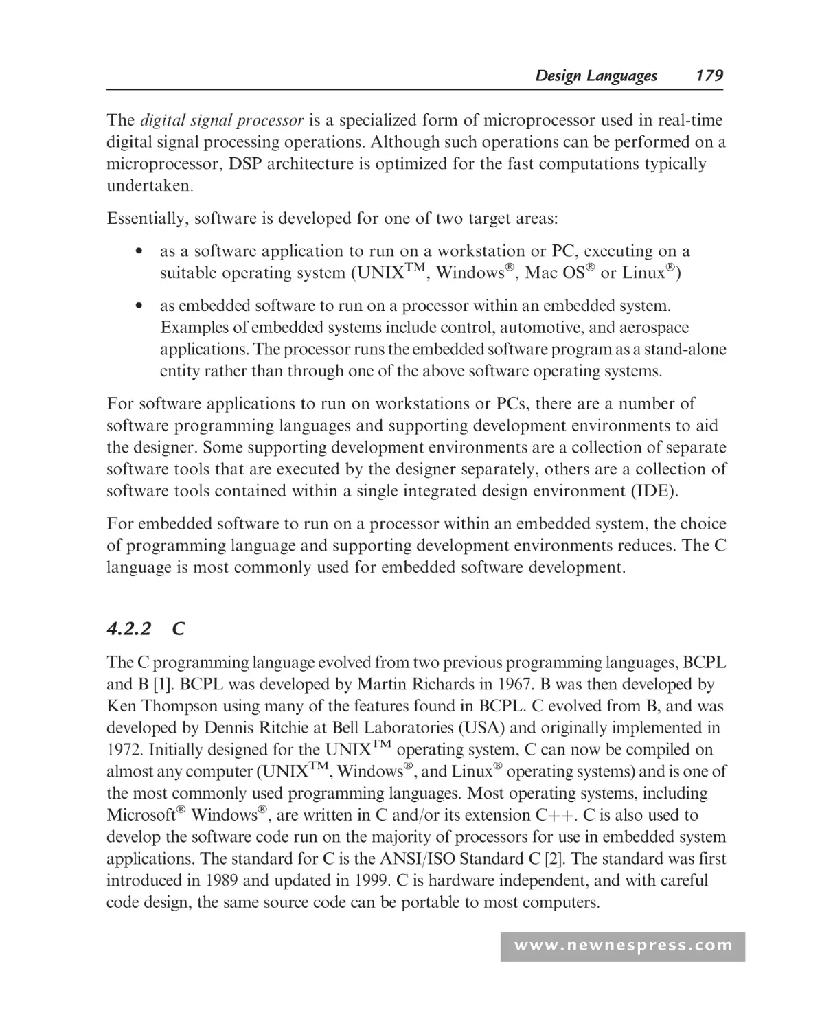


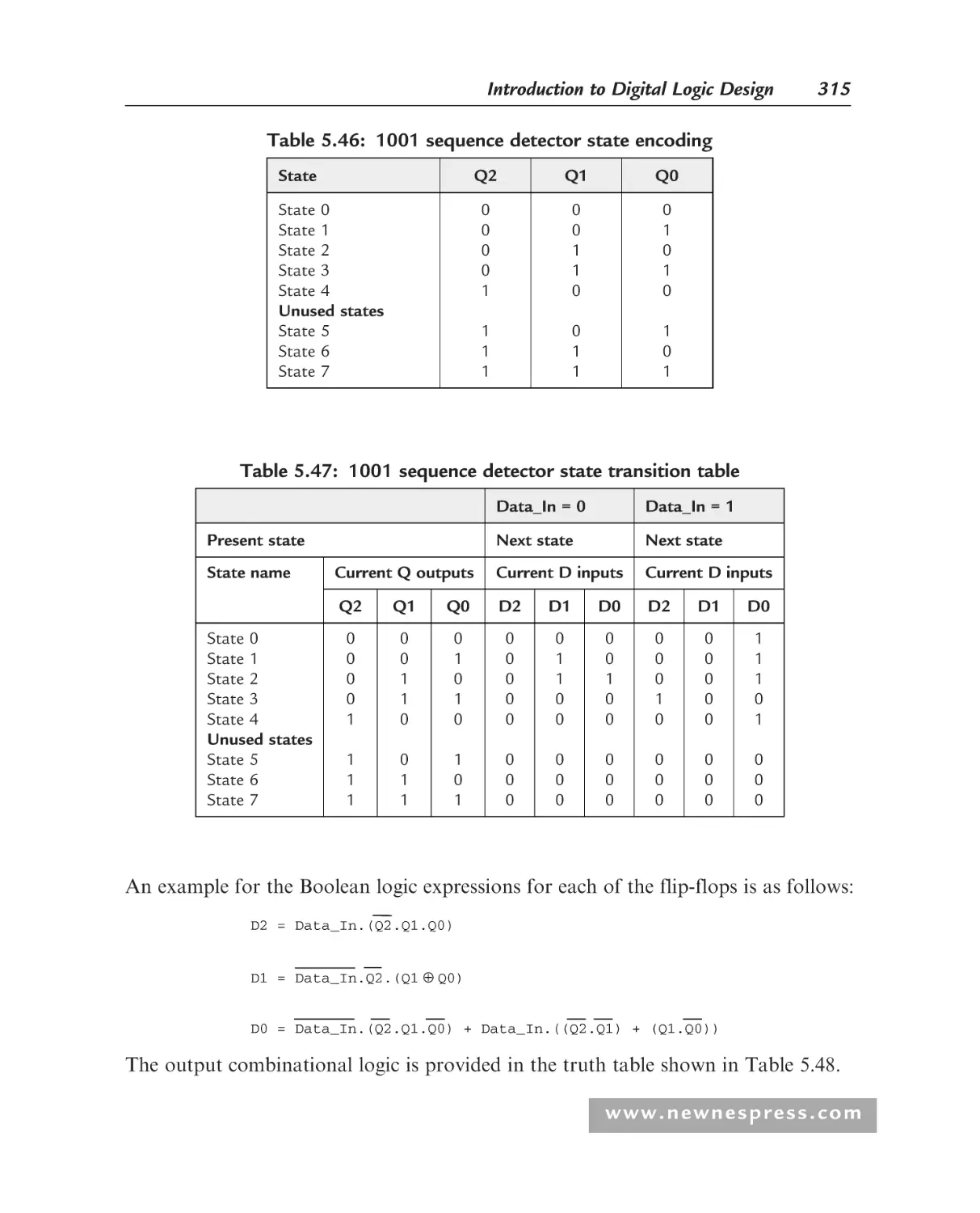
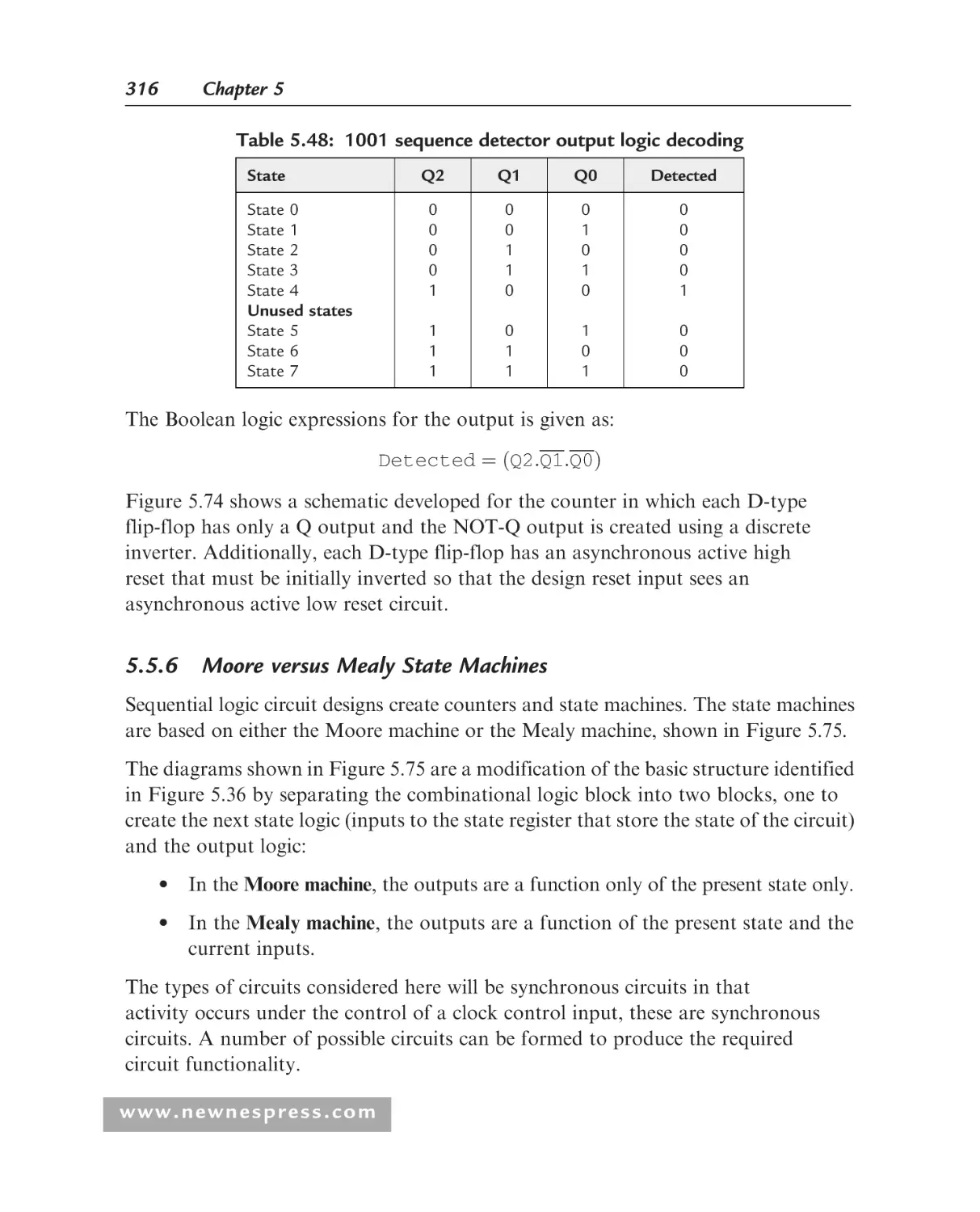
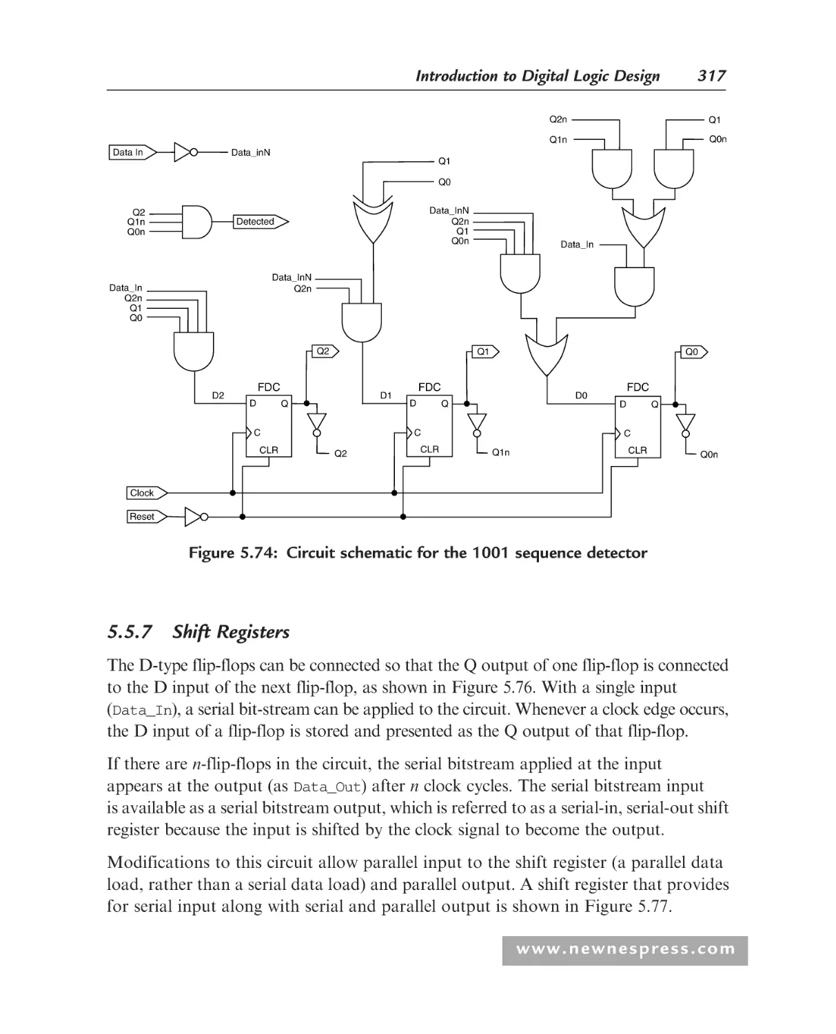
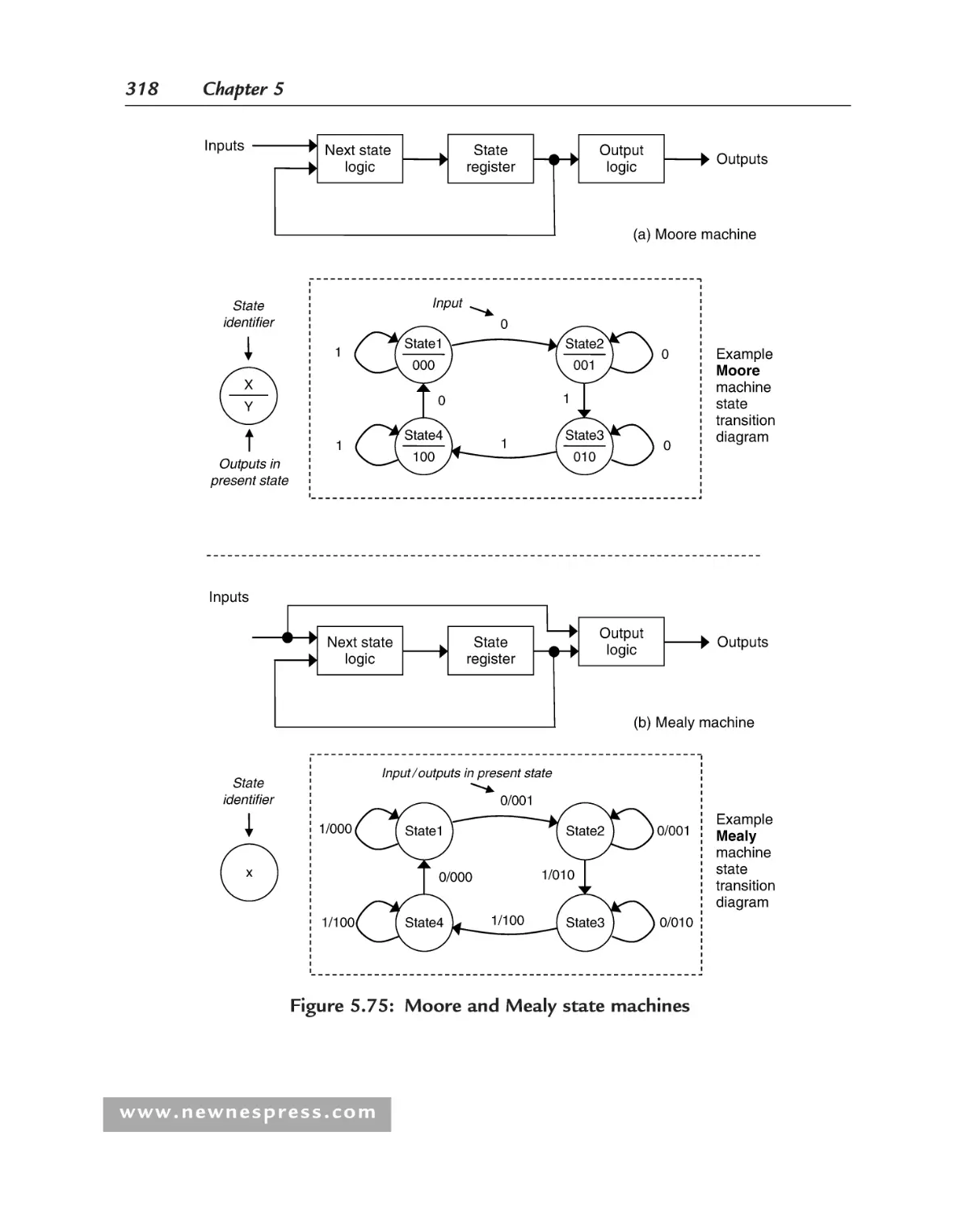


Author: Grout I.
Tags: integrated circuits synthesis arithmetic circuits fpga asic embedded systems digital design hardware synthesis electronic circuits hardware development apress publisher
ISBN: 0-19-861057-2
Year: 2008


Digital Systems Design with
FPGAs and CPLDs
This page intentionally left blank
Digital Systems Design with
FPGAs and CPLDs
Ian Grout
AMSTERDAM • BOSTON • HEIDELBERG • LONDON
NEW YORK • OXFORD • PARIS • SAN DIEGO
SAN FRANCISCO • SINGAPORE • SYDNEY • TOKYO
Newnes is an imprint of Elsevier
Newnes is an imprint of Elsevier
30 Corporate Drive, Suite 400, Burlington, MA 01803, USA
Linacre House, Jordan Hill, Oxford OX2 8DP, UK
Copyright 2008, Elsevier Ltd. All rights reserved.
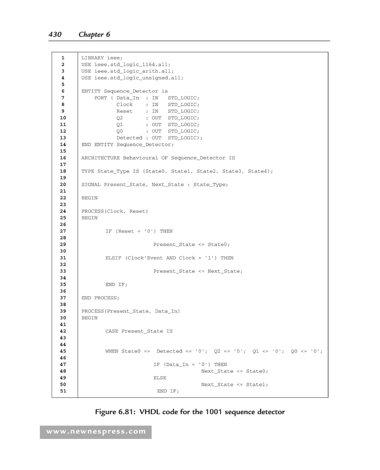
Material in Chapter 6 is reprinted, with permission, from IEEE Std 1076–2002 for VHDL Language Reference Manual, by IEEE.
The IEEE disclaims any responsibility or liability resulting from placement and use in the manner described.
MATLAB and Simulink are trademarks of The MathWorks, Inc. and are used with permission. The MathWorks does not
warrant the accuracy of the text or exercises in this book. This book’s use or discussion of MATLAB and Simulink
software or related products does not constitute endorsement or sponsorship by The MathWorks of a particular pedagogical
approach or particular use of the MATLAB and Simulink software.
Figures based on or adapted from figures and text owned by Xilinx, Inc., courtesy of Xilinx, Inc. Copyright Xilinx, Inc.,
1995–2005. All rights reserved.
Microsoft product screen shot(s) reprinted with permission from Microsoft Corporation.
No part of this publication may be reproduced, stored in a retrieval system, or transmitted in any form or by any means,
electronic, mechanical, photocopying, recording, or otherwise, without the prior written permission of the publisher.
Permissions may be sought directly from Elsevier’s Science & Technology Rights Department in Oxford, UK:
phone: (þ44) 1865 843830, fax: (þ44) 1865 853333, E-mail: permissions@elsevier.com. You may also complete your request
online via the Elsevier homepage (http://elsevier.com), by selecting ‘‘Support & Contact’’ then ‘‘Copyright and Permission’’
and then ‘‘Obtaining Permissions.’’
Recognizing the importance of preserving what has been written, Elsevier prints its books on acid-free paper whenever possible.
Library of Congress Cataloging-in-Publication Data
Grout, Ian.
Digital systems design with FPGAs and CPLDs / Ian Grout.
p. cm.
Includes bibliographical references and index.
ISBN-13: 978-0-7506-8397-5 (alk. paper)
1. Digital electronics.
2. Digital circuits — Design
and construction.
3. Field programmable gate arrays.
4. Programmable logic devices.
I. Title.
TK7868.D5.G76 2008
621.381—dc22
2007044907
British Library Cataloguing-in-Publication Data
A catalogue record for this book is available from the British Library.
For information on all Newnes publications
visit our Web site at www.books.elsevier.com
Printed in the United States of America
08
09
10
11
12
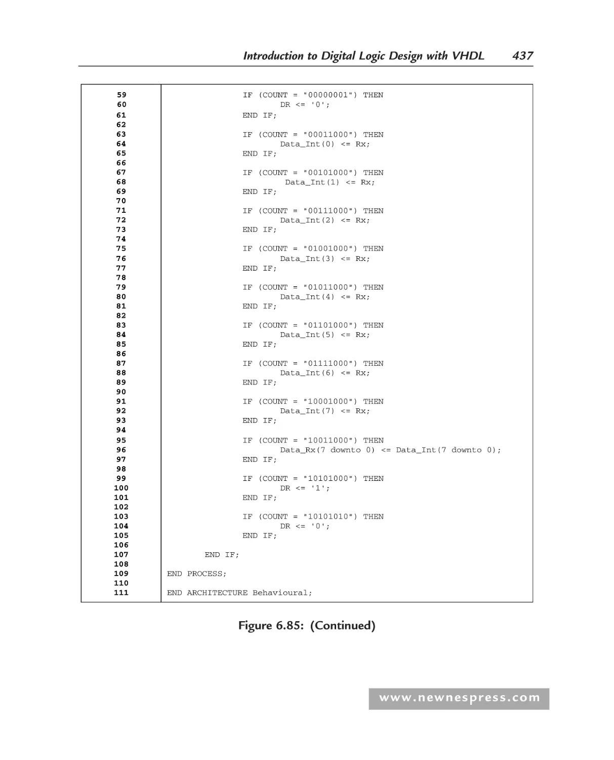
13
10
9
8
7
6
5
4
3 2
1
Working together to grow
libraries in developing countries
www.elsevier.com | www.bookaid.org | www.sabre.org
To my family, but especially to my parents and to Jane.
This page intentionally left blank
Table of Contents
Preface .....................................................................................................xvii
Abbreviations ...........................................................................................xxiii
Chapter 1: Introduction to Programmable Logic ............................................... 1
1.1
1.2
Introduction to the Book ............................................................................1
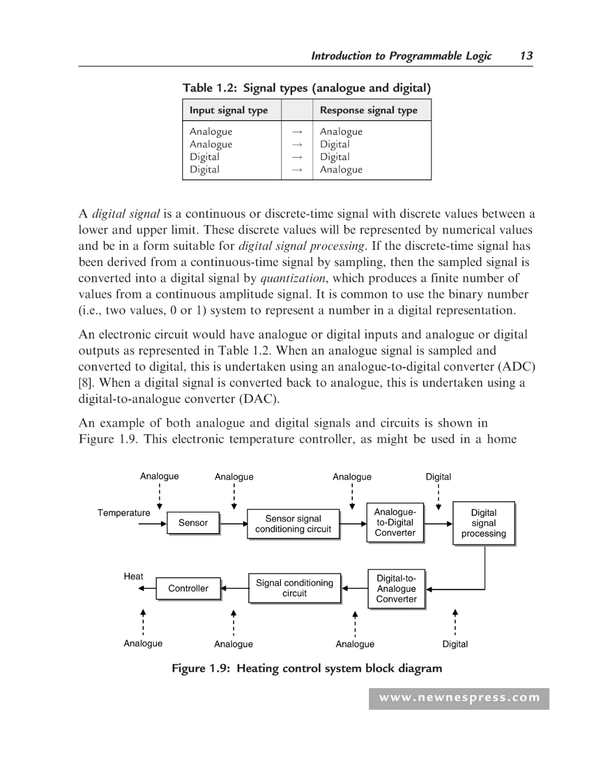
Electronic Circuits: Analogue and Digital ................................................10
1.2.1 Introduction ....................................................................................10
1.2.2 Continuous Time versus Discrete Time...........................................10
1.2.3 Analogue versus Digital ..................................................................12
1.3 History of Digital Logic ............................................................................14
1.4 Programmable Logic versus Discrete Logic ..............................................17
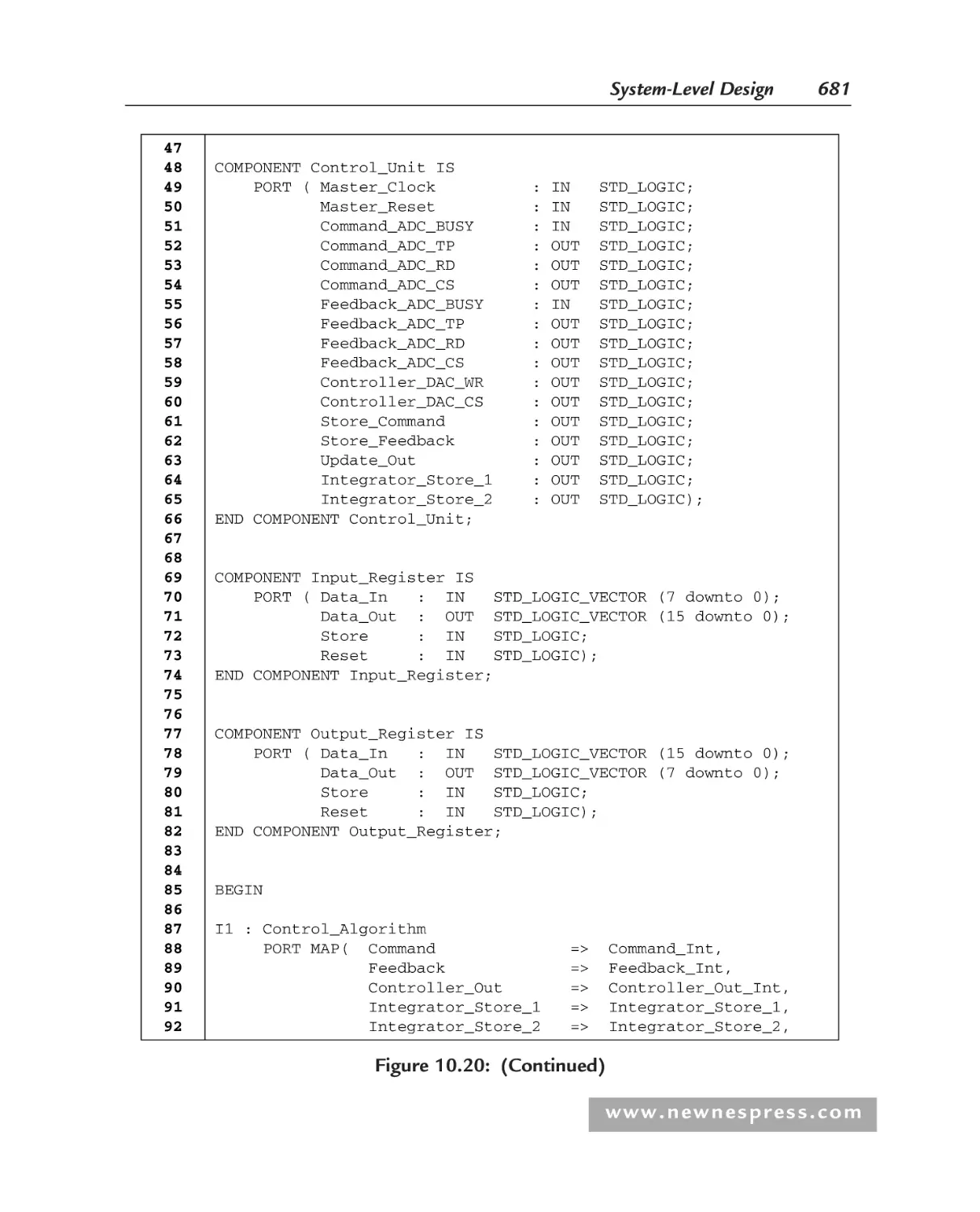
1.5 Programmable Logic versus Processors ....................................................21
1.6 Types of Programmable Logic ..................................................................24
1.6.1 Simple Programmable Logic Device (SPLD) ..................................24
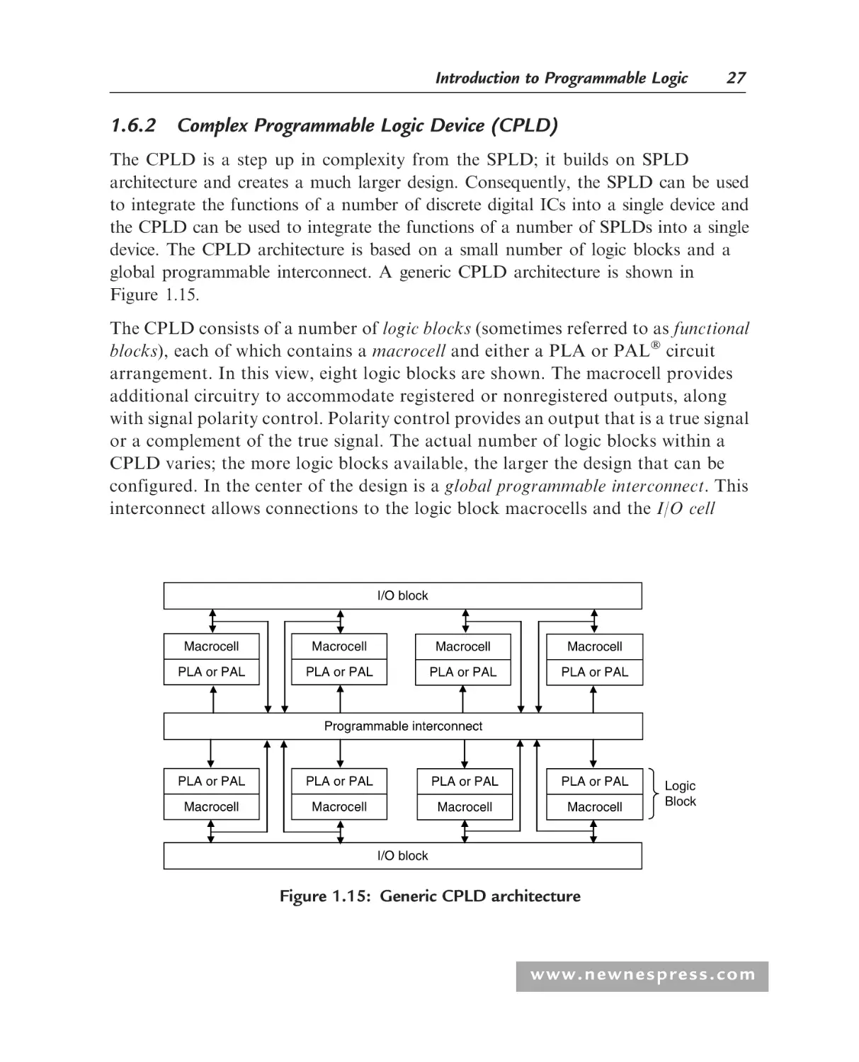
1.6.2 Complex Programmable Logic Device (CPLD) ..............................27
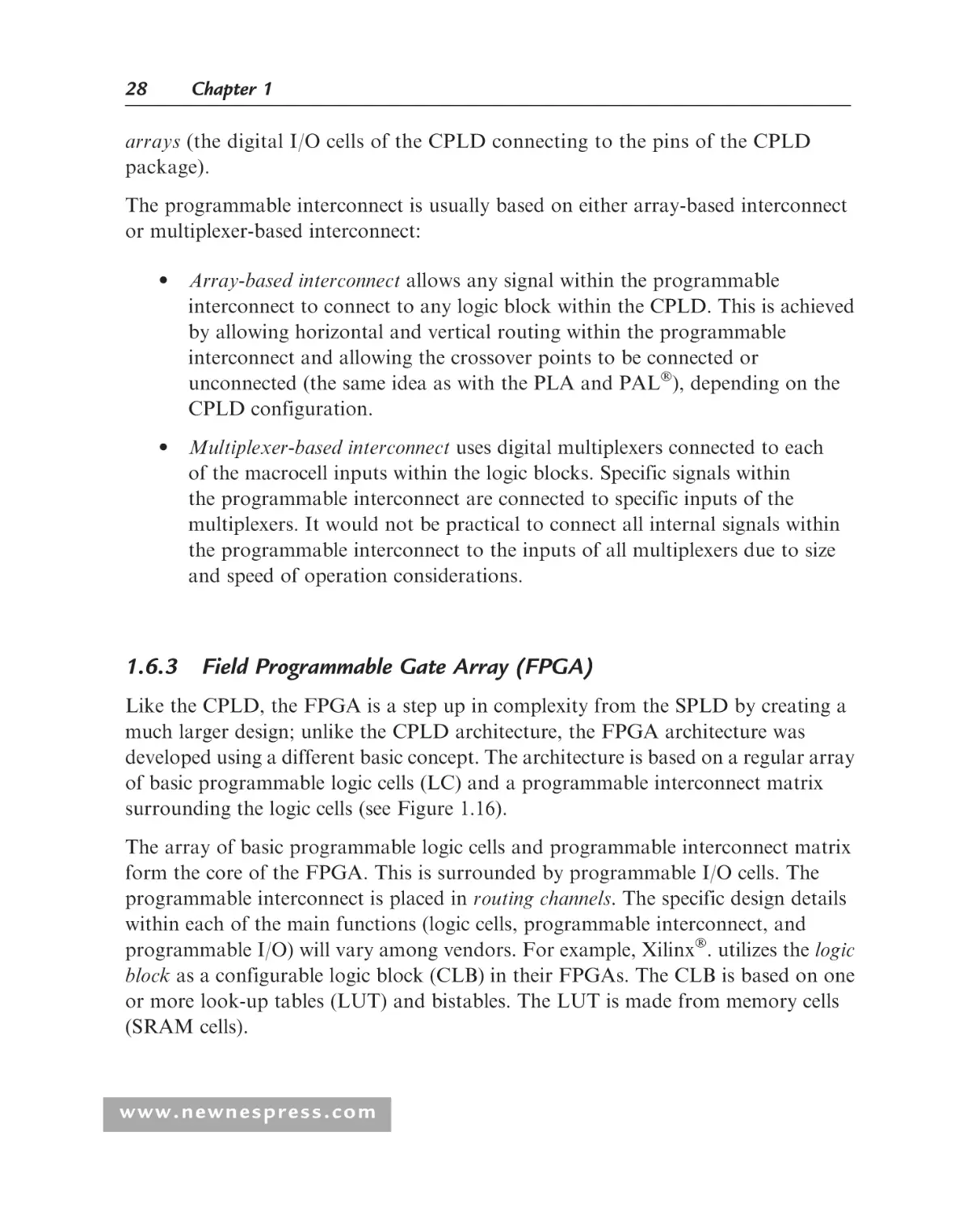
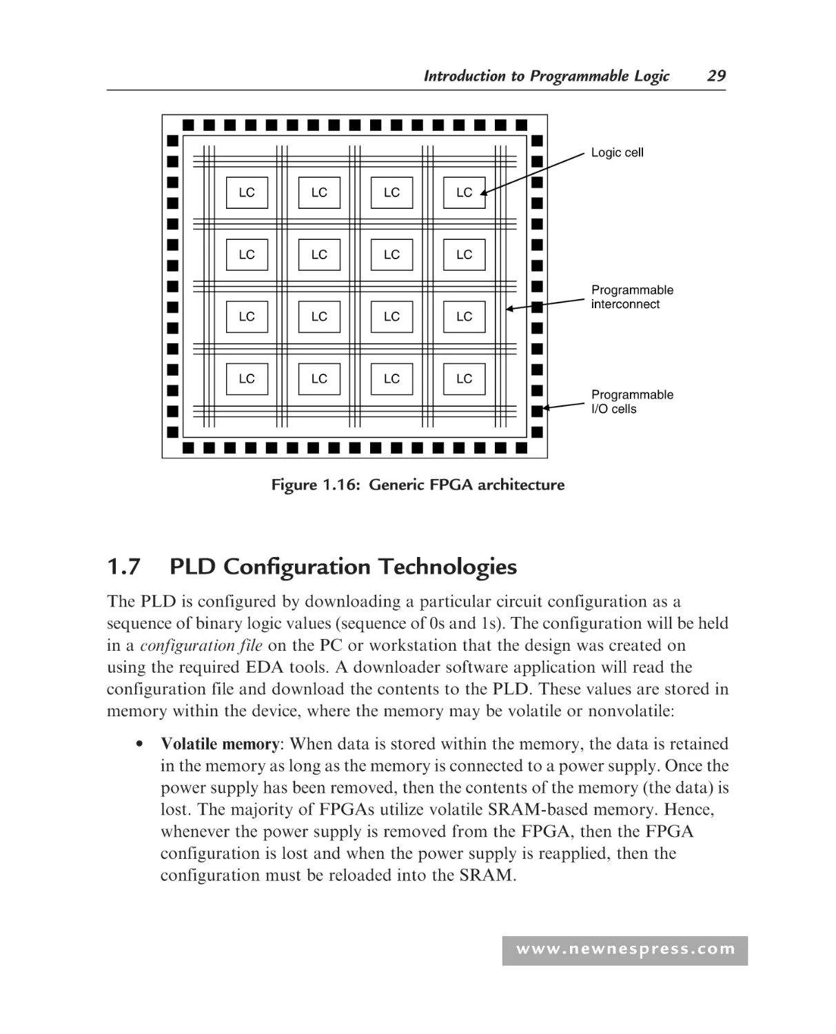
1.6.3 Field Programmable Gate Array (FPGA).......................................28
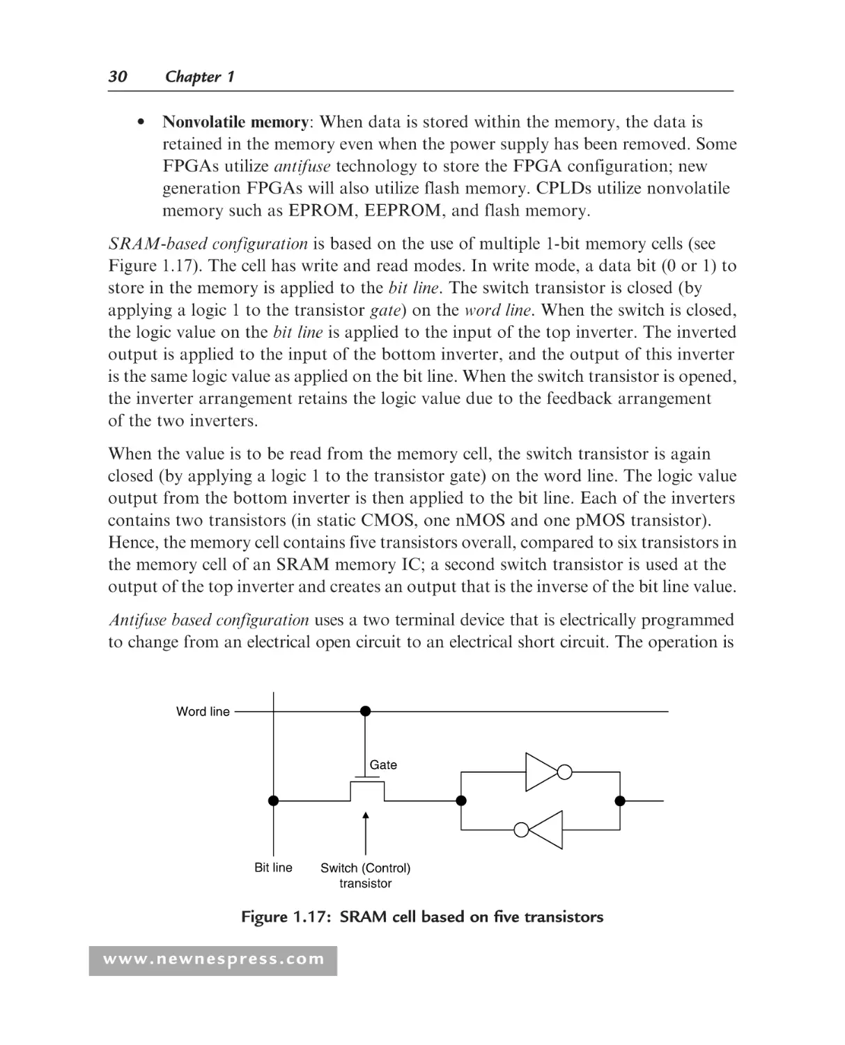
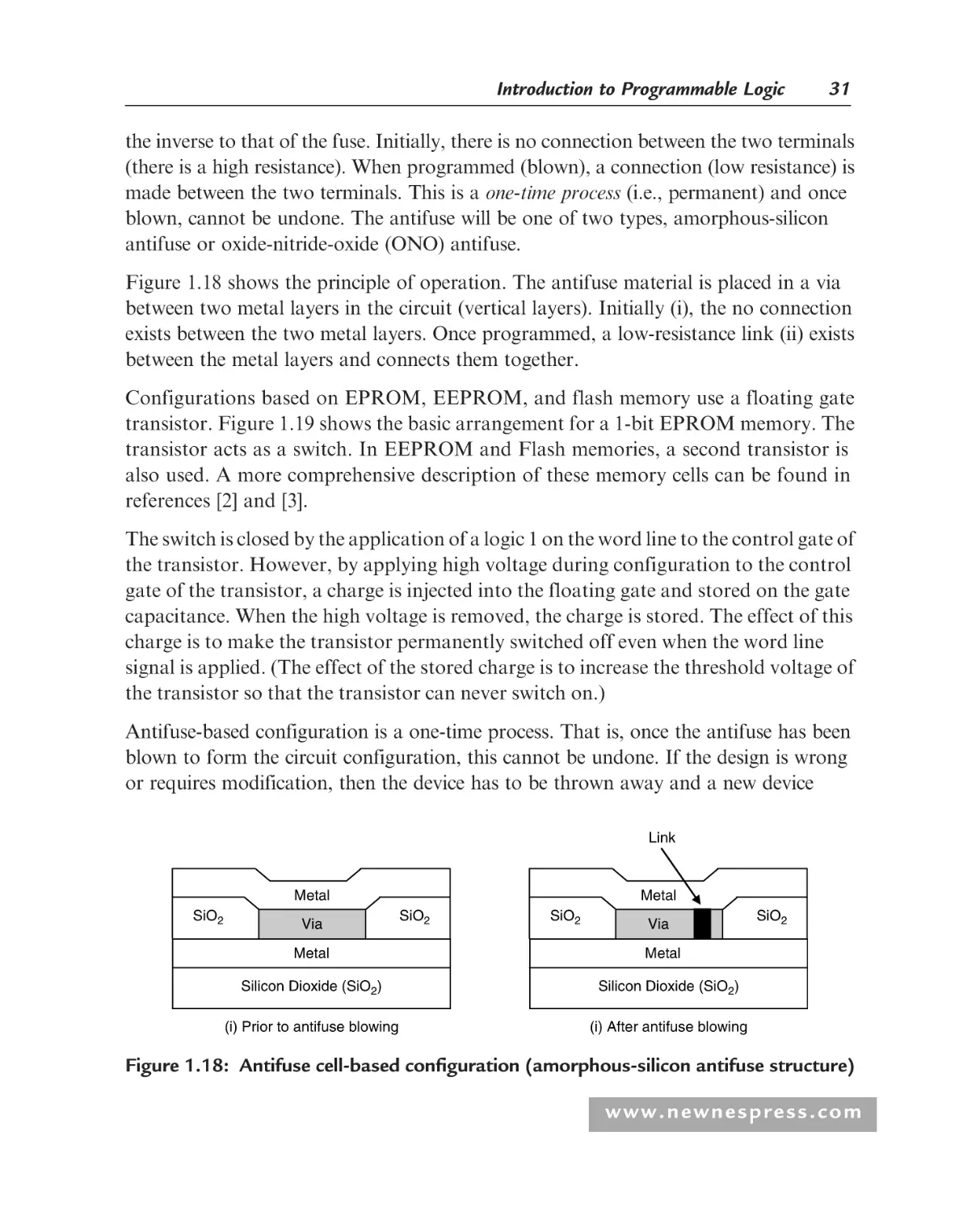
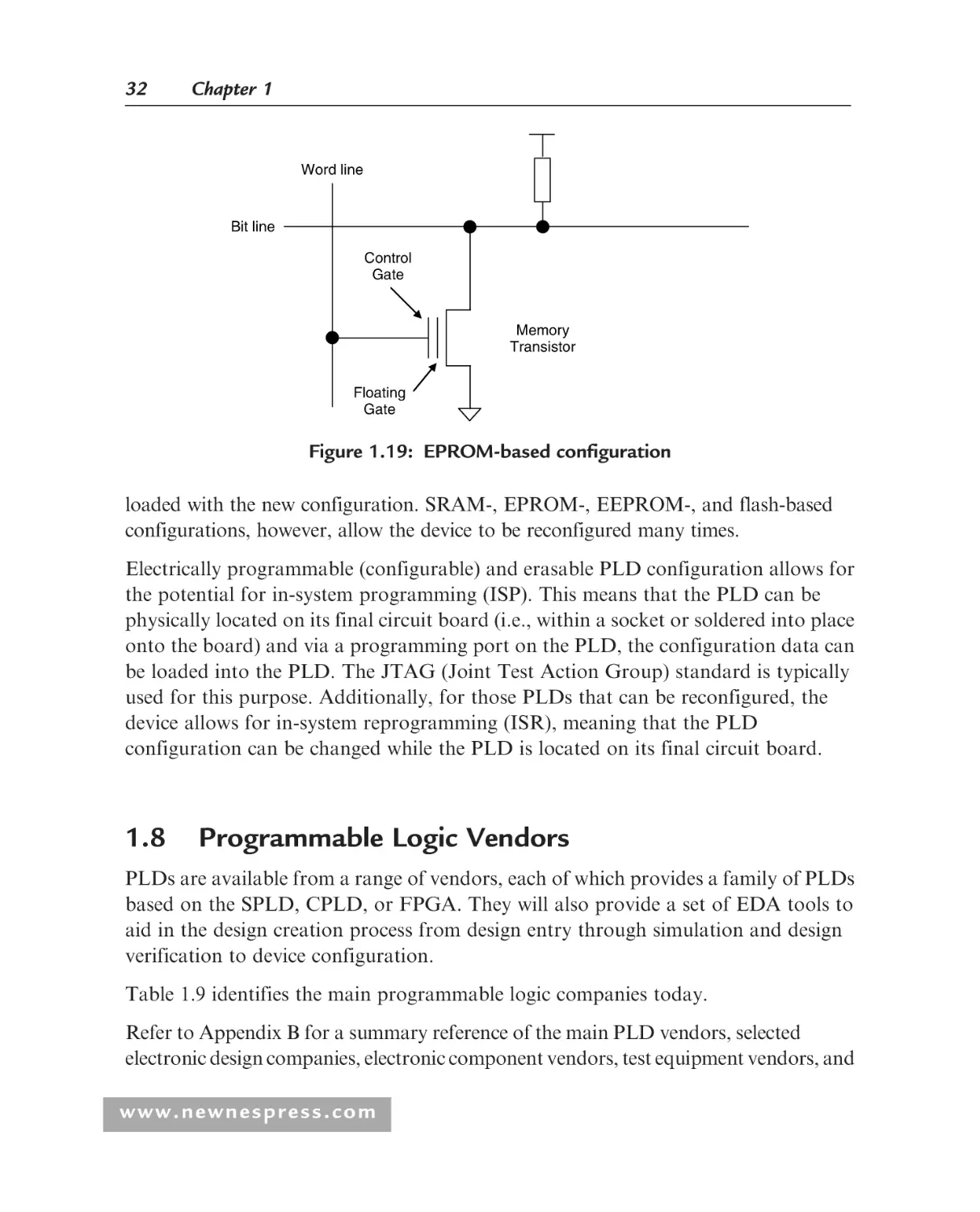
1.7 PLD Configuration Technologies .............................................................29
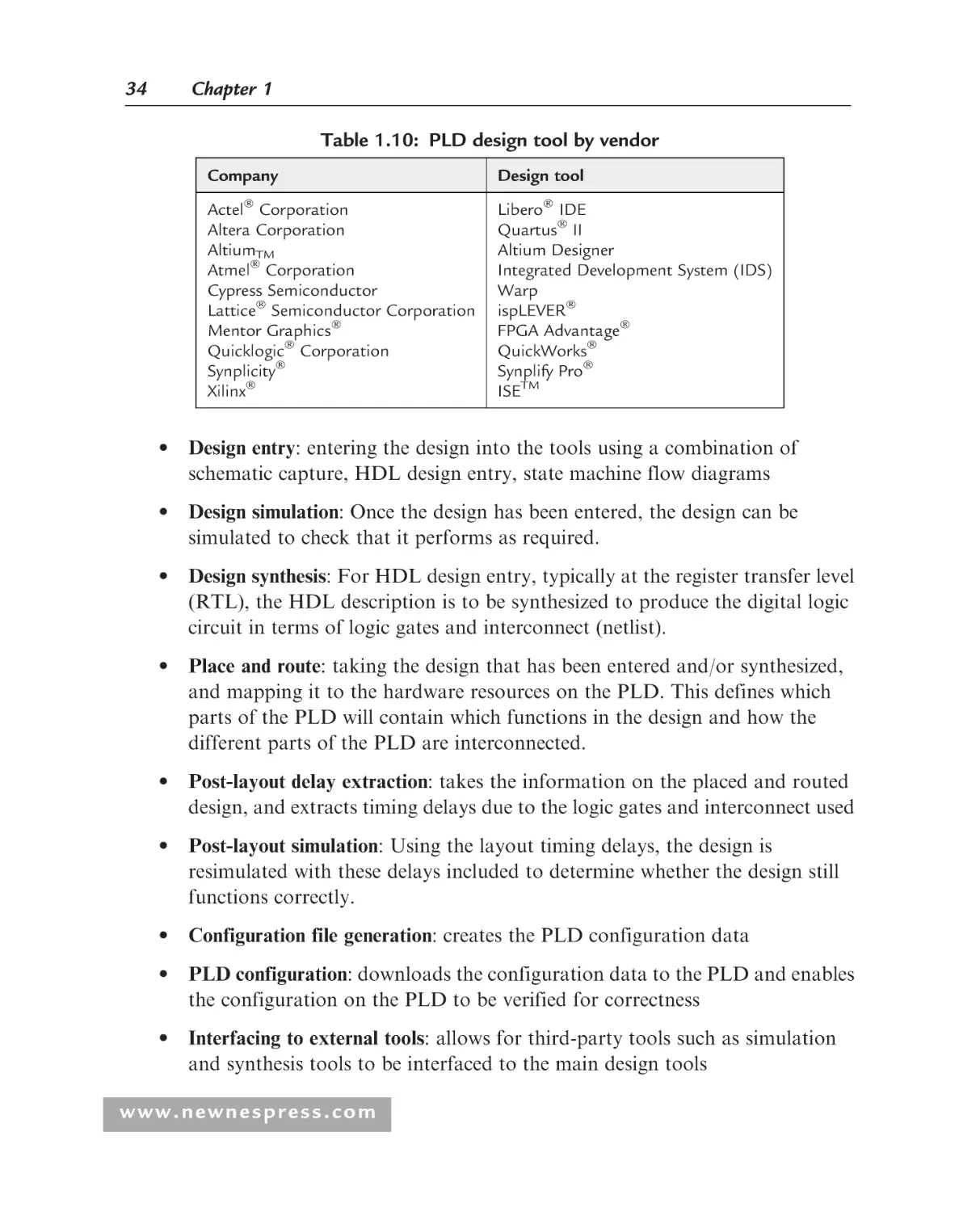
1.8 Programmable Logic Vendors...................................................................32
1.9 Programmable Logic Design Methods and Tools.....................................33
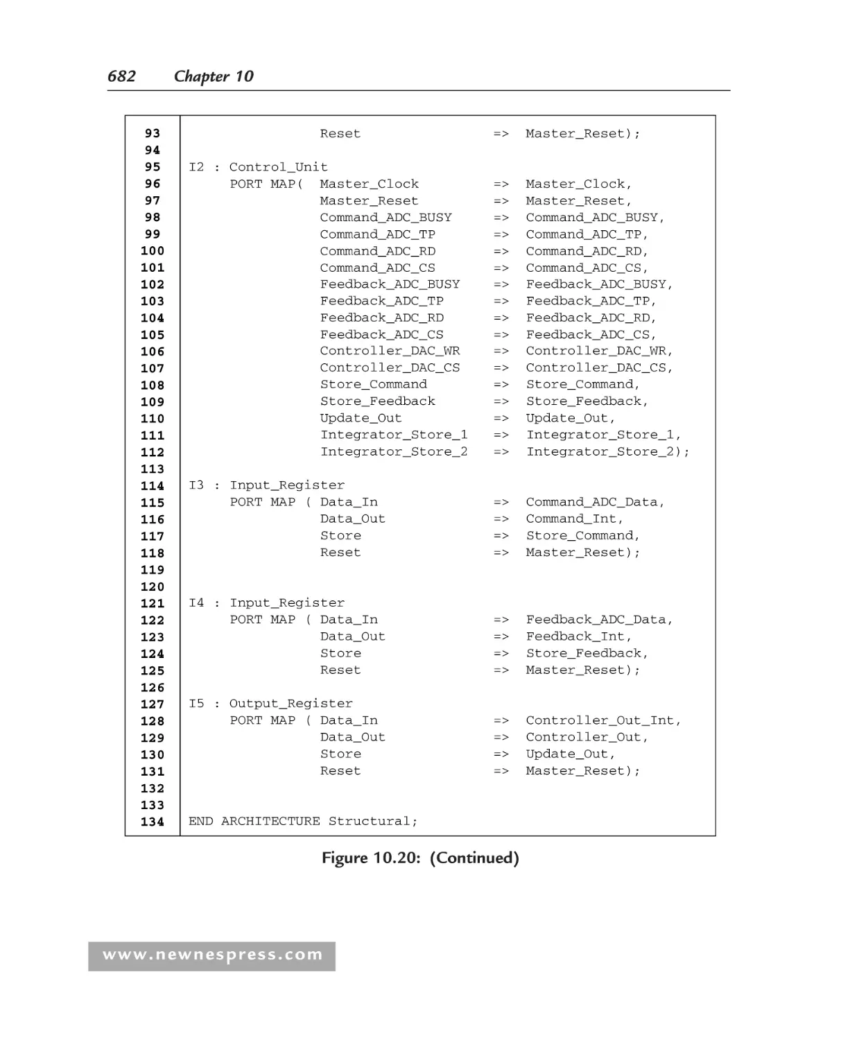
1.9.1 Introduction ....................................................................................33
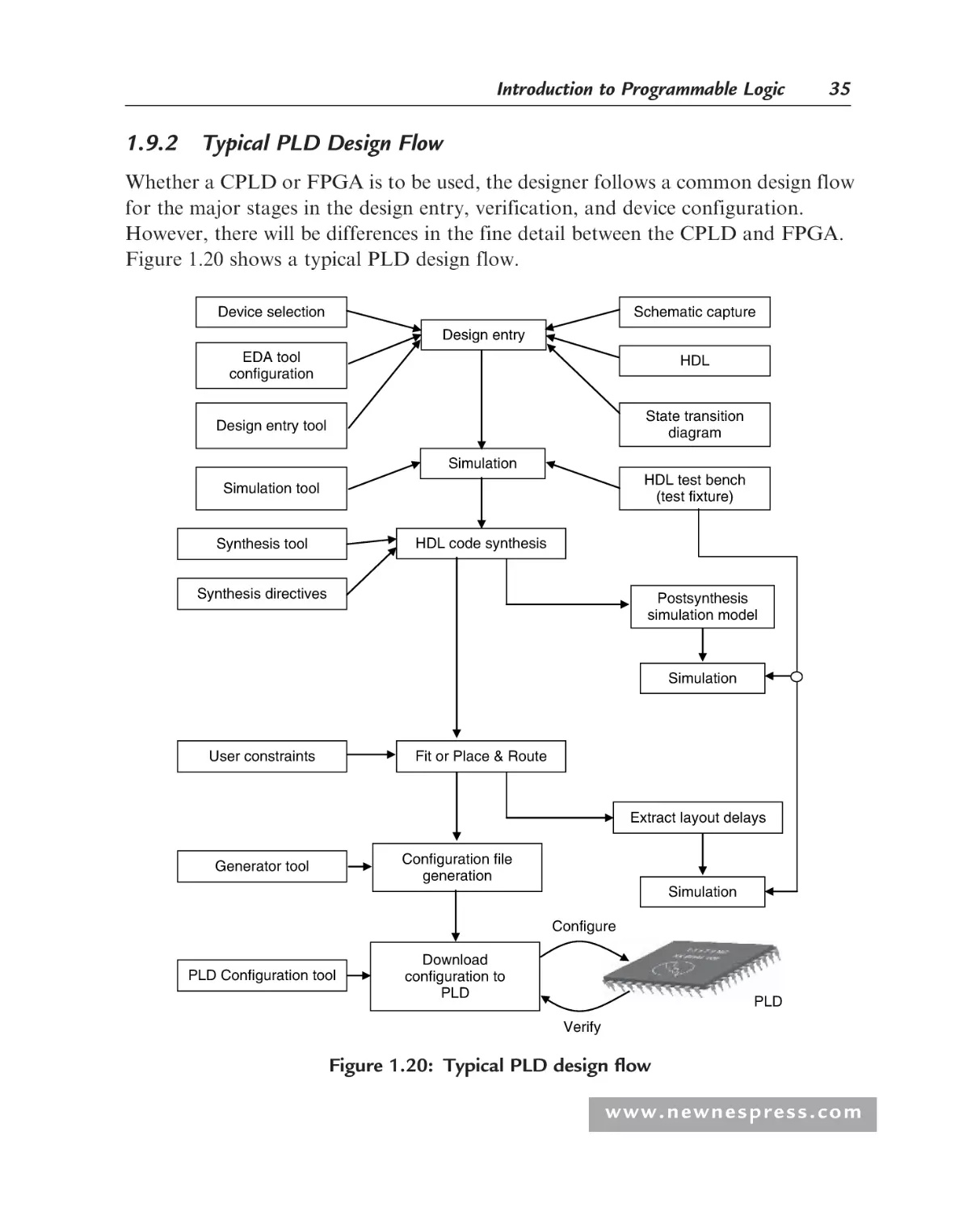
1.9.2 Typical PLD Design Flow...............................................................35
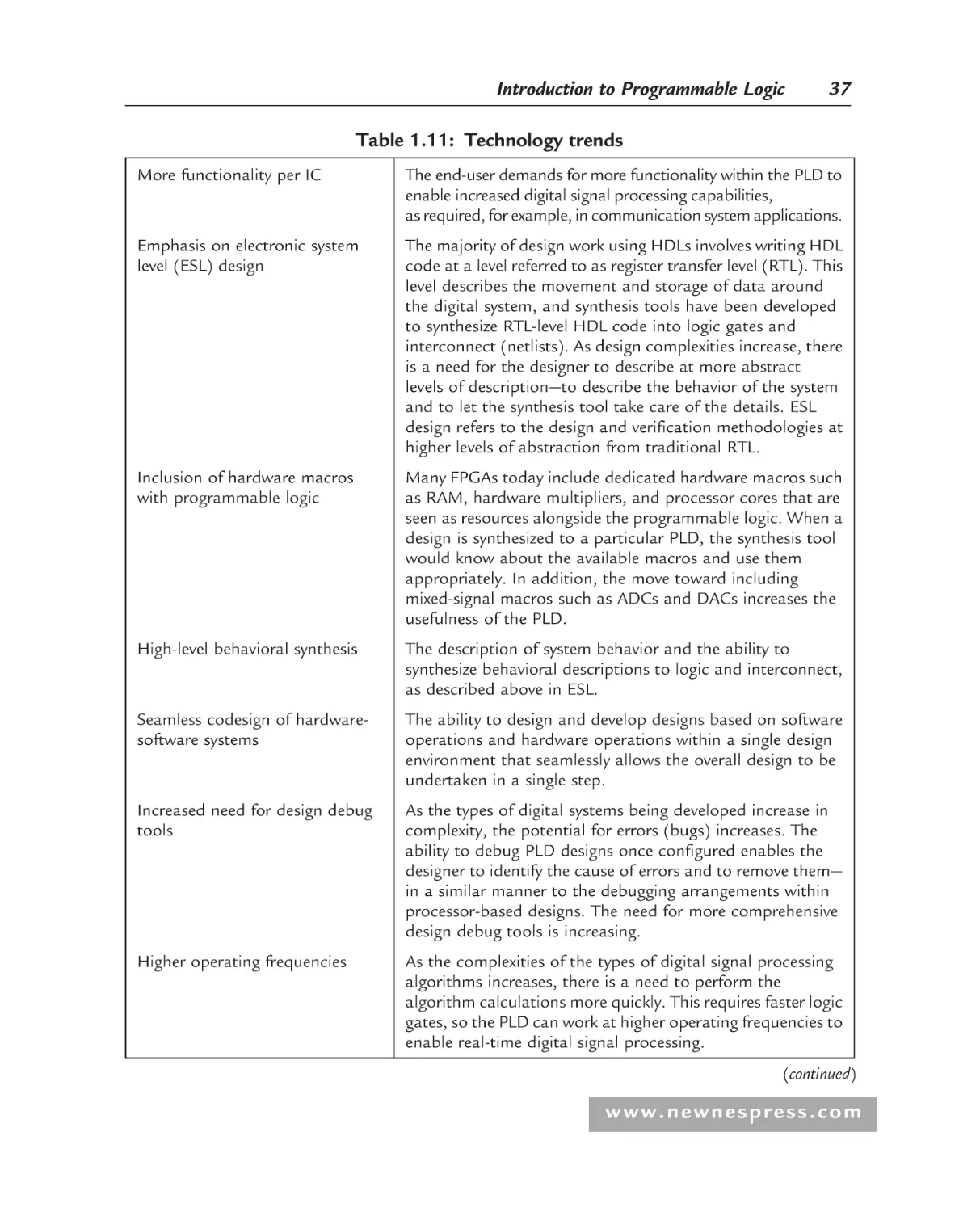
1.10 Technology Trends ....................................................................................36
References .................................................................................................38
Student Exercises ......................................................................................40
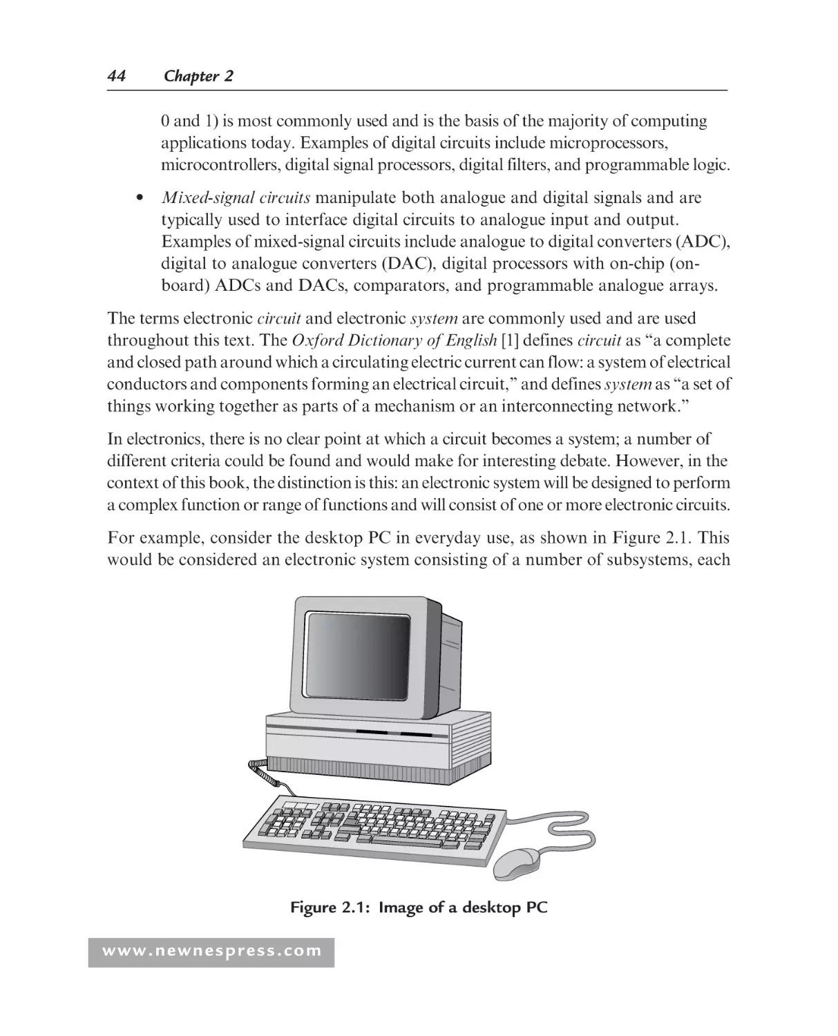
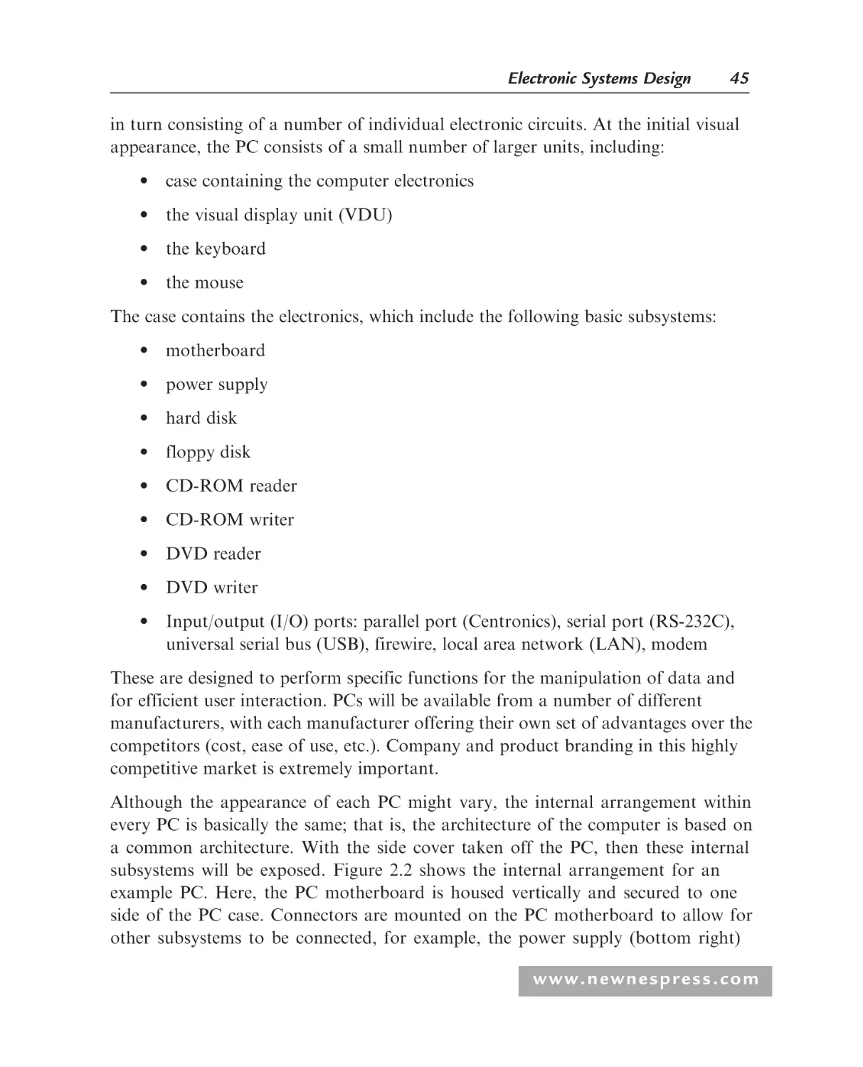
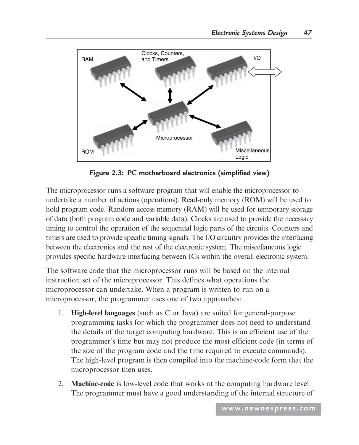
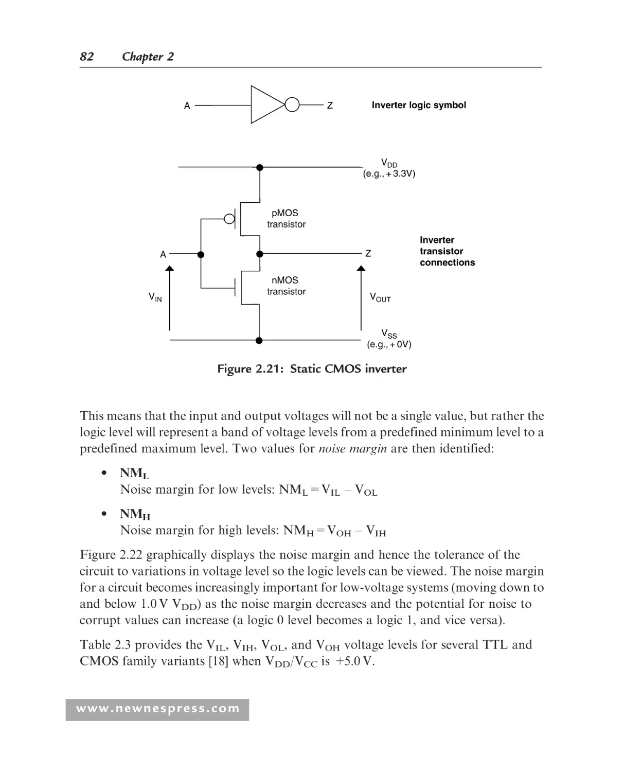
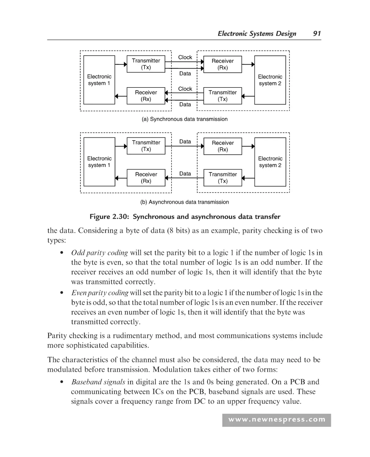
Chapter 2: Electronic Systems Design ........................................................... 43
2.1
2.2
Introduction ..............................................................................................43
Sequential Product Development Process versus Concurrent
Engineering Process...................................................................................52
www.newnespress.com
viii
Table of Contents
2.3
2.4
2.5
2.6
2.7
2.8
2.9
2.10
2.11
2.12
2.13
2.14
2.15
2.16
2.17
2.18
2.19
2.20
2.21
2.22
2.23
2.2.1 Introduction ....................................................................................52
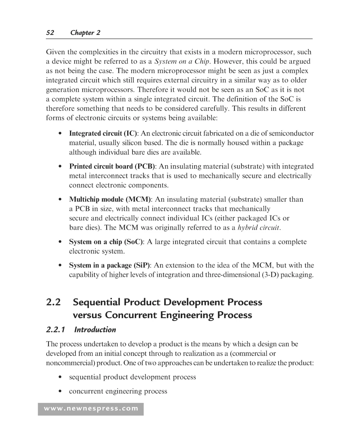
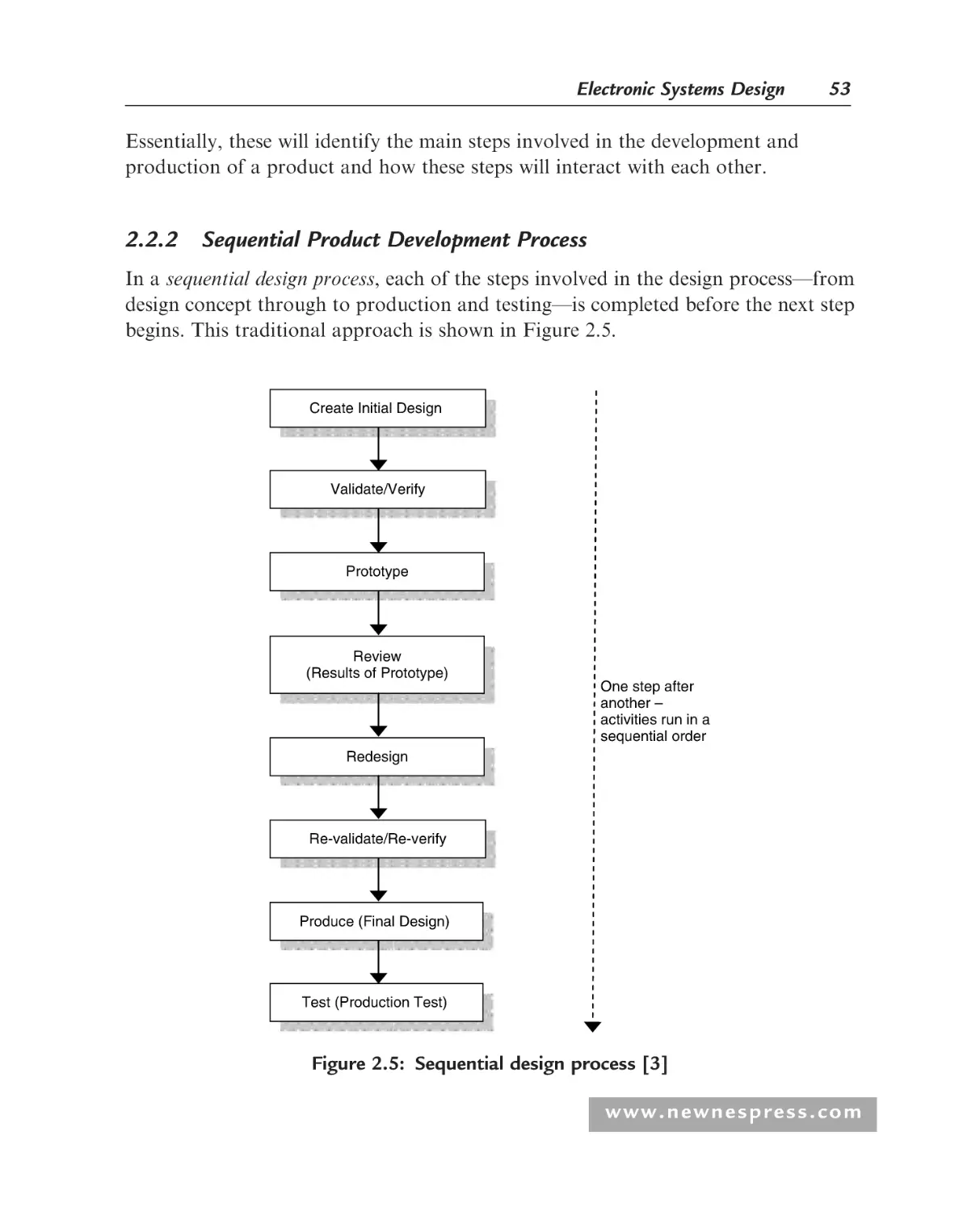
2.2.2 Sequential Product Development Process .......................................53
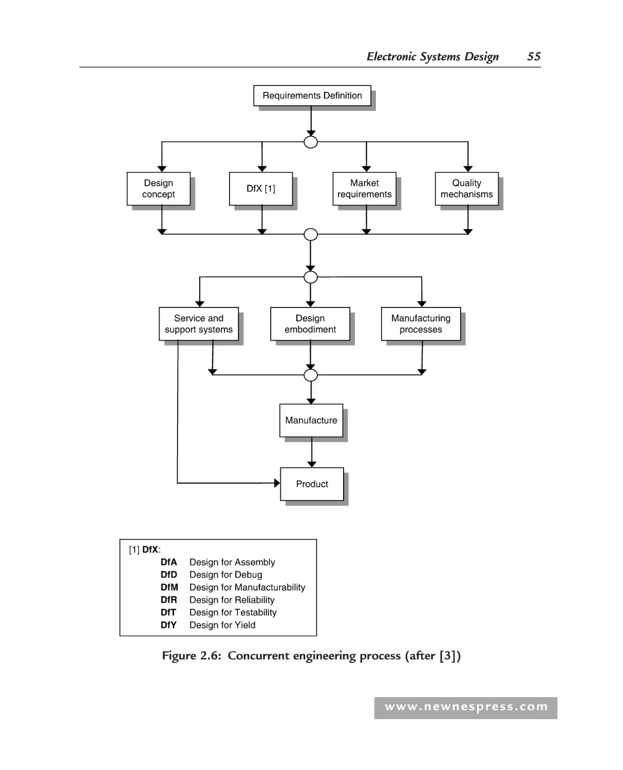
2.2.3 Concurrent Engineering Process......................................................54
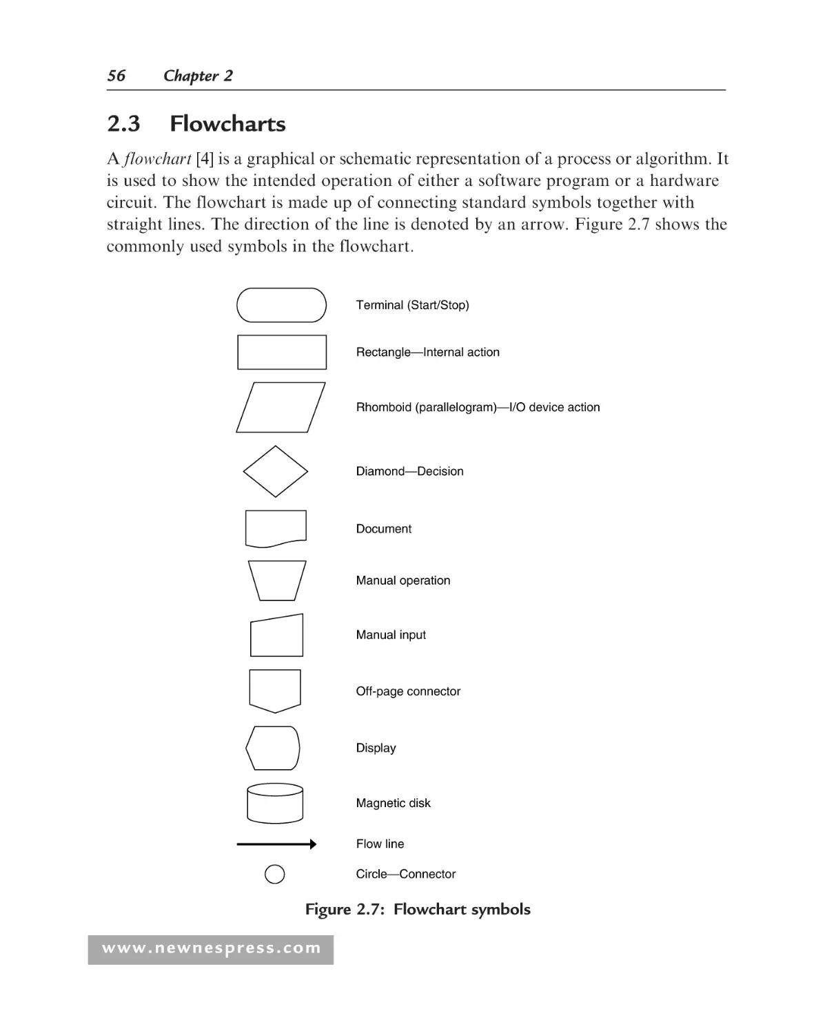
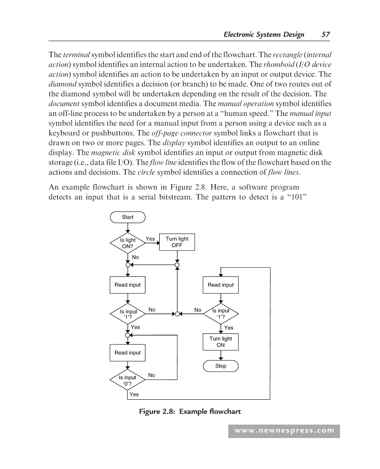
Flowcharts.................................................................................................56
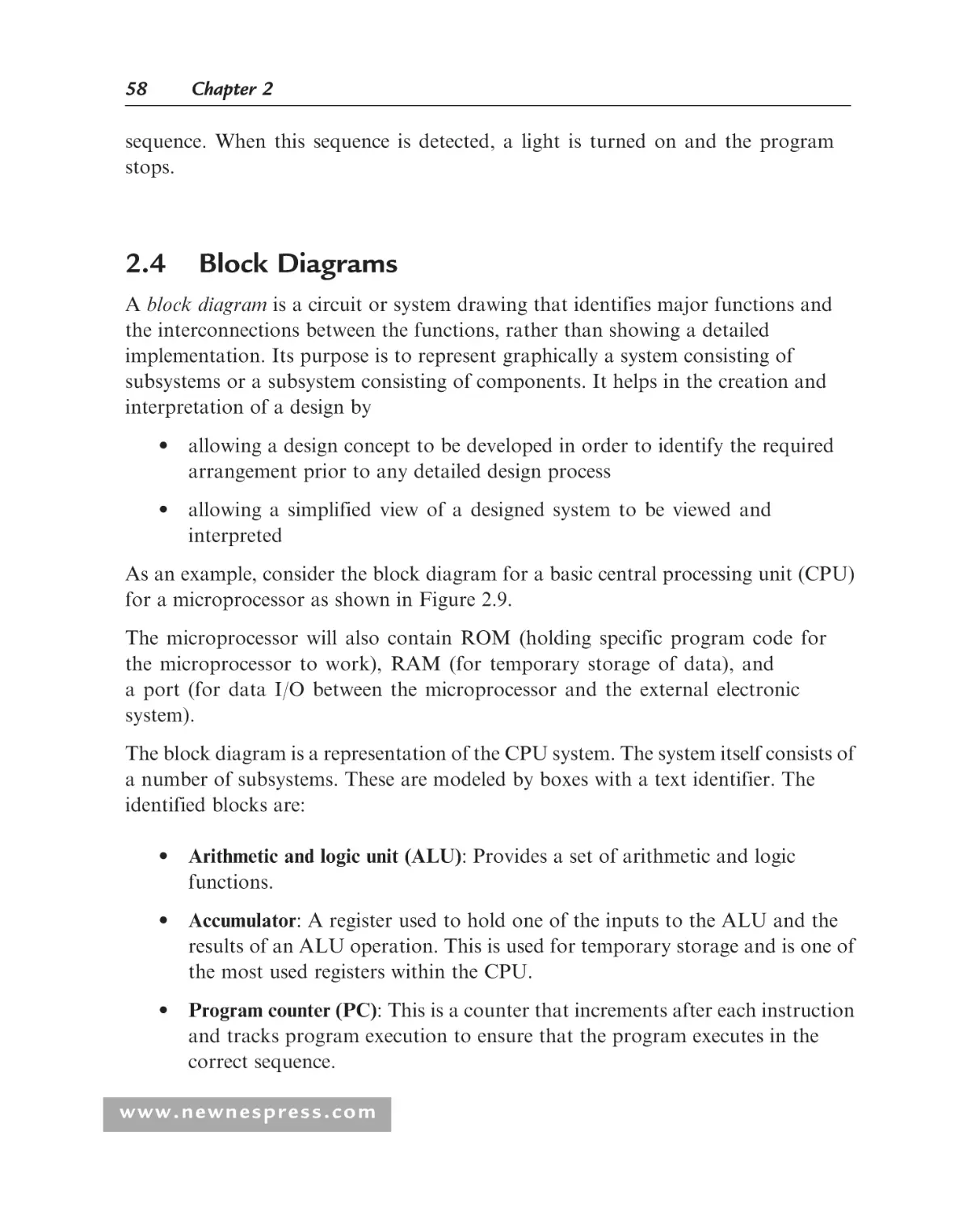
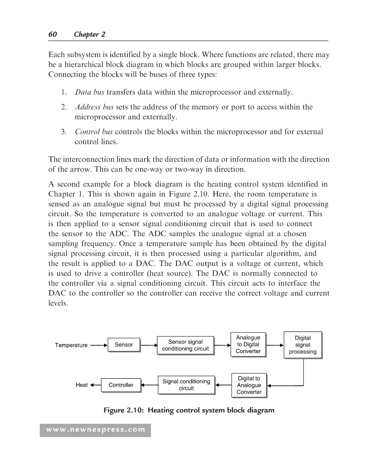
Block Diagrams.........................................................................................58
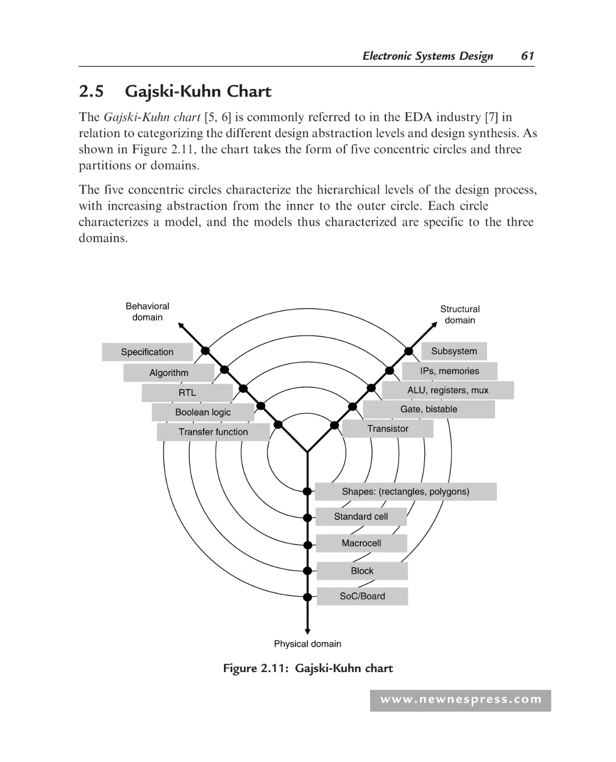
Gajski-Kuhn Chart ...................................................................................61
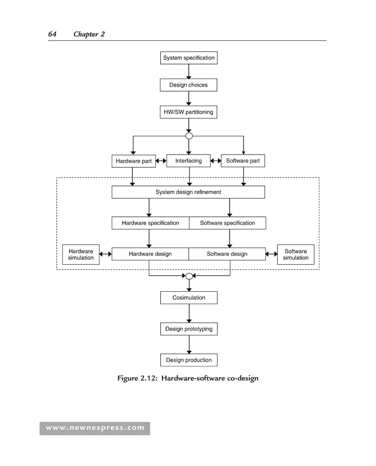
Hardware-Software Co-Design .................................................................62
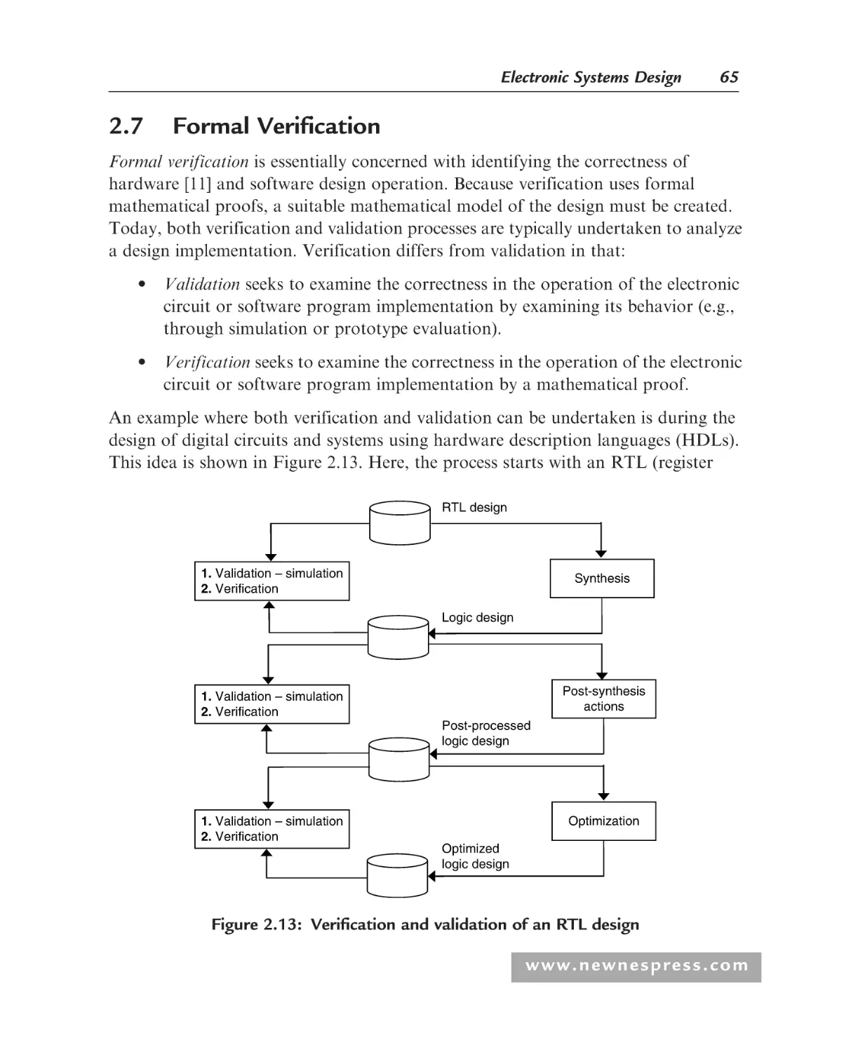
Formal Verification...................................................................................65
Embedded Systems and Real-Time Operating Systems ............................66
Electronic System-Level Design ................................................................67
Creating a Design Specification.................................................................68
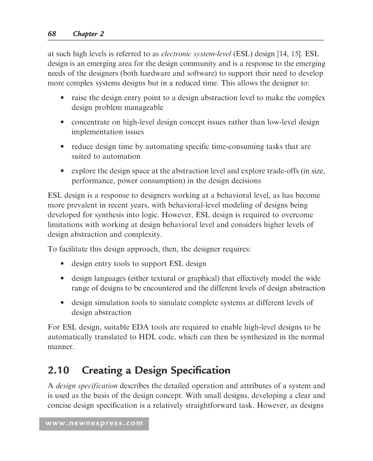
Unified Modeling Language......................................................................70
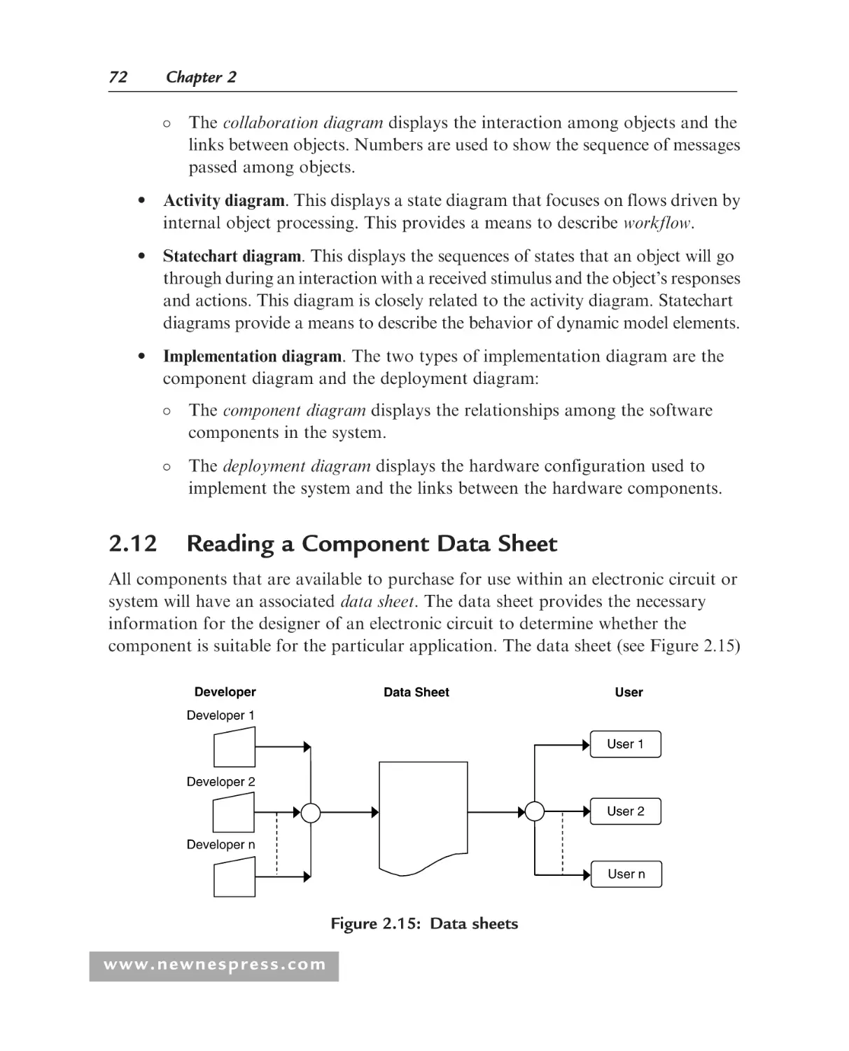
Reading a Component Data Sheet............................................................72
Digital Input/Output .................................................................................75
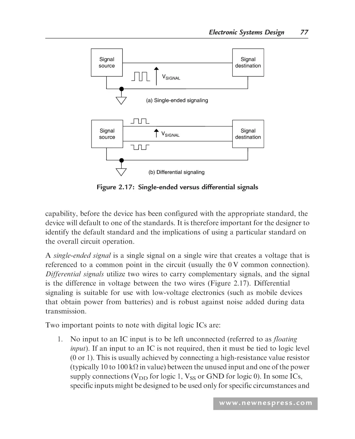
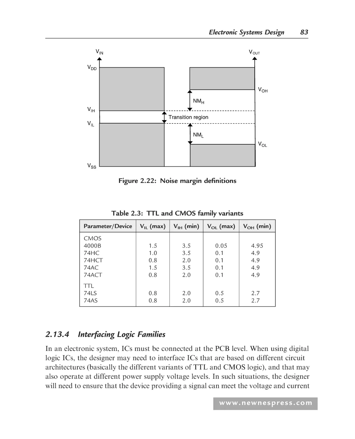
2.13.1 Introduction...................................................................................75
2.13.2 Logic-Level Definitions .................................................................79
2.13.3 Noise Margin.................................................................................81
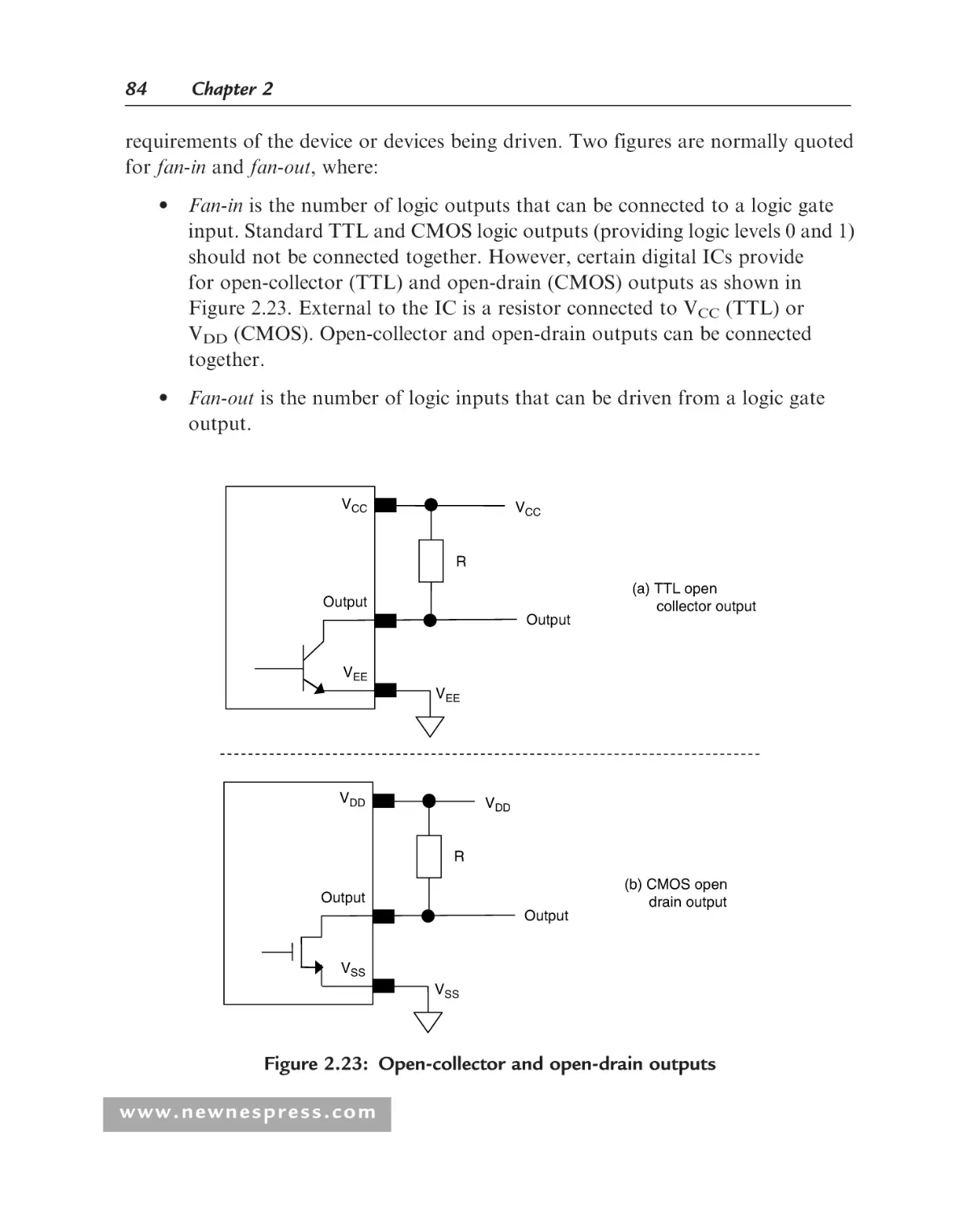
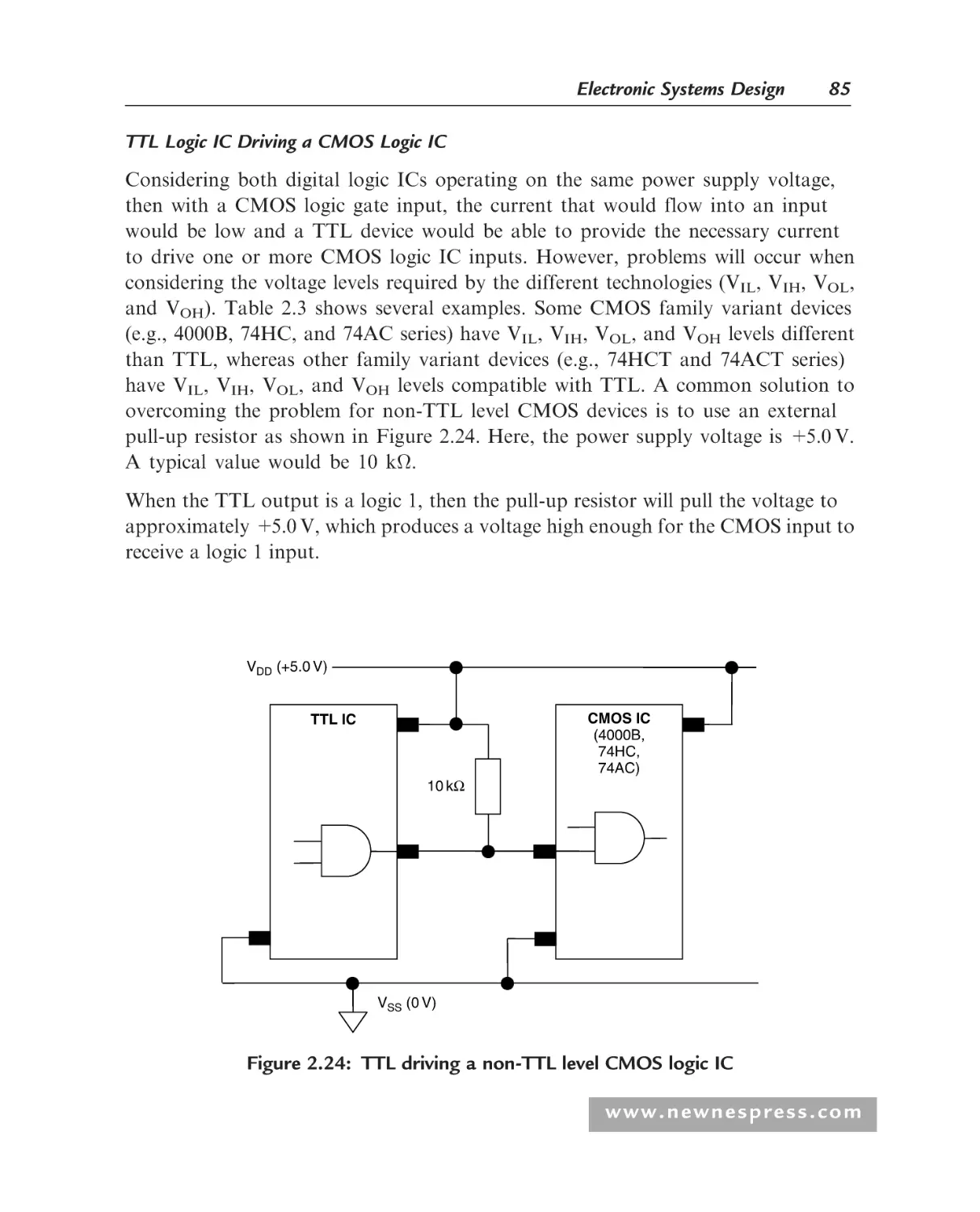
2.13.4 Interfacing Logic Families .............................................................83
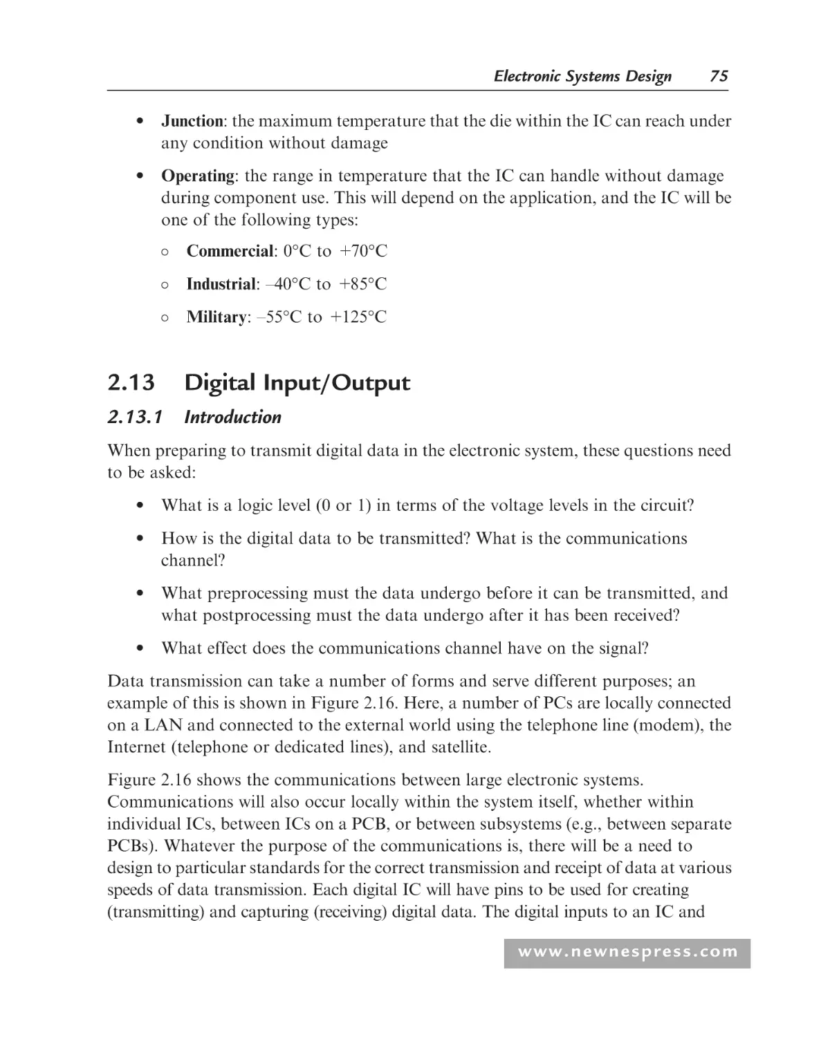
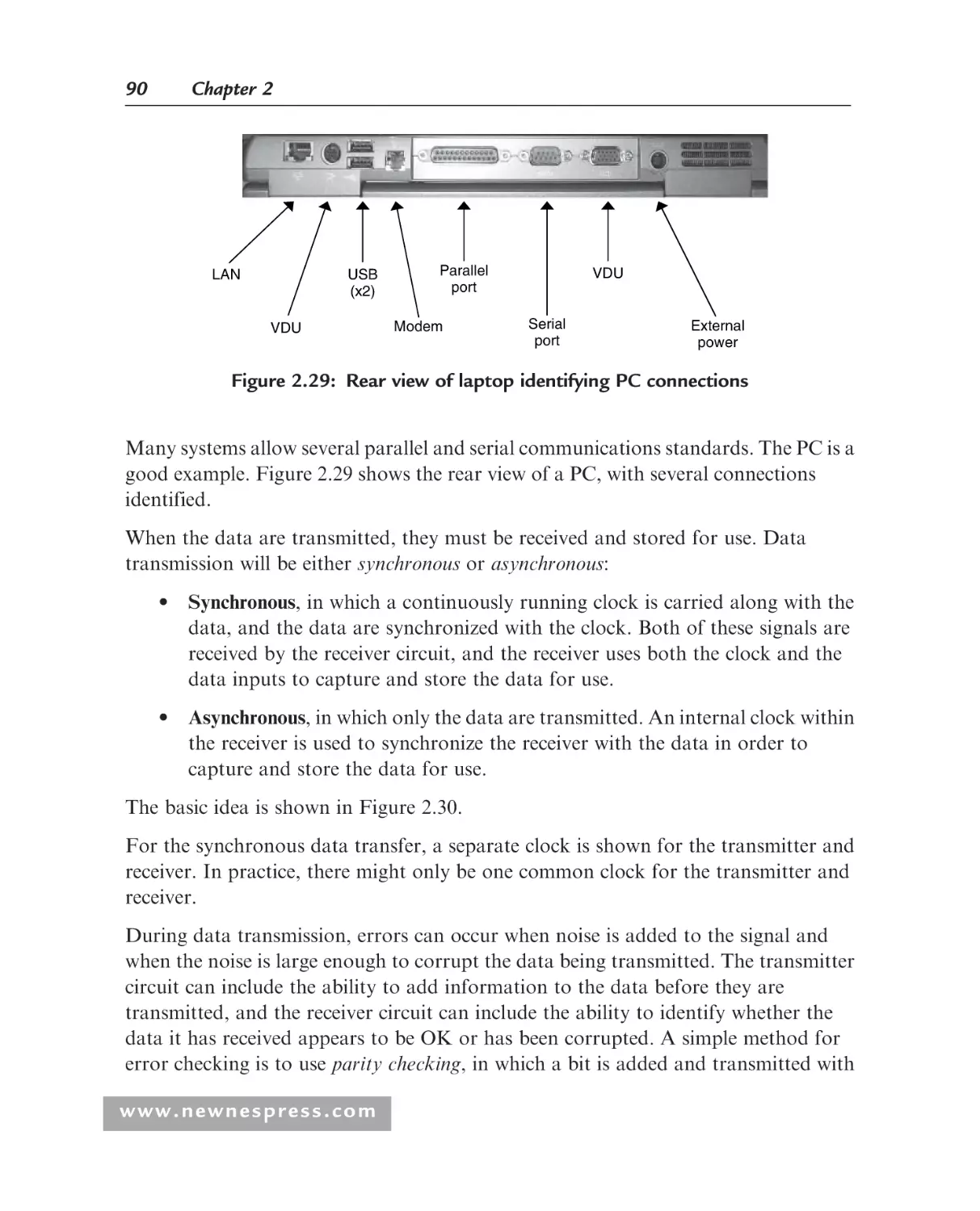
Parallel and Serial Interfacing ...................................................................89
2.14.1 Introduction...................................................................................89
2.14.2 Parallel I/O ....................................................................................95
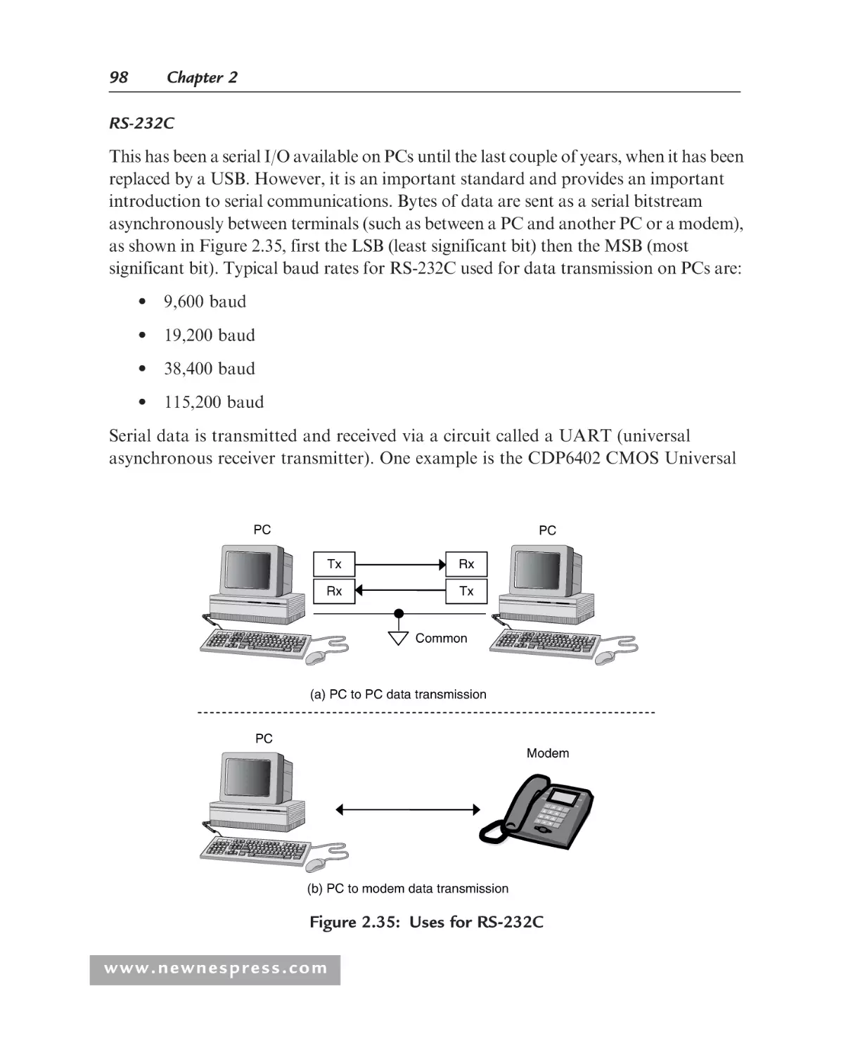
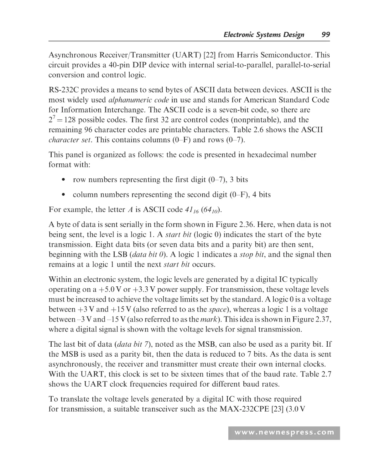
2.14.3 Serial I/O .......................................................................................97
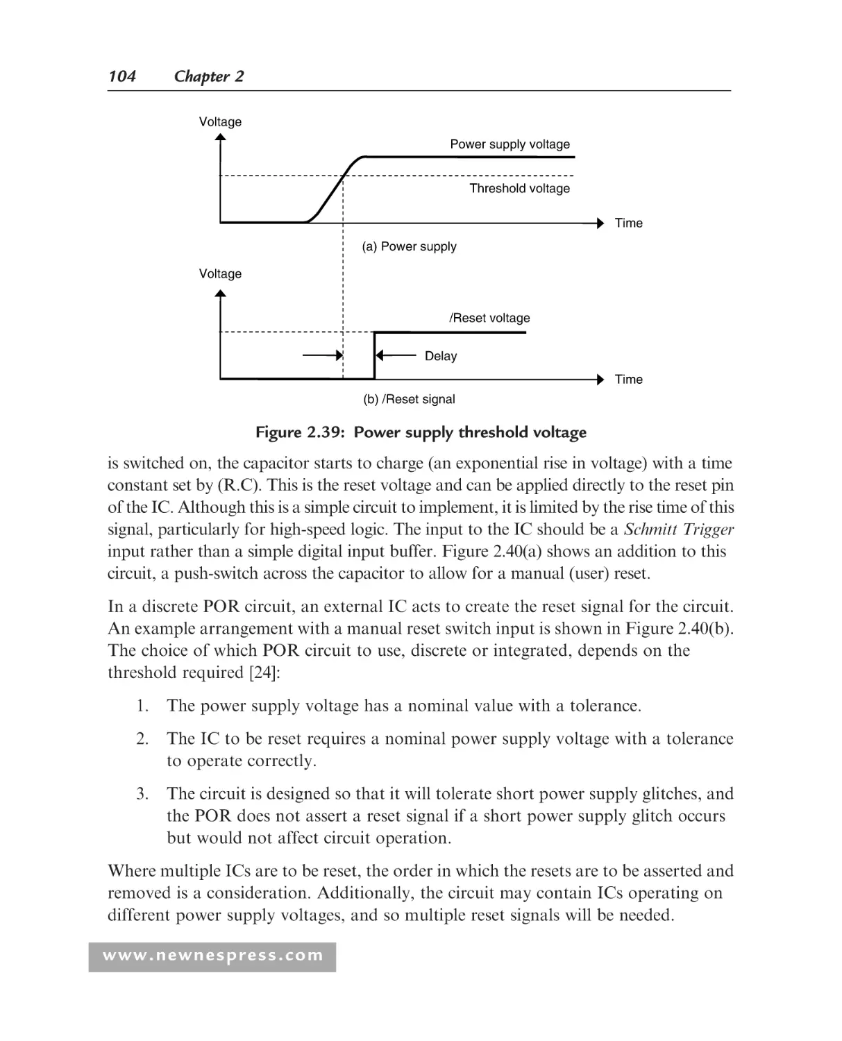
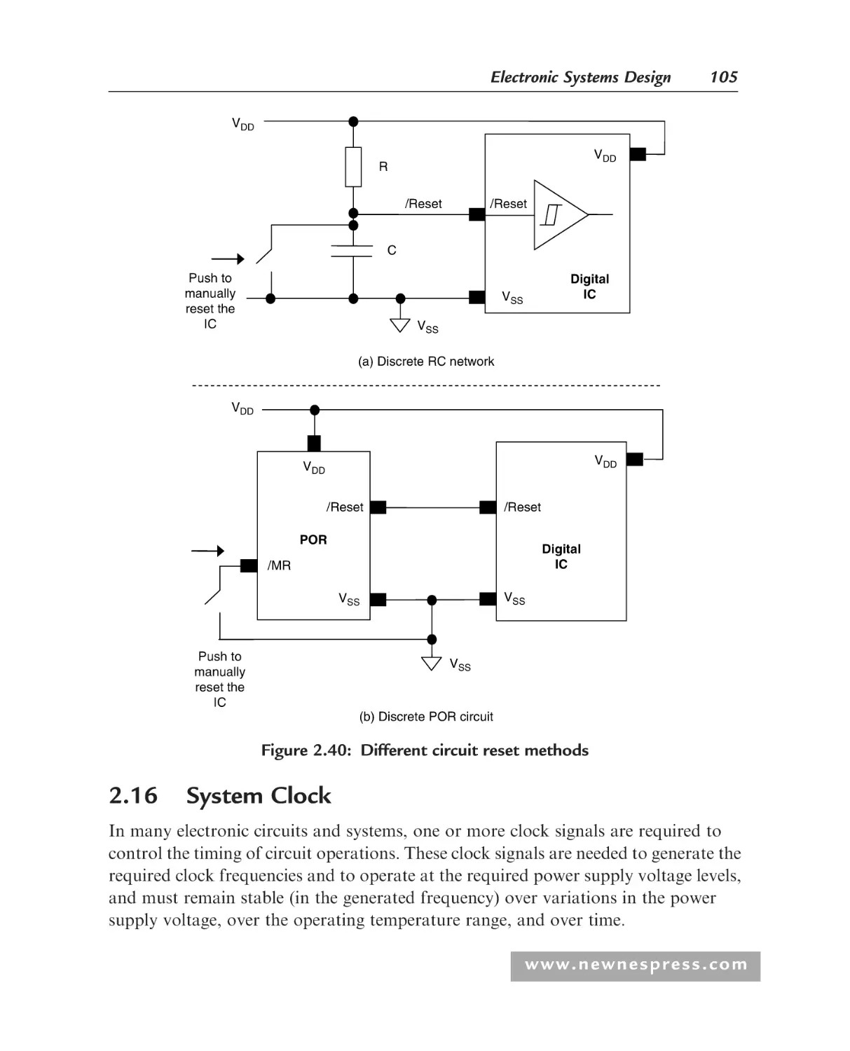
System Reset............................................................................................ 102
System Clock ........................................................................................... 105
Power Supplies ........................................................................................ 107
Power Management................................................................................. 109
Printed Circuit Boards and Multichip Modules ...................................... 110
System on a Chip and System in a Package............................................ 112
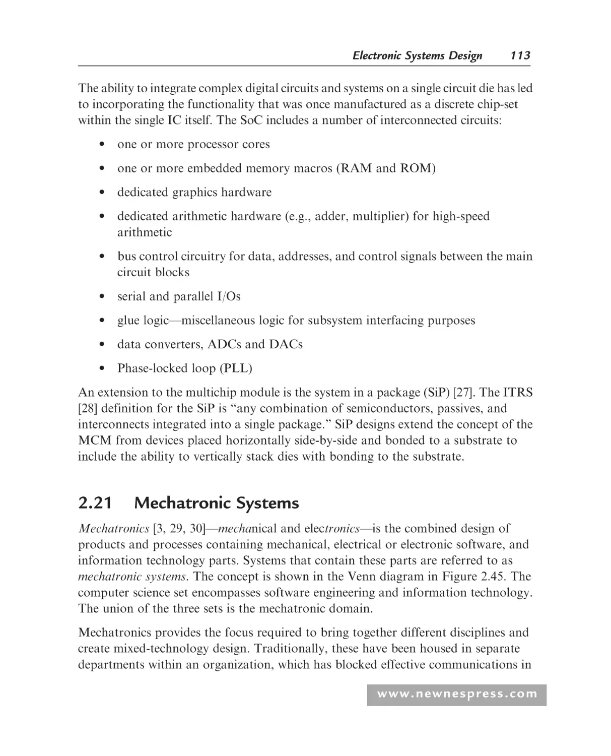
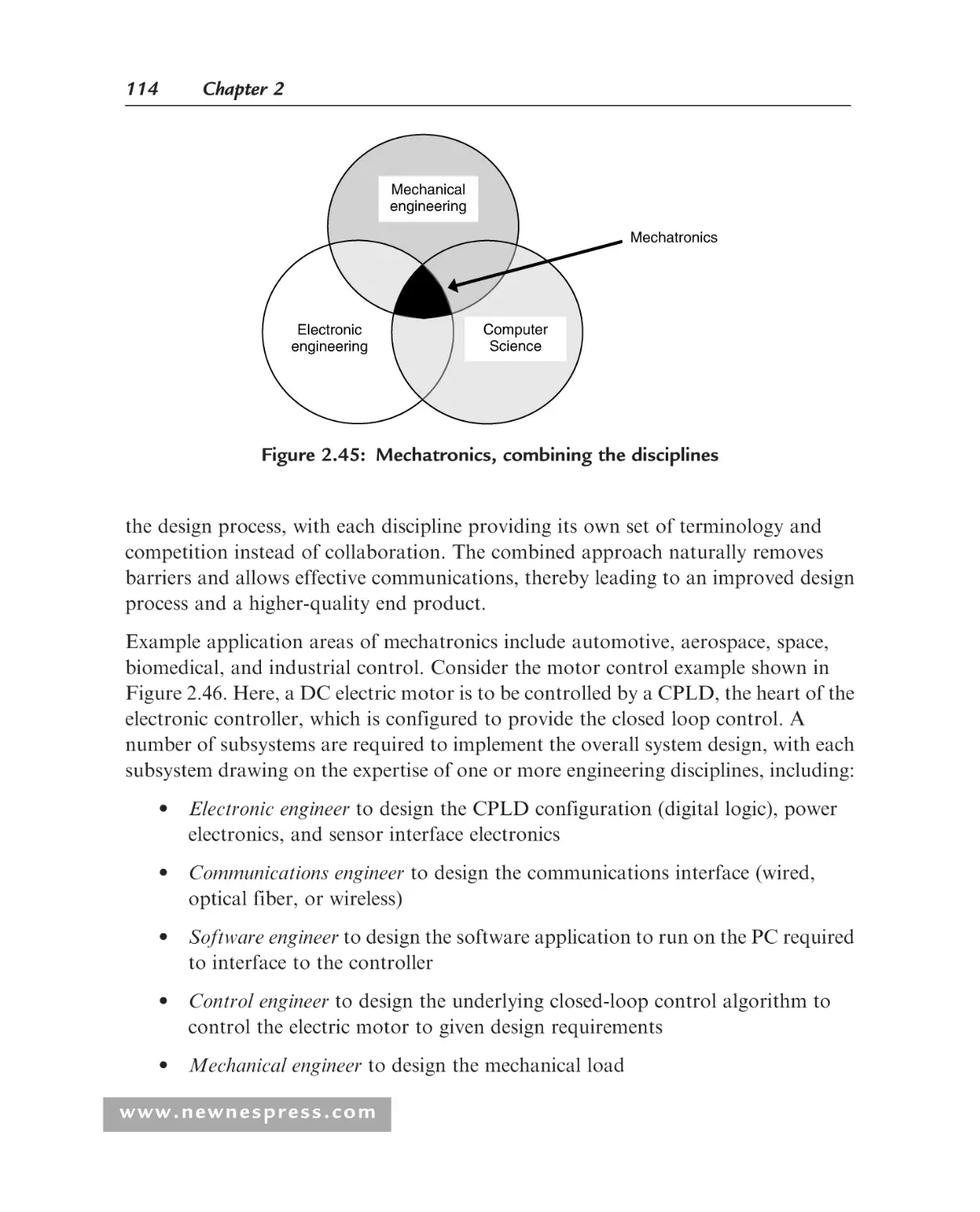
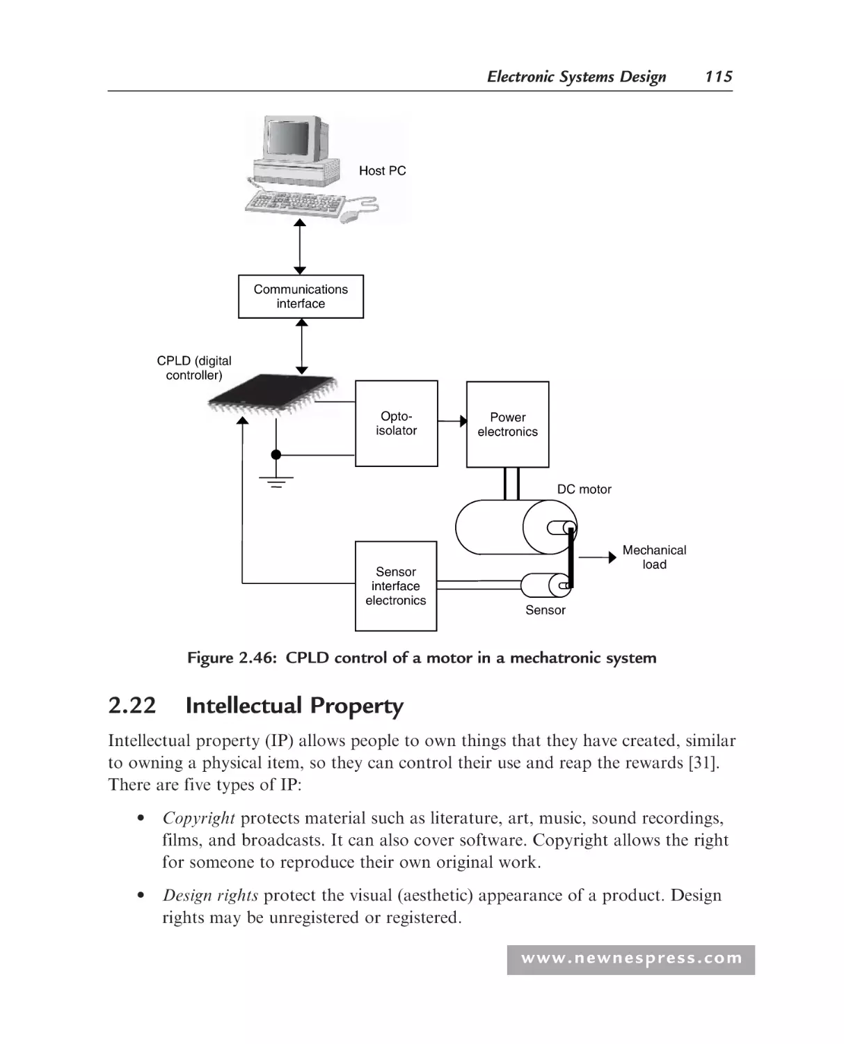
Mechatronic Systems............................................................................... 113
Intellectual Property ................................................................................ 115
CE and FCC Markings ........................................................................... 116
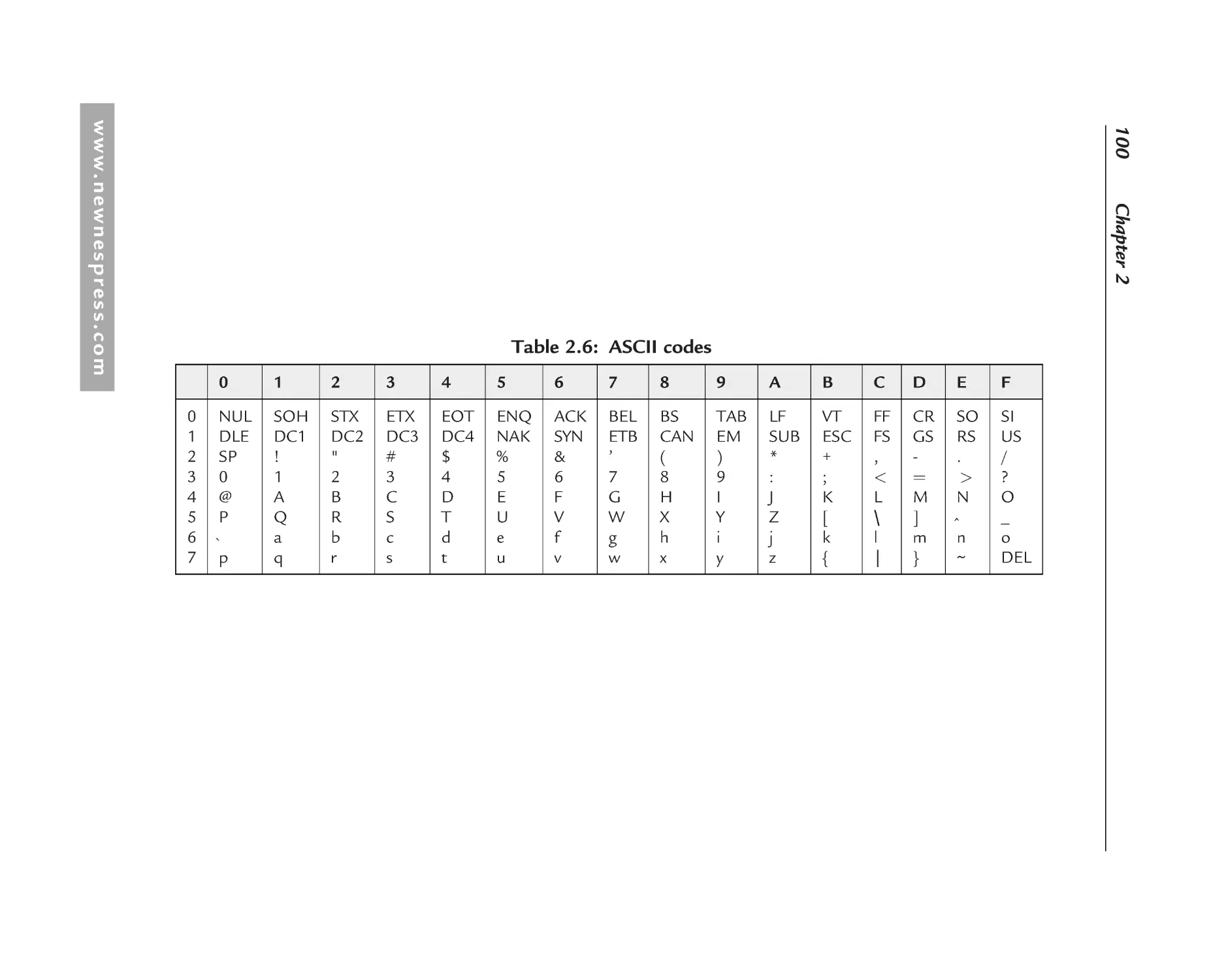
References................................................................................................ 118
Student Exercises ..................................................................................... 121
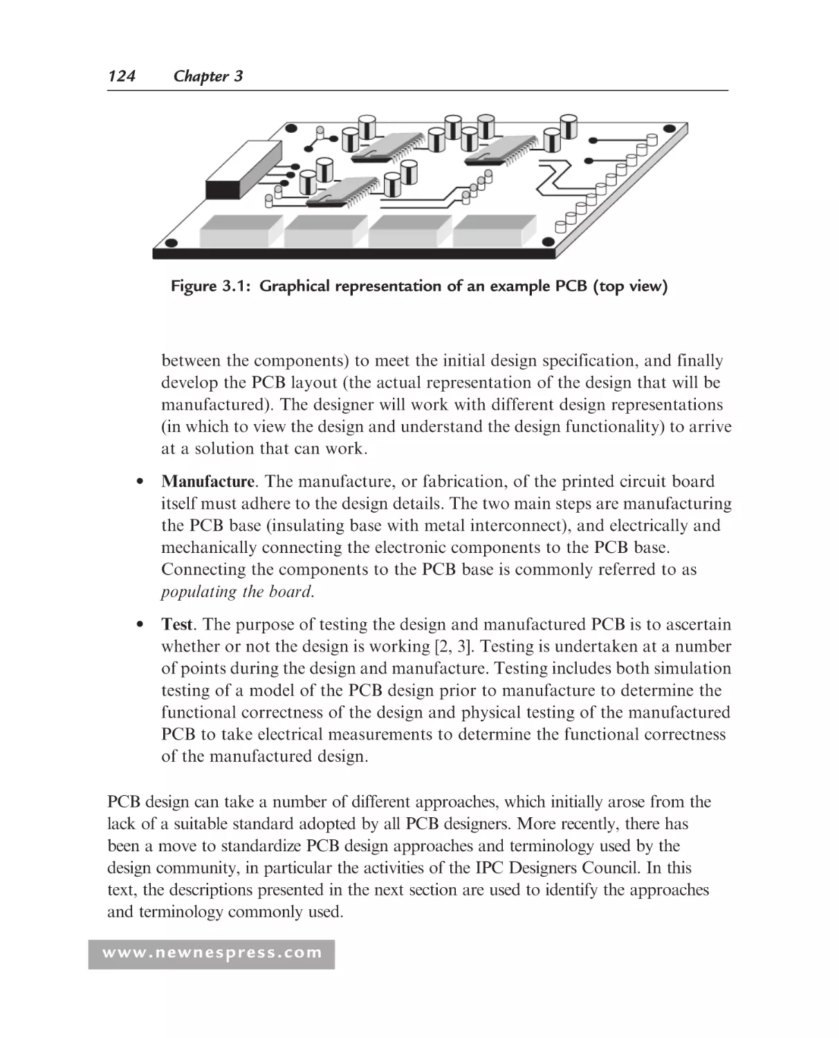
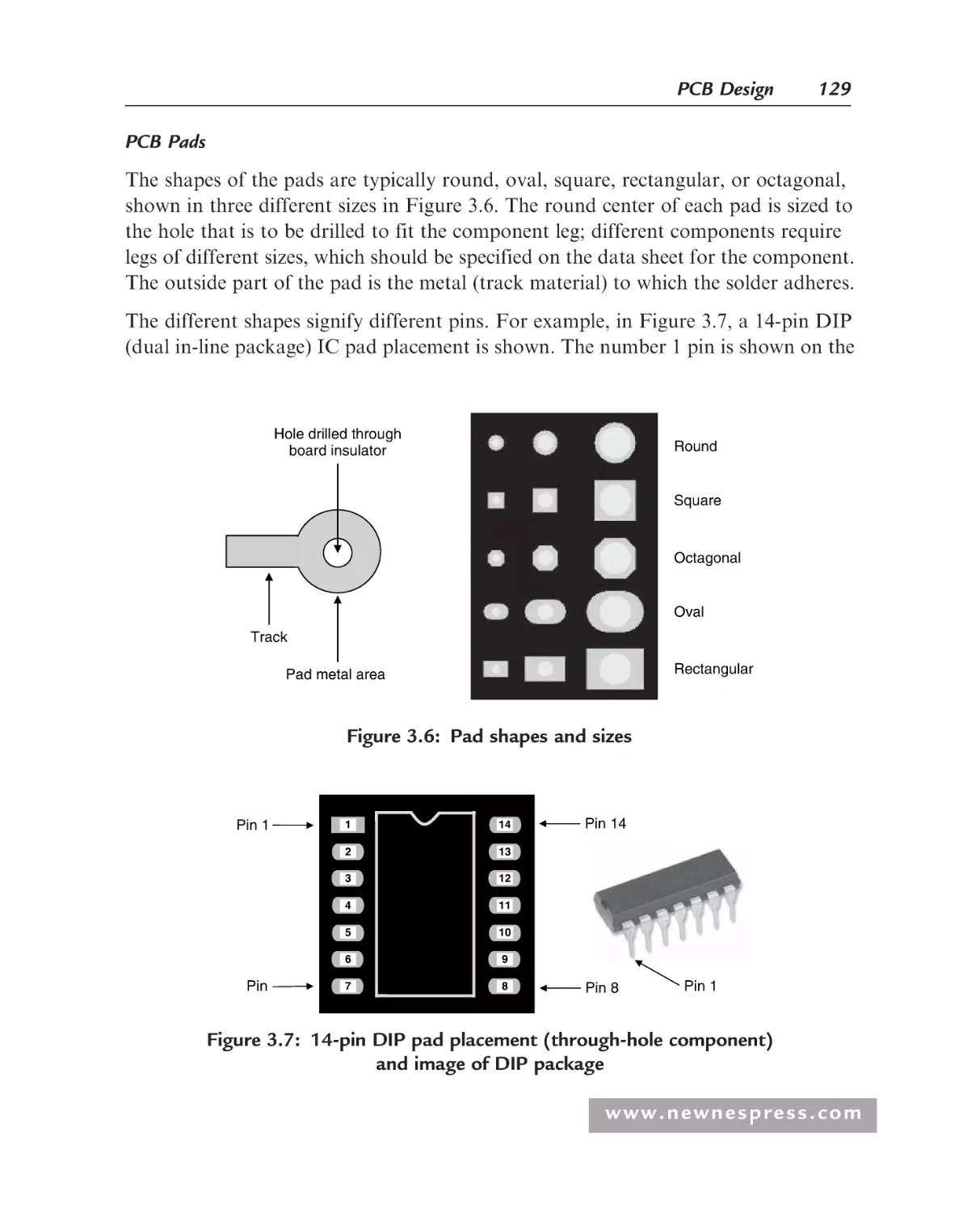
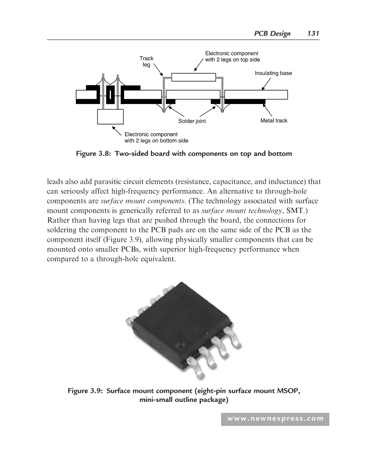
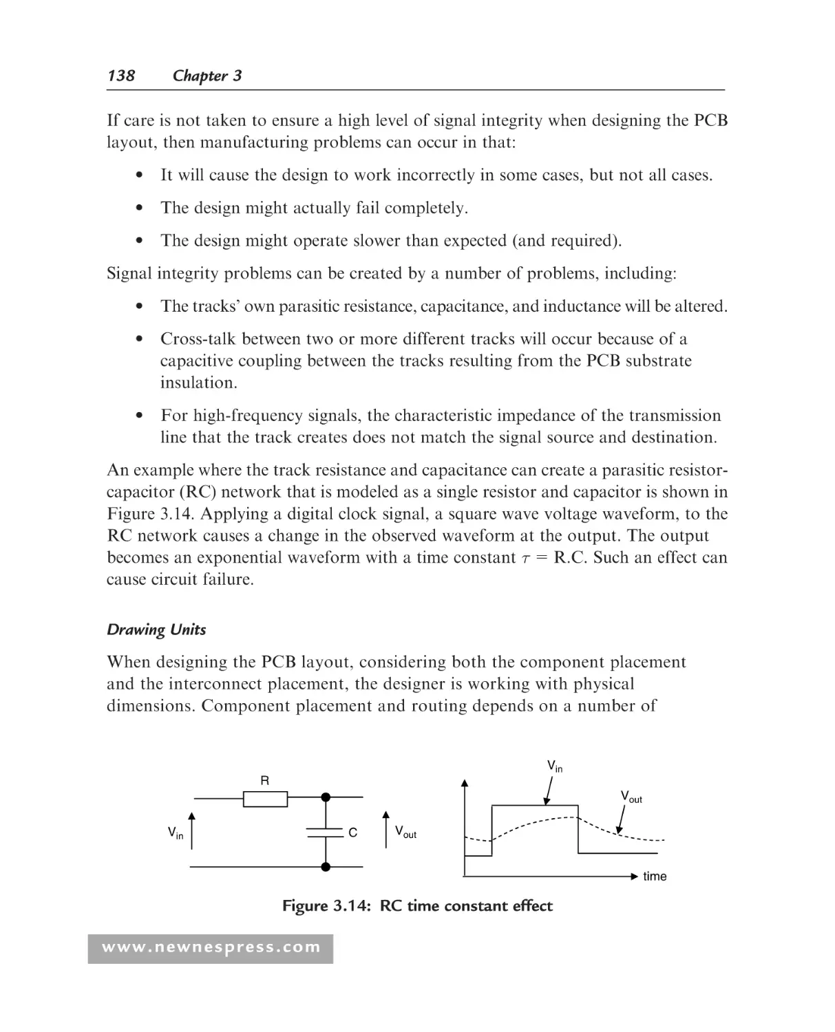
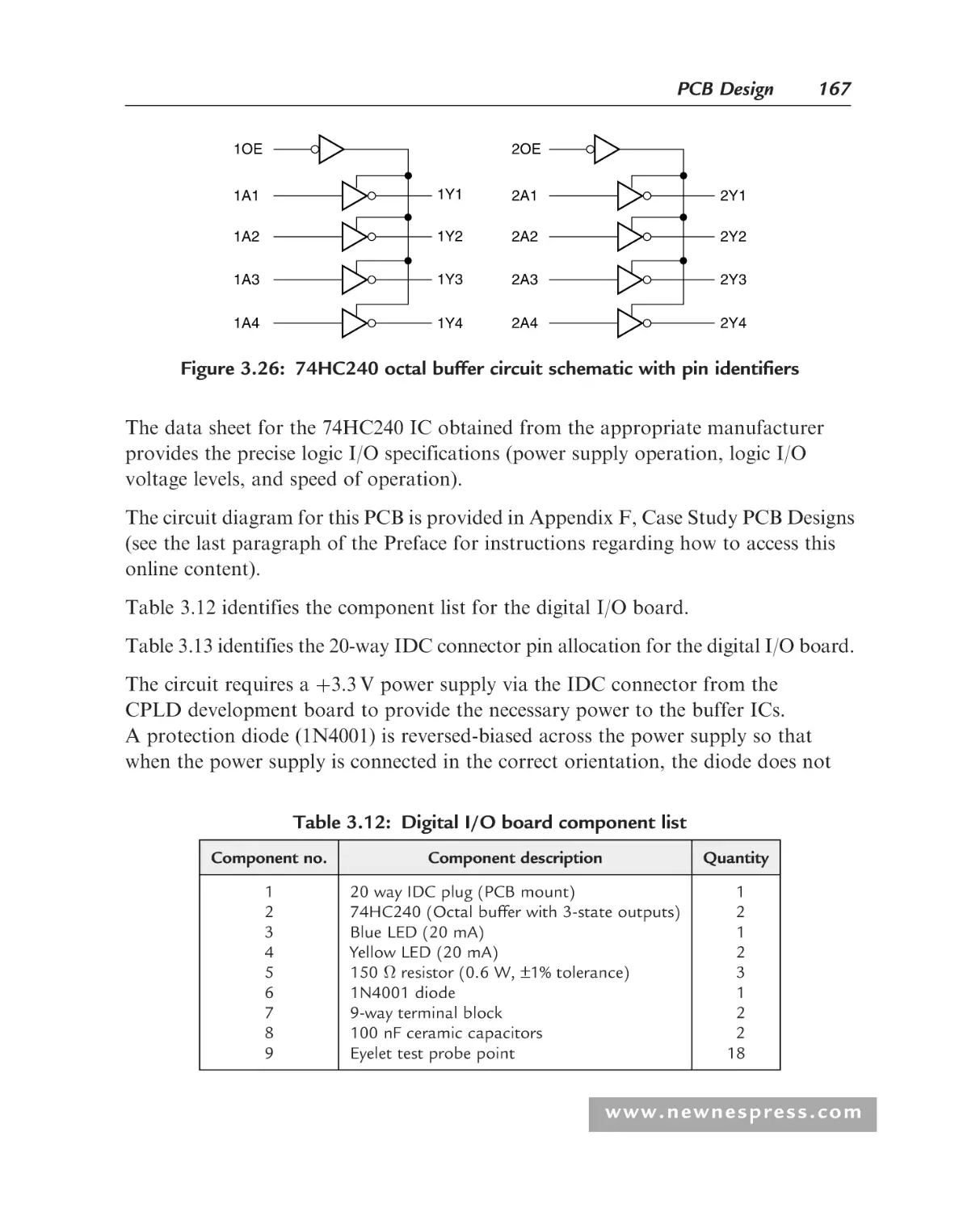
Chapter 3: PCB Design ............................................................................. 123
3.1
3.2
3.3
Introduction ............................................................................................ 123
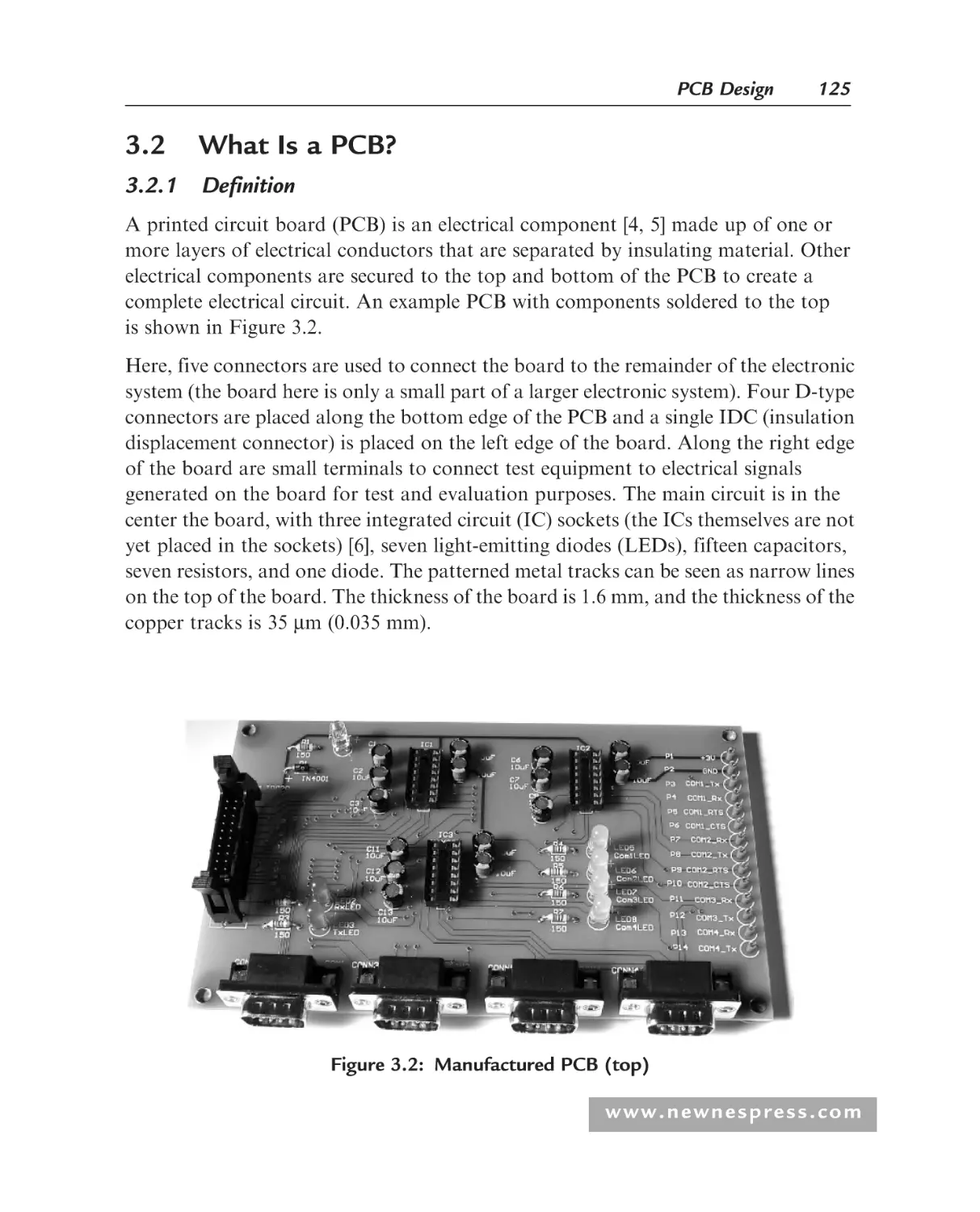
What Is a PCB? ....................................................................................... 125
3.2.1 Definition ...................................................................................... 125
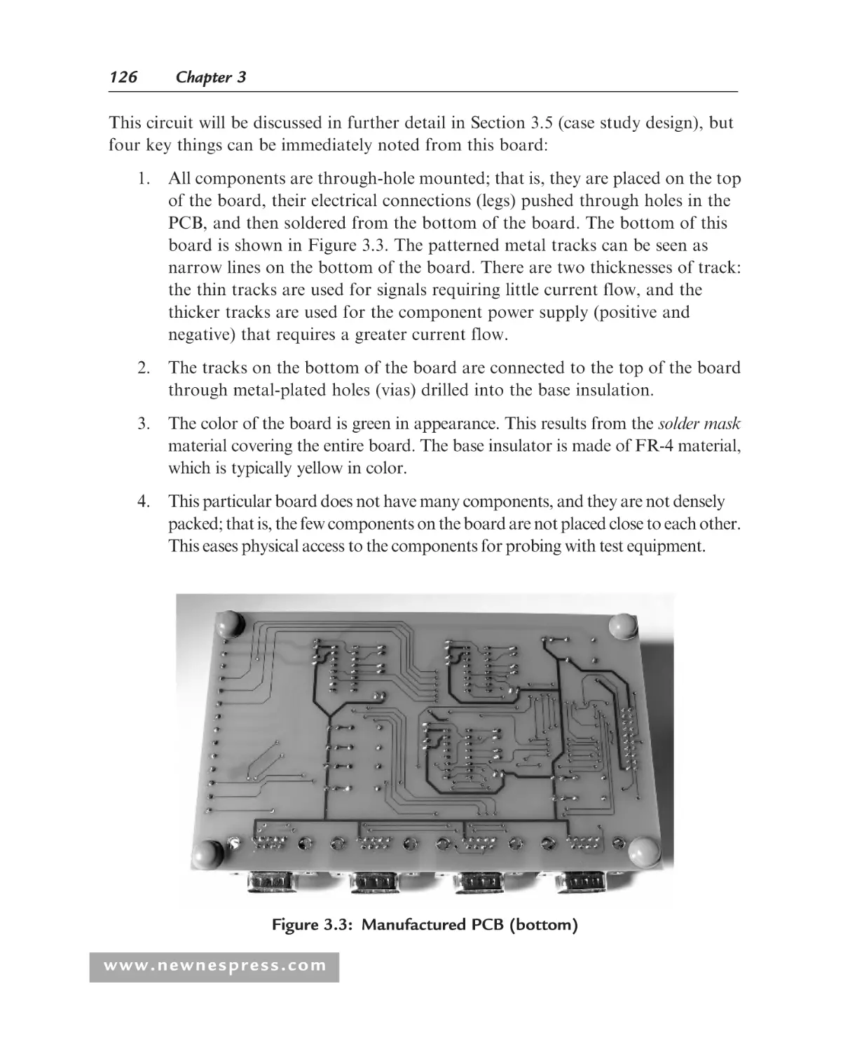
3.2.2 Structure of the PCB ..................................................................... 127
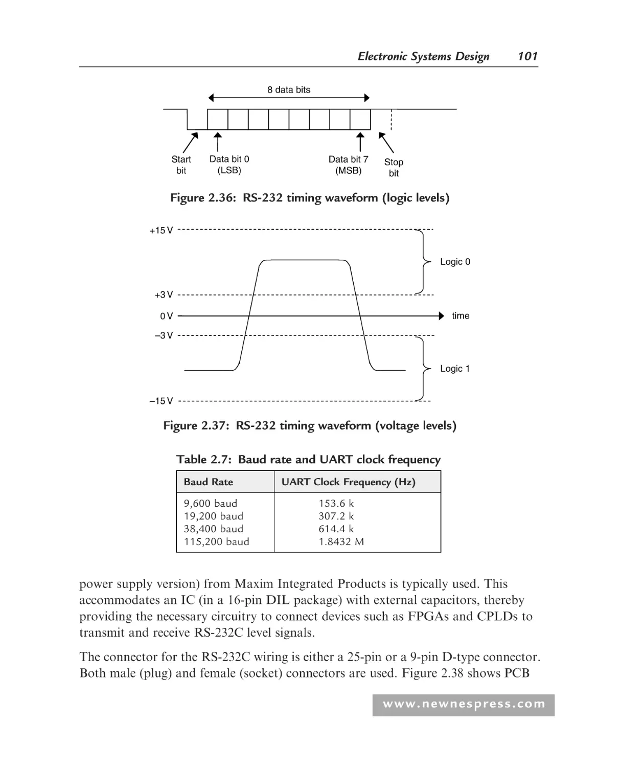
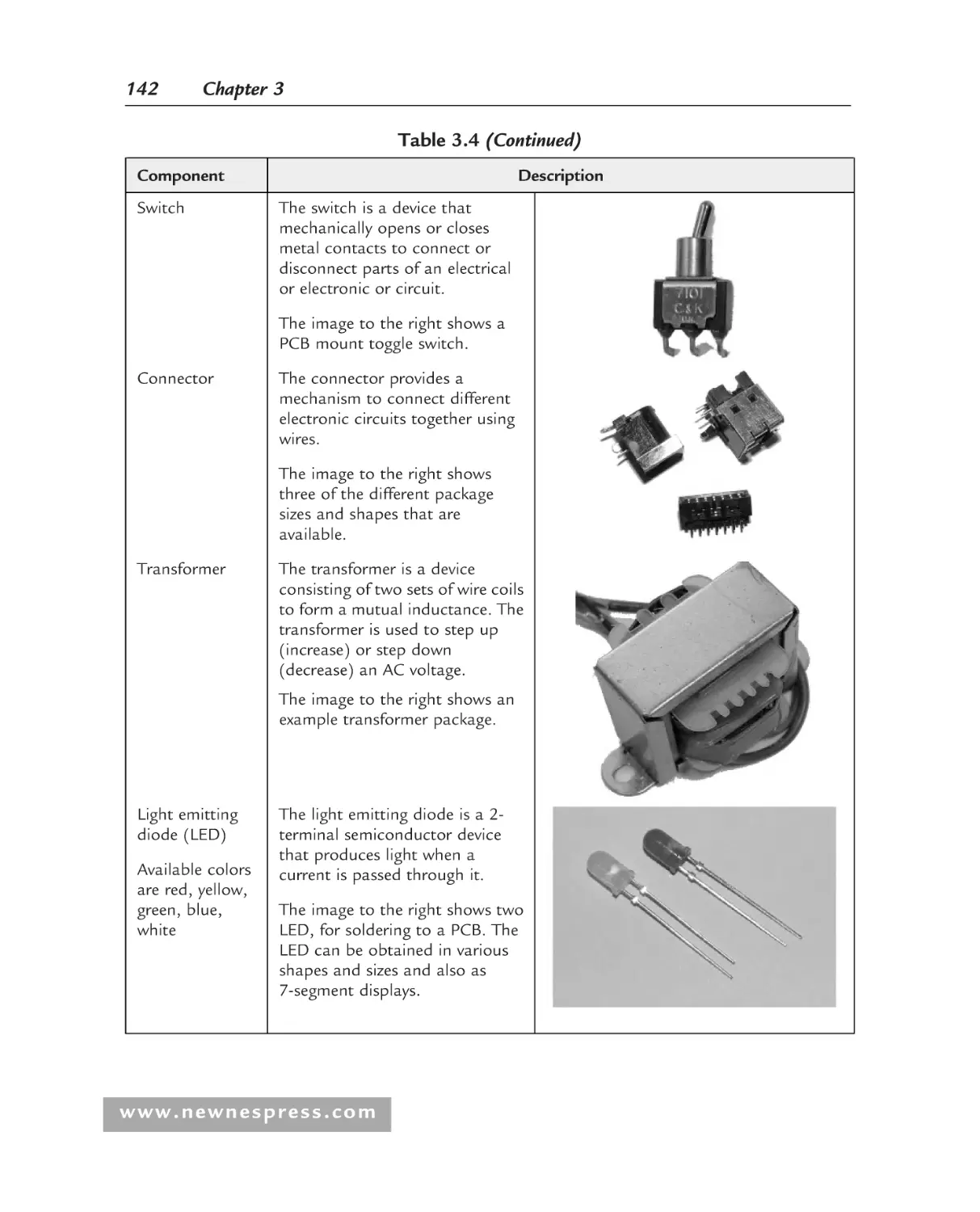
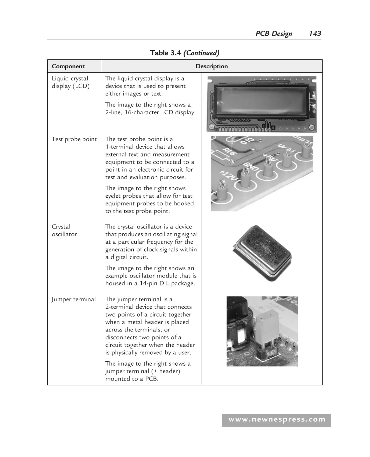
3.2.3 Typical Components...................................................................... 139
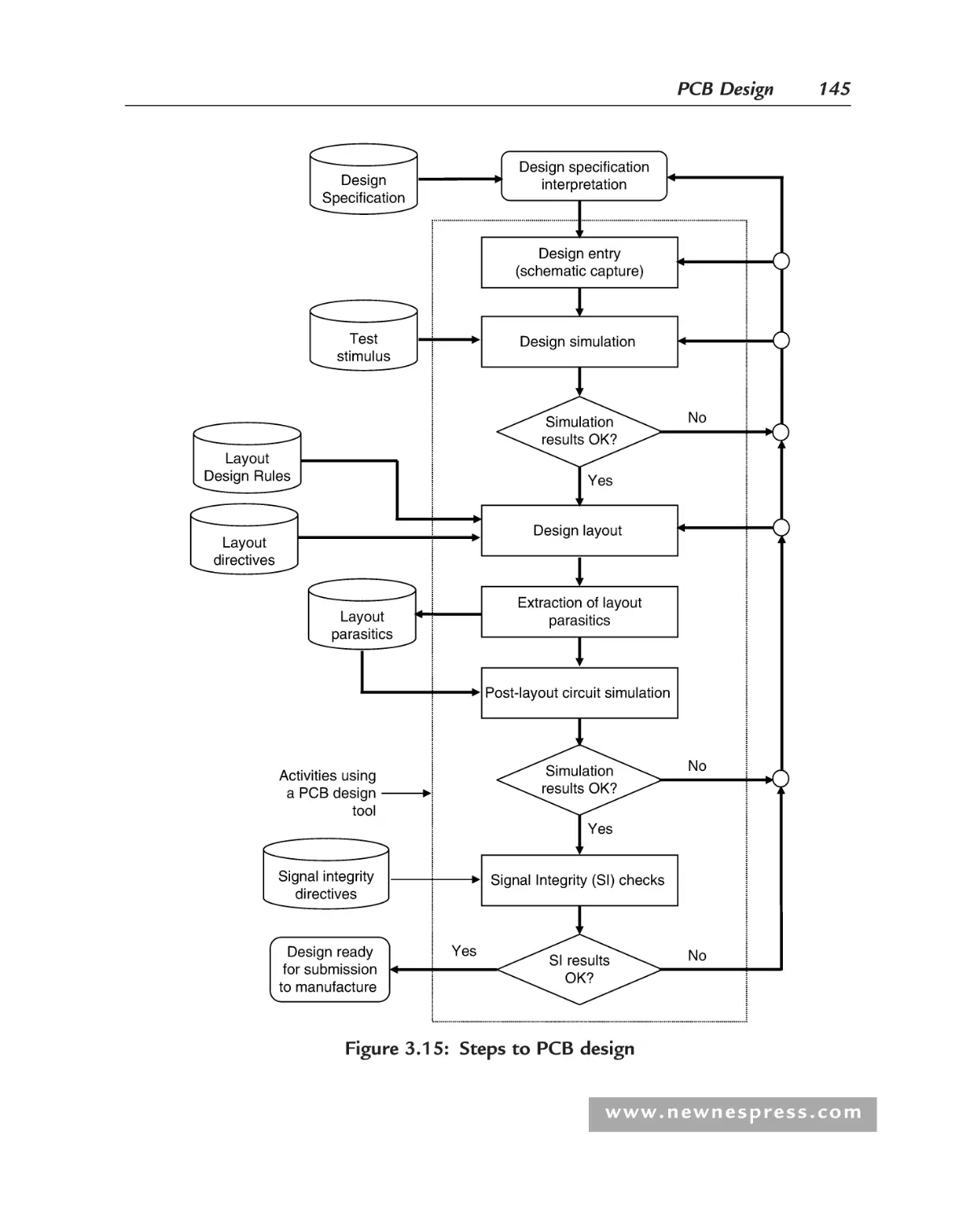
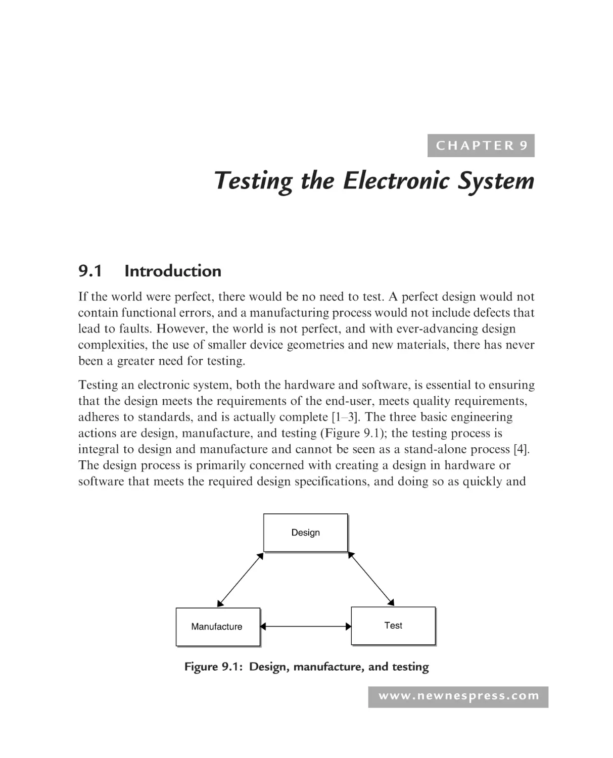
Design, Manufacture, and Testing .......................................................... 144
3.3.1 PCB Design ................................................................................... 144
www.newnespress.com
Table of Contents
3.4
3.5
3.6
ix
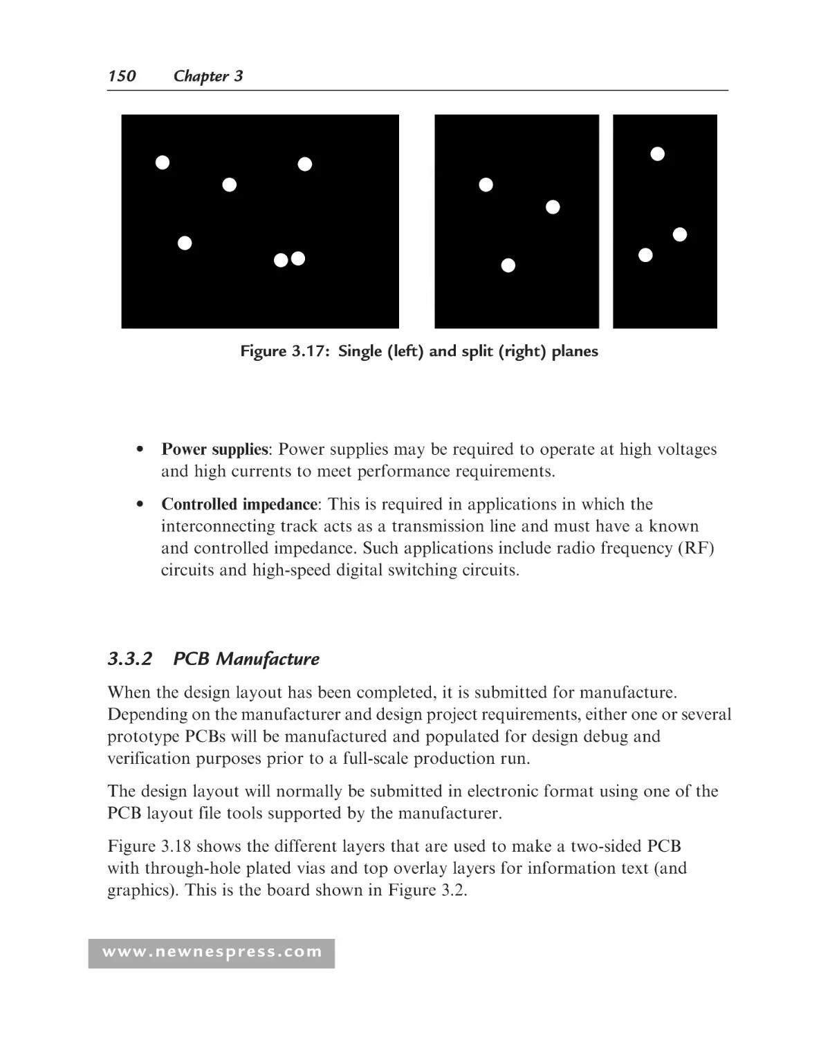
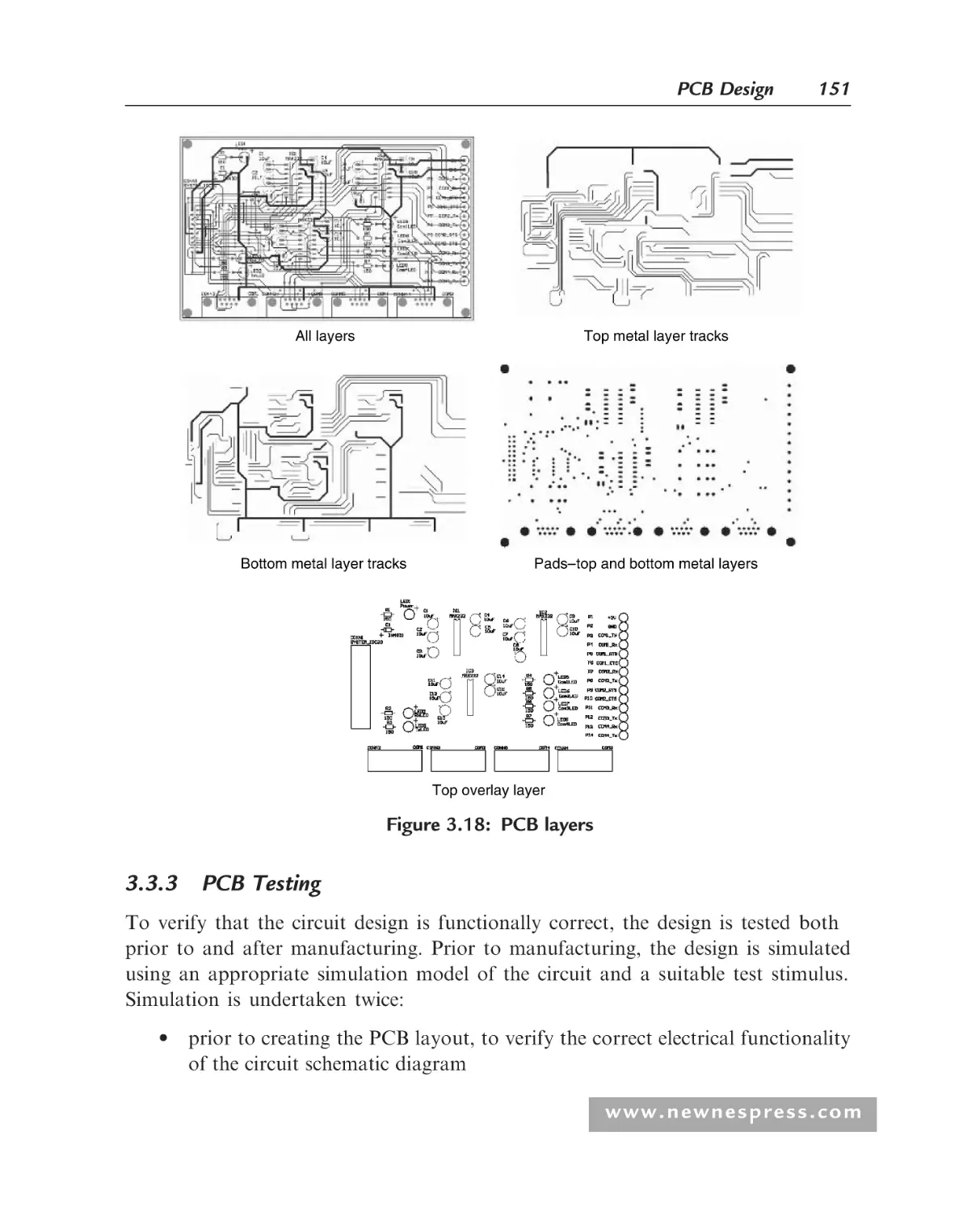
3.3.2 PCB Manufacture.......................................................................... 150
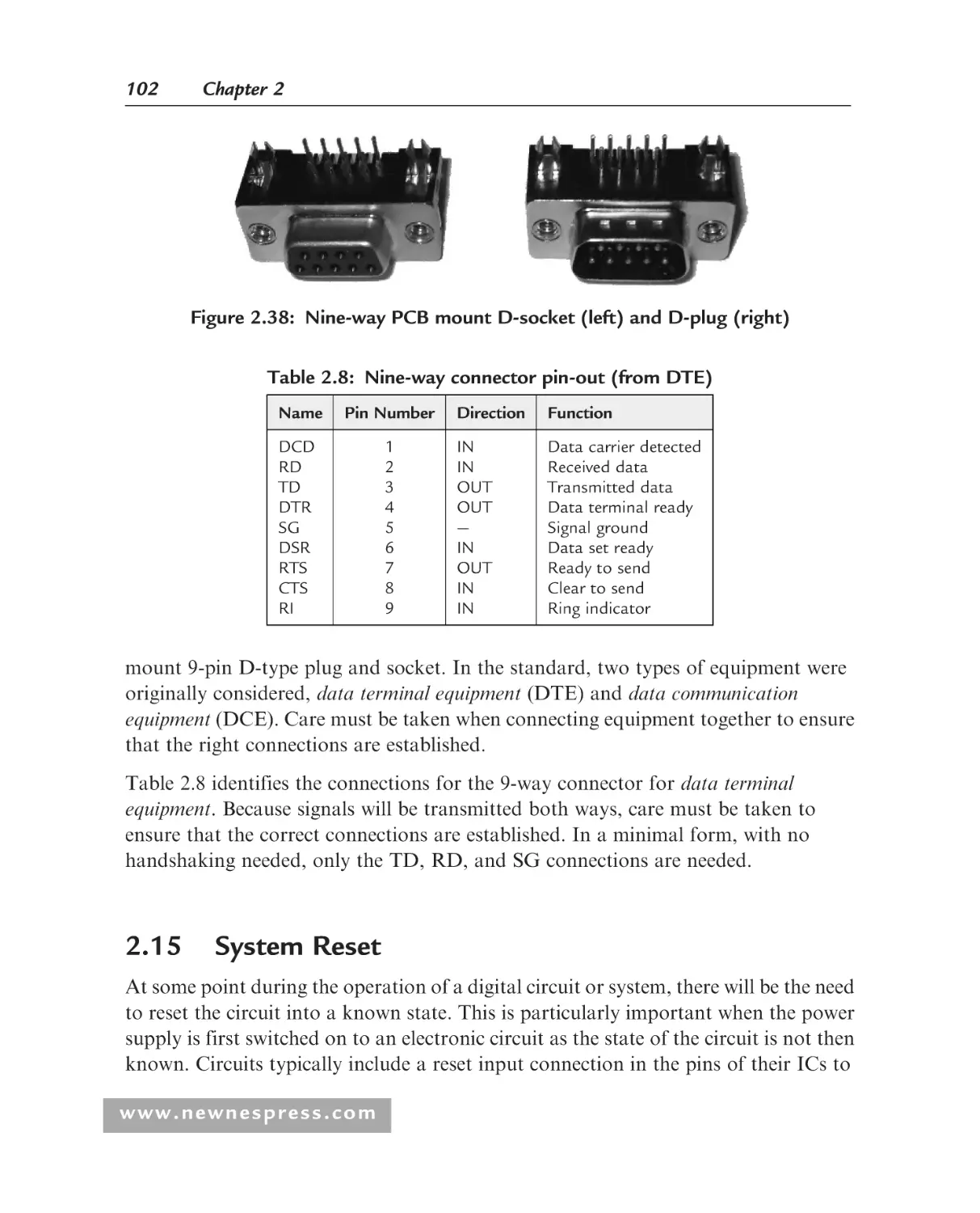
3.3.3 PCB Testing................................................................................... 151
Environmental Issues .............................................................................. 152
3.4.1 Introduction .................................................................................. 152
3.4.2 WEEE Directive ............................................................................ 153
3.4.3 RoHS Directive ............................................................................. 153
3.4.4 Lead-Free Solder ........................................................................... 154
3.4.5 Electromagnetic Compatibility ...................................................... 154
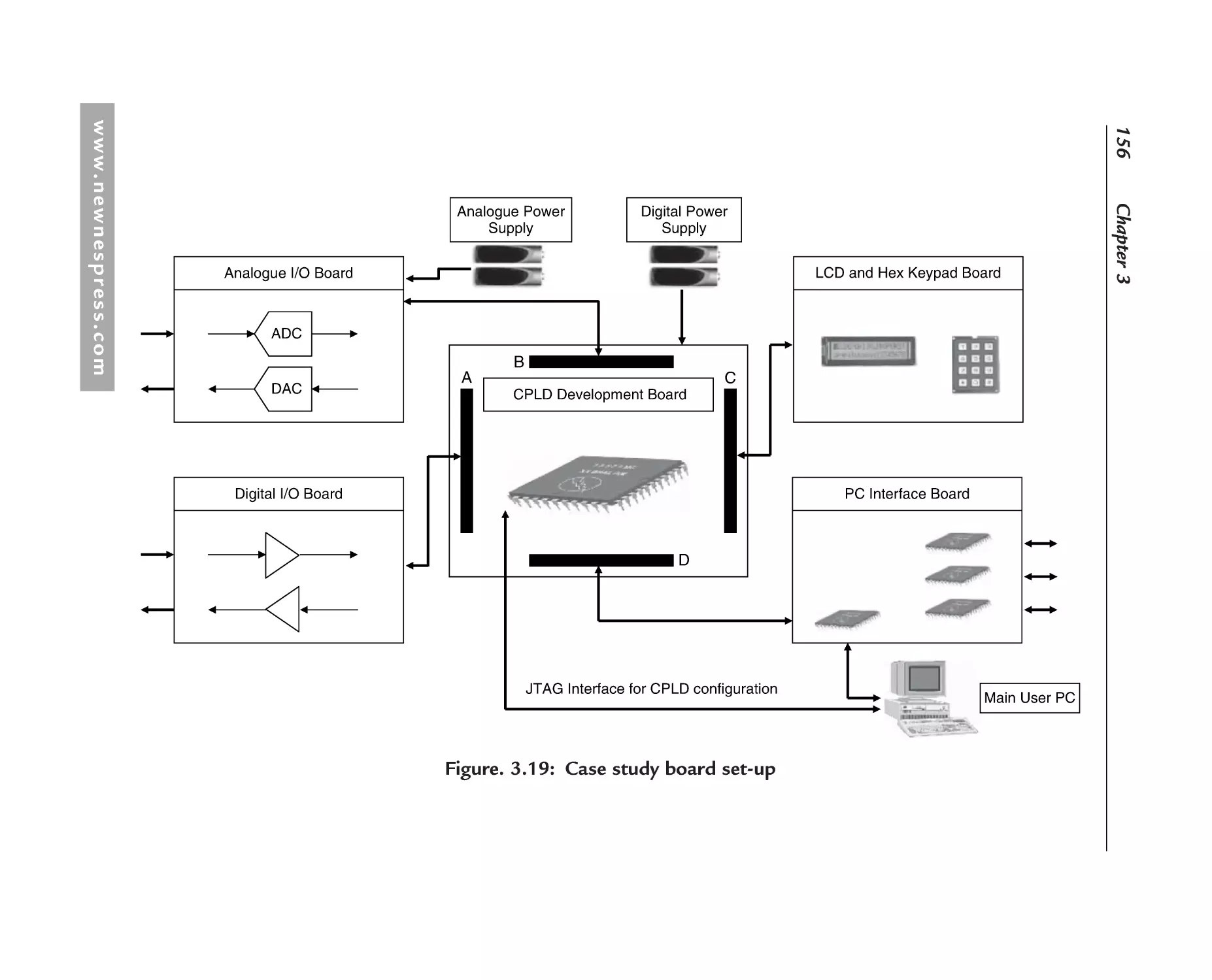
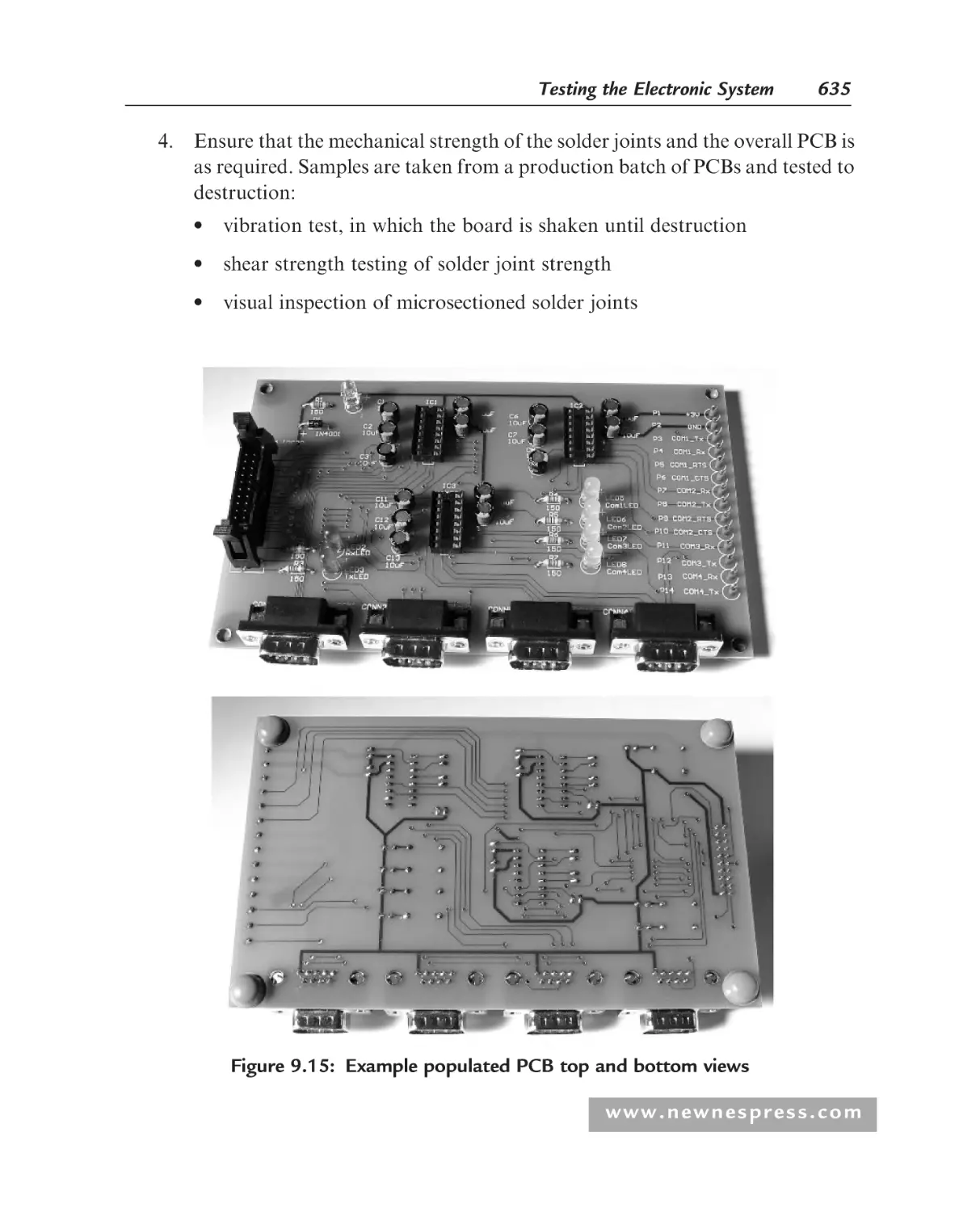
Case Study PCB Designs......................................................................... 155
3.5.1 Introduction .................................................................................. 155
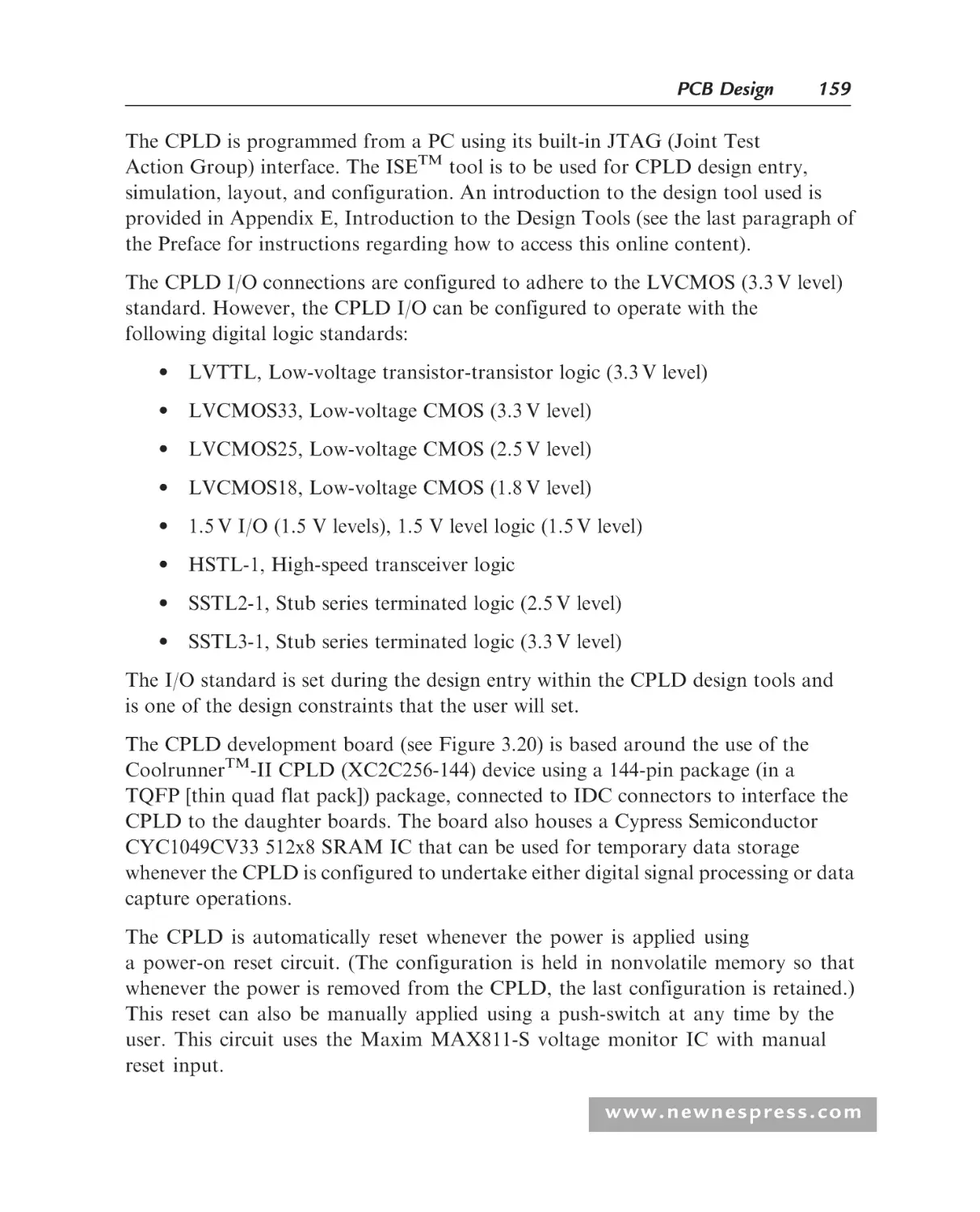
3.5.2 System Overview ........................................................................... 157
3.5.3 CPLD Development Board ........................................................... 158
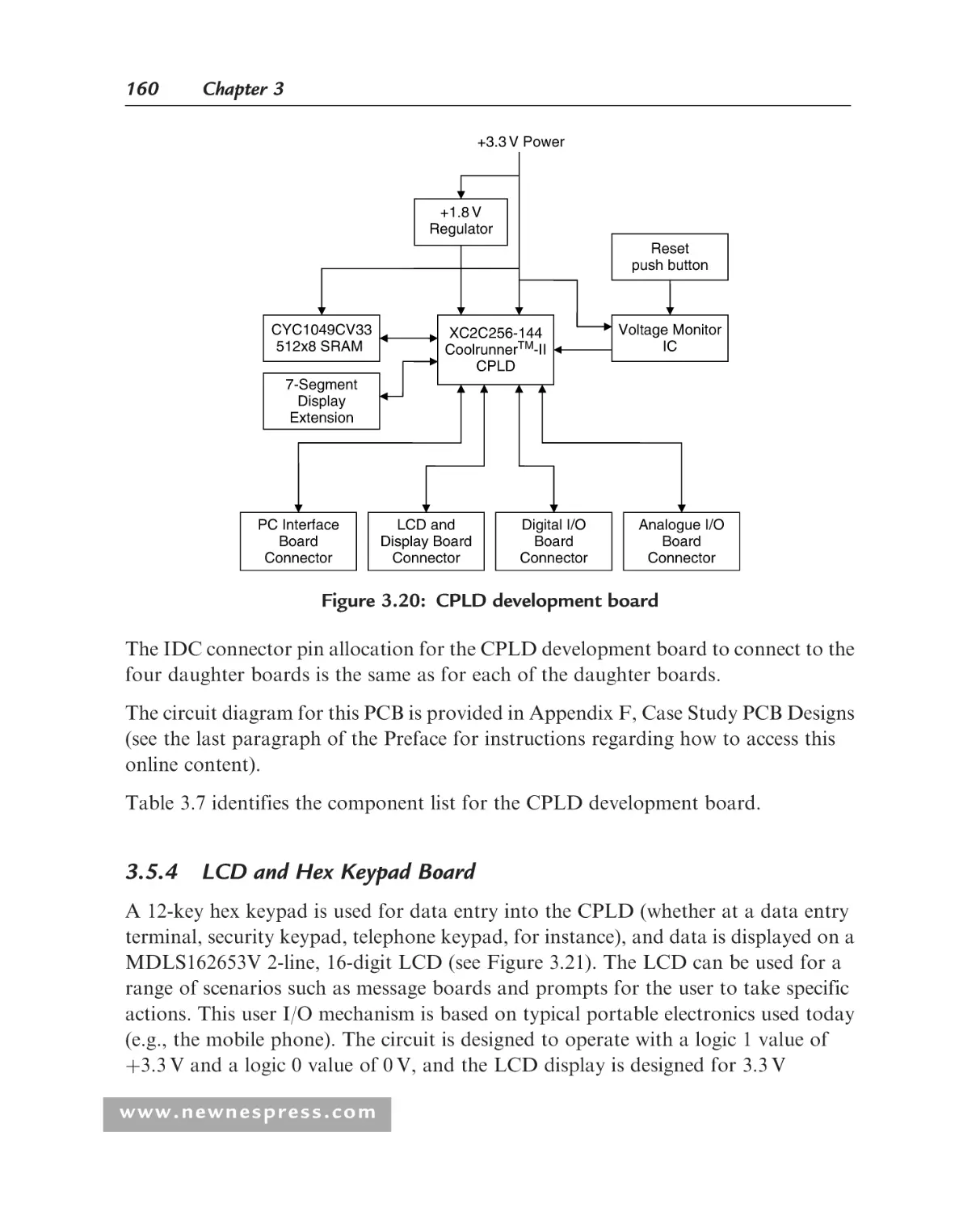
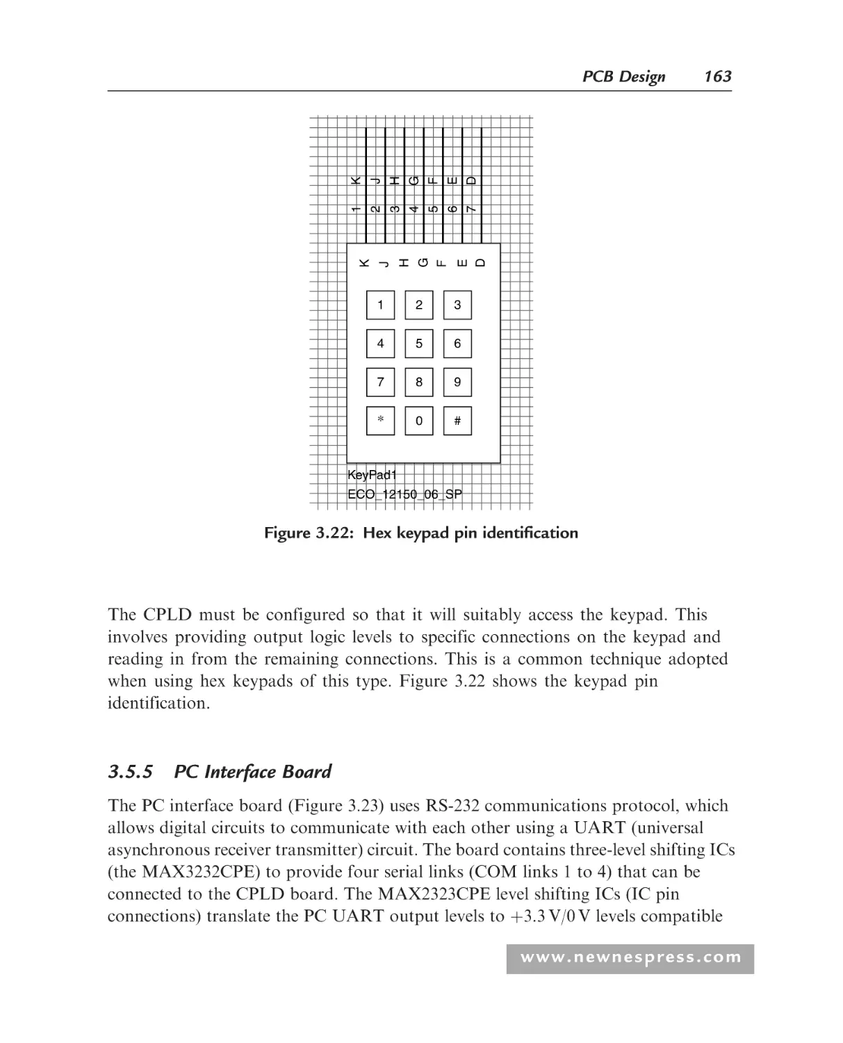
3.5.4 LCD and Hex Keypad Board ....................................................... 160
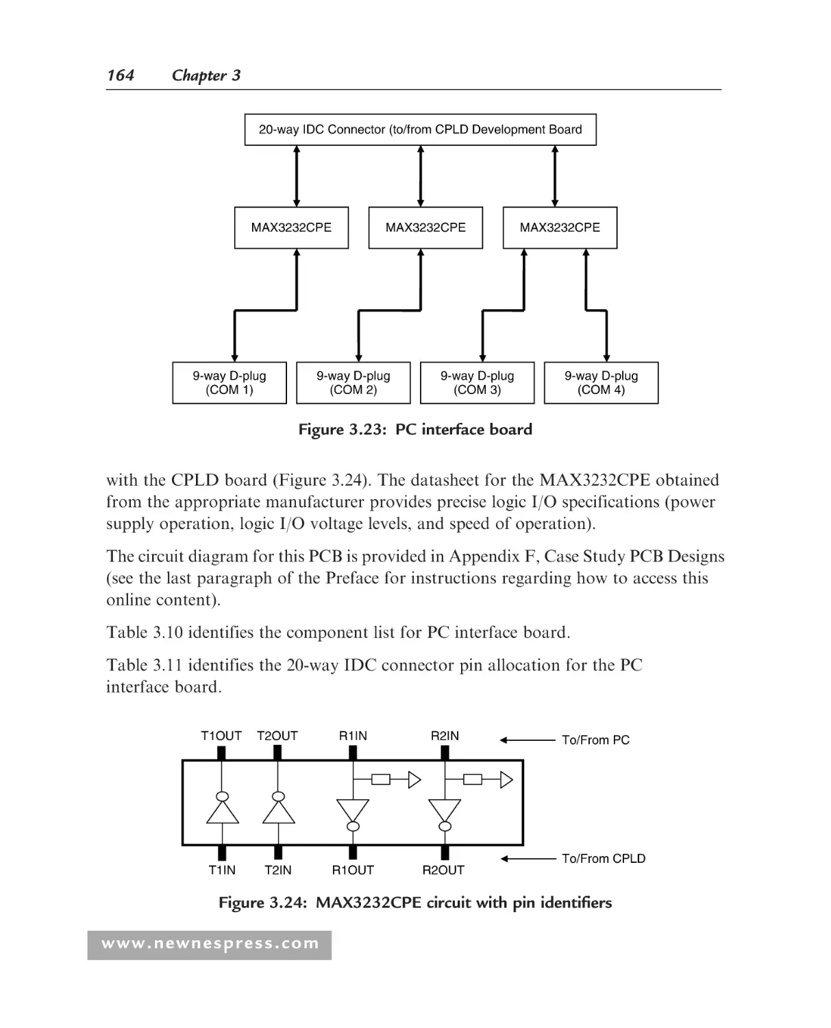
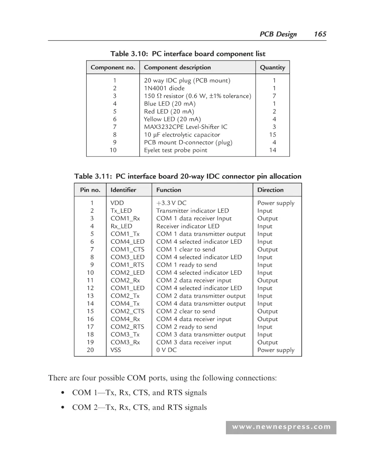
3.5.5 PC Interface Board........................................................................ 163
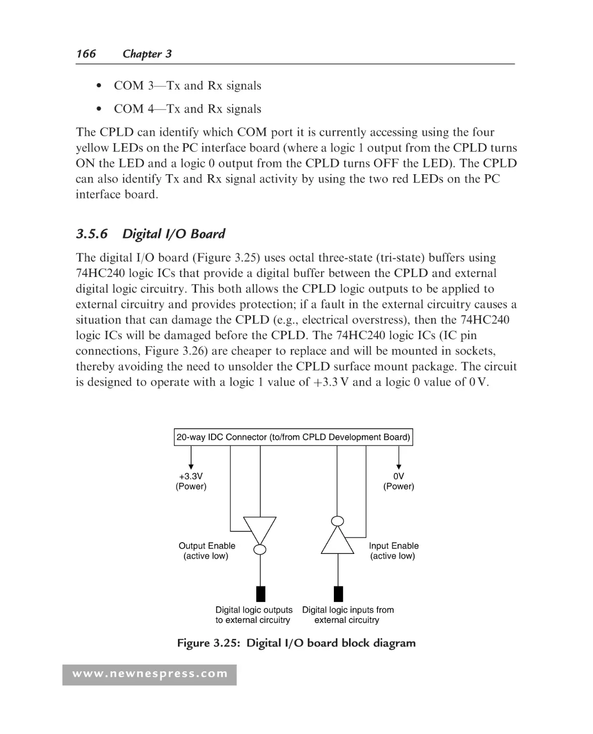
3.5.6 Digital I/O Board .......................................................................... 166
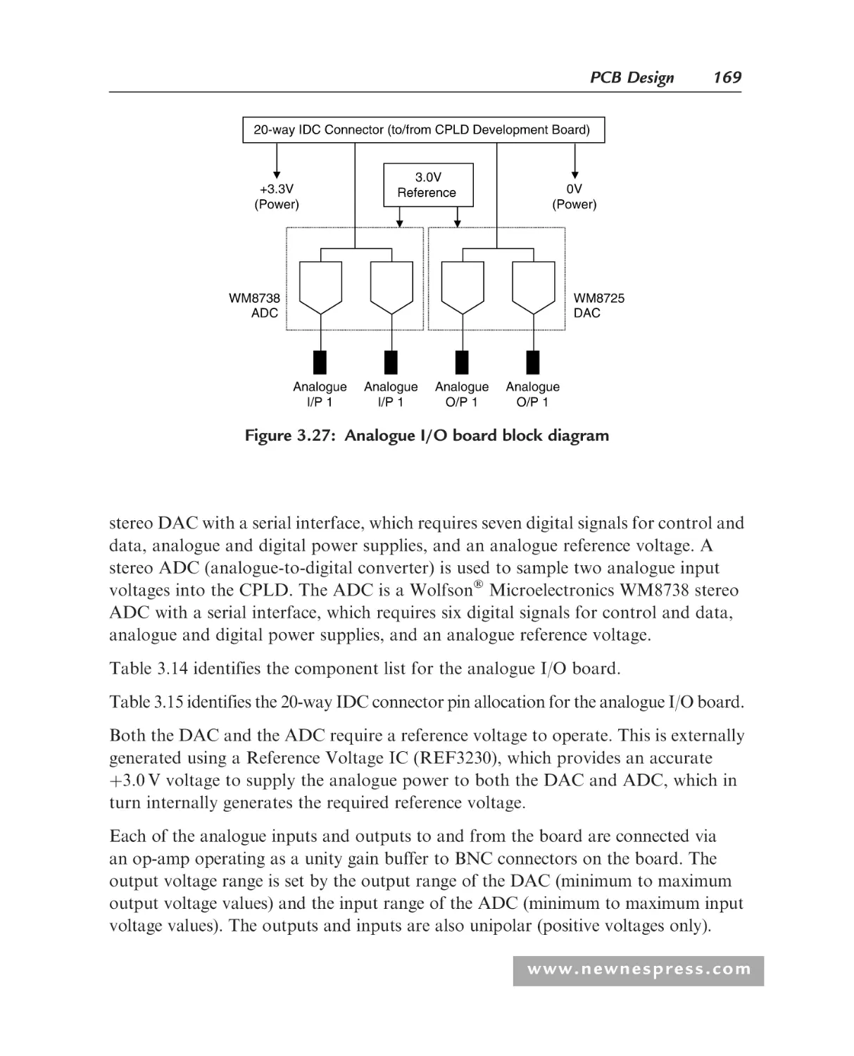
3.5.7 Analogue I/O Board...................................................................... 168
Technology Trends.................................................................................. 171
References ............................................................................................... 173
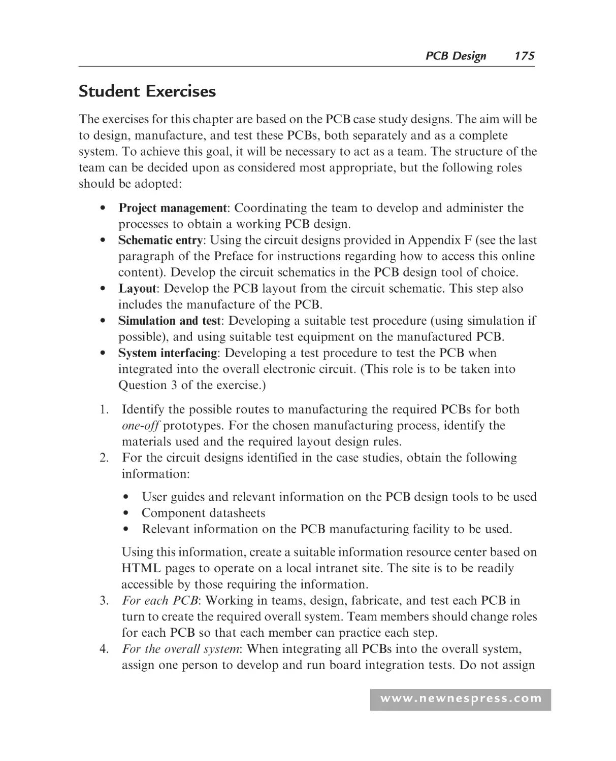
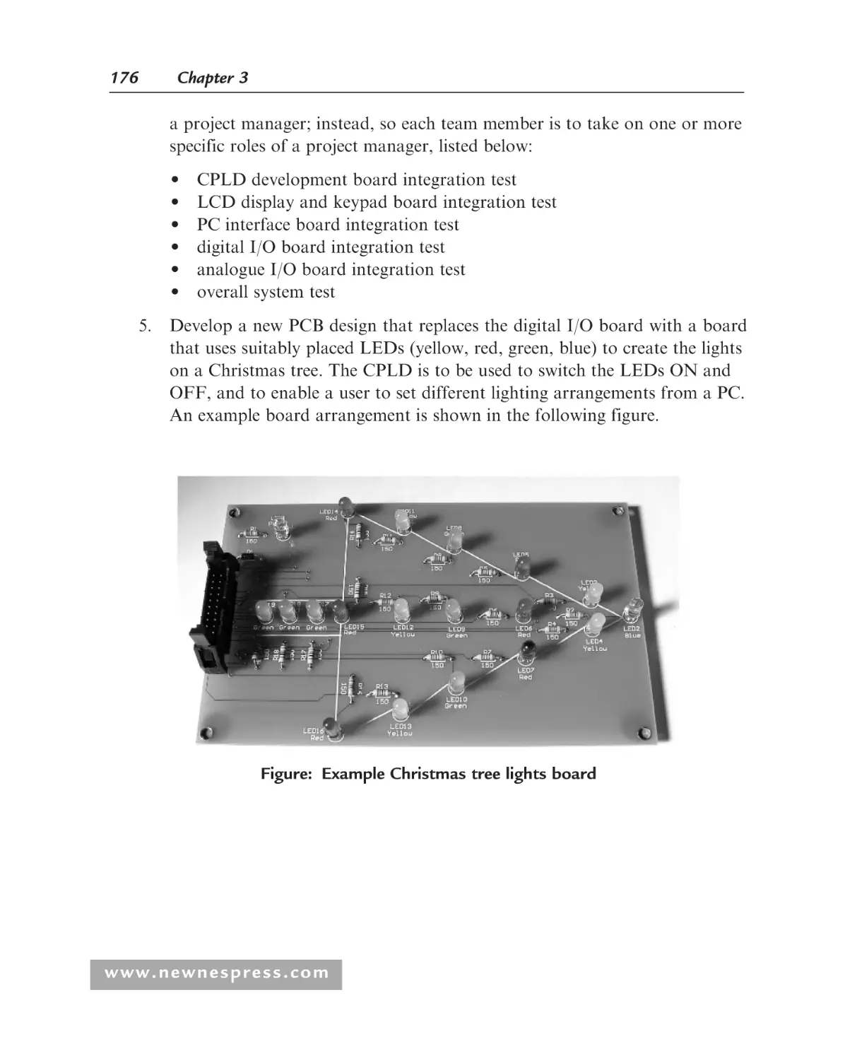
Student Exercises .................................................................................... 175
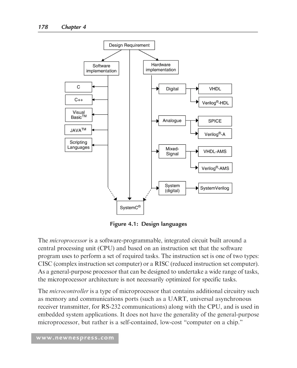
Chapter 4: Design Languages..................................................................... 177
4.1
4.2
4.3
4.4
4.5
4.6
4.7
Introduction ............................................................................................ 177
Software Programming Languages ......................................................... 177
4.2.1 Introduction .................................................................................. 177
4.2.2 C .................................................................................................... 179
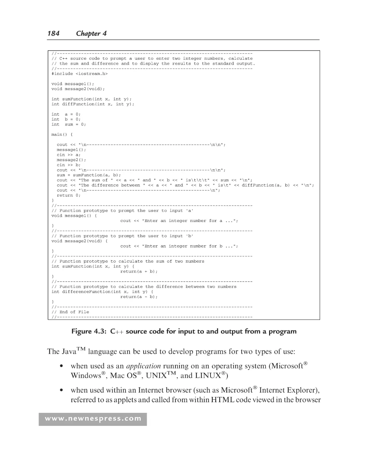
4.2.3 Cþþ .............................................................................................. 181
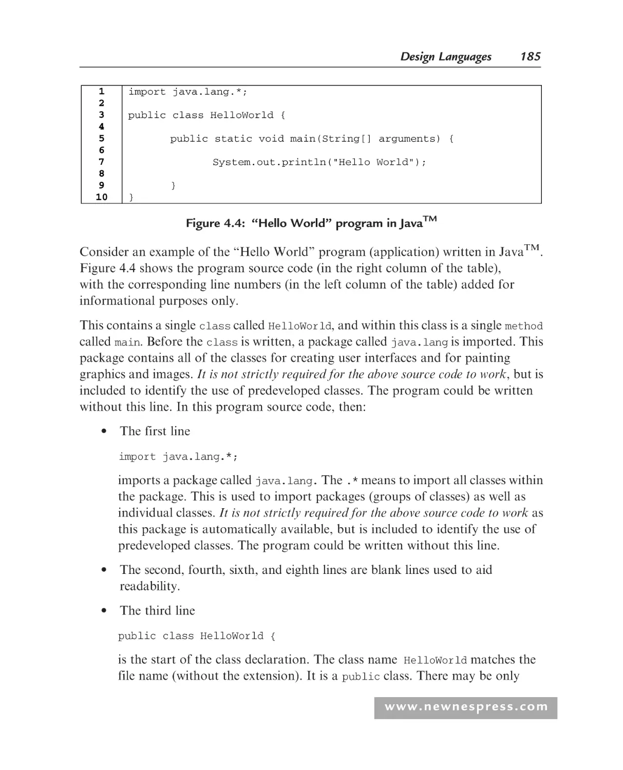
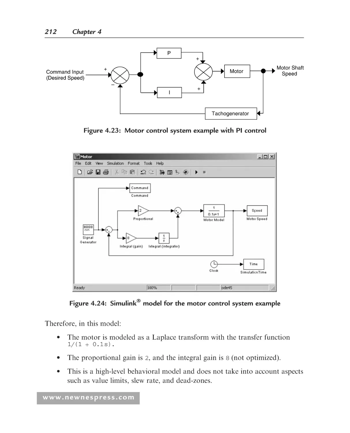
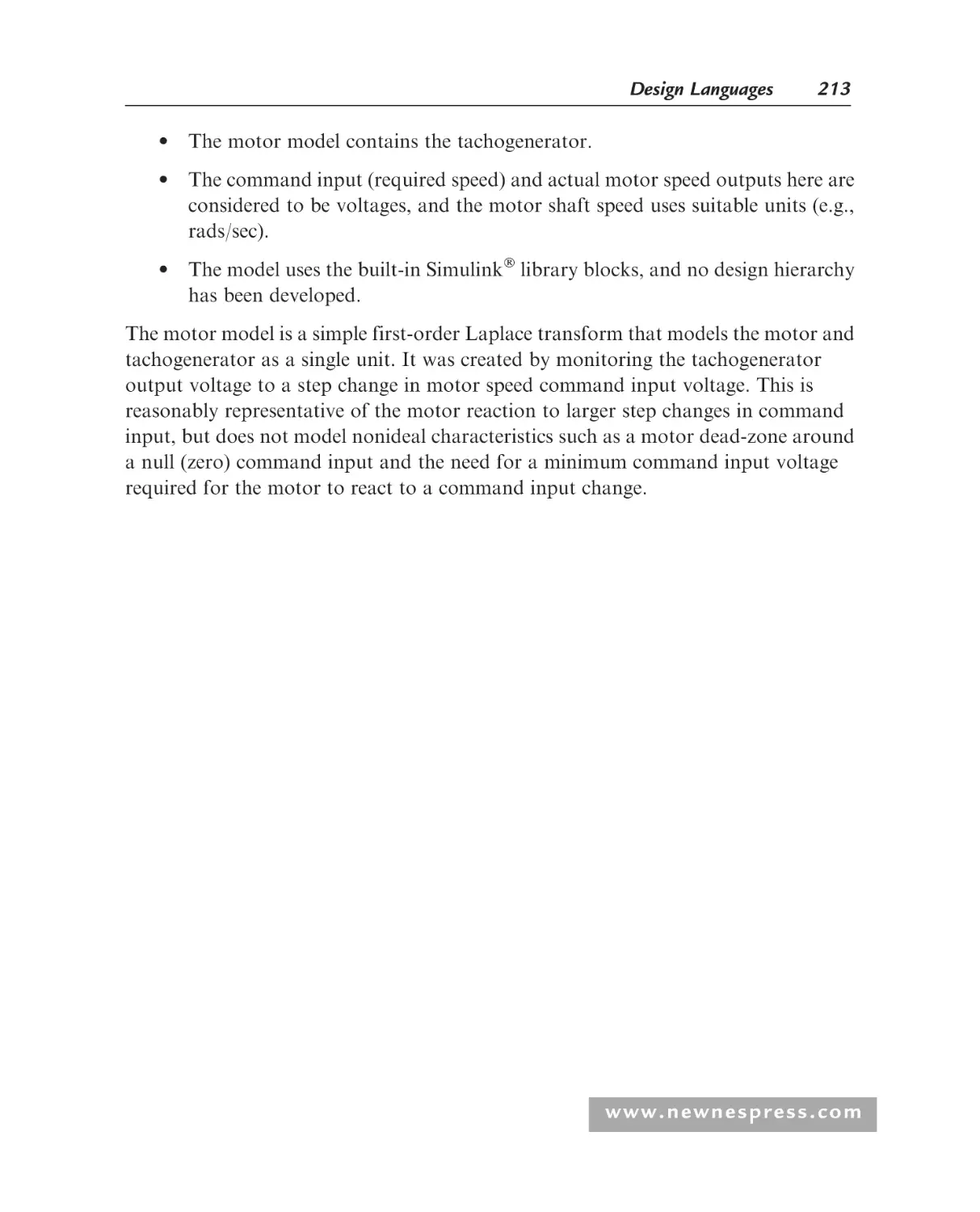
4.2.4 JAVATM ........................................................................................ 183
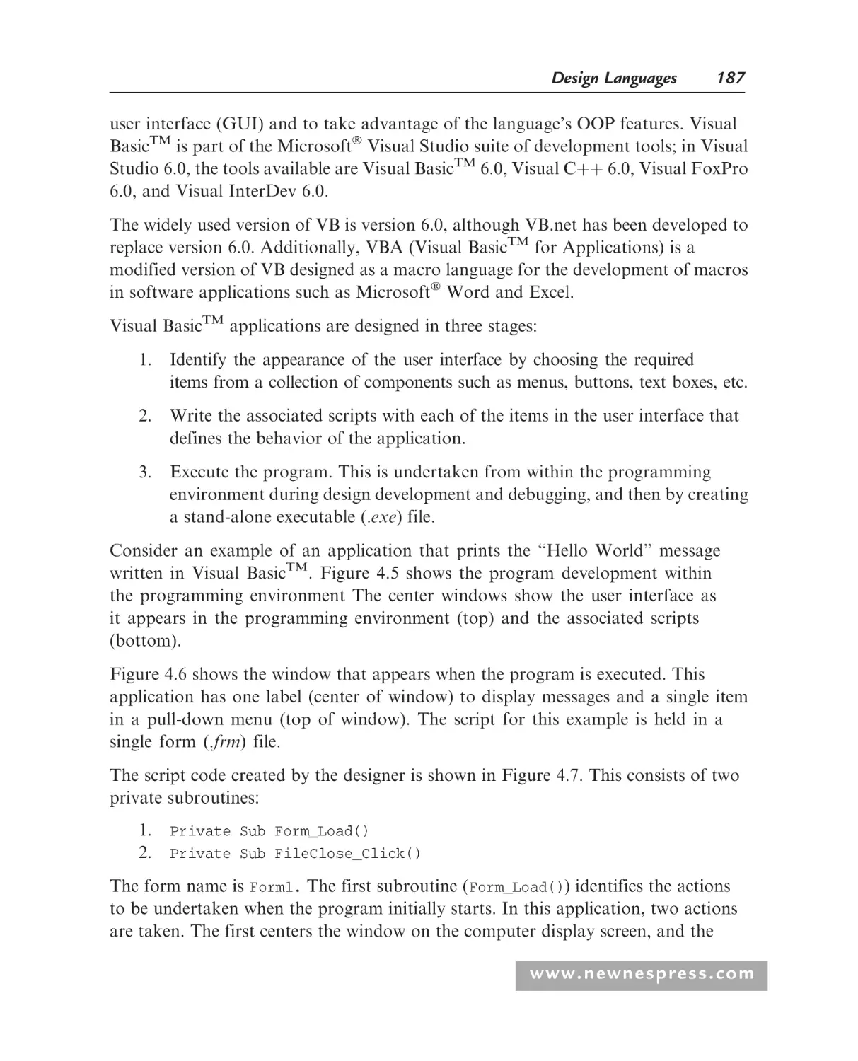
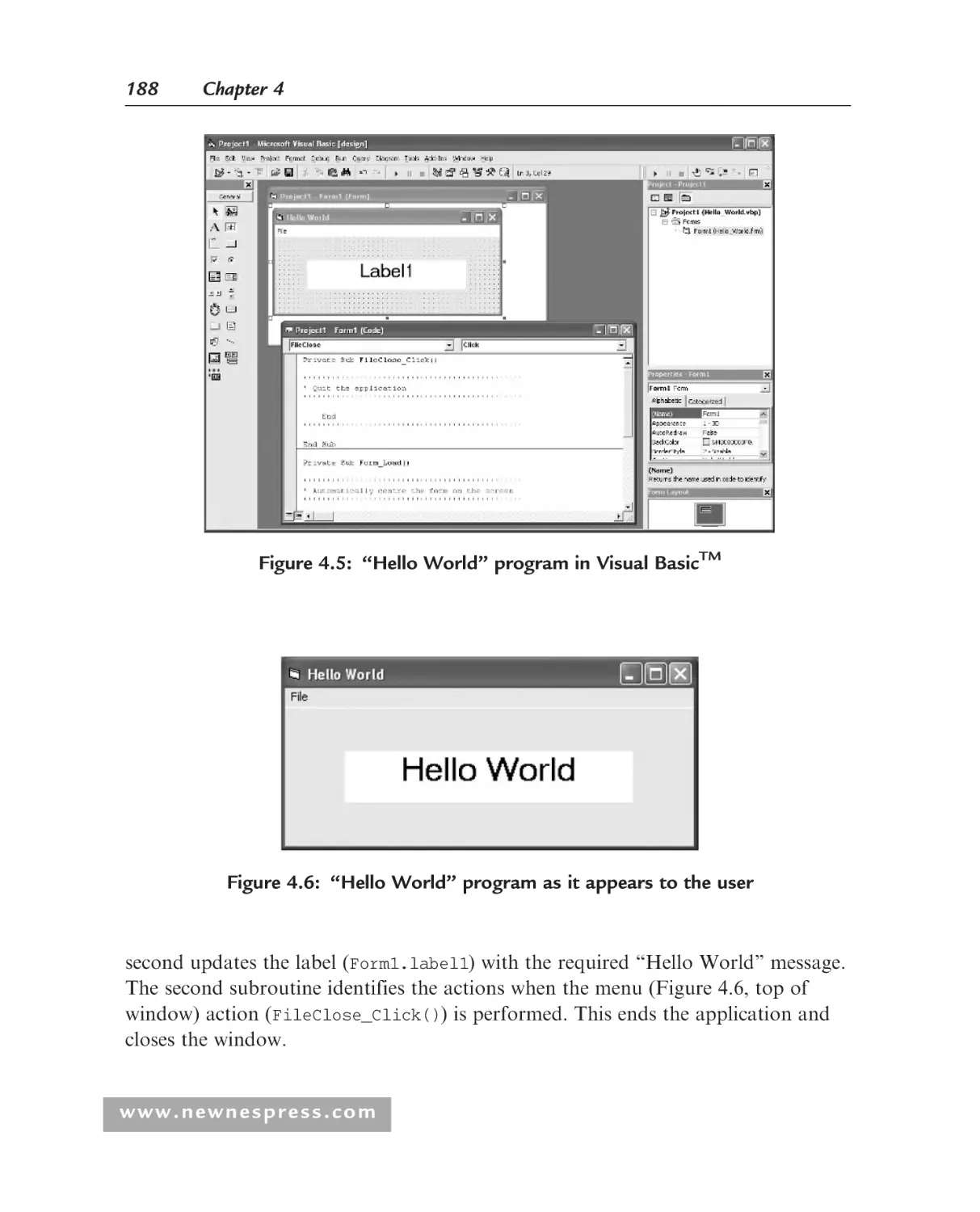
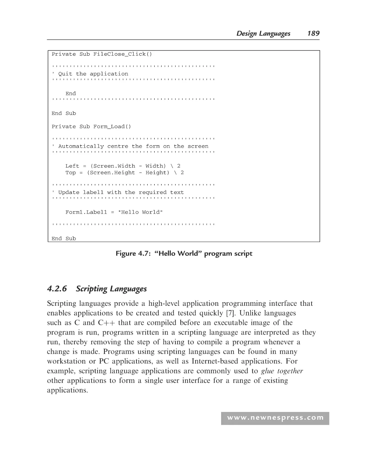
4.2.5 Visual BasicTM............................................................................... 186
4.2.6 Scripting Languages ...................................................................... 189
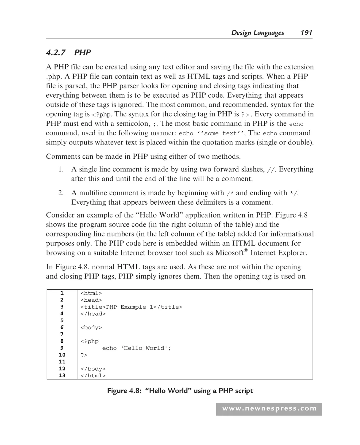
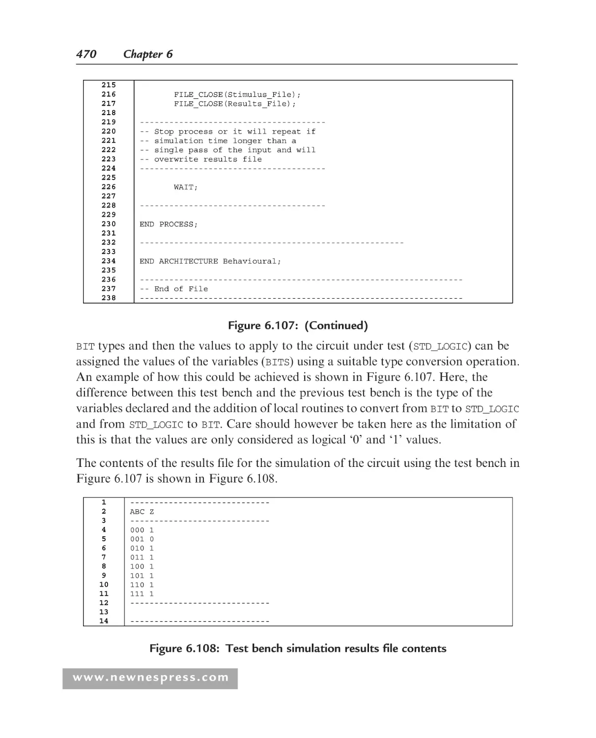
4.2.7 PHP ............................................................................................... 191
Hardware Description Languages ........................................................... 193
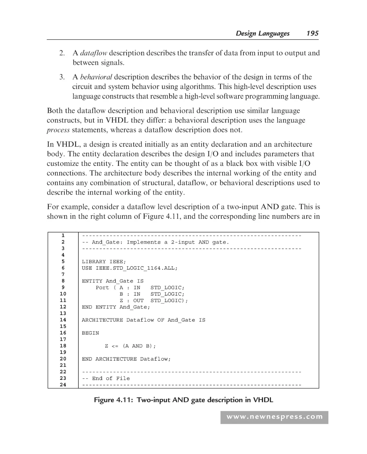
4.3.1 Introduction .................................................................................. 193
4.3.2 VHDL ........................................................................................... 194
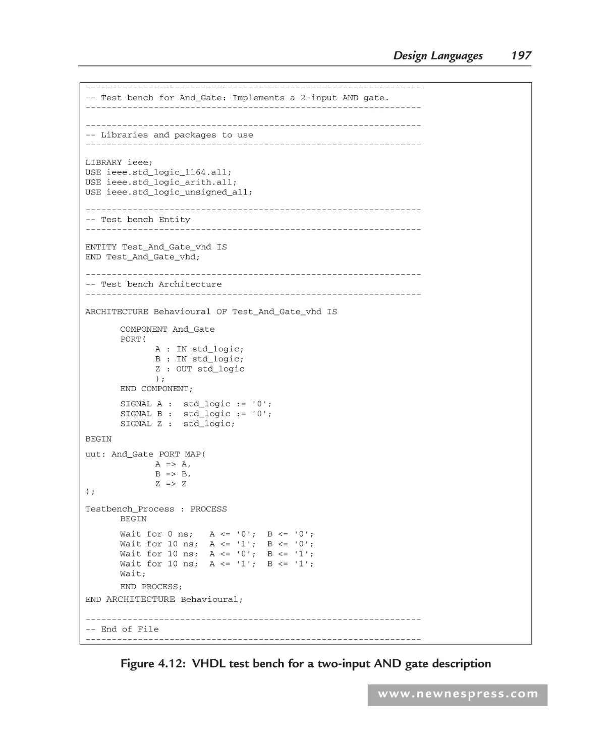
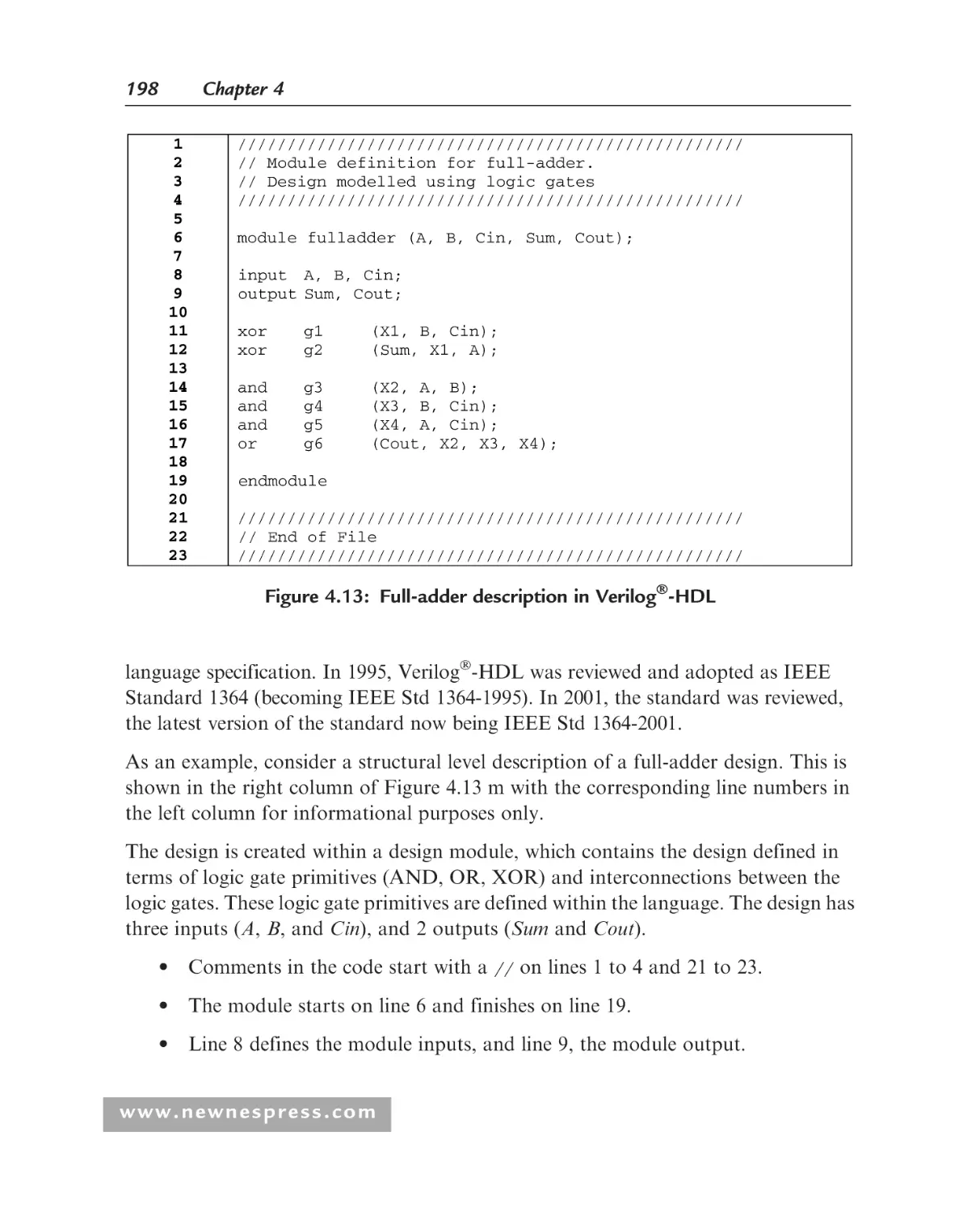
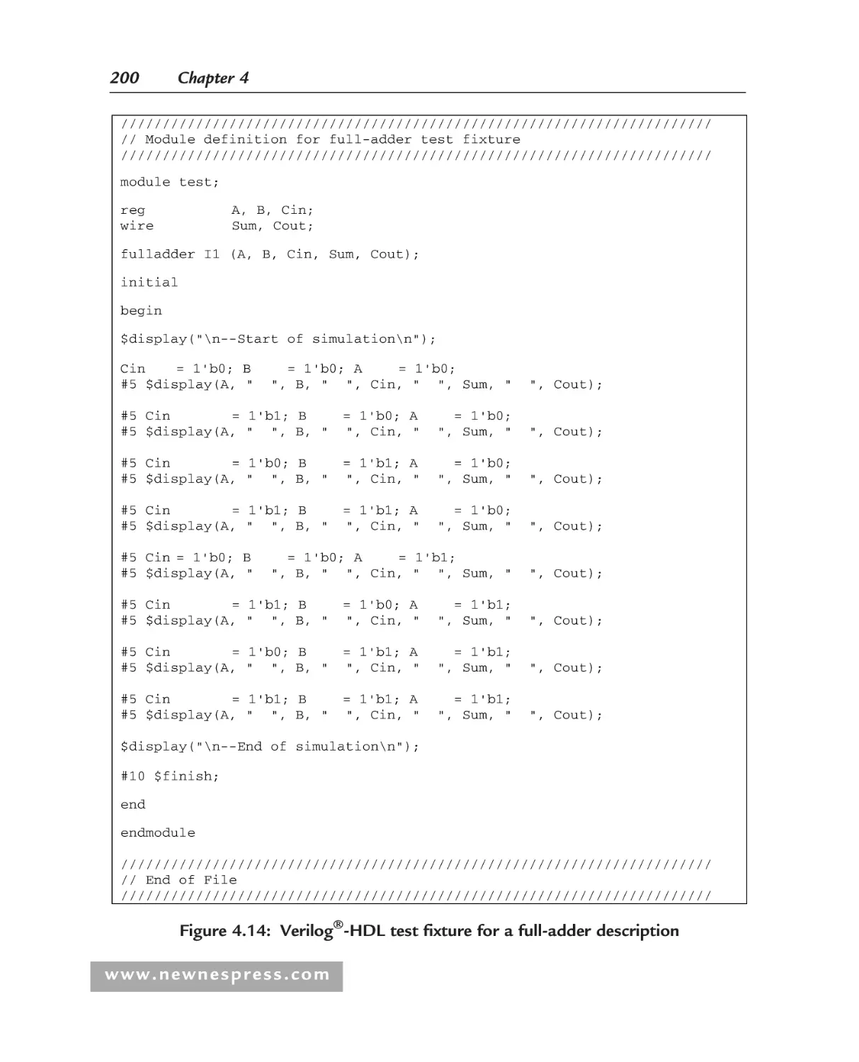
4.3.3 Verilog-HDL ............................................................................... 196
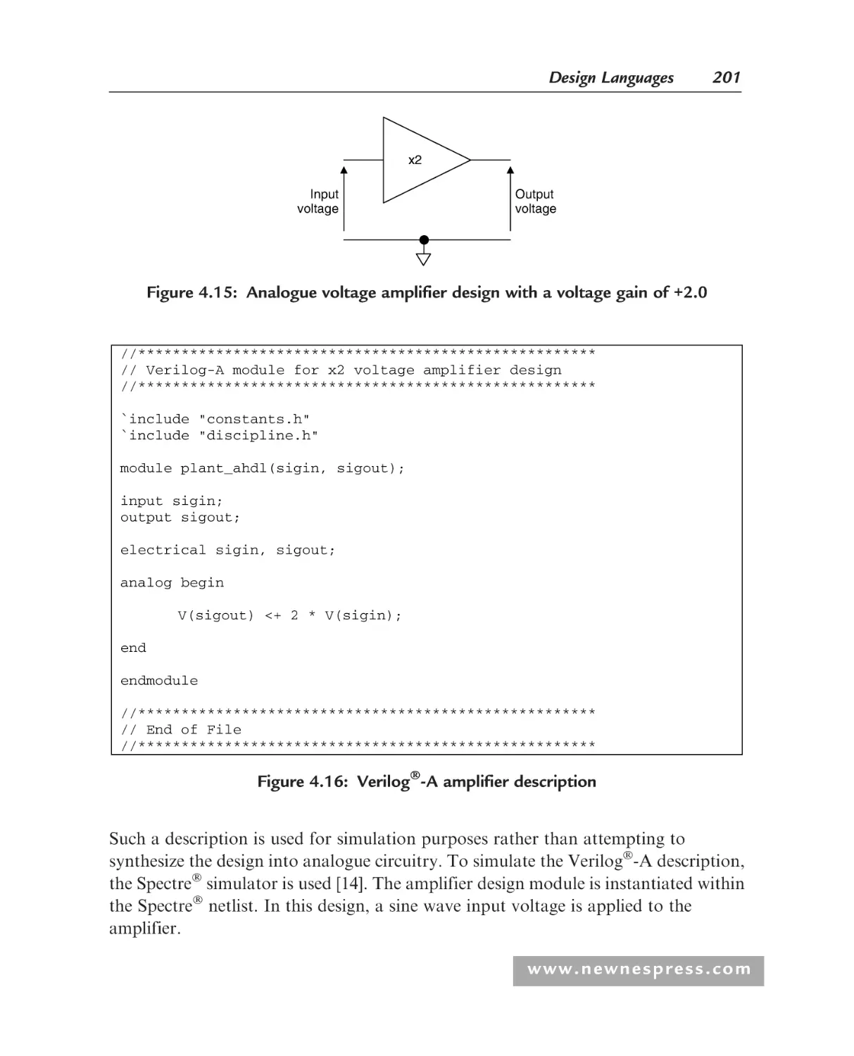
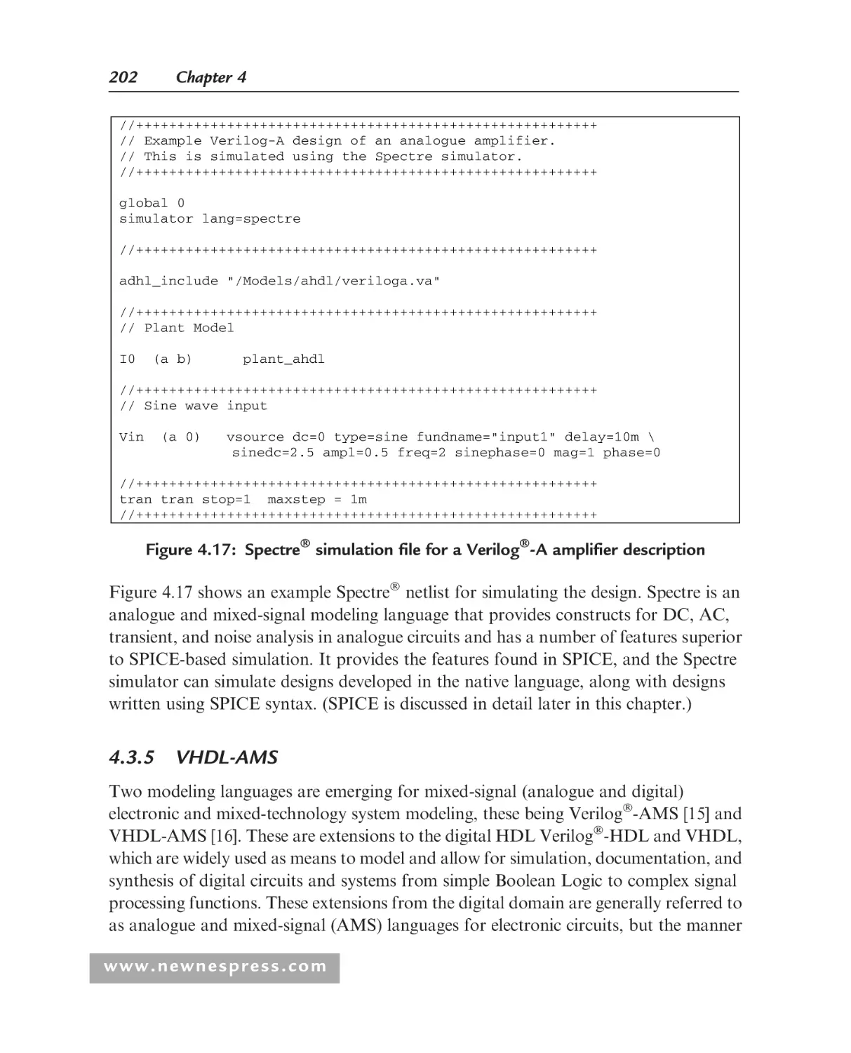
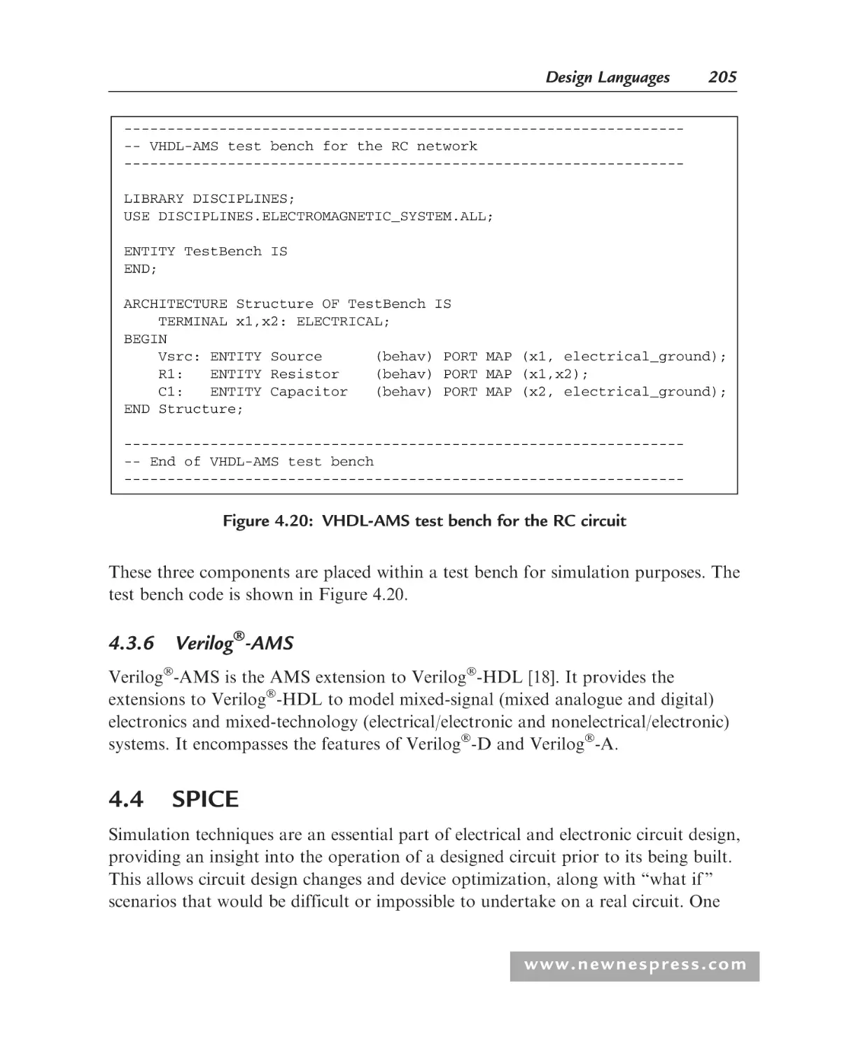
4.3.4 Verilog-A..................................................................................... 199
4.3.5 VHDL-AMS.................................................................................. 202
4.3.6 Verilog-AMS ............................................................................... 205
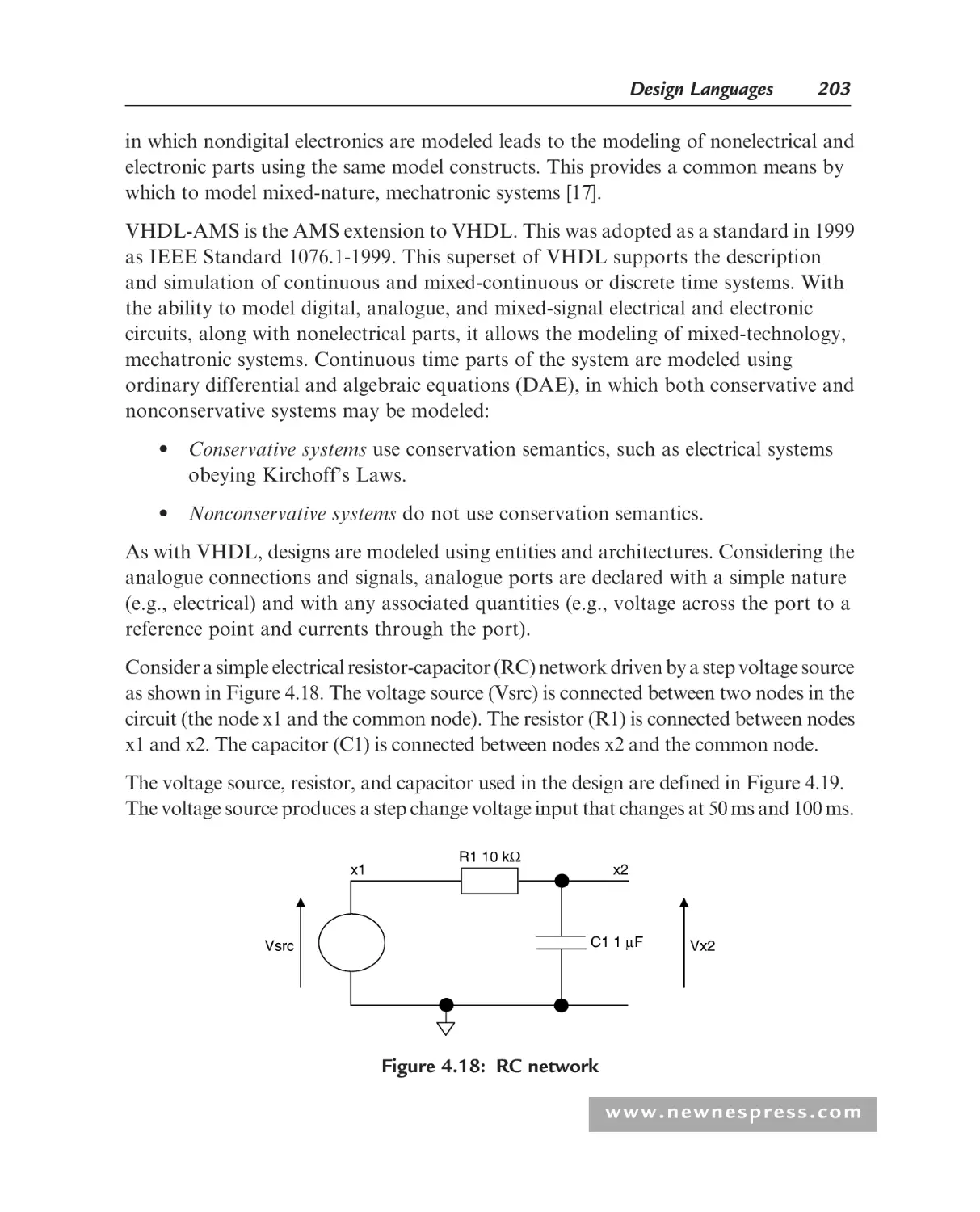
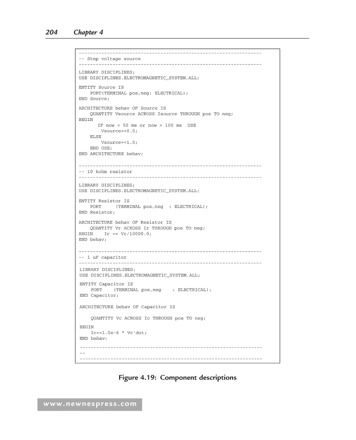
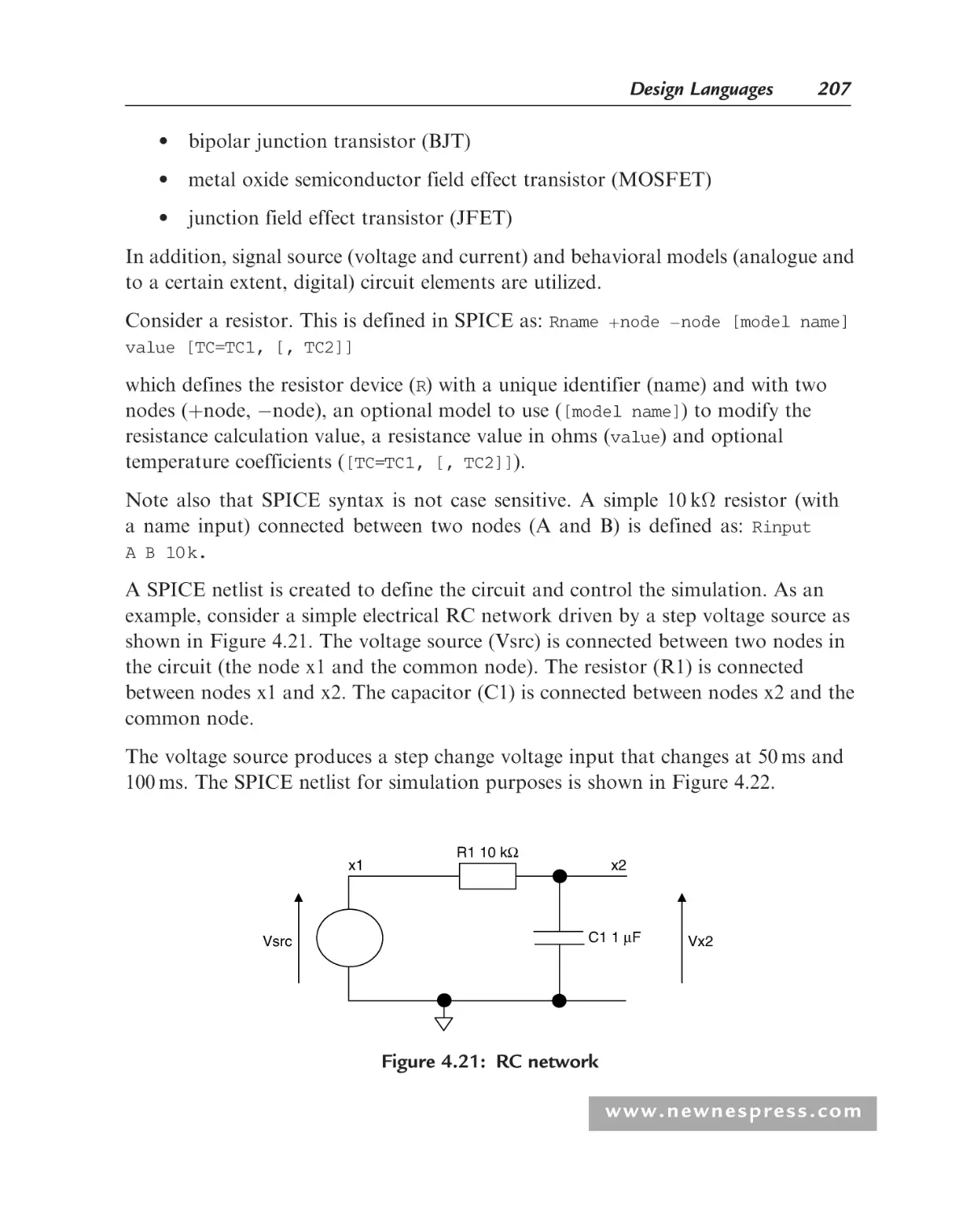
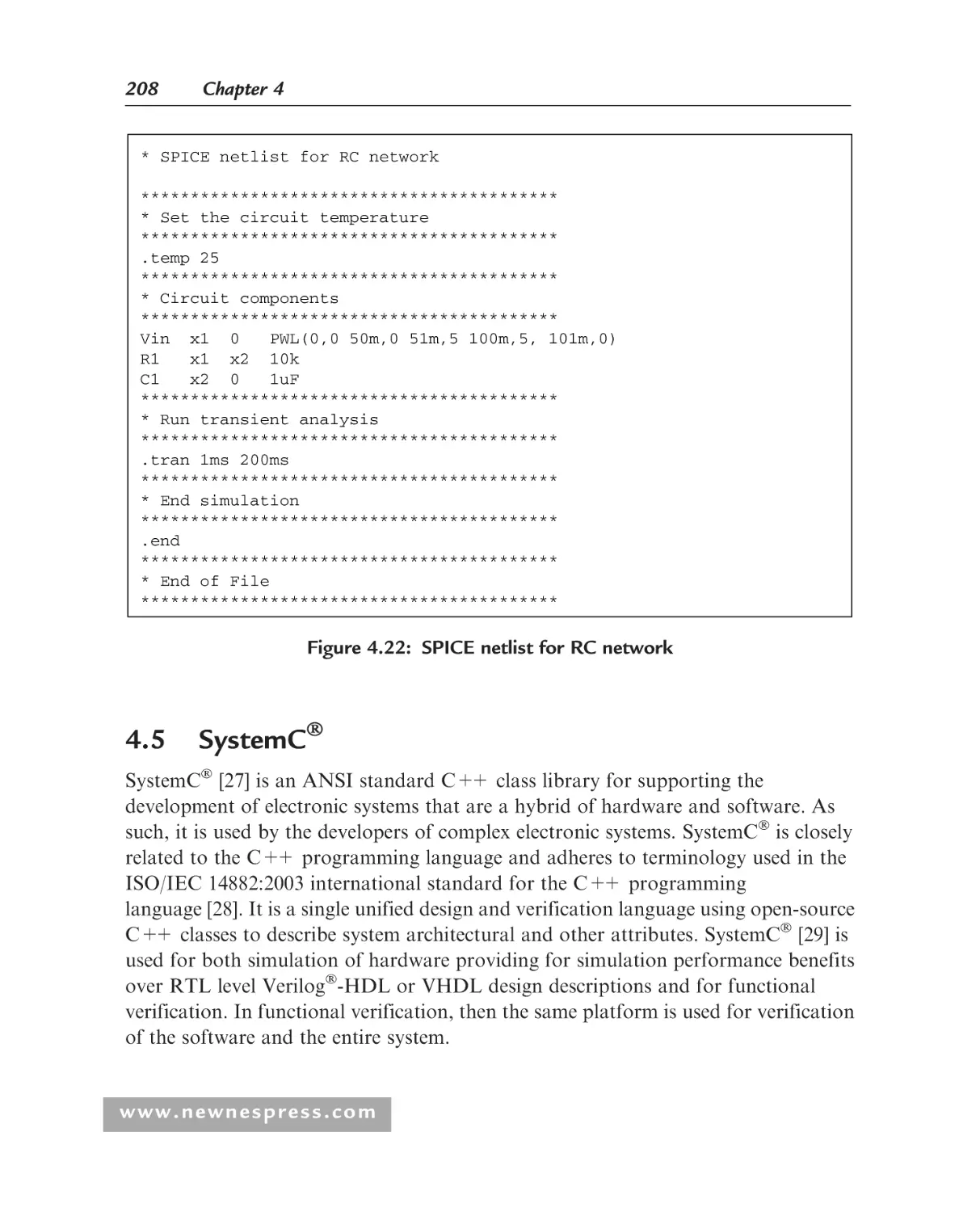
SPICE...................................................................................................... 205
SystemC ................................................................................................ 208
SystemVerilog.......................................................................................... 209
Mathematical Modeling Tools ................................................................ 210
References ............................................................................................... 214
Student Exercises ..................................................................................... 216
www.newnespress.com
x
Table of Contents
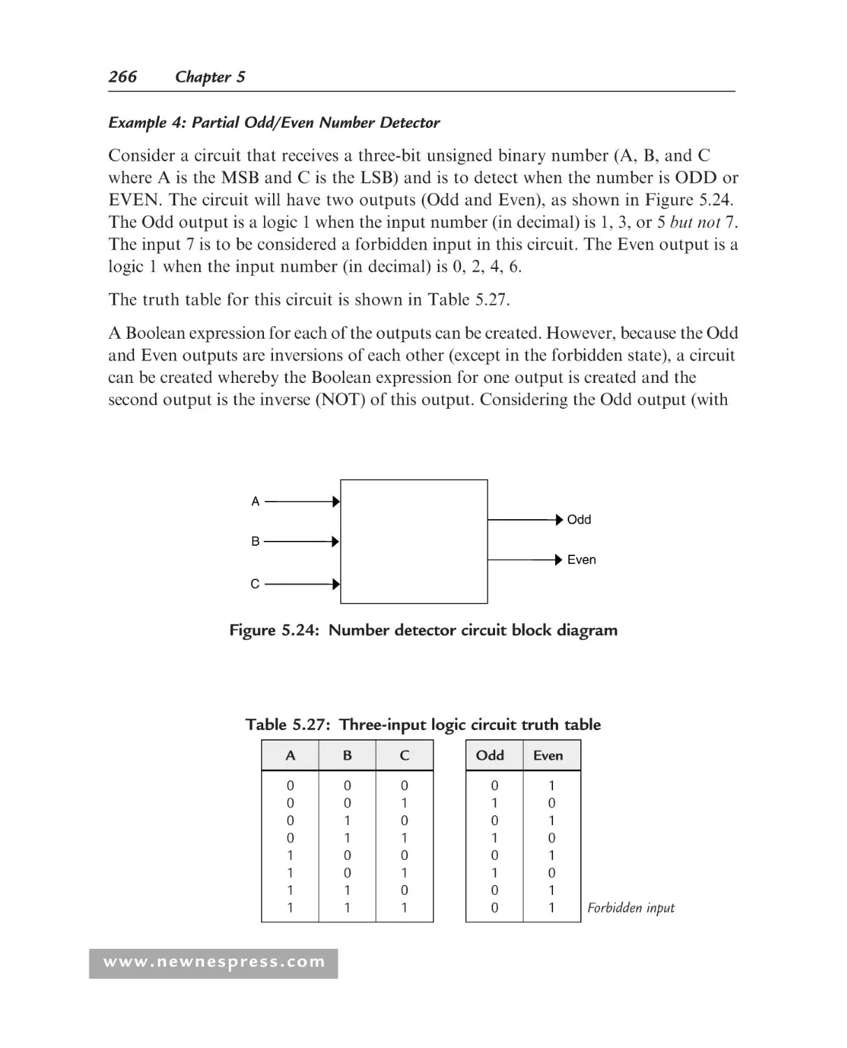
Chapter 5: Introduction to Digital Logic Design ........................................... 217
5.1
5.2
5.3
5.4
5.5
5.6
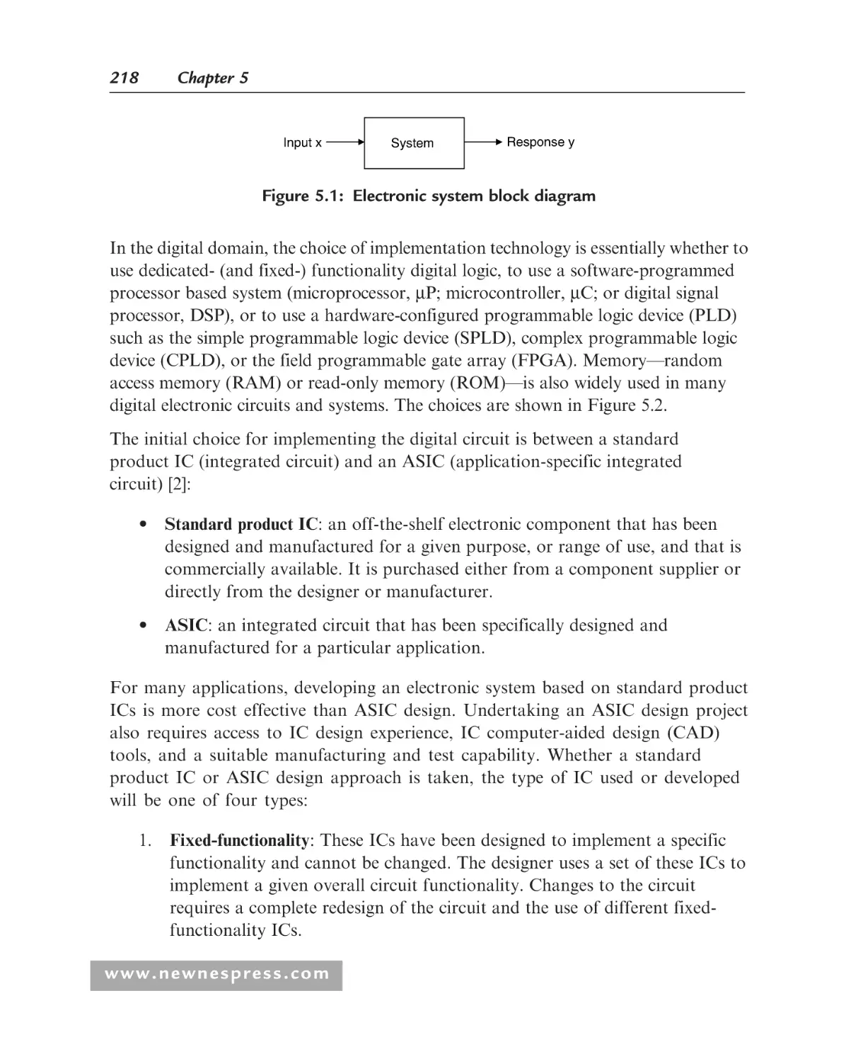
Introduction ............................................................................................ 217
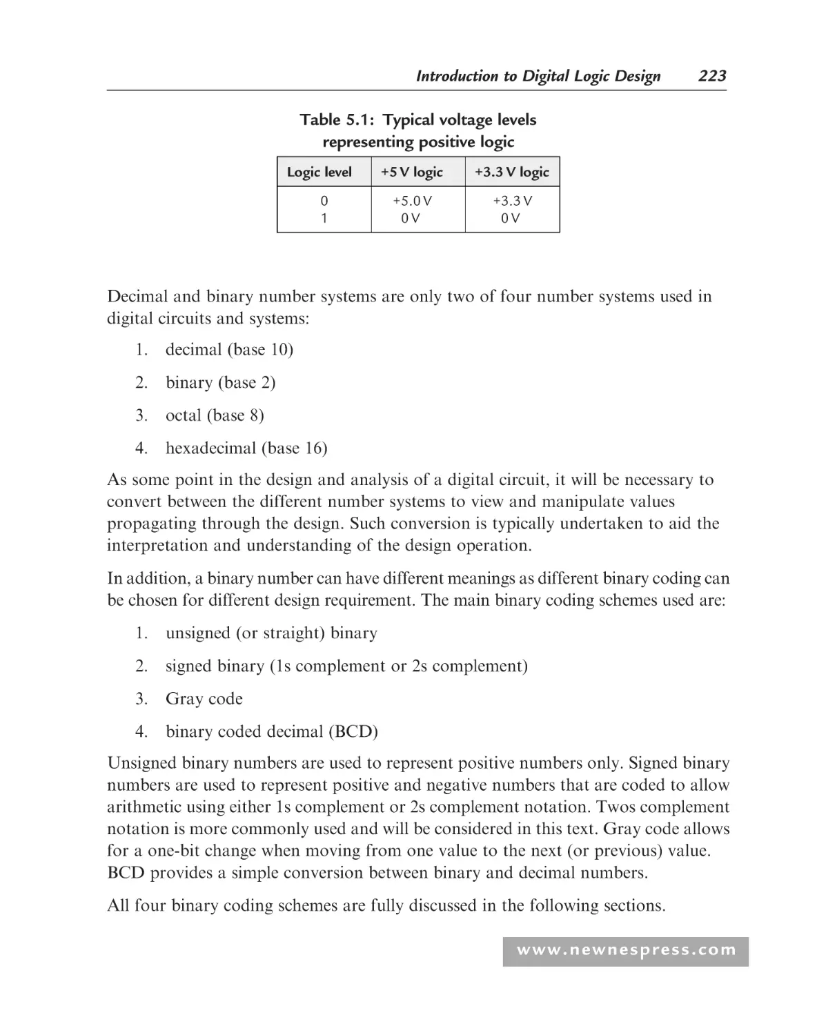
Number Systems...................................................................................... 222
5.2.1 Introduction .................................................................................. 222
5.2.2 Decimal–Unsigned Binary Conversion.......................................... 224
5.2.3 Signed Binary Numbers................................................................. 226
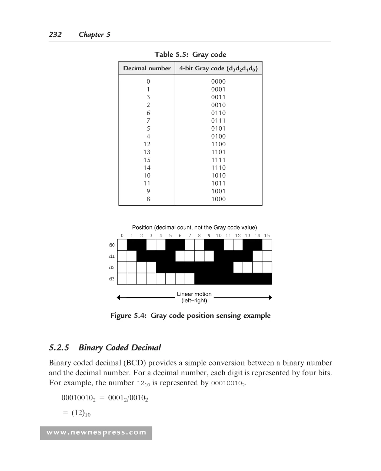
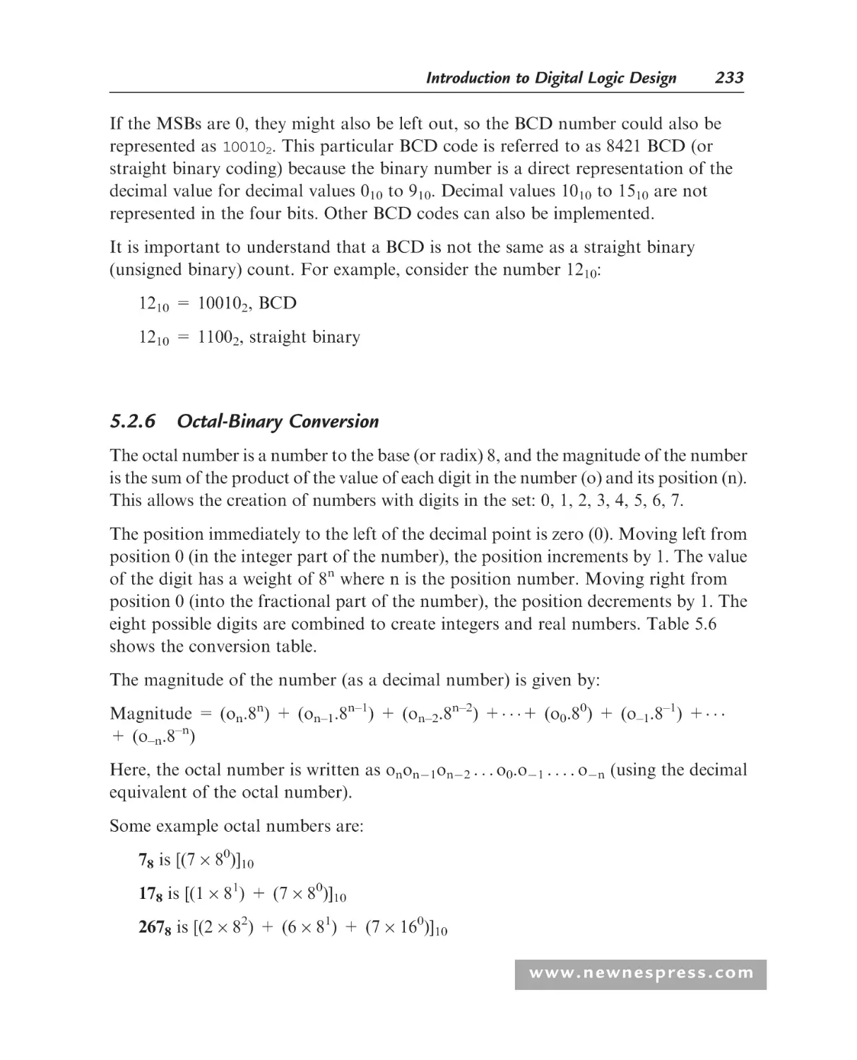
5.2.4 Gray Code ..................................................................................... 231
5.2.5 Binary Coded Decimal .................................................................. 232
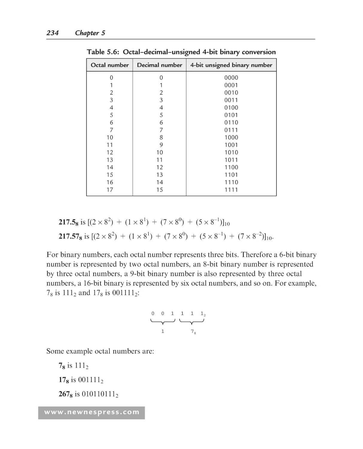
5.2.6 Octal-Binary Conversion ............................................................... 233
5.2.7 Hexadecimal-Binary Conversion ................................................... 235
Binary Data Manipulation...................................................................... 240
5.3.1 Introduction .................................................................................. 240
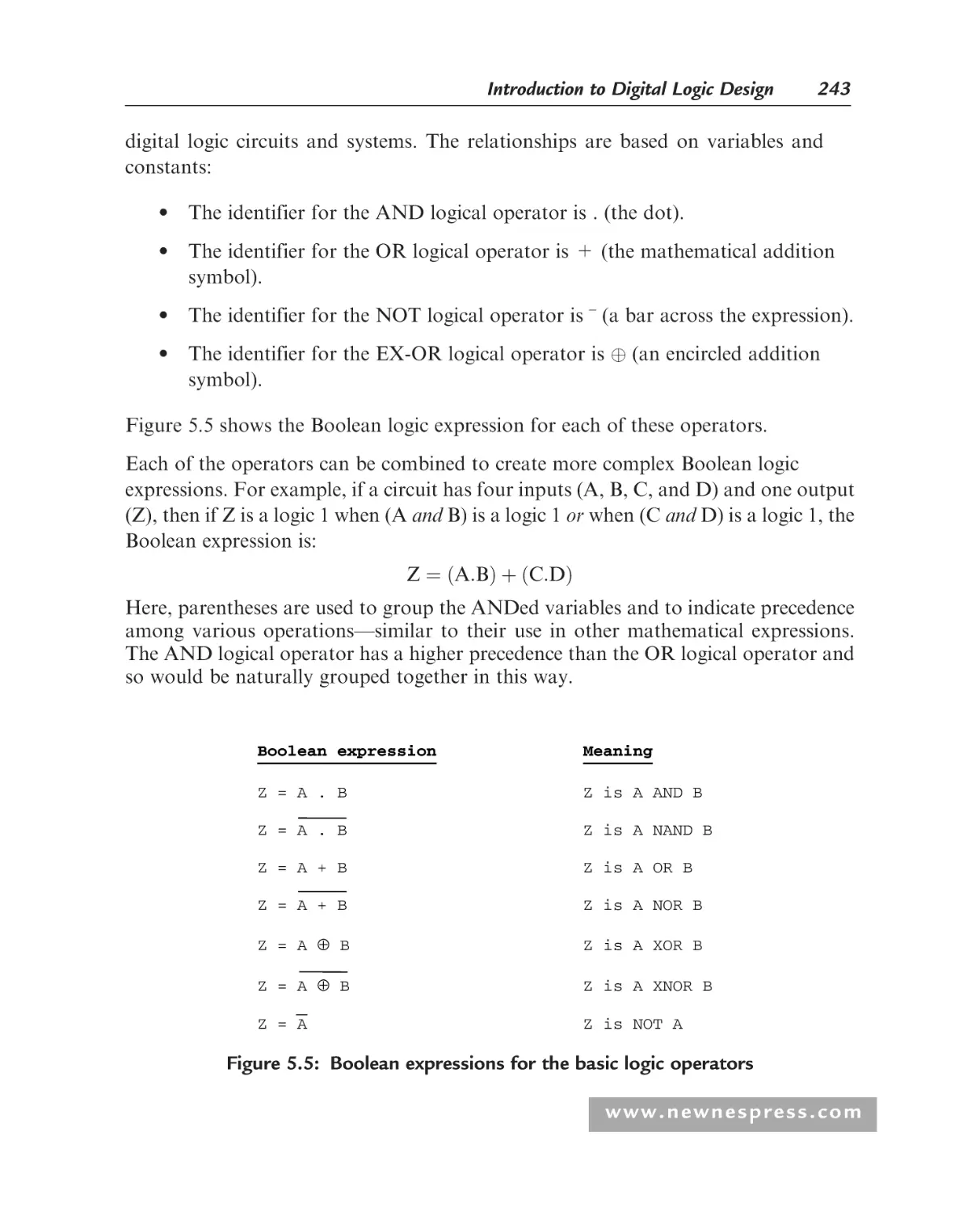
5.3.2 Logical Operations ........................................................................ 241
5.3.3 Boolean Algebra............................................................................ 242
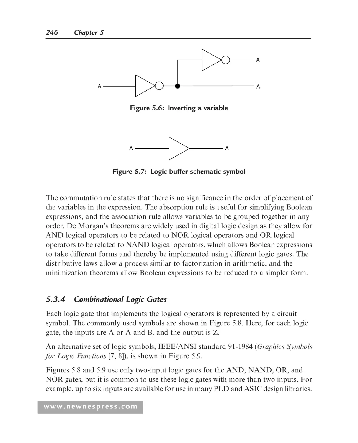
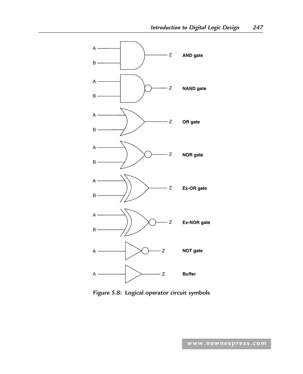
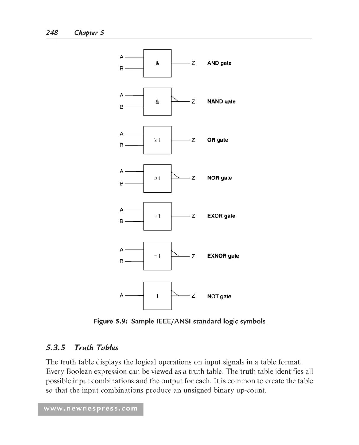
5.3.4 Combinational Logic Gates .......................................................... 246
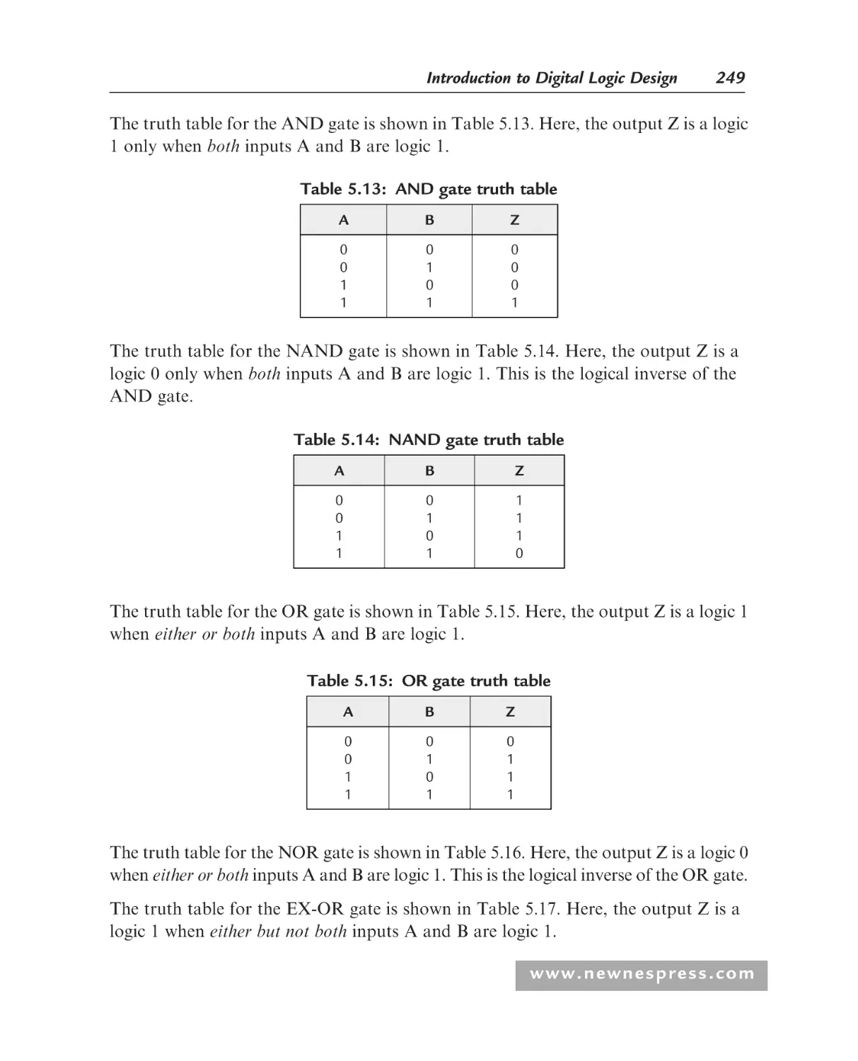
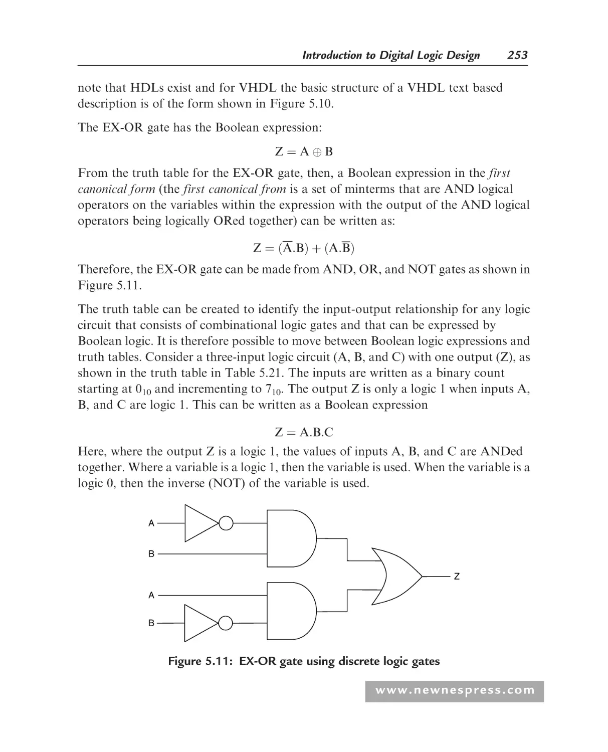
5.3.5 Truth Tables .................................................................................. 248
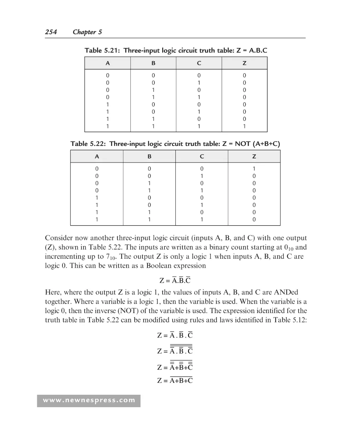
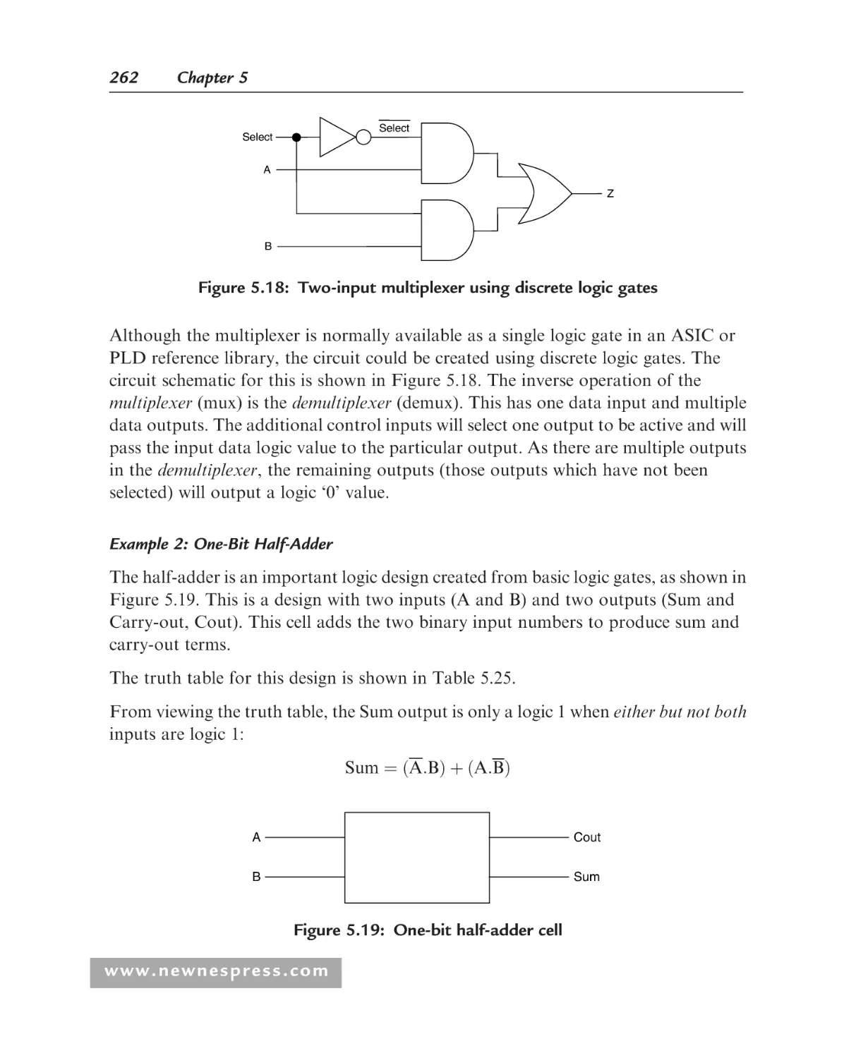
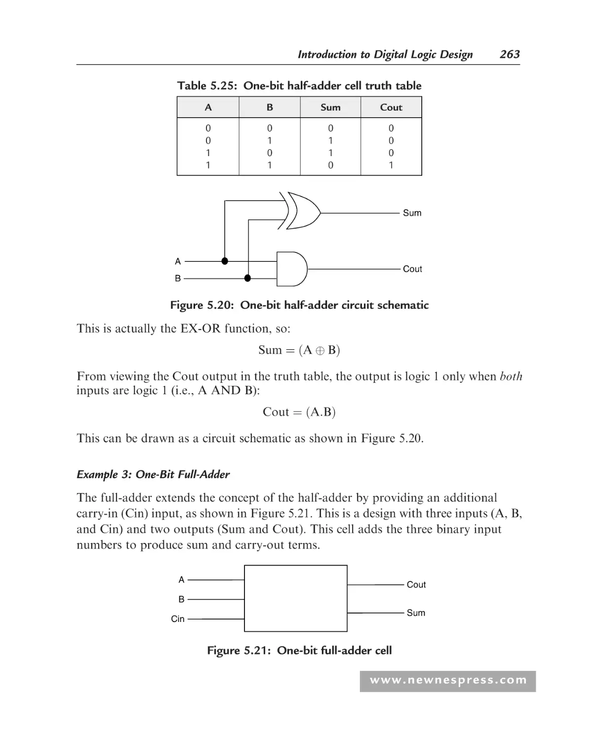
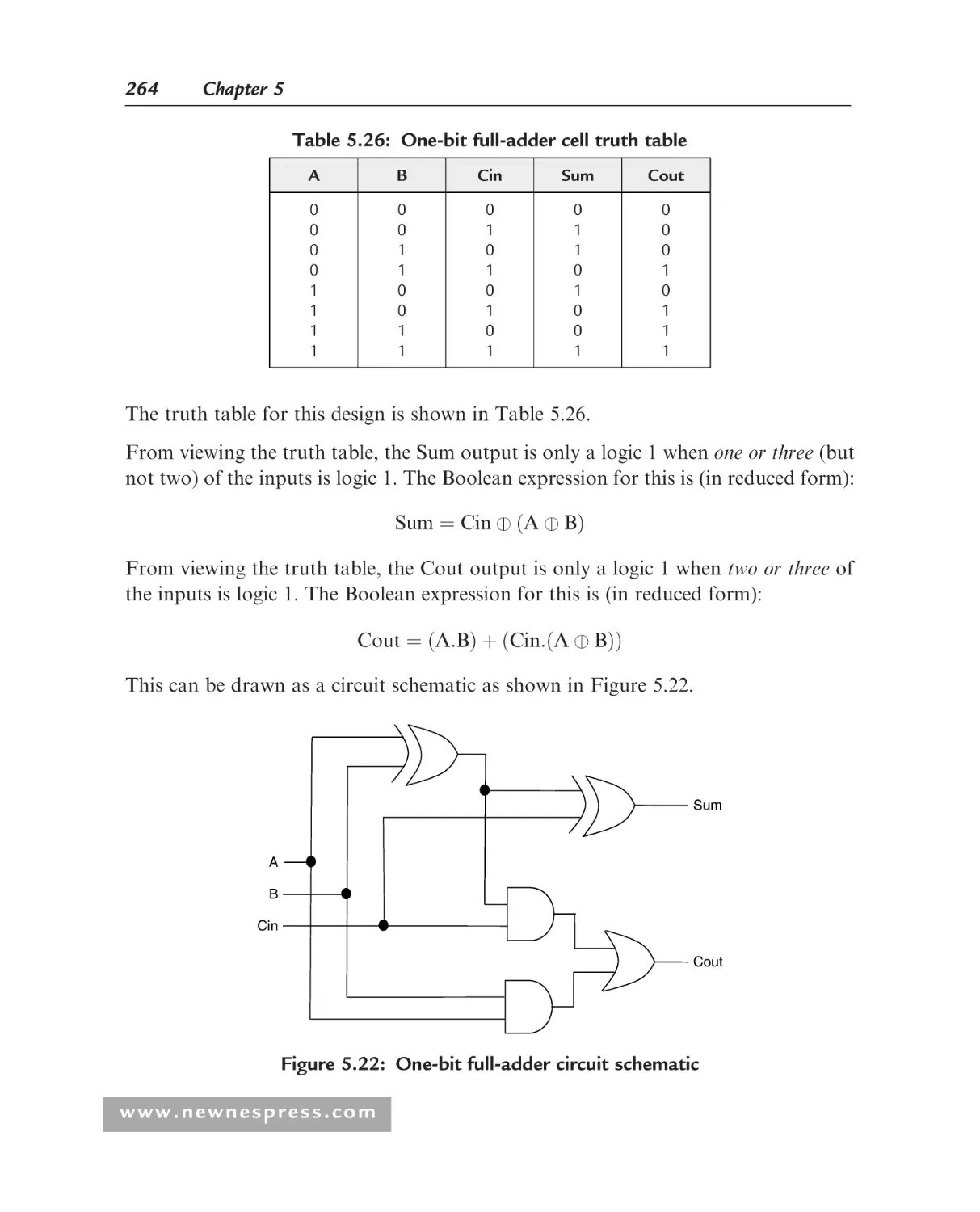
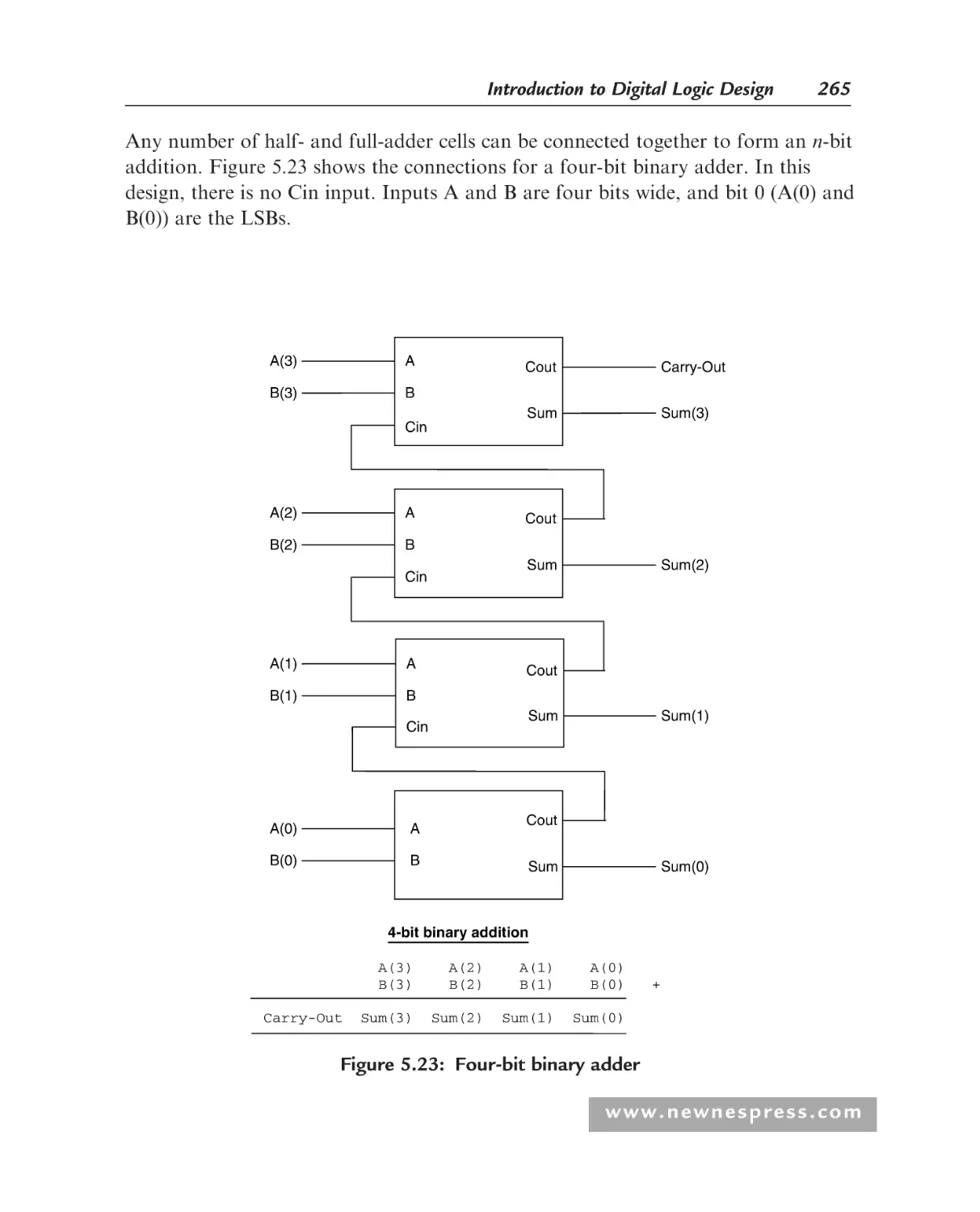
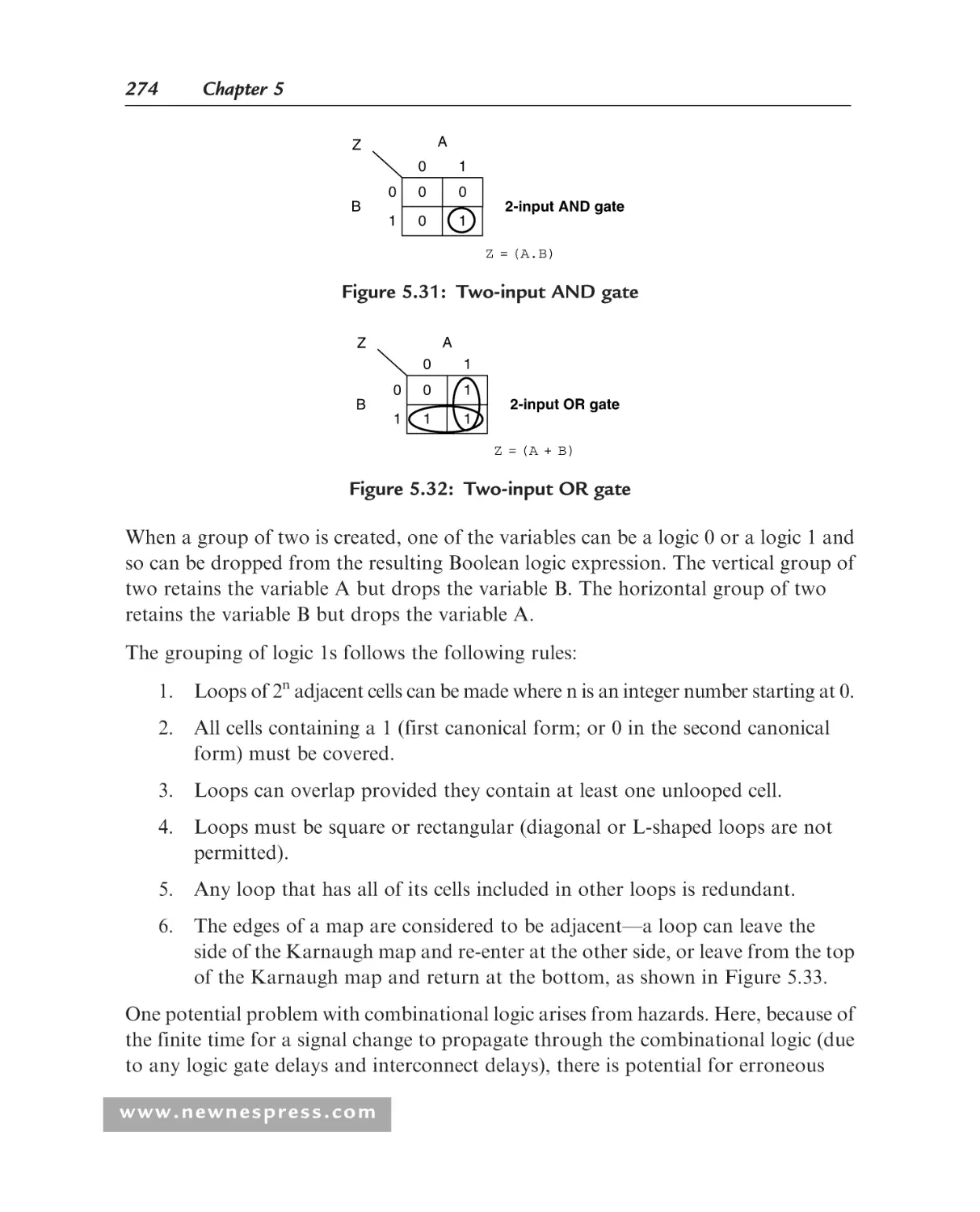
Combinational Logic Design .................................................................. 256
5.4.1 Introduction .................................................................................. 256
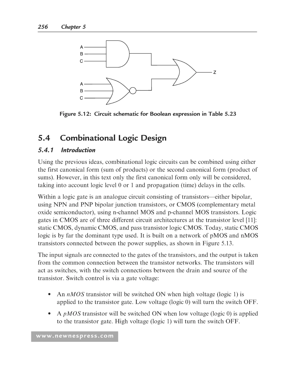
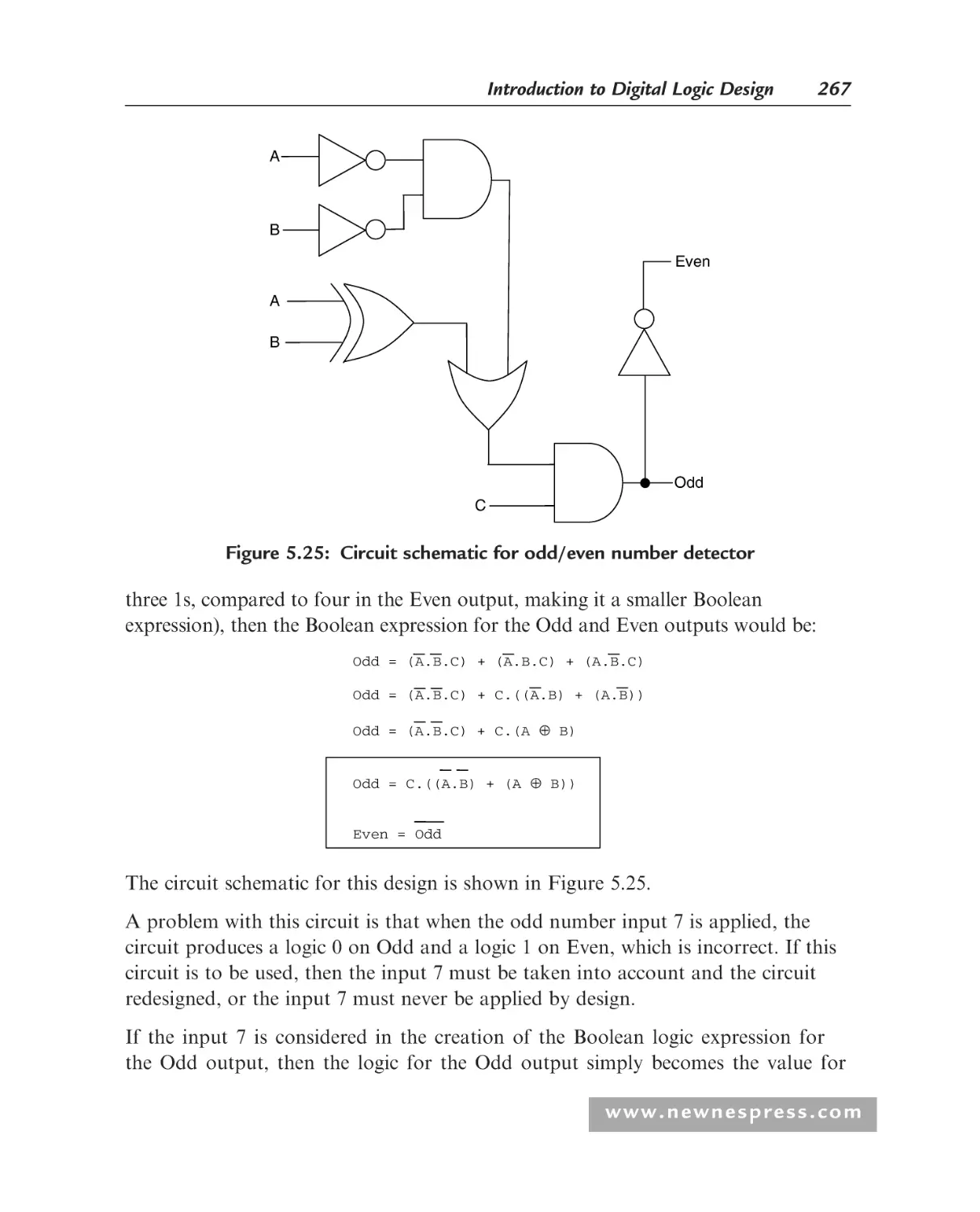
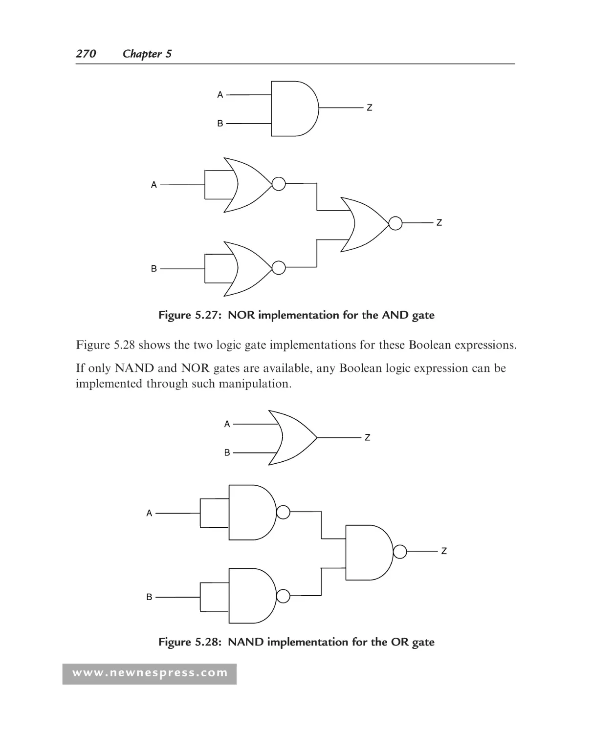
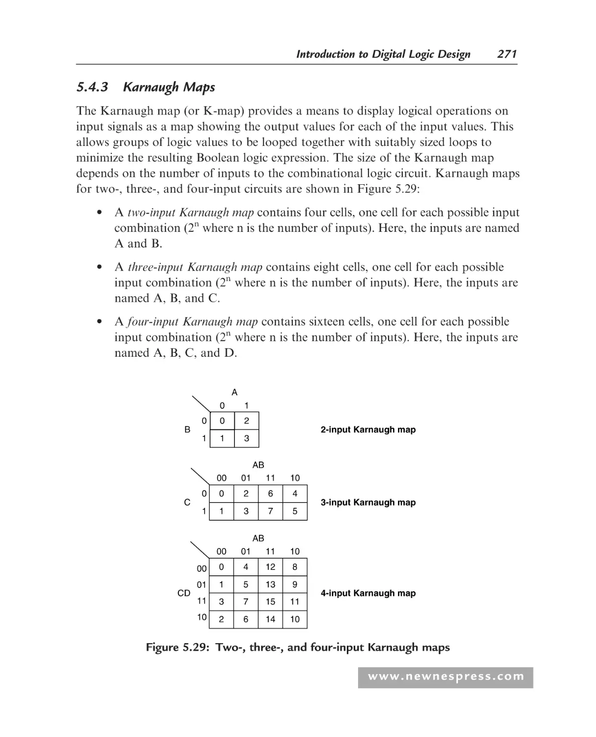
5.4.2 NAND and NOR logic ................................................................. 269
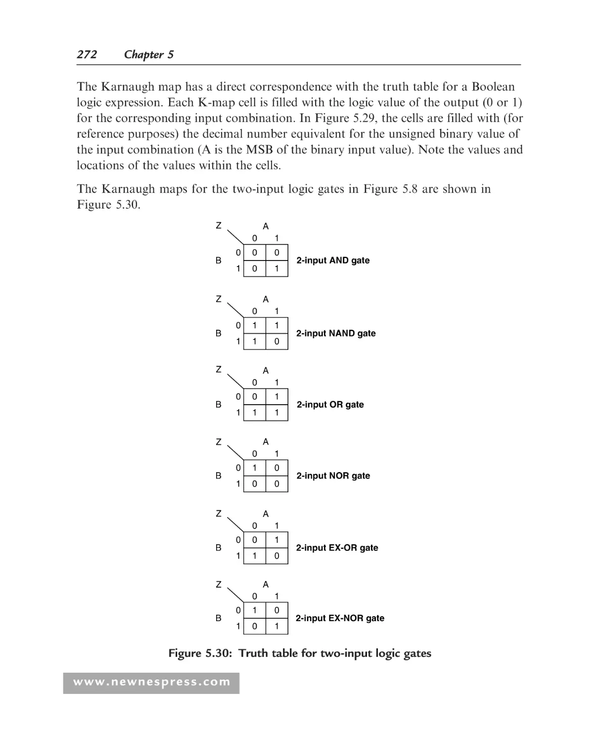
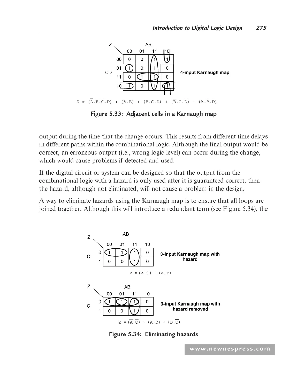
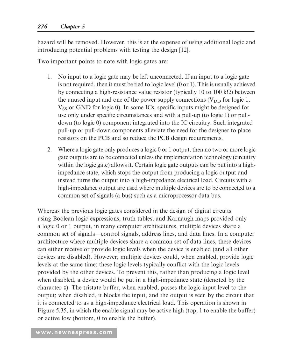
5.4.3 Karnaugh Maps ............................................................................ 271
5.4.4 Don’t Care Conditions................................................................... 277
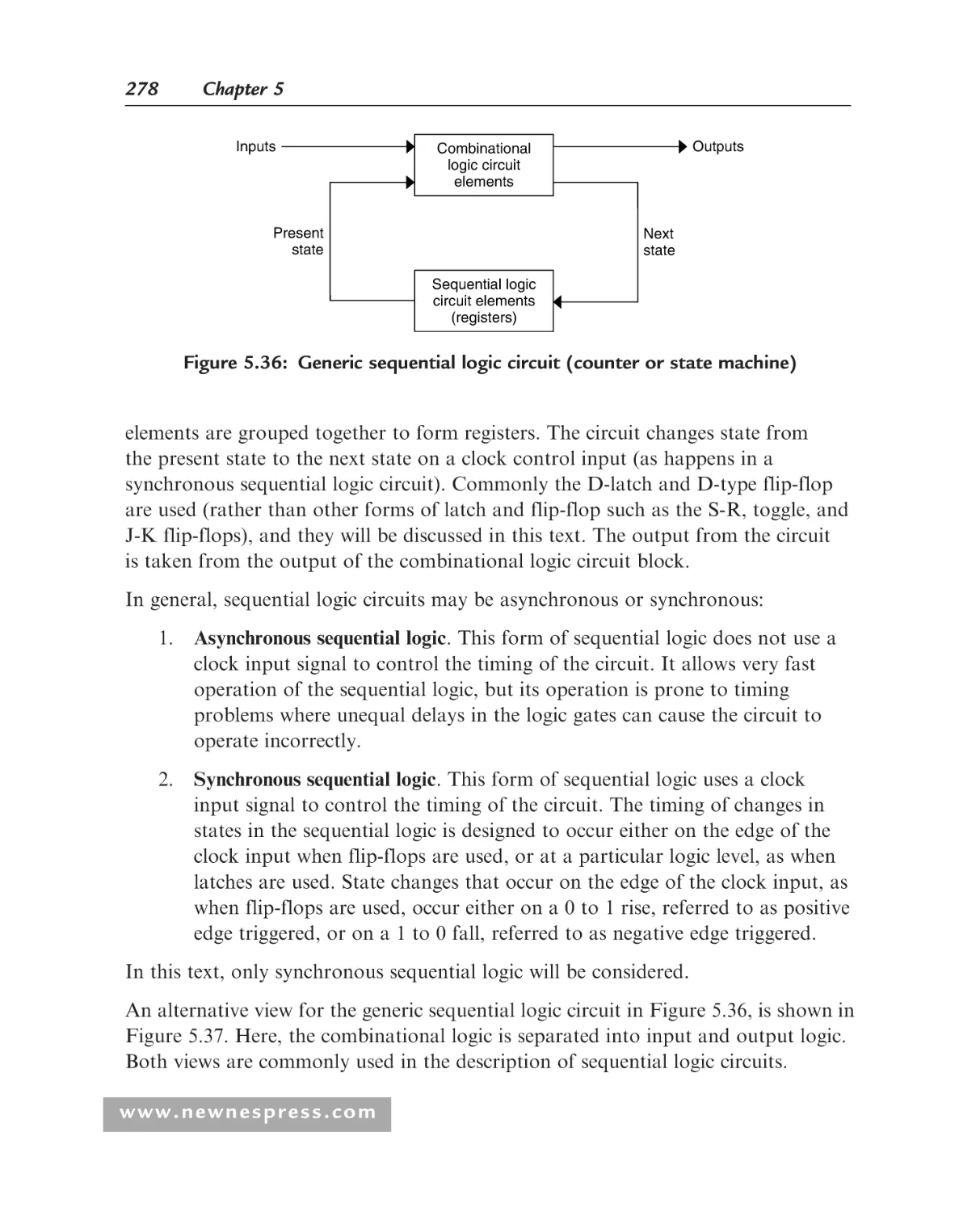
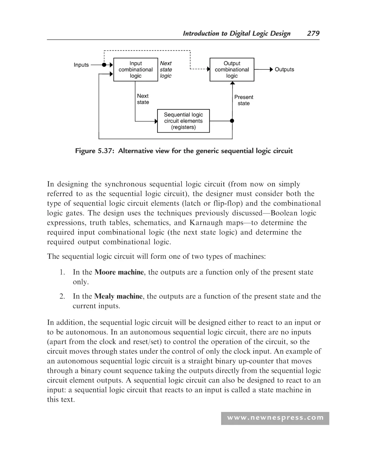
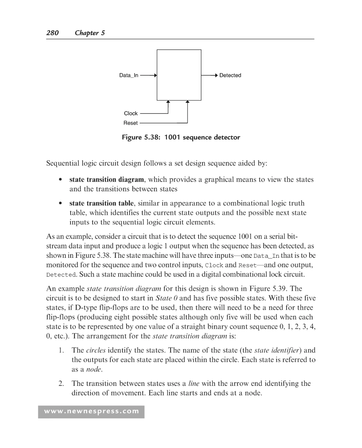
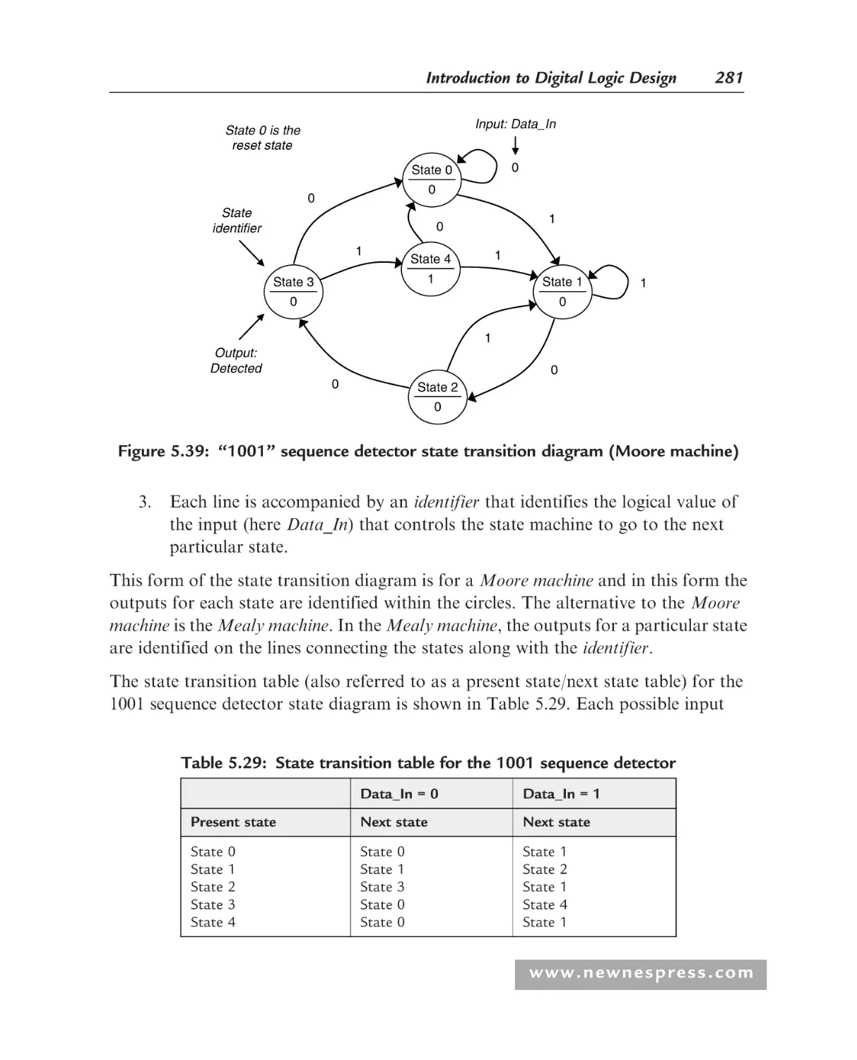
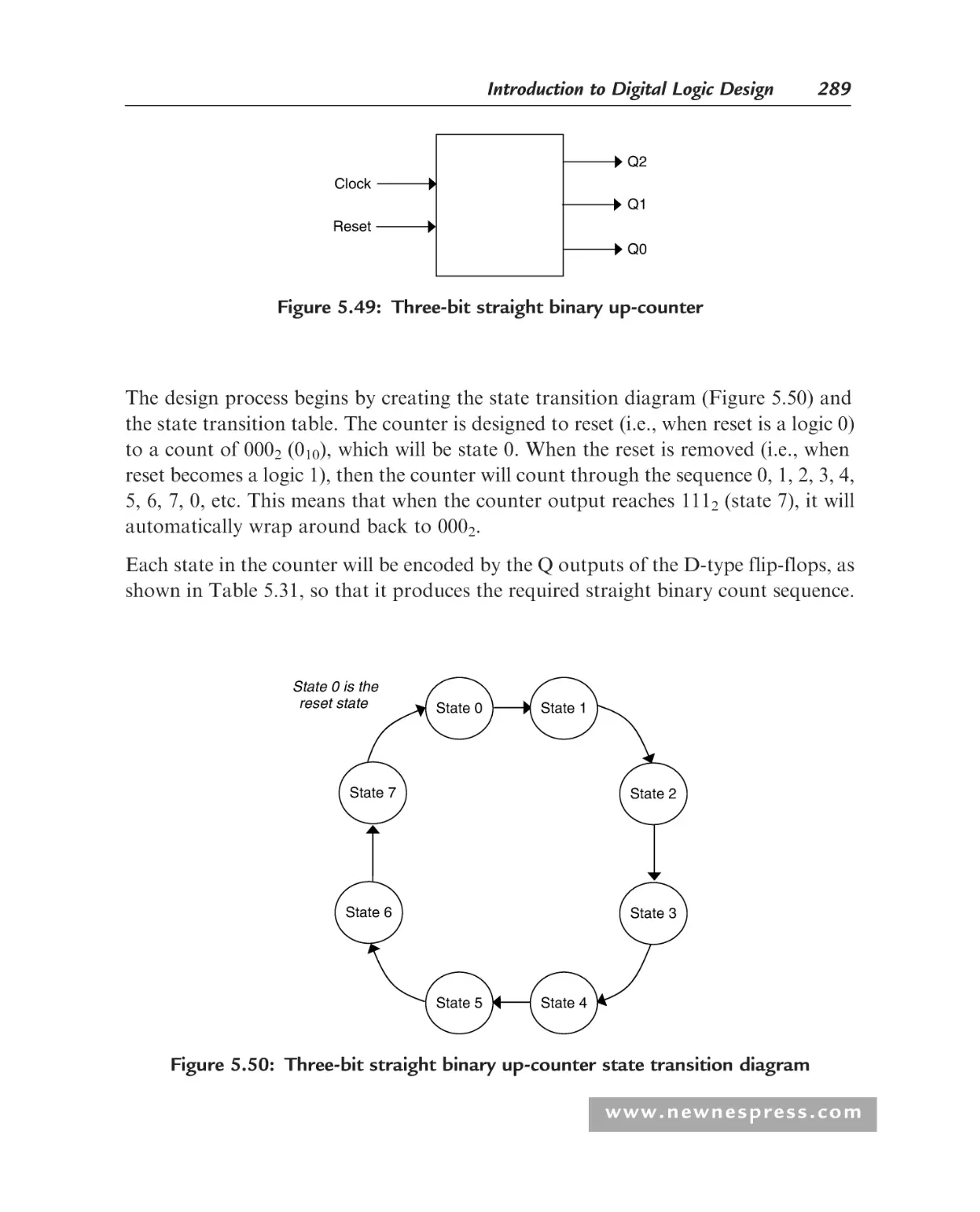
Sequential Logic Design.......................................................................... 277
5.5.1 Introduction .................................................................................. 277
5.5.2 Level Sensitive Latches and Edge-Triggered
Flip-Flops ...................................................................................... 282
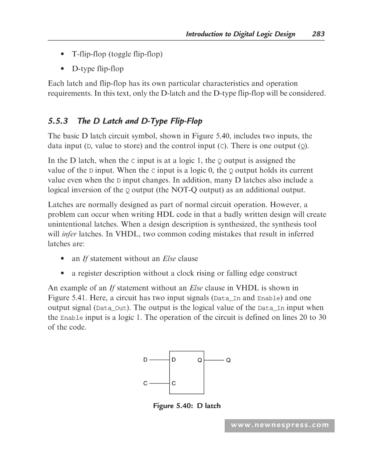
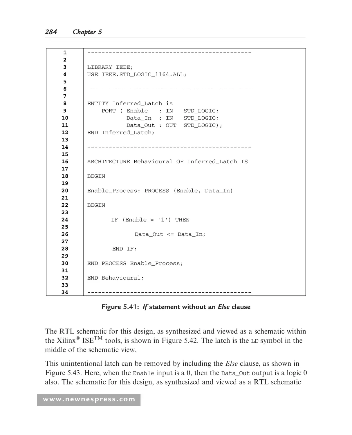
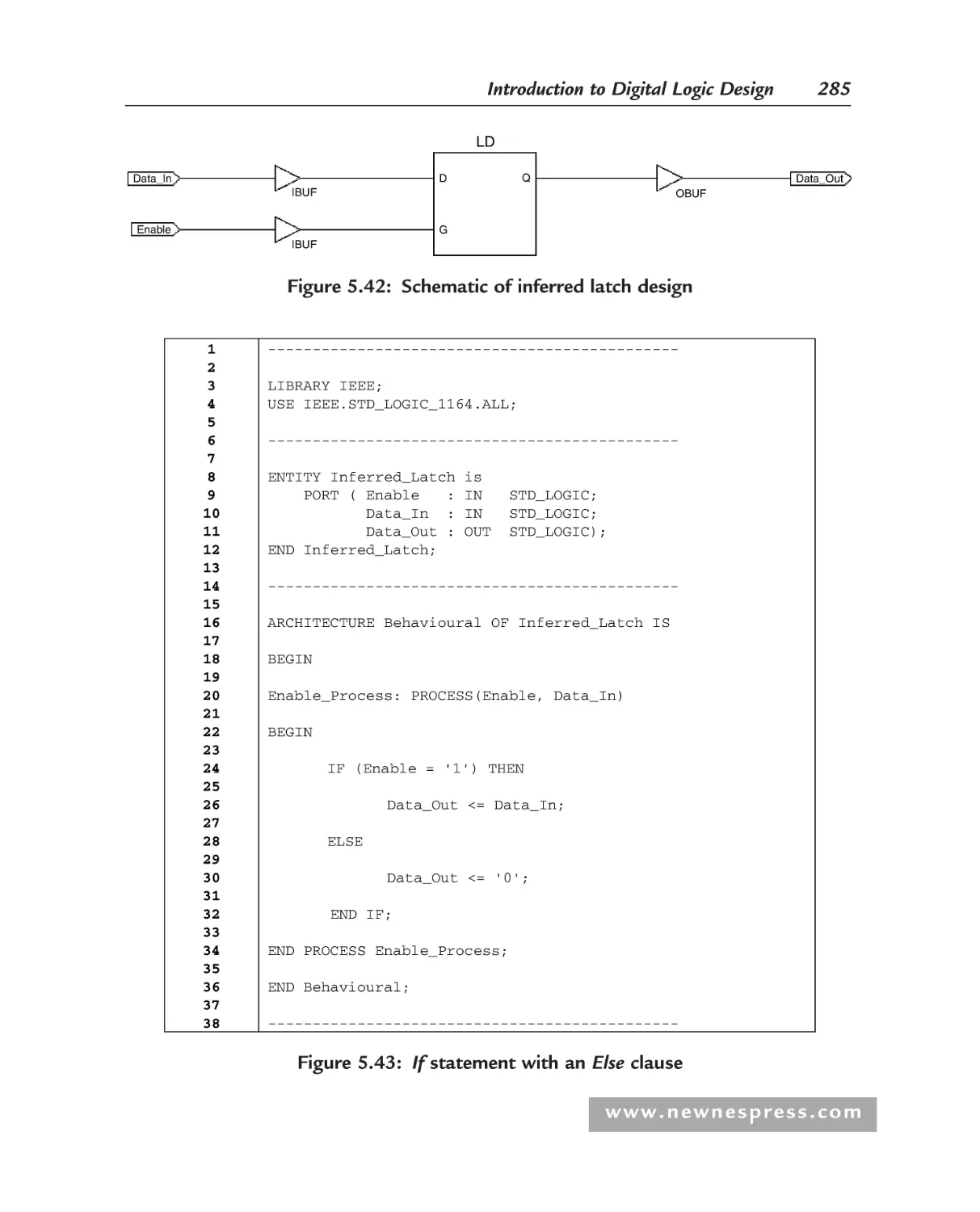
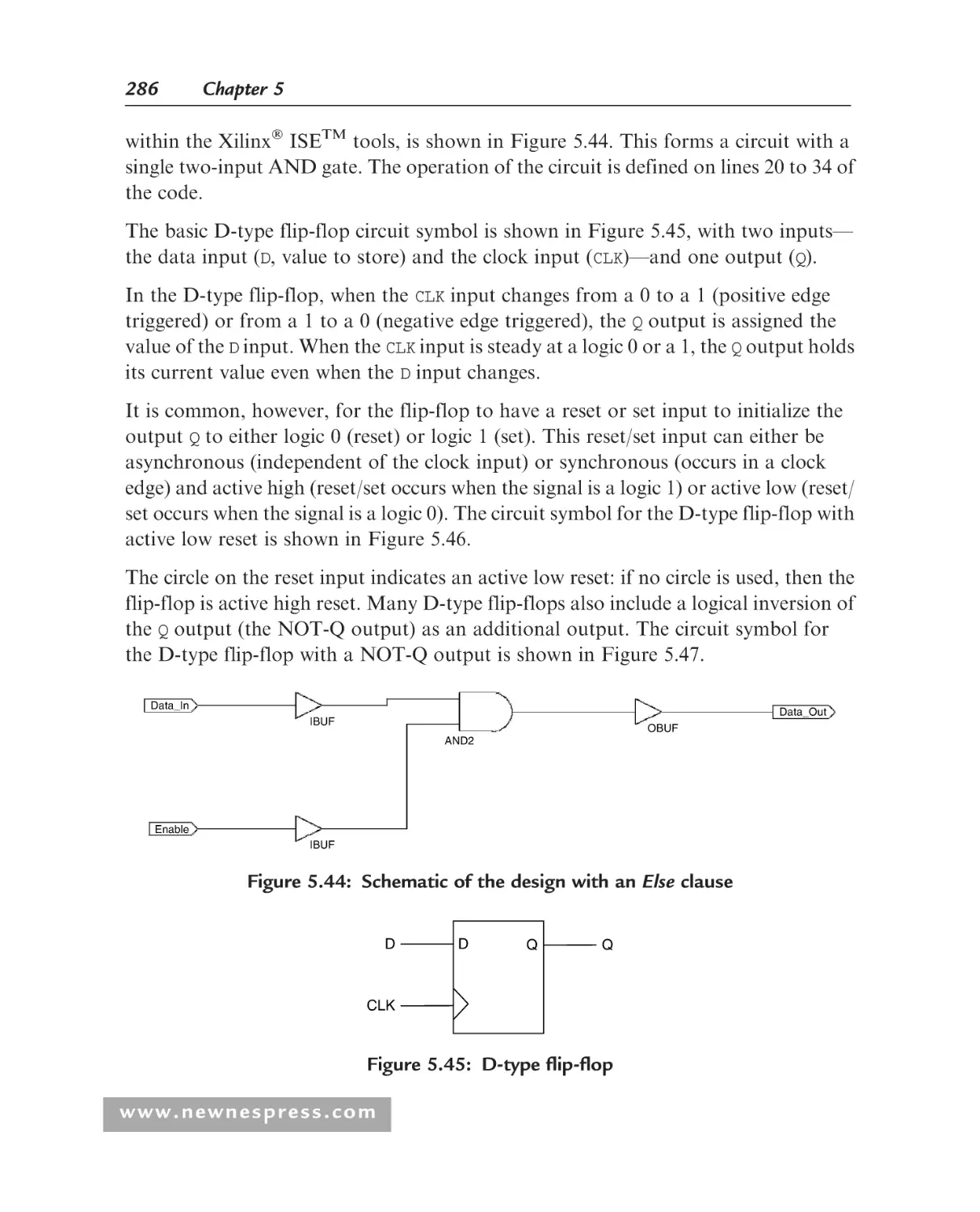
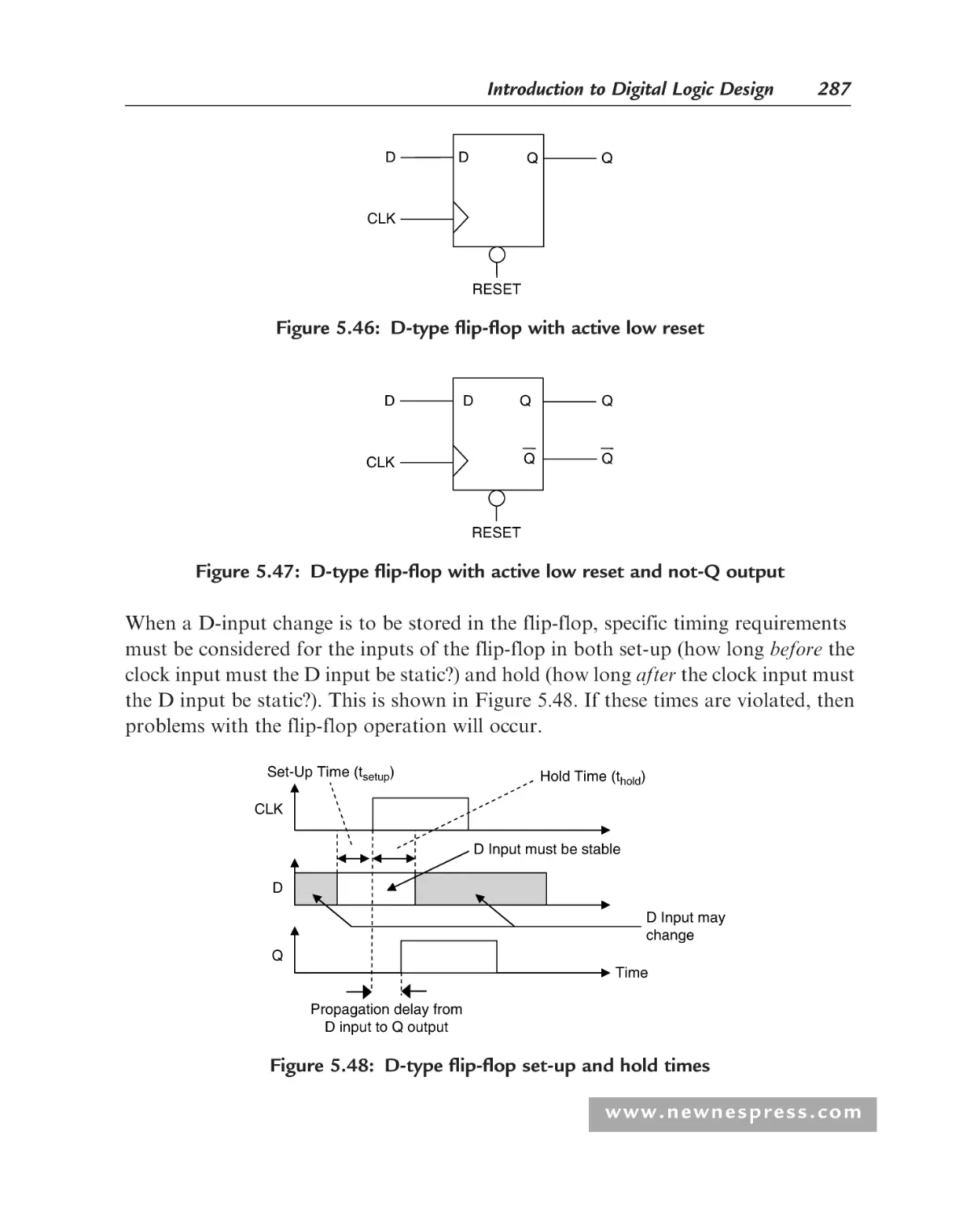
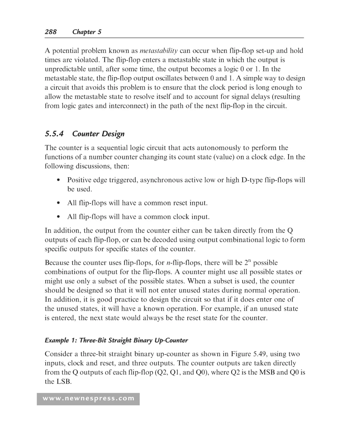
5.5.3 The D Latch and D-Type Flip-Flop ............................................. 283
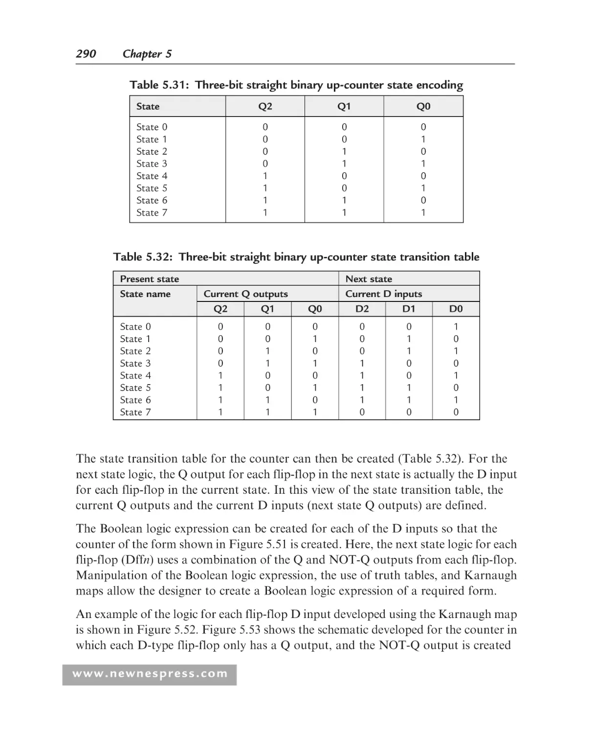
5.5.4 Counter Design.............................................................................. 288
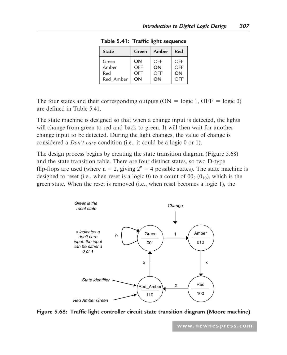
5.5.5 State Machine Design.................................................................... 305
5.5.6 Moore versus Mealy State Machines ............................................ 316
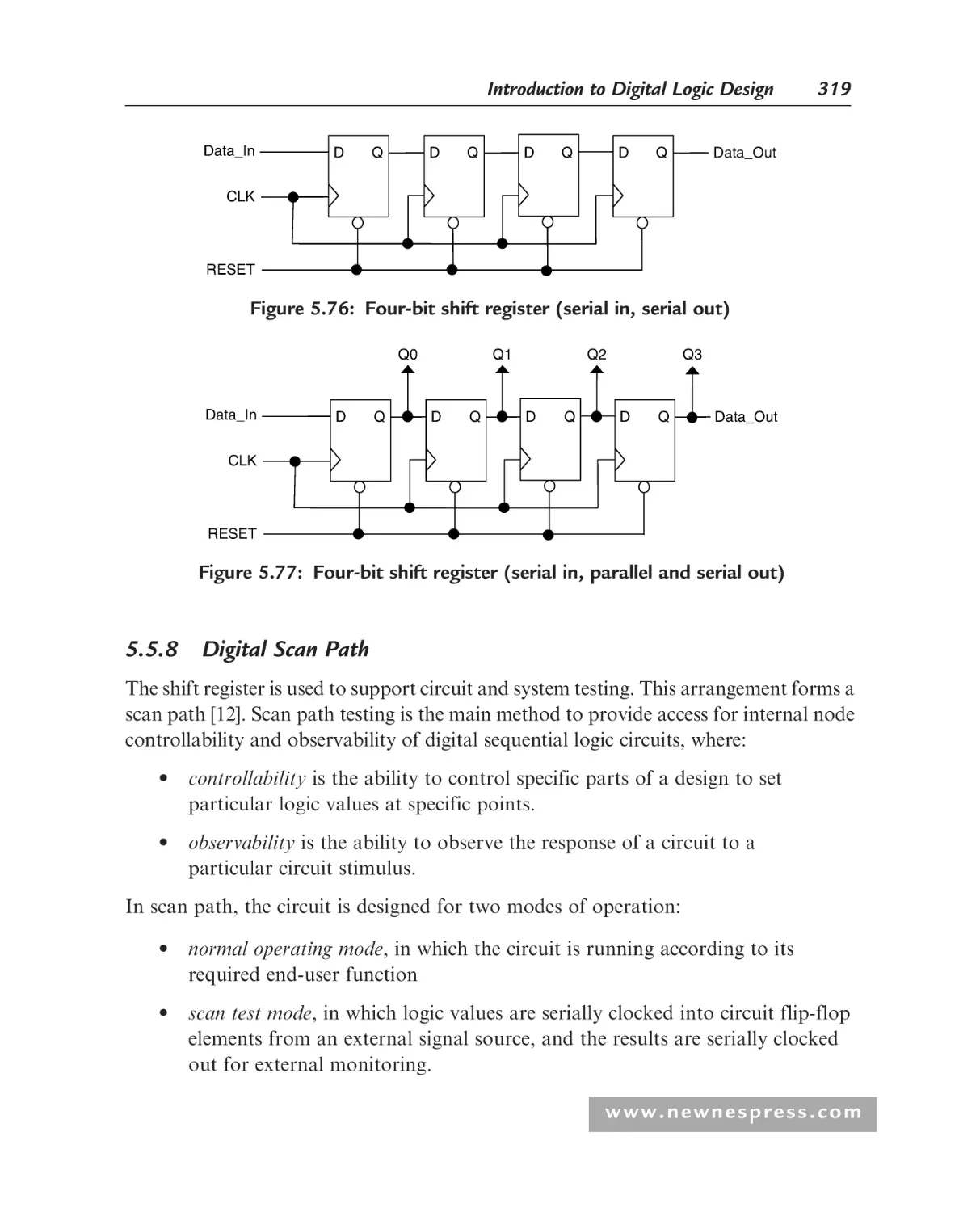
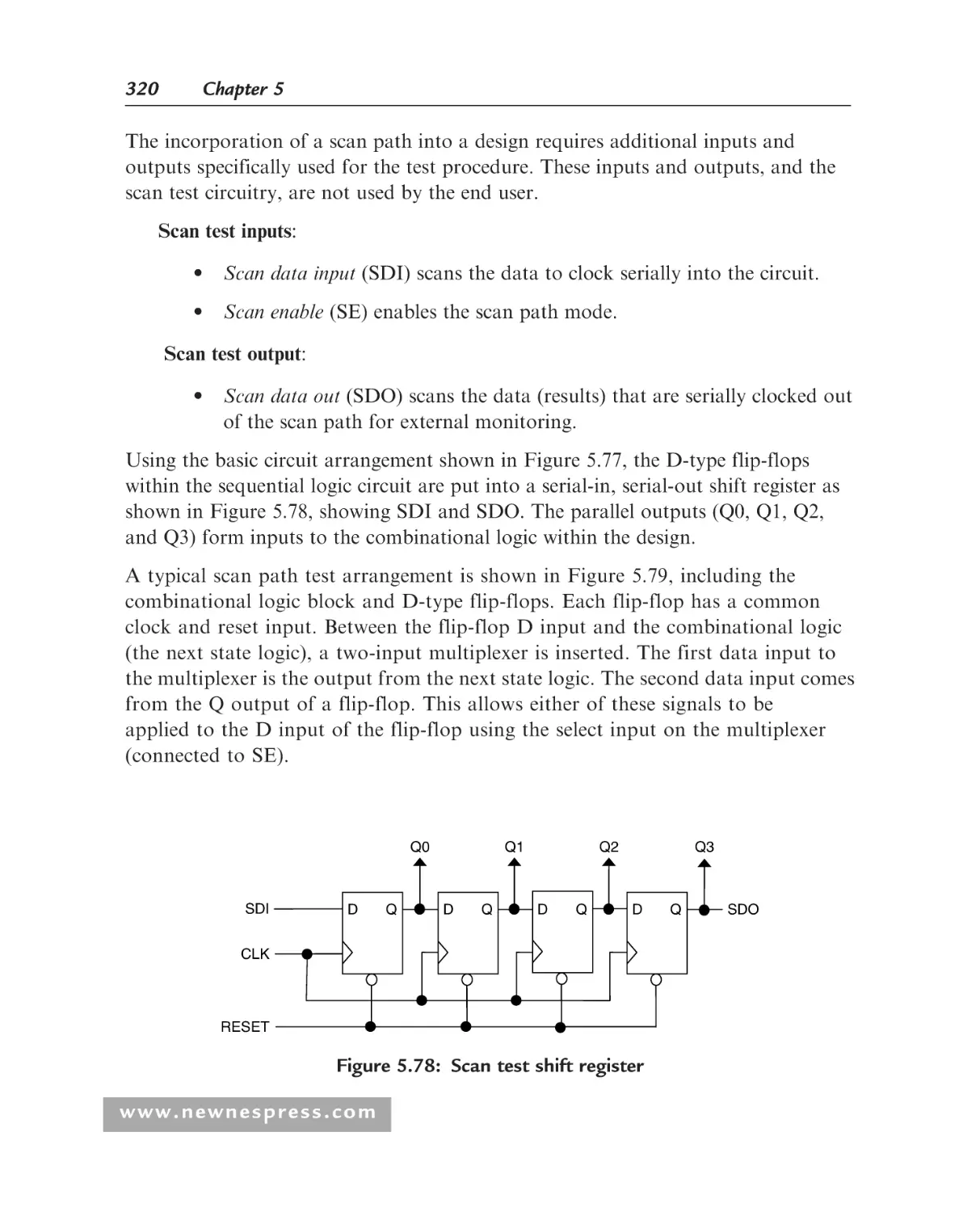
5.5.7 Shift Registers................................................................................ 317
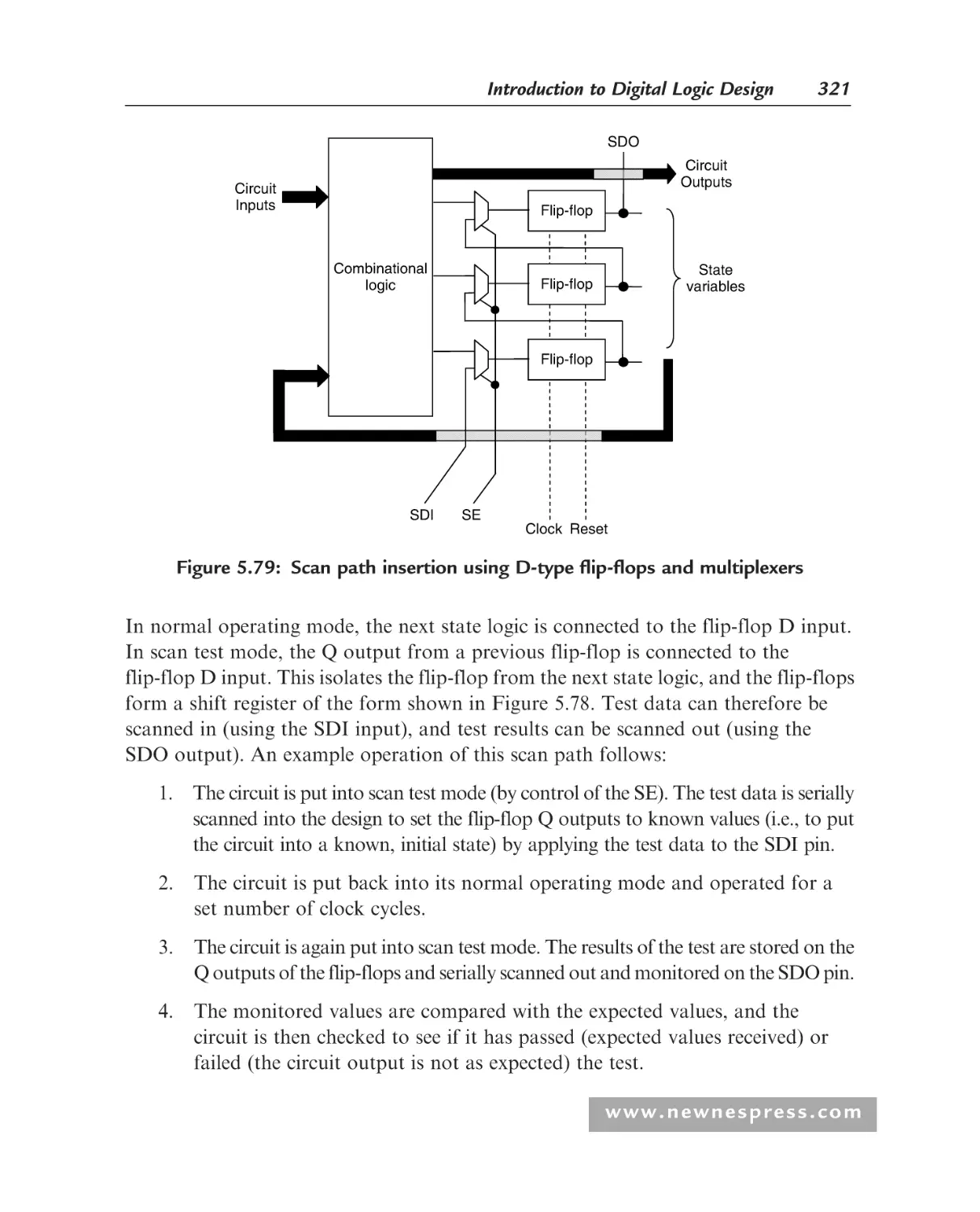
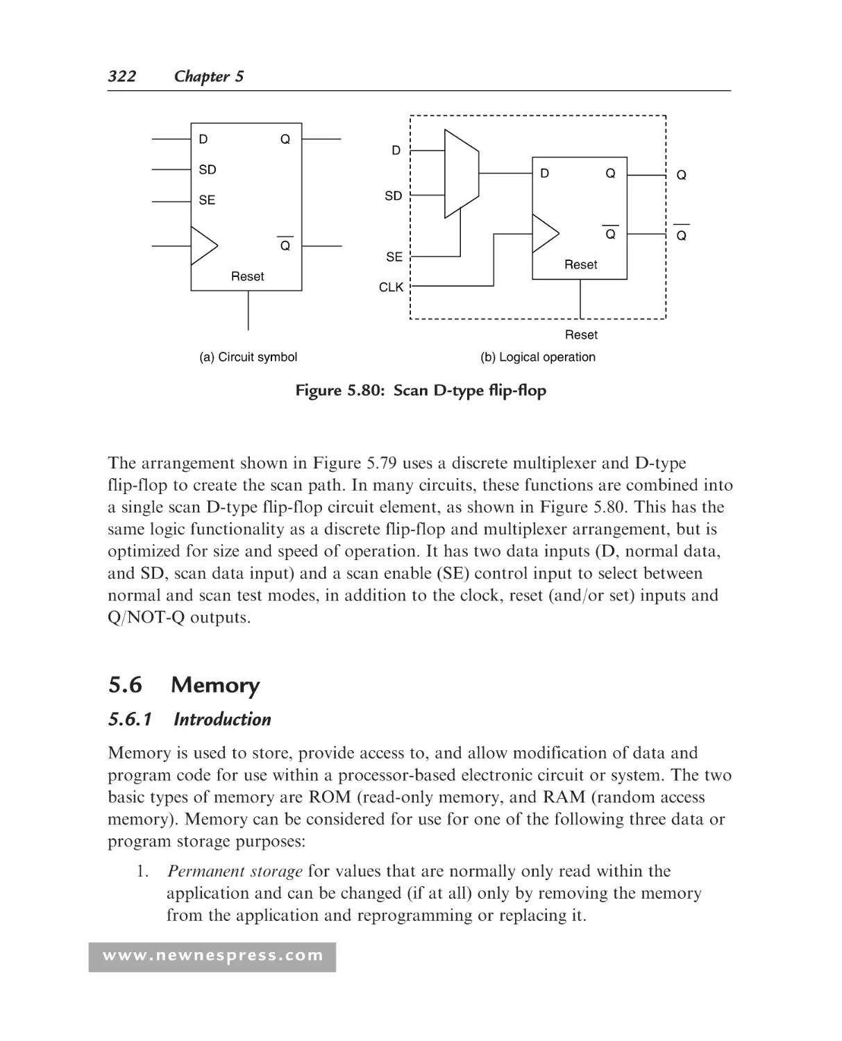
5.5.8 Digital Scan Path........................................................................... 319
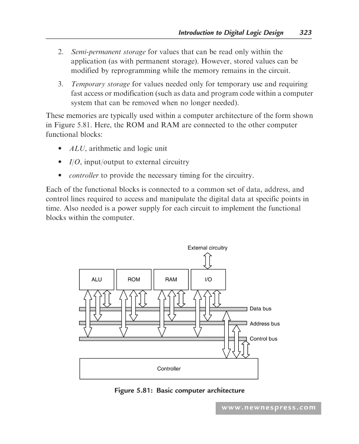
Memory................................................................................................... 322
5.6.1 Introduction .................................................................................. 322
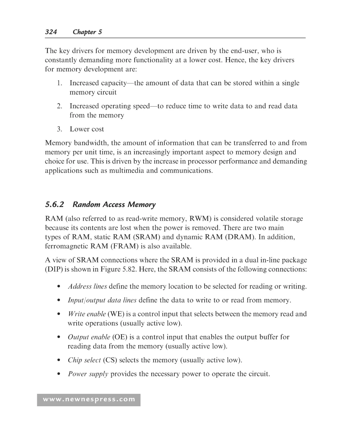
5.6.2 Random Access Memory .............................................................. 324
5.6.3 Read-Only Memory....................................................................... 325
References................................................................................................ 327
Student Exercises ..................................................................................... 328
Chapter 6: Introduction to Digital Logic Design with VHDL .......................... 333
6.1
6.2
Introduction ............................................................................................ 333
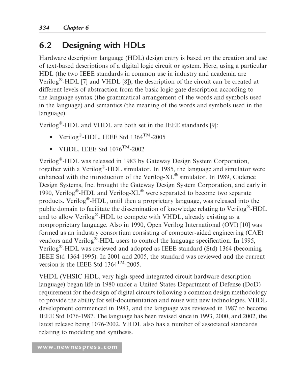
Designing with HDLs ............................................................................. 334
www.newnespress.com
Table of Contents
6.3
6.4
6.5
6.6
6.7
6.8
6.9
6.10
6.11
6.12
6.13
6.14
6.15
6.16
6.17
xi
Design Entry Methods ............................................................................ 338
6.3.1 Introduction .................................................................................. 338
6.3.2 Schematic Capture......................................................................... 338
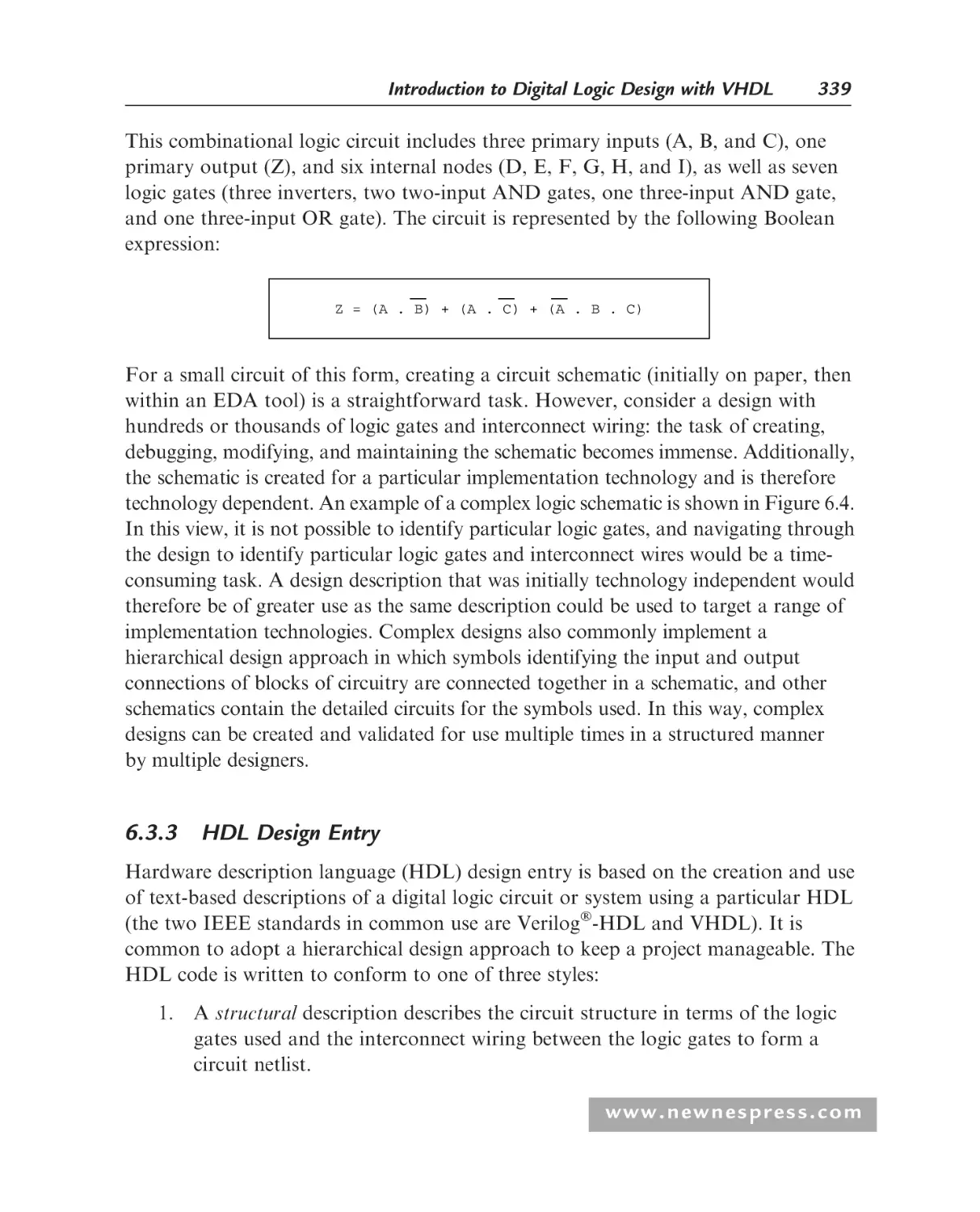
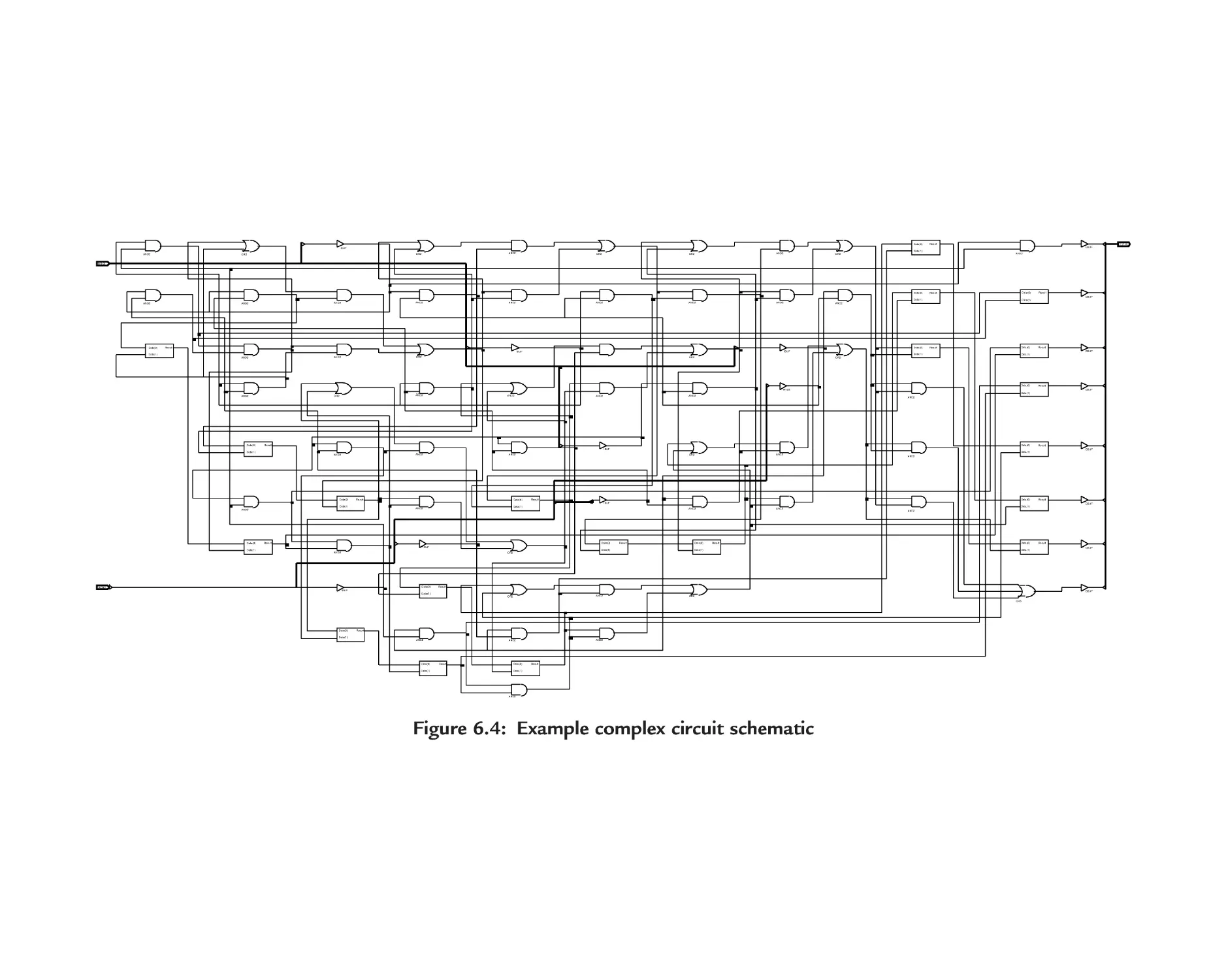
6.3.3 HDL Design Entry ........................................................................ 339
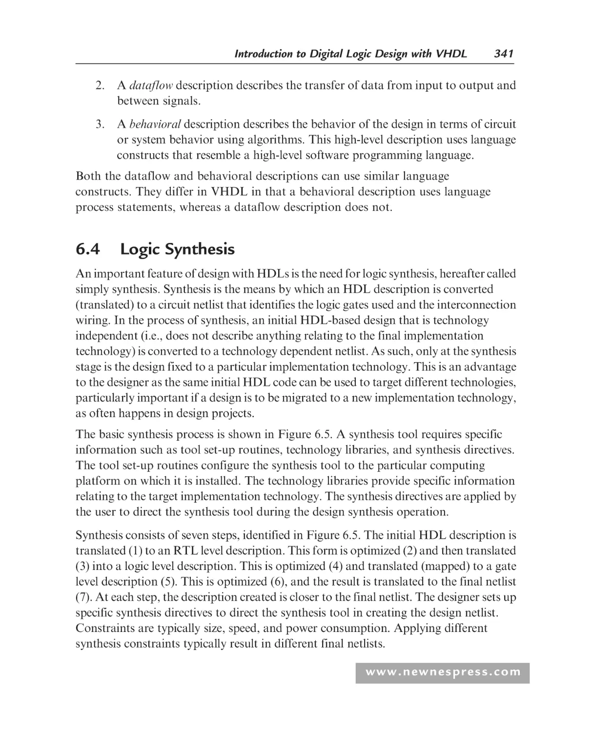
Logic Synthesis........................................................................................ 341
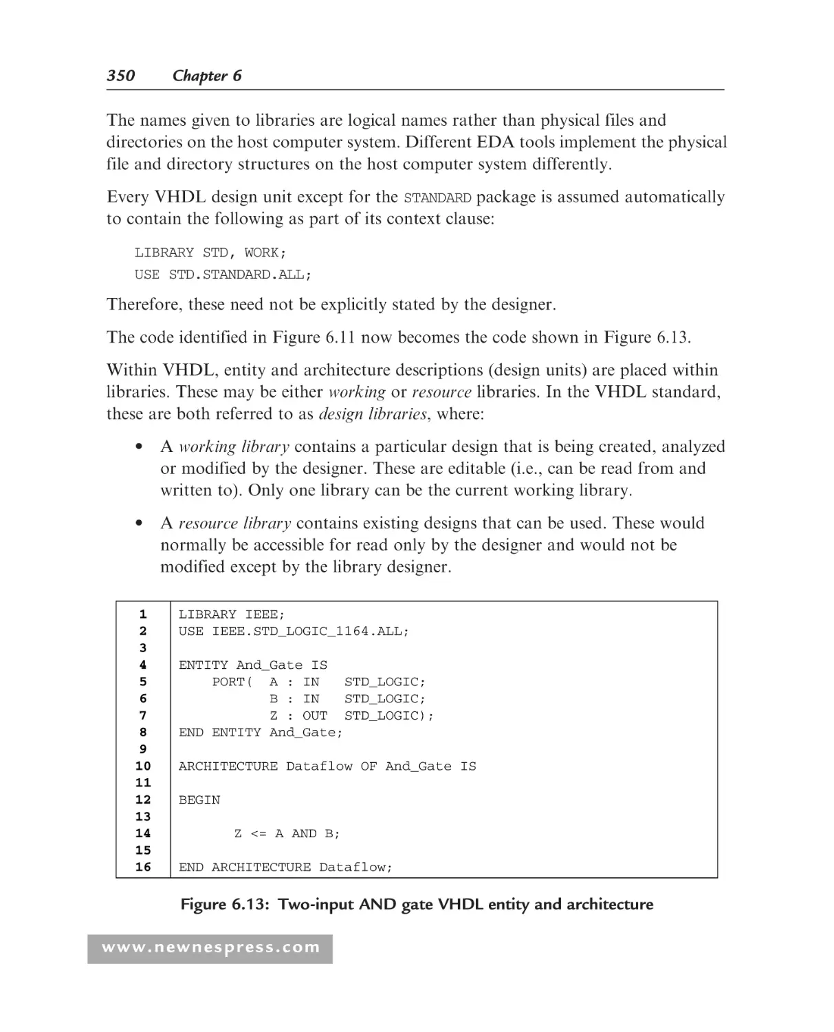
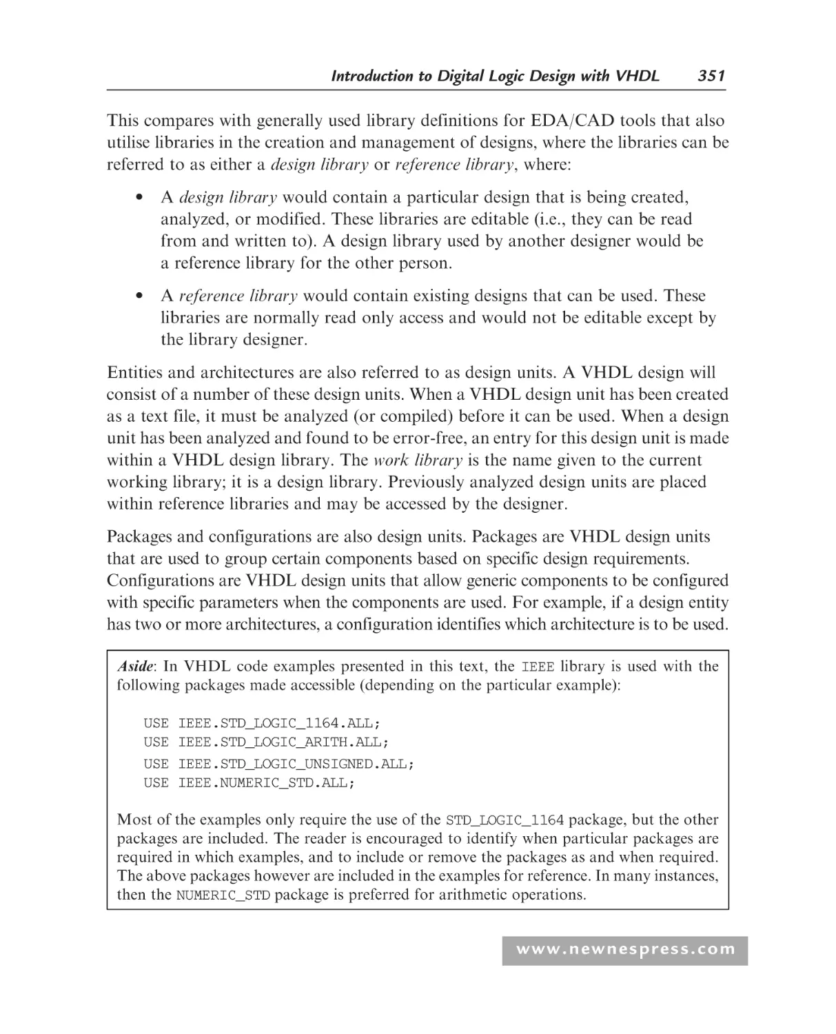
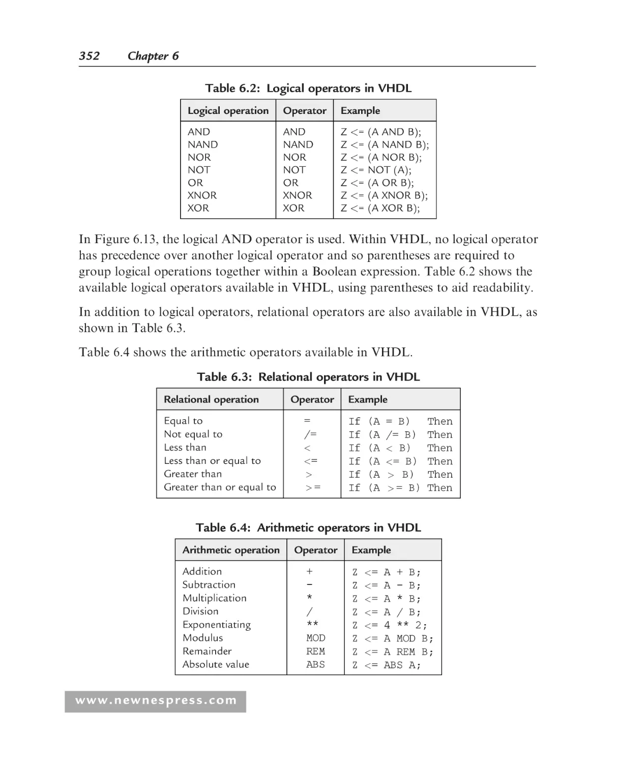
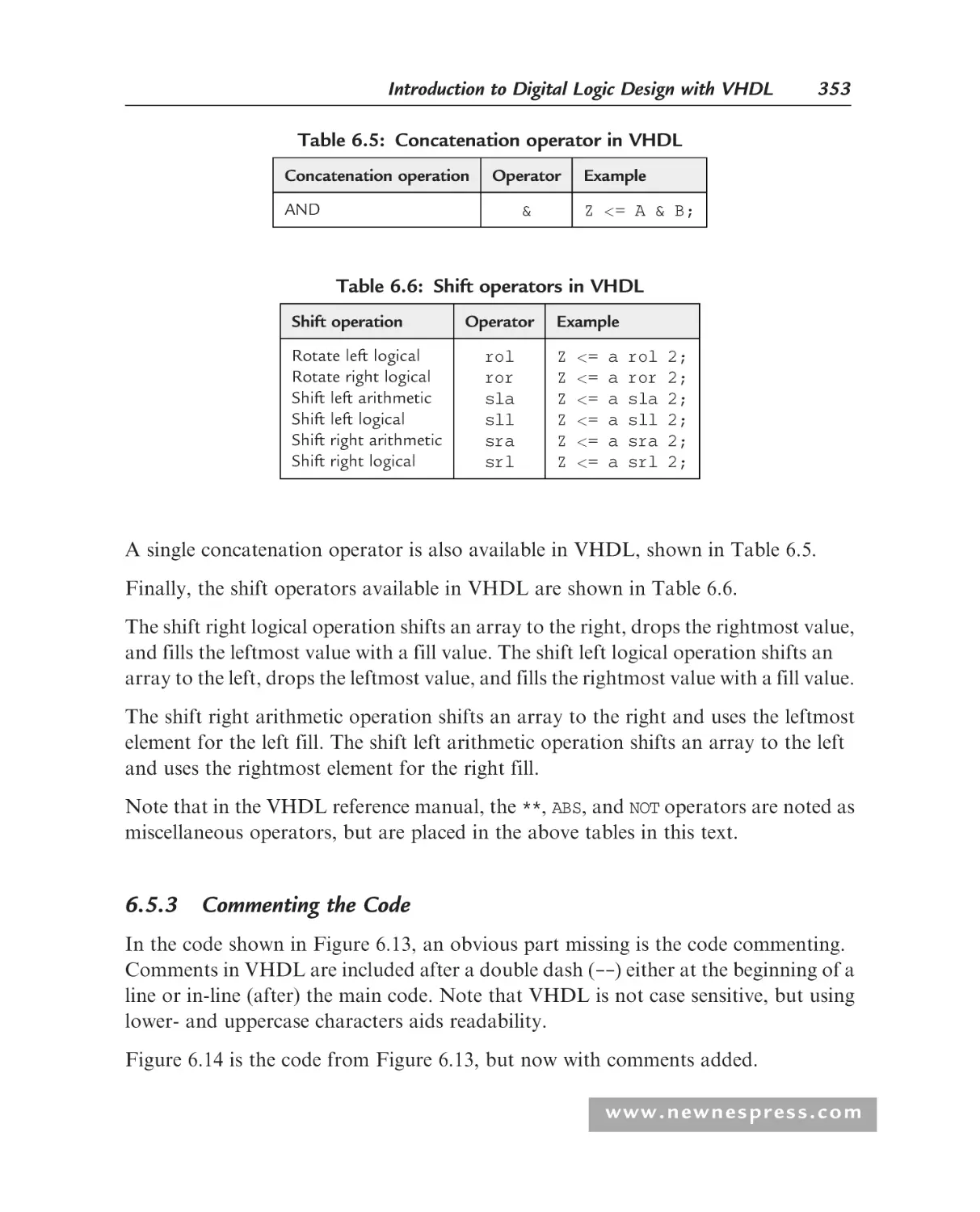
Entities, Architectures, Packages, and Configurations............................ 344
6.5.1 Introduction .................................................................................. 344
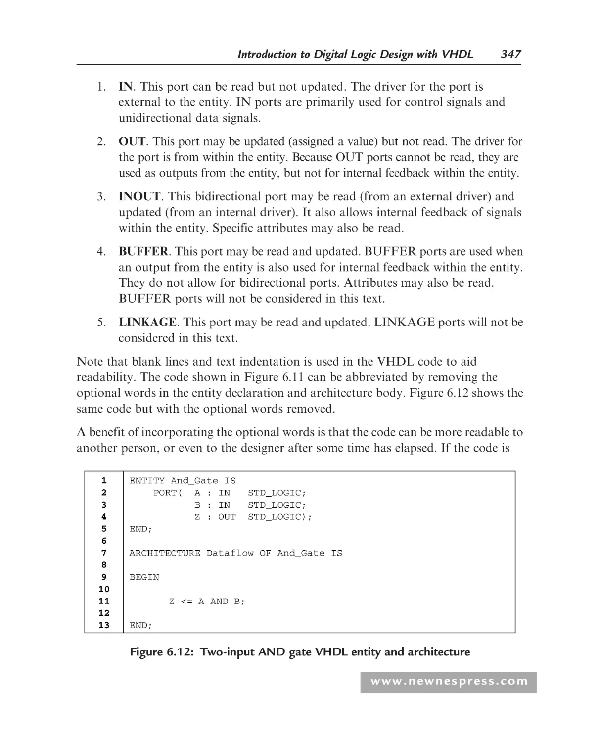
6.5.2 AND Gate Example ...................................................................... 346
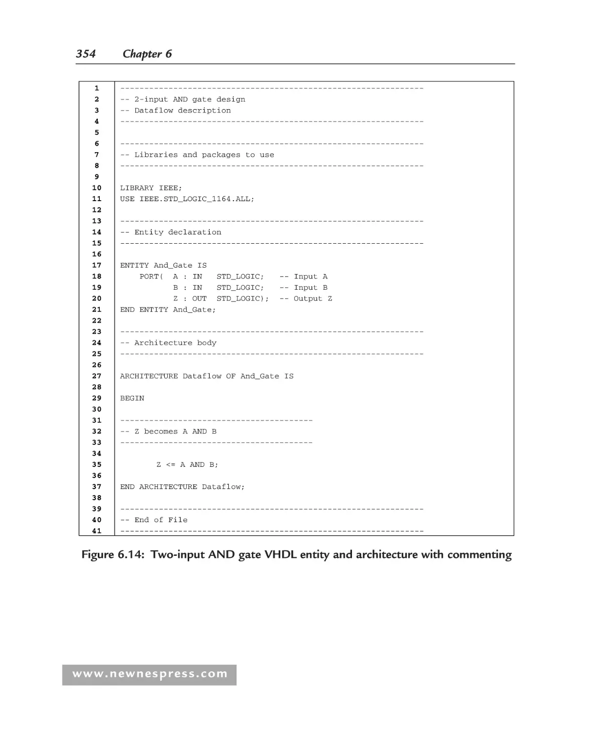
6.5.3 Commenting the Code................................................................... 353
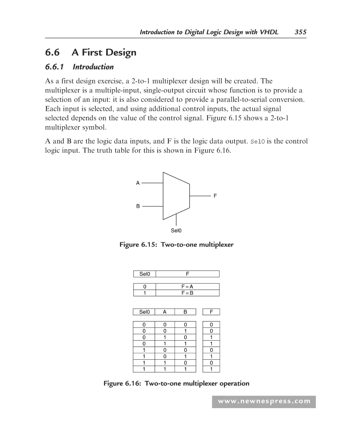
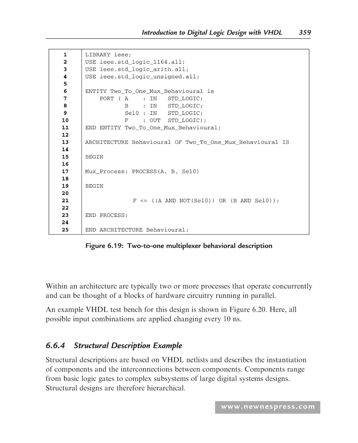
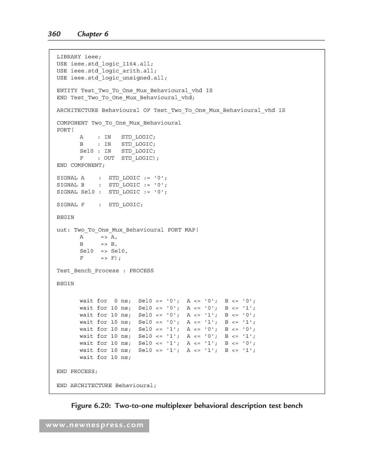
A First Design......................................................................................... 355
6.6.1 Introduction .................................................................................. 355
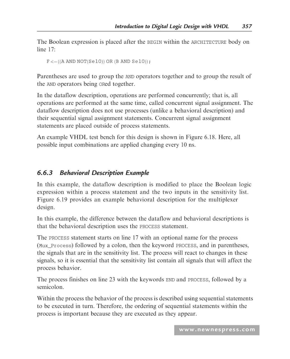
6.6.2 Dataflow Description Example ..................................................... 356
6.6.3 Behavioral Description Example ................................................... 357
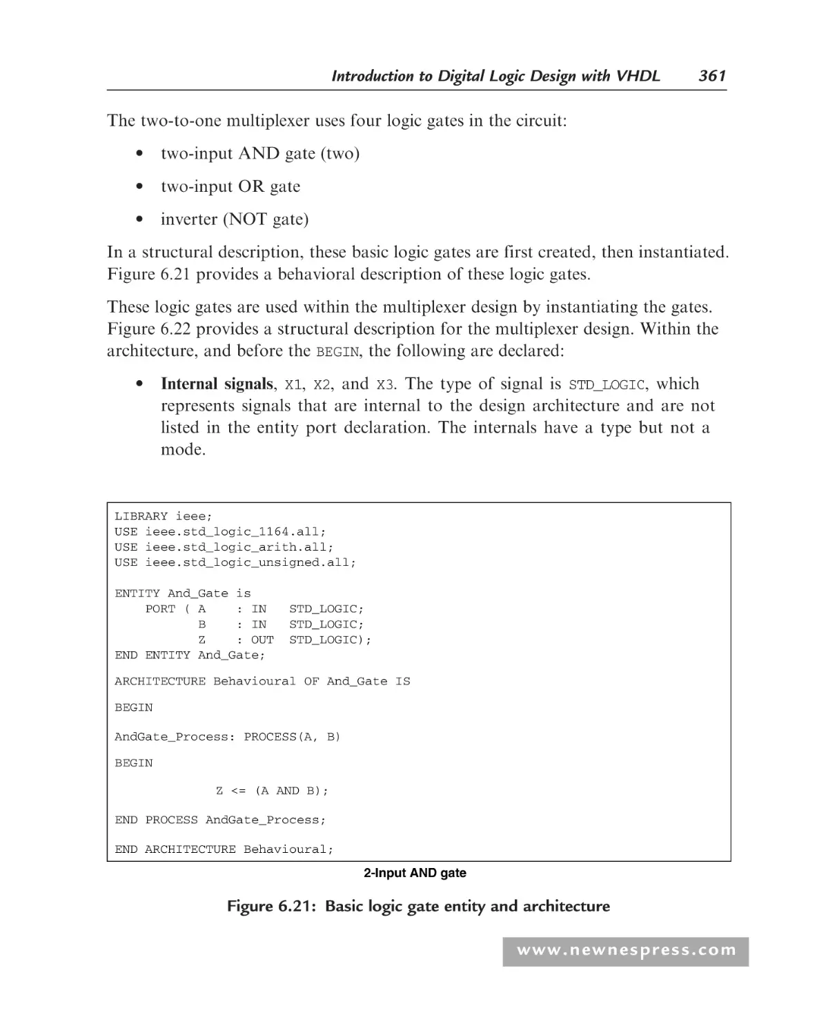
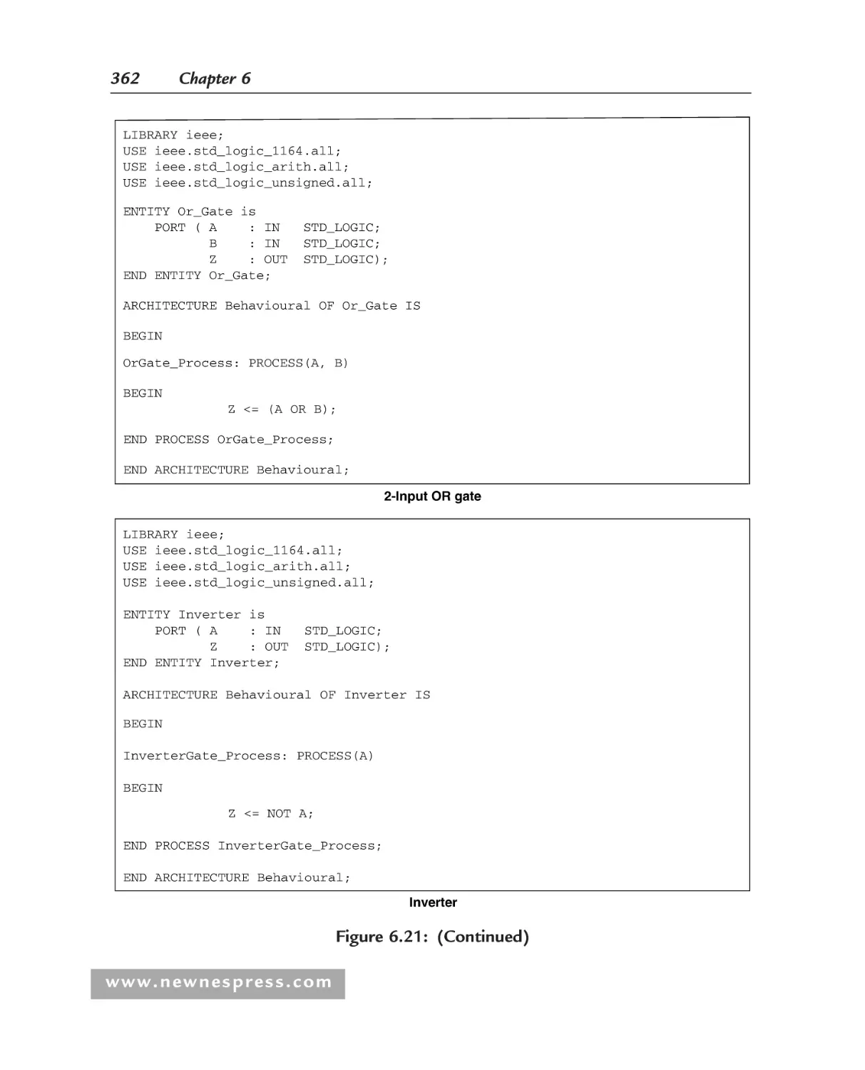
6.6.4 Structural Description Example .................................................... 359
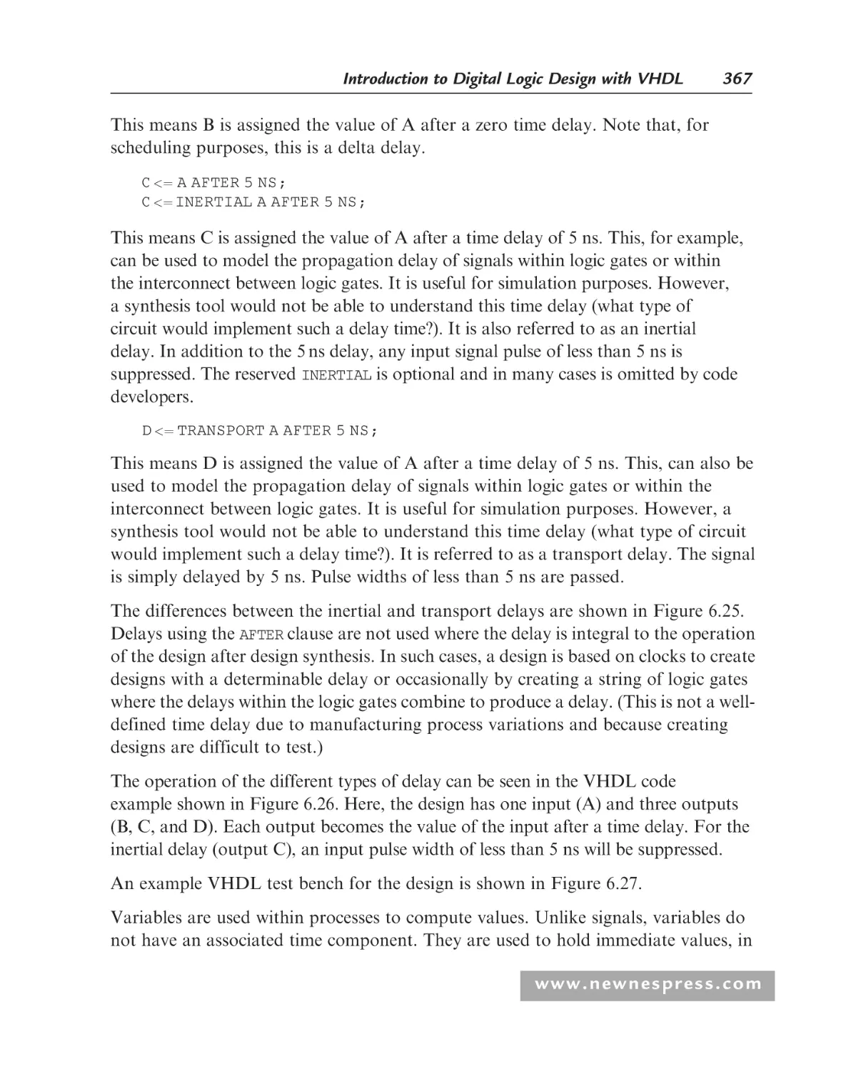
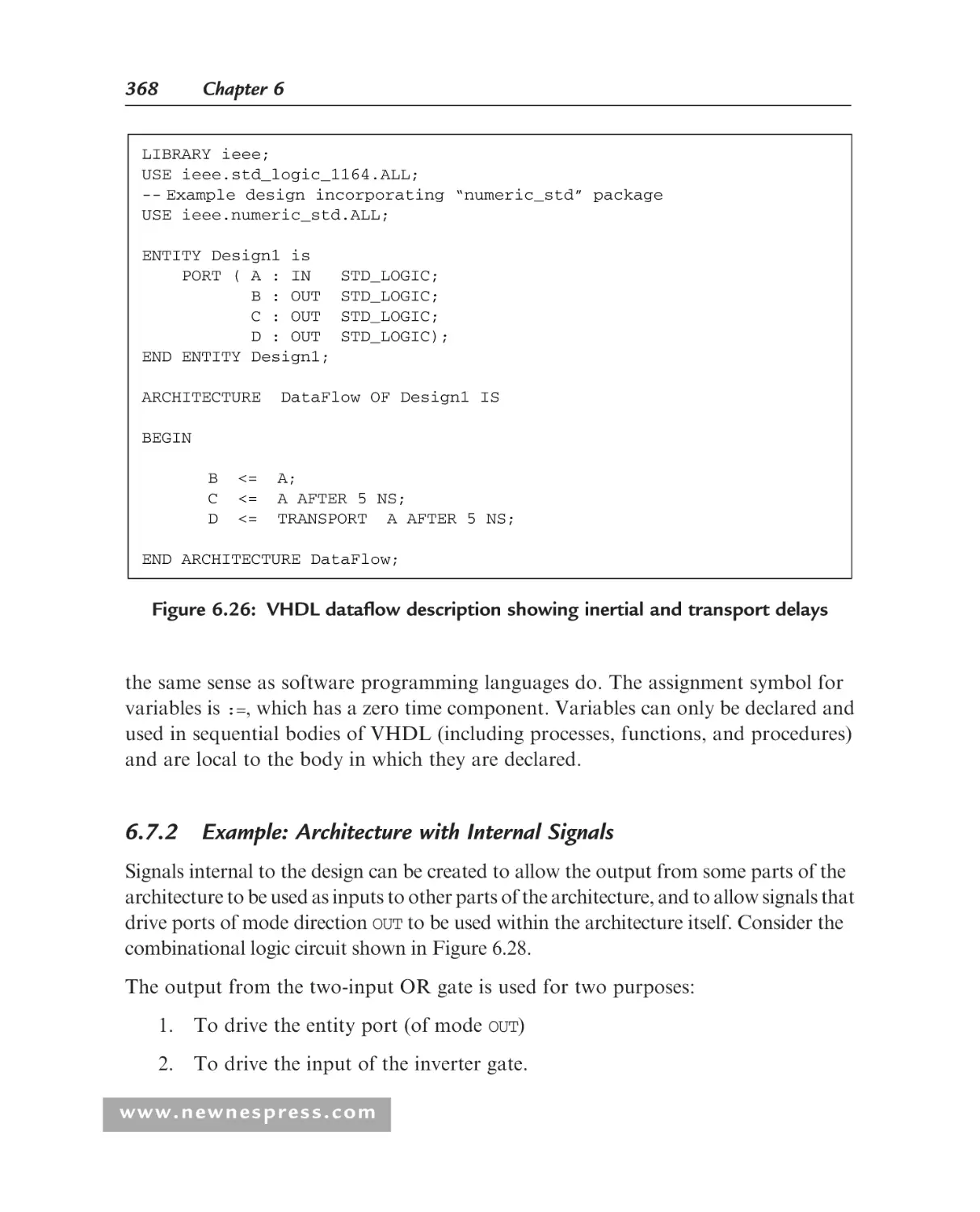
Signals versus Variables .......................................................................... 366
6.7.1 Introduction .................................................................................. 366
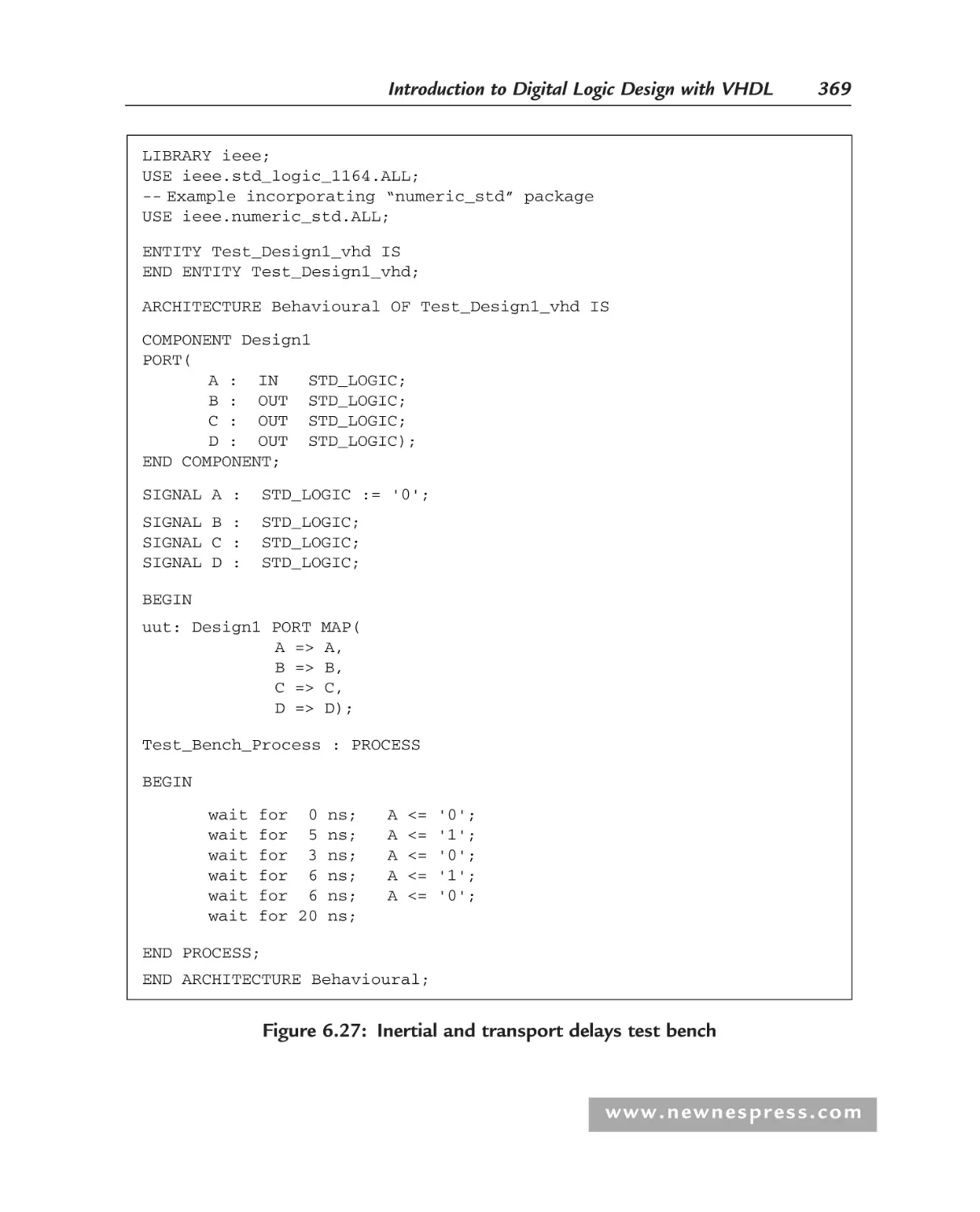
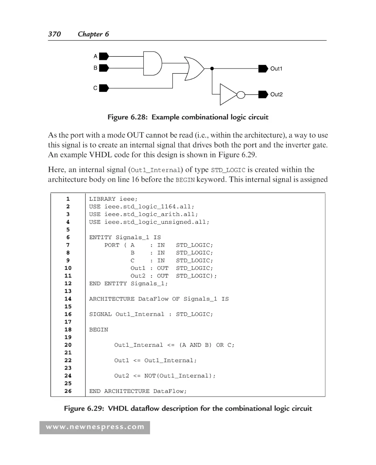
6.7.2 Example: Architecture with Internal Signals ................................. 368
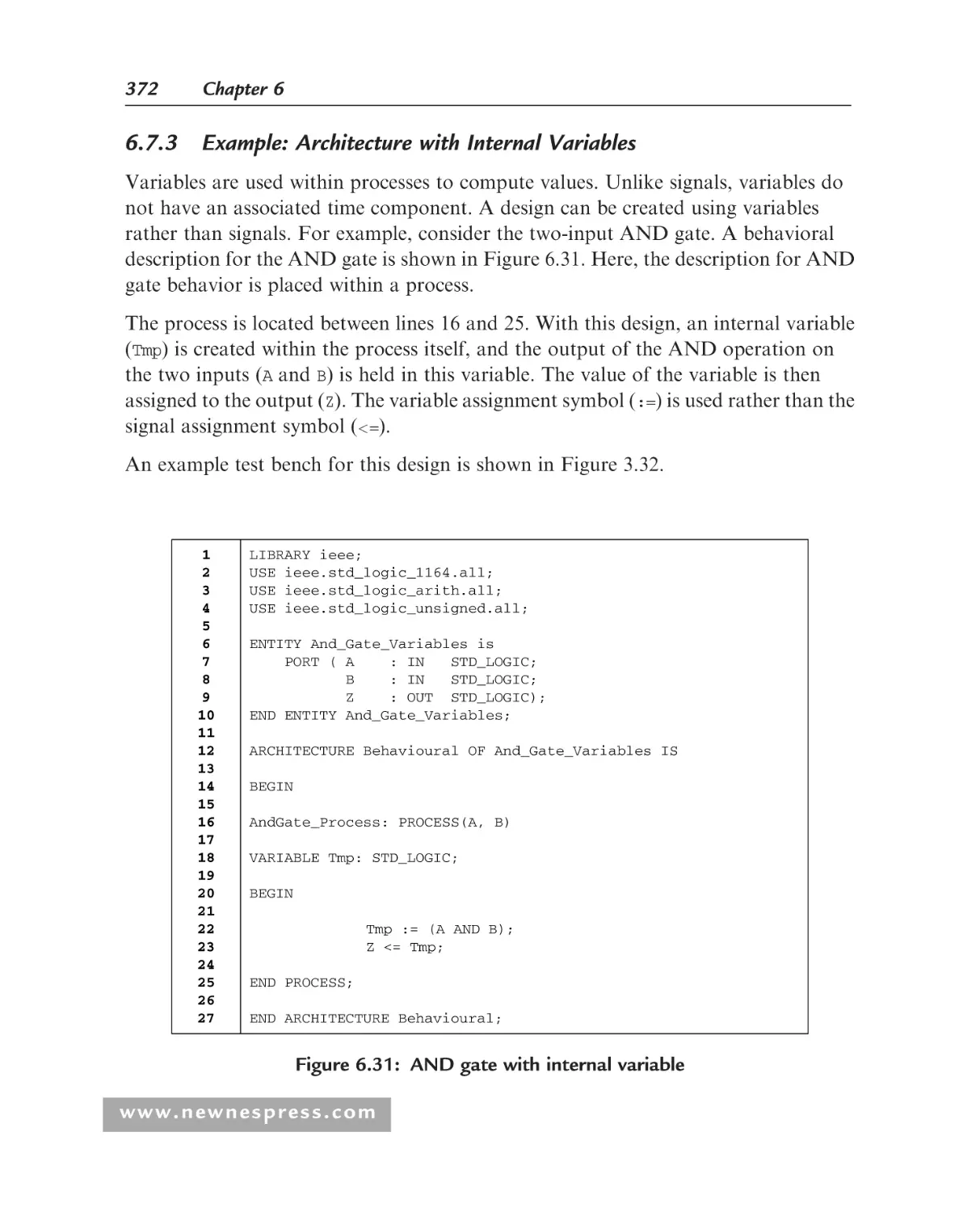
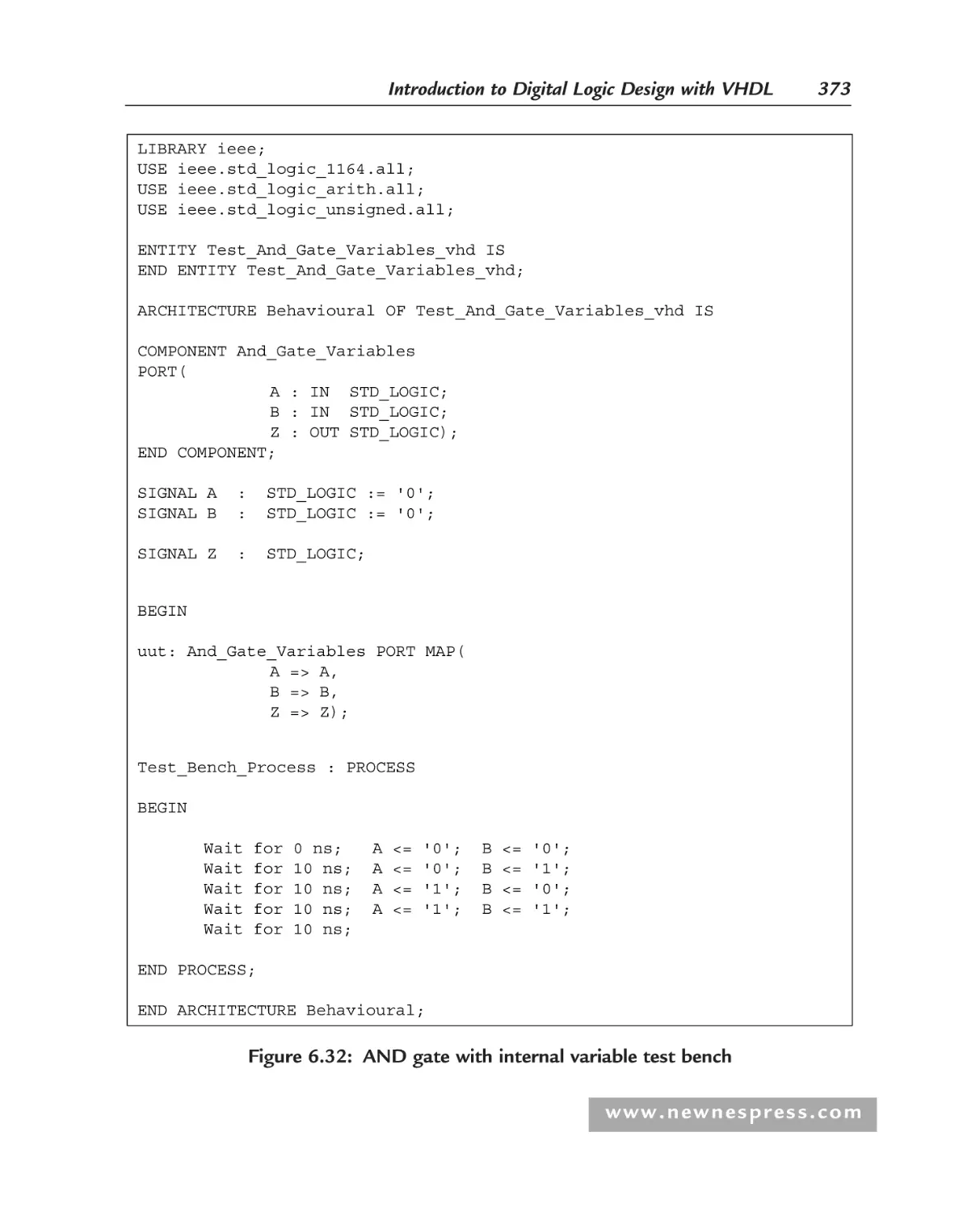
6.7.3 Example: Architecture with Internal Variables ............................. 372
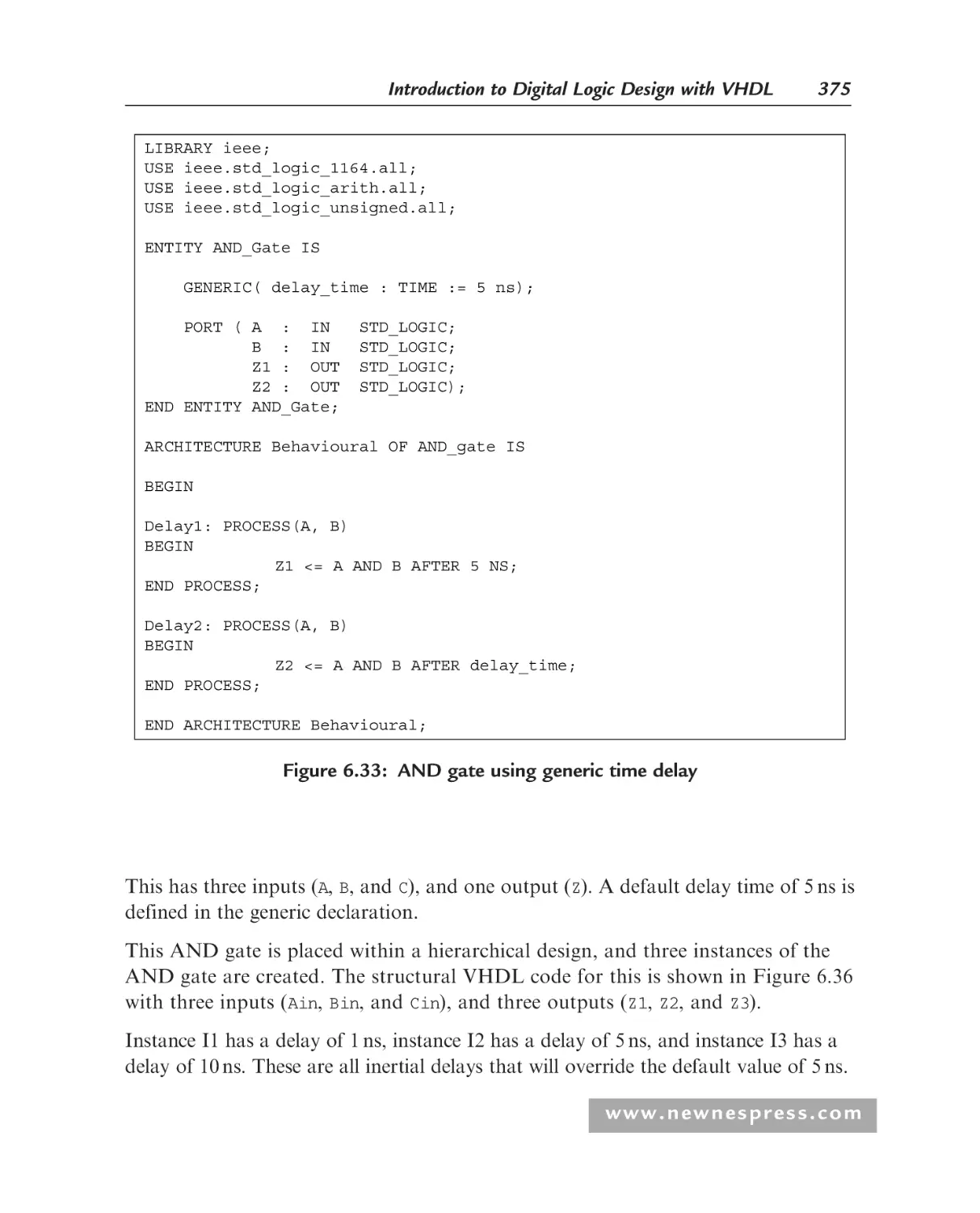
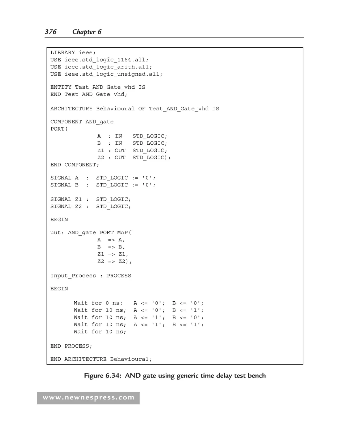
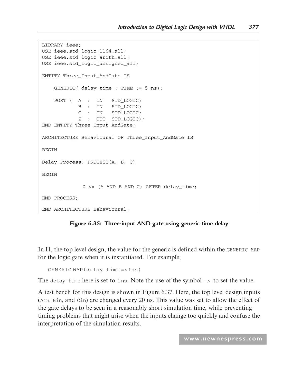
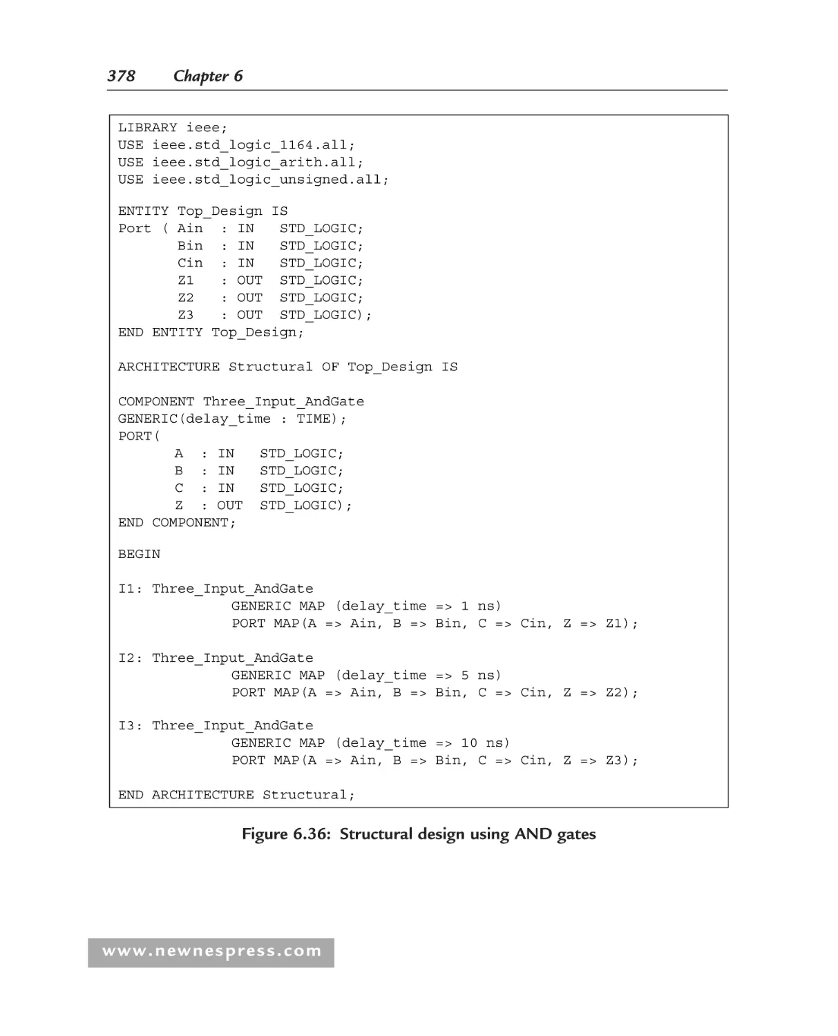
Generics................................................................................................... 374
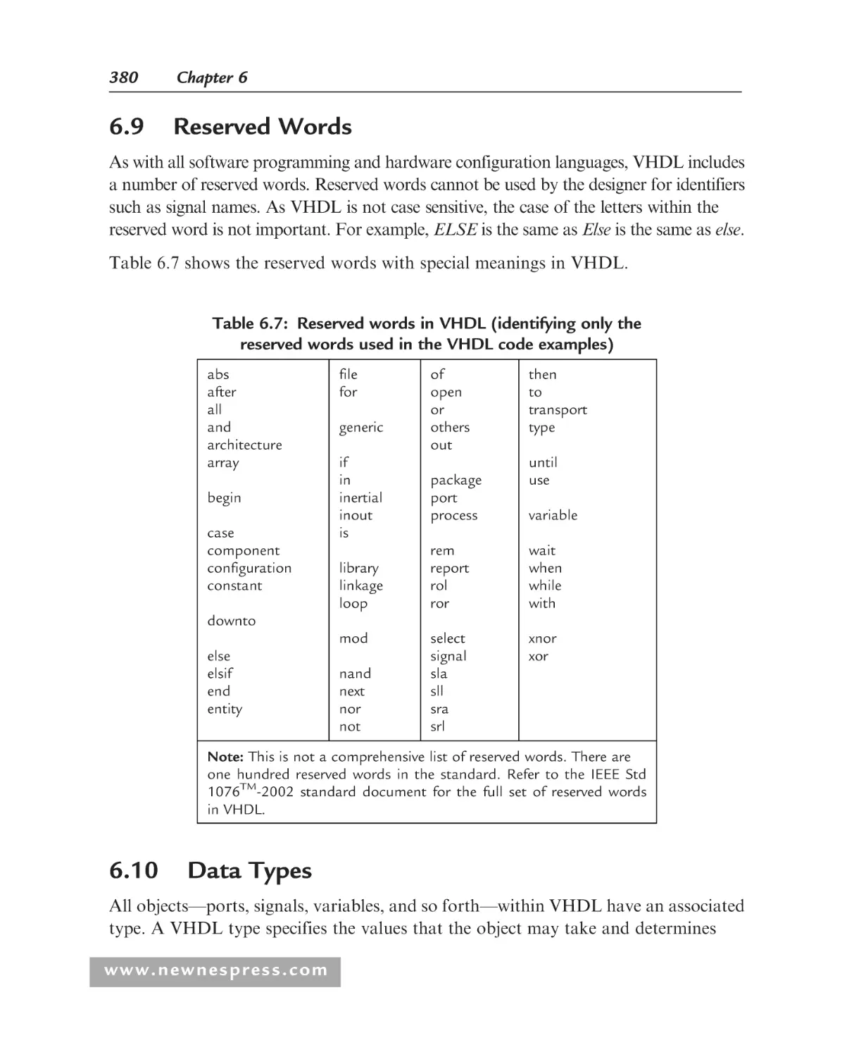
Reserved Words ...................................................................................... 380
Data Types .............................................................................................. 380
Concurrent versus Sequential Statements................................................ 383
Loops and Program Control ................................................................... 383
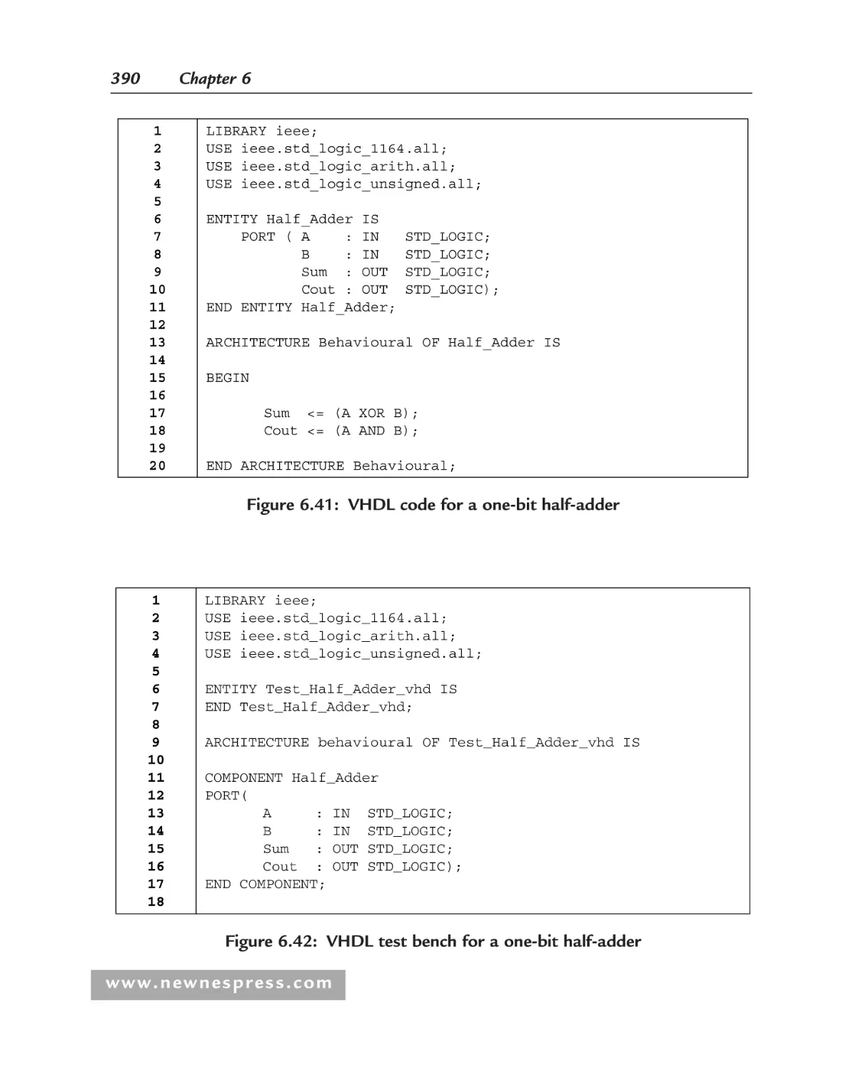
Coding Styles for VHDL......................................................................... 385
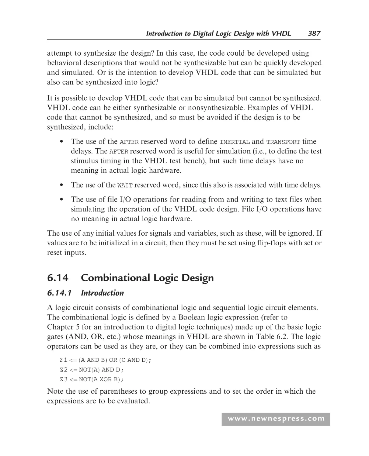
Combinational Logic Design................................................................... 387
6.14.1 Introduction................................................................................. 387
6.14.2 Complex Logic Gates .................................................................. 388
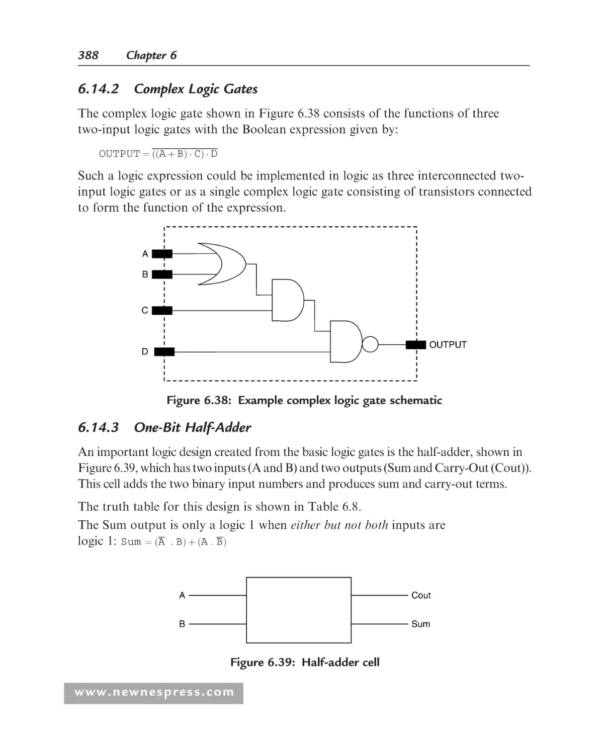
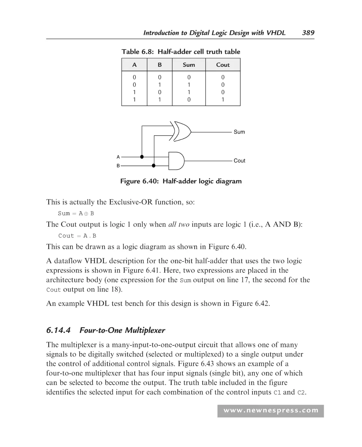
6.14.3 One-Bit Half-Adder ..................................................................... 388
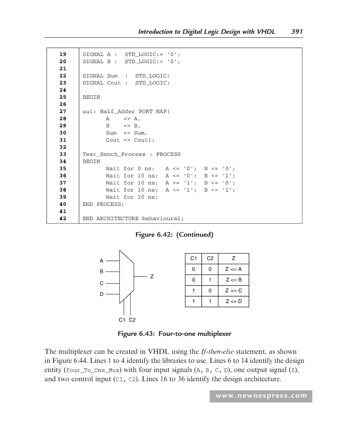
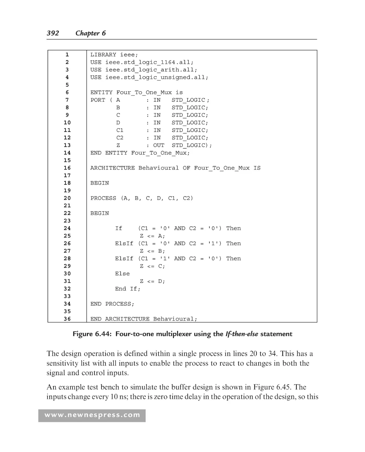
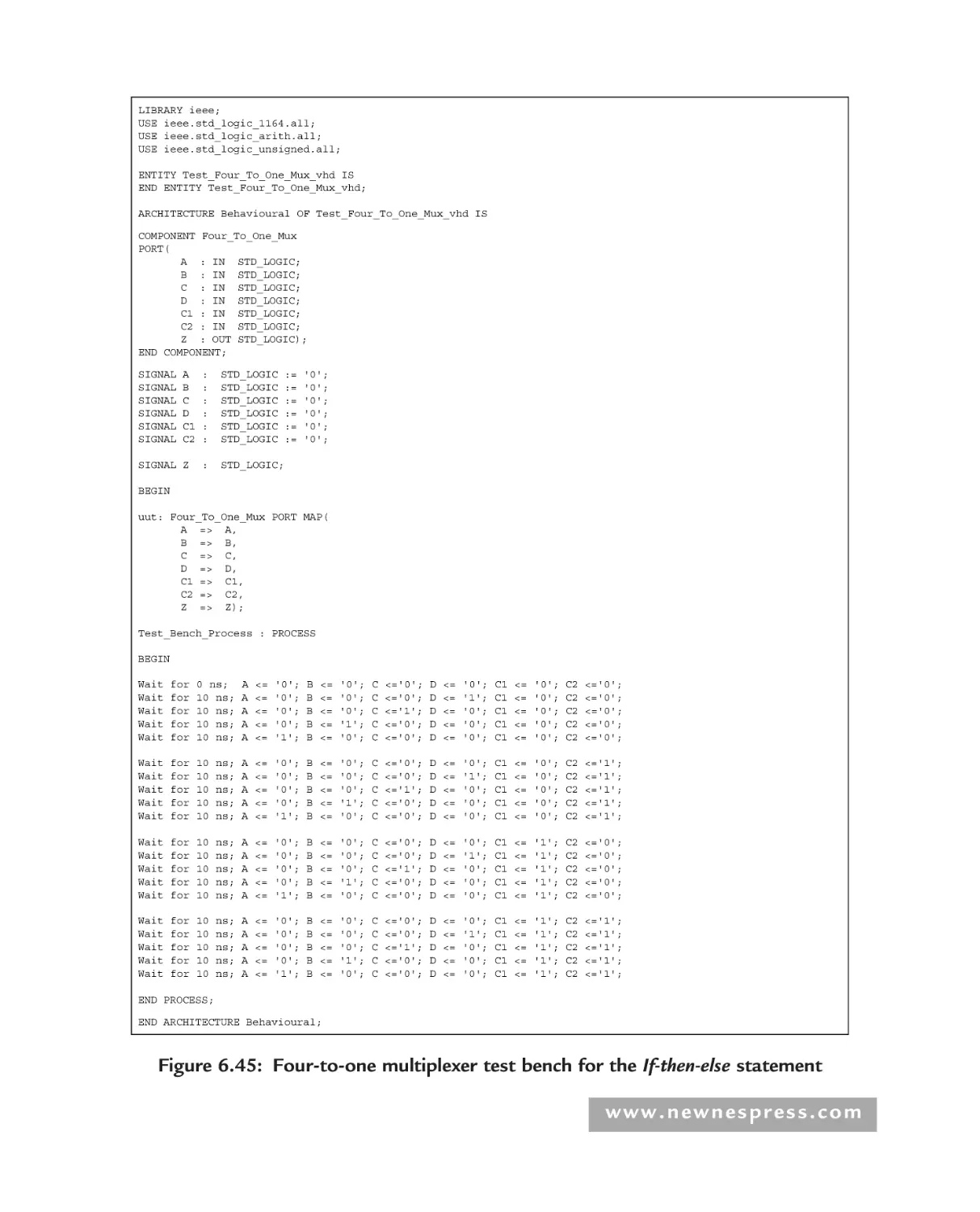
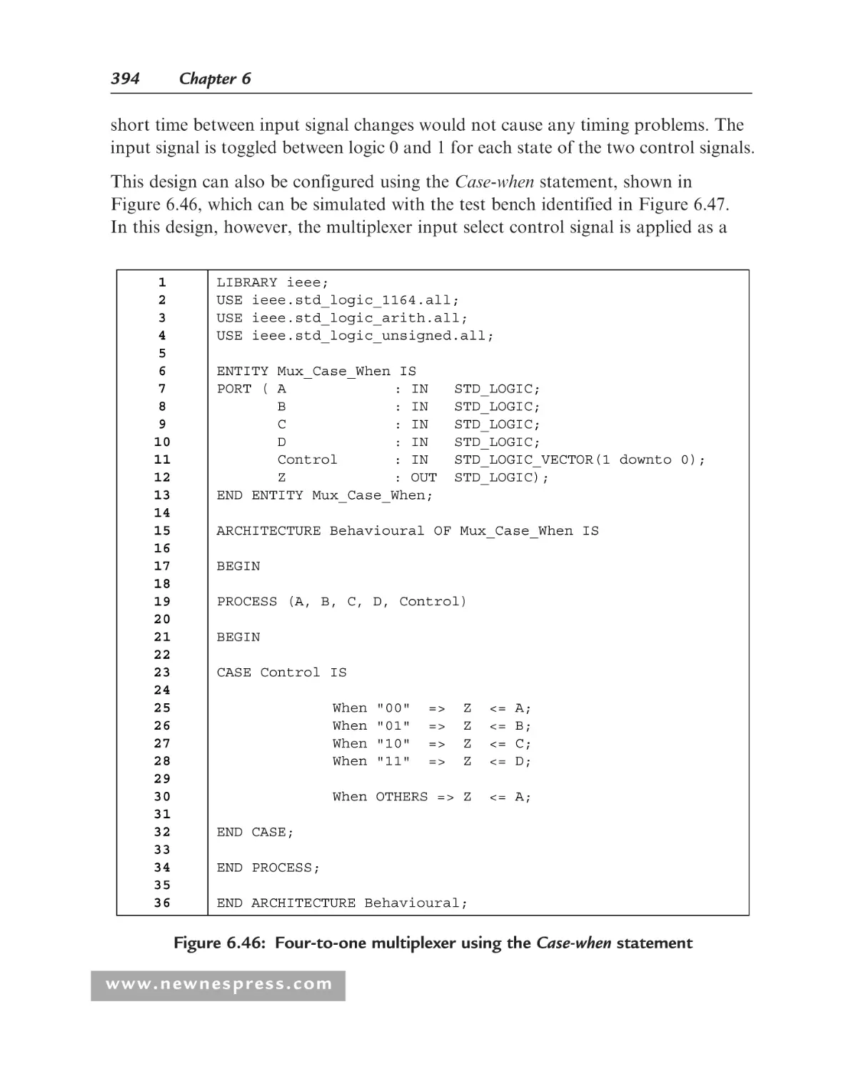
6.14.4 Four-to-One Multiplexer ............................................................. 389
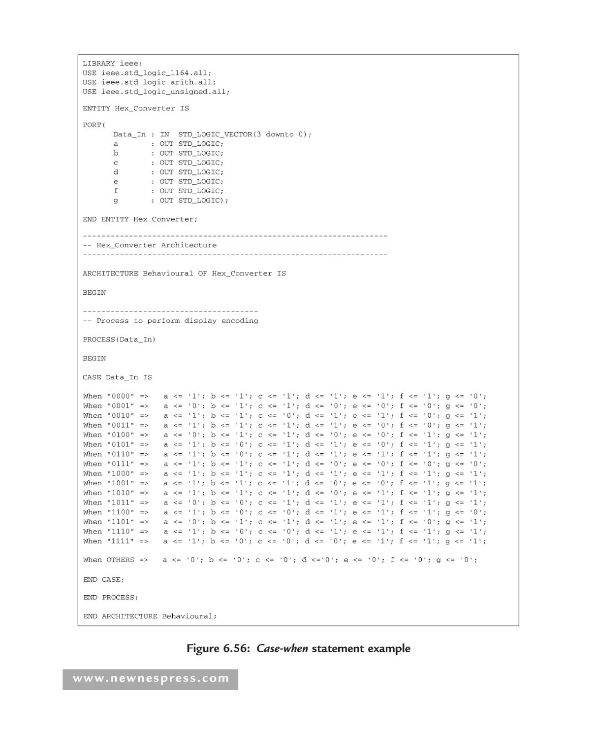
6.14.5 Thermometer-to-Binary Encoder................................................. 397
6.14.6 Seven-Segment Display Driver .................................................... 398
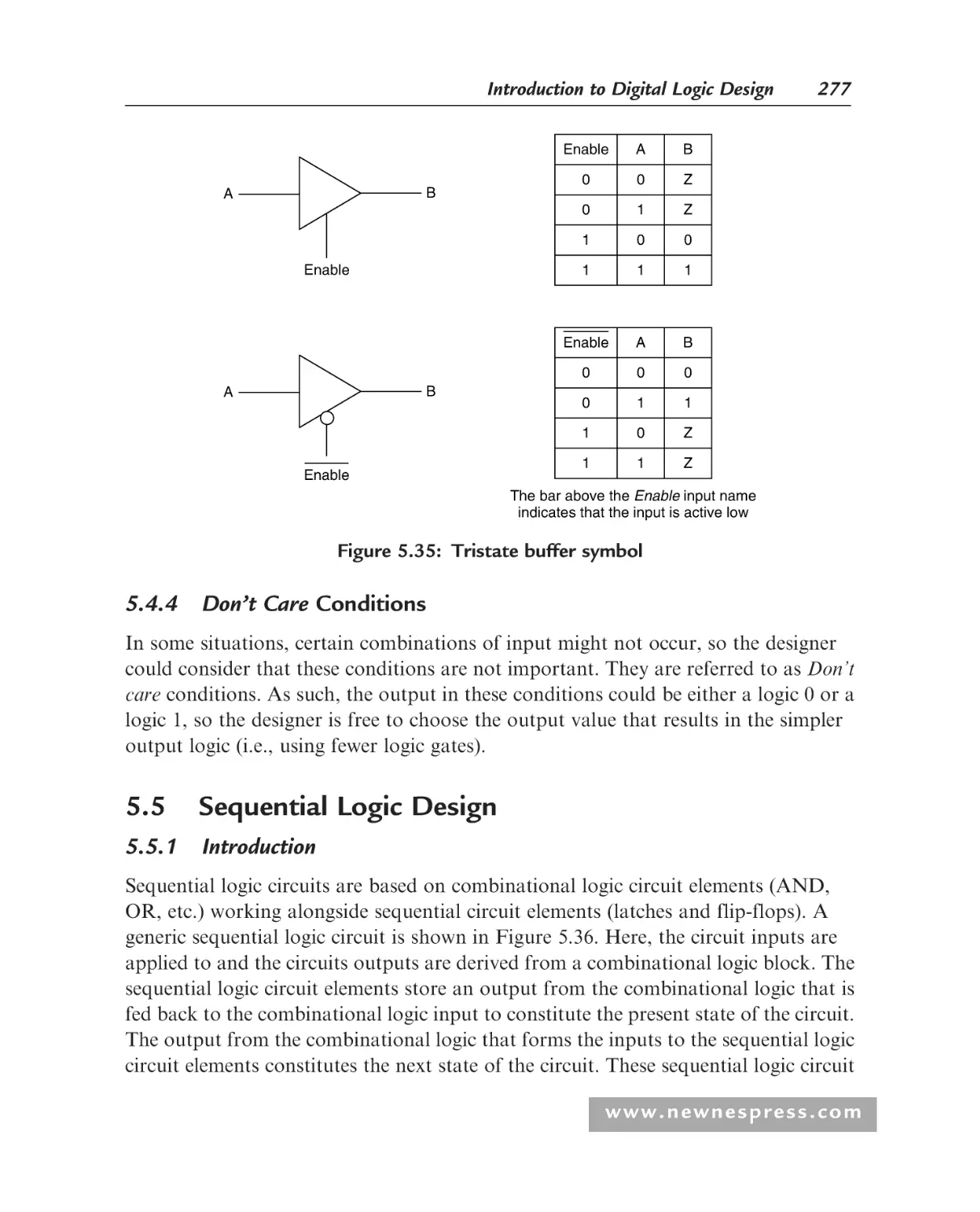
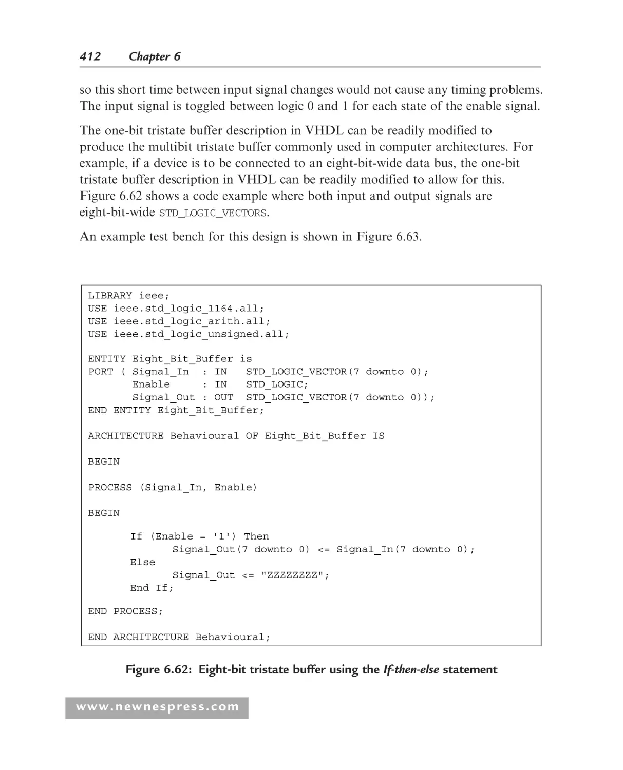
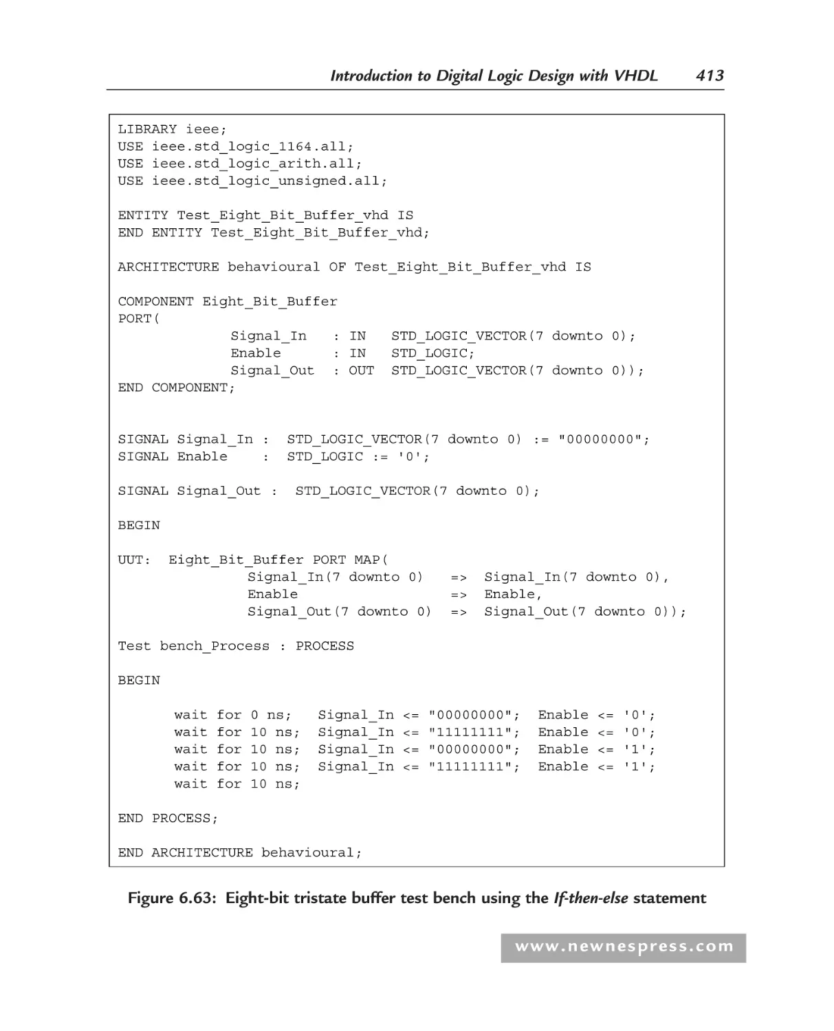
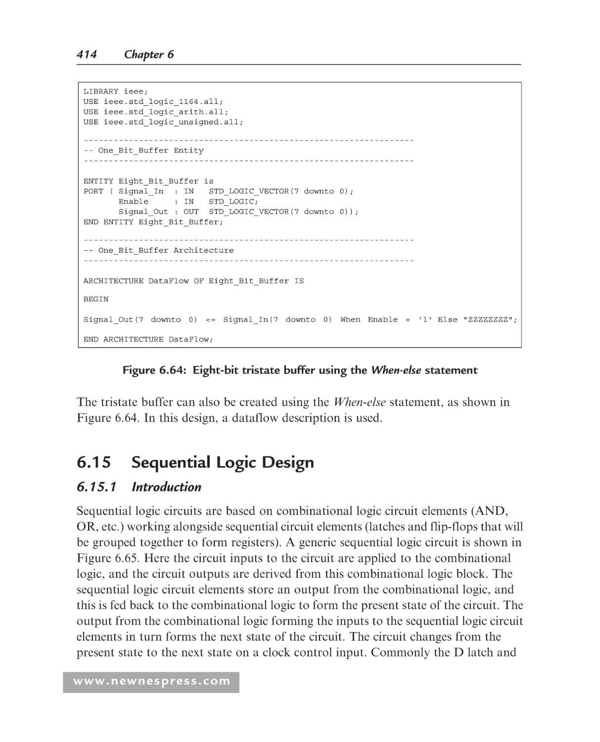
6.14.7 Tristate Buffer ............................................................................. 409
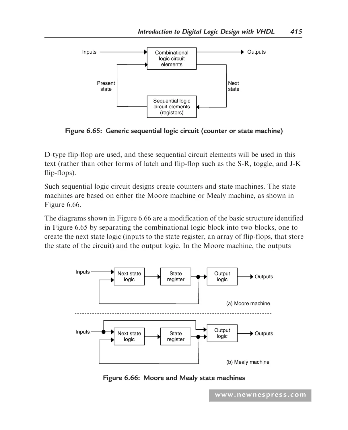
Sequential Logic Design .......................................................................... 414
6.15.1 Introduction................................................................................. 414
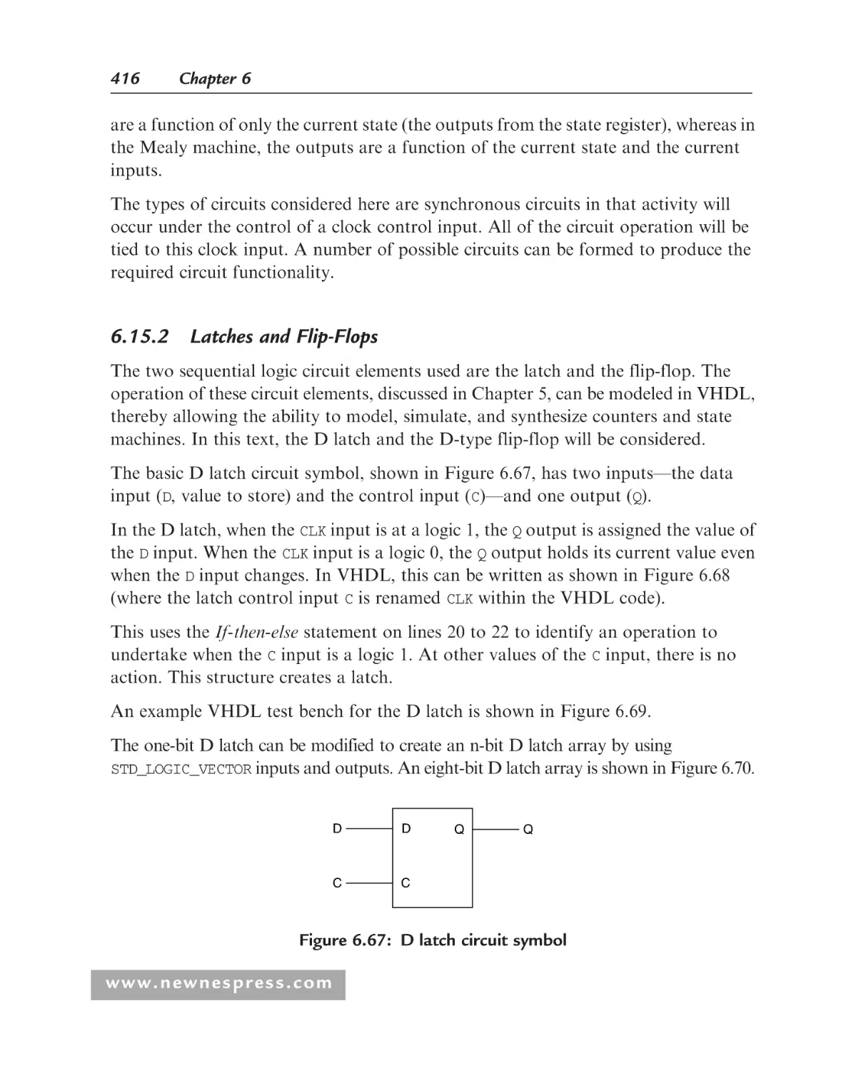
6.15.2 Latches and Flip-Flops................................................................ 416
6.15.3 Counter Design............................................................................ 422
6.15.4 State Machine Design.................................................................. 426
Memories................................................................................................. 440
6.16.1 Introduction................................................................................. 440
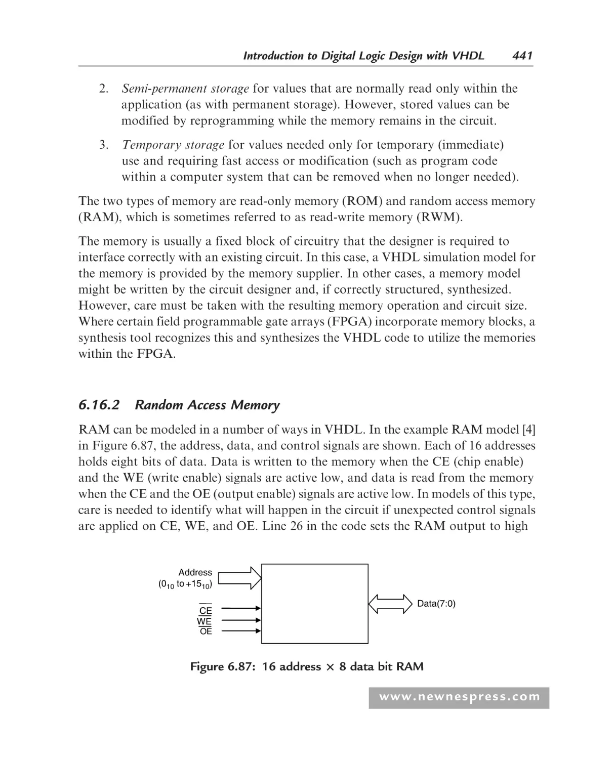
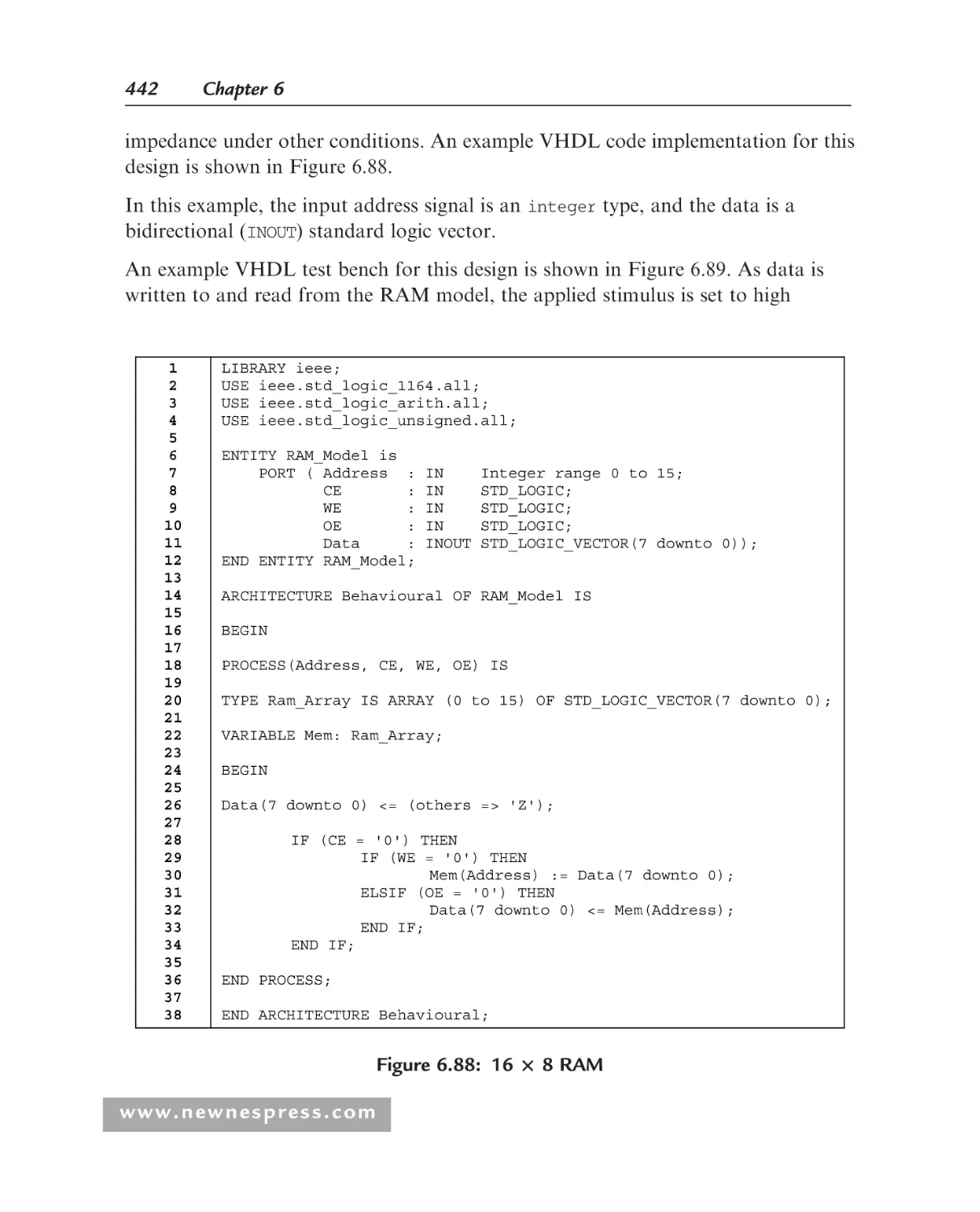
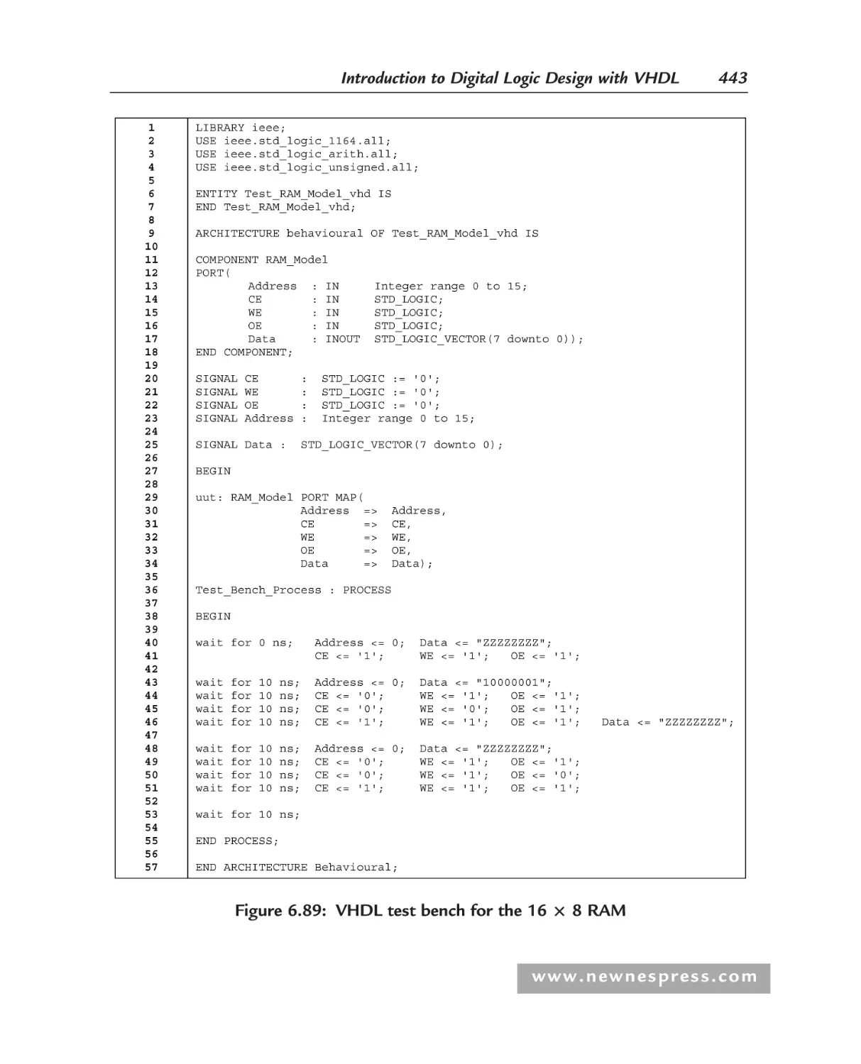
6.16.2 Random Access Memory............................................................. 441
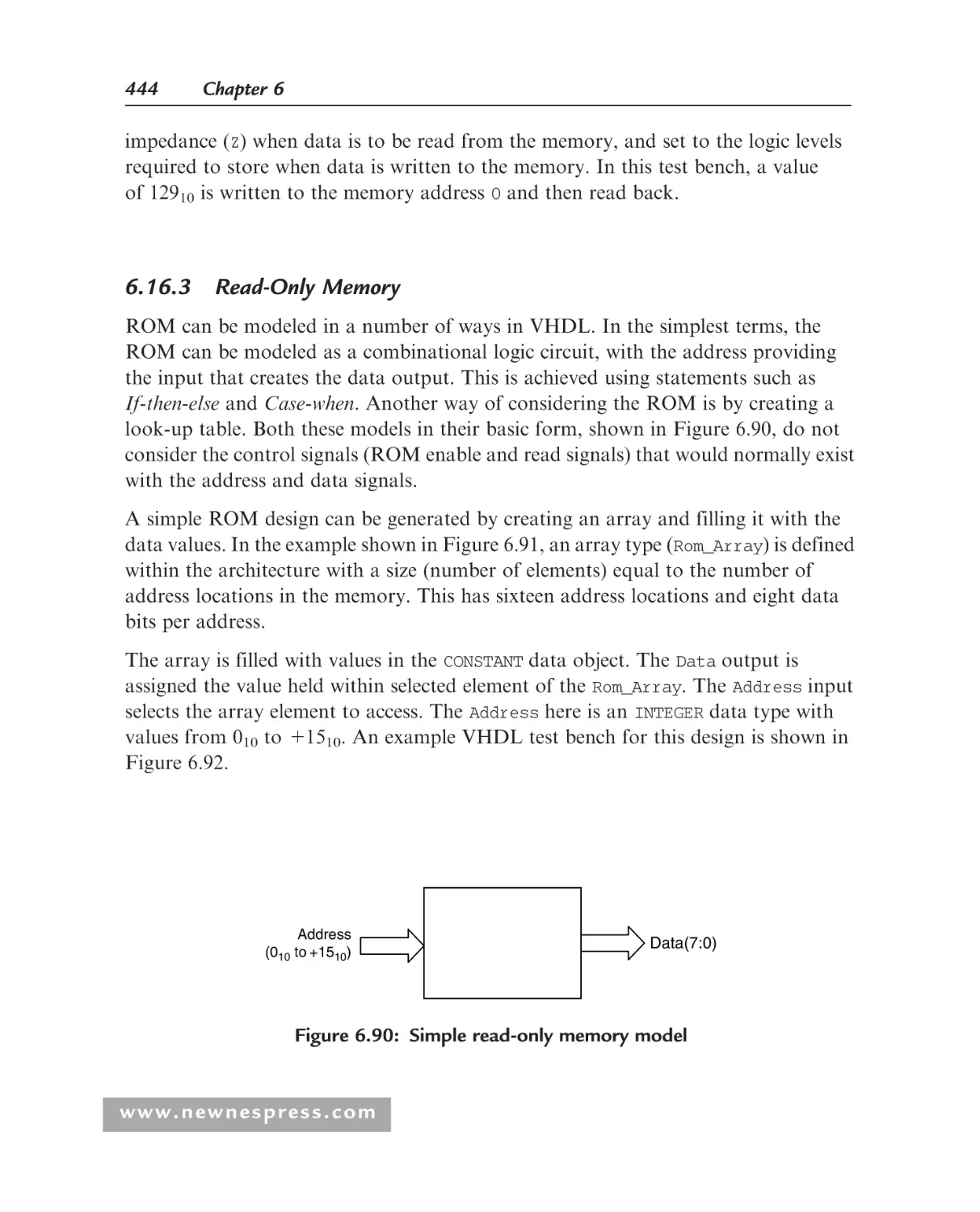
6.16.3 Read-Only Memory..................................................................... 444
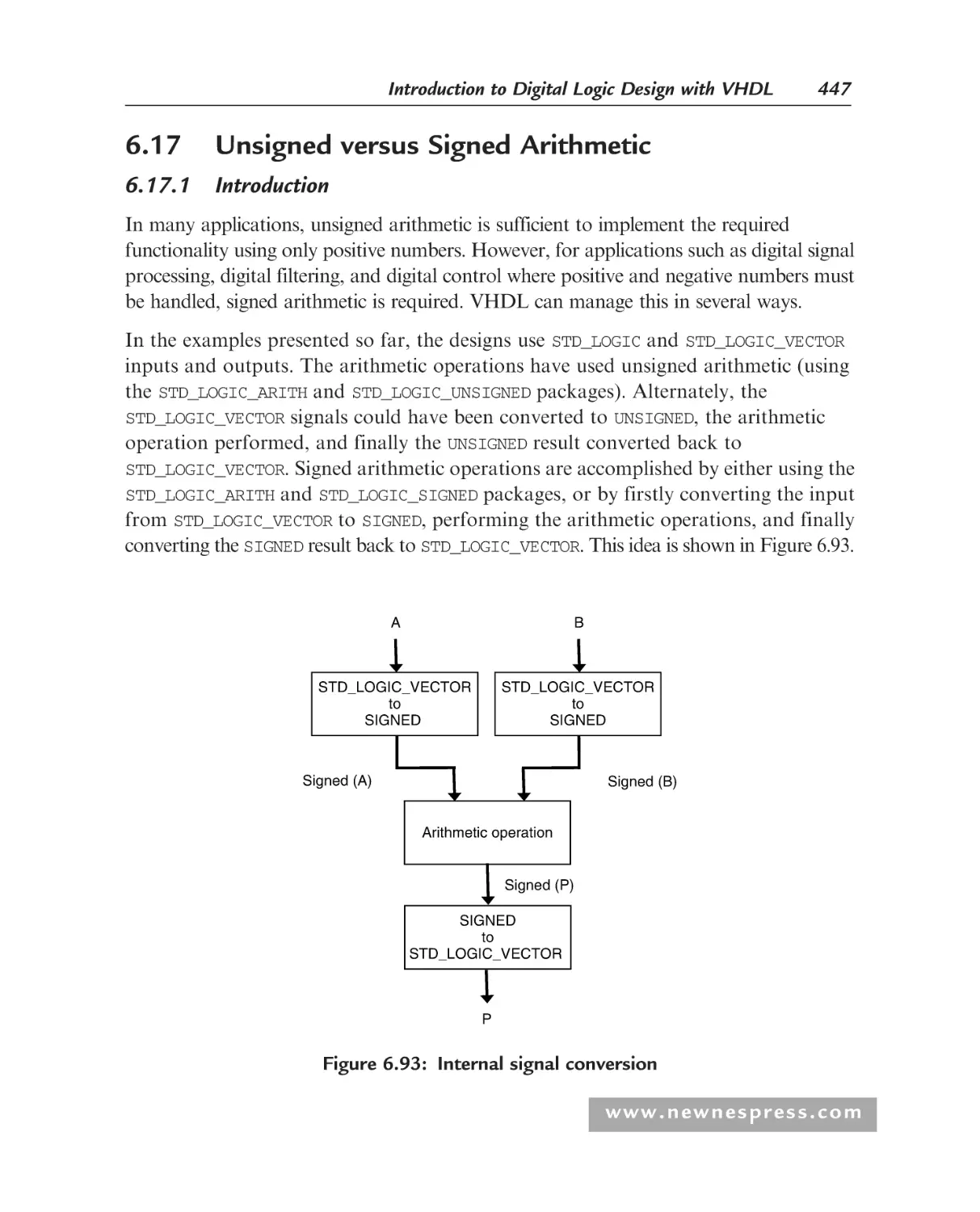
Unsigned versus Signed Arithmetic......................................................... 447
6.17.1 Introduction................................................................................. 447
www.newnespress.com
xii
Table of Contents
6.17.2 Adder Example............................................................................ 448
6.17.3 Multiplier Example...................................................................... 449
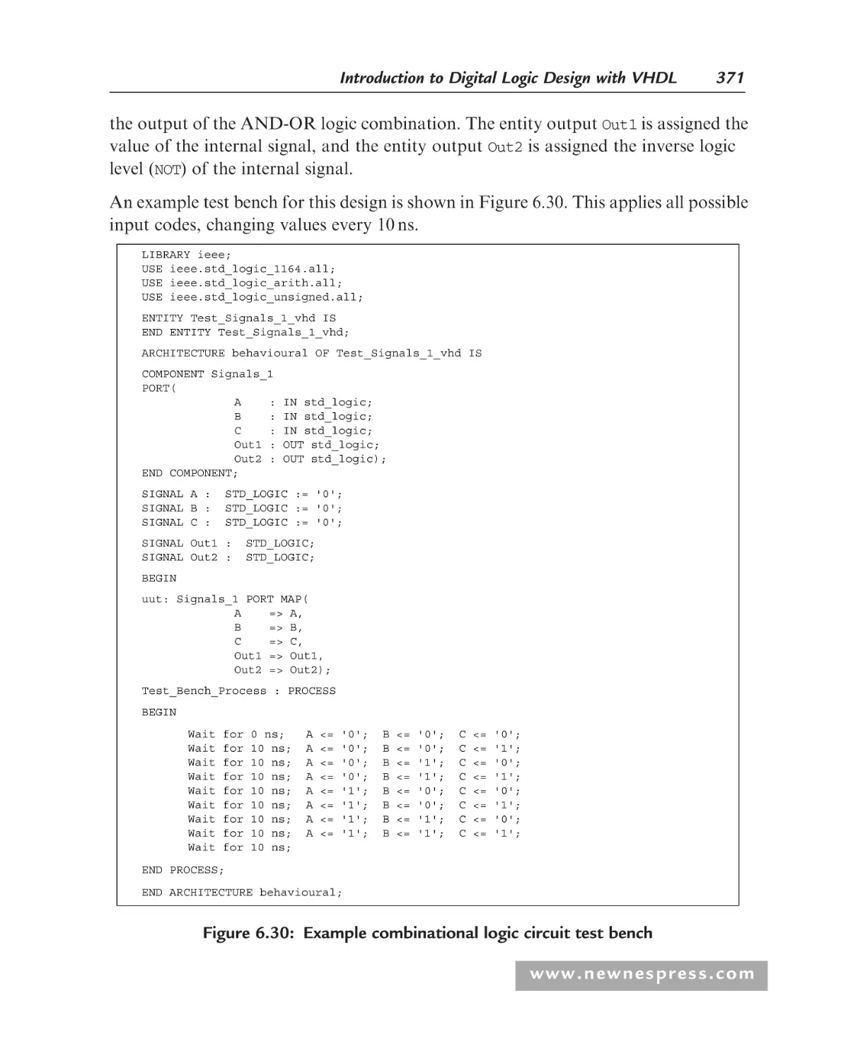
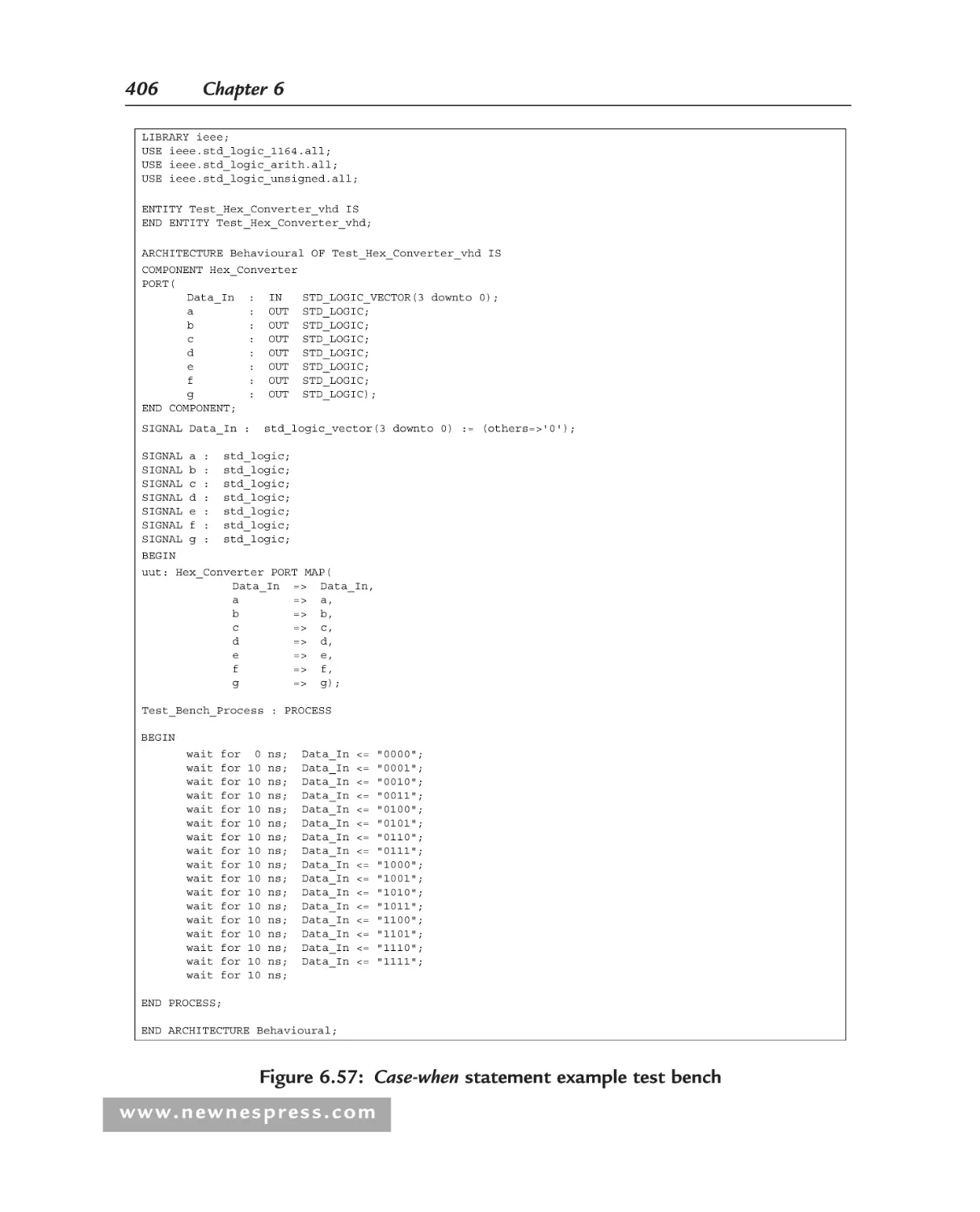
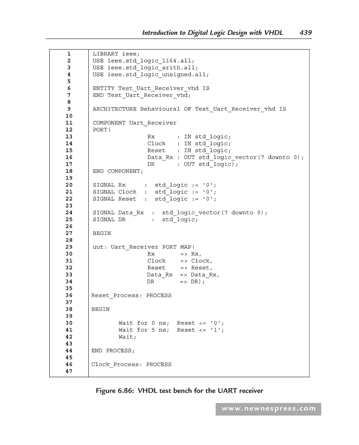
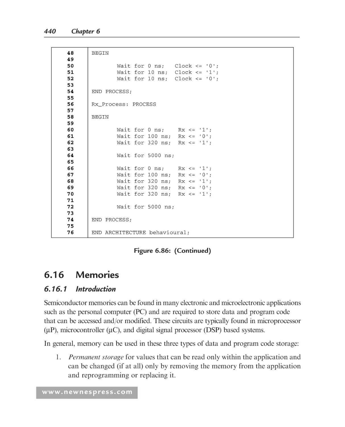
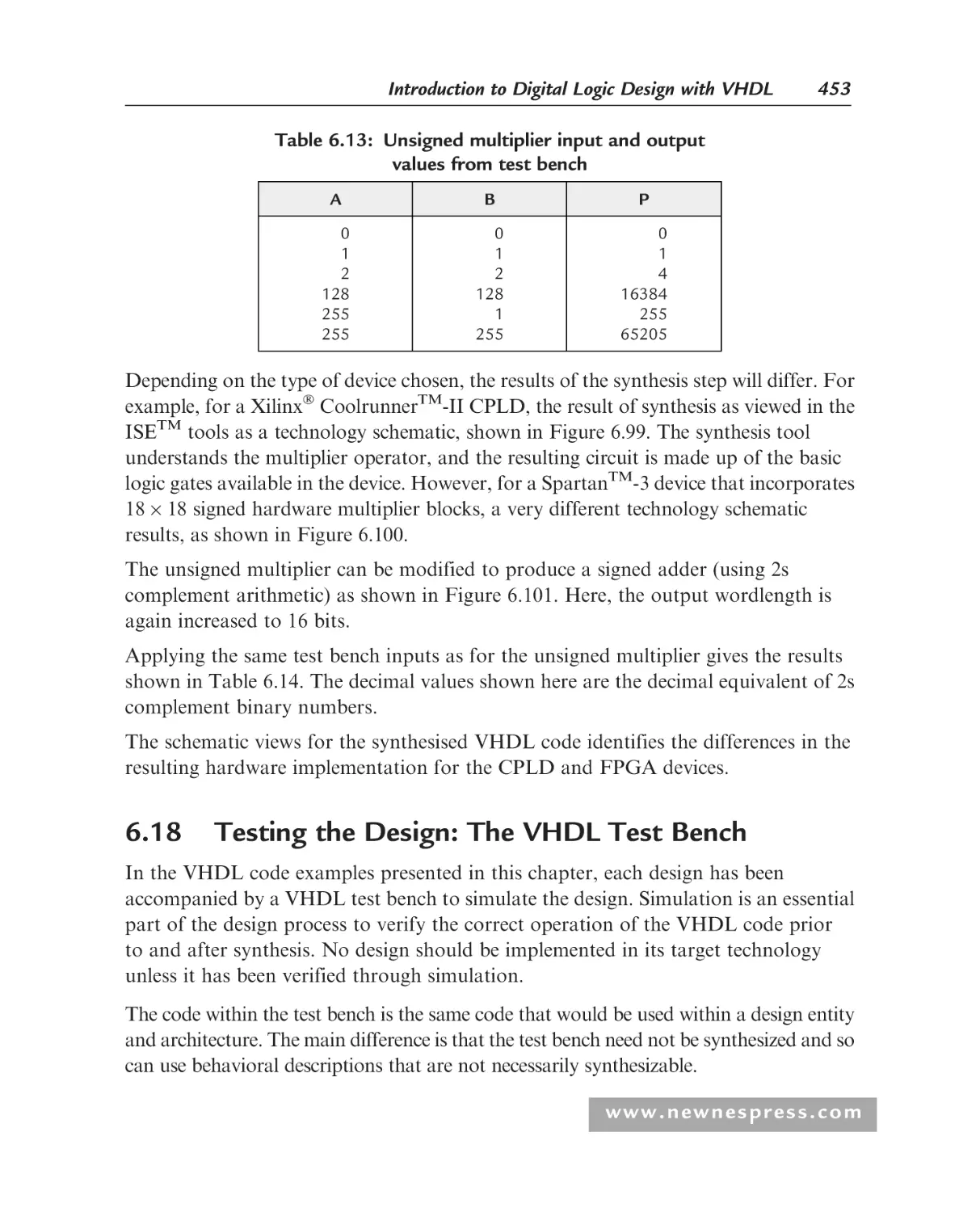
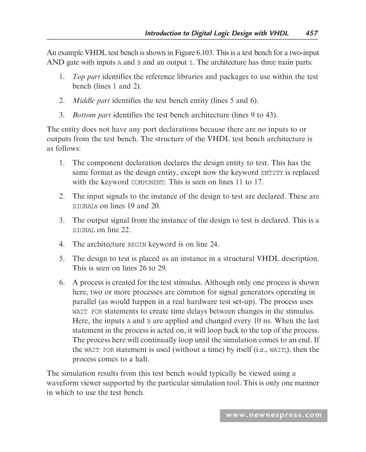
6.18 Testing the Design: The VHDL Test Bench............................................ 453
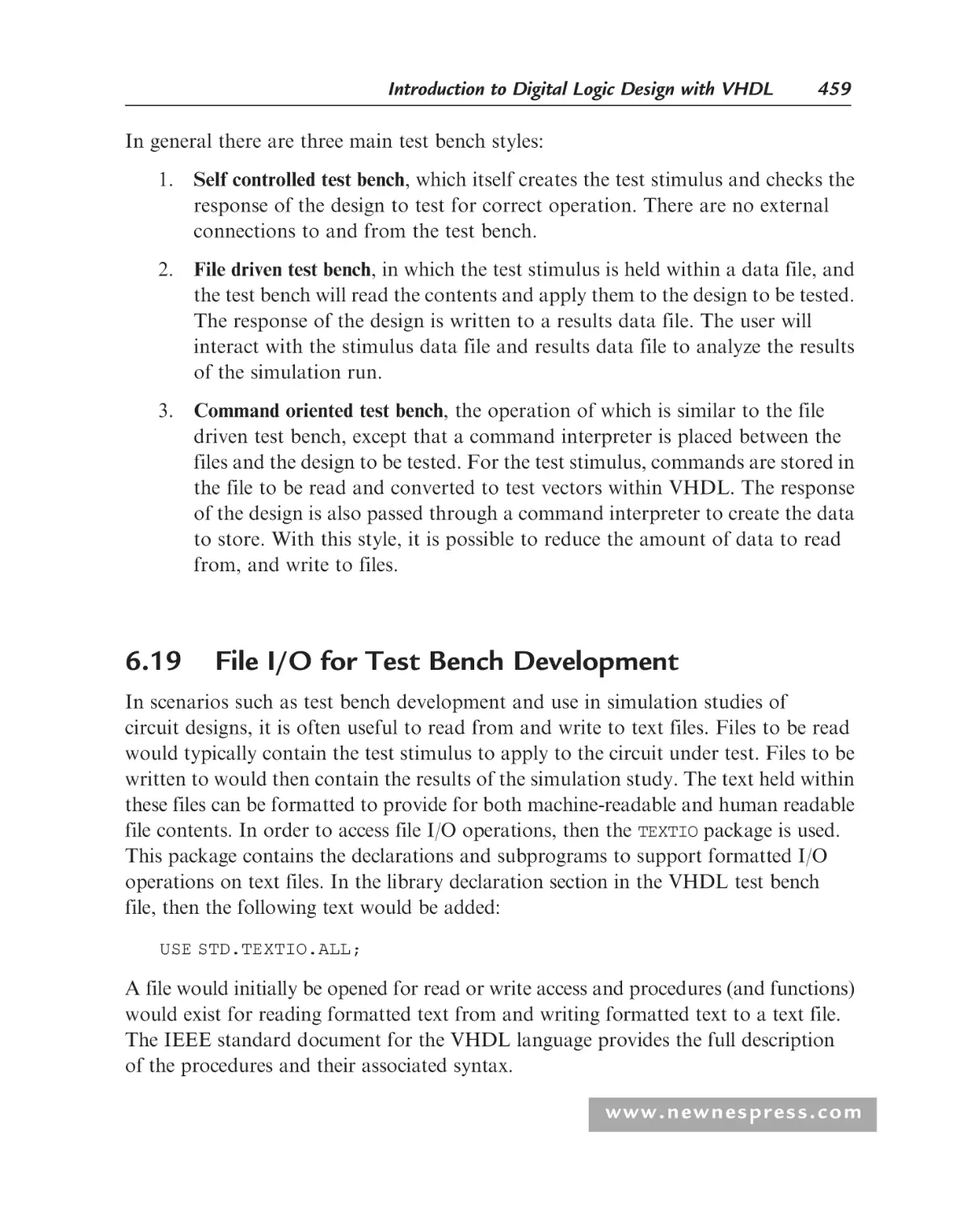
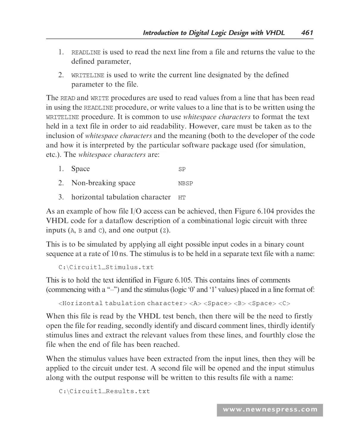
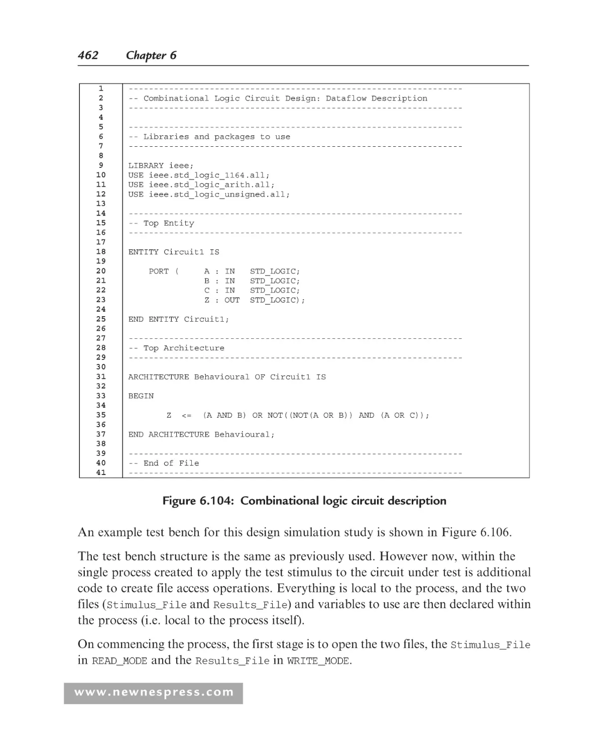
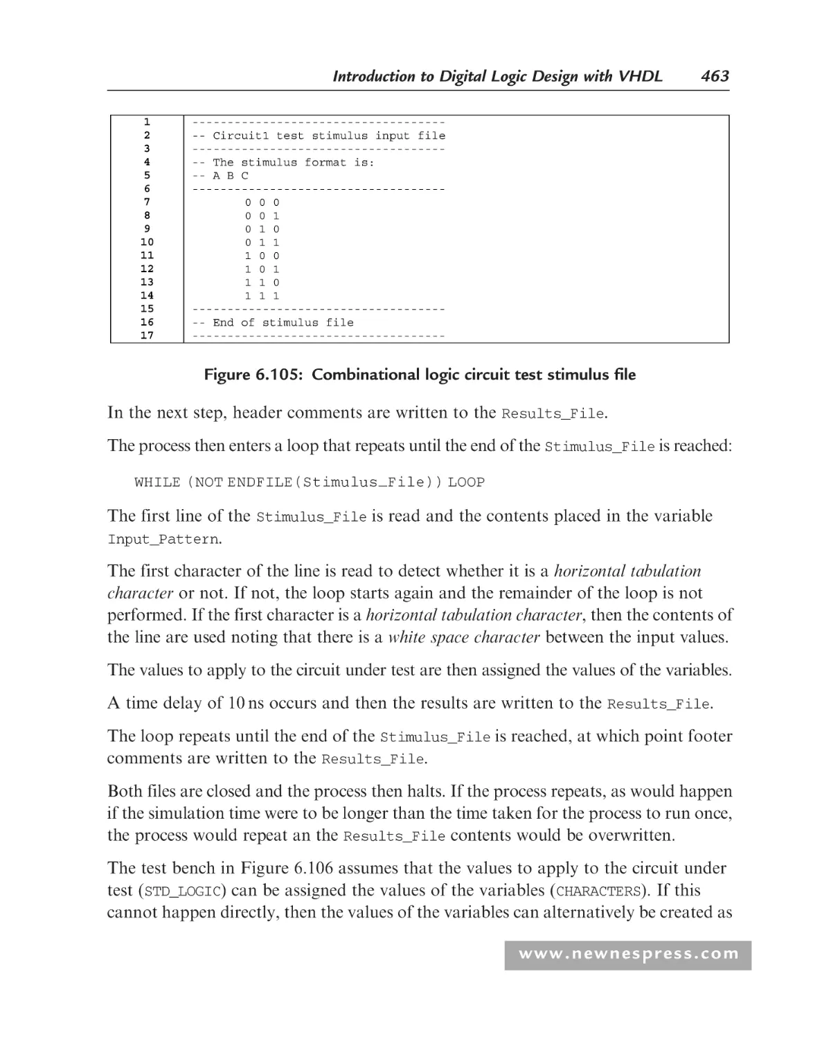
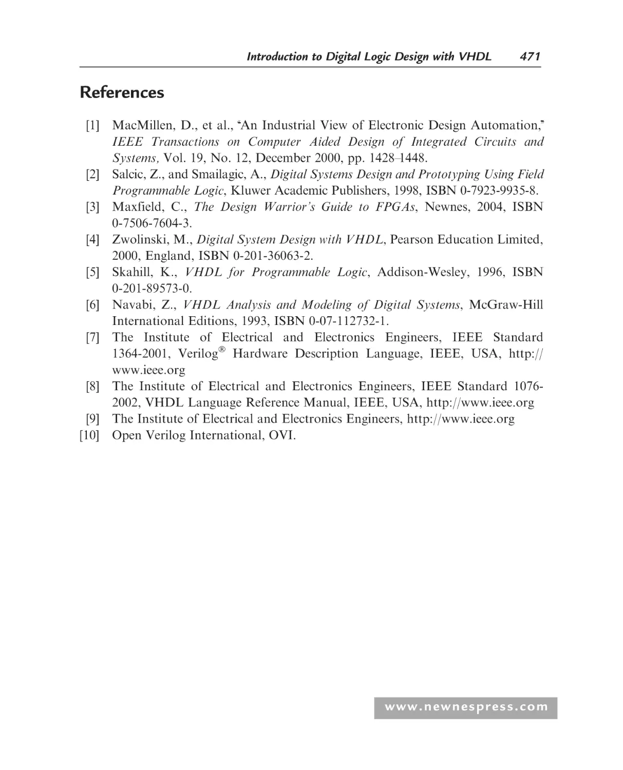
6.19 File I/O for Test Bench Development ..................................................... 459
References................................................................................................ 471
Student Exercises..................................................................................... 472
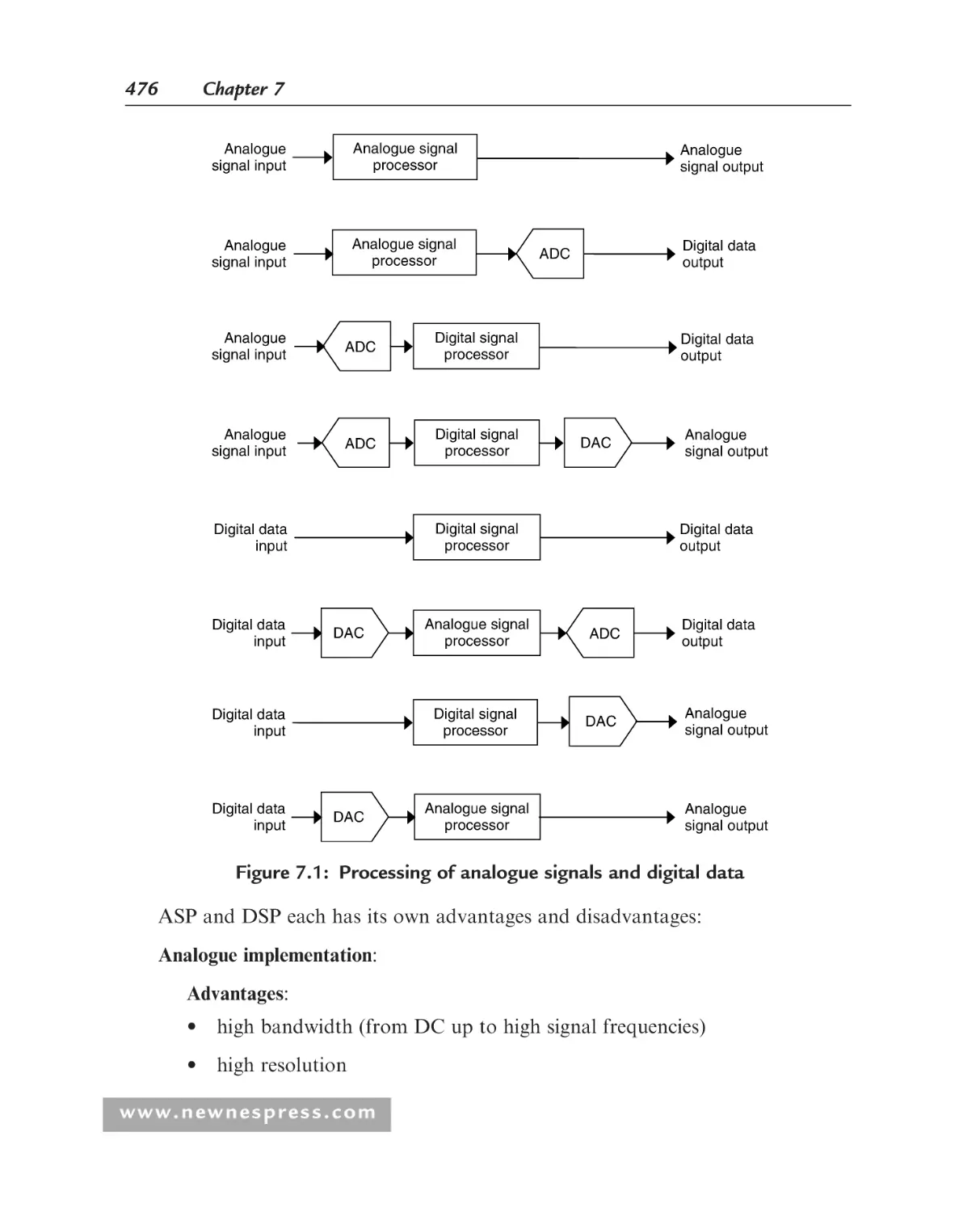
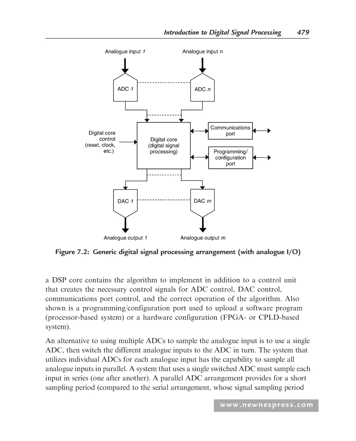
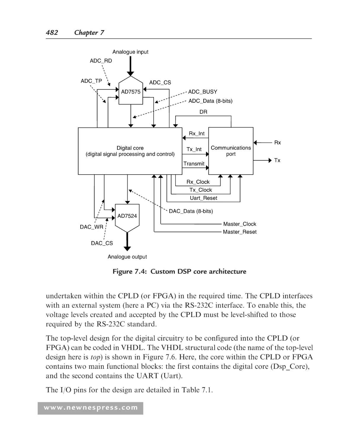
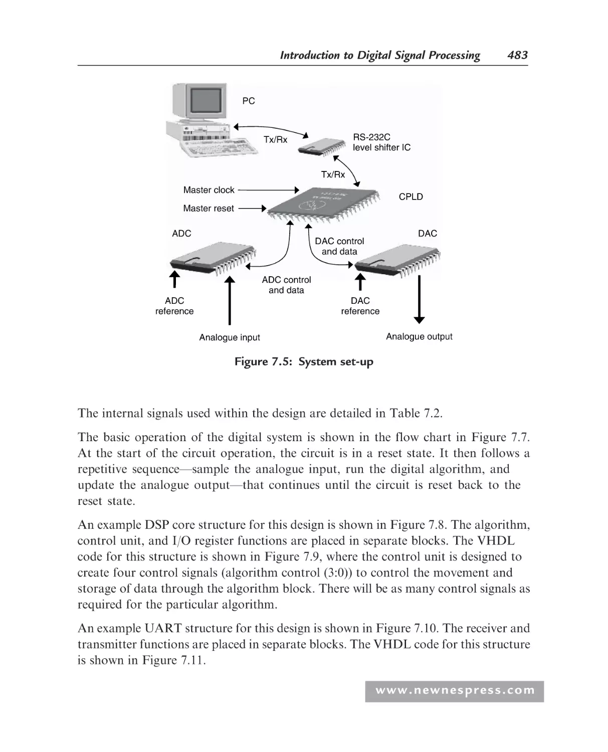
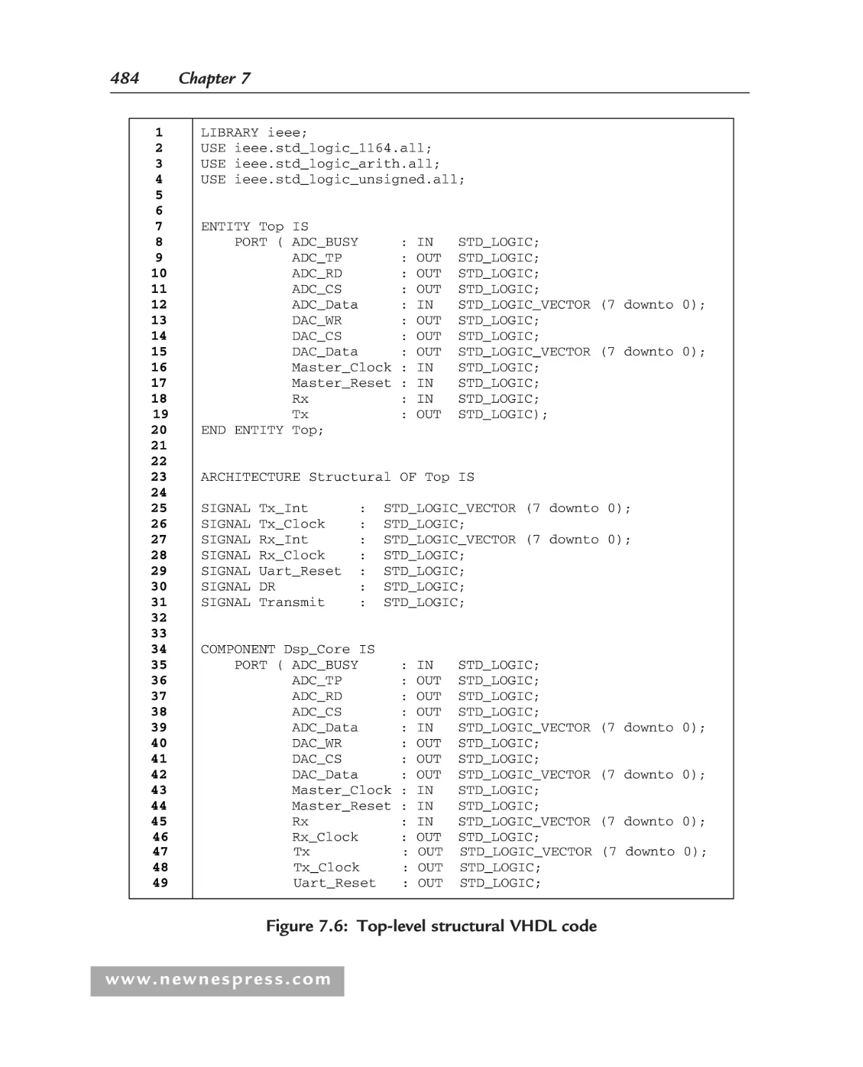
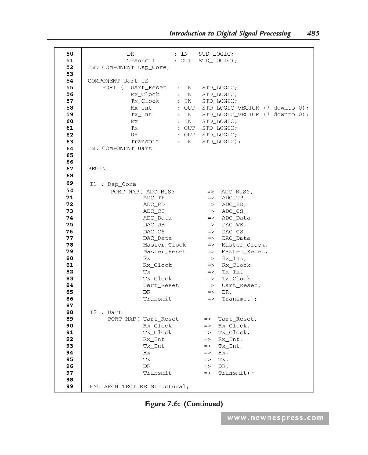
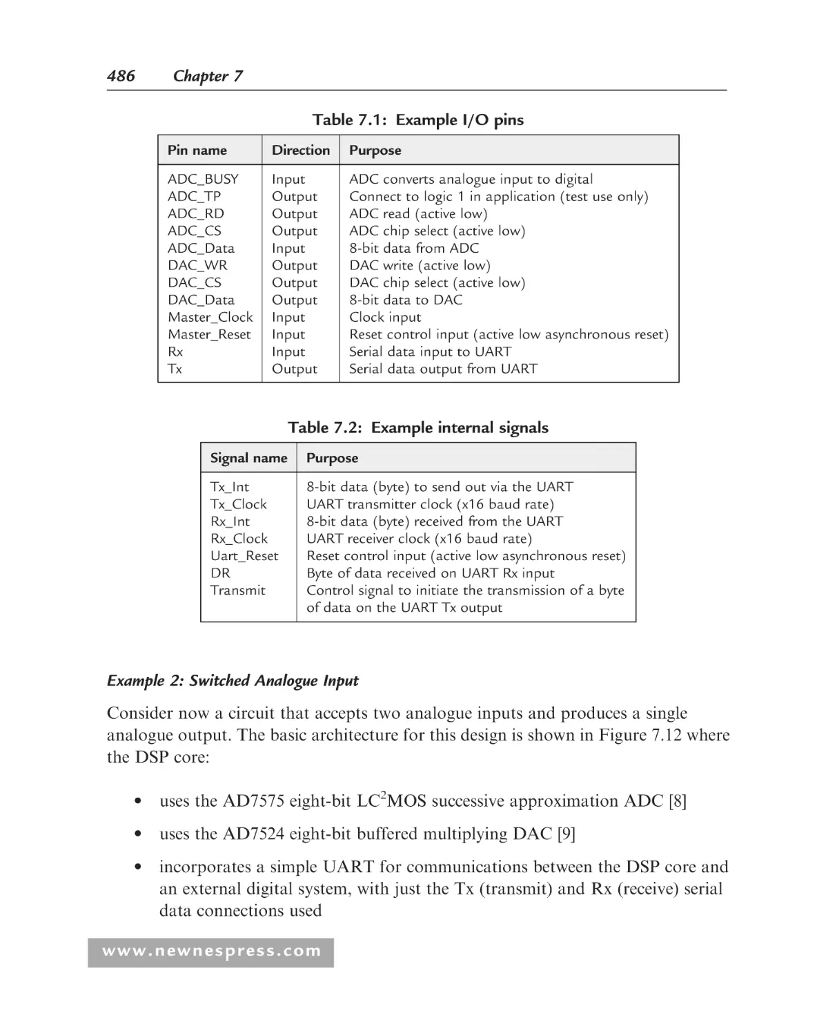
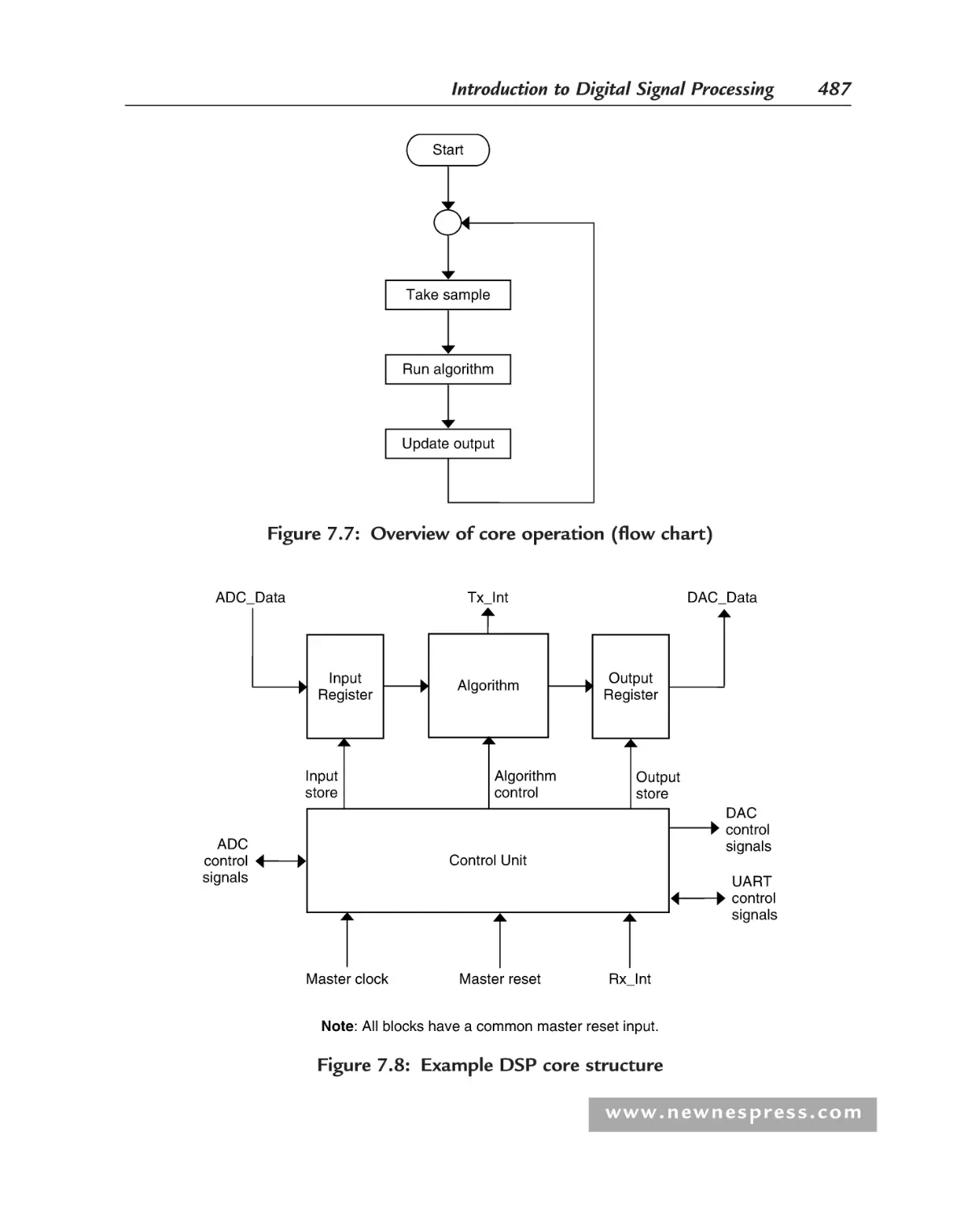
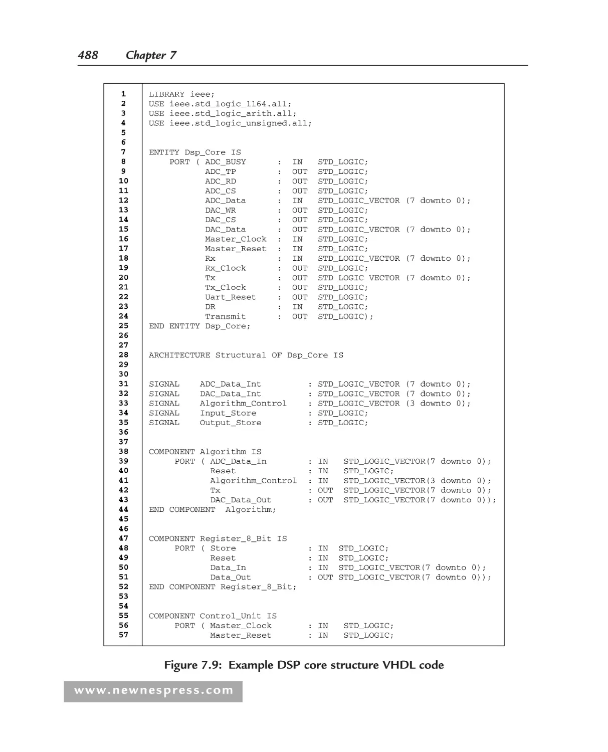
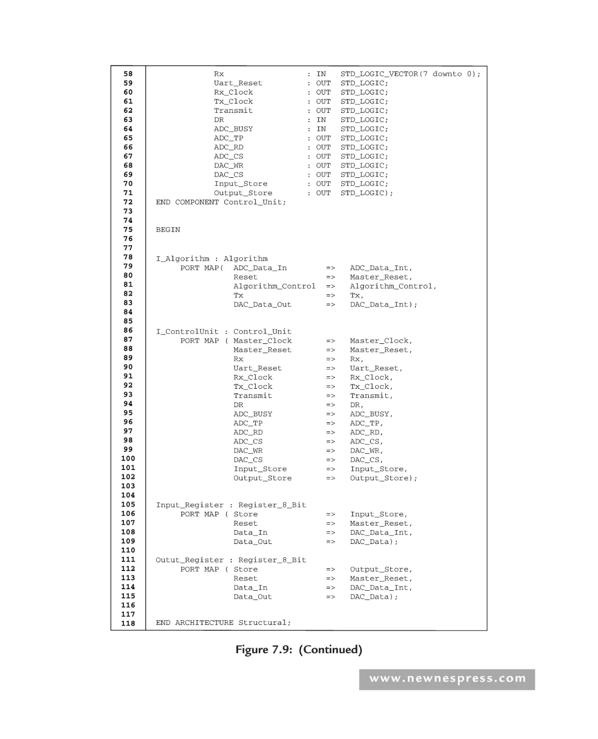
Chapter 7: Introduction to Digital Signal Processing ..................................... 475
7.1
7.2
7.3
7.4
Introduction ............................................................................................ 475
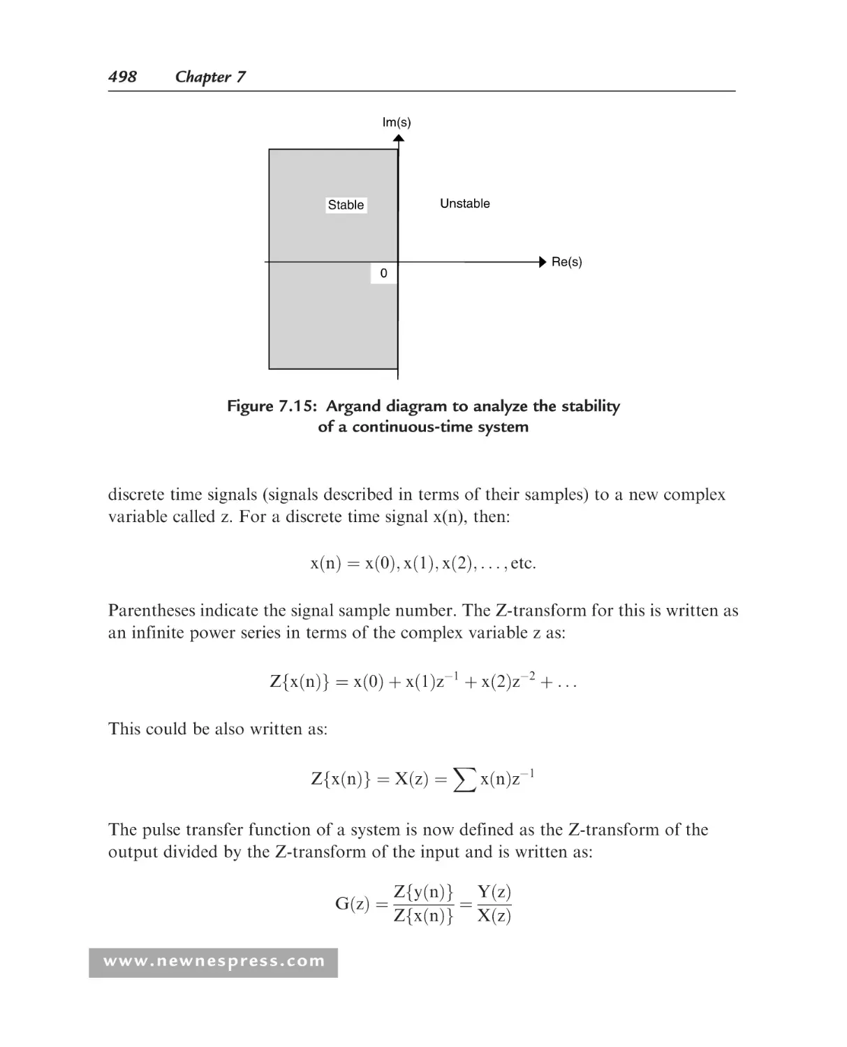
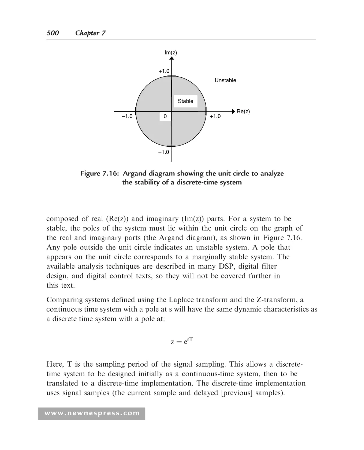
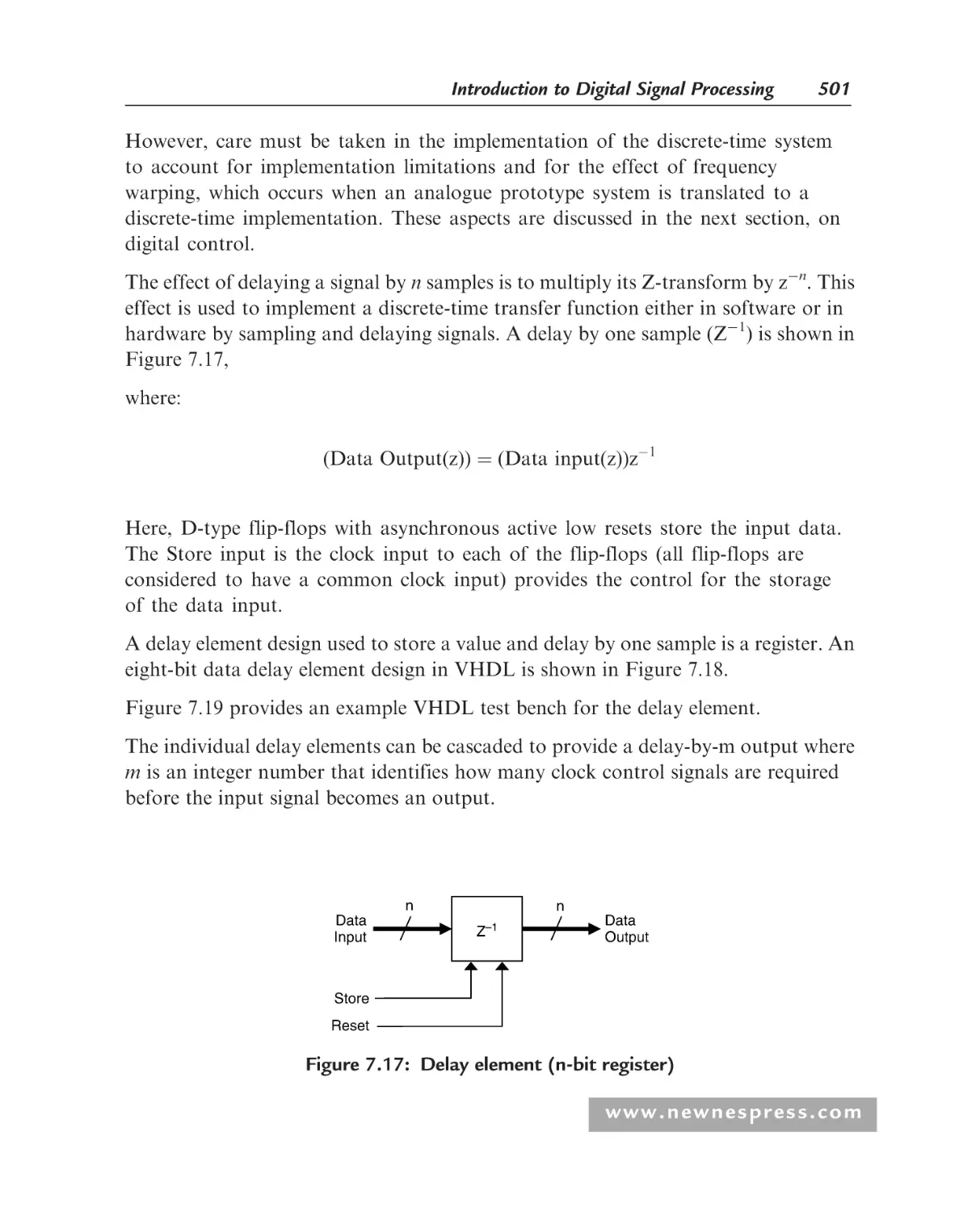
Z-Transform............................................................................................ 496
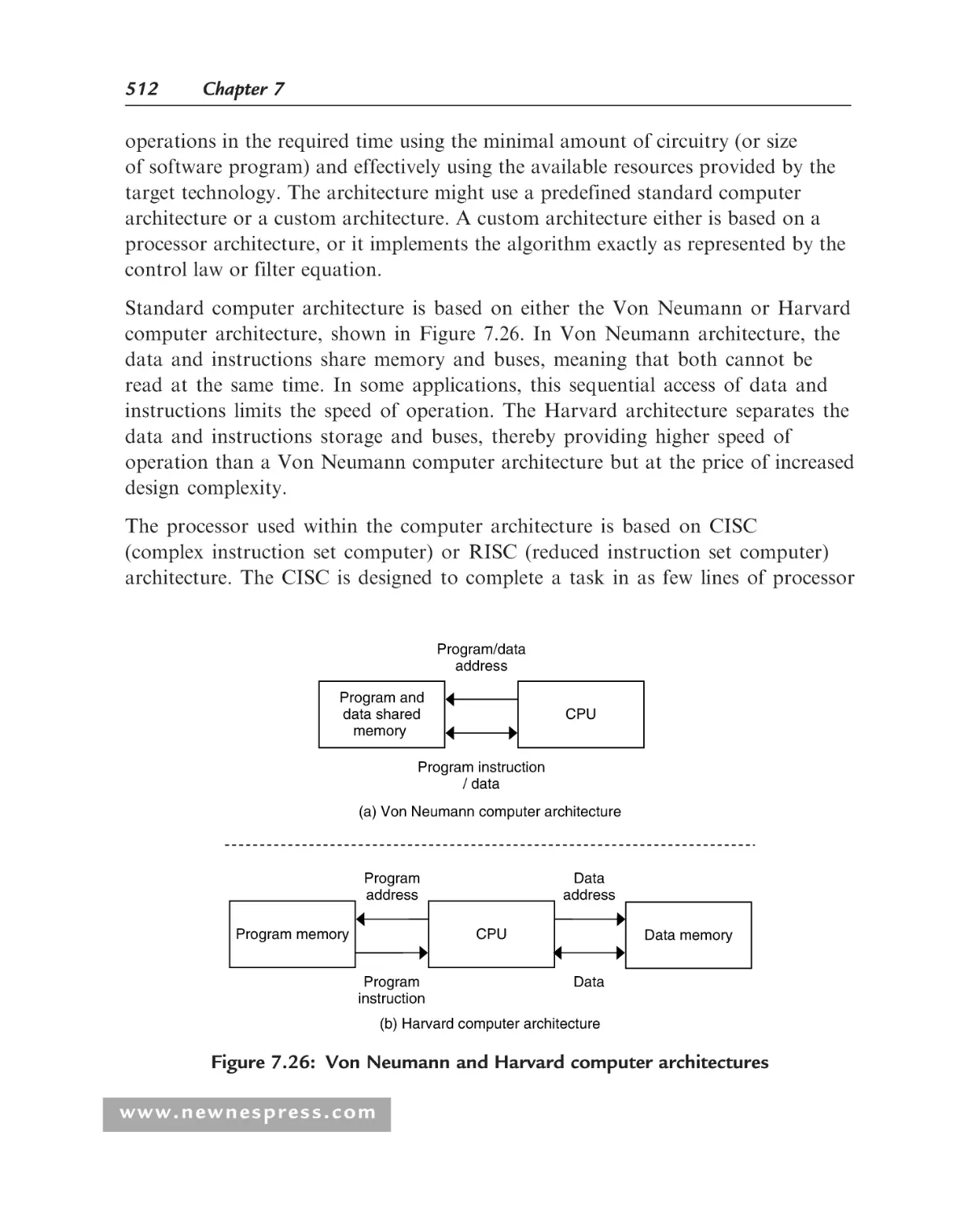
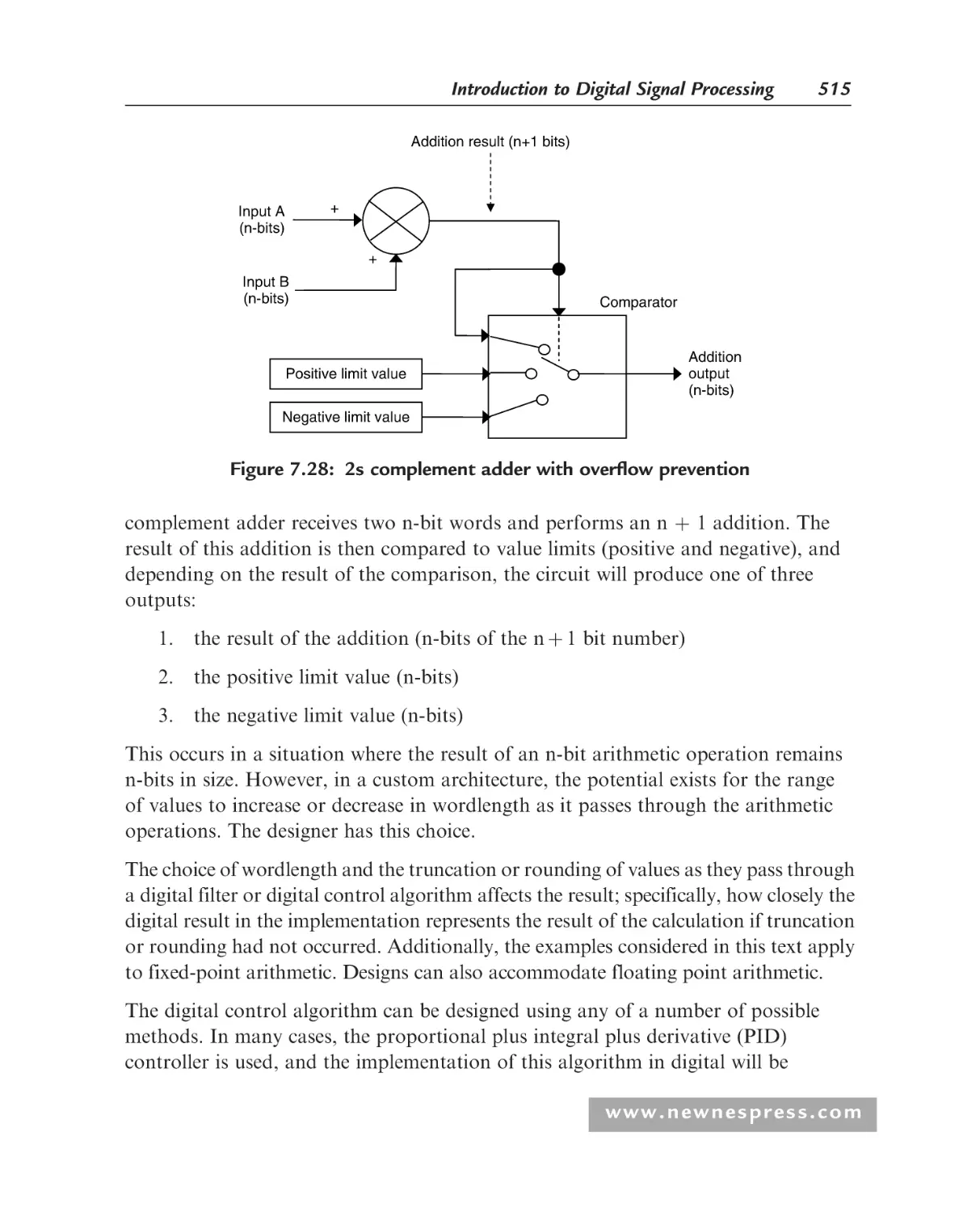
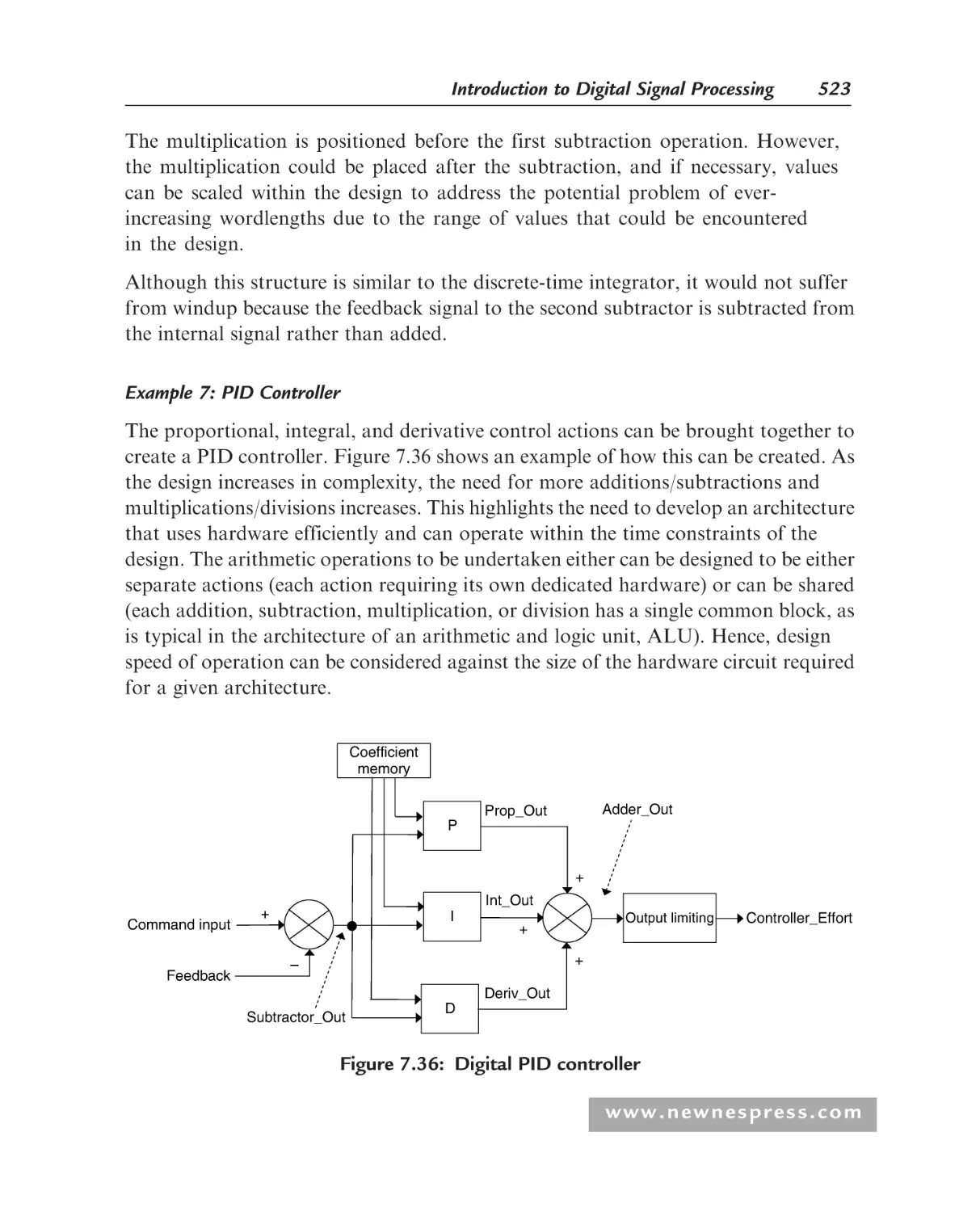
Digital Control ........................................................................................ 509
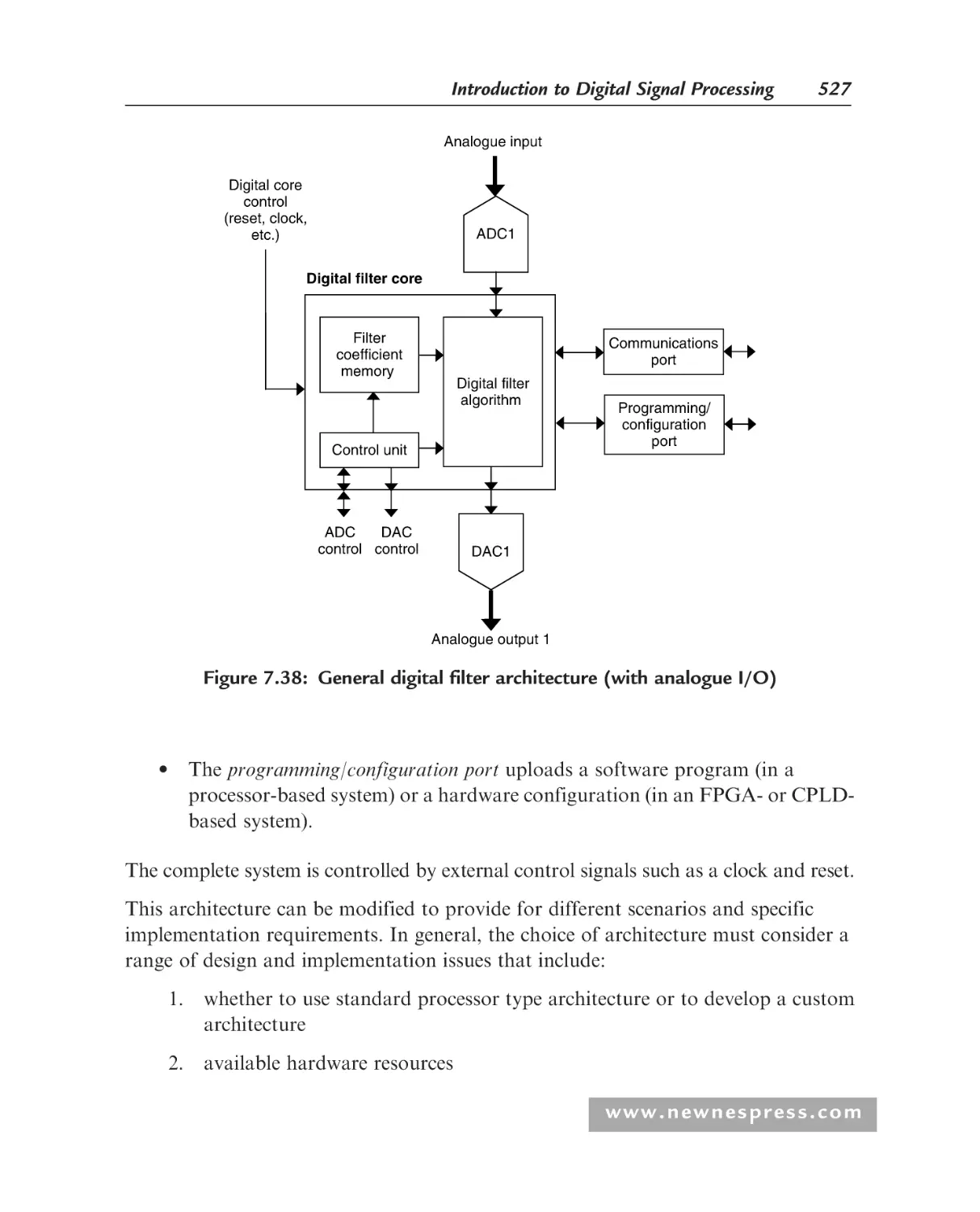
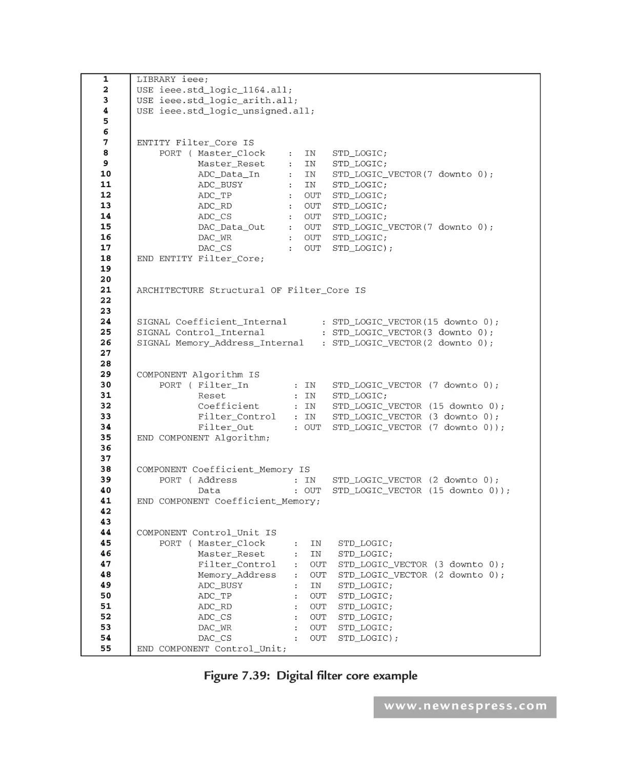
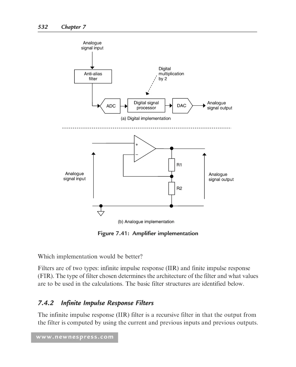
Digital Filtering....................................................................................... 524
7.4.1 Introduction .................................................................................. 524
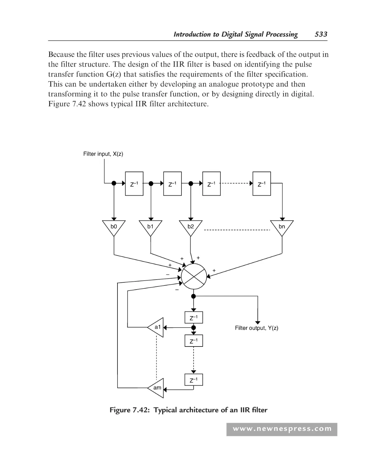
7.4.2 Infinite Impulse Response Filters .................................................. 532
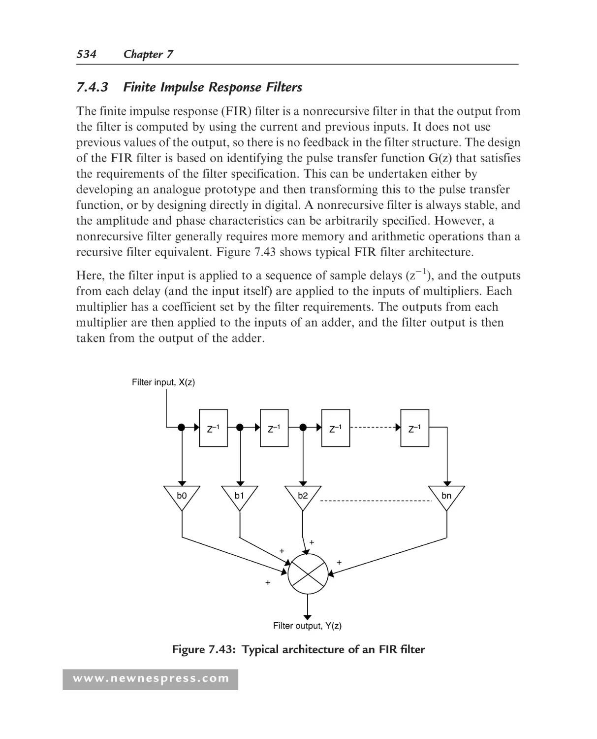
7.4.3 Finite Impulse Response Filters .................................................... 534
References................................................................................................ 535
Student Exercises..................................................................................... 536
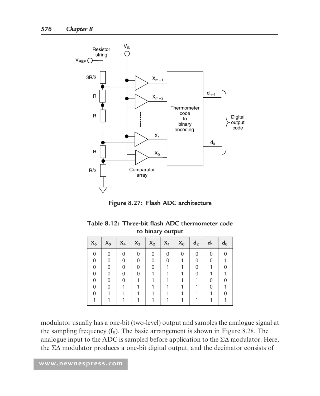
Chapter 8: Interfacing Digital Logic to the Real World: A/D Conversion,
D/A Conversion, and Power Electronics ...................................................... 537
8.1
8.2
8.3
8.4
8.5
8.6
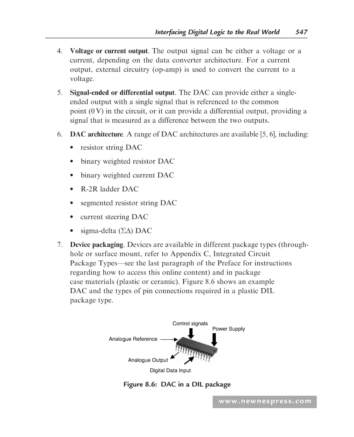
Introduction ............................................................................................ 537
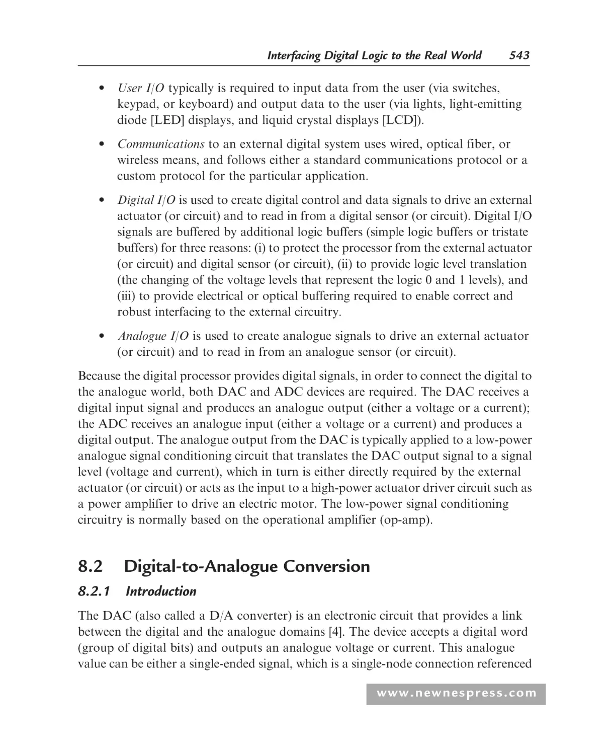
Digital-to-Analogue Conversion ............................................................. 543
8.2.1 Introduction .................................................................................. 543
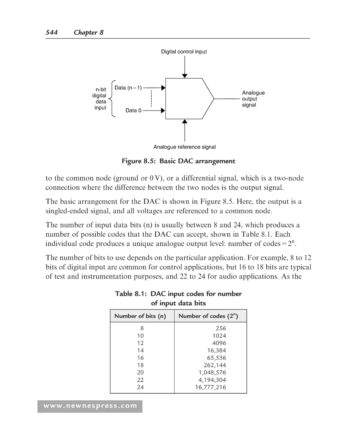
8.2.2 DAC Characteristics...................................................................... 548
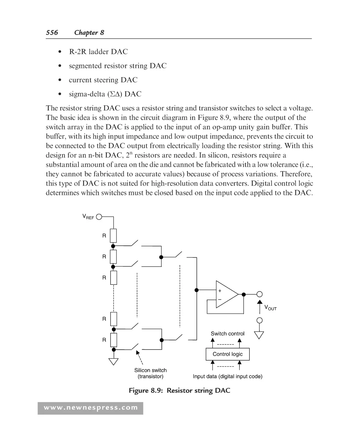
8.2.3 Types of DAC ............................................................................... 555
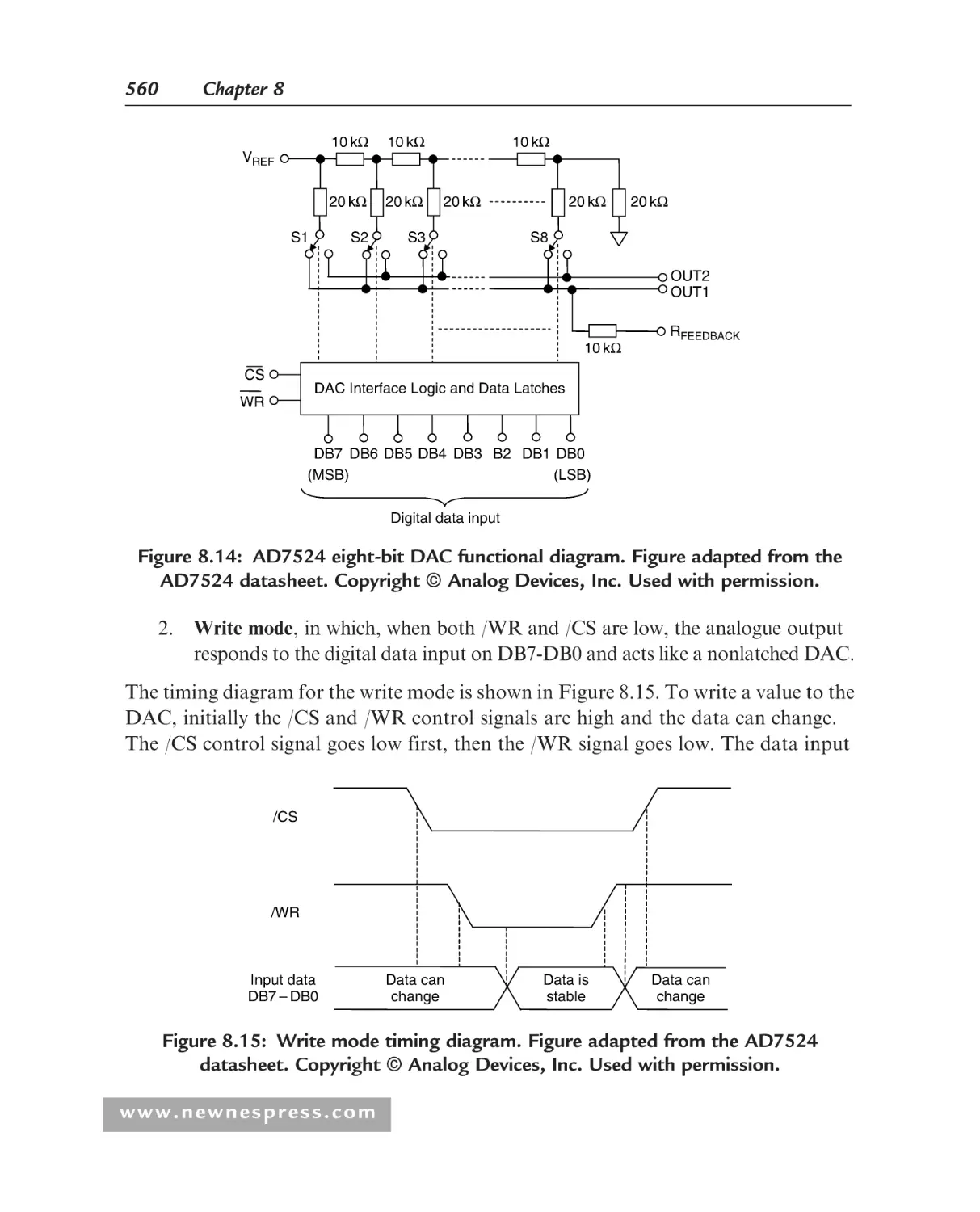
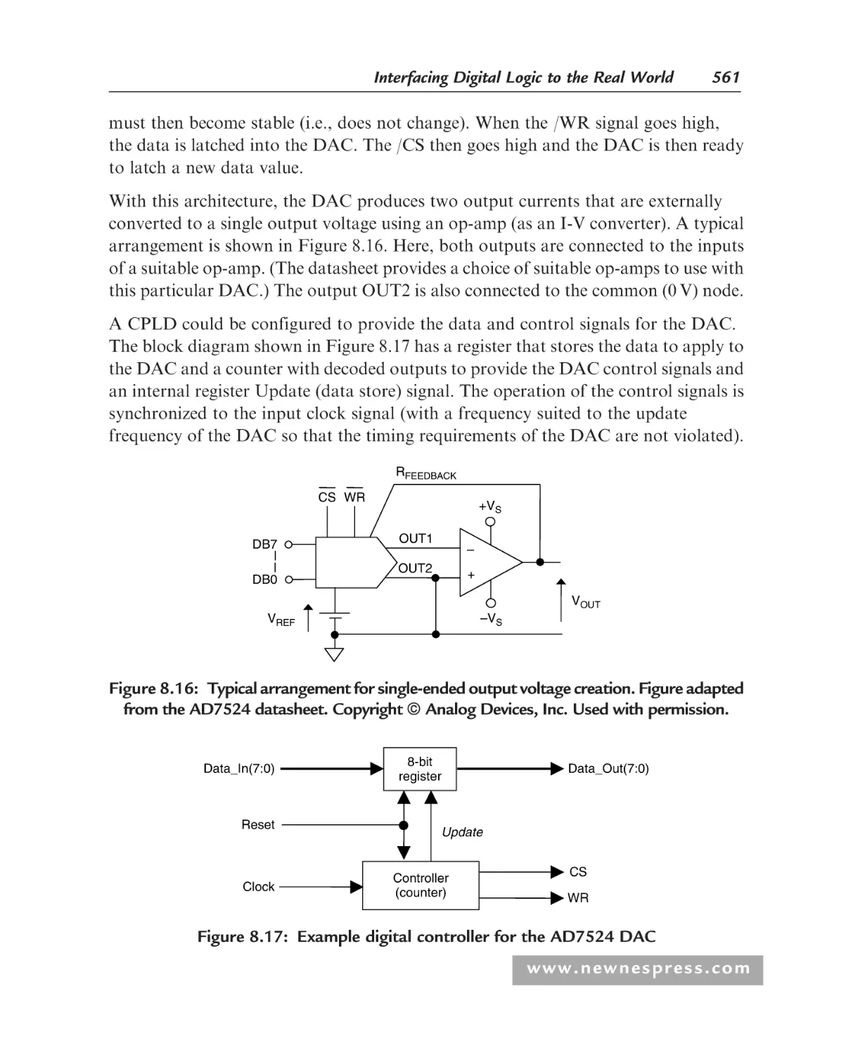
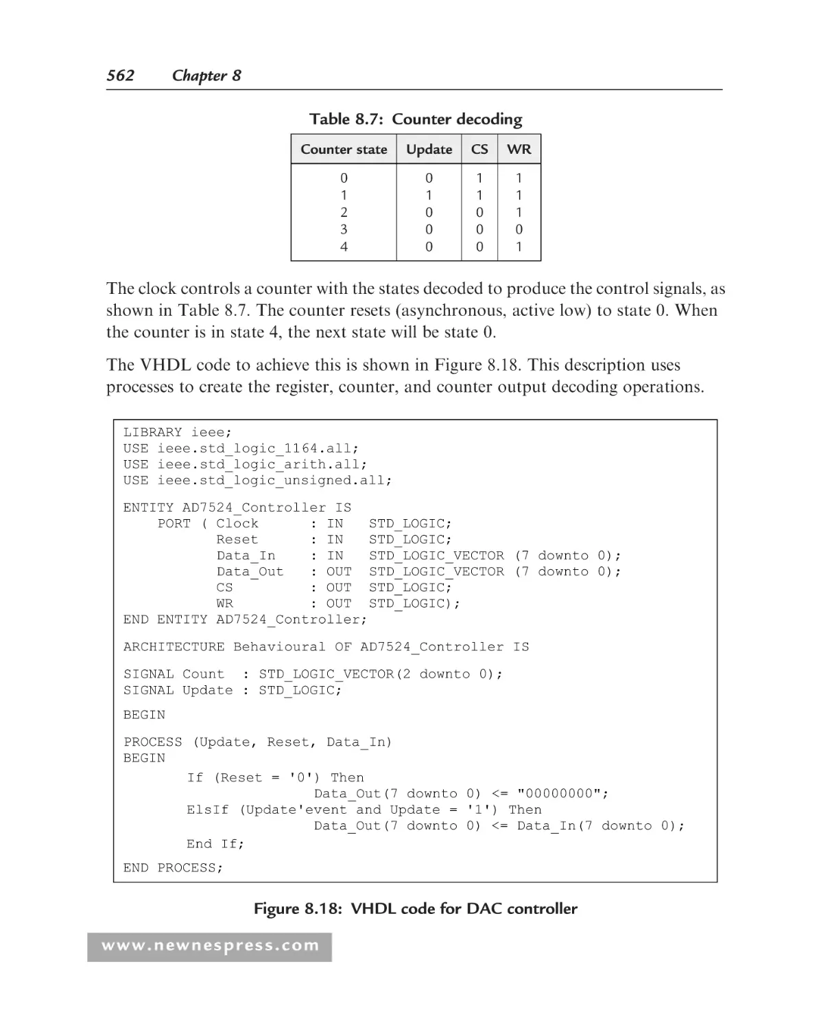
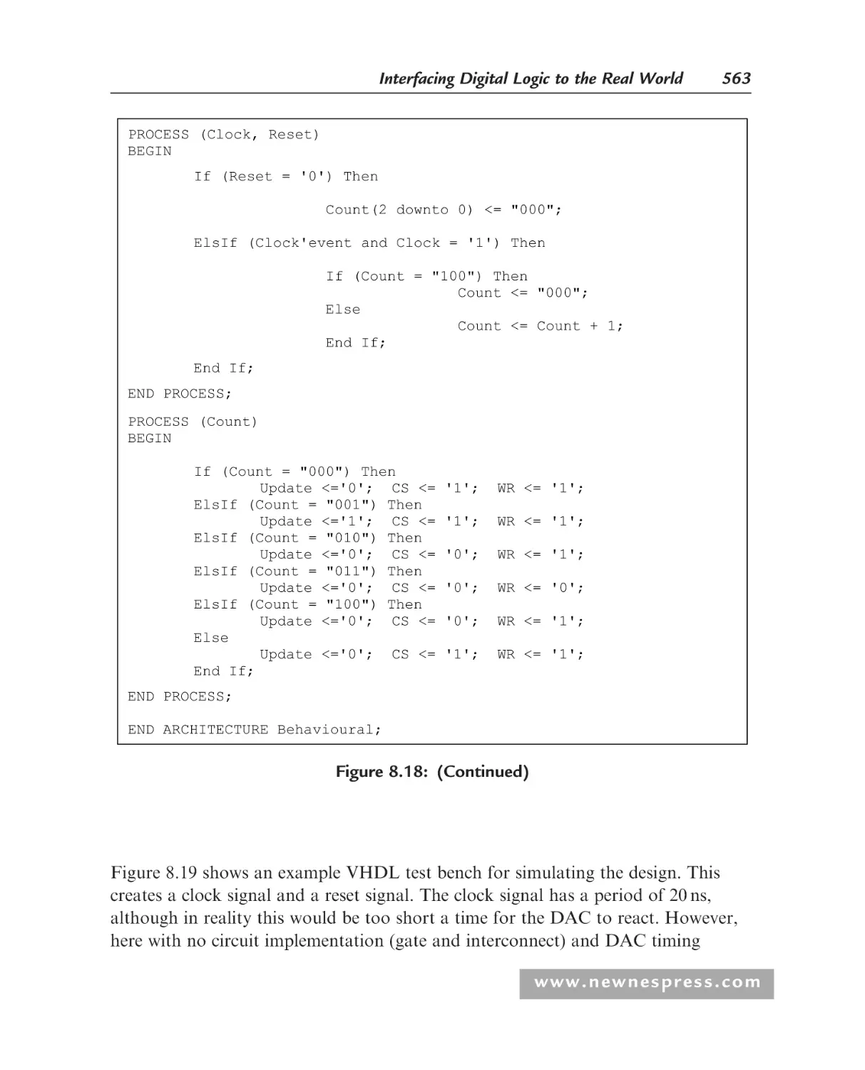
8.2.4 DAC Control Example.................................................................. 559
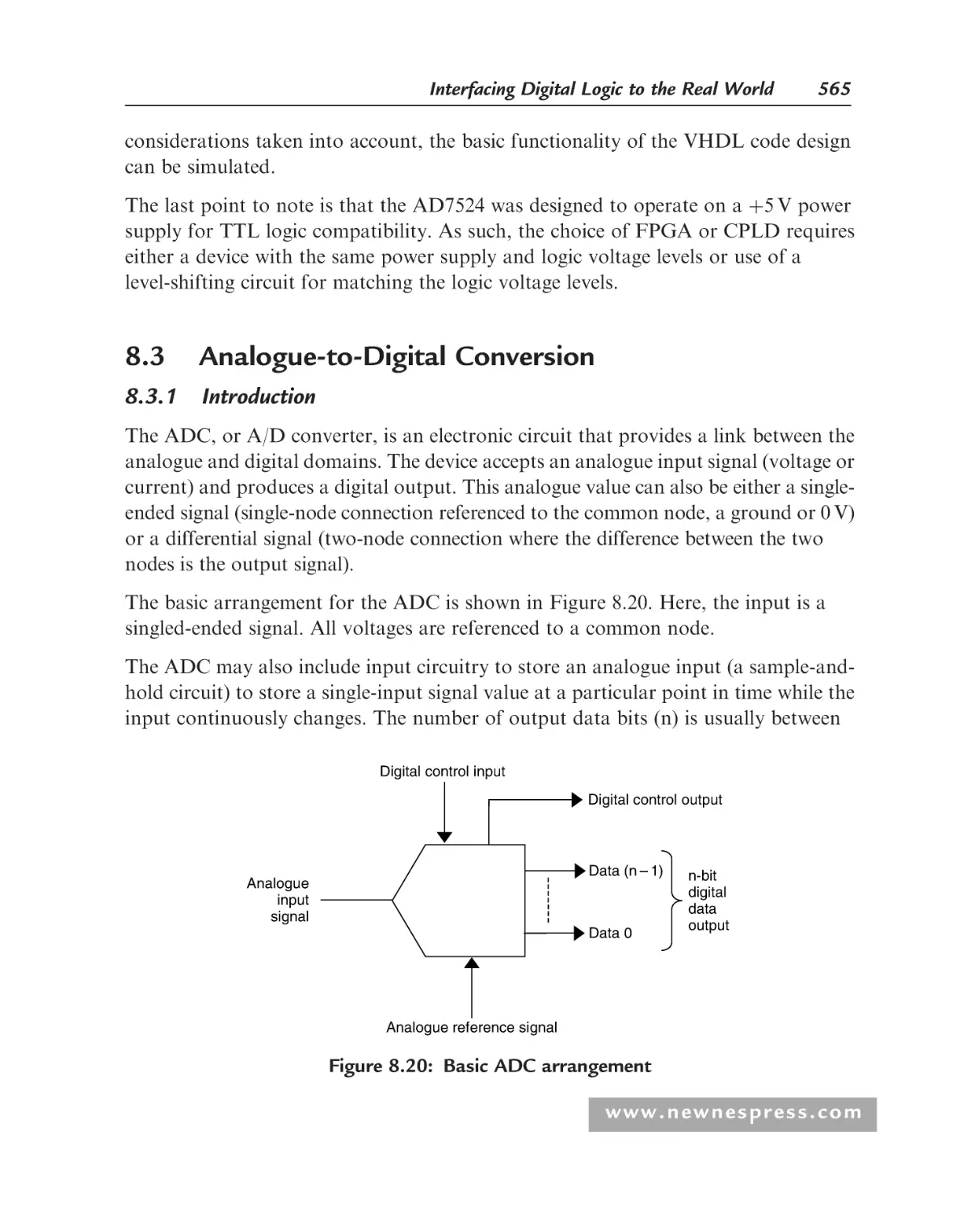
Analogue-to-Digital Conversion ............................................................. 565
8.3.1 Introduction .................................................................................. 565
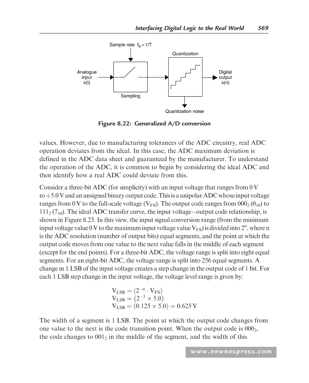
8.3.2 ADC Characteristics...................................................................... 568
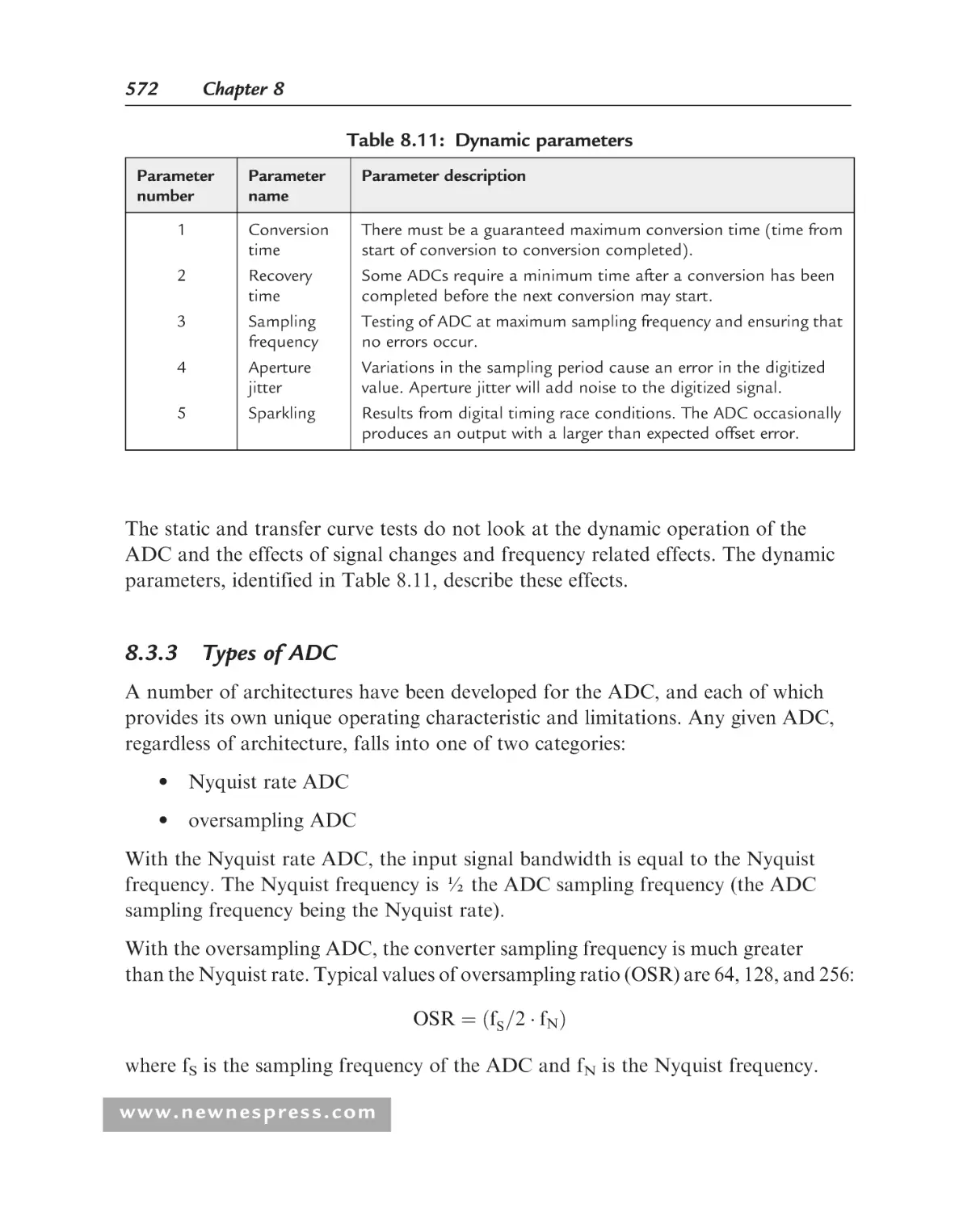
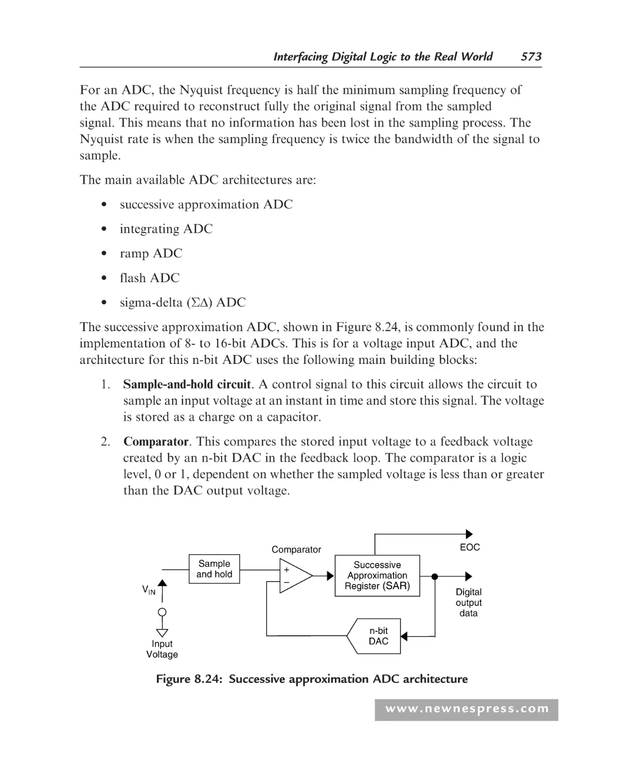
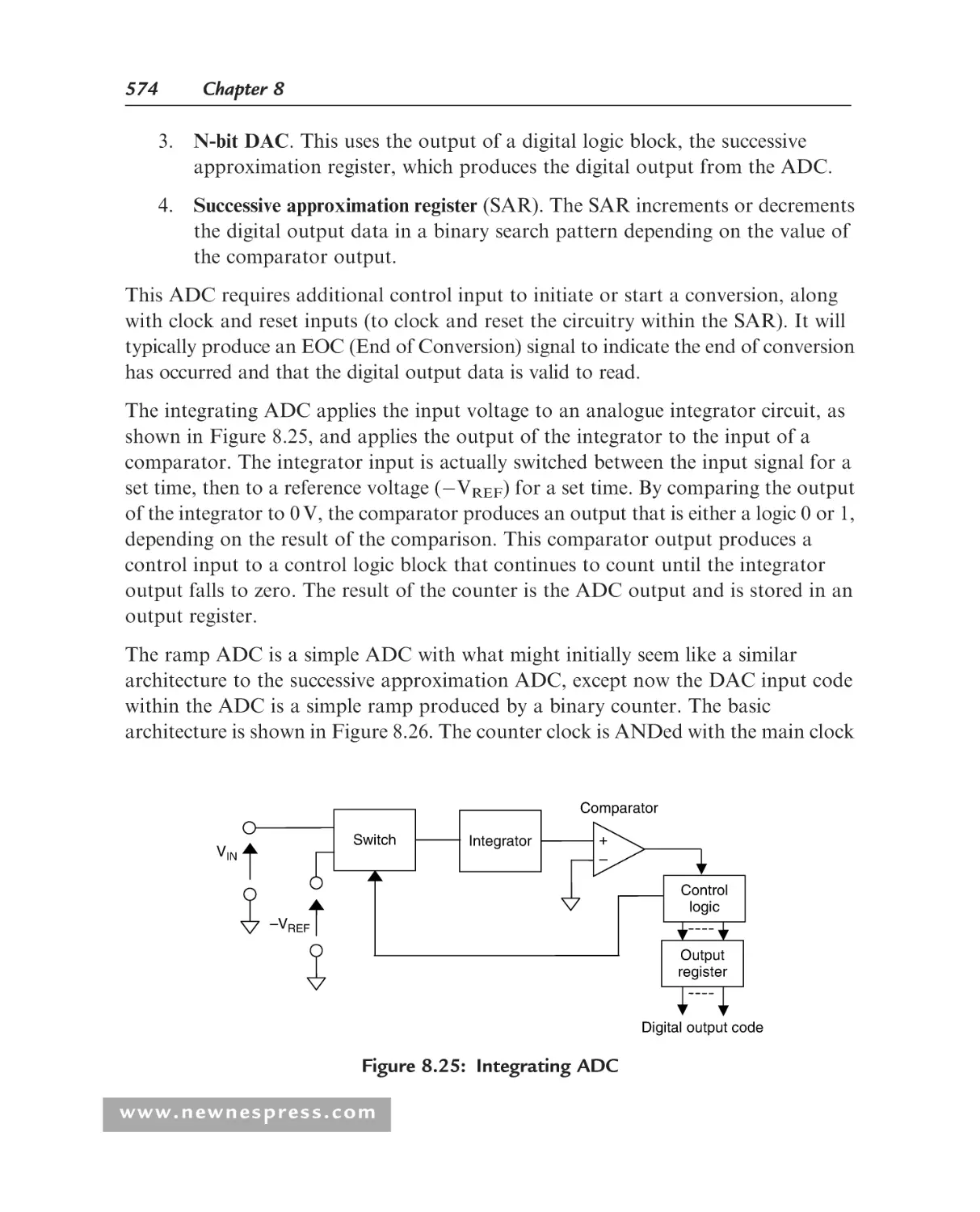
8.3.3 Types of ADC ............................................................................... 572
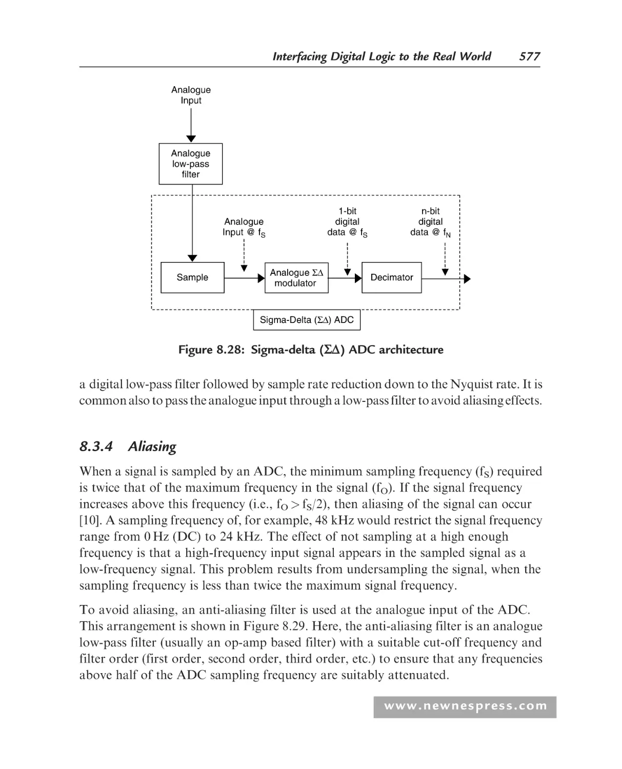
8.3.4 Aliasing.......................................................................................... 577
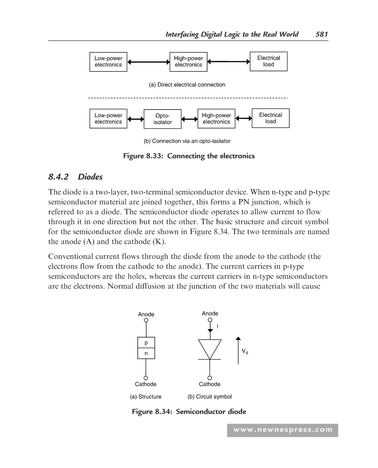
Power Electronics .................................................................................... 580
8.4.1 Introduction .................................................................................. 580
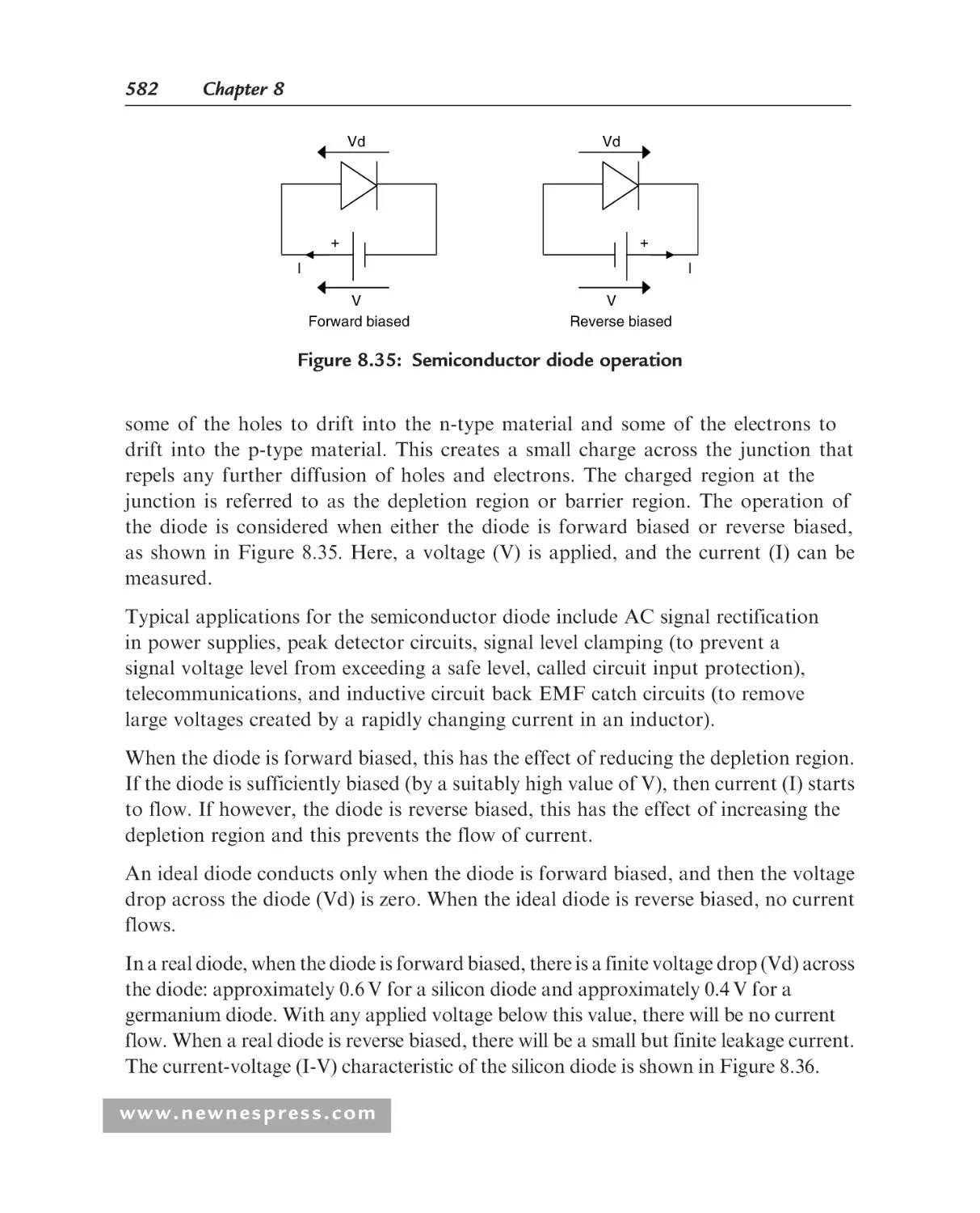
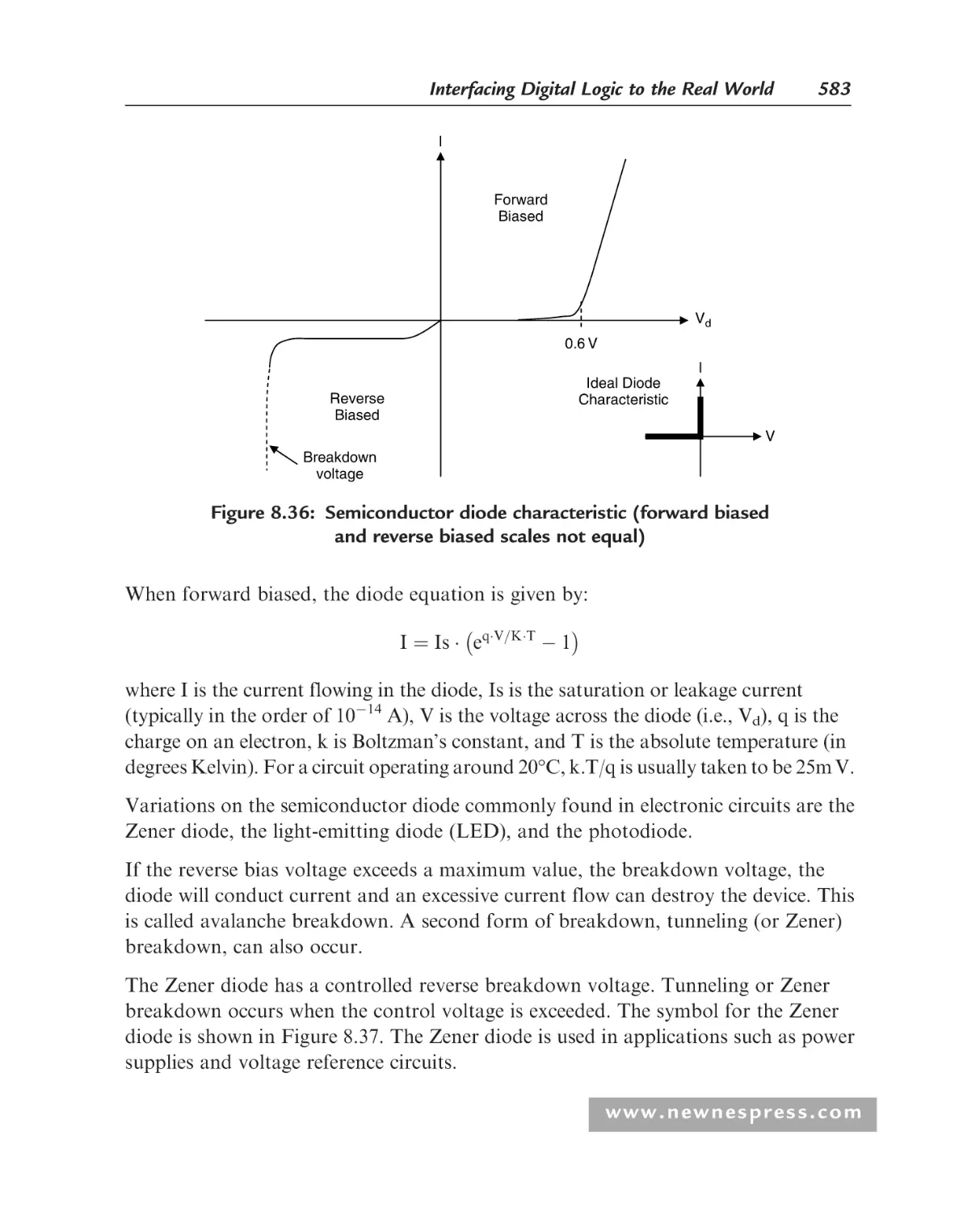
8.4.2 Diodes ........................................................................................... 581
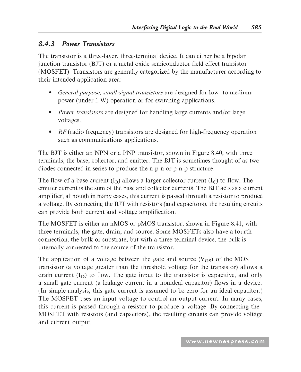
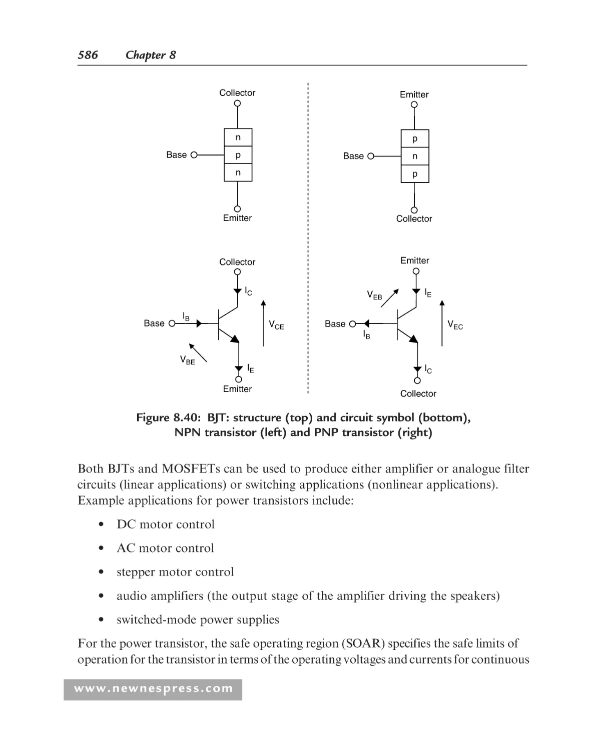
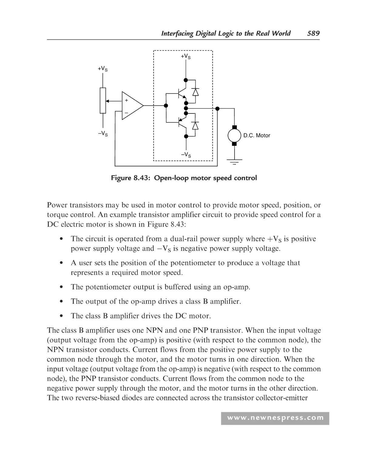
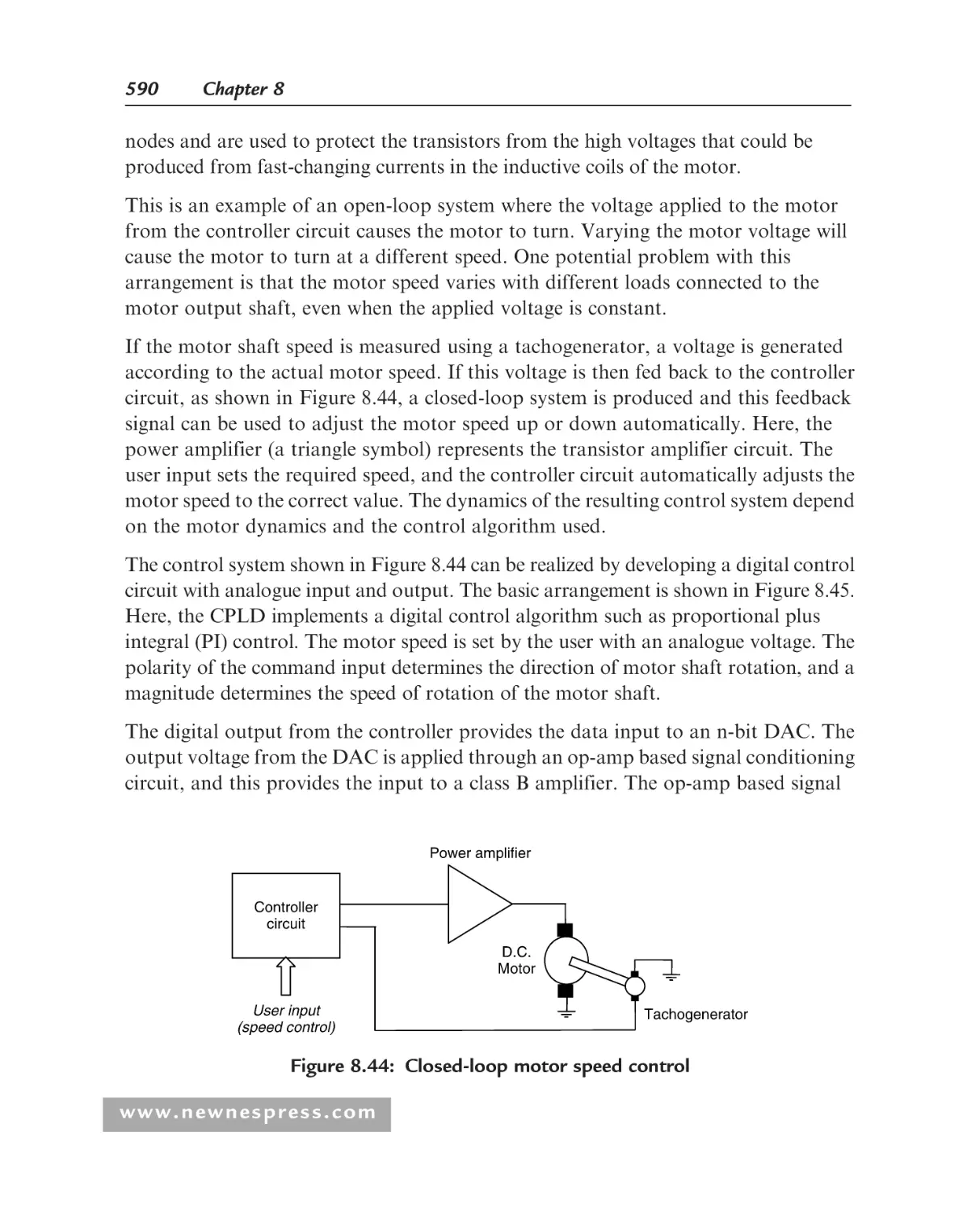
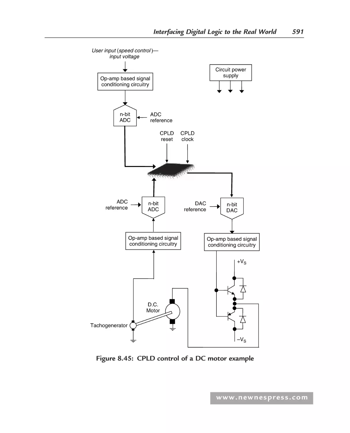
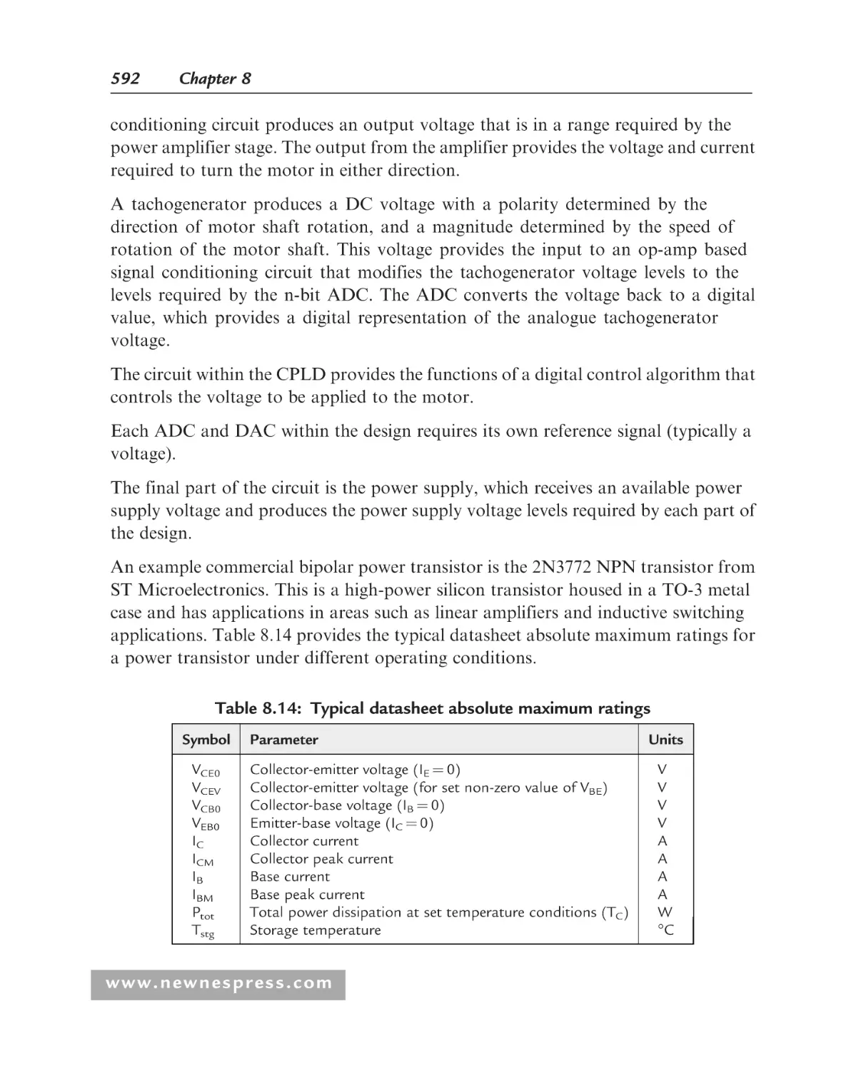
8.4.3 Power Transistors.......................................................................... 585
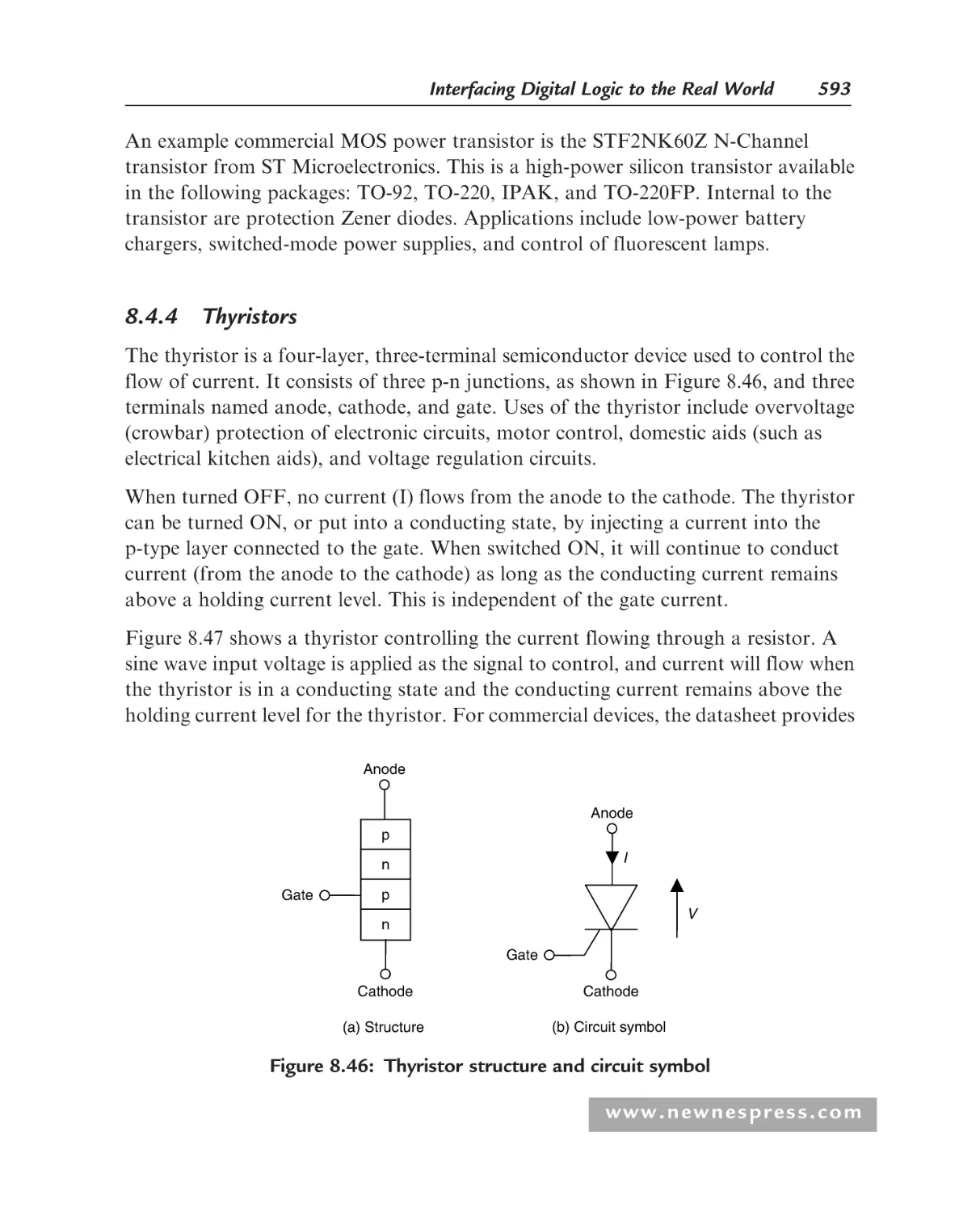
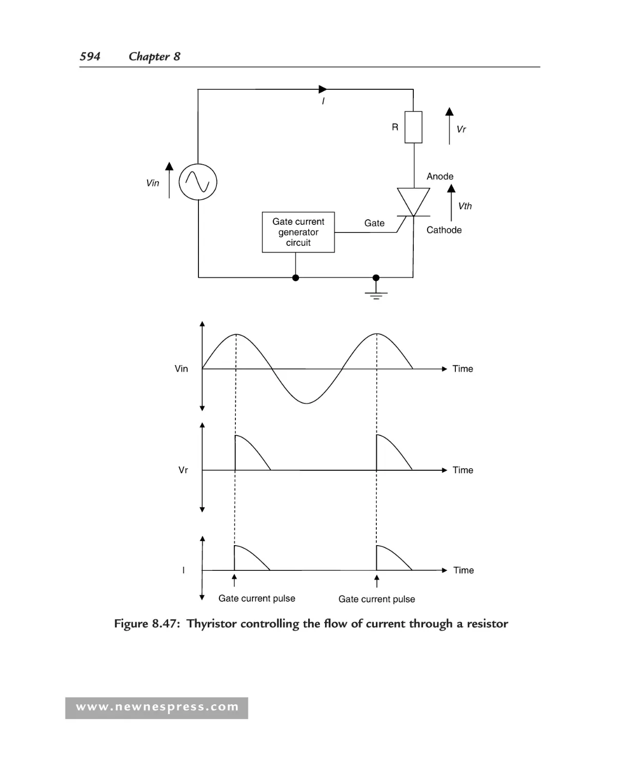
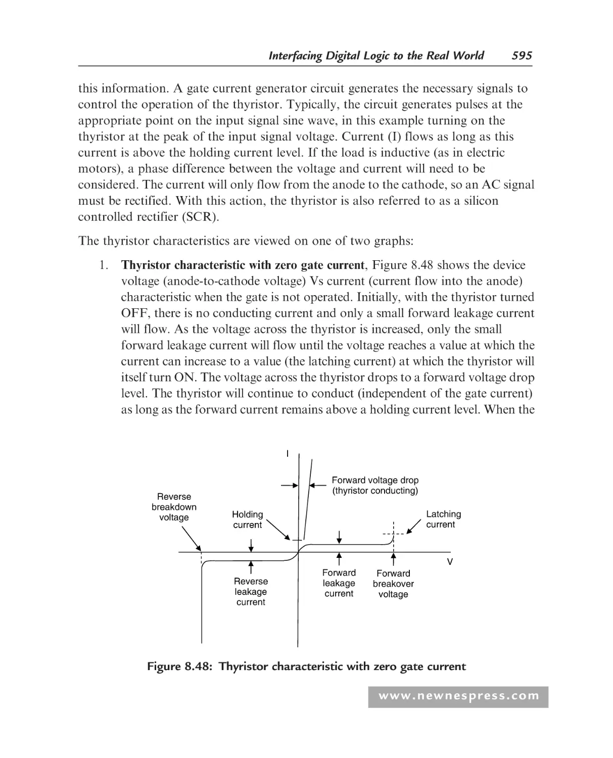
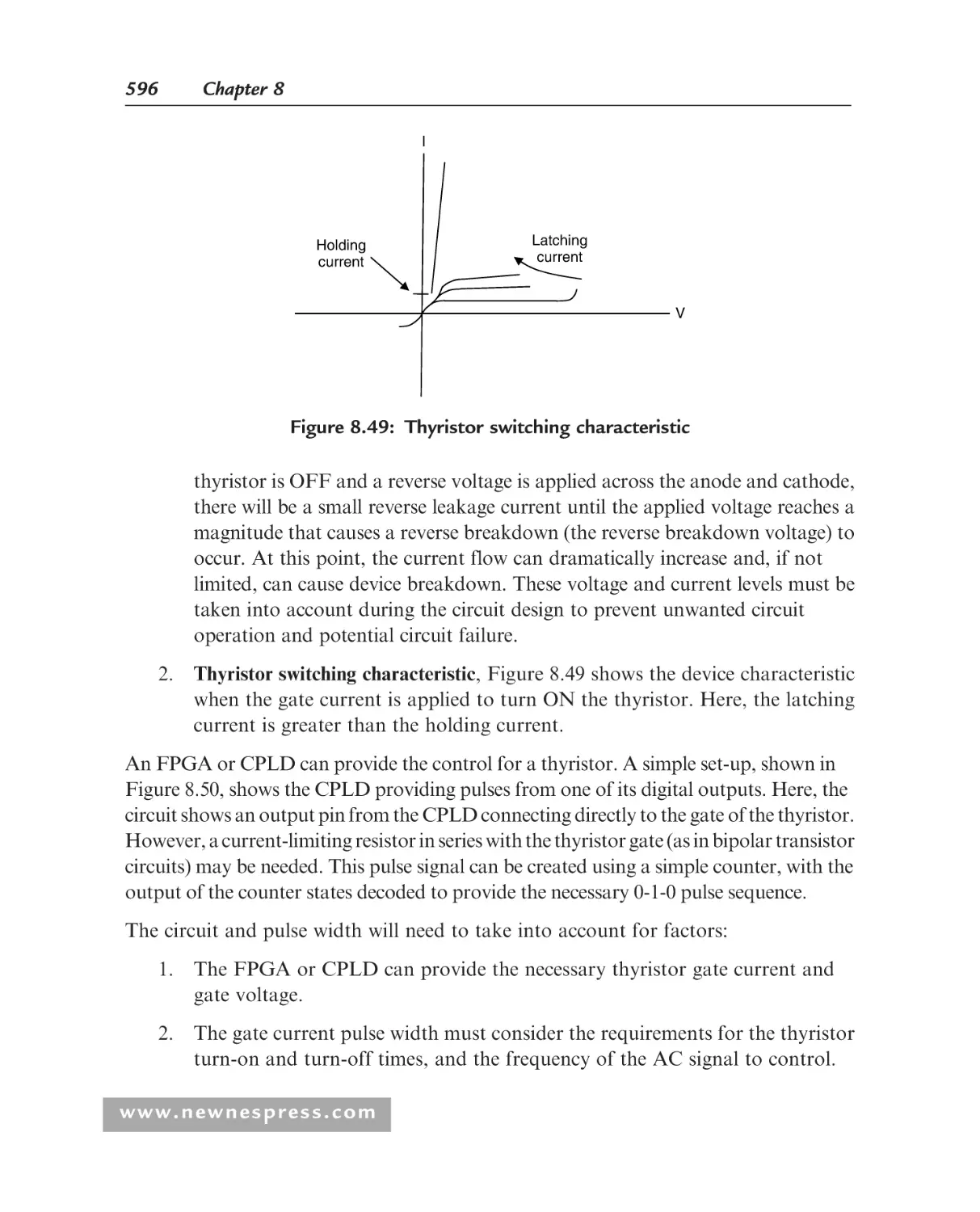
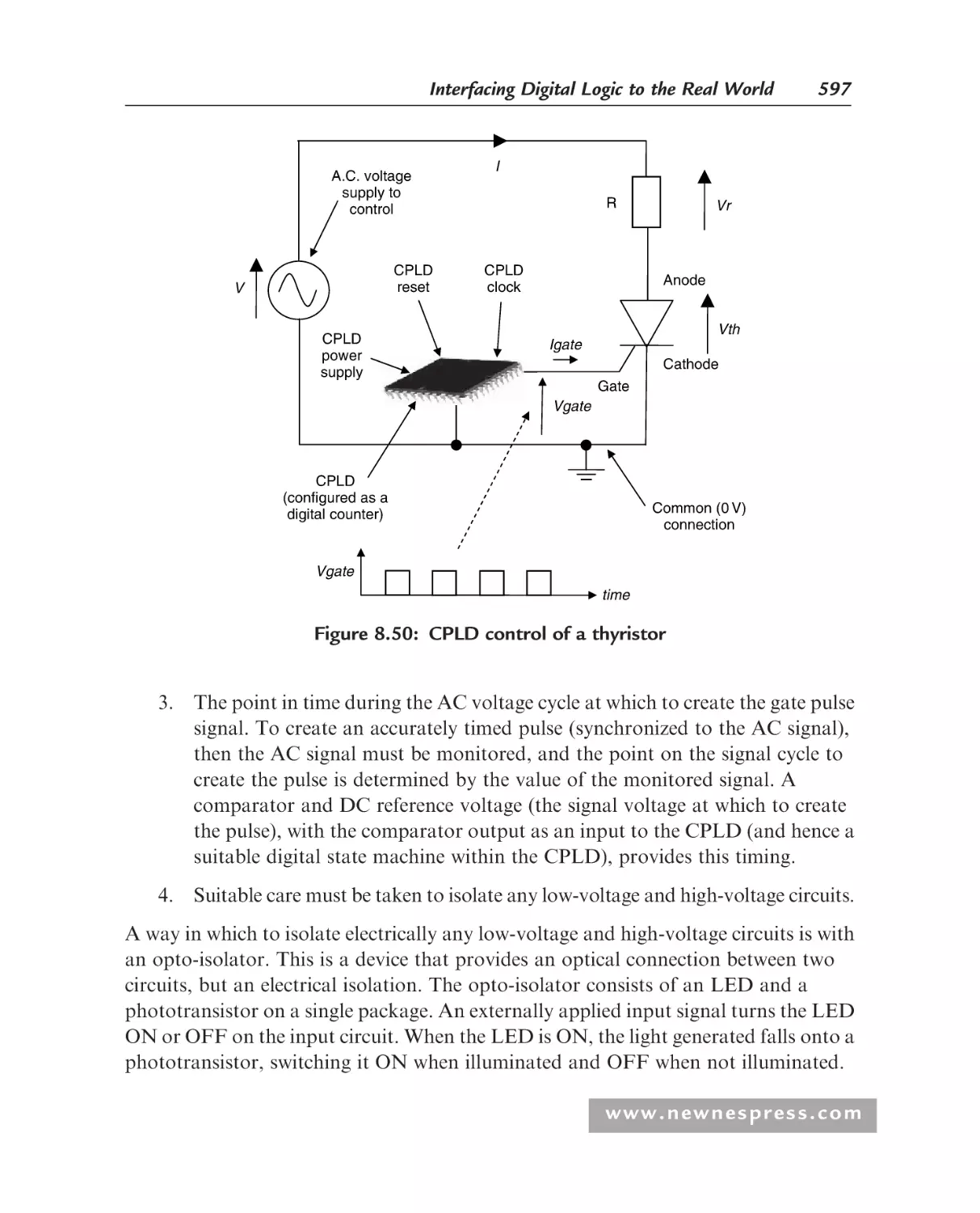
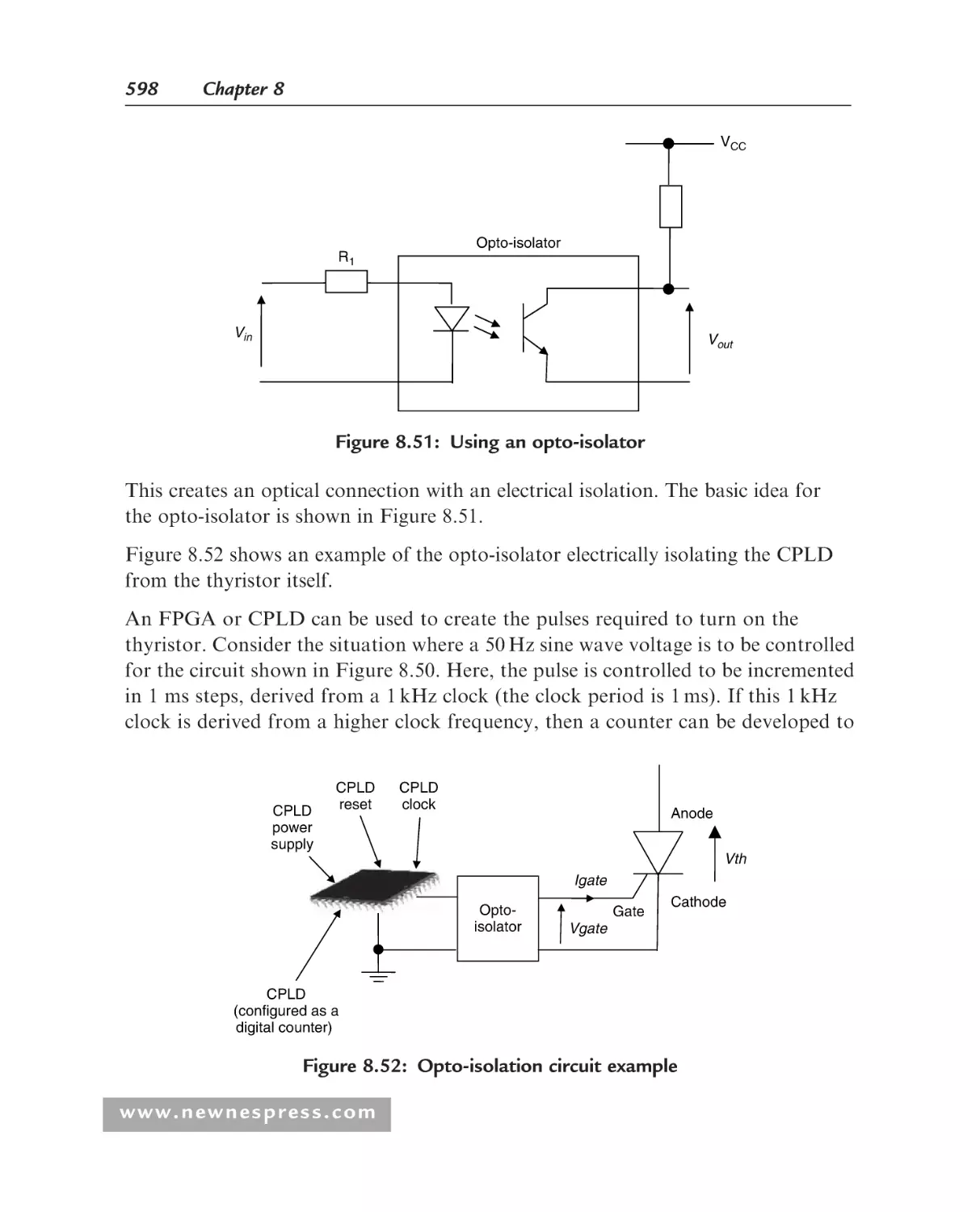
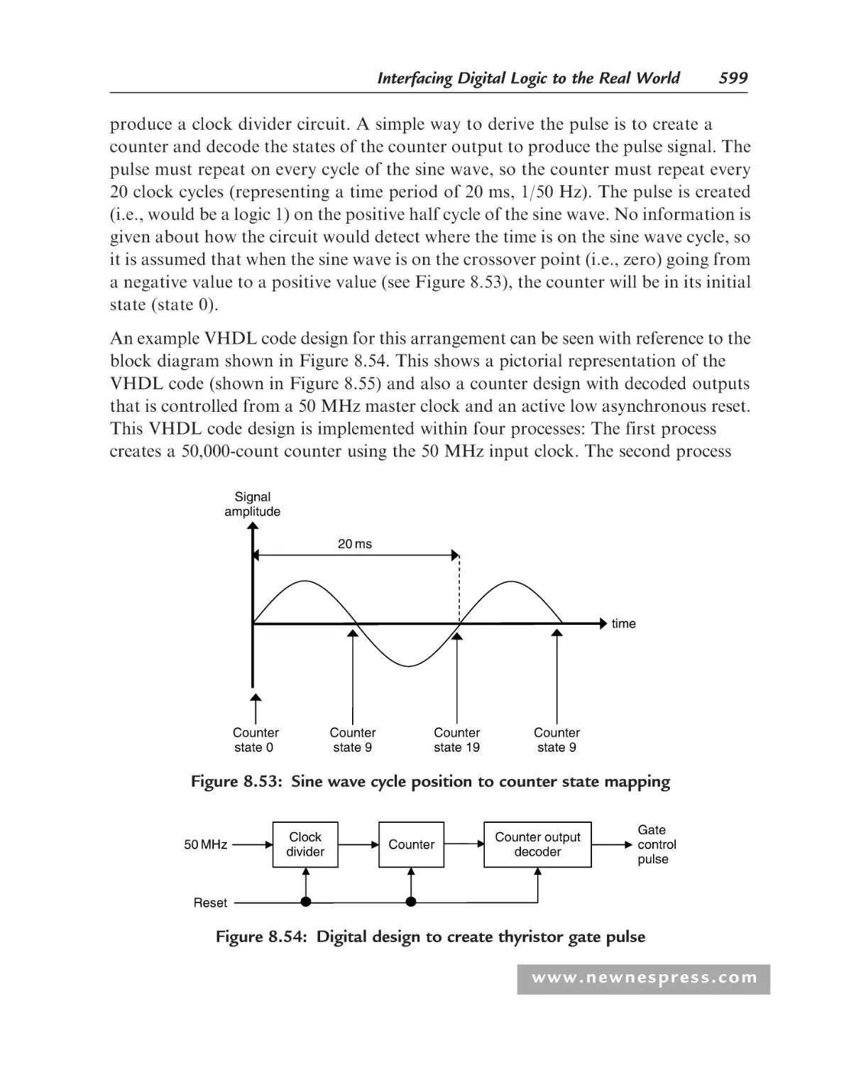
8.4.4 Thyristors ...................................................................................... 593
8.4.5 Gate Turn-Off Thyristors.............................................................. 603
8.4.6 Asymmetric Thyristors .................................................................. 604
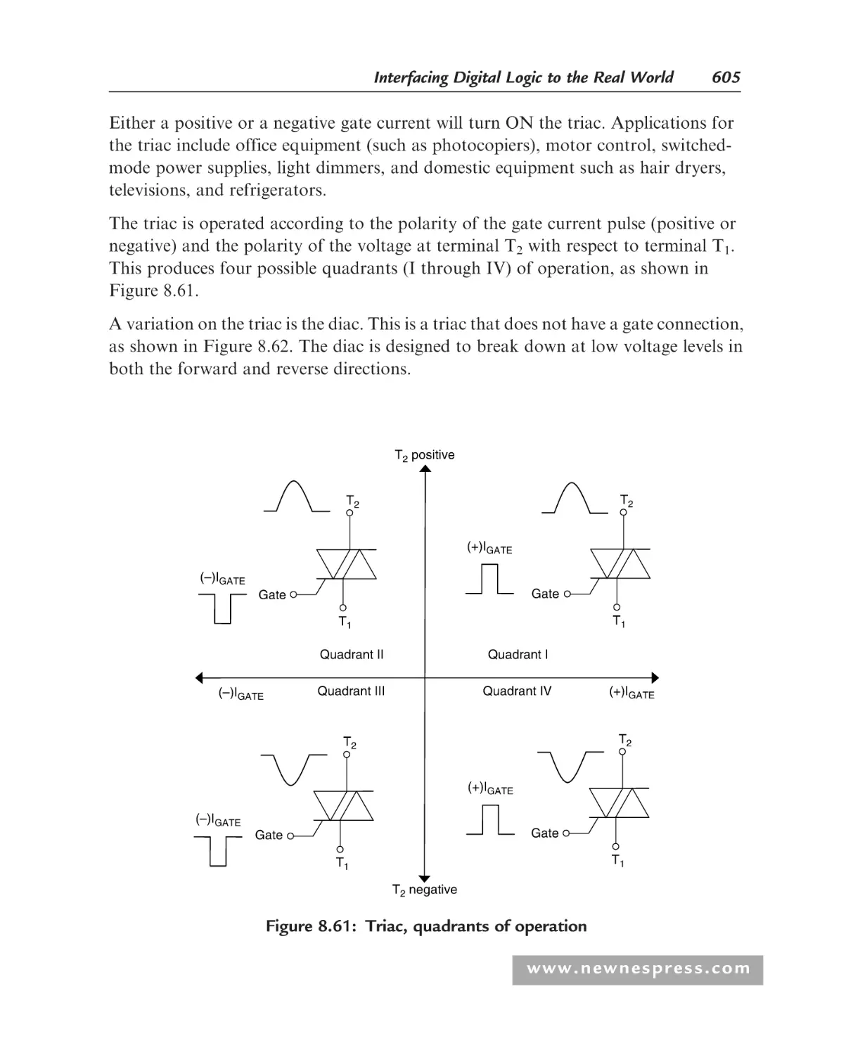
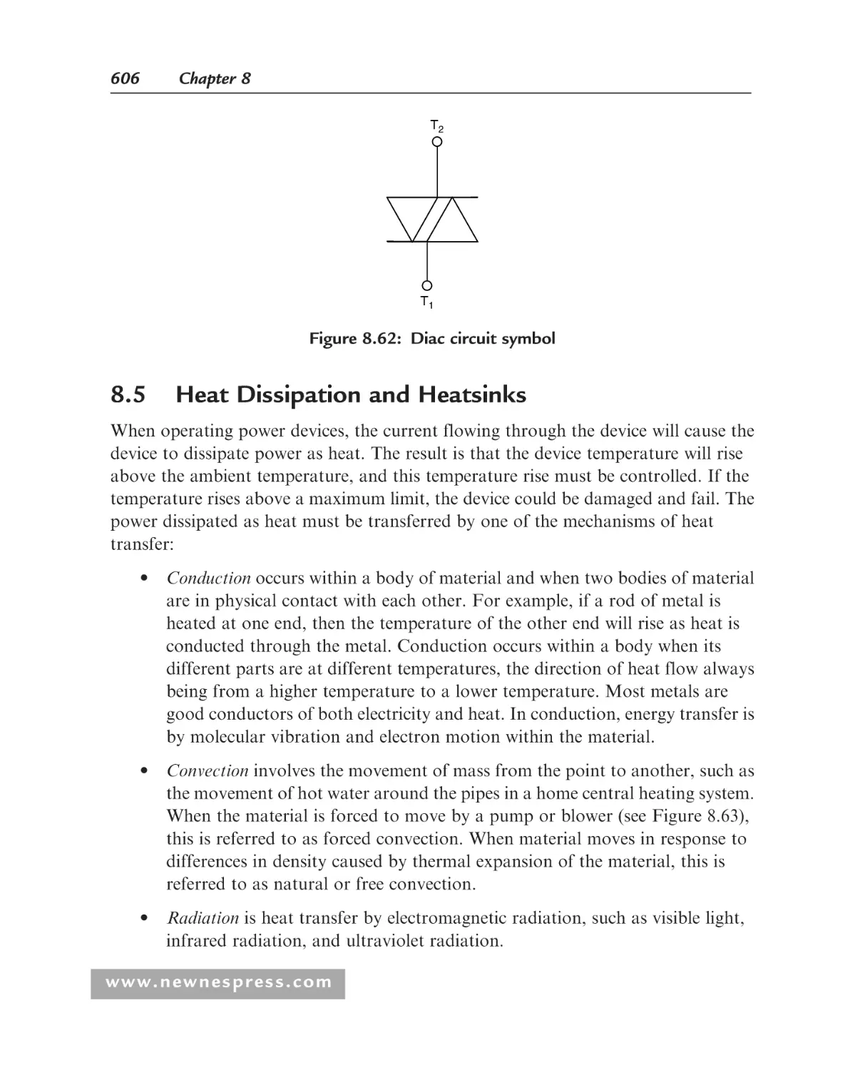
8.4.7 Triacs............................................................................................. 604
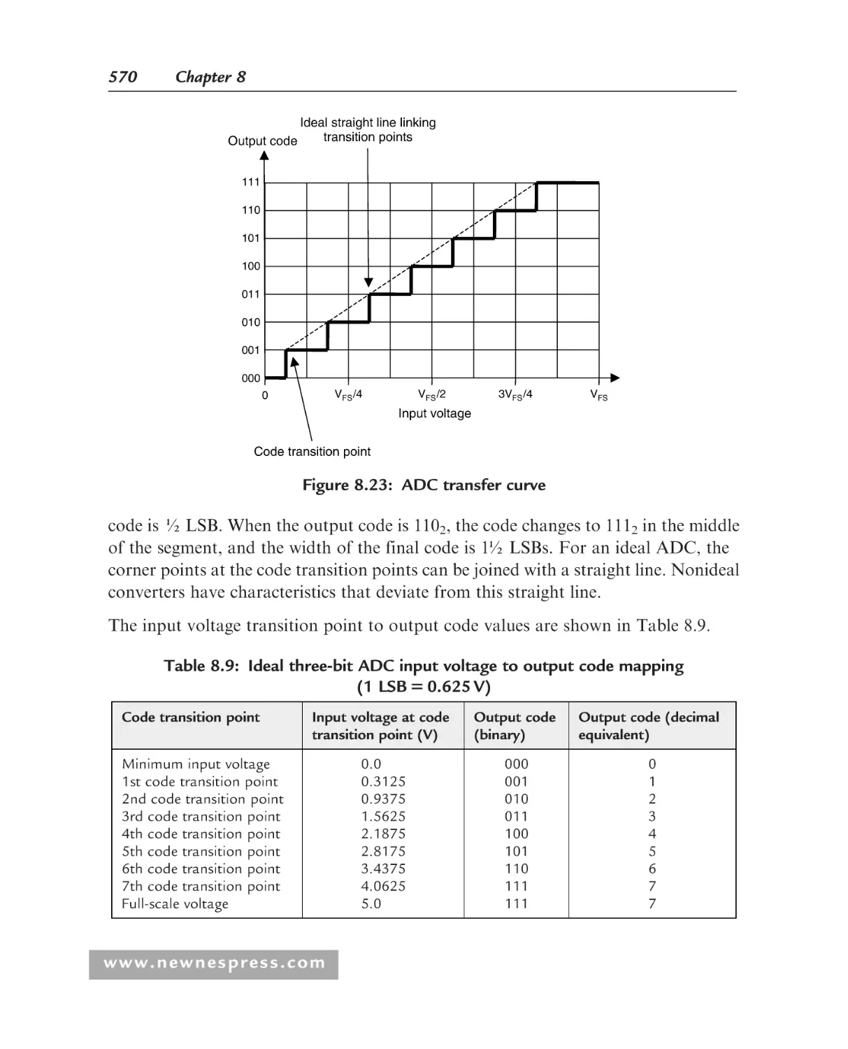
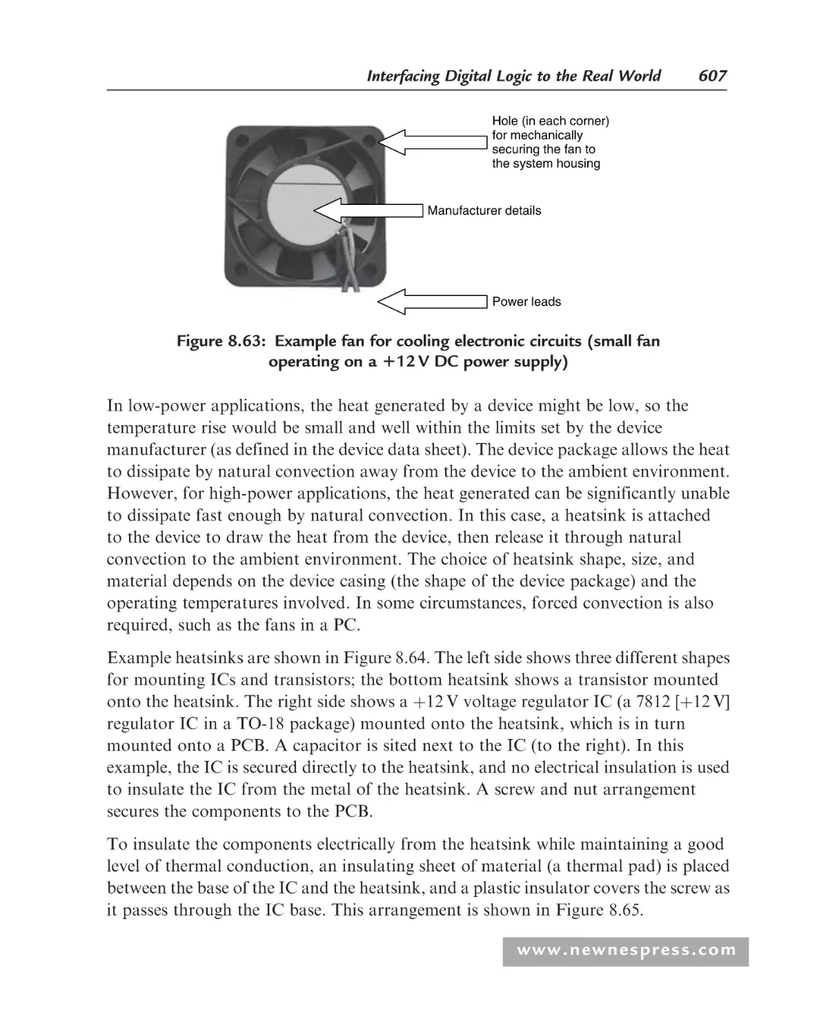
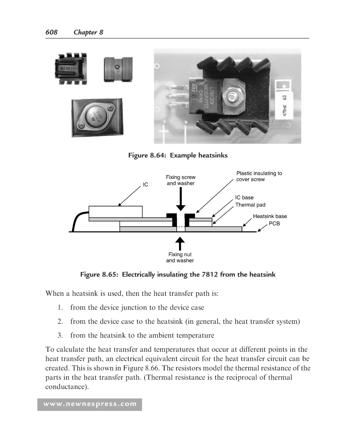
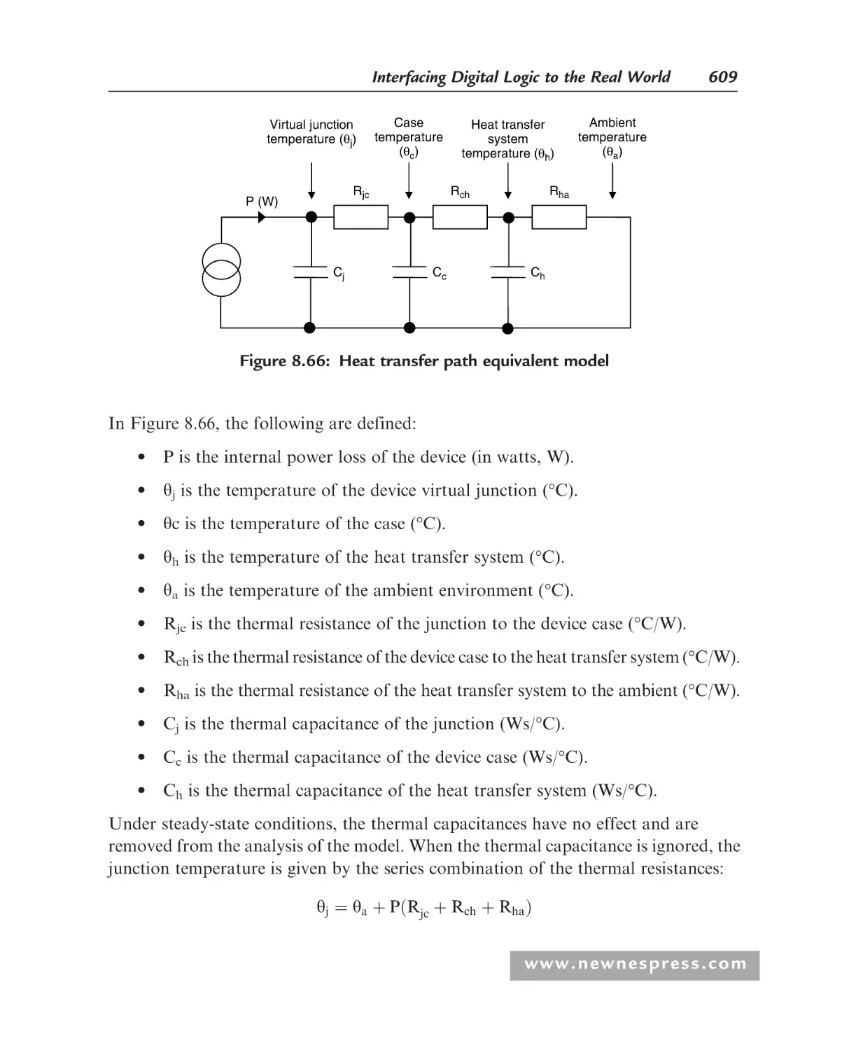
Heat Dissipation and Heatsinks.............................................................. 606
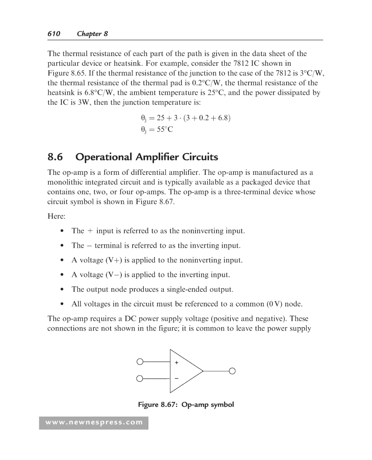
Operational Amplifier Circuits................................................................ 610
www.newnespress.com
Table of Contents
xiii
References................................................................................................ 612
Student Exercises..................................................................................... 613
Chapter 9: Testing the Electronic System .................................................... 615
9.1
9.2
9.3
9.4
9.5
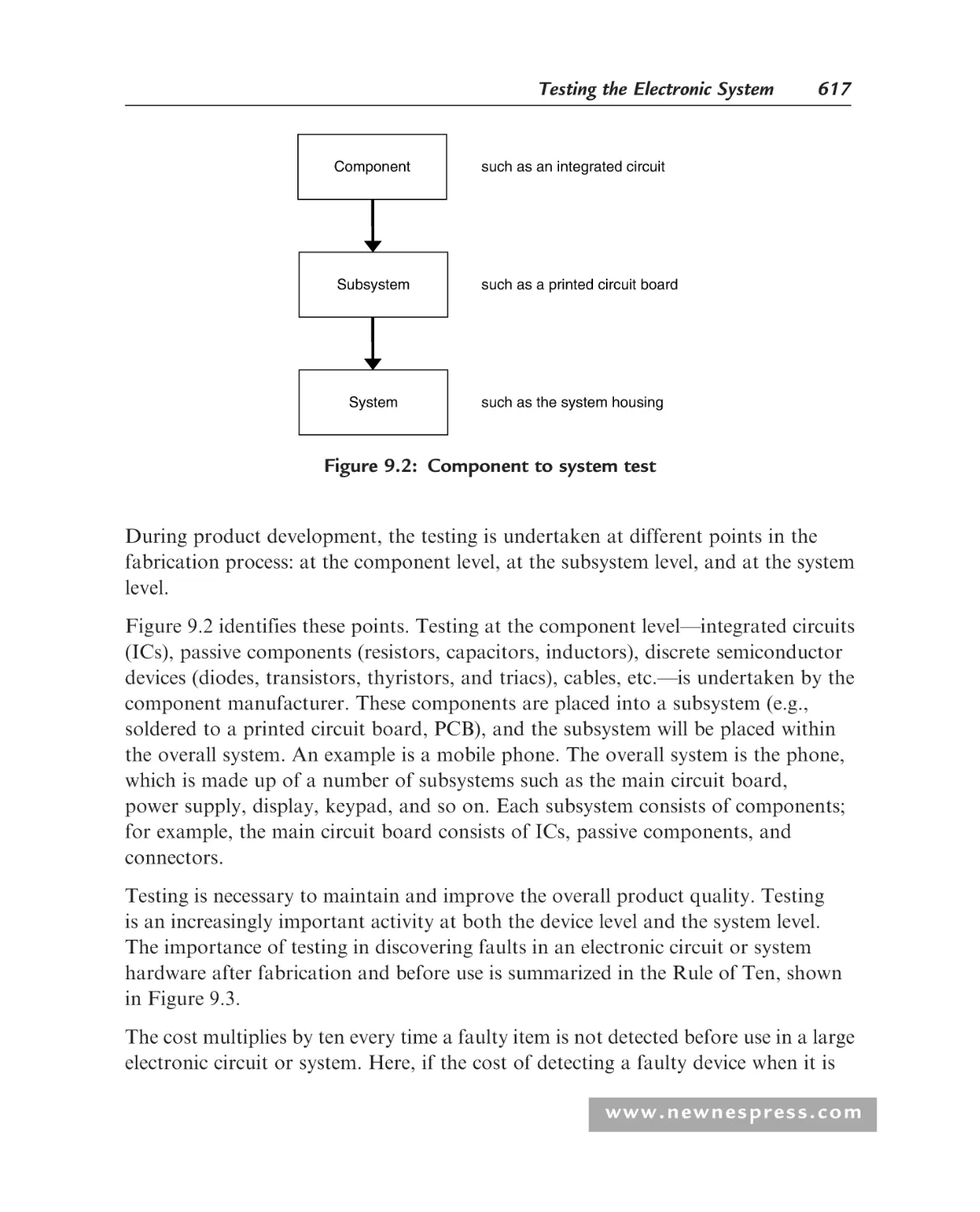
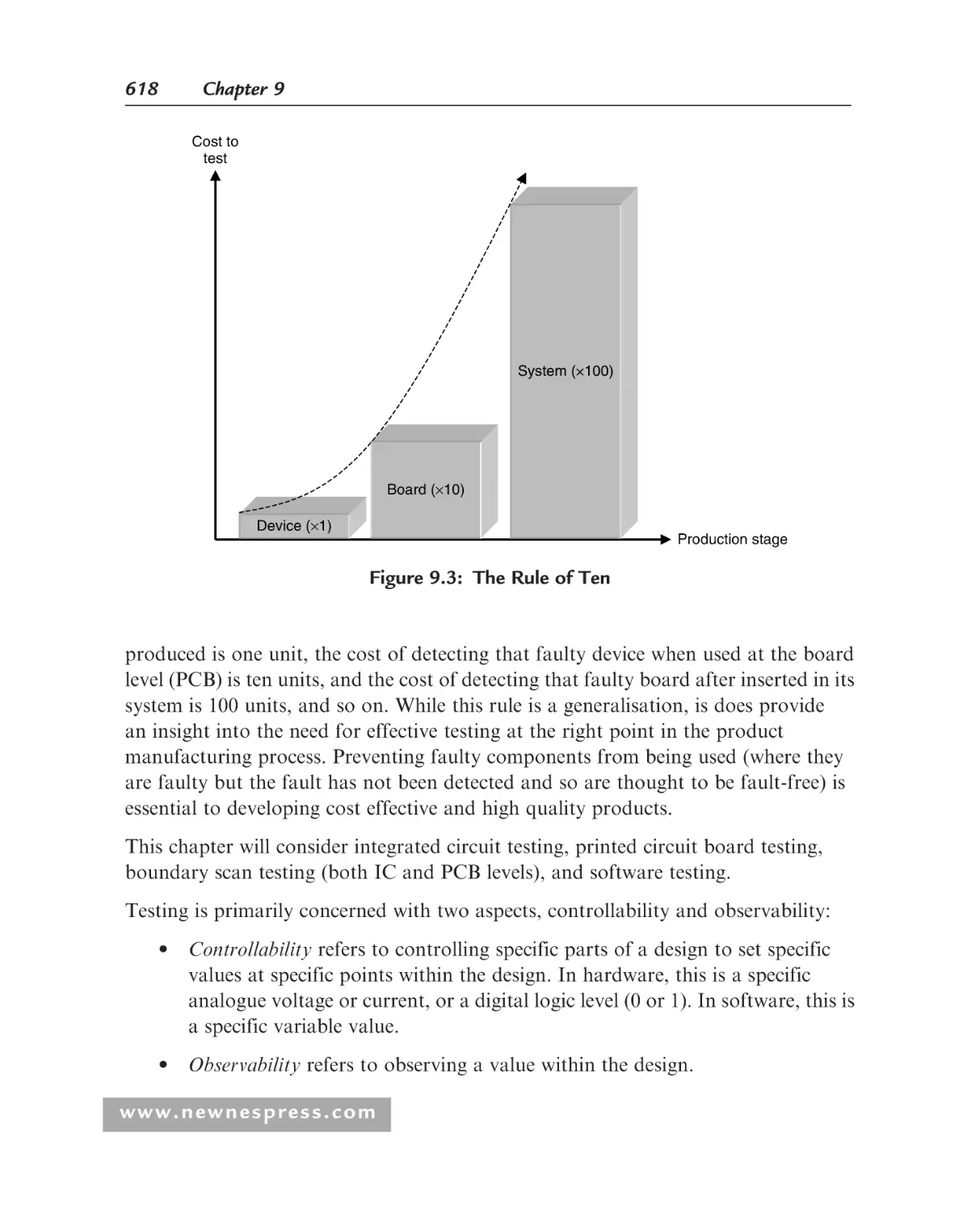
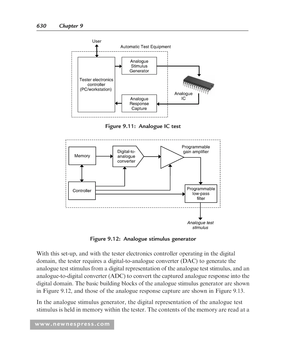
Introduction ............................................................................................ 615
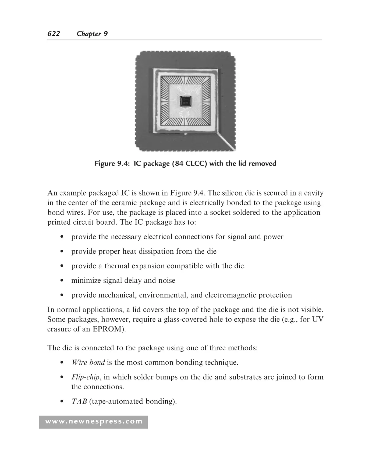
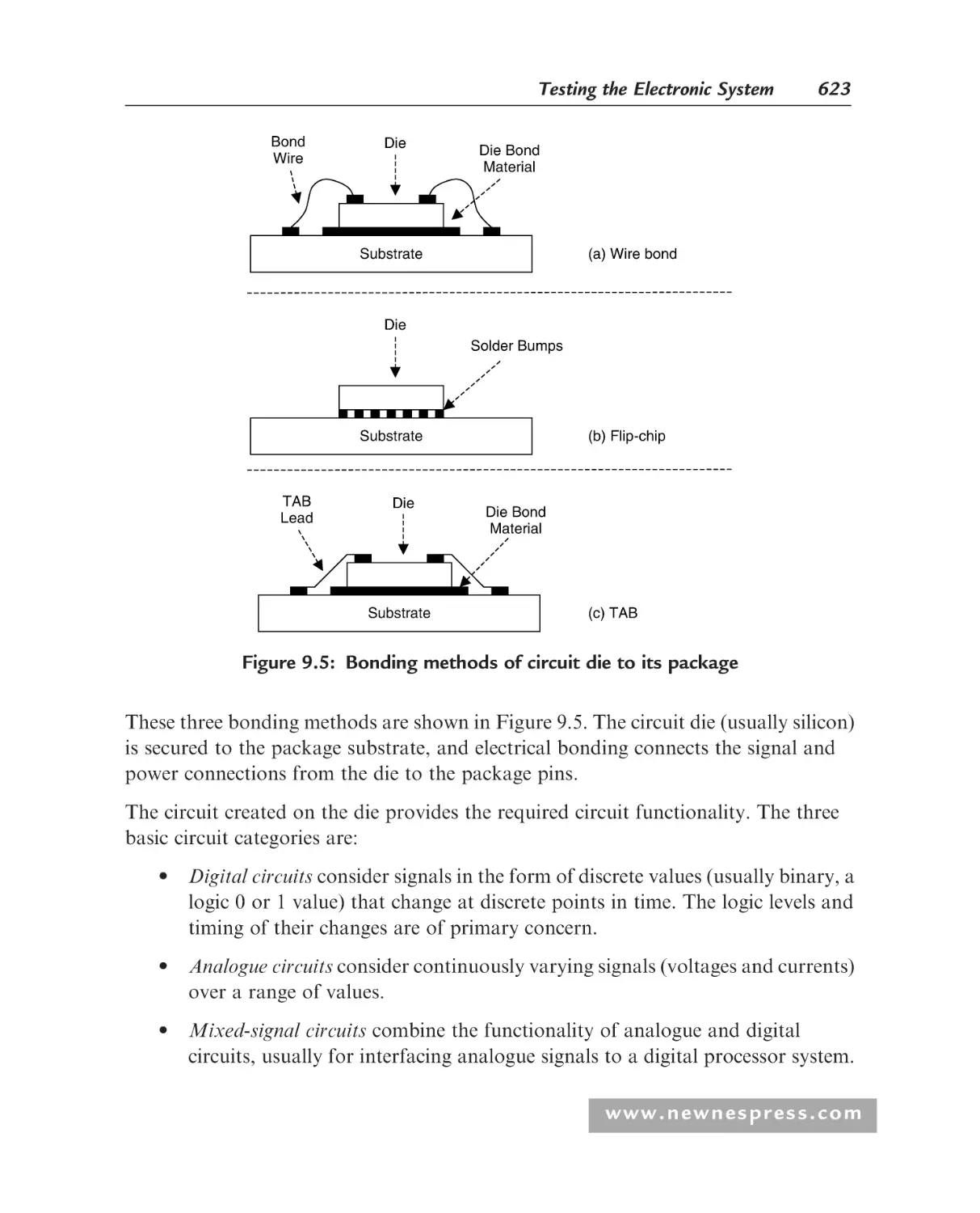
Integrated Circuit Testing ....................................................................... 621
9.2.1 Introduction .................................................................................. 621
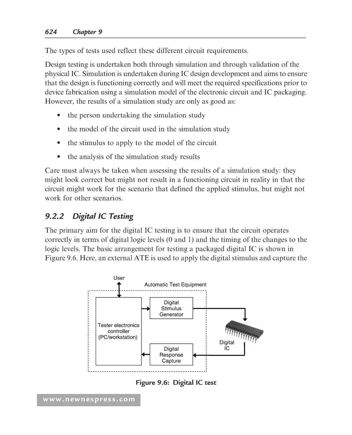
9.2.2 Digital IC Testing.......................................................................... 624
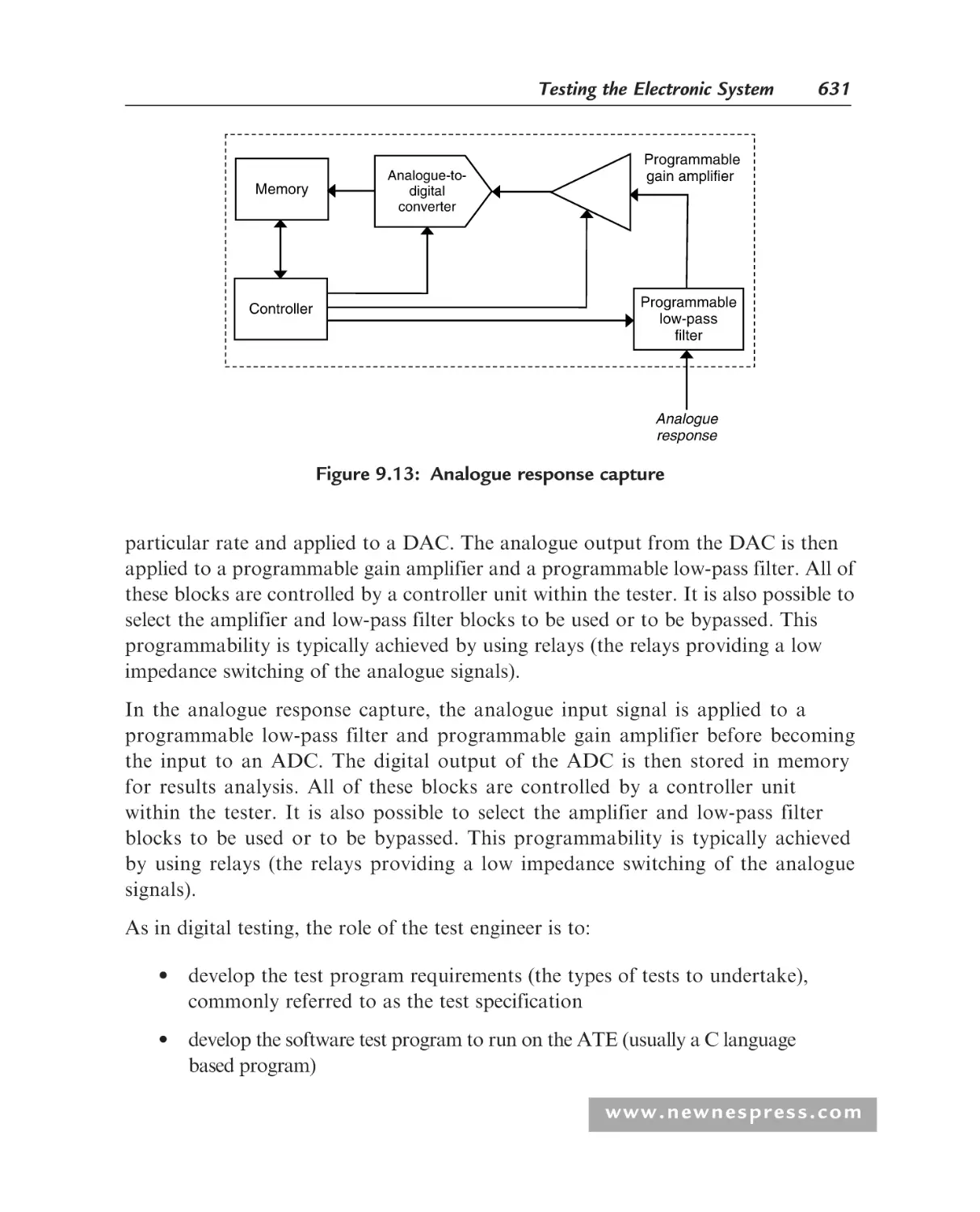
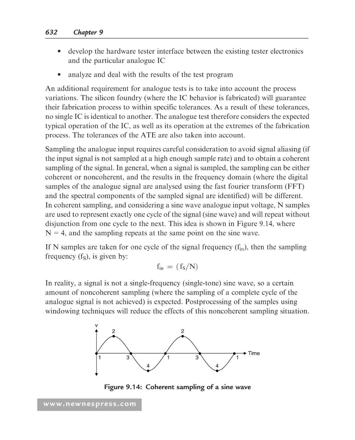
9.2.3 Analogue IC Testing ..................................................................... 629
9.2.4 Mixed-Signal IC Testing................................................................ 633
Printed Circuit Board Testing ................................................................. 633
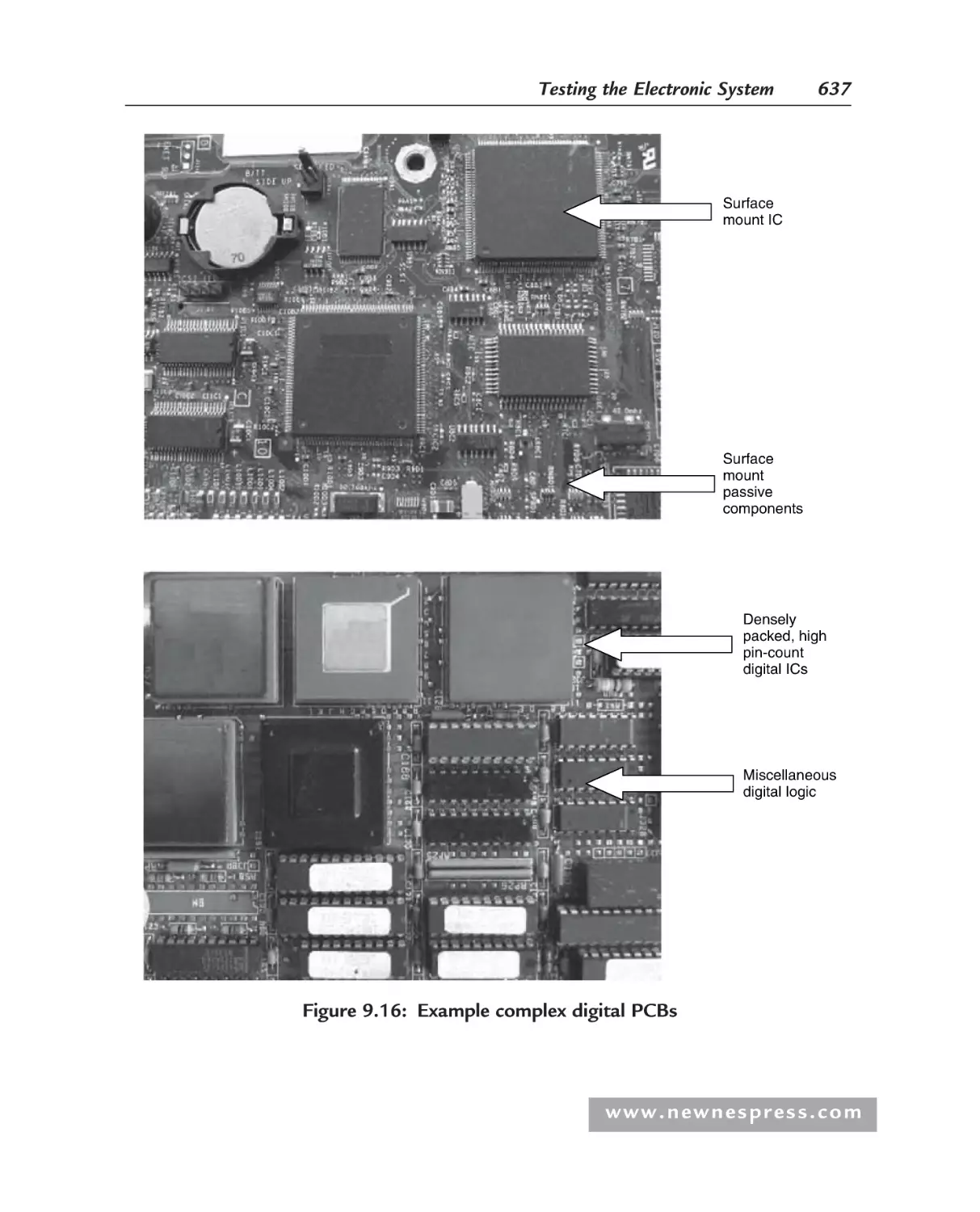
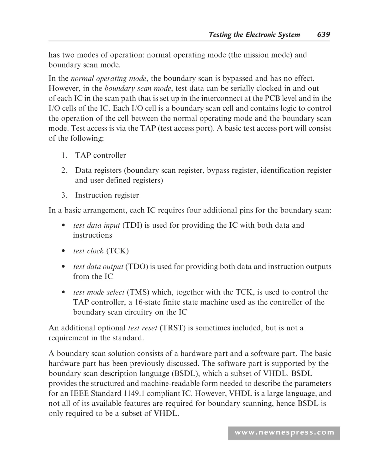
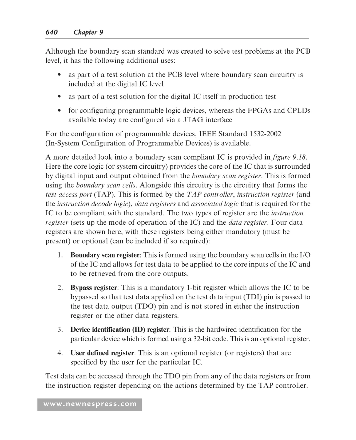
Boundary Scan Testing ........................................................................... 636
Software Testing...................................................................................... 642
References................................................................................................ 645
Student Exercises..................................................................................... 646
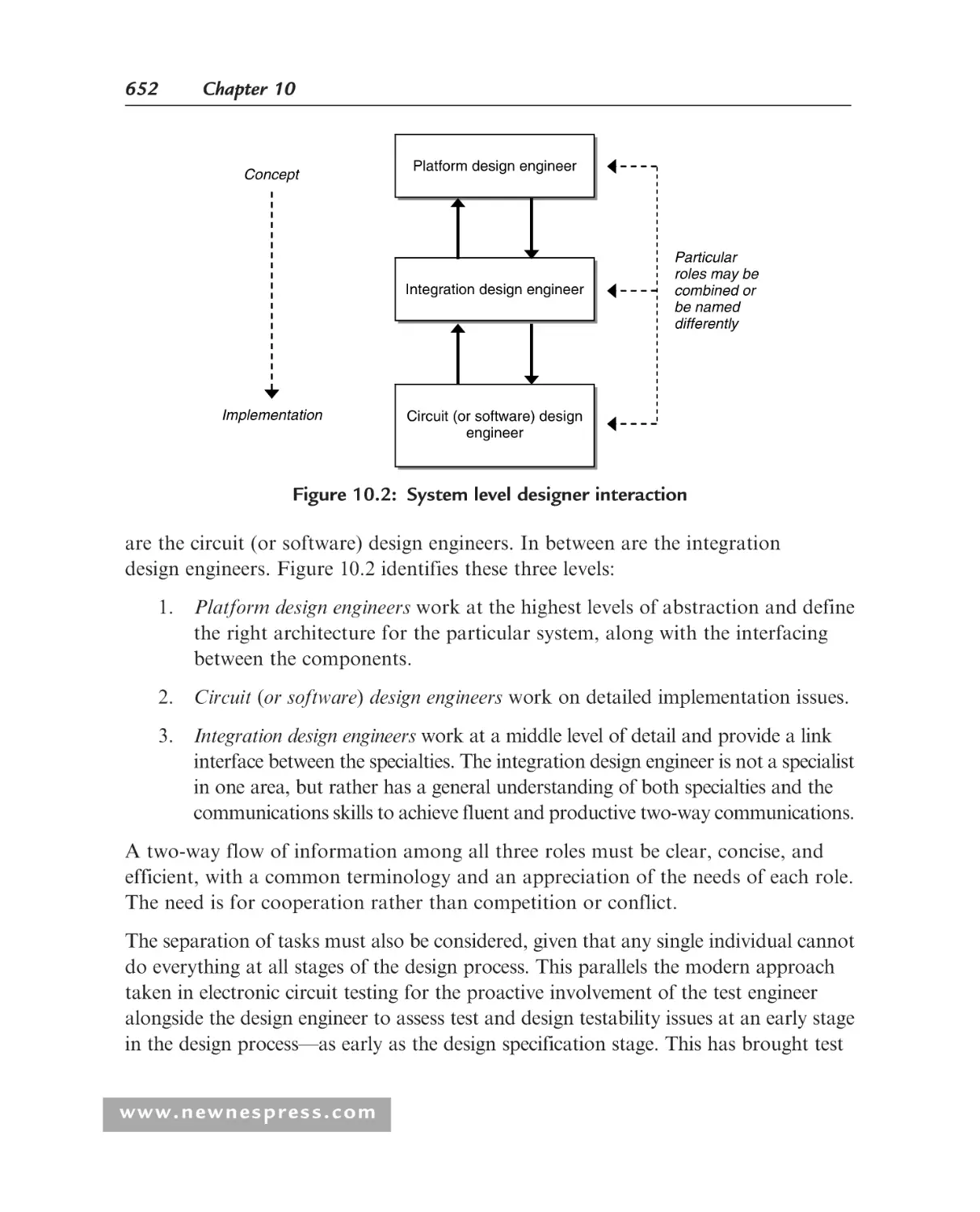
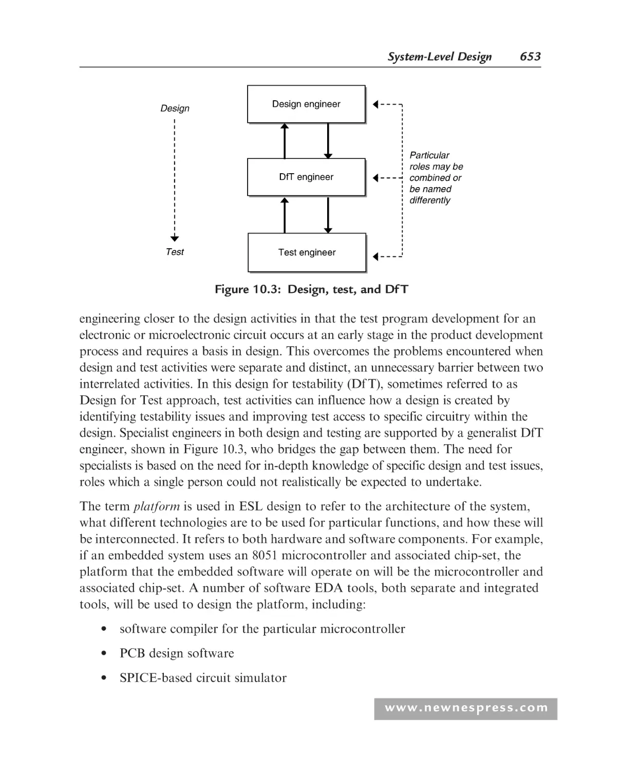
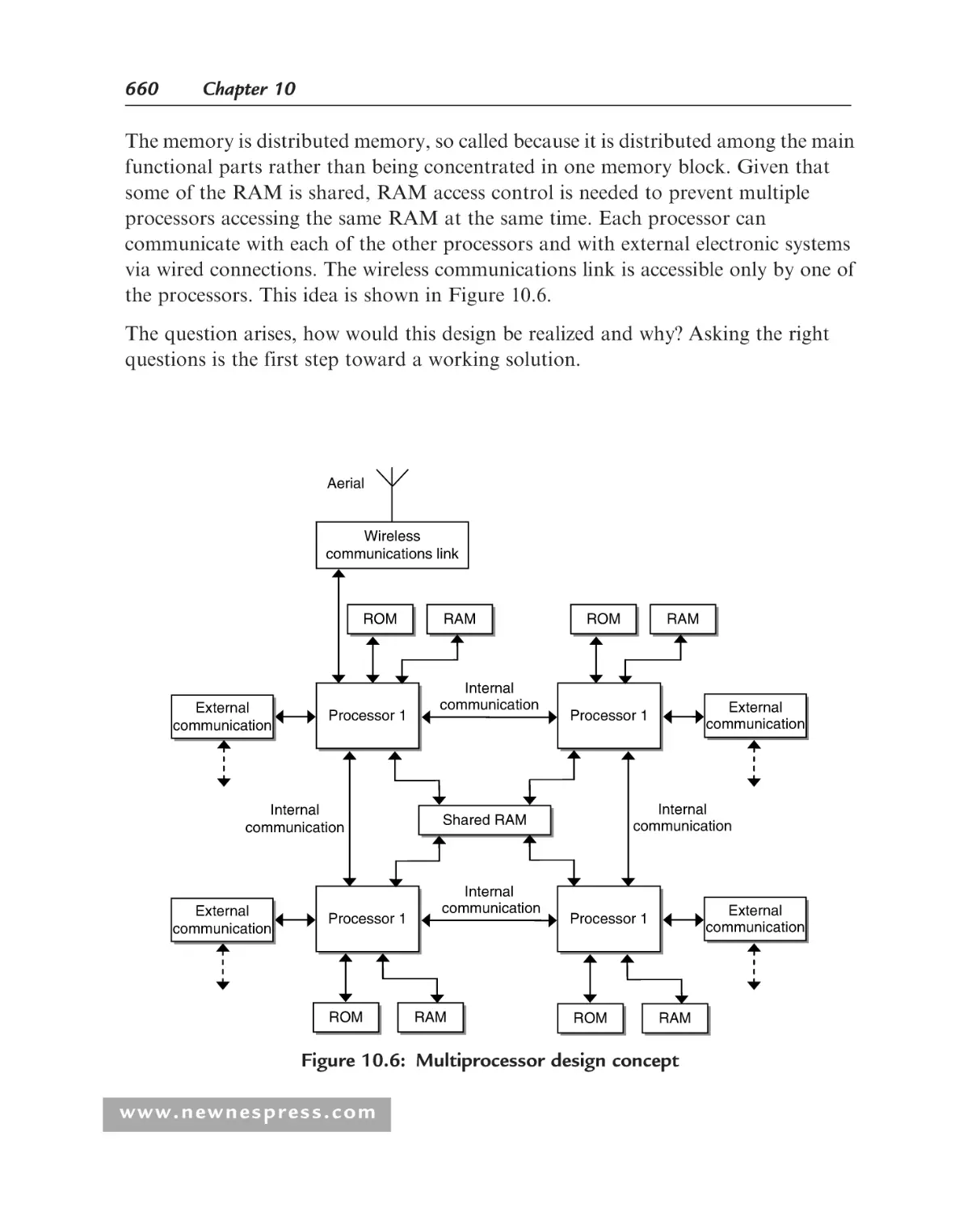
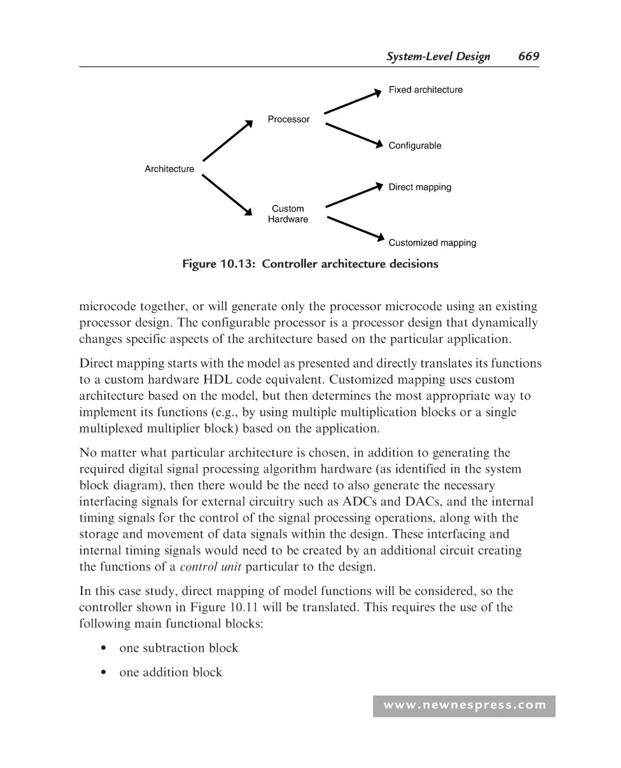
Chapter 10: System-Level Design ............................................................... 647
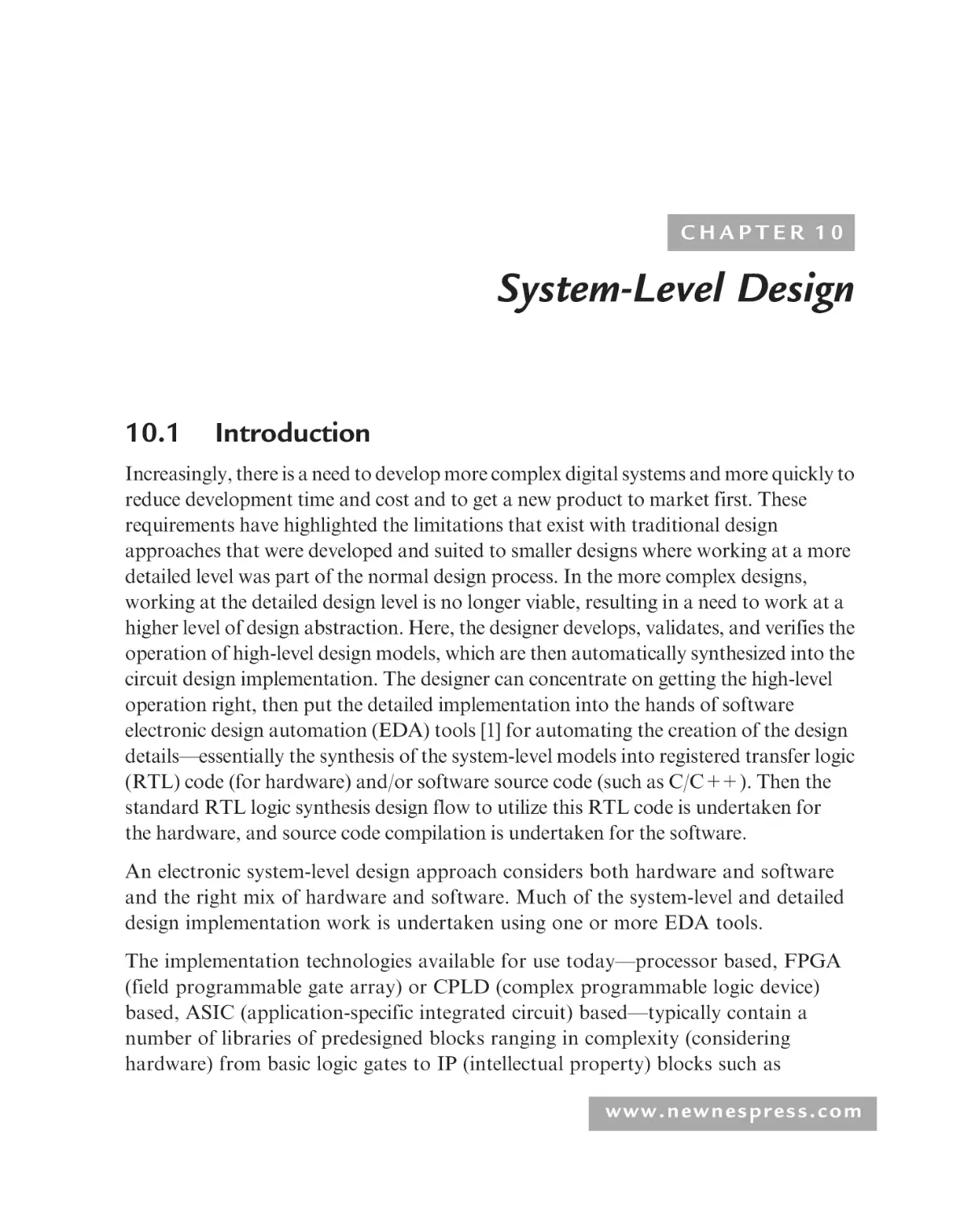
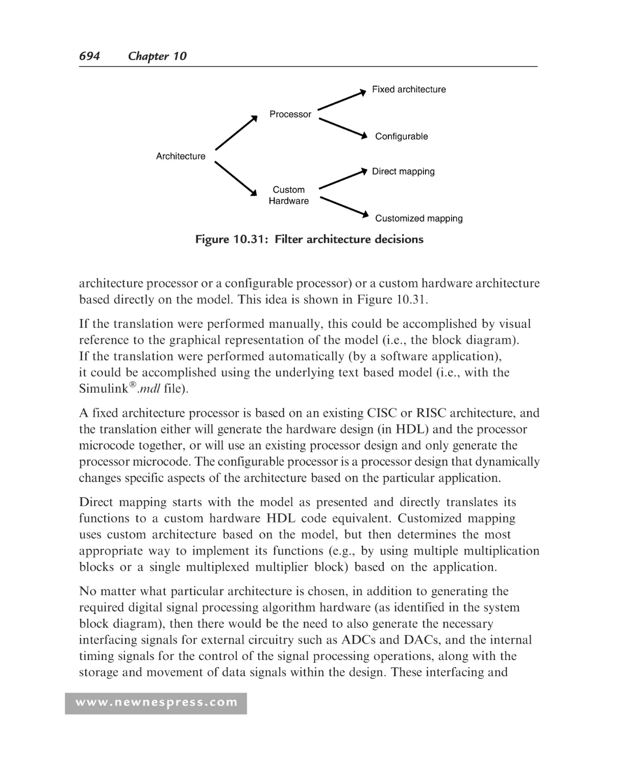
10.1 Introduction ............................................................................................ 647
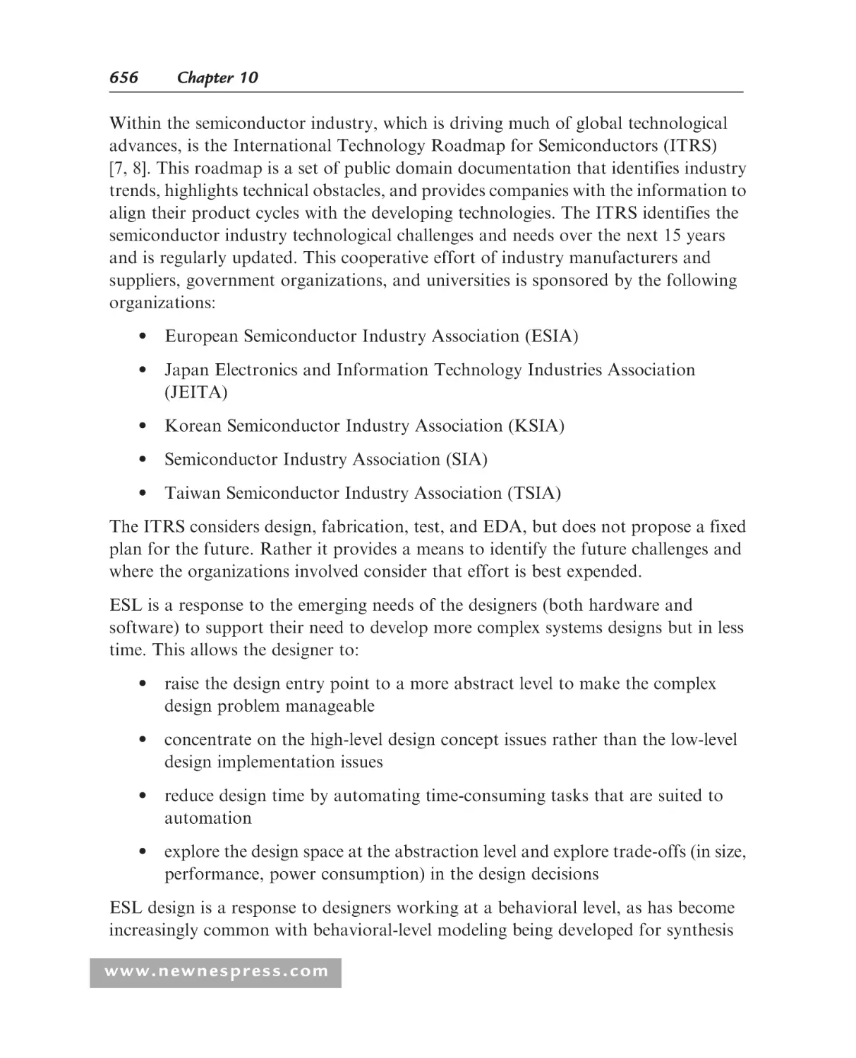
10.2 Electronic System-Level Design .............................................................. 654
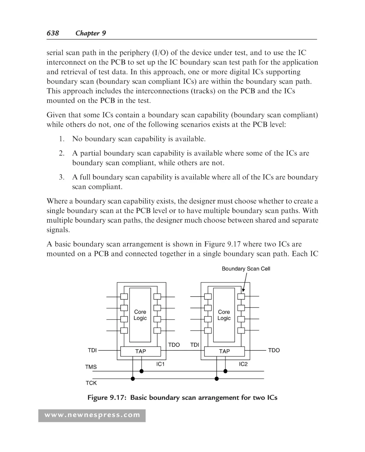
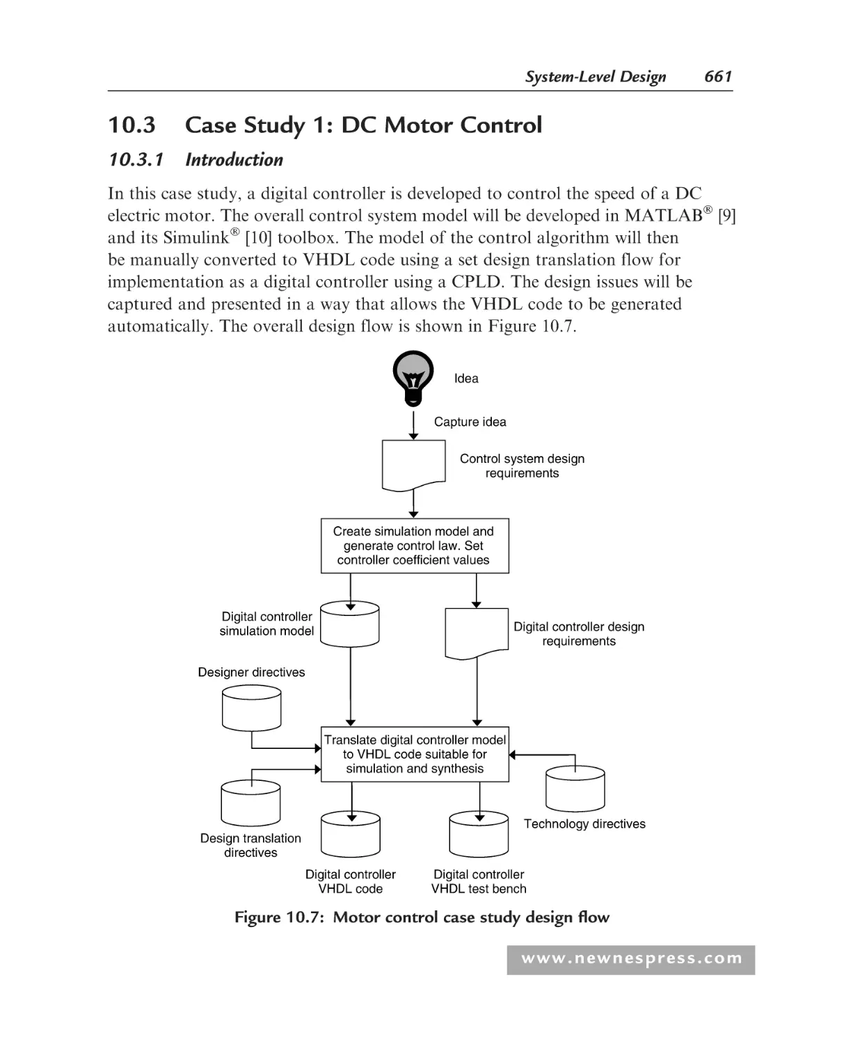
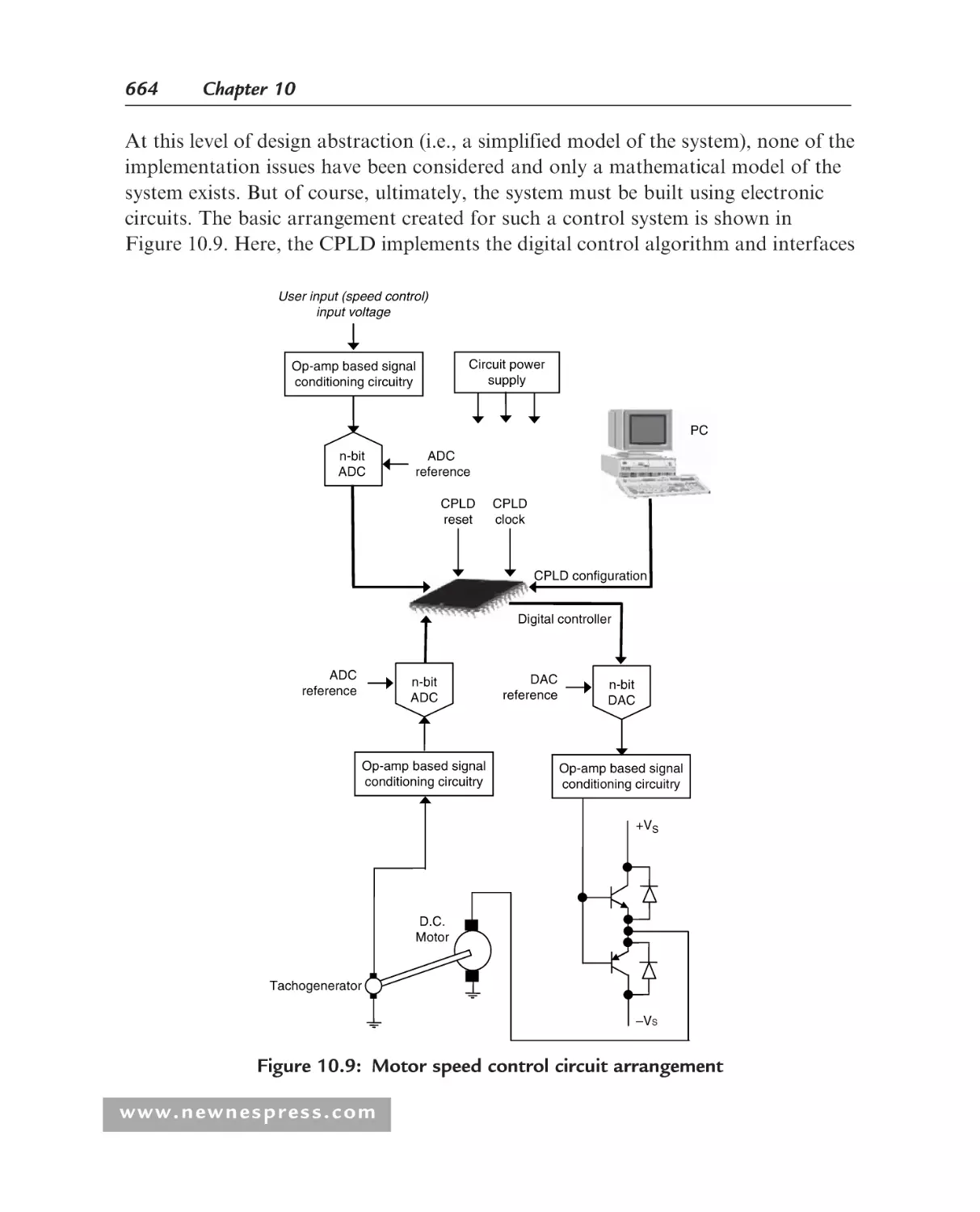
10.3 Case Study 1: DC Motor Control ........................................................... 661
10.3.1 Introduction................................................................................. 661
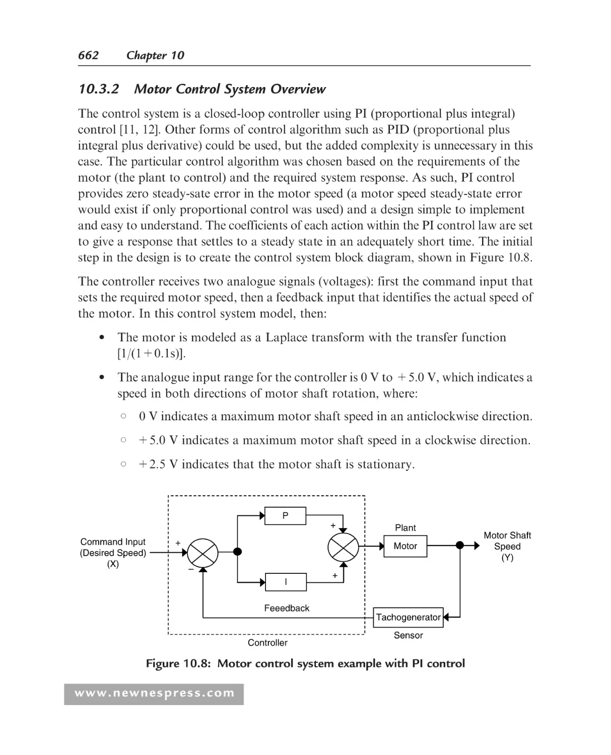
10.3.2 Motor Control System Overview................................................. 662
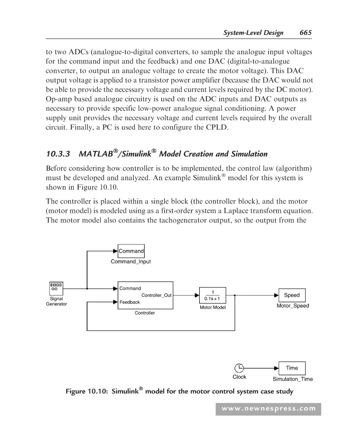
10.3.3 MATLAB/Simulink Model Creation
and Simulation ............................................................................ 665
10.3.4 Translating the Design to VHDL................................................ 666
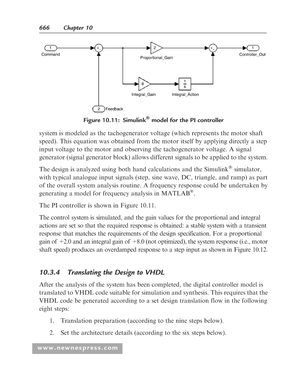
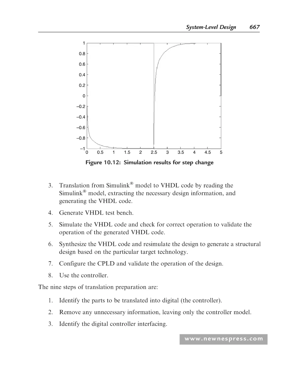
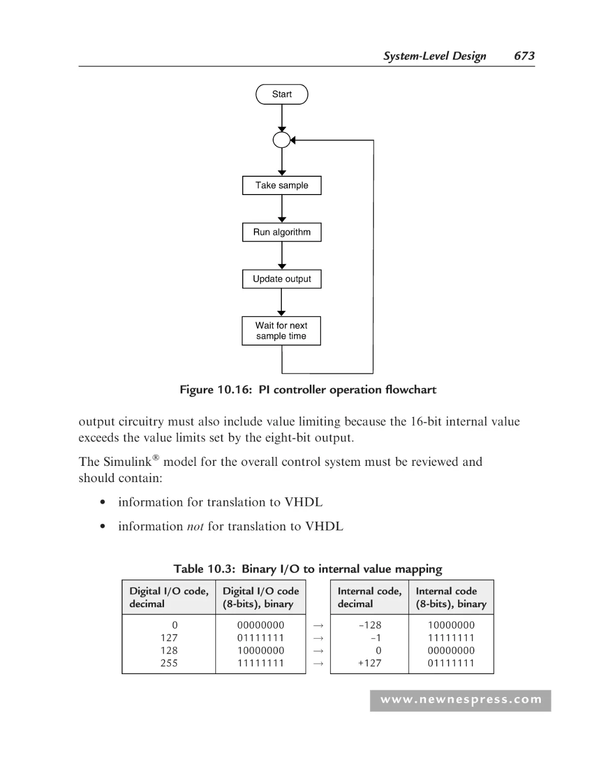
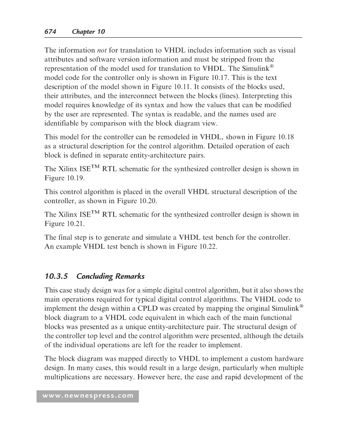
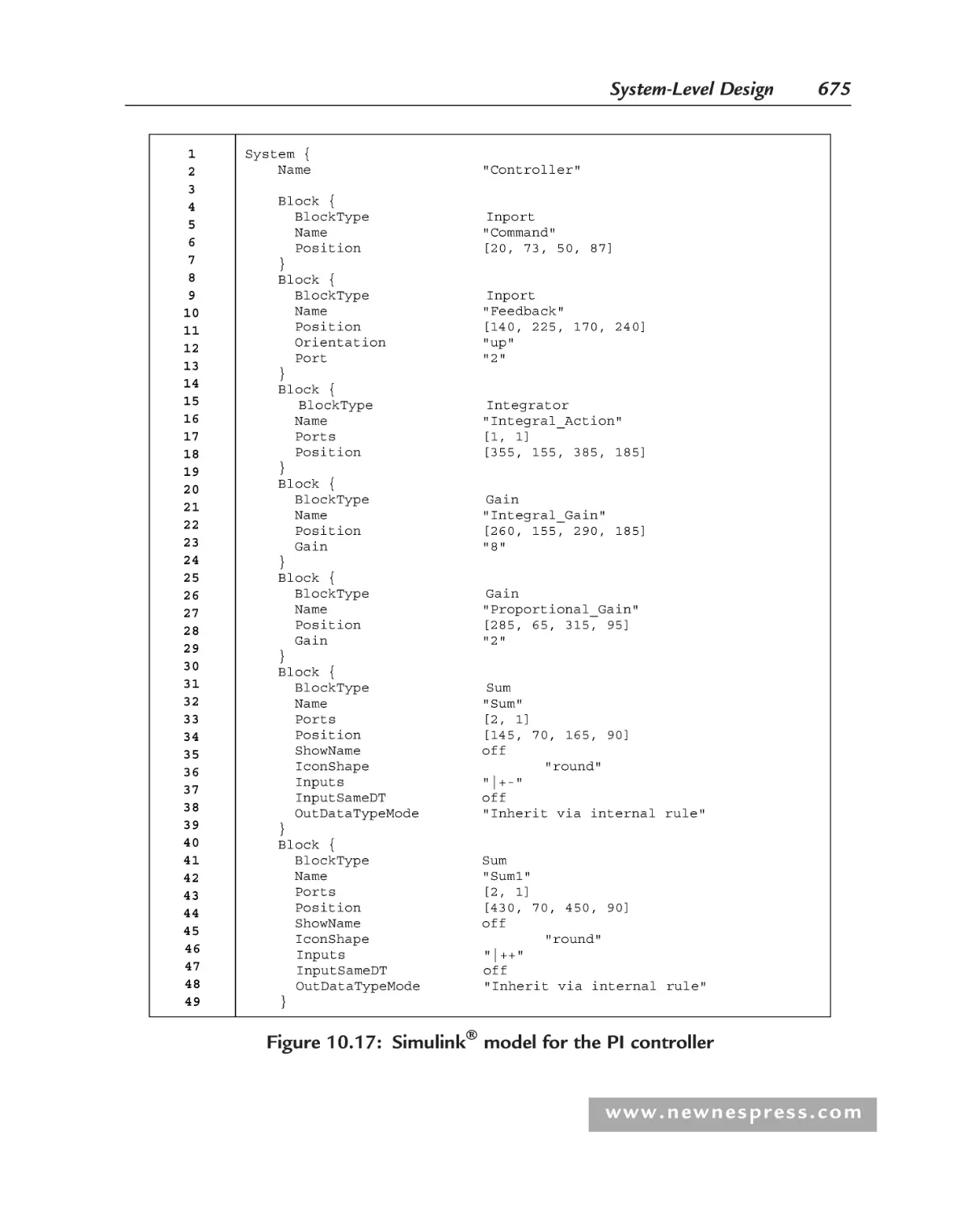
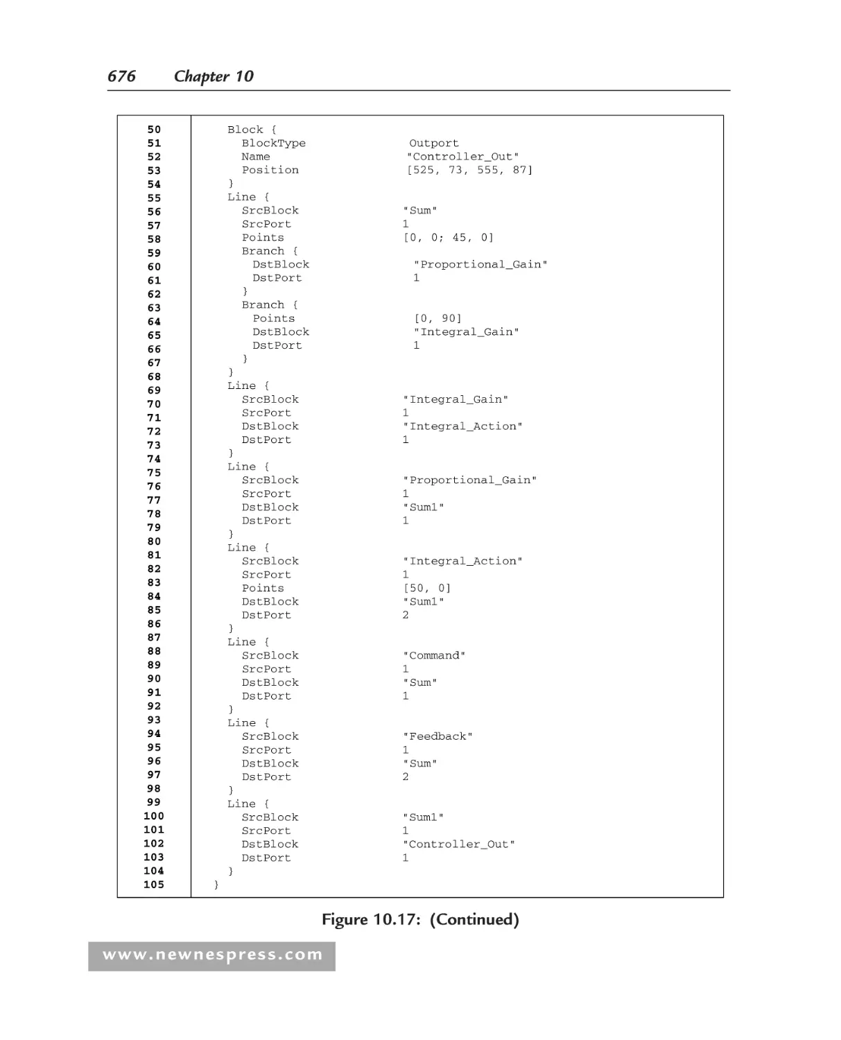
10.3.5 Concluding Remarks ................................................................... 674
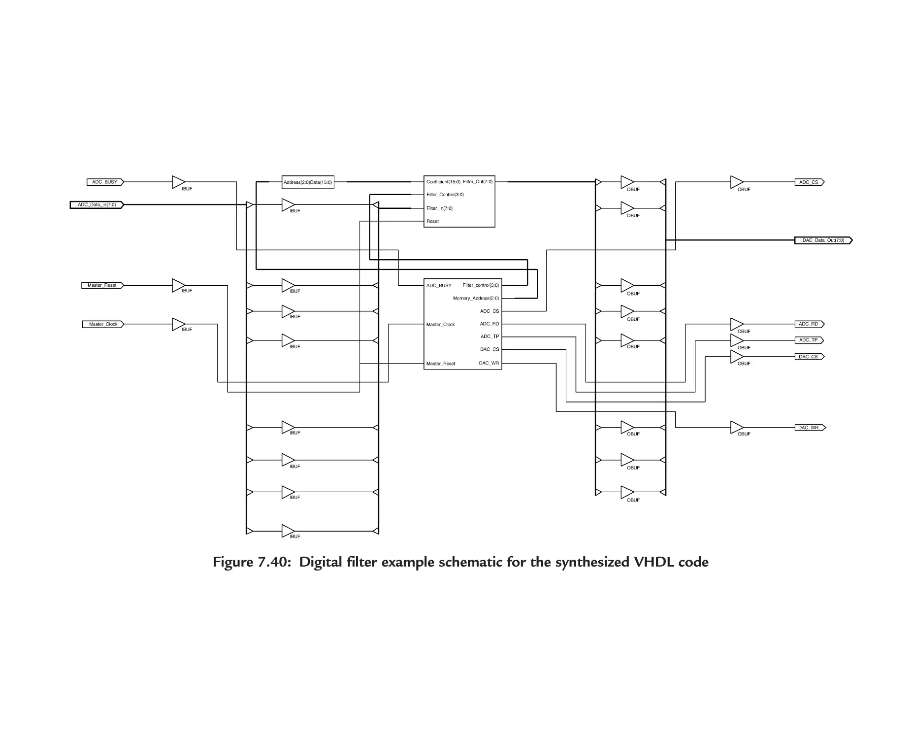
10.4 Case Study 2: Digital Filter Design......................................................... 686
10.4.1 Introduction................................................................................. 686
10.4.2 Filter Overview ............................................................................ 688
10.4.3 MATLAB/Simulink Model Creation
and Simulation ............................................................................ 690
10.4.4 Translating the Design to VHDL................................................ 692
10.4.5 Concluding Remarks ................................................................... 698
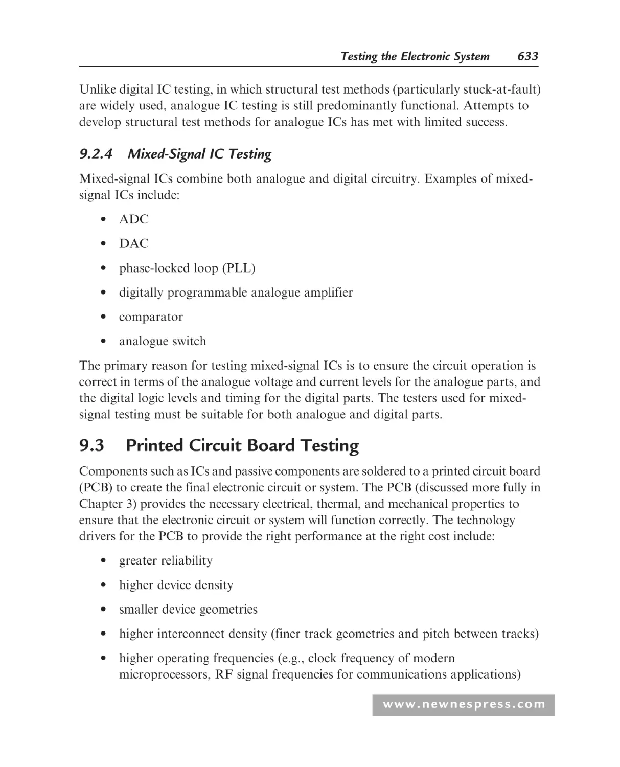
10.5 Automating the Translation .................................................................... 702
10.6 Future Directions .................................................................................... 703
References
.................................................................................................. 704
Student Exercises ..................................................................................... 705
Additional References ............................................................................... 707
Index ...................................................................................................... 717
www.newnespress.com
This page intentionally left blank
system
• noun 1 A set of things working together as parts of a mechanism or an
interconnecting network.
Oxford Dictionary of English
This page intentionally left blank
Preface
In days gone by, life for the electronic circuit designer seems to have been easier.
Designs were smaller, ran at a slower speed, and could easily fit onto a single small
printed circuit board. An individual designer could work on a problem and designs
could be specified and developed using paper and pen only. The circuit schematic
diagrams that were required could be rapidly drawn on the back of an envelope.
Struck by the success of the early circuit designs, customers started to ask for smaller,
faster, and more complex circuits—and at a lower cost. The designers started to work
on solving such problems, which has led to the rapidly expanding electronics industry
that we have today. Driven by the demand from the customer, new materials and
fabrication processes have been developed, new circuit design methodologies and
design architectures have taken over many of the early traditional design approaches,
and new markets for the circuits have evolved.
So how is the design problem tackled today? This is not an easy question to answer, and
there is more than one way to develop an electronic circuit solution to any given
problem. However, the design process is no longer the activity of a single individual.
Rather, a team of engineers is involved in the key engineering activities of design,
fabrication (manufacture), and test. All activities now involve the extensive use of
computing resources, requiring the efficient use of software tools to aid design
(electronic design automation, EDA and computer aided design, CAD), fabrication
(Computer Aided Manufacture, CAM), and test (Computer Aided Test, CAT). The
circuit is no longer a unique and isolated entity. Rather, it is part of a larger system.
Increasingly, much of the design work is undertaken at the system level . . . at a suitably
high level of design abstraction required to reduce design time and increase the designer
efficiency. However, when it comes to the design detail, the correctly specified system
must also work at the basic electric voltage and current level. How to go from an
www.newnespress.com
xviii
Preface
effective system-level specification to an efficient and working circuit implementation
requires the skills of good designers who are aided by good design tools.
For the electronic circuit designer at an early stage in the design process, whether to
implement the required circuit functionality using analogue circuit techniques or digital
circuit techniques must be decided. However, sometimes the choice will have already been
made, and increasingly a digital solution is the preferred choice. The wide use of digital
signal processing (DSP) techniques facilitates complex operations that can provide superior
performance to an analogue circuit equivalent; indeed some cannot be performed in
analogue. Traditionally, DSP functions have been implemented using software programs
written to operate on a target processor. The microprocessor (mP), microcontroller (mC),
and digital signal processor provide the necessary digital circuits, in integrated circuit (IC)
form, to implement the required functions. In fact, these processors are to be found in many
everyday embedded electronics that we take for granted. This book could not have been
written without the aid of an electronic system incorporating a microprocessor running a
software operating system that in turn runs the word processor software.
Increasingly, the functions that have been traditionally implemented in software
running on a processor-based digital system in the DSP world and many control
applications are being evaluated in terms of performance that can be achieved in
software. In many cases, the software solution will be slower than is desired, and the
basic nature of the software programmed system means that this speed limitation
cannot be overcome. The way to overcome the speed limitation is to perform the
required operations in hardware designed for a particular application. However,
custom hardware solutions will be expensive to acquire.
If there were a way to obtain the power of programmability with the power of
hardware speed, then this would be provide a significant way forward.
Fortunately, programmable logic provides the power of programmability with the
power of hardware speed by providing an IC with built-in digital electronic circuitry
that is configured by the user for a particular application. Many devices can be
reconfigured for different applications. Today, two main types of programmable logic
ICs are commonly used: the field programmable gate array (FPGA) and complex
programmable logic device (CPLD).
Therefore, it is possible to implement a complex digital system that can be developed
and the functionality changed or enhanced using either a processor running a
software program or programmable logic with a specific hardware configuration.
www.newnespress.com
Preface
xix
For an end-user, the functionality of both types of system will be the same—the
design details are irrelevant to the end-user as long as the functionality of the unit
is correct. In this book, to provide consistency and to differentiate between the
processor and programmable logic, the following terminology will be used:
• A processor (microprocessor, mP; microcontroller, mC; or digital signal
processor, DSP) will be programmed for a particular application using a
software programming language (SPL).
• Programmable logic (field programmable gate array, FPGA; simple
programmable logic device, SPLD; or complex programmable logic device,
CPLD) will be configured using a hardware description language (HDL).
The aim of this book is to provide a reference source with worked examples in
the area of electronic circuit design using programmable logic. In particular, field
programmable gate arrays and complex programmable logic devices will be presented
and examples of such devices provided.
The choice whether to use a software-programmed processor or hardware-configured
programmable logic device is not a simple one, and many decisions figure into evaluating
the pros and cons of a particular implementation prior to making a final decision. This
book will provide an insight into the design capabilities and aspects relating to the design
decisions for programmable logic so that an informed decision can be made.
The book is structured as follows:
Chapter 1 will introduce the types of programmable logic device that are available
today, their differing architectures, and their use within electronic system design.
Additionally, the terminology used in this area will be presented with the aim of
demystifying the jargon that has evolved.
Chapter 2 will provide a background into the area of electronic systems design, the
types of solutions that may be developed, and the decisions that will need to be
made in order to identify the right technology choice for the design implementation.
Typical design flows will be introduced and discussed for the different technologies.
Chapter 3 will introduce the design of printed circuit boards (PCBs). These provide the
mechanical and electrical base onto which the electronic components will be mounted. The
correct design of the PCB is essential to ensure that the electronic circuit can be realized
(implemented) to operate to the correct specification (power supply voltage, thermal [heat]
dissipation, digital clock frequency, analogue and digital circuit elements, etc.) and to
www.newnespress.com
xx
Preface
ensure that the different electronic circuit components interact with each other correctly
and do not provide unwanted effects. A correctly designed PCB will allow the circuit to
perform as intended. A badly designed PCB will prevent the circuit from working
altogether.
Chapter 4 will discuss the different programming languages that are used to develop
digital designs for implementation in either a processor (software-programmed
microprocessor, microcontroller, or digital signal processor) or in programmable
logic (hardware-configured FPGA or CPLD). The main languages used will be
introduced and examples provided. For programmable logic, the main hardware
description languages used are Verilog-HDL and VHDL (VHSIC Hardware
Description Language). These are IEEE (Institute of Electrical and Electronics
Engineers) standards, universally used in both education and industry.
Chapter 5 will introduce digital logic design principles. A basic understanding of the
principles of digital circuit design, such as Boolean Logic, Karnaugh maps, and
counter/state machine design will be expected. However, a review of these principles
will be provided for designs in schematic diagram form and presented such that the
design functionality may be mapped over a VHDL description in Chapter 6.
Chapter 6 will introduce VHDL as one of the IEEE standard hardware description
languages available to describe digital circuit and system designs in an ASCII
text-based format. This description can be simulated and synthesized. (Simulation
will validate the design operation, and synthesis will translate the text-based
description into a circuit design in terms of logic gates and the interconnections
between the basic logic gates. The gates and gate connections are commonly referred to
as the netlist.) The design examples provided in schematic diagram form in Chapter 5
will be revisited and modeled in VHDL.
Chapter 7 will introduce the development of digital signal processing algorithms in
VHDL and the synthesis of the VHDL descriptions to target programmable logic
(both FPGA and CPLD). Such algorithms include digital filters (low-pass, high-pass,
and band-pass), digital PID (proportional plus integral plus derivative) control
algorithms, and the FFT (fast Fourier transform, an efficient implementation of the
discrete Fourier transform, DFT).
Chapter 8 will discuss the interfacing of programmable logic to what is commonly
referred to as the real world. This is the analogue world that we live in, and such
interfacing requires both the acquisition (capture) and the generation of analogue
www.newnespress.com
Preface
xxi
signals. To enable this, the digital programmable logic device will require an interface to
the analogue world. For analogue signals to be captured and analyzed in digital, an
analogue-to-digital converter (ADC) will be required. For analogue signals to be
generated from the digital, a digital-to-analogue converter (DAC) will be required.
In this book, the convention used for the word analogue will use the -ue at the end of
the word, unless a particular name already in use is referred to spelled as analog.
Chapter 9 will introduce the testing of the electronic system. In this, failure mechanisms
in hardware and software will be introduced, and the need for efficient and
cost-effective test programs from the prototyping phase of the design through
high-volume manufacture and in-system testing.
Chapter 10 will introduce the increasing need to develop programmable logic–based
designs at a high level of abstraction using behavioral descriptions of the system
functionality, and the increasing requirements to enable the synthesis of these
high-level designs into logic. With reference to a design flow taking a digital design
developed in MATLAB or Simulink through a VHDL code equivalent for
implementation in FPGA or CPLD technology, the synthesis of digital control system
algorithms modeled and simulated in Simulink will be translated into VHDL for
implementation in programmable logic.
Throughout the book, the HDL examples provided and evaluated can be implemented
within programmable logic–based circuits that may be designed by the user in addition
to the PCB design examples that are provided. These examples have been developed to
form the basis of laboratory experiments that can be used to accompany the text.
With the broad range of subject material and examples, a feature of the book is its
potential for use in a range of learning and teaching scenarios. For example:
1. As an introduction to design of electronic circuits and systems using
programmable logic. This would allow for the design approaches,
programmable logic architectures, simulation, synthesis, and the final
configuration of an FPGA or CPLD to be undertaken. It would also allow
for investigation into the most appropriate HDL coding styles and device
implementation constraints to be undertaken.
2. As an introduction to hardware description languages, in particular VHDL,
allowing for case study designs to be developed and implemented within
programmable logic. This would allow for VHDL code developers to see the
www.newnespress.com
xxii
Preface
code working on real devices and to enable additional testing of the electronic
circuit with such equipment as oscilloscopes and spectrum analyzers.
3. As an introduction to the design of printed circuit boards, in particular
mixed-signal designs (mixed analogue and digital). This would allow issues
relating to the design of the printed circuit board to be investigated and
designs developed, fabricated, and tested.
4. As an introduction to digital signal processing algorithm development. This
would allow the basics of DSP algorithms and their implementation in
hardware on FPGAs and CPLDs to be investigated through the medium of
VHDL code development, simulation, and synthesis.
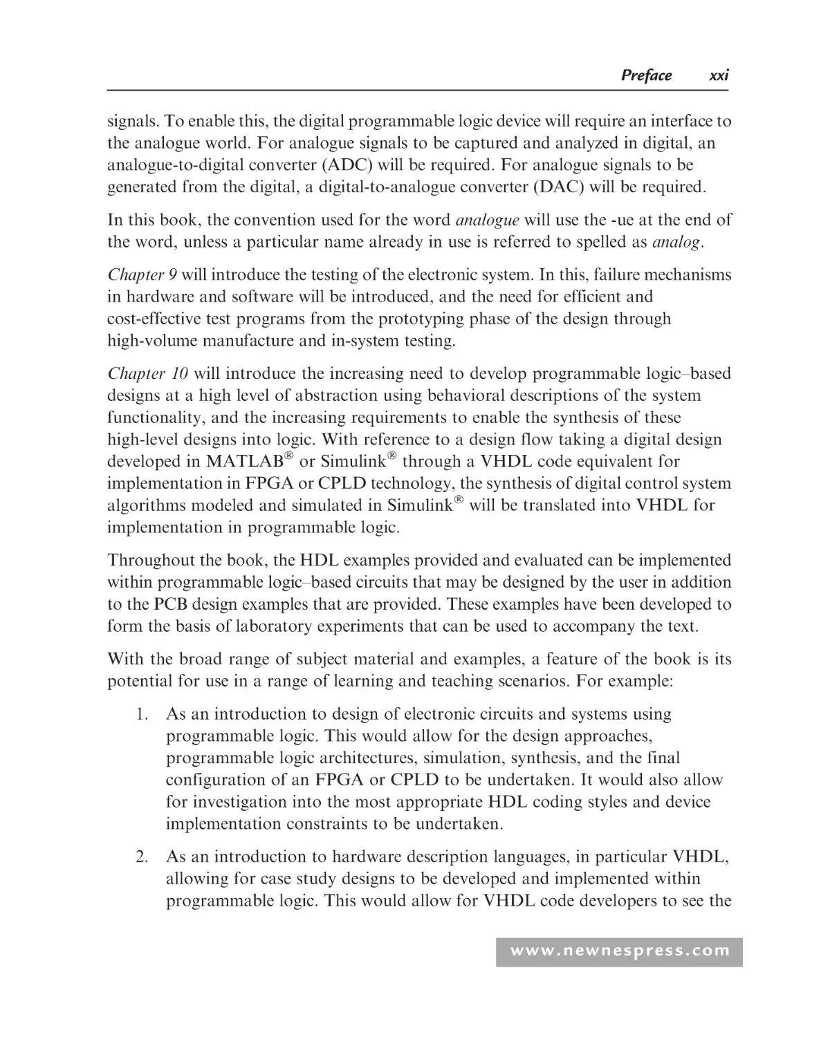
The VHDL examples can be downloaded and run on the hardware prototyping
arrangement that can be built by the reader using the designs provided in the book.
This hardware arrangement is centered on a Xilinx CoolrunnerTM-II CPLD on
which to prototype the digital logic ideas, along with a set of input/output (I/O)
boards. The full set of boards is shown in the figure below.
This arrangement consists of five main system boards and an optional sevensegment display board. The appendices and design schematics are available at the
author’s Web site for this book (refer to http://books.elsevier.com/companions/
9780750683975 and follow the hyperlink to the author’s site).
www.newnespress.com
Abbreviations
A
AC
ADC
ALU
AM
AMD
AMS
AND
ANSI
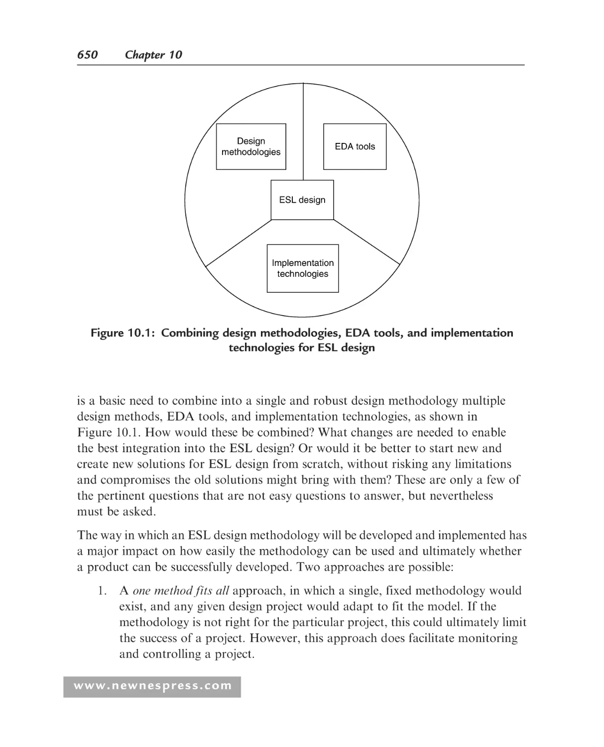
AOI
ASCII
ASIC
ASP
ASSP
ATA
ATE
ATPG
AWG
AXI
alternating current
analogue-to-digital converter
arithmetic and logic unit
amplitude modulation
advanced micro devices
analogue and mixed-signal
logical AND operation on two or more digital signals
American National Standards Institute
automatic optical inspection
American Standard Code for Information Interchange
application-specific integrated circuit
analogue signal processor
application-specific standard product
AT attachment
AT equipment
AT program generation
arbitrary waveform generator
American wire gauge
automatic X-ray inspection
B
BASIC
BCD
BGA
BiCMOS
BIST
Beginner’s All-purpose Symbolic Instruction Code
binary coded decimal
ball grid array
bipolar and CMOS
built-in self-test
www.newnespress.com
xxiv
Abbreviations
bit
BJT
BNC
BPF
BSDL
BS(I)
BST
binary digit
bipolar junction transistor
bayonet Neill-Concelman connector
band-pass filter
boundary scan description language
British Standards (Institution)
boundary scan test
C
CAD
CAE
CAM
CAT
CBGA
CD
CE
CERDIP
CERQUAD
CIC
CISC
CLB
CLCC
CMOS
COTS
CPGA
CPLD
CPU
CQFP
CS
CSOIC
CSP
CSSP
CTFT
CTS
CUT
computer-aided design
computer-aided engineering
computer-aided manufacture
computer-aided test
ceramic BGA
compact disk
chip enable
ceramic DIP
ceramic quadruple side
cascaded integrator comb
complex instruction set computer
configurable logic block
ceramic leadless chip carrier
ceramic leaded chip carrier
complementary metal oxide semiconductor
commercial off-the-shelf
ceramic PGA
complex PLD
central processing unit
ceramic quad flat pack
chip select
ceramic SOIC
chip scale packaging
customer specific standard product
continuous-time Fourier transform
clear to send
circuit under test
www.newnespress.com
Abbreviations
xxv
D
DAC
DAE
DAQ
dB
DBM
DC
DCD
DCE
DCI
DCPSS
DDC
DDR
DDS
DfA
DfD
DFF
DfM
DfR
DfT
DFT
DfX
DfY
DIB
DIL
DIMM
DIP
DL
DMM
DNL
DoD
DPLL
dpm
DR
DRAM
DRC
digital-to-analogue converter
differential and algebraic equation
data acquisition
decibel
digital boundary module
direct current
data carrier detected
data communication equipment
digitally controlled impedance
DC power supply sensitivity
direct digital control
double data rate
direct digital synthesis
design for assembly
design for debug
D-type flip-flop
design for manufacturability
design for reliability
design for testability
discrete Fourier transform
design for X
design for yield
device interface board
dual in-line
dual in-line memory module
dual in-line package
defect level
digital multimeter
differential nonlinearity
U.S. Department of Defense
digital PLL
defects per million
data register
dynamic RAM
design rules checking
www.newnespress.com
xxvi
Abbreviations
DRDRAM
DSM
DSP
DSR
DTE
DTFT
DTR
DUT
DVD
direct Rambus DRAM
deep submicron
digital signal processing
digital signal processor
data set ready
data terminal equipment
discrete-time Fourier transform
data terminal ready
device under test
digital versatile disk
E
EC
ECL
ECU
EDA
EDIF
EHF
EIAJ
ELF
EMC
EMI
ENB
EOC
EOS
EEPROM
E2EPROM
EPROM
ERC
ESD
ESIA
ESL
ESS
EU
EX-NOR
EX-OR
European Commission
emitter coupled logic
electronic control unit
electronic design automation
electronic design interchange format
extremely high frequency
Electronic Industries Association of Japan
extremely low frequency
electromagnetic compatibility
electromagnetic interference
effective number of bits
end of conversion
electrical overstress
electrically erasable PROM
electrically erasable PROM
erasable PROM
electrical rules checking
electrostatic discharge
European Semiconductor Industry Association
electronic system level
environmental stress screening
European Union
NOT-EXCLUSIVE-OR
logical EXCLUSIVE-OR operation on two or more digital
signals
www.newnespress.com
Abbreviations
xxvii
F
F
FA
FBGA (FPBGA)
FCC
FET
FFT
FIFO
FIR
FM
FPAA
FPGA
FPT
FR-4
FRAM
FSM
FT
Farad
failure analysis
fine pitch ball grid array
Federal Communications Commission (USA)
field effect transistor
fast Fourier transform
first-in, first-out
finite impulse response
frequency modulation
field programmable analogue array
field programmable gate array
flying probe tester
flame retardant with approximate dielectric constant of 4
ferromagnetic RAM
finite state machine
functional tester
G
GaAs
GAL
GDSII
GND
GPIB
GTL
GTO
GUI
gallium arsenide
generic array of logic
Graphic Data System II stream file format
ground
general purpose interface bus
Gunning transceiver logic
gate turn-off thyristor
graphical user interface
H
HBM
HBT
HDIP
HDL
HF
HPF
HSTL
HTML
human body model
heterojunction bipolar transistor
hermetic DIP
hardware description language
high frequency
high-pass filter
high-speed transceiver logic
hyphertext markup language
www.newnespress.com
xxviii
HVI
HW
Hz
Abbreviations
human visual inspection
hardware
Hertz
I
IB
IBM
IC
ICC
ICM
IDD
IDDQ
IEE
IFS
IGND
IIH
IIL
ILSB
IO
IOH
IOL
IOS
IOUT
IREF
ISS
ISSQ
IC
I2C (IIC)
I2S
ICT
IDC
IDE
IEC
IEE
IEEE
base current
base peak current
collector current
power supply current (into VCC pin for bipolar circuits)
collector peak current
power supply current (into VDD pin for CMOS circuits)
quiescent power supply current (IDD)
power supply current (out of VEE pin for bipolar circuits)
full-scale current
ground current per supply pin
high-level input current
low-level input current
minimum output current change
output current
high-level output current (logic 1 output)
low-level output current (logic 0 output)
offset current
output current
reference current
power supply current (out of VSS pin for CMOS circuits)
quiescent power supply current (ISS)
integrated circuit
inter-integrated circuit (inter-IC) bus
inter-IC sound bus
in-circuit test
in-circuit tester
insulation displacement connector
integrated design environment
integrated drive electronics
International Electrotechnical Commission
Institution of Electrical Engineers
Institute of Electrical and Electronics Engineers
www.newnespress.com
Abbreviations
IET
IIR
IMAPS
INL
I/O
IP
IR
ISO
ISP
ISR
IT
ITRS
I-V
xxix
Institution of Engineering and Technology
infinite impulse response
International Microelectronics and Packaging Society
integral nonlinearity
input/output
intellectual property
instruction register
infrared
International Organization for Standardization
in-system programmable
in-system reprogrammable
information technology
International Technology Roadmap for Semiconductors
current-to-voltage
J
JDK
JEDEC
JEITA
JETAG
JETTA
JFET
JLCC
JTAG
JAVATM Development Kit
Joint Electron Device Engineering Council
Japan Electronics and Information Technology Industries
Association
Joint European Test Action Group
Journal of Electronic Testing, Theory, and Applications
junction FET
J-leaded chip carrier
Joint Test Action Group
K
KGD
KSIA
known good die
Korean Semiconductor Industry Association
L
LAN
LC
LC2MOS
LCC
LCCMOS
LCD
LED
local area network
logic cell
linear compatible CMOS
leaded chip carrier
leadless chip carrier
leadless chip carrier metal oxide semiconductor (also LC2MOS)
liquid crystal display
light-emitting diode
www.newnespress.com
xxx
Abbreviations
LF
LFSR
LIFO
Linux
LPF
LSB
LSI
LUT
LVCMOS
LVDS
LVS
LVTTL
low frequency
linear feedback shift register
last-in, first-out
Linux is not Unix
low-pass filter
least significant bit
large-scale integration
look-up table
low-voltage CMOS
low-voltage differential signaling
layout versus schematic
low-voltage TTL
M
mBGA
mC
mP
MATLAB
MAX
MCM
MCU
MEMs
MF
MIL
MIN
MISR
MM
MOS
MOSFET
MPGA
MS
MSAF
MSB
MSI
MSOP
MUX
MVI
micro ball grid array
microcontroller
microprocessor
Matrix Laboratory (from The Mathworks, Inc.)
maximum
multichip module
microcontroller unit
micro electro-mechanical systems
medium frequency
military
minimum
multiple-input signature register
machine model
metal oxide semiconductor
metal oxide semiconductor field effect transistor
mask programmable gate array
Microsoft
multiple stuck-at-fault
most significant bit
medium-scale integration
mini-small outline package
multiplexer
manual visual inspection (i.e., HVI)
www.newnespress.com
Abbreviations
xxxi
N
NAND
NDI
NDO
NDT
NMH
NML
nMOS
NOR
NOT
NRE
NVM
NVRAM
NOT-AND
normal data input
normal data output
nondestructive test
noise margin for high levels
noise margin for low levels
n-channel MOS
NOT-OR
logical NOT operation on a single digital signal
nonrecurring engineering
nonvolatile memory
nonvolatile RAM
O
OE
OEM
ONO
OOP
op-amp
OR
OS
OSR
OTP
OVI
output enable
original equipment manufacturer
oxide-nitride-oxide
object-oriented programming
operational amplifier
logical OR operation on two or more digital signals
operating system
oversampling ratio
one-time programmable
Open Verilog International
P
Ptot
PAL
PBGA
PC
PCB
PCBA
PCI
PDA
total dissipation
programmable array of logic
plastic BGA
personal computer
program counter
printed circuit board
printed circuit board assembly
PC interface
personal digital assistant
www.newnespress.com
xxxii
PDF
PDIL
PDIP
PERL
PGA
PI
PID
PIPO
PLA
PLCC
PLD
PLL
PM
pMOS
PMU
PO
PoC
PoP
POR
PPGA
ppm
PQFP
PROM
PRPG
PSOP
PWB
PWM
PXI
Abbreviations
portable document format
plastic DIL
plastic DIP
practical extraction and report language
pin grid array
primary input
proportional plus integral
proportional plus integral plus derivative
parallel in, parallel out
programmable logic array
plastic leadless chip carrier
plastic leaded chip carrier
programmable logic device
phase-locked loop
phase modulation
p-channel MOS
precision measurement unit
primary output
proof of concept
package on package
power-on reset
plastic PGA
parts per million
plastic QFP
programmable ROM
pseudorandom pattern generator
plastic SOP
printed wiring board
pulse width modulation
pulse width modulated
PC extensions for instrument bus
Q
QFJ
QFP
QSOP
QTAG
quad flat pack (J-lead)
quad flat pack
quarter-size SOP
Quality Test Action Group
www.newnespress.com
Abbreviations
xxxiii
R
RAM
RC
RD
RF
RI
RISC
RMS
RoHS
ROM
RTL
RTOS
RTS
RWM
Rx
trademark (registered; TM for unregistered)
random access memory
resistor-capacitor
read
received data
radio frequency
ring indicator
reduced instruction set computer
root mean squared
return of hazardous substances
read-only memory
register transfer level
real-time operating system
ready to send
read-write memory (also referred to as RAM)
receiver
S
D
SA0
SA1
SAF
SAR
SCR
SCSI
SDRAM
SDI
SDO
SE
SFDR
SG
SHF
SI
SIA
sigma-delta
stuck-at-0
stuck-at-1
stuck-at-fault
successive approximation register
silicon-controlled rectifier
small computer system interface
synchronous DRAM
scan data input
scan data out
scan enable
spurious free dynamic range
signal ground
super high frequency
signal integrity
Semiconductor Industries Association
www.newnespress.com
xxxiv
Abbreviations
SiGe
SIM
SINAD
SiP
SIP
SIPO
SISO
SISR
SLDRAM
SMT
SNR
S/(N þ THD)
SOAR
SoB
SoC
SOC
SOI
SOIC
SOJ
SOP
SPGA
SPI
SPICE
SPL
SPLD
SQFP
SRAM
SRBP
SSAF
SSI
SSOP
SSTL
STC
STD
STIL
SW
silicon germanium
subscriber identity module
signal to noise plus distortion (SNR þ THD)
system in a package
single in-line package
serial in, parallel out
Serial in, serial out
Single input, single output
serial input signature register
synchronous-link DRAM
surface mount technology
signal-to-noise ratio
signal to noise plus total harmonic distortion
safe operating region
system on board
system on a chip
start of conversion
silicon on insulator
small outline IC
small outline J-lead package
small outline package
staggered PGA
serial peripheral interface
simulation program with integrated circuit emphasis
software programming language
simple PLD
shrink quad flat pack
static RAM
synthetic resin-bonded paper
single stuck-at-fault
small-scale integration
small shrink outline package
stub series terminated logic
Semiconductor Test Consortium
standard
standard test interface language
software
www.newnespress.com
Abbreviations
xxxv
T
TL
Tstg
TAB
TAP
TCE
TCK
Tcl
TD
TDI
TDO
THD
TM
TMS
TO
TPG
TQFP
TRST
TSIA
TSMC
TSOP
TSSOP
TVSOP
TTL
TTM
TYP
Tx
lead temperature
storage temperature
tape automated bonding
test access port
thermal coefficient of expansion
test clock
tool command language
transmitted data
test data input
test data output
total harmonic distortion
trademark (unregistered, for registered)
test mode select
transistor outline package (single transistor)
test program generation
thin QFP
test reset
Taiwan Semiconductor Industry Association
Taiwan Semiconductor Manufacturing Company
thin SOP
thin shrink SOP
thin very SOP
transistor-transistor logic
time to market
typical
transmitter
U
UART
UHF
UJT
ULSI
UML
UNIXTM
USB
universal asynchronous receiver/transmitter
ultra high frequency
unijunction transistor
ultra large-scale integration
unified modeling language
Uniplexed Information and Computing System (originally
Unics, later renamed Unix)
universal serial bus
www.newnespress.com
xxxvi
UTP
UUT
UV
Abbreviations
unit test period
unit under test
ultraviolet
V
VCB
VCC
VCE0
VCEV
VDD
VEB
VEE
VFS
VFSR
VI
VIH
VIL
VLSB
VO
VOH
VOL
VOS
VOUT
VREF
VSS
VASG
VB
VBA
VCO
VDSM
VDU
VF
VHDL
VHF
VHSIC
VLF
collector-base voltage
power supply voltage (positive, for bipolar circuits)
collector-emitter voltage (IE = 0)
collector-emitter voltage (VBE = 1.5)
power supply voltage (positive, for CMOS circuits)
emitter-base voltage
power supply voltage (negative, for bipolar circuits)
full-scale voltage
full-scale range of voltage
input voltage
minimum input voltage that can be interpreted as a logic 1
maximum input voltage that can be interpreted as a logic 0
minimum output voltage change
output voltage
minimum output voltage when the output is a logic 1
maximum output voltage when the output is a logic 0
offset voltage
output voltage
reference voltage
power supply voltage (negative, for CMOS circuits)
VHDL Analysis and Standardization Group
Visual BasicTM
Visual BasicTM for Applications
voltage-controlled oscillator
very deep submicron
visual display unit
voice frequency
VHSIC hardware description language
very high frequency
very high-speed integrated circuit
very low frequency
www.newnespress.com
Abbreviations
VLSI
VQFP
xxxvii
very large-scale integration
very thin quad flat pack
W
WE
WEEE
WR
WSI
write enable
waste electrical and electronic equipment
write
wafer-scale integration
X
XNF
Xilinx Netlist format
Z
ZIF
ZIP
zero insertion force socket
zig-zag in-line package
www.newnespress.com
This page intentionally left blank
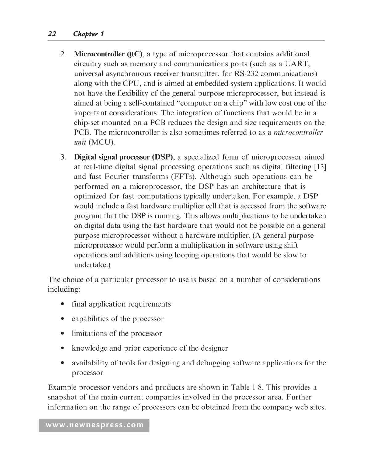
CHAPTER 1
Introduction to Programmable Logic
1.1
Introduction to the Book
Increasingly, electronic circuits and systems are being designed using technologies
that offer rapid prototyping, programmability, and re-use (reprogrammability and
component recycling) capabilities to allow a system product to be developed in a
minimal time, to allow in-service reconfiguration (for normal product upgrading to
improve performance, to provide design debugging capabilities, and for the inevitable
requirement for design bug removal), or even to recycle the electronic components for
another application. These aspects are required by the reduced time-to-market and
increased complexities for applications—from mobile phones through computer and
control, instrumentation, and test applications. So, how can this be achieved using the
range of electronic circuit technologies available today? Several avenues are open.
The main focus of developing electronics with the above capabilities has been in the
digital domain because the design techniques and nature of the digital signals are well
suited to reconfiguration.
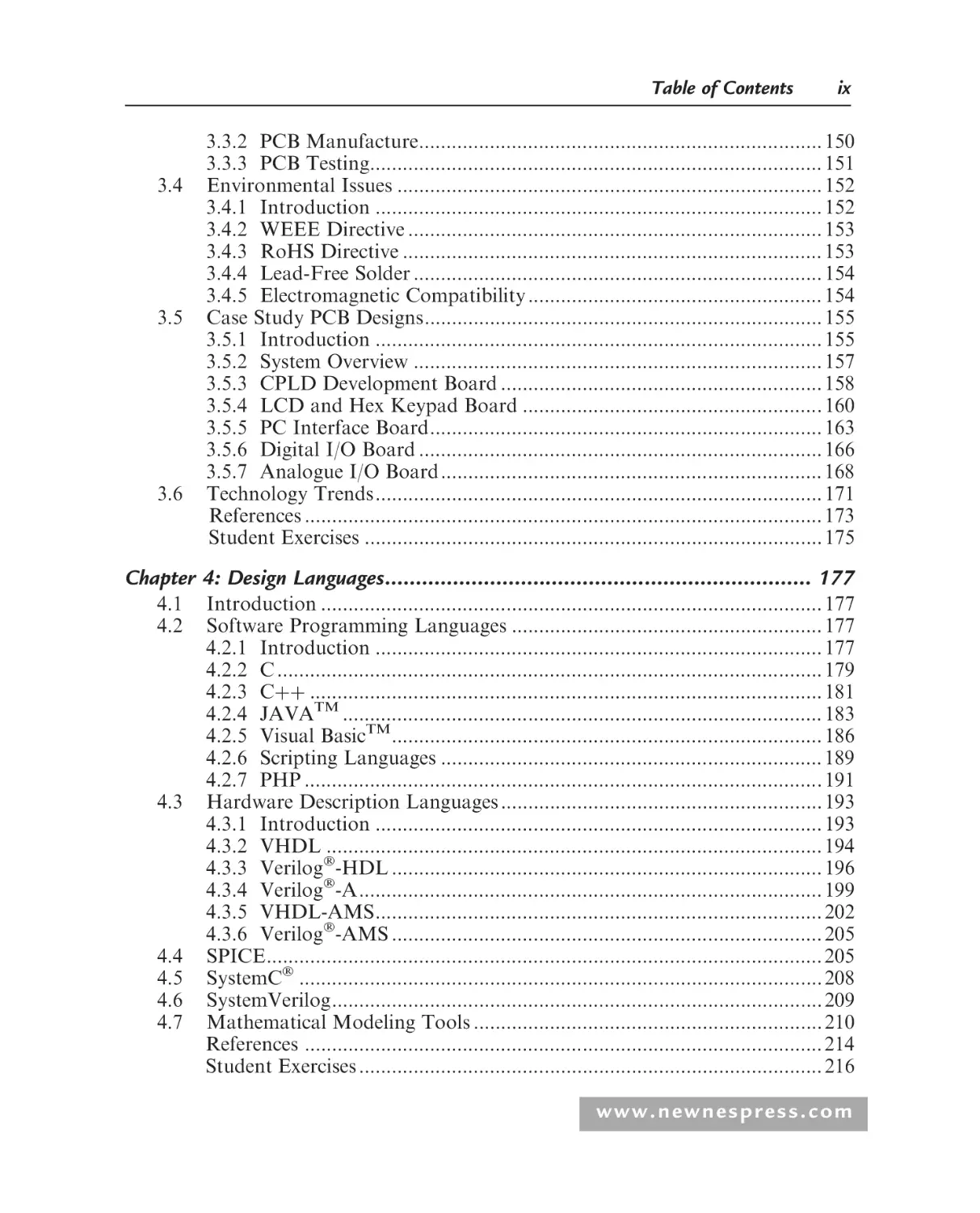
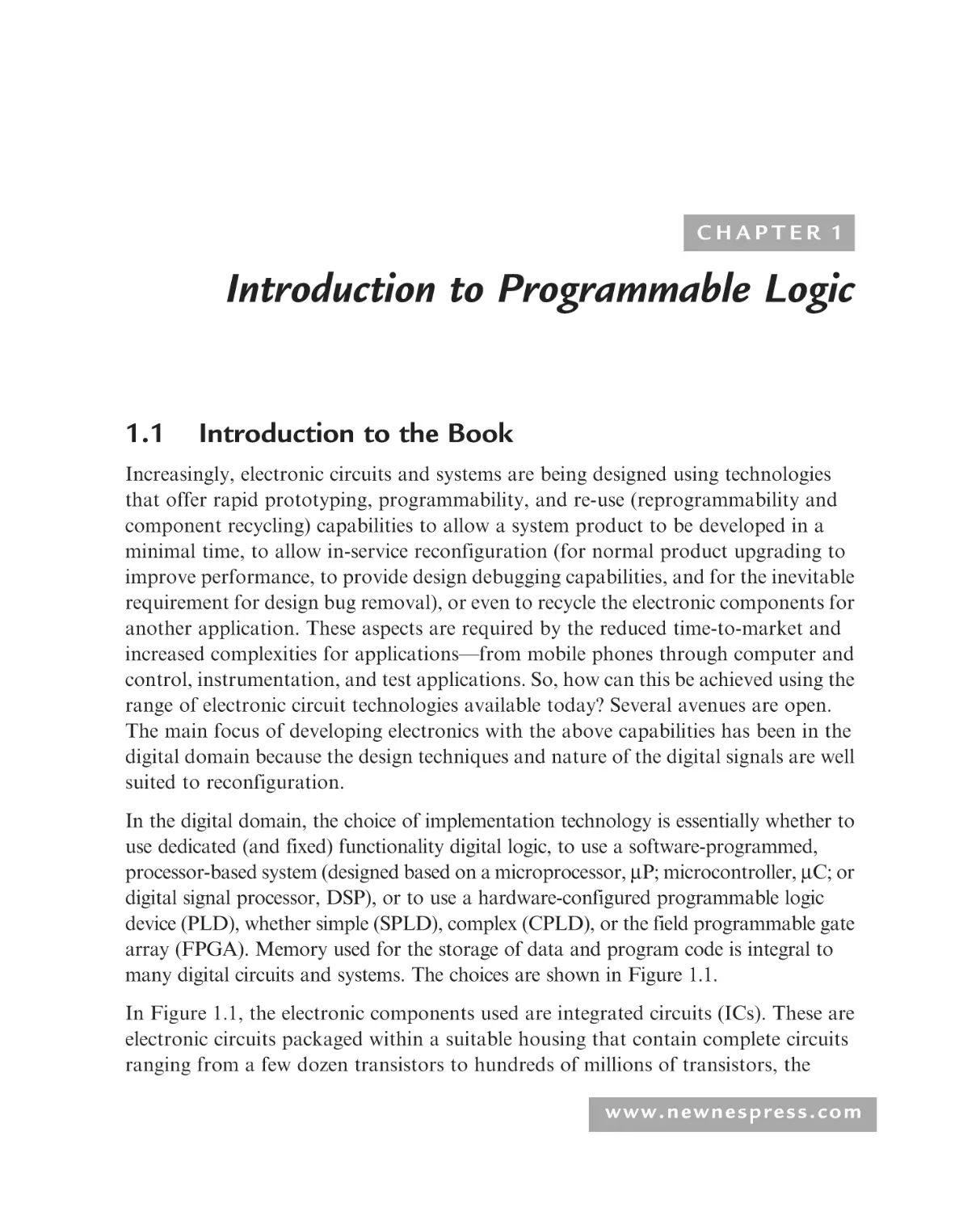
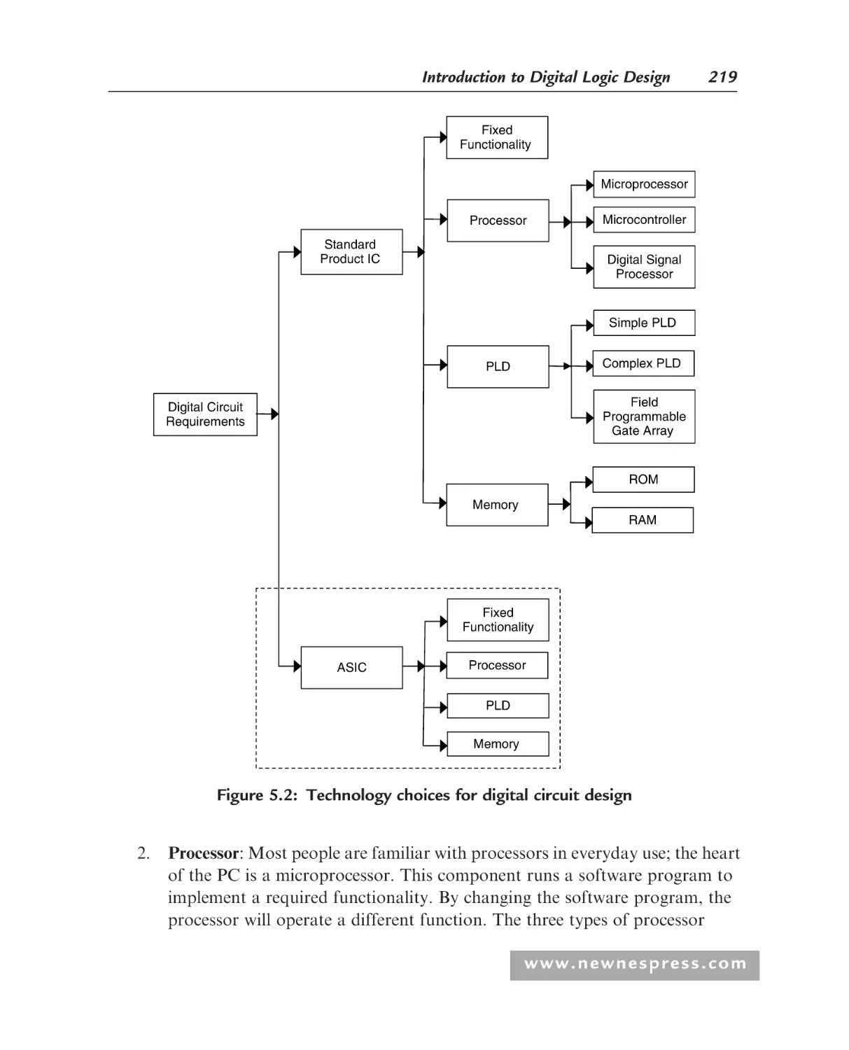
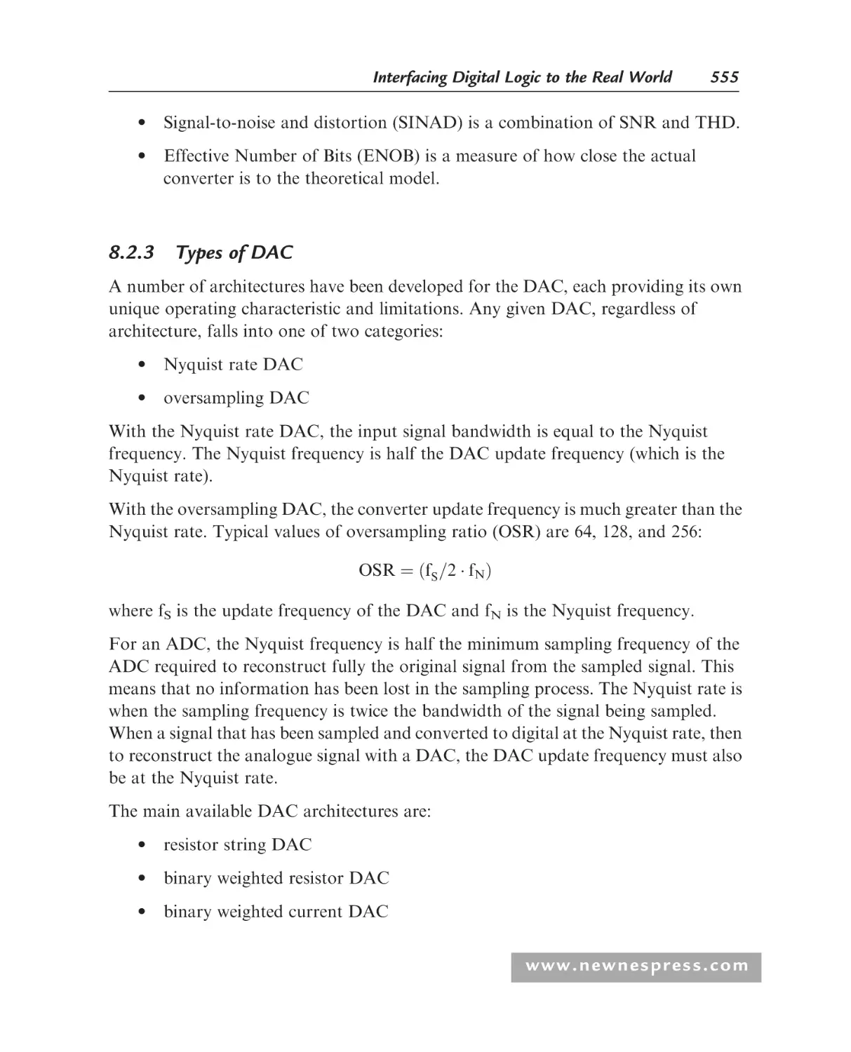
In the digital domain, the choice of implementation technology is essentially whether to
use dedicated (and fixed) functionality digital logic, to use a software-programmed,
processor-based system (designed based on a microprocessor, mP; microcontroller, mC; or
digital signal processor, DSP), or to use a hardware-configured programmable logic
device (PLD), whether simple (SPLD), complex (CPLD), or the field programmable gate
array (FPGA). Memory used for the storage of data and program code is integral to
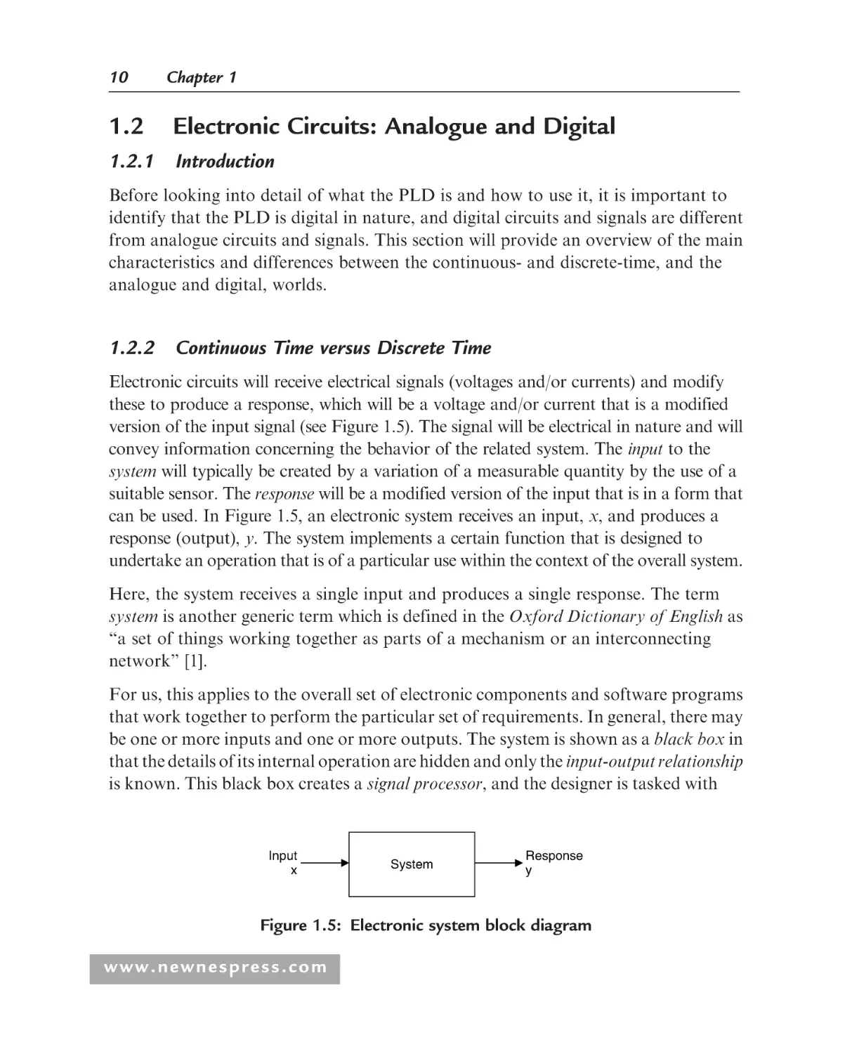
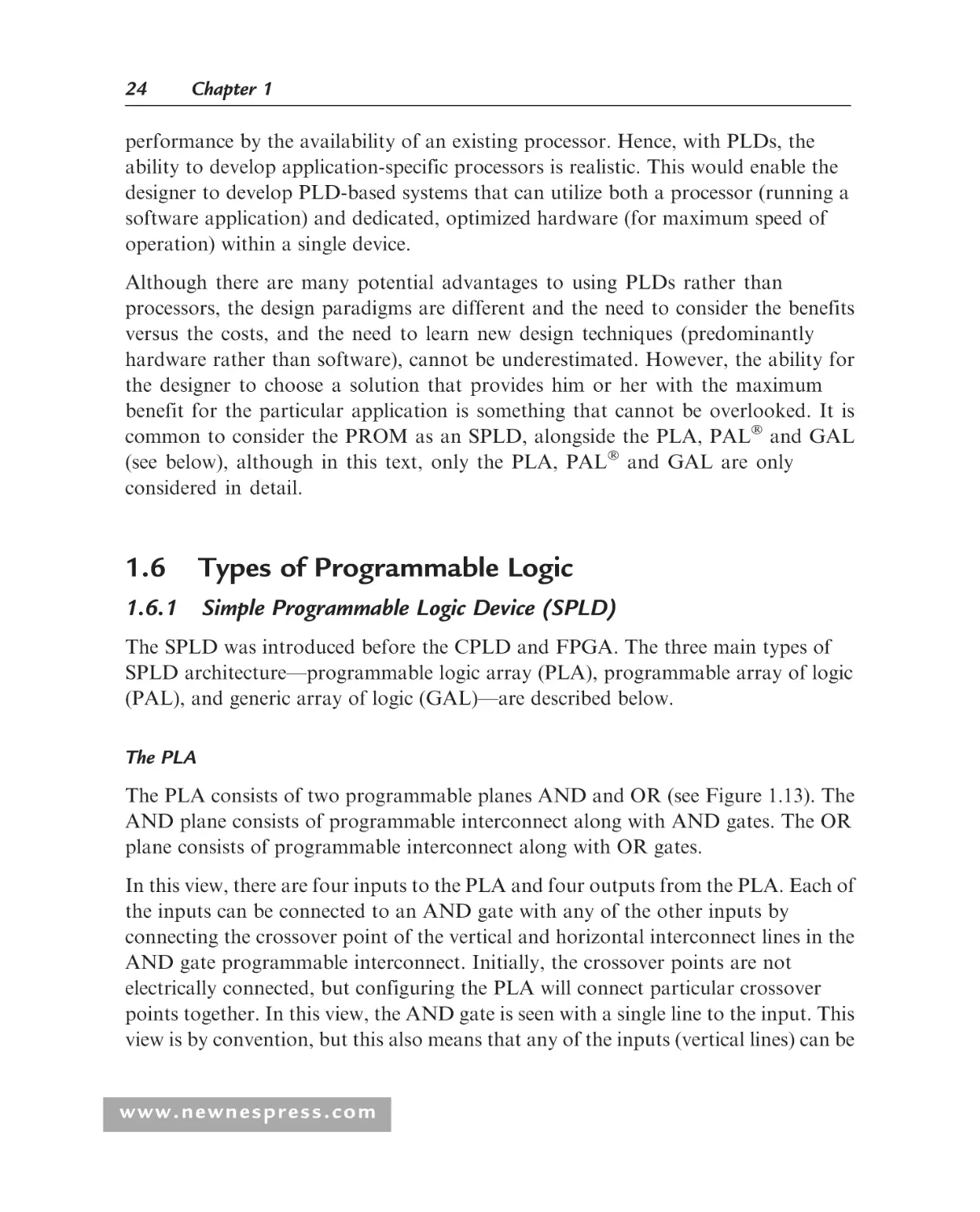
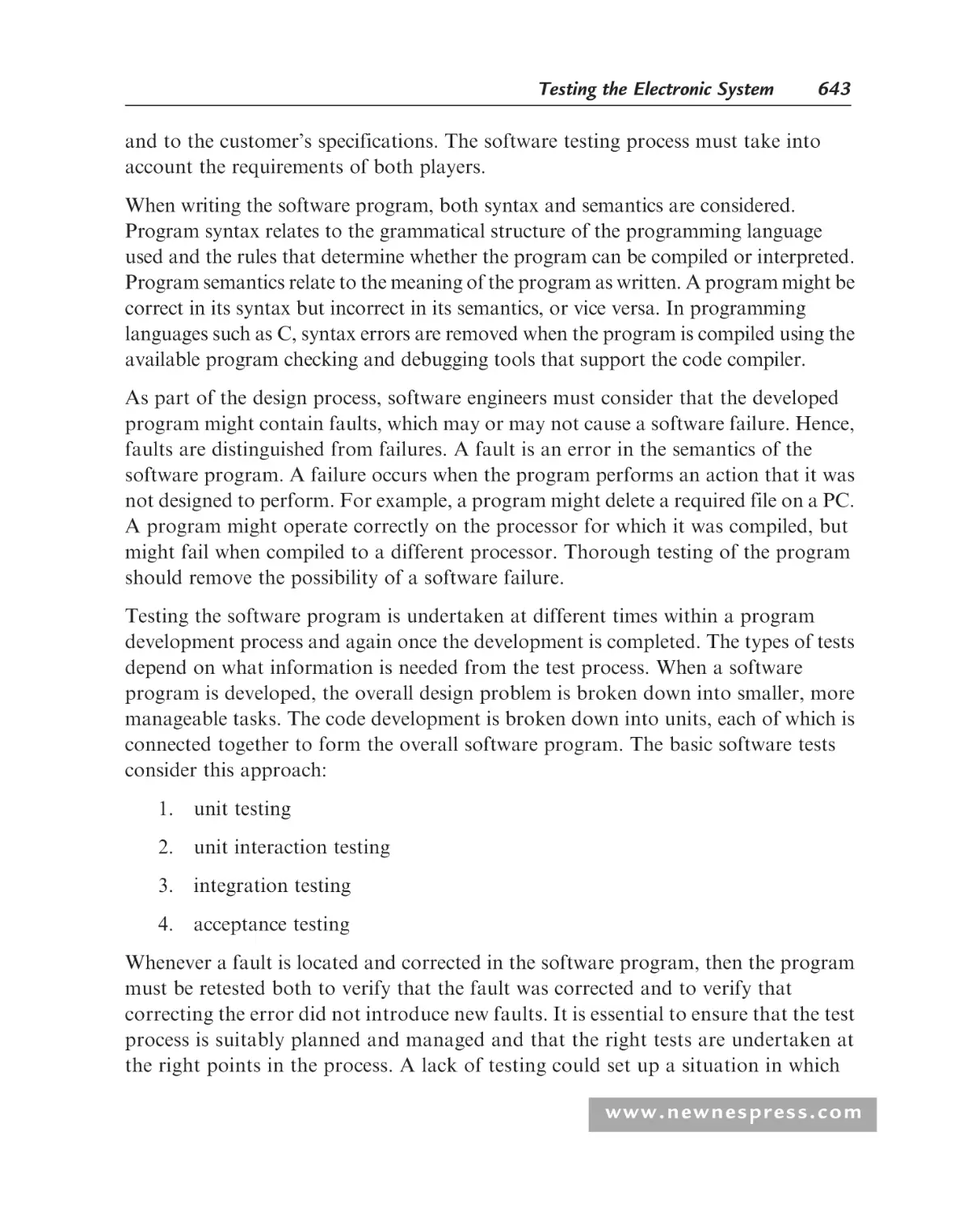
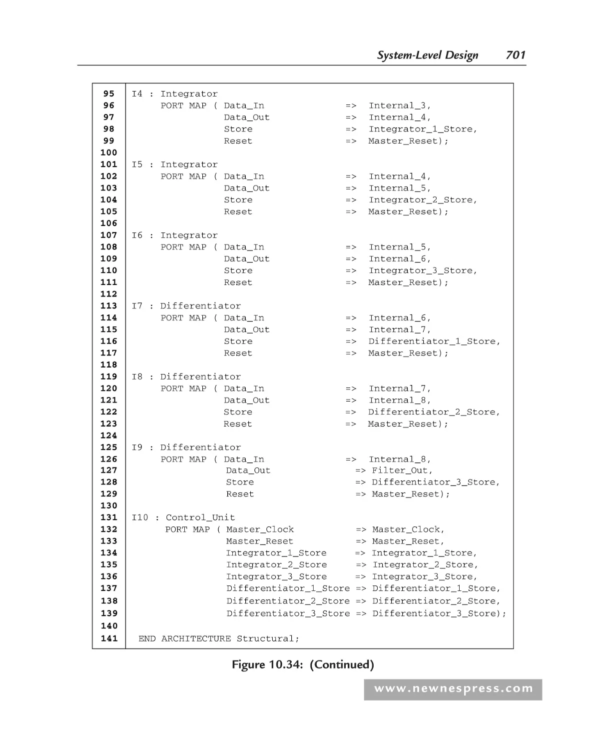
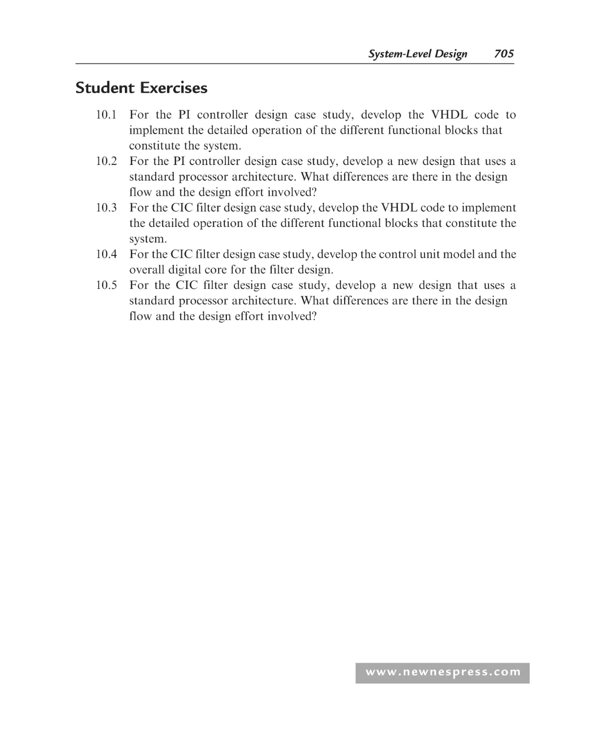
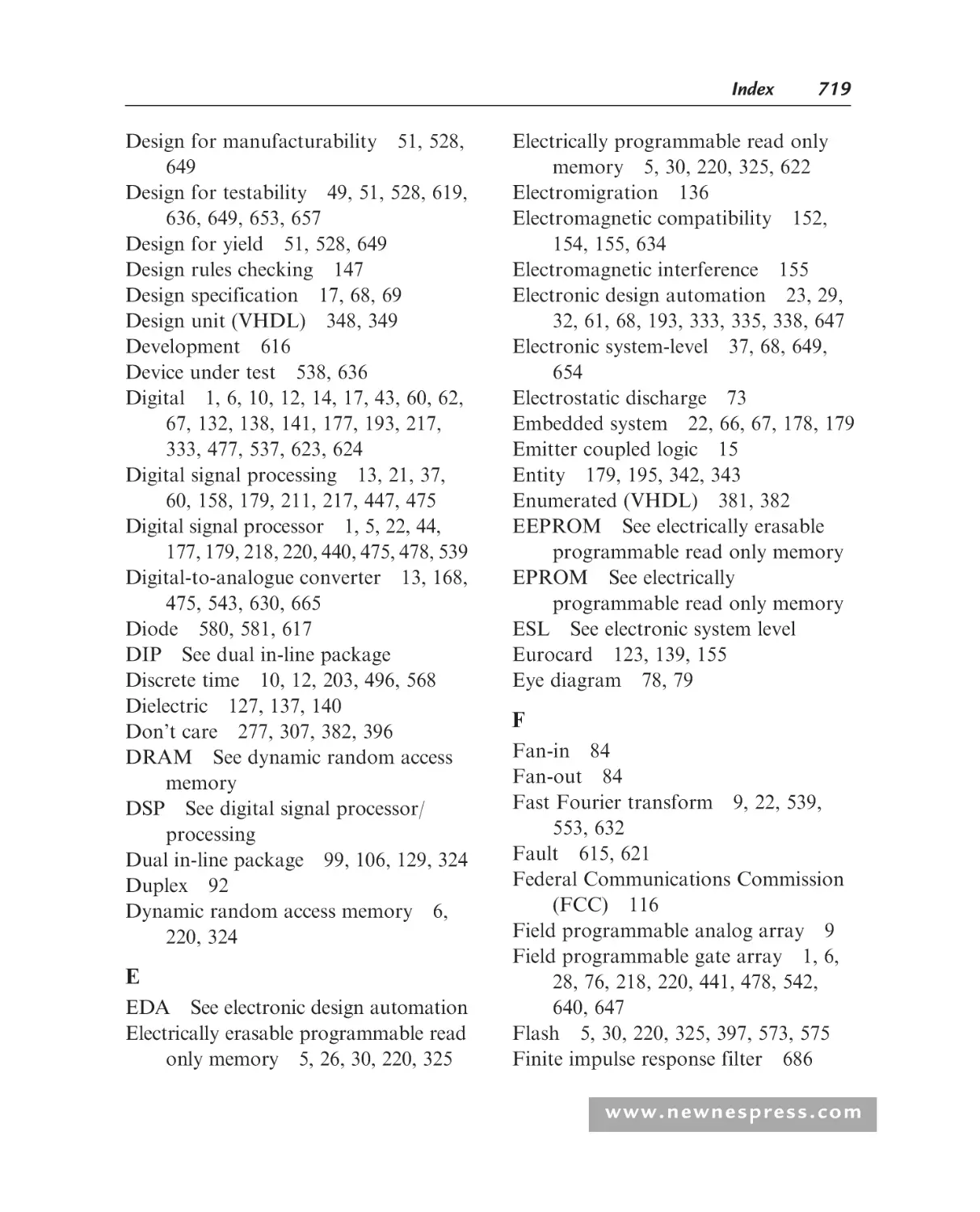
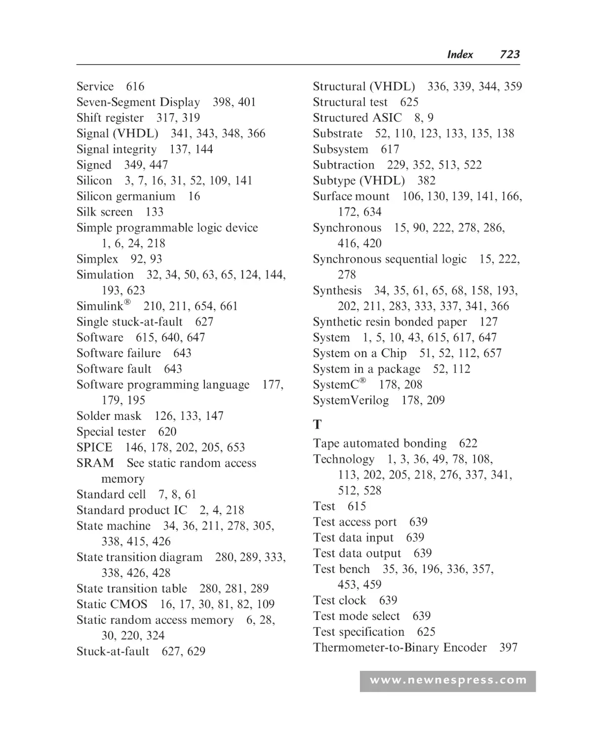
many digital circuits and systems. The choices are shown in Figure 1.1.
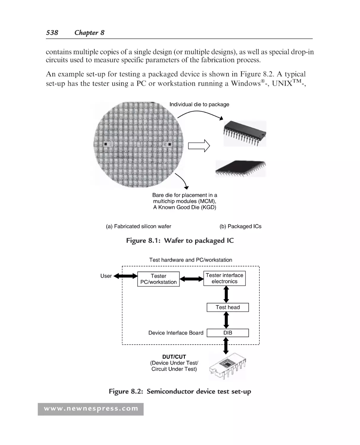
In Figure 1.1, the electronic components used are integrated circuits (ICs). These are
electronic circuits packaged within a suitable housing that contain complete circuits
ranging from a few dozen transistors to hundreds of millions of transistors, the
www.newnespress.com
2
Chapter 1
Fixed
Functionality
Microprocessor
Processor
Standard
Product IC
Microcontroller
Digital Signal
Processor
Simple PLD
PLD
Complex PLD
Field
Programmable
Gate Array
Digital Circuit
Requirements
ROM
Memory
RAM
Fixed
Functionality
ASIC
Processor
PLD
Memory
Figure 1.1: Technology choices for digital circuit design
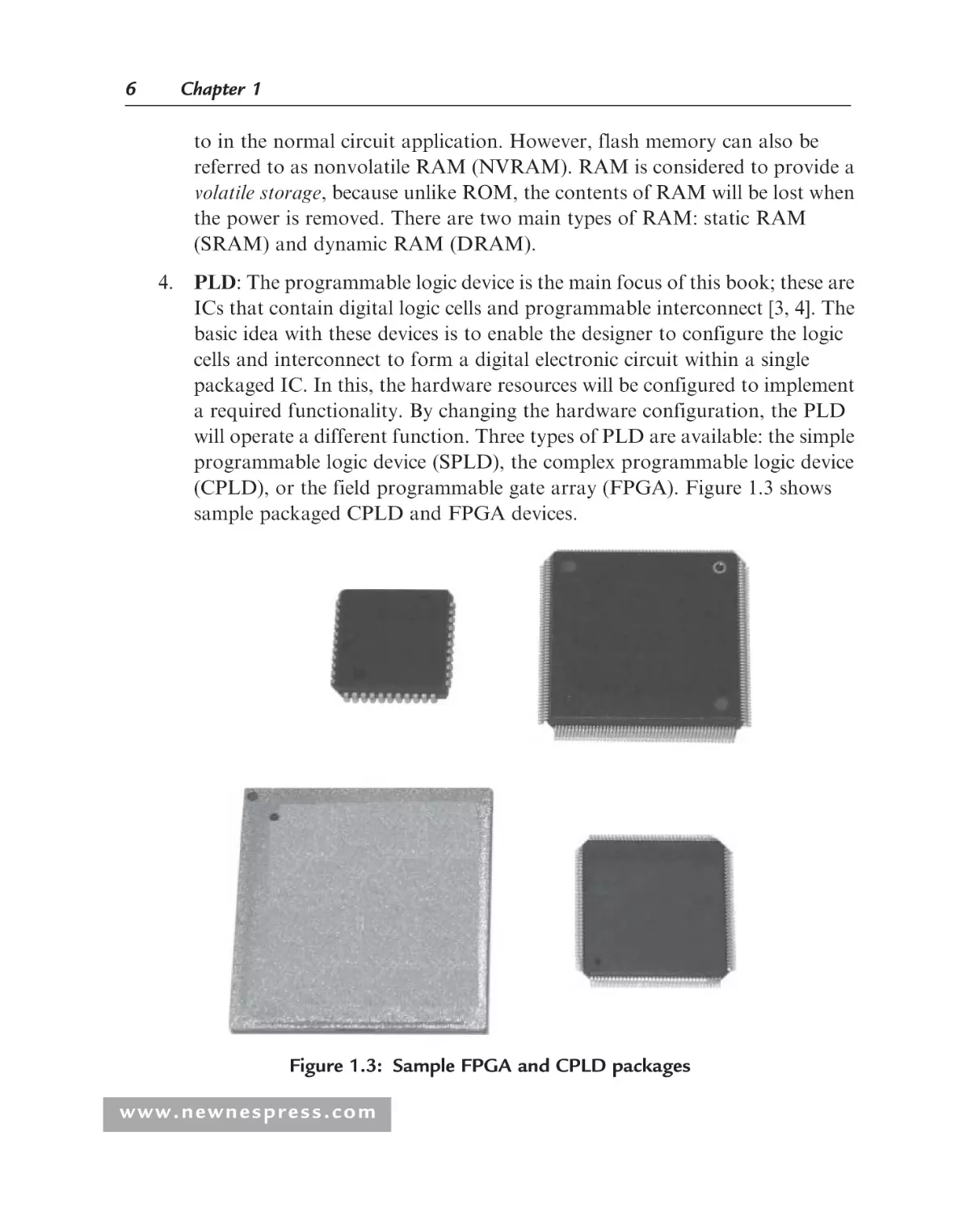
complexity of the circuit depending on the designed functionality. Examples of
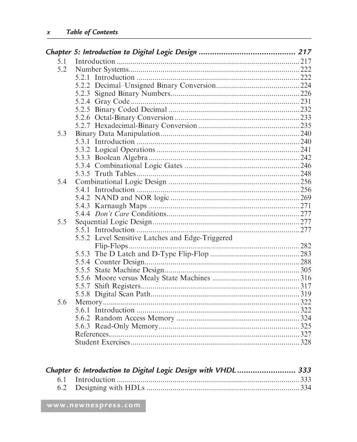
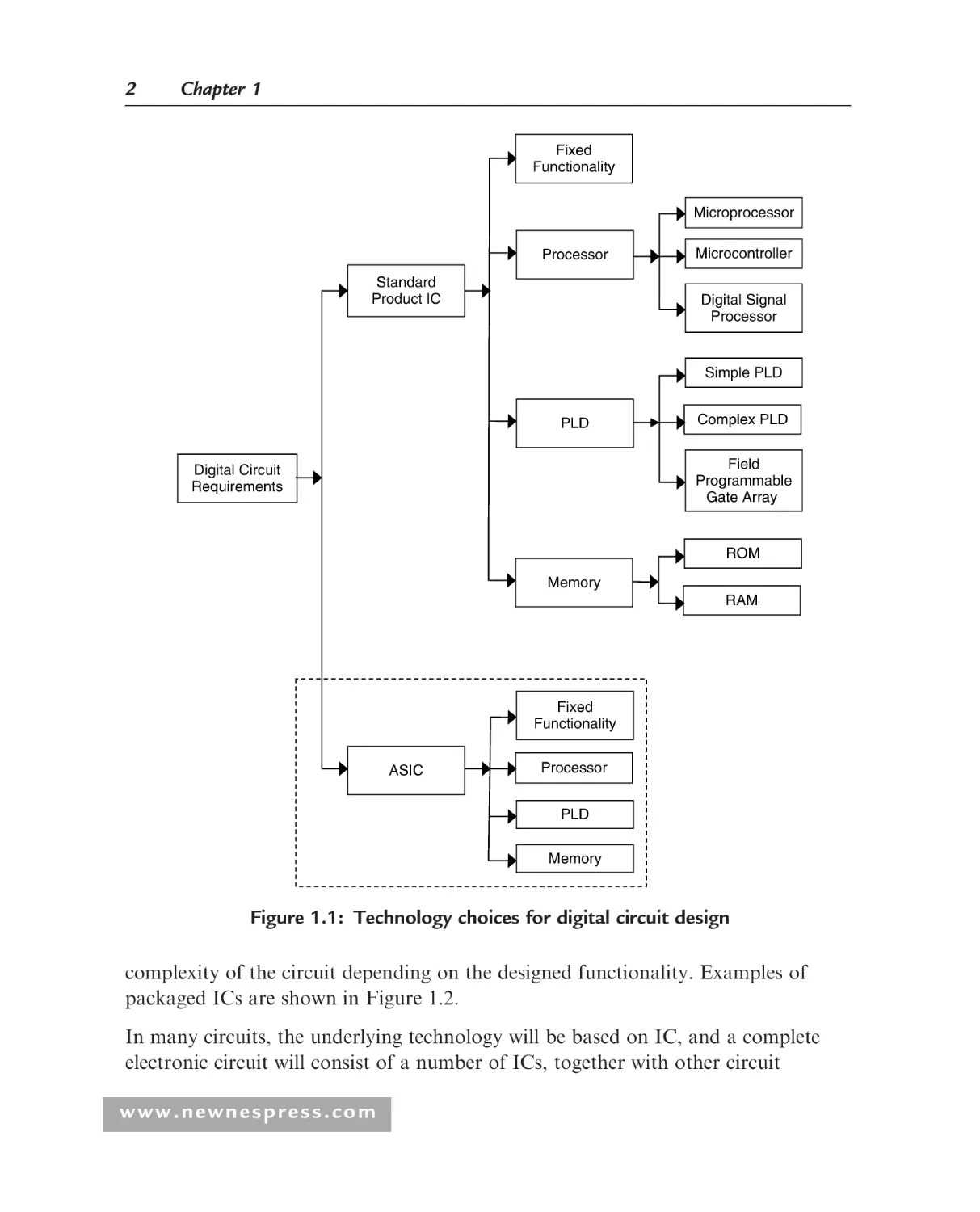
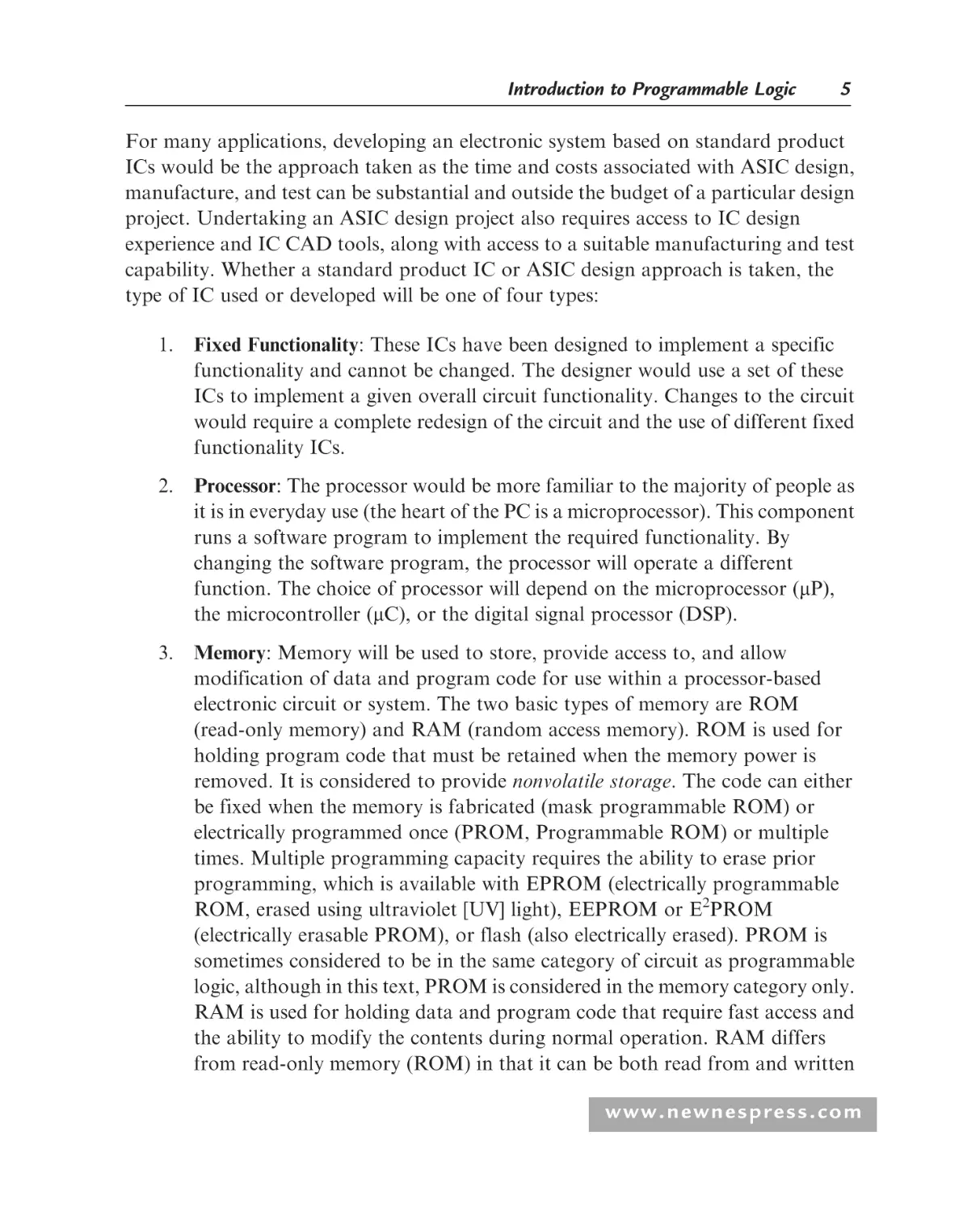
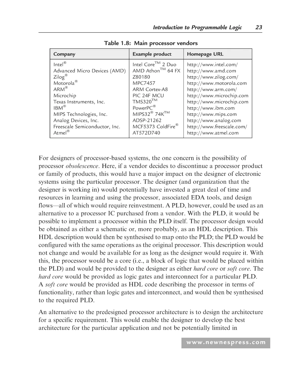
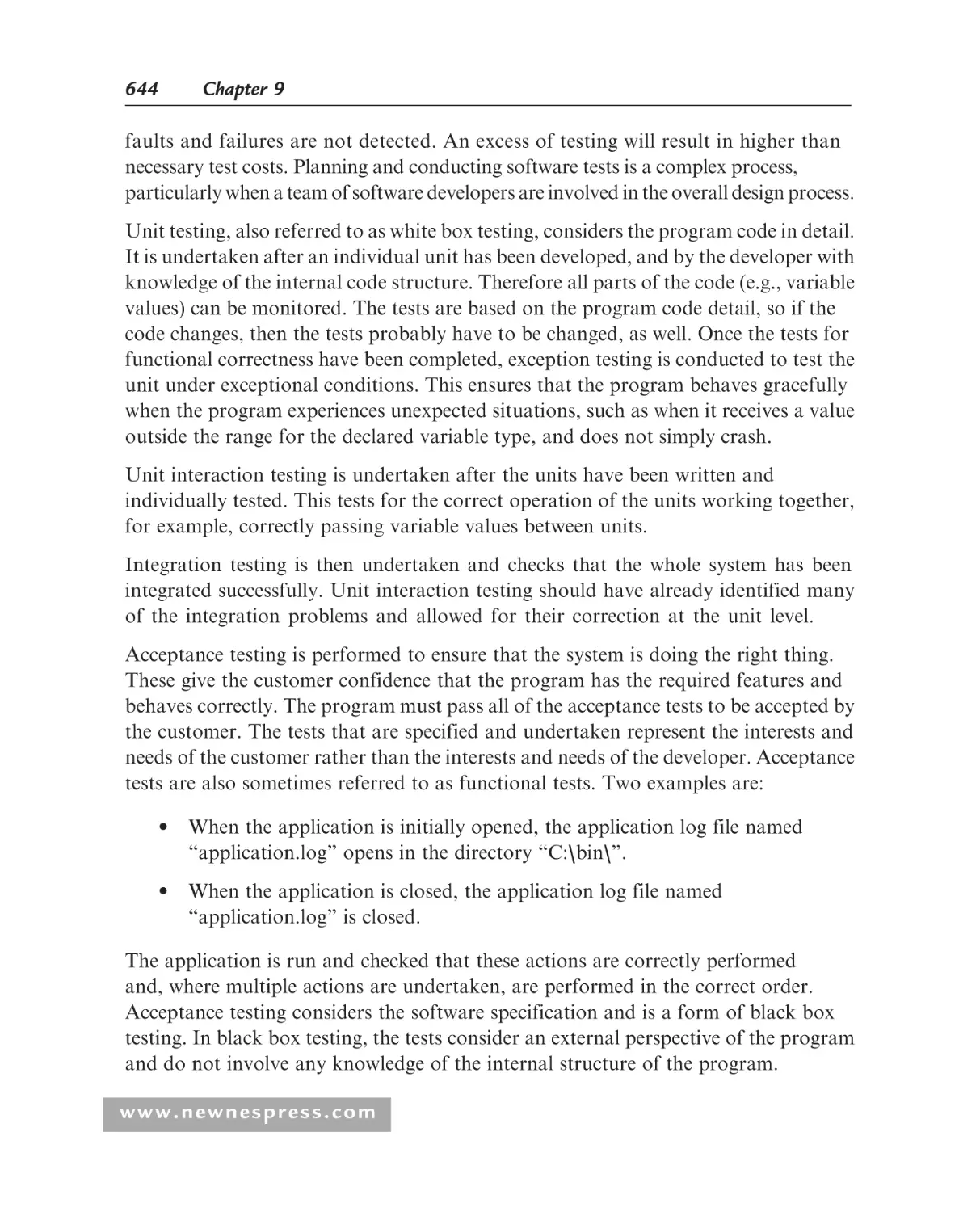
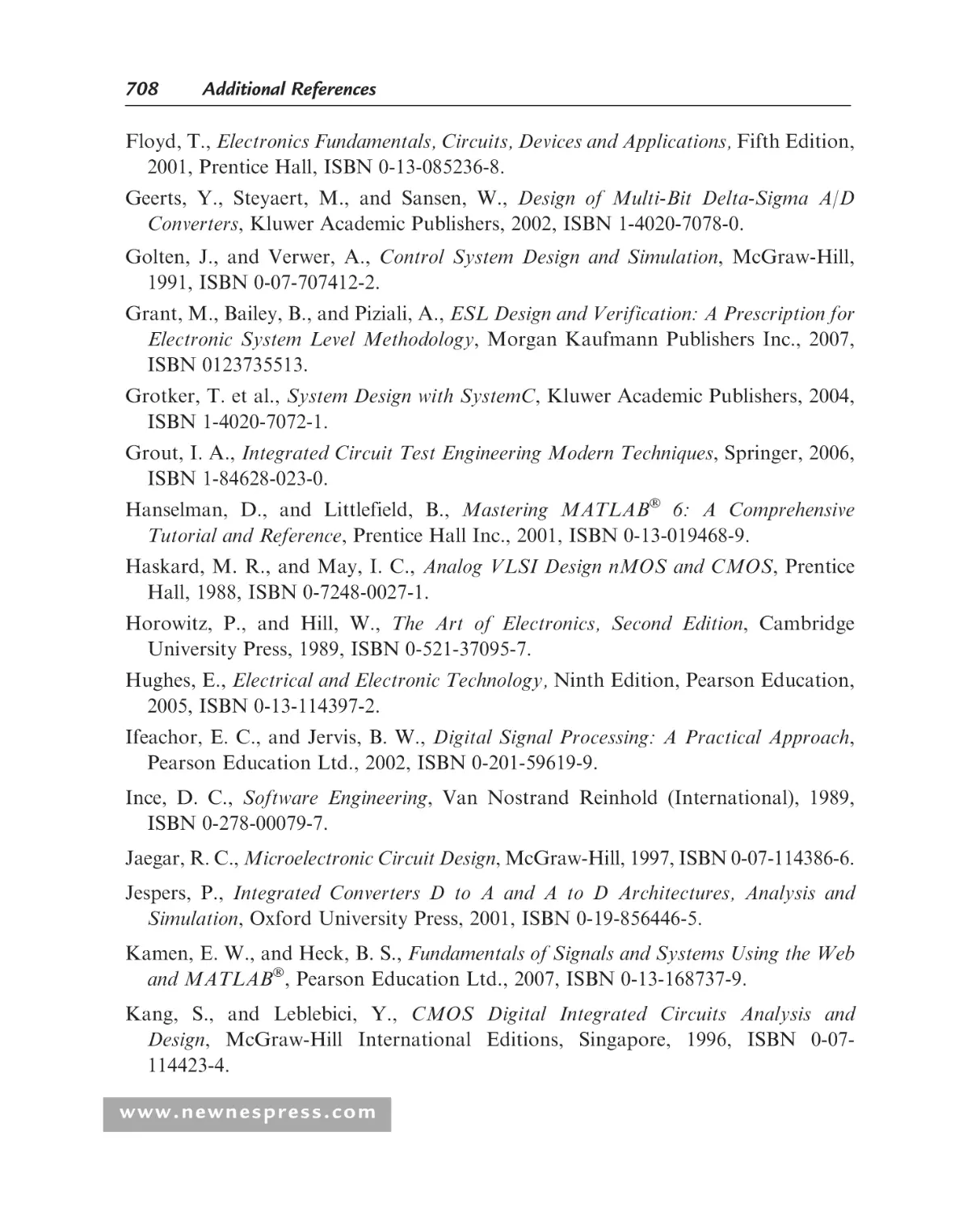
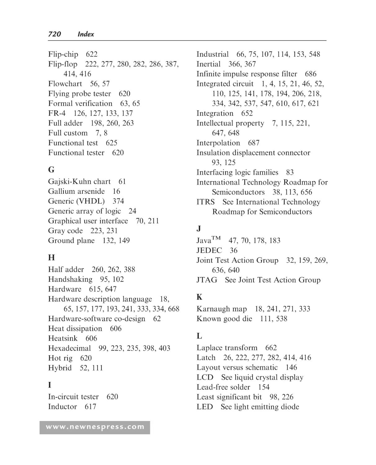
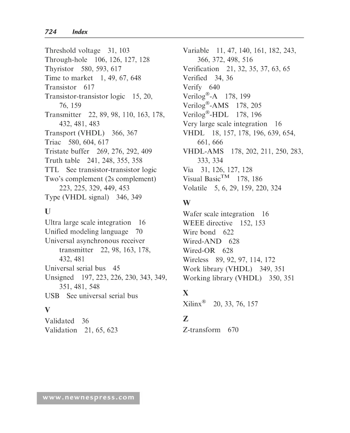
packaged ICs are shown in Figure 1.2.
In many circuits, the underlying technology will be based on IC, and a complete
electronic circuit will consist of a number of ICs, together with other circuit
www.newnespress.com
Introduction to Programmable Logic
3
Figure 1.2: Examples of IC packages with the tops removed and the silicon dies exposed
components such as resistors and capacitors. In this book, the generic word
technology will be used throughout. The Oxford Dictionary of English defines
technology as ‘‘the application of scientific knowledge for practical purposes,
especially in industry’’ [1].
For us, this applies to the underlying electronic hardware and software that can be
used to design a circuit for a given requirement. For the arrangement identified in
Figure 1.1, a given set of digital circuit requirements are developed, and the role of the
designer is to come up with a solution that meets ideally all of the requirements.
Typical requirements include:
• Cost restraints: The design process, the cost of components, the manufacturing
costs, and the maintenance and future development costs must be within
specific limits.
• Design time: The design must be generated within a certain time limit.
www.newnespress.com
4
Chapter 1
• Component supply: The designer might have a free hand in choosing the
components to use, or restrictions may be set by the company or project
management requirements.
• Prior experience: The designer may have prior experience in using a particular
technology, which might or might not be suitable to the current design.
• Training: The designer might require specific training to utilize a specific
technology if he or she does not have the necessary prior experience.
• Contract arrangements: If the design is to be created for a specific customer,
the customer would typically provide a set of constraints that would be set
down in the design contract.
• Size/volume constraints: the design would need to be manufactured to fit into a
specific size/volume,
• Weight constraints: the design would need to be manufactured to be within
specific weight restrictions (e.g. for portable applications such as mobile
phones),
• Power source: the electronic product would be either fixed (in a single location
so allowing for the use of a fixed power source) or portable (to be carried to
multiple places requiring a portable power source (such as battery or solar cell),
• Power consumption constraints: The power consumption should be as low as
possible in order to (i) minimise the power source requirements, (ii) be
operable for a specific time on a limited power source, and (iii) be compatible
with best practice in the development of electronic products that are conscious
of environmental issues.
The initial choice for implementing the digital circuit is between a standard product
IC and an ASIC (application-specific integrated circuit) [2]:
• Standard product IC: This is an off-the-shelf electronic component that has been
designed and manufactured by a company for a given purpose, or range of use,
and that is commercially available for others to use. These would be purchased
either from a component supplier or directly from the designer or manufacturer.
• ASIC: This is an IC that has been specifically designed for an application.
Rather than purchasing an off-the-shelf IC, the ASIC can be designed and
manufactured to fulfil the design requirements.
www.newnespress.com
Introduction to Programmable Logic
5
For many applications, developing an electronic system based on standard product
ICs would be the approach taken as the time and costs associated with ASIC design,
manufacture, and test can be substantial and outside the budget of a particular design
project. Undertaking an ASIC design project also requires access to IC design
experience and IC CAD tools, along with access to a suitable manufacturing and test
capability. Whether a standard product IC or ASIC design approach is taken, the
type of IC used or developed will be one of four types:
1. Fixed Functionality: These ICs have been designed to implement a specific
functionality and cannot be changed. The designer would use a set of these
ICs to implement a given overall circuit functionality. Changes to the circuit
would require a complete redesign of the circuit and the use of different fixed
functionality ICs.
2. Processor: The processor would be more familiar to the majority of people as
it is in everyday use (the heart of the PC is a microprocessor). This component
runs a software program to implement the required functionality. By
changing the software program, the processor will operate a different
function. The choice of processor will depend on the microprocessor (mP),
the microcontroller (mC), or the digital signal processor (DSP).
3. Memory: Memory will be used to store, provide access to, and allow
modification of data and program code for use within a processor-based
electronic circuit or system. The two basic types of memory are ROM
(read-only memory) and RAM (random access memory). ROM is used for
holding program code that must be retained when the memory power is
removed. It is considered to provide nonvolatile storage. The code can either
be fixed when the memory is fabricated (mask programmable ROM) or
electrically programmed once (PROM, Programmable ROM) or multiple
times. Multiple programming capacity requires the ability to erase prior
programming, which is available with EPROM (electrically programmable
ROM, erased using ultraviolet [UV] light), EEPROM or E2PROM
(electrically erasable PROM), or flash (also electrically erased). PROM is
sometimes considered to be in the same category of circuit as programmable
logic, although in this text, PROM is considered in the memory category only.
RAM is used for holding data and program code that require fast access and
the ability to modify the contents during normal operation. RAM differs
from read-only memory (ROM) in that it can be both read from and written
www.newnespress.com
6
Chapter 1
to in the normal circuit application. However, flash memory can also be
referred to as nonvolatile RAM (NVRAM). RAM is considered to provide a
volatile storage, because unlike ROM, the contents of RAM will be lost when
the power is removed. There are two main types of RAM: static RAM
(SRAM) and dynamic RAM (DRAM).
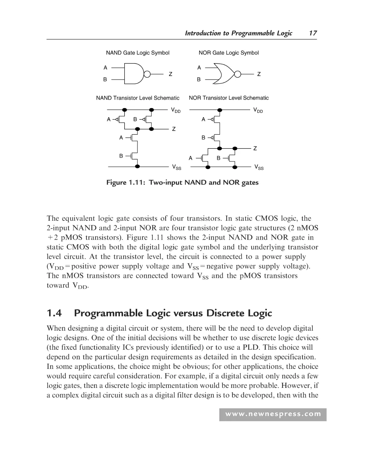
4. PLD: The programmable logic device is the main focus of this book; these are
ICs that contain digital logic cells and programmable interconnect [3, 4]. The
basic idea with these devices is to enable the designer to configure the logic
cells and interconnect to form a digital electronic circuit within a single
packaged IC. In this, the hardware resources will be configured to implement
a required functionality. By changing the hardware configuration, the PLD
will operate a different function. Three types of PLD are available: the simple
programmable logic device (SPLD), the complex programmable logic device
(CPLD), or the field programmable gate array (FPGA). Figure 1.3 shows
sample packaged CPLD and FPGA devices.
Figure 1.3: Sample FPGA and CPLD packages
www.newnespress.com
Introduction to Programmable Logic
7
Both the processor and PLD enable the designer to implement and change the
functionality of the IC by changing either the software program or the hardware
configuration. Because these two different approaches are easily confused, in this
book the following terms will be used to differentiate the PLD from the processor:
• The PLD will be configured using a hardware configuration.
• The processor will be programmed using a software program.
An ASIC can be designed to create any one of the four standard product IC forms
(fixed functionality, processor, memory, or PLD). An ASIC would be designed in the
same manner as a standard product IC, so anyone who has access to an ASIC design,
fabrication, and test facility can create an equivalent to a standard product IC (given
that patent and general legal issues around IP [intellectual property] considerations
for existing designs and devices are taken into account). In addition, an ASIC might
also incorporate a programmable logic fabric alongside the fixed logic hardware.
Figure 1.1 shows what can be done with ASIC solution, but not how the ASIC
would achieve this. Figure 1.4 shows the (i) four different forms of IC (i.e., what the
IC does) that can be developed to emulate a standard product IC equivalent, and
(ii) the three different design and implementation approaches.
In a full-custom approach, the designer would be in control of every aspect of
ASIC design and layout—the way in which the electronic circuit is laid out on the
die, which is the piece of rectangular or square material (usually silicon) onto
Fixed
Functionality
ASIC
Processor
Memory
PLD
(i) What the ASIC does
Full custom
ASIC
Standard cell
Mask
programmable
gate array
Semicustom
(ii) How the ASIC does it
Figure 1.4: ASICs, what and how
www.newnespress.com
8
Chapter 1
which the circuit components are manufactured. This would give the best circuit
performance, but would be time consuming and expensive to undertake. Fullcustom design is predominantly for analogue circuits and the creation of libraries
of components for use in a semi-custom, standard cell design approach. An
alternative to the full-custom approach uses a semi-custom approach. This is
subdivided into a standard cell approach or mask programmable gate array
(MPGA) approach. The standard cell approach uses a library of predesigned basic
circuit components (typically digital logic cells) that are connected within the IC to
form the overall circuit. In a simplistic view, this would be similar to creating a
design by connecting fixed functionality ICs together, but instead of using multiple
ICs, a single IC is created. This approach is faster and lower cost than a full-custom
approach but would not necessarily provide the best circuit performance. Because
only the circuits required within the design would be manufactured (fabricated), there
would be an immediate trade-off between circuit performance, design time, and design
cost (a trade-off that is encountered on a daily basis by the designer). The MPGA
approach is similar to a standard cell approach in that a library of components is
available and connected, but the layout on the (silicon) die is different. An array of
logic gates is predetermined, and the circuit is created by creating metal interconnect
tracks between the logic gates. In the MPGA approach, not necessarily all of the logic
gates fabricated on the die would be used. This would use a larger die than in a
standard cell approach, with the inclusion of unused gates, but it has the advantage of
being faster to fabricate than a standard cell approach.
A complement to the ASIC is the structured ASIC [16, 17]. The structured ASIC is
seen to offer a promising alternative to standard cell ASICs and FPGAs for the mid
and high volume market. Structured ASICs are similar to the mask programmable
gate array in that they have customisable metal interconnect layers patterned on top
of a prefabricated base. Either standard logic gates or look-up tables (LUTs) are
fabricated in a 2-dimensional array that forms the underlying pattern of logic gates,
memory, processors and IP blocks. This base is programmed using a small number of
metal masks. The purpose of this is to reduce the non-recurring engineering (NRE)
costs when compared to a standard cell ASIC approach and to bridge the gap that
exists between the standard cell ASIC and FPGA where:
1. Standard cell ASICs provide support for large, complex designs with high
performance, low cost per unit (if produced in volume), but at the cost of long
www.newnespress.com
Introduction to Programmable Logic
9
development times, high NRE costs and long fabrication times when
implementing design modifications,
2. FPGAs provide for short development times, low NRE costs and short times
to implement design modifications, but at the cost of limited design
complexities, performance limitations and high cost per unit.
NRE cost reductions using Structured ASICs are considered with a reduction in
manufacturing costs and reducing the design tasks. They can also offer mixedsignal circuit capability, a potential advantage when compared to digital only
FPGAs.
Hardware configured devices (i.e., PLDs) are becoming increasingly popular
because of their potential benefits in terms of logic replacement potential
(obsolescence), rapid prototyping capabilities, and design speed benefits in which
PLD-based hardware can implement the same functions as a software-programmed,
processor-based system, but in less time. This is particularly important for
computationally expensive mathematical operations such as the fast Fourier
transform (FFT) [5].
The aim of this book is to provide a reference text for students and practicing
engineers involved in digital electronic circuit and systems design using PLDs. The
PLD is digital in nature and this type of device will be the focus of the book.
However, it should also be noted that mixed-signal programmable devices have also
been developed and are available for use within mixed-signal circuits that require
programmable analogue circuit (e.g. programmable analogue amplifier)
components. Whilst this technology is not covered in this book, the reader is
recommended to undertake their own research activities to (i) identify the
programmable mixed-signal devices currently available (such as the Lattice
Semiconductor Corporation ispPAC and AnadigmTM FPAA (Field Programmable
Analog Array)), and also (ii) the history of programmable mixed-signal and devices
that have been available in the past but no longer available. The text will introduce
the basic concepts of programmable logic, along with case study designs in a range
of electronic systems that target signal generation and data acquisition systems for a
variety of applications from control and instrumentation through test equipment
systems. To achieve this, a range of FPGA and CPLD device types will be
considered. The text will also act as a reference from which the sources of additional
information can be acquired.
www.newnespress.com
10
Chapter 1
1.2
Electronic Circuits: Analogue and Digital
1.2.1
Introduction
Before looking into detail of what the PLD is and how to use it, it is important to
identify that the PLD is digital in nature, and digital circuits and signals are different
from analogue circuits and signals. This section will provide an overview of the main
characteristics and differences between the continuous- and discrete-time, and the
analogue and digital, worlds.
1.2.2
Continuous Time versus Discrete Time
Electronic circuits will receive electrical signals (voltages and/or currents) and modify
these to produce a response, which will be a voltage and/or current that is a modified
version of the input signal (see Figure 1.5). The signal will be electrical in nature and will
convey information concerning the behavior of the related system. The input to the
system will typically be created by a variation of a measurable quantity by the use of a
suitable sensor. The response will be a modified version of the input that is in a form that
can be used. In Figure 1.5, an electronic system receives an input, x, and produces a
response (output), y. The system implements a certain function that is designed to
undertake an operation that is of a particular use within the context of the overall system.
Here, the system receives a single input and produces a single response. The term
system is another generic term which is defined in the Oxford Dictionary of English as
‘‘a set of things working together as parts of a mechanism or an interconnecting
network’’ [1].
For us, this applies to the overall set of electronic components and software programs
that work together to perform the particular set of requirements. In general, there may
be one or more inputs and one or more outputs. The system is shown as a black box in
that the details of its internal operation are hidden and only the input-output relationship
is known. This black box creates a signal processor, and the designer is tasked with
Input
x
System
Response
y
Figure 1.5: Electronic system block diagram
www.newnespress.com
Introduction to Programmable Logic
11
creating the internal details using a suitable electronic circuit technology. The inputoutput relationship will normally be modeled by a suitable mathematical algorithm.
The type of signal [6, 7] that the signal processor accepts and responds to will vary in
time but will be classified as either a continuous-time or a discrete-time signal.
A continuous-time signal can be represented mathematically as a function of a
continuous-time variable. The signal varies in time but is also continuous in time.
Figure 1.6 provides four examples of continuous-time signals: (i) a constant value,
(ii) a sine wave, (iii) a square wave, and (iv) an arbitrary waveform. Waveforms (i),
(ii), and (iv) are continuous in both time and amplitude; (iii) is continuous in time but
discontinuous in amplitude. All signals are classified as continuous-time signals.
A discrete-time signal is defined only by values at set points in time, referred to as the
sampling instants. It is normal to set the time spacing between the sampling instants to a
fixed value, T, referred to as the sampling interval. The sampling frequency is fS = 1/T,
where T is seconds and fS is Hertz (Hz). When a signal is sampled at a fixed rate, this
is referred to as periodic sampling. Figure 1.7 provides examples of discrete-time
signals that are sampled values of the continuous time signals shown in Figure 1.6.
When a discrete-time signal is expressed, it will normally be expressed by the sample
number (n) where n = 0 denotes the first sample, n = p denotes the pth sample, and
n increments in steps of 1. For a signal x, then, the samples will be x[0], x[1], x[2],
x[3], . . . , x[p]. A discrete-time signal would represent a sampled analogue signal.
Hence, an electronic circuit would have continuous-time or discrete-time inputs and
continuous-time or discrete-time outputs as represented in Table 1.1.
time (t)
time (t)
(i) Constant
(ii) Sine wave
time (t)
(iii) Square wave
time (t)
(iv) Arbitrary waveform
Figure 1.6: Examples of continuous-time signals
www.newnespress.com
12
Chapter 1
Amplitude
Amplitude
time (t)
time (t)
(i) Constant
(ii) Sine wave
Amplitude
Amplitude
time (t)
(iii) Square wave
time (t)
(iv) Arbitrary waveform
Figure 1.7: Examples of discrete-time signals
Table 1.1: Signal types (continuous- and discrete-time)
Input signal type
Continuous-time
Continuous-time
Discrete-time
Discrete-time
1.2.3
Response signal type
!
!
!
!
Continuous-time
Discrete-time
Discrete-time
Continuous-time
Analogue versus Digital
The electronic system as shown in Figure 1.8 will perform its operations on signals
that are either analogue or digital in nature, using either analogue or digital electronic
circuits. Hence, a signal may be of one of two types, analogue or digital.
An analogue signal is a continuous- or discrete-time signal whose amplitude is
continuous in value between a lower and upper limit, but may be either a continuous
time or discrete time.
Input
x
System
Response
y
Figure 1.8: Electronic system block diagram
www.newnespress.com
Introduction to Programmable Logic
13
Table 1.2: Signal types (analogue and digital)
Input signal type
Analogue
Analogue
Digital
Digital
Response signal type
!
!
!
!
Analogue
Digital
Digital
Analogue
A digital signal is a continuous or discrete-time signal with discrete values between a
lower and upper limit. These discrete values will be represented by numerical values
and be in a form suitable for digital signal processing. If the discrete-time signal has
been derived from a continuous-time signal by sampling, then the sampled signal is
converted into a digital signal by quantization, which produces a finite number of
values from a continuous amplitude signal. It is common to use the binary number
(i.e., two values, 0 or 1) system to represent a number in a digital representation.
An electronic circuit would have analogue or digital inputs and analogue or digital
outputs as represented in Table 1.2. When an analogue signal is sampled and
converted to digital, this is undertaken using an analogue-to-digital converter (ADC)
[8]. When a digital signal is converted back to analogue, this is undertaken using a
digital-to-analogue converter (DAC).
An example of both analogue and digital signals and circuits is shown in
Figure 1.9. This electronic temperature controller, as might be used in a home
Analogue
Analogue
Digital
Sensor
Sensor signal
conditioning circuit
Analogueto-Digital
Converter
Controller
Signal conditioning
circuit
Digital-toAnalogue
Converter
Temperature
Heat
Analogue
Analogue
Analogue
Digital
signal
processing
Digital
Analogue
Figure 1.9: Heating control system block diagram
www.newnespress.com
14
Chapter 1
Required
temperature
+
Controller
Plant
Plant output
(heat)
–
Temperature
Sensor
Figure 1.10: General control system
heating system, uses digital signal processing. The system is shown as a block
diagram in which each block represents a major operation. In a design each block
would be represented by its own block diagram, going into evermore detail until the
underlying circuit hardware (and software) details are identified. The block
diagram provides a convenient way to represent the major system operations called
a top-down design approach, starting at a high level of design abstraction (initially
independent of the final design implementation details) and working down to the
final design implementation details.
Here, the room temperature is sensed as an analogue signal, but must be processed by a
digital signal processing circuit, so it must be sensed and converted to an analogue
voltage or current. This is then applied to a sensor signal conditioning circuit that is used
to connect the sensor to the ADC. The ADC samples the analogue signal at a chosen
sampling frequency. Once a temperature sample has been obtained by the digital signal
processing circuit, it is then processed using a particular algorithm, and the result is
applied to a DAC. The DAC output is a voltage or current that is used to drive a
controller (heat source). The DAC is normally connected to the controller via a signal
conditioning circuit. This circuit acts to interface the DAC to the controller in order for
the controller to receive the correct voltage and current levels. This particular system is
also an example of a closed-loop control system using an electronic controller. The
control system is generalized as shown in Figure 1.10 [9, 10].
1.3
History of Digital Logic
Early electronic circuits were analogue, and before the advent of digital logic,
signal processing was undertaken using analogue electronic circuits. The
invention of the semiconductor transistor in 1947 at Bell Laboratories [11] and
www.newnespress.com
Introduction to Programmable Logic
15
the improvements in transistor characteristics and fabrication during the 1950s
led to the introduction of linear (analogue) ICs and the first transistor-transistor
logic (TTL) digital logic IC in the early 1960s, closely followed by complementary
metal oxide semiconductor (CMOS) ICs. The early devices incorporated a small
number of logic gates. However, rapid growth in the ability to fabricate an
increasing number of logic gates in a single IC led to the microprocessor in the
early 1970s. This, with the ability to create memory ICs with ever increasing
capacities, laid the foundation for the rapid expansion in the computer industry
and the types of complex digital systems based on the computer architecture that we
have available today. The last fifty years have seen a revolution in the electronics
industry.
Fundamentally, a digital circuit will be categorized into one of three general types,
each of which is created and fabricated within an integrated circuit:
• Combinational logic, in which the response of the circuit is based on a Boolean
logic expression of the input only and the circuit responds immediately to a
change in the input.
• Sequential logic, in which the response of the circuit is based on the current
state of the circuit and the sometimes the current input. This may be
asynchronous or synchronous. In synchronous sequential logic, the logic changes
state whenever an external clock control signal is applied. In asynchronous
sequential logic, the logic changes state on changes of the input data (the
circuit does not utilize a clock control signal).
• Memory, in which digital values can be stored and retrieved some time later. For
a user, memory can be either read-only (ROM) or random-access (RAM). In
ROM, the data stored in the memory are initially placed in the memory and can
only be read by the user. Data cannot normally be altered in the
circuit application. In RAM (also referred to as read-write memory, RWM), the
user can write data to the memory and read the data back from the memory.
The digital IC consists of a number of logic gates, which are combinational or
sequential circuit elements. The logic gates may be implemented using different
fabrication processes and different circuit architectures:
• TTL, transistor-transistor logic (bipolar)
• ECL, emitter-coupled logic (bipolar)
www.newnespress.com
16
Chapter 1
• CMOS, complementary metal oxide semiconductor
• BiCMOS, bipolar and CMOS
The material predominantly used to fabricate the digital logic circuits is silicon.
However, silicon-based circuits are complemented with the digital logic capabilities of
circuits fabricated using gallium arsenide (GaAs) and silicon germanium (SiGe)
technologies. Today, silicon-based CMOS is by far the dominant process used for
digital logic.
The digital logic gate is actually an abstraction of what is happening within the
underlying circuit. All digital logic gates are made up of transistors. The logic gates
may take one of a number of different circuit architectures (the way in which the
transistors are interconnected) at the transistor level:
• static CMOS
• dynamic CMOS
• pass transistor logic CMOS
Today, static CMOS logic is by far the dominant logic cell design structure used. The
number of logic gates within a digital logic IC will range from a few to hundreds of
thousands and ultimately millions for the more complex processors and PLDs. In
previous times, when the potential for higher levels of integration was far less than is
now possible, the digital IC was classified by the level of integration—that is, the
number of logic gate equivalents per IC (see Table 1.3). With increasing levels of
integration, the following levels were identified as follow-on descriptions from VLSI,
but these are not in common usage:
• ULSI, ultra-large-scale integration
• WSI, wafer scale integration
Table 1.3: Levels of integration
Level of integration
Acronym
Small-scale integration
Medium-scale integration
Large-scale integration
Very large-scale integration
SSI
MSI
LSI
VLSI
www.newnespress.com
Number of gate equivalents per IC
<10
10–100
100–10,000
>10,000
Introduction to Programmable Logic
NAND Gate Logic Symbol
17
NOR Gate Logic Symbol
A
A
Z
Z
B
B
NAND Transistor Level Schematic
NOR Transistor Level Schematic
VDD
VDD
A
A
B
Z
B
A
Z
B
A
VSS
B
VSS
Figure 1.11: Two-input NAND and NOR gates
The equivalent logic gate consists of four transistors. In static CMOS logic, the
2-input NAND and 2-input NOR are four transistor logic gate structures (2 nMOS
+2 pMOS transistors). Figure 1.11 shows the 2-input NAND and NOR gate in
static CMOS with both the digital logic gate symbol and the underlying transistor
level circuit. At the transistor level, the circuit is connected to a power supply
(VDD=positive power supply voltage and VSS=negative power supply voltage).
The nMOS transistors are connected toward VSS and the pMOS transistors
toward VDD.
1.4
Programmable Logic versus Discrete Logic
When designing a digital circuit or system, there will be the need to develop digital
logic designs. One of the initial decisions will be whether to use discrete logic devices
(the fixed functionality ICs previously identified) or to use a PLD. This choice will
depend on the particular design requirements as detailed in the design specification.
In some applications, the choice might be obvious; for other applications, the choice
would require careful consideration. For example, if a digital circuit only needs a few
logic gates, then a discrete logic implementation would be more probable. However, if
a complex digital circuit such as a digital filter design is to be developed, then with the
www.newnespress.com
18
Chapter 1
complexity of the resulting logic hardware, a PLD would be the logical choice. These
are the characteristics and aptitudes of each:
Discrete logic:
• Suited for small designs that will not require modification
• Can be used for prototyping designs as well as for the final application
• Can be designed by hand using Boolean logic and Karnaugh map techniques
• Suited for combinational, sequential logic designs and memory
• Any change to the design will require the redesign of the circuit hardware
and wiring
• No need to know how to design and configure PLDs
• For a particular family of devices, the I/O standard is fixed
• The logic gates may be implemented using different fabrication processes and
different circuit architectures: TTL, ECL, CMOS, and BiCMOS.
Table 1.4 identifies selected TTL device family variants in use, Table 1.5 identifies
selected CMOS device family variants in use, and Table 1.6 identifies selected lowvoltage CMOS device family variants in use.
Programmable logic:
• Suited for all designs from small to large
• Can be used for prototyping designs as well as for the final application
• Suited for designs that might require modification
• Easy to change designs without changing the circuit hardware and wiring that
the PLD is connected to by altering the internal PLD circuit configuration
• Can be designed by hand using Boolean logic and Karnaugh map techniques, along
with hardware description languages (HDLs) such as VHDL and Verilog-HDL
• Suited for combinational, sequential logic designs and memory
• The need to know how to design and configure PLDs
www.newnespress.com
Introduction to Programmable Logic
19
Table 1.4: Selected TTL family variants
TTL family variant
74
74AS
74ALS
74F
74H
74L
74LS
74S
LVTTL
Description
Standard TTL
Advanced Schottky
Advanced low-power Schottky
Fast
High-speed
Low-power
Low-power Schottky
Schottky
Low-voltage
Table 1.5: Selected CMOS family variants
CMOS family variant
4000
74C
74HC
74HCT
74AC
74ACT
74AHC
74AHCT
74FCT
LVCMOS
Description
True CMOS (non-TTL levels)
CMOS with pin compatibility to TTL with same number
Same as 74C but with improved switching speed
As with 74HC but can be connected directly to TTL
Advanced CMOS
As with 74AC but can be connected directly to TTL
Advanced high-speed CMOS
As with 74AHC but can be connected directly to TTL
Fast CMOS TTL inputs
Low-voltage CMOS
Table 1.6: Selected low-voltage (LV) CMOS family variants
Low-voltage
CMOS variant
Description
74LV
Low-voltage CMOS
74LVC
Low-voltage CMOS
74ALVC
Advanced lowvoltage CMOS
Advanced very lowvoltage CMOS
74AVC
Low-speed operation, 1.0–3.6 V power supply (some
functions up to 5.5 V power supply)
Medium-speed operation, 1.2–3.6 V power supply
(5 V tolerant I/O)
High-speed operation, 1.2–3.6 V power supply (5 V
tolerant I/O on bus hold types)
Very high-speed operation, 1.2–3.6 V power supply
(3.6 V tolerant I/O)
www.newnespress.com
20
Chapter 1
Table 1.7: Example I/O standards supported by the Xilinx PLDs
Standard
Standard description
LVTTL
LVCMOS33
LVCMOS25
LVCMOS18
1.5 V I/O (1.5 V levels)
HSTL-1
SSTL2-1
SSTL3-1
Low-voltage transistor-transistor logic (3.3 V level)
Low-voltage CMOS (3.3 V level)
Low-voltage CMOS (2.5 V level)
Low-voltage CMOS (1.8 V level)
1.5V level logic (1.5 V level)
High-speed transceiver logic
Stub series terminated logic (2.5 V level)
Stub series terminated logic (3.3 V level)
• Many PLDs will provide a capability for the designer to set the particular I/O
standard to use from those standards supported by the device
• Many PLD vendors provide IP circuit blocks that can be used by the designer
within the vendor’s PLD, whether free or through royalty payments
depending on the licensing arrangement.
Table 1.7 shows example I/O standards that are supported by the Xilinx [12]. PLDs
are configured by the designer. With such programmable I/O capability before the
device has been configured with the appropriate standard, the device will default to
one of the standards. It is important for the designer to identify the default standard
and the implications of using a particular standard on the overall circuit operation.
Early uses of the PLD were for the replacement of standard product discrete logic
ICs with a single PLD (see Figure 1.12), allowing for a digital logic circuit to be
Standard
Product ICs
Standard
Product ICs
PLD
Figure 1.12: Using a PLD to reduce the number of digital logic ICs
www.newnespress.com
Introduction to Programmable Logic
21
implemented in a smaller physical size and therefore reducing the size and cost of the
printed circuit board (PCB) on which the logic ICs were to be mounted.
This then led to the use of PLDs for prototyping digital ASIC designs, allowing for
real hardware emulation of the ASIC prior to fabricating the ASIC itself. This was
useful for design verification and design debugging purposes, but with the early
PLDs, the limited speed of operation and size limitations meant that the PLD-based
hardware emulation of the ASIC was physically large and slower than the resulting
ASIC. Hence, it was not always possible to test the operation of the ASIC hardware
emulator at the intended speed of operation of the ASIC.
However, with the high speed and ability to perform complex digital signal
processing operations within a single PLD, the PLD itself is becoming in many cases
the choice for design prototyping and for use in the final application.
1.5
Programmable Logic versus Processors
The processor is more familiar to the majority of people because it is in everyday
use (the heart of the PC is a microprocessor). This component runs a software
program to implement required functionality. By changing the software program,
the processor will operate a different function. The choice of processor to use will
be based on
1. Microprocessor (mP), an integrated circuit that is programmable by the use of
a software program. This will be based on an instruction set that the software
program uses to perform a set of required tasks. The processor with be based
on one of two types of instruction set: a CISC (complex instruction set
computer) or a RISC (reduced instruction set computer). The microprocessor
is a general purpose processor in that it is designed to undertake a wide range
of tasks. Its architecture would be developed for this purpose and would
not necessarily be optimized for specific tasks. The central part of the
microprocessor is the central processing unit (CPU) to which external circuits
such as memory and I/O interfaces must be added. The CPU has the task of
fetching the instructions to be performed from the memory, interpreting the
instructions, acting on the instructions, and generating the necessary control
signals to fetch, interpret, and act on the instructions. The instructions will be
based on arithmetic, logic, and data transfer operations.
www.newnespress.com
22
Chapter 1
2. Microcontroller (mC), a type of microprocessor that contains additional
circuitry such as memory and communications ports (such as a UART,
universal asynchronous receiver transmitter, for RS-232 communications)
along with the CPU, and is aimed at embedded system applications. It would
not have the flexibility of the general purpose microprocessor, but instead is
aimed at being a self-contained ‘‘computer on a chip’’ with low cost one of the
important considerations. The integration of functions that would be in a
chip-set mounted on a PCB reduces the design and size requirements on the
PCB. The microcontroller is also sometimes referred to as a microcontroller
unit (MCU).
3. Digital signal processor (DSP), a specialized form of microprocessor aimed
at real-time digital signal processing operations such as digital filtering [13]
and fast Fourier transforms (FFTs). Although such operations can be
performed on a microprocessor, the DSP has an architecture that is
optimized for fast computations typically undertaken. For example, a DSP
would include a fast hardware multiplier cell that is accessed from the software
program that the DSP is running. This allows multiplications to be undertaken
on digital data using the fast hardware that would not be possible on a general
purpose microprocessor without a hardware multiplier. (A general purpose
microprocessor would perform a multiplication in software using shift
operations and additions using looping operations that would be slow to
undertake.)
The choice of a particular processor to use is based on a number of considerations
including:
• final application requirements
• capabilities of the processor
• limitations of the processor
• knowledge and prior experience of the designer
• availability of tools for designing and debugging software applications for the
processor
Example processor vendors and products are shown in Table 1.8. This provides a
snapshot of the main current companies involved in the processor area. Further
information on the range of processors can be obtained from the company web sites.
www.newnespress.com
Introduction to Programmable Logic
23
Table 1.8: Main processor vendors
Company
Example product
Homepage URL
Intel
Advanced Micro Devices (AMD)
Zilog
Motorola
ARM
Microchip
Texas Instruments, Inc.
IBM
MIPS Technologies, Inc.
Analog Devices, Inc.
Freescale Semiconductor, Inc.
Atmel
Intel CoreTM 2 Duo
AMD AthonTM 64 FX
Z80180
MPC7457
ARM Cortex-A8
PIC 24F MCU
TMS320TM
PowerPC
MIPS32 74KTM
ADSP-21262
MCF5373 ColdFire
AT572D740
http://www.intel.com/
http://www.amd.com
http://www.zilog.com/
http://www.motorola.com
http://www.arm.com/
http://www.microchip.com
http://www.microchip.com
http://www.ibm.com
http://www.mips.com
http://www.analog.com
http://www.freescale.com/
http://www.atmel.com
For designers of processor-based systems, the one concern is the possibility of
processor obsolescence. Here, if a vendor decides to discontinue a processor product
or family of products, this would have a major impact on the designer of electronic
systems using the particular processor. The designer (and organization that the
designer is working in) would potentially have invested a great deal of time and
resources in learning and using the processor, associated EDA tools, and design
flows—all of which would require reinvestment. A PLD, however, could be used as an
alternative to a processor IC purchased from a vendor. With the PLD, it would be
possible to implement a processor within the PLD itself. The processor design would
be obtained as either a schematic or, more probably, as an HDL description. This
HDL description would then be synthesised to map onto the PLD; the PLD would be
configured with the same operations as the original processor. This description would
not change and would be available for as long as the designer would require it. With
this, the processor would be a core (i.e., a block of logic that would be placed within
the PLD) and would be provided to the designer as either hard core or soft core. The
hard core would be provided as logic gates and interconnect for a particular PLD.
A soft core would be provided as HDL code describing the processor in terms of
functionality, rather than logic gates and interconnect, and would then be synthesised
to the required PLD.
An alternative to the predesigned processor architecture is to design the architecture
for a specific requirement. This would enable the designer to develop the best
architecture for the particular application and not be potentially limited in
www.newnespress.com
24
Chapter 1
performance by the availability of an existing processor. Hence, with PLDs, the
ability to develop application-specific processors is realistic. This would enable the
designer to develop PLD-based systems that can utilize both a processor (running a
software application) and dedicated, optimized hardware (for maximum speed of
operation) within a single device.
Although there are many potential advantages to using PLDs rather than
processors, the design paradigms are different and the need to consider the benefits
versus the costs, and the need to learn new design techniques (predominantly
hardware rather than software), cannot be underestimated. However, the ability for
the designer to choose a solution that provides him or her with the maximum
benefit for the particular application is something that cannot be overlooked. It is
common to consider the PROM as an SPLD, alongside the PLA, PAL and GAL
(see below), although in this text, only the PLA, PAL and GAL are only
considered in detail.
1.6
Types of Programmable Logic
1.6.1
Simple Programmable Logic Device (SPLD)
The SPLD was introduced before the CPLD and FPGA. The three main types of
SPLD architecture—programmable logic array (PLA), programmable array of logic
(PAL), and generic array of logic (GAL)—are described below.
The PLA
The PLA consists of two programmable planes AND and OR (see Figure 1.13). The
AND plane consists of programmable interconnect along with AND gates. The OR
plane consists of programmable interconnect along with OR gates.
In this view, there are four inputs to the PLA and four outputs from the PLA. Each of
the inputs can be connected to an AND gate with any of the other inputs by
connecting the crossover point of the vertical and horizontal interconnect lines in the
AND gate programmable interconnect. Initially, the crossover points are not
electrically connected, but configuring the PLA will connect particular crossover
points together. In this view, the AND gate is seen with a single line to the input. This
view is by convention, but this also means that any of the inputs (vertical lines) can be
www.newnespress.com
Introduction to Programmable Logic
25
Inputs
OR plane
(Programmable interconnect)
AND plane
(Programmable
interconnect)
Outputs
Figure 1.13: PLA architecture
connected. Hence, for four PLA inputs, the AND gate also has four inputs. The single
output from each of the AND gates is applied to an OR gate programmable
interconnect. Again, the crossover points are initially not electrically connected, but
configuring the PLA will connect particular crossover points together. In this view,
the OR gate is seen with a single line to the input. This view is by convention, but this
also means that any of AND gate outputs can be connected to the OR gate inputs.
Hence, for four AND gates, the OR gate also has four inputs.
The PAL
The PAL is similar to the PLA architecture, but now there is only one
programmable plane, the AND plane, and the AND gate programmable plane is
retained (see Figure 1.14). This architecture is simpler than the PLA and removes
the time delays associated with the programmable OR gate plane interconnect,
hence producing a faster design. However, this comes at a cost of flexibility—the
PAL is less flexible in the ways in which a digital logic design can be implemented
than the PLA.
www.newnespress.com
26
Chapter 1
Inputs
OR gate inputs will be connected to the specific
AND gate outputs: FIXED connections when the
device is manufactured
Outputs
AND plane
(Programmable
interconnect)
Figure 1.14: PAL architecture
The PLA and PAL architectures as shown allow combinational logic designs to be
implemented. If the design provides for feedback of the outputs to the inputs, then it
is possible to implement latches and bistables, thereby also allowing sequential logic
circuits to be implemented. This is possible on some commercially available PAL
devices. Additionally, some PAL devices also provide the output to be made
available from the OR gate output or via an additional bistable connected to the
OR gate output. Hence, the types of sequential logic circuits that can be
implemented increase and therefore the usefulness of the particular PAL device
increases.
The GAL
PAL and PLA devices are one-time programmable (OTP) based on PROM, so the
PAL or PLA configuration cannot be changed after it has been configured. This
limitation means that the configured device would have to be discarded and a new
device configured. The GAL, although similar to the PAL architecture, uses
EEPROM and can be reconfigured.
www.newnespress.com
Introduction to Programmable Logic
1.6.2
27
Complex Programmable Logic Device (CPLD)
The CPLD is a step up in complexity from the SPLD; it builds on SPLD
architecture and creates a much larger design. Consequently, the SPLD can be used
to integrate the functions of a number of discrete digital ICs into a single device and
the CPLD can be used to integrate the functions of a number of SPLDs into a single
device. The CPLD architecture is based on a small number of logic blocks and a
global programmable interconnect. A generic CPLD architecture is shown in
Figure 1.15.
The CPLD consists of a number of logic blocks (sometimes referred to as functional
blocks), each of which contains a macrocell and either a PLA or PAL circuit
arrangement. In this view, eight logic blocks are shown. The macrocell provides
additional circuitry to accommodate registered or nonregistered outputs, along
with signal polarity control. Polarity control provides an output that is a true signal
or a complement of the true signal. The actual number of logic blocks within a
CPLD varies; the more logic blocks available, the larger the design that can be
configured. In the center of the design is a global programmable interconnect. This
interconnect allows connections to the logic block macrocells and the I/O cell
I/O block
Macrocell
Macrocell
Macrocell
Macrocell
PLA or PAL
PLA or PAL
PLA or PAL
PLA or PAL
Programmable interconnect
PLA or PAL
PLA or PAL
PLA or PAL
PLA or PAL
Macrocell
Macrocell
Macrocell
Macrocell
Logic
Block
I/O block
Figure 1.15: Generic CPLD architecture
www.newnespress.com
28
Chapter 1
arrays (the digital I/O cells of the CPLD connecting to the pins of the CPLD
package).
The programmable interconnect is usually based on either array-based interconnect
or multiplexer-based interconnect:
• Array-based interconnect allows any signal within the programmable
interconnect to connect to any logic block within the CPLD. This is achieved
by allowing horizontal and vertical routing within the programmable
interconnect and allowing the crossover points to be connected or
unconnected (the same idea as with the PLA and PAL), depending on the
CPLD configuration.
• Multiplexer-based interconnect uses digital multiplexers connected to each
of the macrocell inputs within the logic blocks. Specific signals within
the programmable interconnect are connected to specific inputs of the
multiplexers. It would not be practical to connect all internal signals within
the programmable interconnect to the inputs of all multiplexers due to size
and speed of operation considerations.
1.6.3
Field Programmable Gate Array (FPGA)
Like the CPLD, the FPGA is a step up in complexity from the SPLD by creating a
much larger design; unlike the CPLD architecture, the FPGA architecture was
developed using a different basic concept. The architecture is based on a regular array
of basic programmable logic cells (LC) and a programmable interconnect matrix
surrounding the logic cells (see Figure 1.16).
The array of basic programmable logic cells and programmable interconnect matrix
form the core of the FPGA. This is surrounded by programmable I/O cells. The
programmable interconnect is placed in routing channels. The specific design details
within each of the main functions (logic cells, programmable interconnect, and
programmable I/O) will vary among vendors. For example, Xilinx. utilizes the logic
block as a configurable logic block (CLB) in their FPGAs. The CLB is based on one
or more look-up tables (LUT) and bistables. The LUT is made from memory cells
(SRAM cells).
www.newnespress.com
Introduction to Programmable Logic
29
Logic cell
LC
LC
LC
LC
LC
LC
LC
LC
Programmable
interconnect
LC
LC
LC
LC
LC
LC
LC
LC
Programmable
I/O cells
Figure 1.16: Generic FPGA architecture
1.7
PLD Configuration Technologies
The PLD is configured by downloading a particular circuit configuration as a
sequence of binary logic values (sequence of 0s and 1s). The configuration will be held
in a configuration file on the PC or workstation that the design was created on
using the required EDA tools. A downloader software application will read the
configuration file and download the contents to the PLD. These values are stored in
memory within the device, where the memory may be volatile or nonvolatile:
• Volatile memory: When data is stored within the memory, the data is retained
in the memory as long as the memory is connected to a power supply. Once the
power supply has been removed, then the contents of the memory (the data) is
lost. The majority of FPGAs utilize volatile SRAM-based memory. Hence,
whenever the power supply is removed from the FPGA, then the FPGA
configuration is lost and when the power supply is reapplied, then the
configuration must be reloaded into the SRAM.
www.newnespress.com
30
Chapter 1
• Nonvolatile memory: When data is stored within the memory, the data is
retained in the memory even when the power supply has been removed. Some
FPGAs utilize antifuse technology to store the FPGA configuration; new
generation FPGAs will also utilize flash memory. CPLDs utilize nonvolatile
memory such as EPROM, EEPROM, and flash memory.
SRAM-based configuration is based on the use of multiple 1-bit memory cells (see
Figure 1.17). The cell has write and read modes. In write mode, a data bit (0 or 1) to
store in the memory is applied to the bit line. The switch transistor is closed (by
applying a logic 1 to the transistor gate) on the word line. When the switch is closed,
the logic value on the bit line is applied to the input of the top inverter. The inverted
output is applied to the input of the bottom inverter, and the output of this inverter
is the same logic value as applied on the bit line. When the switch transistor is opened,
the inverter arrangement retains the logic value due to the feedback arrangement
of the two inverters.
When the value is to be read from the memory cell, the switch transistor is again
closed (by applying a logic 1 to the transistor gate) on the word line. The logic value
output from the bottom inverter is then applied to the bit line. Each of the inverters
contains two transistors (in static CMOS, one nMOS and one pMOS transistor).
Hence, the memory cell contains five transistors overall, compared to six transistors in
the memory cell of an SRAM memory IC; a second switch transistor is used at the
output of the top inverter and creates an output that is the inverse of the bit line value.
Antifuse based configuration uses a two terminal device that is electrically programmed
to change from an electrical open circuit to an electrical short circuit. The operation is
Word line
Gate
Bit line
Switch (Control)
transistor
Figure 1.17: SRAM cell based on five transistors
www.newnespress.com
Introduction to Programmable Logic
31
the inverse to that of the fuse. Initially, there is no connection between the two terminals
(there is a high resistance). When programmed (blown), a connection (low resistance) is
made between the two terminals. This is a one-time process (i.e., permanent) and once
blown, cannot be undone. The antifuse will be one of two types, amorphous-silicon
antifuse or oxide-nitride-oxide (ONO) antifuse.
Figure 1.18 shows the principle of operation. The antifuse material is placed in a via
between two metal layers in the circuit (vertical layers). Initially (i), the no connection
exists between the two metal layers. Once programmed, a low-resistance link (ii) exists
between the metal layers and connects them together.
Configurations based on EPROM, EEPROM, and flash memory use a floating gate
transistor. Figure 1.19 shows the basic arrangement for a 1-bit EPROM memory. The
transistor acts as a switch. In EEPROM and Flash memories, a second transistor is
also used. A more comprehensive description of these memory cells can be found in
references [2] and [3].
The switch is closed by the application of a logic 1 on the word line to the control gate of
the transistor. However, by applying high voltage during configuration to the control
gate of the transistor, a charge is injected into the floating gate and stored on the gate
capacitance. When the high voltage is removed, the charge is stored. The effect of this
charge is to make the transistor permanently switched off even when the word line
signal is applied. (The effect of the stored charge is to increase the threshold voltage of
the transistor so that the transistor can never switch on.)
Antifuse-based configuration is a one-time process. That is, once the antifuse has been
blown to form the circuit configuration, this cannot be undone. If the design is wrong
or requires modification, then the device has to be thrown away and a new device
Link
Metal
SiO2
Via
Metal
Metal
SiO2
SiO2
Via
SiO2
Metal
Silicon Dioxide (SiO2)
Silicon Dioxide (SiO2)
(i) Prior to antifuse blowing
(i) After antifuse blowing
Figure 1.18: Antifuse cell-based configuration (amorphous-silicon antifuse structure)
www.newnespress.com
32
Chapter 1
Word line
Bit line
Control
Gate
Memory
Transistor
Floating
Gate
Figure 1.19: EPROM-based configuration
loaded with the new configuration. SRAM-, EPROM-, EEPROM-, and flash-based
configurations, however, allow the device to be reconfigured many times.
Electrically programmable (configurable) and erasable PLD configuration allows for
the potential for in-system programming (ISP). This means that the PLD can be
physically located on its final circuit board (i.e., within a socket or soldered into place
onto the board) and via a programming port on the PLD, the configuration data can
be loaded into the PLD. The JTAG (Joint Test Action Group) standard is typically
used for this purpose. Additionally, for those PLDs that can be reconfigured, the
device allows for in-system reprogramming (ISR), meaning that the PLD
configuration can be changed while the PLD is located on its final circuit board.
1.8
Programmable Logic Vendors
PLDs are available from a range of vendors, each of which provides a family of PLDs
based on the SPLD, CPLD, or FPGA. They will also provide a set of EDA tools to
aid in the design creation process from design entry through simulation and design
verification to device configuration.
Table 1.9 identifies the main programmable logic companies today.
Refer to Appendix B for a summary reference of the main PLD vendors, selected
electronic design companies, electronic component vendors, test equipment vendors, and
www.newnespress.com
Introduction to Programmable Logic
33
Table 1.9: Main programmable logic vendors
Company
Homepage URL
Achronix Semiconductor Corporation
Actel Corporation
Altera Corporation
Atmel Corporation
Cypress Semiconductor
Lattice Semiconductor Corporation
Quicklogic Corporation
Xilinx
http://www.achronix.com
http://www.actel.com
http://www.altera.com
http://www.atmel.com
http://www.cypress.com
http://www.latticesemi.com
http://www.quicklogic.com
http://www.xilinx.com
EDA companies. Details on each PLD can be found on the vendor’s Internet home page;
other useful information usually provided includes:
• device data sheets
• application notes (on how to use the devices)
• white papers (on applications that have been developed with the PLDs)
• audiovisual aids such as tutorial videos and web casts
• vendor EDA tool user guides and tutorials and software download areas
1.9
Programmable Logic Design Methods and Tools
1.9.1
Introduction
To design with a particular PLD, the appropriate design tools are required. In
general, free versions of the tools with limited capabilities are available, as well as
full versions for purchase. Table 1.10 identifies the tools for each of the main
vendors.
Although each software design tool differs in appearance and the manner in which the
designer interacts with it, all have a common set of basic features required to create
and implement designs within a particular tool. These features are:
• Project management: the ability to set up design projects and to manage the
design data in a user-friendly manner
www.newnespress.com
34
Chapter 1
Table 1.10: PLD design tool by vendor
Company
Design tool
Actel Corporation
Altera Corporation
AltiumTM
Atmel Corporation
Cypress Semiconductor
Lattice Semiconductor Corporation
Mentor Graphics
Quicklogic Corporation
Synplicity
Xilinx
Libero IDE
Quartus II
Altium Designer
Integrated Development System (IDS)
Warp
ispLEVER
FPGA Advantage
QuickWorks
Synplify Pro
ISETM
• Design entry: entering the design into the tools using a combination of
schematic capture, HDL design entry, state machine flow diagrams
• Design simulation: Once the design has been entered, the design can be
simulated to check that it performs as required.
• Design synthesis: For HDL design entry, typically at the register transfer level
(RTL), the HDL description is to be synthesized to produce the digital logic
circuit in terms of logic gates and interconnect (netlist).
• Place and route: taking the design that has been entered and/or synthesized,
and mapping it to the hardware resources on the PLD. This defines which
parts of the PLD will contain which functions in the design and how the
different parts of the PLD are interconnected.
• Post-layout delay extraction: takes the information on the placed and routed
design, and extracts timing delays due to the logic gates and interconnect used
• Post-layout simulation: Using the layout timing delays, the design is
resimulated with these delays included to determine whether the design still
functions correctly.
• Configuration file generation: creates the PLD configuration data
• PLD configuration: downloads the configuration data to the PLD and enables
the configuration on the PLD to be verified for correctness
• Interfacing to external tools: allows for third-party tools such as simulation
and synthesis tools to be interfaced to the main design tools
www.newnespress.com
Introduction to Programmable Logic
1.9.2
35
Typical PLD Design Flow
Whether a CPLD or FPGA is to be used, the designer follows a common design flow
for the major stages in the design entry, verification, and device configuration.
However, there will be differences in the fine detail between the CPLD and FPGA.
Figure 1.20 shows a typical PLD design flow.
Device selection
Schematic capture
Design entry
EDA tool
configuration
HDL
Design entry tool
State transition
diagram
Simulation
HDL test bench
(test fixture)
Simulation tool
HDL code synthesis
Synthesis tool
Synthesis directives
Postsynthesis
simulation model
Simulation
User constraints
Fit or Place & Route
Extract layout delays
Configuration file
generation
Generator tool
Simulation
Configure
PLD Configuration tool
Download
configuration to
PLD
PLD
Verify
Figure 1.20: Typical PLD design flow
www.newnespress.com
36
Chapter 1
The first step is to enter the design into the appropriate EDA tool, typically using
a combination of schematic capture, HDL descriptions, and state transition
diagrams (for state machine design). The designs will be added to a design
project, and within this project, the target PLD will also be identified, although
the target PLD can be changed at a later date. When the designs have been
entered, the operation of each design part and then the overall design will be
validated through simulation. This will use a suitable simulation tool and test
bench (test fixture).
When the design, prior to HDL code synthesis, has been validated, the HDL designs
are synthesized into logic. Synthesis will use a suitable synthesis tool and usergenerated synthesis directives (e.g., size [area] and power constraints). A postsynthesis
simulation model of the design is generated and simulated. Normally, the same
test bench as used before would be used and the simulation results on both designs
compared to ensure that the postsynthesis design operation is equivalent to the
presynthesis design operation.
On successful completion of this stage, the design is either fitted to a CPLD or placed
and routed to an FPGA. This will use a suitable layout tool and user-generated
constraints (e.g., device pins and the I/O cell configuration). A post-layout simulation
is then run on the design and additional timing delays resulting from the logic gates
and interconnect used. This simulation ensures that the design at the PLD layout level
will operate at the required speed and that the layout delays are not large enough
to impede circuit operation.
Finally, the configuration file is generated as a bitstream file or JEDEC format file, then
the configuration is downloaded to the PLD. Normally, the configuration tool allows
for the configuration within the PLD to be verified by comparing the configuration
actually within the PLD to the required configuration (by reading the PLD
configuration and comparing this with the original bitstream or JEDEC file [14]).
1.10
Technology Trends
The early SPLDs were, by today’s standards, simple and contained few logic gates.
They are still used for small designs. For many applications, though, the choice now is
whether to use CPLD or FPGA, so the focus of research and product development is
on those two. Key technology trends for programmable logic include the following as
identified in Table 1.11.
www.newnespress.com
Introduction to Programmable Logic
37
Table 1.11: Technology trends
More functionality per IC
The end-user demands for more functionality within the PLD to
enable increased digital signal processing capabilities,
as required, for example, in communication system applications.
Emphasis on electronic system
level (ESL) design
The majority of design work using HDLs involves writing HDL
code at a level referred to as register transfer level (RTL). This
level describes the movement and storage of data around
the digital system, and synthesis tools have been developed
to synthesize RTL-level HDL code into logic gates and
interconnect (netlists). As design complexities increase, there
is a need for the designer to describe at more abstract
levels of description—to describe the behavior of the system
and to let the synthesis tool take care of the details. ESL
design refers to the design and verification methodologies at
higher levels of abstraction from traditional RTL.
Inclusion of hardware macros
with programmable logic
Many FPGAs today include dedicated hardware macros such
as RAM, hardware multipliers, and processor cores that are
seen as resources alongside the programmable logic. When a
design is synthesized to a particular PLD, the synthesis tool
would know about the available macros and use them
appropriately. In addition, the move toward including
mixed-signal macros such as ADCs and DACs increases the
usefulness of the PLD.
High-level behavioral synthesis
The description of system behavior and the ability to
synthesize behavioral descriptions to logic and interconnect,
as described above in ESL.
Seamless codesign of hardwaresoftware systems
The ability to design and develop designs based on software
operations and hardware operations within a single design
environment that seamlessly allows the overall design to be
undertaken in a single step.
Increased need for design debug
tools
As the types of digital systems being developed increase in
complexity, the potential for errors (bugs) increases. The
ability to debug PLD designs once configured enables the
designer to identify the cause of errors and to remove them—
in a similar manner to the debugging arrangements within
processor-based designs. The need for more comprehensive
design debug tools is increasing.
Higher operating frequencies
As the complexities of the types of digital signal processing
algorithms increases, there is a need to perform the
algorithm calculations more quickly. This requires faster logic
gates, so the PLD can work at higher operating frequencies to
enable real-time digital signal processing.
(continued)
www.newnespress.com
38
Chapter 1
Table 1.11 (Continued)
Finer fabrication process
geometries
To provide for more circuitry within a single device, the size of
each of the logic gates and of the interconnect within the
device must be reduced. This is achieved by utilizing finer
geometry processes. Each process is defined by a technology
node that defines the geometries of a particular fabrication
process. This is defined by the International Technology
Roadmap for Semiconductors (ITRS) [15].
Lower power supply voltages
When the speed of operation of a CMOS design increases,
the power consumption increases, and the temperature in
turn increases. To reduce power consumption, excessively
high operating temperatures, and allow for portable, batteryoperated electronics, the power supply voltage is reduced.
This reduction in power supply voltage is also required for
reliability reasons when using the finer fabrication process
geometries.
Newer and faster device test
methods
Whenever a PLD is fabricated, the PLD must be tested to
ensure that the device was fabricated correctly and without
circuit faults. With an ever-increasing device design
complexity, the test problem increases. Effective tests are
needed to set quality levels at the lowest possible cost.
Lower costs
Driven by the end-user requirements for devices with more
functionality but at a lower cost.
References
[1] Oxford Dictionary of English, Second Edition, Revised, eds. C. Soanes and
A. Stevenson, Oxford University Press, 2005, ISBN 0-19-861057-2.
[2] Smith, M., Application Specific Integrated Circuits, Addison-Wesley, 1999,
ISBN 0-201-50022-1.
[3] Skahill, K., VHDL for Programmable Logic, Addison-Wesley, 1996, ISBN
0-201-89573-0.
[4] Maxfield, C., The Design Warrior’s Guide to FPGAs, Elsevier, 2004, ISBN
0-7506-7604-3.
[5] Cooley, J. W., and Tukey, J. W., ‘‘An Algorithm for the Machine Computation
of the Complex Fourier Series,’’ Mathematics of Computation, Vol. 19, April
1965, pp. 297–301.
[6] Meade, M., and Dillon, C., Signals and Systems, Models and Behaviour, Second
Edition, Chapman and Hall, 1991, ISBN 0-412-40110-x.
www.newnespress.com
Introduction to Programmable Logic
39
[7] Parhi, K., VLSI Digital Signal Processing Systems, Design and Implementation,
John Wiley & Sons, Inc., 1999, ISBN 0-471-24186-5.
[8] Jespers, P., Integrated Converters D to A and A to D Architectures, Analysis and
Simulation. Oxford University Press, 2001, ISBN 0-19-856446-5.
[9] Astrom, K., and Wittenmark, B., Computer-Controlled Systems, Theory and
Design, Second Edition, Prentice-Hall International Editions, 1990, ISBN
0-13-172784-2.
[10] Golden, J., and Verwer, A., Control System Design and Simulation, McGrawHill, 1991, ISBN 0-07-707412-2.
[11] Bell Laboratories (Bell Labs), http:www.bell-labs.com/
[12] Xilinx Inc., USA, http://www.xilinx.com
[13] Ifeachor, E., and Jervis, B., Digital Signal Processing, A Practical Approach,
Second Edition, Prentice Hall, 2002, ISBN 0-201-69619-9.
[14] Joint Electronic Device Engineering Council (JEDEC), http://www.jedec.org/
[15] International Technology Roadmap for Semiconductors, 2006 Edition.
[16] Zahiri, B., Structured ASICs: Opportunities and Challenges, Proceedings of the
21st International Conference on Computer Design, Oct. 2003, pp. 404–409.
[17] Ran, Y., and Marek-Sadowska, M., Designing Via Configurable Logic Blocks
for Regular Fabric, IEEE Transactions on Very Large Scale Integration (VLSI)
Systems, Jan. 2006, pp. 1–14.
www.newnespress.com
40
Chapter 1
Student Exercises
The following exercises will involve the use of suitable reference text books and
Internet resources in order to answer.
1.1 The 74LS family of digital logic ICs provides a set of fixed functionality
logic gates. For the following logic gates:
•
•
•
•
•
•
2-input NAND gate
2-input AND gate
2-input NOR gate
2-input NAND gate
buffer
inverter
identify the following characteristics:
•
•
•
•
•
•
the
the
the
the
the
the
power supply voltage requirements
power supply current requirements
number of pins dedicated to the power supply or supplies
package type(s) that the IC is available in
number of logic gates that a designer has access to use
number of I/Os that a designer has access to use
1.2 The 74HC family of digital logic ICs provides a set of fixed functionality logic
gates. What are the main differences between 74LS and 74HC logic gates?
1.3 Repeat Question 1.1 using 74HC logic.
1.4 What is an application-specific standard product (ASSP)?
1.5 The majority of integrated circuits are fabricated using silicon-based
technology. A particular IC fabrication process will be based on a
particular technology node. What is meant by the term technology node?
1.6 For the following PLDs:
•
•
•
•
Xilinx SpartanTM-3 XC3S1000
Xilinx CoolrunnerTM-II XC2C256-144
Lattice Semiconductor MACH4A5-64/32
Lattice Semiconductor ispLSI2064E
identify the following from the device datasheets:
• whether the device is a CPLD or FPGA
www.newnespress.com
Introduction to Programmable Logic
•
•
•
•
•
•
•
•
•
•
41
the power supply voltage requirements
the power supply current requirements
the number of pins dedicated to the power supply or supplies
the maximum digital clocking frequency
the package type(s) that the IC is available in
the number of I/Os that a designer has access to use
the I/O standards that the designer can set for the I/Os
the cost of each PLD
the CAD tools used in the design of circuits and systems with each PLD
the role of each of the CAD tools used in the design of circuits and
systems with each type of PLD
1.7 What is the main difference between a PAL- and a GAL-based SPLD?
1.8 What processors are commonly used in the following:
• desktop PCs
• laptop PCs
• personal digital assistants (PDAs)
Which companies provide these processors?
1.9 Considering the Xilinx CoolrunnerTM-II CPLD family, from the
datasheet, identify the CPLD architecture used. What is the functional
block and what does it do? How does the specific architecture compare to
or differ from the generic CPLD architecture identified in this chapter?
1.10 Considering the FPGA, for each of the main PLD vendors who provide
FPGA devices, choose one small FPGA and identify:
• the architecture of the particular FPGA
• the particular configuration technology (technologies) used with this
device
• the time required to load the configuration into the FPGA
1.11 What are the advantages of using programmable logic over discrete digital
logic ICs? Give two examples of where it would be more beneficial to use
a PLD.
1.12 Give two examples of where it would not necessarily be beneficial to use
a PLD over discrete digital logic ICs.
1.13 What is a structured ASIC? How does this compare and differ from the
traditional ASIC and the PLD?
www.newnespress.com
This page intentionally left blank
CHAPTER 2
Electronic Systems Design
2.1
Introduction
In this chapter, the design of electronic systems will be introduced by looking at the
different parts (subsystems) that are brought together to form the overall system.
However, before considering any design three points should always be noted:
1. Always use common sense. If something does not seem right, then it probably
isn’t.
2. Never leave anything to chance. What can go wrong will go wrong.
3. There is almost always more than one way to solve a problem. The choice for
the designer is to determine the most appropriate solution. The first solution
developed might not necessarily be the best.
Within the context of this book, the interest lies in the ability to design electronic
circuits and systems that can have a wide range of required functions, be practical
and useful, and will ultimately use analogue, digital, or mixed-signal circuits. The
advantage of each type of circuitry is:
• Analogue circuits manipulate electrical signals (voltages and/or currents)
that will vary continuously in amplitude between lower and upper limits.
Theoretically, the analogue signal is capable of changing by infinitesimally
small amounts. Examples of analogue circuits include operational amplifiers,
(voltage, current, audio, and power), and analogue filters (low-pass, high-pass,
band-pass, band-reject).
• Digital circuits manipulate signals that are quantized—that is, using signals that
will vary at discrete values between lower and upper limits. Binary (two-level logic,
www.newnespress.com
44
Chapter 2
0 and 1) is most commonly used and is the basis of the majority of computing
applications today. Examples of digital circuits include microprocessors,
microcontrollers, digital signal processors, digital filters, and programmable logic.
• Mixed-signal circuits manipulate both analogue and digital signals and are
typically used to interface digital circuits to analogue input and output.
Examples of mixed-signal circuits include analogue to digital converters (ADC),
digital to analogue converters (DAC), digital processors with on-chip (onboard) ADCs and DACs, comparators, and programmable analogue arrays.
The terms electronic circuit and electronic system are commonly used and are used
throughout this text. The Oxford Dictionary of English [1] defines circuit as ‘‘a complete
and closed path around which a circulating electric current can flow: a system of electrical
conductors and components forming an electrical circuit,’’ and defines system as ‘‘a set of
things working together as parts of a mechanism or an interconnecting network.’’
In electronics, there is no clear point at which a circuit becomes a system; a number of
different criteria could be found and would make for interesting debate. However, in the
context of this book, the distinction is this: an electronic system will be designed to perform
a complex function or range of functions and will consist of one or more electronic circuits.
For example, consider the desktop PC in everyday use, as shown in Figure 2.1. This
would be considered an electronic system consisting of a number of subsystems, each
Figure 2.1: Image of a desktop PC
www.newnespress.com
Electronic Systems Design
45
in turn consisting of a number of individual electronic circuits. At the initial visual
appearance, the PC consists of a small number of larger units, including:
• case containing the computer electronics
• the visual display unit (VDU)
• the keyboard
• the mouse
The case contains the electronics, which include the following basic subsystems:
• motherboard
• power supply
• hard disk
• floppy disk
• CD-ROM reader
• CD-ROM writer
• DVD reader
• DVD writer
• Input/output (I/O) ports: parallel port (Centronics), serial port (RS-232C),
universal serial bus (USB), firewire, local area network (LAN), modem
These are designed to perform specific functions for the manipulation of data and
for efficient user interaction. PCs will be available from a number of different
manufacturers, with each manufacturer offering their own set of advantages over the
competitors (cost, ease of use, etc.). Company and product branding in this highly
competitive market is extremely important.
Although the appearance of each PC might vary, the internal arrangement within
every PC is basically the same; that is, the architecture of the computer is based on
a common architecture. With the side cover taken off the PC, then these internal
subsystems will be exposed. Figure 2.2 shows the internal arrangement for an
example PC. Here, the PC motherboard is housed vertically and secured to one
side of the PC case. Connectors are mounted on the PC motherboard to allow for
other subsystems to be connected, for example, the power supply (bottom right)
www.newnespress.com
46
Chapter 2
Figure 2.2: Inside a desktop PC
and disk drives. The disk drives here are placed in slots at the bottom left of the
case (empty in this image).
The motherboard is of interest here as it is a printed circuit board (PCB) that houses the
main electronic components, including:
• microprocessor
• memory: ROM and RAM
• clocks, counters, and timers
• miscellaneous logic
• I/O circuitry
The main circuitry is in the form of an integrated circuit (IC). This is shown in Figure 2.3.
www.newnespress.com
Electronic Systems Design
RAM
Clocks, Counters,
and Timers
47
I/O
Microprocessor
ROM
Miscellaneous
Logic
Figure 2.3: PC motherboard electronics (simplified view)
The microprocessor runs a software program that will enable the microprocessor to
undertake a number of actions (operations). Read-only memory (ROM) will be used to
hold program code. Random access memory (RAM) will be used for temporary storage
of data (both program code and variable data). Clocks are used to provide the necessary
timing to control the operation of the sequential logic parts of the circuits. Counters and
timers are used to provide specific timing signals. The I/O circuitry provides the interfacing
between the electronics and the rest of the electronic system. The miscellaneous logic
provides specific hardware interfacing between ICs within the overall electronic system.
The software code that the microprocessor runs will be based on the internal
instruction set of the microprocessor. This defines what operations the
microprocessor can undertake. When a program is written to run on a
microprocessor, the programmer uses one of two approaches:
1. High-level languages (such as C or Java) are suited for general-purpose
programming tasks for which the programmer does not need to understand
the details of the target computing hardware. This is an efficient use of the
programmer’s time but may not produce the most efficient code (in terms of
the size of the program code and the time required to execute commands).
The high-level program is then compiled into the machine-code form that the
microprocessor then uses.
2. Machine-code is low-level code that works at the computing hardware level.
The programmer must have a good understanding of the internal structure of
www.newnespress.com
48
Chapter 2
the microprocessor and its fundamental instruction set. This is time consuming
but can produce efficient code (in terms of the size of the program code and the
time required to execute commands). When a program is written in machinecode form, the program is firstly written in the form of standard instruction
mnemonics that are then converted to the machine-code form. The process of
converting the instruction mnemonics to machine-code is referred to as assembly.
Software programs that undertake this task are referred to as assemblers.
Today, most programming is undertaken using a suitable high-level language.
Aside: An interesting read on how the global computer industry developed from the early
days in Silicon Valley during the 1970s is the book Accidental Empires by Robert Cringley
(Harper and Brothers, 1996).
The previous PC example is only one example of how an electronic system utilizes a
processor. Increasingly, many other systems utilize programmable logic at the center
of the electronics. All designs of this size and complexity need to consider a large
number of issues relating to the design, manufacture, and test of the electronic
system [2]. The chosen design approach will ultimately be a trade-off in resolving often
conflicting requirements, such as performance versus cost. The choices will include:
• Generating the initial idea: What must be designed? What functions are to be
included? Why? How are ideas to be generated and captured (documented)?
• Market requirements: Successful products fulfill a set of market requirements.
Identifying what the market requirements are and what the steps are required
to develop a product that will be a commercial success are essential.
• Cost to design, manufacture, and test: What is the cost to design, manufacture,
and test the design?
• Sales price: What can the sale price be?
• Converting the idea into a specification, or family of specifications: How will the
design requirements be captured into a formal document so that the designers
and the end users will have a common set of documentation relating to the
system? Typically one or more specification documents are created, depending
on the type of system to be created and the need for particular types of
specification documents (for example, documents to be generated and made
available for specific contract requirements).
www.newnespress.com
Electronic Systems Design
49
• Following a design process: How will the design be created from the initial idea
through to production level manufacture? (Sequential and concurrent design
processes are discussed in the next section.)
• The need for teamwork: The creation of any system of design complexity
requires skills from a number of people who will be formed into teams, each
responsible for a specific design task.
• Choosing the right implementation technology: Most designs can be
implemented in a number of different ways. The choices available can initially
be overwhelming, but by suitable care and thought about what exactly is
required and how these requirements can be realized in electronic hardware
and software, a small number of appropriate choices emerges. There might not
necessarily be a right or wrong choice, rather a better or worse choice for the
particular design scenario.
• Incorporating testing and design for testability (DfT): During the design and
production manufacture of a system, testing ensures that the design itself is
correct and that the manufacture of the design has not created defects that
result in a faulty operation. To demonstrate the importance of testing and
the discovering of faults in an electronic circuit or system after fabrication
and before use is referred to as the Rule of Ten: the cost multiplies by a
factor of ten every time an undetected fault is used to form a large electronic
circuit or system (Figure 2.4). Here, if the cost of detecting a faulty device
(component) when it is produced is one unit; the cost to detect that faulty
device when used at the board level (PCB) is 10 units; and the cost to detect
that faulty board when inserted in its system is 100 units, and so on.
• Setting up and using quality control mechanisms: Determine the level of quality
required of the final system, then adopt the appropriate approach to each
stage in design, manufacture, and testing to ensure that the right level of
product quality is achieved and maintained. Quality control mechanisms
are outside the scope of this text book and so are not considered further.
• Product branding: Does the company producing the system and/or the product
have a specific and identifiable brand? Does the potential customer associate
the company and/or product with price, quality, and reliability?
• Time to market (TTM): How long will it take to get the product into the
market so that sales income can be generated?
www.newnespress.com
50
Chapter 2
Cost to
test
System (×100)
Board (×10)
Device (×1)
Production Stage
Figure 2.4: Rule of Ten
• Design simulation: During the design process and prior to building the
prototype, the operation of the design will be simulated. At this stage, many of
the bugs in the design can be removed, although care must always be taken
because the results of a simulation study are only as good as the simulation
set-up (the test stimulus to apply) and the analysis of the simulation results.
• Design prototyping: What steps are required to take the initial design idea to a
prototyping stage in order (i) to identify the correct operation and that it meets
the required specifications, and (ii) where the design does not work correctly,
to identify the problem and the correction, whether in the design itself or in the
manufacturing. Design prototyping will be undertaken on a physical system
that has been built.
• Design debug: Debugging is undertaken during design simulation and design
prototyping to remove bugs in the design that prevent correct design operation.
• Production level manufacture: Once the design prototyping stage has been
successfully completed and the design is correct, then the full-scale manufacture
of the design can be undertaken. The design is then assumed to be correct.
www.newnespress.com
Electronic Systems Design
51
• Production level testing: Testing is undertaken on the systems that have been
manufactured to determine that the system has been manufactured without
defects that cause faults in the system operation.
• Future-proofing the design: Developing a design that is capable of being
modified and its operation enhanced in the future according to the market
requirements.
• Aesthetics: What concerns must be given to the appealing appearance of the
product? For example, if the system is to be embedded within a motor car and
will not be seen by the user of the motor car (or others), then the appearance is
not necessarily of concern. However, if the product is to be used in the home
and will be on display, then the aesthetics will be of great concern.
• Ergonomics: How will the product be used? Will there need to be a great
amount of interaction with the user and so how will the product be designed to
make the system both intuitive and easy to use?
The design process itself will not be an isolated activity. It must consider also the need to
manufacture the design and the need for testing the design. In recent years, significant
emphasis has been placed on the interaction between design and test, leading to the
concept of design for testability (DfT). However, DfT is just one example of DfX
(design for X). In general the following are also considered and approaches developed:
• DfA, design for assembly
• DfD, design for debug
• DfM, design for manufacturability
• DfR, design for reliability
• DfT, design for testability
• DfY, design for yield
The differentiation between a circuit and a system is further complicated by the
increased demands and ability to provide electronic components with ever higher
levels of integration—that is, more circuitry placed within individual components.
This is leading to the situation in which individual ICs, normally used in an electronic
circuit, would themselves be a complete electronic system. Such an IC with a high
level of circuit integration is commonly referred to as a system on a chip (SoC).
www.newnespress.com
52
Chapter 2
Given the complexities in the circuitry that exists in a modern microprocessor, such
a device might be referred to as a System on a Chip. However, this could be argued
as not being the case. The modern microprocessor might be seen as just a complex
integrated circuit which still requires external circuitry in a similar way as to older
generation microprocessors. Therefore it would not be seen as an SoC as it is not
a complete system within a single integrated circuit. The definition of the SoC is
therefore something that needs to be considered carefully. This results in different
forms of electronic circuits or systems being available:
• Integrated circuit (IC): An electronic circuit fabricated on a die of semiconductor
material, usually silicon based. The die is normally housed within a package
although individual bare dies are available.
• Printed circuit board (PCB): An insulating material (substrate) with integrated
metal interconnect tracks that is used to mechanically secure and electrically
connect electronic components.
• Multichip module (MCM): An insulating material (substrate) smaller than
a PCB in size, with metal interconnect tracks that mechanically
secure and electrically connect individual ICs (either packaged ICs or
bare dies). The MCM was originally referred to as a hybrid circuit.
• System on a chip (SoC): A large integrated circuit that contains a complete
electronic system.
• System in a package (SiP): An extension to the idea of the MCM, but with the
capability of higher levels of integration and three-dimensional (3-D) packaging.
2.2
Sequential Product Development Process
versus Concurrent Engineering Process
2.2.1
Introduction
The process undertaken to develop a product is the means by which a design can be
developed from an initial concept through to realization as a (commercial or
noncommercial) product. One of two approaches can be undertaken to realize the product:
• sequential product development process
• concurrent engineering process
www.newnespress.com
Electronic Systems Design
53
Essentially, these will identify the main steps involved in the development and
production of a product and how these steps will interact with each other.
2.2.2
Sequential Product Development Process
In a sequential design process, each of the steps involved in the design process—from
design concept through to production and testing—is completed before the next step
begins. This traditional approach is shown in Figure 2.5.
Create Initial Design
Validate/Verify
Prototype
Review
(Results of Prototype)
One step after
another –
activities run in a
sequential order
Redesign
Re-validate/Re-verify
Produce (Final Design)
Test (Production Test)
Figure 2.5: Sequential design process [3]
www.newnespress.com
54
Chapter 2
Here, the main steps are:
1. Design: Create the initial design.
2. Validate/Verify: Check the initial design for functional correctness.
3. Prototype: Create a physical prototype of the design and test the functionality
of the design.
4. Review: Identify whether the design functions as expected and identify
any issues raised and/or problems with the design that need to be resolved.
5. Redesign: Based on the issues and problems identified, undertake a product
redesign to address them.
6. Revalidate/Reverify: Check the new product design for functional correctness.
7. Produce: Once the design has been passed as functionally correct, then it is
produced (manufactured) in volume.
8. Test: The manufactured product is tested to identify any failures created by
the manufacturing process.
Although this approach appears to be simple, easy to understand, and initially easy to
manage, its sequential nature was inefficient. It does not allow for a step to interact with
any other step except those immediately prior and after; for example, the prototyping step
does not interact with the production step. This in-built restriction can create problems as
issues identified in the prototyping step might have an effect on the production step.
The important information generated in the prototyping step is therefore lost.
2.2.3
Concurrent Engineering Process
In a concurrent engineering process, each of the steps from concept through to
production and testing is interlinked, allowing information to be passed among
the steps. This idea is shown in Figure 2.6. Here, the different steps in the
process appear at different times. The overall process has a flatter structure—in
contrast to the previous sequential approach, activities occur in parallel—allowing
any issues and/or problems to be dealt with together. This allows for all stakeholders
in the development of the product to have the relevant information and assess
the impact of design issues and changes on their part of the product development.
www.newnespress.com
Electronic Systems Design
55
Requirements Definition
Design
concept
Market
requirements
DfX [1]
Service and
support systems
Design
embodiment
Quality
mechanisms
Manufacturing
processes
Manufacture
Product
[1] DfX:
DfA
DfD
DfM
DfR
DfT
DfY
Design for Assembly
Design for Debug
Design for Manufacturability
Design for Reliability
Design for Testability
Design for Yield
Figure 2.6: Concurrent engineering process (after [3])
www.newnespress.com
56
2.3
Chapter 2
Flowcharts
A flowchart [4] is a graphical or schematic representation of a process or algorithm. It
is used to show the intended operation of either a software program or a hardware
circuit. The flowchart is made up of connecting standard symbols together with
straight lines. The direction of the line is denoted by an arrow. Figure 2.7 shows the
commonly used symbols in the flowchart.
Terminal (Start/Stop)
Rectangle—Internal action
Rhomboid (parallelogram)—I/O device action
Diamond—Decision
Document
Manual operation
Manual input
Off-page connector
Display
Magnetic disk
Flow line
Circle—Connector
Figure 2.7: Flowchart symbols
www.newnespress.com
Electronic Systems Design
57
The terminal symbol identifies the start and end of the flowchart. The rectangle (internal
action) symbol identifies an internal action to be undertaken. The rhomboid (I/O device
action) symbol identifies an action to be undertaken by an input or output device. The
diamond symbol identifies a decision (or branch) to be made. One of two routes out of
the diamond symbol will be undertaken depending on the result of the decision. The
document symbol identifies a document media. The manual operation symbol identifies
an off-line process to be undertaken by a person at a ‘‘human speed.’’ The manual input
symbol identifies the need for a manual input from a person using a device such as a
keyboard or pushbuttons. The off-page connector symbol links a flowchart that is
drawn on two or more pages. The display symbol identifies an output to an online
display. The magnetic disk symbol identifies an input or output from magnetic disk
storage (i.e., data file I/O). The flow line identifies the flow of the flowchart based on the
actions and decisions. The circle symbol identifies a connection of flow lines.
An example flowchart is shown in Figure 2.8. Here, a software program
detects an input that is a serial bitstream. The pattern to detect is a ‘‘101’’
Start
Yes
Is light
ON?
Turn light
OFF
No
Read input
Read input
No
Is input
‘1’?
Yes
No
Is input
‘1’?
Yes
Turn light
ON
Read input
Stop
Is input
‘0’?
No
Yes
Figure 2.8: Example flowchart
www.newnespress.com
58
Chapter 2
sequence. When this sequence is detected, a light is turned on and the program
stops.
2.4
Block Diagrams
A block diagram is a circuit or system drawing that identifies major functions and
the interconnections between the functions, rather than showing a detailed
implementation. Its purpose is to represent graphically a system consisting of
subsystems or a subsystem consisting of components. It helps in the creation and
interpretation of a design by
• allowing a design concept to be developed in order to identify the required
arrangement prior to any detailed design process
• allowing a simplified view of a designed system to be viewed and
interpreted
As an example, consider the block diagram for a basic central processing unit (CPU)
for a microprocessor as shown in Figure 2.9.
The microprocessor will also contain ROM (holding specific program code for
the microprocessor to work), RAM (for temporary storage of data), and
a port (for data I/O between the microprocessor and the external electronic
system).
The block diagram is a representation of the CPU system. The system itself consists of
a number of subsystems. These are modeled by boxes with a text identifier. The
identified blocks are:
• Arithmetic and logic unit (ALU): Provides a set of arithmetic and logic
functions.
• Accumulator: A register used to hold one of the inputs to the ALU and the
results of an ALU operation. This is used for temporary storage and is one of
the most used registers within the CPU.
• Program counter (PC): This is a counter that increments after each instruction
and tracks program execution to ensure that the program executes in the
correct sequence.
www.newnespress.com
Electronic Systems Design
59
External Control
Signals
Instruction
Decode,
Control and
Timing
Program
Counter (PC)
Status Register
Internal Data Bus
Internal Address Bus
Store Address
Register
Instruction
Register (IR)
ALU
External
Address
Bus
Accumulator
External Data Bus
Figure 2.9: Basic CPU block diagram
• Store address register: A register that can be loaded with a single address in
memory that might be required by the program.
• Status register: Also referred to as a flag register, it is used to store information
relating to the last operation undertaken by the ALU.
• Instruction decode, control, and timing: Used for organizing the data flow
between the different parts of the CPU.
• Instruction register (IR): Used to store an instruction that the microprocessor
is to decode and act upon.
www.newnespress.com
60
Chapter 2
Each subsystem is identified by a single block. Where functions are related, there may
be a hierarchical block diagram in which blocks are grouped within larger blocks.
Connecting the blocks will be buses of three types:
1. Data bus transfers data within the microprocessor and externally.
2. Address bus sets the address of the memory or port to access within the
microprocessor and externally.
3. Control bus controls the blocks within the microprocessor and for external
control lines.
The interconnection lines mark the direction of data or information with the direction
of the arrow. This can be one-way or two-way in direction.
A second example for a block diagram is the heating control system identified in
Chapter 1. This is shown again in Figure 2.10. Here, the room temperature is
sensed as an analogue signal but must be processed by a digital signal processing
circuit. So the temperature is converted to an analogue voltage or current. This
is then applied to a sensor signal conditioning circuit that is used to connect
the sensor to the ADC. The ADC samples the analogue signal at a chosen
sampling frequency. Once a temperature sample has been obtained by the digital
signal processing circuit, it is then processed using a particular algorithm, and
the result is applied to a DAC. The DAC output is a voltage or current, which
is used to drive a controller (heat source). The DAC is normally connected to
the controller via a signal conditioning circuit. This circuit acts to interface the
DAC to the controller so the controller can receive the correct voltage and current
levels.
Temperature
Sensor
Sensor signal
conditioning circuit
Analogue
to Digital
Converter
Heat
Controller
Signal conditioning
circuit
Digital to
Analogue
Converter
Figure 2.10: Heating control system block diagram
www.newnespress.com
Digital
signal
processing
Electronic Systems Design
2.5
61
Gajski-Kuhn Chart
The Gajski-Kuhn chart [5, 6] is commonly referred to in the EDA industry [7] in
relation to categorizing the different design abstraction levels and design synthesis. As
shown in Figure 2.11, the chart takes the form of five concentric circles and three
partitions or domains.
The five concentric circles characterize the hierarchical levels of the design process,
with increasing abstraction from the inner to the outer circle. Each circle
characterizes a model, and the models thus characterized are specific to the three
domains.
Behavioral
domain
Structural
domain
Subsystem
Specification
IPs, memories
Algorithm
ALU, registers, mux
RTL
Gate, bistable
Boolean logic
Transistor
Transfer function
Shapes: (rectangles, polygons)
Standard cell
Macrocell
Block
SoC/Board
Physical domain
Figure 2.11: Gajski-Kuhn chart
www.newnespress.com
62
Chapter 2
• Behavior: describes the functional behavior of the system
1. Specification
2. Algorithm
3. RTL
4. Boolean logic
5. Transfer function
• Structure: describes the circuits and subsystems that will be connected together
to form the required system
1. Subsystem
2. IPs (IP blocks) and memories
3. ALUs, registers, and multiplexers (MUX)
4. Gates and bistables
5. Transistors
• Physical domain: describes the underlying implementation of the system
1. Shapes (rectangles and polygons)
2. Standard cells
3. Macrocells
4. Blocks
5. SoC and board
2.6
Hardware-Software Co-Design
Many digital circuits and systems are based on digital logic hardware only. However,
many other digital circuits and systems are based on processors running a software
program. These processors will then interface to external hardware circuitry. For such
hardware (HW) and software (SW) designs, it is necessary to design the hardware and
software parts together to create
www.newnespress.com
Electronic Systems Design
63
• a working design (Designing a software program without knowing the
hardware it will run on will ultimately result in a failure.)
• a design that uses the best set of hardware components
• a design that efficiently uses the available hardware
• a design that runs an efficient software program
• a design that is maintainable and can be upgraded
• a design that is cost-effective
Hardware-software co-design [8–10] is an idea that has been around for a long time,
being continually refined and updated to adapt to emerging technologies. However,
the fundamental basis remains the same: to provide an approach for the cooperative
or collaborative design of electronic systems with hardware and software parts.
An approach to hardware-software co-design is shown in Figure 2.12. The design
approach initially starts with the system specification, which contains a document
or set of documents that define what exactly the system is intended to do. The design
choices are then made to identify which parts are to be undertaken in hardware and
which parts are to be undertaken in software. This is followed by the partitioning of
the design into the hardware parts and software parts, along with the parts that
provide the interface between them. It is at this point that the design implementation
typically comes to the hardware and software designers. Given that this initial
partitioning of the design has been completed, then the system design is refined to
develop the specifications for the hardware and software parts.
When those specifications have been developed and formally agreed on, the design can
be undertaken. Specific EDA tools relevant to the electronics or the software
programming are used. When hardware and software designers work in close
co-operation, EDA tools that support an integrated hardware-software co-design
approach can be used. Simulation (validation) and formal verification support the
design process. On integration of hardware and software, a hardware-software
co-simulation might be undertaken that will simulate the operation of the software
program on the actual hardware. Design prototyping creates a physical prototype of
the overall system that allows the operation of the real design to be evaluated. On
successful completion of the design prototyping, the final design would be ready for
design production. Depending on the required application, the number of systems to be
produced can range from one to millions.
www.newnespress.com
64
Chapter 2
System specification
Design choices
HW/SW partitioning
Interfacing
Hardware part
Software part
System design refinement
Hardware
simulation
Hardware specification
Software specification
Hardware design
Software design
Cosimulation
Design prototyping
Design production
Figure 2.12: Hardware-software co-design
www.newnespress.com
Software
simulation
Electronic Systems Design
2.7
65
Formal Verification
Formal verification is essentially concerned with identifying the correctness of
hardware [11] and software design operation. Because verification uses formal
mathematical proofs, a suitable mathematical model of the design must be created.
Today, both verification and validation processes are typically undertaken to analyze
a design implementation. Verification differs from validation in that:
• Validation seeks to examine the correctness in the operation of the electronic
circuit or software program implementation by examining its behavior (e.g.,
through simulation or prototype evaluation).
• Verification seeks to examine the correctness in the operation of the electronic
circuit or software program implementation by a mathematical proof.
An example where both verification and validation can be undertaken is during the
design of digital circuits and systems using hardware description languages (HDLs).
This idea is shown in Figure 2.13. Here, the process starts with an RTL (register
RTL design
1. Validation – simulation
2. Verification
Synthesis
Logic design
Post-synthesis
actions
1. Validation – simulation
2. Verification
Post-processed
logic design
Optimization
1. Validation – simulation
2. Verification
Optimized
logic design
Figure 2.13: Verification and validation of an RTL design
www.newnespress.com
66
Chapter 2
transfer level) description of a digital circuit. This is synthesized using a suitable
synthesis tool.
After the design has been synthesized into a netlist, postsynthesis actions are
undertaken on the design such as clock tree insertion and testability (typically a scan
path test). The design is then optimized to form the final design, then simulated.
Validation is undertaken via simulation, and verification is undertaken using a
mathematical model of the design.
2.8
Embedded Systems and Real-Time
Operating Systems
A real-time operating system (RTOS) is a software operating system that is intended
for use in real-time applications such as:
• consumer electronics—household appliances, cameras, audio equipment
• telecommunications—mobile phones
• automotive—electronic control unit (ECU) and antilock brakes
• aerospace
• spacecraft
• plant control—industrial robots
These are generally referred to as embedded systems [12, 13] because they include
computing functions and are dedicated to a particular application. An obvious aspect
of an embedded system is that it would not necessarily look like a computer, but
instead are enclosed within the everyday items that we use.
An embedded system is evaluated on technical and economical merits:
• Technical merits:
Performance: the execution time of the required tasks
Energy efficiency: the amount of power consumed by the system
Size: specific measurements of the system to meet particular size
constraints for the application
www.newnespress.com
Electronic Systems Design
67
Flexibility: the ability to reconfigure the system for different applications
Deterministic operation: the system performs tasks within a guaranteed
time period.
• Economical merits:
Unit cost: cost to manufacture a unit, excluding nonrecurring engineering
(NRE) costs
Nonrecurring engineering (NRE) costs: costs to design and manufacture
the system. For example, if an ASIC is to be part of the system, then there
would be NRE costs associated with designing and manufacturing the
mask sets required in the lithographic steps in the ASIC wafer fabrication.
Flexibility: the ability to redesign the system, or parts of the system,
without incurring high NRE costs
Time to market (TTM): the time required to develop the system so that it is
in a state that can be sold to the customer
The operating system running on the embedded system processor is a multitasking
operating system in that it is required to execute multiple processes concurrently by
multitasking the CPU of the processor used within the embedded system. Tasks
would be executed using one of two basic design approaches:
1. Event-driven: The CPU switches to a particular task when the task itself
requests servicing (via interrupts on the CPU). Tasks are prioritized, and a
task with a higher priority will be serviced before a task with a lower priority.
2. Time-sharing: The CPU switches to between tasks on a time-sharing basis.
An important aspect of the embedded system would be that its operation is deterministic.
This means that, if designed correctly, it can undertake specific tasks within a specific,
guaranteed time period. This feature differs from the general purpose computer (such as
a desktop or laptop computer), whose operation would not be deterministic.
2.9
Electronic System-Level Design
With the increasing complexities of digital systems to be created today, particularly for
applications such as communications, there is a need to enable the designer to work at
higher levels of design abstraction and away from the detailed design aspects. Designing
www.newnespress.com
68
Chapter 2
at such high levels is referred to as electronic system-level (ESL) design [14, 15]. ESL
design is an emerging area for the design community and is a response to the emerging
needs of the designers (both hardware and software) to support their need to develop
more complex systems designs but in a reduced time. This allows the designer to:
• raise the design entry point to a design abstraction level to make the complex
design problem manageable
• concentrate on high-level design concept issues rather than low-level design
implementation issues
• reduce design time by automating specific time-consuming tasks that are
suited to automation
• explore the design space at the abstraction level and explore trade-offs (in size,
performance, power consumption) in the design decisions
ESL design is a response to designers working at a behavioral level, as has become
more prevalent in recent years, with behavioral-level modeling of designs being
developed for synthesis into logic. However, ESL design is required to overcome
limitations with working at design behavioral level and considers higher levels of
design abstraction and complexity.
To facilitate this design approach, then, the designer requires:
• design entry tools to support ESL design
• design languages (either textural or graphical) that effectively model the wide
range of designs to be encountered and the different levels of design abstraction
• design simulation tools to simulate complete systems at different levels of
design abstraction
For ESL design, suitable EDA tools are required to enable high-level designs to be
automatically translated to HDL code, which can then be synthesized in the normal
manner.
2.10
Creating a Design Specification
A design specification describes the detailed operation and attributes of a system and
is used as the basis of the design concept. With small designs, developing a clear and
concise design specification is a relatively straightforward task. However, as designs
www.newnespress.com
Electronic Systems Design
69
become more complex, with increased functionality and more customer requirements,
then the task of writing a design specification becomes more complex.
In most cases, a specification is a document that can be referred to by all or some of
the stakeholders (active participants—the designers and the customers) involved in
the design process. Normally two or more specification documents are required for
internal use (by the designers only) and for external use (by the designers and the
customer). The purposes of the design specification are to:
• involve all stakeholders in the plans for the system development—the
specification should be written for the particular audience (technical,
nontechnical, management, etc.)
• identify potential problems and risks before they are encountered to save time
and money
• be used as the basis for project planning and review
• be used as the basis for the design itself
Whatever the use of the design specification, it follows the same set of requirements:
1. Be clear.
2. Be concise.
3. Avoid general statements and be specific.
4. Avoid statements that are open to multiple interpretations.
5. Be accurate.
6. Be available in a format that is agreed by its users.
7. Adhere to specific requirements and standards adopted by the organizations
involved.
8. Be readable.
When considering the creation of a design specification, it is sometimes easier to
identify what not to do rather than what to do. For example avoid using statements
such as ‘‘The user interface should be user friendly.’’ After all, what is actually meant by
user friendly? An interface that appears user friendly to one person may be impossible
www.newnespress.com
70
Chapter 2
to use by someone else! For example, a software programmer who works at a UNIXTM
or Linux command line and never touches a graphical user interface (GUI) would not
necessarily appreciate a highly complex GUI with many unnecessary options. Hence,
the requirements of end-user must always be considered.
Aside: A humorous read on how engineers, scientists, and software programmers think is in
‘‘The Dilbert Principle’’ by Scott Adams (Boxtree, 1997). Particularly illuminating is
Chapter 14, ‘‘Engineers, Scientists, Programmers, and Other Odd People’’!
Although a design specification is generally a document, it can also take other forms:
diagrams, charts, tables, databases, prototypes, or mock-ups. Mock-ups are different
from prototypes in that mock-ups are scaled models to show what the system would
look like, whereas the prototype is a fully functional system used for evaluating the
system prior to manufacture.
2.11
Unified Modeling Language
UML (unified modeling language) [16] is a standardized specification language used
in software engineering for object modeling—specifically, for software specification,
visualization, construction, and documentation of the software system and its
component parts. UML was conceived with the aims to:
• provide software developers with a visual programming language with which
to develop models of the software
• provide a means to extend the core concepts
• be independent of any particular programming language and software
development process
• provide a basis on which to formally understand the modeling language
• integrate best practices in software development
• support high-level software development concepts
Although conceived for software engineering, UML is not restricted to modeling
software, but also has applications in such areas as systems engineering modeling and
process modeling. When a model is developed in UML, the UML model forms the
basis to translate the UML model to other languages such as JavaTM.
www.newnespress.com
Electronic Systems Design
71
Because UML is a visual language, a UML diagram is created to allow
developers and customers to view the software system from their different
perspectives and at different levels of abstraction. UML diagrams commonly
include the following:
• Use case diagram. This displays the relationship between actors and use cases.
An actor is a user of the system who applies a stimulus to the system and
cannot be controlled by the system itself. The actor is seen as a role rather than
a physical person. Use cases are services that the system knows how to
perform. Figure 2.14 shows an example case diagram for a user of a bank
ATM machine. The actor is drawn as a stick figure, and the use case is drawn
as an ellipse. The lines show the interactions.
• Class diagram. This display provides a static view of the classes in a model. It
also shows the relationships such as containment, inheritance, and associations.
• Interaction diagram. The two types of interaction diagram are the sequence
diagram and the collaboration diagram:
The sequence diagram displays the time sequence of the objects participating
in a particular interaction. The objects will interact by passing messages
among themselves. On the diagram, the vertical direction represents the
time, and the horizontal direction represents the different objects.
Withdraw
cash
Check
balance
Order
statement
Bank
Customer
Pay bill
Figure 2.14: Example case diagram for a bank ATM machine
www.newnespress.com
72
Chapter 2
The collaboration diagram displays the interaction among objects and the
links between objects. Numbers are used to show the sequence of messages
passed among objects.
• Activity diagram. This displays a state diagram that focuses on flows driven by
internal object processing. This provides a means to describe workflow.
• Statechart diagram. This displays the sequences of states that an object will go
through during an interaction with a received stimulus and the object’s responses
and actions. This diagram is closely related to the activity diagram. Statechart
diagrams provide a means to describe the behavior of dynamic model elements.
• Implementation diagram. The two types of implementation diagram are the
component diagram and the deployment diagram:
The component diagram displays the relationships among the software
components in the system.
The deployment diagram displays the hardware configuration used to
implement the system and the links between the hardware components.
2.12
Reading a Component Data Sheet
All components that are available to purchase for use within an electronic circuit or
system will have an associated data sheet. The data sheet provides the necessary
information for the designer of an electronic circuit to determine whether the
component is suitable for the particular application. The data sheet (see Figure 2.15)
Developer
Data Sheet
User
Developer 1
User 1
Developer 2
User 2
Developer n
User n
Figure 2.15: Data sheets
www.newnespress.com
Electronic Systems Design
73
should be presented in a style that is quick and easy to read, and allows the designer to
evaluate the information to determine component suitability. Reading a component
datasheet takes practice and familiarity with the typical style of presentation [17].
Writing a data sheet takes much more practice.
There is no single style to the presentation of information within the datasheet, but
the following style for a digital IC is a good generic model:
• Company logo and part number (and name)
• Features: the general electrical and thermal features to be found within the
component
• Description: an introduction to the component
• Package types and pinout: the package types that the IC can be obtained in
and the pin designation (pinout) for each package type. Appendix C identifies
the main IC packages commonly used (see the last paragraph of the Preface
for instructions regarding how to access this online content).
• Functional block diagram: a block diagram of the internal architecture of the IC
• Absolute maximum ratings: the absolute maximum ratings give the values of
voltage, current, and temperature that, if exceeded, could cause permanent
damage to the component. Table 2.1 provides example absolute maximum
ratings for an example digital IC.
• ESD warning: a warning logo and description to identify the potential damage
to the component from electrostatic discharge (ESD)
• Terminology: identifies the terminology and abbreviations used in the data
sheet and their meaning
Table 2.1: Example absolute maximum ratings for a digital IC
Symbol
Parameter
Value
Unit
VCC
VI
VO
IO
ICC
IGND
Tstg
TL
D.C. power supply voltage
D.C. input voltage
D.C. output voltage
D.C. output current
D.C. output current per supply pin
D.C. ground current per supply pin
Storage temperature
Lead temperature (10 sec)
0.5 to þ7.0
0.5 to þ7.0
0.5 to þ7.0
50
100
100
65 to þ150
300
V
V
V
mA
mA
mA
C
C
www.newnespress.com
74
Chapter 2
• Thermal information: temperature range and package thermal resistance
information
• Operating conditions: The D.C. power supply voltage and D.C. input voltage
range (minimum and maximum) expected for normal operation
• Static electrical specifications: voltage and current specifications—minimum
(MIN), typical (TYP) and maximum (MAX), or a subset of these—that must
be applied to the IC, or that will be guaranteed by the IC, for correct
operation. In addition, input and output capacitance of the inputs and outputs
would normally be provided.
• Description of operation: a detailed description of the operation of the IC,
including how the designer would use the features of the IC in his or her own
application
• Function pin definition: identification of the name and description of
operation for each pin on the IC in a table format
• Dynamic electrical specifications: timing information for the system timing
waveforms
System timing waveforms: timing diagrams showing the required digital
timing for operation of the IC
Example use: also shows how they can be interfaced to other electronic circuits
Package dimensions: for the different packages in which the component is
available
The parameters for the device will be taken for specific test conditions, such as
ambient temperature and power supply voltage. These conditions should be
noted with care as the quoted parameters are only valid at these operating conditions.
Tstg identifies the storage temperature for the IC. However, the IC will have
temperature ratings for different scenarios:
• Storage: the range in temperature that the IC can handle without damage
during component storage (before power is applied to the IC)
• Lead: the absolute maximum temperature (for a given duration) that the IC
can handle at the IC lead (pin) without damage during component soldering to
a PCB
www.newnespress.com
Electronic Systems Design
75
• Junction: the maximum temperature that the die within the IC can reach under
any condition without damage
• Operating: the range in temperature that the IC can handle without damage
during component use. This will depend on the application, and the IC will be
one of the following types:
Commercial: 0C to +70C
Industrial: –40C to +85C
Military: –55C to +125C
2.13
Digital Input/Output
2.13.1
Introduction
When preparing to transmit digital data in the electronic system, these questions need
to be asked:
• What is a logic level (0 or 1) in terms of the voltage levels in the circuit?
• How is the digital data to be transmitted? What is the communications
channel?
• What preprocessing must the data undergo before it can be transmitted, and
what postprocessing must the data undergo after it has been received?
• What effect does the communications channel have on the signal?
Data transmission can take a number of forms and serve different purposes; an
example of this is shown in Figure 2.16. Here, a number of PCs are locally connected
on a LAN and connected to the external world using the telephone line (modem), the
Internet (telephone or dedicated lines), and satellite.
Figure 2.16 shows the communications between large electronic systems.
Communications will also occur locally within the system itself, whether within
individual ICs, between ICs on a PCB, or between subsystems (e.g., between separate
PCBs). Whatever the purpose of the communications is, there will be a need to
design to particular standards for the correct transmission and receipt of data at various
speeds of data transmission. Each digital IC will have pins to be used for creating
(transmitting) and capturing (receiving) digital data. The digital inputs to an IC and
www.newnespress.com
76
Chapter 2
Local PC
LAN
Local PC
Internet
Satellite
Modem
Figure 2.16: Data communication examples
the digital outputs from an IC will adhere to particular standards. A number of the main
standards will be identified and discussed in Section 2.14, ‘‘Parallel and Serial
Interfacing.’’
The I/O signals will be either single ended or differential depending on the particular
standard. A digital IC will adhere to one or a number of standards. For example,
the Xilinx range of field programmable gate arrays (FPGAs) and complex
programmable logic devices (CPLDs) can be configured by the user to adhere to one
of a number of standards. Table 2.2 shows example I/O standards that are supported
by the Xilinx PLDs and configured by the designer. With such a programmable I/O
Table 2.2: Example I/O standards supported by the Xilinx PLDs
Standard
Standard Description
LVTTL
LVCMOS33
LVCMOS25
LVCMOS18
1.5 V I/O (1.5 V levels)
HSTL-1
SSTL2-1
SSTL3-1
Low-voltage transistor-transistor logic (3.3 V level)
Low-voltage CMOS (3.3 V level)
Low-voltage CMOS (2.5 V level)
Low-voltage CMOS (1.8 V level)
1.5 V level logic (1.5 V level)
High-speed transceiver logic
Stub series terminated logic (2.5 V level)
Stub series terminated logic (3.3 V level)
www.newnespress.com
Electronic Systems Design
Signal
source
77
Signal
destination
VSIGNAL
(a) Single-ended signaling
Signal
source
Signal
destination
VSIGNAL
(b) Differential signaling
Figure 2.17: Single-ended versus differential signals
capability, before the device has been configured with the appropriate standard, the
device will default to one of the standards. It is therefore important for the designer to
identify the default standard and the implications of using a particular standard on
the overall circuit operation.
A single-ended signal is a single signal on a single wire that creates a voltage that is
referenced to a common point in the circuit (usually the 0 V common connection).
Differential signals utilize two wires to carry complementary signals, and the signal
is the difference in voltage between the two wires (Figure 2.17). Differential
signaling is suitable for use with low-voltage electronics (such as mobile devices
that obtain power from batteries) and is robust against noise added during data
transmission.
Two important points to note with digital logic ICs are:
1. No input to an IC input is to be left unconnected (referred to as floating
input). If an input to an IC is not required, then it must be tied to logic level
(0 or 1). This is usually achieved by connecting a high-resistance value resistor
(typically 10 to 100 k in value) between the unused input and one of the power
supply connections (VDD for logic 1, VSS or GND for logic 0). In some ICs,
specific inputs might be designed to be used only for specific circumstances and
www.newnespress.com
78
Chapter 2
will have integrated into the IC input pin circuitry a pull-up (to logic 1) or
pull-down (to logic 0) component. Such integrated pull-up or pull-down
components alleviate the need for the designer to place resistors on the PCB
and so reduce the PCB design requirements.
2. Where a logic gate only produces a logic 0 or 1 output, then no two or more
logic gate outputs are to be connected together unless the implementation
technology (the circuitry within the logic gate) allows this. Certain logic gate
outputs can be put into a high-impedance state, which stops the output from
producing a logic output and instead turns the output into a high-impedance
electrical load. Circuits with a high-impedance output are used where multiple
devices are to be connected to a common set of signals (a bus) such as a
microprocessor data bus.
Whenever an FPGA or CPLD is used, there may be situations where not all of the
available digital I/O pins are used. In this case, the unused pins are not connected
to any circuitry and would be left unconnected on the PCB. However, internally
within the FPGA or CPLD, the pin circuitry would be arranged so that it would
not be left floating. The designer of a system using FPGAs or CPLDs should check
what happens when the pin is not used (i.e, not configured) given the particular
arrangement of the device.
In telecommunications systems, the transmission of high-speed digital data is often
tested using an eye diagram (or eye pattern). Essentially, this is an oscilloscope display
where the received data is sampled at a fixed rate and applied to the vertical input of
the oscilloscope. The data rate is then used to trigger the horizontal sweep of the
oscilloscope. The eye diagram is so called because, for several types of signal, the
pattern looks like a series of eyes. In Figure 2.18, the top eye diagram is for an
undistorted signal, and the bottom eye diagram includes the noise in the signal and
signal timing errors.
Analysis of the eye diagram can identify issues such as:
• signals that are poorly synchronized to the system clock
• noise
• overshoot and undershoot
• signal jitter (variance in signal transmission timing)
www.newnespress.com
Electronic Systems Design
79
Undistorted signal:
known signal voltage
range and timing
Signal amplitude
Time
Distorted signal: Timing
variation observed
Distorted signal:
Voltage variation
observed
Figure 2.18: Eye diagram: undistorted signal (top) and distorted signal (bottom)
2.13.2
Logic-Level Definitions
When designing with logic gates, the primary concern is to consider the logic levels
(logic 0 and logic 1) and ensure that the correct logic levels appear at the required
nodes in the circuit at the right time. However, the underlying circuitry within the
logic gates is analogue (using transistors), so the voltages and currents in the design
must be considered. Shown in Figure 2.19 is a two-input AND gate with voltage
signal generators connected to the inputs A and B, and the resulting voltage is
monitored at the output Z.
A
Z
B
VA
VB
VZ
Figure 2.19: Two-input AND gate with voltage sources
www.newnespress.com
80
Chapter 2
When the voltages and currents are considered, the two values in the digital world (0 or 1)
become, in the analogue world, continuously varying signal levels between a lower and
upper limit. A logic level would be defined by a band of voltage levels from a predefined
minimum level to a predefined maximum level. For each voltage, the following are defined:
• VIL
Maximum input voltage that can be interpreted as a logic 0
• VIH
Minimum input voltage that can be interpreted as a logic 1
• VOL
Maximum output voltage when the output is a logic 0
• VOH
Minimum output voltage when the output is a logic 1
These voltage levels are discussed in the next section.
In addition to the voltages defined above, the logic gate will also have low-level and
high-level input and output currents as shown in Figure 2.20:
• IIH
High-level input current: the current that flows into an input when a high-level
voltage (value to be specified) is applied
• IIL
Low-level input current: the current that flows out of an input when a lowlevel voltage (value to be specified) is applied
IIH
Input A
IIL
A
Z
B
Input B
IIH
IOH
IIL
IOL
Output Z
Figure 2.20: Two-input AND gate with current definitions
www.newnespress.com
Electronic Systems Design
81
• IOH
High-level output current: the current that flows out of an output when a
high-level voltage (logic 1 output) is created. The output load conditions will
need to be specified.
• IOL
Low-level output current: the current that flows into an output when a lowlevel voltage (logic 0 output) is created. The output load conditions will need
to be specified.
When designing with digital ICs, these voltage and current figures should be provided
in the particular device data sheet.
2.13.3
Noise Margin
In digital logic, two logic levels are defined: logic 0 and logic 1. Each logic level
will represent a voltage the analogue circuit level (the transistor operation within
the digital logic gate). In the digital logic inverter, the input and output voltages
and how they will create the required logic levels can be considered. Consider the
static CMOS inverter, which uses one nMOS and one pMOS transistor as shown
in Figure 2.21. Here, the logic symbol and the transistor level connections are
shown.
The circuit requires a DC power supply voltage (VDD/VSS) to operate. Here, two
signal voltages are identified (VIN and VOUT), which represent the input and output
voltages. A logic 0 will be considered as an input voltage at the VSS (0 V) level, and a
logic 1 will be considered an input voltage at the VDD (+3.3 V) level. For each voltage,
the following are defined:
• VIL
Maximum input voltage (VIN) that can be interpreted as a logic 0
• VIH
Minimum input voltage (VIN) that can be interpreted as a logic 1
• VOL
Maximum output voltage (VOUT) when the output is a logic 0
• VOH
Minimum output voltage (VOUT) when the output is a logic 1
www.newnespress.com
82
Chapter 2
Inverter logic symbol
Z
A
VDD
(e.g., + 3.3V)
pMOS
transistor
Z
A
nMOS
transistor
VIN
Inverter
transistor
connections
VOUT
VSS
(e.g., + 0V)
Figure 2.21: Static CMOS inverter
This means that the input and output voltages will not be a single value, but rather the
logic level will represent a band of voltage levels from a predefined minimum level to a
predefined maximum level. Two values for noise margin are then identified:
• NML
Noise margin for low levels: NML=VIL – VOL
• NMH
Noise margin for high levels: NMH=VOH – VIH
Figure 2.22 graphically displays the noise margin and hence the tolerance of the
circuit to variations in voltage level so the logic levels can be viewed. The noise margin
for a circuit becomes increasingly important for low-voltage systems (moving down to
and below 1.0 V VDD) as the noise margin decreases and the potential for noise to
corrupt values can increase (a logic 0 level becomes a logic 1, and vice versa).
Table 2.3 provides the VIL, VIH, VOL, and VOH voltage levels for several TTL and
CMOS family variants [18] when VDD/VCC is +5.0 V.
www.newnespress.com
Electronic Systems Design
VIN
83
V OUT
VDD
VOH
NMH
VIH
Transition region
VIL
NML
VOL
VSS
Figure 2.22: Noise margin definitions
Table 2.3: TTL and CMOS family variants
Parameter/Device
2.13.4
VIL (max)
VIH (min)
VOL (max)
VOH (min)
CMOS
4000B
74HC
74HCT
74AC
74ACT
1.5
1.0
0.8
1.5
0.8
3.5
3.5
2.0
3.5
2.0
0.05
0.1
0.1
0.1
0.1
4.95
4.9
4.9
4.9
4.9
TTL
74LS
74AS
0.8
0.8
2.0
2.0
0.5
0.5
2.7
2.7
Interfacing Logic Families
In an electronic system, ICs must be connected at the PCB level. When using digital
logic ICs, the designer may need to interface ICs that are based on different circuit
architectures (basically the different variants of TTL and CMOS logic), and that may
also operate at different power supply voltage levels. In such situations, the designer
will need to ensure that the device providing a signal can meet the voltage and current
www.newnespress.com
84
Chapter 2
requirements of the device or devices being driven. Two figures are normally quoted
for fan-in and fan-out, where:
• Fan-in is the number of logic outputs that can be connected to a logic gate
input. Standard TTL and CMOS logic outputs (providing logic levels 0 and 1)
should not be connected together. However, certain digital ICs provide
for open-collector (TTL) and open-drain (CMOS) outputs as shown in
Figure 2.23. External to the IC is a resistor connected to VCC (TTL) or
VDD (CMOS). Open-collector and open-drain outputs can be connected
together.
• Fan-out is the number of logic inputs that can be driven from a logic gate
output.
VCC
VCC
R
Output
Output
(a) TTL open
collector output
VEE
VEE
VDD
VDD
R
Output
Output
(b) CMOS open
drain output
VSS
VSS
Figure 2.23: Open-collector and open-drain outputs
www.newnespress.com
Electronic Systems Design
85
TTL Logic IC Driving a CMOS Logic IC
Considering both digital logic ICs operating on the same power supply voltage,
then with a CMOS logic gate input, the current that would flow into an input
would be low and a TTL device would be able to provide the necessary current
to drive one or more CMOS logic IC inputs. However, problems will occur when
considering the voltage levels required by the different technologies (VIL, VIH, VOL,
and VOH). Table 2.3 shows several examples. Some CMOS family variant devices
(e.g., 4000B, 74HC, and 74AC series) have VIL, VIH, VOL, and VOH levels different
than TTL, whereas other family variant devices (e.g., 74HCT and 74ACT series)
have VIL, VIH, VOL, and VOH levels compatible with TTL. A common solution to
overcoming the problem for non-TTL level CMOS devices is to use an external
pull-up resistor as shown in Figure 2.24. Here, the power supply voltage is +5.0 V.
A typical value would be 10 k.
When the TTL output is a logic 1, then the pull-up resistor will pull the voltage to
approximately +5.0 V, which produces a voltage high enough for the CMOS input to
receive a logic 1 input.
VDD (+5.0 V)
CMOS IC
(4000B,
74HC,
74AC)
TTL IC
10 kΩ
VSS (0 V)
Figure 2.24: TTL driving a non-TTL level CMOS logic IC
www.newnespress.com
86
Chapter 2
TTL
74HCT
74ACT
4000B
74HC
74AC
Figure 2.25: TTL to CMOS using an HCT or ACT interface IC
An alternative interfacing method, as shown in Figure 2.25, is to use a 74HCT
or 74ACT device as a buffer between the TTL and non-TTL level CMOS
devices.
CMOS Logic IC Driving a TTL Logic IC
When a CMOS logic IC is to drive a TTL logic IC (+5.0 V power supply),
then:
• A 74HCT or 74ACT IC can be connected directly to a TTL IC.
• A 74HC, 74AC, or 4000B IC can be connected directly to a TTL IC.
Lower Power Supply Voltages
In past times, the þ5.0 V DC power supply was commonly used. Now,
however, many digital ICs operate at þ3.3 V, þ2.5 V, or þ1.8 V, with some
operating as low as þ1.0 V. In this case, care is needed when using different
power supply voltages, particularly in many microprocessors, FPGAs, and
CPLDs that operate on a dual power supply (one power supply for the
core of the IC and a second for the I/O circuitry). The I/O power supply
tends to be higher than the core power supply to enable connections
to other ICs.
In some cases, an IC would operate at a power supply of þ3.3 V, with the digital logic
levels created by 0 V (logic 0) and þ3.3 V (logic 1), but would also be capable of
accepting a higher input voltage (þ5.0 V tolerant) to enable direct connections to
þ5.0 V logic devices.
www.newnespress.com
Electronic Systems Design
87
Where mixed power supply voltages are to be used in a circuit, and the ICs working at
different power supply voltage levels and signals are to be connected, this is typically
achieved by:
1. Direct connection, if the ICs allow for this capability
2. Using a pull-up resistor where a lower-voltage device is to drive a
higher-voltage device
3. By using a special level translator IC
4. By configuring the I/O pin to the required standard (if possible)
Techniques 1 to 3 are shown in Figure 2.26 and Figure 2.27 in relating þ2.5 V logic
to þ3.3 V logic. A similar approach would be taken for interfacing þ3.3 V logic to
þ5.0 V logic. Technique 4 would be identified in the particular IC data sheet.
+3.3 V
+2.5 V
Direct
connection
+3.3 V
logic
+3.3 V
tolerant
inputs
+2.5 V
logic
VSS (0 V)
+3.3 V
+2.5 V
+2.5 V
logic
+3.3 V
logic
Level
translator
VSS (0 V)
Figure 2.26: +3.3 V to +2.5 V interface
www.newnespress.com
88
Chapter 2
+2.5 V
+3.3 V
Direct
connection
+2.5 V
logic
If high-level output
from +2.5 V IC is
sufficient to drive a
logic 1 into the
+3.3 V IC
+3.3 V
logic
VSS (0 V)
+2.5 V
Using
pull-up
+2.5 V
logic
+3.3 V
R
+3.3 V
logic
VSS (0 V)
+3.3 V
+2.5 V
+2.5 V
logic
+3.3 V
logic
Level
translator
VSS (0 V)
Figure 2.27: +2.5 V to +3.3 V interface
www.newnespress.com
Electronic Systems Design
2.14
Parallel and Serial Interfacing
2.14.1
Introduction
89
Interfacing the electronic system allows the electronic circuit or system to
communicate internally and externally. The communications interface allows the
transmission of either analogue signals or digital data. A system that transmits data to
and receives data from an external source is shown in Figure 2.28.
Each electronic system communicates with other systems by transmitting data via a
transmitter (Tx) subsystem and receives data via a receiver (Rx) subsystem. The medium
between the two systems is the communications channel. However, when analogue
signals or digital data are transmitted through the communications channel, noise
might be added to the signal, potentially corrupting the data. A great deal of care must
be taken to ensure that the electronic systems do not use corrupted information.
Although information can be sent or received as analogue signals or digital data,
digital data transmission is increasingly common and occurs as either parallel or serial
data transmission:
• Parallel data transmission. Multiple bits of data are transferred
simultaneously, allowing high-speed data transfer.
• Serial data transmission. One bit of data is transferred at a time (a serial
bitstream). Serial data transmission takes longer, but when the data is
transmitted on electrical wires (typically copper wires), fewer wires are
required than with the parallel data transmission. Serial data transmission also
lends itself to data transmission via optical fibers and wireless methods.
Noise
Electronic
system 1
Transmitter
(Tx)
Receiver
(Rx)
Receiver
(Rx)
Transmitter
(Tx)
Electronic
system 2
Communications
channel
Figure 2.28: Data transmission and receipt
www.newnespress.com
90
Chapter 2
USB
(x2)
LAN
VDU
Parallel
port
Modem
VDU
Serial
port
External
power
Figure 2.29: Rear view of laptop identifying PC connections
Many systems allow several parallel and serial communications standards. The PC is a
good example. Figure 2.29 shows the rear view of a PC, with several connections
identified.
When the data are transmitted, they must be received and stored for use. Data
transmission will be either synchronous or asynchronous:
• Synchronous, in which a continuously running clock is carried along with the
data, and the data are synchronized with the clock. Both of these signals are
received by the receiver circuit, and the receiver uses both the clock and the
data inputs to capture and store the data for use.
• Asynchronous, in which only the data are transmitted. An internal clock within
the receiver is used to synchronize the receiver with the data in order to
capture and store the data for use.
The basic idea is shown in Figure 2.30.
For the synchronous data transfer, a separate clock is shown for the transmitter and
receiver. In practice, there might only be one common clock for the transmitter and
receiver.
During data transmission, errors can occur when noise is added to the signal and
when the noise is large enough to corrupt the data being transmitted. The transmitter
circuit can include the ability to add information to the data before they are
transmitted, and the receiver circuit can include the ability to identify whether the
data it has received appears to be OK or has been corrupted. A simple method for
error checking is to use parity checking, in which a bit is added and transmitted with
www.newnespress.com
Electronic Systems Design
Transmitter
(Tx)
Clock
Receiver
(Rx)
Data
Electronic
system 1
Receiver
(Rx)
Clock
91
Electronic
system 2
Transmitter
(Tx)
Data
(a) Synchronous data transmission
Transmitter
(Tx)
Data
Receiver
(Rx)
Electronic
system 1
Electronic
system 2
Receiver
(Rx)
Data
Transmitter
(Tx)
(b) Asynchronous data transmission
Figure 2.30: Synchronous and asynchronous data transfer
the data. Considering a byte of data (8 bits) as an example, parity checking is of two
types:
• Odd parity coding will set the parity bit to a logic 1 if the number of logic 1s in
the byte is even, so that the total number of logic 1s is an odd number. If the
receiver receives an odd number of logic 1s, then it will identify that the byte
was transmitted correctly.
• Even parity coding will set the parity bit to a logic 1 if the number of logic 1s in the
byte is odd, so that the total number of logic 1s is an even number. If the receiver
receives an even number of logic 1s, then it will identify that the byte was
transmitted correctly.
Parity checking is a rudimentary method, and most communications systems include
more sophisticated capabilities.
The characteristics of the channel must also be considered, the data may need to be
modulated before transmission. Modulation takes either of two forms:
• Baseband signals in digital are the 1s and 0s being generated. On a PCB and
communicating between ICs on the PCB, baseband signals are used. These
signals cover a frequency range from DC to an upper frequency value.
www.newnespress.com
92
Chapter 2
• Modulated signals are baseband signals that have been modulated by a carrier
signal so that the entire signal is now at some higher frequency. Modulation
allows the baseband signals to be transmitted through a particular
communications channel. When modulated signals are transmitted and
received, the electronic system must include a modulator and a demodulator.
The transmission of the signal through the communications channel can be either
one-way or two-way, so the designer must decide whether the communication is to be
simplex, half-duplex, or full-duplex:
• Simplex, in which data transmission is one-way on a single channel.
• Half-duplex, in which data transmission is two-way on a single channel. This
means that the direction of data transmission alternates, so that the system
would be able to receive or transmit, but not both at the same time.
• Full-duplex, in which data transmission is two-way on two channels. This means
that an electronic system would be able to receive or transmit at the same time.
This idea is shown in Figure 2.31.
Finally, the signal will be transmitted through the communications channel via
electrical wires, optical fibers, or using wireless methods.
• Wired, in which metal wires, typically copper, are used to transmit the
electrical signal.
• Optical fiber, in which an electrical signal is converted to an optical (light)
signal and transmitted along the optical fiber. This allows high transmission
rates and low loss, so that signals can be transmitted over long distances, and a
low bit error rate. The electrical signal is generated either by a light-emitting
diode (LED) creating noncoherent light or by a laser creating coherent light.
At the receiver end, the signal is converted back to an electrical signal using a
photodiode or phototransistor.
• Wireless, in which an electrical signal is modulated and applied to an antenna.
The more popular modulation methods are AM (amplitude modulation),
FM (frequency modulation), and PM (phase modulation). The signal is
transmitted through free space, and at the receiver, another antenna picks
up the transmitted signal, demodulates it, and restores it. It must then be
amplified before it can be used.
www.newnespress.com
Electronic Systems Design
Electronic
system
1
Transmitter
(Tx)
Receiver
(Rx)
93
Electronic
system
2
Communications
channel
(a) Simplex communications
Electronic
system
1
Transmitter
(Tx)
Receiver
(Rx)
Receiver
(Rx)
Transmitter
(Tx)
Electronic
system
2
Communications
channel
(b) Half-duplex communications
Electronic
system
1
Transmitter
(Tx)
Receiver
(Rx)
Receiver
(Rx)
Transmitter
(Tx)
Electronic
system
2
Communications
channel
(c) Full-duplex communications
Figure 2.31: Simplex, half-duplex, and full-duplex communications
For wired communications, two example cable assemblies are shown in Figure 2.32.
The cable assembly on the left consists of a ribbon cable with IDC (insulation
displacement connector) terminations. The assembly on the right consists of a multicore
cable terminated at each end with a nine-way D-type connector (female); this type would
be used to connect an external electronic circuit to a PC via the RS-232C standard.
www.newnespress.com
94
Chapter 2
Figure 2.32: Example cable assemblies: IDC connector (left),
nine-way D-type connectors (right)
Both optical fiber transmission and wireless use the electromagnetic spectrum in the
transmission of signals [19]. Wireless transmission occurs at the lower frequencies,
and optical communications use infrared and visible light at the higher frequencies.
Wireless transmission frequencies fall into bands within the radio spectrum, from
3 Hz to 300 GHz. Table 2.4 shows the radio spectrum and the corresponding bands.
Table 2.4: Radio spectrum
Frequency
From
To
3
300
3 kHz
30 kHz
300 kHz
3 MHz
30 MHz
300 MHz
3 GHz
30 GHz
300
3 kHz
30 kHz
300 kHz
3 MHz
30 MHz
300 MHz
3 GHz
30 GHz
300 GHz
www.newnespress.com
Band
Extremely low frequency (ELF)
Voice frequency (VF)
Very low frequency (VLF)
Low frequency (LF)
Medium frequency (MF)
High frequency (HF)
Very high frequency (VHF)
Ultra high frequency (UHF)
Super high frequency (SHF)
Extremely high frequency (EHF)
Electronic Systems Design
95
Figure 2.33: Example antenna (60 kHz)
An example of a low-frequency antenna, consisting of an inductor wound on a ferrite
core with a parallel capacitor to form a 60 kHz tuned circuit, is shown in Figure 2.33.
This antenna is secured to a PCB.
2.14.2
Parallel I/O
Parallel I/O allows groups of data bits to be transmitted simultaneously. In early
versions of the microprocessor, data was grouped into bytes (8 bits). Today,
microprocessors work with 8, 16, 32, 64, and 128 bits of data. Access to more memory
requires address buses with an increased number of bits and the required control
signals. The variety of parallel I/O standards available for use today include:
• Centronics (PC printer port)
• IEEE 488-1975 (also known as GPIB, general purpose instrument bus)
• SCSI (small computer system interface)
• IDE (integrated drive electronics)
• ATA (AT attachment)
PC Parallel Port (Centronics)
The PC parallel port (by Centronics) was until recently the port used primarily to
connect the PC [20, 21] to a printer device, as shown in Figure 2.34. Here, each device is
fitted with a 36-pin connector, and byte-wide data are sent from the PC to the printer
(the peripheral) with handshaking—i.e., both the PC and the peripheral communicate
with each other to control data transmission to be at a time suitable for both.
www.newnespress.com
96
Chapter 2
PC
36-pin connector
Printer
Figure 2.34: Connecting a PC to a printer using the parallel port
Table 2.5 identifies the cable connections for the Centronics printer port. Signals are
transmitted on a twisted-pair (i.e., two wires twisted together) with its own common
connection. Signal directions are shown from the perspective of the PC rather than
the peripheral.
Today, the parallel port connection to the printer is usually replaced by a USB
interface.
Table 2.5: Centronics (printer) port signals (PC connector)
Name
STROBE
D0
D1
D2
D3
D4
D5
D6
D7
ACKNLG
BUSY
PE
SLCT
AUTO FEED XT
INIT
ERROR
SLCT IN
GND
CHASSIS GND
Pin Number
Signal
Common
1
2
3
4
5
6
7
8
9
10
11
12
13
14
31
32
36
–
17
19
20
21
22
23
24
25
26
27
28
29
30
–
–
16
–
–
33
–
www.newnespress.com
Direction (PC)
Meaning
OUT
OUT
OUT
OUT
OUT
OUT
OUT
OUT
OUT
IN
IN
IN
IN
OUT
OUT
IN
OUT
–
–
Data strobe
Data bit 0 (LSB)
Data bit 1
Data bit 2
Data bit 3
Data bit 4
Data bit 5
Data bit 6
Data bit 7 (MSB)
Finished with last character
Not ready
No paper
Pulled high
Auto LF
Initialise printer
Can’t print
Deselect protocol
Additional ground
Chassis ground
Electronic Systems Design
2.14.3
97
Serial I/O
To connect an electronic system to an external device such as a PC or
instrumentation, serial I/O is often preferred because it reduces the amount of
wiring required. This is particularly important when dealing with large data and
address buses, as when parallel I/O is used, and the IC and wiring connectors need
to have more pins. This leads to larger IC packages and the need to route a large
number of tracks on the PCB. Many digital ICs (such as memories) now provide
serial I/O rather than parallel I/O to reduce the package requirements. In the circuits
within such serial ICs, however, data serial-to-parallel and parallel-to-serial
conversion capabilities are needed. Among the serial I/O standards available for
use today are:
• RS-232C
• RS-422
• RS-423
• RS-485
• Ethernet
• USB
• I2S (inter-IC sound bus)
• I2C (inter-IC bus)
• SPI (serial peripheral interface)
• Firewire (IEEE Std 1394a-2000)
• Serial ATA
• Bluetooth (wireless)
• Wi-Fi (wireless, based on IEEE Std 802.11)
• Zigbee (wireless, IEEE Std 802.15.4).
For serial data transmission, each bit is sent one at a time. The bit rate is the number
of bits sent per second. For serial data transmission, the baud rate is the same as the
bit rate.
www.newnespress.com
98
Chapter 2
RS-232C
This has been a serial I/O available on PCs until the last couple of years, when it has been
replaced by a USB. However, it is an important standard and provides an important
introduction to serial communications. Bytes of data are sent as a serial bitstream
asynchronously between terminals (such as between a PC and another PC or a modem),
as shown in Figure 2.35, first the LSB (least significant bit) then the MSB (most
significant bit). Typical baud rates for RS-232C used for data transmission on PCs are:
• 9,600 baud
• 19,200 baud
• 38,400 baud
• 115,200 baud
Serial data is transmitted and received via a circuit called a UART (universal
asynchronous receiver transmitter). One example is the CDP6402 CMOS Universal
PC
PC
Tx
Rx
Rx
Tx
Common
(a) PC to PC data transmission
PC
Modem
(b) PC to modem data transmission
Figure 2.35: Uses for RS-232C
www.newnespress.com
Electronic Systems Design
99
Asynchronous Receiver/Transmitter (UART) [22] from Harris Semiconductor. This
circuit provides a 40-pin DIP device with internal serial-to-parallel, parallel-to-serial
conversion and control logic.
RS-232C provides a means to send bytes of ASCII data between devices. ASCII is the
most widely used alphanumeric code in use and stands for American Standard Code
for Information Interchange. The ASCII code is a seven-bit code, so there are
27 = 128 possible codes. The first 32 are control codes (nonprintable), and the
remaining 96 character codes are printable characters. Table 2.6 shows the ASCII
character set. This contains columns (0–F) and rows (0–7).
This panel is organized as follows: the code is presented in hexadecimal number
format with:
• row numbers representing the first digit (0–7), 3 bits
• column numbers representing the second digit (0–F), 4 bits
For example, the letter A is ASCII code 4116 (6410).
A byte of data is sent serially in the form shown in Figure 2.36. Here, when data is not
being sent, the level is a logic 1. A start bit (logic 0) indicates the start of the byte
transmission. Eight data bits (or seven data bits and a parity bit) are then sent,
beginning with the LSB (data bit 0). A logic 1 indicates a stop bit, and the signal then
remains at a logic 1 until the next start bit occurs.
Within an electronic system, the logic levels are generated by a digital IC typically
operating on a þ5.0 V or þ3.3 V power supply. For transmission, these voltage levels
must be increased to achieve the voltage limits set by the standard. A logic 0 is a voltage
between þ3 V and þ15 V (also referred to as the space), whereas a logic 1 is a voltage
between –3 V and –15 V (also referred to as the mark). This idea is shown in Figure 2.37,
where a digital signal is shown with the voltage levels for signal transmission.
The last bit of data (data bit 7), noted as the MSB, can also be used as a parity bit. If
the MSB is used as a parity bit, then the data is reduced to 7 bits. As the data is sent
asynchronously, the receiver and transmitter must create their own internal clocks.
With the UART, this clock is set to be sixteen times that of the baud rate. Table 2.7
shows the UART clock frequencies required for different baud rates.
To translate the voltage levels generated by a digital IC with those required
for transmission, a suitable transceiver such as the MAX-232CPE [23] (3.0 V
www.newnespress.com
100
www.newnespress.com
Chapter 2
Table 2.6: ASCII codes
0
1
2
3
4
5
6
7
0
1
2
3
4
5
6
7
8
9
A
B
C
D
E
F
NUL
DLE
SP
0
@
P
SOH
DC1
!
1
A
Q
a
q
STX
DC2
"
2
B
R
b
r
ETX
DC3
#
3
C
S
c
s
EOT
DC4
$
4
D
T
d
t
ENQ
NAK
%
5
E
U
e
u
ACK
SYN
&
6
F
V
f
v
BEL
ETB
’
7
G
W
g
w
BS
CAN
(
8
H
X
h
x
TAB
EM
)
9
I
Y
i
y
LF
SUB
*
:
J
Z
j
z
VT
ESC
+
;
K
[
k
{
FF
FS
,
<
L
\
l
|
CR
GS
=
M
]
m
}
SO
RS
.
>
N
SI
US
/
?
O
_
o
DEL
`
p
ˆ
n
~
Electronic Systems Design
101
8 data bits
Start
bit
Data bit 0
(LSB)
Data bit 7
(MSB)
Stop
bit
Figure 2.36: RS-232 timing waveform (logic levels)
+15 V
Logic 0
+3 V
time
0V
–3 V
Logic 1
–15 V
Figure 2.37: RS-232 timing waveform (voltage levels)
Table 2.7: Baud rate and UART clock frequency
Baud Rate
9,600 baud
19,200 baud
38,400 baud
115,200 baud
UART Clock Frequency (Hz)
153.6 k
307.2 k
614.4 k
1.8432 M
power supply version) from Maxim Integrated Products is typically used. This
accommodates an IC (in a 16-pin DIL package) with external capacitors, thereby
providing the necessary circuitry to connect devices such as FPGAs and CPLDs to
transmit and receive RS-232C level signals.
The connector for the RS-232C wiring is either a 25-pin or a 9-pin D-type connector.
Both male (plug) and female (socket) connectors are used. Figure 2.38 shows PCB
www.newnespress.com
102
Chapter 2
Figure 2.38: Nine-way PCB mount D-socket (left) and D-plug (right)
Table 2.8: Nine-way connector pin-out (from DTE)
Name
Pin Number
DCD
RD
TD
DTR
SG
DSR
RTS
CTS
RI
1
2
3
4
5
6
7
8
9
Direction
Function
IN
IN
OUT
OUT
—
IN
OUT
IN
IN
Data carrier detected
Received data
Transmitted data
Data terminal ready
Signal ground
Data set ready
Ready to send
Clear to send
Ring indicator
mount 9-pin D-type plug and socket. In the standard, two types of equipment were
originally considered, data terminal equipment (DTE) and data communication
equipment (DCE). Care must be taken when connecting equipment together to ensure
that the right connections are established.
Table 2.8 identifies the connections for the 9-way connector for data terminal
equipment. Because signals will be transmitted both ways, care must be taken to
ensure that the correct connections are established. In a minimal form, with no
handshaking needed, only the TD, RD, and SG connections are needed.
2.15
System Reset
At some point during the operation of a digital circuit or system, there will be the need
to reset the circuit into a known state. This is particularly important when the power
supply is first switched on to an electronic circuit as the state of the circuit is not then
known. Circuits typically include a reset input connection in the pins of their ICs to
www.newnespress.com
Electronic Systems Design
103
reset internal connections (on the bistables) within the design. The reset signal will be
designed to occur (be asserted) when:
• the power supply is initially switched on
• some time during the normal circuit operation when the circuit must be reset
for normal circuit operation.
When the power supply is initially switched on, the power supply voltage at the power
supply pins of the ICs in the circuit will take a finite time to increase from 0 V to the
normal operating voltage (e.g., þ3.3 V). During this power supply voltage rise time,
the power supply voltage of the ICs increases to the normal operating voltage of the
power supply, which will be sufficient to operate the ICs:
• The power supply voltage is designed to have a typical value (e.g., þ3.3 V) with a
tolerance (e.g., –10%). If a tolerance of –10% is set for a nominal þ3.3 V power
supply, then the power supply voltage would be in the range þ3.0 to þ3.6 V.
• The ICs used in the circuit have a typical power supply voltage value (e.g., þ3.3 V),
but with a tolerance over which the operation of the IC is guaranteed.
The tolerance of the power supply voltage must be such that all components in the
circuit will operate correctly over the normal power supply voltage range variance.
When the power supply is initially switched on, the power supply voltage will rise to a
level at which the IC will start to operate correctly (the power supply threshold voltage), as
shown in Figure 2.39. When this threshold voltage has been reached, the circuit will
operate correctly. During the device power-up, the device should be held in its reset state
(i.e., the reset input is asserted). After the threshold voltage has been reached, the reset
should be removed. The top graph of Figure 2.39 identifies the power supply voltage rise
(in time), and the bottom graph identifies the reset (/reset as it is active low here) signal
being asserted (logic 0) and removed (logic 1).
The reset signal can be generated in one of three ways:
1. by using a discrete RC (resistor-capacitor) network
2. by using a discrete power-on reset (POR) circuit
3. by using an integrated POR circuit
In a discrete RC network, the resistor and capacitor are connected in series across the
power supply. Initially the voltage across the capacitor is zero, and when the power supply
www.newnespress.com
104
Chapter 2
Voltage
Power supply voltage
Threshold voltage
Time
(a) Power supply
Voltage
/Reset voltage
Delay
Time
(b) /Reset signal
Figure 2.39: Power supply threshold voltage
is switched on, the capacitor starts to charge (an exponential rise in voltage) with a time
constant set by (R.C). This is the reset voltage and can be applied directly to the reset pin
of the IC. Although this is a simple circuit to implement, it is limited by the rise time of this
signal, particularly for high-speed logic. The input to the IC should be a Schmitt Trigger
input rather than a simple digital input buffer. Figure 2.40(a) shows an addition to this
circuit, a push-switch across the capacitor to allow for a manual (user) reset.
In a discrete POR circuit, an external IC acts to create the reset signal for the circuit.
An example arrangement with a manual reset switch input is shown in Figure 2.40(b).
The choice of which POR circuit to use, discrete or integrated, depends on the
threshold required [24]:
1. The power supply voltage has a nominal value with a tolerance.
2. The IC to be reset requires a nominal power supply voltage with a tolerance
to operate correctly.
3. The circuit is designed so that it will tolerate short power supply glitches, and
the POR does not assert a reset signal if a short power supply glitch occurs
but would not affect circuit operation.
Where multiple ICs are to be reset, the order in which the resets are to be asserted and
removed is a consideration. Additionally, the circuit may contain ICs operating on
different power supply voltages, and so multiple reset signals will be needed.
www.newnespress.com
Electronic Systems Design
105
VDD
VDD
R
/Reset
/Reset
C
Push to
manually
reset the
IC
Digital
IC
VSS
VSS
(a) Discrete RC network
VDD
VDD
VDD
/Reset
/Reset
POR
Digital
IC
/MR
VSS
VSS
Push to
manually
reset the
IC
VSS
(b) Discrete POR circuit
Figure 2.40: Different circuit reset methods
2.16
System Clock
In many electronic circuits and systems, one or more clock signals are required to
control the timing of circuit operations. These clock signals are needed to generate the
required clock frequencies and to operate at the required power supply voltage levels,
and must remain stable (in the generated frequency) over variations in the power
supply voltage, over the operating temperature range, and over time.
www.newnespress.com
106
Chapter 2
1
Not
connected or
enable output
14
VDD
Package top view
7
VSS
Output
8
Figure 2.41: Four-MHz oscillator module in 14-DIP package: top
and bottom views (top) and typical pin-outs (bottom)
A clock is generated using one of four types of circuit:
1. RC network
2. Quartz crystal
3. Through-hole-mounted oscillator modules
4. Surface-mount oscillator modules
For simple clocks, then an RC network connected to suitable circuitry within the IC is
sufficient (a simple example of this would be the 555 timer IC). However, accurate timing can
be difficult because of tolerances in the values for the resistor and the capacitor. A quartz
crystal (available in either a through-hole or surface-mount package) connected to suitable
circuitry within the IC provides a more accurate clock. This two-terminal device is connected
to circuitry internal to the IC so that the crystal creates an oscillatory electrical signal.
Oscillator modules, which are complete clock signal generators, are available in either
through-hole or surface-mount packages. Figure 2.41 shows an example of a throughhole-mounted 4 MHz oscillator module in a metal case. This is in a metal 14-pin DIP package
with four pins: two for the power supply, one for the oscillator output, and one which would
either be unused (not connected) or used in some modules for a clock enable signal.
www.newnespress.com
Electronic Systems Design
2.17
107
Power Supplies
Whether AC or DC, the power supply provides the necessary power to operate the
circuit. It requires an energy source and will modify the energy to provide the necessary
voltages and currents required by the circuit, as shown in Figure 2.42. This power
supply must guarantee circuit operation within a set range (a nominal value with a
tolerance), be stable over the operating temperature range, be stable over time, and
provide the necessary voltages and currents required by the electronic circuit or system.
The choice of power supply is concerned with:
• the means by which to obtain the energy input
• the required AC and DC voltage and current outputs
• the size and weight of the power supply
• whether the electronics are static (located in a single location) or portable
(mobile)
• the length of time that the power supply is required to operate before it must
be recharged or replaced
A fixed power supply that is to operate indefinitely without being recharged or
replaced will operate from either the domestic or industrial mains power supply or
from a generator (such as a wind turbine or solar panel). A portable power supply
utilizes batteries, whether disposable or rechargeable (from a fixed power supply).
In addition, voltage must be converted from AC input to DC output (using a
transformer and diode-based rectifier circuit or a switched-mode power supply), or
from DC input to AC output (using an inverter, for example, to operate mains
powered electronic equipment from a car battery).
Voltage output 1
Voltage output
power supply
Voltage output n
Energy source
Current output 1
Current output
power supply
Current output n
Figure 2.42: Power supply generating multiple voltage and current power supplies
www.newnespress.com
108
Chapter 2
Battery
Battery charger connection
(on side of phone casing)
Figure 2.43: Mobile phone (portable electronics using a battery power supply)
Images courtesy of NEC, NEC 2001–2004, no longer in stock
Figure 2.43 shows the example of a mobile phone (specifically, the NEC e228). This
is a third generation (3G) mobile phone for use with the 3G mobile phone standards
and technology. Such devices provide for a wide range of services for individuals to
effectively communicate with each other using voice, text and video
communications means. The left view shows the front of the phone (the user
interface). Because this is a portable device, the phone will operate on a rechargeable
battery (3.7 V DC and 1,100 mAh rated lithium-ion) with a charge lifetime in hours.
The battery location is shown in the right view, housed in the rear of the mobile
phone with the back removed.
The battery is recharged using a battery charger that operates from a domestic
electricity connection. A battery consists of one or more electrochemical cells that
converts chemical energy to electrical energy. Batteries will be classed as either
disposable or rechargeable, where:
1. Disposable batteries transform chemical energy into electrical energy and
when the energy has been taken from the battery it cannot be restored.
These are ‘‘use once’’ batteries and are carefully disposed of (in accordance
with the required legislation) when the battery can no longer provide
electrical energy. A range of battery types is available and the type of battery
would be chosen for the required application. Battery types include alkaline
and silver-oxide.
www.newnespress.com
Electronic Systems Design
109
2. Rechargeable batteries also transform chemical energy into electrical
energy, but the energy can be restored by the supply of electrical energy to
the battery. These batteries can be recharged and so can be used multiple
times. A range of battery types is available and the type of battery would
be chosen for the required application. Battery types include nickelcadmium (NiCd), nickel-metal hydride (NiMH) and Lithium-ion.
2.18
Power Management
When an electronic circuit or system is operating, it will consume power from either
a fixed or portable power supply. The power consumption for some circuits can be
large, so any reduction in the power consumption of the circuit is beneficial:
• It will consume less power and so be cheaper to operate.
• It will be suitable for portable, battery-operated systems required to operate
for long durations between charges.
• It will require less heat removal (some ICs such as the microprocessor will
generate heat, which must be removed so the microprocessor can operate
without failure), and so the heat removal system would be smaller and
cheaper.
• The power supply would be smaller, lighter, and cheaper.
Power consumption can be considered by looking at all stages in the creation and use
of the design, in particular by considering:
1. Design architecture. Design circuits using circuit architectures that will
consume less power.
2. Fabrication process. Within an IC the circuits consist of transistors, resistors, and
capacitors. Most ICs are silicon based, and the circuits are bipolar and MOS
transistors. CMOS is suited for low-power, low-voltage circuits, and static
CMOS circuits provide low-power consumption when the circuit activity is low.
3. Reduced power supply voltage. Using electronic components that can operate
at low power.
4. Minimized circuit activity, keeping signal logic transitions from 0 to 1 and
1 to 0. In static CMOS logic gates, current flows when nodes in a digital logic
www.newnespress.com
110
Chapter 2
design change their logic levels, which happens when the transistor switches
move from closed to open and open to closed positions. If this activity is
reduced, then less current would be required to flow from the power supply.
5. Power management features. Some ICs provide the ability to shut down parts of
the circuit when they are not used. (For example, RF transmitters consume
considerable power when the RF circuitry is active, but this circuitry might only
be required to be operational for short periods of time.) Additionally, some
microprocessors allow reduced clock frequency within the microprocessor itself
when the required activity of the microprocessor is low.
2.19
Printed Circuit Boards and Multichip Modules
An electronic system consists of a number of subsystems and components that are
connected together to form the required overall system. In many cases, the main
functions of the system are created using integrated circuits mounted onto a PCB.
There are four package levels between a circuit die (within a package) and the PCB [25]:
1. Die level—Bare die (predominantly based on silicon).
2. Single IC level—Packaged silicon die (considering a single packaged die).
3. Intermediate level—Silicon dies (die level) and/or packaged dies (single IC level)
are mounted onto a suitable substrate that may or may not be further packaged.
4. PCB level—Printed circuit board level.
Combining these four levels creates four types of packaged electronics:
1. Type 1—Packaged silicon die mounted onto a PCB.
2. Type 2—Packaged silicon die mounted onto an intermediate substrate that is
then mounted onto a PCB.
3. Type 3—A bare silicon die mounted onto an intermediate substrate that is
then mounted onto a PCB.
4. Type 4—A bare die mounted directly onto a PCB.
Many semiconductor devices contain a circuit fabricated on a single die (as in the
single IC level). However, sometimes multiple dies are housed within the package,
www.newnespress.com
Electronic Systems Design
111
such as a device that contains a sensor (e.g., accelerometer) along with sensor signal
conditioning circuitry and a communications interface. For either technical or cost
reasons, the sensor and circuitry cannot be fabricated on a single die. Where multiple
dies will be housed within the package, this device is referred to as a multichip module
(MCM, originally referred to as a hybrid circuit). The MCM consists of two or more
integrated circuits and passive components on a common circuit base (substrate), and
interconnected by conductors fabricated within the substrate. The ICs may be either
packaged dies or bare dies (an unpackaged known good die, KGD).
The MCM was developed to address a number of issues relating to the need to reduce
the size of increasingly complex electronic circuits and to the degradation of signals
passing through the packaging and interconnect on a PCB. The MCM can provide
advantages in certain electronic applications over a conventional IC on a PCB
implementation such as:
• increased system operating speed
• reduced overall physical size
• ability to handle ICs with a large number of I/Os
• increased number of interconnections in a given area (higher levels of
interconnect density)
• reduced number of external connections for a given functionality (as the
majority of the interconnect is within the MCM itself)
In addition, an MCM may contain dies produced with different fabrication processes
within a single packaged solution (e.g., mixing low-power CMOS with high-power
bipolar technologies). There are a number of types of MCMs that can be realized:
• MCM-D—MCMs whose interconnections are formed by thin film deposition
of metals on deposited dielectrics. The dielectrics may be polymers or
inorganic dielectrics.
• MCM-L—MCMs using advanced forms of PCB technologies, forming copper
conductors on laminate-based dielectrics.
• MCM-C—MCMs constructed on co-fired ceramic substrates using thick film
(screen printing) technologies to form conductor patterns. The term co-fired relates
to the fact that the ceramic and conductors are heated in the oven at the same time.
www.newnespress.com
112
Chapter 2
Bare Die
MCM Package
Bond Wire
Package Pin
Substrate
Printed Circuit Board
Figure 2.44: Example MCM structure
• MCM-D/C—MCMs using a deposited dielectric on co-fired ceramic.
• MCM-Si—MCMs using a silicon-based substrate similar to conventional
silicon ICs.
The MCM typically uses a similar package as that used for the integrated circuit, so
it is not obvious that the package contains multiple dies and sensors unless the
structure and operation of the packaged device is known. Figure 2.44 shows the
cross-section of a MCM in which the dies are mounted onto a substrate and
electrically connected to the substrate using bond wires. This MCM is mounted
directly to the PCB. The substrate contains additional interconnect in a similar way
to the PCB.
2.20
System on a Chip and System in a Package
An extension to the basic integrated circuit is the system on a chip (SoC) [26]. This is
essentially a complex (mainly digital) IC that can be considered as a complete
electronic system in a single IC. Modern communications ICs are examples of SoC
design. The need to develop such complex ICs has been in response to the end-user
requirements, who need:
• increased device functionality (more circuitry per mm2 of silicon area)
• higher operating frequencies
• reduced physical size (more circuitry in a smaller package)
• lower cost
www.newnespress.com
Electronic Systems Design
113
The ability to integrate complex digital circuits and systems on a single circuit die has led
to incorporating the functionality that was once manufactured as a discrete chip-set
within the single IC itself. The SoC includes a number of interconnected circuits:
• one or more processor cores
• one or more embedded memory macros (RAM and ROM)
• dedicated graphics hardware
• dedicated arithmetic hardware (e.g., adder, multiplier) for high-speed
arithmetic
• bus control circuitry for data, addresses, and control signals between the main
circuit blocks
• serial and parallel I/Os
• glue logic—miscellaneous logic for subsystem interfacing purposes
• data converters, ADCs and DACs
• Phase-locked loop (PLL)
An extension to the multichip module is the system in a package (SiP) [27]. The ITRS
[28] definition for the SiP is ‘‘any combination of semiconductors, passives, and
interconnects integrated into a single package.’’ SiP designs extend the concept of the
MCM from devices placed horizontally side-by-side and bonded to a substrate to
include the ability to vertically stack dies with bonding to the substrate.
2.21
Mechatronic Systems
Mechatronics [3, 29, 30]—mechanical and electronics—is the combined design of
products and processes containing mechanical, electrical or electronic software, and
information technology parts. Systems that contain these parts are referred to as
mechatronic systems. The concept is shown in the Venn diagram in Figure 2.45. The
computer science set encompasses software engineering and information technology.
The union of the three sets is the mechatronic domain.
Mechatronics provides the focus required to bring together different disciplines and
create mixed-technology design. Traditionally, these have been housed in separate
departments within an organization, which has blocked effective communications in
www.newnespress.com
114
Chapter 2
Mechanical
engineering
Mechatronics
Electronic
engineering
Computer
Science
Figure 2.45: Mechatronics, combining the disciplines
the design process, with each discipline providing its own set of terminology and
competition instead of collaboration. The combined approach naturally removes
barriers and allows effective communications, thereby leading to an improved design
process and a higher-quality end product.
Example application areas of mechatronics include automotive, aerospace, space,
biomedical, and industrial control. Consider the motor control example shown in
Figure 2.46. Here, a DC electric motor is to be controlled by a CPLD, the heart of the
electronic controller, which is configured to provide the closed loop control. A
number of subsystems are required to implement the overall system design, with each
subsystem drawing on the expertise of one or more engineering disciplines, including:
• Electronic engineer to design the CPLD configuration (digital logic), power
electronics, and sensor interface electronics
• Communications engineer to design the communications interface (wired,
optical fiber, or wireless)
• Software engineer to design the software application to run on the PC required
to interface to the controller
• Control engineer to design the underlying closed-loop control algorithm to
control the electric motor to given design requirements
• Mechanical engineer to design the mechanical load
www.newnespress.com
Electronic Systems Design
115
Host PC
Communications
interface
CPLD (digital
controller)
Optoisolator
Power
electronics
DC motor
Sensor
interface
electronics
Mechanical
load
Sensor
Figure 2.46: CPLD control of a motor in a mechatronic system
2.22
Intellectual Property
Intellectual property (IP) allows people to own things that they have created, similar
to owning a physical item, so they can control their use and reap the rewards [31].
There are five types of IP:
• Copyright protects material such as literature, art, music, sound recordings,
films, and broadcasts. It can also cover software. Copyright allows the right
for someone to reproduce their own original work.
• Design rights protect the visual (aesthetic) appearance of a product. Design
rights may be unregistered or registered.
www.newnespress.com
116
Chapter 2
Table 2.9: Example patent offices
Patent Office
URL
European Patent Office
Irish Patents Office
United Kingdom Intellectual Property Office
United States Patent and Trademark Office
http://www.epo.org/
http://www.patentsoffice.ie/
http://www.ipo.gov.uk/
http://www.uspto.gov/
• Patents protect the technical and functional aspects of both products and
processes. The patent is a monopoly granted by a government to the first
inventor of a new invention for a fixed period of time. In return for this
monopoly, the inventor is required to make a full disclosure of the invention.
This information is available to anyone who might wish to view the invention
details. To be patentable, the invention must be new, be capable of industrial
application, and involve an inventive step.
• Trademarks protect signs that distinguish a company or goods of one
trader from other traders. Trademarks can be either unregistered (TM) or
registered ().
• Know-how, also known as trade secrets, refers to secret (or proprietary)
information. It is not protected by any of the above means, but only by being
kept secret.
Table 2.9 identifies a number of the existing patent offices and their websites. These
offices provide further information on how to apply for patents and also search
engines for finding existing patents.
2.23
CE and FCC Markings
For electronic circuits and systems to be available for commercial sale, they must meet
the requirements of specific legislation. If electronic products meet the requirements,
they will have a verifying marking on the outside, usually either CE or FCC.
Figure 2.47 shows part of an electronic product (in this case a power supply) with
both CE and FCC markings.
The CE marking is a declaration by a product manufacturer that the product meets all
of the appropriate provisions of the relevant legislation required to implement specific
www.newnespress.com
Electronic Systems Design
117
Area for the
product
description
and marking
on external
surface of
product
Figure 2.47: Electronic product with CE and FCC marking
European Directives [32, 33]. CE is not an abbreviation for any specific words, nor is
it meant to be a mark of product quality.
The FCC marking is for commercial electronic devices for sale in the United States
that are unintentional radio-frequency radiators intended for operation without an
individual broadcast license [34]. It covers devices that use clocks or oscillators,
operate above a frequency of 9 kHz, and use digital techniques. The specific
requirements are set down in the FCC Rules and Regulations, Title 47 CFR Part 15
Subpart B. Most processor-based systems, for example, fall into this category. This is
regulated by the Federal Communications Commission (FCC) and categorizes the
parts into one of two classes:
• Class A: A device intended for an industrial or business environment and not
intended for use in a home or a residential area
• Class B: A device intended for use in a home or a residential area
www.newnespress.com
118
Chapter 2
References
[1] Oxford Dictionary of English, Second Edition, Revised, eds. C. Soanes and
A. Stevenson, Oxford University Press, 2005, ISBN 0-19-861057-2.
[2] MacMillen, D., et al. ‘‘An Industrial View of Electronic Design Automation,’’
IEEE Transactions on Computer Aided Design of Integrated Circuits and
Systems, Vol. 19, No. 12, December 2000, pp. 1428–1448.
[3] Bradley, D., Seward, D., Dawson, D., and Burge, S., Mechatronics and
the Design of Intelligent Machines and Systems, Stanley Thornes, 2000,
ISBN 0-7487-5443-1.
[4] ‘‘Flowcharting With the ANSI Standard: A Tutorial,’’ ACM Computing
Surveys (CSUR), Vol. 2, Issue 2, June 1970, pp. 119–146.
[5] Gajski, D. D., and Ramachandran, L., ‘‘Introduction to high-level synthesis,’’
IEEE Design & Test of Computers, Vol. 11, Issue 4, Winter 1994, pp. 44–54.
[6] Gajski, D. D., and Kuhn, R. H., ‘‘New VLSI Tools,’’ Computer, Vol. 16,
Issue 12, December 1983, pp. 11–14.
[7] Hemani, A., ‘‘Charting the EDA roadmap,’’ IEEE Circuits and Devices
Magazine, Vol. 20, Issue 6, November–December 2004, pp. 5–10.
[8] Wolf, W. H., ‘‘Hardware-Software co-design of embedded systems,’’ Proceedings
of the IEEE, Vol. 82, Issue 7, July 1994, pp. 967–989.
[9] Balarin, F., et al. Hardware-software Co-design of Embedded Systems: The Polis
Approach, Kluwer Academic Publishers, 1997, ISBN 079239936.
[10] Gajski, D. D., and Vahid, F., ‘‘Specification and design of embedded hardwaresoftware systems,’’ IEEE Design & Test of Computers, Vol. 12, Issue 1, Spring
1995, pp. 53–67.
[11] Kropf, T., Introduction to Formal Hardware Verification, Springer, 1999,
ISBN 3-540-65445-3.
[12] Marculescu, R., and Eles, P., ‘‘Guest Editors’ Introduction: Designing RealTime Embedded Multimedia Systems,’’ IEEE Design & Test of Computers,
September–October 2004, pp. 354–356.
[13] Edwards, S. A., ‘‘The Challenges of Synthesizing Hardware from C-Like Languages,’’ IEEE Design & Test of Computers, September–October 2006,
pp. 375–386.
[14] Grant, M., Bailey, B., and Piziali, A., ESL Design and Verification: A Prescription for Electronic System Level Methodology, Morgan Kaufmann Publishers
Inc., 2007, ISBN 0123735513.
www.newnespress.com
Electronic Systems Design
[15]
[16]
[17]
[18]
[19]
[20]
[21]
[22]
[23]
[24]
[25]
[26]
[27]
[28]
[29]
[30]
[31]
119
Densmore, D., et al. ‘‘A Platform-Based Taxonomy for ESL Design,’’ IEEE
Design & Test of Computers, September–October 2006, pp. 359–374.
Bennett, S., Skelton, J., and Lunn, K., UML, McGraw-Hill, 2001,
ISBN 0-07-709673-8.
Mancini, R., ‘‘How to read a semiconductor datasheet,’’ EDN, April 14, 2005,
pp. 85–90, http://www.edn.com
Tocci, R. J., Widmer, N. S., and Moss, G. L. K., Digital Systems, Ninth
Edition, Pearson Education International, USA, 2004, ISBN 0-13-121931-6.
Sears, F., Zemansky, M., and Young, H., University Physics, Seventh Edition,
Addison-Wesley, 1987, ISBN 0-201-06694-7.
Mueller, S., Upgrading and Repairing PCs, Sixteenth Edition, Que Publishing,
2005, ISBN 0-7897-3210-6.
Horowitz, P., and Hill, W., The Art of Electronics, Second Edition, Cambridge
University Press, 1989, ISBN 0-521-37095-7.
Harris Semiconductor, ‘‘CDP6402, CDP6402C CMOS Universal Asynchronous Receiver/Transmitter (UART),’’ product datasheet, March 1997.
Maxim Integrated Products, ‘‘MAX232-CPE RS-232 Transceiver,’’ product
datasheet, 2000.
Maxim Integrated Products, ‘‘Power-on Reset and Related Supervisory Functions,’’ application note 3227, May 11, 2004.
Doane, D. A., and Franzon, P. D., Multichip Module Technologies and Alternatives, The Basics, Van Nostrand Reinhold, New York, 1993, ISBN 0-44201236-5.
Rajsuman, R., System-on-a-Chip Design and Test, Artech House Publishers,
USA, 2000, ISBN 1-58053-107-5.
Rickett, P., ‘‘Cell Phone Integration: SiP, SoC and PoP,’’ IEEE Design & Test of
Computers, May–June 2006, pp. 188–195.
International Technology Roadmap for Semiconductors (ITRS), 2003 Edition,
‘‘Assembly and Packaging.’’
Bolton, W., Mechatronics: Electronic Control Systems in Mechanical Engineering, Second Edition, Longman, 1999, ISBN 0582357055.
Walters, R. M., Bradley, D. A., and Dorey, A. P., ‘‘The High Level Design of
Electronic Systems for Mechatronic Applications,’’ IEE Colloquium on Structured Methods for Hardware Systems Design, 1994, pp. 1/1–1/4.
Wilson, C., Intellectual Property Law, Second Edition, Sweet & Maxwell, 2005,
ISBN 0-421-89150-5.
www.newnespress.com
120
Chapter 2
[32]
Department for Trade and Industry (United Kingdom), http://www.dti.gov.
uk/innovation/strd/cemark/page11646.html
[33] European Commission, Guide to the Implementation of Directives Based on New
Approach and Global Approach, http://ec.europa.eu/enterprise/newapproach/
legislation/guide/
[34] Federal Communications Commission (United States of America), http://
www.fcc.gov/
www.newnespress.com
Electronic Systems Design
121
Student Exercises
1.1 Draw a flowchart for the following processes:
a.
b.
c.
d.
Changing a broken light bulb in a home
Changing the tire of a car
Driving correctly through a crossroad with a set of traffic lights
Making a cup of tea
1.2 Consider the following scenario:
A user of an electronic system enters three different integer numbers from a
keypad (possible numbers are 0 to 9). The electronic system determines which
number is the highest in value and displays this on a two-line LCD display.
Draw a flowchart for the operation of this electronic system function.
Write a design specification for this electronic system.
1.3 Consider the following scenario:
A software program running on a PC is to open a text file and read the contents
of the file character by character until the end of the file is reached. If the
character is upper case (A–Z), then it is displayed on the computer VDU.
Draw a flowchart for the operation of this electronic system function.
Write a design specification for this software program.
1.4 Modify the operation of the software program in Exercise 1.3 so that it now
also writes the uppercase character (A–Z) to a second text file.
Draw a flowchart for the operation of this electronic system function.
Write a design specification for this software program.
1.5 Identify the types of batteries available for use. For each type of battery,
identify its output voltage level and its ampere-hour rating. How does
battery operation vary with temperature?
1.6 Identify the principle of operation of the switched-mode power supply.
www.newnespress.com
This page intentionally left blank
CHAPTER 3
PCB Design
3.1
Introduction
Within an electronic system, the printed circuit board (PCB) fulfils an essential role in
which to mount the main electronic components, whether by soldering or by the use
of fixing aids such as screws, and the means by which the electronic components are
electrically connected to form the required electrical circuit, using metal tracks
patterned onto the PCB and solder joints.
Figure 3.1 shows a 3-D graphical representation of an example PCB with models for
the components placed on the PCB in their intended positions. A number of PCB
design tools (for example, the AltiumTM Protel PCB design software) provide for a
3-D viewing capability that enables the designer to view the PCB as it would appear in
the final fabricated PCB with components inserted prior to PCB fabrication. The
main base (commonly referred to as the substrate) is the insulating material, and
tracks are patterned into it. Here, the electronic components are mounted to the top
of the board, although components may also be mounted to both the top and bottom.
In this example, the board is rectangular and 1.6 mm thick; actually this PCB was designed
to be Eurocard size (160 mm 100 mm [6.300 3.9400 ]). However, the actual shape of the
PCB can be decided by the designer (restricted only by the manufacturing capabilities and
cost to manufacture) to fit into the appropriate housing requirement for the electronics.
To develop a working PCB that operates according to the required functionality,
three key steps must be successfully completed:
• Design. First develop a suitable design specification for the required circuit [1],
then develop the circuit schematic (the components to use and interconnect
www.newnespress.com
124
Chapter 3
Figure 3.1: Graphical representation of an example PCB (top view)
between the components) to meet the initial design specification, and finally
develop the PCB layout (the actual representation of the design that will be
manufactured). The designer will work with different design representations
(in which to view the design and understand the design functionality) to arrive
at a solution that can work.
• Manufacture. The manufacture, or fabrication, of the printed circuit board
itself must adhere to the design details. The two main steps are manufacturing
the PCB base (insulating base with metal interconnect), and electrically and
mechanically connecting the electronic components to the PCB base.
Connecting the components to the PCB base is commonly referred to as
populating the board.
• Test. The purpose of testing the design and manufactured PCB is to ascertain
whether or not the design is working [2, 3]. Testing is undertaken at a number
of points during the design and manufacture. Testing includes both simulation
testing of a model of the PCB design prior to manufacture to determine the
functional correctness of the design and physical testing of the manufactured
PCB to take electrical measurements to determine the functional correctness
of the manufactured design.
PCB design can take a number of different approaches, which initially arose from the
lack of a suitable standard adopted by all PCB designers. More recently, there has
been a move to standardize PCB design approaches and terminology used by the
design community, in particular the activities of the IPC Designers Council. In this
text, the descriptions presented in the next section are used to identify the approaches
and terminology commonly used.
www.newnespress.com
PCB Design
3.2
What Is a PCB?
3.2.1
Definition
125
A printed circuit board (PCB) is an electrical component [4, 5] made up of one or
more layers of electrical conductors that are separated by insulating material. Other
electrical components are secured to the top and bottom of the PCB to create a
complete electrical circuit. An example PCB with components soldered to the top
is shown in Figure 3.2.
Here, five connectors are used to connect the board to the remainder of the electronic
system (the board here is only a small part of a larger electronic system). Four D-type
connectors are placed along the bottom edge of the PCB and a single IDC (insulation
displacement connector) is placed on the left edge of the board. Along the right edge
of the board are small terminals to connect test equipment to electrical signals
generated on the board for test and evaluation purposes. The main circuit is in the
center the board, with three integrated circuit (IC) sockets (the ICs themselves are not
yet placed in the sockets) [6], seven light-emitting diodes (LEDs), fifteen capacitors,
seven resistors, and one diode. The patterned metal tracks can be seen as narrow lines
on the top of the board. The thickness of the board is 1.6 mm, and the thickness of the
copper tracks is 35 mm (0.035 mm).
Figure 3.2: Manufactured PCB (top)
www.newnespress.com
126
Chapter 3
This circuit will be discussed in further detail in Section 3.5 (case study design), but
four key things can be immediately noted from this board:
1. All components are through-hole mounted; that is, they are placed on the top
of the board, their electrical connections (legs) pushed through holes in the
PCB, and then soldered from the bottom of the board. The bottom of this
board is shown in Figure 3.3. The patterned metal tracks can be seen as
narrow lines on the bottom of the board. There are two thicknesses of track:
the thin tracks are used for signals requiring little current flow, and the
thicker tracks are used for the component power supply (positive and
negative) that requires a greater current flow.
2. The tracks on the bottom of the board are connected to the top of the board
through metal-plated holes (vias) drilled into the base insulation.
3. The color of the board is green in appearance. This results from the solder mask
material covering the entire board. The base insulator is made of FR-4 material,
which is typically yellow in color.
4. This particular board does not have many components, and they are not densely
packed; that is, the few components on the board are not placed close to each other.
This eases physical access to the components for probing with test equipment.
Figure 3.3: Manufactured PCB (bottom)
www.newnespress.com
PCB Design
127
In some texts, the PCB is referred to as a PWB (printed wiring board) [7], however in
this text, the term PCB will be used throughout.
3.2.2
Structure of the PCB
Overview
A PCB consists of an electrically insulating base onto which conducting metal tracks
are patterned to form electrical connections for electronic components mounted to the
top, and sometimes the bottom, of the insulating based. The PCB has electrical,
mechanical, and thermal properties that must be considered when creating a design
for a particular application.
The insulating material commonly used is FR-4 (flame retardant with a dielectric
constant of approximately 4), also referred to as the dielectric. FR-4 is usually preferred
over cheaper alternatives such as synthetic resin bonded paper (SRBP) as it can operate
at higher electrical frequencies (important for high frequency applications), is
mechanically stronger, absorbs less moisture (any moisture from the surrounding
ambient conditions), and is highly flame resistant. However, note that the choice of
material for the PCB will depend on the final application requirements and cost.
Simple Single-Sided PCB
The simplest type of PCB consists of a square or rectangle of insulating material with
patterned metal tracks on one side only. The metal is usually copper. This is suitable
for the simplest of circuits but cannot hold a larger number of components because all
of the tracks cannot be physically routed on one side of the board. The electronic
components are placed on the opposite side of the board, and holes (called vias)
drilled through the board allow for the ends of the electronic component legs to be
located on the same side of the board as the metal tracks.
When the leg of the component passes through the board, the component is referred to
as a through-hole component. Where the legs are to be in contact with the tracks, the
tracks are shaped to form pads that are normally larger than the tracks and allow the
component leg to be soldered to a suitably large amount of metal track material.
Figure 3.4 illustrates the placement and soldering of a component. Traditional solder is
an alloy of tin and lead (typically 60–40), which melts at a temperature of about 200C.
(Coating a surface with solder is called tinning because of the tin content of solder.)
www.newnespress.com
128
Chapter 3
Electronic component
with 2 legs
Component
leg
Insulating base
Metal track
Solder joint
Track pad area
Track pad area
Figure 3.4: Single-sided PCB
However, as lead is poisonous, the solder in use today does not contain lead, and
alternative alloys are used. The solder used for electronic circuit manufacture also
contains tiny cores of flux. The flux cleans the metal surfaces as the solder melts.
Without the flux, most solder joints would probably fail because the metals quickly
oxidize, and the solder itself will not flow properly onto a dirty, oxidized, metal surface.
Two-Sided PCB
A more sophisticated and more common PCB has metal tracks on both sides of the
board. This allows twice the area to pattern the tracks, and the electrical connections
formed by the tracks can move between the top and bottom of the board through
holes (vias) drilled in the board. Vias are of two types, plated through-hole and
nonplated through-hole. A nonplated through-hole via is simply the hole that was
drilled. To make an electrical connection through the hole, a piece of metal wire is
soldered top and bottom. The plated through-hole via has a metal plating connecting
the top and bottom track pads formed during the PCB base manufacture (Figure 3.5).
Nonplated
through-hole via
Nonplated through-hole
via with soldered wire to
form electrical connection
Plated
through-hole
Insulating base
Figure 3.5: Through-hole vias
www.newnespress.com
Metal track
PCB Design
129
PCB Pads
The shapes of the pads are typically round, oval, square, rectangular, or octagonal,
shown in three different sizes in Figure 3.6. The round center of each pad is sized to
the hole that is to be drilled to fit the component leg; different components require
legs of different sizes, which should be specified on the data sheet for the component.
The outside part of the pad is the metal (track material) to which the solder adheres.
The different shapes signify different pins. For example, in Figure 3.7, a 14-pin DIP
(dual in-line package) IC pad placement is shown. The number 1 pin is shown on the
Hole drilled through
board insulator
Round
Square
Octagonal
Oval
Track
Rectangular
Pad metal area
Figure 3.6: Pad shapes and sizes
Pin 1
Pin
1
14
2
13
3
12
4
11
5
10
6
9
7
8
Pin 14
Pin 8
Pin 1
Figure 3.7: 14-pin DIP pad placement (through-hole component)
and image of DIP package
www.newnespress.com
130
Chapter 3
top left of the image and is signified by a rectangular shape. The other 13-pin pads are
oval in shape. Here, the pad metal is placed on both sides of the board (top and
bottom). For a through-hole component, the pad need only be on the bottom side
of the board where the leg of the component is to be soldered to the pad. However, if
the pad is placed on both sides of the board, and the via is a plated through-hole via,
then tracks can connect to the bottom and top sides of the pad. This will provide a
benefit for track routing in that both the bottom and top of the board can be used for
routing the required power and signal tracks.
Tracks
The metal tracks connecting the pads and hence the components are for two types
of electrical use:
1. Signal provides the necessary electrical connections for signals (voltage and
current) to flow between components. Unless the signals require high current
levels or the track carrying the signal is very low resistance, the signal track widths
are normally small to allow many signal tracks to be patterned on the PCB.
2. Power provides the required voltage and current to the components. In
general, they are wider than the signal tracks to provide low-resistance paths.
A track will have a certain resistance (due to the resistivity of the metal and
the size of the metal), and when currents flow in the track, voltage will
drop. Care must be taken so that this does not interfere with or degrade
the operation of the circuit.
Components on Two Sides
When a two-sided board is used, tracks can be created on the top and bottom of
the board. Components are usually mounted only on the top side of the board, but
they can be mounted on both top and bottom, as shown in Figure 3.8.
Through-Hole versus Surface Mount
The earliest components, and those still in many everyday electronic circuits, are
through-hole components, as previously discussed. However, the space requirements
for the legs and the need to fit the legs through the PCB itself for soldering has created
the need for considerable surface area and physically large PCBs. The lengths of the
www.newnespress.com
PCB Design
131
Electronic component
with 2 legs on top side
Track
leg
Insulating base
Solder joint
Metal track
Electronic component
with 2 legs on bottom side
Figure 3.8: Two-sided board with components on top and bottom
leads also add parasitic circuit elements (resistance, capacitance, and inductance) that
can seriously affect high-frequency performance. An alternative to through-hole
components are surface mount components. (The technology associated with surface
mount components is generically referred to as surface mount technology, SMT.)
Rather than having legs that are pushed through the board, the connections for
soldering the component to the PCB pads are on the same side of the PCB as the
component itself (Figure 3.9), allowing physically smaller components that can be
mounted onto smaller PCBs, with superior high-frequency performance when
compared to a through-hole equivalent.
Figure 3.9: Surface mount component (eight-pin surface mount MSOP,
mini-small outline package)
www.newnespress.com
132
Chapter 3
Multilayer PCBs
Some fabrication facilities can manufacture PCBs with more than two layers of metal
interconnect, and typically up to six layers are possible. This can dramatically increase
the ability to route a large number of tracks, typically for applications such as
computer motherboards. Where three or more layers are used, the vias will be one of
three types: through-hole, blind, or buried via. Figure 3.10 illustrates this idea. The
through-hole via will extend through the board from top to bottom. A blind via will
extend only from a surface (top or bottom) into the board. A buried via will be buried
within the structure of the PCB.
Ground and Power Planes
A metal layer within the PCB structure can be used as a ground or a power plane. These
are large areas of metal that can span all, or nearly all, of a metal layer to provide a
large area for current to flow, accommodating the power supply connections (positive
and negative) and the common connection (ground for both analogue and digital
circuitry). This creates a low-resistance path for the current and allows for substantially
more current than would be possible in a thin track. One or more of the metal layers
can be used for a power or ground plane. When one layer is used for a single power or
ground plane, this is referred to as a single plane. However, a single layer can be used for
multiple power or ground planes, where the metal is separated into different areas,
one for each connection; this is referred to as a split plane.
Protective Coating
A protective coating is normally applied to the surface of the PCB to prevent damage
from the environment in which it will be used. This protective coating can be applied
Through-hole via
Blind via
Buried via
Top Metal
Insulation
Internal Metal 1
Insulation
Internal Metal 2
Insulation
Bottom Metal
Figure 3.10: Via types in a four-layer board
www.newnespress.com
PCB Design
133
after manufacture and either before or after the electronic components have been
soldered on. The protective coating protects in several different ways:
• The copper commonly used for the tracks will be corroded by exposure to
oxygen in the air, and the protective coating (a passivation layer) puts a barrier
between the oxygen and the metal):
s
If the copper must be accessible, either for soldering (on to pads) or
for electrical contact (such as edge connectors off the PCB), then the
copper is plated with another metal such as tin or nickel. This additional
metal forms a passivation layer that protects the copper from oxidation.
s
Where the copper need not be accessible, then an electrically insulating
protective coating is applied over the metal. This has the additional
advantage of preventing dirt and moisture from reducing the insulation
resistance between the tracks.
• The insulating material used in the substrate (e.g., FR-4) will readily absorb
moisture from the air, thereby reducing the electrical properties of the
substrate. The protective coating puts a barrier between the substrate and the
moisture in the air.
• The protective coating also controls the flow of solder during the soldering
process. This prevents solder from jumping across tracks and causing
short circuits.
When a protective coating is applied prior to soldering the components onto the
board, it is usually referred to as a solder mask. When applied after the components
have been soldered, it is usually referred to as a conformal coating.
Silk Screen
Screen printing techniques using a silk screen can be used to apply solder paste to the
PCB for the attachment of the electronic components when board assembly is
automated. Here, the solder paste is applied only to the places on the PCB on which
solder is required. Additionally, a silk screen is used to create legends, text or shapes,
on top of the protective coating (sometimes referred to as a top overlay). Figure 3.11
shows the legends for four capacitors and one IC created in white ink on the top layer
of a PCB.
www.newnespress.com
134
Chapter 3
Figure 3.11: Silk screen, top overlay
Track Thickness
The thickness of the copper track is normally specified in ounces per square foot,
which refers to the weight if the copper were laid out flat in one square foot of area.
Most common is 1 oz copper, although increased metal thicknesses such as 0.5 oz,
2 oz, and 4 oz are possible. Table 3.1 identifies the resulting thicknesses of the
common specified values.
Thicker copper PCBs are usually for high-current circuits. Calculations for track
width based on a particular track thickness are usually made by considering the
maximum current flow and maximum rise in temperature of the board. The IPC
provides a detailed method to calculate the required track width for given circuit
requirements [8].
Track Resistance
Metal tracks have electrical resistance, determined by both the metal resistivity (r) [9]
and the track dimensions. Example resistivity values for different metals and alloys
are identified in Table 3.2. The units for resistivity are .m (ohm.meter).
Table 3.1: Common copper track thickness values
oz/ft2
0.5
1
2
3
www.newnespress.com
Thickness
mm
inches
mils
17.5
35
70
105
0.0007
0.0014
0.0028
0.0042
0.7
1.4
2.8
4.2
PCB Design
135
Table 3.2: Metal and alloy resistivity values
Metal
Resistivity (r) – W.m
Aluminum
Copper
Iron
Gold
Lead
Platinum
Silver
Tin
Tungsten
2.63 108
1.72 108
1.0 107
2.44 108
2.08 107
1.1 107
1.47 108
1.15 107
5.51 108
Alloy
Brass (an alloy of zinc and copper)
Steel (alloy of iron and carbon)
Resistivity (r) – W.m
0.8 107
1.0 107
When a track is formed on the PCB insulating substrate, it will have a cross-sectional
area and length (Figure 3.12). The resistance of the track () from end to end (A to B)
is given by:
R¼
r:L
A
where:
r is the resistivity of the metal (.m)
R is the resistance of the track ()
L is the length of the track (m)
A is the cross-sectional area of the track, width (W) thickness (T) (m2).
L
A
T
B
W
Figure 3.12: Metal track resistance calculation
www.newnespress.com
136
Chapter 3
The thickness of the track material is a fixed value set by the PCB manufacturing
process, so the resistance will be set by the designer from the given track length
and width. For a given length of track, a wide track will have less resistance than a
narrow track.
For example, a track is created using copper, with a length of 100 mm and a width of
0.25 mm. The track thickness is 17.5 mm (i.e., 1 oz copper). What is the resistance
of the track?
r:L
A
ð1:72 108 Þ ð0:1Þ
R¼
¼ 0:393 W
ð25 105 Þ ð17:5 106 Þ
R¼
Electromigration
A phenomenon known as electromigration can occur when a high current level
flows in a track. If the current density (amount of electrical current flowing per
cross-sectional area, A/m2) is high, then electromigration is the gradual movement
of the ions in a conductor due to the momentum transfer between conducting
electrons and diffusing metal atoms. The effect is for the metal to move, causing a
reduction in the width of one part of the metal as the metal atoms “flow.” Eventually,
the track width reduces to a narrow enough cross-section for the metal to “fuse.” That
is, it becomes an open circuit, in the same manner as a fuse would be designed to
intentionally fuse (or “blow”) when the current passing through the fuse exceeds
a maximum permitted value.
Insulation Capacitance
When a track is patterned in the PCB, and a second track, either above or below,
crosses the first track, then the area created by the combination of the tracks and
insulation between them creates a capacitor. If the overlap area and the capacitance
per unit area of the insulation is known, then the value of the capacitance (a parasitic
[i.e., unwanted] capacitance) can be calculated. At low signal frequencies, this
capacitance does not necessary affect the operation of the circuit. However, as the
www.newnespress.com
PCB Design
A
137
W
L
Capacitor
Dielectric
t
B
Figure 3.13: Track-track capacitance calculation
signal frequency increases, the effect of the capacitance also increases (as its
impedance decreases), which can have a serious effect on circuit operation.
Capacitance value (Figure 3.13) is calculated by:
C¼
eo :eins :A
D
where:
C is the value of the capacitance of the overlapping area of the two tracks A and B
(in Farads, F)
A is the area of overlap of the two tracks, width (W) length (L) (cm2)
D is the thickness of the insulator (dielectric) (cm)
eo is the relative permittivity of the insulating material (for FR-4, this is
approximately 4)
eins is the permittivity of free space (8.85 1014 F/cm).
Signal Integrity
Signal integrity affects the electrical signals as they pass through the tracks in the
PCB. Ideally, the signal should not be altered by the electrical properties of the track.
However, a real track will alter the shape of the signal and so corrupt its integrity.
www.newnespress.com
138
Chapter 3
If care is not taken to ensure a high level of signal integrity when designing the PCB
layout, then manufacturing problems can occur in that:
• It will cause the design to work incorrectly in some cases, but not all cases.
• The design might actually fail completely.
• The design might operate slower than expected (and required).
Signal integrity problems can be created by a number of problems, including:
• The tracks’ own parasitic resistance, capacitance, and inductance will be altered.
• Cross-talk between two or more different tracks will occur because of a
capacitive coupling between the tracks resulting from the PCB substrate
insulation.
• For high-frequency signals, the characteristic impedance of the transmission
line that the track creates does not match the signal source and destination.
An example where the track resistance and capacitance can create a parasitic resistorcapacitor (RC) network that is modeled as a single resistor and capacitor is shown in
Figure 3.14. Applying a digital clock signal, a square wave voltage waveform, to the
RC network causes a change in the observed waveform at the output. The output
becomes an exponential waveform with a time constant = R.C. Such an effect can
cause circuit failure.
Drawing Units
When designing the PCB layout, considering both the component placement
and the interconnect placement, the designer is working with physical
dimensions. Component placement and routing depends on a number of
Vin
R
Vout
Vin
C
Vout
time
Figure 3.14: RC time constant effect
www.newnespress.com
PCB Design
139
Table 3.3: Imperial-to-metric conversion
Imperial (mils)
Metric (mm)
1,000
100
10
1
25.4
2.54
0.254
0.0254
Eurocard size PCB
3937 6299 (3.94” 6.3”)
100 160 (0.1 m 0.16 m)
considerations. The particular PCB manufacturer will provide the necessary
minimum (and possibly maximum) dimensions that can be used for their
manufacturing process.
The dimensions will be provided in either Imperial measurements (using mils) or
metric (using mm). There are 1,000 mils and 25.4 mm in 1 inch. Table 3.3 is a
conversion chart.
3.2.3
Typical Components
The PCB will be populated with a number of components, using both
through-hole and surface mount packages. Component location on the PCB
is critical for:
1. Efficiently routing the PCB tracks (signal and power)
2. Accounting for thermal effects when components heat up during normal
operation. The temperature rise must not be too large on any single part of
the board. Suitable placement of components and the addition of heat sinks
(components that absorb heat and allow it to be dissipated away from the
component that generated it).
3. Ergonomic considerations where a user may need to access part of the PCB to
control components (e.g., switches) or for test and evaluation purposes.
Table 3.4 identifies some of the electronic components more commonly found on
typical PCBs.
www.newnespress.com
140
Chapter 3
Table 3.4: Typical components on a PCB
Component
Resistor
Description
The resistor is a 2-terminal
electronic component that resists
the flow of current and produces
a voltage drop across the
component that is proportional
to the current flow as given by
Ohms Law.
The image to the right shows a
single resistor and a resistor array
(in a14-pin DIL package).
Variable resistor
The variable resistor
(potentiometer or preset) is a
3-terminal device that acts to vary
the resistance between two
connections as a mechanical
screw is rotated.
The image to the right shows
three different preset packages.
Capacitor
The capacitor is a 2-terminal
device that consists of two
metal plates separated by a
dielectric material that creates a
specific value of capacitance. A
range of materials are used as
the dielectric. Specific capacitors
are used for particular
requirements within the circuit,
and specific capacitor types are
polarized; that is, one connection
has a positive potential to the
other connection.
The image to the right shows
four different capacitor types and
packages.
(continued)
www.newnespress.com
PCB Design
141
Table 3.4 (Continued)
Component
Inductor
Diode
Transistor
Integrated
circuit
Description
The inductor is a 2-terminal
device that consists of a winding
of metal that creates a specific
value of inductance.
The image to the right shows an
inductor that is created in a
package similar in size and shape to
a through-hole resistor package.
The diode is a 2-terminal
semiconductor device that allows
current to flow in one direction
through the device but blocks the
flow of current in the opposite
direction.
The image to the right shows a
through-hole package diode.
The transistor is a 3-terminal
semiconductor device that is either
use to amplify a signal (voltage or
current) in analogue circuits or acts
as an electronic switch in digital
circuits. Both bipolar (npn and
pnp) and CMOS (nMOS and
pMOS) transistors, along with
unijunction and JFET transistor
structures, can be created.
The image to the right shows three
of the different package sizes and
shapes that are available.
The integrated circuit is a
semiconductor device that consists
of a packaged circuit die (silicon,
silicon germanium, or gallium
arsenide semiconductor material)
that contains an electronic circuit
consisting of transistors, resistors,
capacitors, and possibly inductors.
The image to the right shows a
surface mount package.
(continued)
www.newnespress.com
142
Chapter 3
Table 3.4 (Continued)
Component
Switch
Description
The switch is a device that
mechanically opens or closes
metal contacts to connect or
disconnect parts of an electrical
or electronic or circuit.
The image to the right shows a
PCB mount toggle switch.
Connector
The connector provides a
mechanism to connect different
electronic circuits together using
wires.
The image to the right shows
three of the different package
sizes and shapes that are
available.
Transformer
The transformer is a device
consisting of two sets of wire coils
to form a mutual inductance. The
transformer is used to step up
(increase) or step down
(decrease) an AC voltage.
The image to the right shows an
example transformer package.
Light emitting
diode (LED)
Available colors
are red, yellow,
green, blue,
white
The light emitting diode is a 2terminal semiconductor device
that produces light when a
current is passed through it.
The image to the right shows two
LED, for soldering to a PCB. The
LED can be obtained in various
shapes and sizes and also as
7-segment displays.
(continued)
www.newnespress.com
PCB Design
143
Table 3.4 (Continued)
Component
Liquid crystal
display (LCD)
Description
The liquid crystal display is a
device that is used to present
either images or text.
The image to the right shows a
2-line, 16-character LCD display.
Test probe point
The test probe point is a
1-terminal device that allows
external text and measurement
equipment to be connected to a
point in an electronic circuit for
test and evaluation purposes.
The image to the right shows
eyelet probes that allow for test
equipment probes to be hooked
to the test probe point.
Crystal
oscillator
The crystal oscillator is a device
that produces an oscillating signal
at a particular frequency for the
generation of clock signals within
a digital circuit.
The image to the right shows an
example oscillator module that is
housed in a 14-pin DIL package.
Jumper terminal
The jumper terminal is a
2-terminal device that connects
two points of a circuit together
when a metal header is placed
across the terminals, or
disconnects two points of a
circuit together when the header
is physically removed by a user.
The image to the right shows a
jumper terminal (+ header)
mounted to a PCB.
www.newnespress.com
144
Chapter 3
3.3
Design, Manufacture, and Testing
3.3.1
PCB Design
Overview
PCB design begins with an insulating base and adds metal tracks for electrical
interconnect and the placement of suitable electronic components to define and create
an electronic circuit that performs a required set of functions. The key steps in
developing a working PCB are shown in Figure 3.15 and briefly summarized below:
• Initially, a design specification (document) is written that identifies the
required functionality of the PCB. From this, the designer creates the circuit
design, which is entered into the PCB design tools.
• The design schematic is analyzed through simulation using a suitably defined
test stimulus, and the operation of the design is verified. If the design does not
meet the required specification, then either the design must be modified, or in
extreme cases, the design specification must be changed.
• When the design schematic is complete, the PCB layout is created, taking
into account layout directives (set by the particular design project) and the
manufacturing process design rules.
• On successful completion of the layout, it undergoes analysis by
(i) resimulating the schematic design to account for the track parasitic
components (usually the parasitic capacitance is used), and (ii) using specially
designed signal integrity tools to confirm that the circuit design on the PCB
will function correctly. If not, the design layout, schematic, or specification
will require modification.
When all steps to layout have been completed, the design is ready for submission for
manufacture.
PCB Design Tools
A range of design tools are available for designing PCBs, running on the main
operating systems (Windows, Linux, UNIXTM). The choice of tool depends on the
actual design requirements, but must consider:
• Schematic capture capabilities: the ability to create and edit schematic
documents representing the circuit diagram
www.newnespress.com
PCB Design
145
Design specification
interpretation
Design
Specification
Design entry
(schematic capture)
Test
stimulus
Design simulation
Simulation
results OK?
Layout
Design Rules
No
Yes
Design layout
Layout
directives
Extraction of layout
parasitics
Layout
parasitics
Post-layout circuit simulation
Simulation
results OK?
Activities using
a PCB design
tool
No
Yes
Signal integrity
directives
Design ready
for submission
to manufacture
Signal Integrity (SI) checks
Yes
SI results
OK?
No
Figure 3.15: Steps to PCB design
www.newnespress.com
146
Chapter 3
• Layout generation capabilities: the ability to create the PCB layout either
manually or using automatic place and route tools. Some design tools will link
the schematic to the layout so that changes in the schematic are reflected as
changes in the layout (and vice versa).
• Circuit simulation capabilities: the ability to simulate the design functionality
using a suitable simulator such as a simulator based on SPICE.
• Supported operating systems: What PC or workstation operating systems are
needed for the software tool to operate?
• Company support: What support is available from the company if problems
are encountered using the design tools?
• Licensing requirements and costs: What are the licensing arrangements for the
software, and is there an annual maintenance fee?
• Ease of use and training requirements: How easy is the design tool to use, and
what training and/or documentation is available to the user?
Table 3.5 shows the main PCB design tools currently used.
LVS
Layout versus schematic (LVS) checking is a process by which the electronic circuit
created in the final PCB layout is compared to the original schematic circuit diagram.
This check is undertaken to ensure that the PCB layout is electrically the same as the
original schematic, and errors have not been introduced. LVS can take a manual
approach, in which the designer manually checks the connections in the layout and
compares them to the schematic connections, or it can be automated using an
LVS software tool.
Table 3.5: Example PCB design tools
Design Tool Name
Allegro
Board System
Eagle
Easy-PC
Orcad
Protel
www.newnespress.com
Company
CadenceTM Design Systems Inc.
Mentor Graphics
CadSoft
Number One Systems
CadenceTM Design Systems Inc.
AltiumTM
PCB Design
147
DRC
Design rules checking (DRC) is a process by which the PCB layout is checked to confirm
that it meets manufacturing requirements. Each manufacturing process has a set of
design rules that identifies the limitations of the manufacturing process and ensures a
high manufacturing yield. Design rules are rarely violated, and only then if clearance is
given by the manufacturer and the designer is aware of and accepts any inherent risks.
Layout Design Rules and Guidelines
To produce a well-designed and working PCB, design guidelines (should be followed
but are not mandatory) and rules (must be followed to avoid manufacturing
problems) are to be followed. For example:
• Do not violate the minimum track widths, track spacing, and via sizes set by
the PCB manufacturer. Table 3.6 provides a set of minimum dimension
constraint examples.
• Avoid exposed metal under component packages. Any metal under a package
should be covered with solder mask.
• Make the pads for soldering the electronic components to the board as large as
possible to aid component soldering.
• Avoid the placement of components and tracks (and ground and power
planes) that will require the removal of a great amount of copper from parts of
Table 3.6: Layout design considerations
Layout
consideration
Meaning
Internal line width
Internal line spacing
External line width
Minimum the width of a metal track inside the PCB structure.
Minimum the distance between two metal tracks inside the PCB structure.
Minimum the width of a metal track on an outside surface (top or
bottom) of the PCB.
Minimum the distance between two metal tracks on an outside surface
of the PCB.
The minimum size allowable for a via.
The minimum distance between adjacent holes in the PCB insulating
material.
The minimum distance from the edge of the PCB to the copper that is
designed for use.
External line spacing
Minimum via size
Hole to hole
Edge to copper
www.newnespress.com
148
Chapter 3
the board, and leaving large amounts of copper in the remainder of the board.
Where possible, have an even spread of tracks and gaps between the tracks
across the entire board. (The copper layer starts as a sheet of metal covering
the entire surface, and an etching process removes the unwanted copper to
pattern the tracks.)
• Use ground (and power) planes for the component power supplies. Where
possible, dedicate a layer to a particular power level (e.g., 0 V as ground). Use
split planes if necessary; these are multiple planes on a layer where a part of
the layer is dedicated to a particular power level.
• Use power supply decoupling capacitors for each power pin on each
component. Place the decoupling capacitor as close as possible to its component
pin. For example, data converter data sheets normally provide information
for the PCB designer in relation to the decoupling capacitor requirements.
• Use decoupling capacitors for each DC reference voltage used in the circuit
(e.g., reference voltages for data converters). For example, data converter data
sheets normally provide information for the PCB designer in relation to the
decoupling capacitor requirements.
• Use separate digital and analogue power supply planes and connect at only
one point in the circuit. For example, a data converter package normally has
separate power (VDD and GND) pins for the analogue and digital circuitry.
The device analogue and digital power will be provided by connecting the IC
to separate power planes. The GND connection is connected at one point only
underneath the IC (see Figure 3.16). Data converter datasheets normally
Analogue VDD
Digital VDD
Data Converter
Digital
power
decoupling
capacitor
Analogue
power
decoupling
capacitor
Digital GND
Analogue GND
Connecting the analogue and digital GND
connections under the IC at one point only
Figure 3.16: Example data converter GND (“common”) connection (top down)
www.newnespress.com
PCB Design
149
provide information for the PCB designer relating to the placement of signal
and power connections.
• Minimize the number of vias required.
• Avoid ground loops, which can form when the ground connections on the
electronic components are laid out to the common track (or plane) so
that loops of metal are formed. They can cause noise problems in analogue
signals.
• For the particular PCB, consider which is more important, the placement of
the components or the routing of the tracks? Adopt a layout design procedure
to reflect this.
• Separate the digital and analogue components and tracks to avoid or
reduce the effects of cross-talk between the analogue signals and digital
signals.
Ground Planes
Ground (GND) and power planes on the PCB are large areas of metal that are
connected to either a power supply potential (e.g., VDD) or the common (0 V)
connection (commonly referred to as ground ). They appear as low-impedance
paths for signals and are used to reduce noise in the circuit, particularly for the
common signal. In a multilayer PCB, one or more of the layers can be dedicated to
a plane. Any given metal layer can have a single plane or multiple planes (split
plane), shown in Figure 3.17. Signals will pass through the plane where the
metal is etched away at specific points only, signified by the white dots in the
illustration.
PCBs for Different Applications
Certain PCB manufacturers will provide a range of different PCB fabrication facilities
to support different applications including:
• High-frequency circuits: Specific materials will be required for the insulating
base and the track metal for the circuit to operate at the required frequencies
[10, 11].
www.newnespress.com
150
Chapter 3
Figure 3.17: Single (left) and split (right) planes
• Power supplies: Power supplies may be required to operate at high voltages
and high currents to meet performance requirements.
• Controlled impedance: This is required in applications in which the
interconnecting track acts as a transmission line and must have a known
and controlled impedance. Such applications include radio frequency (RF)
circuits and high-speed digital switching circuits.
3.3.2
PCB Manufacture
When the design layout has been completed, it is submitted for manufacture.
Depending on the manufacturer and design project requirements, either one or several
prototype PCBs will be manufactured and populated for design debug and
verification purposes prior to a full-scale production run.
The design layout will normally be submitted in electronic format using one of the
PCB layout file tools supported by the manufacturer.
Figure 3.18 shows the different layers that are used to make a two-sided PCB
with through-hole plated vias and top overlay layers for information text (and
graphics). This is the board shown in Figure 3.2.
www.newnespress.com
PCB Design
All layers
151
Top metal layer tracks
Bottom metal layer tracks
Pads– top and bottom metal layers
Top overlay layer
Figure 3.18: PCB layers
3.3.3
PCB Testing
To verify that the circuit design is functionally correct, the design is tested both
prior to and after manufacturing. Prior to manufacturing, the design is simulated
using an appropriate simulation model of the circuit and a suitable test stimulus.
Simulation is undertaken twice:
• prior to creating the PCB layout, to verify the correct electrical functionality
of the circuit schematic diagram
www.newnespress.com
152
Chapter 3
• after the PCB layout, by extracting layout information and (i) resimulating the
design with layout (track) parasitics included, and (ii) using signal
integrity tools
After manufacturing, the PCB is physically tested for electrical and nonelectrical
properties:
• Electrical test. By applying appropriate analogue and digital signals, the
correct electrical operation of the PCB can be ascertained [12, 13]. These will
be compared both to the initial circuit simulation results (for comparison of
the design operation) and to the initial design specification (to ascertain that
the circuit meets the required electrical specifications). These tests will include
EMC/EMI (electromagnetic compatibility/electromagnetic interference)
testing [14, 15].
• Optical test. Optical tests are carried out to inspect the board for the correct
placement of the correct components and for defects in the manufacturing
process (e.g., mechanical damage to the components). Both manual
visual inspection (MVI, also referred to as human visual inspection, HVI)
and automated optical inspection (AOI) techniques will be used.
• Mechanical test. Mechanical testing is undertaken to ensure that the PCB
meets the required mechanical strength for the end application (e.g., it can
withstand a set level of vibrations) and to determine the mechanical strength
of the solder joints [16]. For destructive tests (those that stress the PCB until it
breaks), a set of samples from the main manufacturing run are used.
• Thermal test. Thermal testing ensures that the PCB will operate over the
required operating temperature range without failure.
• WEEE and RoHS compliance. Tests undertaken to ensure that the PCB
is compliant with the required legislation (discussed further in the next section).
3.4
Environmental Issues
3.4.1
Introduction
Increasingly, the whole process of design, manufacture, and test is required to
consider their impact on the environment. There is a need, guided by legislation,
to reduce that environmental impact.
www.newnespress.com
PCB Design
3.4.2
153
WEEE Directive
The WEEE Directive (waste electrical and electronic equipment) was introduced
by the European Union (EU) to increase the electrical and electronic equipment
recycling [17]. A key part of this is to make manufacturers and importers (also
referred to as producers) responsible for meeting the costs of the collection,
treatment, and recovery of equipment that has come to the end of its life span.
This encourages the designers of such equipment to create products with recycling
in mind.
The WEEE Directive covers a number of items, such as:
• small and large household appliances
• Information technology (IT) and telecommunications equipment
• consumer equipment
• lighting
• electrical and electronic tools (except large-scale stationary industrial tools)
• toys, leisure, and sports equipment
• medical devices (with exceptions)
• monitoring and control instruments
• automatic dispensers
3.4.3
RoHS Directive
The RoHS Directive (return of hazardous substances) supports the WEEE
directive by covering the use of certain hazardous substances used in electrical and
electronic equipment [18]. The European Union directive, effective July 1, 2006, limits
the use of certain substances to prescribed maximum concentration levels in electrical
and electronic equipment unless the equipment is exempt from the directive. The
banned substances are:
• lead
• cadmium
www.newnespress.com
154
Chapter 3
• mercury
• hexavalent chromium
• polybrominated biphenyl ethers
• polybrominated diphenyl ethers
Equipment is categorized as RoHS compliant, not RoHS compliant, or RoHS
compliant by exemption. Equipment that is required to be compliant must have a
Certificate of RoHS compliance.
3.4.4
Lead-Free Solder
In electronic circuits, traditional (lead) solder was comprised of 60% tin and 40%
lead (Sn60/Pb40) by mass to produce a near-eutectic mixture. (A eutectic or
eutectic mixture is a mixture of two or more phases at a particular composition
of materials that have the lowest melting point, at which temperature the
phases will simultaneously crystalize.) For Sn60/Pb40, the lowest melting point is
below 190C.
Since the introduction of the WEEE directive and RoHS, lead has been removed from
electrical and electronic equipment. The resulting lead-free solders contain other
metals such as tin, copper, and silver [19]. Lead-free solders have higher melting
points, which has necessitated re-engineering the electronic components to withstand
the higher solder melting points.
3.4.5
Electromagnetic Compatibility
When an electronic circuit is to operate in a particular environment, it will be required
to operate:
• without producing any interference to the operation of any other electronic
circuit
• without itself being interfered to by any other electronic circuit
Electromagnetic noise is produced when an electronic source produces rapidly
changing current and voltage. Nearby electronic circuits that are coupled to the
www.newnespress.com
PCB Design
155
source (by conductive, radiative, capacitive, or inductive coupling) can receive
noise through this coupling mechanism, and electromagnetic interference (EMI) will
occur. Electromagnetic compatibility (EMC) is the ability of an electronic circuit to
function in its operating environment without causing or experiencing performance
degradation resulting from unintentional EMI.
Unless circuits are designed to be coupled, circuit designs can be made to reduce the
noise effect by any of several means:
• reducing any signal switching frequency to as low as possible to maintain the
circuit operation
• physically separating the circuits
• suitably shielding the circuit using shielding material and enclosures
3.5
Case Study PCB Designs
3.5.1
Introduction
The case study designs presented within the book are based on the development
of a complete mixed-signal electronic system, as shown in Figure 3.19, using
a complex programmable logic device (CPLD) development board with plug-in
modules (Eurocard-sized PCBs). As such, the modules can be developed
on a need-to-use basis. With this arrangement, the single experimentation
arrangement will enable a wide range of designs to be designed, developed,
and tested.
Each of the boards can be designed and manufactured as and when required,
depending on the type of system to develop and experiments to undertake.
The core of the system is the CPLD development board, containing a XC2C256
CoolrunnerTM-II CPLD, SRAM (static RAM) memory, and connectors for
connecting the other boards. Hence, the development board must be designed and
manufactured first. The board operates on a single þ3.3 V power supply for both
the CPLD and SRAM. Additionally, a þ1.8 V power supply is derived from the
þ3.3 V input power to provide the necessary power to the CPLD; this particular
CPLD requires a þ1.8 V power supply for the core and a þ3.3 V periphery
interface level to the external circuitry.
www.newnespress.com
156
Digital Power
Supply
LCD and Hex Keypad Board
Analogue I/O Board
ADC
B
DAC
A
C
CPLD Development Board
Digital I/O Board
PC Interface Board
D
JTAG Interface for CPLD configuration
Figure. 3.19: Case study board set-up
Main User PC
Chapter 3
www.newnespress.com
Analogue Power
Supply
PCB Design
157
Aside: In this section, the PCB board operation and connections are identified, along with
the potential uses. The circuit schematics are not provided here, but are available in
Appendix F, Case Study PCB Designs (see the last paragraph of the Preface for instructions regarding how to access this online content).
The digital logic uses LVCMOS standard (logic 1 = þ3.3 V, logic 0 = 0 V), and the
analogue circuits operate on a þ/5.0 V dual rail power supply. The digital logic
power supply for all boards is derived from the CPLD development board, but the
analogue I/O board requires a separate dual rail power supply for the analogue parts.
Hence, the circuit is designed to operate at the lower voltage levels.
If signal voltage levels exceeding the designed levels are required, they must be
generated externally. The external circuit levels must be compatible with the
designed levels for the system and must not under any circumstances exceed the
absolute maximum ratings for each component in the circuit. Absolute maximum
ratings for each component are identified in the datasheet for the particular
component.
3.5.2
System Overview
Once the CPLD development board has been designed, manufactured, and
successfully tested, it can be used for developing digital circuit and systems designs.
Those designs are developed based on logic schematic diagrams and/or hardware
description language (HDL) and using an appropriate CPLD design tool. (The
Xilinx ISETM tools available from the company will be required.) It is possible to use
both VHDL (VHSIC hardware description language) and Verilog-HDL to develop
the digital designs, and synthesizing the resulting HDL RTL (register transfer level)
code into a netlist targeting the CPLD, but in this book, only VHDL will be
considered. Attached to the CPLD development board (the motherboard) will be four
daughter boards, each with a different function as follows:
1. LCD (liquid crystal display) and hex keypad board
2. PC interface board
3. digital I/O board
4. analogue I/O board
www.newnespress.com
158
Chapter 3
With this arrangement, it is possible to develop a wide range of digital and
mixed-signal electronic circuits based on a central digital core, for applications
such as:
• general computing
• communications
• digital signal processing (DSP)
• digital control
• security and alarm systems
• instrumentation
• environmental monitoring
• mixed-signal electronic circuit test equipment
• analogue signal generation (using an arbitrary waveform generator, AWG)
• direct digital synthesis (DDS)
The CPLD I/O connections will be configured to adhere to the LVCMOS (3.3 V level)
standard so that the I/O will interface to the digital circuitry it is attached to.
However, the digital circuitry will be required to adhere to the LVCMOS (3.3 V level)
standard for compatibility, unless suitable level shifting circuitry is utilised to
interface the CPLD to the digital circuitry.
3.5.3
CPLD Development Board
The CPLD development board is the heart of the electronic system. This contains a
XC2C256 CoolrunnerTM-II CPLD, SRAM memory, and connectors for connecting
the other boards. The CPLD development board operates on a single þ3.3 V power
supply, used to power both the CPLD and SRAM. Additionally, a þ1.8 V power
supply is derived from the þ3.3 V input power to provide the necessary power to the
CPLD; this particular CPLD requires a þ1.8 V power supply for the core and
a þ3.3 V periphery interface level to the external circuitry.
The CPLD operates using a 50 MHz crystal oscillator IC and has a power-on reset
circuit (with additional manual reset switch).
www.newnespress.com
PCB Design
159
The CPLD is programmed from a PC using its built-in JTAG (Joint Test
Action Group) interface. The ISETM tool is to be used for CPLD design entry,
simulation, layout, and configuration. An introduction to the design tool used is
provided in Appendix E, Introduction to the Design Tools (see the last paragraph of
the Preface for instructions regarding how to access this online content).
The CPLD I/O connections are configured to adhere to the LVCMOS (3.3 V level)
standard. However, the CPLD I/O can be configured to operate with the
following digital logic standards:
• LVTTL, Low-voltage transistor-transistor logic (3.3 V level)
• LVCMOS33, Low-voltage CMOS (3.3 V level)
• LVCMOS25, Low-voltage CMOS (2.5 V level)
• LVCMOS18, Low-voltage CMOS (1.8 V level)
• 1.5 V I/O (1.5 V levels), 1.5 V level logic (1.5 V level)
• HSTL-1, High-speed transceiver logic
• SSTL2-1, Stub series terminated logic (2.5 V level)
• SSTL3-1, Stub series terminated logic (3.3 V level)
The I/O standard is set during the design entry within the CPLD design tools and
is one of the design constraints that the user will set.
The CPLD development board (see Figure 3.20) is based around the use of the
CoolrunnerTM-II CPLD (XC2C256-144) device using a 144-pin package (in a
TQFP [thin quad flat pack]) package, connected to IDC connectors to interface the
CPLD to the daughter boards. The board also houses a Cypress Semiconductor
CYC1049CV33 512x8 SRAM IC that can be used for temporary data storage
whenever the CPLD is configured to undertake either digital signal processing or data
capture operations.
The CPLD is automatically reset whenever the power is applied using
a power-on reset circuit. (The configuration is held in nonvolatile memory so that
whenever the power is removed from the CPLD, the last configuration is retained.)
This reset can also be manually applied using a push-switch at any time by the
user. This circuit uses the Maxim MAX811-S voltage monitor IC with manual
reset input.
www.newnespress.com
160
Chapter 3
+3.3 V Power
+1.8 V
Regulator
Reset
push button
CYC1049CV33
512x8 SRAM
XC2C256-144
CoolrunnerTM-II
CPLD
Voltage Monitor
IC
7-Segment
Display
Extension
PC Interface
Board
Connector
LCD and
Display Board
Connector
Digital I/O
Board
Connector
Analogue I/O
Board
Connector
Figure 3.20: CPLD development board
The IDC connector pin allocation for the CPLD development board to connect to the
four daughter boards is the same as for each of the daughter boards.
The circuit diagram for this PCB is provided in Appendix F, Case Study PCB Designs
(see the last paragraph of the Preface for instructions regarding how to access this
online content).
Table 3.7 identifies the component list for the CPLD development board.
3.5.4
LCD and Hex Keypad Board
A 12-key hex keypad is used for data entry into the CPLD (whether at a data entry
terminal, security keypad, telephone keypad, for instance), and data is displayed on a
MDLS162653V 2-line, 16-digit LCD (see Figure 3.21). The LCD can be used for a
range of scenarios such as message boards and prompts for the user to take specific
actions. This user I/O mechanism is based on typical portable electronics used today
(e.g., the mobile phone). The circuit is designed to operate with a logic 1 value of
þ3.3 V and a logic 0 value of 0 V, and the LCD display is designed for 3.3 V
www.newnespress.com
PCB Design
161
Table 3.7: CPLD development board component list
Component no.
1
2
3
4
5
6
7
8
9
10
11
12
13
14
15
16
Component description
Quantity
XC2C256-144 CoolrunnerTM-II CPLD
CYC1049CV33 512x8 SRAM
PCB mount Push-switch
1N4001 diode
150 resistor (0.6 W, –1% tolerance)
Blue LED (20 mA)
20-way IDC connector
2.1 mm power connector
50 MHz crystal oscillator (8-pin DIP)
REG1117 +1.8V voltage regulator
MAX811-S voltage monitor IC
14-way connector (specific to JTAG programmer cable)
16-way connector (for LED display board extension)
100 nF capacitor
10 mF electrolytic capacitor
Eyelet test probe point
1
1
1
1
1
1
4
1
1
1
1
1
1
13
1
8
20-way IDC Connector (to/from CPLD Development Board
ECO 12150 06 SP
Hex Keypad
Prototyping
Area
MDLS162653V
LCD Display
Display contrast
adjust preset
Figure 3.21: LCD and hex keypad board
operation. The data sheet for the MDLS162653V display obtained from the
appropriate manufacturer can be referred to for precise logic I/O specifications
(power supply operation, logic I/O voltage levels, and speed of operation).
A preset (variable resistor) is connected to the LCD display to allow the user to adjust
the display contrast. The free space on the PCB (i.e., the area not used by the
components and interconnect track) is filled with a prototyping area consisting of
through-hole plated vias spaced at 2.54 mm in a 24 12 array. The via spacing is set
www.newnespress.com
162
Chapter 3
to that of through-hole DIL (dual in-line) packages. The circuit diagram for this PCB
is provided in Appendix F, Case Study PCB Designs (see the last paragraph of the
Preface for instructions regarding how to access this online content).
Table 3.8 identifies the component list for the LCD display and hex keypad board.
Table 3.9 identifies the 20-way IDC connector pin allocation for the LCD display and
hex keypad board.
Table 3.8: LCD and Hex keypad board component list
Component no.
1
2
3
4
5
6
7
8
Component description
Quantity
20 way IDC plug (PCB mount)
1N4001 diode
150 resistor (0.6 W, –1% tolerance)
Blue LED (20 mA)
10 k preset
LCD display (16 character, 2 line), MDLS162653V
12-key hex keypad – ECO 12150 06 SP
10 k resistor (0.6 W, –1% tolerance)
1
1
1
1
1
1
1
7
Table 3.9: LCD and hex keypad board 20-way IDC connector pin allocation
Pin no.
1
2
3
4
5
6
7
8
9
10
11
12
13
14
15
16
17
18
19
20
Identifier
Function
Direction
VDD
DB0
D
DB1
E
DB2
F
DB3
G
DB4
H
DB5
J
DB6
K
DB7
RS
Enable
R/W
VSS
+3.3 V DC
LCD display data bit 0 (LSB)
Hex keypad (D)
LCD display data bit 1
Hex keypad (E)
LCD display data bit 2
Hex keypad (F)
LCD display data bit 3
Hex keypad (G)
LCD display data bit 4
Hex keypad (H)
LCD display data bit 5
Hex keypad (J)
LCD display data bit 6
Hex keypad (K)
LCD display data bit 7
LCD register select control
LCD enable control
LCD read/write control
0 V DC
Power supply
Input
Input/output
Input
Input/output
Input
Input/output
Input
Input/output
Input
Input/output
Input
Input/output
Input
Input/output
Input
Input
Input
Input
Power supply
www.newnespress.com
6
7
E
D
F
E
D
5
2
3
4
5
6
7
8
9
*
0
#
H
1
J
G
F
H
G
4
J
3
K
2
K
1
PCB Design
163
KeyPad1
ECO_12150_06_SP
Figure 3.22: Hex keypad pin identification
The CPLD must be configured so that it will suitably access the keypad. This
involves providing output logic levels to specific connections on the keypad and
reading in from the remaining connections. This is a common technique adopted
when using hex keypads of this type. Figure 3.22 shows the keypad pin
identification.
3.5.5
PC Interface Board
The PC interface board (Figure 3.23) uses RS-232 communications protocol, which
allows digital circuits to communicate with each other using a UART (universal
asynchronous receiver transmitter) circuit. The board contains three-level shifting ICs
(the MAX3232CPE) to provide four serial links (COM links 1 to 4) that can be
connected to the CPLD board. The MAX2323CPE level shifting ICs (IC pin
connections) translate the PC UART output levels to þ3.3 V/0 V levels compatible
www.newnespress.com
164
Chapter 3
20-way IDC Connector (to/from CPLD Development Board
MAX3232CPE
9-way D-plug
(COM 1)
MAX3232CPE
9-way D-plug
(COM 2)
MAX3232CPE
9-way D-plug
(COM 3)
9-way D-plug
(COM 4)
Figure 3.23: PC interface board
with the CPLD board (Figure 3.24). The datasheet for the MAX3232CPE obtained
from the appropriate manufacturer provides precise logic I/O specifications (power
supply operation, logic I/O voltage levels, and speed of operation).
The circuit diagram for this PCB is provided in Appendix F, Case Study PCB Designs
(see the last paragraph of the Preface for instructions regarding how to access this
online content).
Table 3.10 identifies the component list for PC interface board.
Table 3.11 identifies the 20-way IDC connector pin allocation for the PC
interface board.
T1OUT
T2OUT
R1IN
R2IN
T1IN
T2IN
R1OUT
R2OUT
To/From PC
To/From CPLD
Figure 3.24: MAX3232CPE circuit with pin identifiers
www.newnespress.com
PCB Design
165
Table 3.10: PC interface board component list
Component no.
1
2
3
4
5
6
7
8
9
10
Component description
Quantity
20 way IDC plug (PCB mount)
1N4001 diode
150 resistor (0.6 W, –1% tolerance)
Blue LED (20 mA)
Red LED (20 mA)
Yellow LED (20 mA)
MAX3232CPE Level-Shifter IC
10 mF electrolytic capacitor
PCB mount D-connector (plug)
Eyelet test probe point
1
1
7
1
2
4
3
15
4
14
Table 3.11: PC interface board 20-way IDC connector pin allocation
Pin no.
1
2
3
4
5
6
7
8
9
10
11
12
13
14
15
16
17
18
19
20
Identifier
Function
Direction
VDD
Tx_LED
COM1_Rx
Rx_LED
COM1_Tx
COM4_LED
COM1_CTS
COM3_LED
COM1_RTS
COM2_LED
COM2_Rx
COM1_LED
COM2_Tx
COM4_Tx
COM2_CTS
COM4_Rx
COM2_RTS
COM3_Tx
COM3_Rx
VSS
þ3.3 V DC
Transmitter indicator LED
COM 1 data receiver Input
Receiver indicator LED
COM 1 data transmitter output
COM 4 selected indicator LED
COM 1 clear to send
COM 4 selected indicator LED
COM 1 ready to send
COM 4 selected indicator LED
COM 2 data receiver input
COM 4 selected indicator LED
COM 2 data transmitter output
COM 4 data transmitter output
COM 2 clear to send
COM 4 data receiver input
COM 2 ready to send
COM 3 data transmitter output
COM 3 data receiver input
0 V DC
Power supply
Input
Output
Input
Input
Input
Output
Input
Input
Input
Output
Input
Input
Input
Output
Output
Input
Input
Output
Power supply
There are four possible COM ports, using the following connections:
• COM 1—Tx, Rx, CTS, and RTS signals
• COM 2—Tx, Rx, CTS, and RTS signals
www.newnespress.com
166
Chapter 3
• COM 3—Tx and Rx signals
• COM 4—Tx and Rx signals
The CPLD can identify which COM port it is currently accessing using the four
yellow LEDs on the PC interface board (where a logic 1 output from the CPLD turns
ON the LED and a logic 0 output from the CPLD turns OFF the LED). The CPLD
can also identify Tx and Rx signal activity by using the two red LEDs on the PC
interface board.
3.5.6
Digital I/O Board
The digital I/O board (Figure 3.25) uses octal three-state (tri-state) buffers using
74HC240 logic ICs that provide a digital buffer between the CPLD and external
digital logic circuitry. This both allows the CPLD logic outputs to be applied to
external circuitry and provides protection; if a fault in the external circuitry causes a
situation that can damage the CPLD (e.g., electrical overstress), then the 74HC240
logic ICs will be damaged before the CPLD. The 74HC240 logic ICs (IC pin
connections, Figure 3.26) are cheaper to replace and will be mounted in sockets,
thereby avoiding the need to unsolder the CPLD surface mount package. The circuit
is designed to operate with a logic 1 value of þ3.3 V and a logic 0 value of 0 V.
20-way IDC Connector (to/from CPLD Development Board)
+3.3V
(Power)
0V
(Power)
Output Enable
(active low)
Digital logic outputs
to external circuitry
Input Enable
(active low)
Digital logic inputs from
external circuitry
Figure 3.25: Digital I/O board block diagram
www.newnespress.com
PCB Design
167
2OE
1OE
1A1
1Y1
2A1
2Y1
1A2
1Y2
2A2
2Y2
1A3
1Y3
2A3
2Y3
1A4
1Y4
2A4
2Y4
Figure 3.26: 74HC240 octal buffer circuit schematic with pin identifiers
The data sheet for the 74HC240 IC obtained from the appropriate manufacturer
provides the precise logic I/O specifications (power supply operation, logic I/O
voltage levels, and speed of operation).
The circuit diagram for this PCB is provided in Appendix F, Case Study PCB Designs
(see the last paragraph of the Preface for instructions regarding how to access this
online content).
Table 3.12 identifies the component list for the digital I/O board.
Table 3.13 identifies the 20-way IDC connector pin allocation for the digital I/O board.
The circuit requires a þ3.3 V power supply via the IDC connector from the
CPLD development board to provide the necessary power to the buffer ICs.
A protection diode (1N4001) is reversed-biased across the power supply so that
when the power supply is connected in the correct orientation, the diode does not
Table 3.12: Digital I/O board component list
Component no.
Component description
Quantity
1
2
3
4
5
6
7
8
9
20 way IDC plug (PCB mount)
74HC240 (Octal buffer with 3-state outputs)
Blue LED (20 mA)
Yellow LED (20 mA)
150 resistor (0.6 W, –1% tolerance)
1N4001 diode
9-way terminal block
100 nF ceramic capacitors
Eyelet test probe point
1
2
1
2
3
1
2
2
18
www.newnespress.com
168
Chapter 3
Table 3.13: Digital I/O board 20-way IDC connector pin allocation
Pin no.
1
2
3
4
5
6
7
8
9
10
11
12
13
14
15
16
17
18
19
20
Identifier
Function
Direction
VDD
OE1
A0
A1
A2
A3
A4
A5
A6
A7
OE2
B0
B1
B2
B3
B4
B5
B6
B7
VSS
þ3.3 V DC
Output buffer enable
Output buffer (A), bit 0 (LSB)
Output buffer (A), bit 1
Output buffer (A), bit 2
Output buffer (A), bit 3
Output buffer (A), bit 4
Output buffer (A), bit 5
Output buffer (A), bit 6
Output buffer (A), bit 7 (MSB)
Input buffer enable
Input buffer (B), bit 0 (LSB)
Input buffer (B), bit 1
Input buffer (B), bit 2
Input buffer (B), bit 3
Input buffer (B), bit 4
Input buffer (B), bit 5
Input buffer (B), bit 6
Input buffer (B), bit 7 (MSB)
0 V DC
Power supply
Input
Input
Input
Input
Input
Input
Input
Input
Input
Input
Output
Output
Output
Output
Output
Output
Output
Output
Power supply
have any effect. If, however, the power supply orientation is reversed (i.e., þ3.3 V and
0 V are connected the wrong way around), then the diode will conduct for a short time
until it is damaged, then the IC VDD will be limited to approximately 0.6 V (because
of the forward-biased diode voltage drop), and during this time, the ICs will be
protected from damage resulting from electrical overstress.
Three LEDs are also included on the board: one blue to indicate the power supply is
connected, and two yellow to indicate that the buffers are enabled (LED is OFF) or
disabled (LED is ON).
3.5.7
Analogue I/O Board
The analogue I/O board generates and samples analogue voltages under the control
of the CPLD (Figure 3.27).
A stereo DAC (digital-to-analogue converter) provides two analogue output voltages
digitally generated by the CPLD. The DAC is a Wolfson Microelectronics WM8725
www.newnespress.com
PCB Design
169
20-way IDC Connector (to/from CPLD Development Board)
+3.3V
(Power)
3.0V
Reference
0V
(Power)
WM8738
ADC
WM8725
DAC
Analogue
I/P 1
Analogue
I/P 1
Analogue
O/P 1
Analogue
O/P 1
Figure 3.27: Analogue I/O board block diagram
stereo DAC with a serial interface, which requires seven digital signals for control and
data, analogue and digital power supplies, and an analogue reference voltage. A
stereo ADC (analogue-to-digital converter) is used to sample two analogue input
voltages into the CPLD. The ADC is a Wolfson Microelectronics WM8738 stereo
ADC with a serial interface, which requires six digital signals for control and data,
analogue and digital power supplies, and an analogue reference voltage.
Table 3.14 identifies the component list for the analogue I/O board.
Table 3.15 identifies the 20-way IDC connector pin allocation for the analogue I/O board.
Both the DAC and the ADC require a reference voltage to operate. This is externally
generated using a Reference Voltage IC (REF3230), which provides an accurate
þ3.0 V voltage to supply the analogue power to both the DAC and ADC, which in
turn internally generates the required reference voltage.
Each of the analogue inputs and outputs to and from the board are connected via
an op-amp operating as a unity gain buffer to BNC connectors on the board. The
output voltage range is set by the output range of the DAC (minimum to maximum
output voltage values) and the input range of the ADC (minimum to maximum input
voltage values). The outputs and inputs are also unipolar (positive voltages only).
www.newnespress.com
170
Chapter 3
Table 3.14: Analogue I/O board component list
Component no.
1
2
3
4
5
6
7
8
9
10
11
12
13
14
15
16
Component description
20-way IDC plug (PCB mount)
150 W resistor (0.6 W, –1% tolerance)
1 MW resistor (0.6 W, –1% tolerance)
Blue LED (20 mA)
Red LED (20 mA)
Green LED (20 mA)
1N4001 diode
WM8725 stereo DAC
WM8738 stereo ADC
REF3230 (3.0 V) voltage reference IC
LM324 quad op-amp
PCB mount BNC connector
PCB mount screw terminal (3-way)
10 mF electrolytic capacitor
100 nF ceramic capacitor
Eyelet test probe point
Quantity
1
5
2
1
2
2
5
1
1
1
1
4
1
5
6
6
Table 3.15: Analogue I/O board 20-way IDC connector pin allocation
Pin no.
1
2
3
4
5
6
7
8
9
10
11
12
13
14
15
16
17
18
19
20
Identifier
Function
Direction
VDD
ADC_FMT
ADC_NOHP
ADC_SDATO
ADC_LRCLK
ADC_BCLK
ADC_MCLK
DAC_FORMAT
DAC_SCKI
DAC_LRCIN
DAC_DIN
DAC_BCKIN
DAC_DEEMPH
DAC_MUTE
—
ADC_1_LED
ADC_2_LED
DAC_1_LED
DAC_2_LED
VSS
þ3.3 V DC
WM8738 ADC signal FMT
WM8738 ADC signal NOHP
WM8738 ADC signal SDATO
WM8738 ADC signal LRCLK
WM8738 ADC signal BCLK
WM8738 ADC signal MCLK
WM8725 DAC signal FORMAT
WM8725 DAC signal SCKI
WM8725 DAC signal LRCIN
WM8725 DAC signal DIN
WM8725 DAC signal BCKIN
WM8725 DAC signal DEEMPH
WM8725 DAC signal MUTE
—
ADC input 1 selected indicator LED
ADC input 2 selected indicator LED
DAC input 1 selected indicator LED
DAC input 2 selected indicator LED
0 V DC
Power supply
Input
Input
Output
Input
Input
Input
Input
Input
Input
Input
Input
Input
Input
—
Input
Input
Input
Input
Power supply
www.newnespress.com
PCB Design
171
Therefore, for bipolar (positive and negative voltages) and for a wider range of I/O
voltages, external circuitry is required to appropriately condition the signals.
Four yellow LEDs are also mounted on the PCB so the CPLD can indicate which
DAC or ADC is actually selected at any one time.
The circuit requires a þ3.3 V digital power supply via the IDC connector from the
CPLD development board to provide the necessary power to the buffer ICs. A
protection diode (1N4001) is reversed-biased across the power supply so that when
the power supply is connected in the correct orientation, the diode does not have any
effect. If, however, the power supply orientation is reversed (i.e., þ3.3 V and 0 V are
connected the wrong way around), then the diode will conduct and for a short time
until it is damaged, then the IC VDD will be limited to approximately 0.6 V (because
of the forward-biased diode voltage drop), and during this time, the ICs will be
protected from damage resulting from electrical overstress.
The analogue power for the op-amps is provided by a separate screw terminal
connector. This additional power supply also incorporates protection diodes.
3.6
Technology Trends
The areas of PCB design, manufacture, and test are taking on an increasingly
important role in ensuring that a circuit design will operate correctly once
manufactured. Among the technological and commercial drivers requiring these
improvements are:
• Cost reduction: End users requiring more product for less cost
• Higher quality levels: The need to continually improve the quality of the
manufactured PCB
• Adherence to legislation directives: Increased implementation of legislation that
requires particular design, manufacture, and test specifications
• Adherence to standards: The development of standards by organizations to
ensure consistency in the design, manufacture, and testing of PCBs
• Higher density interconnect: Reduced interconnect track widths and spacing
between the tracks to provide more interconnect on the PCB—particularly
important for computer and communications applications
www.newnespress.com
172
Chapter 3
• Higher density of electronic components: Reduced spacing between the
electronic components to provide more circuit functionality on the PCB—
particularly important for computer and communications applications
• Reduced electronic component package size (the “footprint” on the PCB):
Reduced packaging dimensions for the electronic components to provide more
circuit functionality on the PCB—particularly important for computer and
communications applications
• Increased use of surface mount technology
• Less empty space: A reduction in the amount of PCB surface area left unused
to provide more functionality for the PCB and to reduce overall production
costs
• Higher operating frequencies: Driven by computer and communications
applications so the electronic circuit can undertake more operations in a
reduced time: for computer applications, the need for high-speed digital data
transfer; for communications applications, both high-speed digital data
transfer, wired and wireless data transfer (RF)
www.newnespress.com
PCB Design
173
References
[1] Horowitz, P., and Hill, P., The Art of Electronics, Second Edition, Cambridge
University Press, 1989, ISBN 0-521-37095-7.
[2] O’Connor, P., Test Engineering, A Concise Guide to Cost-effective Design,
Development and Manufacture, John Wiley & Sons, Ltd., 2001, ISBN 0-47149882-3.
[3] Bushnell, M., and Agrawal, V., “Essentials of Electronic Testing for Digital,
Memory & Mixed-Signal VLSI Circuits,” Kluwer Academic Publishers, 2000,
ISBN 0-7923-7991-8.
[4] Hughes, E., Electrical and Electronic Technology, Ninth Edition, Pearson
Education, 2005, ISBN 0-13-114397-2.
[5] Floyd, T., Electronics Fundamentals, Circuits, Devices, and Applications, Fifth
Edition, 2001 Prentice Hall, ISBN 0-13-085236-8.
[6] Smith, M., Application Specific Integrated Circuits, Addison-Wesley, 1999,
ISBN 0-201-50022-1.
[7] Doane, D., and Franzon, P., Multichip Module Technologies and Alternatives,
The Basics, Van Nostrand Reinhold, 1993, ISBN 0442091236-5.
[8] IPC, http://www.ipc.org
[9] Sears, F., Zemansky, M., and Young, H., University Physics, Seventh Edition,
Addison-Wesley, 1987, ISBN 0-201-06694-7.
[10] Smithson, G., “Practical RF printed circuit board design,” IEE Training
Course: “How to Design RF Circuits” (Ref. No. 2000/027), IEE, 5 April
2000, pp. 11/1–11/6.
[11] Sharawi, M. S., “Practical issues in high speed PCB design,” IEEE Potentials,
Vol. 23, Issue 2, April–May 2004, pp. 24–27.
[12] Verma, A., “Optimizing test strategies during PCB design for boards with
limited ICT access,” 27th International IEEE/SEMI Annual Electronics
Manufacturing Technology Symposium (IEMT 2002), 17–18 July 2002,
pp. 364–371.
[13] Reeser, S., “Design for in-circuit testability,” 11th International IEEE/CHMT
Electronics Manufacturing Technology Symposium, 16–18 September 1991,
pp. 325–328.
[14] Ghose, A. K., Mandal, S. K., and Deb, G. K., “PCB Design with Low EMI,”
Proceedings of the International Conference on Electromagnetic Interference and
Compatibility, 6–8 December 1995, pp. 69–76.
www.newnespress.com
174
Chapter 3
[15]
John, W., “Remarks to the solution of EMC-problems on printed-circuitboards,” Proceedings of the 7th International Conference on Electromagnetic
Compatibility, 28–31 August 1990, pp. 68–72.
[16] XiaoKun Zhu, Bo Qi, Xin Qu, JiaJi Wang, Taekoo Lee, and Hui Wang,
“Mechanical test and analysis on reliability of lead-free BGA assembly,” Proceedings of the 6th International Conference on Electronic Packaging Technology, 20 Aug.–2 Sept. 2005, pp. 498–502.
[17] European Union, Directive 2002/96/EC on Waste Electrical and Electronic
Equipment (WEEE).
[18] European Union, Directive 2002/95/EC on the Restriction of Use of Certain
Hazardous Substances.
[19] Deubzer, O., Hamano, H., Suga, T., and Griese, H., “Lead-free solderingtoxicity, energy and resource consumption,” Proceedings of the 2001 IEEE
International Symposium on Electronics and the Environment, 7–9 May 2001,
pp. 290–295.
www.newnespress.com
PCB Design
175
Student Exercises
The exercises for this chapter are based on the PCB case study designs. The aim will be
to design, manufacture, and test these PCBs, both separately and as a complete
system. To achieve this goal, it will be necessary to act as a team. The structure of the
team can be decided upon as considered most appropriate, but the following roles
should be adopted:
• Project management: Coordinating the team to develop and administer the
processes to obtain a working PCB design.
• Schematic entry: Using the circuit designs provided in Appendix F (see the last
paragraph of the Preface for instructions regarding how to access this online
content). Develop the circuit schematics in the PCB design tool of choice.
• Layout: Develop the PCB layout from the circuit schematic. This step also
includes the manufacture of the PCB.
• Simulation and test: Developing a suitable test procedure (using simulation if
possible), and using suitable test equipment on the manufactured PCB.
• System interfacing: Developing a test procedure to test the PCB when
integrated into the overall electronic circuit. (This role is to be taken into
Question 3 of the exercise.)
1. Identify the possible routes to manufacturing the required PCBs for both
one-off prototypes. For the chosen manufacturing process, identify the
materials used and the required layout design rules.
2. For the circuit designs identified in the case studies, obtain the following
information:
•
•
•
User guides and relevant information on the PCB design tools to be used
Component datasheets
Relevant information on the PCB manufacturing facility to be used.
Using this information, create a suitable information resource center based on
HTML pages to operate on a local intranet site. The site is to be readily
accessible by those requiring the information.
3. For each PCB: Working in teams, design, fabricate, and test each PCB in
turn to create the required overall system. Team members should change roles
for each PCB so that each member can practice each step.
4. For the overall system: When integrating all PCBs into the overall system,
assign one person to develop and run board integration tests. Do not assign
www.newnespress.com
176
Chapter 3
a project manager; instead, so each team member is to take on one or more
specific roles of a project manager, listed below:
•
•
•
•
•
•
CPLD development board integration test
LCD display and keypad board integration test
PC interface board integration test
digital I/O board integration test
analogue I/O board integration test
overall system test
5. Develop a new PCB design that replaces the digital I/O board with a board
that uses suitably placed LEDs (yellow, red, green, blue) to create the lights
on a Christmas tree. The CPLD is to be used to switch the LEDs ON and
OFF, and to enable a user to set different lighting arrangements from a PC.
An example board arrangement is shown in the following figure.
Figure: Example Christmas tree lights board
www.newnespress.com
CHAPTER 4
Design Languages
4.1
Introduction
Design languages provide the means by which to describe the operation of both
software programs and hardware. These descriptions, usually text based, are
developed and stored as ASCII text files within the computer on which the
descriptions are being developed. Over the years, a large number of languages have
been developed. Some are still in use today, while others have become obsolete.
Design languages are of two types, software programming languages (SPL) and
hardware description languages (HDL). At one time, designers were either software
or hardware designers, and design teams were clearly distinguished by these separate
roles. Today, however, designers are involved in both software and hardware design
and need skills in both areas, although they may be specialized.
Attempting to identify and introduce all the design languages developed and in use
would be a book in its own right. This chapter will identify and introduce a number of
key languages used in both hardware and software design. Figure 4.1 identifies the
languages to be identified and discussed.
4.2
Software Programming Languages
4.2.1
Introduction
Software programming languages (SPLs) allow a software designer to create
executable software applications that will operate on a suitable processor. The target
processor will be one of three types: microprocessor (mP), microcontroller (mC), or
digital signal processor (DSP).
www.newnespress.com
178
Chapter 4
Design Requirement
Hardware
implementation
Software
implementation
C
Digital
C++
VHDL
Verilog®-HDL
Visual
BasicTM
Analogue
JAVATM
SPICE
Verilog®-A
Scripting
Languages
MixedSignal
VHDL-AMS
Verilog®-AMS
System
(digital)
SystemVerilog
SystemC®
Figure 4.1: Design languages
The microprocessor is a software-programmable, integrated circuit built around a
central processing unit (CPU) and based on an instruction set that the software
program uses to perform a set of required tasks. The instruction set is one of two types:
CISC (complex instruction set computer) or a RISC (reduced instruction set computer).
As a general-purpose processor that can be designed to undertake a wide range of tasks,
the microprocessor architecture is not necessarily optimized for specific tasks.
The microcontroller is a type of microprocessor that contains additional circuitry such
as memory and communications ports (such as a UART, universal asynchronous
receiver transmitter, for RS-232 communications) along with the CPU, and is used in
embedded system applications. It does not have the generality of the general-purpose
microprocessor, but rather is a self-contained, low-cost ‘‘computer on a chip.’’
www.newnespress.com
Design Languages
179
The digital signal processor is a specialized form of microprocessor used in real-time
digital signal processing operations. Although such operations can be performed on a
microprocessor, DSP architecture is optimized for the fast computations typically
undertaken.
Essentially, software is developed for one of two target areas:
• as a software application to run on a workstation or PC, executing on a
suitable operating system (UNIXTM, Windows, Mac OS or Linux)
• as embedded software to run on a processor within an embedded system.
Examples of embedded systems include control, automotive, and aerospace
applications. The processor runs the embedded software program as a stand-alone
entity rather than through one of the above software operating systems.
For software applications to run on workstations or PCs, there are a number of
software programming languages and supporting development environments to aid
the designer. Some supporting development environments are a collection of separate
software tools that are executed by the designer separately, others are a collection of
software tools contained within a single integrated design environment (IDE).
For embedded software to run on a processor within an embedded system, the choice
of programming language and supporting development environments reduces. The C
language is most commonly used for embedded software development.
4.2.2
C
The C programming language evolved from two previous programming languages, BCPL
and B [1]. BCPL was developed by Martin Richards in 1967. B was then developed by
Ken Thompson using many of the features found in BCPL. C evolved from B, and was
developed by Dennis Ritchie at Bell Laboratories (USA) and originally implemented in
1972. Initially designed for the UNIXTM operating system, C can now be compiled on
almost any computer (UNIXTM, Windows, and Linux operating systems) and is one of
the most commonly used programming languages. Most operating systems, including
Microsoft Windows, are written in C and/or its extension Cþþ. C is also used to
develop the software code run on the majority of processors for use in embedded system
applications. The standard for C is the ANSI/ISO Standard C [2]. The standard was first
introduced in 1989 and updated in 1999. C is hardware independent, and with careful
code design, the same source code can be portable to most computers.
www.newnespress.com
180
1
2
3
4
5
6
7
8
9
10
11
12
13
Chapter 4
/********************************************************/
/* This program simply outputs a line of arbitrary text */
/********************************************************/
#include <stdio.h>
void main (void) {
printf(“Hello World\n”);
}
/********************************************************/
/* End of File
*/
/********************************************************/
Figure 4.2: ‘‘Hello World’’ program in C
Consider an example of the ‘‘Hello World’’ program written in C. Figure 4.2 shows
the program source code and the corresponding line numbers are added for
information purposes only.
This program introduces a number of features of C. The first three lines are
comments. A comment is a piece of code that is ignored by the C compiler. Comments
are used to add useful descriptions of the functionality of the source code, and enable
easier reading of the source code by the author as well as by readers. Careful and
comprehensive commenting of the program source code is essential to good
programming practice.
The fourth, sixth, and tenth lines are left blank for readability purposes.
The fifth line is a directive to the C preprocessor. Lines that begin with the number
sign, # (also called a hash character), are processed by the C preprocessor before the
program is compiled.
The seventh line is the beginning of the program and is known as the main function.
A C program is essentially a number of functions that interact with each other in a
predefined manner. At the end of this line is an opening curly bracket, {, and on the
last line is a closing curly bracket, }. Curly brackets are used to group a number of
statements together. In this case, they are used to mark the beginning and the end of
the program, but they can also be used to group statements that are part of other
statements such as an if statement or a while statement.
The eighth line is the statement that outputs information using the printf statement.
Any text that appears between the quotation marks, ‘‘ ’’, will be printed to the
www.newnespress.com
Design Languages
181
standard output (i.e., the computer display screen). The last two characters of
the printf statement are \n. This indicates a new line.
The last three lines are comments.
C program development requires a program development environment, the language,
and a C standard library. The program development environment provides the
software toolset to allow the designer to enter the design software source code, to
undertake the phases necessary for the source code to the executed, to accommodate
project management, and to enable suitable software code debugging tools.
C programs are executed in six phases:
1. Source code editing, in which the designer creates and edits the C source code
file using a suitable stand-alone text editor or an editor built into an IDE,
such as Microsoft Visual Cþþ [3].
2. Preprocessing is undertaken prior to program compilation and uses specific
preprocessor directives that identify needed actions. Such actions include the
replacement of specific text characters within the source code and the
inclusion of other files include the source code file.
3. Compilation uses a compiler program to translate the C source code into
machine language code (also called object code) for the particular processor
used in the computer system on which the program will run.
4. Linking: C programs usually include references to functions defined elsewhere
within libraries of functions created elsewhere. The object code created by
the C compiler, then, contain gaps for the referenced functions. A linker links
the object code with the code for the referenced functions to create an
executable image that can then be run.
5. Loading places the executable image in memory for execution.
6. Execution runs (executes) the executable image on the processor used in the
computer system on which the program will run.
A C source code file carries the file extension ‘‘.c.’’
4.2.3
Cþþ
Cþþ is an extension to the C language that allows an object-oriented programming
approach to application development [1]. Cþþ uses the concepts classes and objects.
Unlike software programming languages such as ANSI standard C, which are procedural
www.newnespress.com
182
Chapter 4
in nature, object-oriented programming (OOP) languages such as Cþþ (and JAVATM)
are based on objects. OOP is a design philosophy that identifies and uses the relationship
between data (variables, constants, and types) and processes (procedures and functions).
Object-oriented design identifies objects, data, and processes that relate to these objects.
Objects can be seen in everyday life and surround us. For example, a motor car that
someone owns is an object that is used for a particular purpose. It has particular
attributes that are specific to the car (such as the color and mileage), but it also has
attributes that are common to all other cars of the make and model (such as
manufacturer, engine, fuel requirements).
A vast number of attributes can be identified for any given motor car. In fact, any
object is made up of smaller objects that combine to enable its functionality.
For the purpose of this explanation (only), people can also be considered as objects in
the world, in that we all have individual attributes (height, age, hair color), and
common attributes (one head, two arms, opposable thumbs). In general, then:
• An object can undertake a number of operations, referred to as methods.
• An object has an internal state that might or might not be available to the user
of the object, either directly or through the use of the methods.
• An object is to be considered as a black box, which means its internal details
are hidden from the user. The user will use the object by applying an input
and then receiving an output. How the input is manipulated to form the
output is hidden from the user.
• An object is created from a class. The class defines the actions that the object can
undertake and the states it can maintain. A class is a template used to create an object.
• An object will have a set of attributes that are particular to the object.
Because Cþþ is a superset of C, C programs are compiled with a Cþþ compiler.
There are two points to note about Cþþ:
1. Some language additions allow programs to be written in the same manner as
a standard C program (i.e., procedural) but they must be kept in mind. The
key points are:
•
single-line comments
•
I/O streams
•
declarations in Cþþ
www.newnespress.com
Design Languages
•
creating new data types in Cþþ
•
function prototypes and type checking
•
inline functions
•
function overloading
183
2. Some language additions allow an OOP approach using classes and objects.
The most noticeable aspect of Cþþ programming are the comments. Both single- and
multiline comments commence with a /* and end with a */. In Cþþ, single-line
comments can also commence with a //. The second most noticeable aspect of Cþþ
programming is the manner in which input to the file and output from the program is
dealt with in the code. In C, input and output is provided with scanf and printf. In
Cþþ, streams are used to handle the input (cin) and output (cout). These aspects are
shown in the sample Cþþ source code shown in Figure 4.3. This program prompts
the user to enter two integer numbers and calculates the sum and difference. A Cþþ
source code carries the a file extension ‘‘.cc.’’
4.2.4
JAVATM
JavaTM was developed in the mid-1990s by developers at Sun Microsystems and was first
released in 1995 [1, 4]. The software development kit (the JavaTMDevelopment Kit, JDK)
is freely available for download via the Internet from the Sun Microsystems [5]. The
current release is Java 2 version 5.0, but both Java 2 and Java 1.1 remain in common use.
The development of this object-oriented language was undertaken to overcome the
limitations posed by the Cþþ object-oriented language. It is now widely used in a
range of computing applications, in particular for Internet-based software systems. It
is an object-oriented and platform neutral language in that:
• Object-oriented allows a programmer to follow an object-oriented programming
(OOP) approach to software development in which objects are used and work
together in the overall system and are created from templates referred to as
classes.
• Platform neutral allows a program written on one operating system to be run
on any other operating system without modification. The source code is
compiled into a format referred to as bytecode, and this bytecode is then run
using a Java interpreter.
www.newnespress.com
184
Chapter 4
//------------------------------------------------------------------------// C++ source code to prompt a user to enter two integer numbers, calculate
// the sum and difference and to display the results to the standard output.
//------------------------------------------------------------------------#include <iostream.h>
void message1();
void message2(void);
int sumFunction(int x, int y);
int diffFunction(int x, int y);
int
int
int
a = 0;
b = 0;
sum = 0;
main() {
cout << "\n----------------------------------------------\n\n";
message1();
cin >> a;
message2();
cin >> b;
cout << "\n----------------------------------------------\n\n";
sum = sumFunction(a, b);
cout << "The sum of " << a << " and " << b << " is\t\t\t" << sum << "\n";
cout << "The difference between " << a << " and " << b << " is\t" << diffFunction(a, b) << "\n";
cout << "\n----------------------------------------------\n";
return 0;
}
//------------------------------------------------------------------------// Function prototype to prompt the user to input 'a'
void message1() {
cout << "Enter an integer number for a ...";
}
//------------------------------------------------------------------------// Function prototype to prompt the user to input 'b'
void message2(void) {
cout << "Enter an integer number for b ...";
}
//------------------------------------------------------------------------// Function prototype to calculate the sum of two numbers
int sumFunction(int x, int y) {
return(a + b);
}
//------------------------------------------------------------------------// Function prototype to calculate the difference betweem two numbers
int differenceFunction(int x, int y) {
return(a - b);
}
//------------------------------------------------------------------------// End of File
//-------------------------------------------------------------------------
Figure 4.3: Cþþ source code for input to and output from a program
The JavaTM language can be used to develop programs for two types of use:
• when used as an application running on an operating system (Microsoft
Windows, Mac OS, UNIXTM, and LINUX)
• when used within an Internet browser (such as Microsoft Internet Explorer),
referred to as applets and called from within HTML code viewed in the browser
www.newnespress.com
Design Languages
1
2
3
4
5
6
7
8
9
10
185
import java.lang.*;
public class HelloWorld {
public static void main(String[] arguments) {
System.out.println("Hello World");
}
}
Figure 4.4: ‘‘Hello World’’ program in JavaTM
Consider an example of the ‘‘Hello World’’ program (application) written in JavaTM.
Figure 4.4 shows the program source code (in the right column of the table),
with the corresponding line numbers (in the left column of the table) added for
informational purposes only.
This contains a single class called HelloWorld, and within this class is a single method
called main. Before the class is written, a package called java.lang is imported. This
package contains all of the classes for creating user interfaces and for painting
graphics and images. It is not strictly required for the above source code to work, but is
included to identify the use of predeveloped classes. The program could be written
without this line. In this program source code, then:
• The first line
import java.lang.*;
imports a package called java.lang. The .* means to import all classes within
the package. This is used to import packages (groups of classes) as well as
individual classes. It is not strictly required for the above source code to work as
this package is automatically available, but is included to identify the use of
predeveloped classes. The program could be written without this line.
• The second, fourth, sixth, and eighth lines are blank lines used to aid
readability.
• The third line
public class HelloWorld {
is the start of the class declaration. The class name HelloWorld matches the
file name (without the extension). It is a public class. There may be only
www.newnespress.com
186
Chapter 4
one public class, which may contain a number of inner private classes.
A class is a collection of methods and properties.
• The fifth line
public static void main(String[] arguments) {
is the first line of a method called main. A class must contain a main method
in a Java application for the Java interpreter to run. A static main method
is first called when an object is created.
• The seventh line is a statement to output a string of text to the system display
(the monitor).
• The ninth line is a closing bracket around the main method.
• The tenth line is a closing bracket around the HelloWorld class.
The basic procedure for creating and running a JavaTM application includes three steps:
1. Create the JavaTM source code using a suitable text editor. The source code
file should have the file extension .java.
2. Compile the JavaTM source code into JavaTM bytecode using javac. This
bytecode is machine independent and may be run on Windows, Linux, Mac
OS, or UNIXTM operating systems. Theoretically, then, all the features used
on one operating system should work on the other operating systems,
although in practice one must identify any differences between the operating
systems. The bytecode carries the file extension .class signifying the JavaTM
class file that contains it.
3. Run the JavaTM bytecode. This action runs the class file (note that the .class
extension is not included). The command java <class file> runs the JavaTM
interpreter on the identified file.
4.2.5
Visual BasicTM
Visual BasicTM (VB) is a programming language developed by Microsoft for
Windows-based software applications [6]. Visual BasicTM is also the name of the
programming environment. This modern version of the BASIC (Beginner’s Allpurpose Symbolic Instruction Code) programming language allows developers to use
the Visual BasicTM programming environment to create applications with a graphical
www.newnespress.com
Design Languages
187
user interface (GUI) and to take advantage of the language’s OOP features. Visual
BasicTM is part of the Microsoft Visual Studio suite of development tools; in Visual
Studio 6.0, the tools available are Visual BasicTM 6.0, Visual Cþþ 6.0, Visual FoxPro
6.0, and Visual InterDev 6.0.
The widely used version of VB is version 6.0, although VB.net has been developed to
replace version 6.0. Additionally, VBA (Visual BasicTM for Applications) is a
modified version of VB designed as a macro language for the development of macros
in software applications such as Microsoft Word and Excel.
Visual BasicTM applications are designed in three stages:
1. Identify the appearance of the user interface by choosing the required
items from a collection of components such as menus, buttons, text boxes, etc.
2. Write the associated scripts with each of the items in the user interface that
defines the behavior of the application.
3. Execute the program. This is undertaken from within the programming
environment during design development and debugging, and then by creating
a stand-alone executable (.exe) file.
Consider an example of an application that prints the ‘‘Hello World’’ message
written in Visual BasicTM. Figure 4.5 shows the program development within
the programming environment The center windows show the user interface as
it appears in the programming environment (top) and the associated scripts
(bottom).
Figure 4.6 shows the window that appears when the program is executed. This
application has one label (center of window) to display messages and a single item
in a pull-down menu (top of window). The script for this example is held in a
single form (.frm) file.
The script code created by the designer is shown in Figure 4.7. This consists of two
private subroutines:
1.
2.
Private Sub Form_Load()
Private Sub FileClose_Click()
The form name is Form1. The first subroutine (Form_Load()) identifies the actions
to be undertaken when the program initially starts. In this application, two actions
are taken. The first centers the window on the computer display screen, and the
www.newnespress.com
188
Chapter 4
Figure 4.5: ‘‘Hello World’’ program in Visual BasicTM
Figure 4.6: ‘‘Hello World’’ program as it appears to the user
second updates the label (Form1.label1) with the required ‘‘Hello World’’ message.
The second subroutine identifies the actions when the menu (Figure 4.6, top of
window) action (FileClose_Click()) is performed. This ends the application and
closes the window.
www.newnespress.com
Design Languages
189
Private Sub FileClose_Click()
'''''''''''''''''''''''''''''''''''''''''''''''
' Quit the application
'''''''''''''''''''''''''''''''''''''''''''''''
End
'''''''''''''''''''''''''''''''''''''''''''''''
End Sub
Private Sub Form_Load()
'''''''''''''''''''''''''''''''''''''''''''''''
' Automatically centre the form on the screen
'''''''''''''''''''''''''''''''''''''''''''''''
Left = (Screen.Width - Width) \ 2
Top = (Screen.Height - Height) \ 2
'''''''''''''''''''''''''''''''''''''''''''''''
' Update label1 with the required text
'''''''''''''''''''''''''''''''''''''''''''''''
Form1.Label1 = "Hello World"
'''''''''''''''''''''''''''''''''''''''''''''''
End Sub
Figure 4.7: ‘‘Hello World’’ program script
4.2.6
Scripting Languages
Scripting languages provide a high-level application programming interface that
enables applications to be created and tested quickly [7]. Unlike languages
such as C and Cþþ that are compiled before an executable image of the
program is run, programs written in a scripting language are interpreted as they
run, thereby removing the step of having to compile a program whenever a
change is made. Programs using scripting languages can be found in many
workstation or PC applications, as well as Internet-based applications. For
example, scripting language applications are commonly used to glue together
other applications to form a single user interface for a range of existing
applications.
www.newnespress.com
190
Chapter 4
The main scripting languages in use today are described below:
• Javascript was created by Brendan Eich in 1995 as a Web scripting language
for creating interactive web pages on via a suitable Internet browser tool. It
was originally called LiveScript and was incorporated into the Netscape
Internet browser. Javascript runs on the user’s machine (client-side scripting)
and allows more operations than possible with HTML alone; the Javascript is
placed within the HTML document [7].
• PERL (Practical Extraction and Report Language) was developed in the late
1980s by Larry Wall as a simple text processing language. It is also used
in a wide range of applications such as file manipulation and processing,
interacting with the operating system, and establishing network connections.
It originated on the UNIXTM operating systems but is now available on all
major operating systems and includes OOP coding capabilities [7].
• Python is a high-level object-oriented scripting language. Python was invented
in 1990 by Guido van Rossum and first appeared in 1991. It has a wide range
of applications from system utility actions through Internet scripting and
database access [8].
• Tcl/Tk is the tool command language (Tcl) commonly used with an
associated toolkit called Tk. This high-level scripting language was created
by Professor John Ousterhout and runs on the Windows, Linux, Mac
OS, and UNIXTM operating systems. It is machine independent in that the
same code (which is stored in an ASCII text file) can be transported across
platforms [9].
• PHP is a recursive acronym that stands for hypertext preprocessor. It is a
server-side scripting language used for creating dynamic web pages. Serverside scripting means that the execution of all PHP source code takes place on
the server on which the PHP file is hosted. The output after the PHP source
code has been executed is HTML on the user’s web browser [10].
• VBA (Visual BasicTM for Applications) is a modified version of Visual
BasicTM designed as a macro language for the development of macros in
software applications such as Microsoft Word and Excel.
• VBScript was developed by Microsoft as an alternative to Javascript. It runs
on the client-side computer and only with Microsoft Internet Explorer.
www.newnespress.com
Design Languages
4.2.7
191
PHP
A PHP file can be created using any text editor and saving the file with the extension
:php. A PHP file can contain text as well as HTML tags and scripts. When a PHP
file is parsed, the PHP parser looks for opening and closing tags indicating that
everything between them is to be executed as PHP code. Everything that appears
outside of these tags is ignored. The most common, and recommended, syntax for the
opening tag is <?php. The syntax for the closing tag in PHP is ?> . Every command in
PHP must end with a semicolon, ;. The most basic command in PHP is the echo
command, used in the following manner: echo ‘‘some text’’. The echo command
simply outputs whatever text is placed within the quotation marks (single or double).
Comments can be made in PHP using either of two methods.
1. A single line comment is made by using two forward slashes,
after this and until the end of the line will be a comment.
//.
Everything
2. A multiline comment is made by beginning with /* and ending with */.
Everything that appears between these delimiters is a comment.
Consider an example of the ‘‘Hello World’’ application written in PHP. Figure 4.8
shows the program source code (in the right column of the table) and the
corresponding line numbers (in the left column of the table) added for informational
purposes only. The PHP code here is embedded within an HTML document for
browsing on a suitable Internet browser tool such as Micosoft Internet Explorer.
In Figure 4.8, normal HTML tags are used. As these are not within the opening
and closing PHP tags, PHP simply ignores them. Then the opening tag is used on
1
2
3
4
5
6
7
8
9
10
11
12
13
<html>
<head>
<title>PHP Example 1</title>
</head>
<body>
<?php
echo 'Hello World';
?>
</body>
</html>
Figure 4.8: ‘‘Hello World’’ using a PHP script
www.newnespress.com
192
Chapter 4
line 8, and the echo statement is used to output the text Hello World on line 9. The
closing tag on line 10 concludes the PHP section of the code. Figure 4.9 shows the file
viewed in Micosoft Internet Explorer.
Another way to create a PHP file is to output every element of the HTML file using
echo statements. This can be useful if the need arose to create totally different pages
depending on a certain event. Figure 4.10 shows a PHP file written in this way; this
file outputs the same page as the file in Figure 4.8.
Figure 4.9: ‘‘Hello World’’ using a PHP script viewed in Micosoft Internet Explorer
1
2
3
4
5
6
7
8
9
10
11
12
13
14
15
16
17
<?php
/* This is a multi-line comment.
It only ends when the closing delimiter
is used.
*/
echo '<html>';
echo '<head><title> PHP Example 2</title></head>';
echo '<body>';
//
This is a single line comment
echo 'Hello World';
echo '</html>';
?>
Figure 4.10: Alternative ‘‘Hello World’’ using a PHP script
www.newnespress.com
Design Languages
4.3
Hardware Description Languages
4.3.1
Introduction
193
Hardware description language (HDL) design is based on the creation and use of
textural based descriptions of a digital logic circuit or system. By using a particular HDL
(the two IEEE standards in common use in industry and academia are Verilog-HDL
[11] and VHDL [12]), the description of the circuit can be created at different levels of
abstraction from the basic logic gate description according to the language syntax
(the grammatical arrangement of the words and symbols used in the language) and
semantics (the meaning of the words and symbols used in the language).
Hardware circuit or system designs created using HDL is generated at different levels
of abstraction. Starting at the highest level (i.e., furthest from the circuit detail), the
system idea or concept is the initial high-level description of the design that provides
the design specification. The algorithm level describes the behavioral of the design in
mathematical terms. Neither the system idea nor the algorithm describes how the
behavior of the design is to be implemented. The algorithm structure in hardware is
described by the architecture, which identifies the high-level functional blocks to use
and how the functions are connected. The algorithm and architecture levels describe
the behavior of the design to be verified in simulation.
The next level down from the architecture is the register transfer level (RTL), which
describes the storage (in registers) and flow of data around a design, along with logical
operations performed on the data. This level is usually used by synthesis tools that
describe the design structure (the netlist of the design in terms of logic gates and
interconnect wiring between the logic gates). The logic gates are themselves
implemented using transistors. The HDL may also support switch level descriptions
that model the transistor operation as a switch (ON/OFF).
When designing with HDLs, the designer chooses what language to use and at what
level of design abstraction to work. When choosing language, the following aspects
must be considered:
• the availability of suitable electronic design automation (EDA) tools to
support the use of the language (including design management capabilities and
availability of tool use within a project)
• previous knowledge
• personal preferences
www.newnespress.com
194
Chapter 4
• availability of simulation models
• synthesis capabilities
• commercial issues
• design re-use
• requirements to learn a new language and the capabilities of the language
• supported design flows within an organization
• existence of standards for the language
• access to the standards for the language
• readability of the resulting HDL code
• ability to create the levels of design abstraction required and language or EDA
tool support for these abstraction levels
• access to design support tools for the language, such as the existence of
automatic code checking tools and documentation generation tools
4.3.2
VHDL
Very high-speed integrated circuit hardware description language—VHSIC HDL or
VHDL—began life in 1980 under a United States Department of Defense (DoD)
requirement for the design of digital circuits following a common design
methodology, providing the ability for self-documentation and re-use with new
technologies. VHDL development commenced in 1983, and the language became an
IEEE standard in 1987 (IEEE Std 1076-1987). The language was revised in 1993,
2000, and 2002, the latest release being 1076-2002. VHDL also has a number of
associated standards relating to modeling and synthesis.
The HDL code is contained in an ASCII text file and therefore is transportable between
EDA tools on the same computing system, between computers, between different versions
of the EDA tools and between the different engineers within the particular design team.
The HDL code is written to conform to one of three styles:
1. A structural description describes the circuit structure in terms of the logic gates
used and the interconnect wiring between the logic gates to form a circuit netlist.
www.newnespress.com
Design Languages
195
2. A dataflow description describes the transfer of data from input to output and
between signals.
3. A behavioral description describes the behavior of the design in terms of the
circuit and system behavior using algorithms. This high-level description uses
language constructs that resemble a high-level software programming language.
Both the dataflow description and behavioral description use similar language
constructs, but in VHDL they differ: a behavioral description uses the language
process statements, whereas a dataflow description does not.
In VHDL, a design is created initially as an entity declaration and an architecture
body. The entity declaration describes the design I/O and includes parameters that
customize the entity. The entity can be thought of as a black box with visible I/O
connections. The architecture body describes the internal working of the entity and
contains any combination of structural, dataflow, or behavioral descriptions used to
describe the internal working of the entity.
For example, consider a dataflow level description of a two-input AND gate. This is
shown in the right column of Figure 4.11, and the corresponding line numbers are in
1
2
3
4
5
6
7
8
9
10
11
12
13
14
15
16
17
18
19
20
21
22
23
24
----------------------------------------------------------------- And_Gate: Implements a 2-input AND gate.
---------------------------------------------------------------LIBRARY IEEE;
USE IEEE.STD_LOGIC_1164.ALL;
ENTITY And_Gate IS
Port ( A : IN
STD_LOGIC;
B : IN
STD_LOGIC;
Z : OUT STD_LOGIC);
END ENTITY And_Gate;
ARCHITECTURE Dataflow OF And_Gate IS
BEGIN
Z <= (A AND B);
END ARCHITECTURE Dataflow;
----------------------------------------------------------------- End of File
----------------------------------------------------------------
Figure 4.11: Two-input AND gate description in VHDL
www.newnespress.com
196
Chapter 4
the left column for informational purposes only. The design has two inputs (A and B)
and one output (Z). The code has three main parts:
1. Top part identifies the reference libraries to use within the design
2. Middle part identifies the design entity
3. Bottom part identifies the design architecture.
Comments in VHDL start with --. Lines 1 to 3 and 22 to 24 are comments at the
beginning and ending of the file (with a .vhd extension) containing the VHDL code.
• Line 5 identifies the reference library to use in this design (IEEE), and line 6
identifies and the part(s) of the library to use.
• Lines 8 to 12 declare the entity (with a name And_Gate) and the I/O
connections (ports).
• Lines 14 to 20 identify the architecture body, using the built-in logical AND
operator to define the operation of the design within the architecture.
• Lines 4, 7, 13, 15, 17, 19, and 21 are blank lines to aid code readability.
An example test bench used to simulate the design is shown in Figure 4.12. The
structure of the test bench is the same as for a circuit design, except that there are
no inputs to or outputs from the test bench. The stimulus to apply to the circuit is
defined within the test bench, and an instance of the circuit is placed within the test
bench.
4.3.3
Verilog-HDL
Verilog-HDL was released in 1983 by Gateway Design System Corporation, together
with a Verilog-HDL simulator. In 1985, the language and simulator were enhanced
with the introduction of the Verilog-XL simulator. In 1989, Cadence Design Systems,
Inc. bought the Gateway Design System Corporation, and in early 1990, VerilogHDL and Verilog-XL were separated into two products. Verilog-HDL, until
then a proprietary language, was released into the public domain to facilitate the
dissemination of knowledge relating to Verilog-HDL and to allow Verilog-HDL to
compete with VHDL, which already existed as a nonproprietary language. In 1990,
Open Verilog International (OVI) was formed as an industry consortium consisting of
computer-aided engineering (CAE) vendors and Verilog-HDL users to control the
www.newnespress.com
Design Languages
197
----------------------------------------------------------------- Test bench for And_Gate: Implements a 2-input AND gate.
-------------------------------------------------------------------------------------------------------------------------------- Libraries and packages to use
---------------------------------------------------------------LIBRARY ieee;
USE ieee.std_logic_1164.all;
USE ieee.std_logic_arith.all;
USE ieee.std_logic_unsigned_all;
----------------------------------------------------------------- Test bench Entity
---------------------------------------------------------------ENTITY Test_And_Gate_vhd IS
END Test_And_Gate_vhd;
----------------------------------------------------------------- Test bench Architecture
---------------------------------------------------------------ARCHITECTURE Behavioural OF Test_And_Gate_vhd IS
COMPONENT And_Gate
PORT(
A : IN std_logic;
B : IN std_logic;
Z : OUT std_logic
);
END COMPONENT;
SIGNAL A :
SIGNAL B :
SIGNAL Z :
std_logic := '0';
std_logic := '0';
std_logic;
BEGIN
uut: And_Gate PORT MAP(
A => A,
B => B,
Z => Z
);
Testbench_Process : PROCESS
BEGIN
Wait for 0 ns;
A <= '0';
Wait for 10 ns; A <= '1';
Wait for 10 ns; A <= '0';
Wait for 10 ns; A <= '1';
Wait;
END PROCESS;
END ARCHITECTURE Behavioural;
B
B
B
B
<=
<=
<=
<=
'0';
'0';
'1';
'1';
----------------------------------------------------------------- End of File
----------------------------------------------------------------
Figure 4.12: VHDL test bench for a two-input AND gate description
www.newnespress.com
198
Chapter 4
1
2
3
4
5
6
7
8
9
10
11
12
13
14
15
16
17
18
19
20
21
22
23
///////////////////////////////////////////////////
// Module definition for full-adder.
// Design modelled using logic gates
///////////////////////////////////////////////////
module fulladder (A, B, Cin, Sum, Cout);
input A, B, Cin;
output Sum, Cout;
xor
xor
g1
g2
(X1, B, Cin);
(Sum, X1, A);
and
and
and
or
g3
g4
g5
g6
(X2, A, B);
(X3, B, Cin);
(X4, A, Cin);
(Cout, X2, X3, X4);
endmodule
///////////////////////////////////////////////////
// End of File
///////////////////////////////////////////////////
Figure 4.13: Full-adder description in Verilog-HDL
language specification. In 1995, Verilog-HDL was reviewed and adopted as IEEE
Standard 1364 (becoming IEEE Std 1364-1995). In 2001, the standard was reviewed,
the latest version of the standard now being IEEE Std 1364-2001.
As an example, consider a structural level description of a full-adder design. This is
shown in the right column of Figure 4.13 m with the corresponding line numbers in
the left column for informational purposes only.
The design is created within a design module, which contains the design defined in
terms of logic gate primitives (AND, OR, XOR) and interconnections between the
logic gates. These logic gate primitives are defined within the language. The design has
three inputs (A, B, and Cin), and 2 outputs (Sum and Cout).
• Comments in the code start with a
//
on lines 1 to 4 and 21 to 23.
• The module starts on line 6 and finishes on line 19.
• Line 8 defines the module inputs, and line 9, the module output.
www.newnespress.com
Design Languages
199
• Lines 11, 12, and 14 to 17 define the circuit in terms of logic gate primitives
and the interconnections between the logic gates.
• Lines 5, 7, 10, 13, 18, and 20 are left blank for readability purposes.
An example test fixture for simulating the operation of the full-adder design is shown
in Figure 4.14.
4.3.4
Verilog-A
Verilog-HDL (sometimes referred to as Verilog-D for digital) was originally
developed to model digital circuits and systems. The need to model analogue circuit
behavior led to the development of Verilog-A, an analogue-only specification
providing a unique set of features over the digital modeling language [13]. Features of
the language include:
• analogue behavioral descriptions contained in separate analogue blocks
• circuit parameters that can be specified with valid range limits
• control of the simulation time step for accurate simulation
• a full set of mathematical functions and operators describe analogue circuit
behavior
• time derivative and integral operators
• circuit noise modeling
• the description of sampled data systems with Z-domain filters and linear
continuous time filters with Laplace transforms.
As an example of a Verilog-A description for an analogue circuit, consider an
analogue voltage amplifier with a gain of þ2.0. The amplifier is modeled within
a module as an ideal amplifier (i.e., infinite input impedance and zero output
impedance, along with frequency independence). Figure 4.15 shows a graphical view
of the amplifier with input and output voltages. This is a single-ended input, singleended output voltage amplifier. (No circuit implementation details are included.)
The Verilog-A description is shown in Figure 4.16. The functionality is the line:
V(sigout) <þ 2 * V(sigin);{, which states that the output voltage is twice
(2) the input voltage. This operation is verified through time domain simulation.
www.newnespress.com
200
Chapter 4
///////////////////////////////////////////////////////////////////////
// Module definition for full-adder test fixture
///////////////////////////////////////////////////////////////////////
module test;
reg
wire
A, B, Cin;
Sum, Cout;
fulladder I1 (A, B, Cin, Sum, Cout);
initial
begin
$display("\n--Start of simulation\n");
Cin
= 1'b0; B
#5 $display(A, "
= 1'b0; A
= 1'b0;
", B, " ", Cin, " ", Sum, "
", Cout);
#5 Cin
= 1'b1; B
#5 $display(A, " ", B, "
= 1'b0; A
", Cin, "
= 1'b0;
", Sum, "
", Cout);
#5 Cin
= 1'b0; B
#5 $display(A, " ", B, "
= 1'b1; A
", Cin, "
= 1'b0;
", Sum, "
", Cout);
#5 Cin
= 1'b1; B
#5 $display(A, " ", B, "
= 1'b1; A
", Cin, "
= 1'b0;
", Sum, "
", Cout);
= 1'b0; A
= 1'b1;
", B, " ", Cin, " ", Sum, "
", Cout);
#5 Cin = 1'b0; B
#5 $display(A, "
#5 Cin
= 1'b1; B
#5 $display(A, " ", B, "
= 1'b0; A
", Cin, "
= 1'b1;
", Sum, "
", Cout);
#5 Cin
= 1'b0; B
#5 $display(A, " ", B, "
= 1'b1; A
", Cin, "
= 1'b1;
", Sum, "
", Cout);
#5 Cin
= 1'b1; B
#5 $display(A, " ", B, "
= 1'b1; A
", Cin, "
= 1'b1;
", Sum, "
", Cout);
$display("\n--End of simulation\n");
#10 $finish;
end
endmodule
///////////////////////////////////////////////////////////////////////
// End of File
///////////////////////////////////////////////////////////////////////
Figure 4.14: Verilog-HDL test fixture for a full-adder description
www.newnespress.com
Design Languages
201
x2
Input
voltage
Output
voltage
Figure 4.15: Analogue voltage amplifier design with a voltage gain of +2.0
//*****************************************************
// Verilog-A module for x2 voltage amplifier design
//*****************************************************
`include "constants.h"
`include "discipline.h"
module plant_ahdl(sigin, sigout);
input sigin;
output sigout;
electrical sigin, sigout;
analog begin
V(sigout) <+ 2 * V(sigin);
end
endmodule
//*****************************************************
// End of File
//*****************************************************
Figure 4.16: Verilog-A amplifier description
Such a description is used for simulation purposes rather than attempting to
synthesize the design into analogue circuitry. To simulate the Verilog-A description,
the Spectre simulator is used [14]. The amplifier design module is instantiated within
the Spectre netlist. In this design, a sine wave input voltage is applied to the
amplifier.
www.newnespress.com
202
Chapter 4
//++++++++++++++++++++++++++++++++++++++++++++++++++++++++
// Example Verilog-A design of an analogue amplifier.
// This is simulated using the Spectre simulator.
//++++++++++++++++++++++++++++++++++++++++++++++++++++++++
global 0
simulator lang=spectre
//++++++++++++++++++++++++++++++++++++++++++++++++++++++++
adhl_include "/Models/ahdl/veriloga.va"
//++++++++++++++++++++++++++++++++++++++++++++++++++++++++
// Plant Model
I0
(a b)
plant_ahdl
//++++++++++++++++++++++++++++++++++++++++++++++++++++++++
// Sine wave input
Vin
(a 0)
vsource dc=0 type=sine fundname="input1" delay=10m \
sinedc=2.5 ampl=0.5 freq=2 sinephase=0 mag=1 phase=0
//++++++++++++++++++++++++++++++++++++++++++++++++++++++++
tran tran stop=1 maxstep = 1m
//++++++++++++++++++++++++++++++++++++++++++++++++++++++++
Figure 4.17: Spectre simulation file for a Verilog-A amplifier description
Figure 4.17 shows an example Spectre netlist for simulating the design. Spectre is an
analogue and mixed-signal modeling language that provides constructs for DC, AC,
transient, and noise analysis in analogue circuits and has a number of features superior
to SPICE-based simulation. It provides the features found in SPICE, and the Spectre
simulator can simulate designs developed in the native language, along with designs
written using SPICE syntax. (SPICE is discussed in detail later in this chapter.)
4.3.5
VHDL-AMS
Two modeling languages are emerging for mixed-signal (analogue and digital)
electronic and mixed-technology system modeling, these being Verilog-AMS [15] and
VHDL-AMS [16]. These are extensions to the digital HDL Verilog-HDL and VHDL,
which are widely used as means to model and allow for simulation, documentation, and
synthesis of digital circuits and systems from simple Boolean Logic to complex signal
processing functions. These extensions from the digital domain are generally referred to
as analogue and mixed-signal (AMS) languages for electronic circuits, but the manner
www.newnespress.com
Design Languages
203
in which nondigital electronics are modeled leads to the modeling of nonelectrical and
electronic parts using the same model constructs. This provides a common means by
which to model mixed-nature, mechatronic systems [17].
VHDL-AMS is the AMS extension to VHDL. This was adopted as a standard in 1999
as IEEE Standard 1076.1-1999. This superset of VHDL supports the description
and simulation of continuous and mixed-continuous or discrete time systems. With
the ability to model digital, analogue, and mixed-signal electrical and electronic
circuits, along with nonelectrical parts, it allows the modeling of mixed-technology,
mechatronic systems. Continuous time parts of the system are modeled using
ordinary differential and algebraic equations (DAE), in which both conservative and
nonconservative systems may be modeled:
• Conservative systems use conservation semantics, such as electrical systems
obeying Kirchoff’s Laws.
• Nonconservative systems do not use conservation semantics.
As with VHDL, designs are modeled using entities and architectures. Considering the
analogue connections and signals, analogue ports are declared with a simple nature
(e.g., electrical) and with any associated quantities (e.g., voltage across the port to a
reference point and currents through the port).
Consider a simple electrical resistor-capacitor (RC) network driven by a step voltage source
as shown in Figure 4.18. The voltage source (Vsrc) is connected between two nodes in the
circuit (the node x1 and the common node). The resistor (R1) is connected between nodes
x1 and x2. The capacitor (C1) is connected between nodes x2 and the common node.
The voltage source, resistor, and capacitor used in the design are defined in Figure 4.19.
The voltage source produces a step change voltage input that changes at 50 ms and 100 ms.
x1
Vsrc
R1 10 kΩ
x2
C1 1 μF
Vx2
Figure 4.18: RC network
www.newnespress.com
204
Chapter 4
------------------------------------------------------------------ Step voltage source
----------------------------------------------------------------LIBRARY DISCIPLINES;
USE DISCIPLINES.ELECTROMAGNETIC_SYSTEM.ALL;
ENTITY Source IS
PORT(TERMINAL pos,neg: ELECTRICAL);
END Source;
ARCHITECTURE behav OF Source IS
QUANTITY Vsource ACROSS Isource THROUGH pos TO neg;
BEGIN
IF now < 50 ms or now > 100 ms USE
Vsource==0.0;
ELSE
Vsource==1.0;
END USE;
END ARCHITECTURE behav;
------------------------------------------------------------------ 10 kohm resistor
----------------------------------------------------------------LIBRARY DISCIPLINES;
USE DISCIPLINES.ELECTROMAGNETIC_SYSTEM.ALL;
ENTITY Resistor IS
PORT
(TERMINAL pos,neg
END Resistor;
: ELECTRICAL);
ARCHITECTURE behav OF Resistor IS
QUANTITY Vr ACROSS Ir THROUGH pos TO neg;
BEGIN
Ir == Vr/10000.0;
END behav;
------------------------------------------------------------------ 1 uF capacitor
----------------------------------------------------------------LIBRARY DISCIPLINES;
USE DISCIPLINES.ELECTROMAGNETIC_SYSTEM.ALL;
ENTITY Capacitor IS
PORT
(TERMINAL pos,neg
END Capacitor;
: ELECTRICAL);
ARCHITECTURE behav OF Capacitor IS
QUANTITY Vc ACROSS Ic THROUGH pos TO neg;
BEGIN
Ic==1.0e-6 * Vc'dot;
END behav;
----------------------------------------------------------------------------------------------------------------------------------
Figure 4.19: Component descriptions
www.newnespress.com
Design Languages
205
------------------------------------------------------------------ VHDL-AMS test bench for the RC network
----------------------------------------------------------------LIBRARY DISCIPLINES;
USE DISCIPLINES.ELECTROMAGNETIC_SYSTEM.ALL;
ENTITY TestBench IS
END;
ARCHITECTURE Structure OF TestBench IS
TERMINAL x1,x2: ELECTRICAL;
BEGIN
Vsrc: ENTITY Source
(behav) PORT MAP (x1, electrical_ground);
R1:
ENTITY Resistor
(behav) PORT MAP (x1,x2);
C1:
ENTITY Capacitor
(behav) PORT MAP (x2, electrical_ground);
END Structure;
------------------------------------------------------------------ End of VHDL-AMS test bench
-----------------------------------------------------------------
Figure 4.20: VHDL-AMS test bench for the RC circuit
These three components are placed within a test bench for simulation purposes. The
test bench code is shown in Figure 4.20.
4.3.6
Verilog-AMS
Verilog-AMS is the AMS extension to Verilog-HDL [18]. It provides the
extensions to Verilog-HDL to model mixed-signal (mixed analogue and digital)
electronics and mixed-technology (electrical/electronic and nonelectrical/electronic)
systems. It encompasses the features of Verilog-D and Verilog-A.
4.4
SPICE
Simulation techniques are an essential part of electrical and electronic circuit design,
providing an insight into the operation of a designed circuit prior to its being built.
This allows circuit design changes and device optimization, along with ‘‘what if ’’
scenarios that would be difficult or impossible to undertake on a real circuit. One
www.newnespress.com
206
Chapter 4
example is investigating the effects on an analogue amplifier design if transistor
parameters were to change because of processing variations.
Electronic circuits and systems can be implemented as:
• printed circuit board (PCB)
• integrated circuit (IC)
• multichip module (MCM)
On a PCB design, simulation is an invaluable input to design verification and can
highlight problems that result from component and interconnect placement (e.g.,
ensuring that signal integrity is maintained). On IC and MCM designs, with complex
circuits and systems implemented on (typically) silicon dies and housed within a
suitable package, simulation is essential due to the nature of the circuits and the
limited ability to access specific parts of the design, with access only via package pins
and with potentially hundreds of thousands or millions of transistors within the IC or
MCM.
For analogue circuit simulation, SPICE (Simulation Program with Integrated
Circuit Emphasis) is the main form of analogue circuit simulation adopted [19, 20].
A range of circuit simulators based on SPICE are available for use (e.g., PSpice and
HSPICE). SPICE allows a range of circuit elements to be modeled, connected, and
analyzed. The basic analysis methods are:
• DC by DC operating point analysis
• transient by time domain simulation
• AC by frequency domain analysis
• noise by circuit noise analysis over a frequency range (used in conjunction
with AC analysis)
The basic (primitive) passive and active circuit elements include:
• resistor
• capacitor
• inductor
• magnetic elements
www.newnespress.com
Design Languages
207
• bipolar junction transistor (BJT)
• metal oxide semiconductor field effect transistor (MOSFET)
• junction field effect transistor (JFET)
In addition, signal source (voltage and current) and behavioral models (analogue and
to a certain extent, digital) circuit elements are utilized.
Consider a resistor. This is defined in SPICE as: Rname
þnode node [model name]
value [TC=TC1, [, TC2]]
which defines the resistor device (R) with a unique identifier (name) and with two
nodes (þnode, node), an optional model to use ([model name]) to modify the
resistance calculation value, a resistance value in ohms (value) and optional
temperature coefficients ([TC=TC1, [, TC2]]).
Note also that SPICE syntax is not case sensitive. A simple 10 k resistor (with
a name input) connected between two nodes (A and B) is defined as: Rinput
A B 10k.
A SPICE netlist is created to define the circuit and control the simulation. As an
example, consider a simple electrical RC network driven by a step voltage source as
shown in Figure 4.21. The voltage source (Vsrc) is connected between two nodes in
the circuit (the node x1 and the common node). The resistor (R1) is connected
between nodes x1 and x2. The capacitor (C1) is connected between nodes x2 and the
common node.
The voltage source produces a step change voltage input that changes at 50 ms and
100 ms. The SPICE netlist for simulation purposes is shown in Figure 4.22.
x1
Vsrc
R1 10 kΩ
x2
C1 1 μF
Vx2
Figure 4.21: RC network
www.newnespress.com
208
Chapter 4
* SPICE netlist for RC network
******************************************
* Set the circuit temperature
******************************************
.temp 25
******************************************
* Circuit components
******************************************
Vin x1 0
PWL(0,0 50m,0 51m,5 100m,5, 101m,0)
R1
x1 x2 10k
C1
x2 0
1uF
******************************************
* Run transient analysis
******************************************
.tran 1ms 200ms
******************************************
* End simulation
******************************************
.end
******************************************
* End of File
******************************************
Figure 4.22: SPICE netlist for RC network
4.5
SystemC
SystemC [27] is an ANSI standard C++ class library for supporting the
development of electronic systems that are a hybrid of hardware and software. As
such, it is used by the developers of complex electronic systems. SystemC is closely
related to the C++ programming language and adheres to terminology used in the
ISO/IEC 14882:2003 international standard for the C++ programming
language [28]. It is a single unified design and verification language using open-source
C++ classes to describe system architectural and other attributes. SystemC [29] is
used for both simulation of hardware providing for simulation performance benefits
over RTL level Verilog-HDL or VHDL design descriptions and for functional
verification. In functional verification, then the same platform is used for verification
of the software and the entire system.
www.newnespress.com
Design Languages
209
Early work on SystemC was undertaken by a number of companies and
organisations and is now covered by the IEEE standard 1666TM-2005 [30].
This standard provides the definition of the SystemC class library so that
a SystemC implementation could be developed with reference solely to the
standard.
4.6
SystemVerilog
SystemVerilog [27] is a unified hardware description language for design, specification
and verification that is used for complex digital ICs that form IC based systems
(i.e. system on a chip (SoC) designs) that:
• Have a large number of logic gates (a large gate count),
• Are IP based (use IP blocks from one or more sources that are connected to
form the overall system),
• Require the use of internal bus arrangements for extensive signal movement
around the IC.
With such designs, the verification [28] of such designs starts to dominate the overall
system development process.
SystemVerilog [29] was originally developed by Accellera [30] and is now covered
by the IEEE standard 1800TM-2005 [31]. The motivation for the development of
SystemVerilog came from the need to improve the productivity in the design of
complex digital ICs that form IC based systems with the above three
characteristics. This unified hardware description language forms a major
extension to the Verilog -HDL standard (IEE Std 1364 TM-2005) [32]. It is
primarily aimed at IC level design implementation and verification, but includes
links into system-level design flow. Through a direct programming interface
(DPI), there is a two-way interface between SystemVerilog and C/C++/SystemC
functions. Therefore, SystemVerilog designs can be co-simulated with SystemC
blocks. This enables a link between system level design and IC implementation/
verification. It also provides features that support the development of hardware
models and test fixtures (test benches) using object oriented programming
techniques.
www.newnespress.com
210
Chapter 4
4.7
Mathematical Modeling Tools
Mathematical modeling and simulation tools are increasingly used in designing
hardware circuits and systems because they allow fast development and interpretation
of the algorithms that the hardware is to implement. A number of mathematical tools
exist:
• MATLAB [21, 22]
• Mathematica [23]
• Modelica [24]
• Maple [25]
• Scilab [26]
As an example of such a tool, consider MATLAB from The Mathworks Inc. It
integrates mathematical computing and data visualization tasks that are underpinned
with the tool using its own modeling language. MATLAB is accompanied with a
range of toolboxes, blocksets, and other tools that allow a range of engineering and
scientific applications. In such an approach, various ideas can be investigated as part
of an overall design process to arrive at a final and optimal solution. The toolboxes
and blocksets are utilized for:
• data acquisition
• data analysis and exploration
• visualization and image processing
• algorithm prototyping and development
• modeling and simulation
• programming and application development
Examples of the currently available toolboxes and blocksets are shown in
Table 4.1.
Simulink is commonly used by control system designers and increasingly by
electronic circuit designers to model the operation of the required circuit or system in
a block diagram format. As an example of this, consider a SISO (single input, single
www.newnespress.com
Design Languages
211
Table 4.1: Example toolboxes within MATLAB
Communications
Blockset
Communications
Toolbox
Control System
Blockset
Filter Design HDL
Coder
Filter Design
Toolbox
Fuzzy Logic
Toolbox
Signal Processing
Toolbox
Simulink
Simulink Fixed
Point
Simulink HDL
Coder
Stateflow
A blockset that builds on the Simulink system level design environment for
modeling the physical layer of a communication system.
A library of MATLAB functions that supports the design of communication
system algorithms and components. It builds on the powerful capabilities
of MATLAB and the Signal Processing Toolbox by providing functions to
model the physical layer of a communication system.
A collection of algorithms that implement common control system design,
analysis, and modeling techniques.
Filter Design HDL Coder allows for the generation of synthesisable and
portable HDL code for fixed-point filters that have been designed using
the Filter Design toolbox. Both Verilog -HDL and VHDL code can be
generated. It also automatically creates VHDL and Verilog -HDL test
fixtures/test benches for simulating, testing, and verifying the generated
HDL code.
The Filter Design Toolbox extends the Signal Processing Toolbox. It is a
collection of tools that provide techniques for designing, simulating and
analysing digital filters with filter architectures and design methods for
complex real-time DSP applications
Provides a graphical user interface to support the steps involved in fuzzy
logic design.
A collection of MATLAB functions that provides a customizable framework
for analogue and digital signal processing.
An interactive tool for modeling, simulation, and analysis of dynamic,
multidomain systems using a graphical, block diagram approach.
Simulink Fixed Point allows for the design of control and signal processing
systems using fixed-point arithmetic.
SimulinkHDL Coder allows for the generation of synthesisable and
portable HDL code from Simulink models, Stateflow charts and
Embedded MATLAB code. Both Verilog-HDL and VHDL code can be
generated.
Stateflowextends Simulink for developing state machines and flow charts
through a design environment. It provides language elements required to
describe complex logic in a natural, readable, and understandable form.
output) closed-loop DC motor control system. Here, speed control is required with no
steady-state error. The motor is modelled as a first-order system with a Laplace
transform and is controlled by a PI (proportional plus integral) controller. Figure 4.23
shows the motor control system block diagram with a PI controller.
An example Simulink model for this system is shown in Figure 4.24.
www.newnespress.com
212
Chapter 4
P
+
Command Input
(Desired Speed)
+
Motor
–
I
Motor Shaft
Speed
+
Tachogenerator
Figure 4.23: Motor control system example with PI control
Figure 4.24: Simulink model for the motor control system example
Therefore, in this model:
• The motor is modeled as a Laplace transform with the transfer function
1/(1 þ 0.1s).
• The proportional gain is 2, and the integral gain is
8
(not optimized).
• This is a high-level behavioral model and does not take into account aspects
such as value limits, slew rate, and dead-zones.
www.newnespress.com
Design Languages
213
• The motor model contains the tachogenerator.
• The command input (required speed) and actual motor speed outputs here are
considered to be voltages, and the motor shaft speed uses suitable units (e.g.,
rads/sec).
• The model uses the built-in Simulink library blocks, and no design hierarchy
has been developed.
The motor model is a simple first-order Laplace transform that models the motor and
tachogenerator as a single unit. It was created by monitoring the tachogenerator
output voltage to a step change in motor speed command input voltage. This is
reasonably representative of the motor reaction to larger step changes in command
input, but does not model nonideal characteristics such as a motor dead-zone around
a null (zero) command input and the need for a minimum command input voltage
required for the motor to react to a command input change.
www.newnespress.com
214
Chapter 4
References
[1] Deitel, H. M., and Deitel, P. J., C, How to Program, Fourth Edition, Prentice
Hall, 2004, ISBN 0-13-122543-X.
[2] American National Standards Institute, INCITS/ISO/IEC 9899-1999 (R2005),
Programming languages – C (formerly ANSI/ISO/IEC 9899-1999), http://
www.ansi.org
[3] Microsoft Corporation, Microsoft Visual Cþþ, http://www.microsoft.com
[4] Sun Microsystems, Java Platform, Standard Edition (J2SE) http://java.sun.com/
j2se/
[5] Cadenhead, R., and Lemay, L., SAMS Teach Yourself JavaTM 2 in 21 days,
SAMS, 2004, ISBN 0-672-32628-0.
[6] Microsoft Corporation, Microsoft Visual BasicTM, http://www.microsoft.com
[7] Barron, D., The World of Scripting Languages, Wiley, 2000, ISBN 0-471-99886-9.
[8] Lutz, M., Programming Python, Second Edition, O’Reilly, ISBN 0-596-00085-5.
[9] Sastry, V., and Sastry, L., SAMS Teach Yourself Tcl/Tk in 24 Hours, SAMS,
2000, ISBN 0-672-31749-4.
[10] Meloni. J. C., SAMS Teach Yourself PHP, MySQLTM and Apache in 24 Hours,
2003, ISBN 0-672-32489-X.
[11] The Institute of Electrical and Electronics Engineers, IEEE Std 1364-2001,
IEEE Standard VHDL Language Reference Manual, http://www.ieee.org
[12] The Institute of Electrical and Electronics Engineers, IEEE Std 1076-2002,
IEEE Standard Verilog Hardware Description Language, http://www.ieee.org
[13] Open Verilog International, Verilog-A Language Reference Manual Analog
Extensions to Verilog HDL ,Version 1.0, August 1996, http://www.verilog.org/
[14] Cadence Design Systems Inc., USA, http:://www.cadence.com
[15] Accelera Verilog Analog Mixed-Signal Group, http://www.verilog.org/verilogams/
[16] The Institute of Electrical and Electronics Engineers, IEEE Std 1076.1-1999.
IEEE Standard VHDL Analog and Mixed-Signal Extensionshttp://www.ieee.org
[17] Bradley, D., Seward, D., Dawson, D., and Burge, S., Mechatronics and the Design
of Intelligent Machines and Systems. Stanley Thornes, 2000, ISBN 0-7487-5443-1.
[18] Pecheux, F., Lallement, C., and Vachoux, A., ‘‘VHDL-AMS and Verilog-AMS
as Alternative Hardware Description Languages for Efficient Modeling of
Multidiscipline Systems,’’ IEEE Transactions on Computer-Aided Design of
Integrated Circuits and Systems, Vol. 24, No. 2, February 2005.
www.newnespress.com
Design Languages
[19]
[20]
[21]
[22]
[23]
[24]
[25]
[26]
[27]
[28]
[29]
[30]
[31]
[32]
[33]
[34]
[35]
[36]
215
SPICE: Simulation Program with Integrated Circuit Emphasis, Version 3f5,
University of California, Berkeley, USA.
Tuinenga, P., SPICE, A Guide to Circuit Simulation and Analysis Using Pspice.
Third Edition, Prentice Hall, 1995, ISBN 0-13-158775-7.
The Mathworks Inc., http://www.themathworks.com
Hanselman, D., and Littlefield, B., Mastering Matlab 6—A Comprehensive
Tutorial and Reference, Prentice Hall, USA, 2001, ISBN 0-13-019468-9.
Wolfram Research, http://www.wolfram.com/
Modelica Association, http://www.modelica.org/
Maplesoft, http://www.maplesoft.com
Scilab, http://www.scilab.org
SystemC, http://www.systemc.org
American National Standards Institute, INCITS/ISO/IEC 14882-2003, Programming languages - C++, http://www.ansi.org
Grotker T. et al., ‘‘System Design with SystemC’’, Kluwer Academic Publishers,
2004, ISBN 1-4020-7072-1
IEEE Std 1666TM-2005, IEEE Standard SystemC Language Reference
Manual, IEEE, http://www.ieee.org
SystemVerilog, http://www.systemverilog.org
Mintz M. and Ekendahl R., ‘‘Hardware Verification with System Verilog:
An Object-Oriented Framework’’, Springer-Verlag New York, May 2007,
ISBN 9780387717388
Sutherland S., Davidmann S. and Flake P., ‘‘SystemVerilog for Design:
A Guide to Using SystemVerilog for Hardware Design and Modeling’’, Second
Edition, Springer, 2006, ISBN 0-387-3399-1
Accellera, http://www.accellera.org
IEEE Std 1800TM-2005, IEEE Standard for SystemVerilog - Unified Hardware
Design, Specification, and Verification Language, IEEE, http://www.ieee.org
IEEE Std 1364TM-2005, IEEE Standard for Verilog Hardware Description
Language, IEEE, http://www.ieee.org
www.newnespress.com
216
Chapter 4
Student Exercises
4.1
Consider the VHDL design description shown in Figure 4.11. This description
is to be placed within a text file on the particular PC or workstation used.
Using the C programming language, write a program that will read in this
design description and identify the number of inputs and outputs that the
design has. This information is to be presented to the user of the program
using both the computer visual display unit and as an output text file. Suitably
format the information to aid the user of the program.
4.2 Repeat question 4.1, but now use JAVATM.
4.3 Repeat question 4.1, but now use Visual BasicTM.
4.4 Consider the Verilog-HDL design description shown in Figure 4.13.
This description is to be placed within a text file on the particular PC or
workstation used. Using the C programming language, write a program
that will read in this design description and identify the number of inputs
and outputs that the design has, along with the number of each type of
logic gate used. This information is to be presented to the user of the
program using both the computer visual display unit and as an output text
file. Suitably format the information to aid the user of the program.
4.5 Repeat question 4.4, but now use JAVATM.
4.6 Repeat question 4.4, but now use Visual BasicTM.
4.7 Consider the SPICE design description shown in Figure 4.22. This description
is to be placed within a text file on the particular PC or workstation used. Using
the C programming language, write a program that will read in this design
description and identify the number of circuit nodes that the design has, along
with the number of each type of electrical component (resistor, capacitor, etc.)
used. This information is to be presented to the user of the program using both
the computer visual display unit and as an output text file. Suitably format the
information to aid the user of the program.
4.8 Repeat question 4.7, but now use JAVATM.
4.9 Repeat question 4.7, but now use Visual BasicTM.
4.10 Consider the Simulink model of the closed-loop control system identified
in Figure 4.24. Using this model as a starting point, identify the overall
system transfer function (i.e., output / input) using Laplace transforms.
4.11 Using the system transfer function derived in question 4.10, identify
the poles and zeros of the system. Comment on the stability of the overall
system with the values used for the proportional and integral gains.
www.newnespress.com
CHAPTER 5
Introduction to Digital Logic
Design
5.1
Introduction
Although the world that we live in is analogue in nature, in electronic circuits and
systems digital circuits are widely used and can be designed to perform many actions
that were originally undertaken in analogue circuitry, as well as providing potential
benefits over analogue circuit operation. The electronic system shown in Figure 5.1
will perform its operations on signals that are either analogue or digital in nature,
using either analogue or digital electronic circuits [1]. Hence, a signal may be one of
two types: analogue or digital.
An analogue signal is a continuous or discrete-time signal with an amplitude that is
continuous in value between a lower and upper limit, but may be either a continuoustime or discrete-time signal.
A digital signal is a continuous or discrete-time signal with discrete values between a
lower and upper limit. These discrete values are represented by numerical values and
are suitable for digital signal processing. If the discrete-time signal has been derived
from a continuous-time signal by sampling, then the sampled signal is converted into
a digital signal by quantization: quantization produces a finite number of values from
a continuous amplitude signal. It is common to use the binary number (i.e., two
values, 0 or 1) system to represent a number digitally.
www.newnespress.com
218
Chapter 5
Input x
System
Response y
Figure 5.1: Electronic system block diagram
In the digital domain, the choice of implementation technology is essentially whether to
use dedicated- (and fixed-) functionality digital logic, to use a software-programmed
processor based system (microprocessor, mP; microcontroller, mC; or digital signal
processor, DSP), or to use a hardware-configured programmable logic device (PLD)
such as the simple programmable logic device (SPLD), complex programmable logic
device (CPLD), or the field programmable gate array (FPGA). Memory—random
access memory (RAM) or read-only memory (ROM)—is also widely used in many
digital electronic circuits and systems. The choices are shown in Figure 5.2.
The initial choice for implementing the digital circuit is between a standard
product IC (integrated circuit) and an ASIC (application-specific integrated
circuit) [2]:
• Standard product IC: an off-the-shelf electronic component that has been
designed and manufactured for a given purpose, or range of use, and that is
commercially available. It is purchased either from a component supplier or
directly from the designer or manufacturer.
• ASIC: an integrated circuit that has been specifically designed and
manufactured for a particular application.
For many applications, developing an electronic system based on standard product
ICs is more cost effective than ASIC design. Undertaking an ASIC design project
also requires access to IC design experience, IC computer-aided design (CAD)
tools, and a suitable manufacturing and test capability. Whether a standard
product IC or ASIC design approach is taken, the type of IC used or developed
will be one of four types:
1. Fixed-functionality: These ICs have been designed to implement a specific
functionality and cannot be changed. The designer uses a set of these ICs to
implement a given overall circuit functionality. Changes to the circuit
requires a complete redesign of the circuit and the use of different fixedfunctionality ICs.
www.newnespress.com
Introduction to Digital Logic Design
219
Fixed
Functionality
Microprocessor
Processor
Standard
Product IC
Microcontroller
Digital Signal
Processor
Simple PLD
Complex PLD
PLD
Field
Programmable
Gate Array
Digital Circuit
Requirements
ROM
Memory
RAM
Fixed
Functionality
ASIC
Processor
PLD
Memory
Figure 5.2: Technology choices for digital circuit design
2. Processor: Most people are familiar with processors in everyday use; the heart
of the PC is a microprocessor. This component runs a software program to
implement a required functionality. By changing the software program, the
processor will operate a different function. The three types of processor
www.newnespress.com
220
Chapter 5
are microprocessor (mP), microcontroller (mC), and digital signal
processor (DSP).
3. Memory: Memory is used to store, provide access to, and allow modification
of data and program code for use within a processor-based electronic circuit/
system. The two types of memory are ROM (read-only memory) and RAM
(random access memory). ROM is used for holding program code that
must be retained when the memory power is removed; this is nonvolatile
storage. The code can either be fixed when the memory is fabricated (mask
programmable ROM), electrically programmed once (PROM, programmable
ROM) or electronically programmed multiple times. Multiple programming
capacity requires the ability to erase prior programming, which is available
with EPROM (electrically programmable ROM, erased using ultraviolet
[UV] light), EEPROM or E2PROM (electrically erasable PROM), or flash
(also electrically erased). PROM is sometimes considered to be in the same
category of circuit as simple programmable logic device (SPLD), although in
this text, PROM is considered in the memory category only. RAM is used for
holding data and program code that require fast access and the ability to
modify the contents during normal operation. RAM differs from read-only
memory (ROM) in that it can be both read from and written to in the normal
circuit application. However, flash memory can also be referred to as
nonvolatile RAM (NVRAM). RAM is considered to provide a volatile
storage since, unlike ROM, the contents of RAM are lost when the power is
removed. There are two main types of RAM: static RAM (SRAM) and
dynamic RAM (DRAM).
4. PLD: The programmable logic device, the main focus of this book, is an IC
that contains digital logic cells and programmable interconnect [3, 4] to enable
the designer to configure the logic cells and interconnect within the IC itself to
form a digital electronic circuit within a single packaged IC. In this, the hardware
resources (the available hardware for use) are configured to implement the
required functionality. By changing the hardware configuration, the PLD
performs a different function. Three types of PLD are available: the simple
programmable logic device (SPLD), the complex programmable logic device
(CPLD), and the field programmable gate array (FPGA).
Both the processor and PLD enable the designer to implement and change the
functionality of the IC by either changing the software program or the hardware
www.newnespress.com
Introduction to Digital Logic Design
221
configuration. To avoid potential confusion, in this book the following terms will be
used to differentiate the PLD from the processor:
• The PLD will be configured using a hardware configuration.
• The processor will be programmed using a software program.
An ASIC can be designed to create any one of the four standard product IC forms
(fixed-functionality, processor, memory, or PLD). A standard product IC is designed
in the same manner as an ASIC, so anyone who has access to an ASIC design,
fabrication, and test facility can create an equivalent to a standard product IC (given
that patent and legal issues of IP [intellectual property] for existing designs and
devices are taken into account).
No matter how complex the digital circuit design, and the types of operations
it is required to undertake, the operation is based on a small number of basic
combinational and sequential logic circuit elements that are connected to form
the required circuit operation:
• Combinational logic: A combinational logic circuit is defined by a Boolean
expression, and the output from the circuit (in logic terms) is a function of
the logic input values, the logic gates used (AND, OR, etc.), and the way in
which the logic gates are connected [5, 6]. The output becomes a final value
when the inputs change after a finite time, which is the time required for the
logic values to propagate through the circuit given signal propagation delays
in each of the logic gates and any delays in the interconnections between
the logic gates. The basic combinational logic circuit elements (gates) are:
*
AND gate
*
NAND gate
*
OR gate
*
NOR gate
*
exclusive-OR (EX-OR) gate
*
exclusive-NOR (EX-NOR) gate
*
inverter
*
buffer
www.newnespress.com
222
Chapter 5
• Sequential logic: In a sequential logic circuit, the output from the circuit becomes
a value based on the logic input values, the logic gates used, the way in which the
logic gates are connected, and on the current state of the circuit [5, 6]. In a
synchronous sequential logic circuit, the output change occurs either on the edge of
a clock signal change (from 0 to 1 or from 1 to 0) or on a clock signal level (logic 0
or 1). However, an asynchronous sequential logic circuit does not use a clock
input. In the sequential logic circuit, the circuit will hold or remember its current
value (state) and will change state only on clock or data changes. A sequential
logic circuit might also contain additional control signals to reset or set the circuit
into a known state either when the circuit is initially turned on or during normal
circuit operation. The basic sequential logic circuit elements (gates) are:
*
S-R flip-flop
*
J-K flip-flop
*
toggle flip-flop
*
D-latch
*
D-type flip-flop
5.2
Number Systems
5.2.1
Introduction
In everyday life, we use the decimal number system (base, or radix, 10), which allows
the creation of numbers with digits in the set: 0, 1, 2, 3, 4, 5, 6, 7, 8, 9. The ten possible
digits are combined to create integer and real numbers. However, base 10 is not the
only number system. Digital circuits and systems use the binary (base, or radix, 2)
number system, which allows for the creation of numbers with digits in the set: 0, 1.
The 0 and 1 numbers are logic levels (0=logic 0, 1=logic 1), which are created by
voltages in a circuit:
• In positive logic, 0 is formed by a low voltage level, and 1 is formed by a high
voltage level.
• In negative logic, 0 is formed by a high voltage level, and 1 is formed by a low
voltage level.
In this text, only positive logic will be used and will use the voltage levels shown in
Table 5.1.
www.newnespress.com
Introduction to Digital Logic Design
223
Table 5.1: Typical voltage levels
representing positive logic
Logic level
0
1
+5 V logic
+3.3 V logic
+5.0 V
0V
+3.3 V
0V
Decimal and binary number systems are only two of four number systems used in
digital circuits and systems:
1. decimal (base 10)
2. binary (base 2)
3. octal (base 8)
4. hexadecimal (base 16)
As some point in the design and analysis of a digital circuit, it will be necessary to
convert between the different number systems to view and manipulate values
propagating through the design. Such conversion is typically undertaken to aid the
interpretation and understanding of the design operation.
In addition, a binary number can have different meanings as different binary coding can
be chosen for different design requirement. The main binary coding schemes used are:
1. unsigned (or straight) binary
2. signed binary (1s complement or 2s complement)
3. Gray code
4. binary coded decimal (BCD)
Unsigned binary numbers are used to represent positive numbers only. Signed binary
numbers are used to represent positive and negative numbers that are coded to allow
arithmetic using either 1s complement or 2s complement notation. Twos complement
notation is more commonly used and will be considered in this text. Gray code allows
for a one-bit change when moving from one value to the next (or previous) value.
BCD provides a simple conversion between binary and decimal numbers.
All four binary coding schemes are fully discussed in the following sections.
www.newnespress.com
224
Chapter 5
5.2.2
Decimal–Unsigned Binary Conversion
The conversion between decimal and binary involves identifying the particular
decimal value for the particular binary code (or vice versa). Both decimal-to-binary
and binary-to-decimal conversion is common and a binary number will be needed
to represent each decimal number. If both the decimal and binary numbers are
unrestricted in size, then an exact conversion is possible.
In unsigned (or straight) binary, the numbers represented by the binary code will be
positive numbers only. Each digit in the binary number will contribute to the
magnitude of the value. For example, consider the decimal value 810. In unsigned
binary, this is represented by 10002. Each digit in the decimal number has a value in
the set of (0, 1, 2, 3, 4, 5, 6, 7, 8, 9). Each digit in the binary number is in the
set of (0, 1). A binary digit is referred to as a bit (binary digit).
The magnitude of the decimal number is the sum of the product of the value
of each digit in the number (d) and its position (n). The position immediately
to the left of the decimal point is position zero (0). The value of the digit has
a weight of 2n where n is the position number. Moving left from position 0
(in the integer part of the number), the position increments by 1. Moving right
from position zero (into the fractional part of the number), the position
decrements by 1. Therefore, the magnitude of the number is given by:
Magnitude = (dn.10n) + (dn1.10n–1) + (dn–2.10n–2) + + (d0.100) + (d–1.10–1)
+ + (d–n.10–n)
Here, the decimal number is written as:
dndn1dn2 . . . d0.d1 . . . . dn
Some example decimal numbers are:
810 is [(8 100)]10
1810 is [(1 101) + (8 100)]10
21810 is [(2 102) + (1 101) + (8 100)]10
218.310 is [(2 102) + (1 101) + (8 100) + (3 10–1)]10
218.3710 is [(2 102) + (1 101) + (8 100) + (3 10–1) + (7 10–2)]10.
www.newnespress.com
Introduction to Digital Logic Design
225
The binary number is a base 2 number whose magnitude is the sum of the
product of the value of each digit in the number (b) and its position (n). Moving
left from position 0 (in the integer part of the number), the position increments
by 1. The value of the digit has a weight of 2n where n is the position number.
Moving right from position zero (into the fractional part of the number), the
position decrements by 1. This allows the creation of numbers with digits in the
set: 0, 1. Therefore, in general the magnitude of the number (as a decimal number)
is given by:
Magnitude = (bn.2n) + (bn–1.2n–1) + (bn–2.2n–2) + + (b0.20) + (b–1.2–1) +
+ (b–n.2–n)
Here, the binary number is written as bnbn1bn2 . . . b0.b1 . . . . bn. Some example
binary numbers are:
12
102
1012
101.12
101.012
The decimal number equivalent for a binary number can be created by taking the
binary number and calculating its magnitude (as a decimal number):
Magnitude = (bn.2n) + (bn–1.2n–1) + (bn–2.2n–2) + + (b0.20) + (b–1.2–1) +
+ (b–n.2–n)
Some example binary numbers are:
110 is [(1 20)]10 = 110
1010 is [(1 21) + (0 20)]10 = 210
10110 is [(1 22) + (0 21) + (1 20)]10 = 510
101.110 is [(1 22) + (0 21) + (1 20) + (1 2–1)]10 = 5.510
101.0110 is [(1 22) + (0 21) + (1 20) + (0 2–1) + (1 2–2)]10 = 5.2510.
www.newnespress.com
226
Chapter 5
The binary number equivalent of a decimal number is created by dividing the decimal
number by 2 until the result of the division is 0. The remainder of the total division
forms the binary number digits, the remainder from the first division forms the least
significant bit (LSB) of the binary number, and the remainder from the last division
forms the most significant bit (MSB) of the binary number.
Consider the number 810. The conversion procedure is:
Action
Division
Start with the decimal number (d = 8)
Divide by 2
Divide by 2
Divide by 2
Divide by 2
d/2 =
d/2 =
d/2 =
d/2 =
8/2 =
4/2 =
2/2 =
1/2 =
Remainder
4
2
1
0
Binary number digit
0
0
0
1
b0
b1
b2
b3
=0
=0
=0
=1
The binary number can be read as: 810=(b3b2b1b0)2=10002.
Consider now the number 21810. The conversion procedure is:
Action
Division
Start with the decimal number (d = 218)
Divide by 2
Divide by 2
Divide by 2
Divide by 2
Divide by 2
Divide by 2
Divide by 2
Divide by 2
d/2
d/2
d/2
d/2
d/2
d/2
d/2
d/2
= 218/2 = 109
= 109/2 = 54
= 54/2 = 27
= 27/2 = 13
= 13/2 = 6
= 6/2 = 3
= 3/2 = 1
= 1/2 = 0
Remainder
0
1
0
1
1
0
1
1
Binary number
digit
b0 =
b1 =
b2 =
b3 =
b4 =
b5 =
b6 =
b7 =
0
1
0
1
1
0
1
1
The binary number can be read as: 21810=(b7b6b5b4b3b2b1b0)2=110110102.
5.2.3
Signed Binary Numbers
Unsigned (or straight) binary numbers are used when the operations use only positive
numbers and the result of any operations is a positive number. However, in most DSP
tasks, both the number and the result can be either positive or negative, and the
unsigned binary number system cannot be used. The two coding schemes used to
achieve this are the 1s complement and 2s complement.
www.newnespress.com
Introduction to Digital Logic Design
227
The 1s complement of a number is obtained by changing (or inverting) each of the bits
in the binary number (0 becomes a 1 and a 1 becomes a 0):
Original binary number: 10001100
1s complement: 01110011
The 2s complement is formed by adding 1 to the 1s complement:
Original binary number: 10001100
1s complement: 01110011
2s complement: 01110100
The MSB of the binary number is used to represent the sign (0=positive, 1=negative)
of the number, and the remainder of the number represents the magnitude. It is
therefore essential that the number of bits used is sufficient to represent the required
range, as shown in Table 5.2. Here, only integer numbers are considered.
Twos complement number manipulation is as follows:
• To create a positive binary number from a positive decimal number, create the
positive binary number for the magnitude of the decimal number where the
MSB is set to 0 (indicating a positive number).
• To create a negative binary number from a negative decimal number, create
the positive binary number for the magnitude of the decimal number where
the MSB is set to 0 (indicating a positive number), then invert all bits and add
1 to the LSB. Ignore any overflow bit from the binary addition.
• To create a negative binary number from a positive binary number, where the
MSB is set to 0 (indicating a positive number), invert all bits and add 1 to the
LSB. Ignore any overflow bit from the binary addition.
• To create a positive binary number from a negative binary number, where the
MSB is set to 1 (indicating a negative number), invert all bits and add 1 to the
LSB. Ignore any overflow bit from the binary addition.
The 2s complement number coding scheme is widely used in digital circuits and
system design and so will be explained further. Table 5.3 shows the binary
representations of decimal numbers for a four-bit binary number. In the unsigned
binary number coding scheme, the binary number represents a positive decimal
www.newnespress.com
228
Chapter 5
Table 5.2: Number range
Number of bits
4
8
16
Unsigned binary range
2s complement number range
010 to +1510
010 to +25510
010 to +65,53510
–810 to +710
–12810 to +12710
–32,76810 to +32,76710
Table 5.3: Decimal to binary conversion
Decimal number
4-bit unsigned binary number
4-bit 2s complement signed binary number
+15
+14
+13
+12
+11
+10
+9
+8
+7
+6
+5
+4
+3
+2
+1
0
–1
–2
–3
–4
–5
–6
–7
–8
1111
1110
1101
1100
1011
1010
1001
1000
0111
0110
0101
0100
0011
0010
0001
0000
—
—
—
—
—
—
—
—
—
—
—
—
—
—
—
—
0111
0110
0101
0100
0011
0010
0001
0000
1111
1110
1101
1100
1011
1010
1001
1000
number from 010 to +1510. In the 2s complement number coding scheme, the decimal
number range is –810 to +710.
In this, the most negative 2s complement number is 110 greater in magnitude than the
most positive 2s complement number. The number range for an n-bit number is: –2N
to +(2N – 1).
www.newnespress.com
Introduction to Digital Logic Design
229
Table 5.4: 2s complement addition and subtraction
Arithmetic
operation
Addition(A + B)
Subtraction(A B)
Polarity
of input A
Polarity of
input B
Augend
Positive
Positive
Negative
Negative
Minuend
Positive
Positive
Negative
Negative
Addend
Positive
Negative
Positive
Negative
Subtrahend
Positive
Negative
Positive
Negative
Action
Add the augend to the addend and disregard
any overflow.
Negate (invert) the subtrahend, add this to the
minuend, and disregard any overflow.
Addition and subtraction are undertaken by addition and if necessary inversion
(creating a negative number from a positive number and vice versa). Table 5.4 shows
the cases for addition and subtraction of two numbers (A and B). It is essential
to ensure that the two numbers have the same number of bits, the MSB represents
the sign of the binary number, and the number of bits used is sufficient to represent
the range of possible inputs and the range of possible outputs.
Figure 5.3 shows an arrangement where two inputs are either added or subtracted,
depending on the logic level of a control input. This arrangement requires an adder, a
Adder
+
A
Result
+
B
Complement
(invert and add 1)
1
0
Digital switch (multiplexer)
Control (0 = add, 1 = subtract)
Figure 5.3: Addition and subtraction (2’s complement arithmetic)
www.newnespress.com
230
Chapter 5
complement (a logical inversion of the inputs bits and add 1, disregarding any
overflow), and a digital switch (multiplexer).
Input numbers in the range –810 to +710 are represented by four bits in binary.
However, the range for the result of an addition is –1610 to +1410, and the range for
the result of a subtraction is –1510 to +1510. The result requires five bits in binary to
represent the number range (one bit more than the number of bits required to
represent the inputs), so the number of bits to represent the inputs will be increased by
one bit before the addition or subtraction:
• In an unsigned binary number, to increase the wordlength (number of bits) by
one bit, append a 0 to the number as the new MSB:
00102 = 000102
10102 = 010102
• In a 2s complement number, to increase the wordlength by one bit, then append
a bit with the same value as the original MSB to the number as the new MSB:
00102 = 000102
10102 = 110102
Consider the addition of +210 to +310 using 2s complement numbers. The result
should be +510. The two input numbers can be represented by three bits, but if 3-bit
addition is undertaken, the result will be in error:
0 1 0
0 1 1 +
+210
+310
1 0 1
-310
INCORRECT RESULT
If, however, the input wordlength is increased by one bit, then the addition is
undertaken, the result becomes:
0 0 1 0
0 0 1 1 +
+210
+310
0 1 0 1
+510
www.newnespress.com
CORRECT RESULT
Introduction to Digital Logic Design
231
Consider the subtraction of +310 from –210. The result should be –510. The two input
numbers can be represented by three bits, but if 3-bit addition is undertaken, then
the result will be in error:
1
1 1 0
1 0 1 +
-210
-310
0 1 1
+310
(Subtrahend is complemented)
INCORRECT RESULT
Overflow is ignored
If, however, the input wordlength is increased by one bit, then the addition is
undertaken, the result becomes:
1
1 1 1 0
1 1 0 1 +
-210
-310
1 0 1 1
-510
(Subtrahend is complemented)
CORRECT RESULT
Overflow is ignored
5.2.4
Gray Code
The Gray code provides a binary code that changes by one bit only when it changes
from one value to the next. The Gray code and the decimal number equivalent of the
binary number (in unsigned binary) are shown in Table 5.5. This is no longer a
straight binary count sequence.
The Gray code is often used in position control systems which represent either a rotary
position as in the output shaft of an electric motor or a linear position as in the position
of a conveyor belt. Figure 5.4 shows the Gray code used on a sensor to identify the
position of an object that can move left and right. Each code represents a point of
position or span of distance in length. The Gray code removes the potential for errors
when changing from sensing one position to the next position that could occur in a
binary code when more than one bit could change. If there is a time delay in the
circuitry that senses the individual bits, and the delay for sensing each bit is different,
the result will be a short but finite time during which the position code would be wrong.
If the circuitry that uses this position signal detects this wrong position code, it will react
to a wrong position, and the result would be an erroneous operation of the circuit.
www.newnespress.com
232
Chapter 5
Table 5.5: Gray code
Decimal number
4-bit Gray code (d3d2d1d0)
0
1
3
2
6
7
5
4
12
13
15
14
10
11
9
8
0000
0001
0011
0010
0110
0111
0101
0100
1100
1101
1111
1110
1010
1011
1001
1000
Position (decimal count, not the Gray code value)
0
1
2
3
4
5
6
7
8
9
10 11 12 13 14 15
d0
d1
d2
d3
Linear motion
(left–right)
Figure 5.4: Gray code position sensing example
5.2.5
Binary Coded Decimal
Binary coded decimal (BCD) provides a simple conversion between a binary number
and the decimal number. For a decimal number, each digit is represented by four bits.
For example, the number 1210 is represented by 000100102.
000100102 = 00012/00102
= (12)10
www.newnespress.com
Introduction to Digital Logic Design
233
If the MSBs are 0, they might also be left out, so the BCD number could also be
represented as 100102. This particular BCD code is referred to as 8421 BCD (or
straight binary coding) because the binary number is a direct representation of the
decimal value for decimal values 010 to 910. Decimal values 1010 to 1510 are not
represented in the four bits. Other BCD codes can also be implemented.
It is important to understand that a BCD is not the same as a straight binary
(unsigned binary) count. For example, consider the number 1210:
1210 = 100102, BCD
1210 = 11002, straight binary
5.2.6
Octal-Binary Conversion
The octal number is a number to the base (or radix) 8, and the magnitude of the number
is the sum of the product of the value of each digit in the number (o) and its position (n).
This allows the creation of numbers with digits in the set: 0, 1, 2, 3, 4, 5, 6, 7.
The position immediately to the left of the decimal point is zero (0). Moving left from
position 0 (in the integer part of the number), the position increments by 1. The value
of the digit has a weight of 8n where n is the position number. Moving right from
position 0 (into the fractional part of the number), the position decrements by 1. The
eight possible digits are combined to create integers and real numbers. Table 5.6
shows the conversion table.
The magnitude of the number (as a decimal number) is given by:
Magnitude = (on.8n) + (on–1.8n–1) + (on–2.8n–2) + + (o0.80) + (o–1.8–1) +
+ (o–n.8–n)
Here, the octal number is written as onon1on2 . . . o0.o1 . . . . on (using the decimal
equivalent of the octal number).
Some example octal numbers are:
78 is [(7 80)]10
178 is [(1 81) + (7 80)]10
2678 is [(2 82) + (6 81) + (7 160)]10
www.newnespress.com
234
Chapter 5
Table 5.6: Octal–decimal–unsigned 4-bit binary conversion
Octal number
Decimal number
4-bit unsigned binary number
0
1
2
3
4
5
6
7
10
11
12
13
14
15
16
17
0
1
2
3
4
5
6
7
8
9
10
11
12
13
14
15
0000
0001
0010
0011
0100
0101
0110
0111
1000
1001
1010
1011
1100
1101
1110
1111
217.58 is [(2 82) + (1 81) + (7 80) + (5 8–1)]10
217.578 is [(2 82) + (1 81) + (7 80) + (5 8–1) + (7 8–2)]10.
For binary numbers, each octal number represents three bits. Therefore a 6-bit binary
number is represented by two octal numbers, an 8-bit binary number is represented
by three octal numbers, a 9-bit binary number is also represented by three octal
numbers, a 16-bit binary is represented by six octal numbers, and so on. For example,
78 is 1112 and 178 is 0011112:
0
0
1
Some example octal numbers are:
78 is 1112
178 is 0011112
2678 is 0101101112
www.newnespress.com
1
1
1
78
12
Introduction to Digital Logic Design
235
217.58 is 010001111.1012
217.578 is 010001111.1011112.
The decimal number equivalent for an octal number is created by calculating the
magnitude of the octal number as a decimal number:
Magnitude = (on.8n) + (on–1.8n–1) + (on–2.8n–2) + + (o0.80) + (o–1.8–1) +
+ (o–n.8–n)
Converting from decimal to octal is accomplished in a similar manner as converting
from decimal to binary, except now dividing by 8 rather than 2. Consider the number
710. The conversion procedure is:
Action
Division
Start with the decimal number (d = 7)
Divide by 8
d/2 = 7/8 = 0
Remainder
Octal number digit
7
o0 = 7
The octal number can be read as: 710 = (o0)8 = 78.
Consider the number 10010. The conversion procedure is:
Action
Division
Start with the decimal number (d = 100)
Divide by 8
Divide by 8
Divide by 8
d/2 = 100/8 = 12
d/2 = 12/8 = 1
d/2 = 1/8 = 0
Remainder
Octal number digit
4
4
1
o0 = 4
o1 = 4
o2 = 1
The octal number can be read as: 10010 = (o2o1o0)8 = 1448.
5.2.7.
Hexadecimal-Binary Conversion
The hexadecimal number is a number to the base (or radix) 16, and its magnitude
is the sum of the product of the value of each digit in the number (h) and its
position (n). This allows the creation of numbers with digits in the set: 0, 1, 2, 3, 4, 5,
6, 7, 8, 9, A, B, C, D, E, F.
The position immediately to the left of the decimal point is zero (0). Moving
left from position 0 (in the integer part of the number), the position increments
by 1. The value of the digit has a weight of 16n where n is the position number.
Moving right from position zero (into the fractional part of the number), the
www.newnespress.com
236
Chapter 5
Table 5.7: Hexadecimal–decimal–unsigned four-bit binary conversion
Hexadecimal number
Decimal number
4-bit unsigned binary number
0
1
2
3
4
5
6
7
8
9
10
11
12
13
14
15
0000
0001
0010
0011
0100
0101
0110
0111
1000
1001
1010
1011
1100
1101
1110
1111
0
1
2
3
4
5
6
7
8
9
A
B
C
D
E
F
position decrements by 1. The sixteen possible digits are combined to create
integers and real numbers. In a decimal equivalent number, the hexadecimal
digits A16 to F16 are the numbers 1010 to 1510. Table 5.7 shows the conversion
table.
The magnitude of the number (as a decimal number) is given by:
Magnitude = (hn.16n)+(hn–1.16n–1)+(hn–2.16n–2)+ +(h0.160)+(h–1.16–1)+
+(h–n.16–n)
Here, the hexadecimal number is written as hnhn1hn2 . . . h0.h1 . . . . hn (using the
decimal equivalent of the hexadecimal number).
Some example hexadecimal numbers are:
816 is [(8 160)]10
A816 is [(10 161) + (8 160)]10
2A816 is [(2 162) + (10 161) + (8 160)]10
218.F16 is [(2 162) + (1 161) + (8 160) + (15 16–1)]10
218.F716 is [(2 162) + (1 161) + (8 160) + (15 16–1) + (7 16–2)]10.
www.newnespress.com
Introduction to Digital Logic Design
237
For binary numbers, each hexadecimal number represents four bits. Therefore, an
8-bit binary number is represented by two hexadecimal numbers, a 16-bit binary is
represented by four hexadecimal numbers, and so on. For example, 816 is 10002 and
A816 is 101010002.
1
0
1
0
A
1
0
0
02
816
Some example hexadecimal numbers are:
816 is 10002
A816 is 101010002
2A816 is 0010101010002
218.F16 is 001000011000.11112
218.F716 is 001000011000.111101112.
The decimal number equivalent for a hexadecimal number is created by calculating
the magnitude of the hexadecimal number, using the decimal equivalent for
hexadecimal numbers A to F, as a decimal number:
Magnitude = (hn.16n)+(hn–1.16n–1)+(hn–2.16n–2)+ +(h0.160)+(h–1.16–1)+
+(h–n.16–n)
Converting from decimal to hexadecimal is accomplished in a similar manner to
converting from decimal to binary, except now dividing by 16 rather than 2, and using
the letters A to F for decimal remainder values of 10 to 15. Consider the number 710.
The conversion procedure is:
Start with the number (d)
Division
Start with the decimal number
(d = 7)
Divide by 16
d/16 = 7/16 = 0
Remainder
7
Hexadecimal number
digit
h0 = 7
www.newnespress.com
238
Chapter 5
The hexadecimal number can be read as: 710 = (h0)16 = 716.
Consider the number 10010. The conversion procedure is:
Action
Division
Start with the decimal number
(d = 100)
Divide by 16
Divide by 16
d/16 = 100/16 = 6
d/16 = 6/16 = 0
Remainder
Hexadecimal number
digit
4
6
h0 = 4
h1 = 6
The hexadecimal number can be read as: 10010 = (h1h0)16 = 6416.
Consider the number 25510. The conversion procedure is:
Start with the number (d)
Start with the decimal number
(d = 255)
Divide by 16
Divide by 16
Division
d/16 = 255/16
= 15
d/16 = 15/16 = 0
Remainder
Hexadecimal number
digit
15
h0 = F
15
h1 = F
The hexadecimal number can be read as: 25510 = (h1h0)16 = FF16.
Converting from hexadecimal to octal, or vice-versa, is accomplished by converting
the number to either a binary or decimal equivalent and from that to the octal to
hexadecimal number.
A summary table for the number systems is shown in Table 5.8. Here, unsigned
decimal numbers from 010 to 1510 are considered.
Both binary and decimal numbers can only be integers or real numbers. Table 5.9
shows the binary and decimal numbers for a real number represented by 40 bits in
binary, with 24 bits representing the integer part of the number and 16 bits
representing the fractional part of the number.
www.newnespress.com
Introduction to Digital Logic Design
239
Table 5.8: Number systems summary
Decimal
Unsigned binary
Octal
Hexadecimal
0
1
2
3
4
5
6
7
8
9
10
11
12
13
14
15
0000
0001
0010
0011
0100
0101
0110
0111
1000
1001
1010
1011
1100
1101
1110
1111
0
1
2
3
4
5
6
7
10
11
12
13
14
15
16
17
0
1
2
3
4
5
6
7
8
9
A
B
C
D
E
F
BCD
0000
0001
0010
0011
0100
0101
0110
0111
1000
1001
00010000
00010001
00010010
00010011
00010100
00010101
Table 5.9: Decimal-binary conversion table, with the positive position to the left of
the decimal point and the negative position to the right of the decimal point
Binary
location
23
22
21
20
19
18
17
16
15
14
13
12
11
10
9
8
7
Unsigned binary number
100000000000000000000000.0000000000000000
010000000000000000000000.0000000000000000
001000000000000000000000.0000000000000000
000100000000000000000000.0000000000000000
000010000000000000000000.0000000000000000
000001000000000000000000.0000000000000000
000000100000000000000000.0000000000000000
000000010000000000000000.0000000000000000
000000001000000000000000.0000000000000000
000000000100000000000000.0000000000000000
000000000010000000000000.0000000000000000
000000000001000000000000.0000000000000000
000000000000100000000000.0000000000000000
000000000000010000000000.0000000000000000
000000000000001000000000.0000000000000000
000000000000000100000000.0000000000000000
000000000000000010000000.0000000000000000
Binary
weighting
Decimal value
223
222
221
220
219
218
217
216
215
214
213
212
211
210
29
28
27
8,388,608
4,194,304
2,097,152
1,048,576
524,288
262,144
131,072
65,536
32,768
16,384
8,192
4,096
2,048
1,024
512
256
128
(continued)
www.newnespress.com
240
Chapter 5
Table 5.9 (Continued)
Binary
location
6
5
4
3
2
1
0
Unsigned binary number
Binary
weighting
Decimal value
26
25
24
23
22
21
20
64
32
16
8
4
2
1
000000000000000001000000.0000000000000000
000000000000000000100000.0000000000000000
000000000000000000010000.0000000000000000
000000000000000000001000.0000000000000000
000000000000000000000100.0000000000000000
000000000000000000000010.0000000000000000
000000000000000000000001.0000000000000000
Decimal point (.)
–1
–2
–3
–4
–5
–6
–7
–8
–9
–10
–11
–12
–13
–14
–15
–16
000000000000000000000000.1000000000000000
000000000000000000000000.0100000000000000
000000000000000000000000.0010000000000000
000000000000000000000000.0001000000000000
000000000000000000000000.0000100000000000
000000000000000000000000.0000010000000000
000000000000000000000000.0000001000000000
000000000000000000000000.0000000100000000
000000000000000000000000.0000000010000000
000000000000000000000000.0000000001000000
000000000000000000000000.0000000000100000
000000000000000000000000.0000000000010000
000000000000000000000000.0000000000001000
000000000000000000000000.0000000000000100
000000000000000000000000.0000000000000010
000000000000000000000000.0000000000000001
5.3
Binary Data Manipulation
5.3.1
Introduction
2–1
2–2
2–3
2–4
2–5
2–6
2–7
2–8
2–9
2–10
2–11
2–12
2–13
2–14
2–15
2–16
0.5
0.25
0.125
0.0625
0.03125
0.015625
0.0078125
0.00390625
0.001953125
0.0009765625
0.00048828125
0.00024414063
0.00012207031
0.000061035156
0.000030517578
0.000015258789
A digital circuit or system utilizes and manipulates binary data to perform a
required operation. Essentially, groups of bits of data are converted from one value to
another at a particular point in time. Software-programmed processors typically
manipulate groups of 8, 16, 32, 64, or 128 bits of data, although a custom design could
manipulate as many bits as required.
www.newnespress.com
Introduction to Digital Logic Design
241
Binary data is manipulated using the following:
• Boolean logic provides a means to display the operations on input signals and
produce a result in mathematical terms using AND, NAND, OR, NOR, EXOR, EX-NOR, and NOT logical operations.
• Truth tables provide a means to display the operations on input signals and
produce a result in table format.
• Karnaugh maps provide a means to display the operations on input signals and
produce a result on a K-map, which allows logic values to be grouped together
with loops.
• Circuit schematics provide a graphical representation of the Boolean logic
expression using logic gate symbols for the logical operations and the
connections between the terminals.
Boolean logic, truth tables, Karnaugh maps, and circuit schematics are used in the
design and analysis of digital circuits and systems, and the designer must move
between these different representations of circuit and system operation many times
during the design process. However, these tools are really only suited for design by
hand (as it were) for small circuits; for more complex circuits and systems, hardware
description languages (HDL) are more commonly used. Understanding Boolean
logic, truth tables, and Karnaugh maps, however, will provide the designer with the
necessary skills to design, develop, and debug circuit and system designs of any size
and complexity.
5.3.2
Logical Operations
A digital circuit or system will consist of a number of operations on logic values. The
basic logical operators are the:
• AND
• NAND
• OR
• NOR
www.newnespress.com
242
Chapter 5
• exclusive-OR (EX-OR)
• exclusive-NOR (EX-NOR)
• NOT
Considering two inputs (here called A and B) to a logical operator, the AND, OR,
and EX-OR operators provide different results:
• The AND operator provides an output when both A and B are at the
required values.
• The NAND operator provides an output that is the inverse of the AND operator.
• The OR operator provides an output when either or both A and B are at
the required values.
• The NOR operator provides an output that is the inverse of the OR operator
• The EX-OR operator provides an output when either but not both A and B
are at the required values.
• The EX-NOR (or equivalence) operator provides an output that is the
inverse of the EX-OR operator.
The NOT operator provides an output that is the logical inverse of the input.
In addition, the BUFFER will provide an output that is the same logic level value as
the input. The BUFFER is essentially two NOT gates in series.
These logical operators function in electronic hardware as logic gates. Two inputs
(A and B) to the logic gate were considered above, but more inputs are possible to
certain logic gates.
5.3.3
Boolean Algebra
Boolean algebra (developed by George Boole and Augustus De Morgan)
forms the basic set of rules that regulate the relationship between true-false
statements in logic. Applied to digital logic circuits and systems, the true-false
statements regulate the relationship between the logic levels (logic 0 and 1) in
www.newnespress.com
Introduction to Digital Logic Design
243
digital logic circuits and systems. The relationships are based on variables and
constants:
• The identifier for the AND logical operator is . (the dot).
• The identifier for the OR logical operator is + (the mathematical addition
symbol).
• The identifier for the NOT logical operator is (a bar across the expression).
• The identifier for the EX-OR logical operator is (an encircled addition
symbol).
Figure 5.5 shows the Boolean logic expression for each of these operators.
Each of the operators can be combined to create more complex Boolean logic
expressions. For example, if a circuit has four inputs (A, B, C, and D) and one output
(Z), then if Z is a logic 1 when (A and B) is a logic 1 or when (C and D) is a logic 1, the
Boolean expression is:
Z ¼ ðA:BÞ þ ðC:DÞ
Here, parentheses are used to group the ANDed variables and to indicate precedence
among various operations—similar to their use in other mathematical expressions.
The AND logical operator has a higher precedence than the OR logical operator and
so would be naturally grouped together in this way.
Boolean expression
Meaning
Z = A . B
Z is A AND B
Z = A . B
Z is A NAND B
Z = A + B
Z is A OR B
Z = A + B
Z is A NOR B
Z = A ⊕ B
Z is A XOR B
Z = A ⊕ B
Z is A XNOR B
Z = A
Z is NOT A
Figure 5.5: Boolean expressions for the basic logic operators
www.newnespress.com
244
Chapter 5
A Boolean expression written using Boolean algebra can be manipulated according to
a number of theorems to modify it into a form that uses the right logic operators (and
therefore the right type of logic gate) and to minimize the number of logic gates. The
theorems of Boolean algebra fall into three main categories:
1. Logical operations on constants
2. Logic operations on one variable
3. Logic operations on two or more variables.
Table 5.10 summarizes the logical operations on constants. Each constant value can
be either a logic 0 or 1. The result is either a logic 0 or 1 according to the logic
operator. A bar above the constant indicates a logical inversion of the constant.
Table 5.10: Logical operations
on constants
NOT
AND
OR
0 = 1
0.0 = 0
0+0 = 0
1 = 0
0.1 = 0
0+1 = 1
1.0 = 0
1+0 = 1
1.1 = 1
1+1 = 1
Table 5.11 summarizes the logical operations on one variable (A). The operation is
performed on the variable alone or on a variable and a constant value. Each variable
and constant value can be either a logic 0 or 1. The result is either a logic 0 or 1
according to the logic operator.
Table 5.11: Logical operations
on one variable
NOT
AND
OR
A = A
A.0 = 0
A+0 = A
A.1 = A
A+1 = 1
A.A = A
A+A = A
A.A = 0
A+A = 1
www.newnespress.com
Introduction to Digital Logic Design
245
A bar above the variable indicates a logical inversion of the variable. A double bar
indicates a logical inversion followed by another logical inversion. Using the circuit
symbol for the NOT gate (the symbol is a triangle with a circle at the end—see
Figure 5.8), this effect is shown in Figure 5.6. Logically, a double inversion of a
signal has no logical effect.
In practice, the logic gates used to create each of the inversions would create a
propagation delay of the value of the variable as it passes through each logic gate.
However, a double inversion produces a logic buffer, as shown in Figure 5.7.
The buffer can be used to allow for a signal to drive a large electrical load.
Table 5.12 summarizes the logical operations on two or more variables. Here, two
(A and B) or three variables (A, B, and C) are considered. Each variable value can be
either a logic 0 or 1. The result is either a logic 0 or 1 according to the logic operator.
Table 5.12: Logical operations on two or three variables
Commutation Rule
A+B = B+A
A.B = B.A
Absorption Rule
A + A.B = A
A.(A+B) = A
Association Rule
A+(B+C) = (A+B)+C = (A+C)+B = A+B+C
A.(B.C) = (A.B).C = (A.C).B = A.B.C
De Morgan’s
Theorems
Distributive Laws
Minimization
Theorems
A+B
A.B
=
=
A.B
A+B
A.(B+C) = A.B + A.C
A+(B.C) = (A+B).(A+C)
A.B + A.B
(A+B).(A+B)
A + A.B
A.(A+B)
=
=
=
=
A
A
A + B
A.B
www.newnespress.com
246
Chapter 5
A
A
A
Figure 5.6: Inverting a variable
A
A
Figure 5.7: Logic buffer schematic symbol
The commutation rule states that there is no significance in the order of placement of
the variables in the expression. The absorption rule is useful for simplifying Boolean
expressions, and the association rule allows variables to be grouped together in any
order. De Morgan’s theorems are widely used in digital logic design as they allow for
AND logical operators to be related to NOR logical operators and OR logical
operators to be related to NAND logical operators, which allows Boolean expressions
to take different forms and thereby be implemented using different logic gates. The
distributive laws allow a process similar to factorization in arithmetic, and the
minimization theorems allow Boolean expressions to be reduced to a simpler form.
5.3.4
Combinational Logic Gates
Each logic gate that implements the logical operators is represented by a circuit
symbol. The commonly used symbols are shown in Figure 5.8. Here, for each logic
gate, the inputs are A or A and B, and the output is Z.
An alternative set of logic symbols, IEEE/ANSI standard 91-1984 (Graphics Symbols
for Logic Functions [7, 8]), is shown in Figure 5.9.
Figures 5.8 and 5.9 use only two-input logic gates for the AND, NAND, OR, and
NOR gates, but it is common to use these logic gates with more than two inputs. For
example, up to six inputs are available for use in many PLD and ASIC design libraries.
www.newnespress.com
Introduction to Digital Logic Design
247
A
Z
AND gate
Z
NAND gate
Z
OR gate
Z
NOR gate
Z
Ex-OR gate
Z
Ex-NOR gate
B
A
B
A
B
A
B
A
B
A
B
A
Z
NOT gate
A
Z
Buffer
Figure 5.8: Logical operator circuit symbols
www.newnespress.com
248
Chapter 5
A
&
Z
AND gate
&
Z
NAND gate
≥1
Z
OR gate
≥1
Z
NOR gate
=1
Z
EXOR gate
=1
Z
EXNOR gate
1
Z
NOT gate
B
A
B
A
B
A
B
A
B
A
B
A
Figure 5.9: Sample IEEE/ANSI standard logic symbols
5.3.5
Truth Tables
The truth table displays the logical operations on input signals in a table format.
Every Boolean expression can be viewed as a truth table. The truth table identifies all
possible input combinations and the output for each. It is common to create the table
so that the input combinations produce an unsigned binary up-count.
www.newnespress.com
Introduction to Digital Logic Design
249
The truth table for the AND gate is shown in Table 5.13. Here, the output Z is a logic
1 only when both inputs A and B are logic 1.
Table 5.13: AND gate truth table
A
B
Z
0
0
1
1
0
1
0
1
0
0
0
1
The truth table for the NAND gate is shown in Table 5.14. Here, the output Z is a
logic 0 only when both inputs A and B are logic 1. This is the logical inverse of the
AND gate.
Table 5.14: NAND gate truth table
A
B
Z
0
0
1
1
0
1
0
1
1
1
1
0
The truth table for the OR gate is shown in Table 5.15. Here, the output Z is a logic 1
when either or both inputs A and B are logic 1.
Table 5.15: OR gate truth table
A
B
Z
0
0
1
1
0
1
0
1
0
1
1
1
The truth table for the NOR gate is shown in Table 5.16. Here, the output Z is a logic 0
when either or both inputs A and B are logic 1. This is the logical inverse of the OR gate.
The truth table for the EX-OR gate is shown in Table 5.17. Here, the output Z is a
logic 1 when either but not both inputs A and B are logic 1.
www.newnespress.com
250
Chapter 5
Table 5.16: NOR gate truth table
A
B
Z
0
0
1
1
0
1
0
1
1
0
0
0
Table 5.17: EX-OR gate truth table
A
B
Z
0
0
1
1
0
1
0
1
0
1
1
0
The truth table for the EX-NOR gate is shown in Table 5.18. Here, the output Z is a
logic 0 when either but not both inputs A and B are logic 1. This is the logical inverse of
the EX-OR gate.
Table 5.18: EX-NOR gate truth table
A
B
Z
0
0
1
1
0
1
0
1
1
0
0
1
The truth table for the NOT gate (inverter) is shown in Table 5.19. This gate has one
input only. The output Z is the logical inverse of the input A.
Table 5.19: NOT gate truth table
A
Z
0
1
1
0
The truth table for the BUFFER is shown in Table 5.20. This gate has one input only.
The output Z is the same logical value as that of the input A.
Another way to describe a digital circuit or system is by using a suitable HDL such as
VHDL [9, 10]. This describes the operation of the circuit or system at different levels
www.newnespress.com
Introduction to Digital Logic Design
251
Table 5.20: BUFFER truth table
A
Z
0
1
0
1
of design abstraction. An example VHDL description for each of the basic logic gates
using the built-in logical operators in VHDL is shown in Figure 5.10. The syntax and
semantics of the language will be provided in Chapter 6. It is sufficient at this point to
LIBRARY IEEE;
USE IEEE.STD_LOGIC_1164.ALL;
ENTITY And_Gate IS
PORT( A : IN
STD_LOGIC;
B : IN
STD_LOGIC;
Z : OUT STD_LOGIC);
END ENTITY And_Gate;
ARCHITECTURE Dataflow OF And_Gate IS
BEGIN
Z <= A AND B;
AND gate
Z = (A.B)
END ARCHITECTURE Dataflow;
LIBRARY IEEE;
USE IEEE.STD_LOGIC_1164.ALL;
ENTITY Nand_Gate IS
PORT( A : IN
STD_LOGIC;
B : IN
STD_LOGIC;
Z : OUT STD_LOGIC);
END ENTITY Nand_Gate;
ARCHITECTURE Dataflow OF Nand_Gate IS
BEGIN
Z <= A NAND B;
END ARCHITECTURE Dataflow;
LIBRARY IEEE;
USE IEEE.STD_LOGIC_1164.ALL;
ENTITY Or_Gate IS
PORT( A : IN
STD_LOGIC;
B : IN
STD_LOGIC;
Z : OUT STD_LOGIC);
END ENTITY Or_Gate;
ARCHITECTURE Dataflow OF Or_Gate IS
BEGIN
NAND gate
Z = /(A.B)
OR gate
Z = (A+B)
Z <= A OR B;
END ARCHITECTURE Dataflow;
LIBRARY IEEE;
USE IEEE.STD_LOGIC_1164.ALL;
ENTITY Nor_Gate IS
PORT( A : IN
STD_LOGIC;
B : IN
STD_LOGIC;
Z : OUT STD_LOGIC);
END ENTITY Nor_Gate;
ARCHITECTURE Dataflow OF Nor_Gate IS
NOR gate
Z = /(A+B)
BEGIN
Z <= A NOR B;
END ARCHITECTURE Dataflow;
Figure 5.10: VHDL code examples for the logic gates in Figure 5.8
www.newnespress.com
252
Chapter 5
LIBRARY IEEE;
USE IEEE.STD_LOGIC_1164.ALL;
EX-OR gate
ENTITY Xor_Gate IS
PORT( A : IN
STD_LOGIC;
B : IN
STD_LOGIC;
Z : OUT STD_LOGIC);
END ENTITY Xor_Gate;
Z = (A ⊕ B)
ARCHITECTURE Dataflow OF Xor_Gate IS
BEGIN
Z <= A XOR B;
END ARCHITECTURE Dataflow;
LIBRARY IEEE;
USE IEEE.STD_LOGIC_1164.ALL;
ENTITY Xnor_Gate IS
PORT( A : IN
STD_LOGIC;
B : IN
STD_LOGIC;
Z : OUT STD_LOGIC);
END ENTITY Xnor_Gate;
EX-NOR gate
Z = /(A ⊕ B)
ARCHITECTURE Dataflow OF Xnor_Gate IS
BEGIN
Z <= A XNOR B;
END ARCHITECTURE Dataflow;
LIBRARY IEEE;
USE IEEE.STD_LOGIC_1164.ALL;
ENTITY Not_Gate IS
PORT( A : IN
STD_LOGIC;
Z : OUT STD_LOGIC);
END ENTITY Not_Gate;
NOT gate
Z = /A
ARCHITECTURE Dataflow OF Not_Gate IS
BEGIN
Z <= NOT A;
END ARCHITECTURE Dataflow;
LIBRARY IEEE;
USE IEEE.STD_LOGIC_1164.ALL;
ENTITY Buffer_Gate IS
PORT( A : IN
STD_LOGIC;
Z : OUT STD_LOGIC);
END ENTITY Buffer_Gate;
ARCHITECTURE Dataflow OF Buffer_Gate IS
BEGIN
Z <= A;
END ARCHITECTURE Dataflow;
Figure 5.10: (Continued)
www.newnespress.com
Buffer
Z = A
Introduction to Digital Logic Design
253
note that HDLs exist and for VHDL the basic structure of a VHDL text based
description is of the form shown in Figure 5.10.
The EX-OR gate has the Boolean expression:
Z¼AB
From the truth table for the EX-OR gate, then, a Boolean expression in the first
canonical form (the first canonical from is a set of minterms that are AND logical
operators on the variables within the expression with the output of the AND logical
operators being logically ORed together) can be written as:
Z ¼ ðA:BÞ þ ðA:BÞ
Therefore, the EX-OR gate can be made from AND, OR, and NOT gates as shown in
Figure 5.11.
The truth table can be created to identify the input-output relationship for any logic
circuit that consists of combinational logic gates and that can be expressed by
Boolean logic. It is therefore possible to move between Boolean logic expressions and
truth tables. Consider a three-input logic circuit (A, B, and C) with one output (Z), as
shown in the truth table in Table 5.21. The inputs are written as a binary count
starting at 010 and incrementing to 710. The output Z is only a logic 1 when inputs A,
B, and C are logic 1. This can be written as a Boolean expression
Z ¼ A:B:C
Here, where the output Z is a logic 1, the values of inputs A, B, and C are ANDed
together. Where a variable is a logic 1, then the variable is used. When the variable is a
logic 0, then the inverse (NOT) of the variable is used.
A
B
Z
A
B
Figure 5.11: EX-OR gate using discrete logic gates
www.newnespress.com
254
Chapter 5
Table 5.21: Three-input logic circuit truth table: Z = A.B.C
A
B
C
Z
0
0
0
0
1
1
1
1
0
0
1
1
0
0
1
1
0
1
0
1
0
1
0
1
0
0
0
0
0
0
0
1
Table 5.22: Three-input logic circuit truth table: Z = NOT (A+B+C)
A
B
C
Z
0
0
0
0
1
1
1
1
0
0
1
1
0
0
1
1
0
1
0
1
0
1
0
1
1
0
0
0
0
0
0
0
Consider now another three-input logic circuit (inputs A, B, and C) with one output
(Z), shown in Table 5.22. The inputs are written as a binary count starting at 010 and
incrementing up to 710. The output Z is only a logic 1 when inputs A, B, and C are
logic 0. This can be written as a Boolean expression
Z = A.B.C
Here, where the output Z is a logic 1, the values of inputs A, B, and C are ANDed
together. Where a variable is a logic 1, then the variable is used. When the variable is a
logic 0, then the inverse (NOT) of the variable is used. The expression identified for the
truth table in Table 5.22 can be modified using rules and laws identified in Table 5.12:
Z = A.B.C
Z = A.B.C
Z = A+B+C
Z = A+B+C
www.newnespress.com
Introduction to Digital Logic Design
255
The original expression was manipulated by first double-inverting the expression
(which logically makes no change), then breaking one of the inversions (the inversion
closest in space to the variables) and changing the AND operator to an OR operator
(the second De Morgan theorem). This leaves a NOR expression with double-inverted
variables. The double-inversion on each input is then dropped.
Now, combining the operations in Table 5.21 and Table 5.22 produces a more
complex operation as shown in Table 5.23.
The Boolean expression for this is:
Z ¼ ðA:B:CÞ þ ðA þ B þ CÞ
Each of the ANDed expressions is ORed together. Parentheses group each expression
to aid readability of the expression. In this form of expression, the first canonical
form, a set of minterms (minimum terms) that are AND logical operators are created
(one for each line of the truth table where the output is a logic 1). The outputs for
each of the AND logical operators are ORed together. This is also referred to as a sum
of products. A circuit schematic for this circuit is shown in Figure 5.12.
The second canonical form is an alternative to the first canonical form. In the second,
a set of maxterms that are OR logical operators on the variables within the expression
are created (one for each line of the truth table where the output is a logic 0). The
outputs for each of the OR logical operators are ANDed together. This is also
referred to as a product of sums.
Using these approaches, any Boolean logic expression can be described, analyzed,
and possibly minimized.
Table 5.23: Three-input logic circuit truth table: complex logic gate
A
B
C
Z
0
0
0
0
1
1
1
1
0
0
1
1
0
0
1
1
0
1
0
1
0
1
0
1
1
0
0
0
0
0
0
1
www.newnespress.com
256
Chapter 5
A
B
C
Z
A
B
C
Figure 5.12: Circuit schematic for Boolean expression in Table 5.23
5.4
Combinational Logic Design
5.4.1
Introduction
Using the previous ideas, combinational logic circuits can be combined using either
the first canonical form (sum of products) or the second canonical form (product of
sums). However, in this text only the first canonical form only will be considered,
taking into account logic level 0 or 1 and propagation (time) delays in the cells.
Within a logic gate is an analogue circuit consisting of transistors—either bipolar,
using NPN and PNP bipolar junction transistors, or CMOS (complementary metal
oxide semiconductor), using n-channel MOS and p-channel MOS transistors. Logic
gates in CMOS are of three different circuit architectures at the transistor level [11]:
static CMOS, dynamic CMOS, and pass transistor logic CMOS. Today, static CMOS
logic is by far the dominant type used. It is built on a network of pMOS and nMOS
transistors connected between the power supplies, as shown in Figure 5.13.
The input signals are connected to the gates of the transistors, and the output is taken
from the common connection between the transistor networks. The transistors will
act as switches, with the switch connections between the drain and source of the
transistor. Switch control is via a gate voltage:
• An nMOS transistor will be switched ON when high voltage (logic 1) is
applied to the transistor gate. Low voltage (logic 0) will turn the switch OFF.
• A pMOS transistor will be switched ON when low voltage (logic 0) is applied
to the transistor gate. High voltage (logic 1) will turn the switch OFF.
www.newnespress.com
Introduction to Digital Logic Design
257
VDD
(e.g., +3.3 V)
pMOS transistor
network
Logic gate
output
Logic gate
input(s)
nMOS transistor
network
VSS
(e.g., + 0 V)
Figure 5.13: Static CMOS logic gate architecture
In the transistor network, a series connection of nMOS transistors will produce an
AND effect (i.e., both transistors must be switched ON for the combined effect to be
ON). A parallel connection of nMOS transistors will produce an OR effect (i.e., any
single transistor must be switched ON for the combined effect to be ON). For the
pMOS transistor network, a series connection of nMOS transistors requires a parallel
connection of pMOS transistors. A parallel connection of nMOS transistors requires
a series connection of pMOS transistors.
The inverter is the most basic logic gate and, in static CMOS, consists of one nMOS
and one pMOS transistor. The basic arrangement is shown in Figure 5.14.
The logic gate has both static (DC) and dynamic (time-related) characteristics. Both
the voltage (at the different points in the circuit with reference to the common, 0 V,
node) and the currents (in particular the power supply current) must be considered.
The static characteristics of the inverter are shown in Figure 5.15; in this case, the
static (DC) voltages are not time related. Two graphs are shown. The top graph
plots the input voltage (VIN) against the output voltage (VOUT). This shows the
operating regions (off, saturation, linear) that each transistor will go through
during the input and output voltage changes. A logic 0 is a voltage level of VSS,
and a logic 1 is a voltage level of VDD. The bottom graph plots the input voltage
(VIN) against the current drawn from the power supply (IDD), showing that the
current drawn from the power supply peaks during changes in the input and
output voltages.
www.newnespress.com
258
Chapter 5
Inverter logic symbol
Z
A
VDD
(e.g., +3.3 V)
pMOS
transistor
Z
A
Inverter
transistor
connections
nMOS
transistor
VSS
(e.g., + 0 V)
Figure 5.14: Static CMOS inverter
The dynamic characteristics of the inverter are shown in Figure 5.16. These show the
operation of the inverter to changes of the inputs and outputs in time. The top graph shows
the input test signal, which in this case is a step change for a 0-1-0 logic level change with an
instantaneous change in logic value in time. The two voltage levels are VOL and VOH:
• VOL defines the maximum output voltage from the logic gate that would
produce a logic 0 output.
• VOH defines the minimum output voltage from the logic gate that would
produce a logic 1 output.
• The middle graph shows the output, which changes from a 1 to a 0 and a 0 to a 1 in
a finite time. Two values for the propagation time delay are defined, tPHL and tPLH:
*
tPHL defines a propagation time delay from a high level (1) to a low level (0)
between the start of the input signal change and the 50 percent change in
output.
*
tPLH defines a propagation time delay from a low level (0) to a high level (1)
between the start of the input signal change and the 50 percent change in
output.
www.newnespress.com
Introduction to Digital Logic Design
259
• The bottom graph shows the output, which changes from a 1 to a 0 and a 0 to
a 1 in a finite time. Two values for the rise and fall times are defined, tFALL and
tRISE:
*
tFALL defines a fall time from a high level (1) to a low level (0) between the
90 percent and 10 percent levels between the high and low levels.
*
tRISE defines a rise time from a low level (0) to a high level (1) between the
10 percent and 90 percent levels between the low and high levels.
Region
A
B
C
D
E
Output voltage
(Vout)
A
B
C
D
nMOS
Cut-off
Saturation
Saturation
Linear
Linear
pMOS
Linear
Linear
Saturation
Saturation
Cut-off
E
VDD
VDD
Input voltage
(Vin)
Power supply
current (IDD)
Input voltage
(Vin)
Figure 5.15: Static CMOS inverter—static characteristics
www.newnespress.com
260
Chapter 5
Vin
VOH
VOL
time
Vout
VOH
τPHL
τPLH
V50%
VOL
time
Vout
τFALL
τRISE
V90%
V10%
time
Figure 5.16: Static CMOS inverter—dynamic characteristics
Having considered the static CMOS inverter operation, the logical operation of more
complex logic gates will be considered through the following four examples:
1. Two-input multiplexer
2. One-bit half-adder
3. One-bit full-adder
4. Partial odd/even number detector
Example 1: Two-Input Multiplexer
Consider a circuit that has two data inputs (A and B) and one data output (Z). An
additional control input, Select, is used to select which input appears at the output,
such that:
• when Select = 0, A ! Z
• when Select = 1, B ! Z
www.newnespress.com
Introduction to Digital Logic Design
261
0
A
Z
1
Digital switch (multiplexer)
operation
B
Select (0 = (A –> Z), 1 = (B –> Z))
A
Z
Multiplexer circuit symbol
B
Select
Figure 5.17: Two-input multiplexer
This circuit is the multiplexer, and the circuit symbol is shown in Figure 5.17.
In general, the multiplexer can have as many data inputs as required, and the number
of control signals required will reflect the number of data inputs. For the two-input
multiplexer, the truth table has three inputs (for eight possible combinations) and the
output as shown in Table 5.24. The Boolean expression can be created for this and a
reduced form would be:
Z ¼ ðSelect:AÞ þ ðSelect:BÞ
Table 5.24: Two-input multiplexer truth table
Select
A
B
Z
0
0
0
0
1
1
1
1
0
0
1
1
0
0
1
1
0
1
0
1
0
1
0
1
0
0
1
1
0
1
0
1
www.newnespress.com
262
Chapter 5
Select
Select
A
Z
B
Figure 5.18: Two-input multiplexer using discrete logic gates
Although the multiplexer is normally available as a single logic gate in an ASIC or
PLD reference library, the circuit could be created using discrete logic gates. The
circuit schematic for this is shown in Figure 5.18. The inverse operation of the
multiplexer (mux) is the demultiplexer (demux). This has one data input and multiple
data outputs. The additional control inputs will select one output to be active and will
pass the input data logic value to the particular output. As there are multiple outputs
in the demultiplexer, the remaining outputs (those outputs which have not been
selected) will output a logic ‘0’ value.
Example 2: One-Bit Half-Adder
The half-adder is an important logic design created from basic logic gates, as shown in
Figure 5.19. This is a design with two inputs (A and B) and two outputs (Sum and
Carry-out, Cout). This cell adds the two binary input numbers to produce sum and
carry-out terms.
The truth table for this design is shown in Table 5.25.
From viewing the truth table, the Sum output is only a logic 1 when either but not both
inputs are logic 1:
Sum ¼ ðA:BÞ þ ðA:BÞ
A
Cout
B
Sum
Figure 5.19: One-bit half-adder cell
www.newnespress.com
Introduction to Digital Logic Design
263
Table 5.25: One-bit half-adder cell truth table
A
B
Sum
Cout
0
0
1
1
0
1
0
1
0
1
1
0
0
0
0
1
Sum
A
Cout
B
Figure 5.20: One-bit half-adder circuit schematic
This is actually the EX-OR function, so:
Sum ¼ ðA BÞ
From viewing the Cout output in the truth table, the output is logic 1 only when both
inputs are logic 1 (i.e., A AND B):
Cout ¼ ðA:BÞ
This can be drawn as a circuit schematic as shown in Figure 5.20.
Example 3: One-Bit Full-Adder
The full-adder extends the concept of the half-adder by providing an additional
carry-in (Cin) input, as shown in Figure 5.21. This is a design with three inputs (A, B,
and Cin) and two outputs (Sum and Cout). This cell adds the three binary input
numbers to produce sum and carry-out terms.
A
Cout
B
Sum
Cin
Figure 5.21: One-bit full-adder cell
www.newnespress.com
264
Chapter 5
Table 5.26: One-bit full-adder cell truth table
A
B
Cin
Sum
Cout
0
0
0
0
1
1
1
1
0
0
1
1
0
0
1
1
0
1
0
1
0
1
0
1
0
1
1
0
1
0
0
1
0
0
0
1
0
1
1
1
The truth table for this design is shown in Table 5.26.
From viewing the truth table, the Sum output is only a logic 1 when one or three (but
not two) of the inputs is logic 1. The Boolean expression for this is (in reduced form):
Sum ¼ Cin ðA BÞ
From viewing the truth table, the Cout output is only a logic 1 when two or three of
the inputs is logic 1. The Boolean expression for this is (in reduced form):
Cout ¼ ðA:BÞ þ ðCin:ðA BÞÞ
This can be drawn as a circuit schematic as shown in Figure 5.22.
Sum
A
B
Cin
Cout
Figure 5.22: One-bit full-adder circuit schematic
www.newnespress.com
Introduction to Digital Logic Design
265
Any number of half- and full-adder cells can be connected together to form an n-bit
addition. Figure 5.23 shows the connections for a four-bit binary adder. In this
design, there is no Cin input. Inputs A and B are four bits wide, and bit 0 (A(0) and
B(0)) are the LSBs.
A(3)
A
B(3)
B
Cout
Carry-Out
Sum
Sum(3)
Cin
A(2)
A
B(2)
B
Cout
Sum
Cin
A(1)
A
B(1)
B
Cout
A
B(0)
B
Sum(1)
Sum
Cin
A(0)
Sum(2)
Cout
Sum
Sum(0)
4-bit binary addition
Carry-Out
A(3)
B(3)
A(2)
B(2)
A(1)
B(1)
A(0)
B(0)
Sum(3)
Sum(2)
Sum(1)
Sum(0)
+
Figure 5.23: Four-bit binary adder
www.newnespress.com
266
Chapter 5
Example 4: Partial Odd/Even Number Detector
Consider a circuit that receives a three-bit unsigned binary number (A, B, and C
where A is the MSB and C is the LSB) and is to detect when the number is ODD or
EVEN. The circuit will have two outputs (Odd and Even), as shown in Figure 5.24.
The Odd output is a logic 1 when the input number (in decimal) is 1, 3, or 5 but not 7.
The input 7 is to be considered a forbidden input in this circuit. The Even output is a
logic 1 when the input number (in decimal) is 0, 2, 4, 6.
The truth table for this circuit is shown in Table 5.27.
A Boolean expression for each of the outputs can be created. However, because the Odd
and Even outputs are inversions of each other (except in the forbidden state), a circuit
can be created whereby the Boolean expression for one output is created and the
second output is the inverse (NOT) of this output. Considering the Odd output (with
A
Odd
B
Even
C
Figure 5.24: Number detector circuit block diagram
Table 5.27: Three-input logic circuit truth table
A
B
C
0
0
0
0
1
1
1
1
0
0
1
1
0
0
1
1
0
1
0
1
0
1
0
1
www.newnespress.com
Odd
0
1
0
1
0
1
0
0
Even
1
0
1
0
1
0
1
1
Forbidden input
Introduction to Digital Logic Design
267
A
B
Even
A
B
Odd
C
Figure 5.25: Circuit schematic for odd/even number detector
three 1s, compared to four in the Even output, making it a smaller Boolean
expression), then the Boolean expression for the Odd and Even outputs would be:
Odd = (A.B.C) + (A.B.C) + (A.B.C)
Odd = (A.B.C) + C.((A.B) + (A.B))
Odd = (A.B.C) + C.(A ⊕ B)
Odd = C.((A.B) + (A ⊕ B))
Even = Odd
The circuit schematic for this design is shown in Figure 5.25.
A problem with this circuit is that when the odd number input 7 is applied, the
circuit produces a logic 0 on Odd and a logic 1 on Even, which is incorrect. If this
circuit is to be used, then the input 7 must be taken into account and the circuit
redesigned, or the input 7 must never be applied by design.
If the input 7 is considered in the creation of the Boolean logic expression for
the Odd output, then the logic for the Odd output simply becomes the value for
www.newnespress.com
268
Chapter 5
+3.3V DC power supply
Xilinx Inc. JTAG programmer
Digital I/O board
Digital input
Digital output
CPLD development board
Figure 5.26: Odd/even number detector implementation using the CPLD
development board
the C input. This design can be implemented in the CPLD development system
(refer to Chapter 3 and Appendix F—See the last paragraph of the Preface for
instructions regarding how to access this online content) using a CPLD
development board and a digital I/O board.
The basic arrangement is shown in Figure 5.26. Here, the CoolrunnerTM-II CPLD on
the CPLD development board is configured with the digital logic circuit, and the
digital I/O board is interfaced to external test and measurement equipment. The
CPLD is configured using the pins identified in Table 5.28.
Table 5.28: Odd/even number detector CPLD pin assignment
Signal name
A
B
C
Odd
Even
Input buffer
enable
Output buffer
enable
CPLD pin
number
Digital I/O board
identifier
Comment
13
14
15
3
4
12
B0 (input bit 0)
B1 (input bit 1)
B2 (input bit 2)
A0 (output bit 0)
A1 (output bit 1)
OE2 (input enable)
2
OE1(output enable)
CPLD input, design A input
CPLD input, design B input
CPLD input, design C input
CPLD output, design Odd output
CPLD output, design Even output
CPLD output, tie to logic 0 in
CPLD design
CPLD output, tie to logic 0 in
CPLD design
www.newnespress.com
Introduction to Digital Logic Design
269
Here, the five design I/Os are defined and are connected to the relevant CPLD pins to
connect to Header A for the digital I/O board. In addition, the CPLD design must
also incorporate two additional outputs to enable the tristate buffers used on the
digital I/O board. Here, the enable (OE, output enable) pins on the tristate buffers
must be tied to logic 0 to enable the buffers.
External circuitry is connected to the digital I/O board to provide the logic levels for
inputs A, B, and C and to monitor the outputs Odd and Even where:
• logic 0 = 0 V
• logic 1 = +3.3 V
The CPLD is programmed from using an appropriate JTAG (Joint Test Action
Group) programmer.
5.4.2
NAND and NOR logic
Logical operations using AND, OR, and NOT logic gates can also be undertaken
using either NAND or NOR logic gates. A Boolean expression using AND, OR, and
NOT logic can be manipulated to produce NAND and NOR logic. For example, the
Boolean expression:
Z ¼ ðA:BÞ
can also be expressed as:
Z = (A + B)
Figure 5.27 shows the two logic gate implementations for these Boolean expressions.
Similarly, the Boolean expression:
Z ¼ ðA þ BÞ
can also be expressed as:
Z = (A . B)
www.newnespress.com
270
Chapter 5
A
Z
B
A
Z
B
Figure 5.27: NOR implementation for the AND gate
Figure 5.28 shows the two logic gate implementations for these Boolean expressions.
If only NAND and NOR gates are available, any Boolean logic expression can be
implemented through such manipulation.
A
Z
B
A
Z
B
Figure 5.28: NAND implementation for the OR gate
www.newnespress.com
Introduction to Digital Logic Design
5.4.3
271
Karnaugh Maps
The Karnaugh map (or K-map) provides a means to display logical operations on
input signals as a map showing the output values for each of the input values. This
allows groups of logic values to be looped together with suitably sized loops to
minimize the resulting Boolean logic expression. The size of the Karnaugh map
depends on the number of inputs to the combinational logic circuit. Karnaugh maps
for two-, three-, and four-input circuits are shown in Figure 5.29:
• A two-input Karnaugh map contains four cells, one cell for each possible input
combination (2n where n is the number of inputs). Here, the inputs are named
A and B.
• A three-input Karnaugh map contains eight cells, one cell for each possible
input combination (2n where n is the number of inputs). Here, the inputs are
named A, B, and C.
• A four-input Karnaugh map contains sixteen cells, one cell for each possible
input combination (2n where n is the number of inputs). Here, the inputs are
named A, B, C, and D.
A
0
1
0
0
2
1
1
3
00
01
11
10
0
0
2
6
4
1
1
3
7
5
00
01
11
10
00
0
4
12
8
01
1
5
13
9
11
3
7
15
11
10
2
6
14
10
2-input Karnaugh map
B
AB
3-input Karnaugh map
C
AB
CD
4-input Karnaugh map
Figure 5.29: Two-, three-, and four-input Karnaugh maps
www.newnespress.com
272
Chapter 5
The Karnaugh map has a direct correspondence with the truth table for a Boolean
logic expression. Each K-map cell is filled with the logic value of the output (0 or 1)
for the corresponding input combination. In Figure 5.29, the cells are filled with (for
reference purposes) the decimal number equivalent for the unsigned binary value of
the input combination (A is the MSB of the binary input value). Note the values and
locations of the values within the cells.
The Karnaugh maps for the two-input logic gates in Figure 5.8 are shown in
Figure 5.30.
Z
B
A
0
1
0
0
0
1
0
1
Z
B
A
0
1
0
1
1
1
1
0
Z
B
1
0
0
1
1
1
1
1
0
1
0
1
0
0
2-input NOR gate
A
1
0
0
0
1
1
1
0
2-input EX-OR gate
A
Z
B
2-input OR gate
A
0
Z
B
2-input NAND gate
A
0
Z
B
2-input AND gate
0
1
0
1
0
1
0
1
2-input EX-NOR gate
Figure 5.30: Truth table for two-input logic gates
www.newnespress.com
Introduction to Digital Logic Design
273
The Karnaugh map can then be analyzed, and loops of output logic levels within the
cells can be created. In the first canonical form, logic 1s are grouped together. In the
second canonical form, logic 0s are grouped together. In this text, the first canonical
form will be considered, so in the Karnaugh map, logic 1s are grouped together.
The larger the loop, the smaller the resulting Boolean logic expression (with fewer
variables to be considered). The variables in the loop will be ANDed together, and
each group will be ORed together.
For a two-input Karnaugh map, then:
•
A group of one logic 1 will result in the ANDing of two variables.
•
A group of two logic 1s will result in one variable.
•
A group of four logic 1s will result in a constant logic 1.
For a three-input Karnaugh map, then:
•
A group of one logic 1 will result in the ANDing of three variables.
•
A group of two logic 1s will result in the ANDing of two variables.
•
A group of four logic 1s will result in one variable.
•
A group of eight logic 1s will result in a constant logic 1.
For a four-input Karnaugh map, then:
•
A group of one logic 1 will result in the ANDing of four variables.
•
A group of two logic 1s will result in the ANDing of three variables.
•
A group of four logic 1s will result in the ANDing of two variables.
•
A group of eight logic 1s will result in one variable.
•
A group of sixteen logic 1s will result in a constant logic 1.
Consider the two-input AND gate: it has only one logic 1, so only a loop of 1 can be
created, as shown in Figure 5.31. Where the input variable is a logic 1, the variable is
used. When the input variable is a logic 0, the inverse (NOT) of the variable is used.
Consider now the two-input OR gate: it has three logic 1s, two loops of two can be
created, as shown in Figure 5.32. Where the input variable is a logic 1, the variable is
used. When the input variable is a logic 0, the inverse (NOT) of the variable is used.
www.newnespress.com
274
Chapter 5
A
Z
0
1
0
0
0
1
0
1
2-input AND gate
B
Z = (A.B)
Figure 5.31: Two-input AND gate
A
Z
0
1
0
0
1
1
1
1
2-input OR gate
B
Z = (A + B)
Figure 5.32: Two-input OR gate
When a group of two is created, one of the variables can be a logic 0 or a logic 1 and
so can be dropped from the resulting Boolean logic expression. The vertical group of
two retains the variable A but drops the variable B. The horizontal group of two
retains the variable B but drops the variable A.
The grouping of logic 1s follows the following rules:
1. Loops of 2n adjacent cells can be made where n is an integer number starting at 0.
2. All cells containing a 1 (first canonical form; or 0 in the second canonical
form) must be covered.
3. Loops can overlap provided they contain at least one unlooped cell.
4. Loops must be square or rectangular (diagonal or L-shaped loops are not
permitted).
5. Any loop that has all of its cells included in other loops is redundant.
6. The edges of a map are considered to be adjacent—a loop can leave the
side of the Karnaugh map and re-enter at the other side, or leave from the top
of the Karnaugh map and return at the bottom, as shown in Figure 5.33.
One potential problem with combinational logic arises from hazards. Here, because of
the finite time for a signal change to propagate through the combinational logic (due
to any logic gate delays and interconnect delays), there is potential for erroneous
www.newnespress.com
Introduction to Digital Logic Design
275
AB
Z
00
01
11
10
00
0
0
1
1
01
1
0
1
0
11
0
1
1
0
10
1
0
1
1
4-input Karnaugh map
CD
Z = (A.B.C.D) + (A.B) + (B.C.D) + (B.C.D) + (A.B.D)
Figure 5.33: Adjacent cells in a Karnaugh map
output during the time that the change occurs. This results from different time delays
in different paths within the combinational logic. Although the final output would be
correct, an erroneous output (i.e., wrong logic level) can occur during the change,
which would cause problems if detected and used.
If the digital circuit or system can be designed so that the output from the
combinational logic with a hazard is only used after it is guaranteed correct, then
the hazard, although not eliminated, will not cause a problem in the design.
A way to eliminate hazards using the Karnaugh map is to ensure that all loops are
joined together. Although this will introduce a redundant term (see Figure 5.34), the
AB
Z
C
00
01
11
10
0
1
1
1
0
1
0
0
1
0
3-input Karnaugh map with
hazard
Z = (A.C) + (A.B)
Z
C
00
AB
01
11
10
0
1
1
1
0
1
0
0
1
0
3-input Karnaugh map with
hazard removed
Z = (A.C) + (A.B) + (B.C)
Figure 5.34: Eliminating hazards
www.newnespress.com
276
Chapter 5
hazard will be removed. However, this is at the expense of using additional logic and
introducing potential problems with testing the design [12].
Two important points to note with logic gates are:
1. No input to a logic gate may be left unconnected. If an input to a logic gate
is not required, then it must be tied to logic level (0 or 1). This is usually achieved
by connecting a high-resistance value resistor (typically 10 to 100 k) between
the unused input and one of the power supply connections (VDD for logic 1,
VSS or GND for logic 0). In some ICs, specific inputs might be designed for
use only under specific circumstances and with a pull-up (to logic 1) or pulldown (to logic 0) component integrated into the IC circuitry. Such integrated
pull-up or pull-down components alleviate the need for the designer to place
resistors on the PCB and so reduce the PCB design requirements.
2. Where a logic gate only produces a logic 0 or 1 output, then no two or more logic
gate outputs are to be connected unless the implementation technology (circuitry
within the logic gate) allows it. Certain logic gate outputs can be put into a highimpedance state, which stops the output from producing a logic output and
instead turns the output into a high-impedance electrical load. Circuits with a
high-impedance output are used where multiple devices are to be connected to a
common set of signals (a bus) such as a microprocessor data bus.
Whereas the previous logic gates considered in the design of digital circuits
using Boolean logic expressions, truth tables, and Karnaugh maps provided only
a logic 0 or 1 output, in many computer architectures, multiple devices share a
common set of signals—control signals, address lines, and data lines. In a computer
architecture where multiple devices share a common set of data lines, these devices
can either receive or provide logic levels when the device is enabled (and all other
devices are disabled). However, multiple devices could, when enabled, provide logic
levels at the same time; these logic levels typically conflict with the logic levels
provided by the other devices. To prevent this, rather than producing a logic level
when disabled, a device would be put in a high-impedance state (denoted by the
character Z). The tristate buffer, when enabled, passes the logic input level to the
output; when disabled, it blocks the input, and the output is seen by the circuit that
it is connected to as a high-impedance electrical load. This operation is shown in
Figure 5.35, in which the enable signal may be active high (top, 1 to enable the buffer)
or active low (bottom, 0 to enable the buffer).
www.newnespress.com
Introduction to Digital Logic Design
B
A
Enable
B
A
Enable
Enable
A
B
0
0
Z
0
1
Z
1
0
0
1
1
1
Enable
A
B
0
0
0
0
1
1
1
0
Z
1
1
Z
277
The bar above the Enable input name
indicates that the input is active low
Figure 5.35: Tristate buffer symbol
5.4.4
Don’t Care Conditions
In some situations, certain combinations of input might not occur, so the designer
could consider that these conditions are not important. They are referred to as Don’t
care conditions. As such, the output in these conditions could be either a logic 0 or a
logic 1, so the designer is free to choose the output value that results in the simpler
output logic (i.e., using fewer logic gates).
5.5
Sequential Logic Design
5.5.1
Introduction
Sequential logic circuits are based on combinational logic circuit elements (AND,
OR, etc.) working alongside sequential circuit elements (latches and flip-flops). A
generic sequential logic circuit is shown in Figure 5.36. Here, the circuit inputs are
applied to and the circuits outputs are derived from a combinational logic block. The
sequential logic circuit elements store an output from the combinational logic that is
fed back to the combinational logic input to constitute the present state of the circuit.
The output from the combinational logic that forms the inputs to the sequential logic
circuit elements constitutes the next state of the circuit. These sequential logic circuit
www.newnespress.com
278
Chapter 5
Inputs
Outputs
Combinational
logic circuit
elements
Present
state
Next
state
Sequential logic
circuit elements
(registers)
Figure 5.36: Generic sequential logic circuit (counter or state machine)
elements are grouped together to form registers. The circuit changes state from
the present state to the next state on a clock control input (as happens in a
synchronous sequential logic circuit). Commonly the D-latch and D-type flip-flop
are used (rather than other forms of latch and flip-flop such as the S-R, toggle, and
J-K flip-flops), and they will be discussed in this text. The output from the circuit
is taken from the output of the combinational logic circuit block.
In general, sequential logic circuits may be asynchronous or synchronous:
1. Asynchronous sequential logic. This form of sequential logic does not use a
clock input signal to control the timing of the circuit. It allows very fast
operation of the sequential logic, but its operation is prone to timing
problems where unequal delays in the logic gates can cause the circuit to
operate incorrectly.
2. Synchronous sequential logic. This form of sequential logic uses a clock
input signal to control the timing of the circuit. The timing of changes in
states in the sequential logic is designed to occur either on the edge of the
clock input when flip-flops are used, or at a particular logic level, as when
latches are used. State changes that occur on the edge of the clock input, as
when flip-flops are used, occur either on a 0 to 1 rise, referred to as positive
edge triggered, or on a 1 to 0 fall, referred to as negative edge triggered.
In this text, only synchronous sequential logic will be considered.
An alternative view for the generic sequential logic circuit in Figure 5.36, is shown in
Figure 5.37. Here, the combinational logic is separated into input and output logic.
Both views are commonly used in the description of sequential logic circuits.
www.newnespress.com
Introduction to Digital Logic Design
Inputs
Input
combinational
logic
Next
state
logic
Next
state
Output
combinational
logic
279
Outputs
Present
state
Sequential logic
circuit elements
(registers)
Figure 5.37: Alternative view for the generic sequential logic circuit
In designing the synchronous sequential logic circuit (from now on simply
referred to as the sequential logic circuit), the designer must consider both the
type of sequential logic circuit elements (latch or flip-flop) and the combinational
logic gates. The design uses the techniques previously discussed—Boolean logic
expressions, truth tables, schematics, and Karnaugh maps—to determine the
required input combinational logic (the next state logic) and determine the
required output combinational logic.
The sequential logic circuit will form one of two types of machines:
1. In the Moore machine, the outputs are a function only of the present state
only.
2. In the Mealy machine, the outputs are a function of the present state and the
current inputs.
In addition, the sequential logic circuit will be designed either to react to an input or
to be autonomous. In an autonomous sequential logic circuit, there are no inputs
(apart from the clock and reset/set) to control the operation of the circuit, so the
circuit moves through states under the control of only the clock input. An example of
an autonomous sequential logic circuit is a straight binary up-counter that moves
through a binary count sequence taking the outputs directly from the sequential logic
circuit element outputs. A sequential logic circuit can also be designed to react to an
input: a sequential logic circuit that reacts to an input is called a state machine in
this text.
www.newnespress.com
280
Chapter 5
Data_In
Detected
Clock
Reset
Figure 5.38: 1001 sequence detector
Sequential logic circuit design follows a set design sequence aided by:
• state transition diagram, which provides a graphical means to view the states
and the transitions between states
• state transition table, similar in appearance to a combinational logic truth
table, which identifies the current state outputs and the possible next state
inputs to the sequential logic circuit elements.
As an example, consider a circuit that is to detect the sequence 1001 on a serial bitstream data input and produce a logic 1 output when the sequence has been detected, as
shown in Figure 5.38. The state machine will have three inputs—one Data_In that is to be
monitored for the sequence and two control inputs, Clock and Reset—and one output,
Detected. Such a state machine could be used in a digital combinational lock circuit.
An example state transition diagram for this design is shown in Figure 5.39. The
circuit is to be designed to start in State 0 and has five possible states. With these five
states, if D-type flip-flops are to be used, then there will need to be a need for three
flip-flops (producing eight possible states although only five will be used when each
state is to be represented by one value of a straight binary count sequence 0, 1, 2, 3, 4,
0, etc.). The arrangement for the state transition diagram is:
1. The circles identify the states. The name of the state (the state identifier) and
the outputs for each state are placed within the circle. Each state is referred to
as a node.
2. The transition between states uses a line with the arrow end identifying the
direction of movement. Each line starts and ends at a node.
www.newnespress.com
Introduction to Digital Logic Design
281
Input: Data_In
State 0 is the
reset state
0
State 0
0
0
State
identifier
1
0
1
1
State 4
1
State 3
State 1
0
1
0
1
Output:
Detected
0
0
State 2
0
Figure 5.39: ‘‘1001’’ sequence detector state transition diagram (Moore machine)
3. Each line is accompanied by an identifier that identifies the logical value of
the input (here Data_In) that controls the state machine to go to the next
particular state.
This form of the state transition diagram is for a Moore machine and in this form the
outputs for each state are identified within the circles. The alternative to the Moore
machine is the Mealy machine. In the Mealy machine, the outputs for a particular state
are identified on the lines connecting the states along with the identifier.
The state transition table (also referred to as a present state/next state table) for the
1001 sequence detector state diagram is shown in Table 5.29. Each possible input
Table 5.29: State transition table for the 1001 sequence detector
Data_In = 0
Data_In = 1
Present state
Next state
Next state
State
State
State
State
State
State 0
State 1
State 3
State 0
State 0
State
State
State
State
State
0
1
2
3
4
1
2
1
4
1
www.newnespress.com
282
Chapter 5
Table 5.30: Detected output for
the 1001 sequence detector
State
State
State
State
State
State
Detected
0
1
2
3
4
0
0
0
0
1
condition has its own column, and each row contains the present state and the next
state for each possible input condition.The Detected output is defined in the truth
table shown in Table 5.30.
Using the circuit architecture shown in Figure 5.37, the input and output
combinational logic blocks are created. Each state is created using the outputs from
the sequential logic circuit element block. Flip-flops form a register whose outputs
produce a binary value that defines one of the states. It is common to create the
states as a straight binary count. Using n-flip-flops, 2n states are possible in the
register output. However, any count sequence could be used. For example, one-hot
encoding uses n-flip-flops to represent n states. In the one-hot encoding scheme, to
change from one state to the next, only two flip-flop outputs will change (the first
from a 1 to a 0, and the second from a 0 to a 1). The advantage of this scheme is
less combinational logic to create the next state values.
5.5.2
Level Sensitive Latches and Edge-Triggered Flip-Flops
The two sequential logic circuit elements are the latch and the flip-flop. These
elements store a logic value (0 or 1). The basic latches and flip-flops are:
Latches:
• D-latch
• S-R latch (set-reset latch)
Flip-flops:
• S-R flip-flop (set-reset flip-flop)
• J-K flip-flop
www.newnespress.com
Introduction to Digital Logic Design
283
• T-flip-flop (toggle flip-flop)
• D-type flip-flop
Each latch and flip-flop has its own particular characteristics and operation
requirements. In this text, only the D-latch and the D-type flip-flop will be considered.
5.5.3
The D Latch and D-Type Flip-Flop
The basic D latch circuit symbol, shown in Figure 5.40, includes two inputs, the
data input (D, value to store) and the control input (C). There is one output (Q).
In the D latch, when the C input is at a logic 1, the Q output is assigned the
value of the D input. When the C input is a logic 0, the Q output holds its current
value even when the D input changes. In addition, many D latches also include a
logical inversion of the Q output (the NOT-Q output) as an additional output.
Latches are normally designed as part of normal circuit operation. However, a
problem can occur when writing HDL code in that a badly written design will create
unintentional latches. When a design description is synthesized, the synthesis tool
will infer latches. In VHDL, two common coding mistakes that result in inferred
latches are:
• an If statement without an Else clause
• a register description without a clock rising or falling edge construct
An example of an If statement without an Else clause in VHDL is shown in
Figure 5.41. Here, a circuit has two input signals (Data_In and Enable) and one
output signal (Data_Out). The output is the logical value of the Data_In input when
the Enable input is a logic 1. The operation of the circuit is defined on lines 20 to 30
of the code.
D
D
C
C
Q
Q
Figure 5.40: D latch
www.newnespress.com
284
Chapter 5
1
2
3
4
5
6
7
8
9
10
11
12
13
14
15
16
17
18
19
20
21
22
23
24
25
26
27
28
29
30
31
32
33
34
---------------------------------------------LIBRARY IEEE;
USE IEEE.STD_LOGIC_1164.ALL;
---------------------------------------------ENTITY Inferred_Latch
PORT ( Enable
:
Data_In :
Data_Out :
END Inferred_Latch;
is
IN
IN
OUT
STD_LOGIC;
STD_LOGIC;
STD_LOGIC);
---------------------------------------------ARCHITECTURE Behavioural OF Inferred_Latch IS
BEGIN
Enable_Process: PROCESS (Enable, Data_In)
BEGIN
IF (Enable = '1') THEN
Data_Out <= Data_In;
END IF;
END PROCESS Enable_Process;
END Behavioural;
----------------------------------------------
Figure 5.41: If statement without an Else clause
The RTL schematic for this design, as synthesized and viewed as a schematic within
the Xilinx ISETM tools, is shown in Figure 5.42. The latch is the LD symbol in the
middle of the schematic view.
This unintentional latch can be removed by including the Else clause, as shown in
Figure 5.43. Here, when the Enable input is a 0, then the Data_Out output is a logic 0
also. The schematic for this design, as synthesized and viewed as a RTL schematic
www.newnespress.com
Introduction to Digital Logic Design
285
LD
Q
D
Data_In
Data_Out
IBUF
OBUF
Enable
G
IBUF
Figure 5.42: Schematic of inferred latch design
1
2
3
4
5
6
7
8
9
10
11
12
13
14
15
16
17
18
19
20
21
22
23
24
25
26
27
28
29
30
31
32
33
34
35
36
37
38
---------------------------------------------LIBRARY IEEE;
USE IEEE.STD_LOGIC_1164.ALL;
---------------------------------------------ENTITY Inferred_Latch
PORT ( Enable
:
Data_In :
Data_Out :
END Inferred_Latch;
is
IN
IN
OUT
STD_LOGIC;
STD_LOGIC;
STD_LOGIC);
---------------------------------------------ARCHITECTURE Behavioural OF Inferred_Latch IS
BEGIN
Enable_Process: PROCESS(Enable, Data_In)
BEGIN
IF (Enable = '1') THEN
Data_Out <= Data_In;
ELSE
Data_Out <= '0';
END IF;
END PROCESS Enable_Process;
END Behavioural;
----------------------------------------------
Figure 5.43: If statement with an Else clause
www.newnespress.com
286
Chapter 5
within the Xilinx ISETM tools, is shown in Figure 5.44. This forms a circuit with a
single two-input AND gate. The operation of the circuit is defined on lines 20 to 34 of
the code.
The basic D-type flip-flop circuit symbol is shown in Figure 5.45, with two inputs—
the data input (D, value to store) and the clock input (CLK)—and one output (Q).
In the D-type flip-flop, when the CLK input changes from a 0 to a 1 (positive edge
triggered) or from a 1 to a 0 (negative edge triggered), the Q output is assigned the
value of the D input. When the CLK input is steady at a logic 0 or a 1, the Q output holds
its current value even when the D input changes.
It is common, however, for the flip-flop to have a reset or set input to initialize the
output Q to either logic 0 (reset) or logic 1 (set). This reset/set input can either be
asynchronous (independent of the clock input) or synchronous (occurs in a clock
edge) and active high (reset/set occurs when the signal is a logic 1) or active low (reset/
set occurs when the signal is a logic 0). The circuit symbol for the D-type flip-flop with
active low reset is shown in Figure 5.46.
The circle on the reset input indicates an active low reset: if no circle is used, then the
flip-flop is active high reset. Many D-type flip-flops also include a logical inversion of
the Q output (the NOT-Q output) as an additional output. The circuit symbol for
the D-type flip-flop with a NOT-Q output is shown in Figure 5.47.
Data_In
Data_Out
IBUF
OBUF
AND2
Enable
IBUF
Figure 5.44: Schematic of the design with an Else clause
D
D
Q
Q
CLK
Figure 5.45: D-type flip-flop
www.newnespress.com
Introduction to Digital Logic Design
D
D
Q
287
Q
CLK
RESET
Figure 5.46: D-type flip-flop with active low reset
D
D
Q
Q
Q
Q
CLK
RESET
Figure 5.47: D-type flip-flop with active low reset and not-Q output
When a D-input change is to be stored in the flip-flop, specific timing requirements
must be considered for the inputs of the flip-flop in both set-up (how long before the
clock input must the D input be static?) and hold (how long after the clock input must
the D input be static?). This is shown in Figure 5.48. If these times are violated, then
problems with the flip-flop operation will occur.
Set-Up Time (tsetup)
Hold Time (thold)
CLK
D Input must be stable
D
D Input may
change
Q
Time
Propagation delay from
D input to Q output
Figure 5.48: D-type flip-flop set-up and hold times
www.newnespress.com
288
Chapter 5
A potential problem known as metastability can occur when flip-flop set-up and hold
times are violated. The flip-flop enters a metastable state in which the output is
unpredictable until, after some time, the output becomes a logic 0 or 1. In the
metastable state, the flip-flop output oscillates between 0 and 1. A simple way to design
a circuit that avoids this problem is to ensure that the clock period is long enough to
allow the metastable state to resolve itself and to account for signal delays (resulting
from logic gates and interconnect) in the path of the next flip-flop in the circuit.
5.5.4
Counter Design
The counter is a sequential logic circuit that acts autonomously to perform the
functions of a number counter changing its count state (value) on a clock edge. In the
following discussions, then:
• Positive edge triggered, asynchronous active low or high D-type flip-flops will
be used.
• All flip-flops will have a common reset input.
• All flip-flops will have a common clock input.
In addition, the output from the counter either can be taken directly from the Q
outputs of each flip-flop, or can be decoded using output combinational logic to form
specific outputs for specific states of the counter.
Because the counter uses flip-flops, for n-flip-flops, there will be 2n possible
combinations of output for the flip-flops. A counter might use all possible states or
might use only a subset of the possible states. When a subset is used, the counter
should be designed so that it will not enter unused states during normal operation.
In addition, it is good practice to design the circuit so that if it does enter one of
the unused states, it will have a known operation. For example, if an unused state
is entered, the next state would always be the reset state for the counter.
Example 1: Three-Bit Straight Binary Up-Counter
Consider a three-bit straight binary up-counter as shown in Figure 5.49, using two
inputs, clock and reset, and three outputs. The counter outputs are taken directly
from the Q outputs of each flip-flop (Q2, Q1, and Q0), where Q2 is the MSB and Q0 is
the LSB.
www.newnespress.com
Introduction to Digital Logic Design
289
Q2
Clock
Q1
Reset
Q0
Figure 5.49: Three-bit straight binary up-counter
The design process begins by creating the state transition diagram (Figure 5.50) and
the state transition table. The counter is designed to reset (i.e., when reset is a logic 0)
to a count of 0002 (010), which will be state 0. When the reset is removed (i.e., when
reset becomes a logic 1), then the counter will count through the sequence 0, 1, 2, 3, 4,
5, 6, 7, 0, etc. This means that when the counter output reaches 1112 (state 7), it will
automatically wrap around back to 0002.
Each state in the counter will be encoded by the Q outputs of the D-type flip-flops, as
shown in Table 5.31, so that it produces the required straight binary count sequence.
State 0 is the
reset state
State 0
State 1
State 7
State 2
State 6
State 3
State 5
State 4
Figure 5.50: Three-bit straight binary up-counter state transition diagram
www.newnespress.com
290
Chapter 5
Table 5.31: Three-bit straight binary up-counter state encoding
State
State
State
State
State
State
State
State
State
0
1
2
3
4
5
6
7
Q2
Q1
Q0
0
0
0
0
1
1
1
1
0
0
1
1
0
0
1
1
0
1
0
1
0
1
0
1
Table 5.32: Three-bit straight binary up-counter state transition table
Present state
State name
State
State
State
State
State
State
State
State
0
1
2
3
4
5
6
7
Current Q outputs
Q2
Q1
0
0
0
0
1
1
1
1
0
0
1
1
0
0
1
1
Q0
0
1
0
1
0
1
0
1
Next state
Current D inputs
D2
D1
0
0
0
1
1
1
1
0
0
1
1
0
0
1
1
0
D0
1
0
1
0
1
0
1
0
The state transition table for the counter can then be created (Table 5.32). For the
next state logic, the Q output for each flip-flop in the next state is actually the D input
for each flip-flop in the current state. In this view of the state transition table, the
current Q outputs and the current D inputs (next state Q outputs) are defined.
The Boolean logic expression can be created for each of the D inputs so that the
counter of the form shown in Figure 5.51 is created. Here, the next state logic for each
flip-flop (Dffn) uses a combination of the Q and NOT-Q outputs from each flip-flop.
Manipulation of the Boolean logic expression, the use of truth tables, and Karnaugh
maps allow the designer to create a Boolean logic expression of a required form.
An example of the logic for each flip-flop D input developed using the Karnaugh map
is shown in Figure 5.52. Figure 5.53 shows the schematic developed for the counter in
which each D-type flip-flop only has a Q output, and the NOT-Q output is created
www.newnespress.com
Introduction to Digital Logic Design
O/Ps from
flip-flops
O/Ps from
flip-flops
D2
O/Ps from
flip-flops
Dff1 next
state logic
Dff2 next
state logic
D1
Dff2
D
Q
Q
Dff0 next
state logic
D0
Dff1
Q2
291
D
Q2
Q
Q
Q1
Dff0
D
Q1
Q
Q
Q0
Q0
Clock
Reset
Figure 5.51: Three-bit counter structure
D2
00
Q2
01
Q1
11
10
0
0
0
1
1
1
0
1
0
1
Q0
D2 = (Q2.Q1.Q0) + (Q2.Q0) + (Q2.Q1)
D1
Q0
00
Q2
01
Q1
11
10
0
0
1
1
0
1
1
0
0
1
00
Q2
01
Q1
11
10
0
1
1
1
1
1
0
0
0
0
D1 = Q1 ⊕ Q0
D0
Q0
D0 = Q0
Figure 5.52: Three-bit up-counter D-input Boolean expressions
www.newnespress.com
292
Chapter 5
Q2n
Q1
Q0
Q2
Q0n
Q2
Q1n
Q1
Q0
Q2
Q0n
Q1
FDC
FDC
Q0
FDC
D1
D2
D
D
Q
C
D
Q
C
CLR
Q
C
CLR
Q2n
CLR
Q1n
Q0n
Clock
Reset
Figure 5.53: Circuit schematic for three-bit up-counter
using a discrete inverter. Additionally, each D-type flip-flop has an asynchronous
active high reset that must be initially inverted so that the design reset input sees an
asynchronous active low reset circuit.
This design can be implemented in the CPLD development system (refer to Chapter 3
and Appendix F—See the last paragraph of the Preface for instructions regarding
how to access this online content) using a CPLD development board and a digital I/O
board. The basic arrangement is shown in Figure 5.54. Here, the CoolrunnerTM-II
CPLD on the CPLD development board is configured with the digital logic circuit,
and the digital I/O board is an interface to external test and measurement equipment.
The CPLD is configured using the pins identified in Table 5.33.
Here, the five design I/Os are defined and connected to the relevant CPLD pins to
connect to Header A for the digital I/O board. In addition, the CPLD design
must also incorporate two additional outputs to enable the tristate buffers used
on the digital I/O board. The enable (OE, output enable) pins on the tristate
buffers must be tied to logic 0 to enable the buffers.
www.newnespress.com
Introduction to Digital Logic Design
+3.3V DC power supply
293
Xilinx Inc. JTAG programmer
Digital I/O board
Digital input Digital output
CPLD development board
Figure 5.54: Three-bit up-counter implementation using the CPLD
development board
Table 5.33: Three-bit up-counter CPLD pin assignment
Signal name
Clock
Reset
Q0
Q1
Q2
Input buffer
enable
Output buffer
enable
CPLD pin
number
13
14
3
4
5
12
2
Digital I/O board
identifier
Comment
B0 (input bit 0)
B1 (input bit 1)
A0 (output bit 0)
A1 (output bit 1)
A2 (output bit 2)
OE2 (input enable)
CPLD input, design Clock input
CPLD input, design Reset input
CPLD output, design Q0 output
CPLD output, design Q1output
CPLD output, design Q2 output
CPLD output, tie to logic 0 in
CPLD design
CPLD output, tie to logic 0 in
CPLD design
OE1 (output enable)
An alternative to using the digital I/O board for the clock and reset inputs is to use the
clock and reset inputs available on the CPLD development board:
• Clock—a 50 MHz clock connected to CPLD pin 38
• Reset—a reset push switch (SW1) that produces a low signal when activated
(pressed) via the MAX811-S voltage monitor IC connected to CPLD pin 143.
www.newnespress.com
294
Chapter 5
This removes the need to generate external clock and reset inputs. If the 50 MHz clock
is used, a clock divider circuit will probably be needed to produce a lower frequency
clock to the counter that will:
• operate within the CPLD without timing errors
• operate correctly with the interconnect between the CPLD and the I/O buffers
• operate correctly with the I/O buffers
• operate correctly with the test and measurement equipment used
External circuitry is connected to the digital I/O board to provide the logic levels
for inputs clock and reset, and to monitor the outputs Q2, Q1, and Q0 where logic
0=0 V and logic 1=+3.3 V.
Example 2: Three-Bit Straight Binary Down-Counter
Consider a three-bit straight binary down-counter, as shown in Figure 5.55 with two
inputs, clock and reset. The counter outputs are taken directly from the Q outputs of
each flip-flop (Q2, Q1, and Q0), where Q2 is the MSB and Q0 is the LSB. This is
similar to the up-counter, except now the binary count is downward.
The design process begins by creating the state transition diagram (Figure 5.56) and
the state transition table. The counter is designed to reset to a count of 0002 (010).
When the reset is removed (i.e., becomes a logic 1), the counter will count through the
sequence 0, 7, 6, 5, 4, 3, 2, 1, 0, etc. This means that when the counter output reaches
0002, it will automatically wrap around back to 1112.
Each state in the counter is encoded by the Q outputs of the D-type flip-flops, as
shown in Table 5.34.
Q2
Clock
Q1
Reset
Q0
Figure 5.55: Three-bit straight binary down-counter
www.newnespress.com
Introduction to Digital Logic Design
State 0 is the
reset state
State 0
State 7
State 1
State 6
State 2
State 5
State 3
295
State 4
Figure 5.56: Three-bit straight binary down-counter state transition diagram
Table 5.34: Three-bit straight binary down-counter state encoding
State
State
State
State
State
State
State
State
State
0
1
2
3
4
5
6
7
Q2
Q1
Q0
0
0
0
0
1
1
1
1
0
0
1
1
0
0
1
1
0
1
0
1
0
1
0
1
The state transition table for the counter can then be created (Table 5.35). For the
next state logic, the Q output for each flip-flop is actually the D input for each flipflop in the current state. In this view of the state transition table, the current Q
outputs and the current D inputs (next state Q outputs) are defined.
The Boolean logic expression can be created for each of the D inputs so that the
counter of the form shown in Figure 5.51 is created. The next state logic for each
flip-flop uses a combination of the Q and NOT-Q outputs from each flip-flop.
www.newnespress.com
296
Chapter 5
Table 5.35: Three-bit straight binary down-counter state transition table
Present state
State name
State
State
State
State
State
State
State
State
0
1
2
3
4
5
6
7
Current Q outputs
Q2
Q1
0
0
0
0
0
1
0
1
1
0
1
0
1
1
1
1
Next state
Current D inputs
D2
D1
1
1
0
0
0
0
0
1
0
1
1
0
1
0
1
1
Q0
0
1
0
1
0
1
0
1
D0
1
0
1
0
1
0
1
0
Manipulation of the Boolean logic expression, use of truth tables, and Karnaugh
maps allows the designer to create a Boolean logic expression of a required form.
An example of the logic for each flip-flop D input developed using the Karnaugh
map is shown in Figure 5.57; Figure 5.58 shows a schematic for the counter. Each
D2
00
Q2
01
Q1
11
10
0
1
0
1
0
1
0
0
1
1
Q0
D2 = (Q2.Q1.Q0) + (Q2.Q1) + (Q2.Q0)
D1
00
Q2
01
Q1
11
10
0
1
0
0
1
1
0
1
1
0
00
Q2
01
Q1
11
10
0
1
1
1
1
1
0
0
0
0
Q0
D1 = Q1 ⊕ Q0
D0
Q0
D0 = Q0
Figure 5.57: Three-bit down-counter D input Boolean expressions
www.newnespress.com
Introduction to Digital Logic Design
Q2n
Q1n
Q0n
Q2
Q1
Q2
Q0
297
Q1
Q0
Q2
Q0n
Q1
FDC
FDC
D2
Q0
FDC
D1
D
Q
D
C
Q
D
C
CLR
C
CLR
Q2n
Q
CLR
Q1n
Q0n
Clock
Reset
Figure 5.58: Xilinx ISETM schematic for three-bit down-counter
D-type flip-flop has only a Q output, and the NOT-Q output is created using a
discrete inverter. Additionally, each D-type flip-flop has an asynchronous active high
reset that must be initially inverted so that the design reset input sees an asynchronous
active low reset circuit.
This design can be implemented in the CPLD development system (refer to Chapter 3
and Appendix F—See the last paragraph of the Preface for instructions regarding
how to access this online content) using a CPLD development board and a digital I/O
board. The basic arrangement is shown in Figure 5.59. Here, the CoolrunnerTM-II
CPLD on the CPLD development board is configured with the digital logic circuit,
and the digital I/O board interfaces to external test and measurement equipment. The
CPLD is configured using the pins identified in Table 5.36.
The five design I/Os are defined and connected to the relevant CPLD pins to connect
to Header A for the digital I/O board. In addition, the CPLD design must also
incorporate two additional outputs to enable the tristate buffers used on the digital
I/O board. The enable (OE, output enable) pins on the tristate buffers must be tied
to logic 0 to enable the buffers.
www.newnespress.com
298
Chapter 5
+3.3V DC power supply
Xilinx Inc. JTAG programmer
Digital I/O board
Digital input
Digital output
CPLD development board
Figure 5.59: Three-bit up-counter implementation using the CPLD
development board
Table 5.36: Three-bit up-counter CPLD pin assignment
Signal name
Clock
Reset
Q0
Q1
Q2
Input buffer
enable
Output buffer
enable
CPLD pin
number
13
14
3
4
5
12
2
Digital I/O board
identifier
Comment
B0 (input bit 0)
B1 (input bit 1)
A0 (output bit 0)
A1 (output bit 1)
A2 (output bit 2)
OE2 (input enable)
CPLD input, design Clock input
CPLD input, design Reset input
CPLD output, design Q0 output
CPLD output, design Q1output
CPLD output, design Q2 output
CPLD output, tie to logic 0 in
CPLD design
CPLD output, tie to logic 0 in
CPLD design
OE1 (output enable)
An alternative to using the digital I/O board for the clock and reset inputs is to use the
clock and reset inputs available on the CPLD development board:
• Clock—a 50 MHz clock connected to CPLD pin 38
• Reset—a reset push switch (SW1) that produces a low signal when activated
(pressed) via the MAX811-S voltage monitor IC connected to CPLD pin 143.
www.newnespress.com
Introduction to Digital Logic Design
299
This removes the need to generate external clock and reset inputs. If the 50 MHz clock
is used, then a clock divider circuit is probably needed to produce a lower frequency
clock to the counter that will:
• operate within the CPLD without timing errors
• operate correctly with the interconnect between the CPLD and the I/O buffers
• operate correctly with the I/O buffers
• operate correctly with the test and measurement equipment used
External circuitry is connected to the digital I/O board to provide the logic levels for
inputs clock and reset, and to monitor the outputs Q2, Q1, and Q0 where logic
0=0 V and logic 1=+3.3 V.
Example 3: Divide-by-5 Circuit
Consider a circuit that receives a clock signal and produces a single output pulse on
every fifth clock input pulse. This simple divide-by-5 circuit, shown in Figure 5.60, can
be used in a clock divider circuit.
Clock
Time
Counter
state
0
1
2
3
4
0
Time
Divided_Clock
Time
Figure 5.60: Divide-by-5 circuit I/O
www.newnespress.com
300
Chapter 5
Q2
Clock
3-bit counter
Reset
Q1
Output
combinational
logic
Divided_Clock
Q0
Figure 5.61: Divide-by-5 circuit
To create this output signal (Divided_Clock), a counter with five count states (0, 1, 2,
3, 4) is created and the output decoded using combinational logic so that on state 4 of
the count, the output is a logic 1 only. This ensures that when the counter is reset
(either at power on or by an external circuit), the output will be a logic 0. This
arrangement is shown in Figure 5.61.
The design process begins by creating the state transition diagram (Figure 5.62) and
the state transition table. The counter is designed to reset (into state 0) to a count
value of 0002 (010). When the reset is removed (i.e., becomes a logic 1), then the
counter will count through the sequence 0, 1, 2, 3, 4, 0, etc. When the counter output
reaches 1002, it will automatically wrap around back to 0002.
Each state in the counter is encoded by the Q outputs of the D-type flip-flops, as
shown in Table 5.37.
The state transition table for the counter can then be created (Table 5.38). For the
next state logic, the Q output for each flip-flop in the next state is actually the D input
State 0 is the
reset state
State 0
State 1
State 4
State 2
State 3
Figure 5.62: Divide-by-5 circuit state transition diagram
www.newnespress.com
Introduction to Digital Logic Design
301
Table 5.37: Divide-by-5 circuit state encoding
State
Q2
Q1
Q0
0
0
0
0
1
0
0
1
1
0
0
1
0
1
0
1
1
1
0
1
1
1
0
1
State 0
State 1
State 2
State 3
State 4
Unused states
State 5
State 6
State 7
Table 5.38: Divide-by-5 circuit state transition table
Present state
State name
State 0
State 1
State 2
State 3
State 4
Unused states
State 5
State 6
State 7
Current Q outputs
Q2
Q1
Q0
0
0
0
0
0
1
0
1
0
0
1
1
1
0
0
1
1
1
0
1
1
1
0
1
Next state
Current D inputs
D2
D1
D0
0
0
1
0
1
0
0
1
1
1
0
0
0
0
0
0
0
0
0
0
0
0
0
0
for each flip-flop in the current state. In this view of the state transition table, the
current Q outputs and the current D inputs (next state Q outputs) are defined. The
unused states are also shown and are set so that if they are entered, the next state will
be state 0.
A Boolean logic expression can be created for each of the D inputs so that a counter
of the form shown in Figure 5.51 is created. Here, the next state logic for each flip-flop
uses a combination of the Q and NOT-Q outputs from each flip-flop. Manipulation
of the Boolean logic expression, the use of truth tables, and Karnaugh maps allow the
designer to create a Boolean logic expression of a required form.
An example of the logic for each flip-flop D input developed using the Karnaugh map
is shown in Figure 5.63. Figure 5.64 shows the schematic developed for the counter, in
www.newnespress.com
302
Chapter 5
D2
00
Q2
01
Q1
11
10
0
0
0
0
0
1
0
0
1
0
Q0
D2 = (Q2.Q1.Q0)
D1
00
Q2
01
Q1
11
10
0
0
1
0
0
1
1
0
0
0
Q0
D1 = (Q2.Q1.Q0) + (Q2.Q1.Q0)
D0
00
Q2
01
Q1
11
10
0
1
1
0
0
1
0
0
0
0
Q0
D0 = (Q2.Q0)
Figure 5.63: Divide-by-5 D input Boolean expressions
Q2n
Q1
Q0n
Q2n
Q1n
Q0
Q2n
Q1
Q0
Q2
Q1n
Q0n
Divided Clock
Q2n
Q0n
Q2
FDC
D2
FDC
FDC
D1
Q
D
Q0
Q1
D
C
Q
D
C
CLR
C
CLR
Q2n
Q
CLR
Q1n
Clock
Reset
Figure 5.64: Xilinx ISETM schematic for the divide-by-5 circuit
www.newnespress.com
Q0n
Introduction to Digital Logic Design
303
Table 5.39: Three divide-by-5 circuit output logic decodings
State
State 0
State 1
State 2
State 3
State 4
Unused states
State 5
State 6
State 7
Q2
Q1
Q0
Divided_Clock
0
0
0
0
1
0
0
1
1
0
0
1
0
1
0
0
0
0
0
1
1
1
1
0
1
1
1
0
1
0
0
0
which each D-type flip-flop only has a Q output, and the NOT-Q output is created
using a discrete inverter. Additionally, each D-type flip-flop has an asynchronous
active high reset that must be initially inverted so that the design reset input sees an
asynchronous active low reset circuit.
The output combinational logic is provided in the truth table shown in Table 5.39.
The output is a logic 1 only when the counter is in state 4.
The Boolean logic expression for the Divided_Clock output is given as:
Divided_Clock = (Q2.Q1.Q0)
This design can be implemented in the CPLD development system (refer to
Chapter 3 and Appendix F—See the last paragraph of the Preface for instruction
regarding how to access this online content) using a CPLD development board and
a digital I/O board. The basic arrangement is shown in Figure 5.65. Here, the
CoolrunnerTM-II CPLD on the CPLD development board is configured with the
digital logic circuit, and the digital I/O board interfaces to external test and
measurement equipment. The CPLD is configured using the pins identified in
Table 5.40.
The three design I/Os are defined and are connected to the relevant CPLD pins
to connect to Header A for the digital I/O board. The CPLD design must also
incorporate two additional outputs to enable the tristate buffers used on the
digital I/O board. The enable (OE, output enable) pins on the tristate buffers
must be tied to logic 0 to enable the buffers.
www.newnespress.com
304
Chapter 5
+3.3 V DC power supply
Xilinx Inc. JTAG programmer
Digital I/O board
Digital input
Digital output
CPLD development board
Figure 5.65: Divide-by-5 circuit implementation using the CPLD development board
Table 5.40: Divide-by-5 circuit CPLD pin assignment
Signal name
Clock
Reset
Divided_Clock
Input buffer
enable
Output buffer
enable
CPLD pin
number
13
14
3
12
2
Digital I/O board identifier
Comment
B0 (input bit 0)
B1 (input bit 1)
A0 (output bit 0)
OE2 (input enable)
CPLD input, design Clock input
CPLD input, design Reset input
CPLD output, design Q0 output
CPLD output, tie to logic 0 in
CPLD design
CPLD output, tie to logic 0 in
CPLD design
OE1 (output enable)
An alternative to using the digital I/O board for the clock and reset inputs is to use the
clock and reset inputs available on the CPLD development board:
• Clock—a 50 MHz clock connected to CPLD pin 38
• Reset—a reset push switch (SW1) that produces a low signal when activated
(pressed) via the MAX811-S voltage monitor IC connected to CPLD pin 143.
www.newnespress.com
Introduction to Digital Logic Design
305
This removes the need to generate external clock and reset inputs. If the 50 MHz
clock is used, a clock divider circuit will probably be necessary to produce a lower
frequency clock to the counter that will:
• operate within the CPLD without timing errors
• operate correctly with the interconnect between the CPLD and the I/O buffers
• operate correctly with the I/O buffers
• operate correctly with the test and measurement equipment used
External circuitry is connected to the digital I/O board to provide the logic levels
for inputs clock and reset, and to monitor the outputs Q2, Q1, and Q0 where logic
0=0 V and logic 1=+3.3 V.
5.5.5
State Machine Design
The sequential logic circuit is designed either to react to an input, called a state
machine in this text, or to be autonomous, in which no inputs control circuit
operation. Figure 5.66 shows the basic structure of the state machine.
In the following discussions, then:
• Positive edge triggered, asynchronous active low or high D-type flip-flops will
be used.
• All flip-flops will have a common reset input.
• All flip-flops will have a common clock input.
Inputs
Input
combinational
logic
Output
combinational
logic
Next
state
Outputs
Present
state
Sequential logic
circuit elements
(registers)
Figure 5.66: State machine structure
www.newnespress.com
306
Chapter 5
In addition, the output from the state machine either can be taken directly from the
Q outputs of each flip-flop or can be decoded using output combinational logic to
form specific outputs for specific states of the counter.
The state machine uses flip-flops, so for n-flip-flops, there are 2n possible
combinations of output. A state machine might use all possible states or might use
only a subset of the possible states. When a sub-set is used, the state machine should
be designed so that in normal operation, it will not enter the unused states. However,
it is good practice to design the circuit so that if it did enter one of the unused states, it
will have a known operation. For example, if an unused state is entered, the next state
would always be the reset state for the state machine.
The state machine will be based on either a Moore machine or Mealy machine. In
the Moore machine, the outputs will be a function of the present state only. As such,
the outputs will be valid whilst the state machine is within this state and will not be
valid during state transitions. In the Mealy machine, the output is a function of the
present state and current inputs. As such, the output of the Mealy machine will
change immediately whenever there is a change on the input whilst the output of
the Moore machine would be synchronised to the clock.
Example 1: Traffic Light Sequencer
Consider a state machine design to control a set of traffic lights that moves from
green to amber to red and back to green whenever a person pushes a button. This
is shown in Figure 5.67. There are three inputs—clock, reset, and change—and
three outputs—red, amber, and green.
The light begins on green (when the circuit is reset) and stays in the green state
when change is a logic 0. When change becomes a 1 (for a duration of 1 clock
cycle), the lights will change according to the following sequence:
Green > Amber > Red > Red Amber > Green
Clock
Red
Reset
Amber
Change
Green
Red
Amber
Green
Figure 5.67: Three-bit straight binary up-counter
www.newnespress.com
Introduction to Digital Logic Design
307
Table 5.41: Traffic light sequence
State
Green
Amber
Red
Green
Amber
Red
Red_Amber
ON
OFF
OFF
ON
OFF
ON
OFF
ON
OFF
OFF
ON
OFF
The four states and their corresponding outputs (ON = logic 1, OFF = logic 0)
are defined in Table 5.41.
The state machine is designed so that when a change input is detected, the lights
will change from green to red and back to green. It will then wait for another
change input to be detected. During the light changes, the value of change is
considered a Don’t care condition (i.e., it could be a logic 0 or 1).
The design process begins by creating the state transition diagram (Figure 5.68)
and the state transition table. There are four distinct states, so two D-type
flip-flops are used (where n = 2, giving 2n = 4 possible states). The state machine is
designed to reset (i.e., when reset is a logic 0) to a count of 002 (010), which is the
green state. When the reset is removed (i.e., when reset becomes a logic 1), the
Green is the
reset state
x indicates a
don’t care
input: the input
can be either a
0 or 1
Change
0
Green
1
Amber
010
001
x
x
State identifier
Red_Amber
110
x
Red
100
Red Amber Green
Figure 5.68: Traffic light controller circuit state transition diagram (Moore machine)
www.newnespress.com
308
Chapter 5
state will count through the sequence Green, Amber, Red, Red_Amber, Green, etc.
when the Change button is pushed, and when the state machanic output reaches 112
(state Red_Amber), it will automatically wrap around back to Green. State machine
changes are summarized below:
• State is green and input (change) is a logic 0: state remains green.
• State is green and input (change) is a logic 1: state changes to amber.
• State is amber and input (change) is a logic 0 or 1: state changes to red.
• State is red and input (change) is a logic 0 or 1: state changes to red_amber.
• State is red_amber and input (change) is a logic 0 or 1: state changes to green.
Each state in the state machine will be encoded by the Q outputs of the D-type flipflops, as shown in Table 5.42.
Table 5.42: Divide-by-5 circuit state encoding
State
Green
Amber
Red
Red_Amber
Q1
Q0
0
0
1
1
0
1
0
1
The state transition table for the counter can then be created, as shown in Table 5.43.
For the next state logic, the Q output for each flip-flop in the next state is actually
the D input for each flip-flop in the current state. In this view of the state transition
Table 5.43: Traffic light controller state transition table
Present state
State name
Green
Amber
Red
Red_Amber
Current Q outputs
Q1
0
0
1
1
www.newnespress.com
Q0
0
1
0
1
Change = 0
Change = 1
Next state
Next state
Current D inputs
Current D inputs
D1
0
1
1
0
D0
0
0
1
0
D1
0
1
1
0
D0
1
0
1
0
Introduction to Digital Logic Design
309
table, the current Q outputs and the current D inputs (next state Q outputs) are
defined. The change input is included in the state transition table, and the state
machine moves into one of two possible next states.
The Boolean logic expression can be created for each D input so that a state machine
like that shown in Figure 5.66 is created. The next state logic for each flip-flop uses a
combination of the Q and NOT-Q outputs from each flip-flop along with the change
input. Manipulation of the Boolean logic expression, the use of truth tables, and
Karnaugh maps allow the designer to create the required Boolean logic expression.
The logic for each flip-flop D input can be developed using the truth table.
As there is only one D input to each flip-flop, but two possible input conditions
(depending on the value of change), Boolean logic expressions for each possible
input are created and the results ORed together to determine the D input of
each flip-flop. This idea is shown in Figure 5.69 The resulting Boolean logic
expression should then be minimized.
O/Ps from
flip-flops
Dffn next state
logic
(Change = 0)
Dffn
Dn
Change
O/Ps from
flip-flops
D
Q
Q
Qn
Qn
Dffn next state
logic
(Change = 1)
Clock
Reset
Figure 5.69: ORing the logic expressions to form the flip-flop D input
www.newnespress.com
310
Chapter 5
Table 5.44: Traffic light controller output logic decoding
State
Green
Amber
Red
Red_Amber
Q1
Q0
Red
0
0
1
1
0
1
0
1
0
0
1
1
Amber
0
1
0
1
Green
1
0
0
0
An example for the Boolean logic expressions for each of the flip-flops is as follows:
D1 = (Q1 ⊕ Q0)
D0 = Change.(Q1.Q0) + (Change.Q0)
This shows that the D1 input is actually independent of the change input logic value.
The output combinational logic is provided in the truth table shown in Table 5.44.
The Boolean logic expressions for the outputs are given as:
Green = (Q1.Q0)
Amber = (Q0)
Red
= (Q1)
Figure 5.70 shows a schematic developed for the counter in which each D-type
flip-flop has only a Q output and the NOT-Q output is created using a discrete
inverter. Additionally, each D-type flip-flop has an asynchronous active high reset
that must be initially inverted so that the design reset input sees an asynchronous
active low reset circuit.
This design can be implemented in the CPLD development system (refer to Chapter 3
and Appendix F—See the last paragraph of the Preface for instructions regarding how
to access this online content) using a CPLD development board and a digital
I/O board. The basic arrangement is shown in Figure 5.71. Here, the CoolrunnerTM-II
CPLD on the CPLD development board is configured with the digital logic circuit,
and the digital I/O board is interfaced to external test and measurement equipment.
The CPLD is configured using the pins identified in Table 5.45.
Here, the three design I/Os are defined and connected to the relevant CPLD pins to
connect to Header A for the digital I/O board. In addition, the CPLD design must
www.newnespress.com
Introduction to Digital Logic Design
Q1n
Change
311
Green
Q0n
Q0n
ChangeN
Q0
Amber
Q1
Red
Q1
Q0n
Change
ChangeN
Q1
Q0
Q1
FDC
FDC
D1
D0
Q
D
Q0
Q
D
C
C
CLR
CLR
Q0n
Q1n
Clock
Reset
Figure 5.70: Circuit schematic for the traffic light controller
+3.3V DC power supply
Xilinx Inc. JTAG programmer
Digital I/O board
Digital input
Digital output
CPLD development board
Figure 5.71: Traffic light controller implementation using the CPLD
development board
www.newnespress.com
312
Chapter 5
Table 5.45: Traffic light controller CPLD pin assignment
Signal name
Clock
Reset
Red
Amber
Green
Input buffer
enable
Output buffer
enable
CPLD pin
number
13
14
3
4
5
12
2
Digital I/O board
identifier
Comment
B0 (input bit 0)
B1 (input bit 1)
A0 (output bit 0)
A0 (output bit 1)
A0 (output bit 2)
OE2 (input enable)
CPLD input, design Clock input
CPLD input, design Reset input
CPLD output, design Red output
CPLD output, design Amber output
CPLD output, design Green output
CPLD output, tie to logic 0 in
CPLD design
CPLD output, tie to logic 0 in
CPLD design
OE1 (output enable)
also incorporate two additional outputs to enable the tristate buffers used on the
digital I/O board. The enable (OE, output enable) pins on the tristate buffers must
be tied to logic 0 to enable the buffers.
An alternative to using the digital I/O board for the clock and reset inputs is to use
the clock and reset inputs available on the CPLD development board:
• Clock—a 50 MHz clock connected to CPLD pin 38
• Reset—a reset push switch (SW1) which produces a low signal when activated
(pressed) via the MAX811-S voltage monitor IC connected to CPLD pin 143.
This removes the need to generate external clock and reset inputs. If the 50 MHz
clock is used, clock divider circuit will likely be needed to produce a lower
frequency clock to the counter that will:
• operate within the CPLD without timing errors
• operate correctly with the interconnect between the CPLD and the I/O
buffers
• operate correctly with the I/O buffers
• operate correctly with the test and measurement equipment used
External circuitry is connected to the digital I/O board to provide the logic levels
for inputs clock, reset, and change, and to monitor the outputs red, amber, and
green where logic 0=0 V and logic 1=+3.3 V.
www.newnespress.com
Introduction to Digital Logic Design
Data_In
313
Detected
Clock
Reset
Figure 5.72: 1001 sequence detector
Example 2: 1001 Sequence Detector
Consider the circuit that is to detect the sequence ‘‘1001’’ on a serial bit-stream
data input and produce a logic 1 output when the sequence has been detected, as
shown in Figure 5.72. The state machine will have three inputs—one Data_In to be
monitored for the sequence and two control inputs, Clock and Reset—and one
output, Detected. Such a state machine could be used in a digital combinational
lock circuit.
The design process begins by creating the state transition diagram (Figure 5.73) and
the state transition table. There are five distinct states, so three D-type flip-flops are
used (where n = 3, giving 2n = 8 possible states, although only five states are used).
The state machine is designed to reset (i.e., when Reset is a logic 0) to a count of
0002 (010), which will be the state 0 state. When the reset is removed (i.e., when reset
becomes a logic 1), then the state machine becomes active. State machine changes
are summarized below:
• At state 0 and input (Data_In) is a logic 0: state remains in state 0.
• At state 0 and input (Data_In) is a logic 1: state changes to state 1.
• At state 1 and input (Data_In) is a logic 0: state changes to state 2.
• At state 1 and input (Data_In) is a logic 1: state remains in state 1.
• At state 2 and input (Data_In) is a logic 0: state changes to state 3.
• At state 2 and input (Data_In) is a logic 1: state changes back to state 1.
www.newnespress.com
314
Chapter 5
Input: Data_In
State 0 is the
reset state
0
State 0
0
0
State
identifier
1
0
1
1
State 4
1
State 3
State 1
1
0
0
1
Output:
Detected
0
0
State 2
0
Figure 5.73: 1001 sequence detector state transition diagram (Moore machine)
• At state 3 and input (Data_In) is a logic 0: state changes back to state 0.
• At state 3 and input (Data_In) is a logic 1: state changes to state 4.
• At state 4 and input (Data_In) is a logic 0: state changes back to state 0.
• At state 4 and input (Data_In) is a logic 1: state changes back to state 1.
Whenever an unused state is encountered, the state machine is designed to enter
state 0 on the next clock rising edge.
Each state in the counter is encoded by the Q outputs of the D-type flip-flops, as
shown in Table 5.46.
The state transition table for the counter can then be created, as shown in Table 5.47.
For the next state logic, the Q output for each flip-flop in the next state is actually the
D input for each flip-flop in the current state. In this view of the state transition table,
the current Q outputs and the current D inputs (next state Q outputs) are defined. The
change input is included in the state transition table, and the state machine can move
into one of two possible next states.
www.newnespress.com
Introduction to Digital Logic Design
315
Table 5.46: 1001 sequence detector state encoding
State
Q2
Q1
Q0
0
0
0
0
1
0
0
1
1
0
0
1
0
1
0
1
1
1
0
1
1
1
0
1
State 0
State 1
State 2
State 3
State 4
Unused states
State 5
State 6
State 7
Table 5.47: 1001 sequence detector state transition table
Data_In = 0
Data_In = 1
Next state
Next state
Current Q outputs
Current D inputs
Current D inputs
Q2
Q1
Q0
D2
D1
D0
D2
D1
D0
0
0
0
0
1
0
0
1
1
0
0
1
0
1
0
0
0
0
0
0
0
1
1
0
0
0
0
1
0
0
0
0
0
1
0
0
0
0
0
0
1
1
1
0
1
1
1
1
0
1
1
1
0
1
0
0
0
0
0
0
0
0
0
0
0
0
0
0
0
0
0
0
Present state
State name
State 0
State 1
State 2
State 3
State 4
Unused states
State 5
State 6
State 7
An example for the Boolean logic expressions for each of the flip-flops is as follows:
D2 = Data_In.(Q2.Q1.Q0)
D1 = Data_In.Q2.(Q1 ⊕ Q0)
D0 = Data_In.(Q2.Q1.Q0) + Data_In.((Q2.Q1) + (Q1.Q0))
The output combinational logic is provided in the truth table shown in Table 5.48.
www.newnespress.com
316
Chapter 5
Table 5.48: 1001 sequence detector output logic decoding
State
State 0
State 1
State 2
State 3
State 4
Unused states
State 5
State 6
State 7
Q2
Q1
Q0
Detected
0
0
0
0
1
0
0
1
1
0
0
1
0
1
0
0
0
0
0
1
1
1
1
0
1
1
1
0
1
0
0
0
The Boolean logic expressions for the output is given as:
Detected ¼ ðQ2:Q1:Q0Þ
Figure 5.74 shows a schematic developed for the counter in which each D-type
flip-flop has only a Q output and the NOT-Q output is created using a discrete
inverter. Additionally, each D-type flip-flop has an asynchronous active high
reset that must be initially inverted so that the design reset input sees an
asynchronous active low reset circuit.
5.5.6
Moore versus Mealy State Machines
Sequential logic circuit designs create counters and state machines. The state machines
are based on either the Moore machine or the Mealy machine, shown in Figure 5.75.
The diagrams shown in Figure 5.75 are a modification of the basic structure identified
in Figure 5.36 by separating the combinational logic block into two blocks, one to
create the next state logic (inputs to the state register that store the state of the circuit)
and the output logic:
• In the Moore machine, the outputs are a function only of the present state only.
• In the Mealy machine, the outputs are a function of the present state and the
current inputs.
The types of circuits considered here will be synchronous circuits in that
activity occurs under the control of a clock control input, these are synchronous
circuits. A number of possible circuits can be formed to produce the required
circuit functionality.
www.newnespress.com
Introduction to Digital Logic Design
Data In
317
Q2n
Q1
Q1n
Q0n
Data_inN
Q1
Q0
Q2
Q1n
Q0n
Data_InN
Q2n
Q1
Q0n
Detected
Data_In
Data_InN
Q2n
Data_In
Q2n
Q1
Q0
Q2
D2
Q1
FDC
D
D1
Q
C
CLR
Q0
FDC
D
D0
Q
C
Q2
CLR
FDC
D
Q
C
Q1n
CLR
Q0n
Clock
Reset
Figure 5.74: Circuit schematic for the 1001 sequence detector
5.5.7
Shift Registers
The D-type flip-flops can be connected so that the Q output of one flip-flop is connected
to the D input of the next flip-flop, as shown in Figure 5.76. With a single input
(Data_In), a serial bit-stream can be applied to the circuit. Whenever a clock edge occurs,
the D input of a flip-flop is stored and presented as the Q output of that flip-flop.
If there are n-flip-flops in the circuit, the serial bitstream applied at the input
appears at the output (as Data_Out) after n clock cycles. The serial bitstream input
is available as a serial bitstream output, which is referred to as a serial-in, serial-out shift
register because the input is shifted by the clock signal to become the output.
Modifications to this circuit allow parallel input to the shift register (a parallel data
load, rather than a serial data load) and parallel output. A shift register that provides
for serial input along with serial and parallel output is shown in Figure 5.77.
www.newnespress.com
318
Chapter 5
Inputs
Next state
logic
Output
logic
State
register
Outputs
(a) Moore machine
Input
State
identifier
0
1
State1
State2
000
001
0
X
1
0
Y
State4
1
State3
1
100
Outputs in
present state
0
010
Example
Moore
machine
state
transition
diagram
Inputs
Next state
logic
Output
logic
State
register
Outputs
(b) Mealy machine
Input / outputs in present state
State
identifier
0/001
1/000
x
State1
State2
1/010
0/000
1/100
State4
0/001
1/100
State3
0/010
Figure 5.75: Moore and Mealy state machines
www.newnespress.com
Example
Mealy
machine
state
transition
diagram
Introduction to Digital Logic Design
Data_In
D
Q
D
Q
D
Q
D
Q
319
Data_Out
CLK
RESET
Figure 5.76: Four-bit shift register (serial in, serial out)
Q0
Data_In
D
Q
Q1
D
Q
Q2
D
Q
Q3
D
Q
Data_Out
CLK
RESET
Figure 5.77: Four-bit shift register (serial in, parallel and serial out)
5.5.8
Digital Scan Path
The shift register is used to support circuit and system testing. This arrangement forms a
scan path [12]. Scan path testing is the main method to provide access for internal node
controllability and observability of digital sequential logic circuits, where:
• controllability is the ability to control specific parts of a design to set
particular logic values at specific points.
• observability is the ability to observe the response of a circuit to a
particular circuit stimulus.
In scan path, the circuit is designed for two modes of operation:
• normal operating mode, in which the circuit is running according to its
required end-user function
• scan test mode, in which logic values are serially clocked into circuit flip-flop
elements from an external signal source, and the results are serially clocked
out for external monitoring.
www.newnespress.com
320
Chapter 5
The incorporation of a scan path into a design requires additional inputs and
outputs specifically used for the test procedure. These inputs and outputs, and the
scan test circuitry, are not used by the end user.
Scan test inputs:
•
Scan data input (SDI) scans the data to clock serially into the circuit.
•
Scan enable (SE) enables the scan path mode.
Scan test output:
•
Scan data out (SDO) scans the data (results) that are serially clocked out
of the scan path for external monitoring.
Using the basic circuit arrangement shown in Figure 5.77, the D-type flip-flops
within the sequential logic circuit are put into a serial-in, serial-out shift register as
shown in Figure 5.78, showing SDI and SDO. The parallel outputs (Q0, Q1, Q2,
and Q3) form inputs to the combinational logic within the design.
A typical scan path test arrangement is shown in Figure 5.79, including the
combinational logic block and D-type flip-flops. Each flip-flop has a common
clock and reset input. Between the flip-flop D input and the combinational logic
(the next state logic), a two-input multiplexer is inserted. The first data input to
the multiplexer is the output from the next state logic. The second data input comes
from the Q output of a flip-flop. This allows either of these signals to be
applied to the D input of the flip-flop using the select input on the multiplexer
(connected to SE).
Q0
SDI
D
Q
Q1
D
Q
Q2
D
Q
Q3
D
CLK
RESET
Figure 5.78: Scan test shift register
www.newnespress.com
Q
SDO
Introduction to Digital Logic Design
321
SDO
Circuit
Outputs
Circuit
Inputs
Flip-flop
Combinational
logic
State
variables
Flip-flop
Flip-flop
SDI
SE
Clock Reset
Figure 5.79: Scan path insertion using D-type flip-flops and multiplexers
In normal operating mode, the next state logic is connected to the flip-flop D input.
In scan test mode, the Q output from a previous flip-flop is connected to the
flip-flop D input. This isolates the flip-flop from the next state logic, and the flip-flops
form a shift register of the form shown in Figure 5.78. Test data can therefore be
scanned in (using the SDI input), and test results can be scanned out (using the
SDO output). An example operation of this scan path follows:
1. The circuit is put into scan test mode (by control of the SE). The test data is serially
scanned into the design to set the flip-flop Q outputs to known values (i.e., to put
the circuit into a known, initial state) by applying the test data to the SDI pin.
2. The circuit is put back into its normal operating mode and operated for a
set number of clock cycles.
3. The circuit is again put into scan test mode. The results of the test are stored on the
Q outputs of the flip-flops and serially scanned out and monitored on the SDO pin.
4. The monitored values are compared with the expected values, and the
circuit is then checked to see if it has passed (expected values received) or
failed (the circuit output is not as expected) the test.
www.newnespress.com
322
Chapter 5
D
Q
D
SD
D
Q
Q
Q
Q
SD
SE
Q
SE
Reset
Reset
CLK
Reset
(a) Circuit symbol
(b) Logical operation
Figure 5.80: Scan D-type flip-flop
The arrangement shown in Figure 5.79 uses a discrete multiplexer and D-type
flip-flop to create the scan path. In many circuits, these functions are combined into
a single scan D-type flip-flop circuit element, as shown in Figure 5.80. This has the
same logic functionality as a discrete flip-flop and multiplexer arrangement, but is
optimized for size and speed of operation. It has two data inputs (D, normal data,
and SD, scan data input) and a scan enable (SE) control input to select between
normal and scan test modes, in addition to the clock, reset (and/or set) inputs and
Q/NOT-Q outputs.
5.6
Memory
5.6.1
Introduction
Memory is used to store, provide access to, and allow modification of data and
program code for use within a processor-based electronic circuit or system. The two
basic types of memory are ROM (read-only memory, and RAM (random access
memory). Memory can be considered for use for one of the following three data or
program storage purposes:
1. Permanent storage for values that are normally only read within the
application and can be changed (if at all) only by removing the memory
from the application and reprogramming or replacing it.
www.newnespress.com
Introduction to Digital Logic Design
323
2. Semi-permanent storage for values that can be read only within the
application (as with permanent storage). However, stored values can be
modified by reprogramming while the memory remains in the circuit.
3. Temporary storage for values needed only for temporary use and requiring
fast access or modification (such as data and program code within a computer
system that can be removed when no longer needed).
These memories are typically used within a computer architecture of the form shown
in Figure 5.81. Here, the ROM and RAM are connected to the other computer
functional blocks:
• ALU, arithmetic and logic unit
• I/O, input/output to external circuitry
• controller to provide the necessary timing for the circuitry.
Each of the functional blocks is connected to a common set of data, address, and
control lines required to access and manipulate the digital data at specific points in
time. Also needed is a power supply for each circuit to implement the functional
blocks within the computer.
External circuitry
ALU
ROM
RAM
I/O
Data bus
Address bus
Control bus
Controller
Figure 5.81: Basic computer architecture
www.newnespress.com
324
Chapter 5
The key drivers for memory development are driven by the end-user, who is
constantly demanding more functionality at a lower cost. Hence, the key drivers
for memory development are:
1. Increased capacity—the amount of data that can be stored within a single
memory circuit
2. Increased operating speed—to reduce time to write data to and read data
from the memory
3. Lower cost
Memory bandwidth, the amount of information that can be transferred to and from
memory per unit time, is an increasingly important aspect to memory design and
choice for use. This is driven by the increase in processor performance and demanding
applications such as multimedia and communications.
5.6.2
Random Access Memory
RAM (also referred to as read-write memory, RWM) is considered volatile storage
because its contents are lost when the power is removed. There are two main
types of RAM, static RAM (SRAM) and dynamic RAM (DRAM). In addition,
ferromagnetic RAM (FRAM) is also available.
A view of SRAM connections where the SRAM is provided in a dual in-line package
(DIP) is shown in Figure 5.82. Here, the SRAM consists of the following connections:
• Address lines define the memory location to be selected for reading or writing.
• Input/output data lines define the data to write to or read from memory.
• Write enable (WE) is a control input that selects between the memory read and
write operations (usually active low).
• Output enable (OE) is a control input that enables the output buffer for
reading data from the memory (usually active low).
• Chip select (CS) selects the memory (usually active low).
• Power supply provides the necessary power to operate the circuit.
www.newnespress.com
Introduction to Digital Logic Design
325
Control
signals
Power
Address bus
Data bus
Figure 5.82: SRAM in a DIL package
Where the SRAM is provided as a discrete packaged device, a suitable power supply
(VDD/VSS) along with power supply decoupling (capacitors) on the PCB will be
needed. Increasingly, SRAMs are provided as macro cells within ICs (such as in the
Xilinx SpartanTM-3 FPGA), in which the power supply has already been routed and
the SRAM is ready for use.
In some RAM designs, the two write enable (WE) and output enable (OE) control
signals identified above are combined into a single read/write (R/W) control signal.
This reduces the pin count by one and the logic level of the R/W input will determine
if the RAM is written to, or read from.
5.6.3
Read-Only Memory
ROM is used for holding program code that must be retained when the memory
power is removed, so it is considered nonvolatile storage. The code can take one of
three forms:
1. Fixed when the memory is fabricated—mask-programmable ROM
2. Electrically programmed once—PROM, programmable ROM
3. Electrically programmed multiple times—EPROM (electrically
programmable ROM) erased using ultraviolet (UV) light; EEPROM
or E2PROM (electrically erasable PROM); and flash (also electrically
erased).
www.newnespress.com
326
Chapter 5
Control
signals
Power
Address bus
Data bus
Figure 5.83: Basic ROM in a DIL package
PROM is sometimes considered in the same category of circuit as
programmable logic, although in this text, PROM is discussed only in the
memory category.
RAM is used for holding data and program code that must be accessed quickly
and modified during normal operation. RAM differs from read-only memory (ROM)
in that it can be both read from and written to in the normal circuit application.
However, flash memory is also referred to as nonvolatile RAM (NVRAM).
A basic ROM design in which ROM is provided in a dual in-line package is shown
in Figure 5.83. Here, the ROM consists of the following connections:
• Address lines define the memory location to be selected for reading or
writing.
• Output data lines access the data from memory.
• Output enable (OE) is a control input that enables the output buffer for
reading data from the memory (usually active low).
• Chip select (CS) selects the memory (usually active low).
• Power supply provides the necessary power to operate the circuit.
In this view, the data bus is considered to be unidirectional (i.e., output only).
Where the ROM may be electrically programmed, then the data and control line
arrangement will be more complex.
www.newnespress.com
Introduction to Digital Logic Design
327
References
[1] Meade, M., and Dillon, C., Signals and Systems, Models and Behaviour, Second
Edition, Chapman and Hall, 1991, ISBN 0-412-40110-x.
[2] Smith, M., Application Specific Integrated Circuits, Addison-Wesley, 1999,
ISBN 0-201-50022-1.
[3] Skahill, K., VHDL for Programmable Logic, Addison-Wesley, 1996, ISBN
0-201-89573-0.
[4] Maxfield, C., The Design Warrior’s Guide to FPGAs, Newnes, 2004, ISBN
0-7506-7604-3.
[5] Stonham, T. J., Digital Logic Techniques: Principles and practice, Second
Edition, Van Nostrand Reinhold, UK, 1988, ISBN 0-278-00011-8.
[6] Tocci, R. J., Widmer, N. S., and Moss, G. L. K., Digital Systems, Ninth
Edition, Pearson Education International, USA 2004, ISBN 0-13-121931-6.
[7] The Institute of Electrical and Electronics Engineers, IEEE Standard, 91-1984,
Graphics Symbols for Logic Functions, IEEE, USA.
[8] Overview of IEEE Standard 91-1984, Explanation of Logic Symbols, 1996,
Texas Instruments, USA.
[9] The Institute of Electrical and Electronics Engineers, IEEE Standard 10762002, IEEE Standard VHDL Language Reference Manual, IEEE, USA.
[10] Zwolinski, M., Digital System Design with VHDL, Pearson Education Limited,
2000, England, ISBN 0-201-36063-2.
[11] Kang, S., and Leblebici, Y., CMOS Digital Integrated Circuits Analysis and
Design. McGraw-Hill International Editions, Singapore, 1996, ISBN 0-07114423-4.
[12] Grout, I. A., Integrated Circuit Test Engineering Modern Techniques, Springer,
2006, ISBN 1-84628-023-0.
www.newnespress.com
328
Chapter 5
Student Exercises
5.1 Convert the following decimal numbers to unsigned binary:
•
•
•
•
14510
1010
21.7510
1,256.12510
5.2 Convert the following decimal numbers to 2s complement signed binary:
•
•
•
•
14510
–1010
21.7510
–1,256.12510
5.3 Convert the following unsigned binary numbers to decimal:
•
•
•
•
101010102
010101012
1100.00110110
1111000011110000.0000111110
5.4 Convert the following unsigned binary numbers to octal:
•
•
•
•
1010100102
1010101012
100.0011012
111100001111.0001112
5.5 Convert the following unsigned binary numbers to hexadecimal:
•
•
•
•
101010102
1010101011112
1100.00112
111100001111.000011112
5.6 Consider the Boolean logic expression:
Z ¼ ððA þ BÞ:CÞ:D
www.newnespress.com
Introduction to Digital Logic Design
329
Draw the logic level schematic for this design:
• As it is presented.
• Using two-input NAND logic gates only.
• Using two-input NOR logic gates only.
5.7 Consider the Boolean logic expression:
z ¼ A þ ðB:CÞ
Draw the logic level schematic for this design:
• As it is presented.
• Using two-input NAND logic gates only.
• Using two-input NOR logic gates only.
5.8 Consider the Boolean expression:
z ¼ ðA:BÞ þ B:CÞ
Draw the logic level schematic for this design:
• As it is presented.
• Using two-input NAND logic gates only.
• Using two-input NOR logic gates only.
5.9 Design a circuit using combinational logic that will convert a four-bit
unsigned binary into Gray code.
5.10 Create the truth table for a five-bit Gray code count.
5.11 Design a circuit using combinational logic that will implement parity
checking on a four-bit input. The circuit is to use even parity coding.
5.12 Design a circuit using combinational logic that will implement parity
checking on a four-bit input. The circuit is to use odd parity coding.
5.13 Design a synchronous sequential circuit that will produce a four-bit
straight binary up-count. The counter is to use positive edge triggered
active low asynchronous reset D-type flip-flops.
5.14 Design a synchronous sequential circuit that will produce a four-bit
straight binary down-count. The counter is to use positive edge triggered
active low asynchronous reset D-type flip-flops.
www.newnespress.com
330
Chapter 5
5.15 Design a synchronous sequential circuit that will produce a four-bit
straight binary up/down-count. When a direction input is 0, the counter
will count up. When the direction input is 1, the counter will count down.
The counter is to use positive edge triggered active low asynchronous
reset D-type flip-flops.
5.16 For the range of Xilinx FPGAs, identify which FPGAs contain
the following:
• Hardware multiplier.
• SRAM.
If these resources are available for the designer to use, identify the
number and size of each macro within each type of FPGA.
5.17 For the range of Xilinx CPLDs, identify which CPLDs contain
the following:
• Hardware multiplier.
• SRAM.
If these resources are available for the designer to use, identify the
number and size of each macro within each type of FPGA.
5.18 For the range of Lattice Semiconductor FPGAs, identify which
FPGAs contain the following:
• Hardware multiplier.
• SRAM.
If these resources are available for the designer to use, identify the
number and size of each macro within each type of FPGA.
5.19 For the range of Lattice Semiconductor CPLDs, identify which
CPLDs contain the following:
• Hardware multiplier.
• SRAM.
If these resources are available for the designer to use, identify the
number and size of each macro within each type of FPGA.
5.20 Design a synchronous counter that will produce a four-bit Gray code
count. The counter is to use active low asynchronous reset D-type flip-flops.
www.newnespress.com
Introduction to Digital Logic Design
331
5.21 Design a synchronous counter that will produce a four-bit BCD count.
The counter is to use active low asynchronous reset D-type flip-flops.
5.22 Design a combinational logic circuit that will accept an eight-bit BCD
value and produce the outputs to display the BCD count on two sevensegment displays (using common cathode displays).
5.23 Design a counter that will control the lights for a traffic light system at
the crossroads of two roads. The counter will automatically cycle through
each road from red to green for each road in turn.
5.24 Modify the traffic light control system so that now each road will become
green if a car is detected on that road. What are the limitations of the
implemented system?
www.newnespress.com
This page intentionally left blank
CHAPTER 6
Introduction to Digital Logic Design
with VHDL
6.1
Introduction
In the past, digital circuits were designed by hand on paper using techniques such as
Boolean expressions, circuit schematics, Karnaugh maps, and state transition
diagrams. With the increasing use of computer-based design methods and tools, the
design process migrated to the computer using electronic design automation (EDA)
tools [1]. These are computer-aided design (CAD) tools developed to support the
designers of electronic hardware and software systems. Circuit schematic design
entry, supported with design simulation tools, became the design entry and validation
(through simulation) method available. With the subsequent development and
standardization of hardware description languages (HDL), the HDL design entry
method using text-based descriptions of circuits is now often the preferred choice of
designers [2–4]. HDL design is supported with simulation, as with circuit schematic
design entry, and with logic synthesis (normally referred to simply as synthesis), which
converts (synthesizes) the HDL design description into a circuit netlist consisting of
the required logic gates and interconnection wiring [5, 6]. Many EDA tools also
provide a means by which to view the HDL code as a circuit schematic, thereby
providing a graphical view of the design hardware. Such graphical views can aid
the designer in understanding the circuit operation and for design debugging
purposes.
This chapter provides an introduction to design with HDLs, with particular emphasis
on the VHDL language. As such, all examples in this chapter and this text book are
provided in VHDL.
www.newnespress.com
334
Chapter 6
6.2
Designing with HDLs
Hardware description language (HDL) design entry is based on the creation and use
of text-based descriptions of a digital logic circuit or system. Here, using a particular
HDL (the two IEEE standards in common use in industry and academia are
Verilog-HDL [7] and VHDL [8]), the description of the circuit can be created at
different levels of abstraction from the basic logic gate description according to
the language syntax (the grammatical arrangement of the words and symbols used
in the language) and semantics (the meaning of the words and symbols used in the
language).
Verilog-HDL and VHDL are both set in the IEEE standards [9]:
• Verilog-HDL, IEEE Std 1364TM-2005
• VHDL, IEEE Std 1076TM-2002
Verilog-HDL was released in 1983 by Gateway Design System Corporation,
together with a Verilog-HDL simulator. In 1985, the language and simulator were
enhanced with the introduction of the Verilog-XL simulator. In 1989, Cadence
Design Systems, Inc. brought the Gateway Design System Corporation, and early in
1990, Verilog-HDL and Verilog-XL were separated to become two separate
products. Verilog-HDL, until then a proprietary language, was released into the
public domain to facilitate the dissemination of knowledge relating to Verilog-HDL
and to allow Verilog-HDL to compete with VHDL, already existing as a
nonproprietary language. Also in 1990, Open Verilog International (OVI) [10] was
formed as an industry consortium consisting of computer-aided engineering (CAE)
vendors and Verilog-HDL users to control the language specification. In 1995,
Verilog-HDL was reviewed and adopted as IEEE standard (Std) 1364 (becoming
IEEE Std 1364-1995). In 2001 and 2005, the standard was reviewed and the current
version is the IEEE Std 1364TM-2005.
VHDL (VHSIC HDL, very high-speed integrated circuit hardware description
language) began life in 1980 under a United States Department of Defense (DoD)
requirement for the design of digital circuits following a common design methodology
to provide the ability for self-documentation and reuse with new technologies. VHDL
development commenced in 1983, and the language was reviewed in 1987 to become
IEEE Std 1076-1987. The language has been revised since in 1993, 2000, and 2002, the
latest release being 1076-2002. VHDL also has a number of associated standards
relating to modeling and synthesis.
www.newnespress.com
Introduction to Digital Logic Design with VHDL
335
When designing with HDLs, the designer must decide what language to use and at
what level of design abstraction to work. When considering the choice of language, a
number of factors come into play, including:
• the availability of suitable EDA tools to support the use of the language
(including design management capabilities and availability of tool use within a
project)
• previous knowledge
• personal preferences
• availability of simulation models
• synthesis capabilities
• commercial issues
• design re-use
• requirements to learn a new language and the capabilities of the language
• supported design flows within an organization
• existence of standards for the language
• access to the standards for the language
• readability of the resulting HDL code
• ability to create the levels of design abstraction required, and language and/or
EDA tool support for these abstraction levels
• access to design support tools for the language (such as the existence of
automatic code checking tools and documentation generation tools)
Figure 6.1 shows the different levels of design abstraction that are used. One or more
levels of abstraction are used in a typical design project.
Starting at the highest level of abstraction (furthest from the circuit detail), the system
idea or concept is the initial high-level description of the design that provides the
design specification. The algorithm level describes a high-level behavioral description
of the design operation at a mathematical description level of behavior. Neither the
system idea nor the algorithm describes the way in which the behavior of the design
is to be implemented. The algorithm structure in hardware is described
www.newnespress.com
336
Chapter 6
System idea (concept)
Algorithm
Toward
behavioral
description
Architecture
Register Transfer Level (RTL)
Toward design
detail and
implementation
Structural Level (Logic gate)
Transistor (Switch level)
Figure 6.1: Levels of design description abstraction
by the architecture, identifying the high-level functional blocks to use and the way in
which the functions are connected together. The algorithm and architecture levels
describe the behavior of the design to be verified in simulation.
The next level down from the architecture is the register transfer level (RTL), which
describes the storage (in registers) and flow of data around a design, along with logical
operations performed on the data. It is this level that is usually used by synthesis tools
to convert the design description into a structural level (the netlist of the design in
terms of logic gates and interconnect wiring between the logic gates). The logic gates
are themselves implemented using transistors. The HDL may also support switch level
descriptions that model the transistor operation as a switch (ON/OFF).
A typical design flow for a digital circuit or system using VHDL is shown in
Figure 6.2. From the initial design idea, a behavioral description of the design is
written in VHDL. This is simulated to verify its operation and determine that the
description matches the design idea (with the design idea in the form of a design
specification).
Both Verilog-HDL and VHDL could be used, the choice depending on a number
of considerations given for a particular design project. A combination of both
languages within a single design project is also common.
In VHDL, the simulation control and test stimulus to apply is created within the
test bench. In Verilog-HDL, the simulation control and test stimulus to apply is
created within the test fixture.
When the behavioral level design description has been successfully validated through
simulation, the design is translated to RTL code. This might be undertaken manually
or automatically, if a suitable behavioral synthesis tool is available. The resulting
www.newnespress.com
Introduction to Digital Logic Design with VHDL
337
Design idea
(specification)
Starting at the
behavioral level
Starting at the RTL level
VHDL
behavioral
description
Behavioral
level
simulation
Behavioral
to RTL
translation
Comparison
VHDL RTL
description
RTL
level
simulation
RTL synthesis
Comparison
VHDL
structural
description
(netlist)
Structural
level
simulation
Technology
information
Synthesis
directives
Design
database
Equivalence
checking
results
Equivalence
checking
results
Figure 6.2: Typical design flow using HDLs
RTL VHDL code is then synthesized using the same set of criterion as the behavioral
level design, and the results of the simulation are compared for equivalence to prove
that the RTL code performs in the same manner as the behavioral level code. If
differences are noted, then the RTL code is modified to ensure equivalence.
To summarize: the design entry point is the design idea. In Figure 6.2, the idea is
then coded in VHDL as a behavioral description. This is one approach. In many
situations, the RTL level code is generated directly from the idea, skipping the
behavioral description stage.
The next step is to perform RTL synthesis on the code to produce a design netlist for
the target technology (ASIC or PLD). Information about the target technology and
user set synthesis directives is required to control the synthesis operation. The preand postsynthesis designs are then compared by simulating the postsynthesis netlist
www.newnespress.com
338
Chapter 6
and checking this against the RTL level code for equivalence. On successful
completion of this step, the netlist is stored in the design database for use.
6.3
Design Entry Methods
6.3.1
Introduction
To enter a design into an EDA tool, a suitable design entry method is required.
Typically, tools will allow the following design entry methods:
1. Circuit schematics present a graphical view of the design using logic gate
symbols and interconnect wiring.
2. Boolean expressions can be entered as a text-based description in
combinational logic designs.
3. HDL design entry allows a description of the digital logic circuit or system
operation to be entered in text form using a suitable language.
4. State transition diagrams present a graphical view of state machines that
identifies the design states and the transitions between states.
The availability of a particular design entry method depends on the EDA tool used.
6.3.2
Schematic Capture
Schematic capture is undertaken by creating a circuit diagram (schematic) showing
the logic gate symbols and the interconnections between the symbols. Figure 6.3
shows an example of a circuit schematic.
A
D
G
B
E
H
C
I
Z
F
Figure 6.3: Example circuit schematic
www.newnespress.com
Introduction to Digital Logic Design with VHDL
339
This combinational logic circuit includes three primary inputs (A, B, and C), one
primary output (Z), and six internal nodes (D, E, F, G, H, and I), as well as seven
logic gates (three inverters, two two-input AND gates, one three-input AND gate,
and one three-input OR gate). The circuit is represented by the following Boolean
expression:
Z = (A . B) + (A . C) + (A . B . C)
For a small circuit of this form, creating a circuit schematic (initially on paper, then
within an EDA tool) is a straightforward task. However, consider a design with
hundreds or thousands of logic gates and interconnect wiring: the task of creating,
debugging, modifying, and maintaining the schematic becomes immense. Additionally,
the schematic is created for a particular implementation technology and is therefore
technology dependent. An example of a complex logic schematic is shown in Figure 6.4.
In this view, it is not possible to identify particular logic gates, and navigating through
the design to identify particular logic gates and interconnect wires would be a timeconsuming task. A design description that was initially technology independent would
therefore be of greater use as the same description could be used to target a range of
implementation technologies. Complex designs also commonly implement a
hierarchical design approach in which symbols identifying the input and output
connections of blocks of circuitry are connected together in a schematic, and other
schematics contain the detailed circuits for the symbols used. In this way, complex
designs can be created and validated for use multiple times in a structured manner
by multiple designers.
6.3.3
HDL Design Entry
Hardware description language (HDL) design entry is based on the creation and use
of text-based descriptions of a digital logic circuit or system using a particular HDL
(the two IEEE standards in common use are Verilog-HDL and VHDL). It is
common to adopt a hierarchical design approach to keep a project manageable. The
HDL code is written to conform to one of three styles:
1. A structural description describes the circuit structure in terms of the logic
gates used and the interconnect wiring between the logic gates to form a
circuit netlist.
www.newnespress.com
Data(0)
Result
P (7:0)
OBUF
IBUF
Data(1)
OR2
AND2
OR2
OR2
AND2
OR2
AND2
AND2
AND2
AND2
AND2
AND2
AND2
AND2
AND2
? ??
OR2
AND2
OR2
?? ? ?
AND2
AND2
AND2
AND2
OR2
AND2
AND2
AND2
B(3:0)
Data(0)
Data(0)
Result
Result
OBUF
Data(1)
Data(0)
Data(0)
Result
Result
Data(0)
Result
OBUF
IBUF
IBUF
Data(1)
Data(1)
Data(1)
OR2
Data(1)
OR2
Data(0)
Result
AND2
Data(0)
OBUF
Data(1)
AND2
AND2
AND2
AND2
Result
Data(0)
Result
IBUF
OBUF
Data(1)
Data(1)
Data(0)
AND2
Result
Data(0)
OR2
AND2
AND2
AND2
AND2
Data(0)
Result
Result
IBUF
Data(1)
Data(0)
OBUF
Data(1)
AND2
AND2
Data(0)
Result
Result
Data(0)
Result
Data(1)
AND2
Data(0)
IBUF
Data(1)
Data(1)
AND2
Data(1)
Data(1)
Result
OBUF
OR2
Data(0)
A(3:0)
Result
IBUF
OBUF
Data(1)
AND2
OR2
OR2
OR3
Data(0)
Result
Data(1)
AND2
Data(0)
Data(1)
AND2
AND2
Result
Data(0)
Result
Data(1)
AND2
Figure 6.4: Example complex circuit schematic
Introduction to Digital Logic Design with VHDL
341
2. A dataflow description describes the transfer of data from input to output and
between signals.
3. A behavioral description describes the behavior of the design in terms of circuit
or system behavior using algorithms. This high-level description uses language
constructs that resemble a high-level software programming language.
Both the dataflow and behavioral descriptions can use similar language
constructs. They differ in VHDL in that a behavioral description uses language
process statements, whereas a dataflow description does not.
6.4
Logic Synthesis
An important feature of design with HDLs is the need for logic synthesis, hereafter called
simply synthesis. Synthesis is the means by which an HDL description is converted
(translated) to a circuit netlist that identifies the logic gates used and the interconnection
wiring. In the process of synthesis, an initial HDL-based design that is technology
independent (i.e., does not describe anything relating to the final implementation
technology) is converted to a technology dependent netlist. As such, only at the synthesis
stage is the design fixed to a particular implementation technology. This is an advantage
to the designer as the same initial HDL code can be used to target different technologies,
particularly important if a design is to be migrated to a new implementation technology,
as often happens in design projects.
The basic synthesis process is shown in Figure 6.5. A synthesis tool requires specific
information such as tool set-up routines, technology libraries, and synthesis directives.
The tool set-up routines configure the synthesis tool to the particular computing
platform on which it is installed. The technology libraries provide specific information
relating to the target implementation technology. The synthesis directives are applied by
the user to direct the synthesis tool during the design synthesis operation.
Synthesis consists of seven steps, identified in Figure 6.5. The initial HDL description is
translated (1) to an RTL level description. This form is optimized (2) and then translated
(3) into a logic level description. This is optimized (4) and translated (mapped) to a gate
level description (5). This is optimized (6), and the result is translated to the final netlist
(7). At each step, the description created is closer to the final netlist. The designer sets up
specific synthesis directives to direct the synthesis tool in creating the design netlist.
Constraints are typically size, speed, and power consumption. Applying different
synthesis constraints typically result in different final netlists.
www.newnespress.com
342
Chapter 6
Initial HDL description
(technology independent)
1
2
RTL level
3
Optimization
4
Logic level
5
Optimization
Synthesis
directives
6
Gate level
Optimization
7
Final HDL description
(technology dependent netlist)
ASIC
PLD
Figure 6.5: Basic synthesis process
These considerations apply to logic synthesis (commonly referred to as synthesis).
However, there is also physical synthesis which relates to the automatic synthesis
of design layouts in integrated circuit (IC) design at the silicon level. However,
physical synthesis will not be considered further in this text.
When RTL code is synthesized, this is referred to as RTL synthesis. When behavioral
level HDL code is synthesized, this is referred to as behavioral synthesis. Additionally,
the initial HDL code must be created so that it is synthesizable. An HDL design
description can be created as simulated and the correct operation ascertained, but in
certain circumstances the HDL code written like this will be unsynthesizable.
As an example of synthesis, Figure 6.6 shows an example VHDL description for a
digital circuit. This is written in the dataflow style and adds two numbers (A and B) to
form a third number (Z). All numbers are eight bits wide.
The code has three main parts:
1. Top part identifies the reference libraries and packages to use within the design.
2. Middle part identifies the design entity.
3. Bottom part identifies the design architecture.
www.newnespress.com
Introduction to Digital Logic Design with VHDL
343
LIBRARY IEEE;
USE IEEE.STD_LOGIC_1164.ALL;
USE IEEE.STD_LOGIC_ARITH.ALL;
USE IEEE.STD_LOGIC_UNSIGNED.ALL;
ENTITY Design1 IS
PORT ( A : IN
STD_LOGIC_VECTOR (7 downto 0);
B : IN
STD_LOGIC_VECTOR (7 downto 0);
Z : OUT STD_LOGIC_VECTOR (7 downto 0));
END ENTITY design1;
ARCHITECTURE Dataflow OF Design1 IS
BEGIN
Z (7 downto 0) <= A (7 downto 0) + B (7 downto 0);
END ARCHITECTURE Dataflow;
Figure 6.6: Eight-bit adder design in VHDL
The design entity has the general declaration of the form as shown in Figure 6.7.
The items enclosed within the square brackets are optional. The SIGNAL preceding
the identifier is often omitted in VHDL design descriptions, although care must
be taken when creating VHDL-AMS (for mixed-signal and mixed-technology
design) descriptions because SIGNAL identifies digital signals and would be
used then.
For VHDL-based designs, note that VHDL is not a case-sensitive language and as
such both lower- and uppercase letters can be used. However, it is wise to adopt a
consistent style (e.g., that uppercase letters have particular meanings).
ENTITY Entity_Name IS
PORT(
SIGNAL Signal_Identifier_1
SIGNAL Signal_Identifier_2
SIGNAL Signal_Identifier_3
SIGNAL Signal_Identifier_4
:
:
:
:
Mode
Mode
Mode
Mode
Signal_Type;
Signal_Type;
Signal_Type;
Signal_Type);
END ENTITY Entity_Name;
Figure 6.7: General entity declaration used within the VHDL code examples
www.newnespress.com
344
Chapter 6
ARCHITECTURE Architecture_Name OF Entity_Name IS
Signal_Declaration
Constant_Declaration
Component_Declaration
BEGIN
Process_Statement
Concurrent_Signal_Assignment_Statement
Component_Instantiation_Statement
END ARCHITECTURE Architecture_Name;
Figure 6.8: General architecture declaration used within the VHDL code examples
The architecture body has the general form as shown in Figure 6.8.
This VHDL description does not describe anything relating to the circuit netlist.
This description can be synthesized into the netlist (structural level) description
and viewed as a schematic. For the above adder design, the resulting
technology schematic created using the Xilinx ISETM tools is shown in
Figure 6.9.
6.5
Entities, Architectures, Packages,
and Configurations
6.5.1
Introduction
In VHDL, a design is created initially as an entity declaration and an architecture
body. The entity declaration describes the design I/O and includes parameters that
customize the design. The entity can be thought of as a black box with the I/O
connections visible. The architecture body describes the internal working of the entity
and contains any combination of structural, dataflow, or behavioral descriptions
needed to describe the internal working of the entity.
www.newnespress.com
Data(0)
B(7:0)
IBUF
AND2
OR2
AND2
OR2
AND2
OR2
AND2
OR2
IBUF
IBUF
IBUF
IBUF
A(7:0)
Data(0)
IBUF
IBUF
IBUF
IBUF
IBUF
AND2
AND2
Result
OR2
OR2
OR2
OR2
IBUF
IBUF
IBUF
Data(0)
Result
Data(1)
Result
Data(0)
Result
OBUF
Data(1)
AND2
Data(0)
IBUF
Z (7:0)
OBUF
OBUF
Data(1)
Data(1)
OR2
Result
Data(1)
AND2
Data(0)
AND2
Data(0)
IBUF
AND2
AND2
Result
Data(1)
AND2
OR2
Result
Data(0)
Result
IBUF
OBUF
Data(1)
Data(1)
AND2
Data(0)
Result
Data(0)
Result
OBUF
Data(1)
Data(1)
AND2
Data(0)
Result
Data(0)
Data(0)
Result
OBUF
Data(1)
Data(1)
Result
Data(0)
Result
OBUF
Data(1)
Data(1)
Data(0)
Result
OBUF
Data(1)
OR2
Figure 6.9: Synthesized design schematic for the eight-bit adder design
346
Chapter 6
6.5.2
AND Gate Example
As an example, consider a two-input AND gate, with two inputs (A and B) and one
output (Z), as shown in Figure 6.10. A VHDL description of this gate is shown in
Figure 6.11.
The entity declaration starts on line 1 with the keyword ENTITY followed by the
entity name and the keyword IS. The entity declaration completes on line 5 with
the keyword END followed by the keyword ENTITY, the entity name and a
semicolon.
Within the entity, the entity I/O connections—ports—are described. The port
description starts on line 2 with the keyword PORT and an open parenthesis (. The port
description completes on line 4 with );. Within the parentheses, the name for each of
the I/O connections is stated, and its mode (direction of data transfer) and type of
connection identified. The port will be one of the following five types, named for the
direction of data transfer:
A
Z
B
Figure 6.10: Two-input AND gate symbol
1
2
3
4
5
6
7
8
9
10
11
12
13
ENTITY And_Gate IS
PORT( A : IN
STD_LOGIC;
B : IN
STD_LOGIC;
Z : OUT STD_LOGIC);
END ENTITY And_Gate;
ARCHITECTURE Dataflow OF And_Gate IS
BEGIN
Z <= A AND B;
END ARCHITECTURE Dataflow;
Figure 6.11: Two-input AND gate VHDL entity and architecture
www.newnespress.com
Introduction to Digital Logic Design with VHDL
347
1. IN. This port can be read but not updated. The driver for the port is
external to the entity. IN ports are primarily used for control signals and
unidirectional data signals.
2. OUT. This port may be updated (assigned a value) but not read. The driver for
the port is from within the entity. Because OUT ports cannot be read, they are
used as outputs from the entity, but not for internal feedback within the entity.
3. INOUT. This bidirectional port may be read (from an external driver) and
updated (from an internal driver). It also allows internal feedback of signals
within the entity. Specific attributes may also be read.
4. BUFFER. This port may be read and updated. BUFFER ports are used when
an output from the entity is also used for internal feedback within the entity.
They do not allow for bidirectional ports. Attributes may also be read.
BUFFER ports will not be considered in this text.
5. LINKAGE. This port may be read and updated. LINKAGE ports will not be
considered in this text.
Note that blank lines and text indentation is used in the VHDL code to aid
readability. The code shown in Figure 6.11 can be abbreviated by removing the
optional words in the entity declaration and architecture body. Figure 6.12 shows the
same code but with the optional words removed.
A benefit of incorporating the optional words is that the code can be more readable to
another person, or even to the designer after some time has elapsed. If the code is
1
2
3
4
5
6
7
8
9
10
11
12
13
ENTITY And_Gate IS
PORT( A : IN
B : IN
Z : OUT
END;
STD_LOGIC;
STD_LOGIC;
STD_LOGIC);
ARCHITECTURE Dataflow OF And_Gate IS
BEGIN
Z <= A AND B;
END;
Figure 6.12: Two-input AND gate VHDL entity and architecture
www.newnespress.com
348
Chapter 6
automatically generated, then the addition of these words is automatic and this aspect
of code generation is transparent to the user of the code. However, for handwritten
code, the addition of the optional words requires a bit more effort to create the code.
The architecture body identifies the functionality internal to the entity and the
relationship between the entity ports. VHDL allows multiple architectures to be
defined for a single entity, each of which is identified by a unique name. However,
only one of the available architectures can be associated with an entity at any one
time. In Figure 6.11, the architecture body is defined between lines 7 and 13.
The architecture body starts on line 7 with the keyword ARCHITECTURE, followed by the
architecture name, the keyword OF, the entity name (with which the architecture is
associated), and the keyword IS. The architecture body is completed on line 13 with the
keyword END, followed by the keyword ARCHITECTURE, the architecture name and a
semicolon. The details within the architecture are placed after the keyword BEGIN
on line 9. The operation of this design appears on one line only, line 11:
Z <¼ A AND B;
This line assigns the signal Z with a value (A AND B). AND is the logical AND operator
in VHDL. No time delay is associated with this; that is, the logic gate has zero time
delay as far as the logic gate is concerned. However, for actual signal assignments
in VHDL without the AFTER clause, the right-hand side of the assignment is
assigned to the left-hand side after delta time interval. In a physical sense, this is zero
time, but for signal scheduling, this delta time is significant. A signal assignment
that is scheduled to occur one delta time later will happen before a signal assignment
that is scheduled to occur two delta times later. The later signal assignment is not
available for use by the earlier signal assignment. However, both signal assignments
will occur before the smallest physical time unit used.
For an entity–architecture pair to be used for simulation and synthesis, the reference
libraries used within the design must be identified before the entity declaration. In the
design shown in Figure 6.11, one reference library is also required:
LIBRARY IEEE;
USE IEEE.STD_LOGIC_1164.ALL;
The first line of the above code identifies the reference library to use with the keyword
LIBRARY followed by the library name IEEE and a semicolon. This clause makes the
library accessible. The IEEE library contains IEEE standard design units such as the
www.newnespress.com
Introduction to Digital Logic Design with VHDL
349
packages std_logic_1164, numeric_std, and numeric_bit. However, the design units
contained within the library are not immediately made accessible. The designer must
make the design units (components, declarations, functions, procedures, etc.) visible
by using the USE clause. This is done on the second line:
USE IEEE.STD_LOGIC_1164.ALL;
The line starts with the keyword USE followed by the library IEEE, then package
std_logic_1164, all definitions within the package (ALL), and a semicolon. Each part
of the statement separated with a full-stop. The package STD_LOGIC_1164 contains a
nine value type called STD_LOGIC and STD_LOGIC_VECTOR, along with simple operators
such as AND, NOT, etc.
Table 6.1 identifies a number of key libraries and packages required for basic operations.
The libraries and packages to be used by an entity will appear immediately before the
particular entity declaration. Therefore the libraries and packages to be used by an entity
will need to appear before each entity declaration.
Table 6.1: Key libraries and packages
Library
Package
Required for
IEEE
STD_LOGIC_1164
Defines the standard for describing the interconnection
data types used in the VHDL language, along with the
STD_LOGIC and STD_LOGIC_VECTOR types.
Defines UNSIGNED and SIGNED types, conversion
functions, and arithmetic/comparison operations for use
with the UNSIGNED and SIGNED types.
Functions to allow the use of STD_LOGIC_VECTOR types
as if they were UNSIGNED types.
Functions to allow the use of STD_LOGIC_VECTOR types
as if they were SIGNED types.
Arithmetic operations following the IEEE standard. For
unsigned and signed arithmetic operations, this is the
preferred package in many scenarios to using the
STD_LOGIC_ARITH, STD_LOGIC_UNSIGNED and
STD_LOGIC_SIGNED packages.
Predefined definitions for the types and functions of the
VHDL language
File I/O operations
Current work library
STD_LOGIC_ARITH
STD_LOGIC_UNSIGNED
STD_LOGIC_SIGNED
NUMERIC_STD
STD
STANDARD
WORK
TEXTIO
<SET BY USER >
www.newnespress.com
350
Chapter 6
The names given to libraries are logical names rather than physical files and
directories on the host computer system. Different EDA tools implement the physical
file and directory structures on the host computer system differently.
Every VHDL design unit except for the STANDARD package is assumed automatically
to contain the following as part of its context clause:
LIBRARY STD, WORK;
USE STD.STANDARD.ALL;
Therefore, these need not be explicitly stated by the designer.
The code identified in Figure 6.11 now becomes the code shown in Figure 6.13.
Within VHDL, entity and architecture descriptions (design units) are placed within
libraries. These may be either working or resource libraries. In the VHDL standard,
these are both referred to as design libraries, where:
• A working library contains a particular design that is being created, analyzed
or modified by the designer. These are editable (i.e., can be read from and
written to). Only one library can be the current working library.
• A resource library contains existing designs that can be used. These would
normally be accessible for read only by the designer and would not be
modified except by the library designer.
1
2
3
4
5
6
7
8
9
10
11
12
13
14
15
16
LIBRARY IEEE;
USE IEEE.STD_LOGIC_1164.ALL;
ENTITY And_Gate IS
PORT( A : IN
STD_LOGIC;
B : IN
STD_LOGIC;
Z : OUT STD_LOGIC);
END ENTITY And_Gate;
ARCHITECTURE Dataflow OF And_Gate IS
BEGIN
Z <= A AND B;
END ARCHITECTURE Dataflow;
Figure 6.13: Two-input AND gate VHDL entity and architecture
www.newnespress.com
Introduction to Digital Logic Design with VHDL
351
This compares with generally used library definitions for EDA/CAD tools that also
utilise libraries in the creation and management of designs, where the libraries can be
referred to as either a design library or reference library, where:
• A design library would contain a particular design that is being created,
analyzed, or modified. These libraries are editable (i.e., they can be read
from and written to). A design library used by another designer would be
a reference library for the other person.
• A reference library would contain existing designs that can be used. These
libraries are normally read only access and would not be editable except by
the library designer.
Entities and architectures are also referred to as design units. A VHDL design will
consist of a number of these design units. When a VHDL design unit has been created
as a text file, it must be analyzed (or compiled) before it can be used. When a design
unit has been analyzed and found to be error-free, an entry for this design unit is made
within a VHDL design library. The work library is the name given to the current
working library; it is a design library. Previously analyzed design units are placed
within reference libraries and may be accessed by the designer.
Packages and configurations are also design units. Packages are VHDL design units
that are used to group certain components based on specific design requirements.
Configurations are VHDL design units that allow generic components to be configured
with specific parameters when the components are used. For example, if a design entity
has two or more architectures, a configuration identifies which architecture is to be used.
Aside: In VHDL code examples presented in this text, the IEEE library is used with the
following packages made accessible (depending on the particular example):
USE IEEE.STD_LOGIC_1164.ALL;
USE IEEE.STD_LOGIC_ARITH.ALL;
USE IEEE.STD_LOGIC_UNSIGNED.ALL;
USE IEEE.NUMERIC_STD.ALL;
Most of the examples only require the use of the STD_LOGIC_1164 package, but the other
packages are included. The reader is encouraged to identify when particular packages are
required in which examples, and to include or remove the packages as and when required.
The above packages however are included in the examples for reference. In many instances,
then the NUMERIC_STD package is preferred for arithmetic operations.
www.newnespress.com
352
Chapter 6
Table 6.2: Logical operators in VHDL
Logical operation
Operator
Example
AND
NAND
NOR
NOT
OR
XNOR
XOR
AND
NAND
NOR
NOT
OR
XNOR
XOR
Z <=
Z <=
Z <=
Z <=
Z <=
Z <=
Z <=
(A AND B);
(A NAND B);
(A NOR B);
NOT (A);
(A OR B);
(A XNOR B);
(A XOR B);
In Figure 6.13, the logical AND operator is used. Within VHDL, no logical operator
has precedence over another logical operator and so parentheses are required to
group logical operations together within a Boolean expression. Table 6.2 shows the
available logical operators available in VHDL, using parentheses to aid readability.
In addition to logical operators, relational operators are also available in VHDL, as
shown in Table 6.3.
Table 6.4 shows the arithmetic operators available in VHDL.
Table 6.3: Relational operators in VHDL
Relational operation
Equal to
Not equal to
Less than
Less than or equal to
Greater than
Greater than or equal to
Operator
=
/=
<
<=
>
>=
Example
If
If
If
If
If
If
(A
(A
(A
(A
(A
(A
= B)
/= B)
< B)
<= B)
> B)
> = B)
Then
Then
Then
Then
Then
Then
Table 6.4: Arithmetic operators in VHDL
Arithmetic operation
Addition
Subtraction
Multiplication
Division
Exponentiating
Modulus
Remainder
Absolute value
www.newnespress.com
Operator
+
*
/
**
MOD
REM
ABS
Example
Z
Z
Z
Z
Z
Z
Z
Z
<=
<=
<=
<=
<=
<=
<=
<=
A + B;
A - B;
A * B;
A / B;
4 ** 2;
A MOD B;
A REM B;
ABS A;
Introduction to Digital Logic Design with VHDL
353
Table 6.5: Concatenation operator in VHDL
Concatenation operation
Operator
AND
Example
Z <= A & B;
&
Table 6.6: Shift operators in VHDL
Shift operation
Rotate left logical
Rotate right logical
Shift left arithmetic
Shift left logical
Shift right arithmetic
Shift right logical
Operator
rol
ror
sla
sll
sra
srl
Example
Z
Z
Z
Z
Z
Z
<=
<=
<=
<=
<=
<=
a
a
a
a
a
a
rol
ror
sla
sll
sra
srl
2;
2;
2;
2;
2;
2;
A single concatenation operator is also available in VHDL, shown in Table 6.5.
Finally, the shift operators available in VHDL are shown in Table 6.6.
The shift right logical operation shifts an array to the right, drops the rightmost value,
and fills the leftmost value with a fill value. The shift left logical operation shifts an
array to the left, drops the leftmost value, and fills the rightmost value with a fill value.
The shift right arithmetic operation shifts an array to the right and uses the leftmost
element for the left fill. The shift left arithmetic operation shifts an array to the left
and uses the rightmost element for the right fill.
Note that in the VHDL reference manual, the **, ABS, and NOT operators are noted as
miscellaneous operators, but are placed in the above tables in this text.
6.5.3
Commenting the Code
In the code shown in Figure 6.13, an obvious part missing is the code commenting.
Comments in VHDL are included after a double dash (--) either at the beginning of a
line or in-line (after) the main code. Note that VHDL is not case sensitive, but using
lower- and uppercase characters aids readability.
Figure 6.14 is the code from Figure 6.13, but now with comments added.
www.newnespress.com
354
1
2
3
4
5
6
7
8
9
10
11
12
13
14
15
16
17
18
19
20
21
22
23
24
25
26
27
28
29
30
31
32
33
34
35
36
37
38
39
40
41
Chapter 6
---------------------------------------------------------------- 2-input AND gate design
-- Dataflow description
------------------------------------------------------------------------------------------------------------------------------ Libraries and packages to use
--------------------------------------------------------------LIBRARY IEEE;
USE IEEE.STD_LOGIC_1164.ALL;
---------------------------------------------------------------- Entity declaration
--------------------------------------------------------------ENTITY And_Gate IS
PORT( A : IN
STD_LOGIC;
B : IN
STD_LOGIC;
Z : OUT STD_LOGIC);
END ENTITY And_Gate;
-- Input A
-- Input B
-- Output Z
---------------------------------------------------------------- Architecture body
--------------------------------------------------------------ARCHITECTURE Dataflow OF And_Gate IS
BEGIN
----------------------------------------- Z becomes A AND B
---------------------------------------Z <= A AND B;
END ARCHITECTURE Dataflow;
---------------------------------------------------------------- End of File
---------------------------------------------------------------
Figure 6.14: Two-input AND gate VHDL entity and architecture with commenting
www.newnespress.com
Introduction to Digital Logic Design with VHDL
6.6
A First Design
6.6.1
Introduction
355
As a first design exercise, a 2-to-1 multiplexer design will be created. The
multiplexer is a multiple-input, single-output circuit whose function is to provide a
selection of an input: it is also considered to provide a parallel-to-serial conversion.
Each input is selected, and using additional control inputs, the actual signal
selected depends on the value of the control signal. Figure 6.15 shows a 2-to-1
multiplexer symbol.
A and B are the logic data inputs, and F is the logic data output. Sel0 is the control
logic input. The truth table for this is shown in Figure 6.16.
A
F
B
Sel0
Figure 6.15: Two-to-one multiplexer
Sel0
F
0
1
F=A
F=B
Sel0
A
B
F
0
0
0
0
1
1
1
1
0
0
1
1
0
0
1
1
0
1
0
1
0
1
0
1
0
0
1
1
0
1
0
1
Figure 6.16: Two-to-one multiplexer operation
www.newnespress.com
356
Chapter 6
The Boolean expression for this in terms of basic logic gates is:
F ¼ ðA Sel0Þ þ ðB Se10Þ
The multiplexer design can be created in VHDL in a number of ways. For the same
combinational logic design, the following coding styles will be considered:
• Dataflow describes the transfer of data from input to output and between signals.
• Behavioral describes the behavior of the design in terms of circuit or system
behavior using algorithms.
• Structural describes the circuit structure in terms of the logic gates and
interconnect wiring between the logic gates to form a circuit netlist.
6.6.2
Dataflow Description Example
In this example, the built-in logical operators AND, OR, and NOT are used to create
the Boolean expression. Figure 6.17 provides an example VHDL code.
1
2
3
4
5
6
7
8
9
10
11
12
13
14
15
16
17
18
19
LIBRARY ieee;
USE ieee.std_logic_1164.all;
USE ieee.std_logic_arith.all;
USE ieee.std_logic_unsigned.all;
ENTITY Two_To_One_Mux_DataFlow is
PORT ( A
: IN
STD_LOGIC;
B
: IN
STD_LOGIC;
Sel0 : IN
STD_LOGIC;
F
: OUT STD_LOGIC);
END ENTITY Two_To_One_Mux_DataFlow;
ARCHITECTURE DataFlow OF Two_To_One_Mux_DataFlow IS
BEGIN
F <= ((A AND NOT(Sel0)) OR (B AND Sel0));
END ARCHITECTURE DataFlow;
Figure 6.17: Two-to-one multiplexer dataflow description
www.newnespress.com
Introduction to Digital Logic Design with VHDL
357
The Boolean expression is placed after the BEGIN within the ARCHITECTURE body on
line 17:
F <¼ ððA AND NOTðSel0ÞÞ OR ðB AND Sel0ÞÞ;
Parentheses are used to group the AND operators together and to group the result of
the AND operators being ORed together.
In the dataflow description, operations are performed concurrently; that is, all
operations are performed at the same time, called concurrent signal assignment. The
dataflow description does not use processes (unlike a behavioral description) and
their sequential signal assignment statements. Concurrent signal assignment
statements are placed outside of process statements.
An example VHDL test bench for this design is shown in Figure 6.18. Here, all
possible input combinations are applied changing every 10 ns.
6.6.3
Behavioral Description Example
In this example, the dataflow description is modified to place the Boolean logic
expression within a process statement and the two inputs in the sensitivity list.
Figure 6.19 provides an example behavioral description for the multiplexer
design.
In this example, the difference between the dataflow and behavioral descriptions is
that the behavioral description uses the PROCESS statement.
The PROCESS statement starts on line 17 with an optional name for the process
(Mux_Process) followed by a colon, then the keyword PROCESS, and in parentheses,
the signals that are in the sensitivity list. The process will react to changes in these
signals, so it is essential that the sensitivity list contain all signals that will affect the
process behavior.
The process finishes on line 23 with the keywords END and PROCESS, followed by a
semicolon.
Within the process the behavior of the process is described using sequential statements
to be executed in turn. Therefore, the ordering of sequential statements within the
process is important because they are executed as they appear.
www.newnespress.com
LIBRARY ieee;
USE ieee.std_logic_1164.all;
USE ieee.std_logic_arith.all;
USE ieee.std_logic_unsigned.all;
ENTITY Test_Two_To_One_Mux_DataFlow_vhd IS
END Test_Two_To_One_Mux_DataFlow_vhd;
ARCHITECTURE Behavioural OF Test_Two_To_One_Mux_DataFlow_vhd IS
COMPONENT Two_To_One_Mux_DataFlow
PORT(
A
: IN
STD_LOGIC;
B
: IN
STD_LOGIC;
Sel0 : IN
STD_LOGIC;
F
: OUT STD_LOGIC);
END COMPONENT;
SIGNAL A
:
SIGNAL B
:
SIGNAL Sel0 :
STD_LOGIC := '0';
STD_LOGIC := '0';
STD_LOGIC := '0';
SIGNAL F
STD_LOGIC;
:
BEGIN
------------------------------------------------------- Instantiate the Unit Under Test (UUT)
-----------------------------------------------------uut: Two_To_One_Mux_DataFlow PORT MAP(
A
=> A,
B
=> B,
Sel0 => Sel0,
F
=> F);
Test_Bench_Process : PROCESS
BEGIN
wait
wait
wait
wait
wait
wait
wait
wait
wait
for
for
for
for
for
for
for
for
for
0
10
10
10
10
10
10
10
10
ns;
ns;
ns;
ns;
ns;
ns;
ns;
ns;
ns;
Sel0
Sel0
Sel0
Sel0
Sel0
Sel0
Sel0
Sel0
<=
<=
<=
<=
<=
<=
<=
<=
'0';
'0';
'0';
'0';
'1';
'1';
'1';
'1';
A
A
A
A
A
A
A
A
<=
<=
<=
<=
<=
<=
<=
<=
'0';
'0';
'1';
'1';
'0';
'0';
'1';
'1';
B
B
B
B
B
B
B
B
<=
<=
<=
<=
<=
<=
<=
<=
'0';
'1';
'0';
'1';
'0';
'1';
'0';
'1';
END PROCESS;
END ARCHITECTURE Behavioural;
Figure 6.18: Two-to-one multiplexer dataflow description test bench
www.newnespress.com
Introduction to Digital Logic Design with VHDL
1
2
3
4
5
6
7
8
9
10
11
12
13
14
15
16
17
18
19
20
21
22
23
24
25
359
LIBRARY ieee;
USE ieee.std_logic_1164.all;
USE ieee.std_logic_arith.all;
USE ieee.std_logic_unsigned.all;
ENTITY Two_To_One_Mux_Behavioural is
PORT ( A
: IN
STD_LOGIC;
B
: IN
STD_LOGIC;
Sel0 : IN
STD_LOGIC;
F
: OUT STD_LOGIC);
END ENTITY Two_To_One_Mux_Behavioural;
ARCHITECTURE Behavioural OF Two_To_One_Mux_Behavioural IS
BEGIN
Mux_Process: PROCESS(A, B, Sel0)
BEGIN
F <= ((A AND NOT(Sel0)) OR (B AND Sel0));
END PROCESS;
END ARCHITECTURE Behavioural;
Figure 6.19: Two-to-one multiplexer behavioral description
Within an architecture are typically two or more processes that operate concurrently
and can be thought of a blocks of hardware circuitry running in parallel.
An example VHDL test bench for this design is shown in Figure 6.20. Here, all
possible input combinations are applied changing every 10 ns.
6.6.4
Structural Description Example
Structural descriptions are based on VHDL netlists and describes the instantiation
of components and the interconnections between components. Components range
from basic logic gates to complex subsystems of large digital systems designs.
Structural designs are therefore hierarchical.
www.newnespress.com
360
Chapter 6
LIBRARY ieee;
USE ieee.std_logic_1164.all;
USE ieee.std_logic_arith.all;
USE ieee.std_logic_unsigned.all;
ENTITY Test_Two_To_One_Mux_Behavioural_vhd IS
END Test_Two_To_One_Mux_Behavioural_vhd;
ARCHITECTURE Behavioural OF Test_Two_To_One_Mux_Behavioural_vhd IS
COMPONENT Two_To_One_Mux_Behavioural
PORT(
A
: IN
STD_LOGIC;
B
: IN
STD_LOGIC;
Sel0 : IN
STD_LOGIC;
F
: OUT STD_LOGIC);
END COMPONENT;
SIGNAL A
:
SIGNAL B
:
SIGNAL Sel0 :
STD_LOGIC := '0';
STD_LOGIC := '0';
STD_LOGIC := '0';
SIGNAL F
STD_LOGIC;
:
BEGIN
uut: Two_To_One_Mux_Behavioural PORT MAP(
A
=> A,
B
=> B,
Sel0 => Sel0,
F
=> F);
Test_Bench_Process : PROCESS
BEGIN
wait
wait
wait
wait
wait
wait
wait
wait
wait
for
for
for
for
for
for
for
for
for
0
10
10
10
10
10
10
10
10
ns;
ns;
ns;
ns;
ns;
ns;
ns;
ns;
ns;
Sel0
Sel0
Sel0
Sel0
Sel0
Sel0
Sel0
Sel0
<=
<=
<=
<=
<=
<=
<=
<=
'0';
'0';
'0';
'0';
'1';
'1';
'1';
'1';
A
A
A
A
A
A
A
A
<=
<=
<=
<=
<=
<=
<=
<=
'0';
'0';
'1';
'1';
'0';
'0';
'1';
'1';
B
B
B
B
B
B
B
B
<=
<=
<=
<=
<=
<=
<=
<=
'0';
'1';
'0';
'1';
'0';
'1';
'0';
'1';
END PROCESS;
END ARCHITECTURE Behavioural;
Figure 6.20: Two-to-one multiplexer behavioral description test bench
www.newnespress.com
Introduction to Digital Logic Design with VHDL
361
The two-to-one multiplexer uses four logic gates in the circuit:
• two-input AND gate (two)
• two-input OR gate
• inverter (NOT gate)
In a structural description, these basic logic gates are first created, then instantiated.
Figure 6.21 provides a behavioral description of these logic gates.
These logic gates are used within the multiplexer design by instantiating the gates.
Figure 6.22 provides a structural description for the multiplexer design. Within the
architecture, and before the BEGIN, the following are declared:
• Internal signals, X1, X2, and X3. The type of signal is STD_LOGIC, which
represents signals that are internal to the design architecture and are not
listed in the entity port declaration. The internals have a type but not a
mode.
LIBRARY ieee;
USE ieee.std_logic_1164.all;
USE ieee.std_logic_arith.all;
USE ieee.std_logic_unsigned.all;
ENTITY And_Gate is
PORT ( A
: IN
B
: IN
Z
: OUT
END ENTITY And_Gate;
STD_LOGIC;
STD_LOGIC;
STD_LOGIC);
ARCHITECTURE Behavioural OF And_Gate IS
BEGIN
AndGate_Process: PROCESS(A, B)
BEGIN
Z <= (A AND B);
END PROCESS AndGate_Process;
END ARCHITECTURE Behavioural;
2-Input AND gate
Figure 6.21: Basic logic gate entity and architecture
www.newnespress.com
362
Chapter 6
LIBRARY ieee;
USE ieee.std_logic_1164.all;
USE ieee.std_logic_arith.all;
USE ieee.std_logic_unsigned.all;
ENTITY Or_Gate is
PORT ( A
: IN
B
: IN
Z
: OUT
END ENTITY Or_Gate;
STD_LOGIC;
STD_LOGIC;
STD_LOGIC);
ARCHITECTURE Behavioural OF Or_Gate IS
BEGIN
OrGate_Process: PROCESS(A, B)
BEGIN
Z <= (A OR B);
END PROCESS OrGate_Process;
END ARCHITECTURE Behavioural;
2-Input OR gate
LIBRARY ieee;
USE ieee.std_logic_1164.all;
USE ieee.std_logic_arith.all;
USE ieee.std_logic_unsigned.all;
ENTITY Inverter is
PORT ( A
: IN
Z
: OUT
END ENTITY Inverter;
STD_LOGIC;
STD_LOGIC);
ARCHITECTURE Behavioural OF Inverter IS
BEGIN
InverterGate_Process: PROCESS(A)
BEGIN
Z <= NOT A;
END PROCESS InverterGate_Process;
END ARCHITECTURE Behavioural;
Inverter
Figure 6.21: (Continued)
www.newnespress.com
Introduction to Digital Logic Design with VHDL
363
LIBRARY ieee;
USE ieee.std_logic_1164.all;
USE ieee.std_logic_arith.all;
USE ieee.std_logic_unsigned.all;
ENTITY Two_To_One_Mux_Structural is
PORT ( A
: IN
STD_LOGIC;
B
: IN
STD_LOGIC;
Sel0 : IN
STD_LOGIC;
F
: OUT STD_LOGIC);
END ENTITY Two_To_One_Mux_Structural;
ARCHITECTURE Structural OF Two_To_One_Mux_Structural IS
SIGNAL
SIGNAL
SIGNAL
X1 : STD_LOGIC;
X2 : STD_LOGIC;
X3 : STD_LOGIC;
COMPONENT And_Gate
PORT(
A : IN
B : IN
Z : OUT
END COMPONENT;
COMPONENT Or_Gate
PORT(
A : IN
B : IN
Z : OUT
END COMPONENT;
COMPONENT Inverter
PORT(
A : IN
Z : OUT
END COMPONENT;
STD_LOGIC;
STD_LOGIC;
STD_LOGIC);
STD_LOGIC;
STD_LOGIC;
STD_LOGIC);
STD_LOGIC;
STD_LOGIC);
BEGIN
I1: And_Gate
PORT MAP(A => A, B => X1, Z => X2);
I2: And_Gate
PORT MAP(A => Sel0, B => B, Z => X3);
I3: Or_Gate
PORT MAP(A => X2, B => X3, Z => F);
I4: Inverter
PORT MAP(A => Sel0, Z => X1);
END ARCHITECTURE Structural;
Figure 6.22: Two-to-one multiplexer structural description
www.newnespress.com
364
Chapter 6
• Components. Each component to be used in the structural description netlist
must be declared. This has the same format as the component entity, except now
the keyword ENTITY is replaced with the keyword COMPONENT. A component
is an entity used within another entity.
After the BEGIN, each of the components placed in the structural design is instantiated.
Each instance has a unique name; for example, the first instance is:
I1: And_Gate
PORT MAP(A => A, B => X1, Z => X2);
The first line commences with the instance name (I1) followed by a colon and the
component name (And_Gate).
The second line, Port Map, identifies how the component is to be connected within
the design netlist. This starts with the keywords Port Map, followed by an open
parenthesis. The mapping of the component port to the design signals is then
declared, and at the end, the line is finished with );. Note that everything is
placed, in this example, on one line to save space. A semicolon indicates a new
line, so another way of writing this case would be:
I1: And_Gate
PORT MAP( A => A,
B => X1,
Z => X2
);
Instantiation and port mapping is shown for the AND gate in Figure 6.23.
An example VHDL test bench for this design is shown in Figure 6.24. Here, all
possible input combinations are applied changing every 10 ns.
A
A
Z
X1
X2
I1: And_Gate PORT MAP(
A => A,
B => X1,
Z => X2);
B
Figure 6.23: Component instantiation and port mapping
www.newnespress.com
Introduction to Digital Logic Design with VHDL
365
LIBRARY ieee;
USE ieee.std_logic_1164.all;
USE ieee.std_logic_arith.all;
USE ieee.std_logic_unsigned.all;
ENTITY Test_Two_To_One_Mux_Structural_vhd IS
END Test_Two_To_One_Mux_Structural_vhd;
ARCHITECTURE Behavioural OF Test_Two_To_One_Mux_Structural_vhd IS
COMPONENT Two_To_One_Mux_Structural
PORT(
A
: IN
STD_LOGIC;
B
: IN
STD_LOGIC;
Sel0 : IN
STD_LOGIC;
F
: OUT STD_LOGIC);
END COMPONENT;
SIGNAL A
:
SIGNAL B
:
SIGNAL Sel0 :
SIGNAL F :
STD_LOGIC := '0';
STD_LOGIC := '0';
STD_LOGIC := '0';
STD_LOGIC;
BEGIN
uut: Two_To_One_Mux_Structural PORT MAP(
A
=> A,
B
=> B,
Sel0 => Sel0,
F
=> F);
Test_Bench_Process : PROCESS
BEGIN
wait
wait
wait
wait
wait
wait
wait
wait
wait
for
for
for
for
for
for
for
for
for
0
10
10
10
10
10
10
10
10
ns;
ns;
ns;
ns;
ns;
ns;
ns;
ns;
ns;
Sel0
Sel0
Sel0
Sel0
Sel0
Sel0
Sel0
Sel0
<=
<=
<=
<=
<=
<=
<=
<=
'0';
'0';
'0';
'0';
'1';
'1';
'1';
'1';
A
A
A
A
A
A
A
A
<=
<=
<=
<=
<=
<=
<=
<=
'0';
'0';
'1';
'1';
'0';
'0';
'1';
'1';
B
B
B
B
B
B
B
B
<=
<=
<=
<=
<=
<=
<=
<=
'0';
'1';
'0';
'1';
'0';
'1';
'0';
'1';
END PROCESS;
END ARCHITECTURE Behavioural;
Figure 6.24: Two-to-one multiplexer structural description test bench
www.newnespress.com
366
Chapter 6
6.7
Signals versus Variables
6.7.1
Introduction
A carrier of values in VHDL can be declared as either a signal or a variable, and this
declaration must be carefully made. Signals are declared when a design is intended
for simulation and synthesis purposes, whereas variables are mainly used for
behavioral modeling and for simulation purposes. The reason for this is that
synthesis of variables in not always well defined in synthesis tools, and although
possible, attempting to synthesize designs that use variables might result in different
results for different synthesis tools.
Signals are used to connect components within a design and to carry information.
Signals have hardware significance in that particular timing components are
associated with them. The assignment symbol for signals is <=, which has a non-zero
time component. Signals can be used in sequential (sequential statements inside
processes) and concurrent bodies of VHDL, but can only be declared within
concurrent bodies of VHDL.
The <= signal assignment symbol can be scheduled (in time) by the use of the AFTER
clause. The delay is either an inertial delay or a transport delay, whose differences are
explained by B<= A ; and illustrated in Figure 6.25.
5 ns
3 ns
6 ns
6 ns
A
B
5 ns
C
5 ns
D
Figure 6.25: Inertial and transport delays
www.newnespress.com
Introduction to Digital Logic Design with VHDL
367
This means B is assigned the value of A after a zero time delay. Note that, for
scheduling purposes, this is a delta delay.
C <= A AFTER 5 NS;
C <= INERTIAL A AFTER 5 NS;
This means C is assigned the value of A after a time delay of 5 ns. This, for example,
can be used to model the propagation delay of signals within logic gates or within
the interconnect between logic gates. It is useful for simulation purposes. However,
a synthesis tool would not be able to understand this time delay (what type of
circuit would implement such a delay time?). It is also referred to as an inertial
delay. In addition to the 5 ns delay, any input signal pulse of less than 5 ns is
suppressed. The reserved INERTIAL is optional and in many cases is omitted by code
developers.
D <= TRANSPORT A AFTER 5 NS;
This means D is assigned the value of A after a time delay of 5 ns. This, can also be
used to model the propagation delay of signals within logic gates or within the
interconnect between logic gates. It is useful for simulation purposes. However, a
synthesis tool would not be able to understand this time delay (what type of circuit
would implement such a delay time?). It is referred to as a transport delay. The signal
is simply delayed by 5 ns. Pulse widths of less than 5 ns are passed.
The differences between the inertial and transport delays are shown in Figure 6.25.
Delays using the AFTER clause are not used where the delay is integral to the operation
of the design after design synthesis. In such cases, a design is based on clocks to create
designs with a determinable delay or occasionally by creating a string of logic gates
where the delays within the logic gates combine to produce a delay. (This is not a welldefined time delay due to manufacturing process variations and because creating
designs are difficult to test.)
The operation of the different types of delay can be seen in the VHDL code
example shown in Figure 6.26. Here, the design has one input (A) and three outputs
(B, C, and D). Each output becomes the value of the input after a time delay. For the
inertial delay (output C), an input pulse width of less than 5 ns will be suppressed.
An example VHDL test bench for the design is shown in Figure 6.27.
Variables are used within processes to compute values. Unlike signals, variables do
not have an associated time component. They are used to hold immediate values, in
www.newnespress.com
368
Chapter 6
LIBRARY ieee;
USE ieee.std_logic_1164.ALL;
-- Example design incorporating “numeric_std” package
USE ieee.numeric_std.ALL;
ENTITY Design1 is
PORT ( A : IN
B : OUT
C : OUT
D : OUT
END ENTITY Design1;
ARCHITECTURE
STD_LOGIC;
STD_LOGIC;
STD_LOGIC;
STD_LOGIC);
DataFlow OF Design1 IS
BEGIN
B
C
D
<=
<=
<=
A;
A AFTER 5 NS;
TRANSPORT A AFTER 5 NS;
END ARCHITECTURE DataFlow;
Figure 6.26: VHDL dataflow description showing inertial and transport delays
the same sense as software programming languages do. The assignment symbol for
variables is :=, which has a zero time component. Variables can only be declared and
used in sequential bodies of VHDL (including processes, functions, and procedures)
and are local to the body in which they are declared.
6.7.2
Example: Architecture with Internal Signals
Signals internal to the design can be created to allow the output from some parts of the
architecture to be used as inputs to other parts of the architecture, and to allow signals that
drive ports of mode direction OUT to be used within the architecture itself. Consider the
combinational logic circuit shown in Figure 6.28.
The output from the two-input OR gate is used for two purposes:
1. To drive the entity port (of mode
OUT)
2. To drive the input of the inverter gate.
www.newnespress.com
Introduction to Digital Logic Design with VHDL
369
LIBRARY ieee;
USE ieee.std_logic_1164.ALL;
-- Example incorporating “numeric_std” package
USE ieee.numeric_std.ALL;
ENTITY Test_Design1_vhd IS
END ENTITY Test_Design1_vhd;
ARCHITECTURE Behavioural OF Test_Design1_vhd IS
COMPONENT Design1
PORT(
A : IN
STD_LOGIC;
B : OUT STD_LOGIC;
C : OUT STD_LOGIC;
D : OUT STD_LOGIC);
END COMPONENT;
SIGNAL A :
STD_LOGIC := '0';
SIGNAL B :
SIGNAL C :
SIGNAL D :
STD_LOGIC;
STD_LOGIC;
STD_LOGIC;
BEGIN
uut: Design1 PORT
A =>
B =>
C =>
D =>
MAP(
A,
B,
C,
D);
Test_Bench_Process : PROCESS
BEGIN
wait
wait
wait
wait
wait
wait
for 0
for 5
for 3
for 6
for 6
for 20
ns;
ns;
ns;
ns;
ns;
ns;
A
A
A
A
A
<=
<=
<=
<=
<=
'0';
'1';
'0';
'1';
'0';
END PROCESS;
END ARCHITECTURE Behavioural;
Figure 6.27: Inertial and transport delays test bench
www.newnespress.com
370
Chapter 6
A
B
Out1
C
Out2
Figure 6.28: Example combinational logic circuit
As the port with a mode OUT cannot be read (i.e., within the architecture), a way to use
this signal is to create an internal signal that drives both the port and the inverter gate.
An example VHDL code for this design is shown in Figure 6.29.
Here, an internal signal (Out1_Internal) of type STD_LOGIC is created within the
architecture body on line 16 before the BEGIN keyword. This internal signal is assigned
1
2
3
4
5
6
7
8
9
10
11
12
13
14
15
16
17
18
19
20
21
22
23
24
25
26
LIBRARY ieee;
USE ieee.std_logic_1164.all;
USE ieee.std_logic_arith.all;
USE ieee.std_logic_unsigned.all;
ENTITY Signals_1 IS
PORT ( A
: IN
B
: IN
C
: IN
Out1 : OUT
Out2 : OUT
END ENTITY Signals_1;
STD_LOGIC;
STD_LOGIC;
STD_LOGIC;
STD_LOGIC;
STD_LOGIC);
ARCHITECTURE DataFlow OF Signals_1 IS
SIGNAL Out1_Internal : STD_LOGIC;
BEGIN
Out1_Internal <= (A AND B) OR C;
Out1 <= Out1_Internal;
Out2 <= NOT(Out1_Internal);
END ARCHITECTURE DataFlow;
Figure 6.29: VHDL dataflow description for the combinational logic circuit
www.newnespress.com
Introduction to Digital Logic Design with VHDL
371
the output of the AND-OR logic combination. The entity output Out1 is assigned the
value of the internal signal, and the entity output Out2 is assigned the inverse logic
level (NOT) of the internal signal.
An example test bench for this design is shown in Figure 6.30. This applies all possible
input codes, changing values every 10 ns.
LIBRARY ieee;
USE ieee.std_logic_1164.all;
USE ieee.std_logic_arith.all;
USE ieee.std_logic_unsigned.all;
ENTITY Test_Signals_1_vhd IS
END ENTITY Test_Signals_1_vhd;
ARCHITECTURE behavioural OF Test_Signals_1_vhd IS
COMPONENT Signals_1
PORT(
A
:
B
:
C
:
Out1 :
Out2 :
END COMPONENT;
SIGNAL A :
SIGNAL B :
SIGNAL C :
IN std_logic;
IN std_logic;
IN std_logic;
OUT std_logic;
OUT std_logic);
STD_LOGIC := '0';
STD_LOGIC := '0';
STD_LOGIC := '0';
SIGNAL Out1 :
SIGNAL Out2 :
STD_LOGIC;
STD_LOGIC;
BEGIN
uut: Signals_1 PORT MAP(
A
=> A,
B
=> B,
C
=> C,
Out1 => Out1,
Out2 => Out2);
Test_Bench_Process : PROCESS
BEGIN
Wait
Wait
Wait
Wait
Wait
Wait
Wait
Wait
Wait
for
for
for
for
for
for
for
for
for
0 ns;
10 ns;
10 ns;
10 ns;
10 ns;
10 ns;
10 ns;
10 ns;
10 ns;
A
A
A
A
A
A
A
A
<=
<=
<=
<=
<=
<=
<=
<=
'0';
'0';
'0';
'0';
'1';
'1';
'1';
'1';
B
B
B
B
B
B
B
B
<=
<=
<=
<=
<=
<=
<=
<=
'0';
'0';
'1';
'1';
'0';
'0';
'1';
'1';
C
C
C
C
C
C
C
C
<=
<=
<=
<=
<=
<=
<=
<=
'0';
'1';
'0';
'1';
'0';
'1';
'0';
'1';
END PROCESS;
END ARCHITECTURE behavioural;
Figure 6.30: Example combinational logic circuit test bench
www.newnespress.com
372
Chapter 6
6.7.3
Example: Architecture with Internal Variables
Variables are used within processes to compute values. Unlike signals, variables do
not have an associated time component. A design can be created using variables
rather than signals. For example, consider the two-input AND gate. A behavioral
description for the AND gate is shown in Figure 6.31. Here, the description for AND
gate behavior is placed within a process.
The process is located between lines 16 and 25. With this design, an internal variable
(Tmp) is created within the process itself, and the output of the AND operation on
the two inputs (A and B) is held in this variable. The value of the variable is then
assigned to the output (Z). The variable assignment symbol (:=) is used rather than the
signal assignment symbol (<=).
An example test bench for this design is shown in Figure 3.32.
1
2
3
4
5
6
7
8
9
10
11
12
13
14
15
16
17
18
19
20
21
22
23
24
25
26
27
LIBRARY ieee;
USE ieee.std_logic_1164.all;
USE ieee.std_logic_arith.all;
USE ieee.std_logic_unsigned.all;
ENTITY And_Gate_Variables is
PORT ( A
: IN
STD_LOGIC;
B
: IN
STD_LOGIC;
Z
: OUT STD_LOGIC);
END ENTITY And_Gate_Variables;
ARCHITECTURE Behavioural OF And_Gate_Variables IS
BEGIN
AndGate_Process: PROCESS(A, B)
VARIABLE Tmp: STD_LOGIC;
BEGIN
Tmp := (A AND B);
Z <= Tmp;
END PROCESS;
END ARCHITECTURE Behavioural;
Figure 6.31: AND gate with internal variable
www.newnespress.com
Introduction to Digital Logic Design with VHDL
373
LIBRARY ieee;
USE ieee.std_logic_1164.all;
USE ieee.std_logic_arith.all;
USE ieee.std_logic_unsigned.all;
ENTITY Test_And_Gate_Variables_vhd IS
END ENTITY Test_And_Gate_Variables_vhd;
ARCHITECTURE Behavioural OF Test_And_Gate_Variables_vhd IS
COMPONENT And_Gate_Variables
PORT(
A : IN STD_LOGIC;
B : IN STD_LOGIC;
Z : OUT STD_LOGIC);
END COMPONENT;
SIGNAL A
SIGNAL B
:
:
STD_LOGIC := '0';
STD_LOGIC := '0';
SIGNAL Z
:
STD_LOGIC;
BEGIN
uut: And_Gate_Variables PORT MAP(
A => A,
B => B,
Z => Z);
Test_Bench_Process : PROCESS
BEGIN
Wait
Wait
Wait
Wait
Wait
for
for
for
for
for
0 ns;
10 ns;
10 ns;
10 ns;
10 ns;
A
A
A
A
<=
<=
<=
<=
'0';
'0';
'1';
'1';
B
B
B
B
<=
<=
<=
<=
'0';
'1';
'0';
'1';
END PROCESS;
END ARCHITECTURE Behavioural;
Figure 6.32: AND gate with internal variable test bench
www.newnespress.com
374
Chapter 6
6.8
Generics
Generics are used where a value required for use within a design may need to be
changed whenever the design is used. For example, an AND gate might be defined
with an inertial time delay, but among the family of available AND gates, each
might have a different delay. It would be possible to create VHDL entity–architecture
pairs for each AND gate, where different entity names and delays would be
required. It would be possible, however, to create a single AND gate entity–
architecture pair and for a delay to be changed whenever the AND gate is to be
used. A generic could then be defined within the design entity and used within the
design architecture. The value for this generic would be set whenever the AND gate
is used.
If an AND gate has an inertial delay of 5 ns, this is written as:
C <=(A AND B)AFTER 5 NS;
The time delay is replaced using a generic:
C <=(A AND B) AFTER delay time;
The generic delay_time is used, and its value is set elsewhere. The use of generics is
shown in Figure 6.33. Here, the design contains two two-input AND gates, each
with a delay. These are placed within process statements. The first process (Delay1)
has a delay of 5 ns explicitly stated within the process. The second process (Delay2)
uses a generic (delay_time). This GENERIC is declared in the entity declaration
(placed immediately before the PORT declaration). The generic name is delay_time
and its type is TIME (for a time delay). Also in the declaration is the default value
of 5 ns, although it need not be included if the value for the generic is to be
passed to the design when the design is used within a structural style VHDL
description.
An example test bench to simulate the design is shown in Figure 6.34. When
simulated, the outputs are initially unknown (shown as a U value) until the delay time
has passed.
The usefulness of using generics is apparent when a logic gate with a generic delay is
used to set the parameter for a logic gate that is used multiple times. Figure 6.35
shows an example three-input AND gate using a generic delay time (delay_time).
www.newnespress.com
Introduction to Digital Logic Design with VHDL
375
LIBRARY ieee;
USE ieee.std_logic_1164.all;
USE ieee.std_logic_arith.all;
USE ieee.std_logic_unsigned.all;
ENTITY AND_Gate IS
GENERIC( delay_time : TIME := 5 ns);
PORT ( A : IN
B : IN
Z1 : OUT
Z2 : OUT
END ENTITY AND_Gate;
STD_LOGIC;
STD_LOGIC;
STD_LOGIC;
STD_LOGIC);
ARCHITECTURE Behavioural OF AND_gate IS
BEGIN
Delay1: PROCESS(A, B)
BEGIN
Z1 <= A AND B AFTER 5 NS;
END PROCESS;
Delay2: PROCESS(A, B)
BEGIN
Z2 <= A AND B AFTER delay_time;
END PROCESS;
END ARCHITECTURE Behavioural;
Figure 6.33: AND gate using generic time delay
This has three inputs (A, B, and C), and one output (Z). A default delay time of 5 ns is
defined in the generic declaration.
This AND gate is placed within a hierarchical design, and three instances of the
AND gate are created. The structural VHDL code for this is shown in Figure 6.36
with three inputs (Ain, Bin, and Cin), and three outputs (Z1, Z2, and Z3).
Instance I1 has a delay of 1 ns, instance I2 has a delay of 5 ns, and instance I3 has a
delay of 10 ns. These are all inertial delays that will override the default value of 5 ns.
www.newnespress.com
376
Chapter 6
LIBRARY ieee;
USE ieee.std_logic_1164.all;
USE ieee.std_logic_arith.all;
USE ieee.std_logic_unsigned.all;
ENTITY Test_AND_Gate_vhd IS
END Test_AND_Gate_vhd;
ARCHITECTURE Behavioural OF Test_AND_Gate_vhd IS
COMPONENT AND_gate
PORT(
A : IN
B : IN
Z1 : OUT
Z2 : OUT
END COMPONENT;
SIGNAL A
SIGNAL B
:
:
STD_LOGIC;
STD_LOGIC;
STD_LOGIC;
STD_LOGIC);
STD_LOGIC := '0';
STD_LOGIC := '0';
SIGNAL Z1 :
SIGNAL Z2 :
STD_LOGIC;
STD_LOGIC;
BEGIN
uut: AND_gate PORT
A =>
B =>
Z1 =>
Z2 =>
MAP(
A,
B,
Z1,
Z2);
Input_Process : PROCESS
BEGIN
Wait
Wait
Wait
Wait
Wait
for
for
for
for
for
0 ns;
10 ns;
10 ns;
10 ns;
10 ns;
A
A
A
A
<=
<=
<=
<=
'0';
'0';
'1';
'1';
B
B
B
B
<=
<=
<=
<=
'0';
'1';
'0';
'1';
END PROCESS;
END ARCHITECTURE Behavioural;
Figure 6.34: AND gate using generic time delay test bench
www.newnespress.com
Introduction to Digital Logic Design with VHDL
377
LIBRARY ieee;
USE ieee.std_logic_1164.all;
USE ieee.std_logic_arith.all;
USE ieee.std_logic_unsigned_all;
ENTITY Three_Input_AndGate IS
GENERIC( delay_time : TIME := 5 ns);
PORT (
A : IN
STD_LOGIC;
B : IN
STD_LOGIC;
C : IN
STD_LOGIC;
Z : OUT STD_LOGIC);
END ENTITY Three_Input_AndGate;
ARCHITECTURE Behavioural OF Three_Input_AndGate IS
BEGIN
Delay_Process: PROCESS(A, B, C)
BEGIN
Z <= (A AND B AND C) AFTER delay_time;
END PROCESS;
END ARCHITECTURE Behavioural;
Figure 6.35: Three-input AND gate using generic time delay
In I1, the top level design, the value for the generic is defined within the GENERIC
for the logic gate when it is instantiated. For example,
MAP
GENERIC MAP(delay time => 1ns)
The
delay_time
here is set to 1ns. Note the use of the symbol = > to set the value.
A test bench for this design is shown in Figure 6.37. Here, the top level design inputs
(Ain, Bin, and Cin) are changed every 20 ns. This value was set to allow the effect of
the gate delays to be seen in a reasonably short simulation time, while preventing
timing problems that might arise when the inputs change too quickly and confuse the
interpretation of the simulation results.
www.newnespress.com
378
Chapter 6
LIBRARY ieee;
USE ieee.std_logic_1164.all;
USE ieee.std_logic_arith.all;
USE ieee.std_logic_unsigned.all;
ENTITY Top_Design IS
Port ( Ain : IN
STD_LOGIC;
Bin : IN
STD_LOGIC;
Cin : IN
STD_LOGIC;
Z1
: OUT STD_LOGIC;
Z2
: OUT STD_LOGIC;
Z3
: OUT STD_LOGIC);
END ENTITY Top_Design;
ARCHITECTURE Structural OF Top_Design IS
COMPONENT Three_Input_AndGate
GENERIC(delay_time : TIME);
PORT(
A : IN
STD_LOGIC;
B : IN
STD_LOGIC;
C : IN
STD_LOGIC;
Z : OUT STD_LOGIC);
END COMPONENT;
BEGIN
I1: Three_Input_AndGate
GENERIC MAP (delay_time => 1 ns)
PORT MAP(A => Ain, B => Bin, C => Cin, Z => Z1);
I2: Three_Input_AndGate
GENERIC MAP (delay_time => 5 ns)
PORT MAP(A => Ain, B => Bin, C => Cin, Z => Z2);
I3: Three_Input_AndGate
GENERIC MAP (delay_time => 10 ns)
PORT MAP(A => Ain, B => Bin, C => Cin, Z => Z3);
END ARCHITECTURE Structural;
Figure 6.36: Structural design using AND gates
www.newnespress.com
LIBRARY ieee;
USE ieee.std_logic_1164.all;
USE ieee.std_logic_arith.all;
USE ieee.std_logic_unsigned.all;
ENTITY Test_Top_Design_vhd IS
END ENTITY Test_Top_Design_vhd;
ARCHITECTURE Behavioural OF Test_Top_Design_vhd IS
COMPONENT Top_Design
PORT(
Ain : IN STD_LOGIC;
Bin : IN STD_LOGIC;
Cin : IN STD_LOGIC;
Z1 : OUT STD_LOGIC;
Z2 : OUT STD_LOGIC;
Z3 : OUT STD_LOGIC);
END COMPONENT;
SIGNAL Ain :
SIGNAL Bin :
SIGNAL Cin :
SIGNAL Z1 :
SIGNAL Z2 :
SIGNAL Z3 :
STD_LOGIC := '0';
STD_LOGIC := '0';
STD_LOGIC := '0';
STD_LOGIC;
STD_LOGIC;
STD_LOGIC;
BEGIN
uut: Top_Design PORT MAP(
Ain => Ain,
Bin => Bin,
Cin => Cin,
Z1 => Z1,
Z2 => Z2,
Z3 => Z3);
Test_Bench_Process : PROCESS
BEGIN
Wait
Wait
Wait
Wait
Wait
Wait
Wait
Wait
Wait
for
for
for
for
for
for
for
for
for
0 ns;
20 ns;
20 ns;
20 ns;
20 ns;
20 ns;
20 ns;
20 ns;
20 ns;
Ain
Ain
Ain
Ain
Ain
Ain
Ain
Ain
<=
<=
<=
<=
<=
<=
<=
<=
'0';
'0';
'0';
'0';
'1';
'1';
'1';
'1';
Bin
Bin
Bin
Bin
Bin
Bin
Bin
Bin
<=
<=
<=
<=
<=
<=
<=
<=
'0';
'0';
'1';
'1';
'0';
'0';
'1';
'1';
Cin
Cin
Cin
Cin
Cin
Cin
Cin
Cin
<=
<=
<=
<=
<=
<=
<=
<=
'0';
'1';
'0';
'1';
'0';
'1';
'0';
'1';
END PROCESS;
END ARCHITECTURE Behavioural;
Figure 6.37: Structural design test bench
www.newnespress.com
380
Chapter 6
6.9
Reserved Words
As with all software programming and hardware configuration languages, VHDL includes
a number of reserved words. Reserved words cannot be used by the designer for identifiers
such as signal names. As VHDL is not case sensitive, the case of the letters within the
reserved word is not important. For example, ELSE is the same as Else is the same as else.
Table 6.7 shows the reserved words with special meanings in VHDL.
Table 6.7: Reserved words in VHDL (identifying only the
reserved words used in the VHDL code examples)
abs
after
all
and
architecture
array
begin
case
component
configuration
constant
file
for
generic
if
in
inertial
inout
is
library
linkage
loop
of
open
or
others
out
package
port
process
then
to
transport
type
until
use
variable
rem
report
rol
ror
wait
when
while
with
select
signal
sla
sll
sra
srl
xnor
xor
downto
mod
else
elsif
end
entity
nand
next
nor
not
Note: This is not a comprehensive list of reserved words. There are
one hundred reserved words in the standard. Refer to the IEEE Std
1076TM-2002 standard document for the full set of reserved words
in VHDL.
6.10
Data Types
All objects—ports, signals, variables, and so forth—within VHDL have an associated
type. A VHDL type specifies the values that the object may take and determines
www.newnespress.com
Introduction to Digital Logic Design with VHDL
381
the operations that can be performed on the objects of that particular type. In this
book, types STD_LOGIC and STD_LOGIC_VECTOR are mainly used.
VHDL puts strictly enforced constraints on the data types. Any operation to be
performed on the object of a particular type is restricted to the types of operation that
are permissible for that type.
VHDL has four classes of data type:
1. scalar
2. composite
3. access
4. file
A scalar type has a value that is a single entity (e.g., a logic 0 or logic 1 on a single signal
line), and it can hold only one value at a time. Scalar types include all the simple data types
in VHDL such as integer, real, physical, and enumerated. Integer types are integer numbers
set between limits (ve to þve). Real types are used to hold floating point numbers. The
physical type is a numeric data type that is used to describe physical quantities such as time
and voltage. An enumerated type defines the values of the type by listing them within an
ordered list. The elements within an enumerated type can be identifiers or character literals.
In many designs, the enumerated types used are BIT and STD_ULOGIC. STD_ULOGIC
allows only one value to be put onto a signal. If more than value is put onto a signal,
then a conflict occurs.
The IEEE Standard 1164 (in the IEEE.STD_LOGIC_1164 package) defines an
enumerated type with nine possible values:
• U, uninitialized
• X, forcing unknown (strong)
• 0, forcing 0
• 1, forcing 1
• Z, high impedance
• W, weak unknown
• L, weak 0
www.newnespress.com
382
Chapter 6
• H, weak 1
• -, don’t care
An enumerated standard logic type (STD_ULOGIC) is defined by:
type std_ulogic is (‘U’, ‘X’, ‘0’, ‘1’, ‘Z’, ‘W’, ‘L’, ‘H’, ‘-’);
A composite type allows objects to have more than one value. Composite types include
arrays and records. Arrays group together elements of the same type as a single object.
Elements of the array can be any VHDL data type, including other arrays. In addition,
constants can be used to initialize the elements of an array to known values. Records
are collections of named elements. These are used to model data structures, which
consist of closely related items of potentially different data types.
In many designs, the composite types (vectors) used are
STD_ULOGIC_VECTOR.
BIT_VECTOR
and
An access type is equivalent to pointers in a software programming language.
A file type is used for file access (read and write).
In addition to these four VHDL data types, there are subtypes. Subtypes are used when
an object is known only to take on a restricted subset of values from the existing type.
STD_ULOGIC has a subtype STD_LOGIC that allows more than one value to be placed on a
signal. It has the same set of values as STD_ULOGIC. However, if more than value is put
onto a signal, then a resolution function defines the actual state of the signal. The
resolution function is named resolved, and the subtype declaration for STD_LOGIC is:
subtype std_logic is resolved std_ulogic;
The values 0, 1, L, and H are supported by synthesis. The value Z is supported by
synthesis for tristate drivers. The value - is supported by synthesis for Don’t care
conditions. The values U, X, and W are not supported by synthesis.
In this text, only STD_LOGIC and STD_LOGIC_VECTOR will be used.
As VHDL is a strongly typed language, operations on an object of any type are
restricted. In some cases, it may be necessary to convert the object from one type to
another type. This is possible with type conversion. In addition to explicitly
undertaking type conversion within the design architecture body, the use of overloaded
operators (such as the + operator) allows for these overloaded operators to be used
on mixed operand types (such as adding an integer number to a STD_LOGIC_VECTOR).
www.newnespress.com
Introduction to Digital Logic Design with VHDL
6.11
383
Concurrent versus Sequential Statements
VHDL architecture supports design descriptions written as concurrent statements
and sequential statements.
• Concurrent statements include concurrent signal assignment, concurrent
process, and component instantiations. They are written within the body of an
architecture and lie outside of a process. The statements conceptually execute
concurrently (at the same time), so their order of placement within the VHDL
code is not important.
• Sequential statements are written within a process statement, function, or
procedure. Sequential statements include:
6.12
Case statement
If-then-else statement
Loop statement
Loops and Program Control
As in software programming languages, looping statements and program control
statements are also available in VHDL. These are:
1. If-then-else, which takes the form:
IF (Reset = ’0’) THEN
Q(7 downto 0) <= "00000000";
ELSIF
(Clk’EVENT AND Clk = ’1’)
THEN
Q(7 DOWNTO 0) <= D(7 DOWNTO 0);
ELSE
END IF;
2.
Case-when, which takes the form:
CASE Control IS
WHEN "00" => Z <= A;
WHEN "01" => Z <= B;
WHEN OTHERS => Z <= C;
END CASE;
www.newnespress.com
384
Chapter 6
3. When-else, which takes the form:
Z <= A WHEN (Control = "00") ELSE
Z <= B WHEN (Control = "01") ELSE
Z <= C;
4. With-select-when, which takes the form:
WITH Control SELECT
Z <= A WHEN "00",
Z <= B WHEN "01",
Z <= C WHEN OTHERS;
5. While-loop, which takes the form:
While_Loop_Example:
WHILE
(Control > 0)
LOOP
Control := Control - 1;
Z <= A + B;
END LOOP
While_Loop_Example;
6. For-loop, which takes the form:
For_Loop_Example:
FOR i IN (1 DOWNTO 0) LOOP
IF (Control(i) = ’0’) THEN
Z := A + B;
END IF;
END LOOP For_Loop_Example;
The ability to develop repetitive operations is achieved using both the for loop and
while loop statements. Loop statements have many uses in hardware designs in
executing a particular operation a set number of times or executing a particular
operation until a certain condition is attained. The basic loop statement identified
above can be extended so that they are executed conditionally by incorporating
NEXT and/or EXIT statements within the loop itself. For example:
1. EXIT loop_label WHEN y = 20;
This will exit (terminate) the loop when the condition (y
www.newnespress.com
= 20)
is attained.
Introduction to Digital Logic Design with VHDL
385
2. NEXT loop_label WHEN condition;
This causes the remainder of the loop to be skipped and for the loop to immediately
return to the start when a condition is reached.
The loop_label is optional. If the loop_label is included, then the NEXT or EXIT
statements apply to that loop. If the loop_label is not included, then the NEXT or EXIT
statements will apply to the innermost enclosing loop.
6.13
Coding Styles for VHDL
VHDL design can be written for the following purposes:
• To simulate the design description.
• To synthesize the design description. (This implies that the design has been
successfully simulated prior to synthesis as it would be pointless to synthesize
a design that does not work.)
• For documentation purposes.
Each of these purposes can be treated as separate or as parts of a whole. When writing
VHDL code, the best practice in software design should be adopted:
1. Develop and use a statement of requirements. This document is written
by the customer at the beginning of a project and can range from a
minimal handwritten note to a detailed document that could run into
volumes of text.
2. Develop and use a system specification. This document is developed from the
statement of requirements and describes how the system will function and
constraints put on the designer. Such constraints will be process constraints on
how code development is to be undertaken and/or product constraints on the
features of the code.
3. System design refers to developing the architecture of the code as a collection
of blocks to meet the system specification.
4. Detailed design refers to defining the algorithms that make up the blocks
identified in the system design.
www.newnespress.com
386
Chapter 6
5. Programming refers to the stage at which the code for the individual blocks
and the overall design is written, and includes:
a. Validation and verification. Validation is a process that ensures that the
developed (or developing, if coding is in progress) system matches the
user requirements. Verification is a process of checking that the system is
a correct reflection of the system specification.
b. Integration testing. This testing refers to the overall design to ensure that
the blocks operate together correctly.
How these steps are undertaken depends on the size of the design. For example, a
simple design will not require much effort in steps 1 through 4, with most of the effort
in step 5. However, for large projects, steps 1 to 4 take a higher priority, and step 5
would require less time.
Whenever any VHDL code is to be written, the designer should consider the layout
of the code (its appearance) as well as the correctness of the code. Care should be
taken to consider:
• use of a suitable amount of commenting to ensure readability of the code
• use of suitable information concerning the design creation such as:
organization name
designer name
design project name
name of the design and intended functionality
date of creation and/or last modification
code modification history
target technology
tools used and their versions
• use of spaces and blank lines
An important aspect to consider when writing the VHDL code is its intended use. For
example, is the intention to develop a high-level behavioral model for use in
simulation studies to verify the operation of the design, but with no intention or
www.newnespress.com
Introduction to Digital Logic Design with VHDL
387
attempt to synthesize the design? In this case, the code could be developed using
behavioral descriptions that would not be synthesizable but can be quickly developed
and simulated. Or is the intention to develop VHDL code that can be simulated but
also can be synthesized into logic?
It is possible to develop VHDL code that can be simulated but cannot be synthesized.
VHDL code can be either synthesizable or nonsynthesizable. Examples of VHDL
code that cannot be synthesized, and so must be avoided if the design is to be
synthesized, include:
• The use of the AFTER reserved word to define INERTIAL and TRANSPORT time
delays. The AFTER reserved word is useful for simulation (i.e., to define the test
stimulus timing in the VHDL test bench), but such time delays have no
meaning in actual logic hardware.
• The use of the WAIT reserved word, since this also is associated with time delays.
• The use of file I/O operations for reading from and writing to text files when
simulating the operation of the VHDL code design. File I/O operations have
no meaning in actual logic hardware.
The use of any initial values for signals and variables, such as these, will be ignored. If
values are to be initialized in a circuit, then they must be set using flip-flops with set or
reset inputs.
6.14
Combinational Logic Design
6.14.1
Introduction
A logic circuit consists of combinational logic and sequential logic circuit elements.
The combinational logic is defined by a Boolean logic expression (refer to
Chapter 5 for an introduction to digital logic techniques) made up of the basic logic
gates (AND, OR, etc.) whose meanings in VHDL are shown in Table 6.2. The logic
operators can be used as they are, or they can be combined into expressions such as
Z1 <= ðA AND BÞ OR ðC AND DÞ;
Z2 <= NOTðAÞ AND D;
Z3 <= NOTðA XOR BÞ;
Note the use of parentheses to group expressions and to set the order in which the
expressions are to be evaluated.
www.newnespress.com
388
Chapter 6
6.14.2
Complex Logic Gates
The complex logic gate shown in Figure 6.38 consists of the functions of three
two-input logic gates with the Boolean expression given by:
OUTPUT ¼ ððA þ BÞ CÞ D
Such a logic expression could be implemented in logic as three interconnected twoinput logic gates or as a single complex logic gate consisting of transistors connected
to form the function of the expression.
A
B
C
OUTPUT
D
Figure 6.38: Example complex logic gate schematic
6.14.3
One-Bit Half-Adder
An important logic design created from the basic logic gates is the half-adder, shown in
Figure 6.39, which has two inputs (A and B) and two outputs (Sum and Carry-Out (Cout)).
This cell adds the two binary input numbers and produces sum and carry-out terms.
The truth table for this design is shown in Table 6.8.
The Sum output is only a logic 1 when either but not both inputs are
logic 1: Sum ¼ ðA : BÞ þ ðA : BÞ
A
Cout
B
Sum
Figure 6.39: Half-adder cell
www.newnespress.com
Introduction to Digital Logic Design with VHDL
389
Table 6.8: Half-adder cell truth table
A
B
Sum
Cout
0
0
1
1
0
1
0
1
0
1
1
0
0
0
0
1
Sum
A
Cout
B
Figure 6.40: Half-adder logic diagram
This is actually the Exclusive-OR function, so:
Sum ¼ A B
The Cout output is logic 1 only when all two inputs are logic 1 (i.e., A AND B):
Cout ¼ A : B
This can be drawn as a logic diagram as shown in Figure 6.40.
A dataflow VHDL description for the one-bit half-adder that uses the two logic
expressions is shown in Figure 6.41. Here, two expressions are placed in the
architecture body (one expression for the Sum output on line 17, the second for the
Cout output on line 18).
An example VHDL test bench for this design is shown in Figure 6.42.
6.14.4
Four-to-One Multiplexer
The multiplexer is a many-input-to-one-output circuit that allows one of many
signals to be digitally switched (selected or multiplexed) to a single output under
the control of additional control signals. Figure 6.43 shows an example of a
four-to-one multiplexer that has four input signals (single bit), any one of which
can be selected to become the output. The truth table included in the figure
identifies the selected input for each combination of the control inputs C1 and C2.
www.newnespress.com
390
Chapter 6
1
2
3
4
5
6
7
8
9
10
11
12
13
14
15
16
17
18
19
20
LIBRARY ieee;
USE ieee.std_logic_1164.all;
USE ieee.std_logic_arith.all;
USE ieee.std_logic_unsigned.all;
ENTITY Half_Adder IS
PORT ( A
: IN
B
: IN
Sum : OUT
Cout : OUT
END ENTITY Half_Adder;
STD_LOGIC;
STD_LOGIC;
STD_LOGIC;
STD_LOGIC);
ARCHITECTURE Behavioural OF Half_Adder IS
BEGIN
Sum <= (A XOR B);
Cout <= (A AND B);
END ARCHITECTURE Behavioural;
Figure 6.41: VHDL code for a one-bit half-adder
1
2
3
4
5
6
7
8
9
10
11
12
13
14
15
16
17
18
LIBRARY ieee;
USE ieee.std_logic_1164.all;
USE ieee.std_logic_arith.all;
USE ieee.std_logic_unsigned.all;
ENTITY Test_Half_Adder_vhd IS
END Test_Half_Adder_vhd;
ARCHITECTURE behavioural OF Test_Half_Adder_vhd IS
COMPONENT Half_Adder
PORT(
A
: IN STD_LOGIC;
B
: IN STD_LOGIC;
Sum
: OUT STD_LOGIC;
Cout : OUT STD_LOGIC);
END COMPONENT;
Figure 6.42: VHDL test bench for a one-bit half-adder
www.newnespress.com
Introduction to Digital Logic Design with VHDL
19
20
21
22
23
24
25
26
27
28
29
30
31
32
33
34
35
36
37
38
39
40
41
42
SIGNAL A :
SIGNAL B :
391
STD_LOGIC:= '0';
STD_LOGIC:= '0';
SIGNAL Sum :
SIGNAL Cout :
STD_LOGIC;
STD_LOGIC;
BEGIN
uut: Half_Adder PORT MAP(
A
=> A,
B
=> B,
Sum => Sum,
Cout => Cout);
Test_Bench_Process : PROCESS
BEGIN
Wait for 0 ns;
A <=
Wait for 10 ns; A <=
Wait for 10 ns; A <=
Wait for 10 ns; A <=
Wait for 10 ns;
END PROCESS;
'0';
'0';
'1';
'1';
B
B
B
B
<=
<=
<=
<=
'0';
'1';
'0';
'1';
END ARCHITECTURE behavioural;
Figure 6.42: (Continued)
A
B
Z
C
D
C1
C2
Z
0
0
Z <= A
0
1
Z <= B
1
0
Z <= C
1
1
Z <= D
C1 C2
Figure 6.43: Four-to-one multiplexer
The multiplexer can be created in VHDL using the If-then-else statement, as shown
in Figure 6.44. Lines 1 to 4 identify the libraries to use. Lines 6 to 14 identify the design
entity (Four_To_One_Mux) with four input signals (A, B, C, D), one output signal (Z),
and two control input (C1, C2). Lines 16 to 36 identify the design architecture.
www.newnespress.com
392
Chapter 6
1
2
3
4
5
6
7
8
9
10
11
12
13
14
15
16
17
18
19
20
21
22
23
24
25
26
27
28
29
30
31
32
33
34
35
36
LIBRARY ieee;
USE ieee.std_logic_1164.all;
USE ieee.std_logic_arith.all;
USE ieee.std_logic_unsigned.all;
ENTITY Four_To_One_Mux is
PORT ( A
: IN
STD_LOGIC ;
B
: IN
STD_LOGIC;
C
: IN
STD_LOGIC;
D
: IN
STD_LOGIC;
C1
: IN
STD_LOGIC;
C2
: IN
STD_LOGIC;
Z
: OUT STD_LOGIC);
END ENTITY Four_To_One_Mux;
ARCHITECTURE Behavioural OF Four_To_One_Mux IS
BEGIN
PROCESS (A, B, C, D, C1, C2)
BEGIN
If
(C1 =
Z <=
ElsIf (C1 =
Z <=
ElsIf (C1 =
Z <=
Else
Z <=
End If;
'0' AND C2 = '0') Then
A;
'0' AND C2 = '1') Then
B;
'1' AND C2 = '0') Then
C;
D;
END PROCESS;
END ARCHITECTURE Behavioural;
Figure 6.44: Four-to-one multiplexer using the If-then-else statement
The design operation is defined within a single process in lines 20 to 34. This has a
sensitivity list with all inputs to enable the process to react to changes in both the
signal and control inputs.
An example test bench to simulate the buffer design is shown in Figure 6.45. The
inputs change every 10 ns; there is zero time delay in the operation of the design, so this
www.newnespress.com
LIBRARY ieee;
USE ieee.std_logic_1164.all;
USE ieee.std_logic_arith.all;
USE ieee.std_logic_unsigned.all;
ENTITY Test_Four_To_One_Mux_vhd IS
END ENTITY Test_Four_To_One_Mux_vhd;
ARCHITECTURE Behavioural OF Test_Four_To_One_Mux_vhd IS
COMPONENT Four_To_One_Mux
PORT(
A : IN STD_LOGIC;
B : IN STD_LOGIC;
C : IN STD_LOGIC;
D : IN STD_LOGIC;
C1 : IN STD_LOGIC;
C2 : IN STD_LOGIC;
Z : OUT STD_LOGIC);
END COMPONENT;
SIGNAL
SIGNAL
SIGNAL
SIGNAL
SIGNAL
SIGNAL
A
B
C
D
C1
C2
SIGNAL Z
:
:
:
:
:
:
STD_LOGIC
STD_LOGIC
STD_LOGIC
STD_LOGIC
STD_LOGIC
STD_LOGIC
:
STD_LOGIC;
:=
:=
:=
:=
:=
:=
'0';
'0';
'0';
'0';
'0';
'0';
BEGIN
uut: Four_To_One_Mux PORT MAP(
A => A,
B => B,
C => C,
D => D,
C1 => C1,
C2 => C2,
Z => Z);
Test_Bench_Process : PROCESS
BEGIN
Wait
Wait
Wait
Wait
Wait
for
for
for
for
for
0 ns;
10 ns;
10 ns;
10 ns;
10 ns;
A
A
A
A
A
<=
<=
<=
<=
<=
'0';
'0';
'0';
'0';
'1';
B
B
B
B
B
<=
<=
<=
<=
<=
'0';
'0';
'0';
'1';
'0';
C
C
C
C
C
<='0';
<='0';
<='1';
<='0';
<='0';
D
D
D
D
D
<=
<=
<=
<=
<=
'0';
'1';
'0';
'0';
'0';
C1
C1
C1
C1
C1
<=
<=
<=
<=
<=
'0';
'0';
'0';
'0';
'0';
C2
C2
C2
C2
C2
<='0';
<='0';
<='0';
<='0';
<='0';
Wait
Wait
Wait
Wait
Wait
for
for
for
for
for
10
10
10
10
10
ns;
ns;
ns;
ns;
ns;
A
A
A
A
A
<=
<=
<=
<=
<=
'0';
'0';
'0';
'0';
'1';
B
B
B
B
B
<=
<=
<=
<=
<=
'0';
'0';
'0';
'1';
'0';
C
C
C
C
C
<='0';
<='0';
<='1';
<='0';
<='0';
D
D
D
D
D
<=
<=
<=
<=
<=
'0';
'1';
'0';
'0';
'0';
C1
C1
C1
C1
C1
<=
<=
<=
<=
<=
'0';
'0';
'0';
'0';
'0';
C2
C2
C2
C2
C2
<='1';
<='1';
<='1';
<='1';
<='1';
Wait
Wait
Wait
Wait
Wait
for
for
for
for
for
10
10
10
10
10
ns;
ns;
ns;
ns;
ns;
A
A
A
A
A
<=
<=
<=
<=
<=
'0';
'0';
'0';
'0';
'1';
B
B
B
B
B
<=
<=
<=
<=
<=
'0';
'0';
'0';
'1';
'0';
C
C
C
C
C
<='0';
<='0';
<='1';
<='0';
<='0';
D
D
D
D
D
<=
<=
<=
<=
<=
'0';
'1';
'0';
'0';
'0';
C1
C1
C1
C1
C1
<=
<=
<=
<=
<=
'1';
'1';
'1';
'1';
'1';
C2
C2
C2
C2
C2
<='0';
<='0';
<='0';
<='0';
<='0';
Wait
Wait
Wait
Wait
Wait
for
for
for
for
for
10
10
10
10
10
ns;
ns;
ns;
ns;
ns;
A
A
A
A
A
<=
<=
<=
<=
<=
'0';
'0';
'0';
'0';
'1';
B
B
B
B
B
<=
<=
<=
<=
<=
'0';
'0';
'0';
'1';
'0';
C
C
C
C
C
<='0';
<='0';
<='1';
<='0';
<='0';
D
D
D
D
D
<=
<=
<=
<=
<=
'0';
'1';
'0';
'0';
'0';
C1
C1
C1
C1
C1
<=
<=
<=
<=
<=
'1';
'1';
'1';
'1';
'1';
C2
C2
C2
C2
C2
<='1';
<='1';
<='1';
<='1';
<='1';
END PROCESS;
END ARCHITECTURE Behavioural;
Figure 6.45: Four-to-one multiplexer test bench for the If-then-else statement
www.newnespress.com
394
Chapter 6
short time between input signal changes would not cause any timing problems. The
input signal is toggled between logic 0 and 1 for each state of the two control signals.
This design can also be configured using the Case-when statement, shown in
Figure 6.46, which can be simulated with the test bench identified in Figure 6.47.
In this design, however, the multiplexer input select control signal is applied as a
1
2
3
4
5
6
7
8
9
10
11
12
13
14
15
16
17
18
19
20
21
22
23
24
25
26
27
28
29
30
31
32
33
34
35
36
LIBRARY ieee;
USE ieee.std_logic_1164.all;
USE ieee.std_logic_arith.all;
USE ieee.std_logic_unsigned.all;
ENTITY Mux_Case_When IS
PORT ( A
: IN
B
: IN
C
: IN
D
: IN
Control
: IN
Z
: OUT
END ENTITY Mux_Case_When;
STD_LOGIC;
STD_LOGIC;
STD_LOGIC;
STD_LOGIC;
STD_LOGIC_VECTOR(1 downto 0);
STD_LOGIC);
ARCHITECTURE Behavioural OF Mux_Case_When IS
BEGIN
PROCESS (A, B, C, D, Control)
BEGIN
CASE Control IS
When
When
When
When
"00"
"01"
"10"
"11"
=>
=>
=>
=>
Z
Z
Z
Z
When OTHERS => Z
<=
<=
<=
<=
A;
B;
C;
D;
<= A;
END CASE;
END PROCESS;
END ARCHITECTURE Behavioural;
Figure 6.46: Four-to-one multiplexer using the Case-when statement
www.newnespress.com
LIBRARY ieee;
USE ieee.std_logic_1164.all;
USE ieee.std_logic_arith.all;
USE ieee.std_logic_unsigned.all;
ENTITY Test_Mux_Case_When_vhd IS
END ENTITY Test_Mux_Case_When_vhd;
ARCHITECTURE Behavioural OF Test_Mux_Case_When_vhd IS
COMPONENT Mux_Case_When
PORT(
A
B
C
D
Control
Z
END COMPONENT;
SIGNAL
SIGNAL
SIGNAL
SIGNAL
SIGNAL
A
B
C
D
Control
SIGNAL Z :
:
:
:
:
:
:
:
:
:
:
:
IN STD_LOGIC;
IN STD_LOGIC;
IN STD_LOGIC;
IN STD_LOGIC;
IN STD_LOGIC_VECTOR(1 downto 0);
OUT STD_LOGIC);
STD_LOGIC := '0';
STD_LOGIC := '0';
STD_LOGIC := '0';
STD_LOGIC := '0';
STD_LOGIC_VECTOR(1 downto 0) := (others=>'0');
STD_LOGIC;
BEGIN
uut: Mux_Case_When PORT MAP(
A => A,
B => B,
C => C,
D => D,
Control => Control,
Z => Z);
Test_Bench_Process : PROCESS
BEGIN
Wait
Wait
Wait
Wait
Wait
for
for
for
for
for
0 ns;
10 ns;
10 ns;
10 ns;
10 ns;
A
A
A
A
A
<=
<=
<=
<=
<=
'0';
'0';
'0';
'0';
'1';
B
B
B
B
B
<=
<=
<=
<=
<=
'0';
'0';
'0';
'1';
'0';
C
C
C
C
C
<='0';
<='0';
<='1';
<='0';
<='0';
D
D
D
D
D
<=
<=
<=
<=
<=
'0';
'1';
'0';
'0';
'0';
Control(1
Control(1
Control(1
Control(1
Control(1
downto
downto
downto
downto
downto
0)
0)
0)
0)
0)
<=
<=
<=
<=
<=
"00";
"00";
"00";
"00";
"00";
Wait
Wait
Wait
Wait
Wait
for
for
for
for
for
10
10
10
10
10
ns;
ns;
ns;
ns;
ns;
A
A
A
A
A
<=
<=
<=
<=
<=
'0';
'0';
'0';
'0';
'1';
B
B
B
B
B
<=
<=
<=
<=
<=
'0';
'0';
'0';
'1';
'0';
C
C
C
C
C
<='0';
<='0';
<='1';
<='0';
<='0';
D
D
D
D
D
<=
<=
<=
<=
<=
'0';
'1';
'0';
'0';
'0';
Control(1
Control(1
Control(1
Control(1
Control(1
downto
downto
downto
downto
downto
0)
0)
0)
0)
0)
<=
<=
<=
<=
<=
"01";
"01";
"01";
"01";
"01";
Wait
Wait
Wait
Wait
Wait
for
for
for
for
for
10
10
10
10
10
ns;
ns;
ns;
ns;
ns;
A
A
A
A
A
<=
<=
<=
<=
<=
'0';
'0';
'0';
'0';
'1';
B
B
B
B
B
<=
<=
<=
<=
<=
'0';
'0';
'0';
'1';
'0';
C
C
C
C
C
<='0';
<='0';
<='1';
<='0';
<='0';
D
D
D
D
D
<=
<=
<=
<=
<=
'0';
'1';
'0';
'0';
'0';
Control(1
Control(1
Control(1
Control(1
Control(1
downto
downto
downto
downto
downto
0)
0)
0)
0)
0)
<=
<=
<=
<=
<=
"10";
"10";
"10";
"10";
"10";
Wait
Wait
Wait
Wait
Wait
for
for
for
for
for
10
10
10
10
10
ns;
ns;
ns;
ns;
ns;
A
A
A
A
A
<=
<=
<=
<=
<=
'0';
'0';
'0';
'0';
'1';
B
B
B
B
B
<=
<=
<=
<=
<=
'0';
'0';
'0';
'1';
'0';
C
C
C
C
C
<='0';
<='0';
<='1';
<='0';
<='0';
D
D
D
D
D
<=
<=
<=
<=
<=
'0';
'1';
'0';
'0';
'0';
Control(1
Control(1
Control(1
Control(1
Control(1
downto
downto
downto
downto
downto
0)
0)
0)
0)
0)
<=
<=
<=
<=
<=
"11";
"11";
"11";
"11";
"11";
END PROCESS;
END ARCHITECTURE Behavioural;
Figure 6.47: Four-to-one multiplexer test bench for the Case-when statement
www.newnespress.com
396
Chapter 6
two-bit-wide STD_LOGIC_VECTOR named Control. All four possible inputs for the
combinations of logic levels 0 and 1 are defined in the CASE statement (in lines 23
to 32). Line 30 is a Catch all others statement that sets the output to input A for all
other (if any) possible input combinations! This can be left out (if the results would be
the same) or set to a Don’t care condition with ‘--’ rather than to A.
Another alternative is to configure the multiplexer using the When-else statement.
This statement is placed in a dataflow description rather than within a behavioral
description process, because only sequential statements may be placed within the
statement part of a process. An example is shown in Figure 6.48 and can be simulated
with the test bench identified in Figure 6.47 (if the reference to Mux_Case_When is
replaced with Mux_When_Else).
A final possible configuration uses the With-select-when statement. This statement is
placed in a dataflow description rather than within a behavioral description process.
An example of this is shown in Figure 6.49 and can be simulated with the test bench
1
2
3
4
5
6
7
8
9
10
11
12
13
14
15
16
17
18
19
20
21
22
23
24
25
LIBRARY ieee;
USE ieee.std_logic_1164.all;
USE ieee.std_logic_arith.all;
USE ieee.std_logic_unsigned.all;
ENTITY Mux_When_Else IS
PORT ( A
: IN
B
: IN
C
: IN
D
: IN
Control
: IN
Z
: OUT
END ENTITY Mux_When_Else;
STD_LOGIC;
STD_LOGIC;
STD_LOGIC;
STD_LOGIC;
STD_LOGIC_VECTOR(1 downto 0);
STD_LOGIC);
ARCHITECTURE Dataflow OF Mux_When_Else IS
BEGIN
Z
<= A
B
C
D
A;
WHEN
WHEN
WHEN
WHEN
(Control(1
(Control(1
(Control(1
(Control(1
downto
downto
downto
downto
0)
0)
0)
0)
=
=
=
=
"00")
"01")
"10")
"11")
ELSE
ELSE
ELSE
ELSE
END ARCHITECTURE Dataflow;
Figure 6.48: Four-to-one multiplexer using the When-else statement
www.newnespress.com
Introduction to Digital Logic Design with VHDL
1
2
3
4
5
6
7
8
9
10
11
12
13
14
15
16
17
18
19
20
21
22
23
24
25
26
27
397
LIBRARY ieee;
USE ieee.std_logic_1164.all;
USE ieee.std_logic_arith.all;
USE ieee.std_logic_unsigned.all;
ENTITY Mux_With_Select_When IS
PORT ( A
: IN
STD_LOGIC;
B
: IN
STD_LOGIC;
C
: IN
STD_LOGIC;
D
: IN
STD_LOGIC;
Control
: IN
STD_LOGIC_VECTOR(1 downto 0);
Z
: OUT STD_LOGIC);
END ENTITY Mux_With_Select_When;
ARCHITECTURE Dataflow OF Mux_With_Select_When IS
BEGIN
WITH Control(1 downto 0) SELECT
Z
<=
A
B
C
D
'-'
WHEN
WHEN
WHEN
WHEN
WHEN
"00",
"01",
"10",
"11",
OTHERS;
END ARCHITECTURE Dataflow;
Figure 6.49: Four-to-one multiplexer using the With-select-when statement
identified in Figure 6.47 (if the reference to (Mux_Case_When is replaced with
Mux_With_Select_When).
6.14.5
Thermometer-to-Binary Encoder
The thermometer-to-binary encoder circuit is used in a number of applications where
a circuit produces an output that is a binary representation of a thermometer code
input. An example is the flash analogue-to-digital converter (ADC). The basic idea is
shown in Table 6.9 with reference to a three-bit binary output. The input code starts
with all 0s, and then from the LSB (here X0), each bit becomes a logic 1 until all
the inputs are at a logic 1 level.
This circuit has seven inputs (X6 to X0) and three outputs (d2 to d0) and can be
implemented in VHDL code using the conditional statements. An example using the
www.newnespress.com
398
Chapter 6
Table 6.9: Thermometer code to three-bit binary encoder
X6
X5
X4
X3
X2
X1
X0
d2
d1
d0
0
0
0
0
0
0
0
1
0
0
0
0
0
0
1
1
0
0
0
0
0
1
1
1
0
0
0
0
1
1
1
1
0
0
0
1
1
1
1
1
0
0
1
1
1
1
1
1
0
1
1
1
1
1
1
1
0
0
0
0
1
1
1
1
0
0
1
1
0
0
1
1
0
1
0
1
0
1
0
1
Case-when statement within a process is shown in Figure 6.50. In this, the inputs and
outputs are declared each as a STD_LOGIC_VECTOR.
An example VHDL test bench for this design is shown in Figure 6.51.
6.14.6
Seven-Segment Display Driver
Consider the seven-segment display, a commonly used display device consisting of
eight LED segments, each of which can be switched ON or OFF independently.
The display is available as either a common cathode (where all the LED cathode
connections are connected together) or a common anode (where all the LED anode
connections are connected together) device. The display is shown in Figure 6.52. Each
segment has a letter identifier (a through f for the character display and dp for the
decimal point for number displays).
The idea is to turn the individual LED segments ON or OFF to create letters or
numbers. When two or more displays are placed side by side, then messages consisting
of words and numbers are created. In digital logic terms, and considering a common
cathode display, applying a logic 1 (i.e., high voltage) will turn the LED segment ON.
It is common to create numbers 0 to 9 and letters A to F, as shown in Table 6.10.
A logic 0 (i.e., low voltage) represents the LED segment OFF.
The display segments ON and OFF for each of the characters in Table 6.10 is shown
in Figure 6.53. Where the segment is black, the segment is ON. Where the segment
is white, the segment is OFF.
Table 6.10 shows sixteen possible combinations with the characters representing the
hexadecimal equivalent of a four-bit binary number. A byte of data (i.e., eight bits)
www.newnespress.com
Introduction to Digital Logic Design with VHDL
1
2
3
4
5
6
7
8
9
10
11
12
13
14
15
16
17
18
19
20
21
22
23
24
25
26
27
28
29
30
31
32
33
34
35
36
399
LIBRARY ieee;
USE ieee.std_logic_1164.all;
USE ieee.std_logic_arith.all;
USE ieee.std_logic_unsigned.all;
ENTITY Thermometer_Case_When IS
PORT ( X
: IN
STD_LOGIC_VECTOR(6 downto 0);
d
: OUT STD_LOGIC_VECTOR(2 downto 0));
END ENTITY Thermometer_Case_When;
ARCHITECTURE Behavioural OF Thermometer_Case_When IS
BEGIN
PROCESS(X)
BEGIN
CASE (X) IS
When
When
When
When
When
When
When
When
"0000000"
"0000001"
"0000011"
"0000111"
"0001111"
"0011111"
"0111111"
"1111111"
When OTHERS
=>
=>
=>
=>
=>
=>
=>
=>
d(2
d(2
d(2
d(2
d(2
d(2
d(2
d(2
downto
downto
downto
downto
downto
downto
downto
downto
0)
0)
0)
0)
0)
0)
0)
0)
<=
<=
<=
<=
<=
<=
<=
<=
"000";
"001";
"010";
"011";
"100";
"101";
"110";
"111";
=>
d(2 downto 0) <= "000";
END CASE;
END PROCESS;
END ARCHITECTURE Behavioural;
Figure 6.50: Thermometer code to three-bit binary encoder using the
Case-when statement
can be viewed in hexadecimal format on two seven-segment displays as the upper
nibble and lower nibble, shown in Figure 6.54.
Circuit implementation must incorporate current-limiting resistors in series with each
LED segment, with the value of resistance dependent on the voltage level representing
www.newnespress.com
400
Chapter 6
1
2
3
4
5
6
7
8
9
10
11
12
13
14
15
16
17
18
19
20
21
22
23
24
25
26
27
28
29
30
31
32
33
34
35
36
37
38
39
40
41
42
LIBRARY ieee;
USE ieee.std_logic_1164.all;
USE ieee.std_logic_arith.all;
USE ieee.std_logic_unsigned.all;
ENTITY Test_Thermometer_Case_When_vhd IS
END ENTITY Test_Thermometer_Case_When_vhd;
ARCHITECTURE Behavioural OF Test_Thermometer_Case_When_vhd IS
COMPONENT Thermometer_Case_When
PORT( X
: IN
STD_LOGIC_VECTOR(6 downto 0);
d
: OUT STD_LOGIC_VECTOR(2 downto 0));
END COMPONENT;
SIGNAL
X :
STD_LOGIC_VECTOR(6 downto 0) := (others=>'0');
SIGNAL
d :
STD_LOGIC_VECTOR(2 downto 0);
BEGIN
uut: Thermometer_Case_When PORT MAP(
X => X,
d => d);
Test_Bench_Process : PROCESS
BEGIN
Wait
Wait
Wait
Wait
Wait
Wait
Wait
Wait
Wait
for
for
for
for
for
for
for
for
for
0 ns;
10 ns;
10 ns;
10 ns;
10 ns;
10 ns;
10 ns;
10 ns;
10 ns;
X
X
X
X
X
X
X
X
<=
<=
<=
<=
<=
<=
<=
<=
"0000000";
"0000001";
"0000011";
"0000111";
"0001111";
"0011111";
"0111111";
"1111111";
END PROCESS;
END ARCHITECTURE Behavioural;
Figure 6.51: Test bench for the thermometer code to a three-bit binary encoder
www.newnespress.com
Introduction to Digital Logic Design with VHDL
401
a
b
f
g
e
c
dp
d
Figure 6.52: Seven-segment display: component (left), segment assignments (right)
Table 6.10: Creating numbers and letters
Character to create
a
b
c
d
e
f
g
0
1
2
3
4
5
6
7
8
9
A
B
C
D
E
F
1
0
1
1
0
1
1
1
1
1
1
0
1
0
1
1
1
1
1
1
1
0
0
1
1
1
1
0
0
1
0
0
1
1
0
1
1
1
1
1
1
1
1
1
0
1
0
0
1
0
1
1
0
1
1
0
1
1
0
1
1
1
1
0
1
0
1
0
0
0
1
0
1
0
1
1
1
1
1
1
1
0
0
0
1
1
1
0
1
1
1
1
1
0
1
1
0
0
1
1
1
1
1
0
1
1
1
1
0
1
1
1
the logic level (e.g., þ3.3 V=logic 1), the current required by the LED to provide
illumination, and the voltage drop across the LED when illuminated. In Figure 6.55, a
voltage (VIN) of þ5.0 V represents a logic high level used to illuminate an LED. The LED
requires a current of 20 mA to illuminate, and when operating, a voltage drop of þ2.0 V
is across the LED. A current-limiting resistor drops the difference voltage between VIN and
VD (i.e., þ3.0 V). From Ohm’s Law, then, the value of resistance (150 ) can be calculated.
www.newnespress.com
402
Chapter 6
0
1
2
3
4
5
6
7
8
9
A
b
C
d
E
F
Figure 6.53: Seven-segment display illumination for different characters
d7
d6
d5
d4
4-bit binary to
seven segment
display encoder
d3
d2
d1
d0
4-bit binary to
seven segment
display encoder
7
7
Figure 6.54: Viewing a byte of data on two seven-segment displays
www.newnespress.com
Introduction to Digital Logic Design with VHDL
403
I
If
R
VDD = +5.0V
I
= 20 mA
VD = 2.0V
VR
VIN
Then
VD
R
= 150 Ω
Figure 6.55: LED current-limiting resistor calculation
If a seven-segment display is to display the hexadecimal value of a four-bit input, then
a combinational logic circuit is required. The following example designs VHDL code
use the following statements:
• Case-when statement
• If-then-else statement
In this example, the dp (decimal point) segment is ignored (and in the circuit would be
connected to 0 V).
Case-when Statement
A design based on a Case-when statement is shown in Figure 6.56. Here, the
architecture contains a single process with one item in the sensitivity list. Data_In is a
four-bit STD_LOGIC_VECTOR and applies the four bits of input data to the entity. The
case statement within the process is of the form:
CASE Control IS
WHEN "00"
WHEN "01"
WHEN OTHERS
END CASE;
= > Z <= A;
= > Z <= B;
= > Z <= C;
In this example, the case statement starts with: CASE
Data_In IS
The keyword CASE is followed by the expression to use (the input signal Data_In) and
the keyword IS.
www.newnespress.com
LIBRARY ieee;
USE ieee.std_logic_1164.all;
USE ieee.std_logic_arith.all;
USE ieee.std_logic_unsigned.all;
ENTITY Hex_Converter IS
PORT(
Data_In
a
b
c
d
e
f
g
:
:
:
:
:
:
:
:
IN
OUT
OUT
OUT
OUT
OUT
OUT
OUT
STD_LOGIC_VECTOR(3 downto 0);
STD_LOGIC;
STD_LOGIC;
STD_LOGIC;
STD_LOGIC;
STD_LOGIC;
STD_LOGIC;
STD_LOGIC);
END ENTITY Hex_Converter;
------------------------------------------------------------------- Hex_Converter Architecture
-----------------------------------------------------------------ARCHITECTURE Behavioural OF Hex_Converter IS
BEGIN
--------------------------------------- Process to perform display encoding
PROCESS(Data_In)
BEGIN
CASE Data_In IS
When
When
When
When
When
When
When
When
When
When
When
When
When
When
When
When
"0000"
"0001"
"0010"
"0011"
"0100"
"0101"
"0110"
"0111"
"1000"
"1001"
"1010"
"1011"
"1100"
"1101"
"1110"
"1111"
=>
=>
=>
=>
=>
=>
=>
=>
=>
=>
=>
=>
=>
=>
=>
=>
When OTHERS =>
a
a
a
a
a
a
a
a
a
a
a
a
a
a
a
a
<=
<=
<=
<=
<=
<=
<=
<=
<=
<=
<=
<=
<=
<=
<=
<=
'1';
'0';
'1';
'1';
'0';
'1';
'1';
'1';
'1';
'1';
'1';
'0';
'1';
'0';
'1';
'1';
b
b
b
b
b
b
b
b
b
b
b
b
b
b
b
b
<=
<=
<=
<=
<=
<=
<=
<=
<=
<=
<=
<=
<=
<=
<=
<=
'1';
'1';
'1';
'1';
'1';
'0';
'0';
'1';
'1';
'1';
'1';
'0';
'0';
'1';
'0';
'0';
c
c
c
c
c
c
c
c
c
c
c
c
c
c
c
c
<=
<=
<=
<=
<=
<=
<=
<=
<=
<=
<=
<=
<=
<=
<=
<=
'1';
'1';
'0';
'1';
'1';
'1';
'1';
'1';
'1';
'1';
'1';
'1';
'0';
'1';
'0';
'0';
d
d
d
d
d
d
d
d
d
d
d
d
d
d
d
d
<=
<=
<=
<=
<=
<=
<=
<=
<=
<=
<=
<=
<=
<=
<=
<=
'1';
'0';
'1';
'1';
'0';
'1';
'1';
'0';
'1';
'0';
'0';
'1';
'1';
'1';
'1';
'0';
e
e
e
e
e
e
e
e
e
e
e
e
e
e
e
e
<=
<=
<=
<=
<=
<=
<=
<=
<=
<=
<=
<=
<=
<=
<=
<=
'1';
'0';
'1';
'0';
'0';
'0';
'1';
'0';
'1';
'0';
'1';
'1';
'1';
'1';
'1';
'1';
f
f
f
f
f
f
f
f
f
f
f
f
f
f
f
f
<=
<=
<=
<=
<=
<=
<=
<=
<=
<=
<=
<=
<=
<=
<=
<=
'1';
'0';
'0';
'0';
'1';
'1';
'1';
'0';
'1';
'1';
'1';
'1';
'1';
'0';
'1';
'1';
g
g
g
g
g
g
g
g
g
g
g
g
g
g
g
g
<=
<=
<=
<=
<=
<=
<=
<=
<=
<=
<=
<=
<=
<=
<=
<=
'0';
'0';
'1';
'1';
'1';
'1';
'1';
'0';
'1';
'1';
'1';
'1';
'0';
'1';
'1';
'1';
a <= '0'; b <= '0'; c <= '0'; d <='0'; e <= '0'; f <= '0'; g <= '0';
END CASE;
END PROCESS;
END ARCHITECTURE Behavioural;
Figure 6.56: Case-when statement example
www.newnespress.com
Introduction to Digital Logic Design with VHDL
405
The case statement ends with the line END CASE;. Within the case statement, each case
for the expression is identified and the outputs set for each case. The first case is:
When "0000" = > a <= ‘1’ b <= ‘1’; c <= ‘1’;
d <= ‘1’; e <= ‘1’; f <= ‘1’; g <= ‘0’;
This states that when Data_In is ‘‘0000’’, then (= >) the outputs will all be set to logic 0
or 1 to create the number 0. Note that everything is placed on one line to save space. A
semicolon indicates a new line, so another way of writing this case would be:
When "0000" =>
a <= ’1’;
b <= ’1’;
c <= ’1’;
d <= ’1’;
e <= ’1’;
f <= ’1’;
g <= ’0’;
The designer can use spaces, line indentation, multiple lines, and blank lines to aid
readability. It is important to ensure that all possible cases of the input signal values
are covered in the case statement. This will ensure that when the design is synthesized,
the output of the synthesis will produce a known result. Otherwise, if some states
are omitted from the case statement, the synthesis tool will decide what the result of the
synthesis should be, and the result might be a circuit that uses more logic than otherwise
required. In Figure 6.56, the last line within the case statement is incorporated:
When OTHERS = > a <= ’0’; b <= ’0’; c <= ’0’;
d <=’0’; e <= ’0’; f <= ’0’; g <= ’0’;
This line uses the keyword OTHERS, which states that any cases for the expression that
have not been previously defined sets all the outputs to logic 0.
Figure 6.57 shows an example VHDL test bench for the design. This will run through
each possible input state for the input signal, changing values every 10 ns.
If-then-else Statement
An alternative to the case statement is the If-then-else statement, shown in
Figure 6.58. Here, the architecture contains a single process with one item in
the sensitivity list. Data_In is a four-bit STD_LOGIC_VECTOR and applies the four
www.newnespress.com
406
Chapter 6
LIBRARY ieee;
USE ieee.std_logic_1164.all;
USE ieee.std_logic_arith.all;
USE ieee.std_logic_unsigned.all;
ENTITY Test_Hex_Converter_vhd IS
END ENTITY Test_Hex_Converter_vhd;
ARCHITECTURE Behavioural OF Test_Hex_Converter_vhd IS
COMPONENT Hex_Converter
PORT(
Data_In : IN
STD_LOGIC_VECTOR(3 downto 0);
a
: OUT STD_LOGIC;
b
: OUT STD_LOGIC;
c
: OUT STD_LOGIC;
d
: OUT STD_LOGIC;
e
: OUT STD_LOGIC;
f
: OUT STD_LOGIC;
g
: OUT STD_LOGIC);
END COMPONENT;
SIGNAL Data_In :
std_logic_vector(3 downto 0) := (others=>'0');
SIGNAL a : std_logic;
SIGNAL b : std_logic;
SIGNAL c : std_logic;
SIGNAL d : std_logic;
SIGNAL e : std_logic;
SIGNAL f : std_logic;
SIGNAL g : std_logic;
BEGIN
uut: Hex_Converter PORT MAP(
Data_In => Data_In,
a
=> a,
b
=> b,
c
=> c,
d
=> d,
e
=> e,
f
=> f,
g
=> g);
Test_Bench_Process : PROCESS
BEGIN
wait
wait
wait
wait
wait
wait
wait
wait
wait
wait
wait
wait
wait
wait
wait
wait
wait
for
for
for
for
for
for
for
for
for
for
for
for
for
for
for
for
for
0
10
10
10
10
10
10
10
10
10
10
10
10
10
10
10
10
ns;
ns;
ns;
ns;
ns;
ns;
ns;
ns;
ns;
ns;
ns;
ns;
ns;
ns;
ns;
ns;
ns;
Data_In
Data_In
Data_In
Data_In
Data_In
Data_In
Data_In
Data_In
Data_In
Data_In
Data_In
Data_In
Data_In
Data_In
Data_In
Data_In
<=
<=
<=
<=
<=
<=
<=
<=
<=
<=
<=
<=
<=
<=
<=
<=
"0000";
"0001";
"0010";
"0011";
"0100";
"0101";
"0110";
"0111";
"1000";
"1001";
"1010";
"1011";
"1100";
"1101";
"1110";
"1111";
END PROCESS;
END ARCHITECTURE Behavioural;
Figure 6.57: Case-when statement example test bench
www.newnespress.com
LIBRARY ieee;
USE ieee.std_logic_1164.all;
USE ieee.std_logic_arith.all;
USE ieee.std_logic_unsigned.all;
ENTITY Hex_Converter IS
PORT(
Data_In
a
b
c
d
e
f
g
:
:
:
:
:
:
:
:
IN
OUT
OUT
OUT
OUT
OUT
OUT
OUT
STD_LOGIC_VECTOR(3 downto 0);
STD_LOGIC;
STD_LOGIC;
STD_LOGIC;
STD_LOGIC;
STD_LOGIC;
STD_LOGIC;
STD_LOGIC);
END ENTITY Hex_Converter;
ARCHITECTURE Behavioural OF Hex_Converter IS
BEGIN
PROCESS(Data_In)
BEGIN
IF (Data_In = "0000") THEN
a <= '1'; b
ELSIF (Data_In = "0001") THEN
a <= '0'; b
ELSIF (Data_In = "0010") THEN
a <= '1'; b
ELSIF (Data_In = "0011") THEN
a <= '1'; b
ELSIF (Data_In = "0100") THEN
a <= '0'; b
ELSIF (Data_In = "0101") THEN
a <= '1'; b
ELSIF (Data_In = "0110") THEN
a <= '1'; b
ELSIF (Data_In = "0111") THEN
a <= '1'; b
ELSIF (Data_In = "1000") THEN
a <= '1'; b
ELSIF (Data_In = "1001") THEN
a <= '1'; b
ELSIF (Data_In = "1010") THEN
a <= '1'; b
ELSIF (Data_In = "1011") THEN
a <= '0'; b
ELSIF (Data_In = "1100") THEN
a <= '1'; b
ELSIF (Data_In = "1101") THEN
a <= '0'; b
ELSIF (Data_In = "1110") THEN
a <= '1'; b
ELSIF (Data_In = "1111") THEN
a <= '1'; b
ELSE
a <= '0'; b
END IF;
<= '1'; c <= '1'; d <= '1'; e <= '1'; f <= '1'; g <= '0';
<= '1'; c <= '1'; d <= '0'; e <= '0'; f <= '0'; g <= '0';
<= '1'; c <= '0'; d <= '1'; e <= '1'; f <= '0'; g <= '1';
<= '1'; c <= '1'; d <= '1'; e <= '0'; f <= '0'; g <= '1';
<= '1'; c <= '1'; d <= '0'; e <= '0'; f <= '1'; g <= '1';
<= '0'; c <= '1'; d <= '1'; e <= '0'; f <= '1'; g <= '1';
<= '0'; c <= '1'; d <= '1'; e <= '1'; f <= '1'; g <= '1';
<= '1'; c <= '1'; d <= '0'; e <= '0'; f <= '0'; g <= '0';
<= '1'; c <= '1'; d <= '1'; e <= '1'; f <= '1'; g <= '1';
<= '1'; c <= '1'; d <= '0'; e <= '0'; f <= '1'; g <= '1';
<= '1'; c <= '1'; d <= '0'; e <= '1'; f <= '1'; g <= '1';
<= '0'; c <= '1'; d <= '1'; e <= '1'; f <= '1'; g <= '1';
<= '0'; c <= '0'; d <= '1'; e <= '1'; f <= '1'; g <= '0';
<= '1'; c <= '1'; d <= '1'; e <= '1'; f <= '0'; g <= '1';
<= '0'; c <= '0'; d <= '1'; e <= '1'; f <= '1'; g <= '1';
<= '0'; c <= '0'; d <= '0'; e <= '1'; f <= '1'; g <= '1';
<= '0'; c <= '0'; d <= '0'; e <= '0'; f <= '0'; g <= '0';
END PROCESS;
END ARCHITECTURE Behavioural;
Figure 6.58: If-then-else statement example
www.newnespress.com
408
Chapter 6
bits of input data to the entity. The If-then-else statement within the process is
of the form:
IF (Reset
= ’0&’)
THEN
Q(7 downto 0) <= "00000000";
ELSIF
(Clk’EVENT AND Clk = ’1’)
THEN
Q(7 DOWNTO 0) <= D(7 DOWNTO 0);
ELSE
END IF;
In this example, the If-then-else statement starts with:
IF (Data_In = "0000") THEN
The keyword IF is followed by the condition (Data_In
= "0000") and the keyword THEN.
On the next line, then the outputs for this condition are set:
a <= ’1’; b <= ’1’; c <= ’1’; d <=’1’; e <= ’1’;
f <= ’1’; g <= ’0’;
The outputs for the other conditions are set using the Elsif conditions. The final Else
condition catches any states that have not been previously defined.
Each condition and its resulting output in this example is created as follows:
ELSIF (Data_In = "0001") THEN
a <= ’0’; b <= ’1’; c <= ’1’; d <= ’0’;
e <= ’0’; f <= ’0’; g <= ’0’;
This is for space saving purposes. A semicolon indicates a new line, so another way of
writing this case would be:
ELSIF (Data_In = ‘‘0001’’) THEN
a <= ‘0’;
b <= ‘1’;
c <= ‘1’;
d <= ‘0’;
e <= ‘0’;
f <= ‘0’;
g <= ‘0’;
The test bench for this design is the same as for the Case-when statement.
www.newnespress.com
Introduction to Digital Logic Design with VHDL
6.14.7
409
Tristate Buffer
In many computer architectures, multiple devices share a common set of signals—
control signals, address lines, and data lines. In a computer architecture where
multiple devices share a common set of data lines, these devices can either receive
or provide logic levels when the device is enabled (and all other devices are
disabled). However, multiple devices could, when enabled, provide logic levels that
would typically conflict with the logic levels provided by other devices. To prevent
this happening, when a device is disabled, it would not produce a logic level, but
would instead be put in a high-impedance state (denoted by the character Z). When
enabled, the buffer passes the input to the output. When disabled, it blocks the
input and the output is seen by the circuit that it is connected to as a
high-impedance electrical load. The operation is shown in Figure 6.59. Here, the
enable signal may be active high (top, 1 to enable the buffer) or active low
(bottom, 0 to enable the buffer).
Enable
A
B
0
0
Z
0
1
Z
1
0
0
1
1
1
Enable
A
B
0
0
0
0
1
1
1
0
Z
1
1
Z
B
A
Enable
B
A
Enable
Figure 6.59: Tristate buffer symbol
www.newnespress.com
410
Chapter 6
1
2
3
4
5
6
7
8
9
10
11
12
13
14
15
16
17
18
19
20
21
22
23
24
25
26
LIBRARY ieee;
USE ieee.std_logic_1164.all;
USE ieee.std_logic_arith.all;
USE ieee.std_logic_unsigned.all;
ENTITY One_Bit_Buffer is
PORT ( Signal_In : IN
STD_LOGIC;
Enable
: IN
STD_LOGIC;
Signal_Out : OUT STD_LOGIC);
END ENTITY One_Bit_Buffer;
ARCHITECTURE Behavioural OF One_Bit_Buffer IS
BEGIN
PROCESS (Signal_In, Enable)
BEGIN
If (Enable = '1') Then
Signal_Out <= Signal_In;
Else
Signal_Out <= 'Z';
End If;
END PROCESS;
END ARCHITECTURE Behavioural;
Figure 6.60: One-bit tristate buffer
The tristate buffer can be created in VHDL using the If-then-else statement, as shown
in Figure 6.60. Lines 1 to 4 identify the libraries and packages to use. Lines 6 to 10
identify the design entity (One_Bit_Buffer) with a signal input (Signal_In) and an
enable control input (Enable). Lines 12 to 26 identify the design architecture.
The design operation is defined within a single process in lines 16 to 24. This has a
sensitivity list with both inputs to enable the process to react to changes in both the
signal and control inputs. The tristate buffer is set to be active high so that when Enable
is a 1, the input signal value is passed to the output signal. When Enable is a 0, the
output is held in a high impedance state (Z) irrespective of the value on the input signal.
An example test bench to simulate the buffer design is shown in Figure 6.61. Here,
the inputs change every 10 ns; there is zero time delay in the operation of the design,
www.newnespress.com
Introduction to Digital Logic Design with VHDL
411
LIBRARY ieee;
USE ieee.std_logic_1164.all;
USE ieee.std_logic_arith.all;
USE ieee.std_logic_unsigned.all;
ENTITY Test_One_Bit_Buffer_vhd IS
END ENTITY Test_One_Bit_Buffer_vhd;
ARCHITECTURE Behavioural OF Test_One_Bit_Buffer_vhd IS
COMPONENT One_Bit_Buffer
PORT(
Signal_In
: IN
Enable
: IN
Signal_Out : OUT
END COMPONENT;
SIGNAL Signal_In :
SIGNAL Enable
:
SIGNAL Signal_Out :
STD_LOGIC;
STD_LOGIC;
STD_LOGIC);
STD_LOGIC := '0';
STD_LOGIC := '0';
STD_LOGIC;
BEGIN
UUT:
One_Bit_Buffer PORT MAP(
Signal_In
=> Signal_In,
Enable
=> Enable,
Signal_Out => Signal_Out);
Test bench_Process : PROCESS
BEGIN
wait
wait
wait
wait
wait
for
for
for
for
for
0 ns;
10 ns;
10 ns;
10 ns;
10 ns;
Signal_In
Signal_In
Signal_In
Signal_In
<=
<=
<=
<=
'0';
'1';
'0';
'1';
Enable
Enable
Enable
Enable
<=
<=
<=
<=
'0';
'0';
'1';
'1';
END PROCESS;
END ARCHITECTURE Behavioural;
Figure 6.61: One-bit tristate buffer test bench
www.newnespress.com
412
Chapter 6
so this short time between input signal changes would not cause any timing problems.
The input signal is toggled between logic 0 and 1 for each state of the enable signal.
The one-bit tristate buffer description in VHDL can be readily modified to
produce the multibit tristate buffer commonly used in computer architectures. For
example, if a device is to be connected to an eight-bit-wide data bus, the one-bit
tristate buffer description in VHDL can be readily modified to allow for this.
Figure 6.62 shows a code example where both input and output signals are
eight-bit-wide STD_LOGIC_VECTORS.
An example test bench for this design is shown in Figure 6.63.
LIBRARY ieee;
USE ieee.std_logic_1164.all;
USE ieee.std_logic_arith.all;
USE ieee.std_logic_unsigned.all;
ENTITY Eight_Bit_Buffer is
PORT ( Signal_In : IN
STD_LOGIC_VECTOR(7 downto 0);
Enable
: IN
STD_LOGIC;
Signal_Out : OUT STD_LOGIC_VECTOR(7 downto 0));
END ENTITY Eight_Bit_Buffer;
ARCHITECTURE Behavioural OF Eight_Bit_Buffer IS
BEGIN
PROCESS (Signal_In, Enable)
BEGIN
If (Enable = '1') Then
Signal_Out(7 downto 0) <= Signal_In(7 downto 0);
Else
Signal_Out <= "ZZZZZZZZ";
End If;
END PROCESS;
END ARCHITECTURE Behavioural;
Figure 6.62: Eight-bit tristate buffer using the If-then-else statement
www.newnespress.com
Introduction to Digital Logic Design with VHDL
413
LIBRARY ieee;
USE ieee.std_logic_1164.all;
USE ieee.std_logic_arith.all;
USE ieee.std_logic_unsigned.all;
ENTITY Test_Eight_Bit_Buffer_vhd IS
END ENTITY Test_Eight_Bit_Buffer_vhd;
ARCHITECTURE behavioural OF Test_Eight_Bit_Buffer_vhd IS
COMPONENT Eight_Bit_Buffer
PORT(
Signal_In
: IN
Enable
: IN
Signal_Out : OUT
END COMPONENT;
SIGNAL Signal_In :
SIGNAL Enable
:
SIGNAL Signal_Out :
STD_LOGIC_VECTOR(7 downto 0);
STD_LOGIC;
STD_LOGIC_VECTOR(7 downto 0));
STD_LOGIC_VECTOR(7 downto 0) := "00000000";
STD_LOGIC := '0';
STD_LOGIC_VECTOR(7 downto 0);
BEGIN
UUT:
Eight_Bit_Buffer PORT MAP(
Signal_In(7 downto 0)
Enable
Signal_Out(7 downto 0)
=>
=>
=>
Signal_In(7 downto 0),
Enable,
Signal_Out(7 downto 0));
Test bench_Process : PROCESS
BEGIN
wait
wait
wait
wait
wait
for
for
for
for
for
0 ns;
10 ns;
10 ns;
10 ns;
10 ns;
Signal_In
Signal_In
Signal_In
Signal_In
<=
<=
<=
<=
"00000000";
"11111111";
"00000000";
"11111111";
Enable
Enable
Enable
Enable
<=
<=
<=
<=
'0';
'0';
'1';
'1';
END PROCESS;
END ARCHITECTURE behavioural;
Figure 6.63: Eight-bit tristate buffer test bench using the If-then-else statement
www.newnespress.com
414
Chapter 6
LIBRARY ieee;
USE ieee.std_logic_1164.all;
USE ieee.std_logic_arith.all;
USE ieee.std_logic_unsigned.all;
------------------------------------------------------------------- One_Bit_Buffer Entity
-----------------------------------------------------------------ENTITY Eight_Bit_Buffer is
PORT ( Signal_In : IN
STD_LOGIC_VECTOR(7 downto 0);
Enable
: IN
STD_LOGIC;
Signal_Out : OUT STD_LOGIC_VECTOR(7 downto 0));
END ENTITY Eight_Bit_Buffer;
------------------------------------------------------------------- One_Bit_Buffer Architecture
-----------------------------------------------------------------ARCHITECTURE DataFlow OF Eight_Bit_Buffer IS
BEGIN
Signal_Out(7 downto 0) <= Signal_In(7 downto 0) When Enable = '1' Else "ZZZZZZZZ";
END ARCHITECTURE DataFlow;
Figure 6.64: Eight-bit tristate buffer using the When-else statement
The tristate buffer can also be created using the When-else statement, as shown in
Figure 6.64. In this design, a dataflow description is used.
6.15
Sequential Logic Design
6.15.1
Introduction
Sequential logic circuits are based on combinational logic circuit elements (AND,
OR, etc.) working alongside sequential circuit elements (latches and flip-flops that will
be grouped together to form registers). A generic sequential logic circuit is shown in
Figure 6.65. Here the circuit inputs to the circuit are applied to the combinational
logic, and the circuit outputs are derived from this combinational logic block. The
sequential logic circuit elements store an output from the combinational logic, and
this is fed back to the combinational logic to form the present state of the circuit. The
output from the combinational logic forming the inputs to the sequential logic circuit
elements in turn forms the next state of the circuit. The circuit changes from the
present state to the next state on a clock control input. Commonly the D latch and
www.newnespress.com
Introduction to Digital Logic Design with VHDL
Inputs
Outputs
Combinational
logic circuit
elements
Present
state
415
Next
state
Sequential logic
circuit elements
(registers)
Figure 6.65: Generic sequential logic circuit (counter or state machine)
D-type flip-flop are used, and these sequential circuit elements will be used in this
text (rather than other forms of latch and flip-flop such as the S-R, toggle, and J-K
flip-flops).
Such sequential logic circuit designs create counters and state machines. The state
machines are based on either the Moore machine or Mealy machine, as shown in
Figure 6.66.
The diagrams shown in Figure 6.66 are a modification of the basic structure identified
in Figure 6.65 by separating the combinational logic block into two blocks, one to
create the next state logic (inputs to the state register, an array of flip-flops, that store
the state of the circuit) and the output logic. In the Moore machine, the outputs
Inputs
Next state
logic
State
register
Output
logic
Outputs
(a) Moore machine
Inputs
Next state
logic
State
register
Output
logic
Outputs
(b) Mealy machine
Figure 6.66: Moore and Mealy state machines
www.newnespress.com
416
Chapter 6
are a function of only the current state (the outputs from the state register), whereas in
the Mealy machine, the outputs are a function of the current state and the current
inputs.
The types of circuits considered here are synchronous circuits in that activity will
occur under the control of a clock control input. All of the circuit operation will be
tied to this clock input. A number of possible circuits can be formed to produce the
required circuit functionality.
6.15.2
Latches and Flip-Flops
The two sequential logic circuit elements used are the latch and the flip-flop. The
operation of these circuit elements, discussed in Chapter 5, can be modeled in VHDL,
thereby allowing the ability to model, simulate, and synthesize counters and state
machines. In this text, the D latch and the D-type flip-flop will be considered.
The basic D latch circuit symbol, shown in Figure 6.67, has two inputs—the data
input (D, value to store) and the control input (C)—and one output (Q).
In the D latch, when the CLK input is at a logic 1, the Q output is assigned the value of
the D input. When the CLK input is a logic 0, the Q output holds its current value even
when the D input changes. In VHDL, this can be written as shown in Figure 6.68
(where the latch control input C is renamed CLK within the VHDL code).
This uses the If-then-else statement on lines 20 to 22 to identify an operation to
undertake when the C input is a logic 1. At other values of the C input, there is no
action. This structure creates a latch.
An example VHDL test bench for the D latch is shown in Figure 6.69.
The one-bit D latch can be modified to create an n-bit D latch array by using
STD_LOGIC_VECTOR inputs and outputs. An eight-bit D latch array is shown in Figure 6.70.
D
D
C
C
Q
Q
Figure 6.67: D latch circuit symbol
www.newnespress.com
Introduction to Digital Logic Design with VHDL
1
2
3
4
5
6
7
8
9
10
11
12
13
14
15
16
17
18
19
20
21
22
23
24
25
26
417
LIBRARY IEEE;
USE IEEE.STD_LOGIC_1164.ALL;
USE IEEE.STD_LOGIC_ARITH.ALL;
USE IEEE.STD_LOGIC_UNSIGNED.ALL;
ENTITY D_Latch is
PORT ( D
: IN
CLK : IN
Q
: OUT
END ENTITY D_Latch;
STD_LOGIC;
STD_LOGIC;
STD_LOGIC);
ARCHITECTURE Behavioural OF D_Latch IS
BEGIN
PROCESS(CLK, D)
BEGIN
If (CLK = '1') THEN
Q <= D;
END IF;
END PROCESS;
END ARCHITECTURE Behavioural;
Figure 6.68: VHDL code for the D latch
The basic D-type flip-flop circuit symbol, shown in Figure 6.71, has two inputs—the
data input (D, value to store) and the clock input (CLK)—and one output (Q).
In the D-type flip-flop, when the CLK input changes from a 0 to a 1 (positive edge
triggered) or from a 1 to a 0 (negative edge triggered), the Q output is assigned the
value of the D input. When the CLK input is steady at a logic 0 or a 1, the Q output holds
its current value even when the D input changes. In VHDL, this can be written as
shown in Figure 6.72. This code example is a modification of the basic D latch and is
for a positive edge triggered flip-flop.
This uses the If-then-else statement on lines 20 to 22 to identify an operation to
undertake when the CLK input changes. This is a positive edge triggered flip-flop in
www.newnespress.com
1
2
3
4
5
6
7
8
9
10
11
12
13
14
15
16
17
18
19
20
21
22
23
24
25
26
27
28
29
30
31
32
33
34
35
36
37
38
39
40
41
42
43
44
45
46
47
48
49
50
51
52
53
54
LIBRARY ieee;
USE ieee.std_logic_1164.all;
USE ieee.std_logic_arith.all;
USE ieee.std_logic_unsigned.all;
ENTITY Test_D_Latch_vhd IS
END Test_D_Latch_vhd;
ARCHITECTURE Behavioural OF Test_D_Latch_vhd IS
COMPONENT D_Latch
PORT(
D
: IN STD_LOGIC;
CLK : IN STD_LOGIC;
Q
: OUT STD_LOGIC);
END COMPONENT;
SIGNAL D
:
SIGNAL CLK :
SIGNAL Q :
STD_LOGIC := '0';
STD_LOGIC := '0';
STD_LOGIC;
BEGIN
uut: D_Latch PORT
D
CLK
Q
MAP(
=> D,
=> CLK,
=> Q);
CLK_Process : PROCESS
BEGIN
Wait for 0 ns;
Wait for 20 ns;
Wait for 20 ns;
CLK <= '0';
CLK <= '1';
CLK <= '0';
END PROCESS;
D_Process : PROCESS
BEGIN
Wait
Wait
Wait
Wait
Wait
for
for
for
for
for
0 ns;
60 ns;
22 ns;
2 ns;
2 ns;
D
D
D
D
D
<=
<=
<=
<=
<=
'0';
'1';
'0';
'1';
'0';
Wait for 16 ns;
END PROCESS;
END ARCHITECTURE Behavioural;
Figure 6.69: VHDL test bench for the D latch
www.newnespress.com
Introduction to Digital Logic Design with VHDL
1
2
3
4
5
6
7
8
9
10
11
12
13
14
15
16
17
18
19
20
21
22
23
24
25
26
419
LIBRARY IEEE;
USE IEEE.STD_LOGIC_1164.ALL;
USE IEEE.STD_LOGIC_ARITH.ALL;
USE IEEE.STD_LOGIC_UNSIGNED.ALL;
ENTITY D_Latch_Array is
PORT ( D
: IN
STD_LOGIC_VECTOR(7 downto 0);
CLK : IN
STD_LOGIC;
Q
: OUT STD_LOGIC_VECTOR(7 downto 0));
END ENTITY D_Latch_Array;
ARCHITECTURE Behavioural OF D_Latch_Array IS
BEGIN
PROCESS(CLK, D)
BEGIN
If (CLK = '1') THEN
Q(7 downto 0) <= D(7 downto 0);
END IF;
END PROCESS;
END ARCHITECTURE Behavioural;
Figure 6.70: VHDL code for an eight-bit D latch array
D
D
Q
Q
CLK
Figure 6.71: D-type flip-flop
that the clock control statement identifies that the clock is on an edge (change) and is
a logic 1 (the final value for the clock):
IF (CLK’Event AND CLK = ’1’) THEN
It is common, however, for the flip-flop to have a reset or set input to initialize the
output Q to either logic 0 (reset) or logic 1 (set). This reset/set input can be either
www.newnespress.com
420
Chapter 6
1
2
3
4
5
6
7
8
9
10
11
12
13
14
15
16
17
18
19
20
21
22
23
24
25
26
LIBRARY IEEE;
USE IEEE.STD_LOGIC_1164.ALL;
USE IEEE.STD_LOGIC_ARITH.ALL;
USE IEEE.STD_LOGIC_UNSIGNED.ALL;
ENTITY D_Type_Flip_Flop is
PORT ( D
: IN
STD_LOGIC;
CLK : IN
STD_LOGIC;
Q
: OUT STD_LOGIC);
END ENTITY D_Type_Flip_Flop;
ARCHITECTURE Behavioural OF D_Type_Flip_Flop IS
BEGIN
PROCESS(CLK, D)
BEGIN
IF (CLK'EVENT AND CLK = '1') THEN
Q <= D;
END IF;
END PROCESS;
END ARCHITECTURE Behavioural;
Figure 6.72: VHDL code for the D-type flip-flop
D
D
Q
Q
CLK
RESET
Figure 6.73: D-type flip-flop with active low reset
asynchronous (independent of the clock) or synchronous (the reset/set occurs on a
clock edge), and active high (active when a logic 1) or active low (active when a logic 0).
The circuit symbol for the D-type flip-flop with active low reset is shown in Figure 6.73.
www.newnespress.com
Introduction to Digital Logic Design with VHDL
421
This idea for this design is shown in Figure 6.74. Here, eight bits of data are stored
in a register consisting of eight flip-flops, and the flip-flops are asynchronous active
low reset.
To include the reset capability, the action to undertake when the reset input (RESET)
is a logic 0 is included. The activity takes place between lines 21 and 29.
1
2
3
4
5
6
7
8
9
10
11
12
13
14
15
16
17
18
19
20
21
22
23
24
25
26
27
28
29
30
31
32
33
LIBRARY IEEE;
USE IEEE.STD_LOGIC_1164.ALL;
USE IEEE.STD_LOGIC_ARITH.ALL;
USE IEEE.STD_LOGIC_UNSIGNED.ALL;
ENTITY D_Type_Register is
PORT ( D
: IN
STD_LOGIC_VECTOR(7 downto 0);
CLK
: IN
STD_LOGIC;
RESET : IN
STD_LOGIC;
Q
: OUT STD_LOGIC_VECTOR(7 downto 0));
END ENTITY D_Type_Register;
ARCHITECTURE Behavioural OF D_Type_Register IS
BEGIN
PROCESS(CLK, D, RESET)
BEGIN
IF (RESET = '0') THEN
Q(7 downto 0) <= "00000000";
ELSIF (CLK'EVENT AND CLK = '1') THEN
Q(7 downto 0) <= D(7 downto 0);
END IF;
END PROCESS;
END ARCHITECTURE Behavioural;
Figure 6.74: VHDL code for the D-type flip-flop register with active low
asynchronous reset
www.newnespress.com
422
6.15.3
Chapter 6
Counter Design
A counter is a circuit that passes through a set sequence of states on the change (edge) of
a clock signal, and the only inputs to the circuit are a clock and a reset or set. The
simplest counter is a straight binary up-counter whose output (Q outputs from the
flip-flops used in the counter) is a straight binary count. The D-type flip-flop register
design can be modified to produce this operation. If all the flip-flops can be reset, then
the initial count value after a reset has occurred is 010. The next count value will be 110,
followed by 210, and so on. The output from a four-bit counter is shown in Table 6.11.
The Q outputs from the counter, as shown in Figure 6.75, are Q3, Q2, Q1, and Q0.
Table 6.11: Four-bit counter output (reset to state 0)
State (count value)
0
1
2
3
4
5
6
7
8
9
10
11
12
13
14
15
Q3
Q2
Q1
Q0
0
0
0
0
0
0
0
0
1
1
1
1
1
1
1
1
0
0
0
0
1
1
1
1
0
0
0
0
1
1
1
1
0
0
1
1
0
0
1
1
0
0
1
1
0
0
1
1
0
1
0
1
0
1
0
1
0
1
0
1
0
1
0
1
Q3 (MSB)
Clock
Q2
Reset
Q1
Q0 (LSB)
Figure 6.75: Four-bit binary counter
www.newnespress.com
Introduction to Digital Logic Design with VHDL
1
2
3
4
5
6
7
8
9
10
11
12
13
14
15
16
17
18
19
20
21
22
23
24
25
26
27
28
29
30
31
32
33
34
35
36
423
library IEEE;
use IEEE.STD_LOGIC_1164.ALL;
use IEEE.STD_LOGIC_ARITH.ALL;
use IEEE.STD_LOGIC_UNSIGNED.ALL;
ENTITY Four_Bit_Counter is
PORT ( Clock : IN
STD_LOGIC;
Reset : IN
STD_LOGIC;
Count : OUT STD_LOGIC_VECTOR (3 downto 0));
END ENTITY Four_Bit_Counter;
ARCHITECTURE Behavioural of Four_Bit_Counter is
SIGNAL Count_Int : STD_LOGIC_VECTOR(3 downto 0);
BEGIN
PROCESS(Clock, Reset)
BEGIN
IF (Reset = '0') THEN
Count_Int(3 downto 0) <= "0000";
ELSIF (Clock'Event AND Clock = '1') THEN
Count_Int(3 downto 0) <= Count_Int(3 downto 0) + 1;
END IF;
END PROCESS;
Count(3 downto 0) <= Count_Int(3 downto 0);
END ARCHITECTURE Behavioural;
Figure 6.76: VHDL code for the four-bit binary counter
The VHDL code for this counter is shown in Figure 6.76. Here, the counter activity
within the architecture is specified between lines 18 and 34. When the Reset input is a
logic 0, the internal signal Count_Int (a four-bit-wide STD_LOGIC_VECTOR) is set to 010.
This is an asynchronous active low reset. At all other values of Reset, the value for
Count_Int increments by 1 on the edge of the Clock signal:
www.newnespress.com
424
Chapter 6
ELSIF (Clock’Event AND Clock = ’1’) THEN
Count_Int(3 downto 0) <= Count_Int(3 downto 0) + 1;
When the value for Count_Int reaches 1510 (11112), the next count value will wrap
around back to 010. Outside the process, the STD_LOGIC_VECTOR output Count is
assigned the value of Count_Int. This is required so that the port signal of mode OUT
cannot be read inside from within the entity.
An example VHDL test bench for this design is shown in Figure 6.77. The two inputs
Clock and Reset are created within their own process statements.
The output from this counter was taken from the flip-flop Q outputs. However, there
are three possible ways to create the output:
1. by taking the flip-flop Q outputs directly
2. by passing the flip-flop Q outputs through combinational logic, then the
outputs of the combinational logic become the counter outputs to form a
nonregistered output
3. by passing the flip-flop Q outputs through combinational logic, then applying
these to the inputs of one or more flip-flops to form a registered output, and
the outputs of the flip-flops become the counter outputs.
These possible arrangements are shown in Figure 6.78.
A straight binary count forms the states of this counter. For n flip-flops, there are
2n possible count states. However, the number of count states could be reduced. For
example, if a counter is required to count from 010 to 410 and back to 010, this is
achieved with three flip-flops (forming a possible maximum of eight count states).
The counter must detect that from count state 4, on the next clock edge, the counter
will jump to count state 0 rather than automatically moving on to count state 5.
Although this design uses a binary count sequence, any count sequence that can be
coded in VHDL can be used. The one-hot encoding is an example of this. It uses n
flip-flops to represent n states. Table 6.12 shows this arrangement for a four-bit
counter, along with the binary count state equivalent.
In the one-hot encoding scheme, to change from one state to the next, only two
flip-flop outputs change: the first from a 1 to a 0, and the second from a 0 to a 1. The
advantage to this scheme is that the combinational logic to create the next state value
is less than required for other encoding schemes. However, it comes at the expense of
www.newnespress.com
Introduction to Digital Logic Design with VHDL
1
2
3
4
5
6
7
8
9
10
11
12
13
14
15
16
17
18
19
20
21
22
23
24
25
26
27
28
29
30
31
32
33
34
35
36
37
38
39
40
41
42
43
44
45
46
47
48
49
50
425
LIBRARY ieee;
USE ieee.std_logic_1164.all;
USE ieee.std_logic_arith.all;
USE ieee.std_logic_unsigned.all;
ENTITY Test_Four_Bit_Counter_vhd IS
END Test_Four_Bit_Counter_vhd;
ARCHITECTURE Behavioural OF Test_Four_Bit_Counter_vhd IS
COMPONENT Four_Bit_Counter
PORT(
Clock : IN std_logic;
Reset : IN std_logic;
Count : OUT std_logic_vector(3 downto 0));
END COMPONENT;
SIGNAL Clock :
SIGNAL Reset :
std_logic := '0';
std_logic := '0';
SIGNAL Count :
std_logic_vector(3 downto 0);
BEGIN
uut: Four_Bit_Counter
Clock =>
Reset =>
Count =>
PORT MAP(
Clock,
Reset,
Count);
Reset_Process: PROCESS
BEGIN
Wait For 0 ns;
Wait For 160 ns;
Wait;
Reset <= '0';
Reset <= '1';
END PROCESS;
Clock_Process: PROCESS
BEGIN
Wait For 0 ns;
Wait For 20 ns;
Wait For 20 ns;
Clock <= '0';
Clock <= '1';
Clock <= '0';
END PROCESS;
END ARCHITECTURE Behavioural;
Figure 6.77: VHDL test bench for the four-bit binary counter
www.newnespress.com
426
Chapter 6
Clock
Counter
Reset
(a) Q outputs from flip-flops directly
Clock
Counter
Reset
Combinational
logic
(b) Outputs from combinational logic decoding
Clock
Counter
Reset
Combinational
logic
Flip-flops
(c) Q outputs from output register flip-flops
Figure 6.78: Decoding the counter output
dealing with the increase in the number of possible states (although only a small
number of the possible states would be used in normal operation). The possibility for
the counter to move into one of the unused states must be considered.
6.15.4
State Machine Design
The state machine is a circuit that reacts to one or more inputs that direct it to move
into one of a number of possible states, depending on the value of the current state
and the value of the current input. State machines are based on either the Moore or
Mealy machines. The state transition diagram is drawn to represent state machine
www.newnespress.com
Introduction to Digital Logic Design with VHDL
427
Table 6.12: One-hot encoding
State
0
1
2
3
4
5
6
7
8
9
10
11
12
13
14
15
One-hot code
0000000000000001
0000000000000010
0000000000000100
0000000000001000
0000000000010000
0000000000100000
0000000001000000
0000000010000000
0000000100000000
0000001000000000
0000010000000000
0000100000000000
0001000000000000
0010000000000000
0100000000000000
1000000000000000
Binary code
0000
0001
0010
0011
0100
0101
0110
0111
1000
1001
1010
1011
1100
1101
1110
1111
operation. This aid is invaluable, particularly when writing VHDL code based
descriptions of the state machine to be able to visualize its operation and relate this to
the VHDL code.
A state machine can be modeled in VHDL as a structural description, dataflow
description, or a behavioral description. In this text, the behavioral description is
considered. The structure of the behavioral description is based here on two processes
within the architecture of the design:
1. The first process describes the transition from the current state to the next state.
2. The second process describes the output values for the current state and
describes the next state.
The behavioral description uses the If-then-else and Case-when statements to achieve
the required state machine behavior. Two case study designs are presented to show
how this can be achieved: 1001 sequence detector and UART receiver.
Example 1: 1001 Sequence Detector
Consider a state machine, such as that shown in Figure 6.79, that is to detect the
sequence 1001 on a data input, then produce a logic 1 output when the sequence has
www.newnespress.com
428
Chapter 6
Data_In
Detected
Clock
Reset
Figure 6.79: 1001 sequence detector
been detected. The state machine has three inputs—one Data_In to be monitored for
the sequence and two control inputs, Clock and Reset—and one output, Detected.
Such a state machine could be used in a digital combinational lock circuit.
The state transition diagram for this design is shown in Figure 6.80.
This state machine defines five states: state 0, state 1, state 2, state 3, and state 4.
The circuit is initially reset to state 0 (a design decision) and monitors the Data_In
Input: Data_In
State 0 is the
reset state
0
State 0
0
0
State
identifier
1
0
1
1
State 4
1
State 3
State 1
0
1
0
1
Output:
Detected
0
0
State 2
0
Figure 6.80: 1001 sequence detector state transition diagram (Moore machine)
www.newnespress.com
Introduction to Digital Logic Design with VHDL
429
input. The Detected output is set to a logic 0. State machine changes are summarized
below:
• At state 0: When Data_In input remains at logic 0, the state remains in state 0.
When a logic 1 is detected (the start of a possible 1001 sequence), the state
changes to state 1. All state transitions will occur here on the positive edge of
the Clock input.
• At state 1: When a logic 1 is detected on the Data_In input, the state remains in
state 1 because the sequence has been broken. However, if a logic 0 is detected
(10 of the sequence), the state changes to state 2.
• At state 2: When a logic 1 is detected on the Data_In input, the state changes
back to state 1 because the sequence has been broken, but the logic 1 input
could be the start of a sequence. However, if a logic 0 is detected (100 of the
sequence), the state changes to state 3.
• At state 3: When a logic 0 is detected on the Data_In input, the state changes
back to state 0 because the sequence has been broken. However, if a logic 1
is detected (1001 of the sequence), the state changes to state 4 and sets the
Detected output to a logic 1.
• At state 4: When a logic 0 is detected on the Data_In input, the state changes
back to state 0. However, if a logic 1 is detected (the logic 1 input could be the
start of a sequence), the state changes to state 1. Whether the state is 0 or 1, the
Detected output is reset to a logic 0.
In VHDL, this sequence detector can be described using a behavioral description with
two processes. The first process describes the transition from the current state to the
next state. The second process describes the output values for the current state and
describes the next state. This is shown in Figure 6.81.
The first process has the same structure as a counter, except now the signals
are defined in the architecture as a defined type, State_Type, and with names
Current_State and Next_State (shown in lines 18 and 20). The five possible states
(State0, State1, State2, State3, and State4) relate to the names of the states given
in the state diagram.
The second process identifies the values of the outputs for each possible state
and identifies the value of the next state (Next_State) for the current state
(Current_State) and the data input (Data_In).
www.newnespress.com
430
1
2
3
4
5
6
7
8
9
10
11
12
13
14
15
16
17
18
19
20
21
22
23
24
25
26
27
28
29
30
31
32
33
34
35
36
37
38
39
30
41
42
43
44
45
46
47
48
49
50
51
Chapter 6
LIBRARY ieee;
USE ieee.std_logic_1164.all;
USE ieee.std_logic_arith.all;
USE ieee.std_logic_unsigned.all;
ENTITY Sequence_Detector is
PORT ( Data_In : IN
STD_LOGIC;
Clock
: IN
STD_LOGIC;
Reset
: IN
STD_LOGIC;
Q2
: OUT STD_LOGIC;
Q1
: OUT STD_LOGIC;
Q0
: OUT STD_LOGIC;
Detected : OUT STD_LOGIC);
END ENTITY Sequence_Detector;
ARCHITECTURE Behavioural OF Sequence_Detector IS
TYPE State_Type IS (State0, State1, State2, State3, State4);
SIGNAL Present_State, Next_State : State_Type;
BEGIN
PROCESS(Clock, Reset)
BEGIN
IF (Reset = '0') THEN
Present_State <= State0;
ELSIF (Clock'Event AND Clock = '1') THEN
Present_State <= Next_State;
END IF;
END PROCESS;
PROCESS(Present_State, Data_In)
BEGIN
CASE Present_State IS
WHEN State0 =>
Detected <= '0';
Q2 <= '0';
Q1 <= '0';
IF (Data_In = '0') THEN
Next_State <= State0;
ELSE
Next_State <= State1;
END IF;
Figure 6.81: VHDL code for the 1001 sequence detector
www.newnespress.com
Q0 <= '0';
Introduction to Digital Logic Design with VHDL
52
53
54
55
56
57
58
59
60
61
62
63
64
65
66
67
68
69
70
71
72
73
74
75
76
77
78
79
80
81
82
83
84
85
86
87
88
89
90
91
92
93
94
WHEN State1 =>
Detected <= '0';
Q2 <= '0';
Q1 <= '0';
431
Q0 <= '1';
IF (Data_In = '0') THEN
Next_State <= State2;
ELSE
Next_State <= State1;
END IF;
WHEN State2 =>
Detected <= '0'; Q2 <= '0';
Q1 <= '1';
Q0 <= '0';
IF (Data_In = '0') THEN
Next_State <= State3;
ELSE
Next_State <= State1;
END IF;
WHEN State3 =>
Detected <= '0'; Q2 <= '0';
Q1 <= '1';
Q0 <= '1';
IF (Data_In = '0') THEN
Next_State <= State0;
ELSE
Next_State <= State4;
END IF;
WHEN State4 =>
Detected <= '1'; Q2 <= '1';
Q1 <= '0';
Q0 <= '0';
IF (Data_In = '0') THEN
Next_State <= State0;
ELSE
Next_State <= State1;
END IF;
END CASE;
END PROCESS;
END ARCHITECTURE Behavioural;
Figure 6.81: (Continued)
This design can be simulated and synthesized into logic. However, the one thing
that is not defined is the state encoding: for example, the transition from one
state to the next could be a binary count, one-hot encoding, or another form of
encoding. In this case, either the synthesis tool is configured to select automatically
www.newnespress.com
432
Chapter 6
a suitable form of encoding, or the user can direct the synthesis tool to use a particular
form of encoding.
An example VHDL test bench for this design is shown in Figure 6.82.
Example 2: UART Receiver
The UART (universal asynchronous receiver transmitter) is used in RS-232 serial
communications to receive and transmit serial data. It consists of a receiver circuit
and a transmitter circuit.
The UART receiver circuit receives a serial input (Rx) and requires the use of Clock
and Reset control inputs. The clock frequency is sixteen times the baud rate of the
serial data transmission. The circuit, shown in Figure 6.83, produces an eight-bit
parallel output (Data_Rx(7:0)) and provides a status output (DR) that becomes a logic
1 when a byte of data has been received.
The timing waveform for the serial data format on the Rx input is shown in Figure
6.84. Although serial data transmission protocol has a number of possible scenarios,
the following sequence of bits received will be considered here:
1. one start bit (logic 0)
2. eight data bits are transmitted (LSB first, MSB last)
3. one stop bit (logic 1)
4. no parity checking
When the receiver circuit is waiting for data, the Rx input is a logic 1. A start (of serial
data transmission by an external circuit) bit is indicated when the Rx input becomes
a logic 0. The eight data bits are then transmitted, and the data transmission
completes with a stop bit (logic 1).
The operation of the UART receiver can be developed in VHDL using a structural
description, a dataflow description, or a behavioral description. A behavioral
description for this circuit in VHDL is shown in Figure 6.85. A state machine
monitors the Rx input and remains in its initial state while the Rx input remains at a
logic 1. This sets up two processes. The first process is a binary counter controlled
(to the next count state) by the current count state and the value on the Rx input.
www.newnespress.com
Introduction to Digital Logic Design with VHDL
1
2
3
4
5
6
7
8
9
10
11
12
13
14
15
16
17
18
19
20
21
22
23
24
25
26
27
28
29
30
31
32
33
34
35
36
37
38
39
40
41
42
43
433
LIBRARY ieee;
USE ieee.std_logic_1164.all;
USE ieee.std_logic_arith.all;
USE ieee.std_logic_unsigned.all;
ENTITY Test_Sequence_Detector_vhd IS
END Test_Sequence_Detector_vhd;
ARCHITECTURE Behavioural OF Test_Sequence_Detector_vhd IS
COMPONENT Sequence_Detector
PORT(
Data_In
: IN
Clock
: IN
Reset
: IN
Q2
: OUT
Q1
: OUT
Q0
: OUT
Detected : OUT
END COMPONENT;
STD_LOGIC;
STD_LOGIC;
STD_LOGIC;
STD_LOGIC;
STD_LOGIC;
STD_LOGIC;
STD_LOGIC);
SIGNAL Data_In
SIGNAL Clock
SIGNAL Reset
:
:
:
STD_LOGIC := '0';
STD_LOGIC := '0';
STD_LOGIC := '0';
SIGNAL
SIGNAL
SIGNAL
SIGNAL
:
:
:
:
STD_LOGIC;
STD_LOGIC;
STD_LOGIC;
STD_LOGIC;
Q2
Q1
Q0
Detected
BEGIN
uut: Sequence_Detector
Data_In
Clock
Reset
Q2
Q1
Q0
Detected
PORT MAP(
=> Data_In,
=> Clock,
=> Reset,
=> Q2,
=> Q1,
=> Q0,
=> Detected);
Figure 6.82: VHDL test bench for the 1001 sequence detector
www.newnespress.com
434
44
45
46
47
48
49
50
51
52
53
54
55
56
57
58
59
60
61
62
63
64
65
66
67
68
69
70
71
72
73
74
75
76
77
78
79
80
81
82
83
84
85
86
87
Chapter 6
Reset_Process : PROCESS
BEGIN
Wait for 0 ns;
Wait for 5 ns;
Wait;
Reset <= '0';
Reset <= '1';
END PROCESS;
Clock_Process : PROCESS
BEGIN
Wait for 0 ns;
Wait for 10 ns;
Wait for 10 ns;
Clock <= '0';
Clock <= '1';
Clock <= '0';
END PROCESS;
Data_In_Process : PROCESS
BEGIN
Wait for 0 ns;
Data_In <= '0';
Wait
Wait
Wait
Wait
Data_In
Data_In
Data_In
Data_In
for
for
for
for
80
20
20
20
ns;
ns;
ns;
ns;
<=
<=
<=
<=
'1';
'0';
'0';
'1';
Wait for 20 ns;
Data_In <= '0';
Wait
Wait
Wait
Wait
Data_In
Data_In
Data_In
Data_In
for
for
for
for
80
20
20
20
ns;
ns;
ns;
ns;
Wait for 20 ns;
<=
<=
<=
<=
'1';
'0';
'0';
'0';
Data_In <= '0';
END PROCESS;
END ARCHITECTURE Behavioural;
Figure 6.82: (Continued)
www.newnespress.com
Introduction to Digital Logic Design with VHDL
435
Data_Rx(7:0)
Rx
DR
Clock
Reset
Figure 6.83: UART receiver circuit
8 data bits
Start Data_Rx(0)
(LSB)
bit
Data_Rx(7) Stop
bit
(MSB)
Figure 6.84: Serial data format
The second process uses the current count state and undertakes an action on the clock
rising edge on specific count states only. The question is, is this actually the best
approach to take, and what will happen in the other count states?
When Rx becomes a 0, then the following sequence of events happens:
1. The internal counter counts for 24 clock pulses and then stores data
bit Data_Rx(0).
2. The internal counter counts for 16 clock pulses and then stores data bit
Data_Rx(1).
3. The internal counter counts for 16 clock pulses and then stores data bit
Data_Rx(2).
www.newnespress.com
436
Chapter 6
1
2
3
4
5
6
7
8
9
10
11
12
13
14
15
16
17
18
19
20
21
22
23
24
25
26
27
28
29
30
31
32
33
34
35
36
37
38
39
40
41
42
43
44
45
46
47
48
49
50
51
52
53
54
55
56
57
58
LIBRARY IEEE;
USE IEEE.STD_LOGIC_1164.ALL;
USE IEEE.STD_LOGIC_ARITH.ALL;
USE IEEE.STD_LOGIC_UNSIGNED.ALL;
ENTITY Uart_Receiver is
PORT ( Rx
: IN
Clock
: IN
Reset
: IN
Data_Rx
: OUT
DR
: OUT
END ENTITY Uart_Receiver;
STD_LOGIC;
STD_LOGIC;
STD_LOGIC;
STD_LOGIC_VECTOR(7 downto 0);
STD_LOGIC);
ARCHITECTURE Behavioural of Uart_Receiver is
SIGNAL Count
SIGNAL Data_Int
: STD_LOGIC_VECTOR(7 downto 0);
: STD_LOGIC_VECTOR(7 downto 0);
BEGIN
PROCESS (Clock, Reset)
BEGIN
IF (Reset='0') then
Count <= "00000000";
ELSIF (Clock'Event and Clock = '1') then
IF (Rx='1' AND (Count = "00000000" or Count = "10101011")) THEN
Count <= "00000000";
ELSE
Count <= Count + 1;
END IF;
END IF;
END PROCESS;
PROCESS (Clock, Reset, Count)
BEGIN
IF (Reset='0') THEN
Data_Int(7 downto 0) <= "00000000";
Data_Rx(7 downto 0) <= "00000000";
DR <= '0';
ELSIF (Clock'Event and Clock = '1') THEN
IF (COUNT = "00000000") THEN
DR <= '0';
END IF;
Figure 6.85: VHDL code for a UART receiver
www.newnespress.com
Introduction to Digital Logic Design with VHDL
59
60
61
62
63
64
65
66
67
68
69
70
71
72
73
74
75
76
77
78
79
80
81
82
83
84
85
86
87
88
89
90
91
92
93
94
95
96
97
98
99
100
101
102
103
104
105
106
107
108
109
110
111
437
IF (COUNT = "00000001") THEN
DR <= '0';
END IF;
IF (COUNT = "00011000") THEN
Data_Int(0) <= Rx;
END IF;
IF (COUNT = "00101000") THEN
Data_Int(1) <= Rx;
END IF;
IF (COUNT = "00111000") THEN
Data_Int(2) <= Rx;
END IF;
IF (COUNT = "01001000") THEN
Data_Int(3) <= Rx;
END IF;
IF (COUNT = "01011000") THEN
Data_Int(4) <= Rx;
END IF;
IF (COUNT = "01101000") THEN
Data_Int(5) <= Rx;
END IF;
IF (COUNT = "01111000") THEN
Data_Int(6) <= Rx;
END IF;
IF (COUNT = "10001000") THEN
Data_Int(7) <= Rx;
END IF;
IF (COUNT = "10011000") THEN
Data_Rx(7 downto 0) <= Data_Int(7 downto 0);
END IF;
IF (COUNT = "10101000") THEN
DR <= '1';
END IF;
IF (COUNT = "10101010") THEN
DR <= '0';
END IF;
END IF;
END PROCESS;
END ARCHITECTURE Behavioural;
Figure 6.85: (Continued)
www.newnespress.com
438
Chapter 6
4. The internal counter counts for 16 clock pulses and then stores data
bit Data_Rx(3).
5. The internal counter counts for 16 clock pulses and then stores data bit
Data_Rx(4).
6. The internal counter counts for 16 clock pulses and then stores data
bit Data_Rx(5).
7. The internal counter counts for 16 clock pulses and then stores data bit
Data_Rx(6).
8. The internal counter counts for 16 clock pulses and then stores data
bit Data_Rx(7).
9. The internal counter counts for 16 clock pulses and then outputs the byte
of data.
10. The internal counter counts for 16 clock pulses and then sets DR to
logic 1.
11. The internal counter counts for 4 clock pulses and then sets DR to
logic 0.
12. The counter returns to its initial state and waits for Rx to become logic 0,
indicating the receipt of the next byte.
The choice of which count states to act on ensures that the action will be taken in
the middle of the received bit (start, data, or stop) so that a correct value is read
from Rx.
The received data is initially stored inside the design using the Data_Int signal, which
allows the byte to be available at the output of the design at one single time. This is a
simple circuit model that decodes a counter output and produces a registered output
to store the received data byte. There are of course possible improvements to this
description.
An example VHDL test bench for this design is shown in Figure 6.86. Two points
should be noted about the code identified in Figure 6.85:
• The If-then-else statements would be formatted better as Elsif statements.
• The Case-when statement could be used instead.
www.newnespress.com
Introduction to Digital Logic Design with VHDL
1
2
3
4
5
6
7
8
9
10
11
12
13
14
15
16
17
18
19
20
21
22
23
24
25
26
27
28
29
30
31
32
33
34
35
36
37
38
39
30
41
42
43
44
45
46
47
439
LIBRARY ieee;
USE ieee.std_logic_1164.all;
USE ieee.std_logic_arith.all;
USE ieee.std_logic_unsigned.all;
ENTITY Test_Uart_Receiver_vhd IS
END Test_Uart_Receiver_vhd;
ARCHITECTURE Behavioural OF Test_Uart_Receiver_vhd IS
COMPONENT Uart_Receiver
PORT(
Rx
:
Clock
:
Reset
:
Data_Rx :
DR
:
END COMPONENT;
SIGNAL Rx
SIGNAL Clock
SIGNAL Reset
SIGNAL Data_Rx
SIGNAL DR
:
:
:
IN std_logic;
IN std_logic;
IN std_logic;
OUT std_logic_vector(7 downto 0);
OUT std_logic);
std_logic := '0';
std_logic := '0';
std_logic := '0';
:
:
std_logic_vector(7 downto 0);
std_logic;
BEGIN
uut: Uart_Receiver PORT
Rx
Clock
Reset
Data_Rx
DR
MAP(
=> Rx,
=> Clock,
=> Reset,
=> Data_Rx,
=> DR);
Reset_Process: PROCESS
BEGIN
Wait for 0 ns;
Wait for 5 ns;
Wait;
Reset <= '0';
Reset <= '1';
END PROCESS;
Clock_Process: PROCESS
Figure 6.86: VHDL test bench for the UART receiver
www.newnespress.com
440
Chapter 6
48
49
50
51
52
53
54
55
56
57
58
59
60
61
62
63
64
65
66
67
68
69
70
71
72
73
74
75
76
BEGIN
Wait for 0 ns;
Wait for 10 ns;
Wait for 10 ns;
Clock <= '0';
Clock <= '1';
Clock <= '0';
END PROCESS;
Rx_Process: PROCESS
BEGIN
Wait for 0 ns;
Wait for 100 ns;
Wait for 320 ns;
Rx <= '1';
Rx <= '0';
Rx <= '1';
Wait for 5000 ns;
Wait
Wait
Wait
Wait
Wait
for
for
for
for
for
0 ns;
100 ns;
320 ns;
320 ns;
320 ns;
Rx
Rx
Rx
Rx
Rx
<=
<=
<=
<=
<=
'1';
'0';
'1';
'0';
'1';
Wait for 5000 ns;
END PROCESS;
END ARCHITECTURE behavioural;
Figure 6.86: (Continued)
6.16
Memories
6.16.1
Introduction
Semiconductor memories can be found in many electronic and microelectronic applications
such as the personal computer (PC) and are required to store data and program code
that can be accessed and/or modified. These circuits are typically found in microprocessor
(mP), microcontroller (mC), and digital signal processor (DSP) based systems.
In general, memory can be used in these three types of data and program code storage:
1. Permanent storage for values that can be read only within the application and
can be changed (if at all) only by removing the memory from the application
and reprogramming or replacing it.
www.newnespress.com
Introduction to Digital Logic Design with VHDL
441
2. Semi-permanent storage for values that are normally read only within the
application (as with permanent storage). However, stored values can be
modified by reprogramming while the memory remains in the circuit.
3.
Temporary storage for values needed only for temporary (immediate)
use and requiring fast access or modification (such as program code
within a computer system that can be removed when no longer needed).
The two types of memory are read-only memory (ROM) and random access memory
(RAM), which is sometimes referred to as read-write memory (RWM).
The memory is usually a fixed block of circuitry that the designer is required to
interface correctly with an existing circuit. In this case, a VHDL simulation model for
the memory is provided by the memory supplier. In other cases, a memory model
might be written by the circuit designer and, if correctly structured, synthesized.
However, care must be taken with the resulting memory operation and circuit size.
Where certain field programmable gate arrays (FPGA) incorporate memory blocks, a
synthesis tool recognizes this and synthesizes the VHDL code to utilize the memories
within the FPGA.
6.16.2
Random Access Memory
RAM can be modeled in a number of ways in VHDL. In the example RAM model [4]
in Figure 6.87, the address, data, and control signals are shown. Each of 16 addresses
holds eight bits of data. Data is written to the memory when the CE (chip enable)
and the WE (write enable) signals are active low, and data is read from the memory
when the CE and the OE (output enable) signals are active low. In models of this type,
care is needed to identify what will happen in the circuit if unexpected control signals
are applied on CE, WE, and OE. Line 26 in the code sets the RAM output to high
Address
(010 to +1510)
CE
WE
Data(7:0)
OE
Figure 6.87: 16 address 3 8 data bit RAM
www.newnespress.com
442
Chapter 6
impedance under other conditions. An example VHDL code implementation for this
design is shown in Figure 6.88.
In this example, the input address signal is an integer type, and the data is a
bidirectional (INOUT) standard logic vector.
An example VHDL test bench for this design is shown in Figure 6.89. As data is
written to and read from the RAM model, the applied stimulus is set to high
1
2
3
4
5
6
7
8
9
10
11
12
13
14
15
16
17
18
19
20
21
22
23
24
25
26
27
28
29
30
31
32
33
34
35
36
37
38
LIBRARY ieee;
USE ieee.std_logic_1164.all;
USE ieee.std_logic_arith.all;
USE ieee.std_logic_unsigned.all;
ENTITY RAM_Model is
PORT ( Address :
CE
:
WE
:
OE
:
Data
:
END ENTITY RAM_Model;
IN
IN
IN
IN
INOUT
Integer range 0 to 15;
STD_LOGIC;
STD_LOGIC;
STD_LOGIC;
STD_LOGIC_VECTOR(7 downto 0));
ARCHITECTURE Behavioural OF RAM_Model IS
BEGIN
PROCESS(Address, CE, WE, OE) IS
TYPE Ram_Array IS ARRAY (0 to 15) OF STD_LOGIC_VECTOR(7 downto 0);
VARIABLE Mem: Ram_Array;
BEGIN
Data(7 downto 0) <= (others => 'Z');
IF (CE = '0') THEN
IF (WE = '0') THEN
Mem(Address) := Data(7 downto 0);
ELSIF (OE = '0') THEN
Data(7 downto 0) <= Mem(Address);
END IF;
END IF;
END PROCESS;
END ARCHITECTURE Behavioural;
Figure 6.88: 16 3 8 RAM
www.newnespress.com
Introduction to Digital Logic Design with VHDL
1
2
3
4
5
6
7
8
9
10
11
12
13
14
15
16
17
18
19
20
21
22
23
24
25
26
27
28
29
30
31
32
33
34
35
36
37
38
39
40
41
42
43
44
45
46
47
48
49
50
51
52
53
54
55
56
57
443
LIBRARY ieee;
USE ieee.std_logic_1164.all;
USE ieee.std_logic_arith.all;
USE ieee.std_logic_unsigned.all;
ENTITY Test_RAM_Model_vhd IS
END Test_RAM_Model_vhd;
ARCHITECTURE behavioural OF Test_RAM_Model_vhd IS
COMPONENT RAM_Model
PORT(
Address : IN
CE
: IN
WE
: IN
OE
: IN
Data
: INOUT
END COMPONENT;
SIGNAL
SIGNAL
SIGNAL
SIGNAL
CE
WE
OE
Address
SIGNAL Data :
:
:
:
:
Integer range 0 to 15;
STD_LOGIC;
STD_LOGIC;
STD_LOGIC;
STD_LOGIC_VECTOR(7 downto 0));
STD_LOGIC := '0';
STD_LOGIC := '0';
STD_LOGIC := '0';
Integer range 0 to 15;
STD_LOGIC_VECTOR(7 downto 0);
BEGIN
uut: RAM_Model PORT MAP(
Address =>
CE
=>
WE
=>
OE
=>
Data
=>
Address,
CE,
WE,
OE,
Data);
Test_Bench_Process : PROCESS
BEGIN
wait for 0 ns;
Address <= 0;
CE <= '1';
Data <= "ZZZZZZZZ";
WE <= '1';
OE <= '1';
wait
wait
wait
wait
for
for
for
for
10
10
10
10
ns;
ns;
ns;
ns;
Address <= 0;
CE <= '0';
CE <= '0';
CE <= '1';
Data <= "10000001";
WE <= '1';
OE <= '1';
WE <= '0';
OE <= '1';
WE <= '1';
OE <= '1';
wait
wait
wait
wait
for
for
for
for
10
10
10
10
ns;
ns;
ns;
ns;
Address <= 0;
CE <= '0';
CE <= '0';
CE <= '1';
Data <= "ZZZZZZZZ";
WE <= '1';
OE <= '1';
WE <= '1';
OE <= '0';
WE <= '1';
OE <= '1';
Data <= "ZZZZZZZZ";
wait for 10 ns;
END PROCESS;
END ARCHITECTURE Behavioural;
Figure 6.89: VHDL test bench for the 16 3 8 RAM
www.newnespress.com
444
Chapter 6
impedance (Z) when data is to be read from the memory, and set to the logic levels
required to store when data is written to the memory. In this test bench, a value
of 12910 is written to the memory address 0 and then read back.
6.16.3
Read-Only Memory
ROM can be modeled in a number of ways in VHDL. In the simplest terms, the
ROM can be modeled as a combinational logic circuit, with the address providing
the input that creates the data output. This is achieved using statements such as
If-then-else and Case-when. Another way of considering the ROM is by creating a
look-up table. Both these models in their basic form, shown in Figure 6.90, do not
consider the control signals (ROM enable and read signals) that would normally exist
with the address and data signals.
A simple ROM design can be generated by creating an array and filling it with the
data values. In the example shown in Figure 6.91, an array type (Rom_Array) is defined
within the architecture with a size (number of elements) equal to the number of
address locations in the memory. This has sixteen address locations and eight data
bits per address.
The array is filled with values in the CONSTANT data object. The Data output is
assigned the value held within selected element of the Rom_Array. The Address input
selects the array element to access. The Address here is an INTEGER data type with
values from 010 to +1510. An example VHDL test bench for this design is shown in
Figure 6.92.
Address
(010 to +1510)
Data(7:0)
Figure 6.90: Simple read-only memory model
www.newnespress.com
Introduction to Digital Logic Design with VHDL
1
2
3
4
5
6
7
8
9
10
11
12
13
14
15
16
17
18
19
20
21
22
23
24
25
26
27
28
29
30
31
32
33
34
35
36
37
445
LIBRARY IEEE;
USE IEEE.STD_LOGIC_1164.ALL;
USE IEEE.STD_LOGIC_ARITH.ALL;
USE IEEE.STD_LOGIC_UNSIGNED.ALL;
ENTITY ROM is
Port ( Address :
Data
:
END ENTITY ROM;
IN
OUT
INTEGER Range 0 to 15;
STD_LOGIC_VECTOR(7 downto 0));
ARCHITECTURE Behavioural of ROM is
TYPE Rom_Array IS Array (0 to 15) of STD_LOGIC_VECTOR(7 downto 0);
CONSTANT ROM: Rom_Array := (
"11000000",
"00010011",
"00100000",
"00110000",
"01000000",
"01010000",
"01100000",
"01110000",
"10000000",
"10011000",
"10100000",
"10110000",
"11000000",
"11010000",
"11100011",
"11111111");
BEGIN
Data <= Rom(Address);
END ARCHITECTURE Behavioural;
Figure 6.91: 16 address 3 8 data bit ROM
This design could be modified either by adding control signals and a tristate output
(the output being high impedance when the ROM is not selected), or by considering
the use of STD_LOGIC_VECTOR data input for the address rather than an INTEGER
data input.
www.newnespress.com
446
Chapter 6
LIBRARY ieee;
USE ieee.std_logic_1164.all;
USE ieee.std_logic_arith.all;
USE ieee.std_logic_unsigned.all;
ENTITY Test_ROM IS
END ENTITY Test_ROM;
ARCHITECTURE Behavioural OF Test_ROM IS
COMPONENT ROM
PORT(
Address :
Data
:
END COMPONENT;
IN
OUT
SIGNAL Address :
SIGNAL Data
:
Integer range 0 to 15;
STD_LOGIC_VECTOR (7 downto 0);
INTEGER Range 0 to 15;
STD_LOGIC_VECTOR(7 downto 0));
BEGIN
uut: ROM PORT MAP(
Address => Address,
Data
=> Data);
Test_Stimulus : PROCESS
BEGIN
wait
wait
wait
wait
wait
wait
wait
wait
wait
wait
wait
wait
wait
wait
wait
wait
wait
for
for
for
for
for
for
for
for
for
for
for
for
for
for
for
for
for
0 ns;
10 ns;
10 ns;
10 ns;
10 ns;
10 ns;
10 ns;
10 ns;
10 ns;
10 ns;
10 ns;
10 ns;
10 ns;
10 ns;
10 ns;
10 ns;
10 ns;
Address
Address
Address
Address
Address
Address
Address
Address
Address
Address
Address
Address
Address
Address
Address
Address
<=
<=
<=
<=
<=
<=
<=
<=
<=
<=
<=
<=
<=
<=
<=
<=
0;
1;
2;
3;
4;
5;
6;
7;
8;
9;
10;
11;
12;
13;
14;
15;
END PROCESS;
END ARCHITECTURE Behavioural;
Figure 6.92: 16 3 8 ROM test bench
www.newnespress.com
Introduction to Digital Logic Design with VHDL
6.17
Unsigned versus Signed Arithmetic
6.17.1
Introduction
447
In many applications, unsigned arithmetic is sufficient to implement the required
functionality using only positive numbers. However, for applications such as digital signal
processing, digital filtering, and digital control where positive and negative numbers must
be handled, signed arithmetic is required. VHDL can manage this in several ways.
In the examples presented so far, the designs use STD_LOGIC and STD_LOGIC_VECTOR
inputs and outputs. The arithmetic operations have used unsigned arithmetic (using
the STD_LOGIC_ARITH and STD_LOGIC_UNSIGNED packages). Alternately, the
STD_LOGIC_VECTOR signals could have been converted to UNSIGNED, the arithmetic
operation performed, and finally the UNSIGNED result converted back to
STD_LOGIC_VECTOR. Signed arithmetic operations are accomplished by either using the
STD_LOGIC_ARITH and STD_LOGIC_SIGNED packages, or by firstly converting the input
from STD_LOGIC_VECTOR to SIGNED, performing the arithmetic operations, and finally
converting the SIGNED result back to STD_LOGIC_VECTOR. This idea is shown in Figure 6.93.
A
B
STD_LOGIC_VECTOR
to
SIGNED
STD_LOGIC_VECTOR
to
SIGNED
Signed (A)
Signed (B)
Arithmetic operation
Signed (P)
SIGNED
to
STD_LOGIC_VECTOR
P
Figure 6.93: Internal signal conversion
www.newnespress.com
448
Chapter 6
Two STD_LOGIC_VECTOR inputs (A and B) are internally converted to signed values,
an operation performed on these internal signals, and the result converted back
to a STD_LOGIC_VECTOR for output (P). This requires the creation of three internal
signals.
This idea is shown in the following two arithmetic operation examples using an
eight-bit data 8+8 adder and an 8 8 multiplier.
6.17.2
Adder Example
In this design, two eight-bit input numbers are added together to produce a ninebit output. An unsigned addition is shown in Figure 6.94. Internal to the unsigned
adder, the wordlength is increased to nine bits, and the MSB of each signal is set to
logic 0 to prevent overflow of the signal.
1
2
3
4
5
6
7
8
9
10
11
12
13
14
15
16
17
18
19
20
21
22
23
24
25
LIBRARY IEEE;
USE IEEE.STD_LOGIC_1164.ALL;
USE IEEE.STD_LOGIC_ARITH.ALL;
USE IEEE.STD_LOGIC_UNSIGNED.ALL;
ENTITY Adder1 IS
PORT ( A : IN
B : IN
P : OUT
END ENTITY Adder1;
STD_LOGIC_VECTOR (7 downto 0);
STD_LOGIC_VECTOR (7 downto 0);
STD_LOGIC_VECTOR (8 downto 0));
ARCHITECTURE DataFlow of Adder1 is
SIGNAL A_Int : STD_LOGIC_VECTOR(8 downto 0);
SIGNAL B_Int : STD_LOGIC_VECTOR(8 downto 0);
BEGIN
A_Int(8) <= '0';
A_Int(7 downto 0) <= A(7 downto 0);
B_Int(8) <= '0';
B_Int(7 downto 0) <= B(7 downto 0);
P(8 downto 0) <= A_Int(8 downto 0) + B_Int(8 downto 0);
END ARCHITECTURE DataFlow;
Figure 6.94: Unsigned addition
www.newnespress.com
Introduction to Digital Logic Design with VHDL
1
2
3
4
5
6
7
8
9
10
11
12
13
14
15
16
17
18
19
20
21
22
23
25
26
27
28
29
449
LIBRARY IEEE;
USE IEEE.STD_LOGIC_1164.ALL;
USE IEEE.STD_LOGIC_ARITH.ALL;
-- USE IEEE.STD_LOGIC_UNSIGNED.ALL;
ENTITY Adder2 IS
PORT ( A : IN
B : IN
P : OUT
END ENTITY Adder2;
STD_LOGIC_VECTOR (7 downto 0);
STD_LOGIC_VECTOR (7 downto 0);
STD_LOGIC_VECTOR (8 downto 0));
ARCHITECTURE DataFlow of Adder2 is
SIGNAL Signed_A : SIGNED(8 downto 0);
SIGNAL Signed_B : SIGNED(8 downto 0);
SIGNAL Signed_P : SIGNED(8 downto 0);
BEGIN
Signed_A(8) <= Signed_A(7);
Signed_A(7 downto 0)
<= Signed(A(7 downto 0));
Signed_B(8) <= Signed_B(7);
Signed_B(7 downto 0)
<= Signed(B(7 downto 0));
Signed_P(8 downto 0) <= Signed_A(8 downto 0) + Signed_B(8 downto 0)
P <= STD_LOGIC_VECTOR(Signed_P(8 downto 0));
END ARCHITECTURE DataFlow;
Figure 6.95: Signed addition
The unsigned adder can be modified to become a signed adder (using 2s complement
arithmetic) as shown in Figure 6.95. Here, the wordlength is increased to nine bits,
and the MSB of each signal is set to the value of bit 7.
An example VHDL test bench for both unsigned and signed adders is shown in
Figure 6.96.
6.17.3
Multiplier Example
The multiplier is an important design in most DSP applications. The multiplier
accepts two inputs and multiplies them to produce a result. The multiplication in on
two binary numbers that can be either unsigned or signed; signed arithmetic
commonly uses 2s complement. Unsigned and signed multiplication require different
circuits. When the multiplier accepts two numbers that can vary, the circuit is created
in logic using either basic logic gates (AND, OR, etc.) with a particular algorithm, or
in some programmable logic devices (such as the Xilinx SpartanTM-3 FPGA), the
www.newnespress.com
450
Chapter 6
1
2
3
4
5
6
7
8
9
10
11
12
13
14
15
16
17
18
19
20
21
22
23
24
25
26
27
28
29
30
31
32
33
34
35
36
37
38
39
40
41
42
43
44
45
LIBRARY ieee;
USE ieee.std_logic_1164.all;
USE ieee.std_logic_arith.all;
USE ieee.std_logic_unsigned.all;
ENTITY Test_Adder1_vhd IS
END Test_Adder1_vhd;
ARCHITECTURE Behavioural OF Test_Adder1_vhd IS
COMPONENT Adder1
PORT(
A : IN std_logic_vector(7 downto 0);
B : IN std_logic_vector(7 downto 0);
P : OUT std_logic_vector(7 downto 0));
END COMPONENT;
SIGNAL A :
SIGNAL B :
std_logic_vector(7 downto 0) := (others=>'0');
std_logic_vector(7 downto 0) := (others=>'0');
SIGNAL P :
std_logic_vector(7 downto 0);
BEGIN
uut: Adder1 PORT
A
B
P
MAP(
=> A,
=> B,
=> P);
Test_Bench_Process : PROCESS
BEGIN
WAIT
WAIT
WAIT
WAIT
WAIT
WAIT
WAIT
WAIT
for
for
for
for
for
for
for
for
0 ns;
10 ns;
10 ns;
10 ns;
10 ns;
10 ns;
10 ns;
10 ns;
A
A
A
A
A
A
A
<=
<=
<=
<=
<=
<=
<=
"00000000";
"00000001";
"00000001";
"11111111";
"11111111";
"11111101";
"11111111";
B
B
B
B
B
B
B
<=
<=
<=
<=
<=
<=
<=
END PROCESS;
END ARCHITECTURE Behavioural;
Figure 6.96: Addition test bench
www.newnespress.com
"00000000";
"00000000";
"00000001";
"00000000";
"00000001";
"11111101";
"11111111";
Introduction to Digital Logic Design with VHDL
1
2
3
4
5
6
7
8
9
10
11
12
13
14
15
16
17
18
19
20
451
LIBRARY IEEE;
USE IEEE.STD_LOGIC_1164.ALL;
USE IEEE.STD_LOGIC_ARITH.ALL;
USE IEEE.STD_LOGIC_UNSIGNED.ALL;
ENTITY Unsigned_Multiplier is
PORT ( A : IN STD_LOGIC_VECTOR (7 downto 0);
B : IN STD_LOGIC_VECTOR (7 downto 0);
P : OUT STD_LOGIC_VECTOR (15 downto 0));
END ENTITY Unsigned_Multiplier;
ARCHITECTURE DataFlow of Unsigned_Multiplier is
BEGIN
P <= A * B;
END ARCHITECTURE DataFlow;
Figure 6.97: Eight-bit unsigned multiplication
design will use one or more of the built-in hardware multipliers. When a hardware
multiplier is available, the synthesis tool will utilize the multiplier if possible.
Consider a multiplier operating on two unsigned eight-bit numbers. An example
VHDL code for this is shown in Figure 6.97. Here, two eight-bit STD_LOGIC_VECTORs
are multiplied to produce a 16-bit result.
This is an example of a dataflow description, and the multiplication is undertaken on
line 18:
P <= A * B;
As A, B, and P are STD_LOGIC_VECTORs, unsigned arithmetic is undertaken by default.
With unsigned binary arithmetic, there is no sign bit (the MSB is a value rather than
a sign), so the multiplier input signal range is 010 to +25510 and the output signal
range is 010 to +6502510.
An example VHDL test bench for this design is shown in Figure 6.98. This applies
the binary values with a decimal equivalent, as shown in Table 6.13, changing values
once every 10 ns.
www.newnespress.com
452
Chapter 6
LIBRARY IEEE;
USE IEEE.STD_LOGIC_1164.ALL;
USE IEEE.STD_LOGIC_ARITH.ALL;
USE IEEE.STD_LOGIC_UNSIGNED.ALL;
ENTITY Test_Unsigned_Multiplier_vhd IS
END ENTITY Test_Unsigned_Multiplier_vhd;
ARCHITECTURE Behavioural OF Test_Unsigned_Multiplier_vhd IS
COMPONENT Unsigned_Multiplier
PORT(
A : IN STD_LOGIC_VECTOR(7 downto 0);
B : IN STD_LOGIC_VECTOR(7 downto 0);
P : OUT STD_LOGIC_VECTOR(15 downto 0));
END COMPONENT;
SIGNAL A :
SIGNAL B :
STD_LOGIC_VECTOR(7 downto 0) := (others=>'0');
STD_LOGIC_VECTOR(7 downto 0) := (others=>'0');
SIGNAL P :
STD_LOGIC_VECTOR(15 downto 0);
BEGIN
uut: Unsigned_Multiplier PORT MAP(
A => A,
B => B,
P => P);
Test_Bench_Process : PROCESS
BEGIN
wait
wait
wait
wait
wait
wait
wait
for
for
for
for
for
for
for
0 ns;
10 ns;
10 ns;
10 ns;
10 ns;
10 ns;
10 ns;
A
A
A
A
A
A
<=
<=
<=
<=
<=
<=
"00000000";
"00000001";
"10000000";
"00000010";
"11111111";
"11111111";
B
B
B
B
B
B
<=
<=
<=
<=
<=
<=
"00000000";
"00000001";
"10000000";
"00000010";
"00000001";
"11111111";
END PROCESS;
END ARCHITECTURE Behavioural;
Figure 6.98: Eight-bit unsigned multiplication test bench
www.newnespress.com
Introduction to Digital Logic Design with VHDL
453
Table 6.13: Unsigned multiplier input and output
values from test bench
A
B
P
0
1
2
128
255
255
0
1
2
128
1
255
0
1
4
16384
255
65205
Depending on the type of device chosen, the results of the synthesis step will differ. For
example, for a Xilinx CoolrunnerTM-II CPLD, the result of synthesis as viewed in the
ISETM tools as a technology schematic, shown in Figure 6.99. The synthesis tool
understands the multiplier operator, and the resulting circuit is made up of the basic
logic gates available in the device. However, for a SpartanTM-3 device that incorporates
18 18 signed hardware multiplier blocks, a very different technology schematic
results, as shown in Figure 6.100.
The unsigned multiplier can be modified to produce a signed adder (using 2s
complement arithmetic) as shown in Figure 6.101. Here, the output wordlength is
again increased to 16 bits.
Applying the same test bench inputs as for the unsigned multiplier gives the results
shown in Table 6.14. The decimal values shown here are the decimal equivalent of 2s
complement binary numbers.
The schematic views for the synthesised VHDL code identifies the differences in the
resulting hardware implementation for the CPLD and FPGA devices.
6.18
Testing the Design: The VHDL Test Bench
In the VHDL code examples presented in this chapter, each design has been
accompanied by a VHDL test bench to simulate the design. Simulation is an essential
part of the design process to verify the correct operation of the VHDL code prior
to and after synthesis. No design should be implemented in its target technology
unless it has been verified through simulation.
The code within the test bench is the same code that would be used within a design entity
and architecture. The main difference is that the test bench need not be synthesized and so
can use behavioral descriptions that are not necessarily synthesizable.
www.newnespress.com
Figure 6.99: Eight-bit unsigned multiplier: synthesis results using CoolrunnerTM-II CPLD
Introduction to Digital Logic Design with VHDL
B[7:0]
MULT18×18
IBUF
GND
455
P[15:0]
OBUF
A[17:0]
P[35:0]
B[17:0]
OBUF
IBUF
IBUF
OBUF
IBUF
IBUF
OBUF
IBUF
IBUF
OBUF
IBUF
IBUF
OBUF
IBUF
IBUF
OBUF
IBUF
IBUF
OBUF
IBUF
IBUF
OBUF
IBUF
OBUF
A[7:0]
OBUF
OBUF
OBUF
OBUF
OBUF
OBUF
Figure 6.100: Eight-bit unsigned multiplier: synthesis results using
SpartanTM-3 FPGA
The test bench is a VHDL design unit that creates a test stimulus that is connected to
an instance of the design to be tested. Unlike the design entity, the test bench does not
have any inputs or outputs (Figure 6.102).
www.newnespress.com
456
1
2
3
4
5
6
7
8
9
10
11
12
13
14
15
16
17
18
19
20
21
22
23
24
25
26
27
28
29
30
Chapter 6
LIBRARY IEEE;
USE IEEE.STD_LOGIC_1164.ALL;
USE IEEE.STD_LOGIC_ARITH.ALL;
-- USE IEEE.STD_LOGIC_UNSIGNED.ALL;
ENTITY Signed_Multiplier is
PORT ( A : IN STD_LOGIC_VECTOR (7 downto 0);
B : IN STD_LOGIC_VECTOR (7 downto 0);
P : OUT STD_LOGIC_VECTOR (15 downto 0));
END ENTITY Signed_Multiplier;
ARCHITECTURE DataFlow of Signed_Multiplier is
SIGNAL
SIGNAL
SIGNAL
A_Signed: SIGNED(7 downto 0);
B_Signed: SIGNED(7 downto 0);
P_Signed: SIGNED(15 downto 0);
BEGIN
A_Signed(7 downto 0)
B_Signed(7 downto 0)
<=
<=
SIGNED(A(7 downto 0));
SIGNED(B(7 downto 0));
P_Signed(15 downto 0) <= A_Signed(7 downto 0) * B_Signed(7 downto 0);
P(15 downto 0) <= STD_LOGIC_VECTOR(P_Signed(15 downto 0));
END ARCHITECTURE DataFlow;
Figure 6.101: Eight-bit signed multiplication
Table 6.14: Signed multiplier input and
output values from test bench
A
B
P
0
1
2
128
255
255
0
1
2
128
1
255
0
1
4
16384
65535
1
Test
Stimulus
Instance of
the design
to test
Figure 6.102: VHDL test bench
www.newnespress.com
Introduction to Digital Logic Design with VHDL
457
An example VHDL test bench is shown in Figure 6.103. This is a test bench for a two-input
AND gate with inputs A and B and an output Z. The architecture has three main parts:
1. Top part identifies the reference libraries and packages to use within the test
bench (lines 1 and 2).
2. Middle part identifies the test bench entity (lines 5 and 6).
3. Bottom part identifies the test bench architecture (lines 9 to 43).
The entity does not have any port declarations because there are no inputs to or
outputs from the test bench. The structure of the VHDL test bench architecture is
as follows:
1. The component declaration declares the design entity to test. This has the
same format as the design entity, except now the keyword ENTITY is replaced
with the keyword COMPONENT. This is seen on lines 11 to 17.
2. The input signals to the instance of the design to test are declared. These are
SIGNALs on lines 19 and 20.
3. The output signal from the instance of the design to test is declared. This is a
SIGNAL on line 22.
4. The architecture BEGIN keyword is on line 24.
5. The design to test is placed as an instance in a structural VHDL description.
This is seen on lines 26 to 29.
6. A process is created for the test stimulus. Although only one process is shown
here, two or more processes are common for signal generators operating in
parallel (as would happen in a real hardware test set-up). The process uses
WAIT FOR statements to create time delays between changes in the stimulus.
Here, the inputs A and B are applied and changed every 10 ns. When the last
statement in the process is acted on, it will loop back to the top of the process.
The process here will continually loop until the simulation comes to an end. If
the WAIT FOR statement is used (without a time) by itself (i.e., WAIT;), then the
process comes to a halt.
The simulation results from this test bench would typically be viewed using a
waveform viewer supported by the particular simulation tool. This is only one manner
in which to use the test bench.
www.newnespress.com
458
Chapter 6
1
2
3
4
5
6
7
8
9
10
11
12
13
14
15
16
17
18
19
20
21
22
23
24
25
26
27
28
29
30
31
32
33
34
35
36
37
38
39
40
41
42
43
LIBRARY ieee;
USE ieee.std_logic_1164.ALL;
ENTITY test_And_Gate_vhd IS
END ENTITY test_And_Gate_vhd;
ARCHITECTURE Behavioural OF test_And_Gate_vhd IS
COMPONENT And_Gate
PORT(
A : IN std_logic;
B : IN std_logic;
Z : OUT std_logic
);
END COMPONENT;
SIGNAL A :
SIGNAL B :
std_logic := '0';
std_logic := '0';
SIGNAL Z :
std_logic;
BEGIN
uut: And_Gate PORT MAP(
A => A,
B => B,
Z => Z);
Input_Process : PROCESS
BEGIN
WAIT
WAIT
WAIT
WAIT
WAIT
FOR
FOR
FOR
FOR
FOR
0 ns;
10 ns;
10 ns;
10 ns;
10 ns;
A
A
A
A
<=
<=
<=
<=
'0';
'1';
'0';
'1';
B
B
B
B
<=
<=
<=
<=
'0';
'0';
'1';
'1';
END PROCESS;
END ARCHITECTURE Behavioural;
Figure 6.103: Two-input AND gate test bench
www.newnespress.com
Introduction to Digital Logic Design with VHDL
459
In general there are three main test bench styles:
1. Self controlled test bench, which itself creates the test stimulus and checks the
response of the design to test for correct operation. There are no external
connections to and from the test bench.
2. File driven test bench, in which the test stimulus is held within a data file, and
the test bench will read the contents and apply them to the design to be tested.
The response of the design is written to a results data file. The user will
interact with the stimulus data file and results data file to analyze the results
of the simulation run.
3. Command oriented test bench, the operation of which is similar to the file
driven test bench, except that a command interpreter is placed between the
files and the design to be tested. For the test stimulus, commands are stored in
the file to be read and converted to test vectors within VHDL. The response
of the design is also passed through a command interpreter to create the data
to store. With this style, it is possible to reduce the amount of data to read
from, and write to files.
6.19
File I/O for Test Bench Development
In scenarios such as test bench development and use in simulation studies of
circuit designs, it is often useful to read from and write to text files. Files to be read
would typically contain the test stimulus to apply to the circuit under test. Files to be
written to would then contain the results of the simulation study. The text held within
these files can be formatted to provide for both machine-readable and human readable
file contents. In order to access file I/O operations, then the TEXTIO package is used.
This package contains the declarations and subprograms to support formatted I/O
operations on text files. In the library declaration section in the VHDL test bench
file, then the following text would be added:
USE STD.TEXTIO.ALL;
A file would initially be opened for read or write access and procedures (and functions)
would exist for reading formatted text from and writing formatted text to a text file.
The IEEE standard document for the VHDL language provides the full description
of the procedures and their associated syntax.
www.newnespress.com
460
Chapter 6
Table 6.15: File I/O procedures and functions used in this text. Adapted from
IEEE Std. 1076-2002. Copyright 2002, by IEEE. All rights reserved.
Procedure or Function
Example
Procedure: FILE_OPEN
FILE_OPEN(Stimulus_File,
"C:\Circuit1_ Stimulus.txt", READ_MODE);
Procedure: READLINE
READLINE(Stimulus_File, Input_Pattern);
Procedure: READ
READ(Input_Pattern, CHAR, Read_OK);
Procedure: WRITELINE
WRITELINE(Results_File, Results_Pattern);
Procedure: WRITE
WRITE(Results_Pattern,
"-----------------------------");
Function: ENDFILE
WHILE (NOT ENDFILE(Stimulus_File)) LOOP
Procedure: FILE_CLOSE
FILE_CLOSE(Stimulus_File);
The procedures and functions to be considered here are identified in Table 6.15. Here,
there are procedures to open a file (for read or write), to read a line of text from a file
(opened for reading), to write a line of text to a file (opened for writing), to read values
from a line that has been read in from a text file, to write values to a line that is to be
written to a text file. Finally, a function is used to identify that an end of file has been
reached (for file read operations).
The standard types for read and write operations are:
•
BIT,
•
BIT_VECTOR,
•
BOOLEAN,
•
CHARACTER,
•
INTEGER,
•
REAL,
•
STRING,
•
TIME.
The READLINE and WRITELINE procedures are used to read and write entire lines of a
file of type TEXT:
www.newnespress.com
Introduction to Digital Logic Design with VHDL
461
1.
READLINE is used to read the next line from a file and returns the value to the
defined parameter,
2.
WRITELINE
is used to write the current line designated by the defined
parameter to the file.
The READ and WRITE procedures are used to read values from a line that has been read
in using the READLINE procedure, or write values to a line that is to be written using the
WRITELINE procedure. It is common to use whitespace characters to format the text
held in a text file in order to aid readability. However, care must be taken as to the
inclusion of whitespace characters and the meaning (both to the developer of the code
and how it is interpreted by the particular software package used (for simulation,
etc.). The whitespace characters are:
1. Space
SP
2. Non-breaking space
NBSP
3. horizontal tabulation character
HT
As an example of how file I/O access can be achieved, then Figure 6.104 provides the
VHDL code for a dataflow description of a combinational logic circuit with three
inputs (A, B and C), and one output (Z).
This is to be simulated by applying all eight possible input codes in a binary count
sequence at a rate of 10 ns. The stimulus is to be held in a separate text file with a name:
C:nCircuit1 Stimulus.txt
This is to hold the text identified in Figure 6.105. This contains lines of comments
(commencing with a ‘‘–’’) and the stimulus (logic ‘0’ and ‘1’ values) placed in a line format of:
<Horizontal tabulation character> <A> <Space> <B> <Space> <C>
When this file is read by the VHDL test bench, then there will be the need to firstly
open the file for reading, secondly identify and discard comment lines, thirdly identify
stimulus lines and extract the relevant values from these lines, and fourthly close the
file when the end of file has been reached.
When the stimulus values have been extracted from the input lines, then they will be
applied to the circuit under test. A second file will be opened and the input stimulus
along with the output response will be written to this results file with a name:
C:nCircuit1 Results.txt
www.newnespress.com
462
1
2
3
4
5
6
7
8
9
10
11
12
13
14
15
16
17
18
19
20
21
22
23
24
25
26
27
28
29
30
31
32
33
34
35
36
37
38
39
40
41
Chapter 6
------------------------------------------------------------------- Combinational Logic Circuit Design: Dataflow Description
------------------------------------------------------------------------------------------------------------------------------------ Libraries and packages to use
-----------------------------------------------------------------LIBRARY ieee;
USE ieee.std_logic_1164.all;
USE ieee.std_logic_arith.all;
USE ieee.std_logic_unsigned.all;
------------------------------------------------------------------- Top Entity
-----------------------------------------------------------------ENTITY Circuit1 IS
PORT (
A
B
C
Z
:
:
:
:
IN
IN
IN
OUT
STD_LOGIC;
STD_LOGIC;
STD_LOGIC;
STD_LOGIC);
END ENTITY Circuit1;
------------------------------------------------------------------- Top Architecture
-----------------------------------------------------------------ARCHITECTURE Behavioural OF Circuit1 IS
BEGIN
Z
<=
(A AND B) OR NOT((NOT(A OR B)) AND (A OR C));
END ARCHITECTURE Behavioural;
------------------------------------------------------------------- End of File
------------------------------------------------------------------
Figure 6.104: Combinational logic circuit description
An example test bench for this design simulation study is shown in Figure 6.106.
The test bench structure is the same as previously used. However now, within the
single process created to apply the test stimulus to the circuit under test is additional
code to create file access operations. Everything is local to the process, and the two
files (Stimulus_File and Results_File) and variables to use are then declared within
the process (i.e. local to the process itself).
On commencing the process, the first stage is to open the two files, the Stimulus_File
in READ_MODE and the Results_File in WRITE_MODE.
www.newnespress.com
Introduction to Digital Logic Design with VHDL
1
2
3
4
5
6
7
8
9
10
11
12
13
14
15
16
17
463
------------------------------------- Circuit1 test stimulus input file
------------------------------------- The stimulus format is:
-- A B C
-----------------------------------0 0 0
0 0 1
0 1 0
0 1 1
1 0 0
1 0 1
1 1 0
1 1 1
------------------------------------- End of stimulus file
------------------------------------
Figure 6.105: Combinational logic circuit test stimulus file
In the next step, header comments are written to the Results_File.
The process then enters a loop that repeats until the end of the Stimulus_File is reached:
WHILE (NOT ENDFILE(Stimulus File)) LOOP
The first line of the
Input_Pattern.
Stimulus_File
is read and the contents placed in the variable
The first character of the line is read to detect whether it is a horizontal tabulation
character or not. If not, the loop starts again and the remainder of the loop is not
performed. If the first character is a horizontal tabulation character, then the contents of
the line are used noting that there is a white space character between the input values.
The values to apply to the circuit under test are then assigned the values of the variables.
A time delay of 10 ns occurs and then the results are written to the Results_File.
The loop repeats until the end of the Stimulus_File is reached, at which point footer
comments are written to the Results_File.
Both files are closed and the process then halts. If the process repeats, as would happen
if the simulation time were to be longer than the time taken for the process to run once,
the process would repeat an the Results_File contents would be overwritten.
The test bench in Figure 6.106 assumes that the values to apply to the circuit under
test (STD_LOGIC) can be assigned the values of the variables (CHARACTERS). If this
cannot happen directly, then the values of the variables can alternatively be created as
www.newnespress.com
1
2
3
4
5
6
7
8
9
10
11
12
13
14
15
16
17
18
19
20
21
22
23
24
25
26
27
28
29
30
31
32
33
34
35
36
37
38
39
40
41
42
43
44
45
46
47
48
49
50
51
52
53
54
55
56
57
58
59
60
61
62
63
64
------------------------------------------------------------------- Test bench for Circuit1
------------------------------------------------------------------------------------------------------------------------------------ Libraries and packages to use
-----------------------------------------------------------------LIBRARY ieee;
USE ieee.std_logic_1164.ALL;
USE ieee.std_logic_unsigned.ALL;
USE ieee.numeric_std.ALL;
USE std.textio.ALL;
------------------------------------------------------------------- Test bench Entity
-----------------------------------------------------------------ENTITY Test_Circuit1_vhd IS
END Test_Circuit1_vhd;
ARCHITECTURE Behavioural OF Test_Circuit1_vhd IS
------------------------------------------------------- Component Declaration for the Unit Under Test (UUT)
-----------------------------------------------------COMPONENT Circuit1
PORT(
A :
B :
C :
Z :
END COMPONENT;
IN
IN
IN
OUT
STD_LOGIC;
STD_LOGIC;
STD_LOGIC;
STD_LOGIC);
------------------------------------------------------- Inputs
-----------------------------------------------------SIGNAL A :
SIGNAL B :
SIGNAL C :
STD_LOGIC := '0';
STD_LOGIC := '0';
STD_LOGIC := '0';
------------------------------------------------------- Outputs
-----------------------------------------------------SIGNAL Z :
STD_LOGIC;
-----------------------------------------------------BEGIN
------------------------------------------------------- Instantiate the Unit Under Test (UUT)
-----------------------------------------------------uut: Circuit1 PORT MAP(
A => A,
B => B,
C => C,
Z => Z);
Figure 6.106: Combinational logic circuit test bench (1)
65
66
67
68
69
70
71
72
73
74
75
76
77
78
79
80
81
82
83
84
85
86
87
88
89
90
91
92
93
94
95
96
97
98
99
100
101
102
103
104
105
106
107
108
109
110
111
112
113
114
115
116
117
118
119
120
121
122
123
124
125
126
127
128
129
130
131
132
133
134
135
136
137
138
139
140
-------------------------------------------------------- Read from stimulus file and apply to circuit process
-------------------------------------------------------
Process_1 : PROCESS
FILE
FILE
Stimulus_File
Results_File
: TEXT;
: TEXT;
VARIABLE
VARIABLE
VARIABLE
VARIABLE
Input_Pattern
Results_Pattern
Read_OK
Char
:
:
:
:
LINE;
LINE;
BOOLEAN;
CHARACTER;
VARIABLE
A_In, B_In, C_In
:
STD_LOGIC;
-------------------------------------BEGIN
--------------------------------------- Open files for READ and WRITE
-------------------------------------FILE_OPEN(Stimulus_File, "C:\Circuit1_Stimulus.txt", READ_MODE);
FILE_OPEN(Results_File, "C:\Circuit1_Results.txt", WRITE_MODE);
--------------------------------------- Write header text to results file
-------------------------------------WRITE(Results_Pattern, "-----------------------------");
WRITELINE(Results_File, Results_Pattern);
WRITE(Results_Pattern, "ABC Z");
WRITELINE(Results_File, Results_Pattern);
WRITE(Results_Pattern, "-----------------------------");
WRITELINE(Results_File, Results_Pattern);
--------------------------------------- Loop read from file and apply
-- stimulus until end of file
-------------------------------------WHILE (NOT ENDFILE(Stimulus_File)) LOOP
--------------------------------------- Read line from 'Stimulus_File' into
-- variable 'Input_Pattern'
-------------------------------------READLINE(Stimulus_File, Input_Pattern);
--------------------------------------- Read first character from
-- 'Input_Pattern'
-------------------------------------READ(Input_Pattern, CHAR, Read_OK);
--------------------------------------- If line is not good or the first
-- character is not a TAB, then
-- skip remainder of loop is not good
-------------------------------------IF((NOT Read_OK) OR (CHAR /=HT)) THEN NEXT;
END IF;
--------------------------------------- Read first stimulus bit
-- Read second stimulus bit
-- Read third stimulus bit
-------------------------------------READ(Input_Pattern, A_In);
READ(Input_Pattern, CHAR);
Figure 6.106: (Continued)
141
142
143
144
145
146
147
148
149
150
151
152
153
154
155
156
157
158
159
160
161
162
163
164
165
166
167
168
169
170
171
172
173
174
175
176
177
178
179
180
181
182
183
185
185
186
187
188
189
190
191
192
193
194
195
196
197
198
199
200
201
202
203
204
205
206
207
208
209
210
211
READ(Input_Pattern, B_In);
READ(Input_Pattern, CHAR);
READ(Input_Pattern, C_In);
A
B
C
<=
<=
<=
A_In;
B_In;
C_In;
--------------------------------------- Wait for time before applying next
-- test stimulus
-------------------------------------WAIT FOR 10 ns;
--------------------------------------- Write stimulus and output to output
-- file
-------------------------------------WRITE(Results_Pattern,
WRITE(Results_Pattern,
WRITE(Results_Pattern,
WRITE(Results_Pattern,
WRITE(Results_Pattern,
A);
B);
C);
" ");
Z)
WRITELINE(Results_File, Results_Pattern);
--------------------------------------- End of Loop
-------------------------------------END LOOP;
--------------------------------------- Write footer text to results file
-------------------------------------WRITE(Results_Pattern, "-----------------------------");
WRITELINE(Results_File, Results_Pattern);
WRITE(Results_Pattern, "-- Test completed");
WRITELINE(Results_File, Results_Pattern);
WRITE(Results_Pattern, "-----------------------------");
WRITELINE(Results_File, Results_Pattern);
--------------------------------------- Close the OPENed files
-------------------------------------FILE_CLOSE(Stimulus_File);
FILE_CLOSE(Results_File);
--------------------------------------- Stop process or it will repeat if
-- simulation time longer than a
-- single pass of the input and will
-- overwrite results file
-------------------------------------WAIT;
-------------------------------------END PROCESS;
-----------------------------------------------------END ARCHITECTURE Behavioural;
------------------------------------------------------------------- End of File
------------------------------------------------------------------
Figure 6.106: (Continued)
1
2
3
4
5
6
7
8
9
10
11
12
13
14
15
16
17
18
19
20
21
22
23
24
25
26
27
28
29
30
31
32
33
34
35
36
37
38
39
40
41
42
43
44
45
46
47
48
49
50
51
52
53
54
55
56
57
58
59
60
61
62
63
64
------------------------------------------------------------------- Test bench for Circuit1
------------------------------------------------------------------------------------------------------------------------------------ Libraries and packages to use
-----------------------------------------------------------------LIBRARY ieee;
USE ieee.std_logic_1164.ALL;
USE ieee.std_logic_unsigned.ALL;
USE ieee.numeric_std.ALL;
USE std.textio.ALL;
------------------------------------------------------------------- Test bench Entity
-----------------------------------------------------------------ENTITY Test_Circuit1_vhd IS
END Test_Circuit1_vhd;
ARCHITECTURE Behavioural OF Test_Circuit1_vhd IS
------------------------------------------------------- Component Declaration for the Unit Under Test (UUT)
-----------------------------------------------------COMPONENT Circuit1
PORT(
A :
B :
C :
Z :
END COMPONENT;
IN
IN
IN
OUT
STD_LOGIC;
STD_LOGIC;
STD_LOGIC;
STD_LOGIC);
------------------------------------------------------- Inputs
-----------------------------------------------------SIGNAL A :
SIGNAL B :
SIGNAL C :
STD_LOGIC := '0';
STD_LOGIC := '0';
STD_LOGIC := '0';
------------------------------------------------------- Outputs
-----------------------------------------------------SIGNAL Z :
STD_LOGIC;
-----------------------------------------------------BEGIN
------------------------------------------------------- Instantiate the Unit Under Test (UUT)
-----------------------------------------------------uut: Circuit1 PORT MAP(
A => A,
B => B,
C => C,
Z => Z);
Figure 6.107: Combinational logic circuit test bench (2)
65
66
67
68
69
70
71
72
73
74
75
76
77
78
79
80
81
82
83
84
85
86
87
88
89
90
91
92
93
94
95
96
97
98
99
100
101
102
103
104
105
106
107
108
109
110
111
112
113
114
115
116
117
118
119
120
121
122
123
124
125
126
127
128
129
130
131
132
133
134
135
136
137
138
139
140
-------------------------------------------------------- Read from stimulus file and apply to circuit process
-------------------------------------------------------
Process_1 : PROCESS
FILE
FILE
Stimulus_File
Results_File
: TEXT;
: TEXT;
VARIABLE
VARIABLE
VARIABLE
VARIABLE
Input_Pattern
Results_Pattern
Read_OK
Char
:
:
:
:
LINE;
LINE;
BOOLEAN;
CHARACTER;
VARIABLE
Variable
A_In, B_In, C_In
Z_Out
:
:
BIT;
BIT;
-------------------------------------BEGIN
--------------------------------------- Open files for READ and WRITE
-------------------------------------FILE_OPEN(Stimulus_File, "C:\Circuit1_Stimulus.txt", READ_MODE);
FILE_OPEN(Results_File, "C:\Circuit1_Results.txt", WRITE_MODE);
--------------------------------------- Write header text to results file
-------------------------------------WRITE(Results_Pattern, "-----------------------------");
WRITELINE(Results_File, Results_Pattern);
WRITE(Results_Pattern, "ABC Z");
WRITELINE(Results_File, Results_Pattern);
WRITE(Results_Pattern, "-----------------------------");
WRITELINE(Results_File, Results_Pattern);
--------------------------------------- Loop read from file and apply
-- stimulus until end of file
-------------------------------------WHILE (NOT ENDFILE(Stimulus_File)) LOOP
--------------------------------------- Read line from 'Stimulus_File' into
-- variable 'Input_Pattern'
-------------------------------------READLINE(Stimulus_File, Input_Pattern);
--------------------------------------- Read first character from
-- 'Input_Pattern'
-------------------------------------READ(Input_Pattern, CHAR, Read_OK);
--------------------------------------- If line is not good or the first
-- character is not a TAB, then
-- skip remainder of loop is not good
-------------------------------------IF((NOT Read_OK) OR (CHAR /=HT)) THEN NEXT;
END IF;
--------------------------------------- Read first stimulus bit
-- Read second stimulus bit
-- Read third stimulus bit
-------------------------------------READ(Input_Pattern, A_In);
Figure 6.107: (Continued)
141
142
143
144
145
146
147
148
149
150
151
152
153
154
155
156
157
158
159
160
161
162
163
164
165
166
167
168
169
170
171
172
173
174
175
176
177
178
179
180
181
182
183
185
185
186
187
188
189
190
191
192
193
194
195
196
197
198
199
200
201
202
203
204
205
206
207
208
209
210
211
212
213
214
READ(Input_Pattern,
READ(Input_Pattern,
READ(Input_Pattern,
READ(Input_Pattern,
CHAR);
B_In);
CHAR);
C_In);
--------------------------------------- Apply test stimulus
-- Initially convert inputs (A, B, C)
-- as BIT to STD_LOGIC – only consider
-- logic '0' or logic '1'
-------------------------------------IF
(A_In = '1') THEN
ELSE A <= '0';
END IF;
A <= '1';
IF
(B_In = '1') THEN
ELSE B <= '0';
END IF;
B <= '1';
IF
(C_In = '1') THEN
ELSE C <= '0';
END IF;
C <= '1';
--------------------------------------- Wait for time before applying next
-- test stimulus
-------------------------------------WAIT FOR 10 ns;
--------------------------------------- Convert 'Z' STD_LOGIC to 'Z_Out'
-- BIT – only consider logic '0' and
-- logic '1' and unknown 'X'
-------------------------------------IF
(Z = '1') THEN
ELSE Z_Out := '0';
END IF;
Z_Out := '1';
--------------------------------------- Write stimulus and output to output
-- file
-------------------------------------WRITE(Results_Pattern,
WRITE(Results_Pattern,
WRITE(Results_Pattern,
WRITE(Results_Pattern,
WRITE(Results_Pattern,
A_In);
B_In);
C_In);
" ");
Z_Out);
WRITELINE(Results_File, Results_Pattern);
--------------------------------------- End of Loop
-------------------------------------END LOOP;
--------------------------------------- Write footer text to results file
-------------------------------------WRITE(Results_Pattern, "-----------------------------");
WRITELINE(Results_File, Results_Pattern);
WRITE(Results_Pattern, "-- Test completed");
WRITELINE(Results_File, Results_Pattern);
WRITE(Results_Pattern, "-----------------------------");
WRITELINE(Results_File, Results_Pattern);
--------------------------------------- Close the OPENed files
--------------------------------------
Figure 6.107: (Continued)
470
Chapter 6
215
216
217
218
219
220
221
222
223
224
225
226
227
228
229
230
231
232
233
234
235
236
237
238
FILE_CLOSE(Stimulus_File);
FILE_CLOSE(Results_File);
--------------------------------------- Stop process or it will repeat if
-- simulation time longer than a
-- single pass of the input and will
-- overwrite results file
-------------------------------------WAIT;
-------------------------------------END PROCESS;
-----------------------------------------------------END ARCHITECTURE Behavioural;
------------------------------------------------------------------- End of File
------------------------------------------------------------------
Figure 6.107: (Continued)
types and then the values to apply to the circuit under test (STD_LOGIC) can be
assigned the values of the variables (BITS) using a suitable type conversion operation.
An example of how this could be achieved is shown in Figure 6.107. Here, the
difference between this test bench and the previous test bench is the type of the
variables declared and the addition of local routines to convert from BIT to STD_LOGIC
and from STD_LOGIC to BIT. Care should however be taken here as the limitation of
this is that the values are only considered as logical ‘0’ and ‘1’ values.
BIT
The contents of the results file for the simulation of the circuit using the test bench in
Figure 6.107 is shown in Figure 6.108.
1
2
3
4
5
6
7
8
9
10
11
12
13
14
----------------------------ABC Z
----------------------------000 1
001 0
010 1
011 1
100 1
101 1
110 1
111 1
---------------------------------------------------------
Figure 6.108: Test bench simulation results file contents
www.newnespress.com
Introduction to Digital Logic Design with VHDL
471
References
[1] MacMillen, D., et al., ‘An
‘
Industrial View of Electronic Design Automation,’’
IEEE Transactions on Computer Aided Design of Integrated Circuits and
Systems, Vol. 19, No. 12, December 2000, pp. 1428–1448.
[2] Salcic, Z., and Smailagic, A., Digital Systems Design and Prototyping Using Field
Programmable Logic, Kluwer Academic Publishers, 1998, ISBN 0-7923-9935-8.
[3] Maxfield, C., The Design Warrior’s Guide to FPGAs, Newnes, 2004, ISBN
0-7506-7604-3.
[4] Zwolinski, M., Digital System Design with VHDL, Pearson Education Limited,
2000, England, ISBN 0-201-36063-2.
[5] Skahill, K., VHDL for Programmable Logic, Addison-Wesley, 1996, ISBN
0-201-89573-0.
[6] Navabi, Z., VHDL Analysis and Modeling of Digital Systems, McGraw-Hill
International Editions, 1993, ISBN 0-07-112732-1.
[7] The Institute of Electrical and Electronics Engineers, IEEE Standard
1364-2001, Verilog Hardware Description Language, IEEE, USA, http://
www.ieee.org
[8] The Institute of Electrical and Electronics Engineers, IEEE Standard 10762002, VHDL Language Reference Manual, IEEE, USA, http://www.ieee.org
[9] The Institute of Electrical and Electronics Engineers, http://www.ieee.org
[10] Open Verilog International, OVI.
www.newnespress.com
472
Chapter 6
Student Exercises
1.1 What are the advantages of using VHDL in the design of digital circuits
and systems for PLDs and digital ASICs?
1.2 What are the disadvantages of using VHDL in the design of digital circuits
and systems for PLDs and digital ASICs?
1.3 Why could a digital circuit design written in VHDL be simulatable but
not necessarily synthesizable?
1.4 What are the advantages of developing designs for PLDs in an HDL rather
than using schematic capture design entry methods?
1.5 Why would a designer choose to use VHDL rather than Verilog-HDL in
the design of a digital logic circuit?
1.6 What are the main differences between a soft-core and a hard-core
intellectual property (IP) block? For the main PLD vendors, identify the
types of processors that they support as IP blocks and whether they are
provided as soft cores or hard cores.
1.7 How could a 2s complement digital hardware multiplier be designed
and implemented within a Xilinx CoolrunnerTM-II CPLD? Compare this
implementation to that in a Xilinx SparatanTM-3 FPGA?
1.8 What does EDIF stand for? Identify and discuss an example of an EDIF
description for:
a. A combinational logic circuit containing a maximum of five logic gates
b. A sequential logic circuit using D-type flip-flops containing a
maximum of four flip-flops.
1.9 Develop the VHDL code for an eight-bit up-counter (straight binary
count) with a synchronous load and an asynchronous reset. Data is
loaded when a load input signal is a 1; otherwise the counter acts to
increment on the positive edge of the clock input. All eight bits are to
be loaded in parallel.
1.10 Modify the design in Exercise 1.9 to implement the counter using Gray
code rather than binary.
1.11 Modify the design in Exercise 1.9 to implement the counter using one-hot
coding rather than binary.
1.12 Develop the VHDL code for a four-to-one multiplexer where each input to
the MUX is eight bits wide. Simulate the design on the CPLD and check
that the design operates as expected. Modify the code to use generics so
that an n-bit wide input four-to-one multiplexer can be created.
www.newnespress.com
Introduction to Digital Logic Design with VHDL
473
1.13 Using the CPLD development board (refer to Appendix F—see the last
paragraph of the Preface for instructions regarding how to access this
online content), develop the VHDL code to implement a checker pattern to
test the operation of the SRAM IC on the development board.
1.14 Using the CPLD design tools, enter the design for an 8 8 Baugh Wooley
hardware multiplier design as a schematic.
a. Simulate the design on the CPLD and check that the design operates
as expected.
b. Implement the design on the CPLD and check that the design operates
as expected.
1.15 Using the CPLD development board and the seven-segment display board
(refer to Appendix F), develop the VHDL code to implement a digital clock.
When the CPLD is reset, the clock output returns to zero. The display is to read
hours (two characters), minutes (two characters), and seconds (two characters).
a. Simulate the design on the CPLD and check that the design operates as
expected.
b. Implement the design on the CPLD and check that the design operates
as expected.
1.16 Using the CPLD development board and the seven-segment display board
(refer to Appendix F), develop the VHDL code to write a message to the
six displays. The message will use all six characters, although a character may
be left blank. Each seven-segment display will be programmed to turn on
and off at the following frequencies: 1 Hz, 10 Hz, 100 Hz, and 1 kHz.
a. Simulate the design on the CPLD and check that the design operates
as expected.
b. Implement the design on the CPLD and check that the design
operates as expected.
1.17 Modify the design in Exercise 1.16 to allow a user to send the message from
a PC via a UART receiver (9600 baud rate, no parity checking). Each
character is to be sent in turn as a byte of data.
1.18 Using the CPLD development board and the seven-segment display board (refer
to Appendix F—see the last paragraph of the Preface for instructions regarding
how to access this online content), develop the VHDL code to write the
VHDL code to implement a ten-bit binary counter. The seven-segment display
board is to display each count state as an integer number (010 to +102310).
a. Simulate the design on the CPLD and check that the design operates
as expected.
www.newnespress.com
474
Chapter 6
b
1.19
1.20
1.21
1.22
1.23
1.24
1.25
1.26
1.27
1.28
Implement the design on the CPLD and check that the design operates
as expected.
Modify the design in Exercise 1.18 to allow the binary output to represent
signed binary (i.e., 51210 to +51110).
Modify the design in Exercise 1.16 to allow the binary output to represent
the counter output as hexadecimal numbers.
Using the CPLD development board and the LCD and hex keypad
board (refer to Appendix F—see the last paragraph of the Preface for
instructions regarding how to access this online content), develop the
VHDL code to implement a two-line message board. The message is to
change every second, and there are to be five two-line messages. Choose
suitable messages to display.
a. Simulate the design on the CPLD and check that the design operates as
expected.
b. Implement the design on the CPLD and check that the design operates
as expected.
Modify the design in Exercise 1.21 to allow the user to enter a number
between 1 and 5 and, if entered from the hex keypad, the appropriate
message will be displayed.
Using the CPLD development board and the LCD and hex keypad board (refer
to Appendix F—see the last paragraph of the Preface for instructions regarding
how to access this online content), develop the VHDL code to implement a
four-number combinational lock. The lock code is to be hard-wired into the
design. If a user successfully enters the four numbers in the correct sequence,
a message is to be displayed on the LCD display. If any number is incorrectly
entered, a message is displayed after all four numbers have been entered.
a. Simulate the design on the CPLD and check that the design operates as
expected.
b. Implement the design on the CPLD and check that the design operates
as expected.
Modify the design in Exercise 1.23 to allow the user a maximum of four
attempts at entering a number before being locked out of the system. The
system must then be manually reset to start again.
How is file I/O dealt with in VHDL?
Develop a UART receiver design that uses the Case-when statement.
Develop a UART transmitter design that uses the If-then-else statement.
Develop a UART transmitter design that uses the Case-when statement.
www.newnespress.com
CHAPTER 7
Introduction to Digital Signal Processing
7.1
Introduction
The processing of analogue electrical signals and digital data from one form to
another is fundamental to many electronic circuits and systems. Both analogue
(voltage and current) signals and digital (logic value) data can be processed by many
types of circuits, and the task of finding the right design is a sometimes confusing
but normal part of the design process. It depends on identifying the benefits and
limitations of the possible implementations to select the most appropriate solution for
the particular scenario. Initial concerns are:
• Is the input analogue or digital?
• Is the output analogue or digital?
• Will signal processing use analogue or digital techniques?
This idea is shown in Figure 7.1, where signal processing uses either an analogue
signal processor (ASP) or a digital signal processor (DSP). If an analogue signal is
to be processed or output as digital data, then the analogue signal must be converted
to digital using the analogue-to-digital converter (ADC). The operation of this
circuit is discussed in Chapter 8. If a digital signal is to be processed or output as
an analogue signal, then the digital data will be converted to analogue using the
digital-to-analogue converter (DAC). The operation of this circuit is also
discussed in Chapter 8.
www.newnespress.com
476
Chapter 7
Analogue
signal input
Analogue signal
processor
Analogue
signal input
Analogue signal
processor
Analogue
signal input
ADC
Digital signal
processor
Analogue
signal input
ADC
Digital signal
processor
DAC
Digital data
input
Digital data
input
Digital data
output
ADC
Digital data
output
DAC
Digital signal
processor
Digital data
input
Digital data
input
Analogue
signal output
DAC
Analogue
signal output
Digital data
output
Analogue signal
processor
ADC
Digital data
output
Digital signal
processor
DAC
Analogue
signal output
Analogue signal
processor
Analogue
signal output
Figure 7.1: Processing of analogue signals and digital data
ASP and DSP each has its own advantages and disadvantages:
Analogue implementation:
Advantages:
•
high bandwidth (from DC up to high signal frequencies)
•
high resolution
www.newnespress.com
Introduction to Digital Signal Processing
•
ease of design
•
good approach for simpler design solutions
477
Disadvantages:
•
component value change occurs with component aging
•
component value change occurs with temperature variations
•
behavior variance between manufactured circuits due to component
tolerances
•
difficult to change circuit operation
Digital implementation:
Advantages:
•
programmable and configurable solution (either programmed in software
on a processor or configured in hardware on a CPLD/FPGA)
•
operation insensitive to temperature variations
•
precise behavior (no behavior variance due to varying component
tolerances)
•
can implement algorithms that cannot be implemented in analogue
•
ease of upgrading and modifying the design
Disadvantages:
•
implementation issues due to issues related to numerical calculations
•
requires high-performance digital processing
•
design complexity
•
higher cost
Increasingly, digital implementations are the preferred choice because of their
advantages over analogue and because of the ability to implement advanced
www.newnespress.com
478
Chapter 7
algorithms that are only possible in the digital domain. In many cases where there
are analogue signals and also a requirement for analogue circuitry, the analogue
circuitry is kept to a minimum, and the majority of the work performed by the
circuit uses digital techniques. The two main areas for digital signal processing
considered in this text are digital filters [1–4] and digital control algorithms [5–7].
These can be implemented both in software on the microprocessor (mP),
microcontroller (mC), or the digital signal processor (DSP) and in hardware on the
complex programmable logic device (CPLD) or field programmable gate array
(FPGA). The basis for all possible implementation approaches is a circuit design that
will accept samples of digitized analogue signals or direct digital data, perform an
algorithm that uses the current sampled value and previous sampled values, and
output the digital data directly or in analogue form. The algorithm to be implemented
is typically developed using the Z-transform. This algorithm is an equation (or set of
equations) that defines a current output in terms of the sums and differences of a
current input sample and previous input samples, along with weighting factors.
However, to achieve a working implementation of the algorithm, a number of key
steps are required:
•
analysis of the signal to filter or system to control
•
creation of the design specification
•
design of the algorithm to fulfill the design requirements
•
simulation of the operation of the algorithm
•
analysis of the stability of the resulting system
•
implementation of the algorithm in the final system
•
testing of the final system
It is not the purpose of this text to provide a comprehensive introduction to the
Z-transform, but rather to highlight its key points and how the algorithm can be
implemented in hardware within a CPLD or FPGA.
Whether digital filtering or digital control is required, a typical system for
undertaking DSP tasks is shown in Figure 7.2. Here, the digital system accepts an
analogue input and outputs an analogue response. This is undertaken on one or
more inputs and creates one or more outputs. In the view shown in Figure 7.2,
www.newnespress.com
Introduction to Digital Signal Processing
Analogue input 1
Analogue input n
ADC 1
ADC n
479
Communications
port
Digital core
control
(reset, clock,
etc.)
Digital core
(digital signal
processing)
Programming /
configuration
port
DAC 1
DAC m
Analogue output 1
Analogue output m
Figure 7.2: Generic digital signal processing arrangement (with analogue I/O)
a DSP core contains the algorithm to implement in addition to a control unit
that creates the necessary control signals for ADC control, DAC control,
communications port control, and the correct operation of the algorithm. Also
shown is a programming/configuration port used to upload a software program
(processor-based system) or a hardware configuration (FPGA- or CPLD-based
system).
An alternative to using multiple ADCs to sample the analogue input is to use a single
ADC, then switch the different analogue inputs to the ADC in turn. The system that
utilizes individual ADCs for each analogue input has the capability to sample all
analogue inputs in parallel. A system that uses a single switched ADC must sample each
input in series (one after another). A parallel ADC arrangement provides for a short
sampling period (compared to the serial arrangement, whose signal sampling period
www.newnespress.com
480
Chapter 7
Analogue
input 1
ADC
Register
Digital
output 1
Analogue
input 2
ADC
Register
Digital
output 2
Analogue
input 3
ADC
Register
Digital
output 3
Analogue
input 4
ADC
Register
Digital
output 4
(a) Parallel sampling of analogue inputs
Analogue
switch
Analogue
input 1
Register
Digital
output 1
Analogue
input 2
Register
Digital
output 2
Analogue
input 3
Register
Digital
output 3
Analogue
input 4
Register
Digital
output 4
ADC
Analogue
switch
control
(b) Serial sampling of analogue inputs
Figure 7.3: Parallel or serial sampling of an analogue input
equals the time taken to sample one analogue input multiplied by the number of
inputs). However, the need for a parallel or serial arrangement depends on the system
requirements and the signal sampling period required. Figure 7.3 shows this idea for a
system with four analogue inputs and each digital output is stored in a register.
The choice of ADC architecture determines the number of control pins required by
the ADCs and DACs and the conversion time (A/D and D/A). The choice of
www.newnespress.com
Introduction to Digital Signal Processing
481
digital code (e.g., unsigned straight binary or 2s complement signed binary)
influences the amount of digital signal encoding and decoding required within the
digital core.
It should now be noted that integral to the design of these circuits but not shown here
are anti-aliasing filters at the system input (analogue input) to remove any highfrequency signals that would cause aliasing problems with the sampled data.
Example 1: Single-Input, Single-Output DSP Top-Level Description
The basic design architecture shown in Figure 7.2 can be coded in VHDL for a
particular design requirement. Consider a custom digital signal processor design that
is to sample a single analogue input via an eight-bit ADC, undertake a particular
digital signal processing algorithm, and produce an analogue output via an eight-bit
DAC. The digital design is to be implemented in hardware using a CPLD or FPGA.
The timing of the digital design is to be controlled by a digital input master clock and
an active low asynchronous reset. The basic architecture for this design is shown in
Figure 7.4. Here, the DSP core:
•
uses the AD7575 eight-bit LC2MOS successive approximation ADC [8]
•
uses the AD7524 eight-bit buffered multiplying DAC [9]
•
incorporates a simple UART (universal asynchronous receiver
transmitter) for communications between the DSP core and an
external digital system, using only the Tx (transmit) and Rx (receive)
serial data connections
The digital core contains the algorithm to implement, the necessary control unit that
will create the ADC and DAC control signals, and the UART control and data
signals. The data to pass to the UART transmitter and the data (or commands) to
be received from the UART receiver are specified in the design requirements. The
UART has a DR (data received) output used to inform the control unit that a byte
has been received from the external digital system and a Transmit input that is used to
instruct the UART to transmit a byte of data.
The set-up is shown in Figure 7.5. Here, a CPLD implements the digital actions and
interfaces directly with the ADC and DAC. All devices are considered to operate on
the same power supply voltage (e.g., þ3.3 V) and use the same I/O standards. A
suitable clock frequency must be chosen to ensure that all operations can be
www.newnespress.com
482
Chapter 7
Analogue input
ADC_RD
ADC_TP
ADC_CS
ADC_BUSY
AD7575
ADC_Data (8-bits)
DR
Rx_Int
Rx
Digital core
(digital signal processing and control)
Tx_Int
Communications
port
Tx
Transmit
Rx_Clock
Tx_Clock
Uart_Reset
AD7524
DAC_Data (8-bits)
Master_Clock
Master_Reset
DAC_WR
DAC_CS
Analogue output
Figure 7.4: Custom DSP core architecture
undertaken within the CPLD (or FPGA) in the required time. The CPLD interfaces
with an external system (here a PC) via the RS-232C interface. To enable this, the
voltage levels created and accepted by the CPLD must be level-shifted to those
required by the RS-232C standard.
The top-level design for the digital circuitry to be configured into the CPLD (or
FPGA) can be coded in VHDL. The VHDL structural code (the name of the top-level
design here is top) is shown in Figure 7.6. Here, the core within the CPLD or FPGA
contains two main functional blocks: the first contains the digital core (Dsp_Core),
and the second contains the UART (Uart).
The I/O pins for the design are detailed in Table 7.1.
www.newnespress.com
Introduction to Digital Signal Processing
483
PC
RS-232C
level shifter IC
Tx/Rx
Tx/Rx
Master clock
CPLD
Master reset
ADC
DAC
DAC control
and data
ADC control
and data
ADC
reference
DAC
reference
Analogue input
Analogue output
Figure 7.5: System set-up
The internal signals used within the design are detailed in Table 7.2.
The basic operation of the digital system is shown in the flow chart in Figure 7.7.
At the start of the circuit operation, the circuit is in a reset state. It then follows a
repetitive sequence—sample the analogue input, run the digital algorithm, and
update the analogue output—that continues until the circuit is reset back to the
reset state.
An example DSP core structure for this design is shown in Figure 7.8. The algorithm,
control unit, and I/O register functions are placed in separate blocks. The VHDL
code for this structure is shown in Figure 7.9, where the control unit is designed to
create four control signals (algorithm control (3:0)) to control the movement and
storage of data through the algorithm block. There will be as many control signals as
required for the particular algorithm.
An example UART structure for this design is shown in Figure 7.10. The receiver and
transmitter functions are placed in separate blocks. The VHDL code for this structure
is shown in Figure 7.11.
www.newnespress.com
484
Chapter 7
1
2
3
4
5
6
7
8
9
10
11
12
13
14
15
16
17
18
19
20
21
22
23
24
25
26
27
28
29
30
31
32
33
34
35
36
37
38
39
40
41
42
43
44
45
46
47
48
49
LIBRARY ieee;
USE ieee.std_logic_1164.all;
USE ieee.std_logic_arith.all;
USE ieee.std_logic_unsigned.all;
ENTITY Top IS
PORT ( ADC_BUSY
ADC_TP
ADC_RD
ADC_CS
ADC_Data
DAC_WR
DAC_CS
DAC_Data
Master_Clock
Master_Reset
Rx
Tx
END ENTITY Top;
:
:
:
:
:
:
:
:
:
:
:
:
IN
OUT
OUT
OUT
IN
OUT
OUT
OUT
IN
IN
IN
OUT
STD_LOGIC;
STD_LOGIC;
STD_LOGIC;
STD_LOGIC;
STD_LOGIC_VECTOR (7 downto 0);
STD_LOGIC;
STD_LOGIC;
STD_LOGIC_VECTOR (7 downto 0);
STD_LOGIC;
STD_LOGIC;
STD_LOGIC;
STD_LOGIC);
ARCHITECTURE Structural OF Top IS
SIGNAL
SIGNAL
SIGNAL
SIGNAL
SIGNAL
SIGNAL
SIGNAL
Tx_Int
Tx_Clock
Rx_Int
Rx_Clock
Uart_Reset
DR
Transmit
:
:
:
:
:
:
:
STD_LOGIC_VECTOR (7 downto 0);
STD_LOGIC;
STD_LOGIC_VECTOR (7 downto 0);
STD_LOGIC;
STD_LOGIC;
STD_LOGIC;
STD_LOGIC;
COMPONENT Dsp_Core IS
PORT ( ADC_BUSY
ADC_TP
ADC_RD
ADC_CS
ADC_Data
DAC_WR
DAC_CS
DAC_Data
Master_Clock
Master_Reset
Rx
Rx_Clock
Tx
Tx_Clock
Uart_Reset
:
:
:
:
:
:
:
:
:
:
:
:
:
:
:
IN
OUT
OUT
OUT
IN
OUT
OUT
OUT
IN
IN
IN
OUT
OUT
OUT
OUT
STD_LOGIC;
STD_LOGIC;
STD_LOGIC;
STD_LOGIC;
STD_LOGIC_VECTOR
STD_LOGIC;
STD_LOGIC;
STD_LOGIC_VECTOR
STD_LOGIC;
STD_LOGIC;
STD_LOGIC_VECTOR
STD_LOGIC;
STD_LOGIC_VECTOR
STD_LOGIC;
STD_LOGIC;
Figure 7.6: Top-level structural VHDL code
www.newnespress.com
(7 downto 0);
(7 downto 0);
(7 downto 0);
(7 downto 0);
Introduction to Digital Signal Processing
50
51
52
53
54
55
56
57
58
59
60
61
62
63
64
65
66
67
68
69
70
71
72
73
74
75
76
77
78
79
80
81
82
83
84
85
86
87
88
89
90
91
92
93
94
95
96
97
98
99
DR
: IN
Transmit
: OUT
END COMPONENT Dsp_Core;
COMPONENT Uart IS
PORT ( Uart_Reset
Rx_Clock
Tx_Clock
Rx_Int
Tx_Int
Rx
Tx
DR
Transmit
END COMPONENT Uart;
:
:
:
:
:
:
:
:
:
IN
IN
IN
OUT
IN
IN
OUT
OUT
IN
485
STD_LOGIC;
STD_LOGIC);
STD_LOGIC;
STD_LOGIC;
STD_LOGIC;
STD_LOGIC_VECTOR (7 downto 0);
STD_LOGIC_VECTOR (7 downto 0);
STD_LOGIC;
STD_LOGIC;
STD_LOGIC;
STD_LOGIC);
BEGIN
I1 : Dsp_Core
PORT MAP( ADC_BUSY
ADC_TP
ADC_RD
ADC_CS
ADC_Data
DAC_WR
DAC_CS
DAC_Data
Master_Clock
Master_Reset
Rx
Rx_Clock
Tx
Tx_Clock
Uart_Reset
DR
Transmit
I2 : Uart
PORT MAP( Uart_Reset
Rx_Clock
Tx_Clock
Rx_Int
Tx_Int
Rx
Tx
DR
Transmit
=>
=>
=>
=>
=>
=>
=>
=>
=>
=>
=>
=>
=>
=>
=>
=>
=>
=>
=>
=>
=>
=>
=>
=>
=>
=>
ADC_BUSY,
ADC_TP,
ADC_RD,
ADC_CS,
ADC_Data,
DAC_WR,
DAC_CS,
DAC_Data,
Master_Clock,
Master_Reset,
Rx_Int,
Rx_Clock,
Tx_Int,
Tx_Clock,
Uart_Reset,
DR,
Transmit);
Uart_Reset,
Rx_Clock,
Tx_Clock,
Rx_Int,
Tx_Int,
Rx,
Tx,
DR,
Transmit);
END ARCHITECTURE Structural;
Figure 7.6: (Continued)
www.newnespress.com
486
Chapter 7
Table 7.1: Example I/O pins
Pin name
Direction
Purpose
ADC_BUSY
ADC_TP
ADC_RD
ADC_CS
ADC_Data
DAC_WR
DAC_CS
DAC_Data
Master_Clock
Master_Reset
Rx
Tx
Input
Output
Output
Output
Input
Output
Output
Output
Input
Input
Input
Output
ADC converts analogue input to digital
Connect to logic 1 in application (test use only)
ADC read (active low)
ADC chip select (active low)
8-bit data from ADC
DAC write (active low)
DAC chip select (active low)
8-bit data to DAC
Clock input
Reset control input (active low asynchronous reset)
Serial data input to UART
Serial data output from UART
Table 7.2: Example internal signals
Signal name
Purpose
Tx_Int
Tx_Clock
Rx_Int
Rx_Clock
Uart_Reset
DR
Transmit
8-bit data (byte) to send out via the UART
UART transmitter clock (x16 baud rate)
8-bit data (byte) received from the UART
UART receiver clock (x16 baud rate)
Reset control input (active low asynchronous reset)
Byte of data received on UART Rx input
Control signal to initiate the transmission of a byte
of data on the UART Tx output
Example 2: Switched Analogue Input
Consider now a circuit that accepts two analogue inputs and produces a single
analogue output. The basic architecture for this design is shown in Figure 7.12 where
the DSP core:
•
uses the AD7575 eight-bit LC2MOS successive approximation ADC [8]
•
uses the AD7524 eight-bit buffered multiplying DAC [9]
•
incorporates a simple UART for communications between the DSP core and
an external digital system, with just the Tx (transmit) and Rx (receive) serial
data connections used
www.newnespress.com
Introduction to Digital Signal Processing
487
Start
Take sample
Run algorithm
Update output
Figure 7.7: Overview of core operation (flow chart)
ADC_Data
Tx_Int
Input
Register
Input
store
Algorithm
Algorithm
control
DAC_Data
Output
Register
Output
store
DAC
control
signals
ADC
control
signals
Control Unit
UART
control
signals
Master clock
Master reset
Rx_Int
Note: All blocks have a common master reset input.
Figure 7.8: Example DSP core structure
www.newnespress.com
488
Chapter 7
1
2
3
4
5
6
7
8
9
10
11
12
13
14
15
16
17
18
19
20
21
22
23
24
25
26
27
28
29
30
31
32
33
34
35
36
37
38
39
40
41
42
43
44
45
46
47
48
49
50
51
52
53
54
55
56
57
LIBRARY ieee;
USE ieee.std_logic_1164.all;
USE ieee.std_logic_arith.all;
USE ieee.std_logic_unsigned.all;
ENTITY Dsp_Core IS
PORT ( ADC_BUSY
ADC_TP
ADC_RD
ADC_CS
ADC_Data
DAC_WR
DAC_CS
DAC_Data
Master_Clock
Master_Reset
Rx
Rx_Clock
Tx
Tx_Clock
Uart_Reset
DR
Transmit
END ENTITY Dsp_Core;
:
:
:
:
:
:
:
:
:
:
:
:
:
:
:
:
:
IN
OUT
OUT
OUT
IN
OUT
OUT
OUT
IN
IN
IN
OUT
OUT
OUT
OUT
IN
OUT
STD_LOGIC;
STD_LOGIC;
STD_LOGIC;
STD_LOGIC;
STD_LOGIC_VECTOR
STD_LOGIC;
STD_LOGIC;
STD_LOGIC_VECTOR
STD_LOGIC;
STD_LOGIC;
STD_LOGIC_VECTOR
STD_LOGIC;
STD_LOGIC_VECTOR
STD_LOGIC;
STD_LOGIC;
STD_LOGIC;
STD_LOGIC);
(7 downto 0);
(7 downto 0);
(7 downto 0);
(7 downto 0);
ARCHITECTURE Structural OF Dsp_Core IS
SIGNAL
SIGNAL
SIGNAL
SIGNAL
SIGNAL
ADC_Data_Int
DAC_Data_Int
Algorithm_Control
Input_Store
Output_Store
:
:
:
:
:
STD_LOGIC_VECTOR (7 downto 0);
STD_LOGIC_VECTOR (7 downto 0);
STD_LOGIC_VECTOR (3 downto 0);
STD_LOGIC;
STD_LOGIC;
COMPONENT Algorithm IS
PORT ( ADC_Data_In
Reset
Algorithm_Control
Tx
DAC_Data_Out
END COMPONENT Algorithm;
:
:
:
:
:
IN
IN
IN
OUT
OUT
COMPONENT Register_8_Bit IS
PORT ( Store
Reset
Data_In
Data_Out
END COMPONENT Register_8_Bit;
:
:
:
:
IN
IN
IN
OUT
COMPONENT Control_Unit IS
PORT ( Master_Clock
Master_Reset
: IN
: IN
STD_LOGIC_VECTOR(7
STD_LOGIC;
STD_LOGIC_VECTOR(3
STD_LOGIC_VECTOR(7
STD_LOGIC_VECTOR(7
downto 0);
downto 0);
downto 0);
downto 0));
STD_LOGIC;
STD_LOGIC;
STD_LOGIC_VECTOR(7 downto 0);
STD_LOGIC_VECTOR(7 downto 0));
STD_LOGIC;
STD_LOGIC;
Figure 7.9: Example DSP core structure VHDL code
www.newnespress.com
58
59
60
61
62
63
64
65
66
67
68
69
70
71
72
73
74
75
76
77
78
79
80
81
82
83
84
85
86
87
88
89
90
91
92
93
94
95
96
97
98
99
100
101
102
103
104
105
106
107
108
109
110
111
112
113
114
115
116
117
118
Rx
Uart_Reset
Rx_Clock
Tx_Clock
Transmit
DR
ADC_BUSY
ADC_TP
ADC_RD
ADC_CS
DAC_WR
DAC_CS
Input_Store
Output_Store
END COMPONENT Control_Unit;
:
:
:
:
:
:
:
:
:
:
:
:
:
:
IN
OUT
OUT
OUT
OUT
IN
IN
OUT
OUT
OUT
OUT
OUT
OUT
OUT
STD_LOGIC_VECTOR(7 downto 0);
STD_LOGIC;
STD_LOGIC;
STD_LOGIC;
STD_LOGIC;
STD_LOGIC;
STD_LOGIC;
STD_LOGIC;
STD_LOGIC;
STD_LOGIC;
STD_LOGIC;
STD_LOGIC;
STD_LOGIC;
STD_LOGIC);
BEGIN
I_Algorithm : Algorithm
PORT MAP( ADC_Data_In
Reset
Algorithm_Control
Tx
DAC_Data_Out
=>
=>
=>
=>
=>
ADC_Data_Int,
Master_Reset,
Algorithm_Control,
Tx,
DAC_Data_Int);
I_ControlUnit : Control_Unit
PORT MAP ( Master_Clock
Master_Reset
Rx
Uart_Reset
Rx_Clock
Tx_Clock
Transmit
DR
ADC_BUSY
ADC_TP
ADC_RD
ADC_CS
DAC_WR
DAC_CS
Input_Store
Output_Store
=>
=>
=>
=>
=>
=>
=>
=>
=>
=>
=>
=>
=>
=>
=>
=>
Master_Clock,
Master_Reset,
Rx,
Uart_Reset,
Rx_Clock,
Tx_Clock,
Transmit,
DR,
ADC_BUSY,
ADC_TP,
ADC_RD,
ADC_CS,
DAC_WR,
DAC_CS,
Input_Store,
Output_Store);
Input_Register : Register_8_Bit
PORT MAP ( Store
Reset
Data_In
Data_Out
=>
=>
=>
=>
Input_Store,
Master_Reset,
DAC_Data_Int,
DAC_Data);
Outut_Register : Register_8_Bit
PORT MAP ( Store
Reset
Data_In
Data_Out
=>
=>
=>
=>
Output_Store,
Master_Reset,
DAC_Data_Int,
DAC_Data);
END ARCHITECTURE Structural;
Figure 7.9: (Continued)
www.newnespress.com
490
Chapter 7
Tx_Int
UART transmitter
Tx
UART receiver
Rx
Tx_Clock
Transmit
Uart_Reset
DR
Rx_Clock
Rx_Int
Figure 7.10: Example UART structure
1
2
3
4
5
6
7
8
9
10
11
12
13
14
15
16
17
18
19
20
21
22
23
24
25
LIBRARY ieee;
USE ieee.std_logic_1164.all;
USE ieee.std_logic_arith.all;
USE ieee.std_logic_unsigned.all;
ENTITY Uart IS
PORT ( Uart_Reset
Rx_Clock
Tx_Clock
Rx_Int
Tx_Int
Rx
Tx
DR
Transmit
END ENTITY Uart;
:
:
:
:
:
:
:
:
:
IN
IN
IN
OUT
IN
IN
OUT
OUT
IN
STD_LOGIC;
STD_LOGIC;
STD_LOGIC;
STD_LOGIC_VECTOR (7 downto 0);
STD_LOGIC_VECTOR (7 downto 0);
STD_LOGIC;
STD_LOGIC;
STD_LOGIC;
STD_LOGIC);
ARCHITECTURE Structural OF Uart IS
COMPONENT Transmitter IS
PORT ( Tx_Clock
: IN
Reset
: IN
STD_LOGIC;
STD_LOGIC;
Figure 7.11: Example UART structure VHDL code
www.newnespress.com
Introduction to Digital Signal Processing
26
27
28
29
30
31
32
33
34
35
36
37
38
39
40
41
42
43
44
45
46
47
48
49
50
51
52
53
54
55
56
57
Transmit
: IN
Tx_Int
: IN
Tx
: OUT
END COMPONENT Transmitter;
COMPONENT Receiver IS
PORT ( Rx_Clock
Reset
Rx
DR
Rx_Int
END COMPONENT Receiver;
:
:
:
:
:
491
STD_LOGIC;
STD_LOGIC_VECTOR(7 downto 0);
STD_LOGIC);
IN
IN
IN
OUT
OUT
STD_LOGIC;
STD_LOGIC;
STD_LOGIC;
STD_LOGIC;
STD_LOGIC_VECTOR(7 downto 0));
BEGIN
I1: Transmitter
PORT MAP ( Tx_Clock
Reset
Transmit
Tx_Int
Tx
I2 : Receiver
PORT MAP ( Rx_Clock
Reset
Rx
DR
Rx_Int
=>
=>
=>
=>
=>
=>
=>
=>
=>
=>
Tx_Clock,
Uart_Reset,
Transmit,
Tx_Int,
Tx);
Rx_Clock,
Uart_Reset,
Rx,
DR,
Rx_Int);
END ARCHITECTURE Structural;
Figure 7.11: (Continued)
The design is basically the same as that described in Example 1, plus an additional
output (Input_Select) from the control unit that selects the analogue input using the
analogue switch such that:
•
When Input_Select = 0, then analogue input 1 is selected.
•
When Input_Select = 1, then analogue input 2 is selected.
The basic operation of the digital system is shown in the flowchart in Figure 7.13.
At the start of the circuit operation, the circuit is in a reset state. It then
www.newnespress.com
492
Chapter 7
Analogue input 1
Analogue input 2
Analogue switch
Input_Select
ADC_RD
ADC_TP
ADC_CS
ADC_BUSY
AD7575
ADC_Data (8-bits)
DR
Rx_Int
Rx
Digital core
(digital signal processing and control)
Tx_Int
Communications
port
Tx
Transmit
Rx_Clock
Tx_Clock
Uart_Reset
AD7524
DAC_Data (8-bits)
Master_Clock
Master_Reset
DAC_WR
DAC_CS
Input_Select
Analogue output
Figure 7.12: Custom DSP core architecture
follows a repetitive sequence—sample both analogue inputs, run the digital
algorithm, and update the analogue output—until the circuit is reset back to the
reset state.
The top-level design for the digital circuitry to be configured into the CPLD (or
FPGA) can be coded in VHDL. The VHDL structural code (the name of the top-level
www.newnespress.com
Introduction to Digital Signal Processing
493
Start
Select analogue
input 1
Take sample and
store input sample
Select analogue
input 2
Take sample and
store input sample
Run algorithm
Update output
Figure 7.13: Overview of core operation (flowchart)
design here is Top) is shown in Figure 7.14. Here, the core within the CPLD or FPGA
contains two main functional blocks: the first contains the digital core (Dsp_Core),
and the second contains the UART (Uart).
The I/O pins for the design are detailed in Table 7.3.
www.newnespress.com
494
Chapter 7
1
2
3
4
5
6
7
8
9
10
11
12
13
14
15
16
17
18
19
20
21
22
23
24
25
26
27
28
29
30
31
32
33
34
35
36
37
38
39
40
41
42
43
44
45
46
47
48
49
50
51
52
53
LIBRARY ieee;
USE ieee.std_logic_1164.all;
USE ieee.std_logic_arith.all;
USE ieee.std_logic_unsigned.all;
ENTITY Top IS
PORT ( ADC_BUSY
ADC_TP
ADC_RD
ADC_CS
ADC_Data
DAC_WR
DAC_CS
DAC_Data
Master_Clock
Master_Reset
Rx
Tx
Input_Select
END ENTITY Top;
:
:
:
:
:
:
:
:
:
:
:
:
:
IN
OUT
OUT
OUT
IN
OUT
OUT
OUT
IN
IN
IN
OUT
OUT
STD_LOGIC;
STD_LOGIC;
STD_LOGIC;
STD_LOGIC;
STD_LOGIC_VECTOR (7 downto 0);
STD_LOGIC;
STD_LOGIC;
STD_LOGIC_VECTOR (7 downto 0);
STD_LOGIC;
STD_LOGIC;
STD_LOGIC;
STD_LOGIC;
STD_LOGIC);
ARCHITECTURE Structural OF Top IS
SIGNAL
SIGNAL
SIGNAL
SIGNAL
SIGNAL
SIGNAL
SIGNAL
Tx_Int
Tx_Clock
Rx_Int
Rx_Clock
Uart_Reset
DR
Transmit
:
:
:
:
:
:
:
STD_LOGIC_VECTOR (7 downto 0);
STD_LOGIC;
STD_LOGIC_VECTOR (7 downto 0);
STD_LOGIC;
STD_LOGIC;
STD_LOGIC;
STD_LOGIC;
COMPONENT Dsp_Core IS
PORT ( ADC_BUSY
ADC_TP
ADC_RD
ADC_CS
ADC_Data
DAC_WR
DAC_CS
DAC_Data
Master_Clock
Master_Reset
Rx
Rx_Clock
Tx
Tx_Clock
Uart_Reset
DR
Transmit
Input_Select
:
:
:
:
:
:
:
:
:
:
:
:
:
:
:
:
:
:
IN
OUT
OUT
OUT
IN
OUT
OUT
OUT
IN
IN
IN
OUT
OUT
OUT
OUT
IN
OUT
OUT
STD_LOGIC;
STD_LOGIC;
STD_LOGIC;
STD_LOGIC;
STD_LOGIC_VECTOR
STD_LOGIC;
STD_LOGIC;
STD_LOGIC_VECTOR
STD_LOGIC;
STD_LOGIC;
STD_LOGIC_VECTOR
STD_LOGIC;
STD_LOGIC_VECTOR
STD_LOGIC;
STD_LOGIC;
STD_LOGIC;
STD_LOGIC;
STD_LOGIC);
(7 downto 0);
(7 downto 0);
(7 downto 0);
(7 downto 0);
Figure 7.14: Top-level structural VHDL code
www.newnespress.com
Introduction to Digital Signal Processing
54
55
56
57
58
59
60
61
62
63
64
65
66
67
68
69
70
71
72
73
74
75
76
77
78
79
80
81
82
83
84
85
86
87
88
89
90
91
92
93
94
95
96
97
98
99
100
101
102
495
END COMPONENT Dsp_Core;
COMPONENT Uart IS
PORT ( Uart_Reset
Rx_Clock
Tx_Clock
Rx_Int
Tx_Int
Rx
Tx
DR
Transmit
END COMPONENT Uart;
:
:
:
:
:
:
:
:
:
IN
IN
IN
OUT
IN
IN
OUT
OUT
IN
STD_LOGIC;
STD_LOGIC;
STD_LOGIC;
STD_LOGIC_VECTOR (7 downto 0);
STD_LOGIC_VECTOR (7 downto 0);
STD_LOGIC;
STD_LOGIC;
STD_LOGIC;
STD_LOGIC);
BEGIN
I1 : Dsp_Core
PORT MAP( ADC_BUSY
ADC_TP
ADC_RD
ADC_CS
ADC_Data
DAC_WR
DAC_CS
DAC_Data
Master_Clock
Master_Reset
Rx
Rx_Clock
Tx
Tx_Clock
Uart_Reset
DR
Transmit
Input_Select
=>
=>
=>
=>
=>
=>
=>
=>
=>
=>
=>
=>
=>
=>
=>
=>
=>
=>
ADC_BUSY,
ADC_TP,
ADC_RD,
ADC_CS,
ADC_Data,
DAC_WR,
DAC_CS,
DAC_Data,
Master_Clock,
Master_Reset,
Rx_Int,
Rx_Clock,
Tx_Int,
Tx_Clock,
Uart_Reset,
DR,
Transmit,
Input_Select);
I2 : Uart
PORT MAP( Uart_Reset
Rx_Clock
Tx_Clock
Rx_Int
Tx_Int
Rx
Tx
DR
Transmit
=>
=>
=>
=>
=>
=>
=>
=>
=>
Uart_Reset,
Rx_Clock,
Tx_Clock,
Rx_Int,
Tx_Int,
Rx,
Tx,
DR,
Transmit);
END ARCHITECTURE Structural;
Figure 7.14: (Continued)
www.newnespress.com
496
Chapter 7
Table 7.3: Example I/O pins
7.2
Pin name
Direction
Purpose
ADC_BUSY
ADC_TP
ADC_RD
ADC_CS
ADC_Data
DAC_WR
DAC_CS
DAC_Data
Master_Clock
Master_Reset
Rx
Tx
Input_Select
Input
Output
Output
Output
Input
Output
Output
Output
Input
Input
Input
Output
Output
ADC converts analogue input to digital
Connect to logic 1 in application (test use only)
ADC read (active low)
ADC chip select (active low)
8-bit data from ADC
DAC write (active low)
DAC chip select (active low)
8-bit data to DAC
Clock input
Reset control input (active low asynchronous reset)
Serial data input to UART
Serial data output from UART
Analogue switch control (0 = analogue input 1 selected,
1 = analogue input 2 selected)
Z-Transform
The Z-transform is used in the design and analysis of sampled data systems to
describe the properties of a sampled data signal and/or a system. It is used in all
aspects of digital signal processing as a way to:
• describe the properties of a sampled data signal and/or a system
• transform a continuous time system described using Laplace transforms into a
discrete time equivalent
• mathematically analyze the signal and/or system
• view a sampled data signal and/or a system graphically as a block diagram
The Laplace transform is used in continuous time systems to describe a transfer
function (the system input-output relationship) with a set of poles and zeros.
A continuous time transfer function of a system is represented by the equation:
YðsÞ
NðsÞ
¼ GðsÞ ¼
XðsÞ
DðsÞ
www.newnespress.com
Introduction to Digital Signal Processing
497
where:
Y(s) is the output signal from the system
X(s) is the input signal to the system
G(s) is the system transfer function
N(s) is the numerator of the equation
D(s) is the denominator of the equation
This equation is then expanded to become:
YðsÞ b0 þ b1 s þ b2 s2 þ ::: þ bm :sm
¼
XðsÞ
a0 þ a1 s þ a2 s2 þ ::: þ an :sn
The poles of the characteristic equation can be found by solving the
denominator for:
DðsÞ ¼ 0
The zeros of the characteristic equation can be found by solving the
denominator for:
NðsÞ ¼ 0
Analysis of the poles and zeros determines the performance of the system in both
the time and frequency domains. These poles and zeros are complex numbers
composed of real (Re(s)) and imaginary (Im(s)) parts. For a system to be stable, the
poles of the system must lie to the left of the imaginary axis on the graph of the
real and imaginary parts (the Argand diagram), as shown in Figure 7.15. Any pole to
the right of the axis indicates an unstable system. A pole that appears on the
imaginary axis corresponds to a marginally stable system. The available analysis
techniques are described in many DSP, digital filter design, and digital control texts,
so they will not be covered further in this text.
The Z-transform is used in discrete time systems to create a discrete time transfer
function of the system with a set of poles and zeros. It is a formal transformation for
www.newnespress.com
498
Chapter 7
Im(s)
Unstable
Stable
Re(s)
0
Figure 7.15: Argand diagram to analyze the stability
of a continuous-time system
discrete time signals (signals described in terms of their samples) to a new complex
variable called z. For a discrete time signal x(n), then:
xðnÞ ¼ xð0Þ; xð1Þ; xð2Þ; : : : ; etc:
Parentheses indicate the signal sample number. The Z-transform for this is written as
an infinite power series in terms of the complex variable z as:
ZfxðnÞg ¼ xð0Þ þ xð1Þz1 þ xð2Þz2 þ : : :
This could be also written as:
ZfxðnÞg ¼ XðzÞ ¼
X
xðnÞz1
The pulse transfer function of a system is now defined as the Z-transform of the
output divided by the Z-transform of the input and is written as:
GðzÞ ¼
www.newnespress.com
ZfyðnÞg YðzÞ
¼
ZfxðnÞg XðzÞ
Introduction to Digital Signal Processing
499
where:
• Y(z), is the output signal from the system
• X(z), is the input signal to the system
• G(z), is the pulse transfer function
for a general discrete time transfer function written as:
GðzÞ ¼
YðzÞ NðzÞ
¼
XðzÞ DðzÞ
where:
• Y(z), is the output signal from the system
• X(z), is the input signal to the system
• G(z), is the system transfer function
• N(z), is the numerator of the general discrete time transfer function
• D(z), is the denominator of the general discrete time transfer function
This is then expanded to become:
YðzÞ b0 þ b1 z þ b2 z2 þ ::: þ bm :zm
¼
XðzÞ
a0 þ a1 z þ a2 z2 þ ::: þ an :zn
The poles of the characteristic equation can be found by solving the
denominator for:
DðzÞ ¼ 0
The zeros of the characteristic equation can be found by solving the
denominator for:
NðzÞ ¼ 0
Analysis of the poles and zeros determines the performance of the system in both
the time and frequency domains. These poles and zeros are complex numbers
www.newnespress.com
500
Chapter 7
Im(z)
+1.0
Unstable
Stable
–1.0
+1.0
0
Re(z)
–1.0
Figure 7.16: Argand diagram showing the unit circle to analyze
the stability of a discrete-time system
composed of real (Re(z)) and imaginary (Im(z)) parts. For a system to be
stable, the poles of the system must lie within the unit circle on the graph of
the real and imaginary parts (the Argand diagram), as shown in Figure 7.16.
Any pole outside the unit circle indicates an unstable system. A pole that
appears on the unit circle corresponds to a marginally stable system. The
available analysis techniques are described in many DSP, digital filter
design, and digital control texts, so they will not be covered further in
this text.
Comparing systems defined using the Laplace transform and the Z-transform, a
continuous time system with a pole at s will have the same dynamic characteristics as
a discrete time system with a pole at:
z ¼ esT
Here, T is the sampling period of the signal sampling. This allows a discretetime system to be designed initially as a continuous-time system, then to be
translated to a discrete-time implementation. The discrete-time implementation
uses signal samples (the current sample and delayed [previous] samples).
www.newnespress.com
Introduction to Digital Signal Processing
501
However, care must be taken in the implementation of the discrete-time system
to account for implementation limitations and for the effect of frequency
warping, which occurs when an analogue prototype system is translated to a
discrete-time implementation. These aspects are discussed in the next section, on
digital control.
The effect of delaying a signal by n samples is to multiply its Z-transform by zn. This
effect is used to implement a discrete-time transfer function either in software or in
hardware by sampling and delaying signals. A delay by one sample (Z1) is shown in
Figure 7.17,
where:
(Data Output(z)) ¼ (Data input(z))z1
Here, D-type flip-flops with asynchronous active low resets store the input data.
The Store input is the clock input to each of the flip-flops (all flip-flops are
considered to have a common clock input) provides the control for the storage
of the data input.
A delay element design used to store a value and delay by one sample is a register. An
eight-bit data delay element design in VHDL is shown in Figure 7.18.
Figure 7.19 provides an example VHDL test bench for the delay element.
The individual delay elements can be cascaded to provide a delay-by-m output where
m is an integer number that identifies how many clock control signals are required
before the input signal becomes an output.
n
Data
Input
n
Z–1
Data
Output
Store
Reset
Figure 7.17: Delay element (n-bit register)
www.newnespress.com
502
Chapter 7
1
2
3
4
5
6
7
8
9
10
11
12
13
14
15
16
17
18
19
20
21
22
23
24
25
26
27
28
29
30
31
32
33
LIBRARY ieee;
USE ieee.std_logic_1164.all;
USE ieee.std_logic_arith.all;
USE ieee.std_logic_unsigned.all;
ENTITY Delay IS
PORT ( Data_In
Store
Reset
Data_Out
END ENTITY Delay;
:
:
:
:
IN
IN
IN
OUT
STD_LOGIC_VECTOR(7 downto 0);
STD_LOGIC;
STD_LOGIC;
STD_LOGIC_VECTOR(7 downto 0));
ARCHITECTURE Behavioural OF Delay IS
BEGIN
Store_Process: PROCESS(Store, Data_In, Reset)
BEGIN
IF (Reset = '0') THEN
Data_Out(7 downto 0) <= "00000000";
ELSIF (Store'EVENT AND Store = '1') THEN
Data_Out(7 downto 0) <= Data_In(7 downto 0);
END IF;
END PROCESS Store_Process;
END ARCHITECTURE Behavioural;
Figure 7.18: Delay element (eight-bit register)
Example 3: Delay-by-3 Circuit
To illustrate the delay-by-m circuit, consider a delay-by-3 circuit using three delay
elements as shown in Figure 7.20, where:
(No Delay(z))
¼
(Delay By One(z)) ¼
(Delay By Two(z)) ¼
(Delay By Three(z)) ¼
www.newnespress.com
(Data
(Data
(Data
(Data
input(z))
input(z)z1
input(z))z2
input(z))z3
1
2
3
4
5
6
7
8
9
10
11
12
13
14
15
16
17
18
19
20
21
22
23
24
25
26
27
28
29
30
31
32
33
34
35
36
37
38
39
40
41
42
43
44
45
46
47
48
49
50
51
52
53
54
55
56
57
58
59
60
61
62
63
64
65
66
67
68
69
70
71
72
LIBRARY ieee;
USE ieee.std_logic_1164.all;
USE ieee.std_logic_arith.all;
USE ieee.std_logic_unsigned.all;
ENTITY Test_Delay_vhd IS
END Test_Delay_vhd;
ARCHITECTURE Behavioural OF Test_Delay_vhd IS
COMPONENT Delay
PORT(
Data_In
Store
Reset
Data_Out
END COMPONENT;
:
:
:
:
IN
IN
IN
OUT
STD_LOGIC_VECTOR(7 downto 0);
STD_LOGIC;
STD_LOGIC;
STD_LOGIC_VECTOR(7 downto 0));
SIGNAL Store
:
SIGNAL Reset
:
SIGNAL Data_In :
STD_LOGIC := '0';
STD_LOGIC := '0';
STD_LOGIC_VECTOR(7 downto 0) := (others=>'0');
SIGNAL Data_Out :
STD_LOGIC_VECTOR(7 downto 0);
BEGIN
uut: Delay PORT MAP(
Data_In
Store
Reset
Data_Out
=>
=>
=>
=>
Data_In,
Store,
Reset,
Data_Out);
Reset_Process : PROCESS
BEGIN
Wait for 0 ns;
Wait for 5 ns;
Wait;
Reset <= '0';
Reset <= '1';
END PROCESS Reset_Process;
Store_Process : PROCESS
BEGIN
Wait for 0 ns;
Wait for 10 ns;
Wait for 10 ns;
Store
Store
Store
<= '0';
<= '1';
<= '0';
END PROCESS Store_Process;
DataIn_Process : PROCESS
BEGIN
Wait
Wait
Wait
Wait
Wait
for
for
for
for
for
0 ns;
60 ns;
20 ns;
20 ns;
20 ns;
Data_In
Data_In
Data_In
Data_In
Data_In
<=
<=
<=
<=
<=
"00000000";
"11111111";
"00000000";
"11111111";
"00000000";
Wait for 20 ns;
END PROCESS DataIn_Process;
END ARCHITECTURE Behavioural;
Figure 7.19: VHDL test bench for delay element
www.newnespress.com
504
Chapter 7
No_Delay
Delay_By_One
Delay_By_Two
Data
Input
Z–1
Z–1
Z–1
Delay_By_Three
Store
Reset
Figure 7.20: Delay-by-3 circuit schematic
Here, the input data and each of the delay element outputs is also available for
monitoring signal progression through the circuit.
Such a circuit could be coded in VHDL using a dataflow, behavioral, or structural
description. Figure 7.21 shows a behavioral description for this design using two
processes. The first process is created to store the input signal in three eight-bit
registers, the outputs of which are internal signals. The second process takes the
internal signals and provides these as outputs. In the structure illustrated here, the
internal signals can be read by another process within the design if this delay-by-3
circuit is modified within a larger design.
Figure 7.22 provides an example VHDL test bench for the delay-by-3 behavioral
description.
Using the delay element shown in Figure 7.18, then a structural VHDL
description for the delay-by-3 circuit can be created. An example of this is
shown in Figure 7.23.
In this design, the outputs from the delay elements are now buffered using an
eight-bit buffer (Buffer_Cell). The VHDL code for this buffer design is shown in
Figure 7.24.
www.newnespress.com
1
2
3
4
5
6
7
8
9
10
11
12
13
14
15
16
17
18
19
20
21
22
23
24
25
26
27
28
29
30
31
32
33
34
35
36
37
38
39
40
41
42
43
44
45
46
47
48
49
50
51
52
53
54
55
56
57
58
59
LIBRARY ieee;
USE ieee.std_logic_1164.all;
USE ieee.std_logic_arith.all;
USE ieee.std_logic_unsigned.all;
ENTITY Delay_By_3_Behavioural IS
PORT ( Data_In
: IN
Store
: IN
Reset
: IN
No_Delay
: OUT
Delay_By_One
: OUT
Delay_By_Two
: OUT
Delay_By_Three
: OUT
END ENTITY Delay_By_3_Behavioural;
STD_LOGIC_VECTOR(7
STD_LOGIC;
STD_LOGIC;
STD_LOGIC_VECTOR(7
STD_LOGIC_VECTOR(7
STD_LOGIC_VECTOR(7
STD_LOGIC_VECTOR(7
downto 0);
downto
downto
downto
downto
0);
0);
0);
0));
ARCHITECTURE Behavioural OF Delay_By_3_Behavioural IS
SIGNAL Internal_1 : STD_LOGIC_VECTOR(7 downto 0);
SIGNAL Internal_2 : STD_LOGIC_VECTOR(7 downto 0);
SIGNAL Internal_3 : STD_LOGIC_VECTOR(7 downto 0);
BEGIN
Store_Process : PROCESS(Store, Data_In, Internal_1, Internal_2, Internal_3, Reset)
BEGIN
IF (Reset = '0') THEN
Internal_1 (7 downto 0)
Internal_2 (7 downto 0)
Internal_3 (7 downto 0)
<=
<=
<=
"00000000";
"00000000";
"00000000";
ELSIF (Store'EVENT AND Store = '1') THEN
Internal_1(7 downto 0)
Internal_2(7 downto 0)
Internal_3(7 downto 0)
<=
<=
<=
Data_In(7 downto 0);
Internal_1(7 downto 0);
Internal_2(7 downto 0);
END IF;
END PROCESS Store_Process;
Update_Outputs: PROCESS(Data_In, Internal_1, Internal_2, Internal_3)
BEGIN
No_Delay(7 downto 0)
Delay_By_One(7 downto 0)
Delay_By_Two(7 downto 0)
Delay_By_Three(7 downto 0)
<=
<=
<=
<=
Data_In(7 downto 0);
Internal_1(7 downto 0);
Internal_2(7 downto 0);
Internal_3(7 downto 0);
END PROCESS Update_Outputs;
END ARCHITECTURE Behavioural;
Figure 7.21: Delay-by-3 circuit behavioral VHDL description
www.newnespress.com
506
Chapter 7
1
2
3
4
5
6
7
8
9
10
11
12
13
14
15
16
17
18
19
20
21
22
23
24
25
26
27
28
29
30
31
32
33
34
35
36
37
38
39
40
41
42
43
44
45
LIBRARY ieee;
USE ieee.std_logic_1164.all;
USE ieee.std_logic_arith.all;
USE ieee.std_logic_unsigned.all;
ENTITY Test_Delay_By_3_Behavioural_vhd IS
END Test_Delay_By_3_Behavioural_vhd;
ARCHITECTURE Behavioural OF Test_Delay_By_3_Behavioural_vhd IS
COMPONENT Delay_By_3_Behavioural
PORT ( Data_In
: IN
STD_LOGIC_VECTOR(7
Store
: IN
STD_LOGIC;
Reset
: IN
STD_LOGIC;
No_Delay
: OUT STD_LOGIC_VECTOR(7
Delay_By_One
: OUT STD_LOGIC_VECTOR(7
Delay_By_Two
: OUT STD_LOGIC_VECTOR(7
Delay_By_Three : OUT STD_LOGIC_VECTOR(7
END COMPONENT;
downto 0);
downto
downto
downto
downto
0);
0);
0);
0));
SIGNAL Store
: STD_LOGIC:= '0';
SIGNAL Reset
: STD_LOGIC := '0';
SIGNAL Data_In : STD_LOGIC_VECTOR(7 downto 0) := (others=>'0');
SIGNAL
SIGNAL
SIGNAL
SIGNAL
SIGNAL
Data_Out
No_Delay
Delay_By_One
Delay_By_Two
Delay_By_Three
:
:
:
:
:
STD_LOGIC_VECTOR(7
STD_LOGIC_VECTOR(7
STD_LOGIC_VECTOR(7
STD_LOGIC_VECTOR(7
STD_LOGIC_VECTOR(7
downto
downto
downto
downto
downto
0);
0);
0);
0);
0);
BEGIN
uut: Delay_By_3_Behavioural PORT MAP(
Data_In
=> Data_In,
Store
=> Store,
Reset
=> Reset,
No_Delay
=> No_Delay,
Delay_By_One
=> Delay_By_One,
Delay_By_Two
=> Delay_By_Two,
Delay_By_Three => Delay_By_Three);
Figure 7.22: VHDL test bench for delay-by-3 circuit behavioral VHDL description
www.newnespress.com
Introduction to Digital Signal Processing
46
47
48
49
50
51
52
53
54
55
56
57
58
59
60
61
62
63
64
65
66
67
68
69
70
71
72
73
74
75
76
77
78
79
80
81
82
83
507
Reset_Process : PROCESS
BEGIN
Wait for 0 ns;
Wait for 5 ns;
Wait;
Reset <= '0';
Reset <= '1';
END PROCESS Reset_Process;
Store_Process : PROCESS
BEGIN
Wait for 0 ns;
Wait for 10 ns;
Wait for 10 ns;
Store
Store
Store
<= '0';
<= '1';
<= '0';
END PROCESS Store_Process;
DataIn_Process : PROCESS
BEGIN
Wait
Wait
Wait
Wait
Wait
for
for
for
for
for
0 ns;
60 ns;
20 ns;
20 ns;
20 ns;
Data_In
Data_In
Data_In
Data_In
Data_In
<=
<=
<=
<=
<=
"00000000";
"11111111";
"00000000";
"11111111";
"00000000";
Wait for 20 ns;
END PROCESS DataIn_Process;
END ARCHITECTURE Behavioural;
Figure 7.22: (Continued)
www.newnespress.com
1
2
3
4
5
6
7
8
9
10
11
12
13
14
15
16
17
18
19
20
21
22
23
24
25
26
27
28
29
30
31
32
33
34
35
36
37
38
39
40
41
42
43
44
45
46
47
48
49
50
51
52
53
54
55
56
57
58
59
60
61
62
63
64
65
66
67
68
69
LIBRARY ieee;
USE ieee.std_logic_1164.all;
USE ieee.std_logic_arith.all;
USE ieee.std_logic_unsigned.all;
ENTITY Delay_By_3_Structural IS
PORT ( Data_In
: IN
Store
: IN
Reset
: IN
No_Delay
: OUT
Delay_By_One
: OUT
Delay_By_Two
: OUT
Delay_By_Three
: OUT
END ENTITY Delay_By_3_Structural;
STD_LOGIC_VECTOR(7
STD_LOGIC;
STD_LOGIC;
STD_LOGIC_VECTOR(7
STD_LOGIC_VECTOR(7
STD_LOGIC_VECTOR(7
STD_LOGIC_VECTOR(7
downto 0);
downto
downto
downto
downto
0);
0);
0);
0));
ARCHITECTURE Structural OF Delay_By_3_Structural IS
SIGNAL Internal_1 : STD_LOGIC_VECTOR(7 downto 0);
SIGNAL Internal_2 : STD_LOGIC_VECTOR(7 downto 0);
SIGNAL Internal_3 : STD_LOGIC_VECTOR(7 downto 0);
COMPONENT Delay IS
PORT ( Data_In
Store
Reset
Data_Out
END COMPONENT Delay;
:
:
:
:
IN
IN
IN
OUT
STD_LOGIC_VECTOR(7 downto 0);
STD_LOGIC;
STD_LOGIC;
STD_LOGIC_VECTOR(7 downto 0));
COMPONENT Buffer_Cell IS
PORT ( Data_In
: IN
Data_Out
: OUT
END COMPONENT Buffer_Cell;
STD_LOGIC_VECTOR(7 downto 0);
STD_LOGIC_VECTOR(7 downto 0));
BEGIN
I_Delay1 : Delay
PORT MAP( Data_In
Store
Reset
Data_Out
=>
=>
=>
=>
Data_In,
Store,
Reset,
Internal_1);
I_Delay2 : Delay
PORT MAP( Data_In
Store
Reset
Data_Out
=>
=>
=>
=>
Internal_1,
Store,
Reset,
Internal_2);
I_Delay3 : Delay
PORT MAP( Data_In
Store
Reset
Data_Out
=>
=>
=>
=>
Internal_2,
Store,
Reset,
Internal_3);
I_Buffer1 : Buffer_Cell
PORT MAP( Data_In => Data_In,
Data_Out => No_Delay);
I_Buffer2 : Buffer_Cell
PORT MAP( Data_In => Internal_1,
Data_Out => Delay_By_One);
I_Buffer3 : Buffer_Cell
PORT MAP( Data_In => Internal_2,
Data_Out => Delay_By_Two);
I_Buffer4 : Buffer_Cell
PORT MAP( Data_In => Internal_3,
Data_Out => Delay_By_Three);
END ARCHITECTURE Structural;
Figure 7.23: Delay-by-3 circuit structural VHDL description
www.newnespress.com
Introduction to Digital Signal Processing
1
2
3
4
5
6
7
8
9
10
11
12
13
14
15
16
17
18
19
20
21
22
23
24
25
509
LIBRARY ieee;
USE ieee.std_logic_1164.all;
USE ieee.std_logic_arith.all;
USE ieee.std_logic_unsigned.all;
ENTITY Buffer_Cell IS
Port ( Data_In : IN
Data_Out : OUT
END ENTITY Buffer_Cell;
STD_LOGIC_VECTOR (7 downto 0);
STD_LOGIC_VECTOR (7 downto 0));
ARCHITECTURE Behavioural OF Buffer_Cell IS
BEGIN
Buffer_Process: PROCESS(Data_In)
BEGIN
Data_Out(7 downto 0) <= Data_In(7 downto 0);
END PROCESS Buffer_Process;
END ARCHITECTURE Behavioural;
Figure 7.24: Eight-bit buffer VHDL description
7.3
Digital Control
A control system is composed of two subsystems, a plant and a controller. The
plant is the object controlled by the controller. The plant and controller can be
either analogue or digital, although digital control algorithms have become more
popular because they can be quickly and cost-effectively implemented. In many
cases, digital algorithms are implemented using a software program running on a
suitable processor within a PC or processor-based embedded system, so the
implementer need not have the skills and/or tools to design controllers in
hardware on FPGAs and CPLDs. The fundamental algorithm design is however
the same, whether the implementation is in hardware or software, and a hardware
implementation using an FPGA or CPLD might in some situations be the
preferred option. A custom digital controller in hardware has several benefits over
processor-based implementation:
www.newnespress.com
510
Chapter 7
Digital controller
+
Command
input
Control
law
ADC
DAC
Plant
–
ADC
Sensor
Plant
output
Figure 7.25: Basic computer-based control system
• Custom hardware can be optimized for the application.
• Any processor features not required in the application are not included
in the design.
• A software program to run on the target hardware need not be developed.
As an example, Figure 7.25 shows a basic computer-based control system with two
analogue inputs and an analogue output. The user sets the required plant output
by applying a suitable command input signal. The controller responds to the
command input and creates a plant control signal based on the difference between
the command input and a feedback signal from the plant. The control law chosen
determines how the controller and plant respond to the command input.
In Figure 7.25, then:
• This is an automatic control system in that once a user has set the command input,
the system will automatically perform to the requirements of the command input
(i.e., it will automatically set the plant to the value set by the command input).
• Using a digital controller, this is also referred to as direct digital control
(DDC).
• The first analogue input is a DC voltage (here rather than a current), which
sets the value required for the plant (the output load to be controlled). In a
motor speed control system, for example, the DC voltage represents the
required motor speed. This is the command input. Increasing the command
www.newnespress.com
Introduction to Digital Signal Processing
511
input in a positive direction increases the motor shaft speed in one direction
of motor shaft rotation. Increasing the command input in a negative direction
increases the motor shaft speed in the opposite direction of motor shaft
rotation. A command input of zero indicates a the motor shaft speed of zero.
• The second analogue input is a feedback voltage whose value indicates the
value attained by the plant. In a motor speed control system, for example, the
DC feedback voltage represents the actual motor shaft speed.
• The analogue output is a signal that is applied to the plant. In a motor speed
control system, for example, this is the voltage applied to the motor terminals.
This is an example of a closed-loop control system in that the feedback signal
applied to the controller is subtracted from the command input to form an error
signal. This error signal is applied to the control law (the algorithm to act on the
current sampled input and previous sampled inputs). In general, there can be one or
more inputs and one or more outputs. The plant is a continuous time plant, and the
inputs to and output from the digital controller are analogue signals.
In general, this leads to the following nine possible arrangements:
1. The control system is either an open-loop system (no feedback) or a closedloop system (feedback).
2. The command input can be either analogue or digital.
3. The feedback can be either analogue or digital.
4. The controller output can be either analogue or digital.
5. There can be one or more command inputs.
6. There can be one or more feedback signals.
7. There can be one or more plant control signals (outputs from the controller).
8. The controller can implement one or more control algorithms.
9. The digital control algorithm can be designed directly in digital, or it can
be created by first creating an analogue prototype, then converting the
analogue control law to a digital control law.
The digital controller (or filter) is designed to undertake the required operations using
a particular circuit architecture. This architecture is chosen to enable the required
www.newnespress.com
512
Chapter 7
operations in the required time using the minimal amount of circuitry (or size
of software program) and effectively using the available resources provided by the
target technology. The architecture might use a predefined standard computer
architecture or a custom architecture. A custom architecture either is based on a
processor architecture, or it implements the algorithm exactly as represented by the
control law or filter equation.
Standard computer architecture is based on either the Von Neumann or Harvard
computer architecture, shown in Figure 7.26. In Von Neumann architecture, the
data and instructions share memory and buses, meaning that both cannot be
read at the same time. In some applications, this sequential access of data and
instructions limits the speed of operation. The Harvard architecture separates the
data and instructions storage and buses, thereby providing higher speed of
operation than a Von Neumann computer architecture but at the price of increased
design complexity.
The processor used within the computer architecture is based on CISC
(complex instruction set computer) or RISC (reduced instruction set computer)
architecture. The CISC is designed to complete a task in as few lines of processor
Program/data
address
Program and
data shared
memory
CPU
Program instruction
/ data
(a) Von Neumann computer architecture
Data
address
Program
address
Program memory
CPU
Program
instruction
Data memory
Data
(b) Harvard computer architecture
Figure 7.26: Von Neumann and Harvard computer architectures
www.newnespress.com
Introduction to Digital Signal Processing
513
assembly code as possible, which it achieves by incorporating hardware into the
processor that can understand and execute a sequence of operations. The RISC
architecture, on the other hand, uses a set of simple instructions that are
executed quickly; to perform a complex operation, those simple instructions are
combined to form the overall complex operation. Although the RISC approach
requires more lines of processor assembly code, it enables smaller and faster
processors to be designed. RISC processors are incorporated into many embedded
systems.
In a digital control or digital filtering application, a number of operations that need to
be performed are common to all applications, and the choice of which operations to
incorporate and in which order depends on the application. Table 7.4 identifies the
types of operation required.
The overflow prevention operation is required to prevent a value from exceeding its
positive and negative limits for correct operation. For example, a four-bit, 2s
complement signed number has a range from 810 (10002) to þ710 (01112). If the
number is at a value of þ710 (01112) and one is added to it, the resulting binary code
Table 7.4: Basic operations for digital control and digital filtering
Type of operation
Description
Arithmetic
Perform the basic operations of addition, subtraction, multiplication, and
division.
Store a value in a register for use at a later time.
Increase/Decrease the wordlength of a value to account for the value
increasing /decreasing as an arithmetic operation is performed on it.
Prevent a value from exceeding a predefined limit (both positive and
negative values).
Limit the wordlength of a value by truncation.
Limit the wordlength of a value by rounding.
Convert values from one form to another (e.g., unsigned binary to 2s
complement signed binary and vice versa).
Control the sampling of the analogue signal(s) to use as the input(s) to
the digital controller or filter.
Control the output of the analogue signal(s) result(s) as the output(s)
from the digital controller or filter.
Communicate with external systems.
Value store
Wordlength
increase/decrease
Overflow
prevention
Value truncation
Value rounding
Conversion
Sample input
control
Update output
control
External
communications
www.newnespress.com
514
Chapter 7
Output
Positive value
output limit
Input
Negative value
output limit
(a) Overflow occurs
Output
Positive value
output limit
Input
Negative value
output limit
(b) Output saturation
Figure 7.27: Overflow and saturation
would be 10002. This is 810 in the number system, even though the number should be
þ810. This effect is referred to as overflow and must be prevented, either by designing
circuitry to detect the possibility of overflow and preventing it, or by ensuring that the
situation would never occur in the normal operation of the design. Figure 7.27 shows
the effect of saturation on an adder that adds 2s complement numbers where (a) there
is no overflow prevention, and (b) the output of the adder is designed to saturate
rather than overflow. The detection circuitry and saturation can be coded in VHDL.
An example schematic for such a circuit is shown in Figure 7.28. Here, the 2s
www.newnespress.com
Introduction to Digital Signal Processing
515
Addition result (n+1 bits)
+
Input A
(n-bits)
+
Input B
(n-bits)
Comparator
Addition
output
(n-bits)
Positive limit value
Negative limit value
Figure 7.28: 2s complement adder with overflow prevention
complement adder receives two n-bit words and performs an n þ 1 addition. The
result of this addition is then compared to value limits (positive and negative), and
depending on the result of the comparison, the circuit will produce one of three
outputs:
1. the result of the addition (n-bits of the n þ 1 bit number)
2. the positive limit value (n-bits)
3. the negative limit value (n-bits)
This occurs in a situation where the result of an n-bit arithmetic operation remains
n-bits in size. However, in a custom architecture, the potential exists for the range
of values to increase or decrease in wordlength as it passes through the arithmetic
operations. The designer has this choice.
The choice of wordlength and the truncation or rounding of values as they pass through
a digital filter or digital control algorithm affects the result; specifically, how closely the
digital result in the implementation represents the result of the calculation if truncation
or rounding had not occurred. Additionally, the examples considered in this text apply
to fixed-point arithmetic. Designs can also accommodate floating point arithmetic.
The digital control algorithm can be designed using any of a number of possible
methods. In many cases, the proportional plus integral plus derivative (PID)
controller is used, and the implementation of this algorithm in digital will be
www.newnespress.com
516
Chapter 7
considered in this text. When an analogue controller is to be used as a prototype for
the digital controller, and the analogue controller is to be developed using Laplace
transforms, then the transformation between the analogue and digital will be
undertaken in three phrases:
1. Develop the initial Laplace transform equation (using the variable s).
2. Replace the variable s with one of the available approximations, so that now
the equation is in terms of the variable z; that is, create the pulse transfer
function G(z).
3. Implement the equation either using digital logic (hardware) or in software.
The pulse transfer function G(z) is created using one of the following:
• Forward difference or Euler’s method:
s¼
z1
T
s¼
z1
zT
• Backward difference method:
• Tustin’s approximation (also referred to as the bilinear transform):
s¼
2 z1
:
T zþ1
Here, T is the signal sampling period. These methods are readily applied by hand
to transform from s to z.
Example 4: Proportional (P) Control
Consider a digital controller that is to perform proportional control. The controller
will accept two inputs, the command input and feedback signals, and will output a
single controller output, the controller effort signal. The two inputs are initially
subtracted and multiplied by a gain value (the proportional gain Kp is set here to þ7).
This gain value is held in a ROM. The arrangement for this controller is shown in
www.newnespress.com
Introduction to Digital Signal Processing
517
Coefficient
memory
Kp
(9-bits)
Command input
(8-bits)
Feedback
(8-bits)
+
Multiplier
Multiplier_Out
(18-bits)
–
Subtractor_Out
(9-bits)
Output limiting
Controller_Effort
(8-bits)
Figure 7.29: Digital proportional gain
Figure 7.29, and here, the internal wordlength increases as the values pass through
the arithmetic operations, but finally will be limited to eight bits at the controller
output (the inputs are also eight bits). The multiplication in this example is
undertaken using a digital multiplier. Figure 7.30 provides the VHDL code for the
structure of this design. In this implementation, each block will be coded as a
unique entity-architecture pair, although this might not necessarily be the best
solution. The design here is purely combinational logic and as such includes no
clock or reset inputs.
Figure 7.31 shows the schematic for the synthesized VHDL code using the Xilinx
ISETM tools. When a digital multiplier is required and the coefficient is fixed, then an
alternative to using a digital multiplier is to use a shift-and-add operation. For
example, multiplying a value by 2 is a shift-left operation by one bit—simple and easy
to do in digital logic and avoids the need for a large digital multiplier.
Example 5: Discrete-Time Integrator
In many situations, then integral action is added to the proportional action in order to
achieve the required response from the plant. The integral action can be represented
www.newnespress.com
1
2
3
4
5
6
7
8
9
10
11
12
13
14
15
16
17
18
19
20
21
22
23
24
25
26
27
28
29
30
31
32
33
34
35
36
37
38
39
40
41
42
43
44
45
46
47
48
49
50
51
52
53
54
55
56
57
58
59
60
61
62
63
64
65
66
67
LIBRARY ieee;
USE ieee.std_logic_1164.all;
USE ieee.std_logic_arith.all;
USE ieee.std_logic_unsigned.all;
ENTITY Proportional_Gain IS
PORT ( Command_Input
Feedback
Controller_Effort
END ENTITY Proportional_Gain;
: IN
: IN
: OUT
STD_LOGIC_VECTOR (7 downto 0);
STD_LOGIC_VECTOR (7 downto 0);
STD_LOGIC_VECTOR (7 downto 0));
ARCHITECTURE Structural OF Proportional_Gain IS
SIGNAL
SIGNAL
SIGNAL
Subtractor_Out
Kp
Multiplier_Out
:
:
:
STD_LOGIC_VECTOR(8 downto 0);
STD_LOGIC_VECTOR(8 downto 0);
STD_LOGIC_VECTOR(17 downto 0);
COMPONENT Subtractor IS
PORT ( Data_In_1
: IN
Data_In_2
: IN
Data_Out
: OUT
END COMPONENT Subtractor;
STD_LOGIC_VECTOR (7 downto 0);
STD_LOGIC_VECTOR (7 downto 0);
STD_LOGIC_VECTOR (8 downto 0));
COMPONENT Coefficient_Memory IS
PORT ( Data_Out
: OUT STD_LOGIC_VECTOR (8 downto 0));
END COMPONENT Coefficient_Memory;
COMPONENT Multiplier IS
PORT ( Data_In
: IN
Coefficient : IN
Data_Out
: OUT
END COMPONENT Multiplier;
COMPONENT Output_Limit IS
PORT ( Data_In
: IN
Data_Out
: OUT
END COMPONENT Output_Limit;
STD_LOGIC_VECTOR (8 downto 0);
STD_LOGIC_VECTOR (8 downto 0);
STD_LOGIC_VECTOR (17 downto 0));
STD_LOGIC_VECTOR (17 downto 0);
STD_LOGIC_VECTOR (7 downto 0));
BEGIN
I1 : Subtractor
PORT MAP ( Data_In_1
Data_In_2
Data_Out
=>
=>
=>
Command_Input,
Feedback,
Subtractor_Out);
I2 : Coefficient_Memory
PORT MAP ( Data_Out
=>
Kp);
I3 : Multiplier
PORT MAP ( Data_In
Coefficient
Data_Out
=>
=>
=>
Subtractor_Out,
Kp,
Multiplier_Out);
I4 : Output_Limit
PORT MAP ( Data_In
Data_Out
=>
=>
Multiplier_Out,
Controller_Effort);
END ARCHITECTURE Structural;
Figure 7.30: Digital proportional gain VHDL structure code
www.newnespress.com
Introduction to Digital Signal Processing
Data_Out(8:0)
Command_Input(7:0)
IBUF
Coefficient(8:0)Data_Out(17:0)
Data_In(8:0)
Data_In(17:0)
Data_Out(7:0)
519
Controller_Effort(7:0)
OBUF
Data_In_1(7:0)Data_Out(8:0)
IBUF
OBUF
Data_In_2(7:0)
IBUF
OBUF
IBUF
OBUF
IBUF
OBUF
IBUF
OBUF
IBUF
OBUF
IBUF
OBUF
Feedback(7:0)
IBUF
IBUF
IBUF
IBUF
IBUF
IBUF
IBUF
IBUF
Figure 7.31: Digital proportional gain schematic for the synthesized VHDL code
Integrator input
X(s)
Ki
s
Integrator output
Y(s)
Figure 7.32: Integral action (Laplace transform)
using Z-transforms. Taking an integral action represented initially using a Laplace
transform as shown in Figure 7.32, this can be translated to a Z-transform by one of a
number of transforms.
www.newnespress.com
520
Chapter 7
Here, Ki is the integral action gain. The (Ki/s) equation can be transformed using
Tustin’s approximation, giving:
1
0
C
B
Ki
CXðzÞ
YðzÞ ¼ B
@
z1 A
2
T
zþ1
This can be manipulated to create:
KiT
YðzÞðz 1Þ ¼ XðzÞ
ðz þ 1Þ
2
Finally, manipulating this further gives the equation in terms of the current sample
and previous (delayed) samples with the equation in terms of zn:
KiT
1
YðzÞ ¼
þ YðzÞz1
xðzÞ þ xðzÞz
2
This can be represented by the block diagram shown in Figure 7.33. Here, each of the
operations is identified and can be implemented in hardware using any of three methods:
1. multiplication by (KiT/2)
2. two addition of two values
3. two value delays by one sample (z1)
Multiply X(z) by (KiT/2)
+
X(z)
+
Y(z)
X
+
+
Z–1
Z–1
Store_1
Store_2
Figure 7.33: Discrete-time integral action
www.newnespress.com
Introduction to Digital Signal Processing
521
This uses the same basic building blocks as previous examples and can be
implemented in VHDL as a structural description (using discrete designs for each
of the functional blocks) or as a behavioral or dataflow description.
The multiplication is positioned before the first addition operation. However, the
multiplication can be placed after the addition, and if necessary, values can be scaled
within the design to address the potential problem of ever-increasing wordlengths due
to the range of values that could be encountered in the design.
A modification to the integrator design shown in Figure 7.33 would include an
antiwindup circuit. Integrator windup can occur when an input is of a size and
polarity that, over time, causes the integrator output to become larger and larger.
It can take a substantial amount of time for the integrator output to reduce when the
input signal reverses polarity. Additionally, as the values within the integrator become
larger, the potential for overflow occurs, which must be taken into account in the
design of the circuit.
Example 6: Discrete-Time Differentiator
In addition to the proportional and integral actions, derivative action (a
differentiator) can be added to achieve the required response from the plant. The
derivative action can be represented using Z-transforms. A derivative action
represented initially using a Laplace transform, as shown in Figure 7.34, can be
translated to a Z-transform by any of a number of transforms.
Here, Kd is the derivative action gain. The (Kd s) equation can be transformed using
Tustin’s approximation. This then gives:
2
z1
XðzÞ
YðzÞ ¼ ðKdÞ
T zþ1
Differentiator input
X(s)
Kd s
Differentiator output
Y(s)
Figure 7.34: Differential action (Laplace transform)
www.newnespress.com
522
Chapter 7
This can be manipulated to create:
2Kd
YðzÞðz þ 1Þ ¼ XðzÞ
ðz 1Þ
T
Finally, manipulating further gives the equation in terms of the current sample and
previous (delayed) samples with the equation in terms of zn:
2Kd
1
xðzÞ xðzÞz
YðzÞz1
YðzÞ ¼
T
This can be represented by the block diagram shown in Figure 7.35. Here, each of the
operations is identified and this can be implemented in hardware using any of three
methods:
1. multiplication by (2Kd/T)
2. two subtraction of two values
3. two value delays by one sample (z1)
This uses the same basic building blocks as previous examples and can be
implemented in VHDL as a structural description (using discrete designs for each
of the functional blocks) or as a behavioral or dataflow description.
Multiply X(z) by (2Kd/T)
+
X(z)
+
Y(z)
X
–
–
Z–1
Z–1
Store_1
Store_2
Figure 7.35: Discrete-time derivative action
www.newnespress.com
Introduction to Digital Signal Processing
523
The multiplication is positioned before the first subtraction operation. However,
the multiplication could be placed after the subtraction, and if necessary, values
can be scaled within the design to address the potential problem of everincreasing wordlengths due to the range of values that could be encountered
in the design.
Although this structure is similar to the discrete-time integrator, it would not suffer
from windup because the feedback signal to the second subtractor is subtracted from
the internal signal rather than added.
Example 7: PID Controller
The proportional, integral, and derivative control actions can be brought together to
create a PID controller. Figure 7.36 shows an example of how this can be created. As
the design increases in complexity, the need for more additions/subtractions and
multiplications/divisions increases. This highlights the need to develop an architecture
that uses hardware efficiently and can operate within the time constraints of the
design. The arithmetic operations to be undertaken either can be designed to be either
separate actions (each action requiring its own dedicated hardware) or can be shared
(each addition, subtraction, multiplication, or division has a single common block, as
is typical in the architecture of an arithmetic and logic unit, ALU). Hence, design
speed of operation can be considered against the size of the hardware circuit required
for a given architecture.
Coefficient
memory
Adder_Out
Prop_Out
P
+
Command input
Feedback
Int_Out
+
I
Output limiting
+
Controller_Effort
+
–
Deriv_Out
Subtractor_Out
D
Figure 7.36: Digital PID controller
www.newnespress.com
524
Chapter 7
With the design shown in Figure 7.36, the actions can be implemented such that one
of the following two scenarios exists:
1. Each action identified in the block diagram can be created using its own
dedicated hardware.
2. Resources can be shared. Table 7.5 provides an example flow of actions for an
implementation using shared resources.
Table 7.5: Shared resources for the digital PID controller
Action number
1
2
3
4
5
6
7
8
9
10
11
12
13
14
Action description
Subtract the feedback input from the command input
Store result (Subtractor_Out)
Read Subtractor_Out and apply to proportional action
Store result (Prop_Out)
Read Subtractor_Out and apply to integral action
Store result (Int_Out)
Read Subtractor_Out and apply to derivative action
Store result (Deriv_Out)
Read Prop_Out, Int_Out, and Deriv_Out
Add Prop_Out, Int_Out, and Deriv_Out
Store result (Adder_Out)
Read Adder_Out
Apply output limiting
Store result (Controller_Effort)
7.4
Digital Filtering
7.4.1
Introduction
A filter is a circuit that performs some type of signal processing on a frequencydependent basis. These filters can be realized in both analogue and digital circuits.
Digital filters receive one or more discrete time signals (signal samples) and modify
these signals to produce one or more outputs, and filters will pass or reject frequencies
based on their required operation:
1. Low-pass filters will pass low-frequency signals but reject high-frequency signals.
2. High-pass filters will pass high-frequency signals but reject low-frequency
signals.
www.newnespress.com
Introduction to Digital Signal Processing
525
3. Band-pass filters will pass a band of signal frequencies but will reject
frequencies lower than or higher than the pass range.
4. Band-reject or notch filters will reject a band of signal frequencies but will pass
frequencies lower than or higher than the pass range.
The idealized response for each of the filters is shown in Figure 7.37. On each plot,
the X-axis is the frequency (f), and the Y-axis is the magnitude (jHj) of the filter
output signal at a particular frequency. The response of an actual filter will deviate
from this idealized response. Additionally, although only the filter signal output
magnitude is shown, both the signal magnitude and phase response would need to
be considered.
|H|
Ideal low-pass filter
f
f0
|H|
Ideal high-pass filter
f
f0
|H|
Ideal band-pass filter
f
fL
fH
|H|
Ideal band-reject filter
f
fL
fH
Figure 7.37: Idealized filter response
www.newnespress.com
526
Chapter 7
There are four types of filter design [10]:
1. Bessel filter
2. Butterworth filter
3. Chebyshev filter
4. elliptic filter
The ideal filter response is also referred to as a brick-wall response due to its shape.
In low-pass and high-pass filters, the cut-off frequency is f0. For the band-pass filter,
two cut-off frequencies exist, lower (fL) and upper (fH), and signals are passed between
them. The center frequency is in the center of the pass-band. The frequency range
between the lower and upper cut-off frequencies is the bandwidth of the filter. The bandreject filter is the complement of the band-pass filter. To the four responses identified in
Figure 7.37 is added a fifth, the all-pass filter. With this, all signal frequencies are passed.
Analogue filters are either passive filters (containing resistors, capacitors, and inductors)
or active filters (using active devices such as a transistor or operational amplifier).
Digital filters use DSP techniques on either software- or hardware-based systems. The
general structure for a digital filter, shown in Figure 7.38, is similar to the digital
controller previously discussed, but the architecture here is presented in a slightly
different arrangement. Only one analogue input signal is to be sampled, and the
output is a single analogue signal.
The following components are identified in Figure 7.38:
• The digital filter core contains three main blocks:
*
The digital filter algorithm is responsible for implementing the algorithm
operations (add, subtract, multiply, divide, store).
*
The filter coefficient memory stores the coefficients used by the digital filter
algorithm for multiplications and divisions.
*
The control unit provides the necessary timing for actions to occur (ADC
input sampling, DAC output updating, filter coefficient memory access,
and digital filter algorithm operation).
• The communications port allows the filter to communicate with an external
digital system.
www.newnespress.com
Introduction to Digital Signal Processing
527
Analogue input
Digital core
control
(reset, clock,
etc.)
ADC1
Digital filter core
Filter
coefficient
memory
Communications
port
Digital filter
algorithm
Control unit
ADC
DAC
control control
Programming/
configuration
port
DAC1
Analogue output 1
Figure 7.38: General digital filter architecture (with analogue I/O)
• The programming/configuration port uploads a software program (in a
processor-based system) or a hardware configuration (in an FPGA- or CPLDbased system).
The complete system is controlled by external control signals such as a clock and reset.
This architecture can be modified to provide for different scenarios and specific
implementation requirements. In general, the choice of architecture must consider a
range of design and implementation issues that include:
1. whether to use standard processor type architecture or to develop a custom
architecture
2. available hardware resources
www.newnespress.com
528
Chapter 7
3. functionality possible with the target technology
4. design performance requirements
5. ability to modify and/or upgrade the design
6. power consumption of the circuit implementation
7. circuit power supply requirements
8. peripheral integration—the ability to connect peripheral devices as and
when necessary
9. cost
10. availability of suitable design tools
11. availability of a suitable design flow
12. support of DfX:
• DfA, design for assembly
• DfD, design for debug
• DfM, design for manufacturability
• DfR, design for reliability
• DfT, design for testability
• DfY, design for yield
Example 8: Digital Filter Structure
Consider the filter architecture shown in Figure 7.38. This can be coded for in VHDL as a
structural description. Consider the case where the digital filter algorithm requires four
control signals and eight fixed 16-bit coefficients. The filter coefficients are stored in a
ROM within the design and are set when the CPLD is configured. A structural description
for each of the main blocks within the digital filter core is shown in Figure 7.39.
The filter coefficient memory has three address lines and sixteen data lines. There are
no memory control signals, so when an address is applied to the memory, the data
stored in that address is applied to the digital filter algorithm.
The ADC used is the AD7575, and the DAC used is the AD7524.
www.newnespress.com
1
2
3
4
5
6
7
8
9
10
11
12
13
14
15
16
17
18
19
20
21
22
23
24
25
26
27
28
29
30
31
32
33
34
35
36
37
38
39
40
41
42
43
44
45
46
47
48
49
50
51
52
53
54
55
LIBRARY ieee;
USE ieee.std_logic_1164.all;
USE ieee.std_logic_arith.all;
USE ieee.std_logic_unsigned.all;
ENTITY Filter_Core IS
PORT ( Master_Clock
Master_Reset
ADC_Data_In
ADC_BUSY
ADC_TP
ADC_RD
ADC_CS
DAC_Data_Out
DAC_WR
DAC_CS
END ENTITY Filter_Core;
:
:
:
:
:
:
:
:
:
:
IN
IN
IN
IN
OUT
OUT
OUT
OUT
OUT
OUT
STD_LOGIC;
STD_LOGIC;
STD_LOGIC_VECTOR(7 downto 0);
STD_LOGIC;
STD_LOGIC;
STD_LOGIC;
STD_LOGIC;
STD_LOGIC_VECTOR(7 downto 0);
STD_LOGIC;
STD_LOGIC);
ARCHITECTURE Structural OF Filter_Core IS
SIGNAL Coefficient_Internal
SIGNAL Control_Internal
SIGNAL Memory_Address_Internal
COMPONENT Algorithm IS
PORT ( Filter_In
Reset
Coefficient
Filter_Control
Filter_Out
END COMPONENT Algorithm;
:
:
:
:
:
: STD_LOGIC_VECTOR(15 downto 0);
: STD_LOGIC_VECTOR(3 downto 0);
: STD_LOGIC_VECTOR(2 downto 0);
IN
IN
IN
IN
OUT
COMPONENT Coefficient_Memory IS
PORT ( Address
: IN
Data
: OUT
END COMPONENT Coefficient_Memory;
COMPONENT Control_Unit IS
PORT ( Master_Clock
Master_Reset
Filter_Control
Memory_Address
ADC_BUSY
ADC_TP
ADC_RD
ADC_CS
DAC_WR
DAC_CS
END COMPONENT Control_Unit;
:
:
:
:
:
:
:
:
:
:
IN
IN
OUT
OUT
IN
OUT
OUT
OUT
OUT
OUT
STD_LOGIC_VECTOR
STD_LOGIC;
STD_LOGIC_VECTOR
STD_LOGIC_VECTOR
STD_LOGIC_VECTOR
(7 downto 0);
(15 downto 0);
(3 downto 0);
(7 downto 0));
STD_LOGIC_VECTOR (2 downto 0);
STD_LOGIC_VECTOR (15 downto 0));
STD_LOGIC;
STD_LOGIC;
STD_LOGIC_VECTOR (3 downto 0);
STD_LOGIC_VECTOR (2 downto 0);
STD_LOGIC;
STD_LOGIC;
STD_LOGIC;
STD_LOGIC;
STD_LOGIC;
STD_LOGIC);
Figure 7.39: Digital filter core example
www.newnespress.com
530
Chapter 7
56
57
58
59
60
61
62
63
64
65
66
67
68
69
70
71
72
73
74
75
76
77
78
79
80
81
82
83
BEGIN
I1 : Algorithm
PORT MAP( Filter_In
Reset
Coefficient
Filter_Control
Filter_Out
=>
=>
=>
=>
=>
ADC_Data_In,
Master_Reset,
Coefficient_Internal,
Control_Internal,
DAC_Data_Out);
I2 : Coefficient_Memory
PORT MAP( Address
Data
=>
=>
Memory_Address_Internal,
Coefficient_Internal);
I3 : Control_Unit
PORT MAP( Master_Clock
Master_Reset
Filter_Control
Memory_Address
ADC_BUSY
ADC_TP
ADC_RD
ADC_CS
DAC_WR
DAC_CS
=>
=>
=>
=>
=>
=>
=>
=>
=>
=>
Master_Clock,
Master_Reset,
Control_Internal,
Memory_Address_Internal,
ADC_BUSY,
ADC_TP,
ADC_RD,
ADC_CS,
DAC_WR,
DAC_CS);
END ARCHITECTURE Structural;
Figure 7.39: (Continued)
The control unit identifies the control signals for the memory, algorithm, ADC, and
DAC, and does not include any control signals for the communications interface.
Figure 7.40 shows the schematic for the synthesized VHDL code using the Xilinx
ISETM tools.
VHDL entity-architecture pairs can then be created to complete the design by adding
the required detail to the algorithm, memory, and control unit blocks.
Example 9: Multiply by Two
Although a digital implementation could be created to solve a given problem, it is not
always suitable. Consider the need to amplify an analogue voltage by two. This could
be implemented in analogue or digital, and Figure 7.41 shows a possible
implementation of both. The analogue circuit uses a noninverting operational
amplifier (op-amp). The digital circuit is rather more complex.
www.newnespress.com
ADC_BUSY
Address(2:0)Data(15:0)
Coefficient(15:0) Filter_Out(7:0)
IBUF
ADC_CS
OBUF
OBUF
Filter_Control(3:0)
ADC_Data_In(7:0)
IBUF
Filter_In(7:0)
OBUF
Reset
DAC_Data_Out(7:0)
Master_Reset
Filter_control(3:0)
ADC_BUSY
IBUF
IBUF
OBUF
Memory_Address(2:0)
ADC_CS
IBUF
Master_Clock
OBUF
Master_Clock
ADC_RD
ADC_RD
IBUF
OBUF
ADC_TP
IBUF
DAC_CS
ADC_TP
OBUF
OBUF
DAC_CS
Master_Reset
DAC_WR
OBUF
DAC_WR
IBUF
OBUF
IBUF
OBUF
IBUF
OBUF
IBUF
Figure 7.40: Digital filter example schematic for the synthesized VHDL code
OBUF
532
Chapter 7
Analogue
signal input
Digital
multiplication
by 2
Anti-alias
filter
ADC
Digital signal
processor
DAC
Analogue
signal output
(a) Digital implementation
+
–
R1
Analogue
signal input
Analogue
signal output
R2
(b) Analogue implementation
Figure 7.41: Amplifier implementation
Which implementation would be better?
Filters are of two types: infinite impulse response (IIR) and finite impulse response
(FIR). The type of filter chosen determines the architecture of the filter and what values
are to be used in the calculations. The basic filter structures are identified below.
7.4.2
Infinite Impulse Response Filters
The infinite impulse response (IIR) filter is a recursive filter in that the output from
the filter is computed by using the current and previous inputs and previous outputs.
www.newnespress.com
Introduction to Digital Signal Processing
533
Because the filter uses previous values of the output, there is feedback of the output in
the filter structure. The design of the IIR filter is based on identifying the pulse
transfer function G(z) that satisfies the requirements of the filter specification.
This can be undertaken either by developing an analogue prototype and then
transforming it to the pulse transfer function, or by designing directly in digital.
Figure 7.42 shows typical IIR filter architecture.
Filter input, X(z)
Z–1
b0
Z–1
Z–1
b1
Z–1
b2
+
bn
+
+
+
–
–
Z–1
a1
Filter output, Y(z)
Z–1
Z–1
am
Figure 7.42: Typical architecture of an IIR filter
www.newnespress.com
534
Chapter 7
7.4.3
Finite Impulse Response Filters
The finite impulse response (FIR) filter is a nonrecursive filter in that the output from
the filter is computed by using the current and previous inputs. It does not use
previous values of the output, so there is no feedback in the filter structure. The design
of the FIR filter is based on identifying the pulse transfer function G(z) that satisfies
the requirements of the filter specification. This can be undertaken either by
developing an analogue prototype and then transforming this to the pulse transfer
function, or by designing directly in digital. A nonrecursive filter is always stable, and
the amplitude and phase characteristics can be arbitrarily specified. However, a
nonrecursive filter generally requires more memory and arithmetic operations than a
recursive filter equivalent. Figure 7.43 shows typical FIR filter architecture.
Here, the filter input is applied to a sequence of sample delays (z1), and the outputs
from each delay (and the input itself) are applied to the inputs of multipliers. Each
multiplier has a coefficient set by the filter requirements. The outputs from each
multiplier are then applied to the inputs of an adder, and the filter output is then
taken from the output of the adder.
Filter input, X(z)
Z–1
b0
Z–1
b1
Z–1
Z–1
b2
bn
+
+
+
+
Filter output, Y(z)
Figure 7.43: Typical architecture of an FIR filter
www.newnespress.com
Introduction to Digital Signal Processing
535
References
[1] Terrell, T. J., Introduction to Digital Filters, The MacMillan Press Ltd., 1980,
ISBN 0-333-24671-3.
[2] Kamen, E. W., and Heck, B. S., Fundamentals of Signals and Systems Using the
Web and MATLAB, Pearson Education Ltd., 2007, ISBN 0-13-168737-9.
[3] Ifeachor, E. C., and Jervis, B. W., Digital Signal Processing: A Practical
Approach, Pearson Education Ltd., 2002, ISBN 0-201-59619-9.
[4] Meade, M. L., and Dillon, C. R., Signals and Systems Models and Behaviour,
Chapman & Hall, 1991, ISBN 0-412-40110-x.
[5] Hanselman, D., and Littlefield, B., Mastering MATLAB 6—A Comprehensive
Tutorial and Reference, Prentice Hall Inc., 2001, ISBN 0-13-019468-9.
[6] Golten, J., and Verwer, A., Control System Design and Simulation, McGrawHill, 1991, ISBN 0-07-707412-2.
[7] Astrom, K. J., and Wittenmark, B., Computer-Controlled Systems Theory and
Design, Second Edition, Prentice Hall International, 1990, ISBN 0-13-172784-2.
[8] Analog Devices Inc., AD7575 LC2MOS Successive Approximation ADC
datasheet.
[9] Analog Devices Inc., AD7524 CMOS 8-Bit Buffered Multiplying DAC
datasheet.
[10] Schaumann, R., and Van Valkenburg, M., Design and Analog Filters, Oxford
University Press, 2001, ISBN 0-19-511877-4.
www.newnespress.com
536
Chapter 7
Student Exercises
7.1 Develop the VHDL code for a design that will perform the following three functions:
•
•
•
Sample an analogue signal from a 12-bit ADC. (Choose an ADC and
obtain the required control signals from the device data sheet.)
Multiply the signal by 0.76 with an error of no more than 5 percent.
Output the result to a 12-bit DAC. (Choose an DAC and obtain the
required control signals from the device data sheet.)
7.2 Modify the design in Exercise 7.1 so that the sample is multiplied by a value
set from a PC via a simple UART receiver (using the integer value of the
byte received from the UART).
7.3 From analysis of the data sheets from available ADCs, create the VHDL
code that will control the sampling from the following ADCs:
•
•
•
•
•
•
8-bit
10-bit
12-bit
14-bit
16-bit
18-bit
7.4 From analysis of the data sheets from available DACs, create the VHDL
code that will control the output of data to the following DACs:
•
•
•
•
•
•
8-bit
10-bit
12-bit
14-bit
16-bit
18-bit
7.5 Develop the VHDL code for a PID controller where each of the actions in the
controller is defined in its own entity-architecture pair. The coefficients for
each of the control actions are to be stored in a ROM. What assumptions are
made in the implementation?
7.6 Develop the VHDL code for a PID controller where the additions/subtractions
and multiplications/divisions are shared by all of the control actions. What
assumptions are made in the implementation?
www.newnespress.com
CHAPTER 8
Interfacing Digital Logic
to the Real World: A/D Conversion,
D/A Conversion, and Power Electronics
8.1
Introduction
Developing a digital algorithm to be implemented in hardware or software is the key
task for many designers. If they develop the required digital logic or software program
to run on an existing electronic circuit, the requirements for interfacing the algorithm to
an external system—commonly referred to as the real world—for typical applications
such as electronic circuit test, control, and instrumentation will have already been
established. The necessary digital control and data signals to access the external system
electronics will then need to be developed. In many other applications, however, the
designer must develop and implement the digital algorithm in hardware or software, as
well as the circuitry for interfacing the algorithm to an external system.
An example of interfacing a digital processor for electronic circuit test applications
is in the testing of semiconductor devices during device production [1–3].
Aside: Consider the discussions in this section as an example of how electronic circuits and
systems can be formed in order to create something useful. Consider in particular how the
system is created, the different functions it is required to undertake, the variations on the
basic idea of the semiconductor tester, and the need to carefully consider future as well as
current requirements of the system. This discussion should be read along with Chapter 9,
Testing the Electronic System.
The production testing of integrated circuits (ICs) is undertaken both at the wafer level
(prior to die packaging, see Figure 8.1) and on the final packaged devices. The wafer
www.newnespress.com
538
Chapter 8
contains multiple copies of a single design (or multiple designs), as well as special drop-in
circuits used to measure specific parameters of the fabrication process.
An example set-up for testing a packaged device is shown in Figure 8.2. A typical
set-up has the tester using a PC or workstation running a Windows-, UNIXTM-,
Individual die to package
Bare die for placement in a
multichip modules (MCM),
A Known Good Die (KGD)
(a) Fabricated silicon wafer
(b) Packaged ICs
Figure 8.1: Wafer to packaged IC
Test hardware and PC/workstation
User
Tester
PC/workstation
Tester interface
electronics
Test head
Device Interface Board
DIB
DUT/CUT
(Device Under Test/
Circuit Under Test)
Figure 8.2: Semiconductor device test set-up
www.newnespress.com
Interfacing Digital Logic to the Real World
539
or Linux-based operating system that runs the software test routines, user I/O, and
results analysis programs. A hardware interface (serial or parallel) from the PC or
workstation connects to the tester interface electronics via a suitable cable
arrangement. The tester interface electronics provides for analogue and digital output
(test stimulus) and analogue and digital input (results capture). Some testers include
additional processors for results analysis purposes, in particular the use of digital
signal processors for analysis routines such as fast Fourier transform (FFT).
A cable arrangement connects the tester interface electronics to the test head. The
test head is a mechanical arrangement with additional electronics built into it.
The mechanical movement capability allows it to be moved around (and away
from the tester PC or workstation) to facilitate fixing additional equipment such
as hot air blowers for burn-in device testing. Burn-in testing applies a higher
operating temperature and higher applied signal and power voltage levels to the
device than would normally be encountered in the final application. By stressing
the device electrically and thermally, any manufacturing defects will develop and
fail faster than they would in normal operation. This test is undertaken for
reliability reasons.
A device interface board (DIB), sometimes called a load board, is a custom-designed
printed circuit board (PCB) that provides local electrical connections to the pins of
the device and sometimes local (i.e., in close proximity to the device) interfacing
electronic circuits.
In general, such test equipment used may be categorized as:
• Dedicated test equipment, which is specially designed to measure specific
parameters for a device and dedicated to a particular device or small set of devices.
• General purpose testers, which are used to test a range of devices, where the
devices may have vastly different operational parameters. This type of tester is
temporarily customized to a particular IC via a software test program and a
hardware DIB.
In production test, the need is for the required tests to be undertaken in a suitably
comprehensive manner for the particular product and product application area, but
at the lowest cost possible. This means using the most cost-effective equipment and
minimizing the test time per device. The semiconductor testers used require both
hardware and software subsystems to set up and control the tester and test program
execution. During the production test stage, automatic test equipment (ATE) is used
www.newnespress.com
540
Chapter 8
to reduce the test time by automating as much of the test process as practical. The test
equipment used will be designed for the testing of particular types of device:
• Digital, including dedicated digital logic, memory, microprocessors, and
programmable logic
• Analogue, including operational amplifiers, filters, and amplifiers
• Mixed-Signal, including analogue-to-digital converters (ADC), digital-toanalogue converters (DAC), phase-locked loops (PLLs), and analogue switches
Each type of test equipment has specific input/output (I/O) capabilities, suitable for
the types of devices it tests. In general, testers are categorized as:
• Digital testers are optimized for digital circuits and systems with typically a
large number of high-speed digital I/O pins and a limited analogue capability.
• Memory testers are optimized for testing of memory devices.
• Analogue testers are optimized for analogue circuits with high-performance
analogue I/O current and voltage pins and high-performance data acquisition,
but with a limited digital capability.
• Mixed-Signal testers provide a good level of both digital and analogue I/O
capabilities, but may not necessarily reach the performance levels attained by
digital or analogue testers.
• System on a Chip (SoC) testers provide specific support for complex (mainly
digital) ICs that are considered to be complete electronic systems within the
packaged device.
• Design for Testability (DfT) testers provide specific support for devices
(mainly digital) that contain structures available from the major ATE vendors.
In addition to the basic arrangement shown in Figure 8.2, it is often necessary to
utilize signal generators and results capture devices external to the basic tester itself.
This happens where the tester does not incorporate the required electronic test and
measurement equipment required for a particular test or set of tests. This is shown in
Figure 8.3.
The test set-up is modified here by typically interfacing external equipment with both
the tester computer and the DIB. Therefore, the computer needs suitable I/O ports
that are compatible with the I/O ports of the test equipment such as RS-232, USB
www.newnespress.com
Interfacing Digital Logic to the Real World
User
541
Computer
Tester
Hardware
Signal
Sources
Test Head
Fixture
Measurement
Devices
Device Interface
Board
DUT/CUT
(Device Under Test/
Circuit Under Test)
Figure 8.3: Semiconductor device hardware arrangement
(universal serial bus), and GPIB (general purpose interface bus). The software test
program must have suitable software drivers (programs to access the I/O) available on
the computer. The DIB must be designed so that the required signals on the DIB can
be connected to the signal sources and measurement devices via appropriate
connectors and required interface standards.
This example is only one of many possible examples of a test set-up. In applications
such as test, control, and instrumentation, the typical arrangement is to have a digital
processor at the core of the design and suitable analogue and digital I/O devices
connecting to suitable connections on the digital processing circuit. A general
arrangement for this is shown in Figure 8.4.
Here, the digital processor is chosen for the target application based on a set of
criterion (also discussed in Chapter 2):
• Software programmed processor: microprocessor (mP), microcontroller (mC),
or digital signal processor (DSP).
www.newnespress.com
542
Chapter 8
System clock
Communications
User
External
communications
System reset
User I/O
(control and data)
DIGITAL PROCESSOR
Data
Data
ADC
DAC
Control
signals
Low-power
signal
conditioning
circuit
Low-power
signal
conditioning
circuit
Data
Control
signals
Data
Digital input
buffer
Digital
output buffer
Sensor
Actuator
High-power
actuator
driver
Sensor
Actuator
Analogue actuation and sensing
External
load
Digital actuation and sensing
Figure 8.4: General digital processor and interfacing hardware
• Hardware configured programmable logic device: simple programmable logic
device (SPLD), complex programmable logic device (CPLD), or field
programmable gate array (FPGA).
The processor is required interface with the following components, systems, or subsystems:
• Control signals typically require an external signal clock for internal timing
and a reset signal for both power-on reset when the power is first applied and
user manual reset during normal operation
www.newnespress.com
Interfacing Digital Logic to the Real World
543
• User I/O typically is required to input data from the user (via switches,
keypad, or keyboard) and output data to the user (via lights, light-emitting
diode [LED] displays, and liquid crystal displays [LCD]).
• Communications to an external digital system uses wired, optical fiber, or
wireless means, and follows either a standard communications protocol or a
custom protocol for the particular application.
• Digital I/O is used to create digital control and data signals to drive an external
actuator (or circuit) and to read in from a digital sensor (or circuit). Digital I/O
signals are buffered by additional logic buffers (simple logic buffers or tristate
buffers) for three reasons: (i) to protect the processor from the external actuator
(or circuit) and digital sensor (or circuit), (ii) to provide logic level translation
(the changing of the voltage levels that represent the logic 0 and 1 levels), and
(iii) to provide electrical or optical buffering required to enable correct and
robust interfacing to the external circuitry.
• Analogue I/O is used to create analogue signals to drive an external actuator
(or circuit) and to read in from an analogue sensor (or circuit).
Because the digital processor provides digital signals, in order to connect the digital to
the analogue world, both DAC and ADC devices are required. The DAC receives a
digital input signal and produces an analogue output (either a voltage or a current);
the ADC receives an analogue input (either a voltage or a current) and produces a
digital output. The analogue output from the DAC is typically applied to a low-power
analogue signal conditioning circuit that translates the DAC output signal to a signal
level (voltage and current), which in turn is either directly required by the external
actuator (or circuit) or acts as the input to a high-power actuator driver circuit such as
a power amplifier to drive an electric motor. The low-power signal conditioning
circuitry is normally based on the operational amplifier (op-amp).
8.2
Digital-to-Analogue Conversion
8.2.1
Introduction
The DAC (also called a D/A converter) is an electronic circuit that provides a link
between the digital and the analogue domains [4]. The device accepts a digital word
(group of digital bits) and outputs an analogue voltage or current. This analogue
value can be either a single-ended signal, which is a single-node connection referenced
www.newnespress.com
544
Chapter 8
Digital control input
n-bit
digital
data
input
Data (n – 1)
Analogue
output
signal
Data 0
Analogue reference signal
Figure 8.5: Basic DAC arrangement
to the common node (ground or 0 V), or a differential signal, which is a two-node
connection where the difference between the two nodes is the output signal.
The basic arrangement for the DAC is shown in Figure 8.5. Here, the output is a
singled-ended signal, and all voltages are referenced to a common node.
The number of input data bits (n) is usually between 8 and 24, which produces a
number of possible codes that the DAC can accept, shown in Table 8.1. Each
individual code produces a unique analogue output level: number of codes=2n.
The number of bits to use depends on the particular application. For example, 8 to 12
bits of digital input are common for control applications, but 16 to 18 bits are typical
of test and instrumentation purposes, and 22 to 24 for audio applications. As the
Table 8.1: DAC input codes for number
of input data bits
Number of bits (n)
8
10
12
14
16
18
20
22
24
www.newnespress.com
Number of codes (2n)
256
1024
4096
16,384
65,536
262,144
1,048,576
4,194,304
16,777,216
Interfacing Digital Logic to the Real World
545
number of bits increases, it becomes more important to ensure that the effects of
the manufacturing process variations are reduced or removed. The main methods
used to account for process variations are:
• Trimming. Passive components (resistors and capacitors) can be trimmed
after fabrication. Laser trimming of resistors and the switching of components
in or out of a circuit are used to trim component values.
• Dynamic element matching. Process variations are averaged out over time by
the dynamic switching of mismatched components.
• Self-calibration. Additional circuitry is included in the design, and an external
control signal causes the DAC to run through a self-calibration algorithm
automatically. It is important to understand what the self-calibration routine
does and how this affects the performance of the data converter.
In addition to the digital data inputs, the device will also accept digital control input
signals. These are used to control the operation of the DAC to enable the device to be
selected, usually with a chip select (CS) signal that will be either active high (CS) or active
low (/CS), and a data write (WR) signal, also either active high (WR) or active low (/WR).
The timing of these signals is important; violating it will cause incorrect operation of the
DAC. Timing data is identified on the device datasheet. In addition to these two basic
control signals, some DAC architectures also require additional control signals such as a
master clock signal (for control of internal sequential logic circuits within the DAC).
Another input to the DAC is the analogue reference signal. This is a DC voltage or
current that sets the output voltage or current range of the DAC. This may be a
unique input to the DAC, and the user will be able to set the value of the analogue
reference signal to fit his or her own circuit design requirements; or the reference
signal may be connected to the power supply voltage and not adjustable by the user.
The datasheet for the particular DAC provides the required information on the
creation and use of this analogue reference signal.
The final inputs to the DAC that are not shown in Figure 8.5 are the power supply
connections to provide power to both the digital and analogue circuitry within the
device. The digital and analogue circuitry may be powered from a single power supply
input, or they may have their own unique power supply pins (VDD and VSS).
Additionally, the power supply may be a single fixed value or may be adjustable
within limits by the user.
www.newnespress.com
546
Chapter 8
The key characteristics to consider for DAC choice and use are:
1. Output range (voltage or current). The DAC produces an analogue output
with a specific range from a minimum value (minimum input code) to a
maximum value (maximum input code) either as a unipolar output (output of
a single polarity, positive or negative) or as a bipolar output (an output
ranging from a negative value to a positive value). The output range
determines the amount of signal conditioning circuitry to be placed at the
DAC output before the signal can be used.
2. Parallel or serial load. With high-resolution (with the data converter
resolution considered here as the number of digital data inputs applied to
the DAC) data converters, the number of digital I/Os significantly increases.
Traditional DACs used parallel data transfer—that is, the applied digital
data is available at a single time, with all the data bits connected to an
external system in parallel. However, for discrete packaged ICs, each data
bit requires a device pin, which leads to physically large packages and in
turn increases package cost and introduces package level nonideal circuit
operation. An alternative to the parallel data load of the DAC is to serially
clock in (load) the data one bit at a time. This requires the use of a serial
communications protocol (in the simplest terms, the data bits are applied in
a set order) and a clock signal to load the serial data. Internal to the data
converter, this serial data is converted to parallel and applied to the data
converter circuitry. Although this requires an additional clock signal, more
complex external digital processing for the serial data transfer, and
additional time to load the data converter with the correct number of bits,
it also results in a fewer package pins (for smaller and cheaper packages)
and a smaller footprint on the final PCB application.
3. Power supply voltage. Early data converters were designed to operate
on a power supply voltage range in excess of þ5 V DC. In many cases,
the DAC could be used in a range typically from þ5 V to þ12 V DC
(unipolar) or in bipolar operation. However, the more recent trend toward
lower power supply voltages, driven by user requirements for portable, lowpower circuit operation, has seen a reduction in the power supply voltage to
between þ5 V and þ3 V DC, and potentially lower. The need to run the
electronics on the available battery voltage levels of þ1.5 V and þ3 V DC is
driving the need for low-voltage (and also low-power) electronics.
www.newnespress.com
Interfacing Digital Logic to the Real World
547
4. Voltage or current output. The output signal can be either a voltage or a
current, depending on the data converter architecture. For a current
output, external circuitry (op-amp) is used to convert the current to a
voltage.
5. Signal-ended or differential output. The DAC can provide either a singleended output with a single signal that is referenced to the common
point (0 V) in the circuit, or it can provide a differential output, providing a
signal that is measured as a difference between the two outputs.
6. DAC architecture. A range of DAC architectures are available [5, 6], including:
•
resistor string DAC
•
binary weighted resistor DAC
•
binary weighted current DAC
•
R-2R ladder DAC
•
segmented resistor string DAC
•
current steering DAC
•
sigma-delta (D) DAC
7. Device packaging. Devices are available in different package types (throughhole or surface mount, refer to Appendix C, Integrated Circuit
Package Types—see the last paragraph of the Preface for instructions
regarding how to access this online content) and in package
case materials (plastic or ceramic). Figure 8.6 shows an example
DAC and the types of pin connections required in a plastic DIL
package type.
Control signals
Power Supply
Analogue Reference
Analogue Output
Digital Data Input
Figure 8.6: DAC in a DIL package
www.newnespress.com
548
Chapter 8
8. Operating temperature range is the range in temperature that the IC can
handle without damage during component use and depends on the
application. The IC will be one of the following types:
•
commercial: 0C to þ70C
•
industrial: 40C to þ85C
•
military: 55C to þ125C
9. Performance. The performance of the DAC is considered in one of three
categories: static (DC) parameters, transfer curve parameters, and dynamic
parameters. These parameters are guaranteed for a particular device, as
defined in the device datasheet, by production testing and/or by end-user
testing. The performance also includes the time required to convert the digital
input before the analogue output appears at the DAC output. The speed of
conversion depends on the DAC architecture, so the architecture determines
the types of applications in which the converter can be used.
8.2.2
DAC Characteristics
The DAC analogue output varies from a set minimum to a set maximum value that is a
function of the reference signal and the value of the digital input code. For the DAC,
the full-scale voltage (VFS) or full-scale current (IFS) sets the limit of operation. It is
common for the DAC input to be an unsigned binary value, although (particularly
for bipolar operation) the digital input might also be provided in signed binary
(2s complement) representation or in BCD (binary coded decimal) representation.
The output of the DAC can be written mathematically. For voltage output DAC with
a reference voltage (VREF), where VFS is set by VREF:
Vout ¼ VFS ðb1 21 þ b2 22 þ b3 23 þ þ bn 2n Þ þ VOS
And for current output DAC with a reference current (IREF), where IFS is set by IREF:
Iout ¼ IFS ðb1 21 þ b2 22 þ b3 23 þ þ bn 2n Þ þ IOS
Here, b1 is the binary value (1 or 0) of the most significant bit (MSB) and bn is the binary
value of the least significant bit (LSB). A change in the LSB creates the smallest single change
in the output signal. It is common for the digital input code to be an unsigned binary count,
www.newnespress.com
Interfacing Digital Logic to the Real World
549
starting at 010 and incrementing in unit steps. However, with the use of suitable digital signal
encoding, any digital code (e.g., 2s complement signed binary) could be used. A change in
the MSB creates the largest single change in the output signal. The above equations include
an offset voltage (VOS) or offset current (IOS) if the output signal is not zero for an input
code of 010. Therefore, the output of the DAC can be either unipolar (either a positive or
negative value only) or bipolar (both positive and negative values can be generated).
The resolution of the converter is given above as the number of digital bits at the
converter input. This is one way to define the resolution of the converter and is
independent of the analogue reference signal value. This is how the resolution of the
converter will be referred to in this text.
A second way to define the resolution of the converter is to identify the minimum
output voltage (or current) change, which occurs with a change of 1 LSB in the digital
input code. For a voltage output converter, the voltage change (VLSB) when the input
changes by 1 LSB is the LSB step size and is given by:
VLSB ¼ ð2n VFS Þvolts
The resolution of the converter in terms of the voltage change (VLSB) is the value of
the LSB step size with units of volts per bit.
Resolution ¼ ðVLSB Þvolts=bit
For example, for a unipolar eight-bit DAC with a full-scale voltage of 5.0 V, VLSB =
19.53 mV. For a 16-bit DAC with a full-scale voltage of 5 V, then VLSB = 76.29 mV.
Therefore the resolution figure given here is the value of VLSB and is dependent on
the value of the analogue reference signal value. For a voltage output DAC, this
value can also be presented as a percentage of the full-scale voltage:
Resolution ð%Þ ¼ ðVLSB =VFS Þ 100%
The characteristics of the DAC must be considered as either ideal or real. An ideal
DAC identifies the operation of the DAC when all values are set to their designed (or
ideal) values. However, manufacturing tolerances of the DAC circuitry causes real
DAC operation to deviate from the ideal. In this case, the DAC maximum deviation
will be defined in the DAC datasheet and will be guaranteed by the manufacturer.
To understand the operation of the DAC, begin by considering the ideal DAC, then
identify how a real DAC could deviate from this.
www.newnespress.com
550
Chapter 8
5
4.5
Output Voltage
4
3.5
3
2.5
2
1.5
1
0.5
0
0
2
4
6
8
Input Code
Figure 8.7: Ideal three-bit DAC transfer curve
Consider a three-bit DAC (for simplicity) that has an input code ranging from
0002 (010) to 1112 (710) and that produces an output voltage. The ideal DAC input
codeoutput voltage relationship, called the transfer curve, is shown in Figure 8.7.
The full-scale voltage is þ5.0 V. This is a unipolar DAC with an output voltage of 0 V
to þ5.0 V. In this range, a change in 1 LSB of the input code creates a step change in
the output voltage. For each 1 LSB step change, the output voltage changes by the
same amount. This voltage level change is given by:
VLSB ¼ ð2n VFS Þ
VLSB ¼ 23 5:0
VLSB ¼ ð0:125 5:0Þ ¼ 0:625 V
The output voltage range 0 to VFS is separated into eight (2n) equal levels. In
Figure 8.7, each input code produces a unique output voltage. When these points
are drawn on the transfer curve graph, they will be joined with a straight line.
The input-code-to-output-voltage values are shown in Table 8.2. The first thing to
notice is that with this DAC, the output voltage rises only to a maximum of 1 LSB
less than the full-scale voltage. This is common of many DACs and of the types
considered here. However, some DACs are designed so that the maximum output
voltage reaches the full-scale voltage.
An actual DAC output voltage would deviate from the ideal for particular or all
input codes. Consider the DAC test results shown in Table 8.3. The table shows the
ideal and actual results taken by measuring the output of a theoretical three-bit DAC.
www.newnespress.com
Interfacing Digital Logic to the Real World
551
Table 8.2: Ideal three-bit DAC input-code-to-outputvoltage mapping (1 LSB 5 0.625 V)
Input code
(binary)
Input code
(decimal equivalent)
000
001
010
011
100
101
110
111
0
1
2
3
4
5
6
7
Output voltage (V)
0.0
0.625
1.25
1.875
2.5
3.125
3.75
4.375
Table 8.3: Three-bit DAC example
Input code
(binary)
Input code
(decimal equivalent)
Ideal output voltage
(V)
Actual output voltage
(V)
000
001
010
011
100
101
110
111
0
1
2
3
4
5
6
7
0.0
0.625
1.25
1.875
2.5
3.125
3.75
4.35
0.0500
0.3125
1.2500
1.8750
2.7000
3.0000
4.0000
4.3400
The performance in this particular theoretical DAC is poor. The results for the ideal
and actual DACs are plotted in Figure 8.8.
The general shape of the graph of the real DAC results is similar to the ideal, but the
deviation is a measure of the quality of the real DAC. From this transfer curve, then
the transfer curve parameters can be identified.
As the resolution (number of bits) of the converter increases and the operating voltage
range of the DAC decreases, the LSB step size (volts or current) will decrease. The
effect of this is that the analogue signal levels become the same order of value as the
noise generated in the circuit, and the inevitable manufacturing process variations
have a more significant impact, leading to problems with design and ultimate use of
these converters. Unwanted circuit effects not seen with the lower-resolution data
converters are seen with the higher-resolution data converters.
www.newnespress.com
552
Chapter 8
4.5
4.5
4
4
3.5
3.5
3
3
2.5
2.5
2
2
1.5
1.5
1
1
0.5
0.5
0
0
1
2
3
4
5
6
7
0
0
1
2
3
4
5
6
7
Figure 8.8: Plot of DAC results: ideal (left) and actual (right)
The characteristics of the DAC are categorized into three types of parameters—static
(DC) parameters, transfer curve parameters, or dynamic parameters—whose details
are specified in the tables that follow.
The static (DC) parameters are identified in Table 8.4:
Table 8.4: Static (DC) parameters
Parameter
number
Parameter
name
Parameter description
1
Code specific
parameters
2
3
Full-scale range
(VFSR)
DC gain error
4
Offset error
5
LSB step size
6
DC PSS
A measure of the output signal value for specific input codes.
Typically the minimum, midpoint, and maximum input codes
are of interest.
The difference between the maximum and minimum output
analogue signal values.
A measure of the deviation of the slope of the straight-line
approximation of the actual converter output from the ideal
converter straight-line output.
Offset of the actual converter output. The offset error may be
taken at the lowest input code, the mid-code, or the highest
input code.
A measure of the average step size between input codes (quoted
in volts per bit).
DC power supply sensitivity, a measure of the sensitivity of the
DAC circuitry to variations in the power supply voltage.
www.newnespress.com
Interfacing Digital Logic to the Real World
553
The transfer curve parameters are identified in Table 8.5:
Table 8.5: Transfer curve parameters
Parameter
number
Parameter name
Parameter description
1
Absolute error
2
Monotonicity
3
Integral
nonlinearity (INL)
4
Differential
nonlinearity
(DNL)
The difference between the ideal DAC output curve and actual
DAC output curve for each input code.
When the input code increments by 1 bit, there should be an
increment in the output signal. This situation occurs when the
DAC is monotonic. In a nonmonotonic DAC, an increase in
the input code results in a decrease in the output signal for
certain code transitions.
The deviation of the actual converter data point from the point
on the straight-line approximation. The ideal converter, endpoints, or best-fit straight-line approximation can be used.
Where the ideal converter is used, this value will be the same as
the absolute error. This is normally quoted in LSBs.
Where a binary input code change of 1 bit occurs, the output
should change by 1 LSB. The DNL is the difference between
each output step size of the converter and an ideal step size of
1 LSB. For a given input code, the output step size is taken
between the current input code and the previous code. This is
normally quoted in LSBs.
The dynamic parameters are identified in Table 8.6.
In addition to the previously identified parameters, the DAC signal frequency response is
usually analyzed. By sampling the DAC output signal and undertaking a FFT (fast
Fourier transform) on the digitized samples, the frequency components of the DAC
output signal can be identified. This can be used to determine the correct or incorrect
operation of the DAC. Where samples of an analogue signal are taken, DSP techniques
can perform analysis of the signal in both the time and frequency domains. The FFT is
undertaken on sampled signals to identify the frequency components of a complex signal
in terms of the signal magnitude per root mean squared (RMS) value and phase at different
frequencies. The FFT is an efficient implementation of the discrete Fourier transform
(DFT), which uses samples of a signal taken at a chosen sampling frequency (fS).
By analyzing the FFT plot, it is possible to identify a number of converter characteristics:
• Signal-to-noise ratio (SNR) is the ratio of the signal power (in the
fundamental frequency when a single-frequency sine wave is applied to the
www.newnespress.com
554
Chapter 8
Table 8.6: DAC dynamic parameters
Parameter
number
Parameter name
Parameter description
1
Conversion time
(settling time)
When the input changes, the output change tends to take
awhile to settle. The conversion time is the time needed for
the output to settle within a specified error band after the
input code has been set.
2
Overshoot and
undershoot
As the output change settles, it tends to overshoot (go past
and become greater than) and undershoot (go back to be less
than) the final value.
3
Rise and fall times
Time needed for the output to rise or fall from 10% to 90%
between the initial and final values.
4
DAC-to-DAC skew
Timing mismatch between DACs to be used in matched
groups.
5
Glitch energy
Specification common to high-frequency DACs.
6
Clock and data
feedthrough
A measure of the cross-talk of the digital signals to the
analogue output signal.
DAC) and the noise power over the frequency band of interest. For an ideal
converter, the SNR (in decibels, dB) is given by:
SNRdB ¼ 6:02N þ 1:76
where SNRdB is the SNR quoted in dB, and N is the resolution of the
converter (number of bits). For an eight-bit DAC, the SNR is 49.92 dB. For a
16-bit DAC, the SNR is 98.08 dB. This equation links the SNR of the
converter to the number of bits.
• Spurious free dynamic range (SFDR) is the difference (in dB) between the
fundamental frequency (for a single-frequency sine wave input) and the largest
ray (of all other frequencies identified on the FFT plot). It is the usable
dynamic range of the converter before noise effects become noticeable.
• Total harmonic distortion (THD) is the ratio of the sum of the power in the
signal harmonics to the power in the fundamental signal (in dB).
• Signal-to-noise plus total harmonic distortion (S/(N þ THD)) is the plot of the
actual SNR curve versus input signal magnitude.
www.newnespress.com
Interfacing Digital Logic to the Real World
555
• Signal-to-noise and distortion (SINAD) is a combination of SNR and THD.
• Effective Number of Bits (ENOB) is a measure of how close the actual
converter is to the theoretical model.
8.2.3
Types of DAC
A number of architectures have been developed for the DAC, each providing its own
unique operating characteristic and limitations. Any given DAC, regardless of
architecture, falls into one of two categories:
• Nyquist rate DAC
• oversampling DAC
With the Nyquist rate DAC, the input signal bandwidth is equal to the Nyquist
frequency. The Nyquist frequency is half the DAC update frequency (which is the
Nyquist rate).
With the oversampling DAC, the converter update frequency is much greater than the
Nyquist rate. Typical values of oversampling ratio (OSR) are 64, 128, and 256:
OSR ¼ ðfS =2 fN Þ
where fS is the update frequency of the DAC and fN is the Nyquist frequency.
For an ADC, the Nyquist frequency is half the minimum sampling frequency of the
ADC required to reconstruct fully the original signal from the sampled signal. This
means that no information has been lost in the sampling process. The Nyquist rate is
when the sampling frequency is twice the bandwidth of the signal being sampled.
When a signal that has been sampled and converted to digital at the Nyquist rate, then
to reconstruct the analogue signal with a DAC, the DAC update frequency must also
be at the Nyquist rate.
The main available DAC architectures are:
• resistor string DAC
• binary weighted resistor DAC
• binary weighted current DAC
www.newnespress.com
556
Chapter 8
• R-2R ladder DAC
• segmented resistor string DAC
• current steering DAC
• sigma-delta (D) DAC
The resistor string DAC uses a resistor string and transistor switches to select a voltage.
The basic idea is shown in the circuit diagram in Figure 8.9, where the output of the
switch array in the DAC is applied to the input of an op-amp unity gain buffer. This
buffer, with its high input impedance and low output impedance, prevents the circuit to
be connected to the DAC output from electrically loading the resistor string. With this
design for an n-bit DAC, 2n resistors are needed. In silicon, resistors require a
substantial amount of area on the die and cannot be fabricated with a low tolerance (i.e.,
they cannot be fabricated to accurate values) because of process variations. Therefore,
this type of DAC is not suited for high-resolution data converters. Digital control logic
determines which switches must be closed based on the input code applied to the DAC.
VREF
R
R
R
+
–
VOUT
R
Switch control
R
Control logic
Silicon switch
(transistor)
Input data (digital input code)
Figure 8.9: Resistor string DAC
www.newnespress.com
Interfacing Digital Logic to the Real World
557
R
–
2nR
bn
4R
b2
0
2R
b1
+
vout
0V
VREF
Figure 8.10: Binary weighted resistor DAC
The binary weighted resistor DAC uses resistors with binary weighted values (n, 2n, 4n,
8n, etc.) that must be switched between the circuit common voltage and a DC reference
voltage (VREF). The basic idea is shown in the circuit diagram in Figure 8.10, where the
common node is 0 V. In this implementation, a logic 1 digital input control to the switch
connects the switch to the common node, and a logic 0 connects the switch to the VREF
node. This is essentially a summing amplifier with the currents flowing through the
binary weighted resistors and combining at the inverting input node. The feedback
resistor between the op-amp output and inverting node can be altered to provide voltage
gain. Because the op-amp is configured to be a summing amplifier, which by its
operation provides an inverted output, if the reference voltage is a positive value, then
the output voltage is a negative value and vice-versa. In this arrangement, the LSB is
controlled by switch bn and the MSB is controlled by switch b1.
A variant on this converter is the binary weighted capacitor DAC. This uses
switched capacitor techniques rather than resistors to implement the circuit resistor
function.
The binary weighted current DAC uses the same basic architecture as the binary
weighted resistor DAC, except now the resistors have been replaced with constant
current sources. The basic idea is shown in the circuit diagram in Figure 8.11. This
produces a variable input (current) to a current-to-voltage converter (I-V) converter,
which is an op-amp with a feedback resistor. The output voltage from the op-amp is
proportional to the current flowing through the resistor R. In this implementation, a
logic 1 digital input control to the switch connects the switch to the op-amp inverting
node, and a logic 0 connects the switch to the op-amp noninverting node. The constant
current source is created using a transistor current mirror. In this arrangement, the LSB
is controlled by switch bn and the MSB is controlled by switch b1.
www.newnespress.com
558
Chapter 8
R
–
+
bn
b2
vout
b1
0V
IFS/2n
IFS/4
IFS/2
VREF
Figure 8.11: Binary weighted current DAC
R
R
R
R
R
–
2R
2R
2R
bn
b2
+
vout
0V
b1
0
VREF
Figure 8.12: R-2R ladder DAC
The R-2R ladder DAC uses a combination of resistors in a R-2R arrangement to produce
the current input to an op-amp based I-V converter. The basic idea is shown in the circuit
diagram in Figure 8.12. This produces a variable output voltage dependent on the switch
positions. In this implementation, a logic 1 digital input control to the switch connects the
switch to the common node, and a logic 0 connects the switch to the VREF node. In this
arrangement, the LSB is controlled by switch bn and the MSB is controlled by switch b1.
The segmented resistor string DAC is a modification of the resistor string DAC. This
consists of two resistor strings, a coarse string as in the resistor string DAC and a fine
resistor string that subdivides the voltage step created by the coarse string.
The current steering DAC uses current mirrors and switches to switch a current
around the circuit. This produces an output current that can be converted to a voltage
using an I-V converter.
The sigma-delta (D) DAC is an example of an oversampling DAC. It uses oversampling
and interpolation to produce the requirements of an n-bit DAC. The design consists
www.newnespress.com
Interfacing Digital Logic to the Real World
n-bit
digital
data @ fN
n-bit
digital
data @ fS
Digital
interpolation
filter
1-bit
digital
data @ fS
Digital
ΣΔ
modulator
2-level
analogue
signal
1-bit
DAC
559
Analogue
output
Analogue
low-pass
filter
Figure 8.13: One-bit sigma-delta (SD) DAC
of a digital interpolation filter, a digital modulator, and usually a one-bit DAC to
produce the n-bit DAC. The output of the D DAC is a bitstream pattern that then must
be low-pass filtered. A D DAC is similar to a D ADC, except that the noise shaping in
the DAC is performed using a digital modulator rather than an analogue modulator. The
basic architecture of a one-bit D DAC is shown in Figure 8.13.
The input to the digital interpolation filter is at the Nyquist rate (FN), which is then
increased to produce a digital signal at the update frequency (fS). This is applied to a digital
D modulator, which produces a one-bit digital output at the update frequency (fS). The
one-bit digital output is then converted to the analogue signal levels by a one-bit DAC.
8.2.4
DAC Control Example
An FPGA or CPLD could be used to control the DAC to create an analogue output
signal. Consider the AD7524 DAC (from Analog Devices Inc.) [7]. This is an eight-bit
multiplying DAC consisting of a thin film R-2R ladder network and n-channel (nMOS
transistor) current switches in a single device. The functional diagram for this DAC is
shown in Figure 8.14. The eight digital inputs control the position of switches S1 to S8.
This is turn directs the current flow from the reference voltage (VREF) to either OUT1
or OUT2 node. The operation of the DAC is controlled by two control inputs
/CS (Chip Select, active low signal) and /WR (Write, active low signal). The switches
are used to select the appropriate node to connect the end of the appropriate 20 k
resistor to when the particular data logic level is either 0 or 1.
The DAC has two modes of operation:
1. Hold mode, which holds the value of the last digital data input on DB7-DB0 at a
time prior to either /WR or /CS control inputs, assuming a high (logic 1) state.
The digital data input is latched, and the analogue output remains static.
www.newnespress.com
560
Chapter 8
10 kΩ
10 kΩ
20 kΩ
20 kΩ
S2
S3
10 kΩ
VREF
S1
20 kΩ
20 kΩ
20 kΩ
S8
OUT2
OUT1
RFEEDBACK
10 kΩ
CS
DAC Interface Logic and Data Latches
WR
DB7 DB6 DB5 DB4 DB3 B2 DB1 DB0
(MSB)
(LSB)
Digital data input
Figure 8.14: AD7524 eight-bit DAC functional diagram. Figure adapted from the
AD7524 datasheet. Copyright ª Analog Devices, Inc. Used with permission.
2. Write mode, in which, when both /WR and /CS are low, the analogue output
responds to the digital data input on DB7-DB0 and acts like a nonlatched DAC.
The timing diagram for the write mode is shown in Figure 8.15. To write a value to the
DAC, initially the /CS and /WR control signals are high and the data can change.
The /CS control signal goes low first, then the /WR signal goes low. The data input
/CS
/WR
Input data
DB7 – DB0
Data can
change
Data is
stable
Data can
change
Figure 8.15: Write mode timing diagram. Figure adapted from the AD7524
datasheet. Copyright ª Analog Devices, Inc. Used with permission.
www.newnespress.com
Interfacing Digital Logic to the Real World
561
must then become stable (i.e., does not change). When the /WR signal goes high,
the data is latched into the DAC. The /CS then goes high and the DAC is then ready
to latch a new data value.
With this architecture, the DAC produces two output currents that are externally
converted to a single output voltage using an op-amp (as an I-V converter). A typical
arrangement is shown in Figure 8.16. Here, both outputs are connected to the inputs
of a suitable op-amp. (The datasheet provides a choice of suitable op-amps to use with
this particular DAC.) The output OUT2 is also connected to the common (0 V) node.
A CPLD could be configured to provide the data and control signals for the DAC.
The block diagram shown in Figure 8.17 has a register that stores the data to apply to
the DAC and a counter with decoded outputs to provide the DAC control signals and
an internal register Update (data store) signal. The operation of the control signals is
synchronized to the input clock signal (with a frequency suited to the update
frequency of the DAC so that the timing requirements of the DAC are not violated).
RFEEDBACK
CS WR
DB7
|
|
DB0
+VS
OUT1
–
OUT2
+
VOUT
–VS
VREF
Figure 8.16: Typical arrangement for single-ended output voltage creation. Figure adapted
from the AD7524 datasheet. Copyright ª Analog Devices, Inc. Used with permission.
Data_In(7:0)
Reset
Clock
8-bit
register
Data_Out(7:0)
Update
Controller
(counter)
CS
WR
Figure 8.17: Example digital controller for the AD7524 DAC
www.newnespress.com
562
Chapter 8
Table 8.7: Counter decoding
Counter state
Update
CS
WR
0
1
2
3
4
0
1
0
0
0
1
1
0
0
0
1
1
1
0
1
The clock controls a counter with the states decoded to produce the control signals, as
shown in Table 8.7. The counter resets (asynchronous, active low) to state 0. When
the counter is in state 4, the next state will be state 0.
The VHDL code to achieve this is shown in Figure 8.18. This description uses
processes to create the register, counter, and counter output decoding operations.
LIBRARY ieee;
USE ieee.std_logic_1164.all;
USE ieee.std_logic_arith.all;
USE ieee.std_logic_unsigned.all;
ENTITY AD7524_Controller IS
PORT ( Clock
: IN
STD_LOGIC;
Reset
: IN
STD_LOGIC;
Data_In
: IN
STD_LOGIC_VECTOR (7 downto 0);
Data_Out
: OUT STD_LOGIC_VECTOR (7 downto 0);
CS
: OUT STD_LOGIC;
WR
: OUT STD_LOGIC);
END ENTITY AD7524_Controller;
ARCHITECTURE Behavioural OF AD7524_Controller IS
SIGNAL Count : STD_LOGIC_VECTOR(2 downto 0);
SIGNAL Update : STD_LOGIC;
BEGIN
PROCESS (Update, Reset, Data_In)
BEGIN
If (Reset = '0') Then
Data_Out(7 downto 0) <= "00000000";
ElsIf (Update'event and Update = '1') Then
Data_Out(7 downto 0) <= Data_In(7 downto 0);
End If;
END PROCESS;
Figure 8.18: VHDL code for DAC controller
www.newnespress.com
Interfacing Digital Logic to the Real World
563
PROCESS (Clock, Reset)
BEGIN
If (Reset = '0') Then
Count(2 downto 0) <= "000";
ElsIf (Clock'event and Clock = '1') Then
If (Count = "100") Then
Count <= "000";
Else
Count <= Count + 1;
End If;
End If;
END PROCESS;
PROCESS (Count)
BEGIN
If (Count = "000") Then
Update <='0'; CS <=
ElsIf (Count = "001") Then
Update <='1'; CS <=
ElsIf (Count = "010") Then
Update <='0'; CS <=
ElsIf (Count = "011") Then
Update <='0'; CS <=
ElsIf (Count = "100") Then
Update <='0'; CS <=
Else
Update <='0'; CS <=
End If;
'1';
WR <= '1';
'1';
WR <= '1';
'0';
WR <= '1';
'0';
WR <= '0';
'0';
WR <= '1';
'1';
WR <= '1';
END PROCESS;
END ARCHITECTURE Behavioural;
Figure 8.18: (Continued)
Figure 8.19 shows an example VHDL test bench for simulating the design. This
creates a clock signal and a reset signal. The clock signal has a period of 20 ns,
although in reality this would be too short a time for the DAC to react. However,
here with no circuit implementation (gate and interconnect) and DAC timing
www.newnespress.com
564
Chapter 8
LIBRARY ieee;
USE ieee.std_logic_1164.all;
USE ieee.std_logic_arith.all;
USE ieee.std_logic_unsigned.all;
ENTITY Test_AD7524_Controller_vhd IS
END Test_AD7524_Controller_vhd;
ARCHITECTURE Behavioural OF Test_AD7524_Controller_vhd IS
COMPONENT AD7524_Controller
PORT(
Clock
: IN
Reset
: IN
Data_In
: IN
Data_Out : OUT
CS
: OUT
WR
: OUT
END COMPONENT;
SIGNAL Clock
SIGNAL Reset
SIGNAL Data_In
:
:
:
SIGNAL Data_Out :
SIGNAL CS
:
SIGNAL WR
:
STD_LOGIC;
STD_LOGIC;
STD_LOGIC_VECTOR (7 downto 0);
STD_LOGIC_VECTOR (7 downto 0);
STD_LOGIC;
STD_LOGIC);
STD_LOGIC := '0';
STD_LOGIC := '0';
STD_LOGIC_VECTOR (7 downto 0) := (others=>'0');
STD_LOGIC_VECTOR(7 downto 0);
STD_LOGIC;
STD_LOGIC;
BEGIN
uut: AD7524_Controller PORT MAP(
Clock
=> Clock,
Reset
=> Reset,
Data_In => Data_In,
Data_Out => Data_Out,
CS
=> CS,
WR
=> WR);
Reset_Process : PROCESS
BEGIN
Wait for 0 ns;
Wait for 5 ns;
Wait;
END PROCESS;
Reset <= '0';
Reset <= '1';
Clock_Process : PROCESS
BEGIN
Wait for 0 ns;
Wait for 10 ns;
Wait for 10 ns;
END PROCESS;
Clock <= '0';
Clock <= '1';
Clock <= '0';
END ARCHITECTURE Behavioural;
Figure 8.19: VHDL test bench for DAC controller
www.newnespress.com
Interfacing Digital Logic to the Real World
565
considerations taken into account, the basic functionality of the VHDL code design
can be simulated.
The last point to note is that the AD7524 was designed to operate on a þ5 V power
supply for TTL logic compatibility. As such, the choice of FPGA or CPLD requires
either a device with the same power supply and logic voltage levels or use of a
level-shifting circuit for matching the logic voltage levels.
8.3
Analogue-to-Digital Conversion
8.3.1
Introduction
The ADC, or A/D converter, is an electronic circuit that provides a link between the
analogue and digital domains. The device accepts an analogue input signal (voltage or
current) and produces a digital output. This analogue value can also be either a singleended signal (single-node connection referenced to the common node, a ground or 0 V)
or a differential signal (two-node connection where the difference between the two
nodes is the output signal).
The basic arrangement for the ADC is shown in Figure 8.20. Here, the input is a
singled-ended signal. All voltages are referenced to a common node.
The ADC may also include input circuitry to store an analogue input (a sample-andhold circuit) to store a single-input signal value at a particular point in time while the
input continuously changes. The number of output data bits (n) is usually between
Digital control input
Digital control output
Data (n – 1)
Analogue
input
signal
Data 0
n-bit
digital
data
output
Analogue reference signal
Figure 8.20: Basic ADC arrangement
www.newnespress.com
566
Chapter 8
Table 8.8: ADC output codes for
number of output data bits
Number of bits (n)
Number of codes (2n)
8
10
12
14
16
18
20
22
24
256
1024
4096
16,384
65,536
262,144
1,048,576
4,194,304
16,777,216
8 and 24 bits, which produces a number of possible codes that the ADC can produce,
as shown in Table 8.8.
The number of bits to use will depend on the particular application. For example,
8 to 12 bits of digital input are common for control applications, 16 to 24 bits for test
and instrumentation purposes, and 22 to 24 bits for audio applications. As the
number of bits increases, be careful to ensure that the manufacturing process
variations do not cause problems.
The device will also accept digital control input signals. These are used to control
ACD operation to enable the device to be selected, usually with a chip select (CS)
signal that is either active high (CS) or active low (/CS). This function may also act as
a control signal to start a conversion of the analogue input to produce the digital
output. In addition to the CS signal, a data read (RD) signal is also either active high
(RD) or active low (/RD)). The timing of these signals is important and must not be
violated, otherwise incorrect ADC operation will occur. This timing data is located in
the device datasheet. In addition to these two basic control signals, some ADC
architectures require additional control signals such as a master clock signal for
control of internal sequential logic circuits within the ADC.
Some ADCs also include digital control output signals. Typical is a digital output that
indicates that a conversion has completed. This can be used by an external digital
circuit to control the reading of the ADC digital data output.
The final input to the ADC is the analogue reference signal. This is a DC voltage or
current that sets the input voltage or current range of the ADC. This might be a
www.newnespress.com
Interfacing Digital Logic to the Real World
567
unique input to the ADC, in which case the user can set the value of the analogue
reference signal to fit his or her own circuit design requirements, or the reference
signal will be connected to the power supply voltage and not adjustable by the user.
The datasheet for the particular ADC will provide the required information on the
creation and use of this analogue reference signal.
Other inputs to the ADC that are not shown on the symbol are the power supply
connections. The power supply provides the power for both the digital and analogue
circuitry within the device. The digital and analogue circuitry may be powered from a
single power supply input, or may have their own unique power supply pins (VDD and
VSS). Additionally, the power supply may be a single fixed value or may be adjustable
within limits by the user.
The key characteristics to consider for DAC choice and use are:
• input range (voltage or current)
• parallel or serial data read
• power supply voltage
• voltage or current input
• signal ended or differential input
• ADC architecture
• device packaging
• operating temperature range
• performance
These requirements are the same as for the DAC, except now the input rather
than the output is an analogue signal. The performance also includes the time
required to convert the analogue input before the digital output becomes a valid
representation of the analogue input. The speed of conversion depends on the ADC
architecture, so the architecture determines the types of applications appropriate
for the converter.
As with the DAC, the ADC can be provided for in a range of packages. For example,
Figure 8.21 shows an example ADC and the types of pin connections required in a
plastic DIL package type.
www.newnespress.com
568
Chapter 8
Control signals Power supply
Analogue
reference signal
Analogue input signal
Digital output signal
Figure 8.21: ADC in a DIL package
8.3.2
ADC Characteristics
The ADC analogue input (voltage or current) can vary from a set minimum value to a
set maximum value to provide a valid digital output representation of the analogue
input. Any analogue input that exceeds these limits (both positive and negative
inputs) can damage the ADC as well as saturate the output at a minimum or
maximum digital output value. It is common for the ADC output to be an unsigned
binary value, although (particularly for bipolar operation) the digital output might
also be provided in signed binary (2s complement) representation.
The digital output is a discrete level signal with a value that represents a range of
analogue input signal levels. As such, there will be a quantization of the analogue input
signal. The ADC creates a quantization error that results from the conversion of
the infinitely variable analogue input signal to a discrete level output signal. This
quantization error will be important to the choice of the ADC resolution (number of
bits). The higher the resolution of the ADC for a given input signal range, the smaller
the quantization error as the number of possible output codes for the given input signal
range increases. This effect is sometimes referred to as a many-to-one mapping.
The conversion process can be considered with the generalized form shown in
Figure 8.22. In this model, two main operations are identified, the sampling operation
and the quantization operation.
The analogue input signal is sampled using an ideal sampling block at a sampling rate
(sampling frequency) of fS Hz. The process converts a continuous time signal into a
discrete time signal. The sampled signal is then fed to a quantization block that
produces the digital output x(n) where n indicates the sample number, as well as
process produces quantization noise.
Both ideal and real characteristics of the ADC must be considered. An ideal ADC
identifies the operation of the ADC when all values are set to their designed (or ideal)
www.newnespress.com
Interfacing Digital Logic to the Real World
569
Sample rate fS = 1/T
Quantization
Analogue
input
x(t)
Digital
output
x(n)
Sampling
Quantization noise
Figure 8.22: Generalized A/D conversion
values. However, due to manufacturing tolerances of the ADC circuitry, real ADC
operation deviates from the ideal. In this case, the ADC maximum deviation is
defined in the ADC data sheet and guaranteed by the manufacturer. To understand
the operation of the ADC, it is common to begin by considering the ideal ADC and
then identify how a real ADC could deviate from this.
Consider a three-bit ADC (for simplicity) with an input voltage that ranges from 0 V
to þ5.0 V and an unsigned binary output code. This is a unipolar ADC whose input voltage
ranges from 0 V to the full-scale voltage (VFS). The output code ranges from 0002 (010) to
1112 (710). The ideal ADC transfer curve, the input voltageoutput code relationship, is
shown in Figure 8.23. In this view, the input signal conversion range (from the minimum
input voltage value 0 V to the maximum input voltage value VFS) is divided into 2n, where n
is the ADC resolution (number of output bits) equal segments, and the point at which the
output code moves from one value to the next value falls in the middle of each segment
(except for the end points). For a three-bit ADC, the voltage range is split into eight equal
segments. For an eight-bit ADC, the voltage range is split into 256 equal segments. A
change in 1 LSB of the input voltage creates a step change in the output code of 1 bit. For
each 1 LSB step change in the input voltage, the voltage level range is given by:
VLSB ¼ ð2n VFS Þ
VLSB ¼ 23 5:0
VLSB ¼ ð0:125 5:0Þ ¼ 0:625 V
The width of a segment is 1 LSB. The point at which the output code changes from
one value to the next is the code transition point. When the output code is 0002,
the code changes to 0012 in the middle of the segment, and the width of this
www.newnespress.com
570
Chapter 8
Output code
Ideal straight line linking
transition points
111
110
101
100
011
010
001
000
VFS /4
0
VFS /2
3VFS /4
VFS
Input voltage
Code transition point
Figure 8.23: ADC transfer curve
code is ½ LSB. When the output code is 1102, the code changes to 1112 in the middle
of the segment, and the width of the final code is 1½ LSBs. For an ideal ADC, the
corner points at the code transition points can be joined with a straight line. Nonideal
converters have characteristics that deviate from this straight line.
The input voltage transition point to output code values are shown in Table 8.9.
Table 8.9: Ideal three-bit ADC input voltage to output code mapping
(1 LSB 5 0.625 V)
Code transition point
Input voltage at code
transition point (V)
Output code
(binary)
Output code (decimal
equivalent)
0.0
0.3125
0.9375
1.5625
2.1875
2.8175
3.4375
4.0625
5.0
000
001
010
011
100
101
110
111
111
0
1
2
3
4
5
6
7
7
Minimum input voltage
1st code transition point
2nd code transition point
3rd code transition point
4th code transition point
5th code transition point
6th code transition point
7th code transition point
Full-scale voltage
www.newnespress.com
Interfacing Digital Logic to the Real World
571
As the resolution (number of bits) of the converter increases and the operating voltage
range of the ADC decreases, the LSB step size (voltage or current) will decrease.
The effect of this is that the analogue signal levels become the same order of value
as the noise generated in the circuit, and the inevitable manufacturing process
variations have a more significant impact, leading to problems with design and
ultimate use of these converters. Unwanted circuit effects not seen with the lowerresolution data converters are then seen with the higher-resolution data converters.
The characteristics of the ADC are categorized into three types of parameters—static
(DC) parameters, transfer curve parameters, or dynamic parameters—whose details
are specified in the tables that follow.
The static (DC) and transfer curve parameters are closely related and are considered
here together in Table 8.10.
Table 8.10: Static (DC) and transfer curve parameters
Parameter
number
Parameter
name
Parameter description
1
DC gain error
2
Offset
3
Integral
nonlinearity
(INL)
4
Differential
nonlinearity
(DNL)
5
Monotonicity
6
Missing
codes
A measure of the deviation of the slope of the straight-line
approximation of the actual converter output from the ideal
converter straight-line output. The best-fit straight-line
approximation is used for the actual converter straight-line
approximation.
The deviation of the first code transition point from the expected.
The ideal converter or best-fit straight-line approximation is
used. This is normally quoted in LSBs.
A measure of the deviation of the actual converter code transition
point from the straight-line approximation for each code. The
best-fit straight-line approximation is used. This is normally
quoted in LSBs.
The difference between the width (range of input signal) between
converter output code changes and an ideal step size of 1 LSB. For a
given input code, the output step size is taken between the current
input code and the previous code. This is normally quoted in LSBs.
The output code should increase with an increase in input signal;
this is a monotonic ADC. A nonmonotonic ADC has an output
code that decreases (at particular codes) as the input signal
increases.
The converter output (digital) should generate 2n codes where n is
the resolution of the converter. Problems may occur within the
converter where certain codes are not generated.
www.newnespress.com
572
Chapter 8
Table 8.11: Dynamic parameters
Parameter
number
1
2
3
4
5
Parameter
name
Parameter description
Conversion
time
Recovery
time
Sampling
frequency
Aperture
jitter
Sparkling
There must be a guaranteed maximum conversion time (time from
start of conversion to conversion completed).
Some ADCs require a minimum time after a conversion has been
completed before the next conversion may start.
Testing of ADC at maximum sampling frequency and ensuring that
no errors occur.
Variations in the sampling period cause an error in the digitized
value. Aperture jitter will add noise to the digitized signal.
Results from digital timing race conditions. The ADC occasionally
produces an output with a larger than expected offset error.
The static and transfer curve tests do not look at the dynamic operation of the
ADC and the effects of signal changes and frequency related effects. The dynamic
parameters, identified in Table 8.11, describe these effects.
8.3.3
Types of ADC
A number of architectures have been developed for the ADC, and each of which
provides its own unique operating characteristic and limitations. Any given ADC,
regardless of architecture, falls into one of two categories:
• Nyquist rate ADC
• oversampling ADC
With the Nyquist rate ADC, the input signal bandwidth is equal to the Nyquist
frequency. The Nyquist frequency is ½ the ADC sampling frequency (the ADC
sampling frequency being the Nyquist rate).
With the oversampling ADC, the converter sampling frequency is much greater
than the Nyquist rate. Typical values of oversampling ratio (OSR) are 64, 128, and 256:
OSR ¼ ðfS =2 fN Þ
where fS is the sampling frequency of the ADC and fN is the Nyquist frequency.
www.newnespress.com
Interfacing Digital Logic to the Real World
573
For an ADC, the Nyquist frequency is half the minimum sampling frequency of
the ADC required to reconstruct fully the original signal from the sampled
signal. This means that no information has been lost in the sampling process. The
Nyquist rate is when the sampling frequency is twice the bandwidth of the signal to
sample.
The main available ADC architectures are:
• successive approximation ADC
• integrating ADC
• ramp ADC
• flash ADC
• sigma-delta (D) ADC
The successive approximation ADC, shown in Figure 8.24, is commonly found in the
implementation of 8- to 16-bit ADCs. This is for a voltage input ADC, and the
architecture for this n-bit ADC uses the following main building blocks:
1. Sample-and-hold circuit. A control signal to this circuit allows the circuit to
sample an input voltage at an instant in time and store this signal. The voltage
is stored as a charge on a capacitor.
2. Comparator. This compares the stored input voltage to a feedback voltage
created by an n-bit DAC in the feedback loop. The comparator is a logic
level, 0 or 1, dependent on whether the sampled voltage is less than or greater
than the DAC output voltage.
EOC
Comparator
Sample
and hold
VIN
Input
Voltage
+
–
Successive
Approximation
Register (SAR)
Digital
output
data
n-bit
DAC
Figure 8.24: Successive approximation ADC architecture
www.newnespress.com
574
Chapter 8
3. N-bit DAC. This uses the output of a digital logic block, the successive
approximation register, which produces the digital output from the ADC.
4. Successive approximation register (SAR). The SAR increments or decrements
the digital output data in a binary search pattern depending on the value of
the comparator output.
This ADC requires additional control input to initiate or start a conversion, along
with clock and reset inputs (to clock and reset the circuitry within the SAR). It will
typically produce an EOC (End of Conversion) signal to indicate the end of conversion
has occurred and that the digital output data is valid to read.
The integrating ADC applies the input voltage to an analogue integrator circuit, as
shown in Figure 8.25, and applies the output of the integrator to the input of a
comparator. The integrator input is actually switched between the input signal for a
set time, then to a reference voltage (VREF) for a set time. By comparing the output
of the integrator to 0 V, the comparator produces an output that is either a logic 0 or 1,
depending on the result of the comparison. This comparator output produces a
control input to a control logic block that continues to count until the integrator
output falls to zero. The result of the counter is the ADC output and is stored in an
output register.
The ramp ADC is a simple ADC with what might initially seem like a similar
architecture to the successive approximation ADC, except now the DAC input code
within the ADC is a simple ramp produced by a binary counter. The basic
architecture is shown in Figure 8.26. The counter clock is ANDed with the main clock
Comparator
Switch
VIN
Integrator
+
–
Control
logic
–VREF
Output
register
Digital output code
Figure 8.25: Integrating ADC
www.newnespress.com
Interfacing Digital Logic to the Real World
575
Clock
Comparator
Sample
and hold
EOC
+
–
Digital
output
data
VIN
Input
voltage
n-bit
DAC
n-bit
binary
counter
Digital output code
Figure 8.26: Ramp ADC
input to control the count. As long as the input voltage is less than the DACgenerated voltage, the comparator output is a 1 and the counter increments, thereby
incrementing the DAC output voltage. As soon as the DAC-generated voltage
exceeds the input voltage, the comparator output becomes a 0 and the counter stops
counting. The AND gate output can also be used to indicate an EOC.
The flash ADC is a fast converter in which the analogue input is applied to a resistor
string and comparator array [8]. The basic converter architecture is shown in
Figure 8.27 for an n-bit ADC. The input signal (VIN) is applied to one input of a
comparator, with the other input derived from taps from a resistor string. Each
comparator output changes at a different input voltage level set by the reference
voltage (VREF). The output from the comparator array is a thermometer code. The
comparator output (digital) is passed through a combinational logic block that
creates the binary output signal. Although this ADC is fast, suited for highfrequency applications such as radar, it needs a large number of resistors and
comparators: for an n-bit ADC, 2n resistors and 2n1 comparators are required.
Resistor tolerances must also be taken into account (i.e., fabrication process
variations), so flash ADCs are restricted to lower-resolution converters. The
comparator array creates a thermometer code output, which is then encoded using
combinational logic to produce a binary output. This is shown in Table 8.12 for a
three-bit ADC.
The sigma-delta (D) ADC is an example of an oversampling ADC [9]. It uses
oversampling and decimation to produce the requirements of an n-bit ADC. The
design consists of an analogue D modulator followed by a digital decimator. The D
www.newnespress.com
576
Chapter 8
VIN
Resistor
string
VREF
3R/2
Xm – 1
R
Xm – 2
dn–1
Thermometer
code
to
binary
encoding
R
Digital
output
code
X1
d0
R
X0
Comparator
array
R/2
Figure 8.27: Flash ADC architecture
Table 8.12: Three-bit flash ADC thermometer code
to binary output
X6
X5
X4
X3
X2
X1
X0
d2
d1
d0
0
0
0
0
0
0
0
1
0
0
0
0
0
0
1
1
0
0
0
0
0
1
1
1
0
0
0
0
1
1
1
1
0
0
0
1
1
1
1
1
0
0
1
1
1
1
1
1
0
1
1
1
1
1
1
1
0
0
0
0
1
1
1
1
0
0
1
1
0
0
1
1
0
1
0
1
0
1
0
1
modulator usually has a one-bit (two-level) output and samples the analogue signal at
the sampling frequency (fS). The basic arrangement is shown in Figure 8.28. The
analogue input to the ADC is sampled before application to the D modulator. Here,
the D modulator produces a one-bit digital output, and the decimator consists of
www.newnespress.com
Interfacing Digital Logic to the Real World
577
Analogue
Input
Analogue
low-pass
filter
1-bit
digital
data @ fS
Analogue
Input @ fS
Sample
Analogue ΣΔ
modulator
n-bit
digital
data @ fN
Decimator
Sigma-Delta (ΣΔ) ADC
Figure 8.28: Sigma-delta (SD) ADC architecture
a digital low-pass filter followed by sample rate reduction down to the Nyquist rate. It is
common also to pass the analogue input through a low-pass filter to avoid aliasing effects.
8.3.4
Aliasing
When a signal is sampled by an ADC, the minimum sampling frequency (fS) required
is twice that of the maximum frequency in the signal (fO). If the signal frequency
increases above this frequency (i.e., fO > fS/2), then aliasing of the signal can occur
[10]. A sampling frequency of, for example, 48 kHz would restrict the signal frequency
range from 0 Hz (DC) to 24 kHz. The effect of not sampling at a high enough
frequency is that a high-frequency input signal appears in the sampled signal as a
low-frequency signal. This problem results from undersampling the signal, when the
sampling frequency is less than twice the maximum signal frequency.
To avoid aliasing, an anti-aliasing filter is used at the analogue input of the ADC.
This arrangement is shown in Figure 8.29. Here, the anti-aliasing filter is an analogue
low-pass filter (usually an op-amp based filter) with a suitable cut-off frequency and
filter order (first order, second order, third order, etc.) to ensure that any frequencies
above half of the ADC sampling frequency are suitably attenuated.
www.newnespress.com
578
Chapter 8
Anti-alias filter
Analogue
input
voltage
Low-pass
filter
n-bit ADC
Digital
output
code
Low-pass filtered
analogue voltage
Figure 8.29: Anti-aliasing filter
The anti-aliasing filter is an analogue low-pass filter with characteristics that are based on
the type of filter and the filter order. An ideal low-pass filter is considered to pass a signal
frequency below the filter cut-off frequency and block signal frequencies above the
cut-off frequency. The amplitude (magnitude) Vs frequency plot for this ideal filter is
shown in Figure 8.30. The transition from the passband to the stopband is at a single
frequency, commonly referred to as a brick wall response because of its shape. However,
both the output signal magnitude and phase will be of interest to the filter designer.
The amplitude axis is presented in dB with the low-frequency response at 0 dB. This
represents the output signal amplitude being the same amplitude at the input signal. A
practical low-pass filter response does not have the ideal response with a transition at
a single frequency. There will be a transition region, as shown in Figure 8.31.
The filter design must provide the necessary attenuation of the signal in the stopband
with a suitable width transition region, and will be one of the following filter
types [11]:
Amplitude
0 dB
Passband
Stopband
Frequency
Figure 8.30: Ideal low-pass filter
www.newnespress.com
Interfacing Digital Logic to the Real World
579
Amplitude
Transition region
0 dB
–3 dB
Passband
Stopband
Frequency
Figure 8.31: Practical low-pass filter
• Bessel filter
• Butterworth filter
• Chebyshev filter
• elliptic filter
The choice depends on the filter design requirements and the shape of the filter
response (in both the passband and stopband), as well as ensuring that the resulting
size of filter (typically implemented using op-amps, resistors, and capacitors) is not
too large and costly. An example of a filter commonly used for anti-aliasing is the
second-order Sallen & Key filter. This uses one op-amp, four resistors, and two
capacitors, as shown in Figure 8.32. In this circuit, the passband gain of the filter is set
C2
R1
R2
+
–
RA
VIN
C1
VOUT
RB
Figure 8.32: Second-order Sallen & Key filter
www.newnespress.com
580
Chapter 8
by resistors RA and RB. When this gain is set to 1.586 (+4 dB), the filter produces a
second-order Butterworth response. However, it is possible to set the gain to other
values, and if the resistors are omitted and the output is connected directly to the
op-amp inverting input, then the op-amp is configured as a unity gain buffer and the
passband gain is 1.0 (0 dB).
8.4
Power Electronics
8.4.1
Introduction
Devices such as FPGAs and CPLDs operate at low voltage levels (5 V and lower)
and at low current levels (mA to mA). These are considered low-power devices as they
are not designed to operate at high-voltage and/or high-current levels. However, in
many situations, low-power devices must control large electrical loads such as DC
motors, AC motors, stepper motors, and audio amplifiers. High-power electronics
[12–14] will need to interface the loads to the low-power electronics. The high-power
circuit components considered here are the:
• diode
• power transistor
• thyristor
• gate turn-off thyristor
• asymmetric thyristor
• triac
Each component type has a particular set of characteristics and use within an
electronic system. Low-power and high-power devices are interfaced either by direct
electrical connection or through an opto-isolator, as show in Figure 8.33.
The opto-isolator connects the electronics using an optical link rather than an
electrical link, so it electrically isolates the electronics but allows for signals to be
transferred by the optical link. This is particularly useful for situations where high
voltage levels in the high-power electronics must be electrically isolated from the
low-power electronics, and where high-power electronics and electrical load create a
substantial amount of electrical noise that could interfere with the operation of the
low-power electronics.
www.newnespress.com
Interfacing Digital Logic to the Real World
Low-power
electronics
581
Electrical
load
High-power
electronics
(a) Direct electrical connection
Low-power
electronics
Optoisolator
Electrical
load
High-power
electronics
(b) Connection via an opto-isolator
Figure 8.33: Connecting the electronics
8.4.2
Diodes
The diode is a two-layer, two-terminal semiconductor device. When n-type and p-type
semiconductor material are joined together, this forms a PN junction, which is
referred to as a diode. The semiconductor diode operates to allow current to flow
through it in one direction but not the other. The basic structure and circuit symbol
for the semiconductor diode are shown in Figure 8.34. The two terminals are named
the anode (A) and the cathode (K).
Conventional current flows through the diode from the anode to the cathode (the
electrons flow from the cathode to the anode). The current carriers in p-type
semiconductors are the holes, whereas the current carriers in n-type semiconductors
are the electrons. Normal diffusion at the junction of the two materials will cause
Anode
Anode
I
p
Vd
n
Cathode
Cathode
(a) Structure
(b) Circuit symbol
Figure 8.34: Semiconductor diode
www.newnespress.com
582
Chapter 8
Vd
+
Vd
+
I
I
V
Forward biased
V
Reverse biased
Figure 8.35: Semiconductor diode operation
some of the holes to drift into the n-type material and some of the electrons to
drift into the p-type material. This creates a small charge across the junction that
repels any further diffusion of holes and electrons. The charged region at the
junction is referred to as the depletion region or barrier region. The operation of
the diode is considered when either the diode is forward biased or reverse biased,
as shown in Figure 8.35. Here, a voltage (V) is applied, and the current (I) can be
measured.
Typical applications for the semiconductor diode include AC signal rectification
in power supplies, peak detector circuits, signal level clamping (to prevent a
signal voltage level from exceeding a safe level, called circuit input protection),
telecommunications, and inductive circuit back EMF catch circuits (to remove
large voltages created by a rapidly changing current in an inductor).
When the diode is forward biased, this has the effect of reducing the depletion region.
If the diode is sufficiently biased (by a suitably high value of V), then current (I) starts
to flow. If however, the diode is reverse biased, this has the effect of increasing the
depletion region and this prevents the flow of current.
An ideal diode conducts only when the diode is forward biased, and then the voltage
drop across the diode (Vd) is zero. When the ideal diode is reverse biased, no current
flows.
In a real diode, when the diode is forward biased, there is a finite voltage drop (Vd) across
the diode: approximately 0.6 V for a silicon diode and approximately 0.4 V for a
germanium diode. With any applied voltage below this value, there will be no current
flow. When a real diode is reverse biased, there will be a small but finite leakage current.
The current-voltage (I-V) characteristic of the silicon diode is shown in Figure 8.36.
www.newnespress.com
Interfacing Digital Logic to the Real World
583
I
Forward
Biased
Vd
0.6 V
I
Reverse
Biased
Ideal Diode
Characteristic
V
Breakdown
voltage
Figure 8.36: Semiconductor diode characteristic (forward biased
and reverse biased scales not equal)
When forward biased, the diode equation is given by:
I ¼ Is eqV=KT 1
where I is the current flowing in the diode, Is is the saturation or leakage current
(typically in the order of 1014 A), V is the voltage across the diode (i.e., Vd), q is the
charge on an electron, k is Boltzman’s constant, and T is the absolute temperature (in
degrees Kelvin). For a circuit operating around 20C, k.T/q is usually taken to be 25m V.
Variations on the semiconductor diode commonly found in electronic circuits are the
Zener diode, the light-emitting diode (LED), and the photodiode.
If the reverse bias voltage exceeds a maximum value, the breakdown voltage, the
diode will conduct current and an excessive current flow can destroy the device. This
is called avalanche breakdown. A second form of breakdown, tunneling (or Zener)
breakdown, can also occur.
The Zener diode has a controlled reverse breakdown voltage. Tunneling or Zener
breakdown occurs when the control voltage is exceeded. The symbol for the Zener
diode is shown in Figure 8.37. The Zener diode is used in applications such as power
supplies and voltage reference circuits.
www.newnespress.com
584
Chapter 8
Figure 8.37: Zener diode symbol
The LED is a diode that causes the device to emit light when current flows through it
(forward biased). The colors available are red, green, orange, blue, and white. The
symbol for the LED is shown in Figure 8.38.
A typical application for the LED is shown in Figure 8.39. Here, the LED is
connected across a circuit power supply voltage and used to indicate that the circuit
has power. The power supply voltage is þ5 V DC. The forward voltage drop across
the LED is 2 V (actual value depending on the particular LED), and the forward
current for standard LEDs is 20 mA (actual value depending on the particular LED).
To connect the LED to the þ5 V source, the current flowing through the diode must
be limited by a suitable value resistor.
The photodiode can be used to measure light intensity as it produces a current
dependent on the amount of light falling onto the pn junction.
Figure 8.38: LED symbol
I
If
R
VDD = +5 V
I = 20 mA
VD = 2 V
VR
VDD
Then
VD
Figure 8.39: LED operation
www.newnespress.com
R = 150 Ω
Interfacing Digital Logic to the Real World
8.4.3
585
Power Transistors
The transistor is a three-layer, three-terminal device. It can either be a bipolar
junction transistor (BJT) or a metal oxide semiconductor field effect transistor
(MOSFET). Transistors are generally categorized by the manufacturer according to
their intended application area:
• General purpose, small-signal transistors are designed for low- to mediumpower (under 1 W) operation or for switching applications.
• Power transistors are designed for handling large currents and/or large
voltages.
• RF (radio frequency) transistors are designed for high-frequency operation
such as communications applications.
The BJT is either an NPN or a PNP transistor, shown in Figure 8.40, with three
terminals, the base, collector, and emitter. The BJT is sometimes thought of as two
diodes connected in series to produce the n-p-n or p-n-p structure.
The flow of a base current (IB) allows a larger collector current (IC) to flow. The
emitter current is the sum of the base and collector currents. The BJT acts as a current
amplifier, although in many cases, this current is passed through a resistor to produce
a voltage. By connecting the BJT with resistors (and capacitors), the resulting circuits
can provide both current and voltage amplification.
The MOSFET is either an nMOS or pMOS transistor, shown in Figure 8.41, with
three terminals, the gate, drain, and source. Some MOSFETs also have a fourth
connection, the bulk or substrate, but with a three-terminal device, the bulk is
internally connected to the source of the transistor.
The application of a voltage between the gate and source (VGS) of the MOS
transistor (a voltage greater than the threshold voltage for the transistor) allows a
drain current (ID) to flow. The gate input to the transistor is capacitive, and only
a small gate current (a leakage current in a nonideal capacitor) flows in a device.
(In simple analysis, this gate current is assumed to be zero for an ideal capacitor.)
The MOSFET uses an input voltage to control an output current. In many cases,
this current is passed through a resistor to produce a voltage. By connecting the
MOSFET with resistors (and capacitors), the resulting circuits can provide voltage
and current output.
www.newnespress.com
586
Chapter 8
Collector
Emitter
n
Base
p
p
Base
n
p
Emitter
Collector
Collector
Emitter
IC
Base
n
IB
VEB
VCE
VBE
IE
Emitter
IE
Base
VEC
IB
IC
Collector
Figure 8.40: BJT: structure (top) and circuit symbol (bottom),
NPN transistor (left) and PNP transistor (right)
Both BJTs and MOSFETs can be used to produce either amplifier or analogue filter
circuits (linear applications) or switching applications (nonlinear applications).
Example applications for power transistors include:
• DC motor control
• AC motor control
• stepper motor control
• audio amplifiers (the output stage of the amplifier driving the speakers)
• switched-mode power supplies
For the power transistor, the safe operating region (SOAR) specifies the safe limits of
operation for the transistor in terms of the operating voltages and currents for continuous
www.newnespress.com
Interfacing Digital Logic to the Real World
587
Gate
Gate
Source
Drain
Source
Drain
n
n
p
p
p
n
Bulk
Bulk
Drain
Source
ID
VSG
VDS
Gate
VGS
IS
VSD
Gate
IS
ID
Source
Drain
Figure 8.41: MOSFET: structure (top) and circuit symbol (bottom),
nMOS transistor (left) and pMOS transistor (right)
operation (continuous current and voltage levels) as well as for levels that exceed
the continuous operation region for a limited time period. When used as a switch
(particularly applicable for motor control), the switching ON and OFF times also
must be considered to ensure correct operation of the circuit in which the transistor
is used. If the circuit attempts to switch the transistor ON and OFF too fast, the
transistor cannot react fast enough and the result will be incorrect circuit operation.
The choice of which power transistor to use depends on a number of factors:
• availability of a transistor capable of operating to the required voltage,
current, and temperature levels
• maximum transistor power dissipation
www.newnespress.com
588
Chapter 8
TO-3 package
TO-218 package
Figure 8.42: Example power transistor packages
• suitable package—the transistor package (two examples are shown in
Figure 8.42) is required to secure the transistor to the PCB or housing and to
provide a path to remove heat generated within the package
• size of the transistor
• package material (plastic, ceramic, or metal)—when metal is used in the
package casing, one of the device terminals must be electrically connected to
the package
• ON and OFF resistance—when the MOSFET is used as a switch
• cost
When the transistor is used as an amplifier, the amplifier circuit created is one of five
classes of amplifier (Table 8.13). Each class has an efficiency rating, which describes the
amount of power delivered to the circuit load (e.g., electric motor) as a percentage of the
power delivered to the amplifier. An efficiency of 100 percent means that the amplifier
does not dissipate any power (as heat), but an efficiency of 100 percent is not attainable.
Table 8.13: Amplifier classes
Amplifier
class
Description
Class A
The transistor conducts during the complete period of the input signal. The
efficiency is low, with a maximum of 25%.
The transistor conducts during one half of the input signal period. The efficiency is
higher, with a maximum of about 78%.
The amplifier operation is somewhere between Class A and Class B.
The transistor conducts for less than half the period of the input signal. The
efficiency approaches 100%, but produces large distortion of the input signal.
The transistor is used as a switch (ON or OFF) and produces an amplifier with good
efficiency. These are often called switching amplifiers or switch-mode amplifiers.
Class B
Class AB
Class C
Class D
www.newnespress.com
Interfacing Digital Logic to the Real World
589
+VS
+VS
+
–
–VS
D.C. Motor
–VS
Figure 8.43: Open-loop motor speed control
Power transistors may be used in motor control to provide motor speed, position, or
torque control. An example transistor amplifier circuit to provide speed control for a
DC electric motor is shown in Figure 8.43:
• The circuit is operated from a dual-rail power supply where þVS is positive
power supply voltage and VS is negative power supply voltage.
• A user sets the position of the potentiometer to produce a voltage that
represents a required motor speed.
• The potentiometer output is buffered using an op-amp.
• The output of the op-amp drives a class B amplifier.
• The class B amplifier drives the DC motor.
The class B amplifier uses one NPN and one PNP transistor. When the input voltage
(output voltage from the op-amp) is positive (with respect to the common node), the
NPN transistor conducts. Current flows from the positive power supply to the
common node through the motor, and the motor turns in one direction. When the
input voltage (output voltage from the op-amp) is negative (with respect to the common
node), the PNP transistor conducts. Current flows from the common node to the
negative power supply through the motor, and the motor turns in the other direction.
The two reverse-biased diodes are connected across the transistor collector-emitter
www.newnespress.com
590
Chapter 8
nodes and are used to protect the transistors from the high voltages that could be
produced from fast-changing currents in the inductive coils of the motor.
This is an example of an open-loop system where the voltage applied to the motor
from the controller circuit causes the motor to turn. Varying the motor voltage will
cause the motor to turn at a different speed. One potential problem with this
arrangement is that the motor speed varies with different loads connected to the
motor output shaft, even when the applied voltage is constant.
If the motor shaft speed is measured using a tachogenerator, a voltage is generated
according to the actual motor speed. If this voltage is then fed back to the controller
circuit, as shown in Figure 8.44, a closed-loop system is produced and this feedback
signal can be used to adjust the motor speed up or down automatically. Here, the
power amplifier (a triangle symbol) represents the transistor amplifier circuit. The
user input sets the required speed, and the controller circuit automatically adjusts the
motor speed to the correct value. The dynamics of the resulting control system depend
on the motor dynamics and the control algorithm used.
The control system shown in Figure 8.44 can be realized by developing a digital control
circuit with analogue input and output. The basic arrangement is shown in Figure 8.45.
Here, the CPLD implements a digital control algorithm such as proportional plus
integral (PI) control. The motor speed is set by the user with an analogue voltage. The
polarity of the command input determines the direction of motor shaft rotation, and a
magnitude determines the speed of rotation of the motor shaft.
The digital output from the controller provides the data input to an n-bit DAC. The
output voltage from the DAC is applied through an op-amp based signal conditioning
circuit, and this provides the input to a class B amplifier. The op-amp based signal
Power amplifier
Controller
circuit
D.C.
Motor
User input
(speed control)
Tachogenerator
Figure 8.44: Closed-loop motor speed control
www.newnespress.com
Interfacing Digital Logic to the Real World
591
User input (speed control )—
input voltage
Circuit power
supply
Op-amp based signal
conditioning circuitry
n-bit
ADC
ADC
reference
CPLD
reset
ADC
reference
n-bit
ADC
Op-amp based signal
conditioning circuitry
CPLD
clock
DAC
reference
n-bit
DAC
Op-amp based signal
conditioning circuitry
+VS
D.C.
Motor
Tachogenerator
–VS
Figure 8.45: CPLD control of a DC motor example
www.newnespress.com
592
Chapter 8
conditioning circuit produces an output voltage that is in a range required by the
power amplifier stage. The output from the amplifier provides the voltage and current
required to turn the motor in either direction.
A tachogenerator produces a DC voltage with a polarity determined by the
direction of motor shaft rotation, and a magnitude determined by the speed of
rotation of the motor shaft. This voltage provides the input to an op-amp based
signal conditioning circuit that modifies the tachogenerator voltage levels to the
levels required by the n-bit ADC. The ADC converts the voltage back to a digital
value, which provides a digital representation of the analogue tachogenerator
voltage.
The circuit within the CPLD provides the functions of a digital control algorithm that
controls the voltage to be applied to the motor.
Each ADC and DAC within the design requires its own reference signal (typically a
voltage).
The final part of the circuit is the power supply, which receives an available power
supply voltage and produces the power supply voltage levels required by each part of
the design.
An example commercial bipolar power transistor is the 2N3772 NPN transistor from
ST Microelectronics. This is a high-power silicon transistor housed in a TO-3 metal
case and has applications in areas such as linear amplifiers and inductive switching
applications. Table 8.14 provides the typical datasheet absolute maximum ratings for
a power transistor under different operating conditions.
Table 8.14: Typical datasheet absolute maximum ratings
Symbol
VCE0
VCEV
VCB0
VEB0
IC
ICM
IB
IBM
Ptot
Tstg
Parameter
Collector-emitter voltage (IE = 0)
Collector-emitter voltage (for set non-zero value of VBE)
Collector-base voltage (IB = 0)
Emitter-base voltage (IC = 0)
Collector current
Collector peak current
Base current
Base peak current
Total power dissipation at set temperature conditions (TC)
Storage temperature
www.newnespress.com
Units
V
V
V
V
A
A
A
A
W
C
Interfacing Digital Logic to the Real World
593
An example commercial MOS power transistor is the STF2NK60Z N-Channel
transistor from ST Microelectronics. This is a high-power silicon transistor available
in the following packages: TO-92, TO-220, IPAK, and TO-220FP. Internal to the
transistor are protection Zener diodes. Applications include low-power battery
chargers, switched-mode power supplies, and control of fluorescent lamps.
8.4.4
Thyristors
The thyristor is a four-layer, three-terminal semiconductor device used to control the
flow of current. It consists of three p-n junctions, as shown in Figure 8.46, and three
terminals named anode, cathode, and gate. Uses of the thyristor include overvoltage
(crowbar) protection of electronic circuits, motor control, domestic aids (such as
electrical kitchen aids), and voltage regulation circuits.
When turned OFF, no current (I) flows from the anode to the cathode. The thyristor
can be turned ON, or put into a conducting state, by injecting a current into the
p-type layer connected to the gate. When switched ON, it will continue to conduct
current (from the anode to the cathode) as long as the conducting current remains
above a holding current level. This is independent of the gate current.
Figure 8.47 shows a thyristor controlling the current flowing through a resistor. A
sine wave input voltage is applied as the signal to control, and current will flow when
the thyristor is in a conducting state and the conducting current remains above the
holding current level for the thyristor. For commercial devices, the datasheet provides
Anode
Anode
p
I
n
Gate
p
V
n
Gate
Cathode
Cathode
(a) Structure
(b) Circuit symbol
Figure 8.46: Thyristor structure and circuit symbol
www.newnespress.com
594
Chapter 8
I
R
Vr
Anode
Vin
Vth
Gate current
generator
circuit
Gate
Cathode
Vin
Time
Vr
Time
I
Time
Gate current pulse
Gate current pulse
Figure 8.47: Thyristor controlling the flow of current through a resistor
www.newnespress.com
Interfacing Digital Logic to the Real World
595
this information. A gate current generator circuit generates the necessary signals to
control the operation of the thyristor. Typically, the circuit generates pulses at the
appropriate point on the input signal sine wave, in this example turning on the
thyristor at the peak of the input signal voltage. Current (I) flows as long as this
current is above the holding current level. If the load is inductive (as in electric
motors), a phase difference between the voltage and current will need to be
considered. The current will only flow from the anode to the cathode, so an AC signal
must be rectified. With this action, the thyristor is also referred to as a silicon
controlled rectifier (SCR).
The thyristor characteristics are viewed on one of two graphs:
1. Thyristor characteristic with zero gate current, Figure 8.48 shows the device
voltage (anode-to-cathode voltage) Vs current (current flow into the anode)
characteristic when the gate is not operated. Initially, with the thyristor turned
OFF, there is no conducting current and only a small forward leakage current
will flow. As the voltage across the thyristor is increased, only the small
forward leakage current will flow until the voltage reaches a value at which the
current can increase to a value (the latching current) at which the thyristor will
itself turn ON. The voltage across the thyristor drops to a forward voltage drop
level. The thyristor will continue to conduct (independent of the gate current)
as long as the forward current remains above a holding current level. When the
I
Reverse
breakdown
voltage
Forward voltage drop
(thyristor conducting)
Latching
current
Holding
current
V
Reverse
leakage
current
Forward
leakage
current
Forward
breakover
voltage
Figure 8.48: Thyristor characteristic with zero gate current
www.newnespress.com
596
Chapter 8
I
Holding
current
Latching
current
V
Figure 8.49: Thyristor switching characteristic
thyristor is OFF and a reverse voltage is applied across the anode and cathode,
there will be a small reverse leakage current until the applied voltage reaches a
magnitude that causes a reverse breakdown (the reverse breakdown voltage) to
occur. At this point, the current flow can dramatically increase and, if not
limited, can cause device breakdown. These voltage and current levels must be
taken into account during the circuit design to prevent unwanted circuit
operation and potential circuit failure.
2. Thyristor switching characteristic, Figure 8.49 shows the device characteristic
when the gate current is applied to turn ON the thyristor. Here, the latching
current is greater than the holding current.
An FPGA or CPLD can provide the control for a thyristor. A simple set-up, shown in
Figure 8.50, shows the CPLD providing pulses from one of its digital outputs. Here, the
circuit shows an output pin from the CPLD connecting directly to the gate of the thyristor.
However, a current-limiting resistor in series with the thyristor gate (as in bipolar transistor
circuits) may be needed. This pulse signal can be created using a simple counter, with the
output of the counter states decoded to provide the necessary 0-1-0 pulse sequence.
The circuit and pulse width will need to take into account for factors:
1. The FPGA or CPLD can provide the necessary thyristor gate current and
gate voltage.
2. The gate current pulse width must consider the requirements for the thyristor
turn-on and turn-off times, and the frequency of the AC signal to control.
www.newnespress.com
Interfacing Digital Logic to the Real World
A.C. voltage
supply to
control
CPLD
reset
V
CPLD
power
supply
597
I
R
CPLD
clock
Vr
Anode
Vth
Igate
Cathode
Gate
Vgate
CPLD
(configured as a
digital counter)
Common (0 V)
connection
Vgate
time
Figure 8.50: CPLD control of a thyristor
3. The point in time during the AC voltage cycle at which to create the gate pulse
signal. To create an accurately timed pulse (synchronized to the AC signal),
then the AC signal must be monitored, and the point on the signal cycle to
create the pulse is determined by the value of the monitored signal. A
comparator and DC reference voltage (the signal voltage at which to create
the pulse), with the comparator output as an input to the CPLD (and hence a
suitable digital state machine within the CPLD), provides this timing.
4. Suitable care must be taken to isolate any low-voltage and high-voltage circuits.
A way in which to isolate electrically any low-voltage and high-voltage circuits is with
an opto-isolator. This is a device that provides an optical connection between two
circuits, but an electrical isolation. The opto-isolator consists of an LED and a
phototransistor on a single package. An externally applied input signal turns the LED
ON or OFF on the input circuit. When the LED is ON, the light generated falls onto a
phototransistor, switching it ON when illuminated and OFF when not illuminated.
www.newnespress.com
598
Chapter 8
VCC
Opto-isolator
R1
Vin
Vout
Figure 8.51: Using an opto-isolator
This creates an optical connection with an electrical isolation. The basic idea for
the opto-isolator is shown in Figure 8.51.
Figure 8.52 shows an example of the opto-isolator electrically isolating the CPLD
from the thyristor itself.
An FPGA or CPLD can be used to create the pulses required to turn on the
thyristor. Consider the situation where a 50 Hz sine wave voltage is to be controlled
for the circuit shown in Figure 8.50. Here, the pulse is controlled to be incremented
in 1 ms steps, derived from a 1 kHz clock (the clock period is 1 ms). If this 1 kHz
clock is derived from a higher clock frequency, then a counter can be developed to
CPLD
power
supply
CPLD
reset
CPLD
clock
Anode
Vth
Igate
Optoisolator
Gate
Cathode
Vgate
CPLD
(configured as a
digital counter)
Figure 8.52: Opto-isolation circuit example
www.newnespress.com
Interfacing Digital Logic to the Real World
599
produce a clock divider circuit. A simple way to derive the pulse is to create a
counter and decode the states of the counter output to produce the pulse signal. The
pulse must repeat on every cycle of the sine wave, so the counter must repeat every
20 clock cycles (representing a time period of 20 ms, 1/50 Hz). The pulse is created
(i.e., would be a logic 1) on the positive half cycle of the sine wave. No information is
given about how the circuit would detect where the time is on the sine wave cycle, so
it is assumed that when the sine wave is on the crossover point (i.e., zero) going from
a negative value to a positive value (see Figure 8.53), the counter will be in its initial
state (state 0).
An example VHDL code design for this arrangement can be seen with reference to the
block diagram shown in Figure 8.54. This shows a pictorial representation of the
VHDL code (shown in Figure 8.55) and also a counter design with decoded outputs
that is controlled from a 50 MHz master clock and an active low asynchronous reset.
This VHDL code design is implemented within four processes: The first process
creates a 50,000-count counter using the 50 MHz input clock. The second process
Signal
amplitude
20 ms
time
Counter
state 0
Counter
state 9
Counter
state 19
Counter
state 9
Figure 8.53: Sine wave cycle position to counter state mapping
50 MHz
Clock
divider
Counter
Counter output
decoder
Gate
control
pulse
Reset
Figure 8.54: Digital design to create thyristor gate pulse
www.newnespress.com
600
Chapter 8
LIBRARY ieee;
USE ieee.std_logic_1164.all;
USE ieee.std_logic_arith.all;
USE ieee.std_logic_unsigned.all;
ENTITY Pulse_Generator is
PORT ( Master_Clock
: IN
Master_Reset
: IN
Gate_Control
: OUT
END ENTITY Pulse_Generator;
STD_LOGIC;
STD_LOGIC;
STD_LOGIC);
ARCHITECTURE Behavioural OF Pulse_Generator IS
SIGNAL
SIGNAL
SIGNAL
Divider : STD_LOGIC_VECTOR(15 downto 0);
Int_Clock : STD_LOGIC;
Count
: STD_LOGIC_VECTOR(4 downto 0);
BEGIN
PROCESS(Master_Clock, Master_Reset)
BEGIN
If (Master_Reset = '0') Then
Divider(15 downto 0) <= "0000000000000000";
ElsIf (Master_Clock'event and Master_Clock = '1') Then
If (Divider = "1100001101001111") Then
Divider(15 downto 0) <= "0000000000000000";
Else
Divider(15 downto 0) <= Divider(15 downto 0) + 1;
End If;
End If;
END PROCESS;
PROCESS(Divider)
BEGIN
If (Divider = "1100001101001111") Then
Int_Clock <= '1';
Else
Int_Clock <= '0';
End If;
END PROCESS;
Figure 8.55: Thyristor gate control pulse generator
www.newnespress.com
Interfacing Digital Logic to the Real World
601
PROCESS(Int_Clock, Master_Reset)
BEGIN
If (Master_Reset = '0') Then
Count(4 downto 0) <= "00000";
ElsIf (Int_Clock'event and Int_Clock = '1') Then
If (Count = "10011") Then
Count(4 downto 0) <= "00000";
Else
Count(4 downto 0) <= Count(4 downto 0) + 1;
End If;
End If;
END PROCESS;
PROCESS(Count)
BEGIN
If (Count = "00001") Then
Gate_Control <= '1';
Else
Gate_Control <= '0';
End If;
END PROCESS;
END ARCHITECTURE Behavioural;
Figure 8.55: (Continued)
creates an internal 1 kHz clock by decoding the output from the first process. The
third process creates a 20-state counter, and the fourth process decodes this counter
output to produce the thyristor gate control signal.
An example VHDL test bench for this design is shown in Figure 8.56.
The point of the input signal on which to trigger the thyristor gate pulse can be
detected with a circuit like that shown in Figure 8.57. Here, a comparator is used to
detect when the input signal exceeds a set DC reference voltage (VREF).
In this arrangement, the two resistors (R1 and R2) are used to reduce the value of the
sine wave input voltage (VIN) to a safe level that can be used by the comparator
without causing damage to the comparator itself.
www.newnespress.com
602
Chapter 8
LIBRARY ieee;
USE ieee.std_logic_1164.all;
USE ieee.std_logic_arith.all;
USE ieee.std_logic_unsigned.all;
ENTITY Test_Pulse_Generator_vhd IS
END Test_Pulse_Generator_vhd;
ARCHITECTURE Behavioural OF Test_Pulse_Generator_vhd IS
COMPONENT Pulse_Generator
PORT(
Master_Clock : IN
Master_Reset : IN
Gate_Control : OUT
END COMPONENT;
STD_LOGIC;
STD_LOGIC;
STD_LOGIC);
SIGNAL Master_Clock :
SIGNAL Master_Reset :
STD_LOGIC := '0';
STD_LOGIC := '0';
SIGNAL Gate_Control :
STD_LOGIC;
BEGIN
uut: Pulse_Generator PORT MAP(
Master_Clock => Master_Clock,
Master_Reset => Master_Reset,
Gate_Control => Gate_Control);
Master_Reset_Process : PROCESS
BEGIN
Wait for 0 ns; Master_Reset <= '0';
Wait for 5 ns; Master_Reset <= '1';
Wait;
END PROCESS;
Master_Clock_Process : PROCESS
Figure 8.56: Thyristor gate control pulse generator test bench
www.newnespress.com
Interfacing Digital Logic to the Real World
603
BEGIN
Wait for 0 ns; Master_Clock <= '0';
Wait for 10 ns; Master_Clock <= '1';
Wait for 10 ns; Master_Clock <= '0';
END PROCESS;
END ARCHITECTURE Behavioural;
Figure 8.56: (Continued)
Control signal
R1
VIN
R2
CPLD
controller
Comparator
VREF
Figure 8.57: Detecting a value of the input sine wave
8.4.5
Gate Turn-Off Thyristors
The gate turn-off (GTO) thyristor is a variant of the basic thyristor that enables the
forward-conducting current to be switched ON by the application of a positive gate
current and switched OFF by the application of a negative gate current. The symbol
for the GTO is shown in Figure 8.58.
Anode
I
V
Gate
Cathode
Figure 8.58: GTO symbol
www.newnespress.com
604
Chapter 8
8.4.6
Asymmetric Thyristors
The asymmetric thyristor is a combined thyristor and reverse diode in parallel in a
single device, shown in Figure 8.59. The forward current flow is controlled by the gate
current; the device always conducts current in the reverse direction.
Anode
Gate
Cathode
Figure 8.59: Asymmetric thyristor
8.4.7
Triacs
The triac is a multilayer device that has the same electrical operation as two thyristors
connected in parallel but in reverse direction, as shown in Figure 8.60. This allows
current to flow in both directions. The three terminals are named T1, T2, and Gate.
T2
T2
n
p
n
Gate
n
p
n
Gate
T1
T1
(a) Structure
(b) Circuit symbol
Figure 8.60: Triac structure and circuit symbol
www.newnespress.com
Interfacing Digital Logic to the Real World
605
Either a positive or a negative gate current will turn ON the triac. Applications for
the triac include office equipment (such as photocopiers), motor control, switchedmode power supplies, light dimmers, and domestic equipment such as hair dryers,
televisions, and refrigerators.
The triac is operated according to the polarity of the gate current pulse (positive or
negative) and the polarity of the voltage at terminal T2 with respect to terminal T1.
This produces four possible quadrants (I through IV) of operation, as shown in
Figure 8.61.
A variation on the triac is the diac. This is a triac that does not have a gate connection,
as shown in Figure 8.62. The diac is designed to break down at low voltage levels in
both the forward and reverse directions.
T2 positive
T2
T2
(+)IGATE
(–)IGATE
Gate
Gate
T1
T1
(–)IGATE
Quadrant II
Quadrant I
Quadrant III
Quadrant IV
(+)IGATE
T2
T2
(+)IGATE
(–)IGATE
Gate
Gate
T1
T1
T2 negative
Figure 8.61: Triac, quadrants of operation
www.newnespress.com
606
Chapter 8
T2
T1
Figure 8.62: Diac circuit symbol
8.5
Heat Dissipation and Heatsinks
When operating power devices, the current flowing through the device will cause the
device to dissipate power as heat. The result is that the device temperature will rise
above the ambient temperature, and this temperature rise must be controlled. If the
temperature rises above a maximum limit, the device could be damaged and fail. The
power dissipated as heat must be transferred by one of the mechanisms of heat
transfer:
• Conduction occurs within a body of material and when two bodies of material
are in physical contact with each other. For example, if a rod of metal is
heated at one end, then the temperature of the other end will rise as heat is
conducted through the metal. Conduction occurs within a body when its
different parts are at different temperatures, the direction of heat flow always
being from a higher temperature to a lower temperature. Most metals are
good conductors of both electricity and heat. In conduction, energy transfer is
by molecular vibration and electron motion within the material.
• Convection involves the movement of mass from the point to another, such as
the movement of hot water around the pipes in a home central heating system.
When the material is forced to move by a pump or blower (see Figure 8.63),
this is referred to as forced convection. When material moves in response to
differences in density caused by thermal expansion of the material, this is
referred to as natural or free convection.
• Radiation is heat transfer by electromagnetic radiation, such as visible light,
infrared radiation, and ultraviolet radiation.
www.newnespress.com
Interfacing Digital Logic to the Real World
607
Hole (in each corner)
for mechanically
securing the fan to
the system housing
Manufacturer details
Power leads
Figure 8.63: Example fan for cooling electronic circuits (small fan
operating on a 112 V DC power supply)
In low-power applications, the heat generated by a device might be low, so the
temperature rise would be small and well within the limits set by the device
manufacturer (as defined in the device data sheet). The device package allows the heat
to dissipate by natural convection away from the device to the ambient environment.
However, for high-power applications, the heat generated can be significantly unable
to dissipate fast enough by natural convection. In this case, a heatsink is attached
to the device to draw the heat from the device, then release it through natural
convection to the ambient environment. The choice of heatsink shape, size, and
material depends on the device casing (the shape of the device package) and the
operating temperatures involved. In some circumstances, forced convection is also
required, such as the fans in a PC.
Example heatsinks are shown in Figure 8.64. The left side shows three different shapes
for mounting ICs and transistors; the bottom heatsink shows a transistor mounted
onto the heatsink. The right side shows a þ12 V voltage regulator IC (a 7812 [þ12 V]
regulator IC in a TO-18 package) mounted onto the heatsink, which is in turn
mounted onto a PCB. A capacitor is sited next to the IC (to the right). In this
example, the IC is secured directly to the heatsink, and no electrical insulation is used
to insulate the IC from the metal of the heatsink. A screw and nut arrangement
secures the components to the PCB.
To insulate the components electrically from the heatsink while maintaining a good
level of thermal conduction, an insulating sheet of material (a thermal pad) is placed
between the base of the IC and the heatsink, and a plastic insulator covers the screw as
it passes through the IC base. This arrangement is shown in Figure 8.65.
www.newnespress.com
608
Chapter 8
Figure 8.64: Example heatsinks
IC
Fixing screw
and washer
Plastic insulating to
cover screw
IC base
Thermal pad
Heatsink base
PCB
Fixing nut
and washer
Figure 8.65: Electrically insulating the 7812 from the heatsink
When a heatsink is used, then the heat transfer path is:
1. from the device junction to the device case
2. from the device case to the heatsink (in general, the heat transfer system)
3. from the heatsink to the ambient temperature
To calculate the heat transfer and temperatures that occur at different points in the
heat transfer path, an electrical equivalent circuit for the heat transfer circuit can be
created. This is shown in Figure 8.66. The resistors model the thermal resistance of the
parts in the heat transfer path. (Thermal resistance is the reciprocal of thermal
conductance).
www.newnespress.com
Interfacing Digital Logic to the Real World
Virtual junction
temperature (θj)
Case
temperature
(θc)
Rjc
P (W)
Cj
Heat transfer
system
temperature (θh)
Rch
Cc
609
Ambient
temperature
(θa)
Rha
Ch
Figure 8.66: Heat transfer path equivalent model
In Figure 8.66, the following are defined:
• P is the internal power loss of the device (in watts, W).
• yj is the temperature of the device virtual junction (C).
• yc is the temperature of the case (C).
• yh is the temperature of the heat transfer system (C).
• ya is the temperature of the ambient environment (C).
• Rjc is the thermal resistance of the junction to the device case (C/W).
• Rch is the thermal resistance of the device case to the heat transfer system (C/W).
• Rha is the thermal resistance of the heat transfer system to the ambient (C/W).
• Cj is the thermal capacitance of the junction (Ws/C).
• Cc is the thermal capacitance of the device case (Ws/C).
• Ch is the thermal capacitance of the heat transfer system (Ws/C).
Under steady-state conditions, the thermal capacitances have no effect and are
removed from the analysis of the model. When the thermal capacitance is ignored, the
junction temperature is given by the series combination of the thermal resistances:
yj ¼ ya þ PðRjc þ Rch þ Rha Þ
www.newnespress.com
610
Chapter 8
The thermal resistance of each part of the path is given in the data sheet of the
particular device or heatsink. For example, consider the 7812 IC shown in
Figure 8.65. If the thermal resistance of the junction to the case of the 7812 is 3C/W,
the thermal resistance of the thermal pad is 0.2C/W, the thermal resistance of the
heatsink is 6.8C/W, the ambient temperature is 25C, and the power dissipated by
the IC is 3W, then the junction temperature is:
yj ¼ 25 þ 3 ð3 þ 0:2 þ 6:8Þ
yj ¼ 55 C
8.6
Operational Amplifier Circuits
The op-amp is a form of differential amplifier. The op-amp is manufactured as a
monolithic integrated circuit and is typically available as a packaged device that
contains one, two, or four op-amps. The op-amp is a three-terminal device whose
circuit symbol is shown in Figure 8.67.
Here:
• The + input is referred to as the noninverting input.
• The terminal is referred to as the inverting input.
• A voltage (Vþ) is applied to the noninverting input.
• A voltage (V) is applied to the inverting input.
• The output node produces a single-ended output.
• All voltages in the circuit must be referenced to a common (0 V) node.
The op-amp requires a DC power supply voltage (positive and negative). These
connections are not shown in the figure; it is common to leave the power supply
+
–
Figure 8.67: Op-amp symbol
www.newnespress.com
Interfacing Digital Logic to the Real World
611
connections out of the diagram. Nonetheless, the power supply connections are
implicit to the design and cannot be left out of the circuit implementation.
The op-amp amplifies the difference in voltage between the two inputs and produces a
single output voltage. A high-differential voltage gain (for many op-amps, in the
order of 100,000) is required. However, the op-amp is typically used to incorporate
feedback between the op-amp output and input terminals to produce linear signal
processing circuits, nonlinear signal processing circuits, and signal generator circuits.
• Linear signal processing circuit applications include inverting amplifiers,
noninverting amplifiers, unity gain buffers, summer amplifiers, difference
amplifiers, low-pass active filters, high-pass active filters, band-pass active
filters, and band-reject (notch) active filters.
• Nonlinear signal processing circuit applications include comparators, peak
detectors, Schmitt triggers, precision half-wave rectifiers, precision full-wave
rectifiers, and logarithmic amplifiers.
• Signal generator circuit waveforms include sine, cosine, square, triangular, and
staircase.
Each op-amp circuit can be used alone or in combination to create a specific signal
conditioning circuit arrangement.
www.newnespress.com
612
Chapter 8
References
[1] Grout, I. A., Integrated Circuit Test Engineering Modern Techniques, Springer,
2006, ISBN 1-84628-023-0.
[2] Bushnell, M. L., Essentials of Electronic Testing for Digital, Memory and
Mixed-Signal VLSI Circuits, Kluwer Academic Publishers, 2000, ISBN
0-7923-7991-8.
[3] Burns, M., and Roberts, G. W., An Introduction to Mixed-Signal IC Test and
Measurement, Oxford University Press, 2001, ISBN 0-19-514016-8.
[4] Jespers, P. G. A., Integrated Converters D to A and A to D Architectures,
Analysis and Simulation, Oxford University Press, 2001, ISBN 0-19-856446-5.
[5] Jaegar, R. C., Microelectronic Circuit Design, McGraw-Hill, 1997, ISBN 0-07114386-6.
[6] Tocci, R. J., Widmer, N. S., and Moss, G. L., Digital Systems Principles and
Applications, Ninth Edition, Pearson Prentice Hall, 2001, ISBN 0-13-121931-6.
[7] Analog Devices Inc., AD7524 CMOS 8-Bit Buffered Multiplying DAC
datasheet.
[8] Haskard, M. R., and May, I. C., Analog VLSI Design nMOS and CMOS,
Prentice Hall, 1988, ISBN 0-7248-0027-1.
[9] Geerts, Y., Steyaert, M., and Sansen, W., Design of Multi-Bit Delta-Sigma A/D
Converters, Kluwer Academic Publishers, 2002, ISBN 1-4020-7078-0.
[10] Meade, M. L., and Dillon, C. R., Signals and Systems, Models and Behaviour,
Second Edition, Chapman & Hall, 1991, ISBN 0-412-40110-x.
[11] Schaumann, R., and Van Valkenburg, M., Design and Analog Filters, Oxford
University Press, 2001, ISBN 0-19-511877-4.
[12] Bradley, D., Power Electronics, Van Nostrand Reinhold (UK), 1987, ISBN
0-442-31778-6.
[13] Horowitz, P., and Hill, W., The Art of Electronics, Second Edition, Cambridge
University Press, 1989, ISBN 0-521-37095-7.
[14] Storey, N., Electronics, A Systems Approach, Second Edition, Addison-Wesley,
1998, ISBN 0-201-17796-X.
www.newnespress.com
Interfacing Digital Logic to the Real World
613
Student Exercises
8.1 Using the CPLD development board and the digital I/O board, develop
a circuit that will flash a single 12 V bulb ON and OFF at a frequency of
1 Hz. Develop the interface circuitry to allow this by using a suitable
opto-isolator.
8.2 Modify the design in Exercise 8.1 so that it now allows the user to set the
light flash frequency to either OFF or 1 Hz for an array of eight bulbs (one
bulb per digital output). The user will control the operation of the bulb by
using the eight digital inputs (0 = bulb OFF, 1 = bulb flashing). Each digital
input is to control one bulb.
8.3 Modify the design in Exercise 8.2 so that it now allows the user to control the
lights from a PC via a UART within the CPLD.
8.4 How could the CPLD control a stepper motor? Choose a small stepper
motor from a component supplier and, using the component data sheet,
develop an interface circuit that will connect the stepper motor to the
CPLD development board and the digital I/O board. Develop a VHDL
code design that will allow the CPLD to control the rotation of the
stepper motor.
8.5 Develop the VHDL code that will allow a user to control the stepper motor
from a PC via a UART within the CPLD.
8.6 Identify and compare the key parameters of importance when choosing the
following power electronic components:
•
•
•
•
•
diode
BJT
MOSFET
thyristor
triac
8.7 In what circuit applications would a power MOSFET be preferred over a
power BJT?
8.8 Identify the types of power electronic components used in the battery
charging system for automobile applications. What are the differences
between a dynamo-based and alternator-based battery charging system?
8.9 What is a Darlington pair? What types of circuit applications would
use it?
www.newnespress.com
614
Chapter 8
8.10 A thyristor has a thermal resistance of 0.8C/W between its virtual
junction and the heat transfer system, and 1.8C/W between the heat
transfer system and the ambient. If the ambient temperature is 30C, what
is the power loss in the thyristor if the junction temperature is 125C?
8.11 What types of power supply are used in a desktop PC? In a laptop PC?
www.newnespress.com
CHAPTER 9
Testing the Electronic System
9.1
Introduction
If the world were perfect, there would be no need to test. A perfect design would not
contain functional errors, and a manufacturing process would not include defects that
lead to faults. However, the world is not perfect, and with ever-advancing design
complexities, the use of smaller device geometries and new materials, there has never
been a greater need for testing.
Testing an electronic system, both the hardware and software, is essential to ensuring
that the design meets the requirements of the end-user, meets quality requirements,
adheres to standards, and is actually complete [1–3]. The three basic engineering
actions are design, manufacture, and testing (Figure 9.1); the testing process is
integral to design and manufacture and cannot be seen as a stand-alone process [4].
The design process is primarily concerned with creating a design in hardware or
software that meets the required design specifications, and doing so as quickly and
Design
Manufacture
Test
Figure 9.1: Design, manufacture, and testing
www.newnespress.com
616
Chapter 9
economically as possible. The manufacturing process is initially concerned with
ensuring that the design can be manufactured, then with manufacturing it as quickly
and economically as possible. The test process is concerned with ensuring initially
that the design is error free (functionally correct) and secondly that it has been
manufactured correctly, and again, as quickly and economically as possible.
However, speed and cost in the design, manufacture, and test processes must not be at
the expense of product quality.
Testing provides a means to ensure that the design:
• meets the requirements of the end-user (the customer)
• adheres to standards
• is technically correct
• is complete
• is reliable—the design works whenever called upon over its defined lifespan
• is durable—the design works over its defined lifespan without component
failure
• is usable
• is capable of working in the intended environment
• is not overstressed by incorrect component specification so that it will fail
early in the final application
• does not include software errors that will lead to a software failure (if applicable)
• does not include any hardware circuit faults
• provides feedback to the design process to identify any problems or potential
problems with the design itself
• provides feedback to the manufacturing process to identify any problems or
potential problems with the manufacturing process
Given the number of steps involved in the creation and use of a particular product,
circuit or system testing will be undertaken at different points in time: during product
development, during product manufacture, and while in service either as part of a
normal routine service arrangement or to rectify faults as they occur.
www.newnespress.com
Testing the Electronic System
Component
such as an integrated circuit
Subsystem
such as a printed circuit board
System
617
such as the system housing
Figure 9.2: Component to system test
During product development, the testing is undertaken at different points in the
fabrication process: at the component level, at the subsystem level, and at the system
level.
Figure 9.2 identifies these points. Testing at the component level—integrated circuits
(ICs), passive components (resistors, capacitors, inductors), discrete semiconductor
devices (diodes, transistors, thyristors, and triacs), cables, etc.—is undertaken by the
component manufacturer. These components are placed into a subsystem (e.g.,
soldered to a printed circuit board, PCB), and the subsystem will be placed within
the overall system. An example is a mobile phone. The overall system is the phone,
which is made up of a number of subsystems such as the main circuit board,
power supply, display, keypad, and so on. Each subsystem consists of components;
for example, the main circuit board consists of ICs, passive components, and
connectors.
Testing is necessary to maintain and improve the overall product quality. Testing
is an increasingly important activity at both the device level and the system level.
The importance of testing in discovering faults in an electronic circuit or system
hardware after fabrication and before use is summarized in the Rule of Ten, shown
in Figure 9.3.
The cost multiplies by ten every time a faulty item is not detected before use in a large
electronic circuit or system. Here, if the cost of detecting a faulty device when it is
www.newnespress.com
618
Chapter 9
Cost to
test
System (×100)
Board (×10)
Device (×1)
Production stage
Figure 9.3: The Rule of Ten
produced is one unit, the cost of detecting that faulty device when used at the board
level (PCB) is ten units, and the cost of detecting that faulty board after inserted in its
system is 100 units, and so on. While this rule is a generalisation, is does provide
an insight into the need for effective testing at the right point in the product
manufacturing process. Preventing faulty components from being used (where they
are faulty but the fault has not been detected and so are thought to be fault-free) is
essential to developing cost effective and high quality products.
This chapter will consider integrated circuit testing, printed circuit board testing,
boundary scan testing (both IC and PCB levels), and software testing.
Testing is primarily concerned with two aspects, controllability and observability:
• Controllability refers to controlling specific parts of a design to set specific
values at specific points within the design. In hardware, this is a specific
analogue voltage or current, or a digital logic level (0 or 1). In software, this is
a specific variable value.
• Observability refers to observing a value within the design.
www.newnespress.com
Testing the Electronic System
619
The controllability and observability are undertaken in the most economic way
possible while providing the necessary test coverage. In hardware, the observation will
be at the circuit nodes at the I/O and power supply pins of the PCB or IC, along
with specific internal nodes within the design. This will be achieved with the use
of suitable test equipment and increasingly by building testability aspects into the
design itself.
Where testability is designed into the circuit, this is referred to as design for
testability (DfT). This may be accomplished by adding specific test hardware or,
in a processor-based system, by including software test routines. A part of DfT,
but usually considered as a subject in its own right, is the built-in self-test (BIST).
BIST is test circuitry included within a design to allow the design to test parts
of itself. With the addition of test functionality, the design must be required to
have two or more modes of operation: mission mode is the normal operating
mode, and one or more test modes dedicated to testing. The end user might
have access only to the normal operating mode and might not even be aware of
the existence of test modes, whereas the developer would have access to all modes
of operation.
The external test equipment [5] used to test the design is either manual test equipment
or automatic test equipment (ATE). Manual test equipment is the type used in the
laboratory and requires the user to control the instruments manually, either by the use
of controls on the equipment itself or via a PC interface. Examples of such equipment
include:
• basic instruments such as an AVO meter (which is used to measure voltage,
current, and resistance) and digital multimeters (DMM)
• oscilloscopes, spectrum analyzers, and waveform generators
• logic analyzers
• special instruments such as signal distortion meters, high-voltage, and highcurrent meters.
Designs are also visually inspected to identify any problems or damage, such as
broken components.
Automatic test equipment (ATE) is programmed for a specific operation and will
automatically test a batch of designs with no or minimal human intervention. This
www.newnespress.com
620
Chapter 9
allows short test times and is used in production testing of devices. Examples of such
equipment include:
• Vision systems optically inspect the circuit by capturing an image of the
circuit and analyzing the image for abnormalities. The types of vision
system are:
automated optical inspection (AOI)
X-Ray inspection (used to inspect hidden features)
infra-red and laser scanning
• In-circuit testers (ICT) test the functionality of components within an
assembled circuit. The ICT equipment accesses components one at a time, via
a test fixture commonly referred to as a bed of nails fixture.
• Flying probe testers, also referred to as a fixtureless tester, access the circuit
with probes that rapidly move between points on the circuit using an accurate,
high-speed positioning system.
• Functional testers (FT) test the circuit via its primary connectors and
additional spring-loaded probes.
• Hot rigs are special test facilities for testing the subassemblies (subsystems)
in a rig.
• Special testers include other test equipment for the testing of specific system
parameters.
The types of circuit and system tests identified above perform tests using either
electrical or optical measurements. Another type of test which would be performed
is a mechanical test, which tests the mechanical strength of the system for the
required operating conditions (e.g., it tests the operation of the circuit or system
when subjected to the mechanical vibrations that would occur in automotive
applications).
Some of the tests to be undertaken are destructive in nature, so samples of a
production run are taken with the intention of testing the circuit or system to
destruction. When the tested system is required for use after testing, the tests need
to be non-destructive and it is essential to ensure that the non-destructive tests do
not cause damage to the circuit or system.
www.newnespress.com
Testing the Electronic System
9.2
Integrated Circuit Testing
9.2.1
Introduction
621
An IC consists of a circuit on a die of semiconductor material such as silicon, which is
secured to a protective package. IC testing must consider the circuit operation as well
as the packaging.
Before considering what tests are to be undertaken on the IC, the physical structure of
the IC should be considered, and the tests should ensure that the circuit design is
correct, and the design has been fabricated without producing a circuit failure.
The ability to fabricate the circuit without producing a circuit failure is essential to
ensuring that the end-user has received a working circuit. Ideally, the manufacturer
can provide the customer with devices, knowing that 100 percent of all supplied
devices are fully functional. However, the ability to test for every possible circuit fault
is prohibitively expensive, and a test program to implement this may be impossible, so
delivering 100 percent of fully functional devices is unlikely to happen. The goal for
the manufacturer is to reduce the number of faulty devices to an acceptable level.
The defect level (DL) is used as a measure of the test quality and is expressed as the
number of faulty ICs that exist within a group of ICs that has passed the test. This
is normally expressed in terms of parts per million (ppm). Typically, a defect level of
0 ppm is the target, but 100 ppm would be considered a high-quality test. The defect
level is determined from analysis of the returned faulty devices. These devices may
have failed the customer incoming acceptance test (supplied devices are tested by the
customer prior to use), may have failed an in-system test (the device has passed the
customer incoming acceptance test but fails in the customer application), or may fail
in the in-field test (either during normal operation or routine maintenance tests).
The IC packaging is of three main types:
• Hermetic, usually ceramic (hermetic-ceramic), is designed for highperformance applications and is usually the most costly. The die is
environmentally decoupled from the external environment with a
vacuum-tight enclosure.
• Plastic refers to a resin material (usually epoxy-based) in which the die is
encapsulated. Over time the external environment penetrates the plastic.
• Metal is commonly used for discrete device (e.g., transistor) packaging.
www.newnespress.com
622
Chapter 9
Figure 9.4: IC package (84 CLCC) with the lid removed
An example packaged IC is shown in Figure 9.4. The silicon die is secured in a cavity
in the center of the ceramic package and is electrically bonded to the package using
bond wires. For use, the package is placed into a socket soldered to the application
printed circuit board. The IC package has to:
• provide the necessary electrical connections for signal and power
• provide proper heat dissipation from the die
• provide a thermal expansion compatible with the die
• minimize signal delay and noise
• provide mechanical, environmental, and electromagnetic protection
In normal applications, a lid covers the top of the package and the die is not visible.
Some packages, however, require a glass-covered hole to expose the die (e.g., for UV
erasure of an EPROM).
The die is connected to the package using one of three methods:
• Wire bond is the most common bonding technique.
• Flip-chip, in which solder bumps on the die and substrates are joined to form
the connections.
• TAB (tape-automated bonding).
www.newnespress.com
Testing the Electronic System
Bond
Wire
Die
623
Die Bond
Material
Substrate
(a) Wire bond
Die
Solder Bumps
Substrate
TAB
Lead
Die
Substrate
(b) Flip-chip
Die Bond
Material
(c) TAB
Figure 9.5: Bonding methods of circuit die to its package
These three bonding methods are shown in Figure 9.5. The circuit die (usually silicon)
is secured to the package substrate, and electrical bonding connects the signal and
power connections from the die to the package pins.
The circuit created on the die provides the required circuit functionality. The three
basic circuit categories are:
• Digital circuits consider signals in the form of discrete values (usually binary, a
logic 0 or 1 value) that change at discrete points in time. The logic levels and
timing of their changes are of primary concern.
• Analogue circuits consider continuously varying signals (voltages and currents)
over a range of values.
• Mixed-signal circuits combine the functionality of analogue and digital
circuits, usually for interfacing analogue signals to a digital processor system.
www.newnespress.com
624
Chapter 9
The types of tests used reflect these different circuit requirements.
Design testing is undertaken both through simulation and through validation of the
physical IC. Simulation is undertaken during IC design development and aims to ensure
that the design is functioning correctly and will meet the required specifications prior to
device fabrication using a simulation model of the electronic circuit and IC packaging.
However, the results of a simulation study are only as good as:
• the person undertaking the simulation study
• the model of the circuit used in the simulation study
• the stimulus to apply to the model of the circuit
• the analysis of the simulation study results
Care must always be taken when assessing the results of a simulation study: they
might look correct but might not result in a functioning circuit in reality in that the
circuit might work for the scenario that defined the applied stimulus, but might not
work for other scenarios.
9.2.2
Digital IC Testing
The primary aim for the digital IC testing is to ensure that the circuit operates
correctly in terms of digital logic levels (0 and 1) and the timing of the changes to the
logic levels. The basic arrangement for testing a packaged digital IC is shown in
Figure 9.6. Here, an external ATE is used to apply the digital stimulus and capture the
User
Automatic Test Equipment
Digital
Stimulus
Generator
Tester electronics
controller
(PC/workstation)
Digital
Response
Capture
Figure 9.6: Digital IC test
www.newnespress.com
Digital
IC
Testing the Electronic System
625
digital response. Internally within the ATE, the response to the test stimulus is
analyzed, and the test program determines whether the IC passes or fails the test for
that particular stimulus.
The role of the test engineer is to:
• develop the test program requirements (the types of tests to undertake),
commonly referred to as the test specification
• develop the software test program to run on the ATE (usually a C language
based program)
• develop the hardware tester interface between the existing tester electronics
and the particular digital IC
• analyze and deal with the results of the test program
Typically each of three types of test is performed to a greater or lesser level for a
particular product:
1. A functional test exercises the operation of the design through the various
functional operations that it is intended to undertake. For complex digital
circuits and systems, this can be extremely time consuming and hence costly.
2. A structural test stimulates faults that may exist in the design resulting from
fabrication defects. The idea is to apply suitable digital vectors that sensitize the
particular fault considered so that the faulty circuit produces a different result
than a fault-free circuit. This requires the creation of suitable fault models to
model fabrication defects. These models are simulated in the design to identify
the right set of digital vectors to apply to the actual fabricated circuit.
3. A parametric test addresses specific analogue parameters (voltage and current)
that are not tested in the functional or structural tests, which address logic level
and timing issues. Parametric testing focuses on the I/O cells within the
periphery of the circuit die (Figure 9.7). The die consists of two main areas, the
core and the periphery, which is a standard arrangement for ICs. The core
contains the main circuitry; this is the circuitry targeted by functional and
structural tests. The periphery contains the cells (the rectangles in the
periphery) that contain circuitry and metal pads (black squares) to bond the die
to the package pins. These connections are for signals and power. It is the
circuitry in the signal periphery cells that the parametric tests target.
www.newnespress.com
626
Chapter 9
Die (usually
a silicon die)
Core
I/O and power
supply cells
Periphery
Figure 9.7: IC die structure
The example IC in Figure 9.8 shows the die within a package and the package lid
removed. The silicon die is in the center of the image, and the bond wires for the
signals and power radiate from all four sides.
Functional tests are required during device development (tests on physical prototypes
prior to high-volume fabrication) to determine that the design operates according to
the required design specification and that the results are consistent with the results
from the simulation studies.
Structural tests are undertaken during production (high-volume) testing to
stimulate faults if they exist (and hence allow for the observation of faulty circuit
behavior). The resulting test program often requires less test time that an exhaustive
functional test and hence costs less. However, specific functional tests to cover
Figure 9.8: Example silicon die bonded to package
www.newnespress.com
Testing the Electronic System
627
circuit operation that cannot be controlled with structural tests is also required.
The structural tests assume that the design functionality is correct, and faults caused
by manufacturing defects are to be detected. Structural tests are based on applying
digital stimulus to the IC to stimulate specifically considered faults. These faults
are based on fault models, and for digital circuits, the main fault models are stuckat-fault, bridging fault, and delay fault.
The stuck-at-fault (SAF) considers a fault to create nodes within the design—either
at the primary inputs/outputs (the circuit die I/O) or at the internal nodes—that
get stuck at a logic level. This basic idea is shown in Figure 9.9. A node is either
stuck-at-logic 0 (SA0) or stuck-at-logic 1 (SA1) and will always be at these fixed logic
levels, even though the circuit might be attempting to set a different logic level. The
premise is that a defect within the circuit causes this type of logical fault. The circuit is
considered to operate in one of three scenarios:
• In fault-free operation: no fault exists in the circuit.
• In single-stuck-at-fault (SSAF) operation, the circuit contains a single stuckat-fault (a single fault assumption).
• In multiple-stuck-at-fault (MSAF) operation, the circuit contains multiple
stuck-at-faults.
It is common to consider only the SSAF scenario because it simplifies the test pattern
generation to manageable levels. The stimulus (test pattern) generation process uses
software tools and a procedure referred to as automatic test pattern generation (ATPG).
Node is SA1
‘1’
Node is fault-free
‘0’
Node is SA0
Figure 9.9: Stuck-at-fault
In the bridging fault, two (or more) nodes are considered to be unintentionally
connected by a conductive material such as metal. An example of this is the resistive
material in the metal interconnect layer connecting tracks, where tracks are placed close
www.newnespress.com
628
Chapter 9
to each other on the physical circuit layout. A bridging fault is usually considered in
terms of logic level behavior, although a resistive bridging fault can be considered in the
analogue rather than digital domain. For the logical bridging fault, the two models are:
• Wired-AND, in which two nodes are considered, and the fault is modeled as logic 0
dominant. The nodes that are bridged are connected to the inputs of a two-input
AND gate. When either or both bridged nets are logic 0, then the output is logic 0.
• Wired-OR, in which two nodes are considered, and the fault is modeled to be
logic 1 dominant. The nodes that are bridged are connected to the inputs of a
two-input OR gate. When either or both bridged nets are logic 1, then the
output is logic 1.
A basic bridging fault is shown in Figure 9.10, in which a two-input NAND gate with
an output nodes Net1 and Net2 that are close enough to result in a bridging fault.
Net1
(a) Fault-free design
Net2
Net1 (fault
model output)
Net1
(b) Faulty design with
wired-AND fault model
Net2
Net2 (fault
model output)
Net1 (fault
model output)
Net1
Net2
Net2 (fault
model output)
Net1
R (Ω)
Net2
(c) Faulty design with
wired-OR fault model
(d) Faulty design with
resistive fault model
(analogue operation)
Figure 9.10: Bridging fault models
www.newnespress.com
Testing the Electronic System
629
In a delay fault, the fault does not cause a logical error in the circuit output, but rather
it causes an error in the timing. The output then reaches its final logical value at a later
time than expected. Several delay fault models have been developed and are in use.
The stuck-at-fault, bridging fault and delay fault are examples of commonly
considered faults that can be modelled using digital logic levels and timing. However,
such faults operate by considering that the faults that could exist in the underlying
analogue circuitry will exhibit such logical and timing faulty behaviour. An
alternative look at the faults would look into the analogue circuit operation in more
detail. Defects in the processing can create analogue faults such as open and short
circuit faults that have both resistive and capacitive effects. For example, a short
circuit between two nets can cause a resistive bridging fault that does not cause a pure
logical bridging fault circuit behaviour (as previously described), but is more complex
in nature. Similarly, an open circuit fault in a metal track (net) could be considered as
either a high value resistance and/or a capacitance between the two parts of the
broken track. Such a broken track could lead to a floating net situation where the
voltage on the net will be set by the charge stored on the net metal track (the broken
net then forming a capacitor between the net and the circuit common node). This can
lead to a complex circuit behaviour that can be caused by a fault that might be
difficult to detect. As the semiconductor processing technology evolves and finer
process geometries are used (as in the high performance digital semiconductor
processing technologies on the 90 nm, 65 nm, 45 nm, and lower technology nodes) in
the fabrication of digital logic, so do the fabrication processing defects and the
resulting circuit behaviour caused by these defects. This then leads on to the need to
detect faults through suitable test programs that now exist in the finer semiconductor
processing technologies that would not have existed in the coarser fabrication
processing technologies.
9.2.3
Analogue IC Testing
The primary reason for testing analogue ICs is to ensure circuit operation is correct in
terms of analogue voltage and current levels, and analogue parameters such as
frequency response, impedance, and noise. The basic arrangement for testing a
packaged analogue IC is shown in Figure 9.11. Here, an external ATE is used to apply
the analogue stimulus and capture the analogue response. Internally within the ATE, the
response to the test stimulus is analyzed, and the test program determines whether the
IC passes or fails the test for the particular stimulus.
www.newnespress.com
630
Chapter 9
User
Automatic Test Equipment
Analogue
Stimulus
Generator
Tester electronics
controller
(PC/workstation)
Analogue
Response
Capture
Analogue
IC
Figure 9.11: Analogue IC test
Memory
Controller
Digital-toanalogue
converter
Programmable
gain amplifier
Programmable
low-pass
filter
Analogue test
stimulus
Figure 9.12: Analogue stimulus generator
With this set-up, and with the tester electronics controller operating in the digital
domain, the tester requires a digital-to-analogue converter (DAC) to generate the
analogue test stimulus from a digital representation of the analogue test stimulus, and an
analogue-to-digital converter (ADC) to convert the captured analogue response into the
digital domain. The basic building blocks of the analogue stimulus generator are shown
in Figure 9.12, and those of the analogue response capture are shown in Figure 9.13.
In the analogue stimulus generator, the digital representation of the analogue test
stimulus is held in memory within the tester. The contents of the memory are read at a
www.newnespress.com
Testing the Electronic System
Memory
Analogue-todigital
converter
631
Programmable
gain amplifier
Programmable
low-pass
filter
Controller
Analogue
response
Figure 9.13: Analogue response capture
particular rate and applied to a DAC. The analogue output from the DAC is then
applied to a programmable gain amplifier and a programmable low-pass filter. All of
these blocks are controlled by a controller unit within the tester. It is also possible to
select the amplifier and low-pass filter blocks to be used or to be bypassed. This
programmability is typically achieved by using relays (the relays providing a low
impedance switching of the analogue signals).
In the analogue response capture, the analogue input signal is applied to a
programmable low-pass filter and programmable gain amplifier before becoming
the input to an ADC. The digital output of the ADC is then stored in memory
for results analysis. All of these blocks are controlled by a controller unit
within the tester. It is also possible to select the amplifier and low-pass filter
blocks to be used or to be bypassed. This programmability is typically achieved
by using relays (the relays providing a low impedance switching of the analogue
signals).
As in digital testing, the role of the test engineer is to:
• develop the test program requirements (the types of tests to undertake),
commonly referred to as the test specification
• develop the software test program to run on the ATE (usually a C language
based program)
www.newnespress.com
632
Chapter 9
• develop the hardware tester interface between the existing tester electronics
and the particular analogue IC
• analyze and deal with the results of the test program
An additional requirement for analogue tests is to take into account the process
variations. The silicon foundry (where the IC behavior is fabricated) will guarantee
their fabrication process to within specific tolerances. As a result of these tolerances,
no single IC is identical to another. The analogue test therefore considers the expected
typical operation of the IC, as well as its operation at the extremes of the fabrication
process. The tolerances of the ATE are also taken into account.
Sampling the analogue input requires careful consideration to avoid signal aliasing (if
the input signal is not sampled at a high enough sample rate) and to obtain a coherent
sampling of the signal. In general, when a signal is sampled, the sampling can be either
coherent or noncoherent, and the results in the frequency domain (where the digital
samples of the analogue signal are analysed using the fast fourier transform (FFT)
and the spectral components of the sampled signal are identified) will be different.
In coherent sampling, and considering a sine wave analogue input voltage, N samples
are used to represent exactly one cycle of the signal (sine wave) and will repeat without
disjunction from one cycle to the next. This idea is shown in Figure 9.14, where
N = 4, and the sampling repeats at the same point on the sine wave.
If N samples are taken for one cycle of the signal frequency (fin), then the sampling
frequency (fS), is given by:
fin ¼ ð fS =NÞ
In reality, a signal is not a single-frequency (single-tone) sine wave, so a certain
amount of noncoherent sampling (where the sampling of a complete cycle of the
analogue signal is not achieved) is expected. Postprocessing of the samples using
windowing techniques will reduce the effects of this noncoherent sampling situation.
v
2
2
1
3
1
4
3
1
Time
4
Figure 9.14: Coherent sampling of a sine wave
www.newnespress.com
Testing the Electronic System
633
Unlike digital IC testing, in which structural test methods (particularly stuck-at-fault)
are widely used, analogue IC testing is still predominantly functional. Attempts to
develop structural test methods for analogue ICs has met with limited success.
9.2.4
Mixed-Signal IC Testing
Mixed-signal ICs combine both analogue and digital circuitry. Examples of mixedsignal ICs include:
• ADC
• DAC
• phase-locked loop (PLL)
• digitally programmable analogue amplifier
• comparator
• analogue switch
The primary reason for testing mixed-signal ICs is to ensure the circuit operation is
correct in terms of the analogue voltage and current levels for the analogue parts, and
the digital logic levels and timing for the digital parts. The testers used for mixedsignal testing must be suitable for both analogue and digital parts.
9.3
Printed Circuit Board Testing
Components such as ICs and passive components are soldered to a printed circuit board
(PCB) to create the final electronic circuit or system. The PCB (discussed more fully in
Chapter 3) provides the necessary electrical, thermal, and mechanical properties to
ensure that the electronic circuit or system will function correctly. The technology
drivers for the PCB to provide the right performance at the right cost include:
• greater reliability
• higher device density
• smaller device geometries
• higher interconnect density (finer track geometries and pitch between tracks)
• higher operating frequencies (e.g., clock frequency of modern
microprocessors, RF signal frequencies for communications applications)
www.newnespress.com
634
Chapter 9
• more terminals and wiring at PCB interfaces
• preservation of signal integrity
• electromagnetic compatibility (EMC)
• multiple layers of interconnect
• move toward surface-mount packaging for ICs (from through-hole packages)
• move toward surface-mount replacement of discrete devices (mainly resistors
and capacitors)
All these are required, but with lower costs and higher product quality!
The functions of PCB testing are to:
1. Ensure that the PCB itself (the substrate and interconnect) has been
fabricated correctly prior to populating the board with components.
Electrical tests on the interconnect detect any open or short circuits in the
tracks, and a visual inspection of the board detects any faults such as missing
protective coating and missing or lifted (away from the substrate) tracks
and pads.
2. Ensure that the circuit operates properly after the PCB has been populated (as
in the example shown in Figure 9.15). Electrical tests confirm that the circuit
operates electrically as required, and a visual inspection identifies problems
such as:
•
missing components
•
misplaced components
•
correct type of component but wrong value
•
short circuits resulting from too much solder
•
open circuits resulting from too little solder
•
badly formed solder joints (shape and color)
3. Ensure that the PCB has the correct thermal performance by operating it at
elevated or reduced temperatures, and through thermal cycling where the
PCB is cycled through a range of temperatures for a set time and under
specific circuit operating conditions.
www.newnespress.com
Testing the Electronic System
635
4. Ensure that the mechanical strength of the solder joints and the overall PCB is
as required. Samples are taken from a production batch of PCBs and tested to
destruction:
•
vibration test, in which the board is shaken until destruction
•
shear strength testing of solder joint strength
•
visual inspection of microsectioned solder joints
Figure 9.15: Example populated PCB top and bottom views
www.newnespress.com
636
Chapter 9
9.4
Boundary Scan Testing
Boundary scan tests [6–8] for digital ICs was introduced as IEEE Standard 1149.11990 in 1990 and now forms one of a family of standards covering boundary scanning
for digital circuits, mixed-signal circuits, and system designs. The current standards
are identified in Table 9.1.
Boundary scan testing is an extension of scan path testing that was developed for digital
logic. Scan path testing provides test access to the core of the IC via the circuit bistables (e.g.,
D-type bistable), and to allow test data to be serially clocked into, and out of, the device
under test (DUT) via the primary I/O (i.e., the device package pins) of the IC. Scan path
testing is an easily adopted DfT approach for digital ICs that allows the controllability
and observability of internal nodes within a digital IC to be maintained for the more
complex ICs. Scan path testing is included within the core of the IC. However, the basic
idea can be adopted for the peripheral cells of the IC and at the PCB level, as well.
Boundary scan testing essentially allows a scan path to be set up in the peripheral cells of
the IC and the PCB to provide test access to the individual ICs mounted onto the PCB.
The motivation for the creation and adoption of boundary scan testing lies in the
increasing complexity of digital ICs, the reduction in IC package dimensions, and the
increasing complexity of PCB designs. Two example PCBs are shown in Figure 9.16.
Here, the size of the IC packages (number of pins and physical footprint) as well
as the close placement on the PCB itself can be seen. These technological advances
have resulted in a decreased ability to probe the PCB nodes with conventional test
equipment such as the flying probe tester and the ICT.
To address the PCB test problem, the Joint Test Action Group (JTAG) was
established in the 1980s. This led to the development of the IEEE Standard 1149.11990, also commonly referred to as JTAG boundary scan. The basic idea is to set up a
Table 9.1: IEEE Standard 1149
IEEE Std 1149.1-1990
IEEE Std 1149.1a-1993
IEEE Std 1149.1b-1994
IEEE Std 1149.1-2001
IEEE Std 1149.4-1999
IEEE Std 1149.5-1995
IEEE Std 1149.6TM-2003
IEEE standard test access port and boundary-scan architecture
IEEE standard test access port and boundary-scan architecture
Supplement to IEEE Std 1149.1-1990, IEEE standard test access
port and boundary-scan architecture
IEEE standard test access port and boundary-scan architecture
IEEE standard for a mixed-signal test bus
IEEE standard for module test and maintenance bus (MTM-Bus)
protocol
IEEE standard for boundary-scan testing of advanced digital networks
www.newnespress.com
Testing the Electronic System
637
Surface
mount IC
Surface
mount
passive
components
Densely
packed, high
pin-count
digital ICs
Miscellaneous
digital logic
Figure 9.16: Example complex digital PCBs
www.newnespress.com
638
Chapter 9
serial scan path in the periphery (I/O) of the device under test, and to use the IC
interconnect on the PCB to set up the IC boundary scan test path for the application
and retrieval of test data. In this approach, one or more digital ICs supporting
boundary scan (boundary scan compliant ICs) are within the boundary scan path.
This approach includes the interconnections (tracks) on the PCB and the ICs
mounted on the PCB in the test.
Given that some ICs contain a boundary scan capability (boundary scan compliant)
while others do not, one of the following scenarios exists at the PCB level:
1. No boundary scan capability is available.
2. A partial boundary scan capability is available where some of the ICs are
boundary scan compliant, while others are not.
3. A full boundary scan capability is available where all of the ICs are boundary
scan compliant.
Where a boundary scan capability exists, the designer must choose whether to create a
single boundary scan at the PCB level or to have multiple boundary scan paths. With
multiple boundary scan paths, the designer much choose between shared and separate
signals.
A basic boundary scan arrangement is shown in Figure 9.17 where two ICs are
mounted on a PCB and connected together in a single boundary scan path. Each IC
Boundary Scan Cell
Core
Logic
Core
Logic
TDO
TDI
TAP
TMS
TDI
TDO
TAP
IC1
IC2
TCK
Figure 9.17: Basic boundary scan arrangement for two ICs
www.newnespress.com
Testing the Electronic System
639
has two modes of operation: normal operating mode (the mission mode) and
boundary scan mode.
In the normal operating mode, the boundary scan is bypassed and has no effect,
However, in the boundary scan mode, test data can be serially clocked in and out
of each IC in the scan path that is set up in the interconnect at the PCB level and in the
I/O cells of the IC. Each I/O cell is a boundary scan cell and contains logic to control
the operation of the cell between the normal operating mode and the boundary scan
mode. Test access is via the TAP (test access port). A basic test access port will consist
of the following:
1. TAP controller
2. Data registers (boundary scan register, bypass register, identification register
and user defined registers)
3. Instruction register
In a basic arrangement, each IC requires four additional pins for the boundary scan:
• test data input (TDI) is used for providing the IC with both data and
instructions
• test clock (TCK)
• test data output (TDO) is used for providing both data and instruction outputs
from the IC
• test mode select (TMS) which, together with the TCK, is used to control the
TAP controller, a 16-state finite state machine used as the controller of the
boundary scan circuitry on the IC
An additional optional test reset (TRST) is sometimes included, but is not a
requirement in the standard.
A boundary scan solution consists of a hardware part and a software part. The basic
hardware part has been previously discussed. The software part is supported by the
boundary scan description language (BSDL), which a subset of VHDL. BSDL
provides the structured and machine-readable form needed to describe the parameters
for an IEEE Standard 1149.1 compliant IC. However, VHDL is a large language, and
not all of its available features are required for boundary scanning, hence BSDL is
only required to be a subset of VHDL.
www.newnespress.com
640
Chapter 9
Although the boundary scan standard was created to solve test problems at the PCB
level, it has the following additional uses:
• as part of a test solution at the PCB level where boundary scan circuitry is
included at the digital IC level
• as part of a test solution for the digital IC itself in production test
• for configuring programmable logic devices, whereas the FPGAs and CPLDs
available today are configured via a JTAG interface
For the configuration of programmable devices, IEEE Standard 1532-2002
(In-System Configuration of Programmable Devices) is available.
A more detailed look into a boundary scan compliant IC is provided in figure 9.18.
Here the core logic (or system circuitry) provides the core of the IC that is surrounded
by digital input and output obtained from the boundary scan register. This is formed
using the boundary scan cells. Alongside this circuitry is the circuitry that forms the
test access port (TAP). This is formed by the TAP controller, instruction register (and
the instruction decode logic), data registers and associated logic that is required for the
IC to be compliant with the standard. The two types of register are the instruction
register (sets up the mode of operation of the IC) and the data register. Four data
registers are shown here, with these registers being either mandatory (must be
present) or optional (can be included if so required):
1. Boundary scan register: This is formed using the boundary scan cells in the I/O
of the IC and allows for test data to be applied to the core inputs of the IC and
to be retrieved from the core outputs.
2. Bypass register: This is a mandatory 1-bit register which allows the IC to be
bypassed so that test data applied on the test data input (TDI) pin is passed to
the test data output (TDO) pin and is not stored in either the instruction
register or the other data registers.
3. Device identification (ID) register: This is the hardwired identification for the
particular device which is formed using a 32-bit code. This is an optional register.
4. User defined register: This is an optional register (or registers) that are
specified by the user for the particular IC.
Test data can be accessed through the TDO pin from any of the data registers or from
the instruction register depending on the actions determined by the TAP controller.
www.newnespress.com
Testing the Electronic System
641
Normal I/O
Data registers
Boundary scan register
Normal
I/O
Normal
I/O
Core logic
(system circuitry)
User defined register
Device ID register
Bypass register
mode 1
mode n
Instruction decode
D
TDI
Q
TDO
Instruction register
ClockDR
ShiftDR
UpdateDR
ClockIR
ShiftIR
UpdateIR
Select
TDI
TCK
TRST
TAP
Controller
TCK
Shift
Figure 9.18: Example boundary scan complaint IC structure
www.newnespress.com
642
Chapter 9
These signals are stored in a bistable and accessed from the TDO pin that is formed
using a tri-state buffer.
9.5
Software Testing
Software programs are designed and written to run on a suitable processor-based
electronic system [9]. Software programs are intended for one of two main uses:
• as an application to run on a PC or workstation
• as an application to run on a processor in an embedded system
Although the basic idea for an application is the same in both uses—it is a software
program that is to be developed for and run on a suitable processor—program
requirements differ. For example, the software program to run on an embedded
system must be capable of real-time operation, consider safety as a primary design
requirement, and the resulting code must occupy as little memory as possible.
Such considerations are not always necessary for a software application to run on a
PC. While a software failure in a word processor application running on a PC might
be annoying and result in the loss of a document, it is not a catastrophic failure.
By contrast, a software failure in the engine control system in a spacecraft might result
in the loss of the spacecraft. For example, on the maiden flight of the European Space
Agency Ariane 5 launcher on June 4, 1996, a software failure caused a catastrophic
failure of the launcher resulting in its destruction. The Ariane 5 is a European rocket
designed to launch commercial payloads such as communications satellites into Earth
orbit. During launch, incorrect control signals were sent to the rockets that caused the
failure. These incorrect control signals were created by a software failure that allowed
diagnostic commands to be transmitted to the engines, which interpreted them as real
data, causing the rockets to swivel to an extreme position. On analysis of the failure, it
was ascertained that the software failure resulted from an attempt to convert a 64-bit
floating point number into a 16-bit integer number, which caused a number overflow.
Because this overflow was not dealt with by an exception handler in the software
program, system exception management was invoked and shut down the software.
This potential scenario was not considered during the software development, and so
not handled within the software.
The development of a software program involves two main players, the developer and
the customer. The developer develops the software program on behalf of the customer
www.newnespress.com
Testing the Electronic System
643
and to the customer’s specifications. The software testing process must take into
account the requirements of both players.
When writing the software program, both syntax and semantics are considered.
Program syntax relates to the grammatical structure of the programming language
used and the rules that determine whether the program can be compiled or interpreted.
Program semantics relate to the meaning of the program as written. A program might be
correct in its syntax but incorrect in its semantics, or vice versa. In programming
languages such as C, syntax errors are removed when the program is compiled using the
available program checking and debugging tools that support the code compiler.
As part of the design process, software engineers must consider that the developed
program might contain faults, which may or may not cause a software failure. Hence,
faults are distinguished from failures. A fault is an error in the semantics of the
software program. A failure occurs when the program performs an action that it was
not designed to perform. For example, a program might delete a required file on a PC.
A program might operate correctly on the processor for which it was compiled, but
might fail when compiled to a different processor. Thorough testing of the program
should remove the possibility of a software failure.
Testing the software program is undertaken at different times within a program
development process and again once the development is completed. The types of tests
depend on what information is needed from the test process. When a software
program is developed, the overall design problem is broken down into smaller, more
manageable tasks. The code development is broken down into units, each of which is
connected together to form the overall software program. The basic software tests
consider this approach:
1. unit testing
2. unit interaction testing
3. integration testing
4. acceptance testing
Whenever a fault is located and corrected in the software program, then the program
must be retested both to verify that the fault was corrected and to verify that
correcting the error did not introduce new faults. It is essential to ensure that the test
process is suitably planned and managed and that the right tests are undertaken at
the right points in the process. A lack of testing could set up a situation in which
www.newnespress.com
644
Chapter 9
faults and failures are not detected. An excess of testing will result in higher than
necessary test costs. Planning and conducting software tests is a complex process,
particularly when a team of software developers are involved in the overall design process.
Unit testing, also referred to as white box testing, considers the program code in detail.
It is undertaken after an individual unit has been developed, and by the developer with
knowledge of the internal code structure. Therefore all parts of the code (e.g., variable
values) can be monitored. The tests are based on the program code detail, so if the
code changes, then the tests probably have to be changed, as well. Once the tests for
functional correctness have been completed, exception testing is conducted to test the
unit under exceptional conditions. This ensures that the program behaves gracefully
when the program experiences unexpected situations, such as when it receives a value
outside the range for the declared variable type, and does not simply crash.
Unit interaction testing is undertaken after the units have been written and
individually tested. This tests for the correct operation of the units working together,
for example, correctly passing variable values between units.
Integration testing is then undertaken and checks that the whole system has been
integrated successfully. Unit interaction testing should have already identified many
of the integration problems and allowed for their correction at the unit level.
Acceptance testing is performed to ensure that the system is doing the right thing.
These give the customer confidence that the program has the required features and
behaves correctly. The program must pass all of the acceptance tests to be accepted by
the customer. The tests that are specified and undertaken represent the interests and
needs of the customer rather than the interests and needs of the developer. Acceptance
tests are also sometimes referred to as functional tests. Two examples are:
• When the application is initially opened, the application log file named
‘‘application.log’’ opens in the directory ‘‘C:\bin\’’.
• When the application is closed, the application log file named
‘‘application.log’’ is closed.
The application is run and checked that these actions are correctly performed
and, where multiple actions are undertaken, are performed in the correct order.
Acceptance testing considers the software specification and is a form of black box
testing. In black box testing, the tests consider an external perspective of the program
and do not involve any knowledge of the internal structure of the program.
www.newnespress.com
Testing the Electronic System
645
References
[1] Bushnell, M. L., Essentials of Electronic Testing for Digital, Memory and MixedSignal VLSI Circuits. Kluwer Academic Publishers, 2000, ISBN 0-7923-7991-8.
[2] Burns, M., and Roberts, G. W., An Introduction to Mixed-Signal IC Test and
Measurement. Oxford University Press, 2001, ISBN 0-19-514016-8.
[3] Rajsuman, R., System-on-a-Chip Design and Test, Artech House Publishers,
USA, 2000, ISBN 1-58053-107-5.
[4] Grout, I. A., Integrated Circuit Test Engineering Modern Techniques, Springer,
2006, ISBN 1-84628-023-0.
[5] O’Connor, P., Test Engineering, A Concise Guide to Cost-effective Design,
Development and Manufacture, John Wiley & Sons Ltd., England, 2001, ISBN
0-471-49882-3.
[6] The Institute of Electrical and Electronics Engineers, IEEE Standard Test Access
Port and Boundary-Scan Architecture, IEEE Standard 1149.1-2001, IEEE, USA.
[7] Van Treuren, B., and Miranda, J., ‘‘Embedded Boundary Scan,’’ IEEE Design
and Test of Computers, March–April 2003, pp. 20–25.
[8] Parker, K., The Boundary-Scan Handbook, Analog and Digital, Second Edition,
Kluwer Academic Publishers, USA, 2000, ISBN 0-7923-8277-3.
[9] Ince, D. C., Software Engineering. Van Nostrand Reinhold International, 1989,
ISBN 0-278-00079-7.
www.newnespress.com
646
Chapter 9
Student Exercises
9.1 What is a scan D-type bistable? How is it used in testing digital ICs?
9.2 What is the principle of IDDQ testing? How is it used in testing digital ICs?
9.3 Built-in self-test (BIST) for digital circuits will normally be based on specific
known circuit designs and operation in order to provide the necessary BIST
functionality, but with a small circuit overhead (the amount of circuitry
required to implement the BIST). One example of a commonly used circuit is
the linear feedback shift register (LFSR). Using suitable texts identified in
the reference list for this chapter, identify the operation of the LFSR and
determine why it is used.
9.4 For the IEEE Standard 1149.1 boundary scan standard, identify the
operation of the TAP controller. For this digital finite state machine, develop
and simulate a VHDL code implementation for this design.
9.5 For each of the case study PCB designs identified in Appendix F, Case Study
PCB Designs (see the last paragraph of the Preface for instructions regarding
how to access this online content), develop a suitable test procedure that
could be used to test the PCBs during design and fabrication.
www.newnespress.com
CHAPTER 10
System-Level Design
10.1
Introduction
Increasingly, there is a need to develop more complex digital systems and more quickly to
reduce development time and cost and to get a new product to market first. These
requirements have highlighted the limitations that exist with traditional design
approaches that were developed and suited to smaller designs where working at a more
detailed level was part of the normal design process. In the more complex designs,
working at the detailed design level is no longer viable, resulting in a need to work at a
higher level of design abstraction. Here, the designer develops, validates, and verifies the
operation of high-level design models, which are then automatically synthesized into the
circuit design implementation. The designer can concentrate on getting the high-level
operation right, then put the detailed implementation into the hands of software
electronic design automation (EDA) tools [1] for automating the creation of the design
details—essentially the synthesis of the system-level models into registered transfer logic
(RTL) code (for hardware) and/or software source code (such as C/C++). Then the
standard RTL logic synthesis design flow to utilize this RTL code is undertaken for
the hardware, and source code compilation is undertaken for the software.
An electronic system-level design approach considers both hardware and software
and the right mix of hardware and software. Much of the system-level and detailed
design implementation work is undertaken using one or more EDA tools.
The implementation technologies available for use today—processor based, FPGA
(field programmable gate array) or CPLD (complex programmable logic device)
based, ASIC (application-specific integrated circuit) based—typically contain a
number of libraries of predesigned blocks ranging in complexity (considering
hardware) from basic logic gates to IP (intellectual property) blocks such as
www.newnespress.com
648
Chapter 10
multipliers, processors, memory, and communications that must be brought together
in the system design and must work together to create a working system.
The question does, however, need to be asked: Why use a system level design approach?
There are many possible answers. For a designer working with smaller designs (What
is small?), the traditional design flows and EDA tools appear to be adequate and well
supported. But what if the needed design is several times larger in magnitude and is
needed in less time? Would the traditional design flows and EDA tools be sufficient?
Probably not. The designer is encountering a number of factors:
• increasing design complexity
• increased speed of operation of designs
• increasing range of possible implementation technologies
• use of third-party IP (intellectual property) blocks
• licensing and IP issues associated with the use of third-party IP blocks
• working with third-party suppliers and keeping up to date with IP supplier
changes
• increased need to work in project teams and on a global scale in various time
zones
• outsourcing of specific design, manufacturing, and test activities to third-party
organizations
• need for cost-efficient and fast design prototyping
• reduced time to market (TTM)
• increased competition
• using best practices in design
• keeping up to date with the latest developments
• use of mature and new design flows
• use of mature and new EDA tools
• reduced costs
• . . . and so on . . .
www.newnespress.com
System-Level Design
649
Even with simpler designs, a number of issues must be considered before a design
concept can be realized as a product. Working at the electronic system-level design,
some of these identified issues become a more critical role in realizing a design concept:
• design implementation efficiency
• increasing distance between the design abstraction level and the design
implementation
• increased potential for detail implementation issues (the devil is in the detail)
• test and testability issues
• DfX, design for X:
*
DfA, design for assembly
*
DfD, design for debugging
*
DfM, design for manufacturability
*
DfR, design for reliability
*
DfT, design for testability
*
DfY, design for yield
• correct, robust, and repeatable system operation
• automated documentation generation
• information at all stages of the process about actions taken automatically (by
the EDA tools for example) so the designer can quickly and easily check
specific design details
• target hardware design issues
• design team communications (on a local and global scale)
• robustness of the design to manufacturing process variations
• keeping up to date with existing and new legislation (e.g., the WEEE directive)
• . . . and so on . . .
The area of electronic system-level (ESL) design is still emerging, and various
activities are undertaken in defining the direction for ESL design [2]. However, there
www.newnespress.com
650
Chapter 10
Design
methodologies
EDA tools
ESL design
Implementation
technologies
Figure 10.1: Combining design methodologies, EDA tools, and implementation
technologies for ESL design
is a basic need to combine into a single and robust design methodology multiple
design methods, EDA tools, and implementation technologies, as shown in
Figure 10.1. How would these be combined? What changes are needed to enable
the best integration into the ESL design? Or would it be better to start new and
create new solutions for ESL design from scratch, without risking any limitations
and compromises the old solutions might bring with them? These are only a few of
the pertinent questions that are not easy questions to answer, but nevertheless
must be asked.
The way in which an ESL design methodology will be developed and implemented has
a major impact on how easily the methodology can be used and ultimately whether
a product can be successfully developed. Two approaches are possible:
1. A one method fits all approach, in which a single, fixed methodology would
exist, and any given design project would adapt to fit the model. If the
methodology is not right for the particular project, this could ultimately limit
the success of a project. However, this approach does facilitate monitoring
and controlling a project.
www.newnespress.com
System-Level Design
651
2. A general framework that can adapt to particular project requirements.
This simple framework would identify the key steps in design, and the details,
the design modules, would be added for a particular project—to use a
computer industry term, providing a plug-and-play capability. This allows
the designer to create dynamic methodologies that can react to different
project requirements and changes that inevitably occur.
Three points raised at the beginning of Chapter 2 bear repeating. Before considering
any design:
1. Always use common sense. If something does not seem right, then it probably isn’t.
2. Never leave anything to chance. What can go wrong will go wrong.
3. There is almost always more than one way to solve a problem. The choice for
the designer is to determine the most appropriate solution. The first solution
developed might not necessarily be the best.
A fourth point is also necessary:
4. All systems are based on the same principles of physics. The principles learned
in the first year of any degree program in electronics and computer
engineering will be always valid.
As design complexity increases, it is easy to lose sight of the requirement to
implement the design, and rather for the designer to become so focused on the higher
levels of design abstraction that common sense falls away.
Aside: Never underestimate the need for basic theorems such as Ohm’s Law.
The designer therefore needs to remember that, although he or she may be working
at a high level of design abstraction, the design must work in a manufactured
system. This is not always easy to achieve, and it may be necessary for a team of
designers working at different levels of abstraction to work closely together and
use the same terminology, talk the same language. At the high level of design
abstraction are the platform design engineers. At the detailed implementation,
www.newnespress.com
652
Chapter 10
Concept
Platform design engineer
Integration design engineer
Implementation
Particular
roles may be
combined or
be named
differently
Circuit (or software) design
engineer
Figure 10.2: System level designer interaction
are the circuit (or software) design engineers. In between are the integration
design engineers. Figure 10.2 identifies these three levels:
1. Platform design engineers work at the highest levels of abstraction and define
the right architecture for the particular system, along with the interfacing
between the components.
2. Circuit (or software) design engineers work on detailed implementation issues.
3. Integration design engineers work at a middle level of detail and provide a link
interface between the specialties. The integration design engineer is not a specialist
in one area, but rather has a general understanding of both specialties and the
communications skills to achieve fluent and productive two-way communications.
A two-way flow of information among all three roles must be clear, concise, and
efficient, with a common terminology and an appreciation of the needs of each role.
The need is for cooperation rather than competition or conflict.
The separation of tasks must also be considered, given that any single individual cannot
do everything at all stages of the design process. This parallels the modern approach
taken in electronic circuit testing for the proactive involvement of the test engineer
alongside the design engineer to assess test and design testability issues at an early stage
in the design process—as early as the design specification stage. This has brought test
www.newnespress.com
System-Level Design
653
Design engineer
Design
Particular
roles may be
combined or
be named
differently
DfT engineer
Test
Test engineer
Figure 10.3: Design, test, and Df T
engineering closer to the design activities in that the test program development for an
electronic or microelectronic circuit occurs at an early stage in the product development
process and requires a basis in design. This overcomes the problems encountered when
design and test activities were separate and distinct, an unnecessary barrier between two
interrelated activities. In this design for testability (Df T), sometimes referred to as
Design for Test approach, test activities can influence how a design is created by
identifying testability issues and improving test access to specific circuitry within the
design. Specialist engineers in both design and testing are supported by a generalist DfT
engineer, shown in Figure 10.3, who bridges the gap between them. The need for
specialists is based on the need for in-depth knowledge of specific design and test issues,
roles which a single person could not realistically be expected to undertake.
The term platform is used in ESL design to refer to the architecture of the system,
what different technologies are to be used for particular functions, and how these will
be interconnected. It refers to both hardware and software components. For example,
if an embedded system uses an 8051 microcontroller and associated chip-set, the
platform that the embedded software will operate on will be the microcontroller and
associated chip-set. A number of software EDA tools, both separate and integrated
tools, will be used to design the platform, including:
• software compiler for the particular microcontroller
• PCB design software
• SPICE-based circuit simulator
www.newnespress.com
654
Chapter 10
The platform designer is also known as a system architect.
Whenever an action, or a sequence of actions, is to be undertaken during the design,
the following four questions should always be asked:
1. WHAT action is to be undertaken, and what information do I need to
undertake this action?
2. WHEN is the action to the undertaken?
3. WHY is the action to be undertaken?
4. HOW is the action to be undertaken?
How is one implementation technology chosen in preference to another?
To consider these questions and to identify some of the implementation issues,
system-level design in this chapter is considered with reference to the development
of VHDL (or VHSIC, very high-speed integrated circuit, hardware description language)
code for implementing required digital algorithms from a system-level simulation model.
In this case, a MATLAB/Simulink model is created and manually translated to
VHDL code [3–6] by considering the required high-level functions and how they can then
be implemented in RTL-level VHDL. Two case study designs are considered, one digital
control algorithm for a motor control scenario and a digital filter design. They are
worked through from design concept through to VHDL coding and simulation.
When looking at particular case studies, be aware that each particular problem
considered has specific needs. Although a number of the issues identified and resolved
for the particular case study may be generic, other issues may be specific to that
particular problem. Attempting to generalize the problem for all possible applications
is not trivial and requires careful consideration.
10.2
Electronic System-Level Design
Electronic system-level (ESL) design is emerging as an important design approach for
more complex electronic system design problems [2]. Rather than focusing on design
details, the ESL approach concentrates on the higher levels of design abstraction. It is
not the same as behavioral modeling, rather it is advancement on what was attempted
to be achieved by behavioral modeling. An important point is to note that ESL has a
taxonomy. Taxonomy has a number of definitions, coming mainly from the natural
www.newnespress.com
System-Level Design
655
sciences. One definition is the science of classification according to a predefined system.
This produces a catalog with which to provide a conceptual framework that allows for
discussion, analysis, and information retrieval by those who use the framework.
There are a number of reasons for considering an ESL approach. The work is
undertaken at a high level of abstraction, allowing ideas to be rapidly developed and
evaluated without time-consuming detail work. The design is created and the
operation simulated using a high-level modeling and simulation language. The
implementation (down to the basic digital logic hardware and software programs) is
undertaken using a suitable EDA tool or set of tools
Aside: A useful compilation of articles on various issues associated with ESL design is
provided in an article entitled ‘‘Electronic System-Level Design’’ in the September–October
2006 issue of Design & Test of Computers (http://www.computer.org/dt).
A number of the companies and organizations currently involved in ESL design are
identified in Table 10.1. As an emerging area, ESL is dynamically changing to the
needs of the complex systems encountered today, as well as predicting the needs for
the future. The need for the future is for insight rather than hindsight.
Table 10.1: Organizations currently involved in ESL
Company
URL
ARM (Advanced RISC Machines)
AltiumTM
AutoESL Design Technologies
Cadence Design Systems
Celoxica
Codetronix
Coware
Mentor Graphics
The Mathworks Inc.
Synopsys
Esterel Technologies
Bluespec
Cebatech
Impulse Accelerated Technologies
Forte Design Systems
Computer Engineering Group (GrecO) of the Informatics
Center of Federal University of Pernambuco
SystemCrafter Ltd.
http://www.arm.com/
http://www.altium.com
http://www.autoesl.com/
http://www.cadence.com/
http://www.celoxica.com/
http://www.codetronix.com
http://www.coware.com
http://www.mentor.com/
http://www.mathworks.com/
http://www.synopsys.com/
http://www.esterel-technologies.com/
http://www.bluespec.com/
http://www.cebatech.com/
http://www.impulsec.com/
http://www.forteds.com
http://www.pdesigner.org/
http://www.systemcrafter.com
www.newnespress.com
656
Chapter 10
Within the semiconductor industry, which is driving much of global technological
advances, is the International Technology Roadmap for Semiconductors (ITRS)
[7, 8]. This roadmap is a set of public domain documentation that identifies industry
trends, highlights technical obstacles, and provides companies with the information to
align their product cycles with the developing technologies. The ITRS identifies the
semiconductor industry technological challenges and needs over the next 15 years
and is regularly updated. This cooperative effort of industry manufacturers and
suppliers, government organizations, and universities is sponsored by the following
organizations:
• European Semiconductor Industry Association (ESIA)
• Japan Electronics and Information Technology Industries Association
(JEITA)
• Korean Semiconductor Industry Association (KSIA)
• Semiconductor Industry Association (SIA)
• Taiwan Semiconductor Industry Association (TSIA)
The ITRS considers design, fabrication, test, and EDA, but does not propose a fixed
plan for the future. Rather it provides a means to identify the future challenges and
where the organizations involved consider that effort is best expended.
ESL is a response to the emerging needs of the designers (both hardware and
software) to support their need to develop more complex systems designs but in less
time. This allows the designer to:
• raise the design entry point to a more abstract level to make the complex
design problem manageable
• concentrate on the high-level design concept issues rather than the low-level
design implementation issues
• reduce design time by automating time-consuming tasks that are suited to
automation
• explore the design space at the abstraction level and explore trade-offs (in size,
performance, power consumption) in the design decisions
ESL design is a response to designers working at a behavioral level, as has become
increasingly common with behavioral-level modeling being developed for synthesis
www.newnespress.com
System-Level Design
657
Design
Project
management
Fabrication
Test
Figure 10.4: Design, fabrication, and testing
into logic. However, ESL design is required to overcome limitations of behaviorallevel modeling by working at higher levels of abstraction and complexity.
The design aspects considered thus far constitute only one part of a three-part story:
design, fabrication, and testing as shown in Figure 10.4. In the center of the triangle is
project management, which provides the necessarily logistic support.
To work efficiently, ESL design methodology must integrate all three parts in a
seamless and easy-to-use manner. For example, with the complexity of digital systemon-a-chip (SoC) designs being developed today, the test circuit is integrated into the
design as part of the DfT strategy.
Table 10.2 provides a list of the main tools and languages currently available today,
including source information. It is typical for the developers and suppliers to provide
information such as product and language specifications, data sheets, and technical
white papers that identify the principles of operation.
Everyone can see the usefulness of electronic systems in everyday life. It is unusual,
for example, for anyone in the developed world not to either own, use, or at least have
seen a mobile phone. Such devices have been in everyday use for the last twenty years,
and now, every couple of months, new phones with additional features become
available. Figure 10.5 shows one example, the NEC e228 phone. The left view shows
the front of the phone (the user interface). As this is a portable device, the phone
operates on a battery, shown on the right view of the side, which is rechargeable and
lasts for a number of hours on a charge (the 1100 mAh rated lithium-ion battery
provides 3.7 V DC). The main functions of the user interface are:
• keypad for hand input
• microphone for audio input
www.newnespress.com
658
Chapter 10
Table 10.2: Summary table for languages and tools used in ESL
Company or organization
Tool or language
Company URL
Agilent Technologies
Agilent Ptolemy
http://eesof.tm.agilent.com
Altera
C2H
http://www.altera.com
Bluespec Inc.
BlueSpec
http://www.bluespec.com/
Cadence Design Systems
Spectre
http://www.cadence.com
Mentor Graphics
Catapult-C
http://www.mentor.com
Celoxica
Handel-C
http://www.celoxica.com/
Forte Design Systems
Cynthesiszer
http://www.forteds.com
Accellera Verilog Analog
Mixed-Signal Group
Verilog-A
http://www.eda.org/verilog-ams/
Verilog-AMS
http://www.eda.org/verilog-ams/
IEEE
Verilog -HDL
http://www.ieee.org
VHDL
http://www.ieee.org
VHDL-AMS
http://www.ieee.org
Language SystemVerilog
http://www.ieee.org
Impulse Accelerated
Technologies
Impulse-C
Inria
Estererel
http://www-sop.inria.fr
Maplesoft
Maple
http://www.maplesoft.com
Mentor Graphics
SystsemVision
http://www.mentor.com
National Instruments
LabVIEWTM
http://www.national.com
Scilab
Scilab and toolboxes such as Scicos
http://www.scilab.org
Sun Microsystems
JAVATM
http://www.sun.com/
Open SystemC Initiative
System-C
http://www.systemc.org
The Mathworks Inc.
MATLAB and toolboxes/blocksets
(such as Simulink)
http://www.themathworks.com
Wolfram Research
Mathematica
http://www.wolfram.com
International Organization for
Standardization
ANSI-C
http://www.iso.org
ANSI-C++
http://www.iso.org
UML Object Management
Group
UML
http://www.uml.org/
University of California, Irvine
SpecC
http://www.ics.uci.edu
University of Kansas
Rosetta
http://wwwsldl.org
University of California at
Berkeley
SPICE
http://bwrc.eecs.berkeley.edu/
Classes/IcBook/SPICE/
Xilinx
Platform Studio
ISE and EDK (Embedded
Development Kit)
http://www.xilinx.com
http://www.xilinx.com
www.newnespress.com
http://www.impulsec.com/
System-Level Design
659
Camera
(rear)
Camera
(front)
Memory
stick slot
Visual
display
(LCD)
Battery
Microphone
SIM card
beneath battery
Battery charger port (on
side of phone case)
Keypad
Battery charger port (on
side of phone case)
Figure 10.5: Mobile phone (portable electronics example) (Images courtesy of NEC,
Copyright NEC 2001–2004, no longer in stock)
• camera for visual input
• speaker for audio output
• LCD (liquid crystal display) for visual output
• battery for power supply
• port for battery recharge
• SIM card for personalizing the system
It is a useful exercise simply to take a look at the electronics in everyday use and to
consider what functions they undertake, how they look, and then to consider what
design decisions led to this.
As another example, consider a conceptual design that uses four separate processors.
Each processor has associated memory (RAM and ROM). Part of the RAM used by
the processor is available only to itself, whereas other parts of the RAM are shared.
www.newnespress.com
660
Chapter 10
The memory is distributed memory, so called because it is distributed among the main
functional parts rather than being concentrated in one memory block. Given that
some of the RAM is shared, RAM access control is needed to prevent multiple
processors accessing the same RAM at the same time. Each processor can
communicate with each of the other processors and with external electronic systems
via wired connections. The wireless communications link is accessible only by one of
the processors. This idea is shown in Figure 10.6.
The question arises, how would this design be realized and why? Asking the right
questions is the first step toward a working solution.
Aerial
Wireless
communications link
ROM
External
communication
Processor 1
Internal
communication
External
communication
Processor 1
ROM
RAM
Internal
communication
ROM
RAM
External
communication
Processor 1
Internal
communication
Shared RAM
Internal
communication
RAM
External
communication
Processor 1
ROM
RAM
Figure 10.6: Multiprocessor design concept
www.newnespress.com
System-Level Design
10.3
Case Study 1: DC Motor Control
10.3.1
Introduction
661
In this case study, a digital controller is developed to control the speed of a DC
electric motor. The overall control system model will be developed in MATLAB [9]
and its Simulink [10] toolbox. The model of the control algorithm will then
be manually converted to VHDL code using a set design translation flow for
implementation as a digital controller using a CPLD. The design issues will be
captured and presented in a way that allows the VHDL code to be generated
automatically. The overall design flow is shown in Figure 10.7.
Idea
Capture idea
Control system design
requirements
Create simulation model and
generate control law. Set
controller coefficient values
Digital controller
simulation model
Digital controller design
requirements
Designer directives
Translate digital controller model
to VHDL code suitable for
simulation and synthesis
Technology directives
Design translation
directives
Digital controller
VHDL code
Digital controller
VHDL test bench
Figure 10.7: Motor control case study design flow
www.newnespress.com
662
Chapter 10
10.3.2
Motor Control System Overview
The control system is a closed-loop controller using PI (proportional plus integral)
control [11, 12]. Other forms of control algorithm such as PID (proportional plus
integral plus derivative) could be used, but the added complexity is unnecessary in this
case. The particular control algorithm was chosen based on the requirements of the
motor (the plant to control) and the required system response. As such, PI control
provides zero steady-sate error in the motor speed (a motor speed steady-state error
would exist if only proportional control was used) and a design simple to implement
and easy to understand. The coefficients of each action within the PI control law are set
to give a response that settles to a steady state in an adequately short time. The initial
step in the design is to create the control system block diagram, shown in Figure 10.8.
The controller receives two analogue signals (voltages): first the command input that
sets the required motor speed, then a feedback input that identifies the actual speed of
the motor. In this control system model, then:
• The motor is modeled as a Laplace transform with the transfer function
[1/(1+0.1s)].
• The analogue input range for the controller is 0 V to +5.0 V, which indicates a
speed in both directions of motor shaft rotation, where:
*
0 V indicates a maximum motor shaft speed in an anticlockwise direction.
*
+5.0 V indicates a maximum motor shaft speed in a clockwise direction.
*
+2.5 V indicates that the motor shaft is stationary.
P
+
Command Input
(Desired Speed)
(X)
+
Plant
Motor
–
I
+
Feeedback
Tachogenerator
Controller
Sensor
Figure 10.8: Motor control system example with PI control
www.newnespress.com
Motor Shaft
Speed
(Y)
System-Level Design
663
• The proportional action (Kp) gain is +2.0, and the integral action gain (Ki) is
+8.0 (not optimized).
• This is a high-level behavioral model (and a linear model of the system) that
does not take into account nonlinear effects such as value limits, slew rate
effects, and any existing motor dead zone.
• The motor model contains a tachogenerator (sensor) that produces an
analogue voltage output in the range 0 V to +5.0 V.
• The command input (required speed) and actual motor speed outputs are
considered to be voltages, and the motor shaft speed uses suitable units (e.g.,
rads/sec).
• The model uses the built-in Simulink library continuous time blocks, and no
design hierarchy has been developed.
• The digital controller is required to sample analogue signals and to undertake
digital signal processing on the discrete time samples. The sampling frequency
for this design is 100 Hz, a slow sampling frequency compared to many
control systems, but adequate for this application.
• The model uses only continuous time blocks, so when the digital controller
is created, the analogue model prototype must be converted to a digital
approximation. Those parts of the controller to be mapped to a digital
algorithm modeled in VHDL must therefore be identified.
The motor model used is a simple first-order Laplace transform that models the
motor and tachogenerator as a single unit. This was created by monitoring the
tachogenerator output voltage to a step change in motor speed command input
voltage. This is reasonably representative of the motor reaction to larger step
changes in command input, but does not model nonideal characteristics such as a
motor dead zone around a null (zero) command input and the need to minimize
the command input voltage required for the motor to react to a command input
change.
A full analysis of the control system is undertaken to determine that the derived
control algorithm is suitable for the application. This analysis is not, however,
covered in this text.
www.newnespress.com
664
Chapter 10
At this level of design abstraction (i.e., a simplified model of the system), none of the
implementation issues have been considered and only a mathematical model of the
system exists. But of course, ultimately, the system must be built using electronic
circuits. The basic arrangement created for such a control system is shown in
Figure 10.9. Here, the CPLD implements the digital control algorithm and interfaces
User input (speed control)
input voltage
Circuit power
supply
Op-amp based signal
conditioning circuitry
PC
n-bit
ADC
ADC
reference
CPLD
reset
CPLD
clock
CPLD configuration
Digital controller
ADC
reference
n-bit
ADC
Op-amp based signal
conditioning circuitry
DAC
reference
n-bit
DAC
Op-amp based signal
conditioning circuitry
+VS
D.C.
Motor
Tachogenerator
–VS
Figure 10.9: Motor speed control circuit arrangement
www.newnespress.com
System-Level Design
665
to two ADCs (analogue-to-digital converters, to sample the analogue input voltages
for the command input and the feedback) and one DAC (digital-to-analogue
converter, to output an analogue voltage to create the motor voltage). This DAC
output voltage is applied to a transistor power amplifier (because the DAC would not
be able to provide the necessary voltage and current levels required by the DC motor).
Op-amp based analogue circuitry is used on the ADC inputs and DAC outputs as
necessary to provide specific low-power analogue signal conditioning. A power
supply unit provides the necessary voltage and current levels required by the overall
circuit. Finally, a PC is used here to configure the CPLD.
10.3.3
MATLAB/Simulink Model Creation and Simulation
Before considering how controller is to be implemented, the control law (algorithm)
must be developed and analyzed. An example Simulink model for this system is
shown in Figure 10.10.
The controller is placed within a single block (the controller block), and the motor
(motor model) is modeled using as a first-order system a Laplace transform equation.
The motor model also contains the tachogenerator output, so the output from the
Command
Command_Input
Command
Signal
Generator
Controller_Out
Feedback
1
0.1s + 1
Speed
Motor Model
Motor_Speed
Controller
Time
Clock
Simulation_Time
Figure 10.10: Simulink model for the motor control system case study
www.newnespress.com
666
1
Chapter 10
+–
++
2
Command
Proportional_Gain
2
1
Controller_Out
8
1
s
Integral_Gain
Integral_Action
Feedback
Figure 10.11: Simulink model for the PI controller
system is modeled as the tachogenerator voltage (which represents the motor shaft
speed). This equation was obtained from the motor itself by applying directly a step
input voltage to the motor and observing the tachogenerator voltage. A signal
generator (signal generator block) allows different signals to be applied to the system.
The design is analyzed using both hand calculations and the Simulink simulator,
with typical analogue input signals (step, sine wave, DC, triangle, and ramp) as part
of the overall system analysis routine. A frequency response could be undertaken by
generating a model for frequency analysis in MATLAB.
The PI controller is shown in Figure 10.11.
The control system is simulated, and the gain values for the proportional and integral
actions are set so that the required response is obtained: a stable system with a transient
response that matches the requirements of the design specification. For a proportional
gain of +2.0 and an integral gain of +8.0 (not optimized), the system response (i.e., motor
shaft speed) produces an overdamped response to a step input as shown in Figure 10.12.
10.3.4
Translating the Design to VHDL
After the analysis of the system has been completed, the digital controller model is
translated to VHDL code suitable for simulation and synthesis. This requires that the
VHDL code be generated according to a set design translation flow in the following
eight steps:
1. Translation preparation (according to the nine steps below).
2. Set the architecture details (according to the six steps below).
www.newnespress.com
System-Level Design
667
1
0.8
0.6
0.4
0.2
0
–0.2
–0.4
–0.6
–0.8
–1
0
0.5
1
1.5
2
2.5
3
3.5
4
4.5
5
Figure 10.12: Simulation results for step change
3. Translation from Simulink model to VHDL code by reading the
Simulink model, extracting the necessary design information, and
generating the VHDL code.
4. Generate VHDL test bench.
5. Simulate the VHDL code and check for correct operation to validate the
operation of the generated VHDL code.
6. Synthesize the VHDL code and resimulate the design to generate a structural
design based on the particular target technology.
7. Configure the CPLD and validate the operation of the design.
8. Use the controller.
The nine steps of translation preparation are:
1. Identify the parts to be translated into digital (the controller).
2. Remove any unnecessary information, leaving only the controller model.
3. Identify the digital controller interfacing.
www.newnespress.com
668
Chapter 10
4. Identify the clock and reset inputs, along with any other control signals.
5. Identify any external communications required.
6. Set up the support necessary to include the translation directives (see
architecture details below).
7. Identify the technology directives (any requirements for the target
technology, such as CPLD) and the synthesis tool to be used.
8. Identify any designer directives.
9. Determine what test circuitry is to be inserted into the design and at what
stage in the design process.
The six steps to set the architecture details are:
1. Identify the particular architecture to use.
2. Identify the internal wordlength within the digital signal processing part of
the digital core.
3. Identify any specific circuits to avoid (e.g., specific VHDL code constructs).
4. Identify the control signals required by the I/O.
5. Identify the number system to use (e.g., 2s complement) in the arithmetic
operations.
6. Identify any number scaling requirements to limit the required wordlength
within the design.
The model translation must initially consider the architecture to use either a
processor-based architecture running a software application (standard fixed
architecture processor or a configurable processor) or a custom hardware architecture
based directly on the model. This idea is shown in Figure 10.13.
If the translation is to be performed manually, this can be undertaken by visual reference
to the graphical representation of the model (i.e., the block diagram). If the translation
is to be performed automatically (by a software application), the translation can be
performed using the underlying text based model (i.e., with the Simulink.mdl file).
A fixed architecture processor is based on an existing CISC or RISC architecture, and
its translation either will generate the hardware design (in HDL) and the processor
www.newnespress.com
System-Level Design
669
Fixed architecture
Processor
Configurable
Architecture
Direct mapping
Custom
Hardware
Customized mapping
Figure 10.13: Controller architecture decisions
microcode together, or will generate only the processor microcode using an existing
processor design. The configurable processor is a processor design that dynamically
changes specific aspects of the architecture based on the particular application.
Direct mapping starts with the model as presented and directly translates its functions
to a custom hardware HDL code equivalent. Customized mapping uses custom
architecture based on the model, but then determines the most appropriate way to
implement its functions (e.g., by using multiple multiplication blocks or a single
multiplexed multiplier block) based on the application.
No matter what particular architecture is chosen, in addition to generating the
required digital signal processing algorithm hardware (as identified in the system
block diagram), then there would be the need to also generate the necessary
interfacing signals for external circuitry such as ADCs and DACs, and the internal
timing signals for the control of the signal processing operations, along with the
storage and movement of data signals within the design. These interfacing and
internal timing signals would need to be created by an additional circuit creating
the functions of a control unit particular to the design.
In this case study, direct mapping of model functions will be considered, so the
controller shown in Figure 10.11 will be translated. This requires the use of the
following main functional blocks:
• one subtraction block
• one addition block
www.newnespress.com
670
Chapter 10
• one proportional action
• one integral action (shown as the integral gain and integrator action blocks)
One complication with this model is that it was created using continuous time blocks as
an analogue prototype of the digital controller. The Simulink model uses Laplace
transforms, which much be approximated to a pulse transfer function for discrete time
implementation. The pulse transfer function G(z) is created from the Laplace (s)
transform form using one of the following methods where T is the signal sampling period:
1. Forward difference or Euler’s method:
s¼
z1
T
s¼
z1
zT
2. Backward difference method:
3. Tustin’s approximation (also referred to as the bilinear transform):
s¼
2 z1
:
T zþ1
These methods are readily applied by hand to transform from s to z.
In this case study, Tustin’s approximation is used. It applies only to the integral action
since the proportional action is simply a multiplication on the sampled data.
The proportional action (using Z-transforms) is:
PðzÞ ¼ Kp:XðzÞ
The integral action (using Z-transforms) is:
KiT
1
xðzÞ þ xðzÞz
þ IðzÞz1
IðzÞ ¼
2
The PI controller block diagram can be remodeled using Z-transforms, as shown
in Figure 10.14. The two storage (z–1) blocks have a common clock signal that controls
when the inputs to the blocks are stored. This control signal must be created. The
www.newnespress.com
System-Level Design
671
Proportional action
Command
Input
X(z)
Error
E(z)
+
Proportional
action output
P(z)
2
+
Controller
effort
P(z)
+
–
Feedback
Y(z)
0.04
+
I(z)
+
+
+
Integrator gain
Z –1
Z –1
Store 1
Store 2
Integral action output I(z)
Figure 10.14: Discrete time PI controller
controller block shown in Figure 10.14 forms the digital signal processing core of the
overall controller design. Figure 10.15 shows this core along with the necessary control
unit that generates the internal control signals based on the timing requirements of the
controller. The inputs to the controller are sampled at a sampling frequency of 100 Hz;
this timing is generated from a master input clock. After the algorithm has been run on
the current input signal (and previous inputs along with previous outputs), the current
output is updated. Because these actions are performed in less time than the 100 Hz
sampling frequency allows, the design must wait until the next sample is required. This
idea is shown in Figure 10.16.
Signed arithmetic is used inside the control algorithm hardware (2s complement in this case
study). To achieve this, and given that the input is straight binary, the sampled value must
be stored (in a register) and converted to a 2s complement number, as shown in Table 10.3.
Finally, the interconnects between the main functional blocks must be considered.
The inputs are analogue inputs sampled using two AD7575 eight-bit LC2MOS
(leadless chip carrier metal oxide semiconductor) successive approximation ADCs
[13]. The output is an analogue signal created using a single AD7524 eight-bit
buffered multiplying DAC [14]. The internal wordlength is 16 bits, so the eight-bit
input and analogue output is transformed from 16-bit input and output. The eight-bit
www.newnespress.com
672
16-bit
register
Chapter 10
www.newnespress.com
8
8-bit ADC
Unsigned binary to 2s complement and
2s complement to unsigned binary conversion
internal to algorithm
16
Vcommand
Store_Command
8
8-bit ADC
Proportional
action gain
Subtractor
Command_ADC
16
16-bit
register
Integral action
gain
Vfeedback
Store_Feedback
Int_Store 1
Feedback_ADC
Integral action
integrator
Int_Store 2
8
8-bit DAC
16-bit
register
16
Summer
Vcontroller
Update_Out
Update_Out
Store_Feedback
Store_Command
Int_Store
Master_ Clock
Controller_DAC
Command_ADC
Feedback_ADC
Controller_DAC
Control Unit
Figure 10.15: Electronic controller circuit block diagram
Master_Reset
System-Level Design
673
Start
Take sample
Run algorithm
Update output
Wait for next
sample time
Figure 10.16: PI controller operation flowchart
output circuitry must also include value limiting because the 16-bit internal value
exceeds the value limits set by the eight-bit output.
The Simulink model for the overall control system must be reviewed and
should contain:
• information for translation to VHDL
• information not for translation to VHDL
Table 10.3: Binary I/O to internal value mapping
Digital I/O code,
decimal
Digital I/O code
(8-bits), binary
0
127
128
255
00000000
01111111
10000000
11111111
!
!
!
!
Internal code,
decimal
Internal code
(8-bits), binary
–128
–1
0
+127
10000000
11111111
00000000
01111111
www.newnespress.com
674
Chapter 10
The information not for translation to VHDL includes information such as visual
attributes and software version information and must be stripped from the
representation of the model used for translation to VHDL. The Simulink
model code for the controller only is shown in Figure 10.17. This is the text
description of the model shown in Figure 10.11. It consists of the blocks used,
their attributes, and the interconnect between the blocks (lines). Interpreting this
model requires knowledge of its syntax and how the values that can be modified
by the user are represented. The syntax is readable, and the names used are
identifiable by comparison with the block diagram view.
This model for the controller can be remodeled in VHDL, shown in Figure 10.18
as a structural description for the control algorithm. Detailed operation of each
block is defined in separate entity-architecture pairs.
The Xilinx ISETM RTL schematic for the synthesized controller design is shown in
Figure 10.19.
This control algorithm is placed in the overall VHDL structural description of the
controller, as shown in Figure 10.20.
The Xilinx ISETM RTL schematic for the synthesized controller design is shown in
Figure 10.21.
The final step is to generate and simulate a VHDL test bench for the controller.
An example VHDL test bench is shown in Figure 10.22.
10.3.5
Concluding Remarks
This case study design was for a simple digital control algorithm, but it also shows the
main operations required for typical digital control algorithms. The VHDL code to
implement the design within a CPLD was created by mapping the original Simulink
block diagram to a VHDL code equivalent in which each of the main functional
blocks was presented as a unique entity-architecture pair. The structural design of
the controller top level and the control algorithm were presented, although the details
of the individual operations are left for the reader to implement.
The block diagram was mapped directly to VHDL to implement a custom hardware
design. In many cases, this would result in a large design, particularly when multiple
multiplications are necessary. However here, the ease and rapid development of the
www.newnespress.com
System-Level Design
1
2
3
4
5
6
7
8
9
10
11
12
13
14
15
16
17
18
19
20
21
22
23
24
25
26
27
28
29
30
31
32
33
34
35
36
37
38
39
40
41
42
43
44
45
46
47
48
49
System {
Name
Block {
BlockType
Name
Position
}
Block {
BlockType
Name
Position
Orientation
Port
}
Block {
BlockType
Name
Ports
Position
}
Block {
BlockType
Name
Position
Gain
}
Block {
BlockType
Name
Position
Gain
}
Block {
BlockType
Name
Ports
Position
ShowName
IconShape
Inputs
InputSameDT
OutDataTypeMode
}
Block {
BlockType
Name
Ports
Position
ShowName
IconShape
Inputs
InputSameDT
OutDataTypeMode
}
675
"Controller"
Inport
"Command"
[20, 73, 50, 87]
Inport
"Feedback"
[140, 225, 170, 240]
"up"
"2"
Integrator
"Integral_Action"
[1, 1]
[355, 155, 385, 185]
Gain
"Integral_Gain"
[260, 155, 290, 185]
"8"
Gain
"Proportional_Gain"
[285, 65, 315, 95]
"2"
Sum
"Sum"
[2, 1]
[145, 70, 165, 90]
off
"round"
"|+-"
off
"Inherit via internal rule"
Sum
"Sum1"
[2, 1]
[430, 70, 450, 90]
off
"round"
"|++"
off
"Inherit via internal rule"
Figure 10.17: Simulink model for the PI controller
www.newnespress.com
676
Chapter 10
50
51
52
53
54
55
56
57
58
59
60
61
62
63
64
65
66
67
68
69
70
71
72
73
74
75
76
77
78
79
80
81
82
83
84
85
86
87
88
89
90
91
92
93
94
95
96
97
98
99
100
101
102
103
104
105
Block {
BlockType
Name
Position
}
Line {
SrcBlock
SrcPort
Points
Branch {
DstBlock
DstPort
}
Branch {
Points
DstBlock
DstPort
}
}
Line {
SrcBlock
SrcPort
DstBlock
DstPort
}
Line {
SrcBlock
SrcPort
DstBlock
DstPort
}
Line {
SrcBlock
SrcPort
Points
DstBlock
DstPort
}
Line {
SrcBlock
SrcPort
DstBlock
DstPort
}
Line {
SrcBlock
SrcPort
DstBlock
DstPort
}
Line {
SrcBlock
SrcPort
DstBlock
DstPort
}
Outport
"Controller_Out"
[525, 73, 555, 87]
"Sum"
1
[0, 0; 45, 0]
"Proportional_Gain"
1
[0, 90]
"Integral_Gain"
1
"Integral_Gain"
1
"Integral_Action"
1
"Proportional_Gain"
1
"Sum1"
1
"Integral_Action"
1
[50, 0]
"Sum1"
2
"Command"
1
"Sum"
1
"Feedback"
1
"Sum"
2
"Sum1"
1
"Controller_Out"
1
}
Figure 10.17: (Continued)
www.newnespress.com
System-Level Design
1
2
3
4
5
6
7
8
9
10
11
12
13
14
15
16
17
18
19
20
21
22
23
24
25
26
27
28
29
30
31
32
33
34
35
36
37
38
39
40
41
42
43
44
45
46
47
48
49
50
677
LIBRARY ieee;
USE ieee.std_logic_1164.all;
USE ieee.std_logic_arith.all;
USE ieee.std_logic_unsigned.all;
ENTITY Control_Algorithm IS
PORT ( Command
:
Feedback
:
Controller_Out
:
Integrator_Store_1 :
Integrator_Store_2 :
Reset
:
END ENTITY Control_Algorithm;
IN
IN
OUT
IN
IN
IN
STD_LOGIC_VECTOR (15 downto 0);
STD_LOGIC_VECTOR (15 downto 0);
STD_LOGIC_VECTOR (15 downto 0);
STD_LOGIC;
STD_LOGIC;
STD_LOGIC);
ARCHITECTURE Structural OF Control_Algorithm IS
SIGNAL
SIGNAL
SIGNAL
SIGNAL
SIGNAL
SIGNAL
SIGNAL
Error
Proportional
Int_1
Int_2
Int_3
Int_4
Integral
COMPONENT Adder IS
PORT ( Data_In_1 : IN
Data_In_2 : IN
Data_Out : OUT
END COMPONENT Adder;
:
:
:
:
:
:
:
STD_LOGIC_VECTOR
STD_LOGIC_VECTOR
STD_LOGIC_VECTOR
STD_LOGIC_VECTOR
STD_LOGIC_VECTOR
STD_LOGIC_VECTOR
STD_LOGIC_VECTOR
(15
(15
(15
(15
(15
(15
(15
downto
downto
downto
downto
downto
downto
downto
0);
0);
0);
0);
0);
0);
0);
STD_LOGIC_VECTOR (15 downto 0);
STD_LOGIC_VECTOR (15 downto 0);
STD_LOGIC_VECTOR (15 downto 0));
COMPONENT Subtractor IS
PORT ( Data_In_1 : IN
STD_LOGIC_VECTOR (15 downto 0);
Data_In_2 : IN
STD_LOGIC_VECTOR (15 downto 0);
Data_Out : OUT STD_LOGIC_VECTOR (15 downto 0));
END COMPONENT Subtractor;
COMPONENT Integral_Gain IS
PORT ( Data_In : IN
STD_LOGIC_VECTOR (15 downto 0);
Data_Out : OUT STD_LOGIC_VECTOR (15 downto 0));
END COMPONENT Integral_Gain;
COMPONENT Proportional_Gain IS
PORT ( Data_In : IN
STD_LOGIC_VECTOR (15 downto 0);
Data_Out : OUT STD_LOGIC_VECTOR (15 downto 0));
END COMPONENT Proportional_Gain;
Figure 10.18: VHDL model for the control algorithm
www.newnespress.com
678
51
52
53
54
55
56
57
58
59
60
61
62
63
64
65
66
67
68
69
70
71
72
73
74
75
76
77
78
79
80
81
82
83
84
85
86
87
88
89
90
91
92
93
94
95
96
97
98
99
100
101
Chapter 10
COMPONENT Delay IS
PORT ( Data_In
:
Data_Out :
Store
:
Reset
:
END COMPONENT Delay;
IN
OUT
IN
IN
STD_LOGIC_VECTOR (15 downto 0);
STD_LOGIC_VECTOR (15 downto 0);
STD_LOGIC;
STD_LOGIC);
BEGIN
I1 : Subtractor
PORT MAP ( Data_In_1
Data_In_2
Data_Out
=>
=>
=>
Command,
Feedback,
Error);
=>
=>
Error,
Proportional);
=>
=>
=>
Proportional,
Integral,
Controller_Out);
=>
=>
Error,
Int_1);
=>
=>
=>
=>
Int_1,
Int_2,
Reset,
Integrator_Store_1);
( Data_In_1
Data_In_2
Data_Out
=>
=>
=>
Int_1,
Int_2,
Int_3);
( Data_In_1
Data_In_2
Data_Out
=>
=>
=>
Int_3,
Int_4,
Integral);
( Data_In
Data_Out
Reset
Store
=>
=>
=>
=>
Integral,
Int_4,
Reset,
Integrator_Store_2);
I2 : Proportional_Gain
PORT MAP ( Data_In
Data_Out
I3 : Adder
PORT MAP ( Data_In_1
Data_In_2
Data_Out
I4 : Integral_Gain
PORT MAP ( Data_In
Data_Out
I5 : Delay
PORT MAP ( Data_In
Data_Out
Reset
Store
I6 : Adder
PORT MAP
I7 : Adder
PORT MAP
I8 : Delay
PORT MAP
END ARCHITECTURE Structural;
Figure 10.18: (Continued)
www.newnespress.com
Data_In(15:0)Data_Out(15:0)
Feedback (15:0)
Data_In_1(15:0)Data_Out(15:0)
Data_In(15:0)Data_Out(15:0)
Data_In_2(15:0)
Data_In_1(15:0)Data_Out(15:0)
Data_In_2(15:0)
Command (15:0)
Reset
Integrator_Store_1
Data_In(15:0)Data_Out(15:0)
Data_In_1(15:0)Data_Out(15:0)
Data_In_1(15:0)Data_Out(15:0)
Reset
Data_In_2(15:0)
Data_In_2(15:0)
Store
Data_In(15:0)Data_Out(15:0)
Reset
Integrator_Store_2
Store
Figure 10.19: Digital control algorithm synthesis results (CoolrunnerTM-II CPLD)
Controller Out (15:0)
680
Chapter 10
1
2
3
4
5
6
7
8
9
10
11
12
13
14
15
16
17
18
19
20
21
22
23
24
25
26
27
28
29
30
31
32
33
34
35
36
37
38
39
40
41
42
43
44
45
46
LIBRARY ieee;
USE ieee.std_logic_1164.all;
USE ieee.std_logic_arith.all;
USE ieee.std_logic_unsigned.all;
ENTITY Controller IS
PORT ( Command_ADC_BUSY
Command_ADC_TP
Command_ADC_RD
Command_ADC_CS
Command_ADC_Data
Feedback_ADC_BUSY
Feedback_ADC_TP
Feedback_ADC_RD
Feedback_ADC_CS
Feedback_ADC_Data
Controller_DAC_WR
Controller_DAC_CS
Controller_Out
Master_Clock
Master_Reset
END ENTITY Controller;
:
:
:
:
:
:
:
:
:
:
:
:
:
:
:
IN
OUT
OUT
OUT
IN
IN
OUT
OUT
OUT
IN
OUT
OUT
OUT
IN
IN
STD_LOGIC;
STD_LOGIC;
STD_LOGIC;
STD_LOGIC;
STD_LOGIC_VECTOR (7 downto 0);
STD_LOGIC;
STD_LOGIC;
STD_LOGIC;
STD_LOGIC;
STD_LOGIC_VECTOR(7 downto 0);
STD_LOGIC;
STD_LOGIC;
STD_LOGIC_VECTOR(7 downto 0);
STD_LOGIC;
STD_LOGIC);
ARCHITECTURE Structural OF Controller IS
SIGNAL
SIGNAL
SIGNAL
SIGNAL
SIGNAL
SIGNAL
SIGNAL
SIGNAL
Command_Int
Feedback_Int
Controller_Out_Int
Store_Command
Store_Feedback
Update_Out
Integrator_Store_1
Integrator_Store_2
:
:
:
:
:
:
:
:
STD_LOGIC_VECTOR (15 downto 0);
STD_LOGIC_VECTOR (15 downto 0);
STD_LOGIC_VECTOR (15 downto 0);
STD_LOGIC;
STD_LOGIC;
STD_LOGIC;
STD_LOGIC;
STD_LOGIC;
COMPONENT Control_Algorithm IS
PORT ( Command
: IN
Feedback
: IN
Controller_Out
: OUT
Integrator_Store_1 : IN
Integrator_Store_2 : IN
Reset
: IN
END COMPONENT Control_Algorithm;
STD_LOGIC_VECTOR(15 downto 0);
STD_LOGIC_VECTOR(15 downto 0);
STD_LOGIC_VECTOR(15 downto 0);
STD_LOGIC;
STD_LOGIC;
STD_LOGIC);
Figure 10.20: VHDL model for the controller
www.newnespress.com
System-Level Design
47
48
49
50
51
52
53
54
55
56
57
58
59
60
61
62
63
64
65
66
67
68
69
70
71
72
73
74
75
76
77
78
79
80
81
82
83
84
85
86
87
88
89
90
91
92
COMPONENT Control_Unit IS
PORT ( Master_Clock
Master_Reset
Command_ADC_BUSY
Command_ADC_TP
Command_ADC_RD
Command_ADC_CS
Feedback_ADC_BUSY
Feedback_ADC_TP
Feedback_ADC_RD
Feedback_ADC_CS
Controller_DAC_WR
Controller_DAC_CS
Store_Command
Store_Feedback
Update_Out
Integrator_Store_1
Integrator_Store_2
END COMPONENT Control_Unit;
:
:
:
:
:
:
:
:
:
:
:
:
:
:
:
:
:
IN
IN
IN
OUT
OUT
OUT
IN
OUT
OUT
OUT
OUT
OUT
OUT
OUT
OUT
OUT
OUT
681
STD_LOGIC;
STD_LOGIC;
STD_LOGIC;
STD_LOGIC;
STD_LOGIC;
STD_LOGIC;
STD_LOGIC;
STD_LOGIC;
STD_LOGIC;
STD_LOGIC;
STD_LOGIC;
STD_LOGIC;
STD_LOGIC;
STD_LOGIC;
STD_LOGIC;
STD_LOGIC;
STD_LOGIC);
COMPONENT Input_Register IS
PORT ( Data_In
: IN
STD_LOGIC_VECTOR (7 downto 0);
Data_Out : OUT STD_LOGIC_VECTOR (15 downto 0);
Store
: IN
STD_LOGIC;
Reset
: IN
STD_LOGIC);
END COMPONENT Input_Register;
COMPONENT Output_Register IS
PORT ( Data_In
: IN
STD_LOGIC_VECTOR (15 downto 0);
Data_Out : OUT STD_LOGIC_VECTOR (7 downto 0);
Store
: IN
STD_LOGIC;
Reset
: IN
STD_LOGIC);
END COMPONENT Output_Register;
BEGIN
I1 : Control_Algorithm
PORT MAP( Command
Feedback
Controller_Out
Integrator_Store_1
Integrator_Store_2
=>
=>
=>
=>
=>
Command_Int,
Feedback_Int,
Controller_Out_Int,
Integrator_Store_1,
Integrator_Store_2,
Figure 10.20: (Continued)
www.newnespress.com
682
Chapter 10
93
94
95
96
97
98
99
100
101
102
103
104
105
106
107
108
109
110
111
112
113
114
115
116
117
118
119
120
121
122
123
124
125
126
127
128
129
130
131
132
133
134
Reset
=>
Master_Reset);
I2 : Control_Unit
PORT MAP( Master_Clock
Master_Reset
Command_ADC_BUSY
Command_ADC_TP
Command_ADC_RD
Command_ADC_CS
Feedback_ADC_BUSY
Feedback_ADC_TP
Feedback_ADC_RD
Feedback_ADC_CS
Controller_DAC_WR
Controller_DAC_CS
Store_Command
Store_Feedback
Update_Out
Integrator_Store_1
Integrator_Store_2
=>
=>
=>
=>
=>
=>
=>
=>
=>
=>
=>
=>
=>
=>
=>
=>
=>
Master_Clock,
Master_Reset,
Command_ADC_BUSY,
Command_ADC_TP,
Command_ADC_RD,
Command_ADC_CS,
Feedback_ADC_BUSY,
Feedback_ADC_TP,
Feedback_ADC_RD,
Feedback_ADC_CS,
Controller_DAC_WR,
Controller_DAC_CS,
Store_Command,
Store_Feedback,
Update_Out,
Integrator_Store_1,
Integrator_Store_2);
I3 : Input_Register
PORT MAP ( Data_In
Data_Out
Store
Reset
=>
=>
=>
=>
Command_ADC_Data,
Command_Int,
Store_Command,
Master_Reset);
I4 : Input_Register
PORT MAP ( Data_In
Data_Out
Store
Reset
=>
=>
=>
=>
Feedback_ADC_Data,
Feedback_Int,
Store_Feedback,
Master_Reset);
I5 : Output_Register
PORT MAP ( Data_In
Data_Out
Store
Reset
=>
=>
=>
=>
Controller_Out_Int,
Controller_Out,
Update_Out,
Master_Reset);
END ARCHITECTURE Structural;
Figure 10.20: (Continued)
www.newnespress.com
Command ADC BUSY
IBUF
Data_In(7:0)data_Out(15:0)
Command(15:0) Controller_Out(15:0)
Data_In(7:0)data_Out(15:0)
Reset
Feedback(15:0)
Reset
Store
Integrator_Store_1
Store
Command ADC CS
OBUF
IBUF
OBUF
IBUF
Integrator_Store_2
Reset
Controller Out(7:0)
Command ADC Data(7:0)
Data_In(7:0)data_Out(15:0)
Master Reset
IBUF
IBUF
Command_ADC_BUSYCommand_ADC_CS
OBUF
Reset
Command_ADC_RD
Store
Command_ADC_TP
Command_ADC_RD
OBUF
IBUF
OBUF
Controller_DAC_CS
Controller_DAC_CS
OBUF
Feedback_ADC_BUSYController_DAC_WR
IBUF
Feedback_ADC_CS
OBUF
Feedback_ADC_RD
IBUF
Master_Clock
Feedback_ADC_TP
Master_Clock
OBUF
Integrator_Store_1
IBUF
IBUF
Feedback ADC BUSY
Integrator_Store_2
IBUF
OBUF
Store_Command
IBUF
Store_Feedback
Master_Reset
OBUF
Update_Out
Command_ADC_TP
OBUF
Controller_DAC_WR
OBUF
Feedback ADC CS
OBUF
Feedback_ADC_RD
OBUF
Feedback ADC Data(7:0)
Feedback_ADC_TP
IBUF
IBUF
IBUF
IBUF
IBUF
IBUF
IBUF
IBUF
Figure 10.21: Digital controller synthesis results (CoolrunnerTM-II CPLD)
OBUF
684
1
2
3
4
5
6
7
8
9
10
11
12
13
14
15
16
17
18
19
20
21
22
23
24
25
26
27
28
29
30
31
32
33
34
35
36
37
38
39
40
41
42
43
44
45
46
47
48
49
50
51
52
Chapter 10
LIBRARY ieee;
USE ieee.std_logic_1164.all;
USE ieee.std_logic_arith.all;
USE ieee.std_logic_unsigned.all;
ENTITY Test_Controller_vhd IS
END Test_Controller_vhd;
ARCHITECTURE Behavioural OF Test_Controller_vhd IS
COMPONENT Controller
PORT(
Command_ADC_BUSY
Command_ADC_Data
Feedback_ADC_BUSY
Feedback_ADC_Data
Master_Clock
Master_Reset
Command_ADC_TP
Command_ADC_RD
Command_ADC_CS
Feedback_ADC_TP
Feedback_ADC_RD
Feedback_ADC_CS
Controller_DAC_WR
Controller_DAC_CS
Controller_Out
END COMPONENT;
:
:
:
:
:
:
:
:
:
:
:
:
:
:
:
IN
IN
IN
IN
IN
IN
OUT
OUT
OUT
OUT
OUT
OUT
OUT
OUT
OUT
STD_LOGIC;
STD_LOGIC_VECTOR(7 downto 0);
STD_LOGIC;
STD_LOGIC_VECTOR(7 downto 0);
STD_LOGIC;
STD_LOGIC;
STD_LOGIC;
STD_LOGIC;
STD_LOGIC;
STD_LOGIC;
STD_LOGIC;
STD_LOGIC;
STD_LOGIC;
STD_LOGIC;
STD_LOGIC_VECTOR(7 downto 0));
SIGNAL
SIGNAL
SIGNAL
SIGNAL
SIGNAL
SIGNAL
Command_ADC_BUSY
Feedback_ADC_BUSY
Master_Clock
Master_Reset
Command_ADC_Data
Feedback_ADC_Data
:
:
:
:
:
:
STD_LOGIC := '0';
STD_LOGIC := '0';
STD_LOGIC := '0';
STD_LOGIC := '0';
STD_LOGIC_VECTOR(7 downto 0) := (others=>'0');
STD_LOGIC_VECTOR(7 downto 0) := (others=>'0');
SIGNAL
SIGNAL
SIGNAL
SIGNAL
SIGNAL
SIGNAL
SIGNAL
SIGNAL
SIGNAL
Command_ADC_TP
Command_ADC_RD
Command_ADC_CS
Feedback_ADC_TP
Feedback_ADC_RD
Feedback_ADC_CS
Controller_DAC_WR
Controller_DAC_CS
Controller_Out
:
:
:
:
:
:
:
:
:
STD_LOGIC;
STD_LOGIC;
STD_LOGIC;
STD_LOGIC;
STD_LOGIC;
STD_LOGIC;
STD_LOGIC;
STD_LOGIC;
STD_LOGIC_VECTOR(7 downto 0);
Figure 10.22: VHDL test bench for the controller
www.newnespress.com
System-Level Design
53
54
55
56
57
58
59
60
61
62
63
64
65
66
67
68
69
70
71
72
73
74
75
76
77
78
79
80
81
82
83
84
85
86
87
88
89
90
91
92
93
94
95
96
97
98
99
100
101
102
103
104
685
BEGIN
uut: Controller PORT MAP(
Command_ADC_BUSY
Command_ADC_TP
Command_ADC_RD
Command_ADC_CS
Command_ADC_Data
Feedback_ADC_BUSY
Feedback_ADC_TP
Feedback_ADC_RD
Feedback_ADC_CS
Feedback_ADC_Data
Controller_DAC_WR
Controller_DAC_CS
Controller_Out
Master_Clock
Master_Reset
=>
=>
=>
=>
=>
=>
=>
=>
=>
=>
=>
=>
=>
=>
=>
Command_ADC_BUSY,
Command_ADC_TP,
Command_ADC_RD,
Command_ADC_CS,
Command_ADC_Data,
Feedback_ADC_BUSY,
Feedback_ADC_TP,
Feedback_ADC_RD,
Feedback_ADC_CS,
Feedback_ADC_Data,
Controller_DAC_WR,
Controller_DAC_CS,
Controller_Out,
Master_Clock,
Master_Reset);
Reset_Process : PROCESS
BEGIN
Wait for 0 ns;
Wait for 5 ns;
Wait;
Master_Reset <= '0';
Master_Reset <= '1';
END PROCESS;
Clock_Process : PROCESS
BEGIN
Wait for 0 ns; Master_Clock <= '0';
Wait for 10 ns; Master_Clock <= '1';
Wait for 10 ns; Master_Clock <= '0';
END PROCESS;
ADC_Data_Process : PROCESS
BEGIN
Wait for 0 ns;
Command_ADC_Data <= "00000000";
Feedback_ADC_Data <= "00000000";
Wait;
END PROCESS;
ADC_Busy_Process : PROCESS
Figure 10.22: (Continued)
www.newnespress.com
686
105
106
107
108
109
110
111
112
113
114
Chapter 10
BEGIN
Wait for 0 ns;
Command_ADC_BUSY <= '0';
Feedback_ADC_BUSY <= '0';
Wait;
END PROCESS;
END ARCHITECTURE Behavioural;
Figure 10.22: (Continued)
VHDL code by a direct mapping for this small design reduced the design time. The
multiplications were undertaken within the Proportional_Gain and Integrator_Gain
blocks. The design can use either a full 16 16 multiplier design or a shift-and-add
approach. Given that the multiplications are fixed and relatively simple, a full
multiplier design can be expected to produce a larger hardware design than
necessary.
An internal wordlength of 16 bits is used in this case study and must be considered
in the calculations performed. Where the potential for number overflow existed, this
was prevented either by ensuring that the internal values are never large enough to
create an overflow, or if an overflow situation does occur, by saturating the output
from a computation to the limits set by the wordlength. The internal multiplication
within the integrator gain also produces a number with integer and fractional parts.
Therefore, for a fixed-point calculation, the lower part of the 16-bit wordlength must
be used to represent the fractional part, and the upper part must be used to represent
the integer part. Placing the decimal point in the number is a design decision. If the
finite wordlength creates errors in calculations, that information is fed back to the
original simulation model for the control system and used to modify the controller.
10.4
Case Study 2: Digital Filter Design
10.4.1
Introduction
Digital filters perform the operations of addition, subtraction, multiplication, and
division on sampled data. Among the types of digital filter are the infinite impulse
response (IIR) filter, the finite impulse response (FIR) filter [15], and the
www.newnespress.com
System-Level Design
687
computationally efficient cascaded integrator comb (CIC) filter [16]. The CIC filter is
widely used in decimation and interpolation in communications systems:
• Decimation is the process of sample rate reduction. Where a signal is sampled
at a particular sampling rate, a decimator reduces the original sample rate
(fs) to a lower rate (fs/M). For example, if a signal is sampled at 10 kHz and
M=5, a decimator outputs a value once every M samples and discards the
other (M – 1) samples. When M=5, the sample rate is reduced from 10 kHz
to 2 kHz.
• Interpolation is the process of sample rate increase. Where a signal is
sampled at a particular sampling rate, the interpolation process increases
the sample rate (fs) to a higher rate (Lfs). For example, if a signal is sampled
at 10 kHz and L=5, an interpolator outputs a value at an increased
rate of 50 kHz. The input sample is output once every L output values,
and the interpolator will fill the remaining (L – 1) output values with a
zero value.
This idea is shown in Figure 10.23.
Decimation and interpolation functions are used in communications systems and in
circuits such as the digital signal conditioning circuitry within sigma-delta modulator
architecture ADCs and DACs. For example, CIC filters are suited for digital antialiasing filtering prior to decimation; a typical arrangement is shown in Figure 10.24.
Here, the input is applied to the CIC filter, and the output from the CIC filter is
applied to an FIR filter.
x(n)
↓M
y(m)
(a) Decimation
x(n)
↑L
y(m)
(b) Interpolation
Figure 10.23: Decimation and interpolation
www.newnespress.com
688
Chapter 10
x(n)
CIC filter
and
decimation
Input signal at a
rate of fs
FIR filter
CIC output signal
at a rate of fs/M
y(m)
Filter output signal
at a rate of fs/M
Figure 10.24: CIC filter in decimation
FIR filter
x(n)
Input signal at a
rate of fs
CIC input signal
at a rate of fs
CIC filter
and
interpolation
y(m)
Filter output signal
at a rate of Lfs
Figure 10.25: CIC filter in interpolation
A CIC filter used in interpolation is shown in Figure 10.25. Here, the input is applied
to the FIR filter, and the output from the FIR filter is applied to an CIC filter.
In this case study, a third-order digital CIC filter will be developed to filter a single-bit
bitstream pattern. The overall filter model will be developed in MATLAB [9] and its
Simulink toolbox [10]. The model of the filter algorithm will then be manually
converted to VHDL code using a set design translation flow for implementation as a
digital filter using a CPLD. The design issues will be captured and presented in a way that
allows the VHDL code to be generated automatically. The overall design flow is shown in
Figure 10.26.
10.4.2
Filter Overview
The CIC filter consists of an integrator section and a comb section. The integrator
implements integration of the signal, and the comb implements differentiation on the
signal. The operation of the CIC filter is well explained in many texts, so it is not
considered further here. For use in decimation, the CIC filter has the form shown in
Figure 10.27. This design is for a third-order CIC filter with three integrator and three
www.newnespress.com
System-Level Design
689
Idea
Capture idea
Digital filter design
requirements
Create simulation model and
generate filter design
Digital filter
simulation model
Digital filter design
requirements
Designer directives
Translate digital filter model to
VHDL code suitable for
simulation and synthesis
Technology directives
Design translation
directives
Digital filter
VHDL code
Digital filter
VHDL test bench
Figure 10.26: CIC filter case study design flow
comb circuits. (A fourth-order CIC filter would use four integrators and four comb
circuits, etc.) Variations on this basic structure are possible. Note that the decimator is
placed between the integrator and comb parts of the design.
The integrator is modeled using Z-transforms as:
OutputðzÞ
¼
InputðzÞ
1
1 z1
www.newnespress.com
690
Chapter 10
Integrator ( × 3 integrators)
x(n)
+
+
+
+
+
+
z–1
z–1
z–1
Decimator
↓M
+
+
+
–
z–1
–
z–1
y(m)
–
z–1
Comb ( × 3 differentiators)
Figure 10.27: Third-order CIC filter in decimation
The differentiator is modeled using Z-transforms as:
OutputðzÞ
¼ 1 z1
InputðzÞ
Each delay block has a control signal to store the input to the delay. Note that
these forms for the integrator and differentiator differ from those presented in
Chapter 7.
10.4.3
MATLAB/Simulink Model Creation and Simulation
Before considering how the controller is to be implemented, the algorithm must
be developed and analyzed. An example Simulink model for this system is
shown in Figure 10.28.
Here, the CIC filter is separated into the integrator and differentiator parts.
Within the integrators, the inputs are sampled at a sampling rate of fs. Within
www.newnespress.com
System-Level Design
691
1
Constant
Filter_In
In1
Bit_Stream
Switch
Out1
In1
Out1
In1
Out1
Integrator_1
Integrator_2
Integrator_3
In1 Out1
In1 Out1
In1 Out1
Differentiator_1
Differentiator_2
Differentiator_3
–1
Constant1
Filter_Out
Filter_Out
L
Clock
Time
Simulation_Time
Figure 10.28: Simulink model for the CIC filter
the differentiators, the inputs are sampled at a sampling rate of (fs/M). In this
model, the CIC filter is intended for use in the digital signal conditioning
circuitry within a sigma-delta ADC design. A single-bit bitstream pattern
(Filter_In) is applied to the filter input, and a 16-bit output from the CIC filter
(Filter_Out) is created. This is achieved by a switch block at the input of the
filter such that:
• When the input is a logic 0, then using 2s complement arithmetic, a value of
–110 is applied to the filter input.
• When the input is a logic 1, then using 2s complement arithmetic, a value of
+110 is applied to the filter input.
The integrator design is shown in Figure 10.29, and the differentiator design is shown
in Figure 10.30.
The design is analyzed using both hand calculations and the Simulink simulator,
with typical bitstream patterns representing different signal frequencies as part of the
overall system analysis routine. A frequency response could be undertaken by
generating a model for frequency analysis in MATLAB.
www.newnespress.com
692
Chapter 10
1
1
++
1
Z
In1
Out1
Unit Delay
Figure 10.29: Simulink model for the integrator
1
+–
1
Out1
In1
1
z
Unit Delay
Figure 10.30: Simulink model for the differentiator
10.4.4
Translating the Design to VHDL
After system analysis of the system has been completed, the digital filter model is
translated to VHDL code suitable for simulation and synthesis. This requires that the
VHDL code be generated according to a set design translation in the following eight
steps:
1. Translation preparation (according to the nine steps below).
2. Set the architecture details (according to the six steps below).
3. Translation from Simulink model to VHDL code by reading the
Simulink model, extracting the necessary design information, and
generating the VHDL code.
4. Generate VHDL test bench.
5. Simulate the VHDL code and check for correct operation to validate the
operation of the generated VHDL code.
6. Synthesize the VHDL code and resimulate the design to generate a structural
design based on the particular target technology.
www.newnespress.com
System-Level Design
693
7. Configure the CPLD and validate the operation of the design.
8. Use the filter.
The nine steps of translation preparation are:
1. Identify the parts to be translated into digital (the filter).
2. Remove any unnecessary information, leaving only the filter model.
3. Identify the digital filter interfacing.
4. Identify the clock and reset inputs, along with any other filter signals.
5. Identify any external communications required.
6. Set up the support necessary to include the translation directives (see
architecture details below).
7. Identify the technology directives (any requirements for the target
technology, such as CPLD) and the synthesis tool to be used.
8. Identify any designer directives.
9. Determine what test circuitry is to be inserted into the design and at what
stage in the design process.
The six steps to set the architecture details are:
1. Identify the particular architecture to use.
2. Identify the internal wordlength within the digital signal processing part of
the digital core.
3. Identify any specific circuits to avoid (e.g., specific VHDL code constructs).
4. Identify the control signals required by the I/O.
5. Identify the number system to use (e.g., 2s complement) in the arithmetic
operations.
6. Identify any number scaling requirements to limit the required wordlength
within the design.
The model translation must initially consider which architecture to use, either a
processor-based architecture running a software application (standard fixed
www.newnespress.com
694
Chapter 10
Fixed architecture
Processor
Configurable
Architecture
Direct mapping
Custom
Hardware
Customized mapping
Figure 10.31: Filter architecture decisions
architecture processor or a configurable processor) or a custom hardware architecture
based directly on the model. This idea is shown in Figure 10.31.
If the translation were performed manually, this could be accomplished by visual
reference to the graphical representation of the model (i.e., the block diagram).
If the translation were performed automatically (by a software application),
it could be accomplished using the underlying text based model (i.e., with the
Simulink.mdl file).
A fixed architecture processor is based on an existing CISC or RISC architecture, and
the translation either will generate the hardware design (in HDL) and the processor
microcode together, or will use an existing processor design and only generate the
processor microcode. The configurable processor is a processor design that dynamically
changes specific aspects of the architecture based on the particular application.
Direct mapping starts with the model as presented and directly translates its
functions to a custom hardware HDL code equivalent. Customized mapping
uses custom architecture based on the model, but then determines the most
appropriate way to implement its functions (e.g., by using multiple multiplication
blocks or a single multiplexed multiplier block) based on the application.
No matter what particular architecture is chosen, in addition to generating the
required digital signal processing algorithm hardware (as identified in the system
block diagram), then there would be the need to also generate the necessary
interfacing signals for external circuitry such as ADCs and DACs, and the internal
timing signals for the control of the signal processing operations, along with the
storage and movement of data signals within the design. These interfacing and
www.newnespress.com
System-Level Design
695
internal timing signals would need to be created by an additional circuit creating
the functions of a control unit particular to the design.
In this case study, direct mapping of model functions will be considered, so the
filter shown in Figure 10.28 will be translated. This requires the use of the
following main functional blocks:
• three integrator blocks
• three differentiator blocks
• one switch block
• two constant values
The input is a single-bit bitstream pattern, and the output is a 16-bit pattern. The
Simulink model for the overall control system must be reviewed and should
contain:
• information for translation to VHDL
• information not for translation to VHDL
The information not for translation to VHDL includes information such as
visual attributes and software version information, which must be stripped
from the representation of the model used for translation to VHDL.
The Simulink model code for the filter only is shown in Figure 10.32.
This is the text description of the model shown in Figure 10.28. It consists of
the blocks used, their attributes, and the interconnect between the blocks (lines).
Interpreting this model requires knowledge of its model syntax and how the
values that can be modified by the user are represented in the model. The syntax
is readable, and the names used can be identified by comparison with the block
diagram view.
To create a digital design to implement the filter, a control unit is needed within the
design to generate the necessary timing signals to control the operation of the filter
parts from master clock and reset inputs. The basic structure for this is shown in
Figure 10.33.
www.newnespress.com
696
Chapter 10
1
2
3
4
5
6
7
8
9
10
11
12
13
14
15
16
17
18
19
20
21
22
23
24
25
26
27
28
29
30
31
32
33
34
35
36
37
38
39
40
41
42
43
44
45
46
47
48
49
50
51
52
53
54
55
56
57
System {
Name
Block {
BlockType
Name
Position
VariableName
SampleTime
}
Block {
BlockType
Name
Position
}
Block {
BlockType
Name
Position
Value
}
Block {
BlockType
Name
Ports
Position
TreatAsAtomicUnit
}
Block {
BlockType
Name
Ports
Position
TreatAsAtomicUnit
}
Block {
BlockType
Name
Ports
Position
TreatAsAtomicUnit
}
Block {
BlockType
Name
Position
VariableName
MaxDataPoints
SampleTime
SaveFormat
}
Block {
BlockType
Name
Ports
Position
TreatAsAtomicUnit
}
"comb_filter_1"
FromWorkspace
"Bit_Stream"
[25, 78, 90, 102]
"Filter_In"
"0"
Constant
"Constant"
[135, 20, 165, 50]
Constant
"Constant1"
[135, 145, 165, 175]
"-1"
SubSystem
"Differentiator_1"
[1, 1]
[355, 215, 395, 275]
off
SubSystem
"Differentiator_2"
[1, 1]
[455, 215, 495, 275]
off
SubSystem
"Differentiator_3"
[1, 1]
[550, 215, 590, 275]
off
ToWorkspace
"Filter_Out"
[715, 230, 775, 260]
"Filter_Out"
"inf"
"-1"
"Structure"
SubSystem
"Integrator_1"
[1, 1]
[330, 66, 395, 114]
off
Figure 10.32: Simulink model for the CIC filter
www.newnespress.com
System-Level Design
58
59
60
61
62
63
64
65
66
67
68
69
70
71
72
73
74
75
76
77
78
79
80
81
82
83
84
85
86
87
88
89
90
91
92
93
94
95
96
97
98
99
100
101
102
103
104
105
106
107
108
109
110
111
112
113
114
115
Block {
BlockType
Name
Ports
Position
TreatAsAtomicUnit
}
Block {
BlockType
Name
Ports
Position
TreatAsAtomicUnit
}
Block {
BlockType
Name
Position
InputSameDT
}
Line {
SrcBlock
SrcPort
DstBlock
DstPort
}
Line {
SrcBlock
SrcPort
Points
DstBlock
DstPort
}
Line {
SrcBlock
SrcPort
Points
DstBlock
DstPort
}
Line {
SrcBlock
SrcPort
DstBlock
DstPort
}
Line {
SrcBlock
SrcPort
DstBlock
DstPort
}
Line {
SrcBlock
SrcPort
DstBlock
DstPort
}
697
SubSystem
"Integrator_2"
[1, 1]
[430, 66, 495, 114]
off
SubSystem
"Integrator_3"
[1, 1]
[530, 66, 595, 114]
off
Switch
"Switch"
[235, 75, 265, 105]
off
"Bit_Stream"
1
"Switch"
2
"Constant"
1
[25, 0; 0, 45]
"Switch"
1
"Constant1"
1
[25, 0; 0, -60]
"Switch"
3
"Switch"
1
"Integrator_1"
1
"Integrator_1"
1
"Integrator_2"
1
"Integrator_2"
1
"Integrator_3"
1
Figure 10.32: (Continued)
www.newnespress.com
698
Chapter 10
Bit_Stream
CIC filter
Filter_Out
Filter control signals
Master_Clock
Control Unit
Master_Reset
Figure 10.33: Digital filter control
The CIC filter can be remodeled in VHDL, shown in Figure 10.34 as a structural
description for the filter. Detailed operation of each of the blocks is defined in
separate entity-architecture pairs.
10.4.5
Concluding Remarks
In this case study, a third-order CIC digital filter was developed as a Simulink block
diagram and translated to a VHDL model for implementation within a CPLD. The
structural VHDL description for the CIC filter section of a digital core was
developed. The following VHDL code is also needed to configure the CPLD:
• top-level design containing the CIC filter and the control unit
• switch block details
• integrator details
• differentiator details
The block diagram was mapped directly to VHDL to implement a custom hardware
design. In many cases, this would result in a large design, particularly where
multiple repeated operations are needed. However, the ease and rapid development
of the VHDL code by direct mapping for this small design reduced design time.
This design included no multiplications, so the multiplier implementation required
in other digital filter designs was not needed.
An internal wordlength of 16 bits was required for this design, which has to be
accommodated in the calculations. When number overflow was possible in the
www.newnespress.com
System-Level Design
1
2
3
4
5
6
7
8
9
10
11
12
13
14
15
16
17
18
19
20
21
22
23
24
25
26
27
28
29
30
31
32
33
34
35
36
37
38
39
40
41
42
43
44
45
46
47
699
library IEEE;
use IEEE.STD_LOGIC_1164.ALL;
use IEEE.STD_LOGIC_ARITH.ALL;
use IEEE.STD_LOGIC_UNSIGNED.ALL;
ENTITY CIC_Filter IS
Port ( Bit_Stream
Master_Clock
Master_Reset
Filter_Out
END ENTITY CIC_Filter;
:
:
:
:
IN
IN
IN
OUT
STD_LOGIC;
STD_LOGIC;
STD_LOGIC;
STD_LOGIC_VECTOR (15 downto 0));
ARCHITECTURE Structural OF CIC_Filter IS
SIGNAL
SIGNAL
SIGNAL
SIGNAL
SIGNAL
SIGNAL
SIGNAL
SIGNAL
SIGNAL
SIGNAL
SIGNAL
SIGNAL
SIGNAL
SIGNAL
Internal_1
Internal_2
Internal_3
Internal_4
Internal_5
Internal_6
Internal_7
Internal_8
Integrator_1_Store
Integrator_2_Store
Integrator_3_Store
Differentiator_1_Store
Differentiator_2_Store
Differentiator_3_Store
COMPONENT Switch IS
PORT ( Bit_Stream
Data_In_1
Data_In_2
Data_Out
END COMPONENT Switch;
:
:
:
:
COMPONENT Plus_One IS
PORT ( Data_Out : OUT
END COMPONENT Plus_One;
:
:
:
:
:
:
:
:
:
:
:
:
:
:
IN
IN
IN
OUT
STD_LOGIC_VECTOR(15
STD_LOGIC_VECTOR(15
STD_LOGIC_VECTOR(15
STD_LOGIC_VECTOR(15
STD_LOGIC_VECTOR(15
STD_LOGIC_VECTOR(15
STD_LOGIC_VECTOR(15
STD_LOGIC_VECTOR(15
STD_LOGIC;
STD_LOGIC;
STD_LOGIC;
STD_LOGIC;
STD_LOGIC;
STD_LOGIC;
downto
downto
downto
downto
downto
downto
downto
downto
0);
0);
0);
0);
0);
0);
0);
0);
STD_LOGIC;
STD_LOGIC_VECTOR (15 downto 0);
STD_LOGIC_VECTOR (15 downto 0);
STD_LOGIC_VECTOR (15 downto 0));
STD_LOGIC_VECTOR (15 downto 0));
Figure 10.34: VHDL model for the CIC filter
www.newnespress.com
700
Chapter 10
48
49
50
51
52
53
54
55
56
57
58
59
60
61
62
63
64
65
66
67
68
69
70
71
72
73
74
75
76
77
78
79
80
81
82
83
84
85
86
87
88
89
90
91
92
93
94
COMPONENT Minus_One IS
PORT ( Data_Out : OUT
END COMPONENT Minus_One;
STD_LOGIC_VECTOR (15 downto 0));
COMPONENT Integrator IS
PORT ( Data_In
: IN
Data_Out : OUT
Store
: IN
Reset
: IN
END COMPONENT Integrator;
STD_LOGIC_VECTOR (15 downto 0);
STD_LOGIC_VECTOR (15 downto 0);
STD_LOGIC;
STD_LOGIC);
COMPONENT Differentiator IS
PORT ( Data_In
: IN
STD_LOGIC_VECTOR (15 downto 0);
Data_Out : OUT STD_LOGIC_VECTOR (15 downto 0);
Store
: IN
STD_LOGIC;
Reset
: IN
STD_LOGIC);
END COMPONENT Differentiator;
COMPONENT Control_Unit is
PORT ( Master_Clock
Master_Reset
Integrator_1_Store
Integrator_2_Store
Integrator_3_Store
Differentiator_1_Store
Differentiator_2_Store
Differentiator_3_Store
END COMPONENT Control_Unit;
:
:
:
:
:
:
:
:
IN
IN
OUT
OUT
OUT
OUT
OUT
OUT
STD_LOGIC;
STD_LOGIC;
STD_LOGIC;
STD_LOGIC;
STD_LOGIC;
STD_LOGIC;
STD_LOGIC;
STD_LOGIC);
I1: Switch
PORT MAP ( Bit_Stream
Data_In_1
Data_In_2
Data_Out
=>
=>
=>
=>
Bit_Stream,
Internal_1,
Internal_2,
Internal_3);
I2 : Plus_One
PORT MAP ( Data_Out
=>
Internal_1);
I3 : Minus_One
PORT MAP ( Data_Out
=>
Internal_2);
BEGIN
Figure 10.34: (Continued)
www.newnespress.com
System-Level Design
95
96
97
98
99
100
101
102
103
104
105
106
107
108
109
110
111
112
113
114
115
116
117
118
119
120
121
122
123
124
125
126
127
128
129
130
131
132
133
134
135
136
137
138
139
140
141
I4 : Integrator
PORT MAP ( Data_In
Data_Out
Store
Reset
=>
=>
=>
=>
Internal_3,
Internal_4,
Integrator_1_Store,
Master_Reset);
I5 : Integrator
PORT MAP ( Data_In
Data_Out
Store
Reset
=>
=>
=>
=>
Internal_4,
Internal_5,
Integrator_2_Store,
Master_Reset);
I6 : Integrator
PORT MAP ( Data_In
Data_Out
Store
Reset
=>
=>
=>
=>
Internal_5,
Internal_6,
Integrator_3_Store,
Master_Reset);
I7 : Differentiator
PORT MAP ( Data_In
Data_Out
Store
Reset
=>
=>
=>
=>
Internal_6,
Internal_7,
Differentiator_1_Store,
Master_Reset);
I8 : Differentiator
PORT MAP ( Data_In
Data_Out
Store
Reset
=>
=>
=>
=>
Internal_7,
Internal_8,
Differentiator_2_Store,
Master_Reset);
I9 : Differentiator
PORT MAP ( Data_In
Data_Out
Store
Reset
=> Internal_8,
=> Filter_Out,
=> Differentiator_3_Store,
=> Master_Reset);
I10 : Control_Unit
PORT MAP ( Master_Clock
Master_Reset
Integrator_1_Store
Integrator_2_Store
Integrator_3_Store
Differentiator_1_Store
Differentiator_2_Store
Differentiator_3_Store
=>
=>
=>
=>
=>
=>
=>
=>
701
Master_Clock,
Master_Reset,
Integrator_1_Store,
Integrator_2_Store,
Integrator_3_Store,
Differentiator_1_Store,
Differentiator_2_Store,
Differentiator_3_Store);
END ARCHITECTURE Structural;
Figure 10.34: (Continued)
www.newnespress.com
702
Chapter 10
integrators, it was prevented either by ensuring that the internal values encountered are
never large enough to create an overflow situation, or if an overflow situation could
occur, saturating the output from a computation to the limits set by the wordlength.
10.5
Automating the Translation
The two case studies presented provide a snapshot of two possible target applications
for the automatic generation of VHDL code from a system-level simulation model.
A number of design implementation issues were raised and solved for these two
scenarios. However, for automating the translation process into VHDL, the
translation steps must be adaptable to a more generic application. Any possible
approach to automating model translation, however, must:
1. be capable of being manually undertaken (i.e., by hand) if required
2. allow the designer to enter specific requirements for the particular
application
3. be presented to the designer in a way that is familiar to his or her particular
engineering domain and technical language
4. not intentionally restrict the designer to such an extent that the translation
tool cannot be used
5. be aware that different versions of the software can vary the syntax of the
underlying text file containing the model description, so a translation
tool written for one version of the simulation software must be validated
for a different version
6. select a software programming language appropriate to the end use of the
application
7. select an architecture appropriate to the required operation and coding
styles in VHDL
8. be developed in a modular manner so that the translation tool can be readily
modified and enhanced
9. consider timing issues in the underlying digital logic
10. consider testability issues for the designs to be implemented
www.newnespress.com
System-Level Design
703
11. Effectively and efficiently deal with design hierarchy
12. Consider the circuit functions that are required to support the algorithm
modelled at the high level of description, but which are not modelled
at this level. For example, in digital designs there would be the need to
include some form of circuit control. This would be required to perform
synchronisation of signals around the circuit and ensure that the correct
data flow is provided. In addition, specific control signals for signal
sampling (e.g. through and ADC) and output updating (e.g. through
a DAC) would be required
13. Include the capability for automatic documentation creation as part of
the translation process. This can be in the form of document formats
such as plain text, postscript, portable document format (PDF) and
hypertext markup language (HTML)
10.6
Future Directions
The area of ESL design is still emerging, and various activities are undertaken in defining
the direction for ESL design. However, there is a basic need to combine into a single and
robust design methodology multiple design methods, EDA tools, and implementation
technologies. With the area of ESL design dynamically changing, designers must be
aware of the technologies, ESL design methodologies, and EDA tools that are becoming
available to provide the right approach for the types of complex electronic systems
being developed. This will come from the collaboration between the developers and
the design community. Initially, a number of different approaches will be adopted;
those showing the most promise will ultimately become industry standards, adopted
and formally developed by one or more of the professional bodies.
Alongside the systems-level design methods and EDA tools being developed to solve
the complex problems encountered today and expected in the future, there is still the
need for electronic circuit and computer software designers who work at the most
detailed level of design. Advances at this detailed level allow more complex systems to
be developed of smaller size, in less time, and at lower cost. No matter how complex a
system becomes, the devil will always remain in the details, so the need for effective
communication and collaboration among the designers working at all levels of
abstraction will always exist.
www.newnespress.com
704
Chapter 10
References
[1] MacMillen, D., et al., ‘‘An Industrial View of Electronic Design Automation,’’
IEEE Transactions on Computer Aided Design of Integrated Circuits and
Systems, Vol. 19, No. 12, December 2000, pp. 1428–1448.
[2] Bailey, B., Martin, G., and Piziali, A., ESL Design and Verification, Morgan
Kaufmann Publishers, 2007, ISBN 0-12-373551-3.
[3] Grout, I. A., and Keane, K., ‘‘A Matlab to VHDL Conversion Toolbox for
Digital Control,’’ IFAC Symposium on Computer Aided Control System
Design (CACSD2000), Salford, UK, September 2000.
[4] Grout, I. A., and O’Shea, T., ‘‘MATLAB/VHDL-AMS Modelling and Simulation Support for Microelectronic Circuit Design and Test,’’ Proceedings of the
10th International Mixed-Signal Testing Workshop, 2004, pp. 178–183.
[5] Simulink HDL Coder, The Mathworks Inc., http://www.themathworks.com
[6] Karnofsky, K., ‘‘Simulink Brings Model-Based Design to Embedded Signal
Processing,’’ Xcell Journal, Xilinx Inc., Winter 2004.
[7] International Technology Roadmap for Semiconductors, 2003 Edition,
‘‘Executive Summary.’’
[8] Edenfeld, D., et al., ‘‘2003 Technology Roadmap for Semiconductors,’’ Computer, IEEE Computer Society, January 2004, pp. 47–56.
[9] MATLAB, The Mathworks Inc., http://www.themathworks.com
[10] Simulink, The Mathworks Inc., http://www.themathworks.com
[11] Golden, J., and Verwer, A., Control System Design and Simulation, McGrawHill, 1991, ISBN 0-07-707412-2.
[12] Astrom, K. J., and Wittenmark, B., Computer-Controlled Systems Theory and
Design, Second Edition, Prentice Hall International, 1990, ISBN 0-13-172784-2.
[13] Analog Devices Inc., AD7575 LC2MOS Successive Approximation ADC
datasheet.
[14] Analog Devices Inc., AD7524 CMOS 8-Bit Buffered Multiplying DAC
datasheet.
[15] Ifeachor, E. C., and Jervis, B. W., Digital Signal Processing: A Practical
Approach, Pearson Education Ltd., 2002, ISBN 0-201-59619-9.
[16] Crochiere, R. E., ‘‘Interpolation and Decimation of Digital Signals—A Tutorial
Review,’’ Proceedings of the IEEE, Vol. 69, No. 3, March 1981, pp. 300–331.
www.newnespress.com
System-Level Design
705
Student Exercises
10.1 For the PI controller design case study, develop the VHDL code to
implement the detailed operation of the different functional blocks that
constitute the system.
10.2 For the PI controller design case study, develop a new design that uses a
standard processor architecture. What differences are there in the design
flow and the design effort involved?
10.3 For the CIC filter design case study, develop the VHDL code to implement
the detailed operation of the different functional blocks that constitute the
system.
10.4 For the CIC filter design case study, develop the control unit model and the
overall digital core for the filter design.
10.5 For the CIC filter design case study, develop a new design that uses a
standard processor architecture. What differences are there in the design
flow and the design effort involved?
www.newnespress.com
This page intentionally left blank
Additional References
Books
Astrom, K. J., and Wittenmark, B., Computer-Controlled Systems Theory and Design,
Second Edition, Prentice Hall International, 1990, ISBN 0-13-172784-2.
Balarin, F., et al., Hardware-Software Co-Design of Embedded Systems: The Polis
Approach, Kluwer Academic Publishers, 1997, ISBN 079239936.
Barron, D., The World of Scripting Languages, Wiley, 2000, ISBN 0-471-99886-9.
Bennett, S., Skelton, J., and Lunn, K., UML, McGraw-Hill, 2001, ISBN 0-07709673-8.
Bolton, W., Mechatronics: Electronic Control Systems in Mechanical Engineering,
Second Edition, Longman, 1999, ISBN 0582357055.
Bradley, D., Power Electronics, Van Nostrand Reinhold (UK), 1987, ISBN 0-442-31778-6.
Bradley, D., Seward, D., Dawson, D., and Burge, S., Mechatronics and the Design
of Intelligent Machines and Systems, Stanley Thornes, 2000, ISBN 0-7487-5443-1.
Burns, M., and Roberts, G. W., An Introduction to Mixed-Signal IC Test and Measurement, Oxford University Press, 2001, ISBN 0-19-514016-8.
Bushnell, M., and Agrawal, V., Essentials of Electronic Testing for Digital, Memory and
Mixed-Signal VLSI Circuits, Kluwer Academic Publishers, 2000, ISBN 0-7923-7991-8.
Cadenhead, R., and Lemay, L., SAMS Teach Yourself JavaTM 2 in 21 days, SAMS,
2004, ISBN 0-672-32628-0.
Deitel, H. M., and Deitel, P. J., C, How to Program, Fourth Edition, Prentice Hall,
2004, ISBN 0-13-122543-X.
Doane, D. A., and Franzon, P. D., Multichip Module Technologies and Alternatives,
the Basics, Van Nostrand Reinhold, New York, 1993, ISBN 0-442-01236-5.
www.newnespress.com
708
Additional References
Floyd, T., Electronics Fundamentals, Circuits, Devices and Applications, Fifth Edition,
2001, Prentice Hall, ISBN 0-13-085236-8.
Geerts, Y., Steyaert, M., and Sansen, W., Design of Multi-Bit Delta-Sigma A/D
Converters, Kluwer Academic Publishers, 2002, ISBN 1-4020-7078-0.
Golten, J., and Verwer, A., Control System Design and Simulation, McGraw-Hill,
1991, ISBN 0-07-707412-2.
Grant, M., Bailey, B., and Piziali, A., ESL Design and Verification: A Prescription for
Electronic System Level Methodology, Morgan Kaufmann Publishers Inc., 2007,
ISBN 0123735513.
Grotker, T. et al., System Design with SystemC, Kluwer Academic Publishers, 2004,
ISBN 1-4020-7072-1.
Grout, I. A., Integrated Circuit Test Engineering Modern Techniques, Springer, 2006,
ISBN 1-84628-023-0.
Hanselman, D., and Littlefield, B., Mastering MATLAB 6: A Comprehensive
Tutorial and Reference, Prentice Hall Inc., 2001, ISBN 0-13-019468-9.
Haskard, M. R., and May, I. C., Analog VLSI Design nMOS and CMOS, Prentice
Hall, 1988, ISBN 0-7248-0027-1.
Horowitz, P., and Hill, W., The Art of Electronics, Second Edition, Cambridge
University Press, 1989, ISBN 0-521-37095-7.
Hughes, E., Electrical and Electronic Technology, Ninth Edition, Pearson Education,
2005, ISBN 0-13-114397-2.
Ifeachor, E. C., and Jervis, B. W., Digital Signal Processing: A Practical Approach,
Pearson Education Ltd., 2002, ISBN 0-201-59619-9.
Ince, D. C., Software Engineering, Van Nostrand Reinhold (International), 1989,
ISBN 0-278-00079-7.
Jaegar, R. C., Microelectronic Circuit Design, McGraw-Hill, 1997, ISBN 0-07-114386-6.
Jespers, P., Integrated Converters D to A and A to D Architectures, Analysis and
Simulation, Oxford University Press, 2001, ISBN 0-19-856446-5.
Kamen, E. W., and Heck, B. S., Fundamentals of Signals and Systems Using the Web
and MATLAB, Pearson Education Ltd., 2007, ISBN 0-13-168737-9.
Kang, S., and Leblebici, Y., CMOS Digital Integrated Circuits Analysis and
Design, McGraw-Hill International Editions, Singapore, 1996, ISBN 0-07114423-4.
www.newnespress.com
Additional References
709
Kropf, T., Introduction to Formal Hardware Verification, Springer 1999, ISBN 3-54065445-3.
Lutz, M., Programming Python, Second Edition, O’Reilly, 2006, ISBN 0-596-00925-9.
Maxfield, C., The Design Warrior’s Guide to FPGAs, Elsevier, 2004, ISBN 0-75067604-3.
Meade, M. L., and Dillon, C. R., Signals and Systems Models and Behaviour,
Chapman & Hall, 1991, ISBN 0-412-40110-X.
Meloni, J. C., SAMS Teach Yourself PHP, MySQLTM and Apache in 24 Hours, 2003,
ISBN 0-672-32489-X.
Mintz, M. and Ekendahl, R., Hardware Verification with System Verilog: An ObjectOriented Framework, Springer-Verlag New York, May 2007, ISBN
9780387717388.
Mueller, S., Upgrading and Repairing PCs, Sixteenth Edition, Que Publishing, 2005,
ISBN 0-7897-3210-6.
Navabi, Z., VHDL Analysis and Modeling of Digital Systems, McGraw-Hill International Editions, 1993, ISBN 0-07-112732-1.
O’Connor, P., Test Engineering, A Concise Guide to Cost-Effective Design, Development and Manufacture, John Wiley & Sons, Ltd, 2001, ISBN 0-471-49882-3.
Parhi, K., VLSI Digital Signal Processing Systems, Design and Implementation, John
Wiley & Sons, Inc., 1999, ISBN 0-471-24186-5.
Parker, K., The Boundary-Scan Handbook, Analog and Digital, Second Edition,
Kluwer Academic Publishers, USA, 2000, ISBN 0-7923-8277-3.
Rajsuman, R., System-on-a-Chip Design and Test, Artech House Publishers, USA,
2000, ISBN 1-58053-107-5.
Salcic, Z., and Smailagic, A., Digital Systems Design and Prototyping Using Field
Programmable Logic, Kluwer Academic Publishers, 1998, ISBN 0-7923-9935-8.
Sastry, V., and Sastry, L., SAMS Teach Yourself Tcl/Tk in 24 Hours, SAMS, 2000,
ISBN 0-672-31749-4.
Schaumann, R., and Van Valkenburg, M., Design and Analog Filters, Oxford University Press, 2001, ISBN 0-19-511877-4.
Sears, F., Zemansky, M., and Young, H., University Physics, Seventh Edition, AddisonWesley Publishing Company, 1987, ISBN 0-201-06694-7.
www.newnespress.com
710
Additional References
Skahill, K., VHDL for Programmable Logic, Addison-Wesley, 1996, ISBN 0-20189573-0.
Smith, M., Application Specific Integrated Circuits, Addison-Wesley, 1999, ISBN
0-201-50022-1.
Soanes, C., and Stevenson, A. (Eds.), Oxford Dictionary of English, Second Edition,
Revised, Oxford University Press, 2005, ISBN 0-19-861057-2.
Stonham, T. J., Digital Logic Techniques Principles and Practice, Second Edition,
Van Nostrand Reinhold (UK), 1988, ISBN 0-278-00011-8.
Storey, N., Electronics, a Systems Approach, Second Edition, Addison-Wesley, 1998,
ISBN 0-201-17796-X.
Sutherland, S., Davidmann, S. and Flake, P., SystemVerilog for Design: A Guide to
Using SystemVerilog for Hardware Design and Modeling, Second Edition, Springer,
2006, ISBN 0-387-3399-1.
Terrell, T. J., Introduction to Digital Filters, The MacMillan Press Ltd, 1980, ISBN
0-333-24671-3.
Tocci, R. J., Widmer, N. S., and Moss, G. L. K., Digital Systems, Ninth Edition,
Pearson Education International, USA, 2004, ISBN 0-13-121931-6.
Tuinenga, P., SPICE, A Guide to Circuit Simulation and Analysis Using Pspice, Third
Edition, Prentice Hall, 1995, ISBN 0-13-158775-7.
Wilson, C., Intellectual Property Law, Second Edition, Sweet & Maxwell, 2005, ISBN
0-421-89150-5.
Zwolinski, M., Digital System Design with VHDL, Pearson Education Limited, 2000,
England, ISBN 0-201-36063-2.
Journals, Conferences, and Symposium Papers
Chapin, N., ‘‘Flowcharting With the ANSI Standard: A Tutorial,’’ ACM Computing
Surveys (CSUR), Vol. 2, Issue 2, June 1970, pp. 119–146.
Cooley, J. W., and Tukey, J. W., ‘‘An Algorithm for the Machine Computation of the
Complex Fourier Series,’’ Mathematics of Computation, Vol. 19, April 1965, pp. 297–301.
Densmore, D., et al., ‘‘A Platform-Based Taxonomy for ESL Design,’’ IEEE Design &
Test of Computers, September–October 2006, pp. 359–374.
www.newnespress.com
Additional References
711
Deubzer, O., Hamano, H., Suga, T., and Griese, H., ‘‘Lead-free soldering-toxicity,
energy and resource consumption,’’ Proceedings of the 2001 IEEE International
Symposium on Electronics and the Environment, 7–9 May 2001, pp. 290–295.
Edwards, S. A., ‘‘The Challenges of Synthesizing Hardware from C-Like Languages,’’
IEEE Design & Test of Computers, September–October 2006, pp. 375–386.
Gajski, D. D., and Ramachandran, L., ‘‘Introduction to high-level synthesis,’’ IEEE
Design & Test of Computers, Vol. 11, Issue 4, Winter 1994, pp. 44–54.
Gajski, D. D., and Kuhn, R. H., ‘‘New VLSI Tools,’’ Computer, Vol. 16, Issue 12,
Dec. 1983, pp. 11–14.
Gajski, D. D., and Vahid, F., ‘‘Specification and design of embedded hardwaresoftware systems,’’ IEEE Design & Test of Computers, Vol. 12, Issue 1, Spring
1995, pp. 53–67.
Ghose, A. K., Mandal, S. K., and Deb, G. K., ‘‘PCB Design with low EMI,’’
Proceedings of the International Conference on Electromagnetic Interference and
Compatibility, 6–8 December 1995, pp. 69–76.
Hemani, A., ‘‘Charting the EDA Roadmap,’’ IEEE Circuits and Devices Magazine,
Vol. 20, Issue 6, November–December 2004, pp. 5–10.
John, W., ‘‘Remarks to the solution of EMC-problems on printed-circuit-boards,’’
Proceedings of the Seventh International Conference on Electromagnetic Compatibility, 28–31 August 1990, pp. 68–72.
MacMillen, D., et al., ‘‘An Industrial View of Electronic Design Automation,’’ IEEE
Transactions on Computer-Aided Design of Integrated Circuits and Systems, Vol. 19,
No. 12, December 2000, pp. 1428–1448.
Mancini, R., ‘‘How to read a semiconductor datasheet,’’ EDN, 14 April 2005, pp.
85–90, http://www.edn.com.
Marculescu, R., and Eles, P., ‘‘Guest Editors’ Introduction: Designing Real-Time
Embedded Multimedia Systems,’’ IEEE Design & Test of Computers, September–
October 2004, pp. 354–356.
Pecheux, F., Lallement, C., and Vachoux, A., ‘‘VHDL-AMS and Verilog-AMS as
Alternative Hardware Description Languages for Efficient Modeling of Multidiscipline Systems,’’ IEEE Transactions on Computer-Aided Design of Integrated
Circuits and Systems, Vol. 24, No. 2, February 2005.
www.newnespress.com
712
Additional References
Ran, Y., and Marek-Sadowska, M., ‘‘Designing Via Configurable Logic Blocks for
Regular Fabric,’’ IEEE Transactions on Very Large Scale Integration (VLSI)
Systems, Jan. 2006, pp. 1–14.
Reeser, S., ‘‘Design for in-circuit testability,’’ 11th International IEEE/CHMT Electronics Manufacturing Technology Symposium, 16–18 September 1991, pp. 325–328.
Rickett, P., ‘‘Cell Phone Integration: SiP, SoC and PoP,’’ IEEE Design & Test of
Computers, May–June 2006, pp. 188–195.
Sharawi, M. S., ‘‘Practical issues in high speed PCB design,’’ IEEE Potentials, Vol. 23,
Issue 2, April–May 2004, pp. 24–27.
Smithson, G., ‘‘Practical RF printed circuit board design,’’ IEE Training Course on
‘‘How to Design RF Circuits’’ (Ref. No. 2000/027), IEE, 5 April 2000, pp. 11/1–11/6.
Van Treuren, B., and Miranda, J., ‘‘Embedded Boundary Scan,’’ IEEE Design and
Test of Computers, March–April 2003, pp. 20–25.
Verma, A., ‘‘Optimizing test strategies during PCB design for boards with limited
ICT access,’’ 27th International IEEE/SEMI Annual Electronics Manufacturing
Technology Symposium (IEMT 2002), 17–18 July 2002, pp. 364–371.
Walters, R. M., Bradley, D. A., and Dorey, A. P., ‘‘The High-Level Design of
Electronic Systems for Mechatronic Applications,’’ IEE Colloquium on Structured
Methods for Hardware Systems Design, 1994, pp. 1/1–1/4.
Wolf, W. H., ‘‘Hardware-software co-design of embedded systems,’’ Proceedings of
the IEEE, Vol. 82, Issue 7, July 1994, pp. 967–989.
XiaoKun Zhu, Bo Qi, Xin Qu, JiaJi Wang, Taekoo Lee, and Hui Wang, ‘‘Mechanical
test and analysis on reliability of lead-free BGA assembly,’’ Proceedings of the 6th
International Conference on Electronic Packaging Technology, 20 August–2 September 2005, pp. 498–502.
Zahiri, B., ‘‘Structured ASICs: Opportunities and Challenges,’’ Proceedings of the 21st
International Conference on Computer Design, Oct. 2003, pp. 404–409.
Internet Resources
Accelera Verilog Analog Mixed-Signal Group, http://www.verilog.org/verilog-ams/
Accellera, http://www.accellera.org
American National Standards Institute, INCITS/ISO/IEC 9899–1999 (R2005), Programming languages—C (formerly ANSI/ISO/IEC 9899–1999), http://www.ansi.org
www.newnespress.com
Additional References
713
Bell Laboratories (Bell Labs), http:www.bell-labs.com/
Cadence Design Systems Inc., USA, http:://www.cadence.com
Department for Trade and Industry (United Kingdom), http://www.dti.gov.uk/
innovation/strd/cemark/page11646.html
European Commission, Guide to the Implementation of Directives Based on New
Approach and Global Approach, http://ec.europa.eu/enterprise/newapproach/
legislation/guide/
Federal Communications Commission (USA), http://www.fcc.gov/
The Institute of Electrical and Electronics Engineers, IEEE Std 1076-2002, IEEE
Standard Verilog Hardware Description Language, http://www.ieee.org
The Institute of Electrical and Electronics Engineers, IEEE Std 1364-2001, IEEE
Standard VHDL Language Reference Manual, http://www.ieee.org
The Institute of Electrical and Electronics Engineers, IEEE Std 1076.1-1999. IEEE
Standard VHDL Analog and Mixed-Signal Extensions, http://www.ieee.org
IPC, http://www.ipc.org
Joint Electronic Device Engineering Council (JEDEC), http://www.jedec.org/
Maplesoft, http://www.maplesoft.com
The Mathworks Inc., http://www.themathworks.com
Microsoft Corporation, Microsoft Visual C++, http://www.microsoft.com
Microsoft Corporation, Microsoft Visual BasicTM, http://www.microsoft.com
Modelica Association, http://www.modelica.org/
Open Verilog International, Verilog-A Language Reference Manual Analog Extensions to Verilog HDL, Version 1.0, August 1996, http://www.verilog.org/
Scilab, http://www.scilab.org
Sun Microsystems, Java Platform, Standard Edition (J2SE) http://java.sun.com/j2se/
SystemC, http://www.systemc.org
SystemVerilog, http://www.systemverilog.org
Wolfram Research, http://www.wolfram.com/
Xilinx Inc., USA, http://www.xilinx.com
www.newnespress.com
714
Additional References
Datasheets
Analog Devices Inc., AD7524 CMOS 8-Bit Buffered Multiplying DAC datasheet.
Analog Devices Inc., AD7575 LC2MOS 5 s 8-Bit ADC with Track/Hold.
Harris Semiconductor, ‘‘CDP6402, CDP6402C CMOS Universal Asynchronous
Receiver/Transmitter (UART),’’ product datasheet, March 1997.
Maxim Integrated Products, ‘‘MAX232-CPE RS-232 Transceiver,’’ product datasheet, 2000.
Standards
American National Standards Institute, INCITS/ISO/IEC 14882-2003, Programming
languages – C++, http://www.ansi.org
IEEE, IEEE Std 91-1984, Graphics Symbols for Logic Functions, IEEE, USA.
IEEE Std 1076TM-2002, IEEE Standard VHDL Language Reference Manual, IEEE,
USA.
IEEE Std 1666TM-2005, IEEE Standard SystemC Language Reference Manual,
IEEE, http://www.ieee.org
IEEE Std 1800TM-2005, IEEE Standard for SystemVerilog – Unified Hardware
Design, Specification, and Verification Language, IEEE, http://www.ieee.org
IEEE Std 1364TM-2005, IEEE Standard for Verilog Hardware Description Language,
IEEE, http://www.ieee.org
IEEE Std 1149.1-2001, IEEE standard test access port and boundary-scan architecture,
IEEE, USA.
Overview of IEEE Standard 91-1984, Explanation of Logic Symbols, 1996, Texas
Instruments, USA.
Other Documents
European Union, Directive 2002/96/EC on waste electrical and electronic equipment
(WEEE).
European Union, Directive 2002/95/EC on the restriction of use of certain hazardous
substances.
www.newnespress.com
Additional References
715
International Technology Roadmap for Semiconductors, 2006 Edition.
International Technology Roadmap for Semiconductors (ITRS), 2003 Edition,
‘‘Assembly and Packaging.’’
Maxim Integrated Products, ‘‘Power-On Reset and Related Supervisory Functions,’’
application note 3227, 11 May 2004.
SPICE: Simulation Program with Integrated Circuit Emphasis, Version 3f5, University of California, Berkeley, USA.
www.newnespress.com
This page intentionally left blank
Index
A
Abstraction 14, 37, 61, 71, 193,
251, 334
Adder 113, 198, 260, 343, 388, 448
Addition 227, 265, 352, 448, 513
Aliasing 577, 632
Algorithm 537
Analog See analogue
Analogue 8, 12, 43, 60, 132, 158, 178,
207, 217, 256, 397, 475, 539, 543,
577, 623, 629
Analogue-to-digital converter 13, 169,
397, 475, 540, 543, 565, 572, 630, 665
Anti-aliasing filter 578
Antifuse 30
American standard code for information
interchange 99, 177, 190
Amorphous-silicon antifuse 31
Application specific integrated
circuit 4, 24, 218, 647
Architecture 15, 23, 109, 193, 195,
256, 336, 342, 348, 480, 545, 572
Arithmetic 21, 58, 211, 223, 323, 349,
447, 513, 523
ASCII See American standard code
for information interchange
ASIC See application specific
integrated circuit
Assembler 48
Asynchronous 15, 22, 90, 98, 163, 178,
222, 288, 420, 432, 481, 562
Asynchronous sequential logic
15, 222, 278
ATE See automatic test equipment
ATPG See automatic test pattern
generation
Automatic optical inspection 620
Automatic test equipment 619, 625
Automatic test pattern generation 627
B
Baseband 91
Battery 4, 38, 107, 546, 593
Baud rate 97, 432, 486
Bed of nails fixture 620
Behavioral 37, 61, 68, 93, 207, 335,
341, 372, 504, 522
Behavioural See behavioral
BiCMOS 16, 18
Binary 13, 29, 43, 217, 222, 388, 397,
422, 451, 481, 513, 547, 555
Binary coded decimal 223, 232, 548
www.newnespress.com
718
Index
BIST Self built-in self-test
Block diagram 10, 14, 58, 73, 210, 211,
218, 266, 496, 520, 561, 599
Boolean algebra 242, 244
Boolean logic 15, 18, 61, 202, 253, 255,
271, 279, 290, 357, 387
Boundary scan 636
Boundary scan description
language 639
Bridging fault 627, 629
Built-in self-test 619
C
C programming language 179, 647
C++ programming language 101,
208, 209, 647
CAD See computer aided design
Capacitance 31, 74, 131, 136, 144, 609
Capacitor 617
Cascaded integrator comb filter 687
Central processing unit 21, 58, 178
CE marking 116
Circuit 1, 4, 10, 43, 58, 123, 125, 178,
193, 217, 333, 338, 475, 537, 540
Circuit under test 538
Clock 15, 46, 66, 78, 90, 105, 110, 117,
138, 143, 222, 278, 283, 367, 414
Coherent sampling 632
Combinational logic 15, 26, 221, 246,
256, 271, 274, 338, 387, 414
Comment (VHDL) 353
Commercial 4, 26, 48, 52, 75, 116, 171,
194, 218, 335, 548
Complement 8, 27, 223, 226, 449, 453,
481, 513, 548, 568
Complementary metal oxide
semiconductor 15, 256
www.newnespress.com
Complex programmable logic
device 1, 6, 27, 76, 155, 218, 220,
478, 542, 640, 647, 661
Complex instruction set computer 21,
178, 512, 668
Component 1, 4, 44, 58, 70, 72, 123,
187, 218, 344, 351, 364, 617
Computer aided design 5, 218, 334, 351
Computer Aided Engineering 196, 334
Concurrent 344, 357, 366, 383
Concurrent engineering process 52, 54
Configuration 1, 7, 26, 29, 34, 72, 114,
156, 159, 220, 344, 351, 479
Conformal coating 133
Continuous time 10, 199, 203, 217,
496, 568
Controllability 618
Counter 47, 58, 278, 288, 294, 415,
422, 432, 561
D
D/A conversion 537
D latch 222, 278, 282, 283, 414, 416
D-type flip-flop 222, 278, 283, 415, 416
Data communication equipment 102
Data terminal equipment 102
Dataflow 195, 341, 342
Datasheet (data sheet) 72, 73
Decimal 222, 223, 398, 548, 551
Decimation 687
Defect 615
Defect level 621
Delay fault 629
Design 615
Design for assembly 51, 528, 649
Design for debug 51, 528, 649
Design for reliability 51, 528, 649
Index
Design for manufacturability 51, 528,
649
Design for testability 49, 51, 528, 619,
636, 649, 653, 657
Design for yield 51, 528, 649
Design rules checking 147
Design specification 17, 68, 69
Design unit (VHDL) 348, 349
Development 616
Device under test 538, 636
Digital 1, 6, 10, 12, 14, 17, 43, 60, 62,
67, 132, 138, 141, 177, 193, 217,
333, 477, 537, 623, 624
Digital signal processing 13, 21, 37,
60, 158, 179, 211, 217, 447, 475
Digital signal processor 1, 5, 22, 44,
177, 179, 218, 220, 440, 475, 478, 539
Digital-to-analogue converter 13, 168,
475, 543, 630, 665
Diode 580, 581, 617
DIP See dual in-line package
Discrete time 10, 12, 203, 496, 568
Dielectric 127, 137, 140
Don’t care 277, 307, 382, 396
DRAM See dynamic random access
memory
DSP See digital signal processor/
processing
Dual in-line package 99, 106, 129, 324
Duplex 92
Dynamic random access memory 6,
220, 324
E
EDA See electronic design automation
Electrically erasable programmable read
only memory 5, 26, 30, 220, 325
719
Electrically programmable read only
memory 5, 30, 220, 325, 622
Electromigration 136
Electromagnetic compatibility 152,
154, 155, 634
Electromagnetic interference 155
Electronic design automation 23, 29,
32, 61, 68, 193, 333, 335, 338, 647
Electronic system-level 37, 68, 649,
654
Electrostatic discharge 73
Embedded system 22, 66, 67, 178, 179
Emitter coupled logic 15
Entity 179, 195, 342, 343
Enumerated (VHDL) 381, 382
EEPROM See electrically erasable
programmable read only memory
EPROM See electrically
programmable read only memory
ESL See electronic system level
Eurocard 123, 139, 155
Eye diagram 78, 79
F
Fan-in 84
Fan-out 84
Fast Fourier transform 9, 22, 539,
553, 632
Fault 615, 621
Federal Communications Commission
(FCC) 116
Field programmable analog array 9
Field programmable gate array 1, 6,
28, 76, 218, 220, 441, 478, 542,
640, 647
Flash 5, 30, 220, 325, 397, 573, 575
Finite impulse response filter 686
www.newnespress.com
720
Index
Flip-chip 622
Flip-flop 222, 277, 280, 282, 286, 387,
414, 416
Flowchart 56, 57
Flying probe tester 620
Formal verification 63, 65
FR-4 126, 127, 133, 137
Full adder 198, 260, 263
Full custom 7, 8
Functional test 625
Functional tester 620
G
Gajski-Kuhn chart 61
Gallium arsenide 16
Generic (VHDL) 374
Generic array of logic 24
Graphical user interface 70, 211
Gray code 223, 231
Ground plane 132, 149
H
Half adder 260, 262, 388
Handshaking 95, 102
Hardware 615, 647
Hardware description language 18,
65, 157, 177, 193, 241, 333, 334, 668
Hardware-software co-design 62
Heat dissipation 606
Heatsink 606
Hexadecimal 99, 223, 235, 398, 403
Hot rig 620
Hybrid 52, 111
I
In-circuit tester
Inductor 617
620
www.newnespress.com
Industrial 66, 75, 107, 114, 153, 548
Inertial 366, 367
Infinite impulse response filter 686
Integrated circuit 1, 4, 15, 21, 46, 52,
110, 125, 141, 178, 194, 206, 218,
334, 342, 537, 547, 610, 617, 621
Integration 652
Intellectual property 7, 115, 221,
647, 648
Interpolation 687
Insulation displacement connector
93, 125
Interfacing logic families 83
International Technology Roadmap for
Semiconductors 38, 113, 656
ITRS See International Technology
Roadmap for Semiconductors
J
JavaTM 47, 70, 178, 183
JEDEC 36
Joint Test Action Group 32, 159, 269,
636, 640
JTAG See Joint Test Action Group
K
Karnaugh map 18, 241, 271, 333
Known good die 111, 538
L
Laplace transform 662
Latch 26, 222, 277, 282, 414, 416
Layout versus schematic 146
LCD See liquid crystal display
Lead-free solder 154
Least significant bit 98, 226
LED See light emitting diode
Index
Library 8, 181, 186, 208, 211, 348, 349
Light emitting diode 92, 125, 142, 398
Liquid crystal display 659
Look up table 8, 28, 444
Logic 1, 5, 7, 43, 47, 58, 155 ,157, 193,
217, 218, 333, 334
Loop 14, 113, 114, 211, 241, 271,
380, 383
M
Manufacture 615, 616
Mask programmable gate array 8
MATLAB 210, 211, 654, 661
Mealy machine 279, 281, 306, 415, 426
Memory 1, 5, 8, 15, 46, 47, 155, 158,
1278, 181, 218, 220, 322, 440
Metastability 288
Microcontroller 1, 5, 22, 44, 177, 218,
220, 440, 478, 541
Microprocessor 1, 5, 15, 21, 44, 46,
52, 177, 178, 218, 220, 276, 440,
478, 540
Military 75, 548
Mixed-signal 9, 37, 43, 155, 158, 202,
205, 343, 540, 623, 632
Mock-up 70
Mode (VHDL signal) 343, 361
Modulated 91, 92
Moore machine 279, 281, 306, 316,
415, 428
Most significant bit 98, 226, 548
Mechatronics 113
Multichip module 52, 110
Multiple stuck-at-fault 627
Multiplexer 28, 62, 229, 260, 355
Multiplier 22, 37, 113, 448, 449,
517, 534
721
N
NAND and NOR logic 269
Noise margin 81
Noncoherent sampling 632
Nonrecurring engineering 67
Nonvolatile 5, 6, 29, 30, 159, 220, 325
O
Observability 618
Obsolescence 9, 23
Octal 166, 223, 233
Operating system 66, 144, 146, 179,
183, 539
Operational amplifier 610
Optical fiber 89, 92, 114, 543
Oxide-nitride-oxide 31
P
Package 1, 6, 52, 73, 97, 110, 112, 129,
185, 197, 206, 220, 324, 342, 344,
349, 351, 537, 621
Parallel 45, 54, 89, 95, 99, 113, 257,
317, 355, 432, 457, 479, 539,
546, 567
Parametric test 625
Parity 90, 91, 99, 432
Passivation layer 133
PC See personal computer
PCB See printed circuit board
Personal computer 44, 440
Phase-locked loop 113, 540
PHP 190, 191
Platform 652, 653
Power electronics 580
Power management 109, 110
Power on reset 103, 158, 159, 542
Power plane 132, 147
www.newnespress.com
722
Index
Power supply 17, 29, 38, 45, 74, 81, 86,
102, 126, 132, 148, 155, 257, 481,
528, 545
Power transistor 580, 585
Processor 1, 5, 21, 23, 37, 44, 47, 52,
58, 62, 67, 95, 109, 177, 218, 240,
322, 440, 475, 509, 537, 541, 640
Programmable logic device 1, 6, 24,
27, 76, 155, 218, 220, 449, 478, 542
Programmable read only memory
5, 24, 26, 220, 325
Printed circuit board 21, 46, 49, 52,
75, 123, 125, 206, 276, 325, 539,
546, 617, 632, 653
Program control 383
Programmable logic array 24
Programmable array of logic 24
Proportional plus integral control 662
Proportional plus integral plus
derivative control 662
Prototype 50, 53, 63, 70, 150, 183, 501,
511, 516, 533
Prototyping 1, 9, 18, 21, 50, 54, 63,
161, 210
Q
Quantization 13, 217, 568
R
Radio 94, 117, 150, 585
RAM See random access memory
Random access memory 5, 15, 47,
218, 220, 322, 324, 441, 659
Read only memory 5, 15, 47, 218, 220,
322, 325, 444, 659
Read-write memory 15, 324, 441
Real time operating system 66
www.newnespress.com
Receiver 22, 89, 98, 163, 178, 427, 432,
481, 483
Reduced instruction set computer 21,
178, 668
Register transfer level 34, 37, 157, 193,
336, 647, 653
Reserved words (VHDL) 380
Resistance 31, 74, 77, 130, 134, 140,
207, 276, 399, 588, 608
Resistor 617
Resource library (VHDL) 350
RoHS directive 153
ROM See read only memory
RS-232 22, 45, 93, 97, 98, 163, 178,
432, 482, 540
Reset 102, 158, 222, 279, 387
Rule of ten 49, 617
S
Sampling 11, 13, 60, 479, 500, 513,
516, 553, 555, 568
Scan path 66, 319
Schematic 17, 23, 34, 56, 123, 144,
146, 241, 333, 338
Scripting languages 178, 189
Semi-custom 8
Sequence detector 280, 427
Sequential 15, 18, 26, 47, 48, 52, 221,
222, 277, 357, 366, 383, 387, 414,
512, 545, 566
Sequential logic 15, 18, 26, 47, 221,
222, 277, 387, 414
Sequential product development
process 52
Serial 45, 57, 76, 89, 97, 99, 163,
169, 280, 313, 317, 355, 432, 479,
539, 546
Index
Service 616
Seven-Segment Display 398, 401
Shift register 317, 319
Signal (VHDL) 341, 343, 348, 366
Signal integrity 137, 144
Signed 349, 447
Silicon 3, 7, 16, 31, 52, 109, 141
Silicon germanium 16
Silk screen 133
Simple programmable logic device
1, 6, 24, 218
Simplex 92, 93
Simulation 32, 34, 50, 63, 65, 124, 144,
193, 623
Simulink 210, 211, 654, 661
Single stuck-at-fault 627
Software 615, 640, 647
Software failure 643
Software fault 643
Software programming language 177,
179, 195
Solder mask 126, 133, 147
Special tester 620
SPICE 146, 178, 202, 205, 653
SRAM See static random access
memory
Standard cell 7, 8, 61
Standard product IC 2, 4, 218
State machine 34, 36, 211, 278, 305,
338, 415, 426
State transition diagram 280, 289, 333,
338, 426, 428
State transition table 280, 281, 289
Static CMOS 16, 17, 30, 81, 82, 109
Static random access memory 6, 28,
30, 220, 324
Stuck-at-fault 627, 629
723
Structural (VHDL) 336, 339, 344, 359
Structural test 625
Structured ASIC 8, 9
Substrate 52, 110, 123, 133, 135, 138
Subsystem 617
Subtraction 229, 352, 513, 522
Subtype (VHDL) 382
Surface mount 106, 130, 139, 141, 166,
172, 634
Synchronous 15, 90, 222, 278, 286,
416, 420
Synchronous sequential logic 15, 222,
278
Synthesis 34, 35, 61, 65, 68, 158, 193,
202, 211, 283, 333, 337, 341, 366
Synthetic resin bonded paper 127
System 1, 5, 10, 43, 615, 617, 647
System on a Chip 51, 52, 112, 657
System in a package 52, 112
SystemC 178, 208
SystemVerilog 178, 209
T
Tape automated bonding 622
Technology 1, 3, 36, 49, 78, 108,
113, 202, 205, 218, 276, 337, 341,
512, 528
Test 615
Test access port 639
Test data input 639
Test data output 639
Test bench 35, 36, 196, 336, 357,
453, 459
Test clock 639
Test mode select 639
Test specification 625
Thermometer-to-Binary Encoder 397
www.newnespress.com
724
Index
Threshold voltage 31, 103
Through-hole 106, 126, 127, 128
Thyristor 580, 593, 617
Time to market 1, 49, 67, 648
Transistor 617
Transistor-transistor logic 15, 20,
76, 159
Transmitter 22, 89, 98, 110, 163, 178,
432, 481, 483
Transport (VHDL) 366, 367
Triac 580, 604, 617
Tristate buffer 269, 276, 292, 409
Truth table 241, 248, 355, 358
TTL See transistor-transistor logic
Two’s complement (2s complement)
223, 225, 329, 449, 453
Type (VHDL signal) 346, 349
Variable 11, 47, 140, 161, 182, 243,
366, 372, 498, 516
Verification 21, 32, 35, 37, 63, 65
Verified 34, 36
Verify 640
Verilog-A 178, 199
Verilog-AMS 178, 205
Verilog-HDL 178, 196
Very large scale integration 16
VHDL 18, 157, 178, 196, 639, 654,
661, 666
VHDL-AMS 178, 202, 211, 250, 283,
333, 334
Via 31, 126, 127, 128
Visual BasicTM 178, 186
Volatile 5, 6, 29, 159, 220, 324
U
Wafer scale integration 16
WEEE directive 152, 153
Wire bond 622
Wired-AND 628
Wired-OR 628
Wireless 89, 92, 97, 114, 172
Work library (VHDL) 349, 351
Working library (VHDL) 350, 351
Ultra large scale integration 16
Unified modeling language 70
Universal asynchronous receiver
transmitter 22, 98, 163, 178,
432, 481
Universal serial bus 45
Unsigned 197, 223, 226, 230, 343, 349,
351, 481, 548
USB See universal serial bus
V
Validated 36
Validation 21, 65, 623
www.newnespress.com
W
X
Xilinx
20, 33, 76, 157
Z
Z-transform 670