/


Text
Amber Open Source Project
Amber 2 Core Specification
March 2015
Amber
Amber 2 Core Specification
March 2015
Table of Contents
1
2
3
4
5
6
7
8
9
Introduction ......................................................................................................................................
3
1.1
1.2
Amber 23 Features .........................................................................................................
Amber 25 Features .........................................................................................................
4
4
Amber 23 Pipeline Architecture .............................................................................
6
2.1
2.2
ALU .............................................................................................................................................
Pipeline Operation ...........................................................................................................
7
8
Instruction Set ...............................................................................................................................
Instruction Set Encoding ................................................................................................
11
14
4.1
4.2
4.3
4.4
4.5
4.6
4.7
4.8
Condition Encoding .........................................................................................................
Opcode Encoding ............................................................................................................
Shifter Operand Encoding .........................................................................................
Register transfer offset encoding .........................................................................
Shift Encoding .....................................................................................................................
Load & Store Multiple ....................................................................................................
Branch offset ........................................................................................................................
Booth's Multiplication Algorithm ............................................................................
14
15
15
16
17
17
18
18
Interrupts ..............................................................................................................................................
Registers ..............................................................................................................................................
Cache ........................................................................................................................................................
Amber Project ................................................................................................................................
20
21
22
23
8.1
8.2
Amber Port List ..................................................................................................................
Amber 23 Verilog Files .................................................................................................
23
23
License ....................................................................................................................................................
26
Released under the GNU Lesser General Public License (v2.1) terms
2 of 26
Amber
1
Amber 2 Core Specification
March 2015
Introduction
The Amber processor core is an ARM-compatible 32-bit RISC processor. The Amber
core is fully compatible with the ARM® v2a instruction set architecture (ISA) and is
therefore supported by the GNU toolset. This older version of the ARM instruction
set is supported because it is not covered by patents so can be implemented without a
license from ARM. The Amber project provides a complete embedded system
incorporating the Amber core and a number of peripherals, including UARTs, timers
and an Ethernet MAC.
There are two versions of the core provided in the Amber project. The Amber 23 has
a 3-stage pipeline, a unified instruction & data cache, a Wishbone interface, and is
capable of 0.8 DMIPS per MHz. The Amber 25 has a 5-stage pipeline, seperate data
and instruction caches, a Wishbone interface, and is capable of 1.0 DMIPS per Mhz.
Both cores implement exactly the same ISA and are 100% software compatible.
The Amber 23 core is a very small 32-bit core that provides good performance.
Register based instructions execute in a single cycle, except for instructions involving
multiplication. Load and store instructions require three cycles. The core's pipeline is
stalled either when a cache miss occurs, or when the core performs a wishbone
access.
The Amber 25 core is a little larger and provides 15% to 20% better performance that
the 23 core. Register based instructions execute in a single cycle, except for
instructions involving multiplication. Load and store instructions also execute in a
single cycle unless there is a register conflict with a following instruction. The core's
pipeline is stalled when a cache miss occurs in either cache, when an instruction
conflict is detected, or when the core performs a wishbone access.
Both cores has been verified by booting a 2.4 Linux kernel. Versions of the Linux
kernel from the 2.4 branch and earlier contain configurations for the supported ISA.
The 2.6 version of Linux does not explicitly support the ARM v2a ISA so requires
more modifications to run. Also note that the cores do not contain a memory
management unit (MMU) so they can only run the non-virtual memory variant of
Linux.
The cores were developed in Verilog 2001, and are optimized for FPGA synthesis.
For example there is no reset logic, all registers are reset as part of FPGA
initialization. The complete system has been tested extensively on the Xilinx SP605
Spartan-6 FPGA board. The full Amber system with the A23 core uses 32% of the
Spartan-6 XC6SLX45T-3 FPGA Look Up Tables (LUTs), with the core itself
occupying less than 20% of the device using the default configuration, and running at
40MHz. It has also been synthesized to a Virtex-6 device at 80MHz, but not yet
tested on a real Virtex-6 device. The maximum frequency is limited by the execution
stage of the pipline which includes a 32-bit barrel shifter, 32-bit ALU and address
incrementing logic.
For a description of the ISA, see "Archimedes Operating System - A Dabhand Guide,
Copyright Dabs Press 1991", or "Acorn RISC Machine Family Data Manual, VLSI
Released under the GNU Lesser General Public License (v2.1) terms
3 of 26
Amber
Amber 2 Core Specification
March 2015
Technology Inc., 1990".
1.1
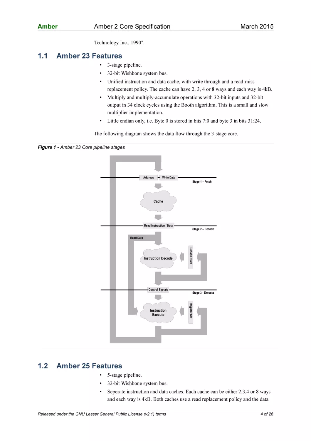
Amber 23 Features
•
3-stage pipeline.
•
32-bit Wishbone system bus.
•
Unified instruction and data cache, with write through and a read-miss
replacement policy. The cache can have 2, 3, 4 or 8 ways and each way is 4kB.
•
Multiply and multiply-accumulate operations with 32-bit inputs and 32-bit
output in 34 clock cycles using the Booth algorithm. This is a small and slow
multiplier implementation.
•
Little endian only, i.e. Byte 0 is stored in bits 7:0 and byte 3 in bits 31:24.
The following diagram shows the data flow through the 3-stage core.
Figure 1 - Amber 23 Core pipeline stages
Address
Write Data
Stage 1 – Fetch
Cache
Read Instruction / Data
Stage 2 – Decode
Read Data
Control Signals
1.2
Stage 3 - Execute
Register Set
Instruction
Execute
Decode State
Instruction Decode
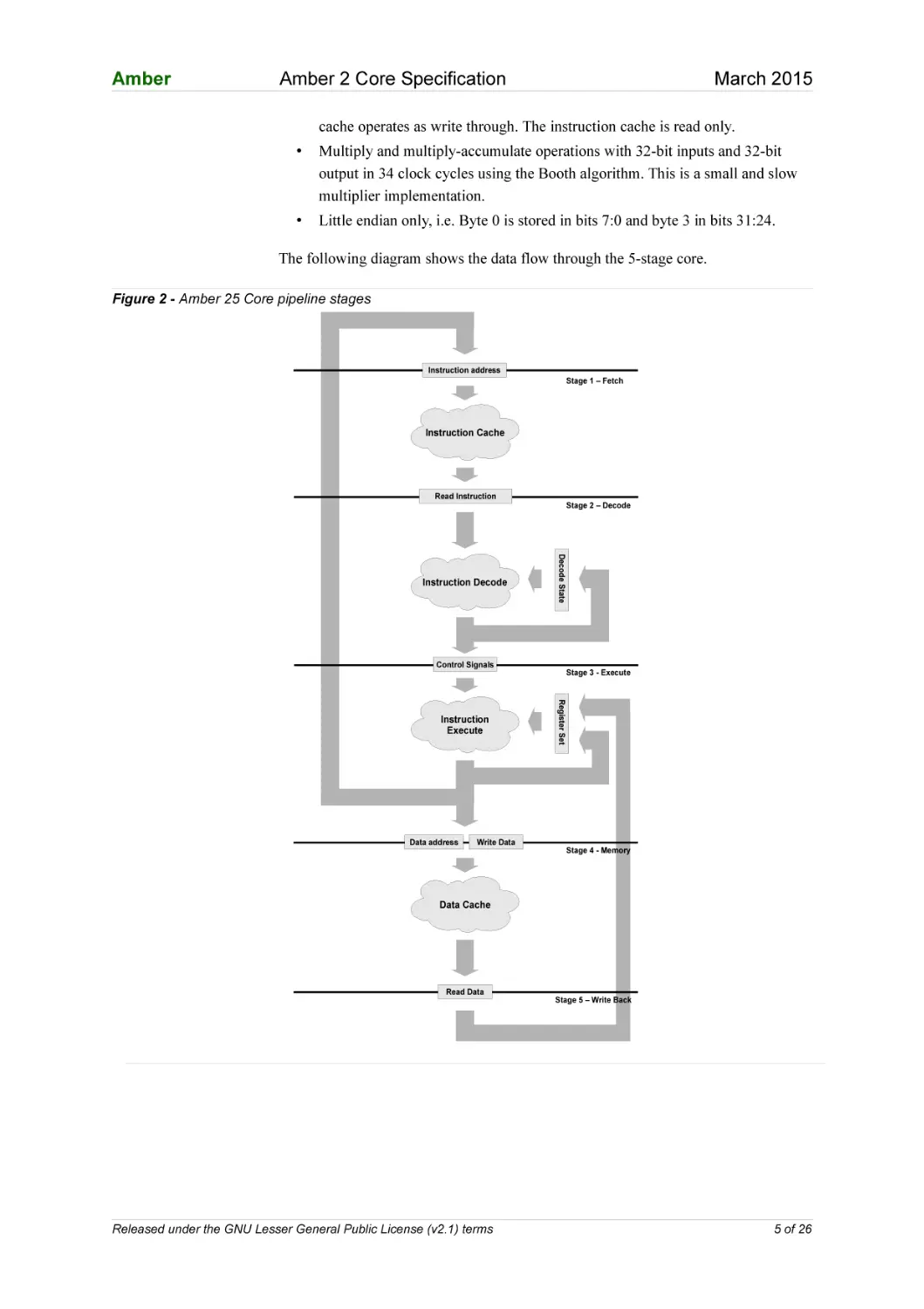
Amber 25 Features
•
5-stage pipeline.
•
32-bit Wishbone system bus.
•
Seperate instruction and data caches. Each cache can be either 2,3,4 or 8 ways
and each way is 4kB. Both caches use a read replacement policy and the data
Released under the GNU Lesser General Public License (v2.1) terms
4 of 26
Amber
Amber 2 Core Specification
March 2015
cache operates as write through. The instruction cache is read only.
•
Multiply and multiply-accumulate operations with 32-bit inputs and 32-bit
output in 34 clock cycles using the Booth algorithm. This is a small and slow
multiplier implementation.
•
Little endian only, i.e. Byte 0 is stored in bits 7:0 and byte 3 in bits 31:24.
The following diagram shows the data flow through the 5-stage core.
Figure 2 - Amber 25 Core pipeline stages
Instruction address
Stage 1 – Fetch
Instruction Cache
Read Instruction
Control Signals
Data address
Write Data
Stage 3 - Execute
Register Set
Instruction
Execute
Decode State
Instruction Decode
Stage 2 – Decode
Stage 4 - Memory
Data Cache
Read Data
Released under the GNU Lesser General Public License (v2.1) terms
Stage 5 – Write Back
5 of 26
Amber
2
Amber 2 Core Specification
March 2015
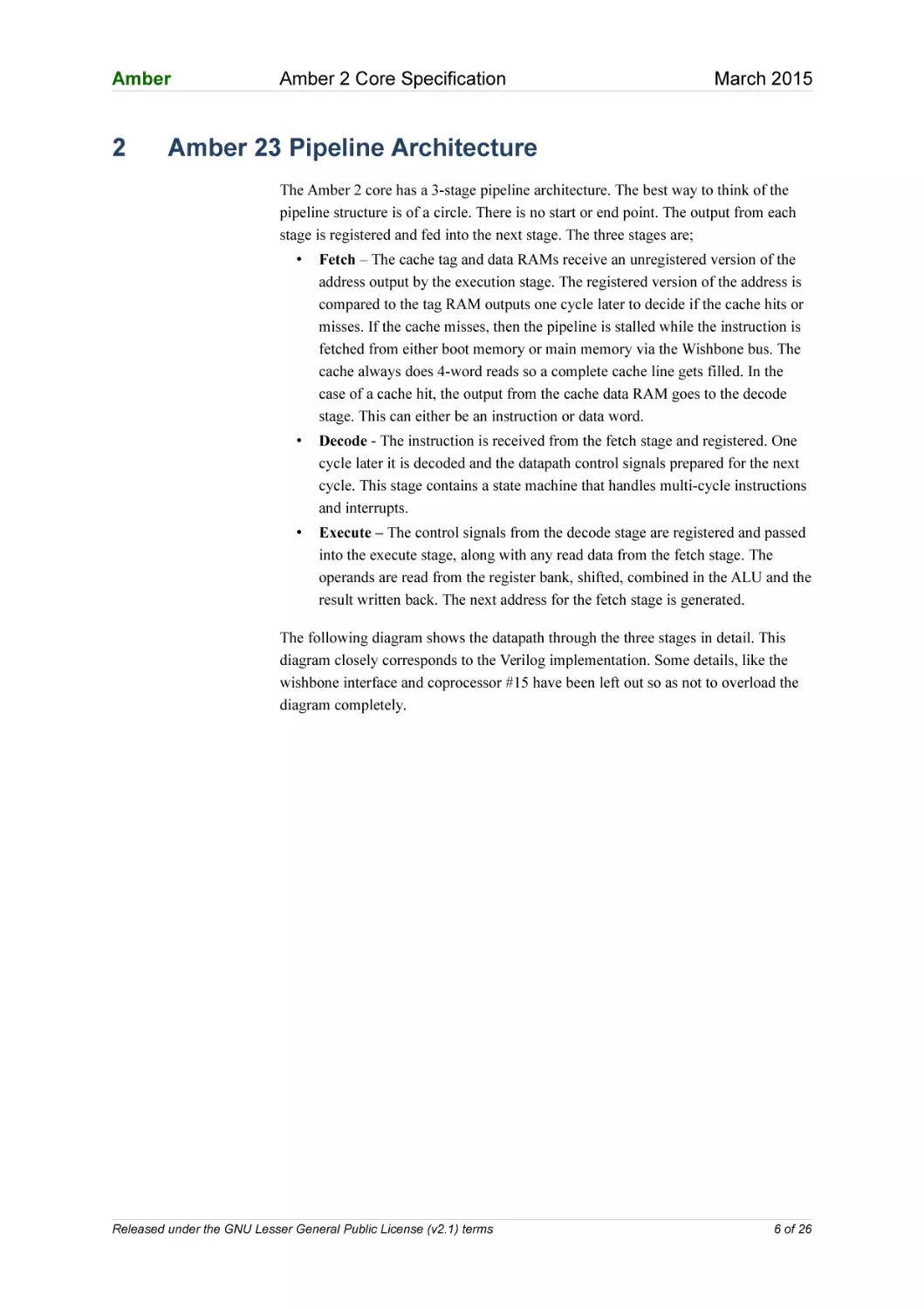
Amber 23 Pipeline Architecture
The Amber 2 core has a 3-stage pipeline architecture. The best way to think of the
pipeline structure is of a circle. There is no start or end point. The output from each
stage is registered and fed into the next stage. The three stages are;
•
Fetch – The cache tag and data RAMs receive an unregistered version of the
address output by the execution stage. The registered version of the address is
compared to the tag RAM outputs one cycle later to decide if the cache hits or
misses. If the cache misses, then the pipeline is stalled while the instruction is
fetched from either boot memory or main memory via the Wishbone bus. The
cache always does 4-word reads so a complete cache line gets filled. In the
case of a cache hit, the output from the cache data RAM goes to the decode
stage. This can either be an instruction or data word.
•
Decode - The instruction is received from the fetch stage and registered. One
cycle later it is decoded and the datapath control signals prepared for the next
cycle. This stage contains a state machine that handles multi-cycle instructions
and interrupts.
•
Execute – The control signals from the decode stage are registered and passed
into the execute stage, along with any read data from the fetch stage. The
operands are read from the register bank, shifted, combined in the ALU and the
result written back. The next address for the fetch stage is generated.
The following diagram shows the datapath through the three stages in detail. This
diagram closely corresponds to the Verilog implementation. Some details, like the
wishbone interface and coprocessor #15 have been left out so as not to overload the
diagram completely.
Released under the GNU Lesser General Public License (v2.1) terms
6 of 26
Amber
Amber 2 Core Specification
March 2015
Figure 3 - Detailed 3-Stage Pipeline Structure
address [31:0]
write_enable
address_nxt [11:4]
Cache State
Address
Miss Address
write_data [31:0]
WData
Address
Cache Tag SRAM
WData
Address
Cache Tag SRAM
WData
Address
Cache Data SRAM
WData
Cache Data SRAM
FETCH
address [31:12]
Way Select
Cache State Machine
Hit?
Hit?
Word Select
Data
Abort
DABT
address [3:2]
Prefetch Address
Abort Exception
PABT
ADEX
Decode State
irq
firq
IRQ
FIRQ
Saved Current Instruction
Read Instruction / Data
read_data [31:0]
DECODE
address [1:0]
Instruction Decode Logic
And
State Machine
Pre-Fetch Instruction
Instruction
Select
{ address[1:0], 3'd0 }
(Used for ldrb Shifts)
instruction [31:0]
(for ldm data aborts)
Base Address
Execute Control Signals
Register Bank
PC
Rm Select
Rd/s Select
Rn Select
rds_sel [3:0]
rn_sel 3:0]
pc
Status Bits
rm_sel [3:0]
rd
rn
rs
rm
copro_read_data
imm_shift_amount [4:0]
imm32 [31:0]
rd
5'h0
pc
Barrel Shift Amount Select
Barrel Shift Data Select
barrel_shift_amount_sel [1:0]
multiply_function [1:0]
barrel_shift_data_sel [1:0]
a_in [31:0] b_in [31:0]
Multiply
flags [1:0]
+4
Barrel Shift
rn
barrel_shift_out
pc_plus4
Interrupt Vector
Select
carry_out
barrel_shift_carry
b_in [31:0]
a_in [31:0]
BL: Save PC-4 to LR
EXECUTE
'0x0000001C'
barrel_shift_function [1:0]
shifter_operand[31:0]
out [31:0]
'0x00000000'
'0x00000004'
'0x00000008'
'0x0000000C'
'0x00000010'
'0x00000014'
'0x00000018'
in [31:0]
shift_amount [4:0]
-4
out [31:0]
alu_function [8:0]
ALU
carry
out [31:0]
flags [3:0]
interrupt_vector_sel [2:0]
interrupt_vector
alu_out
copro_read_data[31:28]
address_nxt [1:0]
4 { rds [7:0] }
Encode Single
Byte Enable
4'hF
+4
+4
+4
Address
Select
Program Counter
Select
address_sel [2:0]
Write Data
Select
Register Write
Select
Status Bits
Select
reg_write_sel [2:0]
pc_sel [1:0]
status_bits_sel [2:0]
Byte Enable
Select
byte_enable_sel
copro_write_data_wen
Coprocessor Write Data
copro_write_data [31:0]
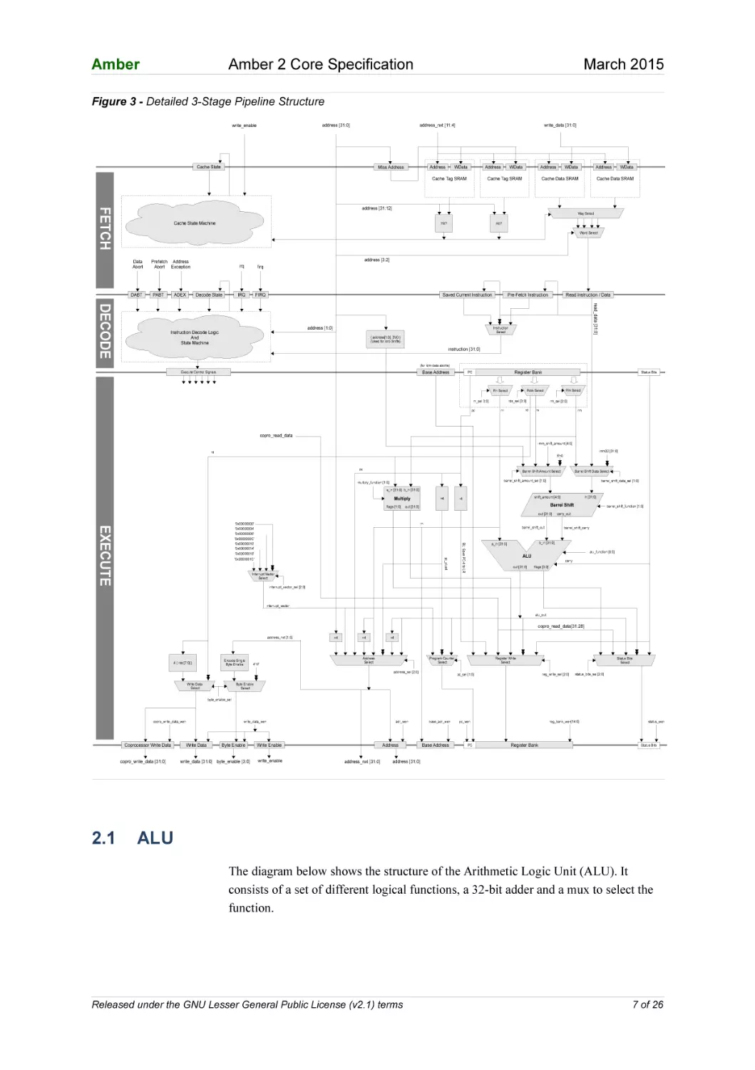
2.1
write_data_wen
Write Data
Byte Enable
write_data [31:0] byte_enable [3:0]
adr_wen
Write Enable
write_enable
Address
address_nxt [31:0]
base_adr_wen
Base Address
pc_wen
PC
reg_bank_wen[14:0]
Register Bank
status_wen
Status Bits
address [31:0]
ALU
The diagram below shows the structure of the Arithmetic Logic Unit (ALU). It
consists of a set of different logical functions, a 32-bit adder and a mux to select the
function.
Released under the GNU Lesser General Public License (v2.1) terms
7 of 26
Amber
Amber 2 Core Specification
March 2015
Figure 4 - ALU Structure
alu_function = { swap_sel, not_sel, cin_sel [1:0], cout_sel, out_sel [2:0] }
a_in [31:0]
b_in [31:0]
cpsr_carry
barrel_shift_carry
B
Select
A
Select
swap_sel
NOT
Not
Select
not_sel
'1'
'0'
Cin
Select
AND
5
OR
4
Zero
Extend 8
XOR
3
2
cin_sel[1:0]
Full
Adder
1
0
overflow
Out Select
out_sel[2:0]
Zero
detect
BE
Encode
be [3:0]
Cout
Select
cout_sel
bit [31]
out [31:0]
n
z
v
c
flags = { n, z, c, v }
The alu_function[6:0] bus in the core is a concatenation of the individual control
signals in the ALU. The following table describes these control signals.
Table 1
2.2
ALU Function Encoding
Field
Function
swap_sel
Swaps the a and b inputs
not_sel
Selects the NOT version of b
cin_sel[1:0]
Selects the carry in to the full added from { c_in, !c_in, 1, 0 }. Note that bs_c_in is the carry_in
from the barrel shifter.
cout_sel
Selects the carry out from { full_adder_cout, barrel_shifter_cout }
out_sel[2:0]
Selects the ALU output from { 0, b_zero_extend_8, b, and_out, or_out, xor_out,
full_adder_out }
Pipeline Operation
2.2.1 Load Example
The load instruction causes the pipeline to stall for two cycles. This section explains
why this is necessary. The following is a simple fragment of assembly code with a
single load instructon with register instructions before and after it.
0
4
8
c
mov
add
ldr
add
r0,
r1,
r4,
r4,
#0x100
r0, #8
[r1]
r4, r0
Released under the GNU Lesser General Public License (v2.1) terms
8 of 26
Amber
Amber 2 Core Specification
March 2015
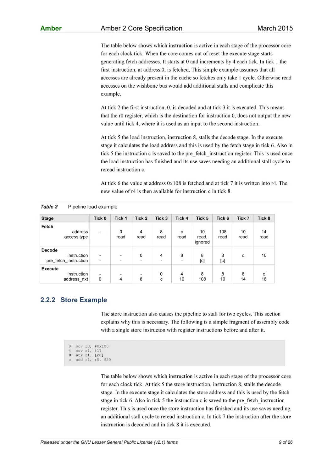
The table below shows which instruction is active in each stage of the processor core
for each clock tick. When the core comes out of reset the execute stage starts
generating fetch addresses. It starts at 0 and increments by 4 each tick. In tick 1 the
first instruction, at address 0, is fetched, This simple example assumes that all
accesses are already present in the cache so fetches only take 1 cycle. Otherwise read
accesses on the wishbone bus would add additional stalls and complicate this
example.
At tick 2 the first instruction, 0, is decoded and at tick 3 it is executed. This means
that the r0 register, which is the destination for instruction 0, does not output the new
value until tick 4, where it is used as an input to the second instruction.
At tick 5 the load instruction, instruction 8, stalls the decode stage. In the execute
stage it calculates the load address and this is used by the fetch stage in tick 6. Also in
tick 5 the instruction c is saved to the pre_fetch_instruction register. This is used once
the load instruction has finished and its use saves needing an additional stall cycle to
reread instruction c.
At tick 6 the value at address 0x108 is fetched and at tick 7 it is written into r4. The
new value of r4 is then available for instruction c in tick 8.
Table 2
Pipeline load example
Stage
Tick 0
Tick 1
Tick 2
Tick 3
Tick 4
Tick 5
Tick 6
Tick 7
Tick 8
address
access type
-
0
read
4
read
8
read
c
read
10
read,
ignored
108
read
10
read
14
read
instruction
pre_fetch_instruction
-
-
0
-
4
-
8
-
8
[c]
8
[c]
c
10
0
4
8
0
c
4
10
8
108
8
10
8
14
c
18
Fetch
Decode
Execute
instruction
address_nxt
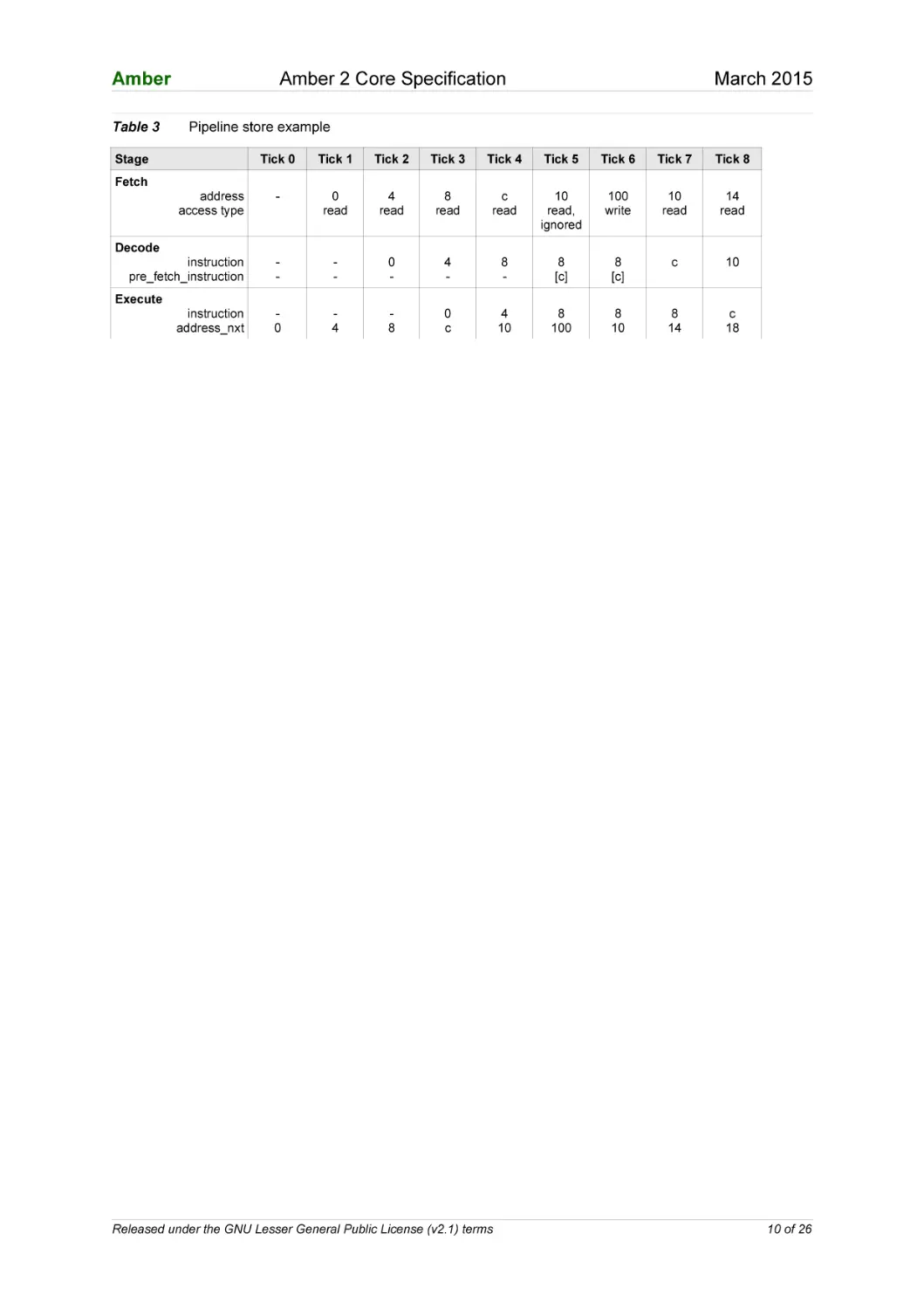
2.2.2 Store Example
The store instruction also causes the pipeline to stall for two cycles. This section
explains why this is necessary. The following is a simple fragment of assembly code
with a single store instructon with register instructions before and after it.
0
4
8
c
mov
mov
str
add
r0,
r1,
r1,
r1,
#0x100
#17
[r0]
r0, #20
The table below shows which instruction is active in each stage of the processor core
for each clock tick. At tick 5 the store instruction, instruction 8, stalls the decode
stage. In the execute stage it calculates the store address and this is used by the fetch
stage in tick 6. Also in tick 5 the instruction c is saved to the pre_fetch_instruction
register. This is used once the store instruction has finished and its use saves needing
an additional stall cycle to reread instruction c. In tick 7 the instruction after the store
instruction is decoded and in tick 8 it is executed.
Released under the GNU Lesser General Public License (v2.1) terms
9 of 26
Amber
Table 3
Amber 2 Core Specification
March 2015
Pipeline store example
Stage
Tick 0
Tick 1
Tick 2
Tick 3
Tick 4
Tick 5
Tick 6
Tick 7
Tick 8
address
access type
-
0
read
4
read
8
read
c
read
10
read,
ignored
100
write
10
read
14
read
instruction
pre_fetch_instruction
-
-
0
-
4
-
8
-
8
[c]
8
[c]
c
10
0
4
8
0
c
4
10
8
100
8
10
8
14
c
18
Fetch
Decode
Execute
instruction
address_nxt
Released under the GNU Lesser General Public License (v2.1) terms
10 of 26
Amber
3
Amber 2 Core Specification
March 2015
Instruction Set
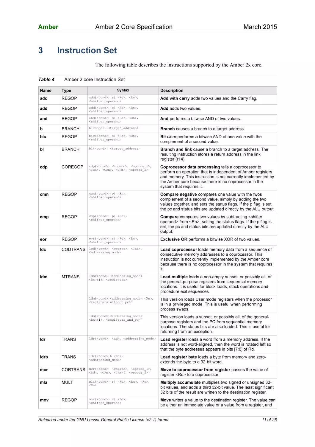
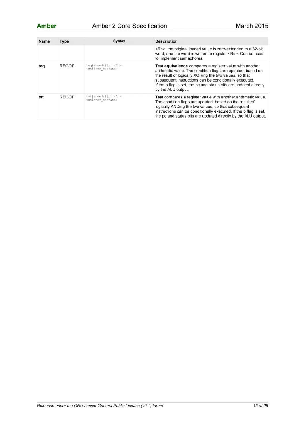
The following table describes the instructions supported by the Amber 2x core.
Table 4
Amber 2 core Instruction Set
Name
Type
adc
REGOP
adc{<cond>}{s} <Rd>, <Rn>,
<shifter_operand>
Add with carry adds two values and the Carry flag.
add
REGOP
add{<cond>}{s} <Rd>, <Rn>,
<shifter_operand>
Add adds two values.
and
REGOP
and{<cond>}{s} <Rd>, <Rn>,
<shifter_operand>
And performs a bitwise AND of two values.
b
BRANCH
b{<cond>} <target_address>
Branch causes a branch to a target address.
bic
REGOP
bic{<cond>}{s} <Rd>, <Rn>,
<shifter_operand>
Bit clear performs a bitwise AND of one value with the
complement of a second value.
bl
BRANCH
bl{<cond>} <target_address>
Branch and link cause a branch to a target address. The
resulting instruction stores a return address in the link
register (r14).
cdp
COREGOP
cdp{<cond>} <coproc>, <opcode_1>,
<CRd>, <CRn>, <CRm>, <opcode_2>
Coprocessor data processing tells a coprocessor to
perform an operation that is independent of Amber registers
and memory. This instruction is not currently implemented by
the Amber core because there is no coprocessor in the
system that requires it.
cmn
REGOP
cmn{<cond>}{p} <Rn>,
<shifter_operand>
Compare negative compares one value with the twos
complement of a second value, simply by adding the two
values together, and sets the status flags. If the p flag is set,
the pc and status bits are updated directly by the ALU output.
cmp
REGOP
cmp{<cond>}{p} <Rn>,
<shifter_operand>
Compare compares two values by subtracting <shifter
operand> from <Rn>, setting the status flags. If the p flag is
set, the pc and status bits are updated directly by the ALU
output.
eor
REGOP
eor{<cond>}{s} <Rd>, <Rn>,
<shifter_operand>
Exclusive OR performs a bitwise XOR of two values.
ldc
CODTRANS
lcd{<cond>} <coproc>, <CRd>,
<addressing_mode>
Load coprocessor loads memory data from a sequence of
consecutive memory addresses to a coprocessor. This
instruction is not currently implemented by the Amber core
because there is no coprocessor in the system that requires
it.
ldm
MTRANS
ldm{<cond>}<addressing_mode>
<Rn>{!}, <registers>
Load multiple loads a non-empty subset, or possibly all, of
the general-purpose registers from sequential memory
locations. It is useful for block loads, stack operations and
procedure exit sequences.
ldm{<cond>}<addressing_mode> <Rn>,
<registers_without_pc>^
This version loads User mode registers when the processor
is in a privileged mode. This is useful when performing
process swaps.
ldm{<cond>}<addressing_mode>
<Rn>{!}, <registers_and_pc>^
This version loads a subset, or possibly all, of the generalpurpose registers and the PC from sequential memory
locations. The status bits are also loaded. This is useful for
returning from an exception.
Syntax
Description
ldr
TRANS
ldr{<cond>} <Rd>, <addressing_mode>
Load register loads a word from a memory address. If the
address is not word-aligned, then the word is rotated left so
that the byte addresses appears in bits [7:0] of Rd.
ldrb
TRANS
ldr{<cond>}b <Rd>,
<addressing_mode>
Load register byte loads a byte from memory and zeroextends the byte to a 32-bit word.
mcr
CORTRANS
mcr{<cond>} <coproc>, <opcode_1>,
<Rd>, <CRn>, <CRm>{, <opcode_2>}
Move to coprocessor from register passes the value of
register <Rd> to a coprocessor.
mla
MULT
mla{<cond>}{s} <Rd>, <Rm>, <Rs>,
<Rn>
Multiply accumulate multiplies two signed or unsigned 32bit values, and adds a third 32-bit value. The least significant
32 bits of the result are written to the destination register.
mov
REGOP
mov{<cond>}{s} <Rd>,
<shifter_operand>
Move writes a value to the destination register. The value can
be either an immediate value or a value from a register, and
Released under the GNU Lesser General Public License (v2.1) terms
11 of 26
Amber
Name
Amber 2 Core Specification
Type
Syntax
March 2015
Description
can be shifted before the write.
mrc
CORTRANS
mrc{<cond>} <coproc>, <opcode_1>,
<Rd>, <CRn>, <CRm>{, <opcode_2>}
mul
MULT
mul{<cond>}{s} <Rd>, <Rm>, <Rs>
Multiply multiplies two signed or unsigned 32-bit values. The
least significant 32 bits of the result are written to the
destination register.
mvn
REGOP
mvn{<cond>}{s} <Rd>,
<shifter_operand>
Move not generates the logical ones complement of a value.
The value can be either an immediate value or a value from a
register, and can be shifted before the MVN operation.
orr
REGOP
orr{<cond>}{s} <Rd>, <Rn>,
<shifter_operand>
Logical OR performs a bitwise OR of two values. The first
value comes from a register. The second value can be either
an immediate value or a value from a register, and can be
shifted before the OR operation.
rsb
REGOP
rsb{<cond>}{s} <Rd>, <Rn>,
<shifter_operand>
Reverse subtract subtracts a value from a second value.
rsc
REGOP
rsc{<cond>}{s} <Rd>, <Rn>,
<shifter_operand>
Reverse subtract with carry subtracts one value from
another, taking account of any borrow from a preceding less
significant subtraction. The normal order of the operands is
reversed, to allow subtraction from a shifted register value, or
from an immediate value.
sbc
REGOP
sbc{<cond>}{s} <Rd>, <Rn>,
<shifter_operand>
Subtract with carry subtracts the value of its second
operand and the value of NOT(Carry flag) from the value of
its first operand. The first operand comes from a register. The
second operand can be either an immediate value or a value
from a register, and can be shifted before the subtraction.
stc
CODTRANS
stc{<cond>} <coproc>, <CRd>,
<addressing_mode>
Store coprocessor stores data from a coprocessor to a
sequence of consecutive memory addresses. This instruction
is not currently implemented by the Amber core because
there is no coprocessor in the system that requires it.
stm
MTRANS
stm{<cond>}<addressing_mode>
<Rn>{!}, <registers>
Store multiple stores a non-empty subset (or possibly all) of
the general-purpose registers to sequential memory
locations. The '!' causes Rn to be updated. The registers are
stored in sequence, the lowest-numbered register to the
lowest memory address (start_address), through to the
highest-numbered register to the highest memory address
(end_address).
STM{<cond>}<addressing_mode> <Rn>,
<registers>^
This version stores a subset (or possibly all) of the User
mode general-purpose registers to sequential memory
locations. The registers are stored in sequence, the lowestnumbered register to the lowest memory address
(start_address), through to the highest-numbered register to
the highest memory address (end_address).
TRANS
str{<cond>} <Rd>, <addressing_mode>
Store register stores a word from a register to memory.
strb
TRANS
str{<cond>}b <Rd>,
<addressing_mode>
Store register byte stores a byte from the least significant
byte of a register to memory.
sub
REGOP
sub{<cond>}{s} <Rd>, <Rn>,
<shifter_operand>
i.e. Rd = Rn - shifter_operand
Subtract subtracts one value from a second value.
swi
SWI
swi{<cond>} <immed_24>
Software interrupt causes a SWI exception. <immed_24> Is
a 24-bit immediate value that is put into bits[23:0] of the
instruction. This value is ignored by the Amber core, but can
be used by an operating system SWI exception handler to
determine what operating system service is being requested.
swp
SWAP
swp{<cond>} <Rd>, <Rm>, [<Rn>]
Swap loads a word from the memory address given
by the value of register <Rn>. The value of register <Rm> is
then stored to the memory address given by the value of
<Rn>, and the original loaded value is written to register
<Rd>. If the same register is specified for <Rd> and <Rm>,
this instruction swaps the value of the register and the value
at the memory address.
swpb
SWAP
swp{<cond>}b <Rd>, <Rm>, [<Rn>]
Swap Byte swaps a byte between registers and memory. It
loads a byte from the memory address given by the value of
register <Rn>. The value of the least significant byte of
register <Rm> is stored to the memory address given by
str
Move to register from coprocessor causes a coprocessor
to transfer a value to an Amber register or to the condition
flags.
Released under the GNU Lesser General Public License (v2.1) terms
12 of 26
Amber
Name
Amber 2 Core Specification
Type
Syntax
March 2015
Description
<Rn>, the original loaded value is zero-extended to a 32-bit
word, and the word is written to register <Rd>. Can be used
to implement semaphores.
teq
REGOP
teq{<cond>}{p} <Rn>,
<shifter_operand>
Test equivalence compares a register value with another
arithmetic value. The condition flags are updated, based on
the result of logically XORing the two values, so that
subsequent instructions can be conditionally executed.
If the p flag is set, the pc and status bits are updated directly
by the ALU output.
tst
REGOP
tst{<cond>}{p} <Rn>,
<shifter_operand>
Test compares a register value with another arithmetic value.
The condition flags are updated, based on the result of
logically ANDing the two values, so that subsequent
instructions can be conditionally executed. If the p flag is set,
the pc and status bits are updated directly by the ALU output.
Released under the GNU Lesser General Public License (v2.1) terms
13 of 26
Amber
4
Amber 2 Core Specification
March 2015
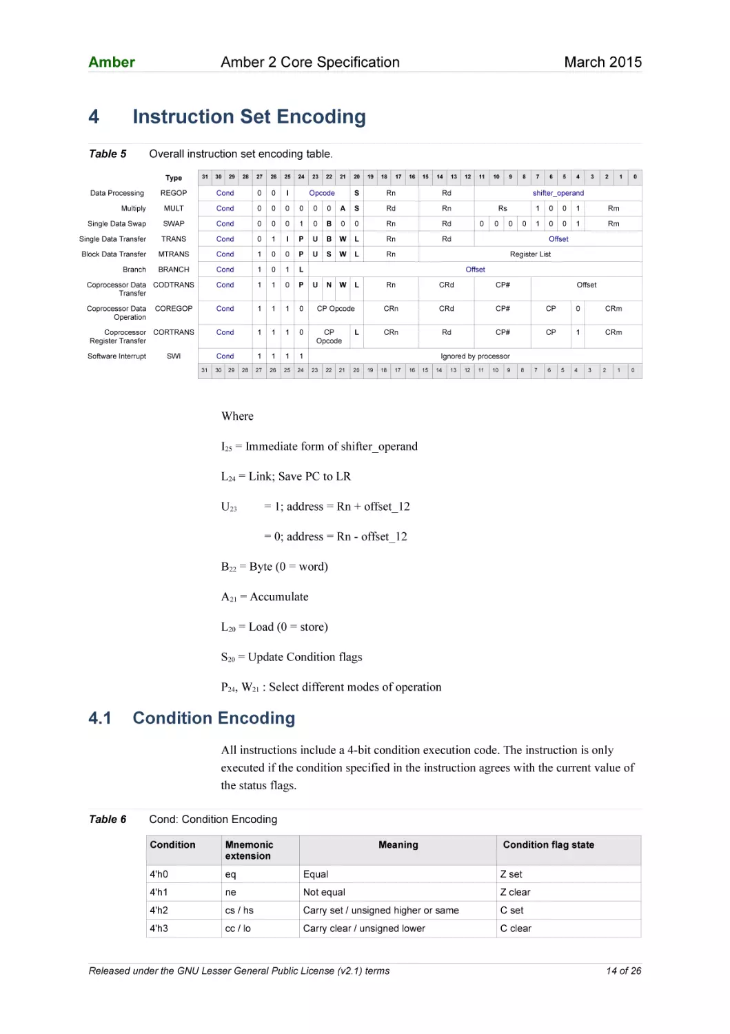
Instruction Set Encoding
Table 5
Overall instruction set encoding table.
27
26
25
REGOP
Cond
0
0
I
MULT
Cond
0
0
0
Type
Data Processing
Multiply
31
30
29
28
24
23
22
21
Opcode
0
0
0
A
20
19
18
17
16
15
14
13
S
Rn
Rd
S
Rd
Rn
Single Data Swap
SWAP
Cond
0
0
0
1
0
B
0
0
Rn
Rd
Single Data Transfer
TRANS
Cond
0
1
I
P
U
B
W
L
Rn
Rd
Block Data Transfer
MTRANS
Cond
1
0
0
P
U
S
W
L
Rn
Branch
BRANCH
Cond
1
0
1
L
Coprocessor Data CODTRANS
Transfer
Cond
1
1
0
P
Coprocessor Data
Operation
COREGOP
Cond
1
1
1
0
Coprocessor CORTRANS
Register Transfer
Cond
1
1
1
0
Software Interrupt
SWI
Cond
31
30
29
28
1
1
1
1
27
26
25
24
12
11
10
9
8
7
6
5
4
3
2
1
0
shifter_operand
Rs
0
0
1
0
0
1
0
0
1
Rm
0
0
1
Rm
Offset
Register List
Offset
U
N
W
L
Rn
CRd
CP#
CP Opcode
CRn
CRd
CP#
CP
0
CRm
CP
Opcode
CRn
Rd
CP#
CP
1
CRm
L
Offset
Ignored by processor
23
22
21
20
19
18
17
16
15
14
13
12
11
10
9
8
7
6
5
4
3
2
1
0
Where
I25 = Immediate form of shifter_operand
L24 = Link; Save PC to LR
U23
= 1; address = Rn + offset_12
= 0; address = Rn - offset_12
B22 = Byte (0 = word)
A21 = Accumulate
L20 = Load (0 = store)
S20 = Update Condition flags
P24, W21 : Select different modes of operation
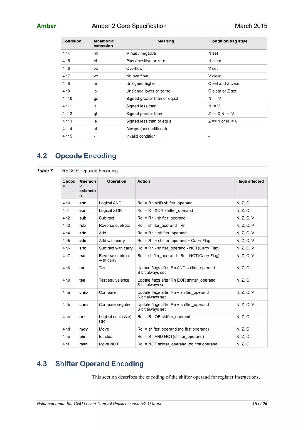
4.1
Condition Encoding
All instructions include a 4-bit condition execution code. The instruction is only
executed if the condition specified in the instruction agrees with the current value of
the status flags.
Table 6
Cond: Condition Encoding
Condition
Mnemonic
extension
Meaning
4'h0
eq
Equal
Z set
4'h1
ne
Not equal
Z clear
4'h2
cs / hs
Carry set / unsigned higher or same
C set
4'h3
cc / lo
Carry clear / unsigned lower
C clear
Released under the GNU Lesser General Public License (v2.1) terms
Condition flag state
14 of 26
Amber
4.2
Table 7
Amber 2 Core Specification
Condition
Mnemonic
extension
4'h4
mi
Minus / negative
N set
4'h5
pl
Plus / positive or zero
N clear
4'h6
vs
Overflow
V set
4'h7
vc
No overflow
V clear
4'h8
hi
Unsigned higher
C set and Z clear
4'h9
ls
Unsigned lower or same
C clear or Z set
4'h10
ge
Signed greater than or equal
N == V
4'h11
lt
Signed less than
N != V
4'h12
gt
Signed greater than
Z == 0,N == V
4'h13
le
Signed less than or equal
Z == 1 or N != V
4'h14
al
Always (unconditional)
-
4'h15
-
Invalid condition
-
Meaning
Condition flag state
Opcode Encoding
REGOP: Opcode Encoding
Opcod Mnemon
e
ic
extensio
n
4.3
March 2015
Operation
Action
Flags affected
4'h0
and
Logical AND
Rd := Rn AND shifter_operand
N, Z, C
4'h1
eor
Logical XOR
Rd := Rn XOR shifter_operand
N, Z, C
4'h2
sub
Subtract
Rd := Rn - shifter_operand
N, Z, C, V
4'h3
rsb
Reverse subtract
Rd := shifter_operand - Rn
N, Z, C, V
4'h4
add
Add
Rd := Rn + shifter_operand
N, Z, C, V
4'h5
adc
Add with carry
Rd := Rn + shifter_operand + Carry Flag
N, Z, C, V
4'h6
sbc
Subtract with carry
Rd := Rn - shifter_operand - NOT(Carry Flag)
N, Z, C, V
4'h7
rsc
Reverse subtract
with carry
Rd := shifter_operand - Rn - NOT(Carry Flag)
N, Z, C, V
4'h8
tst
Test
Update flags after Rn AND shifter_operand
S bit always set
N, Z, C
4'h9
teq
Test equivalence
Update flags after Rn EOR shifter_operand
S bit always set
N, Z, C
4'ha
cmp
Compare
Update flags after Rn – shifter_operand
S bit always set
N, Z, C, V
4'hb
cmn
Compare negated
Update flags after Rn + shifter_operand
S bit always set
N, Z, C, V
4'hc
orr
Logical (inclusive)
OR
Rd := Rn OR shifter_operand
N, Z, C
4'hd
mov
Move
Rd := shifter_operand (no first operand)
N, Z, C
4'he
bic
Bit clear
Rd := Rn AND NOT(shifter_operand)
N, Z, C
4'hf
mvn
Move NOT
Rd := NOT shifter_operand (no first operand)
N, Z, C
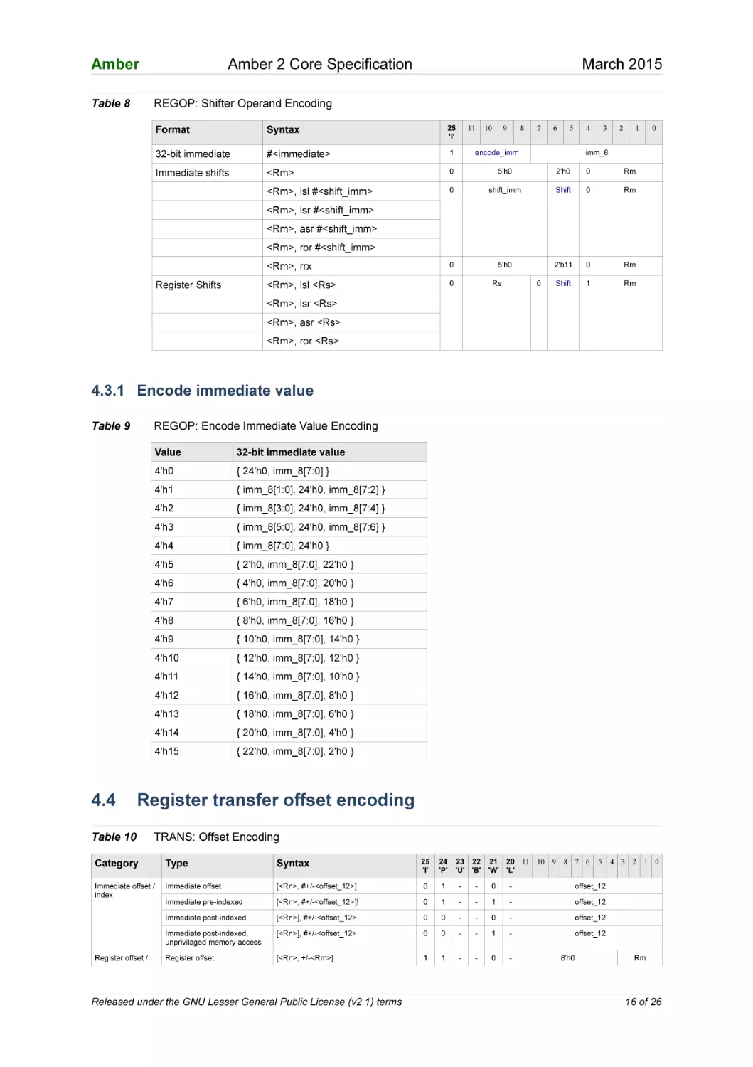
Shifter Operand Encoding
This section describes the encoding of the shifter operand for register instructions.
Released under the GNU Lesser General Public License (v2.1) terms
15 of 26
Amber
Table 8
Amber 2 Core Specification
March 2015
REGOP: Shifter Operand Encoding
Format
Syntax
25
'I'
32-bit immediate
#<immediate>
1
Immediate shifts
<Rm>
0
5'h0
2'h0
0
Rm
<Rm>, lsl #<shift_imm>
0
shift_imm
Shift
0
Rm
<Rm>, rrx
0
5'h0
2'b11
0
Rm
<Rm>, lsl <Rs>
0
Shift
1
Rm
11
10
9
8
7
6
5
4
encode_imm
3
2
1
0
imm_8
<Rm>, lsr #<shift_imm>
<Rm>, asr #<shift_imm>
<Rm>, ror #<shift_imm>
Register Shifts
Rs
0
<Rm>, lsr <Rs>
<Rm>, asr <Rs>
<Rm>, ror <Rs>
4.3.1 Encode immediate value
Table 9
4.4
REGOP: Encode Immediate Value Encoding
Value
32-bit immediate value
4'h0
{ 24'h0, imm_8[7:0] }
4'h1
{ imm_8[1:0], 24'h0, imm_8[7:2] }
4'h2
{ imm_8[3:0], 24'h0, imm_8[7:4] }
4'h3
{ imm_8[5:0], 24'h0, imm_8[7:6] }
4'h4
{ imm_8[7:0], 24'h0 }
4'h5
{ 2'h0, imm_8[7:0], 22'h0 }
4'h6
{ 4'h0, imm_8[7:0], 20'h0 }
4'h7
{ 6'h0, imm_8[7:0], 18'h0 }
4'h8
{ 8'h0, imm_8[7:0], 16'h0 }
4'h9
{ 10'h0, imm_8[7:0], 14'h0 }
4'h10
{ 12'h0, imm_8[7:0], 12'h0 }
4'h11
{ 14'h0, imm_8[7:0], 10'h0 }
4'h12
{ 16'h0, imm_8[7:0], 8'h0 }
4'h13
{ 18'h0, imm_8[7:0], 6'h0 }
4'h14
{ 20'h0, imm_8[7:0], 4'h0 }
4'h15
{ 22'h0, imm_8[7:0], 2'h0 }
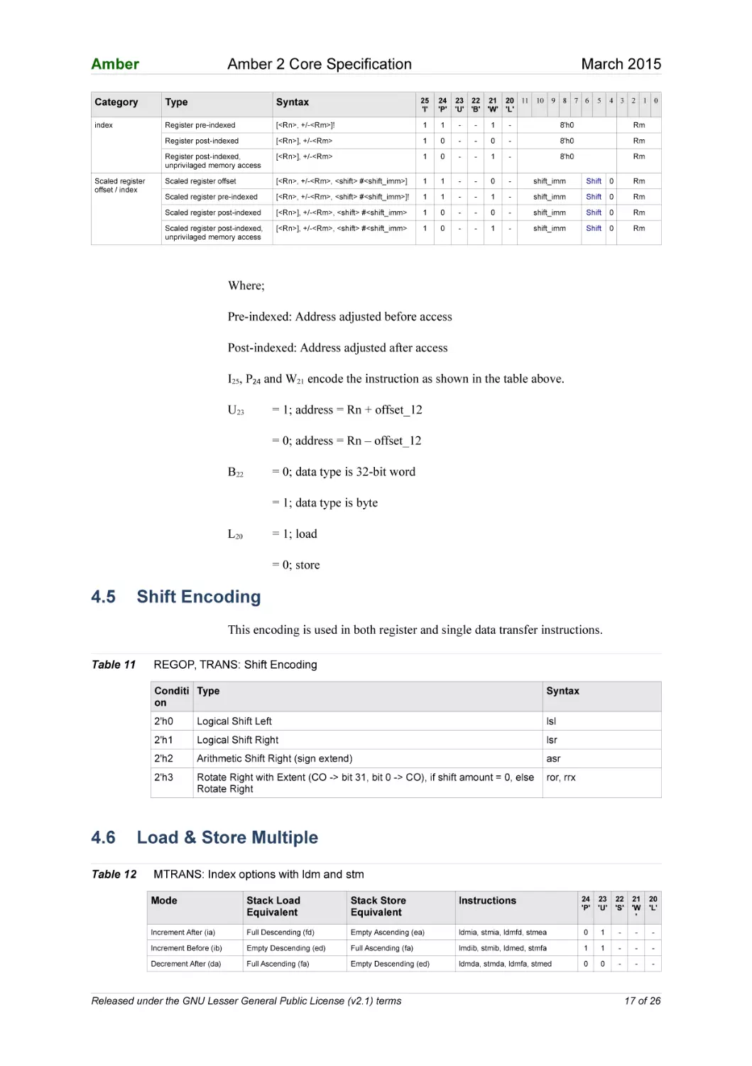
Register transfer offset encoding
Table 10
TRANS: Offset Encoding
Category
Type
Syntax
25
'I'
24
'P'
Immediate offset /
index
Immediate offset
[<Rn>, #+/-<offset_12>]
0
1
-
-
0
-
offset_12
Immediate pre-indexed
[<Rn>, #+/-<offset_12>]!
0
1
-
-
1
-
offset_12
Immediate post-indexed
[<Rn>], #+/-<offset_12>
0
0
-
-
0
-
offset_12
Immediate post-indexed,
unprivilaged memory access
[<Rn>], #+/-<offset_12>
0
0
-
-
1
-
offset_12
Register offset
[<Rn>, +/-<Rm>]
1
1
-
-
0
-
Register offset /
Released under the GNU Lesser General Public License (v2.1) terms
23 22 21 20 11 10
'U' 'B' 'W' 'L'
9
8
7 6
8'h0
5
4 3
2
1 0
Rm
16 of 26
Amber
Amber 2 Core Specification
March 2015
23 22 21 20 11 10
'U' 'B' 'W' 'L'
9
8
7 6
5
4 3
2
1 0
Category
Type
Syntax
25
'I'
24
'P'
index
Register pre-indexed
[<Rn>, +/-<Rm>]!
1
1
-
-
1
-
8'h0
Rm
Register post-indexed
[<Rn>], +/-<Rm>
1
0
-
-
0
-
8'h0
Rm
Register post-indexed,
unprivilaged memory access
[<Rn>], +/-<Rm>
1
0
-
-
1
-
8'h0
Rm
Scaled register offset
[<Rn>, +/-<Rm>, <shift> #<shift_imm>]
1
1
-
-
0
-
shift_imm
Shift
0
Rm
Scaled register pre-indexed
[<Rn>, +/-<Rm>, <shift> #<shift_imm>]!
1
1
-
-
1
-
shift_imm
Shift
0
Rm
Scaled register post-indexed
[<Rn>], +/-<Rm>, <shift> #<shift_imm>
1
0
-
-
0
-
shift_imm
Shift
0
Rm
Scaled register post-indexed,
unprivilaged memory access
[<Rn>], +/-<Rm>, <shift> #<shift_imm>
1
0
-
-
1
-
shift_imm
Shift
0
Rm
Scaled register
offset / index
Where;
Pre-indexed: Address adjusted before access
Post-indexed: Address adjusted after access
I25, P24 and W21 encode the instruction as shown in the table above.
U23
= 1; address = Rn + offset_12
= 0; address = Rn – offset_12
B22
= 0; data type is 32-bit word
= 1; data type is byte
L20
= 1; load
= 0; store
4.5
Shift Encoding
This encoding is used in both register and single data transfer instructions.
Table 11
4.6
Table 12
REGOP, TRANS: Shift Encoding
Conditi Type
on
Syntax
2'h0
Logical Shift Left
lsl
2'h1
Logical Shift Right
lsr
2'h2
Arithmetic Shift Right (sign extend)
asr
2'h3
Rotate Right with Extent (CO -> bit 31, bit 0 -> CO), if shift amount = 0, else
Rotate Right
ror, rrx
Load & Store Multiple
MTRANS: Index options with ldm and stm
Mode
Stack Load
Equivalent
Stack Store
Equivalent
Instructions
24
'P'
23
'U'
22
'S'
21
'W
'
20
'L'
Increment After (ia)
Full Descending (fd)
Empty Ascending (ea)
ldmia, stmia, ldmfd, stmea
0
1
-
-
-
Increment Before (ib)
Empty Descending (ed)
Full Ascending (fa)
lmdib, stmib, ldmed, stmfa
1
1
-
-
-
Decrement After (da)
Full Ascending (fa)
Empty Descending (ed)
ldmda, stmda, ldmfa, stmed
0
0
-
-
-
Released under the GNU Lesser General Public License (v2.1) terms
17 of 26
Amber
Amber 2 Core Specification
March 2015
Mode
Stack Load
Equivalent
Stack Store
Equivalent
Instructions
24
'P'
23
'U'
22
'S'
21
'W
'
20
'L'
Decrement Before (db)
Empty Ascending (ea)
Full Descending (fd)
lmddb, stmdb, ldmea, stmfd
1
0
-
-
-
S22
The S bit for ldm that loads the PC, the S bit indicates that the status bits loaded. For
ldm instructions that do not load the PC and all stm instructions, the S bit indicates
that when the processor is in a privileged mode, the User mode banked registers are
transferred instead of the registers of the current mode. Ldm with the S bit set is
unpredictable in User mode.
W21
Indicates that the base register is updated after the transfer.
L20
Distinguishes between Load (L==1) and Store (L==0) instructions.
4.7
Branch offset
Branch instructions contain an offset in the lower 24 bits of the instruction. This
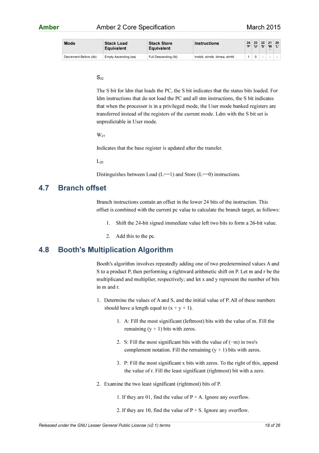
offset is combined with the current pc value to calculate the branch target, as follows:
4.8
1.
Shift the 24-bit signed immediate value left two bits to form a 26-bit value.
2.
Add this to the pc.
Booth's Multiplication Algorithm
Booth's algorithm involves repeatedly adding one of two predetermined values A and
S to a product P, then performing a rightward arithmetic shift on P. Let m and r be the
multiplicand and multiplier, respectively; and let x and y represent the number of bits
in m and r.
1. Determine the values of A and S, and the initial value of P. All of these numbers
should have a length equal to (x + y + 1).
1. A: Fill the most significant (leftmost) bits with the value of m. Fill the
remaining (y + 1) bits with zeros.
2. S: Fill the most significant bits with the value of (−m) in two's
complement notation. Fill the remaining (y + 1) bits with zeros.
3. P: Fill the most significant x bits with zeros. To the right of this, append
the value of r. Fill the least significant (rightmost) bit with a zero.
2. Examine the two least significant (rightmost) bits of P.
1. If they are 01, find the value of P + A. Ignore any overflow.
2. If they are 10, find the value of P + S. Ignore any overflow.
Released under the GNU Lesser General Public License (v2.1) terms
18 of 26
Amber
Amber 2 Core Specification
March 2015
3. If they are 00, do nothing. Use P directly in the next step.
4. If they are 11, do nothing. Use P directly in the next step.
3. Arithmetically shift the value obtained in the 2nd step by a single place to the
right. Let P now equal this new value.
4. Repeat steps 2 and 3 until they have been done y times.
5. Drop the least significant (rightmost) bit from P. This is the product of m and r.
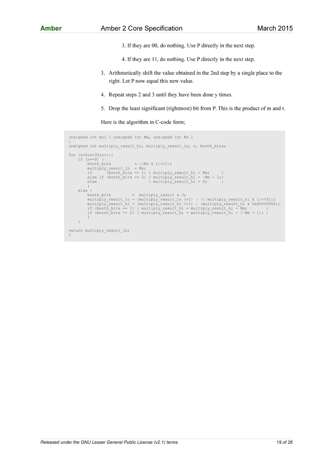
Here is the algorithm in C-code form;
unsigned int mul ( unsigned int Rm, unsigned int Rs )
{
unsigned int multiply_result_hi, multiply_result_lo, n, booth_bits;
for (n=0;n<33;n++){
if (n==0) {
booth_bits
= ((Rs & 1)<<1);
multiply_result_lo = Rs;
if
(booth_bits == 1) { multiply_result_hi = Rm;
}
else if (booth_bits == 2) { multiply_result_hi = ~Rm + 1;}
else
{ multiply_result_hi = 0;
}
}
else {
booth_bits
= multiply_result & 3;
multiply_result_lo = (multiply_result_lo >>1) | (( multiply_result_hi & 1)<<31);
multiply_result_hi = (multiply_result_hi >>1) | (multiply_result_hi & 0x80000000);
if (booth_bits == 1) { multiply_result_hi = multiply_result_hi + Rm;
}
if (booth_bits == 2) { multiply_result_hi = multiply_result_hi + (~Rm + 1); }
}
}
return multiply_result_lo;
}
Released under the GNU Lesser General Public License (v2.1) terms
19 of 26
Amber
5
Amber 2 Core Specification
March 2015
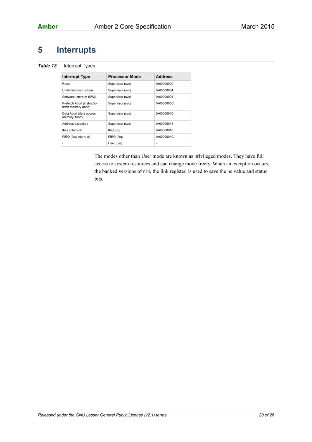
Interrupts
Table 13
Interrupt Types
Interrupt Type
Processor Mode
Address
Reset
Supervisor (svc)
0x00000000
Undefined Instructions
Supervisor (svc)
0x00000004
Software Interrupt (SWI)
Supervisor (svc)
0x00000008
Prefetch Abort (instruction
fetch memory abort)
Supervisor (svc)
0x0000000C
Data Abort (data access
memory abort)
Supervisor (svc)
0x00000010
Address exception
Supervisor (svc)
0x00000014
IRQ (interrupt)
IRQ (irq)
0x00000018
FIRQ (fast interrupt)
FIRQ (firq)
0x0000001C
-
User (usr)
-
The modes other than User mode are known as privileged modes. They have full
access to system resources and can change mode freely. When an exception occurs,
the banked versions of r14, the link register, is used to save the pc value and status
bits.
Released under the GNU Lesser General Public License (v2.1) terms
20 of 26
Amber
6
Amber 2 Core Specification
March 2015
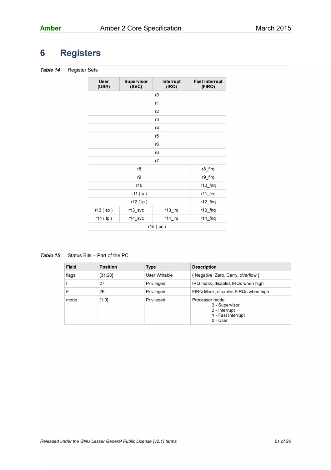
Registers
Table 14
Register Sets
User
(USR)
Supervisor
(SVC)
Interrupt
(IRQ)
Fast Interrupt
(FIRQ)
r0
r1
r2
r3
r4
r5
r6
r6
r7
r8
r8_firq
r9
r9_firq
r10
r10_firq
r11 (fp )
r11_firq
r12 ( ip )
r12_firq
r13 ( sp )
r13_svc
r13_irq
r13_firq
r14 ( lp )
r14_svc
r14_irq
r14_firq
r15 ( pc )
Table 15
Status Bits – Part of the PC
Field
Position
Type
Description
flags
[31:28]
User Writable
{ Negative, Zero, Carry, oVerflow }
I
27
Privileged
IRQ mask, disables IRQs when high
F
26
Privileged
FIRQ Mask, disables FIRQs when high
mode
[1:0]
Privileged
Processor mode
3 - Supervisor
2 - Interrupt
1 - Fast Interrupt
0 - User
Released under the GNU Lesser General Public License (v2.1) terms
21 of 26
Amber
7
Amber 2 Core Specification
March 2015
Cache
The Amber cache size is optimized to use FPGA Block RAMs. Each way has 256
lines of 16 bytes. 256 lines x 16 bytes x 2 ways = 8k bytes. The address tag is 20 bits.
Each cache can be configured with either 2, 3, 4 or 8 ways.
Table 16
Cache Specification
Ways
2
3
4
8
Lines per way
256
256
256
256
Words per line
4
4
4
4
Total words
2048
3072
4096
8192
Total bytes
8192
12288
16384
32768
FPGA 9K Block RAMs
8 + 2 = 10
12 + 3 = 15
16 + 4 = 20
32 + 8 = 40
Released under the GNU Lesser General Public License (v2.1) terms
22 of 26
Amber
8
Amber 2 Core Specification
March 2015
Amber Project
The Amber project is a complete processor system implemented on an FPGA
development board. The purpose of the project is to provide an evironment that gives
an example usage of the Amber 2 core, and supports a set of tests that verify the
correct functionality of the code. This is especially important if modificatiosn to the
core are made.
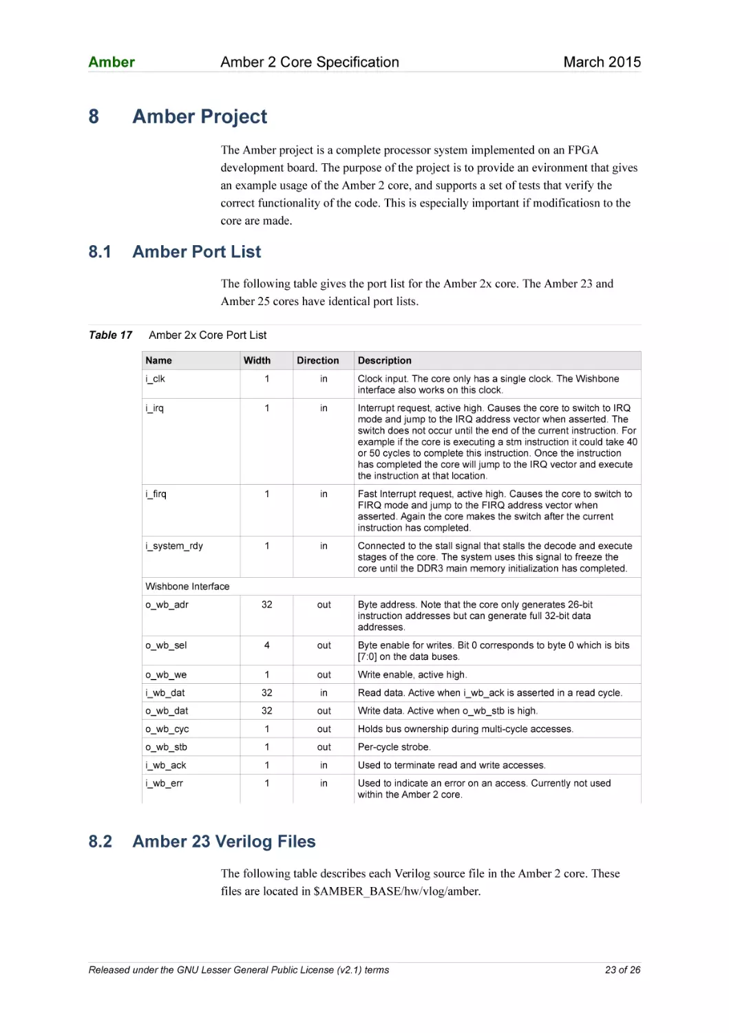
8.1
Amber Port List
The following table gives the port list for the Amber 2x core. The Amber 23 and
Amber 25 cores have identical port lists.
Table 17
Amber 2x Core Port List
Name
Width
Direction
Description
i_clk
1
in
Clock input. The core only has a single clock. The Wishbone
interface also works on this clock.
i_irq
1
in
Interrupt request, active high. Causes the core to switch to IRQ
mode and jump to the IRQ address vector when asserted. The
switch does not occur until the end of the current instruction. For
example if the core is executing a stm instruction it could take 40
or 50 cycles to complete this instruction. Once the instruction
has completed the core will jump to the IRQ vector and execute
the instruction at that location.
i_firq
1
in
Fast Interrupt request, active high. Causes the core to switch to
FIRQ mode and jump to the FIRQ address vector when
asserted. Again the core makes the switch after the current
instruction has completed.
i_system_rdy
1
in
Connected to the stall signal that stalls the decode and execute
stages of the core. The system uses this signal to freeze the
core until the DDR3 main memory initialization has completed.
o_wb_adr
32
out
Byte address. Note that the core only generates 26-bit
instruction addresses but can generate full 32-bit data
addresses.
o_wb_sel
4
out
Byte enable for writes. Bit 0 corresponds to byte 0 which is bits
[7:0] on the data buses.
o_wb_we
1
out
Write enable, active high.
i_wb_dat
32
in
o_wb_dat
32
out
Write data. Active when o_wb_stb is high.
o_wb_cyc
1
out
Holds bus ownership during multi-cycle accesses.
o_wb_stb
1
out
Per-cycle strobe.
i_wb_ack
1
in
Used to terminate read and write accesses.
i_wb_err
1
in
Used to indicate an error on an access. Currently not used
within the Amber 2 core.
Wishbone Interface
8.2
Read data. Active when i_wb_ack is asserted in a read cycle.
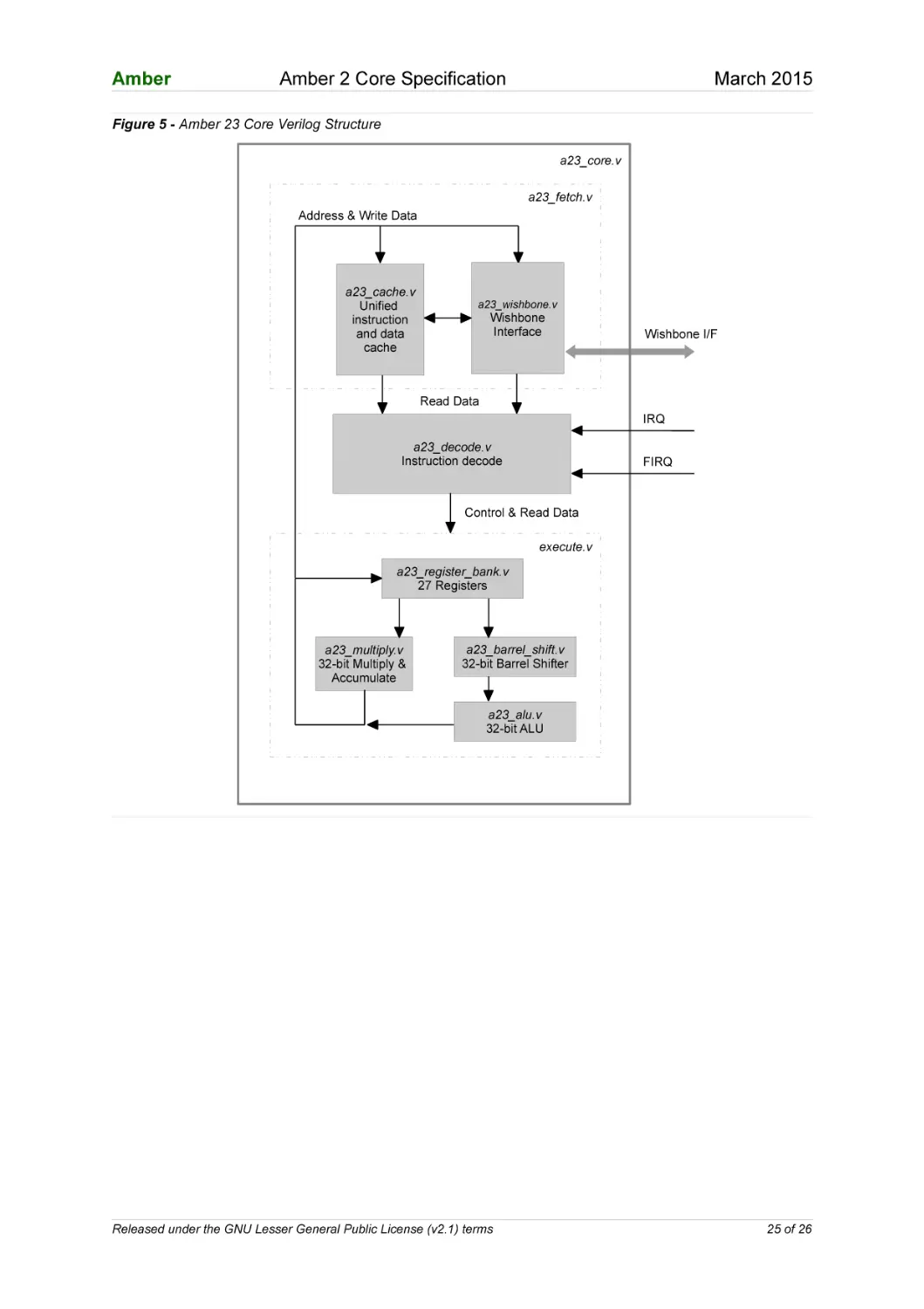
Amber 23 Verilog Files
The following table describes each Verilog source file in the Amber 2 core. These
files are located in $AMBER_BASE/hw/vlog/amber.
Released under the GNU Lesser General Public License (v2.1) terms
23 of 26
Amber
Table 18
Amber 2 Core Specification
March 2015
Amber 23 Core Source Files
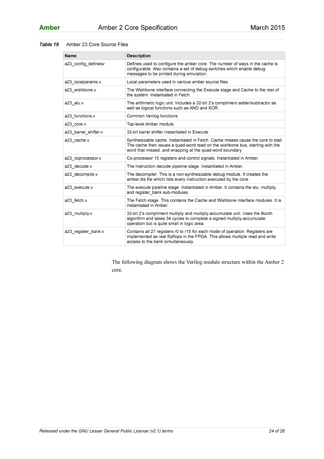
Name
Description
a23_config_definesv
Defines used to configure the amber core. The number of ways in the cache is
configurable. Also contains a set of debug switches which enable debug
messages to be printed during simulation.
a23_localparams.v
Local parameters used in various amber source files.
a23_wishbone.v
The Wishbone interface connecting the Execute stage and Cache to the rest of
the system. Instantiated in Fetch.
a23_alu.v
The arithmetic logic unit. Includes a 32-bit 2's compliment adder/subtractor as
well as logical functions such as AND and XOR.
a23_functions.v
Common Verilog functions.
a23_core.v
Top-level Amber module.
a23_barrel_shifter.v
32-bit barrel shifter instantiated in Execute.
a23_cache.v
Synthesizable cache. Instantiated in Fetch. Cache misses cause the core to stall.
The cache then issues a quad-word read on the wishbone bus, starting with the
word that missed, and wrapping at the quad-word boundary.
a23_coprocessor.v
Co-processor 15 registers and control signals. Instantiated in Amber.
a23_decode.v
The instruction decode pipeline stage. Instantiated in Amber.
a23_decompile.v
The decompiler. This is a non-synthesizable debug module. It creates the
amber.dis file which lists every instruction executed by the core.
a23_execute.v
The execute pipeline stage. Instantiated in Amber. It contains the alu, multiply,
and register_bank sub-modules.
a23_fetch.v
The Fetch stage. This contains the Cache and Wishbone interface modules. It is
instantiated in Amber.
a23_multiply.v
32-bit 2's compliment multiply and multiply-accumulate unit. Uses the Booth
algorithm and takes 34 cycles to complete a signed multiply-accumulate
operation but is quite small in logic area.
a23_register_bank.v
Contains all 27 registers r0 to r15 for each mode of operation. Registers are
implemented as real flipflops in the FPGA. This allows multiple read and write
access to the bank simultaneously.
The following diagram shows the Verilog module structure within the Amber 2
core.
Released under the GNU Lesser General Public License (v2.1) terms
24 of 26
Amber
Amber 2 Core Specification
March 2015
Figure 5 - Amber 23 Core Verilog Structure
a23_core.v
a23_fetch.v
Address & Write Data
a23_cache.v
Unified
instruction
and data
cache
a23_wishbone.v
Wishbone
Interface
Wishbone I/F
Read Data
IRQ
a23_decode.v
Instruction decode
FIRQ
Control & Read Data
execute.v
a23_register_bank.v
27 Registers
a23_multiply.v
32-bit Multiply &
Accumulate
a23_barrel_shift.v
32-bit Barrel Shifter
a23_alu.v
32-bit ALU
Released under the GNU Lesser General Public License (v2.1) terms
25 of 26
Amber
9
Amber 2 Core Specification
March 2015
License
All source code provided in the Amber package is release under the following license
terms;
Copyright (C) 2010 Authors and OPENCORES.ORG
This source file may be used and distributed without
restriction provided that this copyright statement is not
removed from the file and that any derivative work contains
the original copyright notice and the associated disclaimer.
This source file is free software; you can redistribute it
and/or modify it under the terms of the GNU Lesser General
Public License as published by the Free Software Foundation;
either version 2.1 of the License, or (at your option) any
later version.
This source is distributed in the hope that it will be
useful, but WITHOUT ANY WARRANTY; without even the implied
warranty of MERCHANTABILITY or FITNESS FOR A PARTICULAR
PURPOSE. See the GNU Lesser General Public License for more
details.
You should have received a copy of the GNU Lesser General
Public License along with this source; if not, download it
from http://www.opencores.org/lgpl.shtml
Author(s):
- Conor Santifort, csantifort.amber@gmail.com
Released under the GNU Lesser General Public License (v2.1) terms
26 of 26