/


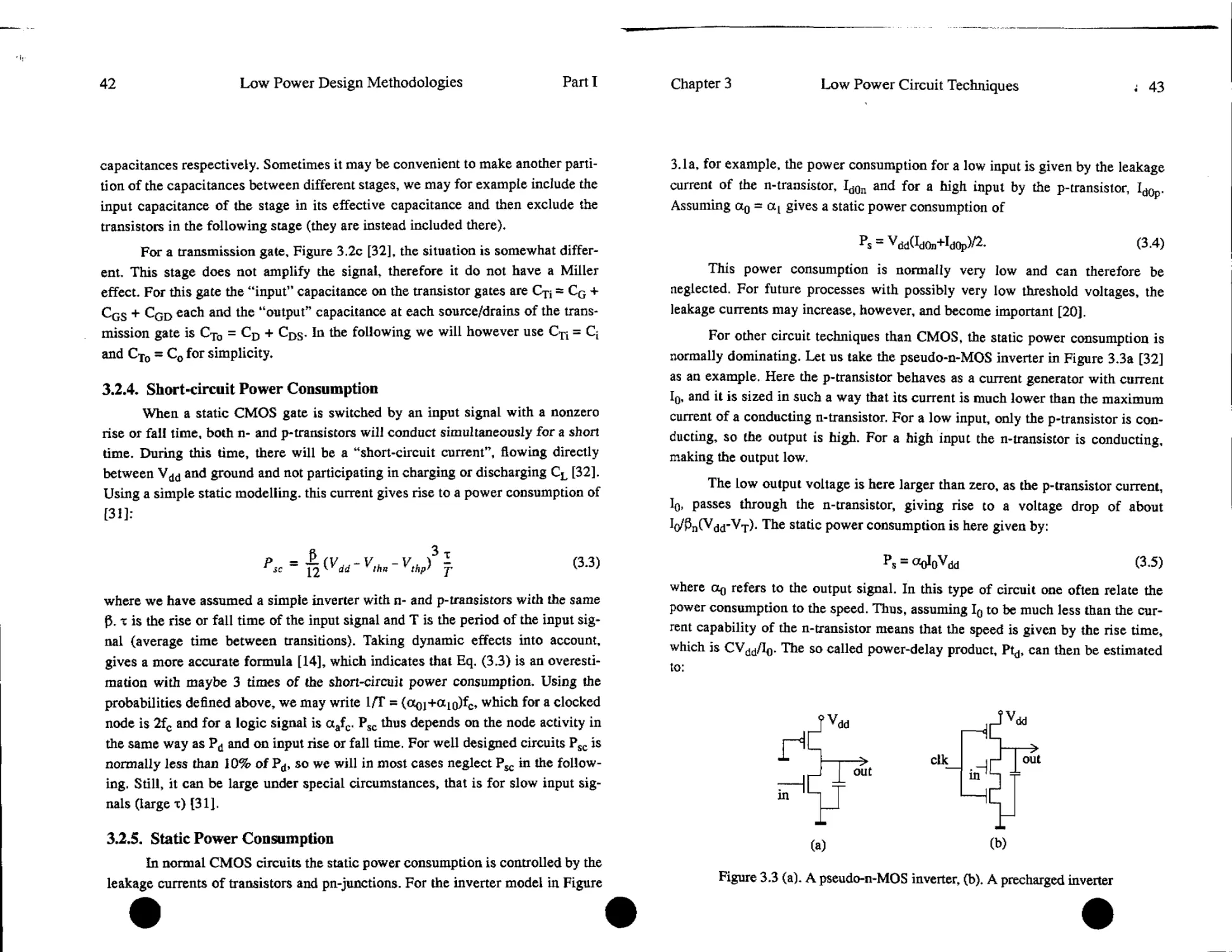

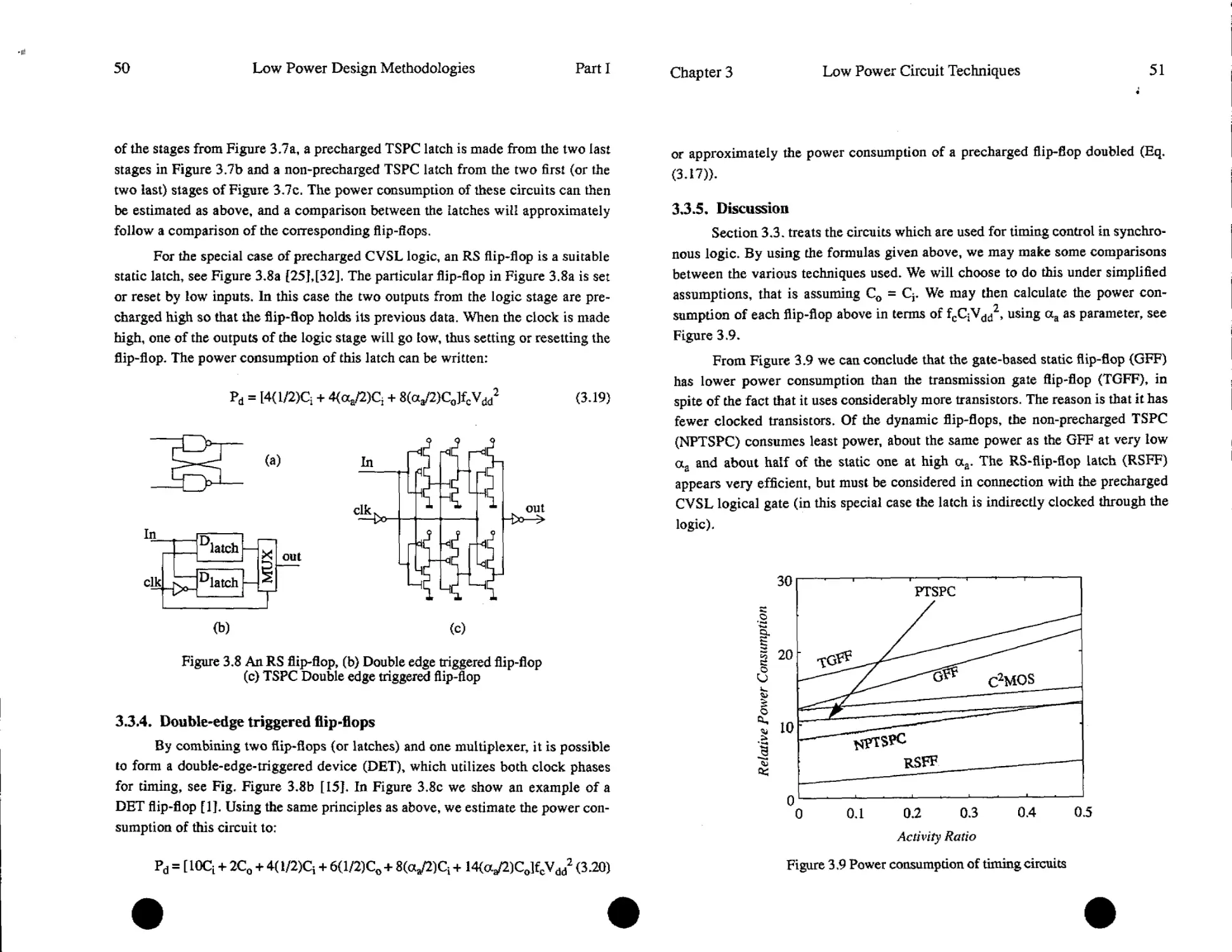


Text
LOW POWER DESIGN
METHODOLOGIES
edited by
Jan M. Rabaey
University California
////. Л /I.
and
Massoud Pedram
University of Southern California
KLUWER ACADEMIC PUBLISHERS
Boston / Dordrecht / London
Distributors for North America:
Kluwer Academic Publishers
101 Philip Drive
Assinippi Park
Norwell, Massachusetts 02061 USA
Distributors for all other countries:
Kluwer Academic Publishers Group
Distribution Centre
Post Office Box 322
3300 AH Dordrecht, THE NETHERLANDS
Consulting Editor: Jonathan Allen, Massachusetts Institute of Technology
Library of Congress Cataloging-in-Publication Data
A CJ.P. Catalogue record for this book is available
from the Library of Congress.
Copyright ® 1996 by Kluwer Academic Publishers
All rights reserved. No part of this publication may be reproduced, stored in
a retrieval system or transmitted in any form or by any means, mechanical,
photo-copying, recording, or otherwise, without the prior written permission of
the publisher, Kluwer Academic Publishers, 101 Philip Drive, Assinippi Park,
Norwell, Massachusetts 02061
Printed on add-free paper.
Printed in the United States of America
Table of Contents
Table of Contents v
Preface ix
Author Index xi
1. Introduction 1
Jan M.Rabaey, Massoud Pedram and Paul Landman
l.L Motivation..................................................1
1.2. Sources of Dissipation in Digital Integrated Circuits.......5
1.3. Degrees of Freedom..........................................8
1.4. Recurring Themes in Low-Power..............................12
1.5. Emerging Low Power Approaches — An Overview................14
1.6. Summary....................................................15
PART I Technology and Circuit Design Levels
2. Device and Technology Impact on Low Power Electronics 21
Chenming Hu
2.1. Introduction...............................................21
2.2. Dynamic Dissipation in CMOS................................21
2.3. Effects of and on Speed....................................22
2.4. Constraints on Reduction................................. 25
2.5. Transistor Sizing and Optimal Gate Oxide Thickness.........26
2.6. Impact of Technology Scaling...............................28
2.7. Technology and Device Innovations..........................31
2.8. Summary....................................................33
• •
vi
Low Power Design Methodologies
3. Low Power Circuit Techniques 37
Christ er Svensson and Dake Liu
3.1. Introduction ................................................ 37
3.2. Power Consumption in Circuits..................................38
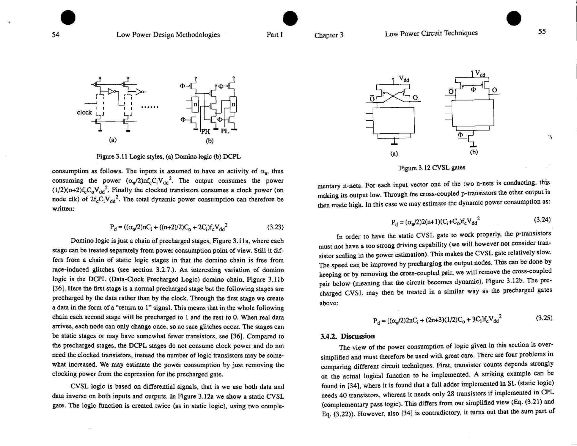
3.3. Flip-flops and Latches........................... ............47
3.4. Logic..........................................................52
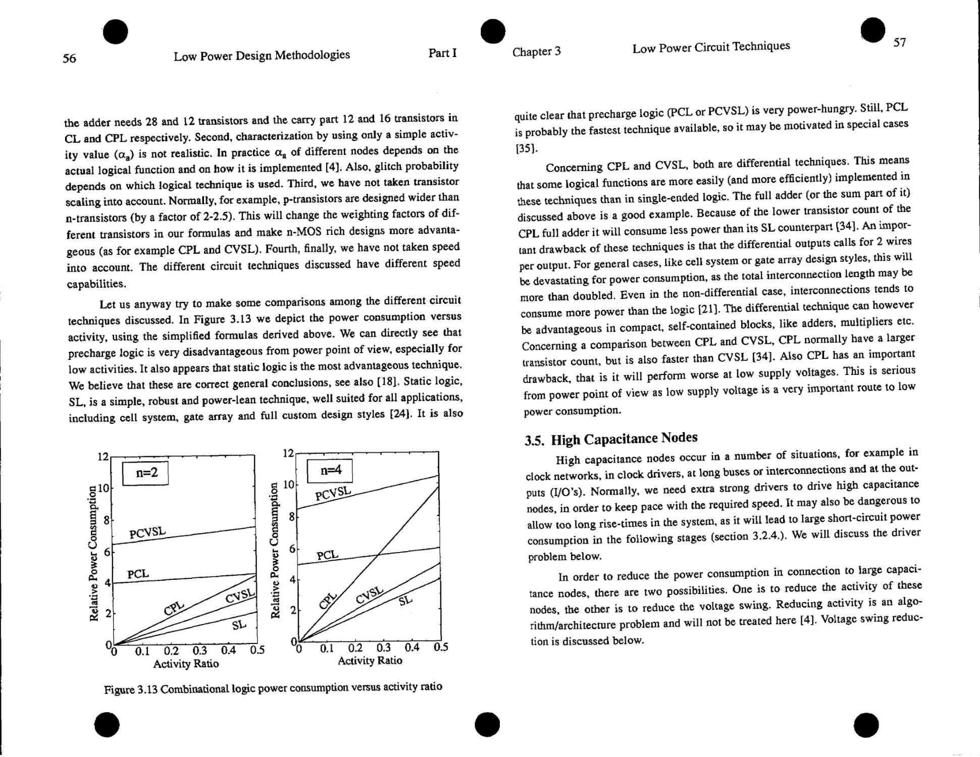
3.5. High Capacitance Nodes....................................... 57
3.6. Summary.................................................... 62
4. Energy-Recovery CMOS 65
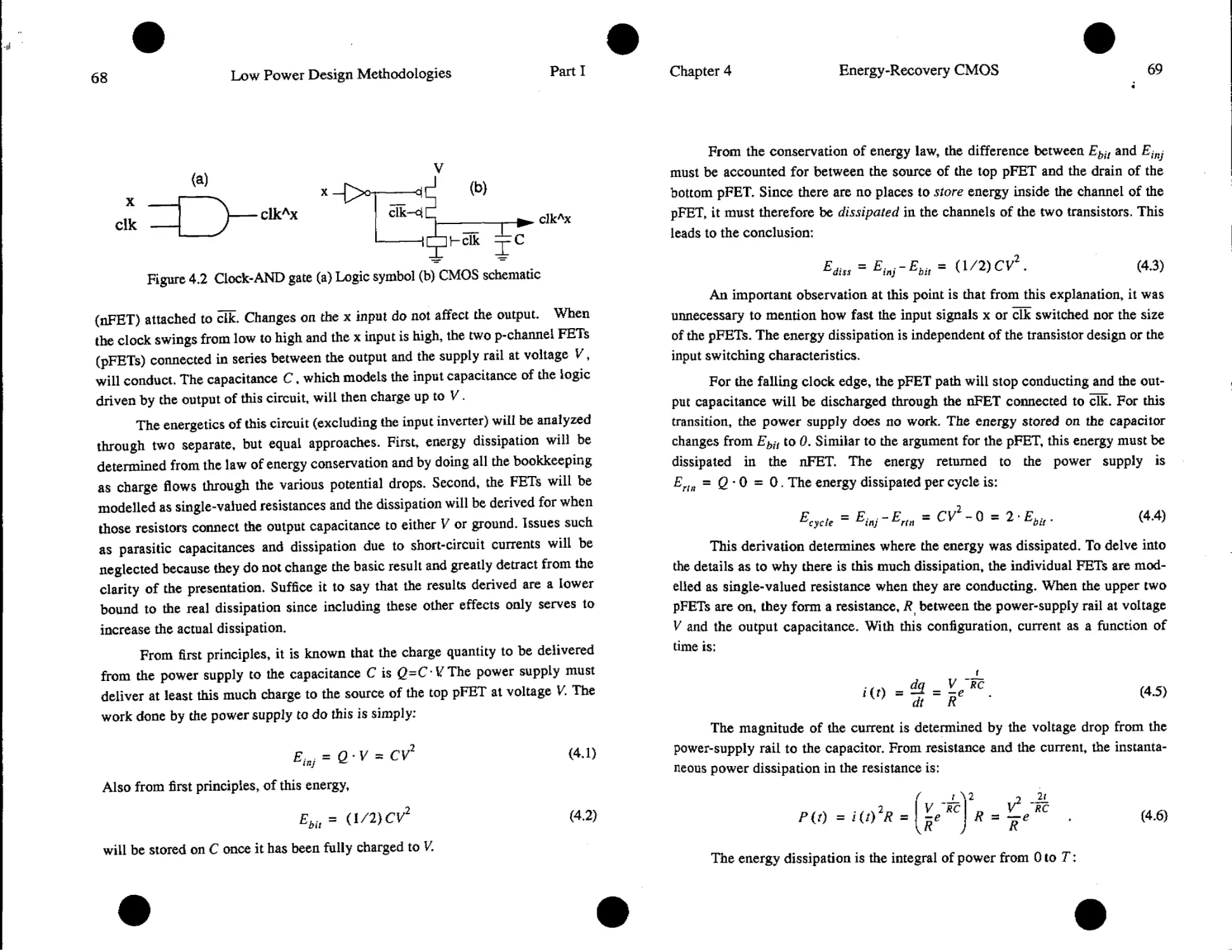
William C. Athas
4.1. A Simple Example............................................. 67
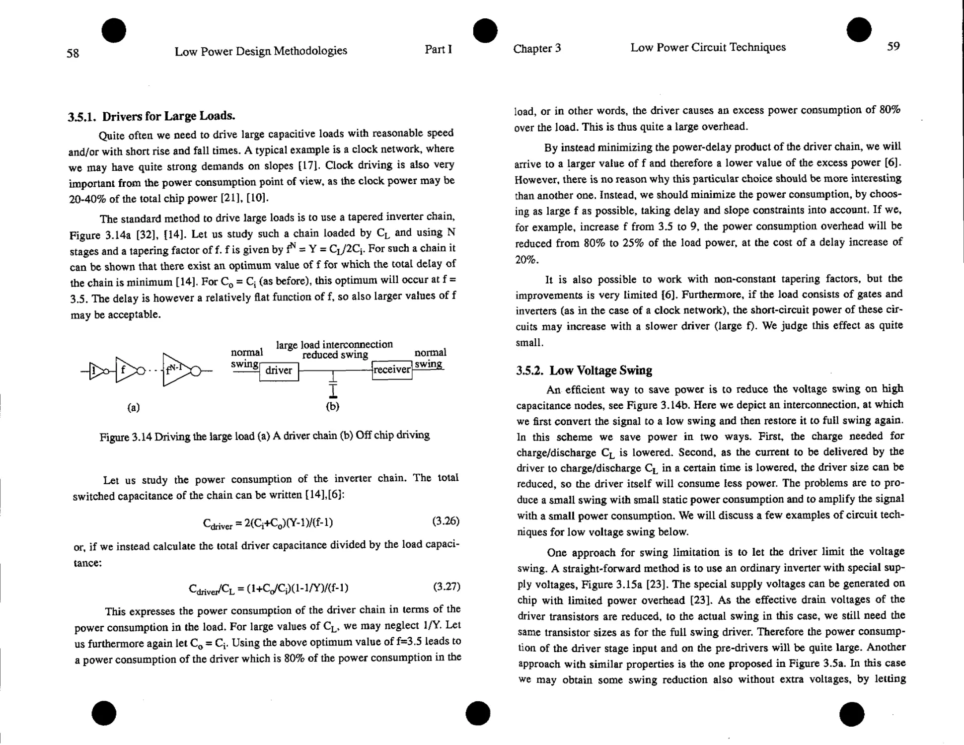
4.2. A look at some practical details..,........................ 72
4.3. Retractile Logic........................................... 76
4.4. Reversible Pipelines...........................................79
4.5. High-Performance Approaches................................ 84
4.6. Summary.................................................. 94
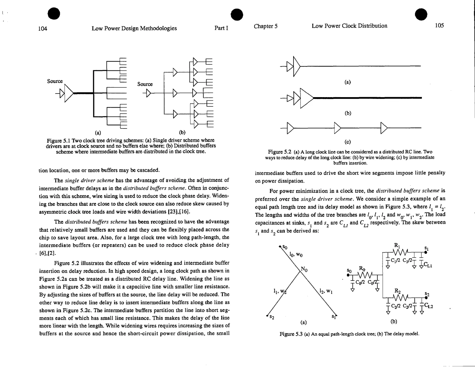
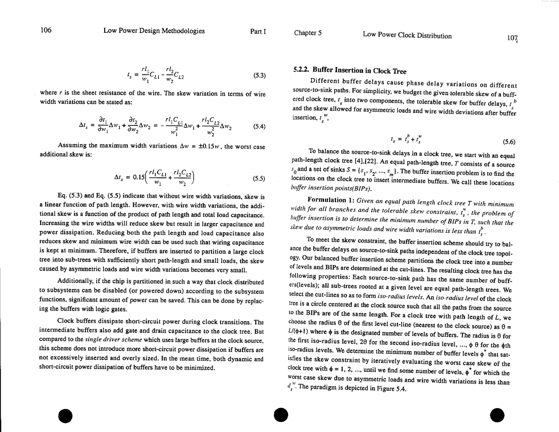
5. Low Power Clock Distribution 101
Joe G. Xi and Wayne W-M. Dai
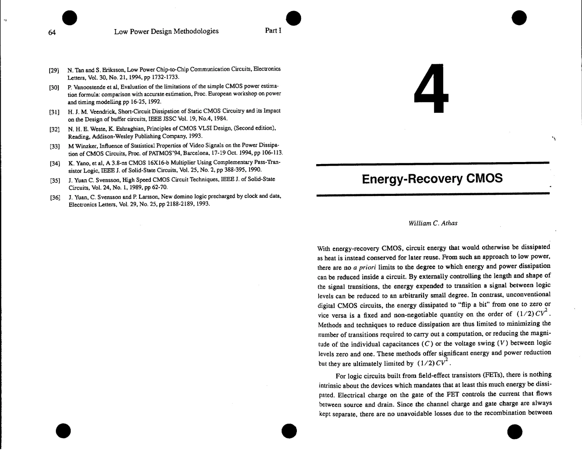
5.1. Power Dissipation in Clock Distribution........................101
5.2. Single Driver vs. Distributed Buffers.........................103
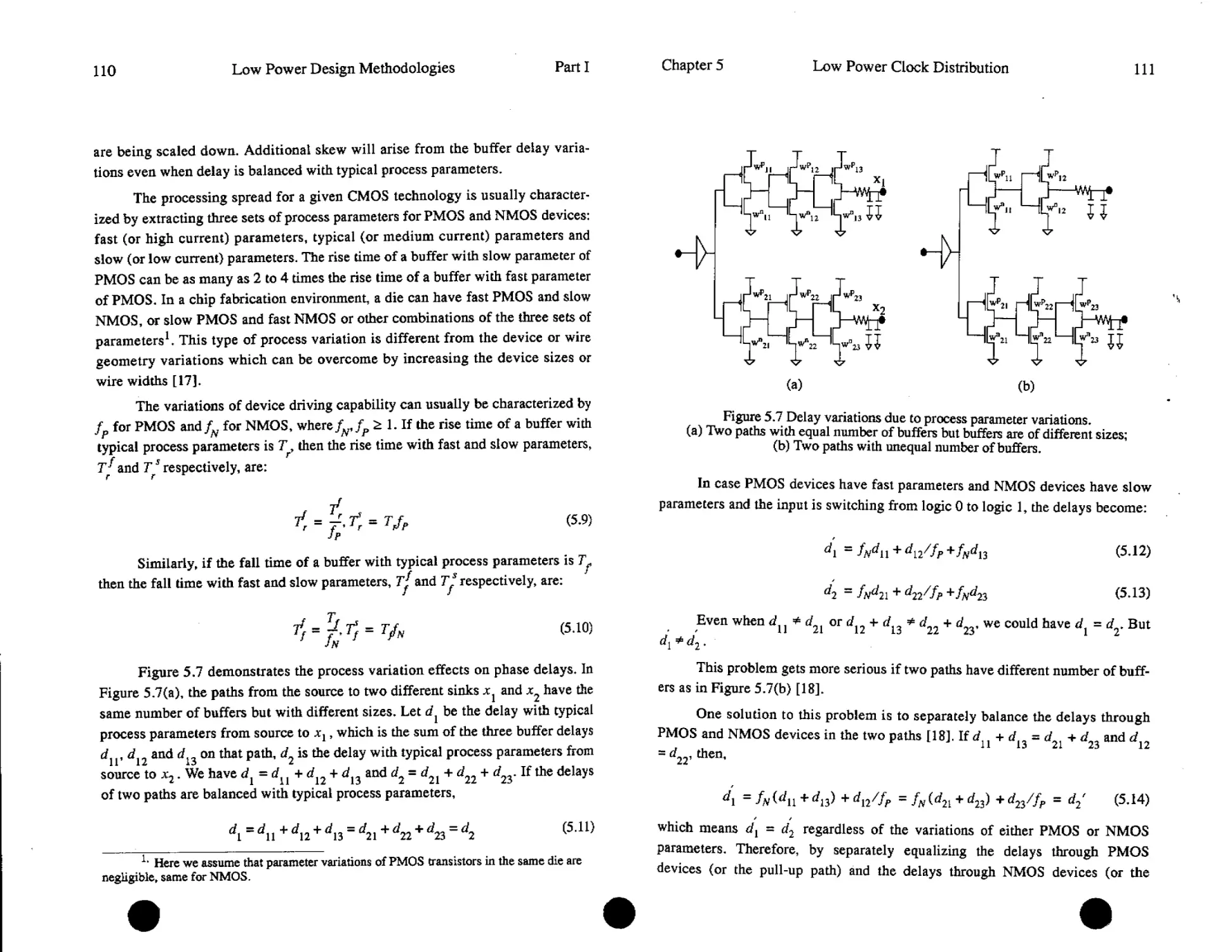
5.3. Buffer and Device Sizing under Process Variations......... 109
5.4. Zero Skew vs. Tolerable Skew................................ 114
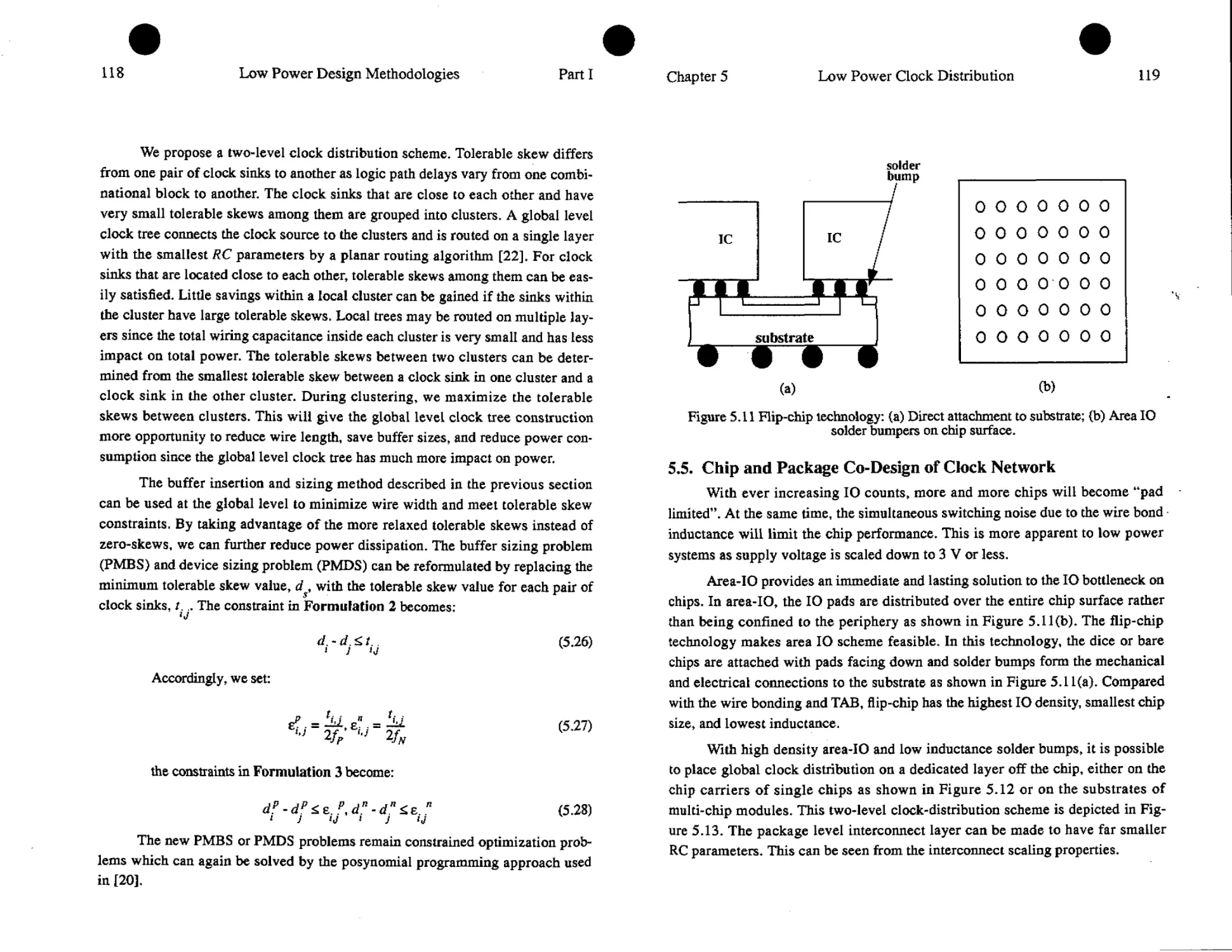
5.5. Chip and Package Со-Design of Clock Network...................119
5.6. Summary.......................................................123
Table of Contents vii
PART II Logic and Module Design Levels
6. Logic Synthesis for Low Power 129
Massoud Pedram
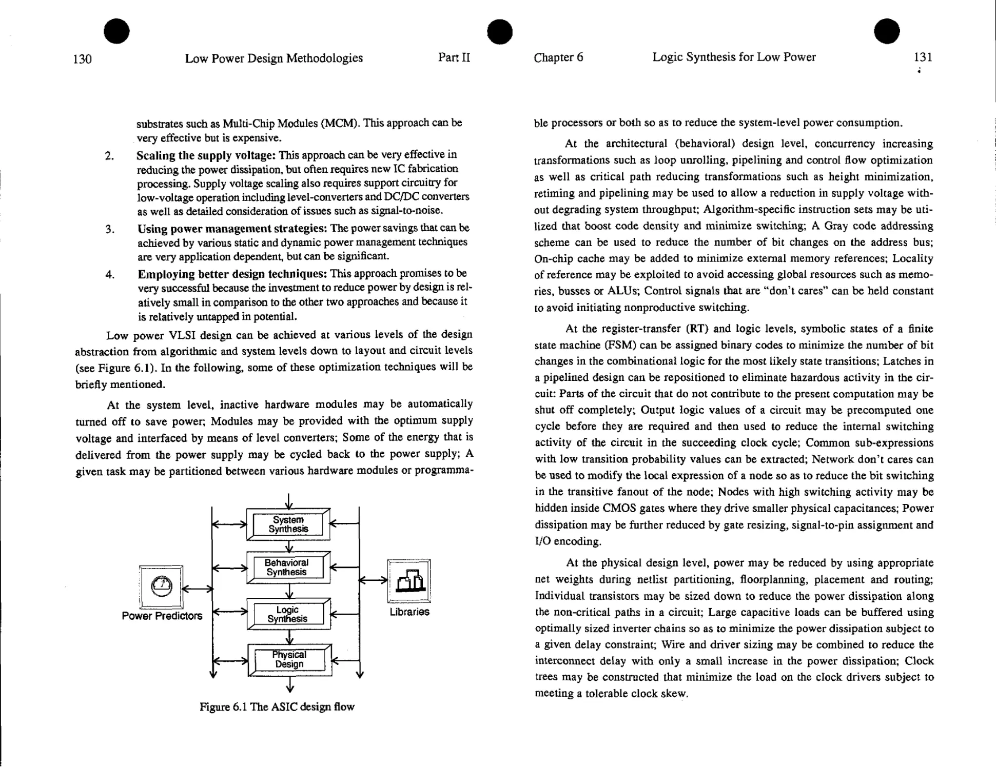
6.1. Introduction.................................................129
6.2. Power Estimation Techniques..................................132
6.3. Power Minimization Techniques................................146
6,4. Concluding Remarks...........................................156
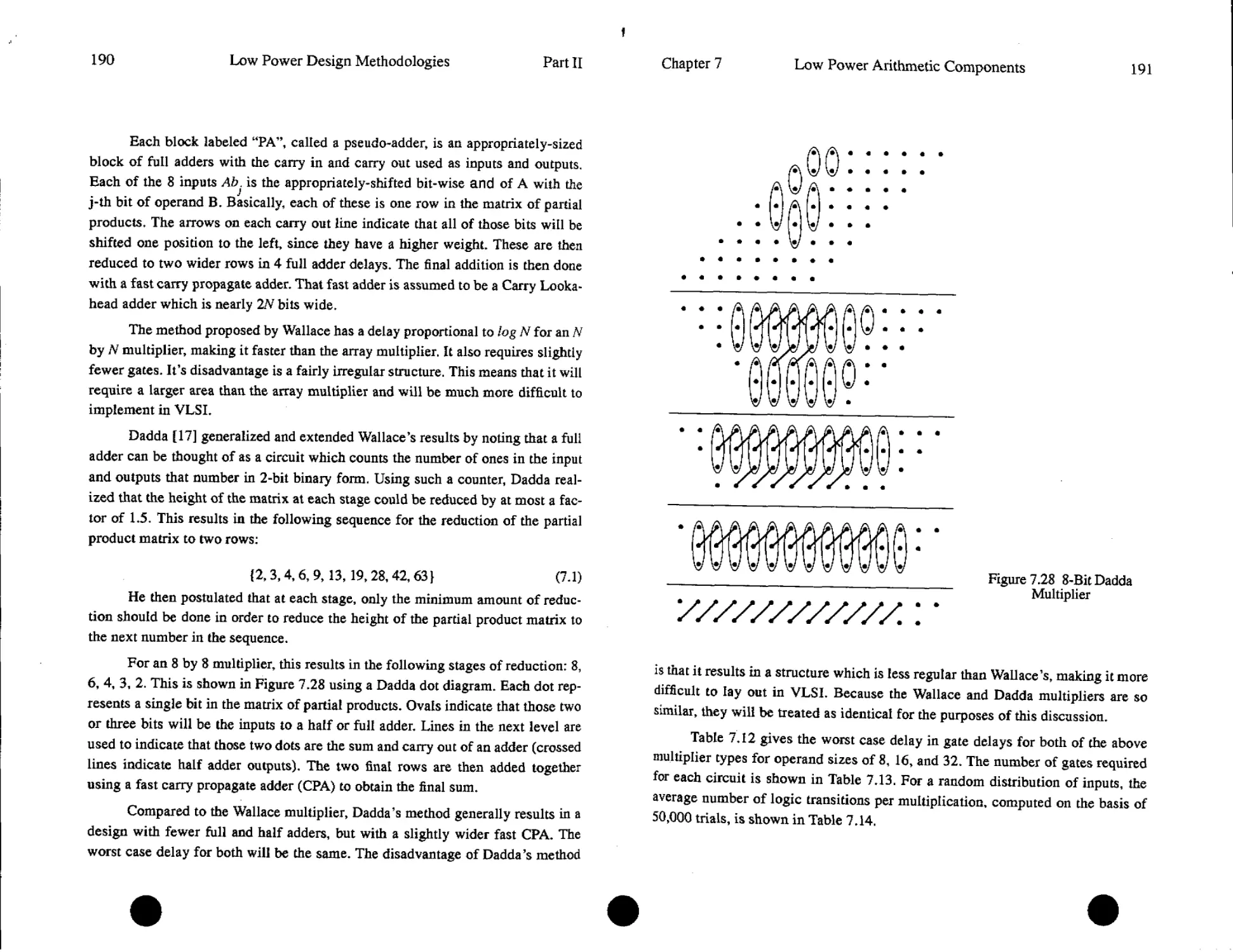
7. Low Power Arithmetic Components 161
Thomas K. Callaway and Earl E. Swartzlander
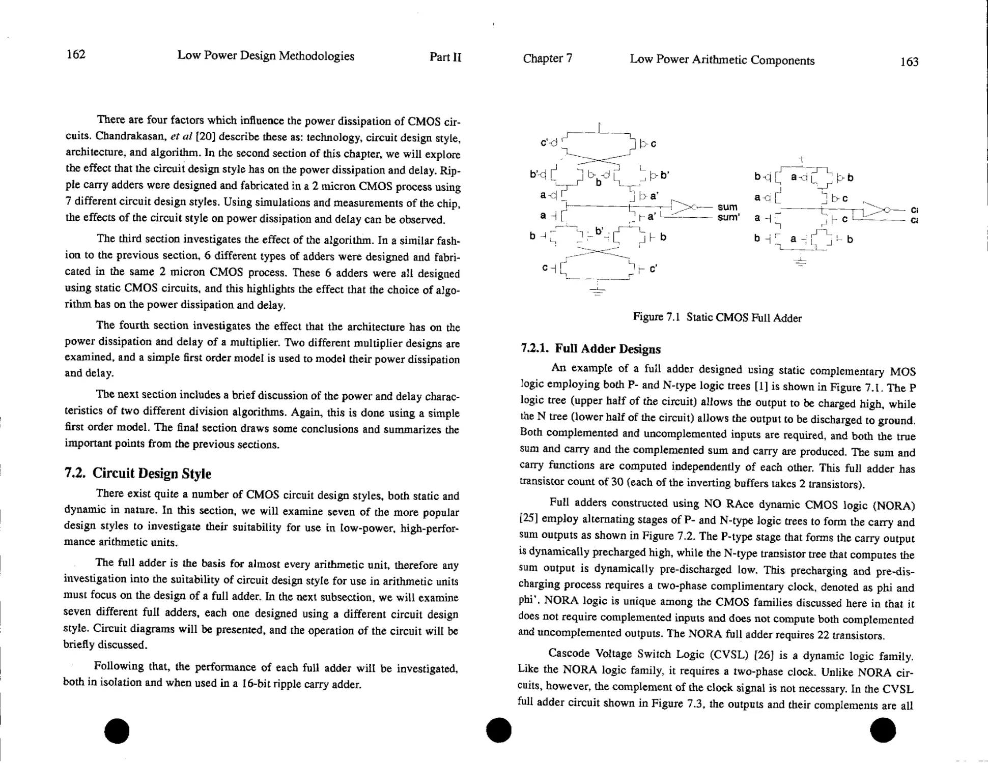
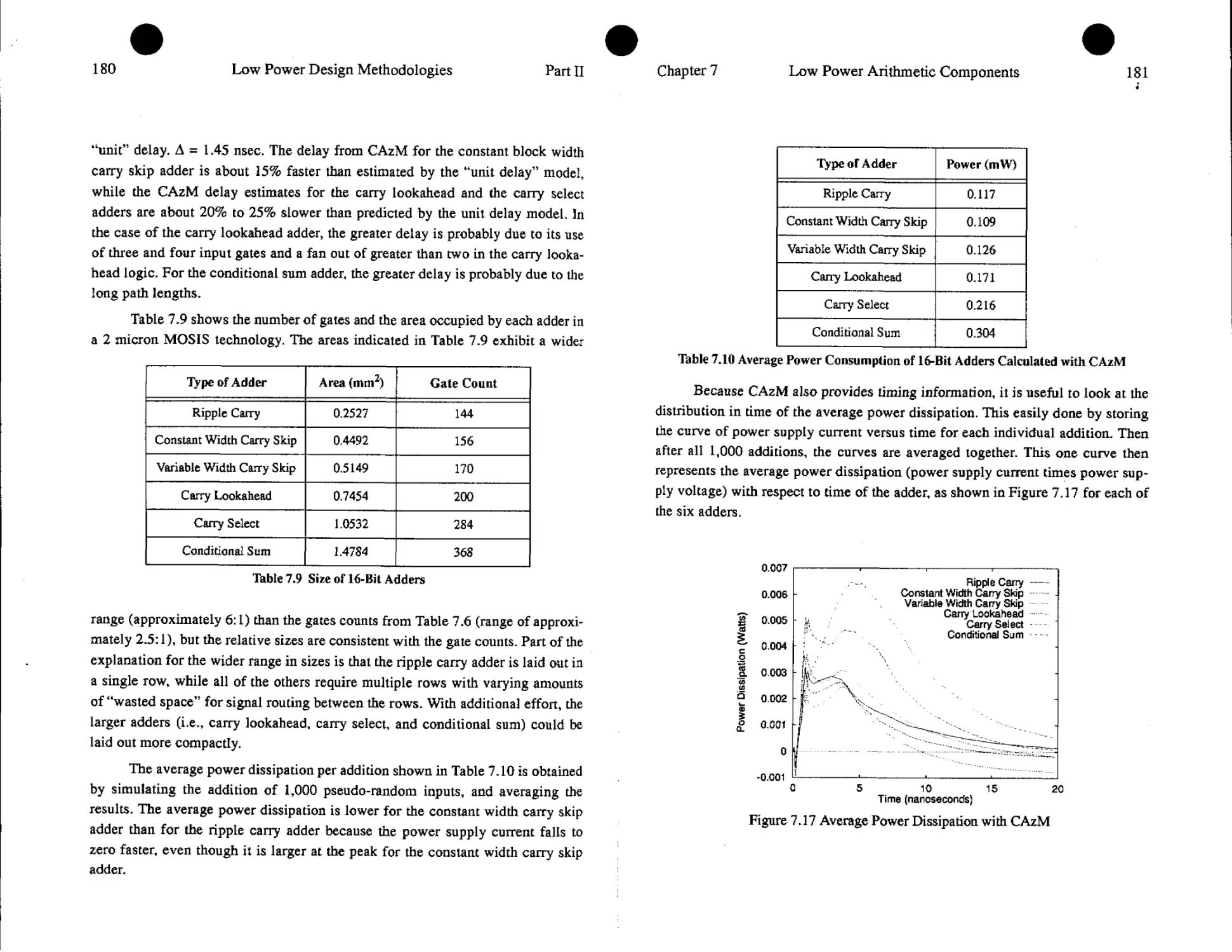
7.1. Introduction.................................................161
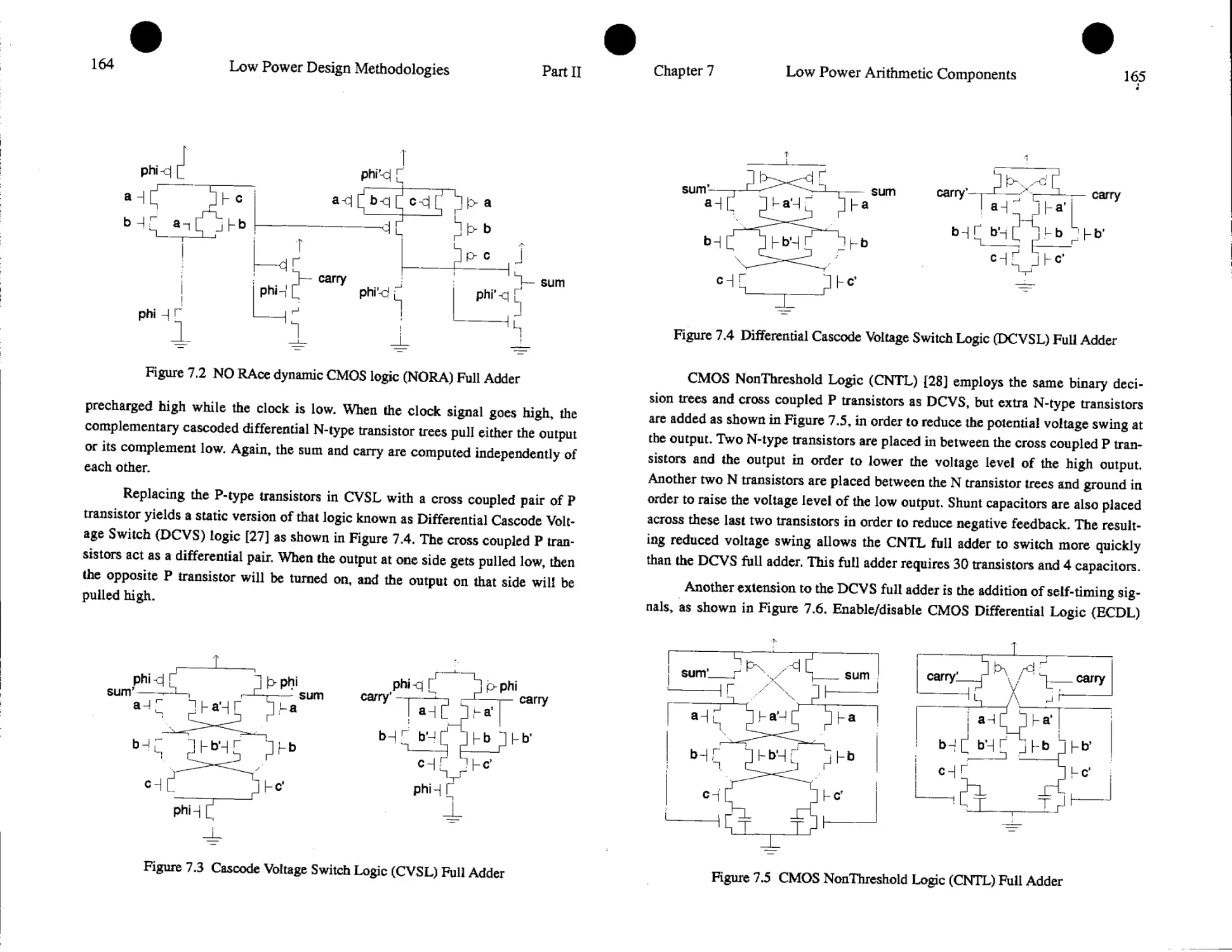
7.2, Circuit Design Style.........................................162
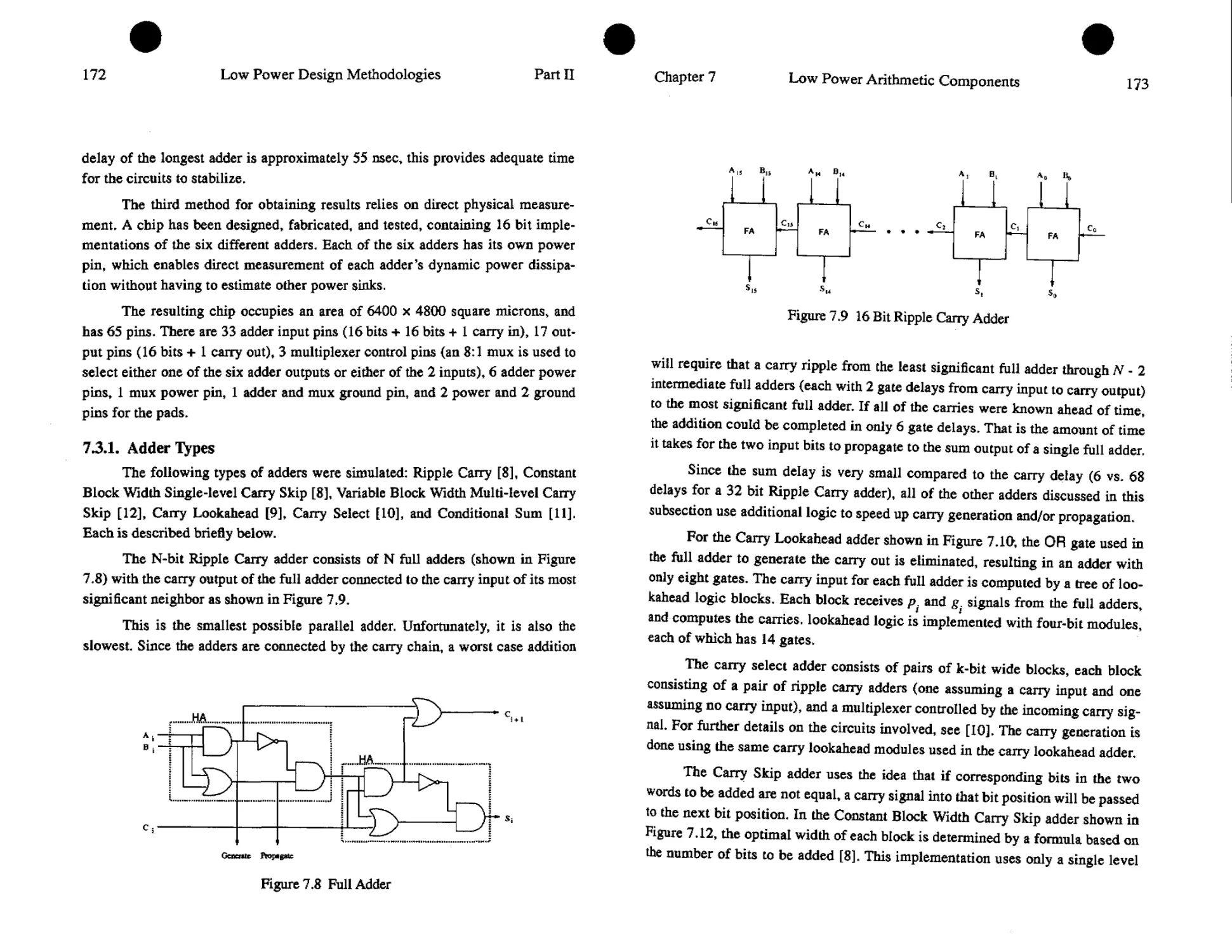
7,3. Adders.......................................................170
7.4. Multipliers................................................ 186
7.5. Division.....................................................194
7.6. Summary......................................................198
8. Low Power Memory Design 201
Kiyoh Itoh
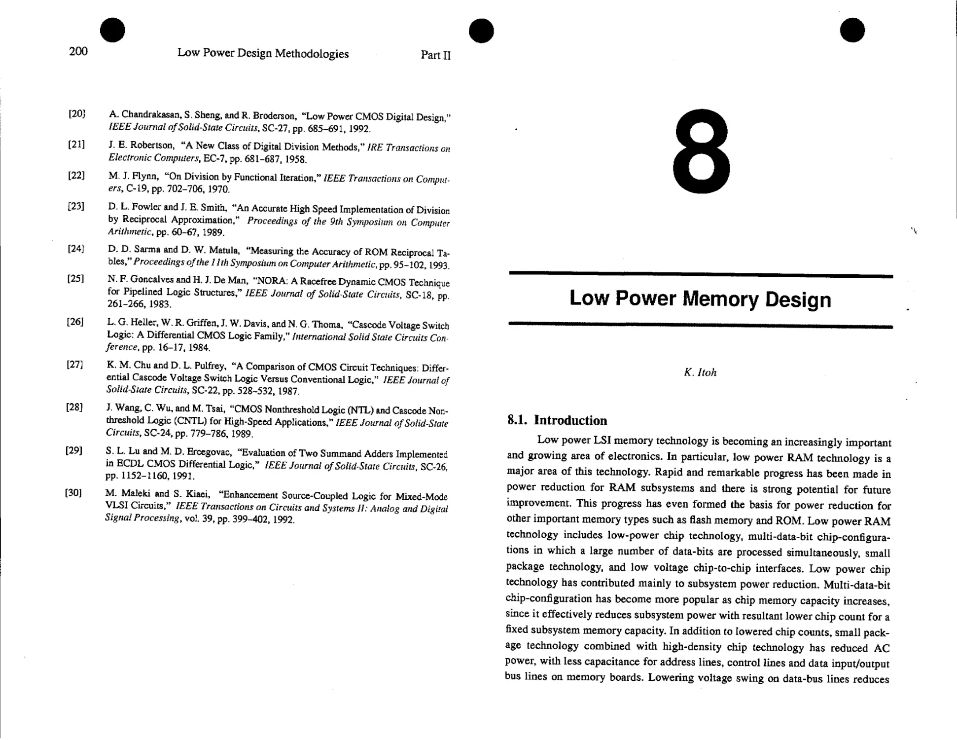
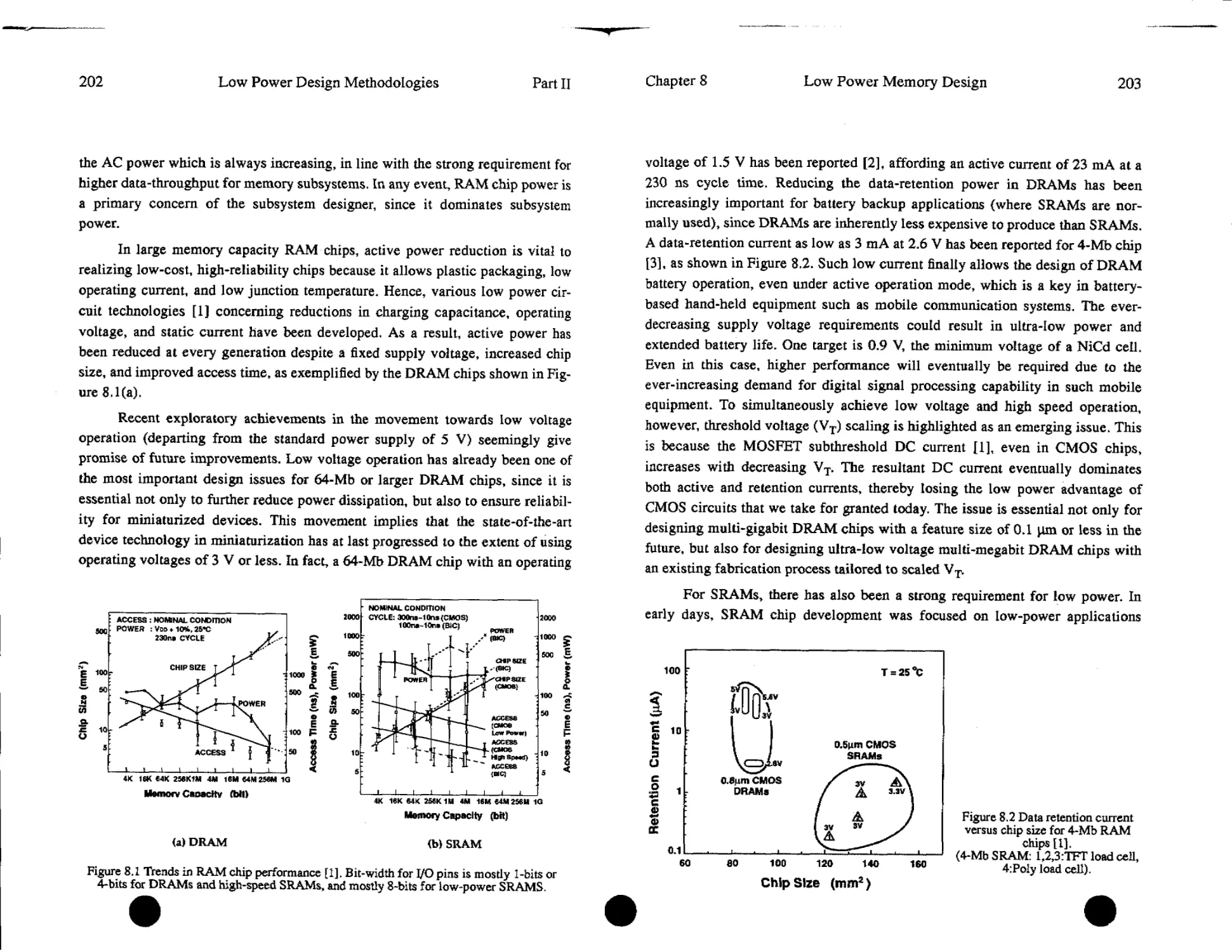
8.1. Introduction.................................................201
8.2. Sources and Reductions of Power Dissipation in Memory Subsystem.205
8.3. Sources of Power Dissipation in DRAM and SRAM................213
8.4. Low Power DRAM Circuits......................................218
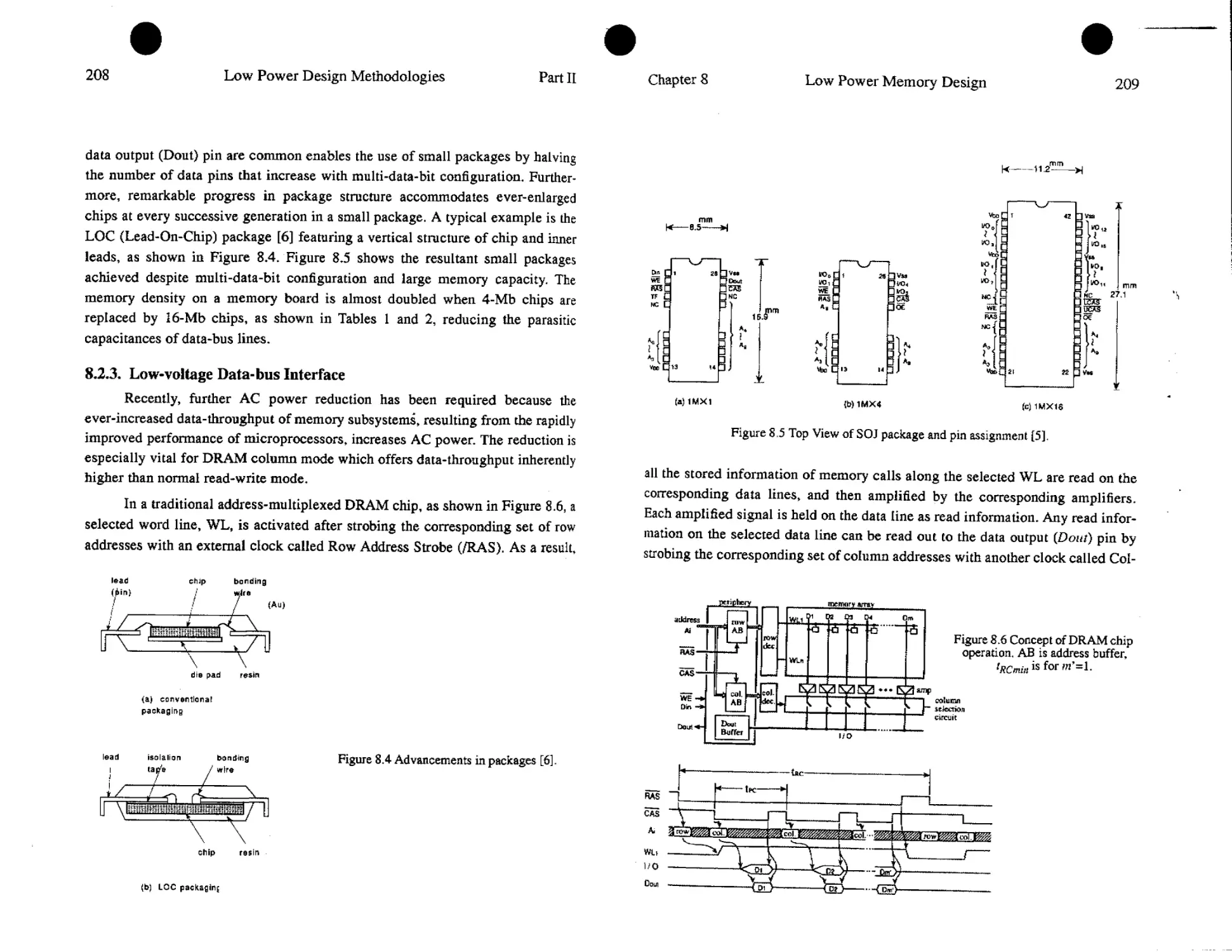
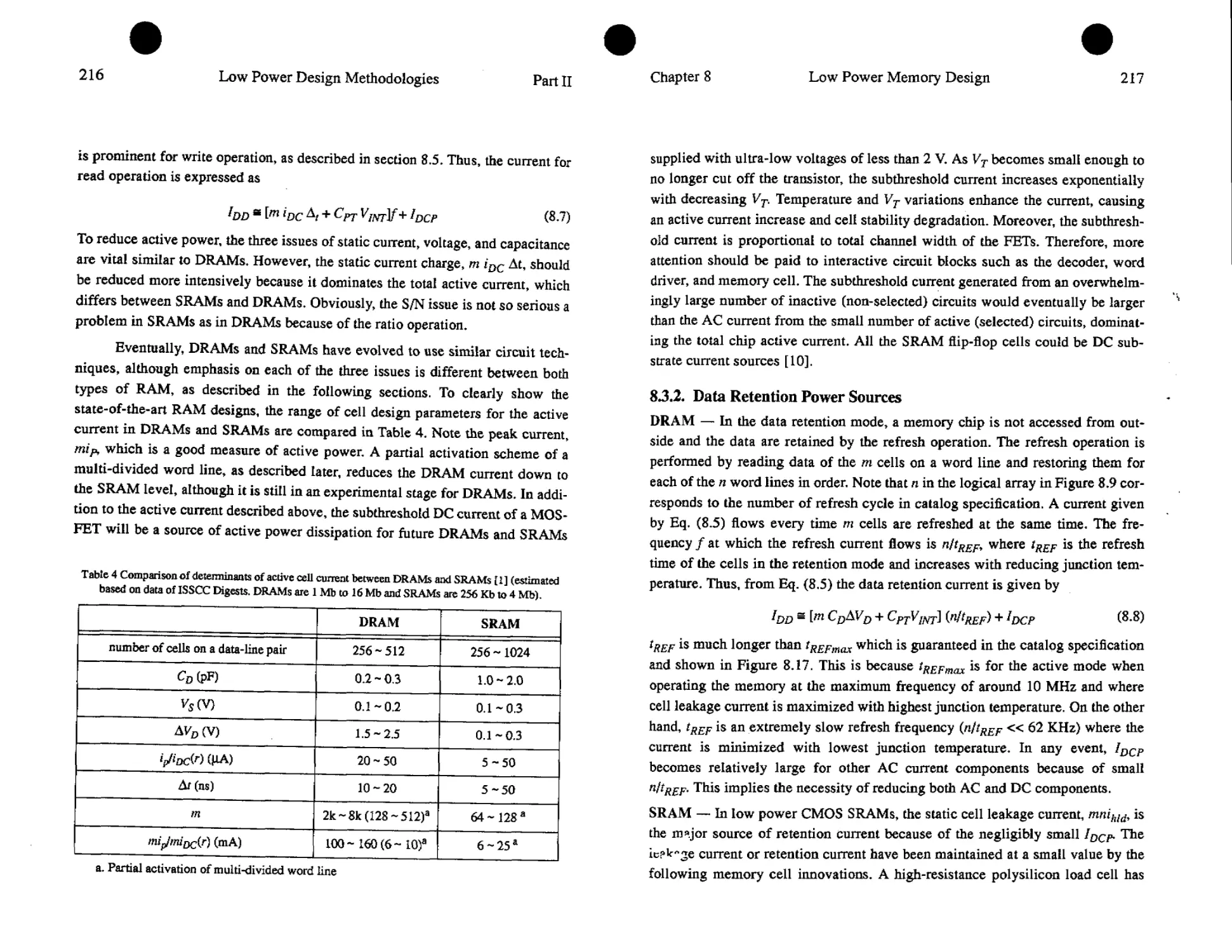
8.5. Low Power SRAM Circuits......................................241
viii
Low Power Design Methodologies
PART III Architecture and System Design Levels
9. Low-Power Microprocessor Design 255
Sonya Gary
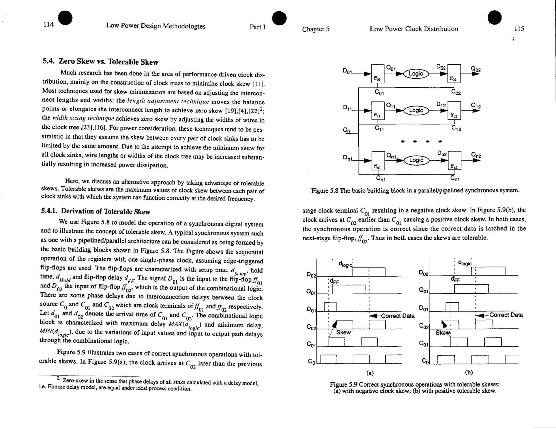
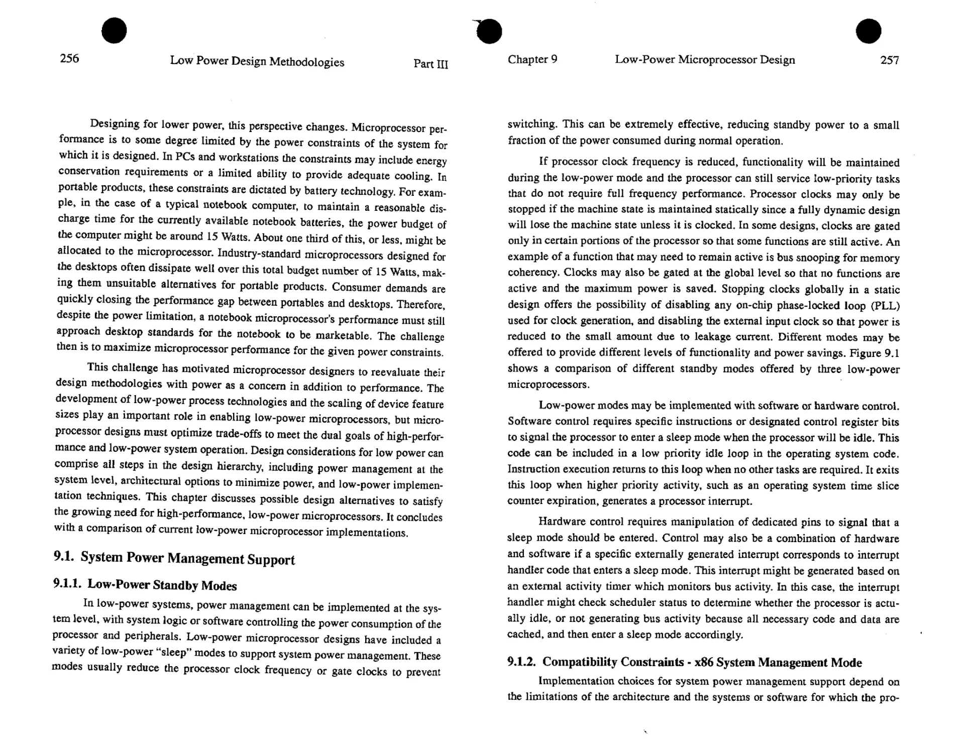
9.1. System Power Management Support........................... 256
9,2. Architectural Trade-Offs For Power.........................260
9.3. Choosing the Supply Voltage................................273
9.4. Low-Power Clocking.........................................276
95. Implementation Options for Low Power........................281
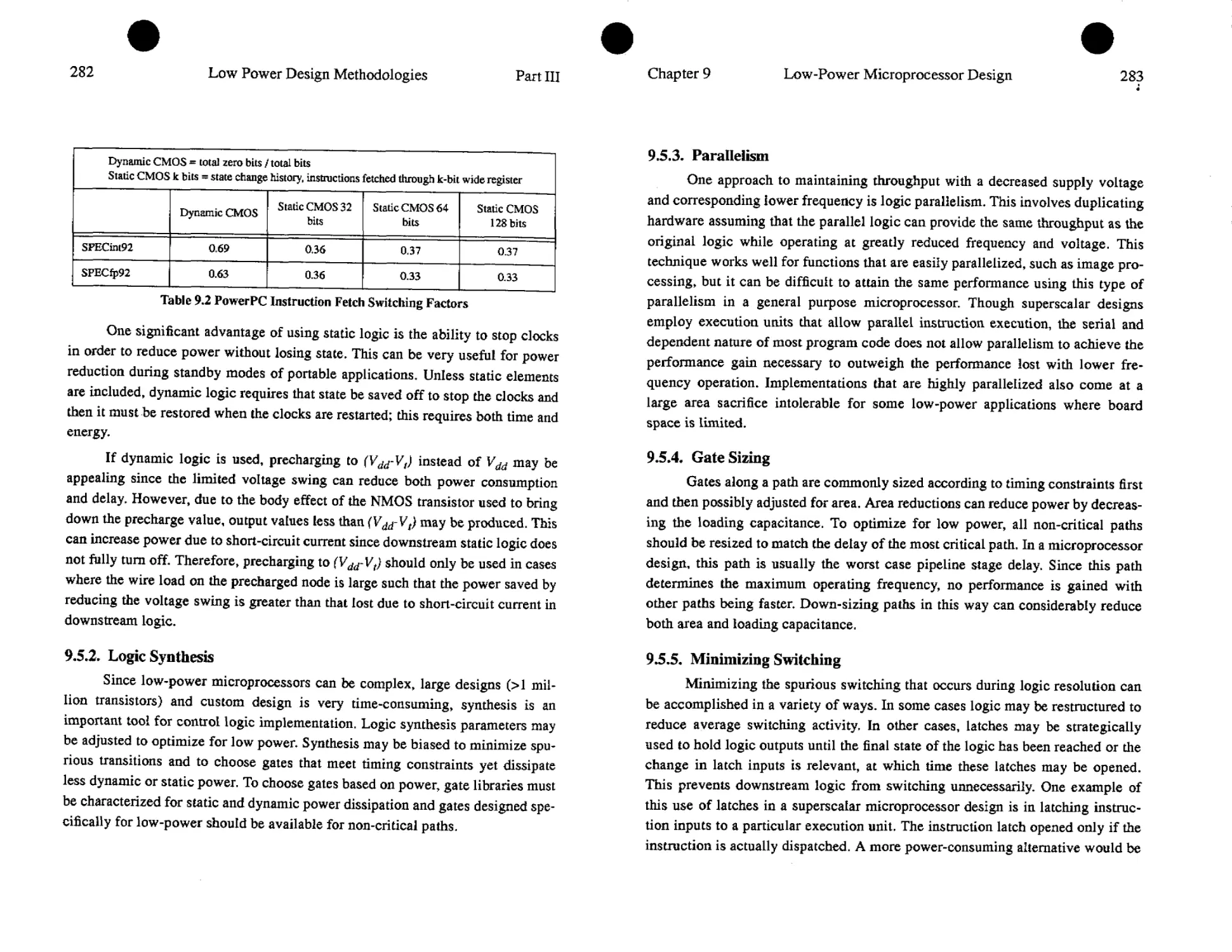
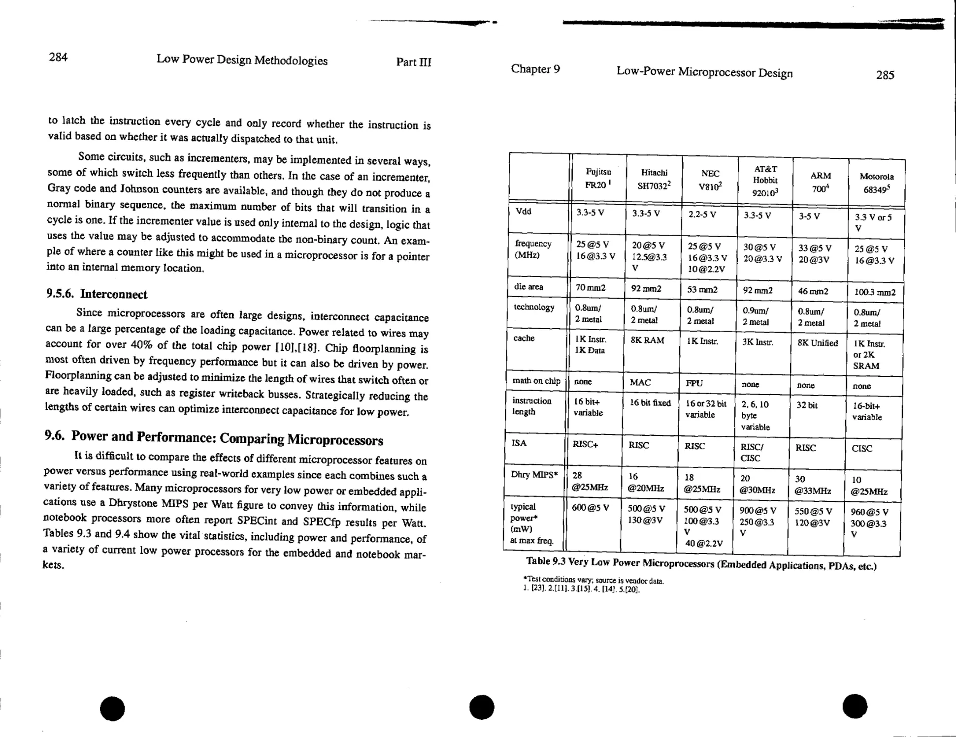
9.6. Power and Performance: Comparing Microprocessors...........284
9.7. Summary....................................................286
10. Portable Video-on-Demand in Wireless Communication 289
Teresa H. Meng, Benjamin M. Gordon, and Ely K. Tsern
10.1. Introduction...............................................290
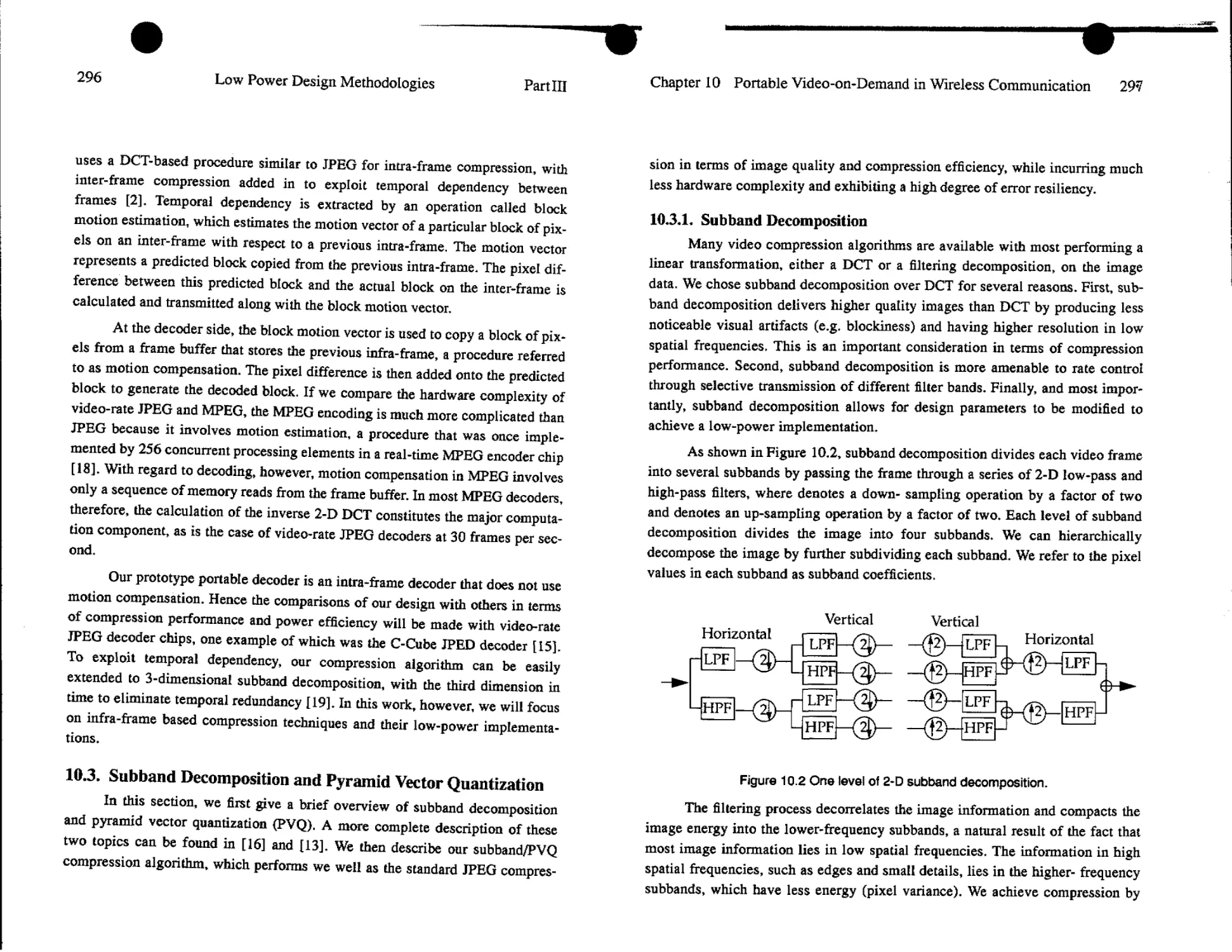
10.2. Video Compression for Portable Applications................292
10.3, Subband Decomposition and Pyramid Vector Quantization......296
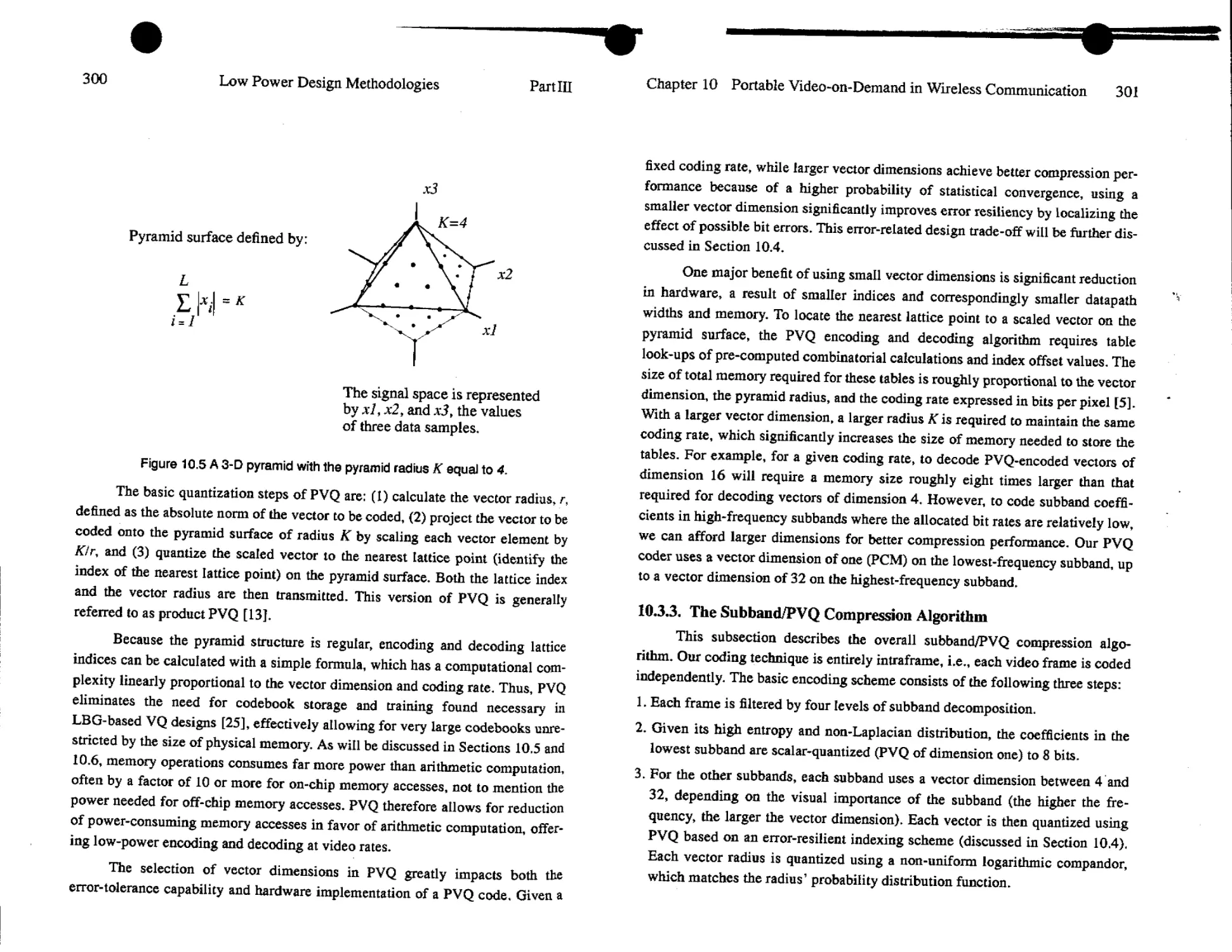
10.4. Error-Resilient Compression................................302
10.5. Low-Power Circuit Design Techniques........................308
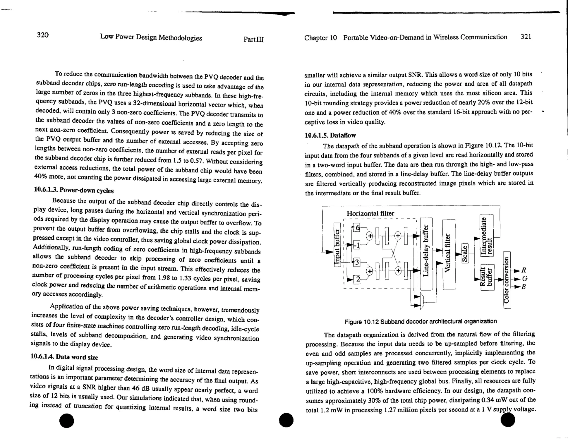
10.6. Low-Power Decoder Architectures............................317
10.7. Summary....................................................332
IL Algorithm and Architectural Level Methodologies 335
Renu Mehr a, David Lidsky, Arthur Abnous, Paul Landman and Jan
Rabaey
11.1. Introduction...............................................335
11.2. Design Flow................................................336
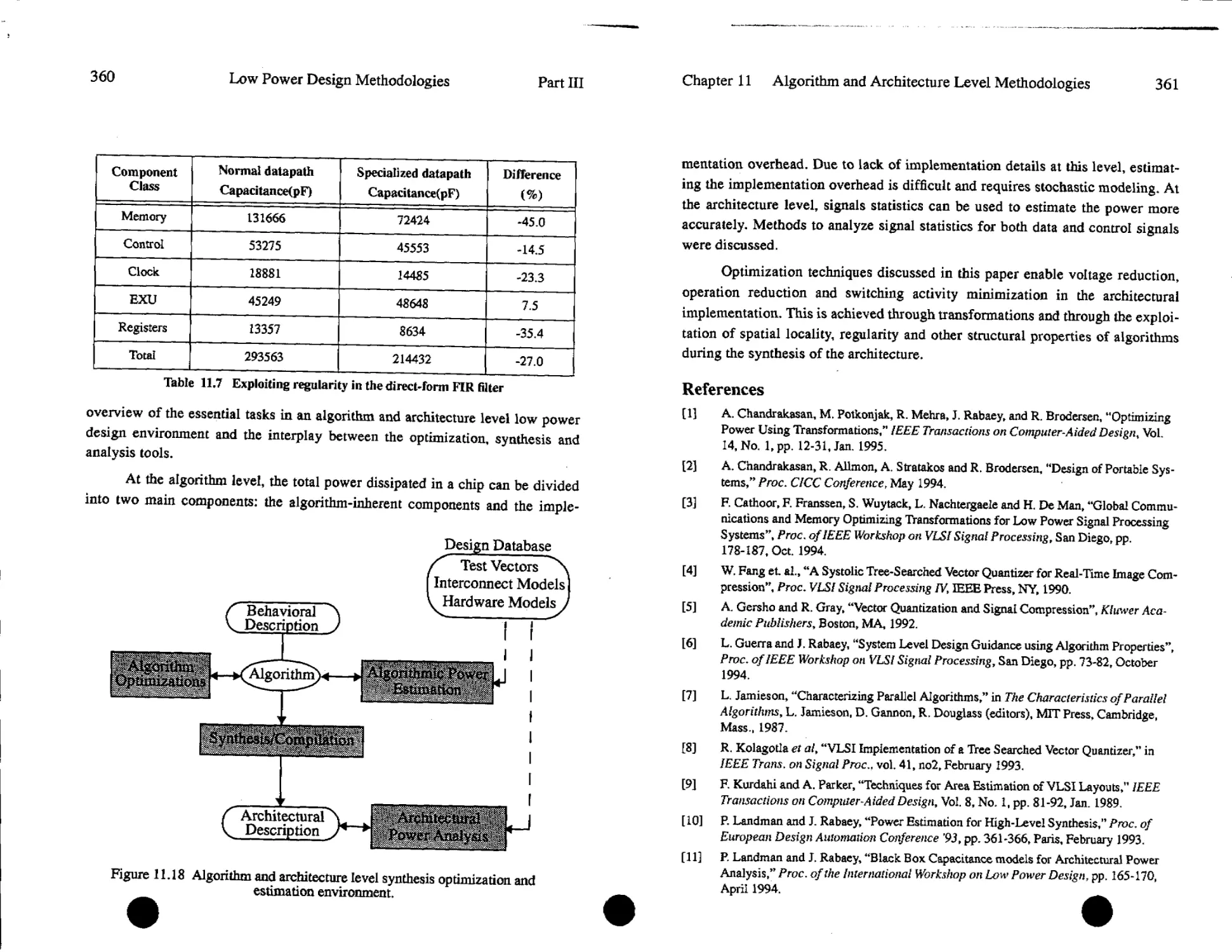
11.3. Algorithm level: Analysis and Optimization.................338
11.4. Architecture level: Estimation and Synthesis...............350
115. Summary....................................................359
Index 363
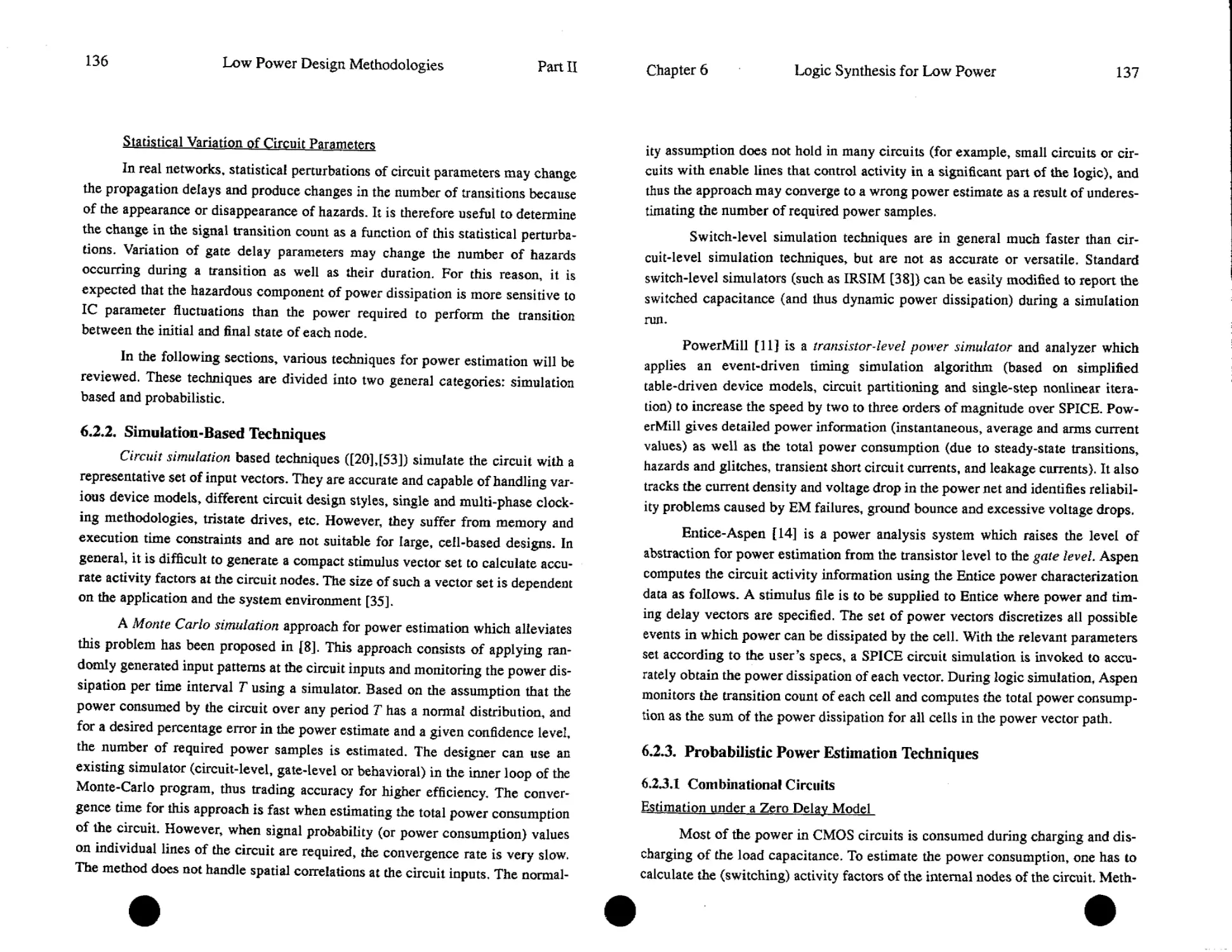
Preface
Most of the research and development efforts in the area of digital electron-
ics have been oriented towards increasing the speed and the complexity of single
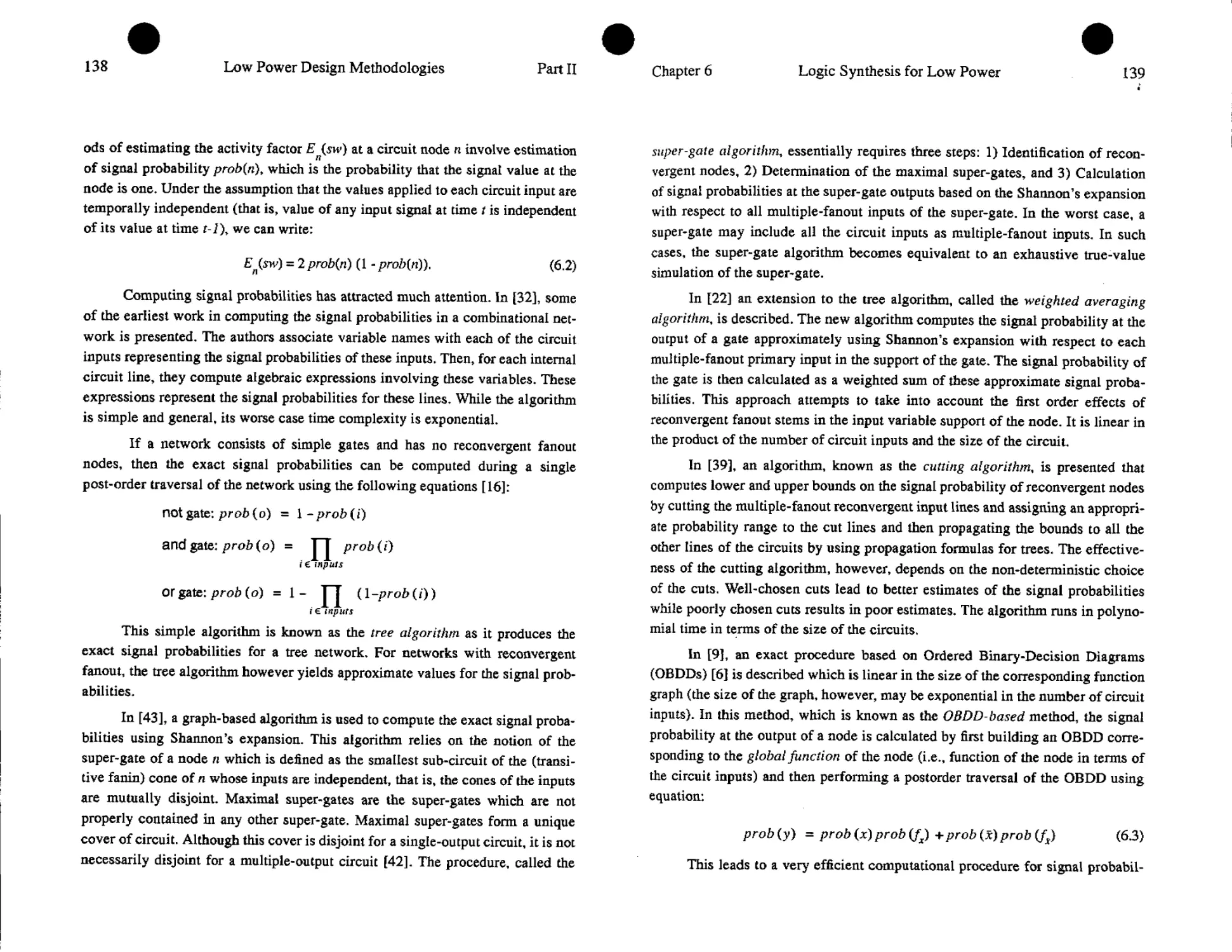
chip digital systems* This has resulted in a powerful, but power-hungry, design
technology, which enabled the development of personal workstations, sophisti-
cated computer graphics, and multi-media capabilities such as real-time speech
recognition and real-time video* While focusing the attention on speed and area,
power consumption has long been ignored.
This picture is, however, undergoing some radical changes* Power con-
sumption of individual components is reaching the limits of what can be dealt
with by economic packaging technologies, resulting in reduced device reliability*
Dealing with power is rapidly becoming one of the most demanding issues in dig-
ital system design* This situation is aggravated by the increasing demand for por-
table systems in the areas of communication, computation and consumer
electronics* Improvements in battery technology are easily offset by the increas-
ing complexity and performance of those applications. To guarantee a reasonable
battery operation time, a dramatic (e.g., lOOx) reduction of the power consump-
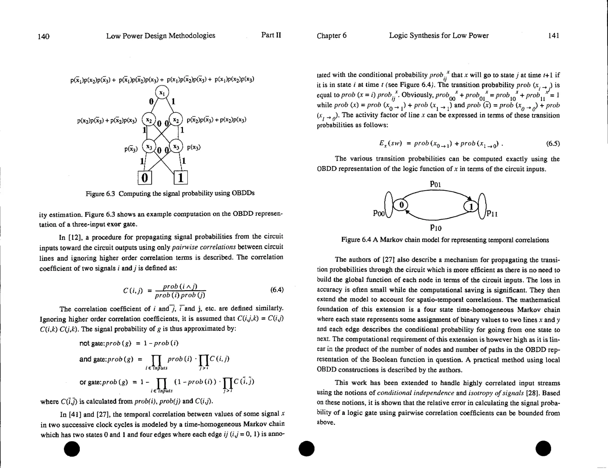
tion is essential.
These realizations spurred a renewed interest in low power design over the
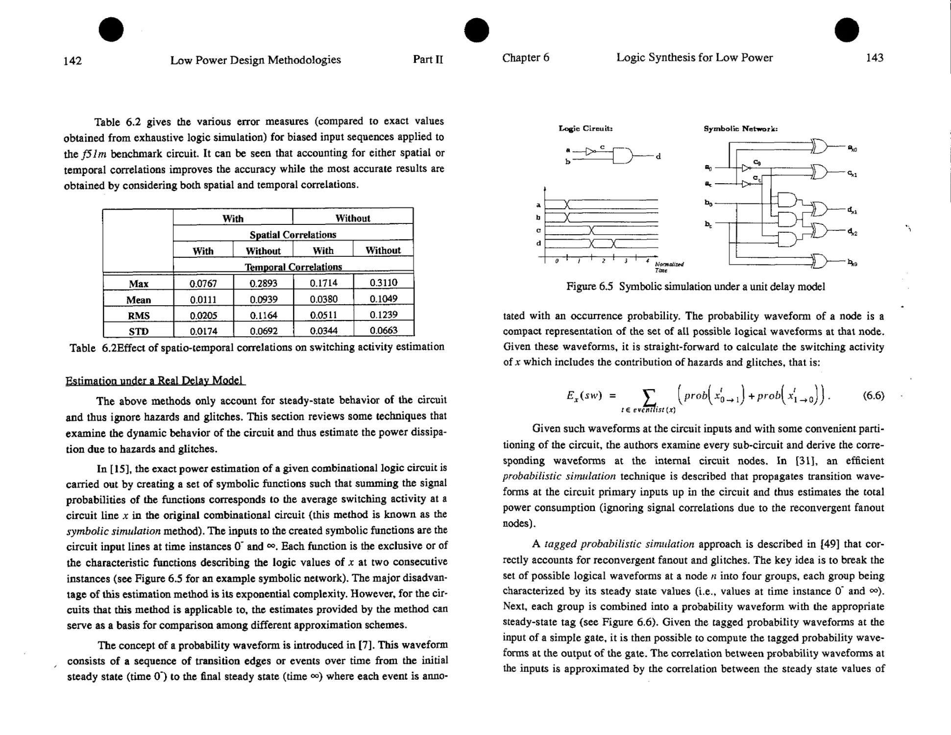
last five years. Researchers learned quickly that there is no single solution to the
power dissipation problem. In fact, to be meaningful and have a real impact,
power optimization should occur at all levels of the design hierarchy, including
the technology, circuit, layout, logic, architectural and algorithmic levels. It is our
experience that combining optimizations at all those levels easily results in orders
of magnitude of power reduction.
Realizing these potential savings requires a thorough understanding of
where power is dissipated in a digital integrated circuit* Once the dominant
sources of dissipation are identified, a whole battery of low power design tech-
niques can be brought in action* A significant portion of the overall challenge of
making low power design techniques and methodologies practical involves going
1
Introduction
Jan M. Rabaey, Massoud Pedram and Paul E. Landman
1.1. Motivation
Historically, system performance has been synonymous with circuit speed
or processing power. For example, in the microprocessor world, performance is
often measured in Millions of Instructions Per Second (MIPS) or Millions of
Floating point Operations Per Second (MFLOPS). In other words, the highest
“performance” system is the one that can perform the most computations in a
given amount of time. The question of cost really depends on the implementation
strategy being considered. For integrated circuits there is a fairly direct corre-
spondence between silicon area and cost. Increasing the implementation area
tends to result in higher packaging costs as well as reduced fabrication yield with
both effects translating immediately to increased product cost. Moreover,
improvements in system performance generally come at the expense of silicon
real estate. So, historically, the task of the VLSI designer has been to explore the
Area-Time (AT) implementation space, attempting to strike a reasonable balance
between these often conflicting objectives.
But area and time are not the only metrics by which we can measure imple-
mentation quality. Power consumption is yet another criterion. Until recently,
2
Low Power Design Methodologies
INTRO
power considerations were often of only secondary concern, taking the back seat
to both area and speed. Of course, there are exceptions to this rule; for example,
designers of portable devices such as wrist watches have always placed consider-
able emphasis on minimizing power in order to maximize battery life. For the
most part, however, designers of mainstream electronic systems have considered
power consumption only as an afterthought — designing for maximum perfor-
mance regardless of the effects on power.
In recent years, however, this has begun to change and, increasingly, power
is being given comparable weight to area and speed considerations. Several fac-
tors have contributed to this trend. Perhaps the most visible driving factor has
been the remarkable success and growth of the portable consumer electronics
market [16],[17],[18],[19], [29]. Lap-top computers, Personal Digital Assistants
(PDA’s), cellular phones, and pagers have enjoyed considerable success among
consumers, and the market for these and other portable devices is only projected
to increase in the future.
For these applications, average power consumption has become a critical
design concern and has perhaps superceded speed and area as the overriding
implementation constraint [5][7][11]. The reason for this is illustrated with the
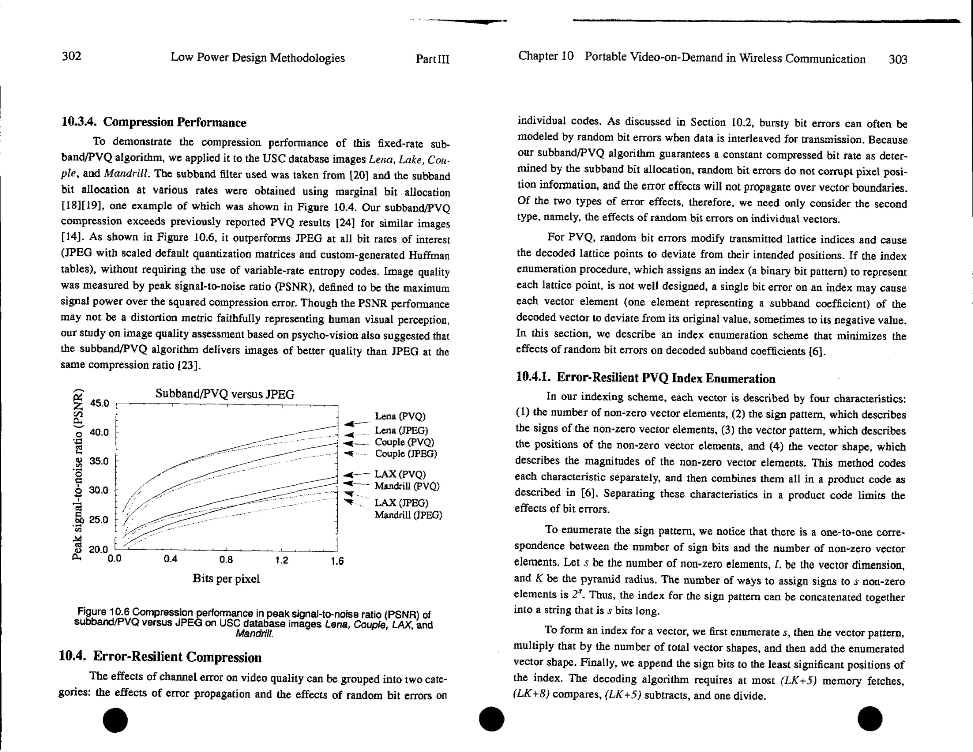
simple example of a future portable multi-media terminal, which supports high
bandwidth wireless communication, bi-directional motion video, high quality
audio, speech and pen-based input and full texts/graphics. The projected power
budget for a such a terminal, when implemented using off-the-shelf components
not designed for low-power operation [9], hovers around 40 W. With modem
Nickel-Cadmium battery technologies offering around 20 Watt-hours/pound (Fig-
ure 1.1), this terminal would require 20 pounds of batteries for 10 hours of opera-
tion between recharges [13][15]. More advanced batteiy technologies such as
Nickel-Metal-Hydride offer little relief at 30-35 Watt-hours/pound, bringing bat-
tery weights down to a still unacceptable 7 pounds. From Figure 1.1, it can be
observed that battery capacity has only improved with a factor 2 to 4 over the last
30 years (while the computational power of digital IC’s has increased with more
than 4 orders of magnitude). Even with new batteiy technologies such as
rechargeable lithium or polymers, it is anticipated that the expected battery life-
time will increase with no more than 30 to 40% over the next 5 years. In the
absence of low-power design techniques then, current and future portable devices
will suffer from either very short battery life or unreasonably heavy battery packs
unless a low power design approach is adopted.
Chapter 1
Introduction
3
Figure 1.1 Energy storage capacity trends for common battery technologies [13]
On the other hand, peak power (maximum possible power dissipation)
determines the electrical limits of a design, dictates battery type and power distri-
bution network, and impacts the signal integrity through the and LdUdt prob-
lems. It is therefore essential to have the peak power under control.
Portability is by no means the sole driving force behind the push for
low-power. There exists a strong pressure for producers of high-end products to
reduce their power consumption as well. Figure 1.2 shows the trend in micropro-
cessor power consumption. It plots the dissipation of a number of well known
processors as a function of die area x clock frequency. The figure demonstrates
that contemporary high performance processors dissipate as much as 30 W [12] 1
More importantly, it shows that the dissipation increases approximately linearly
with the area-frequency product. The following expression seems to hold approx-
imately
P = a area with a = 0.063 W/cm2 * MHz (1.1)
Newer, high performance processors do not display a considerably differ-
ent behavior. For instance, the DEC 21164 (300 MHz on a die area of 3 cm2) [4]
consumes 50 Watts, compared to the 56.6 Watt predicted by Eq. (1.1). Assuming
that the same trend continues in the future, it can be extrapolated that a 10 cm2
4
Low Power Design Methodologies
INTRO
microprocessor, clocked at 500 MHz (which is a not too aggressive estimate for
the next decade) would consume 315 Watt. The cost associated with packaging
and cooling such devices is becoming prohibitive. Since core power consumption
must be dissipated through the packaging, increasingly expensive packaging and
cooling strategies are required as chip power consumption increases [20]. Conse-
quently, there is a clear financial advantage to reducing the power consumed by
high performance systems.
In addition to cost, there is the issue of reliability. High power systems tend
to run hot, and high temperature tends to exacerbate several silicon failure mech-
anisms. Every 10 °C increase in operating temperature roughly doubles a compo-
nent’s failure rate [22]. Figure 1.3 illustrates this very definite relationship
between temperature and the various failure mechanisms such as electromigra-
tion, junction fatigue, and gate dielectric breakdown.
From the environmental viewpoint, the smaller the power dissipation of
electronic systems, the lower the heat pumped into the rooms, the lower the elec-
tricity consumed and therefore, the less the impact on global environment.
Obviously, the motivations in reducing power consumption differ from
application to applications. For instance, for a number of application domains
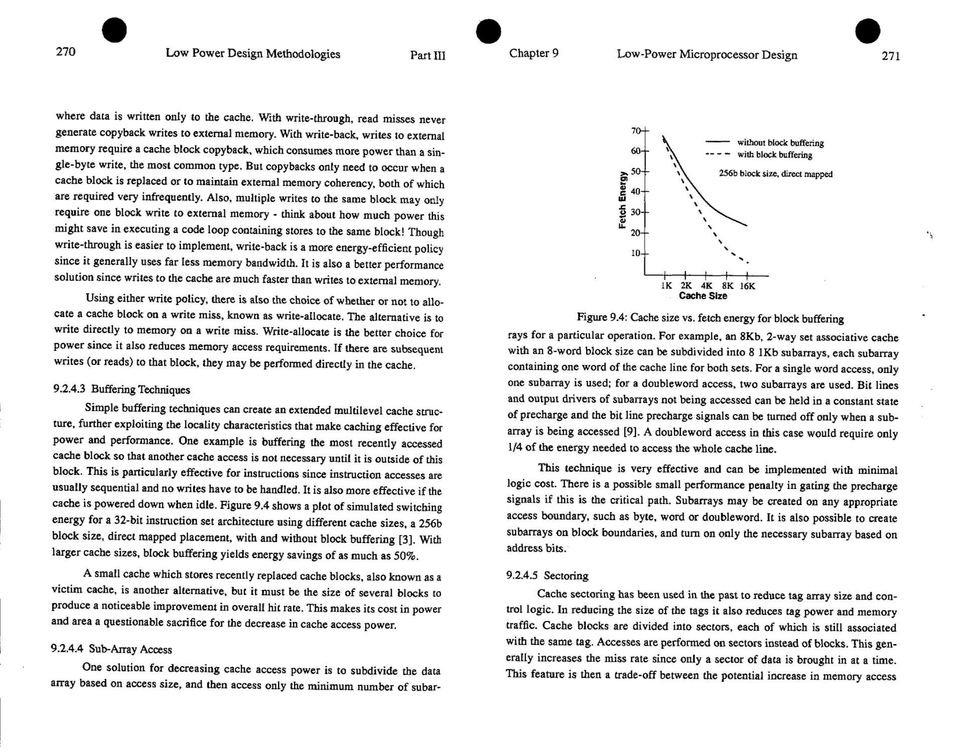
such as pace makers and digital watches, minimizing power to an absolute mini-
mum is the absolute prime requirement. In this class of ultra low power applica-
tions, overall power levels are normally held below 1 mW. In a large class of
Figure 1.2 Trends in microprocessor power consumption (after [30]).
Chapter 1
Introduction
5
applications, such as cellular phones and portable computers (Ztnv power), the
goal is to keep the battery lifetime reasonable and packaging cheap. Power levels
below 2 Watt, for instance, enable the use of cheap plastic packages. Finally, for
high performance systems such as workstations and set-top computers, the over-
all goal of power minimization is to reduce system cost (cooling, packaging,
energy bill). These different requirements impact how power optimization is
addressed and how much the designer is willing to sacrifice in cost or perfor-
mance to obtain his power objectives.
1.2, Sources of Dissipation in Digital Integrated Circuits
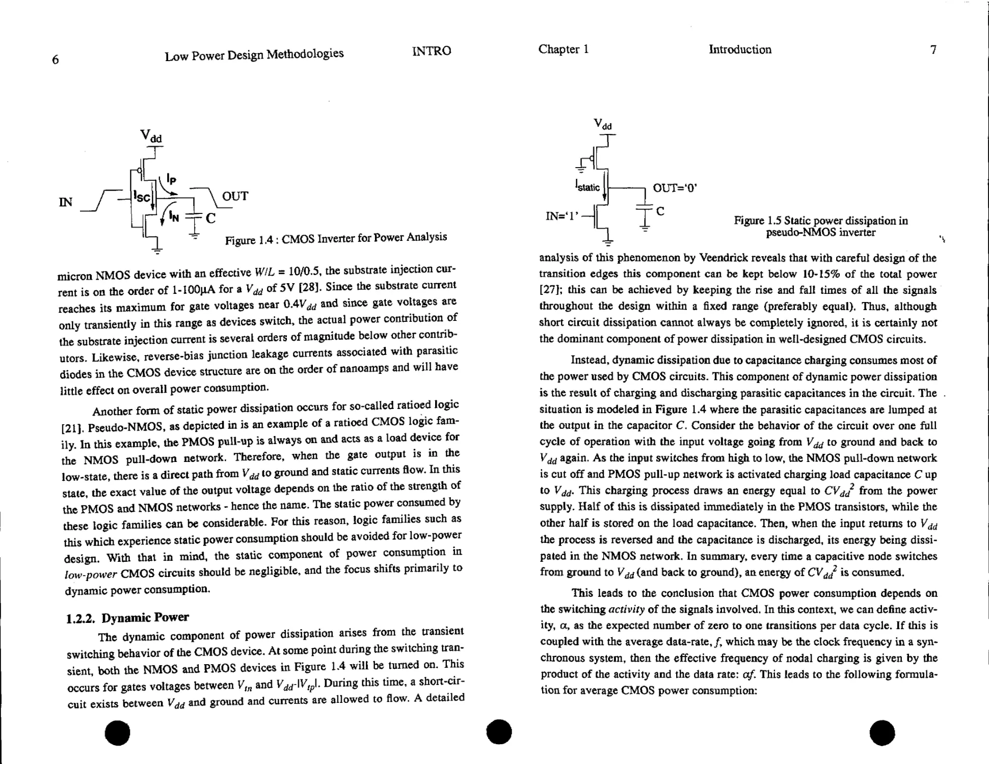
To set the scene for the rest of this book, it is judicious at this point to
briefly discuss the mechanisms for power consumption in CMOS circuits. Con-
sider the CMOS inverter of Figure 1.4. The power consumed when this inverter is
in use can be decomposed into two basic classes: static and dynamic. Each of
these components will now be analyzed individually.
1.2.1. Static Power
Ideally, CMOS circuits dissipate no static (DC) power since in the steady
state there is no direct path from Vdd to ground. Of course, this scenario can never
be realized in practice since in reality the MOS transistor is not a perfect switch.
Thus, there will always be leakage currents and substrate injection currents,
which will give rise to a static component of CMOS power dissipation. For a sub-
Thermal runaway
Gate dielectric
Junction fatigue
Electron! igration diffusion
Electrical-parameter shift
Package-related failure
Silicon-interconnect fatigue
100 200 300
°C above normal operating temperature
Figure 1.3 Onset temperatures of various failure mechanisms (after [22]).
6
Low Power Design Methodologies
INTRO
micron NMOS device with an effective WL = 10/0,5, the substrate injection cur-
rent is on the order of l-100pA for a Vdd of 5 V [28], Since the substrate current
reaches its maximum for gate voltages near 0.4У^ and since gate voltages are
only transiently in this range as devices switch, the actual power contribution of
the substrate injection current is several orders of magnitude below other contrib-
utors, Likewise, reverse-bias junction leakage currents associated with parasitic
diodes in the CMOS device structure are on the order of nanoamps and will have
little effect on overall power consumption.
Another form of static power dissipation occurs for so-called ratioed logic
[21]. Pseudo-NMOS, as depicted in is an example of a ratioed CMOS logic fam-
ily. In this example, the PMOS pull-up is always on and acts as a load device for
the NMOS pull-down network. Therefore, when the gate output is in the
low-state, there is a direct path from Vdd to ground and static currents flow. In this
state, the exact value of the output voltage depends on the ratio of the strength of
the PMOS and NMOS networks - hence the name. The static power consumed by
these logic families can be considerable. For this reason, logic families such as
this which experience static power consumption should be avoided for low-power
design. With that in mind, the static component of power consumption in
low-power CMOS circuits should be negligible, and the focus shifts primarily to
dynamic power consumption.
1,2.2, Dynamic Power
The dynamic component of power dissipation arises from the transient
switching behavior of the CMOS device. At some point during the switching tran-
sient, both the NMOS and PMOS devices in Figure 1.4 will be turned on. This
occurs for gates voltages between VJn and During this lime, a short-cir-
cuit exists between Vdd and ground and currents are allowed to flow. A detailed
Chapter 1
Introduction
7
Vdd
Utatic|----- OUT=‘0’
IN= 1 || _ Figure 1.5 Static power dissipation in
~ pseudo-NMOS inverter
analysis of this phenomenon by Veendrick reveals that with careful design of the
transition edges this component can be kept below 10-15% of the total power
[27}; this can be achieved by keeping the rise and fall times of all the signals
throughout the design within a fixed range (preferably equal). Thus, although
short circuit dissipation cannot always be completely ignored, it is certainly not
the dominant component of power dissipation in well-designed CMOS circuits.
Instead, dynamic dissipation due to capacitance charging consumes most of
the power used by CMOS circuits. This component of dynamic power dissipation
is the result of charging and discharging parasitic capacitances in the circuit. The
situation is modeled in Figure 1.4 where the parasitic capacitances are lumped at
the output in the capacitor C. Consider the behavior of the circuit over one full
cycle of operation with the input voltage going from to ground and back to
again. As the input switches from high to low, the NMOS pull-down network
is cut off and PMOS pull-up network is activated charging load capacitance C up
to This charging process draws an energy equal to CVdd2 from the power
supply. Half of this is dissipated immediately in the PMOS transistors, while the
other half is stored on the load capacitance. Then, when the input returns to
the process is reversed and the capacitance is discharged, its energy being dissi-
pated in the NMOS network. In summary, every time a capacitive node switches
from ground to (and back to ground), an energy of CVdd2 is consumed.
This leads to the conclusion that CMOS power consumption depends on
the switching activity of the signals involved. In this context, we can define activ-
ity, a, as the expected number of zero to one transitions per data cycle. If this is
coupled with the average data-rate, which may be the clock frequency in a syn-
chronous system, then the effective frequency of nodal charging is given by the
product of the activity and the data rate: of. This leads to the following formula-
tion for average CMOS power consumption:
8
Low Power Design Methodologies INTRO
= ^CV2ddf (1.2)
This classical result illustrates that the dynamic power is proportional to
switching activity, capacitive loading, and the square of the supply voltage. In
CMOS circuits, this component of power dissipation is by far the most important,
(typically) accounting for at least 90% of the total power dissipation [27]) as
illustrated by the previous discussion.
1.3. Degrees of Freedom
The previous section revealed the three degrees of freedom inherent in the
low-power design space: voltage, physical capacitance, and activity. Optimizing
for power invariably involves an attempt to reduce one or more of these factors.
Unfortunately, these parameters are not completely orthogonal and cannot be
optimized independently. This section briefly discusses each of these factors,
describing their relative importance, as well as the interactions that complicate
the power optimization process.
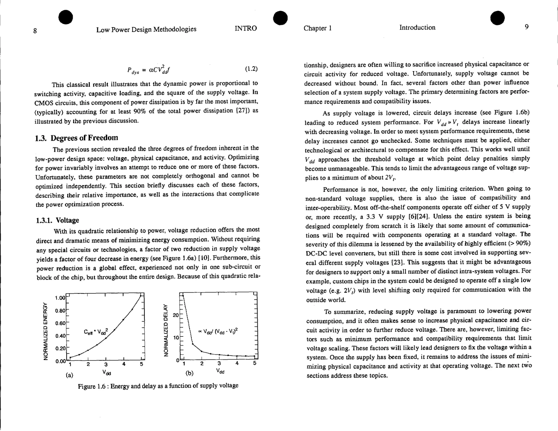
1.3Л , Voltage
With its quadratic relationship to power, voltage reduction offers the most
direct and dramatic means of minimizing energy consumption. Without requiring
any special circuits or technologies, a factor of two reduction in supply voltage
yields a factor of four decrease in energy (see Figure 1.6a) [ 10]. Furthermore, this
power reduction is a global effect, experienced not only in one sub-circuit or
block of the chip, but throughout the entire design. Because of this quadratic rela-
Figure 1.6 : Energy and delay as a function of supply voltage
Chapter 1
Introduction
9
tionship, designers are often willing to sacrifice increased physical capacitance or
circuit activity for reduced voltage. Unfortunately, supply voltage cannot be
decreased without bound. In fact, several factors other than power influence
selection of a system supply voltage. The primary determining factors are perfor-
mance requirements and compatibility issues.
As supply voltage is lowered, circuit delays increase (see Figure 1,6b)
leading to reduced system performance. For V^»Vf delays increase linearly
with decreasing voltage. In order to meet system performance requirements, these
delay increases cannot go unchecked. Some techniques must be applied, either
technological or architectural to compensate for this effect. This works well until
approaches the threshold voltage at which point delay penalties simply
become unmanageable. This tends to limit the advantageous range of voltage sup-
plies to a minimum of about 2Vt.
Performance is not, however, the only limiting criterion. When going to
non-standard voltage supplies, there is also the issue of compatibility and
inter-operability. Most off-the-shelf components operate off either of 5 V supply
or, more recently, a 33 V supply [6][24]. Unless the entire system is being
designed completely from scratch it is likely that some amount of communica-
tions will be required with components operating at a standard voltage. The
severity of this dilemma is lessened by the availability of highly efficient (> 90%)
DC-DC level converters, but still there is some cost involved in supporting sev-
eral different supply voltages [23]. This suggests that it might be advantageous
for designers to support only a small number of distinct intra-system voltages. For
example, custom chips in the system could be designed to operate off a single low
voltage (e.g. 2Vt) with level shifting only required for communication with the
outside world.
To summarize, reducing supply voltage is paramount to lowering power
consumption, and it often makes sense to increase physical capacitance and cir-
cuit activity in order to further reduce voltage. There are, however, limiting fac-
tors such as minimum performance and compatibility requirements that limit
voltage scaling. These factors will likely lead designers to fix the voltage within a
system. Once the supply has been fixed, it remains to address the issues of mini-
mizing physical capacitance and activity at that operating voltage. The next two
sections address these topics.
10
Low Power Design Methodologies
INTRO
L3.2. Physical Capacitance
Dynamic power consumption depends linearly on the physical capacitance
being switched. So, in addition to operating at low voltages, minimizing capaci-
tances offers another technique for minimizing power consumption. In order to
consider this possibility we must first understand what factors contribute to the
physical capacitance of a circuit. Only then can we consider how those factors
can be manipulated to reduce power.
The physical capacitance in CMOS circuits stems from two primary
sources: devices and interconnect. For past technologies, device capacitances
dominated over interconnect parasitics. As technologies continue to scale down,
however, this no longer holds true and we must consider the contribution of inter-
connect to the overall physical capacitance [2] ,[21].
With this understanding, we can now consider how to reduce physical
capacitance. From the previous discussion, we recognize that capacitances can be
kept at a minimum by using less logic, smaller devices, fewer and shorter wires.
Example techniques for reducing the active area include resource sharing, logic
minimization and gate sizing. Example techniques for reducing the interconnect
include register sharing, common sub-function extraction, placement and routing.
As with voltage, however, we are not free to optimize capacitance independently.
For example, reducing device sizes reduces physical capacitance, but it also
reduces the current drive of the transistors making the circuit operate more
slowly. This loss in performance might prevent us from lowering Vdd as much as
we might otherwise be able to do. In this scenario, we are giving up a possible
quadratic reduction in power through voltage scaling for a linear reduction
through capacitance scaling. So, if the designer is free to scale voltage it does not
make sense to minimize physical capacitance without considering the side effects.
Similar arguments can be applied to interconnect capacitance. If voltage and/or
activity can be significantly reduced by allowing some increase in physical inter-
connect capacitance, then this may result in a net decrease in power. The key
point to recognize is that low-power design is a joint optimization process in
which the variables cannot be manipulated independently.
1.3.3. Activity
In addition to voltage and physical capacitance, switching activity also
influences dynamic power consumption. A chip can contain a huge amount of
physical capacitance, but if it does not switch then no dynamic power will be con-
Chapter 1
Introduction
11
sumed. The activity determines how often this switching occurs. As mentioned
above, there are two components to switching activity. The first is the data rate,/,
which reflects how often on average new data arrives at each node. This data
might or might not be different from the previous data value. In this sense, the
data rate/describes how often on average switching, not will but could occur. For
example, in synchronous systems/might correspond to the clock frequency (see
Figure 1.7).
P « oCLVdd2f = CeffVdd2f
ОИ/4
Figure 1.7 : Interpretation of switching activity in synchronous systems
The second component of activity is the data activity, a. This factor corre-
sponds to the expected number of energy consuming transitions that will be trig-
gered by the arrival of each new piece of data. So, while/determines the average
periodicity of data arrivals, a determines how many transitions each arrival will
spark. For circuits that do not experience glitching, a can be interpreted as the
probability that an energy consuming (zero to one) transition will occur during a
single data period. Even for these circuits, calculation of a is difficult as it
depends not only on the switching activities of the circuit inputs and the logic
function computed by the circuit, but also on the spatial and temporal correlations
among the circuit inputs. The data activity inside a 16-bit multiplier may change
by as much as one order of magnitude as a function of input correlations.
For certain logic styles, however, glitching can be an important source of
signal activity and, therefore, deserves some mention here [3]. Glitching refers to
spurious and unwanted transitions that occur before a node settles down to its
final steady-state value. Glitching often arises when paths with unbalanced propa-
gation delays converge at the same point in the circuit. Calculation of this spuri-
ous activity in a circuit is very difficult and requires careful logic and/or circuit
12
Low Power Design Methodologies
INTRO
level characterization of the gates in a library as well as detailed knowledge of the
circuit structure [26]. Since glitching can cause a node to make several power
consuming transitions instead of one <Le. a > 1) it should be avoided whenever
possible.
The data activity a can be combined with the physical capacitance C to
obtain an effective capacitance, C^=aC, which describes the average capaci-
tance charged during each 1/f data period. This reflects the fact that neither the
physical capacitance nor the activity alone determine dynamic power consump-
tion. Instead, it is the effective capacitance, which combines the two, that truly
determines the power consumed by a CMOS circuit
P = aCVy^CtffVy (1.3)
Evaluating the effective capacitance of a design is non-trivial as it requires
a knowledge of both the physical aspects of the design (that is, technology param-
eters, circuit structure, delay model) as well as the signal statistics (that is, data
activity and correlations). This explains why, lacking proper tools, power analysis
is often deferred to the latest stages of the design process or is only obtained from
measurements on the finished parts.
As with voltage and physical capacitance, we can consider techniques for
reducing switching activity as a means of saving power. For example, switching
activity of a finite state machine can be significantly reduced via power-conscious
state encoding [25] and multi-level logic optimization [14]. As another example,
certain data representations such as sign magnitude have an inherently lower
activity than two’s-complement [8]. Since sign-magnitude arithmetic is much
more complex than two’s-complement, however, there is a price to be paid for the
reduced activity in terms of higher physical capacitance. This is yet another indi-
cation that low-power design is truly a joint optimization problem. In particular,
optimization of activity cannot be undertaken independently without consider-
ation for the effects on voltage and capacitance.
1.4. Recurring Themes in Low-Power
The previous sections have provided a strong foundation from which to
consider low-power CMOS design. The different chapters in this book present a
number of specific power reduction techniques applicable at various levels of
abstraction. Many of these techniques follow a small number of common themes.
Chapter 1
Introduction
13
The four principle themes are trading area-performance for power, adapting
designs to environmental conditions or data statistics, avoiding waste, and
exploiting locality.
Unquestionably, the most important theme is trading area-performance for
power. As mentioned earlier, power can be reduced by decreasing the system sup-
ply voltage and allowing the performance of the system to degrade. This is clear
example of trading performance for power. If the system designer is not willing to
give up the performance, she can consider applying techniques such as parallel
processing to maintain performance at low voltage. Since many of these tech-
niques incur an area penalty, we can think of this as trading area for power.
An effective power saving technique is to dynamically change operation of
the circuits as the characteristics of the environment and/or the statistics of the
input streams vary. Examples include choosing the most economic communica-
tion medium and changing error recovery and encoding to suit the channel noise
and error tolerance. Another example is to selectively precompute the output
logic values of the circuits one clock cycle before they are required, and then use
the precomputed values to reduce internal switching activity in the succeeding
clock cycle [1].
Another recurring low-power theme involves avoiding waste. For example,
clocking modules when they are idle is a waste of power. Glitching is another
good example of wasted power and can be avoided by path balancing and choice
of logic family. Other strategies for avoiding waste include using dedicated rather
than programmable hardware and reducing control overhead by using regular
algorithms and architectures. Avoiding waste can also take the form of designing
systems to meet rather than surpass performance requirements. If an application
requires 25 MIPS of processing performance, there is no advantage gained by
implementing a 50 MIPS processor at twice the power.
Exploiting locality is another recurring theme of low-power design. Global
operations inherently consume a lot of power. Data must be transferred йот one
part of the chip to another at the expense of switching a large bus capacitance.
Furthermore, the same data might need to be stored in many parts of the chip
wasting still more power. In contrast, a design partitioned to exploit locality of
reference can minimize the amount of expensive global communications
employed in favor of much less costly local interconnect networks. Moreover,
especially for DSP applications local data is more likely to be correlated and,
14
Low Power Design Methodologies
INTRO
therefore, to require much fewer power consuming transitions. So, in its various
forms, locality is an important concept in low-power design.
While not all low-power techniques can be classified as trading-off
area-performance for power, avoiding waste, and exploiting locality these basic
themes do describe many of the strategies that will be presented in this book.
1.5. Emerging Low Power Approaches — An Overview
While long being neglected, the topic of low power digital design has
vaulted to the forefront of the attention in the last couple of years and, suddenly, a
myriad of low power design techniques has emerged from both universities,
research laboratories and industry.
Barring a dramatic introduction of a novel low power manufacturing tech-
nology, it is now commonly agreed that low power digital design requires optimi-
zation at all levels of the design hierarchy, i.e. technology, devices, circuits, logic,
architecture (structure), algorithm (behavior) and system levels, as is illustrated
in Figure 1.8. Furthermore, an accompanying computer aided design methodol-
ogy is required. The goal of this book is to give a comprehensive overview of the
different approaches that are currently being conceived at the various levels of
design abstraction.
The presented techniques and approaches ultimately all come down to a
fundamental set of concepts: dissipation is reduced by lowering either the supply
voltage, the voltage swing, the physical capacitance, the switching activity or a
combination of the above (assuming that a reduction in performance is not allow-
able).
System
Partitioning, Power-down, Power states
Algorithm
Complexity, Concurrency, Regularity, Locality
Architecture
Paral lelism,Pi pel ining,Redu ndancy,Data encoding
es+ manipulation,Transistor sizing,Energy recovery
Threshold Reduction, Double-threshold devices
Figure 1.8 An integrated low-power methodology requires optimization at all
design abstraction layers.
Chapter 1
Introduction
15
The first part of the book discusses power minimization approaches at the
technology and circuit design levels. The various roads towards a low voltage
technology are explored in Chapter 2. An important conclusion from this chapter
is that various improvements and innovations in silicon technology can help us to
keep power dissipation within bounds but that no huge break-through’s should be
expected. Chapter 3 presents an in depth analysis and comparison of the design
options at the circuit level, including the impact of device sizing, circuit style
selection and clocking techniques. An entirely new and alternative approach to .
low power circuits is presented in Chapter 4 that discusses the topic of
energy-recovery CMOS. Since clock distribution is one of the important sources
of power dissipation (up to 60% in some of the highest performing microproces-
sors), a careful analysis and optimization of the low power clock generation and
distribution networks is recommendable. This is the topic of Chapter 5.
In the second part, we focus in power analysis and minimization at the
logic and module levels. Chapter 6 presents a complete design methodology and
computer-aided design approach for low-power design at the logic level. The next
two chapters focus on the power minimization of complete modules. Chapter 7
gives an in-depth and experimental view on the design of low-power arithmetic
modules, while Chapter 8 analyzes the options in low-power memory design.
The last three chapters of the book address the highest levels in the design
hierarchy, being the architecture and system levels. Both the low-power options
in the high-performance and the portable communities are represented. Chapter 9
discusses current and future trends in low-power microprocessor design, while
Chapter 10 analyzes how to reduce power dissipation in portable, wireless com-
munication devices. Finally, Chapter 11 presents an integrated design methodol-
ogy for these higher levels of design abstraction.
1.6. Summary
To conclude this introduction, it is worthwhile to summarize the major
challenges that, to our belief, have to be addressed if we want to keep power dis-
sipation within bounds in the next generations of digital integrated circuits.
• A low voltage/low threshold technology and circuit design approach,
targeting supply voltages around 1 Volt and operating with reduced
thresholds. This may include power savings techniques that recycle the
signal energies rather than dissipating them as heat
18
Low Power Design Methodologies
INTRO
no. 4, pp. 41-46, Feb. 17,1994.
[23] A. Stratakos, R. W. Brodersen, and S. R.Sanders, “High-Efficiency Low-Voltage
DC-DC Conversion for Portable Applications,” 1994 International Workshop on
Low-Power Design, Napa Valley, CA, April 1994.
[24] J. Sweeney and K. Ulery, “3.3V DSPs for Multimedia and Communications Products;
Designers Hamess Low-Power, Application-Specific DSPs ” EON, vol. 38, no. 21 A,
pp. 29-30, Oct. 18,1993.
[25] C-Y. Tsui, M. Pedram, C-H. Chen, and A. M. Despain. r Low power state assignment
targeting two- and multi-level logic implementations. " In Proceedings of the IEEE
international Conference on Computer Aided Design, pages 82-87, November 1994.
[26] C-Y. Tbui, M. Pedram, and A. M. Despain. ” Efficient estimation of dynamic power dis-
sipation under a real delay model." In Proceedings of the IEEE International Confer-
ence on Computer Aided Design, pages 224-228, November 1993.
[27] H. L M Veendrick, “Short-Circuit Dissipation of Static CMOS Circuitry and its Impact
on the Design of Buffer Circuits,” IEEE JSSCC, pp. 468-473, August 1984.
[28] R. K. Watts, ed„ Submicron Integrated Circuits, John Wiley & Sons, New York, 1989.
[29] R. Wilson, “Phones on the Move; Pocket Phone Sales are on Line for a Boom,” Elec-
tronics Weekly, no. 1606, pp. 25, Aug. 12,1992.
[30] Lemnios et al, “Issues in Low Power Design”, internal document ARPA 1993.
PARTI
Technology and
Circuit Design Levels
16
Low Power Design Methodologies
INTRO
• Low power interconnect, using advanced technology, reduced swing or
reduced activity approaches.
• Introduction of low-power system synchronization approaches, using
either self-timed, locally synchronous or other activity minimizing
approaches.
• Dynamic power management techniques, varying supply voltage and
execution speed according to activity measurements. This includes
self-adjusting and adaptive circuit architectures that can quickly and
efficiently respond to the environmental change as well as varying data
statistics.
• Application specific processing. This might rely on the increased use of
application specific circuits or application or domain specific proces-
sors.
• A conscientious drive towards parallel and distributed computing, even
in the general purpose world. This might mean a rethinking of the pro-
gramming paradigms, currently in use.
• A system-level approach towards power minimization. System perfor-
mance can be improved by moving the work to less energy constrained
parts of the system, for example, by performing the task on fixed sta-
tions rather than mobile sites, by using asymmetric communication pro-
tocols, or unbalanced data compression schemes.
• An integrated design methodology - including synthesis and compila-
tion tools. This requires the development of power conscious techniques
and tools for behavioral synthesis, logic synthesis and layout optimiza-
tion. Prime requirements for this are accurate and efficient estimation of
the power cost of alternative implementations and the ability to mini-
mize the power dissipation subject to given performance constraints and
supply voltage levels. This might very well require a progression to
higher level programming and specification paradigms (e.g. data flow or
object oriented programming).
Overall, low power design will require a change in mind-set. This can only
be achieved by introducing the power element early in the educational process,
not only with regards to circuit and logic design but also at the architectural level.
References
[1] M. Alidina, J. Monteiro, S. Devadas, A. Ghosh, and M. Papaefthymiou." Precomputa-
tion-based Sequential Logic Optimization for Low Power." In Proceedings of the 1994
International Workshop on Low Power Design, pages 57-62, April 1994.
[2] H. Bakoglu, Circuits, Interconnections, and Packaging for VLSI, Addison-Wesley,
Menlo Park, CA, 1990.
Chapter 1
Introduction
17
[3] L. Benini, M. Favalli, and B. Ricco, “Analysis of Hazard Contributions to Power Dissi-
pation in CMOS IC’s,” 1994 International Workshop on Low-Power Design, Napa Val-
ley, CA, pp. 27-32, April 1994.
[4] W Bowhill, et al., “A 300 MHz Quad-Issue CMOS RISC Microprocessor/’ Technical
Digest of the 1995ISSCC Conference, San Fransisco, 1995.
[5] R. W. Brodersen et al, “Technologies for Personal Communications," Proceedings of
the VLSI Symposium ‘91 Conference, Japan, pp. 5-9,1991.
[6] D. Bursky, “A Tidal Wave of 3-V IC’s Opens Up Many Options; Logic Chips that
Operate at 3V or Less Offer a Range of Low-Power Choices for Portable Systems,"
Electronic Design, vol. 40, no. 17, pp. 37-45, August 20,1992.
[7] В. Case, “Low-Power Design, Pentium Dominate ISSCC/* Microprocessor Report, vol.
8, no, 4, pp. 26-28, March 28, 1994.
[81 A. Chandrakasan, R. Allmon, A. Stratakos, and R. W. Brodersen, “Design of Portable
Systems,” Proceedings of CICC *94, San Diego, May 1994.
[9] A. Chandrakasan, S. Sheng, and R. W. Brodersen, “Low-Power Techniques for Portable
Real-Time DSP Applications,” VLSI Design ‘92, India, 1992.
[10] A. Chandrakasan, S. Sheng, and R. W. Brodersen, “Low-Power CMOS Design/* IEEE
Journal of Solid-State Circuits, pp. 472-484, April 1992.
[11] В. Cole, “At CICC: Designers Face Low-Power Future/* Electronic Engineering Times,
no. 745, pp. 1-2, May 10,1993.
[12] D. Dobbeipuhl et al, “A 200MHz, 64b, Dual Issue CMOS Microprocessor/* Digest of
Technical Papers, ISSC ‘92, pp. 106-107,1992.
[13] J. Eager, “Advances in Rechargeable Batteries Spark Product Innovation,** Proceedings
of the 1992 Silicon Valley Computer Conference, Santa Clara, pp. 243-253, Aug. 1992.
[14] S. Iman and M. Pedram. ” Multi-level network optimization for low power. " In Pro-
ceedings of the IEEE International Conference on Computer Aided Design, pages
372-377, November 1994.
[15] D. Maliniak, “Better Batteries for Low-Power Jobs,” Electronic Design, vol. 40, no .15,
pp. 18, July 23, 1992.
[16] D. Manners, “Portables Prompt Low-Power Chips/’ Electronics Weekly, no.1574, pp.
22, Nov. 13,1991.
[17] J. Mayer, “Designers Heed the Portable Mandate,” EDN, vol. 37, no. 20A, pp,65-68,
November 5,1992.
[18] J. Mello and P. Wayner, “Wireless Mobile Communications,” Byte, vol, 18, no. 2, pp.
146-153, Feb. 1993.
[19] -, “Mobile Madness. CCD Becomes PC,” LAN Magazine, vol. 9, no. 1, pp+ 46-48,1994.
[20] D. Pivin, “Pick the Right Package for Your Next ASIC Design/’ EDN, vol. 39, no. 3,
pp. 91-108, Feb. 3, 1994.
[21] J. Rabaey, Digital Integrated Circuits: A Design Perspective, Prentice Hall, Englewood
Cliffs, N.L , Nov. 1995.
[22] C. Small, “Shrinking Devices Put the Squeeze on System Packaging/’ EDN, vol. 39,
2
Device and Technology Impact on Low
Power Electronics
Chenming Hu
2.1. Introduction
In this chapter, we will explore the interplay between device technology
and low power electronics. For device designers, this study may contain lessons
for how to optimize the technology for low power. For circuit designers, а тоге
accurate understanding of device performance limitations and new possibilities
both for the present and the future should emerge from reading this chapter.
This chapter will focus on silicon CMOS technology for it is the dominant
technology today and probably for a long, long time to come. Alternative materi-
als and novel devices will be briefly mentioned.
2.2. Dynamic Dissipation in CMOS
Let us consider a CMOS logic gate. The power dissipation consists of a
static and dynamic component. Dynamic power is usually the dominant compo-
nent and is incurred only when the node voltage is switched.
? = ^dynamic* ? static
22
Low Power Design Methodologies
Parti
0
P dynamic = CV^af+P^ (2.2a)
r. C
(2.2b)
The second term in Eq, (2,2a) is known as the short-circuit power. When
the inverter input is around V^/2 during the turn-on and turn-off switching tran-
sients, both the PFET and the NFET are on and a short circuit current Isc flows
from Vdd to ground. The width of this short-circuit current pulse is about 1/4 of
the input rise and fall time. This term is typically only 10% of the first term as
shown in Eq, (2,2b), There, we assumed « тош « V^C/I^ « VddC/5Igc,
Combining Eq. (2,2a) and Eq, (2,2b),
^dynamic = *CV*da/ (2.3)
Switching Energy, E = £CV^ (2.4)
C = oxide capacitance + junction capacitance + interconnect capacitance
= c +C + C (2.5a)
= А + С^СЬ1 (2.5b)
What can one do to reduce Pdynamic? * is approximately 1.1 with a lower
bound of 1.0, No one seems to have a clever idea for reducing it except for raising
the ratio Vt/Vdd. We will discuss ways of minimizing C later, f is the clock fre-
quency. af is the average rate of cycling this node experiences. For example, an
idle block of the circuit may not experience switching because the clock signals
to the function blocks are gated. In this case a may be much smaller than one.
2.3. Effects of vdd and vt on Speed
Reducing Vdd in Eq. (2,3) is an obvious and very effective way of reducing
CMOS power. However, lower Vdd, for a given device technology, leads to lower
gate speed. Parallelism can be applied to compensate for speed loss to realize a
large net reduction in power [1]. On the other hand, optimizing the technology for
a lower Vdd could minimize or eliminate the speed loss due to Vdd reduction.
SPICE simulations confirm that the gate delay may be expressed as
Chapter 2 Device and Technology Impact on Low Power Electronics
23
cvaar i.i
4 It +t
4 dsatn dsatpj
(2.6a)
(2.6b)
dsatn p
т may be interpreted as the average of the time for the NFET saturation
current, Idsahl to discharge C from Vdd to Vdd/2, when the switching may be
considered to be complete, and the time for Idsatp to charge C from zero to
V^/2, In Eq. (2.6b), we used the fact Idsatn « 2.21^^ if Wn = Wp (see Table
2,2 in a later section).
The classical MOSFET model
(2.7)
Idsato = <JHCwW(Vg-Vt)VL
over-states the benefit of L reduction and the disadvantage of Vg, i.e. Vdd,
reduction. A very accurate model makes use of the fact that all inversion layer
charge carriers move with the saturation velocity, v^, at the pinch-off point in
the channel, where the potential is Vdsat. Therefore, [2]
(Idsat = W inversion charge density at "pinch-off" point
= W«satC<Bt(Vg-Vt-Vdsat) (2.8)
where W is the channel width, Vdsat is the drain saturation voltage,
^sat = 8 x 106cm/s for electrons and 6.5 x 10⁵cw/s for holes. It can be shown
that Vdsat is a function of L [2], and therefore
(2.9)
। _ _______I d sat о_
dsal (V,-Vt)u
Eq, (2.9) agrees well with experimental data (Fig. 2,1). It reduces to Eq. (2.7) for
large L or small Vg - Vt as expected. In the limit of very small L,
(2.10)
Idsat = WV«(VrVt)
The surface mobility, Ц, which appears in Eq. (2.9) in two places, is a
function of Tox and Vg as well [3]. The approximate L, Vg and Tox dependence
®f Idsat is
24
Low Power Design Methodologies
Parti
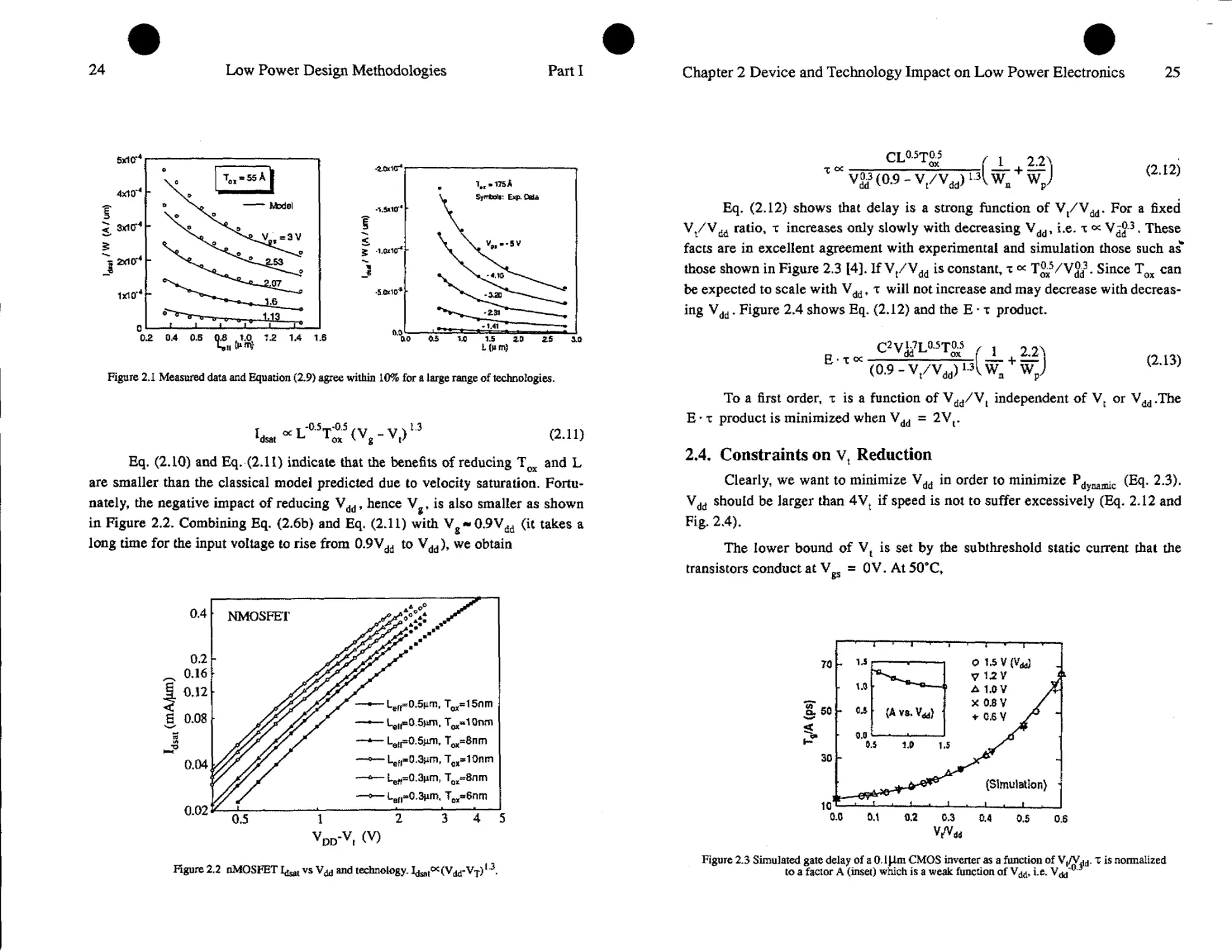
Figure 2.1 Measured data and Equation (2.9) agree within 10% for a large range of technologies.
IdMt“L-OiT^(Vg-Vt)U (2.11)
Eq, (2.10) and Eq. (2.11) indicate that the benefits of reducing Tox and L
are smaller than the classical model predicted due to velocity saturation. Fortu-
nately, the negative impact of reducing Vdd, hence V , is also smaller as shown
in Figure 2.2. Combining Eq. (2.6b) and Eq. (2.11) with Vg**0.9Vdd (it takes a
long time for the input voltage to rise from 0.9Vdd to Vdd), we obtain
v0D-vr (V)
Figure 2.2 nMOSFET 1^ vs and technology. Idsat^V^-V-r) 4
Chapter 2 Device and Technology Impact on Low Power Electronics
25
/ 1 22\
T K v«(o.9-vt/vd(J) 4 wn+w;J (2'I2)
Eq. (2.12) shows that delay is a strong function of V/V^. For a fixed
Vt/Vdd ratio, r increases only slowly with decreasing Vdd, i.e. т ос VjJ3. These
facts are in excellent agreement with experimental and simulation those such as*
those shown in Figure 2.3 [4]. If Vt/Vdd is constant, т K T^/V^3. Since Tox can
be expected to scale with Vdd, т will not increase and may decrease with decreas-
ing Vdd. Figure 2.4 shows Eq. (2.12) and the E * т product.
л t 2.2>
(0.9-V/Vdd)*4Wa WpJ
(2.13)
To a first order, т is a function of Vdd/Vt independent of VE or Vdd .The
E * r product is minimized when Vdd = 2Vt.
2.4. Constraints on vt Reduction
Clearly, we want to minimize Vdd in order to minimize Pdynafflic (Eq. 2.3).
Vdd should be larger than 4Vt if speed is not to suffer excessively (Eq. 2.12 and
Fig* 2.4).
The lower bound of Vt is set by the subthreshold static current that the
transistors conduct at V„ = 0V.At50oC,
Figure 23 Simulated gate delay of а ОЛЦт CMOS inverter as a function of т is normalized
to a factor A (inset) which is a weak function of i.e.
26
Low Power Design Methodologies
Parti
Figure 2.4 Speed is almost independent of Vid as long as V, is linearly scaled with Vd x E is a strong
Junction of Vdc].
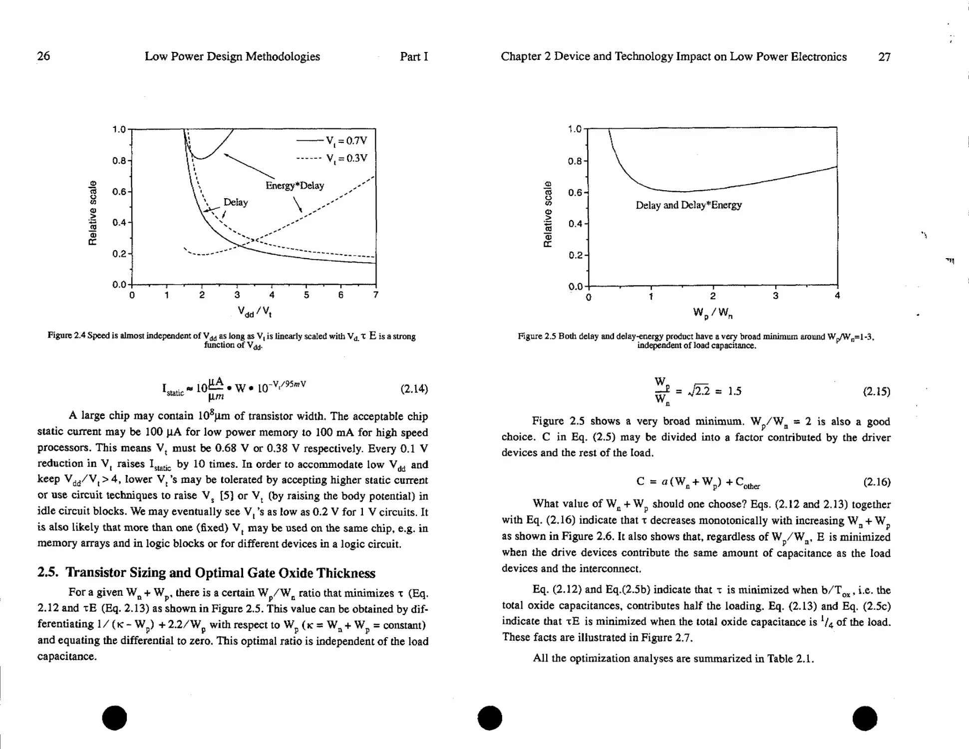
^static - 10^ * W • L0-V«»V (2.14)
A large chip may contain 108pm of transistor width. The acceptable chip
static current may be 100 pA for low power memory to 100 mA for high speed
processors. This means Vt must be 0.68 V or 038 V respectively. Every 0.1 V
reduction in Vt raises Istatic by 10 times. In order to accommodate low Vdd and
keep Vdd/Vt > 4, lower Vt’s may be tolerated by accepting higher static current
or use circuit techniques to raise Vs [5] or Vt (by raising the body potential) in
idle circuit blocks. We may eventually see Vt’s as low as 0.2 V for 1 V circuits. It
is also likely that more than one (fixed) Vt may be used on the same chip, e.g. in
memory arrays and in logic blocks or for different devices in a logic circuit.
2.5. Transistor Sizing and Optimal Gate Oxide Thickness
For a given Wn + Wp, there is a certain Wp/Wn ratio that minimizes т (Eq.
2.12 and tE (Eq. 2.13) as shown in Figure 2.5. This value can be obtained by dif-
ferentiating 1 / (к - Wp) + 2.2/Wp with respect to Wp (к = Wn + Wp = constant)
and equating the differential to zero. This optimal ratio is independent of the load
capacitance.
Chapter 2 Device and Technology Impact on Low Power Electronics
27
Figure 2.5 Both delay and delay-energy product have a very broad minimum around Wp/Wn=l-3.
independent of load capacitance.
-e = J12 = 1.5 (2.15)
Figure 2.5 shows a very broad minimum. Wp/Wa = 2 is also a good
choice» C in Eq. (2.5) may be divided into a factor contributed by the driver
devices and the rest of the load.
c = ^(W^WpJ+C^ (2.16)
What value of Wn + Wp should one choose? Eqs. (2.12 and 2.13) together
with Eq. (2.16) indicate that т decreases monotonically with increasing Wa + Wp
as shown in Figure 2.6. It also shows that, regardless of Wp/Wa, E is minimized
when the drive devices contribute the same amount of capacitance as the load
devices and the interconnect.
Eq. (2.12) and Eq.(2.5b) indicate that r is minimized when b/Tox, i.e. the
total oxide capacitances, contributes half the loading. Eq. (2.13) and Eq. (2.5c)
indicate that tE is minimized when the total oxide capacitance is !/4 of the load.
These facts are illustrated in Figure 2.7.
All the optimization analyses are summarized in Table 2.1.
28
Low Power Design Methodologies
Parti
Figure 2.6 Delay decreases monotonically with increasing Wn+Wp but the delay-energy product is
minimized when the drive devices contribute half of the total load capacitance.
Total Oxide Capacitance as Fraction of Load
Decreasing Tox "
Figure 2.7 Minimum delay is obtained when TOK is chosen such that oxide capacitance accounts for
half the total load. The minimum delay-energy product requires thicker Tox such that 74 of the load is
attributable to oxide capacitance.
2.6. Impact of Technology Scaling
Defect-free gate oxide field should be limited to 7-8MV/cm for a 20 year
lifetime at 125°C [7], Allowing margins for oxide defects, Vdd/Tox will likely be
Chapter 2 Device and Technology Impact on Low Power Electronics
29
Delay: r = —r-1— + , Energy: E = CVjd * ^dsatn ^dsalj/
L Vdd Tox Wp/wn wp+wn
to minimize T min max, >4Vt p s II MIO 1-3 max
to minimize tE min 2Vt 1-3 Cd=i
C: total load capacitance, С\ок: all load capacitances attributable to gate oxide, Cd: load capacitance attributable to driver devices.
Table 2.1 Optimization for Delay and Delay-Energy Product
limited to 4MV/cm. This sets an important and usually dominant factor in oxide
thickness selection in addition to the Tox optimization summarized in Table 2. L
A historical review and projection for future device technology is shown in
Table 2.2. Note that the PFET current remains to be about half the NFET current.
Figure 2.8 shows the projected trend of ldsat with technology scaling [8].Even in
the high-speed scenario where Eox is allowed to rise with time towards a very
aggressive 5 MV/cm, Idsa/W basically ceases to rise with scaling beyond the 0.5
pm generation because of velocity saturation» i.e. Eq, (2.9). Figure 2.9 shows the
projected inverter speed. The historical trend of speed doubling every two gener-
ations will slow down only slightly. Figure 2.9 agrees well with experimental data
Gate Length (Щп)е 3 2 L5 1 0.7 0.5 035 0.25 0.18 0.12
Vdd(V) 5 5 5 5 5 5/3.3 3.3/2.5 2.5/2.0 1.5 1.5
VT(V) 0.7 0.7 0.7 0.7 0.7 0.7/0.7 0.7/0.6 0.6/0.5 0.4 0.4
Tox(nm) 70 40 25 25 20 15/10 9/7 63/5.5 4.5 4
Idsatn (тА/Цт) 0.1 0.14 0.23 0.27 0.36 0.56/0.35 0.49/0.40 0.48/0.41 0.38 0.48
Idsatp 0.06 0.11 0.14 0.19 0.27/0.16 0.24/0.18 0.23/0.19 0.18 0.24
Inverter Delay (ps) 800 350 250 200 160 90/100 70/65 50/47 40 32
Table 2.2 Impact of Vddf L, and Tox scaling on MOSFET current and inverter speed
30
Low Power Design Methodologies
Part I
down to 0.1 gm [9]. Speed in the low-power scenario is only modestly lower than
in the high-power scenario.
Technology Generation
Figure 2.8 MOSFET current hardly increases beyond the 0.5 Jim generation of technology due to
velocity saturation even in the high-speed scenario, where oxide field rises aggressively.
Figure 2.9 Speed in the low-power scenario lags that in the high-speed scenario, where speed doubles
every 4 generations, rather than 2 generations as in the past.
I
Chapter 2 Device and Technology Impact on Low Power Electronics * 31
2 J. Technology and Device Innovations
Many novel high-speed low-power devices have been proposed [10] based
on quantum tunneling, single-electron effect, or even the motion of atoms. While
these devices have excellent intrinsic switching speed and energy, they are not
capable of driving the capacitance of long interconnects. In addition to the diffi-
culty of manufacturing, there are no suitable circuit architectures that are compat-
ible with the characteristics of these devices today. It may be more productive to
look for new low power architectures first and then find new devices that match
the needs of the architecture. An example of the latter model is the many device
innovations spawned by the need for programmable weights and summing
devices in neural networks.
The intrinsic speed-power benefit of GaAs is probably not sufficient to
overcome the difference in cost and technology momentum with respect to Si
except in very high speed circuits such as MMIC. In the foreseeable future, inno-
vations in silicon CMOS technology such as those discussed below, together with
the expected voltage and device scaling discussed earlier, will fuel the low power
electronics industry.
Silicon-On-Insulator (SOI) technology shown in Figure 2.10 can improve
delay and power through a *25% reduction in total capacitance [11]. SOI sub-
strates are produced by either wafer bonding or SIMOX (Separation by IMplanta-
tion of Oxygen). In wafer bonding, two bulk silicon wafers are oxidized and the
two oxide surfaces are held together and bonded at a moderately high tempera-
ture. One of the starting wafers is thinned by polishing, possibly followed by
C (SOI) C (bulk) C(SO1) /C(bvlk)
Active Gate (F.O.=1) 36J> fp 37.6 IF 0.97
N* Junction (1 drain) 9.5 IF 18.9 IF 0.50
P* Junction (1 drain) cJt₽5 7.6 tF 21Л fF 0.35
Polystlicon (1{J рГП1) CpOLt 0.43 IF 0.98 IF 0.44
Hl Aluminum (1mm) 72.6 IF 173.2 IF 0.59
2nd Aluminum (1mm) C ?iL 63.91F 9B.4 IF 0 65
Figure 2,10 Silicon-On-Insulator
technology achieves speed and power
improvements through denser layout,
reduced capacitances and reduced bulk
charge (body) effect.
32
Low Power Design Methodologies
Parti
chemical or plasma etching, until a thin layer (~2000A) of Si is left over the oxide
layer. In SIMOX, oxygen is ion implanted into a Si substrate at ~150keV to a
dose of ~1018 cm’2. A 2500A buried SiO2 layer with flat interface is formed under
a thin crystalline Si film during a *1350* anneal.
Optimized SOI MOSFETs can have a lower capacitance and slightly higher
Idsat than bulk devices because of the reduced body charge and a small reduction
in the minimum acceptable Vt, Together with some improvement in layout den-
sity, this potentially can result in up to 40% improvement in speed as Figure 2.11
[13]. That is two generations’ worth of speed advantage. This may be traded for
lower Vdd and obtain up to a factor 3 in power savings.
Technology Generation
Figure 2.11 Potential speed advantage of SOI technology. Speed may be traded for lower to
obtain a 3-fold power reduction.
Another way to reduce capacitance is to use the minimum possible width
for metal interconnects that carry ac signals such as the clock and data busses. A
recent breakthrough in electromigration research is the discovery that ac intercon-
nects can carry a many times higher current density than design rules based on de
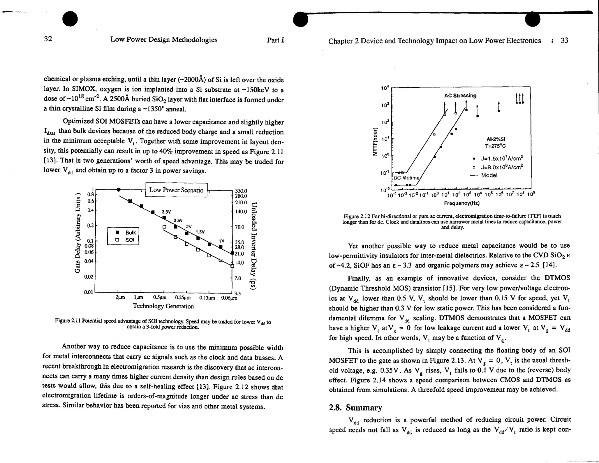
tests would allow, this due to a self-healing effect [13]. Figure 2.12 shows that
electromigration lifetime is orders-of-magnitude longer under ac stress than de
stress. Similar behavior has been reported for vias and other metal systems.
Chapter 2 Device and Technology Impact on Low Power Electronics ; 33
Figure 2.12 For bi-directional or pure ac current, electromigration time-to-failure (TTF) is much
longer than for de. Clock and datelines can use narrower metal lines to reduce capacitance, power
and delay.
Yet another possible way to reduce metal capacitance would be to use
low-permittivity insulators for inter-metal dielectrics. Relative to the CVD SiO2 e
of-4.2, SiOF has an e ~ 3.3 and organic polymers may achieve e ~ 2.5 [14].
Finally, as an example of innovative devices, consider the DTMOS
(Dynamic Threshold MOS) transistor [15]. For very low power/voltage electron-
ics at Vdd lower than 0.5 V, Vt should be lower than 0.15 V for speed, yet Vt
should be higher than 0.3 V for low static power. This has been considered a fun-
damental dilemma for Vdd scaling. DTMOS demonstrates that a MOSFET can
have a higher Vt atVg = 0 for low leakage current and a lower Vt at Vg = Vdd
for high speed. In other words, Vt may be a function of Vg.
This is accomplished by simply connecting the floating body of an SOI
MOSFET to the gate as shown in Figure 2.13. At Vg = 0, Vt is the usual thresh-
old voltage, e.g. 0.35V. As Vg rises, Vt falls to 0.1 V due to the (reverse) body
effect. Figure 2.14 shows a speed comparison between CMOS and DTMOS as
obtained from simulations. A threefold speed improvement may be achieved.
2.8. Summary
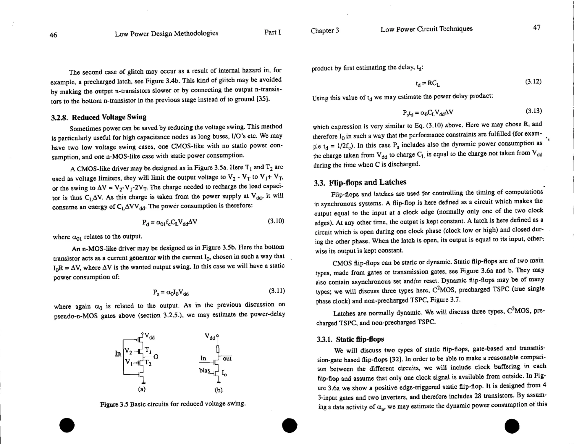
Vdd reduction is a powerful method of reducing circuit power. Circuit
speed needs not fall as Vdd is reduced as long as the Vdd/Vt ratio is kept con-
34
Low Power Design Methodologies
Parti
Buried Oxide
Substrate
Figure 2.13 Schematic of DTMOS, ал SOI MOSFET with body connected to the gate.
О
Gfl
Ю-w
109
Wn=5nm} Мр=10цт
Len=0.3gm
DTMOS, Tech-B
' □ CMOS, Tech-B
• DTMOS, Tech-A
О CMOS, Tech-A
10‘8 I
0.40 0.45 0.50 0.55 0.60 0.65 0.70
Power Supply Voltage (V)
Figure 2.14 Delay of CMOS and DTMOS inverter chains.
stant. The lowest acceptable Vt is determined by the static current that can be tol-
erated. However, one novel device DTMOS has demonstrated that VT can be
made to vary between a high value at Vg = 0 and a low value at Vg = Vdd.
Although the transistor current per pm width is not expected to drop, nei-
ther is it expected to double every technology generation as in the past even if
high Vdd is used without regard to power. Current will increase only marginally
beyond the 0.5 pm generation due to velocity saturation and the oxide breakdown
Chapter 2 Device and Technology Impact on Low Power Electronics L 35
field limit. However, gate speed continues to improve.
Innovations for reducing circuit capacitance are being developed. SOI is an
attractive evolutionary new technology. It reduces capacitance and increases cur-
rent, while layout density may improve speed by 30%. This may be traded for
lower Vdd and hence a significant reduction in power. Low dielectric-constant
inter-metal layer dielectrics are being developed. Finally, the recent discovery of
metal's ability to take high AC current density without electromigration should
bring a significant reduction to clock and data bus widths and capacitances.
There appears to be no revolutionary low power device/technology. e.g.
quantum devices, that is manufacturable or compatible with mainstream circuit
architectures today. Evolutionary innovations and optimization for low volt-
age/power plus continued device scaling will fortunately be able to support the
need of low power ULSI for a long time into the future.
References
[13 R. Brodersen et al, ISSCC Technical Digest, pp. 168-9, February 1193.
[2] P.K. Ko, Chapter 1 of “VLSI Electronics: Microstructure Science,”, Vol. 18, Academic
Press, 1989.
[3] M.S. Liang et al, IEEE Electron Device Letters, March 1986, pp. 409-413.
[4] Y. Mii et al, 1994 Symposium on VLSI Technology Digest of Technical Papers, pp. 9-10,
June 1994.
[5] K. Itoh, K. Sasaki, Y. Nakagome, IEEE Symposium of Low Power Electronics, pp. 84-85,
Oct. 1994.
[6] B. Burr, J. Schott, ISSCC, February 1994.
[7] R. Moazzami, et al, “Projecting Gate Oxide Reliability and Optimizing Bum-in ” IEEE
Trans. Electron Devices, p 1643, July 1990.
[8] C. Hu, “Future CMOS Scaling and Reliability,” Proc, of the IEEE, p. 682, May 1993.
[9] G. Shahidi, et al, “0.1 gm CMOS devices,” Symposium on VLSI Technology, p. 67, May
1993.
£10] Y. Wada, T, Uda, M. Lutwyche, S, Kondo, 1993 International Conference on Solid State
Devices and Materials, pp. 347-349, August 1993.
[11] Y. Yamaguchi, et al, IEEE Tran. Electron Devices, p. 179, 1993.
[12] C. Hu, “Silicon-on-Insulator for High Speed ULSI,” International Conference on Solid
State Devices and Materials, p. 137, August 1993.
[13] B.K Liew, etal, “Electromigration Interconnect Lifetime under AC and Pulse DC Stress,”
International Reliability Physics Symp., p. 215, 1989.
[14] J. Ida, et al, Symposium on VLSI Technology Digest, pp. 59-60, June 1994,
[15] F. Assaderaghi, et al, Technical Digest IEDM, pp. 809-812, December 1994.
Low Power Circuit Techniques
Christer Svensson and Dake Liu
3.1. Introduction
When CMOS (Complementary Metal Oxide Semiconductor) technology
was originally introduced, low power was one of the main motivations [32].
CMOS circuits was the first (and only) digital circuit technique which did not
consume any static power. Power was only consumed when the circuit was
switched. By using CMOS it was believed that the power consumption problem
was solved. Since then, integrated circuit complexity and speed have been contin-
uously increased. One result of this is that also CMOS now approaches the limits
of acceptable power consumption [10]. We will therefore investigate the power
consumption of CMOS circuits in this chapter, and make some brief comparisons
with other circuit techniques.
The scope of this chapter is thus to investigate the power consumption on
the circuit level, and to compare different circuit techniques from power con-
sumption point of view. We will limit ourselves to CMOS circuit techniques, with
some references to other techniques (as pseudo-n-MOS). We will further restrict
ourselves to synchronous systems.
We will start with a general model of the power consumption in CMOS cir-
cuits, taking also signal statistics into account. We will then discuss different cir-
38
Low Power Design Methodologies
Parti
cuit techniques, first timing circuits, as flip-flops and latches, and then logic
circuits or gates. Then we will discuss high capacitance nodes, as for example
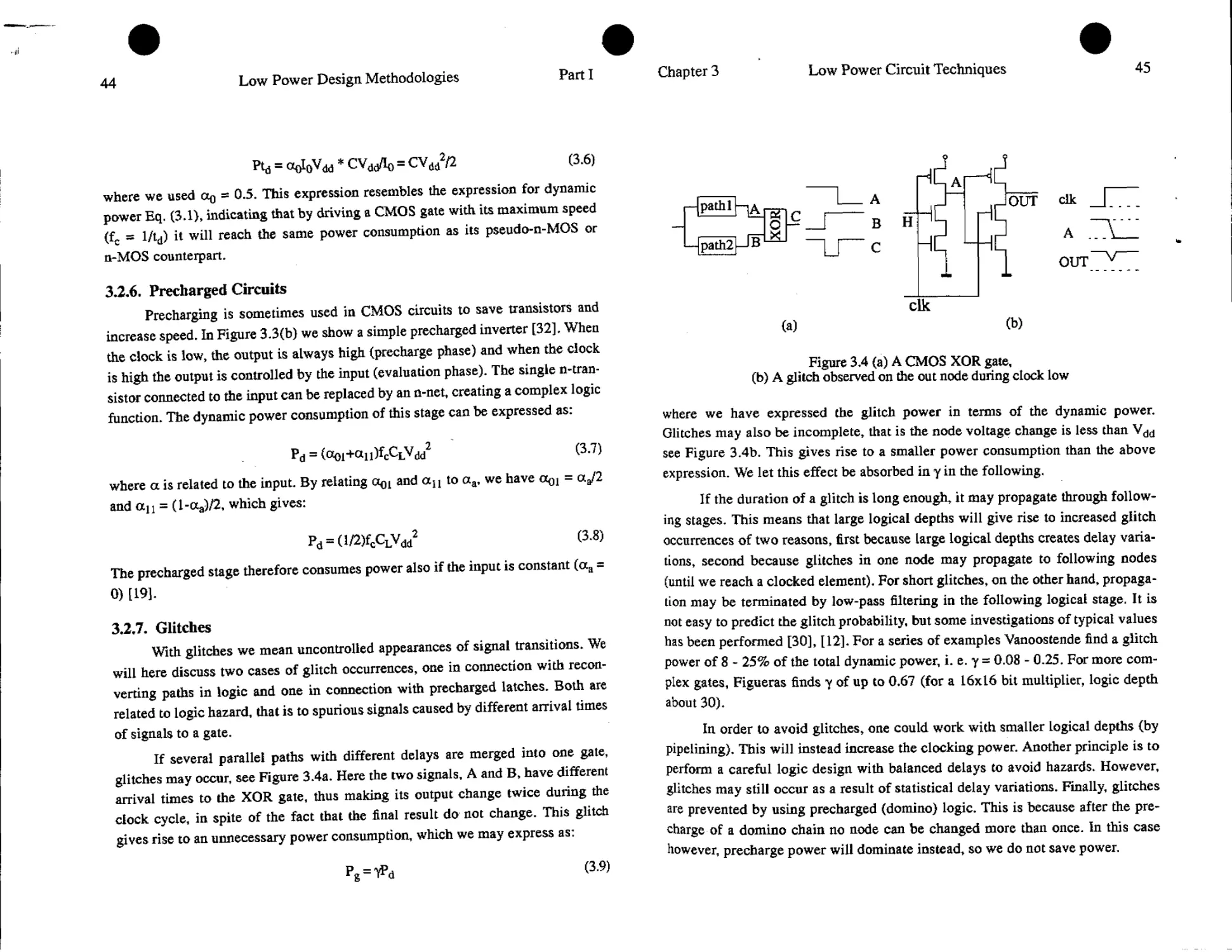
I/O’s separately. Finally we will give some conclusions.
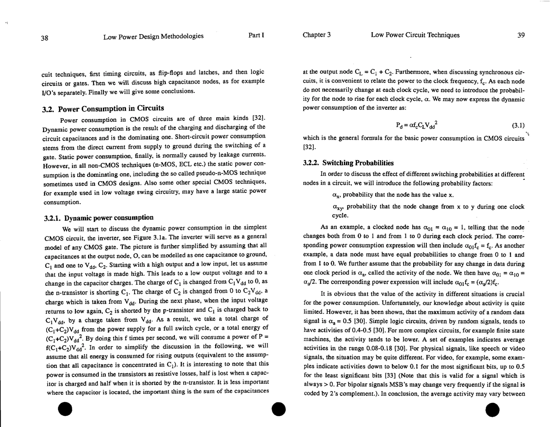
3.2. Power Consumption in Circuits
Power consumption in CMOS circuits are of three main kinds [32].
Dynamic power consumption is the result of the charging and discharging of the
circuit capacitances and is the dominating one. Short-circuit power consumption
stems from the direct current from supply to ground during the switching of a
gate. Static power consumption, finally, is normally caused by leakage currents.
However, in all non-CMOS techniques (n-MOS, ECL etc.) the static power con-
sumption is the dominating one, including the so called pseudo-n-MOS technique
sometimes used in CMOS designs, Also some other special CMOS techniques,
for example used in low voltage swing circuitry, may have a large static power
consumption.
3.2.1. Dynamic power consumption
We will start to discuss the dynamic power consumption in the simplest
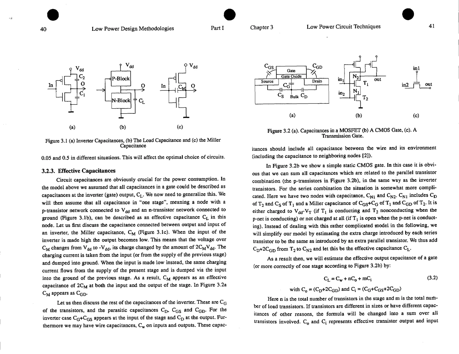
CMOS circuit, the inverter, see Figure 3.1a. The inverter will serve as a general
model of any CMOS gate. The picture is further simplified by assuming that all
capacitances at the output node, O, can be modelled as one capacitance to ground,
Cj and one to Vdd, C2. Starting with a high output and a low input, let us assume
that the input voltage is made high. This leads to a low output voltage and to a
change in the capacitor charges. The charge of Cj is changed from Cj Vdd to 0, as
the n-transistor is shorting Cp The charge of C2 is changed from 0 to C2Vdd, a
charge which is taken from Vdd. During the next phase, when the input voltage
returns to low again, C2 is shorted by the p-transistor and Ci is charged back to
CjVdd, by a charge taken from Vdd. As a result, we take a total charge of
(C!+C2)Vdd from the power supply for a full switch cycle, or a total energy of
(C2+C2)Vdd2. By doing this f times per second, we will consume a power of P =
f(Ci+C2)Vdd^. In order to simplify the discussion in the following, we will
assume that all energy is consumed for rising outputs (equivalent to the assump-
tion that all capacitance is concentrated in Cj). It is interesting to note that this
power is consumed in the transistors as resistive losses, half is lost when a capac-
itor is charged and half when it is shorted by the n-transistor. It is less important
where the capacitor is located, the important thing is the sum of the capacitances
Chapter 3
Low Power Circuit Techniques
39
at the output node CL = Q + C2. Furthermore, when discussing synchronous cir-
cuits, it is convenient to relate the power to the clock frequency, fc. As each node
do not necessarily change at each clock cycle, we need to introduce the probabil-
ity for the node to rise for each clock cycle, a. We may now express the dynamic
power consumption of the inverter as:
Pd = ctfcCLVdd2 (3.1)
which is the general formula for the basic power consumption in CMOS circuits
[32].
3.2 J. Switching Probabilities
In order to discuss the effect of different switching probabilities at different
nodes in a circuit, we will introduce the following probability factors:
«x, probability that the node has the value x.
Oxy, probability that the node change from x to у during one clock
cycle.
As an example, a clocked node has = a10 = 1, telling that the node
changes both from 0 to 1 and from 1 to 0 during each clock period. The corre-
sponding power consumption expression will then include aoifc = fc. As another
example, a data node must have equal probabilities to change from 0 to 1 and
from 1 to 0. We further assume that the probability for any change in data during
one clock period is aa, called the activity of the node. We then have = a10 =
The corresponding power expression will include aoifc = (aa/2)fc.
It is obvious that the value of the activity in different situations is crucial
for the power consumption. Unfortunately, our knowledge about activity is quite
limited. However, it has been shown, that the maximum activity of a random data
signal is aa = 0.5 [30]. Simple logic circuits, driven by random signals, tends to
have activities of 0.4-0.5 [30]. For more complex circuits, for example finite state
machines, the activity tends to be lower. A set of examples indicates average
activities in the range 0.08-0.18 [30]. For physical signals, like speech or video
signals, the situation may be quite different. For video, for example, some exam-
ples indicate activities down to below 0.1 for the most significant bits, up to 0.5
for the least significant bits [33] (Note that this is valid for a signal which is
always > 0. For bipolar signals MSB’s may change very frequently if the signal is
coded by 2’s complement.). In conclusion, the average activity may vary between
40
Low Power Design Methodologies
Parti
Figure 3.1 (a) Inverter Capacitances, (b) The Load Capacitance and (c) the Miller
Capacitance
0.05 and 0.5 in different situations. This will affect the optimal choice of circuits.
3.2.3. Effective Capacitances
Circuit capacitances are obviously crucial for the power consumption. In
the model above we assumed that all capacitances in a gate could be described as
capacitances at the inverter (gate) output, CL. We now need to generalize this. We
will then assume that all capacitance in “one stage”, meaning a node with a
p-transistor network connected to Vdd and an n-transistor network connected to
ground (Figure 3.1b), can be described as an effective capacitance CL in this
node. Let us first discuss the capacitance connected between output and input of
an inverter, the Miller capacitance, CM (Figure 3.1c). When the input of the
inverter is made high the output becomes low. This means that the voltage over
CM changes from Vdd to -Vdd, its charge changed by the amount of 2CMVdd. The
charging current is taken from the input (or from the supply of the previous stage)
and dumped into ground. When the input is made low instead, the same charging
current flows from the supply of the present stage and is dumped via the input
into the ground of the previous stage. As a result, CM appears as an effective
capacitance of 2Cm at both the input and the output of the stage. In Figure 3.2a
CM appears as CqD.
Let us then discuss the rest of the capacitances of the inverter. These are CG
of the transistors, and the parasitic capacitances CD, CGS and CGD. For the
inverter case CG+CGS appears at the input of the stage and CD at the output. Fur-
thermore we may have wire capacitances, Cw on inputs and outputs. These capac-
Chapter 3
Low Power Circuit Techniques
41
(a)
(b)
(c)
Figure 3.2 (a). Capacitances in a MOSFET (b) A CMOS Gate, (c). A
Transmission Gate.
itances should include all capacitance between the wire and its environment
(including the capacitance to neighboring nodes [2]).
In Figure 3.2b we show a simple static CMOS gate. In this case it is obvi-
ous that we can sum all capacitances which are related to the parallel transistor
combination (the p-transistors in Figure 3.2b), in the same way as the inverter
transistors. For the series combination the situation is somewhat more compli-
cated. Here we have two nodes with capacitance, CN1 and CN2. CN1 includes CD
of T2 and Cs of T! and a Miller capacitance of CqS+Cg of and CGD of T2. It is
either charged to Vdd-VT (if Ti is conducting and T2 nonconducting when the
p-aet is conducting) or not charged at all (if Ti is open when the p-net is conduct-
ing). Instead of dealing with this rather complicated model in the following, we
will simplify our model by estimating the extra charge introduced by each series
transistor to be the same as introduced by an extra parallel transistor. We thus add
Cd+2Cgd from T2 to CN2 and let this be the effective capacitance CL.
As a result then, we will estimate the effective output capacitance of a gate
(or more correctly of one stage according to Figure 3.2b) by:
CL = Cw + nC0 + mQ (3.2)
with Co = (CD+2CGD) and Cj = (Cg+Cgs+2CqD)
Here n is the total number of transistors in the stage and m is the total num-
ber of load transistors. If transistors are different in sizes or have different capac-
itances of other reasons, the formula will be changed into a sum over all
transistors involved. Co and Cj represents effective transistor output and input
42
Low Power Design Methodologies
Parti
capacitances respectively* Sometimes it may be convenient to make another parti-
tion of the capacitances between different stages, we may for example include the
input capacitance of the stage in its effective capacitance and then exclude the
transistors in the following stage (they are instead included there)*
For a transmission gate, Figure 3.2c [32], the situation is somewhat differ-
ent, This stage does not amplify the signal, therefore it do not have a Miller
effect. For this gate the “input” capacitance on the transistor gates are CTi = CG +
Cgs + QjD eac^ and the “output” capacitance at each source/drains of the trans-
mission gate is CTo = CD + CDS, In the following we will however use CTi = Q
and CTo = Co for simplicity*
3.2.4. Short-circuit Power Consumption
When a static CMOS gate is switched by an input signal with a nonzero
rise or fall time, both n- and p-transistors will conduct simultaneously for a short
time. During this time, there will be a “short-circuit current”, flowing directly
between Vdd and ground and not participating in charging or discharging CL [32]*
Using a simple static modelling, this current gives rise to a power consumption of
[31]:
fl 3 x
= г (3.3)
where we have assumed a simple inverter with n- and p-transistors with the same
p* т is the rise or fall time of the input signal and T is the period of the input sig-
nal (average time between transitions). Taking dynamic effects into account,
gives a more accurate formula [14], which indicates that Eq. (3*3) is an overesti-
mation with maybe 3 times of the short-circuit power consumption. Using the
probabilities defined above, we may write 1/T = (aoi+aio)fc, which for a clocked
node is 2fc and for a logic signal is aafc. Psc thus depends on the node activity in
the same way as Pd and on input rise or fall time. For well designed circuits Psc is
normally less than 10% of Pd, so we will in most cases neglect Рк in the follow-
ing. Still, it can be large under special circumstances, that is for slow input sig-
nals (large t) [31].
3.2.5. Static Power Consumption
In normal CMOS circuits the static power consumption is controlled by the
leakage currents of transistors and pn-junctions. For the inverter model in Figure
Chapter 3
Low Power Circuit Techniques
« 43
ЗЛ а Дог example, the power consumption for a low input is given by the leakage
current of the n-transistor, 1ЙОп and for a high input by the p-transistor, IdOp.
Assuming a0 = cq gives a static power consumption of
Ps = Vdd(IdQn+IdOp)^ (3.4)
This power consumption is normally very low and can therefore be
neglected. For future processes with possibly very low threshold voltages, the
leakage currents may increase, however, and become important [20].
For other circuit techniques than CMOS, the static power consumption is
normally dominating. Let us take the pseudo-n-MOS inverter in Figure 3.3a [32]
as an example. Here the p-transistor behaves as a current generator with current
Io, and it is sized in such a way that its current is much lower than the maximum
current of a conducting n-transistor. For a low input, only the p-transistor is con-
ducting, so the output is high. For a high input the n-transistor is conducting,
making the output low.
The low output voltage is here larger than zero, as the p-transistor current,
Io, passes through the n-transistor, giving rise to a voltage drop of about
WPn(^dd'^T)* The static power consumption is here given by:
Ps = «oloVdd (3.5)
where ccq refers to the output signal. In this type of circuit one often relate the
power consumption to the speed. Thus, assuming Io to be much less than the cur-
rent capability of the n-transistor means that the speed is given by the rise time,
which is CVdd/I0. The so called power-delay product, Ptd, can then be estimated
to:
Figure 3.3 (a). A pseudo-n-MOS inverter, (b). A precharged inverter
44
Low Power Design Methodologies
Parti
Ptd = aoIoV41*CV<1(A)=CVM2/2 (3.6)
where we used ocq = 0.5. This expression resembles the expression for dynamic
power Eq. (3.1), indicating that by driving a CMOS gate with its maximum speed
(fc = l/td) it will reach the same power consumption as its pseudo-n-MOS or
n-MOS counterpart.
3.2.6. Precharged Circuits
Precharging is sometimes used in CMOS circuits to save transistors and
increase speed. In Figure 3.3(b) we show a simple precharged inverter [32]. When
the clock is low, the output is always high (precharge phase) and when the clock
is high the output is controlled by the input (evaluation phase). The single n-tran-
sistor connected to the input can be replaced by an n-net, creating a complex logic
function. The dynamic power consumption of this stage can be expressed as:
Pd = (ao1+a1l)fcCLVtid2 (3.7)
where a is related to the input. By relating Ощ and an to aa, we have = ajl
and an = (l-aa)/2, which gives:
Pd= (l/2)fcCLVdd2 (3.8)
The precharged stage therefore consumes power also if the input is constant (aa =
0) [19].
32.7. Glitches
With glitches we mean uncontrolled appearances of signal transitions. We
will here discuss two cases of glitch occurrences, one in connection with recon-
verting paths in logic and one in connection with precharged latches. Both are
related to logic hazard, that is to spurious signals caused by different arrival times
of signals to a gate.
If several parallel paths with different delays are merged into one gate,
glitches may occur, see Figure 3.4a. Here the two signals, A and B, have different
arrival times to the XOR gate, thus making its output change twice during the
clock cycle, in spite of the fact that the final result do not change. This glitch
gives rise to an unnecessary power consumption, which we may express as:
(3.9)
Chapter 3
Low Power Circuit Techniques
45
Figure 3.4 (a) A CMOS XOR gate,
(b) A glitch observed on the out node during clock low
where we have expressed the glitch power in terms of the dynamic power.
Glitches may also be incomplete, that is the node voltage change is less than Vdd
see Figure 3.4b. This gives rise to a smaller power consumption than the above
expression. We let this effect be absorbed in у in the following.
If the duration of a glitch is long enough, it may propagate through follow-
ing stages. This means that large logical depths will give rise to increased glitch
occurrences of two reasons, first because large logical depths creates delay varia-
tions, second because glitches in one node may propagate to following nodes
(until we reach a clocked element). For short glitches, on the other hand, propaga-
tion may be terminated by low-pass filtering in the following logical stage. It is
not easy to predict the glitch probability, but some investigations of typical values
has been performed [30], [12]. For a series of examples Vanoostende find a glitch
power of 8 - 25% of the total dynamic power, i. e. у = 0.08 - 0.25. For more com-
plex gates, Figueras finds у of up to 0.67 (for a 16x16 bit multiplier, logic depth
about 30).
In order to avoid glitches, one could work with smaller logical depths (by
pipelining). This will instead increase the clocking power. Another principle is to
perform a careful logic design with balanced delays to avoid hazards. However,
glitches may still occur as a result of statistical delay variations. Finally, glitches
are prevented by using precharged (domino) logic. This is because after the pre-
charge of a domino chain no node can be changed more than once. In this case
however, precharge power will dominate instead, so we do not save power.
46
Low Power Design Methodologies
Parti
The second case of glitch may occur as a result of internal hazard in, for
example, a precharged latch, see Figure 3.4b. This kind of glitch may be avoided
by making the output n-transistors slower or by connecting the output n-transis-
tors to the bottom n-transistor in the previous stage instead of to ground [35].
3.2.8, Reduced Voltage Swing
Sometimes power can be saved by reducing the voltage swing. This method
is particularly useful for high capacitance nodes as long buses, I/O’s etc. We may
have two low voltage swing cases, one CMOS-like with no static power con-
sumption, and one n-MOS-like case with static power consumption.
A CM OS-like driver may be designed as in Figure 3.5a. Here Tj and T2 are
used as voltage limiters, they will limit the output voltage to V2 - VT to Vj+ VT,
or the swing to AV = V3-Vi-2VT. The charge needed to recharge the load capaci-
tor is thus ClAV. As this charge is taken from the power supply at Vdd, it will
consume an energy of CLAVVdd. The power consumption is therefore:
Pd = <WcCLVddAV (3.10)
where relates to the output.
An n-MOS-like driver may be designed as in Figure 3.5b. Here the bottom
transistor acts as a current generator with the current Io, chosen in such a way that
IqR = AV, where AV is the wanted output swing. In this case we will have a static
power consumption of:
= aoIoVdd (3.11)
where again ot^ is related to the output. As in the previous discussion on
pseudo-n-MOS gates above (section 3.2.5.), we may estimate the power-delay
Figure 3.5 Basic circuits for reduced voltage swing.
Chapter 3
Low Power Circuit Techniques
47
product by first estimating the delay, td:
td = RCL (3.12)
Using this value of td we may estimate the power delay product:
Pstd = aoCLVddAV (3.13)
which expression is very similar to Eq, (3,10) above, Here we may chose R, and
therefore Io in such a way that the performance constraints are fulfilled (for exam-
ple td = l/2fc). In this case Ps includes also the dynamic power consumption as
the charge taken from Vdd to charge CL is equal to the charge not taken from Vdd
during the time when C is discharged,
3.3. Flip-flops and Latches
Flip-flops and latches are used for controlling the timing of computations
in synchronous systems. A flip-flop is here defined as a circuit which makes the
output equal to the input at a clock edge (normally only one of the two clock
edges). At any other time, the output is kept constant. A latch is here defined as a
circuit which is open during one clock phase (clock low or high) and closed dur-
ing the other phase. When the latch is open, its output is equal to its input, other-,
wise its output is kept constant.
CMOS flip-flops can be static or dynamic. Static flip-flops are of two main
types, made from gates or transmission gates, see Figure 3.6a and b. They may
also contain asynchronous set and/or reset. Dynamic flip-flops may be of many
types; we will discuss three types here, C2MOS, precharged TSPC (true single
phase clock) and non-precharged TSPC, Figure 3.7.
Latches are normally dynamic. We will discuss three types, C2MOS, pre-
charged TSPC, and non-precharged TSPC,
33.L Static flip-flops
We will discuss two types of static flip-flops, gate-based and transmis-
sion-gate based flip-flops [32]. In order to be able to make a reasonable compari-
son between the different circuits, we will include clock buffering in each
flip-flop and assume that only one clock signal is available from outside. In Fig-
ure 3.6a we show a positive edge-triggered static flip-flop. It is designed from 4
3-input gates and two inverters, and therefore includes 28 transistors. By assum-
ing a data activity of ota, we may estimate the dynamic power consumption of this
48
Low Power Design Methodologies
Parti
Figure 3.6 (a) A static D flip-flop made from gates,
(b) A static D flip-flop made from transmission gates.
flip-flop according to the following. We have 4 clocked inputs and 1 inverter, with
a total of 10 transistor input capacitances and 2 output capacitances. Furthermore,
we have two And-Or-Inv, and two Or-And-Inv gates, each gate including 6 tran-
sistors, and an inverter. There are 10 inputs driven by data signals, each with 2
transistors and also one inverter output (with 2 connected transistors) and 4 gate
outputs, each with 6 transistors connected. Thus totally:
Pd = lOfcCiVda2 + 2fcC0Vdd2 + (10+2)(aa/2)fcCiVdd2 +
2(aaZ2)fcC0Vdd2 + 24(aa/2)fcC0Vdd2
or
Pd = [IOC, + 2C0 + 12(aj/2)Ci + 26(a/l)C0] fcVdd2 (3.14)
In Figure 3.6b we have a positive edge-triggered static flip-flop based on
transmission gates. This circuit is made from 7 inverters and 4 transmission gates,
that is a total of 22 transistors. Following the same procedure as above, we may
estimate the power consumption by noting that 12 transistor gates are clocked, 2
inverter outputs are clocked, and 5 inverters and 4 transmission gates have a data
signal on their inputs and outputs. This gives a total power consumption of:
Pd = [12Ci + 4C0 + lOCa^Ci + 26(aa/2)C0]fcVdd2 (3.15)
where we have treated transmission gate inputs and outputs as inverter outputs
from a capacitance of view (this may be a slight overestimation as the transmis-
sion gate do not have a Miller effect, see section 3,2.3.).
3.3.2. Dynamic flip-flops
Dynamic flip-flops may be of many types. Again, we will assume that only
one clock signal is available from outside and that clock buffering is included in
Chapter 3
Low Power Circuit Techniques
49
(a) (b) (c)
Figure 3.7 Dynamic MS D flip-flops, (a) C2MOS,
(b) TSPC, (c) Non-precharged TSPC
each flip-flop. We will treat 3 types below. We start with an edge-triggered
flip-flop made from two C2MOS latches, Figure 3.7a. This circuit contains 12
transistors, of which 8 are clocked at their gates and 4 at their outputs. Further-
more there are 4 transistors with data on their inputs and 8 transistors with data on
their outputs. From this we may estimate the power consumption as:
Pd = (8Cj + 4C0 + 4(а/2)С4 + 8(a/2)C0)fcVdd2 (3.16)
In Figure 3,7b we have a precharged TSPC (true single phase clock)
flip-flop containing 11 transistors, of which 6 are clocked on their inputs, 2 are
clocked on their outputs, there are 3 transistors with simple data on their inputs, 2
transistor gates connected to a precharged node, 2 data nodes with 3 transistors
and 1 precharged node with 3 transistors. Totally we estimate the power con-
sumption to:
Pd = (6Ci + 2CO + 3(a/2)Ci + 6(aa/2)C0 + 2(1/2)С; + 3(l/2)C0)fcVdd2 (3.17)
We may also create an edge-triggered flip-flop from two non-precharged
TSPC latches, see Figure 3.7c. In this case we have 14 transistors, of which 6 are
clocked on their inputs, 2 are clocked on their outputs and the others have data
signals. From this we get:
Pd = (6Ci + 2C0 + 8(aa/2)Ci + L2(aa/2)C0)fcVdd2 (3.18)
3.3.3. Latches
Common latches are normally dynamic. In our case we can derive these
from the dynamic flip-flops discussed above. A C2MOS latch thus consists of one
50
Low Power Design Methodologies
Part I
of the stages from Figure 3/7a, a precharged TSPC latch is made from the two last
stages in Figure 35b and a non-precharged TSPC latch from the two first (or the
two last) stages of Figure 3,7c. The power consumption of these circuits can then
be estimated as above, and a comparison between the latches will approximately
follow a comparison of the corresponding flip-flops.
For the special case of pre charged CVSL logic, an RS flip-flop is a suitable
static latch, see Figure 3,8a (25],[32]. The particular flip-flop in Figure 3.8a is set
or reset by low inputs. In this case the two outputs from the logic stage are pre-
charged high so that the flip-flop holds its previous data. When the clock is made
high, one of the outputs of the logic stage will go low, thus setting or resetting the
flip-flop. The power consumption of this latch can be written:
Pd = [4(l/2)Ci + 4(aa/2)C, + 8(aa/2)C0]fcVdd2 (3.19)
(a)
(b)
(c)
Figure 3,8 An RS flip-flop, (b) Double edge triggered flip-flop
(c) TSPC Double edge triggered flip-flop
3.3.4. Double-edge triggered flip-flops
By combining two flip-flops (or latches) and one multiplexer, it is possible
to form a double-edge-triggered device (DET), which utilizes both clock phases
for timing, see Fig. Figure 3,8b [15]. In Figure 3.8c we show an example of a
DET flip-flop [1]. Using the same principles as above, we estimate the power con-
sumption of this circuit to:
Pd = [LOCi + 2C0 + 4(l/2)Ci + 6(1/2)CO + 8(аЛ)С1 + ^о^С^У^2 (3.20)
Chapter 3
Low Power Circuit Techniques
51
or approximately the power consumption of a precharged flip-flop doubled (Eq.
(3.17)).
3.3.5. Discussion
Section 3.3. treats the circuits which are used for timing control in synchro-
nous logic. By using the formulas given above, we may make some comparisons
between the various techniques used. We will choose to do this under simplified
assumptions, that is assuming Co = Cj, We may then calculate the power con-
sumption of each flip-flop above in terms of fcCiVdd2, using aa as parameter, see
Figure 3.9.
From Figure 3.9 we can conclude that the gate-based static flip-flop (GFF)
has lower power consumption than the transmission gate flip-flop (TGFF), in
spite of the fact that it uses considerably more transistors. The reason is that it has
fewer clocked transistors. Of the dynamic flip-flops, the non-precharged TSPC
(NPTSPC) consumes least power, about the same power as the GFF at very low
aa and about half of the static one at high aa. The RS-flip-flop latch (RSFF)
appears very efficient, but must be considered in connection with the pre charged
CVSL logical gate (in this special case the latch is indirectly clocked through the
logic).
Figure 3.9 Power consumption of timing circuits
52
Low Power Design Methodologies
Part I
Considering the double-edge triggered flop-flop (DETFF), the example
above has a power consumption which is double compared to the corresponding
simple flip-flop (PTSPC in this case). However, for a fixed data throughput it
needs only half the clock frequency, making its power consumption for a given
data throughput equal to the corresponding single edge triggered flip-flop.
3,4. Logic
Logic circuits or gates are performing boolean functions. We will here con-
sider single-valued functions of n variables (the gate have a fan-in of n). The clas-
sical CMOS gate consists of two transistor networks connected to the output, one
n-net connected to ground and one p-net connected to the supply voltage (Vdd),
see Figure 3,2a [32]. Both networks performs the boolean function, in a comple-
mentary way, so that the output is always connected to ground or Vdd. For simple
functions (nor and nand), we need 2n transistors for performing the function (Fig-
ure 3.2b). For more complicated functions we may need up to 2nn transistors,
depending on the function. Note also, that one static gate stage can only perform
an inverting boolean function, for a general function we need also inverted inputs,
Figure 3.10a,
В HL BH[
(a)
(b)
A^A-41
B-4L B^l
Figure 3.10 XOR gate of (a) Static CMOS (b) CPL logic
In the comparisons between different types of logic circuit techniques
below, we will use simple nand or nor-gates as examples, that is we assume that
the number of transistors in each net is equal to the fan-in, n. We will also, as in
section 3 above, estimate the power consumption for each gate by including both
input and output capacitance of the gate. In this section we will assume that the
activity, aa, is the same of all nodes (output and inputs).
For simple static logic we may estimate the dynamic power consumption
to:
Chapter 3
Low Power Circuit Techniques
53
Pd = (а/2)(2пС1 + 2nC0)fcVdd2 (3.21)
Where we have combined the results from sections 3*2.1., 3.2*2., and 3.2*3*.
The static gale is characterized by a direct relation between the power con-
sumption and the activity, and also a proportionality to the number of transistors
in the circuit (which in general is between 2n and 2nn, where n is the number of
inputs).
3.4.1. Alternative CMOS Logic Circuit Techniques
Many different CMOS circuit techniques has been proposed [32]. We will
here discuss a limited number of techniques, which hopefully are representative
for most proposed techniques. The techniques treated are Standard static logic
(Figure 3.1b), CPL (Complementary Pass-transistor logic, using n-type pass tran-
sistors and inverter buffers) [34], Precharged logic (representing NORA [13],
TSPC [35] etc.), Domino logic (chain of precharged stages, and CVSL logic
(static and dynamic) [32][7].
Complementary pass transistor logic creates the logic function by pass
transistors, see Figure 3.10b. As the pass transistor network can not restore the
logic levels, we need to add an inverter for level restoring. Also, normally we
need both data and inverted data on the inputs. In the same time some gates, as for
example XOR, are easier to implement in pass transistor logic than in other
forms. We will, just for illustration, choose a gate of the type in Figure 3.10b, as
our example. Its power consumption can be written:
Pd = [(<V2)2(n- l)(2Cj + 2C0 + 2vCo) + 2(a/2)(2vCi + 2Co)]fcVdd2 (3.22)
where the first term represents the pass transistor inputs and output (the term with
v) and the second term represents the inverter* v = (Vdd-VT)/Vdd represents the
lower voltage swing of Vdd-VT at the inverter input, n in the above expression is
the number of inputs (n=2 in Figure 3.10b). For n>2 we assume a simple NAND
or NOR type of gate (as for the static logic above), see [34]. For a more general
gate, the number of transistors will be larger, n inputs may need up to 2tn‘l\n-l)
transistors, corresponding to a binary tree with depth (n-1) restructured into a
matrix (see [32]).
In Figure 3.3b, we show an example of a precharged gate (section 3.2*6.).
Note, that for a gate the input n-transistor is replaced by an n-net performing the
appropriate logical function. For this case we can estimate the dynamic power
54
Low Power Design Methodologies
Parti
Figure 3.11 Logic styles, (a) Domino logic (b) DCPL
consumption as follows. The inputs is assumed to have an activity of aa, thus
consuming the power (aa/2)nfcCiVdd2. The output consumes the power
(l/2)(n+2)fcCoVdd2. Finally the clocked transistors consumes a clock power (on
node elk) of 2fcCiVdd2. The total dynamic power consumption can therefore be
written:
Pd = ((a^nCi + ((n+2)/2)C0 + 2Ci)fcVdd2 (3.23)
Domino logic is just a chain of precharged stages, Figure 3.11a, where each
stage can be treated separately from power consumption point of view. Still it dif-
fers from a chain of static logic stages in that the domino chain is free from
race-induced glitches (see section 3.2.7.). An interesting variation of domino
logic is the DCPL (Data-Clock Precharged Logic) domino chain, Figure 3.11b
[361. Here the first stage is a normal precharged stage but the following stages are
precharged by the data rather than by the clock. Through the first stage we create
a data in the form of a “return to 1” signal. This means that in the whole following
chain each second stage will be precharged to 1 and the rest to 0. When real data
arrives, each node can only change once, so no race glitches occur. The stages can
be static stages or may have somewhat fewer transistors, see [36]. Compared to
the precharged stages, the DCPL stages do not consume clock power and do not
need the clocked transistors, instead the number of logic transistors may be some-
what increased. We may estimate the power consumption by just removing the
clocking power from the expression for the precharged gate.
CVSL logic is based on differential signals, that is we use both data and
data inverse on both inputs and outputs. In Figure 3.12a we show a static CVSL
gate. The logic function is created twice (as in static logic), using two comple-
Chapter 3
Low Power Circuit Techniques
55
Figure 3.12 CVSL gates
mentary n-nets. For each input vector one of the two n-nets is conducting, this
making its output low. Through the cross-coupled p-transistors the other output is
then made high. In this case we may estimate the dynamic power consumption as:
Pd = (a^2)2(n+l )(Ci+C0)fcVdd2 (3.24)
In order to have the static CVSL gate to work properly, the p-transistors
must not have a too strong driving capability (we will however not consider tran-
sistor scaling in the power estimation). This makes the CVSL gate relatively slow.
The speed can. be improved by precharging the output nodes. This can be done by
keeping or by removing the cross-coupled pair, we will remove the cross-coupled
pair below (meaning that the circuit becomes dynamic), Figure 3.12b. The pre-
charged CVSL may then be treated in a similar way as the precharged gates
above:
Pd = [(<V2)2nCj + (2n+3)(l/2)C0 + 3Ci]fcVdd2 (3.25)
34.2. Discussion
The view of the power consumption of logic given in this section is over-
simplified and must therefore be used with great care. There are four problems in
comparing different circuit techniques. First, transistor counts depends strongly
on the actual logical function to be implemented. A striking example can be
found in [34], where it is found that a full adder implemented in SL (static logic)
needs 40 transistors, whereas it needs only 28 transistors if implemented in CPL
(complementary pass logic). This differs from our simplified view (Bq. (3.21) and
Eq. (3.22)). However, also [34] is contradictory, it turns out that the sum part of
56
Low Power Design Methodologies
Parti
the adder needs 28 and 12 transistors and the carry part 12 and 16 transistors in
CL and CPL respectively, Second, characterization by using only a simple activ-
ity value (aa) is not realistic. In practice <xa of different nodes depends on the
actual logical function and on how it is implemented [4], Also, glitch probability
depends on which logical technique is used. Third, we have not taken transistor
scaling into account. Normally, for example, p-transistors are designed wider than
n-transistors (by a factor of 2-2.5). This will change the weighting factors of dif-
ferent transistors in our formulas and make n-MOS rich designs more advanta-
geous (as for example CPL and CVSL). Fourth, finally, we have not taken speed
into account. The different circuit techniques discussed have different speed
capabilities.
Let us anyway try to make some comparisons among the different circuit
techniques discussed. In Figure 3.13 we depict the power consumption versus
activity, using the simplified formulas derived above. We can directly see that
precharge logic is very disadvantageous from power point of view, especially for
low activities. It also appears that static logic is the most advantageous technique.
We believe that these are correct general conclusions, see also [18]. Static logic,
SL, is a simple, robust and power-lean technique, well suited for all applications,
including cell system, gate array and full custom design styles [24]. It is also
Figure 3.13 Combinational logic power consumption versus activity ratio
Chapter 3
Low Power Circuit Techniques
57
quite clear that precharge logic (PCL or PCVSL) is very power-hungry. Still, PCL
is probably the fastest technique available, so it may be motivated in special cases
[35].
Concerning CPL and CVSL, both are differential techniques. This means
that some logical functions are more easily (and more efficiently) implemented in
these techniques than in single-ended logic. The full adder (or the sum part of it)
discussed above is a good example. Because of the lower transistor count of the
CPL full adder it will consume less power than its SL counterpart [34]. An impor-
tant drawback of these techniques is that the differential outputs calls for 2 wires
per output. For general cases, like cell system or gate array design styles, this will
be devastating for power consumption, as the total interconnection length may be
more than doubled. Even in the non-differential case, interconnections tends to
consume more power than the logic [21]. The differential technique can however
be advantageous in compact, self-contained blocks, like adders, multipliers etc.
Concerning a comparison between CPL and CVSL, CPL normally have a larger
transistor count, but is also faster than CVSL [34]. Also CPL has an important
drawback, that is it will perform worse at low supply voltages. This is serious
from power point of view as low supply voltage is a very important route to low
power consumption.
3.5. High Capacitance Nodes
High capacitance nodes occur in a number of situations, for example in
clock networks, in clock drivers, at long buses or interconnections and at the out-
puts (VO*s). Normally, we need extra strong drivers to drive high capacitance
nodes, in order to keep pace with the required speed. It may also be dangerous to
allow too long rise-rimes in the system, as it will lead to large short-circuit power
consumption in the following stages (section 3.2.4.). We will discuss the driver
problem below.
In order to reduce the power consumption in connection to large capaci-
tance nodes, there are two possibilities. One is to reduce the activity of these
nodes, the other is to reduce the voltage swing. Reducing activity is an algo-
rithm/architecture problem and will not be treated here [4]. Voltage swing reduc-
tion is discussed below.
58
Low Power Design Methodologies
Parti
33.1. Drivers for Large Loads.
Quite often we need to drive large capacitive loads with reasonable speed
and/or with short rise and fall times. A typical example is a clock network, where
we may have quite strong demands on slopes [17]. Clock driving is also very
important from the power consumption point of view, as the clock power may be
20-40% of the total chip power [21], [10].
The standard method to drive large loads is to use a tapered inverter chain,
Figure 3.14a [32], [14]. Let us study such a chain loaded by CL and using N
stages and a tapering factor of f. f is given by f** = Y = Cl/2Ci. For such a chain it
can be shown that there exist an optimum value of f for which the total delay of
the chain is minimum [14]. For Co = Q (as before), this optimum will occur at f =
3.5. The delay is however a relatively flat function of f, so also larger values of f
may be acceptable.
(b)
Figure 3.14 Driving the large load (a) A driver chain (b) Off chip driving
Let us study the power consumption of the inverter chain. The total
switched capacitance of the chain can be written [14], [6]:
^driver = 2(Ci+C0)(Y-l)/(f-l)
(3.26)
or, if we instead calculate the total driver capacitance divided by the load capaci-
tance:
Cdriver/CL = (i+Co/qjd-l/YMf-l) (3.27)
This expresses the power consumption of the driver chain in terms of the
power consumption in the load. For large values of CL, we may neglect 1/Y. Let
us furthermore again let Co = C|. Using the above optimum value of f=3.5 leads to
a power consumption of the driver which is 80% of the power consumption in the
Chapter 3
Low Power Circuit Techniques
59
load, or in other words, the driver causes an excess power consumption of 80%
over the load. This is thus quite a large overhead.
By instead minimizing the power-delay product of the driver chain, we will
arrive to a larger value of f and therefore a lower value of the excess power [6].
However, there is no reason why this particular choice should be more interesting
than another one. Instead, we should minimize the power consumption, by choos-
ing as large f as possible, taking delay and slope constraints into account. If we,
for example, increase f from 3.5 to 9, the power consumption overhead will be
reduced from 80% to 25% of the load power, at the cost of a delay increase of
20%.
It is also possible to work with non-constant tapering factors, but the
improvements is very limited [6]. Furthermore, if the load consists of gates and
inverters (as in the case of a clock network), the short-circuit power of these cir-
cuits may increase with a slower driver (large f). We judge this effect as quite
small.
3.5.2 . Low Voltage Swing
An efficient way to save power is to reduce the voltage swing on high
capacitance nodes, see Figure 3.14b. Here we depict an interconnection, at which
we first convert the signal to a low swing and then restore it to full swing again.
In this scheme we save power in two ways. First, the charge needed for
charge/discharge CL is lowered. Second, as the current to be delivered by the
driver to charge/discharge CL in a certain time is lowered, the driver size can be
reduced, so the driver itself will consume less power. The problems are to pro-
duce a small swing with small static power consumption and to amplify the signal
with a small power consumption. We will discuss a few examples of circuit tech-
niques for low voltage swing below.
One approach for swing limitation is to let the driver limit the voltage
swing. A straight-forward method is to use an ordinary inverter with special sup-
ply voltages, Figure 3.15a [23]. The special supply voltages can be generated on
chip with limited power overhead [23]. As the effective drain voltages of the
driver transistors are reduced, to the actual swing in this case, we still need the
same transistor sizes as for the full swing driver. Therefore the power consump-
tion of the driver stage input and on the pre-drivers will be quite large. Another
approach with similar properties is the one proposed in Figure 3.5a. In this case
we may obtain some swing reduction also without extra voltages, by letting
60
Low Power Design Methodologies
Parti
Figure 3.15 Low swing circuit techniques
V2=Vdd and Vi=0 (giving a swing of Vdd-2VT). Also, as the drain voltages is
larger than the output swing, we may use smaller transistor sizes than in the full
swing case.
Another straight-forward approach is to use a simple n-MOS driver with a
resistive load (as in Figure 3.5b). Even simpler, we may size the n-transistor to
give the correct current, Io, as in Figure 3.15b. The drawback with this circuit is
that it consumes static power (it can however be put in a standby mode just by
setting the output to high). The benefits are many. The n-transistor runs at full
drain voltage, so its size can be reduced considerably compared to the corre-
sponding full swing CMOS driver. For the same speed, we need only AV/Vdd of
the current needed in the full swing case. Furthermore, compared to an inverter,
we need no p-transistor. As the p-transistor normally is scaled larger than the
n-transistor, this gives very large savings on the drivers input capacitance For
example, assuming a voltage swing of AV = 0.2Vdd and a normal p-transistor size
of twice the n-transistor size, will make the input capacitance of the driver in Fig-
ure 3.15b 15 times smaller than that of a full swing inverter driver. Besides the
power savings on the load itself (Eq. (3.13)), we will save considerably on the
driver input and on the pre-drivers. The n-MOS driver with a resistive load can
also be implemented as an open-drain output driver (with the load external to the
Chapter 3
Low Power Circuit Techniques
61
chip)» it can be used as a terminated driver for driving transmission lines [28], and
similar circuits can be used to produce ECL-compatible outputs [27].
On the receiving side we need to amplify the low voltage swing back to
normal again. This can be accomplished by a normal amplifier, for example as in
Figure 3,15c [28]. By using a differential amplifier, it is easier to set the switch
voltage to an appropriate value. It may also be used for detecting differential sig-
nals directly [28]. A drawback is that the amplifier consumes static power. In [23]
another amplifier is proposed, which do not consume static power (if the swing is
not too small). A third possibility is to use a clocked sense amplifier, as is used at
the bit lines in memories, see for example Figure 3.15d [3]. Such a solution do not
consume static power either.
A second approach for swing limitation is to let the receiver limit the volt-
age swing. To some extent, we have already discussed this case. If we just move
the resistor in Figure 3.15b to the receiver side, we can say that the receiver is
limiting the voltage swing. The idea is thus to have a current-mode driver and a
low-impedance receiver. We may for example use an inverter driver (still with
reduced size), combined with a low input impedance receiver. By using a current
conveyor input stage, it is possible to obtain an extremely low input impedance
and therefore a very low voltage swing [29], Tan demonstrated that this principle
can reduce power consumption more than 40 times. Again, all current-mode
approaches consumes static power. An important application of this approach is
the memory bit-lines. Here, the driver is the memory cell, where we can not
accept any overhead. Therefore, even if the bit-line swing normally is small, it
can not be controlled by the memory cell, so the swing may become large if the
memory is run slowly or if the process is faster than typical. The only way to con-
trol the power consumption of the bit-lines is then to limit their swing by the
receiver (sense amplifier in this case).
In conclusion, there are many possibilities to save power by utilizing low
swing on large capacitive loads. Important examples are chip I/Os, which nor-
mally have much higher capacitance than internal nodes, bit-lines in memories,
which have large capacitance and no opportunity to use large drivers (the memory
cell is driver) and long wires or buses. Less obvious is to use low voltage swing
on the clock distribution, even if such schemes has been proposed [8]. The reason
is of course that we want to use the clock directly on switch transistors and also
that we need to minimize clock delay. For I/Os, the need for power savings is one
important motivation for creating a new I/O standard, IEEE Std 1596.3 [11],
62
Low Power Design Methodologies
Parti
which is based on a differential current mode transmitter and a low impedance
(100 Q) receiver and which uses a voltage swing between 250 and 400 mV.
3.6. Summary
The aim of this chapter was to describe the main parameters controlling
circuit power consumption and to discuss and compare different low power cir-
cuit techniques.
We conclude that combinational static logic with simple, non-precharged,
dynamic flip-flops appears to be best suited for low power applications. This is
also in agreement with the branch-based approach for low power [24]. Also static
flip-flops based on gates are quite good. Other techniques, like for example com-
binational complementary pass transistor logic, may be advantageous in complex,
self-contained blocks of logic. By using double-edge-triggered flip-flops, the
clock frequency can be halved for a given data rate. This can lead to large power
savings in the clock distribution network.
Driving large loads always consumes much power. When full swing is nec-
essary, special care should be taken not to consume too much power in the driv-
ers. Otherwise, reducing the voltage swing is an efficient method to save power.
Several techniques for low voltage swing interconnects were discussed.
References
[1] M. Afghahi, J. Yuan, Double edge-triggered D-flip-flops for High Speed CMOS Cir-
cuits, IEEE J. of Solid-State Circuits, Vol 26, No. 8 pp 1168-1170,1991.
[2] H. B. Bakoglu, Circuits, Interconnections, and Packaging for VLSI, Reading, Addi-
son-Wesley Publishing Company, 1990.
[3] T Blalock and J Jaeger, A High-Speed Clamped Bitline Current-Mode Sense Amplifier,
IEEE J. of Solid State Circuits, Vol. 26, pp 542-548,1991.
[4] A. Chandr akasan, S. Sheng and R. W. Brodersen, Low-Power CMOS Digital Design,
IEEE Journal of Solid-State Circuits Vol. 27, No. 4, 1992.
[5] A. Chandrakasan et al.„ Design of Portable Systems, Proc, of IEEE 1994 Custom Inte-
grated Circuits Conference, pp 12.1.1-12.1.8,1994.
[6] J.-S. Choi and K. Lee, Design of CMOS tapered Buffer for Minimum Power-Delay
Product, IEEE Journal of Solid-State Circuits Vol. 29, No. 9, pp 1142-1145,1988.
[7] К. M. Chu and D. L. Pulfrey, A Comparison of CMOS Circuits Techniques: Differen-
tial Cascade Voltage Switch Logic Versus Conventional Logic, IEEE J. of Solid-State
Circuits, Vol. 22, No. 4, pp 528-532,1992.
[8] E. De Man and M. Schdbinger, Power Dissipation in the Clock System of Highly Pipe-
lined CMOS Circuits, Proc. 1994 Int. workshop on Low Power Design, ppl33-138.
Chapter 3
Low Power Circuit Techniques
63
[9] D. Deschacht, M. Robert, and D. Auvergne, Explicit Formulation of Delay in CMOS
Data Paths, IEEE Journal of Solid-State Circuits Vol. 23, No. 5, pp 1257-1264,1988.
[10] D. W. Dobberpuhl et al, A 200-MHz 64-b Dual-Issue CMOS Microprocessor, IEEE J.
of Solid-State Circuits, Vol. 27, No. 11, pp 1555-1566,1992.
[11] Draft 1.00 IEEE Std 1596.3-1994, IEEE Standard for Low-Voltage Differential Signal
for SCI (LVDS).
[12] M. A. Ortega and J. Figueras, Bounds on the Harzard Power Consumption in Modular
Static CMOS Circuits, a talk on PATMOS’94, Barcelona, Spain, unpublished.
[13] N. F. Goncalves, H. J. DeMan, NORA; A Race-free Dynamic CMOS Technique for
Pipelined Logic Structures, IEEE J. of Solid-State Circuits, Vol. 18, June 1983.
[14] N. Hedenstierna and K. Jeppson, CMOS Circuit Speed and Buffer Optimization, IEEE
IL of Computer Aided Design, Vol. 6, March 1987, pp, 270 - 28L
[15] R. Hossain, L. D. Wronski, and A. Albicki, Low Power Design Using Double Edge
Triggered Flip-Flops, IEEE Tr. on VLSI Systems, Vol.2, No. 2,1994, pp 261-265.
[16] M. Ishibeetal. High-Speed CMOS I/O Buffer Circuits, IEEE J. of Solid-State Circuits,
VoL 27, No. 4, pp 671-673, 1992.
[17] P. Larsson, C. Svensson, Noise in Digital Dynamic CMOS Circuits, IEEE Journal of
Solid-State Circuits, Vol. 29. No. 6, pp 655-662,1994.
[18] W. Lee et al, A Comparative Study on CMOS Digital Circuit Families for Low Power
Applications, Proc. 1994 Int. workshop on Low Power Design, ppl29-132.
[19] D. Liu, C. Svensson, Comparison of power consumption in CMOS synchronous logic
circuits, Proc, of European workshop on power and timing modelling pp 31-37,1992
[20] D. Liu, C. Svensson, Trading Speed for Low Power by Choice of Supply and Threshold
Voltages, IEEE Journal of Solid-State Circuits Vol. 28, No, 1, pp 10-17,1993.
[21] D. Liu, C. Svensson, Power Consumption Estimation in CMOS VLSI Chips, IEEE
Journal of Solid-State Circuits Vol. 29, No. 6, pp 663-670, 1994.
[22] C. Metra, Minimal Power-Delay Product CMOS Buffer, 4th International Workshop on
PATMOS, Oct 1994, Barcelona, pp 150-157.
[23] Y. Nakagome et al. Sub-l-V Swing Internal Bus Architecture for Future Low-Power
ULSTs, IEEE Journal of Solid-State Circuits Vol. 28, No. 4, pp 414-419,1993.
[24] C. Piguet, J-M. Masgonty, S. Cserveny, E. Dijkstra, Low-Power Low-Voltage Digital
CMOS Cell Design, 4th Int. Workshop on PATMOS, Oct. 1994, Barcelona, pp 132-139.
[25] D. Renshaw and С. H. Lau, Race-Free Clocking of CMOS Pipelines Using a Single
Global Clock, IEEE J. of Solid-State Circuits, VoL 25, No. 3, pp 766-769,1990.
[26] W. Roethig, E. Melcher, and M. Dana, Probabilistic Power Consumption Estimations in
Digital Circuits, Proc. European Workshop on power and timing modelling pp 7-15,
1992.
[27] M, S. J. Steyaert et al., ECL-CMOS and CMOS-ECL Interface for 150-MHz Digital
ECL Data Transmission Systems, IEEE JSSC, Vol. 26, No. 1, pp 18-23, 1991.
[28] C Svensson and J Yuan, High Speed CMOS Chip to Chip Communication Circuit,
Proc. 1991 Int. Symp. on Circuits and Systems, pp. 2221-2231.
64
Low Power Design Methodologies
Parti
[29] N. Tan and S. Eriksson, Low Power Chip-to-Chip Communication Circuits, Electronics
Letters, Vol. 30, No. 21, 1994, pp 1732-1733.
[30] P. Vanoostende et al, Evaluation of the limitations of the simple CMOS power estima-
tion formula: comparison with accurate estimation, Proc. European workshop on power
and timing modelling pp 16-25, 1992.
[31] H. J. M. Veendrick, Short-Circuit Dissipation of Static CMOS Circuitry and its Impact
on the Design of buffer circuits, IEEE JSSC VoL 19, No.4, 1984.
[32] N. H. E. Weste, K. Eshraghian, Principles of CMOS VLSI Design, (Second edition),
Reading, Addison-Wesley Publishing Company, 1993.
[33] M Winzker, Influence of Statistical Properties of Video Signals on the Power Dissipa-
tion of CMOS Circuits, Proc, of PATMOS *94, Barcelona, 17-19 Oct. 1994, pp 106-113.
[34] K. Yano, et al, A 3.8-ns CMOS 16X16-6 Multiplier Using Complementary Pass-Tran-
sistor Logic, IEEE J. of Solid-State Circuits, Vol. 25, No. 2, pp 388-395, 1990.
[35] J. Yuan C. Svensson, High Speed CMOS Circuit Techniques, IEEE J. of Solid-State
Circuits, VoL 24, No. 1, 1989, pp 62-70.
[36] J. Yuan, C. Svensson and P. Larsson, New domino logic precharged by clock and data,
Electronics Letters, Vol. 29, No. 25, pp 2188-2189, 1993.
4
Energy-Recovery CMOS
William C. Athas
With energy-recovery CMOS, circuit energy that would otherwise be dissipated
as heat is instead conserved for later reuse. From such an approach to low power,
there are no a priori limits to the degree to which energy and power dissipation
can be reduced inside a circuit. By externally controlling the length and shape of
the signal transitions, the energy expended to transition a signal between logic
levels can be reduced to an arbitrarily small degree. In contrast, unconventional
digital CMOS circuits, the energy dissipated to “flip a bit” from one to zero or
2
vice versa is a fixed and non-negotiable quantity on the order of (1/2) CV .
Methods and techniques to reduce dissipation are thus limited to minimizing the
number of transitions required to carry out a computation, or reducing the magni-
tude of the individual capacitances (C) or the voltage swing (V) between logic
levels zero and one. These methods offer significant energy and power reduction
but they are ultimately limited by (1/2) CV* 2 .
For logic circuits built from field-effect transistors (FETs), there is nothing
intrinsic about the devices which mandates that at least this much energy be dissi-
pated. Electrical charge on the gate of the FET controls the current that flows
between source and drain. Since the channel charge and gate charge are always
kept separate, there are no unavoidable losses due to the recombination between
66
Low Power Design Methodologies
Part I
charges of opposite polarity. This property of FETs can be exploited to reduce the
energy dissipated per transition by operating the FETs according to two principles
which have been stated in a number of different ways. The definition of Frank and
Solomon is a succinct and clear statement of the principle [11]:
1, When the FET is off, the source and drain are brought to the same potential.
2. When the FET is on, the source potential can vary while the drain floats.
The variations must be sufficiently slow so that the drain follows fairly closely,
with only a small potential difference between source and drain.
The term adiabatic charging has been coined to describe FET circuits that
operate in this way. The term “adiabatic” is taken from thermodynamics both lit-
erally and figuratively in that literally, the asymptotic dissipation is zero, and fig-
uratively, because the FETs drain “adiabatically” follows the source.
This approach to low-power operation is applicable to any system where
the circuit load, which is attached to the drain of the FET, can be characterized as
capacitive. For CMOS circuits, conceptually the most important capacitance is
the gate-to-channel capacitance because by charging or discharging that capaci-
tance, the channel current is controlled. Practically, the parasitic capacitances can
play a far more important role to the circuit’s power dissipation than the
gate-to-channel capacitances.
Figure 4.1 defines the fundamental relationships between the basic ele-
ments of an energy-recovery computing system. In this system, a computation
consists of charging and discharging the capacitive circuit nodes, adiabatically or
otherwise. The role of the middle component, labelled the regenerator, is all
important since it determines the ultimate efficiency of the energy-recovery pro-
cess. The regenerator is also the governor, in that it determines the length and the
shape of the transitions for the purpose of charging and discharging the logic cir-
cuits* signal capacitances. It serves the dual purpose of power source for energy
and clock source for timing.
Figure 4.1 Basic energy-recovery computing system
Chapter 4
Energy-Recovery CMOS
67
It is possible to build regenerators through a variety of mechanisms such as
commuting the energy between electrical and magnetic forms1, or using banks of
switched capacitors to incrementally step energy on to and off of the circuit load.
The theory and design of circuits that work in this way is an important topic but
its theory is not explored in this chapter. For the sake of completeness, a simple,
though inefficient design is presented in Appendix 4.A. There is emerging
research on how to design highly efficient regenerators [26][4].
To adiabatically cycle the energy between the logic circuit loads and the
regenerator requires that there always be an adiabatic path connecting the two. A
simple way to meet this requirement is to reverse each transition by backing out
the energy along the same set of wires and transistors that were used to steer it in.
This has been called temporal [26] or trivial [3] reversibility and requires that the
logic circuit’s state be otherwise held constant throughout the entire charge/dis-
charge cycle. As will be explored later, separate circuits for injecting and ejecting
charge are possible and often desirable.
Readers familiar with charge-steering and precharge design techniques can
immediately begin to think up schemes for building logic circuits that could work
in this manner. Indeed, there are myriad ways to invent FET-based circuits that
operate adiabatically or semi-adiabatically as well as circuits that are either fully
or partially reversible. Although the principles are simple, analyzing energy and
performance is typically subtle and tedious. Therefore, the first part of this chap-
ter investigates a simple logic style and some rudimentary circuit building blocks
based on CMOS transmission gates (T-gates). These circuits are simpler to ana-
lyze and have been successfully demonstrated in some small chip-building exper-
iments. However, they have some serious practical performance limitations. Later
in this chapter, the T-gate logic is compared to some emerging logic styles which
offer significantly better performance but are more difficult to model.
4.L A Simple Example
To illustrate a simple example of a practical energy-recovery circuit, consider the
design of a clock-AND gate, which is an AND gate with one input tied to the
clock [19]. Figure 4.2 depicts a “conventional,” non-adiabatic CMOS design. The
input x is assumed to be well-behaved and only changes when the clock signal,
elk, is low. With the clock low, the output is held low by the n-channel FET
lb See Appendix 4.A
68
Low Power Design Methodologies
Parti
Figure 4.2 Clock-AND gate (a) Logic symbol (b) CMOS schematic
(nFET) attached to elk. Changes on the x input do not affect the output. When
the clock swings from low to high and the x input is high, the two p-channel FETs
(pFETs) connected in series between the output and the supply rail at voltage V,
will conduct. The capacitance C, which models the input capacitance of the logic
driven by the output of this circuit, will then charge up to V.
The energetics of this circuit (excluding the input inverter) will be analyzed
through two separate, but equal approaches. First, energy dissipation will be
determined from the law of energy conservation and by doing all the bookkeeping
as charge flows through the various potential drops. Second, the FETs will be
modelled as single-valued resistances and the dissipation will be derived for when
those resistors connect the output capacitance to either V or ground. Issues such
as parasitic capacitances and dissipation due to short-circuit currents will be
neglected because they do not change the basic result and greatly detract from the
clarity of the presentation. Suffice it to say that the results derived are a lower
bound to the real dissipation since including these other effects only serves to
increase the actual dissipation.
From first principles, it is known that the charge quantity to be delivered
from the power supply to the capacitance C is (2=0 V The power supply must
deliver at least this much charge to the source of the top pFET at voltage V. The
work done by the power supply to do this is simply:
Einj = Q-V = CV2 (4.1)
Also from first principles, of this energy,
Ebil = (l/DCV2 (4.2)
will be stored on C once it has been fully charged to V.
Chapter 4
Energy-Recovery CMOS
69
From the conservation of energy law, the difference between Ebi( and Einj
must be accounted for between the source of the top pFET and the drain of the
bottom pFET Since there are no places to store energy inside the channel of the
pFET, it must therefore be dissipated in the channels of the two transistors. This
leads to the conclusion:
= = (1/2) CV2. (4.3)
An important observation at this point is that from this explanation, it was
unnecessary to mention how fast the input signals x or elk switched nor the size
of the pFETs, The energy dissipation is independent of the transistor design or the
input switching characteristics.
For the falling clock edge, the pFET path will stop conducting and the out-
put capacitance will be discharged through the nFET connected to elk. For this
transition, the power supply does no work. The energy stored on the capacitor
changes from EbU to 0. Similar to the argument for the pFET, this energy must be
dissipated in the nFET The energy returned to the power supply is
Erift = 2*0 = 0. The energy dissipated per cycle is:
^e/e = ^-^w»CV2-0 = 2-EiZf. (4.4)
This derivation determines where the energy was dissipated. To delve into
the details as to why there is this much dissipation, the individual FETs are mod-
elled as single-valued resistance when they are conducting. When the upper two
pFETs are on, they form a resistance, R between the power-supply rail at voltage
V and the output capacitance. With this configuration, current as a function of
time is:
/(0=^ = ^ЯС- (4-5)
dt R
The magnitude of the current is determined by the voltage drop from the
power-supply rail to the capacitor. From resistance and the current, the instanta-
neous power dissipation in the resistance is:
( _J_V 2 -2L
P(t) = i(t)2R = RC . (4.6)
The energy dissipation is the integral of power from 0 to T:
70
Low Power Design Methodologies
Part I
Ediss = = ^~e~RCdt = 1 - e *CJ (4.7)
0 0
The asymptotic energy dissipation, i.e., the limit as T approaches infinity,
equals that of Eq. 4.3, which was derived by tracking the potential differences
that the charge was forced to traverse through. The analysis for the discharging of
C is similar and the details are not presented.
One way to summarize these results is to notice that at the beginning of
2
each cycle, the energy injected by the power supply is CV , which is twice the bit
energy. To deliver a “bit” to the circuity the power supply must inject the energy
of two bits through the pFET pullup network. To discard a bit, its energy is dissi-
pated through the nFET pulldown network. Viewed in this way, conventional cir-
cuits represent a maximum in wastefulness. Note that this wastefulness stems
from how the FETs are connected and operated.
To investigate the energy dissipation for an energy-recovery version of this
circuit, the starting point is a “discrete” solution which will lead to a continuous,
adiabatic solution. In Eqs. 4.5-4.7, cunent, power, and energy are exponential in
time relative to the circuit’s RC time constant. For example, current asymptoti-
cally approaches zero and energy dissipation asymptotically approaches
(1/2) CV2. After 3 RC, the output voltage is within 95% of its final value, cur-
rent is less than 5% of its initial value, and energy dissipation is within 97.5% of
its final value.The assumption is made then, with only a negligible amount of
error, that after 3 • RC, the circuit has reached its final output value.
Assume that the allowed transition time is twice this, or 6-/?C. With a
conventional circuit, the extra charging time would bring the output ever closer to
the supply rail. Another idea is to apply a variable voltage in the form of a “step”
voltage to the circuit, by adding a second power supply that outputs a voltage of
V/2. The V/2 supply powers the circuit for the first 3 RC, and then the V
supply powers the circuit from 3 RC to 6 RC. The energy dissipation of Eq.
4.7 is then split into two parts:
3RC 6RC
r r 1 (W 1 (VV 1 2
Edia = f W + f W a у + -J = JCV2 . (4.8)
0 IRC
Chapter 4
Energy-Recovery CMOS
71
Doubling the transition time T and halving the maximum voltage drop
reduces the net dissipation by a factor of two. Through the same line of reasoning,
quadrupling the transition time and quartering the maximum voltage drop into
four steps yields a net energy reduction of a factor of four. In general, by stretch-
ing the transition time by a factor of n and keeping the maximum voltage drop to
V/n , the energy savings scales by a factor of n . This approach to energy recov-
ery is called step-wise charging [22].
The next case to be considered is where the regenerator continuously varies
the input voltage V so that current remains constant throughout the entire
charge/discharge process, i.e.,
'W = (4,9)
The energy-dissipation equation is [19]:
т т
Edtss = = ^cv2 . (4.10)
0 0
Energy dissipation is directly inversely proportional to the transition time.
Starting with this new equation to reducing dissipation, the design problem is to
devise a circuit that has the same functionality as that of Figure 4.2 but exploits
adiabatic charging. The first sub-problem to solve is how to exploit the regenera-
tor as a constant-current, variable-voltage source. One solution is to introduce a
new power source, but this is not necessary because the clock signal can be
employed for this purpose. A suitable circuit is shown in Figure 4.3. In this cir-
cuit, the clock signal, which is powered by the regenerator, directly drives the
output. Following the example of Denker, the clock signal is renamed to be the
power-clock [10], because of its twofold role. As before, whenever x is high the
output will be clamped low. If x is low, then the T-gate of Ml and М2 will pass
....l....... T-gate
I ml
pwr-clk — ------1—|---]--------1—clkAx
/
X L-^-J
Figure 4.3 Adiabatic, Clocked-CMOS Inverter
72
Low Power Design Methodologies
Part I
the power-clock to the output. The nFET (Ml) connected to x serves two pur-
poses. The first is for when x is high and the power-clock is low. In this case, Ml
pulls the output down to the low-voltage level of the power-clock. The second
reason is more subtle. Without Ml, the pFET (М2) would not turn on until the
power-clock’s voltage was above M2’s threshold voltage. This would incur a
non-adiabatic bump in the dissipation between the input and output,
Dynamically adjusting the power-clock voltage to comply with con-
stant-cuirent charging of Eq. 4.10 achieves an adiabatic-charging effect. The
power supply and the clock generator are now one and the same, and the circuit
has exactly the same input/output functionality as the circuit in Figure 4.2.
4.2, A look at some practical details
In the preceding section, the FET channels were modelled as single-valued resis-
tances and the gates as lumped capacitances. The ideal situation would be to be
able to directly apply such simple energy equations to CMOS circuits. To this
end, FETs can be modelled by an “on-resistance,” but, this resistance is a highly
non-linear function of the gate and channel voltages. This section investigates
how much additional detail is necessary.
Even though the resistances are highly non-linear, the general results about
energy dissipation hold because they are based on how charge is transported
between the logic circuits and regenerator, and not about the exact nature of the
switching devices. Following the analysis in Section 4.1, time-varying on-resis-
tance could be substituted into Eqs. 4.7-4.10, and all the integrations could be
redone to get the energy dissipations. However, for even the simple case of RC
charging, the equations can become quite involved. It is easy to construct circuit
topologies which are difficult to analyze because of this complication. Aware of
this pitfail, a simple circuit style is presented based on the CMOS T-gate, which
can be reasonably modelled by a single resistance when it is conducting [2],
As in the example of Figure 4.3, a T-gate is an nFET and a pFET connected
in parallel. To turn on the T-gate with minimal on-resistance, the pFET’s gate is
grounded and the nFET’s gate is tied to V. For a small potential difference across
the channel, which is the intended region for adiabatic circuits, the small-signal
model [24] for the conductances, Gp and Gn, of the FETs is applied.
C
Cp = C0XLWp Kp = ±- (4.11)
p
Chapter 4
Energy-Recovery CMOS
73
C„ L2
Gn = fWch~VT) C„ = C0XLWn Kn = ±- (4.12)
Я Hi
Channel length L, oxide capacitance per unit area, Cox, and mobilities pHand
, are well-known simulation parameters for modelling CMOS FETs. For bulk
CMOS, the threshold voltage parameter VT will vary with channel voltage
because of the body effect. For a starting point, VT is set equal to VT0 which
specifies threshold voltage for a channel-to-bulk voltage of zero volts. From these ..
parameters, thee process constants Kp and Kn are defined. Channel length is
assumed to be the minimum allowable for smallest on-resistance. Cox could also
be included in these constants, but since the analyses are mostly about energy in
terms of capacitance, resistance, and voltage, it is more convenient to separately
consider the gate capacitances of the FETs by Cp and Cn , which are calculated e
from L, Cox, and channel width W. This last parameter is under direct control of
the designer who can choose the gate capacitance by varying the channel width.
The equations do not take into account body effects or the difference in threshold
voltage between nFETs and pFETs, which limits accuracy.
By selecting the widths of the two FETs such that
K„/C„ = Kp/Cp, (4.13)
the sum of the two conductances simplifies to:
Gp+G" = {v v<* -VT+(v’2v-») (414)
The on-resistance of the T-gate is the reciprocal of this sum:
In this model, on-resistance is independent of channel voltage. The next
question is then: is there enough detail in Eq. 4.15 to reasonably model energy
dissipation from Eq. 4.10? To answer this question, the on-resistance from Eq.
4.15 is inserted into Eq. 4.10 to calculate the energy dissipated for the circuit of
Figure 4.3.
7 C 1 AL 2
^ = ^_cv2 = £.1._jl_c^ (4.16)
74
Low Power Design Methodologies
Parti
L (ЦЩ) ^ox (fF/цт2) V* (V) u« (cm2/Vs) Ир (cm2/Vs) (ps) KP (ps) С» (fF) cp (fF)
2pm 0.83 0.82 552 185 2.16 6.42 6.6 19.7
Table 4Л SPICE Model Parameters and Calculated Constants
Next, values calculated from this equation are compared to measurements taken
from the device-level, circuit-simulation program SPICE for a constant-current
source driving a large capacitance through a T-gate.
Values for Ctt, Cp, Kn, Kpy etc., are calculated from the level-two SPICE
model parameters for a MOSIS 2 gm process. They are listed in Table 1. The
width of the nFET is 4 m (the minimum size for this process is 3 m) and the
pFET is 12 m. The calculated on-resistance is 3.2 к £2. The load capacitance is
selected to be 250 fF so that it is much larger than the combined gate capacitance,
otherwise all or part of the gate capacitance would have to be included as part of
the load capacitance. The constant-current source is configured so that charge
delivery is spread out over intervals of Ins to 10ns. Appendix 4.B is a complete
pSPICE listing for the simulation experiment.
The graph of Figure 4.4 compares the simulation results to Eq. 4.16 for an
output swing of 0 to 5 volts. The RC product is 820 ps. The values from the
equation consistently show smaller energy dissipation than the measurements.
Part of this discrepancy is due to the body effect and to the mismatch between the
threshold voltages which was exacerbated in this experiment because it was nec-
essary to bias the pFET body voltage to 20% more than the output voltage swing.
This was necessary because to maintain constant current for the shorter transition
times, the power-clock voltage went above V. Regardless, even with this simple
model, the equation is within 25% of the SPICE measurements. Furthermore, for
fabrication technologies such as Silicon-on-Insulator (SOI), body effects will not
be present and Eq. 4,16 should be of higher accuracy.
One way to improve the T-gate’s performance is to increase the gate capac-
itances Cp and Cn . However, the energy requirements for driving these capaci-
tances should be included in the calculated dissipation since they also contribute
to the total dissipation. There are two general cases to consider. The first is when
conventional logic powers the inputs. In this case all of the input energy is dissi-
pated. The second case is when inputs are driven adiabatically.
Chapter 4
Energy-Recovery CMOS
75
For the conventional case, the input energy is simply:
E,„ = kC,/ (4-17)
The quantity кСп models the gates of an nFET and a pFET as a single lumped
capacitance. To determine how output energy dissipation scales as a function of
кСл , Eq. 4.16 is re-written in terms of V and the/?C product of the input capaci-
tance and on-resistance of the T-gate, called тгс.
Eouf= XTG = RTG-C„ (4.18)
The total system dissipation is:
Esys = + Eeu, = V2 = (kC„ + V2 . (4.19)
Eq. 4.19 defines an important trade-off in energy-recover CMOS circuits.
When the channel width, and thereby the input capacitance, is increased, the
energy dissipated in driving the load decreases, but the energy dissipated in driv-
ing the inputs increases proportionately. The optimization process is straightfor-
ward. The optimal value for Cn is found given all the other parameters:
c„ (4.20)
Inserting Eq. 4.20 into Eq. 4.19 yields the following expression for the minimum
dissipation:
Figure 4.4 Comparison of Eq.4.16 to SPICE simulation
76
Low Power Design Methodologies
Parti
= 2k£\,/ = J8-^Cy2 <4’21)
Clearly, something important has been lost at this point. Originally, by increasing
the transition time, the dissipation would drop off linearly. By Eq. 4.21, the deri-
vation for the optimal powering of an adiabatic load from a conventional source
yields a far less attractive result: the dissipation only scales as 7“1/2 .
An obvious improvement is to cascade two circuits, where the smaller
drives the input of the larger. By doing so, the total minimum energy dissipation
is [5]:
£^.e8l¥J cv (4-22>
From Eq. 4.21 to 4.22, the energy scaling improves from T~1/2 to T-3/4 . It has
been conjectured that for a cascading of n such stages, the energy dissipation
scales as:
<4-23>
This result is impractical since the parasitic capacitances can no longer be
neglected when the capacitances of the final gate-drive FETs become comparable
to that of the load. Also, for a constant cycle time interval, the transition time for
each of the steps must decrease at least linearly in the number of cascaded driver
stages.
In summary, to keep the energy-recovery scaling linear in transition time,
the inputs and outputs must be powered adiabatically. The next two sections
explore the implications to logic design when all of the logic including the inputs
and outputs are driven adiabatically.
43. Retractile Logic
Figure 4.5 depicts a two-level tree decoder of two inputs and four outputs built
from six T-gates. This decoder can be configured to implement the functions of
NAND, NOR, XOR, and XNOR by selectively tying together different mutu-
ally-exclusive outputs. The tree decoder can be a useful energy-recovery circuit
but it is often neither the smallest or fastest. It does concisely establish that any of
the readily known universal logic elements can be built from T-gate logic.
Chapter 4
Energy-Recovery CMOS
77
Implementing logic functions when there are more than two inputs is diffi-
cult to do efficiently. One way to proceed is to build a single logic network of
T-gates through which the power-clock signal is steered to one of two mutu-
ally-exclusive outputs, e.g., the tree decoder. Each series connections between
power-clock and output implements an ANDing of the inputs and each parallel
path an ORing of the inputs, Dual-rail encoding, which is needed otherwise to
drive the complementary inputs of the T-gates, can be put to good use here in that
logical NOT is trivially implemented by interchanging the two signal rails.
Such circuits become quite large and slow because signal delay through n
pass transistors increases as n2 [18], For reasons of performance and also for
complexity management, it is desirable to compose small logic cells, such as the
tree decoder, as building blocks for larger functions. As it turns out, composition
of adiabatic circuits is hard because signals that ripple through logic blocks can
cause non-adiabatic charge flow.
One way to ensure that all charge flow is adiabatic between composed or
“cascaded” logic blocks is to operate them in a retractile fashion [13], Figure 4.6
diagrams how retractile cascades would be arranged for n=4. The generalization
to larger n is straightforward. Each logic block requires a separate power-clock.
The first power-clock is the first to go high and the last to go low. The second is
the next to go high and the next-to-last to go low. The fourth is the shortest pulse,
is the last to go high, and the first to go low. Note also that in this diagram, as in
the diagrams that will follow, the multiple signal lines that flow between logic
blocks are considered to be bundled together and are drawn as a single thick line.
The necessity for sequencing the powering of the logic blocks from one to
и is because T-gate inputs for each block must be at stable logic levels before the
outputs of the block can be adiabatically cycled. The necessity for retracting the
power-clock signals in the reverse order is a bit more subtle. Referring back to the
У
pwr-clk—
X rib с1клхлу
—1 tp- с1клхлу
s
s '
a-j 1 |—b a-| h b
T
s
Figure 4.5 Two-level tree decoder built from T-gates
78
Low Power Design Methodologies
Parti
clock-AND circuit in Figure 4.3, the input x was stable during the power-clock
pulse. The input x must be stable on the rising edge of the power-clock, otherwise
the output would not be a full-swing signal. A requirement of the timing disci-
pline was that x was always stable during the power-clock transition.
If the input x changes while the power-clock is high, there are no immedi-
ate problems. The energy of the output is not returned to the regenerator but nei-
ther is it dissipated. This does, however, lead to a complication which will result
in an unavoidable, non-adiabatic dissipation. If x changes from high to low while
the power-clock is high, the bit energy will not be returned to the regenerator, but
will be marooned. One idea would be to try to recover it the next time the
power-clock goes high again. This will work if somehow the circuit remembers
that the charge was left behind last time. In which case there is the added require-
ment that x changes from a low to high only after the power-clock has gone high
again. If x changes from low to high when the power-clock is low, then there will
be a large potential drop across the conducting T-gate and a non-adiabatic dissipa-
tion will occur. If x changes from low to high only after the power-clock signal
has gone high again and the circuit remembered wrong, that is the output was low
and not high, then again there will be a non-adiabatic dissipation.
The reader may be a bit uneasy, and rightly so, about the need for an extra
memory bit to keep track of the state of the signal to be retracted since in essence,
the isolated charge on the wrong side of the T-gate is in fact a dynamic memory
bit. This conundrum is pursued in the next section on reversible pipelines.
The retractile cascades avoid this problem by holding the inputs for each
stage constant until the output energy has been returned. This approach is suffi-
cient, in that any task which can be done with combinational logic can be done in
this manner. However, the approach has significant undesirable properties. Fore-
most is the low duty factor on each of the logic stages, which are only cycled
(a)
Figure 4.6 (a) Retractile cascade of 4-stages (b) and its timing
Chapter 4
Energy-Recovery CMOS
79
pwr-clk
the inputs
j the logic circuit
^output
ldiode connected”
? ?
Figure 4.7 General scheme for retractile-free, adiabatic operation
1/nth of the time. Secondly, the recursive nature of the retractile clock signals
requires that the number of power-clock signals and their timing depends on the
number of logic stages employed. Ideally, the number of power-clocks and their
timing would be independent of the logic depth.
4.4, Reversible Pipelines
The state of the retractile cascade before and after a cycle is the same—fully
de-energized with all of the power-clocks low. In the process of computing, the
incremental application of the power-clocks advances the computation one
stage/step towards the final answer. Once the end is reached, the computation
reverses one stage at a time back towards the initial input. The retractile cascade
is a reversible-computing system.
At every point in the operation of the retractile cascade, the path for steer-
ing charge to an output is also the same path along which the charge returns to the
regenerator. The T-gate inputs along the path must remain stable while the associ-
ated power-clock is active. This imposes a serious restriction to throughput. By
decoupling the changing of the inputs from the switching of the outputs, the
stages could operate concurrently on different data. To implement this, a way is
needed to return the energy of the outputs although the input has changed.
A first implication is that there must be a second path for the energy to
return along, as diagrammed in Figure 4.7. The power-clock and the inputs to the
logic circuit function as they did before, while the return-path circuit brings the
energy back to the regenerator once the inputs have changed. The fundamental
question is then: where do the return-path inputs come from?
80
Low Power Design Methodologies
Parti
One idea is to apply the energy of the output itself to drive the inputs for
the return path, as shown by the dotted line. This approach cannot be completely
successful since the controlling energy cannot do double duty as the controlled
energy, at least not entirely. The proof is simple for situations where the switching
device requires a minimal amount of energy on its control element, i.e. the FET’s
gate. As energy is transferred from the control element through the channel, a
minimum energy level is reached below which the channel no longer conducts.
The remaining energy is marooned on the output. For a “diode-connected” FET,
this energy is (1/2) CV^. This problem of self reference [6] will exist for any
switching device that requires a minimal energy to keep the device turned on.
Energy cannot be used to keep the switch on while at the same time, transport the
same energy through the switch. Some portion of the energy must remain while
the rest is returned. This stranded or marooned energy contributes to an inevitable
and unavoidable, non-adiabatic dissipation since the next time the switch is
turned on, the voltage drop across the switch will result in a dissipation of
(i/2)Cl4-
It is tempting to try to engineer a way out of this problem with a clever cir-
cuit that introduces an auxiliary circuit to control the devices in the return path.
As with the retractile cascades, another power-clock could be introduced to adia-
batically make a copy of the output and then “reverse” the original output from
the copy. This idea is essentially to introduce a memory element to latch the out-
put. It also has a problem of a circular definition, since the outcome of this pro-
cession is the original problem except that it is the copy (i.e., latched value) that
must now be reversed.
This leads to a non-intuitive conclusion about the relationship between
information and energy. Bits can be adiabatically generated, and they can be adia-
batically copied, but they be cannot adiabatically erased. However, through copy-
ing, the non-adiabatic dissipation can be postponed. The consequence of erasure
causing an inevitable dissipation is a famous result from the theory of the thermo-
dynamics for computing engines [16]. However, postponing the dissipation leads
to a small loophole that minimizes the overall impact of erasure.
Perhaps the simplest, practical circuit example of the postponement princi-
ple is a shift register. The timing for the shift register and its structure can then be
generalized to implement reversible pipelines.
Chapter 4
Energy-Recovery CMOS
81
Figure 4.8 Four-phase overlapping power-clock scheme
With two power-clocks, dissipation can be deferred by copying the output
and then adiabatically erasing the original using the copy. At the end of this
action, the original problem remains but is relocated from the original to the copy.
In principle, by recursively applying this technique the dissipation could be post-
poned indefinitely, providing it was possible to keep introducing additional copy,
circuits and power-clocks. From a circuit perspective, the net effect is to move
data along a chain of circuit elements, which is, in essence, the function of a shift
register. An important observation is that data can be adiabatically load new data
into a circuit cell once the bit it was storing had “moved on” and the cell had been
returned to its initial, “unloaded,” condition. This leads to a novel shift-register
construction which has the following property: data is only erased when it reaches
the end of the shift register. For an л-bit shift register, when a new bit is shifted in
and one bit is shifted out, the non-adiabatic dissipation is independent of n.
There are myriad ways of building and clocking such a circuit and a few
have been reduced to practice [3], [25]. Described here is a T-gate approach that
is in some sense minimal in circuitry and power-clocks.
The timing requirements of the retractile cascades resulted in a peculiar
relationship between the power-clocks. A power-clock from one stage fully over-
lapped all of the power-clocks in the stages that followed it (see Figure 4.6(b)).
This was necessary to ensure that the charge path was stable for both the rising
and falling edge of the “steered” power-clock. With the introduction of the return
path, this requirement is relaxed so that each rising edge of a power-clock must
occur while the power-clock from the previous stage is high, while each falling
edge must occur while the power-clock from the successor stage is high. From
these requirements, a four-phase scheme, as diagrammed in Figure 4.8, is suffi-
cient and has the added benefits of symmetric signals of equal duty cycle.
Figure 4.9 depicts a block diagram and T-gate circuit for a shift register.
Each of the shift register’s cells is composed of two T-gates: one for the logic cir-
82
Low Power Design Methodologies
Parti
Figure 4.9 A 4-stage, shift-register cell built from T-gates
cuit and the other for the return circuit. The logic-circuits inputs are from the pre-
vious stage and the return-circuit inputs from the successor stage. The
overlapping power-clocks establish three distinct intervals for each data bit: set,
hold, and reset. The set interval occurs when the power-clock transitions from
low to high while the previous-stage inputs are stable. The hold interval occurs
while the power-clock signal is high. During hold» the output serves two pur-
poses: to reset the previous stage when the power-clock signal for the previous
stage goes low and to set the successor stage when the power-clock signal for the
successor stage goes high. After the hold interval, the stage is reset when the
power-clock goes low while the successor-stage inputs are stable.
For the shift register, the non-adiabatic dissipation at the end can be elimi-
nated entirely by connecting the end back to the beginning. In this configuration
as a circular shift register, there is no net flow of information into or out of the
system. Once the register is loaded with a bit pattern, the pattern will recirculate
indefinitely and adiabatically. The circular shift register is a curious contraption.
In and of itself, it is a self-sustaining, adiabatic system. The laws of thermody-
namics have not been broken. By reversing the sequencing of the power-clocks, it
can as easily shift in one direction as it can in the other. It is a fully reversible sys-
tem.
Systems of this type are not limited to shift registers. Younis and Knight
have invented and demonstrated general-purpose pipeline stages that work in a
similar fashion as the shift register [25]. One way to visualize these general-pur-
pose systems is diagrammed in Figure 4.10. The lines between the adjacent stages
are in fact bundles of data wires. As long as combinational logic is included along
Chapter 4
Energy-Recovery CMOS
83
Figure 4.10 Reversible pipeline using the shift register approach
the return path that can undo what was done along the forward path, e.g., comput-
ing the inverse function of the forward logic, the situation is the same as that of
the shift register.
For example, using the nomenclature of Figure 4.10, let the functions a,
P, and % be л + 1 , Jx, and Tan(x). Then providing a-1, (3”1, and are x - 1,
2
x , and ArcTan(x), i.e., the inverses of the original functions, then the flow of
data through the pipeline will be the same as it was for the shift register.
There is an important complication though, which will increase the number
of power-clocks and possibly the number of signal rails per bit [25] for pipelines
more sophisticated than the shift register. Each signal in the shift register goes
through the events of set, hold, and reset. Before set and after reset, an output sig-
nal is either undefined or held at a valid logic level called idle. In the shift register
example, the positive-rail output was set low and the negative-rail output was set
high during idle. This configuration naturally turned off any T-gates connected to
the output. This will work as long as the rails are not interchanged, i.e., a logic
NOT is performed between the stages. If this does occur, then the interchange
will naturally turn-on idle T-gates connected to the output, possibly resulting in
non-adiabatic charge flow.
The problem can be solved by adding “guard” T-gates [3] (Figure 4.11) and
more power-clocks to control the guard T-gates. These additional power-clocks
Figure 4.11 The reversible logic cell with guard T-gates
84
Low Power Design Methodologies
Parti
can be exploited to drive other pipeline stages. In practice, eight power-clocks is
sufficient for a fully-static, pipeline structure [21]. Two bit-level-pipelined chips,
a reversible parity generator and a reversible three-bit adder [4], were built and
demonstrated with this pipeline structure. A higher performance approach using a
single-rail, ternary encoding but more power-clocks was invented and demon-
strated by Younis and Knight[26].
4.5. High-Performance Approaches
From Eq. 4.10, transition time and energy dissipation are inversely propor-
tional. For example, for a fixed voltage swing and capacitive load, doubling the
transition time decreases the energy dissipated by a factor of two. For the T-gate
logic, the cost for this inverse relationship was dual-rail logic and signalling. For
the reversible pipelines, there was the logic overhead to implement the inverse
functions for the return paths. Since for conventional circuits, these requirements
would be either optional or superfluous, it is important to investigate their corre-
sponding dependence between energy and time.
By far the most direct and well-known method to reduce energy and power
conventionally is to decrease the voltage swing that in turn is equal to the poten-
tial difference between the power supply rails. If the voltage swing cannot be
decreased, for example, because of application requirements, then energy recov-
ery is the only means to decrease energy and power for a fixed capacitive load. In
this case, efficiency depends on the magnitude of the voltage swing, the transition
time, and how the energy-recovery circuitry inputs are powered. Assuming equal
input and output voltage swing, then as the swing is increased, the magnitude of
the signal energy increases as the voltage squared while the from Eq. 4.15, T-gate
on-resistance will decrease linearly. Hence, the relative energy savings increases
approximately linearly with voltage swing.
When the voltage swing can be decreased, doing so will have desirable and
undesirable ramifications for energy-recovery and conventional circuits. For both,
the magnitude of the signal decreases as the square of the voltage swing, and in
both cases, energy dissipation is proportional to signal energy. For energy recov-
ery, however, decreasing voltage swing increases the on-resistance and thus
decreases the efficiency of the energy-recovery process. For conventional, reduc-
ing voltage swing increases the transition time or delay.
One consequence of reducing the signal energy is the impact upon noise
margins. Fortunately, internal noise, i.e., inductive, capacitive, and resistive,
Chapter 4
Energy-Recovery CMOS
85
becomes proportionately less severe as voltage swing is reduced [8]. External
noise, of course, depends on the application environment. The power supply is
another noise source and may become the limiting factor for many portable appli-
cations because of supply-voltage ripple from dc-dc conversion [8].
To proceed then, noise margin issues are neglected and the focus is upon
the energy - ver sus-de lay properties of FETs driving FETs. This reduced problem
is still difficult to analyze concisely because of the many remaining factors
involved such as, choice of circuit topology, process technology, transition time,
and how the circuit is to be used. Conclusions from one example or comparison
do not generalize to other, larger examples.
Therefore, the nature of the FETs will be characterized as it pertains to the
relationship between energy and delay. The starting point is a charge-model view-
point of the FET with the important assumption that the FET behavior can be
modelled independent of the instantaneous channel voltage. Between energy
recovery and conventional then, the FET, as a mechanism, is used in two signifi-
cantly different ways:
1. Conventional logic: FETs operate in the saturation region; signal energy is
dissipated.
2. Energy-recovery logic: FETs operate in the linear region; signal energy is
recovered.
For conventional logic, energy and voltage can be related to transition time
by modelling saturation current via the well-known Shichman and Hodges equa-
tion [20]:
hat = ^Cn/L2j(V-Vr)2 C„ = W-L-C0, (4.24)
Delay or transition time is then the time to discharge the capacitor at volt-
age V from the current of Eq. 4.23.
Ю CV C
T - 3=L - _________ L________________- —______<4 25’1
h“t (I/2)ii^Cn/L2J/(V-Vr) C«(V-yr)
This expression does not take into account the linear region or sub-threshold con-
duction near VT and thus is inapplicable when V is near Vr . However, exclud-
ing the region near VT , it has been used elsewhere with reported good results [9].
It will be used here because of this positive experimental experience, and because
it meets the requirement for channel-voltage independence.
86
Low Power Design Methodologies
Parti
To further simplify the expression of Eq. 4.25 for our purposes, the supply
voltage V is expressed as a multiple ms of the threshold voltage.
V = ms VT (4.26)
By introducing , the expression for transition time can be neatly parti-
tioned into separate factors for parameters that are process related versus those
that are circuit-load related.
(K\ ( C\
т — O . | л . f ° I . J
v (7^ _ J)
(4.27)
has units of time and contains all of the process-related parame-
ters. C/Ca is the ratio of the input to output load capacitance. Delay varies
approximately linearly with ms, while the energy varies as the square of ms.
The energy-recovery case could be stated in terms of the T-gate formula of
Eq. 4.15. It will be advantageous, however, to generalize the equation by consid-
ering the two contributing factors of gate-to-source voltage, and the effective
threshold voltage, VTE. The small-signal model, conductance formula for the
nFET is then:
g» = F(^’v^)' (4-28)
and VTE will depend on the energy-recovery circuit topology. To sim-
plify and parameterize these dependencies, Vgs and VTE are approximated by the
linear relationships:
Vgs = amVlh VTE = fiVT. (4.29)
Applying these definitions to Eq. 4.28, on-resistance can be expressed as:
R°n= G'n “ (vrXcJ (атд-₽) ’ (430)
For the T-gate on-resistance of Eq. 4.15, a equals one and P equals two.
Energy dissipation as a function of and T is expressed by inserting Eq.
4.30 into Eq. 4.10.
2
(43l>
Chapter 4
Energy-Recovery CMOS
87
Eq. 4.31 is factored similarly to that of the conventional delay formula. A
useful observation about this formula is that there is an optimal mR for which the
dissipation in the energy-recovery circuit is minimal:
r f 1 C V46A 2 ’ (4.32)
= 2^ ВД = Er(T.mK) = Ulf -21 CV2
The time scale for Eq. 4.32 is in units of seconds. To relate how the
energy-recovery case compares to the conventional case, the delay is set equal to
Ts . This time-scale normalization to the conventional eliminates the process and
circuit-load constants.
r - I)2 2
Er(Ts) = ----CV2T (4.33)
a s
The final step is to normalize the energy dissipation to the conventional.
CV2T 2
W , a ms . p (ms - o (4341
(l/2)CmX a ms
The graph of Figure 4.12 depicts the behavior of this normalized energy
dissipation as a function of ms for T-gate logic. That is, ms determines the delay
of the conventional circuit by fixing the supply voltage at ms • VT . This delay is
then used for the transition time of the T-gate circuit with voltage swing mR VT.
In this graph, у-axis values less than one indicate where the energy-recov-
ery dissipation is less than the conventional dissipation for the same transition
m
s
Figure 4.12 Energy dissipated normalized to conventional
88
Low Power Design Methodologies
Parti
time. The graph should be interpreted for its shape rather than exact numeric
value. Different values for a and P will shift the graph up or down. Similarly, the
larger capacitance of the energy-recovery circuit will also shift the graph up or
down either linearly or as the square of the capacitance, depending upon where
the capacitance exists in the circuit. In the comparisons that follow, the quantity
4(a/p2) will be used as the figure of merit for evaluating the efficiency of the
energy-recovery mechanisms.
What may be concluded from this analysis is that energy recovery can offer
better energy-versus-delay when m is small and also possibly for when m is large.
The relative flatness of the curve for large tn is misleading because in reality, the
FETs will become velocity saturated at the higher voltages. Hence higher voltage
will not contribute to increased speed, only higher dissipation.
In the critical region of a few multiples of VT , if energy-recovery is to be
superior, then the efficiency of the energy-recovery process, capacitive overhead,
and other contributing factors have to made significantly smaller than that of the
T-gate logic. To this end, some high-performance approaches are now examined.
4.5.1. Split-Rail Charge-Recovery Logic
The T-gate logic required dual-rail versions of every signal for the complemen-
tary inputs to each T-gate, which in turn required that each logic function be
implemented twice. Furthermore, there was the performance degradation due to
the body effect which is largely absent for conventional logic because FET source
nodes are often tied to the same potential as the body. A fully-adiabatic logic that
either solves or diminishes these problems is Split-Rail Charge-Recovery Logic
(SCRL). It is based on conventional, static, logic structures [26], thus dual-rail
logic and signalling are not needed and because of how the signals swing, body
effects are less severe. Figure 4.13 depicts how the venerable clock-AND gate
would be cast in SCRL. A pivotal idea to SCRL is to encode the idle interval as
V/2. In contrast, for the T-gate logic, this interval was encoded by keeping both
rails at zero, or as in the shift register, at their “off” values. An SCRL multiplier
organized as a reversible pipeline has been designed and implemented as a CMOS
chip [26].
Following the clock-AND example, the two power-clocks Ф1 and /Ф1 are
initially set to V/2 while the output is also at V/2 . Excluding the first inverter,
changes on the input x will not cause dissipation in the FETs because there are no
potential drops in the circuit. With the input x stable at 0 or V, the power-clocks
Chapter 4
Energy-Recovery CMOS
89
Ф1
/Ф1
Ф1лх
Figure 4.13 SRCL version of the clocked-CMOS inverter [25].
split apart, with Ф1 swinging from V/2 to V and /Ф1 swinging from V/2 to 0.
The output adiabatically tracks the power-clock that it is connected to. The sig-
nals /Р1 and Pl are full-swing signals that latch the output before the
power-clocks merge back to V. These signals and their T-gate are not necessary
for the clocked-inverter example.
There are advantages and disadvantages to SCRL. Of the advantages, the
logic swing is reduced to a maximum of V/2; thus the magnitude of the dissipa-
2
tion is proportional to V/4, This will shift the graph of Figure 4.12 down and
increase the range over which energy-recovery outperforms conventional logic.
Furthermore, the effective electric field between gate and channel is larger than
that for the T-gates because of the opposite direction of the voltage swing on the
output relative to the input signal level. This contributes to an effective higher
conductance, i.e., lower on-resistance. Also, because of the reduced swing, body
effects are reduced. To compare SCRL to the T-gate logic, SCRL’s a can be esti-
mated as 3/4 by using the midway point for the output-voltage swing. P equals
one. The figure of merit (4&/a2) equals 7.1, which is slightly better than that of
T-gate logic. However, since voltage swing is reduced by a factor of two, the total
dissipation will be reduced overall by a factor of four, which will shift the curve
in Figure 4.12 down by a factor of four.
There are, however, some non-trivial disadvantages. Probably the most sig-
nificant is the number of power-clocks needed to sustain a reversible SCRL pipe-
line. Power-clock requirements range from sixteen signals for two-phase dynamic
logic to twenty for four-phase static logic [26]. A second drawback is that SCRL
signals typically cannot be directly interfaced to conventional logic because of
the voltage level for the idle state.
90
Low Power Design Methodologies
Part I
4.5.2. Semi-Adiabatic Approaches
SCRL goes a long way towards providing both high performance and adiabatic
operation. However, the low throughput of the retractile cascades and the logic
overhead of the reversible pipelines still loom as practical barriers. In simple situ-
ations such as the clocked-CMOS inverter, there is a simple rationale for exploit-
ing energy recovery. In contrast, for more complex situations involving sequential
operation, there is the extra logic and intricate timing. The goal is to find schemes
where adiabatic and non-adiabatic circuits are judiciously interposed to get the
simplicity of the former and the functionality of the latter.
This new operating regime, where the balance between the adiabatic and
non-adiabatic dissipation comes into play, leads to an “Amdahl’s law” [1] for
semi-adiabatic circuits. Assume that a fraction p of the energy of a chip can be
recovered adiabatically while the rest must be dissipated. The dissipation for this
fraction p will decrease, say linearly, with increasing switching time. Energy dis-
sipation can be modelled as:
Esa (4.35)
The dissipation, if the chip were operated conventionally, would be Ec^ip, The
potentially energy-savings factor is the ratio of the non-adiabatic to the semi-adi-
abatic:
&NA _ ________^chip_______ _ 1
Esa ^chip+^-P>Etbll, |+(l-/>)
The asymptotic savings is:
(436)
(437)
The asymptotic savings is inversely proportional to 1 - p. If 90% of the
chip’s capacitance can be driven adiabatically, then the reduction is limited to a
factor of ten. The primary interest is therefore in chip designs for which better
than 90% of the chip can be driven adiabatically. In practice, this may not be dif-
ficult to achieve since depending on the design, a large portion of the switched
capacitance may be in driving large loads such as data buses and decoder lines
Chapter 4
Energy-Recovery CMOS
91
(b)
Figure 4.14 Logic symbol (a) and FET schematic (b) for irreversible latch
operated semi-adiabatically.
[7]. These loads can be trivially reversed and are typically one to two orders of
magnitude larger than the minimum gate capacitances.
Partially-Erasable Latches
A self-contained latch that could be adiabatically erased would be an extremely
useful component, since it would reduce the complexity of the reversible pipeline
to that of a conventional one. However, it is impossible to build a latch that would
be perfectly adiabatic when its content is erased. An alternative is to build a latch
that can be partially erased through adiabatic discharging and to compare its dis-
sipation to the ideal, fully-adiabatic discharge. An approach that is representative
of the general idea is to start with a conventional latch composed of two
cross-coupled inverters and replace the de supply voltage with a power-clock that
swings between 0 and V. Assume initially that XI and XO of Figure 4.14 are set
to Vand 0, respectively, and the power-clock is at V. The power-clock then
ramps from V to 0 as before. The pFET attached to XO will conduct until the
input voltage reaches VT . At this point the voltage drop from gate to source will
be equal to VT and the pFET will turn off. Consequently the latch “forgets what
it is trying to forget” and the output XI will remain at VT . The stranded energy
left on the output capacitance C is (1/2) CVT as opposed to the conventional
(1/2) CV2 dissipation. This idea of starting with an irreversible latch and using
the pFETs to recover the major portion of the total energy was proposed and
SPICE simulated for a small shift-register chip [15].
A significant advance over this approach was made with the 2N-2N2P logic
family [10]. Figure 4.15 depicts a 2N-2N2P NAND/AND gate. The earlier
shift-register experiment assumed that the residual (1/2) CV^ energy would be
dissipated by clocked nFETs. With 2N-2N2P, the output is not discharged. Refer-
ring again to Figure 4,15, the two cases to consider are when the output does or
does not change after the power-clock has returned to zero. For the case when it
92
Low Power Design Methodologies
Parti
does not, then when the power-clock is reapplied, the output that ramped down to
VT will charge up from VT to V adiabatically. If the bit did flip, i.e., the output
was discharged by the pulldown FETs, then when the power-clock is applied, both
outputs will try to simultaneously charge up once the power-clock voltage
exceeds VT . This will be a source of non-adiabatic dissipation. The output that is
not held low by the pulldown nFETs will charge up while the other will stay
clamped low. There will be some short-circuit current through the pulldown
nFETs of the clamped-low output which will decrease as the other output charges
up. Neglecting the short circuit current, the dissipation for charge up will be at
least CvJ,.
Simplicity in clocking is an important advantage to 2N-2N2P. The logic can be
powered and clocked by two-phase, possibly partially overlapping, clock signals
that can be compatible with conventional logic and constitute a major improve-
ment from the eight-to-twenty overlapping power-clocks required for the revers-
ible, fully adiabatic approaches. Chip area to implement many-input gates is
reportedly smaller than that of conventional gates and noise immunity is report-
edly excellent. There are a few disadvantages, such as the need for dual-rail logic
and signalling. A more serious limitation is the modest scalability of the
approach. Using the previously introduced definition for m, the dissipation per
transition for the conventional case can be expressed as (1/2) m2CV^ . In con-
trast, approaches bases on partially-erasable latches such as 2N-2N2P have a dis-
sipation per transition of roughly CV^h. The asymptotic benefit depends therefore
on m, which in the critical region of the graph in Figure 4,12 is between two and
five.
Bootstrapped Gates
A key advantage to the 2N-2N2P approach is that a small signal energy of
(1/2) CV^ could be adiabatically increased to (1/2) CV2. Before bits are
Ф
Figure 4.15 NAND/AND gate in the 2N-2N2P logic family
Chapter 4
Energy-Recovery CMOS
93
flipped their energies are first reduced to the small levels, then flipped, and then
restored to the full levels so that they can drive the inputs of other 2N-2N2P cir-
cuits. The drawback is that the energy dissipation can only be reduced to
(1/2) CV^.
With bootstrapped circuits [14], [19], [12], the output energy dissipation
can be fully adiabatic while the input is semi-adiabatic. The uplifting idea is to
exploit the voltage-dependent capacitances that form between the gate and source
or drain of a FET. Below threshold, the capacitance is small because charge carri-
ers of polarity opposite to those on the gate are located deep in the substrate.
Increasing the gate voltage causes charge carriers to draw near the surface region
under the gate. In addition to enhancing this region to form a channel, this also
greatly increases the capacitance between gate and channel which is inversely
proportional to the distance between the opposite charges.
It is possible to design logic gates and dynamic latches that exploit this
effect. Figure 4.16 depicts once again the clock-AND gate. With x low, the output
is clamped low. If x is high, the isolation transistor Ml will charge-up the boot
node to V - VTE, and then turn off. This charging can be carried out adiabatically.
The power-clock can then swing the boot transistor’s drain (М2) from 0 to V. In
the style of Tzartzanis [23], the direction of the bootstrap action is indicated by
drawing an arrow at one end of the FET. The voltage that is capacitively-coupled
from drain to gate will be less than V because of the capacitive divider formed
between the gate-to-channel capacitance and the other (e.g., parasitic) capaci-
tances present on the node. Nevertheless, if sufficient charge is deposited on the
gate, the capacitively-coupled voltage will add to the original voltage and raises
the gate voltage above V while Ml remains off. This is the bootstrapping action.
Figure 4.16 Bootstrapped clock-AND gate.
clkAx
94
Low Power Design Methodologies
Parti
Relating the performance of this approach to the performance model, a
represents the effectiveness of the capacitance divider which increases with the
gate capacitance of М2, i.e.,
a = - Cbl°r (4.38)
'-'boot ^par
Typical values for a range from 0.6 to 0.9. P equals two because of an additional
threshold drop through M1.
For a=0.8, the quantity 4p/a equals ten which is somewhat worse than
the value of eight for the T-gate logic. However, there are some important mitigat-
ing factors. Foremost is the absence of a ratioed pFET, which means that for the
same amount of input capacitance, the on-resistance will be a factor of two to
three smaller. Also, dual-rail logic is not necessary, though is often desirable for
better noise immunity and higher speed [23].
Bootstrapped gates are potentially appealing because of the possibility of
high performance and adiabatic operation, but as always, there are some disad-
vantages. For example, the presence of pFET devices can be a source of latch-up,
the logic is dynamic, and the circuits are sensitive to circuit noise. These prob-
lems are topics for future research.
4.6. Summary
This chapter has explored the prospect of reducing power dissipation in digital
CMOS circuits by employing techniques to recover energy that would otherwise
be dissipated as heat. At the device level, adiabatic charging is the key to exploit-
ing useful amounts of energy recovery.
At the circuit level, power-clock signals directly drive the large capacitive
loads of a chip. Starting with T-gates to implement charge-steering logic and the
power-clock signals, it was shown how to implement arbitrarily combinational
logic functions in CMOS that exploited the adiabatic-charging principles. The sit-
uation for sequential logic was more involved and introduced some intriguing
theoretical issues about the fundamental nature of computation as a physical pro-
cess. Regardless, energy recovery can be used for circuits that exhibit sequential
behavior, as was shown with the reversible, adiabatic pipelines.
It can be done. The question at hand then is: When, if ever, is it worth
doing? In addressing this question, the issues of input and output capacitance,
Chapter 4
Energy-Recovery CMOS
95
voltage swing, process performance, and transition time are all important. When
input and output capacitance, and voltage swing are fixed, energy recovery is the
only way to reduce dissipation. For situations where the voltage swing can be
reduced, then for conventional circuits, doing so will reduce the energy dissipa-
tion but increase the transition time. In principle, the voltage swing can be
reduced down to the threshold voltage without giving up conventionality. For
energy-recovery circuits to work adiabatically, however, they must operate at
voltages significantly above the threshold voltage. The choice of which is more
energy efficient depends on many factors. The necessity that energy-recovery cir-
cuits operate at voltages well above threshold is also a virtue, in that there is wide
range of circuit-design styles and approaches to choose from. One such approach, .
that of bootstrapping, appears to offer both high-performance and efficient energy
recovery.
Ultimately, the practicality of energy-recovery CMOS depends on the effi-
ciency of the energy-recovery process in both the logic circuits and the regenera-
tor that produces the power-clocks. In this chapter, the regenerator has been
treated as a black box, since its circuitry deals principally in a different branch of
electronics and because, if energy-recovery CMOS is to be successfully used for
designing VLSI chips, then there must be a separation of concerns between the
power-supply design and the logic-circuit design. Appendix A outlines some of
the issues in building an efficient regenerator.
Acknowledgments
The author wishes to express his sincere thanks to his colleagues Lars
“Johnny” Svensson Jeff Koller, Nestoras Tzartzanis, Tom Knight, Saed Younis,
Paul Solomon, and Dave Frank. Thanks to Chuck Seitz and Sven Mattison for
many of the original good ideas. The work described in this paper was supported
by the Advanced Research Projects Agency, contract DABT63-92-C0052.
References
[1] G. M, Amdahl, “Validity of Single-processor Approach to Achieving Large-scale Com-
puting Capability”, Proc. AFIPS Conference, pp. 4B3-485, Reston VA., 1967.
[2] W.C. Athas, LG. Koller, L. Svensson, "An Energy-Efficient CMOS Line Driver Using
Adiabatic Switching,” Fourth Great Lakes Symposium on VLSI, Mar. 1994.
[3] W.C. Athas, L. Svensson, LG. Koller, N, Tzartzanis, E. Chou, “A Framework for Prac-
tical Low-Power Digital CMOS Systems Using Adiabatic-Switching Principles,” 1994
International Workshop on Low Power Design, Apr. 1994.
96
Low Power Design Methodologies
Part I
[4] W.C. Athas, L. Svensson, “Reversible Logic Issues in Adiabatic CMOS,” Proc, of the
1994 Workshop on Physics and Computation, Nov. 1994.
[5] W.C. Athas, L. Svensson, J.G. Koller, N. Tzartzanis, E.Y.-C. Chou, “Low-Power Digi-
tal Systems Based on Adiabatic-Switching Principles,” IEEE Trans, on VLSI Systems,
Vol. 2, No. 4, Dec. 1994.
[6] W.C. Athas, “Low Power Design Methodologies,” Kluwer Academic Press, 1995.
[7] J.D. Bunda, ‘Instruction-Processing Optimizations Techniques for VLSI Microproces-
sors,” Ph.D. thesis, Univ, of Texas at Austin, May, 1993.
[8] J.B Burr, A.M. Petersen, “Energy Considerations in Multichip-Module based Multipro-
cessors,” IEEE International Conference on Computer Design, 1991.
[9] A.P. Chandrakasan, S. Sheng, R.W. Brodersen. “Low-Power CMOS Digital Design,”
IEEEJSSC, vol. 27, no. 4, pp. 473-484, Apr. 1992.
[10] J.S. Denker, “A Review of Adiabatic Computing,” 1994 IEEE Symposium on Low
Power Electronics, Oct. 1994.
[ 11] D.J. Frank, P. Solomon, “Electroid-Oriented Adiabatic Switching Circuits,” 1995 Inf I
Symposium on Low-Power Design, Apr. 1995.
[12] L.A. Glasser, D.W. Dobberpuhl, “The Design and Analysis of VLSI Circuits,” Addi-
son-Wesley, Reading, 1985.
[13] J. S. Hall, “An Electroid Switching Model of Reversible Computer Architectures,” Proc.
ICCI *92, Fourth International Conf, on Computing and Information, 1992.
[14] R .E. Joynson, J. L. Mundy, J.F. Burgess, C. Neugebauer, “Eliminating Threshold Losses
in MOS Circuits by Bootstrapping Using Varactor Coupling,” IEEE Jnl. of Solid-State
Circuits, SC-7,No. 3, June 1972.
[15] J.G. Koller, W.C. Athas, “Adiabatic Switching, Low Energy Computing, and the Phys-
ics of Storing and Erasing Information,” Proc, of the 1991 Workshop on Physics and
Computation, Nov. 1991.
[16] R. Landauer, “Irreversibility and Heat Generation in the Computing Process,” IBM
Journal, July 1961.
[17] D. Maksimovic. “A MOS Gate Drive with Resonant Transitions,” Proc. IEEE Power
Electronics Specialists Conference, IEEE Press, 1991.
[18] C.A. Mead, L. Conway, “Introduction to VLSI Systems,” Addison-Wesley, Reading,
1980.
[19] C.L. Seitz, A.H. Frey, S. Mattisson, S.D. Rabin, DA.. Speck, J.L.A. van de Snepscheut,
“Hot-Clock nMOS ” Proc.of the 1985 Chapel-Hill Conf, on VLSI, Apr. 1985.
[20] M. Shichman, D.A. Hodges, “Modeling and simulation of insulated-gate field-effect
transistor switching circuits,” IEEE JnL of Solid-State Circuits, SC-3,285, Sept. 1968.
[21] L. Svensson, “Logic Style for Adiabatic Circuits,” ISI Internal Report, Mar. 1994.
[22] L. Svensson, J.G. Koller “Driving a Capacitive Load without Dissipating fCV2,” 1994
IEEE Symposium on Low Power Electronics, Oct. 1994.
[23] N. Tzartzanis, W.C. Athas, “Design and Analysis of a Low Power Energy-Recovery
Adder,” Fifth Great Lakes Symposium on VLSI, Mar. 1995.
Chapter 4
Energy-Recovery CMOS
97
[24] N.H.E. Weste, K. Eshraghian, “Principles of CMOS VLSI Design: A Systems Perspec-
tive,” Addison-Wesley Publishing Company, 1994.
[25] S.G. Younis, Т.Е Knight, “Practical Implementation of Charge Recovery Asymptoti-
cally Zero Power CMOS,” Proc, of the 1993 Sym. on Integrated Systems, MIT Press,
Apr. 1993.
[26] S.G. Younis, “Asymptotically Zero Energy Computing Using Split-Level Charge
Recovery Logic/’ Ph.D. thesis, Massachusetts Institute of Technology, June 1994.
[27] S.G. Younis, T.R Knight, “Switchless Non-Dissipative Rail Drivers for Adiabatic Cir-
cuits,” Proc, of the 1995 Chapel-Hill Conference on VLSI, Apr. 1995.
98
Low Power Design Methodologies
Part I
Appendix 4<A
A simple regenerator for the power-clock is the resonant-transition-gate drive
[17] that was originally invented for improving the efficiency of controlling the
power MOSFET in switching power supplies. The overall idea is to build up a
large current in an inductor without the capacitive load in the current loop.
Energy stored in the inductor is then transferred to the capacitor at quasi-constant
current. Dissipation is minimized by turning the switches on and off when the
voltage drop across them is close to zero.
Figure 4.17 is a simplified schematic. To generate a qua si-constant-current
pulse of magnitude CV/T, the switch SI is closed. With one end of the inductor
at V/2 and the other grounded, a current will linearly build up. When the current
reaches CV/T * switch SI is opened and the circuit enters “RLC” mode. Current
will flow from the inductor into the capacitor C through resistance R at a
quasi-constant rate of CV/T. Once the capacitor has fully charged to V, switch
S2 is then closed, which will clamp the output to V. The current in the inductor
will begin to decrease and then reverse direction. When it reaches -CV/T , the
switch S2 opens and charge is drawn from the capacitor back to the voltage
source. If the V/2 voltage source is in practice implemented as a large capacitor
then the energy can be recovered.
The principal source of energy dissipation for the power supply is f'R
losses through the switches during current build up and build down. The interval
for current build-up and build-down must be significantly larger than T to model
the charging approximately constant-current. To take this into account, auxiliary
variable b models the time for current build-up and build-down as b T. With this
assumption, the dissipation is:
'—J—I
Figure 4.17 Resonant-Transition-Gate Drive Schematic
Chapter 4
Energy-Recovery CMOS
* 99
(i-T) Ib'T)
Erj.= J Pdt=Ron J = (4.39)
0 0
For comparison» for a highly under-damped rail-driver circuit operating at a fre-
quency well below the critical-damping point [2][3]:
erd = 7-7-CV2 (4.40)
The resonant-transition-gate drive compares poorly since a practical value for m
is ten or larger, but there are some important mitigating factors:
1 .The critical-damping point is much higher for the resonant transition gate
drive than for the rail driver: T> (RC) / (b • n) versus T> (n/2) * RC .
2 .There are no body effects if the switches are implemented at bulk FETs.
3 .The on-resistance of the switches is not in series with the load resistance /?.
If the switches are implemented in the same technology as the VLSI circuits then,
as has previously been described [2][3], the combined energy dissipation will
scale only as the square root of the switching time. For asymptotically-zero
energy dissipation behavior, this is a severe limitation. However, for the critical
region in the graph of Figure 4.12, and the first factor of ten below the critical
region, it is possible [26] to appeal to a better device technology that has an RC
product smaller than the VLSI chip’s CMOS transistors. For this scenario, the
energy dissipation will initially decrease linearly with switching time.
A second, and perhaps more important concern, is that for circuit
approaches such as bootstrapped logic, the charge transfer is not equal in both
directions because of the charge-trapping effect. The implications of this asym-
metry need to be investigated. There is also the problem that for transitions of
length T, the cycle time is 2(b + 1) Tand the output waveform is of 50% duty
cycle, which may not be not directly compatible with system clocking require-
ments. However, it may be possible to employ a multiplicity of resonant-transi-
tion-gate drives to generate the required waveforms.
100
Low Power Design Methodologies
Parti
Appendix 4.B: SPICE file for the Т-Gate Experiment
Т-Gate Experiment for Section 4.2
.probe
.param Vdd-5
.param Cload=250fF
.param Q={(Cload+25fF)*Vdd}
.param Lambda=lum
.param Trise=lns
.step param Trise LIST Ins 2ns 3ns 4ns 5ns 6ns 7ns 8ns 9ns 10ns
Vsup 1 0 DC {Vdd}
Vbb 9 0 DC {1.4*Vdd}
* The constant current pulse
1103 pulse (OA (Q/(Trise+0,1ns)} Ins 0.Ins 0.1ns {Trise} 100ns)
Vm 2 3 DC 0V
* The T-gate
Ml 2140 cmosn L={2*Lambda} W={4*Lambda} NRD-0.0 NRS’0.0
М2 2049 cmosp L={2*Larabda} W’{12*Lambda} NRD=0.0 NRS=0.0
Cl 4 0 {Cload} IC=OV
* record instantaneous power
Epower 7 0 value = {1(Vm)*(v(4)-v(2))/(0.5*Q*Vdd) }
.tran 0.1ns 15ns UIC
.MODEL CMOSN NMOS LEVEL-2
+ PHI-0.600000 TOX-4.1700E-08 XJ-0.25000U TPG=1
+ VTO-0.8236 DELTA’S.1270E+00 LD=1.8070E-07 KP=4.5744E-05
+ UO-552.4 UEXP=1»5150E-01 UCRIT=9.2630E+04 RSH-2.6550E+01
+ GAMMA=0.5049 NSUB-5.267OE+15 NFS-1.9800E+11 NEFF=1.OOOOE+OO
+ VMAX=5.8570E+04 LAMBDA-2.9840E-02 CGDO=2.2445E-10
+ CGSO=2.2445E-10 CGBO-3.9785E-10 CJ=9.1699E-05 MJ=0.8283
+ CJSW=4.1092E-10 MJSW-C.297720 PB=0.800000
.MODEL CMOSP PMOS LEVEL-2
+ PHI=0.600000 TOX-4.1700E-0B XJ=0.25000U TPG=-1
+ VTO-0.9584 DELTA=3.6660E+00 LD=3.1970E-07 KP-1.5386E-05
+ UO-185.8 UEXP-3.0820E-01 UCRIT=1.0260E+05 RSH=5.1080E+01
4- GAMMA=0.7510 NSUB’l. 1650E+16 NFS-3.270E+11 NEFF-1 .OOOOE+OO
+ VMAX-9.9990E+05 LAMBDA-4.2020E-02 CGDO=3.971IE-10
+ CGSO-3.9711E-10 CGBO=3.9682E-10 CJ=3.2659E-04 MJ=0.5680
+ CJSW=3.1624E-10 MJSW’0.260598 PB=0.800000
. end
5
Low Power Clock Distribution
Joe G. Xi and Wayne W-M, Dai
5.1. Power Dissipation in Clock Distribution
The clock frequencies of CMOS digital systems are approaching gigahertz
range as a result of the submicron technology. At the same time, power dissipa-
tion is becoming a limiting factor in integrating more transistors on a single chip
and achieving the desired performance. With the recent advances in portable
wireless computing and communication systems, we have seen the shift from a
performance driven paradigm to one in which power drain becomes the most
important attribute.
Layout or physical design has traditionally been a key stage in optimizing the
design to achieve performance and cost goals. As the demand for minimizing power
increases, low-power driven physical design has attracted more and more attention.
Recently, low power considerations were given in the floorplan stage of chip layout
[3] while placement and routing techniques for minimizing power consumption were
also studied [10],[13]. An iterative method for transistor sizing and wire length mini-
mization has been applied to semi-custom design [14]. In this chapter, we consider a
physical design problem which has more global impact on the total system power
102
Low Power Design Methodologies
Part I
consumption —the physical design of clock distribution.
The synchronization of a digital system requires one or more reference signals
to coordinate and insure correct sequences of operations. Fully synchronous operation
with a common clock has been the dominant design approach for digital systems. A
clock tree is usually constructed to globally distribute the clock signal to all modules
throughout the system. The transitions of clock signal provide the reference time for
each module to latch in data, trigger operations and transmit outputs. Clock has been
recognized as the most important signal in determining system performance and total
power consumption.
The amount of power dissipated by a CMOS circuit consists mainly of two
parts:
• Dynamic power — due to charging and discharging capacitive loads at
every clock cycle.
• Short-circuit power — due to the short-circuit current through PMOS
and NMOS transistors during the switching interval.
Carrying large loads and switching at high frequency, the clock is a major
source of dynamic power dissipation in a digital system. For example, the DEC Alpha
chip uses a clock driver which drives 3250 pF capacitive load [7]. When operating at
200 MHz, with a 3.3 V supply voltage, the dynamic power dissipation alone on the
clock is 7.08 W, which amounts to 30% of the chip’s total power dissipation. In fact,
the dynamic power dissipated by switching the clock can be given by:
where is the total load on the clock and is the clock driver capacitance.
Given the total number of clock terminals /V, the nominal input capacitance at
each terminal, c , the unit length wire capacitance, and the chip dimension, D,
assuming an H-tree based global clock routing of h levels [2], CL can be given by.
CL = Ncg + 1.5 (2* - 1) DcK + ajN4hcw (5.2)
where the second and third terms are the global and local wiring capacitance
respectively, a is an estimation factor depending on the algorithm used for local
clock routing [5].
Eq. (5.1) and Eq. (5.2) suggest that the dynamic power dissipated by clock
increases as the number of clocked devices and the chip dimensions increase. A
Chapter 5
Low Power Clock Distribution
103
global clock may account for up to 40% of the total system power dissipation [7].
For low power clock distribution, measures have to be taken to reduce the clock
terminal load, the routing capacitance and the driver capacitance.
Clock skews are the variations of delays from clock source to clock termi-
nals. To achieve the desired performance, clock skews have to be controlled
within very small or tolerable values [11]. Clock phase delay, the longest delay
from source to sinks, also has to be controlled in order to maximize system
throughput [6],[1].
Traditionally, the amount of capacitive load carried by the clock was
largely due to the loading capacitance of clock terminals (or sinks). However, as
technology advances into de ep-submicron, device sizes are shrinking rapidly
which reduces the clock terminal capacitances. The increases of chip dimensions
also make the interconnect capacitance increasingly important [2]. Moreover,
because of the high frequency requirement, performance driven clock tree con-
struction methods such as adjusting wire lengths or widths to reduce clock skew
[19],[23] increase the interconnect capacitance to a more dominant part of the
total load capacitance on clock. Reducing the interconnect capacitance may sig-
nificantly reduce the overall system power consumption, On the other hand, low
power systems with reduced supply voltages require increasing the device sizes to
maintain the necessary speed, i.e. the sizes of clock drivers are increased substan-
tially to ensure fast clock transitions. This exacerbates both the dynamic and
short-circuit power dissipated by clock. Therefore, clock distribution is a
multi-objective design problem. Minimizing clock power consumption has to be
considered together with meeting the constraints of clock skew and phase delay.
In the following sections, we address some of the issues and propose some solu-
tions in low power clock distribution.
5.2. Single Driver vs. Distributed Buffers
5.2.1. Clock Driving Schemes
To ensure fast clock transitions, buffers have to be used to drive the large
load capacitance on a clock [2],[7]. There are two common clock driving
schemes: In the single driver scheme as shown in Figure 5.1a, a chain of cascaded
buffers with a very large buffer at the end is used at the clock source, no buffers
are used elsewhere; in the distributed buffers scheme as shown in Figure 5.1b,
intermediate buffers are inserted in various parts of the clock tree. At each inset-
104
Low Power Design Methodologies
Part I
Figure 5.1 Two clock tree driving schemes: (a) Single driver scheme where
drivers are at clock source and no buffers else where; (b) Distributed buffers
scheme where intermediate buffers are distributed in the clock tree.
tion location, one or more buffers may be cascaded.
The single driver scheme has the advantage of avoiding the adjustment of
intermediate buffer delays as in the distributed buffers scheme. Often in conjunc-
tion with this scheme, wire sizing is used to reduce the clock phase delay. Widen-
ing the branches that are close to the clock source can also reduce skew caused by
asymmetric clock tree loads and wire width deviations [23],[16].
The distributed buffers scheme has been recognized to have the advantage
that relatively small buffers are used and they can be flexibly placed across the
chip to save layout area. Also, for a large clock tree with long path-length, the
intermediate buffers (or repeaters) can be used to reduce clock phase delay
[6],[2].
Figure 5.2 illustrates the effects of wire widening and intermediate buffer
insertion on delay reduction. In high speed design, a long clock path as shown in
Figure 5.2a can be treated as a distributed RC delay line. Widening the line as
shown in Figure 5.2b will make it a capacitive line with smaller line resistance.
By adjusting the sizes of buffers at the source, the line delay will be reduced. The
other way to reduce line delay is to insert intermediate buffers along the line as
shown in Figure 5.2c. The intermediate buffers partition the line into short seg-
ments each of which has small line resistance. This makes the delay of the line
more linear with the length. While widening wires requires increasing the sizes of
buffers at the source and hence the short-circuit power dissipation, the small
Chapter 5
Low Power Clock Distribution
105
4>--------------------[>----------------------------------
(c)
Figure 5.2 (a) A long clock line can be considered as a distributed RC line. Two
ways to reduce delay of the long clock line: (b) by wire widening; (c) by intermediate
buffers insertion.
intermediate buffers used to drive the short wire segments impose little penalty
on power dissipation.
For power minimization in a clock tree, the distributed buffers scheme is
preferred over the single driver scheme. We consider a simple example of an
equal path length tree and its delay model as shown in Figure 5.3, where = /2.
The lengths and widths of the tree branches are l& l2 and и>2. The load
capacitances at sinks, and s2 are CLJ and C respectively. The skew between
and j2 can be derived as:
Figure 5.3 (a) An equal path-length clock tree; (b) The delay model.
106
Low Power Design Methodologies
Parti
ri, rL
t, = —Ql " — CL2
S VPj W2
(53)
where г is the sheet resistance of the wire. The skew variation in terms of wire
width variations can be stated as:
&tt = =------+----------~=Aw2 (5.4)
3wi Зи'2 w?
Assuming the maximum width variations Aw = ±0.15w, the worst case
additional skew is:
Ar = 0.15 (5.5)
J V Wj iv2 J
Eq. (53) and Eq. (5.5) indicate that without wire width variations, skew is
a linear function of path length. However, with wire width variations, the addi-
tional skew is a function of the product of path length and total load capacitance.
Increasing the wire widths will reduce skew but result in larger capacitance and
power dissipation. Reducing both the path length and load capacitance also
reduces skew and minimum wire width can be used such that wiring capacitance
is kept at minimum. Therefore, if buffers are inserted to partition a large clock
tree into sub-trees with sufficiently short path-length and small loads, the skew
caused by asymmetric loads and wire width variations becomes very small.
Additionally, if the chip is partitioned in such a way that clock distributed
to subsystems can be disabled (or powered down) according to the subsystem
functions, significant amount of power can be saved. This can be done by replac-
ing the buffers with logic gates.
Clock buffers dissipate short-circuit power during clock transitions. The
intermediate buffers also add gate and drain capacitance to the clock tree. But
compared to the single driver scheme which uses large buffers at the clock source,
this scheme does not introduce more short-circuit power dissipation if buffers are
not excessively inserted and overly sized. In the mean time, both dynamic and
short-circuit power dissipation of buffers have to be minimized.
Chapter 5
Low Power Clock Distribution
107.
4
5.2.2. Buffer Insertion in Clock Tree
Different buffer delays cause phase delay variations on different
source-to-sink paths. For simplicity, we budget the given tolerable skew of a buff-
ered clock tree, into two components, the tolerable skew for buffer delays, t$
and the skew allowed for asymmetric loads and wire width deviations after buffer
insertion, t w,
s
h w
*, = G + G (5.6)
To balance the source-to-sink delays in a clock tree, we start with an equal
path-length clock tree [4],[22]. An equal path-length tree, T consists of a source
sn and a set of sinks S = {5,, ..., s }. The buffer insertion problem is to find the
0 1 1 2 r
locations on the clock tree to insert intermediate buffers. We call these locations
buffer insertion points(BIPs).
Formulation 1: Given an equal path length clock tree T with minimum
width for all branches and the tolerable skew constraint, t* , the problem of
buffer insertion is to determine the minimum number of BSPs in Tt such that the
skew due to asymmetric loads and wire width variations is less than f.
To meet the skew constraint, the buffer insertion scheme should try to bal-
ance the buffer delays on source-to-sink paths independent of the clock tree topol-
ogy. Our balanced buffer insertion scheme partitions the clock tree into a number
of levels and BIPs are determined at the cut-lines. The resulting clock tree has the
following properties: Each source-to-sink path has the same number of buff-
ers(levels); all sub-trees rooted at a given level are equal path-length trees. We
select the cut-lines so as to form iso-radius levels. An iso-radius level of the clock
tree is a circle centered at the clock source such that all the paths from the source
to the BIPs are of the same length. For a clock tree with path length of L, we
choose the radius 9 of the first level cut-line (nearest to the clock source) as 0 =
£/(ф+1) where ф is the designated number of levels of buffers. The radius is 0 for
the first iso-radius level, 20 for the second iso-radius level,..., ф 0 for the фШ
iso-radius levels. We determine the minimum number of buffer levels ф that sat-
isfies the skew constraint by iteratively evaluating the worst case skew of the
clock tree with ф = 1,2,..., until we find some number of levels, ф for which the
worst case skew due to asymmetric loads and wire width variations is less than
The paradigm is depicted in Figure 5.4.
108
Low Power Design Methodologies
Parti
Ьо-radius level number = 1
Figure 5.4 Buffer levels are increased until the tolerable skew bound is satisfied.
Iso-radius level number = 2
An example of the buffer insertion scheme is shown in Figure 5.5(a). Previ-
ous methods [17] insert buffers level-by-level at the branch split points of the
clock tree as shown in Figure 5.5(b). This works well in a full binary tree where
all sinks have the same number of levels. In the case of a general equal
path-length tree, such as the case in Figure 5.6, different numbers of buffers are
inserted on different source to sink paths. Depending on the clock tree topology,
some large sub-trees may still require wire widening to reduce skew.
Figure 5.5 An example of buffer insertion in an equal path-length clock tree:
(a) using the balanced buffer insertion method; (b) using the level-by-level method.
Chapter 5
Low Power Clock Distribution
109
Figure 5.6 Comparison of buffer insertion in a general equal path-length clock tree
using: (a) the balanced buffer insertion method; (b) the level-by-level method.
5A Buffer and Device Sizing under Process Variations
The sizes of buffers can be further adjusted to reduce power dissipation.
We formulate buffer sizing as a constrained optimization problem with power as
the minimization objective and skew and phase delay as the constraints.
Formulation 2: Given a clock tree T with intermediate buffers inserted by
the balanced buffer insertion algorithm, the problem of power minimization by
buffer sizing(PMBS) is to determine the size of each buffer in T to minimize total
power, subject to the phase delay constraint, d? and skew constraint, t&:
max (d.) £ t (5.7)
max (d.-d^tb (5.8)
where J. and d. are the phase delays from to any sinks 5. and s^ respectively.
The above formulation assumes typical process parameters and a fixed
PMOS/NMOS transistor ratio for CMOS buffers, i.e. wp/wn = 2.0. In reality,
MOS device parameters such as carrier mobilities and threshold voltages may
vary in a remarkably wide range from die to die for the same process. Moreover,
process spread causes PMOS and NMOS device parameters to vary indepen-
dently from die to die in a chip production environment [18]t[2]. This type of pro-
cess variations are becoming more significant as feature sizes and supply voltages
по
Low Power Design Methodologies
Parti
are being scaled down. Additional skew will arise from the buffer delay varia-
tions even when delay is balanced with typical process parameters.
The processing spread for a given CMOS technology is usually character-
ized by extracting three sets of process parameters for PMOS and NMOS devices:
fast (or high current) parameters, typical (or medium current) parameters and
slow (or low current) parameters. The rise time of a buffer with slow parameter of
PMOS can be as many as 2 to 4 times the rise time of a buffer with fast parameter
of PMOS. In a chip fabrication environment, a die can have fast PMOS and slow
NMOS, or slow PMOS and fast NMOS or other combinations of the three sets of
parameters1. This type of process variation is different from the device or wire
geometry variations which can be overcome by increasing the device sizes or
wire widths [17].
The variations of device driving capability can usually be characterized by
fo for PMOS and . for NMOS, where fD 1. If the rise time of a buffer with
J P JN JN JP
typical process parameters is 7\ then the rise time with fast and slow parameters,
f s r
TJr and T respectively, are:
f 7*
Г, =/X - Ы
JP
(5.9)
Similarly, if the fall time of a buffer with typical process parameters is 7\
f s j
then the fall time with fast and slow parameters, T' and 7y respectively, are:
J JV
(5.10)
Figure 5.7 demonstrates the process variation effects on phase delays. In
Figure 5.7(a), the paths from the source to two different sinks Xj and have the
same number of buffers but with different sizes. Let d^ be the delay with typical
process parameters from source to Xj, which is the sum of the three buffer delays
б/п, and on that path, d2 is the delay with typical process parameters from
source to x2. We have + d^ + and d2 = d21 + d22 + d^. If the delays
of two paths are balanced with typical process parameters,
^n+^12 + ^13 ^21 + 6?22 + й?23_^2
(5.11)
11 Here we assume that parameter variations of PMOS transistors in the same die are
negligible, same for NMOS.
Chapter 5
Low Power Clock Distribution
111
(a)
(b)
Figure 5.7 Delay variations due to process parameter variations.
(a) Two paths with equal number of buffers but buffers are of different sizes;
(b) Two paths with unequal number of buffers.
In case PMOS devices have fast parameters and NMOS devices have slow
parameters and the input is switching from logic 0 to logic 1, the delays become:
(5Л2)
^2 ” + ^22^fp +A^23 (5.13)
Even when d * d or d + d * d + d , we could have d = d . But
* / 11 X 1 IX 1J XX X<J 1 X
d^d2.
This problem gets more serious if two paths have different number of buff-
ers as in Figure 5.7(b) [18].
One solution to this problem is to separately balance the delays through
PMOS and NMOS devices in the two paths [18]. If d + d = d + d and d
11 Ij XI X3 IX
= d2r then,
^1 = + + dftffp = + + ^23^fp = ^2' (5’14)
which means dx = d2 regardless of the variations of either PMOS or NMOS
parameters. Therefore, by separately equalizing the delays through PMOS
devices (or the pull-up path) and the delays through NMOS devices (or the
112
Low Power Design Methodologies
Parti
pull-down path) on different paths, this type of process variation effects can be
eliminated.
Let dp, dp be the pull-up path delays and d d* be the pull-down path
delays from clock source to any two sinks s,. Then the phase delays with typi-
cal process parameters from source to s.and 5. are d. ~ dp + dn and d. = dp + d”.
If the pull-up and pull-down path delays with typical process parameters
satisfy:
df - dp <. e^, d" - d* £ eji (5.15)
where the pull-up path skew and pull-down path skew,
then in the worst case when both PMOS and NMOS have slow parameters, d. = f
dp + dn, d.=fn dp + f dn, the skew constraint, Л, can still be satisfied:
1 i j } jn j 1
d. - d. (d? - df) +fN (d rt - d.”) <Jp J +fN e" = t, (5.17)
Therefore, a buffer sizing problem can be formulated to overcome the
effects of process variations on skews and phase delays.
Formulation 3: Given a buffered clock tree T with intermediate buffers,
the problem of power minimization by device sizing (PMDS) while satisfying
delay and skew constraints irrespective of process parameter variations is to
determine the sizes of PMOS and NMOS devices of each buffer on T, such that,
the total power dissipation, P is minimized, subject to the phase delay con-
straint, t, pull-up path and pull-down path skew constraints, e^ and &n:
max (d.) £ tp (5.18)
max (dp - dp) £ e^ max (d- d”) £ ел (5.19)
where dp and dp are the pull-up path delays on the paths from to sinks s. and s.
respectively; d^ and d^n are the pull-down path delays on the paths from to /
and s , respectively.
Chapter 5
Low Power Clock Distribution
113
The above formulated buffer and device sizing problems, PMBS and
PMDS can be transformed into posynomial programming problems for which the
global minima can be obtained if a local minima is found [20].
Some experiments were done to construct buffered clock trees with the bal-
anced buffer insertion algorithm. Buffer and device sizing were also done to min-
imize the total power dissipation. Table 5.1 gives the power dissipation results for
four benchmarks. Significant power reduction can be seen when compared to an
optimal wire sizing method which minimizes skew [23].
Dynamic (W) Short-circuit (mW) Power Reduction (%)
WS BIS WS BIS
Example 1 1.334 0.389 75.8 42.9 326
Examples 1.623 0.792 96.3 48.4 200
Primary 1 4.383 1.327 209.5 112.3 306
Primary? 4.578 2.218 458.3 241.2 200
Table 5.1 Comparisons of power dissipation in clock distribution. Buffer Insertion and
Sizing method versus the Wire Sizing method.
In all the four examples, the parameters of a 0.65 pm CMOS process were
used. The width of all branches was chosen as 1 pm as the result of buffer inser-
tions. A 3.3 V supply voltage is used. The clock tree results are summarized in
Table 5.2
Examples Frequency (MHz) Buffer levels # of buffers Skew (ns)
Example 1 200 5 62 0.07
Example? 100 4 24 0.02
Prim aryl 300 6 86 0.23
Primary? 200 7 148 0.67
Table 5.2 Four clock tree examples, Primary 1 and Primary 2 are based on MCNC
benchmarks.
114
Low Power Design Methodologies
Part I
5.4. Zero Skew vs. Tolerable Skew
Much research has been done in the area of performance driven clock dis-
tribution, mainly on the construction of clock trees to minimize clock skew [11].
Most techniques used for skew minimization are based on adjusting the intercon-
nect lengths and widths: the length adjustment technique moves the balance
points or elongates the interconnect length to achieve zero skew [19],[4],[22]2;
the width sizing technique achieves zero skew by adjusting the widths of wires in
the clock tree [23],[16]. For power consideration, these techniques tend to be pes-
simistic in that they assume the skew between every pair of clock sinks has to be
limited by the same amount. Due to the attempt to achieve the minimum skew for
all clock sinks, wire lengths or widths of the clock tree may be increased substan-
tially resulting in increased power dissipation.
Here, we discuss an alternative approach by taking advantage of tolerable
skews. Tolerable skews are the maximum values of clock skew between each pair of
clock sinks with which the system can function correctly at the desired frequency.
5.4.1. Derivation of Tolerable Skew
We use Figure 5.8 to model the operation of a synchronous digital system
and to illustrate the concept of tolerable skew. A typical synchronous system such
as one with a pipelined/parallel architecture can be considered as being formed by
the basic building blocks shown in Figure 5.8. The Figure shows the sequential
operation of the registers with one single-phase clock, assuming edge-triggered
flip-flops are used. The flip-flops are characterized with setup time, dSetu , hold
time, dHM and flip-flop delay d^ The signal Z>01 is the input to the flip-flop #01
and DQ2 the input of flip-flop ff^ which is the output of the combinational logic.
There are some phase delays due to interconnection delays between the clock
source Co and and CQ2 which are clock terminals of# and ,#02 respectively.
Let and dQ2 denote the arrival time of CQ1 and The combinational logic
block is characterized with maximum delay MAXijd and minimum delay,
MZlV(d Д due to the variations of input values and input to output path delays
through the combinational logic.
Figure 5.9 illustrates two cases of correct synchronous operations with tol-
erable skews. In Figure 5.9(a), the clock arrives at CQ2 later than the previous
2‘ Zero-skew in the sense that phase delays of all sinks calculated with a delay model,
i.e. Elmore delay model, are equal under ideal process condition.
Chapter 5
Low Power Clock Distribution
115
Figure 5.8 The basic building block in a parallel/pipelined synchronous system.
stage clock terminal C0J resulting in a negative clock skew. In Figure 5.9(b), the
clock arrives at CQ2 earlier than CQ1 causing a positive clock skew. In both cases,
the synchronous operation is correct since the correct data is latched in the
next-stage flip-flop, Thus in both cases the skews are tolerable.
Cq _[
D02
Q01
Doi
^02
Сот
Correct Data
Skew
(a) (b)
Figure 5.9 Correct synchronous operations with tolerable skews:
(a) with negative clock skew; (b) with positive tolerable skew.
116
Low Power Design Methodologies
Parti
D02
Qfl1
D01
CO0
C01
(a) (b)
Figure 5.10 Incorrect synchronous operations with excessive clock skews:
(a) Double-clocking with negative skew; (b) Zero-clocking with positive skew.
However, with excessive clock skew, incorrect operations may occur as
shown in Figure 5.10. In the case shown in Figure 5.10(a), a phenomenon called
double-clocking is caused by the late arrival of the clock signal at At the first
clock transition, data is latched in by the first flip-flop, ff^. The second stage
flip-flop, latches in the data produced by the combinational logic at the same
clock transition while missing the data at the next clock transition. In the case
shown in Figure 5.10(b), a phenomenon called zero-clocking occurs when the
clock arrives at CQ2 too early and the second stage flip-flop, ff^ is unable to latch
in the data produced by the combinational logic at the next clock transition. To
avoid these clock hazards under a given clock cycle time, P, the clock timing has
to satisfy the following constraints [8],[15].
To avoid double-clocking:
dm + d^ + J м (5.20)
01 FF logic 02 Hold
To avoid zero-clocking:
dm+d^ + MAX(di ) + ^dno + P (5.21)
01 FF logic Setup 02
From these constraints, the values of tolerable skew between clock sinks
C and CQ2 can be derived:
Chapter 5
Low Power Clock Distribution
117
• Negative tolerable skew, dQ1 d^:
= ''О! - “'Ol 5 “fF + - 4.» <S22>
• Positive tolerable skew, d^:
Skew =d -d £P-(d +MAX(d ) + dCt ) (5.23)
to/ 01 02 FF 4 logic' Setup 4 f
If level-sensitive latches are used instead of edge triggered flip-flops, the
sequential operations of registers will allow larger positive tolerable skews and
smaller negative skews [2]. Given the desired clock cycle time, P, clock pulse
width, P } , latch delay, dT ., latch setup time, dr and hold time, d„ tJ,
pulse J Latch r Setup Hold
* Negative tolerable skew with latches, d^ d^t
Skew =dm-d<>d +MIN(d )-du -P ( (5.24)
tot 02 01 Latch v logic' Hold pulse y
• Positive tolerable skew with latches,
Stew = 4 -d<P + P } •(dJ + MAX(d J + ) (5.25)
tol 01 02 pulse Latch logic Setup' v
For a clock distributed to the parallel flip-flops or latches, such as JSqj and
ff,, in Figure 5.9, the maximum tolerable skew between C . and C,, can also be
determined based on P, dc and drr ,, [21].
Setup Hold
5.4.2, A Two-level Clock Distribution Scheme
Given the desired clock frequency, the setup time, hold time, the delay of
flip-flops and the maximum and minimum delays of the combinational logic
between each pair of flip-flops, the tolerable skew between each pair of clock
sinks is well defined. In designing a low power system, tolerable skew instead of
minimum skew should be used during clock tree construction.
In high-performance VLSI processes with four or five metal layers, one
layer, possibly the one with the smallest RC parameters can be dedicated to clock
distribution. Placing clock tree on a single metal layer reduces delays and the
attenuations caused by via’s and decreases the sensitivity to process induced wire
or via variations. The clock wiring capacitance is also substantially reduced.
However, it is not always practical to embed the entire clock tree on a single
layer.
118
Low Power Design Methodologies
Parti
We propose a two-level clock distribution scheme. Tolerable skew differs
from one pair of clock sinks to another as logic path delays vary from one combi-
national block to another. The clock sinks that are close to each other and have
very small tolerable skews among them are grouped into clusters. A global level
clock tree connects the clock source to the clusters and is routed on a single layer
with the smallest RC parameters by a planar routing algorithm [22]. For clock
sinks that are located close to each other, tolerable skews among them can be eas-
ily satisfied. Little savings within a local cluster can be gained if the sinks within
the cluster have large tolerable skews. Local trees may be routed on multiple lay-
ers since the total wiring capacitance inside each cluster is very small and has less
impact on total power. The tolerable skews between two clusters can be deter-
mined from the smallest tolerable skew between a clock sink in one cluster and a
clock sink in the other cluster. During clustering, we maximize the tolerable
skews between clusters. This will give the global level clock tree construction
more opportunity to reduce wire length, save buffer sizes, and reduce power con-
sumption since the global level clock tree has much more impact on power.
The buffer insertion and sizing method described in the previous section
can be used at the global level to minimize wire width and meet tolerable skew
constraints. By taking advantage of the more relaxed tolerable skews instead of
zero-skews, we can further reduce power dissipation. The buffer sizing problem
(PMBS) and device sizing problem (PMDS) can be reformulated by replacing the
minimum tolerable skew value, dg9 with the tolerable skew value for each pair of
clock sinks, t... The constraint in Formulation 2 becomes:
tj
d.-d.^t^ (5.26)
Accordingly, we set:
ki
24
(5.27)
the constraints in Formulation 3 become:
- dp <. e. Л d " - d<: e. " (5.28)
< J » j ч
The new PMBS or PMDS problems remain constrained optimization prob-
lems which can again be solved by the posynomial programming approach used
in [20].
Chapter 5
Low Power Clock Distribution
119
0 0 0 0 0 0 0
0 0 0 0 0 0 0
0 0 0 0 0 0 0
ООО 00 о 0
0 0 0 0 0 0 0
0 0 0 0 0 0 0
(b)
Figure 5.11 Flip-chip technology: (a) Direct attachment to substrate; (b) Area 10
solder bumpers on chip surface.
5.5. Chip and Package Со-Design of Clock Network
With ever increasing 10 counts, more and more chips will become “pad
limited”. At the same time, the simultaneous switching noise due to the wire bond
inductance will limit the chip performance. This is more apparent to low power
systems as supply voltage is scaled down to 3 V or less.
Area-IO provides an immediate and lasting solution to the IO bottleneck on
chips. In area-IO, the 10 pads are distributed over the entire chip surface rather
than being confined to the periphery as shown in Figure 5.11(b). The flip-chip
technology makes area IO scheme feasible. In this technology, the dice or bare
chips are attached with pads facing down and solder bumps form the mechanical
and electrical connections to the substrate as shown in Figure 5.11(a). Compared
with the wire bonding and TAB, flip-chip has the highest IO density, smallest chip
size, and lowest inductance.
With high density area-IO and low inductance solder bumps, it is possible
to place global clock distribution on a dedicated layer off the chip, either on the
chip carriers of single chips as shown in Figure 5.12 or on the substrates of
multi-chip modules. This two-level clock-distribution scheme is depicted in Fig-
ure 5.13. The package level interconnect layer can be made to have far smaller
RC parameters. This can be seen from the interconnect scaling properties.
120
Low Power Design Methodologies
Parti
Figure 5.12 Chip and package со-design of interconnects.
For a multi-layer embedded niicrostrip-line, the capacitance per unit length
and the inductance per unit length are scale invariant [9]:
C * (ew) L * (Щ-) /w
(5.29)
where w is the line width, t. the dielectric thickness, e the dielectric permittivity,
and |X the dielectric permeability. Therefore, if we uniformly scale the intercon-
nect cross-section of a line, the capacitance per unit length and inductance per
unit length will remain the same. However, the resistance per unit length is
inversely proportional to the area of the cross-section:
/? p jwt
m
(5.30)
where p is the metal resistivity, and the metal thickness.
Figure 5.13 Two-level clock tree using chip and package co-design.
Chapter 5
Low Power Clock Distribution
121
The interconnect scaling properties imply that with all other factors the
same, the thicker film results in smaller signal delay and lower power. An experi-
ment was designed to verify the benefits of the new chip and package co-design
schemes for clock networks. The chip is designed to use a 3.0 V supply voltage
and is 20x20 mm in size. The clock net connects to 13440 loads. We redesigned
the clock tree by putting the first level tree on the package layer. The package is a
40 x 20 mm plastic ball grid array (BGA) using flip-chip assembly, HSpice sim-
ulation results showed the delays from the clock driver to loads are significantly
reduced. The line capacitance on the package is 10 times less than that on the chip
and the line resistance on the package is 500 times smaller than that on chip. In
addition, by removing the global clock distribution from the chip, we can com-
pact the layout and reduce the chip size. Furthermore, the clock driver can be
scaled down from two parallel buffers to one buffer, since the RC delay of the
clock net is significantly reduced. As supply voltage is scaled down, the logic
level becomes sensitive to crosstalk noise between signals, especially noise gen-
erated by fast switching (or noisy) signals such as clocks. Moving the global
clock off the chip will significantly improve the reliability of a low power system.
Also saving on-chip wiring reduces the on-chip power dissipation.
This clock distribution scheme is also applicable to the design of MCMs.
Figure 5.14 illustrates a two-level clock routing scheme for MCMs. We partition
Figure 5.14 Two level clock routing scheme for a multi-chip module.
(a) global clock tree on the substrate route module clock source to area clock
p^as; (b) A die is partitioned into isochronous bins with area pads as the roots of
local clock trees.
122
Low Power Design Methodologies
Parti
each die into a number of regions, called isochronous bins, and assign an area IO
as the root of the local clock tree in each bin. The global clock tree on the sub-
strate connects the area IOs of local clock trees. MCMs bring chips much closer
together so that the distances of clock distribution to multiple chips are shortened
significantly thus reducing delay and total capacitance as well as power dissipa-
tion. Figure 5.15 shows the significant reduction in interconnect capacitance
using silicon-on-silicon MCM with flip-chip assembly.
Loading Capacitance Reduction
Conventional
PCB Packaging
I I Lead Frame
chip I/O Pads
i Interconnect
Flip-chip
Si-cn-Si MCM
Figure 5.15 Loading capacitance in flip-chip silicon-on-silicon MCM, IO pads
optimized silicon-on-siHcon MCM compared to conventional PCB packaging,
At present, noise considerations limit the speed of the IO buffers. Taking
advantages of the low loading capacitance of MCM interconnect and the negligi-
ble series inductance of flip-chip attachment, AT&T has redesigned low voltage
differential driver and receiver circuits [12]. Shown in Figure 5.16, the driver cir-
cuit uses a separate low-voltage power supply The circuit uses n-channel
pull-up and pull-down transistors to take advantage of their higher transconduc-
tance. The receiver circuit shown in Figure 5.16 is designed to restore the signals
to the chip’s regular operating level (V ) without dissipating excessive quies-
cent power. To improve the speed of the receiver, two p-channel pull-up transis-
tors connected to VDD are added to a cross-coupled latch. Interconnects which are
internal to MCMs use low-voltage differential interconnection. For area IOs that
do not connect to external pins, little electrostatic discharge (ESD) protection is
needed. The active area required for the output driver is about one tenth that of
Chapter 5
Low Power Clock Distribution
123
Figure 5*16 Low-voltage
differential driver and receiver
circuits*
conventional buffers* The optimized IO pads improve the speed by a factor of
three and reduce the power consumption by a factor of six. Figure 5.16 also
shows a further reduction of load capacitance due to the optimized IO pads.
5,6, Summary
Clock distribution is critical for determining system performance and
power dissipation* In this chapter, several issues involved in low power clock dis-
tribution have been addressed* To minimize the power dissipated by clock, the
distributed buffering scheme should be used instead of the single driver scheme
because of its advantages in reducing wiring capacitance and driver power dissi-
pation* In using the distributed buffering scheme, the process variation induced
skews should be taken into account and an optimization method can be used to
remedy this problem. For low power systems, tolerable skew instead of zero-skew
should be considered as the goal of clock distribution to relax the delay balance
constraints and reduce total capacitance* We can also apply a two-level clock dis-
tribution scheme by taking advantage of the flip-chip packaging and area-pad
technology. By placing the global level clock tree on to the package level and
lock clock trees on the chip, the clock delay and power can be substantially
reduced in either a single-chip or an MCM system. Moreover, low-voltage differ-
ential driver and receiver circuits can be designed when using the flip-chip pack-
aging technology to further reduce loading capacitance and power dissipation*
124
Low Power Design Methodologies
Parti
Acknowledgment
The authors would like to acknowledge Qing Zhu for his contributions on
the chip/package со-design of clock network and his work oh the planar equal
path-length clock tree routing. The authors would also like to thank David Stae-
pelaere for reviewing the manuscript and his valuable suggestions. This work was
supported in part by the National Science Foundation Presidential Young Investi-
gator Award under grant MIP-9058100 and in part by the Semiconductor
Research Corporation under grant SRC-93-DJ-196.
References
[1] M. Afghahi and C. Svensson, “Performance of synchronous and asynchronous schemes
for vlsi systems,” In IEEE Transactions on Computers, pages 858-871, 1992.
[2] H. В akoglu. Circuits, Interconnections, and Packag ing for VLSI. Addison-Wesley Pub-
lishing Company, 1987.
[3] K-Y. Chao and D.F. Wong, “Low power considerations in floorplan design,” In Proc.
Inti. Workshop on Low Power Design., pages 45-50,1994.
[4] Т.Н. Chao, Y. Hsu, J. Ho, K. Boese, and A. Kahng, “Zero skew clock net routing,”
IEEE Transactions on Circuits and Systems, 39(11)599-814, November 1992.
[5] J.D Cho and M. Sarrafzadeh, “A buffer distribution algorithm for high-performance
clock net optimization,” IEEE Transactions on VLSI Systems, 3(l):84-97, March 1995.
[6] S. Dhar, M. A. Franklin, and D. E Wann, “Reduction of clock delays in VLSI struc-
tures,” In Digest of Tech. Papers of IEEE Inti. Conf, on Custom Integrated Circuits,
pages 778-783,1984.
[7] D. Dobberpuhl and R. Witek, “A 200mhz 64b dual-issue CMOS microprocessor,” in
Proc. IEEE Inti. Solid-State Circuits Conf, pages 106-107,1992.
[8] J. P. Fishbum, “Clock skew optimization,” IEEE Transactions on Computers,
39(7):945-951, 1990.
[9] R. C. Frye, “Physical scaling and interconnection delay in multichip modules,” IEEE
Transactions on Components, Packaging, And Manufacturing Technology. Part 8:
Advanced Packaging, 17(1) . 30-37, February 1994.
[10] V. Hirendu and M. Pedram. Pcube, “A performance driven placement algorithm for
lower power designs,” In Proc, of Euro-DAC, pages 72-77, 1993.
[11] M. A. B. Jackson, A. Srinivasan, and E. S. Kuh, “Clock routing for high-performance
ics,” In Proc, of 27th Design Automation Conf, pages 573-579,1990.
[12] S.Knauer T.Gabara, W.Fischer. An i/o buffer set for silicon multichip modules. In Pro-
ceedings of IEEE Multi-Chip Module Conference, pages 147-152,1993.
[13] C-K. Koh and J. Cong. Simultaneous driver and wire sizing for performance and power
optimization. IEEE Trans, on VLSI Systems, 2(4):408-425,1994.
[14] S. Kurosawa, M. Yamada, R. Nojima, N. Kojima, “A 200mhz 64b dual-issue CMOS
microprocessor,” In Proc. IEEE Symp. on Low Power Electronics., pp. 50-51, 1994.
Chapter 5
Low Power Clock Distribution
125
[15] J.L. Neves and E. Friedman, “Design methodology for synthesizing clock distribution
networks exploiting non-zero localized clock skew/’ To appear in IEEE Transaction on
VLSI Systems, 1995.
[16] S. Pullela, N+ Menezes, J. Omar, and L. Pillage, “Skew and delay optimization for reli-
able buffered clock trees,” in Digest of Tech. Papers of IEEE Inti. Conf, on Computer
Aided Design, pages 556-562,1993.
[17] S. Pullela, N. Menezes, and L. Pillage, “Reliable non-zero skew clock trees using wire
width optimization/’ In Proc, of 30th ACM/IEEE Design Automation Conference, pp.
165-170,1993.
[18] M. Shoji, “Elimination of process-dependent clock skew in CMOS VLSI/’ IEEE Jour-
nal of Solid-State Circuits, sc-21 (1}:875-880, 1986.
[19] K.S .Tsay, “An exact zero-skew clock routing algorithm,” IEEE Trans, on Com-
puter-Aided Design, 12(3):242-249,1993.
[20] J. Xi and W. Dai, “Buffer insertion and sizing under process variations for low power
clock distribution,” To appear in the 32nd Design Automation Conference, San Fran-
cisco., June 1995.
[21] J. Xi and W. Dai, “Clocking with tolerable skews for low power design,” In Technical
Report, UCSC-CRL-95-2I, University of California, Santa Cruz., 1995.
[22] D. Zhu and W. Dai, “Perfect-balance planar clock routing with minimal path-length. In
Digest of Tech. Papers of IEEE Inti. Conf on Computer Aided Design, pages 473-476.,
Nov, 1992.
[23] D. Zhu, W. Dai and J. Xi, “Optimal sizing of high speed clock networks based on dis-
tributed rc and transmission line models,” In Digest of Tech. Papers of IEEE Inti. Conf,
on Computer Aided Design, pages 628-633., Nov, 1993.
PART II
Logic and
Module Design Levels
Logic Synthesis for Low Power
Massoud Pedram
6.1. Introduction
Low power, yet high-throughput and computationally intensive, circuits are
becoming a critical application domain. One driving factor behind this trend is the
growing class of personal computing devices (portable desktops, audio- and
video-based multimedia products) and wireless communications systems (per-
sonal digital assistants and personal communicators) which demand high-speed
computations and complex functionalities with low power consumption. Another
crucial driving factor is that excessive power consumption is becoming the limit-
ing factor in integrating more transistors on a single chip or on a multiple-chip
module. Unless power consumption is dramatically reduced, the resulting heat
will limit the feasible packing and performance of VLSI circuits and systems.
Furthermore, circuits synthesized for low power are also less susceptible to run
time failures.
To address the challenge to reduce power, the semiconductor industry has
adopted a multifaceted approach, attacking the problem on four fronts:
1. Reducing chip and package capacitance: This can be achieved
through process development such as SOI with fully depleted wells,
process scaling to submicron device sizes, and advanced interconnect
130
Low Power Design Methodologies
Part II
substrates such as Multi-Chip Modules (MCM). This approach can be
very effective but is expensive.
2. Scaling the supply voltage: This approach can be very effective in
reducing the power dissipation, but often requires new IC fabrication
processing. Supply voltage scaling also requires support circuitry for
low-voltage operation including level-converters and DC/DC converters
as well as detailed consideration of issues such as signal-to-noise.
3. Using power management strategies: The power savings that can be
achieved by various static and dynamic power management techniques
are very application dependent, but can be significant.
4. Employing better design techniques: This approach promises to be
very successful because the investment to reduce power by design is rel-
atively small in comparison to the other two approaches and because it
is relatively untapped in potential.
Low power VLSI design can be achieved at various levels of the design
abstraction from algorithmic and system levels down to layout and circuit levels
(see Figure 6.1). In the following, some of these optimization techniques will be
briefly mentioned.
At the system level, inactive hardware modules may be automatically
turned off to save power; Modules may be provided with the optimum supply
voltage and interfaced by means of level converters; Some of the energy that is
delivered from the power supply may be cycled back to the power supply; A
given task may be partitioned between various hardware modules or programma-
Figure 6.1 The ASIC design flow
Chapter 6 Logic Synthesis for Low Power 131
ble processors or both so as to reduce the system-level power consumption.
At the architectural (behavioral) design level, concurrency increasing
transformations such as loop unrolling, pipelining and control flow optimization
as well as critical path reducing transformations such as height minimization,
retiming and pipelining may be used to allow a reduction in supply voltage with-
out degrading system throughput; Algorithm-specific instruction sets may be uti-
lized that boost code density and minimize switching; A Gray code addressing
scheme can be used to reduce the number of bit changes on the address bus;
On-chip cache may be added to minimize external memory references; Locality
of reference may be exploited to avoid accessing global resources such as memo-
ries, busses or ALUs; Control signals that are “don’t cares" can be held constant
to avoid initiating nonproductive switching.
At the register-transfer (RT) and logic levels, symbolic states of a finite
state machine (FSM) can be assigned binary codes to minimize the number of bit
changes in the combinational logic for the most likely state transitions; Latches in
a pipelined design can be repositioned to eliminate hazardous activity in the cir-
cuit: Parts of the circuit that do not contribute to the present computation may be
shut off completely; Output logic values of a circuit may be precomputed one
cycle before they are required and then used to reduce the internal switching
activity of the circuit in the succeeding clock cycle; Common sub-expressions
with low transition probability values can be extracted; Network don’t cares can
be used to modify the local expression of a node so as to reduce the bit switching
in the transitive fanout of the node; Nodes with high switching activity may be
hidden inside CMOS gates where they drive smaller physical capacitances; Power
dissipation may be further reduced by gate resizing, signal-to-pin assignment and
I/O encoding.
At the physical design level, power may be reduced by using appropriate
net weights during netlist partitioning, floorplanning, placement and routing;
Individual transistors may be sized down to reduce the power dissipation along
the non-critical paths in a circuit; Large capacitive loads can be buffered using
optimally sized inverter chains so as to minimize the power dissipation subject to
a given delay constraint; Wire and driver sizing may be combined to reduce the
interconnect delay with only a small increase in the power dissipation; Clock
trees may be constructed that minimize the load on the clock drivers subject to
meeting a tolerable clock skew.
132
Low Power Design Methodologies
Part II
At the circuit level, power savings techniques that recycle the signal ener-
gies using the adiabatic switching principles rather than dissipating them as heat
are promising in certain applications where speed can be traded for lower power.
Similarly, techniques based on combining self-timed circuits with a mechanism
for selective adjustment of the supply voltage that minimizes the power while sat-
isfying the performance constraints show good signs. Techniques based on partial
transfer of the energy stored on a capacitance to some charge sharing capacitance
and then reusing this energy at a later time. Design of energy efficient level-con-
verters and DC/DC converters is also essential to the success of adaptive supply
voltage strategies.
The design for low power problem cannot be achieved without accurate
power prediction and optimization tools or without power efficient gate and mod-
ule libraries (see Figure 6.1). Therefore, there is a critical need for CAD tools to
1) estimate power dissipation during the design process to meet the power budget
without having to go through a costly redesign effort, 2) enable efficient design
and characterization of the design libraries and 3) reduce the power dissipation
using various transformations and optimizations.
The remainder of this chapter describes the CAD methodologies and tech-
niques required to effect power efficient design at the logic level. In Section 6.2,
various power simulation and estimation techniques are reviewed. In Section 6.3,
state of the art in sequential and combinational logic synthesis targeting low
power consumption will be described. Concluding remarks will be given in Sec-
tion 6.4.
6.2. Power Estimation Techniques
62.1. Sources of Power Dissipation
Power dissipation in CMOS circuits is caused by three sources: 1) the leak-
age current which consists of reverse bias current in the parasitic diodes formed
between source and drain diffusions and the bulk region in a MOS transistor as
well as the subthreshold current that arises from the inversion charge that exists at
the gate voltages below the threshold voltage, 2) the short-circuit (rush-through)
current which is due to the DC path between the supply rails during output transi-
tions and 3) the charging and discharging of capacitive loads during logic
changes.
The short-circuit and subthreshold currents in CMOS circuits can be made
Chapter 6
Logic Synthesis for Low Power
133
small with proper circuit and device design techniques. The dominant source of
power dissipation is thus the charging and discharging of the node capacitances
(also referred to as the dynamic power dissipation) and is given by:
P =
(6Л)
where Vdd is the supply voltage, Г is the clock cycle time, C$ is the capaci-
tance seen by gate g and E$(sw) (referred as the switching activity} is the expected
number of transitions at the output of g per clock cycle. The product of Cg and
is often referred as the switched capacitance. At the logic level, we
assume that Vdd and Tcvcie are fixed, and thus, minimize the total switched capac-
itance of the circuit.
Power dissipation is linearly dependent on the switched capacitance of the
circuits. Caiculation of the switched capacitances is however difficult as it
depends on a number of circuit parameters and technology-dependent factors
which are not readily available or precisely characterized. Some of these factors
are described next.
Physical Capacitance
Power dissipation is dependent on the physical capacitances seen by indi-
vidual gates in the circuit. Estimating this capacitance at the technology indepen-
dent phase of logic synthesis is difficult and imprecise as it requires estimation of
the load capacitances from structures which are not yet mapped to gates in a cell
library, this calculation can however be done easily after technology mapping by
using the logic and delay information from the library.
Interconnect plays an increasing role in determining the total chip area,
delay and power dissipation, and hence, must be accounted for as early as possi-
ble during the design process. The interconnect capacitance estimation is how-
ever a difficult task even after technology mapping due to lack of detailed place
and route information. Approximate estimates can be obtained by using informa-
tion derived from a companion placement solution [33] or by using stochastic /
procedural interconnect models [34].
Circuit Structure
The major difficulty in computing the switching activities is the recon ver-
gent nodes. Indeed, if a network consists of simple gates and has no reconvergent
134
Low Power Design Methodologies
Part II
fanout nodes (that is, circuit nodes that receive inputs from two paths that fanout
from some other circuit node), then the exact switching activities can be com-
puted during a single post-order traversal of the network. For networks with
reconvergent fanout, the problem is much more challenging as internal signals
may become strongly correlated and exact consideration of these correlations
cannot be performed with reasonable computational effort or memory usage. Cur-
rent power estimation techniques either ignore these correlations or approximate
them, thereby improving the accuracy at the expense of longer run times.
Input Pattern Dependence
Switching activity at the output of a gate depends not only on the switching
activities at the inputs and the logic function of the gate, but also on the spatial
and temporal dependencies among the gate inputs. For example, consider a
two-input and gate g with independent inputs i and j whose signal probabilities
are 1/2, then Е^(ли’)=3/8. This holds because in 6 out of 16 possible input transi-
tions, the output of the two-input and gate makes a transition. Now suppose it is
known that only patterns 00 and 11 can be applied to the gate inputs and that both
patterns are equally likely, then £^(sw)=l/2 (see Table 6.1 a). Alternatively,
assume that it is known that every 0 applied to input i is immediately followed by
a 1 while every 1 applied to input j is immediately followed by a 0, then
£^(sw)=4/9 (see Table 6.1 b). Finally, assume that it is known that i changes
exactly if j changes value, then E^(w)=l/4 (see Table 6.1 c). The first case is an
example of spatial correlations between gate inputs, the second case illustrates
temporal correlations on gate inputs while the third case describes an instance of
spatiotemporal correlations.
The straight-forward approach of estimating power by using a simulator is
greatly complicated by this pattern dependence problem. It is clearly infeasible to
(a) (b) (0
i j i j i j
0 0 0-+0 0-*0 1 0-*0 0-»0 0->0 0->0 0-*0
0-^1 0^1 0-> 1 • 0-> 1 0->l 0-* 1 * 0->0 1 1 0->0
l->0 1 -*0 1 ->0* 0^1 1 ->0 0->0 0->l 0-»l 0-> 1 *
1 1 1 -> 1 1 -> 1 1 -*0 0-^0 0->0 0-> 1 1-+0 0->0
1 0-> 1 0-^0 1 ->0 1 ->0 l->0*
1 1 ->0 1 -^0 * 1 ->o 0->0
1 ->1 0->0 0-*0 1 1 0->0 0-»0
1 ->1 0-» 1 0->l * 1 -> 1 1 1
1->1 1 ->0 1 ->0*
Table 6.1Effect of the input correlations
Chapter 6
Logic Synthesis for Low Power
135
estimate the power by exhaustive simulation of the circuit. Recent techniques
overcome this difficulty by using probabilities that describe the set of possible
logic values at the circuit inputs and developing mechanisms to calculate these
probabilities for gates inside the circuit» Alternatively, exhaustive simulation may
be replaced by Monte-Carlo simulation with well-defined stopping criterion for
specified relative or absolute error in power estimates for a given confidence level
[8].
Delay Model
Based on the delay model used, the power estimation techniques could
account for steady-state transitions (which consume power, but are necessary to
perform a computational task) and/or hazards and glitches (which dissipate power
without doing any useful computation). Sometimes, the first component of power
consumption is referred as the functional activity while the latter is referred as the
spurious activity. It is shown in [2j that the mean value of the ratio of hazardous
component to the total power dissipation varies significantly with the considered
circuits (from 9% to 38%) and that the spurious power dissipation cannot be
neglected in CMOS circuits» Indeed, an average of 15-20% of the total power is
dissipated in glitching. The spurious power dissipation is likely to become even
more important in the future scaled technologies.
Current power estimation techniques often handle both zero-delay
(non-glitch) and real delay models. In the first model, it is assumed that all
changes at the circuit inputs propagate through the internal gates of the circuits
instantaneously. The latter model assigns each gate in the circuit a finite delay and
can thus account for the hazards in the circuit (see Figure 6.1). A real delay model
significantly increases the computational requirements of the power estimation
techniques while improving the accuracy of the estimates.
Zero Delay Model
Real Delay Model
Figure 6»2 Effect of the delay model
136
Low Power Design Methodologies
Part II
Statistical Variation of Circuit Parameters
In real networks, statistical perturbations of circuit parameters may change
the propagation delays and produce changes in the number of transitions because
of the appearance or disappearance of hazards. It is therefore useful to determine
the change in the signal transition count as a function of this statistical perturba-
tions. Variation of gate delay parameters may change the number of hazards
occurring during a transition as well as their duration. For this reason, it is
expected that the hazardous component of power dissipation is more sensitive to
IC parameter fluctuations than the power required to perform the transition
between the initial and final state of each node.
In the following sections, various techniques for power estimation will be
reviewed. These techniques are divided into two general categories: simulation
based and probabilistic.
6,2,2, Simulation-Based Techniques
Circuit simulation based techniques ([20],[53]) simulate the circuit with a
representative set of input vectors. They are accurate and capable of handling var-
ious device models, different circuit design styles, single and multi-phase clock-
ing methodologies, tristate drives, etc. However, they suffer from memory and
execution time constraints and are not suitable for large, cell-based designs. In
general, it is difficult to generate a compact stimulus vector set to calculate accu-
rate activity factors at the circuit nodes. The size of such a vector set is dependent
on the application and the system environment [35].
A Monte Carlo simulation approach for power estimation which alleviates
this problem has been proposed in [8]. This approach consists of applying ran-
domly generated input patterns at the circuit inputs and monitoring the power dis-
sipation per time interval T using a simulator. Based on the assumption that the
power consumed by the circuit over any period T has a normal distribution, and
for a desired percentage error in the power estimate and a given confidence level,
the number of required power samples is estimated. The designer can use an
existing simulator (circuit-level, gate-level or behavioral) in the inner loop of the
Monte-Carlo program, thus trading accuracy for higher efficiency. The conver-
gence time for this approach is fast when estimating the total power consumption
of the circuit. However, when signal probability (or power consumption) values
on individual lines of the circuit are required, the convergence rate is very slow.
The method does not handle spatial correlations at the circuit inputs. The normal-
Chapter 6 Logic Synthesis for Low Power 137
ity assumption does not hold in many circuits (for example, small circuits or cir-
cuits with enable lines that control activity in a significant part of the logic), and
thus the approach may converge to a wrong power estimate as a result of underes-
timating the number of required power samples.
Switch-level simulation techniques are in general much faster than cir-
cuit-level simulation techniques, but are not as accurate or versatile. Standard
switch-level simulators (such as IRSIM [38]) can be easily modified to report the
switched capacitance (and thus dynamic power dissipation) during a simulation
run.
PowerMill [11] is a transistor-level power simulator and analyzer which
applies an event-driven timing simulation algorithm (based on simplified
table-driven device models, circuit partitioning and single-step nonlinear itera-
tion) to increase the speed by two to three orders of magnitude over SPICE. Pow-
erMill gives detailed power information (instantaneous, average and arms current
values) as well as the total power consumption (due to steady-state transitions,
hazards and glitches, transient short circuit currents, and leakage currents). It also
tracks the current density and voltage drop in the power net and identifies reliabil-
ity problems caused by EM failures, ground bounce and excessive voltage drops.
Entice-Aspen [14] is a power analysis system which raises the level of
abstraction for power estimation from the transistor level to the gate level. Aspen
computes the circuit activity information using the Entice power characterization
data as follows. A stimulus file is to be supplied to Entice where power and tim-
ing delay vectors are specified. The set of power vectors discretizes all possible
events in which power can be dissipated by the cell. With the relevant parameters
set according to the user’s specs, a SPICE circuit simulation is invoked to accu-
rately obtain the power dissipation of each vector. During logic simulation, Aspen
monitors the transition count of each cell and computes the total power consump-
tion as the sum of the power dissipation for all cells in the power vector path.
6.2.3. Probabilistic Power Estimation Techniques
6.2J.1 Combinational Circuits
Estimation under a Zero Delay Model
Most of the power in CMOS circuits is consumed during charging and dis-
charging of the load capacitance. To estimate the power consumption, one has to
calculate the (switching) activity factors of the internal nodes of the circuit. Meth-
138
Low Power Design Methodologies
Part II
ods of estimating the activity factor E^sw) at a circuit node n involve estimation
of signal probability probfyi), which is the probability that the signal value at the
node is one* Under the assumption that the values applied to each circuit input are
temporally independent (that is, value of any input signal at time t is independent
of its value at time t-2), we can write:
= 2 prob(n) (1 - prob{n)). (6.2)
Computing signal probabilities has attracted much attention. In [32], some
of the earliest work in computing the signal probabilities in a combinational net-
work is presented. The authors associate variable names with each of the circuit
inputs representing the signal probabilities of these inputs. Then, for each internal
circuit line, they compute algebraic expressions involving these variables. These
expressions represent the signal probabilities for these lines. While the algorithm
is simple and general, its worse case time complexity is exponential.
If a network consists of simple gates and has no reconvergent fanout
nodes, then the exact signal probabilities can be computed during a single
post-order traversal of the network using the following equations [16]:
not gate: prob (o) = 1 - prob (i)
and gate: prob (o) = prob (I)
i e inputs
or gate: prob (o) =1- (l-prob(0)
i e inputs
This simple algorithm is known as the tree algorithm as it produces the
exact signal probabilities for a tree network. For networks with reconvergent
fanout, the tree algorithm however yields approximate values for the signal prob-
abilities.
In [43], a graph-based algorithm is used to compute the exact signal proba-
bilities using Shannon’s expansion. This algorithm relies on the notion of the
super-gate of a node n which is defined as the smallest sub-circuit of the (transi-
tive fanin) cone of n whose inputs are independent, that is, the cones of the inputs
are mutually disjoint. Maximal super-gates are the super-gates which are not
properly contained in any other super-gate. Maximal super-gates form a unique
cover of circuit. Although this cover is disjoint for a single-output circuit, it is not
necessarily disjoint for a multiple-output circuit [42]. The procedure, called the
Chapter 6
Logic Synthesis for Low Power
139
super-gate algorithm* essentially requires three steps: 1) Identification of recon-
vergent nodes, 2) Determination of the maximal super-gates, and 3) Calculation
of signal probabilities at the super-gate outputs based on the Shannon’s expansion
with respect to all multiple-fanout inputs of the super-gate. In the worst case, a
super-gate may include all the circuit inputs as multiple-fanout inputs. In such
cases, the super-gate algorithm becomes equivalent to an exhaustive true-value
simulation of the super-gate.
In [22] an extension to the tree algorithm, called the weighted averaging
algorithm, is described. The new algorithm computes the signal probability at the
output of a gate approximately using Shannon’s expansion with respect to each
multiple-fanout primary input in the support of the gate. The signal probability of
the gate is then calculated as a weighted sum of these approximate signal proba-
bilities. This approach attempts to take into account the first order effects of
reconvergent fanout stems in the input variable support of the node. It is linear in
the product of the number of circuit inputs and the size of the circuit.
In [39], an algorithm, known as the cutting algorithm, is presented that
computes lower and upper bounds on the signal probability of reconvergent nodes
by cutting the multiple-fanout reconvergent input lines and assigning an appropri-
ate probability range to the cut lines and then propagating the bounds to all the
other lines of the circuits by using propagation formulas for trees. The effective-
ness of the cutting algorithm, however, depends on the non-deterministic choice
of the cuts. Well-chosen cuts lead to better estimates of the signal probabilities
while poorly chosen cuts results in poor estimates. The algorithm runs in polyno-
mial time in terms of the size of the circuits.
In [9], an exact procedure based on Ordered Binary-Decision Diagrams
(OBDDs) [6] is described which is linear in the size of the corresponding function
graph (the size of the graph, however, may be exponential in the number of circuit
inputs). In this method, which is known as the OBDD-based method, the signal
probability at the output of a node is calculated by first building an OBDD corre-
sponding to the global function of the node (i.e., function of the node in terms of
the circuit inputs) and then performing a postorder traversal of the OBDD using
equation:
prob (y) = prob (x) prob + prob (x) prob (6.3)
This leads to a very efficient computational procedure for signal probabil-
140
Low Power Design Methodologies
Part II
p(x1)p(x2)p(x3) + p(xi)p(x2)p(x3) + p(x!)p(x2)p(x3) + p(x1)p(x2)p(x3)
Figure 63 Computing the signal probability using OBDDs
ity estimation. Figure 63 shows an example computation on the OBDD represen-
tation of a three-input exor gate.
In [12], a procedure for propagating signal probabilities from the circuit
inputs toward the circuit outputs using only pairwise correlations between circuit
lines and ignoring higher order correlation terms is described. The correlation
coefficient of two signals г and j is defined as:
C(i,j)
prob(i/\j)
prob (i) prob (j)
(64)
The correlation coefficient of i and i and j, etc. are defined similarly.
Ignoring higher order correlation coefficients, it is assumed that = C(iJ)
C(i,k) The signal probability of g is thus approximated by:
not gate:prob (g) = 1 - prob (x)
and gate: prob (g) = prob(.i) •
/€ inputs j>i
or gate:prob(g) = 1- (1 -prob(i))
i € inputs j > I
where C(i J) is calculated from prob(i), problj) and C(iJ).
In [41] and [27], the temporal correlation between values of some signal x
in two successive clock cycles is modeled by a time-homogeneous Markov chain
which has two states 0 and 1 and four edges where each edge ij (ij = 0,1) is anno-
Chapter 6
Logic Synthesis for Low Power
141
tated with the conditional probability prob* that x will go to state j at time t+1 if
it is in state i at time t (see Figure 64J. The transition probability prob (x. .) is
equal to prob (x = i) prob.*. Obviously, Pr°b()QX + = Pr°b\$ + Рго&\\ = *
while prob (x) = prob (xQ p + prob Uj _> J and prob (x) = prob (xfl + prob
[xj _> p). The activity factor of line x can be expressed in terms of these transition
probabilities as follows:
E^Cnv) = +prob(xt_>0) . (6,5)
The various transition probabilities can be computed exactly using the
OBDD representation of the logic function of x in terms of the circuit inputs,
Poi
Pio
Figure 6.4 A Markov chain model for representing temporal correlations
The authors of [27] also describe a mechanism for propagating the transi-
tion probabilities through the circuit which is more efficient as there is no need to
build the global function of each node in terms of the circuit inputs. The loss in
accuracy is often small while the computational saving is significant. They then
extend the model to account for spatio-temporal correlations. The mathematical
foundation of this extension is a four state time-homogeneous Markov chain
where each state represents some assignment of binary values to two lines x and у
and each edge describes the conditional probability for going from one state to
next. The computational requirement of this extension is however high as it is lin-
ear in the product of the number of nodes and number of paths in the OBDD rep-
resentation of the Boolean function in question. A practical method using local
OBDD constructions is described by the authors.
This work has been extended to handle highly correlated input streams
using the notions of conditional independence and isotropy of signals [28]. Based
on these notions, it is shown that the relative error in calculating the signal proba-
bility of a logic gate using pairwise correlation coefficients can be bounded from
above.
142
Low Power Design Methodologies
Partn
Table 6.2 gives the various error measures (compared to exact values
obtained from exhaustive logic simulation) for biased input sequences applied to
the f51m benchmark circuit. It can be seen that accounting for either spatial or
temporal correlations improves the accuracy while the most accurate results are
obtained by considering both spatial and temporal correlations.
With Without
Spatial Correlations
With Without With Without
Temporal Correlations
Max 0.0767 0.2893 0.1714 0.3110
Mean 0.0Ш 0.0939 0.03S0 0.1049
RMS 0.0205 0.1164 0.0511 0.1239
STD 0.0174 0.0692 0.0344 0.0663
Table 6.2Effect of spatio-temporal correlations on switching activity estimation
Estimationimder a Real Pela^LModel
The above methods only account for steady-state behavior of the circuit
and thus ignore hazards and glitches. This section reviews some techniques that
examine the dynamic behavior of the circuit and thus estimate the power dissipa-
tion due to hazards and glitches.
In [15], the exact power estimation of a given combinational logic circuit is
carried out by creating a set of symbolic functions such that summing the signal
probabilities of the functions corresponds to the average switching activity at a
circuit line x in the original combinational circuit (this method is known as the
symbolic simulation method). The inputs to the created symbolic functions are the
circuit input lines at time instances 0' and °0. Each function is the exclusive or of
the characteristic functions describing the logic values of x at two consecutive
instances (see Figure 6.5 for an example symbolic network). The major disadvan-
tage of this estimation method is its exponential complexity. However, for the cir-
cuits that this method is applicable to, the estimates provided by the method can
serve as a basis for comparison among different approximation schemes.
The concept of a probability waveform is introduced in [7]. This waveform
consists of a sequence of transition edges or events over time from the initial
steady state (time 0") to the final steady state (time °°) where each event is anno-
Chapter 6
Logic Synthesis for Low Power
143
Logic Circuit;
Figure 6.5 Symbolic simulation under a unit delay model
tated with an occurrence probability. The probability waveform of a node is a
compact representation of the set of all possible logical waveforms at that node.
Given these waveforms, it is straight-forward to calculate the switching activity
of x which includes the contribution of hazards and glitches, that is:
(6.6)
= V
i E eventtist (jc)
Given such waveforms at the circuit inputs and with some convenient parti-
tioning of the circuit, the authors examine every sub-circuit and derive the corre-
sponding waveforms at the internal circuit nodes. In [31], an efficient
probabilistic simulation technique is described that propagates transition wave-
forms at the circuit primary inputs up in the circuit and thus estimates the total
power consumption (ignoring signal correlations due to the reconvergent fanout
nodes).
A tagged probabilistic simulation approach is described in [49] that cor-
rectly accounts for reconvergent fanout and glitches. The key idea is to break the
set of possible logical waveforms at a node n into four groups, each group being
characterized by its steady state values (i.e., values at time instance 0“ and °°).
Next, each group is combined into a probability waveform with the appropriate
steady-state tag (see Figure 6.6). Given the tagged probability waveforms at the
input of a simple gate, it is then possible to compute the tagged probability wave-
forms at the output of the gate. The correlation between probability waveforms at
the inputs is approximated by the correlation between the steady state values of
144
Low Power Design Methodologies
Part II
probability waveform
i
0.75
0.5
0.25
0
tu(0)=0.25
td(0)=0.25
tagged waveforms
0.2^
oo
logic waveforms prob, of waveforms i- w__________
wlO-----;--- P(wl) = 0.25 ’P <’> woi ’
w2 -----Г---- P(w2) = 0.25 f^ul(O)To,25
◄«в -------j P(w3) = 0.25 ।-------------r
w4 1----1= P(w4) = 0.25 SP «__________w>°
t=0 °-25! ltd1 fV0) = 0.25
----—_________
t
Figure 6.6 Probability waveforms
these lines. This is much more efficient than trying to estimate the dynamic corre-
lations between each pair of events. This approach requires significantly less
memory and runs much faster than symbolic simulation, yet achieves very high
accuracy, e.g., the average error in aggregate power consumption is about 10%. In
order to achieve this level of accuracy, detailed timing simulation along with
careful glitch filtering and library characterization are needed. The first item
refers to the scheme for eliminating some of the short glitches that cannot over-
come the gate inertias from the probability waveforms. The second item refers to
the process of generating accurate and detailed macro-modeling data for the gates
in the cell library.
6.2J.2 Sequential Circuits
Recently developed methods for power estimation have primarily focused
on combinational logic circuits. The estimates produced by purely combinational
methods can greatly differ from those produced by the exact method. Indeed,
accurate average switching activity estimation for finite state machines (FSMs) is
considerably more difficult than that for combinational circuits for two reasons:
1) The probability of the circuit being in each of its possible states has to be cal-
culated; 2) The present state line inputs of the FSM are strongly correlated (that
is, they are temporally correlated due to the machine behavior as represented in
its State Transition Graph description and they are spatially correlated because of
the given state encoding).
A first attempt at estimating switching activity in FSMs has been presented
in [15]. The idea is to unroll the next state logic once (thus capturing the temporal
Chapter 6
Logic Synthesis for Low Power
145
Figure 6.7 Power estimation for sequential circuits
conelations of present state lines) and then perform symbolic simulation on the
resulting circuit (which is hence treated as a combinational circuit) as shown in
Figure 6.7. This method does not however capture the spatial correlations among
present state lines and makes the simplistic assumption that the state probabilities
are uniform.
The above work is improved upon in [51] and [30] where results obtained
by using the Chapman-Kolmogorov equations for discrete-time Markov Chains to
compute the exact state probabilities of the machine are presented. We describe
the method below.
For each state S.f 1 £ i £ К in the STG, we associate a variable probfS.) cor-
responding to the steady-state probability of the machine being in state S. at t = «.
For each edge e in the STG, we have 1 signifying the input combination corre-
sponding to the edge. Given static probabilities for the primary inputs to the
machine, we can compute prob{S. I Sp, the conditional probability of going from
S. to S_, For each state we can write an equation:
prob(Sj) = prob (5Z) prob{Sj\S) (6.7)
Se instates(Sp
where instates(S) is the set of fanin states of S in the STG. Given К states, we
obtain К equations out of which any one equation can be derived from the
remaining К - 1 equations. We have a final equation:
146
Low Power Design Methodologies
Part II
Yprob(Sj) = 1. (6.8)
J
This linear set of К equations is solved to obtain the different prob(S^'s.
The Chapman-Kolmogorov method requires the solution of a linear system
of equations of size 2 , where /V is the number of flip-flops in the machine. Thus,
this method is limited to circuits with a small number of flip-flops, since it
requires the explicit consideration of each state in the circuit.
The authors of [51] and [30] also describe a method for approximate
switching activity estimation of sequential circuits. The basic computation step is
the solution of a non-linear system of equations as follows:
Ph = fi(P‘<Ph<Ps2.....Ps«>
(6.9)
Psn - fn^-Pi’Ph'Ph....PSJ
where ps. denotes the state bit probabilities of the ith next state bit at the output
and thejh present state bit at the input of the FSM, respectively and/^s are non-
linear algebraic functions. The fixed point (or zero) of this system of equations
can be found using the Picard-Peano (or Newton-Raphson) iteration [24].
Increasing the number of variables or the number of equations in the above
system results in increased accuracy [47]. For a wide variety of examples, it is
shown that the approximation scheme is within 1-3% of the exact method, but is
orders of magnitude faster for large circuits. Previous sequential switching activ-
ity estimation methods exhibit significantly greater inaccuracies.
6.3. Power Minimization Techniques
Logic synthesis fits between the register transfer level and the netlist of
gates specification. It provides the automatic synthesis of netlists minimizing
some objective function subject to various constraints. Example inputs to a logic
synthesis system include two-level logic representation, multi-level Boolean net-
works, finite state machines and technology mapped circuits. Depending on the
input specification (combinational versus sequential, synchronous versus asyn-
chronous), the target implementation (two-level versus multi-level, unmapped
versus mapped, ASICs versus FPGAs), the objective function (area, delay, power,
Chapter 6
Logic Synthesis for Low Power
147
testability) and the delay models used (zero-delay, unit-delay, unit-fanout delay,
or library delay models), different techniques are applied to transform and opti-
mize the original RTL description.
Once various system level, architectural and technological choices are
made, it is the switched capacitance of the logic that determines the power con-
sumption of a circuit. In this section, a number of techniques for power estimation
and minimization during logic synthesis will be presented. The strategy for syn-
thesizing circuits for low power consumption will be to restructure or optimize
the circuit to obtain low switching activity factors at nodes which drive large
capacitive loads.
Both the switching activity and the capacitive loading can be optimized
during logic synthesis. Research in this area is focusing on the following: (1)
Developing low power version of various logic optimization and restructuring
techniques and doing this in such a way that the timing and/or area constraints are
met, (2) Developing more accurate, yet simple, computational models for estimat-
ing the parasitic wiring capacitances, signal correlations, short circuit currents,
etc. In the following, we present a number of techniques for power reduction dur-
ing sequential and combinational logic synthesis which essentially target dynamic
power dissipation under a zero-delay or a simple library delay model.
Precomputation Logic
The basic idea is to selectively precompute the output logic values of the
circuits one clock cycle before they are required, and then use the precomputed
values to reduce internal switching activity in the succeeding clock cycle [1]. A
precomputation architecture is shown in Figure 6.8. The inputs to block A have
been partitioned into two sets, corresponding to registers R} and The output of
the logic block A feeds register /?3. Two Boolean functions gj and g2 are the pre-
dictor functions, It is required that:
gj = 1 = 1 (6.Ю)
g2=l^/=0 (6.U)
Therefore, during clock cycle t if either g} or g2 evaluates to 1, we set the
load enable signal of register R2 to 0. This implies that the outputs of R2 during
clock cycle t+7 do not change. However, since the outputs of R[ are updated,
function/will be calculated correctly. Power reduction is achieved because only a
148
Low Power Design Methodologies
Parti!
Figure 6,8 A precomputation architecture
subset of the inputs to block A change, implying reduced switching activity in
block A, An example that illustrates the precomputation logic is the л-bit compar-
ator that compares two л-bit numbers C and D and computes the function C > D.
Assuming that each C<i> and D<i> has a 0.5 signal probability, the probability
of correctly predicting the output result is 0.5, regardless of n. Thus, one can
achieve a power reduction of 50%.
In a combinational circuit, it is also possible to identify subsets of gates
which do not contribute to the computation initiated with some input stimulus.
Power can thus be reduced by turning off these subsets of gates [46]. The over-
head of detecting and disabling these sub-circuits may however be large. Power
reductions of up to 40% have been reported in some examples.
Retiming is the process of re-positioning the flip-flops in a pipelined circuit
so as to either minimize the number of flip-flops or minimize the delay through
the longest pipeline stage. In [29], it is noted that a flip-flop output makes at most
one transition when the clock is asserted (see Figure 6.9). Based on this observa-
tion, the authors then describe a circuit retiming technique targeting low power
dissipation. The idea is to identify circuit nodes with high hazard activity and
high load capacitance as candidates for adding a flip-flop. The technique does not
produce the optimal retiming solution as the retiming of a single node can dramat-
ically change the switching activity of many other nodes in the circuit.
The authors report that the power dissipated by the 3-stage pipelined cir-
cuits obtained by retiming for low power with a delay constraint is about 8% less
than that obtained by retiming for minimum number of flip-flops given a delay
constraint.
Chapter 6
Logic Synthesis for Low Power
149
Figure 6.9 Flip-flop insertion to minimize hazard activity
State Assignment
State assignment of a finite state machine (which is the process of assign-
ing binary codes to the states) has a significant impact on the area of its final logic
implementation. In the past, many researchers have addressed the encoding prob-
lem for minimum area of two-level or multi-level logic implementations. These
techniques can be modified to minimize the power dissipation. One approach is to
minimize the switching activity on the present state lines of the machine by giv-
ing uni-distance codes to states with high transition frequencies to one another
[37].
This formulation however ignores the power consumption in the combina-
tional logic that implements the next state and output logic functions. A more
effective approach [48] is to consider the complexity of the combinational logic
resulting from the state assignment and to directly modify the objective functions
used in the conventional encoding schemes such as NOVA [55]and JEDI [26] to
achieve lower power dissipation. Experimental results on a large number of
benchmark circuits show 10% and 17% power reductions for two-level logic and
multi-level implementations compared to NOVA and JEDI, respectively.
Multi-Level Network Optimization
Network don’t cares can be used for minimizing the intermediate nodes in
a boolean network [40]. Two multi-level network optimization techniques for low
power are described in [44] and [17]. One difference between these procedures
and the procedure in [40] is in the cost function used during the two-level logic
minimization. The new cost function minimizes a linear combination of the num-
ber of product terms and the weighted switching activity. In addition, [17] consid-
ers how changes in the global function of an internal node affects the switching
activity (and thus, the power consumption) of nodes in its transitive fanout. The
paper presents a greedy, yet effective, network optimization procedure as summa-
rized below.
150
Low Power Design Methodologies
Part II
The procedure presented in [17] proceeds in a reverse topological fashion
from the circuit outputs to the circuit inputs simplifying fanout’s of a node before
reaching that node. Once a node n is simplified, the procedure propagates those
don’t care conditions which could only increase (or decrease) the signal probabil-
ity of that node if its current signal probability is greater than (less than or equal
to) 0,5. This will ensure that as nodes in the transitive fanin of n are being simpli-
fied, the switching activity of n will not increase beyond its value when node n
was optimized. Power consumption in a combinational logic circuit has been
reduced by some 10% as a result of this optimization.
The above restriction on the construction of ODC may be overly constrain-
ing for the resynthesis process. In [23], a node simplification procedure is pre-
sented that identifies good candidates for re synthesis, that is, nodes where a local
change in their activity plus the change in activity throughout their transitive
fanout nodes, reduces the power consumption in the circuit. Both (delay-indepen-
dent) functional activity and (delay-dependent) spurious activity are considered.
Common Sub-expression Extraction
The major issue in decomposition is the identification of common
sub-expressions. Sharing of such expressions across the design reduces the com-
plexity of the synthesized network and its implementation cost. Extraction based
on algebraic division (using cube-free primary divisors or kernels) has proven to
be very successful in creating an area-optimized multi-level Boolean network
[4], The kernel extraction procedure is modified in [37] to generate multi-level
circuits with low power consumption. The main idea is to calculate the power
savings factor for each candidate kernel based on how its extraction will affect
the loading on its input lines and the amount of logic sharing. In [18], an alternate
power-saving factor has been proposed which assumes that nodes in the
multi-level network are in two-level logic form. This is consistent with the
assumption made for calculating the literal-saving cost of a candidate divisors
during algebraic operations.
An example decomposition is shown in Figure 6,10 where two network
structures that compute the same function f=ab+ac+bc are depicted. Note that
the two configurations have the same number of literals in the factored form of
their intermediate nodes. It can be also seen that if Ea(sw) + Eg(sw)> Ec(sw) +
£/i(sw), then pA > P3. For example, if prob(a)=0.5 and prob(b)=prob(c)=0.25,
thenP4-?* =13/128, In general, power savings of about 10% (compared to a min-
Chapter 6
Logic Synthesis for Low Power
151
a b c
PB = Ea+2Eb+2Ec+Eh+Ef
Figure 6.10 Logic decomposition for low power
imum-literal network) are expected.
As the active area (e.g., the number of literals) in a circuit strongly influ-
ences the power consumption, one must minimize a lexicographic cost (A^, A )
where Ад is the literal saving factor and is the power saving factor. At the same
time, the above power saving factor is expensive to compute, therefore, it is desir-
able to calculate it only for a subset of candidate divisors (say, the top 10% of
divisors in terms of their literal saving factors).
Path Balancing
Balancing path delays reduces hazards/glitches in the circuit which in turn
reduces the average power dissipation in the circuit. This can be achieved before
technology mapping by selective collapsing and logic decomposition or after
technology mapping by delay insertion and pin reordering.
The rationale behind selective collapsing is that by collapsing the fanins of
a node into that node, the arrival time at the output of the node can be changed.
Logic decomposition and extraction can be performed so as to minimize the level
difference between the inputs of nodes which are driving high capacitive nodes.
152
Low Power Design Methodologies
Part II
The key issue in delay insertion is to use the minimum number of delay elements
to achieve the maximum reduction in spurious switching activity. Path delays
may sometimes be balanced by appropriate signal to pin assignment. This is pos-
sible as the delay characteristics of CMOS gates vary as a function of the input
pin which is causing a transition at the output.
Technology Decomposition
This is the problem of converting a set of Boolean equations (or a Boolean
network) to another set (or another network) consisting of only two-input NAND
and inverter gates. It is difficult to come up with a NAND decomposed network
which will lead to a minimum power implementation after technology mapping
since gate loading and mapping information are unknown at this stage. Neverthe-
less, it has been observed that a decomposition scheme which minimizes the sum
of the switching activities at the internal nodes of the network, is a good starting
point for power-efficient technology mapping.
Given the switching activity value at each input of a complex node, a pro-
cedure for AND decomposition of the node is described in [50] which minimizes
the total switching activity in the resulting two-input AND tree under a
zero-delay model. The principle is to inject high switching activity inputs into the
decomposition tree as late as possible. The decomposition procedure (which is
similar to Huffman’s algorithm for constructing a binary tree with minimum aver-
age weighted path length) is optimal for dynamic CMOS circuits and produces
very good results for static CMOS circuits. An example is shown in Figure 6.11
where the input signal with the highest switching activity (that is, signal d) is
injected last in the decomposition tree in configuration A, thus yielding lower
power dissipation for this configuration.
Ea(sw)
= p(ab)+p(abc)+p(abcd)
= 0.246
EB(sw)
= p(ab)+p{cd)+p(abcd)
= 0.512
Figure 6.11 Technology decomposition for low power
Chapter 6
Logic Synthesis for Low Power
153
In general, the low power technology decomposition procedure reduces the
total switching activity in the networks by 5% over the conventional balanced tree
decomposition method.
Technology Mapping
This is the problem of binding a set of logic equations (or a boolean net-
work) to the gates in some target cell library. A successful and efficient solution
to the minimum area mapping problem was suggested in [21] and implemented in
programs such as DAGON and MIS. The idea is to reduce technology mapping to
DAG covering and to approximate DAG covering by a sequence of tree coverings
which can be performed optimally using dynamic programming.
The problem of minimizing the average power consumption during tech-
nology mapping is addressed in [50], [45] and [25]. The general principle is to
hide nodes with high switching activity inside the gates where they drive smaller
load capacitances (see Figure 6.12).
h: node with high switching activity
I: node with low switching activity
Figure 6,12 Technology mapping for low power
The approach presented in [50] consists of two steps. In the first step,
power-delay curves (that capture power consumption versus arrival time
trade-off) at all nodes in the network are computed. In the second step, the map-
ping solution is generated based on the computed power-delay curves and the
required times at the primary outputs. For a NAND-decomposed tree, subject to
load calculation errors, this two step approach finds the minimum area mapping
satisfying any delay constraint if such a solution exists. Compared to a technol-
ogy mapper that minimizes the circuit delay, this procedure leads to an average of
18% reduction in power consumption at the expense of 16% increase in area with-
out any degradation in performance.
154
Low Power Design Methodologies
Part II
Generally speaking, the power-delay mapper reduces the number of high
switching activity nets at the expense of increasing the number of low switching
activity nets. In addition, it reduces the average load on the nets. By taking these
two steps, this mapper minimizes the total weighted switching activity and hence
the total power consumption in the circuit.
Under a real delay model, the dynamic programming based tree mapping
algorithm does not guarantee to find an optimum solution even for a tree. The
dynamic programming approach was adopted based on the assumption that the
current best solution is derived from the best solutions stored at the fanin nodes of
the matching gate. This is true for power estimation under a zero delay model, but
not for that under a real delay model.
The extension to a real delay model is also considered in [49]. Every point
on the power-delay curve of a given node uniquely defines a mapped subnetwork
from the circuit inputs up to the node. Again, the idea is to annotate each such
point with the probability waveform for the node in the corresponding mapped
subnetwork. Using this information, the total power cost (due to steady-state tran-
sitions and hazards) of a candidate match can be calculated from the annotated
power-delay curves at the inputs of the gate and the power-delay characteristics
of the gate itself.
Gate Resizing
The treatment of gate sizing problem is closely related to finding a
macro-model which captures the main features of a complex gate (area, delay,
power consumption) through a small number of parameters (typically, width or
transconductance). An efficient approach to gate sizing for low power is to linear-
ize the path-based timing constraints and use a linear programming solver to find
the global optimum solution [3]. The drawbacks of this approach are the omission
of slope factor (input ramp time) of input waveforms from the delay model and
use of simple power dissipation model that ignores short-circuit currents. This
work can be easily extended to account for the slope factor and the short-circuit
currents.
PLA Minimization
High speed PL As are built by transforming the SOP representation of a two
level logic to the NOR-NOR structure with inverting inputs and outputs and
implementing it with two NOR arrays. Two common types of implementing the
NOR arrays are pseudo-NMOS NOR gates and dynamic CMOS NOR gate.
Chapter 6
Logic Synthesis for Low Power
155
The primary source of power consumption for a pseudo-NMOS NOR gate
is the static power dissipation (see Figure 6.13). When the NOR gate evaluates to
zero, both the PMOS and NMOS parts of the gate are on and there exists a direct
current path. The charging and discharging energy is negligible compared with
that dissipated by the direct current. Furthermore» the direct current ldc is rela-
tively constant irrespective of the number of NMOS transistors that are on. There-
fore the power cost for a product (AND) term is given by:
КиЛ/рЧй (6.12)
where p^b°AND is the probability that the AND term evaluates to 0.
In a dynamic PLA circuit, dynamic power consumption is the major source
of power dissipation (see Figure 6.13). The output of the product term is pre-
charged to 1 and switches when it is evaluated to 0. Therefore the power cost for
a product (AND) term is given by:
£ Cfr (w) + CANDprobQAND + 2Cdoct (6.13)
1 = 1 '
where C, is the gate capacitance seen by the Ith input of the AND term, CAND is
the load capacitance that the AND term is driving, and Cc/ocjt is the load capaci-
tance of the precharge and evaluate transistors that the clock drives and f is the
clock frequency.
Fortunately, in both cases it has been shown that the optimum two-level
cover will consist of only prime implicants [19]. The resulting minimization
problems can be solved exactly by changing the cost function used in the
Pseudo-NMOS PLA
Figure 6.13 NOR-NOR PLAs
156
Low Power Design Methodologies
Part II
Quine-McClusky procedure or the Espresso heuristic minimizer [5]. In general,
optimization for power resulted in a 5% increase in the number of cubes of the
function while reducing the power by an average of 11%.
Signal-to-Pin Assignment
In general, library gates have pins that are functionally equivalent which
means that inputs can be permuted on those pins without changing function of the
gate output. These equivalent pins may have different input pin loads and pin
dependent delays. It is well known that the signal to pin assignment in a CMOS
logic gate has a sizable impact on the propagation delay through the gate.
If we ignore the power dissipation due to charging and discharging of inter-
nal capacitances, it becomes obvious that high switching activity inputs should be
matched with pins that have low input capacitance. However, the internal power
dissipation also varies as a function of the switching activities and the pin assign-
ment of the input signals. To find the minimum power pin assignment for a gate g,
one must solve a difficult optimization problem [52]. Alternatively, one can use
heuristics, for example, a reasonable heuristic assigns the signal with largest
probability of assuming a controlling value (zero for NMOS and one for PMOS)
to the transistor near the output terminal of the gate. The rationale is that this tran-
sistor will switch off as often as possible, thus blocking the internal nodes from
non-productive charge and discharge events.
6.4. Concluding Remarks
The need for lower power systems is being driven by many market seg-
ments. There are several approaches to reducing power, however the highest
Return On Investment approach is through designing for low power. Unfortu-
nately designing for low power adds another dimension to the already complex
design problem; the design has to be optimized for Power as well as Performance
and Area.
Optimizing the three axes necessitates a new class of power conscious
CAD tools. The problem is further complicated by the need to optimize the design
for power at all design phases. The successful development of new power con-
scious tools and methodologies requires a clear and measurable goal. In this con-
text the research work should strive to reduce power by 5-10x in three years
through design and tool development.
Chapter 6
Logic Synthesis for Low Power
157
References
[1] M. Alidina, J. Monteiro, S. Devadas, A. Ghosh, and M. Papaefthymiou." Precomputa-
tion-based Sequential Logic Optimization for Low Power. ” In Proceedings of the 1994
International Workshop on Low Power Design, pages 57-62, April 1994.
[2] L. Benini, M. Favalli, and B. Ricco. ” Analysis of hazard contribution to power dissipa-
tion in CMOS IC’s. ” In Proceedings of the 1994 International Workshop on Low
Power Design, pages 27-32, April 1994.
[3] M. Berkelaar and J. Jess. " Gate sizing in {MOS} digital circuits with linear program-
ming. " In Proceedings of the European Design Automation Conference, pages
217-221,1990.
[4] R. K. Brayton, G. D. Hachtel, and A. L. Sangiovanni-Vincente Hi." Multilevel logic
synthesis." Proceedings of the IEEE, volume 78, pages 264-300, February 1990.
[5] R. K. Brayton, G. D. HachteL C. McMullen and A. L. Sangiovanni-Vincentelli.11 Logic
minimization algorithms for VLSI synthesis." Kluwer Academic Publishers, Boston,
Massachusetts, 1984.
[6] R. Bryant.11 Graph-based algorithms for Boolean function manipulation. "IEEE Trans-
actions on Computers, volume C-35, pages 677-691, August 1986.
[7] R. Burch, R Najm, P. Yang, and D. Hocevar. * Pattern independent current estimation
for reliability analysis of CMOS circuits." In Proceedings of the 25th Design Automa-
tion Conference, pages 294-299, June 1988.
[8] R. Burch, E N. Najm, P. Yang, and T. Trick. ” A Monte Carlo approach for power esti-
mation. ” IEEE Transactions on VLSI Systems, 1(1):63-71, March 1993.
[9] S. Chakravarty." On the complexity of using BDDs for the synthesis and analysis of
boolean circuits. " In Proceedings of the 27th Annual Allerton Conference on Commu-
nication, Control and Computing, pages 730-739,1989.
[10] K. Chaudhary and M. Pedram." A near-optimal algorithm for technology mapping
minimizing area under delay constraints. ” In Proceedings of the 29th Design Automa-
tion Conference, pages*492-498, June 1992.
[11] C. Deng." Power analysis for CMOS/BiCMOS circuits. ” In Proceedings of the 1994
International Workshop on Low Power Design, pages 3-8, April 1994.
[12] S. Ercolani, M. Favalli, M. Damiani, P. Olivo, and В. Ricco. " Estimate of signal proba-
bility in combinational logic networks. " In First European Test Conference, pages
132-138, 1989.
[13] T. A. Fjeldly and M. S hur." r Threshold voltage m odeling and the subthreshold regime of
operation of short-channel MOSFETs. ” IEEE Transactions on Electron Devices,
40(l):137-145, Jan. 1993.
[14] B. J. George, D. Gossain, S. C. Tyler, M. G. Wloka, and G. К. H. Yeap." Power analy-
sis and characterization for semi-custom design." In Proceedings of the 1994 Interna-
tional Workshop on Low Power Design, pages 215-218, April 1994.
[15] A. Ghosh, S. Devadas, K. Keutzer, and J. White. " Estimation of average switching
activity in combinational and sequential circuits. ” In Proceedings of the 29th Design
Automation Conference, pages 253-259, June 1992.
160
Low Power Design Methodologies
Part II
targeting two- and multi-level logic implementations. ” In Proceedings of the IEEE
International Conference on Computer Aided Design, pages 82-87, November 1994.
[49] C-Y. Tsui, M. Pedram, and A. M. Despain. ” Efficient estimation of dynamic power dis-
sipation under a real delay model." In Proceedings of the IEEE International Confer-
ence on Computer Aided Design, pages 224-228, November 1993.
[50] C-Y. Tsui, M. Pedram, and A. M. Despain.11 Technology decomposition and mapping
targeting low power dissipation. " In Proceedings of the 30th Design Automation Con-
ference, pages 68-73, June 1993.
[51] C-Y Tsui, M. Pedram, and A. M. Despain." Exact and approximate methods for calcu-
lating signal and transition probabilities in fsms." In Proceedings of the 31st Design
Automation Conference, pages 18-23, June 1994.
[52] C-Y. Tsui, M. Pedfam, and A. M. Despain." Power efficient technology decomposition
and mapping under an extended power consumption model." IEEE Transactions on
Computer-Aided Design of Integrated Circuits and Systems, 13(9), September 1994.
[53] A. Tyagi." Hercules: A power analyzer of MOS VLSI circuits." In Proceedings of the
IEEE International Conference on Computer Aided Design, pages 530-533, November
1987.
[54] H. J. M. VeendricL " Short-circuit dissipation of static CMOS circuitry and its impact
on the design of buffer circuits. " IEEE Journal of Solid State Circuits, 19:468-473,
August 1984.
[55] T. Villa and A. Sangiovanni-Vincentelli." NOVA: State assignment of finite state
machines for optimal two-level logic implementations." IEEE Transactions on Com-
puter-Aided Design of Integrated Circuits and Systems, 9: 905-924, September 1990.
7
Low Power Arithmetic Components
Thomas K. Callaway and Earl E. Swartzlander, Jr.
Minimizing the power consumption of circuits is important for a wide vari-
ety of applications, both because of the increasing levels of integration and the
desire for portability. Since performance is often limited by the arithmetic compo-
nents’ speed, it is also important to maximize the speed. Frequently, the compro-
mise between these two conflicting demands of low power dissipation and high
speed can be accomplished by selecting the optimum circuit architecture.
7,1, Introduction
An important attribute of arithmetic circuits for most applications is maxi-
mizing the speed (for general purposes applications) or throughput (for signal
processing applications). For a growing number of applications, minimizing the
power consumption is also of great importance. The most direct way to reduce the
power is to use CMOS circuits, which generally dissipate less power than their
bipolar counterparts. Even for CMOS, the use of adders with minimum power
consumption is attractive to increase battery life in portable computers, to avoid
local areas of high power dissipation which may cause hot spots, and to reduce
the need for a low impedance power and ground distribution network which may
interfere with signal interconnections.
162
Low Power Design Methodologies
Part II
There are four factors which influence the power dissipation of CMOS cir-
cuits. Chandrakasan, et al [20] describe these as: technology, circuit design style,
architecture, and algorithm. In the second section of this chapter, we will explore
the effect that the circuit design style has on the power dissipation and delay. Rip-
ple cany adders were designed and fabricated in a 2 micron CMOS process using
7 different circuit design styles. Using simulations and measurements of the chip,
the effects of the circuit style on power dissipation and delay can be observed.
The third section investigates the effect of the algorithm. In a similar fash-
ion to the previous section, 6 different types of adders were designed and fabri-
cated in the same 2 micron CMOS process. These 6 adders were all designed
using static CMOS circuits, and this highlights the effect that the choice of algo-
rithm has on the power dissipation and delay,
The fourth section investigates the effect that the architecture has on the
power dissipation and delay of a multiplier. Two different multiplier designs are
examined, and a simple first order model is used to model their power dissipation
and delay.
The next section includes a brief discussion of the power and delay charac-
teristics of two different division algorithms. Again, this is done using a simple
first order model. The final section draws some conclusions and summarizes the
important points from the previous sections.
7.2. Circuit Design Style
There exist quite a number of CMOS circuit design styles, both static and
dynamic in nature. In this section, we will examine seven of the more popular
design styles to investigate their suitability for use in low-power, high-perfor-
mance arithmetic units.
The full adder is the basis for almost every arithmetic unit, therefore any
investigation into the suitability of circuit design style for use in arithmetic units
must focus on the design of a full adder. In the next subsection, we will examine
seven different full adders, each one designed using a different circuit design
style. Circuit diagrams will be presented, and the operation of the circuit will be
briefly discussed.
Following that, the performance of each full adder will be investigated,
both in isolation and when used in a 16-bit ripple carry adder.
Chapter 7 Low Power Arithmetic Components
163
Figure 7.1 Static CMOS Full Adder
72.1. Full Adder Designs
An example of a full adder designed using static complementary MOS
logic employing both P- and N-type logic trees [1] is shown in Figure 7.1. The P
logic tree (upper half of the circuit) allows the output to be charged high, while
the N tree (lower half of the circuit) allows the output to be discharged to ground.
Both complemented and uncomplemented inputs are required, and both the true
sum and carry and the complemented sum and cany are produced. The sum and
carry functions are computed independently of each other, This full adder has
transistor count of 30 (each of the inverting buffers takes 2 transistors).
Full adders constructed using NO RAce dynamic CMOS logic (NORA)
[25] employ alternating stages of P- and N-type logic trees to form the carry and
sum outputs as shown in Figure 7.2. The P-type stage that forms the carry output
is dynamically precharged high, while the N-type transistor tree that computes the
sum output is dynamically pre-discharged low. This precharging and pre-dis-
charging process requires a two-phase complimentary clock, denoted as phi and
phi\ NORA logic is unique among the CMOS families discussed here in that it
does not require complemented inputs and does not compute both complemented
and uncomplemented outputs. The NORA full adder requires 22 transistors.
Cascode Voltage Switch Logic (CVSL) [26] is a dynamic logic family.
Like the NORA logic family, it requires a two-phase clock. Unlike NORA cir-
cuits, however, the complement of the clock signal is not necessary. In the CVSL
full adder circuit shown in Figure 7.3, the outputs and their complements are all
164
Low Power Design Methodologies
Part II
Figure 7.2 NO RAce dynamic CMOS logic (NORA) Full Adder
precharged high while the clock is low. When the clock signal goes high, the
complementary cascoded differential N-type transistor trees pull either the output
or its complement low. Again, the sum and carry are computed independently of
each other.
Replacing the P-type transistors in CVSL with a cross coupled pair of P
transistor yields a static version of that logic known as Differential Cascode Volt-
age Switch (DCVS) logic [27] as shown in Figure 7.4. The cross coupled P tran-
sistors act as a differential pair. When the output at one side gets pulled low, then
the opposite P transistor will be turned on, and the output on that side will be
pulled high.
phi <j H 'j p* phi
салу’ carry
I ad Q pa’I
b-iq b’JOI-ь pi-b’
cdrjjhc’
phH Г
Figure 7.3 Cascode Voltage Switch Logic (CVSL) Full Adder
Chapter 7 Low Power Arithmetic Components
165
*
Figure 7.4 Differential Cascode Voltage Switch Logic (DCVSL) Full Adder
carry
CMOS NonThreshold Logic (CNTL) [28] employs the same binary deci-
sion trees and cross coupled P transistors as DCVS, but extra N-type transistors
are added as shown in Figure 7.5, in order to reduce the potential voltage swing at
the output. Two N-type transistors are placed in between the cross coupled P tran-
sistors and the output in order to lower the voltage level of the high output.
Another two N transistors are placed between the N transistor trees and ground in
order to raise the voltage level of the low output. Shunt capacitors are also placed
across these last two transistors in order to reduce negative feedback. The result-
ing reduced voltage swing allows the CNTL full adder to switch more quickly
than the DCVS full adder. This full adder requires 30 transistors and 4 capacitors.
Another extension to the DCVS full adder is the addition of self-timing sig-
nals, as shown in Figure 7.6. Enable/disable CMOS Differential Logic (ECDL)
Figure 7.5 CMOS NonThreshold Logic (CNTL) Full Adder
166
Low Power Design Methodologies
Part II
Figure 7,6 Enable/Disable CMOS Differential Logic (ECDL) Full Adder
[29] uses a completion signal, DONE, to pre-discharge the outputs of each stage.
While the DONE input signal is held high, the sum and carry outputs are dis-
charged. The DONE input signal goes low when the previous stage has finished
its computation. Once the DONE input signal goes low, the full adder operates in
the same manner as the standard DCVS full adder. This full adder requires 35
transistors.
Enhancement Source Coupled Logic (ESCL) [30] is another variation on
the DCVS full adder. As shown in Figure 7.7, it replaces the P-type transistors
with two biased N-type transistors, and replaces the cross coupled pair of P tran-
sistors with 2 N-type transistors, whose inputs are held at voltage Vb. The value
for Vb is about a diode drop less than Vdd. This circuit is further biased by the
insertion of a constant current source in between the bottom of the N-type transis-
tor tree and ground. Inputs to the ESCL circuit steer current from one branch of
the tree to another The current source is a simple 2 transistor current mirror,
bringing the total transistor count of this full adder to 24 transistors.
Now that we have introduced each of the full adder designs, we will evalu-
ate their characteristics in the next subsection.
7,2,2, Ripple Carry Adder Characteristics
In this subsection, we will consider the characteristics of each of the full
adder designs when used as the basic building block for a 16-bit ripple carry
adder. One of the primary concerns in VLSI designs is minimizing the area,
Chapter 7
Low Power Arithmetic Components
167
Figure 7.7 Enhancement Source Coupled Logic (ESCL) Full Adder
which is often approximated by the number of transistors, as shown in Table 7.L
The area given is the minimum bounding box for a 2 micron technology.
Transistors Rank 2 Area (p ) Rank
CMOS 30 5 21,294 3
NORA 22 1 14,319 1
CVSL 24 3 25,740 4
DCVS 22 1 21,080 2
CNTL 34 6 40,020 7
ECDL 35 1 34,170 6
ESCL 24 3 26,522 5
Table 7.1 Full Adder Transistor Count and Area
It is interesting to note that even though the static CMOS full adder is the
only one which has both full P and N transistor trees, it has one of the smaller
areas. As expected, the adder with the largest and smallest numbers of transistors,
occupy the largest and smallest areas, respectively. The NORA adder has an espe-
cially low area, likely due to the fact that it does not use either uncomplemented
inputs or outputs. This reduces the amount of interconnect required, thus reducing
the total area.
168 Low Power Design Methodologies Part II
Table 1A gives both the transistor count and area for full adders imple-
mented in each of the seven logic styles previously discussed. Because ripple
carry adders are so simple, the area of an bit ripple carry adder is almost exactly
/V times the area of a single full adder. Thus, multiplying every entry in Table 7.1
by 16 yields the transistor counts and area for the 16 bit ripple carry adders imple-
mented in the seven circuit styles discussed above.
In studying the power dissipation, peak switching current, and delay, two
different strategies will be followed. The first strategy consists of designing and
laying out the adders in full custom CMOS, and then extracting information from
the layouts for use in a circuit simulator.
The second method involves direct measurements from a test chip, which
has been fabricated in order to verify the results of the circuit simulations. This
test chip provides a separate power supply pin for each adder, thus simplifying
the job of measuring the power dissipation of each adder. This chip is very similar
in conception to the one described in detail in the next section.
Although ripple carry adders are not generally suitable for use in situations
where a low latency is required, the delay of the seven ripple carry adders, as
shown in Table 7.2, varies widely enough that the delay may be the deciding fac-
tor in the decision to use one circuit style. In this case, the slowest adder (ESCL)
has a worst case delay more than twice that of the faster one (CVSL). The table
includes both simulation results and actual measurements.
Simulated (nsec) Rank Measured (nsec) Rank
CMOS 46.3 3 60 3
NORA 45.9 2 47.2 1
CVSL 45.4 1 49.2 2
DCVS 61.5 5 72.6 4
CNTL 54.1 4 87.0 6
ECDL 79.7 6 85.0 5
ESCL 94.1 7 166.0 7
Table 7.2 16-bit Ripple Carry Adder Delays
Chapter 7
Low Power Arithmetic Components
169
One measure of the power consumption of a circuit is its peak switching
current, The peak switching current is defined to be the largest difference between
the steady state power supply current, and the value of the power supply current
when the circuit is performing a computation. All of the full adders discussed in
this section except for the ESCL design have an effective steady state power sup-
ply current of zero.
Because the test chip provides a separate power pin for each of the adders,
measuring the peak switching current is relatively simple. Small (100 Q) resistors
are placed in series with the power supply and the power pins, along with some
bypass capacitors to filter spikes. The current drawn by each adder can then be
easily obtained. The measurements shown in Table 7.3 were made using a circuit
simulator and a Tektronix digital oscilloscope while the adders were being pre-
sented with pseudo-random inputs at a frequency of 2 MHz.
Simulated (mA) Rank Measured (mA) Rank
CMOS 2.42 6 1.30 7
NORA 274 7 1.20 5
CVSL 1.08 2 1.06 3
DCVS 1.19 3 1.22 6
CNTL 1.25 4 1.18 4
ECDL 1.27 5 0.98 2
ESCL 0.04 1 0.23 1
Table 7316 Bit Ripple Carry Adder Peak Switching Current
The ESCL adder switches its output by “steering” current from one branch
of the transistor tree to another, in a fashion similar to Emitter Coupled Logic
(ECL). Because there are always two open paths from power to ground, there is a
steady state current of 0.3 mA. In comparison, the static CMOS adder has a
steady state power supply current of 3 micro amps.
The ESCL logic family is therefore best suited to use in mixed-signal VLSI
circuits, where power supply noise is a problem. It seems to be ill suited to use in
low power applications.
170
Low Power Design Methodologies
Part II
In addition to the peak switching current, the average power dissipation is
also of interest. In order to measure this average power dissipation, a digital
multi-meter was placed in series with the power supply, and the average power
supply current was recorded for each adder as shown in Table 7.4.
Current (HA) Rank
CMOS 98 1
NORA 948 5
CVSL 925 4
DCVS 116 2
CNTL 1320 6
ECDL 422 3
ESCL 4514 7
Table 7.4 Average Measured Power Supply Current
The results presented in this section indicate that although the ESCL circuit
family has the lowest peak switching current of the seven studied, it is unsuitable
for use in systems where low power dissipation is essential. Because it has a rela-
tively large standby current, and offers little in the way of performance, it’s use
seems to be limited to use alongside sensitive analog circuits.
The other logic families all appear to have quite similar characteristics,
with static CMOS and DCVS offering the best compromise between low standby
current and low latency, while the NORA circuit style offers the smallest area
penalty.
73. Adders
In static CMOS the dynamic power dissipation of a circuit depends prima-
rily on the number of logic transitions per unit time [1]. As a result, the average
number of logic transitions per addition can serve as the basis for comparing the
efficiency of a variety of adder designs. If two adders require roughly the same
amount of time and roughly the same number of gates, the circuit which requires
fewer logic transitions is more desirable as it will require less dynamic power
Chapter 7
Low Power Arithmetic Components
171
This is only a first order approximation as the power also depends on switching
speed, gate size (i.e., fan-in), fan-out, output loading, etc.
Previous attempts to estimate energy consumption (dissipation) for VLSI
circuits have included attempts to estimate the worst-case energy consumption for
general circuits* Kissin [2] calculated worst-case upper and lower bounds of acy-
clic circuits built out of 2-input and and or gates, and inverters where power is
consumed by the wires connecting gates as well as the gates themselves. Cirit [3]
attempts to measure the average power dissipation of CMOS circuits under a wide
range of operating conditions by using statistical methods to calculate the proba-
bility that a gate will switch states. Jagau [4] attempts to find the worst-case
power dissipation of static CMOS circuits by combining a logic simulator with
results from the analog simulation of two switching reference gates.
More recently, Callaway and Swartzlander have investigated the average
power dissipation of adders [5] and multipliers [6]. Devadas, el al [7] have
attempted to estimate the maximum power dissipation of CMOS circuits using
boolean function manipulation combined with a simple gate model. Nagendra, et
al [19] investigated the effects of transistor sizing on power dissipation and delay
for ripple carry, block carry lookahead, and signed digit adders designed using
static CMOS.
The results presented in this section were obtained from three different
sources. A gate level simulator was used to generate a first estimate of each
adder’s dynamic power consumption. For that gate level simulator, the adders are
constructed using only and, or, and invert gates. The circuits are then subjected
to 50,000 pseudo-random inputs. For each input, the number of gates transitions
that occurred during the addition is counted and the average number of logic tran-
sitions per addition is computed.
The second estimate is derived from detailed circuit simulation using a pro-
gram called CAzM, which is similar in behavior to SPICE. A 16 bit version of
each adder was designed in 2 micron static CMOS using MAGIC, and the result-
ing layout was the basis for the circuit simulation. Transistor parameters are those
of a recent 2 micron MOSIS fabrication run. Each adder is presented with 1,000
pseudo-random inputs, and the average power supply current waveform is plot-
ted. Each addition is allowed a time of 100 nanoseconds, so that the voltages will
stabilize completely before the next addition is performed. Since the worst case
172
Low Power Design Methodologies
Part П
delay of the longest adder is approximately 55 nsec, this provides adequate time
for the circuits to stabilize.
The third method for obtaining results relies on direct physical measure-
ment. A chip has been designed, fabricated, and tested, containing 16 bit imple-
mentations of the six different adders. Each of the six adders has its own power
pin, which enables direct measurement of each adder’s dynamic power dissipa-
tion without having to estimate other power sinks.
The resulting chip occupies an area of 6400 x 4800 square microns, and
has 65 pins. There are 33 adder input pins (16 bits + 16 bits + 1 carry in), 17 out-
put pins (16 bits + 1 carry out), 3 multiplexer control pins (an 8:1 mux is used to
select either one of the six adder outputs or either of the 2 inputs), 6 adder power
pins, 1 mux power pin, 1 adder and mux ground pin, and 2 power and 2 ground
pins for the pads.
73Л. Adder Types
The following types of adders were simulated: Ripple Carry [8], Constant
Block Width Single-level Cany Skip [8], Variable Block Width Multi-level Carry
Skip [12], Carry Lookahead [9], Carry Select [10], and Conditional Sum [11].
Each is described briefly below.
The N-bit Ripple Carry adder consists of N full adders (shown in Figure
7.8) with the carry output of the full adder connected to the carry input of its most
significant neighbor as shown in Figure 7.9.
This is the smallest possible parallel adder. Unfortunately, it is also the
slowest. Since the adders are connected by the carry chain, a worst case addition
Figure 7.8 Full Adder
Chapter 7
Low Power Arithmetic Components
173
Figure 7.9 16 Bit Ripple Cany Adder
will require that a carry ripple from the least significant full adder through - 2
intermediate full adders (each with 2 gate delays from carry input to carry output)
to the most significant full adder. If all of the carries were known ahead of time,
the addition could be completed in only 6 gate delays. That is the amount of time
it takes for the two input bits to propagate to the sum output of a single full adder,
Since the sum delay is very small compared to the carry delay (6 vs. 68
delays for a 32 bit Ripple Carry adder), all of the other adders discussed in this
subsection use additional logic to speed up carry generation and/or propagation.
For the Carry Lookahead adder shown in Figure 7.10, the OR gate used in
the full adder to generate the carry out is eliminated, resulting in an adder with
only eight gates. The carry input for each full adder is computed by a tree of loo-
kahead logic blocks. Each block receives p. and g, signals from the full adders,
and computes the carries, lookahead logic is implemented with four-bit modules,
each of which has 14 gates.
The carry select adder consists of pairs of к-bit wide blocks, each block
consisting of a pair of ripple carry adders (one assuming a carry input and one
assuming no carry input), and a multiplexer controlled by the incoming carry sig-
nal. For further details on the circuits involved, see [10]. The carry generation is
done using the same carry lookahead modules used in the carry lookahead adder.
The Carry Skip adder uses the idea that if corresponding bits in the two
words to be added are not equal, a carry signal into that bit position will be passed
to the next bit position. In the Constant Block Width Carry Skip adder shown in
Figure 7.12, the optimal width of each block is determined by a formula based on
the number of bits to be added [8]. This implementation uses only a single level
174
Low Power Design Methodologies
Part II
I 1 IJ 1 I J ; II 1 1
| ADOEI^ I ADOei4*= |ADDER|£ ГарреН*-
M КI
[ LOOKAHEAD LOQC
Oju -
S *4 «5 % \ b*
| ADDEFk^ [ADDeM* I ADDERS8 [ADOEF^ :
I 4 i* 1I ЧТ I
LOOKAHEAD LOGIC
Эт*
LOOKAHEAD LOGIC
6111*15^-5 *14*Hb14. в1зАзЦз
L„.‘ 1 IJ ‘ 1 L
| ADDEttf1 VCDE^^fADD^^^ADD^bi,
P^| Ц |Pi< Ц ;Рц| Ц |ha
LOOKAHEAD LOGIC L—
9ie
9iati2
| Second Level LOOKAH EAD LOGIC j ।
J®
Figure 7ДО 16-Bit Carry
Lookahead Adder
Figure 7,11 16-Bit Carry Select Adder (CSA)
Chapter 7
Low Power Arithmetic Components
175
Figure 7.12 16 Bit Constant Block Width Carry Skip Adder
of skip logic. The optimal block size for a 16 bit adder is 3 bits, so that the 16 bit
adder is realized by dropping the two most significant bits of an 18 bit adder.
For the Variable Block Width Carry Skip adder shown in Figure 7,13, mul-
tiple levels of skip logic (two or three in this chapter) and variable block sizes are
used in order to create a faster circuit. The Turrini algorithm [12] is used to gener-
ate the optimal grouping of skip groups and block sizes. Application of this algo-
rithm generally results in an adder larger than the desired size. The unnecessary
full adders and skip logic on the most significant end can be eliminated without
affecting the delay.
Figure 7.13 16 Bit Variable Block Width Carry Skip Adder
The Conditional Sum adder [11] shown in Figure 7.14 uses 2:1 multiplex-
ers to recursively combine successively larger blocks of conditional sum and
carry bits. The basic cell of this adder is based on the Sklansky “H” cell [11]. This
circuit accepts as inputs the two bits to be added, and produces four outputs: the
sum and carry for an assumed carry in of zero, and the sum and carry for an
assumed carry in of one.
In choosing an adder for a particular application, several things must be
considered, including speed, size, and dynamic power consumption. The speed is
usually considered to be the worst case number of gate delays from input to the
slowest output (typically the most significant sum bit). Table 7.5 presents the
worst case number of gate delays for the six adders For the purposes of this chap-
ter, all gates are assumed to have the same delay, regardless of the fan-in or
fan-out.
176
Low Power Design Methodologies
Part II
Figure 7,14 8-Bit Conditional Sum Adder
Adder Type Adder Size
16 32 64
Ripple Cany 36 68 132
Constant Width Carry Skip 23 33 39
Variable Width Carry Skip 17 19 23
Cany Lookahead 10 14 14
Carry Select 14 14 14
Conditional Sum 12 15 18
Table 7.5 Worst Case Delay (in gate units)
The size of each adder is approximated to a first order by the number of
gates, which is given in Table 7,6. The actual area required for a given adder will
depend on the types of gates (i.e„ three or four input gates require more area than
Chapter 7
Low Power Arithmetic Components
177
two input gates), the amount of wiring area, and the available form factor, as will
be seen in the next subsection.
Adder Type Adder Size
16 32 64
Ripple Carry 144 288 576
Constant Width Carry Skip 156 304 608
Variable Width Carry Skip 170 350 695
Carry Lookahead 200 401 808
Cany Select 284 597 1228
Conditional Sum 368 857 1938
Table 7.6 Number of Gates
7.3.2. Gate Level Simulation
The gate-level simulator used to measure the average number of gates that
switch during an addition accepts as its input a linked list of gates, with each gate
pointing to its inputs, and also the next gate to be evaluated. The circuits them-
selves are built in C subroutines, and a pointer to the first gate in the circuit is
passed to the simulator. The circuits then perform a user-specified number of
additions with pseudo-random input patterns. For each pattern, the number of
gates that switch during the addition is counted.
Before the first pseudo-random pattern is applied, the adder is initialized by
applying zero inputs and allowing it to stabilize. Any gate transitions during this
initialization are not counted. After that, pseudo-random inputs are presented one
after the other, with no zero inputs in between. This is analogous to the adder
being used in a vector processor with a vector length of 50,000. Table 7.7 gives
the average number of transitions per addition observed for each adder in 50,000
randomly distributed input patterns with a random distribution of carry inputs.
Figures 7.15 and 7.16 show the probability distributions of the number of
gate transitions for 16-bit and 64-bit adders of the six different types, based on the
simulations with 50,000 input patterns. In both sizes, the ripple carry, carry skip,
and carry lookahead adders have roughly the same distribution, while the carry
178
Low Power Design Methodologies
Part II
Adder Type Adder Size
16 32 64
Ripple Carry 90 182 366
Constant Width Carry Skip 102 199 392
Variable Width Carry Skip 108 220 437
Carry Lookahead 100 202 405
Carry Select 161 344 711
Conditional Sum 218 543 1323
Table 7.7 Average Number of Logic Transitions
select adder peaks at about twice the ripple carry adder, and the conditional sum
peaks at three times that value.
73.3. Circuit Simulation Results
The simulator used to obtain the results in the previous section uses a
rather simple model, and provides no time information. In order to verify those
results, 16 bit versions of the six different adders were custom designed in 2
micron CMOS using Magic. Netlists were extracted from the layout, and the
Figure 7.15 16-Bit Adder Logic Transition Histogram
Chapter 7 Low Power Arithmetic Components
179
1.0e-02
9.09-03
в.0е-03
I 7 0e-03
£
I б.Ое-ОЗ
2 5-Ое-ОЗ
i" 4.09-03
Ja
о З.Ое-ОЗ
2.0e-03
1.0e-03
O.Oe+OO
Ripple Carry —
Constant Width Cany Skip —
Variable Width Carry Skip
Carry Lookahead
Carry Select —
Conditional Sum
/ Carry Select
/ Conditional
0 500 1000 1500 2000
Number of Transitions
Figure 7.16 64-Bit Adder Logic Transition Diagram
CAzM circuit simulator was then used to estimate the worst case delay and the
average power dissipation.
Table 7.8 shows the worst case delay of the six adders as estimated with
CAzM. This delay was obtained by setting all of the inputs to zero initially* and
then changing the carry in and one of the inputs words to all ones. The delay is
then the length of time that the circuit takes to stabilize.
l^pe of Adder Delay from CAzM (nsec) Delay from Unit Delay Model (nsec) Difference
Ripple Carry 54.27 52.2 I 2.1
Constant Width Carry Skip 2838 333 -4.9
Variable Width Carry Skip 21.84 24.6 -2.8
Carry Lookahead 17.13 14.5 2.6
Carry Select 19.56 203 -0.7
Conditional Sum 20.05 17.4 2.7
Table 7.8 Worst case delay of a 16-bit Adder Estimated with CAzM
The table also shows an approximate delay based on the unit gate delay
model (with the delays shown in Table 7.5) for an assumed 1.45 nsec for the
180
Low Power Design Methodologies
Part II
“unit” delay. A = 1.45 nsec. The delay from CAzM for the constant block width
carry skip adder is about 15% faster than estimated by the “unit delay” model,
while the CAzM delay estimates for the carry lookahead and the carry select
adders are about 20% to 25% slower than predicted by the unit delay model. In
the case of the carry lookahead adder, the greater delay is probably due to its use
of three and four input gates and a fan out of greater than two in the carry looka-
head logic. For the conditional sum adder, the greater delay is probably due to the
long path lengths.
Table 7.9 shows the number of gates and the area occupied by each adder in
a 2 micron MOSIS technology. The areas indicated in Table 7.9 exhibit a wider
Type of Adder Area (mm2) Gate Count
Ripple Carry 0.2527 144
Constant Width Carry Skip 0.4492 156
Variable Width Carry Skip 0.5149 170
Carry Lookahead 0.7454 200
Carry Select 1.0532 2S4
Conditional Sum 1.47S4 368
Ihble 7.9 Size of 16-Bit Adders
range (approximately 6:1) than the gates counts from Table 7.6 (range of approxi-
mately 2.5:1), but the relative sizes are consistent with the gate counts. Part of the
explanation for the wider range in sizes is that the ripple carry adder is laid out in
a single row, while all of the others require multiple rows with varying amounts
of “wasted space” for signal routing between the rows. With additional effort, the
larger adders (i.e., carry lookahead, carry select, and conditional sum) could be
laid out more compactly.
The average power dissipation per addition shown in Table 7.10 is obtained
by simulating the addition of 1,000 pseudo-random inputs, and averaging the
results. The average power dissipation is lower for the constant width carry skip
adder than for the ripple carry adder because the power supply current falls to
zero faster, even though it is larger at the peak for the constant width carry skip
adder.
Chapter 7
Low Power Arithmetic Components
181
Type of Adder Power (mW)
Ripple Carry 0.117
Constant Width Carry Skip 0.109
Variable Width Carry Skip 0.126
Carry Lookahead 0.171
Carry Select 0.216
Conditional Sum 0.304
Table 7.10 Average Power Consumption of 16-Bit Adders Calculated with CAzM
Because CAzM also provides timing information, it is usefill to look at the
distribution in time of the average power dissipation. This easily done by storing
the curve of power supply current versus time for each individual addition. Then
after all 1,000 additions, the curves are averaged together. This one curve then
represents the average power dissipation (power supply current times power sup-
ply voltage) with respect to time of the adder, as shown in Figure 7.17 for each of
the six adders.
Figure 7.17 Average Power Dissipation with CAzM
182
Low Power Design Methodologies
Part II
7.3.4. Physical Measurement
The third method of obtaining results is to directly measure the power dis-
sipation. The test chip shown in Figure 7.18 was constructed so that each adder
has a separate power pin. Only the pads and the output multiplexer share a power
net. There is a common ground for all devices.
Figure 7.18 Die Photo of Test Chip
Chapter 7
Low Power Arithmetic Components
183
All six of the adders in Figure 7.18 are contained in the center of the chip.
The adders run horizontally, and are laid out from top to bottom in the same order
as in the tables, i.e. the topmost adder is the ripple carry adder, and the bottom-
most adder is the conditional sum adder. The vertical row of cells to the left of the
adders is a 17-bit wide 8:1 output multiplexer.
Because each adder has its own power pin, measuring the power dissipa-
tion is simple. The mux is set to select the correct adder output for test purposes,
and two power supplies are connected, one for the pads and the mux, and one for
the adder. A simple test board was constructed to provide inputs and functionality
testing for the chips. Linear Feedback Shift Registers on the test board were used
to generate the pseudo-random operands, and a separate adder on the test board
was used to verify that the adders were functional at the 2 MHz clock rate of the
test board.
The power supply current was measured by inserting a 100 £1 resistor in
series with the power supply, and a small (about 1 nanofarad) bypass capacitor to
provide some spike filtering. The power supply current can then be determined by
measuring the voltage across the resistor. A Tektronix TDS 460 digital Oscillo-
scope was used to collect and average the voltage across that resistor over a mov-
ing window of 1,000 additions. Figures 7.19 - 7.24 show photos of the average
voltage across that 100 fl resistor for the six different adders at a clock frequency
of 2 MHz.
As seen in the scope photos in Figures 7.19 - 7.24, the test board adds quite
a bit of delay. The power supply current indicates that the operands are not even
received by the adder inputs until about 50 nsec have passed. The long tail of the
Figure 7.19 Ripple Carry Adder
184
Low Power Design Methodologies
Part II
Figure 7.20 Constant Width
Cany Skip Adder
Figure 7.21 Variable Width
Carry Skip Adder
Figure 7.22 Carry Lookahead
Adder
Chapter 7
Low Power Arithmetic Components
185
Figure 7.23 Carry Select Adder
Figure 7.24 Conditional Sum
Adder
power supply current is most likely due to the oscilloscope being set for 20 MHz
band limiting.
Another set of measurements was made by connecting a multi-meter in
series with the power supply and measuring the current while the adders are
accepting pseudo-random inputs. The average current drawn by each adder is pre-
sented in Table 7.11. The problem with this measurement is that it is difficult to
tell exactly what period of time the multi-meter is measuring the current over.
These measurements are in close agreement with the results from the simple gate
level model and the results from CAzM.
186
Low Power Design Methodologies
Part II
Type of Adder Current (pA)
Ripple Carry 0.2527
Constant Width Carry Skip 0.4492
Variable Width Carry Skip 0.5149
Carry Lookahead 0.7454
Carry Select 1.0532
Conditional Sum 1,4784
ТШе 7.11 Average Measured Power Supply Current
73.5. Conclusions
In this section we have examined 6 types of adders in an attempt to model
their power dissipation. We have shown that the use of a relatively simple model
provides results that are qualitatively accurate, when compared to more sophisti-
cated models, and to physical implementations of the circuits.
The main discrepancy between the simple model and the physical measure-
ments seems to be the assumption that all gates will consume the same amount of
power when they switch, regardless of their fan-in or fan-out. Because the carry
lookahead adder has several gates with a fan-out and fan-in higher than 2, the
simple model underestimates its power dissipation. The next step in this research
is the development of a more accurate gate-level model which will include the
ability to provide timing information and will model the power dissipation of
each gate according to its fan-in and fan-out.
7.4. Multipliers
In this section, we investigate the importance of the choice of algorithm on
the power and delay of multipliers. Although most previous research has focused
on adders, there has been some work directed towards multipliers. Chau and Pow-
ell [15] investigate the power dissipation of VLSI processor arrays suitable for
use as matrix-matrix multipliers. They focus primarily on the optimum partition-
ing of an algorithm onto a smaller number of processing elements. Recently, the
power dissipation of adders was examined [5] using a method similar to the one
presented here. Lemonds and Shetti [18] demonstrate that the use of latches to
Chapter 7
Low Power Arithmetic Components
187
prevent glitches can drastically reduce power dissipation in a 16 by 16 array mul-
tiplier,
7.4. L Multiplier Types
In general, multiplication can be viewed as repeated shifts and adds. Multi-
plication can be implemented very easily and simply using only an adder, a shift
register, and a small amount of control logic. The advantage of this approach is
that it is small. The obvious disadvantage is that it is slow. Not only is it a serial
circuit, which will result in delays due to latching, but the number of additions it
requires is equal to one minus the number of bits in the operands.
One fairly simple improvement to this is to form the matrix of partial prod-
ucts in parallel, and then use a 2-dimensional array of full adders to sum the rows
of partial products. The only difficulty in such an approach is that the matrix of
partial products is rhomboidal in shape due to the shifting of the partial products.
This can be overcome by simply skewing the matrix into a square and then propa-
gating the sum and carry signals of the full adders accordingly. This structure
shown in Figure 7.25 is known as an array multiplier.
Each cell in the N by N array includes an and gate to form the appropriate
partial product bit. The cells labeled “G” consist of just the and gate. The cells
labeled “FA” are an and gate and a full adder as shown in Figure 7.26. The cells
labeled “HA” are similar to the full adder cells, but with a half adder. The bottom
row of one half adder and N -2 full adders is simply a ripple cany adder. None of
the cells in the bottom row include the and gate.
The advantages of the anay multiplier are that it has a regular structure and
a local interconnect. Each cell is connected only to its neighbors. This translates
into a small, dense layout in actual implementations. The disadvantage is that the
worst case delay path of an N by N array multiplier goes from the upper left cor-
ner diagonally down to the lower right comer and then across the ripple carry
adder. This means that the delay is linearly proportional to the operand size.
One method which can be employed to decrease the delay of the array mul-
tiplier is to replace the ripple carry adder at the bottom with a carry lookahead
adder. By doing this, the delay can be reduced by 10% for the 8 bit multiplier and
20% for the 32 bit multiplier while increasing the number of gates by only 6% for
the 8 bit multiplier and 1% for the 32 bit multiplier. In this section, such a multi-
plier is referred to as a Modified Array multiplier.
188
Low Power Design Methodologies
Part II
The area and the power dissipation of the two types of array multipliers do
Chapter 7 Low Power Arithmetic Components
189
not differ by much. The carry lookahead adder has roughly the same power dissi-
pation as the ripple carry adder it replaces, and only increases the gate count very
slightly, while reducing the delay quite a bit. Because of this combination, only
the Modified Array Multiplier will be discussed.
Wallace [16] showed that it was possible to improve the delay to logarith-
mic time. He noted that by using a pseudo-adder (a row of N full adders with no
carry chain), it is possible to sum three operands into a two operand result with
only a single full adder delay. The two resulting words are added together using a
carry propagate adder, and the result is the sum of the three initial operands. He
proposed using pseudo-adders repeatedly in a tree structure for summing the par-
tial products into 2 larger partial products, and then using a fast carry propagate
adder to sum them and produce the product. The structure for such a Wallace tree
is shown in Figure 7.27.
Figure 7.27 8-Bit Wallace Tree Multiplier
P = Ax В
190
Low Power Design Methodologies
Part II
Each block labeled “PA”, called a pseudo-adder, is an appropriately-sized
block of full adders with the carry in and carry out used as inputs and outputs.
Each of the 8 inputs Ab. is the appropriately-shifted bit-wise and of A with the
j-th bit of operand B. Basically, each of these is one row in the matrix of partial
products. The arrows on each carry out line indicate that all of those bits will be
shifted one position to the left, since they have a higher weight. These are then
reduced to two wider rows in 4 full adder delays. The final addition is then done
with a fast carry propagate adder. That fast adder is assumed to be a Carry Looka-
head adder which is nearly 2V bits wide.
The method proposed by Wallace has a delay proportional to log N for an V
by A multiplier, making it faster than the array multiplier. It also requires slightly
fewer gates. It’s disadvantage is a fairly irregular structure. This means that it will
require a larger area than the array multiplier and will be much more difficult to
implement in VLSI.
Dadda [17] generalized and extended Wallace’s results by noting that a full
adder can be thought of as a circuit which counts the number of ones in the input
and outputs that number in 2-bit binary form. Using such a counter, Dadda real-
ized that the height of the matrix at each stage could be reduced by at most a fac-
tor of 1.5. This results in the following sequence for the reduction of the partial
product matrix to two rows:
{2,3,4,6,9, 13, 19,28,42,63} (7.1)
He then postulated that at each stage, only the minimum amount of reduc-
tion should be done in order to reduce the height of the partial product matrix to
the next number in the sequence.
For an 8 by 8 multiplier, this results in the following stages of reduction: 8,
6, 4, 3, 2. This is shown in Figure 7.28 using a Dadda dot diagram. Each dot rep-
resents a single bit in the matrix of partial products. Ovals indicate that those two
or three bits will be the inputs to a half or full adder. Lines in the next level are
used to indicate that those two dots are the sum and carry out of an adder (crossed
lines indicate half adder outputs). The two final rows are then added together
using a fast carry propagate adder (CPA) to obtain the final sum.
Compared to the Wallace multiplier, Dadda’s method generally results in a
design with fewer full and half adders, but with a slightly wider fast CPA. The
worst case delay for both will be the same. The disadvantage of Dadda’s method
Chapter 7
Low Power Arithmetic Components
191
Figure7.28 8-Bit Dadda
Multiplier
'////////////.: •
is that it results in a structure which is less regular than Wallace’s, making it more
difficult to lay out in VLSI. Because the Wallace and Dadda multipliers are so
similar, they will be treated as identical for the purposes of this discussion.
Table 7.12 gives the worst case delay in gate delays for both of the above
multiplier types for operand sizes of 8, 16, and 32. The number of gates required
for each circuit is shown in Table 7.13. For a random distribution of inputs, the
average number of logic transitions per multiplication, computed on the basis of
50,000 trials, is shown in Table 7.14.
192
Low Power Design Methodologies
Part II
Multiplier Type Multiplier Size (bits)
8 16 32
Modified Array 50 98 198
Wallace/Dadda 35 51 63
Thble7.12 Worst Case Delay
Multiplier Type Multiplier Size (bits)
8 16 32
Modified Array 567 2405 9918
Wallace/Dadda 613 2569 10,417
Table 7.13 Number of Gates
Multiplier Type Multiplier Size (bits)
8 16 32
Modified Array 583 7348 99,102
Wallace/Dadda 573 3874 19,548
Table 7.14 Average Number of Logic Transitions per Multiplication
7.4.2. Results
Figures 7.29, 7.30 and 7.31 show the probability distributions of the aver-
age number of logic transitions per multiplication for the 8-, 16-, and 32-bit mul-
tipliers.
At 8 bits, both of the multiplier types are close, but as the word length
increases, the array multiplier becomes increasingly unattractive. This is due both
to the higher average number of logic transitions and to its much higher (linear)
delay. The one advantage of the array multiplier is regularity, which will lead to a
compact and simple layout, On the other hand, the Wallace and Dadda type multi-
pliers will tend to have an irregular layout, making them larger than the gate
count indicates.
Chapter 7
Low Power Arithmetic Components
193
Figure 7.29 8-Bit Multiplier Logic Transition Histogram
Figure 7.30 16-Bit Multiplier Logic Transition Histogram
7.4,3. Multiplier Conclusions
This section has examined several parallel multipliers to determine their
utility for low power, high speed applications and presented a figure of merit that
can be used to compare the multipliers based on their delay and dynamic power
consumption. This figure of merit provides a common ground for ranking the
multipliers in terms of their utility for low power applications. By this figure of
194
Low Power Design Methodologies
Part II
Figure 731 32-Bit Multiplier Logic Transition Histogram
merit, either the Wallace or the Dadda multipliers are the best for word sizes
between 8 and 32 bit inclusive.
7.5. Division
In this section, we will develop some general estimates for the number of
logic transitions per division operation. Division is inherently a serial operation,
unlike addition and multiplication, which are usually implemented with large
combinational circuits. There are generally two methods for high-speed division:
SRT [21] and Newton-Raphson [22]. In both of these cases, the division operation
takes the form of successive approximation until an accurate enough answer is
obtained.
7.5. L SRT Division
SRT division takes the form of repeated shift and add/subtract operations.
The amount of hardware required is rather modest: an N-bit adder, some gates for
the quotient prediction logic, and a state machine.
SRT division converges linearly, and in its simplest form requires cycles,
resulting in a delay of N x (adder delay + predict delay), and a total average num-
ber of logic transitions equal to # x (adder transitions + predict transitions),
ignoring the delay and power dissipation of the latches or flip-hops.
Chapter 7
Low Power Arithmetic Components
195
As an example, let us now discuss the design of a radix-2 SRT divider for
64-bit numbers. We require one 64-bit adder, and about 10 gates for the quotient
selection logic, plus some small control overhead. We know that each cycle, the
adder will be responsible for about 405 gate output transitions (from Table 7.7).
Simulating the quotient prediction gates with random inputs reveals that they will
account for about 5 logic transitions per cycle. This gives a total of 410 logic tran-
sitions per cycle. An average of 64.5 cycles are required to perform the division
(N = 64, so we need at least 64 cycles, and half the time the remainder will be
negative, requiring an additional corrective step). This results in an average of
64.5 x 410 = 26,445 logic transitions per division.
The worst case delay is 65 times the delay of the adder plus the delay of the
quotient prediction logic. The quotient logic has a delay of 3 in the worst case, so
the worst case delay for the divider is 65 x (14 + 3) = 1105 gate delays.
It is possible to reduce the number of cycles required by using a radix
larger than 2. As an example, we will examine the use of radix 4 SRT division.
Using radix 4 means that two bits of the answer are produced each cycle, so that
we need do only half as many cycles. However, the quotient prediction logic
becomes more complicated, having a delay of 6 gates, and an average of 37 logic
transitions per cycle.
This means that the average number of logic transitions is 32.5 x (405 +
37) = 14365, and the worst case delay is 33 x (14 + 6) = 660 gate delays. Tables
7.15 and 7.16 summarize these results, and also includes figures for 16- and
32-bit operands, again ignoring the effects of the latches on both the delay and
number of logic transitions.
Tables 7.15 and 7.16 indicate that radix 4 SRT division is better than radix
2 SRT division for word lengths between 16 and 64 bits, inclusive.
Divider Type Per Cycle Operand Size
16 32 64
Radix 2 17 221 561 1105
Radix 4 20 180 340 660
Table 7Л5 Worst Case Delay for SRT Division
Low Power Design Methodologies
I
Part II
196
Divider Type Per Cycle Operand Size
16 32 64
Radix 2 410 6765 13,325 26,445
Radix 4 442 3757 7293 14,365
Table 7.16 Average Logic Transitions for SRT Division
7.5.2. Newton-Raphson Division
A popular alternative to SRT division is Newton-Raphson division. In one
of its common forms, the division q = | is obtained first by computing the recip-
rocal of b> and then multiplying that reciprocal by a to obtain q. The basic itera-
tion for obtaining - is: x. + ] = x. (2 - b л,). Each iteration, therefore, requires 2
multiplications and a subtraction. Because each iteration requires two multiplica-
tions, a high-speed multiplier is required in order to provide acceptable perfor-
mance.
However, in contrast to the linear convergence of the SRT division algo-
rithm, Newton-Raphson division converges quadratically, roughly doubling the
number of correct bits each iteration. This means that fewer cycles are required
than in SRT division, although each cycle is longer.
One area of active research is selection of the initial approximation [23],
[24]. One approach presented by Schulte et al demonstrates that a simple linear
approximation will provide an initial approximation accurate to at least 4 bits.
This means that after one Newton-Raphson iteration, the answer will be accurate
to 8 bits, after two iterations we will have 16 bits, and after 4 iterations, we will
have 64 bits, which is sufficient in this case.
Calculating the initial approximation requires one 8-bit multiplication, and
one 8-bit subtraction. This represents a worst case delay of 45 gate delays, and an
average of 625 logic transitions.
In order to form an approximation of the average number of logic transi-
tions, we will follow the same procedure as with SRT division, and ignore the
effects of latches and the control logic. Extrapolating from Table 7.14, a 64-bit
Wallace/Dadda multiplier will have an average of about 90,000 logic transitions
per multiplication. However, only the final iteration needs to be done in full preci-
sion. The other iterations can be done in much smaller precision. As an example,
Chapter 7 Low Power Arithmetic Components
197
the result after the first iteration is accurate to only 8 bits, so that the arithmetic in
the first iteration needs to performed to an accuracy of only 8 bits.
By doing this, the total number of logic transitions can be greatly reduced,
although the worst case delay is unlikely to be affected, unless some sort of
self-timed logic is used. The last iteration will require full precision operations,
and will thus determine the cycle time for a synchronous system.
A 64 by 64-bit multiplier has a worst case delay of 80 gate delays, and a
64-bit carry lookahead adder has a worst case delay of 14 gate delays, so the cycle
time looks to be 80 + 14 + 80 = 174 gate delays. However, the operation 2 - b x.
simply computes the 2’s complement of b x. and can be incorporated into the mul-
tiplier with very little overhead. So, the cycle time is actually the time needed to
perform two multiplications, or 160 gate delays.
Again, the total number of iterations needed to form ЦЬ is 4, so the total
number of gate delays is 4 x 160, plus an additional 45 gate delays to form the
initial approximation, plus an additional 80 gate delays to multiply 1/b by a to get
q, Therefore, the total delay is 765 gate delays. For smaller operands, a smaller
multiplier is needed, so not only will fewer iterations be required, but each itera-
tion will be faster as well. Table 7.17 presents the delay for Newton-Raphson
division for 64, 32, and 16 bit operands.
Operand Size Number of Iterations Total Delay
16 3 367
32 4 581
64 5 894
Table 7.17 Worst Case Delay for Newton-Raphson Division
In order to form an estimate of the average number of logic transitions per
cycle, we will use Table 7.14 as a basis. The estimates for the average number of
logic transitions for Newton-Raphson division are shown in Table 7.18. The first
column shows the average number of logic transitions in the initial approximation
and the iterations needed to obtain 1/h. The second column shows the total aver-
age number of logic transitions, which includes the final multiplication needed to
obtain q = a/b.
198
Low Power Design Methodologies
Part II
Operand Size Iterations Total
16 14,000 18,000
32 74,300 95,000
64 341,000 428,000
Table 7.18 Average Number of Logic Transitions for Newton-Raphson Division
Comparing the average number of logic transitions required indicates that
SRT division is clearly superior. This is not unexpected, because the basic opera-
tions in SRT division are addition and shifting, which tend to have fewer logic
transitions than multiplication, which is the basis for Newton-Raphson division.
In terms of the worst-case delay, the comparison is not quite so simple. Although
looking at Table 7,15 and Table 7.17 indicates that SRT division will be faster,
this may not always be the case. In particular, because both are sequential opera-
tions, if the clock period is long enough to allow one Newton-Raphson iteration
every other cycle, then the SRT division will take more time,
7.6. Summary
We have seen that both circuit design styles and the choice of algorithm can
have a significant impact on the area, delay, and power dissipation of arithmetic
units. There is still quite a lot of research to be done in this area, including exam-
inations of the interactions between the 4 factor mentioned above (circuit design
style,technology,algorithm, and architecture).
Acknowledgments
The authors would like to thank Crystal Semiconductor, and in particular
David Medlock, for help in testing the chips. The authors would also like to
express their appreciation to Mel Hagge and Jeff Dorst for their help in designing
and testing the different full adder types.
References
[1] N. Wes to and K. Eshraghian, Principles of CMOS VLSI Design: A Systems Perspec-
tive, Addison-Wesley Publishing Company, 1988.
[2] G. Kissin, “Measuring Energy Consumption in VLSI Circuits: A Foundation,” Pro-
ceedings of the 14th ACM Symposium on the Theory of Computing, pp. 99-104,1982.
[3] M. Cirit, “Estimating Dynamic Power Consumption of CMOS Circuits,” ICC AD,
Chapter 7
Low Power Arithmetic Components
199
pages 534-537, 1987.
[4] U. Jagau, “SIMCURRENT - An Efficient Program for the Estimation of the Current
Flow of Complex CMOS Circuits,” DAC, pp. 396-399,1990.
[5] T. K. Callaway and E. E. Swartzlander, Jr., “Optimizing Adders for WSI,” In IEEE
International Conference on Wafer Scale Integration, pp. 251-260,1992.
[6] T. K. Callaway and E. E. Swartzlander, Jr., “Optimizing Arithmetic Elements for Sig-
nal Processing,” VLSI Signal Processing, V, pp. 91-100,1992.
[7] S. Devadas, K. Keutzer, and J. White, “Estimation of Power Dissipation in CMOS
Combinational Circuits Using Boolean Function Manipulation,” IEEE Transactions
on CAD, vol 11, pp. 373-380,1992.
[8] D. Goldberg. “Computer Arithmetic,” In D. A. Patterson and J. A. Hennessey, Com-
puter Architecture: A Quantitative Approach, Morgan Kaufmann Publishers, 1990,
pp. A2, АЗ, A31-A39.
[9] O. L. MacSorley, “High-Speed Arithmetic in Binary Computers,” IRE Proceedings,
vol. 49, pp. 67-91,1961.
[10] O. J. Bedrij, “Carry-Select Adder," IRE Transactions on Electronic Computers, vol.
EC-11, pp. 340-346,1962.
[11] J. Sklansky, “Conditional-Sum Addition Logic,” IRE Transactions on Electronic
Computers, vol. EC-9, pp. 226-231,1960.
[12] S. Turrini, “Optimal Group Distribution in Cany-Skip Adders,” Proceedings of the
9th Symposium on Computer Arithmetic, pp. 96-103,1989.
[13] P. K. Chan, et al, “Delay Optimization of Carry-Skip Adders and Block Carry-Loo-
kahead Adders Using Multidimensional Dynamic Programming,” IEEE Transactions
on Computers, vol. EC-41, pp. 920-930, August 1992.
[14] A. Aggarwal, A. Chandra, and P. Raghavan, “Energy Consumption in VLSI Cir-
cuits,” Proceedings of the 20th Annual ACM Symposium on the Theory of Computing,
pp. 205-216,1988.
[15] P. M. Chau and S. R. Powell, “Estimating Power Dissipation of VLSI Signal Process-
ing Chips: The PFA Technique,” Journal of VLSI Signal Processing, 4, pp. 250-259,
1990.
[16] C. S. Wallace, “A Suggestion for a Fast Multiplier,” IEEE Transactions on Electron-
ic Computers, EC-13, pp. 14-17, 1964.
[17] L. Dadda, “Some Schemes for Parallel Multipliers,” Alta Frequenza, 34, pp.
349-356,1965.
[18] C. Lemonds and S. S. Shetti, “A Low Power 16 by 16 Multiplier Using Transition
Reduction Circuitry,” Proceedings of the 1994 International Workshop on Low Pow-
er Design, pp, 139-142,1994.
[19] C. Nagendra, R. M. Owens, and M. J. Irwin, “Power-Delay Characteristics of CMOS
Adders,” IEEE Transactions on VLSI Systems, vol. 2, pp. 377-381, September 1994.
200
Low Power Design Methodologies
Part II
[20] A. Chandrakasan, S. Sheng, and R. Broders on, “Low Power CMOS Digital Design,”
IEEE Journal of Solid-State Circuits, SC-27, pp. 685-691, 1992.
[21] J. E. Robertson, “A New Class of Digital Division Methods,” IRE Transactions on
Electronic Computers, EC-7, pp. 681-687,1958.
[22] M. J. Flynn, “On Division by Functional Iteration,” IEEE Transactions on Comput-
ers, C-19, pp. 702-706,1970.
[23] D. L. Fowler and J. E, Smith, “An Accurate High Speed Implementation of Division
by Reciprocal Approximation,” Proceedings of the 9th Symposium on Computer
Arithmetic, pp. 60-67, 1989.
[24] D. D. Sarma and D. W. Matula, “Measuring the Accuracy of ROM Reciprocal Ta-
bles,” Proceedings of the 11th Symposium on Computer Arithmetic, pp. 95-102,1993.
[25] N. F. Goncalves and H. J. De Man, “NORA: A Racefree Dynamic CMOS Technique
for Pipelined Logic Structures,” IEEE Journal of Solid-State Circuits, SC-18, pp.
261-266,1983.
[26] L. G. Heller, W. R. Griffen, J. W. Davis, and N. G. Thoma, “Cascode Voltage Switch
Logic: A Differential CMOS Logic Family,” International Solid State Circuits Con-
ference, pp. 16-17, 1984,
[27] К. M. Chu and D. L. Pulfrey, “A Comparison of CMOS Circuit Techniques. Differ-
ential Cascode Voltage Switch Logic Versus Conventional Logic,” IEEE Journal of
Solid-State Circuits, SC-22, pp. 528-532,1987.
[28] J. Wang, C. Wu, and M. Tsai, “CMOS Nonthreshold Logic (NTL) and Cascode Non-
threshold Logic (CNTL) for High-Speed Applications,” IEEE Journal of Solid-State
Circuits, SC-24, pp. 779-786,1989.
[29] S. L. Lu and M. D. Ercegovac, “Evaluation of Two Summand Adders Implemented
in ECDL CMOS Differential Logic,” IEEE Journal of Solid-State Circuits, SC-26,
pp.1152-1160,1991.
[30] M. Maleki and S. Kiaei, “Enhancement Source-Coupled Logic for Mixed-Mode
VLSI Circuits,” IEEE Transactions on Circuits and Systems II: Analog and Digital
Signal Processing, vol. 39, pp. 399-402,1992.
8
Low Power Memory Design
K. Itoh
8.1. Introduction
Low power LSI memory technology is becoming an increasingly important
and growing area of electronics. In particular, low power RAM technology is a
major area of this technology. Rapid and remarkable progress has been made in
power reduction for RAM subsystems and there is strong potential for future
improvement. This progress has even formed the basis for power reduction for
other important memory types such as hash memory and ROM. Low power RAM
technology includes low-power chip technology, multi-data-bit chip-configura-
tions in which a large number of data-bits are processed simultaneously, small
package technology, and low voltage chip-to-chip interfaces. Low power chip
technology has contributed mainly to subsystem power reduction. Multi-data-bit
chip-configuration has become more popular as chip memory capacity increases,
since it effectively reduces subsystem power with resultant lower chip count for a
fixed subsystem memory capacity. In addition to lowered chip counts, small pack-
age technology combined with high-density chip technology has reduced AC
power, with less capacitance for address lines, control lines and data input/output
bus lines on memory boards. Lowering voltage swing on data-bus lines reduces
202
Low Power Design Methodologies
Part II
the AC power which is always increasing, in line with the strong requirement for
higher data-throughput for memory subsystems. In any event, RAM chip power is
a primary concern of the subsystem designer, since it dominates subsystem
power.
In large memory capacity RAM chips, active power reduction is vital to
realizing low-cost, high-reliability chips because it allows plastic packaging, low
operating current, and low junction temperature. Hence, various low power cir-
cuit technologies [1] concerning reductions in charging capacitance, operating
voltage, and static current have been developed. As a result, active power has
been reduced at every generation despite a fixed supply voltage, increased chip
size, and improved access time, as exemplified by the DRAM chips shown in Fig-
ure 8.1(a).
Recent exploratory achievements in the movement towards low voltage
operation (departing from the standard power supply of 5 V) seemingly give
promise of future improvements. Low voltage operation has already been one of
the most important design issues for 64-Mb or larger DRAM chips, since it is
essential not only to further reduce power dissipation, but also to ensure reliabil-
ity for miniaturized devices. This movement implies that the state-of-the-art
device technology in miniaturization has at last progressed to the extent of using
operating voltages of 3 V or less. In fact, a 64-Mb DRAM chip with an operating
Memory Caoacftv (Ы1)
Memory Capacity (bit)
(b) SRAM
Figure 8.1 Trends in RAM chip performance [1]. Bit-width for VO pins is mostly 1-bits or
4-bits for DRAMs and high-speed SRAMs, and mostly 8-bits for low-power SRAMS.
(a) DRAM
Chapter 8
Low Power Memory Design
203
voltage of 1.5 V has been reported [2], affording an active current of 23 mA at a
230 ns cycle time. Reducing the data-retention power in DRAMs has been
increasingly important for battery backup applications (where SRAMs are nor-
mally used), since DRAMs are inherently less expensive to produce than SRAMs.
A data-retention current as low as 3 mA at 2.6 V has been reported for 4-Mb chip
[3], as shown in Figure 8,2. Such low current finally allows the design of DRAM
battery operation, even under active operation mode, which is a key in battery-
based hand-held equipment such as mobile communication systems. The ever-
decreasing supply voltage requirements could result in ultra-low power and
extended battery life. One target is 0.9 V, the minimum voltage of a NiCd cell.
Even in this case, higher performance will eventually be required due to the
ever-increasing demand for digital signal processing capability in such mobile
equipment. To simultaneously achieve low voltage and high speed operation,
however, threshold voltage (VT) scaling is highlighted as an emerging issue. This
is because the MOSFET subthreshold DC current [1], even in CMOS chips,
increases with decreasing VT. The resultant DC current eventually dominates
both active and retention currents, thereby losing the low power advantage of
CMOS circuits that we take for granted today. The issue is essential not only for
designing multi-gigabit DRAM chips with a feature size of 0.1 pm or less in the
future, but also for designing ultra-low voltage multi-megabit DRAM chips with
an existing fabrication process tailored to scaled VT.
For SRAMs, there has also been a strong requirement for low power. In
early days, SRAM chip development was focused on low-power applications
Chip Size (mm2)
Figure 8.2 Data retention current
versus chip size for 4-Mb RAM
chips [1].
(4-Mb SRAM: 1,2,3 :TFT load ceM,
4:Poly load cell).
204
Low Power Design Methodologies
Part II
especially with very low standby and data-retention power, while increasing
memory capacity with high-density technology. Nowadays, however, more
emphasis has been placed on high-speed rather than large memory capacity
[24][25], primarily led by cache applications in high speed microprocessors. ECL
BiCMOS SRAM chips with access times of 5 ns to 10 ns are good examples* In
this case, power and chip size are of less concern, as shown in Figure 8.1(b)* For
low power applications, however, the primary concern is for CMOS technology to
realize high-speed with minimum power* Tremendous efforts have been made to
minimize power with more emphasis on static current reduction and low voltage
operation on long signal transmission lines. Consequently, there has been a
decrease in CMOS SRAM power dissipation, in spite of a rapid increase in chip
size and improved operating speed. However, this reduction trend does not look
very significant compared with the trend in DRAMs. This is because high-speed
characteristics have been more emphasized in the recent development of 1-Mb or
larger SRAM chips. A typical example of a low-power high-density SRAM chip
is a 16-Mb CMOS SRAM that achieves an access time of 15 ns and power dissi-
pation of 165 mW at 30 MHz with 3-V power supply [4]. As for data-retention
current, recent 4-Mb CMOS SRAM chips achieve sub-mA data-retention cur-
rents, as shown in Figure 8*2, which are still about one order of magnitude less
than those of 4-Mb DRAM chips, because they don’t require a refresh operation.
Ultra-low voltage operation is also essential in SRAM design. This poses serious
concerns for a subthreshold current and a VT mismatch developed in a memory
cell*
DRAMs and SRAMs both have reduced power dissipation through the use
of common low power circuit designs. However, there are few papers clarifying
which circuits are common or different based on a systematic comparison. This
chapter consists of two parts: low-power RAM subsystem design and low-power
standard CMOS RAM chip design. In the first, power sources and power reduc-
tions in RAM subsystems are discussed, with emphasis given to the importance of
RAM-chip power reduction* In the second, low-power RAM chip designs are dis-
cussed in terms of three key issues: charging capacitance, operating voltage, and
DC static current, differentiating between DRAMs and SRAMs. First, in section
8.3*, power sources for active and data retention modes in a chip are described
and essential differences in power sources between DRAMs and SRAMs are clar-
ified. Next, the power reduction circuits for each power source are separately
reviewed in the following chapters, first for DRAMs, then for SRAMs. In section
Chapter 8
Low Power Memory Design
205*
8.4., DRAM circuits are discussed, with emphasis on charging capacitance for the
memory array. In section 8.5., SRAM circuits are intensively discussed with
emphasis on DC current reduction for memory array and column circuitry. Per-
spectives on ultra-low voltage design are also described in each section, mainly in
terms of subthreshold current, although this style of design is still in its infancy.
8.2, Sources and Reductions of Power Dissipation in Memory
Subsystem
Major sources of active power in a modem CMOS memory subsystem are
the active chips, whose power is a product of the activated chip power and the
number of simultaneously activated chips. Other minor sources are the capaci-
tances of data-bus lines, address lines and control lines on a memory board. In
particular, data-bus lines are of special concern. They cause a heavy capacitance
compared with other lines because of their inherently large values in number and
capacitance. Active chip power and AC capacitive power have both been reduced
by low-power circuits, miniaturized device technology, multi-data-bit chip-con-
figuration, small package technology and low voltage interfaces. On the other
hand, sources of subsystem retention power are all the memory chips in the sub-
system, and thus the retention power has also been reduced by low power circuits
and the improvement of device technologies.
In this section, sources and reductions of power dissipation in a typical
DRAM subsystem are described in terms of multi-data-bit chip-configuration,
small package technology and low voltage interface. Here, chip power data, as a
major determinant of subsystem power, is from modem catalog specifications
[5] which have resulted from low-power chip-technology advancement, as dis-
cussed in the succeeding sections.
8.2Д. Multi-data-bit Configuration Chip
The multi-data-bit configuration is becoming important and more favorable
for power reduction, as well as design flexibility, as chip memory capacity
increases. This is due to the resultant lower chip count, combined with low-power
chip technology, for a fixed memory capacity of a subsystem, For example, a
4-MByte (B), 32-bit data-bus subsystem necessitates 32 memory chips for 1-Mb
chip of 1-Mword x 1 bit configuration, as shown in Figure 8.3(a). With
multi-data-bit configuration, however, the number of chips necessary is 8 for a
4-Mb chip (1-Mword x 4-bit) and 2 for a 16-Mb chip (1-Mword x 16-bit). Gener-
206
Low Power Design Methodologies
Part II
{a) subsystem using mutti-bit-date configuration ctiip
(b) subsystem using bed-bit-data configuration chip
Figure 83 Impact of multi-bit data configuration on a 32-bit data-bus system.
1MX1: 1-M word X 1-bit configuration.
ally, in addition to increasing memory capacity of a chip, widening data-bit width
increases chip power because of the resultant increased number of column and
sense circuits» However, chip power has been suppressed with low power circuits,
as shown later Thus, multi-data-bit configuration combined with larger memory
capacity dramatically reduces subsystem power with less chip count. Less chip
count also allows design flexibility so subsystem memory capacity can be added
on with an increment of as small as 4MB with a minimum memory capacity of
4MB. These features are essential for small systems such as personal computers
and hand-held equipment in which power, physical size and price are critical. On
the contrary, a fixed data-bit configuration gives disadvantages; such as larger
power as well as design inflexibility, as shown in Figure 83(b). Table 1 shows
more detailed advantages of the multi-data-bit configuration. Data is from a cata-
log specification [5] which guarantees the power at the worst combination within
variations of temperature and fabrication process. Obviously, drastic reduc-
tion in subsystem power is achieved with less chip count resulting from
multi-data-bit configuration combined with large memory capacity, and
low-power chip-technology advancement, as shown in Table 2. For example, the
chip component of the normal mode active power for a 110 ns cycle is reduced
from 17.4 W for a 1-Mb chip subsystem down to 1.1 W for a 16-Mb chip sub-
system. Note that inactive (non-selected) chips consume a negligibly small power
compared with active (selected) chips. Thus, chip power is almost determined by
Chapter 8
Low Power Memory Design
207
Table I 5V DRAM subsystems with 32 data-bit bus |j пез
memory chip 1Mb (1-Mword Xl-bHJ 4 Mb (1-Mword X4-bilJ 16-Mb (1 Mword Х16Чм|)
memory subsystem 3S В <B пмнпхну дес*зда Doul/1 0 в ran bus 1 "B -fl nos & ! 2d at a I/O bus l-B " r 4“ i li ine iS 0 0 32 dal a I/O Ы Ё- 0 IS lint iB
number cl chaps «imuttaneaisty activated 32 s 2
norrntf mode active power 17.45W 4 05W 1.15W
Пас ® a i un&j I | tfiRp/AC* 17.4A).05W 4 6/0 05W 1.1/0.05 W
page mode active power (tpc *4Cns) |“ — 15.63W 4U3W 123W
1 cHp/AC* 15.5/0.13W 4 0/0.13W 1.1/0.13W
date-rcienrtMxi power | ter ЭМВ subsystem 108.6m W 17.6mW T1.2mW
memory density on memory board {ratio) 1 4 a
* 32X1 ДС( A V)2 I tar TTL interlac& C^2DpF far 8МЙ subsystem, Д V»Voo -Vr -4V for 5V Voo. !«9MHz or 25MHz .
Table 2 5VDRAM chip and package advancement (51
memory capacity 1-Mb (l44wordXT-brt) 4-Mb (1-M word 16-Mb (VM word Х16-Ы1)
powersupply (Voo) 5V 5V 5V firrtemul 3.3V)
active power normal mode ftnc 110ns} 545 mW max. 60S mW max. 550 mW max.
page mode ftoe- 40nsi 484 mW max. 605 mW max. 550 mW max.
data retention power 1.7 mW max. 1.1 mW max. 2.8 mW max.
refresh cycle (nJ 512 1024 4096
feature sob 1.3pm O.B^m 0.5 pm
chip size (ratio) 1 1.5 2.5
package size 8.5 гетХ1в.9*“ (1.0) 6 5™ X16 9 “'(1.0) 112"МХ27.1Я*(2Л)
the number of chips simultaneously activated, independently of the subsystem
memory capacity.
8.2.2. Small Package
In addition to the lower chip count described above, small package tech-
nology reduces the AC capacitive power by reducing the capacitance on the mem-
ory board. Common I/O pin assignment in which the data input (Din) pin and the
208
Low Power Design Methodologies
Part II
data output (Dout) pin are common enables the use of small packages by halving
the number of data pins that increase with multi-data-bit configuration. Further-
more, remarkable progress in package structure accommodates ever-enlarged
chips at every successive generation in a small package. A typical example is the
LOC (Lead-On-Chip) package [6] featuring a vertical structure of chip and inner
leads, as shown in Figure 8.4. Figure 8.5 shows the resultant small packages
achieved despite multi-data-bit configuration and large memory capacity. The
memory density on a memory board is almost doubled when 4-Mb chips are
replaced by 16-Mb chips, as shown in Tables 1 and 2, reducing the parasitic
capacitances of data-bus lines.
8.2.3. Low-voltage Data-bus Interface
Recently, further AC power reduction has been required because the
ever-increased data-throughput of memory subsystems, resulting from the rapidly
improved performance of microprocessors, increases AC power. The reduction is
especially vital for DRAM column mode which offers data-throughput inherently
higher than normal read-write mode.
In a traditional address-multiplexed DRAM chip, as shown in Figure 8.6, a
selected word line, WL, is activated after strobing the corresponding set of row
addresses with an external clock called Row Address Strobe (/RAS). As a result,
lead cbiJp bonding
die pad resin
(a) conventional
packaging
(b) LOC packaging
Figure 8.4 Advancements in packages [6].
Chapter 8
Low Power Memory Design
209
mm
fa) 1MX1
{b) 1MX4
. J _ _ПП m
К------11.2------>J
(g) 1MX16
Figure S.5 Top View of SO J package and pin assignment [5].
all the stored information of memory calls along the selected WL are read on the
corresponding data lines» and then amplified by the corresponding amplifiers.
Each amplified signal is held on the data line as read information. Any read infor-
mation on the selected data line can be read out to the data output (Dout) pin by
strobing the corresponding set of column addresses with another clock called Col-
210
Low Power Design Methodologies
Part II
umn Address Strobe (/CAS). A different word line is activated by the succeeding
/RAS strobing of the corresponding row addresses. This is the so-called normal
mode always entailing word-line activations. Here, during a /RAS activation
(/RAS: Low), any amplified signal held on the data line can be successively read
out to the Dout pin by successive data-line selection (column mode) that is per-
formed only by /CAS and address activations. Column mode (/CAS) cycle (tPC) is
inherently much faster than normal mode (/RAS) cycle (/дс). The difference in
speed originates from the fact that a /CAS cycle is accomplished only by column
circuits operation while a /RAS cycle entails both row and column circuits opera-
tions. The inherently slow operation of row circuits, which include relatively
heavy loads such as word and data lines responsible for the large physical size of
memory array, makes the difference larger. Thus, the minimum tPQ is about 40 ns
while the minimum tRC is about 110 ns in a modem DRAM chip. Page mode, nib-
ble mode and static column mode are typical examples of column mode address-
ing [5]. Note that for 4 data-bit configuration, for example, a memory array is
divided into 4 sub-arrays which are simultaneously accessible. Thus, a 4-bit par-
allel read operation from 4 sub-arrays can be performed.
Now, we will evaluate the AC capacitive power of data-bus lines at the
minimum column cycle. For 5 V TTL (Transistor Transistor Logic) shown in Fig-
ure 8.7, each bus line power is expressed by
clock
____L_ ,_____________
acib/e | nactive
databus line
(a} TTL (Vdd “SV}
LVTTL
(b}CTT
Figure 8.7 Typical interfaces [7].
AV = VDD - VT = 4 V for TTL, = VDD= 3.3 V for LVTTL, = 0.8 V forCTT.
Chapter 8
Low Power Memory Design
211
1 2
P = iC(AV)7 (8.1)
where C, AV and f are the loading capacitance, voltage swing and frequency,
respectively It is found that the AC power of an 8-Mb, 32-bit data-bus-line sub-
system becomes relatively large as the width of data I/O increases, although it is
still small portion of total power as shown in Table 1. In fact, it is as small as 0.13
W even for a 40 ns page mode cycle, occupying 10% of the total power for a
16-Mb chip subsystem. In this subsystem two 16-Mb chips are connected to each
data-bus line with a resulting capacitance of 20 pF, and AV is 4 V (= VDD-VTyT\
transistor threshold voltage), since the gate voltage of the Dout transistor usually
equals VDD. For a large system connecting many chips on each data-bus line,
however, the AC power component is more prominent with large capacitance* For
the example of a 16-Mb chip subsystem, it occupies about 37% of total power for
C = 100 pF.
Low VDD operation enabling low voltage interfaces reduces not only the
chip power, but also the AC power, as shown in Table 3. The LVTTL (Low Volt-
age TTL) reduces the subsystem power by 34% by reducing VDD and AV to 3.3 V.
However, even LVTTL can manage no further power increase due to more
Table 3 Impact of low voltage 16-Mb DRAM operation on subsystem power [5J
chip power 5VTTL 1-MwordX 16-bit 3.3V LVTTL 1-MwordX 16-bit
active chip power normal mode (Irc ж 110ns) 550mW max. 360mW max.
page mode (1 pc = 40ns) 550mW max. 360mW max.
data-relention chip power 2,8mW max. 1.4mW max.
normal mode power of 8MB 1.15W 0.75W
(tnc- 110ns) chip/AC 1.1/0.05W 0.72/0.03W
page mode power of 8MB 1.23WJ1] 0.81 W [0.66]
(t pc = 40ns) chip/AC 1.W.13W 0.72/0.09W
data-retention power of 8MB subsystem 11.2mW 5.6mW
212
Low Power Design Methodologies
Part II
enhanced cycle time. Chip power also increases since the Dout transistor,
enlarged according to high speed driving of the bus capacitance, increases the
internal node capacitance of the chip. Recently, new interfaces [7] called GTL
(Gunning Transceiver Logic), CTT (Center Tapped Termination) and Rambus
interfaces featuring small-amplitude impedance-matched bus lines have been pro-
posed. Small amplitude minimizes AC capacitive power while impedance match-
ing allows extremely high-speed transmission. They enable high-speed column
cycles of 2 to 20 ns with low power. This is when high-speed DRAM chip opera-
tion is achieved using pipelined column-circuit operation synchronous to an
external clock. The power consumption at each CTT interface, as shown in Figure
8.7, is difficult to express because of formation of a complicated transmission line
[7][30]. However, it is roughly estimated by using a lumped circuit approximation
as
p = [
( 2 A 1 2 (8'2)
+1 I он(VDD - V0H) + RTl20H\duty + ic(AV)7
where IqL and l он are currents for the low signal voltage (V0L) and the high sig-
nal voltage (Уф/Д respectively, and RT is a termination resistance. The signal
swing AV is 0.8 V for 8 mA 8 mA I он and 50 Q Total power consumed at
32 bus lines is about 500 mW even for 100 pF and 10 ns cycle, as shown in Figure
8.8. Thus, the interface provides low power with high speed compared with TTL
Figure 8.8 Interface power for
various interfaces.
Frequency (MHz)
Chapter 8
Low Power Memory Design
213
and LVTTL even in the high speed region of less than 40 ns cycle. Note that even
for new interfaces, the chip power component dominates the total power. This is
because it increases due to additional on-chip interface circuits while the interface
power component is still low enough in high speed region. With regard to the data
retention power of the memory subsystem, the main determinant is also the chip
power component. Multi-bit configuration combined with low-power chip tech-
nology reduces data retention power, as shown in Table 1.
83. Sources of Power Dissipation in DRAM and SRAM
83.1. Active Power Sources
Figure 8.9 shows a simplified memory chip architecture [1J for investigat-
ing its power dissipation. The chip comprises three major blocks of power
sources: memory cell array, decoders (row and column), and periphery. Note that
all the m cells on one word line are simultaneously activated in this logical array
model. A unified active power equation for modem CMOS DRAMs and SRAMs
is approximately given by
(83)
^DD “ m tact + + (rt + m^DE^IKT + + ^DCP (8.4)
for normal read cycle, where is the external supply voltage, IDD is the cur-
rent of iact is the effective current of active or selected cells, ihi{i is the effec-
CHIP_________IK-IC.AV,»*!»,,
( nCMAVMf )m
Mlected frni(
CTl
-t?-----H
П
ROW
\ _ ф ф i I
non-«.ieit«i (m(n—1)1
ARRAY \/
r-( mCt*v»q*
| COLUMN DEC |
Figure 8.9 Sources of power dissipation in a
RAM chip [1]
214
Low Power Design Methodologies
Part II
live data retention current of an inactive or non-selected cell, CD£ is the output
node capacitance of each decoder, is the internal supply voltage, CPT is the
total capacitance of the CMOS logic and the driving circuits in periphery, IDCP is
the total static (DC) or quasi-static current of the periphery, and f is the operating
frequency (= 1Лдс: z/?c the cycle time). Major sources of IDCP are the column
circuitry and the differential amplifiers on the I/O lines. Other contributors to
fDCp агс refresh-related circuits and on-chip voltage converters essential to
DRAM operation; these include a substrate back-bias generator, a voltage-down
converter, a voltage-up converter, a voltage reference circuit, and a half-VDD gen-
erator. The DC currents of these circuits are virtually independent of the operat-
ing frequency. Hence, for high speed operation /рСР becomes relatively small
compared to other AC current components. At high frequencies, the data reten-
tion current, m (n - 1) is negligible evidenced by the small cell leakage cur-
rent and small periphery current necessary for the refresh operation in DRAMs.
In SRAMs, iMd is also quite small, as described later. The decoder charging cur-
rent, (fl+m)CD£ Vint* also negligibly small in modem RAMs incorporating a
CMOS NAND decoder [8], because only one out of n or m (nodes) is charged at
every selection: n+m = 2. The active current for both DRAMs and SRAMs is
shown in Figure 8.10. Note that increases with increasing memory capacity,
that is, with increased m and n.
DRAM — Destructive read-out characteristics of a DRAM cell necessitate suc-
cessive operations of amplification and restoration for a selected cell on every
data line. This is performed by a latch-type CMOS sense amplifier on each data
line. Consequently, a data line is charged and discharged with a large voltage
swing of (usually 1.5 ~ 2.5 V) and with charging current of where
is the data line capacitance. Hence, the current is expressed as
^dd s &V$ + CPP VfNTl + /DCp (8.5)
Eq. (8.3) and Eq. (8.5) show that the following issues are the keys to reducing
active power for a fixed cycle time: (1) reducing the charging capacitance (m CD,
Cpr), (2) lowering the external and internal voltages (V^p, V/wp, AVp), and (3)
reducing the static current (4эс7>). particular, emphasis must be placed on
reduction of the total data-line dissipation charge (mCD&VD)t since it dominates
the total active power, as described in section 8.4. However, the dissipation
charge must be reduced while maintaining an acceptable signal-to-noise-ratio
(S/N), since they are closely related to each other. S/N is an extremely important
Chapter 8
Low Power Memory Design
215
DRAM
Figure 8.10 Comparison between DRAM and SRAM read operation [1].
The half-precharging scheme is assumed in DRAMs.
SRAM
issue [9] for stable operation. The DRAM cell 1 is not only very small, but is fur-
thermore read out onto a floating data line, that is susceptible to noise. The signal,
v5, is approximately expressed as
v. = (CsICd)VodI2 = {CSICD}&VD = Q5/Cd (8.6)
for the half-Vp# precharging scheme (AVn = ^£>/2) described in section 8.4.,
where C$ and Q$ are the cell capacitance and cell signal charge, respectively. It is
obvious from Eq. (8.5) and Eq. (8.6) that reducing is effective for both reduc-
ing Ips and increasing v5, while reducing degrades vs, despite the reduc-
tion. This implies the importance of increasing Cs and/or decreasing noise
instead.
SRAM — The non-destructive read-out characteristics of SRAM never require
restoration of cell data, allowing the elimination of a sense amplifier on each data
line. To obtain a fast read, the cell signal on the data line is made as small as pos-
sible, transmitted to the common I/O line through the column switch, and ampli-
fied by a sense amplifier. Since the cell signal is developed as the ratio of the
data-line load impedance to the cell transistors, a ratio current iDC flows along the
data line during the word-line activation time, At. Here, the data-line charging
current is negligibly small due to a very small AVD (=0.1 V- 0.3 V), although it
216
Low Power Design Methodologies
Part II
is prominent for write operation, as described in section 8.5. Thus, the current for
read operation is expressed as
*DC V}Nr\f+ ^DCP (8.7)
To reduce active power, the three issues of static current, voltage, and capacitance
are vital similar to DRAMs. However, the static current charge, m iDC At, should
be reduced more intensively because it dominates the total active current, which
differs between SRAMs and DRAMs. Obviously, the S/N issue is not so serious a
problem in SRAMs as in DRAMs because of the ratio operation.
Eventually, DRAMs and SRAMs have evolved to use similar circuit tech-
niques, although emphasis on each of the three issues is different between both
types of RAM, as described in the following sections. To clearly show the
state-of-the-art RAM designs, the range of cell design parameters for the active
current in DRAMs and SRAMs are compared in Table 4. Note the peak current,
mip, which is a good measure of active power. A partial activation scheme of a
multi-divided word line, as described later, reduces the DRAM current down to
the SRAM level, although it is still in an experimental stage for DRAMs. In addi-
tion to the active current described above, the subthreshold DC current of a MOS-
FET will be a source of active power dissipation for future DRAMs and SRAMs
Table 4 Comparison of determinants of active cell current between DRAMs and SRAMs [I] (estimated
based on data of ISSCC Digests. DRAMs are 1 Mb to 16 Mb and SRAMs are 256 Kb to 4 Mb).
DRAM SRAM
number of cells on a data-line pair 256*512 256 * 1024
C0(pF) 0.2*03 1.0 *2.0
VS(V) 0.1 *0.2 0.1*03
AVD(V) 1.5 *2.5 0.1*03
ipHncfri (ЦА) 20*50 5*50
Af (ns) 10*20 5*50
m 2k~8k(128~512)a 64 -128 “
mipImiDcW (mA) 100- 160(6- 10)a 6~25a
a. Partial activation of multi-divided word line
Chapter 8
Low Power Memory Design
217
supplied with ultra-low voltages of less than 2 V. As VT becomes small enough to
no longer cut off the transistor, the subthreshold current increases exponentially
with decreasing VT. Temperature and VT variations enhance the current, causing
an active current increase and cell stability degradation. Moreover, the subthresh-
old current is proportional to total channel width of the FETs. Therefore, more
attention should be paid to interactive circuit blocks such as the decoder, word
driver, and memory cell. The subthreshold current generated from an overwhelm-
ingly large number of inactive (non-selected) circuits would eventually be larger
than the AC current from the small number of active (selected) circuits, dominat-
ing the total chip active current. All the SRAM flip-flop cells could be DC sub-
strate current sources [10].
83.2. Data Retention Power Sources
DRAM — In the data retention mode, a memory chip is not accessed from out-
side and the data are retained by the refresh operation. The refresh operation is
performed by reading data of the m cells on a word line and restoring them for
each of the n word lines in order. Note that n in the logical array in Figure 8.9 cor-
responds to the number of refresh cycle in catalog specification. A current given
by Eq. (8.5) flows every time m cells are refreshed at the same time. The fre-
quency f at which the refresh current flows is ri/tREF, where tREF is the refresh
time of the cells in the retention mode and increases with reducing junction tem-
perature. Thus, from Eq. (8.5) the data retention current is given by
^DD ” СрАУр + + ^DCP (8-^)
tREF is much longer than tgEFmax which is guaranteed in the catalog specification
and shown in Figure 8.17. This is because tREFmax is for the active mode when
operating the memory at the maximum frequency of around 10 MHz and where
cell leakage current is maximized with highest junction temperature. On the other
hand, tREF is an extremely slow refresh frequency (n/tREF « 62 KHz) where the
current is minimized with lowest junction temperature. In any event, IDEF
becomes relatively large for other AC current components because of small
«/^£7?. This implies the necessity of reducing both AC and DC components.
SRAM — In low power CMOS SRAMs, the static cell leakage current, is
the m*jor source of retention current because of the negligibly small Idcp*
ic?krtge current or retention current have been maintained at a small value by the
following memory cell innovations. A high-resistance polysilicon load cell has
218
Low Power Design Methodologies
Part II
been widely used for its high-density and low characteristics, although a full
CMOS 6-T cell provides the smallest For 4-Mb or higher density SRAMs,
however, the polysilicon load cell starts to be replaced by a TFT-load cell since it
faces difficulty in keeping low power retention characteristics. For ultra-low volt-
age operation involving scaled VT, subthreshold currents from almost all circuits
in DRAMs and SRAMs could drastically increase the retention current, again
posing a serious concern.
8.4. Low Power DRAM Circuits
8.4.1. Active Power Reduction
The power has been gradually decreased in spite of the increase in memory
capacity, as shown in Figure 8.1 and Figure 8.11 [1]. This is due to low-power cir-
cuits developed at each generation. For a given memory capacity chip, successive
circuit advancements have produced a power reduction equivalent to 2 to 3 orders
of magnitude over the last decade. Figure 8.12 shows the power dissipation of a
64-Mb DRAM, hypothetically designed with the NMOS circuit of the 64-Kb gen-
eration in 1980, compared with the CMOS circuit presented in 1990 [2]. Almost
the same process and device technologies are assumed. The drastic reduction in
power by about two orders of magnitude is due to many sophisticated circuits:
partial activation of a multi-divided data-Iine and shared I/O which reduce mCD
in Eq. (8.5); CMOS NAND decoder which reduces (n+m)CD£9 external supply
voltage (VDD) reduction from 5 to 3.3 V, half-VDD data line precharge and
on-chip voltage- down conversion which reduce AVp, and VfNT in Eq. (8.3)
Figure 8.11 Trend in power dissipation of DRAM chips [1].
Chapter 8
Low Power Memory Design
219
EXAMPLE : 64Mb DRAM (110ns cycle}
1980
1990
I
1994
UUU t П «л ЦО Ml r ntn T
[0.012]
304.
ARRAY
25,400
—HmW
24,240
г- rpart. act- multt-dMded 0.L i
Jow c [shared VO, CMOS NA ND «fee. J
low V [5-* 3.3Vt Vdo/2 prech., VDC]
low loc [CMOS circuit, ATDJ
( low C [part, act of mu№ditfded W, LJ
47 (0.002] 1 low V [3.3—1.5V]
Figure 812 Low power circuit advancement of DRAMs over the last decade [1].
and Eq. (8.5); and CMOS drivers and pulse operation of column circuitry and
amplifiers which reduce periphery static current, I^cp. An exploratory 64-Mb
DRAM chip, also hypothetically designed using the state-of-the-art technology,
could further reduce operating power to about 1/10 that of the 1990 chip. Sub-
threshold current reduction to enable 1.5-V VDD and partial activation of a
muiti-divided word line are responsible for this reduction. In this section, these
key circuit technologies are reviewed. The details of CMOS circuits, although
crucial to reduce the power of mega-bit DRAMs, are omitted because they are
well known, [8].
8.4.1 J Charging Capacitance Reduction
The charging capacitance of a data-line is reduced by partial activation of
multi-divided data lines, which is now widely accepted in commercial 16-Mb
chips. Partial activation of multi-divided word lines further reduces the capaci-
tance, although this is still in the experimental stage. Thus, a combination of
multi-division of the data-line and word-line minimizes the capacitance.
Partial Activation of Multi-divided Data Line — With increasing memory
capacity, the ever-increasing number of memory cells connected to one data-line
causes an increased CD and thus increased power as well as a poor signal-to-noise
ratio, as expressed by Eq. (8.5) and Eq. (8.6). A practical solution is to divide one
data line into several sections and to activate only one section. In the early days,
the number of divisions was increased by simply increasing the number of Y
decoders by using additional chip area. This Y-decoder division was applied to
various sense amplifier (SA) arrangements such as one SA at each division (nor-
220
Low Power Design Methodologies
1
Part II
Figure 8.13 Multi-divided data-line architecture with shared SA, shared I/O and shared
Y-decoder scheme.
mal arrangement) and a shared SA [9]. However, this division was almost
exhausted at the 16-Mb generation with the combination of shared SA, shared
I/O, and shared Y decoder, as shown in Figure 8.13 [11]. Shared I/O further
divides a multi-divided data line into two, which are selected by the isolation
switches, ISO and ASO. The shared SA provides an almost doubled cell signal
with halved A shared Y decoder can be made without any increase in area by
using the second-level metal wiring for the column selection line (YS), The par-
tial activation is performed by activating only one sense amplifier along the data
line. Figure 8.14(a) shows trends in total data-line charging capacitance,
(=/nCp). The CDT has been minimized by sharing SA, I/O, and Y decoder, and by
increasing the number of л, as described later. Figure 8.14(b) shows trends in
total data-line dissipating charge, QDT (=mCDDVD). The QDT has been suppressed
as much as possible with the help of ever-reducing operating voltage, as shown in
Figure 8.11 and described later.
Partial Activation of Multi-divided Word Line — The concept behind partial
activation of multi-divided word line is shown in Figure 8.15. Figure 8.15(a) rep-
resents the non-divided word line, a method which has been used in all the com-
mercial chips since the 1-Mb generation. Each poly-Si word line is shunted with
Al wiring once every 64 or 128 cells to reduce the large RC delay due to the con-
siderable resistivity of poly Si. In this case, all the data lines are activated once a
word line is activated. For the multi-division shown in Figure 8.15(b), one word
Chapter 8
Low Power Memory Design
221
(a) Total data-line capacitance
Memory Capacity (bit)
(b) Total data-line dissipating charge.
Figure 8.14 Trend in total charging capacitance and dissipating charge of data lines [1]. C& of
200 fF and &VD of 1 V are assumed for 256 Mb.
is divided into several parts by the sub-word-line (SWL) drivers. Any SWL is
selected by the coincidence of the selected main word line (MWL) and the
selected row line (RX). High-speed SWL selection is performed by the use of
two-level Al wirings: AIl for MWL and Al2 for RX, Only the signals from the
cells on the selected SWL are amplified by the corresponding amplifiers, allowing
for a partial activation of the word line. Thus, the multi- division method provides
less data-line charging capacitance than the no-division scheme. Note that the
number of cells connected to one SWL in this physical anray corresponds to m in
the logical array in Figure 8.9. Figure 8.16 shows the actual word-line structure
222
Low Power Design Methodologies
Part II
Figure 8.15 Concept behind
partial activation of
multi-divided word-line.
(b) multi-division
recently proposed in an experimental 256-Mb DRAM [12]. The MWL pitch can
be relaxed to 1/4 with this configuration. SWL drivers are placed alternately to
relax the tight layout pitch of the DRAM* although the architecture is similar to
that of an SRAM, as described later. The architecture seemingly does not meet
requirements for the traditional address multiplexing scheme since it increases
the number of row address signals or introduces a speed penalty involved in addi-
tional selection. However, as far as power reduction is concerned, it has great
potential. For example, the could be reduced down to about 100 pF at 256
Mb, as shown in Figure 8Л4, with assuming a CD of 200 fF, a AVD of 1 V and the
Figure 8.16 Hierachical
word-line architecture [12].
Chapter 8
Low Power Memory Design
223
number of activated data lines reduced by 1/32 as in reference [12]. Conse-
quently, the architecture almost halves the chip power of the partial activation of
the data line.
Refresh Time Increase — Even though reduction of Cp is achieved by the use of
partial activations described above, reduction of m is never achieved without the
help of increasing the maximum refresh time of the cell, tR£Fmax, This stems from
the necessity to preserve the refresh-busy rate [9], y, expressed by
Y " ^RCmirJ^REFmax/^ ~ RCmlJtREFmax) (8.9)
where an^ Af are the minimum cycle time and memory capacity, respec-
tively. It expresses what percentage of the time the memory is not accessible from
outside. A smaller у is preferable since it involves less conflict between refresh
and normal operation. Hence, for a fixed M, it is necessary to maintain fntRFFmax
to keep yconstant assuming a fixed tRcmirrThis implies a reduced m accompanied
by an increased lRFFmax. Moreover, to quadruple Af, mtREFmax must be quadru-
pled. This has been achieved by almost doubling both m and tREFmax, which
results from compromising the power with cell leakage current [9]. As a result,
has gradually increased with each successive generation with increased
for commercial DRAMs [13], as shown in Figure 8.17. Alternative
choices for n and ш, as shown in Figs. 11 and 14, have been eventually rejected
by this compromise. However, it seems difficult to keep the pace of doubling
at еас^ generation because it is determined by cell leakage cunent. One
solution is the use of a new refreshing scheme [12] favorable to partial activation
I
1
Figure 8.17 Trends in power
dissipation (Fmar), refresh-busy
rate (y) and maximum refresh
time refmax) [13].
224
Low Power Design Methodologies
Part II
of a multi-divided word line. Note that the traditional scheme uses the same n,
that is, the same m for both normal and refresh operations. The new scheme, how-
ever, uses a reduced m for normal operation which is a determinant of maximum
power, while maintaining the same m as in the traditional scheme for refresh
operation to preserve y. The resulting power reduction allows an increased
^EFmax a reduced junction temperature.
8.4.1.2 Operating Voltage Reduction
VDD reductions from 12 to 5 V at the 64-Kb generation and then to 3.3 V at
the 64-Mb generation, as shown in Figure 8.11, and half-VpD data-line precharge
which has been widely used since commercial 1-Mb DRAMs are well known as
contributors to low power. On-chip voltage down converters [9] which are
employed in commercial 16-Mb DRAMs to maintain a standard 5 V supply also
contribute to low power. This low power operation necessitates an improvement
in signa 1-to-noise-ratio, as described in section 8.3.
Half-VDD Data Line Precharge — An excellent circuit for reducing the array
operating current is half-V^ data-line precharge [8] [14]. Table 5 shows full-V^p
precharge with an NMOS sense amplifier (SA) which was popular until the
256-Kb generation and half-VDD data-line precharge favorable to CMOS SA. In
Table 5 Half-Vdo Precharging scheme [8].
Chapter 8
Low Power Memory Design
225
full-VDD precharge, the voltage difference on the data lines is amplified by apply-
ing pulse фл and then the resultant degraded high level is restored to full-V^
level by applying pulse фд to the active restore circuit. In contrast, the restore
operation in half-V^p precharge is simply achieved by applying pulse фй to the
cross-coupled P-MOSFETs. In principle, half-VD£ precharge halves the data-line
power of full-VpD precharge with halved data-line voltage swing. A large spike
current caused during restoring or precharging periods is also halved with less
noise generation, allowing a quiet array.
On-chip Voltage-Down Converter (VDC) — For a fixed external supply a
voltage-down conversion scheme combined with scaled-down devices reduces
chip power, as shown in Table 6. An internal voltage, reduced by scaling
factor (k >1), permits the use of scaled devices in core circuits while maintaining
the same electric field, This eventually provides a low power (reduced by 1/k)
with higher speed and smaller chip area. This is justified by the negligibly low
VDC current (about 3% of total 16-Mb chip current) and the negligibly small
VDC area (less than 1% of 16-Mb chip area). The breakdown voltage of devices
in the VDC can be adjusted to a sufficiently high level through slight modifica-
Table 6 Impact of VDC approach on CMOS-chip performances under a fixed Vdd
external voltage (Vcd) 1 1
internal vottage (V w) 1 1/k (k>1)
fet dimensions (L,, Wj, tw, x j 1 1/k
electric field tor FETs (E) 1 1
FET Current { Idsi •') 1 1/k
power dissipation ()« * Voo) 1 1/k
on resistance (R <т -V*t/IdsO 1 1
delay { re Cgi‘s) 1 1/k
circuit area 1 1/k
*1 Ins • (Wi 't. Wr . *2 , +3 Ca «WU
226
Low Power Design Methodologies
Part II
{1} Circuit »chem*tic.
{b) Step response Icr loading.
Figure 8.18 Voltage down converter [15].
tions involving device parameters. The keys to designing VDC are provision of a
stable and accurate output voltage under rapidly changing load current and provi-
sion of on-chip bum-in capability. Figure 8.18 shows a schematic of a typical
VDC [15] and the step response for the load current, IL. The almost fixed output
voltage, is about 3.3 V for V^-5 V, 16-Mb DRAMs. For accuracy and load
current driving capability, it consists of a current-mirror differential amplifier
(QrQ^Qs) an<l common-source drive transistor (Q6). As shown in Table 4, the
array current for a DRAM is fairly large compared with that of a SRAM. The
peak height is more than 100 mA with a peak width of around 20 ns. Thus, the
gate width of Qg has to be more than 1000 pm. In order to minimize the output
voltage drop the gate voltage of Q& VG, has to respond quickly when the
output goes low. An amplifier current, ls, of 2 to 3 mA enables such a fast
response time. Bias current source I# is needed to clamp the output voltage when
the load current becomes almost zero. To ensure enough loop stability with mini-
mized area and operating current, phase compensation [15] is indispensable. The
reference voltage, VEEF, must be accurate over wide variations of process,
and temperature for stable operation, because the voltage level determines the
amount of cell signal charge as well as the speed performance. A band-gap VrEE
generator and a CMOS generator [16] utilizing the threshold voltage differ-
ence have been proposed to meet the requirements. A bum-in operation with the
application of a high stress voltage to devices is indispensable in VLSI produc-
tion, both for reliability testing and for chip screening. For this purpose, the VREF
generator is designed to output a raised voltage when VDD is higher than the value
Chapter 8
Low Power Memory Design
227
for normal operation [16], Otherwise, the fixed voltage fails to apply a higher
stress voltage.
Signabto-Noise-Ratio Improvement — Low-voltage operation has to be accom-
panied by high S/N design [9] because it reduces the cell margin with reduced
signal charge, as described previously. The operating margin of the cell shown in
Figure 8.19 can be roughly expressed as
Qs > Ql + Qc + Qn
Qs (signal charge) = (VDD-Vf)Cs
Ql (leakage charge) = iL tREFmax
Qq (maximum charge collected at the cell node by an a particle hitting)
Qn (data-line noise charge) = CD vN (8.10)
and where the available signal voltage for “1” or “0” is VDD-VP for reference
voltage Vp (= VDD/2\ iL is the cell leakage-current, and vN is the noise caused by
capacitive couplings on the data line from other conductors, the electrical imbal-
ance between a pair of data lines and amplifier offset voltage. It is essential to
maximize the signal charge, C$ (Vp-Vp), while minimizing the effective noise
charges in order to achieve stable memory operation. The following are develop-
ments that have been made to meet these requirements.
1. Signal Charge — Word-line bootstrapping with a word voltage higher than
VDD+Vr is an well-known circuit for increasing Qs with storing a full-VDD level.
The half-VD£) cell plate shown in Figure 8.20 is also an important concept Until
the 64-Kb generation, the VDD plate, in which a gate-to source MOS capacitor
was utilized as a cell capacitor, was standard (Figure 8.20(a)). The capacitor-plate
(gate) voltage is while the storage-node (source) voltages are VDD or 0
depending on the stored information. In the 256-Kb generation, however, a
change was made to the (0V) plate, since the VDD plate suffered from signal
charge loss due to VDD bounce at the plate. The n+ layer can form capacitance
Figure 8.19 Memory cell margin [9].
2L_VL
JL_VN
margin
228
Low Power Design Methodologies
Part П
plate storage node
vss(0) VDD(0 W2 VDD(0
(a) VDD PLATE (b) Vss PLATE
(4K-64K) (256K)
(a) half-vdd plate
(1M-256M)
Figure 8.20 Voltage supplying schemes to the cell capacitor plate.
despite the plate. The p+ layer increases the capacitance and works as a barrier
against soft error. Note that the maximum voltage across the gate insulator is
for both the VDD plate and plate. For the 1-Mb generation and beyond, the
half-VDD plate has become standard, since it halves the insulator thickness for the
same electric field, enabling doubled C$ and Qs. In addition to thin insulator and
new insulating films having a higher dielectric constant, vertical capacitors such
as trench and stacked capacitors, as shown in Figure 8.21, are vital to increase the
capacitor area. They have been used in commercial DRAMs of 4-Mb and beyond
instead of a planar capacitor cell. Due to such innovations, signal charge reduction
from the 64-K to 64-Mb generations is less than 1/5 while the cell area becomes
1/100, as shown in Figure 8.22. The resultant Qs- decrease, however, more
strongly requires noise reduction techniques.
2. Leakage Charge —Cell-node structures with less p-n junction area such as
stacked capacitors are essential, as is suppressing the increase injunction temper-
ature, Tj, as well as improving the quality of the fabrication process. This is
because a longer Is required with increases in memory capacity, as
(a) planar capacitor celt
PL WL D
VDD/2poly1 poly 2 Al/polyckJe
(b) trench capacitor cell
Figure 8.21 Trends in cell capacitor.
WL: word line; D: data lines; PL/PL 1/PL2: capacitor plate.
(c) stack capacitor cell
Chapter 8
Low Power Memory Design
229
Memory Capacity (bit)
described above. Thus, low power dissipation and low thermal resistance pack-
ages are important in order to reduce Tj.
3. Critical Charge —The a-particle-induced soft efforts have been a major prob-
lem. Fortunately, however, it has been found that the critical charge Qc decreases
with reduced diagonal length of the depletion region in the memory celt This sug-
gests that a smaller Qc is obtained by increasing cell density Furthermore, less
charge collection structure with reducing the volume of the depletion region is
efficient for attaining even smaller Qc. Thus, stacked capacitor cells and p+ barrier
are favourable. Chip coating and purification of materials are both indispensable
to reduce the number of a-particles from package and materials in a chip.
4. Data-Line Noise Charge — Cp has been suppressed effectively through the
multi- division of data lines, as shown before. In addition, many attempts have
been made to reduce the differential noise yy on the pair of data lines. Obviously,
the noise increases in the number of its sources and in its magnitude with an
increase in memory capacity. Furthermore, higher speed requirements at every
successive generation have increased noise. Hence, the S/N ratio decreases with
increases in memory capacity, considering that the actual cell signal v$ is almost
constant, independent of the memory capacity. The S/N ratio of the given memory
cell can be degraded by two kinds of internal noise. The first is generated in the
memory array. It is higher in larger logical and physical array sizes and is further
increased by the scaling down of cells. The other is coupled from peripheral cir-
cuits to the memory array. Large spike currents due to peripheral circuit opera-
tions, which increase with chip size, are the noise sources during the memory cell
operation. These noises are closely related to data-line arrangements, as shown in
Figure 8.23. They seriously degrade the cell margin of an open data-line arrange-
ment, which was standard until 16-Kb generation. However, they can be effi-
230
Low Power Design Methodologies
Part II
craes Mcttaft (Q)
(a) open data-line arrangement
стояв section (Q)
Figure 8.23 Data-line
arrangements and their
structures exemplified by
planar capacitances [9]
(b) folded data-line arrangement
ciently suppressed to an acceptable level by employing a folded data-line
arrangement. The data-line interference noise as a serious limiting factor for
16-Mb and beyond, can be classified as being the one generated in the memory
array. The noise becomes prominent with a decrease in data-line pitch. There are
two approaches [1 ][9] to overcome this problem: a data-line transposition with a
folded data-line arrangement, and a data-line shielded cell structure.
8.4.1.3 DC Current Reduction
Figure 8.24 shows column signal path circuitry [1] which is a main source
of static current. It consists of a pair of data lines, a column switch, a pair of I/O
lines, a load circuit for the I/O lines, and a differential amplifier (“main amp”) for
detecting the small signal voltage on the I/O lines. DC current flows from the I/O
line load to data lines while the column switch is on. Also, the main amplifier
consumes DC current for amplifying the signal, because it usually employs the
conventional current mirror differential amplifier. The current reductions are
Chapter 8
Low Power Memory Design
231
Voo
LOAD
ITO Line
MAIN
AMP
[Флто
COLUMN
^Hswitch
Vdo
AMP
D
Figure 8.24 Pulse operation of column signal path circuitry [ 1].
Typical parameters for 16-Mb DRAMs are: I = 0.5/1 mA,
AV = 0.5V, С!Ю = 2 pF
h
essential especially for multi-data-bit chip because of the increased number of
column circuitries. The DC currents are shut down with pulse-operation tech-
nique that will be described in detail in section 8.5. For example, in the static col-
umn mode where a DRAM operates as an SRAM for the column address signals,
the column switch and the main amplifier is activated only when address-signal
transition occurs. The ATD generates such control pulses, as described in section
8.5.
8.4.2. Data Retention Power Reduction
Reduction of both DC and AC current components in data-retention mode
is a prime concern. Minimizing the power of on-chip voltage converters such as
VDC, voltage-up (VDH) converter, substrate back-bias (Vg5) generator, VREF gen-
erator, and half-Vpp generator reduces the DC current component. Extending the
refresh time and reducing refresh charge reduce the AC current component. They
reduce Wiref* and mC$DVD in Eq. (8.8), respectively.
8.4.2.1 Voltage Conversion Circuits
A precisely controlled VDH level is important for eliminating VT loss in
memory cells and the periphery. However, a dynamic type booster which utilizes
a capacitor to overdrive the output to the level suffers from uncontrollable
output voltage for variation of because VDH is determined only by the
capacitance ratio. A possible solution is a static word driver which directly oper-
ates from a Vp/j DC power supply [1].
232
Low Power Design Methodologies
Part II
Figure 8.25 shows a VDH generator. It features the use of two kinds of
charge-pump circuits to provide charges for a pure capacitive output load: a main
pump and an active kicker. The main pump compensates for a small charge loss
due to the leakage current of the load. It is driven by the ring oscillator which is
activated when is lower than the level determined by the level monitor. The
active kicker operates synchronously with the load-circuit operation such as ISO
driving (Figure 8.13), word-line driving, and output buffer driving. This circuit
compensates for a large charge loss due to load circuit operations. Non operation
of the main pump and extremely slow cycle operation of the active kicker in the
data-re tention mode provide a minimized retention current.
A VBB generator is indispensable for stable operation of a DRAM, espe-
cially for the array. This provides a negative DC voltage of around -2 to -3 V to
the P-substrate which is almost capacitive. Figure 8.26 shows the VBB generator
featuring two sets of charge pump circuits: a slow cycle ring oscillator 1 for sup-
plying a small current during retention and stand-by modes and a fast cycle ring
oscillator 2 for supplying a sufficiently larger current during the active cycle
(/RAS on) or when the level monitor detects the VBB level is high. Thus, it mini-
mizes the retention current by shutting down the fast cycle circuit. A similar
approach is useful for a VDC design. Another alternative is to stop the oscillation
of the VBB generator while the DRAM is not in an active cycle. This configuration
is also useful for a VDC design.
Chapter 8
Low Power Memory Design
233
With regard to a Vgenerator, a static Vref generator has been proposed*
However, a practical generator consumes more than 10 pA, because it needs a
gain-trimmable amplifier circuit in order to get an accurate voltage level [16].
Gain trimming with poly silicon resistance makes it difficult to get high resistance
values of over 1 Mil without a large area and poor noise immunity against sub-
strate bounce. Thus, an exploratory dynamic Vref generator, as shown in Figure
8.27, has been proposed. It features dynamic operation like a sample and hold
AVt/Ir Converter; Voltage up Converter
Self-Ref. Clock
Figure 8.27 Dynamic Vref generator [1].
234
Low Power Design Methodologies
Part II
technique. Reference current IRt which is determined by the threshold-voltage
difference &VT and resistance Rr, is mirrored to the output node and converted to
the voltage determined by the value of resistance RL. The output voltage is deter-
mined only by the V? difference and resistance ratio. Thus an accurate voltage can
be obtained by trimming Rr, with well-known poly silicon fuses, even when AV7
fluctuates due to process variations. The cunent path is enabled while 44 is
applied and the output voltage is sampled on the hold capacitance CH while ф2 is
applied. These control pulses are generated from an on-chip self refresh circuit.
For a pulse width of 200 ns and a sampling interval of more than 100 ms, the
total current is reduced to as low as 0.3 pA.
8.4.2.2 Refresh Time Extension
To extend the refresh time iREF according to a reduced junction tempera-
ture in data-retention mode, a self-refresh control with an on-chip temperature
detection circuit and the use of a cell-leakage monitor circuit on the chip [1] have
been proposed.
8.4,23 Refresh Charge Reduction
One practical way to reduce the refresh charge is to reduce n (increase m}
from that for active operation. This effectively reduces the operating frequency
for the periphery while maintaining the array power constant. Another possible
way is to reduce the voltage swing of data lines in the data-retention mode. The
resultant reduced signal charge and increase in soft error rate are additional issues
with this scheme. A charge recycle refresh scheme [1] has been proposed to
reduce the data-line dissipating charge. In this scheme, the charges used in one
array, conventionally poured out in every cycle, are transferred to another array
and used, enabling the data-line charging current to be halved.
8.43. Perspective
8.43.1 Implication of VT Scaling
As is described in section 8.1., VT scaling is the major concern for achiev-
ing ultra-low-voltage and hence ultra-low-power VLSIs. To evaluate the sub-
threshold current caused by VT scaling [17], the definition of MOSFET threshold
voltage must be clarified. There are two kinds of [18]: the extrapolated VT and
constant-current VT, as shown in Figure 8.28. The extrapolated VT is defined by
extrapolation of the saturation current on the VlDS-VGS plane, neglecting the tail-
Chapter 8
Low Power Memory Design
235
(a) extrapolation
Source Gate Drain
M0
L=io1<TVr/s
o vT~>v“
(Vtc)
S=83mV/dec. (25’C)
97mV/cfec. (75 V)
Vte-Vtc=? 0«2V (2ПАД1Ш
(b) constant current
Figure 8.28 Definition of MOSFET threshold voltage.
ing current actually developed at approximately Vr. Our major concern is the sub-
threshold current which is developed at OV VG5, If VT is high enough, the
subthreshold current is 0. With decreasing Vy, however, a substantial subthreshold
current starts to be developed, at a VT higher than expected. This current is not
expressed in this definition, although extrapolated is familiar to circuit design-
ers. Thus, constant current VT is indispensable for evaluating the current. The VT
is defined as a VGS for a given current density on the log Ids_^GS plane* This
constant current VT (VTC} is empirically estimated to be smaller than the extrapo-
lated VT (Vr£) by about 0.2V. The subthreshold swing, 5, is expressed by FET
parameters and junction temperature (7y), as shown in the figure. 5 is about 83
mV/decade at 25°C while it is 97 mV/decade at 75aC for conventional MOS
FETs. Hence, subthreshold current <JL) exponentially increases with decreasing
Vt-
The subthreshold current is a source of DC current for the basic CMOS cir-
cuit shown in Figure 8.29. For VDD higher than approximately 2 V where the VT
(= VTE) can be higher than around 0.4 V, either the NMOSFET or the PMOSFET
in the inverter are completely cut off. For VDD less than 2 V, however, a sub-
threshold current is developed. The VT reduction, accompanied by lowering
to maintain high speed, no longer cuts off the FETs. It causes an exponential
increase in subthreshold current with decreasing Vr, and thus enhances the current
with high temperature and VT variation. This issue poses a serious concern
regarding the power dissipation of memory chips as well as microprocessor chips,
236
Low Power Design Methodologies
Part II
Vdd>2V (Vt>0.4V)
1=0
Vdd<2V (Vt<0.4V)
i« W10"Vt/S
VT= aV00 (a = 0.1 - 0.2)
Figure 8.29 Subthreshold current increase in CMOS inverter with VT scaling.
which comprise random circuits and iterative circuit blocks, as shown in Figure
8.30. Note that the subthreshold DC chip current, IDC, from the overwhelmingly
large number of inactive circuits, increases exponentially with the VT reduction
accompanied by lowering VpD, and would increase not only the data-r etention
current, but also the active current. As a result, IDq would exceed even the AC
chip current, /лс, which is the total charging current for capacitive loadings of the
small number of active circuits, and would eventually dominate the active current
of the chip, 1ACT, as shown in Figure 8.31 [22]. This is because, in addition to the
huge difference in the number of circuits, AC capacitive current from each active
circuit decreases with lowering V$D while subthreshold current from each inac-
tive circuit increases with lowering Thus, our special concern is how to
reduce the cunent from inactive circuits, especially from iterative circuits such as
CHIP (memory/MPU)
'aCT= *AC + *DC
= I with low VT
*AC * ^CJVODf
ioc= 2ik - 2w„io-v''s
k»j, VT = aVDD
Figure 8.30 Subthreshold current increase in CMOS LSIs.
Chapter 8
Low Power Memory Design
237
array, row and column decoders, and drivers. Attempts proposed so far to solve
the problem are: source-gate back biasing and cutting off the leakage path with a
high-Vr MOS PET while using a low-Vy MOS FET for the main signal path dur-
ing the active period. These techniques reduce the DC current during the inactive
period. This section gives details from a circuit design standpoint.
Capacity (Ьй) 25БМ 1G 4G 16G 64G
Vino (V) 2.0 1 -2 t.O 0Л
Vrc(V) 0,04 -0.04 -0,09 -0.12 -0.15
№ror>u / L (m / цт) 4/0,2 8/0.18 16/0.16 32/0.15 64/0,14
Figure 8.31 Trends in active
current in future DRAM chips [22].
The threshold voltage is defined for
a constant drain-source current of
10 nA.
8.43.2 Subthreshold Current Reduction Circuits
CMOS Basic Circuit — Figure 832(a) shows a schematic of the
switched-source-impedance (SSI) CMOS circuit [19], It features a switched
Vdd
777
Has
Ию
Figure 8.32 Subthreshold current reduction for basic CMOS circuit [19][20].
238
Low Power Design Methodologies
Part II
impedance (Sw-Z) at the source of the N-MOSFET QN, consisting of a resistor
for limiting the subthreshold cunent and a switch for bypassing Й5. The switch
keeps on during the active period so that the circuit works as a conventional
CMOS circuit. For the inactive period when the switch is off, the subthreshold
current raises the source voltage to giving a gate-source back-biasing so that
the current is reduced. This is just a negative feedback effect. Thus, the circuit
features immunity to VT fluctuations as a result of negative feedback. Resistor Rs
may be implemented as a highly resistive poly-Si wire or as a MOSFET with a
small channel widthflength ratio. In fact, an intentional resistor is not necessarily
needed. When the resistor is eliminated, Rs is regarded as the leakage resistance
of switch SS. This scheme is also applicable to other logic gates as long as the
input voltages are predictable. Another circuit for reducing the subthreshold cur-
rent is to use a switched-power-supply inverter with a level holder [20], as shown
in Figure 8.32(b), This is useful for some applications in which input voltage is
not predictable as in the active mode of a DRAM, although there is a speed degra-
dation due to Q# and Qp\ and high-Vr eventually restricts the lower limit of
The power supply of the CMOS circuit is controlled by FET switches QN' and
Qp. The V/s of all FETs except QN and Qp are high enough, allowing negligible
subthreshold current. As soon as the input level has been evaluated at high speed
due to low-Vy of QN and Qp and the resultant output is held in the holder, the
switches are turned off. Thus, the output level is maintained without subthreshold
current. The level holder can be laid out with minimized area since it plays only a
role of level holding.
Iterative Circuit Blocks — One of the most efficient applications of the SSI
scheme is to iterative circuit blocks. To reduce the subthreshold current in
stand-by mode, it has been implemented in the decoded word driver of an experi-
mental 256-Mb DRAM [21], as shown in Figure 8.33. A P-channel switching
FET, QSf was inserted between the power-supply line VDH and the driver-FET’s
(C 5) common-source terminal. The node PSL decreases in the standby mode by
related to the subthreshold current («/) in the P-MOSFETs in the driver cir-
cuits. VSL is proportional to InfnlF^/IFy). The channel width of the switching tran-
sistor can be narrowed to an extent comparable to that of the driver FET
without speed degradation in active mode, since only one of n (n ~ 256, for exam-
ple) driver FETs turns on. Then, the subthreshold current decreases exponentially
with and the descent of the node PSL stops within 200-300 mV below V$h-
This enables a high-speed recovery (2-3 ns) of the node PSL back to the
Chapter 8
Low Power Memory Design
239
active < standby
Vdh
Ф —3—J
PSL—Уон-Уя.
__ -V«JS
T|= 10
u S . nWp
VSL= T~77r’n-ii7—
In 10 Ws
Figure 833 Subthreshold current reduction of DRAM word driver [22]. T) is the current
reduction ratio.
level in the transition from the standby mode to the active mode. The sub-thresh-
old current in active mode is another concern for iterative circuit blocks, although
that in stand-by mode is reduced by the circuit described above. After one
selected word line is activated, all the drivers are sources of subthreshold current,
eventually dominating the total active current. The issue is overcome by partial
activation of multi-divided power-line [20], as shown in Table 7. One-dimen-
sional (ID) power-line selection features a selective power-supply to part of the
Table 7 Partial activation of multi-divided power- line [22},
240
Low Power Design Methodologies
Part II
circuit block by dividing it into m sub-blocks each consisting of n circuits. The
operation is performed by turning on a switch corresponding to a selected (acti-
vated) sub-block, while the others remain off. All the non-selected (in-activated)
sub-blocks substantially have no subthreshold current since the same voltage rela-
tionship, as in stand-by mode in Figure 8.33, is established in each sub-block.
This reduces the current to n*l with an m-fold reduction. For further reduction of
the current, two-dimensional (2D) selection [22] has been reported. In this config-
uration, a circuit block having m*n circuits is divided into sub-blocks, m in a
row and к in a column. The subthreshold current is reduced, in inverse proportion
to the number of sub-blocks, to with an m*<-fold reduction. In the conven-
tional scheme, the active DC current is as high as 1.2 A for a hypothetically
designed 16-Gb DRAM [20]. The dominant factor is the subthreshold current in
the iterative circuit blocks such as word drivers, decoders, and SA driving cir-
cuits. These DC currents could be reduced with a 2-D selection scheme down to
22 mA, as shown by point P in Figure 8.31. When this scheme is combined with
partial activation of multi-divided word line, an additional AC power and layout
area due to 2-D control is negligible. This is because sub-array decode signal can
be utilized for driving switches.
Memory Cell — The subthreshold current of a ceil transistor would flow from
the cell storage node to the data line while the data line is held at the low level.
The current flow can be prevented by the use of a source-gate back-biasing
scheme. Figure 8.34 is an example of the application to a 256-Mb DRAM [23]. It
is called the boosted sense-ground scheme. In an active cycle, the CMOS
latch-type amplifier (SA) and Qj are activated and the voltage of the sense ground
Chapter 8
Low Power Memory Design
241
becomes Q2 is turned on by using signal SE at the beginning of the sensing
operation in order to accelerate data-line discharging. Both 2; and Q2 are turned
off during the stand-by period and Q3 is used to clamp the voltage level of the
sense ground to minimize the stand-by current.
8.5, Low Power SRAM Circuits
8.5.1. Active Power Reduction
SRAM chip development [24] [25] has been driven by low power circuit
applications, although the emphasis has recently been on more enhanced speed.
Partial activation of a multi-divided word line and pulse operation of word-line
circuitry are typical examples of low power circuits, which drastically reduce the
DC current that dominates total active cunent with decreasing m and At in Eq.
(8.7). Pulse operation of the column/sense circuitry is another example of low
power techniques. Column/sense circuitry inevitably includes differential cir-
cuits, which unfortunately consumes much DC current to achieve high speed.
Therefore, the pulse operation is essential to reducing in Eq. (8.7). ATD
(Address Transition Detection) plays an important role in the pulse operations for
word-line and column/sense circuitry. For column/sense circuitry, lowering the
operating voltage, while maintaining high-speed amplification capability for
small signals, is also critical.
8.5.1.1 DC Current Reduction
Partial Activation of Multi-divided Word Lines — The multiple row decoder
scheme and double-word line scheme [1], which divides a word line into sub
word lines, greatly reduces the static cunent of SRAMs. A more sophisticated
word-line division, called DWL (Divided Word Line), adopts a two-stage hierar-
chical row decoder structure [26], as shown in Figure 8.35. The DWL scheme
requires two levels of metal layers; one for a main word line and the other for a
data line. The number of sub-word lines connected to one main word line in the
data-line direction is generally four (at most eight), compromising an area to a
main row decoder with an area to a local row decoder DWL features two-step
decoding to select one word line, greatly reducing the capacitance of the address
lines to a row decoder and the word-line RC delay. Figure 8.36 [26] shows that
the column current (fniDC) and word-line delay decrease as the word-line division
number increases. The DWL scheme has been used in most high-density SRAMs
of 1 Mb and greater. In a recent 16-Mb SRAM [4], a word line was divided into
242
Low Power Design Methodologies
Part II
MAIN
ROW DEC.
LOCAL SUB-ARRAY
ROW DEC. 1
LOCAL SUB-ARRAY
ROW DEC. N
32 sub-word lines: A=32 and m=256. The cell cunent was reduced to one
thirty-second of its original level with the DWL scheme. However, this scheme
eventually results in a long main word line having a load capacitance that
increases due to the increase in the number of local row decoders. This is because
the word-line division number, N, must increase while keeping m (number of cells
selected simultaneously) small. To overcome the problem, two approaches [1]
have been proposed: a combination of a multiple row decoder and a DWL, and a
three-stage hierarchical row decoder scheme. An experimental 4-Mb SRAM with
Chapter 8
Low Power Memory Design
243
4
the three-stage hierarchical decoder reveals a reduction of total capacitance in the
decoding pass by 30% and a reduction in delay by 20% compared with the DWL
scheme.
Pulse Operation of Word-Line Circuitry — The duration of the active duty
cycle can be shortened by pulsing the word-line for the minimum time required
for reading and writing in a cell array, as shown in Figure 837 [27]. This reduces
the power by the duty ratio of the pulse duration to the cycle time. The word-acti-
vating pulse, ф.р is obtained by lengthening out the original ATD pulse, described
shortly, enough to build up the data-line signal and latch the amplified signal by
Figure 837 Simplified view of pulsed operation of word line, sense amplifier SA, and latch
circuit [27].
244
Low Power Design Methodologies
Part II
фд. This scheme is usually employed with a pulsed sense amplifier and a latch cir-
cuit, as shown in Figure 837, One of data line signal pairs (D, /D) is selected by
фу and /фу, and transmitted to I/O and /I/O, respectively. The I/O signals are
amplified by a sense amplifier SA. The amplified S and /S signals from a
sub-array are selected by signals T and /Т and then are transmitted to the latch
where the signals are latched to keep the data output valid after the word line and
sense amplifier are inactivated. An on-chip pulse-generating scheme using ATD
appeared in SRAMs first, then in DRAMs. An ATD circuit comprises delay cir-
cuits and an exclusive OR circuit, as shown in Figure 838 (a) (b) [1]. An ATD
pulse, ф(аД is generated by detecting “L” to “H” or “H” to “L” transitions of any
input address signal as shown in Figure 838 (c). All the ATD pulses generated
from all the address input transitions are summed up to one pulse, фАТр, as shown
in (d). This summation pulse is usually stretched out with a delay circuit and used
to reduce power or speed up signal propagation,
An additional DC current in the write cycle, as shown in Figure 839 [1], is
another concern. An accurate array current expression for the read cycle, exclu-
sive of periphery AC and DC currents in Eq. (8.7), is given by
/ddaW = + /nCpAVJ/ (8.11)
and a corresponding current for the write cycle is given by
Figure 8.38 Address transition detection circuits [1].
(a) (b) ATD pulse generating circuits; (c) ATD pulse wave form; (d) Summation circuits of all
ATD pulses generated from all address transitions.
Chapter 8
Low Power Memory Design
245
°
D ------
VO V
VO -----
Figure 839 Simplified diagram of data line load control with write-enable signal WE
(variable imepdance data-line load) [1].
Write Cycle
Add HI TT~
VDD
^DDaM ~ + P^D^wif (8-12)
where ipcW and data-line static currents in the read and write cycles;
AVr and AVI}? are data-line voltage swings in the read and write cycles, respec-
tively; p is the number of data which are simultaneously written into cells. In a
typical 5V 4-Mb SRAM, and IqdaM are 6A and 10.4 mA, respec-
tively, assuming iDc(r) = 100 pA, = 1-0 mA, &VT ~ 0.2 V, AVW @ VpD, CD
= 1 pF, m = 128, p = 8, Az = 30 ns, and f = 10 MHz. Inherently large pipc(iv) and
pCp&Vw make larger than especially for multi-bit SRAMs
which make p large. To reduce 1рвд(уу), both ipcW att^ must decreased.
To reduce i£ic(w), the variable impedance load [1] makes all the data-line load
impedances high in the write cycle by cutting off Qj and Q4 with the write enable
signal, /WE, as shown in Figure 8.39. In some SRAMs the loads are entirely cut
off during the write cycle to stop any DC current. CD is reduced by partially acti-
vating the data lines that are divided into two or more portions, just as in DRAMs.
Pulse Operation of Column/Seitse Circuitry — A DC current of 1 mA to 5 mA
flows in a sense amplifier on the I/O line. The power dissipation becomes the
larger portion of the total chip power as the number of I/O lines increases to
obtain higher data throughput for high-speed processors. Figure 8.40 shows a
switching scheme of well-known current-mirror sense amplifiers [27]. Two
amplifiers are serially connected to obtain a full supply-voltage swing output,
246
Low Power Design Methodologies
Part II
I/O I/O
Figure 8.40 Power switching of
current-mirror sense amplifier [27].
since one stage of the amplifier does not provide a gain enough for a full swing. A
positive pulse, ф5л, activates the sense amplifiers just long enough to amplify the
small input signal; then the amplified output is latched. Hence, the switching
scheme combined with a pulsed word line scheme reduces the power, especially
at relatively low frequencies, as shown in Figure 8.41 [1]. Pulse operation of
word-line circuitry and sense circuitry was also applied to fast SRAMs [1],
achieving 24-mA power consumption at 40 MHz and 13-ns access time. Further
current reduction is gained by sense amplifier current control which switches the
Figure 8.41 Measured active current in a 4-Mb CMOS SRAM with pulse word line and pulse
sense amplifier control [1]. and are high and low input voltage levels, respectively.
Chapter 8
Low Power Memory Design
247
current to the minimum level required for maintaining data from a high level nec-
essary only during amplification. Moreover, a latch-type sense amplifier, such as
a PMOS cross-coupled amplifier [28], as shown in Figure 8.42, greatly reduces
the DC current after amplification and latching, since the amplifier provides a
nearly full supply-voltage swing with positive feedback of outputs to PMOS-
FETs. As a result, the current in the PMOS cross-coupled sense amplifier is less
than one-fifth of that in a current-mirror amplifier, while affording fast sensing
speed. Equalizers EQL equilibrate the paired outputs of the amplifier before
amplification, which requires much more accurate timings for stable operation.
Figure 8.42 PMOS cross-coupled sense amplifier
[28].
8.5.1.2 Operating Voltage Reduction
Low Voltage Sense Amplifier — A 5-V power supply and NMOS data-line
loads, as shown in Figure 8.37, have been widely used for SRAMs. An NMOS VT
drop provides intermediate input voltages, essential to obtain large gains and fast
sensing speeds, to sense amplifiers. For lower VDD operation, however, if a result-
ant data-line signal voltage close to VDD is amplified, PMOS data-line loads with-
out the VT drop are more suitable. This is made possible by level-shifting the
data-line voltages. A resulting intermediate voltage allows it to use conventional
voltage amplifiers for the succeeding stage. The use of NMOS source followers
and scaled I0W-V7 NMOSs are good examples of level shifting [1].
A current sense amplifier combined with PMOS data-line loads [29], as
shown in Figure 8.43, facilitates low voltage, high speed operation. A nor-
mally-on equalizer makes a small current difference between the paired data lines
248
Low Power Design Methodologies
Part II
Figure 8.43 Current sense amplifier [29].
during a read cycle, depending on cell information. The current-mirror configura-
tion of the amplifier circuit makes a cunent difference of Д1/2 between QI and Q5
(Q4 and Q8), which eventually discharges and charges the outputs, S and /S. The
bias voltage generator provides an intermediate voltage of 1 V to 1.5 V at 3.3-V
VDD to increase gain by operating QI - Q4 close to the saturation region. Current
sensing provides the advantage of an extremely small data-line voltage swing of
less than 30 mV, and eliminates the need for pulsed data-line equalization, which
allows for fast sensing. Note that the required voltage swing in a conventional
voltage amplifier is 100 mV to 300 mV, as shown in Table 4. For a fixed delay of
1.2 ns, the amplifier reduces the current consumption by about 2 pA compared
with a conventional current-mirror voltage amplifier.
Chapter 8
Low Power Memory Design
249
On-chip Voltage Down Conversion [1] — On-chip power supply conversion
was first used for a 256-Kb SRAM to internally supply 3,3 V to the 0.7-jim
devices with a 5-V VDD. The SRAM has a power down mode to reduce standby
chip current to 5 |1A. A 4-Mb SRAM, which turns off one of two VDCs (voltage
down converters) to provide a 50-pA standby current, automatically shuts down
the two VDCs when the external supply voltage is reduced to 33 V to obtain a
1-pA data retention current. An experimental VDC which achieves sub-|lA
standby current has been reported. The VDC circuits in SRAMs are basically the
same as DRAM VDCs, as shown in section 8,4.
85.1.3 Charging Capacitance Reduction
Charging capacitance reduction techniques, initially targeted at obtaining
high speed in SRAMs, also contribute to power reduction, which is more of an
issue in DRAMs. These techniques include data-line division, I/O line division,
and pre-decoding scheme. Inserting a pre-decoding stage between an address
buffer and a final decoder optimizes both speed and power, and has been used in
most SRAMs.
8.5.2. Data Retention Power Reduction
On-chip voltage converters in commercial SRAMs have not been widely
used, although there have been many attempts which differ from the DRAM
approach. This is mainly due to an inherently wider voltage margin and a differ-
ent operating principle of the SRAM cell. Thus, data retention current has been
sufficiently reduced solely by the memory cell improvement, as described in sec-
tion 8.3. Switching the power supply voltage to 2 V to 3 V, from 5 V at normal
operation, further reduces the data retention current. However, this voltage
switching approach is eventually restricted by the ultra-low voltage ability of
SRAMs, described in the following section.
8.5.3. Perspective
Low voltage operation capability of a SRAM memory cell is a critical
issue. A full CMOS memory cell with an inherently wide voltage margin can be
operated at the lowest supply voltages, as exemplified by a 1-Mb SRAM with a
200-ns access time at 1 V [1]. For polysilicon-loads or polysilicon PMOS load
cells, a two-step word voltage scheme and an array operational scheme with a
raised DC voltage have been proposed for widening the voltage margin [1]. The
raised DC voltage supplied to the source of PMOSFETs in a cell allows the stor-
250
Low Power Design Methodologies
Part II
age node voltage of the cell to quickly rise in the write operation. However, the
low-voltage SRAMs mentioned above are quite slow because of relatively high
VT of 0.5 V and more. Thus, the low VT designs are indispensable for high-speed
operation. However, this in turn increases the cell leakage currents tremendously
[ 10] due to subthreshold current. Subthreshold current increases in the periphery
could be overcome by the use of reduction circuits as described in section 8.4. In
addition to a soft error increase due to a decreased signal charge, the VT mismatch
that continues to increase between paired FETs in a cell, and variation, are also
prime concerns [1]. Circuit techniques to suppress the mismatch in sense amplifi-
ers with a 3 V power supply have been recently reported [1]. However, there are
still challenges facing ultra-low voltage SRAMs.
References
[1] K. Itoh, K. Sasaki and Y. Nakagome, "Trends in Low-Power RAM Circuit Technolo-
gies/ Proc IEEE., April 1995
[2] Y. Nakagome et al., "An experimental 1.5-V 64-Mb DRAM," IEEE J. Solid-State Cir-
cuits, vol. 26, no. 3,pp. 465-472, April 1991.
[3] K. Satoh et at, ° A 4Mb pseudo-SRAM operating at 2.6 £ IV with 3nA data- retention
current," ISSCC Dig. Tech. Papers, pp. 268-269, Feb. 1991.
[4] M. Matsumiya et al., "A 15ns 16Mb CMOS SRAM with Reduced Voltage Amplitude
Data Bus," ISSCC Dig. Tech. Papers, pp. 214-215, Feb. 1992.
[5] HITACHI MEMORY CATALOGS, Aug. 1993 and Aug. 1994.
[6] M. Lamson et al., "Lead-On-Chip Technology for High Performance Packaging," Proc.
43rd Electronic Components and Technology Conference, pp.1045-1050, June, 1993.
[7] M. Taguchi, "High-Speed, Small-Amplitude VO Interface Circuits for Memory Bus
Application," /Е/СЕ Trans. Electron., vol. E77-C, No, 12, pp. 1944-1950, Dec. 1994.
[8] K. Kimura et al., "Power reduction techniques in megabit DRAM's," IEEE J. Solid-
State Circuits, nqI.SC-21, pp. 381-389, June 1986.
[9] K. Itoh, "Trends in megabit DRAM circuit design," IEEE J. Solid-State Circuits, Vol.
25, pp. 778-789, June 1990.
[10] M. Aoki and K. Itoh," Low-Voltage, Low-Power ULSI Circuit Techniques,"
1E1CE,Transactions on Electronics, vol. E77-C, No. 8, pp. 1351-1360, August 1994.
[11] K. Itoh et al., "An experimental 1Mb DRAM with on-chip voltage limiter," ISSCC Dig.
Tech. Papers, pp. 106-107, Feb. 1984.
[12] T. Sugibayashi et al., "A 30ns 256Mb DRAM with multi-divided array structure/
ISSCC Dig.Tech. Papers, pp. 50-51, Feb. 1993 .
[13] K. Itoh, "Reviews and prospects of deep sub-micron DRAM technology," International
Conf. Solid Slate Devices and Materials, Yokohama, pp. 468-471, Aug. 1991.
[14] N.C.C. Lu and H. Chao, "Half-Vpp bit-line sensing scheme in CMOS DRAM,” IEEE
Chapter 8
Low Power Memory Design
251?
J. Solid-State Circuits, vol.SC-19, pp. 451-454, Aug. 1984.
[15] H. Tanaka et al., "Stabilization of voltage limiter circuit for high-density DRAM's
using pole-zero compensation/’ IEICE Trails. Electron., vol.E75-C, no.ll, pp.
1333-1343, Nov. 1992.
[16] M. Horiguchi et a!., "Dual-regulator dual-decoding-trimmer DRAM voltage limiter for
burn-in test/1 IEEE J. Solid-State Circuits, vol.26, no. 11, pp. 1544-1549, Nov. 1991.
[17] S. M. Sze, "Physics of Semiconductor Devices (2nd ed.)/' Wiley, New York, 1981.
[18] Y. P. Tsividis, "Operation and Modeling of the MOS Transistor," New York,
McGraw-Hill, 1988.
[19] M. Horiguchi et al., "Switched-source-impedance CMOS circuit for low standby sub-
threshold current giga-scale LSI's," IEEE J. Solid-State Circuits, vol.28, pp.
1131-1135, Nov. 1993.
[20] T. Sakata et al., "Subthreshold-current reduction circuits for multi-gigabit DRAM’s/"
Symp. VLSI Circuits Dig. Tech. Papers, pp. 45-46, May 1993 .
[21] T. Kawahara et al., "Subthreshold current reduction for decoded-driver by self bias-
ing," IEEE J. Solid-State Circuits, vol.28, no. 11, pp. 1136- 1144, Nov. 1993.
[22] T Sakata et al., ’Two-dimensional power-line selection scheme for low sub threshold-
current multi-gigabit DRAMs," ESSCIRC Dig. Tech. Papers, pp. 33-36, Sept. 1993.
[23] M. Asakura et al., "A 34ns 256Mb DRAM with Boosted Sense-Ground Scheme,"
ISSCC Dig. Tech. Papers, pp. 140-141, Feb. 1994.
[24] M. Takada, et al., "Reviews and Prospects of SRAM Technology," IEICE Transactions,
vol. E74, No. 4, pp. 827-838, April 1991 .
[25] K. Sasaki, "High-Speed, Low-Voltage Design for High-Performance Static RAMs,"
Proc, of Tech. Papers, VLSI Technology, System, and Applications, pp. 292-296, May
1993.
[26] M. Yoshimoto, et al., "A 64Kb CMOS RAM with Divided Word Line Structure,"
ISSCC Dig. Tech. Papers, pp. 58-59, Feb. 1983 .
[27] O. Minato, et al., "A 20ns 64K CMOS RAM," ISSCC Dig. Tech. Papers, pp. 222- 223,
Feb.1984.
[28] K. Sasaki, et al., "A 9-ns 1-Mbit CMOS RAM," IEEE J. Solid-State Circuits, vol. 24,
pp. 1219-1225, Oct. 1989.
[29] K. Sasaki, et al., "A 7Mb 140mW CMOS SRAM with Current Sense Amplifier/’ ISSCC
Dig. Tech. Papers, pp. 208-209, Feb. 1992.
[30] H. W. Johnson and M. Graham, "High-Speed Digital Design," Prentice-Hall, 1993.
PART III
Architecture and
System Design Levels
9
Low-Power Microprocessor Design
Sonya Gary
The selection of low-power microprocessors was in the past limited to
low-performance, application-specific products or microcontrollers. Recent
industry trends toward portable computers and energy-conscious, or “green,” PCs
have spurred the development of microprocessors that can achieve a balance
between power consumption and performance. This balance must satisfy the
broad range of applications included in these new trends, such as notebook com-
puters, personal digital assistants (PDA), and digital personal communicators.
Power and performance have generally been at odds in microprocessor
design. The design focus has traditionally been on boosting performance with
higher frequency operation and additional circuitry for expanded functionality or
throughput. The increase in power dissipation accompanying these performance
advances was previously a concern only with regard to heat dissipation. Until
recently, this could be resolved easily with simple packaging techniques and heat
sinks. Since battery operation was not a requirement, the energy source was con-
sidered limitless. Features might have been rejected on the basis of additional
area if cost was a factor, but seldom were they rejected based on additional power
consumed. Power was never a limiting factor in determining performance.
256
Low Power Design Methodologies
Part III
Designing for lower power, this perspective changes. Microprocessor per-
formance is to some degree limited by the power constraints of the system for
which it is designed. In PCs and workstations the constraints may include energy
conservation requirements or a limited ability to provide adequate cooling. In
portable products, these constraints are dictated by battery technology. For exam-
ple, in the case of a typical notebook computer, to maintain a reasonable dis-
charge time for the currently available notebook batteries, the power budget of
the computer might be around 15 Watts. About one third of this, or less, might be
allocated to the microprocessor. Indus try-standard microprocessors designed for
the desktops often dissipate well over this total budget number of 15 Watts, mak-
ing them unsuitable alternatives for portable products. Consumer demands are
quickly closing the performance gap between portables and desktops. Therefore,
despite the power limitation, a notebook microprocessor's performance must still
approach desktop standards for the notebook to be marketable. The challenge
then is to maximize microprocessor performance for the given power constraints.
This challenge has motivated microprocessor designers to reevaluate their
design methodologies with power as a concern in addition to performance. The
development of low-power process technologies and the scaling of device feature
sizes play an important role in enabling low-power microprocessors, but micro-
processor designs must optimize trade-offs to meet the dual goals of high-perfor-
mance and low-power system operation. Design considerations for low power can
comprise ail steps in the design hierarchy, including power management at the
system level, architectural options to minimize power, and low-power implemen-
tation techniques. This chapter discusses possible design alternatives to satisfy
the growing need for high-performance, low-power microprocessors. It concludes
with a comparison of current iow-power microprocessor implementations.
9Д. System Power Management Support
9.1 .L Low-Power Standby Modes
In low-power systems, power management can be implemented at the sys-
tem level, with system logic or software controlling the power consumption of the
processor and peripherals. Low-power microprocessor designs have included a
variety of low-power “sleep” modes to support system power management. These
modes usually reduce the processor clock frequency or gate clocks to prevent
Chapter 9
Low-Power Microprocessor Design
257
switching. This can be extremely effective, reducing standby power to a small
fraction of the power consumed during normal operation.
If processor clock frequency is reduced, functionality will be maintained
during the low-power mode and the processor can still service low-priority tasks
that do not require full frequency performance. Processor clocks may only be
stopped if the machine state is maintained statically since a fully dynamic design
will lose the machine state unless it is clocked. In some designs, clocks are gated
only in certain portions of the processor so that some functions are still active. An
example of a function that may need to remain active is bus snooping for memory
coherency. Clocks may also be gated at the global level so that no functions are
active and the maximum power is saved. Stopping clocks globally in a static
design offers the possibility of disabling any on-chip phase-locked loop (PLL)
used for clock generation, and disabling the external input clock so that power is
reduced to the small amount due to leakage current. Different modes may be
offered to provide different levels of functionality and power savings. Figure 9.1
shows a comparison of different standby modes offered by three low-power
microprocessors.
Low-power modes may be implemented with software or hardware control.
Software control requires specific instructions or designated control register bits
to signal the processor to enter a sleep mode when the processor will be idle. This
code can be included in a low priority idle loop in the operating system code.
Instruction execution returns to this loop when no other tasks are required. It exits
this loop when higher priority activity, such as an operating system time slice
counter expiration, generates a processor interrupt.
Hardware control requires manipulation of dedicated pins to signal that a
sleep mode should be entered. Control may also be a combination of hardware
and software if a specific externally generated interrupt corresponds to interrupt
handler code that enters a sleep mode. This interrupt might be generated based on
an external activity timer which monitors bus activity. In this case, the interrupt
handler might check scheduler status to determine whether the processor is actu-
ally idle, or not generating bus activity because all necessary code and data are
cached, and then enter a sleep mode accordingly.
9Л.2. Compatibility Constraints - x86 System Management Mode
Implementation choices for system power management support depend on
the limitations of the architecture and the systems or software for which the pro-
258
Low Power Design Methodologies
Partlll
microprocessor1
Ц normal operation
Д Doze: clocks running to
data cache, snooping logic,
time base/decrementer only
Nap: clocks running to
time base/decrementer only
П Sleep: all clocks stopped,
no external input clock
И normal operation
Щ1 Reduced power: clocks at
1/4 bus clock frequency
(4200 is a dynamic design -
state must be saved off-chip
if clocks are stopped.)
microprocessor3
normal operation
ЕШ Sleep; CPU clocks stopped,
peripherals remain clocked
H Standby: all clocks stopped
peripherals initialized
1.(81 2.(13]. 3.(111
Figure 9.1: Power consumption of microprocessor standby modes
cessor is being designed. Most new architectures have introduced simple forms of
software power management control that may be incorporated into an operating
system. Older architectures dependent upon “shrink-wrapped” operating systems
and applications that cannot directly support power management may require
more complex control mechanisms. For example, many low-power x86 imple-
mentations include an architectural extension called System Management Mode
(SMM) which maintains compatibility with the PC/AT environment by managing
power outside of the operating system and applications code. SMM provides sup-
port for both processor and peripheral shutdown with a special non-maskable
hardware interrupt, called system management interrupt (SMI), and new system
management address space and instructions. These are necessary for compatibil-
ity since PC applications often do such things as make direct access to system
resources, remap memory space and make private use of interrupt vectors [22].
Chapter 9
Low-Power Microprocessor Design
259
SMM includes three low-power states - local standby, global standby, and
suspend, which offer increasing levels of power savings. A software HALT
instruction or an SMI enables SMM, which maps a special memory, system man-
agement RAM, into the main memory space. The current processor state is saved
in system management RAM starting at a specific address. A user-written SMM
handler is then executed to enter one of the low-power states. A resume instruc-
tion at the end of the handler restores the processor state. SMM can also be
entered if there is an I/O instruction to a powered-down peripheral. In this case an
I/O trap can initiate an SMI and the SMM handler can power-up the peripheral.
The I/O instruction automatically gets reexecuted when the resume instruction is
encountered [7].
Since SMM activity is independent of the operating system, the processor
and peripherals are powered down based on a external timers expiring and not
based on system inactivity as known by the operating system. This means that the
processor and peripherals may still be powered up during some idle times while
waiting for these timers to expire. Also, they may be powered down right before
they need to be active, which may affect performance. For example, if access to a
hard disk should take X milliseconds, but the disk drive has been powered down
right before the disk access is requested, the access time will increase by the
amount of time it takes to spin up the disk.
9.1 Л Supply Voltage For Standby
Since reducing the supply voltage reduces power but also reduces perfor-
mance, it may be desirable to reduce the supply voltage below that required for
minimum performance during times when performance is not an issue, such as
during standby. If a voltage and frequency can be specified below which the pro-
cessor will lose data, the system might reduce the voltage and clock frequency
during times when the processor will be idle for a considerable length of time. It
is also possible to reduce the voltage to О V during these times if the necessary
processor state may be saved off-chip and then reloaded when activity resumes.
This should only be done when the power and time required to save the processor
state is insignificant compared to the power savings achieved. Future options may
include selective control of the internal voltage to different portions of the pro-
cessor, though the additional design complexity is currently prohibitive.
260
Low Power Design Methodologies
Part HI
9.2 . Architectural Trade-Offs For Power
Depending on the intended use of a microprocessor or microprocessor fam-
ily, an architecture may be defined or altered to save power, sometimes with per-
formance or area improvements, sometimes with trade-offs. Currently, the major
obstacle to weighing architectural decisions with respect to power is the difficulty
in estimating the power effects of these trade-offs, especially in the absence of an
implementation. Even with an implementation, it is very difficult to gauge the
effect of a specific design decision on power. Architectural power modeling tools
are being developed, but decisions may still be approached based on general
knowledge of the amount of circuit activity or additional die area that might be
generated as a result of a decision. Given the function of a microprocessor, the
optimal architecture for low power should use the least number of cycles, the
least amount of I/O activity, and implement the least number of transistors to per-
form that function.
Limiting the power optimization of many designs are the predefined stan-
dards of a specific instruction set architecture, such as the Intel x86 architecture.
These standards allow a microprocessor to be compatible with systems and soft-
ware designed for this architecture, but require that it support a specific instruc-
tion set and a specific minimum feature set. Microprocessors designed for a
specific instruction set architecture may still incorporate other microarchitectural
decisions based on power concerns - examples are choices in pipeline staging,
superscalar features, and cache memory. Newer microprocessor designs for prod-
ucts such as PDAs are less dependent on an existing software base since the final
PDA products ship with most or all of the software installed. For these applica-
tions, designers may choose to define the architecture from scratch so that the
processor can provide the best performance/power balance for its markets. Sev-
eral architectural issues that may be addressed are discussed here including
instruction set architecture, instruction execution pipelining, datapath design,
caching and memory management.
9.2.1. Instruction Set Architecture
In creating a new architecture, the instruction set may be defined to reduce
the amount of memory required to store a program encoding. Because a large por-
tion of the energy required to perform an operation is the energy required to fetch
the associated instructions, smaller program encodings, or those with greater code
density, are generally more energy-efficient. Reducing the size of a program or
Chapter 9
Low-Power Microprocessor Design
261
critical code loop such that it may fit in an on-chip cache can cut the instruction
fetch energy in half. Even reductions of less magnitude can significantly reduce
instruction fetch energy. Reducing code size also reduces system power and cost
by reducing the amount of memory required to contain it.
Many higher performance notebook processors are following perfor-
mance-oriented design trends of recent years which preclude the use of some of
power-saving instruction set techniques discussed here. Many of these trends
need large opcodes, larger register files and fixed instruction length to maintain
their performance gains. Some of these trends are reduced instruction sets
(RISC), superscalar organization, which allows parallel instruction execution,
load/store architectures, which manipulate values through registers instead of
memory, and very long instruction word (VLIW) architectures.
9.2.1.1 Instruction Complexity: RISC or CISC
One way of improving code density is to create more complex instructions
so that fewer instructions are required to code a function. Complex instruction set
computer, or CISC, architectures were originally developed because memory
speeds were so slow that designers created more complex instructions to more
efficiently use the time between instruction fetches. CISC architectures have in
recent years been rejected in favor of reduced instruction set computer, or RISC,
architectures because the flexibility of a simpler instruction set can provide fur-
ther performance improvements. Figure 9.2 shows a code size comparison of
benchmarks compiled for a CISC architecture, the Motorola 68000 architecture,
and a RISC architecture, the PowerPC™ architecture, jointly developed by IBM,
Motorola and Apple (19].
Unfortunately, a complex instruction set also naturally complicates instruc-
tion decode, which can be an energy issue for larger instruction sets due to the
amount of decode logic required. A small, complex instruction set may be an
appropriate option for application specific designs that do not require a broad
spectrum of instruction types. Alternatively, the addition of certain complex
instructions to a RISC instruction set may provide greater code density while
maintaining relative decode simplicity and higher performance. Examples of
CISC-style instructions which improve code density and reduce memory traffic
are load and store multiple operations and indivisible byte instructions for sema-
phore operations to memory.
262
Low Power Design Methodologies
Part III
20 + C++
PowerPC 68000
(RISC) (CISC)
Figure 9.2: Code density comparison of RISC and CISC
9.2.1.2 Register Variables vs. Memory Variables
The use of registers to hold variables has many advantages. These include
increased performance since registers are faster than memory, reduced memory
traffic since operations are performed on registers, and increased code density in
some cases since registers can be specified with fewer bits than memory in an
instruction. Conversely, using variables directly in memory may provide better
code density by reducing the number of instructions to perform an operation. This
is particularly true for cases where the value being stored to memory is the result
of a single operation. Support for a limited number of memory-memory or regis-
ter-memory operations can be provided within a RISC instruction set for selected
use in improving code density. Good choices might be memory-to-memory moves
and logic instructions that modify memory directly.
9.2.13 Reduced Instruction Length
Another way to improve code density is to reduce the instruction length.
Though more instructions may be required to perform an operation, fewer total
instruction words are fetched and instruction decode is greatly simplified. Studies
have shown that for the same basic RISC architecture, choosing a 16-bit, two
address instruction set over the more traditional 32-bit, three address instruction
set provides greater code density and increases instruction fetch energy efficiency
by as much as 40% using instruction caching and buffering [3].
Chapter 9 Low-Power Microprocessor Design
263
One example of a recent RISC architecture with a 16-bit fixed-length
instruction set is the Hitachi SH architecture which is used for the SH7000 series
integrated processors designed for PDAs. Like many processors for embedded
applications, the SH7000 series products use a non-Harvard architecture with no
instruction or data caches and a shared memory system. Since the SH architecture
has a fixed 16-bit instruction length, two instructions may be fetched per cycle
using a 32-bit bus, freeing the bus every other cycle for data transfers. Using a
16-bit bus, fewer memory chips are required to support the bus width, which can
decrease system power.
The shorter instruction length of this architecture can significantly impact
program size - Dhrystone compiled for SH is about 40% smaller than the version
compiled for the SPARC or MIPS RISC architectures [11]. The shorter instruc-
tion length does impose some limitations for this architecture. SH processors are
limited to 16 32-bit registers so that all operations can be encoded in the 16-bit
format. Arithmetic instructions have only two operands, while RISC instructions
typically have three, Also, conditional branch and load/store instructions are lim-
ited to 8-bit displacements. These limitations may, in a strict sense, reduce perfor-
mance for some code sequences, but since the SH processors do not incorporate
an instruction cache, minimizing the number of memory accesses is important for
both power and performance.
9.2.1.4 Variable Instruction Length
In order to avoid the most common limitations of moving from a 32-bit
instruction length to a 16-bit instruction length, some new RISC architectures
have opted for variable length instructions. This technique has already been used
in CISC architectures for increased code density to improve performance. In
these new instruction set architectures shorter instruction lengths are used for the
majority of instructions, while optional longer lengths are used to include com-
monly used formats that cannot be accommodated in the shorter length. Several
current PDA architectures have done this including the NEC V800. The V800
architecture includes both 16-bit and 32-bit instructions, with the 32-bit length
being used for loads and stores, long-displacement branches, and three-op erand
calculations.
With variable instruction length, program coding is simplified and the code
density is still much improved. The V800 version of Dhrystone is approximately
the same size as the SH version [11]. The 32-bit instructions do not provide a sig-
264
Low Power Design Methodologies
Part HI
nificant performance advantage for V800 since many of the long format instruc-
tions, the function of which can only be replicated on SH with multiple single
cycle instructions, take two or more cycles to execute. This architecture does
allow for 32 32-bit general puipose registers and this larger register file makes
fewer memory references necessary.
The major disadvantage of a variable length instruction set is the complex-
ity of sequential instruction decode, particularly if the instruction set is large and
varied. This decode complexity may limit performance and require considerably
more decode logic. For example, superscalar processors, i.e. those which may
dispatch and execute multiple instructions in parallel, may have performance dif-
ficulties with parallel decode since the length of the instructions being decoded
must first be sequentially determined.
9.2.1.5 Memory Addressing
Memory addressing modes can impact code density by affecting the size of
instructions and by offering opportunities to code with fewer instructions.
Depending on the type and number of addressing modes, many instruction bits
may be consumed encoding these modes. Additional addressing modes also
increase design complexity. Beyond the minimum that are necessary, it may be
optimum to provide select addressing modes which have the greatest effect on
reducing the number of instructions required. RISC architectures usually include
addressing modes such as register, immediate, displacement, indexed and abso-
lute. There are a variety of memory addressing modes not typically included in
RISC architectures which allow a selection of functions to be performed using
fewer instructions. Examples are postincrement and predecrement memory
addressing options for loads and stores. These are useful for reducing the code
necessary to step through arrays within a loop or to implement a stack.
9.2.1.6 Instruction Encoding and Addressing
Another alternative for creating a more energy-efficient instruction set is to
group instruction encodings for common sequences so that these sequences mini-
mize instruction bit switching. In fetching these instruction sequences, switching
of the instruction bus is reduced. In moving these sequences through an execution
pipeline, switching of internal instruction busses is reduced.
Support for Gray code instruction addressing provides another opportunity
for power savings. Gray code is an alternative to binary code that encodes only
Chapter 9
Low-Power Microprocessor Design
265
one different bit in consecutive numbers* The locality of program execution and
the knowledge of instruction addresses upon coding helps Gray code minimize
the amount of bit switching for instruction address sequences* Experiments have
shown Gray code addressing for typical RISC programs to reduce the switching
activity of instruction address lines from the processor to cache or memory by
30-50% compared to normal binary code addressing [21]*
9.2.2. Instruction Execution Pipeline
As with most other microarchitectural decisions, the choice of execution
pipeline is one in which performance, area and power requirements must be con-
sidered* Pipelining is a key technique used to improve microprocessor through-
put. Two parameters to be considered are the number of pipeline stages and the
number of execution pipelines* Major high-performance trends in RISC architec-
tures, superscalar and superpipelined design, have involved increasing both of
these numbers* Performance advantages and power disadvantages of using these
techniques are listed here.
Superscalar
• performance: increases throughput by providing multiple execution
units so that parallel execution pipelines may be implemented
• power: multiple units increase design complexity and area require-
ments; instruction dispatch logic increases considerably due to extra
data dependency checking requirements
Superpipelined
• performance: simplifies and increases the number of pipeline stages so
that each pipeline stage may be performed faster and clock frequency
may be increased
• power: increases design complexity and the number of necessary
latches and clock elements; has the distinct power disadvantage of need-
ing to increase frequency for performance
The standard RISC execution pipeline is five stages - instruction fetch,
instruction decode, execute, memory access (if necessary), register writeback -
with the execute stage for most instructions being a single cycle. Five stages
allows enough pipelining to maintain throughput during stalls or cache misses,
while maintaining a low average cycles per instruction. Microprocessors designed
for low-power have typically chosen pipelines of five stages or less, with super-
266
Low Power Design Methodologies
Part III
scalar design used as an option only for those with higher performance require-
ments and less restrictive area and power requirements.
923. Datapath
The processor datapath includes execution units and the communication
paths between them. These essentially define the functions of the processor, so in
many cases, little can he spared at the architectural level that will reduce the
energy required for a computation. Though area may be saved, associated perfor-
mance losses can result in more cycles per computation.
General low-power logic and circuit implementation methods may be
applied to a processor datapath to save power, but in some cases, datapath switch-
ing factors can be very low. Table 9.1 shows switching factors for the integer unit
result bus of the PowerPC 601™ microprocessor based on functional simulation
of SPEC92 code segments [2]. This data shows that the average datapath switch-
ing factor may be as low as 20%, which indicates that the focus of saving power
in datapaths should be on heavily loaded signals and busses.
Instruction Type Number of Instructions Average Per Cycle Switching Factor
#of Is # of 0 to 1 s # of 1 to 0s
ALL 27277 7.70 3.05 3.13 0.19
rotate/shift/logical 3175 3.09 1.98 4.63 0.21
add/subtract 4937 5.90 3.41 4.31 0.24
effective address calculation 15496 9.76 3.15 2.37 0.17
multiply/divide 1070 2.11 1.50 1.56 0.10
control register 192 2.12 1.44 2.26 0.12
compare 2349 7.10 3.81 4.11 0.25
branch 58 9.24 5.03 13.50 0.58
Total number of cycles: 40633 Total number of cycles with valid integer instruction execution: 27277 (67%) Total number of cycles with valid data on integer result bus: 24S70 (61%)
Table 9.1 PowerPC 601 Integer Result Bus Activity
Chapter 9 Low-Power Microprocessor Design 267
9.2.3 .1 Register Files
Along with being responsible for the performance of load/store architec-
tures, register files save system power by reducing memory traffic. Operations
may be performed on register values and results written to registers instead of
memory. Several ways that power consumption resulting from the operation of
the register file itself may be reduced are:
• Disable read ports when operands are sourced from other locations,
• Block redundant register writes during stalls.
• Write results to the register file simultaneous with operand forwarding,
• Only read operands from the register file (no operand forwarding) to
eliminate extra bussing. (Note: This reduces performance for both
superscalar implementations using register renaming and superpipelined
implementations due to additional stalls.)
• Use tristate busses with logic to hold the last values read and written -
this minimizes switching on these busses which are usually heavily
loaded.
9.2.4. Cache Effects
One method of significantly decreasing memory traffic is to include
instruction and/or data caches. Though caches can consume considerable power
and die area themselves, they in turn can improve system power and performance
by reducing I/O and memory activity and by making instructions and data avail-
able more quickly.
9.2.4.1 To Cache Or Not To Cache
In most cases, the choice to include caching is a performance one. Proces-
sors designed for consumer computer markets cannot achieve acceptable levels of
performance without caches. Cache size becomes particularly important for pro-
cessors trying to achieve desktop performance for software-emulated code
sequences. Operating systems and applications that must be emulated in software
run less efficiently than those that are native code. Architectures dependent upon
emulation for a software base must have an instruction cache large enough to hold
a significant measure of emulator code. This helps to maintain competitive per-
formance with those already having native software support.
For embedded application processors, power and die size, or cost, are
weighed more heavily in the cache decision. For some specific applications, a
cache cannot buy much performance improvement unless it is large. Often, exter-
268
Low Power Design Methodologies
Part III
nal memory of sufficient speed can be relatively inexpensive and may be a sim-
pler alternative. Another popular option is to provide on-chip RAM and ROM
with the CPU core; this can improve performance and decrease I/O power by
keeping frequently used code or data on chip. Still, some processors for bat-
tery-powered embedded applications have found caches to be a good choice to
reduce memory traffic power. Also, new embedded processor architectures
designed for good code density can more easily achieve better cache perfor-
mance. These architectures can choose a smaller cache to provide improved
power and performance characteristics. For example, the Hobbit CPU, based on
AT&T’s CRISP architecture, includes a 3Kb, 3-way set associative on-chip
instruction cache. The hit rate of this cache is roughly equivalent to that of an
8Kb, direct-mapped cache in a typical RISC architecture. This is due to the code
density provided by the variable length CRISP instruction set. The Hobbit
decoder converts the variable length instructions into 192-bit control words and a
decoded instruction cache holds 32 of these values. This balances the perfor-
mance limitations of decoding variable length instructions. It also limits the num-
ber of cache accesses, which further reduces power dissipation[15]-
9.2.4.2 Cache Organization
The issue of cache organization is generally considered in terms of perfor-
mance and, in most cases, choices that increase performance by decreasing miss
rate also increase the power consumption of the cache. To decrease system power,
this increase in cache power can be traded for the power saved due to the consid-
erable decrease in memory traffic associated with the lower miss rate. Here, we
briefly discuss the relationship between power and several major cache organiza-
tion parameters.
Cache size. Miss rate decreases dramatically with increasing cache size up to the
point when the cache is large enough to capture the majority of the code and data
used in a relatively long execution period. Power due to memory traffic decreases
in the same fashion, but cache power continues to increase at the same rate with
cache size. Bit-line power essentially doubles when the cache size is doubled.
Eventually, cache power dissipation dominates and the increased cache size con-
tributes to performance, but not power savings. Figure 9.3a illustrates the rela-
tionship between cache size and total fetch energy.
Block size. Miss rate decreases with increasing block size until the smaller number
of blocks begins to cause more conflict misses. As block size increases, the
Chapter 9
Low-Power Microprocessor Design
269
energy required to service a miss increases due to the increased memory access. It
is possible to hide some of the time required to perform the larger memory access
with critical-word-first forwarding and servicing hits during misses, but the
energy remains the same. Eventually, this energy cost may outweigh the energy
savings of a smaller miss ratio, since some of the instruction or data brought in on
a miss will not be used due to context switches. Figure 9.3b illustrates the rela-
tionship between block size and total fetch energy.
Figure 9.3a
Figure 9.3a: Cache size vs. fetch energy
Figure 9.3b: Cache block size vs. fetch energy
Set associativity. Miss rate decreases with more degrees of associativity, though
this effect diminishes with increasing cache size. Cache power does increase with
more degrees of associativity since an n-way set-associative cache increases
sense amp power by n times. Bit-line power is much greater than sense amp
power, however, so cache size affects power more than degrees of associativity.
Direct-mapped caches have the lowest access power and faster access times, but
miss rates are much higher, increasing system power.
Unified vs. split. The power consumption difference is negligible between a uni-
fied cache and split instruction and data caches using the same total array size.
Arbitration for unified cache access generally requires very little extra logic. The
major difference in system power lies in the miss rates, which are heavily depen-
dent on the percentage of program memory references to each cache.
Write Policies. There are two standard choices for write policy - write through,
where data is written both to the cache and external memory, and write-back,
270
Low Power Design Methodologies
PartHI
where data is written only to the cache. With write-through, read misses never
generate copyback writes to external memory. With write-back, writes to external
memory require a cache block copyback, which consumes more power than a sin-
gle-byte write, the most common type. But copybacks only need to occur when a
cache block is replaced or to maintain external memory coherency, both of which
are required very infrequently. Also, multiple writes to the same block may only
require one block write to external memory - think about how much power this
might save in executing a code loop containing stores to the same block! Though
write-through is easier to implement, write-back is a more energy-efficient policy
since it generally uses far less memory bandwidth. It is also a better performance
solution since writes to the cache are much faster than writes to external memory.
Using either write policy, there is also the choice of whether or not to allo-
cate a cache block on a write miss, known as write-allocate. The alternative is to
write directly to memory on a write miss. Write-allocate is the better choice for
power since it also reduces memory access requirements. If there are subsequent
writes (or reads) to that block, they may be performed directly in the cache.
9.2.4.3 Buffering Techniques
Simple buffering techniques can create an extended multilevel cache struc-
ture, further exploiting the locality characteristics that make caching effective for
power and performance. One example is buffering the most recently accessed
cache block so that another cache access is not necessary until it is outside of this
block. This is particularly effective for instructions since instruction accesses are
usually sequential and no writes have to be handled. It is also more effective if the
cache is powered down when idle. Figure 9.4 shows a plot of simulated switching
energy for a 32-bit instruction set architecture using different cache sizes, a 256b
block size, direct mapped placement, with and without block buffering [3]. With
larger cache sizes, block buffering yields energy savings of as much as 50%.
A small cache which stores recently replaced cache blocks, also known as a
victim cache, is another alternative, but it must be the size of several blocks to
produce a noticeable improvement in overall hit rate. This makes its cost in power
and area a questionable sacrifice for the decrease in cache access power.
9.2.4.4 Sub-Array Access
One solution for decreasing cache access power is to subdivide the data
array based on access size, and then access only the minimum number of subar-
Chapter 9
Low-Power Microprocessor Design
271
Cache Size
Figure 9.4: Cache size vs. fetch energy for block buffering
rays for a particular operation. For example, an 8Kb, 2-way set associative cache
with an 8-word block size can be subdivided into 8 1Kb subarrays, each subarray
containing one word of the cache line for both sets. For a single word access, only
one subarray is used; for a doubleword access, two subarrays are used* Bit lines
and output drivers of subarrays not being accessed can be held in a constant state
of precharge and the bit line precharge signals can be turned off only when a sub-
array is being accessed [9]. A doubleword access in this case would require only
1/4 of the energy needed to access the whole cache line.
This technique is very effective and can be implemented with minimal
logic cost. There is a possible small performance penalty in gating the precharge
signals if this is the critical path. Subarrays may be created on any appropriate
access boundary, such as byte, word or double word. It is also possible to create
subarrays on block boundaries, and turn on only the necessary subarray based on
address bits,
9.2.4,5 Sectoring
Cache sectoring has been used in the past to reduce tag array size and con-
trol logic. In reducing the size of the tags it also reduces tag power and memory
traffic. Cache blocks are divided into sectors, each of which is still associated
with the same tag. Accesses are performed on sectors instead of blocks. This gen-
erally increases the miss rate since only a sector of data is brought in at a time.
This feature is then a trade-off between the potential increase in memory access
272
Low Power Design Methodologies
PartHI
power, which depends on the resulting miss rate and memory access size, and the
reduced tag power and area.
9*2.4.6 Cache Locking
Some caches use a locking capability to prevent crucial instructions or data
from being pushed out to memory. If a cache block is loaded then locked, it can-
not be replaced* This feature may be used to decrease instruction fetch traffic or
data traffic during specific code sequences to reduce power and improve perfor-
mance. Caches may be designed to lock by block or by way, or the cache may be
locked as a whole* This technique requires software support to initiate the lock.
9.2*4.7 Array Design
Crucial in reducing the power dissipation of a cache is the array design.
Following are a few methods that have effectively been used to reduce cache and
tag array power*
6T vs. 4T. Low-power cache designs typically use a six-transistor (6T) SRAM cell
instead of a four-transistor (4T) cell, primarily due to the DC cunent always
drawn by a 4T cell. A 6T cell is designed as a full-CMOS cross-coupled inverter
circuit, each inverter using one n and one p transistor. A 4T cell replaces the p
transistors with resistors, so that one of the resistors is always drawing cunent
whether the ceil is holding a zero or one value.
Pulsed word lines. Pulsed word lines can be used to eliminated unnecessary bit
line discharge once the sense amps have been strobed. In some cases the bit line
discharge can be limited to a certain voltage to save power at lower frequencies,
where one of each pair of bit lines would discharge completely*
Single-ended bit line reads. With some sacrifice in access time, a single-ended bit
line can be used for reads. Dual-ended bit lines are usually used for speed but sin-
gle-ended bit lines can reduce power by cutting the chance of bit line discharge in
half for unbiased data.
9.2.5. Memory Management
Operating systems that run on notebooks and PDAs most often require
memory management support. Many of the techniques used to minimize cache
power may also be used to reduce power for arrays dedicated to the use of virtual
memory such as translation lookaside buffers (TLB), segment registers, and block
Chapter 9
Low-Power Microprocessor Design
273
address translation. This includes buffering and subarray techniques along with
the design of the arrays themselves.
One of the few processor families to incorporate a memory management
structure specifically designed for low-power systems is the ARM family, used in
Apple’s Newton PDAs. The ARM610 includes a virtual cache. Instead of requir-
ing a TLB and cache flush on each context switch, as would be done in a tradi-
tional operating system, each process is assigned its own virtual address space
within the operating system so that a flush on every context switch is not neces-
sary. Permission changes in the memory management page tables also force TLB
flushes. Apple uses a technique called domain memory management which allows
permissions to be globally changed on a domain by writing to a single internal
32-bit register so that no TLB flushes are required [6]. No data indicating power
savings due to this particular technique has yet been published.
9.3. Choosing the Supply Voltage
93.1. CV2f - Why Voltage Is So Important
The total power for each node in CMOS digital circuits may be represented
by the following equation:
P = + (lSC^ + (9.1)
Here, the first term represents the power dissipated in charging and dis-
charging a capacitive load, CL. Vdd is the supply voltage and fp is the switching
frequency. The second term is the power dissipated due to the short circuit cur-
rent, Isc, generated when both NMOS and PMOS transistors are simultaneously
active as during gate output switching. The last term is due to leakage current,
which varies with fabrication technology [25]. Dominating this power
equation is the first term, which is due to logic switching. Since this component is
proportional to Vdd squared, any decrease in the supply voltage will provide a
squared power savings. Thus, lowering the voltage is the most effective means of
power reduction.
For current technologies with feature sizes below 1.0 micron, if the feature
size is not adjusted, performance decreases linearly with decreasing supply volt-
age down to very low voltages. Despite this decrease in circuit speed, smaller
process geometries are offering a greater relative increase in circuit speed to
274
Low Power Design Methodologies
Part Ш
the fact that gate delay is inversely proportional to the square of the effective
channel length of the devices. The net effect is that circuit performance improves
as CMOS technologies shrink into the sub-half micron region, despite Vdd reduc-
tions. Another consideration is that smaller geometries include thinner gate
oxides which impose voltage limitations. As geometries decrease, the voltage
must be lowered to support these new technologies. In effect, we cannot continue
to push the performance of process technologies without lowering the supply
voltage.
9.3.2. Moving From 5 V to 33 V
The goal of maximizing performance in microprocessors has kept designs
using 5 V processes to maximize switching speed. Another factor in the reluc-
tance to decrease the supply voltage is the availability of compatible external
components. Most are designed to operate at the 5 V TTL standard. External
level-shifting logic to interface to these components can consume valuable board
space or increase system cost. Alternatively, protective circuitry on-chip to han-
dle input voltages above the chosen supply, for example, 3.3 V I/O buffers that
are 5 V tolerant, also add cost and decrease performance [24].
These concerns are now being reconsidered in light of the low power
requirements of portable systems. Since microprocessor power may be a large
fraction of the power budget, and since lowering the voltage can provide a qua-
dratic decrease in power consumption, moving the voltage below 5 V can make a
significant impact. The trend has been to move from a 5 V to 3.3 V supply volt-
age, which can offer a 50-60% power savings. New low voltage industry stan-
dards are being designated, such as LVTTL, which is the TTL standard with a
Vcc of 3.3 V. At a reduced voltage of 3.3 V, advanced CMOS and BiCMOS
processes still offer a substantial improvement in circuit speed.
9.33. Moving Below 33 V
For very low power applications, it may be desirable to design a micropro-
cessor with an optimum supply voltage for low power. This voltage may be lower
than the 3.3 V standard, depending on the given process technology. As the sup-
ply voltage is reduced to a value closer to the threshold voltage, device current
decreases with the square of the difference between the supply voltage and
threshold voltage. Therefore, the supply voltage cannot be chosen too close to the
threshold voltage without a significant speed loss. This would push a micropro-
Chapter 9
Low-Power Microprocessor Design
275;
cessor out of the acceptable frequency range for many low-power markets* Also,
since products such as PDAs, digital personal communicators, or even notebooks,
are frequently placed in “sleep” modes during idle periods, leakage current must
be considered. As the threshold voltage is reduced, leakage current increases,
however, as the supply voltage is reduced, leakage current decreases* The power
saved by choosing a very low supply voltage must be weighed against possible
performance losses and increased leakage current affected by the choice of both
the supply and threshold voltages*
In order to avoid the significant loss in performance of extreme reductions
in the supply voltage, one technique being considered is scaling the voltage to the
point just outside velocity saturation for the specific technology* When the elec-
tric field from the drain to source is great enough to accelerate carriers to their
terminal velocity, the device is in velocity saturation* Before this point, the drive
current is a quadratic function of the voltage* Beyond this point, the drive current
increases linearly with voltage. Because electric fields increase as a process is
shrunk, the supply voltage at which velocity saturation occurs will be lower for
smaller process geometries.
Designing for a worst case supply voltage equal to the value at velocity sat-
uration allows a power reduction to the point at which any further reduction in the
supply voltage will produce a much greater loss in performance. It is also the
point of the lowest power-delay product and therefore the most efficient design
point in terms of power and performance [5]. Behavior in velocity saturation is
part of the reason why the move from 5 V to 3.3 V decreases power dissipation
without an unreasonable loss in circuit speed - the power decreases quadratically
while the performance decreases linearly. Also, since the move to a lower voltage
for a particular processor design is typically coupled with a smaller process tech-
nology, circuit speed can increase considerably despite the decreased supply volt-
age*
9.3.4, Supporting Mixed Voltage Systems
It will be some time before all component designs are standardized to a
lower supply voltage* In the meantime, support for mixed voltage systems is
important in the move toward lower power* There are several ways a micropro-
cessor can support both 5 V and 3.3 V systems. One method is to provide a 3.3 V
CPU with separate groups of power pins to control the voltage for the bus and
DRAM interfaces, as on the Intel 486SL. This allows each to run at either 3.3 V
276
Low Power Design Methodologies
Part Ш
or 5 V. Early systems designed with this microprocessor might operate only the
CPU at 3.3 V, while later systems might include 3.3 V DRAM and peripherals,
and eventually a 3.3 V bus standard. Another option is to operate internally at 3.3
V and provide on-chip level shifters to drive 5 V peripherals.
Some microprocessors have been designed with both 5 V and 3.3 V process
technologies to provide a design easy to retrofit into current systems with the
former, and a low-power design with the latter. The MIPS 4400 is an example of
this. Others have been designed with 5 V processes but have been specified by the
manufacturer with a 3.3 V to 5 V operating range, such as the Hitachi SH7034. A
lower maximum frequency and a lower maximum wattage are specified for 3.3 V,
appropriate for lower performance applications. Another option, used on the
PowerPC 603™ microprocessor, is to design with a 3.3 V process but maintain
Г/Os that are 5 V TTL tolerant. The addition of features to support mixed voltage
systems allows system designers to choose a low-power microprocessor with the
flexibility of choosing other components based on cost, availability and power
savings.
9.4 . Low-Power Clocking
Power dissipation increases linearly with frequency, as shown in Equation
9.1. Clocks typically switch with the highest frequency on a microprocessor, and,
since clocks must be distributed across a microprocessor, clock switching has a
considerable impact on power. Clock power can be as much as twice the logic
power for static logic and three times the logic power for dynamic logic [18]. To
minimize clock power, a microprocessor should be operated at the minimum fre-
quency necessary to attain the required level of performance. Along with this,
clock generation and distribution may be designed to further reduce clock and
system power demands.
9.4.1. Clock Generation
To generate a global clock, many low-power microprocessors incorporate a
PLL (phase-locked loop) to maintain proper edge alignment between the external
input clock and the processor’s internal clock. If a PLL is not used, clock latency
is an issue. This is commonly resolved by reducing routing resistance with
increased wire width, which increases routing capacitance and therefore power.
The global clock is driven across a processor and is used to create local clocks fed
to processor circuitry. Regenerating or buffering clocks locally controls global
Chapter 9 Low-Power Microprocessor Design 277
clock loading, reducing power. All clocks, including scan clocks for LSSD (level
sensitive scan design test protocol), may be generated locally from a single global
clock to minimize power due to clock routing.
Microprocessor designs often employ a single type of clock regenerator or
buffer throughout the design, adding various “dummy” loads to balance loading
and control clock skew. Designing with power in mind, a better approach is to
provide a family of clock regenerators with different output drive strengths that
drive predefined values of clock line capacitance. With this selection of clock
regenerators, an appropriate regenerator may be chosen to drive a group of
latches based on the drive strength required for that particular load. In this way,
clock skew may be controlled without any unnecessary power dissipation
incurred in driving “dummy” loads.
9.4.2. Adjusting Clock Frequency for Power
In light of increasing processor frequency to achieve higher performance,
many clock circuits, including PLLs, are also designed to be configurable to pro-
vide an internal processor clock that is faster than the external input clock or bus
clock. With this feature, a system may take advantage of the performance of oper-
ating the processor at a higher frequency without the power or transmission line
penalties associated with higher frequency operation of the external bus. The
most popular option has been to double the frequency of the external input clock,
though many others have been pursued, including generating multiples of the
external clock or fractional ratios such as 3:2. Configurations have also included
halving or quartering the external input clock frequency to reduce power during
times when maximum performance is not a requirement. Controls to change the
clock configuration may be done in software, possibly by setting appropriate bits
in a control register, or it may be done in hardware, by configuring pins dedicated
to this purpose.
One disadvantage of using a PLL is the inability to quickly change internal
clock speed. Each time the processor frequency is changed, time must be allo-
cated for the PLL to relock to the new frequency (10-100 microseconds). Depend-
ing on the PLL design, some processors may require that the processor clocks be
stopped before the input frequency is changed to guard against frequency over-
shoot. If the frequency must be changed dynamically, a bypass option might be
provided whereby the external input clock is fed directly into the global clock
driver, bypassing the PLL. The system can then directly control processor fire-
278
Low Power Design Methodologies
Part III
quency to manage power without the PLL relock penalty or any required proces-
sor support» The drawback in bypassing the PLL is that clock latency is
introduced»
9.4.3» Clock Distribution
The most important factor considered in clock distribution is the difference
in clock arrival times across the chip, or clock skew, which can reduce the effec-
tive clock period. There are several methods used for clock distribution that mini-
mize skew, but not all methods have the same effect on power dissipation.
Distributed clock buffers dissipate more active power than a passive clock distri-
bution network» Though it may provide greater power savings, passive distribu-
tion may negatively affect performance by producing slower rise and fall times at
the local clock regenerator inputs. Grid distribution networks can produce good
clock skew results but may also produce very high routing capacitance, which
increases power. One method that is effective in both minimizing skew and con-
trolling power is an H-tree clock distribution network. This configuration is illus-
trated in Figure 9»5.
This network uses a recursive H structure to distribute the clock signal in
such a way that the interconnections carrying the clock signal to the functional
subblocks are equal in length» The clock signals are thus delayed equally and are
Figure 9.5: H-tree clock distribution network
Chapter 9
Low-Power Microprocessor Design
279
synchronous in arriving at the subblocks* The H structure is duplicated until the
subblocks are small enough to produce tolerable skew within the subblocks [1].
At each point of a new H in the tree, the resistance is halved and the capacitance
is doubled* Therefore, a larger line width is used for the main H structure to mini-
mize resistance, while a narrower line width is used at branching points along the
tree to minimize capacitance. Routing resistance and capacitance can be carefully
controlled to minimize both clock skew and power dissipation. The H-tree distri-
bution method is very effective for processor designs that are not so large that the
necessary depth of the H-tree produces excessive routing capacitance in a manner
similar to a grid network.
9.4.4. Clock Gating
On any given clock cycle, some circuits in a microprocessor will be idle.
Only a subset of the functions implemented will be active depending on the type
of instructions being executed. For example, in a superscalar design incorporating
multiple execution units, not all units are always busy, even if code is efficiently
scheduled. Figure 9.6 shows estimated idle times of the execution units on the
superscalar PowerPC 603 microprocessor. These idle times were estimated for the
SPEC92™ benchmark suite using a trace-driven architectural simulator [10].
In a static design, it is possible to save substantial power by disabling
clocks to different areas of the processor when these areas are idle. This saves
both clock power and power consumed by logic resolution when registered values
Figure 9.6: Execution unit idle time for the PowerPC 603 microprocessor
280
Low Power Design Methodologies
Partffi
change. This technique may be approached at any level of the design hierarchy,
from a small logic block up to the entire chip.
Clocks may be disabled at their respective regenerators or with higher
granularity at the latches which they feed. Signals may be defined to dynamically
do this cycle-by-cycle or to do this under state machine control. Clocks may be
easily gated along functional boundaries. An example of this is a superscalar
design where clocks are gated to different execution units based on the instruc-
tions being dispatched and executed each cycle. The PowerPC 603 microproces-
sor is a low-power design with this type of implementation [10], This approach is
very beneficial in cases when this processor is executing integer code since clocks
are disabled to the floating-point unit, which is a large circuit block with a large
number of clock regenerators and significant clock loading. Also, floating-point
code does not always contain a large percentage of integer operations, so while
executing this code, clocks to the fixed-point unit are disabled during a large per-
centage of the execution time. Figure 9.7 shows the power saved using this type
of clock gating, sometimes known as “dynamic power management,” for the
PowerPC 603 microprocessor [8],
It is possible to implement dynamic power management using a central
control logic block or distributed logic. The distributed approach can be more
efficient since logic to control clock gating can often be composed of the same
logic that determines instruction execution, possibly even the same gates if the
Figure 9.7: Power decrease for the PowerPC 603 microprocessor
using dynamic power management
Chapter 9
Low-Power Microprocessor Design
281
extra loading is not prohibitive. In this way, dynamic power management adds lit-
tle area or complexity to the design. Clock gating may also be used to implement
low-power modes used during processor idle times. (See Section 9.1, System
Power Management Support)
9.5 « Implementation Options for Low Power
A variety of logic, circuit and floorplanning design techniques have been
pursued for low power in CMOS digital design, and many of these can be used to
substantially affect microprocessor power. Several possible options and their suit-
ability for microprocessor design are briefly discussed here.
9.5.1. Static vs. Dynamic Logic
Static and dynamic implementations have both been chosen for low-power
microprocessor designs and each has advantages and disadvantages for power
consumption. Most recent implementations have been static, but the MIPS 4200
and the Fujitsu FR20 are current examples of dynamic low-power microprocessor
designs. Static logic generally averages less switching activity. The major reason
is that dynamic logic requires nodes to be precharged every cycle so a great deal
of switching is generated by nodes that are precharged then discharged. Also,
driving the precharge signal can consume considerable power.
Static logic does not have the precharge requirement, but it can generate
spurious transitions or “glitches” during a cycle as the function resolves. Static
logic can be designed to minimize glitching, but dynamic logic never generates
glitches since each node can transition at most once each cycle. Static logic is
also susceptible to short circuit current unless n and p transistors are designed for
equal rise and fall times. Depending on the function to be implemented, it may be
possible to implement that function with dynamic logic having fewer intermedi-
ate nodes that switch than with a static implementation.
To minimize power, a function must be evaluated to determine which
implementation generates less switching and less capacitive loading on switching
nodes* For example, Table 9.2 shows PowerPC instruction fetch switching factors
of dynamic and static implementations for SPEC92 trace samples [2]. The trace
samples were one million instructions and the results were based on a serial scan
of the trace instructions. The dynamic case assumes a precharge to one, but
results would be comparable to the static cases if the precharge was to zero.
282
Low Power Design Methodologies
Partill
Dynamic CMOS = total zero bits / total bits Static CMOS к bits = state change history, instructions fetched through к-bit wide register
Dynamic CMOS Static CMOS 32 bits Static CMOS 64 bits Static CMOS 128 bits
SFECint92 0.69 036 037 037
SPEC^92 0.63 0.36 033 033
Table 9.2 PowerPC Instruction Fetch Switching Factors
One significant advantage of using static logic is the ability to stop clocks
in order to reduce power without losing state. This can be very usefill for power
reduction during standby inodes of portable applications. Unless static elements
are included, dynamic logic requires that state be saved off to stop the clocks and
then it must be restored when the clocks are restarted; this requires both time and
energy.
If dynamic logic is used, precharging to instead of may be
appealing since the limited voltage swing can reduce both power consumption
and delay. However, due to the body effect of the NMOS transistor used to bring
down the precharge value, output values less than (Vdd-Vt) may be produced. This
can increase power due to short-circuit current since downstream static logic does
not fully turn off. Therefore, precharging to (Vdd-Vt) should only be used in cases
where the wire load on the precharged node is large such that the power saved by
reducing the voltage swing is greater than that lost due to short-circuit current in
downstream logic.
9.5.2. Logic Synthesis
Since low-power microprocessors can be complex, large designs (>1 mil-
lion transistors) and custom design is very time-consuming, synthesis is an
important tool for control logic implementation. Logic synthesis parameters may
be adjusted to optimize for low power. Synthesis may be biased to minimize spu-
rious transitions and to choose gates that meet timing constraints yet dissipate
less dynamic or static power. To choose gates based on power, gate libraries must
be characterized for static and dynamic power dissipation and gates designed spe-
cifically for low-power should be available for non-critical paths.
Chapter 9 Low-Power Microprocessor Design 283
9.5.3. Parallelism
One approach to maintaining throughput with a decreased supply voltage
and corresponding lower frequency is logic parallelism* This involves duplicating
hardware assuming that the parallel logic can provide the same throughput as the
original logic while operating at greatly reduced frequency and voltage. This
technique works well for functions that are easily parallelized, such as image pro-
cessing, but it can be difficult to attain the same performance using this type of
parallelism in a general purpose microprocessor. Though superscalar designs
employ execution units that allow parallel instruction execution, the serial and
dependent nature of most program code does not allow parallelism to achieve the
performance gain necessary to outweigh the performance lost with lower fre-
quency operation* Implementations that are highly parallelized also come at a
large area sacrifice intolerable for some low-power applications where board
space is limited.
9.5.4. Gate Sizing
Gates along a path are commonly sized according to timing constraints first
and then possibly adjusted for area. Area reductions can reduce power by decreas-
ing the loading capacitance. To optimize for low power, all non-critical paths
should be resized to match the delay of the most critical path. In a microprocessor
design, this path is usually the worst case pipeline stage delay. Since this path
determines the maximum operating frequency, no performance is gained with
other paths being faster. Down-sizing paths in this way can considerably reduce
both area and loading capacitance.
95.5. Minimizing Switching
Minimizing the spurious switching that occurs during logic resolution can
be accomplished in a variety of ways. In some cases logic may be restructured to
reduce average switching activity. In other cases, latches may be strategically
used to hold logic outputs until the final state of the logic has been reached or the
change in latch inputs is relevant, at which time these latches may be opened.
This prevents downstream logic from switching unnecessarily. One example of
this use of latches in a superscalar microprocessor design is in latching instruc-
tion inputs to a particular execution unit. The instruction latch opened only if the
instruction is actually dispatched. A more power-consuming alternative would be
284
Low Power Design Methodologies
Partin
to latch the instruction every cycle and only record whether the instruction is
valid based on whether it was actually dispatched to that unit.
Some circuits, such as incrementers, may be implemented in several ways,
some of which switch less frequently than others* In the case of an incrementer,
Gray code and Johnson counters are available, and though they do not produce a
normal binary sequence, the maximum number of bits that will transition in a
cycle is one. If the incrementer value is used only internal to the design, logic that
uses the value may be adjusted to accommodate the non-binary count. An exam-
ple of where a counter like this might be used in a microprocessor is for a pointer
into an internal memory location.
9.5.6. Interconnect
Since microprocessors are often large designs, interconnect capacitance
can be a large percentage of the loading capacitance. Power related to wires may
account for over 40% of the total chip power [10],[18]. Chip floorplanning is
most often driven by frequency performance but it can also be driven by power.
Floorplanning can be adjusted to minimize the length of wires that switch often or
are heavily loaded, such as register writeback busses. Strategically reducing the
lengths of certain wires can optimize interconnect capacitance for low power*
9.6. Power and Performance: Comparing Microprocessors
It is difficult to compare the effects of different microprocessor features on
power versus performance using real-world examples since each combines such a
variety of features. Many microprocessors for very low power or embedded appli-
cations use a Dhrystone MIPS per Watt figure to convey this information, while
notebook processors more often report SPECint and SPECfp results per Watt.
Tables 9.3 and 9.4 show the vital statistics, including power and performance, of
a variety of current low power processors for the embedded and notebook mar-
kets.
Chapter 9
Low-Power Microprocessor Design
285
Fujitsu FR20 1 Hitachi SH70322 NEC V81O2 AT&T Hobbit 920103 ARM 7004 Motorola 683495
Vdd 33-5 V 3.3-5 V 2.2-5 V 33-5 V 3-5 V 33 Vor5 V
frequency (MHz) 25 @5 V 16 @33 V 20 @5 V I2.5@33 V 25 @5 V 16@33V 10@2.2V 30 @5 V 20 @3.3 V 33 @5 V 20@3V 25 @5 V 16@3.3V
die area 70 mm2 92 mm2 53 mm2 92 mm2 46 mm2 1003 mm2
technology 0.8unV 2 metal 0.8um/ 2 metal 0.8um/ 2 metal 0.9um/ 2 metal 0.8um/ 2 metal 0.8um/ 2 metal
cache IK Instr. IK Data 8KRAM IK Instr. 3K Instr. 8K Unified IK Instr, or 2K SRAM
math on chip none MAC FPU none none none
instruction length 16 bit+ variable 16 bit fixed 16 or 32 bit variable 2,6,10 byte variable 32 bit 16-bit+ variable
ISA RISC+ RISC RISC RISC/ CISC RISC CISC
Dhry MIPS* 28 @25 MHz 16 ' @20MHz 18 @25 MHz 20 @30MHz 30 @33MHz 10 @25MHz
typical power* (mW) at max freq. 600@5 V 500 @5 V 130@3V 500 @5 V 100 @33 V 40@2.2V 900 @5 V 250 @33 V 550 @5 V 12O@3V 960 @5 V 300 @33 V
Table 9.3 Very Low Power Microprocessors (Embedded Applications, PDAs, etc.)
*Test conditions vary; source is vendor data.
1. [231 3.(1514. [14]. 5.(20].
286
Low Power Design Methodologies
Part III
PowerPC 603 ЦР1 MIPS 42002 Sun micro- SPARC3 QED Orion4 Intel 486DX45 Intel P54C5
Vdd 3.3 V 3.3 V 5 V 3.3 V 3.3 V 3.3 V
frequency (MHz) 80 @3.3 V 80 @3.3 V 50 @5 V 100 @3.3 V 100@3.3V 100@3.3V
die area 85 mm2 76 mm2 225 mm2 77 mm2 77 mm2 163 mm2
technology 0.5um/ 4 metal 0.6um/ 3 metal 0.8шп/ 2 metal 0.6um/ 3 metal 0.6um/ 4 metal 0.6um/ 4 metal
cache 8K Instr. 8K Data 16K Instr. 8KData 4K Instr. 2KData 16K Instr. 16KData 16K Unified 8K Instr. 8K Data
instruction length 32 bit fixed 32 bit fixed 32 bit fixed 32 bit fixed 2-14 byte variable 2-14 byte variable
ISA RISC RISC RISC RISC CISC CISC
SPEC92int* 75 55 22.8 68 51 100
SPEC92fp* 85 30 18.4 60 27 80
typical power* (W) at max freq. 2.2 @3.3 V 1.5 @3.3 V 3.3@3.3V : 4.0 @3.3 V 4.3 @3.3 V 4.0@3.3 V
Thble 9.4 Notebook Microprocessor
*Test conditions vary; source is vendor data
1. [10]. 2. [27]. 3.[4J, 4. [17]. 5. 112J
9.7< Summary
New low-power applications have brought about the development of
microprocessors that combine features which enhance performance and reduce
power. To truly optimize performance and power, all aspects of a microprocessor
design must be addressed including operating voltage and frequency, clocking,
instruction set, microarchitecture, logic and circuit design, floorplanning and pro-
cess technology. Beyond the techniques discussed in this chapter to address these
parameters, a variety of new and formerly abandoned methods are being exam-
ined for microprocessor design. Among these are asynchronous design, on-chip
variance of frequency and supply voltage, double-edge triggered latching, appli-
Chapter 9
Low-Power Microprocessor Design
287
cation-specific instruction set architectures, and highly integrated design incorpo-
rating multiple system components on a single chip. With the demand for portable
computer products continually increasing, the market for low-power micropro-
cessors is progressively providing vast opportunities for innovative development
in this field.
PowerPC, PowerPC 603 and PowerPC 601 are trademarks of International Business Machines Corporation.
REFERENCES
[1] Bakoglu, H. B., Circuits, Interconnections and Packaging for VLSI, Reading, MA:
Addison-Wesley, 1990.
[2] Bunda, J. and M. Vaden of IBM Corp., Private communication.
[3] Bunda, J., W. C. Athas, and D, Fussell, “RISC Instruction Set Design for Low Power,”
Proceedings of the Hawaii International Conference on System Sciences, Wailea,
Hawaii, January 1995.
[4] Case, В. “SPARC Hits Low End With TTs microSPARC,” Microprocessor Report, Vol.
6, No. 14 (October 28), 1992, pp. 11-14.
[5] Chandrakasan A., S. Sheng, and R. Brodersen, “Low Power CMOS Digital Design/'
IEEE Journal of Solid Stale Circuits, Vol. 27, No.4, Apr, 1992, pp. 473-484.
[6] Culbert, M., “Low Power Hardware for a High Performance PDA,” Proceedings of
COMPCON, February 1994, pp. 144-147.
[7] Gallant, J., “Low Power uPs simplify design of portable computers,” EDN, VoL 38,
No. 9, April 29,1993, pp. 39-44.
[8] Gary, S„ et. al, “PowerPC 603™, A Microprocessor for Portable Computers,” IEEE
Design & Test of Computers, Vol. 11, No. 4, Winter 1994, pp. 14-23.
[9] Gary, S., et al., “The PowerPC™ 603 Microprocessor: A Low-Power Design for Porta-
ble Applications,” Proceedings of COMPCON, February 1994, pp. 307-315.
[10] Gerosa, G., et. al., “A 2.2W, 80 MHz, Superscalar RISC Microprocessor,” IEEE Jour-
nal of Solid State Circuits, Vol. 29, No. 12, December 1994, pp. 1440-1454.
[11] Gwennap, L., “Hitachi, NEC Processors Take Aim at PDAs,” Microprocessor Report,
Vol. 7, No. 8 (June 21), 1993, pp. 9-13.
[12] Gwennap, L„ “Intel Extends 486, Pentium Families,” Microprocessor Report, Vol. 8,
No. 3 (March 7), 1994, pp. 1, 6-11.
[13] Gwennap, L., “MIPS Reaches New Lows With R4200 Design,” Microprocessor
Report, Vol. 7, No. 7 (May 31), 1993, pp. 1,6-9.
[14] Gwennap, L., “ARM7 Cuts Power, Increases Performance,” Microprocessor Report,
Vol. 7, No. 15 (November 15), 1993, pp. 12-13.
[15] Gwennap, L., “ Hobbit Enables Personal Communicator s,” Mi coprocessor Report, Vol.
6, No. 14 (October 28), 1992, pp. 15-21.
[16] Hennessy, J. and D. Patterson, Computer Architecture: A Quantitative Approach, San
Mateo, CA: Morgan Kaufmann Publishers, 1990.
288
Low Power Design Methodologies
Partin
[17] Killian, E., “Orlon: One Year Later/* Proceedings of the Sixth Annual Microprocessor
Forum, October 18-20,1993, pp. 24.1-10: MicroDesign Resources, 874 Gravenstein
Hwy. South, Sebastapol, CA 95472.
[18] Liu, D., and C. Svensson, “Power Consumption Estimation in CMOS VLSI Chips/’
IEEE Journal of Solid State Circuits, Vol. 29, No. 6, June 1994, pp. 663-670.
[19] Moat, K. and B. Lucas, “Benchmark Analysis of an Energy Efficient CPU Instruction
Set/’ presented at the 2nd Annual Motorola War on Current Drain Symposium, Septem-
ber 22-23, 1994.
[20] Slater, M. “Motorola Extends 68300 Line far CD-I, PDAs/’ Microprocessor Report,
Vol. 7, No. 8 (June 21), 1993, pp. 14-17.
[21] Su, С., C. Tsui, and A. M. Despain, “Low-Power Architecture Design and Compilation
Techniques for High-Performance Processors,” Proceedings of COMPCON, February
1994, pp. 489-498.
[22] Thorson, M., “System Management Mode Explained,” Microprocessor Report, Vol. 6,
No. 8 (Junel7), 1992, pp. 14-16, 21.
[23] Turley, J., “Fujitsu Starts New Embedded CPU Family,” Microprocessor Report, Vol.
8, No. 13 (October 3), 1994, pp. 20-22, 25.
[24] Voidman, S. and G. Gerosa, “Mixed-Voltage Interface ESD Protection Circuits For
Advanced Microprocessors In Shallow Trench and LOCOS Isolation CMOS Technolo-
gies,” to be published in Proceedings of I EDM ‘94, December 1994.
[25] Weste, N. and K. Eshragian, Principles of CMOS VLSI Design: A Systems Perspective.
Reading, MA: Addison-Wesley, 1988.
[26] Yeung, N., B. Zivkov, and G. Ezer, “Unified Datapath: An Innovative Approach to the
Design of a Low-Cost, Low-Power, High-Performance Microprocessor,” Proceedings
of COMPCON, February 1994, pp. 32-37.
[27] Zivkov, В., В. Ferguson, and M Gupta, “M4200, A High-Performance MIPS Micropro-
cessor for Portables,” Proceedings of COMPCON, February 1994, pp. 18-25.
10
Portable Video-on-Demand in Wireless
Communication
Teresa H. Meng, Benjamin M. Gordon, and Ely K. Tsern
Our present ability to work with video has been confined to a wired envi-
ronment, requiring both the video encoder and decoder to be physically connected
to a power supply and a wired communication link* This chapter describes an
integrated approach to the design of a portable video-on-demand system capable
of delivering high-quality image and video data in a wireless communication
environment, The discussion will focus on both the algorithm and circuit design
techniques developed for implementing a low-power video decompression system
at power levels that are two orders of magnitude below existing solutions. This
low-power video compression system not only provides a compression efficiency
similar to industry standards, but also maintains a high degree of error tolerance
to guard against transmission errors often encountered in wireless communica-
tion. The required power reduction can best be attained through reformulating
compression algorithms for energy conservation. We developed an intra-frame
compression algorithm that requires minimal computation energy in its hardware
implementations. Examples of algorithmic trade-offs are the development of a
290
Low Power Design Methodologies
PartHI
vector quantization scheme that allows on-chip computation to eliminate off-chip
memory accesses, the use of channel-optimized data representations to avoid the
error control hardware that would otherwise be necessary, and the coding of inter-
nal data representations to further reduce the energy consumed in data exchanges.
The architectural and circuit design techniques used include the selection of a fil-
ter bank structure that minimizes the energy consumed in the datapath, the data
shuffle strategy that results in reduced internal memory size, and the design of
digital and analog circuits optimized for low supply voltages. Our hardware pro-
totype is a video decoding chip set for decompressing full-motion video transmit-
ted through a wireless link at less than 10 mW, which is incorporated into a
hand-held portable communication device with a color display. We will describe
the design trade-offs of the prototype for low-power purposes, and quantify the
system’s performance in both compression efficiency and power dissipation.
10.1. Introduction
Video communication has rapidly become an integrated part of information
exchange. A growing number of computer systems are incorporating multi-media
capabilities for displaying and manipulating video data. This interest in
multi-media combined with the great popularity of portable computers and porta-
ble phones provides the impetus for creating a portable video-on-demand system.
Video-on-demand requires a bandwidth far greater than broadcast video, as each
user can subscribe to different video programs at any time in any place. Because
of the large bandwidth requirement, for both storage and transmission, data com-
pression must be employed, requiring real-time video decoding in the portable
unit. The key design consideration for portability is reduction of power consump-
tion to allow for extended battery life.
Besides the constraint on power, the compressed video signals delivered by
wireless communication are often corrupted in transmission. As wireless channel
characteristics usually cannot be predicted beforehand, the received video quality
may be degraded. To design a portable video-on-demand system that is suffi-
ciently resistant to transmission errors, the compression algorithm not only need
to deliver good compression performance, but also to maintain a high degree of
error tolerance. To meet these goals, the design of a portable video-on-demand
system must satisfy the following three criteria: low power consumption, high
compression efficiency, and channel-error resiliency.
Chapter 10 Portable Video-on-Demand in Wireless Communication 291
Of the three criteria, minimal power consumption is the guiding principle
for both algorithm development and system trade-offs evaluation. Our video
decoder operates at a power level that is more than two orders of magnitude
below that of comparable decoders in similar technology. This tremendous saving
in power consumption was attained through both algorithm reformulation and
architecture innovations specifically targeted for energy conservation. How to
reduce the overall power dissipation in real-time video compression/decompres-
sion is the main focus of this chapter.
As our application is the delivery of video-on-demand, the quality of
decompressed video must not fall below the level of industry compression stan-
dards [1Ц2ЦЗ]. The selection of compression algorithms, however, is largely
directed by their hardware implementations. Our goal is to design a compression
algorithm with a performance meeting that of industry standards, while at the
same time requiring only minimal power in both encoding and decoding opera-
tions.
In addition to the provision of high compression efficiency, error resiliency
is another important factor in assessing system performance of a wireless portable
application. Error resiliency as an aspect of video compression has not received
much attention until recently [4][5][6], when wireless transmission of com-
pressed video became regarded as a desirable feature. This criterion dramatically
influences the design considerations in both algorithm development and hardware
implementation. To combat channel error, most systems use error-correcting
codes to protect data from being damaged in transmission and storage. One exam-
ple is the Reed-Solomon code used on the data stored in compact discs [7]. On the
other hand, error-correcting codes not only limit the bandwidth available for com-
pressed data, but also result in greater hardware complexity, complicating the
decoder design. Our approach to error resiliency, however, is to embed a high
degree of error tolerance in the compression algorithm itself. We therefore guar-
antee consistent video quality under all error conditions, without the use of
error-correcting codes.
The development of our prototype portable decoder required fabricating
two custom chips and a low-voltage D/А converter. This chapter will discuss the
architectural trade-offs and circuit techniques used in designing the prototype
decoder. It will also offer an analysis of the effects of these trade-offs and tech-
niques on power consumption. Implementation goals include low power, high
throughput, display resolution-independent decoding, and good compression per-
292
Low Power Design Methodologies
PartHI
formance. The reduction in power consumption is achieved by using power-effi-
cient compression algorithms and architectural mapping, low-power circuit
design techniques, and a reduced supply voltage. An additional goal in develop-
ing this prototype is to establish an efficient design path from conception to tran-
sistor-level testing, creating cell libraries and identifying needed tools.
This chapter is organized as follows. Section 2 offers a brief overview of
the standard video compression algorithms and their application to video com-
pression in wireless communication. Section 3 details the compression algorithms
developed for our portable video system and their performance in comparison
with industry standards. Section 4 describes the error-tolerant capability of our
algorithm in comparison with other algorithms under various channel error condi-
tions. Section 5 discusses low-power circuit design techniques in general, while
Section 6 discusses the low-power architectural strategies employed in designing
our prototype decoder. In both Sections 5 and 6, the amount of power savings
achieved in each step will be quantified and substantiated by measured data.
Finally, in Section 7 we offer our conclusions and outlook for the future.
102. Video Compression for Portable Applications
10.2.1. Standard Compression Algorithms
The image and video compression standards (JPEG, MPEG, and H.261)
have adopted the 2-dimensional discrete-cosine transform (2-D DCT) [8][9] as
the basic information compaction engine. The 2-D DCT is performed on blocks
of pixels of an image to obtain transform coefficients, each coefficient roughly
corresponding to a spacial frequency. As most natural images have information
concentrated at low frequencies, the 2-D DCT can be thought of as an energy
compactor, compacting pixel energy in an block to those coefficients correspond-
ing to low spacial frequencies. The concentration of energy into the lowest fre-
quencies allows a more efficient, compressed representation.
Each transform coefficient is quantized to reduce the total number of bits
necessary to represent the whole image. The standard image compression proce-
dure recommended by JPEG (Joint Photographic Expert Group) uses a uniform
quantizer with a different quantization step size for each of the 64 transform coef-
ficients [1]. As most visual information is concentrated in low spacial frequen-
cies, compression is achieved by quantizing the coefficients of low frequencies
finely and the coefficients of high frequencies very coarsely. This strategy is
Chapter 10 Portable Video-on-Demand in Wireless Communication 293
designed to match the human visual system which is less sensitive to quantization
error at higher frequencies. The values of these quantization step sizes were
determined experimentally, under fixed viewing conditions with a constant dis-
play width and viewer distance. These conditions may not hold in general, but the
quantization matrix seems to work quite well in most cases. To adjust for differ-
ent compression ratios, one may uniformly scale the quantization step size for
each transform coefficient by a constant factor.
As high-frequency coefficients are usually quantized by a fairly large step
size, many of the coefficients will be quantized to zero. Instead of transmitting
long sequences of zeros, zero run-length encoding is used to encode the length of
repeated zeros, reducing transmission bandwidth. After zero run-length encoding,
the zero lengths and non-zero coefficients are Huffman encoded, a procedure that
assigns shorter binary representations to more frequently occurring symbols [10].
Both zero run-length encoding and Huffman encoding are lossless com-
pression procedures, meaning that they do not decrease the information content,
or entropy, of the data being compressed. Losslessly compressed data can be per-
fectly reconstructed bit by bit at the decoder side, if there is no bit error intro-
duced in transmission. Figure 10.1 illustrates the standard JPEG compression
procedure that uses lossless entropy encoding of zero lengths and Huffman codes
to further reduce the bit representations of quantized DCT coefficients.
7^12
o Xo
image
blocks
2-D 8x8 Quantization
DCT
—► 01101
Lossless
entropy
encoding
Figure 10.1 The JPEG compression procedure.
Although JPEG is a reasonably efficient compression procedure, the use of
the 2-D DCT often introduces visual blocking artifacts in the decompressed
image at high compression ratios. This corresponds to image content mismatches
at the block boundaries, due to coarse quantization. These blocking artifacts are a
general characteristic of block-based transform coding. We will return to this
point in the next section.
294
Low Power Design Methodologies
Partill
10.2.2, Variable-Rate Codes and Error Propagation
One major feature of JPEG compression is that its compressed bit rate is
not constant, but a function of image content given a fixed quantization matrix
and the coding of zero lengths* Variable-rate codes usually provide better com-
pression capability than fixed-rate codes because of the use of entropy encoding*
Variable-rate codes, however, result in greater hardware complexity, requiring
additional buffering and synchronization control in decoding* Variable-rate codes
are also highly susceptible to bit errors, as a single bit error can cause error prop-
agation and produce totally erroneous decoded results until the next synchroniza-
tion point.
Although a single bit error in a fixed-rate encoded sequence can also cause
some deviation of decoded pixel values, at least the error will not corrupt the
information on pixel positions. As wireless channels are much noisier than wired
channels, and their channel characteristics depend highly on the positions of and
the interference pattern between the transmitter and receiver at any point in time,
a fixed-rate code that does not cause error propagation would be desirable for
wireless transmission* The objective is to design a fixed-rate code that delivers
similar or better compression performance than a variable-rate code such as
JPEG.
10'2.3. Error-Correcting Codes vs. Error-Resilient Compression
Because our portable video-on-demand system is to be embedded in a wire-
less communication environment, the first step in designing a suitable compres-
sion algorithm is to analyze the wireless channel characteristics. Wireless
channels, depending on the channel modulation techniques used, display a wide
range of error patterns. Experiments with mobile receivers and transmitters show
that received signal power may experience fades exceeding 10 dB approximately
20% of the time, and 15 dB (measuring limit) up to 10% of the time [11], causing
bursty transmission bit errors in the received data stream* Bursty bit errors are
much more difficult to correct than random bit errors. To “randomize” burstiness,
the transmitted data stream can be interleaved over a certain period of lime so that
if consecutive bit errors occur (as is typical with bursty bit errors) in the received
data stream, the error pattern appearing in the decoded data stream will resemble
that of random bit errors*
To reduce random bit errors, error-correcting codes are usually used. With
the knowledge of a target channel bit error rate (BER) and the channel’s sig-
Chapter 10 Portable Video-on-Demand in Wireless Communication 295
nal-to-noise ratio (SNR), error-correcting codes can be very effective in correct-
ing random bit errors. In wireless communication, however, the BER and the
channel’s instantaneous SNR vary widely over time and space, making a
fixed-point design, as in the selection of an appropriate error-correcting code, a
sub-optimal solution at best.
For wireless and mobile channels that experience very low BERs most of
the time but with intermittent severe channel degradation occasionally, error-cor-
recting codes are not as effective as one might think. On the one hand, under low
distortion conditions (low BERs), when almost perfect transmission is available,
error-correcting codes incur unnecessary bandwidth overhead, generating redun-
dant bits that could be used for representing compressed video data to improve
video quality. This bandwidth overhead can be substantial, from 10% to 50% in
recent mobile transceiver designs [12]. On the other hand, under severe distortion
conditions in which the BER exceeds the designed capacity, error-correcting
codes may actually introduce more decoded errors than received ones. On top of
all this, error-correcting codes require additional hardware at the decoder unit,
making the design of our portable decoder a more difficult task.
Our approach to error tolerance is to design error-resilient compression
algorithms so that if channel distortion does occur, its effect will be a gradual
degradation of video quality, and the best possible quality will be maintained at
all BERs. In this way, we do not pay a high premium in bandwidth overhead when
protection against error is not needed (under low channel distortion), and still
deliver reasonable-quality video when error-correcting codes would have failed
(under severe channel distortion). Furthermore, an overriding assumption auto-
matically made in using error-correcting codes is exact binary reproduction of the
transmitted bits. Because our goal is to transmit compressed video data — and
human vision is fairly fault-tolerant — exact binary reproduction at the decoder is
not necessary. As long as the effects of error are localized and do not cause cata-
strophic loss of image sequences, a robust error-resilient compression algorithm
without resorting to error-correcting codes for data protection can be the solution,
and our best compromise among the goals of consistent video quality, minimum
transmission bandwidth, and low-power implementation. The development of
such an algorithm will be the focus of the next section.
To this point, we have discussed compression techniques for single frames,
while the standard NTSC video displays 30 frames per second. The standard
video compression recommended by MPEG (Motion Pictures Expej^^jroup)
296
Low Power Design Methodologies
Partin
uses a DCT-based procedure similar to JPEG for intra-frame compression, with
inter-frame compression added in to exploit temporal dependency between
frames [2]. Temporal dependency is extracted by an operation called block
motion estimation, which estimates the motion vector of a particular block of pix-
els on an inter-frame with respect to a previous intra-frame. The motion vector
represents a predicted block copied from the previous intra-frame. The pixel dif-
ference between this predicted block and the actual block on the inter-frame is
calculated and transmitted along with the block motion vector.
At the decoder side, the block motion vector is used to copy a block of pix-
els from a frame buffer that stores the previous inffa-frame, a procedure referred
to as motion compensation. The pixel difference is then added onto the predicted
block to generate the decoded block. If we compare the hardware complexity of
video-rate JPEG and MPEG, the MPEG encoding is much more complicated than
JPEG because it involves motion estimation, a procedure that was once imple-
mented by 256 concurrent processing elements in a real-time MPEG encoder chip
[18], With regard to decoding, however, motion compensation in MPEG involves
only a sequence of memory reads from the frame buffer. In most MPEG decoders,
therefore, the calculation of the inverse 2-D DCT constitutes the major computa-
tion component, as is the case of video-rate JPEG decoders at 30 frames per sec-
ond.
Our prototype portable decoder is an intra-frame decoder that does not use
motion compensation. Hence the comparisons of our design with others in terms
of compression performance and power efficiency will be made with video-rate
JPEG decoder chips, one example of which was the C-Cube JPED decoder [15].
To exploit temporal dependency, our compression algorithm can be easily
extended to 3-dimensional subband decomposition, with the third dimension in
time to eliminate temporal redundancy [19]. In this work, however, we will focus
on infra-frame based compression techniques and their low-power implementa-
tions.
10.3. Subband Decomposition and Pyramid Vector Quantization
In this section, we first give a brief overview of subband decomposition
and pyramid vector quantization (PVQ). A more complete description of these
two topics can be found in [16] and [13]. We then describe our subband/PVQ
compression algorithm, which performs we well as the standard JPEG compres-
Chapter 10 Portable Video-on-Demand in Wireless Communication 297
sion in terms of image quality and compression efficiency, while incurring much
less hardware complexity and exhibiting a high degree of error resiliency.
10.3.L Subband Decomposition
Many video compression algorithms are available with most performing a
linear transformation, either a DCT or a filtering decomposition, on the image
data. We chose subband decomposition over DCT for several reasons. First, sub-
band decomposition delivers higher quality images than DCT by producing less
noticeable visual artifacts (e.g. blockiness) and having higher resolution in low
spatial frequencies. This is an important consideration in terms of compression
performance. Second, subband decomposition is more amenable to rate control
through selective transmission of different filter bands. Finally, and most impor-
tantly, subband decomposition allows for design parameters to be modified to
achieve a low-power implementation.
As shown in Figure 10,2, subband decomposition divides each video frame
into several subbands by passing the frame through a series of 2-D low-pass and
high-pass filters, where denotes a down- sampling operation by a factor of two
and denotes an up-sampling operation by a factor of two. Each level of subband
decomposition divides the image into four subbands. We can hierarchically
decompose the image by further subdividing each subband. We refer to the pixel
values in each subband as subband coefficients.
Vertical
Vertical
Figure 10.2 One level of 2-D subband decomposition.
The filtering process decorrelates the image information and compacts the
image energy into the lower-frequency subbands, a natural result of the fact that
most image information lies in low spatial frequencies. The information in high
spatial frequencies, such as edges and small details, lies in the higher- frequency
subbands, which have less energy (pixel variance). We achieve compression by
298
Low Power Design Methodologies
Partin
quantizing each of the subbands at a different bit rate according to the amount of
energy and the relative visual importance in each subband.
We apply four levels of subband decomposition in our compression
scheme, using LL to represent the filtered output of the low-pass vertical and
low-pass horizontal filter, LH the output of the low-pass vertical and high-pass
horizontal filter, HL the output of the high-pass vertical and low-pass horizontal
filter, and HH the output of the high-pass vertical and high-pass horizontal filter.
Because each subband has a reduced frequency content, it is down-sampled by a
factor of two in each dimension. The LL subband can be recursively filtered cre-
ating four levels of 13 subbands, as shown in Figure 103. For decoding, the four
lowest-level subbands are each up-sampled and filtered, then summed together to
form a reconstructed LL subband. This process is repeated through all four levels
until the final image is formed.
Horizontal frequency
Figure 10.3 Four levels of subband decomposition.
Another pattern of decomposition is to filter the LL, LH, HL bands into 31
subbands, as shown in Figure 10.4, where a bit rate (bits/pixel) is assigned to each
subband at a compression ratio of 12:1 for encoding image Man. This bit alloca-
tion was selected by using the marginal bit allocation strategy, i.e. recursively
allocating bits to those frequency bands which best minimize the overall distor-
tion per bit [21] [22] .The non-integer bit rate assigned to each subband is a result
of using a vector quantization technique, as will be discussed in the next subsec-
tion.
The choice of low-pass and high-pass filter coefficients is determined by
their ability to accurately reproduce the original image and cancel frequency
Chapter 10 Portable Video-on-Demand in Wireless Communication 299
aliasing between subbands. Examples are quadrature mirror filters (QMF) which
have near-perfect reconstruction [20] and wavelet filters with perfect reconstruc-
tion in magnitude, though with a non-linear phase response [16][17].
8.00 4.81 3.19 3.94
4.50 3.88 2.88 3.19
2.81 3.75 2.44
2.50 3.19
/ 1.56 2.65 0.30 0.92
0.94 1.88
1.31 2.31 0.84 0.11 0.38
0.94 1.88
0.20 0.64 0.00
0.11 0.30
Figure 10.4 Subband bit allocation for encoding image Man at a 12:1 compression
ratio.
10.3 J. Pyramid Vector Quantization
Vector quantization is a technique that groups a number of samples
together to form a vector, and then represents each vector by an index defined in a
previously established codebook. Vector quantization differs from scalar quanti-
zation in that a vector of samples is quantized together instead of individually.
Pyramid vector quantization (PVQ) is a vector quantization technique that groups
data into vectors and scales them onto a multi-dimensional pyramid surface.
Fisher first introduced PVQ as a fast method of encoding Laplacian-distributed
data and later applied this technique to encoding high-frequency DCT coeffi-
cients, which resemble the Laplacian distribution [13] [24] [26]. An example of a
3-dimensional pyramid surface is shown in Figure 10.5, where L is the vector
dimension, which specifies the number of samples per vector, and К is an integer
defined as the pyramid radius. In Figure 10.5, a pyramid surface withL = 3 and К
= 4 is illustrated.
The lattice points on the pyramid surface, defined by all the points whose
absolute norm equals the pyramid radius K, form the PVQ codebook. Each lattice
point is assigned an index to represent the vector on the pyramid surface. The pyr-
amid radius К and the vector dimension L determine the codebook size and there-
fore the coding rate (bits/pixel).
300
Low Power Design Methodologies
Partin
The signal space is represented
by xl, x2t and x3t the values
of three data samples.
Figure 10.5 A 3-D pyramid with the pyramid radius К equal to 4.
The basic quantization steps of PVQ are: (1) calculate the vector radius, r,
defined as the absolute norm of the vector to be coded, (2) project the vector to be
coded onto the pyramid surface of radius К by scaling each vector element by
K/r, and (3) quantize the scaled vector to the nearest lattice point (identify the
index of the nearest lattice point) on the pyramid surface. Both the lattice index
and the vector radius are then transmitted. This version of PVQ is generally
referred to as product PVQ [13].
Because the pyramid structure is regular, encoding and decoding lattice
indices can be calculated with a simple formula, which has a computational com-
plexity linearly proportional to the vector dimension and coding rate. Thus, PVQ
eliminates the need for codebook storage and training found necessary in
LBG-based VQ designs [25], effectively allowing for very large codebooks unre-
stricted by the size of physical memory. As will be discussed in Sections 10,5 and
10.6, memory operations consumes far more power than arithmetic computation,
often by a factor of 10 or more for on-chip memory accesses, not to mention the
power needed for off-chip memory accesses. PVQ therefore allows for reduction
of power-consuming memory accesses in favor of arithmetic computation, offer-
ing low-power encoding and decoding at video rates.
The selection of vector dimensions in PVQ greatly impacts both the
error-tolerance capability and hardware implementation of a PVQ code. Given a
Chapter 10 Portable Video-on-Demand in Wireless Communication 301
fixed coding rate, while larger vector dimensions achieve better compression per-
formance because of a higher probability of statistical convergence, using a
smaller vector dimension significantly improves error resiliency by localizing the
effect of possible bit errors. This error-related design trade-off will be further dis-
cussed in Section 10.4.
One major benefit of using small vector dimensions is significant reduction
in hardware, a result of smaller indices and correspondingly smaller datapath
widths and memory. To locate the nearest lattice point to a scaled vector on the
pyramid surface, the PVQ encoding and decoding algorithm requires table
look-ups of pre-computed combinatorial calculations and index offset values. The
size of total memory required for these tables is roughly proportional to the vector
dimension, the pyramid radius, and the coding rate expressed in bits per pixel [5].
With a larger vector dimension, a larger radius К is required to maintain the same
coding rate, which significantly increases the size of memory needed to store the
tables. For example, for a given coding rate, to decode PVQ-encoded vectors of
dimension 16 will require a memory size roughly eight times larger than that
required for decoding vectors of dimension 4. However, to code subband coeffi-
cients in high-frequency subbands where the allocated bit rates are relatively low,
we can afford larger dimensions for better compression performance. Our PVQ
coder uses a vector dimension of one (PCM) on the 1 о west-frequency subband, up
to a vector dimension of 32 on the highest-frequency subband.
10.3.3, The Subband/PVQ Compression Algorithm
This subsection describes the overall subband/PVQ compression algo-
rithm. Our coding technique is entirely intraframe, i.e., each video frame is coded
independently. The basic encoding scheme consists of the following three steps:
1. Each frame is filtered by four levels of subband decomposition.
2. Given its high entropy and non-Laplacian distribution, the coefficients in the
lowest subband are scalar-quantized (PVQ of dimension one) to 8 bits.
3. For the other subbands, each subband uses a vector dimension between 4 and
32, depending on the visual importance of the subband (the higher the fre-
quency, the larger the vector dimension). Each vector is then quantized using
PVQ based on an error-resilient indexing scheme (discussed in Section 10.4).
Each vector radius is quantized using a non-uniform logarithmic compandor,
which matches the radius’ probability distribution function.
302
Low Power Design Methodologies
Part III
1034. Compression Performance
To demonstrate the compression performance of this fixed-rate sub-
band/PVQ algorithm, we applied it to the USC database images Lena, Lake, Cou-
ple, and Mandrill. The subband filter used was taken from [20] and the subband
bit allocation at various rates were obtained using marginal bit allocation
[18][19], one example of which was shown in Figure 10,4. Our subband/PVQ
compression exceeds previously reported PVQ results [24] for similar images
[14]. As shown in Figure 10.6, it outperforms JPEG at all bit rates of interest
(JPEG with scaled default quantization matrices and custom-genera ted Huffman
tables), without requiring the use of variable-rate entropy codes. Image quality
was measured by peak signal-to-noise ratio (PSNR), defined to be the maximum
signal power over the squared compression error. Though the PSNR performance
may not be a distortion metric faithfully representing human visual perception,
our study on image quality assessment based on psycho-vision also suggested that
the subband/PVQ algorithm delivers images of better quality than JPEG at the
same compression ratio [23].
Figure 10.6 Compression performance in peak signal-to-noise ratio (PSNR) of
subband/PVQ versus JPEG on USC database images Lena, Couple, LAX, and
Mandrill.
10.4. Error-Resilient Compression
The effects of channel error on video quality can be grouped into two cate-
gories: the effects of error propagation and the effects of random bit errors on
Chapter 10 Portable Video-on-Demand in Wireless Communication 303
individual codes. As discussed in Section 10.2, bursty bit errors can often be
modeled by random bit errors when data is interleaved for transmission. Because
our subband/PVQ algorithm guarantees a constant compressed bit rate as deter-
mined by the subband bit allocation, random bit errors do not corrupt pixel posi-
tion information, and the error effects will not propagate over vector boundaries.
Of the two types of error effects, therefore, we need only consider the second
type, namely, the effects of random bit errors on individual vectors.
For PVQ, random bit errors modify transmitted lattice indices and cause
the decoded lattice points to deviate from their intended positions. If the index
enumeration procedure, which assigns an index (a binary bit pattern) to represent
each lattice point, is not well designed, a single bit error on an index may cause
each vector element (one element representing a subband coefficient) of the
decoded vector to deviate from its original value, sometimes to its negative value.
In this section, we describe an index enumeration scheme that minimizes the
effects of random bit errors on decoded subband coefficients [6].
10.4.1. Error-Resilient PVQ Index Enumeration
In our indexing scheme, each vector is described by four characteristics:
(1) the number of non-zero vector elements, (2) the sign pattern, which describes
the signs of the non-zero vector elements, (3) the vector pattern, which describes
the positions of the non-zero vector elements, and (4) the vector shape, which
describes the magnitudes of the non-zero vector elements. This method codes
each characteristic separately, and then combines them all in a product code as
described in [6]. Separating these characteristics in a product code limits the
effects of bit errors.
To enumerate the sign pattern, we notice that there is a one-to-one corre-
spondence between the number of sign bits and the number of non-zero vector
elements. Let j be the number of non-zero elements, L be the vector dimension,
and К be the pyramid radius. The number of ways to assign signs to s non-zero
elements is 2J. Thus, the index for the sign pattern can be concatenated together
into a string that is 5 bits long.
To form an index for a vector, we first enumerate 5, then the vector pattern,
multiply that by the number of total vector shapes, and then add the enumerated
vector shape. Finally, we append the sign bits to the least significant positions of
the index. The decoding algorithm requires at most (LK+5) memory fetches,
(LK+8) compares, (LK+5) subtracts, and one divide.
304
Low Power Design Methodologies
Partin
To code the vector pattern, we notice that the total number of possible pat-
terns of 5 non-zero elements equals P(L,s)=^ , which describes selecting s posi-
tions from a vector of length L. The total number of possible vector shapes, given
s non-zero vector elements whose magnitudes must sum to £, is 5(5, K) =
U-iJ •
The total number of points on a pyramid surface is obtained by taking the
product of all possible sign combinations, patterns, and shapes and summing the
product over all possible values of s:
m m
X(L,K) = £2JP(£,s)S(s,K) = £ 3 (101)
5-1 5=1
where m denotes
The enumeration is channel-error resilient because the sign bits form a
binary product code -- a single bit error in the sign bits only causes a sign change
in a single pixel without affecting other pixels. Furthermore, the pattern informa-
tion rests in only a few of the most significant bits of the product code, while the
shape information composes the majority of the index bits. Thus, single bit errors
that occur in most bits only affect the shape (pixel values) without changing its
sign or pattern; only bit errors that occur in the few most significant bits would
corrupt both the pattern and the shape.
A slightly more robust enumeration can be used, which concatenates the
pattern and shape bits, instead of multiplying them together. A single bit error can
then affect only one characteristic, either pattern, shape or sign. This method also
has the advantage of eliminating the need for a division in decoding, but can add
an overhead of at most bit/pixel to the overall bit rate. This product code was used
in our portable decoder design, for the purposes of reduced hardware and
improved error resiliency.
10.4.2. Error-Resiliency Performance
We now evaluate our compression scheme based on its error-resiliency
properties. To provide a relative measure of performance, we compare our
fixed-rate, intra-frame technique to variable-rate JPEG, which is an intra-frame,
DCT-based algorithm using zero run-length and Huffman codes to achieve a high
degree of compression. To make the comparison fair, we applied error-correcting
codes to JPEG-encoded data and used JPEG’s resynchronization intervals of 6, as
would be necessary if JPEG compression was used in wireless transmission. To
Chapter 10 Portable Video-on-Demand in Wireless Communication 305
test the effectiveness of different error-correcting codes in improving the image
quality at various BERs, we selected three commonly used error-correcting
codes: a (127, 120) Hamming code, which incurs a bandwidth overhead of 6% to
the overall bit rate and is capable of correcting one bit error in 127 consecutive
bits; a (73, 45) Weldon difference-set block code with a threshold decoding
scheme, which offers good protection (Hamming distance of 10) and incurs a
bandwidth overhead of 60% to the overall bit rate [27]; and a rate-1/2 (2,1,6)
NASA planetary convolutional code, which offers a high degree of error correc-
tion but requires Viterbi decoding at the decoder and doubles the overall bit rate
[28].
For subband/PVQ, we apply a simple 3-bit repetition code on the most sig-
nificant bit (MSB) and the next MSB of each pixel in the lowest LL subband.
Because the 4-level subband decomposition effectively compacts most image
energy into the lowest LL subband, the size of which is only 1/256 of the total
image, this simple DC protection scheme incurs a bandwidth overhead of merely
0.016 bit/pixel to the overall bit rate. In the following simulation the sub-
band/PVQ algorithm actually uses a slightly lower bit rate than JPEG, even with
the added DC protection. The simulation was conducted using image Mandrill
compressed at 12:1 or 0.66 bit/pixel, a rate at which both JPEG and the sub-
band/PVQ algorithm give good compression performance.
Figure 10.7 graphically shows the performance of our algorithm under
noisy channel conditions for the Mandrill image. Under most error conditions,
our subband/PVQ algorithm performs slightly better than JPEG with or without
protection, as expected from the facts that our algorithm outperforms JPEG even
without channel error (as shown in Figure 10.6), and that the subband/PVQ algo-
rithm does not suffer from the bandwidth overhead incurred by the use of
error-correcting codes. On the JPEG with error correction curves, we note that
error-correcting codes do an excellent job of eliminating bit errors, but start to fail
at BERs around 10‘2. Once the BER increases past this point, catastrophic errors
occur, causing severe block loss and rapid drop in PSNR performance. Our
fixed-rate code, however, maintains a gradual decline in quality, even under
severe BER conditions. This gradual degradation in performance makes the sub-
band/PVQ scheme well suited for situations where image quality must be main-
tained under deep channel fades and severe data loss, a characteristic of wireless
transmission.
306
Low Power Design Methodologies
PartHI
Subband/PVQ versus JPEG
10'3
Bit error rates (BERs)
Figure 10.7 Peak signal-to-noise ratios (PSNR) versus bit error rates (BERs) for
subband/PVQ and JPEG with error-correcting codes.
To show the effects of bit errors on decompressed images, we used image
Mandrill compressed at 0,66 bit/pixel as an example. We corrupted the transmit-
ted data at BERs of 10'3 and 2xl0‘2. In order to limit error propagation in decod-
ing the JPEG-compressed image (as a result of using variable-rate codes), we
used the (73,45) block code mentioned above, reducing the effective bandwidth
for the image data by approximately 40%. Figure 10.8 shows decompressed
images under such channel conditions. At the BER of 10'3, no noticeable artifact
caused by channel error is present in the JPEG-compressed image (Figure 10,8
(c)), indicating that the error-correcting code is quite effective in correcting ran-
dom bit errors at this rate, The JPEG-compressed image, however, displays lower
quality than the subband/PVQ-compressed image (Figure 10.8 (a)), because 40%
of the bandwidth had been used to provide for error correction. At the BER of
2xl0'2, the subband/PVQ-compressed image (Figure 10.8 (b)) is still recogniz-
able with reasonable quality, though bit errors cause ringing artifacts, locally dis-
torting the image. In the JPEG-compressed image (Figure 10.8 (d)), bit errors
become very noticeable when error propagation occurs, causing total block loss.
Chapter 10 Portable Video-on-Demand in Wireless Communication 307
Figure 10-8 Compressed Ata/idriffat 12:1 (0.66 brt/pixel) with BERs at 10"3 and 2x1O'2:
(a) and (b) were encoded using the subband/PVQ algorithm, while (c) and (d) were
encoded using JPEG with the (73,45) block code.
As for the quality of compressed video, when the BER approaches 10'3, the
random loss of blocks in JPEG-compressed video sequences becomes evident,
causing continuous flickering that makes it difficult to view the video. In sub-
308
Low Power Design Methodologies
Partin
band/PVQ-compressed video, increasing bit errors cause increased blurriness and
wavering artifacts, but most of the video details remain distinguishable for BERs
past 10“2.
We attribute the error-tolerance capability of our algorithm to the following
factors:
1. The fixed-rate nature of our algorithm prevents error propagation and elimi-
nates the need for resynchronization.
2. Subband decomposition compacts most image information to the LL subband,
where PCM is used to encode each pixel, limiting the effects of bit errors to a
small region.
3. Error-resilient index enumeration helps improve image quality by up to 3 dB
compared to random indexing under high BER conditions [6].
In summary, we demonstrate an entirely fixed-rate compression scheme
based on subband/PVQ that both achieves the compression performance of the
variable-rate JPEG standard and exhibits resiliency to channel error. In the next
two sections, we will discuss the low-power design strategies used in implement-
ing a prototype portable decoder based on our subband/PVQ algorithm, to be
operated at a power level two orders of magnitude below existing JPEG decoders
in comparable technology.
10.5. Low-Power Circuit Design Techniques
Compared with the C-Cube JPEG decoder [15], implemented in 1.2 pm
COMS technology and dissipating approximately 1 W while decoding 30 frames
of video per second, our subband/PVQ decoder is more than 100 times more
power efficient, not accounting the power dissipated in accessing off-chip mem-
ory necessary in the JPEG decoding operation. Within this factor of 100, a factor
of 10 can be easily obtained by voltage scaling of the power supply. Reduced sup-
ply voltage, however, increases circuit delay. This increase in delay needs to be
compensated for by duplicating hardware, or chip area, to maintain the same
real-time throughput. For example, reducing the supply voltage from 5 V to 1.5 V
increases the circuit delay by more than a factor of 7 in standard CMOS design
[29]. To maintain the same throughput, or real-time performance, the hardware
must be duplicated 7 times, increasing the total chip area by at least the same
amount. The fact that our video-rate decoder can be implemented with less than
700,000 transistors (including 300,000 transistors for on-chip memory) operating
Chapter 10 Portable Video-on-Demand in Wireless Communication 309
at a power-supply voltage less than 1.5 V, without requiring any off-chip memory
support, indicates the efficiency of our decoding procedure. How we designed the
decoder module to achieve minimal power consumption will be the focus of this
and the next sections.
10.5.1. Low-Power Design Guidelines
The dynamic power consumption of a CMOS gate with a capacitive load
Cioad is given by
?dynamic ~ Pf ^ioad Л (10.2)
where f is the frequency of operation, p? the activity factor, and V the voltage
swing [30]. Reducing power consumption amounts to the reduction of one or
more of these factors. Analysis in [29] indicated that for energy-efficient design,
we should seek to minimize the power-delay product of the circuit, or the energy
consumed per operation.
A more complete discussion on low-power CMOS circuit design is given in
[31]. This subsection only briefly describes the guidelines used in designing our
low-power circuit library. CMOS circuits operated at extremely low supply volt-
ages allow a very small noise margin. A safe design is therefore of ultimate
importance. The static CMOS logic style was chosen for its reliability and rela-
tively good noise immunity. The transistors were sized in the ratio of 2:1 for
PMOS and NMOS, multiplied by the number of transistors in series. A library of
standard cells has been designed with these specifications in mind.
103.1.1. Scaling factor in a buffer chain
Well-known analysis of a multistage buffer chain indicates that the optimal
scaling factor of the inverters in a buffer chain should be e (the exponential con-
stant) [28]. This number is usually too small for practical use, however, as many
stages of inverter buffers would be needed to drive a large capacitive load such as
clock lines, consuming more power than necessary. Through simulations we have
found that a scaling factor of 5 to 6 is optimal for low-power buffer chains oper-
ated at 1 V to 1.5 V, where the total delay would be comparable to that of a buffer
chain with a scaling factor of e while consuming only two-thirds of its power.
Table 10.1 shows the energy consumed by a buffer chain at a supply volt-
age of 1.5 V with different scaling factors. The energy consumption of a buffer
chain with a scaling factor of 6 remains a constant fraction of the energy con-
sumed by buffer chains with a scaling factor of 4 or less over a wide range of
310
Low Power Design Methodologies
Partin
loads, and its delay relative to the buffer chains of smaller scaling factors only
increases slightly for large loads (over 5 pF). This is attributed to the fact that if
we can save one or more stages in a buffer chain by increasing the scaling factor
by a reasonable margin, the net result is a lower-power design with a comparable
delay.
(-'load (pF) Scaling factor = e Scaling factor = 4
#of buffer stages Energy/s witch (PD Avg. Delay (ns) # of buffer stages Energy/ switch (pJ) Avg. Delay (ns)
0.5 4 1.15 4.44 3 0.90 4.07
5 6 11.69 7.27 4 8.99 6.24
20 7 47.09 8.62 5 36.22 7.96
50 8 116.87 9.88 6 90.57 9.69
(-'load (pF) Scaling factor = 6
#of buff erst ages Energy/s witch (pJ) Avg. Delay (ns) Normalized to factor e Normalized to factor 4
Energy Delay Energy Delay
0.5 2 0.75 3.83 0.66X 0.86x 0.84x 0.94x
5 3 7.66 6.24 0.66x 0.86x 0.85X LOOx
20 4 30.67 8.63 0.66X l.OOx 0.85x L08x
50 5 76.64 10.11 0.66x 1.02x 0.85x L04x
Table 10.1 Comparison of buffer chains with different scaling factors (in 0.8 pm CMOS
technology).
With a larger scaling factor, the slope of the voltage transfer function of
each buffer is smaller. This may potentially increase power consumption due to
short-circuit currents when both the PMOS and NMOS branches may be simulta-
neously on for a longer period of time. However, hSPICE simulations indicated
Chapter 10 Portable Video-on-Demand in Wireless Communication 311
that the factor of short-circuit currents is negligible, consuming less than 5% of
the total power.
105.1.2. Minimizing the occurrence of spurious switching
Spurious switching, which consumes power but does not generate correct
output signals, was quoted to account for from 20% to 70% of total circuit switch-
ing power [32]. Spurious switching is caused by unmatched delays such as
glitches in combinational circuits and input signals not arriving at the same time.
Power-optimized logic synthesis and careful circuit design can limit spurious
switching to a minimum.
In designing our library cells, extra care was taken to ensure that unwanted
switching is never allowed to drive a buffer chain, as the power consumed is fur-
ther amplified by the large capacitive load in successive buffer stages. To prevent
spurious switching from driving a buffer chain, the input signal to the first buffer
is either latched or gated. The former limits the switching to occur only when the
latch is on, holding the signal constant when it is off. The latter is used if a com-
pletion signal can be identified from the logic module that drives a buffer chain to
gate its outputs.
105.13 . Equalizing the delays between logic paths
In our design, we tried to equalize the delays of all logic paths so that there
is no single critical path. The reason is that if the delays of different logic paths
are not matched, some logic paths will operate faster than others. As a result,
energy will be wasted in those paths with shorter delays by delivering a current
larger than necessary. Since switching speed is a function of transistor sizing,
which determines switching currents and capacitive loads, we can effectively
“slow down” the faster paths by using smaller transistors and fewer buffer stages
to reduce both driving currents and transistor capacitive loads.
10.5.2. Design Example: the Adder
We use the design of an adder to illustrate the performance trade-off
between low-power and high-speed designs. The choice of an adder design is
determined by the area, speed and power budget available. Carry-prop agate
adders are compact and useful for adding numbers of short wordlengths (fewer
than 4 bits), but too slow for adding numbers of wider wordlengths. On the other
hand, tree adders perform both carry and summation computations in parallel,
each carry taking only log; n gate delays, where n is the wordlength. The area
312
Low Power Design Methodologies
Partlll
needed for a full tree adder, however, is relatively large, requiring long intercon-
nects and large capacitive loads. Hence, tree adders only yield significant advan-
tage for adders with more than 32 bits. As our system requires adders of a
wordlength between 10 and 20 bits, the adders to be considered are carry-select
and carry-lookahead adders. By paying close attention to layout and the loading
on input signals that an adder introduces, we can identify the most energy-effi-
cient adder class meeting a give speed requirement.
(a) A 1 -bit carry circuit
(complementary function is
obtained by inverting the inputs).
(c) A 3-bit carry select adder using
2 carry-chain blocks (CO & Cl) and
one sum block (Sum).
(b) A 1-bit sum circuit using
2 transmission-gate XORs.
Figure 10.9 Schematics of the carry-select adder.
IQ+2
The adder used in our decoder design, shown in Figure 10.9, is a variant of
the standard carry-select adder. Each adder block has two speed-optimized rip-
ple-carry chains, one with a zero carry-in, the other with a one carry-in. The out-
put carry bit is chosen by the actual carry-in to the adder block, then used in the
final XOR to produce the sum bit. The transistor sizing in each adder block was
designed to hide the delay of ripple-carry chains, guaranteeing that all output
Chapter 10 Portable Video-on-Demand in Wireless Conununication 513
carry bits will be ready by the time the сапу-in reaches the adder block, eliminat-
ing the probability of spurious switching mentioned earlier, By simulation, the
different adder block sizes are chosen to be 2, 4, 5, 6 and 8 bits respectively.
HSPICE simulations of a 17-bit adder indicated a worst case delay of 35 ns at 1.5
V, with an energy consumption of only 19 pJ per add operation.
A comparative study of various adder classes is given in Table 10.2, illus-
trating the types of adders compared and the sizes of their layouts in MAGIC. The
performance comparisons were obtained by simulations of the extracted layouts
using hSPICE in 0.8 pm CMOS technology (the BSIM model). Figure 10.10 (a)
and (b) compare the delays of the sum and carry circuits respectively, while Fig-
ure 13 (c) graphs the energy consumed per add operation. Figure 10.10 (d), which
shows the energy-delay product, is a measure of the efficiency of the various
adders.
Name Number of Bits Description of Adders Layout Area (in 0.8 p CMOS)
Cpl6 16 16-bit cany-propagate adder. 890A. x 190A.
Man 16 16 16-bit static Manchester carry adder, in 4-bit blocks with 4-bit cany-bypass. 1284XX265A
Tree 16 16 16-bit tree adder (Brent-Kung). 1292A.X545Z
ClaI6 16 16-bit carry-lookahead adder, in 4-bit blocks. 1260A.X484X.
Csf 17 17 17-bit carry-select adder (standard), selecting sum, in 2-4-5-6 bit blocks. 1236A x 440Л
Csl7 17 Our implementation of a 17-bit cany-select adder, selecting carry, in 2-4-5-6 bit blocks. 1236А.Х332Л
Table 10.2 Various adder classes in comparison.
Our carry-select adder (Csl7) differs from the traditional carry-select adder
(Csf 17) by selecting carry bits instead of sum bits. By eliminating one sum gate,
which is equivalent to 2 transmission-gate XORs, our design consumes less
power and is faster. By not computing both sums from carry 0 and carry 1, the
only additional delay for the whole adder is a final XOR gate, negligible com-
pared to the critical path of the carry-select circuit. Furthermore, removing one
314
Low Power Design Methodologies
Partill
sum gate reduces area overhead and lowers capacitive loads on both the inputs
and output carry bits, resulting in faster switching.
Supply voltage (V) Supply voltage (V)
Figure 10.10 Performance comparisons among different adder implementations.
From the performance comparisons shown in Figure 10.10, it can be seen
that our carry-select adder is the fastest among the various adders to compute a
16- or 17-bit sum. The carry-lookahead adder has a slightly faster carry-out delay
because it is optimized for generating fast carries. Its sum delay is larger, how-
ever, and the layout is asymmetric because of the non-uniform carry function
across the bits. The tree adder delivers slower performance, as its design is more
suited for adding numbers of wider wordlengths.
Chapter 10 Portable Video-on-Demand in Wireless Communication 315
Our design is not the most energy-efficient one. The reason for not choos-
ing the more efficient Manchester carry-chain adder is to meet the timing con-
straint of a 50 ns clock cycle at 1.5 V, This choice is a trade-off between
maintaining the throughput required by the system and the energy needed to
achieve that throughput. A slower adder implies not only that more adders need to
be implemented to meet a throughput requirement, but also that other faster logic
blocks will be idle waiting for some addition to complete, resulting in unmatched
delays in logic paths.
10.5.3. Low-Power Memory Design
Within a large system, the memory can potentially be the largest
power-consuming element, thus requiring special attention to its design. In addi-
tion to the power dissipation, the memory speed is also important, as the memory
access time may be in the critical path, determining overall system performance.
The first design criterion is of course to guarantee correct circuit operation, espe-
cially with regard to the sense amps, at supply voltages down to 1 V. As with most
memory design, this requires extensive modelling and simulation.
For low-power memory design, only those memory cells actually being
accessed should be activated. This can be accomplished by using a local word
line that activates only the bank of memory being used. The width of a memory
bank should be selected to match the bandwidth requirement of the overall sys-
tem, delivering multiple words per access, thus saving on access power overhead
dissipated by global word line activation. Next, the power consumed in the path
from memory cells to their input/output ports needs to be minimized. A
self-timed circuit can be used to control the amount of voltage swing on the bit
lines from memory cells, ensuring that the energy consumed in the bit lines will
remain constant independent of operation frequency. Further savings can be
achieved by using a small swing differential bus that connects all memory banks
together [34]. This bus, which runs the entire width of the memory and connects
to every memory bank, can have significant capacitance -- reducing the swing of
this differential bus is vital to keeping the power consumption low. The required
power consumption, however, is data dependent, as the activity of a full-swing
single-ended bus will depend upon how often the data value changes.
From our decoder design, measurements on the actual memory design were
taken. For 8 banks of memory each of 128x20 bits operated at a supply voltage of
316
Low Power Design Methodologies
Partin
i .5 V, our memory design delivers an access time of approximately 36 ns and
consumes 17 pJ per bit for a write followed by a read operation.
10.5.4» Performance and Power Consumption of Library Cells
Table 10.3 summaries the hSPICE simulations of the energy consumed per
operation in our cell library. The energy per operation numbers shown in Table
10.3 give us a guideline for eliminating some operations in favor of others in
designing our decoder architecture. For example, a SRAM write access consumes
9 times, a chip I/O access 10 times, and a multiplication approximately 4 times
more energy than a simple add operation. Given that it is possible to implement
an algorithm in many different ways, the motivation is to replace memory
accesses with computation, as computation dissipates less energy per operation.
This trade-off will be crucial on architectural design, as will be discussed in the
next section.
Mod ule/O peration Word Size Energy/op (pJ) Normalized to adder
Carry-select adder 16 bits 18 1
Multiplier 16 bits 64 3.6
Latch 16 bits 4 0.22
8x128x16 SRAM (Read) 16 bits 80 4.4
8x128x16 SRAM (Write) 16 bits 160 9
External I/O access3 16 bits 180 10
a. Estimate of the off-chip access energy is based on a total capacitance of 20 pF per pin. 180 pJ was
obtained by multiplying the 720 pJ (CV2) by an activity factor of 1/4. This activity factor is based on
a uniform distribution of 1 ’s and 04. The capacitance values were estimated from [33].
Table 10.3 Energy per operation at a 1.5 V supply in 0.8 pm CMOS technology.
The relatively large energy dissipated by off-chip I/O accesses is the moti-
vation for minimizing external data communication. In our design, we eliminated
external frame buffers and placed memory on-chip whenever possible. As
high-quality video implies high pixel bandwidth, with at least millions of pixel
operations per second, external frame buffers lead to huge energy waste and over-
whelm all other low-power improvements made. Requiring no off-chip memory
Chapter 10 Portable Video-on-Demand in Wireless Communication 317
support is one of the main factors enabling our portable decoder to deliver
high-quality video at a minimal power level.
10.6. Low-Power Decoder Architectures
The largest savings in power can be achieved through careful algorithm
and architectural design. In this section, we will discuss the architectural
trade-offs made in the design of our decoder chip set to reduce overall power con- ч
sumption, in addition to the power savings already obtained through voltage scal-
ing and low-power circuit design.
Figure 10,11 shows the block diagram of our portable video decoder. The
subband/PVQ-encoded bit stream is transmitted through a wireless link with a
bandwidth of 500 Kbps to 1 Mbps. The received bit stream is decoded by the-
PVQ decoder chip into subband coefficients. The subband decoder chip then fil-
ters these coefficients and reconstructs them into image pixels each represented
by three digital RGB color components. The PVQ decoder chip and the subband
decoder chip form our decoder chip set.
Synchronization and control
Figure 10.11 System organization of the portable decoder chip set.
The digital RGB color components are converted to an analog format by a
D/А converter (DAC) suitable for a color LCD display. The video synchroniza-
tion signals to control the LCD display are also generated by the subband decoder
chip. For global synchronization, the entire portable video decoder runs on a com-
mon clock, with the subband decoder chip operated at half the rate of the PVQ
decoder chip.
318
Low Power Design Methodologies
Partin
10.6.1. Low-Power VLSI Architecture for the Subband Decoder
In designing the subband decoder chip, we emphasized a low-power imple-
mentation without introducing noticeable degradation in decompressed video
quality. As memory accessing is by far the most power-consuming operation, the
main design strategy has been to eliminate memory accesses in favor of on-chip
computation. Table 10.4 lists the major architectural decisions made for the
implementation of a low-power subband decoder
Technique Description Benefit
Filter choice Use a 4-tap filter with coefficients (3,6,2,-1). 3x power saving vs. using a 9- tap filter.
External accesses Reconstructed LL subband coefficients are kept on-chip, requiring no frame buffer. High-frequency subband coefficients are zero run-length encoded. 3x reduction in the number of exter- nal memory accesses.
Zero process- ing Skip processing of zeros in high-frequency subbands. 1.5x reduction in processing cycles.
Word size Rounding to 10 bits gives the same quanti- zation error as truncation to 12 bits (from simulation). 1.2x reduction in memory and data- path width.
Internal mem- ory Interleave subband levels so that only one line of horiz. filter results and two lines of vert, filter results are stored. 2x reduction in the internal memory size.
Color conver- sion Simplify coefficients to allow a multi- plier-free implementation. Over 5x reduction in converter area and power.
Table 10.4 Architecture strategies in designing a low-power sub band decoder
10.6.1.1. Fitter selection and subband decomposition structure
One important design parameter for subband decoding is the subband filter
that determines the numbers of multiplies and memory accesses required. To
achieve low power consumption, the filter coefficients in our portable
video-on-demand prototype were determined by extensive simulation, both to
minimize the computation energy required and to deliver adequate compression
performance. The coefficients [3, 6, 2, -1] for the low-pass filter and coefficients
[1,2, -6, 3] for the high-pass filter were chosen as a result [35]. The simple 4-tap
filter requires only a single carry-save adder followed by a carry-select adder to
Chapter 10 Portable Video-on-Demand in Wireless Communication 319
implement one up-sampling and filtering operation. This reduces the energy and
hardware by a factor of 3 when compared with an efficient shift-and-add imple-
mentation of a 9-tap QMF. If a full multiplier/accumulate implementation were
used, the power saving would be another 20 times greater. Furthermore, the num-
ber of internal memory accesses and the amount of line-delay buffering required
by a 4-tap filter are much less than those for a longer filter. For example, com-
pared with a 4-tap filter which requires only 2 data samples from a line-delay
buffer holding only one line of horizontally filtered data, a 9-tap filter would
require 5 data samples from a line-delay buffer holding 5 lines of data. The
on-chip implementation of the line-delay buffer for a 9-tap filter would be a major
problem given the required pixel resolution.
The disadvantage of using a filter with a smaller number of coefficients is
its lower compression performance due to a slower frequency roll-off. The asym-
metric 4-tap filter, however, performs nearly as well as a symmetric filter of twice
the length but with reduced memory requirements as mentioned above. Also, the
4-tap filter can easily handle exact reproduction at image edges which, when
compared with the performance of approximated horizontal edges often used for
longer filters, compensates for the overall coding loss. The decrease in coding
performance is negligible, especially considering the large reduction in power,
complexity, and size of the chip.
The subband decomposition structure used in our prototype decoder con-
sists of four levels of subband decomposition into 13 different frequency bands,
as shown in Figure 10.3, The compression performance achievable with 13 fre-
quency bands is slightly less than that of using 31 bands. We made this compro-
mise, however, to lower the total decoding power consumption, as a 31-band
subband/PVQ decoder would require external memory given the available tech-
nology. The image quality delivered by our prototype decoder is still comparable
to that of JPEG-compressed images [5],
10.6J.2. External accesses
External data and memory accesses represent one major energy-consuming
operation that need to be minimized. Intermediate reconstructed LL subband data
are therefore stored internally and not written off chip. This reduces the number
of external reads per pixel from 1.98 to 1.5 and the number of external writes per
pixel from 3.48 to 3. Also, as the design does not require a frame buffer, an addi-
tional 3 external accesses per pixel are saved.
320
Low Power Design Methodologies
PartlU
To reduce the communication bandwidth between the PVQ decoder and the
subband decoder chips, zero run-length encoding is used to take advantage of the
large number of zeros in the three highest-frequency subbands. In these high-fre-
quency subbands, the PVQ uses a 32-dimensional horizontal vector which, when
decoded, will contain only 3 non-zero coefficients. The PVQ decoder transmits to
the subband decoder the values of non-zero coefficients and a zero length to the
next non-zero coefficient. Consequently power is saved by reducing the size of
the PVQ output buffer and the number of external accesses. By accepting zero
lengths between non-zero coefficients, the number of external reads per pixel for
the subband decoder chip is further reduced from 1.5 to 0.57. Without considering
external access reductions, the total power of the subband chip would have been
40% more, not counting the power dissipated in accessing large external memory.
10.6.1.3. Power-down cycles
Because the output of the subband decoder chip directly controls the dis-
play device, long pauses during the horizontal and vertical synchronization peri-
ods required by the display operation may cause the output buffer to overflow. To
prevent the output buffer from overflowing, the chip stalls and the clock is sup-
pressed except in the video controller, thus saving global clock power dissipation.
Additionally, run-length coding of zero coefficients in high-frequency subbands
allows the subband decoder to skip processing of zero coefficients until a
non-zero coefficient is present in the input stream. This effectively reduces the
number of processing cycles per pixel from 1.98 to 1.33 cycles per pixel, saving
clock power and reducing the number of arithmetic operations and internal mem-
ory accesses accordingly.
Application of the above power saving techniques, however, tremendously
increases the level of complexity in the decoder’s controller design, which con-
sists of four finite-state machines controlling zero run-length decoding, idle-cycle
stalls, levels of subband decomposition, and generating video synchronization
signals to the display device.
10.6.1.4. Data word size
In digital signal processing design, the word size of internal data represen-
tations is an important parameter determining the accuracy of the final output. As
video signals at a SNR higher than 46 dB usually appear nearly perfect, a word
size of 12 bits is usually used. Our simulations indicated that, when using round-
ing instead of truncation for quantizing internal results, a word size two bits
Chapter 10 Portable Video-on-Demand in Wireless Communication 321
smaller will achieve a similar output SNR. This allows a word size of only 10 bits
in our internal data representation, reducing the power and area of all datapath
circuits, including the internal memory which uses the most silicon area. This
10-bit rounding strategy provides a power reduction of nearly 20% over the 12-bit
one and a power reduction of 40% over the standard 16-bit approach with no per-
ceptive loss in video quality,
10.6X5, Dataflow
The datapath of the subband operation is shown in Figure 10,12. The 10-bit
input data from the four subbands of a given level are read horizontally and stored
in a two-word input buffer. The data are then run through the high- and low-pass
filters, combined, and stored in a line-delay buffer. The line-delay buffer outputs
are filtered vertically producing reconstructed image pixels which are stored in
the intermediate or the final result buffer.
Figure 10.12 Subband decoder architectural organization
The datapath organization is derived from the natural flow of the filtering
processing. Because the input data needs to be up-sampled before filtering, the
even and odd samples are processed concurrently, implicitly implementing the
up-sampling operation and generating two filtered samples per clock cycle. To
save power, short interconnects are used between processing elements to replace
a large high-capacitive, high-frequency global bus. Finally, all resources are fully
utilized to achieve a 100% hardware efficiency. In our design, the datapath con-
sumes approximately 30% of the total chip power, dissipating 034 mW out of the
total 1.2 mW in processing 1.27 million pixels per second at a 1 V supply voltage.
322
Low Power Design Methodologies
PartHI
10.6Д.6. Internal memory
The data ordering across the four levels of subbands is designed to mini-
mize the amount of internal memory required, reducing both chip area and power.
One line of data from a given level is processed producing two lines of outputs
for the next level. At the next level, instead of processing both lines to produce
four lines of outputs for yet another level, only one line is initially used thereby
requiring only two lines of buffering for the result buffer and one line of buffering
for the line-delay buffer. Processing of the second line is delayed until after the
first line’s outputs have been processed. This results in an interleaved sequencing
of subband levels, but needs only half the memory space that would have been
required if interleaving were not used.
The final output buffer consists of four horizontal scan lines to prevent
buffer underflow. Since the output data is buffered and arranged in a raster scan
order, it can be sent directly to a DAC which feeds the decoded analog signal to a
display device without the need for an externa! frame buffer.
10.6,1.7, Color conversion
Another consideration is the power consumed by color conversion.
Because human visual system is less sensitive to quantization error caused by
course quantization of chrominance components (color) than of luminance com-
ponents (intensity), a more efficient color representation than the standard RGB
representation is to decompose the RGB components to the luminance component
Y and the chrominance components U and V. Our compression scheme uses the
YUV color representation in compression/decompression and therefore the sub-
band decoder has to perform YUV to RGB color conversion before sending the
data to a color display. A brute force approach requires 4 multiplies and 6 adds
per pixel which would consume a significant amount of power. Because quantiza-
tion errors introduced in the YUV to RGB color conversion are usually not visu-
ally perceptible, the conversion coefficients can be rounded to only two bits. This
provides an efficient implementation requiring only 5 carry-select adds and 1
carry-save add per pixel per RGB component. Our color conversion circuit con-
sumes only 90 mW at a 1 V supply for three components at 1.27 Mpixels/sec.
10.6.1.8. Edge handling
A final concern is the handling of image edges and different image resolu-
tions. For our 4-tap filter, the first coefficient from a line is saved and reused with
the last coefficient of the line to correctly reproduce the edges. This does intro-
Chapter 10 Portable Video-on-Demand in Wireless Communication 323
duce a stall cycle into the pipeline which is handled by the control logic. To
decode higher-resolution images, multiple chips are used each processing a verti-
cal slice of up to 256 pixels wide. To prevent artificial lines appearing down the
center of an image, our design allows the subband chips that handle the middle
slices of an image to access two additional coefficients from the next slice instead
of using coefficients in the same slice, thus realizing a display-resolution inde-
pendent design.
10.6.1.9. Total power consumption
The subband decoder chip, implemented in 0.8gm CMOS technology,
occupies a chip area of 9.5 x 8.7 mm2 (with an active area of 44 mm2) and con-
tains 415K transistors [36]. At a 1 V supply voltage, the chip runs at a maximum
frequency of 4 MHz and delivers one output pixel of three color components at
every two clock cycles. To satisfy the throughput requirement of 1.27 Mpix-
els/sec (176 x 240 pixels/frame at 30 frames/sec), the subband decoder chip only
needs to run at 3.2 MHz. This fairly low operating frequency is an indication of
the efficiency of our compression algorithm. Even for video of the standard SIF
format (352 x 240 pixels/frame at 30 frames/sec), the subband decoder chip only
needs to run at 6.4 MHz, while most JPEG decoding chips are required to run at a
frequency between 30 MHz and 50 MHz.
Figure 10.13 illustrates the power dissipation of the subband decoder chip
at 3.2 MHz over various supply voltages. At our target supply voltage of 1 V, the
subband decoder chip consumes only 1.2 mW to perform real-time video-rate
decoding. At a slightly higher supply voltage, for example at 1.5 V, the subband
decoder chip would consume 2.64 mW.
Figure 10.14 plots the power consumption versus maximum operating fre-
quency of the subband decoder chip at various supply voltages. The performance
at 3.5 V achieves a 90 MHz clock frequency, generating 45 Mpixels/sec of three
RGB components and dissipating 0.38 W.
Table 10.5 displays the breakdown of total power consumption of the sub-
band decoder chip among the different sections of the chip, where the operations
included are arithmetic computation, clocking, internal memory accesses, and
external accesses. The power consumed on global clock lines is only a small frac-
tion of the total power, but when combined with the power consumed on local
clock lines in the datapath and control latches, the total clock power represents a
modest percentage (approximately 25%) of the total power. Power consumption
324
Low Power Design Methodologies
Partin
Figure 10.13 Total power consumption of the subband decoder chip at 3.2 MHz over
various supply voltages.
Figure 10.14 Power consumption and the maximum operating frequency of
the subband decoder chip at various supply voltages.
in the control section remains a small percentage (approximately 15%) despite the
increased complexity required to implement the power saving strategies applied
to the memory and datapaths. This justifies the decision to concentrate the power
reduction efforts on computation, memory, and external accesses.
Chapter 10 Portable Video-on-Demand in Wireless Communication 325
Operation Mops/sec Energy/op (p/) Estimated Power (mW) Measured Power (mW)
Total datapath 0.35 0.34
Сапу-select add (16 bits) 17.7 7 0.12
3-2 add (16 bits) 25 2 0.05
Latching (16 bits) (including clock) 100 1.8 0.18
Global clock 2.5 22 0.06
Control 2.5 53 0.13 0.09
Internal memory 0.26 0.39
Internal read (16 bits) 2.4 36 0.09
Internal write (16 bits) 2.4 71 0.17
External access (16 bits) 2.7 80 0.22 0.38
Total 1.02 mW 1.20 mW
Table 10.5 Power breakdown of the subband decoder chip by operations at a 1 V supply
(3.2 MHz).
This decoder chip was designed using a modular approach and therefore
supports higher- resolution images as well. Table 10.6 illustrates the power dissi-
pated at the required clock frequency when used for decompressing high-resolu-
tion images. The operating voltages were determined by the real-time
computation requirements. For higher-resolution images, multiple chips would be
cascaded, each operating on a slice of the image of up to 256 pixels wide. This
additional parallelism keeps the operating frequency and thus the supply voltage
low, resulting in extremely low power dissipation even for HDTV applications.
Format Size No. of chips Clock freq. (MHz) Power (mW)
Sharp LCD 176x240x30 1 3.2 1.2 (1 V)
CD-I (TV) 352x240x30 2 3.2 2.4 (1 V)
CCIR video 704x480x30 3 8.4 12.6(1.2 V)
HDTV 1920x1035x30 8 19 122(1.5 V)
Hires monitor 1024x768X75 4 37 192 (2.0 V)
Thble 10.6 Power consumption of the sub band decoder for various display rag^utions,
326
Low Power Design Methodologies
PartHI
10.6.2. Low-Power VLSI Architecture for the PVQ Decoder
The second custom chip designed for the portable video decoder is the
PVQ decoder chip. It accepts an input bit stream encoded in a pre-arranged order,
parses the bit stream into PVQ indices, decodes these indices into a vector, scales
the vector, and stores the scaled vector elements in an output buffer for subse-
quent subband decoding. The overall block diagram in Figure 10.15 shows the
general dataflow of the chip.
Figure 10.15 Block diagram of the PVQ decoder chip.
The PVQ decoder is divided into four main processing elements: (1) the
stream parser, (2) the index parser, which parses a PVQ index into four intermedi-
ate fields that characterize the index’s four properties (as described in Section
4.1), (3) the vector decoding unit, which translates the four properties to individ-
ual vector elements, and (4) a 6x8-bit pipelined multiplier, which performs the
final scaling of each vector element. The bulk of the computations occur in the
index parser and vector decoding unit, which mainly perform compares, sub-
tracts, and shifts in a 16-bit datapath.
In addition to operating at a low supply voltage, the PVQ decoder chip
employs several key architectural strategies to minimize its power consumption
as listed in Table 10.7.
Chapter 10 Portable Video-on-Demand in Wireless Communication 327
Technique Description Benefit
Independent process- ing elements (PE’s) Each PE operates independently, dis- tributing processing cycles to match the non-de term inis tic nature of the decoding process. 2x reduction in total power by using gated clocks.
Fast block search in vector decoding Fast block search (4 at a time) reduces processing cycles in the criti- cal-path vector decoding unit. 2x reduction in processing cycles and the size of the output buffer.
Minimized external accesses All combinatorial and indexing data, required for the decoding process, are stored on-chip. 2x reduction in the number of external accesses.
Run-length encoding Decoder outputs of the high-fre- quency subbands are zero run-length encoded to compress the output bit stream. lOx reduction in the number of internal buffer accesses. 3x reduction in the size of out- put buffer storage.
Data reordering Interleaved data between subband levels trades off additional control complexity for reduced overall sys- tem memory requirements. Eliminates the off-chip frame buffer.
Thble 10.7 Architecture strategies in designing a low-power PVQ decoder.
10.6.2.1. Independent processing elements
The PVQ decoding algorithm is non-deterministic in nature, i.e., the num-
ber of processing steps to decode a PVQ index depends on the vector data. As a
result, the latency in the decoding process (the index parser and vector decoding
unit) is non-detenninistic. To reduce power consumption, each of the four pro-
cessing elements operates independently, with its own local control, and enters a
power-conserving stand-by mode when not being used. Each processing element
is separated by FIFO’s and only continues processing when either its input FIFO
is not empty or its output FIFO is not full.
To minimize power in the stand-by mode, the global clock to each process-
ing element is gated. Capacitance measurements indicate that more than half of
the chip’s total clock capacitance lies in gated clocks. With the exception of the
328
Low Power Design Methodologies
Part III
vector decoding unit, whose activity rate is typically 90%, the other processing
elements have a typical activity rate ranging from 40% to 50%. These relatively
low activity rates lead to savings in total clock power dissipation by roughly a
factor of 2.
10,6.2.2. Block search in the vector decoding unit
For typical image data, the vector decoding unit constitutes the critical path
of the chip. Increasing the throughput of this unit directly increases chip through-
put, reduces processing cycles, and reduces the amount of output buffering
required to meet real-time throughput requirements. Direct implementation of the
PVQ algorithm would require a linear search to locate correct index offset. For
example, for К = 30, the average number of iterations required by a linear search
will be 15 for uniformly distributed indices, which is unnecessarily slow and inef-
ficient. Improved throughput was achieved by processing a block of 4 vectors at a
time. This scheme significantly reduces the search time (speedup by a factor of 5
in the example above), and on the average results in a factor of 2 reduction in the
number of processing cycles and the amount of output buffering.
10.6.2.3. Externa] accesses and zero run-length encoding
Combinatorial calculations and index offsets, required for the vector
decoding unit, were stored on-chip in low-power ROM’s. In addition, parsing
information for subband bit allocation was also stored in this ROM. This scheme
essentially trades off greater programmability for less external accesses to
off-chip memory.
As described in the previous subsection, zero run-length encoding of
high-frequency subband coefficients reduces the amount of external accesses by a
factor of 3. More significantly for the PVQ decoder chip, because zero run-length
encoding compresses the representation of consecutive zero coefficients, it also
reduces the amount of output buffering on the PVQ chip by a factor of 3 and the
number of internal buffer accesses by up to a factor of 10. Here again, we traded
off additional control to perform zero run-length encoding to lower I/O power and
on-chip data buffering.
10.6.2.4. Data reordering
Interleaving data between subband levels, in fact, increased the control
complexity of the PVQ decoder chip by about 15%, since each processing ele-
ment needs to keep track of its location in the reordering scheme and set the
Chapter 10 Portable Video-on-Demand in Wireless Communication 329
appropriate PVQ parameters (e.g. the bit rate and vector dimension)» However,
this trade-off was made to eliminate the overall system requirement for an
off-chip frame buffer»
10.6.2.5. Throughput
The PVQ decoder chip meets the throughput requirement of real-time
video decoding at 176x240 pixels/frame at 30 frames/sec. From simulations of
buffer occupancy of different image sequences, the worst-case sizes of various
FIFO buffers between processing elements were found, each of a different size
between 4 and 192. The different FIFO sizes indicate the relative speeds of pro-
duction and consumption of data between different processing elements. By
ensuring that all buffers are never full nor empty while there is incoming data to
the PVQ decoder, the system is guaranteed to operate at maximum performance.
From this performance figure, we calculated the maximum delay allowed to meet
the video-rate throughput requirement at the lowest power consumption, A clock
frequency of 6.4 MHz was found to be adequate to satisfy this requirement»
10.6.2.6. Total power consumption
The PVQ decoder chip occupies a chip area of 9.7x13 mm2 (with an active
area of 74.9 mm2). Because the PVQ decoder chip will operate at a frequency
twice of that of the subband decoder chip, to meet the video-rate throughput at
1.27 Mpixels/sec, the PVQ decoder chip needs to run at 6.4 MHz, powered by a
1.5 V supply. At this rate, the total power consumption of the PVQ decoder chip
was measured to be 6.63 mW. The breakdown of the total chip power is shown in
Table 10.8, where the operations included are arithmetic computation, control,
FIFOs, clocking, internal ROM accesses, and external accesses.
Operations Mops/sec Energy/op (pJ> Estimated Power (mW) Measured Power (mW)
Total datapath: CSA (16 bits) Shift (16 bits) Multiply (8x6 bits) Registers (16 bits) (including clock) 3.1 15 0.9 52.3 16.1 8.3 26.0 15.3 0.88 0.05 0.01 0.02 0.80
Control 056 177.1 0.99
330
Low Power Design Methodologies
Partin
Operations Mops/sec Energy/op (pJ) Estimated Power (mW) Measured Power (mW)
Total FIFOs: Local clock Registers Control 6.4 10.1 10.1 153.3 15.3 60.4 1.75 0.98 0.16 0.61
Clock Global clock Global half-clock Clock buffer 6.4 3.2 4.4 107.4 21.3 44.3 0.94 0.68 0.07 0.19
ROM access (16 bits) 2.0 98.0 0.20
External access (16 bits) 0.94 180.0 0.17
Total 4.94 mW 6.63 mW
Table 10.8 Power breakdown of the PVQ decoder chip at a 1.5 V supply (6.4 Mhz},
The PVQ decoder consumes roughly three times the power of the subband
decoder chip. The doubled clock frequency of the PVQ decoder explains much of
this difference. A third of the chip power is consumed by the register FIFO stor-
age with approximately 55% of this power dissipated on local clock lines. Using a
memory-based design instead of the register-based FIFO storage would have
helped reduce this power as well as area. It is also interesting to note that the
datapath power is roughly equal to the control power. There are several reasons
for this: (1) the datapaths use local gated clocks, while the control sections do not
— a significant factor in that the chip may be idle up to 40% of the time, and (2)
the control sections require greater complexity due to the non-deterministic
nature of the PVQ decoding algorithm and the data reordering scheme.
Because of the relatively large design, extensive global clock routing
results in significant power consumption. Overall the total power consumed by
clocking, including global clocking and local clocking in the control, datapaths,
and FIFOS, makes up approximately 50% of the chip power. Finally, the power
consumed in external accesses is a relatively small fraction, because the design
limits off-chip accesses to only compressed data, at both the input and output.
The lower power estimate compared with the measured data is primarily
due to the DC power consumed in the ROM’s, which is not accounted for in the
Chapter 10 Portable Video-on-Demand in Wireless Communication 331
dynamic power simulation, Although the ROM’s consume no power when not in
use, the static design consumes both DC and AC power when the ROM’s are
being accessed. Using a pre-charged ROM design would have eliminated this
additional power component.
10.63, Portable Video-on-Demand Prototype
The complete video-on-demand system consists of a portable decoder with .
a color LCD display that decodes and displays compressed video sequences, a
radio transmitter and receiver, and an encoding base station implemented by a
DSP multiprocessor board. The wireless data transmission is provided by three
pairs of direct-sequence spread spectrum radio transceivers manufactured by
Proxim, delivering a raw data rate at 720 Kbits/sec. The decoding chip set on the .
portable decoder receives compressed video data and decompresses them to RGB
color components, which are then converted to analog signals for the color dis-
play. The display is a 4” color thin-film-transistor active matrix display with a
resolution of 160 pixels by 234 lines.
As shown in Figure 10.16, the video-on-demand system accepts video data
from two sources, a video server with a compressed-video database and an NTSC
camera. Video sequences stored in the video database are pre-compressed using
our PVQ/subband encoding algorithm. The NTSC camera is connected to a
real-time encoder to allow for live video sources such as a camcorder as an input
device. The encoder consists of an NTSC decoder and multiple TMSC40s on a
DSP multiprocessor board, which implements the PVQ/subband encoding algo-
rithm in real time. As the compressed bit rate ranges from 0.5 Mbits/sec to 1
Mbits/sec, a simple bus interface between the video server (a SUN workstation)
and the radio transmitter has been built to support this rate of data transfer. Fram-
ing information necessary for synchronization at the decoder end is also added in
at this interface.
In the portable decoder the digital RGB color components output from the
subband decoder chip must be converted to analog signals to be displayed. Our
design is a current-switching DAC, based on a current-mirror configuration with
a bias current of 5 mA. The transistors in the current mirror were sized for digital
inputs at extremely low voltages, delivering a resolution of 6 bits per pixel, an
adequate resolution for the 4” color display. The DAC generates analog current
outputs that can be converted to the required dynamic range through gain-control
op-amps. The maximum frequency of the DAC runs up to 10 MHz at a supply
332
Low Power Design Methodologies
Partin
Base Station
* Video server
* Real-time video encoder
Video Sources
* Video database
* Video camera
* Topical BER < 10"5
* Bursty BER - 1СГ2
* Bit rate 0,5 * 1,0 Mbps
Low-Power Portable Decoder
* CDMA radio receiver
* PVQ decoder chip
* Subband decoder chip
* DACs
* Portable display panel
Figure 10.16 The portable video-on-demand system — Block diagram.
voltage of 1.5 V and each conversion operation consumes on average an energy
of 42 pJ per color component.
10.7. Summary
The design of low-power electronics systems, especially portable systems,
requires a vertical integration of the design process at all levels, from algorithm
development, system architecture, to circuit layout. System performance needs
not be sacrificed for lower power consumption, if the design of algorithms and
hardware can be considered concurrently,
In our portable video decoder, more than a factor of 100 reduction in power
consumption is demonstrated. We achieved this high level of power efficiency
without degrading performance in video quality. In addition, by embedding error
resiliency into our system development consideration, we were able to avoid the
hardware complexity and bandwidth penalty incurred by the use of error-correct-
ing codes, a procedure often considered necessary for wireless communication.
From designing this portable video-on-demand system, we learned that
power reduction can be best attained through algorithm and architecture innova-
tions, guided by the knowledge of underlying hardware and circuit properties.
This hardware-driven algorithm design approach is key to the design of future
Chapter 10 Portable Video-on-Demand in Wireless Communication 333
portable systems under stringent power budgets. Without appropriate high-level
synthesis tools, this vertical integration task is by no means trivial. The designer
is required to be well-informed at all levels of the design process, willing to com-
promise and make sensible trade-offs in order to reach a globally optimal solu-
tion.
References
[1] W. B. Pennebaker and J. L. Mitchell, JPEG Stitt Image Compression Standard, Van
Nostrand Reinhold, New York, 1993.
[2] D. LeGall, “MPEG: A video compression standard for multimedia applications,”
Communications of the ACM, vol. 34(4), pp. 37-48.
[3] M. Liou, “Overview of the Px64 Kbits/sec video coding standard,” Communica-
tions of the ACM, vol. 34(4), pp. 60-63.
[4] N. Farvardin, “A study of vector quantization for noisy channels,” IEEE Trans.
Inform. Theory, vol. 36, pp. 799-809, July 1990.
[5] E. K. Tsern, A. C. Hung, T. H. Meng, “Video compression for portable communica-
tion using pyramid vector quantization of subband coefficients,” Proc. 1993 IEEE
Workshop on VLSI Signal Processing, October 1993.
[6] A. C. Hung and T. H. Meng, “Error-resilient pyramid vector quantization for image
compression,” Proc. International Conference on Image Compression, Nov. 1994.
[7] К. C. Pohlmann, The Compact Disc: a Handbook of Theory and Use, A-R Editions,
Madison, Wisconsin, 1989.
[8] N. Ahmed, T. Natarajan, K. R. Rao, “Discrete cosine transform,” IEEE Trans, on
Computers, vol. 23, pp. 90-93, January 1974.
[9] K. R. Rao and P. Yip, Discrete Cosine Transform: Algorithms, Advantages, Appli-
cations, Academic Press, Boston, 1990.
[10] D. A. Huffman, “A method for the construction of minimum-redundancy codes,”
Proc. IRE, vol. 40, pp. 1098-1101, September 1952.
[11] W. C. Lee, Mobile Cellular Telecommunication Systems, McGraw Hill, New York,
1989.
[12] J. Walker, Mobile Information Systems, Artech House, Boston, 1990.
[13] T. R. Fischer, “A pyramid vector quantizer,” IEEE Trans. Inform. Theory, vol. 32,
pp. 568-583, July 1986.
[14] E. K. Tsern and T. H. Meng, “Image coding using pyramid vector quantization of
subband coefficients,” Proc, of IEEE ICASSP 1994, pp. V-601-604, April 1994.
[15] S. Purcell, "C-Cube CL550 image processor,” Proc. HOT Chip Symposium, 1990.
[16] J. W. Woods, editor, Subband Image Coding, Kluwer Academic Publishers, Boston,
1991.
[17] M. Bar laud, P. Sole, M. Antonini, and P. Mathieu, “A pyramidal scheme for lattice
vector quantization of wavelet transform coefficients applied to image coding,”
Proc. IEEE ICASSP 1992, pp. 401-404, March 1992.
334
Low Power Design Methodologies
Partin
[18] S. K. Rao, M. Hatamian, et. al, “A real-time PV64/MPEG video encoder chip,”
Digest of Technical Papers. IEEE International Solid-State Circuits Conference,
February 1993.
[19] D. Taubtnan and A. Zakhor, “Multi-rate 3-D subband coding of video/’ IEEE
Trans, on Image Processings September 1994.
[20] T. Senoo and B. Girod, “Vector quantization for entropy coding of image sub-
bands,” IEEE Trans, on Image Processing, pp. 526-533, October 1992.
[21] A. Segall, “Bit allocation and encoding for vector sources/’ IEEE Trans, on Infor-
mation Theory, Vol. 22, pp. 162-169, March 1976.
[22] A. K. Jain, “Image data compression, a review/’ Proceedings of the IEEE, Vol. 69,
pp. 349-389, March 1981.
[23] N. Chaddha and T. H. Meng, “Psycho-visual based distortion measure for mono-
chrome image compression,” Proc. SPIE Visual Communications and Image Pro-
cessing, pp. 1680-1690, November 1993.
[24] H. C. Tseng and T. R. Fisher, “Transform and hybrid transform/DPCM coding of
images using pyramid vector quantization,” IEEE Trans, on Comm., vol. 35, pp.
79-86, January 1987.
[25] A. Gersho and R. M. Gray, Vector Quantization and Signal Compression, Kluwer
Academic Publishers, Boston, 1992.
[26] R. C. Reininger and J. D. Gibson, “Distributions of the two-dimensional DCT coef-
ficients for images,” IEEE Trans, on Comm., Vol. COM-31, pp. 835, June 1983.
[27] G. C. Clark, Jr„ and J. Bibb Cain. Error-Correction Coding for Digital Communi-
cations, Plenum Press, New York, 1981.
[28] S. Lin and D. J. Costello Jr., Error Control Coding: Fundamentals and Applica-
tions, Prentice Hall, Englewood Cliffs, 1983.
[29] A. Chandr akas an, S. Sheng, and R. W. Brodersen, “Low power CMOS digital
design,” IEEE Journal of Solid-State Circuits, pp. 685-691, April 1992.
[30] N. Weste and K. Eshragian, Principles of CMOS VLSI Design: A Systems Perspec-
tive, 2nd Ed., Addison-Wesley, MA, 1992.
[31] A. P. Chandrakasan and R. W. Brodersen, “Minimizing power consumption in digi-
tal CMOS circuits,” IEEE Proceedings, April, 1995.
[32] A. Shen, A. Ghosh, S. Devadas, and K. Keutzer, “On average power dissipation and
random pattern testability of CMOS combination logic networks,” IEEE ICC AD
Digest of Technical Papers, pp. 402-407, November 1992.
[33] H. B. Bakoglu, Circuits, Interconnections, and Packaging for VLSI, Addison-Wes-
ley, 1990, pp. 423-425.
[34] B. Amrutur and M. Horowitz, “Techniques to reduce power in fast wide memo-
ries”, Proc. 1994 Symposium on Low-Power Electronics, October 1994.
[35] В. M. Gordon and T. H. Meng, “A low power subband video decoder architecture,”
Proc. IEEE ICASP 1994, pp. П-409-412, April 1994.
[36] В. M. Gordon, T. H. Meng, and N. Chaddha, “A 1.2 mW video-rate 2D color sub-
band decoder,” Digest of Technical Papers, 1995 IEEE International Solid-State
Circuits Conference, February 1995.
11
Algorithm and Architectural Level
Methodologies for Low Power
Renn Mehra.David В. Lidsky t Arthur Almons,
Paul E. Landman and Jan M. Rabaey
11.1. Introduction
With ever increasing integration levels, power has become a critical design
parameter. Consequently, a lot of effort has gone into achieving lower dissipation
at all levels of the design process. It has been demonstrated by several researchers
that algorithm and architecture level design decisions can have a dramatic impact
on power consumption [25][27]. However, design automation techniques at this
level of abstraction have received scant attention. In this chapter we explore some
of the known synthesis, optimization and estimation techniques applicable at the
algorithm and architectural levels. The techniques mentioned in this chapter are
targeted for DSP applications but can readily be adapted for more general appli-
cations.
Two examples — a vector quantizer encoder and an FIR filter — are used
throughout the chapter to illustrate how the methodologies may be applied. While
the former is evaluated and optimized for ASIC design, the latter is targeted for a
programmable processor.
336
Low Power Design Methodologies
Part III
11.2. Design Flow
A design environment oriented towards power minimization must embody
optimization and estimation tools at all levels of the design flow. A top-down
approach, annotated with examples of associated tools, is illustrated in Figure
11.1.
The most effective design decisions derive from choosing and optimizing
algorithms at the highest levels. However, implementation details cannot be accu-
rately modeled or estimated at this level of abstraction so relative metrics must be
judiciously used in making design selections. More information is available at the
architectural level, hence estimates are more accurate and the effectiveness of
optimizations can be more accurately quantified.
Level of abstraction Design flow Prediction tools
Algorithm
Architecture
Gate/
Circuit/
Layout
Figure 11.1 Design flow and some supporting tools for proposed low-power
CAD framework
Chapter 11 Algorithm and Architecture Level Methodologies
337
Design Example 1: Vector Quantization, Introduction
Throughout this chapter we will be using the design of a video vector quan-
tizer to illustrate design flow at the different levels. Vector Quantization (VQ) is a
data compression method used in voice recognition and video systems. This
example implements 16-to-l video compression. For further details on this exam-
ple, readers are referred to [14].
In this approach to video quantization, an image is broken up into a
sequence of 4x4 pixel images (Figure 11.2). Each pixel is represented by an 8-bit
word indicating luminance. The 4x4 image, therefore, can be thought of as a vec-
tor of 16 words, each 8 bits in length. Each of these vectors are compared with a
previously generated codebook of — in this case — 256 different vectors. This
codebook is generated a priori with the intention of covering enough of the vector
space to give a good representation of all probable vectors. The creation of the
codebook is studied in greater detail in [5]. After compression, an 8 bit word is
generated delineating the address of a codevector that approximates the original
4x4 vector image the best. This corresponds to a compression ratio of 16:1, since
16 8-bit words are now represented as a single word. Our design is directed
toward a 240x128 pixel grey scale display. Processing the standard 30 frames/sec
moving picture necessitates that one 4x4 pixel-vector be compressed every 17.3
ps.
Blocked
Vectors
(4x4 pixels)
Figure 11.2 Vector Quantization, Encoding and Decoding
"SIMPLE"
TABLE
LOOKUP
CODEBOOK
(256 levels)
Design Example 2: FIR Filter, Introduction
The second example that will be used throughout this chapter is a 14 tap,
low-pass Finite Impulse Response (FIR) filter. The algorithm will j^^ptimized
338
Low Power Design Methodologies
Part III
for targeted architectures and various implementations of the filter —using dedi-
cated and programmable hardware— will be analyzed in terms of their power con-
sumption characteristics.
11.3. Algorithm level: Analysis and Optimization
Given a design specification, a designer is faced with several different
choices such as selecting a particular algorithm, selecting and ordering transfor-
mations to be applied on it and determining various parameters such as clock
period and supply voltage. The multi-dimensional space offers a large range of
possible trade-off’s, hence the need for fast prediction mechanisms. Section
11.3.1 explores estimation at the algorithm level, the techniques available and
their limitations. In section 11.3.2, algorithm level approaches to power optimiza-
tion are described.
113Л. Estimation (Analysis)
The sources of power consumption on a CMOS chip can be classified as
dynamic power, short circuit currents and leakage. At the algorithm level, it
makes sense to only consider the dynamic power. The contributions of short cir-
cuit currents and leakage are mostly determined at the circuit level and are only
marginally effected by algorithm-level decisions. Using smart circuit techniques,
we can reduce the dissipation due to short circuit currents to less than 15% of the
entire power [28]. Also, lower operating voltages as advocated in this chapter
tend to reduce the short circuit component. Hence, the power dissipated can be
described by the following well-known equation for dynamic power:
Power = Ceff^f (11.1)
where f is the frequency of operations, V is the supply voltage and Ceff is the
effective capacitance switched. C€$ combines two factors — C, the physical
capacitance being charged/discharged, and a the corresponding switching proba-
bility:
Ceff = aC (11.2)
Since algorithm-level power predictions are to be used for guiding design
decisions and not for making any absolute claims about the power consumption, it
Chapter 11 Algorithm and Architecture Level Methodologies 339
is important that these predictions give accurate relative information. Since algo-
rithm level decisions can result in orders of magnitude improvement in perfor-
mance, the accuracy requirements on the tools can be relaxed, while still
providing meaningful power predictions to guide high level decisions.
For the purpose of estimation, we can divide power dissipation into two
components: algorithm-inherent dissipation and implementation overhead. The
algorithm-inherent dissipation comprises the power of the execution units and
memory. This is “inherent” in the sense that it is necessary to achieve the basic
functionality of the algorithm, and cannot be avoided irrespective of the imple-
mentation. On the other hand, the implementation overhead includes control,
interconnect and registers. The power consumed by this component depends
largely on the choice of architecture/implementation.
Estimating the algorithm-inherent dissipation — The algorithm-inherent
dissipation refers to the power consumed by the execution units and memory.
This component is fundamental to a given algorithm and is the prime factor for
comparisons between different algorithms as well as for quantifying the effect of
algorithm level design decisions. Its dissipation can be estimated by a weighted
sum of the number of operations in the algorithm. The weights used for the differ-
ent operations must reflect the respective capacitances switched. Library-based
approaches can use a high level model of the average capacitance switched by a
hardware modules to determine the weighting factor [16]. In [26], a measurement
based technique is proposed to determine the weighting factor for each operation
in the Intel-486 instruction set.
To estimate the capacitance switched at this level it is necessary to ignore
the statistics of the applied data and to employ a white-noise model, i.e. assume
random data. Switching statistics are strongly influenced by the hardware archi-
tecture. The mapping of operators onto hardware resources effects the temporal
correlations between signals. This information is not available until the architec-
ture is finalized. Under this assumption, an algorithm with five additions con-
sumes the same power (in the adders) irrespective of the amount of hardware
sharing. Note that hardware sharing affects the power consumption units only in
that it changes the switching activities at the inputs. It also introduces the extra
overhead of multiplexors and tri-state buffers. In our power model, the latter fac-
tors are part of the implementation overhead.
340
Low Power Design Methodologies
Part Ш
For data-dependent algorithms such as certain sorting algorithms» the oper-
ation count and the number of memory accesses are input-dependent. These algo-
rithms require advance profiling with typical input vectors to provide either
average or worst case estimates.
Estimating the implementation overhead — The implementation overhead
consists of the control, interconnect and implementation related memory/register
power. The power consumed by these components depends on the specific archi-
tecture platform chosen and on the mapping of the algorithm onto the hardware.
Since this overhead is not essential to the basic functionality of a given algorithm,
several estimation tools ignore its effect for algorithm level comparisons (21].
However the power consumed by these components is often comparable if not
greater than the algorithm-inherent dissipation. It is clear, therefore, that it impor-
tant to get reasonable estimates of the implementation overhead for realistic com-
parisons between algorithms and to guide high level decisions. This is a
formidable task without a complete architecture description. Fortunately, it is
possible to produce first-order predictions of the overhead component given some
properties of both the algorithm and the targeted hardware platform or architec-
ture.
In fact, it has been determined that the implementation-dependent power
consumption is strongly correlated to of a number of properties that a given algo-
rithm may have [22]. An example of a structural property of an algorithm that
may affect the amount of this overhead is the locality of reference. In terms of
algorithm structure, spatial locality refers to the extent to which an algorithm can
be partitioned into natural clusters based on connectivity and temporal locality
refers to the average lifetimes of variables. A spatially-local algorithm renders
itself more easily to efficient partitioning on hardware, allowing highly capacitive
global buses to be used sparingly. A temporally-local algorithm tends to require
less temporary storage and have small register files leading to lower capacitances.
In terms of memory/register access, spatial locality refers to distance between the
addresses of items referenced close together in time and temporal locality refers
to the probability of future accesses to items referenced in the recent past. A spa-
tially-local memory access pattern allows partitioning of memory into smaller
blocks that require less power per access. The effect of structural properties on
power is examined in [22].
Given a targeted hardware platform and a number of algorithm properties,
techniques can be developed for early prediction of the implementation overhead.
Chapter 11 Algorithm and Architecture Level Methodologies
341
Consider the interconnect power in an custom ASIC implementation. It has been
established that in general the average length and, hence, the physical capacitance
of the busses is proportional to the predicted die area [24]. In its turn, the active
area is a function of algorithmic parameters such as the number of operations to
be performed and their concurrency pattern. The switching activity can be
derived from the number of bus accesses, which is proportional to the number of
edges in the computational graph of the algorithm. The value of the weighting
coefficients in the model can be determined from statistical studies. Such a study
was performed in [16] for a custom ASIC hardware implementation platform
based on the HYPER synthesis tool. Figure 11.3 demonstrates that such models
can achieve reasonable accuracy levels. An important side-benefit of this
approach is that it helps to understand the underlying dependencies and relation-
ships of the various contributions to the power budget.
(a) Controller model
(b) Area model (used for interconnect estimation)
Figure 11.3 Controller and
interconnect models: high-level
prediction vs. chip measurements
342
Low Power Design Methodologies
Part Ш
Another method that has been used successfully is to solve a simplified
version of the actual synthesis problem by relaxing some implementation con-
straints in order to obtain fast estimates [21]. The amount of relaxation/simplifi-
cation determines the accuracy and speed of the estimation process,
Design Example 1: Vector Quantization, Algorithmic Estimation
We have established that at this high level of design description, there is no
means to accurately estimate absolute power. However by using such metrics as
operation count and first-order estimates of the critical path, design decisions can
be made. To illustrate this level of estimation we use the most straightforward
method of coding the vector, a full search through the entire codebook (FSVQ)
combined with the standard Mean Square Error (MSE) distortion measure given
by Eq. (113).
15
MSE = £ (Q-X.)2 (113)
i = 0
where C is the codebook codevector, X is the original 4x4 vector representation,
and i is the index of the individual pixel word.
The computational complexity per vector can be quantified by enumerating
executions (e.g. memory accesses, multiplications, additions, etc.) required to
search the codebook. This gives a reasonable first order approximation of relative
power consumption. Computing the MSE between two vectors requires 16 mem-
ory accesses, 16 subtractions, 16 multiplies and 16 additions. In FSVQ, this is
done for each of the 256 vectors in the codebook, and each of these vectors are
compared with the leading MSE candidate at the time.
Memory Access Multiplications Add/Subtract
Full Search 4096 4096 8448
Table 11.1 Full Search Vector Quantization Operation Count
Algorithm-inherent dissipation - Operation count can now be used to
estimate the switching capacitance inherent to the algorithm if the targeted hard-
Chapter 11 Algorithm and Architecture Level Methodologies
343
ware library is known. Using black box capacitance models of the hardware [11],
and making assumptions on the bit-widths of each operator, a first order estimate
of capacitance can be made.
Capacitance/ Operation Operation Count/ Look-up Capacitance Look-up
Memory Access 88.8 pF 4096 363.7 nF
Multiplications 16.2 pF 4096 65.91 nF
Add/Subtract 608 fF 8448 5.14nF
Table 11.2 Full Search Vector Quantization Algorithmic Inherent Dissipation
Knowing that memory accesses and multiplications are power hungry, the
first-order analysis produces the insight that these are the functions most in need
of optimization. This picture can be refined by introducing some architectural
constraints. Assume for instance that a single one-ported memory is used to store
the codebook. This sets the maximum concurrency of the memory accesses to one
or, equivalently, imposes a sequential execution of the algorithm. To meet the real
time constraint of 17.3 gsec/block, this means that the memory access time has to
be smaller than 4.2 nsec. For a power efficient implementation, it is obvious that
either a more complex memory architecture, or a revised algorithm is necessary.
Design Example 2: FIR Filter, Algorithmic Exploration
We can go a step beyond a mere estimation of operation count if low-level
design information (e.g., power consumption of the different modules in the hard-
ware library) is available. Consider a direct-form structure (Figure 11.4) of the
FIR filter and assume a throughput constraint of 3.125 MHz. As the voltage is
reduced, it is necessary to choose faster hardware to meet the required time con-
Figure 11.4 Direct-form structure of FIR filter
344
Low Power Design Methodologies
Partin
straint. Availability of power and area estimates of different modules in the
cell-library allows us to evaluate power and area trade-off’s involved in using dif-
ferent library cells. Though the ripple adder dissipates less power than the cany
select adder (CSA), it fails to meet the required throughput below 5 V whereas
the CSA continues to meet the throughput requirement down to 3 V, Table 11.3
summarizes the energy and area estimates obtained using the techniques
described in Section 11.3,1. Using the carry select adder reduces the power con-
sumption to a third of its original value with minimal area penalty.
Voltage (V) Energy (nJ) Area (mm2) Modules selected
5.00 24.00 16.75 ripple adder, cany save multiplier
3.00 8.51 16.86 carry select adder, carry save multiplier
Table 11.3 Area/energy predictions for direct form FIR filter.
Having looked at techniques of power estimation, we must now see how
such a facility would be useful in an automated design environment. The primary
importance of early prediction lies in the design guidance that it can provide.
Therefore, estimation tools must be integrated with design space exploration and
optimization tools in such a way as to provide an easy-to-use environment for the
designer.
As design automation moves to higher levels of abstraction a large number
of options are available that cannot be exhaustively explored manually and cannot
be effectively automated into a single design tool. Design space exploration pro-
vides an interactive environment giving quick feedback to the designer about the
effect of design choices on specified performance metrics and allows the user to
make intelligent decisions. In [18], [1] and [16], several different case studies
have shown that such design space exploration is useful in providing guidance for
the selection of algorithms, as a cost function for transformations, and for hard-
ware selection resulting in large power savings. In the next section, the FIR filter
example illustrates how such an exploration tool may be used.
Chapter 11 Algorithm and Architecture Level Methodologies
345
11.32. Power Minimization Techniques at the Algorithm Level
After examining methods for estimating power consumption at the algo-
rithm level, the next logical step is to examine power minimization techniques at
this level. We will start by mentioning some of the general approaches for power
minimization and then look at specific techniques that can be used for minimiza-
tion of both the algorithm-inherent dissipation and the implementation overhead.
The recurring theme in low power design at all levels of abstraction is volt-
age reduction. At the algorithm level, functional pipelining, retiming, algebraic
transformations and loop transformations can be used to increase speed and allow
lower voltages. Be aware that these approaches often translate into larger silicon
area implementations, hence the approach has been termed trading area for
power [1]. Estimation and exploration tools help us decide how much we can
drop the voltage while still meeting the required performance constraints, as well
as the associated area penalty.
Another technique for low power design is avoiding wasteful activity. At
the algorithm level, the size and complexity of a given algorithm (e.g. operation
counts, word lengths) determine the activity. If there are several algorithms for a
given task, the one with least number of operations is generally preferable. This
became clearly apparent in [13], where various filter topologies implementing an
Avenhaus filter were compared with respect to power.
Reducing the algorithm-inherent dissipation — Important transformations
in this category include operation and strength reduction [2]. Operation reduction
includes common sub-expression elimination, algebraic transformations (e.g.
reverse distributivity), dead code elimination. Strength reduction refers to replac-
ing energy consuming operations by a combination of simpler operations. The
most common in this category is expansion of multiplications by constants into
shift and add operations. Though this transformation typically results in lower
power, it may sometimes have the opposite effect if it results in an increase in
critical path. Another drawback is that it introduces extra overhead in the form of
registers and control. For transformations such as this one whose effect is not
always obvious, estimation and exploration tools are indispensable in evaluating
the effects. Another important component of the algorithm-inherent dissipation is
the memory power. Algorithm level transformations for minimizing the power
consumption of memories are presented in [3]. These include conversion of back-
ground memory to foreground register files and reduction of memory size using
346
Low Power Design Methodologies
Part HI
loop reordering and ioop merging transformations.
Minimization of the implementation overhead — is a more challenging
problem. In section 11.3.1, it was explained how certain algorithms have poten-
tially less overhead than others as they possess certain structural properties such
as locality and regularity. For selection of algorithms, therefore, we must be able
to detect these properties. Optimizations on the algorithm level should enhance
and preserve them. Spatial locality can be detected and used to guide partitioning.
Regular algorithms typically require less control and interconnect overhead.
Though there has been some effort to detect and quantify useful properties of
algorithms [6],[7], transformations for enhancing these properties are largely
unexplored.
One other way to reduce the implementation overhead is to reduce the chip
area, as this typically translates into reduced bus capacitances. In [2], the authors
demonstrate how retiming can be used to increase resource utilization by distrib-
uting operations more uniformly. Other area-reducing transformations can also be
used for this purpose as well. Be aware however that a larger area can help to
reduce the algorithm-inherent power. This shows again that power minimization
is a subtle trade-off process. The availability of early estimation and exploration
techniques is clearly indispensable.
Design Example 1: Vector Quantization, Algorithmic Optimization
Continuing with this design example, the properties of operation count and
critical path will be used to aid in the choice and optimization of algorithms.
Using an estimate of algorithm-inherent dissipation of Table 11.1, memory access
has been identified as the main hurdle to achieving a low-power design. To
achieve significant power savings, other algorithms are investigated.
Tree Search Vector Quantization (TSVQ) — Tree Search Vector Quan-
tizer (TSVQ) encoding [5] requires far less computation. TSVQ performs a
binary search of the vector space instead of a full search. As a result, the compu-
tational complexity is proportional to log2V rather than V, where N is the number
of vectors in the codebook. Figure 11.5 diagrams the structure of the tree search.
At each level of the tree, the input vector is compared with two codebook entries.
If at level 1, for example, the input vector is closer to the left entry, then the right
branch of the tree is analyzed no further and an index bit 0 is transmitted. This
Chapter 11 Algorithm and Architecture Level Methodologies 347
process is repeated until a leaf of the tree is reached. Hence only 2*Iog2(256) = 16
distortion comparisons have to be made, compared to 256 distortion calculations
in the FSVQ.
Mathematical Optimizations — In TSVQ, there is a large computational
reduction available by mathematically rearranging the computation of the differ-,
ence between the input vector X, and two code vectors Ca and C& [4], originally
given by Eq. (11.4).
15 15
MS£ai = £ (Cai-Xi)l - £ (Cbi-X^ (11.4)
< = 0 1=0
Since a given node in the comparison tree always compares the same two
code vectors, the calculation of the errors can be combined under one summation.
With the quadratics expanded, this yields
15 ( A
MSEab = £ Cfl 2 - 2Х,СШ + X 2 - (C.,2 - 2XtCbi + X,2] (11.5)
i = 0
which can be simplified and regrouped into Eq. (11.6).
15 z .15
MSEab = £ (Л/ - CbO + £ 2ХЛСЬ. ~ Cai) (П.6)
1=0 i = 0
The first summation can be precomputed once the codebook is known and stored
in a single memory location. The quantities 2(C^- - Ca/) may also be calculated
and pre-stored.
348
Low Power Design Methodologies
Part Ш
Therefore, at each level of the tree the number of multiplications is reduced
from 32 to 16, while memory accesses and add/subtracts go from 32 to 17, and
from 33 to 17 respectively. The impact of the algorithm selection and the mathe-
matical transformations is summarized in Table 11.4 for a 256 vector codebook.
Observe that a side-effect of the transformations is that each memory word must
be extended from 8 to 9 bits to preserve accuracy. Even though this results in an
increased memory size (and capacitance per access), the substantial reduction in
the number of memory accesses still translates into a sizable power reduction.
Memory Access Multiplications Add/Subtract
Full Search 4096 4096 8448
Tree Search 256 256 520
Optimized Tree 136 128 136
Table 1L4 VQ Operation Count Summary
Memory Access Multiplications Add/Subtract
Full Search 363.7 nF 66.3 nF 5.1 nF
Tree Search 227 nF 4.1 nF 155 pF
Optimized Tree 12.1 nF 2.1 nF 82.7 pF
Table 11.5 VQ Algorithmic Inherent Dissipation
Inherent dissipation values must be interpreted carefully. Since the timing
requirements of the Full Search is much more stringent than for the Tree Search,
the supply voltage and frequency will probably make the comparison even more
favorable to a tree search. The two tree searches, however, have roughly the same
timing requirements so a direct comparison of the capacitance numbers should be
indicative of their final performance. The Optimized Search, therefore, is chosen
as the favorable algorithm.
Chapter 11 Algorithm and Architecture Level Methodologies
349
Design Example 2: FIR Filter, Algorithmic Optimization
The algorithmic transformations described in this section represent one of
the most powerful and widely applicable class of optimization techniques. We
revisit our FIR example to demonstrate their advantages. As mentioned before,
the throughput required is 3.125 MHz, The direct form has 12 additions and 1
multiplication in the critical path and cannot meet the throughput constraint
below 3 V for the given hardware library. We use retiming to reduce the critical
Figure 11.6 Structure of the retimed version of the FIR filter.
path. Figure 11.6 shows the structure of the retimed version. The critical path is
now reduced to only 1 multiplication and 1 addition operation. This allow for a
reduction in supply voltage below 3 V while maintaining the same throughput.
The area-energy trade-off’s for both the versions with the variation of the supply
voltage, as generated by the algorithmic estimation tools, are shown in
Figure 1L7. The retimed version allows the voltage to be reduced to 1,5 V, thus
reducing the power consumption drastically. However, the area penalty may be
(a) Area
Figure 11.7 Effect of voltage scaling on the direct and retimed versions.
Supply voltage (V)
(b) Energy
350
Low Power Design Methodologies
Partin
prohibitive. The designer can choose the voltage that best suited simultaneously
taking into account the area, throughput and energy.
Design space exploration curves such as these clearly show the advantages
of one design over another and also illustrate trade-off’s. Similar exploration is
possible over other design parameters such as the clock period.
11.4. Architecture level: Estimation and Synthesis
The lack of implementation-specific information limits the accuracy of
estimation tools at the algorithmic level. More accurate results can be obtained at
the architectural level once the datapath, memory, control and interconnect struc-
tures are fully defined. Section 11.4.1 describes some of the state-of-the-art archi-
tectural estimation techniques. Optimization at this level of abstraction means
finding the best architectural composition for the given algorithm. The process of
mapping a given algorithm onto a particular architecture style is called architec-
ture synthesis. Section 11.4.2 discusses power optimizations possible during
architecture synthesis targeted for an ASIC architecture style.
11.4.1. Architectural Estimation/Analysis
Estimating power at the architectural level can be more accurate for two
reasons:
• More precise information can be obtained regarding the signal statistics,
hence yielding more accurate models for the hardware operators and
modules.
• The implementation overhead is now precisely defined in terms of con-
trollers, memories and busses and can thus be estimated more accu-
rately.
While obviously not of the same precision as power estimation at the cir-
cuit, switch or logic levels, architectural analysis has the advantage of being
orders of magnitudes more efficient in terms of computation time. For complex
circuits, this approach might be the only feasible one. Furthermore, it can be per-
formed BEFORE the logical or physical design is completed, hence allowing for
early design decisions.
Reliable power analysis at the module level requires two important entities:
capacitance models for hardware modules and activity models for data or control
signals.
Chapter 11 Algorithm and Architecture Level Methodologies
; 351
Capacitance models for hardware modules — The capacitance of an RTL
level module such as an adder, multiplier or memory can be expressed as a func-
tion of the complexity parameters of that module [19], [10], [15]. For example, the
switching capacitance of a multiplier is proportional to the square of its input
wordlength. The latter is a common complexity parameter for most modules.
Some modules may require more parameters. For example, the capacitance model
for a logarithmic shifter is given by
CT = Co/V + C{L + C2NL + C3№L + C^MNL + C5SNL (nj)
where N is the wordlength, S and M are the actual and maximum shift val-
ues, while L=j"Л represents the number of shift stages [11].
Activity models for data signals: The average dissipation of a module is a
strong function of the applied signals. Enumerating the capacitance model over
all possible input patterns is clearly non-feasible. The Power Factor Approxima-
tion (PFA) technique [19],[20] uses a heuristically or experimentally determined
weighting factor, called the power factor, to model the average power consumed
by the given module over a range of designs. This approach works fine if the
applied data resembles random white noise, but produces large errors for corre-
lated data. A more accurate model for incorporating the effect of the switching
activity is based on the realization that two’s-complement data words can be
divided into two regions based on their activity behavior [10],[11]. The activity in
the higher order sign bits depends on the temporal correlation of the data, whereas
the lower order bits behave similar to white noise data. The distinct activity
behavior of the two bit types is depicted in Figure 11.8. The figure displays 0 -> 1
bit transition probabilities for data streams with different temporal correlations p.
A module is now completely characterized by its capacitance models in the msb
and the Isb regions. The break-points between the regions can be determined from
the applied signal statistics, as obtained from simulation or theoretical analysis.
This model, called the Dual Bit Type or DBT model, has been utilized to accu-
rately determine datapath and memory power consumption [10]. Figure 11.9
shows a comparison between the power predicted by the DBT model and by a
switch level estimator (IRSIM) for the logarithmic shifter mentioned previously.
The overall nns error is only 9.9%.
Activity models for control signals — The DBT model is restricted in use
to two’s complement (or similar) signals and is, for instance, not applicable to
control busses. For those signals, a simpler model has to be employed that uses
352
Low Power Design Methodologies
Part III
Figure 11.8 Transition activity versus bit for typical data streams
SHIFT
Figure 11.9 Log shifter: switch level power vs. module level power model
the average number of bits switching per event as the main statistical parameter.
This so-called Activity-Based Control (ABC) model can be effectively used to
estimate the power consumption of random-logic controllers [12]. The power dis-
sipation of such a module is, once again, a function of a number of complexity
parameters — Nf, the total number of inputs (primary and current state) to the
combinational logic implementing the controller; the total number of outputs
(primary and next state) from the logic block; and an estimate of the number
of min-terms for the given logic function. The capacitive weighting coefficients
are a function of the switching parameters and a#, that represent the average
number of bits switching on the in- and output busses. Figure 11.10 compares the
Chapter 11 Algorithm and Architecture Level Methodologies
353
I No: 8 16 32 8 16 32 8 16 32
8 Nm:40 48 60 68 86 117 132 177 225
< Njf*----5 M 7 " 8
Figure 11.10 Random logic controller: IRSIM-CAP vs, ABC model.
power consumption estimated by the ABC model to that of a switch-level simula-
tor (IRSIM) for a standard cell implementation. For the more predictable ROM
and PLA implementations, estimation error is within 10%,
Uncertainties of the final placement and routing make it difficult to esti-
mate interconnect power consumption at the architecture level. Possible solutions
to this dilemma include using interconnect estimations based on derivatives of
Rent’s Rule [9] or back-annotation after early fioorplanning.
Design Example 2: FIR Filter, Analysis at the Architectural Level
The techniques discussed in the above sections are utilized here to analyze
the differences between the direct and retimed versions (Figure 11.4 and 11.6
respectively) of the FIR filter. The algorithmic level exploration curves (Figure
11.7) show that the retimed version has lower power consumption at a given volt-
age. A more accurate analysis is possible at the architectural level. SPA (Stochas-
tic Power Analyzer) [12] is an architecture-level power estimation program that
relies on the DBT and ABC models to provide fairly accurate estimates for the
power consumption. A VHDL simulation is run over a set of typical input vectors
to obtain the signal statistics. Table 11.6 shows a comparison of the two different
354
Low Power Design Methodologies
Partin
Component Class Direct-Form: Capacitance (pF) Retimed Version: Capacitance (pF) Difference (%)
Memory 131666 106814 -18.9
Control 53275 43802 -17.8
Clock 18881 15483 -18.0
EXU 45249 32031 -29.2
Registers 13357 10740 -19.6
Total 293563 234637 -20.1
Table 11,6 Architecture level power analysis of direct-form and retimed versions of the
FIR filter
FIR programs running on the datapath shown in Figure 11.11. The difference
between the two is that the retimed version does not require any explicit memory
transfers to implement the delay line. Even though the two programs perform the
same computations, the multiplier consumes significantly less power for the
retimed version because one of its inputs is fixed at the value of the input sample
for the entire sample period. This is not the case for the direct form.
Figure 11.11 Processor datapath implementing the FIR filters
114.2. Architecture Optimizations/Synthesis
The power consumption of the final implementation of a given algorithm
(especially the implementation-overhead component) depends on the quality of
Chapter 11 Algorithm and Architecture Level Methodologies
355
its mapping onto the architecture. The mapping/synthesis process must exploit
the relevant properties of a given algorithm. In this section we briefly discuss a
sub-set of the potential optimization techniques available during architecture syn-
thesis.
Spatial locality inherent in the algorithm can be utilized during the binding
of operations to hardware units operations. Resource sharing should be done only
between operations that are strongly connected. This partitions the architecture
according to the clusters inherent in the algorithm which reduces the number of
“highly capacitive” data transfers and preserves data correlations. Figure 11.12
shows a parallel-form, sixth-order HR filter. The structure consists of three dis-
tinct clusters. In the first case, the algorithm was mapped onto a single large,
unpartitioned chip with resource sharing between units in different clusters. In the
second case, resource sharing was only allowed between operations in the same
cluster. A 35% saving in power was obtained without any area penalty [22].
Figure 11.12 Spatial locality in a sixth order parallel form IIR filter.
The assignment process can further reduce the switching activity by map-
ping those operations with correlated input signals (or with the least number of bit
transitions) to the same hardware unit [23]. This can be used effectively in the
example of the FIR filter by assigning coefficients with small numbers of bit tran-
sitions to the same multiplier. Finally, temporal locality can be exploited during
scheduling to reduce the size and hence the access capacitance of register files.
Another structural property of algorithms that can be exploited during
architecture synthesis for low power is regularity. Regularity refers to existence
of repeated patterns of computation in a graph. For example, a single pattern of
computation occurs three times in Figure 11.12 (as highlighted by the gray cir-
cles). A dedicated hardware module constructed corresponding to this template
356
Low Power Design Methodologies
Partni
(or a specialized instruction, so to speak) can be reused three times while simpli-
fying interconnect (busses, multiplexers and buffers) considerably. Preserving
regularity is therefore an important method to reduce the interconnect-overhead
power component.
The DBT model suggests that the correct choice of the number representa-
tion system can have an important impact on the switching activity. Though com-
mon and easy to use, two’s complement representation is not always the best for
power purposes. A comparison between switching activity of two’s complement
and sign magnitude data streams is given in [2]. The latter is typically prone to
less switching transitions, as only the MSB switches during a zero crossing transi-
tion, while all sign bits are toggled in the 2’s complement representation.
Finally, power-down of unused modules is a commonly employed approach
to power reduction. Since all power-down approaches incur some overhead, its is
important to cluster related operations and compact the active time-slots of a unit
into consecutive intervals. For example, spatial locality of memory references can
be detected and exploited during memory assignment to induce effective power
down of large blocks of memory.
Design Example 1: Vector Quantization, Architectural Optimizations
To illustrate the effectiveness of using algorithmic properties to guide
architectural design, we take a final look at the Vector Quantizer example. The
methodology is to start with a simple implementation and then, using algorithmic
properties as a guide, improve upon it.
Single Memory/Processor — In one approach, all the operations are
time-multiplexed onto a single data path as shown in Figure 11.13. Processing
one node of the search tree requires 17 memory accesses, 16 multiply/accumulate
operations, and a final add to produce the comparison bit indicating the location
of the next node of the tree. A total of eighteen clock cycles are required per com-
parison: the first cycle to fetch the first word to be compared, then 16 operations
for the multiply/accumulate, and the 18th cycle to produce the next location.
The same number of calculations is required for each node of the tree. Processing
of a single block, therefore, requires 8x18=146 clock cycles to be executed every
17.3 |is. This necessitates a clocking frequency of 8.3 MHz and a memory access
time less than 115 ns, which in turn puts a lower bound on the supply voltage.
Chapter 11 Algorithm and Architecture Level Methodologies
357
Figure 1LI3 Centralized memory
architecture.
The usual methods for shortening the critical path, and hence the operating
voltage and clocking frequencies, are difficult to apply using the single memory
configuration. The memory must be accessed 16 of the 18 clock cycles making it
impossible to process more than one vector at a time. Therefore methods to
reduce the critical path such as pipelining and parallelism can not be applied
without duplicating the entire memory.
However, if the memory is partitioned and a distributed memory approach
is used, pipeline stages can be introduced enabling reductions in voltage, clocking
frequency, and switching capacitance.
Distributed Memory — In TS VQ each level of the search tree has specific
codevectors Cr associated to it. Also, these codevectors are found only at that spe-
cific level. In other words, all the memory required for a single level of the code-
book is referenced at one and only one level of the tree. This locality of reference,
indicated by the dashed lines in Figure 11.14, enables the partitioning of the
memory into smaller memories, each associated to a single level of the tree [8].
Associated to each memory are identical processing elements and controllers.
This architecture can utilize a pipelined structure that greatly reduces the critical
path (Figure 11.15).
The architecture can process eight vectors simultaneously with only a neg-
ligible increase in latency. The frequency of the clock can be reduced by a factor
of eight, and since the execution units need only to process at 960 ns, the supply
voltage can be dropped from 3.0 V to 1.1 V.
A less obvious benefit associated with a distributive architecture is a reduc-
tion in switching capacitance. A large fraction of the power on both th^single and
358
Low Power Design Methodologies
Part HI
Figure 11.14 Locality of Reference Identification
Figure 11.15 Distributive Memory
distributive memory architectures is dissipated by memory accesses. Compared to
the centralized case, the distributive architecture switches less capacitance read-
ing codevectors since there is less overhead in reading from smaller memories.
Although there are now eight controllers and eight processors clocking on chip,
they are clocked at one-eighth the frequency, so the capacitance switched per
vector by these elements is unchanged. The effect of the interconnect between
blocks is negligible since it is clocked at one-eighteenth of the clock frequency.
The final implementations of the two designs showed a savings in power
from 4.28 mW for the centralized case to 412 pW for the distributed implementa-
tion.
Design Example 2: FIR Filter, Architectural Optimizations.
In the FIR example, the multiply-add pattern of computation is repeated
several times. This regularity can be exploited when deciding the specific archi-
tecture to be used. Here we compare two different datapaths used to implement
Chapter 11 Algorithm and Architecture Level Methodologies
• 359
Centralized Distributed
I Memory
Processor
Centralized Distributed
Figure 11.16 Power and Area Breakdown
the direct-form FIR filter. In the first case the regularity is ignored and the datap-
ath of Figure 11.11 is used. In the second case, the datapath has been modified to
allow for multiply-accumulate (MAC) instructions (Figure 11.17). This reduces
the number of accesses to the data and instruction memories. Table 11.7 shows a
comparison of the power consumption of the two different processor architectures
that implement the FIR filter example. A 27% reduction in power is obtained by
exploiting regularity.
Figure 11.17 Processor datapath with MAC support
11.5. Summary
In this chapter, we have described techniques for power estimation and
minimizations at the algorithm and the architecture levels. Figure 11.18 shows an
360
Low Power Design Methodologies
Part III
Component Class Normal datapath CapacitancefpF) Specialized datapath Capadtance(pF) Difference (%)
Memory 131666 72424 -45.0
Control 53275 45553 -14.5
Clock 18881 14485 -23.3
EXU 45249 48648 7.5
Registers 13357 8634 -35.4
Total 293563 214432 -27.0
Table 11.7 Exploiting regularity in the direct-form FIR filter
overview of the essential tasks in an algorithm and architecture level low power
design environment and the interplay between the optimization, synthesis and
analysis tools.
At the algorithm level, the total power dissipated in a chip can be divided
into two main components: the algorithm-inherent components and the imple-
Design Database
Algorithm)-
Figure П.18 Algorithm and architecture level synthesis optimization and
estimation environment.
Chapter 11 Algorithm and Architecture Level Methodologies
361
mentation overhead. Due to lack of implementation details at this level, estimat-
ing the implementation overhead is difficult and requires stochastic modeling. At
the architecture level, signals statistics can be used to estimate the power more
accurately. Methods to analyze signal statistics for both data and control signals
were discussed.
Optimization techniques discussed in this paper enable voltage reduction,
operation reduction and switching activity minimization in the architectural
implementation. This is achieved through transformations and through the exploi-
tation of spatial locality, regularity and other structural properties of algorithms
during the synthesis of the architecture.
References
[11 A. Chandrakasan, M. Potkonjak, R. Mehra, J. Rabaey, and R. Brodersen, MOptimizing
Power Using Transformations,” IEEE Transactions on Computer-Aided Design* Vol.
14, No. l,pp. 12-31, Jan. 1995.
[2] A. Chandrakasan, R. Allmon, A. Stratakos and R. Brodersen, "Design of Portable Sys-
tems,” Proc. CICC Conference, May 1994.
[3] F. Cathoor, F. Franssen, S. Wuytack, L. Nachteigaele and H. De Man, “Global Commu-
nications and Memory Optimizing Transformations for Low Power Signal Processing
Systems”, Proc, of IEEE Workshop on VLSI Signal Processing, San Diego, pp.
178-187, Oct. 1994.
[4] W. Fang et al., “A Systolic Tree-Searched Vector Quantizer for Real-Time Image Com-
pression”, Proc, VLSI Signal Processing IV, IEEE Press, NY, 1990.
[5] A. Gersho and R. Gray, “Vector Quantization and Signal Compression”, Kluwer Aca-
demic Publishers, Boston, MA, 1992.
[6] L. Guerra and J. Rabaey, “System Level Design Guidance using Algorithm Properties”,
Proc, of IEEE Workshop on VLSI Signal Processing, San Diego, pp. 73-82, October
1994.
[7] L. Jamieson, “Characterizing Parallel Algorithms,” in The Characteristics of Parallel
Algorithms, L. Jamieson, D. Gannon, R. Douglass (editors), МГГ Press, Cambridge,
Mass., 1987.
[8] R. Kolagotla et al, “VLSI Implementation of a Tree Searched Vector Quantizer,” in
IEEE Trans, on Signal Proc., vol. 41, no2, February 1993.
[9] F. Kurdahi and A. Parker, “Techniques for Area Estimation of VLSI Layouts,” IEEE
Transactions on Computer-Aided Design, Vol. 8, No. 1, pp. 81-92, Jan. 1989.
[10] P. Landman and J. Rabaey, “Power Estimation for High-Level Synthesis,” Proc, of
European Design Automation Conference '93, pp. 361-366, Paris, February 1993.
[11] P. Landman and J. Rabaey, “Black Box Capacitance models for Architectural Power
Analysis,” Proc, of the International Workshop on Low Power Design, pp. 165-170,
April 1994.
362
Low Power Design Methodologies
Part III
[12] P. Landman» “Low Power Architectural Design Methodologies’1, Ph. D. thesis, UC.
Berkeley, August 1994,
[13] P, Landman, R. Mehra and J. Rabaey “An Integrated CAD Environment for Low Power
Design/’ to be published, IEEE Design and Test, 1995,
[14] D. Lidsky and J. Rabaey, “Low Power Design of Memory Intensive Functions, Case
Study: Vector Quatization’1, Proc. of IEEE Workshop on VLSI Signal Processing, San
Diego, pp. 378-379, October 1994.
[15] D. Liu, and C. Svensson, “Power Consumption Estimation in CMOS VLSI Chips/1
IEEE Journal of Solid State Circuits, Vol. 29, No.6, June 1994, pp. 663-670.
[16] R. Mehra and J. Rabaey, “Behavioral Level Power Estimation and Exploration,” Proc,
of the International Workshop on Low Power Design, pp. 197-202, April 1994.
[17] M. Potkonjak and J, Rabaey, “Exploring the Algorithmic Design Space using High
Level Synthesis,” Proc, of IEEE Workshop on VLSI Signal Processing VI, pp. 123-131,
1993.
[18] M. Potkonjak and J. Rabaey, “Power Minimization in DSP Application Specific Sys-
tems Using Algorithm Selection”, Proc, of the ICASSP, 95.
[19] S. Powell and P. Chau, “Estimating Power Dissipation of VLSI Signal Processing
Chips: The PFA Technique,” Proc, of IEEE Workshop on VLSI Signal Processing TV,
pp. 250-259,1990.
[20] S. Powell and P. Chau, “A Model for Estimating Power Dissipation in a Class of DSP
VLSI Chips,” IEEE Transactions on Circuits and Systems, pp. 646-650, June 1991.
[21] J. Rabaey and M. Potkonjak, “Estimating Implementation Bounds for Real Time DSP
Application Specific Circuits”, IEEE Trans, on CAD, pp. 669-683, June 1994.
[22] J. Rabaey, L. Guerra and R. Mehra, “Design Guidance in the Power Dimension,” Proc,
of the ICASSP, 1995.
[23] A. Ragunathan and N. Jha, “Behavioral Synthesis for Low Power”, Proc, of the ICCD,
pp. 318-322,1994.
[24] G. Sorkin, “Asymptotically Perfect Trivial Global Routing: A Stochastic Analysis,”
IEEE Trans, on Computer-Aided Design, vol. CAD-6, pp. 820,1987.
[25] S. Sheng, A. Chandrakasan and R. Brodersen, “A Portable Multimedia Terminal,”
IEEE Commumications Magazine, pp. 64-75, December 1992.
[26] V. Tiwari, S. Malik and A. Wolfe, “Power Analysis of Embedded Software: A First
Step Towards Software Power Minimization”, IEEE Transactions on VLSI Systems,
No. $, Vol. 2, pp. 437-445, Dec. 1994.
[27] E. Tsern, T. Meng, and A. Hung, “Video Compression for Portable Communications
Using Pyramid Vector Quantization of Subband Coefficients,” Proc, of IEEE Workshop
on VLSI Signal Processing, Veldhoven, pp. 444-452, October 1993.
[28] H. J. M. Veendrick, “Short-Circuit Dissipation of Static CMOS Circuitry and its Impact
on the Design of Buffer Circuits,” IEEE Journal of Solid-State Circuits, pp. 468-473,
August 1984.
INDEX
A
active matrix display 331
activity-based control (ABC) model 352
adder 170-136, 311-315
carry lookahead 173, 312
carry select 173,312,344
carry skip 173
conditional sum 175
Manchester carry-chain 315
ripple carry 166-170, 172
address transition detection (ATD) 241, 244
adiabatic 66
algorithm level power
analysis 338-344
minimization 345-350
algorithm-inherent dissipation 339
Alpha microprocessor 102
application specific processing 16
architecture level power
analysis 350-354
minimization 354-359
area-IO 119
arithmetic components 161-198
ARM microprocessor 273
В
battery technology 2
bit error rate (BER) 294
boosted sense-ground scheme 240
bootstrapped gate 92
buffer chain 309
c
C2MOS latch 49
cache 267-272
locking 272
sectoring 271
set associativity 269
unified vs. split 269
capacitance
effective 12,40
physical 10,133
model 351
cascode voltage switch logic. See CVSL
CAzM circuit simulator 179
Chapman-Kolmogorov equations 145
chip-package co-design 120
circuit simulation (estimation) 136
CISC 261
clock buffer sizing 109-113
clock distribution 101-123,278-279
buffer insertion 107
distributed buffer scheme 104
driving schemes 103-108
length adjustment technique 114
single driver scheme 104
two-level scheme 117
width sizing technique 114
clock gating 279-281
clock generation 276-278
clock phase delay 103
clock skew 103
tolerable skew 114
zero skew 114
clock-AND gate 67
bootstrapped 93
energy dissipation 70
clocked-CMOS inverter 90
CMOS gate
static 41
CMOS inverter 40
codebook 337
common s ub-expression extraction 131,
150, 345
compression efficiency 291
CPL 53
CRISP (AT&T) 268
critical charge 229
critical path reducing transformations 131
CTT (Center Tapped Termination) 212
364
Low Power Design Methodologies
Index
current sense amplifier 248
current-mirror differential amplifier 226
current-mode driver 61
cutting algorithm (estimation) 139
CVSLlogic 50.51.53,163
D
D/А converter (DAC) 317
data retention 203,217
data word size 320
dataflow 321
DC-DC converter 9
DCVSL 164
delay model 135
real delay 135
zero delay 135,137
design space exploration 344
device impact 21-35
differential cascode voltage switch logic. See
DCVSL
discrete-cosine transform (DCT) 292
display resolution 325
distributed clock-driver 103
distributed memory 357
divider 194-198
Newton-Raphson 196
SRT 194
domino logic 45,53
double-clocking 116
double-edge-triggered flip-flop 50
DRAM
low power circuits 218-241
refresh time 223,234
signal-to-noise ratio 227
sources of power dissipation 214,217
trends in performance 202
trends in power dissipation 218
drivers 58,309
DTMOS, see Dynamic threshold MOS
dual-bit type (DBT) model 351
dynamic hazards. See glitching
dynamic logic 44
dynamic threshold MOS 33
dynamic versus static logic 281
E
effective capacitance 338
effective threshold voltage 86
electromigration 32
enable/disable CMOS differential logic
(ECDL) 165
energy-delay product 25
energy-recovery CMOS 65-94
high performance 84-94
enhancement source coupled logic
(ESCL) 166
Entice-Aspen 137
equal path-length clock tree 105,108
error-resilient encoding 291,294,302
F
failure mechanisms 5
FIFO 330
FIR filter 337,343.349, 353, 358
flip-chip technology 119
flip-flop 47-52
double-edge-triggered 50
dynamic 48
edge-triggered 48
RS 51
static 47
transmission gate 51
Frank and Solomon principle 66
Fujitsu FR20 281
functional activity 135
G
gallium-arsenide 31
gate delay 22
gate sizing 154.283
gate-level simulation 137
gate-oxide thickness 26
glitch filtering 144
glitching 11.44.311
governor 66
Gray code 131.264,284
green PC 255
GTL (Gunning Transceiver Logic) 212
guard transmission-gate 83
H
H.261 video compression standard 292
height minimization 131
high-capacitance nodes 57-62
Hitachi SH7000 microprocessor 263
Hitachi SH7034 microprocessor 276
Hobbit CPU 268
H-tree clock routing 102, 278
Index
365
Huffman encoding 293
HYPER synthesis tool 341
I
IEEE Std 1596.3 61
implementation overhead (dissipation) 339
instruction encoding 264
instruction length
reduced 262
variable 263
very long (VUW) 261
interconnect 284
IRSIM 137,351
isochronous bin 122
isotropy of signals 141
J
Johnson counter 284
JPED decoder (C-Cube) 296
JPEG 292,293
junction leakage current 6
L
latch 47-52
library (low power) 316
linear-feedback shift register 183
ioad/store architecture 261
LOC (Lead-On-Chip) package 208
locality 13
locality of reference 340,357
logic hazard. See glitching 44
logic styles 52-57
CNTL 165
CPL 53
CVSL 53, 163
DCVSL 164
domino logic 53
ECDL 165
ESCL 166
NORA 53,163
standard CMOS 52,163
TSPC 53
logic synthesis 129-156, 282
logical depth 45
loop unrolling 131
low-permittivity insulators 33
M
Markov chain model 141
memory 201-250,315-316
data-bus interface 208
multi-data-bit configuration 205
sources of power dissipation 213-218
memory management 272-273
microprocessor architecture
cache 267-272
datapath 266-267
instruction execution pipeline 265-266
instruction set 260-265
memory management 272-273
microprocessor design 255-287
microprocessor power consumption 4,
284-286
standby 258
microstrip-line 120
MIPS 263,276
Monte Carlo simulation 136
MOSFET model 23
Motorola 68000 261
MPEG 292, 295
multi-chip module 119,122
multi-divided data line 219
multi-divided word line 220,241
multi-level logic optimization 149
multiplier 186-194
array 187
Dadda 190
modified array 187
shift and add 187
Wallace 189
N
NiCd 203
Nickel-Cadmium 2
Nickel-Metal-Hydride 2
non-threshold Logic (CNTL) 165
NORA 53
notebook microprocessors 286
number representation 356
О
OBDD. See ordered binary decision diagram
operation reduction 345
ordered binary-decision diagram 139
366
Low Power Design Methodologies
Index
P
package technology 207
parallelism 22, 283
partially-erasable latch 91
path balancing 151,311
phase-locked loop (PLL) 257, 276
Picard-Peano iteration 146
pin reordering 151
pipelining 131
PLA 353
PLA minimization 154
power dissipation
average 2
dynamic 6,21,38-39
peak 3
short circuit 7,22,42
static 5,42
power estimation
probabilistic 137-146
sequential circuits 144
simulation based 136-137
power factor approximation (PFA) 351
power management 16,256-260
compatibility issues 257
dynamic 280
standby modes 256
power-clock 71
four-phase 81
power-down 320, 356
PowerMill 137
PowerPC 261
PowerPC 603 280
precharged logic 44,45
precomputation 131
precomputation logic 147
probabilistic simulation 143
pseudo NMOS 6,43
pseudo-adder 190
pulse operated
column/sense circuitry 245
word-line circuitry 243
pulsed word line (memory) 272
Pyramid vector quantization
(PVQ) 299-301
Q
quadrature mirror filter (QMF) 299
R
Rambus 212
RAS/CAS strobes 210
reduced voltage swing 46,59
regenerator 66
regularity 346, 355
reliability 4
Rent’s Rule 353
resonant-transition gate 98
retiming 148,349
retractile logic 76-79
reversibility
temporal 67
trivial 67
reversible pipelines 79-84
RISC 261
ROM 353
s
saturation velocity 23
SCRL. See split-rail charge-recovery logic
self-timed 16
semi-adiabatic 90
sense amplifier 247
shift register 82
signal integrity 3
signal-to-noise ratio (SNR) 294
signal-to-pin assignment 156
silicon-on-insulator 74
silicon-on-insulator (SOI) 31
SIMOX 31
single-ended bit line 272
solder bumps 119
SPA power analysis tool 353
SPARC 263
spatial locality 340,346, 355
split-rail charge-recovery logic 88
spurious activity 135,311
SRAM
low power circuits 241-249
sources of power dissipation 215,217
trends in performance 204
standard cell 353
state assignment 149
statistical parameter variation 136
strength reduction 345
subband decomposition 296-299
substrate injection 6
subthreshold current 25,203,235
super-gate algorithm (estimation) 139
Index
367
superpipelined 265
superscalar 261, 265,2S3
supply voltage 8, 22, 224,273-276,345
mixed voltage systems 275
standby operation 259
surface mobility 23
switched capacitance. See also effective
capacitance 133
switched-source-impedance circuit 237
switching activity 7, 10, 133
switching probabilities 39,339
switch-level simulation 137
symbolic simulation method 142
synchronization 16
system management interrupt (SMI) 258
System Management Mode (SMM)
(standby) 258
T
technology decomposition 152
technology impact 21-35
technology mapping 153
technology scaling 28
high-speed scenario 29
low-power scenario 30
temporal correlations 339,355
temporal locality 340,355
TFT SRAM cell 218
threshold voltage
reduction 25
threshold voltage reduction 234
trading area-performance for power 13,345
transistor sizing 26
translation lookaside buffer (TLB) 272
transmission gate 42
tree algorithm (estimation) 138
true single phase clock (TSPC) 49
TSPC. See true single phase clock
'TIL logic levels 210
u
uniformity 346
V
variable impedance load 245
vector quantization 337,342
tree search 346
velocity saturation 23
video compression 292-296, 337
error-correcting codes 294
error-resilient codes 294
low power decoder 317-332
standard algorithms 292
subband/PVQ algorithm 301-308
variable-rate codes 294
video-on-demand 289
VLIW 261
voltage conversion circuits 231
voltage swing 46,59
voltage-down converter 225,249
VREF generator 233
w
waste 13
wavelet filter 299
weighted averaging algorithm
(estimation) 139
white-noise model 339
wireless communication 289
Y
YUV-RGB color conversion 322
z
zero run-length encoding 293
zero-clocking 116