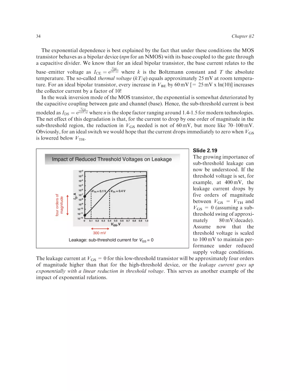
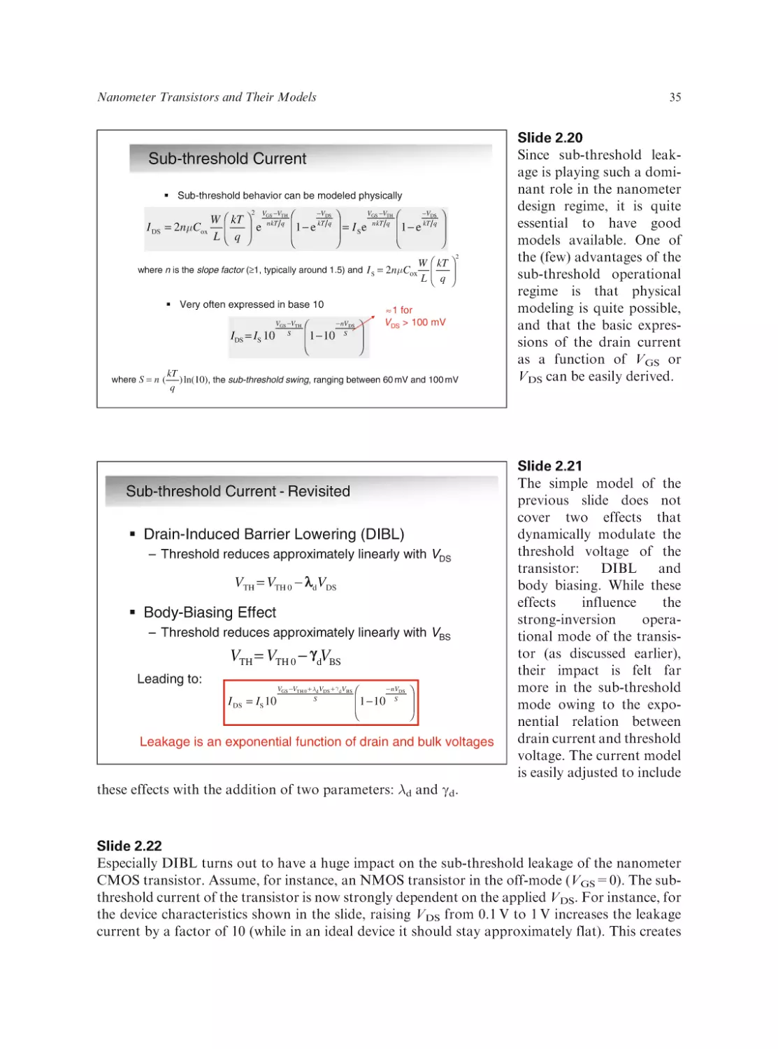
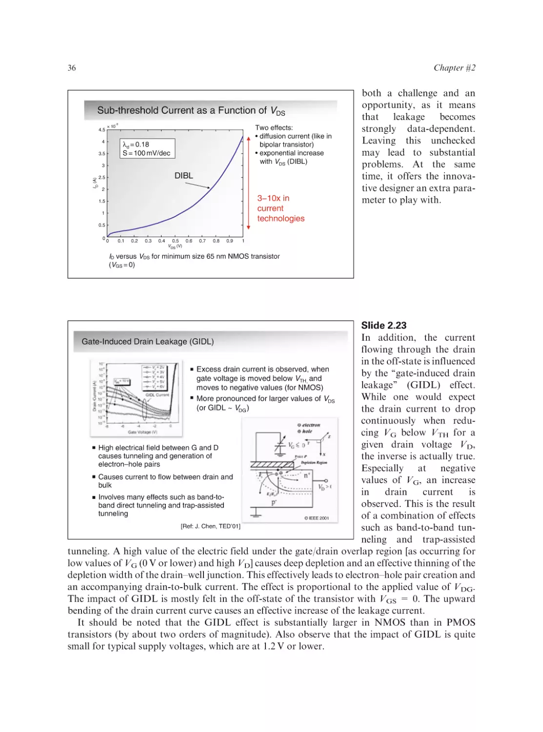
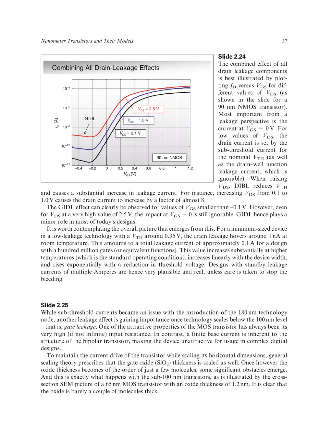
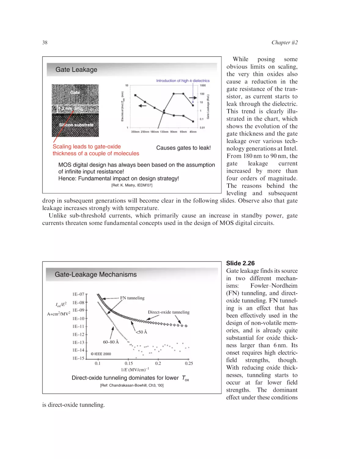
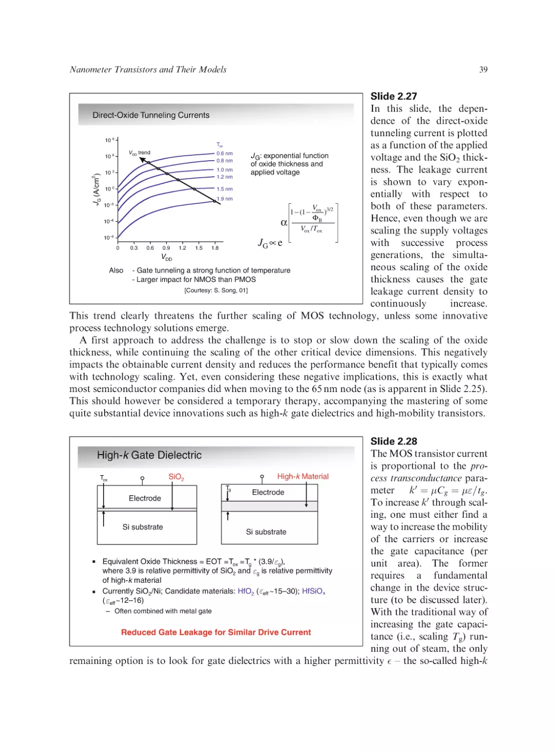
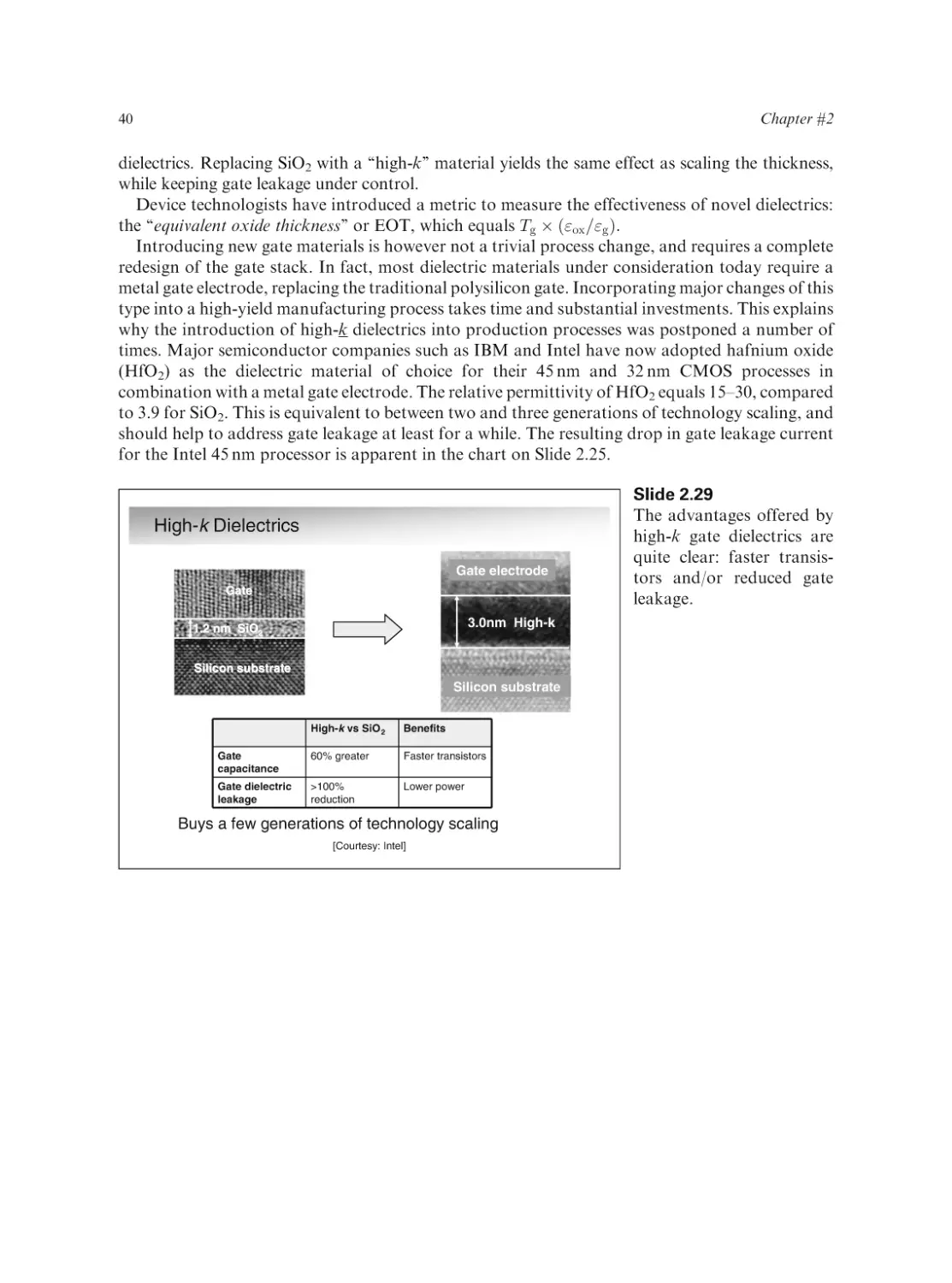
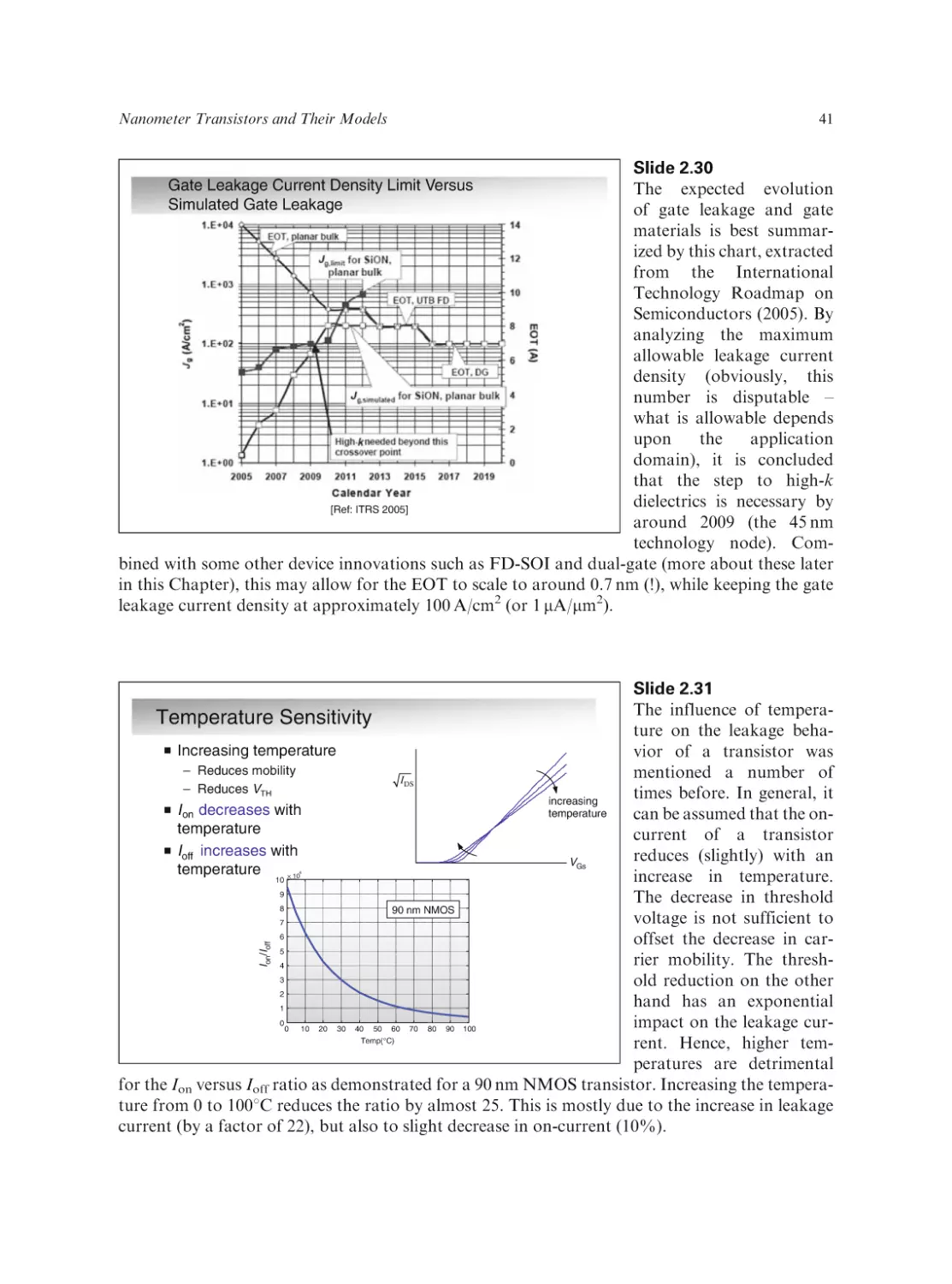
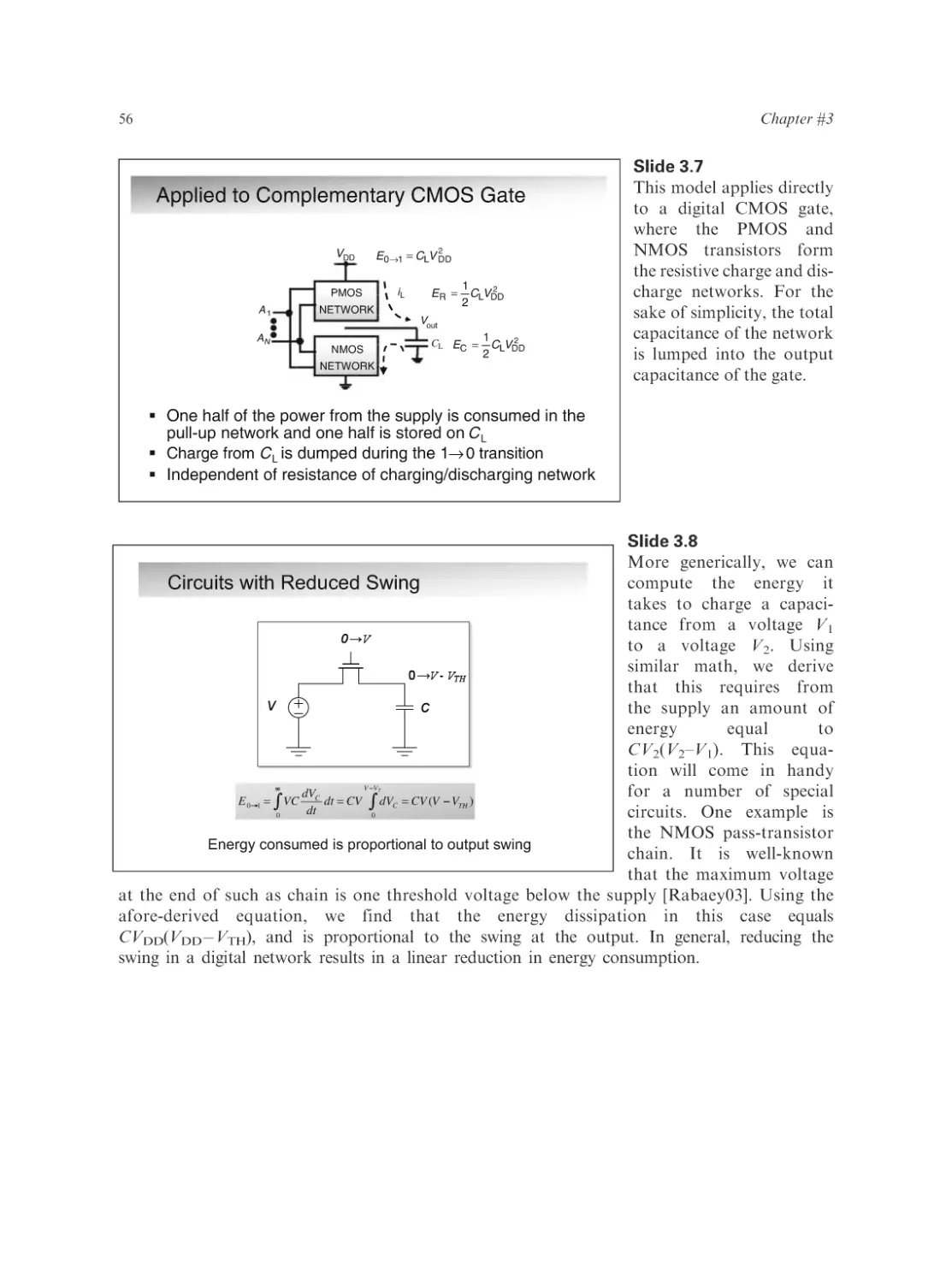
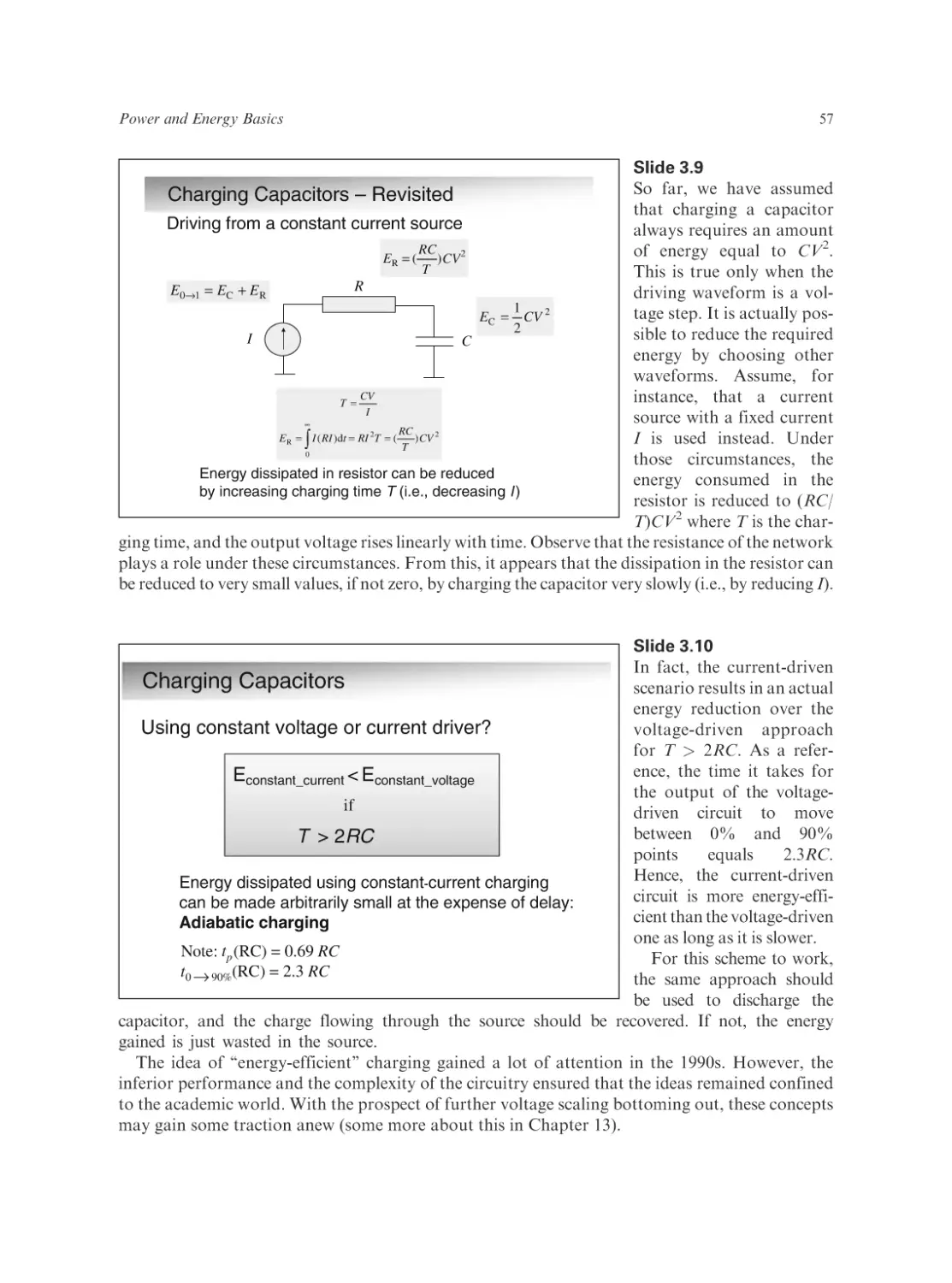
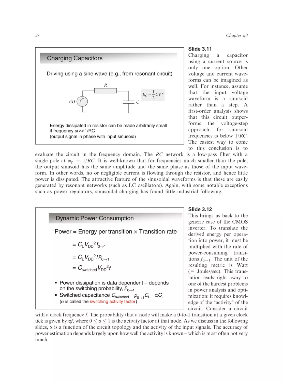
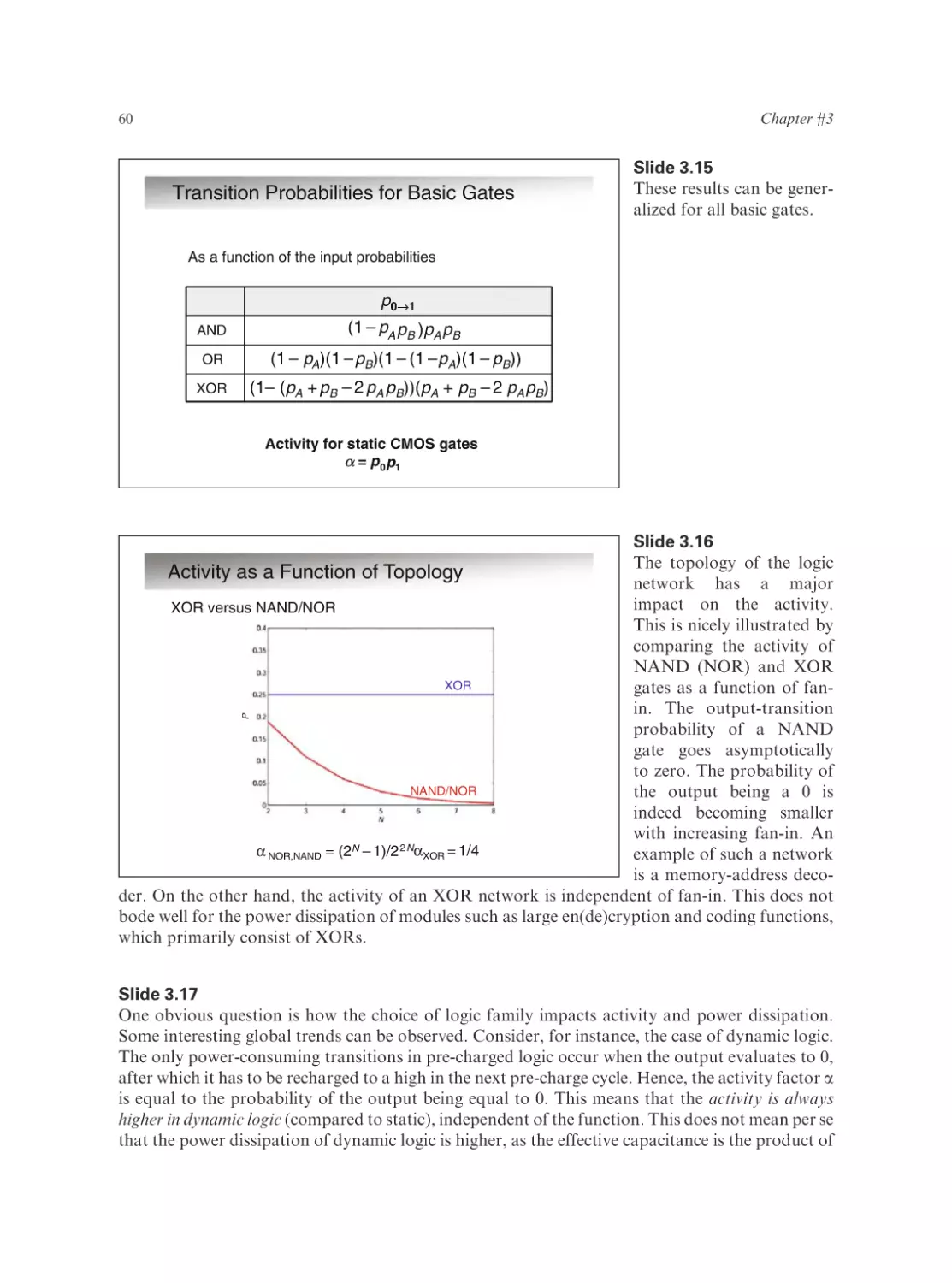
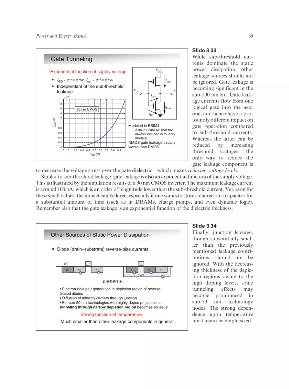
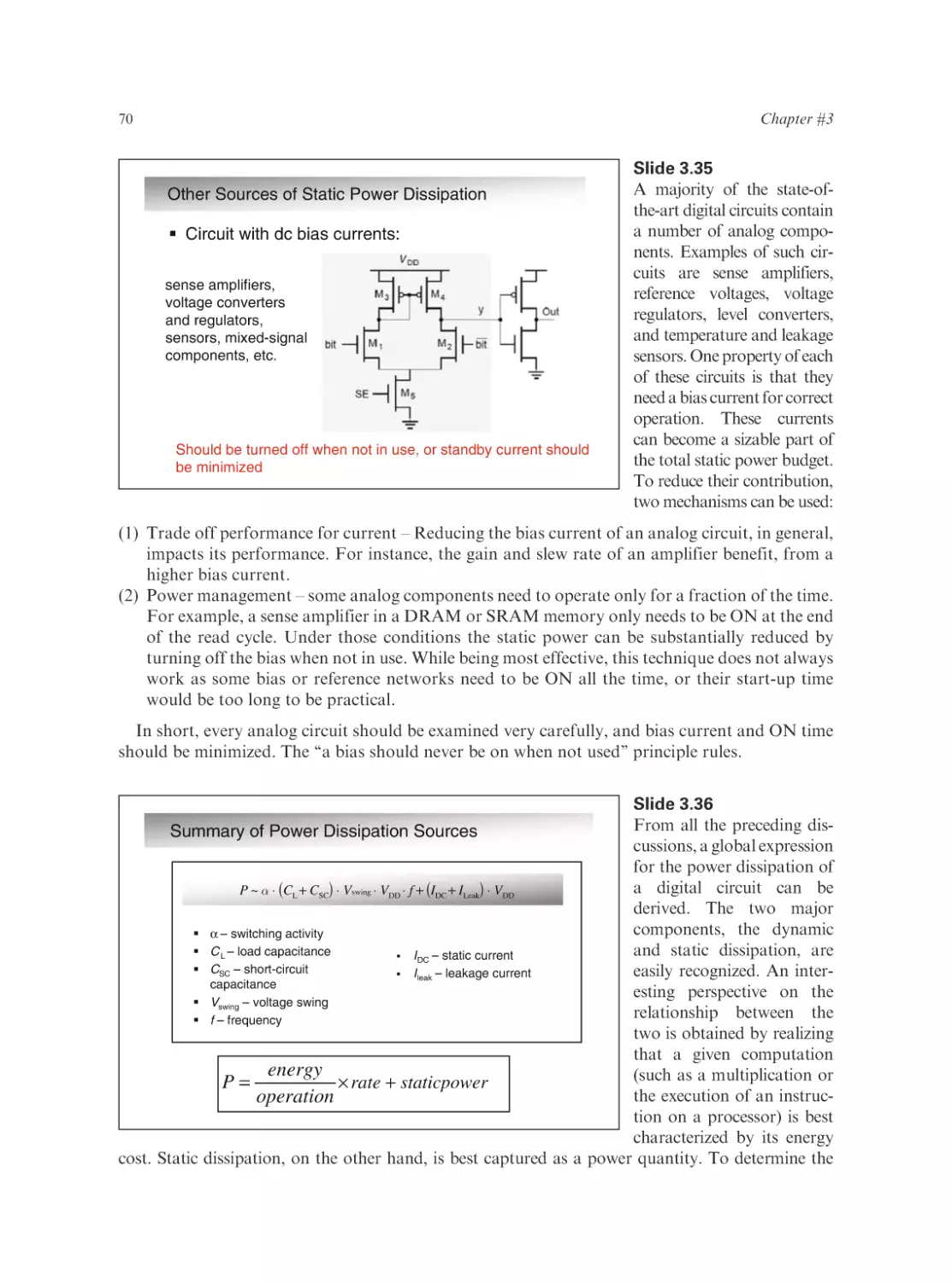
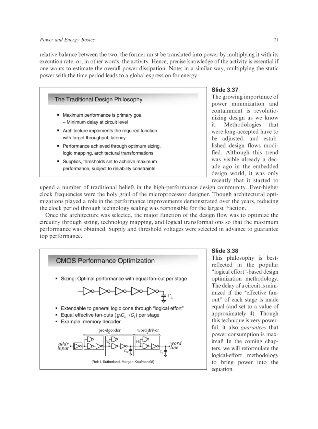
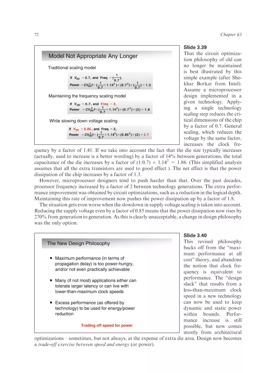
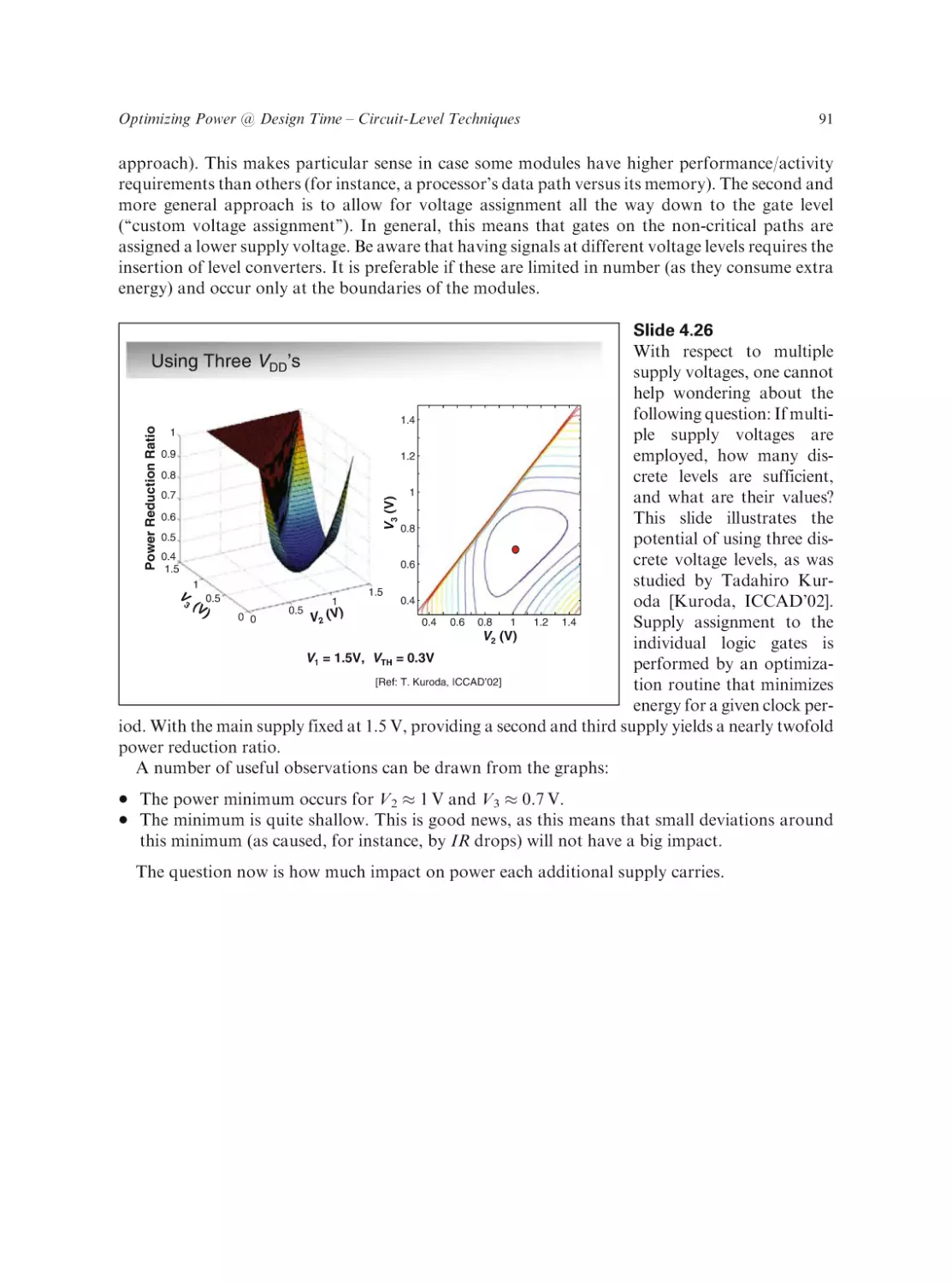
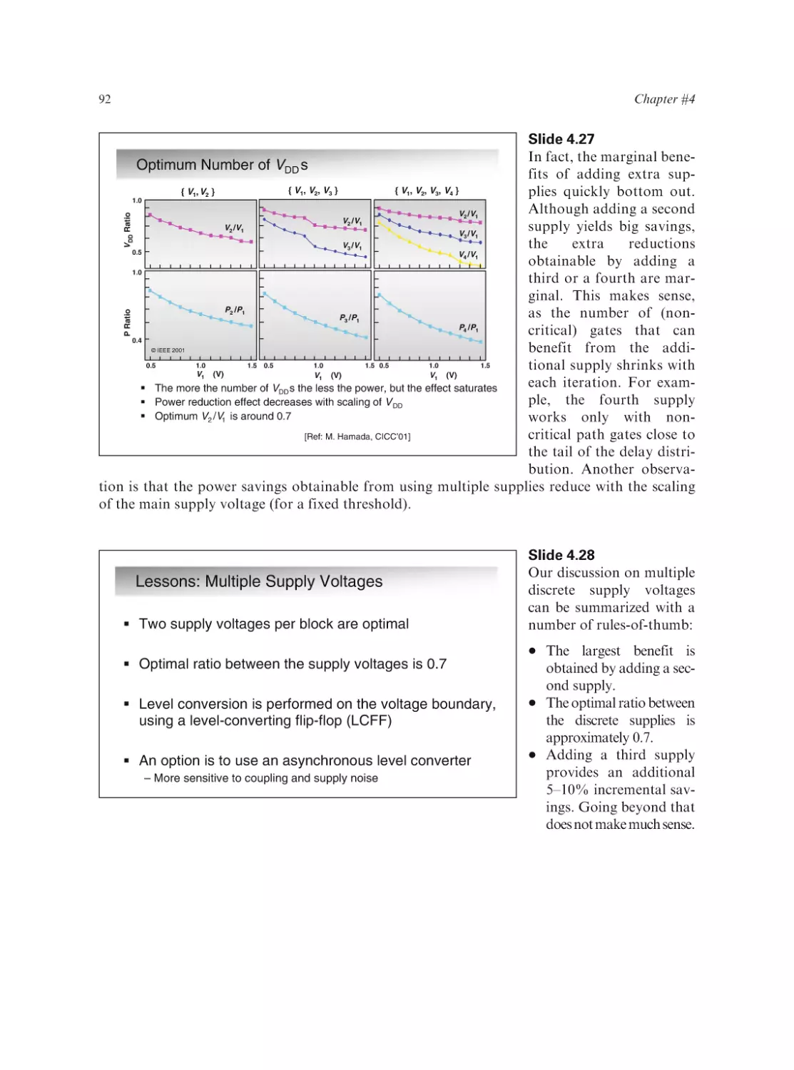
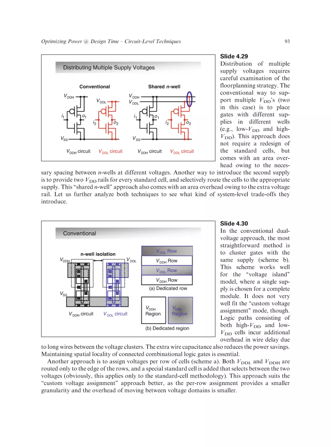
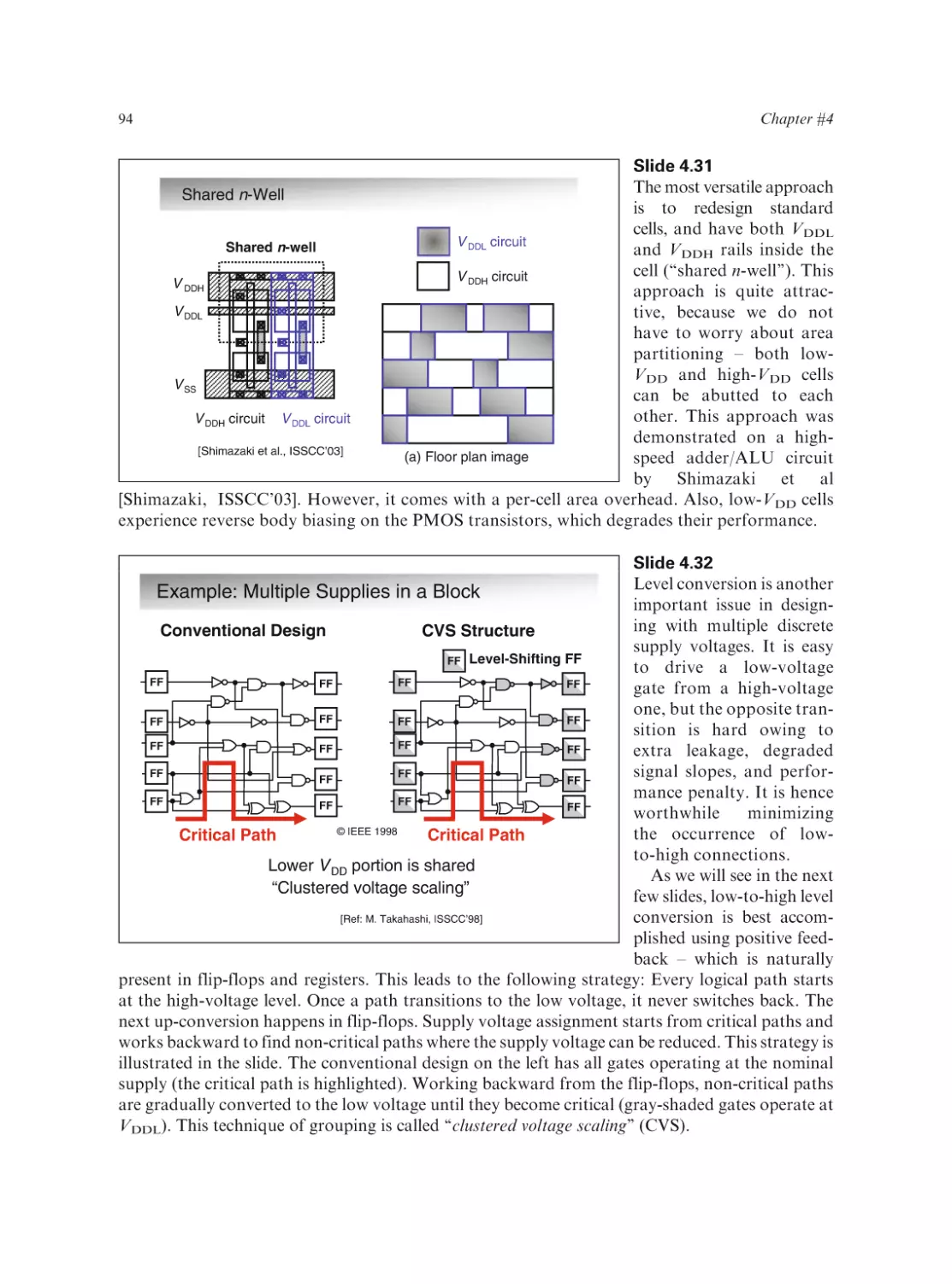
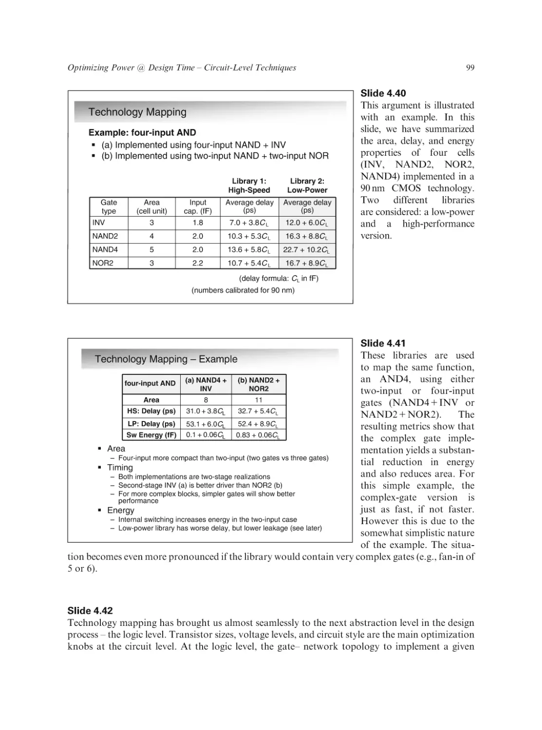
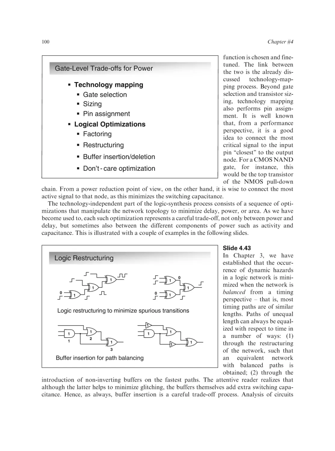
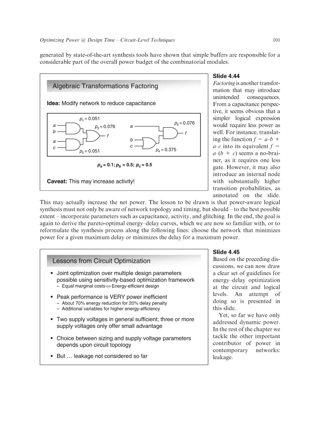
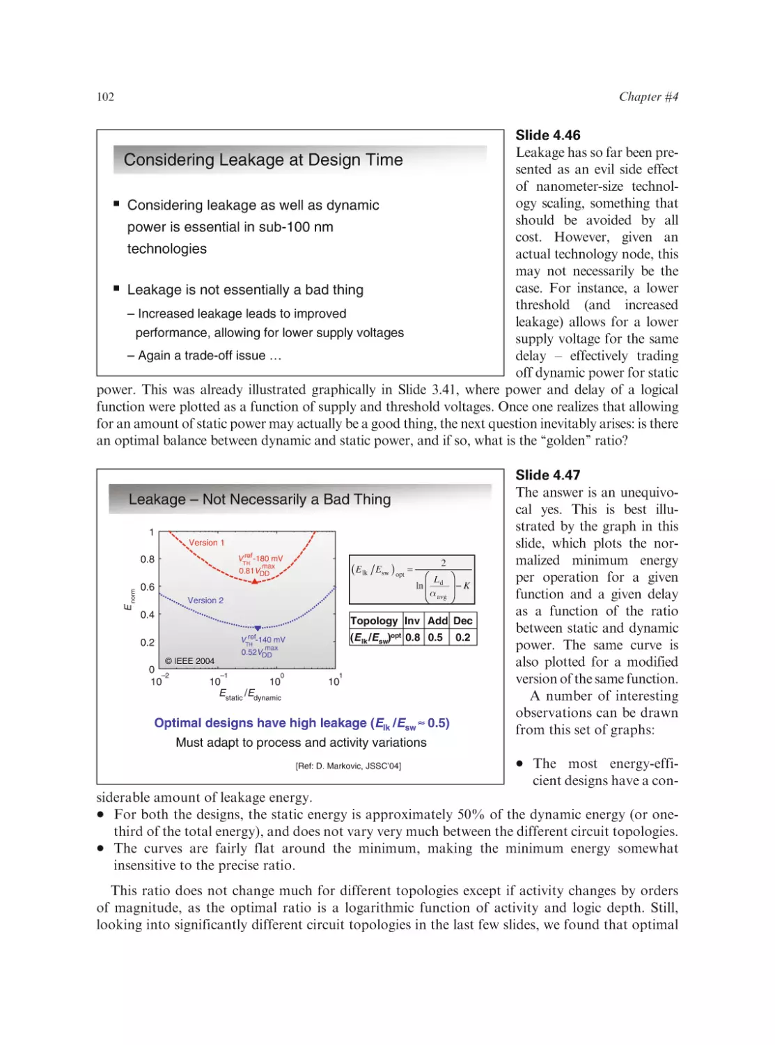
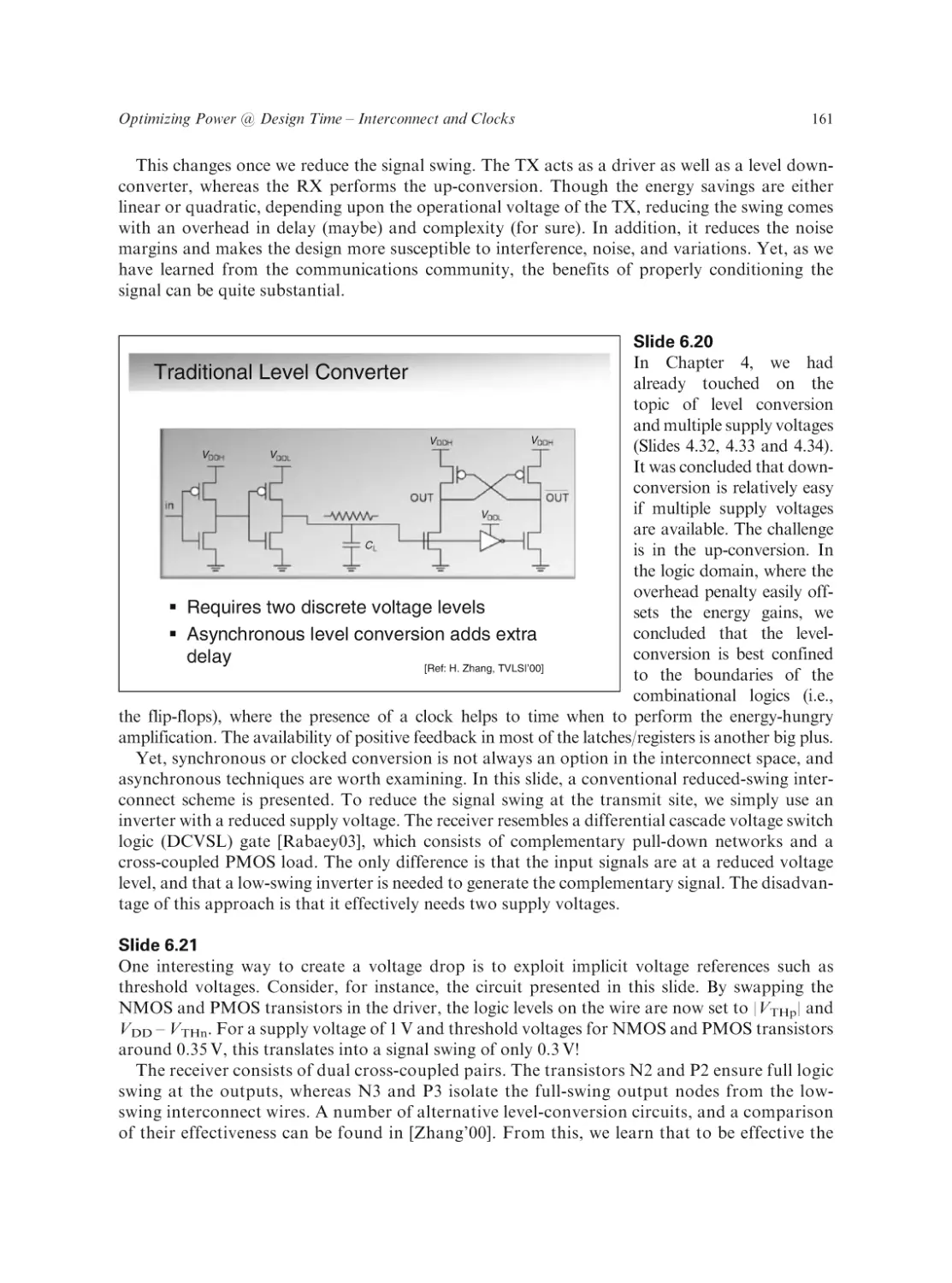
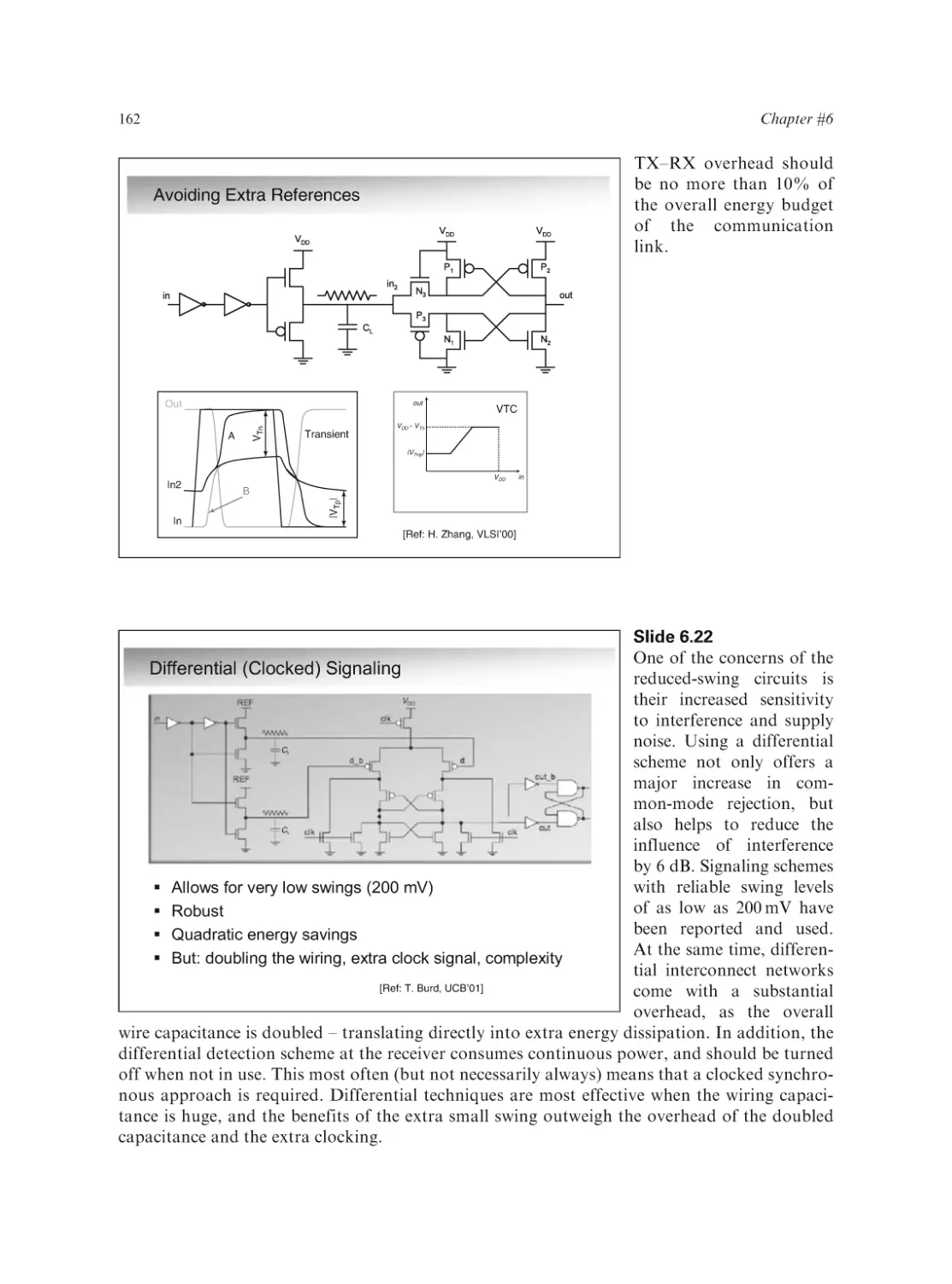
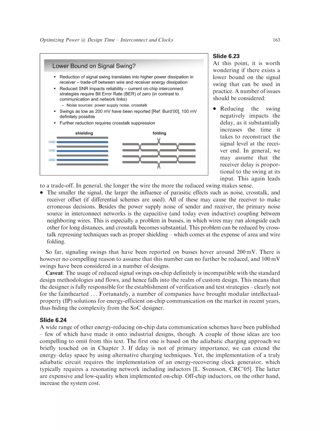
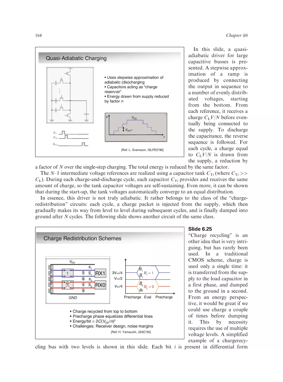
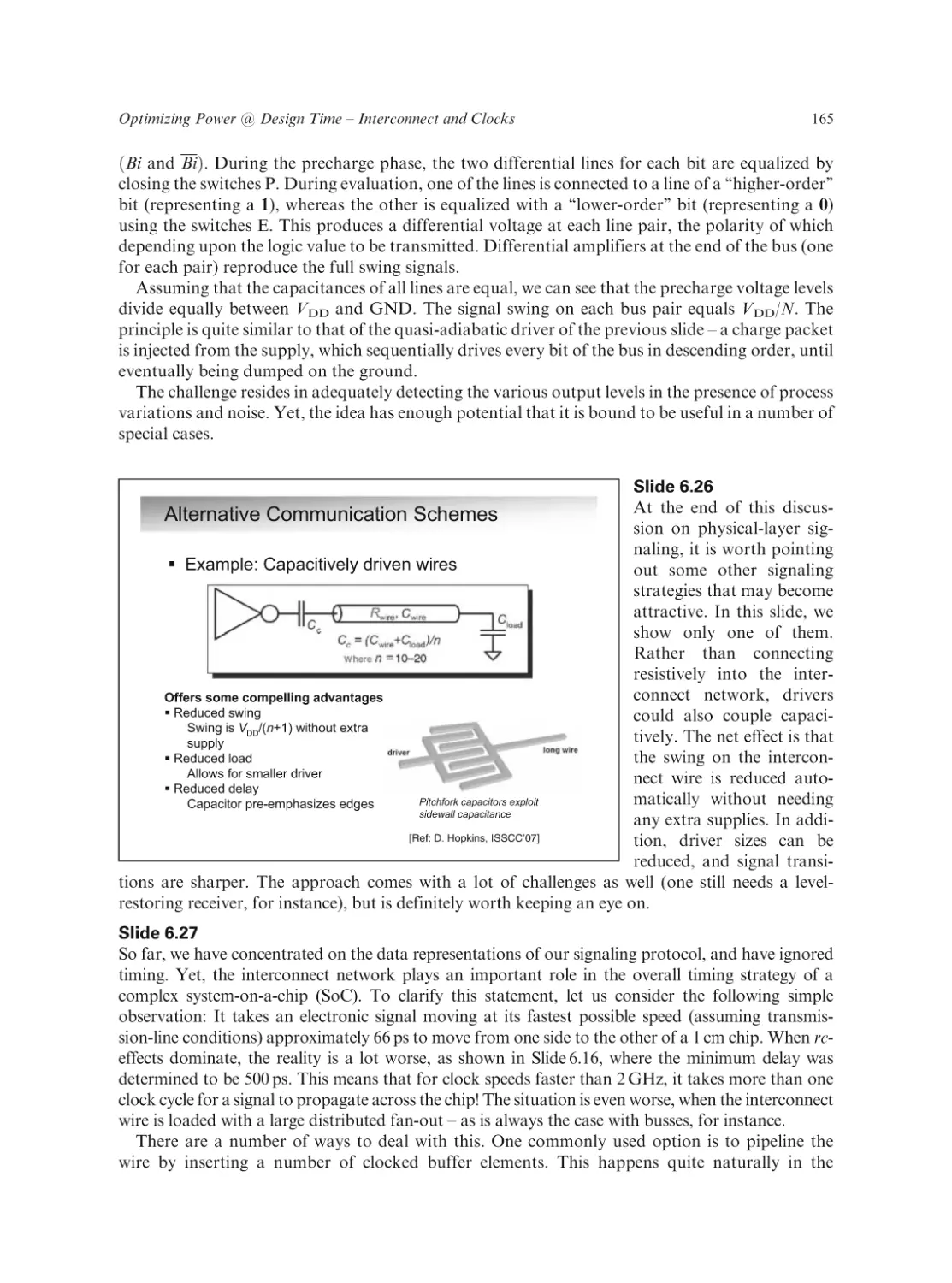
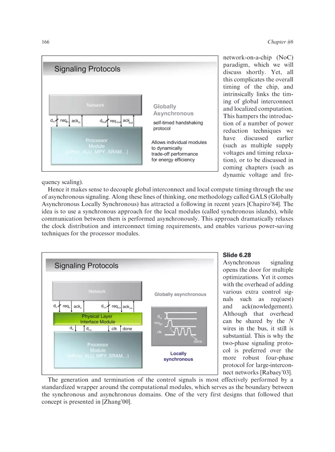
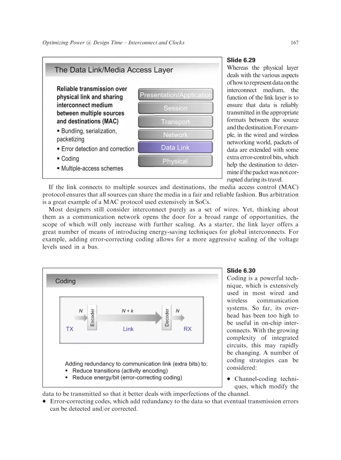
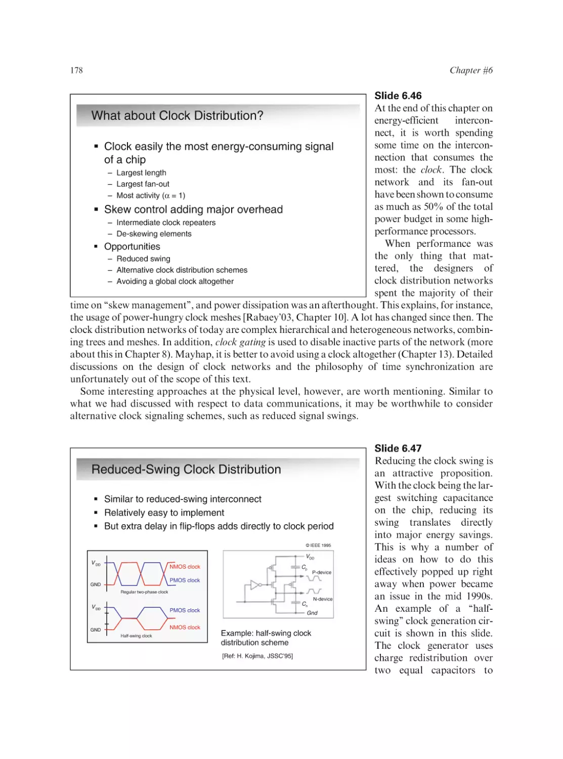
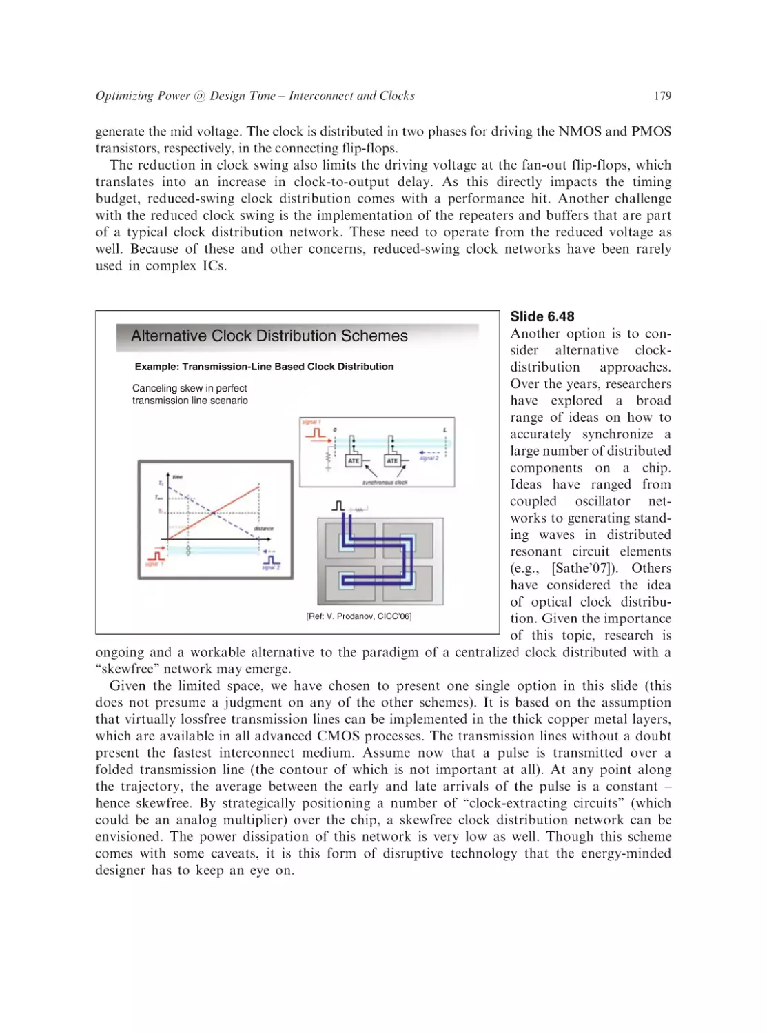
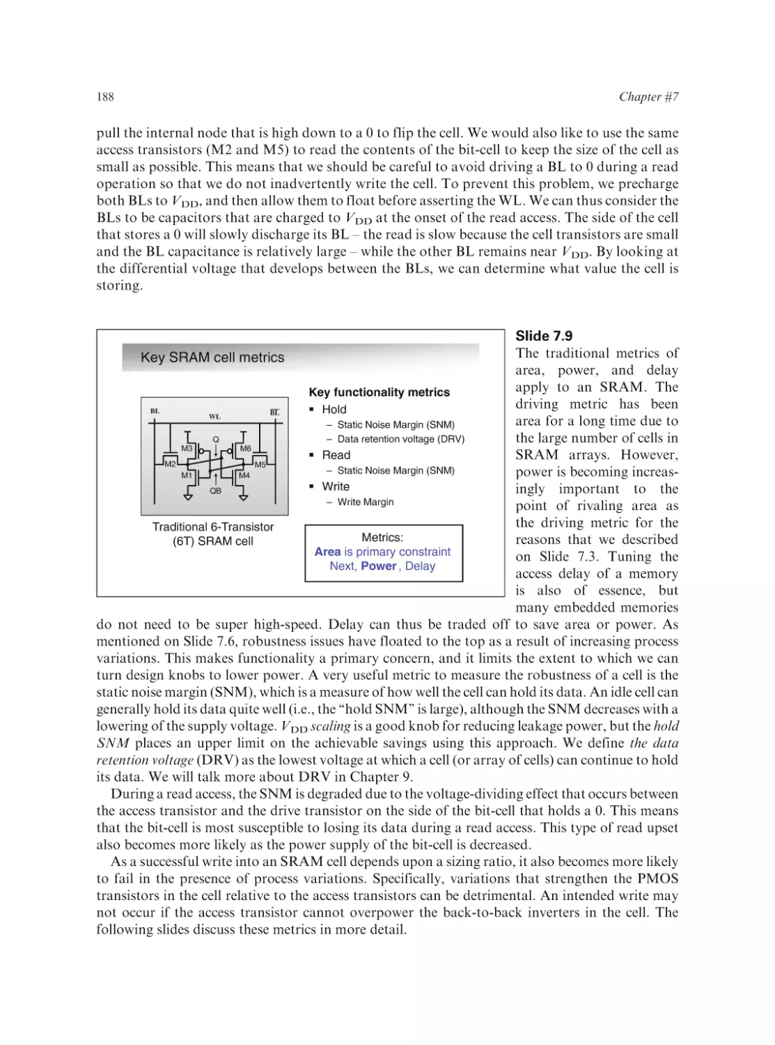
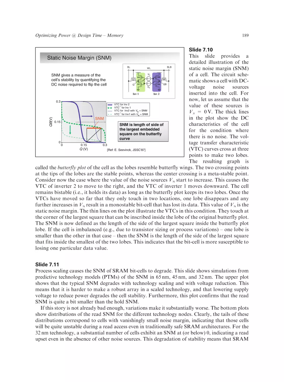
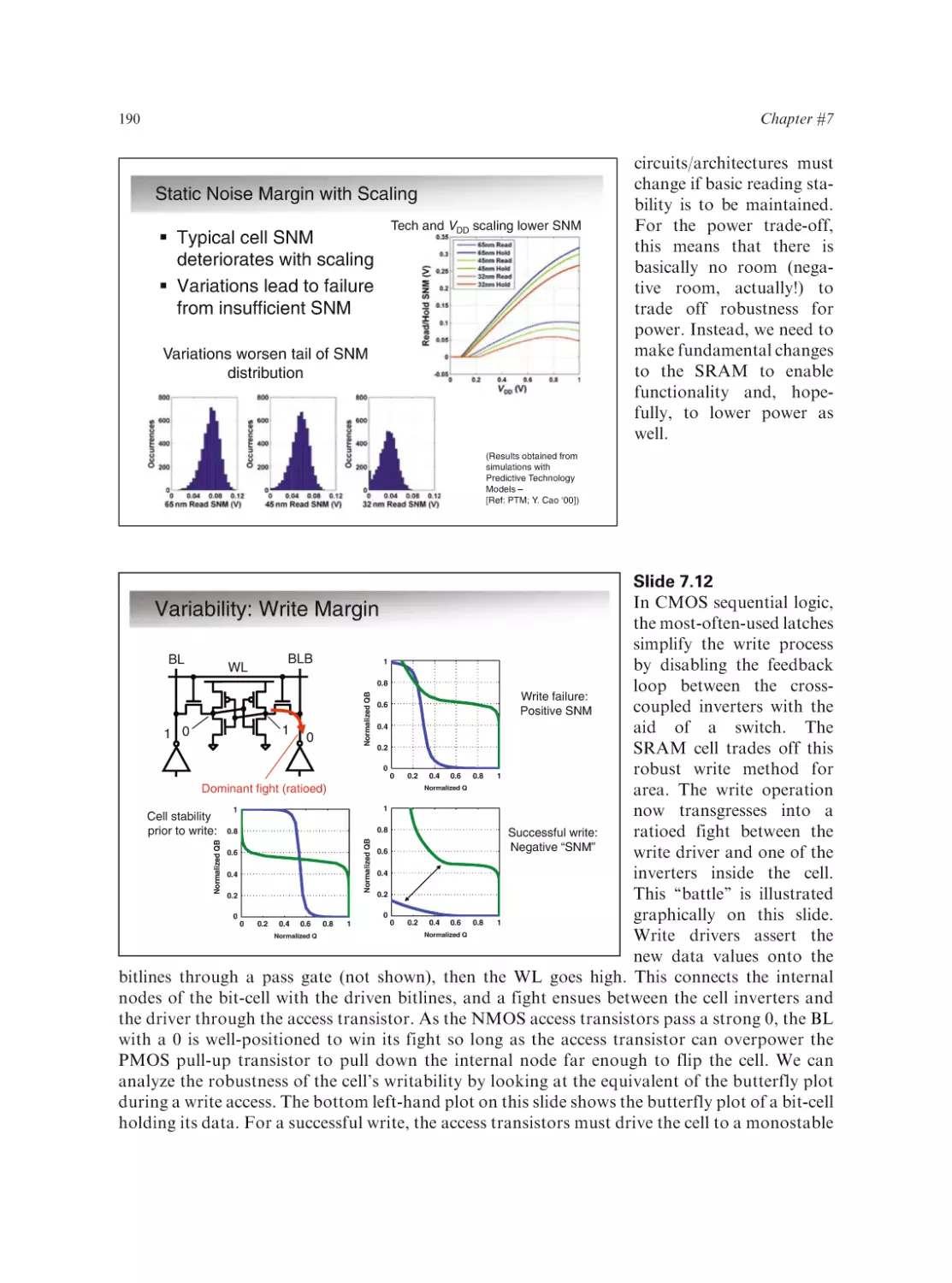
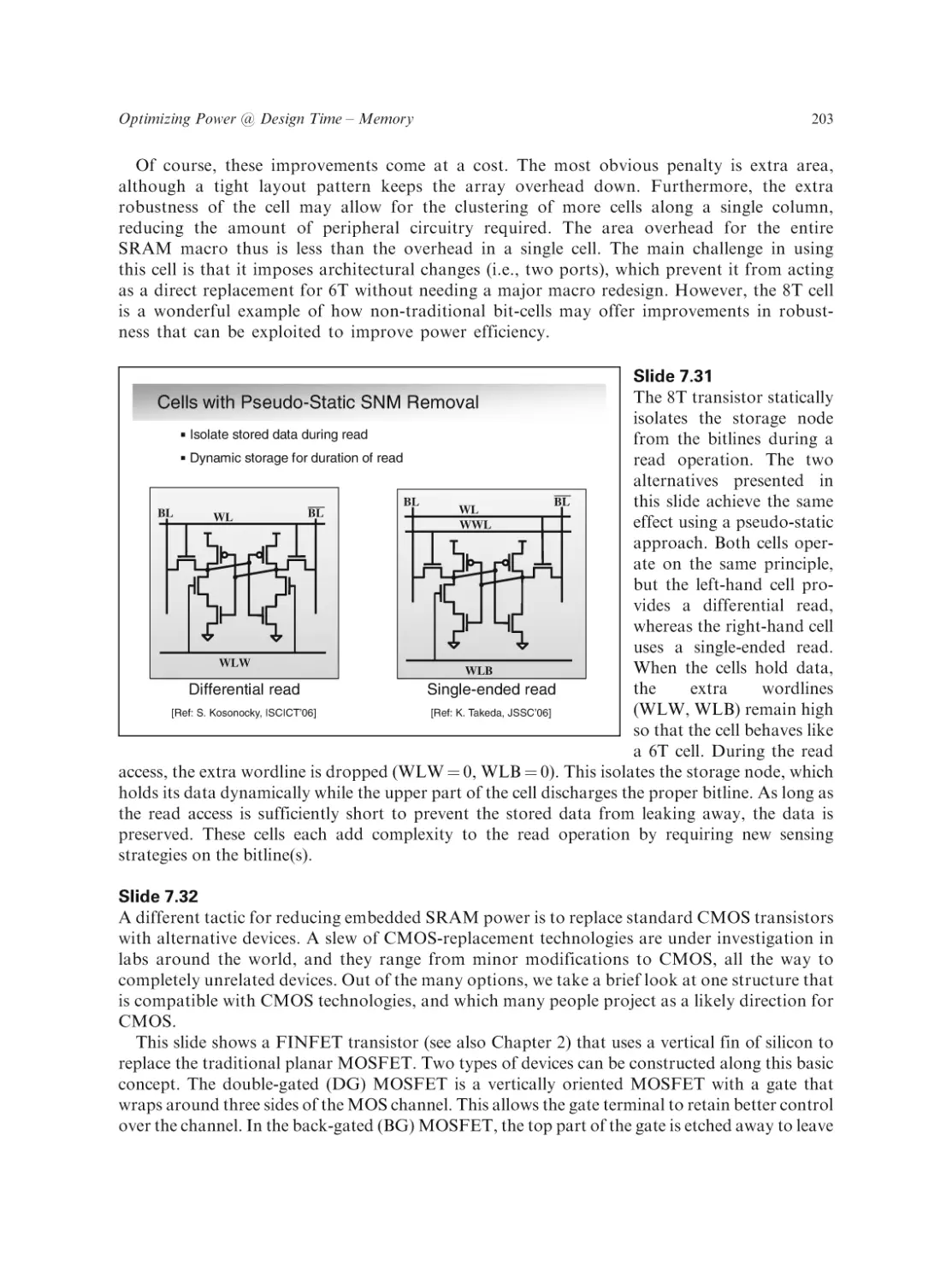
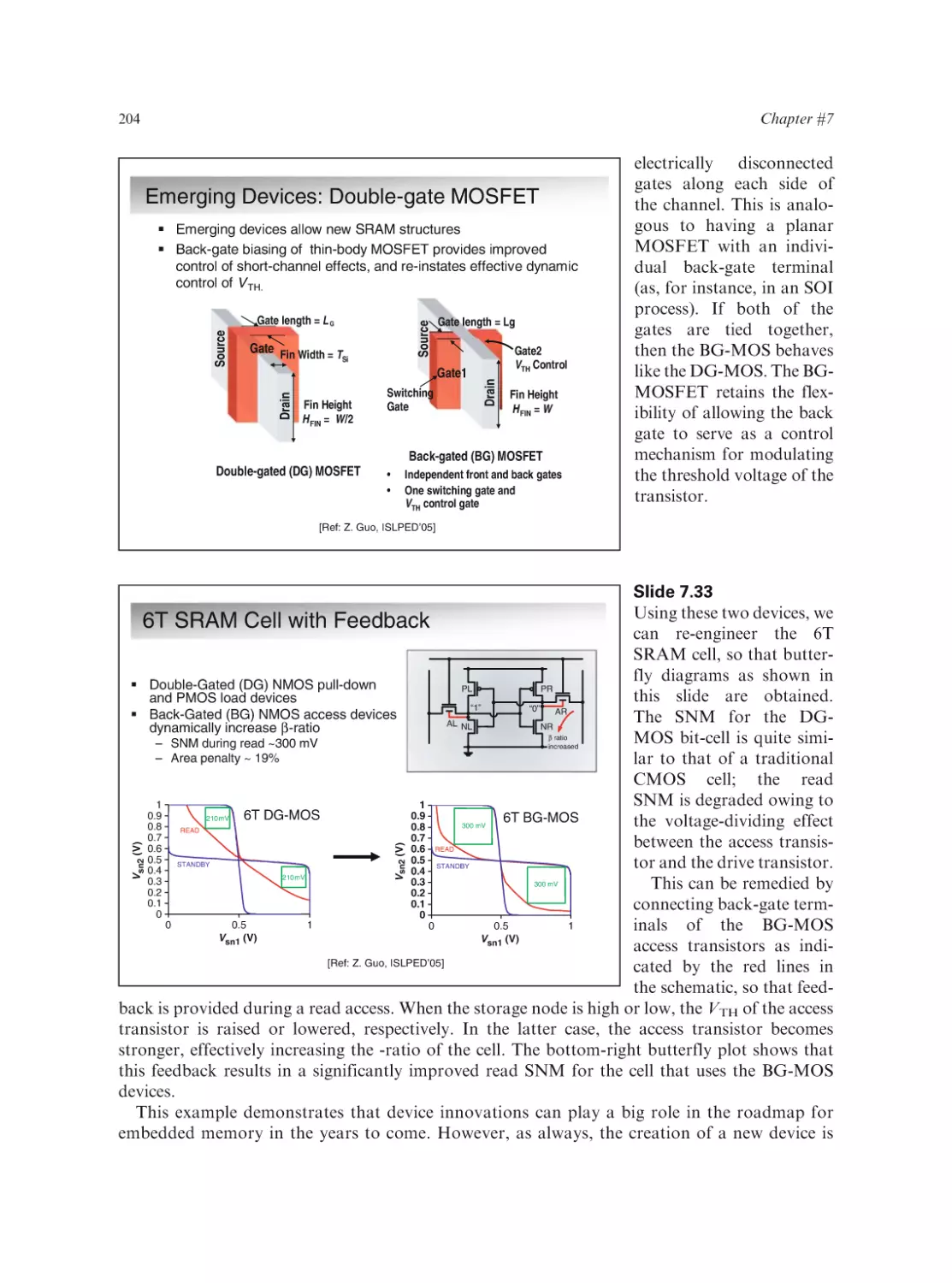
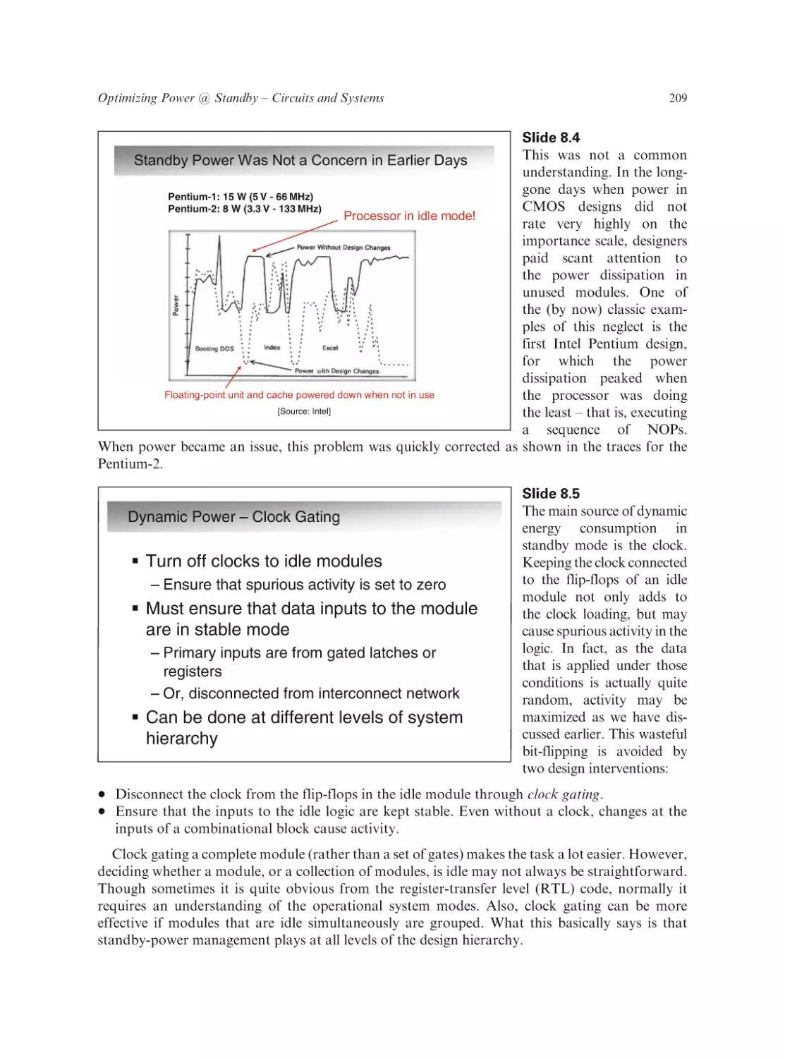
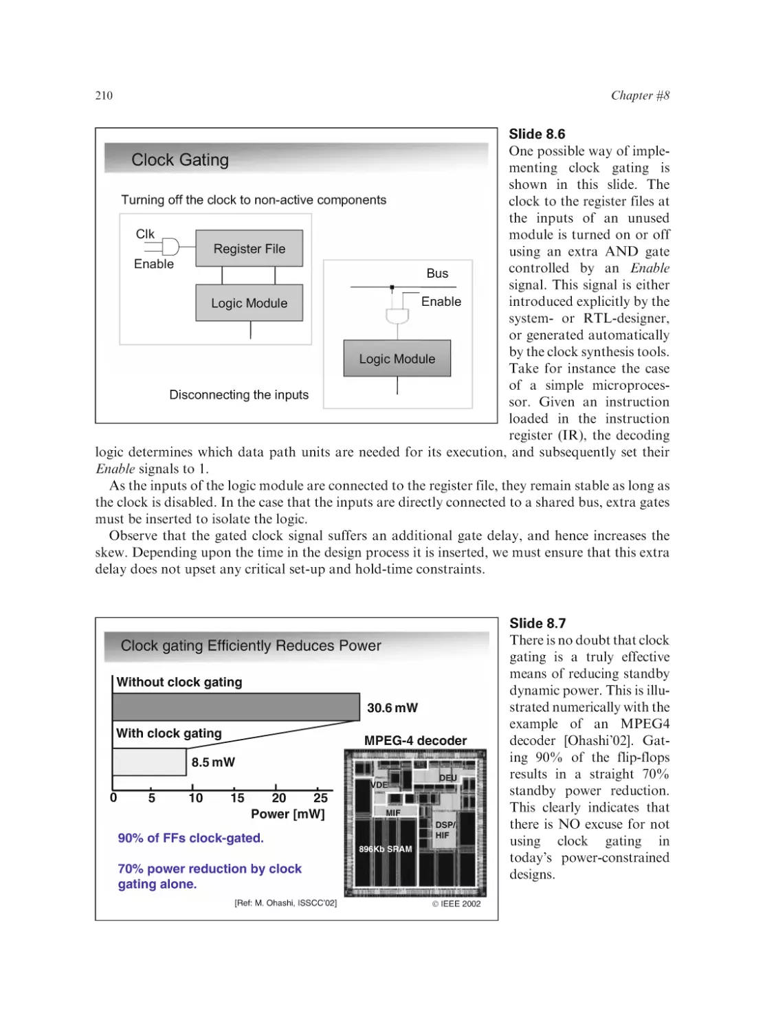
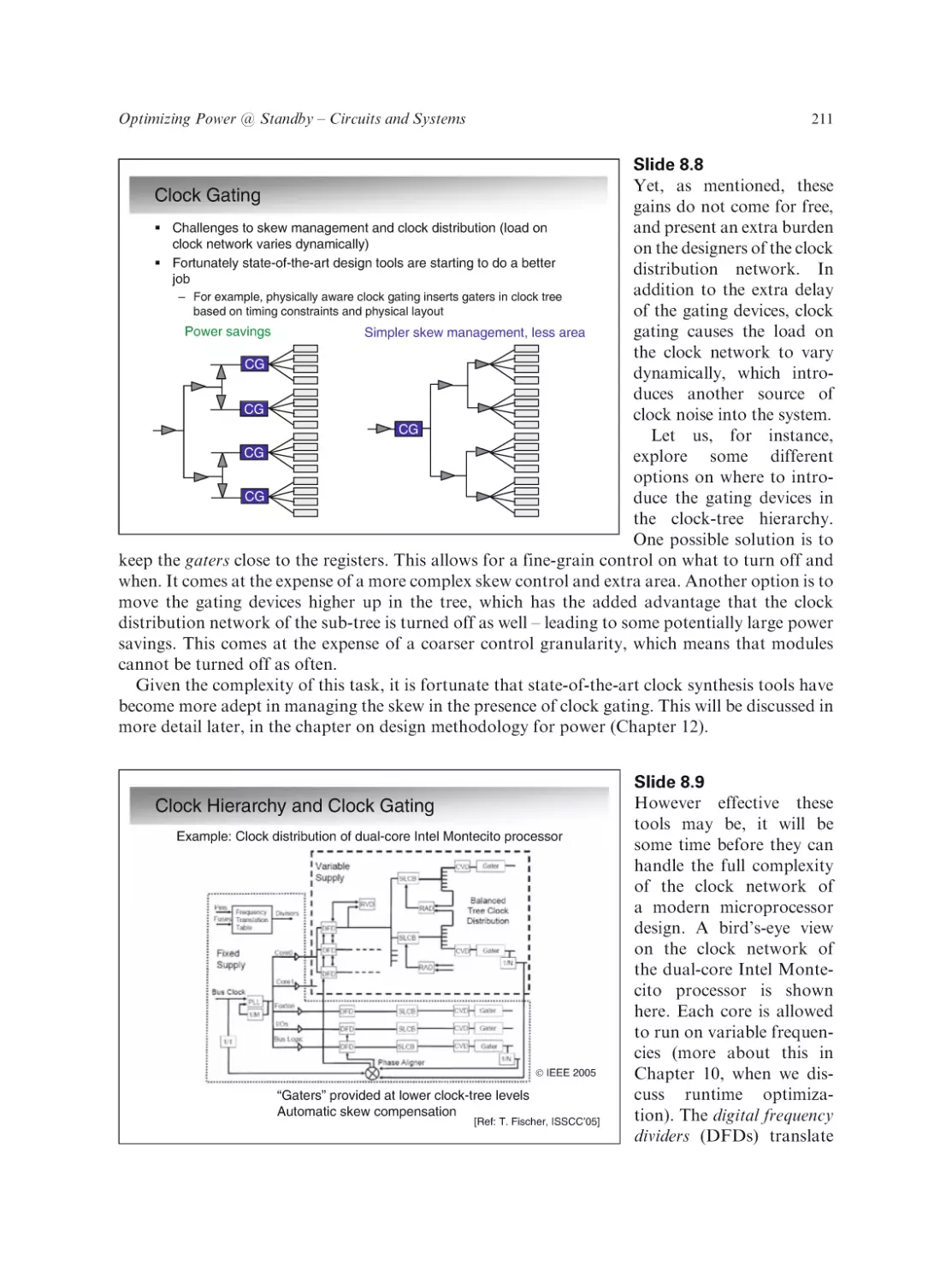
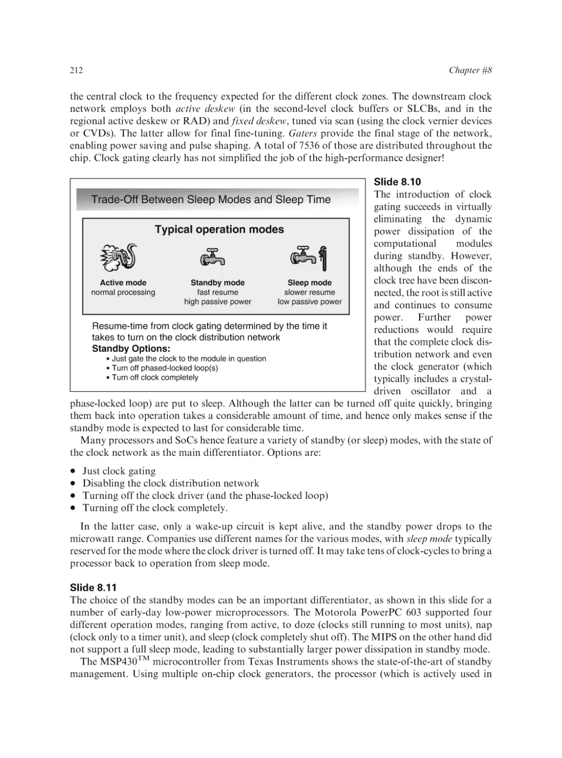
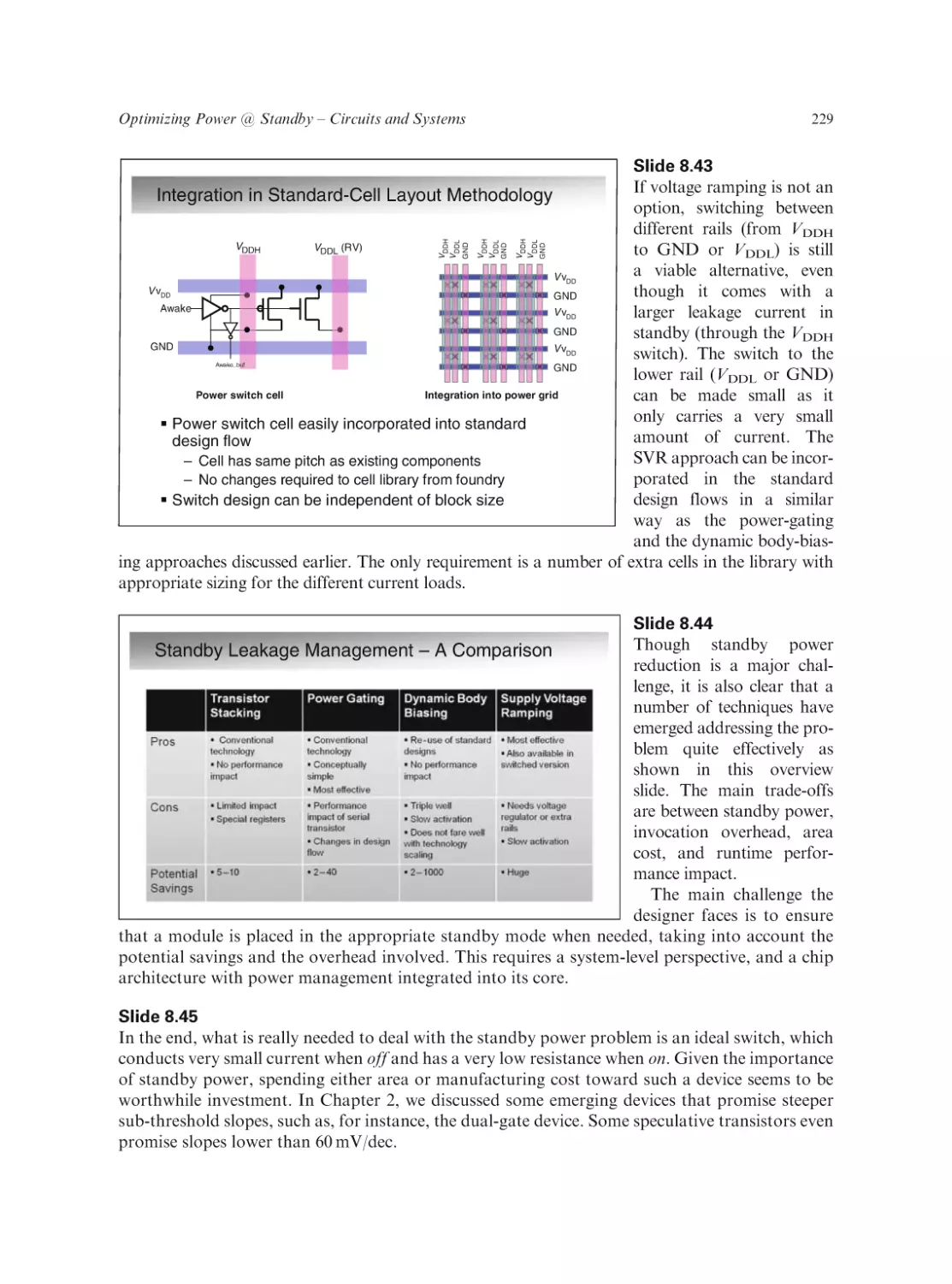
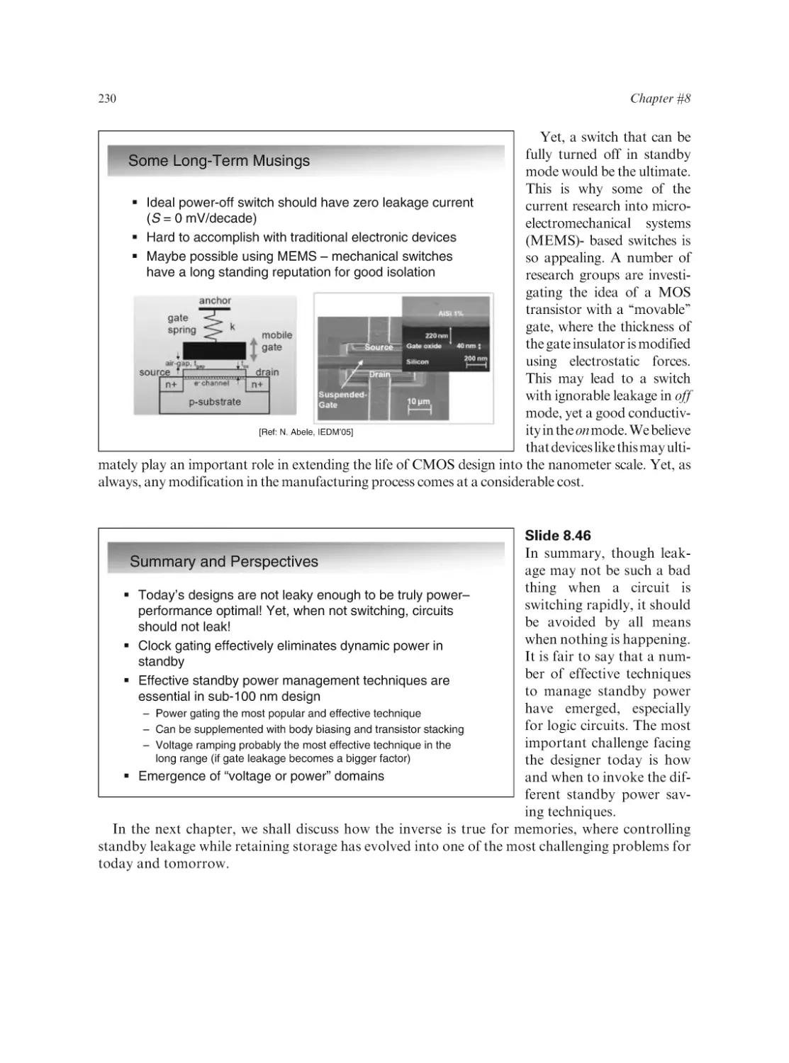
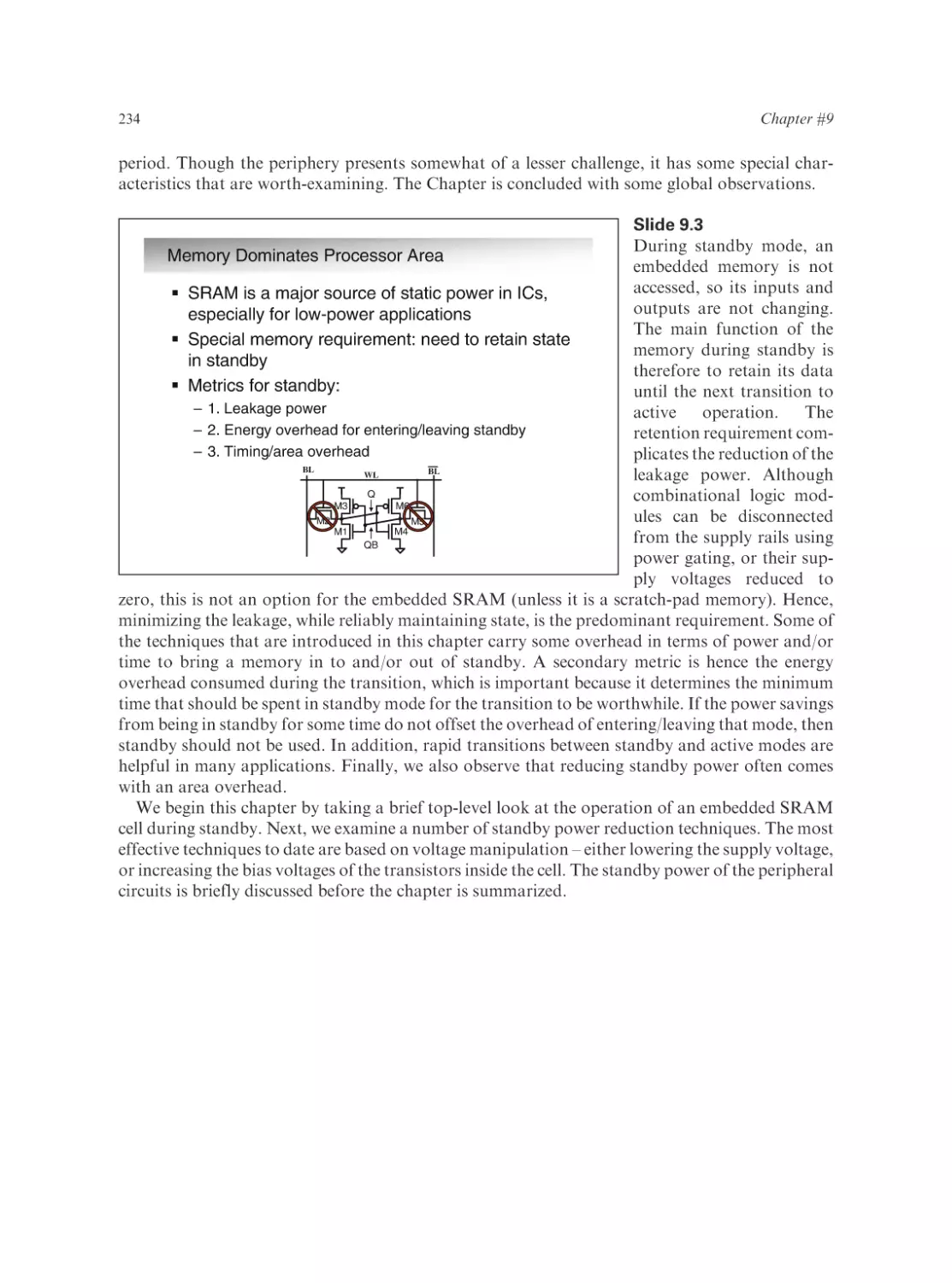
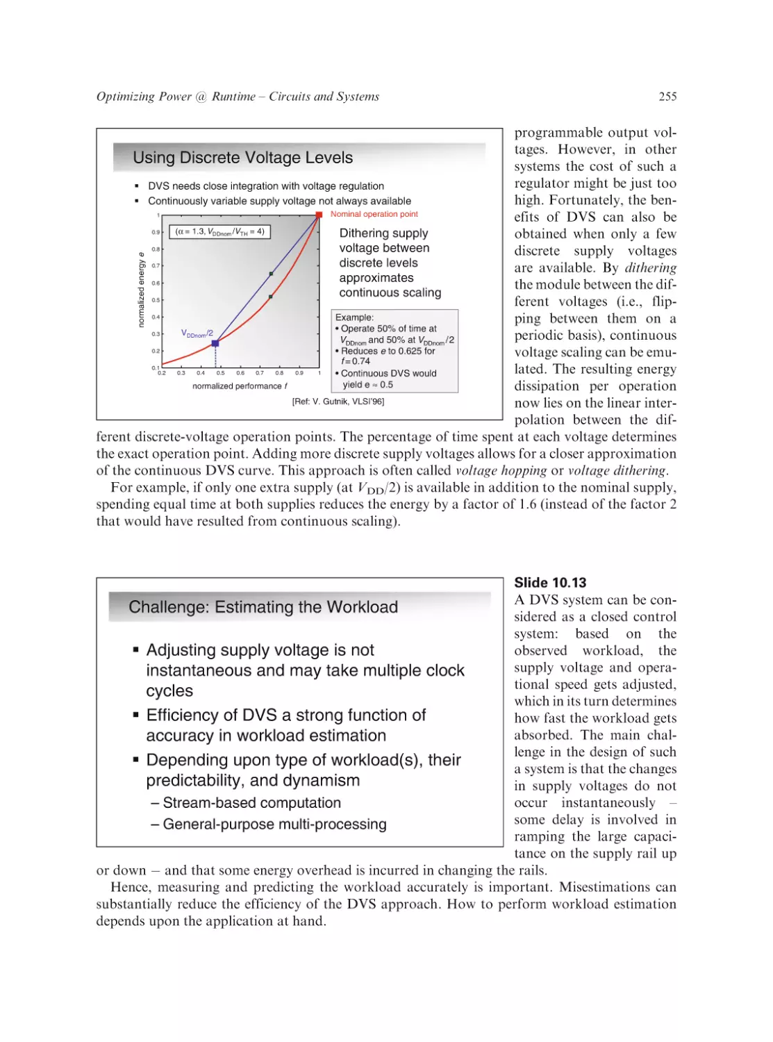
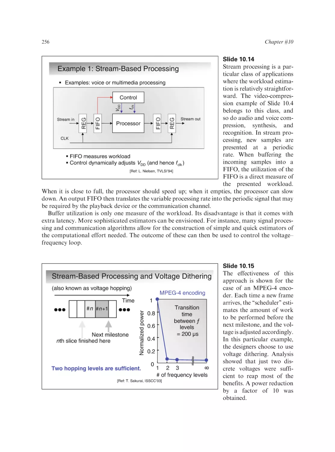
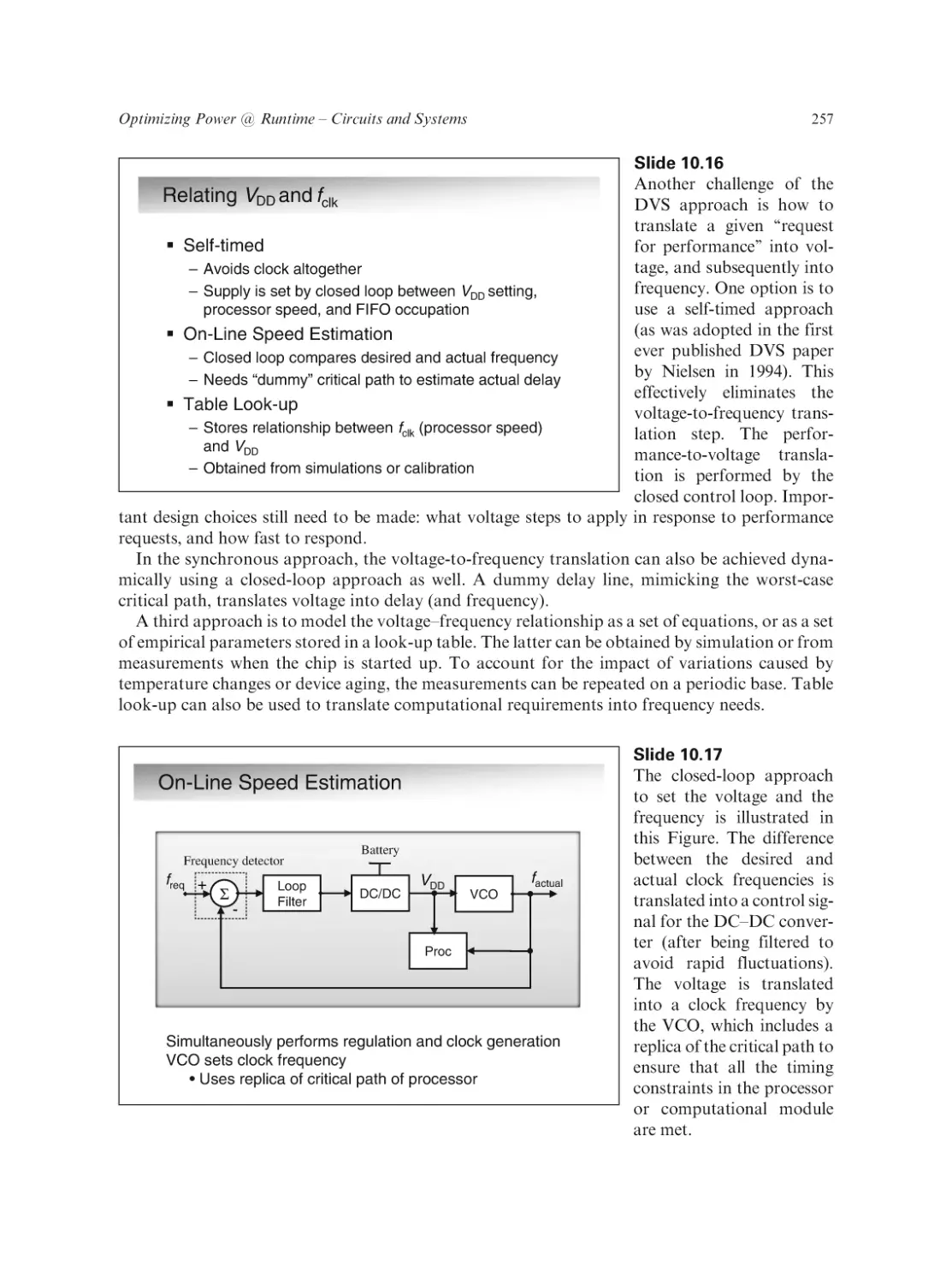
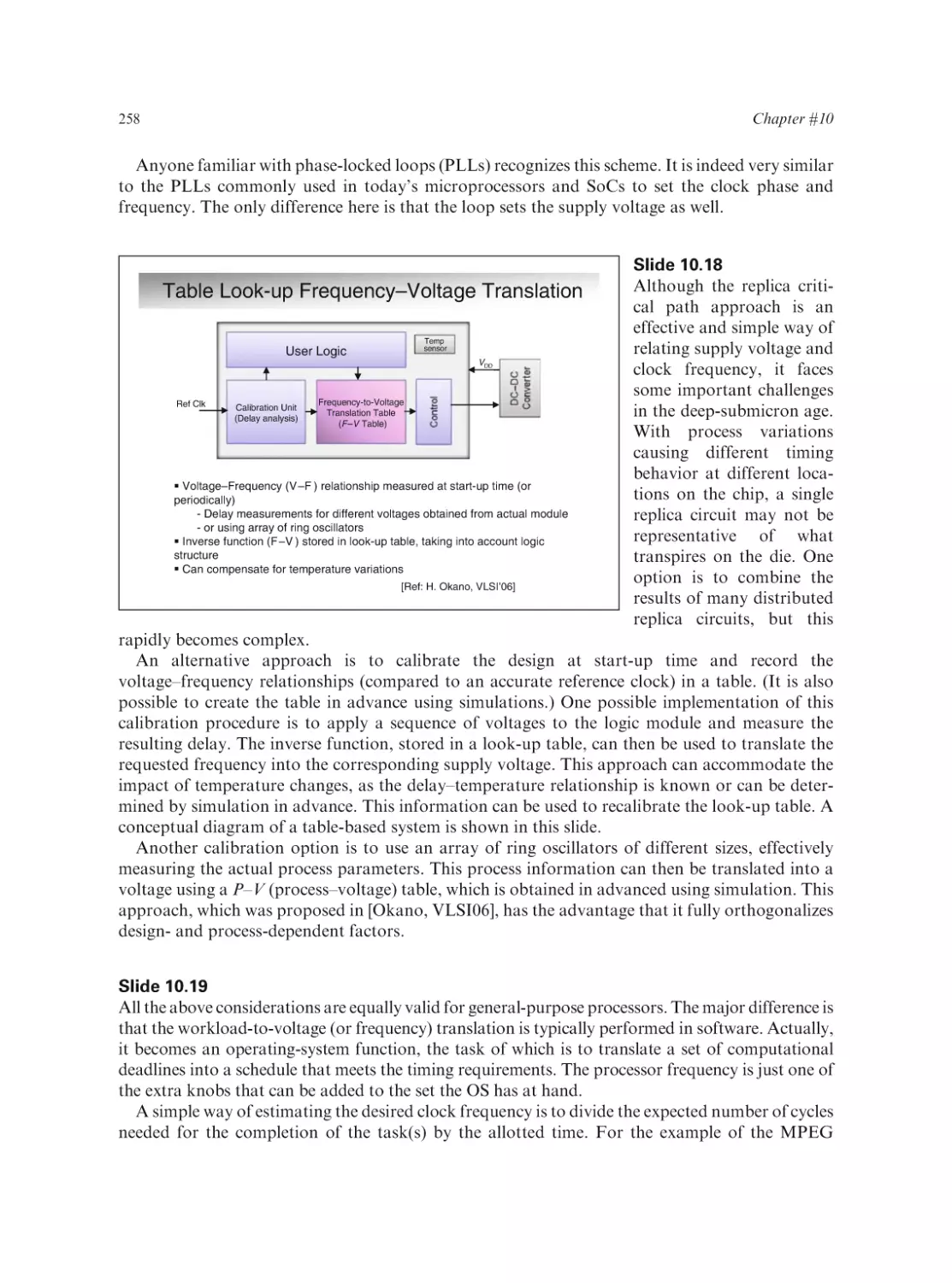
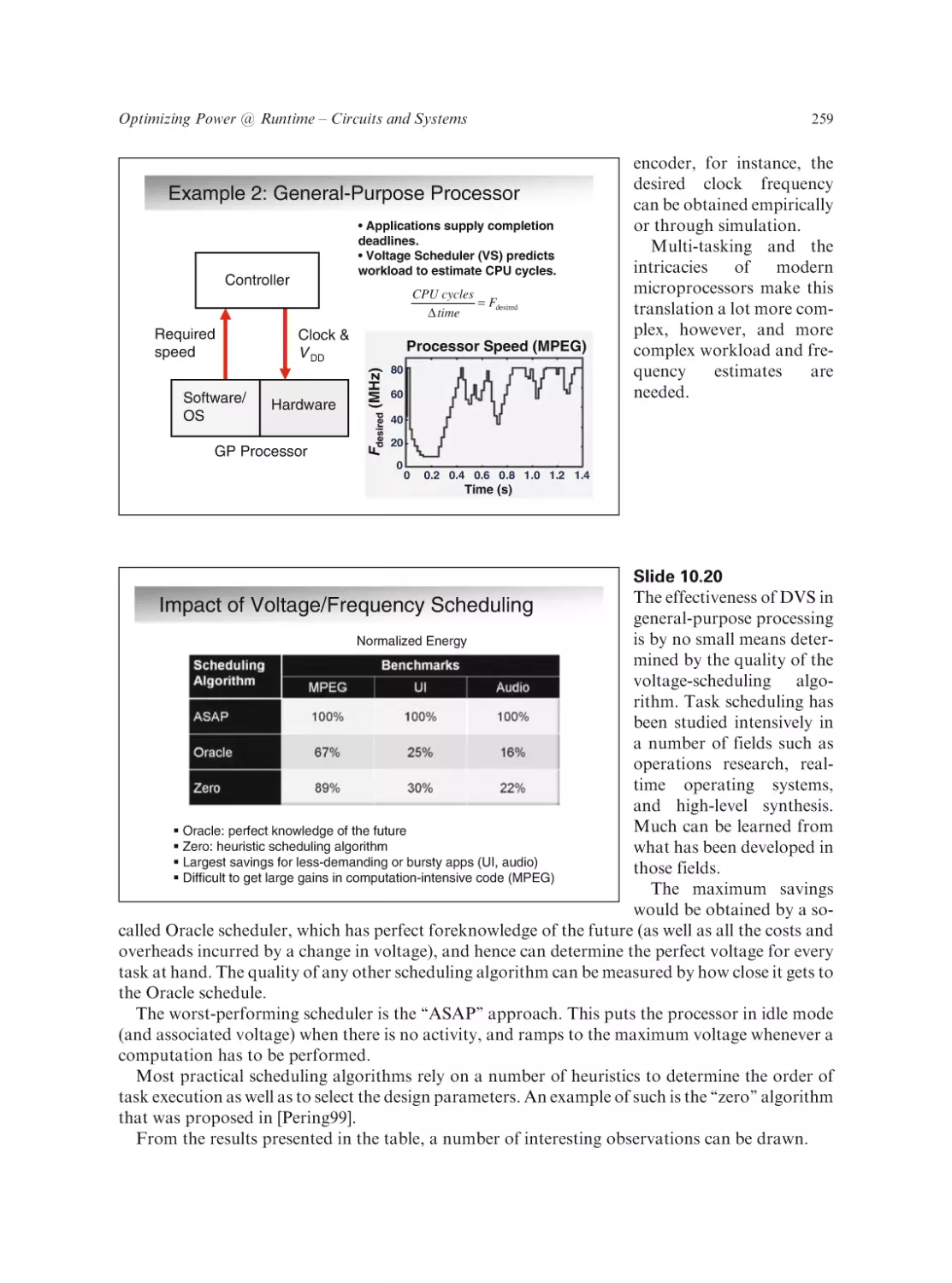
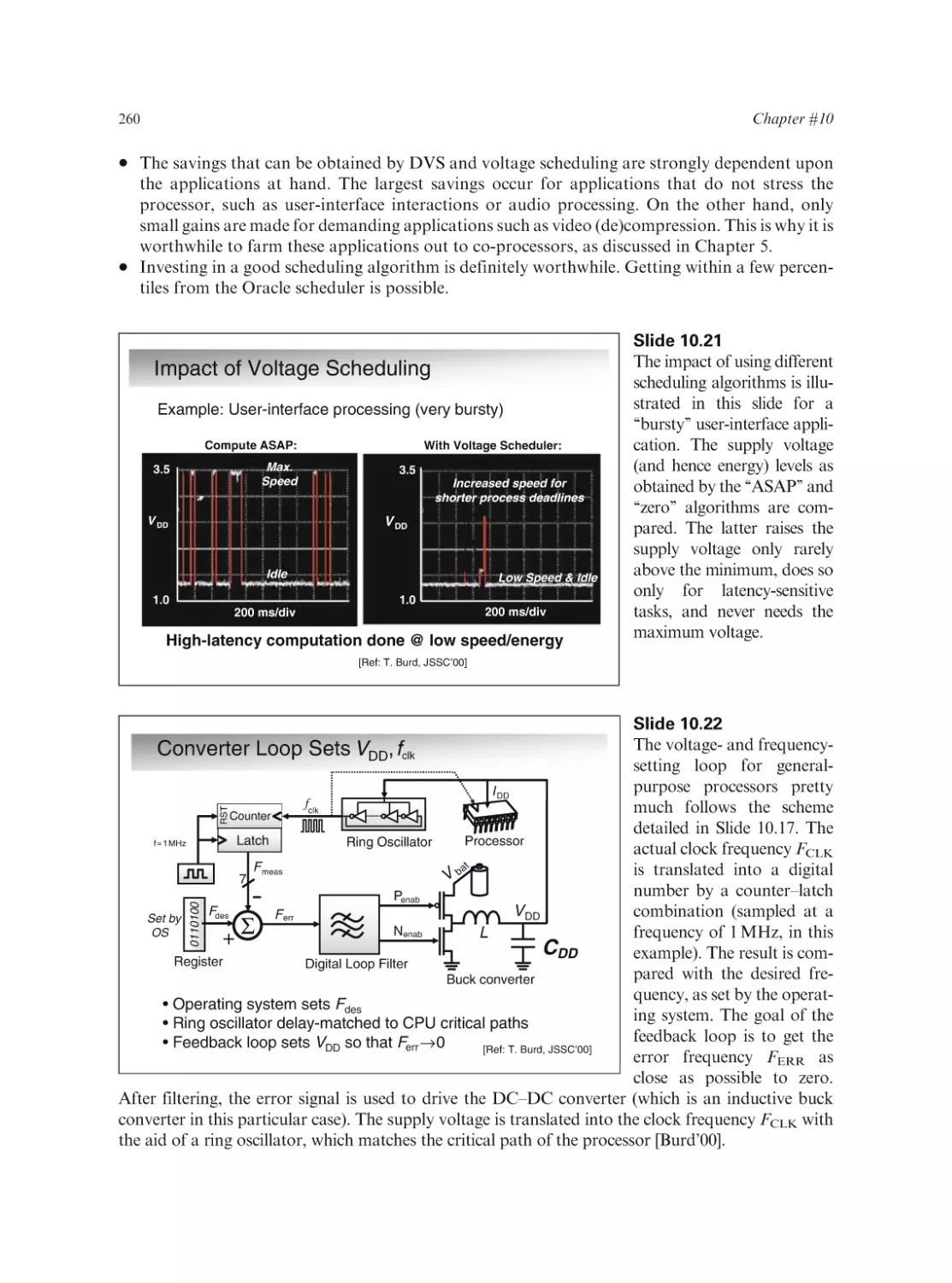
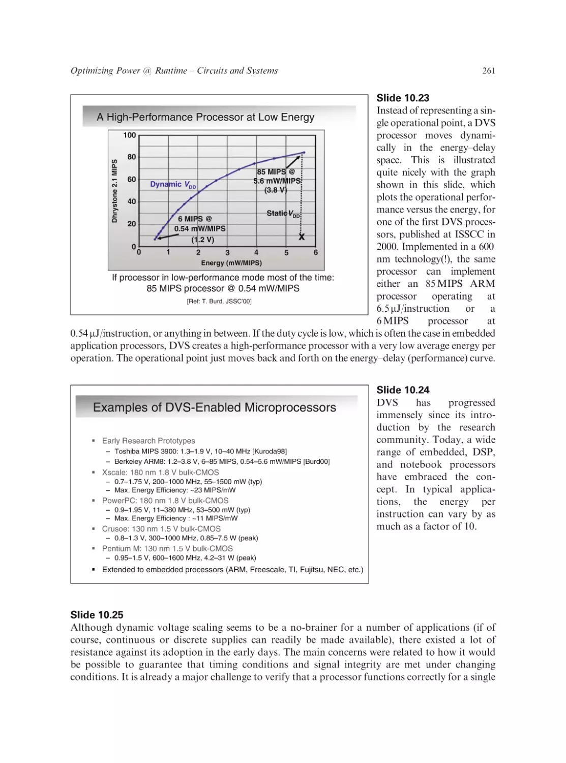
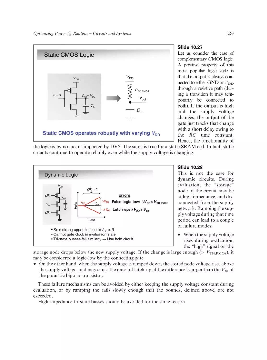
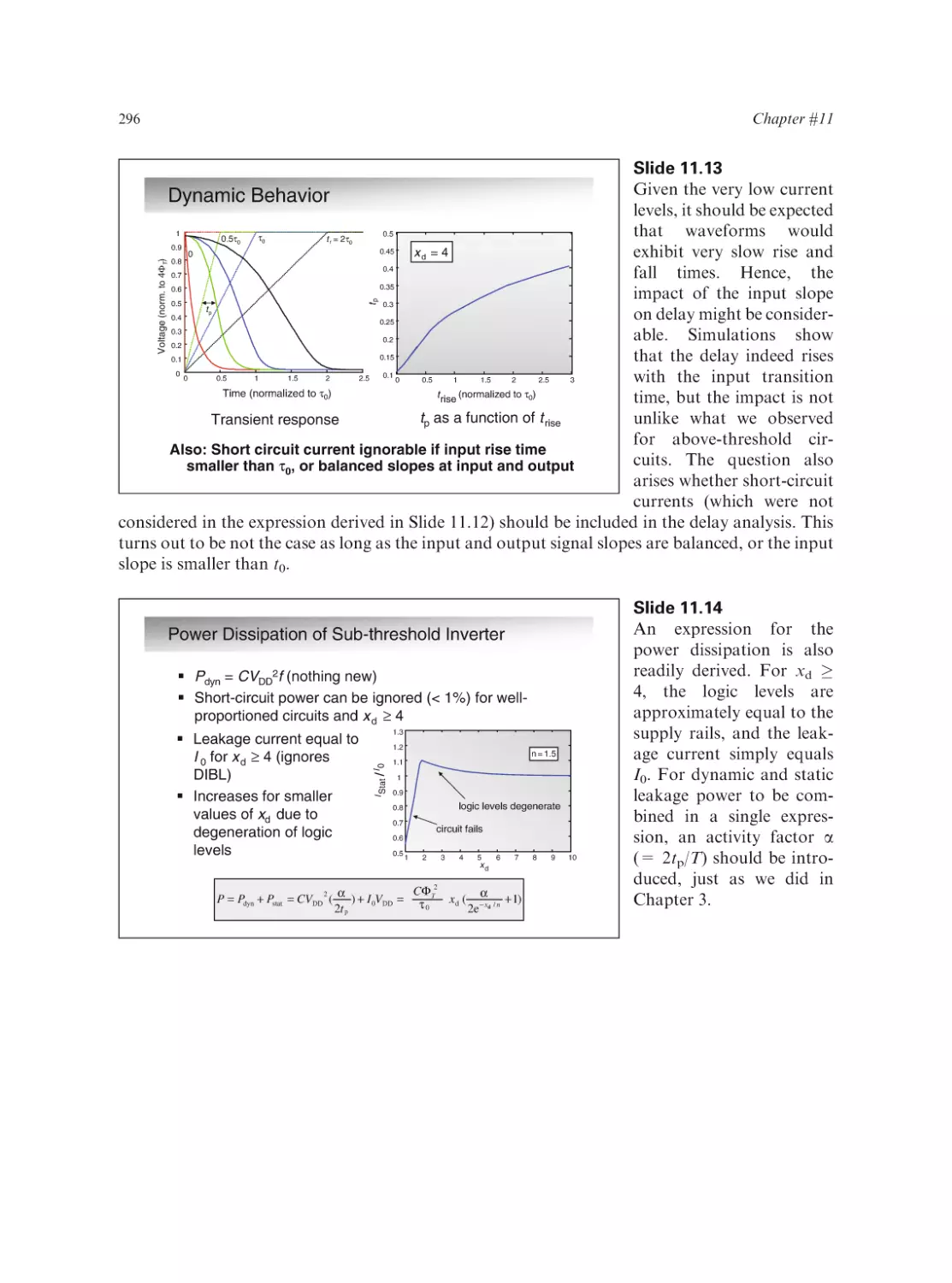
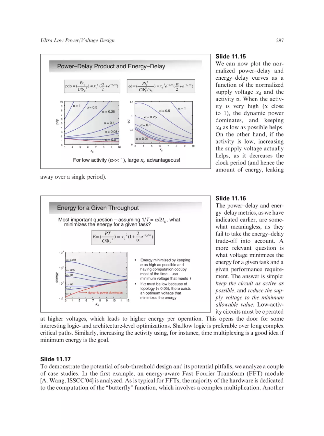
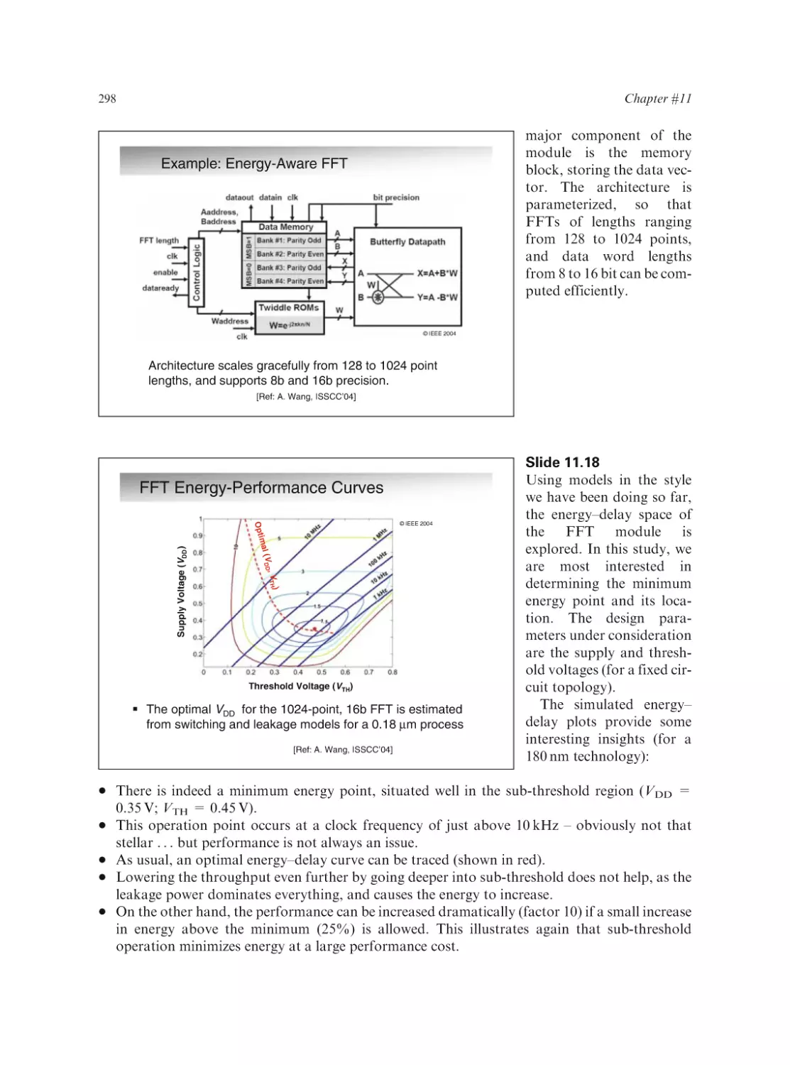
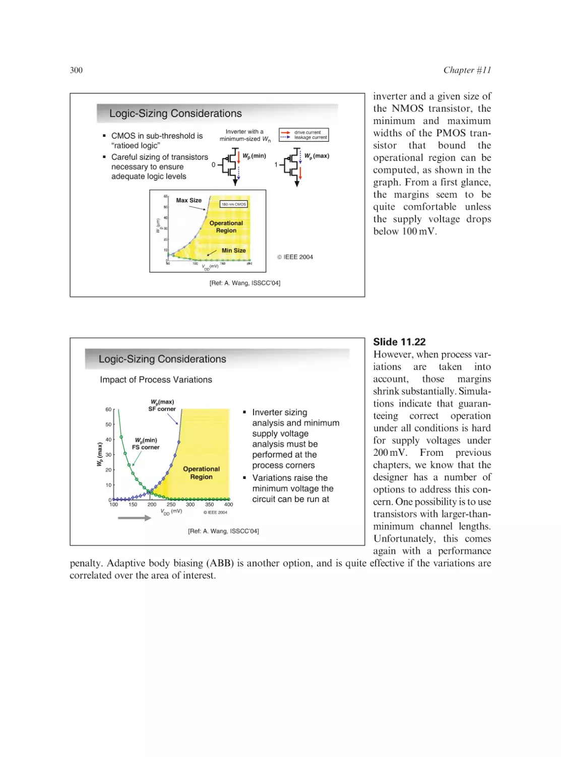
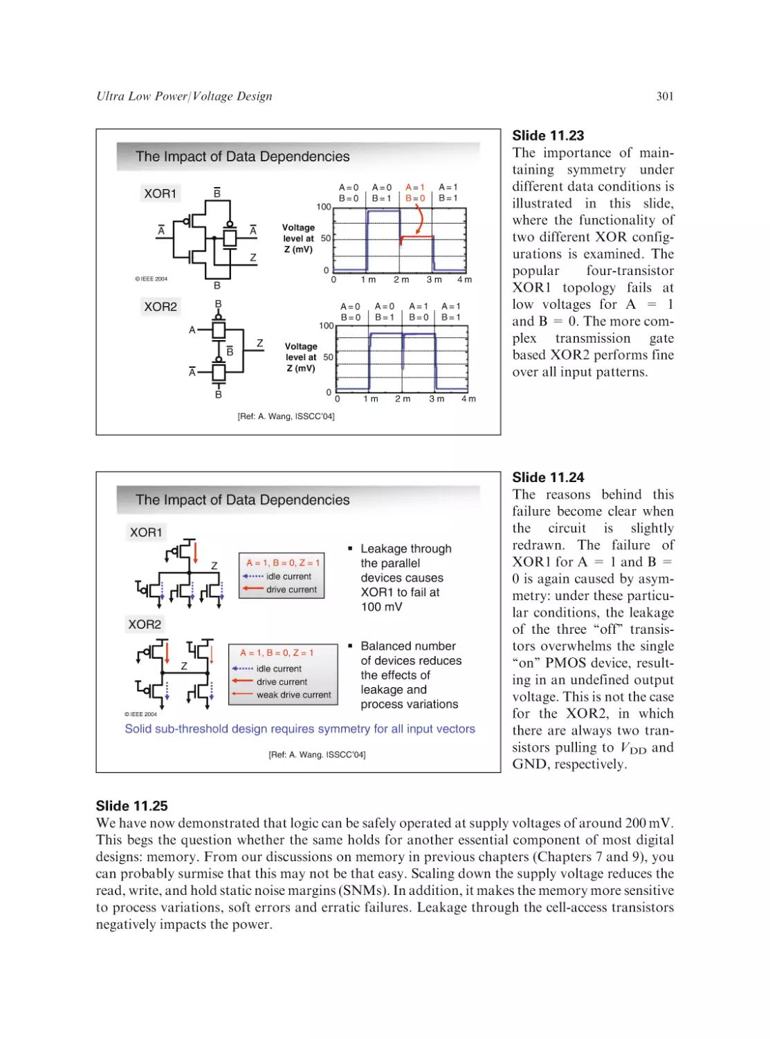
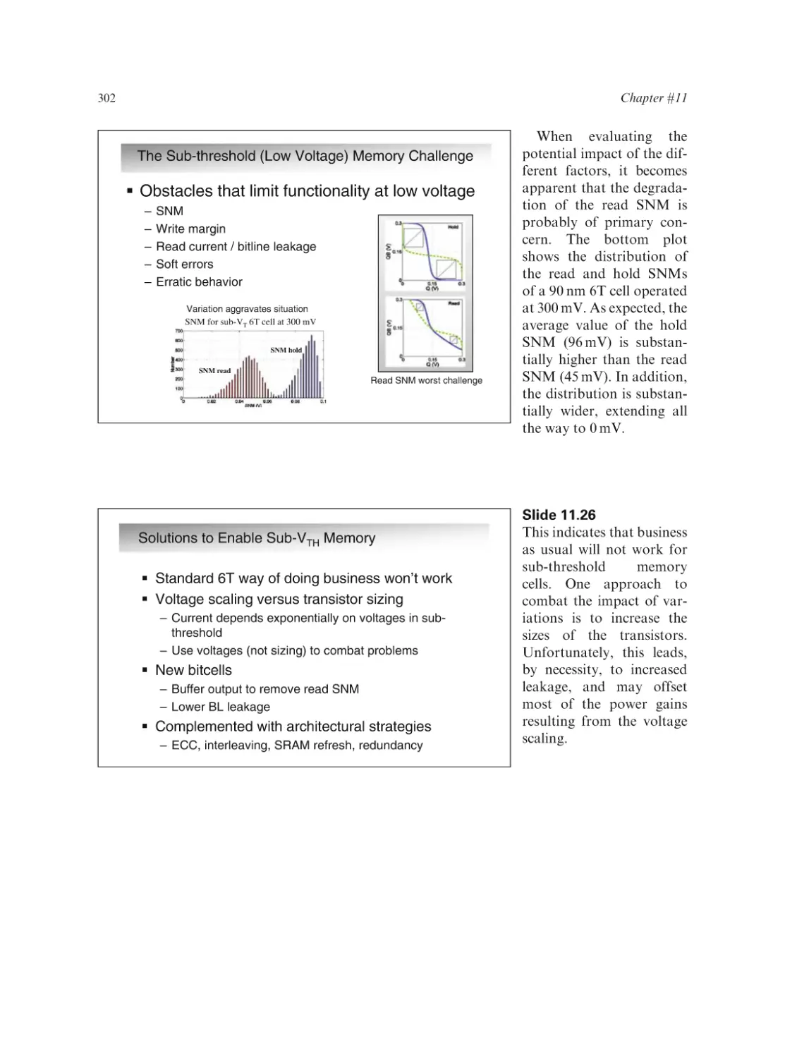
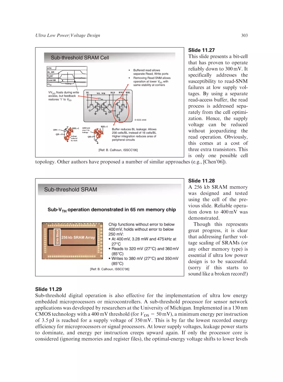
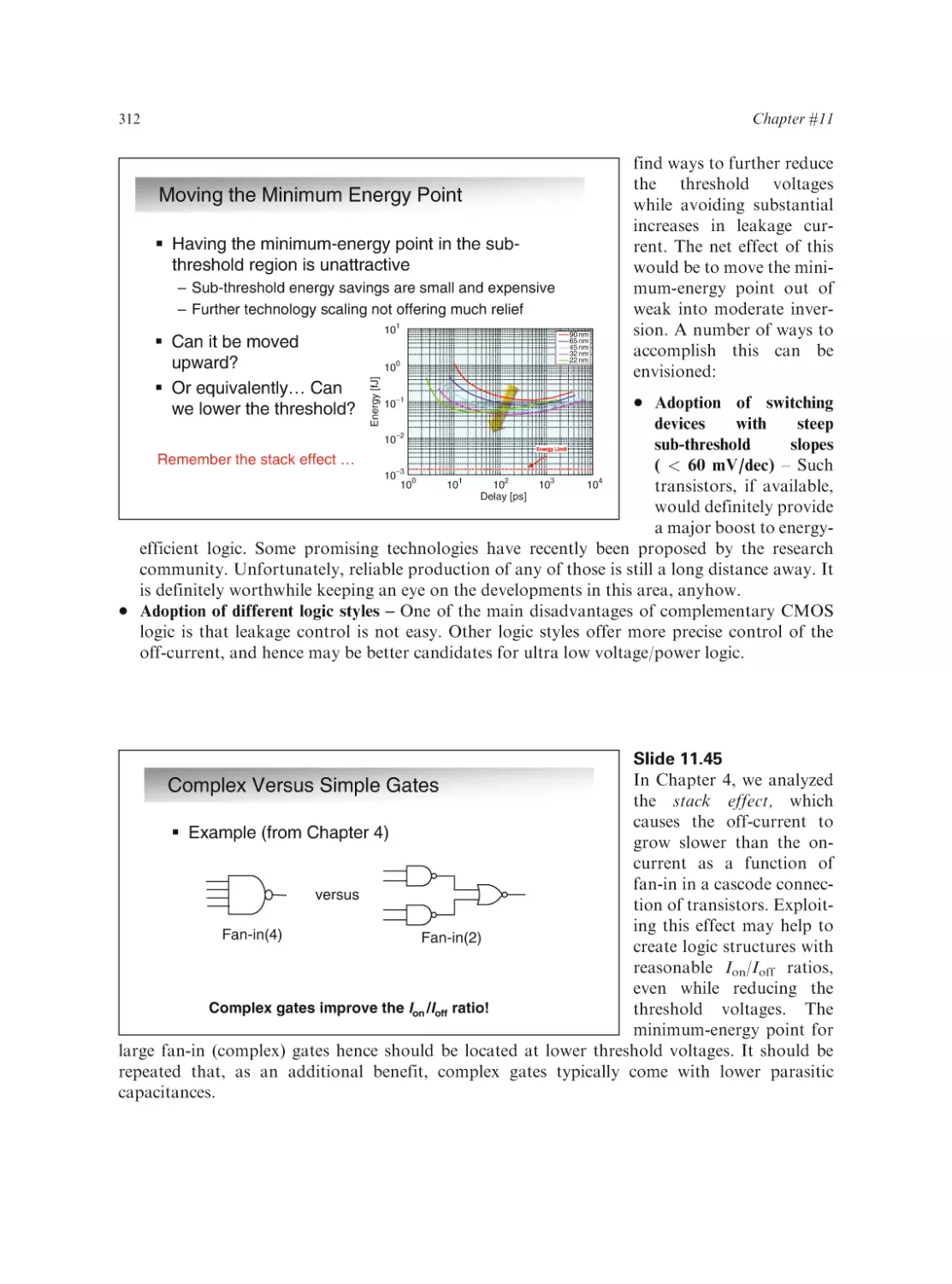
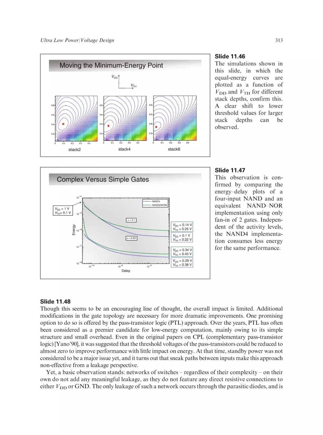
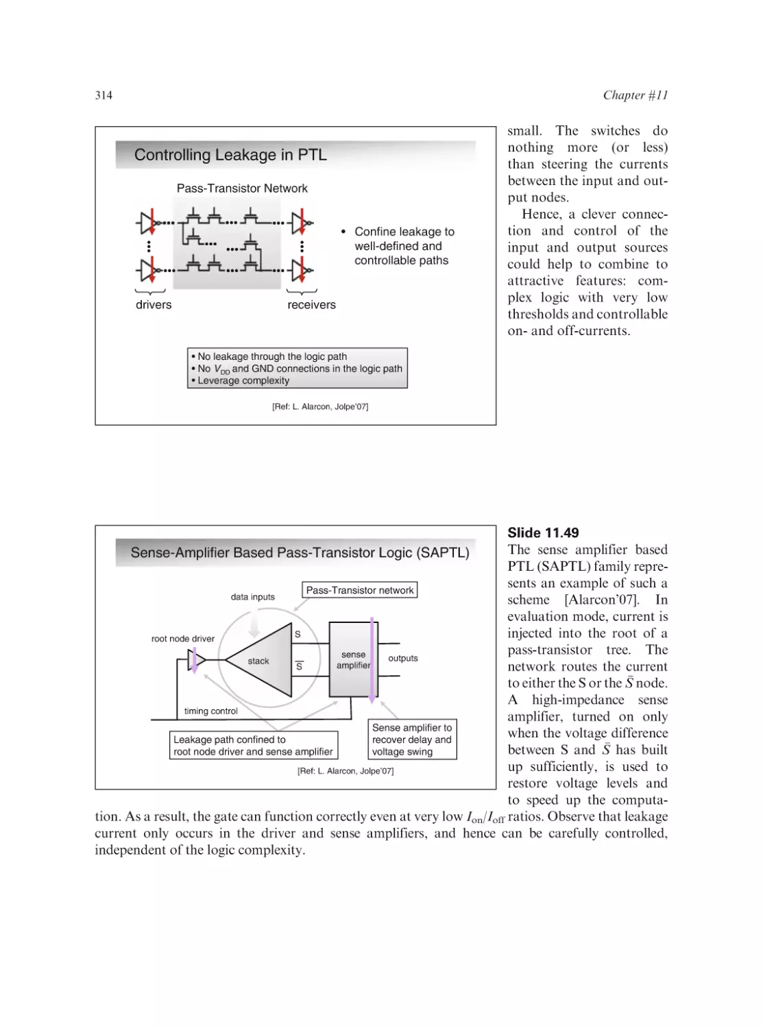
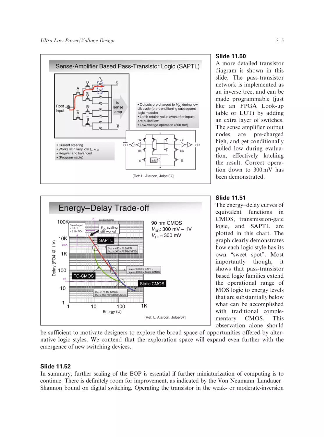
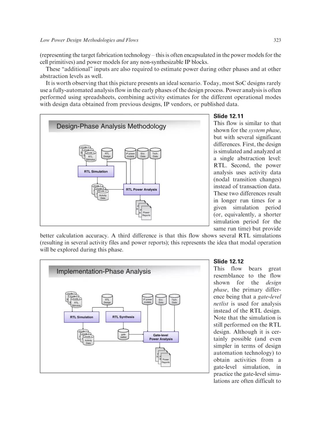
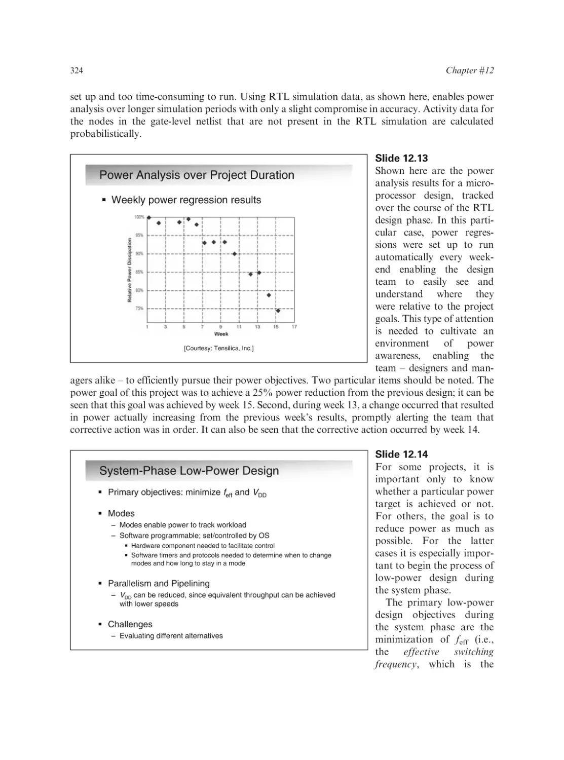
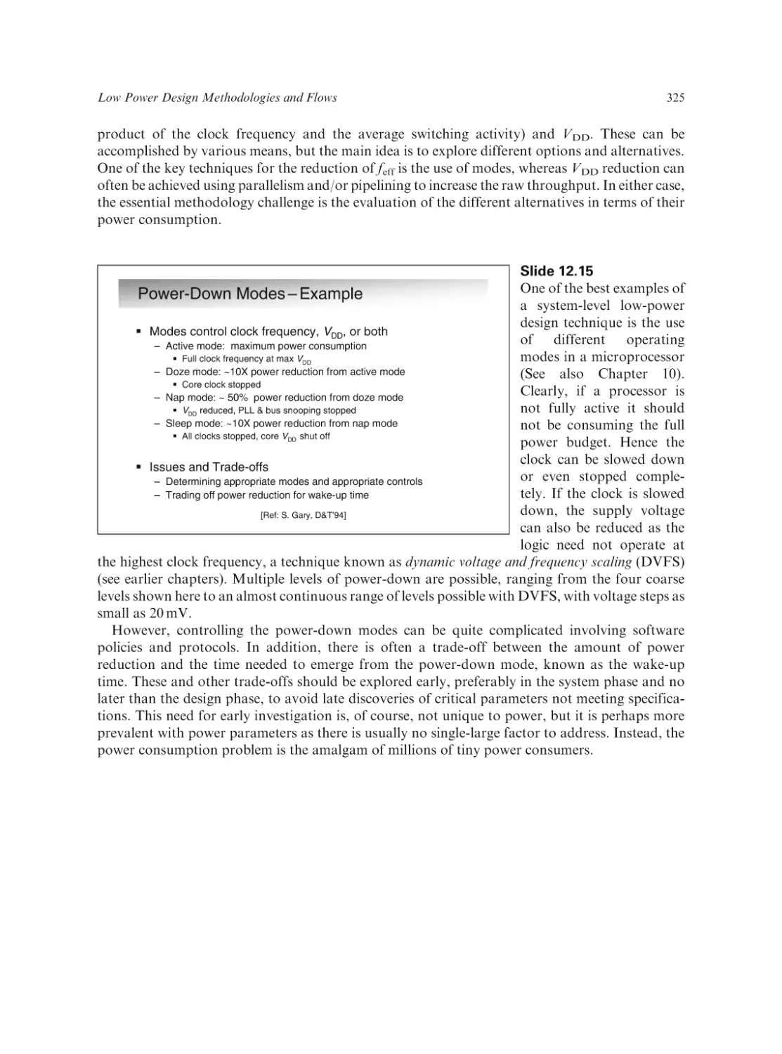
/


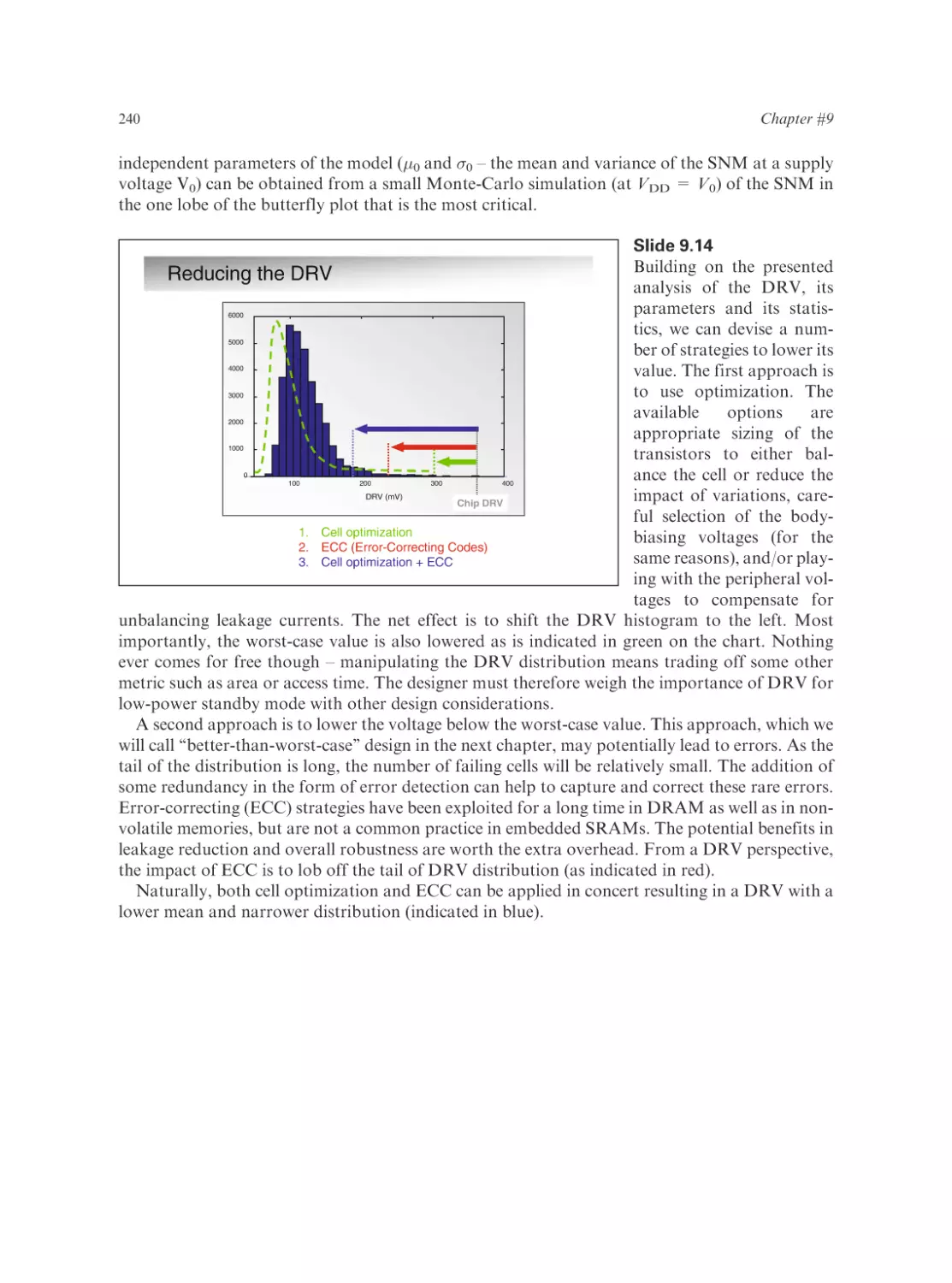
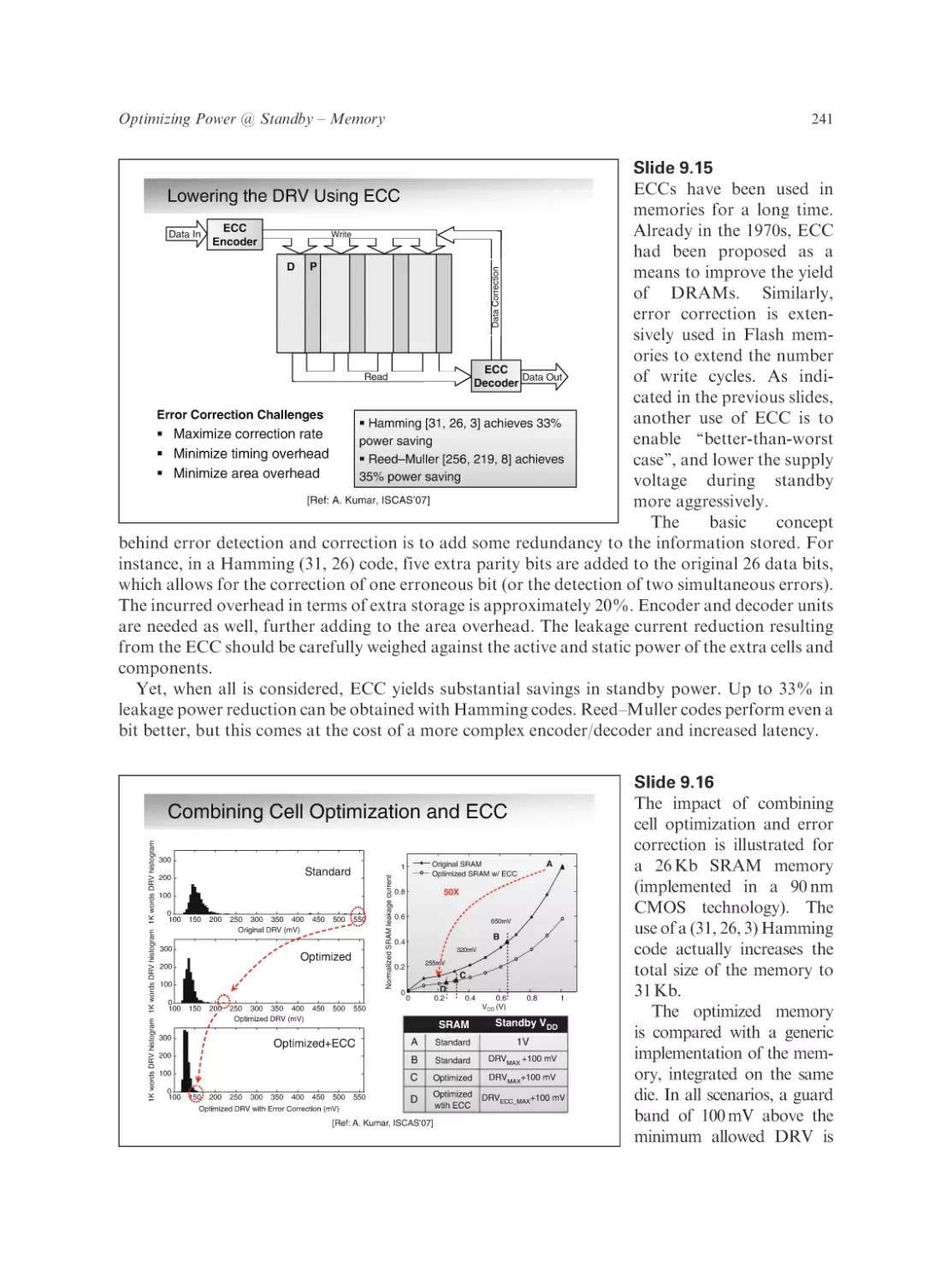
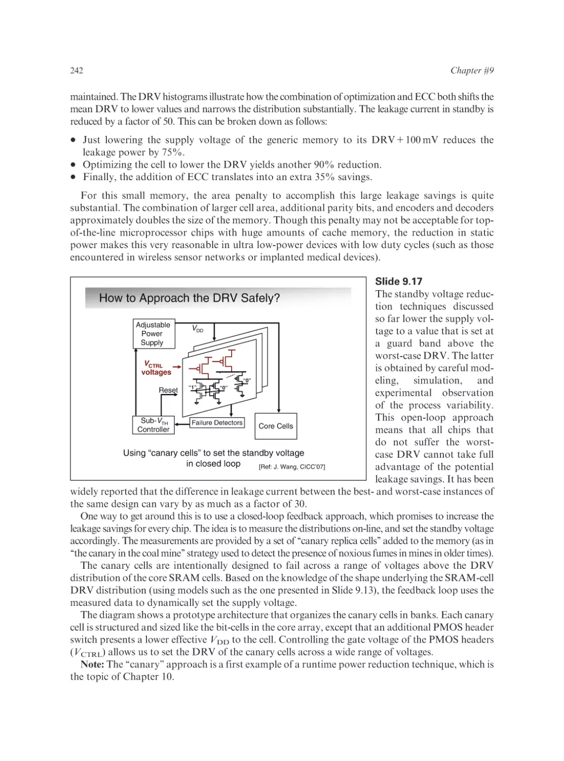


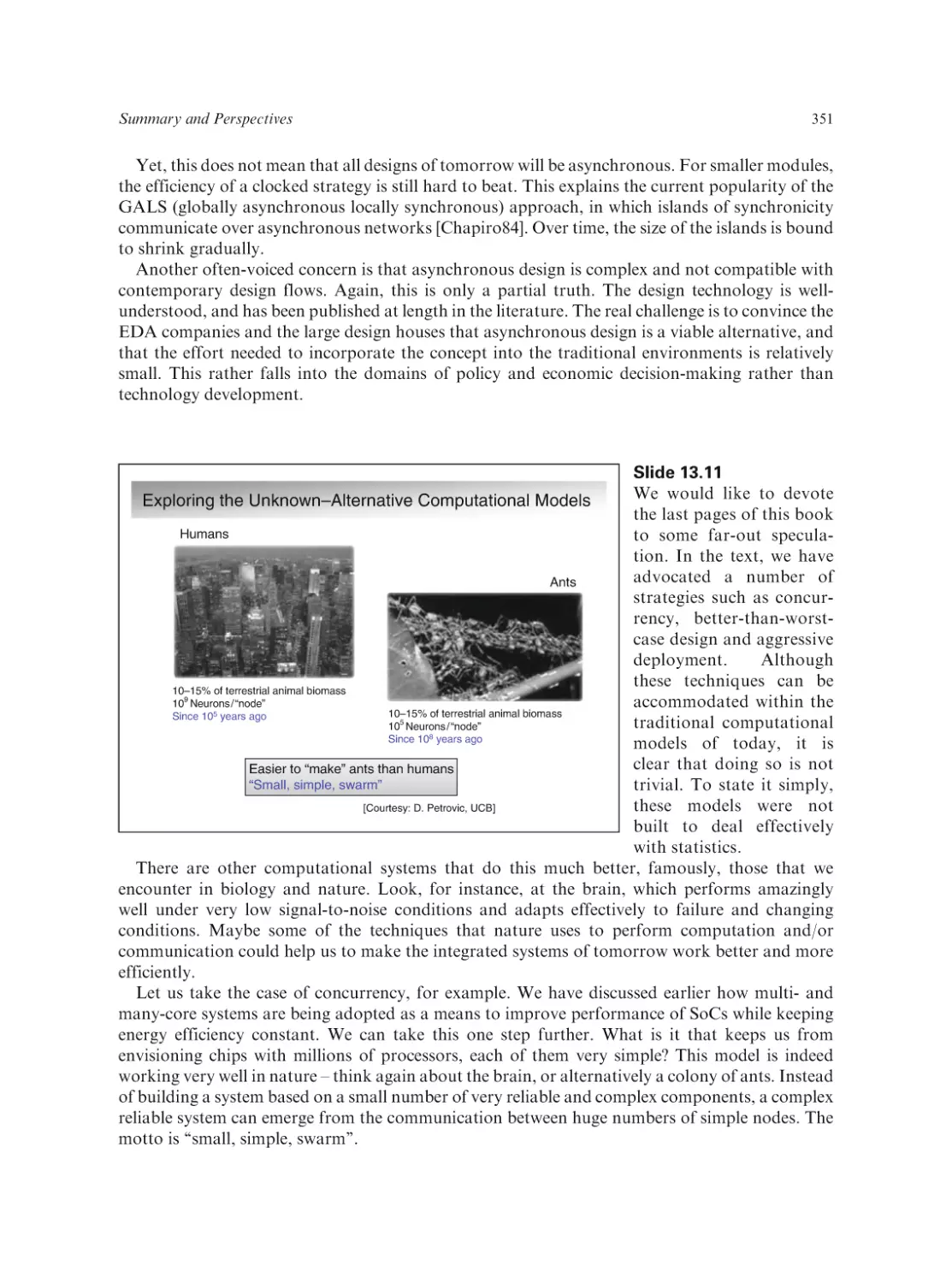


Text
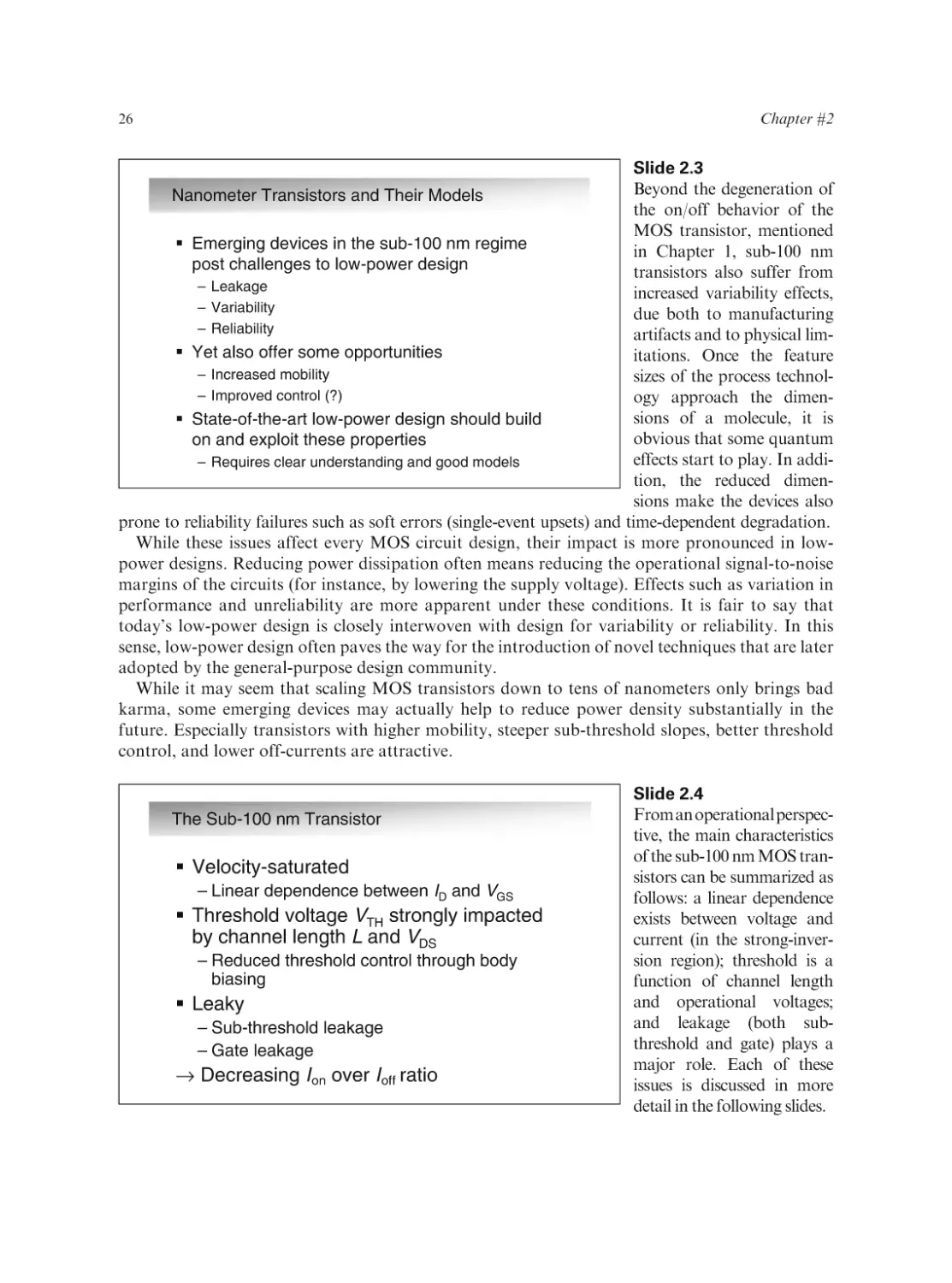
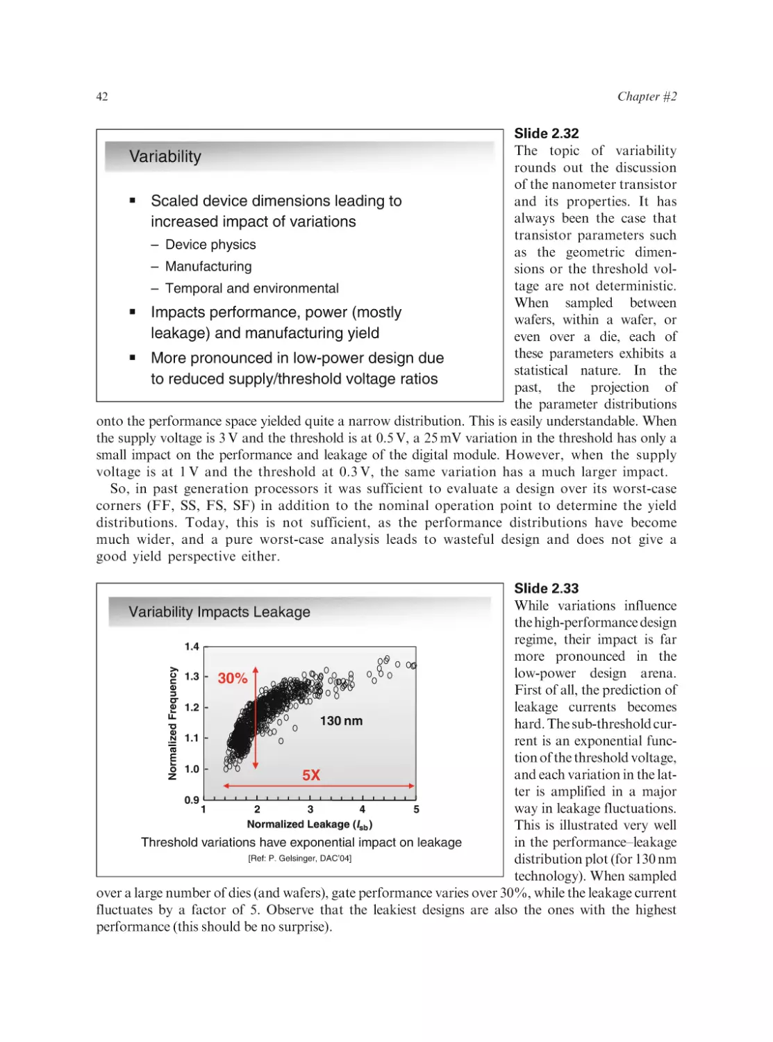
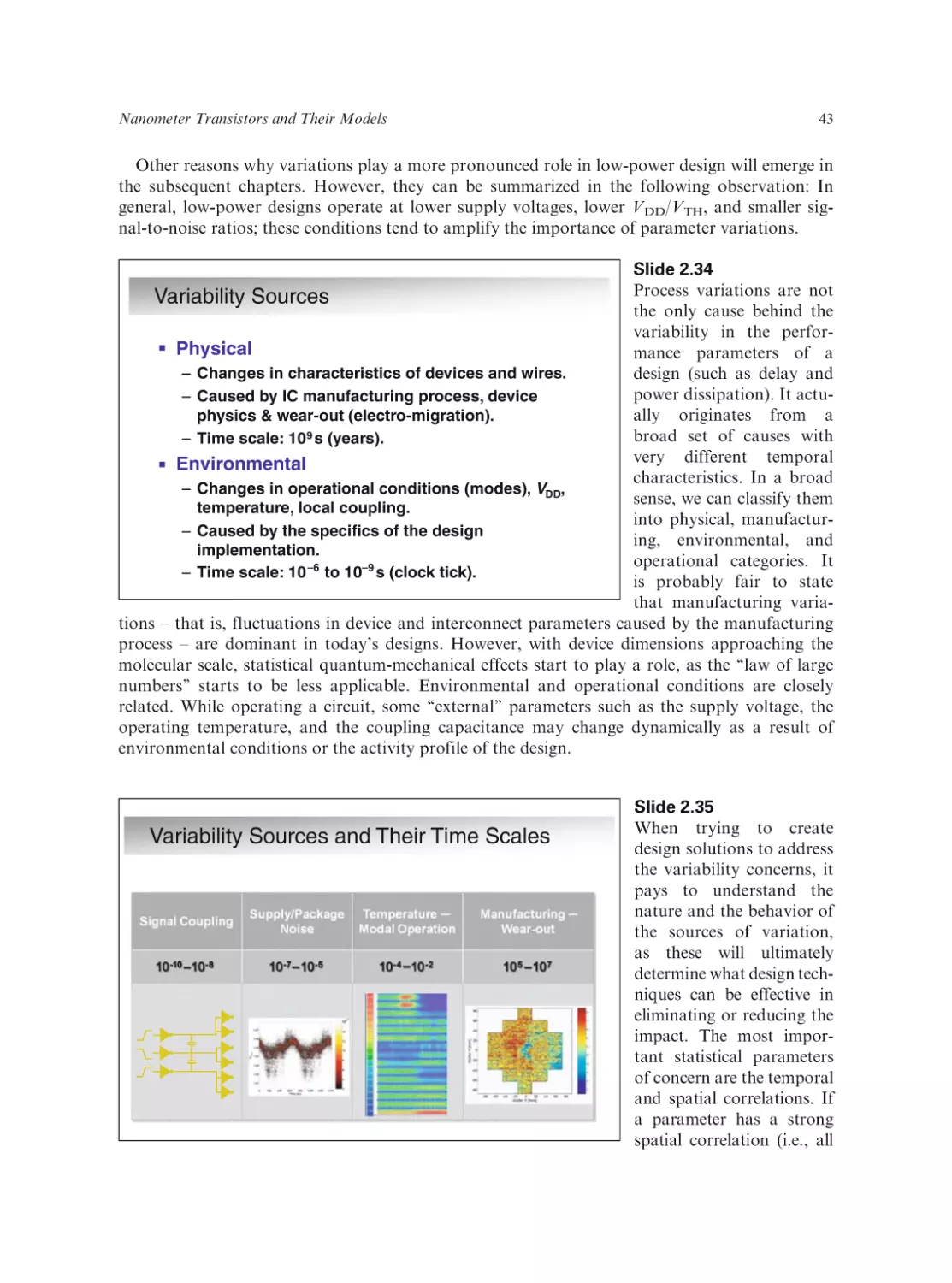
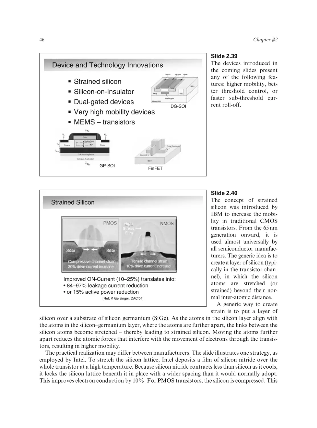
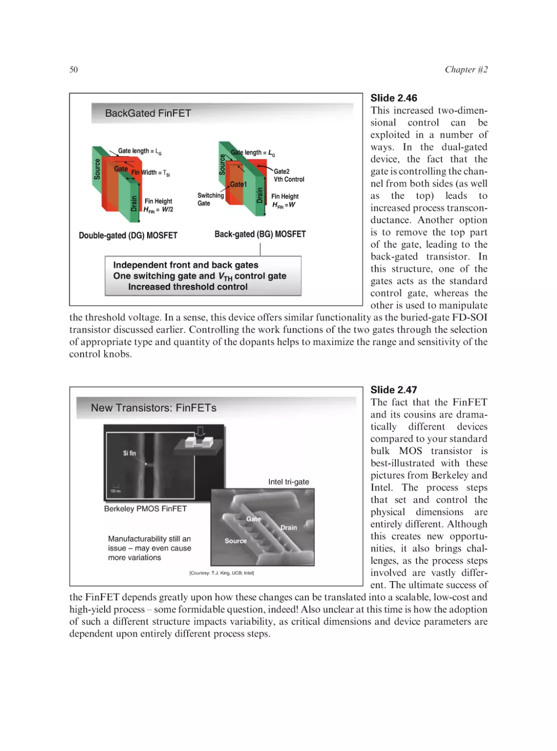
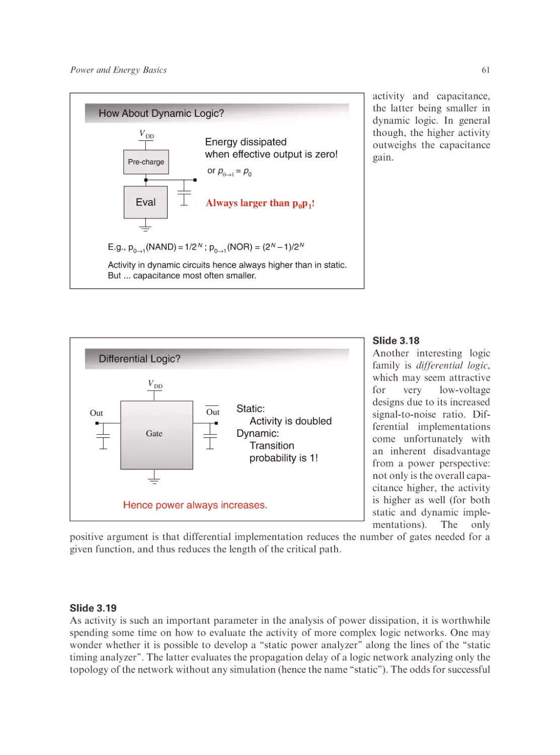
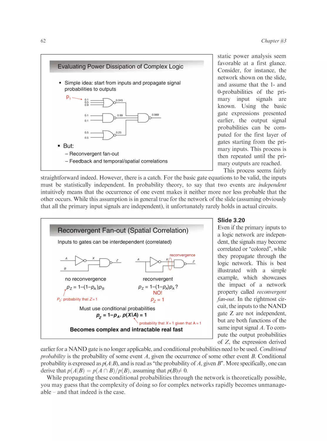
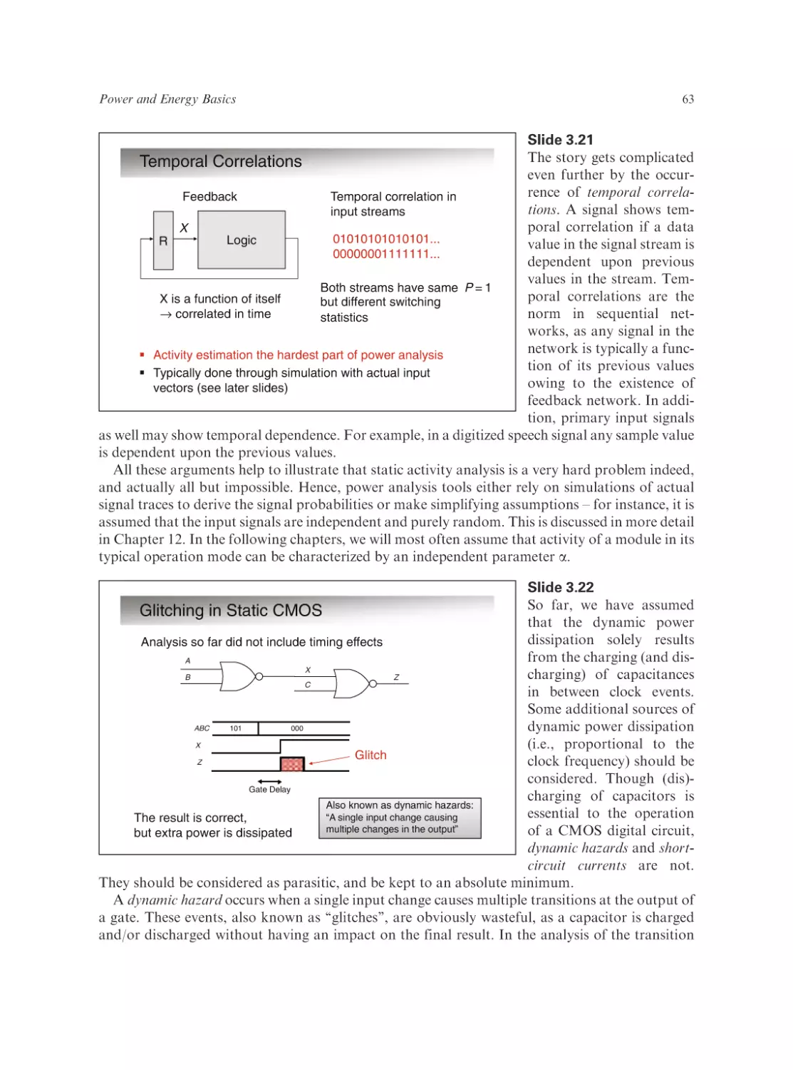
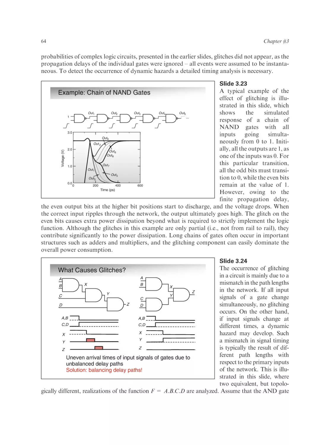
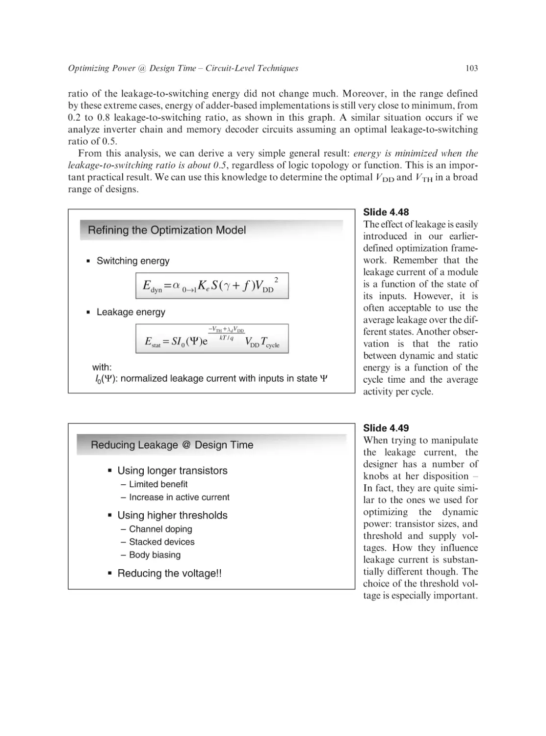
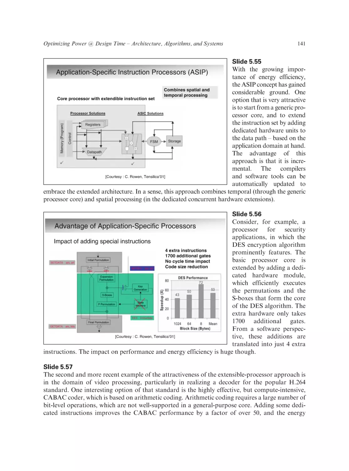
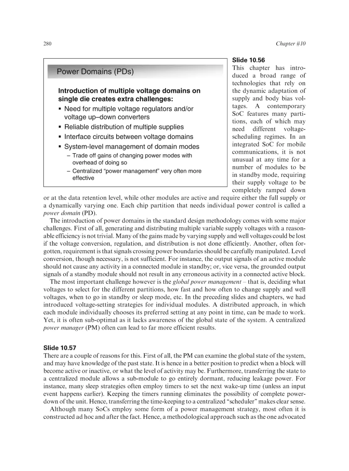
Low Power Design Essentials
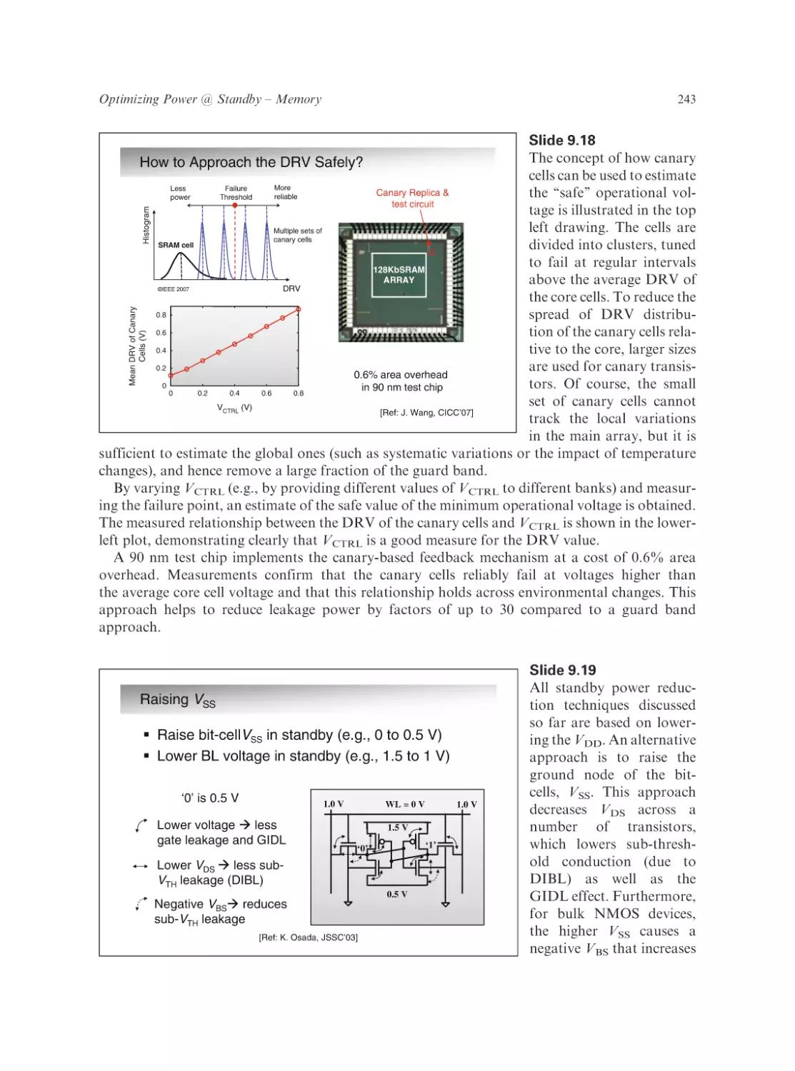
Series on Integrated Circuits and Systems
Series Editor:
Anantha Chandrakasan
Massachusetts Institute of Technology
Cambridge, Massachusetts
Low Power Design Essentials
Jan Rabaey
ISBN 978-0-387-71712-8
Carbon Nanotube Electronics
Ali Javey and Jing Kong (Eds.)
ISBN 978-0-387-36833-7
Wafer Level 3-D ICs Process Technology
Chuan Seng Tan, Ronald J. Gutmann, and L. Rafael Reif (Eds.)
ISBN 978-0-387-76532-7
Adaptive Techniques for Dynamic Processor Optimization: Theory and Practice
Alice Wang and Samuel Naffziger (Eds.)
ISBN 978-0-387-76471-9
mm-Wave Silicon Technology: 60 GHz and Beyond
Ali M. Niknejad and Hossein Hashemi (Eds.)
ISBN 978-0-387-76558-7
Ultra Wideband: Circuits, Transceivers, and Systems
Ranjit Gharpurey and Peter Kinget (Eds.)
ISBN 978-0-387-37238-9
Creating Assertion-Based IP
Harry D. Foster and Adam C. Krolnik
ISBN 978-0-387-36641-8
Design for Manufacturability and Statistical Design: A Constructive Approach
Michael Orshansky, Sani R. Nassif, and Duane Boning
ISBN 978-0-387-30928-6
Low Power Methodology Manual: For System-on-Chip Design
Michael Keating, David Flynn, Rob Aitken, Alan Gibbons, and Kaijian Shi
ISBN 978-0-387-71818-7
Modern Circuit Placement: Best Practices and Results
Gi-Joon Nam and Jason Cong
ISBN 978-0-387-36837-5
CMOS Biotechnology
Hakho Lee, Donhee Ham and Robert M. Westervelt
ISBN 978-0-387-36836-8
SAT-Based Scalable Formal Verification Solutions
Malay Ganai and Aarti Gupta
ISBN 978-0-387-69166-4, 2007
Ultra-Low Voltage Nano-Scale Memories
Kiyoo Itoh, Masashi Horiguchi and Hitoshi Tanaka
ISBN 978-0-387-33398-4, 2007
Continued after index
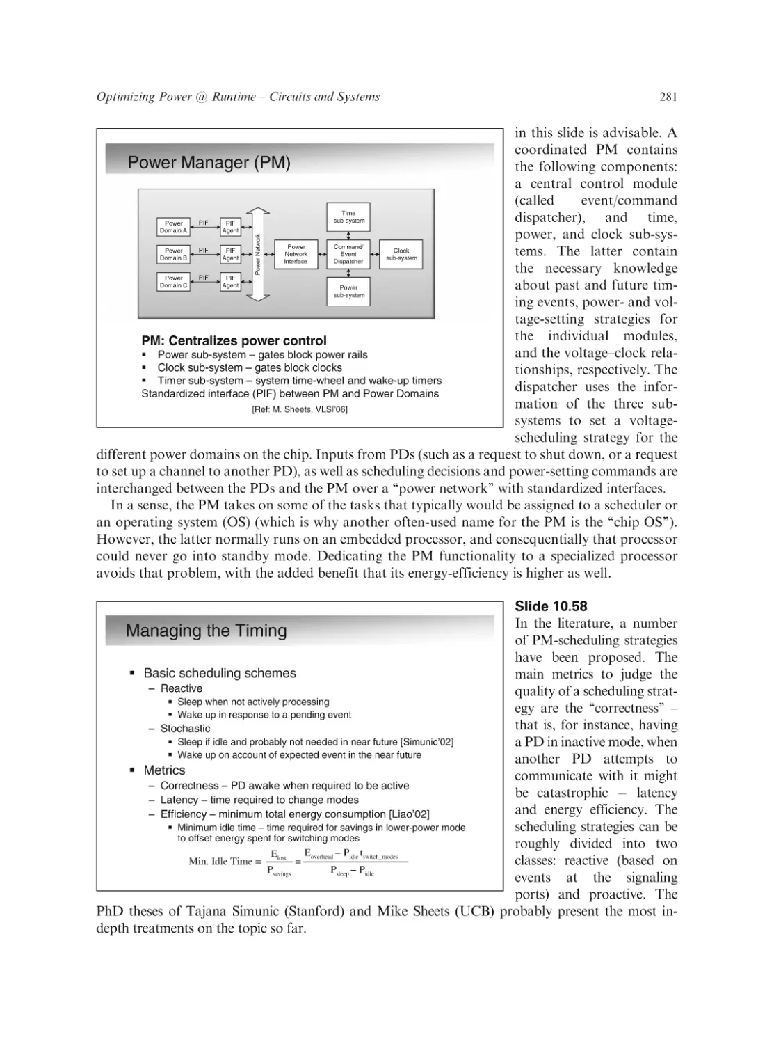
Jan Rabaey
Low Power Design Essentials
13
Jan Rabaey
Department of Electrical Engineering &
Computer Science (EECS)
University of California
Berkeley, CA 94720
USA
jan@eecs.berkeley.edu
ISSN 1558-9412
ISBN 978-0-387-71712-8
e-ISBN 978-0-387-71713-5
DOI 10.1007/978-0-387-71713-5
Library of Congress Control Number: 2008932280
# Springer ScienceþBusiness Media, LLC 2009
All rights reserved. This work may not be translated or copied in whole or in part without the written permission of the
publisher (Springer ScienceþBusiness Media, LLC, 233 Spring Street, New York, NY 10013, USA), except for brief
excerpts in connection with reviews or scholarly analysis. Use in connection with any form of information storage and
retrieval, electronic adaptation, computer software, or by similar or dissimilar methodology now known or hereafter
developed is forbidden.
The use in this publication of trade names, trademarks, service marks, and similar terms, even if they are not identified as
such, is not to be taken as an expression of opinion as to whether or not they are subject to proprietary rights.
Printed on acid-free paper
springer.com
To Kathelijin
For so many years, my true source of support and motivation.
To My Parents
While I lost you both in the past two years, you still inspire me to reach ever further.
Preface
Slide 0.1
Welcome to this book titled
‘‘Low Power Design Essentials’’. (A somewhat more
accurate title for the book
would be ‘‘Low Power
Digital Design Essentials’’,
as virtually all of the mateJan M. Rabaey
rial is focused on the digital
integrated-circuit
design
domain.)
In recent years, power
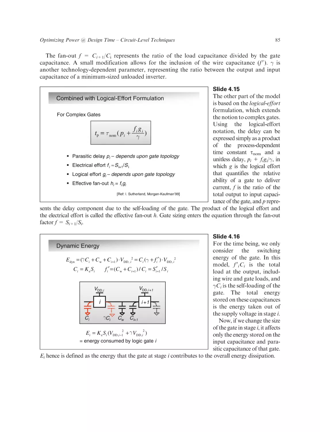
and energy have become
one of the most compelling
issues in the design of digital circuits. On one end,
power has put a severe limitation on how fast we can
run our circuits; at the other end, energy reduction techniques have enabled us to build ubiquitous
mobile devices that can run on a single battery charge for an exceedingly long time.
Preface
Slide 0.2
You may wonder why there is a need for yet another book on low-power design, as there are quite a
number of those already on the market (some of them co-authored by myself). The answer is quite
simple: all these books are edited volumes, and target the professional who is already somewhat
versed in the main topics of design for power or energy. With these topics becoming one of the most
compelling issues in design today, it is my opinion that it is time for a book with an educational
approach. This means building up from the basics, and exposing the different subjects in a rigorous
and methodological way with consistent use of notations and definitions. Concepts are illustrated
with examples using state-of-the-art technologies (90 nm and below). The book is primarily
intended for use in short-to-medium length courses on low-power design. However, the format
also should work well for the working professional, who wants to update her/himself on low-power
design in a self-learning manner.
vii
viii
Preface
This preface also presents an opportunity for
Goals of This Book
me to address an issue that
has been daunting lowpower design for a while.
Provide an educational perspective on
Many people in the field
low-power desgn for digital integrated
circuits
seem to think that it is just
a ‘‘bag of tricks’’ applied in
Promote a structured design methodology
a somewhat ad hoc fashfor low power/energy design
ion, that it needs a guru to
Traverse the levels of the design hierarchy
get to the bottom, and that
Explore bounds and roadblocks
the concept of a low-power
Provide future perspectives
methodology is somewhat
an oxymoron. In fact, in
recent years researchers
and developers have demonstrated that this need not be the case at all. One of the most important
realizations over the past years is that minimum-energy design, though interesting, is not what we
truly are pursuing. In general, we design in an energy–delay trade-off space, where we try to find
design with the lowest energy for a given performance, or vice versa. A number of optimization and
design exploration tools can be constructed that help us to traverse this trade-off space in an
informed fashion, and this at all levels of the design hierarchy.
In addition to adhering to such a methodology throughout the text, we are also investigating the
main roadblocks that we have to overcome in the coming decades if we want to keep reducing the
energy per operation. This naturally leads to the question of what the physical limits of energy
scaling might be. Wherever possible, we also venture some perspectives on the future.
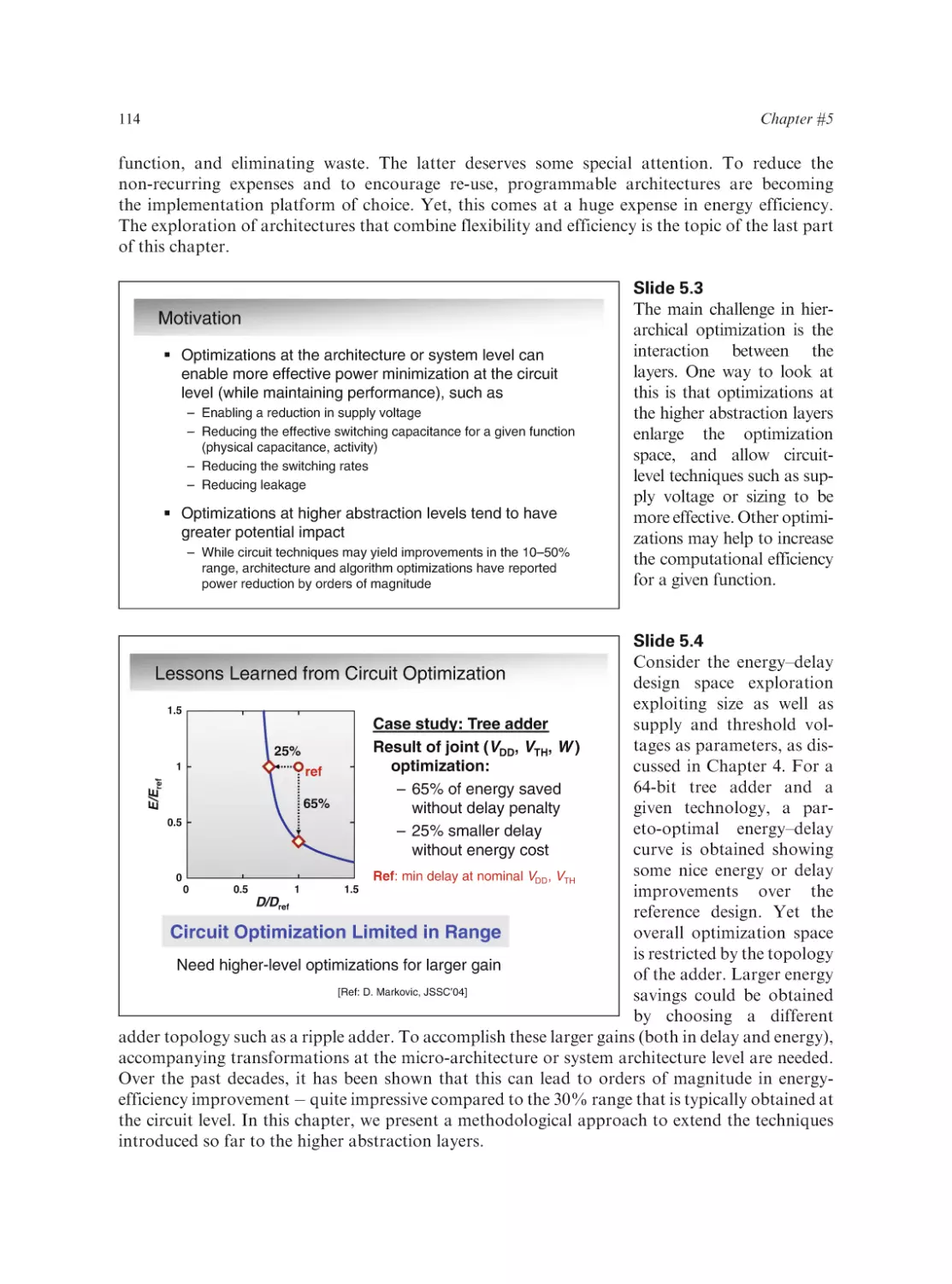
Slide 0.3
An Innovative Format
Already in this preface,
you observe the somewhat
Pioneered in W. Sansen’s book Analog Design
unorthodox approach the
Essentials (Springer)
book is taking. Rather
PowerPoint slides present a quick outline
than choosing the tradiof essential points and issues, and provide
tional approach of a
a graphical perspective
lengthy continuous text,
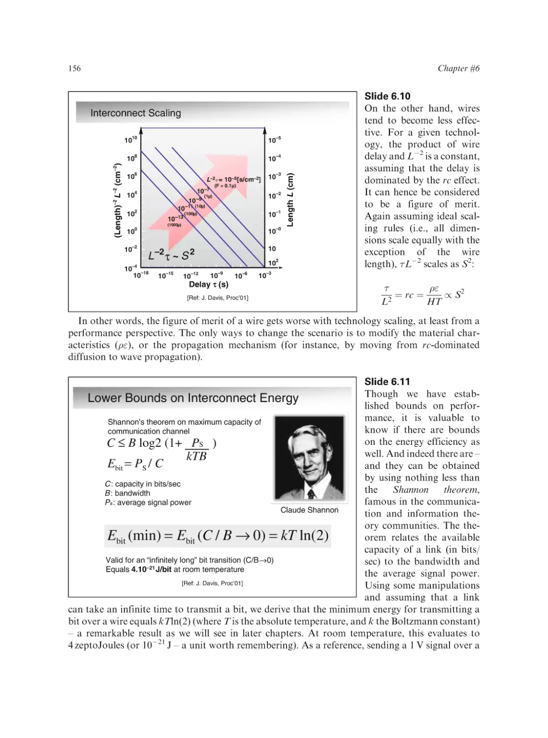
occasionally interspersed
Side notes provide depth, explain
reasonings, link topics
with some figures, we use
the reverse approach: graSupplemented with web-site:
http://bwrc.eecs.berkeley.edu/LowPowerEssentials
phics first, text as a side
note. In my experience, a
An ideal tool for focused-topic courses
single figure does a lot
more to convey a message
than a page of text (‘‘A picture is worth a 1000 words’’). This approach was pioneered by Willy
Sansen in his book Analog Design Essentials (also published by Springer). The first time I saw the
book, I was immediately captivated by the idea. The more I looked at it, the more I liked it. Hence
this book . . . . When browsing through it, you will notice that the slides and the notes play entirely
Preface
ix
different roles. Another advantage of the format is that the educator has basically all the lecturing
material in her/his hands rightaway. Besides distributing the slideware freely, we also offer additional material and tools on the web-site of the book.
Slide 0.4
Outline
The outline of the book
proceeds as follows: After
1. Introduction
first establishing the basics,
2. Advanced MOS Transistors and Their Models
we proceed to address
3. Power Basics
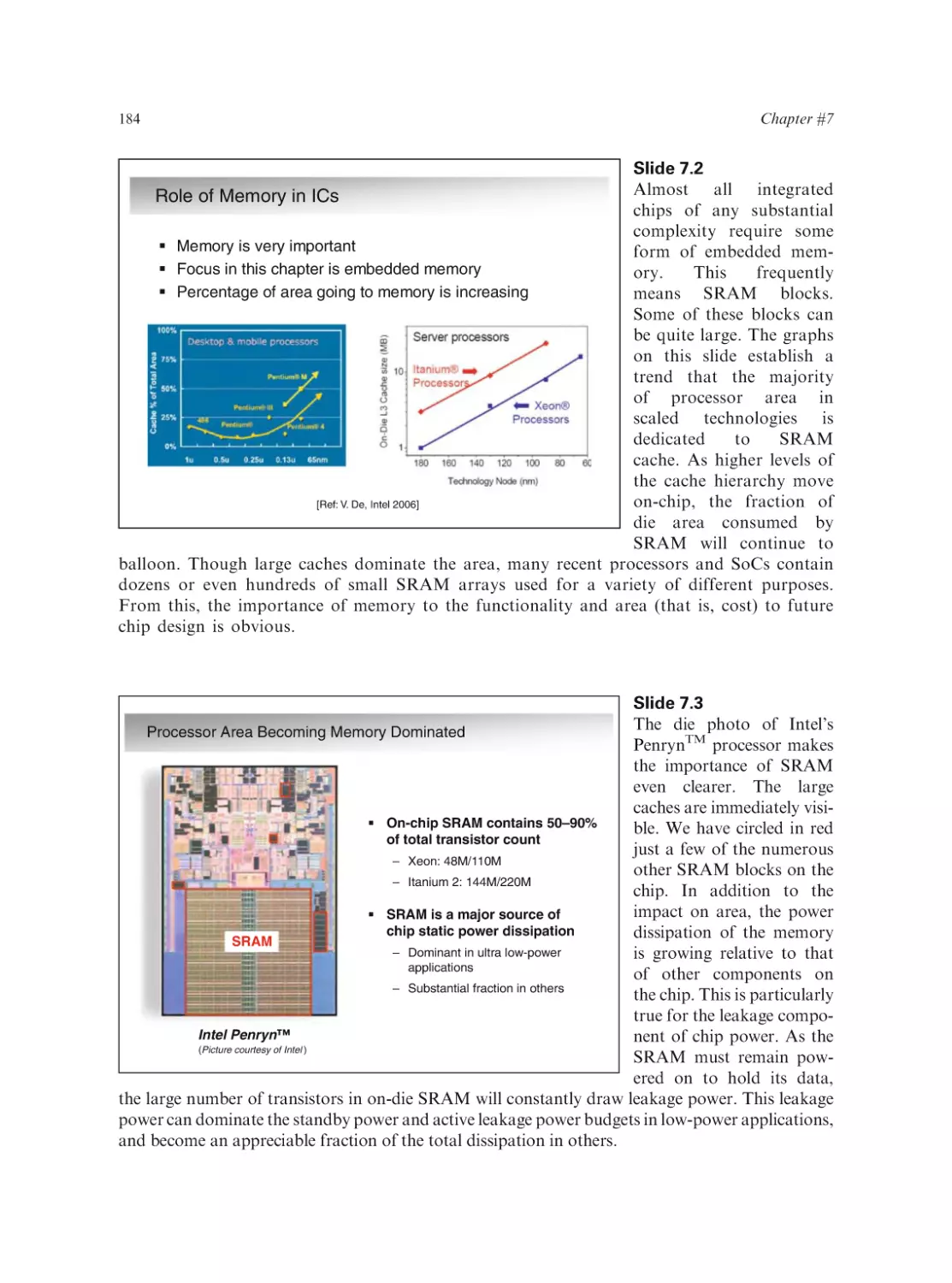
power optimization in
Optimizing Power @ Design Time
three different operational
4. Circuits
modes:
design
time,
5. Architectures, Algorithms, and Systems
6. Interconnect and Clocks
standby time, and run
7. Memories
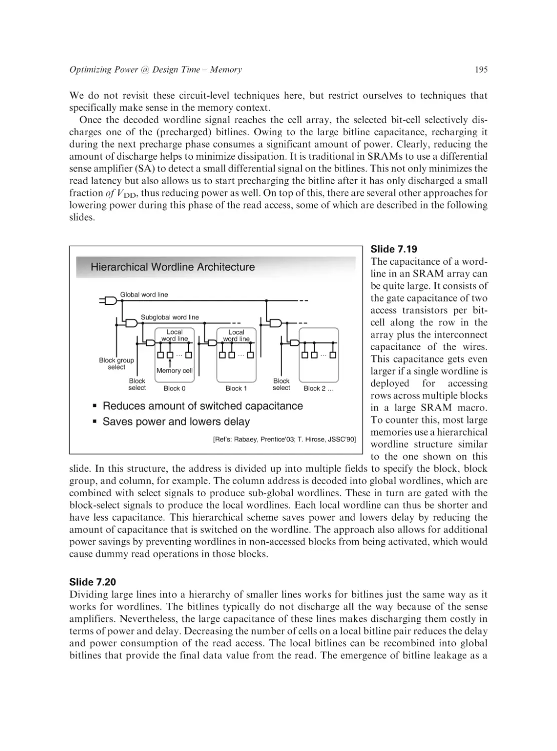
time. The techniques used
Optimizing Power @ Standby
in each of these modes dif8. Circuits and Systems
fer considerably. Observe
9. Memory
that we treat dynamic and
Optimizing Power @ Runtime
10. Circuits, Memory, and Systems
static
power
simultaPerspectives
neously throughout the
11. Ultra Low Power/ VoltageDesign
text – in today’s semicon12. Low Power Design Methodologies and Flows
ductor technology, leakage
13. Summary and Perspectives
power is virtually on parwith switching power.
Hence separating them does not make much sense. In fact, a better design is often obtained if
the two are carefully balanced. Finally, the text concludes with a number of general topics such as
design tools, limits on power, and some future projections.
Background
Acknowledgements
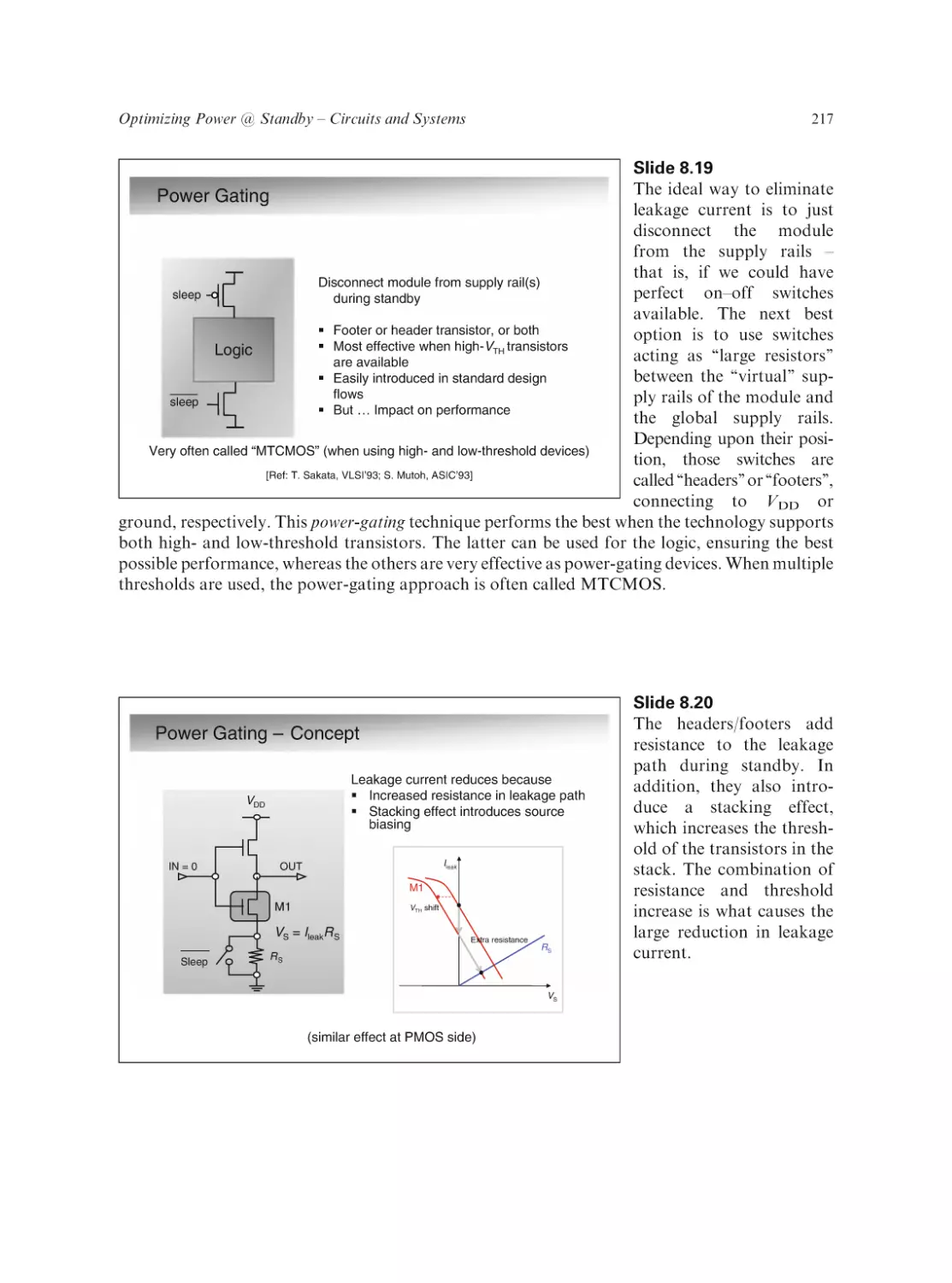
Slide 0.5
T
Putting a book like this
together without help is virtually impossible, and a
couple of words of thanks
and appreciation are in
order. First and foremost,
I am deeply indebted to
Ben Calhoun, Jerry Frenkil, Dejan Marković, and
Bora Nikolić for their help
and co-authorship of some
of the chapters. In addition,
a long list of people have
helped in providing the
basic slideware used in the
text, and in reviewing the
he contributions of many of my colleagues to this book are greatly
appreciated. Without them, building this collection of slides would have been
iimpossible.
ibl Especially,
E
i ll I would
ld like
lik to
t single
i l outt the
th iinputs
t off the
th following
f ll i
individuals who have contributed in a major way to the book: Ben Calhoun,
Jerry Frenkil, and Dejan Marković. As always, it has been an absolute pleasure
working with them.
I
n addition, a large number of people have helped to shape the book by
contrib
ting material
ie ing the chapters as they
emerged I am
contributing
reviewing
b re
the emerged.
material, or by
deeply indebted to all of them: E. Alon, T. Austin, D. Blaauw, S. Borkar, R.
Brodersen, T. Burd, K. Cao, A. Chandrakasan, H. De Man, K. Flautner, M.
Rowen T.
Sakurai A
A. Sangiovanni
Horowitz
B Nikolić,
Nikolić C.
C Rowen,
T Sakurai,
Horowitz, K
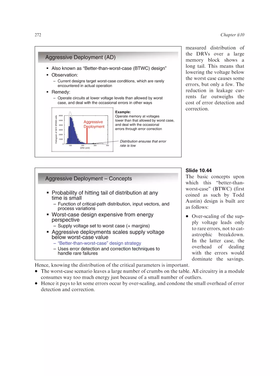
K. Itoh
T. Kuroda
Kuroda, B.
SangiovanniItoh, T
Vincentelli, N. Shanbhag, V. Stojanović, T. Sakurai, J. Tschanz, E. Vittoz, A.
Wang, and D. Wingard, as well as all my graduate students at BWRC.
I
also would like to express my appreciation for the funding agencies that have
provided strong support to the development of low-power design technologies
and methodologies
methodologies. Especially the FCRP program (and its member companies)
and DARPA deserve special credit.
x
Preface
earlier drafts of the book. Special gratitude goes to a number of folks who have shaped the lowpower design technology world in a tremendous way – and as a result have contributed enormously
to this book: Bob Brodersen, Anantha Chandrakasan, Tadahiro Kuroda, Takayasu Sakurai,
Shekhar Borkar, and Vivek De. Working with them over the past decade(s) has been a great
pleasure and a truly exciting experience!
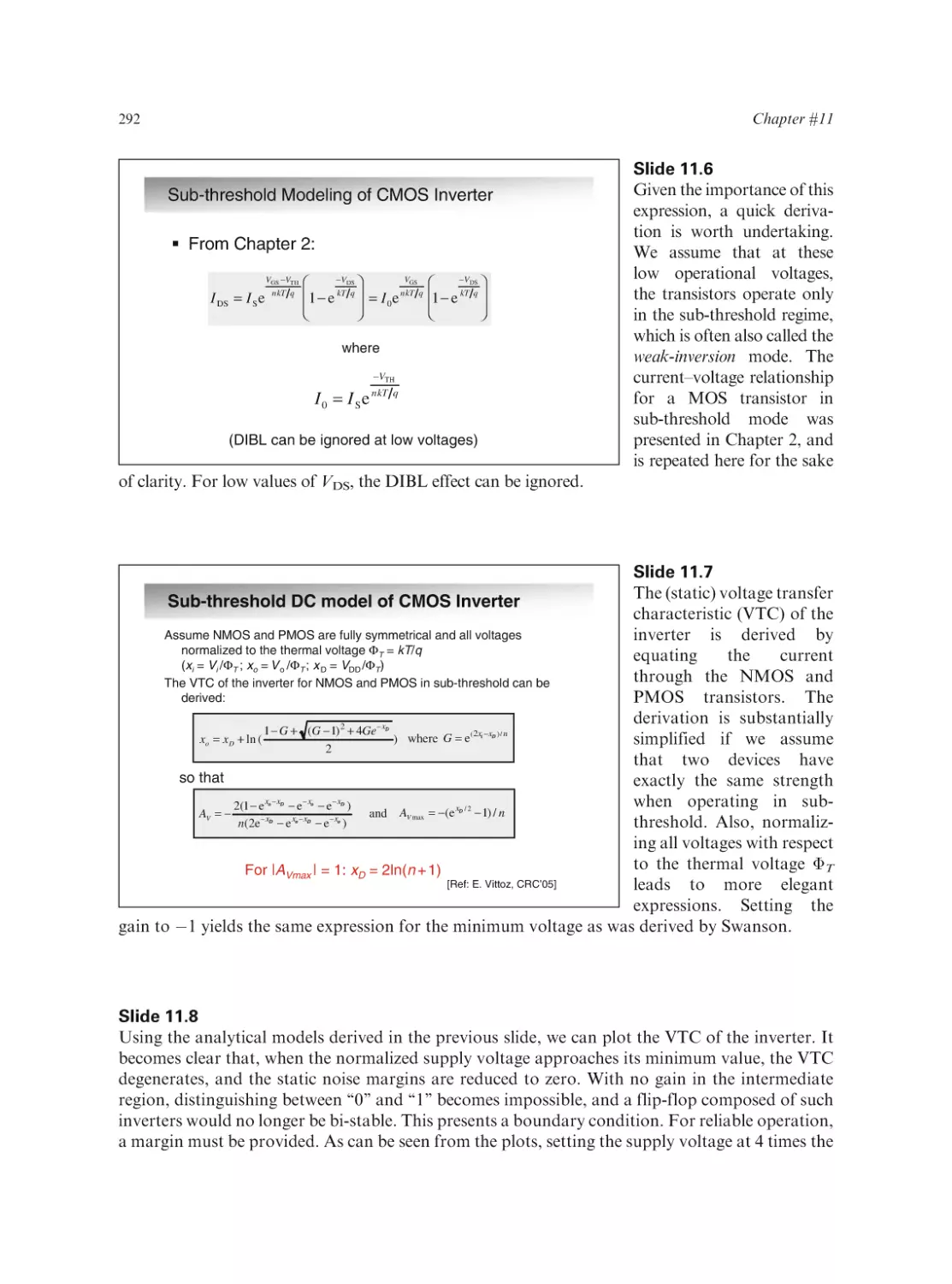
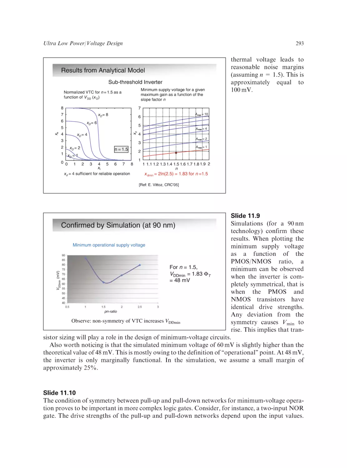
Slide 0.6–0.7
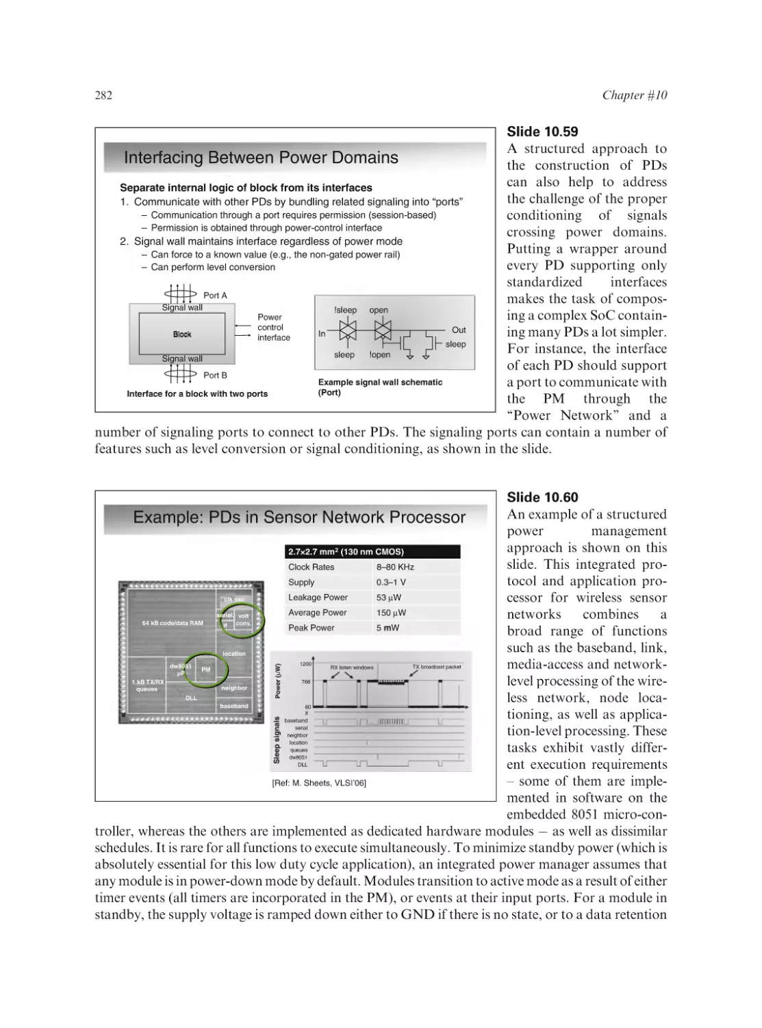
Low Power Design – Reference Books
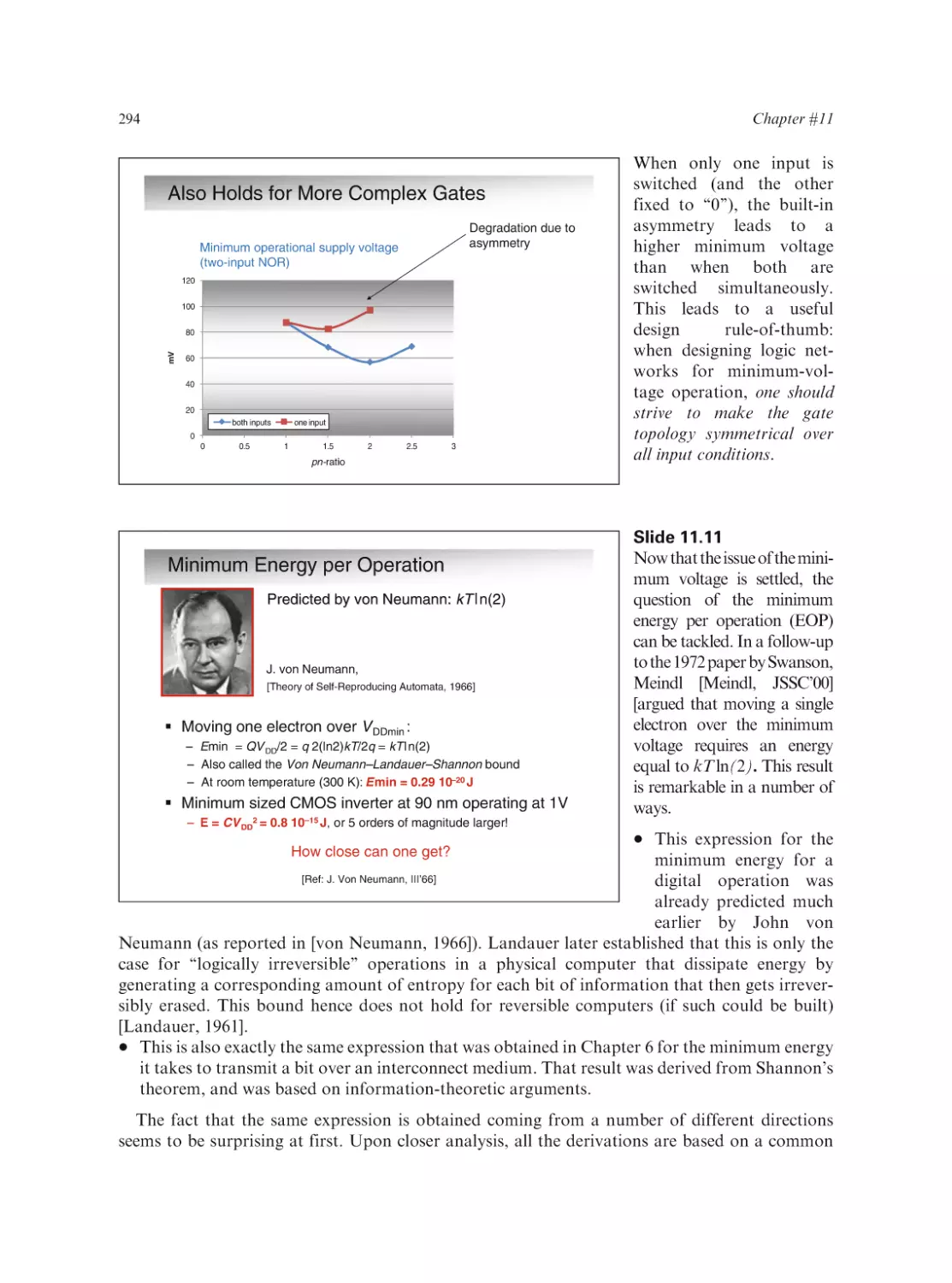
A. Chandrakasan and R. Brodersen, Low Power CMOS Design, Kluwer Academic Publishers,
1995.
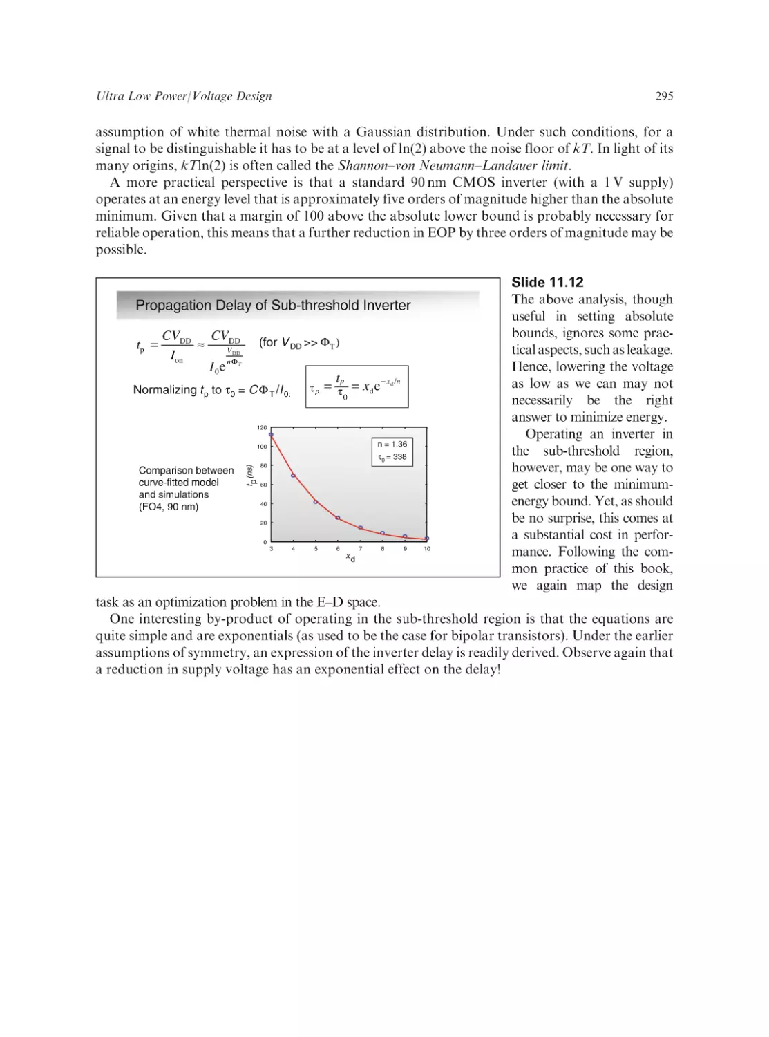
A. Chandrakasan and R. Brodersen, Low-Power CMOS Design, IEEE Press, 1998 (Reprint
Volume)
Volume).
A. Chandrakasan, Bowhill, and Fox, Design of High-Performance Microprocessors, IEEE Press,
2001.
• Chapter 4, “Low-Voltage Technologies,” by Kuroda and Sakuraipggy
• Chapter 3, “Techniques for Leakage Power Reduction,” by De, et al.
•
M. Keating et al., Low Power Methodology Manual, Springer, 2007.
S. Narendra and A. Chandrakasan, Leakage in Nanometer CMOS Technologies, Springer,
2006.
M. Pedram and J. Rabaey, Ed., Power Aware Design Methodologies, Kluwer Academic
Publishers, 2002.
C. Piguet, Ed., Low-Power Circuit Design, CRC Press, 2005.
J. Rabaey and M. Pedram, Ed., Low Power Design Methodologies, Kluwer Academic
Publishers, 1995.
J. Rabaey, A. Chandrakasan, and B. Nikolic, Digital Integrated Circuits - A Design Perspective,
Prentice Hall, 2003.
S. Roundy, P. Wright and J.M. Rabaey, Energy Scavenging for Wireless Sensor Networks,
Kluwer Academic Publishers, 2003.
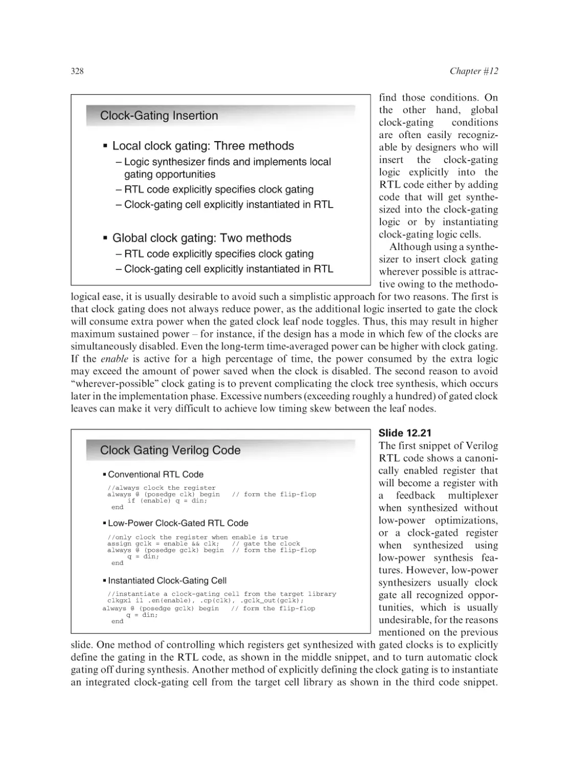
Every chapter in the book
is concluded with a set of
references supporting the
material presented in the
chapter. For those of you
who are truly enamored
with the subject of lowpower design, these slides
enumerate a number of
general reference works,
overview
papers,
and
visionary presentations on
the topic.
A. Wang, Adaptive Techniques for Dynamic Power Optimization, Springer, 2008.
Low-Power Design – Special References
S. Borkar, “Design challenges of technology scaling,” IEEE Micro, 19 (4),
p. 23–29, July–Aug. 1999.
T.Kuroda, T. Sakurai, “Overview of low-power ULSI circuit techniques,”
IEICE Trans. on Electronics, E78-C(4), pp. 334–344, Apr. 1995.
Journal-o fLow Power Electronics (JOLPE), http://www.aspbs.com/jolpe/
Proceedings of the IEEE, Special Issue on Low Power Design, Apr. 1995.
Proceedings of the ISLPED Conference (starting 1994)
Proceedings of ISSCC, VLSI Symposium, ESSCIRC, A-SSCC, DAC,
ASPDAC, DATE, ICCAD conferences
I personally had a wonderful and truly enlightening time putting this material together while
traversing Europe during my sabbatical in the spring of 2007. I hope you will enjoy it as well.
Jan M. Rabaey, Berkeley, CA
Contents
1
Introduction . . . . . . . . . . . . . . . . . . . . . . . . . . . . . . . . . . . . . . . . . . . . . . . . . . . . . . . . . . .
1
2
Nanometer Transistors and Their Models . . . . . . . . . . . . . . . . . . . . . . . . . . . . . . . . . . . .
25
3
Power and Energy Basics . . . . . . . . . . . . . . . . . . . . . . . . . . . . . . . . . . . . . . . . . . . . . . . . .
53
4
Optimizing Power @ Design Time: Circuit-Level Techniques . . . . . . . . . . . . . . . . . . . . .
77
5
Optimizing Power @ Design Time – Architecture, Algorithms, and Systems. . . . . . . . . .
113
6
Optimizing Power @ Design Time – Interconnect and Clocks . . . . . . . . . . . . . . . . . . . . .
151
7
Optimizing Power @ Design Time – Memory . . . . . . . . . . . . . . . . . . . . . . . . . . . . . . . . .
183
8
Optimizing Power @ Standby – Circuits and Systems . . . . . . . . . . . . . . . . . . . . . . . . . . .
207
9
Optimizing Power @ Standby – Memory . . . . . . . . . . . . . . . . . . . . . . . . . . . . . . . . . . . .
233
10
Optimizing Power @ Runtime: Circuits and Systems . . . . . . . . . . . . . . . . . . . . . . . . . . .
249
11
Ultra Low Power/Voltage Design . . . . . . . . . . . . . . . . . . . . . . . . . . . . . . . . . . . . . . . . . .
289
12
Low Power Design Methodologies and Flows. . . . . . . . . . . . . . . . . . . . . . . . . . . . . . . . . .
317
13
Summary and Perspectives . . . . . . . . . . . . . . . . . . . . . . . . . . . . . . . . . . . . . . . . . . . . . . . .
345
Index . . . . . . . . . . . . . . . . . . . . . . . . . . . . . . . . . . . . . . . . . . . . . . . . . . . . . . . . . . . . . . . . . . . .
357
xi
Chapter 1
Introduction
Slide 1.1
In this chapter we discuss
why power and energy consumption has become one
of the main (if not the
main) design concerns in
today’s complex digital
integrated circuits. We
first aalyze the different
Jan M. Rabaey
application domains and
evaluate how each has its
own specific concerns and
requirements,
from
a
power perspective soon. Most projections into the future show that these concerns most likely
will not go away. In fact, everything seems to indicate that they will even aggravate. Next, we
evaluate technology trends – in the idle hope that technology scaling may help to address some of
these problems. Unfortunately, CMOS scaling only seems to make the problem worse. Hence,
design solutions will be the primary mechanism in keeping energy/power consumption in control
or within bounds. Identifying the central design themes and technologies, and finding ways to
apply them in a structured and methodological fashion, is the main purpose of this book. For quite
some time, low-power design consisted of a collection of ad hoc techniques. Applying those
techniques successfully on a broad range of applications and without too much ‘‘manual’’ intervention requires close integration in the traditional design flows. Over the past decade, much
progress in this direction was made. Yet, the gap between low-power design technology and
methodology remains.
Introduction
Slide 1.2
There are many reasons why designers and application developers worry about power dissipation.
One concern that has come consistently to the foreground in recent years is the need for ‘‘green’’
electronics. While the power dissipation of electronic components until recently was only a small
fraction of the overall electrical power budget, this picture has changed substantially in the last few
decades. The pervasive use of desktops and laptops has made its mark in both the office and home
environments. Standby power of electronic consumer components and set-up boxes is rising
rapidly such that at the time of writing this book their power drain is becoming equivalent to
J. Rabaey, Low Power Design Essentials, Series on Integrated Circuits and Systems,
DOI 10.1007/978-0-387-71713-5_1, Ó Springer ScienceþBusiness Media, LLC 2009
1
2
Chapter #1
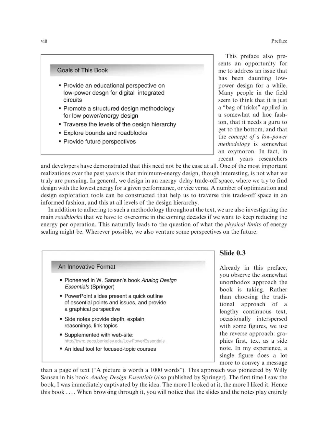
that of a decent-size fridge.
Electronics are becoming a
Why Worry About Power?
sizable fraction of the
power budget of a modern
The Tongue-in-Cheek Answer
automobile. These trends
Total energy of Milky Way
will only become more progalaxy: 1059 J
nounced in the coming
Minimum switching energy for
decade(s).
digital gate (1 electron@100
In this slide, the growing
–20
mV): 1.6 × 10 J
importance
of electronics
(limited by thermal noise)
as part of the power budget
Upper bound on number of digital operations: 6 × 1078
is brought home with a
Operations/year performed by 1 billion 100 MOPS
‘‘tongue-in-cheek’’ extracomputers: 3 × 1024
polation. If Moore’s law
Entire energy might be consumed in 180 years, assuming a doubling
would continue unabated
of computational requirements every year (Moore’s Law).
in the future and the computational needs would
keep on doubling every
year, the total energy of our galaxy would be exhausted in the relatively low time span of 180
years (even if we assume that every digital operation is performed at its lowest possible level).
However, as Gordon Moore himself stated in his keynote address at the 2001 ISSCC conference,
‘‘No exponential is forever’’, adding quickly thereafter, ‘‘. . . but forever can be delayed’’.
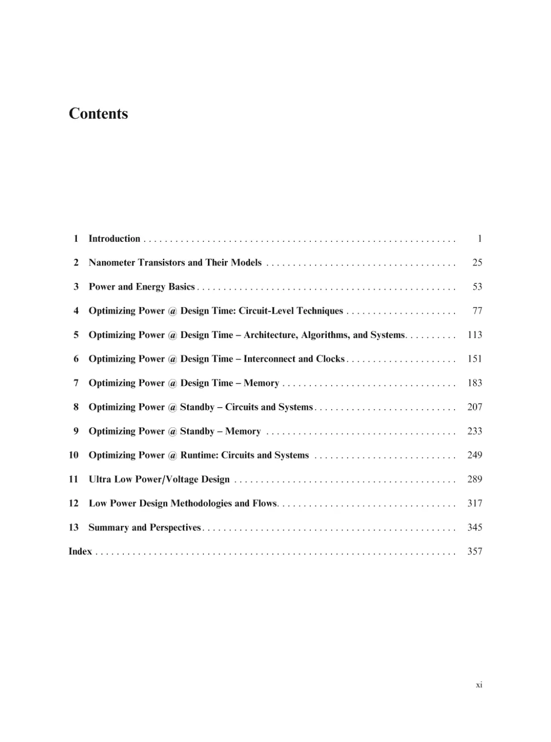
Slide 1.3
The subsequent slide sets
Power: The Dominant Design Constraint (1)
evaluate the power need
and trends for a number of
Cost of large data centers solely determined by power bill …
dominant application areas
of digital integrated cirNY Times, June 06
Columbia River
cuits. First, the domains of
computation and communication infrastructure are
discussed. The advent of
the Internet, combined
Google Data Center, The Dalles, Oregon
450,000
with ubiquitous access to
400 Millions of Personal Computers
the network using both
worldwide (Year 2000)
8,000
wired and wireless inter-Assumed to consume 0.16 Tera (1012)
100,000
kWh per year
faces, has dramatically
-Equivalent to 26 nuclear power plants
Over 1 Giga kWh per year just for cooling
changed the nature of com-Including manufacturing electricity
puting. Today massive data
[Ref: Bar-Cohen et al., 2000]
storage and computing
centers operated by large
companies at a number of centralized locations have absorbed a huge amount of the worldwide
computational loads of both corporations and individuals. And this trend is not showing any signs
of slowing down, as new server farms are being brought online at a staggering rate. Yet, this
centralization comes at a price. The ‘‘computational density’’ of such a center, and hence the power
usage, is substantial. To quote Luis Barosso from Google (a company which is one of the most
prolific promoters of the remote-computation concept), the cost of a data center is determined
Introduction
3
solely by the monthly power bill, not by the cost of hardware or maintenance. This bill results from
both the power dissipation in the electronic systems and the cost of removing the dissipated heat –
that is, air conditioning. This explains why most data centers are now implanted at carefully chosen
locations where power is easily available and effective cooling techniques are present (such as in the
proximity of major rivers – in an eerie similarity to nuclear plants).
While data centers represent a major fraction of the power consumed in the computation and
communication infrastructure, other components should not be ignored. The fast routers that zip
the data around the world, as well as the wireless base stations (access points) which allow us to
connect wirelessly to the network, offer major power challenges as well. Owing to their location,
the availability of power and the effectiveness of cooling techniques are often limited. Finally, the
distributed computing and communication infrastructure cannot be ignored either; the wired and
wireless data routers in the office, plant, or home, the back-office computing servers and the
desktop computers add up to a sizable power budget as well. A large fraction of the air conditioning bill in offices is due to the ever-growing computational infrastructure.
Slide 1.4
It is worth spending some
Power: The Dominant Design Constraint
time on the cooling issue.
A typical computing server
rack in a server farm can
consume up to 20 kW.
With the racks in a farm
easily numbering over one
hundred, power dissipation
can top the 2 MW (all of
which is transformed into
heat). The design of the air
conditioning system and
the flow of air through the
room and the racks is quite
complicated and requires
[Ref: R. Schmidt, ACEED’03]
extensive modeling and
analysis. The impact of an
ill-designed system can be major (i.e., dramatic failure), or more subtle. In one such data center
design, cool air is brought in from the floor and is gradually heated while it rises through the blades
(boards) in the rack. This leads to a temperature gradient, which may mean that processors closer
to the floor operate faster than the ones on the top! Even with the best air-cooling design practices,
predicting the overall dynamics of the center can be hard and can lead to under-cooling. Sometimes
some quick improvised fixes are the only rescue, as witnessed in these ironic pictures, provided by
Roger Schmidt, a distinguished engineer at IBM and a leading expert in the engineering and
engineering management of the thermal design of large-scale IBM computers.
Slide 1.5
While temperature gradients over racks can lead to performance variations, the same is true for
the advanced high-performance processors of today. In the past die sizes were small enough,
and activity over the die was quite uniform. This translated into a flat temperature profile at
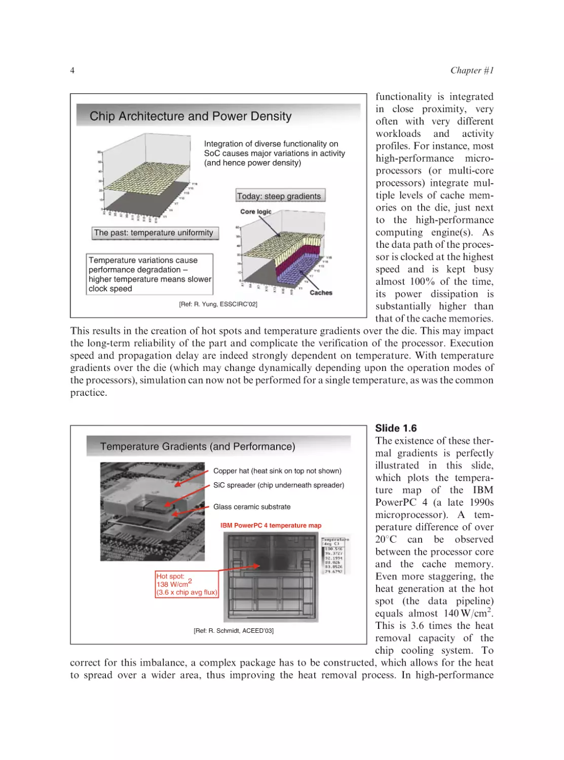
the surface of the die. With the advent of Systems-on-a-Chip (SoC), more and more diverse
4
Chapter #1
functionality is integrated
in close proximity, very
Chip Architecture and Power Density
often with very different
workloads and activity
Integration of diverse functionality on
profiles. For instance, most
SoC causes major variations in activity
high-performance micro(and hence power density)
processors (or multi-core
processors) integrate multiple levels of cache memToday: steep gradients
ories on the die, just next
to the high-performance
The past: temperature uniformity
computing engine(s). As
the data path of the processor is clocked at the highest
Temperature variations cause
performance degradation –
speed and is kept busy
higher temperature means slower
almost 100% of the time,
clock speed
its power dissipation is
[Ref: R. Yung, ESSCIRC’02]
substantially higher than
that of the cache memories.
This results in the creation of hot spots and temperature gradients over the die. This may impact
the long-term reliability of the part and complicate the verification of the processor. Execution
speed and propagation delay are indeed strongly dependent on temperature. With temperature
gradients over the die (which may change dynamically depending upon the operation modes of
the processors), simulation can now not be performed for a single temperature, as was the common
practice.
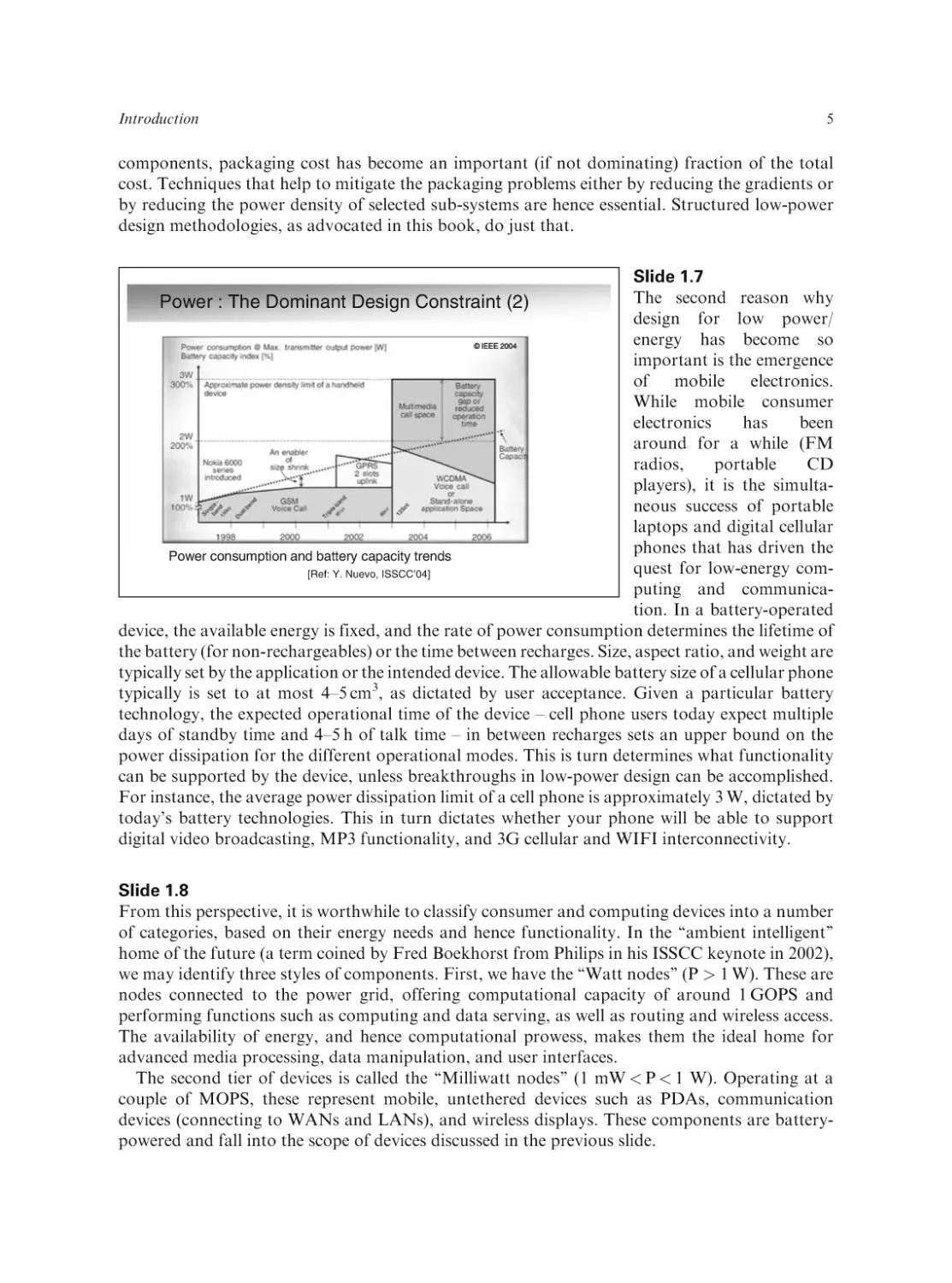
Slide 1.6
The existence of these therTemperature Gradients (and Performance)
mal gradients is perfectly
illustrated in this slide,
Copper hat (heat sink on top not shown)
which plots the temperaSiC spreader (chip underneath spreader)
ture map of the IBM
PowerPC 4 (a late 1990s
Glass ceramic substrate
microprocessor). A temIBM PowerPC 4 temperature map
perature difference of over
208C can be observed
between the processor core
and the cache memory.
Hot spot:
Even more staggering, the
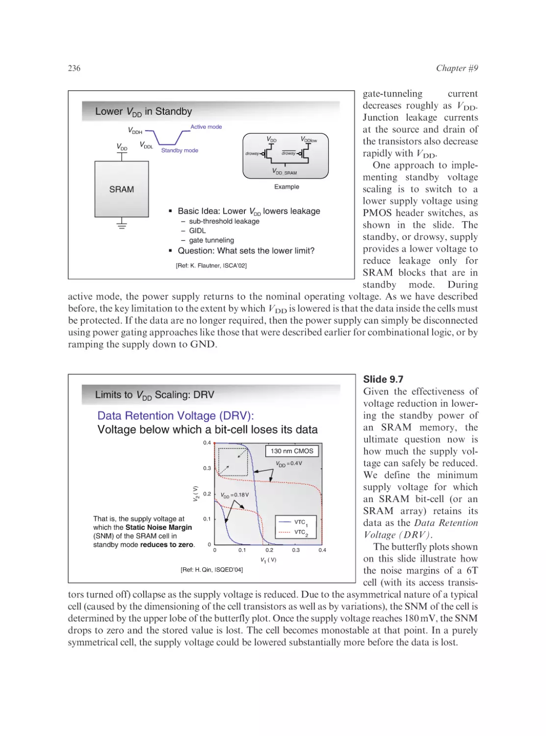
138 W/cm2
heat generation at the hot
(3.6 x chip avg flux)
spot (the data pipeline)
equals almost 140 W/cm2.
This is 3.6 times the heat
[Ref: R. Schmidt, ACEED’03]
removal capacity of the
chip cooling system. To
correct for this imbalance, a complex package has to be constructed, which allows for the heat
to spread over a wider area, thus improving the heat removal process. In high-performance
Introduction
5
components, packaging cost has become an important (if not dominating) fraction of the total
cost. Techniques that help to mitigate the packaging problems either by reducing the gradients or
by reducing the power density of selected sub-systems are hence essential. Structured low-power
design methodologies, as advocated in this book, do just that.
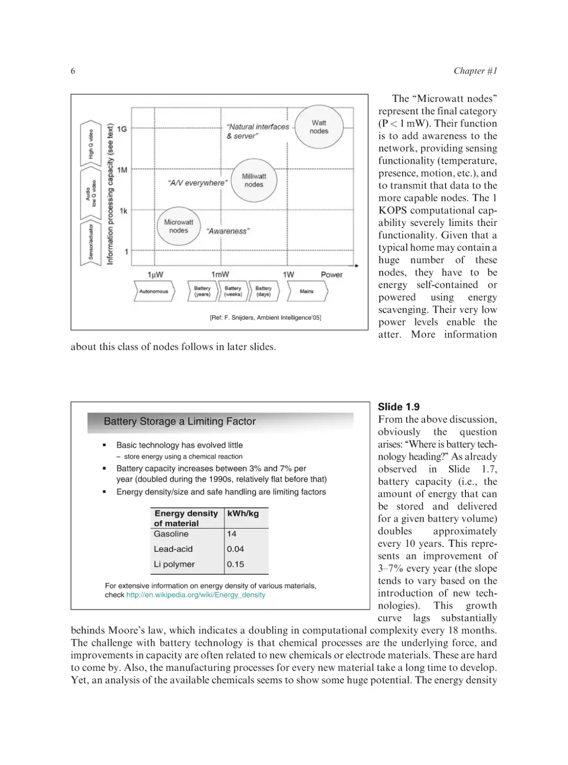
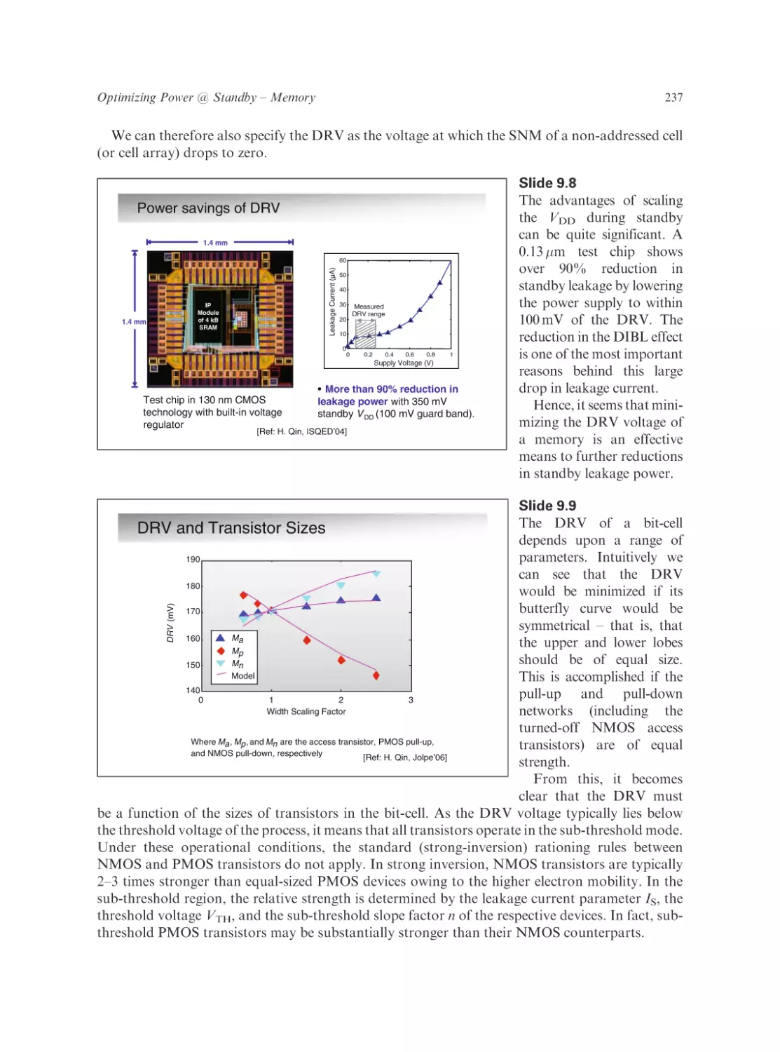
Slide 1.7
The second reason why
Power : The Dominant Design Constraint (2)
design for low power/
energy has become so
© IEEE 2004
important is the emergence
of mobile electronics.
While mobile consumer
electronics
has
been
around for a while (FM
radios,
portable
CD
players), it is the simultaneous success of portable
laptops and digital cellular
phones that has driven the
Power consumption and battery capacity trends
quest for low-energy com[Ref: Y. Nuevo, ISSCC’04]
puting and communication. In a battery-operated
device, the available energy is fixed, and the rate of power consumption determines the lifetime of
the battery (for non-rechargeables) or the time between recharges. Size, aspect ratio, and weight are
typically set by the application or the intended device. The allowable battery size of a cellular phone
typically is set to at most 4–5 cm3, as dictated by user acceptance. Given a particular battery
technology, the expected operational time of the device – cell phone users today expect multiple
days of standby time and 4–5 h of talk time – in between recharges sets an upper bound on the
power dissipation for the different operational modes. This is turn determines what functionality
can be supported by the device, unless breakthroughs in low-power design can be accomplished.
For instance, the average power dissipation limit of a cell phone is approximately 3 W, dictated by
today’s battery technologies. This in turn dictates whether your phone will be able to support
digital video broadcasting, MP3 functionality, and 3G cellular and WIFI interconnectivity.
Slide 1.8
From this perspective, it is worthwhile to classify consumer and computing devices into a number
of categories, based on their energy needs and hence functionality. In the ‘‘ambient intelligent’’
home of the future (a term coined by Fred Boekhorst from Philips in his ISSCC keynote in 2002),
we may identify three styles of components. First, we have the ‘‘Watt nodes’’ (P > 1 W). These are
nodes connected to the power grid, offering computational capacity of around 1 GOPS and
performing functions such as computing and data serving, as well as routing and wireless access.
The availability of energy, and hence computational prowess, makes them the ideal home for
advanced media processing, data manipulation, and user interfaces.
The second tier of devices is called the ‘‘Milliwatt nodes’’ (1 mW < P < 1 W). Operating at a
couple of MOPS, these represent mobile, untethered devices such as PDAs, communication
devices (connecting to WANs and LANs), and wireless displays. These components are batterypowered and fall into the scope of devices discussed in the previous slide.
Chapter #1
6
[Ref: F. Snijders, Ambient Intelligence’05]
The ‘‘Microwatt nodes’’
represent the final category
(P < 1 mW). Their function
is to add awareness to the
network, providing sensing
functionality (temperature,
presence, motion, etc.), and
to transmit that data to the
more capable nodes. The 1
KOPS computational capability severely limits their
functionality. Given that a
typical home may contain a
huge number of these
nodes, they have to be
energy self-contained or
powered using energy
scavenging. Their very low
power levels enable the
atter. More information
about this class of nodes follows in later slides.
Slide 1.9
From the above discussion,
Battery Storage a Limiting Factor
obviously the question
arises: ‘‘Where is battery techBasic technology has evolved little
– store energy using a chemical reaction
nology heading?’’ As already
Battery capacity increases between 3% and 7% per
observed in Slide 1.7,
year (doubled during the 1990s, relatively flat before that)
battery capacity (i.e., the
Energy density/size and safe handling are limiting factors
amount of energy that can
be stored and delivered
Energy density kWh/kg
for a given battery volume)
of material
doubles
approximately
Gasoline
14
every
10
years.
This repre0.04
Lead-acid
sents an improvement of
Li polymer
0.15
3–7% every year (the slope
tends to vary based on the
For extensive information on energy density of various materials,
introduction of new techcheck http://en.wikipedia.org/wiki/Energy_density
nologies). This growth
curve lags substantially
behinds Moore’s law, which indicates a doubling in computational complexity every 18 months.
The challenge with battery technology is that chemical processes are the underlying force, and
improvements in capacity are often related to new chemicals or electrode materials. These are hard
to come by. Also, the manufacturing processes for every new material take a long time to develop.
Yet, an analysis of the available chemicals seems to show some huge potential. The energy density
Introduction
7
of alcohol or gasoline is approximately two orders of magnitude higher than that of lithiumpolymer. Unfortunately, concerns about the effective and safe handling of these substances make it
hard to exploit them in small form factors.
Slide 1.10
The historical trends in battery capacity actually vary
quite a bit. Up to the 1980s,
160
140
very little or even no pro120
Energy Density
gress was made – there was
100
(Wh/kg)
80
actually little incentive to
Trend Line
60
do so, as the scope of appli40
20
cation was quite limited.
0
Flash lights were probably
1940 1950 1960 1970 1980 1990 2000 2010
the driving application. In
First Commercial Use
the 1990s, mobile applicaLi-ion
tions took off. Intensive
research combined with
advanced
manufacturing
Accelerated since the 1990s, but slower than IC power growth.
strategies changed the slope
substantially, improving the
capacity by a factor of four in almost a decade. Unfortunately, the process has stalled somewhat
since the beginning of the 21st century. A major improvement in battery capacity can only be achieved
by the introduction of new battery chemicals. It should also be observed that the capacity of a battery
(that is the energy that can be extracted from it) also depends upon its discharge profile. Draining a
battery slowly will deliver more energy than flash discharge. It is hence worthwhile to match the battery
structure to the application at hand.
Battery Evolution
Slide 1.11
The fact that the energy
Battery Technology Saturating
delivery capacity of a battery
is ultimately determined
by the basic chemical properties of the materials involved
is clearly illustrated in this
slide. In the 1990s, the capacity of Lithium-ion batteries
improved substantially. This
was mostly due to better
engineering: improved electrode structures, better
charging technology, and
advanced battery system
Battery capacity naturally plateaus as systems develop
design. This ultimately
[Courtesy: M. Doyle, Dupont]
saturated as the intrinsic
maximum potential of the
material is being approached. Today, progress in Lithium-ion battery technology has stalled,
and little improvement is foreseen in the future.
Chapter #1
8
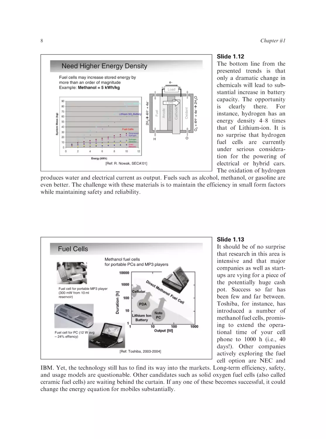
Slide 1.12
The bottom line from the
Need Higher Energy Density
presented trends is that
Fuel cells may increase stored energy by
only a dramatic change in
e
more than an order of magnitude
chemicals will lead to sub–
+
Example: Methanol = 5 kWh/kg
Load
stantial increase in battery
capacity. The opportunity
+ ions
is clearly there. For
instance, hydrogen has an
energy density 4–8 times
that of Lithium-ion. It is
no surprise that hydrogen
O
H
fuel cells are currently
under serious consideration for the powering of
[Ref: R. Nowak, SECA’01]
electrical or hybrid cars.
The oxidation of hydrogen
produces water and electrical current as output. Fuels such as alcohol, methanol, or gasoline are
even better. The challenge with these materials is to maintain the efficiency in small form factors
while maintaining safety and reliability.
2H2O
O2 + 4H+ + 4e–
Oxidant
Cathode
Fuel
Anode
Electrolyte
2H2
4H+ + 4e–
–
Duration [h]
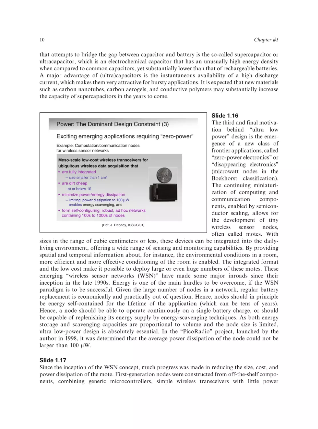
Slide 1.13
It should be of no surprise
Fuel Cells
that research in this area is
Methanol fuel cells
intensive and that major
for portable PCs and MP3 players
companies as well as startups are vying for a piece of
the potentially huge cash
Fuel cell for portable MP3 player
pot. Success so far has
(300 mW from 10 ml
reservoir)
been few and far between.
Toshiba, for instance, has
introduced a number of
methanol fuel cells, promising to extend the operaFuel cell for PC (12 W avg
tional time of your cell
– 24% effiency)
phone to 1000 h (i.e., 40
days!). Other companies
[Ref: Toshiba, 2003-2004]
actively exploring the fuel
cell option are NEC and
IBM. Yet, the technology still has to find its way into the markets. Long-term efficiency, safety,
and usage models are questionable. Other candidates such as solid oxygen fuel cells (also called
ceramic fuel cells) are waiting behind the curtain. If any one of these becomes successful, it could
change the energy equation for mobiles substantially.
Introduction
9
Slide 1.14
Another interesting new
Micro batteries: When Size Is an Issue
entry in the battery field is
the ‘‘micro battery’’. Using
Using micro-electronics or thin-film
technologies inherited from
manufacturing techniques to create
thin-film and semiconducintegrated miniature (backup) batteries
on chip or on board
tor manufacturing, battery
anodes and cathodes are
printed on the substrate,
and micromachined encapBattery printed on wireless sensor node
sulations are used to contain the chemicals. In this
way, it is possible to print
batteries on printed circuit
boards (PCBs), or even
Stencil press for printing patterns
embed them into integrated
[Courtesy: P. Wright, D. Steingart, UCB]
circuits. While the capacity
of these circuits will never
be large, micro batteries can serve perfectly well as backup batteries or as energy storage devices in
sensor nodes. The design of the battery involves trading off between current delivery capability
(number of electrodes) and capacity (volume occupied by the chemicals). This technology is clearly
still in its infancy but could occupy some interesting niche in the years to come.
Slide 1.15
As a summary of the above
How Much Energy Storage in 1 cm3?
discussions, it is worthwhile
ordering the various energy
storage technologies for
μW/cm /year
J/cm
mobile nodes based on
Micro fuel cell
3500
110
their capacity (expressed in
Primary
2880
90
J/cm3). Another useful
battery
Ultracapacitor
Secondary
1080
34
metric is the average current
battery
that can be delivered over
Ultracapacitor
100
3.2
the time span of a year by
a 1 cm3 battery (mW/cm3/
Micro fuel cell
year), which provides a
measure of the longevity of
the battery technology for a
Ultracapacitor
particular application.
Miniature fuel cells
clearly provide the highest
capacity. In their currently
best incarnation, they are approximately three times more efficient than the best rechargeable
(secondary) batteries. Yet, the advantage over non-rechargeables (such as alkaline) is at most 25%.
One alternative strategy for the temporary storage of energy was not discussed so far: the
capacitor. The ordinary capacitor constructed from high-quality dielectrics has the advantage of
simplicity, reliability, and longevity. At the same time, its energy density is limited. One technology
3
3
10
Chapter #1
that attempts to bridge the gap between capacitor and battery is the so-called supercapacitor or
ultracapacitor, which is an electrochemical capacitor that has an unusually high energy density
when compared to common capacitors, yet substantially lower than that of rechargeable batteries.
A major advantage of (ultra)capacitors is the instantaneous availability of a high discharge
current, which makes them very attractive for bursty applications. It is expected that new materials
such as carbon nanotubes, carbon aerogels, and conductive polymers may substantially increase
the capacity of supercapacitors in the years to come.
Slide 1.16
The third and final motivaPower: The Dominant Design Constraint (3)
tion behind ‘‘ultra low
Exciting emerging applications requiring “zero-power”
power’’ design is the emergence of a new class of
Example: Computation/communication nodes
for wireless sensor networks
frontier applications, called
‘‘zero-power electronics’’ or
Meso-scale low-cost wireless transceivers for
‘‘disappearing electronics’’
ubiquitous wireless data acquisition that
(microwatt nodes in the
• are fully integrated
– size smaller than 1 cm3
Boekhorst classification).
• are dirt cheap
The continuing miniaturi–at or below 1$
zation of computing and
• minimize power/energy dissipation
communication
compo– limiting power dissipation to 100 μW
enables energy scavenging, and
nents, enabled by semicon• form self-configuring, robust, ad hoc networks
ductor scaling, allows for
containing 100s to 1000s of nodes
the development of tiny
[Ref: J. Rabaey, ISSCC’01]
wireless sensor nodes,
often called motes. With
sizes in the range of cubic centimeters or less, these devices can be integrated into the dailyliving environment, offering a wide range of sensing and monitoring capabilities. By providing
spatial and temporal information about, for instance, the environmental conditions in a room,
more efficient and more effective conditioning of the room is enabled. The integrated format
and the low cost make it possible to deploy large or even huge numbers of these motes. These
emerging ‘‘wireless sensor networks (WSN)’’ have made some major inroads since their
inception in the late 1990s. Energy is one of the main hurdles to be overcome, if the WSN
paradigm is to be successful. Given the large number of nodes in a network, regular battery
replacement is economically and practically out of question. Hence, nodes should in principle
be energy self-contained for the lifetime of the application (which can be tens of years).
Hence, a node should be able to operate continuously on a single battery charge, or should
be capable of replenishing its energy supply by energy-scavenging techniques. As both energy
storage and scavenging capacities are proportional to volume and the node size is limited,
ultra low-power design is absolutely essential. In the ‘‘PicoRadio’’ project, launched by the
author in 1998, it was determined that the average power dissipation of the node could not be
larger than 100 mW.
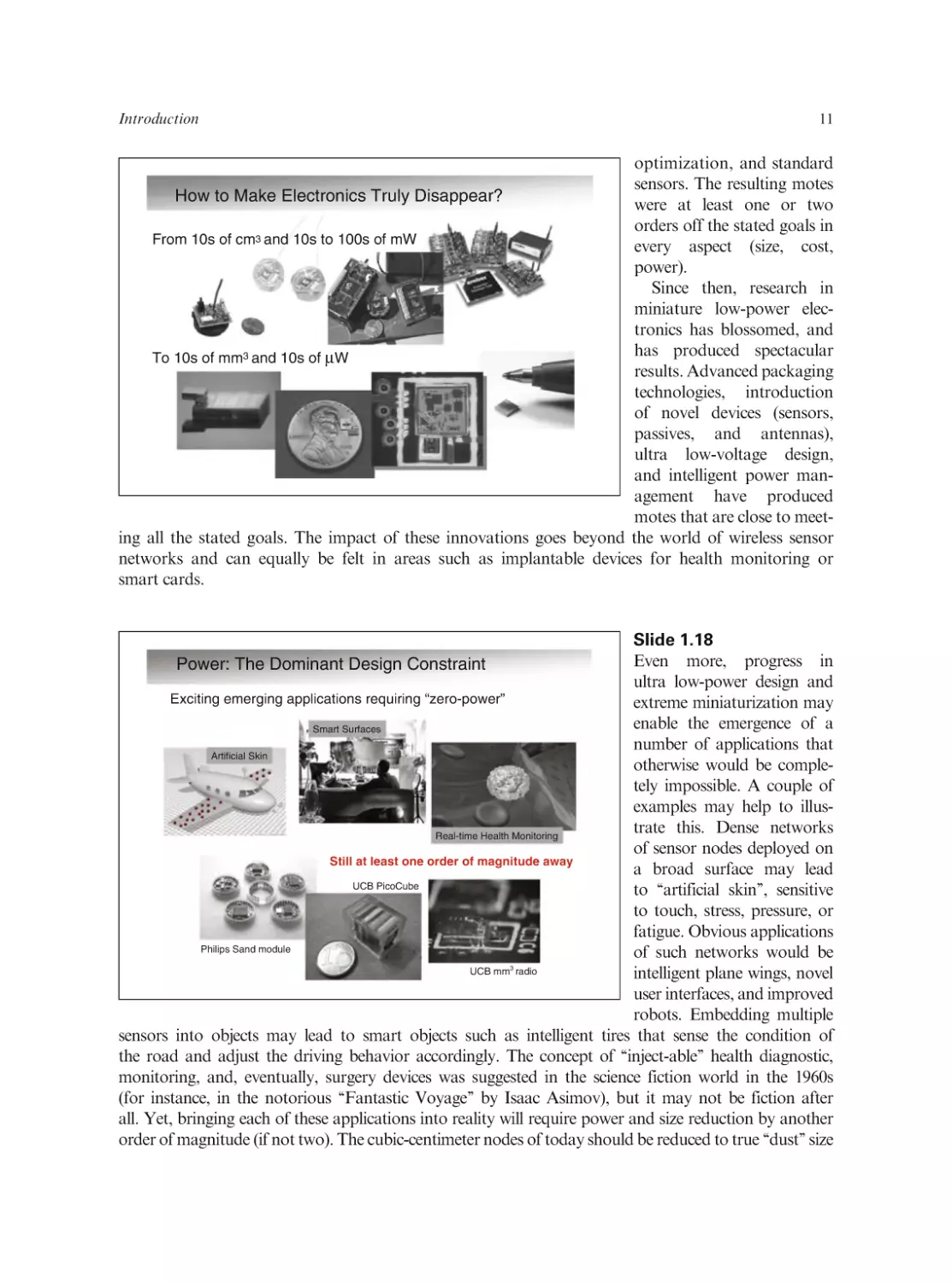
Slide 1.17
Since the inception of the WSN concept, much progress was made in reducing the size, cost, and
power dissipation of the mote. First-generation nodes were constructed from off-the-shelf components, combining generic microcontrollers, simple wireless transceivers with little power
Introduction
11
optimization, and standard
sensors. The resulting motes
How to Make Electronics Truly Disappear?
were at least one or two
orders off the stated goals in
From 10s of cm3 and 10s to 100s of mW
every aspect (size, cost,
power).
Since then, research in
miniature low-power electronics has blossomed, and
has produced spectacular
3
To 10s of mm and 10s of μW
results. Advanced packaging
technologies, introduction
of novel devices (sensors,
passives, and antennas),
ultra low-voltage design,
and intelligent power management have produced
motes that are close to meeting all the stated goals. The impact of these innovations goes beyond the world of wireless sensor
networks and can equally be felt in areas such as implantable devices for health monitoring or
smart cards.
Slide 1.18
Even more, progress in
Power: The Dominant Design Constraint
ultra low-power design and
Exciting emerging applications requiring “zero-power”
extreme miniaturization may
enable the emergence of a
Smart Surfaces
number of applications that
Artificial Skin
otherwise would be completely impossible. A couple of
examples may help to illustrate this. Dense networks
Real-time Health Monitoring
of sensor nodes deployed on
Still at least one order of magnitude away
a broad surface may lead
UCB PicoCube
to ‘‘artificial skin’’, sensitive
to touch, stress, pressure, or
fatigue. Obvious applications
Philips Sand module
of such networks would be
UCB mm radio
intelligent plane wings, novel
user interfaces, and improved
robots. Embedding multiple
sensors into objects may lead to smart objects such as intelligent tires that sense the condition of
the road and adjust the driving behavior accordingly. The concept of ‘‘inject-able’’ health diagnostic,
monitoring, and, eventually, surgery devices was suggested in the science fiction world in the 1960s
(for instance, in the notorious ‘‘Fantastic Voyage’’ by Isaac Asimov), but it may not be fiction after
all. Yet, bringing each of these applications into reality will require power and size reduction by another
order of magnitude (if not two). The cubic-centimeter nodes of today should be reduced to true ‘‘dust’’ size
3
Chapter #1
12
(i.e., cubic millimeter). This provides a true motivation for further exploration of the absolute boundaries
of ultra low-power design, which is the topic of Chapter 11 in this book.
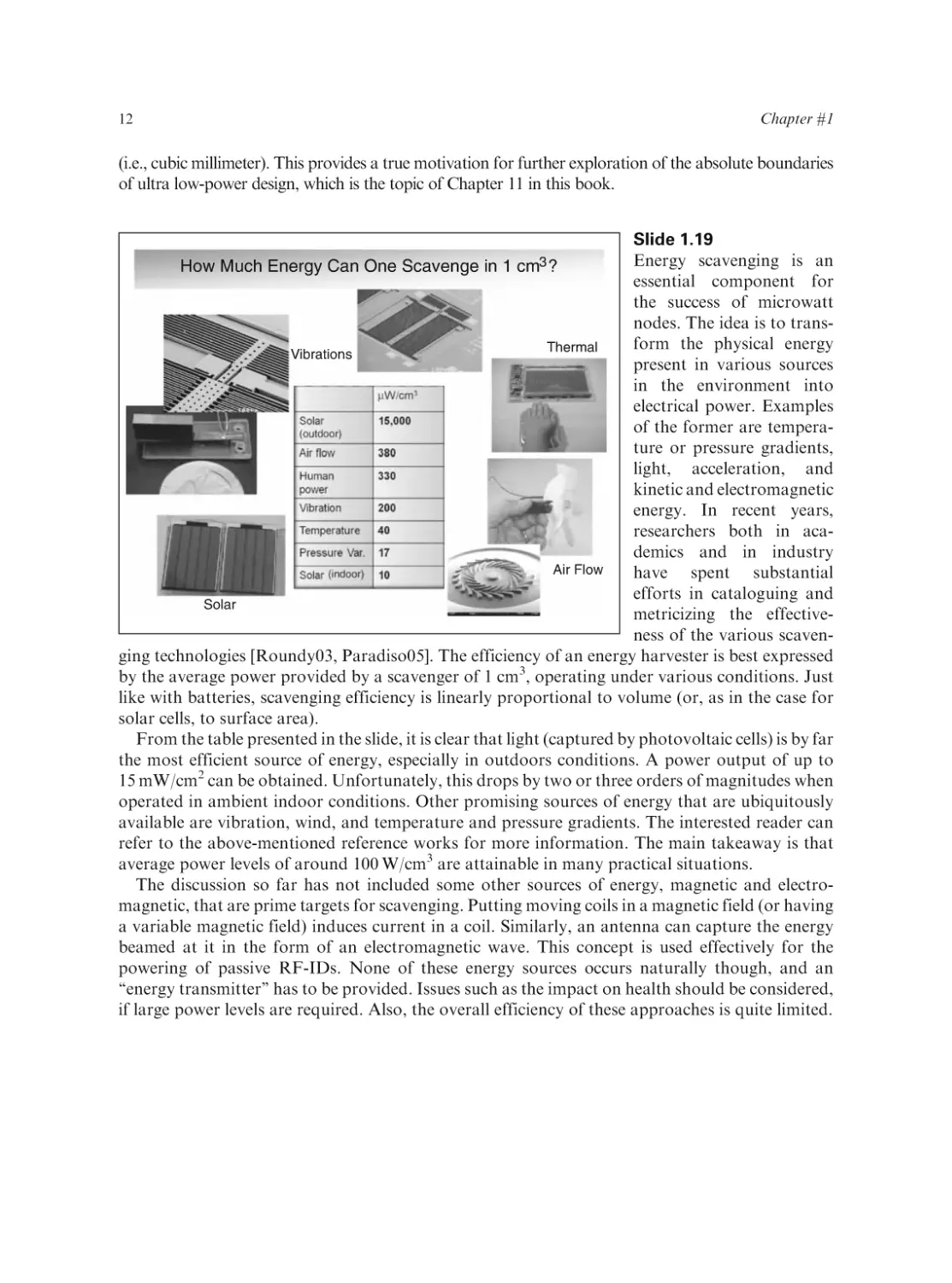
Slide 1.19
Energy scavenging is an
How Much Energy Can One Scavenge in 1
essential component for
the success of microwatt
nodes. The idea is to transform the physical energy
Thermal
Vibrations
present in various sources
in the environment into
electrical power. Examples
of the former are temperature or pressure gradients,
light, acceleration, and
kinetic and electromagnetic
energy. In recent years,
researchers both in academics and in industry
Air Flow
have spent substantial
efforts in cataloguing and
Solar
metricizing the effectiveness of the various scavenging technologies [Roundy03, Paradiso05]. The efficiency of an energy harvester is best expressed
by the average power provided by a scavenger of 1 cm3, operating under various conditions. Just
like with batteries, scavenging efficiency is linearly proportional to volume (or, as in the case for
solar cells, to surface area).
From the table presented in the slide, it is clear that light (captured by photovoltaic cells) is by far
the most efficient source of energy, especially in outdoors conditions. A power output of up to
15 mW/cm2 can be obtained. Unfortunately, this drops by two or three orders of magnitudes when
operated in ambient indoor conditions. Other promising sources of energy that are ubiquitously
available are vibration, wind, and temperature and pressure gradients. The interested reader can
refer to the above-mentioned reference works for more information. The main takeaway is that
average power levels of around 100 W/cm3 are attainable in many practical situations.
The discussion so far has not included some other sources of energy, magnetic and electromagnetic, that are prime targets for scavenging. Putting moving coils in a magnetic field (or having
a variable magnetic field) induces current in a coil. Similarly, an antenna can capture the energy
beamed at it in the form of an electromagnetic wave. This concept is used effectively for the
powering of passive RF-IDs. None of these energy sources occurs naturally though, and an
‘‘energy transmitter’’ has to be provided. Issues such as the impact on health should be considered,
if large power levels are required. Also, the overall efficiency of these approaches is quite limited.
cm3 ?
Introduction
13
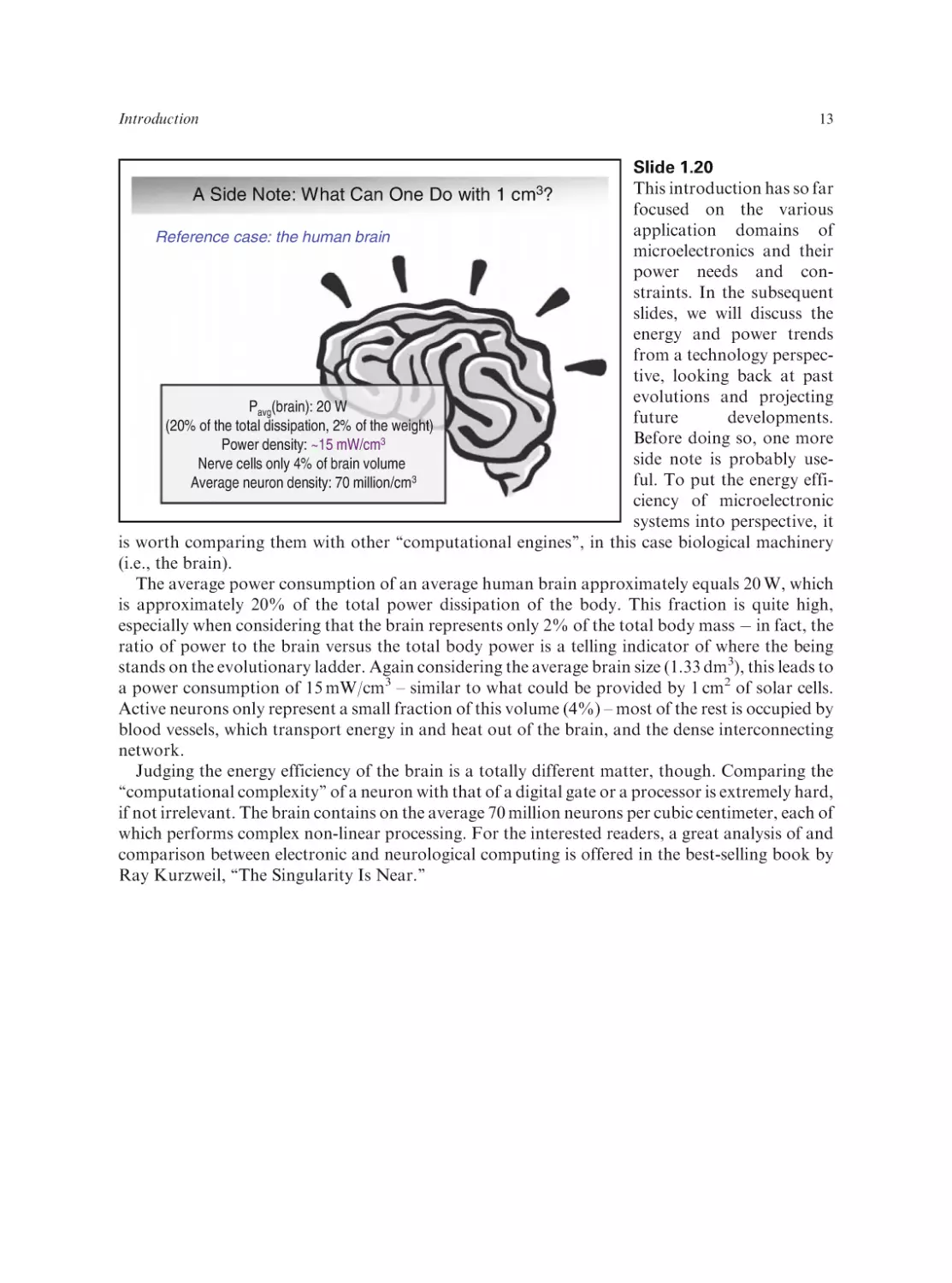
Slide 1.20
This introduction has so far
A Side Note: What Can One Do with 1
focused on the various
application domains of
Reference case: the human brain
microelectronics and their
power needs and constraints. In the subsequent
slides, we will discuss the
energy and power trends
from a technology perspective, looking back at past
evolutions and projecting
Pavg(brain): 20 W
future
developments.
(20% of the total dissipation, 2% of the weight)
Before
doing
so, one more
3
Power density: ~15 mW/cm
side
note
is
probably
useNerve cells only 4% of brain volume
3
ful.
To
put
the
energy
effiAverage neuron density: 70 million/cm
ciency of microelectronic
systems into perspective, it
is worth comparing them with other ‘‘computational engines’’, in this case biological machinery
(i.e., the brain).
The average power consumption of an average human brain approximately equals 20 W, which
is approximately 20% of the total power dissipation of the body. This fraction is quite high,
especially when considering that the brain represents only 2% of the total body mass in fact, the
ratio of power to the brain versus the total body power is a telling indicator of where the being
stands on the evolutionary ladder. Again considering the average brain size (1.33 dm3), this leads to
a power consumption of 15 mW/cm3 – similar to what could be provided by 1 cm2 of solar cells.
Active neurons only represent a small fraction of this volume (4%) – most of the rest is occupied by
blood vessels, which transport energy in and heat out of the brain, and the dense interconnecting
network.
Judging the energy efficiency of the brain is a totally different matter, though. Comparing the
‘‘computational complexity’’ of a neuron with that of a digital gate or a processor is extremely hard,
if not irrelevant. The brain contains on the average 70 million neurons per cubic centimeter, each of
which performs complex non-linear processing. For the interested readers, a great analysis of and
comparison between electronic and neurological computing is offered in the best-selling book by
Ray Kurzweil, ‘‘The Singularity Is Near.’’
cm3?
14
Chapter #1
Slide 1.21
Before discussing trends,
Power Versus Energy
some words about useful
metrics
are
necessary
Power in high-performance systems
(more details to follow in
Chapter 3). So far, we
– Heat removal
have used the terms power
– Peak power and its impact on power delivery networks
and energy quite inter Energy in portable systems
changeably. Yet, each has
– Battery life
its specific role depending
Energy/power in “zero-power systems”
upon the phenomena that
– Energy-scavenging and storage capabilites
are being addressed or the
constraints of the applica Dynamic (energy) vs. static (power) consumption
tion at hand. Average
– Determined by operation modes
power dissipation is the
prominent parameter when
studying heat-removal and packaging concerns of high-performance processors. Peak power
dissipation, on the other hand, is the parameter to watch when designing the complex power supply
delivery networks for integrated circuits and systems.
When designing mobile devices or sensor network nodes, the type of energy source determines
which property is the most essential. In a battery-powered system, the energy supply is finite, and
hence energy minimization is crucial. On the other hand, the designer of an energy-scavenging
system has to ensure that the average power consumed is smaller than the average power provided
by the scavenger.
Finally, dividing power dissipation into dynamic (proportional to activity) and static (independent of activity) is crucial in the design of power management systems exploiting the operational
modes of the system. We will see later that the reality here is quite complex and that a careful
balancing between the two is one of the subtleties of advanced low-power design.
Slide 1.22
While concerns about power density may seem quite recent to most designers, the issue has
surfaced a number of times in the design of (electrical) engineering systems before. Obviously
heat removal was and is a prime concern in many thermodynamic systems. In the electronics world,
power dissipation, and consequent high temperatures, was a main cause of unreliability in vacuumtube computers. While bipolar computer design offered prime performance, exceeding what could
be delivered by MOS implementations at that time, power density and the ensuing reliability
concerns limited the amount of integration that could be obtained. The same happened with pure
NMOS logic – the static current inherent in non-complimentary logic families ultimately caused
semiconductor manufacturers to switch to CMOS, even though this meant an increased process
complexity and a loss in performance. When CMOS was adopted as the technology-of-choice in
the mid 1980s, many felt that the power problem had been dealt with effectively, and that CMOS
design would enjoy a relatively trouble-free run to ever higher performance. Unfortunately, it was
not to be. Already in the early 1990s, the ever-increasing clock frequencies and the emergence of
new application domains brought power back to the foreground.
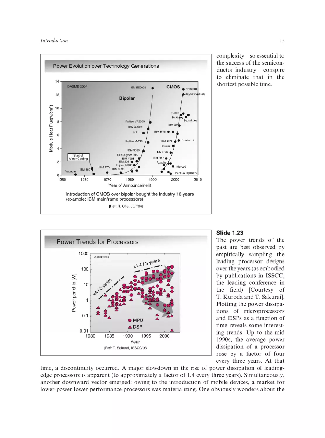
The charts in this slide document how the increases in heat flux in bipolar and CMOS systems
mirror each other, only offset by about a decade. They make the interesting point that exponentials
are hard to get around. New technologies create a fixed offset, but the exponential increases in
Introduction
15
complexity – so essential to
the success of the semiconductor industry – conspire
to eliminate that in the
shortest possible time.
Power Evolution over Technology Generations
14
©ASME 2004
Module Heat Flux(w/cm2)
CMOS
IBM ES9000
Prescott
Jayhawk(dual)
12
Bipolar
10
T-Rex
Mckinley
Squadrons
Fujitsu VP2000
8
IBM GP
IBM 3090S
IBM RY5
NTT
6
Pentium 4
IBM RY7
Fujitsu M-780
Pulsar
4
IBM 3090
Start of
Water Cooling
2
Vacuum
0
1950
IBM 360
IBM RY6
CDC Cyber 205
IBM 4381
IBM 3081
Fujitsu M380
IBM 370
IBM 3033
IBM RY4
Apache
Merced
Pentium II(DSIP)
1960
1970
1980
1990
2000
2010
Year of Announcement
Introduction of CMOS over bipolar bought the industry 10 years
(example: IBM mainframe processors)
[Ref: R. Chu, JEP’04]
Power per chip [W]
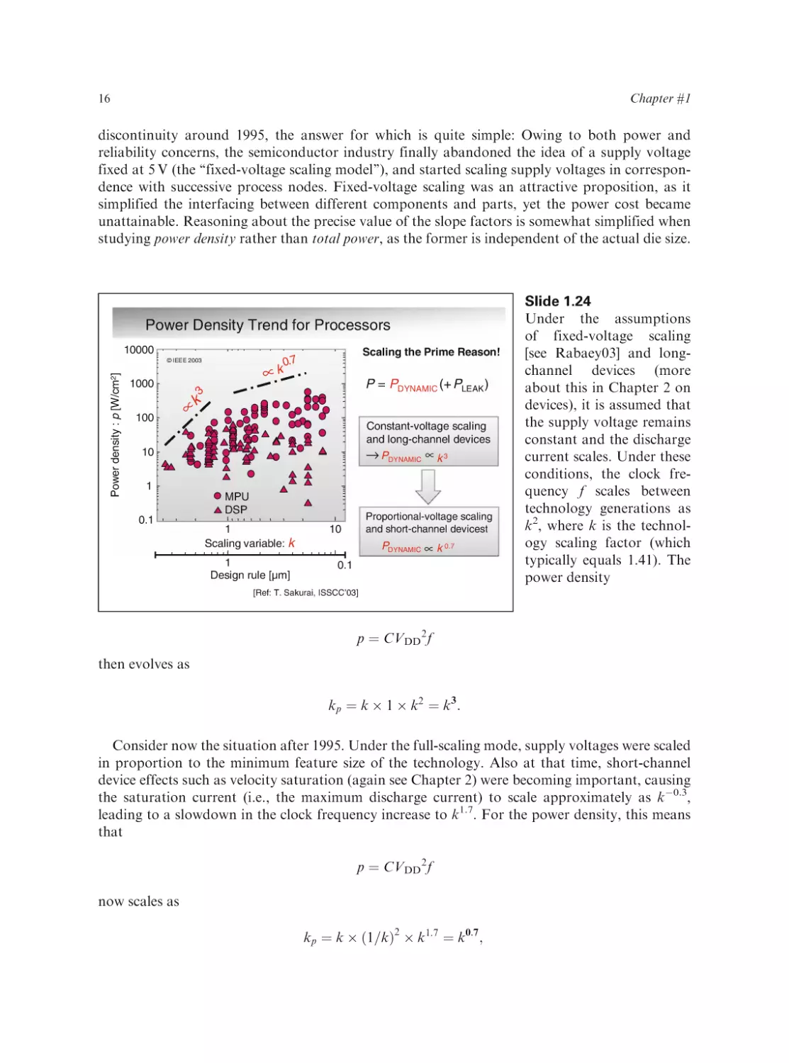
Slide 1.23
The power trends of the
Power Trends for Processors
past are best observed by
1000
empirically sampling the
© IEEE 2003
s
r
a
leading processor designs
e
/3y
x1.4
over the years (as embodied
100
by publications in ISSCC,
rs
a
the leading conference in
10
ye
the field) [Courtesy of
/3
x4
T. Kuroda and T. Sakurai].
1
Plotting the power dissipations of microprocessors
0.1
and DSPs as a function of
MPU
time reveals some interestDSP
0.01
ing trends. Up to the mid
1980
1985
1990
1995
2000
1990s, the average power
Year
dissipation of a processor
[Ref: T. Sakurai, ISSCC’03]
rose by a factor of four
every three years. At that
time, a discontinuity occurred. A major slowdown in the rise of power dissipation of leadingedge processors is apparent (to approximately a factor of 1.4 every three years). Simultaneously,
another downward vector emerged: owing to the introduction of mobile devices, a market for
lower-power lower-performance processors was materializing. One obviously wonders about the
Chapter #1
16
discontinuity around 1995, the answer for which is quite simple: Owing to both power and
reliability concerns, the semiconductor industry finally abandoned the idea of a supply voltage
fixed at 5 V (the ‘‘fixed-voltage scaling model’’), and started scaling supply voltages in correspondence with successive process nodes. Fixed-voltage scaling was an attractive proposition, as it
simplified the interfacing between different components and parts, yet the power cost became
unattainable. Reasoning about the precise value of the slope factors is somewhat simplified when
studying power density rather than total power, as the former is independent of the actual die size.
Power Density Trend for Processors
10000
Power density : p [W/cm2]
1000
100
∝
Scaling the Prime Reason!
0.7
© IEEE 2003
∝k
P = PDYNAMIC (+ PLEAK )
3
k
Constant-voltage scaling
and long-channel devices
→ PDYNAMIC ∝ k 3
10
1
MPU
DSP
0.1
1
Scaling variable: k
1
Design rule [µm]
Proportional-voltage
scaling
Proportional
V scaling
and
and short-channel
devicest
devices
short-channel
0.7
0
.7
0.7
PDYNAMIC
DYNAMIC ∝ k
10
0.1
Slide 1.24
Under the assumptions
of fixed-voltage scaling
[see Rabaey03] and longchannel devices (more
about this in Chapter 2 on
devices), it is assumed that
the supply voltage remains
constant and the discharge
current scales. Under these
conditions, the clock frequency f scales between
technology generations as
k2, where k is the technology scaling factor (which
typically equals 1.41). The
power density
[Ref: T. Sakurai, ISSCC’03]
p ¼ CVDD 2 f
then evolves as
kp ¼ k 1 k2 ¼ k3 :
Consider now the situation after 1995. Under the full-scaling mode, supply voltages were scaled
in proportion to the minimum feature size of the technology. Also at that time, short-channel
device effects such as velocity saturation (again see Chapter 2) were becoming important, causing
the saturation current (i.e., the maximum discharge current) to scale approximately as k0.3,
leading to a slowdown in the clock frequency increase to k1.7. For the power density, this means
that
p ¼ CVDD 2 f
now scales as
kp ¼ k ð1=kÞ2 k1:7 ¼ k0:7 ;
Introduction
17
which corresponds with the empirical data. Even though this means that power density is still
increasing, a major slowdown is observed. This definitely is welcome news.
Supply Voltage (V)
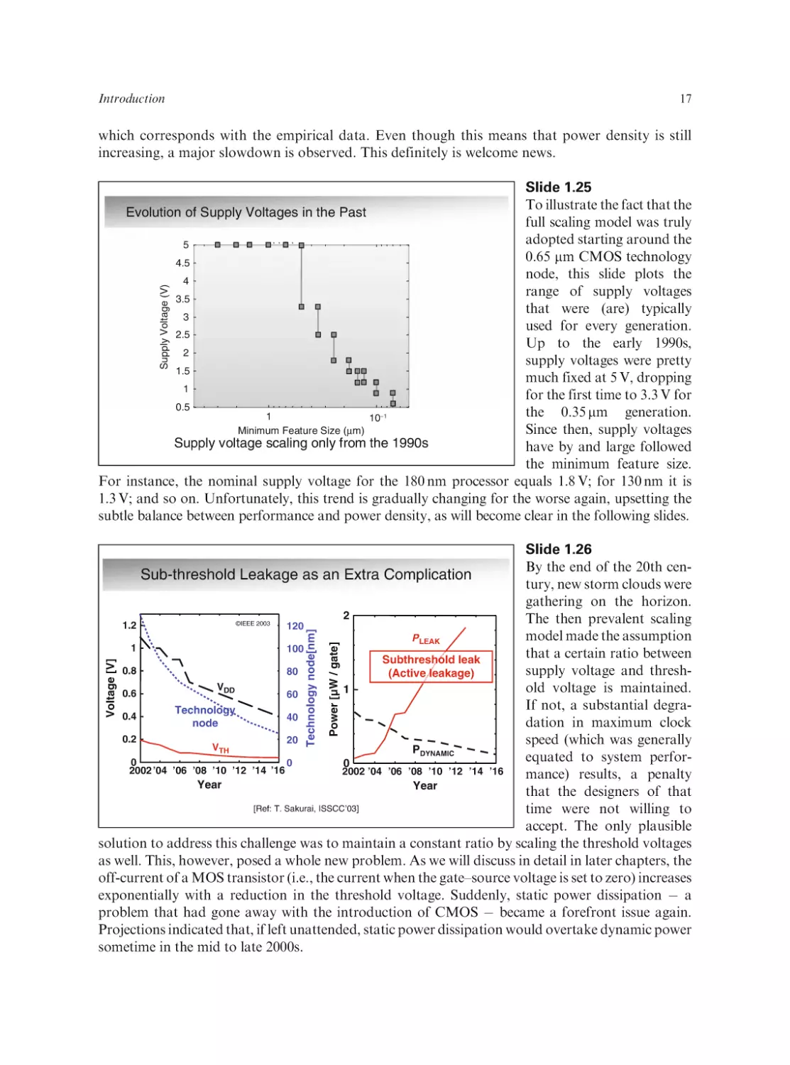
Slide 1.25
To illustrate the fact that the
Evolution of Supply Voltages in the Past
full scaling model was truly
adopted starting around the
5
0.65 mm CMOS technology
4.5
node, this slide plots the
4
range of supply voltages
3.5
that were (are) typically
3
used for every generation.
2.5
Up to the early 1990s,
2
supply voltages were pretty
1.5
much fixed at 5 V, dropping
1
for the first time to 3.3 V for
0.5
the 0.35 mm generation.
1
10–1
Since then, supply voltages
Minimum Feature Size (μm)
Supply voltage scaling only from the 1990s
have by and large followed
the minimum feature size.
For instance, the nominal supply voltage for the 180 nm processor equals 1.8 V; for 130 nm it is
1.3 V; and so on. Unfortunately, this trend is gradually changing for the worse again, upsetting the
subtle balance between performance and power density, as will become clear in the following slides.
Power [µW / gate]
Technology node[nm]
Voltage [V]
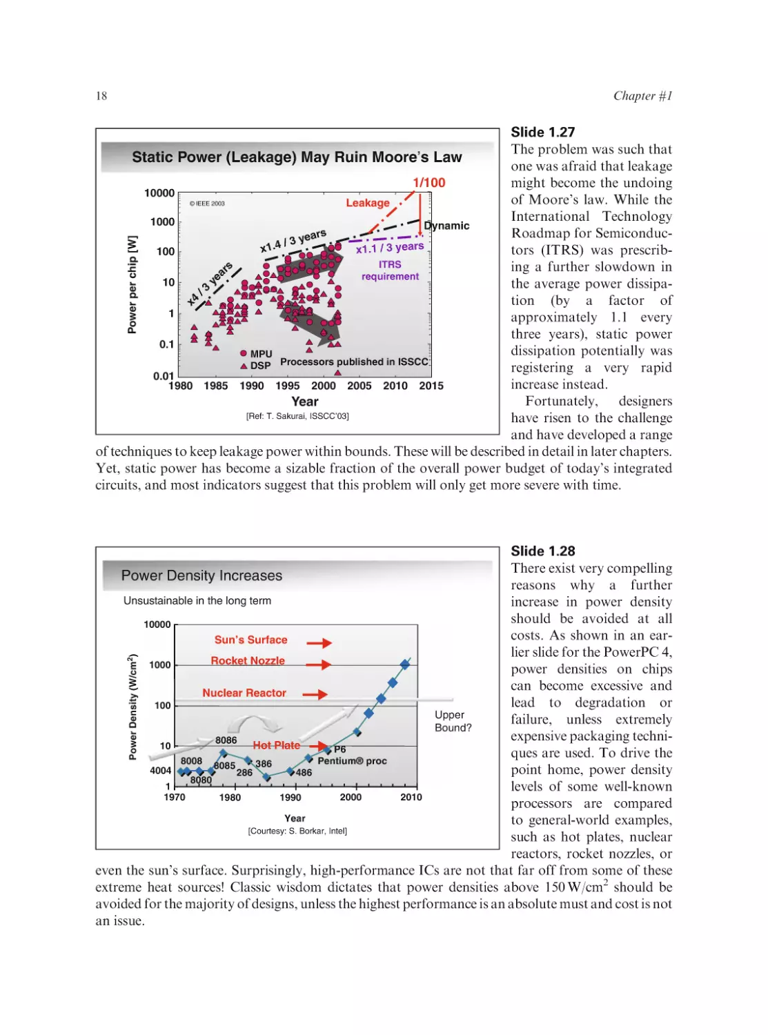
Slide 1.26
By the end of the 20th cenSub-threshold Leakage as an Extra Complication
tury, new storm clouds were
gathering on the horizon.
2
The then prevalent scaling
©IEEE 2003
1.2
120
model made the assumption
P LEAK
1
100
that a certain ratio between
Subthreshold leak
0.8
80
supply voltage and thresh(Active leakage)
VDD
old voltage is maintained.
1
0.6
60
If not, a substantial degraTechnology
0.4
40
node
dation in maximum clock
0.2
20
speed (which was generally
VTH
PDYNAMIC
equated to system perfor0
0
0
2002’04 ’06 ’08 ’10 ’12 ’14 ’16
2002 ’04 ’06 ’08 ’10 ’12 ’14 ’16
mance) results, a penalty
Year
Year
that the designers of that
[Ref: T. Sakurai, ISSCC’03]
time were not willing to
accept. The only plausible
solution to address this challenge was to maintain a constant ratio by scaling the threshold voltages
as well. This, however, posed a whole new problem. As we will discuss in detail in later chapters, the
off-current of a MOS transistor (i.e., the current when the gate–source voltage is set to zero) increases
exponentially with a reduction in the threshold voltage. Suddenly, static power dissipation a
problem that had gone away with the introduction of CMOS became a forefront issue again.
Projections indicated that, if left unattended, static power dissipation would overtake dynamic power
sometime in the mid to late 2000s.
Chapter #1
18
Power per chip [W]
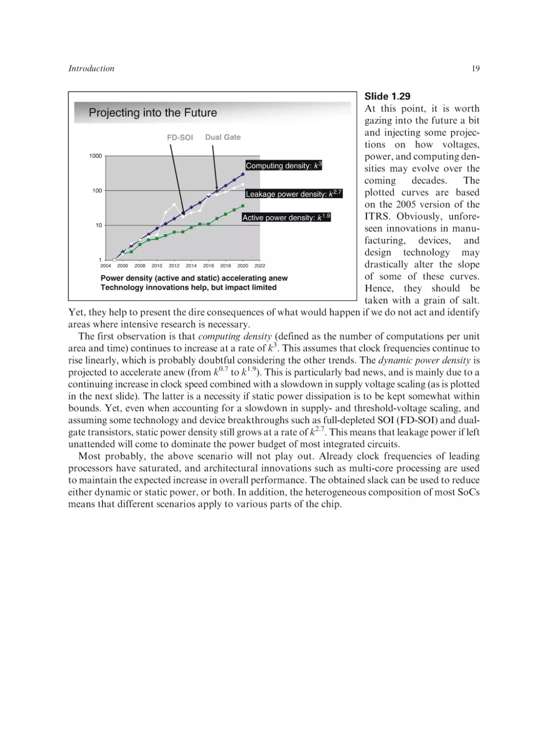
Slide 1.27
The problem was such that
Static Power (Leakage) May Ruin Moore’s Law
one was afraid that leakage
1/100
might become the undoing
10000
of Moore’s law. While the
© IEEE 2003
Leakage
International Technology
1000
Dynamic
s
Roadmap for Semiconducr
a
e
/3y
x1.4
x1.1 / 3 years
tors (ITRS) was prescrib100
ITRS
s
ing a further slowdown in
r
a
requirement
ye
10
the average power dissipa3
/
tion (by a factor of
x4
1
approximately 1.1 every
three years), static power
0.1
dissipation potentially was
MPU
DSP Processors published in ISSCC
registering a very rapid
0.01
increase instead.
1980 1985 1990 1995 2000 2005 2010 2015
Fortunately, designers
Year
[Ref: T. Sakurai, ISSCC’03]
have risen to the challenge
and have developed a range
of techniques to keep leakage power within bounds. These will be described in detail in later chapters.
Yet, static power has become a sizable fraction of the overall power budget of today’s integrated
circuits, and most indicators suggest that this problem will only get more severe with time.
Power Density (W/cm2)
Slide 1.28
There exist very compelling
Power Density Increases
reasons why a further
Unsustainable in the long term
increase in power density
should be avoided at all
10000
costs. As shown in an earSun’s Surface
lier slide for the PowerPC 4,
Rocket Nozzle
1000
power densities on chips
can become excessive and
Nuclear Reactor
lead to degradation or
100
Upper
failure, unless extremely
Bound?
expensive packaging techni8086
Hot Plate
10
P6
ques are used. To drive the
8008 8085
Pentium® proc
386
4004
point home, power density
286
486
8080
1
levels of some well-known
1970
2000
2010
1980
1990
processors are compared
Year
to general-world examples,
[Courtesy: S. Borkar, Intel]
such as hot plates, nuclear
reactors, rocket nozzles, or
even the sun’s surface. Surprisingly, high-performance ICs are not that far off from some of these
extreme heat sources! Classic wisdom dictates that power densities above 150 W/cm2 should be
avoided for the majority of designs, unless the highest performance is an absolute must and cost is not
an issue.
Introduction
19
Slide 1.29
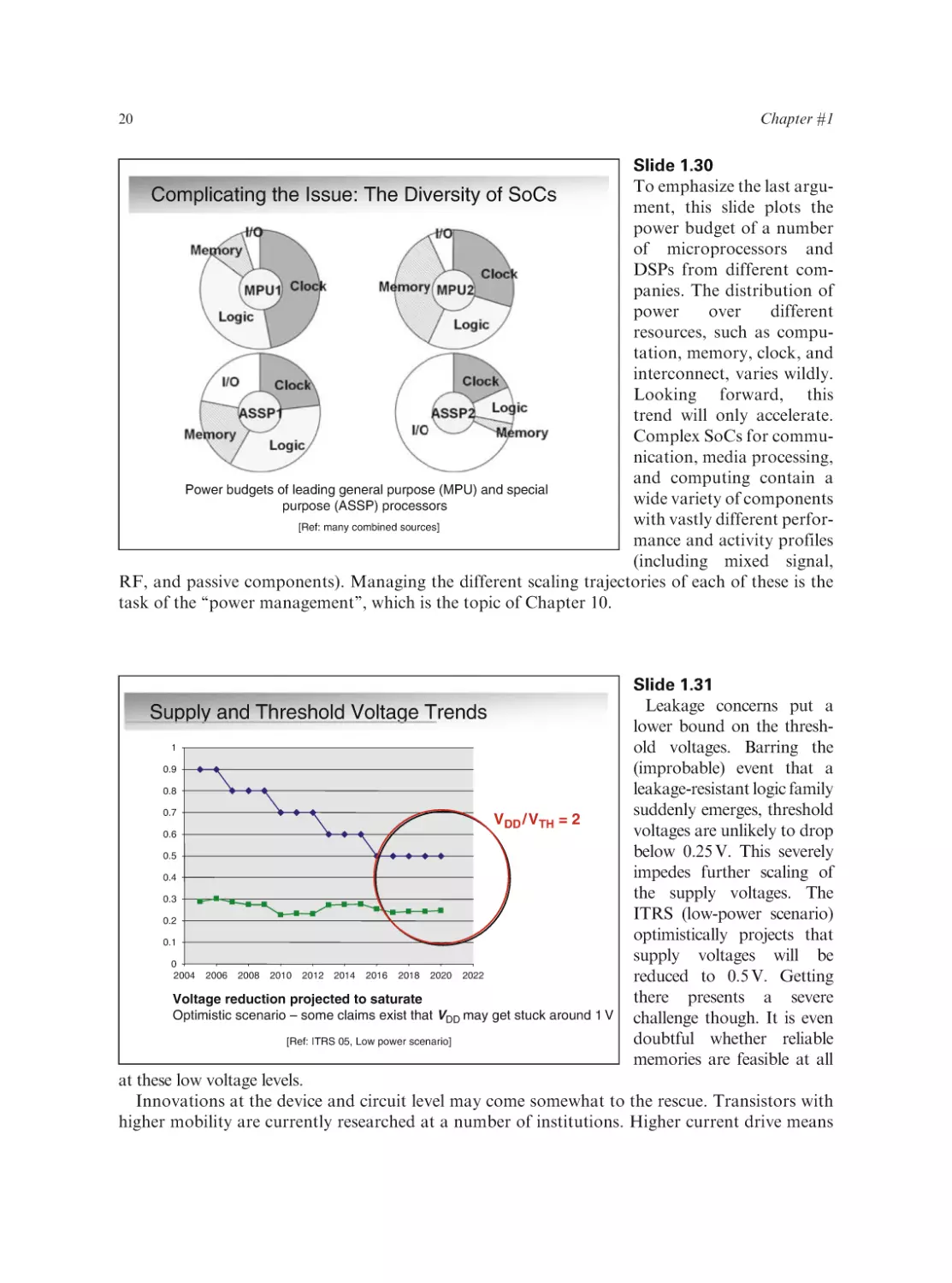
At this point, it is worth
Projecting into the Future
gazing into the future a bit
and injecting some projecDual Gate
FD-SOI
tions on how voltages,
1000
power, and computing denComputing density: k 3
sities may evolve over the
coming
decades.
The
100
2.7
plotted
curves
are
based
Leakage power density: k
on the 2005 version of the
ITRS. Obviously, unforeActive power density: k 1.9
10
seen innovations in manufacturing, devices, and
design technology may
1
2004 2006 2008 2010 2012 2014 2016 2018 2020 2022
drastically alter the slope
of some of these curves.
Power density (active and static) accelerating anew
Technology innovations help, but impact limited
Hence, they should be
taken with a grain of salt.
Yet, they help to present the dire consequences of what would happen if we do not act and identify
areas where intensive research is necessary.
The first observation is that computing density (defined as the number of computations per unit
area and time) continues to increase at a rate of k3. This assumes that clock frequencies continue to
rise linearly, which is probably doubtful considering the other trends. The dynamic power density is
projected to accelerate anew (from k0.7 to k1.9). This is particularly bad news, and is mainly due to a
continuing increase in clock speed combined with a slowdown in supply voltage scaling (as is plotted
in the next slide). The latter is a necessity if static power dissipation is to be kept somewhat within
bounds. Yet, even when accounting for a slowdown in supply- and threshold-voltage scaling, and
assuming some technology and device breakthroughs such as full-depleted SOI (FD-SOI) and dualgate transistors, static power density still grows at a rate of k2.7. This means that leakage power if left
unattended will come to dominate the power budget of most integrated circuits.
Most probably, the above scenario will not play out. Already clock frequencies of leading
processors have saturated, and architectural innovations such as multi-core processing are used
to maintain the expected increase in overall performance. The obtained slack can be used to reduce
either dynamic or static power, or both. In addition, the heterogeneous composition of most SoCs
means that different scenarios apply to various parts of the chip.
Chapter #1
20
Slide 1.30
To emphasize the last arguComplicating the Issue: The Diversity of SoCs
ment, this slide plots the
power budget of a number
of microprocessors and
DSPs from different companies. The distribution of
power
over
different
resources, such as computation, memory, clock, and
interconnect, varies wildly.
Looking forward, this
trend will only accelerate.
Complex SoCs for communication, media processing,
and computing contain a
Power budgets of leading general purpose (MPU) and special
wide variety of components
purpose (ASSP) processors
with vastly different perfor[Ref: many combined sources]
mance and activity profiles
(including mixed signal,
RF, and passive components). Managing the different scaling trajectories of each of these is the
task of the ‘‘power management’’, which is the topic of Chapter 10.
Supply and Threshold Voltage Trends
1
0.9
0.8
0.7
VDD / VTH = 2
VDD
0.6
0.5
0.4
0.3
VT
0.2
0.1
0
2004
2006
2008
2010
2012
2014
2016
2018
2020
2022
Voltage reduction projected to saturate
Optimistic scenario – some claims exist that VDD may get stuck around 1 V
[Ref: ITRS 05, Low power scenario]
Slide 1.31
Leakage concerns put a
lower bound on the threshold voltages. Barring the
(improbable) event that a
leakage-resistant logic family
suddenly emerges, threshold
voltages are unlikely to drop
below 0.25 V. This severely
impedes further scaling of
the supply voltages. The
ITRS (low-power scenario)
optimistically projects that
supply voltages will be
reduced to 0.5 V. Getting
there presents a severe
challenge though. It is even
doubtful whether reliable
memories are feasible at all
at these low voltage levels.
Innovations at the device and circuit level may come somewhat to the rescue. Transistors with
higher mobility are currently researched at a number of institutions. Higher current drive means
Introduction
21
that performance can be maintained even at a low VDD/VTH ratio. Transistors with a sharp
transition between the on and off states are another opportunity. In later chapters, we will also
explore how we can design reliable and efficient circuits, even at very low voltages.
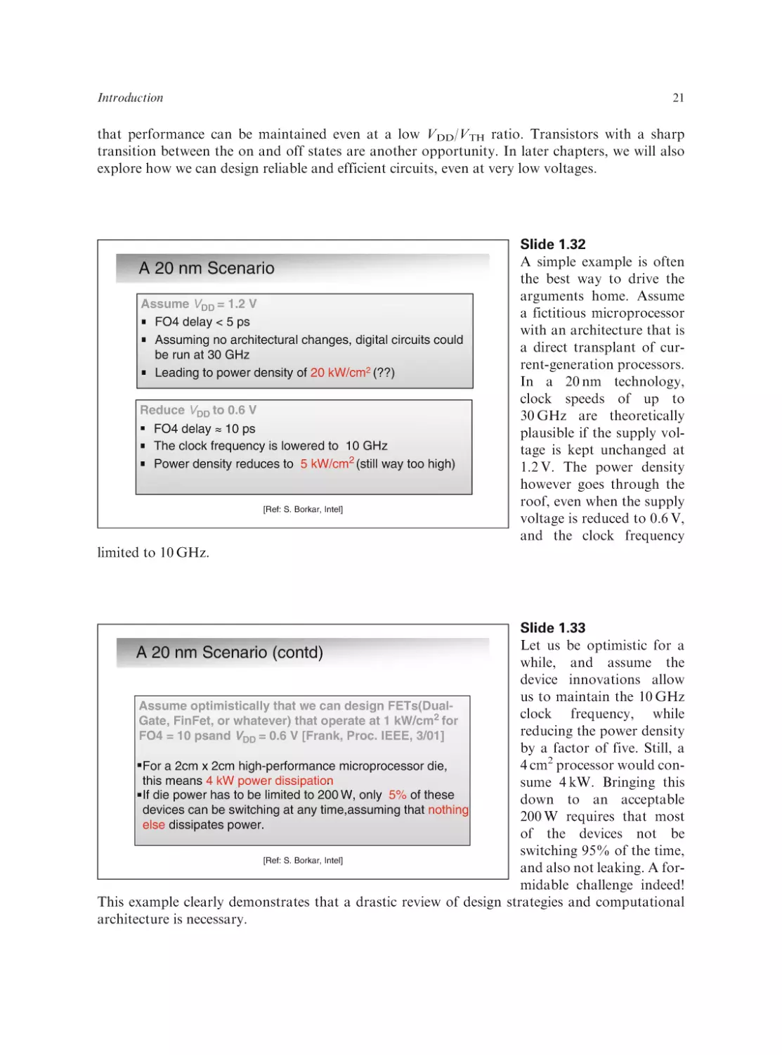
A 20 nm Scenario
Assume VDD = 1.2 V
FO4 delay < 5 ps
Assuming no architectural changes, digital circuits could
be run at 30 GHz
Leading to power density of 20 kW/cm2 (??)
Reduce VDD to 0.6 V
FO4 delay ~ 10 ps
The clock frequency is lowered to 10 GHz
Power density reduces to 5 kW/cm2 (still way too high)
[Ref: S. Borkar, Intel]
Slide 1.32
A simple example is often
the best way to drive the
arguments home. Assume
a fictitious microprocessor
with an architecture that is
a direct transplant of current-generation processors.
In a 20 nm technology,
clock speeds of up to
30 GHz are theoretically
plausible if the supply voltage is kept unchanged at
1.2 V. The power density
however goes through the
roof, even when the supply
voltage is reduced to 0.6 V,
and the clock frequency
limited to 10 GHz.
Slide 1.33
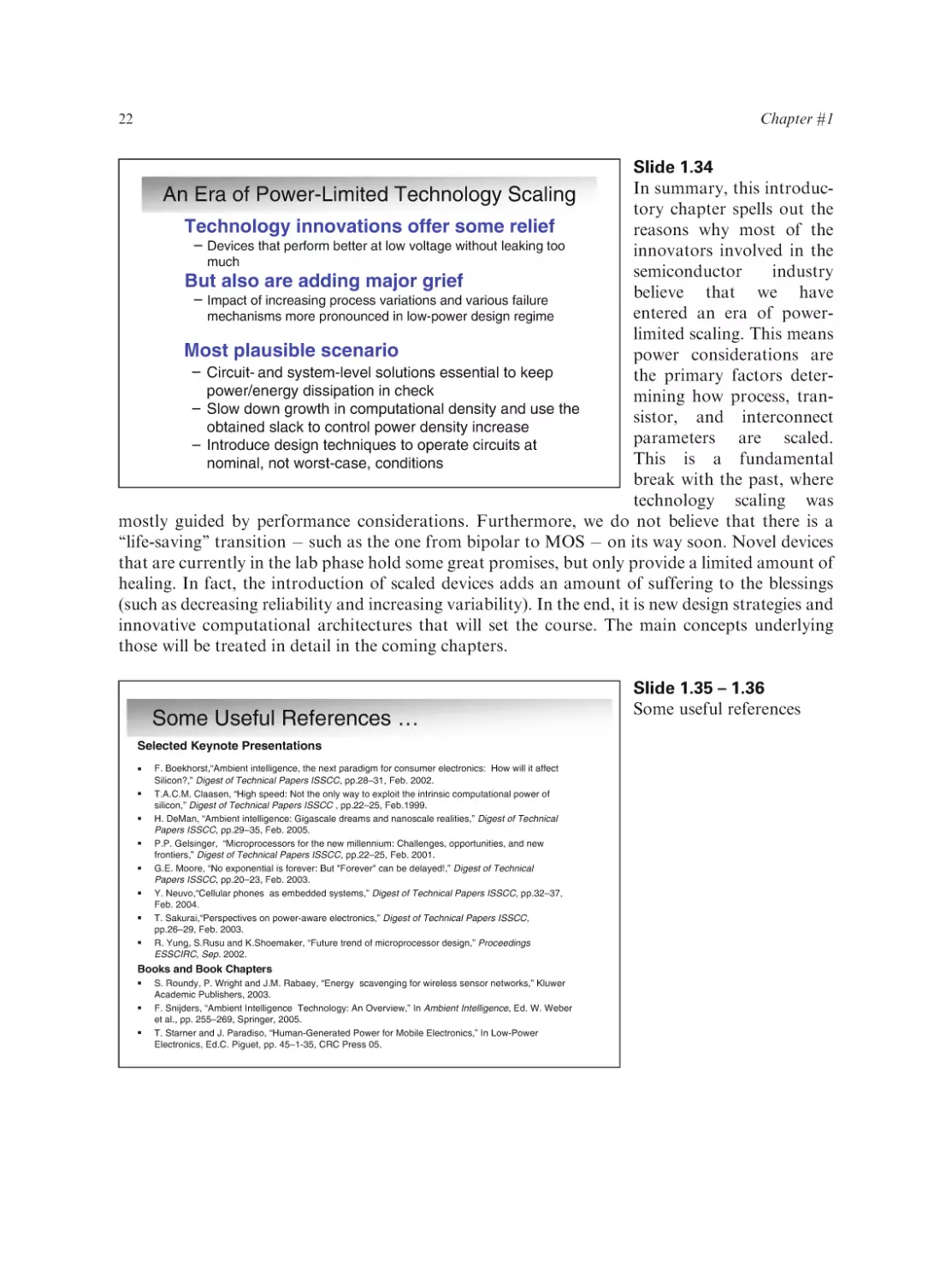
Let us be optimistic for a
A 20 nm Scenario (contd)
while, and assume the
device innovations allow
us to maintain the 10 GHz
Assume optimistically that we can design FETs(Dualclock frequency, while
2
Gate, FinFet, or whatever) that operate at 1 kW/cm for
reducing the power density
FO4 = 10 psand VDD = 0.6 V [Frank, Proc. IEEE, 3/01]
by a factor of five. Still, a
4 cm2 processor would conFor a 2cm x 2cm high-performance microprocessor die,
.
this means 4 kW power dissipation
sume 4 kW. Bringing this
If die power has to be limited to 200 W, only 5% of these
down to an acceptable
devices can be switching at any time,assuming that nothing
200 W requires that most
else dissipates power.
of the devices not be
switching 95% of the time,
[Ref: S. Borkar, Intel]
and also not leaking. A formidable challenge indeed!
This example clearly demonstrates that a drastic review of design strategies and computational
architecture is necessary.
Chapter #1
22
Slide 1.34
In summary, this introducAn Era of Power-Limited Technology Scaling
tory chapter spells out the
Technology innovations offer some relief
reasons why most of the
– Devices that perform better at low voltage without leaking too
innovators involved in the
much
semiconductor
industry
But also are adding major grief
believe
that
we
have
– Impact of increasing process variations and various failure
entered
an
era
of
powermechanisms more pronounced in low-power design regime
limited scaling. This means
Most plausible scenario
power considerations are
– Circuit- and system-level solutions essential to keep
the primary factors deterpower/energy dissipation in check
mining how process, tran– Slow down growth in computational density and use the
sistor, and interconnect
obtained slack to control power density increase
parameters are scaled.
– Introduce design techniques to operate circuits at
This is a fundamental
nominal, not worst-case, conditions
break with the past, where
technology scaling was
mostly guided by performance considerations. Furthermore, we do not believe that there is a
‘‘life-saving’’ transition such as the one from bipolar to MOS on its way soon. Novel devices
that are currently in the lab phase hold some great promises, but only provide a limited amount of
healing. In fact, the introduction of scaled devices adds an amount of suffering to the blessings
(such as decreasing reliability and increasing variability). In the end, it is new design strategies and
innovative computational architectures that will set the course. The main concepts underlying
those will be treated in detail in the coming chapters.
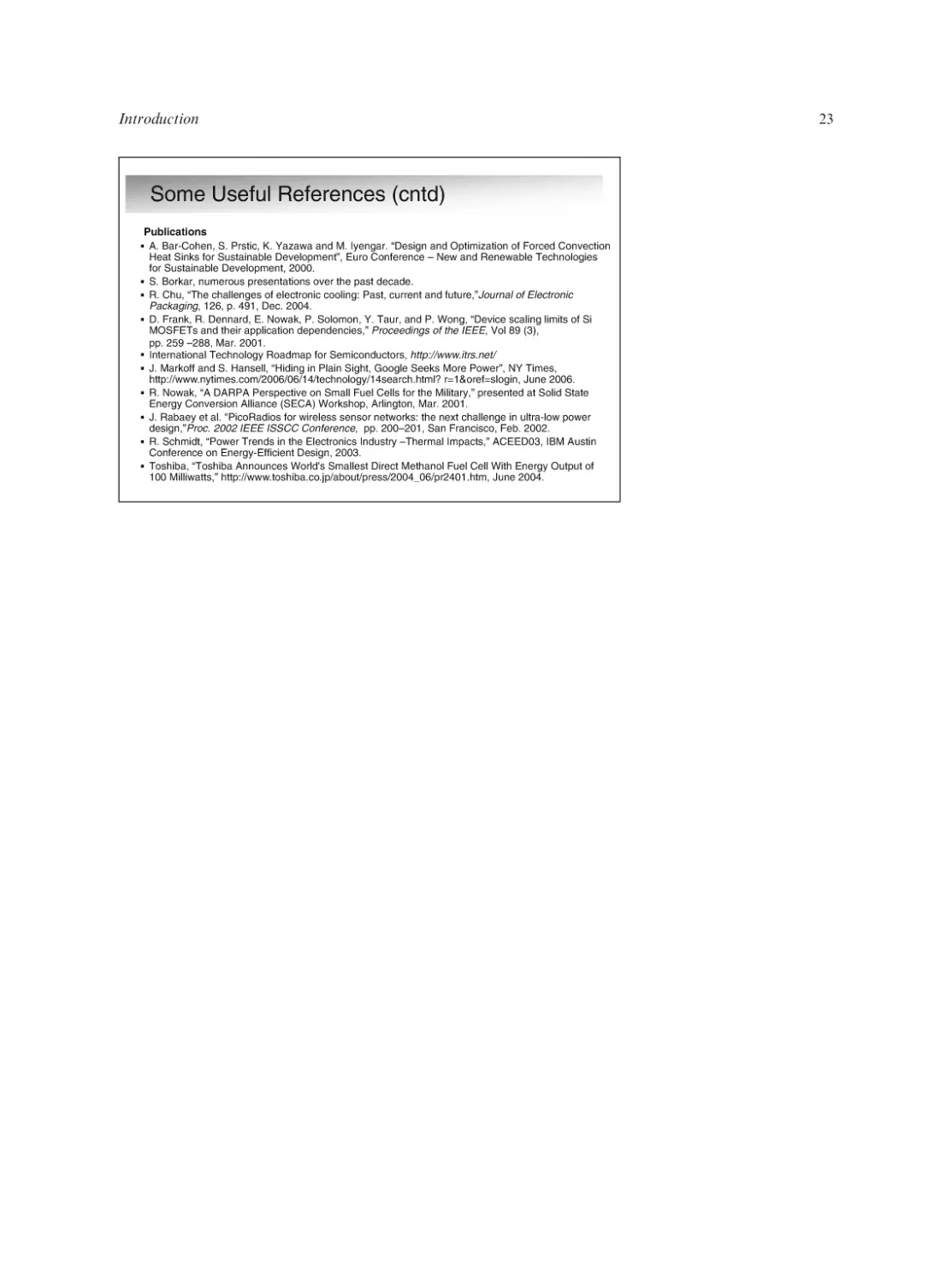
Some Useful References …
Selected Keynote Presentations
F. Boekhorst,“Ambient intelligence, the next paradigm for consumer electronics: How will it affect
Silicon?,” Digest of Technical Papers ISSCC, pp.28–31, Feb. 2002.
T.A.C.M. Claasen, “High speed: Not the only way to exploit the intrinsic computational power of
silicon,” Digest of Technical Papers ISSCC , pp.22–25, Feb.1999.
H. DeMan, “Ambient intelligence: Gigascale dreams and nanoscale realities,” Digest of Technical
Papers ISSCC, pp.29–35, Feb. 2005.
P.P. Gelsinger, “Microprocessors for the new millennium: Challenges, opportunities, and new
frontiers,” Digest of Technical Papers ISSCC, pp.22–25, Feb. 2001.
G.E. Moore, “No exponential is forever: But "Forever" can be delayed!,” Digest of Technical
Papers ISSCC, pp.20–23, Feb. 2003.
Y. Neuvo,“Cellular phones as embedded systems,” Digest of Technical Papers ISSCC, pp.32–37,
Feb. 2004.
T. Sakurai,“Perspectives on power-aware electronics,” Digest of Technical Papers ISSCC,
pp.26–29, Feb. 2003.
R. Yung, S.Rusu and K.Shoemaker, “Future trend of microprocessor design,” Proceedings
ESSCIRC, Sep. 2002.
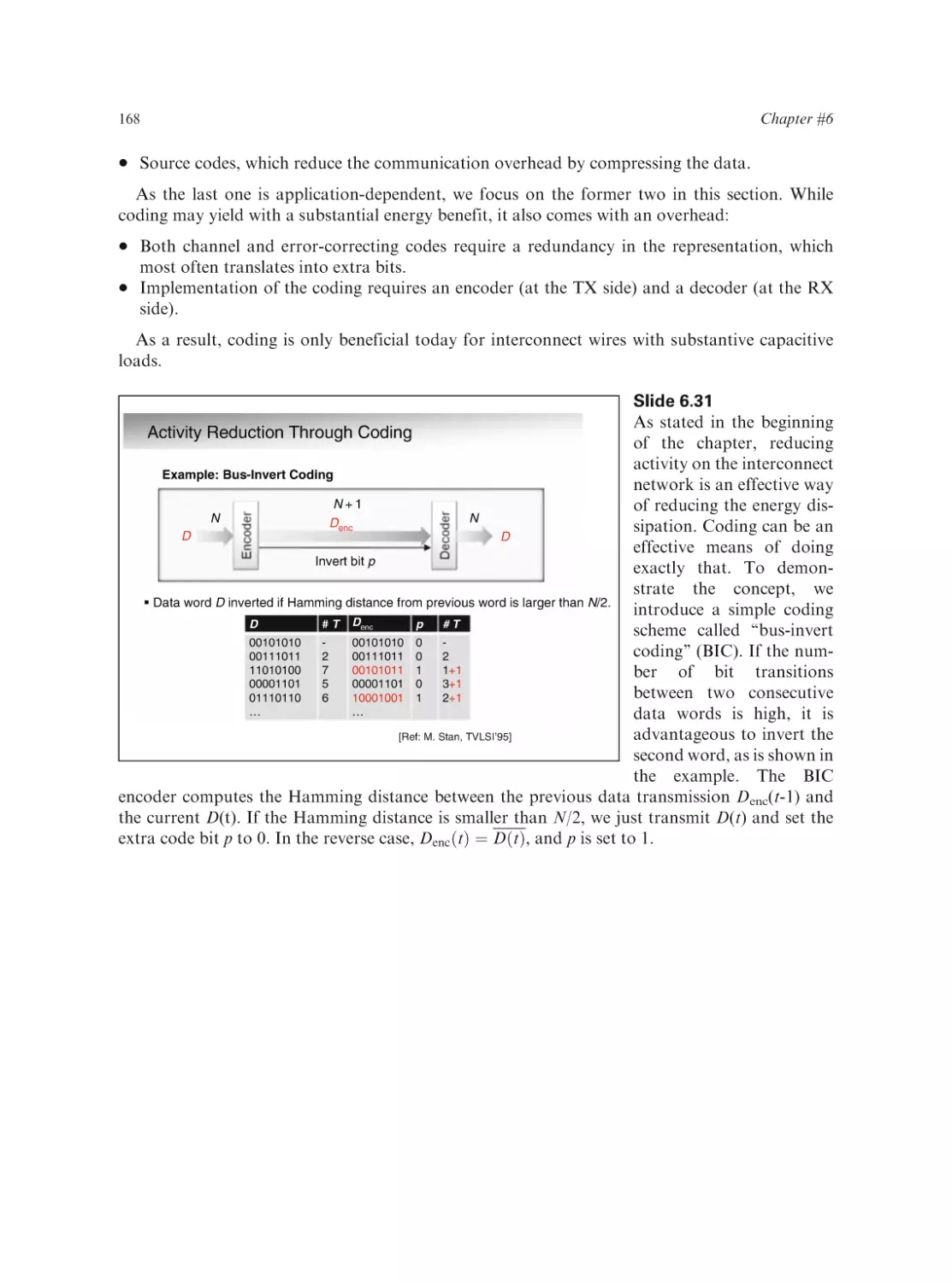
Books and Book Chapters
S. Roundy, P. Wright and J.M. Rabaey, “Energy scavenging for wireless sensor networks,” Kluwer
Academic Publishers, 2003.
F. Snijders, “Ambient Intelligence Technology: An Overview,” In Ambient Intelligence, Ed. W. Weber
et al., pp. 255–269, Springer, 2005.
T. Starner and J. Paradiso, “Human-Generated Power for Mobile Electronics,” In Low-Power
Electronics, Ed.C. Piguet, pp. 45–1-35, CRC Press 05.
Slide 1.35 – 1.36
Some useful references
Introduction
Some Useful References (cntd)
Publications
A. Bar-Cohen, S. Prstic, K. Yazawa and M. Iyengar. “Design and Optimization of Forced Convection
Heat Sinks for Sustainable Development”, Euro Conference – New and Renewable Technologies
for Sustainable Development, 2000.
S. Borkar, numerous presentations over the past decade.
R. Chu, “The challenges of electronic cooling: Past, current and future,”Journal of Electronic
Packaging, 126, p. 491, Dec. 2004.
D. Frank, R. Dennard, E. Nowak, P. Solomon, Y. Taur, and P. Wong, “Device scaling limits of Si
MOSFETs and their application dependencies,” Proceedings of the IEEE, Vol 89 (3),
pp. 259 –288, Mar. 2001.
International Technology Roadmap for Semiconductors, http://www.itrs.net/
J. Markoff and S. Hansell, “Hiding in Plain Sight, Google Seeks More Power”, NY Times,
.http://www.nytimes.com/2006/06/14/technology/14search.html? r=1&oref=slogin, June 2006.
R. Nowak, “A DARPA Perspective on Small Fuel Cells for the Military,” presented at Solid State
Energy Conversion Alliance (SECA) Workshop, Arlington, Mar. 2001.
J. Rabaey et al. "PicoRadios for wireless sensor networks: the next challenge in ultra-low power
design,”Proc. 2002 IEEE ISSCC Conference, pp. 200–201, San Francisco, Feb. 2002.
R. Schmidt, “Power Trends in the Electronics Industry –Thermal Impacts,” ACEED03, IBM Austin
Conference on Energy-Efficient Design, 2003.
Toshiba, “Toshiba Announces World's Smallest Direct Methanol Fuel Cell With Energy Output of
100 Milliwatts,” http://www.toshiba.co.jp/about/press/2004_06/pr2401.htm, June 2004.
23
Chapter 2
Nanometer Transistors and Their Models
Slide 2.1
As has become apparent in
Nanometer Transistors
Chapter 1, the behavior of
the MOS transistor, when
and Their Models
scaled into the sub-100 nm
regime, is having a large
impact on how and where
power is consumed in the
next-generation integrated
Jan M. Rabaey
circuits. Hence, any discussion on low-power design
should start with a good
understanding of the deep
submicron MOS transistor, and an analysis of its future trends. In addition, the availability of
adequate models, for both manual and computer-aided analysis, is essential. As this book emphasizes optimization, simple yet accurate models that can serve in an automated (MATLAB-style)
optimization framework are introduced.
Results in this and in the coming chapters are based on the Predictive MOS models, developed
by UCB and the University of Arizona, as well as industrial models spanning from 180 nm down to
45 nm. Whenever possible, MATLAB code is made available on the web site of the book.
Slide 2.2
The chapter starts with a
Chapter Outline
discussion of the nanometer transistor and its
behavior. Special attention
Nanometer transistor behavior and models
is devoted to the leakage
Sub-threshold currents and leakage
behavior of the transistor.
Variability
The increasing influence of
variability is analyzed next.
Device and technology innovations
At the end of the chapter,
we evaluate some innovative devices that are emerging from the research labs and discuss their potential impact on low-power design technology.
J. Rabaey, Low Power Design Essentials, Series on Integrated Circuits and Systems,
DOI 10.1007/978-0-387-71713-5_2, Ó Springer ScienceþBusiness Media, LLC 2009
25
Chapter #2
26
Slide 2.3
Beyond the degeneration of
Nanometer Transistors and Their Models
the on/off behavior of the
MOS transistor, mentioned
Emerging devices in the sub-100 nm regime
in Chapter 1, sub-100 nm
post challenges to low-power design
transistors also suffer from
– Leakage
increased variability effects,
– Variability
due both to manufacturing
– Reliability
artifacts and to physical limYet also offer some opportunities
itations. Once the feature
– Increased mobility
sizes of the process technol– Improved control (?)
ogy approach the dimensions of a molecule, it is
State-of-the-art low-power design should build
obvious that some quantum
on and exploit these properties
effects start to play. In addi– Requires clear understanding and good models
tion, the reduced dimensions make the devices also
prone to reliability failures such as soft errors (single-event upsets) and time-dependent degradation.
While these issues affect every MOS circuit design, their impact is more pronounced in lowpower designs. Reducing power dissipation often means reducing the operational signal-to-noise
margins of the circuits (for instance, by lowering the supply voltage). Effects such as variation in
performance and unreliability are more apparent under these conditions. It is fair to say that
today’s low-power design is closely interwoven with design for variability or reliability. In this
sense, low-power design often paves the way for the introduction of novel techniques that are later
adopted by the general-purpose design community.
While it may seem that scaling MOS transistors down to tens of nanometers only brings bad
karma, some emerging devices may actually help to reduce power density substantially in the
future. Especially transistors with higher mobility, steeper sub-threshold slopes, better threshold
control, and lower off-currents are attractive.
The Sub-100 nm Transistor
Velocity-saturated
– Linear dependence between ID and VGS
Threshold voltage VTH strongly impacted
by channel length L and VDS
– Reduced threshold control through body
biasing
Leaky
– Sub-threshold leakage
– Gate leakage
→ Decreasing I on over I off ratio
Slide 2.4
Fromanoperationalperspective, the main characteristics
of the sub-100 nm MOS transistors can be summarized as
follows: a linear dependence
exists between voltage and
current (in the strong-inversion region); threshold is a
function of channel length
and operational voltages;
and leakage (both subthreshold and gate) plays a
major role. Each of these
issues is discussed in more
detail in the following slides.
Nanometer Transistors and Their Models
27
Slide 2.5
The simulated ID versus
ID versus VDS for 65 nm bulk NMOS transistor
VDS behavior of a 65 nm
NMOS transistor clearly
× 10
1
demonstrates the linear
0.9
V = 1.0
relationship between ID
0.8
and
VGS in the saturation
0.7
V = 0.8
ID is a linear
region. This is a result of
0.6
function of
0.5
the well-known velocityVGS
0.4
saturation effect, which
V = 0.6
0.3
started to impact CMOS
0.2
transistors around the
V = 0.4
0.1
250 nm technology genera0
0
0.1
0.2
0.3
0.4
0.5
0.6
0.7
0.8
0.9
1
tion. The main impact is a
V (V)
Decreased output
reduced current drive for a
Early saturation
resistance
given gate voltage. Of
course, this means that the
simple models of the past are inaccurate. To address this issue, we introduce some simplified
transistor models of varying complexity and accuracy. The main goal in the context of this book is
to provide the necessary tools to the circuit and systems designer to predict power and performance
quickly.
Another important effect to be observed from the curves is the decrease in output resistance of
the device in saturation.
–4
GS
ID (A)
GS
GS
GS
DS
Slide 2.6
Probably the most accurate
Drain Current Under Velocity Saturation
model, which still allows
for fast analysis and
2
(VGS − VTH)
requires only a restricted
I DSat = vSatWCox
VGS − VTH + ECL
set of parameters, was
introduced by Taur and
Good model, could be used in hand or MATLAB analysis
Ning in 1998. One important parameter in this
W μ eff Cox
model is the critical electriVDSat (VGS − VTH)
I DSat =
2
L
cal field EC, which determines the onset of velocity
(VGS − VTH ) EC L
VDSat =
with
saturation. The problem
VGS − VTH + EC L
with this model is its highly
non-linear nature, which
[Ref: Taur-Ning, ‘98]
makes it hard to use in optimization programs (and
hand analysis); for instance, EC itself is a function of VGS. Hence, some further simplification is
desirable.
Chapter #2
28
Slide 2.7
The ‘‘unified model’’ of the
Models for Sub-100 nm CMOS Transistors
MOS transistor was introduced in [Rabaey03]. A
Further simplification:
single non-linear equation
The unified model – useful for hand analysis
suffices to describe the
Assumes VDSat constant
transistor in the saturation
and linear regions. The
main simplification in this
model is the assumption
that velocity saturation
occurs at a fixed voltage
VDSat, independent of the
value of VGS. The main
advantages of the model
are its elegance and simpli[Ref: Rabaey, DigIC’03]
city. A total of only five
parameters are needed to
describe the transistor: k0 , VTH, VDSat, and g. Each of these can be empirically derived using
curve-fitting with respect to the actual device plots. Observe that these parameters are purely
empirical, and have no or little relation to traditional physical device parameters such as the
channel-length modulation .
IDS [μA]
Slide 2.8
Simplicity comes at a cost
Models for Sub-100 nm CMOS Transistors
however. Comparing the
I–V curves produced by
unified model
simulation
the model to those of the
700
1.2V
actual devices (BSIM-4
600
SPICE model), a large dis1.0V
crepancy can be observed
500
linear
for intermediate values of
400
vel. saturation
VDS (around VDSat). When
0.8V
300
using the model for the
derivation of propagation
200
0.6V
delays (performance) of a
100
CMOS gate, accuracy in
saturation
0.4V
this section of the overall
0
0
0.2 VDSat 0.4
0.6
0.8
1
1.2
operation region is not
VDS [V]
that crucial. What is most
important is that the values
of current at the highest values of VDS and VGS are predicted correctly – as these predominantly
determine the charge and discharge times of the output capacitor. Hence, the propagation delay
error is only a couple of percents, which is only a small penalty for a major reduction in model
complexity.
Nanometer Transistors and Their Models
29
Slide 2.9
Even simpler is the alpha
Alpha Power Law Model
model,
introduced
by
Sakurai
and
Newton
in
Alternate approach, useful for hand
1990, which does not even
analysis of propagation delay
attempt to approximate
α
W
the actual I–V curves.
μ Cox VGS − VTH
I DS =
This is not a physical model
The values of and VTH
2L
Simply empirical:
are
purely
empirical,
– Can fit (in minimum mean
chosen
such
that
the
propaParameter α is between
squares sense) to a variety of
1 and 2.
α’s, VTH
gation delay of a digital
– Need to find one with
In 65–180 nm CMOS
gate, approximated by
minimum square error – fitted
technology α ~ 1.2–1.3
DD
tp ¼ ðVDDkVV
, best resemVTH can be different from
TH Þ
physical
bles
the
propagation
delay
curves
obtained
[Ref: Sakurai, JSSC’90]
from simulation. Typically,
curve-fitting
techniques
such as the minimum-mean square (MMS) are used. Be aware that these do not yield unique solutions
and that it is up to the modeler to find the ones with the best fit.
Owing to its simplicity, the alpha model is the corner stone of the optimization framework
discussed in later chapters.
(kΩ)
Slide 2.10
Beyond velocity saturaOutput Resistance
tion, reducing the transistor dimensions also lowers
Drain current keeps increasing beyond the saturation point
the output resistance of the
Slope in I–V characteristics caused by:
device in saturation. This
– Channel-length modulation (CLM)
translates into reduced
– Drain-induced barrier lowering (DIBL).
noise margins for digital
gates. Two principles are
The simulations
underlying this phenomshow approximately
enon: (1) channel-length
linear dependence
of I DS on V DS in
modulation – which was
saturation (modeled
also present in long-channel
by λ factor)
devices – and (2) draininduced barrier lowering
(DIBL). The latter is a
deep-submicron effect and
[Ref: BSIM 3v3 Manual]
is related to a reduction of
the threshold voltage as a
function of the drain voltage. DIBL primarily impacts leakage (as discussed later), yet its effect on
output resistance is quite sizable as well. SCBE (Substrate Current Body Effect) only kicks in at
voltages higher than the typical operation regime, and its impact is hence not that important.
Fortunately, the relationship between drain voltage and current proves to be approximately
linear, and is adequately modeled with a single parameter .
Chapter #2
30
IDS [A]
Slide 2.11
With the continuing reducThresholds and Sub-Threshold Current
tion of the supply voltages,
scaling of the threshold volDrain current vs. gate–source voltage
tage is a necessity as well, as
8.0E–04
illustrated at length in
VDS = 1.2 V
Chapter 1. Defining the
6.0E–04
actual threshold voltage of
a transistor is not simple, as
many factors play and mea4.0E–04
surements may not be that
straightforward. The ‘‘phy2.0E–04
sics’’ definition of the
threshold voltage is the
0.0E+00
value of VGS that causes
0
0.2
0.4
0.6
0.8
1
1.2
strong inversion to occur
VGS [V]
underneath the gate. This
VTHZ
is however impossible to
measure. An often-used
empirical approach is to derive VTH from the ID–VGS plot by linearly extrapolating the current in
the saturation region (see plot). The cross-point with the zero-axis is then defined as VTH (also called
VTHZ). Another approach is the ‘‘constant-current’’ (CC) technique, which defines the threshold
voltage as the point where the drain–source current drops below a fixed value (ID0), scaled appropriately with respect to the (W/L) ratio of the transistor. The choice of ID0 is however quite arbitrary.
Hence, in this book we use the extrapolation technique, unless otherwise mentioned.
VTH (V)
Slide 2.12
The threshold voltage is
Forward and Reverse Body Bias
unfortunately not a constant parameter, but is influThreshold value can be adjusted through the fourth terminal,
the transistor body.
enced by a number of operational parameters. The
0.5
Forward bias restricted
foremost is the body-bias
by SB and DB junctions
or back-bias effect, where
0.45
the fourth terminal of the
transistor (the bulk or well
0.4
voltage) serves as an extra
control knob. The relation0.35
ship between VTH and VSB is
well-known, and requires
0.3
the introduction of one
extra device parameter, the
Reverse bias
Forward bias
body-effect parameter g.
0.25
0.1 0.2 0.3 0.4 0.5
–0.5 –0.4 –0.3 –0.2 –0.1
0
Observe that body-biasing
VBS (V)
can be used either to
increase (reverse bias) or to
decrease (forward bias) the threshold voltage. The forward-biasing effect is limited in its scope, as the
Nanometer Transistors and Their Models
31
source–bulk diode must remain in reverse-bias conditions (that is VSB > –0.6 V). If not, current is
directly injected into the body from the source, effectively killing the gain of the transistor. For the
130 nm technology, a 1 V change in VSB changes the threshold voltage by approximately 200 mV.
The beauty of the body-biasing effect is that it allows for a dynamic adjustment of the threshold
voltage during operation, thus allowing for the compensation of process variations or a dynamic
trade-off between performance and leakage.
ΔVTH (V)
Slide 2.13
Regrettably, scaling of
Evolution of Threshold Control
device technology is graduBody-biasing effect diminishes with technology scaling below 100 nm.
ally eroding the bodyNo designer control at all in FD−SOI technology
biasing effect. With the
doping levels in the channel
0.15
increasing, changes in the
130 nm
bias voltage have little
0.1
210 mV
effect on the onset of strong
90 nm
inversion. This is clearly
0.05
95 mV
illustrated in this slide,
55 mV
0
which plots the impact of
65 nm
body biasing for three tech–0.05
nology nodes.
Emerging technologies,
–0.1
such as fully-depleted SOI
–0.5
0
0.5
(in which the body of the
VBB (V)
transistor is floating), even
do away completely with
the body biasing. This development is quite unfortunate, as this takes away one of the few
parameters a designer can use to actively control leakage effects.
VTH [V]
VTH
Slide 2.14
Channel length is another
Impact of Channel Length on Threshold Voltages
parameter that influences
the threshold voltage. For
With halo implants
very short channels, the
Long-channel threshold
depletion regions of the
drain (and source) junctions themselves deplete a
sizable fraction of the channel. Turning the transistor
on becomes easier, thus
L
Lmin
causing a reduction in the
(for small values of VDS)
threshold voltage. To offset
Partial depletion of channel due
this effect, device engineers
to source and drain junctions
add some extra ‘‘halo
larger in short-channel devices
Channel Length [m]
implants’’, which cause the
Simulated VTH of 90 nm technology
threshold to peak around
the nominal value of the
channel length. While this is beneficial in general, it also increases the sensitivity of the threshold
Chapter #2
32
voltage with respect to channel-length variations. For instance, it may happen that the channel
lengths of a particular wafer batch are consistently below the nominal value. This causes the
thresholds to be substantially below the expected value, leading to faster, but leaky, chips.
Impact of Channel Length on Threshold Voltages
1
Normalized leakage current
0.9
0.8
0.7
0.6
0.5
0.4
0.3
0.2
0.1
0
50
100
150
200
250
300
350
400
Length (nm)
50% increase in channel length
decreases leakage current by almost a factor of 20 for 90 nm technology
Slide 2.15
Designers vying for large
threshold values with relatively small variations
often size their transistors
above the nominal channel length. This obviously
comes at a penalty in area.
The impact can be quite
substantial. In a 90 nm
technology, leakage currents can be reduced by
an order of magnitude by
staying away from the
minimum channel lengths.
Just a 10% increase
already reaps major benefits. This observation has
not escaped the attention
of designers of leakage-
sensitive modules, such as SRAM memories.
VTH
Slide 2.16
Drain voltage is another
Drain-Induced Barrier Lowering (DIBL)
variable that has a sizable
impact on the threshold
In a short-channel device, source−drain distance
voltage. The DIBL effect
is comparable to the depletion region widths,
was already mentioned in
and the drain voltage can modulate the
the context of the output
threshold
resistance of short-channel
VTH = VTH0 – λdVDS
devices. As the drain voltage increases, the depleVDS = 0.2V
tion region of the junction
VDS = 1.2V
Short channel
between the drain and the
Long channel
channel increases in size
and extends under the
Channel
gate, effectively lowering
0 (S)
L (D)
the threshold voltage (this
is a hugely simplified explanation, but it catches the main tenet). The most negative feature of DIBL effect is that it turns the
threshold voltage into a signal-dependent variable. For all practical purposes, it is fair to assume
that VDS changes the threshold in a linear fashion, with d being the proportionality factor.
Nanometer Transistors and Their Models
33
Slide 2.17
Quite a number of times in
MOS Transistor Leakage Components
the introduction, we have
alluded to the increasing
effects of ‘‘leakage’’ curG
Gate leakage
rents in the nanometer
MOS transistor. An ideal
S
D
MOS transistor (at least
from a digital perspective)
should not have any curD−S
leakage
Junction
leakage
rents flowing into the bulk
(or well), should not conduct any current between
B(W)
drain and source when off,
and should have an infinite
gate resistance. As indicated in the accompanying
slide, a number of effects are causing the contemporary devices to digress from this ideal model.
Leakage currents, flowing through the reverse-biased source–bulk and drain–bulk pn junctions,
have always been present. Yet, the levels are so small that their effects could generally be ignored,
except in circuitry that relies on charge storage such as DRAMs and dynamic logic.
The scaling of the minimum feature sizes has introduced some other leakage effects that are far
more influential and exceed junction leakage currents by 3–5 orders of magnitude.
Most important are the sub-threshold drain–source and the gate leakage effects, which we will
discuss in more detail.
Sub-threshold Leakage
The transistor in “weak inversion”
VDS = 1.2V
–3
log IDS [log A]
–4
G
Ci
–5
S
D
–6
Cd
Sub
–7
Sub-threshold slope S = kT/q ln10 (1+Cd /Ci)
–8
–9
0
0.2
0.4
0.6
0.8
1
VGS [V]
Drain leakage current varies exponentially with VGS
Sub-threshold swing S is ~ 70−100 mV/decade
the current is plotted on a logarithmic scale.
1.2
Slide 2.18
In earlier slides, we have
alluded to a relationship
between the value of the
threshold voltage VTH and
(sub-threshold)
leakage.
When the gate voltage of a
transistor is lowered below
the threshold voltage, the
transistor does not turn off
instantaneously. In fact,
the transistor enters the
so-called ‘‘sub-threshold
regime’’ (or weak inversion). In this operation
mode, the drain–source
current becomes an exponential function of VGS.
This is clearly observed
from the ID–VGS curves, if
Chapter #2
34
The exponential dependence is best explained by the fact that under these conditions the MOS
transistor behaves as a bipolar device (npn for an NMOS) with its base coupled to the gate through
a capacitive divider. We know that for an ideal bipolar transistor, the base current relates to the
VBE
base–emitter voltage as ICE ¼ eðkT =qÞ where k is the Boltzmann constant and T the absolute
temperature. The so-called thermal voltage (kT/q) equals approximately 25 mV at room temperature. For an ideal bipolar transistor, every increase in VBE by 60 mV [= 25 mV x ln(10)] increases
the collector current by a factor of 10!
In the weak inversion mode of the MOS transistor, the exponential is somewhat deteriorated by
the capacitive coupling between gate and channel (base). Hence, the sub-threshold current is best
VGS
modeled as IDS ¼ enðkT =qÞ where n is the slope factor ranging around 1.4-1.5 for modern technologies.
The net effect of this degradation is that, for the current to drop by one order of magnitude in the
sub-threshold region, the reduction in VGS needed is not of 60 mV, but more like 70–100 mV.
Obviously, for an ideal switch we would hope that the current drops immediately to zero when VGS
is lowered below VTH.
four orders of
magnitude
Slide 2.19
The growing importance of
Impact of Reduced Threshold Voltages on Leakage
sub-threshold leakage can
now be understood. If the
threshold voltage is set, for
example, at 400 mV, the
leakage current drops by
five orders of magnitude
between VGS = VTH and
VGS = 0 (assuming a subthreshold swing of approximately
80 mV/decade).
Assume now that the
300 mV
threshold voltage is scaled
to 100 mV to maintain perLeakage: sub-threshold current for VGS = 0
formance under reduced
supply voltage conditions.
The leakage current at VGS = 0 for this low-threshold transistor will be approximately four orders
of magnitude higher than that for the high-threshold device, or the leakage current goes up
exponentially with a linear reduction in threshold voltage. This serves as another example of the
impact of exponential relations.
Nanometer Transistors and Their Models
35
Sub-threshold Current
Sub-threshold behavior can be modeled physically
I DS = 2nμ Cox
W
L
2
⎛ kT ⎞
⎜⎜ q ⎟⎟ e
⎝ ⎠
VGS −VTH
n kT q
−VDS
⎛
⎜1 − e kT q
⎜
⎝
VGS −VTH
−VDS
⎞
⎛
⎟ = I S e n kT q ⎜1 − e kT q
⎟
⎜
⎠
⎝
where n is the slope factor (≥1, typically around 1.5) and
Very often expressed in base 10
IDS = IS 10
where S = n (
VGS −VTH
S
− nVDS
⎛
⎜1 − 10 S
⎜
⎝
⎞
⎟
⎟
⎠
I S = 2nμ Cox
W
L
⎞
⎟
⎟
⎠
⎛ kT ⎞
⎜⎜ ⎟⎟
⎝ q ⎠
2
≈ 1 for
VDS > 100 mV
kT
) ln(10), the sub-threshold swing, ranging between 60 mV and 100 mV
q
Sub-threshold Current - Revisited
Drain-Induced Barrier Lowering (DIBL)
– Threshold reduces approximately linearly with VDS
VTH = VTH 0 − λdVDS
Body-Biasing Effect
– Threshold reduces approximately linearly with VBS
VTH = VTH 0 − γ dVBS
Leading to:
I DS = IS 10
VGS −VTH 0 + λ d VDS + γd VBS
S
− nVDS
⎛
⎜1 − 10 S
⎜
⎝
⎞
⎟
⎟
⎠
Leakage is an exponential function of drain and bulk voltages
Slide 2.20
Since sub-threshold leakage is playing such a dominant role in the nanometer
design regime, it is quite
essential to have good
models available. One of
the (few) advantages of the
sub-threshold operational
regime is that physical
modeling is quite possible,
and that the basic expressions of the drain current
as a function of VGS or
VDS can be easily derived.
Slide 2.21
The simple model of the
previous slide does not
cover two effects that
dynamically modulate the
threshold voltage of the
transistor:
DIBL
and
body biasing. While these
effects
influence
the
strong-inversion
operational mode of the transistor (as discussed earlier),
their impact is felt far
more in the sub-threshold
mode owing to the exponential relation between
drain current and threshold
voltage. The current model
is easily adjusted to include
these effects with the addition of two parameters: d and gd.
Slide 2.22
Especially DIBL turns out to have a huge impact on the sub-threshold leakage of the nanometer
CMOS transistor. Assume, for instance, an NMOS transistor in the off-mode (VGS=0). The subthreshold current of the transistor is now strongly dependent on the applied VDS. For instance, for
the device characteristics shown in the slide, raising VDS from 0.1 V to 1 V increases the leakage
current by a factor of 10 (while in an ideal device it should stay approximately flat). This creates
Chapter #2
36
Sub-threshold Current as a Function of VDS
–9
4.5
× 10
4
Two effects:
• diffusion current (like in
bipolar transistor)
• exponential increase
with VDS (DIBL)
λd = 0.18
S = 100 mV/dec
3.5
3
DIBL
I D (A)
2.5
2
3−10x in
current
technologies
1.5
1
both a challenge and an
opportunity, as it means
that leakage becomes
strongly data-dependent.
Leaving this unchecked
may lead to substantial
problems. At the same
time, it offers the innovative designer an extra parameter to play with.
0.5
0
0
0.1
0.2
0.3
0.4
0.5
0.6
0.7
0.8
0.9
1
VDS (V)
ID versus VDS for minimum size 65 nm NMOS transistor
(VGS = 0)
Slide 2.23
In addition, the current
Gate-Induced Drain Leakage (GIDL)
flowing through the drain
in the off-state is influenced
Excess drain current is observed, when
by the ‘‘gate-induced drain
gate voltage is moved below VTH, and
leakage’’ (GIDL) effect.
moves to negative values (for NMOS)
While one would expect
More pronounced for larger values of VDS
(or GIDL ~ VDG )
the drain current to drop
continuously when reducing VG below VTH for a
given drain voltage VD,
High electrical field between G and D
causes tunneling and generation of
the inverse is actually true.
electron–hole pairs
Especially at negative
Causes current to flow between drain and
values of VG, an increase
bulk
in
drain
current
is
Involves many effects such as band-toobserved. This is the result
band direct tunneling and trap-assisted
tunneling
of a combination of effects
© IEEE 2001
[Ref: J. Chen, TED’01]
such as band-to-band tunneling and trap-assisted
tunneling. A high value of the electric field under the gate/drain overlap region [as occurring for
low values of VG (0 V or lower) and high VD] causes deep depletion and an effective thinning of the
depletion width of the drain–well junction. This effectively leads to electron–hole pair creation and
an accompanying drain-to-bulk current. The effect is proportional to the applied value of VDG.
The impact of GIDL is mostly felt in the off-state of the transistor with VGS = 0. The upward
bending of the drain current curve causes an effective increase of the leakage current.
It should be noted that the GIDL effect is substantially larger in NMOS than in PMOS
transistors (by about two orders of magnitude). Also observe that the impact of GIDL is quite
small for typical supply voltages, which are at 1.2 V or lower.
Nanometer Transistors and Their Models
37
I D (A)
Slide 2.24
The combined effect of all
Combining All Drain-Leakage Effects
drain leakage components
is best illustrated by plotting ID versus VGS for dif–4
10
ferent values of VDS (as
shown in the slide for a
90 nm NMOS transistor).
10–6
VDS = 2.5 V
Most important from a
GIDL
VDS = 1.0 V
leakage perspective is the
10–8
current at VGS = 0 V. For
VDS = 0.1 V
low values of VDS, the
drain current is set by the
10–10
sub-threshold current for
the nominal VTH (as well
90 nm NMOS
as the drain–well junction
10–12
–0.4
–0.2
0
0.2
0.4
0.6
0.8
1
1.2
leakage current, which is
VGS (V)
ignorable). When raising
VDS, DIBL reduces VTH
and causes a substantial increase in leakage current. For instance, increasing VDS from 0.1 to
1.0 V causes the drain current to increase by a factor of almost 8.
The GIDL effect can clearly be observed for values of VGS smaller than –0.1 V. However, even
for VDS at a very high value of 2.5 V, the impact at VGS = 0 is still ignorable. GIDL hence plays a
minor role in most of today’s designs.
It is worth contemplating the overall picture that emerges from this. For a minimum-sized device
in a low-leakage technology with a VTH around 0.35 V, the drain leakage hovers around 1 nA at
room temperature. This amounts to a total leakage current of approximately 0.1 A for a design
with a hundred million gates (or equivalent functions). This value increases substantially at higher
temperatures (which is the standard operating condition), increases linearly with the device width,
and rises exponentially with a reduction in threshold voltage. Designs with standby leakage
currents of multiple Amperes are hence very plausible and real, unless care is taken to stop the
bleeding.
Slide 2.25
While sub-threshold currents became an issue with the introduction of the 180 nm technology
node, another leakage effect is gaining importance once technology scales below the 100 nm level
– that is, gate leakage. One of the attractive properties of the MOS transistor has always been its
very high (if not infinite) input resistance. In contrast, a finite base current is inherent to the
structure of the bipolar transistor, making the device unattractive for usage in complex digital
designs.
To maintain the current drive of the transistor while scaling its horizontal dimensions, general
scaling theory prescribes that the gate oxide (SiO2) thickness is scaled as well. Once however the
oxide thickness becomes of the order of just a few molecules, some significant obstacles emerge.
And this is exactly what happens with the sub-100 nm transistors, as is illustrated by the crosssection SEM picture of a 65 nm MOS transistor with an oxide thickness of 1.2 nm. It is clear that
the oxide is barely a couple of molecules thick.
Chapter #2
38
While posing some
obvious limits on scaling,
Gate Leakage
the very thin oxides also
Introduction of high-k dielectrics
cause a reduction in the
gate resistance of the tranGate
sistor, as current starts to
leak through the dielectric.
1.2 nm SiO2
This trend is clearly illustrated in the chart, which
Silicon substrate
shows the evolution of the
gate thickness and the gate
leakage over various techScaling leads to gate-oxide
Causes gates to leak!
nology generations at Intel.
thickness of a couple of molecules
From 180 nm to 90 nm, the
gate
leakage
current
MOS digital design has always been based on the assumption
increased by more than
of infinite input resistance!
four orders of magnitude.
Hence: Fundamental impact on design strategy!
[Ref: K. Mistry, IEDM’07]
The reasons behind the
leveling and subsequent
drop in subsequent generations will become clear in the following slides. Observe also that gate
leakage increases strongly with temperature.
Unlike sub-threshold currents, which primarily cause an increase in standby power, gate
currents threaten some fundamental concepts used in the design of MOS digital circuits.
Gate-Leakage Mechanisms
1E–07
Iox/E2
A*cm2/MV2
FN tunneling
1E–08
1E–09
Direct-oxide tunneling
1E–10
1E–11
<50 Å
1E–12
60–80 Å
1E–13
1E–14
© IEEE 2000
1E–15
0.1
0.15
1/E (MV/cm)–1
0.2
0.25
Direct-oxide tunneling dominates for lower Tox
[Ref: Chandrakasan-Bowhill, Ch3, ‘00]
is direct-oxide tunneling.
Slide 2.26
Gate leakage finds its source
in two different mechanisms:
Fowler–Nordheim
(FN) tunneling, and directoxide tunneling. FN tunneling is an effect that has
been effectively used in the
design of non-volatile memories, and is already quite
substantial for oxide thickness larger than 6 nm. Its
onset requires high electricfield strengths, though.
With reducing oxide thicknesses, tunneling starts to
occur at far lower field
strengths. The dominant
effect under these conditions
Nanometer Transistors and Their Models
39
Slide 2.27
In this slide, the depenDirect-Oxide Tunneling Currents
dence of the direct-oxide
tunneling current is plotted
10
T
as a function of the applied
V trend
0.6 nm
J G: exponential function
10
voltage and the SiO2 thick0.8 nm
of oxide thickness and
1.0 nm
ness. The leakage current
10
applied voltage
1.2 nm
is shown to vary expon1.5 nm
10
entially with respect to
1.9 nm
10
both of these parameters.
Vox 3/2 ⎤
⎡
⎢1 − (1 − Φ ) ⎥
Hence, even though we are
B
10
⎢
⎥
α ⎢ V /T
⎥
ox ox
scaling the supply voltages
⎢
⎥
10
⎣
⎦
J
∝
e
with successive process
G
0
0.3
0.6
0.9
1.2
1.5
1.8
generations, the simultaVDD
neous scaling of the oxide
Also - Gate tunneling a strong function of temperature
- Larger impact for NMOS than PMOS
thickness causes the gate
[Courtesy: S. Song, 01]
leakage current density to
continuously
increase.
This trend clearly threatens the further scaling of MOS technology, unless some innovative
process technology solutions emerge.
A first approach to address the challenge is to stop or slow down the scaling of the oxide
thickness, while continuing the scaling of the other critical device dimensions. This negatively
impacts the obtainable current density and reduces the performance benefit that typically comes
with technology scaling. Yet, even considering these negative implications, this is exactly what
most semiconductor companies did when moving to the 65 nm node (as is apparent in Slide 2.25).
This should however be considered a temporary therapy, accompanying the mastering of some
quite substantial device innovations such as high-k gate dielectrics and high-mobility transistors.
9
ox
JG (A/cm2)
6
DD
3
0
–3
–6
–9
Slide 2.28
The MOS transistor current
is proportional to the proHigh-k Material
SiO2
Tox
cess transconductance paraTg
meter k0 ¼ Cg ¼ "=tg .
Electrode
Electrode
To increase k0 through scaling, one must either find a
Si substrate
way to increase the mobility
Si substrate
of the carriers or increase
the gate capacitance (per
Equivalent Oxide Thickness = EOT = Tox = Tg * (3.9/ εg),
unit area). The former
where 3.9 is relative permittivity of SiO2 and ε g is relative permittivity
requires a fundamental
of high-k material
change in the device strucCurrently SiO2/Ni; Candidate materials: HfO2 ( εeff ~15–30); HfSiO x
( ε eff ~12–16)
ture (to be discussed later).
– Often combined with metal gate
With the traditional way of
increasing the gate capaciReduced Gate Leakage for Similar Drive Current
tance (i.e., scaling Tg) running out of steam, the only
remaining option is to look for gate dielectrics with a higher permittivity – the so-called high-k
High-k Gate Dielectric
Chapter #2
40
dielectrics. Replacing SiO2 with a ‘‘high-k’’ material yields the same effect as scaling the thickness,
while keeping gate leakage under control.
Device technologists have introduced a metric to measure the effectiveness of novel dielectrics:
the ‘‘equivalent oxide thickness’’ or EOT, which equals Tg ð"ox ="g Þ:
Introducing new gate materials is however not a trivial process change, and requires a complete
redesign of the gate stack. In fact, most dielectric materials under consideration today require a
metal gate electrode, replacing the traditional polysilicon gate. Incorporating major changes of this
type into a high-yield manufacturing process takes time and substantial investments. This explains
why the introduction of high-k dielectrics into production processes was postponed a number of
times. Major semiconductor companies such as IBM and Intel have now adopted hafnium oxide
(HfO2) as the dielectric material of choice for their 45 nm and 32 nm CMOS processes in
combination with a metal gate electrode. The relative permittivity of HfO2 equals 15–30, compared
to 3.9 for SiO2. This is equivalent to between two and three generations of technology scaling, and
should help to address gate leakage at least for a while. The resulting drop in gate leakage current
for the Intel 45 nm processor is apparent in the chart on Slide 2.25.
High-k Dielectrics
Gate electrode
Gate
3.0nm High-k
1.2 nm SiO2
Silicon substrate
Silicon substrate
High-k vs SiO 2
Benefits
Gate
capacitance
60% greater
Faster transistors
Gate dielectric
leakage
>100%
reduction
Lower power
Buys a few generations of technology scaling
[Courtesy: Intel]
Slide 2.29
The advantages offered by
high-k gate dielectrics are
quite clear: faster transistors and/or reduced gate
leakage.
Nanometer Transistors and Their Models
41
Slide 2.30
The expected evolution
of gate leakage and gate
materials is best summarized by this chart, extracted
from the International
Technology Roadmap on
Semiconductors (2005). By
analyzing the maximum
allowable leakage current
density (obviously, this
number is disputable –
what is allowable depends
upon
the
application
domain), it is concluded
that the step to high-k
dielectrics is necessary by
[Ref: ITRS 2005]
around 2009 (the 45 nm
technology node). Combined with some other device innovations such as FD-SOI and dual-gate (more about these later
in this Chapter), this may allow for the EOT to scale to around 0.7 nm (!), while keeping the gate
leakage current density at approximately 100 A/cm2 (or 1 mA/mm2).
Gate Leakage Current Density Limit Versus
Simulated Gate Leakage
Slide 2.31
The influence of temperaTemperature Sensitivity
ture on the leakage behaIncreasing temperature
vior of a transistor was
– Reduces mobility
mentioned a number of
IDS
– Reduces VTH
times before. In general, it
increasing
I on decreases with
temperature
can be assumed that the ontemperature
current of a transistor
Ioff increases with
reduces (slightly) with an
VGs
temperature
increase in temperature.
10
9
The decrease in threshold
8
90 nm NMOS
voltage is not sufficient to
7
6
offset the decrease in car5
rier mobility. The thresh4
3
old reduction on the other
2
hand has an exponential
1
0
impact on the leakage cur0
10 20 30 40 50 60 70 80 90 100
Temp(°C)
rent. Hence, higher temperatures are detrimental
for the Ion versus Ioff ratio as demonstrated for a 90 nm NMOS transistor. Increasing the temperature from 0 to 1008C reduces the ratio by almost 25. This is mostly due to the increase in leakage
current (by a factor of 22), but also to slight decrease in on-current (10%).
4
Ion/Ioff
× 10
Chapter #2
42
Slide 2.32
The topic of variability
Variability
rounds out the discussion
of the nanometer transistor
and its properties. It has
Scaled device dimensions leading to
always been the case that
increased impact of variations
transistor parameters such
– Device physics
as the geometric dimen– Manufacturing
sions or the threshold voltage are not deterministic.
– Temporal and environmental
When sampled between
Impacts performance, power (mostly
wafers, within a wafer, or
leakage) and manufacturing yield
even over a die, each of
these parameters exhibits a
More pronounced in low-power design due
statistical nature. In the
to reduced supply/threshold voltage ratios
past, the projection of
the parameter distributions
onto the performance space yielded quite a narrow distribution. This is easily understandable. When
the supply voltage is 3 V and the threshold is at 0.5 V, a 25 mV variation in the threshold has only a
small impact on the performance and leakage of the digital module. However, when the supply
voltage is at 1 V and the threshold at 0.3 V, the same variation has a much larger impact.
So, in past generation processors it was sufficient to evaluate a design over its worst-case
corners (FF, SS, FS, SF) in addition to the nominal operation point to determine the yield
distributions. Today, this is not sufficient, as the performance distributions have become
much wider, and a pure worst-case analysis leads to wasteful design and does not give a
good yield perspective either.
Normalized Frequency
Slide 2.33
While variations influence
Variability Impacts Leakage
the high-performance design
regime, their impact is far
1.4
more pronounced in the
low-power design arena.
1.3
30%
First of all, the prediction of
1.2
leakage currents becomes
130 nm
hard. The sub-threshold cur1.1
rent is an exponential function of the threshold voltage,
1.0
and each variation in the lat5X
ter is amplified in a major
0.9
1
2
3
4
5
way in leakage fluctuations.
Normalized Leakage (I
(Isb )
This is illustrated very well
Threshold variations have exponential impact on leakage
in the performance–leakage
[Ref: P. Gelsinger, DAC’04]
distribution plot (for 130 nm
technology). When sampled
over a large number of dies (and wafers), gate performance varies over 30%, while the leakage current
fluctuates by a factor of 5. Observe that the leakiest designs are also the ones with the highest
performance (this should be no surprise).
Nanometer Transistors and Their Models
43
Other reasons why variations play a more pronounced role in low-power design will emerge in
the subsequent chapters. However, they can be summarized in the following observation: In
general, low-power designs operate at lower supply voltages, lower VDD/VTH, and smaller signal-to-noise ratios; these conditions tend to amplify the importance of parameter variations.
Slide 2.34
Process variations are not
Variability Sources
the only cause behind the
variability in the perforPhysical
mance parameters of a
– Changes in characteristics of devices and wires.
design (such as delay and
power dissipation). It actu– Caused by IC manufacturing process, device
ally originates from a
physics & wear-out (electro-migration).
broad set of causes with
– Time scale: 10 9 s (years).
very different temporal
Environmental
characteristics. In a broad
– Changes in operational conditions (modes), VDD,
sense, we can classify them
temperature, local coupling.
into physical, manufactur– Caused by the specifics of the design
ing, environmental, and
implementation.
operational categories. It
– Time scale: 10 –6 to 10–9 s (clock tick).
is probably fair to state
that manufacturing variations – that is, fluctuations in device and interconnect parameters caused by the manufacturing
process – are dominant in today’s designs. However, with device dimensions approaching the
molecular scale, statistical quantum-mechanical effects start to play a role, as the ‘‘law of large
numbers’’ starts to be less applicable. Environmental and operational conditions are closely
related. While operating a circuit, some ‘‘external’’ parameters such as the supply voltage, the
operating temperature, and the coupling capacitance may change dynamically as a result of
environmental conditions or the activity profile of the design.
Variability Sources and Their Time Scales
Slide 2.35
When trying to create
design solutions to address
the variability concerns, it
pays to understand the
nature and the behavior of
the sources of variation,
as these will ultimately
determine what design techniques can be effective in
eliminating or reducing the
impact. The most important statistical parameters
of concern are the temporal
and spatial correlations. If
a parameter has a strong
spatial correlation (i.e., all
Chapter #2
44
devices in the neighborhood show the same trend), a solution such as global tuning proves to be
effective. The same is true in the time domain. Very strong temporal correlations (i.e., a device
parameter is totally predictable or may not even change over time) can again be addressed by onetime or slow adaptation.
In this slide, we have classified the different sources of variations from a temporal perspective. At
the slow extreme of the spectrum are manufacturing variations, which last for the lifetime of the
product. Almost similar from a lifetime perspective, but entirely different in nature, are variations
caused by wear-out, which manifest themselves only after a very long time of operation (typically
years). Examples of such sources are electro-migration, hot-electron degradation, and negativebias temperature instability (NBTI). Next on the time scale are slow operational or environmental
conditions. The temperature gradients on a die vary slowly (in the range of milliseconds), and
changes are typically the result of alterations in the operation mode of the system. An example of
such is putting a module to sleep or standby mode after a time of intensive computation. Other
variations happen at a much faster time scale such as the clock period or even a single signal
transition. Their very dynamic nature does not leave room for adaptive cancellation, and circuit
techniques such as shielding are the only way to eliminate their impact.
3σ/mean
Slide 2.36
Process and manufacturing
Process Variations
variations are probably of
the most concern. The evoPercentage of total
lutionary trend is clear: virvariation accounted for
40%
Leff
by within-die
tually all technology paravariation(device and
30%
meters such as transistor
interconnect)
20%
length, width, oxide thickw, h, ρ
ness, and interconnect
10%
Tox, VTH
resistivity show an increas0%
250
180
130
90
65
ing variability over time (as
Technology Node (nm)
measured by the ratio of
[Courtesy: S. Nassif, IBM]
standard deviation over
the mean value). Although
L (nm)
250 180 130
90
65
45
VTH (mV)
450 400 330
300
280
200
each of these parameters is
27
28
30
32
σ(VTH) (mV) 21 23
important on its own, the
σ(VTH) /VTH 4.7% 5.8% 8.2% 9.3% 10.7% 16%
resulting impact on the
threshold voltage is what
counts most from a digital-design perspective. As shown in the table, the threshold variability is rising from 4% to 16%
while evolving from 250 nm to 45 nm CMOS technologies. One may assume that this variation
primarily results from the increasing deviations in channel length, since the VTH is quite sensitive to
variations in L around the critical dimension (remember the halo implants). The resulting impact
on both performance and power metrics is quite substantial.
Slide 2.37
Since the lengths of neighboring transistors tend to be similarly affected by deviations in the
manufacturing process, one would assume that the threshold voltages of closely spaced transistors
should be strongly correlated. This conclusion holds especially for > 100 nm technology nodes,
where strong systematic trends in thresholds of local neighborhoods can be observed.
Nanometer Transistors and Their Models
45
Mean Number of Dopant Atoms
However, the observation
becomes less true with
Threshold Variations Most Important for Power
continued scaling, when
deviations
in another
10000
device parameter, channel
doping, start to become an
1000
issue. As shown in the
graph, the number of
dopant atoms, which is a
100
discrete number, drops
below 100 for transistor
10
1000
500
250
130
65
32
dimensions smaller than
Technology Node (nm)
100 nm. The exact number
Decrease of random dopants in channel increases
of dopants in the channel is
impact of variations on threshold voltage
a random variable, and can
[Courtesy: S. Borkar, Intel]
change from transistor to
transistor. We may hence
expect that the correlation in threshold voltages between neighboring transistors will reduce
substantially in future technology generations.
The main takeaway from this discussion on process variations is that most device and design
parameters will feature broader distributions over time, and that this is primarily caused by
variations in the transistor threshold. While these variations tend to be mostly systematic today,
we may expect larger random components in the future.
Slide 2.38
One may wonder whether
Device and Technology Innovations
these many and profound
challenges
may
make
Power challenges introduced by nanometer
design in the nanometer
MOS transistors can be partially addressed by
regime all but impossible.
new device structures and better materials
This is a very valid question
– Higher mobility
indeed, which has kept
– Reduced leakage
many semiconductor com– Better control
pany executives awake at
night over the past years.
However …
While reflecting, it pays
– Most of these techniques provide only a one (or two)
technology generation boost
to keep the following con– Need to be accompanied by circuit and system level
siderations in mind. Over
methodologies
the years, designers have
proven to be quite ingenious, and they have come up over and over again with new design technologies and methodologies
to address emerging challenges and roadblocks. We can be confident that this will continue to
happen in the future (this is what this book is about, after all). At the same time, device engineers
are not sitting still either. On the drawing board are a number of device structures that may help to
address some, if not all, of the concerns raised in this chapter. For a designer, it is important to be
aware of what may be coming down the device pipeline and plan accordingly.
Chapter #2
46
Device and Technology Innovations
Strained silicon
Silicon-on-Insulator
Dual-gated devices
Very high mobility devices
MEMS – transistors
GP-SOI
DG-SOI
Slide 2.39
The devices introduced in
the coming slides present
any of the following features: higher mobility, better threshold control, or
faster sub-threshold current roll-off.
FinFET
Slide 2.40
The concept of strained
Strained Silicon
silicon was introduced by
IBM to increase the mobility in traditional CMOS
transistors. From the 65 nm
generation onward, it is
used almost universally by
all semiconductor manufacturers. The generic idea is to
create a layer of silicon (typically in the transistor channel), in which the silicon
Improved ON-Current (10–25%) translates into:
atoms are stretched (or
• 84–97% leakage current reduction
strained) beyond their nor• or 15% active power reduction
mal inter-atomic distance.
[Ref: P. Gelsinger, DAC’04]
A generic way to create
strain is to put a layer of
silicon over a substrate of silicon germanium (SiGe). As the atoms in the silicon layer align with
the atoms in the silicon–germanium layer, where the atoms are further apart, the links between the
silicon atoms become stretched – thereby leading to strained silicon. Moving the atoms further
apart reduces the atomic forces that interfere with the movement of electrons through the transistors, resulting in higher mobility.
The practical realization may differ between manufacturers. The slide illustrates one strategy, as
employed by Intel. To stretch the silicon lattice, Intel deposits a film of silicon nitride over the
whole transistor at a high temperature. Because silicon nitride contracts less than silicon as it cools,
it locks the silicon lattice beneath it in place with a wider spacing than it would normally adopt.
This improves electron conduction by 10%. For PMOS transistors, the silicon is compressed. This
Nanometer Transistors and Their Models
47
is accomplished by carving trenches along opposite ends of the channel. These are filled with silicon
germanium, which has a larger lattice size than silicon alone and so compresses the regions nearby.
This improves hole conduction by 25%.
Strained Silicon
Improves Transistor Performance and/or Reduces Leakage
Transistor Leakage Current
(nA/μm)
1000
Std
100
Strain
Std
+25% ION
Strain
+10% ION
0.20 × IOFF
10
Slide 2.41
The higher mobility may be
used to increase the performance. From a power perspective, a better approach
is to use the higher mobility
to obtain the same performance with either a higher
threshold voltage (reducing
leakage), or with a reduced
VDD/VTH ratio, as is illustrated in this slide.
0.04 × IOFF
NMOS
PMOS
1
0.2
0.4
0.6
0.8
1.0
1.2
1.4
1.6
Transistor Drive Current
(mA/μm)
[Ref: S. Chou, ISSCC’05]
Mobility (cm/s)
Slide 2.42
Straining is only one first
Beyond Straining
step toward higher mobility. Materials such as Ge
Hetero-junction devices allow for even larger carrier mobility
and GaAs are known to
have an intrinsic electron
100000
InSb
Electrons (intrinsic)
mobility that is substanSi + strain
tially above what Si can
10000
InAs
offer. Researchers at varGe, GaAs
ious locations are exploring
1000
ε Si
the potential of so-called
hetero-devices that com100
5.2
5.4
5.6
5.8
6
6.2
6.4
6.6
bine Si with other materials
Lattice Constant (Å)
such as Ge, offering the
potential of carriers that
are 10 times as mobile,
Example: Si-Ge-Si heterostructure channel
while still relying on traditional Si technology. An
[Courtesy: G. Fitzgerald (MIT), K. Saraswat (Stanford)]
example of such a device
is the Si-Ge-Si heterostructure developed at Stanford (this is only one example of the many structures being investigated). While these high-mobility devices will need quite some time before making it to the
production line (if ever), they offer a clear glimpse at the potential for further improvement.
48
Chapter #2
Slide 2.43
Silicon-on-Insulator (SOI)
Silicon-on-Insulator (SOI)
is a technology that has
[Courtesy: IBM]
G
been ‘‘on the horizon’’ for
quite a long time, yet it
S
D
Thin
never managed to really
silicon
FD
break ground, though with
layer
Thin Oxide
some exceptions here and
Substrate
there. An SOI MOS transistor differs from a ‘‘bulk’’
Reduced capacitance (source and drain to bulk) results
device in that the channel is
in lower dynamic power
formed in a thin layer of
Faster sub-threshold roll-off (close to 60 mV/decade)
silicon deposited above an
Random threshold fluctuations eliminated in fullyelectrical insulator, typidepleted SOI
cally silicon dioxide.
Reduced impact of soft-errors
Doing so offers some
But
– More expensive
attractive features. First,
– Secondary effects
as drain and source diffusions extend all the way
down to the insulator layer, their junction capacitances are substantially reduced, which translates
directly into power savings. Another advantage is the higher sub-threshold slope factor (approaching the ideal 60 mV/decade), reducing leakage. Finally, the sensitivity to soft errors is reduced
owing to the smaller collection efficiency, leading to a more reliable transistor. There are some
important negatives as well. The addition of the SiO2 layer and the thin silicon layer increases the
cost of the substrate material, and may impact the yield as well. In addition, some secondary effects
should be noted. The SOI transistor is essentially a three-terminal device without a bulk (or body)
contact, and a ‘‘body’’ that is floating. This effectively eliminates body biasing as a thresholdcontrol technique. The floating transistor body also introduces some interesting (ironically speaking. . .) features such as hysteresis and state-dependency.
Device engineers differentiate between two types of SOI transistors: partially-depleted (PD-SOI)
and fully-depleted (FD-SOI). In the latter, the silicon layer is so thin that it is completely depleted
under nominal transistor operation, which means that the depletion/inversion layer under the gate
extends all the way to the insulator. This has the advantage of suppressing some of the floatingbody effects, and an ideal sub-threshold slope is theoretically achievable. From a variation
perspective, the threshold voltage becomes independent of the doping in the channel, effectively
eliminating a source of random variations (as discussed in Slide 2.37). FD-SOI requires the
depositing of extremely thin silicon layers (3–5 times thinner than the gate length!).
Nanometer Transistors and Their Models
49
Example: Double-Gated Fully Depleted SOI
G (Ni silicide ) thin SOI (< 20 nm)
D
Buried gate provides
accurate threshold
control over wide
range
well
contact
S
thin BOX
( < 10nm)
VT control
dopant
(10 18 /cm3 )
well
well
STI
STI
STI
sub
sub
© IEEE 2004
Threshold voltage VTH (V)
0.6
0.5
0.4
High dose
V DD = 1.0 V
t SOI = 20 nm
t BOX = 10 nm
Low dose
45 nm bulk
32 nm bulk
w/o
σint σ (VT )
σext
65 nm FD-SOI
0.1
45 nm FD-SOI
0.0
–0.1
–1.0
σ (V T )
65 nm bulk
0.3
0.2
σint
σext
90 nm bulk
32 nm FD-SOI
0.5
–0.5
0.0
Well-bias voltage Vwell (V)
1.0
0
2
1
Standard deviation (a.u.)
[Ref: M. Yamaoka, VLSI’04, R. Tsuchiya, IEDM’04]
Slide 2.44
The FD-SOI device architecture can be further
extended with an extra feature that reinstates threshold control through a
fourth terminal. A buried
gate below the SiO2 insulator layer helps to control
the charge in the channel,
and thus also the threshold
voltage. As shown in these
graphs (published by Hitachi), the buried-gate concept pretty much reinstates
the idea of body biasing as
a viable design option. The
reduced impact of random
doping variations on the
threshold voltage, as is
typical in FD-SOI, is also illustrated.
Slide 2.45
The FinFET (called a triFinFETs – An Entirely New Device Architecture
gate transistor by Intel) is
an entirely different tran© IEEE 1999
sistor structure that actually offers some properties
similar to the ones offered
by the device presented in
the previous slide. The term
FinFET was coined by
researchers at the UniverUC Berkeley, 1999
sity of California at Berkeley to describe a non-planar,
double-gated transistor built
S = 69 mV/decade
• Suppressed short-channel effects
on an SOI substrate. The
• Higher on-current for reduced leakage
distinguishing characteristic
• Undoped channel – No random dopant fluctuations
of the FinFET is that the
[Ref: X. Huang, IEDM’99]
controlling gate is wrapped
around a thin silicon ‘‘fin’’,
which forms the body of the device. The dimensions of the fin determine the effective channel length
of the device. The device structure has shown the potential to scale the channel length to values that are
hard, if not impossible, to accomplish in traditional planar devices. In fact, operational transistors with
channel lengths down to 7 nm have been demonstrated.
In addition to a suppression of deep submicron effects, a crucial advantage of the device is again
increased control, as the gate wraps (almost) completely around the channel.
Chapter #2
50
Drain
D
rain
rain
ra
Drain
Drain
Source
Source
Slide 2.46
This increased two-dimenBackGated FinFET
sional control can be
exploited in a number of
ways. In the dual-gated
Gate length = LG
Gate length = LG
device, the fact that the
Gate
ate Fin Width = T
Gate2
gate is controlling the chanSi
Vth Control
nel from both sides (as well
Gate1
Gate1
Switching
Fin Height
as the top) leads to
Fin Height
Gate
H FIN =W
increased process transconH FIN = W /2
ductance. Another option
is to remove the top part
Back-gated (BG) MOSFET
Double-gated (DG) MOSFET
of the gate, leading to the
back-gated transistor. In
Independent front and back gates
this structure, one of the
One switching gate and VTH control gate
gates acts as the standard
Increased threshold control
control gate, whereas the
other is used to manipulate
the threshold voltage. In a sense, this device offers similar functionality as the buried-gate FD-SOI
transistor discussed earlier. Controlling the work functions of the two gates through the selection
of appropriate type and quantity of the dopants helps to maximize the range and sensitivity of the
control knobs.
Slide 2.47
The fact that the FinFET
New Transistors: FinFETs
and its cousins are dramatically different devices
compared to your standard
bulk MOS transistor is
best-illustrated with these
pictures from Berkeley and
Intel tri-gate
Intel. The process steps
that set and control the
Berkeley PMOS FinFET
physical dimensions are
Gate
entirely different. Although
Drain
this creates new opportuManufacturability still an
Source
issue – may even cause
nities, it also brings chalmore variations
lenges, as the process steps
[Courtesy: T.J. King, UCB; Intel]
involved are vastly different. The ultimate success of
the FinFET depends greatly upon how these changes can be translated into a scalable, low-cost and
high-yield process – some formidable question, indeed! Also unclear at this time is how the adoption
of such a different structure impacts variability, as critical dimensions and device parameters are
dependent upon entirely different process steps.
Nanometer Transistors and Their Models
51
Some Futuristic Devices
FETs with sub-threshold swing < kT/q (I-MOS)
Impact Ionization
Region
Poly
I-MOS
VS = –1V
VD = 0V
1.0E–03
1.0E–05
P+
I-MOS
N+
Buried-Oxide
Buried Oxide
1.0E–07
1.0E–09
1.0E–11
ON
MOS
OFF
0
5 mV/dec.
L I = 25 nm
L G = 25 nm
Tox = 1 nm
Tsi = 25 nm
0.2
0.4
0.6
[Courtesy: J. Plummer, Stanford]
Zero off-current transistor
Uses MEMS technology to
physically change gate control.
Allows for zero-leakage sleep
transistors and advanced
memories
[Ref: Abele05, Kam05]
© IEEE 2005
Slide 2.48
It is worth pointing out
that the devices described
here represent by no
means the complete spectrum of new transistors
and switching devices that
are
currently
being
explored. In fact, the number of options that are
emerging from the research
labs these days is quite
extraordinary, and the
excitement is palpable.
Most of these will probably
die with a whimper, while
other ones are still decades
out in terms of true applicability. Of the latter,
carbon-nanotube (CNT)
transistors seem to present
some true potential, but the jury is still out.
When looking from a power angle, some device structures emerging from the research labs merit
some special attention. The I-MOS transistor uses substantially different mechanisms, such as
impact ionization, to produce a transistor with a sub-threshold slope substantially below 60 mV/
decade. This opens the door for a switch with close-to-ideal characteristics. The availability of such
a device would allow operation at supply voltages that are substantially lower than what we can
allow today.
Another entirely new device would allow for an almost complete elimination of leakage current
in standby mode: Using MEMS (Micro-electromechanical systems) technology, the suspendedgate MOSFET (SG-MOS) physically moves the actual gate up and down depending upon the
applied gate voltage. In the down-position this device resembles a traditional transistor. Moving
the gate into the up-position is physically equivalent to mechanically turning off the switch,
effectively squelching all leakage current. The availability of such a device would come extremely
handy in the design of low-standby power components.
Chapter #2
52
Slide 2.49
For the circuit designer,
Summary
there are some important
takeaways from this chapPlenty of opportunity for scaling in the
ter. Scaling into the nannanometer age
ometer regime has some
Deep-submicron behavior of MOS
profound impact on the
behavior of the CMOS
transistors has substantial impact on
transistor, both in the ON
design
and in the OFF modes.
Power dissipation mostly influenced by
Simple models that capture
increased leakage (SD and gate) and
the behavior of the transisincreasing impact of process variations
tor in both modes are availNovel devices and materials will ensure
able, and will help us in
scaling to a few nanometers
later chapters to build
effective analysis and optimization frameworks. A profound awareness of the device characteristics and the ability to
adapt to its varying properties will prove to be essential tenets in low-power design in the
nanometer era.
References
Books and Book Chapters
A. Chandrakasan, W. Bowhill, and F. Fox (eds.), “Design of High-Performance Microprocessor Circuits”, IEEE Press 2001.
J. Rabaey, A. Chandrakasan, and B. Nikolic, “Digital Integrated Circuits: A Design Perspective,”2nd ed, Prentice Hall 2003.
Y. Taur and T.H. Ning, Fundamentals of Modern VLSI Devices, Cambridge University Press, 1998.
Articles
N. Abele, R. Fritschi, K. Boucart, F. Casset, P. Ancey, and A.M. Ionescu, “Suspended-Gate MOSFET: Bringing New MEMS
Functionality into Solid-State MOS Transistor,” Proc. Electron Devices Meeting, 2005. IEDM Technical Digest. IEEE International,
pp.479–481, Dec. 2005
BSIM3V3 User Manual, http://www.eecs.berkeley.edu/Pubs/TechRpts/1998/3486.html
J.H. Chen et al., “An analytic three-terminal band-to-band tunneling model on GIDL in MOSFET,” IEEE Trans. On Electron
Devices, 48(7), pp. 1400–1405, July 2001.
S. Chou, “Innovation and Integration in the Nanoelectronics Era,” Digest ISSCC 2005, pp. 36–38, February 2005.
P. Gelsinger, “Giga-scale Integration for Tera-Ops Performance,” 41st DAC Keynote, DAC, 2004, (www.dac.com)
X. Huang et al., "Sub 50-nm FinFET: PMOS,” International Electron Devices Meeting Technical Digest, p. 67.
Dec. 5–8, 1999.
International Technology Roadmap for Semiconductors, http://www.itrs.net/
H. Kam et al., “A new nano-electro-mechanical field effect transistor (NEMFET) design for low-power electronics, “IEDM Tech.
Digest, pp. 463–466, Dec. 2005.
K. Mistry et al., “A 45nm Logic Technology with High-k+Metal Gate Transistors, Strained Silicon, 9 Cu Interconnect Layers, 193 nm
Dry Patterning, and 100% Pb-free Packaging,” Proceedings, IEDM, p. 247, Washington, Dec. 2007.
Predictive Technology Model (PTM), http://www.eas.asu.edu/~ptm/
T. Sakurai and R. Newton. “Alpha-power law MOSFET model and its applications to CMOS inverter delay and other formulas.,” IEEE
Journal of Solid-State Circuits, 25(2), 1990.
R. Tsuchiya et al., “Silicon on thin BOX: a new paradigm of the CMOSFET for low-power high-performance application featuring
wide-range back-bias control,” Proceedings IEDM 2004, pp. 631–634, Dec. 2004.
M. Yamaoka et al., “Low power SRAM menu for SOC application using Yin-Yang-feedback memory cell technology,” Digest of
Technical Papers VLSI Symposium, pp. 288–291, June 2004.
W. Zhao, Y. Cao, “New generation of predictive technology model for sub-45nm early design exploration,” IEEE Transactions on
Electron Devices, 53 (11), pp. 2816 –2823, November 2006
Slide 2.50
Some references . . .
Chapter 3
Power and Energy Basics
Slide 3.1
The goal of this chapter is
to derive clear and unamPower and Energy Basics
biguous definitions and
models for all of the design
metrics relevant in the lowpower design domain.
Anyone with some training
and experience in digital
design is probably already
Jan M. Rabaey
familiar with a majority of
them. If you are one of
them, you should consider
this chapter as a review. However, we recommend that everyone at least browse through the
material, as some new definitions, perspectives, and methodologies are offered. In addition, if one
truly wants to tackle the energy problem, it is essential to have an in-depth understanding of the
causes of energy dissipation in today’s advanced digital circuits.
Slide 3.2
Before discussing the varChapter Outline
ious sources of power dissipation in modern digital
Metrics
integrated circuits, it is
worth spending some time
Dynamic power
evaluating the metrics typiStatic power
cally used to evaluate the
Energy– delay trade-offs
quality of a circuit or
design. Unambiguous definitions are essential if one
wants to provide fair comparisons. The rest of this chapter divides the sources of power roughly
along the lines of dynamic and static power. At the end of the chapter, we make the point that
optimization for power or energy alone rarely makes sense. Design for low power is most often a
trade-off process, performed primarily in the energy-delay space. Realizing this goes a long way in
setting up the foundations for an effective power-minimization design methodology.
J. Rabaey, Low Power Design Essentials, Series on Integrated Circuits and Systems,
DOI 10.1007/978-0-387-71713-5_3, Ó Springer ScienceþBusiness Media, LLC 2009
53
Chapter #3
54
Slide 3.3
The basic design metrics –
Metrics
propagation delay, energy,
and power – are well-known
Delay (s):
to anyone with a digital
– Performance metric
design experience. Yet, they
Energy (Joule)
– Efficiency metric: effort to perform a task
may not be sufficient. In
Power (Watt)
today’s design environment,
– Energy consumed per unit time
where both delay and energy
Power*Delay (Joule)
play on an almost equal base,
– Mostly a technology parameter – measures the efficiency of
performing an operation in a given technology
optimizing for only one paraEnergy*Delay = Power*Delay2 (Joule s)
meter rarely makes sense.
– Combined performance and energy metric – figure of merit of
design style
For instance, the design
Other Metrics: Energy-Delayn(Joule sn)
with the minimum propaga– Increased weight on performance over energy
tion delay in general takes an
exorbitant amount of energy,
and, vice versa, the design with the minimum energy is unacceptably slow. Both represent extremes in a
rich optimization space, where many other optimal operational points exist. Hence some other metrics of
potential interest have been defined, such as the energy–delay product, which puts an equal weight on
both parameters. In fact, the normalized energy–delay products for a number of optimized generalpurpose designs fall consistently within a narrow range. While being an interesting metric, the energy–delay product of an actual design only tells us how close the design is to a perfect balance between
performance and energy efficiency. In real designs, achieving that balance may not necessarily be of
interest. Typically, one metric is assigned greater weight – for instance, energy is minimized for a given
maximum delay or delay is minimized for a given maximum energy. For these off-balance situations,
other metrics can be defined such as energy– delayn. Though interesting, these derived metrics however are
rarely used, as they lead to optimization for only one target in the overall design space.
It is worth at this point to recap the definition of propagation delay: it is measured as the time
difference between the 50% transition points of the input and output waveforms. For modules with
multiple inputs and outputs, we typically define the propagation delay as the worst-case delay over all
possible scenarios.
Where Is Power Dissipated in CMOS?
Active (Dynamic) power
– (Dis)charging capacitors
– Short-circuit power
Both pull-up and pull-down on during transition
Static (leakage) power
– Transistors are imperfect switches
Static currents
– Biasing currents
Slide 3.4
Power dissipation sources
can be divided in two
major classes: dynamic and
static.
The
difference
between the two is that the
former is proportional to
the activity in the network
and the switching frequency, whereas the latter
is independent of both.
Until recently, dynamic
power vastly outweighed
static power. With the
emergence of leakage as a
major power component
Power and Energy Basics
55
though, both should now be treated on an equal footing. Biasing currents for ‘‘analog’’ components
such as sense amplifiers or level converters strictly fall under the static power-consumption class,
but originate from a design choice rather than a device deficiency.
Active (or Dynamic) Power
Key property of active power:
Pdyn ∝ f
where f is the switching frequency
Sources:
Charging and discharging capacitors
Temporary glitches (dynamic hazards)
Short-circuit currents
Slide 3.5
As mentioned, dynamic
power is proportional to
the switching frequency.
The charging and discharging of capacitances is and
should be the main source
of dynamic power dissipation – as these operations
are at the core of what constitutes MOS digital circuit
design. The other contributions (short-circuit currents
and dynamic hazards or
glitches) are parasitic effects
and should be made as small as possible.
Slide 3.6
The following equation is
Charging Capacitors
probably the most important one you will encounApplying a voltage step
ter in this book: to
1
E R = CV 2
charge a capacitance C
2
by applying a voltage
2
R
E0→1 = CV
step V, an amount of
1
E C = CV 2
energy equal to CV2 is
2
V
C
taken from the supply.
Half of that energy is
stored on the capacitor;
d C
the other half is dissidC
d
d
pated as heat in the resistance of the charging netValue of R does not impact energy!
work. During discharge
the stored energy in turn
is dissipated as heat as well. Observe that the resistance of the networks does not enter the
equation.
Chapter #3
56
Applied to Complementary CMOS Gate
VDD
2
E 0→1 = CLV DD
iL
PMOS
A1
AN
ER =
NETWORK
1
2
CLVDD
2
Vout
CL EC =
NMOS
1
2
CLVDD
2
NETWORK
Slide 3.7
This model applies directly
to a digital CMOS gate,
where the PMOS and
NMOS transistors form
the resistive charge and discharge networks. For the
sake of simplicity, the total
capacitance of the network
is lumped into the output
capacitance of the gate.
One half of the power from the supply is consumed in the
pull-up network and one half is stored on C L
Charge from C L is dumped during the 1→ 0 transition
Independent of resistance of charging/discharging network
Slide 3.8
More generically, we can
compute the energy it
Circuits with Reduced Swing
takes to charge a capacitance from a voltage V1
to a voltage V2. Using
similar math, we derive
that this requires from
the supply an amount of
energy
equal
to
CV2(V2–V1). This equation will come in handy
V V
for a number of special
dVC
E 0 1 = VC
dt = CV dVC = CV (V VTH )
dt
circuits. One example is
0
0
the NMOS pass-transistor
Energy consumed is proportional to output swing
chain. It is well-known
that the maximum voltage
at the end of such as chain is one threshold voltage below the supply [Rabaey03]. Using the
afore-derived equation, we find that the energy dissipation in this case equals
CVDD(VDDVTH), and is proportional to the swing at the output. In general, reducing the
swing in a digital network results in a linear reduction in energy consumption.
T
Power and Energy Basics
57
Slide 3.9
So far, we have assumed
Charging Capacitors – Revisited
that charging a capacitor
Driving from a constant current source
always requires an amount
RC
of energy equal to CV2.
2
ER = ( ) CV
T
This is true only when the
R
E0→1 = EC + E R
driving waveform is a vol1
2
tage step. It is actually posEC = CV
2
sible to reduce the required
I
C
energy by choosing other
waveforms. Assume, for
CV
instance, that a current
T=
I
source with a fixed current
∞
RC
E R = ∫ I ( RI ) dt = RI 2T = (
) CV 2
I is used instead. Under
T
0
those circumstances, the
Energy dissipated in resistor can be reduced
energy consumed in the
by increasing charging time T (i.e., decreasing I)
resistor is reduced to (RC/
T)CV2 where T is the charging time, and the output voltage rises linearly with time. Observe that the resistance of the network
plays a role under these circumstances. From this, it appears that the dissipation in the resistor can
be reduced to very small values, if not zero, by charging the capacitor very slowly (i.e., by reducing I).
Slide 3.10
In fact, the current-driven
Charging Capacitors
scenario results in an actual
energy reduction over the
Using constant voltage or current driver?
voltage-driven approach
for T > 2RC. As a reference, the time it takes for
Econstant_current < Econstant_voltage
the output of the voltageif
driven circuit to move
between 0% and 90%
T > 2RC
points
equals
2.3RC.
Hence,
the
current-driven
Energy dissipated using constant-current charging
circuit is more energy-effican be made arbitrarily small at the expense of delay:
cient than the voltage-driven
Adiabatic charging
one as long as it is slower.
Note: tp (RC) = 0.69 RC
For this scheme to work,
t0 → 90%(RC) = 2.3 RC
the same approach should
be used to discharge the
capacitor, and the charge flowing through the source should be recovered. If not, the energy
gained is just wasted in the source.
The idea of ‘‘energy-efficient’’ charging gained a lot of attention in the 1990s. However, the
inferior performance and the complexity of the circuitry ensured that the ideas remained confined
to the academic world. With the prospect of further voltage scaling bottoming out, these concepts
may gain some traction anew (some more about this in Chapter 13).
58
Chapter #3
Slide 3.11
Charging
a
capacitor
Charging Capacitors
using a current source is
only one option. Other
Driving using a sine wave (e.g., from resonant circuit)
voltage and current waveforms can be imagined as
R
well. For instance, assume
1
2
that the input voltage
EC = CV
2
waveform is a sinusoid
v(t)
C
rather than a step. A
first-order analysis shows
that this circuit outperforms the voltage-step
Energy dissipated in resistor can be made arbitrarily small
approach, for sinusoid
if frequency ω << 1/RC
frequencies o below 1/RC.
(output signal in phase with input sinusoid)
The easiest way to come
to this conclusion is to
evaluate the circuit in the frequency domain. The RC network is a low-pass filter with a
single pole at op = 1/RC. It is well-known that for frequencies much smaller than the pole,
the output sinusoid has the same amplitude and the same phase as those of the input waveform. In other words, no or negligible current is flowing through the resistor, and hence little
power is dissipated. The attractive feature of the sinusoidal waveforms is that these are easily
generated by resonant networks (such as LC oscillators). Again, with some notable exceptions
such as power regulators, sinusoidal charging has found little industrial following.
Slide 3.12
This brings us back to the
Dynamic Power Consumption
generic case of the CMOS
inverter. To translate the
Power = Energy per transition × Transition rate
derived energy per operation into power, it must be
= CLVDD2 f0→1
multiplied with the rate of
power-consuming transi= CLVDD2 f p0→1
tions f0!1. The unit of the
resulting
metric is Watt
= CswitchedVDD2f
(= Joules/sec). This translation leads right away to
Power dissipation is data dependent – depends
one of the hardest problems
on the switching probability, p0→1
in power analysis and optiSwitched capacitance Cswitched = p0→1CL= αCL
mization: it requires knowl(α is called the switching activity factor)
edge of the ‘‘activity’’ of the
circuit. Consider a circuit
with a clock frequency f. The probability that a node will make a 0-to-1 transition at a given clock
tick is given by af, where 0 a 1 is the activity factor at that node. As we discuss in the following
slides, a is a function of the circuit topology and the activity of the input signals. The accuracy of
power estimation depends largely upon how well the activity is known – which is most often not very
much.
Power and Energy Basics
59
The derived expression can be expanded for a complete module by summing over all nodes. The
average power is then expressed as (aC)V2f. Here aC is called the effective capacitance of the
module, and equals the average amount of capacitance that is being charged in the module every
clock cycle.
Slide 3.13
Let us, for instance, derive
Impact of Logic Function
the activity of a two-input
NOR gate (which defines
Example: Static two-input NOR gate
the topology of the circuit).
Assume that each input has
Assume signal probabilities
an equal probability of being
A
B
Out
pA =1 = 1/2
a 1 or a 0, and that the probpB =1 = 1/2
0
0
1
ability of a transition at a
0
1
0
Then transition probability
clock tick is 50–50 as well,
1
0
0
p0→1 = pout=0 × pout=1
ensuring an even distribution
1
1
0
between states. With the aid
= 3/4 × 1/4 = 3/16
of the truth table we derive
If inputs switch every cycle
that the probability of a
α NOR = 3/16
0!1 transition (or the activity) equals 3/16. More generNAND gate yields similar result
ally, the activity at the output
node can be expressed as a
function of the 1-probabilities of the inputs A and B: NOR ¼ pA pB ð1 pA pB Þ.
Impact of Logic Function
Example: Static two-input XOR gate
Assume signal probabilities
pA=1 = 1/2
pB=1 = 1/2
A
B
Out
0
0
1
0
1
0
1
0
0
Then transition probability
p0→1 = pout=0 × pout=1
1
1
0
= 1/2 × 1/2 = 1/4
If inputs switch every cycle
p0→1 = 1/4
Slide 3.14
A similar analysis can be
performed for an XOR
gate. The observed activity
is a bit higher (1/4).
Chapter #3
60
Transition Probabilities for Basic Gates
Slide 3.15
These results can be generalized for all basic gates.
As a function of the input probabilities
p0→1
(1 – pA pB )pA pB
AND
OR
(1 – pA)(1 –pB)(1 – (1 –pA)(1 – pB))
XOR
(1– (pA + pB – 2 pA pB))(pA + pB – 2 pA pB)
Activity for static CMOS gates
α = p 0 p1
P
Slide 3.16
The topology of the logic
Activity as a Function of Topology
network has a major
impact on the activity.
XOR versus NAND/NOR
This is nicely illustrated by
comparing the activity of
NAND (NOR) and XOR
XOR
gates as a function of fanin. The output-transition
probability of a NAND
gate goes asymptotically
to zero. The probability of
NAND/NOR
the output being a 0 is
indeed becoming smaller
with increasing fan-in. An
α NOR,NAND = (2N – 1)/2 2NαXOR = 1/4
example of such a network
is a memory-address decoder. On the other hand, the activity of an XOR network is independent of fan-in. This does not
bode well for the power dissipation of modules such as large en(de)cryption and coding functions,
which primarily consist of XORs.
Slide 3.17
One obvious question is how the choice of logic family impacts activity and power dissipation.
Some interesting global trends can be observed. Consider, for instance, the case of dynamic logic.
The only power-consuming transitions in pre-charged logic occur when the output evaluates to 0,
after which it has to be recharged to a high in the next pre-charge cycle. Hence, the activity factor a
is equal to the probability of the output being equal to 0. This means that the activity is always
higher in dynamic logic (compared to static), independent of the function. This does not mean per se
that the power dissipation of dynamic logic is higher, as the effective capacitance is the product of
Power and Energy Basics
61
How About Dynamic Logic?
V DD
Pre-charge
Energy dissipated
when effective output is zero!
activity and capacitance,
the latter being smaller in
dynamic logic. In general
though, the higher activity
outweighs the capacitance
gain.
or p0→1 = p0
Eval
Always larger than p 0p 1!
E.g., p0→1(NAND) = 1/2 N ; p0→1 (NOR) = (2 N – 1)/2N
Activity in dynamic circuits hence always higher than in static.
But ... capacitance most often smaller.
Slide 3.18
Another interesting logic
Differential Logic?
family is differential logic,
which may seem attractive
V DD
for
very
low-voltage
designs due to its increased
Static:
Out
Out
signal-to-noise ratio. DifActivity is doubled
ferential implementations
Gate
Dynamic:
come unfortunately with
Transition
an inherent disadvantage
probability is 1!
from a power perspective:
not only is the overall capacitance higher, the activity
is higher as well (for both
Hence power always increases.
static and dynamic implementations). The only
positive argument is that differential implementation reduces the number of gates needed for a
given function, and thus reduces the length of the critical path.
Slide 3.19
As activity is such an important parameter in the analysis of power dissipation, it is worthwhile
spending some time on how to evaluate the activity of more complex logic networks. One may
wonder whether it is possible to develop a ‘‘static power analyzer’’ along the lines of the ‘‘static
timing analyzer’’. The latter evaluates the propagation delay of a logic network analyzing only the
topology of the network without any simulation (hence the name ‘‘static’’). The odds for successful
62
Chapter #3
static power analysis seem
favorable at a first glance.
Evaluating Power Dissipation of Complex Logic
Consider, for instance, the
network shown on the slide,
Simple idea: start from inputs and propagate signal
and assume that the 1- and
probabilities to outputs
0-probabilities of the prip1
0.1
mary input signals are
0.045
0.5
0.9
known. Using the basic
gate expressions presented
0.989
0.99
0.1
0.1
earlier, the output signal
probabilities can be com0.25
0.5
puted for the first layer of
0.5
gates starting from the priBut:
mary inputs. This process is
– Reconvergent fan-out
then repeated until the pri– Feedback and temporal/spatial correlations
mary outputs are reached.
This process seems fairly
straightforward indeed. However, there is a catch. For the basic gate equations to be valid, the inputs
must be statistically independent. In probability theory, to say that two events are independent
intuitively means that the occurrence of one event makes it neither more nor less probable that the
other occurs. While this assumption is in general true for the network of the slide (assuming obviously
that all the primary input signals are independent), it unfortunately rarely holds in actual circuits.
Slide 3.20
Even if the primary inputs to
Reconvergent Fan-out (Spatial Correlation)
a logic network are indepenInputs to gates can be interdependent (correlated)
dent, the signals may become
correlated or ‘‘colored’’, while
reconvergence
they propagate through the
X
A
A
X
Z
Z
logic network. This is best
B
illustrated with a simple
example, which showcases
no reconvergence
reconvergent
the impact of a network
p Z = 1–(1–pA)pA ?
p Z = 1–(1–pA )p B
property called reconvergent
NO!
PZ : probability that Z = 1
pZ = 1
fan-out. In the rightmost circuit, the inputs to the NAND
Must use conditional probabilities
gate Z are not independent,
pZ = 1–p A . p(X |A) = 1
but are both functions of the
probability that X = 1 given that A = 1
same input signal A. To comBecomes complex and intractable real fast
pute the output probabilities
of Z, the expression derived
earlier for a NAND gate is no longer applicable, and conditional probabilities need to be used. Conditional
probability is the probability of some event A, given the occurrence of some other event B. Conditional
probability is expressed as p(A|B), and is read as ‘‘the probability of A, given B’’. More specifically, one can
derive that pðAjBÞ ¼ pðA \ BÞ=pðBÞ; assuming that p(B)6¼ 0.
While propagating these conditional probabilities through the network is theoretically possible,
you may guess that the complexity of doing so for complex networks rapidly becomes unmanageable – and that indeed is the case.
Power and Energy Basics
63
Slide 3.21
The story gets complicated
Temporal Correlations
even further by the occurrence of temporal correlaFeedback
Temporal correlation in
tions. A signal shows teminput streams
poral correlation if a data
X
01010101010101...
Logic
R
value in the signal stream is
00000001111111...
dependent upon previous
values in the stream. TemBoth streams have same P = 1
poral correlations are the
X is a function of itself
but different switching
→ correlated in time
norm in sequential netstatistics
works, as any signal in the
network is typically a funcActivity estimation the hardest part of power analysis
tion of its previous values
Typically done through simulation with actual input
owing to the existence of
vectors (see later slides)
feedback network. In addition, primary input signals
as well may show temporal dependence. For example, in a digitized speech signal any sample value
is dependent upon the previous values.
All these arguments help to illustrate that static activity analysis is a very hard problem indeed,
and actually all but impossible. Hence, power analysis tools either rely on simulations of actual
signal traces to derive the signal probabilities or make simplifying assumptions – for instance, it is
assumed that the input signals are independent and purely random. This is discussed in more detail
in Chapter 12. In the following chapters, we will most often assume that activity of a module in its
typical operation mode can be characterized by an independent parameter a.
Slide 3.22
So far, we have assumed
Glitching in Static CMOS
that the dynamic power
dissipation solely results
Analysis so far did not include timing effects
from the charging (and disA
X
charging) of capacitances
B
Z
C
in between clock events.
Some additional sources of
ABC
101
000
dynamic power dissipation
X
(i.e., proportional to the
Glitch
Z
clock frequency) should be
considered. Though (dis)Gate Delay
charging of capacitors is
Also known as dynamic hazards:
essential to the operation
“A single input change causing
The result is correct,
multiple
changes
in
the
output”
of a CMOS digital circuit,
but extra power is dissipated
dynamic hazards and shortcircuit currents are not.
They should be considered as parasitic, and be kept to an absolute minimum.
A dynamic hazard occurs when a single input change causes multiple transitions at the output of
a gate. These events, also known as ‘‘glitches’’, are obviously wasteful, as a capacitor is charged
and/or discharged without having an impact on the final result. In the analysis of the transition
Chapter #3
64
probabilities of complex logic circuits, presented in the earlier slides, glitches did not appear, as the
propagation delays of the individual gates were ignored – all events were assumed to be instantaneous. To detect the occurrence of dynamic hazards a detailed timing analysis is necessary.
Slide 3.23
A typical example of the
Example: Chain of NAND Gates
effect of glitching is illustrated in this slide, which
Out
Out
Out
Out
Out
shows
the
simulated
1
response of a chain of
NAND gates with all
3.0
inputs
going
simultaOut 6
neously
from
0
to
1. InitiOut 2
2.0
ally,
all
the
outputs
are
1, as
Out 6
Out 8
one of the inputs was 0. For
this particular transition,
Out 7
1.0
Out 1
all the odd bits must transiOut 5
Out 3
tion to 0, while the even bits
0.0
0
200
400
600
remain at the value of 1.
Time (ps)
However, owing to the
finite propagation delay,
the even output bits at the higher bit positions start to discharge, and the voltage drops. When
the correct input ripples through the network, the output ultimately goes high. The glitch on the
even bits causes extra power dissipation beyond what is required to strictly implement the logic
function. Although the glitches in this example are only partial (i.e., not from rail to rail), they
contribute significantly to the power dissipation. Long chains of gates often occur in important
structures such as adders and multipliers, and the glitching component can easily dominate the
overall power consumption.
2
3
4
5
Voltage (V)
1
Slide 3.24
The occurrence of glitching
What Causes Glitches?
in a circuit is mainly due to a
A
A
mismatch in the path lengths
X
B
B
X
in the network. If all input
Z
Y
Y
C
signals of a gate change
C
Z
simultaneously, no glitching
D
D
occurs. On the other hand,
A,B
A,B
if input signals change at
C,D
C,D
different times, a dynamic
X
hazard may develop. Such
X
Y
a mismatch in signal timing
Y
Z
is typically the result of difZ
ferent path lengths with
Uneven arrival times of input signals of gates due to
respect to the primary inputs
unbalanced delay paths
of the network. This is illuSolution: balancing delay paths!
strated in this slide, where
two equivalent, but topologically different, realizations of the function F = A.B.C.D are analyzed. Assume that the AND gate
Power and Energy Basics
65
has a unit delay. The leftmost network suffers from glitching as a result of the disparity between the
arrival times of the input signals for gates Y and Z. For example, for gate Z, input D settles at time 0,
whereas input Y only settles at time 2. Redesigning the network so that all arrival times are identical can
dramatically reduce the number of superfluous transitions, as shown in the rightmost network.
Short-Circuit Currents
(also called crowbar currents)
V DD
V DD–V TH
V in
V in
V out
I sc
CL
I peak
V TH
t
I sc
t
PMOS and NMOS simultaneously ON during transition
Psc ~ f
Slide 3.25
So far, it was assumed that the
NMOS and PMOS transistors of a CMOS gate are
never ON simultaneously.
This assumption is not entirely
correct, as the finite slope of
the input signal during switching causes a direct current
path between VDD and
GND for a short period of
time. The extra power dissipation due to these ‘‘shortcircuit’’ or ‘‘crowbar’’ currents is proportional to the
switching activity, similar
to the capacitive power
dissipation.
Isc (A)
Slide 3.26
The peak value of the shortShort-Circuit Currents
circuit current is also a
V
DD
VDD
strong function of the ratio
Isc = IMAX
between the slopes of the
Isc∼ 0
input and output signals.
Vout
Vout
Vin
Vin
This relationship is best illuC
L
CL
strated by the following
× 10−4
2.5
simple analysis: Consider a
C = 20 fF
Large load
Small load
2
static CMOS inverter with a
1.5
C = 100 fF
0!1 transition at the input.
1
C = 500 fF
Assume first that the load
0.5
capacitance is very large,
0
−0.5
so that the output fall time
0
20
40
60
time (s)
is significantly larger than
Equalizing rise/fall times of input and output signals limits Psc to 10–15%
the input rise time (left
of the dynamic dissipation
side). Under those circum[Ref: H. Veendrick, JSSC’84]
stances, the input moves
through the transient region
before the output starts to change. As the source–drain voltage of the PMOS device is approximately
zero during that period, the device shuts off without ever delivering any current. The short-circuit
current is close to zero. Consider now the reverse case (right side), where the output capacitance is
very small, and the output fall time is substantially smaller than the input rise time. The drain–source
voltage of the PMOS device equals VDD for most of the transition time, guaranteeing a maximal
Chapter #3
66
short-circuit current. This clearly represents the worst-case condition. The conclusions of this
intuitive analysis are confirmed by the simulation results.
This analysis may lead to the (faulty) conclusion that the short-circuit dissipation is minimized
by making the output rise/fall time substantially larger than the input rise/fall time. On the other
hand, making the output rise/fall time too large slows down the circuit, and causes large shortcircuit currents in the connecting gates. A more practical rule that optimizes the power consumption in a global way, can be formulated: The power dissipation due to short-circuit currents is
minimized by matching the rise/fall times of the input and output signals. At the overall circuit level,
this means that rise/fall times of all signals should be kept constant within a range. Equalizing the
input and output transition times of a gate is not the optimum solution for the individual gate, but
keeps the overall short-circuit current within bounds (maximum 10–15% of the total dynamic
power dissipation). Observe also that the impact of short-circuit current is reduced when we lower
the supply voltage. In the extreme case, when VDD < VTHn + |VTHp|, the short-circuit dissipation
is completely eliminated, because the devices are never ON simultaneously.
Modeling Short-Circuit Power
Can be modeled as capacitor
τin
C SC = k (a τ + b)
out
a, b: technology parameters
k : function of supply and threshold voltages, and transistor sizes
Slide 3.27
As the short-circuit power is
proportional
to
the
clock frequency, it can be modeled as an equivalent capacitor:
Psc = CscVDD2f, which then
can be lumped into the output
capacitance of the gate. Be
aware however that CSC is a
function of the input and output transition times.
E SC = C SCVDD2
Easily included in timing and power models
Transistors Leak
Drain leakage
– Diffusion currents
– Drain-induced barrier lowering (DIBL)
Junction leakage
– Gate-induced drain leakage (GIDL)
Gate leakage
– Tunneling currents through thin oxide
Slide 3.28
Although dynamic power traditionally has dominated the
power budget, static power
has become an increasing
concern when scaling below
100 nm. The main reasons
behind this have been
discussed at length in
Chapter 2. Sub-threshold
drain–source leakage, junction leakage, and gate leakage
all play important roles, but in
contemporary design it is the
sub-threshold leakage that is
the main cause of concern.
Power and Energy Basics
67
Sub-threshold Leakage
Off-current increases exponentially when reducing VTH
I leak = I 0
W
10
W0
−VTH
S
Pleak = VDD.I leak
Sub-Threshold Leakage
Leakage current increases with drain voltage
(mostly due to DIBL)
I leak = I 0
W
10
W0
−VTH + λ dVDS
S
(for VDS > 3 kT/q)
Hence
Pleak = ( I 0
Slide 3.29
In Chapter 2, it was
pointed out that the main
reason behind the increase
in drain–source leakage is
the gradual reduction of
the
threshold
voltage
forced by the lowering of
the supply voltages. Any
reduction in threshold voltage causes the leakage current to grow exponentially.
The chart illustrating this is
repeated for the purpose of
clarity.
W
10
W0
−VTH
S
λ d VDD
)(VDD 10
S
)
Slide 3.30
An additional factor is the
increasing impact of the
DIBL effect. Combining
the equations for subthreshold leakage and the
influence of DIBL on VTH,
an expression for the leakage power of a gate can be
derived. Observe the exponential dependence of leakage power upon both VTH
and VDD.
Leakage power is a strong function of supply voltage
Slide 3.31
The dependence of the leakage current on the applied drain–source voltage creates some interesting
side effects in complex gates. Consider, for example, the case of a two-input NAND gate where the
two NMOS transistors in the pull-down network are turned off. If the off-resistance of NMOS
transistors would be fixed, and not a function of the applied voltage, one would expect that the
doubling of the resistance by putting two transistors in series would halve the leakage current
(compared to a similar-sized inverter).
An actual analysis shows that the reduction in leakage is substantially larger. When the pulldown chain is off, node M settles to an intermediate voltage, set by balancing the leakage
currents of transistors M1 and M2. This reduces the drain–source voltage of both transistors
(especially of transistor M2), which translates into a substantial reduction in the leakage currents
Chapter #3
68
due to DIBL. In addition,
the gate–source voltage of
Stacking Effect
transistor M1 becomes
negative, resulting in an
Assume that body-biasing effect in short-channel
transistor is small
exponential reduction of
NAND gate:
the leakage current. This
−VM − VTH + λ d (VDD − VM )
S
is further augmented by
I leak,M1 = I 0′ 10
VDD
the reverse body-biasing,
−VTH + λ dVM
which raises the threshold
S
Ileak,M2 = I 0′ 10
of M1 – this effect is only
secondary though.
λd
VM ≈
VDD
Using the expressions for
λ
1+ 2 d
the
leakage
currents
λ V
1+ λd
− d DD (
)
derived earlier, we can
I stack
1+ 2 λd (instead of the
S
≈ 10
expected factor of 2)
determine the voltage
I inv
value of the intermediate
node, VM, and derive an
expression for the leakage current as a function of the DIBL factor d and the sub-threshold
swing S. The resulting equation shows that the reduction in leakage current obtained by stacking
transistors is indeed larger than the linear factor one would initially expect. This is called the
stacking effect.
I leak (A)
Slide 3.32
The mechanics of the stackStacking Effect
ing effect are illustrated
× 10–9
with the example of two
3
stacked NMOS transistors
2.5
90 nm NMOS
(as in the NAND gate of
2
Slide 3.31) implemented in
I M1
factor 9
1.5
a 90 nm technology. The
IM2
currents through transis1
tors M1 and M2 are plotted
0.5
Leakage Reduction
as a function of the inter2 NMOS
9
0
mediate voltage VM. The
0 0.1 0.2 0.3 0.4 0.5 0.6 0.7 0.8 0.9 1
3 NMOS
17
VM (V)
actual
operation point is
4 NMOS
24
situated
at the crossing of
2 PMOS
8
the two load lines. As can
3 PMOS
12
be observed, the drain–
4 PMOS
16
source voltage of M2 is
reduced from 1 V to
60 mV, resulting in a ninefold reduction in leakage current. The negative VGS of 60 mV for
transistor M1 translates into a similar reduction.
The impact of the stacking effect is further detailed in the table, which illustrates the reduction in
leakage currents for various stack sizes in 90 nm technology. The leakage reductions for both
NMOS and PMOS stacks are quite impressive. The impact is somewhat smaller for the PMOS
chains, as the DIBL effect is smaller for those devices. The stacking effect will prove to be a
powerful tool in the fight against static power dissipation.
Power and Energy Basics
69
Slide 3.33
While sub-threshold curGate Tunneling
rents dominate the static
VDD
power dissipation, other
Exponential function of supply voltage
leakage sources should not
IGD~ e–Tox eVGD , IGS ~ e–Tox eVGS
ISUB
be ignored. Gate leakage is
Independent of the sub-threshold
becoming significant in the
VDD
0V
leakage
IGD
sub-100 nm era. Gate leakage currents flow from one
1.8
ILeak
logical gate into the next
1.6
90 nm CMOS
1.4
IGS
one, and hence have a pro1.2
foundly different impact on
1
Modeled
in
BSIM4
gate operation compared
0.8
Also in BSIM3v3 (but not
0.6
to sub-threshold currents.
always included in foundry
0.4
models)
Whereas the latter can be
0.2
NMOS gate leakage usually
reduced by increasing
0
worse than PMOS
0 0.1 0.2 0.3 0.4 0.5 0.6 0.7 0.8 0.9 1
threshold voltages, the
V (V)
only way to reduce the
gate leakage component is
to decrease the voltage stress over the gate dielectric – which means reducing voltage levels.
Similar to sub-threshold leakage, gate leakage is also an exponential function of the supply voltage.
This is illustrated by the simulation results of a 90 nm CMOS inverter. The maximum leakage current
is around 100 pA, which is an order of magnitude lower than the sub-threshold current. Yet, even for
these small values, the impact can be large, especially if one wants to store a charge on a capacitor for
a substantial amount of time (such as in DRAMs, charge pumps, and even dynamic logic).
Remember also that the gate leakage is an exponential function of the dielectric thickness.
Igate (A)
× 10
DD
Other Sources of Static Power Dissipation
Diode (drain–substrate) reverse-bias currents
p+
n+
n+
p+
p+
n+
n well
p substrate
• Electron-hole pair generation in depletion region of reversebiased diodes
• Diffusion of minority carriers through junction
• For sub-50 nm technologies with highly doped pn junctions,
tunneling through narrow depletion region becomes an issue
Strong function of temperature
Much smaller than other leakage components in general
Slide 3.34
Finally, junction leakage,
though substantially smaller than the previously
mentioned leakage contributions, should not be
ignored. With the decreasing thickness of the depletion regions owing to the
high doping levels, some
tunneling
effects
may
become pronounced in
sub-50 nm technology
nodes. The strong dependence upon temperature
must again be emphasized.
Chapter #3
70
Other Sources of Static Power Dissipation
Circuit with dc bias currents:
sense amplifiers,
voltage converters
and regulators,
sensors, mixed-signal
components, etc.
Should be turned off when not in use, or standby current should
be minimized
Slide 3.35
A majority of the state-ofthe-art digital circuits contain
a number of analog components. Examples of such circuits are sense amplifiers,
reference voltages, voltage
regulators, level converters,
and temperature and leakage
sensors. One property of each
of these circuits is that they
need a bias current for correct
operation. These currents
can become a sizable part of
the total static power budget.
To reduce their contribution,
two mechanisms can be used:
(1) Trade off performance for current – Reducing the bias current of an analog circuit, in general,
impacts its performance. For instance, the gain and slew rate of an amplifier benefit, from a
higher bias current.
(2) Power management – some analog components need to operate only for a fraction of the time.
For example, a sense amplifier in a DRAM or SRAM memory only needs to be ON at the end
of the read cycle. Under those conditions the static power can be substantially reduced by
turning off the bias when not in use. While being most effective, this technique does not always
work as some bias or reference networks need to be ON all the time, or their start-up time
would be too long to be practical.
In short, every analog circuit should be examined very carefully, and bias current and ON time
should be minimized. The ‘‘a bias should never be on when not used’’ principle rules.
Slide 3.36
From all the preceding disSummary of Power Dissipation Sources
cussions, a global expression
for the power dissipation of
a digital circuit can be
P ~ α ⋅ (CL + CSC) ⋅ Vswing ⋅ VDD ⋅ f + (IDC + ILeak) ⋅ VDD
derived. The two major
components, the dynamic
α – switching activity
and static dissipation, are
C L – load capacitance
I DC – static current
CSC – short-circuit
easily recognized. An interI leak – leakage current
capacitance
esting perspective on the
Vswing – voltage swing
relationship between the
f – frequency
two is obtained by realizing
that a given computation
energy
(such as a multiplication or
× rate + staticpower
P=
the execution of an instrucoperation
tion on a processor) is best
characterized by its energy
cost. Static dissipation, on the other hand, is best captured as a power quantity. To determine the
Power and Energy Basics
71
relative balance between the two, the former must be translated into power by multiplying it with its
execution rate, or, in other words, the activity. Hence, precise knowledge of the activity is essential if
one wants to estimate the overall power dissipation. Note: in a similar way, multiplying the static
power with the time period leads to a global expression for energy.
Slide 3.37
The growing importance of
The Traditional Design Philosophy
power minimization and
containment is revolutioMaximum performance is primary goal
nizing design as we know
– Minimum delay at circuit level
it. Methodologies that
Architecture implements the required function
were long-accepted have to
with target throughput, latency
be adjusted, and established design flows modiPerformance achieved through optimum sizing,
fied. Although this trend
logic mapping, architectural transformations
was visible already a decSupplies, thresholds set to achieve maximum
ade ago in the embedded
performance, subject to reliability constraints
design world, it was only
recently that it started to
upend a number of traditional beliefs in the high-performance design community. Ever-higher
clock frequencies were the holy grail of the microprocessor designer. Though architectural optimizations played a role in the performance improvements demonstrated over the years, reducing
the clock period through technology scaling was responsible for the largest fraction.
Once the architecture was selected, the major function of the design flow was to optimize the
circuitry through sizing, technology mapping, and logical transformations so that the maximum
performance was obtained. Supply and threshold voltages were selected in advance to guarantee
top performance.
CMOS Performance Optimization
Sizing: Optimal performance with equal fan-out per stage
CL
Extendable to general logic cone through “logical effort”
Equal effective fan-outs (g i Ci+1 /Ci ) per stage
Example: memory decoder
pre-decoder
addr
input
word driver
3
15
CW
{Ref: I. Sutherland, Morgan-Kaufman‘98]
word
line
CL
Slide 3.38
This philosophy is bestreflected in the popular
‘‘logical effort’’-based design
optimization methodology.
The delay of a circuit is minimized if the ‘‘effective fanout’’ of each stage is made
equal (and set to a value of
approximately 4). Though
this technique is very powerful, it also guarantees that
power consumption is maximal! In the coming chapters, we will reformulate the
logical-effort methodology
to bring power into the
equation.
72
Chapter #3
Slide 3.39
That the circuit optimizaModel Not Appropriate Any Longer
tion philosophy of old can
no longer be maintained
Traditional scaling model
is best illustrated by this
1
),
If VDD = 0 . 7 , and Freq = (
simple example (after She0 .7
1
1
2
khar Borkar from Intel).
× 1 . 14 2 ) × ( 0 . 7 2 ) × (
Power = CVDD
f= (
) = 1 .3
0 .7
0 .7
Assume a microprocessor
design implemented in a
Maintaining the frequency scaling model
given technology. ApplyIf V DD = 0 . 7 , and Freq = 2 ,
1
2
ing a single technology
× 1 . 14 2 ) × ( 0 . 7 2 ) × ( 2 ) = 1 . 8
Power = CVDD
f= (
0 .7
scaling step reduces the critical dimensions of the chip
While slowing down voltage scaling
by a factor of 0.7. General
If V DD = 0 . 85 , and Freq = 2 ,
scaling, which reduces the
1
2
2
2
×
=
=
×
×
=
Power
CVDD f (
1 . 14 ) ( 0 . 85 ) ( 2 ) 2 . 7
0 .7
voltage by the same factor,
increases the clock frequency by a factor of 1.41. If we take into account the fact that the die size typically increases
(actually, used to increase is a better wording) by a factor of 14% between generations, the total
capacitance of the die increases by a factor of (1/0.7) 1.142 = 1.86. (This simplified analysis
assumes that all the extra transistors are used to good effect ). The net effect is that the power
dissipation of the chip increases by a factor of 1.3.
However, microprocessor designers tend to push harder than that. Over the past decades,
processor frequency increased by a factor of 2 between technology generations. The extra performance improvement was obtained by circuit optimizations, such as a reduction in the logical depth.
Maintaining this rate of improvement now pushes the power dissipation up by a factor of 1.8.
The situation gets even worse when the slowdown in supply voltage scaling is taken into account.
Reducing the supply voltage even by a factor of 0.85 means that the power dissipation now rises by
270% from generation to generation. As this is clearly unacceptable, a change in design philosophy
was the only option.
Slide 3.40
This revised philosophy
The New Design Philosophy
backs off from the ‘‘maximum performance at all
Maximum performance (in terms of
cost’’ theory, and abandons
propagation delay) is too power-hungry,
the notion that clock freand/or not even practically achievable
quency is equivalent to
performance. The ‘‘design
Many (if not most) applications either can
slack’’ that results from a
tolerate larger latency or can live with
less-than-maximum clock
lower-than-maximum clock speeds
speed in a new technology
can now be used to keep
Excess performance (as offered by
dynamic and static power
technology) to be used for energy/power
reduction
within bounds. Performance increase is still
Trading off speed for power
possible, but now comes
mostly from architectural
optimizations – sometimes, but not always, at the expense of extra die area. Design now becomes
a trade-off exercise between speed and energy (or power).
Power and Energy Basics
73
Delay (s)
Power (W)
Slide 3.41
This trade-off is wonderRelationship Between Power and Delay
fully illustrated by this set
of, by now legendary,
–4
charts.
Originated
by
–10
× 10
× 10
1
5
T. Kuroda and T. Sakurai
0.8
4
in the mid 1990s, the
0.6
3
graphs plot power and
A
2
0.4
(propagation) delay of a
0.2
1
CMOS module as a funcB
0
0
tion of the supply and
4
4
A
B
V 3
threshold voltages – two
V 3 2
–0. 4
–0.4
DD
0
2
0
DD
(V
(V
)
1 0.8 0.4
1 0.8 0.4
V)
V)
)
parameters that were conVTH (
V TH (
sidered to be fixed in earlier
For a given activity level, power is reduced while delay is unchanged if both
years. The opposing nature
VDD and VTH are lowered, such as from A to B
of optimization for perfor[Ref: T. Sakurai and T. Kuroda, numerous references]
mance and power becomes
obvious – the highest performance happens to occur exactly where power dissipation peaks (high VDD, low VTH). Another
observation is that the same performance can be obtained at a number of operational points with
vastly different levels of power dissipation. The existence of these ‘‘equal-delay’’ and ‘‘equal-power’’
curves proves to be an important optimization instrument when trading off in the delay–power (or
energy) space.
VDD
Slide 3.42
Contours of identical perThe Energy–Delay Space
formance or energy are
more evident in the twodimensional plots of the
delay and the (average)
energy per operation as
Equal-performance curves
functions of supply and
threshold voltages. The latter is obtained by multiplyEqualing the average power (as
energy
curves
obtained using the expressions of Slide 3.36) by the
length of the clock period.
Similar trends as shown in
VTH
the previous slide can be
Energy minimum
observed.
Particularly
interesting is that a point
of minimum energy can be located. Lowering the voltages beyond this point makes little sense as
the leakage energy dominates, and the performance deteriorates rapidly.
Be aware that this set of curves is obtained for one particular value of the activity. For other
values of a, the balance between static and dynamic power shifts, and so do the trade-off curves.
Also, the curves shown here are for fixed transistor sizes.
74
Chapter #3
Slide 3.43
A further simplification of
Energy–Delay Product As a Metric
the graphs is obtained by
keeping the threshold vol3.5
tage constant. The oppos3
90 nm technology
delay
ing trends between energy
VTH approx 0.35 V
2.5
and delay when reducing
2
the supply voltage are
1.5
obvious. One would expect
that the product of the two
1
energy–delay product
(the energy–delay product
0.5
energy
or EDP) to show a mini0
0.6
0.7
0.8
0.9
1
1.1
1.2
mum, which it does. In
VDD
fact, it turns out that for
Energy–delay product exhibits minimum at approximately 2V TH
CMOS designs, the mini(typical unless leakage dominates)
mum value of the EDP
occurs
approximately
around two times the device threshold. In fact, a better estimate is 3VTH/(3–a) (with a the fit
parameter in the alpha delay model – not to be confused with the activity factor). For a = 1.4, this
translates to 1.875 VTH. Although this is an interesting piece of information, its meaning should not
be over-estimated. As mentioned earlier, the EDP metric is only useful when equal weight is placed
on delay and energy, which is rarely the case.
Slide 3.44
The above charts amply
Exploring the Energy–Delay Space
demonstrate that design
for low power is a tradeEnergy
Unoptimized
off process. We have
design
found that the best way to
capture the duality between
Emax
Pareto-optimal
performance and energy
designs
efficiency is the energy–delay curves. Given a particuEmin
lar design and a set of
Dmax Delay
Dmin
design parameters, it is possible to derive a paretoIn energy-constrained world, design is trade-off process
optimal curve that for
♦ Minimize energy for a given performance requirement
every delay value gives
♦ Maximize performance for given energy budget
the minimum attainable
[Ref: D. Markovic, JSSC’04]
energy and vice versa. This
curve is the best characterization of the energy and performance efficiency of a design. It also helps to redefine the design
problem from ‘‘generate the fastest possible design’’ into a two-dimensional challenge: given a
maximum delay, minimize the energy, or, given the maximum energy, find the design with the
minimum delay.
We will use energy–delay curves extensively in the coming chapters. In the next chapter, we
provide effective techniques to derive the energy–delay curves for a contemporary CMOS design.
Power and Energy Basics
75
Slide 3.45
In summary, we have anaSummary
lyzed in detail the various
sources of power dissipaPower and energy are now primary design
tion in today’s CMOS digiconstraints
tal design, and we have
Active power still dominating for most
derived analytical and
applications
empirical models for all of
–Supply voltage, activity and capacitance the key
them. Armed with this
parameters
knowledge, we are ready
Leakage becomes major factor in sub-100 nm
to start exploring the
technology nodes
many ways of reducing
power dissipation and
–Mostly impacted by supply and threshold voltages
making circuits energy-effiDesign has become energy–delay trade-off
cient. One of the main lesexercise!
sons at the end of this story
is that there is no free lunch.
Optimization for energy most often comes at the expense of extra delay (unless the initial design is
sub-optimal in both, obviously). Energy–delay charts are the best way to capture this duality.
References
D. Markovic, V. Stojanovic, B. Nikolic, M.A. Horowitz and R.W.
Brodersen, “Methods for true energy–performance optimization,”
IEEE Journal of Solid-State Circuits, 39(8), pp. 1282–1293,
Aug. 2004.
J. Rabaey, A. Chandrakasan and B. Nikolic, Digital Integrated Circuits:
A Design Perspective,” 2nd ed, Prentice Hall 2003.
T. Sakurai, “Perspectives on power-aware electronics,”
Digest of Technical Papers ISSCC, pp. 26–29, Feb. 2003.
I. Sutherland, B. Sproull and D. Harris, “Logical Effort”, Morgan
Kaufmann, 1999.
H. Veendrick, “Short-circuit dissipation of static CMOS circuitry
and its impact on the design of buffer circuits,” IEEE Journal of
Solid-State Circuits, SC-19(4), pp. 468–473, 1984.
Slide 3.46
Some references . . .
Chapter 4
Optimizing Power @ Design Time – Circuit-Level Techniques
Slide 4.1
With the sources of power
dissipation in modern inteOptimizing Power @ Design Time
grated circuits well understood, we can start to
Circuits
explore the various sorts
of power reduction techniques. As is made clear in
the beginning of the chapter, power or energy miniJan M. Rabaey
mization can be performed
Dejan Markovic
at many stages in the design
Borivoje Nikolic
process and may address
different targets such as
dynamic or static power. This chapter focuses on techniques for power reduction at design time
and at circuit level. Practical questions often expressed by designers are addressed: whether gate
sizing or choice of supply voltage yields larger returns in terms of power–delay; how many supplies
are needed; what the preferred ratio of discrete supplies to thresholds is; etc. As was made clear at
the end of the previous chapter, all optimizations should be seen in the broader light of an
energy–delay trade-off. To help guide this process, we introduce a unified sensitivity-based
optimization framework. The availability of such a framework makes it possible to compare in
an unbiased way the impact of various parameters such as gate size and supply and threshold
voltages on a given design topology. The results serve as the foundation for optimization at the
higher levels of abstraction, which is the focus of later chapters.
J. Rabaey, Low Power Design Essentials, Series on Integrated Circuits and Systems,
DOI 10.1007/978-0-387-71713-5_4, Ó Springer ScienceþBusiness Media, LLC 2009
77
78
Chapter #4
Slide 4.2
The chapter starts with the
Chapter Outline
introduction of a unified
energy–delay optimization
framework, constructed as
Optimization framework for energy–delay trade-off
an extension of the powerDynamic-power optimization
ful logical-effort approach,
– Multiple supply voltages
which was originally con– Transistor sizing
structed to target perfor– Technology mapping
mance optimization. The
developed techniques are
Static-power optimization
then used to evaluate the
– Multiple thresholds
effectiveness and applic– Transistor stacking
ability
of
design-time
power reduction techniques at the circuit level. Strategies to address both dynamic and static power are considered.
Slide 4.3
Before embarking on any
Energy/Power Optimization Strategy
optimization, we should
recall that the power and
For given function and activity, an optimal operation
energy metrics are related,
point can be derived in the energy–performance space
but that they are by no
Time of optimization depends upon activity profile
Different optimizations apply to active and static power
means identical. The link
between the two is the activity, which changes the ratio
Fixed
Variable
No Activity
between the dynamic and
Activity
Activity
– Standby
static power components,
Active
and which may vary dynaDesign time Run time
Sleep
mically between operational
Static
states. Take, for instance,
the example of an adder.
When the circuit is operated at its maximum speed and inputs are changing constantly and
randomly, the dynamic power component dominates. On the other hand, when the activity is
low, static power rules. In addition, the desired performance of the adder may very well vary over
time as well, further complicating the optimization trajectory.
It will become apparent in this chapter that different design techniques apply to the
minimization of dynamic and static power. Hence it is worth classifying power reduction
techniques based on the activity level, which is a dynamically varying parameter as discussed
before. Fortunately, there exists a broad spectrum of optimizations that can be readily applied
at design time, either because they are independent of the activity level or because the module
activity is fixed and known in advance. These ‘‘design-time’’ design techniques are the topic of
the next four chapters. In general though, activity and performance requirements vary over
time, and the minimization of power/energy under these circumstances requires techniques that
adapt to the prevailing conditions. These are called ‘‘run-time’’ optimizations. Finally, one
operational condition requires special attention: the case where the system is idle (or is in
‘‘standby’’). Under such circumstances, the dynamic power component approaches zero, and
Optimizing Power @ Design Time – Circuit-Level Techniques
79
leakage power dominates. Keeping the static power within bounds under such conditions
requires dedicated design techniques.
Energy–Delay Optimization and Trade-off
Energy/op
Trade-off space
Unoptimized
design
Emax
Emin
Dmin
Dmax Delay
Maximize throughput for given energy or
Minimize energy for given throughput
Other important metrics: Area, Reliability, Reusability
Slide 4.4
At the end of the previous
chapter, it was argued that
design optimization for
power
and/or
energy
requires trade-offs, and
that energy and delay
represent the major axes of
the trade-off space. (Other
metrics such as area or
reliability play a role as
well, but are only considered as secondary factors
in this book.) This naturally motivates the use of
energy–delay (E–D) space
as the coordinate system in
which designers evaluate
the effectiveness of their techniques.
By changing the various independent design parameters, each design maps onto a constrained
region of the energy–delay plane. Starting from a non-optimized design, we want to either speed up
the system while keeping the design under the power cap (indicated by Emax), or minimize energy
while satisfying the throughput constraint (Dmax). The optimization space is bounded by the optimal
energy–delay curve. This curve is optimal (for the given set of design parameters), because all other
achievable points either consume more energy for the same delay or have a longer delay for the same
energy. Although finding the optimal curve seems quite simple in this slide, in real life it is far more
complex. Observe also that any optimal energy–delay curve assumes a given activity level, and that
changes in activity may cause the curve to shift.
Slide 4.5
The problem is that there are many sets of parameters to adjust. Some of these variables are
continuous, like transistor sizes, and supply and threshold voltages. Others are discrete, like
different logic styles, topologies, and micro-architectures. In theory, it should be possible to
consider all parameters at the same time, and to define a single optimization problem. In practice,
we have learned that the complexity of the problem becomes overwhelming, and that the resulting
designs (if the process ever converges) are very often sub-optimal.
Hence, design methodologies for integrated circuits rely on some important concepts to help
manage complexity: abstraction (hiding the details) and hierarchy (building larger entities through
a composition of smaller ones). The two most often go hand-in-hand. The abstraction stack of a
typical digital IC design flow is shown in this slide. Most design parameters are, in general,
confined to and selected in a single layer of the stack only. For instance, the choice between
different instruction sets is a typical micro-architecture optimization, while the choice between
devices with different threshold voltages is best performed at the circuit layer.
Chapter #4
80
The Design Abstraction Stack
A very rich set of design parameters to consider!
It helps to consider options in relation to their
abstraction layer
System/Application
This Chapter
Software
Layering, hence, is the
preferred technique to manage complexity in the design
optimization process.
Choice of algorithm
Amount of concurrency
(Micro-)Architecture
Parallel versus pipelined,
general purpose versus
application-specific
Logic/RT
logic family, standard cell
versus custom
Circuit
sizing, supply, thresholds
Device
Bulk versus SOI
Slide 4.6
The layered approach may
Optimization Can/Must Span Multiple Levels
give the false impression
that optimizations within
Architecture
different layers are independent of each other.
This is definitely not the
Micro-Architecture
case. For instance, the
choice of the threshold voltages at the circuit layer
Circuit (Logic & FFs)
changes the shape of the
optimization space at the
Design optimization combines top-down and bottom-up:
logical or architectural
“meet-in-the-middle”
layers. Similarly, introducing architectural transformations such as pipelining may increase the size of the optimization space at the circuit level, thus
leading to larger potential gains. Hence, optimizations may and must span the layers.
Design optimization in general follows a ‘‘meet-in-the-middle’’ formulation: specifications and
requirements are propagated from the highest abstraction layer downward (top-down), and
constraints are propagated upward from the lowest abstraction later (bottom-up).
Slide 4.7
Continuous design parameters such as supply voltages and transistor sizes give rise to a continuous
optimization space and a single optimal energy–delay curve. Discrete parameters, such as the choice
between different adder topologies, result in a set of optimal boundary curves. The overall optimum
is then defined by their composite.
For example, topology B is better in the energy-performance sense for large target delays,
whereas topology A is more effective for shorter delays.
Optimizing Power @ Design Time – Circuit-Level Techniques
81
topology A
topology B
Delay
Energy/op
Energy/op
Energy–Delay Optimization
topology A
One of the goals of this
chapter is to demonstrate
how we can quickly search
for this global optimum,
and based on that, build
an understanding of the
scope and effectiveness
of the different design
parameters.
topology B
Delay
Globally optimal energy–delay curve for a
given function
Energy
Slide 4.8
Given an appropriate forSome Optimization Observations
mulation of the energy and
delay as a function of the
design parameters, any
∂E/∂A
optimization program can
SA =
∂D/∂A A=A 0
be used to derive the optimal energy–delay curve.
(A 0,B 0)
SA
Most of the optimizations
and design explorations in
f(A,B0)
this text were performed
SB
using various modules of
f(A 0,B)
the MATLAB program
[Mathworks].
Delay
D0
Yet, though relying on
automated optimization is
Energy–Delay Sensitivities
very useful to address large
[Ref: V. Stojanovic, ESSCIRC’02]
problems or to get precise
results quickly, some analytical techniques often come
in handy to judge the effectiveness of a given parameter, or to come to a closed-form solution.
The energy–delay sensitivity is a tool that does just that: it presents an effective way to evaluate the
effectiveness of changes in various design variables. It relies on simple gradient expressions that
quantify the profitability of a design modification: how much change in energy and delay results
from tuning one of the design variables. Consider, for instance, the operation point (A0,B0), where A
and B are the design variables being studied. The sensitivity to each of the variables is simply the
slope of the curve obtained by a small change in that variable. Observe that the sensitivities are
negative owing to the nature of energy–delay trade-off (when we compare sensitivities in the rest of
Chapter #4
82
the text, we will use their absolute values – a larger absolute value indicates a higher potential for
energy reduction). For example, variable B has higher energy–delay sensitivity at point (A0,B0) than
the variable A. Changing B hence yields a larger potential gain.
Energy
Slide 4.9
The optimal energy–delay
Finding the Optimal Energy–Delay Curve
curve as defined earlier is a
pareto-optimal curve (a
Pareto-optimal:
notion borrowed from ecothe best that can be achieved without disadvantaging at least one metric.
nomics). An assignment or
operational point in a
f(A 1,B)
multi-dimensional search is
ΔE = SA · (−ΔD) + SB · ΔD
pareto-optimal if improving
(A 0 ,B 0)
on one metric by necessity
means hurting another.
f(A,B0)
An interesting property
of
a pareto-optimal point is
ΔD
f(A 0 ,B)
that the sensitivities to all
design variables must be
Delay
D0
equal. This can be underOn the optimal curve, all sensitivities must be equal
stood intuitively. If the sensitivities are not equal, the
difference can be exploited to generate a no-loss improvement. Consider, for instance, the example
presented here, where we strive to minimize the energy for a given delay D0. Using the ‘‘lower-energycost’’ variable A, we first create some timing slack D at a small expense in energy E (proportional
to A’s E–D sensitivity). From the new operation point (A1,B0), we can now use ‘‘higher-energy-cost’’
variable B to achieve an overall energy reduction as indicated by the formula. The fixed point in the
optimization is clearly reached when all sensitivities are equal.
Slide 4.10
In the rest of the chapter,
Reducing Active Energy @ Design Time
we primarily focus on the
circuit and logic layers.
Eactive ~ α ⋅ C L ⋅ Vswing ⋅ VDD
Let us first focus on the
Pactive ~ α ⋅ C L ⋅ Vswing ⋅ VDD ⋅ f
active component of power
dissipation, or, in light of
the E–D trade-off perspecReducing voltages
– Lowering the supply voltage (VDD) at the expense of clock speed
tive, active energy dissipa– Lowering the logic swing (Vswing)
tion. The latter is a product
Reducing transistor sizes (C L )
of switching activity at the
– Slows down logic
output of a gate, load capaReducing activity (α)
citance at the output, logic
– Reducing switching activity through transformations
– Reducing glitching by balancing logic
swing, and supply voltage.
The simple guideline for
energy reduction is therefore to reduce each of the terms in the product expression. Some variables,
however, are more efficient than others.
The largest impact on active energy is effected seemingly through supply voltage scaling, because of its
quadratic impact on power (we assume that the logic swing scales accordingly). All other terms have
Optimizing Power @ Design Time – Circuit-Level Techniques
83
linear impact. For example, smaller transistors have less capacitance. Switching activity mostly depends
on the choice of circuit topology.
For a fixed circuit topology, the most interesting trade-off exists between supply voltage and gate
sizing, as these tuning knobs affect both energy and performance. Threshold voltages play a
secondary role in this discussion as they impact performance without influencing dynamic energy.
# of paths
# of paths
Slide 4.11
Throughout this discussion,
Observation
it is useful to keep in mind
that the optimizations in the
Downsizing and/or lowering the supply on the critical path
E–D space also impact
lowers the operating frequency
other important design
Downsizing non-critical paths reduces energy for free, but
metrics that are not cap– Narrows down the path–delay distribution
tured here, such as area
– Increases impact of variations, impacts robustness
or reliability. Take, for
example, the relationship
between transistor sizing
target
target
and circuit reliability. Trimdelay
delay
ming the gates on the noncritical paths saves power
without a performance
t p(path)
t p(path)
penalty – and hence seems
to be a win-win operation.
Yet in the extreme case, this
results in all paths becoming critical (unless a minimum gate size constraint is reached, of course).
This effect is illustrated in the slide. The downsizing of non-critical gates narrows the delay distribution and moves the average closer to the maximum delay. This makes this design vulnerable to
process-variation effects and degrades its reliability.
Circuit Optimization Framework
Energy (VDD, VTH, W )
Delay (VDD, VTH, W ) ≤ Dcon
Constraints
VDD min < VDD < VDD max
VTH min < VTH< VTH max
Wmin < W
Reference case
– Dmin sizing @ VDD max, VTH ref
topology A
Energy/op
minimize
subject to
topology B
Delay
Slide 4.12
To evaluate fully the impact
of the design variables in
question, that of supply
and threshold voltages and
gate size on energy and performance, we need to construct a simple and effective,
yet accurate, optimization
framework. The search for
a globally optimal energy–
delay curve for a given circuit topology and activity
level is formulated as an
optimization problem:
[Ref: V. Stojanovic, ESSCIRC’02]
Minimize energy subject to a delay constraint and bounds on the range of the optimization variables (VDD, VTH,
and W).
Chapter #4
84
Optimization is performed with respect to a reference design, sized for minimum delay at the
nominal supply and threshold voltages as specified for the technology (e.g., VDD = 1.2 V and
VTH = 0.35 V for a 90 nm process). This reference point is convenient, as it is well-defined.
Slide 4.13
The core of the framework
Optimization Framework: Generic Network
consists of effective models
of delay and energy as a
function of the design parameters. To develop the
VDD i +1
VDD i
expressions, we assume a
generic circuit configuration
i
i +1
as illustrated in the slide.
The gate under study is at
the i-th stage of a logical netγ Ci
Ci
Cw Ci +1
work, and is loaded by a
number of gates in stage
i+1, which we have lumped
Gate in stage i loaded by fan-out (stage i +1)
into a single equivalent gate.
Cw represents the capacitance of the wire, which we will assume to be proportional to the fan-out (this is a reasonable
assumption for a first-order model).
Delay (ps)
FO4 delay (norm.)
Slide 4.14
The delay modeling of the
Alpha-Power Based Delay Model
complex gate i proceeds in
γ C i +C w + Ci +1
Kd VDD
1 Ci′+1
two steps. First, we derive
)
tp =
(
) = τnom (1 + ⋅
γ Ci
the delay of an inverter as a
γ Ci
(VDD − Von ) α d
function of supply voltage,
Fit parameters: Von, α d, Kd,γ
threshold, and fan-out; Next,
4
60
we expand this to more comsimulation
simulation
3.5
50
model
model
plex gates.
3
τ nom = 6 ps
Von = 0.37 V
40
The delay of an inverter is
2.5
=
1.35
γ
α d = 1.53
expressed using a simple lin2
30
1.5
ear delay model, based on
20
tp
1
the alpha-power law for the
10
0.5
drain current (see Chapter
0
0
0
2
4
6
8
10
0.5 0.6 0.7 0.8 0.9 1
2). Note that this model is
VDD /VDD ref
Fan-out (Ci +1/Ci)
based on curve-fitting. The
VDD ref = 1.2 V, technology 90 nm
parameters Von and d are
intrinsically related, yet not
equal, to the transistor threshold and the velocity saturation index. Kd is another fit parameter and
relates to the transconductance of the process (amongst others). The model fits SPICE simulated
data quite nicely, across a range of supply voltages, normalized to the nominal supply voltage (which
is 1.2 V for our 90 nm CMOS technology). Observe that this model is only valid if the supply voltage
exceeds the threshold voltage by a reasonable amount. (This constraint will be removed in Chapter
11, where we present a modified model that extends into the sub-threshold region.)
Optimizing Power @ Design Time – Circuit-Level Techniques
85
The fan-out f = Ci+1/Ci represents the ratio of the load capacitance divided by the gate
capacitance. A small modification allows for the inclusion of the wire capacitance (f 0 ). is
another technology-dependent parameter, representing the ratio between the output and input
capacitance of a minimum-sized unloaded inverter.
Slide 4.15
The other part of the model
Combined with Logical-Effort Formulation
is based on the logical-effort
formulation, which extends
For Complex Gates
the notion to complex gates.
Using the logical-effort
fi gi
notation, the delay can be
tp = τ nom ( pi + γ )
expressed simply as a product
of the process-dependent
time constant tnom and a
Parasitic delay pi – depends upon gate topology
unitless delay, pi + fi gi/ , in
Electrical effort f i ≈ S i+1/S i
which g is the logical effort
that quantifies the relative
Logical effort gi – depends upon gate topology
ability of a gate to deliver
Effective fan-out hi = fi gi
current, f is the ratio of the
[Ref: I. Sutherland, Morgan-Kaufman’99]
total output to input capacitance of the gate, and p represents the delay component due to the self-loading of the gate. The product of the logical effort and
the electrical effort is called the effective fan-out h. Gate sizing enters the equation through the fan-out
factor f = Si+1/Si.
Slide 4.16
For the time being, we only
Dynamic Energy
consider the switching
2
energy of the gate. In this
2
Edyn = (γ Ci + Cw + Ci +1 ) ⋅ VDD , i = Ci (γ + f i′ ) ⋅ VDD , i
model, f 0 i Ci is the total
Ci = K e S i
f i′ = (Cw + Ci +1 ) / Ci = Si′+1 / S i
load at the output, including wire and gate loads, and
Ci is the self-loading of the
VDD,i +1
VDD,i
gate. The total energy
stored on these capacitances
i
i +1
is the energy taken out of
the supply voltage in stage i.
γCi Cw Ci+1
Ci
Now, if we change the size
of
the gate in stage i, it affects
2
Ei = K e S i (VDD ,i −12 + γ VDD ,i )
only the energy stored on the
= energy consumed by logic gate i
input capacitance and parasitic capacitance of that gate.
Ei hence is defined as the energy that the gate at stage i contributes to the overall energy dissipation.
86
Chapter #4
Slide 4.17
As mentioned, sensitivity
Optimizing Return on Investment (ROI)
analysis provides intuition
about the profitability of
Depends on Sensitivity (∂E/∂D)
optimization. Using the
Gate Sizing
models developed in the
previous slides, we can
∂E
∞ for equal h
Ei
∂Si
now derive expressions for
=−
(Dmin)
∂D
τ nom (hi − hi −1 )
the sensitivities to some of
∂Si
the key design parameters.
The formulas indicate
Supply Voltage
that the largest potential
V
for energy savings is at the
max at VDD(max)
∂E
2 ⋅ (1 − on )
E
∂VDD
VDD
minimum delay, Dmin,
=− ⋅
(Dmin)
∂D
D α − 1 + Von
which is obtained by equal∂VDD
d
VDD
izing the effective fan-out
of all stages, and setting
the supply voltage at the maximum allowable value. This observation intuitively makes sense: at
minimum delay, the delay cannot be reduced beyond the minimum achievable value, regardless of
how much energy is spent. At the same time, the potential of energy savings through voltage scaling
decreases with reducing supply voltages: E decreases, while D and the ratio Von/VDD increase.
The key point to realize is that optimization primarily exploits the tuning variable with the
largest sensitivity, which ultimately leads to the solution where all sensitivities are equal. You will
see this concept at work in a number of examples.
Slide 4.18
We use a number of wellExample: Inverter Chain
known circuit topologies to
illustrate the concepts of
Properties of inverter chain
circuit optimization for
– Single path topology
energy. The examples differ
– Energy increases geometrically from input to output
in the amount of off-path
loading and path reconvergence. By analyzing how
1
these properties affect the
CL
SN
S1 = 1
S2
S3
…
energy profile, we may
come to some general principles related to the impact
Goal
– Find optimal sizing S = [S1, S2, …, SN ], supply voltage, and
of the various design parabuffering strategy to achieve the best energy–delay trade-off
meters. More precisely, we
study the (well-understood)
inverter chain and the tree adder – as these examples differ widely in the number of paths and path
reconvergence.
Let us begin with the inverter chain. The goal is to find the optimal sizing, the supply voltages,
and the number of stages that result in the best energy–delay trade-off.
Optimizing Power @ Design Time – Circuit-Level Techniques
87
effective fan-out, h
Slide 4.19
The inverter chain has been
Inverter Chain: Gate Sizing
the focus of a lot of attention,
as it is a critical component in
25
nom
D = 50%
Si −1 ⋅ Si +1
digital design, and some clear
2
inc
opt
Si =
20
guidelines about optimal
1 + μ Si −1
30%
design can be derived in
2
15
2 ⋅ K e ⋅ VDD
closed form. For minimum
μ
=
−
τnom ⋅ FS
10%
delay, the fan-out of each
10
stage is kept constant, and
1%
Ei
5
FS ∝
each subsequent stage is up0%
hi − hi −1
sized with a constant factor.
0
1 2 3 4 5 6 7
[Ref: Ma, JSSC’94]
This means that the energy
stage
stored per stage increases geoVariable taper achieves minimum energy
metrically toward the output,
with the largest energy stored
in the final load.
In a first step, we consider solely transistor sizing. For a given delay increment, the optimum size
of each stage, which minimizes energy, can be derived. The sensitivities derived in Slide 4.17 already
give a first idea on what may unfold: the sensitivity to gate sizing is proportional to the energy
stored on the gate, and is inversely proportional to the difference in effective fan-outs. What this
means is that, for equal sensitivity in all stages, the difference in the effective fan-outs of a gate must
increase in proportion to the energy stored on the gate, indicating that the difference in the effective
fan-outs should increase exponentially toward the output.
This result was already analytically derived by Ma and Franzon [Ma, JSSC’94], who showed that a
tapered staging is the best way to combine performance and energy efficiency. One caveat: At large delay
increments, a more efficient solution can be found by reducing the number of stages this was not
included as a design parameter in this first-order optimization, in which the topology was kept unchanged.
V
DD
/VDDnom
Slide 4.20
Let us now consider the
Inverter Chain: VDD Optimization
potential of supply voltage
scaling. We assume that
0%
each stage can be run at a
1.0
different voltage. As in siz1%
0.8
ing, the optimization tackles
10%
the largest consumers – the
0.6
30%
final stages – first by scaling
0.4
D
= 50%
their supply voltages. The net
inc
nom
effect is similar to a ‘‘virtual’’
0.2
opt
tapering. An important dif0
1
2 3 4 5 6 7
ference between sizing and
stage
supply reduction is that sizing does not affect the energy
VDD reduces energy of the final load first
stored in the final output
Variable taper achieved by voltage scaling
load CL. Supply reduction,
on the other hand, lowers
this source of energy consumption first, by reducing the supply voltage of the gate that drives the load.
As (dis)charging CL is the largest source of energy consumption, the impact of this is quite profound.
Chapter #4
88
energy reduction (%)
Sensitivity (norm)
Slide 4.21
Now, how good can all this
Inverter Chain: Optimization Results
be in terms of energy reduc1.0
100
tion? In the graphs, we present the results of various
0.8
S
80
gV DD
optimizations performed
2V DD
0.6
60
on the inverter chain: sizcV DD
ing, reducing the global
0.4
40
VDD, two discrete VDDs,
0.2
20
and a customizable VDD
per
stage. For each of
0
0
0 10 20 30 40 50
0 10 20 30 40 50
these cases, the sensitivity
D inc (%)
D inc (%)
and the energy reduction
are plotted as functions of
Parameter with the largest sensitivity has the largest
potential for energy reduction
the delay increment (over
Dmin). The prime observaTwo discrete supplies mimic per-stage V DD
tion is that increasing the
delay by 50% reduces the
energy dissipation by more than 70%. Again, it is shown that for any value of the delay increment,
the parameter with the largest sensitivity has the largest potential for energy reduction. For
example, at small delay increments sizing has the largest sensitivity (initially infinity), so it offers
the largest energy reduction. Its potential however quickly falls off. At large delay increments, it
pays to scale the supply voltage of the entire circuit, achieving the sensitivity equal to that of sizing
at around 25% excess delay. The largest reductions can be obtained by custom voltage scaling. Yet,
two discrete voltages are almost as good, and are a lot simpler from an implementation perspective.
Slide 4.22
An inverter chain has a
Example: Kogge–Stone Tree Adder
particularly simple energy
distribution, which grows
geometrically until the
(A15, B15)
S15
final stage. This type of
profile drives the optimization (for both sizing and
Tree adder
supply) to focus on the
– Long wires
final stages first. However,
– Reconvergent paths
most practical circuits have
– Multiple active outputs
a more complex energy
profile.
(A0, B0)
S0
An interesting counterCin
part is formed by the tree
adder, which features long
[Ref: P. Kogge, Trans. Comp’73]
wires, large fan-out variations, reconvergent fan-out, and multiple active outputs qualified by paths of various logic depths.
We have selected a popular instance of such an adder, the Kogge–Stone version, for our study
[Kogge’93, Rabaey’03]. The overall architecture of the adder consists of a number of propagate/
generate functions at the inputs (identified by the squares), followed by carry-merge operators
Optimizing Power @ Design Time – Circuit-Level Techniques
89
(circles).The final-sum outputs are generated through XOR functions (diamonds). To balance the
delay paths, buffers (triangles) are inserted in many of the paths.
Tree Adder: Sizing vs. Dual-VDD Optimization
Reference design: all paths are critical
energy
9
Internal energy ⇒ S more effective than V DD
– S: E(–54%), Dual VDD : E(–27%) at D inc = 10%
3
01
7
ge
5
sta
ge
sta
ce
100
80
60
40
9
20
7
5
63 47
63 47
3
31
31
bit sli 15 0 1
bit sli 15
ce
ce
100
80
60
40
20
ge
9
7
5
63 47
3
31
bit sli 15 0 1
Dual VDD : E (–27%)
D inc = 10%
sta
energy
100
80
60
40
20
sizing: E (–54%)
D inc = 10%
energy
reference
D = D min
Slide 4.23
The adder topology is
best understood in a twodimensional plane. One
axis is formed by the different bit slices N (we are
considering a 64-bit adder
for this example), whereas
the other is formed by the
consecutive gate stages. As
befits a tree adder, the
number of stages equals
log2(N)+M, where M is the
extra stages for propagate/
generate and the final XOR
functionality. The energy of
an internal node is best
understood when plotted with respect to this two-dimensional topology.
As always, we start from a reference design that is optimized for minimum delay, and we explore
how we can trade off energy and delay starting from that point. The initial sizing makes all paths in
the adder equal to the critical path. The first figure shows the energy map for the minimum delay.
Though the output nodes are responsible for a sizable fraction of the energy consumption, a
number of internal nodes (around stage 5) dominate.
The large internal energy increases the potential for energy reduction through gate sizing. This is
illustrated by the case where we allow for a 10% delay increase. We have plotted the energy
distribution resulting from sizing, as well as from the introduction of two discrete supply voltages.
The former results in 54% reduction in overall energy, whereas the latter only (!) saves 27%.
This result can be explained as follows. Given the fact that the dominant energy nodes are
internal, sizing allows each of these nodes to be attacked individually without too much of a global
impact. In the case of dual supplies, one must be aware that driving a high-voltage node from a
low-voltage node is hard. Hence the preferable assignment of low-voltage nodes is to start from
the output nodes and to work one’s way toward the input nodes. Under these conditions, we
have already sacrificed a lot of delay slack on low-energy intermediate nodes before we reach the
internal high-energy nodes. In summary, supply voltages cannot be randomly assigned to nodes.
This makes the usage of discrete supply voltages less effective in modules with high internal energy.
Slide 4.24
We can now put it all together, and explore the tree adder in the energy–delay space. Each of the
design parameters (VDD, VTH, S) is analyzed separately and in combination with the others. (Observe
that inclusion of the threshold voltage as a design parameter only makes sense when the leakage
energy is considered as well – how this is done is discussed later in the chapter).
A couple of interesting conclusions can be drawn:
Through circuit optimization, we can reduce the energy consumption of the adder by a factor of
10 by doubling the delay.
Chapter #4
90
Exploiting only two out
of the three variables
yields close to the optimal
gain. For the adder, the
1
most effective parameters
Reference
V ,V
are sizing and threshold
0.8
S, V
selection. At the reference
S, V
0.6
design point, sizing and
S, V , V
threshold reduction fea0.4
ture the largest and
0.2
the smallest sensitivities,
respectively. Hence, this
0
0.4 0.6 0.8
1
1.2 1.4 1.6 1.8
2
combination has the larDelay/Dmin
gest potential for energy
reduction along the
Can get pretty close to optimum with only two variables
lines demonstrated in
Getting the minimum speed or delay is very expensive
Slide 4.8.
Finally, circuit optimization is most effective in a small region around the reference point. Expanding beyond that
region typically becomes too expensive in terms of energy or delay cost for small gains, yielding
a reduced return on investment.
Tree Adder: Multi-dimensional Search
Energy/E ref
DD
TH
DD
TH
DD
TH
Multiple Supply Voltages
Block-level supply assignment
– Higher-throughput/lower-latency functions are
implemented in higher VDD
– Slower functions are implemented with lower VDD
– This leads to so-called voltage islands with separate
supply grids
– Level conversion performed at block boundaries
Multiple supplies inside a block
– Non-critical paths moved to lower supply voltage
– Level conversion within the block
– Physical design challenging
Slide 4.25
So far, we have studied the
theoretical impact of circuit
optimization on energy and
delay. In reality, the design
space is more constrained.
Choosing a different supply
or threshold voltage for
every gate is not a practical
option. Transistor sizes
come in discrete values, as
determined by the available
design library. One of the
fortunate conclusions emerging from the preceding
studies is that a couple of
well-chosen discrete values
for each of the design para-
meters can get us quite close to the optimum.
Let us first consider the practical issues related to the use of multiple supply voltages – a practice
that until recent was not common in digital integrated circuit design at all. It impacts the layout
strategy and complicates the verification process (as will be discussed in Chapter 12). In addition,
generating, regulating, and distributing multiple supplies are non-trivial tasks.
A number of different design strategies exist with respect to the usage of multiple supply
voltages. The first is to assign the voltage at the block/macro level (the so-called voltage island
Optimizing Power @ Design Time – Circuit-Level Techniques
91
approach). This makes particular sense in case some modules have higher performance/activity
requirements than others (for instance, a processor’s data path versus its memory). The second and
more general approach is to allow for voltage assignment all the way down to the gate level
(‘‘custom voltage assignment’’). In general, this means that gates on the non-critical paths are
assigned a lower supply voltage. Be aware that having signals at different voltage levels requires the
insertion of level converters. It is preferable if these are limited in number (as they consume extra
energy) and occur only at the boundaries of the modules.
V3 (V)
Power Reduction Ratio
Slide 4.26
With respect to multiple
Using Three VDD’s
supply voltages, one cannot
help wondering about the
following question: If multi1.4
1
ple supply voltages are
0.9
1.2
employed, how many dis0.8
crete levels are sufficient,
1
0.7
and what are their values?
0.6
This slide illustrates the
0.8
0.5
potential of using three dis+
0.4
crete voltage levels, as was
0.6
1.5
studied by Tadahiro Kur1
1.5
V
0.4
1
3 ( 0.5
oda [Kuroda, ICCAD’02].
V)
0.5
0 0
V 2 (V)
0.4 0.6 0.8
1
1.2 1.4
Supply assignment to the
V2 (V)
individual logic gates is
V1 = 1.5V, VTH = 0.3V
performed by an optimiza[Ref: T. Kuroda, ICCAD’02]
tion routine that minimizes
energy for a given clock period. With the main supply fixed at 1.5 V, providing a second and third supply yields a nearly twofold
power reduction ratio.
A number of useful observations can be drawn from the graphs:
The power minimum occurs for V2 1 V and V3 0.7 V.
The minimum is quite shallow. This is good news, as this means that small deviations around
this minimum (as caused, for instance, by IR drops) will not have a big impact.
The question now is how much impact on power each additional supply carries.
Chapter #4
92
VDD Ratio
Slide 4.27
In fact, the marginal beneOptimum Number of VDD s
fits of adding extra sup{ V1 , V 2 , V 3 }
{ V 1, V 2, V3, V4 }
{ V1, V2 }
plies quickly bottom out.
1.0
Although adding a second
V /V
V /V
V /V
supply yields big savings,
V /V
V /V
the
extra
reductions
0.5
V /V
obtainable by adding a
1.0
third or a fourth are marginal. This makes sense,
P /P
as the number of (nonP /P
P /P
critical) gates that can
0.4
benefit from the addi© IEEE 2001
1.0
1.5
0.5
1.0
1.5 0.5
1.0
1.5 0.5
tional supply shrinks with
V (V)
V (V)
V (V)
each iteration. For examThe more the number of VDD s the less the power, but the effect saturates
ple, the fourth supply
Power reduction effect decreases with scaling of V DD
Optimum V2 /V1 is around 0.7
works only with noncritical path gates close to
[Ref: M. Hamada, CICC’01]
the tail of the delay distribution. Another observation is that the power savings obtainable from using multiple supplies reduce with the scaling
of the main supply voltage (for a fixed threshold).
P Ratio
2
2
1
3
1
2
1
3
1
4
1
4
1
1
3
1
2
1
1
1
1
Lessons: Multiple Supply Voltages
Two supply voltages per block are optimal
Optimal ratio between the supply voltages is 0.7
Level conversion is performed on the voltage boundary,
using a level-converting flip-flop (LCFF)
An option is to use an asynchronous level converter
– More sensitive to coupling and supply noise
Slide 4.28
Our discussion on multiple
discrete supply voltages
can be summarized with a
number of rules-of-thumb:
The largest benefit is
obtained by adding a second supply.
The optimal ratio between
the discrete supplies is
approximately 0.7.
Adding a third supply
provides an additional
5–10% incremental savings. Going beyond that
does not make much sense.
Optimizing Power @ Design Time – Circuit-Level Techniques
93
Slide 4.29
Distribution of multiple
Distributing Multiple Supply Voltages
supply voltages requires
careful examination of the
floorplanning strategy. The
Conventional
Shared n-well
conventional way to supV DDH
V DDH
port multiple VDD’s (two
V DDL
V DDL
in this case) is to place
gates with different supi1
o1
i1
o1
plies in different wells
i2
o2
i2
o2
(e.g., low-VDD and highV
DD). This approach does
VSS
V SS
not require a redesign of
V DDH circuit
the standard cells, but
V DDH circuit
V DDL circuit
V DDL circuit
comes with an area overhead owing to the necessary spacing between n-wells at different voltages. Another way to introduce the second supply
is to provide two VDD rails for every standard cell, and selectively route the cells to the appropriate
supply. This ‘‘shared n-well’’ approach also comes with an area overhead owing to the extra voltage
rail. Let us further analyze both techniques to see what kind of system-level trade-offs they
introduce.
Slide 4.30
In the conventional dualConventional
voltage approach, the most
straightforward method is
V DDL Row
to cluster gates with the
n-well isolation
VDDH
V DDL
same supply (scheme b).
V DDH Row
This scheme works well
V DDL Row
for the ‘‘voltage island’’
V DDH Row
model, where a single sup(a) Dedicated row
ply is chosen for a complete
VSS
module. It does not very
well fit the ‘‘custom voltage
VDDH
VDDL
assignment’’ mode, though.
V DDH circuit
V DDL circuit
Region
Region
Logic paths consisting of
both high-VDD and low(b) Dedicated region
VDD cells incur additional
overhead in wire delay due
to long wires between the voltage clusters. The extra wire capacitance also reduces the power savings.
Maintaining spatial locality of connected combinational logic gates is essential.
Another approach is to assign voltages per row of cells (scheme a). Both VDDL and VDDH are
routed only to the edge of the rows, and a special standard cell is added that selects between the two
voltages (obviously, this applies only to the standard-cell methodology). This approach suits the
‘‘custom voltage assignment’’ approach better, as the per-row assignment provides a smaller
granularity and the overhead of moving between voltage domains is smaller.
94
Chapter #4
Slide 4.31
The most versatile approach
Shared n-Well
is to redesign standard
cells, and have both VDDL
V DDL circuit
Shared n-well
and VDDH rails inside the
cell (‘‘shared n-well’’). This
V DDH circuit
V DDH
approach is quite attracV DDL
tive, because we do not
have to worry about area
partitioning – both lowVDD and high-VDD cells
V SS
can be abutted to each
other. This approach was
V DDH circuit V DDL circuit
demonstrated on a high[Shimazaki et al., ISSCC’03]
(a) Floor plan image
speed adder/ALU circuit
by Shimazaki et al
[Shimazaki, ISSCC’03]. However, it comes with a per-cell area overhead. Also, low-VDD cells
experience reverse body biasing on the PMOS transistors, which degrades their performance.
Slide 4.32
Level conversion is another
Example: Multiple Supplies in a Block
important issue in designing with multiple discrete
Conventional Design
CVS Structure
supply voltages. It is easy
FF Level-Shifting FF
to drive a low-voltage
FF
FF
FF
FF
gate from a high-voltage
one, but the opposite tranFF
FF
FF
FF
sition is hard owing to
FF
FF
FF
FF
extra leakage, degraded
signal slopes, and perforFF
FF
FF
FF
mance penalty. It is hence
FF
FF
FF
FF
worthwhile
minimizing
© IEEE 1998
the occurrence of lowCritical Path
Critical Path
to-high connections.
Lower V DD portion is shared
As we will see in the next
“Clustered voltage scaling”
few slides, low-to-high level
[Ref: M. Takahashi, ISSCC’98]
conversion is best accomplished using positive feedback – which is naturally
present in flip-flops and registers. This leads to the following strategy: Every logical path starts
at the high-voltage level. Once a path transitions to the low voltage, it never switches back. The
next up-conversion happens in flip-flops. Supply voltage assignment starts from critical paths and
works backward to find non-critical paths where the supply voltage can be reduced. This strategy is
illustrated in the slide. The conventional design on the left has all gates operating at the nominal
supply (the critical path is highlighted). Working backward from the flip-flops, non-critical paths
are gradually converted to the low voltage until they become critical (gray-shaded gates operate at
VDDL). This technique of grouping is called ‘‘clustered voltage scaling’’ (CVS).
Optimizing Power @ Design Time – Circuit-Level Techniques
95
Slide 4.33
As the level-converting
Level-Converting Flip-Flops (LCFFs)
flip-flops play a crucial
role in the CVS scheme,
level conversion
level conversion
we present a number of
ck sf
ckb
ck sf
db
so
mo
so
flip-flops that can do level
d
q
q (inv.)
d
ck
conversion and maintain
mf
good speed.
MN1 MN2
The first circuit is based
ckb
ck
ck
clk
on
the traditional master–
clk
slave scheme, with the
master and slave stages
Pulsed Half-Latch
Master–Slave
operating at the low and
© IEEE 2003
Pulsed Half-Latch versus Master–Slave LCFFs
high voltages, respectively.
Smaller # of MOSFETs/clock loading
The positive feedback
Faster level conversion using half-latch structure
action in the slave latch
Shorter D–Q path from pulsed circuit
[Ref: F. Ishihara, ISLPED’03]
ensures efficient low-tohigh level conversion. The
high voltage node sf is isolated from low-voltage node mo by the pass-transistor, gated by the
low-voltage signal ck.
The same concept can also be applied in an edge-triggered flip-flop, as shown in the second circuit
(called the pulse-based half-latch). A pulse generator derives a short pulse from the clock edge, ensuring
that the latch is enabled only for a very short time. This circuit has the advantage of being simpler.
Slide 4.34
Dynamic gates with NMOSDynamic Realization of Pulsed LCFF
only evaluation transistors
are naturally suited for
V
operation with reduced
xb
logic swing, as the input
level conversion
clk
MN2
signal does not need to
Pulsed precharge
V
V
MN1
develop a full high-VDD
LCFF (PPR)
IV1
ckd1
MP1
x
swing to drive the output
– Fast level conversion by
q (inv.)
qb
clk
precharge mechanism
node to logic zero. The
ckd1
db
– Suppressed
reduced swing only results
charge/discharge toggle
d
ck
in a somewhat longer
by conditional capture
delay. A dynamic structure
– Short D–Q path
qb
with implicit level conversion is shown in the figure.
Pulsed Precharge Latch
Observe that level con[Ref: F. Ishihara, ISLPED’03]
version is also possible in
© IEEE 2003
an asynchronous fashion.
A number of such nonclocked converters will be presented in a later chapter on Interconnect (Chapter 6). Clocked
circuits tend to be more reliable, however.
DDH
DDH
DDH
Chapter #4
96
Slide 4.35
A real-life example of a
Case Study: ALU for 64-bit Microprocessor
high-performance Itaniumclass (#Intel) data path
clock gen.
helps to demonstrate the
effective use of dual-VDD.
clk
From
the block diagram, it
a
ain0
in
carry
sum
is
apparent
that the critical
9:1
5:1
carry
sum
gen.
sel.
MUX
MUX
component
from
an energy
INV1
gp
perspective
is
the
very large
INV2
gen.
s0/s1
output
capacitance
of the
9:1
2:1
partial
MUX
MUX
sum
0.5 pF
ALU, which is due to its
high fan-out. Hence, lowerbin
logical
ing the supply voltage on
: V DDH circuit
unit
the output bus yields the
: V DDL circuit
largest potential for power
sumb (long loop-back bus)
[Ref: Y. Shimazaki, ISSCC’03]
reduction.
© IEEE 2003
The shared-well technique was chosen for the
implementation of this 64-bit ALU module, which is composed of the ALU, the loop-back bus
driver, the input operand selectors, and the register files. For performance reasons, a domino
circuit-style was adopted. As the carry generation is the most critical operation, circuits in the carry
tree are assigned to the VDDH domain. On the other hand, the partial-sum generator and the logical
unit are assigned to the VDDL domain. In addition, the bus driver, as the gate with the largest load,
is also supplied from VDDL. The level conversion from the VDDL signal to the VDDH signal is
performed by the sum selector and the 9:1 multiplexer.
Low-Swing Bus and Level Converter
VDDH
pc
VDDL
VDDL
sumb
sum
INV1
keeper
VDDH
ain0
sel
(VDDH)
INV2
Slide 4.36
This schematic shows the
low-swing loop-back bus
and the domino-style level
converter. Since the loopback bus sumb has a large
capacitive load, low-voltage
implementation is quite
attractive. Some issues
deserve special attention:
One of the concerns of the
domino level converter (9:1 MUX)
© IEEE 2003
INV2 is placed near 9:1 MUX to increase noise immunity
Level conversion is done by a domino 9:1 MUX
[Ref: Y. Shimazaki, ISSCC’03]
shared-well approach is
the reverse biasing on the
PMOS transistor. As sum
is a monotonically rising
signal (output of a domino
stage), this does not impact
the performance of the
important gate INV1.
Optimizing Power @ Design Time – Circuit-Level Techniques
97
In dynamic-logic designs, noise is one of the critical issues. To eliminate the effects of disturbances on the loop-back bus, the receiver INV2 is placed near the 9:1 multiplexer to increase
noise immunity.
The output of INV2, which is a VDDL signal, is converted VDDH by the 9:1 multiplexer. The level
conversion is fast, as the precharge levels are independent of the level of the input signal.
Measured Results: Energy and Delay
Energy [pJ]
800
Room temperature
© IEEE 2003
700
600
500
400
300
1.16 GHz
VDDL=1.4 V
Energy:–25.3%
Delay :+2.8%
Single-supply
Shared-well
(VDDH=1.8 V)
VDDL=1.2 V
Energy:–33.3%
Delay :+8.3%
200
0.6
0.8
1.0 1.2
TCYCLE [ns]
1.4
1.6
[Ref: Y. Shimazaki, ISSCC’03]
Slide 4.37
This figure plots the familiar
energy–delay plots of the
ALU (as measured). The
energy–delay curve for single-supply operation is
drawn as a reference. At the
nominal supply voltage of
1.8 V (for a 180 nm CMOS
technology), the chip operates at 1.16 GHz. Introducing a second supply yields
an energy saving of 33% at
the small cost of 8% in delay
increase. This example
demonstrates that the theoretical results derived in the
earlier slides of this chapter
are actually for real.
Slide 4.38
Transistor sizing is the
Practical Transistor Sizing
other high-impact design
parameter
we
have
explored at the circuit level
Continuous sizing of transistors only an option in
so far. The theoretical anacustom design
lysis assumes a continuous
In ASIC design flows, options set by available
sizing model, which is only
library
a possibility in purely custom design. In ASIC design
Discrete sizing options made possible in
flows, transistor sizes are
standard-cell design methodology by providing
predetermined in the cell
multiple options for the same cell
library. In the early days
– Leads to larger libraries (> 800 cells)
of application-specific inte– Easily integrated into technology mapping
grated
circuit
(ASIC)
design and automated
synthesis, libraries used to be quite small, counting between 50 and 100 cells. Energy considerations
have changed the picture substantially. With the need for various sizing options for each logical cell,
98
Chapter #4
industrial libraries now count close to 1000 cells. As with supply voltages, it is necessary to move from
a continuous model to a discrete one. Similarly, the overall impact on energy efficiency of doing so
can be quite small.
Slide 4.39
In the ASIC design flow, it
Technology Mapping
is in the ‘‘technology mapping’’ phase that the actual
library cells are selected for
a
the implementation of a
given logical function. The
b
f
logic network, resulting
c
from ‘‘technology-independent’’ optimizations, is
mapped onto the library
d
cells such that performance
slack = 1
constraints are met and
energy
is
minimized.
Hence, this is where the
transistor (gate) sizing
Larger gates reduce capacitance, but are slower
actually happens. Beyond
choosing between identical
cells with different sizes, technology mapping also gets to choose between different gate mappings:
simple cells with small fan-in, or more complex cells with large fan-in. Over the last decade(s), it has
been common understanding that simple gates are good from a performance perspective delay is
a quadratic function of fan-in. From an energy perspective, complex gates are more attractive, as the
intrinsic capacitance of these is substantially smaller than the inter-gate routing capacitances of a
network of simple gates. Hence, it makes sense for complex gates to be preferentially used on noncritical paths.
Optimizing Power @ Design Time – Circuit-Level Techniques
Technology Mapping
Example: four-input AND
(a) Implemented using four-input NAND + INV
(b) Implemented using two-input NAND + two-input NOR
Gate
type
Library 1:
High-Speed
Library 2:
Low-Power
Area
(cell unit)
Input
cap. (fF)
Average delay
(ps)
Average delay
(ps)
INV
3
1.8
7.0 + 3.8C L
12.0 + 6.0C L
NAND2
4
2.0
10.3 + 5.3C L
16.3 + 8.8C L
NAND4
5
2.0
13.6 + 5.8C L
22.7 + 10.2C L
NOR2
3
2.2
10.7 + 5.4C L
16.7 + 8.9C L
99
Slide 4.40
This argument is illustrated
with an example. In this
slide, we have summarized
the area, delay, and energy
properties of four cells
(INV, NAND2, NOR2,
NAND4) implemented in a
90 nm CMOS technology.
Two different libraries
are considered: a low-power
and a high-performance
version.
(delay formula: C L in fF)
(numbers calibrated for 90 nm)
Slide 4.41
These libraries are used
Technology Mapping – Example
to map the same function,
an AND4, using either
(a)
NAND4
+
(b)
NAND2
+
four-input AND
NOR2
INV
two-input or four-input
Area
8
11
gates (NAND4+INV or
32.7 + 5.4C L
HS: Delay (ps) 31.0 + 3.8CL
NAND2+NOR2).
The
LP: Delay (ps)
52.4 + 8.9C L
53.1 + 6.0CL
resulting metrics show that
Sw Energy (fF) 0.1 + 0.06CL
0.83 + 0.06CL
the complex gate impleArea
mentation yields a substan– Four-input more compact than two-input (two gates vs three gates)
tial reduction in energy
Timing
and also reduces area. For
– Both implementations are two-stage realizations
– Second-stage INV (a) is better driver than NOR2 (b)
this simple example, the
– For more complex blocks, simpler gates will show better
complex-gate version is
performance
just as fast, if not faster.
Energy
– Internal switching increases energy in the two-input case
However this is due to the
– Low-power library has worse delay, but lower leakage (see later)
somewhat simplistic nature
of the example. The situation becomes even more pronounced if the library would contain very complex gates (e.g., fan-in of
5 or 6).
Slide 4.42
Technology mapping has brought us almost seamlessly to the next abstraction level in the design
process – the logic level. Transistor sizes, voltage levels, and circuit style are the main optimization
knobs at the circuit level. At the logic level, the gate– network topology to implement a given
100
Chapter #4
function is chosen and finetuned. The link between
Gate-Level Trade-offs for Power
the two is the already discussed technology-mapTechnology mapping
ping process. Beyond gate
selection and transistor sizGate selection
ing, technology mapping
Sizing
also performs pin assignPin assignment
ment. It is well known
that, from a performance
Logical Optimizations
perspective, it is a good
Factoring
idea to connect the most
critical signal to the input
Restructuring
pin ‘‘closest’’ to the output
Buffer insertion/deletion
node. For a CMOS NAND
gate, for instance, this
Don’t - care optimization
would be the top transistor
of the NMOS pull-down
chain. From a power reduction point of view, on the other hand, it is wise to connect the most
active signal to that node, as this minimizes the switching capacitance.
The technology-independent part of the logic-synthesis process consists of a sequence of optimizations that manipulate the network topology to minimize delay, power, or area. As we have
become used to, each such optimization represents a careful trade-off, not only between power and
delay, but sometimes also between the different components of power such as activity and
capacitance. This is illustrated with a couple of examples in the following slides.
Slide 4.43
In Chapter 3, we have
Logic Restructuring
established that the occurrence of dynamic hazards
0
in a logic network is mini1
1
mized when the network is
1
1
balanced from a timing
0
0
1
1
perspective – that is, most
timing paths are of similar
Logic restructuring to minimize spurious transitions
lengths. Paths of unequal
length can always be equal1
ized with respect to time in
1
1
1
1
a number of ways: (1)
2
1
1
1
through the restructuring
1
3
of the network, such that
an equivalent network
Buffer insertion for path balancing
with balanced paths is
obtained; (2) through the
introduction of non-inverting buffers on the fastest paths. The attentive reader realizes that
although the latter helps to minimize glitching, the buffers themselves add extra switching capacitance. Hence, as always, buffer insertion is a careful trade-off process. Analysis of circuits
Optimizing Power @ Design Time – Circuit-Level Techniques
101
generated by state-of-the-art synthesis tools have shown that simple buffers are responsible for a
considerable part of the overall power budget of the combinatorial modules.
Slide 4.44
Factoring is another transforAlgebraic Transformations Factoring
mation that may introduce
unintended consequences.
Idea: Modify network to reduce capacitance
From a capacitance perspective, it seems obvious that a
simpler logical expression
p1 = 0.051
p5 = 0.076
a
would require less power as
a
p3 = 0.076
b
well. For instance, translatf
f
ing the function f = ab +
b
a
c
ac into its equivalent f =
c
p4 = 0.375
p2 = 0.051
a(b + c) seems a no-brainer, as it requires one less
pa = 0.1; pb = 0.5; pc = 0.5
gate. However, it may also
introduce an internal node
with substantially higher
Caveat: This may increase activity!
transition probabilities, as
annotated on the slide.
This may actually increase the net power. The lesson to be drawn is that power-aware logical
synthesis must not only be aware of network topology and timing, but should – to the best possible
extent – incorporate parameters such as capacitance, activity, and glitching. In the end, the goal is
again to derive the pareto-optimal energy–delay curves, which we are now so familiar with, or to
reformulate the synthesis process along the following lines: choose the network that minimizes
power for a given maximum delay or minimizes the delay for a maximum power.
Lessons from Circuit Optimization
Joint optimization over multiple design parameters
possible using sensitivity-based optimization framework
– Equal marginal costs ⇔ Energy-efficient design
Peak performance is VERY power inefficient
– About 70% energy reduction for 20% delay penalty
– Additional variables for higher energy-efficiency
Two supply voltages in general sufficient; three or more
supply voltages only offer small advantage
Choice between sizing and supply voltage parameters
depends upon circuit topology
But … leakage not considered so far
Slide 4.45
Based on the preceding discussions, we can now draw
a clear set of guidelines for
energy–delay optimization
at the circuit and logical
levels. An attempt of
doing so is presented in
this slide.
Yet, so far we have only
addressed dynamic power.
In the rest of the chapter we
tackle the other important
contributor of power in
contemporary networks:
leakage.
Chapter #4
102
Slide 4.46
Leakage has so far been preConsidering Leakage at Design Time
sented as an evil side effect
of nanometer-size technology scaling, something that
Considering leakage as well as dynamic
should be avoided by all
power is essential in sub-100 nm
cost. However, given an
technologies
actual technology node, this
may not necessarily be the
case. For instance, a lower
Leakage is not essentially a bad thing
threshold (and increased
– Increased leakage leads to improved
leakage) allows for a lower
performance, allowing for lower supply voltages
supply voltage for the same
– Again a trade-off issue …
delay – effectively trading
off dynamic power for static
power. This was already illustrated graphically in Slide 3.41, where power and delay of a logical
function were plotted as a function of supply and threshold voltages. Once one realizes that allowing
for an amount of static power may actually be a good thing, the next question inevitably arises: is there
an optimal balance between dynamic and static power, and if so, what is the ‘‘golden’’ ratio?
Leakage – Not Necessarily a Bad Thing
1
Version 1
ref -180 mV
VTH
0.8
( E lk
max
E norm
0.81VDD
2
Esw ) opt =
ln
0.6
Version 2
0.4
Ld
α avg
−K
Topology Inv Add Dec
(E lk /Esw)opt 0.8 0.5
ref-140 mV
VTH
0.2
max
0.52VDD
© IEEE 2004
0 –2
10
–1
0
10
10
Estatic /Edynamic
1
10
Optimal designs have high leakage (Elk /Esw ≈ 0.5)
0.2
Slide 4.47
The answer is an unequivocal yes. This is best illustrated by the graph in this
slide, which plots the normalized minimum energy
per operation for a given
function and a given delay
as a function of the ratio
between static and dynamic
power. The same curve is
also plotted for a modified
version of the same function.
A number of interesting
observations can be drawn
from this set of graphs:
Must adapt to process and activity variations
[Ref: D. Markovic, JSSC’04]
The most energy-effi-
cient designs have a considerable amount of leakage energy.
For both the designs, the static energy is approximately 50% of the dynamic energy (or onethird of the total energy), and does not vary very much between the different circuit topologies.
The curves are fairly flat around the minimum, making the minimum energy somewhat
insensitive to the precise ratio.
This ratio does not change much for different topologies except if activity changes by orders
of magnitude, as the optimal ratio is a logarithmic function of activity and logic depth. Still,
looking into significantly different circuit topologies in the last few slides, we found that optimal
Optimizing Power @ Design Time – Circuit-Level Techniques
103
ratio of the leakage-to-switching energy did not change much. Moreover, in the range defined
by these extreme cases, energy of adder-based implementations is still very close to minimum, from
0.2 to 0.8 leakage-to-switching ratio, as shown in this graph. A similar situation occurs if we
analyze inverter chain and memory decoder circuits assuming an optimal leakage-to-switching
ratio of 0.5.
From this analysis, we can derive a very simple general result: energy is minimized when the
leakage-to-switching ratio is about 0.5, regardless of logic topology or function. This is an important practical result. We can use this knowledge to determine the optimal VDD and VTH in a broad
range of designs.
Refining the Optimization Model
Switching energy
Edyn = α 0→1 Ke S ( γ + f )VDD
2
Leakage energy
Estat = SI 0 (Ψ )e
−VTH + λ d VDD
kT / q
VDD Tcycle
with:
I0(Ψ): normalized leakage current with inputs in state Ψ
Reducing Leakage @ Design Time
Using longer transistors
– Limited benefit
– Increase in active current
Using higher thresholds
– Channel doping
– Stacked devices
– Body biasing
Reducing the voltage!!
Slide 4.48
The effect of leakage is easily
introduced in our earlierdefined optimization framework. Remember that the
leakage current of a module
is a function of the state of
its inputs. However, it is
often acceptable to use the
average leakage over the different states. Another observation is that the ratio
between dynamic and static
energy is a function of the
cycle time and the average
activity per cycle.
Slide 4.49
When trying to manipulate
the leakage current, the
designer has a number of
knobs at her disposition –
In fact, they are quite similar to the ones we used for
optimizing the dynamic
power: transistor sizes, and
threshold and supply voltages. How they influence
leakage current is substantially different though. The
choice of the threshold voltage is especially important.
Chapter #4
104
Normalized switching energy
Normalized leakage power
Slide 4.50
While wider transistors
Longer Channels
obviously leak more, the
chosen transistor length
1.0
10
has an impact as well. As
0.9
9
90 nm CMOS
0.8
8
already shown in Slide
10% longer gates
0.7
7
2.15, very short transistors
Leakage power
reduce leakage by
0.6
6
suffer from a sharp reduc50%
0.5
5
tion in threshold voltage,
Increases switching
0.4
4
and hence an exponential
power
by
18%
with
Switching energy
0.3
3
W/L = constant
increase in leakage current.
0.2
2
In leakage-critical designs
0.1
1
such as memory cells, for
100 110 120 130 140 150 160 170 180 190 200
Transistor length (nm)
instance, it makes sense to
Doubling L reduces leakage by 5x
consider the use of transisImpacts performance
tors with longer channel
– Attractive when not required to increase W (e.g., memory)
lengths rather than the
ones prescribed by the
nominal process parameters. This comes at a penalty in dynamic power though, but that increase
is relatively small. For a 90 nm CMOS technology, it was shown that increasing the channel length
by 10% reduces the leakage current by 50%, while raising the dynamic power by 18%. It may seem
strange to deliberately forgo one of the key benefits of technology scaling – that is, smaller
transistors – yet sometimes the penalty in area and performance is inconsequential, whereas the
gain in overall power consumption is substantial.
Slide 4.51
Using multiple threshold
Using Multiple Thresholds
voltages is an effective tool
in the static-power optimiThere is no need for level conversion
zation portfolio. In contrast
to the usage of multiple supDual thresholds can be added to standard design flows
ply voltages, introducing
– High-VTH and Low-VTH libraries are a standard in sub-0.18 μm
multiple thresholds has
processes
relatively little impact on
– For example: can synthesize using only high-VTH and then simply
the design flow. No level
swap-in low-VTH cells to improve timing.
converters are needed, and
– Second VTH insertion can be combined with resizing
no special layout strategies
are required. The real burOnly two thresholds are needed per block
den is the added cost to
– Using more than two yields small improvements
the manufacturing process.
From a design perspective,
the challenge is on the technology mapping process, which is where the choice between cells with
different thresholds is really made.
Optimizing Power @ Design Time – Circuit-Level Techniques
105
1.4
1
1.2
0.8
0.6
VTH.2(V)
Leakage Reduction Ratio
Three VTH ’s
0.4
0.2
0
1.5
V
TH
.
1
0.8
0.6
1
2 (V
1
0.5
)
0 0
1.5
0.4
(V)
V TH.3
+
0.5
0.4
0.6
0.8
1
VTH.3(V)
VDD = 1.5 V, VTH.1 = 0.3 V
Impact of third threshold very limited
[Ref: T. Kuroda, ICCAD’02]
1.2
1.4
Slide 4.52
The immediate question is
how many threshold voltages are truly desirable.
As with supply voltages,
the addition of more levels
comes at a substantial cost,
and most likely yields a
diminishing return. A number of studies have shown
that although there is still
some benefit in having
three discrete threshold
voltages for both NMOS
and PMOS transistors, it
is quite marginal. Hence,
two thresholds for both
devices have become the
norm in the sub-100 nm technologies.
Slide 4.53
As was the case with
Using Multiple Thresholds
dynamic power reduction,
the strategy is to increase
Cell-by-cell VTH assignment (not at block level)
the threshold voltages in
Achieves all-low-VTH performance with substantial
timing paths that are not
reduction in leakage
critical, leading to static
leakage power reduction
at no performance and
FF
FF
dynamic power costs. The
appealing factor is that
FF
high-threshold cells can be
introduced anywhere in the
FF
FF
logic structure without
major side effects. The burden is clearly on the tools,
High V TH
Low V TH
as timing slack can be used
[Ref: S. Date, SLPE’94]
in a number of ways: reducing transistor sizes, supply
voltages, or threshold voltages. The former two reduce both dynamic and static power, whereas the
latter only influences the static component. Remember however that an optimal design carefully
balances both components.
106
Chapter #4
Slide 4.54
Most of the discussion on
Dual-VTH Domino
leakage so far has concentrated on static logic.
Low-threshold transistors used only in critical paths
I reckon that dynamiccircuit designers are even
more worried: for them,
Inv3
Inv2
leakage means not only
power dissipation but also
Clk n+1
a serious degradation in
Clkn
P1
noise margin. Again, a
careful selection between
Dn+1
low- and high-threshold
Inv1
devices can go a long
…
Dn
way. Low-threshold tranShaded transistors are
sistors are used in the
low-threshold
timing-critical paths, such
as the pull-down logic
module. Yet even with these options, it is becoming increasingly apparent that dynamic logic
is facing serious challenges in the extreme-scaling regimes.
Slide 4.55
Repeating what was stated
Multiple Thresholds and Design Methodology
earlier, the concept of multiple thresholds is introduced quite easily in the
Easily introduced in standard-cell design
existing commercial design
methodology by extending cell libraries with cells
flows. In hindsight, this is
with different thresholds
clearly a no-brainer. The
– Selection of cells during technology mapping
major impact is that the
size of the cell library dou– No impact on dynamic power
bles (at least), which
– No interface issues (as was the case with multiple
increases the cost of the
VDDs)
characterization process.
This, combined with the
Impact: Can reduce leakage power substantially
introduction of a range of
size options for each cell,
has led to an explosion in the size of a typical library. Libraries with more than 1000 cells are not
an exception.
Optimizing Power @ Design Time – Circuit-Level Techniques
Dual-VTH for High-Performance Design
HighVTH Only
LowVTH Only
Total Slack
–53 ps
0 ps
0 ps
Dynamic
Power
3.2 mW
3.3 mW
3.2 mW
Static
Power
914 nW
3873 nW
1519 nW
Dual-VTH
107
Slide 4.56
In this experiment, performed jointly by Toshiba
and Synopsys, the impact
of the introduction of cells
with multiple thresholds in
a high-performance design
is analyzed. The dualthreshold strategy leaves
timing and dynamic power
unchanged, while reducing
the leakage power by half.
All designs synthesized automatically using Synopsys Flows
[Courtesy: Synopsys, Toshiba, 2004]
Leakage Power (nW)
Slide 4.57
A more detailed analysis is
Example: High- vs. Low-Threshold Libraries
shown in this slide, which
also illustrates the impact
of the chosen design flow
Selected combinational tests
over a set of six bench130 nm CMOS
marks with varying complexity. It compares the
high-VTH and low-VTH
TH
TH
TH
designs (the extremes) with
TH
a design starting from
TH
TH
low-VTH transistors only
followed by a gradual
introduction of high-VTH
devices, and vice-versa.
It shows that the latter
strategy – that is, starting
[Courtesy: Synopsys 2004]
exclusively with high-VTH
transistors and introducing
low-VTH transistors only in the critical paths to meet the timing constraints – yields better results
from a leakage perspective.
Chapter #4
108
Complex Gates Increase Ion /Ioff Ratio
140
3
(90 nm technology)
(90 nm technology)
120
2.5
100
No stack
Ion (μ A)
Ioff (nA)
2
1.5
1
80
60
No stack
40
Stack
0.5
Stack
20
0
0
0
0.1 0.2 0.3 0.4 0.5 0.6 0.7 0.8 0.9
VDD (V)
1
0
0.1 0.2
0.3 0.4
0.5 0.6 0.7
VDD (V)
Ion and Ioff of single NMOS versus stack of 10 NMOS
transistors
Transistors in stack are sized up to give similar drive
0.8 0.9
1
Slide 4.58
In earlier chapters, we have
already introduced the
notion that stacking transistors reduces the leakage current super-linearly primarily
due to the DIBL effect. The
stacking effect is an effective
means of managing leakage
current at design time. As
illustrated in the graphs, the
combination of stacking
and transistor sizing allows
us to maintain the oncurrent, while keeping the
off-current in check, even
for higher supply voltages.
Slide 4.59
This combined effect is put
Complex Gates Increase I on /I off Ratio
in a clear perspective in this
× 10
3.5
graph, which plots the Ion/
(90 nm technology)
Ioff ratio of a transistor
3
stack of 10 versus a single
2.5
Stack
transistor as a function of
2
Factor 10!
VDD. For a supply voltage
1.5
of 1 V, the stacked transis1
tor chain features an onNo stack
0.5
versus-off current ratio
0
that is 10 times higher.
0
0.1 0.2 0.3 0.4 0.5 0.6 0.7 0.8 0.9
1
This enables us to lower
V (V)
thresholds to values that
Stacking transistors suppresses submicron effects
would be prohibitive in
Reduced velocity saturation
simple gates. Overall, it
Reduced DIBL effect
Allows for operation at lower thresholds
also indicates that the
usage of complex gates,
already beneficial in the reduction of dynamic power, helps to reduce static power as well. From
a power perspective, this is a win–win situation.
I on /I off ratio
5
DD
Optimizing Power @ Design Time – Circuit-Level Techniques
109
Leakage Current (nA)
Slide 4.60
The advantage of using comComplex Gates Increase I on /Ioff Ratio
plex gates is illustrated with a
simple example: a fan-in(4)
Example: four-input NAND
NAND versus a fan-in(2)
NAND/NOR implementaversus
tion of the same function.
The leakage current is anaFan-in(4)
Fan-in(2)
lyzed over all 16 input com14
binations (remember that
12
With transistors sized for
leakage is state-dependent).
10
similar performance:
Fan-in(2)
On the average, the com8
Leakage of Fan-in(2) =
plex-gate topology has a
6
Leakage of Fan-in(4) x 3
leakage current that is three
4
(Averaged over all possible
Fan-in(4)
input patterns)
2
times smaller than that of the
0
implementation employing
12
2
4
6
8
10
14
16
simple gates. One way of
Input pattern
looking at this is that, for
the same functionality, complex gates come with fewer leakage paths. However, they also carry a performance penalty. For highperformance designs, simple gates are a necessity in the critical-timing paths.
% of input vectors
Slide 4.61
The complex-versus-simple
Example: 32-bit Kogge–Stone Adder
gate trade-off is illustrated
with the example of a
factor 18
complex
Kogge–Stone
adder (from [Narendra,
© Springer 2001
ISLPED’01]). This is the
same circuit we studied
V H
V H
earlier in this chapter. The
histogram of the leakage
currents over a large range
of random input signals is
plotted. It can be observed
Standby leakage current (μ
μ A)
that the average leakage
current of the low-VTH verReducing the threshold by 150 mV increases leakage of
sion is only 18 times larger
single NMOS transistor by a factor of 60
than that of the high-VTH
[Ref: S. Narendra, ISLPED’01]
version, which is substantially smaller than what
would be predicted by the threshold ratios. For a single NMOS transistor, reducing the threshold
by 150 mV would cause the leakage current to go up by a factor of 60 (for the slope factor n = 1.4).
Chapter #4
110
Slide 4.62
In summary, the energy–
Summary
delay trade-off challenge
can be redefined into
Circuit optimization can lead to substantial
a perfectly manageable
energy reduction at limited performance loss
optimization
problem.
Energy–delay plots are the perfect mechanisms
Transistor sizing, multiple
for analyzing energy–delay trade-offs
supply and threshold voltages, and circuit topology
Well-defined optimization problem over W,
are the main knobs
VDD and VTH parameters
available to a designer.
Increasingly better support by today’s CAD
Also worth remembering
flows
is that energy-efficient
Observe: leakage is not necessarily bad – if
designs carefully balance
appropriately managed
the dynamic and static
power components, subject to the predicted activity level of the modules. The burden is now on the EDA companies to translate these concepts
into generally applicable tool flows.
References
Books:
A. Bellaouar and M.I Elmasry, Low-Power Digital VLSI Design Circuits and Systems, Kluwer
Academic Publishers, 1st ed, 1995.
D. Chinnery and K. Keutzer, Closing the Gap Between ASIC and Custom, Springer, 2002.
D. Chinnery and K. Keutzer, Closing the Power Gap Between ASIC and Custom, Springer, 2007.
J. Rabaey, A. Chandrakasan and B. Nikolic, Digital Integrated Circuits: A Design Perspective, 2nd ed,
Prentice Hall 2003.
I. Sutherland, B. Sproul and D. Harris, Logical Effort: Designing Fast CMOS Circuits,
Morgan- Kaufmann, 1st ed, 1999.
Articles:
R.W. Brodersen, M.A. Horowitz, D. Markovic, B. Nikolic and V. Stojanovic, “Methods for True Power
Minimization,” Int. Conf. on Computer-Aided Design (ICCAD), pp. 35–42, Nov. 2002.
S. Date, N. Shibata, S. Mutoh, and J. Yamada, "1-V 30-MHz Memory-Macrocell-Circuit Technology
with a 0.5 gm Multi-Threshold CMOS," Proceedings of the 1994 Symposium on Low Power
Electronics, San Diego, CA, pp. 90–91, Oct. 1994.
M. Hamada, Y. Ootaguro and T. Kuroda, “Utilizing Surplus Timing for Power Reduction,” IEEE
Custom Integrated Circuits Conf., (CICC), pp. 89–92, Sept. 2001.
F. Ishihara, F. Sheikh and B. Nikolic, “Level Conversion for Dual-Supply Systems,” Int. Conf. Low
Power Electronics and Design, (ISLPED), pp. 164–167, Aug. 2003.
P.M. Kogge and H.S. Stone, “A Parallel Algorithm for the Efficient Solution of General Class of
Recurrence Equations,” IEEE Trans. Comput., C-22(8), pp. 786–793, Aug 1973.
T. Kuroda, “Optimization and control of VDD and VTH for Low-Power, High-Speed CMOS Design,”
Proceedings ICCAD 2002, San Jose, Nov. 2002.
Slide 4.63 and 4.64
Some references . . .
Optimizing Power @ Design Time – Circuit-Level Techniques
References
Articles (cont.):
H.C. Lin and L.W. Linholm, “An optimized output stage for MOS integrated circuits,” IEEE Journal of
Solid-State Circuits, SC-102, pp. 106–109, Apr. 1975.
S. Ma and P. Franzon, “Energy control and accurate delay estimation in the design of CMOS
buffers,” IEEE Journal of Solid-State Circuits, (299), pp. 1150–1153, Sep. 1994.
D. Markovic, V. Stojanovic, B. Nikolic, M.A. Horowitz and R.W. Brodersen, “Methods for true energyPerformance Optimization,” IEEE Journal of Solid-State Circuits, 39(8),
pp. 1282–1293, Aug. 2004.
MathWorks, http://www.mathworks.com
S. Narendra, S. Borkar, V. De, D. Antoniadis and A. Chandrakasan, “Scaling of stack effect and its
applications for leakage reduction,” Int. Conf. Low Power Electronics and Design, (ISLPED),
pp. 195–200, Aug. 2001.
T. Sakurai and R. Newton, “Alpha-power law MOSFET model and its applications to CMOS
inverter delay and other formulas,” IEEE Journal of Solid-State Circuits, 25(2),
pp. 584–594, Apr. 1990.
Y. Shimazaki, R. Zlatanovici and B. Nikolic, “A shared-well dual-supply-voltage 64-bit ALU,” Int. Conf.
Solid-State Circuits, (ISSCC), pp. 104–105, Feb. 2003.
V. Stojanovic, D. Markovic, B. Nikolic, M.A. Horowitz and R.W. Brodersen, “Energy-delay tradeoffs
in combinational logic using gate sizing and supply voltage optimization,” European SolidState Circuits Conf., (ESSCIRC), pp. 211–214, Sep. 2002.
M. Takahashi et al., “A 60mW MPEG video codec using clustered voltage scaling with variable
supply-voltage scheme,” IEEE Int. Solid-State Circuits Conf., (ISSCC), pp. 36–37,
Feb. 1998.
111
Chapter 5
Optimizing Power @ Design Time – Architecture, Algorithms,
and Systems
Slide 5.1
This chapter presents
Optimizing Power @ DesignTime
power–area–performance
optimization at the higher
levels of the design hierarArchitectures, Algorithms, and Systems
chy – this includes joint
optimization efforts at the
circuit, architecture, and
algorithm levels. The
common goal in all these
Jan M. Rabaey
optimizations is to reach
a global optimum in the
Dejan Markovi
power–area–performance
space for a given design.
The complexity of global optimization involving variables from all layers of the designabstraction chain can be quite high. Fortunately, it turns out that many of the variables can
be independently tuned, so a designer can partition optimization routines into smaller
tractable problems. This modular approach helps gain insight into individual variables
and provides a way to navigate top-level optimization through inter-layer interactions.
Chapter Outline
The architecture/system trade-off space
Concurrency improves energy-efficiency
Exploring alternative topologies
Removing inefficiency
The cost of flexibility
Slide 5.2
The goal of system-level
power (energy) optimizations is to transform the
energy–delay space such
that a broader range of
options becomes available
at the logic or circuit levels.
In this chapter, we classify
these transformations into
a number of classes: the
usage of concurrency,
considering
alternative
topologies for the same
J. Rabaey, Low Power Design Essentials, Series on Integrated Circuits and Systems,
DOI 10.1007/978-0-387-71713-5_5, Ó Springer ScienceþBusiness Media, LLC 2009
113
Chapter #5
114
function, and eliminating waste. The latter deserves some special attention. To reduce the
non-recurring expenses and to encourage re-use, programmable architectures are becoming
the implementation platform of choice. Yet, this comes at a huge expense in energy efficiency.
The exploration of architectures that combine flexibility and efficiency is the topic of the last part
of this chapter.
Motivation
Optimizations at the architecture or system level can
enable more effective power minimization at the circuit
level (while maintaining performance), such as
– Enabling a reduction in supply voltage
– Reducing the effective switching capacitance for a given function
(physical capacitance, activity)
– Reducing the switching rates
– Reducing leakage
Optimizations at higher abstraction levels tend to have
greater potential impact
– While circuit techniques may yield improvements in the 10–50%
range, architecture and algorithm optimizations have reported
power reduction by orders of magnitude
Slide 5.3
The main challenge in hierarchical optimization is the
interaction between the
layers. One way to look at
this is that optimizations at
the higher abstraction layers
enlarge the optimization
space, and allow circuitlevel techniques such as supply voltage or sizing to be
more effective. Other optimizations may help to increase
the computational efficiency
for a given function.
E/Eref
Slide 5.4
Consider the energy–delay
Lessons Learned from Circuit Optimization
design space exploration
exploiting size as well as
1.5
Case study: Tree adder
supply and threshold voltages as parameters, as disResult
of
joint
(V
,
V
,
W
)
25%
DD
TH
1
optimization:
cussed in Chapter 4. For a
ref
64-bit tree adder and a
– 65% of energy saved
65%
without delay penalty
given technology, a par0.5
eto-optimal energy–delay
– 25% smaller delay
curve is obtained showing
without energy cost
some nice energy or delay
Ref: min delay at nominal VDD, VTH
0
0
0.5
1
1.5
improvements over the
D/Dref
reference design. Yet the
Circuit Optimization Limited in Range
overall optimization space
is restricted by the topology
Need higher-level optimizations for larger gain
of the adder. Larger energy
[Ref: D. Markovic, JSSC’04]
savings could be obtained
by choosing a different
adder topology such as a ripple adder. To accomplish these larger gains (both in delay and energy),
accompanying transformations at the micro-architecture or system architecture level are needed.
Over the past decades, it has been shown that this can lead to orders of magnitude in energyefficiency improvement quite impressive compared to the 30% range that is typically obtained at
the circuit level. In this chapter, we present a methodological approach to extend the techniques
introduced so far to the higher abstraction layers.
Optimizing Power @ Design Time – Architecture, Algorithms, and Systems
115
Chapter 4
Slide 5.5
The digital design abstracThe Design Abstraction Stack
tion stack is pictured in this
slide. So far, we have
mostly covered the device,
circuit, and logic levels.
System/Application
Now, we will explore the
micro-architecture
and
Software
Increasing
architecture levels. While
Return-on(Micro-)Architecture
software- and system-level
Investment (ROI)
optimizations may have a
Logic/RT
at higher levels
huge impact as well, they
of the stack
are somewhat out of the
Circuit
scope of this text, and are
discussed only in passing.
Device
To make higher-level
exploration effective however, it is essential that information from the lower-level layers percolates upward and is available
as information to the architecture or system designer. For example, the energy–delay curve of a
given adder in a given technology determines the design space that can be offered by that adder
(overall, its design parameters). Here the information propagates ‘‘bottom-up’’. At the same time,
the application at hand imposes constraints on the implementation (such as, for instance, the
minimum performance or maximum energy). These constraints propagate in the ‘‘top-down’’
fashion. Exploration at a given level of design abstraction hence becomes an exercise in marrying
the top-down constraints to the bottom-up information. This process is called ‘‘meet-in-themiddle’’.
Slide 5.6
The design parameters at
Expanding the Playing Field
the circuit level were mostly
continuous (sizing, choice
E
E
of threshold and/or supply
voltage). At the higher
abstraction levels, the
choices are rather more disD
D
crete: which adder topolRemoving inefficiencies (1)
Alternative topologies (2)
ogy to use, how much
pipelining to introduce,
E
etc. From an exploration
Architecture and system
perspective, these discrete
transformations and
choices help to expand the
optimizations reshape
energy–delay space. For
D
the E – D curves
instance, when two adder
Discrete options (3)
topologies are available,
each of them comes with
its own optimal energy–delay curve. The design space is now the combination of the two, and a
new optimal E–D curve emerges as shown in trade-off plot 2. In some cases, one version of a
Chapter #5
116
function is always superior to another, which makes the selection process very simple (trade-off
plot 1). This may not be obvious at a first glance, and may only be revealed after a rigorous
analytical inspection. Using an informed design-space exploration, we will demonstrate in this
chapter that some adder topologies are inferior under all circumstances and should never be used
(at least, not in modern CMOS processes). A third scenario is where the exploration space consists
of many discrete options (such as the sizes and the number of register files). In this case, we can
derive an optimal composite E–D curve by selecting the best available option for each performance
level (trade-off plot 3).
Although the E–D space represents one very interesting projection of the overall design space,
the designer should be aware that the overall design space is far more complex, and that other
metrics such as area and design cost are relevant as well. On the first two scenarios, the gray arrows
points towards implementations with smaller area. In most cases, implementations with lower
energy also are smaller in size, but that is not necessarily always the case. It holds however for most
instances of the first two exploration scenarios. This is indicated on the graphs by the gray arrows,
which point toward smaller implementations.
Complex systems are built through by composing a number of simpler modules in a hierarchical
fashion. Deriving the E–D curves of the composition can be quite involved. The energy component
is purely additive, and hence quite straightforward. Delay analysis may be more complex, yet is
very well understood.
Reducing the Supply Voltage
(while maintaining performance)
Concurrency:
trading off clock frequency for area to reduce power
Consider the following reference design
R
F1
R
F2
R
Pref = Cref . V 2DDref . fref
fref
R: register,
F1, F2: combinational logic blocks
(adders, ALUs, etc.)
Cref: average switching capacitance
[A. Chandrakasan, JSSC’92]
Slide 5.7
A first (and famous) example of architectural energy–delay trade-off is the exploitation of concurrency to
enable aggressive supply
voltage scaling [Chandrakasan, JSSC’92], or equivalently, to provide improved
performance at a fixed
energy
per
operation
(EOP). To demonstrate the
concept, we start from a simple reference design that
operates at a nominal (reference) supply voltage VDD ref
and a frequency fref. The
average switched capacitance of this design is Cref.
Slide 5.8
A parallel implementation of the same design essentially replicates the design such that
parallel branches process interleaved input samples. Therefore, the inputs coming into
each parallel branch are effectively down-sampled. An output multiplexer is needed to
recombine the outputs, and produce a single data stream.
Optimizing Power @ Design Time – Architecture, Algorithms, and Systems
A Parallel Implementation
fpar = fref / 2
Cpar = (2 + ovpar) . Cref
F1
R
F2
VDD par =
R
∋
R
par /.VDD ref
fref /2
R
Almost cancels
F1
R
F2
R
par
par
par
fref /2
Running slower reduces required supply voltage
Yields quadratic reduction in power
ref
117
Owing to the parallelism,
branches now can operate
at half the speed, hence fpar
= fref/2. This reduced delay
requirement enables a
reduction of the supply voltage by a factor par. It is
the squared effect of that
reduction that makes this
technique so effective. The
multiplexing overhead is
typically small, especially
when parallelism is applied
to large blocks. Notice that
though the overhead in
switching capacitance is
minimal, the area overhead
is substantial (effectively
larger than the amount of concurrency introduced).
Example: Parallelism in 90 nm Technology
5
4.5
t p (norm.)
4
par
3.5
3
2.5
par
2
1.5
1
0.5
0.6
0.7
0.8
0.9
1
VDD (norm.)
Assuming
ovpar = 7.5%
par
par
ref
ref
ref
ref
Slide 5.9
The impact of introducing
concurrency to reduce EOP
for a fixed performance
hinges on the delay–supply
voltage relationship. For a
90 nm technology, increasing the delay by a factor of
2 is equivalent to reducing
the supply voltage by a factor of 0.66. Squaring this
translates into an energy
reduction by a factor of
more than one half (including the overhead). Increasing the parallelism by
another factor of 2 reduces
the required supply voltage
to 0.52 V, resulting in even higher power savings (71%).
Slide 5.10
Other forms of introducing concurrency can be equally effective in reducing the supply voltage,
and hence reducing power dissipation. An example of such is pipelining, which improves
throughput at the cost of latency by inserting extra registers between logic gates. The area
overhead of pipelining is much smaller than that of parallelism – the only cost being the extra
registers, compared to replicating the design and adding multiplexers. However, owing to the
Chapter #5
118
A Pipelined Implementation
R
F1
fpipe = fref
Cpipe = (1+ovpipe) .Cref
VDDpipe = εpipe .VDD ref
R
R
F2
R
R
fref
fref
Ppipe = ε2pipe . (1+ovpipe) . Pref
Shallower logic reduces required supply voltage
(this example assumes equal V DD for par / pipe designs)
extra switching capacitance introduced by the
registers (and the extra
clock load), pipelined
implementations typically
come with a higher
switched capacitance than
parallel designs. Assuming
a 10% pipelining overhead, power savings are
similar to those obtained
with parallelism. The area
cost is substantially lower,
though.
Ppipe = 0.662.1.1. Pref = 0.48Pref
Assuming
ovpipe = 10% Ppipe4 = 0.522.1.1. Pref = 0.29Pref
Increasing Use of Concurrency Saturates
Can combine parallelism and pipelining to drive VDD down
But close to process threshold, overhead of excessive
concurrency starts to dominate
1
0.9
0.8
Power
0.7
0.6
0.5
0.4
0.3
0.2
0.1
2
4
6
8
10
12
14
16
Concurrency
Assuming constant % overhead
Slide 5.11
As we have learned from our
earlier discussions on circuit-level optimization, the
effect of reducing the supply
voltage quickly saturates –
especially when the VDD/
VTH ratio gets small. Under
those conditions, a small
incremental reduction in
VDD translates into a large
increase in delay, which
must be compensated by
even more concurrency. As
shown for a typical 90 nm
technology,
concurrency
levels higher than eight do
little to further improve the
power dissipation.
Slide 5.12
The reality is even worse. The introduction of concurrency comes with an overhead. At low
voltage levels (and hence high levels of concurrency), that overhead starts to dominate the gain
made by the further reduction in supply voltage, and the power dissipation actually increases
anew. Leakage also has a negative impact, as parallelism decreases the activity factor. The
Optimizing Power @ Design Time – Architecture, Algorithms, and Systems
Increasing Use of Concurrency Saturates
P
Nominal design
(no concurrency)
Fixed
Throughput
Overhead +
leakage
Concurrency
Pmin
VDD
Only option: Reduce VTH as well!
But: Must consider leakage …
Mapping into the Energy–Delay Space
© IEEE 2004
N=3
N=2
nominal
EOP
N=5 N=4
Fixed throughput
Optimum
Energy–Delay
point
increasing level of parallelism
Delay = 1/ Throughput
For each level of performance, optimum amount of concurrency
Concurrency only energy-optimal if requested throughput larger
than optimal operation point of nominal function
[Ref: D. Markovic, JSSC’04]
119
presence of a large number
of gates with long delays
tends to emphasize static
over dynamic power.
The only way to keep
increasing
concurrency
levels (and hence the EOP)
is to reduce the threshold as
well allowing for a further
reduction in voltage without a major performance
penalty. However, this
requires a careful management of the leakage currents, which is non-trivial
(as you must be convinced
about by now).
Slide 5.13
The overall impact of the
introduction of concurrency
and its potential benefits are
best understood in our
familiar energy–delay space.
In this plot, we have plotted
the optimal energy–delay
curves for an ALU design
implemented with varying
degrees of concurrency (for
each implementation, the
pareto-optimal curve is
obtained using the techniques described in Chapter
4). Again, the curves can be
combined to yield a single
optimal E–D curve.
Two different optimization scenarios using concurrency can be considered:
– Fixed Performance: Adding concurrency reduces the EOP until a given point at which the
overhead starts to dominate. Hence, for every performance level there exists an optimum level
of concurrency that minimizes the energy.
– Fixed EOP: Introducing concurrency helps to improve performance at no EOP cost. This is in
contrast to the traditional approach, where an increase in performance is equivalent to higher
clock frequencies, and hence larger dynamic power.
It is interesting to observe that each design instance is optimal over a limited delay range. For
instance, if the requested throughput is small, using a high level of parallelism is an inferior option,
Chapter #5
120
as the overhead dominates. The attraction of the energy–delay curve representation is that it allows
the designer to make architectural decisions in an informed way.
What If the Required Throughput Is Below Minimum?
(that is, at no concurrency)
Introduce Time-Multiplexing!
A
f
f
f
f
f
A
A
f
2f
f
2f
f
time-mux
reference
Absorb unused time slack by increasing clock frequency
(and voltage …)
Again comes with some area and capacitance overhead!
Slide 5.14
The question now arises
as to what to do when
the requested throughput
is really low (for instance,
in the case of the microwatt nodes described in
Chapter 1). This is especially valid with scaling
of technology, where the
speed of the transistors
may be more than what is
needed for a given application, and the nominal that
is, no concurrency implementation is still too fast. In
such cases, the solution is to
introduce the inverse of concurrency, which is time-mul-
tiplexing, to trade off the excess speed for reduced area.
Concurrency and Multiplexing Combined
Data for 64-b ALU
4
par 3 2
alle
lism 1
time
-mu
1
x
1
1
2
3
4 1
5
Max Eop
A =
T
D target
SMALL
LARGE
AREA
1
A
5 ref
Slide 5.15
Reverting to energy–delay
space, we observe that
with parallelism and timemultiplexing we can span a
very wide range on the
performance axis. Relaxeddelay (low-throughput) targets prefer time-multiplexed
solutions, whereas increased
concurrency is the right
option when high throughput is needed. One additional factor to bring to the
game is the area cost, which
we would like to minimize
for a given set of design constraints. Let us consider different scenarios:
– For a given maximum delay (Dtarget in the figure): if the goal is to minimize the EOP, then
there exists an optimum amount of concurrency (= 1/2); on the other hand, if the goal is to
minimize the area for a given EOP, a smaller amount of concurrency is desirable (= 1/5).
– For a given maximum of EOP, we choose the amount of concurrency that meets the
minimum performance and minimizes the area, as indicated by the red and blue curves on
Optimizing Power @ Design Time – Architecture, Algorithms, and Systems
121
the plot. In this scenario, concurrency and time-multiplexing provide an efficient way to
trade off throughput for area.
Slide 5.16
To summarize, maximumSome Energy-Inspired Design Guidelines
performance designs request
the maximum possible conFor maximum performance
currency at the expense of
increased area. For a given
– Maximize use of concurrency at the cost of area
performance, however, one
For given performance
should optimize the amount
– Optimal amount of concurrency for minimum energy
of concurrency to minimize
For given energy
energy.
– Least amount of concurrency that meets performance
Equivalently, for a given
goals
energy budget, the least
amount of concurrency that
For minimum energy
meets the performance goals
– Solution with minimum overhead (that is – direct
should be used. For the
mapping between function and architecture)
absolute minimum energy,
a direct mapping architecture (concurrency = 1) should be used because it has no overhead in switched capacitance, provided
of course that this architecture meets the design constraints.
Transistors/chip
Normalized
processor speed
[mA/ MIPS]
Slide 5.17
The ideas that were put forConcepts Slowly Embraced in Late 1990s
ward in the previous slides
originated in the early
12
10
1990s. Yet it took some
11
10
memory
time for them to be fully
10
10
embraced by the comput9
10
ing community. That hap8
10
microprocessor/DSP
pened only when people
100
107
started to realize that the
10
106
traditional
performance
5
1
10
4
improvement
strategies
for
0.1
10
3
processors
–
that
is,
tech0.01
computational
10
efficiency
nology scaling combined
0.001
102
1
with increasing the clock
10
0
frequency – started to
10
1960
1980
2010
1970
1990
2000
yield less, as is shown in
[Ref: R. Subramanyan, Tampere’99]
this graph. It was mostly
power constraints that slowed down the increases in clock frequency, and ultimately conspired to halt it altogether. Remember how clock frequency was the main differentiator in the advertisements of new processors in the
1980s and 1990s? With stalling clock frequencies, the only way to maintain the scaling of the
performance of the single processor was to increase the instructions per cycle (IPC) through the
introduction of extra architectural performance-enhancing techniques such as multi-threading and
Chapter #5
122
speculation. All of these add to the complexity of the processor, and come at the expense of energy
efficiency. (Caveat: this is an in-a-nutshell summary – the real equation is a lot more complex).
100
300
500
700
900
1100
1300
1500
1700
1900
Slide 5.18
The reality of these conConfirmed by Actual Processors …
cerns is quite clearly illustrated in this three-dimenPentium
sional chart, which plots
Pentium EE
three
Intel
processor
Pentium M
Power (W)
families in the power–
clock frequency–Spec2K/
120
MHz space. The latter
100
metric measures the effective performance of a pro80
cessor, independent of the
60
1
clock frequency. It shows
40
0.8
that ultimately the effec0.6
20
Spec2K/MHz
tive performance of the
0.4
0.2
0
processors within a single
0
500 1000 1500 2000
2500 3000 3500 40000
family increased little over
Frequency (Hz)
time, and that clock fre[Courtesy: J. DeVale and B. Black, Intel, ‘05]
quency was the primary
tuning knob. Unfortunately this translated directly into massive increases in power dissipation.
And Finally Accepted in the 2000s
10x
Dual/Many Core
10
Single Core
3x
Processor performance
(for constant power envelope)
100
1
2000
2004
[Ref: S. Chou, ISSCC’05]
2008+
Slide 5.19
After a slow adoption, the
idea of using concurrency as
the way out of the quagmire
gathered full steam in the
2000s, when all major microprocessor vendors agreed
that the only way to improve
performance within a given
power envelope is to adopt
concurrency, leading to the
multitude of multi-core
architectures we are seeing
today.
Optimizing Power @ Design Time – Architecture, Algorithms, and Systems
Fully Accepted in the 2000s
UCB Pleiades
Heterogeneous
Heterogeneous
reconfigurable
reconfigurable
fabric
fabric
XilinxVertex4
Intel Montecito
ARM
ARM
AMD Dual Core
NTT Video codec
(4 Tensilicacores)
IBM/Sony Cell Processor
123
Slide 5.20
This slide just shows a sample of the many multi-core
architectures that were
introduced starting 2005.
Initially adopted in application-specific
processors
(telecommunications,media
processing, graphics, gaming), the multi-core idea
spread to general-purpose
processing starting with
the dual-core architecture,
expanding rapidly to four
and more cores on a die
thereafter.
[© Xilinx, Intel, AMD, IBM, NTT]
Performance
Slide 5.21
There is one important
The Quest for Concurrency
caveat though. Conceptually, we can keep on
Serial = 0%
10
improving the performance
Serial = 6.7%
8
(for a given technology) at
6
a fixed EOP cost by providing more concurrency. This
4
Serial = 20%
requires however that the
2
concurrency is available in
0
0
10
20
30
the application(s) at hand.
Number of Cores
From
the
(in)famous
Amdahl’s law, we know
that the amount of speedup attainable through conAmdahl’s Law:
currency is limited by the
amount of serial (nonparallelizable) code. Even
if only 20% of the code is sequential, the maximum amount of performance gain is limited to
just a little more than 4.
Slide 5.22
The impact of this is clearly illustrated in the following case study performed at Intel. A set of
benchmarks is mapped on three different multi-core architectures with different granularity and
different amount of concurrency (12 large, 48 medium, or 144 small processors). Each realization
is such that it occupies the same area (13 mm on the side), and dissipates the same maximum power
(100 W) in a speculative 22 nm CMOS technology. The large processors are more powerful from a
computational throughput perspective, but operate at a higher EOP cost.
Chapter #5
124
When comparing the overall performance of the three alternatives over a set of benchmarks with
different levels of concurrency, it shows that large-processor version outperforms the others when
little parallelism is available. However, when plenty of concurrency is present, the ‘‘many small cores’’
option outperforms the others. This is especially the case for the TPT (totally parallel) benchmark.
In summary, it becomes clear that ‘‘massively parallel’’ architectures only pay off for applications where there is sufficient concurrency. There is no clear answer about the right granularity of
the computational elements. It is fair to assume that architectures of the future will combine a
variety of processing elements with different granularities (such as, for instance, the IBM cell
processorTM, or the Xilinx VertexTM).
1
y4(k–3)
1
y3(k–2)
y2(k–1)
Slide 5.23
One option to improve the
Manipulating Concurrency Through Transformations
odds is to make the applications more parallel with the
Loop folding / unfolding
aid of optimizing transformations. Loop transformay (k)
in
tions such as loop unrolling
*Alg
y (k)
F
F
F
F
FF
and loop retiming/pipelining
f
f
f
f
4f
are the most effective. Algebraic transformations (comAlgebraic transformations
mutativity,
associativity,
F
distributivity) come in very
handy as well. Automating
F
F
F
F
this process is not easy
F
though. The (dormant, but
reviving) field of high-level
Others: loop retiming, loop pipelining, (de)interleaving …
synthesis actually created
[Ref: A. Chandrakasan, TCAD’95; D. Markovic, JSSC’07]
some real breakthroughs in
this area, especially in the
domain of signal processing. In the latter, an infinite loop (i.e., time) is always present, allowing for
the creation of almost limitless amounts of concurrency [Chandrakasan, TCAD’95].
For example, the loop-unfolding transformation translates a sequential execution (as captured
in a recursive loop) into a concurrent one by unrolling the loop a number of times and introducing
pipelining. The reverse is obviously also possible.
Optimizing Power @ Design Time – Architecture, Algorithms, and Systems
125
Slide 5.24
The
effectiveness
of
Concurrent Compilers to Pick up the Pace
today’s optimizing compilers in exposing concurExample: Visualizing MPEG-4 encoder
rency is illustrated with
Parallelism
the well-known example
of MPEG-4 video encoder.
Interpolation
X
The hierarchical composiMotionEstimatePicture
MBMotionEstimation
tion of the computational
SAD_Macroblock
X
Iteration-parallel loop
FindSubPel
core of MPEG-4, that is
Semi-iteration-parallel
loop
X
GetMotionImages
requiring store serialization
X
ChrominanceComp
the motion compensation,
Sequential loop
LuminanceComp
Spurious dependence
X
FrameSubtraction
Partially broken
is shown on the left. On the
X
VopShapeMotText
spurious dependence
CodeMB
Cross-loop parallelism
DCT
right, the amount of availX
Quant
prevented by spurious dep.
Dequant
able parallelism in the
IDCT
X
MBBlockRebuild
X
BlockRebuildUV
reference design is visuaBitstreamEncode
lized. White represents
(a) Original : Affine expression
intraprocedural array disambiguation
analysis with a context-insensitive,
fully concurrent loops,
field-insensitive pointer
whereas black stands for
[Courtesy : W.M. Hwu, Illinois]
fully sequential ones.
Gray represents a loop
that is only partially concurrent. Also important are the ‘‘spurious dependencies’’, which prevent
the code from being concurrent, but only occur intermittently, or even may be false. It is quite
obvious that the reference design, as it is, is not very friendly for concurrent architectures.
Loop
Granularity
MotionEstimation
Interpolation
pixel
MotionEstimatePicture
pixel row
FullPelMotionEstMB
MBMotionEstimation
SAD_Macroblock
component
block
macroblock
FindSubPel x 5
GetMotionImages
MotionCompensation
Luminance
Comp
Chrominance
Comp
FrameSubtraction
VopShapeMotText
CodeMB
BlockDCT
BlockQuant
BlockDequant
BlockIDCT
Block
RebuildUV
MBBlock
Rebuild
BitstreamEncode
Slide 5.25
The application of a single
Impact of Code Transformations
transformation (such as
pointer analysis or disamSingle transformation
biguation) can make some
major inroads, but it is only
the combined effect of multiple transformations executed in concert that can
make the code almost fully
concurrent (which is an
Combined transformations
amazing accomplishment
in itself). The reader should
realize that the latter cannot be performed automatically right now, but needs
the manual intervention of
the software developer. It is
[Courtesy : W.M. Hwu, Illinois]
not clear when, if ever, fully
automatic parallelization
of sequential code will become feasible. Very often, a high-level perspective is needed, which is
hard to accomplish through localized transformations. User intervention guided by the appropriate visualization may be a necessity. Even better would be to train software engineers to write
X
X
X
X
X
X
X
X
X
X
X
X
X
X
X
X
X
X
X
X
X
X
X
X
X
X
X
X
X
X
X
(b) Original + interprocedural
array disambiguation
(c) Original + non-affine
expression array
disambiguation
(d) Original + heap-sensitive,
context-sensitive pointer
analysis
(e) Original + field-sensitive
pointer analysis
X
X
X
X
X
X
X
X
X
X
X
X
(g) Combination #2:
(h) Combination #3:
(f) Combination #1: Original +
Combination #1 + non-affine Combination #2 + fieldinterprocedural array
expression array
disambiguation + context-&
sensitive pointer analysis
disambiguation
heap-sensitive pointer analysis
(i) Final: Combination #3 with
value constraint and
relationship inference analyses
Chapter #5
126
concurrent code from scratch. This is best accomplished through the use of programming environments that make concurrency explicit (such as the Mathworks SimulinkTM environment).
In summary, concurrency is a great tool to keep energy in check, or to even reduce it. It requires a
rethinking however on how complex design is done.
Choosing Between Alternative Topologies
E
Multiple computational topologies
for single function F
F′
F′′
E.g.: adders, ALUs, multipliers, dividers,
goniometric functions
Each topology comes with its own optimal
E–D curve
D
Absolute optimal E–D for
function F obtained by
composite plotting
E
Unarguably the best
possible implementation of
F for a given E or D and
technology
Slide 5.26
Beyond the introduction of
concurrency, other architectural strategies can be
explored, such as considering
alternative implementation
topologies for a given function. For each topology, an
energy–delay curve can be
obtained in a bottom-up fashion. The architectural exploration process then selects the
most appropriate implementation for a given set of performance or energy constraints.
The E–D curves of the
alternative topologies can
be combined to define a
composite, globally optimum, trade-off curve for the function (bottom graph). The boundary line
is optimal, because all other points consume more energy for the same delay, or have longer delay for
the same energy.
D
Energy [pJ]
Slide 5.27
Consider, for instance, the
Adder Example: Static Versus Domino
case of the adder module,
which is often the most
performance- and energyDomino R2
38
critical component in a
Static adders lowCompound Domino R2
design. The quest for the
33
power but slow
ultimate adder topology
28
Dynamic adders
has filled many conference
the preferred
23
Domino R4
rooms, journal articles,
choice for higher
18
performance
and book chapters. The
Static R2
13
choices are between ripHigher radix
ple, carry-select, carryorders improve
8
5
7
9
11
13
15
efficiency overall
bypass, and various styles
Delay [FO4]
of look-ahead adders
(amongst others). Within
R2: Radix 2; R4: Radix 4
64-bit CLA Adders; 130 nm CMOS;
each of these categories,
[Ref: R. Zlatanovici, ESSCIRC’03]
an extra number of design
choices must be made,
such as the exact topology (e.g., the radix in a look-ahead adder) or the circuit style to be
used. Although it seems that the number of options is overwhelming, using some hierarchy in
Optimizing Power @ Design Time – Architecture, Algorithms, and Systems
127
the decision-making process makes the selection process a lot more amenable, and may even
lead to the establishment of some fundamental selection rules and some definitive truths.
Let us consider the case of a 64-bit carry look-ahead adder. Design parameters include the radix
number (fan-out in the tree) as well as the circuit style. Optimizing transistor sizes and supply
voltages (using the methodology introduced in Chapter 4), optimal energy–delay curves can be
provided for each option, as shown in the slide. As a result, the decision process is substantially
simplified: For high performance, use higher-radix solutions and dynamic logic, whereas static
logic and lower-radix numbers are preferred for low-energy solutions. The beauty of this E–D
exploration is that designers can rely on objective comparisons to make their decisions.
Adder Example: Static CLA Versus Ling
Radix 2
Radix 4
50
Energy [pJ]
40
R2
Ling
30
R2
CLA
6 stages
Moderate
branching
20
R4
R4 CLA
Ling
10
0
6
8
10
12
Delay [FO4]
14
3 stages
Larger
branching
Conventional CLA
Higher stack in first stage
Simple sum precompute
Ling CLA
Lower stack in first stage
Complex sum precompute
Higher speed
[Ref: R. Zlatanovici, ESSCIRC03]
Slide 5.28
The same approach equally
applies to higher levels of the
decision hierarchy. Even with
the carry look-ahead topology,
many options exist, an example of which is the Ling adder
that uses some logic manipulations to get even higher performance. Again, some ground
truths can be established.
Radix-2 CLA adders rarely
seem to be attractive. If performance is the primary goal,
then radix-4 Ling adder is the
preferred choice.
The bottom line of this
discussion is that energy–
delay trade-off can be
turned into an engineering
science, and should not be a
black art.
Chapter #5
128
Slide 5.29
The plots in the previous
Improving Computational Efficiency
slides already indicate
that some architectural
options are truly inferior
E
Implementations for a given function
in all aspects, and hence
maybe inefficient and can often be
should be discarded from
replaced with more efficient versions
the designer’s considerawithout penalty in energy or delay
tion. Such inefficiencies
D
may arise from a number
of reasons including legacy
Inefficiencies arise from:
or historical issues, overOver-dimensioning or over-design
design, use of inferior logic
Generality of function
style, inferior design methodology, etc. Although this
Design methodologies
may seem obvious, it is surLimited design time
prising that inefficient
Need for flexibility, re-use, and programmability
options are still in frequent
use, often because of lack of
knowledge or lack of exploration capabilities and most often because of adherence to generally
accepted design paradigms or methodologies.
Improving Computational Efficiency
Some simple guidelines:
Match computation and architecture
– Dedicated solutions superior by far
Preserve locality present in algorithm
– Getting data from far away is expensive
Exploit signal statistics
– Correlated data contains less transitions than random data
Slide 5.30
Some simple and general
guidelines are valid when
it comes to improving
computational efficiency.
Whereas the slide enumerates a number of concepts
that are worked out in
more detail in subsequent
pages, it is worth condensing this to an even smaller
number of ground truths.
Energy on demand
– Only spend energy when truly needed
Generality comes with a major penalty in efficiency.
It pays to have the architecture match the intent of the computation.
Never have anything consume power when it is not in use.
Slide 5.31
Consider first the issue of matching computation to architecture. To illustrate this, let us consider a
simple example of computing a second-order polynomial. In a traditional Von–Neumann style
processor, the computation is taken apart into a set of sequential instructions, multiplexed on a
generic ALU. The architecture of the computational engine and the topology of the algorithm are
Optimizing Power @ Design Time – Architecture, Algorithms, and Systems
129
totally disjoint and have little in common. Mapping the
Matching Computation and Architecture
two onto each other leads to
substantial overhead and
Choice of computational architecture can have major
inefficiency. Another option
impact on energy efficiency (see further)
is to have algorithm and
architecture match each
other directly (as shown on
2
Example: Compute y = A·x +B·x+C
the left). The advantage of
t1 ← x
this is that every operation
B
t2 ← A × t1
t1
and every communication is
t
t2 ← t2 × B
2
C
A
performed without any overt2 ← t2 × t1
or
A
B
y ← t2 × C
head. This style of programC
mable architecture is called
‘‘spatial programming’’, and
is best suited for reconfigurable hardware platforms.
The former approach is also
known as ‘‘temporal programming’’. As we will show later, the difference in energy efficiency between the two is huge.
Matching Computation and Architecture
Example: Word-length optimization
quantizers
Most algorithms (wireless, multimedia) simulated and developed in floating
point
Programmable architectures operate on fixed word length (16, 32,64 bit)
Creates substantial amount of switching overhead for many computations
Careful selection of word length leads to substantial power reduction
Slide 5.32
Another example of the
matching between algorithm
and architecture is the choice
of the word length. Most programmable processors come
with a fixed word length (16,
32, or 64 bit), although the
actual computation may
need far less. During execution, this leads to a sizable
amount of switching energy
(as well as leakage) being
wasted. This is avoided if the
word length of the computational engine can either be
matched or adjusted to the
algorithmic needs.
Slide 5.33
To illustrate the impact of the architectural optimizations discussed so far and their interaction, we use a
case study of a singular-value decomposition (SVD) processor for multiple-input and multiple-output
(MIMO) communications [D. Marković, JSSC’07]. Multi-antenna techniques are used to improve
robustness or increase capacity of a wireless link. Link robustness is improved by averaging the signal
over multiple propagation paths as shown in the illustration. The number of averaging paths can be
artificially increased by sending the same signal over multiple antennas. Even more aggressively, the
Chapter #5
130
...
capacity of the link can be
further increased by sending
Design Example: SVD Processor for MIMO
independent and carefully
tailored data streams over
the transmit antennas. This
st
1 path,
α1 = 1
is called spatial multiplexing.
Rx
Tx
MIMO channel:
array
array
In a MIMO system, the
Matrix H
channel
is a complex
2nd path,
y
x
α2 = 0.6
matrix H formed of trans© IEEE 2007
fer functions between indiChannel
z'1
Tx
Rx
vidual antenna pairs. x and
σ1
y are vectors of Tx and Rx
Demodulation
Encoding x'
y
'
y
x
&
V†
z'4 U
V
U†
&
symbols. Given x and y, the
Decoding
Modulation
σ4
question is how to estimate
gains of these spatial subH =U·Σ·V†
channels. An optimal way
y ' = Σ ⋅ x'+ z '
to extract the spatial multi[Ref: D. Markovic, JSSC’07]
plexing gains is to use singular-value decomposition.
This algorithm is however quite complex, and involves hundreds of additions and multiplications,
as well as divisions and square roots, all of which have to be executed real-time at the data rate (which
is in the range of 100s of MHz). This far exceeds the complexity of standard communication blocks
such as FFT or Viterbi en(de)coding. The challenge is to come up with an architecture that is both
energy- and area-efficient. In this particular case, we study a multi-antenna algorithm that can
achieve around 250 Mbps over 16 frequency sub-channels using a 44 antenna system.
Energy
Area
Slide 5.34
This slide illustrates how
SVD: Optimization Techniques
various optimization techniques are used to reach
© IEEE 2007
max VDD
the target speed with miniword length (30%)
mal power and area. The
sizing (20%)
process starts with a fully
target speed
parallel implementation,
interleaving
+folding (36x)
which is both very large
and too fast. The excess
Clock Period
performance is traded for
word length (30%)
area and energy reduction.
sizing (40%)
Qualitatively, word-length
optimization reduces both
VDD scaling (7x)
area and energy; interleaving and folding mainly
Clock Period
initial synthesis
impact area and have a
[Ref: D. Markovic, JSSC’07]
small impact on energy
(neglected in this simplified
diagram); gate sizing primarily affects the energy (small change in area of standard-cell based design); and, finally, voltage
scaling has a major impact on energy.
Optimizing Power @ Design Time – Architecture, Algorithms, and Systems
131
Slide 5.35
The Energy–Delay–Area
Energy-Area-Delay Tradeoff in SVD
diagram is a convenient
way to look at the comImpact of combined optimizations
Folding, interleaving, sizing, word length, voltage scaling
bined effect of all optimiza64x area & 16x energy reduction compared to direct mapping
tion steps. As the slide
shows, the major impact
Energy
Interl. Fold
on energy comes from sup13.8x
2.6x
16-bit it design
ply voltage scaling and gate
sizing, whereas area is priword size 30%
30%
marily reduced by interInitial synthesis
leaving and folding.
sizing 40%
20%
The process proceeds
V
scaling
Optim.
as
follows: Starting from
DD
Final design
VDD, W
a 16-bit realization of
© IEEE 2007
the algorithm, word-length
Delay
Area
0
optimization yields a 30%
[Ref: D. Markovic, JSSC’07]
reduction in energy and
area. The next step is logic
synthesis, which includes gate sizing and supply voltage optimizations. From prior discussions, we
know that sizing is most effective at small incremental delays compared to the minimum delay, so we
synthesize the design with 20% slack and perform incremental compilation to utilize benefits of
sizing for a 40% reduction in energy and a 20% reduction in area. Standard cells are characterized
for 1 V supply, so we translate timing specifications to that voltage. At the optimal VDD and W,
energy–delay curves of sizing and VDD are tangential, which means that the sensitivities are equal.
The final design is 64 times smaller and consumes 16 times less energy than the original 16-bit directmapped parallel realization.
Power/Area Optimal 4x4 SVD Chip
Comparison with ISSCC chips
2.1 GOPS/mW
@ VDD = 0.4V
2.1 GOPS/mW
– 100 MHz clock
– 70 GOPS
– Power = 34 mW
20 GOPS/mm2
– 3.5 mm2
– 70 GOPS
Area efficiency
(GOPS/mm2)
34 mW, 3.5 mm2
100
2004
18-5
10
1998
18-6
1
0.1
SVD
1998
7-6 1998
18-3
2000
4-2 1999
15-5
0.01
0.01
2000
14-8
0.1
2000
14-5
1
Energy efficiency
(GOPS/mW)
[Ref: D. Markovic, JSSC’07]
10
Slide 5.36
The measured performance
data of a chip implementation of the SVD algorithm
are shown in this slide.
Implemented in a 90 nm
CMOS technology, the
optimal supply voltage is
0.4 V for a 100 MHz clock.
The chip is actually functional all the way down to
255 mV, running with a
10 MHz clock. The leakage
power is 12% of the total
power in the worst case,
and clocking power is
14 mW, including leakage.
A comparison against a
number of custom chips
132
Chapter #5
from the multimedia and wireless tracks of the ISSCC conference shows how this combined set of
optimizations leads to a design that simultaneously excels in area and energy efficiency. Publication year and paper number are indicated; figures are normalized to a 90 nm, 1 V process.
Slide 5.37
Maintaining locality of referLocality of Reference
ence is another mechanism to
increase the efficiency of an
Fetching data and instructions from local rather than global
architecture. This in fact not
resources reduces access cost (interconnect, access energy)
only is true for power, but
Prime example: memory hierarchy
also helps performance and
register files, caches, instruction loop buffers, memory partitioning,
area (in other words, a win–
distributed memory
win). Anytime a piece of data
Slow,
Main
Main
or an instruction has to be
expensive
memory
memory
fetched from a long distance,
PC
Instr.
it comes at a cost in energy
Cache
small,
Memory
and delay. Hence, keeping
fast,
μP
efficient
relevant or often-used data
PC
Instr.
and instructions close to the
μP
location where they are processed is a good idea. This is,
for instance, the main motivation behind the construction of memory hierarchies, such as multi-level caches.
Slide 5.38
The instruction loop buffer
Locality of Reference
(ILB) is an example of how
locality of reference is
effectively used in Digital
(Hardware) instruction loop buffer
Signal Processors (DSPs).
Many DSP algorithms
such as FIR filters, correlators, and FFTs can be
IMEM
PC
On first iteration, code
described as short loops
cached in loop buffer
with only a few instrucLoop
Fetched from loop buffer on
tions. Rather than fetching
IC
Buffer
subsequent iterations
the instructions from a
+
Popular
feature
in
DSPs
large instruction memory
LC
Proc. Core
or cache, it is far more
energy-efficient to load
these few instructions into
a small buffer memory on the first execution of the loop, and fetch them from there on the
subsequent iterations.
Slide 5.39
Similar considerations are true for data locality. Sometimes a careful reorganization of the
algorithm or code is sufficient to realize major benefits – without needing any extra hardware
Optimizing Power @ Design Time – Architecture, Algorithms, and Systems
133
support. Consider, for
example, the case of
Software Optimizations Crucial
image or video processing.
Instr.
Data
ALU
Many algorithms require
Power
that a video frame is traversed first in the horizonGHz
tal, next in the vertical
D$
R CPU
D
I
direction. This requires
© IEEE 2005
the intermediate result to
be stored in a frame buffer
Compiler
(which can be quite large),
translating into a lot of
Loop2
Loop2
Loop1
Loop1
memory accesses into a
or
large SRAM memory. If
the code could be reorgaImproved temporal
nized (either manually or
Reference code
locality of data
by the compiler) to tra[Ref: H. De Man, ISSCC’05]
verse the data in the horizontal direction twice, the
intermediate storage requirements are reduced substantially (that is, to a single line), leading to
both energy reduction and performance improvement.
Software Optimizations – Example
VGA quality MPEG-4 on 1.6 GHz Pentium M
500
400
300
200
100
30
DRAM
Cache
Register
D
R
A
M
© IEEE 2005
25
frames / sec
106 Accesses / frame
600
C
A
C
H
E
20
15
10
5
0
Ref DTSE1 DTSE2
Code
Opt
0
Ref
Code
Lower Power
DTSE1 DTSE2
Opt
Slide 5.40
Even on generic architectures such as the Pentium,
the impact of optimizations
for data locality can be
huge. Starting from generic
reference code for MPEG-4,
memory accesses can be
reduced by a factor of 12
through a sequence of software transformations. This
translates almost directly
into energy savings, simultaneously improving the performance by a factor of
almost 30.
Higher Throughput
[Ref: H. De Man, ISSCC’05]
Slide 5.41
Architectural optimizations can also be used to minimize activity – an important component of the
dynamic power component. In fact, when taking a close look at many integrated circuits, we can
discover a large amount of spurious activity which little or even zero computational meaning, and
some of it being a direct consequence of architectural choices.
A simple example can help to illustrate this. Many data streams exhibit temporal correlations.
Examples are speech, video, images, sensor data, etc. Under such conditions, the probability of a
Chapter #5
134
Cntr1
bit to undergo a transition
from sample to sample is
Exploiting Signal Statistics
substantially smaller than
when the data is purely ranSequential data very often displays temporal correlation
dom. In the latter case, the
Temporally uncorrelated data maximizes transitions
Preserving correlations (= avoiding time sharing) a good idea.
transition probability per
bit would be exactly 1/2.
Consider now the case of
an N-bit counter. The averbus2
age transition probability
(per bit) equals 2/N (for
or
large N), which is substantially lower than the random case for N>4.
mbus
Time multiplexing two
or more unrelated streams
over the same bus destroys
[Courtesy : A. Chandrakasan]
these correlations, and
turns every signal into a random one, hence maximizing the activity. When data is very strongly
correlated (and the load capacitance is large), it is often advisable to avoid multiplexing.
Cntr2
Cntr1
Cntr2
Slide 5.42
Another example on how
Exploiting Signal Statistics
data correlations can help
to reduce activity is shown
in this slide. In signal processing applications, multiplication with a fixed number
is often replaced by a
sequence of adds and shifts.
This avoids the use of
expensive multipliers, is faster, and saves energy. The
order in which we add
those numbers (which is
totally arbitrary owing to
the associativity of the add
30% reduction in signal activity
function) impacts the activity in the network. In general, it is advisable to combine closely correlated signals first (such as x>>8 and x>>7), as this
preserves the correlation and minimizes spurious activity.
Optimizing Power @ Design Time – Architecture, Algorithms, and Systems
The Cost of Flexibility
Programmable solutions very attractive
– Shorter time to market
– High re-use
– Field updates (reprogramming)
But come at a large efficiency cost
– Energy per function and throughput-latency per function substantially
higher than in dedicated implementation
How to combine flexibility and efficiency?
– Simple versus complex processors
– Stepping away from “completely flexible” to “somewhat
dedicated”
– Concurrency versus clock frequency
– Novel architectural solutions such as reconfiguration
135
Slide 5.43
One dominant source of
energy inefficiency in contemporary integrated circuits and systems is the
provision for ‘‘flexibility’’
or
‘‘programmability’’.
Although programmability
is a very attractive proposition from an economic
and business perspective, it
comes at a huge efficiency
cost. The design challenge is
to derive effective architectures that combine flexibility
and programmability with
computational efficiency.
#
Ap
ps
Slide 5.44
Quantifying flexibility is
The Cost of Flexibility
not simple. The only real
way to evaluate the flexibility of a given architecture is
to analyze its performance
metrics over a set of representative applications, or
E
Programmable
benchmark sets. A fitting
framework is our energy–
delay graph, extended with
an extra ‘‘application axis’’.
N
A dedicated or custom
architecture only executes
Dedicated
a single application, and
1
yields a single energy–delay
D
curve. For a more flexible
architecture, energy–delay
curves can be generated for each member of the test bench. One (preferred) option is then to
have the average of these curves represent the architecture. Another option is to use the circumference of the E–D plots over all individual applications.
Slide 5.45
Whatever representation is chosen, it is important to realize that the energy– delay curves of the
same application implemented in custom style and on a programmable processor are generally
quite far apart. It has been reported a number of times that for the same performance the EOP
(measured in MIPS/mW or billion operations/Joule) for different implementation styles can be as
much as three orders of magnitude apart, with custom implementation and general-purpose
Chapter #5
136
Energy Efficiency
MOPS/mW (or MIPS/mW)
programmable logic at the
extreme ends. To fill in the
The Cost of Flexibility
gap between the two,
designers have come up
Benchmark numbers
1000
with some intermediate
Dedicated
@ 1999
approaches such as appliHW
100
cation-specific instruction
Pleiades
Reconfigurable
processors (ASIPs) and
10–80
MOPS/mW
Processor/Logic
10
DSPs, which trade generalASIPs
ity for energy efficiency.
DSP:
3
MOPS/mW
DSPs
For instance, by adding
1
SA110
dedicated hardware and
Embedded Processors
0.4 MIPS/mW
instructions, a processor
0.1
can become more efficient
Flexibility (Coverage)
for a specific class of appliApproximately three orders of magnitude in inefficiency
cations at the expense of
from general-purpose to dedicated!
[Ref: J. Rabaey, Tampere’99]
others. Even closer to dedicated hardware are the
configurable spatial programming approaches, in which dedicated functional units are reconfigured to perform a given function or task.
Power efficiency PE (GOPS/Watt)
The Cost of Flexibility – Evolution
1000
100
32-bit IPE
10
cg
s
path
fg
data
ing
P
d
e
x
m put
e
l
IP–DS
o
S
c
p
i
A
t
l
l
e
ll
Mu
a
r
a
p
mpu
rable
nfigu
ing
Re c o
mput
o
C
IS
1
0.1
Slide 5.46
T. Claasen and H. De Man
observed similar ratios in
their ISSCC keynotes.
Observe that these graphs
project that the extremes
grow even further apart
with
the
scaling
of
technology.
GP microprocessor
0.01
0.001
2
1
0.5
0.25
0.13
0.07
feature size ( μm)
[Ref: T. Claasen, ISSCC’99: H. De Man, ISSCC’05]
Slide 5.47
The trade-off between flexibility and energy efficiency is beautifully illustrated in this example,
which explores a variety of implementations of correlators for CDMA (Code-division multiple
access), as used in 3G cellular telephony. All implementations are normalized to the same technology node. Implementing this compute-intensive function as a custom module reduces the energy
per execution by a factor of approximately 150 over a software implementation on a DSP. Observe
that the area cost is reduced substantially as well. A reconfigurable solution gets closer to the
custom one, but still needs six times more energy.
Optimizing Power @ Design Time – Architecture, Algorithms, and Systems
137
An
energy-conscious
person may wonder who
The Cost of Flexibility – Example
would ever use such inefficient
implementations.
Least-mean-square Pilot
However, the design tradeCorrelators for CDMA
off space is much broader
(1.67 MSymbols Data Rate)
than just performance and
Complexity: 300 Mmult/sec and
energy. The addition of
360 Mmac/sec
software
programming
adds an abstraction layer
ASIC implementation
1.2–2.4 GOP @ 12 mW
that allows a much wider
Architecture comparison – single correlator
range of developers to
Type
Power
Area
map applications, while
Commercial DSP
460 mW
1100 mm2
reducing the time-to-marConfigurable Proc.
18 mW
5.5 mm2
ket and risk. In fact, with
Dedicated
3 mW
1.5 mm2
nanometer design and fab[Ref: N. Zhang, PhD’01]
rication becoming ever
more complex and challenging, the trend is clearly toward ever more flexibility and programmability. The challenge for the
micro-architecture and system-on-a-chip designer now is how to effectively combine the two. We
have already mentioned the use of concurrent architectures. However, the range of options and
choices is much broader than that. Without a structured exploration strategy, solutions are mostly
chosen in an ad hoc fashion, and decisions are made based on rules of thumb or pure intuition.
Slide 5.48
To illustrate the process, let
The Architectural Choices
us first consider the case of
a single-instruction procesM
sor to be used in a systemM1
on-a-chip. The first option
ALU
M$
is to use a generic procesM2
sor, which can be obtained
Bus
either for free, or from an
General-purpose processor
Application-specific processor
intellectual-property (IP)
company. Even within
RC1
M
M
that constrained frameRC2
work, a range of options
RC3
μP
μP AC1 AC2
exist, such as choosing the
RN
width of the data path or
Bus
Bus
the structure of the memReconfigurable processor
Dedicated accelarators
ory architecture. If energy
efficiency is crucial, further
options should be considered as well, some of which are indicated on this slide and are elaborated
on in the subsequent ones.
Given the potential benefits, industry has been intensely exploring all these options (and many
others). Companies in the networking, communications, and signal processing domains all have
their own (and different) processor recipes. Numerous start-ups have had high hopes that their
Chapter #5
138
unique concept presents the perfect solution (and the road to richness). Only a few have succeeded,
though.
Slide 5.49
Consider first the case of a
Simple Versus Complex Processors?
single generic processor
designed to cover a set of
Best explored using Energy–Delay curves
representative benchmarks.
To determine whether a simFor each proposed architecture and parameter set,
determine average energy–delay over a library of
ple or a more complex probenchmark examples
cessor is the best choice for a
given performance or EOP
Modern computer-aided design tools allow for quick
specification, a structuredsynthesis and analysis
exploration approach can
– Leads to fair comparison
be used. Given the relevant
design parameters, a set of
Example: Subliminal Project – University of Michigan
meaningful instances are
– Explores processor architecture over the following parameters:
generated, synthesized, and
Depth and number of pipeline stages; Memory: Von Neumann or
extracted
(courtesy
of
Harvard; ALU Width(8/16/32); With or without explicit register file
David Blaauw). The energy–delay metrics are found
by simulating the obtained instances over the benchmark set, and averaging the results.
Simple versus Complex Processors
3.0
2s_h_08w_r
Energy (pJ/inst.)
2.8
2.6
2.4
2s_v_08w_r
w/ explicit register file
2s_v_32w
3s_h_16w_r
3s_h_08w_r
#stages = 3
Architecture
= Von–Neumann
2s_v_16w
2s_h_32w_r 2s_h_16w_r
3s_h_32w_r
3s_v_16w
2.2
ALU width = 16
2.0
3s_h_32w
1.8
1.6
3s_h_08w
3s_v_08w
3s_h_16w
2s_h_32w
2s_v_08w
2s_h_16w
1s_v_08w
2s_h_08w
1.4
5
10
[Ref: D. Blaauw, ISCA’05]
15
20
25
30
Inst. Latency (1/perf == μs / inst.)
Pareto analysis over 19 processors
35
40
Slide 5.50
Each of the processor
instances is now a single
point in the architecture’s
energy–delay space. With
sufficient representative
points, we see the common hockey-stick paretooptimal curve emerge. A
couple of quick observations: for the absolute
lowest energy, choose the
simplest processor; for
the highest performance,
go for the complex one.
Also, a large number of
processor options are
inferior from any perspective, and should be
rejected right off the bat.
The results shown in this slide suggest again that the energy–delay trade-off game takes on
identical formats at all levels of the design hierarchy.
Optimizing Power @ Design Time – Architecture, Algorithms, and Systems
Application-Specific Processors
Tailored processor to be efficient for a sub-set of applications
– Memory architecture, interconnect structure, computational units,
instructions
Digital signal processors best known example
– Special memory architecture provides locality
– Datapath optimized for vector-multiplication (originally)
Examples now available in many other areas
(graphics, security, control, etc.)
Example 1: DSPs
The first type of application-specific processor to become
popular
Initially mostly for performance, but energy benefit
also recognized now
Key properties: dedicated
memory architecture
(multiple data memories),
data path specialized for
specific functions such as
vector multiplies and FFTs
Over time: introduction of
more and more
concurrency (VLIW)
RamX
N × 16
RamY
N × 16
Mult 16 × 16
ALU 40
Acc 40
139
Slide 5.51
To further improve energy
and extend the energy–
delay space, the processor
can be fine-tuned to better
fit the scope of a sub-set of
applications (such as communications, graphics, multimedia, or networking). Often,
recurring operations or functions are captured in dedicated hardware in the data
path, and special instructions
are introduced. In addition,
register files, interconnect
structure, and memory architecture can be modified. This
leads to the so-called ASIP.
Slide 5.52
The premier example of an
ASIP is the DSP. Introduced first by Intel and
AT&T in the late 1970s,
the concept was ultimately
popularized by Texas
Instruments. Whereas performance was the initial
driving force, it was soon
realized that focusing on a
specific application domain
(such as FIR filtering,
FFTs, modems, and cellular processors) ultimately
leads to energy efficiency
as well.
Chapter #5
140
DSPs Deliver Improved Energy Efficiency
DSP Power Dissipation Trends
1,000
mW / MMACs
100
10
1
0.1
0.01
Gene’s Law
0.001
DSP Power
0.0001
0.00001
1982
1986
1990
1994
1998
2002
2006
2010
Year
Energy efficiency of DSPs doubles every 18 months (“Gene’s Law”),
but…
[Ref: G. Frantz, TI]
Performances of DSPs
DSP
1982
1992
2002
2012 (?)
Techno (nm)
3000
800
180
20
# Gates
50K
500K
5G
50G
VDD (V)
5.0
5.0
1.0
0.2
GHz
0.020
0.08
0.5
10
MIPS
5
40
5K
50K
MIPS / W
4
80
10K
1G
mW / MIPS
250
12.5
0.1
0.001
[Ref: G. Frantz, TI]
Slide 5.53
It was Gene Frantz of TI
fame who was the first one
to observe that the energy
efficiency of DSPs doubles
every 18 months as a result
of both technology scaling
and architectural improvements, pretty much along
the same lines as performance in general-purpose
processors (GPP). It is interesting to observe that the efficiency improvements started
to saturate in the early 2000s,
in close resemblance to the
performance in GPPs.
Slide 5.54
Extrapolating from the past
predicts that DSPs may
require only 1 mW per MIPS
by 2012. Given the technological trends, this is highly
unlikely. In fact, in recent
years the DSP concept has
been severely challenged,
and other ideas such as hardware accelerators and coprocessors
have
firmly
gained ground.
Optimizing Power @ Design Time – Architecture, Algorithms, and Systems
141
Slide 5.55
With the growing imporApplication-Specific Instruction Processors (ASIP)
tance of energy efficiency,
the ASIP concept has gained
Combines spatial and
considerable ground. One
temporal processing
Core processor with extendible instruction set
option that is very attractive
is to start from a generic processor core, and to extend
the instruction set by adding
dedicated hardware units to
the data path – based on the
application domain at hand.
The advantage of this
approach is that it is incremental. The compilers
[Courtesy : C. Rowen, Tensilica’01]
and software tools can be
automatically updated to
embrace the extended architecture. In a sense, this approach combines temporal (through the generic
processor core) and spatial processing (in the dedicated concurrent hardware extensions).
Slide 5.56
Consider, for example, a
Advantage of Application-Specific Processors
processor for security
applications, in which the
Impact of adding special instructions
DES encryption algorithm
4 extra instructions
prominently features. The
1700 additional gates
basic processor core is
No cycle time impact
Code size reduction
extended by adding a dedicated hardware module,
which efficiently executes
the permutations and the
S-boxes that form the core
of the DES algorithm. The
extra hardware only takes
1700 additional gates.
From a software perspec[Courtesy : C. Rowen, Tensilica’01]
tive, these additions are
translated into just 4 extra
instructions. The impact on performance and energy efficiency is huge though.
Slide 5.57
The second and more recent example of the attractiveness of the extensible-processor approach is
in the domain of video processing, particularly in realizing a decoder for the popular H.264
standard. One interesting option of that standard is the highly effective, but compute-intensive,
CABAC coder, which is based on arithmetic coding. Arithmetic coding requires a large number of
bit-level operations, which are not well-supported in a general-purpose core. Adding some dedicated instructions improves the CABAC performance by a factor of over 50, and the energy
Chapter #5
142
efficiency by a factor of 30,
for the extra cost of just
20K extra gates
Optimizing Energy in Video
I-Mem
SOC
D-Mem
Xtensa
Stream Processor
(2-and 3-issue)
I-Mem
D-Mem
Xtensa
Pixel Processor
(SIMD)
Transpose
Block
ISA extensions to support
Context-adaptive Binary
Arithmetic Coding (CABAC)
in H.264 decoding*
* 5 Mbps H.264 MP stream with MBAff enabled, at D1 resolution
Xtensa Processor Interface Interconnect
CABAC cycles
Diamond Standard
Video Engine
unaugmented
core
ISA extended
core
Multichannel DMA
Port 0
Part 1
On-Chip
Other System Functions
System Memory
I/O Devices
DDR DRAM & Flash
Diamond 388VDO Video Processor Top-Level
Block Diagram
710 Mcycles/sec 13 Mcycles/sec
Energy/sec
164 mJ
5 mJ
Area cost for CABAC ISA
Extensions: 20 Kgates
[Courtesy: C. Rowen, Tensilica’07]
.
Slide 5.58
One step that goes a bit
further is to spawn off comHardware Accelerators
plete functions as co-proOften-executed functions implemented as dedicated
cessors (often called accelmodules and executed as co-processors
erators). The difference
Opportunities: Network processing, MPEG Encode/Decode, Speech,
with the extended ISA is
Wireless Interfaces
that the co-processors not
TMS320C55
Advantage: Energy
ARM11
only perform data operaDSP
efficiency of custom
tions but also feature their
implementation
Imaging Video
2D/3D Graphics
Accelerator
Accelerator
Disadvantage: Area
own sequencers, and hence
overhead
Security Accelerator:
operate
independently
SHA-1, DES, AES, PKA, Secure WDT
from the core processor.
Timers, Interrupt Controllers
Once started, the co-proShared Memory Controller, DMA
cessor operates until completion upon which control
Example: Computational core of Texas
Instruments OMAP 2420 Platform
is passed back to the main
[Ref: OMAP Platform, TI]
core. Most often, these
accelerators embody small
loops with large iteration counts. The advantage is even better energy efficiency at the expense of
area overhead. Typical examples of co-processors are correlators for wideband CDMA and FFT
units for wireless OFDM (as used in WiFi implementations).
As an example, we show the computational core (all periphery omitted) of the Texas
Instruments OMAP 2420 platform TM, targeting mobile wireless applications. In addition to
an ARM general-purpose core and a TI C55 DSP processor, the system-on-a-chip contains a
number of accelerator processors for graphics, video, and security functions.
TM
Optimizing Power @ Design Time – Architecture, Algorithms, and Systems
Hardware Accelerators
TCP Offload Engine
Example:
networking co-processor
PLL
PLL
106
105
MIPS
Input
seq
Send
buffer
CAM1
CLB
ExecROM
Exec
ROM
Core
Core
TCB
TCB
OOO
ROB
GP MIPS
@75 W
104
103
APS MIPS
@~2 W
102
1995
2000
2.23 mm X 3.54 mm, 260K
transistors
[Courtesy : S. Borkar, Intel’05]
2005
Year
2010
2015
143
Slide 5.59
The effectiveness of the
accelerator approach is
demonstrated by this example (provided by Intel). It
features an accelerator for
the prevalent TCP networking stack. Given a power
budget of 2 W, the TCP
accelerator processor outperforms a general-purpose
processor (with a 75 W budget). In fact, the gap
between the two is shown
to be increasing over time
(as we have already
observed in Slide 5.46).
Slide 5.60
One of the main negatives
(Re)configurable Processors
of the accelerator approach
is the hardware overhead –
Configuration Bus
Though energy-efficient,
the dedicated accelerators
Arithmetic Arithmetic Arithmetic
are only used a fraction of
“Programming in space”
Module
Module
Module
the time, and their area effiCreates dedicated coprocessors by reconfiguring
ciency is quite low. ReconConfigurable Interconnect
the interconnections between
figurable spatial programdedicated computational
ming presents a means to
Configurable
Configurable
modules
μP
Logic
Logic
provide
simultaneously
energy and area efficiencies. The idea is to create
accelerators on a temporEfficiency of hardwired accelerators, but increased
flexibility and re-use (smaller area)
ary basis by assembling a
[Ref: H. Zhang, JSSCC’00]
number of functional units
into a dedicated computational engine. When the
task at hand is finished, the structure is de-assembled, and the computational units can be reused in other functions. The underlying tenet is that reconfiguration is performed on a per-task
basis. Reconfiguration events hence are rare enough that their overhead is small compared to the
energy benefits of spatial computing and the area benefits of re-use.
144
Chapter #5
Slide 5.61
An example again goes a
Programming in Space Versus Time
long way in illustrating the
concept. A number of sigExample: Co-variance Matrix Computation
nal-processing applications,
Embedded processor
such as speech compression,
Code seg
end
start
require the computation of
a co-variance matrix. The
AddrGen
for(i=1;i<=L;i++)
sequential ‘‘C’’ language
MEM: in
for(k=i;k<=L;k++)
code implementing this
AddrGen
phi[i][k]= phi[i-1][k-1]
function is shown on the
MPY
MPY
+in[NP-i]*in[NP-k]
left. However, rather than
MEM: phi
-in[NA-1-i]*in[NA-1-k];
implementing it on a
ALU
sequential instruction set
Code seg
ALU
processor, the same function can be more efficiently
Programming in time
Programming in space
implemented in a spatial
fashion by connecting a
number of functional units such as ALUs, multipliers, memories, and most importantly address
generators. The latter replace, in a sense, the indexes of the nested loops. Observe that all the units are
quite generic. Creating a dedicated function requires two actions: setting the parameters of the
computational modules and programming the interconnections.
Slide 5.62
There are many ways of
Example: Reconfigurable Processor for Wireless
translating this idea into
silicon. This slide shows
one particular incarnation.
The intended application
area was speech processing
for cellular telephony (by
now, this application only
represents a small fraction
of the computational needs
of a mobile communicator,
but in the late 1990s it was a
big thing). The system-ona-chip consists of an
VCELP coder for wireless
embedded core (ARM)
(1 mW at 250 nm CMOS)
[Ref: H. Zhang, JSSCC’00]
and an array of computational units, address generators, and memories of various stripes. To provide even more spatial programmability for
small-granularity functions, two FPGA modules are included as well. The key element linking
all these modules is the reconfigurable network.
Optimizing Power @ Design Time – Architecture, Algorithms, and Systems
Results of VCELP Voice Coder
VCELP code breakdown
VCELP Energy breakdown
Functionality
Dot product
FIR filter
IIIR filter
Kernels Vector sum with
scalar multiply
Compute code
Co-variance matrix
compute
Program control
Total
79.7% of VCELP Code maps
onto reconfigurable data path
Energy (mJ) for 1 sec
of VCELP speech
processing
0.738
0.131
0.021
0.042
0.011
0.006
0.838
1.787
Compared to state-of-art 17 mW DSP
CPU
VME
VME
Power-consuming
heavier tasks
for ( ) {
....
}
Loop -level granularity
mapping in source code
CPU
Slide 5.63
When mapping a VCELP
coder on this architecture, it
turns out that approximately
80% of the computational
cycles can be performed on
the reconfigurable fabric,
whereas 20% remains on
the ARM core (remember
Amdahl’s law mentioned
earlier in the chapter). The
net effect is a gain of almost
20 over equivalent implementations on ASIP processors.
[Ref: H. Zhang et al., JSSCC’00]
Example: Sony Virtual Mobile Engine (VME)
Control tasks
145
time
time
Reconfigure into dedicated circuits
on the fly!
Dynamic Reconfigurable vector engine
Reconfigured on the fly
One–cycle context switch
Coarse-grain heterogeneous type
Native 24bit data width
Max Clock Freq. 166 MHz
Deployed in portable music and game players
Other examples: ADRES, Cluster, CoolDSP, SiliconHive
[Ref: K. Seno, HotChips’04]
Slide 5.64
Reconfigurable accelerators are now used in a
wide range of applications,
including high-volume components such as CD, DVD,
and MP3 players. For example, Sony has been using an
architecture called the Virtual Mobile Engine (VME)
in quite a number of its
consumer applications. The
VME architecture bears close
resemblance to the reconfigurable processor structure presented in the previous slides.
A quick scan of today’s system-on-a-chip architectures
reveals many cases that closely
fit this model.
Slide 5.65
Yet, the effectiveness of the ASIP and accelerator ideas is limited by just the same factor that
hampers the multi-core idea, presented earlier in the chapter: Amdahl’s law. In other words, the
potential gains in energy efficiency are bounded by the fraction of the application or algorithm that
is purely sequential. Augmenting concurrency through input languages with explicit concurrency
semantics, automated transformations, and/or algorithmic innovations is absolutely essential.
Chapter #5
146
Remember: Amdahl’s Law Still Holds
Effectiveness of alternative architectures (ASIP,
Accelerator, Reconfigurable) determined by the amount
of code spawned from GP
Mostly effective for repetitive kernels
80%–20% rule typically seems to apply
Transformations can help to improve effectiveness
Although this is not a new
idea at all, it has gained substantially more urgency over
the past years. We recall a
quote by John Tukey, one
of the co-inventors of the
popular FFT algorithm in
the 1980s: ‘‘In the past we
had to concentrate on minimizing the number of computations, now it is more important for an algorithm to be
parallel and regular.’’
Most important: code development and algorithm
selection that encourage concurrency
Slide 5.66
To bring all the aforemenBringing It All Together
tioned concepts together, it
Domain-specific platforms combine multiple computational
is worth analyzing some of
concepts to optimize flexibility, performance, and energy
the integrated solutions
efficiency
that industry is using today
TriMedia
MIPS
SDRAM
for embedded applications
Example:
NXP Nexperia Platform for
such as multimedia and
MIPS CPU
TriMedia CPU
MMI
Multimedia Applications
D$
D$
communications, which are
PRxxxx
TM-xxxx
I$
I$
energy- and cost-constrained.
DEVICE I/P BLOCK
DEVICE I/P BLOCK
To reduce design time and
DEVICE I/P
DEVICE I/P BLOCK
. BLOCK
.
time-to-market, the industry
.
.
has embraced the so-called
.
.
DEVICE I/P BLOCK
DEVICE I/P BLOCK
platform-based design strategy [K. Keutzer, TCAD’00].
A platform is a structured
DVP System Silicon
[Ref: Nexperia, NXP]
approach to programmable
architectures. Built around
one or more general-purpose processors and/or DSPs and a fixed interconnect structure, one can choose
to add a variety of special-purpose modules and accelerators to target the component for a particular
product line and to ensure that the necessary performance and energy efficiency is obtained. Re-use
dramatically reduces the cost and the time for a new design.
An example is the NXP NexperiaTM platform, targeting multimedia applications. The core of
the platform is an interconnect structure and two cores (either of which can be omitted): a MIPS
GPP and a TrimediaTM DSP. Nexperia provides a large library of I/O modules, memory structures, and fixed and reconfigurable accelerators. Various versions of the platform are now in use in
HDTVs, DVD players, portable video players, etc.
PI BUS
DVP MEMORY BUS
TM
PI BUS
TM
Optimizing Power @ Design Time – Architecture, Algorithms, and Systems
A Heterogeneous Platform
Combines VLIW DSP with
configurable media co-processors
Example:
A programmable HDTV
media processor
Configurable accelerator for image filtering
[Ref: Nexperia, NXP]
147
Slide 5.67
One instance of the Nexperia platform, a media
processor for HDTV, is
shown here. This incarnation only contains a DSP,
no GPP. Most interesting
are the wide range of input
–output processing modules
and the MPEG-2 and
HDVO accelerator units.
The latter is a reconfigurable co-processor for image
filtering, combining flexibility, performance, and energy
efficiency at a low area overhead.
Slide 5.68
Another example of the
platform approach to energyefficient programmable systems-on-a-chip is the already
mentioned OMAP platformTM of Texas Instruments. The application target
of this platform is the wireless-communications arena.
With wireless portable devices
embracing a wider range of
functionality (ranging from
MP3 player over TV and
Combines “enhanced ARM processor”, multiple
video playback to gaming),
accelerator processors, I/O modules, and sophisticated
interconnect network
as well as a broad spectrum
[Ref: OMAP, TI]
of interfaces (3G cellular,
WiFi, Bluetooth, WiMAX,
etc.), programmability and flexibility are essential. At the same time, the form factor limits the amount of
energy available. Power is capped at 3 W, as we discussed in Chapter 1. This slide shows one instance of the
OMAP platform (OMAP3430), focused in particular on providing graphics and multimedia functionality.
OMAP Platform for Wireless
Chapter #5
148
Slide 5.69
In summary, this chapter
Summary and Perspectives
demonstrates that architectural and algorithmic innoArchitectural and algorithmic optimization can lead to
vation is one of the most
drastic improvements in energy efficiency
effective ways in managing
and reducing energy dissiConcurrency is an effective means to improve throughput
pation. In addition, for this
at fixed energy or reduce energy for fixed throughput
innovation to become an
integral part of the everyday
Energy-efficient architectures specialize the
design process, a structured
implementation of often-recurring instructions or functions
exploration strategy is essential (instead of the ad hoc
process mostly used today). Understanding the trade-offs in the energy–delay–(area, flexibility) space
goes a long way in establishing such a methodology.
References
Theses:
M. Potkonjak, “Algorithms for high level synthesis: resource utilization based approach,” PhD thesis, UC
Berkeley, 1991.
N. Zhang, “Algorithm/Architecture Co-Design for Wireless Communication Systems,” PhD thesis, UC
Berkeley, 2001.
Articles:
D. Blaauw and B. Zhai, “Energy efficient design for subthreshold supply voltage operation,” IEEE
International Symposium on Circuits and Systems (ISCAS), April, 2006
S. Borkar, “Design challenges of technology scaling,” IEEE Micro, 19(4), pp. 23–29, July–Aug. 1999.
A.P. Chandrakasan, S. Sheng and R.W. Brodersen, “Low-power CMOS digital design,” IEEE Journal of
Solid-State Circuits, 27(4), pp. 473–84, April 1992.
A. Chandrakasan, M. Potkonjak, J. Rabaey and R. Brodersen, “Optimizing power using
transformations”, IEEE Transactions on Computer Aided Design, 14(1), pp. 12–31. Jan. 1995.
S. Chou, “Integration and innovation in the nanoelectronics era, “ Keynote presentation, Digest of
Technical Papers, International Solid-State Circuits Conference (ISSCC05), pp. 36–41, Feb. 2005.
T. Claasen, “High speed: not the only way to exploit the intrinsic computational power of silicon,” Keynote
presentation, Digest of Technical Papers, International Solid-State Circuits Conference (ISSCC99), pp. 22–25,
Feb. 1999.
H. De Man, “Ambient intelligence: gigascale dreams and nanoscale realities,” Keynote presentation,
Digest of Technical Papers, International Solid-State Circuits Conference (ISSCC '05), pp. 29–35,
Feb. 2005.
G. Frantz, http://blogs.ti.com/2006/06/23/what-moore-didn%e2%80%99t-tell-us-about-ics/
K. Keutzer, S. Malik, R. Newton, J. Rabaey and A. Sangiovanni-Vincentelli, “System level design:
orthogonalization of concerns and platform-based design,” IEEE Transactions on Computer-Aided
Design of Integrated Circuits & Systems, 19(12), pp.1523–1543, Dec. 2000.
Slides 5.70 and 5.71
Some references . . .
Optimizing Power @ Design Time – Architecture, Algorithms, and Systems
References
Articles (contd.)
T. Kuroda and T. Sakurai, “Overview of low-power ULSI circuit techniques,” IEICE Trans. on Electronics,
E78-C(4), pp. 334–344, April 1995.
D. Markovic, V. Stojanovic, B. Nikolic, M.A. Horowitz and R.W. Brodersen, “Methods for true energyperformance optimization,” IEEE Journal of Solid-State Circuits, 39(8), pp. 1282–1293, Aug. 2004.
D. Markovic, B. Nikolic and R.W. Brodersen, “Power and area minimization for multidimensional signal
processing,” IEEE Journal of Solid-State Circuits, 42(4), pp. 922–934, April 2007.
Nexperia, NXP Semiconductors, http://www.nxp.com/products/nexperia/about/index.html
OMAP, Texas Instruments,
http://focus.ti.com/general/docs/wtbu/wtbugencontent.tsp?templateId=6123&navigationId=11988&conte
ntId=4638
J. Rabaey, “System-on-a-Chip – A Case for Heterogeneous Architectures”, Invited Presentation,
Wireless Technology Seminar, Tampere, May 1999. Also in HotChips’ 2000.
K. Seno, “A 90nm embedded DRAM single chip LSI with a 3D graphics, H.264 codec engine, and a
reconfigurable processor”, HotChips 2004.
R. Subramanyan, “Reconfigurable Digital Communications Systems on a Chip”, Invited Presentation,
Wireless Technology Seminar, Tampere, May 1999.
H. Zhang, V. Prabhu, V. George, M. Wan, M. Benes, A. Abnous and J. Rabaey, “A 1V heterogeneous
reconfigurable processor IC for baseband wireless applications,” IEEE Journal of Solid-State Circuits,
35(11), pp. 1697–1704, Nov. 2000 (also ISSCC 2000).
R. Zlatanovici and B. Nikolic, “Power-Performance Optimal 64-bit Carry-Lookahead Adders,” in Proc.
European Solid-State Circuits Conf. (ESSCIRC), pp. 321–324, Sept. 2003.
149
Chapter 6
Optimizing Power @ Design Time – Interconnect and Clocks
Slide 6.1
So far we have focused our
discussion mostly on the
Optimizing Power @ Design Time
energy efficiency of logic.
However, interconnect and
communication constitute
Interconnect and Clocks
a major component of
the overall power budget, as
we will demonstrate. They
hence deserve some special
Jan M. Rabaey
attention, especially in light
of the fact that the physics
of interconnect scale somewhat differently than those
of logic. As with logic, power optimization can again be considered at multiple levels of the design
hierarchy.
Slide 6.2
The chapter commences
Chapter Outline
with an analysis of the scaling behavior of interconnect wires. Some fundamental bounds on the
energy dissipation of inter Trends and bounds
connect are established.
An OSI approach to interconnect-optimization
One particular aspect of
– Physical layer
this chapter is that it treats
– Data link and MAC
on-chip communication as
– Network
a generic networking pro– Application
blem, and hence classifies
the low-energy design tech Clock distribution
niques along the lines of the
standard OSI layering (just
as we would do for large-scale networking). The chapter concludes with a discussion of one class of
wires that need special attention: the clock distribution network.
J. Rabaey, Low Power Design Essentials, Series on Integrated Circuits and Systems,
DOI 10.1007/978-0-387-71713-5_6, Ó Springer ScienceþBusiness Media, LLC 2009
151
Chapter #6
152
Slide 6.3
If we consult the ITRS
ITRS Projections
predictions on how interconnect will evolve in the
coming
decade,
we
Calendar Year
2012
2018
2020
observe that scaling is
Interconnect One Half Pitch
35 nm
18 nm
14 nm
projected to go forward
MOSFET Physical Gate Length
14 nm
7 nm
6 nm
at the same pace as it
Number of Interconnect Levels
12–16
14–18
14–18
does today. This leads to
On-Chip Local Clock
20 GHz
53 GHz
73 GHz
some staggering numbers.
Chip-to-Board Clock
15 GHz
56 GHz
89 GHz
By 2020, we may have
# of Hi Perf. ASIC Signal I/O Pads
2500
3100
3100
14–18 (!) layers of inter# of Hi Perf. ASIC Power/Ground Pads
2500
3100
3100
connect with the lowest
Supply Voltage
0.7–0.9 V
0.5–0.7 V
0.5–0.7 V
levels of the interconnect
Supply Current
283–220 A
396–283 A
396–283 A
stack at a half pitch of
only 14 nm. Clocks speeds
could be at multiple tens of GHz, and the number of input and output signals may be larger
than 3000. A simple analysis of what it means to switch this huge interconnect volume leads
to some incredible power numbers. Even aggressive voltage scaling may not be sufficient to
keep the dissipation within bounds. Hence, novel approaches on how to distribute signals on
a chip are required.
Slide 6.4
In fact, the problem is
already with us today. If
we evaluate today’s most
advanced 65 nm devices
Interconnect is now exceeding transistors in
with up to 8 interconnect
– Latency
layers, multiple hundreds
– Power dissipation
of I/O pins, and clock fre– Manufacturing complexity
quencies (at least locally)
of up to 5 GHz, we see
Direct consequence of scaling
that providing connectivity
between the components
poses an essential limitation on the latency levels that can be achieved. It also dominates the
power dissipation at least, if we also take the clock distribution network into account. Manufacturing the multiple layers of metal (mostly Cu and Al) and dielectric material in a reliable and
predictable fashion is already a challenge in itself.
Increasing Impact of Interconnect
Slide 6.5
To drive the point home, this slide shows the power distribution over the different resources for a
number of typical classes of integrated circuits. If I/O, interconnect, and clocks are lumped together,
they constitute 50% or more of the budget for each class of devices. The worst case is the FPGA,
Optimizing Power @ Design Time – Interconnect and Clocks
153
Communication Dominant Part of Power Budget
Control
I/O Drivers
15% 10%
I/O
CLB
9%
Execution
Units 15%
5%
Interconnect
Clock 21%
65%
40% Clocks
20%
Caches
where interconnect power
takes more than 80% of
the
power
budget
[Kusse’98]. Observe that
these numbers represent
designs of the late 1990s
and that the pendulum has
swung even more in the
direction of interconnect in
recent years.
FPGA
μProcessor
Clock
I/O
ASSP
Logic
Memory
Signal processor
Slide 6.6
To understand why this shift
Idealized Wire Scaling Model
is happening, it is worthwhile examining the overall
scaling behavior of wires.
The ideal scaling model
assumes that the two dimenRelation
Local Wire
Global Wire
Constant Length
Parameter
sions of the cross-section of
W, H, t
1/S
1/S
1/S
the wire (W and H) are
L
1/S
1
1/S
reduced with the same scalC
LW/t
1/S
1
1/S
ing factor S between process
R
S
L/WH
S
S /S
nodes (with S the same as
S /S
t ~ CR
L /Ht
1
S
the scaling factor of the criE
1/(S U )
CV
1/SU
1/U
tical dimensions of the process). How wire delay and
energy dissipation per transition evolve depends upon how the wire length evolves with scaling. The
length of local wires (e.g., those between gates) typically evolves the same way as the logic, whereas
global wires (such as busses and clock networks) tend to track the chip dimensions (as is illustrated in
the next slide). With the values of S and SC (the chip scaling factor) typically being at 1.4 and 0.88,
respectively, between subsequent processor nodes, we can derive the following scaling behavior:
C
C
p
2
2
2
2
2
2
2
C
2
C
2
2
C
The delay of a local wire remains constant (in contrast to the gate delay which reduces by 1.4),
whereas long wire gets 2.5 times slower!
From an energy perspective, the picture does not seem too bad, and depends strongly on how
the supply voltage scales (U). In the ideal model (U = S), things look quite good as the energy
dissipation of a transition of a local and global wire reduces by 2.7 and 1.7, respectively. If the
voltage is kept constant, the scaling factors are 1.4 and 0.88, respectively. Gate and wire energy
exhibit approximately the same scaling behavior.
Chapter #6
154
Unfortunately, the ideal model does not reflect reality. To address the wiring delay challenge,
wire dimensions have not been scaled equally. For the layers at the bottom of the interconnect
stack, where reducing the wire pitch is essential, wire heights have been kept almost constant
between technology generations. This increases the cross-section, and hence decreases resistance
– which is good for delay reduction. On the other hand, it increases capacitance (and hence
energy) due to the increased contributions of the sidewalls of the wires.
Wires on the top of the stack are not scaled at all. These ‘‘fat’’ wires are used mostly for global
interconnect. Their capacitance and energy now scales with the chip dimensions – which means
that they are going up.
An important divergence between logic and interconnect is worth mentioning: though leakage
has become an important component in the energy budget of logic, the same is not true (yet) in
interconnect. The dielectrics used so far have been good enough to keep their leakage under
control. This picture may change in the future though.
Interconnect Density Function f(t)
Distribution of Wire Lengths on Chip
© IEEE 1998
1.0E + 5
Actual Data
Stochastic Model
1.0E + 4
1.0E + 3
1.0E + 2
N – 86161
p – 0.8
k – 5.0
1.0E + 1
1.0E + 0
1.0E – 1
1
10
100
Interconnect Length, Γ[gate pitches]
1000
Slide 6.7
This slide plots a histogram
showing the distribution of
wire lengths in an actual
microprocessor
design,
which contains approximately
90,000
gates.
Though most of the wires
are only a couple of gate
pitches long, a substantial
number of them are much
longer, reaching lengths of
up to 500 gate pitches,
which is approximately the
size of the die.
[Ref: J. Davis, C&S’98]
Slide 6.8
The obvious question is what technology innovations can do to address the problem. Research in
novel interconnect strategies has been intense and is ongoing. In a nutshell, they can be summarized as follows:
Interconnect materials with lower resistance – This only indirectly impacts energy. For the same
delay, wires can be made thinner, thus reducing capacitance and in turn switching-energy.
However, this avenue has led to a dead end. With copper in general use, there are no other
materials in sight that can provide a next step.
Dielectrics with lower permittivity (so-called low-k materials) – These directly reduce capacitance
and hence energy. Advanced process technologies already use organic materials such as polyimides, which reduce the permittivity compared to the traditional SiO2. The next step would be
to move to aerogels ("r = 1.5). This is probably as close as we will ever get to free space. A
number of companies are currently researching ways to effectively deposit ‘‘air bubbles’’, by
using self-assembly, for instance.
Optimizing Power @ Design Time – Interconnect and Clocks
155
Shorter wire lengths –
One way to effectively
reduce the wire lengths (at
Reduce resistivity
least those of the global
Reduce dielectric
(e.g., Copper)
permittivity
wires) is to go the three(e.g., Aerogels or air)
dimensional route. Stacking components vertically
has been shown to have a
substantialeffectonenergy
andperformance.Theconcept has been around for a
© IEEE 1998
long time, but recently has
gathered a lot of renewed
interest (especially in light
Novel interconnect
media (carbon
of the perceived limits to
nanotubes, optical)
horizontal scaling). The
Reduce wire lengths through
challenges still remain for3D-integration
midable – with yield and
(Courtesy of IBM and IFC FCRP)
heat removal being the
foremost ones.
Novel interconnect media – optical interconnect strategies have long been touted as offering
major performance and energy benefits. Although it is questionable if optical signaling ever will
become competitive for on-chip interconnect due to the optical–electrical conversion overhead,
recent advances have made off-chip optical interconnect a definitive possibility. Over the long
term, carbon nanotubes and graphene offer other interesting opportunities. On an even longer
time scale, we can only wish that we would be able to exploit the concept of quantum entanglement one day (tongue-in-cheek).
Technology Innovations
Logic Scaling
100
10–6 J
Power P (W)
10–3
10–9 J
10–12J
10–6
10–15J
10–9
10–12
10–18J
pt p ~ 1/s3
10–12 10–9 10–6
10–3
Delay tp (s)
[Ref: J. Davis, Proc’01]
100
Slide 6.9
It is worthwhile to spend
some time reflecting on the
fundamental scaling differences between logic and
wires. Under ideal scaling
conditions, the Power–
Delay product (i.e., the
energy) of a digital gate
scales as 1/S3. Hence gates
get more effective with
scaling.
Chapter #6
156
1010
10–5
108
10–4
106
L–2 τ = 10 –5[s/cm–2]
10–7
(1µ)
10 –9
104
10
102
10 –13
10–2
–11 (10µ)
10–1
(100µ)
(1000µ)
10–0
100
10–2
10
L –2 τ ~ S 2
10–4 –18
10
10
–15
10–3
(F = 0.1µ)
–12
10
102
–9
10
Delay τ (s)
10
–6
[Ref: J. Davis, Proc’01]
10
Length L (cm)
(Length)–2 L–2 (cm–2)
Interconnect Scaling
Slide 6.10
On the other hand, wires
tend to become less effective. For a given technology, the product of wire
delay and L2 is a constant,
assuming that the delay is
dominated by the rc effect.
It can hence be considered
to be a figure of merit.
Again assuming ideal scaling rules (i.e., all dimensions scale equally with the
exception of the wire
length), L2 scales as S2:
–3
"
/ S2
¼ rc ¼
2
L
HT
In other words, the figure of merit of a wire gets worse with technology scaling, at least from a
performance perspective. The only ways to change the scenario is to modify the material characteristics ("), or the propagation mechanism (for instance, by moving from rc-dominated
diffusion to wave propagation).
Slide 6.11
Though we have estabLower Bounds on Interconnect Energy
lished bounds on performance, it is valuable to
Shannon’s theorem on maximum capacity of
know if there are bounds
communication channel
on the energy efficiency as
C ≤ B log2 (1+ PS )
well. And indeed there are –
kTB
Ebit = PS / C
and they can be obtained
by using nothing less than
C : capacity in bits/sec
the Shannon theorem,
B : bandwidth
famous in the communicaPs : average signal power
Claude Shannon
tion and information theory communities. The theEbit (min) = Ebit (C / B → 0) = kT ln(2)
orem relates the available
capacity of a link (in bits/
Valid for an “infinitely long” bit transition (C/B→0)
sec) to the bandwidth and
Equals 4.10–21 J/bit at room temperature
the average signal power.
[Ref: J. Davis, Proc’01]
Using some manipulations
and assuming that a link
can take an infinite time to transmit a bit, we derive that the minimum energy for transmitting a
bit over a wire equals kTln(2) (where T is the absolute temperature, and k the Boltzmann constant)
– a remarkable result as we will see in later chapters. At room temperature, this evaluates to
4 zeptoJoules (or 1021 J – a unit worth remembering). As a reference, sending a 1 V signal over a
Optimizing Power @ Design Time – Interconnect and Clocks
157
1 mm intermediate-layer copper wire implemented in a 90 nm technology takes approximately
200 fJ, or eight orders of magnitude more than the theoretical minimum.
Slide 6.12
The techniques to make
Reducing Interconnect Power/Energy
interconnect more energy
efficient are in many ways
similar to what we do for
Same philosophy as with logic: reduce capacitance,
logic. In a way, they are
voltage (or voltage swing), and/or activity
somewhat simpler, as they
A major difference: sending a bit(s) from one point to
relate directly to what peoanother is fundamentally a communications/
ple have learned for a long
networking problem, and it helps to consider it as
time in the world of (largesuch
scale) communications and
Abstraction layers are different:
networking. Hence, it hence
– For computation: device, gate, logic, micro-architecture
pays off to consider carefully
– For communication: wire, link, network, transport
what designers have come
Helps to organize along abstraction layers, wellup with in those areas. We
understood in the networking world: the OSI protocol
should keep the following
stack
caveat in mind however:
what works on the macro
scale, does not always scale well to the micro scale. Not all physical parameters scale equally. For
example, at shorter wire lengths and lower energy levels, the cost of signal shaping and detection
becomes more important (and often even dominant). Yet, over time we have seen more and more of
what once was system- or board-level architecture migrate to the die.
Slide 6.13
We had introduced the
OSI Protocol Stack
logical abstraction layers
in Chapter 5. A similar
Presentation/Application
approach can be taken for
Reference model for wired
interconnect. Here, the
and wireless protocol design
Session
layers are well understood,
— Also useful guide for
and have long been stanconception and optimization
Transport
dardized as the OSI proof on-chip communication
Network
tocol stack (check http://
Layered approach allows for
orthogonalization of concerns
en.wikipedia.org/wiki/OSI_
Data Link
and decomposition of
model if you are not familconstraints
iar with the concept). The
Physical
top layers of the stack (such
No requirement to implement all layers of the stack
as the session and the pre Layered structure need not necessarily be maintained in
sentation layers) are curfinal implementation
rently not really relevant
[Ref: M. Sgroi, DAC’01]
for chip interconnects, and
are more appropriate for
the seamless communication between various applications over the internet. Yet, this picture
may change over time when 100s to 1000s of processors get integrated on a single die. Today
Chapter #6
158
though, the relevant layers are the physical, link/MAC, and network layers. We organize the rest of
the chapter along those lines. Before embarking on the discussion of the various techniques, it is
worth pointing out that, just as for logic, optimizations at the higher layers of the abstraction chain
often have more impact. At the same time, some problems are more easily and more cheaply
addressed at the physical level.
Slide 6.14
The physical layer of the
The Physical Layer
interconnect stack addresses how the information
Transmits bits over
Presentation/Application
to be transmitted is reprephysical interconnect
sented in the interconnect
medium (wire)
Session
medium (in this case,
Physical medium
the wire). Almost without
– Material choice, repeater
Transport
exception, we are using
insertion
voltage levels as the
Network
Signal waveform
data representation today.
– Discrete levels, pulses,
Data Link
modulated sinusoids
Other options would be to
Voltages
use either currents, pulses
Physical
– Reduced swing
(exploiting a wider band Timing, synchronization
width), or modulated sinusoids (as used in most
So far, on-chip communication almost uniquely “level-based”
wireless communication systems).
These
schemes
increase the complexity of the transmitter and/or receiver, and hence have not been very attractive
for integrated circuits. Yet, this may change in the future, as we discuss briefly at the end of the chapter.
Slide 6.15
The majority of the wires
Repeater Insertion
on a chip can be considered either as being purely
capacitive (for very short
I
connections), or as disR/m
R/m
R/m
R/m
Vout
Vin
tributed rc-lines. With the
C/m
C/m
C/m
C/m
availability of thick copper lines at the top of the
chip, on-chip transmission
Optimal receiver insertion results in wire delay linear with L
lines have become an
option as well. They form
t p ∝ L ( R d C d )( rw c w )
an interesting option for
the distribution of signals
with RdCd and rwcw intrinsic delays of inverter and wire, respectively
over longer distances.
Given their promiBut: At major energy cost!
nence, we focus most of
our attention on the rc
lines in this chapter. It is well-known that the delay of the wire increases quadratically with
pdef
Optimizing Power @ Design Time – Interconnect and Clocks
159
its length, whereas the energy dissipation rises linearly. The common technique to get around
the delay concern is to insert repeaters at carefully selected intervals, which makes it possible to
make the delay proportional to the length of the wire. The optimal insertion rate (from a
performance perspective) depends upon the intrinsic delays of both the driver and the interconnect material.
The introduction of repeaters adds active components to an otherwise passive structure, and
hence adds extra energy dissipation.
Repeater Insertion ─ Example
1 cm Cu wire in 90 nm technology (on
intermediate layers)
– rw = 250 Ω/mm; cw = 200 fF/mm
– tp = 0.69rwcwL2= 3.45 ns
Optimal driver insertion:
– tp opt= 0.5 ns
– Requires insertion of 13 repeaters
– Energy per transition 8 times larger than just charging
the wire (6 pJ verus 0.75 pJ)!
It pays to back off!
Slide 6.17
As always, the trade-off
opportunities are best captured by the energy–delay
curves.
Doubling
the
allowable delay reduces
the required energy by a
factor of 5.5! Even just
backing off 10% already
buys a 30% energy
reduction.
Wire Energy–Delay Trade-off
1
(dmin , emax)
L = 1 cm (Cu)
90 nm CMOS
0.8
0.7
Enorm
Repeater overhead
0.9
0.6
0.5
0.4
wire energy only
0.3
0.2
0.1
1
2
3
4
Dnorm
5
6
7
Slide 6.16
The cost of optimal performance is very high (this
should be of no surprise
by now). Consider, for
instance, a 1 cm copper
line implemented in a
90 nm technology. The
energy cost of the receiver
is six times higher than
what it takes to just charge
the wire with a single driver. Again, just backing
off a bit from the absolute
minimum delay goes a long
way in making the design
more energy-efficient.
8
Chapter #6
160
Number of stages
VDD(V)
Slide 6.18
It is worth spending some
Multi-Dimensional Optimization
time contemplating on how
1.2
this pareto-optimal E–D
1.1
curve was obtained. The
1
Design parameters:
design parameters involved
0.9
include the supply (signal)
Voltage, number of
0.8
stages, buffer sizes
voltage, the number of
0.7
stages, and the transistor
Voltage scaling has the
0.6
largest impact, followed
sizes (in the buffer/repea0.5
by selection of number
ters). From the results of
12
of repeaters
the multi-dimensional opti10
Transistor sizing
mization, it can be seen that
8
secondary
the supply voltage has the
6
biggest impact, followed by
4
insertion rate of the repea2
ters. Observe that the width
0
1
2
3
4
5
6
7
8
of the wire only has a secDnorm
ondary impact on the wire
delay. Once the wire is wide
enough to make the contribution of the fringing capacitance or sidewall capacitance ignorable, further increases in the wire
width do nothing more than raising the energy dissipation, as is illustrated by the equations below.
cw ¼ w cpp þ cf
rw ¼ rsq =w
w ¼ cpp rsq þ cf rsq =w
Slide 6.19
With reduction of the supReduced Swing
ply voltage (or more precisely, the signal swing)
proven to be the most effective technique to save
energy, some contemplation on how to accomplish
Transmitter (TX)
Receiver (RX)
this effectively is at hand.
As we have observed earlier, sending a signal along
Ebit = CVDDVswing
a wire is a communication
Concerns:
problem, and it is worth
– Overhead (area, delay)
considering as such. A
– Robustness (supply noise, crosstalk, process variations)
communication link consists of a transmitter (TX),
– Repeaters?
a communication medium,
and a receiver (RX). The generic configuration in CMOS is to have a driver (inverter) as TX, a
stretch of aluminum or copper wire in between, and another inverter as a receiver.
Optimizing Power @ Design Time – Interconnect and Clocks
161
This changes once we reduce the signal swing. The TX acts as a driver as well as a level downconverter, whereas the RX performs the up-conversion. Though the energy savings are either
linear or quadratic, depending upon the operational voltage of the TX, reducing the swing comes
with an overhead in delay (maybe) and complexity (for sure). In addition, it reduces the noise
margins and makes the design more susceptible to interference, noise, and variations. Yet, as we
have learned from the communications community, the benefits of properly conditioning the
signal can be quite substantial.
Slide 6.20
In Chapter 4, we had
Traditional Level Converter
already touched on the
topic of level conversion
and multiple supply voltages
V
V
(Slides 4.32, 4.33 and 4.34).
V
V
It was concluded that downconversion is relatively easy
if multiple supply voltages
V
are available. The challenge
C
is in the up-conversion. In
the logic domain, where the
overhead penalty easily off Requires two discrete voltage levels
sets the energy gains, we
concluded that the level Asynchronous level conversion adds extra
conversion is best confined
delay
[Ref: H. Zhang, TVLSI’00]
to the boundaries of the
combinational logics (i.e.,
the flip-flops), where the presence of a clock helps to time when to perform the energy-hungry
amplification. The availability of positive feedback in most of the latches/registers is another big plus.
Yet, synchronous or clocked conversion is not always an option in the interconnect space, and
asynchronous techniques are worth examining. In this slide, a conventional reduced-swing interconnect scheme is presented. To reduce the signal swing at the transmit site, we simply use an
inverter with a reduced supply voltage. The receiver resembles a differential cascade voltage switch
logic (DCVSL) gate [Rabaey03], which consists of complementary pull-down networks and a
cross-coupled PMOS load. The only difference is that the input signals are at a reduced voltage
level, and that a low-swing inverter is needed to generate the complementary signal. The disadvantage of this approach is that it effectively needs two supply voltages.
Slide 6.21
One interesting way to create a voltage drop is to exploit implicit voltage references such as
threshold voltages. Consider, for instance, the circuit presented in this slide. By swapping the
NMOS and PMOS transistors in the driver, the logic levels on the wire are now set to |VTHp| and
VDD – VTHn. For a supply voltage of 1 V and threshold voltages for NMOS and PMOS transistors
around 0.35 V, this translates into a signal swing of only 0.3 V!
The receiver consists of dual cross-coupled pairs. The transistors N2 and P2 ensure full logic
swing at the outputs, whereas N3 and P3 isolate the full-swing output nodes from the lowswing interconnect wires. A number of alternative level-conversion circuits, and a comparison
of their effectiveness can be found in [Zhang’00]. From this, we learn that to be effective the
Chapter #6
162
TX–RX overhead should
be no more than 10% of
the overall energy budget
of the communication
link.
Avoiding Extra References
Out
VTn
out
A
Transient
VTC
VDD - VTn
|VTHp|
VDD
in
B
|VTp|
In2
In
[Ref: H. Zhang, VLSI’00]
Slide 6.22
One of the concerns of the
Differential (Clocked) Signaling
reduced-swing circuits is
their increased sensitivity
to interference and supply
noise. Using a differential
C
scheme not only offers a
major increase in common-mode rejection, but
also helps to reduce the
C
influence of interference
by 6 dB. Signaling schemes
with reliable swing levels
Allows for very low swings (200 mV)
of as low as 200 mV have
Robust
been reported and used.
Quadratic energy savings
At the same time, differen But: doubling the wiring, extra clock signal, complexity
tial interconnect networks
[Ref: T. Burd, UCB’01]
come with a substantial
overhead, as the overall
wire capacitance is doubled – translating directly into extra energy dissipation. In addition, the
differential detection scheme at the receiver consumes continuous power, and should be turned
off when not in use. This most often (but not necessarily always) means that a clocked synchronous approach is required. Differential techniques are most effective when the wiring capacitance is huge, and the benefits of the extra small swing outweigh the overhead of the doubled
capacitance and the extra clocking.
L
L
Optimizing Power @ Design Time – Interconnect and Clocks
Lower Bound on Signal Swing?
Reduction of signal swing translates into higher power dissipation in
receiver – trade-off between wire and receiver energy dissipation
Reduced SNR impacts reliability – current on-chip interconnect
strategies require Bit Error Rate (BER) of zero (in contrast to
communication and network links)
– Noise sources: power supply noise, crosstalk
163
Slide 6.23
At this point, it is worth
wondering if there exists a
lower bound on the signal
swing that can be used in
practice. A number of issues
should be considered:
Reducing
the swing
negatively impacts the
delay, as it substantially
increases the time it
shielding
folding
takes to reconstruct the
GND
signal level at the receiGND
ver end. In general, we
may assume that the
GND
receiver delay is proportional to the swing at its
input. This again leads
to a trade-off. In general, the longer the wire the more the reduced swing makes sense.
The smaller the signal, the larger the influence of parasitic effects such as noise, crosstalk, and
receiver offset (if differential schemes are used). All of these may cause the receiver to make
erroneous decisions. Besides the power supply noise of sender and receiver, the primary noise
source in interconnect networks is the capacitive (and today even inductive) coupling between
neighboring wires. This is especially a problem in busses, in which wires may run alongside each
other for long distances, and crosstalk becomes substantial. This problem can be reduced by crosstalk repressing techniques such as proper shielding – which comes at the expense of area and wire
folding.
Swings as low as 200 mV have been reported [Ref: Burd’00], 100 mV
definitely possible
Further reduction requires crosstalk suppression
So far, signaling swings that have been reported on busses hover around 200 mV. There is
however no compelling reason to assume that this number can no further be reduced, and 100 mV
swings have been considered in a number of designs.
Caveat: The usage of reduced signal swings on-chip definitely is incompatible with the standard
design methodologies and flows, and hence falls into the realm of custom design. This means that
the designer is fully responsible for the establishment of verification and test strategies – clearly not
for the fainthearted . . . Fortunately, a number of companies have brought modular intellectualproperty (IP) solutions for energy-efficient on-chip communication on the market in recent years,
thus hiding the complexity from the SoC designer.
Slide 6.24
A wide range of other energy-reducing on-chip data communication schemes have been published
– few of which have made it onto industrial designs, though. A couple of those ideas are too
compelling to omit from this text. The first one is based on the adiabatic charging approach we
briefly touched on in Chapter 3. If delay is not of primary importance, we can extend the
energy–delay space by using alternative charging techniques. Yet, the implementation of a truly
adiabatic circuit requires the implementation of an energy-recovering clock generator, which
typically requires a resonating network including inductors [L. Svensson, CRC’05]. The latter
are expensive and low-quality when implemented on-chip. Off-chip inductors, on the other hand,
increase the system cost.
Chapter #6
164
In this slide, a quasiadiabatic driver for large
Quasi-Adiabatic Charging
capacitive busses is presented. A stepwise approximation of a ramp is
• Uses stepwise approximation of
produced by connecting
C
adiabatic (dis)charging
the output in sequence to
• Capacitors acting as “charge
reservoir”
a number of evenly distrib• Energy drawn from supply reduced
C
uted voltages, starting
by factor n
from the bottom. From
C
C
each reference, it receives a
V
VDD
charge CLV/N before eventually being connected to
VDD/ n
the supply. To discharge
C
the capacitance, the reverse
t
C
sequence is followed. For
C
each cycle, a charge equal
[Ref: L. Svensson, ISLPED’96]
to CLV/N is drawn from
the supply, a reduction by
a factor of N over the single-step charging. The total energy is reduced by the same factor.
The N–1 intermediate voltage references are realized using a capacitor tank CTi (where CTi >>
CL). During each charge-and-discharge cycle, each capacitor CTi provides and receives the same
amount of charge, so the tank capacitor voltages are self-sustaining. Even more, it can be shown
that during the start-up, the tank voltages automatically converge to an equal distribution.
In essence, this driver is not truly adiabatic. It rather belongs to the class of the ‘‘chargeredistribution’’ circuits: each cycle, a charge packet is injected from the supply, which then
gradually makes its way from level to level during subsequent cycles, and is finally dumped into
ground after N cycles. The following slide shows another circuit of the same class.
Tn-1
T2
T1
L
T1
T2
Tn–1
Slide 6.25
‘‘Charge recycling’’ is an
Charge Redistribution Schemes
other idea that is very intriguing, but has rarely been
used. In a traditional
CMOS scheme, charge is
VDD
used only a single time: it
B1
E
B1
is transferred from the sup3V /4
B1 = 1
1
B1 RX1
P
B1
V /2
ply to the load capacitor in
B0
E
0
B0
P
B0 RX0
a first phase, and dumped
V /4
B0 = 0
B0
E
to the ground in a second.
Precharge Eval Precharge
From an energy perspecGND
tive, it would be great if we
could use charge a couple
Charge recycled from top to bottom
of times before dumping
Precharge phase equalizes differential lines
Energy/bit = 2C(VDD /n)2
it. This by necessity
Challenges: Receiver design, noise margins
requires the use of multiple
[Ref: H. Yamauchi, JSSC’95]
voltage levels. A simplified
example of a chargerecycling bus with two levels is shown in this slide. Each bit i is present in differential form
DD
DD
DD
Optimizing Power @ Design Time – Interconnect and Clocks
165
ðBi and BiÞ. During the precharge phase, the two differential lines for each bit are equalized by
closing the switches P. During evaluation, one of the lines is connected to a line of a ‘‘higher-order’’
bit (representing a 1), whereas the other is equalized with a ‘‘lower-order’’ bit (representing a 0)
using the switches E. This produces a differential voltage at each line pair, the polarity of which
depending upon the logic value to be transmitted. Differential amplifiers at the end of the bus (one
for each pair) reproduce the full swing signals.
Assuming that the capacitances of all lines are equal, we can see that the precharge voltage levels
divide equally between VDD and GND. The signal swing on each bus pair equals VDD/N. The
principle is quite similar to that of the quasi-adiabatic driver of the previous slide – a charge packet
is injected from the supply, which sequentially drives every bit of the bus in descending order, until
eventually being dumped on the ground.
The challenge resides in adequately detecting the various output levels in the presence of process
variations and noise. Yet, the idea has enough potential that it is bound to be useful in a number of
special cases.
Slide 6.26
At the end of this discusAlternative Communication Schemes
sion on physical-layer signaling, it is worth pointing
Example: Capacitively driven wires
out some other signaling
strategies that may become
attractive. In this slide, we
show only one of them.
Rather than connecting
resistively into the interconnect network, drivers
Offers some compelling advantages
Reduced swing
could also couple capaciSwing is VDD/(n+1) without extra
tively. The net effect is that
supply
Reduced load
the swing on the interconAllows for smaller driver
nect wire is reduced auto Reduced delay
matically without needing
Pitchfork
capacitors
exploit
Capacitor pre-emphasizes edges
sidewall capacitance
any extra supplies. In addi[Ref: D. Hopkins, ISSCC’07]
tion, driver sizes can be
reduced, and signal transitions are sharper. The approach comes with a lot of challenges as well (one still needs a levelrestoring receiver, for instance), but is definitely worth keeping an eye on.
Slide 6.27
So far, we have concentrated on the data representations of our signaling protocol, and have ignored
timing. Yet, the interconnect network plays an important role in the overall timing strategy of a
complex system-on-a-chip (SoC). To clarify this statement, let us consider the following simple
observation: It takes an electronic signal moving at its fastest possible speed (assuming transmission-line conditions) approximately 66 ps to move from one side to the other of a 1 cm chip. When rceffects dominate, the reality is a lot worse, as shown in Slide 6.16, where the minimum delay was
determined to be 500 ps. This means that for clock speeds faster than 2 GHz, it takes more than one
clock cycle for a signal to propagate across the chip! The situation is even worse, when the interconnect
wire is loaded with a large distributed fan-out – as is always the case with busses, for instance.
There are a number of ways to deal with this. One commonly used option is to pipeline the
wire by inserting a number of clocked buffer elements. This happens quite naturally in the
Chapter #6
166
Signaling Protocols
Network
reqin ackin
d in
Globally
Asynchronous
dout req out ackout
Processor
Module
(μProc, ALU, MPY, SRAM…)
self-timed handshaking
Din
protocol
Allows individual modules
to dynamically
trade-off performancedone
for energy efficiency
network-on-a-chip (NoC)
paradigm, which we will
discuss shortly. Yet, all
this complicates the overall
timing of the chip, and
intrinsically links the timing of global interconnect
and localized computation.
This hampers the introduction of a number of power
reduction techniques we
have discussed earlier
(such as multiple supply
voltages and timing relaxation), or to be discussed in
coming chapters (such as
dynamic voltage and fre-
quency scaling).
Hence it makes sense to decouple global interconnect and local compute timing through the use
of asynchronous signaling. Along these lines of thinking, one methodology called GALS (Globally
Asynchronous Locally Synchronous) has attracted a following in recent years [Chapiro’84]. The
idea is to use a synchronous approach for the local modules (called synchronous islands), while
communication between them is performed asynchronously. This approach dramatically relaxes
the clock distribution and interconnect timing requirements, and enables various power-saving
techniques for the processor modules.
Slide 6.28
Asynchronous
signaling
Signaling Protocols
opens the door for multiple
optimizations. Yet it comes
with the overhead of adding
Network
various extra control sigGlobally asynchronous
nals such as req(uest)
d
req ack
d
req ack
and
ack(nowledgement).
Although
that overhead
din
Physical Layer
can
be
shared
by the N
Interface Module
reqin
d
d
clk done
wires
in
the
bus,
it still is
clk
substantial. This is why the
done
two-phase signaling protoProcessor
Module
col is preferred over the
Locally
(mProc, ALU, MPY, SRAM…)
more robust four-phase
synchronous
protocol for large-interconnect networks [Rabaey’03].
The generation and termination of the control signals is most effectively performed by a
standardized wrapper around the computational modules, which serves as the boundary between
the synchronous and asynchronous domains. One of the very first designs that followed that
concept is presented in [Zhang’00].
in
in
out
in
in
out
out
out
Optimizing Power @ Design Time – Interconnect and Clocks
167
Slide 6.29
Whereas the physical layer
The Data Link/Media Access Layer
deals with the various aspects
ofhowtorepresentdataonthe
Reliable transmission over
interconnect medium, the
Presentation/Application
physical link and sharing
function of the link layer is to
ensure that data is reliably
interconnect medium
Session
transmitted in the appropriate
between multiple sources
formats between the source
and destinations (MAC)
Transport
andthedestination.Forexam Bundling, serialization,
ple, in the wired and wireless
Network
packetizing
networking world, packets of
Data Link
Error detection and correction
data are extended with some
extra error-control bits, which
Coding
Physical
help the destination to deter Multiple-access schemes
mine if the packet was not corrupted during its travel.
If the link connects to multiple sources and destinations, the media access control (MAC)
protocol ensures that all sources can share the media in a fair and reliable fashion. Bus arbitration
is a great example of a MAC protocol used extensively in SoCs.
Most designers still consider interconnect purely as a set of wires. Yet, thinking about
them as a communication network opens the door for a broad range of opportunities, the
scope of which will only increase with further scaling. As a starter, the link layer offers a
great number of means of introducing energy-saving techniques for global interconnects. For
example, adding error-correcting coding allows for a more aggressive scaling of the voltage
levels used in a bus.
Coding
N
TX
N+k
Link
N
RX
Adding redundancy to communication link (extra bits) to:
Reduce transitions (activity encoding)
Reduce energy/bit (error-correcting coding)
Slide 6.30
Coding is a powerful technique, which is extensively
used in most wired and
wireless
communication
systems. So far, its overhead has been too high to
be useful in on-chip interconnects. With the growing
complexity of integrated
circuits, this may rapidly
be changing. A number of
coding strategies can be
considered:
Channel-coding techni-
ques, which modify the
data to be transmitted so that it better deals with imperfections of the channel.
Error-correcting codes, which add redundancy to the data so that eventual transmission errors
can be detected and/or corrected.
168
Chapter #6
Source codes, which reduce the communication overhead by compressing the data.
As the last one is application-dependent, we focus on the former two in this section. While
coding may yield with a substantial energy benefit, it also comes with an overhead:
Both channel and error-correcting codes require a redundancy in the representation, which
most often translates into extra bits.
Implementation of the coding requires an encoder (at the TX side) and a decoder (at the RX
side).
As a result, coding is only beneficial today for interconnect wires with substantive capacitive
loads.
Slide 6.31
As stated in the beginning
Activity Reduction Through Coding
of the chapter, reducing
activity on the interconnect
Example: Bus-Invert Coding
network is an effective way
N +1
of reducing the energy disN
N
Denc
sipation. Coding can be an
D
D
effective means of doing
Invert bit p
exactly that. To demonstrate the concept, we
Data word D inverted if Hamming distance from previous word is larger than N/2.
introduce a simple coding
D
# T Denc
p
#T
scheme called ‘‘bus-invert
00101010
00101010 0
coding’’ (BIC). If the num00111011
2
00111011 0
2
11010100
7
00101011 1
1+1
ber of bit transitions
00001101
5
00001101 0
3+1
between two consecutive
01110110
6
10001001 1
2+1
…
…
data words is high, it is
advantageous to invert the
[Ref: M. Stan, TVLSI’95]
second word, as is shown in
the example. The BIC
encoder computes the Hamming distance between the previous data transmission Denc(t-1) and
the current D(t). If the Hamming distance is smaller than N/2, we just transmit D(t) and set the
extra code bit p to 0. In the reverse case, Denc ðtÞ ¼ DðtÞ, and p is set to 1.
Optimizing Power @ Design Time – Interconnect and Clocks
Bus-Invert Coding
Denc
D
D
p
Decode
P
Bus
Encode
Gain:
25%
25 %(at
(atbest
best––for
forrandom
randomdata)
data)
Overhead:
Extra wire (and activity)
Encoder, decoder
Not effective for correlated data
[Ref: M. Stan, TVLSI’95]
169
Slide 6.32
One possible realization of
the BIC scheme is shown in
this slide. The Encode module computes the cardinality
of the number of bit transitions between Denc(t-1) and
D(t). If the result is larger
than N/2, the input word is
inverted by a bank of
XORs, otherwise it is
passed along unchanged.
Decoding requires no more
than another bank of XORs
and a register. Observe that
the BIC scheme comes with
the overhead of one extra
bit (p).
Under the best possible conditions, the bus-invert code may result in a 25% power reduction.
This occurs when there is very little correlation between subsequent data words (in other words,
data is pretty much random, and transitions are plentiful). When the data exhibits a lot of
correlations, other schemes can be more effective. Also, the code is less effective for larger values
of N (> 16).
Slide 6.33
The idea of transition codSlide 6.33
Other Transition Coding Schemes
ing has gained quite some
traction since the BIC
Advanced bus-invert coding (e.g. partition bus into sub-components)
(e.g. [M.Stan, TVLSI’97])
scheme was introduced.
Coding for address busses (which often display sequentiality)
For the sake of brevity, we
(e.g. [L. Benini, DATE’98])
Full-fledged channel coding, borrowed from communication links
just provide a number of
(e.g. [S. Ramprasad, TVLSI’99])
references. One class of
schemes further optimizes
Coding to reduce impact
bit k-1
bitk
bit k+1
Delay factor g
the BIC scheme by, for
of Miller capacitance
1
between neighboring
instance, partitioning the
−
1+r
wires
bus if the word length N
[Ref:
Sotiriadis,
ASPDAC’01]
1 + 2r
gets too large. More generic
−
−
1 + 2r
−
1 + 3r
channel-coding
schemes
1 + 4r
have been considered as
Maximum capacitance
transition – can be
well.
avoided by coding
In case the data exhibits
a lot of temporal correlation, a totally different class of codes comes into play. For example, memory is often accessed
sequentially. Using address representations that exploit the correlations, such as Gray coding, can
help to reduce the number of transitions substantially.
Most transition-coding techniques focus on temporal effects. Yet spatial artifacts should
not be ignored either. As we have observed before, bus wires tend to run alongside one
170
Chapter #6
another for long distances. The intra-wire capacitance can hence be as or even more
important than the capacitance to ground. Under unfavorable conditions, as the table on
the slide indicates, a wire can experience a capacitance that is many times larger than the
most favorable case. Codes can be engineered to minimize the occurrence of ‘‘aggressions’’
between neighboring bits. Their overhead is manageable as well, as was established in
[Sotiriades’01].
Slide 6.34
Error-correction codes preError-Correcting Codes
sent another interesting
opportunity. Under the
N+k
motto of ‘‘better-thanN
N
Denc
worst-case’’ design a conD
D
cept that receives a lot more
attention in Chapter 10 it
often serves well to
purposely violate a design
Example: (4,3,1) Hamming Code e.g.,
constraint, such as the
P1P2B3P4B 5B 6B 7
B3
Adding redundancy allows
wrong
minimum supply voltage
with
for more aggressive scaling of
or clock period. If this
1
P1 + B 3 + B 5 + B 7 = 0
signal swings and/or timing
only results in errors on an
Simpler codes such as
P2 + B 3 + B 6 + B 7 = 0
1
=3
Hamming prove most effective
occasional basis, the energy
P4 + B 5 + B 5 + B 7 = 0
0
savings can be substantial.
Again, this requires that
the overhead of encoding/
decoding and transmitting a couple of extra bits is lower than the projected savings. This concept,
which is instrumental to the operation of virtually all wireless communications, has been used
extensively in various memory products such as DRAM and Flash over the last decades.
It is not too hard to envision that error-correcting coding (ECC) will play a major role in on-chip
interconnect in the very near future as well. Our colleagues in the information theory community
have done a wonderful job in coming up with a very broad range of codes, ranging from the simple
and fast to the very complex and effective. A code is classified by the number of initial data bits, the
number of parity bits, and the number of errors it can detect and/or correct. At the current time
instance on the technology roadmap, only the simplest codes, such as Hamming, truly make sense.
Most other schemes come with too much latency to be useful. An example of a (4,3,1) Hamming
code is shown in the slide.
As we had established earlier, scaling causes the cost of communication and computation to
increase and decrease, respectively. This will make coding techniques more and more attractive as
time progresses.
Slide 6.35
Another aspect of the link layer is the management of media access control (MAC) – in case multiple
senders and receivers share the media. A bus is a perfect example of such a shared medium. To avoid
collisions between data streams from different sources, time-division multiplexing (TDM) is used. The
overhead for sharing the media (in addition to the increased capacitance) is the scheduling of the
traffic.
Optimizing Power @ Design Time – Interconnect and Clocks
171
With an eye on the future,
it is again worth pondering
Media Access
the possibility of borrowing
Sharing of physical media over multiple data streams
ideas from the wirelessincreases capacitance and activity (see Chapter 5), but
and optical-communication
reduces area
communities that utilize the
Many multi-access schemes known from communications
diversity offered by the fre– Time domain: Time-Division Multiple Access (TDMA)
quency domain. Today, all
– Frequency domain: narrow band, code division multiplexing
IC communications are
Buses based on Arbitration-based TDMA most common
situated in the baseband
in today’s ICs
(i.e., from 0 Hz to 100s of
MHz), similar to where
optical
communications
used to be for a long time
(before the introduction of
wave-division multiplexing
or WDM). Modulation of
signal streams to a number
of higher-frequency channels allow for the same wire to be used simultaneously by a number of
streams. The overhead of modulation/demodulation is quite substantial – yet, it is plausible that
frequency-division multiplexing (FDM) or code-division multiplexing (CDM) techniques may be
used in the foreseeable future for high-capacity energy-efficient communication backplanes
between chips, where the link capacitance is large. A great example of such a strategy is given in
[Chang’08].
In light of this, TDM is the only realistic on-chip media-access protocol today. Even here, many
different options exist, especially regarding the granting of access to the channel. The simplest
option is for a source to just start transmitting when data is available. The chance for a collision
with other sources is extremely high though, and the overhead of retransmission attempts dominates the energy and latency budgets. The other extreme is to assign each stream its own time slot,
granted in advance. This works well for streams that need guaranteed throughput, but may leave
some channels heavily under-utilized. Bus arbitration is the most common scheme: a source with
data available requests the channel, and starts transmitting when access is granted. The overhead
of this scheme is in the execution of the ‘‘arbitration’’ protocol.
172
Chapter #6
Slide 6.36
It is possible to combine
Bus Protocols and Energy
energy efficiency, latency
control, channel utilizaSome lessons from the communications world:
tion, and fairness in a single
– When utilization is low, simple schemes are more effective
scheme. Streams that are
– When traffic is intense, reservation of resources minimizes
periodic and have strict
overhead and latency (collisions, resends)
latency requirements can
Combining the two leads to energy efficiency
be assigned their own time
Example: Silicon backplane micro-network
slots. Other time slots can
Current
be made available through
Slot
Arbitration
arbitration. The OCP-IP
protocol [Ref: Sonics, Inc]
Command
does exactly that. OCP
(open-core protocol) creIndependent arbitration for every cycle includes two phases:
ates a clean abstraction of
- Distributed TDMA for guaranteed latency/bandwidth
- Round-robin for random access
the interconnect network.
[Courtesy: Sonics, Inc]
Modules access the network through a socket
with a well-defined protocol (which is orthogonal to the actual interconnect implementation).
Based on throughput and latency requirements, links are either granted a number of fixed slots, or
compete for the others using a round-robin arbitration protocol.
Slide 6.37
The network is the next
The Network Layer
layer in the OSI stack.
With the number of indePresentation/Application
pendent processing modTopology-independent
ules on a chip growing at a
end-to-end communication
Session
fast rate, this layer – which
over multiple data links
(routing, bridging,
was missing on chips until
Transport
repeaters)
very recently – is rapidly
Network
gaining attention. The netTopology
working and parallel comStatic versus dynamic
Data Link
puting communities have
configuration/routing
provided us with an overPhysical
whelming array of options,
a large number of which is
Becoming more important in today’s complex multi-processor designs
not really relevant to
“The Network-on-a-Chip (NoC)”
[Ref: G. De Micheli, Morgan-Kaufman’06]
the ‘‘network-on-a-chip’’
(NoC)
concept.
The
choices can be classified into two major groups: (1) the network topology; and (2) the time of
configuration.
Optimizing Power @ Design Time – Interconnect and Clocks
173
Slide 6.38
One may wonder if a netNetwork-on-a-Chip (NoC)
work-on-a-chip approach
truly makes sense. We are
convinced that it is an
absolute necessity. With a
large number of modules,
or
point-to-point connections
rapidly become unwieldy,
and occupy a disproportionate amount of area. A
shared
time-multiplexed
Dedicated networks with reserved links preferable for
resource,
such
as a bus, satuhigh-traffic channels – but limited connectivity, area
rates, if the number of conoverhead
nected components becomes
Flexibility an increasing requirement in (many) multi-core
too high. Hence, breaking
chip implementations
up the connection into multiple segments does more
than make sense. In addition, the inserted switches/routers act as repeaters and help to control the
interconnect delay.
The Network Trade-offs
Interconnect-oriented architecture trades off flexibility, latency,
energy and area efficiency through the following concepts
Locality – eliminate global structures
Hierarchy – expose locality in communication requirements
Concurrency/Multiplexing
Very Similar to Architectural Space Trade-offs
Local
Logic
Router
Slide 6.39
The architectural exploration of NoCs follows the
lines of everything else in
this text: it involves a
trade-off between delay
and energy, and in addition,
flexibility and area. From
an energy perspective, common themes re-emerge:
Preserving locality – The
advantage of a partitioned network is that
communications between
components that are near
to each other and
Network-on-a-Chip
Dedicated wiring
which
make up a lot of
[Courtesy: B. Dally, Stanford]
the overall traffic are
more energy-efficient.
Building hierarchy – This creates a separation between local and global communications.
Networks that work well for one do not work well for the other.
Optimal re-use of resources – depending upon the energy and delay constraints there exists an
optimum amount of concurrency and/or multiplexing that minimizes the area.
Network
Wires
Proc
Sound familiar?
Chapter #6
174
Networking Topologies
FF
Homogeneous
– Crossbar, Butterfly, Torus,
Mesh,Tree, …
FF
FF
Heterogeneous
FF
Crossbar
– Hierarchy
Tree
Mesh (FPGA)
Slide 6.40
We could spend a lot of valuable book ‘‘real estate’’ on an
overview of all the possible
interconnect topologies that
are known to mankind, but
much of it would be wasted.
For instance, a number of
structures that excel in highperformance parallel computers do not map well on the
two-dimensional surface of
an integrated circuit; an
example of such is the hyper
cube. We therefore restrict
our discussion to the topologies that are commonly used
on-chip.
The crossbar presents a
latency-efficient way of connecting n sources to m destinations. However, it is expensive from both
an area and energy perspective.
The mesh is the most popular NoC architecture today. The FPGA was the first chip family to
adopt this topology. The advantage of the mesh is that it uses only nearest-neighbor connections, thus preserving locality when necessary. For long-distance connections, the multi-hop
nature of the mesh leads to large latencies. To combat this effect, FPGAs overlay meshes with
different granularity.
A binary tree network realizes a log2(N) latency network (where N is the number of elements in
the network) with relatively low wiring and capacitance costs. Other versions of this network
vary the cardinality of the tree. In a fat tree, the cardinality is gradually increased for the higher
levels. Trees offer an interesting counterpart to meshes as they are more effective in establishing
long-distance connectivity.
Given that each network topology has its strengths and weaknesses, it comes as no surprise that
many of the deployed NoCs pragmatically combine a number of schemes in a hierarchical fashion,
presenting one solution for local wiring supplemented by another for the global connections. In
addition, point-to-point connections are used whenever needed.
Slide 6.41
Navigating the myriad choices in an educated fashion once again requires an exploration environment that allows a study of the trade-off between the relevant metrics over the parameter set.
This is illustrated by the example in this slide, which compares the mesh and binary tree
networks in the energy–delay space. As can be expected, the mesh network is the most
effective solution for short connections, whereas the tree is the preferred choice for the
longer ones. A solution that combines the two networks leads to a network with a merged
pareto-optimal curve.
This combination is not entirely effective. If the goal is to make the latency between any two
modules approximately uniform, straightforwardly combining the tree and the mesh topologies
Optimizing Power @ Design Time – Interconnect and Clocks
175
Energy x Delay
Network Topology Exploration
Mesh
Binary Tree
Short connections in tree are redundant
Manhattan Distance
Energy x Delay
Mesh
Inverse clustering complements mesh
Binary Tree
helps somewhat, but longer
connections are still expensive. It would be better if
the lower levels of the tree
span nodes that are further
away from each other, as
shown in the lower diagram,
picturing
an
‘‘inverted-clustering’’ tree.
The combination of the
mesh with the inverse-clustering tree provides a
superior solution, which
only rises slightly with the
Manhattan
distance
between the nodes.
Mesh + Inverse-clustering tree
Manhattan Distance
[Ref: V. George, Springer’01]
Slide 6.42
The other important
Circuit-Switched Versus Packet-Based
dimension in the network
exploration is the choice
C
C
of the routing strategy,
On-chip reality : Wires (bandwidth) are
relatively cheap; buffering and routing
and the time at which it
Bus
expensive
is established. The static
C
C
Packet-switched approach versatile
routing is the simplest
– Preferred approach in large networks
Bus to connect over
option. In this case, net– But … routers come with large overhead
short distances
work routes are set up at
– Case study Intel: 18% of power in link, 82%
in router
design time. This is, for
C
C
C
C
Circuit-switched approach attractive for
instance, the case in FPGAs,
BusR
Bus R
high-data-rate quasi-static links
where the switches in the
C
C
C
C
Hierarchical combination often preferred
interconnect network are set
choice
C
C
C
C
at design time. A simple
modification of this is to
R
R
Bus
Bus
Hierarchical circuit- and packetswitched networks for longer
enable reconfiguration. This
C
C
C
C
connections
allows for a route to be set up
for a time (for instance, for
the duration of a computational task), and then be ripped up and rerouted. This approach resembles the
circuit-switched approach of the traditional telephone networks. The advantage of both static- and
circuit-switched routing is that the overhead is reasonable and solely attributable to the additional
switches in the routing paths. (Note: for performance reasons, these switches are often made quite
large and add a sizable amount of capacitance).
Packet-switched networks present a more flexible solution, where routes are chosen on a perpacket basis (as is done in some of the Internet routers). The overhead for this is large, as each
router element has to support buffering as well as dynamic route selection. A major improvement is
Chapter #6
176
inspired by the realization that most data communications consist of a train of sequential packets.
Under those conditions, the routing decision can be made once (for the first packet), with the other
packets in the train just following. This approach is called ‘‘flit-routing’’ [Ref: Dally’01].
Experiments have shown that flit routing in NoCs is still quite expensive and that the energy cost
of the dynamic routing is multiple times higher than the cost of the link. This realization is quite
essential: the energy cost of transmitting a bit over a wire on a chip is still quite reasonable compared
to the implementation cost of routers and buffers. As long as this is the case, purely dynamic network
strategies may not be that attractive. Heterogeneous topologies, such as combining busses for short
connections with mesh- or tree-based circuit- or packet-switched networks for the long-distance
ones, most probably offer a better solution.
Example: The Pleiades Network-on-a-Chip
Configuration Bus
Arithmetic
Module
Arithmetic
Module
Arithmetic
Module
Configurable Interconnect
μP
Configurable
Logic
Configurable
Logic
Energy-efficient flexible network
essential to the concept
• Configurable platform for
low-energy communication
and signal-processing
applications
(see Chapter 5)
• Allows for dynamic tasklevel reconfiguration of
process networks
Network Interface
Dedicated
Arithmetic
Configuration
[Ref: H. Zhang, JSSC’00]
Slide 6.43
One of the earlier NoCs,
with particular focus on
energy efficiency, is found
in the Pleiades reconfigurable architecture, already
discussed in Chapter 5. In
this platform, modules are
wired together to form a
dedicated
computational
engine on a per-task basis.
Once the task is completed,
the routes are ripped up and
new ones established, reusing interconnect and compute modules for different
functions. This approach
hence falls into the ‘‘circuitswitched’’ class of networks.
Optimizing Power @ Design Time – Interconnect and Clocks
177
Slide 6.44
To maximize the energy
Pleiades Network Layer
efficiency, the Pleiades network consists of a two-layer
Hierarchical reconfigurable mesh network
heterogeneous
mesh.
Observe
that
the
computaLevel-1 Mesh
Level-2 Mesh
tional modules span a wide
range of aspect ratios and
sizes. The first-layer mesh
follows the periphery of all
the nodes with universal
switchboxes at each crosspoint. Long-distance conUniversal Switchbox
Hierarchical Switchbox
nectivity is supported by a
second, coarser mesh (which
• Network statically configured atstart of session and ripped up at end
• Structured approach reduces interconnect energy by a factor of 7
couples into the lower-layer
over straightforward crossbar
network). Nodes are divided
into four clusters. The limited
traffic requirements at this level allow for the use of a simpler and more restrictive switchbox. This
topology, which was produced by an automated exploration tool, reduces the interconnect energy by a
factor of seven over a straightforward crossbar, and is also substantially more area-efficient.
Cluster
Cluster
Top Layers of the OSI Stack
Abstracts communication
architecture to system and
performs data formatting
and conversion
Establishes and maintains
end-to-end
communications
– flow control, message
reordering, packet
segmentation and
reassembly
Presentation/Application
Session
Transport
Network
Data Link
Physical
Example: Establish, maintain, and rip up connections in
dynamically reconfigurable systems-on-a-chip –
Important in power management
Slide 6.45
Traditional OSI network
stacks support even more
abstraction layers, such as
transport, session, presentation, and application. Each
of these layers serves to
further abstract away the
intricacies of setting up,
maintaining, and removing
a reliable link between two
nodes. It will take some
time before these abstractions truly make sense for
a NoC. Yet, some elements
are already present in
today’s on-chip networks.
For example, the concept
of a session is clearly present in the circuit-switched Pleiades network.
Although the impact on energy may not immediately be obvious, it is the existence of these
higher abstraction levels that allow for a consistent, scalable, and manageable realization of
energy-aware networks.
Chapter #6
178
Slide 6.46
At the end of this chapter on
What about Clock Distribution?
energy-efficient
interconnect, it is worth spending
some time on the interconClock easily the most energy-consuming signal
nection that consumes the
of a chip
most: the clock. The clock
– Largest length
network and its fan-out
– Largest fan-out
have been shown to consume
– Most activity (α = 1)
as much as 50% of the total
Skew control adding major overhead
power budget in some high– Intermediate clock repeaters
performance processors.
– De-skewing elements
When performance was
Opportunities
the
only thing that mat– Reduced swing
tered,
the designers of
– Alternative clock distribution schemes
clock distribution networks
– Avoiding a global clock altogether
spent the majority of their
time on ‘‘skew management’’, and power dissipation was an afterthought. This explains, for instance,
the usage of power-hungry clock meshes [Rabaey’03, Chapter 10]. A lot has changed since then. The
clock distribution networks of today are complex hierarchical and heterogeneous networks, combining trees and meshes. In addition, clock gating is used to disable inactive parts of the network (more
about this in Chapter 8). Mayhap, it is better to avoid using a clock altogether (Chapter 13). Detailed
discussions on the design of clock networks and the philosophy of time synchronization are
unfortunately out of the scope of this text.
Some interesting approaches at the physical level, however, are worth mentioning. Similar to
what we had discussed with respect to data communications, it may be worthwhile to consider
alternative clock signaling schemes, such as reduced signal swings.
Reduced-Swing Clock Distribution
Similar to reduced-swing interconnect
Relatively easy to implement
But extra delay in flip-flops adds directly to clock period
© IEEE 1995
VDD
V DD
NMOS clock
Cp
P-device
PMOS clock
GND
Regular two-phase clock
Cn
V DD
PMOS clock
NMOS clock
GND
Half-swing clock
N-device
Gnd
Example: half-swing clock
distribution scheme
[Ref: H. Kojima, JSSC’95]
Slide 6.47
Reducing the clock swing is
an attractive proposition.
With the clock being the largest switching capacitance
on the chip, reducing its
swing translates directly
into major energy savings.
This is why a number of
ideas on how to do this
effectively popped up right
away when power became
an issue in the mid 1990s.
An example of a ‘‘halfswing’’ clock generation circuit is shown in this slide.
The clock generator uses
charge redistribution over
two equal capacitors to
Optimizing Power @ Design Time – Interconnect and Clocks
179
generate the mid voltage. The clock is distributed in two phases for driving the NMOS and PMOS
transistors, respectively, in the connecting flip-flops.
The reduction in clock swing also limits the driving voltage at the fan-out flip-flops, which
translates into an increase in clock-to-output delay. As this directly impacts the timing
budget, reduced-swing clock distribution comes with a performance hit. Another challenge
with the reduced clock swing is the implementation of the repeaters and buffers that are part
of a typical clock distribution network. These need to operate from the reduced voltage as
well. Because of these and other concerns, reduced-swing clock networks have been rarely
used in complex ICs.
Slide 6.48
Another option is to consider alternative clockExample: Transmission-Line Based Clock Distribution
distribution approaches.
Over the years, researchers
Canceling skew in perfect
transmission line scenario
have explored a broad
range of ideas on how to
accurately synchronize a
large number of distributed
components on a chip.
Ideas have ranged from
coupled oscillator networks to generating standing waves in distributed
resonant circuit elements
(e.g., [Sathe’07]). Others
have considered the idea
of optical clock distribu[Ref: V. Prodanov, CICC’06]
tion. Given the importance
of this topic, research is
ongoing and a workable alternative to the paradigm of a centralized clock distributed with a
‘‘skewfree’’ network may emerge.
Given the limited space, we have chosen to present one single option in this slide (this
does not presume a judgment on any of the other schemes). It is based on the assumption
that virtually lossfree transmission lines can be implemented in the thick copper metal layers,
which are available in all advanced CMOS processes. The transmission lines without a doubt
present the fastest interconnect medium. Assume now that a pulse is transmitted over a
folded transmission line (the contour of which is not important at all). At any point along
the trajectory, the average between the early and late arrivals of the pulse is a constant –
hence skewfree. By strategically positioning a number of ‘‘clock-extracting circuits’’ (which
could be an analog multiplier) over the chip, a skewfree clock distribution network can be
envisioned. The power dissipation of this network is very low as well. Though this scheme
comes with some caveats, it is this form of disruptive technology that the energy-minded
designer has to keep an eye on.
Alternative Clock Distribution Schemes
Chapter #6
180
Summary
Interconnect important component of overall
power dissipation
Structured approach with exploration at different
abstraction layers most effective
Lot to be learned from communications and
networking community – yet, techniques must be
applied judiciously
– Cost relationship between active and passive
components different
Some exciting possibilities for the future: 3D
integration, novel interconnect materials, optical
or wireless I/O
References
Books and Book Chapters
T. Burd, Energy-Efficient Processor System Design,
http://bwrc.eecs.berkeley.edu/Publications/2001/THESES/energ_eff_process-sys_des/index.htm,
UCB, 2001.
G. De Micheli and L. Benini, Networks on Chips: Technology and Tools, Morgan-Kaufman, 2006.
V. George and J. Rabaey, “Low-energy FPGAs: Architecture and Design”, Springer 2001.
J. Rabaey, A. Chandrakasan and B. Nikolic, Digital Integrated Circuits: A Design Perspective, 2nd ed,
Prentice Hall 2003.
C. Svensson, “Low-Power and Low-Voltage Communication for SoC’s,” in C. Piguet, Low-Power
Electronics Design, Ch. 14, CRC Press, 2005.
L. Svensson, “Adiabatic and Clock-Powered Circuits,” in C. Piguet, Low-Power Electronics Design,
Ch. 15, CRC Press, 2005.
G. Yeap, “Special Techniques”, in Practical Low Power Digital VLSI Design, Ch 6., Kluwer
Academic Publishers, 1998.
Articles
L. Benini et al., “Address Bus Encoding Techniques for System-Level Power Optimization,” Proceedings
DATE’98, pp. 861–867, Paris, Feb. 1998.
T. Burd et al., “A Dynamic Voltage Scaled Microprocessor System,” IEEE ISSCC Digest of Technical
Papers, pp. 294–295, Feb. 2000.
M. Chang et al., “CMP Network-on-Chip Overlaid with Multi-Band RF Interconnect”, International
Symposium on High-Performance Computer Architecture, Feb. 2008.
D.M. Chapiro, “Globally Asynchronous Locally Synchronous Systems,” PhD thesis, Stanford
University, 1984.
Slide 6.49
The summary of this chapter is pretty much the same
as that of the previous one:
establishing clean abstractions and adhering to
structured
exploration
methodologies is the key
to low-energy interconnect
networks. Borrowing ideas
from the communication
and networking communities is a good idea, but
one must be watchful for
some of the major differences between networking
in the large and in the
small.
Slides 6.50–6.52
Some references . . .
Optimizing Power @ Design Time – Interconnect and Clocks
References (cont.)
W. Dally, “Route packets, not wires: On-chip interconnect networks,” Proceedings DAC 2001,
pp. 684–689, Las Vegas, June 2001.
J. Davis and J. Meindl, “Is Interconnect the Weak Link?,” IEEE Circuits and Systems Magazine,
pp. 30–36, Mar. 1998.
J. Davis et al., “Interconnect limits on gigascale integration (GSI) in the 21st century,” Proceedings
of the IEEE, 89(3), pp. 305–324, Mar. 2001.
D. Hopkins et al., "Circuit techniques to enable 430Gb/s/mm2 proximity communication," IEEE
International Solid-State Circuits Conference, vol. XL, pp. 368–369, Feb. 2007.
H. Kojima et al., “Half-swing clocking scheme for 75% power saving in clocking circuitry,” Journal
of Solid Stated Circuits, 30(4), pp. 432–435, Apr. 1995.
E. Kusse and J. Rabaey, “Low-energy embedded FPGA structures,” Proceedings ISLPED’98,
pp.155–160, Monterey, Aug. 1998.
V. Prodanov and M. Banu, “GHz serial passive clock distribution in VLSI using bidirectional
signaling,” Proceedings CICC 06.
S. Ramprasad et al., “A coding framework for low-power address and data busses,” IEEE
Transactions on VLSI Signal Processing, 7(2), pp. 212–221, June 1999.
M. Sgroi et al.,“Addressing the system-on-a-chip woes through communication-based design,”
Proceedings DAC 2001, pp. 678–683, Las Vegas, June 2001.
P. Sotiriadis and A. Chandrakasan, “Reducing bus delay in submicron technology using coding,”
Proceedings ASPDAC Conference, Yokohama, Jan. 2001.
References (cont.)
M. Stan and W. Burleson, “Bus-invert coding for low-power I/O,” IEEE Transactions on VLSI,
pp. 48–58, Mar. 1995.
M.. Stan and W. Burleson, "Low-power encodings for global communication in CMOS VLSI", IEEE
Transactions on VLSI Systems, pp. 444–455, Dec. 1997.
V. Sathe, J.-Y. Chueh and M. C. Papaefthymiou, “Energy-efficient GHz-class charg-recovery
logic”, IEEE JSSC, 42(1), pp. 38–47, Jan. 2007.
L. Svensson et al., “A sub-CV2 pad driver with 10 ns transition time,” Proc. ISLPED 96,
Monterey, Aug. 12–14, 1996.
D. Wingard, “Micronetwork-based integration for SOCs,” Proceedings DAC 01, pp. 673–677,
Las Vegas, June 2001.
H. Yamauchi et al., “An asymptotically zero power charge recycling bus,” IEEE Journal of SolidStated Circuits, 30(4), pp. 423–431, Apr. 1995.
H. Zhang, V. George and J. Rabaey, “Low-swing on-chip signaling techniques: Effectiveness
and robustness,” IEEE Transactions on VLSI Systems, 8(3), pp. 264–272, June 2000.
H. Zhang et al., “A 1V heterogeneous reconfigurable processor IC for baseband wireless
applications,” IEEE Journal of Solid-State Circuits, 35(11), pp. 1697–1704, Nov. 2000.
181
Chapter 7
Optimizing Power @ Design Time – Memory
Slide 7.1
In this chapter, we disOptimizing Power @ Design Time
cuss techniques for optimizing power in memory
Memory
circuits. Specifically, we
focus on embedded static
random access memory
(SRAM). Though other
memory structures such as
dynamic RAM (DRAM),
Benton H. Calhoun
Flash, and MagnetoresisJan M. Rabaey
tive RAM (MRAM) also
require power optimization, embedded SRAM is definitely the workhorse for on-chip data storage owing to its robust
operation, high speed, and low power consumption relative to other options. Also, SRAM is
fully compatible with standard CMOS processes, whereas the other memory options are technology-based solutions that usually require special tweaks to the manufacturing process (e.g.,
special capacitors for embedded DRAM).
This chapter focuses on design time approaches to reducing power consumption for an active
SRAM. Although most of the cells in a large SRAM are not accessed at any given time, they must
remain in a state of alert, so to speak, to provide timely access when required. This means that the
total active power of the SRAM consists of both the switching power of the active cells and the
leakage power of the non-active cells of the SRAM.
J. Rabaey, Low Power Design Essentials, Series on Integrated Circuits and Systems,
DOI 10.1007/978-0-387-71713-5_7, Ó Springer ScienceþBusiness Media, LLC 2009
183
184
Chapter #7
Slide 7.2
Almost all integrated
Role of Memory in ICs
chips of any substantial
complexity require some
Memory is very important
form of embedded memFocus in this chapter is embedded memory
ory.
This
frequently
Percentage of area going to memory is increasing
means SRAM blocks.
Some of these blocks can
be quite large. The graphs
on this slide establish a
trend that the majority
of processor area in
scaled technologies is
dedicated
to
SRAM
cache. As higher levels of
the cache hierarchy move
on-chip, the fraction of
[Ref: V. De, Intel 2006]
die area consumed by
SRAM will continue to
balloon. Though large caches dominate the area, many recent processors and SoCs contain
dozens or even hundreds of small SRAM arrays used for a variety of different purposes.
From this, the importance of memory to the functionality and area (that is, cost) to future
chip design is obvious.
Slide 7.3
The die photo of Intel’s
Processor Area Becoming Memory Dominated
PenrynTM processor makes
the importance of SRAM
even clearer. The large
caches are immediately visiOn-chip SRAM contains 50–90%
ble. We have circled in red
of total transistor count
just a few of the numerous
– Xeon: 48M/110M
other SRAM blocks on the
– Itanium 2: 144M/220M
chip. In addition to the
impact on area, the power
SRAM is a major source of
chip static power dissipation
dissipation of the memory
SRAM
– Dominant in ultra low-power
is growing relative to that
applications
of other components on
– Substantial fraction in others
the chip. This is particularly
true for the leakage compoIntel Penryn™
Penryn
nent of chip power. As the
(Picture courtesy of Intel )
SRAM must remain powered on to hold its data,
the large number of transistors in on-die SRAM will constantly draw leakage power. This leakage
power can dominate the standby power and active leakage power budgets in low-power applications,
and become an appreciable fraction of the total dissipation in others.
Optimizing Power @ Design Time – Memory
185
Slide 7.4
We begin our discussion of
Chapter Outline
memory power optimization with an introduction
Introduction to Memory Architectures
to memory structures with
a focus on embedded
Power in the Cell Array
SRAM. Then we describe
Power for Read Access
design time techniques for
Power for Write Access
lowering power in the cell
array itself, for reducing
New Memory Technologies
power
during
read
accesses, and for decreasing power during write accesses. Finally, we present emerging devices
that show promising results for reducing power in SRAM.
Given the limited space, an in-depth discussion on the operation of SRAM memories and the
prevailing trends is unfortunately not an option. We refer the reader to specialized textbooks on the
topic, such as [Itoh’07].
Slide 7.5
A two-dimensional array
Basic Memory Structures
of SRAM bit-cells is the
basic building block of
Block 0
Block i
Block P – 1
large SRAM memories.
Row
The dimension of each cell
address
array is limited by physical
Column
address
considerations such as the
Block
capacitance and resistance
address
of the lines used to access
cells in the array. As a
Global data bus
result, memories larger
Control
Block selector
Global
circuitry
amplifier/driver
than 64–256 Kb are divided
into multiple blocks, as
I/O
shown on this slide. The
[Ref: J. Rabaey, Prentice’03]
memory address contains
three fields that select the
block, the column, and the
row of the desired word in the memory. These address bits are decoded so that the correct block is
enabled and appropriate cells in that block are selected. Other circuits drive data into the cells for a
write operation or drive data from the cells onto a data bus during a read. We may treat all of these
peripheral circuits (e.g., decoders, drivers, control logic) as logic and apply to them the powersaving techniques from the preceding chapters of this book. The truly unique structure in an
embedded SRAM is the array of bit-cells itself. In this chapter, we will focus on power-saving
approaches specifically targeted at the bit-cell array.
Slide 7.6
In standard CMOS logic, the trade-off between power and delay tends to take precedence over
other metrics. Although we certainly need combinational logic to function properly, static CMOS
is sufficiently robust to make functionality relatively easy to achieve (at least for the time being). In
186
Chapter #7
memory, this is not necessarily the case. The need for
SRAM Metrics
ever more storage density
makes area the dominant
Why is functionality a “metric”?
metric – even though
Functionality
power is recently gaining
– Data retention
ground in terms of its
– Readability
Process variations
importance. SRAMs give
increase with scaling
– Writability
up some of the important
– Soft Errors
Large number of cells
properties of static CMOS
requires analysis of
logic (e.g., large noise martails (out to 6σ or 7σ)
Area
gins, non-ratioed circuits)
Power
to reduce the cell area. A
Within-die V TH variation
typical cell is thus less
due to Random Dopant
robust (closer to failure)
Fluctuations (RDFs)
than typical logic. As we
have discussed quite a
number of times, the rapid
increase in process variations that has accompanied CMOS process technology scaling causes
circuit parameters to vary. Although process variations certainly impact logic, they have an even
more profound impact on SRAM due to the tighter margins. One of the most insidious sources of
variation is random doping fluctuation (RDF), which refers to the statistical variation of the
number and position of doping ions in a MOSFET channel. RDF leads to significant variation in
the threshold voltage of transistors with an identical layout. This means that physically adjacent
memory cells exhibit different behaviors based on where their devices fall in the distribution of
threshold voltages. As a result, important metrics related to the cell, such as delay and leakage,
should be considered a distribution rather than a constant. When we further consider that
embedded SRAMs may have many millions of transistors, we realize that some cells will necessarily exhibit behavior well out of the tail of the metric distribution (as far as 6 or 7).
Although the power–delay trade-off certainly exists in memory, the more pressing issue in deeply
scaled technologies is the trade-off between power and functional robustness (and area as a close
second). Turning the circuit knobs to reduce SRAM power degrades the robustness of the array, so
functionality is usually the limiting factor that prevents further power reduction. This means that,
for SRAM, the primary goal when attempting to lower power is to achieve savings while maintaining correct operation across the entire array. The dominant aspects of functionality are readability, writability, data retention, and soft errors. In this chapter, we focus on the first two. We will
look at data retention limits in detail in Chapter 9. Soft-error rates (SERs) for modern SRAM are
increasing because each bit-cell uses less charge to store its data owing to smaller capacitance and
lower voltage. As a result, the bits are more easily upset by cosmic rays and alpha particles. We will
not discuss soft-error immunity in detail, although there is a variety of techniques that help to
reduce the SER, such as error correction and bit interleaving.
The theme of this chapter centers around these threats to SRAM functionality: To save power in
SRAM, introduce new techniques to improve robustness, and trade off that gained robustness to lower
power subsequently.
Slide 7.7
Before we begin to reduce power in SRAM, we ought to ask ourselves, ‘‘Where does SRAM power
go?’’ Unfortunately, this is a difficult question to answer. An expedition through the literature
Optimizing Power @ Design Time – Memory
187
uncovers numerous analytical models for SRAM
Where Does SRAM Power Go?
power consumption, and
each one is complicated
Numerous analytical SRAM power models
and different. Papers that
report power breakdowns
Great variety in power breakdowns
for SRAMs are equally
Different applications cause different
inconsistent in their results.
components of power to dominate
The reason for this variety
Hence: Depends on applications: e.g., high
speed versus low power, portable
goes back to our observation on Slide 7.2: SRAMs
serve a huge variety of purposes. Even on the same chip, one large high-speed four-way cache may
sit next to a 1 Kb rarely accessed look-up-table. From chip to chip, some applications require highperformance accesses to a cache nearly every cycle, whereas some portable applications need ultra
low-energy storage with infrequent accesses. As a result, the optimal SRAM design for one
application may differ substantially from that for another. As the constraints and specifications
for each application determine the best SRAM for the job, we restrict ourselves to a survey of the
variety of power-saving techniques that fall under the trade-off theme of this text book. Again, for
SRAM, the trade-off is usually for functional robustness rather than for delay.
Slide 7.8
The circuit schematic on
SRAM cell
this slide shows the traditional topology for an
Three tasks of a cell
SRAM bit-cell. It consists
BL
BL
Hold data
WL
of six transistors, and is
– WL = 0; BLs = X
Q
thus often called the 6T
M3
M6
Write
cell. The primary job of
M2
M5
– WL = 1; BLs driven with new
the bit-cell is to store a sinM4
M1
data
QB
gle bit of data, and it also
Read
must provide access to that
– WL = 1; BLs precharged
data through read and
and left floating
Traditional 6-Transistor
write functions. The cell
(6T) SRAM cell
stores a single bit of data
by using the positive feedback inherent in the back-to-back inverters formed by the transistors M1, M3 and M4, M6. As
long as power is supplied to the cell and the wordline (WL) remains low (so that the transistors
M2 and M5 are off), data at node Q will drive node QB to the opposite value, which will in turn
hold the data at node Q. In this configuration, the voltages on the bitlines (BL and BL [or BLB])
do not impact the functionality of the bit-cell. To write the bit-cell (change the data in the bitcell), we must overpower the positive feedback inside the cell to flip it to the opposite state. For
example, if Q ¼ 1 and QB ¼ 0, we must drive Q to 0 and QB to 1 in order to write a new value into
the cell. To accomplish this, we can drive the new data onto the BLs (e.g., BL ¼ 0 and BLB ¼ 1)
and then assert the WL. This write operation is clearly ratioed, as it creates a fight between the
devices inside the cell and the access transistors (M2 and M5). The NMOS access transistors are
good at passing a 0, so we will rely on the side of the cell with a BL at ground to execute the write.
To ensure that this works properly, we size M2 (M5) to win the fight with M3 (M6) so that we can
Chapter #7
188
pull the internal node that is high down to a 0 to flip the cell. We would also like to use the same
access transistors (M2 and M5) to read the contents of the bit-cell to keep the size of the cell as
small as possible. This means that we should be careful to avoid driving a BL to 0 during a read
operation so that we do not inadvertently write the cell. To prevent this problem, we precharge
both BLs to VDD, and then allow them to float before asserting the WL. We can thus consider the
BLs to be capacitors that are charged to VDD at the onset of the read access. The side of the cell
that stores a 0 will slowly discharge its BL – the read is slow because the cell transistors are small
and the BL capacitance is relatively large – while the other BL remains near VDD. By looking at
the differential voltage that develops between the BLs, we can determine what value the cell is
storing.
Slide 7.9
The traditional metrics of
area, power, and delay
apply to an SRAM. The
Key functionality metrics
driving metric has been
BL
Hold
BL
WL
area for a long time due to
– Static Noise Margin (SNM)
Q
the large number of cells in
– Data retention voltage (DRV)
M3
M6
Read
SRAM arrays. However,
M2
M5
–
Static
Noise
Margin
(SNM)
power is becoming increasM4
M1
Write
ingly important to the
QB
– Write Margin
point of rivaling area as
the driving metric for the
Traditional 6-Transistor
Metrics:
reasons that we described
(6T) SRAM cell
Area is primary constraint
on Slide 7.3. Tuning the
Next, Power , Delay
access delay of a memory
is also of essence, but
many embedded memories
do not need to be super high-speed. Delay can thus be traded off to save area or power. As
mentioned on Slide 7.6, robustness issues have floated to the top as a result of increasing process
variations. This makes functionality a primary concern, and it limits the extent to which we can
turn design knobs to lower power. A very useful metric to measure the robustness of a cell is the
static noise margin (SNM), which is a measure of how well the cell can hold its data. An idle cell can
generally hold its data quite well (i.e., the ‘‘hold SNM’’ is large), although the SNM decreases with a
lowering of the supply voltage. VDD scaling is a good knob for reducing leakage power, but the hold
SNM places an upper limit on the achievable savings using this approach. We define the data
retention voltage (DRV) as the lowest voltage at which a cell (or array of cells) can continue to hold
its data. We will talk more about DRV in Chapter 9.
During a read access, the SNM is degraded due to the voltage-dividing effect that occurs between
the access transistor and the drive transistor on the side of the bit-cell that holds a 0. This means
that the bit-cell is most susceptible to losing its data during a read access. This type of read upset
also becomes more likely as the power supply of the bit-cell is decreased.
As a successful write into an SRAM cell depends upon a sizing ratio, it also becomes more likely
to fail in the presence of process variations. Specifically, variations that strengthen the PMOS
transistors in the cell relative to the access transistors can be detrimental. An intended write may
not occur if the access transistor cannot overpower the back-to-back inverters in the cell. The
following slides discuss these metrics in more detail.
Key SRAM cell metrics
Optimizing Power @ Design Time – Memory
189
Slide 7.10
This slide provides a
Static Noise Margin (SNM)
detailed illustration of the
BL
BLB
WL
static noise margin (SNM)
V
of a cell. The circuit scheSNM gives a measure of the
cell’s stability by quantifying the
matic shows a cell with DCQB
Q
DC noise required to flip the cell
V
voltage
noise
sources
Inv 1
Inv 2
inserted into the cell. For
now, let us assume that the
0.3
VTC for Inv 2
value of these sources is
VTC for Inv 1
VTC for Inv2 with V = SNM
VN = 0 V. The thick lines
VTC for Inv1 with V = SNM
in the plot show the DC
SNM
0.15
characteristics of the cell
SNM is length of side of
the largest embedded
for the condition where
square on the butterfly
there is no noise. The volcurve
0
tage transfer characteristic
0
0.15
0.3
Q (V)
(VTC) curves cross at three
[Ref: E. Seevinck, JSSC’87]
points to make two lobes.
The resulting graph is
called the butterfly plot of the cell as the lobes resemble butterfly wings. The two crossing points
at the tips of the lobes are the stable points, whereas the center crossing is a meta-stable point.
Consider now the case where the value of the noise sources VN start to increase. This causes the
VTC of inverter 2 to move to the right, and the VTC of inverter 1 moves downward. The cell
remains bistable (i.e., it holds its data) as long as the butterfly plot keeps its two lobes. Once the
VTCs have moved so far that they only touch in two locations, one lobe disappears and any
further increases in VN result in a monostable bit-cell that has lost its data. This value of VN is the
static noise margin. The thin lines on the plot illustrate the VTCs in this condition. They touch at
the corner of the largest square that can be inscribed inside the lobe of the original butterfly plot.
The SNM is now defined as the length of the side of the largest square inside the butterfly plot
lobe. If the cell is imbalanced (e.g., due to transistor sizing or process variations) – one lobe is
smaller than the other in that case – then the SNM is the length of the side of the largest square
that fits inside the smallest of the two lobes. This indicates that the bit-cell is more susceptible to
losing one particular data value.
N
M3
M6
M1
M4
M5
M2
N
–1
–1
N
QB(V)
N
Slide 7.11
Process scaling causes the SNM of SRAM bit-cells to degrade. This slide shows simulations from
predictive technology models (PTMs) of the SNM in 65 nm, 45 nm, and 32 nm. The upper plot
shows that the typical SNM degrades with technology scaling and with voltage reduction. This
means that it is harder to make a robust array in a scaled technology, and that lowering supply
voltage to reduce power degrades the cell stability. Furthermore, this plot confirms that the read
SNM is quite a bit smaller than the hold SNM.
If this story is not already bad enough, variations make it substantially worse. The bottom plots
show distributions of the read SNM for the different technology nodes. Clearly, the tails of these
distributions correspond to cells with vanishingly small noise margin, indicating that those cells
will be quite unstable during a read access even in traditionally safe SRAM architectures. For the
32 nm technology, a substantial number of cells exhibit an SNM at (or below) 0, indicating a read
upset even in the absence of other noise sources. This degradation of stability means that SRAM
Chapter #7
190
Static Noise Margin with Scaling
Typical cell SNM
deteriorates with scaling
Variations lead to failure
from insufficient SNM
Tech and VDD scaling lower SNM
Variations worsen tail of SNM
distribution
circuits/architectures must
change if basic reading stability is to be maintained.
For the power trade-off,
this means that there is
basically no room (negative room, actually!) to
trade off robustness for
power. Instead, we need to
make fundamental changes
to the SRAM to enable
functionality and, hopefully, to lower power as
well.
(Results obtained from
simulations with
Predictive Technology
M d l –
Models
[Ref: PTM; Y. Cao ‘00])
Normalized QB
Slide 7.12
In CMOS sequential logic,
Variability: Write Margin
the most-often-used latches
simplify the write process
BLB
BL
1
by disabling the feedback
WL
0.8
loop between the crossWrite failure:
0.6
coupled inverters with the
Positive SNM
0.4
aid of a switch. The
1
0
1
0
0.2
SRAM cell trades off this
0
robust write method for
0
0.2 0.4 0.6
0.8
1
Dominant fight (ratioed)
area. The write operation
1
1
now transgresses into a
Cell stability
0.8
prior to write: 0.8
Successful write:
ratioed fight between the
Negative “SNM”
0.6
0.6
write driver and one of the
0.4
0.4
inverters inside the cell.
0.2
0.2
This ‘‘battle’’ is illustrated
0
0
graphically on this slide.
0
0.2
0.4
0.6
0.8
1
0
0.2 0.4 0.6
0.8
1
Write drivers assert the
new data values onto the
bitlines through a pass gate (not shown), then the WL goes high. This connects the internal
nodes of the bit-cell with the driven bitlines, and a fight ensues between the cell inverters and
the driver through the access transistor. As the NMOS access transistors pass a strong 0, the BL
with a 0 is well-positioned to win its fight so long as the access transistor can overpower the
PMOS pull-up transistor to pull down the internal node far enough to flip the cell. We can
analyze the robustness of the cell’s writability by looking at the equivalent of the butterfly plot
during a write access. The bottom left-hand plot on this slide shows the butterfly plot of a bit-cell
holding its data. For a successful write, the access transistors must drive the cell to a monostable
Normalized QB
Normalized QB
Normalized Q
Normalized Q
Normalized Q
Optimizing Power @ Design Time – Memory
191
condition. The lower right-hand plot shows a butterfly plot that no longer looks like a butterfly
plot because it has successfully been made monostable (writing a 1 to Q). This corresponds to a
negative SNM. In the upper right plot, the butterfly curve maintains bistability as indicated by
the fact that both lobes of the butterfly plot persist during the write. This means that the write
attempt has failed.
SNM (V)
Slide 7.13
As with SNM, the write
Variability: Cell Writability
margin degrades in the
VDD = 0.6 V
presence of process varia0.05
tions. This is illustrated in
Write Fails
0
this graph, which plots the
onset of negative SNM for
–0.05
a write operation at the
–0.1
different global corners of
a 65 nm process (e.g., typi–0.15
cal NMOS, typical PMOS
TT
WW
[TT]; weak NMOS, strong
–0.2
SS
WS
PMOS [WS]). Even before
SW
–0.25
we account for local varia–40 –20 0 20 40 60 80 100 120
Temperature (°C)
tions, 600 mV is the lowest
voltage at which a 6T bitWrite margin limits VDD scaling for 6T cells to 600 mV, best case.
cell allows for a successful
65 nm process, VDD = 0.6 V
Variability and large number of cells makes this worse
write operation across global PVT (process, voltage,
temperature) corners in
this process. Local variations make the minimum operating voltage even higher. This indicates
that successful write operation is compromised even for traditional 6T bit-cells and architectures
in scaled technologies. As with read SNM, this limits the amount of flexibility that we have for
trading off to save power. Hence approaches that improve functional robustness must be
introduced. Only after this is accomplished can we start trading off robustness for power
reduction.
Slide 7.14
Now that we have reviewed the traditional SRAM architecture, the bit-cell, and its important
metrics, we take a look at the power consumption inside the bit-cell array when it is not being
accessed. We assume for the moment that the array is still active in the sense that read or write
accesses are imminent. In Chapter 9, we look at the standby case where no accesses are anticipated.
Since the non-accessed array is merely holding its data, it does not consume switching power. Its
power consumption is almost entirely leakage power.
Inactive cells leak current so long as the array is powered. This slide shows the primary paths for
sub-threshold leakage inside the bit-cell. As we can assume that both the bitlines are precharged
when the cell array is not being accessed, both BL and BLB are at VDD. This means that the drainto-source voltage across the access transistor on the ‘‘0’’-side of the cell equals VDD, causing that
device to leak. Similar leakage occurs in the PMOS transistor on the same side of the cell, and the
NMOS drive transistor on the opposite side. These three compose the dominant leakage paths
inside the bit-cell.
Chapter #7
192
Other leakage mechanisms are also significant in
Cell Array Power
modern technologies (see
earlier chapters). Most
notably, leakage through
Leakage Power dominates while the
the gate terminal occurs
memory holds data
for thin-gate-oxide transisBL
BL
WL
tors with a large VGD or
VGS. Most scaled technolImportance of Gate
ogies have kept gate leaktunneling and GIDL
age to acceptable levels by
depends on
slowing down the scaling of
‘1’
‘0’
technology and
the gate oxide thickness.
voltages applied
Emerging technologies at
the 45 nm process node
Sub-threshold leakage
promise to include high-k
dielectric material for the
gate insulator, enabling
further dielectric scaling. Assuming that this occurs, we postulate that sub-threshold leakage will
continue to be the dominant leakage source in a CMOS cell. If not, the impact of gate leakage
should be included in the design optimization process.
In the following slides, we examine two knobs for reducing the leakage power of an array: the
threshold voltage and the peripheral voltages. These knobs can be set at design time such that
SRAM leakage during active operation (e.g., when the array is ready to be accessed) decreases.
1 MB array retention current (A)
Using Threshold Voltage to Reduce Leakage
100
Tj = 125 °C L g = 0.1 μm
100°C
75 °C
50 °C
25°C
W (QT) = 0.20 μm
W (QD) = 0.28 μm
W (QL) = 0.18 μm
Slide 7.15
As established earlier, the
sub-threshold
leakage
current
equals
I
SUB
VTH ¼
VGS VTH þld VDS
. We
Io exp
nkT=q
can directly observe from
this equation that the
high speed
10–2
threshold voltage, VTH, is
(0.49)
a powerful knob, exponenlow power
10–4
tially reducing the off(0.71)
10 µA
current of a MOSFET.
Hence, one SRAM leakage
–6
10
reduction technique is to
0.1 µA
select a technology with a
10–8
sufficiently high threshold
–0.2 0
0.2 0.4 0.6 0.8 1.0
voltage. The plot on this
Average extrapolated VTH (V) at 25°C
Extrapolated V = V (nA /μm) + 0.3 V
slide shows the leakage cur[Ref: K. Itoh, ISCAS’06]
rent for a 1 Mb array (log
scale) versus the threshold
voltage at different temperatures. Clearly, selecting a larger VTH has an immediate and powerful effect on reducing the
leakage current. If we assume that a high-speed memory application can tolerate 10 mA of leakage
High-VTH cells necessary if
all else is kept the same
To keep leakage in 1 MB
memory within bounds, V TH
must be kept in 0.4–0.6 V
range
TH
TH
Optimizing Power @ Design Time – Memory
193
current at 508C, then this plot indicates that the VTH of that array must be 4908mV. Likewise, the
plot shows that a low-power array (0.18mA of leakage current at 758C) needs a VTH of over 7108mV
if all other design parameters remain the same. This analysis not only indicates that threshold
voltage can be used to control the leakage in an array, but also that it must remain fairly large if it is
the lone knob used for controlling leakage power. On the negative side, the higher VTH decreases
the drive current of the bit-cells and limits the speed of the memory.
Slide 7.16
One alternative to using
Multiple Threshold Voltages
high-VTH transistors for the
entire cell is to selectively
BL
BL
WL
replace some high-VTH
devices with low-threshold
BL
BL
WL
transistors. Out of the large
number of possible arrangements using transistors with
‘0’
two threshold voltages, only
Dual VTH cells with low-VTH
a few make sense. The best
access transistors provide
choice depends upon the
good tradeoffs in power and
Use high-VTH devices to lower
delay
desired behavior of the
leakage for stored ‘0’, which is
[Ref: Hamzaoglu, et al., TVLSI’02]
much more common than a
memory and the technology
stored ‘1’
High VTH
at hand.
A potential shortcoming
Low VTH
of
the multiple-threshold
[Ref: N. Azizi, TVLSI’03]
approach is that design
rules may be imposed that
force FETs with different VTHs to be further apart. If area increases can be avoided or fall within an
acceptable range, dual-VTH cells can offer some nice advantages. One example is the cell shown on
the left side of this slide (with low-VTH devices shaded). The cross-coupled inverters in the cell are
high-threshold, thereby effectively eliminating the leakage paths through the inverters. The access
transistors are low-VTH, along with the peripheral circuits. This translates into an improved drive
current during read, minimizing the read-delay degradation due to the use of high-VTH transistors.
The cell on the right side of the slide exploits the property that in many applications the majority
of the cells in a memory store a ‘‘0’’. Selectively reducing the leakage of these cells hence makes
sense. In fact, the leakage in a ‘‘0’’ cell is reduced by as much as 70% in this circuit. This obviously
translates into a higher leakage for the ‘‘1’’ cells, but as these are a minority, the overall memory
leakage is substantially reduced.
Slide 7.17
The use of multiple cell voltages provides another strong leakage reduction knob. Careful selection
of the voltages inside and around the cell can decrease leakage in key devices by, for example,
producing negative gate-to-source voltages. The sub-threshold current equation shows us that a
negative VGS has the same exponential impact on leakage current as raising VTH. In the cell shown
on this slide, the WL is at 0, but the source voltage of the cross-coupled inverters is increased to
0.5 V. This sets the VGS for the access transistors to –0.5 V and –1.0 V for the sides of the cell
holding a logical ‘‘0’’ and ‘‘1’’, respectively, producing a dramatic decrease in sub-threshold
leakage. The supply voltage inside the cell must consequently be increased to maintain an adequate
194
Chapter #7
SNM. In this particular
implementation,
the
Multiple Voltages
author uses high-VTH
FETs in conjunction with
voltage assignment to
Selective usage of multiple voltages in cell array
achieve a 16 fA/cell leak– e.g.,16 fA/cell at 25°C in 0.13 μm technology
age current in a 130 nm
technology.
In summary, increasing
High VTH to lower sub1.0V
WL=0V
1.0V
the threshold voltage is a
VTH leakage
1.5V
strong knob for lowering
Raised source, raised
sub-threshold leakage in
VDD, and lower BL
reduce gate stress
the ‘‘non-active’’ cell, but
while maintaining SNM
higher-threshold devices
0.5V
translate into longer read
[Ref: K. Osada, JSSC’03]
or write latencies. Lowering the cell voltage or introducing multiple voltages
also helps to reduce leakage power, but must be executed with care to avoid a degradation of the
cell robustness. Be aware also of the hidden cost and area penalties associated with some of these
techniques. For instance, extra thresholds mean extra masks – fortunately, most state-of-the-art
processes already offer two thresholds. Providing extra supply voltages imposes a system cost due
to the extra DC–DC converter(s) required, whereas routing multiple supply voltages incurs cell and
periphery area overhead. All of these sources of overhead must be weighed against the power
savings for a complete design.
In the next set of slides, we concentrate on how to impact power during a read access.
Slide 7.18
As the read access involves
Power Breakdown During Read
active transitions in the
SRAM, the dominant
VDD_Prech
Accessing correct cell
source of power consumpWL
D
Deco
ders, WL d
drivers
i
tion during a read is
Address
– For Lower Power:
switching power. This slide
Mem
hi
hierarchical
hi l WLs
WL
provides a general conceppulsed decoders
tual breakdown for where
Sense
the switching power is dismp
Performing read
sipated during a read
Data
– Charge and discharge
access. When the address
large BL capacitance
is first applied to the mem– For Lower Power :
ory, this address is decoded
SAs and low BL swing
Lower VDD
to assert the proper word– May require read assist
Hierarchical BLs
line. The decoded signals
Lower BL precharge
are buffered to drive the
large capacitance of the
wordline. The decoder and wordline drivers are nothing else but combinational logic, and techniques to manage power in this style of networks were treated in-depth in previous chapters.
Optimizing Power @ Design Time – Memory
195
We do not revisit these circuit-level techniques here, but restrict ourselves to techniques that
specifically make sense in the memory context.
Once the decoded wordline signal reaches the cell array, the selected bit-cell selectively discharges one of the (precharged) bitlines. Owing to the large bitline capacitance, recharging it
during the next precharge phase consumes a significant amount of power. Clearly, reducing the
amount of discharge helps to minimize dissipation. It is traditional in SRAMs to use a differential
sense amplifier (SA) to detect a small differential signal on the bitlines. This not only minimizes the
read latency but also allows us to start precharging the bitline after it has only discharged a small
fraction of VDD, thus reducing power as well. On top of this, there are several other approaches for
lowering power during this phase of the read access, some of which are described in the following
slides.
Slide 7.19
The capacitance of a wordHierarchical Wordline Architecture
line in an SRAM array can
be quite large. It consists of
Global word line
the gate capacitance of two
access transistors per bitSubglobal word line
cell along the row in the
Local
Local
array plus the interconnect
word line
word line
capacitance of the wires.
…
…
…
This capacitance gets even
Block group
select
Memory cell
larger if a single wordline is
Block
Block
deployed for accessing
select
select
Block 0
Block 2 …
Block 1
rows across multiple blocks
Reduces amount of switched capacitance
in a large SRAM macro.
To counter this, most large
Saves power and lowers delay
memories use a hierarchical
[Ref’s: Rabaey, Prentice’03; T. Hirose, JSSC’90]
wordline structure similar
to the one shown on this
slide. In this structure, the address is divided up into multiple fields to specify the block, block
group, and column, for example. The column address is decoded into global wordlines, which are
combined with select signals to produce sub-global wordlines. These in turn are gated with the
block-select signals to produce the local wordlines. Each local wordline can thus be shorter and
have less capacitance. This hierarchical scheme saves power and lowers delay by reducing the
amount of capacitance that is switched on the wordline. The approach also allows for additional
power savings by preventing wordlines in non-accessed blocks from being activated, which would
cause dummy read operations in those blocks.
Slide 7.20
Dividing large lines into a hierarchy of smaller lines works for bitlines just the same way as it
works for wordlines. The bitlines typically do not discharge all the way because of the sense
amplifiers. Nevertheless, the large capacitance of these lines makes discharging them costly in
terms of power and delay. Decreasing the number of cells on a local bitline pair reduces the delay
and power consumption of the read access. The local bitlines can be recombined into global
bitlines that provide the final data value from the read. The emergence of bitline leakage as a
Chapter #7
196
major issue in SRAM
design for deep submicron
technologies has made
hierarchical bitlines more
common, and the number
of cells on a local bitline
pair is decreasing to compensate for bitline leakage.
Hierarchical Bitlines
Local BLs
Global BLs
Divide up bitlines hierarchically
– Many variants possible
Reduces RC delay, also decreases CV 2 power
Lower BL leakage seen by accessed cell
Bit-line
Slide 7.21
Bitline leakage refers to
BL Leakage During Read Access
leakage current paths that
flow from the bitlines into
Leakage into nonthe bit-cells along an
accessed cells
SRAM column. We have
“1”
– Raises power and delay
already identified this leak– Affects BL differential
age path from a more local
perspective on Slide 7.14.
“0”
Bitline leakage is actually
more problematic than
described there, as it
degrades the ability of the
“0”
SRAM to read properly.
This is illustrated in this
slide, where a single cell
tries to drive a ‘‘1’’ on the
line while other cells on the
column hold a ‘‘0’’. For this data vector, all of the non-accessed cells contribute leakage currents
that oppose the (very small) drive current from the accessed bit-cell. As a result, the bitline, which
should keep its precharged voltage at VDD, may actually discharge to some lower voltage. As a
consequence, the difference in its voltage from the voltage on the opposite bitline (not shown),
which is supposed to discharge, is diminished. At the very least, this leakage increases the time for
the sense amplifier to make its decision (hence raising the read latency).
The impact of the data distribution on the memory-access time is shown in the graph on the left.
Clearly, if all of the non-accessed cells contain data opposite to that of the accessed cell, the delay
increases dramatically. The variation of the access time also increases. In the worst case, bitline
Optimizing Power @ Design Time – Memory
197
leakage into a large number of non-accessed cells can potentially become equal or larger than the
drive current of the accessed cell, leading to a failure of the SRAM to read the cell. The number of
bit-cells along a bitline pair must be carefully selected to prevent this type of bitline-leakage
induced error.
Slide 7.22
A number of possible soluBitline Leakage Solutions
tions to combat bitline
leakage are listed on this
V
V
“0”
“1”
slide.
“1”
“0”
Hierarchical
bitlines
VGND
VG
reduce the number of cells
Negative Wordline (NWL)
Raise V SS in cell (VGND)
connected to a line, but
increase complexity and
Hierarchical BLs
area by requiring more per Raise VSS in cell
ipheral circuits per bit-cell.
Negative WL voltage
Raising the virtual ground
Longer access FETs
node inside the non Alternative bit-cells
accessed bit-cells lowers
Active compensation
leakage from the bitline
Lower BL precharge
at the cost of added area
voltage
and reduced SNM. Redu[Ref: A. Agarwal, JSSC’03]
cing the wordline voltage
below zero (negative WL) exponentially decreases the sub-threshold leakage through the access
transistors, but this approach may be limited by gate current, which increases as a result of the
large VDG. Lengthening the access transistors lowers leakage at the cost of a decreasing drive
current. Alternative bit-cells have been proposed, such as an 8-transistor (8T) cell that uses two
extra access transistors (that are always off) to couple the same amount of leakage current to
both bitlines. This cell successfully equalizes the leakage on both bitlines, but it does so by
making the leakage worst-case. Hence, it is only successful in reducing the impact of bitline
leakage on delay, not on power. Some active-compensation approaches have been proposed
that measure the leakage on the bitline and then apply additional current to prevent the
erroneous discharging of the high bitline. These sorts of schemes increase complexity and
tend to focus on decreasing the delay at the expense of power. Reducing the precharge voltage
is another approach (as it merits further discussion, we postpone its description to the next
slide).
All of these techniques can help with the bitline leakage problem, but translate into some sort of
trade-off. The best solution for a given application, as always, depends upon the specific circumstances and settings.
The bar graph on this slide provides a high-level comparison of the effectiveness of several of
these techniques (obtained by simulations using the predictive modeling technology or PTM) with
respect to read-access latency. The conventional approach and the 8T cell do not work all the way
to the 32 nm node. Raising the virtual ground in non-accessed cells, using a negative wordline
voltage, and subdividing the array with hierarchical bitlines all help to make the array less sensitive
to bitline leakage. Again, the trade-offs that each approach makes to accomplish this must be
carefully weighed, and included in the exploration process.
SSWL
SSWL
198
Chapter #7
Slide 7.23
Reducing the precharge
Lower Precharge Voltage
voltage on the bitlines
below the traditional VDD
value helps to reduce bitline leakage into the nonLower BL precharge
accessed bit-cells, because
voltage decreases power
of the lower VDS across
and improves Read SNM
the access transistors.
Internal bit-cell node rises
Since the access transistor
less
that drives a 1 onto the bitSharp limit due to
line during a read does not
accidental cell writing iff
turn on unless the bitline
access FET pulls internal ‘1’
drops to VDD–VTH anylow
way, the lower precharge
voltage does not negatively
affect the read itself. In
fact, by weakening the access transistor on the 0 side of the cell, the lower precharge voltage
actually makes the read more robust by improving the read SNM. The chart shows that a lower
precharge value can improve the read SNM by over 10%, in conjunction with a lower leakage
power. One simple way to implement this method is to precharge using NMOS devices instead of
the traditional PMOS. The chart also indicates the major limitation to this approach: if the
precharged bitline is at too low a voltage, the cell may be inadvertently written during a read
access. This is indicated by a sharp roll-off in the read SNM.
Slide 7.24
A discussion of the power
VDD Scaling
saving-approaches during
read is incomplete without
Lower VDD (and other voltages) via classic
a closer look at ‘‘classic’’
voltage scaling
VDD scaling. Lowering the
supply voltage of an
– Saves power
SRAM array during active
– Increases
I
d
delay
l
mode clearly decreases the
– Limited by lost margin (read and write)
switching power consumed
Recover Read SNM with read assist
by that array (P ¼ fCV2). It
– Lower BL precharge
also decreases leakage
– Boosted cell VDD [Ref: Bhavnagarwala’04, Zhang’06]
power as P ¼ VIoff, and
– Pulsed WL and/or Write-after-Read [Ref: Khellah’06]
Ioff mostly decreases as a
– Lower WL [Ref: Ohbayashi’06]
result of the DIBL effect.
This double power-wins
comes at the cost of increased access delays. We also know by now that the reduction in the
operational VDD is quite limited owing to functional barriers such as SNM and read/write margins.
There are two solutions to this problem. The first is to admit defeat so far as the array is
concerned by using high-VTH devices and maintaining a high VDD to provide sufficient operating
margins and speed. The peripheral circuits, on the other hand, can be scaled using traditional
voltage scaling as they are essentially combinational logic. The complication to this approach is the
Optimizing Power @ Design Time – Memory
199
need for level conversion at the interface between periphery and the array. The second solution is to
recover the lost margin (read margin, as we are talking about the read access here) using read-assist
techniques. These are circuit-level approaches that improve the read margin, which in turn can be
used to reduce the VDD. Examples of read-assist approaches include lowering the BL precharge
voltage, boosting the bit-cell VDD, pulsing the WL briefly, re-writing data to the cells after a read,
and lowering the WL voltage. All of these approaches essentially work to sidestep the read-upset
problem or to strengthen the drive transistor relative to the access transistor so as to reduce read
SNM. The slide provides a number of references for the interested reader.
Slide 7.25
We now move on to look at
Power Breakdown During Write
the power consumed during the write access. We
VDD_Prech
Accessing cell
can partition the power
WL
– Similar to Read
consumed during a write
Address
access as belonging to two
– For Lower Power:
Mem
Cell
Hierarchical WLs
phases, similar to the way
that we partitioned the read
Performing write
access. First, we must
– Traditionally drive BLs full swing
access the proper cells in
– For Lower Power :
Data
the SRAM array, and secCharge sharing
ond we must perform the
Data dependencies
write. The cell access is
Low swing BLs with amplification
basically the same as for
the read access. Once the
correct local wordline is asserted, the new data must be driven into the accessed bit-cell to update
the cell to the new value. The traditional mechanism for accomplishing this is to drive the
differential value of the new data onto the bitlines in a full-swing fashion. As a subsequent write
with a different data or a subsequent read (with precharge) will charge up the discharged bitline,
this approach can be costly in terms of power. In fact, the power for a write access is typically larger
than that for a read access owing to this full-swing driving of the bitlines. Fortunately write
operations tend to occur less commonly than read operations. We examine techniques that use
charge sharing, exploit data dependencies, and use low-swing bitlines to reduce the power consumption associated with the write access in the following three slides.
Slide 7.26
The full swing on the bitlines during a write operation seems particularly wasteful if successive
writes are performed in the same block. In this case, the bitlines are charged and discharged
according to the incoming data. The large capacitance of the bitlines causes significant CV2
power consumption. If consecutive writes have different data values, then one bitline must
discharge while the opposite bitline charges up for the next write. Instead of performing these
operations separately, we can apply charge recycling to reduce the power consumption. This slide
shows a simple example of how this works. The key concept is to introduce a phase of chargesharing in between phases of driving data. Assume that the old values are 0 and VDD on BL and
BLB, respectively. During the charge-sharing phase, the bitlines are floating (e.g., not driven) and
shorted together. If they have the same capacitance, then they will each settle at VDD/2. Finally, the
bitlines are driven to their new values. As BL only needs to be charged to VDD from VDD/2, the
Chapter #7
200
Charge recycling to reduce write power
Share charge between BLs or pairs of BLs
Saves for consecutive write operations
Need to assess overhead
Basic charge recycling – saves 50% power in theory
1
BL =
0V
0
BLB =
VDD
old values
BL =
VDD/2
1
BLB =
VDD/2
connect
floating BLs
BL =
VDD
BLB =
0V
power drawn from the supply equals P ¼ CBLVDD
VDD/2. Hence, in theory
this saves 50% of the
power for this transition.
In practice, the overhead
of introducing the extra
phase (both in terms of timing and power) needs to be
weighed against the actual
savings.
disconnect and
drive new values
[Ref’s: K. Mai, JSSC’98; G. Ming, ASICON’05]
Slide 7.27
A different type of appMemory Statistics
roach to reducing write
power is based on the ear0’s more common
lier observation that one of
– SPEC2000: 90% 0s in data
the data values is more
– SPEC2000: 85% 0s in instructions
common. Specifically, for
the SPEC2000 benchAssumed write value using inverted data as
marks, 90% of the bits in
necessary [Ref: Y. Chang, ISLPED’99]
the data are 0, and 85% of
New Bitcell:
BL
BL
WZ
the bits in the instruction
WL
memory are 0 [Chang’04].
WWL
We can take advantage of
1R, 1W port
the predominance of 0s in a
W0: WZ = 0, WWL = 1, WS = 1
W1: WZ = 1, WWL = 1, WS = 0
few ways.
First, we can use a write
WS
methodology that presets
the BLs prior to each write
[Ref: Y. Chang, TVLSI’04]
based on the assumption
that all of the bits will be
0. Then, as long as a word contains more 0s than 1s, the power consumed for driving the BLs to
the proper values is reduced compared to the case in which both BLs are precharged to VDD. In
addition, words with more 1s than 0s can be inverted (keeping track of this requires one extra bit
per word) to conform to the precharge expectation. This approach can reduce write power by up to
50% [Chang’99].
Second, an alternative bit-cell introduces asymmetry to make the power consumed when writing
a 0 very low. As this is the common case, at least for some applications, the average write access
power can be reduced by over 60% at a cost of 9% area increase. These approaches point out the
intriguing concept that an application-level observation (i.e., the preponderance of 0s) can be
Optimizing Power @ Design Time – Memory
201
exploited at the circuit level to save power. Of course, this is in accord with our discussion on
Slide 7.7 regarding the close relationship between the intended application for a specific SRAM
design and the memory design trade-offs.
Slide 7.28
As the large bitline swing
Low-Swing Write
for a traditional write is
the primary source of
Drive the BLs with low swing
VDD_Prech
power dissipation, one seeUse amplification in cell to restore EQ
mingly obvious approach
values
to is to reduce the swing
BL
BLB
on the bitlines. Doing so,
SLC
WL
of course, makes the access
WL
transistors less capable of
Q
QB
driving the new data into
EQ
SLC
the cell. This slide illusWE
column
VWR = VDD–VTH–ΔV BL
trates a solution that utidecoder
VWR
BL/BLB
V –V – delV
lizes low-swing bitlines for
Din
V –V
Q/QB
writing along with an
WE
amplification mechanism
[Ref: K. Kanda, JSSC’04]
in the cell to ensure successful write. The idea requires
that a power gating NMOS footer be placed in series with VSS for the bit-cell. This device (driven
by SLC in the schematic) can be shared among multiple bits in the word. Prior to the onset of the
write, this footer switch is disabled to turn off the NMOS driver FETs inside the bit-cell. The WL
goes high, and the internal nodes of the bit-cell are set high. The (weakened) access transistors are
able to do so, as the pull-down paths in the cell are cut off. Then, the bitlines are driven to
VDD–VTH and to VDD–VTH–VBL, respectively, according to the input data. This bitline
differential is driven into the bit-cell, and it is subsequently amplified to full swing inside the
bit-cell after WL goes low and SLC goes high. This scheme can save up to 90% of the write power
[Kanda’04].
DD
TH
BL
DD
TH
Write Margin
Fundamental limit to most power-reducing
techniques
Recover write margin with write assist, e.g.,
–
–
–
–
Boosted WL
Collapsed cell VDD [Itoh’96, Bhavnagarwala’04]
Raised cell VSS [Yamaoka’04, Kanda’04]
Cell with amplification [Kanda’04]
Slide 7.29
As
with
read-power
reduction techniques, the
fundamental
limit
to
most write-power saving
approaches is the reduced
functional
robustness
(i.e., the write margin
becomes too small, and
some cells become nonwritable).
Again
the
approach for pushing
past this hurdle is to
202
Chapter #7
improve the write margin using some circuit innovations, and to trade off the improved
robustness for power savings.
On this slide, we refer to a few of the many successful mechanisms for enabling this trade-off.
Raising the voltage of the wordline during a write access relative to the VDD does strengthen the
access transistor relative to the cell pull-up transistors, creating a larger write margin and allowing
for lower-voltage operation. Collapsing the VDD or raising the VSS inside of the bit-cell has the
equivalent effect of reducing the strength of the cell relative to the access transistors. Finally, we
have already described a method that provides amplification inside the cell. The references can help
the interested reader to explore further.
Slide 7.30
Most of the techniques
Non-traditional cells
described up to this point
use the basic 6T as the
Key tradeoff is with functional robustness
basis. A more dramatic
Use alternative cell to improve robustness, then trade
approach is to explore
off for power savings
alternatives to the 6T bite.g. Remove read SNM
cell itself. These alternative
bit-cells usually improve on
RWL
• Register file cell
the 6T cell in one or more
•
1R,
1W
port
WBL
WBL
WWL
• Read SNM eliminated
ways at the expense of a
• Allows lower VDD
larger area. A number of
• 30% area overhead
cells that may replace the
• Robust layout
6T cell in some usage scenarios are proposed in the
RBL
following slides. Even more
8T SRAM cell
dramatic
(and
much
[Ref: L. Chang, VLSI’05]
needed) changes to the
SRAM cell could come
from modifying the CMOS devices themselves (or even abandoning CMOS altogether). A number
of new devices that offer enticing properties and may potentially change the way we design
memories are therefore discussed as well. There is a huge amount of very creative activity going
on in this field, and it will be no surprise to the authors if this leads one day to a very different
approach of implementing embedded memory.
As we have repeatedly described, the key obstacle to power savings in SRAM is degraded
functional robustness. Non-traditional bit-cells can provide improved robustness over the 6T
bit-cell, which we can then trade off for power savings. In general, this leads to a larger area
owing to the additional transistors.
One attractive alternative to the 6T with a number of interesting properties is the 8T, as shown
on this slide. A 2T read buffer is added to the 6T cell. This extra read buffer isolates the storage
node during a (single-ended) read so that the read SNM is no longer degraded. By decoupling the
drive transistor from the storage node, this cell also allows for larger drive current and shorter read
access times. In addition, the extra read buffer effectively enables separate read and write ports.
This can improve the access rate to a memory by overlapping writes and reads. These improvements in read robustness allow the 8T to operate at lower supply voltages, and it does so without
using extra voltage supplies.
Optimizing Power @ Design Time – Memory
203
Of course, these improvements come at a cost. The most obvious penalty is extra area,
although a tight layout pattern keeps the array overhead down. Furthermore, the extra
robustness of the cell may allow for the clustering of more cells along a single column,
reducing the amount of peripheral circuitry required. The area overhead for the entire
SRAM macro thus is less than the overhead in a single cell. The main challenge in using
this cell is that it imposes architectural changes (i.e., two ports), which prevent it from acting
as a direct replacement for 6T without needing a major macro redesign. However, the 8T cell
is a wonderful example of how non-traditional bit-cells may offer improvements in robustness that can be exploited to improve power efficiency.
Slide 7.31
The 8T transistor statically
Cells with Pseudo-Static SNM Removal
isolates the storage node
Isolate stored data during read
from the bitlines during a
Dynamic storage for duration of read
read operation. The two
alternatives presented in
BL
BL
this slide achieve the same
WL
BL
BL
WL
effect using a pseudo-static
WWL
approach. Both cells operate on the same principle,
but the left-hand cell provides a differential read,
whereas the right-hand cell
uses a single-ended read.
WLW
When the cells hold data,
WLB
the
extra
wordlines
Differential read
Single-ended read
(WLW, WLB) remain high
[Ref: S. Kosonocky, ISCICT’06]
[Ref: K. Takeda, JSSC’06]
so that the cell behaves like
a 6T cell. During the read
access, the extra wordline is dropped (WLW ¼ 0, WLB ¼ 0). This isolates the storage node, which
holds its data dynamically while the upper part of the cell discharges the proper bitline. As long as
the read access is sufficiently short to prevent the stored data from leaking away, the data is
preserved. These cells each add complexity to the read operation by requiring new sensing
strategies on the bitline(s).
Slide 7.32
A different tactic for reducing embedded SRAM power is to replace standard CMOS transistors
with alternative devices. A slew of CMOS-replacement technologies are under investigation in
labs around the world, and they range from minor modifications to CMOS, all the way to
completely unrelated devices. Out of the many options, we take a brief look at one structure that
is compatible with CMOS technologies, and which many people project as a likely direction for
CMOS.
This slide shows a FINFET transistor (see also Chapter 2) that uses a vertical fin of silicon to
replace the traditional planar MOSFET. Two types of devices can be constructed along this basic
concept. The double-gated (DG) MOSFET is a vertically oriented MOSFET with a gate that
wraps around three sides of the MOS channel. This allows the gate terminal to retain better control
over the channel. In the back-gated (BG) MOSFET, the top part of the gate is etched away to leave
Chapter #7
204
Emerging Devices: Double-gate MOSFET
Emerging devices allow new SRAM structures
Back-gate biasing of thin-body MOSFET provides improved
control of short-channel effects, and re-instates effective dynamic
control of V TH.
Gate Fin Width = T
Si
Gate length = Lg
Drain
Gate1
Fin Height
H FIN = W /2
Switching
Gate
Gate2
VTH Control
Drain
Source
Source
Gate length = L G
Fin Height
H FIN = W
Back-gated (BG) MOSFET
Double-gated (DG) MOSFET
•
•
Independent front and back gates
One switching gate and
VTH control gate
electrically disconnected
gates along each side of
the channel. This is analogous to having a planar
MOSFET with an individual back-gate terminal
(as, for instance, in an SOI
process). If both of the
gates are tied together,
then the BG-MOS behaves
like the DG-MOS. The BGMOSFET retains the flexibility of allowing the back
gate to serve as a control
mechanism for modulating
the threshold voltage of the
transistor.
[Ref: Z. Guo, ISLPED’05]
Vsn2 (V)
Vsn2 (V)
Slide 7.33
Using these two devices, we
6T SRAM Cell with Feedback
can re-engineer the 6T
SRAM cell, so that butterfly diagrams as shown in
Double-Gated (DG) NMOS pull-down
PL
PR
this slide are obtained.
and PMOS load devices
“1”
“0”
AR
Back-Gated (BG) NMOS access devices
The SNM for the DGAL NL
NR
dynamically increase β-ratio
β ratio
MOS bit-cell is quite simi– SNM during read ~300 mV
increased
– Area penalty ~ 19%
lar to that of a traditional
CMOS cell; the read
SNM is degraded owing to
1
1
0.9
0.9
6T DG-MOS
210 mV
6T BG-MOS
the voltage-dividing effect
300
mV
0.8
0.8
READ
0.7
0.7
between the access transis0.6
0.6 READ
0.5 STANDBY
0.5 STANDBY
tor and the drive transistor.
0.4
0.4
210 mV
0.3
0.3
300 mV
This can be remedied by
0.2
0.2
0.1
0.1
connecting
back-gate term0
0
0
0.5
1
0
0.5
1
inals of the BG-MOS
Vsn1 (V)
Vsn1 (V)
access transistors as indi[Ref: Z. Guo, ISLPED’05]
cated by the red lines in
the schematic, so that feedback is provided during a read access. When the storage node is high or low, the VTH of the access
transistor is raised or lowered, respectively. In the latter case, the access transistor becomes
stronger, effectively increasing the -ratio of the cell. The bottom-right butterfly plot shows that
this feedback results in a significantly improved read SNM for the cell that uses the BG-MOS
devices.
This example demonstrates that device innovations can play a big role in the roadmap for
embedded memory in the years to come. However, as always, the creation of a new device is
Optimizing Power @ Design Time – Memory
205
only the first step in a long chain of events that ultimately may lead to a manufactureable
technology.
Slide 7.34
As we have seen repeatSummary and Perspectives
edly, process scaling and
variations challenge the
Functionality is main constraint in SRAM
functionality of modern
– Variation makes the outlying cells limiters
embedded SRAMs. The
large sizes of embedded
– Look at hold, read, write modes
SRAM arrays, along with
Use various methods to improve robustness
robustness,
local variations, require us
then trade off for power savings
to examine the far tails
–C
Cellll voltages,
lt
th
thresholds
h ld
(>6) of distributions to
– Novel bit-cells
identify cells that will limit
–E
Emerging
devices
i d
i
the array’s functionality.
Embedded memory major threat to continued
Depending upon the application and the operating
technology scaling – innovative solutions
environment, the limiting
necessary
conditions can occur during hold, read, or write
operations. As robustness is so critical, the most effective method for saving power is to apply
techniques to the memory that improve functional robustness. The resulting surplus of functional
headroom can then be traded off for power savings. A number of techniques for doing so using
device threshold voltages, cell and peripheral supply voltages, novel cells, and emerging devices
have been presented.
In the long term, only novel storage devices can help to address the joined problem of power
dissipation and reliability in memory. While waiting for these technologies to reach maturity
(which may take some substantial amount of time and tax your patience), it is clear that in the
shorter term the only solution is to take an area-penalty hit. Another option is to move large
SRAM memories to a die different from that of the logic, and to operate it on larger supply and
threshold voltages. Three-dimensional packaging techniques can then be used to reconnect logic
and memory.
Chapter #7
206
References
B k and
Books
dB
Book
k Ch
t
Chapters
K. Itoh et al., Ultra-Low Voltage Nano-scale Memories, Springer 2007.
A. Macii, “Memory Organization for Low-Energy Embedded Systems,” in Low-Power Electronics
Design, C. Piguet Ed., Chapter 26, CRC Press, 2005.
V. Moshnyaga and K. Inoue, “Low Power Cache Design,” in Low-Power Electronics Design,
C., Piguet Ed., Chapter 25, CRC Press, 2005.
J. Rabaey, A. Chandrakasan and B. Nikolic, Digital Integrated Circuits, Prentice Hall, 2003.
T. Takahawara and K. Itoh, “Memoryy Leakage
g Reduction,” in Leakage
g in Nanometer CMOS
Technologies, S. Narendra, Ed., Chapter 7, Springer 2006.
Articles
A A
A.
Agarwal,
l H. Li and K. Roy, “A Single-Vt
Vt low-leakage gated-ground cache for deep
submicron,” IEEE Journal of Solid-State Circuits,38(2),pp.319–328, Feb. 2003.
N. Azizi, F. Najm and A. Moshovos, “Low-leakage asymmetric-cell SRAM,” IEEE Transactions
on VLSI, 11(4), pp. 701–715, Aug. 2003.
A. Bhavnagarwala, S. Kosonocky, S. Kowalczyk, R. Joshi, Y. Chan, U. Srinivasan and
J. Wadhwa, “A transregional CMOS SRAM with single, logic VDD and dynamic power rails,” in
Symposium on VLSI Circuits, pp. 292–293, 2004.
Y. Cao, T. Sato, D. Sylvester, M. Orshansky and C. Hu, “New paradigm of predictive MOSFET
and interconnect modeling for early circuit design, ” in Custom Integrated Circuits Conference
(CICC), Oct. 2000, pp. 201–204.
L. Chang, D. Fried, J. Hergenrother et al., “Stable SRAM cell design for the 32 nm node and
beyond,” Symposium on VLSI Technology, pp. 128–129, June 2005.
Y. Chang, B. Park and C. Kyung, “Conforming inverted data store for low power memory,” IEEE
International Symposium on Low Power Electronics and Design, 1999.
References (cont.)
Y. Chang, F. Lai and C. Yang, “Zero-aware asymmetric SRAM cell for reducing cache power in
writing zero,” IEEE Transactions on VLSI Systems, 12(8), pp. 827–836, Aug. 2004.
Z. Guo, S. Balasubramanian, R. Zlatanovici, T.-J. King, and B. Nikolic, “FinFET-based SRAM
design,” International Symposium on Low Power Electronics and Design, pp. 2–7, Aug. 2005.
F. Hamzaoglu, Y. Ye, A. Keshavarzi, K. Zhang, S. Narendra, S. Borkar, M. Stan, and V. De,
“Analysis of Dual-VT SRAM cells with full-swing single-ended bit line sensing for on-chip
cache,” IEEE Transactions on Very Large Scale Integration (VLSI) Systems, 10(2),
pp. 91–95, Apr. 2002.
T. Hirose, H. Kuriyama, S. Murakam, et al., “A 20-ns 4-Mb CMOS SRAM with hierarchical word decoding
architecture,”IEEE Journal of SolidState Circuits-, 25(5) pp. 1068–1074, Oct. 1990.
K. Itoh, A. Fridi, A. Bellaouar and M. Elmasry, “A Deep sub-V, single power-supply SRAM cell
with multi-VT, boosted storage node and dynamic load,” Symposium on VLSI Circuits,
133, June 1996.
K. Itoh, M. Horiguchi and T. Kawahara, “Ultra-low voltage nano-scale embedded RAMs,” IEEE
Symposium on Circuits and Systems, May 2006.
K. Kanda, H. Sadaaki and T. Sakurai, “90% write power-saving SRAM using sense-amplifying
memory cell,” IEEE Journal of Solid-State Circuits, 39(6), pp. 927–933, June 2004.
S.
Kosonocky,
S K
k A.
A Bhavnagarwala
Bh
l and L. Chang, International conference on solid-state and
integrated circuit technology, pp. 689–692, Oct. 2006.
K. Mai, T. Mori, B. Amrutur et al., ‘‘Low-power SRAM design using half-swing pulse-mode techniques,”
IEEE Journal of Solid-State Circuits, 33(11) pp. 1659–1671, Nov. 1998.
G. Ming, Y. Jun and X. Jun, ‘‘Low Power SRAM Design Using Charge Sharing Technique, ’’
pp.102–105, ASICON, 2005.
K. Osada, Y. Saitoh, E. Ibe and K. Ishibashi, “16.7-fA/cell tunnel-leakage- suppressed 16-Mb
SRAM for handling cosmic-ray-induced multierrors,” IEEE Journal of Solid-State Circuits,
38(11), pp. 1952–1957, Nov. 2003.
PTM – Predictive Models. Available: http://www.eas.asu.edu/˜ptm
References (cont.)
E. Seevinck, F. List and J. Lohstroh, “Static noise margin analysis of MOS SRAM Cells,” IEEE Journal
of Solid-State Circuits, SC-22(5), pp. 748–754, Oct. 1987.
K. Takeda, Y. Hagihara, Y. Aimoto, M. Nomura, Y. Nakazawa, T. Ishii and H. Kobatake, “A readstatic-noise-margin-free SRAM cell for low-vdd and high-speed applications,” IEEE
International Solid-State Circuits Conference, pp. 478–479, Feb. 2005.
M. Yamaoka, Y. Shinozaki, N. Maeda, Y. Shimazaki, K. Kato, S. Shimada, K. Yanagisawa and
K. Osadal, “A 300 MHz 25 µA/Mb leakage on-chip SRAM module featuring process-variation
immunity and low -leakage -active mode for mobile -phone application processor, ” IEEE
International Solid-State Circuits Conference, 2004, pp. 494–495.
Slides 7.35–7.37
Some references . . .
Chapter 8
Optimizing Power @ Standby – Circuits and Systems
Slide 8.1
In Chapter 3, we observed
Optimizing Power @ Standby
that the optimal operation
point in Energy–Delay
space is a strong function
Circuits and Systems
of the activity – or, in
other words, the operation
mode of the circuit – and
that there exists an optimal
ratio between dynamic and
Jan M. Rabaey
static power dissipation.
One special case is when
there is no computational
activity going on at all,
that is, the standby mode. In an ideal world, this would mean that the dynamic power consumption
should be zero or very small. Moreover (given the constant ratio), static power dissipation should be
eliminated as well. Although the former can be achieved through careful management, the latter is
becoming harder with advanced technology scaling. When all transistors are leaky, completely
turning off a module is hard. In this chapter, we discuss a number of circuit and system techniques
to keep both dynamic and static power in standby to an absolute minimum. As standby power is
the main concern in memories (and as memories are somewhat special anyhow), we have relegated
the discussion on them to Chapter 9.
J. Rabaey, Low Power Design Essentials, Series on Integrated Circuits and Systems,
DOI 10.1007/978-0-387-71713-5_8, Ó Springer ScienceþBusiness Media, LLC 2009
207
Chapter #8
208
Chapter Outline
Why Sleep Mode Management?
Dynamic power in standby
– Clock gating
Static power in standby
– Transistor sizing
– Power gating
– Body biasing
– Supply voltage ramping
Slide 8.2
We start the chapter with a
discussion on the growing
importance of reducing
standby power. Next, we
analyze what it takes to
reduce dynamic power in
standby to an absolute
minimum. The bulk of the
chapter is devoted to the
main challenge; that is, the
elimination (or at least,
minimization) of leakage
during standby. Finally,
some future perspectives
are offered.
Slide 8.3
With the advent of mobile
Arguments for Sleep Mode Management
applications, the importance of standby modes
Many computational applications operate in burst
has become more promodes, interchanging active and non-active modes
nounced, as it was realized
– General-purpose computers, cell phones, interfaces, embedded
processors, consumer applications, etc.
that standby operation
Prime concept: Power dissipation in standby should be
consumes a large part of
absolutely minimum, if not zero
the overall energy budget.
Sleep mode management has gained importance with
In fact, a majority of appliincreasing leakage
cations tend to perform in a
bursty fashion – that is,
they exhibit short periods
of intense activity interClock gating
spersed with long intervals
of no or not much activity.
Leakage
This is the case even in
elimination
more traditional product
lines such as microprocessors. Common sense dictates that modules or processors not performing any task should consume
zero dynamic and also (preferably) zero static power.
Optimizing Power @ Standby – Circuits and Systems
209
Slide 8.4
This was not a common
Standby Power Was Not a Concern in Earlier Days
understanding. In the longgone days when power in
Pentium-1: 15 W (5 V - 66 MHz)
CMOS designs did not
Pentium-2: 8 W (3.3 V - 133 MHz)
Processor in idle mode!
rate very highly on the
importance scale, designers
paid scant attention to
the power dissipation in
unused modules. One of
the (by now) classic examples of this neglect is the
first Intel Pentium design,
for which the power
dissipation peaked when
Floating-point unit and cache powered down when not in use
the processor was doing
[Source: Intel]
the least – that is, executing
a sequence of NOPs.
When power became an issue, this problem was quickly corrected as shown in the traces for the
Pentium-2.
Dynamic Power – Clock Gating
Turn off clocks to idle modules
– Ensure that spurious activity is set to zero
Must ensure that data inputs to the module
are in stable mode
– Primary inputs are from gated latches or
registers
– Or, disconnected from interconnect network
Can be done at different levels of system
hierarchy
Slide 8.5
The main source of dynamic
energy consumption in
standby mode is the clock.
Keeping the clock connected
to the flip-flops of an idle
module not only adds to
the clock loading, but may
cause spurious activity in the
logic. In fact, as the data
that is applied under those
conditions is actually quite
random, activity may be
maximized as we have discussed earlier. This wasteful
bit-flipping is avoided by
two design interventions:
Disconnect the clock from the flip-flops in the idle module through clock gating.
Ensure that the inputs to the idle logic are kept stable. Even without a clock, changes at the
inputs of a combinational block cause activity.
Clock gating a complete module (rather than a set of gates) makes the task a lot easier. However,
deciding whether a module, or a collection of modules, is idle may not always be straightforward.
Though sometimes it is quite obvious from the register-transfer level (RTL) code, normally it
requires an understanding of the operational system modes. Also, clock gating can be more
effective if modules that are idle simultaneously are grouped. What this basically says is that
standby-power management plays at all levels of the design hierarchy.
Chapter #8
210
Slide 8.6
One possible way of impleClock Gating
menting clock gating is
shown in this slide. The
Turning off the clock to non-active components
clock to the register files at
the inputs of an unused
Clk
module is turned on or off
Register File
using an extra AND gate
Enable
controlled by an Enable
Bus
signal. This signal is either
Enable
introduced explicitly by the
Logic Module
system- or RTL-designer,
or generated automatically
by the clock synthesis tools.
Logic Module
Take for instance the case
of a simple microprocesDisconnecting the inputs
sor. Given an instruction
loaded in the instruction
register (IR), the decoding
logic determines which data path units are needed for its execution, and subsequently set their
Enable signals to 1.
As the inputs of the logic module are connected to the register file, they remain stable as long as
the clock is disabled. In the case that the inputs are directly connected to a shared bus, extra gates
must be inserted to isolate the logic.
Observe that the gated clock signal suffers an additional gate delay, and hence increases the
skew. Depending upon the time in the design process it is inserted, we must ensure that this extra
delay does not upset any critical set-up and hold-time constraints.
Clock gating Efficiently Reduces Power
Without clock gating
30.6 mW
With clock gating
MPEG-4 decoder
8.5 mW
VDE
0
5
10
15
20
25
Power [mW]
DEU
MIF
DSP/
HIF
90% of FFs clock-gated.
896Kb SRAM
70% power reduction by clock
gating alone.
[Ref: M. Ohashi, ISSCC’02]
© IEEE 2002
Slide 8.7
There is no doubt that clock
gating is a truly effective
means of reducing standby
dynamic power. This is illustrated numerically with the
example of an MPEG4
decoder [Ohashi’02]. Gating 90% of the flip-flops
results in a straight 70%
standby power reduction.
This clearly indicates that
there is NO excuse for not
using clock gating in
today’s power-constrained
designs.
Optimizing Power @ Standby – Circuits and Systems
211
Slide 8.8
Yet, as mentioned, these
Clock Gating
gains do not come for free,
Challenges to skew management and clock distribution (load on
and present an extra burden
clock network varies dynamically)
on the designers of the clock
Fortunately state-of-the-art design tools are starting to do a better
distribution network. In
job
addition to the extra delay
– For example, physically aware clock gating inserts gaters in clock tree
based on timing constraints and physical layout
of the gating devices, clock
Power savings
gating causes the load on
Simpler skew management, less area
the clock network to vary
CG
dynamically, which introduces another source of
CG
clock noise into the system.
CG
Let us, for instance,
CG
explore some different
options on where to introCG
duce the gating devices in
the clock-tree hierarchy.
One possible solution is to
keep the gaters close to the registers. This allows for a fine-grain control on what to turn off and
when. It comes at the expense of a more complex skew control and extra area. Another option is to
move the gating devices higher up in the tree, which has the added advantage that the clock
distribution network of the sub-tree is turned off as well – leading to some potentially large power
savings. This comes at the expense of a coarser control granularity, which means that modules
cannot be turned off as often.
Given the complexity of this task, it is fortunate that state-of-the-art clock synthesis tools have
become more adept in managing the skew in the presence of clock gating. This will be discussed in
more detail later, in the chapter on design methodology for power (Chapter 12).
Clock Hierarchy and Clock Gating
Example: Clock distribution of dual-core Intel Montecito processor
© IEEE 2005
“Gaters” provided at lower clock-tree levels
Automatic skew compensation
[Ref: T. Fischer, ISSCC’05]
Slide 8.9
However effective these
tools may be, it will be
some time before they can
handle the full complexity
of the clock network of
a modern microprocessor
design. A bird’s-eye view
on the clock network of
the dual-core Intel Montecito processor is shown
here. Each core is allowed
to run on variable frequencies (more about this in
Chapter 10, when we discuss runtime optimization). The digital frequency
dividers (DFDs) translate
212
Chapter #8
the central clock to the frequency expected for the different clock zones. The downstream clock
network employs both active deskew (in the second-level clock buffers or SLCBs, and in the
regional active deskew or RAD) and fixed deskew, tuned via scan (using the clock vernier devices
or CVDs). The latter allow for final fine-tuning. Gaters provide the final stage of the network,
enabling power saving and pulse shaping. A total of 7536 of those are distributed throughout the
chip. Clock gating clearly has not simplified the job of the high-performance designer!
Slide 8.10
The introduction of clock
Trade-Off Between Sleep Modes and Sleep Time
gating succeeds in virtually
eliminating the dynamic
Typical operation modes
power dissipation of the
computational
modules
during standby. However,
although the ends of the
clock tree have been disconActive mode
Standby mode
Sleep mode
fast resume
normal processing
slower resume
nected, the root is still active
high passive power
low passive power
and continues to consume
power. Further power
Resume-time from clock gating determined by the time it
reductions would require
takes to turn on the clock distribution network
that the complete clock disStandby Options:
tribution network and even
Just gate the clock to the module in question
the clock generator (which
Turn off phased-locked loop(s)
Turn off clock completely
typically includes a crystaldriven oscillator and a
phase-locked loop) are put to sleep. Although the latter can be turned off quite quickly, bringing
them back into operation takes a considerable amount of time, and hence only makes sense if the
standby mode is expected to last for considerable time.
Many processors and SoCs hence feature a variety of standby (or sleep) modes, with the state of
the clock network as the main differentiator. Options are:
Just clock gating
Disabling the clock distribution network
Turning off the clock driver (and the phase-locked loop)
Turning off the clock completely.
In the latter case, only a wake-up circuit is kept alive, and the standby power drops to the
microwatt range. Companies use different names for the various modes, with sleep mode typically
reserved for the mode where the clock driver is turned off. It may take tens of clock-cycles to bring a
processor back to operation from sleep mode.
Slide 8.11
The choice of the standby modes can be an important differentiator, as shown in this slide for a
number of early-day low-power microprocessors. The Motorola PowerPC 603 supported four
different operation modes, ranging from active, to doze (clocks still running to most units), nap
(clock only to a timer unit), and sleep (clock completely shut off). The MIPS on the other hand did
not support a full sleep mode, leading to substantially larger power dissipation in standby mode.
The MSP430TM microcontroller from Texas Instruments shows the state-of-the-art of standby
management. Using multiple on-chip clock generators, the processor (which is actively used in
Optimizing Power @ Standby – Circuits and Systems
213
Sleep Modes in μProcessors and μControllers
[Ref: S. Gary, Springer’95]
[Ref: TI’06]
low-duty-cycle
powersensitive control applications) can go from standby
(1 mA) to active mode
(250 mA) in 1 ms. This
rapid turnaround helps to
keep the processor in
standby longer, and makes
it attractive to go into
standby more often.
TI MSP430™
From standby to active in 1 μs
using dual clock system
• 0.1-μA power down
• 0.8-μA standby
• 250-μA/MIPS @ 3 V
Wake-up Delay
The Standby Design Exploration Space
Sleep
Nap
Doze
Standby
Standby Power
Trade-off between different operational modes
Should blend smoothly with runtime optimizations
Slide 8.12
From the previous slides,
a new version of our classic
E–D trade-off curve emerges.
The metrics to be traded off
here are standby power versus
wake-up delay.
Chapter #8
214
Slide 8.13
Although standby modes
Also the Case for Peripheral Devices
are most often quoted for
processors, they make just
Hard disk
as much (if not more) sense
Psleep
Pactive
Tactive
Tsleep
for peripheral devices.
sec
sec
W
W
Disks, wired and wireless
IBM
0.75
3.48
0.51
6.97
interfaces, and input/outFujitsu
0.13
0.95
0.67
1.61
put devices all operate in
a bursty fashion. For instWireless LAN Card
ance, a mouse is in standby
most of the time, and even
when operational, data is
only transmitted periodically. Clock gating and
[Ref: T. Simunic, Kluwer’02]
the support of different
standby modes are hence
essential. In this slide, the measured power levels and the transition times for two such peripheral
devices are shown. Clearly the timing overhead associated with the wake-up from the standby
mode cannot be ignored in each of these. Cutting down that time is crucial if standby is to be used
more effectively.
The Leakage Challenge – Power in Standby
With clock gating employed in most
designs, leakage power has become the
dominant standby power source
With no activity in module, leakage power
should be minimized as well
– Remember constant ratio between dynamic
and static power …
Challenge – how to disable unit most
effectively given that no ideal switches are
available
Slide 8.14
Given the effectiveness of
clock gating, there is little
excuse for dynamic power
dissipation in standby. Eliminating or drastically reducing standby currents is a
lot more problematic. The
main challenge is that contemporary CMOS processes
do not feature a transistor
that can be turned off
completely.
Optimizing Power @ Standby – Circuits and Systems
215
Slide 8.15
A standby leakage control
Standby Static Power Reduction Approaches
technique must be such
that it has minimal impact
Transistor stacking
on the normal operation
of the circuit, both from a
Power gating
functional and performance
Body biasing
perspective. Lacking a perfect switch, only two leakSupply voltage ramping
age-reduction techniques
are left to the designer:
increase the resistance in the leakage path, or reduce the voltage over that path. As the latter is
harder to accomplish – you need either a variable or multiple supply voltages – most of the techniques
presented in this chapter fall in the former category.
Slide 8.16
In Chapter 4 we established
Transistor Stacking
that the stacking of transistors has a super-linear
Off-current reduced in complex gates (see
leakage reduction effect.
leakage power reduction @ design time)
Hence, it pays to ensure
that the stacking effect is
Some input patterns more effective than others
maximized in standby. For
in reducing leakage
each gate, an optimal input
Effective standby power reduction strategy:
pattern can be determined.
– Select input pattern that minimizes leakage current of
To get the maximum effect,
combinational logic module
one has to control the
– Force inputs of module to correspond to that pattern
inputs of each gate individuring standby
dually, which is unfortuPros: Little overhead, fast transition
nately not an option. Only
the primary inputs of a
Con: Limited effectiveness
combinational block are
controllable. Hence, the
challenge is to find the primary input pattern that minimizes the leakage of the complete block.
Even though stacking has a limited impact on the leakage, the advantage is that it virtually comes
for free, and that it has a negligible impact on performance.
Chapter #8
216
Latches
Combinational
Module
…
Clk
…
Latches
Transistor Stacking
Standby
[Ref: S. Narendra, ISLPED’01]
Slide 8.17
Standby leakage control
using the stack effect
requires only one real modification to the circuitry: all
input latches or registers
have to be presetable (either
to the ‘‘0’’ or to the ‘‘1’’ state).
This slide shows how this
modification can be accomplished with only a minor
impact on performance.
Once the logic topology of
a module is known, computer-aided design (CAD)
tools can easily determine
the optimal input pattern,
and the corresponding
latches can be inserted into
the logic design.
Slide 8.18
Even when the technologyForced Transistor Stacking
mapping phase of the logical-synthesis process is
acutely aware of the stacking
opportunity, it is unavoidable that some gates in the
module end up with small
fan-in. An inverter here or
there is hard to avoid. And
these simple gates contribute
largely to the leakage. This
can be remedied through the
use of forced stacking, which
replaces a transistor in a
shallow stack by a pair
Useful for reducing leakage in non-critical shallow gates
(maintaining the same input
(in addition to high VTH)
loading). Although this
[Ref: S. Narendra, ISLPED’01]
transistor doubling, by
necessity, impacts the performance of the gate – and hence should only be used in non-critical paths – the leakage reduction is
substantial. This is perfectly illustrated by the leakage current (i.e., standby power) versus delay plots,
shown on the slide for the cases of high- and low-threshold transistors. The advantage of forced
stacking is that it can be fully automated.
Observe that this slide introduces another important trade-off metric: standby power versus
active delay.
Optimizing Power @ Standby – Circuits and Systems
217
Slide 8.19
The ideal way to eliminate
Power Gating
leakage current is to just
disconnect the module
from the supply rails –
that is, if we could have
Disconnect module from supply rail(s)
perfect on–off switches
sleep
during standby
available. The next best
Footer or header transistor, or both
option is to use switches
Most effective when high-VTH transistors
Logic
acting as ‘‘large resistors’’
are available
between the ‘‘virtual’’ supEasily introduced in standard design
flows
ply rails of the module and
sleep
But … Impact on performance
the global supply rails.
Depending upon their posiVery often called “MTCMOS” (when using high- and low-threshold devices)
tion, those switches are
[Ref: T. Sakata, VLSI’93; S. Mutoh, ASIC’93]
called ‘‘headers’’ or ‘‘footers’’,
connecting to VDD or
ground, respectively. This power-gating technique performs the best when the technology supports
both high- and low-threshold transistors. The latter can be used for the logic, ensuring the best
possible performance, whereas the others are very effective as power-gating devices. When multiple
thresholds are used, the power-gating approach is often called MTCMOS.
Power Gating – Concept
Leakage current reduces because
Increased resistance in leakage path
Stacking effect introduces source
biasing
VDD
IN = 0
Ileak
OUT
M1
M1
VTH shift
VS = IleakR S
Sleep
Extra resistance
RS
RS
VS
(similar effect at PMOS side)
Slide 8.20
The headers/footers add
resistance to the leakage
path during standby. In
addition, they also introduce a stacking effect,
which increases the threshold of the transistors in the
stack. The combination of
resistance and threshold
increase is what causes the
large reduction in leakage
current.
218
Chapter #8
Slide 8.21
Obviously, introducing an
Power Gating Options
extra transistor in the
charge
and
discharge
paths
of
a
gate
comes
with
sleep
sleep
a performance penalty, the
effects of which we would
Low VTH
Low VTH
like to mitigate as much as
Low VTH
possible. In principle, it is
sufficient to insert only a
sleep
sleep
single transistor (either
footer or header) for leakheader only
footer only
footer + header
age reduction. The addition of the second switch,
NMOS sleeper transistor more area-efficient than PMOS
though far less dramatic in
Leakage reduction more effective (under all input patterns)
leakage reduction, ensures
when both footer and header transistors are present
that the stacking effect is
exploited independent of
the input patterns. If one chooses a single power-gating device, the NMOS footer is the preferred
option, because its on-resistance is smaller for the same transistor width. It can hence be sized
smaller than its PMOS counterpart. This is the approach that is followed in a majority of today’s
power-conscious IC designs.
Slide 8.22
A number of modifications
Other option: Boosted-Gate MOS (BGMOS)
to the standard powergating techniques can be
VDD
envisioned, producing even
larger leakage reductions,
or reducing the performance
CMOS logic
- low VTH
penalty. The ‘‘boosted-gate’’
- thin TOX
approach raises the gate voltage of the footer (header)
Virtual GND
transistors above the supply
voltage, effectively decreasing their resistance. This
Leak cut-off Switch (LS)
<Standby><Active>
- high VTH
technique is only applicable
VBOOST
- thick TOX
when the technology allows
VDD
(eliminates tunneling)
0V
for high voltages to be
applied to the gate. This
[T. Inukai, CICC’00]
may even require the use of
thick-oxide
transistors.
Some CMOS processes make these available to allow for the design of voltage-converting input and
output pads (Note: the core of a chip often operates at a supply voltage lower than the board-level
signals to reduce power dissipation).
Optimizing Power @ Standby – Circuits and Systems
219
Other Option: Boosted-Sleep MOS
(also called Super-Cutoff CMOS or SCCMOS)
VDD
CMOS logic
- low VTH
- thin TOX
Virtual GND
<Standby><Active>
VDD
0V
-Vboost
Leak cut-off Switch (LS)
- normal (or high) VTH
- normal TOX
Area-efficient
Slide 8.23
The reverse is also possible.
Instead of using a highVTH device, the sleeper
transistor can be implemented with a low-VTH
device, leading to better
performance. To reduce
the leakage in standby, the
gate of the sleeper is reverse
biased. Similar to the
‘‘boosted-gate’’ technique,
this requires a separate supply rail. Be aware that this
increases the latch-up
danger.
[Ref: T. Inukai, CICC’00]
Slide 8.24
It is worth observing
Virtual Supplies
what happens with the
virtual supplies in active
and sleep modes. The
Active Mode
Standby Mode
extra resistance on the
©IEEE 2003
V
V
supply rail not only
Virtual
V
ON
OFF
Virtual V
impacts performance, but
also introduces extra IR...
...
induced supply noise –
impacting
the
signal
integrity.
During
standby
Virtual
GND
ON
Virtual GND
OFF
GND
mode, the virtual supply
GND
rails start drifting, and
ultimately converge to
Noise on virtual supplies
Virtual supply collapse
voltage levels determined
[Ref: J. Tschanz, JSSC’03]
by the resistive divider
formed by the on and off
transistors in the stack. The conversion process is not immediate though, and is determined
by the leakage rates.
DD
DD
DD
DD
Slide 8.25
Reaching the standby operation mode is hence not immediate. This poses some interesting
questions on where to put most of the decoupling capacitance (decap): on the chip supply
rails, or on the virtual rails? The former has the advantage that relatively lower capacitance
has to be (dis)charged when switching modes, leading to faster convergence and smaller
overhead. The cost and overhead of going to standby mode is smaller. Also, the energy
overhead for charging and discharging the decoupling capacitance is avoided. This approach
Chapter #8
220
also has some important
disadvantages: (1) the virDecoupling Capacitor Placement
tual supplies are more
prone to noise, and (2)
the gate-oxide capacitance
that serves as decap stays
under full voltage stress,
and keeps contributing
gate leakage current even
in standby (Note that onchip decoupling capaci© IEEE 2003
tance is often realized
Decap on supply rails
Decap on virtual rails
using huge transistors
with their sources and
Performance
drains
short-circuited).
Convergence time
Putting the decap on the
Oxide leakage savings
chip supply rails hence is
[Ref: J. Tschanz, JSSC’03]
the preferred option if
standby mode is most
often invoked for a short time. The ‘‘decap on virtual supply’’ works best for long, infrequent
standby invocations.
Normalized leakage power in idle
mode
Leakage Power Savings versus Decap
1
Low-leakage
133 nF decap on
virtual VCC
0.8
1.32 V
75°C
40%
0.6
No decap on
virtual VCC
0.4
0.2
0
Slide 8.26
This trade-off is illustrated
in the simulation of the virtual supply rails. After
10 ms, the leakage power
of the ‘‘no decap on virtual
rails’’ scenario has dropped
by 90%. It takes 10 times as
long for the ‘‘decap on virtual rails’’ to reach the same
level of effectiveness.
90%
© IEEE 2003
10 ns
1 µs
10 µs 100 µs
10 ms
Idle time
[Ref: J. Tschanz, JSSC’03]
Slide 8.27
As mentioned earlier, the sleep transistor does not come for free, as it impacts the performance of
the module in active mode, introduces supply noise, and costs extra area. To minimize the area, a
single switch is most often shared over a set of gates. An important question hence is how to size the
transistor: making it wider minimizes performance impact and noise, but costs area. A typical
target for sleep transistor sizing is to ensure that the extra ripple on the supply rail is smaller than
5% of the full swing.
Optimizing Power @ Standby – Circuits and Systems
How to Size the Sleep Transistor?
Sleep transistor is not free – it will degrade
the performance in active mode
Circuits in active mode see the sleep
transistor as extra power-line resistance
– The wider the sleep transistor, the better
Wide sleep transistors cost area
– Minimize the size of the sleep transistor for given
ripple (e.g., 5%)
– Need to find the worst-case vector
221
If the designer has access
to power distribution analysis and optimization tools,
sizing of the sleep transistors
can be done automatically –
as we will discuss in Chapter
12. If not, it is up to her to
determine the peak current
of the module through
simulations (or estimations), and size the transistor
such that the voltage drop
over the switch is no larger
than the allowable 5%.
Slide 8.28
The table on this slide
Sleep Transistor Sizing
compares the effectiveness
of the different powerHigh-VTH transistor must be very large for low resistance
gating approaches. In the
in linear region
MTCMOS approach, a
Low-VTH transistor needs less area
high-VTH device is used
for same resistance.
for the sleeper. To support
the necessary current, the
transistor must be quite
large. When a low-VTH
transistor is used, the area
overhead is a lot smaller at
the expense of increased
leakage. The boosted-sleep
mode combines the best of
both, that is small transis[Ref: R. Krishnamurthy, ESSCIRC’02]
tor width and low leakage,
at the expense of an extra
supply rail. The transistors were sized such that the supply bounce for each of them is approximately the same.
Slide 8.29
The attentive reader must already have wondered about one important negative effect of power
gating: when we disconnect the supply rails, all data stored in the latches, registers and memories of
the module ultimately are lost. This sometimes is not a problem, especially when the processor
always restarts from the same initial state – that is, all intermediate states can be forgotten. More
often, the processor is expected to remember some part of its prior history, and rebooting from
scratch after every sleep period is not an option. This can be dealt with in a number of ways:
All essential-states are copied to memory with data retention before going to sleep, and is
reloaded upon restart. Everything in the scratch-pad memory can be forgotten. The extra time
for copying and reloading adds to the start-up delay.
Chapter #8
222
The essential memory in
Preserving State
Virtual supply collapse in sleep mode
causes the loss of state in registers
Keeping the registers at nominal VDD
preserves the state
– These registers leak …
Can lower the VDD in sleep
– Some impact on robustness, noise, and softerror immunity
the module is notpowered
down, but put in data
retention mode. This
approach increases the
standby power, but minimizes the start-up and
power-down timing overhead. We will talk more
about memory retention
in the next chapter.
Only the logic is powergated, and all registers
are designed for data
retention.
Slide 8.30
The latter approach has the
Latch-Retaining State During Sleep
smallest granularity of control, but yields the smallest
reduction in standby leakage, as all registers are still
Transmission gate
sleep
sleep
powered up. Also, the
active performance of the
D
Q
latch/register may only be
minimally impacted.
sleep
sleep
An example of a master
slave
register that combines
Clk
high-speed active-mode performance with low-leakage
Black-shaded devices use low-VTH tranistors
data retention is shown in
All others are high-VTH.
this slide. High-VTH devices
[Ref: S. Mutoh, JSSC’95]
are used for all transistors
with the exception of the
transistors or gates that are shaded black. In essence, these are the transistors in the forward path,
where performance is essential. The high-VTH cross-coupled inverter pair in the second latch acts as
the data retention loop and is the only leakage-producing circuitry that is on during standby.
Slide 8.31
The above represents only a single example of a data retention latch. Many others have been
perceived since then.
A very different option for state retention is to ensure that the standby voltage over the registers
does not drop below the retention voltage (i.e., the minimum voltage at which the register or latch
still reliably stores data). This is, for instance, accomplished by setting the standby voltage to
VDD–VD (where VD is the voltage over a reverse-biased diode), or by connecting it to a separate
supply rail called Vretain. The former approach has the advantage that no extra supply is needed,
whereas the latter allows for careful selection of the retention voltage so that leakage is minimized
Optimizing Power @ Standby – Circuits and Systems
223
MTCMOS Derivatives Preventing State Loss
VDD
VDD
Vretain
HVT
low-VTH
logic
High-VTH
sleep
(small W )
virtual GND
virtual-VDD
sleep
High-VTH
low-VTH
logic
Clamping
Retention
Reduce voltage and retain state
while retaining reliable storage. Both cases come with
the penalty that the leakage
through the logic may be
higher than what would be
obtained by simple power
gating. The advantage is
that the designer does not
have to worry about state
retention.
The topic of retention
voltages and what determines their value is discussed in more detail in
the next chapter on memory standby (Chapter 9).
M4
M4
Slide 8.32
To conclude the discussion
Sleep Transistor Placement
on power gating, it is worth
asking ourselves how this
VDD
“strapper”
impacts layout strategy and
Standard cell row
cells
how much area overhead
GND
this brings with it. Fortunately power switches can
VDD ′
VDD ′
M3
be introduced in contemporary standard layout tools
with only minor variations.
In a traditional standard-cell design strategy,
it is standard practice to
GND′
GND′
M3
introduce ‘‘strapper’’ cells
VDD
VDD
GND
GND
at regular intervals, which
No sleep transistors
With headers and footers
connect the VDD and GND
wires in the cells to the
global power distribution network. These cells can easily be modified to include header and footer
switches of the appropriate sizes. Actually, quite often one can determine the size of the switches based
on the number of the cells they are feeding in a row.
224
Chapter #8
Slide 8.33
The area overhead of the
Sleep Transistor Layout
power-gating approach was
quantified in a study performed at Intel in 2003
ALU
[Ref: J. Tschanz, ISSCC’03],
which compared the effecSleep
transistor
tiveness of various leakage
cells
control strategies for the
same design (a high-speed
ALU). Both footers and
headers were used, and all
sleep transistors were implemented using low-threshold
transistors to minimize the
impact on performance. It
[Ref: J. Tschanz, JSSC’03]
was found that the area overhead of the power gating was
6% for the PMOS devices, and 3% for the NMOS footers. We will come back to the same study in a
couple of slides.
Slide 8.34
An alternative to the
Dynamic Body Biasing
power-gating approach is
to decrease the leakage curIncrease thresholds of transistors during sleep
rent by increasing the
using reverse body biasing
thresholds of the transis– Can be combined with forward body biasing in active mode tors. Indeed, every transisNo delay penalty
tor has a fourth terminal,
which can be used to
But
increase the threshold volRequires triple-well technology
tage through reverse biasLimited range of threshold adjustments (<100 mV)
ing. Recall that a linear
– Not improving with technology scaling
change in threshold voltage
Limited leakage reduction (<10x)
translates into an exponenEnergy cost of charging/discharging the substrate
tial change in leakage curcapacitance
rent. Even better, this
approach can also be used
to decrease the transistor threshold in active mode through forward biasing! The alluring feature of
dynamic biasing of the transistor is that it does not come with a performance penalty, and it does
not change the circuit topology. The only drawback seems to be the need for a triple-well
technology if we want to control both NMOS and PMOS transistors.
Although all this looks very attractive at a first glance, there are some other negatives that
cannot be ignored. The range of the threshold control through dynamic biasing is limited, and, as
we established in Chapter 2, it is rapidly decreasing with the scaling of the technology below
100 nm. Hence the effectiveness of the technique is quite small in nano-meter technologies, and will
not get better in the future unless novel devices with much better threshold control emerge (for
instance, the dual-gate transistors we briefly introduced in Chapter 2). Finally, changing the
Optimizing Power @ Standby – Circuits and Systems
225
back-gate bias of the transistors requires the charging or discharging of the well capacitance, which
adds a sizable amount of overhead energy and time.
Slide 8.35
The concept of dynamic
body biasing (DBB), as first
introduced by Seta et al. in
1995, is illustrated pictorially
Active mode: Forward Body Bias
Standby mode: Reverse Body Bias
in this slide. Obviously the
PMOS
V
V
body
approach needs some extra
FBB
V
PMOS
PMOS
PMOS
RBB
supply voltages that must be
body
bias
bias
...
...
distributed over the chip.
...
...
NMOS
NMOS
NMOS
Fortunately, these extra supbody
bias
RBB
bias
FBB
GND
plies have to carry only little
GND
NMOS
V
body
continuous current, and can
© IEEE 2003
be generated using simple
Low threshold, high performance
High threshold, low leakage
on-chip voltage converters.
Can also be used to compensate for threshold variations
The technique of dynamic
[Ref’s: T Kuroda ISSCC’96; J. Tschanz, JSSC’03]
body biasing is by no means
new, as it has been applied
in memory designs for quite some time. Yet, it is only with leakage power becoming an important topic
that it is being applied to computational modules. The attentive reader probably realizes that this
technique has more to offer than just leakage management. It can, for instance, also be used for the
compensation of threshold variations. To hear more about this, you have to wait for the later chapters.
Dynamic Body Biasing
HIGH
DD
DD
LOW
Slide 8.36
Though the adoption of
DBB requires little changes
VNBB (4 V)
M3
in the computational modM4
VNwell (2 or 4 V)
V1
CW
M5
ules, it takes some extra cirVDD (2 V)
CE
cuitry to facilitate the
V2
switching between the varV3
M2
ious biasing levels, which
M1
CE
VSS (0 V)
may extend above or
CW
V4
VPwell (0 or –2 V)
below the standard voltage
©
IEEE
1995
VPBB (–2 V)
rails. Adapting the sleep
Level shifter
Voltage switch
CE off
CE on
control signals (CE) to the
4
VNBB
V
3
appropriate levels requires
Needs level-shifting and
2
VDD
a set of level converters,
V
Nwell
V
voltage-switch circuitry
1
V
whose outputs in turn are
VPwell
0
VSS
used to switch the well vol–1
V
tages. The resulting voltage
VPBB
–2
0
100
200
waveforms, as recorded in
[Ref: K. Seta, ISSCC’95]
Time (ns)
[Seta95], are shown on the
slide as well. Observe that
in this early incarnation of the DBB approach it takes approximately the same time to charge and
discharge the wells – for a total transient time of somewhat less than 100 ns.
The Dynamics of Dynamic Body Bias
Stand by –> Active mode Active –> Standby mode
Voltage (V)
1
3
2
4
Chapter #8
226
Slide 8.37
The area overhead of the
Body Bias Layout
dynamic-biasing approach
Sleep transistor LBGs
mainly consists of the genALU core LBGs
eration of the bias voltages,
ALU
the voltage switches, and the
distribution network for the
bias voltages. To compare
DBB with power gating, the
example of Slide 8.33 is revisited. The body-bias circuitry
consists of two main blocks:
a central bias generator
(CBG) and many distributed
local
bias
generators
ALU core LBGs
(LBGs). The function of the
Sleep transistor LBGs
CBG is to generate a proLBG: Local bias generator
cess-, voltage-, and tempera[Ref: J. Tschanz, JSSC’03]
ture-invariant reference voltage, which is then routed to the LBGs. The CBG uses a scaled-bandgap circuit to generate a reference
voltage, which is 450 mV below the main supply — this represents the amount of forward bias to apply in
active mode. This reference voltage is then routed to all the distributed LBGs. The function of the LBG is
to refer the offset voltage to the supply voltages of the local block. This ensures that any variations in the
local supplies will be tracked by the body voltage, maintaining a constant 450 mV of FBB.
To ensure that the impedance presented to the well is low enough, the forward biasing of the
ALU required 30 LBGs. Observe that in this study only the PMOS transistors are dynamically
biased, and that only forward biasing is used (in standby, zero bias is used). The total area overhead
of all the bias units and the wiring turned out to be approximately 8%.
DBB for Standby Leakage Reduction - Example
VBC (0.13 mm2)
© Springer 2006
Application-specific processor
(SH-mobile)
250 nm technology
core at 1.8 V
I/O at 3.3 V
3.3M transistors
[Ref: M. Miyazaki, Springer’06]
Slide 8.38
The effectiveness of the
DBB approach is demonstrated with an example of
an
application-specific
processor, the SH-mobile
from Renesas (also called
the SuperH Mobile Application Processor). The
internal core of the processor operates at 1.8 V (for a
250 nm CMOS technology). In standby mode,
reverse body-biasing is
applied to the PMOS
(3.3 V) and the NMOS
(1.5 V) transistors. The
3.3 V supply is already
externally available for the
Optimizing Power @ Standby – Circuits and Systems
227
I/O pins, whereas the 1.5 V supply is generated on-chip. Similar to the power-gating approach,
special ‘‘switch cells’’ are included in every row of standard cells, providing the circuitry to
modulate the well voltages.
For this particular design, the DBB approach reduces the leakage by a factor of 28 for a fairly
small overhead. Unfortunately, what works for 250 nm does not necessarily translate into similar
savings in the future.
Slide 8.39
As we had already
Effectiveness of Dynamic Body Biasing
observed in Slide 2.12, the
effectiveness of back biasing reduces with technology scaling. Although for
a 90 nm technology, a combination of FBB and RBB
Forward V BS
may still yield a 150 mV
threshold change, the effect
Reverse VBS
is substantially smaller for
65 nm. This trend is not
expected to change course
substantially in the coming
VBS(V )
technology
generations.
The
potential
savior is
Practical VTH tuning range less than 150 mV in 90 nm technology
the adoption of dual-gate
devices, which may be
adopted in the 45 nm (and beyond) technology generations. Hence, as for now, DBB is a useful
technology up to 90 nm, but its future truly depends upon device and manufacturing innovations.
0.6
0.5
VTH (V )
0.4
0.3
0.2
0.1
0
-2
-1
0
1
2
Slide 8.40
Ultimately, the best way to
Supply Voltage Ramping (SVR)
reduce leakage in standby
mode is to ramp the supply
Reduce supply voltage of modules in sleep mode
– Can go to 0 V if no state-retention is necessary
voltage all the way down to
– Down to state retention voltage otherwise,
0 V. This is the only way to
(see Memory in next chapter),
or move state to persistent memory before power-down
guarantee the total eliminaMost effective leakage reduction technique
tion of leakage. A controlla– Reduces current and voltage
ble voltage regulator is the
But
preferred way of accomplishNeeds controllable voltage regulator
– Becoming present more often in modern integrated system designs
ing this Supply Voltage
Longer reactivation time
Ramping (SVR) scheme.
With voltage islands and
Simplified version switches between VDD and GND (or VDDL)
dynamic voltage scaling
[Ref: M. Sheets, VLSI’06]
becoming common practice
(see Chapter 10), voltage regulators and converters are being integrated into the SoC design process, and the overhead of SVR is
negligible. In designs where this is not the case, switches can be used to swap the ‘‘virtual’’ supply rail
between VDD and GND. As the switches themselves leak, this approach is not as efficient as the ramping.
Chapter #8
228
The overhead of the SVR scheme is that upon reactivation all the supply capacitance has to be
charged up anew, leading to a longer start-up time. Obviously all state data are lost in this regime.
If state retention is a concern, techniques discussed earlier in the chapter such as the transfer of
essential state information to persistent memory or keeping the supply voltage of the state memory
above the retention voltage (DRV), are equally valid.
Slide 8.41
This slide shows a pictorial
Supply Ramping
perspective of the supply
ramping approach (both
VDD
VDD
for ramping down to GND
0
DRV
or to the data retention voltage DRV). SVR in concert
with dynamic voltage scalModule
Module
ing (DVS – see Chapter 10)
is at the core of the ‘‘voltage
island’’ concept, in which a
Full power-down
Power-down with data retention
chip is divided into a number of voltage domains that
Standby power = VDD(standby) × I leak(standby)
can change their values
Modules must be isolated from neighbors
dynamically and independently. To have the maxiCreating “voltage islands”
mum effect, it is important
that signals crossing the
boundaries of voltage islands are passed through adequate converters and isolators. This is in a
sense similar to the boundary conditions that exist for signals crossing clock domains.
Supply Ramping – Impact
Leakage power as a function of the supply voltage (90 nm)
–9
4
× 10
3.5
3
Inverter
2.5
2
1.5
1
Factor 8.5
NAND 4
0.5
0
0
0.1
0.2
0.3
0.4
0.5
0.6
0.7
0.8
0.9
1
Because of DIBL, dropping supply voltage causes dramatic reduction
in leakage – Can go as low as 300 mV before data retention is lost
Slide 8.42
The impact of SVR is quite
important. Because of the
exponential nature of the
DIBL effect, just reducing
the supply voltage from 1 V
to 0.5 V already reduces the
static leakage power by a
factor of 8.5 for a fourinput NAND gate in a
90 nm CMOS technology.
With the proper precautions (as we will discuss in
Chapter 9), data retention
may be ensured all the way
to 300 mV. However, nothing beats scaling down all
the way to ground.
Optimizing Power @ Standby – Circuits and Systems
229
GND
VDDH
VDDL
GND
VDDH
VDDL
GND
VDDH
VDDL
Slide 8.43
If voltage ramping is not an
Integration in Standard-Cell Layout Methodology
option, switching between
different rails (from VDDH
VDDH
VDDL (RV)
to GND or VDDL) is still
a viable alternative, even
V vDD
V vDD
though it comes with a
GND
Awake
V vDD
larger leakage current in
GND
standby (through the VDDH
GND
V vDD
switch). The switch to the
GND
lower rail (VDDL or GND)
Power switch cell
Integration into power grid
can be made small as it
only carries a very small
Power switch cell easily incorporated into standard
amount of current. The
design flow
SVR approach can be incor– Cell has same pitch as existing components
porated in the standard
– No changes required to cell library from foundry
design flows in a similar
Switch design can be independent of block size
way as the power-gating
and the dynamic body-biasing approaches discussed earlier. The only requirement is a number of extra cells in the library with
appropriate sizing for the different current loads.
Awake_buf
Slide 8.44
Though standby power
Standby Leakage Management – A Comparison
reduction is a major challenge, it is also clear that a
number of techniques have
emerged addressing the problem quite effectively as
shown in this overview
slide. The main trade-offs
are between standby power,
invocation overhead, area
cost, and runtime performance impact.
The main challenge the
designer faces is to ensure
that a module is placed in the appropriate standby mode when needed, taking into account the
potential savings and the overhead involved. This requires a system-level perspective, and a chip
architecture with power management integrated into its core.
Slide 8.45
In the end, what is really needed to deal with the standby power problem is an ideal switch, which
conducts very small current when off and has a very low resistance when on. Given the importance
of standby power, spending either area or manufacturing cost toward such a device seems to be
worthwhile investment. In Chapter 2, we discussed some emerging devices that promise steeper
sub-threshold slopes, such as, for instance, the dual-gate device. Some speculative transistors even
promise slopes lower than 60 mV/dec.
230
Chapter #8
Yet, a switch that can be
fully
turned off in standby
Some Long-Term Musings
mode would be the ultimate.
This is why some of the
Ideal power-off switch should have zero leakage current
current research into micro(S = 0 mV/decade)
electromechanical systems
Hard to accomplish with traditional electronic devices
(MEMS)- based switches is
Maybe possible using MEMS – mechanical switches
so appealing. A number of
have a long standing reputation for good isolation
research groups are investigating the idea of a MOS
transistor with a ‘‘movable’’
gate, where the thickness of
the gate insulator is modified
using electrostatic forces.
This may lead to a switch
with ignorable leakage in off
mode, yet a good conductivity in theon mode.Webelieve
[Ref: N. Abele, IEDM’05]
that deviceslike this may ultimately play an important role in extending the life of CMOS design into the nanometer scale. Yet, as
always, any modification in the manufacturing process comes at a considerable cost.
Slide 8.46
In summary, though leakSummary and Perspectives
age may not be such a bad
thing when a circuit is
Today’s designs are not leaky enough to be truly power–
switching rapidly, it should
performance optimal! Yet, when not switching, circuits
be avoided by all means
should not leak!
when nothing is happening.
Clock gating effectively eliminates dynamic power in
It is fair to say that a numstandby
ber of effective techniques
Effective standby power management techniques are
to manage standby power
essential in sub-100 nm design
have emerged, especially
– Power gating the most popular and effective technique
for logic circuits. The most
– Can be supplemented with body biasing and transistor stacking
important challenge facing
– Voltage ramping probably the most effective technique in the
long range (if gate leakage becomes a bigger factor)
the designer today is how
Emergence of “voltage or power” domains
and when to invoke the different standby power saving techniques.
In the next chapter, we shall discuss how the inverse is true for memories, where controlling
standby leakage while retaining storage has evolved into one of the most challenging problems for
today and tomorrow.
Optimizing Power @ Standby – Circuits and Systems
References
Books and Book Chapters
V. De et al., “ Techniques for Leakage Power Reduction,” in A. Chandrakasan et al., Design of
High-Performance Microprocessor Circuits, Ch. 3, IEEE Press, 2001.
S. Gary, “Low-Power Microprocessor Design,” in Low Power Design Methodologies,
Ed. J. Rabaey and M. Pedram, Chapter 9, pp. 255–288, Kluwer Academic, 1995.
M. Miyazaki et al., “Case study: Leakage reduction in hitachi/renesas microprocessors”, in
A. Narendra, Leakage in Nanometer CMOS Technologies, Ch 10., Springer, 2006.
S. Narendra and A. Chandrakasan, Leakage in Nanometer CMOS Technologies, Springer, 2006.
K. Roy et al., “Circuit Techniques for Leakage Reduction,” in C. Piguet, Low-Power Electronics
Design, Ch. 13, CRC Press, 2005.
T. Simunic, ‘‘Dynamic Management of Power Consumption’’, in Power Aware Computing, edited
by R. Graybill, R. Melhem, Kluwer Academic Publishers, 2002.
Articles
N. Abele, R. Fritschi, K. Boucart, F. Casset, P. Ancey, and A.M. Ionescu, “Suspended-gate
MOSFET: bringing new MEMS functionality into solid-state MOS transistor,” Proc. Electron
Devices Meeting, 2005. IEDM Technical Digest. IEEE International, pp. 479–481, Dec. 2005
T. Fischer, et al., “A 90-nm variable frequency clock system for a power-managed Itanium®
architecture processor,” IEEE J. Solid-State Circuits, pp. 217–227, Feb. 2006.
T. Inukai et al., “Boosted Gate MOS (BGMOS): Device/Circuit Cooperation Scheme to AchieveLeakage-Free Giga-Scale Integration,” CICC, pp. 409–412, May 2000.
H. Kam et al., “A new nano-electro-mechanical field effect transistor (NEMFET) design for lowpower electronics, ” IEDM Tech. Digest, pp. 463–466, Dec. 2005.
R. Krishnamurthy et al., “High-performance and low-power challenges for sub-70 nm
microprocessor circuits,” 2002 IEEE ESSCIRC Conf., pp. 315–321, Sep. 2002.
T. Kuroda et al., “A 0.9 V 150 MHz 10 mW 4 mm2 2-D discrete cosine transform core processor
with variable-threshold-voltage scheme,” JSSC, 31(11), pp. 1770–1779, Nov. 1996.
References (cont.)
S. Mutoh et al., 1V high-speed digital circuit technology with 0.5 mm multi-threshold CMOS, “Proc.
Sixth Annual IEEE ASIC Conference and Exhibit, pp. 186–189, Sep. 1993.
S. Mutoh et al., “1-V power supply high-speed digital circuit technology with multithreshold -voltage
CMOS”, IEEE Journal of Solid-State Circuits, 30, pp. 847–854, Aug. 1995.
S. Narendra, et al., “Scaling of stack effect and its application for leakage reduction,” ISLPED,
pp. 195–200, Aug. 2001.
M. Ohashi et al., “A 27MHz 11.1mW MPEG-4 video decoder LSI for mobile application,” ISSCC,
pp. 366–367, Feb. 2002.
T. Sakata, M. Horiguchi and K. Itoh, Subthreshold-current reduction circuits for multi-gigabit DRAM's,
Symp. VLSI Circuits Dig., pp. 45–46, May 1993.
K. Seta, H. Hara, T. Kuroda, M. Kakumu and T. Sakurai, “50% active-power saving without speed
degradation using standby power reduction (SPR) circuit,” IEEE International Solid-State Circuits
Conference, XXXVIII, pp. 318–319, Feb. 1995.
M. Sheets et al., J, “A Power-Managed Protocol Processor for Wireless Sensor Networks,” Digest
of Technical Papers 2006 Symposium on VLSI Circuits, pp. 212–213, June 15–17, 2006.
TI MSP430 Microcontroller family, http://focus.ti.com/lit/Slab034n/slab034n.pdf
J. W. Tschanz, S. G. Narendra, Y. Ye, B. A. Bloechel, S. Borkar and V. De, ‘‘Dynamic sleep
transistor and body bias for active leakage power control of microprocessors,’’ IEEE Journal of
Solid-State Circuits, 38, pp. 1838–1845, Nov. 2003.
231
Slides 8.47 and 8.48
Some references.
Chapter 9
Optimizing Power @ Standby – Memory
Slide 9.1
This chapter describes
Optimizing Power @ Standby
approaches for optimizing
the power consumption of
Memory
an embedded memory,
when in standby mode. As
mentioned in Chapter 7,
the power dissipation of
memories is, in general,
only a fraction of the overBenton H. Calhoun
all power budget of a
Jan M. Rabaey
design in active mode. The
reverse is true when the circuit is in standby. Owing to the large (and growing) number of memory cells on a typical IC, their
contribution to the leakage power is substantial, if not dominant. Reducing the standby power
dissipation of memories is hence essential.
Slide 9.2
In this Chapter, we first
Chapter Outline
discuss why the standby
leakage current of large
embedded SRAM memories is becoming a growing
concern. When looking at
the
possible
solution
Memory in Standby
space, it becomes clear
Voltage Scaling
that static power in the
Body Biasing
memory core is best contained by manipulating the
Periphery
various voltages in and
around the cell. One option
is to reduce the supply voltage(s); another is to change the transistor bias voltages. Various
combinations of these two can be considered as well. Bear in mind however that any realistic
leakage power reduction technique must ensure that the data is reliably retained during the standby
J. Rabaey, Low Power Design Essentials, Series on Integrated Circuits and Systems,
DOI 10.1007/978-0-387-71713-5_9, Ó Springer ScienceþBusiness Media, LLC 2009
233
234
Chapter #9
period. Though the periphery presents somewhat of a lesser challenge, it has some special characteristics that are worth-examining. The Chapter is concluded with some global observations.
Slide 9.3
During standby mode, an
Memory Dominates Processor Area
embedded memory is not
accessed, so its inputs and
SRAM is a major source of static power in ICs,
outputs are not changing.
especially for low-power applications
The main function of the
Special memory requirement: need to retain state
memory during standby is
in standby
therefore to retain its data
Metrics for standby:
until the next transition to
– 1. Leakage power
active operation.
The
– 2. Energy overhead for entering/leaving standby
retention requirement com– 3. Timing/area overhead
plicates the reduction of the
BL
BL
WL
leakage power. Although
Q
combinational logic modM3
M6
ules can be disconnected
M2
M5
M4
M1
from the supply rails using
QB
power gating, or their supply voltages reduced to
zero, this is not an option for the embedded SRAM (unless it is a scratch-pad memory). Hence,
minimizing the leakage, while reliably maintaining state, is the predominant requirement. Some of
the techniques that are introduced in this chapter carry some overhead in terms of power and/or
time to bring a memory in to and/or out of standby. A secondary metric is hence the energy
overhead consumed during the transition, which is important because it determines the minimum
time that should be spent in standby mode for the transition to be worthwhile. If the power savings
from being in standby for some time do not offset the overhead of entering/leaving that mode, then
standby should not be used. In addition, rapid transitions between standby and active modes are
helpful in many applications. Finally, we also observe that reducing standby power often comes
with an area overhead.
We begin this chapter by taking a brief top-level look at the operation of an embedded SRAM
cell during standby. Next, we examine a number of standby power reduction techniques. The most
effective techniques to date are based on voltage manipulation – either lowering the supply voltage,
or increasing the bias voltages of the transistors inside the cell. The standby power of the peripheral
circuits is briefly discussed before the chapter is summarized.
Optimizing Power @ Standby – Memory
235
Slide 9.4
Some of the approaches
Reminder of “Design-Time” Leakage Reduction
described in Chapter 7 for
lowering power at design
time reduce leakage power
Design-time techniques (Chapter 7) also impact
in both active and standby
leakage
modes. These approaches
include using high-thresh– High-VTH transistors
old-voltage
transistors,
– Different precharge voltages
lowering the precharge vol– Floating BLs
tage, or allowing bitlines to
This chapter: adaptive methods that
float (they float to a voltage
that minimizes leakage into
uniquely address memory standby power
the bitcells. Though these
approaches do affect the
leakage power during standby, this chapter focuses on approaches that uniquely address the
standby leakage.
Slide 9.5
Though there are many
The Voltage Knobs
circuit-level knobs available for addressing leakage
V -δ
V
NMOS
-δ
0
0
0
power, the various voltage
Changing internal
1
0 C
0
levels in and around the bitvoltages has different
B1
impact on leakage of
ΔV ≅ k ( δ + 2ψ − 2ψ )
cell are the most effective.
10
B2
various transistors in
ΔV ≅ − δ
V
In Chapter 7, we discussed
cell
10
0
how these voltages can be
A2 V
+δ
Voltage changes
-δ
0
assigned at design time to
10
accomplished by
0
A1 V
reduce power. Altering the
= 90 nm, T = 2 nm
L
playing tricks with
0
0
V =1V
S = 100 mV/decade
voltages by manipulating
10
peripheral circuits
+δ
ψ
,
2
=
0.6
V
=
0.2
V
K
λ = 0.05
the peripheral circuits dur10
0
0.2
0.4
0.6
0.8
1.0
ing standby mode can
Offset voltage, δ (V)
decrease leakage power
[Ref: Y. Nakagome, IBM’03]
during standby mode.
There is more flexibility to
alter the voltages in standby mode because many of the functionality-limiting metrics are no longer
relevant, such as read static noise margin and write margin. In standby mode, the primary
functionality metric of concern is the hold static noise margin, as the bit-cells are only holding
their data.
DD
DD
Leakage reduction (ratio)
(DIBL)
TH
DD
TH
DD
DD
DD
1/2
Slide 9.6
The most straightforward voltage scaling approach to lowering standby leakage power in a
memory is reducing the supply voltage, VDD. This approach lowers power in two ways: (1) voltage
reduction (P = VI) and (2) leakage current reduction. The dominant mechanism behind the latter
is the drain-induced barrier lowering (DIBL) effect. In addition, other contributors to leakage
current drop off as well. Gate-induced drain leakage (GIDL) quickly decreases with VDD, and
Chapter #9
236
gate-tunneling
current
decreases roughly as VDD.
Lower VDD in Standby
Junction leakage currents
Active mode
VDDH
at the source and drain of
VDD
VDDlow
the transistors also decrease
V
DDL
VDD
Standby mode
drowsy
drowsy
rapidly with VDD.
One approach to impleVDD_SRAM
menting standby voltage
Example
scaling is to switch to a
SRAM
lower supply voltage using
Basic Idea: Lower VDD lowers leakage
PMOS header switches, as
– sub-threshold leakage
shown in the slide. The
– GIDL
standby, or drowsy, supply
– gate tunneling
provides a lower voltage to
Question: What sets the lower limit?
reduce leakage only for
[Ref: K. Flautner, ISCA’02]
SRAM blocks that are in
standby mode. During
active mode, the power supply returns to the nominal operating voltage. As we have described
before, the key limitation to the extent by which VDD is lowered is that the data inside the cells must
be protected. If the data are no longer required, then the power supply can simply be disconnected
using power gating approaches like those that were described earlier for combinational logic, or by
ramping the supply down to GND.
V2 ( V)
Slide 9.7
Given the effectiveness of
Limits to VDD Scaling: DRV
voltage reduction in lowering the standby power of
Data Retention Voltage (DRV):
an SRAM memory, the
Voltage below which a bit-cell loses its data
ultimate question now is
0.4
130 nm CMOS
how much the supply volVDD = 0.4 V
tage can safely be reduced.
0.3
We define the minimum
supply voltage for which
0.2
VDD = 0.18 V
an SRAM bit-cell (or an
SRAM array) retains its
0.1
That is, the supply voltage at
VTC
data as the Data Retention
1
which the Static Noise Margin
VTC
2
Voltage (DRV).
(SNM) of the SRAM cell in
0
standby mode reduces to zero.
The butterfly plots shown
0
0.1
0.2
0.3
0.4
V1 ( V)
on this slide illustrate how
[Ref: H. Qin, ISQED’04]
the noise margins of a 6T
cell (with its access transistors turned off) collapse as the supply voltage is reduced. Due to the asymmetrical nature of a typical
cell (caused by the dimensioning of the cell transistors as well as by variations), the SNM of the cell is
determined by the upper lobe of the butterfly plot. Once the supply voltage reaches 180 mV, the SNM
drops to zero and the stored value is lost. The cell becomes monostable at that point. In a purely
symmetrical cell, the supply voltage could be lowered substantially more before the data is lost.
Optimizing Power @ Standby – Memory
237
We can therefore also specify the DRV as the voltage at which the SNM of a non-addressed cell
(or cell array) drops to zero.
Power savings of DRV
1.4 mm
Leakage Current ( A)
60
IP
Module
of 4 kB
SRAM
1.4 mm
50
40
30
Measured
DRV range
20
10
0
0
0.2
0.4
0.6
0.8
1
Supply Voltage (V)
Test chip in 130 nm CMOS
technology with built-in voltage
regulator
• More than 90% reduction in
leakage power with 350 mV
standby V DD (100 mV guard band).
[Ref: H. Qin, ISQED’04]
Slide 9.8
The advantages of scaling
the VDD during standby
can be quite significant. A
0.13 m test chip shows
over 90% reduction in
standby leakage by lowering
the power supply to within
100 mV of the DRV. The
reduction in the DIBL effect
is one of the most important
reasons behind this large
drop in leakage current.
Hence, it seems that minimizing the DRV voltage of
a memory is an effective
means to further reductions
in standby leakage power.
DRV (mV)
Slide 9.9
The DRV of a bit-cell
DRV and Transistor Sizes
depends upon a range of
parameters. Intuitively we
190
can see that the DRV
180
would be minimized if its
butterfly curve would be
170
symmetrical – that is, that
Ma
160
the upper and lower lobes
Mp
should be of equal size.
Mn
150
Model
This is accomplished if the
140
pull-up and pull-down
0
1
2
3
Width Scaling Factor
networks (including the
turned-off NMOS access
Where Ma , Mp , and Mn are the access transistor, PMOS pull-up,
transistors) are of equal
and NMOS pull-down, respectively
[Ref: H. Qin, Jolpe’06]
strength.
From this, it becomes
clear that the DRV must
be a function of the sizes of transistors in the bit-cell. As the DRV voltage typically lies below
the threshold voltage of the process, it means that all transistors operate in the sub-threshold mode.
Under these operational conditions, the standard (strong-inversion) rationing rules between
NMOS and PMOS transistors do not apply. In strong inversion, NMOS transistors are typically
2–3 times stronger than equal-sized PMOS devices owing to the higher electron mobility. In the
sub-threshold region, the relative strength is determined by the leakage current parameter IS, the
threshold voltage VTH, and the sub-threshold slope factor n of the respective devices. In fact, subthreshold PMOS transistors may be substantially stronger than their NMOS counterparts.
Chapter #9
238
The influence of changing the respective transistor sizes on a generic 6T cell is shown in the slide.
For this cell, increasing the size of the PMOS transistors has the largest impact on DRV. Given the
strong pull-down/weak pull-up approach in most of the generic cells, this is not unexpected.
Note: Though a symmetrical butterfly curve minimizes the DRV voltage, it is most likely not the
best choice from an active read/write perspective. SRAM memories provide fast read access
through precharged bitlines and strong NMOS discharge transistors. This leads automatically to
an asymmetrical cell.
Slide 9.10
Any variation from the
symmetrical bit-cell causes
a deterioration of the
DRV. This is illustrated in
this slide where the impact
of changing the relative
strengths of the sub-threshold transistors is shown.
Both strong NMOS (SN)
and strong PMOS (SP)
transistors warp the butterfly curves and reduce the
SNM.
Impact of Process “Balance”
Stronger PMOS or NMOS (SP, SN ) in subthreshold lowers SNM even for typical cell
[Ref: J. Ryan, GLSVLSI’07]
Slide 9.11
Given the high sensitivity
Impact of Process Variations on DRV
of the DRV to the relative
strengths of transistors, it
DRV varies widely from cell to
should be no surprise that
cell
Most variations random with
process variations have a
some systematic effects (e.g.,
major impact on the minimodule boundaries)
DRV histogram has long tail
mal operational voltage of
an SRAM cell. Local variaDRV histogram for 32 Kb SRAM
tions in channel length and
130 nm CMOS
threshold voltages are the
most important cause of
DRV Spatial Distribution
DRV degradation. This is
best demonstrated with
some experimental results.
This plot shows a 3-D renDRV (mV)
[Ref: H. Qin, ISQED’04]
dition of the DRV of a
130 nm 32 Kb SRAM
memory, with the x- and y-axis indicating the position of the cell in the array, and the z-axis
denoting the value of the DRV. Local transistor variations seem to cause the largest DRV changes.
Especially threshold variations play a major role.
6000
5000
4000
3000
2000
1000
0
100
200
300
400
Optimizing Power @ Standby – Memory
239
The histogram of the DRVs shows a long tail, which means that only a few cells exhibit very high
values of the DRV. This is bad news: the minimum operation voltage of a complete memory (that
is, the DRV of the complete memory) is determined by the DRV of the worst-case cell, padded with
some extra safety margin. This means that the DRV of this particular memory should be approximately 450 mV (with a 100 mV safety margin added), though most of the cells operate perfectly well
even at 200 mV.
Impact of Process Variations on DRV
DRV distribution for 90 nm and 45 nm CMOS
0.10
©IEEE 2007
Frequency
0.08
0.06
0.04
90 nm tail
0.02
0
50
100
150
200
45 nm tail
250
300
350
DRV (mV)
Other sources of variation:
Global variations, data values, temperature (weak), bitline voltage (weak
[Ref: J. Wang, CICC’07]
)
Slide 9.12
A similar picture emerges
for memories implemented
in the 90 nm and 45 nm (in
this particular case, a 5 Kb
memory). Clearly, local
variations cause a DRV
distribution with a long
tail toward higher DRVs,
and the influence of local
variations increases with
process technology scaling.
The DRV also depends
on other factors (but less
strongly so) such as global
variations, the stored data
values, temperature, and
the bitline voltage.
Worst DRV (mV)
Slide 9.13
Understanding the statistiDRV Statistics for an Entire Memory
cal distribution of the DRV
is a first and essential step
DRV distribution is neither normal nor log-normal
toward identifying which
CDF model of DRV distribution (FDRV(x ) = 1 –P(SNM < 0, VDD = x ))
circuit techniques would
be most effective in lower350
Model
ing operational voltage and
Normal
300
Log-normal
Monte-Carlo
hence leakage. (This will be
250
painstakingly made clear in
Chapter 10, where we dis200
cuss runtime power reduc150
tion techniques).
Inspection of the DRV
100
3
4
5
6
7
8
distribution shows that it
Memory size σ
follows neither a normal
[Ref: J. Wang, ESSCIRC’07]
nor a log-normal model. A
better match is presented
by the equation shown in the slide. The resulting model matches true Monte-Carlo simulation
along the DRV tail to 6 – which means that outliers can be predicted quite effectively. The
© IEEE 2007
Chapter #9
240
independent parameters of the model (0 and 0 – the mean and variance of the SNM at a supply
voltage V0) can be obtained from a small Monte-Carlo simulation (at VDD = V0) of the SNM in
the one lobe of the butterfly plot that is the most critical.
Slide 9.14
Building on the presented
Reducing the DRV
analysis of the DRV, its
parameters and its statistics, we can devise a number of strategies to lower its
value. The first approach is
to use optimization. The
available
options
are
appropriate sizing of the
transistors to either balance the cell or reduce the
DRV (mV)
impact of variations, careChip DRV
ful selection of the body1. Cell optimization
biasing voltages (for the
2. ECC (Error-Correcting Codes)
same reasons), and/or play3. Cell optimization + ECC
ing with the peripheral voltages to compensate for
unbalancing leakage currents. The net effect is to shift the DRV histogram to the left. Most
importantly, the worst-case value is also lowered as is indicated in green on the chart. Nothing
ever comes for free though – manipulating the DRV distribution means trading off some other
metric such as area or access time. The designer must therefore weigh the importance of DRV for
low-power standby mode with other design considerations.
A second approach is to lower the voltage below the worst-case value. This approach, which we
will call ‘‘better-than-worst-case’’ design in the next chapter, may potentially lead to errors. As the
tail of the distribution is long, the number of failing cells will be relatively small. The addition of
some redundancy in the form of error detection can help to capture and correct these rare errors.
Error-correcting (ECC) strategies have been exploited for a long time in DRAM as well as in nonvolatile memories, but are not a common practice in embedded SRAMs. The potential benefits in
leakage reduction and overall robustness are worth the extra overhead. From a DRV perspective,
the impact of ECC is to lob off the tail of DRV distribution (as indicated in red).
Naturally, both cell optimization and ECC can be applied in concert resulting in a DRV with a
lower mean and narrower distribution (indicated in blue).
6000
5000
4000
3000
2000
1000
0
100
200
300
400
Optimizing Power @ Standby – Memory
241
Data Correction
Slide 9.15
ECCs have been used in
Lowering the DRV Using ECC
memories for a long time.
ECC
Already in the 1970s, ECC
Write
Data In
Encoder
had been proposed as a
D P
means to improve the yield
of DRAMs. Similarly,
error correction is extensively used in Flash memories to extend the number
ECC
Read
Data Out
of write cycles. As indiDecoder
cated in the previous slides,
Error Correction Challenges
another use of ECC is to
Hamming [31, 26, 3] achieves 33%
Maximize correction rate
enable ‘‘better-than-worst
power saving
Minimize timing overhead
Reed–Muller
[256, 219,
219, 8]
8] achieves
achieves
Reed-Muller [256,
case’’, and lower the supply
Minimize area overhead
35% power saving
voltage during standby
[Ref: A. Kumar, ISCAS’07]
more aggressively.
The
basic
concept
behind error detection and correction is to add some redundancy to the information stored. For
instance, in a Hamming (31, 26) code, five extra parity bits are added to the original 26 data bits,
which allows for the correction of one erroneous bit (or the detection of two simultaneous errors).
The incurred overhead in terms of extra storage is approximately 20%. Encoder and decoder units
are needed as well, further adding to the area overhead. The leakage current reduction resulting
from the ECC should be carefully weighed against the active and static power of the extra cells and
components.
Yet, when all is considered, ECC yields substantial savings in standby power. Up to 33% in
leakage power reduction can be obtained with Hamming codes. Reed–Muller codes perform even a
bit better, but this comes at the cost of a more complex encoder/decoder and increased latency.
300
100
0
100
150
200
250 300 350 400
Original DRV (mV)
300
450
500
550
Optimized
200
100
150
200
250 300 350 400
Optimized DRV (mV)
300
450
500
0.6
100
200
250
300
350
400
B
320mV
255mV
0.2
C
D
0
0.2
0.4
SRAM
Optimized+ECC
150
650mV
0.4
550
200
0
100
50X
0.8
0
0
100
450
500
Optimized DRV with Error Correction (mV)
550
A
Original SRAM
Optimized SRAM w/ ECC
1
Standard
200
Normalized SRAM leakage current
1K words DRV histogram 1K words DRV histogram 1K words DRV histogram
Combining Cell Optimization and ECC
0.6
VDD (V)
0.8
1
Standby VDD
A
Standard
1V
B
Standard
DRVMAX +100 mV
C
Optimized
DRVMAX+100 mV
D
Optimized
wtih ECC
DRVECC_MAX+100 mV
[Ref: A. Kumar, ISCAS’07]
Slide 9.16
The impact of combining
cell optimization and error
correction is illustrated for
a 26 Kb SRAM memory
(implemented in a 90 nm
CMOS technology). The
use of a (31, 26, 3) Hamming
code actually increases the
total size of the memory to
31 Kb.
The optimized memory
is compared with a generic
implementation of the memory, integrated on the same
die. In all scenarios, a guard
band of 100 mV above the
minimum allowed DRV is
242
Chapter #9
maintained. The DRV histograms illustrate how the combination of optimization and ECC both shifts the
mean DRV to lower values and narrows the distribution substantially. The leakage current in standby is
reduced by a factor of 50. This can be broken down as follows:
Just lowering the supply voltage of the generic memory to its DRV+100 mV reduces the
leakage power by 75%.
Optimizing the cell to lower the DRV yields another 90% reduction.
Finally, the addition of ECC translates into an extra 35% savings.
For this small memory, the area penalty to accomplish this large leakage savings is quite
substantial. The combination of larger cell area, additional parity bits, and encoders and decoders
approximately doubles the size of the memory. Though this penalty may not be acceptable for topof-the-line microprocessor chips with huge amounts of cache memory, the reduction in static
power makes this very reasonable in ultra low-power devices with low duty cycles (such as those
encountered in wireless sensor networks or implanted medical devices).
Slide 9.17
The standby voltage reducHow to Approach the DRV Safely?
tion techniques discussed
so far lower the supply volAdjustable
VDD
tage to a value that is set at
Power
Supply
a guard band above the
worst-case DRV. The latter
VCTRL
is obtained by careful modvoltages
“1”
“0”
eling, simulation, and
“0”
Reset “1”
experimental observation
of the process variability.
This open-loop approach
Sub-VTH
Failure Detectors
Core Cells
Controller
means that all chips that
do not suffer the worstUsing “canary cells” to set the standby voltage
case DRV cannot take full
in closed loop
[Ref: J. Wang, CICC’07]
advantage of the potential
leakage savings. It has been
widely reported that the difference in leakage current between the best- and worst-case instances of
the same design can vary by as much as a factor of 30.
One way to get around this is to use a closed-loop feedback approach, which promises to increase the
leakage savings for every chip. The idea is to measure the distributions on-line, and set the standby voltage
accordingly. The measurements are provided by a set of ‘‘canary replica cells’’ added to the memory (as in
‘‘the canary in the coal mine’’ strategy used to detect the presence of noxious fumes in mines in older times).
The canary cells are intentionally designed to fail across a range of voltages above the DRV
distribution of the core SRAM cells. Based on the knowledge of the shape underlying the SRAM-cell
DRV distribution (using models such as the one presented in Slide 9.13), the feedback loop uses the
measured data to dynamically set the supply voltage.
The diagram shows a prototype architecture that organizes the canary cells in banks. Each canary
cell is structured and sized like the bit-cells in the core array, except that an additional PMOS header
switch presents a lower effective VDD to the cell. Controlling the gate voltage of the PMOS headers
(VCTRL) allows us to set the DRV of the canary cells across a wide range of voltages.
Note: The ‘‘canary’’ approach is a first example of a runtime power reduction technique, which is
the topic of Chapter 10.
Optimizing Power @ Standby – Memory
243
Histogram
Slide 9.18
The concept of how canary
How to Approach the DRV Safely?
cells can be used to estimate
More
Less
Failure
Canary
Replica
&
the ‘‘safe’’ operational volreliable
power
Threshold
test circuit
tage is illustrated in the top
left drawing. The cells are
Multiple sets of
canary cells
SRAM cell
divided into clusters, tuned
to fail at regular intervals
128KbSRAM
ARRAY
above the average DRV of
DRV
the core cells. To reduce the
0.8
spread of DRV distribu0.6
tion of the canary cells rela0.4
tive to the core, larger sizes
0.2
are used for canary transis0.6% area overhead
0
tors. Of course, the small
in 90 nm test chip
0
0.2
0.4
0.6
0.8
set of canary cells cannot
VCTRL (V)
[Ref: J. Wang, CICC’07]
track the local variations
in the main array, but it is
sufficient to estimate the global ones (such as systematic variations or the impact of temperature
changes), and hence remove a large fraction of the guard band.
By varying VCTRL (e.g., by providing different values of VCTRL to different banks) and measuring the failure point, an estimate of the safe value of the minimum operational voltage is obtained.
The measured relationship between the DRV of the canary cells and VCTRL is shown in the lowerleft plot, demonstrating clearly that VCTRL is a good measure for the DRV value.
A 90 nm test chip implements the canary-based feedback mechanism at a cost of 0.6% area
overhead. Measurements confirm that the canary cells reliably fail at voltages higher than
the average core cell voltage and that this relationship holds across environmental changes. This
approach helps to reduce leakage power by factors of up to 30 compared to a guard band
approach.
Mean DRV of Canary
Cells (V)
©IEEE 2007
Raising VSS
Raise bit-cellVSS in standby (e.g., 0 to 0.5 V)
Lower BL voltage in standby (e.g., 1.5 to 1 V)
‘0’ is 0.5 V
1.0 V
Lower voltage
less
gate leakage and GIDL
WL = 0 V
1.0 V
1.5 V
‘1’
‘0’
Lower VDS less subVTH leakage (DIBL)
Negative VBS reduces
sub-VTH leakage
[Ref: K. Osada, JSSC’03]
0.5 V
Slide 9.19
All standby power reduction techniques discussed
so far are based on lowering the VDD. An alternative
approach is to raise the
ground node of the bitcells, VSS. This approach
decreases VDS across a
number of transistors,
which lowers sub-threshold conduction (due to
DIBL) as well as the
GIDL effect. Furthermore,
for bulk NMOS devices,
the higher VSS causes a
negative VBS that increases
Chapter #9
244
the threshold voltage of the transistors, and lowers the sub-threshold current exponentially. The
cell presented in this slide exploits all of these effects. The choice between raising VSS and lowering
VDD depends primarily on the dominant sources of leakage in a given technology and on the
relative overhead of the different schemes.
Slide 9.20
Another option is to intenBody Biasing
tionally apply reverse body
Reverse Body Bias (RBB) for leakage reduction
biasing (RBB) to the transis– Move FET source (as in raised V SS )
tors in the cell during
– Move FET body
standby mode. Again, an
Example: Whenever WL is low, apply RBB
increase in threshold voltage
Active
Standby
translates into an exponenV PB
V
WL
tial decrease in sub-thresh0V
BL
BLB
WL
old drain–source leakage
V
V DD
current, which makes it a
VDD,VSS
0V
powerful tool for lowering
2V
standby currents.
V
To induce RBB, you can
VPB,VNB
V SS
0V
either
raise the source volV NB
-V
tage (as in raised-VSS
approach of Slide 9.19) or
[Ref: H. Kawaguchi, VLSI Symp. 98]
lower the body voltage for
an NMOS. In traditional bulk CMOS, modulating the NMOS body node means driving the full
capacitance of the P-type substrate. Transitioning in and out of standby mode hence comes with a
substantial power overhead. Changing the body voltage of the PMOS is relatively easier because of
the smaller-granularity control offered by the N-well. Many bulk technologies now offer a triplewell option that allows for the placement of NMOS transistors in a P-well nested inside an N-well.
This option makes adjustable RBB for standby mode more attractive, but the energy involved in
changing the voltage of the wells must still be considered.
This slide shows an RBB scheme that raises and lowers the PMOS and NMOS bulk voltages,
respectively, whenever a row is not accessed. The advantage of this approach is that it operates at a
low level of granularity (row-level), in contrast to all techniques discussed previously, which work
on a per-block level. In general, at most a single row of a memory module is accessed at any given
time. The penalty is an increase in read and write access times.
DD
DD
DD
DD
DD
Optimizing Power @ Standby – Memory
245
Slide 9.21
Body biasing is a technique
Combining Body Biasing and Voltage Scaling
that can easily be deployed
in conjunction with other
Active
Standby
VPB
standby power reduction
V
WL
methods. This slide, for
0V
BL
BLB
WL
example, shows an SRAM
V
VDD
VDD,VSS
that combines body biasing
0V
and supply voltage scaling.
2V
During active mode, the
V
VDD and VSS rails for the
VPB,VNB
VSS
0V
accessed cells are set at
V NB
-V
slightly more positive and
negative, respectively, than
[Ref: A. Bhavnagarwala, SOC’00]
during standby. At the
same time, the body terminals of the transistors are driven to 0 and VDD such that the cell transistors have a slight forward
body bias (FBB). The reduced VTH improves the read/write access times. In standby mode, the power
rails are pinched inward and RBB is applied. The combination of voltage scaling and body bias
potentially provides for a dramatic reduction in standby power. However, one has to ensure that the
double overhead of supply and body voltage scaling does not offset the gains. Also, one has to make
sure that the source/drain diodes are not forward biased in FBB mode.
DD
DD
DD
DD
DD
Combining Raised VSS and RBB
VPB
BL
WL
VDD
VNB
VSS
BLB
Slide 9.22
Similarly we can combine
the raised-VSS approach
with RBB. During standby,
the
raised-VSS
node
reduces the effective supply
voltage of the cell, while
providing RBB for the
NMOS transistors. A
raised N-well voltage provides RBB to the PMOS
devices. The advantage of
this approach is that a triple-well technology is not
required.
28X savings in standby power reported
[Ref: L. Clark, TVLSI’04]
Slide 9.23
From Chapters 7 and 9 emerges a wide spectrum of choices in setting the voltages in SRAMs
during active and standby modes. The design parameters include the choice of not only the supply
and well voltages, but also the peripheral voltages such as wordline and bitline voltages. A
literature survey illustrates the broad range of options available.
Chapter #9
246
Voltage Scaling in and Around the Bitcell
In essence, each of these
approaches follows the
same principles:
For each operational
Large number of reported techniques
[1] K. Osada et al. JSSC 2001
[2] N. Kim et al. TVLSI 2004
[3] H. Qin et al. ISQED 2004
[4] K. Kanda et al. ASIC/SOC 2002
[5] A. Bhavnagarwala et al. SymVLSIC 2004
[6] T. Enomoto et al. JSSC 2003
[7] M. Yamaoka et al. SymVLSIC 2002
[8] M. Yamaoka et al. ISSC 2004
[9] A. Bhavnagarwala et al. ASIC/SOC 2000
[10] K. Itoh et al. SymVLSIC 1996
[11] H. Yamauchi et al. SymVLSIC 1996
[12] K. Osada et al. JSSC 2003
[13] K. Zhang et al. SymVLSIC 2004
[14] K. Nii et al. ISSCC 2004
[15] A. Agarwal et al. JSSC 2003
[16] K. Kanda et al. JSSC 2004
mode, voltage values
are selected to minimize
power while ensuring
functionality and reliability. The latter means
that noise margin and
DRV constraints must
be met in active and
standby mode, respectively. In addition, the
impact on read and
write access times as
well as on memory area must be kept within bounds.
Transition between modes often means that multiple voltages must be adopted. The overhead in
time and power of these transitions should be carefully weighed against the gains.
Anyone who has ever designed SRAMs knows that the impact of a change in the cell or the
periphery can be quite subtle. Although the different techniques presented here may seem to yield
huge benefits, a careful analysis including intensive simulation and actual prototyping is absolutely
essential in defining the ultimate benefits and pitfalls.
Periphery Breakdown
Periphery leakage often not ignorable
– Wide transistors to drive large load capacitors
– Low-VTH transistors to meet performance specs
Chapter 8 techniques for logic leakage reduction
equally applicable, but …
Task made easier than for generic logic because
of well-defined structure and signal patterns of
periphery
– e.g., decoders output 0 in standby
Lower peripheral VDD can be used, but needs fast
level-conversion to interface with array
Slide 9.24
As we had mentioned in
Chapter 7, the peripheral
circuits that go around the
SRAM array primarily
consist of combinational
logic (examples are the
write drivers, row and column decoders, I/O drivers).
Most of these circuits can be
disabled during standby
mode, and their leakage
can be reduced using the
techniques from Chapter 8.
However, there are some
characteristics
of
the
SRAM periphery circuits
that differentiate them from generic logic and thus deserve mentioning.
Although the majority of transistors in an SRAM are situated in the memory array, the SRAM
periphery can still contribute a sizable amount of leakage. This can be attributed to the fact that
most components of the periphery must be sized fairly large to drive the large capacitances inside
the array (e.g., wordline and bitlines). These wide transistors come with large leakage currents.
Optimizing Power @ Standby – Memory
247
Whereas the SRAM bit-cells typically use high-threshold transistors, performance considerations dictate the use of low-threshold devices in the periphery.
From our discussion, it had become clear that memory cells and logic are on somewhat different
voltage-scaling trajectories. Logic supply voltages are expected to keep on scaling downward, whereas
reliability concerns in the presence of increasing process variations force the voltages in memory to
stay constant (if not increasing). Interfacing between periphery and memory core hence increasingly
requires the presence of voltage-up and -down converters, which translates into a timing and power
overhead. Moreover, this interface must be properly conditioned in standby mode. For example,
floating wordlines caused by power gating of the periphery, could cause data loss in the bit-cells.
On the other hand, a sizable number of the generic standby power management techniques
introduced in Chapter 8 perform even better when applied to memory periphery. This is largely due
to the well-behaved repetitive structure of the peripheral circuits. In addition, many of the signal
voltages during standby are known very well. For instance, we know that all of the wordlines must
be 0 in standby. This knowledge makes it easier to apply power gating or forced stacking to
maximally reduce the leakage power.
Slide 9.25
In summary, SRAM leakSummary and Perspectives
age power is a dominant
component of the overall
SRAM standby power is leakage-dominated
standby power consumption
Voltage knobs are effective to lower power
in many SoCs and generalAdaptive schemes must account for variation to
purpose processing devices.
allow outlying cells to function
For components that operate at low duty cycles, it is
Combined schemes are most promising
often THE most important
– e.g., Voltage scaling and ECC
source of power consumpImportant to assess overhead!
tion. In this chapter, we
– Need for exploration and optimization framework, in
have established that the
the style we have defined for logic
most effective knobs in lowering leakage power are the
various voltages that drive the bit-cells. However, these voltages must be manipulated carefully so that
data preservation is not endangered.
As with active operation, the large number of small transistors in an embedded SRAM means that the
far tails of power and functionality distributions drive the design. This means that any worst-case or
adaptive schemes must account for the outliers on the distributions to preserve proper SRAM functionality. The most promising schemes for leakage reduction combine several different voltage-scaling
approaches (selected from the set of VTH, VDD, VSS, and well and periphery voltages) along with
architectural changes (e.g., ECC). In all of these approaches, the overhead requires careful attention to
ensure that the overall leakage savings are worth the extra cost in area, performance, or overhead power.
All this having been said, one cannot escape the notion that some more dramatic steps may be
needed to improve the long-term perspectives of on-chip memory. Non-volatile memory structures
that are compatible with logic processes and that do not require high voltages present a promising
venue. Their non-volatile nature effectively eliminates the standby power concern. However, their
write and (sometimes) read access times are substantially longer than what can be obtained with
SRAMs. It is worth keeping an eye on the multitude of cell structures that are currently trying to
make their way out of the research labs.
Chapter #9
248
References
Books and Book Chapters:
K. Itoh, M. Horiguchi and H. Tanaka, Ultra-Low Voltage Nano-Scale Memories, Springer 2007.
T. Takahawara and K. Itoh, “Memory Leakage Reduction,” in Leakage in Nanometer CMOS
Technologies, S. Narendra, Ed, Chapter 7, Springer 2006.
Articles:
A. Agarwal, L. Hai and K. Roy, “A single-V/sub t/low-leakage gated-ground cache for deep
submicron,” IEEE Journal of Solid-State Circuits, pp. 319–328, Feb. 2003.
A. Bhavnagarwala, A. Kapoor, J. Meindl, “Dynamic-threshold CMOS SRAM cells for fast,
portable applications,” Proceedings of IEEE ASIC/SOC Conference, pp. 359–363, Sep. 2000.
A. Bhavnagarwala et al., “A transregional CMOS SRAM with single, logic V/sub DD/and dynamic
power rails,” Proceedings of IEEE VLSI Circuits Symposium, pp. 292–293, June 2004.
L. Clark, M. Morrow and W. Brown, “Reverse-body bias and supply collapse for low effective
standby power,” IEEE Transactions on VLSI, pp. 947–956, Sep. 2004.
T. Enomoto, Y. Ota and H. Shikano, “A self-controllable voltage level (SVL) circuit and its lowpower high-speed CMOS circuit applications, “ IEEE Journal of Solid-State Circuits,” 38(7),
pp. 1220–1226, July 2003.
K. Flautner et al., “Drowsy caches: Simple techniques for reducing leakage power”.,
Proceedings of ISCA 2002, pp. 148–157, Anchorage, May 2002.
K. Itoh et al., “A deep sub-V, single power-supply SRAM cell with multi-VT, boosted storage node
and dynamic load, ”Proceedings of VLSI Circuits Symposium, pp. 132–133, June, 1996.
K. Kanda, T. Miyazaki, S. Min, H. Kawaguchi and T. Sakurai, “Two orders of magnitude leakage
power reduction of low voltage SRAMs by row-by-row dynamic Vdd control (RRDV) scheme,”
Proceedings of IEEE ASIC/SOC Conference, pp. 381–385, Sep. 2002.
References (cont.)
K. Kanda, et al., “90% write power-saving SRAM using sense-amplifying memory cell,”IEEE
Journal of Solid-State Circuits, pp. 927–933, June 2004
H. Kawaguchi, Y. Itaka and T. Sakurai, “Dynamic leakage cut-off scheme for low-voltage
SRAMs,”Proceedings of VLSI Symposium, pp. 140–141, June 1998.
A. Kumar et al., “Fundamental bounds on power reduction during data-retention in standby
SRAM,”Proceedings ISCAS 2007, pp. 1867–1870, May 2007.
N.Kim, K. Flautner, D. Blaauw and T. Mudge, “Circuit and microarchitectural techniques for
reducing cache leakage power,”IEEE Transactions on VLSI, pp. 167–184, Feb. 2004 167–184
Y. Nakagome et al., “Review and prospects of low-voltage RAM circuits,”IBM J. R & D, 47(516),
pp. 525–552, Sep./Nov. 2003.
K. Osada, “Universal-Vdd 0.65–2.0-V 32-kB cache using a voltage-adapted timing-generation
scheme and a lithographically symmetrical cell,” IEEE Journal of Solid-State Circuits,
pp. 1738–1744, Nov. 2001.
K. Osada et al., “16.7-fA/cell tunnel-leakage-suppressed 16-Mb SRAM for handling cosmic-rayinduced multierrors,”IEEE Journal of Solid-State Circuits, pp. 1952–1957, Nov. 2003.
H. Qin, et al., “SRAM leakage suppression by minimizing standby supply voltage,”Proceedings of
ISQED, pp. 55–60, 2004.
H. Qin, R. Vattikonda, T. Trinh, Y. Cao and J. Rabaey, “SRAM cell optimization for ultra-low
power standby,”Journal of Low Power Electronics, 2(3), pp. 401–411, Dec. 2006.
J. Ryan, J. Wang and B. Calhoun, "Analyzing and modeling process balance for sub-threshold
circuit design” Proceedings GLSVLSI, pp. 275–280, Mar. 2007.
J. Wang and B. Calhoun, “Canary replica feedback for Near-DRV standby VDD scaling in a
90 nm SRAM,” Proceedings of Custom Integrated Circuits Conference (CICC ), pp. 29–32,
Sep. 2007.
References (cont.)
J. Wang, A . Singhee, R. Rutenbar and B. Calhoun, “Statistical modeling for the minimum standby
supply voltage of a full SRAM array ”, Proceedings of European Solid-State Circuits Conference
(ESSCIRC ), pp. 400–403, Sep. 2007.
M. Yamaoka et al., “0.4-V logic library friendly SRAM array using rectangular-diffusion cell and
delta-boosted-array-voltage scheme, Proceedings of VLSI Circuits Symposium, pp. 13–15,
June 2002.
M. Yamaoka, et al., “A 300 MHz 25 μA/Mb leakage on-chip SRAM module featuring processvariation immunity and low-leakage-active mode for mobile-phone application processor,”
Proceedings of IEEE Solid-State Circuits Conference, pp. 15–19, Feb. 2004.
K. Zhang et al., “SRAM design on 65 nm CMOS technology with integrated leakage reduction
scheme,” Proceedings of VLSI Circuits Symposium, 2004, pp. 294–295, June 2004.
Slides 9.26–9.28
Some references . . .
Chapter 10
Optimizing Power @ Runtime – Circuits and Systems
Slide 10.1
The computational load
and hence the activity of a
Optimizing Power @ Runtime
processor or an SoC may
change substantially over
Circuits and Systems
time. This has some profound repercussions on the
design strategy for low
power, as this means that
the optimal design point
Jan M. Rabaey
changes dynamically. The
standby case, discussed in
the previous chapters, is
just a special case of these dynamic variations (with the activity dropping to zero). The concept
of runtime optimization in the energy–delay space presents a fundamental departure from traditional design methodology, in which all design parameters such as transistor sizes and supply and
threshold voltages were set by the designer or the technology, and remained fixed for the lifetime of
the product. Though runtime optimization creates some unique opportunities, it also presents
some novel challenges.
J. Rabaey, Low Power Design Essentials, Series on Integrated Circuits and Systems,
DOI 10.1007/978-0-387-71713-5_10, Ó Springer ScienceþBusiness Media, LLC 2009
249
250
Chapter #10
Slide 10.2
The Chapter starts by motiChapter Outline
vating the need for dynamic
adaptation. A number of
different strategies to exploit
Motivation behind runtime optimization
the variation in activity or
Dynamic voltage and frequency scaling
operation mode of a design
are then described in detail.
Adaptive body biasing
Dynamic voltage- and bodyGeneral self-adaptation
bias scaling are the bestknown examples. IncreasAggressive deployment
ingly, it becomes necessary
Power domains and power management
to dynamically adjust a
broad range of design parameters, leading to a self-adapting approach. In the extreme case, one can even adjust the design
outside the safe operation zone to further save energy. This approach is called ‘‘aggressive deployment’’ or ‘‘better than worst-case’’ design. Finally, we discuss how the adoption of these runtime
techniques leads to the need for a power management system, or, in other words, ‘‘a chip operating
system’’.
Slide 10.3
Activity variations and
Why Runtime Optimization for Power?
their impact on power are
an important reason why
Power dissipation strong function of activity
runtime optimization had
In many applications, activity varies strongly over time:
become an attractive idea
– Example 1: Operational load varies dramatically in general-purpose
in the late 1990s. Since
computing. Some computations also require faster response than
others.
then, other important
– Example 2: The amount of computation to be performed in many signal
sources of dynamic variaprocessing and communication functions (such as compression or
filtering) is a function of the input data stream and its properties.
tions have emerged. Device
Optimum operation point in the performance – energy space hence
parameters change over
varies over time
time owing to aging or
Changes in manufacturing, environmental, or aging conditions also
stress effects, or owing to
lead to variable operation points
varying
environmental
Designs for a single, fixed operation point are sub-optimal
conditions (e.g., temperature). Changes in current
loads cause the supply rails to bounce up and down. These added effects have made runtime
optimization over the available design parameters even more attractive. Sticking to a single
operational point is just too ineffective.
Slide 10.4
To illustrate just how much workloads can vary over time, let us consider the case of a video
compression module. A fundamental building block of virtually every compression algorithm is
the motion compensation block, which computes how much a given video frame differs from the
previous one and how it has changed. Motion compensation is one of the most computationally
intensive functions in video compression algorithms such as MPEG-4 and H.264.
Optimizing Power @ Runtime – Circuits and Systems
Variable Workload in Media Processing
Example: Video Compression
Typical MPEG IDCT Histogram
True also for voice
processing, graphics,
multimedia, and
communications
[Courtesy: A. Chandrakasan]
251
One can intuitively understand that the motion compensation module has to
work a lot harder in a fastmoving car chase scene than
in a slow pan of a nature
landscape. This is clearly
illustrated in the chart of
the lower-right corner, which
plots a histogram of the number of IDCTs (inverse discrete
cosine transforms) that have
to be performed per frame.
The distribution is strongly
bi-modal. It also shows that
the computational effort per
frame can vary over 2–3
orders of magnitude.
Slide 10.5
The same broad distribuVariable Workloads in General-Purpose Computing
tion holds for general-purpose computing as well.
Just watch the ‘‘CPU
Usage’’ chart of your lapLaptop CPU usage chart
top for a while. Most of
the time, the processor
Dial-up server
runs at about 2–4% utilization, with occasional computational bursts extending
all the way to 100% utilization. Identical scenarios
can be observed for other
File server
Workstation
computer classes, such as
[Ref: A. Sinha, VLSI’01]
desktops,
workstations,
Workload traces of three processor styles over 60 seconds
file servers, and data centers. When observing these
utilization
traces,
it
becomes quite obvious that there must be an opportunity to exploit the periods of low activity to
reduce energy dissipation.
Slide 10.6
As stated in earlier chapters, the variation in activity moves or changes the optimal E–D curve. In
addition, the delay expectation may change as well depending upon operating modes. The optimal
operation point hence moves, which means that an energy-efficient design should adapt itself to the
changing conditions. Unfortunately, the number of knobs that are available to the designer of the
runtime system is restricted. Of the traditional design parameters, only supply and threshold
voltages are truly available. Dynamically changing the transistor sizes is not very practical or
Chapter #10
252
Adapting to Variable Workloads
effective. One additional
parameter we may consider
is the dynamic adaptation
of the clock frequency.
Goal: Position design in optimal operational
point, given required throughput
Useful dynamic design parameters: VDD and
VTH
– Dynamically changing transistor sizes nontrivial
Variable supply voltage most effective for
dynamic power reduction
Delivered Throughput
Slide 10.7
Consider, for instance, the
Adjusting Only the Clock Frequency
case of the microprocessor
Often used in portable processors
embedded in a laptop comOnly reduces power – leaves energy per operation unchanged
puter. Assume that the
– Does not save battery life
computational tasks can
Compute ASAP
be divided into highExcess
throughput
performance tasks with
short latency requirements,
and background tasks,
time
Always high throughput
where the latency is not
Clock Frequency Reduction
that important. A procesfCLK
sor that runs at a fixed freReduced
quency and voltage executes both types of tasks in
Energy per operation remains unchanged
time
the same way – this means
whereas throughput scales down with fclk
[Ref: T. Burd, UCB’01]
that the high-performance
task is executed within specifications (as shown by the dotted lines), whereas the low-end task is performed way too fast.
Executing the latter slower would still meet specifications, and offers the opportunity for power
and energy savings.
One approach that was adopted by the mobile-computing industry early on is to turn down the
clock frequency when the computer is operating on battery power. Lowering the clock frequency
reduces the power dissipation (P ¼ CV2f ) proportional to the frequency reduction (assuming that
leakage is not a factor). However, it comes with two disadvantages:
The reduced-frequency processor does fine with the high-latency tasks, but fails to meet the
specifications for the high-performance functions;
Though it scales power, this approach does not change the energy per operation. Hence, the
amount of work that can be performed on a single battery charge remains the same.
Optimizing Power @ Runtime – Circuits and Systems
253
The first concern can be addressed by changing the frequency dynamically in response to the
presented workload. Dynamic Frequency Scaling (or DFS) makes sure that performance requirements are always met (‘‘just in time computing’’), but misses out on the energy reduction
opportunity.
Delivered
Throughput
Slide 10.8
A more effective way of
Dynamic Voltage Scaling (DVS)
exploiting the reduced
workload is to scale clock
Vary VDD and fclk based on requested throughput
frequency and supply
voltage
simultaneously
(called dynamic voltage
scaling, or DVS). The latter is possible as frequency
scaling allows for higher
delays, and hence reduced
time
supply voltages. Whereas
pure frequency scaling
Matches execution
execution speed
speed to
to requirements
requirements
• Matches
• Minimizesaverage
averageenergy/operation
energy per operation
•Minimizes
does reduce power line• Extendsbattery
batterylife
lifeup
byto
upone
to one
•Extends
or order of magnitude with the
arly, the additional voltage
exactly
same hardware!
same
hardware!
scaling adds a quadratic
[Ref: T. Burd, UCB’01]
factor, and reduces not
only the average power
but also the energy per operation, while meeting all the performance needs.
normalized supply v
Slide 10.9
To analyze the effectiveFlashback: VDD and Throughput
ness of DVS, it is worth
revisiting the relationship
Nominal operation point
1
between supply voltage
0.9
and delay (or clock fre0.8
quency).
Using
the
v − vt α 1
f =(
) ( )
0.7
–delay
expression
intro1 − vt
v
duced in Chapter 4, and
0.6
Where f and v are the throughput
normalizing supply vol0.5
and supply voltage
tage and frequency to
normalized
to
the
nominal
0.4
f =v
values, and vt is the ratio
their nominal values, an
0.3
between threshold and
expression between the
nominal supply voltages.
0.3 0.4 0.5 0.6 0.7 0.8 0.9
1
normalized performance f
normalized frequency and
required supply voltage
For α=2 and VDD >>V TH, f = v (long-channel device)
can be derived. For longchannel devices, a linear
dependency between frequency and voltage is observed. In short-channel transistors, the supply
voltage initially scales super-linearly, but the effect saturates for larger reductions in clock
frequency.
Chapter #10
254
Slide 10.10
The results of the previous
Dynamic Voltage Scaling (DVS)
slide can now be used to
compute the energy savings
Reduces Dynamic Energy per Operation Super-linearly
resulting from simultaNominal operation point
1
neous supply and fre(α = 1.3, V
/V = 4)
0.9
quency scaling. The result0.8
ing
chart
clearly
0.7
demonstrates that DVS
0.6
reduces energy per opera0.5
tion super-linearly. Reduc0.4
tions of the clock frequency
0.3
by factors of 2 and 4 trans0.2
late into energy savings by
0.1
0.2 0.3 0.4 0.5 0.6 0.7 0.8 0.9
1
factors of 3.8 and 7.4,
normalized performance f
respectively (in a 90 nm
When performance is not needed, relax and save energy.
CMOS technology). Scaling only the frequency
would have left the energy per operation unchanged – and taking leakage into account, it might
even go up!
TH
normalized energy e
DDnom
normalized power p
Slide 10.11
The impact of DVS is even
Dynamic Voltage Scaling (DVS)
more impressive when conEven more impressive when considering power
sidering power dissipation,
Nominal operation point
where an almost third1
(α = 1.3, VDDnom /VTH = 4)
0.9
order reduction can be
0.8
observed. More precisely,
0.7
scaling of the clock fre0.6
quency by factors of 2 and
Third-order
0.5
4 translates into energy
reduction in power
0.4
savings by factors of 7.8
when scaling supply
0.3
voltage with
and 30.6, respectively. Scalworkload
0.2
ing only the clock fre(for α = 2 and
0.1
VDD >> VTH)
quency, leaving the voltage
0.3
0.4
0.6
0.8
0.9
1
0.2
0.5
0.7
unchanged, would have led
normalized performance f
to a linear scaling – hence
But … needs continuously variable supply voltage
power would have been
reduced by factors of 2
and 4, respectively.
The dynamic voltage scaling approach, though very attractive, comes with one major setback: it
requires a supply voltage that can be adjusted continuously!
Slide 10.12
Having to adjust the supply voltage adaptively and continuously may or may not present a
substantial overhead depending upon the system the processor is embedded in. Most microprocessor mother boards include sophisticated voltage regulators that allow for a range of
Optimizing Power @ Runtime – Circuits and Systems
255
normalized energy e
programmable output voltages. However, in other
Using Discrete Voltage Levels
systems the cost of such a
regulator might be just too
DVS needs close integration with voltage regulation
Continuously variable supply voltage not always available
high. Fortunately, the benNominal operation point
1
efits of DVS can also be
(α = 1.3, VDDnom /VTH = 4)
0.9
Dithering supply
obtained when only a few
0.8
voltage between
discrete supply voltages
discrete levels
0.7
are available. By dithering
approximates
0.6
the module between the difcontinuous scaling
0.5
ferent voltages (i.e., flip0.4
Example:
ping between them on a
• Operate 50% of time at
VDDnom /2
0.3
periodic basis), continuous
VDDnom and 50% at VDDnom / 2
0.2
• Reduces e to 0.625 for
voltage scaling can be emuf = 0.74
0.1
lated. The resulting energy
1
0.2
0.3
0.4
0.5
0.6
0.7
0.8
0.9
• Continuous DVS would
yield e ≈ 0.5
normalized performance f
dissipation per operation
[Ref: V. Gutnik, VLSI’96]
now lies on the linear interpolation between the different discrete-voltage operation points. The percentage of time spent at each voltage determines
the exact operation point. Adding more discrete supply voltages allows for a closer approximation
of the continuous DVS curve. This approach is often called voltage hopping or voltage dithering.
For example, if only one extra supply (at VDD/2) is available in addition to the nominal supply,
spending equal time at both supplies reduces the energy by a factor of 1.6 (instead of the factor 2
that would have resulted from continuous scaling).
Slide 10.13
A DVS system can be conChallenge: Estimating the Workload
sidered as a closed control
system: based on the
observed workload, the
Adjusting supply voltage is not
supply voltage and operainstantaneous and may take multiple clock
tional speed gets adjusted,
cycles
which in its turn determines
Efficiency of DVS a strong function of
how fast the workload gets
absorbed. The main chalaccuracy in workload estimation
lenge in the design of such
Depending upon type of workload(s), their
a system is that the changes
predictability, and dynamism
in supply voltages do not
occur instantaneously –
– Stream-based computation
some delay is involved in
– General-purpose multi-processing
ramping the large capacitance on the supply rail up
or down and that some energy overhead is incurred in changing the rails.
Hence, measuring and predicting the workload accurately is important. Misestimations can
substantially reduce the efficiency of the DVS approach. How to perform workload estimation
depends upon the application at hand.
Chapter #10
256
fclk
VDD
Slide 10.14
Stream processing is a parExample 1: Stream-Based Processing
ticular class of applications
where the workload estimaExamples: voice or multimedia processing
tion is relatively straightforward. The video-compresControl
sion example of Slide 10.4
belongs to this class, and
so do audio and voice comStream out
Stream in
Processor
pression, synthesis, and
recognition. In stream proCLK
cessing, new samples are
presented at a periodic
rate. When buffering the
FIFO measures workload
incoming samples into a
Control dynamically adjusts VDD (and hence f clk )
FIFO, the utilization of the
[Ref: L. Nielsen, TVLSI’94]
FIFO is a direct measure of
the presented workload.
When it is close to full, the processor should speed up; when it empties, the processor can slow
down. An output FIFO then translates the variable processing rate into the periodic signal that may
be required by the playback device or the communication channel.
Buffer utilization is only one measure of the workload. Its disadvantage is that it comes with
extra latency. More sophisticated estimators can be envisioned. For instance, many signal processing and communication algorithms allow for the construction of simple and quick estimators of
the computational effort needed. The outcome of these can then be used to control the voltage–
frequency loop.
Stream-Based Processing and Voltage Dithering
(also known as voltage hopping)
MPEG-4 encoding
1
Next milestone
nth slice finished here
Two hopping levels are sufficient.
Transition
time
between ƒ
levels
= 200 µs
0.8
0.6
0.4
0.2
0
1 2 3
# of frequency levels
[Ref: T. Sakurai, ISSCC’03]
8
#n #n +1
Normalized power
Time
Slide 10.15
The effectiveness of this
approach is shown for the
case of an MPEG-4 encoder. Each time a new frame
arrives, the ‘‘scheduler’’ estimates the amount of work
to be performed before the
next milestone, and the voltage is adjusted accordingly.
In this particular example,
the designers choose to use
voltage dithering. Analysis
showed that just two discrete voltages were sufficient to reap most of the
benefits. A power reduction
by a factor of 10 was
obtained.
Optimizing Power @ Runtime – Circuits and Systems
257
Slide 10.16
Another challenge of the
Relating VDD and fclk
DVS approach is how to
translate a given ‘‘request
Self-timed
for performance’’ into voltage, and subsequently into
– Avoids clock altogether
frequency. One option is to
– Supply is set by closed loop between VDD setting,
use a self-timed approach
processor speed, and FIFO occupation
(as was adopted in the first
On-Line Speed Estimation
ever published DVS paper
– Closed loop compares desired and actual frequency
by Nielsen in 1994). This
– Needs “dummy” critical path to estimate actual delay
effectively eliminates the
Table Look-up
voltage-to-frequency trans– Stores relationship between fclk (processor speed)
lation step. The perforand VDD
mance-to-voltage transla– Obtained from simulations or calibration
tion is performed by the
closed control loop. Important design choices still need to be made: what voltage steps to apply in response to performance
requests, and how fast to respond.
In the synchronous approach, the voltage-to-frequency translation can also be achieved dynamically using a closed-loop approach as well. A dummy delay line, mimicking the worst-case
critical path, translates voltage into delay (and frequency).
A third approach is to model the voltage–frequency relationship as a set of equations, or as a set
of empirical parameters stored in a look-up table. The latter can be obtained by simulation or from
measurements when the chip is started up. To account for the impact of variations caused by
temperature changes or device aging, the measurements can be repeated on a periodic base. Table
look-up can also be used to translate computational requirements into frequency needs.
On-Line Speed Estimation
Frequency detector
freq +
Σ
-
Loop
Filter
Battery
DC/DC
VDD
factual
VCO
Proc
Simultaneously performs regulation and clock generation
VCO sets clock frequency
• Uses replica of critical path of processor
Slide 10.17
The closed-loop approach
to set the voltage and the
frequency is illustrated in
this Figure. The difference
between the desired and
actual clock frequencies is
translated into a control signal for the DC–DC converter (after being filtered to
avoid rapid fluctuations).
The voltage is translated
into a clock frequency by
the VCO, which includes a
replica of the critical path to
ensure that all the timing
constraints in the processor
or computational module
are met.
Chapter #10
258
Anyone familiar with phase-locked loops (PLLs) recognizes this scheme. It is indeed very similar
to the PLLs commonly used in today’s microprocessors and SoCs to set the clock phase and
frequency. The only difference here is that the loop sets the supply voltage as well.
Table Look-up Frequency–Voltage Translation
Temp
sensor
User Logic
VDD
Ref Clk
Calibration Unit
(Delay analysis)
Frequency-to-Voltage
Translation Table
(F–V Table)
Voltage–Frequency (V –F ) relationship measured at start-up time (or
periodically)
- Delay measurements for different voltages obtained from actual module
- or using array of ring oscillators
Inverse function (F –V ) stored in look-up table, taking into account logic
structure
Can compensate for temperature variations
[Ref: H. Okano, VLSI’06]
Slide 10.18
Although the replica critical path approach is an
effective and simple way of
relating supply voltage and
clock frequency, it faces
some important challenges
in the deep-submicron age.
With process variations
causing different timing
behavior at different locations on the chip, a single
replica circuit may not be
representative of what
transpires on the die. One
option is to combine the
results of many distributed
replica circuits, but this
rapidly becomes complex.
An alternative approach is to calibrate the design at start-up time and record the
voltage–frequency relationships (compared to an accurate reference clock) in a table. (It is also
possible to create the table in advance using simulations.) One possible implementation of this
calibration procedure is to apply a sequence of voltages to the logic module and measure the
resulting delay. The inverse function, stored in a look-up table, can then be used to translate the
requested frequency into the corresponding supply voltage. This approach can accommodate the
impact of temperature changes, as the delay–temperature relationship is known or can be determined by simulation in advance. This information can be used to recalibrate the look-up table. A
conceptual diagram of a table-based system is shown in this slide.
Another calibration option is to use an array of ring oscillators of different sizes, effectively
measuring the actual process parameters. This process information can then be translated into a
voltage using a P–V (process–voltage) table, which is obtained in advanced using simulation. This
approach, which was proposed in [Okano, VLSI06], has the advantage that it fully orthogonalizes
design- and process-dependent factors.
Slide 10.19
All the above considerations are equally valid for general-purpose processors. The major difference is
that the workload-to-voltage (or frequency) translation is typically performed in software. Actually,
it becomes an operating-system function, the task of which is to translate a set of computational
deadlines into a schedule that meets the timing requirements. The processor frequency is just one of
the extra knobs that can be added to the set the OS has at hand.
A simple way of estimating the desired clock frequency is to divide the expected number of cycles
needed for the completion of the task(s) by the allotted time. For the example of the MPEG
Optimizing Power @ Runtime – Circuits and Systems
Example 2: General-Purpose Processor
• Applications supply completion
deadlines.
• Voltage Scheduler (VS) predicts
workload to estimate CPU cycles.
Controller
CPU cycles
= Fdesired
Δtime
Software/
OS
Clock &
V DD
Hardware
GP Processor
Processor Speed (MPEG)
Fdesired (MHz)
Required
speed
80
60
259
encoder, for instance, the
desired clock frequency
can be obtained empirically
or through simulation.
Multi-tasking and the
intricacies
of
modern
microprocessors make this
translation a lot more complex, however, and more
complex workload and frequency
estimates
are
needed.
40
20
0
0
0.2 0.4 0.6 0.8 1.0 1.2 1.4
Time (s)
Slide 10.20
The effectiveness of DVS in
Impact of Voltage/Frequency Scheduling
general-purpose processing
is by no small means deterNormalized Energy
mined by the quality of the
voltage-scheduling algorithm. Task scheduling has
been studied intensively in
a number of fields such as
operations research, realtime operating systems,
and high-level synthesis.
Much can be learned from
Oracle: perfect knowledge of the future
Zero: heuristic scheduling algorithm
what has been developed in
Largest savings for less-demanding or bursty apps (UI, audio)
those fields.
Difficult to get large gains in computation-intensive code (MPEG)
The maximum savings
would be obtained by a socalled Oracle scheduler, which has perfect foreknowledge of the future (as well as all the costs and
overheads incurred by a change in voltage), and hence can determine the perfect voltage for every
task at hand. The quality of any other scheduling algorithm can be measured by how close it gets to
the Oracle schedule.
The worst-performing scheduler is the ‘‘ASAP’’ approach. This puts the processor in idle mode
(and associated voltage) when there is no activity, and ramps to the maximum voltage whenever a
computation has to be performed.
Most practical scheduling algorithms rely on a number of heuristics to determine the order of
task execution as well as to select the design parameters. An example of such is the ‘‘zero’’ algorithm
that was proposed in [Pering99].
From the results presented in the table, a number of interesting observations can be drawn.
Chapter #10
260
The savings that can be obtained by DVS and voltage scheduling are strongly dependent upon
the applications at hand. The largest savings occur for applications that do not stress the
processor, such as user-interface interactions or audio processing. On the other hand, only
small gains are made for demanding applications such as video (de)compression. This is why it is
worthwhile to farm these applications out to co-processors, as discussed in Chapter 5.
Investing in a good scheduling algorithm is definitely worthwhile. Getting within a few percentiles from the Oracle scheduler is possible.
Impact of Voltage Scheduling
Example: User-interface processing (very bursty)
Compute ASAP:
Max.
Speed
3.5
V DD
With Voltage Scheduler:
3.5
Increased speed for
shorter process deadlines
V DD
Idle
1.0
Low Speed & Idle
1.0
200 ms/div
200 ms/div
High-latency computation done @ low speed/energy
Slide 10.21
The impact of using different
scheduling algorithms is illustrated in this slide for a
‘‘bursty’’ user-interface application. The supply voltage
(and hence energy) levels as
obtained by the ‘‘ASAP’’ and
‘‘zero’’ algorithms are compared. The latter raises the
supply voltage only rarely
above the minimum, does so
only for latency-sensitive
tasks, and never needs the
maximum voltage.
[Ref: T. Burd, JSSC’00]
0110100
RST
Slide 10.22
The voltage- and frequencyConverter Loop Sets VDD, fclk
setting loop for generalpurpose processors pretty
I DD
fclk
much follows the scheme
Counter
detailed in Slide 10.17. The
Latch
Processor
f= 1MHz
Ring Oscillator
actual clock frequency FCLK
t
F meas
is translated into a digital
ba
V
7
number by a counter–latch
Penab
Fdes
V
combination (sampled at a
F
DD
err
Set by
Σ
Nenab
OS
frequency of 1 MHz, in this
L
+
CDD
example). The result is comRegister
Digital Loop Filter
pared with the desired freBuck converter
quency, as set by the operat• Operating system sets Fdes
ing system. The goal of the
• Ring oscillator delay-matched to CPU critical paths
feedback loop is to get the
• Feedback loop sets VDD so that Ferr →0
[Ref: T. Burd, JSSC’00]
error frequency FERR as
close as possible to zero.
After filtering, the error signal is used to drive the DC–DC converter (which is an inductive buck
converter in this particular case). The supply voltage is translated into the clock frequency FCLK with
the aid of a ring oscillator, which matches the critical path of the processor [Burd’00].
Optimizing Power @ Runtime – Circuits and Systems
261
Dhrystone 2.1 MIPS
Slide 10.23
Instead of representing a sinA High-Performance Processor at Low Energy
gle operational point, a DVS
100
processor moves dynamically in the energy–delay
80
space. This is illustrated
85 MIPS @
quite nicely with the graph
60
5.6 mW/MIPS
Dynamic VDD
shown in this slide, which
(3.8 V)
plots the operational perfor40
mance versus the energy, for
StaticVDD
6 MIPS @
one of the first DVS proces20
0.54 mW/MIPS
sors, published at ISSCC in
x
(1.2 V)
0
2000. Implemented in a 600
1
0
4
2
6
3
5
nm technology(!), the same
Energy (mW/MIPS)
processor can implement
If processor in low-performance mode most of the time:
either an 85 MIPS ARM
85 MIPS processor @ 0.54 mW/MIPS
processor operating at
[Ref: T. Burd, JSSC’00]
6.5 mJ/instruction
or
a
6 MIPS
processor
at
0.54 mJ/instruction, or anything in between. If the duty cycle is low, which is often the case in embedded
application processors, DVS creates a high-performance processor with a very low average energy per
operation. The operational point just moves back and forth on the energy–delay (performance) curve.
Examples of DVS-Enabled Microprocessors
Early Research Prototypes
– Toshiba MIPS 3900: 1.3–1.9 V, 10–40 MHz [Kuroda98]
– Berkeley ARM8: 1.2–3.8 V, 6–85 MIPS, 0.54–5.6 mW/MIPS [Burd00]
Xscale: 180 nm 1.8 V bulk-CMOS
– 0.7–1.75 V, 200–1000 MHz, 55–1500 mW (typ)
– Max. Energy Efficiency: ~23 MIPS/mW
PowerPC: 180 nm 1.8 V bulk-CMOS
– 0.9–1.95 V, 11–380 MHz, 53–500 mW (typ)
– Max. Energy Efficiency : ~11 MIPS/mW
Crusoe: 130 nm 1.5 V bulk-CMOS
Slide 10.24
DVS
has
progressed
immensely since its introduction by the research
community. Today, a wide
range of embedded, DSP,
and notebook processors
have embraced the concept. In typical applications, the energy per
instruction can vary by as
much as a factor of 10.
– 0.8–1.3 V, 300–1000 MHz, 0.85–7.5 W (peak)
Pentium M: 130 nm 1.5 V bulk-CMOS
– 0.95–1.5 V, 600–1600 MHz, 4.2–31 W (peak)
Extended to embedded processors (ARM, Freescale, TI, Fujitsu, NEC, etc.)
Slide 10.25
Although dynamic voltage scaling seems to be a no-brainer for a number of applications (if of
course, continuous or discrete supplies can readily be made available), there existed a lot of
resistance against its adoption in the early days. The main concerns were related to how it would
be possible to guarantee that timing conditions and signal integrity are met under changing
conditions. It is already a major challenge to verify that a processor functions correctly for a single
Chapter #10
262
supply voltage – a task that
is getting more compliDVS Challenge: Verification
cated with the increasing
influence of process variations. Imagine now what it
Functional verification
takes if the supply voltage
– Circuit design constraints
is varied dynamically.
Timing verification
Must one check correct
functionality at every sup– Circuit delay variation
ply voltage within the
Power distribution integrity
operation range? What
– Noise margin reduction
about the transient conditions while the voltage is
– Delay sensitivities (local power grid)
being ramped? Must one
halt the processor during
Need to verify at every voltage operation point?
that time, or can it keep
on running?
All these questions are very pertinent. Fortunately, a number of key properties make the
verification task a lot simpler than what would be expected.
Design for Dynamically Varying VDD
Logic needs to be functional under
varying VDD
– Careful choice of logic styles is important
(static versus dynamic, tri-state busses,
memory cells, sense amplifiers
Also: need to determine max |dVDD /dt |
Slide 10.26
Consider first the issue of
ensuring functionality. It is
important that the circuit
does not fail as a result of
the supply voltage changes.
This depends upon a number of factors such as the
logic style used, or the type
of memory cell chosen.
Most important is how fast
the supply voltage is
ramped during transitions.
Optimizing Power @ Runtime – Circuits and Systems
263
Slide 10.27
Let us consider the case of
Static CMOS Logic
complementary CMOS logic.
A positive property of this
most popular logic style is
that the output is always conV DD
V DD
nected to either GND or VDD
through a resistive path (durR DS,PMOS
ing a transition it may temIn = 0
Vout = VDD
Vout
porarily be connected to
CL
both). If the output is high
CL
and the supply voltage
changes, the output of the
gate just tracks that change
with a short delay owing to
Static CMOS operates robustly with varying VDD
the RC time constant.
Hence, the functionality of
the logic is by no means impacted by DVS. The same is true for a static SRAM cell. In fact, static
circuits continue to operate reliably even while the supply voltage is changing.
Dynamic Logic
VDD
Vin
clk = 1
Errors
Vout
Volts
clk
VDD
Vout
ΔVDD
−ΔVDD
clk
False logic-low: ΔV DD >V TH, PMOS
Latch-up: ΔVDD >V be
Time
• Sets strong upper limit on |dV DD /dt |
• Cannot gate clock in evaluation state
• Tri-state busses fail similarly → Use hold circuit
Slide 10.28
This is not the case for
dynamic circuits. During
evaluation, the ‘‘storage’’
node of the circuit may be
at high impedance, and disconnected from the supply
network. Ramping the supply voltage during that time
period can lead to a couple
of failure modes:
When the supply voltage
rises during evaluation,
the ‘‘high’’ signal on the
storage node drops below the new supply voltage. If the change is large enough (> VTH,PMOS), it
may be considered a logic-low by the connecting gate.
On the other hand, when the supply voltage is ramped down, the stored node voltage rises above
the supply voltage, and may cause the onset of latch-up, if the difference is larger than the Vbe of
the parasitic bipolar transistor.
These failure mechanisms can be avoided by either keeping the supply voltage constant during
evaluation, or by ramping the rails slowly enough that the bounds, defined above, are not
exceeded.
High-impedance tri-state busses should be avoided for the same reason.
Chapter #10
264
Slide 10.29
The simulated response of a
CMOS ring oscillator,
shown in this slide, amply
serves to validate our argument that static CMOS
keeps performing correctly
while the voltage is ramped.
The plot shows how the
output clock signal fclk
keeps on rising while the
supply voltage increases.
DVS System Transient Response
Ring oscillator (for |dVDD /dt | = 20 V/μs)
4
0.6 μm CMOS
3
VDD
2
1
f
CLK
0
60
80
100
120 140
160
180
Time (ns)
200 220
240
260
Output f clk instantaneously adapts to new V DD
[Ref: T. Burd, JSSC’00]
Percent Delay Variation
Slide 10.30
Even if a circuit works corRelative Timing Variation
rectly at one voltage from a
Delay relative to ring oscillator
timing perspective, this by
+40
no means guarantees that it
also does so at another one.
Four extreme cases of
The relative delays from
critical paths:
+20
modules in different logic
styles may change owing
Gate
to the voltage scaling. If
Ring oscillator
0
so, it may be necessary to
Interconnect
check the timing at every
Diffusion
Series
supply voltage in the opera–20
4V TH
3V TH
2V TH
tion range.
VTH
VDD
To
evaluate
what
Delay for all components varies monitonically with VDD
transpires
during
voltage
Timing verification only needed at min & max VDD
scaling, the relative delay
[Ref: T. Burd, UCB’01]
(normalized to the delay of
a ring oscillator) versus
supply voltage is plotted for four typical circuit elements. These include inverter chains, of which
the loads are dominated by gate, interconnect, and diffusion capacitance (as each of these has a
different voltage dependence). To model paths dominated by stacked devices, a fourth chain
consisting of 4 PMOS and 4 NMOS transistors in series is analyzed as well. The relative delay of
all four circuits is at a maximum at only the lowest or highest operating voltages, and is either
monotonically falling or rising in between. This means that it is sufficient to ensure timing
compliance at the extreme ends of the supply voltage range to guarantee compliance everywhere
in between. This substantially reduces the timing verification effort.
Optimizing Power @ Runtime – Circuits and Systems
265
Note: it may be possible to create a relative-delay curve with a minimum or a maximum
occurring in-between the end points, by combining circuits of the different types. However,
because the gate-capacitance-dominated delay curve is convex, whereas the others are concave,
the combination typically results in a rather flat curve, and the observation above pretty much still
holds.
Normalized ∂ Delay/Delay
Slide 10.31
Another concern is the
Delay Sensitivity
effect of supply bounce as
it may induce timing varia∂Delay ∂Delay
ΔVDD
=
⋅
, where ΔVDD = I (VDD ) ⋅ R
tions and potential violaDelay
∂VDD Delay ( VDD )
tions. We are not con1
cerned about global supply
voltage changes as they
0.8
affect all timing paths
0.6
equally and the clock per0.4
iod is adjusted as well –
remember that the clock
0.2
frequency is derived from
0
the supply voltage in a
4VTH
VTH
3VTH
2VTH V
DD
DVS system.
Sensitivity max at 2V TH
Localized supply variaLocal power grid only needs to be verified at VDD ≈ 2VTH
tions,
however, may only
[Ref: T. Burd, UVB’01]
affect the critical paths,
and not the clock generator, and can lead to timing violations if the local supply drop is sufficiently large. As such, careful
attention has to be paid to the local supply routing. As always, a certain percentage of the timing
budget must be set aside to accommodate the impact of supply bounce. However, the question
again arises as to the voltage at which the impact of supply noise is the largest and whether we
should check it for the complete range.
The sensitivity of delay with respect to VDD can be quantified analytically, and the normalized
result is plotted as a function of VDD in this slide. For a submicron CMOS process, the delay
sensitivity peaks at approximately 2VTH. Thus, in the design of the local power grid, we only need
to ensure that the resistive (inductive) voltage drop of the power distribution grid meets the design
margins for one single supply voltage (i.e., 2VTH). This is sufficient to guarantee that they are also
met at all other voltages.
All in all, though the DVS approach undoubtedly increases the verification task, the extra effort
is bounded. In fact, one may even argue that the adaptive closed loop actually simplifies the task
somewhat as some process variations are automatically adjusted for.
Slide 10.32
So far, we have only considered the dynamic adaptation of the supply voltage. In line with our
discussions on design-time optimization, it seems only natural to consider adjusting the threshold
voltages at runtime as well. This approach, called Adaptive Body Biasing or ABB, is especially
appealing in light of the increasing impact of static power dissipation. Raising the thresholds when
Chapter #10
266
the activity is low (and the
clock period high), and
Adapative Body Biasing (ABB)
lowering them when the
activity is high and the
clock period short, seems
Similar to DVS, transistor thresholds can be varied
to be a perfect alternative
dynamically during operation using body biasing
or complement to the
Extension of DBB approach considered for standby
DVS approach. It should
leakage management
be apparent that ABB is
Motivation:
the runtime equivalent of
– Extends dynamic E–D optimization scope (as a function of
the Dynamic Body Biasing
activity)
(DBB) approach, intro– Helps to manipulate and control leakage
duced in Chapter 8 to
– Helps to manage process and environmental variability
(especially VTH variations)
address standby leakage.
– Is becoming especially important for low VDD /VTH ratios
In addition to dynamically adjusting the static
power, ABB can help to compensate for some of the effects introduced by static or dynamic
threshold variations – caused by manufacturing imperfections, temperature variations, aging
effects, or all of the above. In fact, if well-executed, threshold variations can be all but
eliminated.
Threshold Variability and Performance
1.4
1.3
V DD = 0.45 V
V THnom = 0.325 V
normalized delay
1.2
V DD = 0.6 V
1.1
V DD = 1 V
1
0.9
0.8
90 nm CMOS
0.7
–0.025 –0.02 –0.015 –0.01 –0.005
0
0.005 0.01 0.015 0.02 0.025
Δ(V TH ) (V)
Delay variation at 1 V and 0.45 V are 13% and 55%, respectively
Slide 10.33
As can be observed, variations in thresholds may
cause the performance of a
module to vary substantially. This effect is more
pronounced when the supply voltage is scaled down
and the VDD/VTH ratio
reduced. Though a 50 mV
change in threshold causes
a delay change of only 13%
at a supply voltage of 1 V
(for a 90 nm CMOS technology), it results in a 55%
change when the supply is
reduced to 0.45 V.
Slide 10.34
The idea of using ABB to address process variations was already introduced in 1994 [Kobayashi94]
in a scheme called SATS (self-adjusting threshold voltage scheme). An on-chip leakage sensor
amplifies the leakage current (the resistive divider biases the NMOS transistor for maximum gain).
When the leakage current exceeds a preset threshold, the well bias generation circuit is turned on,
and the reverse bias is increased by lowering the well voltage. The same bias is used for all NMOS
Optimizing Power @ Runtime – Circuits and Systems
Self-adjusting Threshold Voltage Scheme (SATS)
Leakage
Sensor
ON/OFF
Well-Bias
Circuit
V well
V DD
V DD
ON/OFF
Vwell
Low V TH → large leakage →
SSB ON → V BB → High V TH
High V TH → little leakage →
SSB OFF → V BB ↑ → Low V TH
VG
[Ref: T. Kobayashi, CICC’94]
SATS Experimental Results
©
267
transistors on the chip.
Though the circuit shown
in the slide addresses the
threshold adjustment of
the NMOS transistors, the
thresholds of the PMOS
devices also can be controlled in a similar way.
Note that the overall
goal of the SAT scheme is
to set leakage to a specific
value; that is, the transistor
thresholds are set to the
lowest possible value that
still meets the power
specifications.
Slide 10.35
The effectiveness of the
SATS is quite apparent
from the measured results
shown in this chart. Even
with the raw threshold
varying by as much as
300 mV, the control loop
keeps the actual threshold
within a 50 mV range.
[Ref: T. Kobayashi, CICC’94]
Slide 10.36
This slide features a more recent study of the potential of adaptive body biasing. A test chip
implemented by a group of researchers at Intel in a 150 nm CMOS technology [Tschanz02]
features 21 autonomous body-biasing modules. The idea is to explore how ABB can be
exploited to deal not only with inter-die, but also with intra-die variations. Both the reverse
and forward body biasing options are available. Each sub-site contains a replica of the critical
path of the circuit under test (CUT), a phase detector (PD) comparing the critical path delay
with the desired clock period, and a phase-to-bias converter consisting of a counter, a D/A
converter, and an op-amp driver. Only PMOS threshold control is implemented in this
Chapter #10
268
Adaptive Body Bias — Experiment
5.3 mm
Multiple
sub-sites
PD & Counter
Delay
CUT
Resistor
Network
Bias
Amplifier
particular prototype circuit. The area overhead
of the adaptive biasing,
though quite substantial
in
this
experimental
device, can be limited to
a couple of percents in
more realistic settings.
4.5 mm
© IEEE 2002
[Ref: J. Tschanz, ISSCC’02]
Accepted die
Number of dies
Slide 10.37
Measurement results colAdaptive Body Bias — Results
lected over a large batch of
dies are summarized in this
too
slide. A design without
ABB
leaky
adaptation shows a broad
too
slow
distribution with the fast,
FBB
RBB
leaky modules with low
thresholds on one side and
f target
f target
Frequency
the slow, low-leakage modwithin-die ABB
noBB
ABB
ules with high thresholds
100%
For given frequency and
97% highest bin
on the other. Applying
power density
100% yield
RBB and FBB, respec• 100% yield with ABB
60%
• 97% in high-freq bin with
tively, tightens the freABB for within-die variability
20%
quency distribution, as
0%
expected. In addition, it
low frequency bin
high frequency bin
helps to set the leakage current at a level that is both
desirable and acceptable.
The economic impact of applying ABB should not be ignored either. In the microprocessor
world, it is common to sort manufactured dies into frequency bins based on the measured
performance (in addition, all of the accepted dies should meet both functionality and maximum
power requirements). Without ABB, a majority of the dies ends up in the not-so-lucrative lowfrequency bin, whereas a large fraction does not meet specifications at all. The application of perdie and (even more) within-die ABB manages to move a large majority to the high-frequency bin,
while pushing parametric yield close to 100%.
From this, it becomes apparent that adaptively tuning a design is a powerful tool of the designer
in the nanometer era.
Optimizing Power @ Runtime – Circuits and Systems
269
Eswitching (fJ)
Slide 10.38
ABB is even more effective
Advantage of Adaptive Biasing at Low VDD /VTH
in circuits operating at low
50
supply voltages and low
Adaptive Tuning
45
VDD/VTH ratios. Under
Worst Case, w/o V TH tuning
40
those conditions, a small
Worst Case, w/ V TH tuning
35
Nominal, w/o V TH tuning
variation in the threshold
30
Nominal, w/ V TH tuning
voltage can cause either a
25
large performance penalty
12x
20
or a major increase in
15
energy consumption. This
10 VDD: 200–500 mV
is illustrated by the distance
5
1.0E+03
1.0E+04
1.0E+05
1.0E+06
1.0E+07
between the ‘‘nominal’’ and
Path Delay (ps)
‘‘worst-case’’ E–D curves of
a complex arithmetic logic
VTH tuning allows operation at nominal conditions
function, implemented in a
[Courtesy: K. Cao, Asu]
130 nm CMOS technology.
The supply voltage is variable and ranges between 200 and 500 mV, whereas the threshold voltage is kept constant. Observe
that the delay is plotted on a logarithmic scale.
A substantial improvement is made when we allow the threshold voltages to be tuned. One
option is to simultaneously modify all threshold voltages of a modules by adjusting the well
voltage. Even then, the worst-case scenario still imposes a performance penalty of a factor of at
least two over the nominal case. This difference is virtually eliminated if the granularity of threshold adjustment is reduced – e.g., allowing different body bias values for every logical path. Overall,
introducing ‘‘adaptive tuning’’ allows a performance improvement by a factor of 12 over the worstcase un-tuned scenario, while keeping energy constant.
Slide 10.39
At this point, it is only a
Combining DVS and ABB
small step to consider the
advantages of simultaneously applying DVS and
ABB.
Whereas
DVS
mainly
addresses
the
dynamic power dissipation, ABB serves to set the
passive power to the appropriate level. This combined
action should lead to E–D
curves that are superior to
those obtained by applying
the techniques separately.
© IEEE 2002
An example of a circuit
[Ref: M. Miyazaki, ISSCC’02]
incarnation that adjusts
both VDD and VTH is
shown on this slide [Miyazaki02]. The requested workload is translated into a desired supply
Chapter #10
270
voltage using the table look-up approach. Given the selected VDD, a replica of the critical path is
used to set the well voltages for NMOS and PMOS transistors so that the requested clock
frequency is met. This approach obviously assumes that the replica path shows the same variation
behavior as the actual processor.
Adapting VDD and VTH
© IEEE 2002
140
180 nm CMOS
Power (mW)
120
Dynamic
Voltage
Scaling
100
80
60
Adaptive Supply
and Body Bias
40
Slide 10.40
Actual measurements for
the circuit of Slide 10.39
indeed show the expected
improvements. Compared
to DVS only, adding ABB
improves the average performance of the circuit substantially for the same
power level (and vice versa).
20
0
0
10
20
30
40
Frequency (MHz)
50
60
[Ref: M. Miyazaki, ISSCC’02]
Slide 10.41
Although these perforCombining DVS and ABB
mance improvements are
quite impressive, one may
question how effective the
combined
DVS/ABB
approach is in suppressing
© IEEE 2003
the effects of (threshold)
variations. The chart on
the left side of the slide
plots the measured clock
frequency and power numbers for the same circuit as
collected from a large number of dies (over different
[Ref: T. Chen, VLSI’03]
wafers). For these measurements, supply voltages
were fixed to the nominal value, and no body biasing was applied. Though the measurements
show a very broad and wide distribution (20% in both clock frequency and power), a general trend
can be observed – that is, slower circuits consume less power (this obviously is not a surprise!).
With the introduction of DVS and ABB, circuits that do not meet the performance or power
specification are adjusted and brought within the acceptable bounds (with the exception of some
circuits that cannot be corrected within the acceptable range of supply and bias voltages, and hence
should be considered faulty). The resulting distribution is plotted on the right, which indicates that
Optimizing Power @ Runtime – Circuits and Systems
271
dynamic adaptation and tuning is indeed a very effective means of addressing the impact of
technology and device variations.
One very important caveat should be injected here: just when device variations are becoming a
crucial design concern, one of the most effective means of combating them – that is body biasing –
is losing its effectiveness. As we had already indicated in Chapter 2, the high doping levels used in
sub-100 nm technologies reduce the body-effect factor: at 65 nm and below, ABB maybe barely
worth the effort (if at all). This is quite unfortunate, and is hopefully only temporary. The
introduction of novel devices, such as dual-gate transistors, may restore this controllability at or
around the 32 nm technology node.
Slide 10.42
Another important and
A Generalized Self-adapting Approach
general observation is
worth making. The DVS
Motivation: Most variations are systematic or slow,
and ABB schemes, preand can be measured and adjusted for on a periodic basis
sented in the previous
• Parameters to be measured: temperature, delay, leakage
slides, are great examples
• Parameters to be controlled: VDD, VTH (or VBB)
of a new class of circuits
(called self-adaptive) that
Sensors
deal with variations (be it
caused by changes in activTclock
V
V
ity, manufacturing, or the
BB, DD
Controller
Module
environment) by using a
closed feedback loop. Online sensors measure a set
• Achieves the maximum power saving under technology limit
of indicative parameters
• Inherently improves the robustness of design timing
such as leakage, delay, tem• Minimum design overhead required over the traditional design methodology
perature, and activity. The
resulting information is
then used to set the value of design parameters such as the supply voltage and the body bias. In
even more advanced schemes, functions might even be moved to other processing elements if
performance requirements cannot be met.
The idea is definitely not new. In the 1990s, high-performance processors started to incorporate
temperature sensors to detect over-heating conditions and to throttle the clock frequency when the
chip got too hot. The difference is that today’s self-adaptive circuits (as adopted in high-end
products) are a lot more sophisticated, use a broad range of sensors, and control a wide range of
parameters.
Slide 10.43
Although adaptive techniques go a long way in dealing with runtime variability, ultimately their
effectiveness is limited by the ‘‘worst-case’’ conditions. These may be the voltage at which the timing
constraints of a critical path cannot be met or when a memory cell fails. In a traditional-design
approach, this is where the voltage scaling ends. However, on closer inspection, one realizes that
these worst-case conditions occur only rarely. Hence, if we can cheaply detect the occurrence of such
a condition and correct the resulting error when it occurs, we could over-scale the voltage, further
reducing the energy dissipation.
Let us, for instance, consider the case of an SRAM memory. As we had discussed in Chapter 9,
the minimum operational voltage of an SRAM cell (the DRV) varies cell-by-cell. Fortunately, the
Chapter #10
272
Aggressive Deployment (AD)
Also known as “Better-than-worst-case (BTWC) design”
Observation:
– Current designs target worst-case conditions, which are rarely
encountered in actual operation
Remedy:
Histogram of 32 K SRAM cells
– Operate circuits at lower voltage levels than allowed by worst
case, and deal with the occasional errors in other ways
Example:
Operate memory at voltages
lower than that allowed by worst case,
and deal with the occasional
errors through error correction
6000
5000
Aggressive
Deployment
4000
3000
measured distribution of
the DRVs over a large
memory block shows a
long tail. This means that
lowering the voltage below
the worst case causes some
errors, but only a few. The
reduction in leakage currents far outweighs the
cost of error detection and
correction.
2000
1000
0
100
200
300
DRV (mV)
400
Distribution ensures that error
rate is low
Aggressive Deployment – Concepts
Probability of hitting tail of distribution at any
time is small
– Function of critical-path distribution, input vectors, and
process variations
Worst-case design expensive from energy
perspective
Slide 10.44
The basic concepts upon
which this ‘‘better-thanworst-case’’ (BTWC) (first
coined as such by Todd
Austin) design is built are
as follows:
Over-scaling of the sup-
– Supply voltage set to worst case (+ margins)
Aggressive deployments scales supply voltage
below worst-case value
– “Better-than-worst-case” design strategy
– Uses error detection and correction techniques to
handle rare failures
ply voltage leads only
to rare errors, not to catastrophic breakdown.
In the latter case, the
overhead of dealing
with the errors would
dominate the savings.
Hence, knowing the distribution of the critical parameters is important.
The worst-case scenario leaves a large number of crumbs on the table. All circuitry in a module
consumes way too much energy just because of a small number of outliers.
Hence it pays to let some errors occur by over-scaling, and condone the small overhead of error
detection and correction.
Optimizing Power @ Runtime – Circuits and Systems
Aggressive Deployment – Components
Must include the following components:
Voltage-setting mechanism
– Distribution profile learned through simulation or dynamic learning
Error Detection
– Simple and energy-efficient detection is crucial
Error Correction
– As errors are rare, its overhead is only of secondary importance
Concept can be employed at many layers of the abstraction chain
(circuit, architecture, system)
VDD
VDD setting
Error
Count
273
Slide 10.45
Like DVS and ABB,
BTWC (very often also
called aggressive deployment, or AD) relies on the
presence of a feedback
loop, positioning the system at its optimal operation point from a performance/energy perspective.
A BTWC system consists
of the following elements:
A mechanism for setting
the supply voltage based
on the understanding of
the trade-off between
Correction
introducing errors and
correcting them. In one
way or another, this control mechanism should be aware of the error distribution (either by
simulation in advance, or by adaptive learning).
An error-detection mechanism – As this function is running continuously, its energy overhead
should be small. Coming up with efficient error-detection approaches is the main challenge in
the conception of BTWC systems.
An error-correction strategy – As errors are expected to be rare, it is ok to spend some effort in
correcting them. The correction mechanisms can vary substantially, and depend upon the
application area as well as the layer in the abstraction chain where the correction is performed.
Module
Error
Detection
It is important to realize that the BTWC approach is very generic, and can be applied at many
layers of the design abstraction chain (circuit, architecture, system) and for a broad range of
application spaces, some of which are briefly discussed in the following slides.
Chapter #10
274
Error rate
Slide 10.46
As a first example, let us
Error Rate Versus Supply Voltage
consider what happens
when we lower the supply
Example: 18 × 18 bit multiplier @ 90 MHz on FPGA
voltage of a logical module
(using random input patterns)
such as a multiplier, which
100.0000000%
typically has a wide distribu10.0000000%
1.0000000%
tion of timing paths. In a
35% energy savings with 1.3% error
0.1000000%
traditional design, the mini0.0100000%
mum supply voltage is set by
0.0010000%
22% saving
0.0001000%
the worst-case timing path
random
0.0000100%
with an extra voltage margin
0.0000010%
added for safety. The exam0.0000001%
0.0000000%
ple on the slide shows the
1.78 1.74 1.70 1.66 1.62 1.58 1.54 1.50 1.46 1.42 1.38 1.34 1.30 1.26 1.22 1.18 1.14
results for an 1818 multiSupply Voltage (V)
plier,
implemented on an
Environmental-margin Zero-margin
@ 1.54 V
@ 1.69 V
FPGA. Including the safety
[Courtesy: T. Austin, U. Mich]
margin, the minimal operational voltage equals 1.69 V.
Once we start lowering the supply voltages, some timing paths may not be met and errors start to
appear. In the FPGA prototype, the first errors occur at 1.54 V. Observe that the y-scale of this plot
is logarithmic. If we would allow for a 1.3% error rate (which means that one out of 75 samples is
wrong), the supply voltage can be scaled all the way down to 1.36 V. This translates into a power
reduction of 35%.
Error rate
Slide 10.47
It is worth observing that
Error Rate versus Supply Voltage
error rate and the shape of
the error histogram are
Example: Kogge–Stone adder (870 MHz) (SPICE
functions of the data patSimulations) with realistic input patterns
terns that are applied. For
the example of a multiplier,
100.00%
random data patterns tend
10.00%
to trigger the worst-case
paths more often than the
1.00%
correlated data patterns
0.10%
that commonly occur in
random
signal-processing applicabzip
0.01%
ammp
tions. The same holds for
0.00%
many other computational
2
1.8
1.6
1.4
1.2
1
0.8
0.6
functions, as is illustrated in
Supply Voltage
this slide for a Kogge–Stone
[Courtesy: T. Austin, U. Mich]
adder. When applying data
patterns from applications
such as bzip or ammp, the voltage can be scaled down by an extra 200 mV for the same error rate.
Hence, to be effective, the voltage-setting module must somehow be aware of the voltage-toerror function. As for DVS, this information can be obtained by simulation or during a training
period and can be stored in a table.
Optimizing Power @ Runtime – Circuits and Systems
275
Slide 10.48
Based on these observaAD@Circuit Level – Razor Logic
tions, it seems worthwhile
to reduce the supply voltage below its worst-case
MEM
clk
value, assuming that a simple mechanism for detectclk_del
ing timing errors can be
devised. One way of doing
so (called RAZOR) is
Error Detection
shown here. Every latch at
– Double-sampling latches (latch + shadow latch) detect timing errors
the end of a critical timing
– Second sample is correct-by-design
path is replicated by a ‘‘shaError Correction
dow latch’’, clocked a cer– Micro-architectural support restores state
tain time T later. The
– Timing errors treated like branch mispredictions
value captured in the main
Challenges: metastability and short-path constraints
latch is correct, if and only
[Ref: D. Ernst, Micro’03]
if the shadow latch shows
an identical value. If on
the other hand, the main clock arrives too early and a path has not stabilized yet, main latch and
shadow latch will capture different values. A sole XOR is sufficient to detect the error.
The above description is somewhat over-simplifying, and some other issues need to be addressed
for this approach to work. For instance, no shadow latches should be placed on ‘‘short paths’’ as
this may cause the shadow latch to catch the next data wave. In other words, checking the set-up
and hold-time constraints becomes more complicated. Also, the first latch may get stuck in a
metastable state, leading to faulty or undecided error conditions. Extra circuitry can be added to
get around this problem. For more detailed information, we refer the interested reader to [D. Ernst,
MICRO’03].
Upon detection of an error, a number of strategies can be invoked for correction (depending
upon the application space). For instance, since the original RAZOR targets microprocessors, it
passes the correction task on to the micro-architectural level.
clk
clk
clk_del
Chapter #10
276
recover
flushID
recover
flushID
(read-only)
error
bubble
recover
error
bubble
Stabilizer FF
bubble
Razor FF
error
(reg/mem)
recover
flushID
flushID
3.0 mm
MEM
Flush
Control
bubble
Razor FF
error
Razor FF
PC
Razor FF
Slide 10.49
In a sense, an error in the
Razor: Distributed Pipeline Recovery
data-path pipeline is similar
to a branch misprediction.
Upon detection of an error,
MEM
WB
ID
EX
IF
the pipeline stalled, a bubble
can be inserted, or the complete pipeline flushed. One
interesting observation is
that, upon error, the correct
3.3
mm
© IEEE 2003
value is available in the shadow register. It can hence be
Builds on existing branch
prediction framework
re-injected in the pipeline at
Icache
RF
Multiple cycle penalty for
the next clock cycle, while
WB
timing failure
IF ID
EX
stalling the next instruction.
Scalable design as all
To state it simply, a number
Dcache
communication is local
of techniques are available
to the micro-architecture
[Ref: D. Ernst, Micro’03]
designer to effectively deal
with the problem. It comes
with some cycle (and energy) overhead, but remember: errors are expected to occur only rarely if the
voltage-setting mechanism works correctly.
Razor: Voltage Setting Mechanism
reset
Ediff = Eref – Esample
-
Ediff Voltage
Control
Function
Voltage
Regulator
VDD
Pipeline
error
signals
Eref
.
.
.
Σ
Energy reduction can be realized with a simple
proportional control function
– Control algorithm implemented in software
Esample
Slide 10.50
The voltage-setting mechanism is a crucial part of any
AD scheme. In the RAZOR
scheme, the errors per clock
cycle occurring in the data
path are tallied and integrated. The error rate is
used to set the supply voltage adaptations. As mentioned earlier, knowledge of
the voltage–error distribution helps to improve the
effectiveness of the control
loop.
[Ref: D. Ernst, Micro’03]
Slide 10.51
Given our previous discussion of adaptive optimizations in the delay–energy space, it should come
as no surprise that BTWC schemes converge to an optimal supply voltage that minimizes the
energy per operation. Reducing the supply voltage lowers the energy, but at the same time increases
the correction overhead. If the voltage–error relationship is gradual (such as the ones shown for the
multiplier and the Kogge–Stone adder), the optimal operational point shows a substantial
improvement in energy for a very small performance penalty.
Optimizing Power @ Runtime – Circuits and Systems
277
Trade-off curves such as
the one shown are typical
Energy–Performance Characteristics
for any BTWC approach, as
© IEEE 2003
Pipeline
will be demonstrated in some
Throughput
of the subsequent slides.
Energy
Caveat: For aggressive
IPC
deployment schemes to be
Total Energy
effective, it is essential that
Etotal = Eproc + Erecovery
the voltage–error distribution has a ‘‘long tail’’. This
Optimal Etotal
means that the onset of
Energy of
Energy of Processor
errors should be gradual
Pipeline
Operations, Eproc
once the supply voltage is
Recovery,
Energy of Processor
Erecovery
dropped below its worstw/o Razor Support
case value. The scheme
Decreasing Supply Voltage
obviously does not work if
1% performance impact, 50% energy reduction
a small reduction leads to
[Ref: D. Ernst, Micro’03]
‘‘catastrophic
failures’’.
Unfortunately, a broad
range of the energy-reduction techniques, introduced earlier in this book, tend to create just this type of condition. Designtime techniques, such as the use of multiple supply and threshold voltages as well as transistor
sizing, exploit the slack on the non-critical paths to minimize energy dissipation. The net result of
this is that a larger percentage of timing paths become critical. Under such conditions, a small
voltage reduction can lead to a catastrophic breakdown. This opens the door for an interesting
discussion: wouldn’t it be better to forgo the design-time optimizations and let the runtime
optimizations do their job – or vice versa? The only way to get a relevant answer to this question
is to exploit the systematic system-level design exploration framework, advocated in this book.
Slide 10.52
Although concepts such as
The Industrial Experience
runtime adaptation and
BTWC design show great
potential, it takes substantial
effort to transfer them into
producible artifacts. Similar
to DVS, AD requires a reevaluation of the standard
design flows and a rethinking of traditional design concepts. As we had mentioned
in the previous slide, conUnder typical case conditions all chips are at least 39% more energycepts such as RAZOR
efficient
- Worst-case design uses margins for corners that are very infrequent, or
require an understanding of
even impossible
how and when a chip
Typical-case operation requires an understanding of when and how
breaks. To make the
systems break!
[Courtesy: K. Flautner, ARM Ltd]
approach more effective, we
may even want to rethink
accepted design technologies. But the benefits of doing so can be very substantial.
278
Chapter #10
In this slide, the impact of applying the RAZOR concept to an embedded processor of the
ARMTM-family is shown. An energy reduction of at least 39% over all processors is obtained,
whereas average savings are at least 50%. Getting to this point required a major redesign not only
of the data path but also of the memory modules. But the results show that that effort is ultimately
very rewarding.
Slide 10.53
The RAZOR concept comAggressive Deployment at the Algorithm Level
bines error detection at the
circuit level with error cory a [n ]
Main Block
x[n ]
rection at the microarchitecture level. Many
>Th
yˆ[ n]
other BTWC strategies
Estimator
can be envisioned. For
y e [n ]
example, in this slide we
show an approach that
Main Block aggressively scaled in
voltage
employs both error detecError detection: Estimator provides
tion and correction at the
upper and lower bounds for output y
algorithm level.
Error correction: Estimator bounds used
One interesting property
when output of Main Block falls outside.
of
many signal-processing
Mostly applicable to signal-processing
and communication applications where
and communication appliestimators can be devised.
cations is that the theory
[Ref: B. Shim, VLSI’06]
community has provided
us with simple ways to estimate the approximate outcome of a complex computation (based on the past input stream). The
availability of such estimates provides us with a wonderful opportunity to reduce energy through
BTWC.
The ‘‘Main Block’’ in the diagram represents some complex energy-intensive algorithm, such as
for instant motion compensation for video compression. In normal operation, we assume this
block to be error-free. Assume now that we aggressively scale the supply voltage of this block so
that errors start to occur. In parallel with the ‘‘Main Block’’, a simple estimator is run which
computes the expected outcome of the ‘‘Main Block’’. Whenever the latter ventures to values far
from the prediction, an error condition is flagged (detection), upon which the faulty outcome is
replaced by the estimation (correction). This obviously deteriorates the quality of the processor – in
signal-processing speak, it reduces the signal-to-noise ratio (SNR). However, if the estimator is
good enough, the increase in the noise level is masked by the noise of the input signal or by the
added noise of the signal-processing algorithm, and hence barely matters. Also observe that ‘‘small
errors’’ (errors that only effect the least-significant bits [LSBs]) may go undetected, which is ok as
they only impact the SNR in a minor way.
As for RAZOR, algorithmic BTWC leads to an optimal supply voltage. If the error rate gets
higher, the error correcting overhead starts to dominate (in addition, the deterioration in SNR may
not be acceptable). For this scheme to work, clearly it is essential that the estimator does not make
any errors itself. This requires that the ‘‘Estimate Module’’ be run at the nominal voltage. Since it is
supposed to be a simple function, its energy overhead is small.
Optimizing Power @ Runtime – Circuits and Systems
279
Slide 10.54
The
effectiveness
of
Example: Motion Estimation for Video Compression
algorithmic-level AD is
demonstrated with a video
Up to 60% power savings
compression example, more
using AD, 6X reduction in
specifically for its motion
PSNR variance in
estimation block, which is
presence of process
the most compute-intensive
variations
function. The main algorithm uses MSAD (main
error-free
with errors
error-corrected
sum of absolute differ22.44 dB
23.54 dB
23.95 dB
ences), whereas the estimator uses a simpler version
called ISR-SAD (Inputsub-sampled replica of sum
of absolute differences).
The main simplifications
[Ref: G. Varatkar, ISLPED’06]
used in the estimator are a
reduced precision as well as
a reduced sampling rate (through sub-sampling). Only the MSAD is voltage scaled. A pleasant
surprise is that in the presence of process variations, the AD version performs better than the original
one, from an SNR perspective. It turns out that this is not an exception – techniques that exploit
the joined statistics of the application and the process often end up performing better than those
that don’t.
Other Better-Than-Worst-Case Strategies
© IEEE 2004
Self-tuning Circuits [Kehl93]
– Early work on dynamic timing error
avoidance
– Adaptive clock control
Time-Based Transient Fault Detection
[Anghel00]
– Double sampling latches for speed testing
Going beyond worst-case specs with
TEAtime [Uht00]
On-Chip Self-Calibrating Communication
Techniques Robust to Electrical Parameter
Variations [Worm02]
– Error recovery logic for on-chip busses
IEEE Computer Magazine,
March 2004.
Slide 10.55
As mentioned, the concepts
of runtime adaptation and
AD are broad and farreaching. We have only
shown a couple of examples in this chapter. A number of other instantiations
of the concept are enumerated on this slide. We also
suggest that you consult
the March 2004 issue of
the IEEE Computer Magazine, which features a variety of BTWC technologies.
280
Chapter #10
Slide 10.56
This chapter has introPower Domains (PDs)
duced a broad range of
technologies that rely on
the dynamic adaptation of
Introduction of multiple voltage domains on
supply and body bias volsingle die creates extra challenges:
tages. A contemporary
Need for multiple voltage regulators and/or
SoC features many partivoltage up–down converters
tions, each of which may
Reliable distribution of multiple supplies
need different voltagescheduling regimes. In an
Interface circuits between voltage domains
integrated SoC for mobile
System-level management of domain modes
communications, it is not
– Trade off gains of changing power modes with
unusual at any time for a
overhead of doing so
number of modules to be
– Centralized “power management” very often more
in standby mode, requiring
effective
their supply voltage to be
completely ramped down
or at the data retention level, while other modules are active and require either the full supply or
a dynamically varying one. Each chip partition that needs individual power control is called a
power domain (PD).
The introduction of power domains in the standard design methodology comes with some major
challenges. First of all, generating and distributing multiple variable supply voltages with a reasonable efficiency is not trivial. Many of the gains made by varying supply and well voltages could be lost
if the voltage conversion, regulation, and distribution is not done efficiently. Another, often forgotten, requirement is that signals crossing power boundaries should be carefully manipulated. Level
conversion, though necessary, is not sufficient. For instance, the output signals of an active module
should not cause any activity in a connected module in standby; or, vice versa, the grounded output
signals of a standby module should not result in any erroneous activity in a connected active block.
The most important challenge however is the global power management – that is, deciding what
voltages to select for the different partitions, how fast and how often to change supply and well
voltages, when to go in standby or sleep mode, etc. In the preceding slides and chapters, we had
introduced voltage-setting strategies for individual modules. A distributed approach, in which
each module individually chooses its preferred setting at any point in time, can be made to work.
Yet, it is often sub-optimal as it lacks awareness of the global state of the system. A centralized
power manager (PM) often can lead to far more efficient results.
Slide 10.57
There are a couple of reasons for this. First of all, the PM can examine the global state of the system,
and may have knowledge of the past state. It is hence in a better position to predict when a block will
become active or inactive, or what the level of activity may be. Furthermore, transferring the state to
a centralized module allows a sub-module to go entirely dormant, reducing leakage power. For
instance, many sleep strategies often employ timers to set the next wake-up time (unless an input
event happens earlier). Keeping the timers running eliminates the possibility of complete powerdown of the unit. Hence, transferring the time-keeping to a centralized ‘‘scheduler’’ makes clear sense.
Although many SoCs employ some form of a power management strategy, most often it is
constructed ad hoc and after the fact. Hence, a methodological approach such as the one advocated
Optimizing Power @ Runtime – Circuits and Systems
281
Power Network
in this slide is advisable. A
coordinated PM contains
Power Manager (PM)
the following components:
a central control module
(called
event/command
Time
dispatcher), and time,
sub-system
PIF
Power
PIF
Domain A
Agent
power, and clock sub-sysPower
Command/
PIF
Power
PIF
Clock
tems. The latter contain
Network
Event
Domain B
Agent
sub-system
Interface
Dispatcher
the necessary knowledge
PIF
Power
PIF
Domain C
Agent
about past and future timPower
sub-system
ing events, power- and voltage-setting strategies for
the individual modules,
PM: Centralizes power control
and the voltage–clock relaPower sub-system – gates block power rails
Clock sub-system – gates block clocks
tionships, respectively. The
Timer sub-system – system time-wheel and wake-up timers
dispatcher uses the inforStandardized interface (PIF) between PM and Power Domains
mation of the three sub[Ref: M. Sheets, VLSI’06]
systems to set a voltagescheduling strategy for the
different power domains on the chip. Inputs from PDs (such as a request to shut down, or a request
to set up a channel to another PD), as well as scheduling decisions and power-setting commands are
interchanged between the PDs and the PM over a ‘‘power network’’ with standardized interfaces.
In a sense, the PM takes on some of the tasks that typically would be assigned to a scheduler or
an operating system (OS) (which is why another often-used name for the PM is the ‘‘chip OS’’).
However, the latter normally runs on an embedded processor, and consequentially that processor
could never go into standby mode. Dedicating the PM functionality to a specialized processor
avoids that problem, with the added benefit that its energy-efficiency is higher as well.
Slide 10.58
In the literature, a number
Managing the Timing
of PM-scheduling strategies
have been proposed. The
Basic scheduling schemes
main metrics to judge the
– Reactive
quality of a scheduling stratSleep when not actively processing
egy are the ‘‘correctness’’ –
Wake up in response to a pending event
that is, for instance, having
– Stochastic
Sleep if idle and probably not needed in near future [Simunic’02]
a PD in inactive mode, when
Wake up on account of expected event in the near future
another PD attempts to
Metrics
communicate with it might
– Correctness – PD awake when required to be active
be catastrophic latency
– Latency – time required to change modes
and energy efficiency. The
– Efficiency – minimum total energy consumption [Liao’02]
Minimum idle time – time required for savings in lower-power mode
scheduling strategies can be
to offset energy spent for switching modes
roughly divided into two
Eoverhead − Pidle tswitch_modes
Elost
Min. Idle Time =
=
classes: reactive (based on
Psavings
Psleep − Pidle
events at the signaling
ports) and proactive. The
PhD theses of Tajana Simunic (Stanford) and Mike Sheets (UCB) probably present the most indepth treatments on the topic so far.
Chapter #10
282
Slide 10.59
A structured approach to
Interfacing Between Power Domains
the construction of PDs
can also help to address
Separate internal logic of block from its interfaces
the challenge of the proper
1. Communicate with other PDs by bundling related signaling into “ports”
– Communication through a port requires permission (session-based)
conditioning of signals
– Permission is obtained through power-control interface
crossing power domains.
2. Signal wall maintains interface regardless of power mode
Putting a wrapper around
– Can force to a known value (e.g., the non-gated power rail)
every PD supporting only
– Can perform level conversion
standardized
interfaces
Port A
makes the task of composSignal wall
!sleep open
ing a complex SoC containPower
control
Out
ing many PDs a lot simpler.
In
Block
interface
sleep
For instance, the interface
sleep
!open
Signal wall
of each PD should support
Port B
Example signal wall schematic
a port to communicate with
(Port)
Interface for a block with two ports
the PM through the
‘‘Power Network’’ and a
number of signaling ports to connect to other PDs. The signaling ports can contain a number of
features such as level conversion or signal conditioning, as shown in the slide.
Sleep signals
Power (μW)
Slide 10.60
An example of a structured
Example: PDs in Sensor Network Processor
power
management
approach
is
shown
on this
2
2.7×2.7 mm (130 nm CMOS)
slide.
This
integrated
proClock Rates
8–80 KHz
Supply
0.3–1 V
tocol and application proLeakage Power
53 μW
clk osc
cessor for wireless sensor
Average Power
150 μW
serial. volt
networks
combines
a
64 kB code/data RAM
if conv.
Peak Power
5 mW
broad range of functions
such as the baseband, link,
location
dw8051
media-access and networkPM
μP
1 kB TX/RX
level processing of the wireneighbor
queues
DLL
less network, node locabaseband
tioning, as well as application-level processing. These
tasks exhibit vastly different execution requirements
– some of them are imple[Ref: M. Sheets, VLSI’06]
mented in software on the
embedded 8051 micro-controller, whereas the others are implemented as dedicated hardware modules as well as dissimilar
schedules. It is rare for all functions to execute simultaneously. To minimize standby power (which is
absolutely essential for this low duty cycle application), an integrated power manager assumes that
any module is in power-down mode by default. Modules transition to active mode as a result of either
timer events (all timers are incorporated in the PM), or events at their input ports. For a module in
standby, the supply voltage is ramped down either to GND if there is no state, or to a data retention
1200
766
60
if
baseband
serial
neighbor
location
queues
dw8051
DLL
RX listen windows
TX broadcast packet
Optimizing Power @ Runtime – Circuits and Systems
283
voltage of 300 mV. The latter is the case for the embedded micro-controller, whose state is retained in
between active modes. To minimize overhead, the retention voltage is generated by an on-chip
voltage converter. When the chip is in its deepest sleep mode, only the PM running at an 80 kHz clock
frequency is still active.
The logic analyzer traces show how all modules are in standby mode by default. Power is mostly
consumed during a periodic RX cycle, when the node is listening for incoming traffic, or during a
longer TX cycle. Modules servicing the different layers of the protocol stack are only fired up when
needed. For instance, it is possible to forward a packet without waking up the micro-controller.
Slide 10.61
For low-power applicaIntegrated Switched-Capacitor Voltage Converter
tions, such as wireless sensor networks, using off-theClk
Clk
shelf components to gener10 pF
10 pF
10 pF
10 pF
10 pF
ate the various voltages
that are needed on the
Clk
chip turns out to be very
inefficient. Most commerRload
cial voltage regulators are
optimized for high-power
Clk
applications
drawing
C
C
Clk
Amperes
of
current.
When
1V
C Charging phase
Equalizing phase
85% efficiency at 1 V
C
operated at mW levels,
C C C C C Rload
Rload
C
when optimized for load
their efficiency drops to
the single-digit percentage
Output voltage ripple function of Rload and fClk
level (or even lower).
[Ref: H. Qin, ISQED’04]
Hence, integrating the regulators and converters onchip is an attractive solution. The fact that the current demands for these converters are very low
helps substantially in that respect. An additional benefit of the integrated approach is that the
operational parameters of the converter can be adapted to the current demand, maintaining a high
level of efficiency over the complete operation range.
The ‘‘switched-capacitor’’ (SC) converter, shown in this slide, works very well at low current
levels, and can be easily integrated on a chip together with the active circuitry (such as in the case of
the sensor-network processor of Slide 10.60). No special demands are placed on the technology.
The ripple on the output voltage is determined by the current drawn (represented by the load
resistor Rload), the total capacitance in the converter, and the clocking frequency. During the
standby mode, the load resistance is large, which means that the clock frequency of the converter
can be reduced substantially while keeping the voltage ripple constant. Hence, high levels of
efficiency can be maintained for both active and standby modes. The only disadvantage is that
the capacitors composing SC converters consume a substantial amount of silicon area. This makes
their use prohibitive for applications that draw a substantial amount of current. Advanced
packaging technologies can help to offset some of these concerns.
Slide 10.62
Using the SC-converter concept, it is possible to create a fully integrated power train for wireless
sensor applications. As was mentioned in the introduction chapter (Chapter 1), distributed sensor
284
Chapter #10
network nodes strive to harvest their energy from the
environment to ensure
operational
longevity.
Depending upon the energy
source, rectification may be
necessary. The scavenged
energy is temporarily stored
on either a rechargeable
battery or a supercapacitor
to balance supply and
demand times. The sensor
node itself requires a variety
of voltages. Sensors, for
example, tend to require
higher operational voltages
than digital or mixed-signal
hardware. A bank of
switched-capacitor converters can be used to provide the necessary voltage levels, all of which need to have the possibility to
be ramped down to zero volt or the DRV for standby.
A dedicated integrated power-conversion chip, accomplishing all these functions for a wireless
sensor node targeting tire-pressure monitoring applications, is shown in this slide. The IC contains
the rectifiers as well as the various level converters. High levels of conversion efficiency are
maintained over all operational modes.
Slide 10.63
Unfortunately, SC voltage
converters are only effective at low current and
power levels (i.e., at the
mA and mW range). Most
integrated circuits run at
substantially higher current levels, and require
more intricate voltage regulators and converters.
The most efficient ones
are based on resonant LC
networks (most often
called buck converters),
where energy is transferred
with
minimal
losses
between an inductor and a
capacitor at a well-defined
switching rate. An example of such a converter is shown on the slide.
Optimizing Power @ Runtime – Circuits and Systems
285
LC-based voltage regulators are generally implemented as stand-alone components. There is a
very good reason for this: the required values and quality factors of the inductors and capacitors
are hard to accomplish on-chip. Hence, the passives are most often implemented as discrete
components. For SoCs with multiple power domains and dynamically varying voltage requirements, there are some compelling reasons to strive for a tighter integration of the passives with the
active circuitry. Direct integration of the controller circuitry with the load leads to more precise
control, higher efficiencies, and increased flexibility.
Though integrating the Ls and Cs directly on the IC may not be feasible, an alternative
approach is to implement the passives on a second die (implemented on a substrate of silicon
or some other material such as a plastic/glass interposer), which provides high-quality conductors and isolators, but does not require small feature sizes. The dies can then be connected
together using advanced packaging strategies. An example of such a combined inductor/capacitor circuit is shown. Capacitance and inductance values in the nF and nH range, respectively,
can be realized in this way. The concept of stacking dies in a 3D fashion is gaining rapid
acceptance these days – driven mostly by the size constraints of mobile applications. This
trend surely plays in favor of closer integration of the power regulation with the load circuitry,
and of distributed power generation and conversion.
Slide 10.64
The possibility of multidimensional
integration
may lead to a complete
rethinking of how power is
distributed for complex
SoCs. In the ICs of the
past years, the power distribution network consisted
of a large grid of connected
Copper (or Al) wires, all of
which were set to the nominal supply voltage (e.g.,
1 V). The concept of power
gating has changed this
practice a little: instead of
being connected directly to
the power grid, modules now connect through switches that allow an idle module to be
disconnected.
If it becomes possible to integrate voltage converters (transformers) more tightly into the network, a totally new approach may arise. This would resemble the way power is distributed in large
scale at the metropolitan and national levels: the main grid is operated at high voltage levels, which
helps to reduce the current levels and improves the efficiency. When needed, the power is downconverted to lower levels. In addition to the introduction of transformers, switches also can be
introduced at multiple levels of the hierarchy.
286
Chapter #10
Slide 10.65
A graphical representation
Revisiting Power Distribution
of the constructions this
vision could lead to is
Power supply
L&C
& other wires
cell array
Embedded
shown. Most standard cirInductors
in interposer
Capacitors
cuitry is implemented on
THVs
Pads &
the base chip. Also included
bumps
Interposer
on the die is the control cirPackage
cuitry for the power regulaSensor, MEMS,
High-voltage generation,
tors of the various power
Stacked memories
Analog, RF etc.
(thinned)
domains. However, the
(3D stacked)
power grids of the latter
Parallel
processors
are not connected on the
with
own DC−DC
die. The ‘‘higher levels’’ of
converters
Base
the power distribution netchip
work are implemented on
[Ref: K. Onizuka, JSSC’07]
an interposer die, which
implements a grid of highquality inductors and capacitors, as well as a high-voltage power grid. The 2.5D integration strategy
also allows for non-traditional technologies such as MEMs, or non-digital technologies such as
DRAMs, to be tightly integrated with the computational fabric in a compact package.
Note: The term 2.5D integration relates to a three-dimensional IC technology, where individual
dies are stacked on top of each other and interconnected using solder bumps or wire bonding. A
true three-dimensional integration strategy, on the other hand, supposes that all active and passive
devices are realized as a single artifact by constructively creating a stack of many layers deposited
on top of one another. Although this ultimately may be the better solution, a large volume of
economical and technological issues make the latter approach quite impractical for the time being.
Slide 10.66
In summary, the combinaSummary
tion of variations in activity,
process, and environmental
Power and energy optimality a function of operational
conditions is leading to funparameters
damental changes in the
Runtime power optimization tracks changes in activity
way ICs and SoCs are
and environmental conditions to dynamically set supply
being designed and manaand threshold voltages
ged. Rather than relying
Aggressive deployment scales supply voltage below the
solely on design-time optitraditional worst-case and uses error detection/correction
mizations, contemporary
to deal with rare errors
integrated circuits adjust
Interesting idea: errors are not always fatal and can be
allowed under certain conditions
parameters such as the supply and well voltages on the
Challenge: Integrated power management and
distribution supporting dynamic variations
fly, based on observation of
parameters such as the
workload, leakage, and temperature. In addition, different parameter sets can be applied to individual regions of the chip called power domains.
Optimizing Power @ Runtime – Circuits and Systems
287
This design strategy represents a major departure from the methodologies of the past. It
challenges the standard design flows – yet does not make them obsolete. Actually, upon further
contemplation, we can come to the conclusion that the idea of runtime optimization may make the
traditional design strategies more robust in light of the challenges of the nanometer era, at the same
time helping to reduce energy substantially.
Literature
Books, Magazines, Theses
T. Burd, Energy-Efficient Processor System Design,”
http://bwrc.eecs.berkeley.edu/Publications/2001/THESES/energ_eff_process-sys_des/index.htm,
UCB, 2001.
Numerous authors, Better than worst case design, IEEE Computer Magazine, March 2004.
T. Simunic, "Dynamic Management of Power Consumption", in Power-Aware Computing, edited by
R. Graybill, R. Melhem, Kluwer Academic Publishers, 2002.
A. Wang, Adaptive Techniques for Dynamic Processor Optimization, Springer, 2008.
Articles
L. Anghel and M. Nicolaidis, “Cost reduction and evaluation of temporary faults detecting technique,”
Proc. DATE 2000, pp. 591–598, 2000.
T. Burd, T. Pering, A. Stratakos and R. Brodersen; “A dynamic voltage scaled microprocessor system,”
IEEE Journal of Solid-State Circuits, 35, pp. 1571−1580, Nov. 2000.
T. Chen and S. Naffziger, “Comparison of adaptive body bias (ABB) and adaptive supply voltage
(ASV) for improving delay and leakage under the presence of process variation,” Trans. VLSI
Systems, 11(5), pp. 888−899, Oct. 2003.
D. Ernst et al., “Razor: A low-power pipeline based on circuit-level timing speculation,” Micro
Conference, Dec. 2003.
V. Gutnik and A. P. Chandrakasan, "An efficient controller for variable supply voltage low power
processing," IEEE Symposium on VLSI Circuits, pp. 158−159, June 1996.
T. Kehl, “Hardware self-tuning and circuit performance monitoring,”: Proceedings ICCD 1993.
T. Kobayashi and T. Sakurai, “Self-adjusting threshold-voltage scheme (SATS) for low-voltage high-speed
operation, ”IEEE Custom Integrated Circuits Conference, pp. 271−274, May 1994.
References (cont.)
T. Kuroda et al., “Variable supply-voltage scheme for low-power high-speed CMOS digital
design”, IEEE Journal of Solid-State Circuits, 33(3), pp. 454−462, Mar. 1998.
W. Liao, J. M. Basile and L. He, “Leakage power modeling and reduction with data retention," in
Proceedings IEEE ICCAD, pp. 714−719, San Jose, Nov. 2002.
M. Miyazaki, J. Kao, A. Chandrakasan, "A 175 mV multiply-accumulate unit using an adaptive
supply voltage and body bias (ASB) Architecture," IEEE ISSCC, pp. 58–59, San
Francisco, California, Feb. 2002.
L. Nielsen and C. Niessen, “Low-power operation using self-timed circuits and adaptive scaling of the
supply voltage,” IEEE Transactions on VLSI Systems, pp. 391−397, Dec. 1994.
H. Okano, T. Shiota, Y. Kawabe, W. Shibamoto, T. Hashimoto and A. Inoue, "Supply voltage
adjustment technique for low power consumption and its application to SOCs with multiple
threshold voltage CMOS," Symp. VLSI Circuits Dig., pp. 208−209, June 2006.
K. Onizuka, H. Kawaguchi, M. Takamiya and T. Sakurai, “Stacked-chip Implementation of onchip buck converter for power-aware distributed power supply systems,” A-SSCC, Nov. 2006.
K. Onizuka, K. Inagaki, H. Kawaguchi, M. Takamiya and T. Sakurai, “Stacked-chip Implementation of on-chip
buck-converter for distributed power supply system in SIPS, IEEE JSSC, pp. 2404–2410, Nov. 2007.
T. Pering, T. Burd and R. Brodersen. “The simulation and evaluation of dynamic voltage scaling
algorithms.” Proceedings of International Symposium on Low Power Electronics and Design 1998,
pp. 76−81, June 1998.
H. Qin, Y. Cao, D. Markovic, A. Vladimirescu and J. Rabaey, "SRAM leakage
suppression by minimizing standby supply voltage," Proceedings of 5th International Symposium on
Quality Electronic Design, 2004, Apr. 2004.
J. Rabaey, “Power Management in Wireless SoCs,” Invited presentation MPSOC 2004, Aix-enProvence, Sep. 2004; http://www.eecs.berkeley.edu/~jan/Presentations/MPSOC04.pdf
Slide 10.67–10.69
Some references . . .
Chapter #10
288
References (cont.)
T. Sakurai, “Perspectives on power-aware electronics”, IEEE International Solid-State Circuits
Conference, vol. XLVI, pp. 26−29. Feb 2003.
M. Seeman, S. Sanders and J. Rabaey, “An ultra-low-power power management IC for wireless
sensor nodes”, Proceedings CICC 2007, San Jose, Sep. 2007.
A. Sinha and A. P. Chandrakasan, "Dynamic voltage scheduling using adaptive filtering of
workload traces," VLSI Design 2001, pp. 221−226, Bangalore, India, Jan. 2001.
M. Sheets et al., "A power-managed protocol processor for wireless sensor networks," Digest of
Technical Papers VLSI06, pp. 212–213, June 2006.
B. Shim and N. R. Shanbhag, “Energy-efficient soft error-tolerant digital signal processing,” IEEE
Transactions on VLSI, 14(4), 336−348, Apr. 2006.
J. Tschanz et al., “Adaptive body bias for reducing impacts of die-to-die and within-die parameter
variations on microprocessor frequency and leakage,” IEEE International Solid-State Circuits
Conference, vol. XLV, pp. 422−423, Feb. 2002.
A. Uht, “Achieving typical delays in synchronous systems via timing error toleration,” Technical
Report TR-032000-0100, University of Rhode Island, Mar. 2000.
G. Varatkar and N. Shanbhag, “Energy-efficient motion estimation using error-tolerance,”
Proceedings of ISLPED 06, pp. 113−118, Oct. 2006.
F. Worm, P. Ienne, P. Thiran and G. D. Micheli. “An adaptive low-power transmission scheme for
on-chip networks,” Proceedings of the International Symposium on System Synthesis (ISSS),
pp. 92–100, 2002.
Chapter 11
Ultra Low Power/Voltage Design
Slide 11.1
In previous chapters, we
had established that conUltra Low Power/Voltage
sidering energy in isolation
Design
rarely makes sense. Most
often, a multi-dimensional
optimization process is
essential equally considering other metrics such as
Jan M. Rabaey
throughput, area, or reliability. Yet, in a number of
applications, minimizing
energy (or power) is the
singlemost important goal, and all other measures are secondary. Under such conditions, it is
worth exploring what the minimum energy is to perform a given task in a given technology.
Another interesting question is whether and how this minimum changes with further scaling of
the technology. Addressing these questions is the main goal of this chapter.
Slide 11.2
The chapter commences
Chapter Outline
with the rationale behind
the concept of ultra low
Rationale
power (ULP) design, and
the establishment of some
Lower Bounds on Computational Energy
firm lower bounds on the
Sub-threshold Logic
minimum energy for a digiModerate Inversion as a Trade-off
tal operation. From this, it
emerges that ULP is quite
Revisiting Logic Gate Topologies
synonymous to ultra low
Summary
voltage (ULV) design.
Unless we find a way to
scale down threshold voltages without dramatically increasing the leakage currents, ULV circuits,
by necessity, operate in the sub-threshold region. A sizable fraction of the chapter is hence devoted
to the modeling, operation, and optimization of digital logic and memory operating in this mode.
We will show that, though this most often leads to a minimum-energy design, it also comes at an
J. Rabaey, Low Power Design Essentials, Series on Integrated Circuits and Systems,
DOI 10.1007/978-0-387-71713-5_11, Ó Springer ScienceþBusiness Media, LLC 2009
289
Chapter #11
290
exponentially increasing cost in performance. Hence, backing off just a bit to the moderateinversion region gives almost identical results in energy, but with a dramatically better performance. An E–D optimization framework that covers all the possible operational regions of a MOS
transistor (strong, moderate, and weak inversion) is proposed. Finally, we ponder the question
whether other logic families than traditional complementary CMOS might not be better suited to
enable ULP at better performance.
Slide 11.3
Already in the IntroducRationale
tory chapter of this book,
it had become apparent
Continued increase of computational density
that the continuation of
must be combined with decrease in
technology scaling requires
energy per operation (EOP)
the power density (i.e., the
Further scaling of supply voltage essential to
accomplish that
power consumed per unit
– The only other option is to keep on reducing activity
area) to be constant. The
Some key questions:
ITRS projects a different
– How far can the supply voltage be scaled?
trajectory though, with
– What is the minimum energy per operation that can
both dynamic and static
be obtained theoretically and practically?
power densities continuing
– What to do about the threshold voltage and leakage?
– How to practically design circuits that approach the
to increase over the coming
minimum energy bounds?
decade unless some innovative solutions emerge. One
option is to have the circuit do less – reduce the activity, in other words – but this seems hardly
attractive. The other more sensible approach is to try continuing the scaling of the energy per
operation (EOP). This begs for an answer to the following questions: Is there an absolute lower
bound on the EOP? And how far away we are from reaching it?
It turns out that answers to these queries are closely related to the question of the minimum
supply voltage at which a digital logic gate can still operate, which turns out to be well-defined. The
major topic of this chapter is the exploration of circuit techniques that allow us to approach as
close to that minimum as possible.
Opportunities for Ultra-Low Voltage
Number of applications emerging that do
not need high performance, only extremely
low power dissipation
Examples:
– Standby operation for mobile components
– Implanted electronics and artificial senses
– Smart objects, fabrics, and e-textiles
Need power levels below 1 mW (even μW
in certain cases)
Slide 11.4
Although keeping the
power density constant is
one motivation for the continued search to lower the
EOP, another, maybe even
more important, reason is
the exciting applications
that only become feasible
at very low energy/power
levels.
Consider,
for
instance, the digital wristwatch.
The
concept,
though
straightforward,
only became attractive
once the power dissipation
Ultra Low Power/Voltage Design
291
was made low enough for a single small battery to last for many years. As such, wristwatches in
the early 1980s became the very first application using ultra low power and voltage design
technologies.
Today, ULP technology is making it possible for a range of far more complex applications to
become reality. Wireless sensor network nodes, combining integrated wireless front ends with
signal acquisition and processing, are currently making their way into the market. Further power
reductions by one or two orders of magnitude may enable even more futuristic functionality, such
as intelligent materials, smart objects that respond to a much broader range of input sense, and the
in situ observation of human cells. Each of these requires that the electronics are completely
embedded into the object, and operate solely off the ambient energy. To realize this lofty goal, it
is essential that power levels for the complete node are at the microwatt level, or below (remember
the microwatt nodes described in Chapter 1).
Slide 11.5
The question of the miniMinimum Operational Voltage of Inverter
mum operational voltage
of a CMOS inverter was
Swanson, Meindl (April 1972)
addressed in a landmark
Further extended in Meindl
(Oct 2000)
paper [Swanson72] in the
Limitation: gain at midpoint > –1
early 1970s – published
Cd
kT
VDD (min) = 2( ) ln(2 +
)
even before CMOS inteq
Cox
or
grated circuits came in
kT
VDD (min) = 2( ) ln(1 + n)
q
vogue! For an inverter to
Cox: gate capacitance
be regenerative and to
Cd : diffusion capacitance
n: slope factor
have two distinct steadystate operation points (a
For ideal MOSFET (60 mV/decade slope):
‘‘1’’ and a ‘‘0’’), it is essential
kT
kT
= 1.38
= 0.036 V
VDD (min) = 2 ln(2)
q
q
that the absolute value of
at a temperature of 300 K
the gain of the gate in the
[Ref: R. Swanson, JSSC’72; J. Meindl, JSSC’00]
transient region be larger
than 1. Solving for those
conditions leads to an expression for Vmin equal to 2(kT/q)ln(1+n), where n is the slope factor
of the transistors. One important observation is that Vmin is proportional to the operational
temperature T. Cooling down a CMOS circuit to temperatures close to absolute zero (e.g., liquid
Helium), makes operation at mV levels possible. (Unfortunately, the energy going into the cooling
more than often offsets the gains in operational energy.) Also, the closer the MOS transistor
operating in sub-threshold mode gets to the ideal bipolar transistor behavior, the lower the
minimum voltage. At room temperature, an ideal CMOS inverter (with a slope factor of 1)
could marginally operate at as low as 36 mV!
© IEEE 1972
Chapter #11
292
Sub-threshold Modeling of CMOS Inverter
From Chapter 2:
⎞
⎟
⎟
⎟
⎠
VGS −VTH
n kT q
−VDS ⎞
VGS
⎞
⎟
⎟
⎟
⎠
I DS = I S e
−VDS ⎞
1 − e kT q ⎟⎟ = I 0 e n kT q 1 − e kT q ⎟⎟
⎟
⎠
⎟
⎠
where
−VTH
I 0 = I S e n kT q
(DIBL can be ignored at low voltages)
Slide 11.6
Given the importance of this
expression, a quick derivation is worth undertaking.
We assume that at these
low operational voltages,
the transistors operate only
in the sub-threshold regime,
which is often also called the
weak-inversion mode. The
current–voltage relationship
for a MOS transistor in
sub-threshold mode was
presented in Chapter 2, and
is repeated here for the sake
of clarity. For low values of VDS, the DIBL effect can be ignored.
Slide 11.7
The (static) voltage transfer
Sub-threshold DC model of CMOS Inverter
characteristic (VTC) of the
Assume NMOS and PMOS are fully symmetrical and all voltages
inverter is derived by
normalized to the thermal voltage ΦT = kT/q
equating
the
current
(xi = Vi /ΦT ; xo = V o /ΦT ; x D = VDD /ΦT)
through
the
NMOS
and
The VTC of the inverter for NMOS and PMOS in sub-threshold can be
derived:
PMOS transistors. The
derivation is substantially
1 − G + (G − 1) 2 + 4Ge − x
( 2x −x ) / n
) where G = e
xo = xD + ln (
simplified if we assume
2
that two devices have
so that
exactly the same strength
−x
x −x
−x
when operating in sub2(1 − e
−e −e )
and AV max = −(e x / 2 − 1) / n
AV = −
n ( 2e − x − e x − x − e − x )
threshold. Also, normalizing all voltages with respect
to the thermal voltage T
For |AVmax | = 1: xD = 2ln(n + 1)
[Ref: E. Vittoz, CRC’05]
leads to more elegant
expressions. Setting the
gain to 1 yields the same expression for the minimum voltage as was derived by Swanson.
Slide 11.8
Using the analytical models derived in the previous slide, we can plot the VTC of the inverter. It
becomes clear that, when the normalized supply voltage approaches its minimum value, the VTC
degenerates, and the static noise margins are reduced to zero. With no gain in the intermediate
region, distinguishing between ‘‘0’’ and ‘‘1’’ becomes impossible, and a flip-flop composed of such
inverters would no longer be bi-stable. This presents a boundary condition. For reliable operation,
a margin must be provided. As can be seen from the plots, setting the supply voltage at 4 times the
Ultra Low Power/Voltage Design
293
Results from Analytical Model
Sub-threshold Inverter
Minimum supply voltage for a given
maximum gain as a function of the
slope factor n
Normalized VTC for n = 1.5 as a
function of V DD (x D )
8
7
7
xD = 8
6
6
xD = 6
5
4
xd
5
x
thermal voltage leads to
reasonable noise margins
(assuming n = 1.5). This is
approximately equal to
100 mV.
xD = 4
3
A
= 10
A
=4
A
=2
A
=1
4
3
2
xD = 2
n = 1.5
1 x =1
D
0 0
2
1
1
2
3
4 5 6 7 8
x
xd = 4 sufficient for reliable operation
1 1.1 1.2 1.3 1.4 1.5 1.6 1.7 1.8 1.9 2
n
x dmin = 2ln(2.5) = 1.83 for n =1.5
[Ref: E. Vittoz, CRC’05]
VDDmin (mV)
Slide 11.9
Simulations (for a 90 nm
Confirmed by Simulation (at 90 nm)
technology) confirm these
results. When plotting the
Minimum operational supply voltage
minimum supply voltage
as a function of the
PMOS/NMOS ratio, a
For n = 1.5,
minimum can be observed
VDDmin = 1.83 ΦT
when the inverter is com= 48 mV
pletely symmetrical, that is
when the PMOS and
NMOS transistors have
identical drive strengths.
pn-ratio
Any deviation from the
Observe: non-symmetry of VTC increases VDDmin
symmetry causes Vmin to
rise. This implies that transistor sizing will play a role in the design of minimum-voltage circuits.
Also worth noticing is that the simulated minimum voltage of 60 mV is slightly higher than the
theoretical value of 48 mV. This is mostly owing to the definition of ‘‘operational’’ point. At 48 mV,
the inverter is only marginally functional. In the simulation, we assume a small margin of
approximately 25%.
Slide 11.10
The condition of symmetry between pull-up and pull-down networks for minimum-voltage operation proves to be important in more complex logic gates. Consider, for instance, a two-input NOR
gate. The drive strengths of the pull-up and pull-down networks depend upon the input values.
Chapter #11
294
Also Holds for More Complex Gates
Degradation due to
asymmetry
Minimum operational supply voltage
(two-input NOR)
120
100
mV
80
60
40
20
one input
both inputs
0
0
0.5
1
1.5
2
2.5
3
pn-ratio
Minimum Energy per Operation
Predicted by von Neumann: kT ln(2)
J. von Neumann,
. Automata, 1966]
[Theory of Self-Reproducing
Moving one electron over V DDmin :
– Emin = QV DD/2 = q 2(ln2)kT/2q = kT ln(2)
– Also called the Von Neumann–Landauer–Shannon bound
– At room temperature (300 K): E min = 0.29 10–20 J
Minimum sized CMOS inverter at 90 nm operating at 1V
– E = CV DD2 = 0.8 10–15 J, or 5 orders of magnitude larger!
How close can one get?
When only one input is
switched (and the other
fixed to ‘‘0’’), the built-in
asymmetry leads to a
higher minimum voltage
than when both are
switched simultaneously.
This leads to a useful
design
rule-of-thumb:
when designing logic networks for minimum-voltage operation, one should
strive to make the gate
topology symmetrical over
all input conditions.
Slide 11.11
Now that the issue of the minimum voltage is settled, the
question of the minimum
energy per operation (EOP)
can be tackled. In a follow-up
tothe1972paperbySwanson,
Meindl [Meindl, JSSC’00]
[argued that moving a single
electron over the minimum
voltage requires an energy
equal to kT ln(2). This result
is remarkable in a number of
ways.
This expression for the
minimum energy for a
digital operation was
already predicted much
earlier by John von
Neumann (as reported in [von Neumann, 1966]). Landauer later established that this is only the
case for ‘‘logically irreversible’’ operations in a physical computer that dissipate energy by
generating a corresponding amount of entropy for each bit of information that then gets irreversibly erased. This bound hence does not hold for reversible computers (if such could be built)
[Landauer, 1961].
This is also exactly the same expression that was obtained in Chapter 6 for the minimum energy
it takes to transmit a bit over an interconnect medium. That result was derived from Shannon’s
theorem, and was based on information-theoretic arguments.
[Ref: J. Von Neumann, III’66]
The fact that the same expression is obtained coming from a number of different directions
seems to be surprising at first. Upon closer analysis, all the derivations are based on a common
Ultra Low Power/Voltage Design
295
assumption of white thermal noise with a Gaussian distribution. Under such conditions, for a
signal to be distinguishable it has to be at a level of ln(2) above the noise floor of kT. In light of its
many origins, kTln(2) is often called the Shannon–von Neumann–Landauer limit.
A more practical perspective is that a standard 90 nm CMOS inverter (with a 1 V supply)
operates at an energy level that is approximately five orders of magnitude higher than the absolute
minimum. Given that a margin of 100 above the absolute lower bound is probably necessary for
reliable operation, this means that a further reduction in EOP by three orders of magnitude may be
possible.
Propagation Delay of Sub-threshold Inverter
tp =
CVDD CVDD
≈
VDD
Ion
I 0 e n ΦT
(for V DD >> ΦT )
τp
Normalizing t p to τ0 = C Φ T /I 0:
tp
= τ = xd e − xd /n
0
120
n = 1.36
100
t p (ns)
τ0 = 338
Comparison between
curve-fitted model
and simulations
(FO4, 90 nm)
80
60
40
20
0
3
4
5
6
7
xd
8
9
10
Slide 11.12
The above analysis, though
useful in setting absolute
bounds, ignores some practical aspects, such as leakage.
Hence, lowering the voltage
as low as we can may not
necessarily be the right
answer to minimize energy.
Operating an inverter in
the sub-threshold region,
however, may be one way to
get closer to the minimumenergy bound. Yet, as should
be no surprise, this comes at
a substantial cost in performance. Following the common practice of this book,
we again map the design
task as an optimization problem in the E–D space.
One interesting by-product of operating in the sub-threshold region is that the equations are
quite simple and are exponentials (as used to be the case for bipolar transistors). Under the earlier
assumptions of symmetry, an expression of the inverter delay is readily derived. Observe again that
a reduction in supply voltage has an exponential effect on the delay!
Chapter #11
296
Slide 11.13
Given the very low current
Dynamic Behavior
levels, it should be expected
1
that waveforms would
0.5
τ
0.5τ
t = 2τ
0.9
0.45
xd = 4
0
exhibit very slow rise and
0.8
0.4
0.7
fall times. Hence, the
0.35
0.6
impact of the input slope
0.5
0.3
t
on delay might be consider0.4
0.25
0.3
able. Simulations show
0.2
0.2
0.15
that the delay indeed rises
0.1
0
0.1
0
0.5
1
1.5
2
2.5
with the input transition
0
1
0.5
1.5
2
2.5
3
Time (normalized to τ0)
t rise (normalized to τ )
time, but the impact is not
tp as a function of t rise
unlike what we observed
Transient response
for above-threshold cirAlso: Short circuit current ignorable if input rise time
cuits. The question also
smaller than τ0, or balanced slopes at input and output
arises whether short-circuit
currents (which were not
considered in the expression derived in Slide 11.12) should be included in the delay analysis. This
turns out to be not the case as long as the input and output signal slopes are balanced, or the input
slope is smaller than t0.
0
r
0
tp
Voltage (norm. to 4ΦT)
0
p
0
Power Dissipation of Sub-threshold Inverter
Pdyn = CVDD2f (nothing new)
Short-circuit power can be ignored (< 1%) for wellproportioned circuits and x d ≥ 4
1.3
1.2
I Stat I 0
Leakage current equal to
I 0 for x d ≥ 4 (ignores
DIBL)
Increases for smaller
values of xd due to
degeneration of logic
levels
n = 1.5
1.1
1
0.9
logic levels degenerate
0.8
0.7
circuit fails
0.6
0.5
1
2
3
4
5
xd
CΦ 2
2
P = Pdyn + Pstat = CVDD ( α ) + I 0VDD = τ T xd ( −αx
0
2t p
2e
6
/n
7
+ 1)
8
9
10
Slide 11.14
An expression for the
power dissipation is also
readily derived. For xd
4, the logic levels are
approximately equal to the
supply rails, and the leakage current simply equals
I0. For dynamic and static
leakage power to be combined in a single expression, an activity factor a
(= 2tp/T) should be introduced, just as we did in
Chapter 3.
Ultra Low Power/Voltage Design
297
Power–Delay Product and Energy–Delay
pdp = (
Pt p
CΦ T
2
) = x d2 ( α + e − xd / n )
2
10
Pt p2
3
α
) = x d e − x d /n ( + e − x d / n )
2
2
CΦT / τ0
1.5
α= 1
9
8
α = 0.5
7
1
6
α = 0.1
5
4
2
α = 0.1
α = 0.01
α = 0.01
1
0
0
3
4
5
6
7
8
9
α = 0.25
0.5
α = 0.05
3
α=1
α = 0.5
α = 0.25
ed
pdp
ed = (
10
3
4
5
6
7
8
xd
xd
For low activity (α<< 1), large x d advantageous!
9
10
Slide 11.15
We can now plot the normalized power–delay and
energy–delay curves as a
function of the normalized
supply voltage xd and the
activity a. When the activity is very high (a close
to 1), the dynamic power
dominates, and keeping
xd as low as possible helps.
On the other hand, if the
activity is low, increasing
the supply voltage actually
helps, as it decreases the
clock period (and hence the
amount of energy, leaking
away over a single period).
Slide 11.16
The power–delay and enerEnergy for a Given Throughput
gy–delay metrics, as we have
Most important question – assuming 1/T = α/2t p , what
indicated earlier, are someminimizes the energy for a given task?
what meaningless, as they
PT
2 −x / n
2
fail to take the energy–delay
E= (
) = x d (1 + e
)
2
α
CΦ T
trade-off into account. A
more relevant question is
10
what voltage minimizes the
α= 0.001
Energy minimized by keeping
energy for a given task and a
α as high as possible and
10
having computation occupy
α= .005
given performance requiremost of the time – use
α= .01
ment. The answer is simple:
minimum voltage that meets T
10 α = .05
keep the circuit as active as
If α must be low because of
α= .1
topology (< 0.05), there exists
possible, and reduce the supdynamic power dominates
an optimum voltage that
α= 1
minimizes the energy
ply voltage to the minimum
10
3
4
5
7
8
10 11 12
6
9
xd
allowable value. Low-activity circuits must be operated
at higher voltages, which leads to higher energy per operation. This opens the door for some
interesting logic- and architecture-level optimizations. Shallow logic is preferable over long complex
critical paths. Similarly, increasing the activity using, for instance, time multiplexing is a good idea if
minimum energy is the goal.
d
4
energy
3
2
1
Slide 11.17
To demonstrate the potential of sub-threshold design and its potential pitfalls, we analyze a couple
of case studies. In the first example, an energy-aware Fast Fourier Transform (FFT) module
[A. Wang, ISSCC’04] is analyzed. As is typical for FFTs, the majority of the hardware is dedicated
to the computation of the ‘‘butterfly’’ function, which involves a complex multiplication. Another
Chapter #11
298
major component of the
module is the memory
block, storing the data vector. The architecture is
parameterized, so that
FFTs of lengths ranging
from 128 to 1024 points,
and data word lengths
from 8 to 16 bit can be computed efficiently.
Example: Energy-Aware FFT
© IEEE 2004
Architecture scales gracefully from 128 to 1024 point
lengths, and supports 8b and 16b precision.
[Ref: A. Wang, ISSCC’04]
© IEEE 2004
)
, V TH
a l (V D D
Optim
Supply Voltage (VDD )
FFT Energy-Performance Curves
Threshold Voltage (VTH)
The optimal VDD for the 1024-point, 16b FFT is estimated
from switching and leakage models for a 0.18 μm process
[Ref: A. Wang, ISSCC’04]
Slide 11.18
Using models in the style
we have been doing so far,
the energy–delay space of
the FFT module is
explored. In this study, we
are most interested in
determining the minimum
energy point and its location. The design parameters under consideration
are the supply and threshold voltages (for a fixed circuit topology).
The simulated energy–
delay plots provide some
interesting insights (for a
180 nm technology):
There is indeed a minimum energy point, situated well in the sub-threshold region (VDD =
0.35 V; VTH = 0.45 V).
This operation point occurs at a clock frequency of just above 10 kHz – obviously not that
stellar . . . but performance is not always an issue.
As usual, an optimal energy–delay curve can be traced (shown in red).
Lowering the throughput even further by going deeper into sub-threshold does not help, as the
leakage power dominates everything, and causes the energy to increase.
On the other hand, the performance can be increased dramatically (factor 10) if a small increase
in energy above the minimum (25%) is allowed. This illustrates again that sub-threshold
operation minimizes energy at a large performance cost.
Ultra Low Power/Voltage Design
299
Clock frequency
Energy (nJ)
2.1 mm
Slide 11.19
The simulation data are
Sub–threshold FFT
10 MHz
confirmed by actual measurements from a 180 nm
1 MHz
prototype chip. The design
100 kHz
Data Memory
is shown to be functional
10 kHz
from 900 mV down to
1 kHz
180 mV. Our earlier analysis
Control logic
© IEEE 2004
Butterfly
would have indicated even
100 Hz
Twiddle
200 300 400 500 600 700 800 900
Datapath
ROMs
lower operational supply
VDD(mV)
1000
voltages – however, as we
900
1024-point, 16 bit
made apparent in Chapters
800
2.6 mm
700
7 and 9, SRAM memories
600
0.18 μm CMOS process
measured
500
tend to be the first points of
VDD = 180–900 mV
400
300
fclock = 164 Hz–6 MHz
failure, and probably are setestimated
200
At 0.35 V, Energy = 155 nJ/FFT;
100
ting the lower bound on the
fclock = 10 kHz; W = 0.6 μW
0
200 300 400 500 600 700 800 900
supply voltage in this case.
VDD(mV)
From an energy perspec[Ref: A. Wang, ISSCC’04]
tive, simulations and measurements track each other
quite well, confirming again the existence of a minimum-energy point in the sub-threshold region.
Slide 11.20
This case study, though
Challenges in Sub-threshold Design
confirming the feasibility
of operation in the weakObviously only for very low-speed design
inversion region, also
serves to highlight some of
Analysis so far only for symmetrical gates
the challenges. Careful siz– minimum operation voltage increases for
ing is essential if correct
non-symmetrical structures
operation is to be guaranCareful selection and sizing of logic
teed. Symmetrical gate
structures is necessary
structures are of the essence
– Data dependencies may cause gates to fail
to avoid the impact of data
Process variations further confound the
dependencies. Deviations
problem
caused by process variations further complicate
Registers and memory a major concern
the design challenge –
especially threshold variations have a severe impact in the sub-threshold regime. And as mentioned in the previous slide,
ensuring reliable memory operation at these ultra low voltages is not a sinecure. In the following
slides, we explore some of these design concerns.
Slide 11.21
The operation in the sub-threshold region boils down to the balancing of the PMOS and NMOS
leakage currents against each other. If one of the devices is too strong, it overwhelms the other
device under all operational conditions, resulting in faulty operation. For the case of a simple
Chapter #11
300
Logic-Sizing Considerations
CMOS in sub-threshold is
“ratioed logic”
Careful sizing of transistors
0
necessary to ensure
adequate logic levels
Max Size
Inverter with a
minimum-sized W n
drive current
leakage current
Wp (max)
Wp (min)
1
W (μm)
p
180 nm CMOS
Operational
Region
Min Size
V
DD
inverter and a given size of
the NMOS transistor, the
minimum and maximum
widths of the PMOS transistor that bound the
operational region can be
computed, as shown in the
graph. From a first glance,
the margins seem to be
quite comfortable unless
the supply voltage drops
below 100 mV.
© IEEE 2004
(mV)
[Ref: A. Wang, ISSCC’04]
Slide 11.22
However, when process varLogic-Sizing Considerations
iations are taken into
account, those margins
Impact of Process Variations
shrink substantially. SimulaW (max)
tions indicate that guaranSF corner
60
Inverter sizing
teeing correct operation
analysis and minimum
50
under all conditions is hard
supply voltage
40
W (min)
for supply voltages under
analysis must be
FS corner
200 mV. From previous
30
performed at the
chapters, we know that the
process
corners
Operational
20
Region
designer has a number of
Variations raise the
10
minimum voltage the
options to address this con0
circuit
can
be
run
at
cern. One possibility is to use
200
100
150
250
300
350
400
V (mV)
DD
transistors with larger-thanminimum channel lengths.
[Ref: A. Wang, ISSCC’04]
Unfortunately, this comes
again with a performance
penalty. Adaptive body biasing (ABB) is another option, and is quite effective if the variations are
correlated over the area of interest.
Wp (max)
p
p
© IEEE 2004
Ultra Low Power/Voltage Design
301
The Impact of Data Dependencies
XOR1
A=0
B=0
B
A=1
B=1
A=1
B=0
A=0
B=1
100
A
Voltage
level at 50
Z (mV)
A
Z
0
© IEEE 2004
B
XOR2
B
Z
2m
A=0
B=1
A=0
B=0
100
A
A
1m
0
B
3m
A=1
B=0
4m
A=1
B=1
Voltage
level at 50
Z (mV)
0
B
0
1m
2m
3m
Slide 11.23
The importance of maintaining symmetry under
different data conditions is
illustrated in this slide,
where the functionality of
two different XOR configurations is examined. The
popular
four-transistor
XOR1 topology fails at
low voltages for A = 1
and B = 0. The more complex transmission gate
based XOR2 performs fine
over all input patterns.
4m
[Ref: A. Wang, ISSCC’04]
The Impact of Data Dependencies
XOR1
Z
A = 1, B = 0, Z = 1
idle current
drive current
Leakage through
the parallel
devices causes
XOR1 to fail at
100 mV
XOR2
A = 1, B = 0, Z = 1
Z
idle current
drive current
weak drive current
Balanced number
of devices reduces
the effects of
leakage and
process variations
© IEEE 2004
Solid sub-threshold design requires symmetry for all input vectors
[Ref: A. Wang. ISSCC’04]
Slide 11.24
The reasons behind this
failure become clear when
the circuit is slightly
redrawn. The failure of
XOR1 for A = 1 and B =
0 is again caused by asymmetry: under these particular conditions, the leakage
of the three ‘‘off’’ transistors overwhelms the single
‘‘on’’ PMOS device, resulting in an undefined output
voltage. This is not the case
for the XOR2, in which
there are always two transistors pulling to VDD and
GND, respectively.
Slide 11.25
We have now demonstrated that logic can be safely operated at supply voltages of around 200 mV.
This begs the question whether the same holds for another essential component of most digital
designs: memory. From our discussions on memory in previous chapters (Chapters 7 and 9), you
can probably surmise that this may not be that easy. Scaling down the supply voltage reduces the
read, write, and hold static noise margins (SNMs). In addition, it makes the memory more sensitive
to process variations, soft errors and erratic failures. Leakage through the cell-access transistors
negatively impacts the power.
Chapter #11
302
The Sub-threshold (Low Voltage) Memory Challenge
Obstacles that limit functionality at low voltage
–
–
–
–
–
SNM
Write margin
Read current / bitline leakage
Soft errors
Erratic behavior
Variation aggravates situation
SNM for sub-VT 6T cell at 300 mV
SNM hold
SNM read
Read SNM worst challenge
Solutions to Enable Sub-VTH Memory
Standard 6T way of doing business won’t work
Voltage scaling versus transistor sizing
– Current depends exponentially on voltages in subthreshold
– Use voltages (not sizing) to combat problems
New bitcells
– Buffer output to remove read SNM
– Lower BL leakage
Complemented with architectural strategies
– ECC, interleaving, SRAM refresh, redundancy
When evaluating the
potential impact of the different factors, it becomes
apparent that the degradation of the read SNM is
probably of primary concern. The bottom plot
shows the distribution of
the read and hold SNMs
of a 90 nm 6T cell operated
at 300 mV. As expected, the
average value of the hold
SNM (96 mV) is substantially higher than the read
SNM (45 mV). In addition,
the distribution is substantially wider, extending all
the way to 0 mV.
Slide 11.26
This indicates that business
as usual will not work for
sub-threshold
memory
cells. One approach to
combat the impact of variations is to increase the
sizes of the transistors.
Unfortunately, this leads,
by necessity, to increased
leakage, and may offset
most of the power gains
resulting from the voltage
scaling.
Ultra Low Power/Voltage Design
303
Slide 11.27
This slide presents a bit-cell
that has proven to operate
reliably down to 300 mV. It
Buffered read allows
separate Read, Write ports
specifically addresses the
Removing Read SNM allows
operation at lower V with
susceptibility to read-SNM
same stability at corners
failures at low supply volRWL RBL
BL
VVDD floats during write
BLB
WL_WR
tages. By using a separate
access, but feedback
VV
restores ‘1’ to V
read-access buffer, the read
process is addressed sepaQ
QB
rately from the cell optimization. Hence, the supply
voltage can be reduced
RBL=1
0 RBL=1
0
Buffer reduces BL leakage: Allows
without jeopardizing the
256 cells/BL instead of 16 cells/BL
QB = 0
Higher integration reduces area of
QB=1
read operation. Obviously,
peripheral circuits
this comes at a cost of
three extra transistors. This
[Ref: B. Calhoun, ISSCC’06]
is only one possible cell
topology. Other authors have proposed a number of similar approaches (e.g., [Chen’06]).
Sub-threshold SRAM Cell
write
WL_WR
VDDon
Q and QB
DD
floating
VVDD
DD
DD
© IEEE 2006
QBB held
near 1 by
leakage
QBB = 1
leakage
reduced
by stack
Sub-threshold SRAM
32 kb Block
Sub-VTH operation demonstrated in 65 nm memory chip
256 kb SRAM Array
Chip functions without error to below
400 mV, holds without error to below
250 mV:
At 400 mV, 3.28 mW and 475 kHz at
27°C
Reads to 320 mV (27°C) and 360 mV
(85°C)
Writes to 380 mV (27°C) and 350 mV
(85°C)
[Ref: B. Calhoun, ISSCC’06]
Slide 11.28
A 256 kb SRAM memory
was designed and tested
using the cell of the previous slide. Reliable operation down to 400 mV was
demonstrated.
Though this represents
great progress, it is clear
that addressing further voltage scaling of SRAMs (or
any other memory type) is
essential if ultra low power
design is to be successful.
(sorry if this starts to
sound like a broken record!)
Slide 11.29
Sub-threshold digital operation is also effective for the implementation of ultra low energy
embedded microprocessors or microcontrollers. A sub-threshold processor for sensor network
applications was developed by researchers at the University of Michigan. Implemented in a 130 nm
CMOS technology with a 400 mV threshold (for VDS = 50 mV), a minimum energy per instruction
of 3.5 pJ is reached for a supply voltage of 350 mV. This is by far the lowest recorded energy
efficiency for microprocessors or signal processors. At lower supply voltages, leakage power starts
to dominate, and energy per instruction creeps upward again. If only the processor core is
considered (ignoring memories and register files), the optimal-energy voltage shifts to lower levels
Chapter #11
304
(i.e., 290 mV). Further
energy reductions can be
Example: Sub - threshold Microprocessor
obtained by reverse biasing – at the expense of performance, for sure.
Processor for sensor network
As was established earapplications
lier in this chapter, the
Simple 8b architecture to
minimum voltage operaoptimize energy efficiency
tion coincides with the
3.5 pJ per instruction at 350 mV
operational point where
and 354 kHz operation
the driving strengths of
10X less energy than previously
reported
NMOS and PMOS tran11 nW at 160 mV (300 mV RBB)
sistors under sub-thresh41 year operation on 1 g Li-ion
old
conditions
are
battery
matched. Given the strong
impact of process varia© IEEE 2007
tions on the sub-threshold
[Ref: S. Hanson, JSSC’07]
operation, accomplishing
this match using designtime techniques only is hard. The use of runtime body-biasing of NMOS and PMOS transistors
helps to compensate for the differences in driving strengths. In [Hanson’07], it was established that
optimal application of substrate biasing helps to reduce the minimum operational voltage by
30–150 mV.
IF-STAGE
ID-STAGE
EX/MEM-STAGE
8
16
32
8-bit
16-bit
32-bit
Reg File
Acc
8 x 16 bits
16 x 8 bits
32 x 4 bits
32 bits
8-bit words
32 bits
ROM
Prefetch Buffer
I-Mem
8-bit words
ALU
8
16
32
Shifter
x1
D-Mem
External
Interrupts
Event
Scheduler
8-bit words
16-bit words
32-bit words
CONTROL LOGIC
Slide 11.30
A prototype implementation
Prototype Implementation
of the sub-threshold processor is shown in this slide
large solar cell
[Hanson07]. With the power
dissipation of the processor
solar cell for processor
low enough, it actually
becomes possible to power
solar cell for discretes
the digital logic and memdiscrete cells / xtors
ories from solar cells inteprocessor memories
grated on the same die. This
test memories
probably represents one of
level converter
Chip Layout with
array
the first ever totally energy
7 processors
self-contained
processor
test module
dies. In addition to a number
Level converter array
of processors, the chip also
solar cell for adders discrete adders 6 subliminal processors
contains various test circuits
[Courtesy: D. Blaauw, Univ. Michigan]
as well as voltage regulators.
Note: Just recently, the
same group published another incarnation of their ULP processor (now called the Phoenix)
[Seok’08]. Implemented in a 180 nm CMOS process, the processor consumes only 29.6 pW in sleep
mode, and 2.8 pJ/cycle in active mode at VDD = 0.5 V for a clock frequency of 106 kHz. Observe that
the authors deliberately chose to use an older-technology node to combat the leakage problems
associated with newer processes. This turns out to be a big plus in reducing the standby power.
Ultra Low Power/Voltage Design
305
tp(μs)
Slide 11.31
The preceding discussion
Is Sub-threshold the Way to Go?
clearly demonstrated that
sub-threshold operation is a
good way to go if operating
at minimum energy is the pri Achieves lowest possible energy dissipation
mary design goal. Although
But … at a dramatic cost in performance
this was well-known in the
ultra low power design community for a while (dating
3.5
back to the late 1970s), it
3.0
2.5
has caught the attention of
2.0
the broader design commu1.5
1.0
nity only over the past few
0.5
years. This is inspiring some
0.0
0
0.2
0.4
0.6
0.8
1
very interesting efforts in acaVDD(V)
demia and industry, which
will be worth-tracking over
the coming years.
Yet, you should be fully aware that sub-threshold design comes with an enormous performance penalty. This is apparent in this chart, which plots the propagation delay as a function of
the supply voltage (on a linear scale). As we had established earlier, an exponential degradation
of the delay occurs once the circuit drops into the sub-threshold region. For applications that
happily operate at clock rates of 100s of kHz, this is not an issue. However, not many applications fall in this class.
In Addition: Huge Timing Variance
σ/μ(%)
80
70
60
50
40
30
20
10
0
0
0.2
0.4
0.6
0.8
1
VDD (V)
Normalized timing variance increases dramatically
with VDD reduction
Design for yield means huge overhead at low
voltages:
– Worst-case design at 300 mV : >200% overkill
Slide 11.32
In addition, the design
becomes a lot more vulnerable and sensitive to process variations. This is
clearly demonstrated in
this chart, which plots the
variance of the delay as a
function of the supply voltage. When operating
under worst-case design
conditions, this results in a
huge delay penalty.
Chapter #11
306
Ion over Ioff
Slide 11.33
Beyond the impact on perIncreased Sensitivity to Variations
formance, process variations may also threaten the
Sub-threshold circuits operate at low Ion /Ioff ratios, from
reliability of the subabout a 1000 to less than 10 (at xd = 4)
threshold circuits. This is
Small variations in device parameters can have a large
illustrated magnificently
impact, and threaten the circuit operation
3
with a plot of the Ion/Ioff
10
ratio of an inverter as a
function of the supply vol2
10
tage (using the expressions
derived earlier in the chapter). With ratios in the
1
10
small tens, variations can
easily cause the circuit to
fail, or force an increase in
0
10
1 2 3 4 5 6 7 8 9 10
the supply voltage. Proper
xd
transistor sizing can help to
mitigate some of these vulnerabilities (as we had demonstrated in the design of the FFT processor). Yet, variability clearly
puts a limit on how far sub-threshold design can be driven.
Energy
Slide 11.34
A very attractive option
One Solution: Back Off a Bit …
to deliver both low energy
as well as reasonable per The performance cost of minimum energy is exponentially
formance is obtained by
high.
practicing one of our estab Operating slightly above the threshold voltage improves
lished rules of thumb: that
performance dramatically while having small impact on
is, operating at the extremienergy
ties of the energy–delay
space is rarely worth it.
Backing off just a bit gets
you very close at a much
smaller cost. Operating a
circuit just above the
Delay
Optimal E–D Trade-off Curve
threshold voltages avoids
the exponential perforThe Challenge: Modeling in the moderate-inversion region
mance penalty.
One of the reasons
designers avoided this region for a long time was the (mostly correct) perception that transistor
models in this region are inaccurate. Manual analysis and optimization in this region is considered
hard as well, as the simple performance models (such as the -law) do not apply any longer.
However, the combination of reducing supply and constant threshold voltages has made the
moderate-inversion region increasingly attractive. Even better, transistor and performance models
are now available that cover all the operational regions of the MOS transistor equally well.
Ultra Low Power/Voltage Design
307
Slide 11.35
In 1995, Enz and Vittoz
Modeling over All Regions of Interest
[Enz95] introduced the
EKV MOS transistor
The EKV Model covers strong, moderate, and weak
model, which covers all
inversion regions
operational regions of the
CVDD
transistor in a seamless
where k is a fit factor,
tp = k
IS the specific current and
IC ⋅ IS
manner. A crucial paraIC the inversion coefficient.
meter in the model is the
Inversion Coefficient IC measures the degree of
Inversion Coefficient (IC),
saturation
IDS
IDS
which measures the degree
IC =
=
W
2
IS
2nμ Cox( )Φ T
of inversion of the device.
L
Large values of IC indicate
and is related directly to VDD
strong inversion, whereas
IC
values substantially below
V + 2nΦ T ln (e − 1)
VDD = TH
mean that the transistor
1 + λd
[Ref: C. Enz, Analog’95]
operates in weak inversion
(or sub-threshold). The
transistor operates in moderate inversion when IC is between 1 and 10. IC is a direct function of
the supply and threshold voltages.
Relationship Between VDD and IC
1
0.9
90 nm CMOS
0.8
Threshold
changes
move curves up
or down
0.7
VDD
0.6
0.5
0.4
IC = 1 equals
VDD ~ VTH
Slide 11.36
The relationship between
supply voltage and inversion coefficient IC is
plotted in this chart (for a
given threshold voltage).
Moving from weak to moderate and strong inversion
requires an increasing
amount of supply voltage
investment.
0.3
0.2
0.1
0 –3
10
–2
10
10
–1
10
0
10
1
10
2
IC
weak
moderate strong
Slide 11.37
The EKV-based delay equation presented in Slide 11.33 provides an excellent match over a broad
operation range (after fitting the model parameters k and IS to the simulation data). Though the
delay model performs very well in the weak- and moderate-inversion regions, some deviation can
be observed for stronger inversion, caused by the fact that the model does not handle velocity
saturation very well. However, this should not be an issue in most contemporary designs, in which
Chapter #11
308
Provides Good Match Over Most of the Range
Normalized tp
103
10
2
10
1
10
0
Model
Simulation
strong
inversion
–1
10
the IC rarely exceeds 100.
Also, more recent incarnations of the model have
resolved this issue. This
analysis demonstrates that
there should be no fear in
operating a design at the
boundary of the moderate
and weak inversion.
weak
inversion
10–2
10
0
–2
10
10
2
IC
Largest deviations in strong inversion –
Velocity saturation not well-handled by simple model
Slide 11.38
An energy model based on
Modeling Energy
IC can be constructed as
λ dVDD −VTH
λ d VDD
well. Again, the activity
2t P
nΦ
Ileak = IS ⋅ e
= I 0e n Φ
EOP = VDD⋅ Ileak ⋅ ( α ) + VDD2 ⋅ C
parameter a (= 2tp/T) is
used to combine the active
and static energy compoα = 0.002
nents. The capacitance C
is the effective capacitance,
10
which is the average
switching capacitance per
α = 0.02
operation. The energy-peroperation (EOP) is plotted
α = 0.2
10
as a function of IC and a.
The full lines represent the
α=1
model, whereas the dots
10
10
10
10
10
10
represent
simulation
IC
results. As can be expected,
the EOP is minimized for all operational regimes when a = 1. Under that condition, reducing the
supply voltage as much as possible and operating the circuit at very low values of IC make sense.
However, for less-active circuits, the minimum energy point shifts to larger values of IC, and
eventually even moves to the moderate threshold region.
T
T
EOP [J]
-15
-16
-3
-2
-1
0
1
2
Slide 11.39
We can now combine the EKV delay and energy models, and plot the energy and delay planes as a
function of VDD and VTH, with activity as an independent parameter. For an activity level of 0.02,
we see that the minimum EOP (red dots) moves from the weak- to the moderate-inversion region
Ultra Low Power/Voltage Design
309
High-Activity Scenario
Equal energy
1
0.1
1
3
3
0.9
3
3
Equal performance
1
0.8
2
0.7
1
VDD
0.6
2
2
0.5
2
2
4
2
1
2
0.4
6
4
1
1
0.3
2
IC = 1
1
8
6
for increasing performance
values. It is interesting to
notice that the increased
performance is obtained
almost completely from a
reduction of the threshold
voltage at a fixed supply
voltage. Also, observe how
the equal-energy curves are
almost horizontal, which
illustrates how little impact
the increased performance
has on the EOP.
10
1
4
0.2
6
0.15
10
0.1
4
0.1
0.1
0.2
0.25
0.1
0.18
0.3
0.35
VTH
0.1
0.4
0.01
0.01
12
14
0.45
Minimum energy
0.5
(90 nm, α = 0.02)
Slide 11.40
When the activity is further
Low-Activity Scenario
reduced (a = 0.002), the
Equal energy
minimum-energy
point
1
occurs at a higher supply
0.9
voltage. Hence, the moder0.8
Equal performance
ate-inversion
region
0.7
becomes attractive even
earlier.
0.6
This set of simple-analy0.5
IC = 1
sis
examples shows that the
0.4
EKV
model is an effective
0.3
Minimum energy
tool
in
analyzing the ener0.2
gy–delay performance over
0.1
0.1
0.15
0.2
0.25
0.3
0.35
0.4
0.45
0.5
a broad range of operation
V
regimes. Even from this
(90 nm, α = 0.002)
simple example, we can
deduce some important guiding principles (most of which we had already mentioned when
discussing sub-threshold behavior):
1
0.1
3
2
2
1
2
2
1
2
VDD
2
1
14
1
1
2
4
2
4
6
1
8 0.1
0.01
10
0.1
8
2
1
4
6
0.1
6
10
1
12
14
TH
From an energy perspective, a circuit performs better if the activity (i.e., duty cycle) is as high as
possible.
Sometimes this is not possible – for instance, if the required throughput is substantially below
what the technology can deliver, the optimum operation point is not within the reliable
Chapter #11
310
operation range of the technology, or the operation conditions vary over a wide range. In such
cases, there are a number of possible solutions to consider:
1. Change the architecture to increase activity (e.g., time multiplexing).
2. Run the circuit at a high activity level, and put it in standby when finished.
3. Find the best possible operation condition given the lower activity level. This will often be at
a higher supply voltage.
Slide 11.41
Whereas the example used
Example: Adder
in the previous slides is
quite indicative in illustrat Simple full-adder using NAND & INV only
ing the potential of the
EKV model, it is quite simple as well. To demonstrate
that the modeling and optimization strategy also
works for more complex
examples, let us consider
the case of a full adder
cell. The cell we are considering is implemented using
only two-input NAND
gates and inverters.
The EKV model for the 90 nm CMOS technology-of-choice was derived in the earlier slides. The
logical-effort model parameters are also available. For a small effort, we can now derive the delay
and energy models of the complete adder.
Optimizing over Size, VDD, VTH (Full Range)
0
10
(min delay, max energy)
VTH ↑
VDD ↓
–1
α = 0.1
α = 0.01
–2
10
α = 0.001
–3
10
0
10
2
10
IC
Delay and energy
normalized to minimum
delay and corresponding
maximum energy
Significant energy savings
within strong inversion
Relatively little energy
savings going from
moderate to weak
Higher potential for energy
savings when activity is
lower
energy
10
1
10
0
10
10
–1
[Ref: C. Marcu, UCB’06]
1
10
delay
2
10
3
10
Slide 11.42
The resulting energy–delay
curves as a function of
activity (and the inversion
coefficient IC) are plotted
here. Observe that these
analytical results now span
all operational regions. As
expected, the largest energy
savings are obtained when
migrating from the strongto the moderate-inversion
region. Going from moderate to weak inversion has
only a minor impact on
the EOP. Evident also is
that the lowest delay
comes at a huge penalty in
energy. In addition, the
Ultra Low Power/Voltage Design
311
graph shows that a larger reduction in energy consumption is achievable for lower activity factors.
This can largely be explained by the increased importance of leakage currents at low activities.
Slide 11.43
Another advantage of havSensitivity to Parameter Variations
ing analytical delay and
energy expressions availSensitivity of Energy to VDD
Sensitivity of Delay to VDD
able is that sensitivities to
0
6
–5
4
parameter variations can
–10
2
be easily computed. In this
–15
0
slide, we plot the normal–20
–2
–25
–4
ized sensitivities of delay
–30 –2
–6 –2
–1
1
–1
and energy with respect to
101
10
100
102
10
100
102
10
10
10
IC
IC
variations in the supply and
Sensitivity of Delay to VTH
Sensitivity of Energy to VTH
threshold voltages (for dif0
30
–0.5
25
ferent values of VTH).
–1
20
–1.5
Please observe that these
–2
15
sensitivities hold only for
–2.5
10
–3
small deviations of the cor5
–3.5
–4
0 –2
responding variable, as
–2
–1
0
1
2
–1
0
1
2
10
10
10
10
10
10
10
10
10
10
IC
IC
they represent the gradients
[Ref: C. Marcu, UCB’06]
of energy and delay.
The plots on the left show
a major increase in delay sensitivity with respect to both VDD and VTH when going into weak
inversion (more or less independent of the chosen VTH). The sensitivity of energy with respect to VDD
is positive when dynamic energy dominates, and negative when leakage takes the largest share. This
makes intuitive sense: an increase in VDD in strong inversion mainly affects the energy consumption;
in weak inversion, it increases the performance substantially, reducing the time the circuit is leaking.
The absolute sensitivity for energy with respect to VTH turns out to be equal for all values of VTH.
However, owing to the different absolute values of the energy for different VTH, a maximum in the
normalized sensitivity occurs at the point where the absolute energy is at its minimum.
V
V
V
TH
TH
TH
=V
=V
=V
–50mV
THO
THO
+50mV
THO
Slide 11.44
So far, we have investigated how ultra low energy operation can be obtained by further lowering of
the supply voltage, while keeping the threshold voltage more or less constant. Though this enables
substantial energy reductions, the ultimate savings are limited. Moreover, the Von Neumann–
Landauer–Shannon bound stays far out of reach. This becomes more than apparent in the graph
on this slide, which shows the energy–delay curves for an inverter for technologies ranging from
90 nm to 22 nm. The graphs are obtained from simulations of a 423-stage ring-oscillator using the
predictive technology models (PTM), operating at the nominal threshold voltages. Though it is clear
from the simulations that the minimum EOP will continue to scale down, the projected reduction is
quite small – no more than a factor of four, over five technology generations. This, of course, does
not reflect potential technology innovations that are not included in the models. Even when assuming
that the ultimate energy bound is a factor of 500 above kTln(2) (for reliability reasons), the 22 nm
solution still is at least a factor of 40 above that!
Hence, we cannot refrain from wondering what is needed to reduce the energy even further.
Aside from adopting completely different technologies, it seems that the only plausible option is to
Chapter #11
312
Moving the Minimum Energy Point
Having the minimum-energy point in the subthreshold region is unattractive
– Sub-threshold energy savings are small and expensive
– Further technology scaling not offering much relief
1
10
100
Energy [fJ]
Can it be moved
upward?
Or equivalently… Can
we lower the threshold?
10–1
90 nm
65 nm
45 nm
32 nm
22 nm
find ways to further reduce
the threshold voltages
while avoiding substantial
increases in leakage current. The net effect of this
would be to move the minimum-energy point out of
weak into moderate inversion. A number of ways to
accomplish this can be
envisioned:
Adoption of switching
devices
with
steep
sub-threshold
slopes
Remember the stack effect …
( < 60 mV/dec) – Such
10–3 0
10
101
102
103
104
transistors, if available,
Delay [ps]
would definitely provide
a major boost to energyefficient logic. Some promising technologies have recently been proposed by the research
community. Unfortunately, reliable production of any of those is still a long distance away. It
is definitely worthwhile keeping an eye on the developments in this area, anyhow.
Adoption of different logic styles – One of the main disadvantages of complementary CMOS
logic is that leakage control is not easy. Other logic styles offer more precise control of the
off-current, and hence may be better candidates for ultra low voltage/power logic.
10–2
Slide 11.45
In Chapter 4, we analyzed
Complex Versus Simple Gates
the stack effect, which
causes the off-current to
Example (from Chapter 4)
grow slower than the oncurrent as a function of
fan-in in a cascode connecversus
tion of transistors. Exploiting this effect may help to
Fan-in(4)
Fan-in(2)
create logic structures with
reasonable Ion/Ioff ratios,
even while reducing the
Complex gates improve the Ion /Ioff ratio!
threshold voltages. The
minimum-energy point for
large fan-in (complex) gates hence should be located at lower threshold voltages. It should be
repeated that, as an additional benefit, complex gates typically come with lower parasitic
capacitances.
Ultra Low Power/Voltage Design
313
Slide 11.46
The simulations shown in
this slide, in which the
equal-energy curves are
plotted as a function of
VDD and VTH for different
stack depths, confirm this.
A clear shift to lower
threshold values for larger
stack depths can be
observed.
Moving the Minimum-Energy Point
VDD
VTH
stack4
stack2
stack6
Complex Versus Simple Gates
–14
10
NAND4
Nand4
NAND2/NOR2
NaNo2
VDD = 1 V
VTH= 0.1 V
–15
10
Energy
α = 0.1
VDD = 0.14 V
VTH = 0.25 V
–16
10
VDD = 0.1 V
VTH = 0.22 V
α = 0.001
–17
10
VDD = 0.34 V
VTH = 0.43 V
–18
10
10
–10
10
–9
10
–8
Slide 11.47
This observation is confirmed by comparing the
energy–delay plots of a
four-input NAND and an
equivalent NAND–NOR
implementation using only
fan-in of 2 gates. Independent of the activity levels,
the NAND4 implementation consumes less energy
for the same performance.
VDD = 0.29 V
VTH = 0.38 V
Delay
Slide 11.48
Though this seems to be an encouraging line of thought, the overall impact is limited. Additional
modifications in the gate topology are necessary for more dramatic improvements. One promising
option to do so is offered by the pass-transistor logic (PTL) approach. Over the years, PTL has often
been considered as a premier candidate for low-energy computation, mainly owing to its simple
structure and small overhead. Even in the original papers on CPL (complementary pass-transistor
logic) [Yano’90], it was suggested that the threshold voltages of the pass-transistors could be reduced to
almost zero to improve performance with little impact on energy. At that time, standby power was not
considered to be a major issue yet, and it turns out that sneak paths between inputs make this approach
non-effective from a leakage perspective.
Yet, a basic observation stands: networks of switches – regardless of their complexity – on their
own do not add any meaningful leakage, as they do not feature any direct resistive connections to
either VDD or GND. The only leakage of such a network occurs through the parasitic diodes, and is
Chapter #11
314
Controlling Leakage in PTL
Pass-Transistor Network
• Confine leakage to
well-defined and
controllable paths
drivers
receivers
small. The switches do
nothing more (or less)
than steering the currents
between the input and output nodes.
Hence, a clever connection and control of the
input and output sources
could help to combine to
attractive features: complex logic with very low
thresholds and controllable
on- and off-currents.
• No leakage through the logic path
• No VDD and GND connections in the logic path
• Leverage complexity
[Ref: L. Alarcon, Jolpe’07]
Slide 11.49
The sense amplifier based
PTL (SAPTL) family represents an example of such a
Pass-Transistor
Pass Transistor network
data inputs
scheme [Alarcon’07]. In
evaluation mode, current is
S
injected into the root of a
root node driver
pass-transistor tree. The
sense
outputs
stack
amplifier
S
network routes the current
to either the S or the S node.
A high-impedance sense
timing control
amplifier, turned on only
Sense amplifier to
when the voltage difference
Leakage path confined to
recover delay and
between S and S has built
root node driver and sense amplifier
voltage swing
up sufficiently, is used to
[Ref: L. Alarcon, Jolpe’07]
restore voltage levels and
to speed up the computation. As a result, the gate can function correctly even at very low Ion/Ioff ratios. Observe that leakage
current only occurs in the driver and sense amplifiers, and hence can be carefully controlled,
independent of the logic complexity.
Sense-Amplifier Based Pass-Transistor Logic (SAPTL)
Ultra Low Power/Voltage Design
315
Sense-Amplifier Based Pass-Transistor Logic (SAPTL)
B
P0
S
A
B
Root
Input
to
sense
amp
B
A
• Outputs pre-charged to VDDduring
during low
low
clk cycle
onditioning subsequent
CK
cycle (pre-c
(pre-conditioning
logic module)
• Latch retains value even after inputs
are pulled low
Low-voltage
• Low
voltage operation (300 mV)
B
S
• Currentsteering
steering
•Current
• Works with very low Ion /Ioff
• Regular and balanced
• (Programmable)
clk
clk
clk
clk
Out
Out
S
clk
CK
[Ref: L. Alarcon, Jolpe’07]
S
Slide 11.50
A more detailed transistor
diagram is shown in this
slide. The pass-transistor
network is implemented as
an inverse tree, and can be
made programmable (just
like an FPGA Look-up
table or LUT) by adding
an extra layer of switches.
The sense amplifier output
nodes are pre-charged
high, and get conditionally
pulled low during evaluation, effectively latching
the result. Correct operation down to 300 mV has
been demonstrated.
Slide 11.51
The energy–delay curves of
Energy–Delay Trade- off
equivalent functions in
10
CMOS, transmission-gate
100K Sweet-spot:
90 nm CMOS
logic, and SAPTL are
V scaling
< 10 fJ
VDD: 300 mV – 1V
> 2.5k FO4
still works!
plotted in this chart. The
VTH ≈ 300 mV
10K
SAPTL
graph clearly demonstrates
2.5K
V = 450 mV SAPTL
how each logic style has its
V = 300 mV TG-CMOS
1K
own ‘‘sweet spot’’. Most
importantly though, it
V = 900 mV SAPTL
shows that pass-transistor
100
V = 400 mV Static CMOS
TG-CMOS
based logic families extend
20
the operational range of
Static CMOS
10
MOS logic to energy levels
V =1 V TG-CMOS
V = 550 mV Static CMOS
that are substantially below
1
what can be accomplished
1K
1
10
100
Energy (fJ)
with traditional comple[Ref: L. Alarcon, Jolpe’07]
mentary CMOS. This
observation alone should
be sufficient to motivate designers to explore the broad space of opportunities offered by alternative logic styles. We contend that the exploration space will expand even further with the
emergence of new switching devices.
Delay (FO4 @ 1 V)
DD
DD
DD
Slide 11.52
In summary, further scaling of the EOP is essential if further miniaturization of computing is to
continue. There is definitely room for improvement, as indicated by the Von Neumann–Landauer–
Shannon bound on digital switching. Operating the transistor in the weak- or moderate-inversion
Chapter #11
316
regions helps somewhat to
get closer to this far-out
Summary
bound, but does not make
huge inroads. The only way
to accomplish the latter is to
To continue scaling, a reduction in energy per operation is
profoundly revise the ways
necessary
we design logic functions.
This is complicated by the perceived lower limit on the
Moreover, it will most probsupply voltage
ably require that we revisit
Design techniques such as circuits operating in weak or
the way we do logic altomoderate inversion, combined with innovative logic styles,
are essential if voltage scaling is to continue
gether. In today’s design
Ultimately the deterministic Boolean model of computation
world, the outcome of logic
is supposed to be fully determay have to be abandoned
ministic. When we approach
the physical limits of scaling, it may be unwise to stick to this model – when all processes are statistical,
maybe computation should be as well.
References
Books and Book Chapters
J. von Neumann, “Theory of self-reproducing automata,” A.W. Burks, Ed., University of Illinois Press, Urbana, 1966.
E. Vittoz, “Weak Inversion for Ultimate Low-Power Logic,” in C. Piguet, Ed., Low-Power Electronics Design, Ch. 16,
CRC Press, 2005.
A. Wang and A. Chandrakasan, Sub-Threshold Design for Ultra Low-Power Systems, Springer, 2006.
Articles
L. Alarcon, T.T. Liu, M. Pierson and J. Rabaey, “Exploring very low-energy logic: A case study,” Journal of Low Power
Electronics, 3(3), Dec. 2007.
B. Calhoun and A. Chandrakasan, “A 256kb Sub-threshold SRAM in 65nm CMOS,” Digest of Technical Papers,
ISSCC 2006, pp. 2592–2601, San Francisco, Feb. 2006.
J. Chen et al., “An ultra-low_power memory with a subthreshold power supply voltage,” IEEE Journal of Solid-State
Circuits, 41(10), pp. 2344-2353, Oct. 2006.
C. Enz, F. Krummenacher and E. Vittoz, “An analytical MOS transistor model valid in all regions of operation and
Dedicated to low-voltage and low-current applications,” Analog Integrated Circuits and Signal Proc., 8, pp. 83–114,
July 1995.
S. Hanson et al., “Exploring variability and performance in a sub-200-mV Processor,” Journal of Solid State
Circuits, 43(4), pp. 881–891, Apr. 2008.
R. Landauer, “Irreversibility and heat generation in the computing process,” IBM Journal of Research and Development,
5:183–191, 1961.
C. Marcu, M. Mark and J. Richmond, “Energy-performance optimization considerations in all regions of MOSFET
operation with Emphasis on IC=1”, Project Report EE241, UC Berkeley, Spring 2006.
J.D. Meindl and J. Davis,“The fundamental limit on binary switching energy for tera scale integration (TSI)”, IEEE Journal
of Solid-State Circuits, 35(10), pp. 1515–1516, Oct. 2000.
M. Seok et al., “ The phoenix processor: A 30 pW platform for sensor applications,” Proceedings VLSI Symposium,
Honolulu, June 2008.
References (contd.)
R. Swanson and J. Meindl, “Ion-implanted complementary MOS transistors in low-voltage Circuits,” IEEE Journal of
Solid-State Circuits, SC-7, pp. 146–153, Apr. 1972.
E. Vittoz and J. Fellrath, “CMOS analog integrated circuits based on weak-inversion operation,” IEEE Journal of SolidState Circuits, SC-12, pp. 224–231, June 1977.
A. Wang and A. Chandrakasan, "A 180mV FFT processor using subthreshold circuit techniques", Digest of
Technical Papers, ISSCC 2004, pp. 292–293, San Francisco, Feb. 2004.
K. Yano et al., “A 3.8 ns CMOS 16 × 16 Multiplier using complementary pass-transistor logic,” IEEE Journal of
Solid-State Circuits, SC-25(2), pp. 388–395, Apr. 1990.
Slides 11.53–11.54
Some references . . .
Chapter 12
Low Power Design Methodologies and Flows
Slide 12.1
The goal of this chapter is
to describe the methodoloLow Power
gies and flows currently
Design Methodologies and Flows
used in low-power design.
It is one thing to understand a technique for
achieving low power; it is
another to understand
how to efficiently and effecJerry Frenkil
tively implement that techJan M. Rabaey
nique. Previous chapters
have focused upon particular techniques and how they achieve energy efficiency. This chapter explores methodologies for
implementing those techniques along with issues and trade-offs associated with those
methodologies.
Slide 12.2
There is more to the story of low-power design than power minimization. A substantial amount of
time and effort are needed to achieve that sought-after energy efficiency. One of the main
challenges is that, in effect, the task of low-power design itself is a multi-variable optimization
problem. As we will later see, optimizing for power in one mode of operation can actually cause
increased power in other modes and, if one is not careful, the time and effort spent on various
power-related issues can swell to match and even exceed that spent on basic functionality. Hence,
the motivations for an effective low-power design methodology include minimizing time and effort
in addition to minimizing power.
The first decade of power-efficient design was mostly devoted to the development of
design technologies – that is, techniques to reduce power. With power efficiency becoming
a prime design metric, at the same level of importance as area and speed, electronic design
automation (EDA) companies are gradually getting engaged in the development of integrated design flows (and the supporting tools) for low power. This proves to be advantageous, as many design techniques, described in this book, are now becoming an integral part
of the design flow, and, as such, are available to a broader audience. This is testified by the
J. Rabaey, Low Power Design Essentials, Series on Integrated Circuits and Systems,
DOI 10.1007/978-0-387-71713-5_12, Ó Springer ScienceþBusiness Media, LLC 2009
317
Chapter #12
318
Low Power Design Methodology – Motivations
Minimize power
– Reduce power in various modes of device operation
– Dynamic power, leakage power, or total power
detailed low-power design
methodologies, advertised
by each EDA company
(e.g., [Cadence, Sequence,
Synopsys]).
Minimize time
– Reduce power quickly
Complete the design in as little time as possible
– Prevent downstream issues caused by LPD techniques
Avoid complicating timing and functional verification
Minimize effort
– Reduce power efficiently
Complete the design with as few resources as possible
– Prevent downstream issues caused by LPD techniques
Avoid complicating timing and functional verification
Slide 12.3
There are a variety of issues
Methodology Issues
to consider when developPower Characterization and Modeling
ing a low-power design
– How to generate macro-model power data?
methodology.
– Model accuracy
Power Analysis
The first issue pertains to
– When to analyze?
characterization
and model– Which modes to analyze?
– How to use the data?
ing. In cell-based systemPower Reduction
on-chip
(SoC)
design
– Logical modes of operation
For which modes should power be reduced?
flows, each cell must have
– Dynamic power versus leakage power
a power model in addition
– Physical design implications
– Functional and timing verification
to the usual functional and
– Return on Investment
How much power is reduced for the extra effort? Extra logic? Extra area?
timing models. Without a
Power Integrity
full set of sufficiently accu– Peak instantaneous power
– Electromigration
rate models, the methodol– Impact on timing
ogy’s effectiveness will be
compromised.
The methodology must define the points in the design process at which power analysis will be
performed; that is, is it only a major milestone check or something that is performed regularly and
with great frequency, or something in between? The answer may depend upon the project’s goals
and the complexity of the device being designed. Similarly, what will the results of the analysis be
used for – is it simply to check whether the overall design is on target to meet a basic specification or
to check against multiple operational modes, or to use as a guidance on how to reduce power
further? Or perhaps, is the goal not power reduction at all, but instead verification of the power
delivery network (also known as power integrity)? The answers to these questions will determine the
frequency of and the level of detail needed from power analysis.
Similarly, power reduction efforts should be driven by specific project objectives. How many
different power targets have been specified? What are the priorities of those targets relative to other
project parameters such as die size, performance, and design time? The answers to these questions
Low Power Design Methodologies and Flows
319
help determine not only the particular power reduction techniques to be employed but also the
methodologies used to implement them.
Slide 12.4
Despite the various quesSome Methodology Reflections
tions raised in contemplating the aforementioned
Generate required models to support chosen methodology
issues, several truisms
Analyze power early and often
hold. Models are needed
Employ (only) as many LPD techniques as needed to
reach the power spec
and can be generated dur– Some techniques are used at only one abstraction level; others are
ing the earliest stages of the
used at several
Clock Gating: multiple levels
project, often well before
Timing-slack redistribution: only physical level
usage is actually required.
Methodology particulars dependent upon choice of
Power should be analyzed
techniques
– Power gating versus Clock gating
early and often so as to
Very different methodologies
keep a close watch on it
No free lunch
– Most LPD techniques complicate the design flow
and to prevent surprises.
– Methodology must avoid or mitigate the complications
The number of reduction
techniques should be limited to only those that are needed to meet project power targets as each technique usually
complicates other design tasks.
Slide 12.5
In cell-based SoC design
Power Characterization and Modeling
flows, power models are
needed for each cell used
Objective: Build models to support lowin the design. So an
power design methodology
enabling task is to build
– Power consumption models
the models required for
– Current waveform models
the chosen methodology.
For example, to calculate
– Voltage-sensitive timing models
leakage power consumpIssues
tion, leakage currents must
– Model formats, structures, and complexity
be characterized and modExample: Liberty-power
eled. To analyze voltage
drop, basic average-power
– Run times
models can be used, but
– Accuracy
for best accuracy, current
[Ref: Liberty]
waveform models should
be created for each cell.
Similarly, if the methodology calls for checking the effects of voltage drop on timing (more on
this later), voltage-sensitive timing models need to be built.
Whichever models are built, they must be compatible with the tools to be used in the methodology. There are several standards, along with proprietary formats, for modeling power, and usually
various modeling options exist for each format. The most widely used format for modeling power
at the time of this writing is Liberty power. It provides for pin-based and path-based dynamic
power modeling. In the former case, power is consumed whenever a particular pin on that
cell transitions, whereas in the latter a full path – from an input transition to an output
Chapter #12
320
transition – must be stimulated to consume power. In either case, power is represented as a single
value, for a particular input transition time and output load pair, representing the total power
consumed for the entire event. A recent extension to Liberty power, known as CCS (composite
current source [Liberty Modeling Standard]) uses a time-varying current waveform to model
power, instead of a single value.
Both formats support both state-dependent and state-independent leakage models. As the name
implies, state-independent models use a single value to represent the leakage of the cell, independent of whatever state the cell might be in, whereas state dependent models contain a different
leakage value for each state. The trade-off here is model complexity versus accuracy and evaluation
time. A state-independent model sacrifices accuracy for fast evaluations and a compact model,
whereas a state-dependent model provides the best accuracy. In most cases, for standard-cell type
primitives, full state dependent models are preferred. State-independent models or limited state
dependency models are often used for more complex cells or for those cells with more than about
eight inputs.
Slide 12.6
A common flow for generPower Characterization and Modeling
ating power models is
shown here. This flow is
almost identical to that for
generating timing models.
In effect, multiple SPICE,
VDD
Power Characterization
(using a circuit or power simulator)
or SPICE-like, simulations
are run on the transistorIL
level netlist for each cell
I sc
Characterization
Database
CL
primitive: one simulation
(raw power data)
I leakage
for each input-to-output
path/input transition time/
Power Modeler
output load combination,
monitoring the current
drawn from the supply.
[Ref: J. Frenkil, Kluwer’02]
The resulting data, IL, Isc,
and Ileakage (in this case),
are collected and formatted into a particular model structure. This flow is usually encapsulated
into a characterization tool that automatically runs SPICE based upon user-supplied parameters
such as the characterization conditions (PVT: process, voltage, temperature), data model table
sizes, and types of characterization to perform (power, timing, noise, etc.). The simulation stimulus
is automatically generated by exhaustively stimulating every potential input-to-output path.
However, the ease of use of this approach is mitigated by its lack of scalability, as the number of
simulations grows exponentially O(2n).
Note that this type of characterization can be performed on larger objects or functional blocks,
such as memories, controllers, or even processors. In such applications, the characterization engine
might be a high-capacity SPICE simulator, or a gate or RTL (register transfer level) power analysis
tool. For objects that have a large number of states, a target model template is essential. Such a
template specifies the specific logical conditions under which to characterize the target block. This
utilizes the block designer’s knowledge to avoid the 2n simulation runs.
Process
Model
Spice
Netlists
Library
Params
Power
Models
Model
Templates
Low Power Design Methodologies and Flows
321
Slide 12.7
A generalized low-power
design flow involves both
analysis and reduction at
Design Phase Low-Power Design Activities
multiple points in the devel• Explore architectures and algorithms for power efficiency
• Map functions to s/w and/or h/w blocks for power efficiency
opment cycle, although the
System-Level Design
• Choose voltages and frequencies
• Evaluate power consumption for different operational modes
precise motivations for each
• Generate budgets for power, performance, area
analysis and reduction
• Generate RTL to match system-level model
activity will differ. In this
• Select IP blocks
RTL Design
• Analyze and optimize power at module level and chip level
abstracted view of a low• Analyze power implications of test features
• Check power against budget for various modes
power design flow, the
overall effort is divided
• Synthesize RTL to gates using power optimizations
into three phases: system• Floorplan, place, and route design
Implementation
• Optimize dynamic and leakage power
level design, RTL design,
• Verify power budgets and power delivery
and implementation. The
system-level design (SLD)
phase is when most of the large design decisions are made, especially in regard to how particular
algorithms will be implemented. As such, this is also the phase in which designers have the largest
opportunities to influence power consumption.
The RTL design phase is when the decisions made during the system-level design phase are
codified into executable RTL form. The RTL may be manually coded to match the system
conceived in the earlier phase, or it may be directly synthesized from a system-level description
in C, C++, or SystemVerilog.
The implementation phase includes both the synthesis of the RTL description into a netlist of
logic gates and the physical implementation of that netlist. It also includes tasks associated with
final signoff such as timing and power closure and power grid verification.
Generalized Low-Power Design Flow
Slide 12.8
Power analysis has two difPower-Analysis Methodology
ferent, albeit related, motivations. The first is to
Motivation
determine whether the
– Determine ASAP if the design will meet the power spec
power consumption char– Identify opportunities for power reduction, if needed
acteristics meet the desired
Method
specification; the second is
– Set up regular, automatic power analysis runs (nightly, weekly)
to identify opportunities,
– Run regular power analysis regressions as soon as a simulation
or to enable methods, for
environment is ready
Initially can re-use functional verification tests
reducing the power if the
Add targeted mode- and module-specific tests to increase coverage
specification is not met.
– Compare analysis results against design spec
The technique for analyzCheck against spec for different operational modes (idle, xmit, rcv)
– Compare analysis results against previous analysis results
ing power is to simulate the
Identify power mistakes - changes/fixes resulting in increased power
design using a power simu– Identify opportunities for power reduction
lator or create an estimate
using an estimation tool.
The methodology is to do so regularly and automatically by creating a set of power regression
tests as soon as possible in the overall development. Such a setup raises the awareness not just of the
design’s overall power characteristics but also of the impact of individual design decisions. Having
Chapter #12
322
the power data always available and regularly updated is a major help in accomplishing such
analysis.
Slide 12.9
This ‘‘early and often’’
Power Analysis Methodology Issues
methodology raises some
issues requiring consideraDevelopment phases
tion. A general trade-off
– System
Description available early in the design cycle
exists between the amount
Least accurate but fastest turn around times (if synthesizing ESL to RTL)
of detail used to generate a
– Design
Most common design representation
power estimate and its
Easy to identify power-saving opportunities
accuracy – the earlier the
– Power results can be associated with specific lines of code
– Implementation
estimate, the less detail is
Gate-level design available late in the design cycle
available and the less accuSlowest turn around times (due to lengthy gate-level simulations) but most
accurate results
racy is possible. On the
Difficult to interpret results for identifying power-saving opportunities
– can’t see the forest for the trees
other hand, the later in the
design process the design is
Availability of data
– When are simulation traces available?
analyzed, the more detailed
– When is parasitic data available?
the information (sized
gates, extracted parasitics)
available and the greater the accuracy. But this increased accuracy comes at the expense of longer
run times and increasing difficulty in using the results to find power reduction opportunities, as the
greater detail can obscure the big picture – a ‘‘can’t see the forest for the trees’’ situation. In
addition, the later in the design process, the harder it is to introduce major changes with large
power impact. A useful concept to keep in mind is the following: the granularity of the analysis
should be on par with the impact of the design decisions that are being made.
Slide 12.10
A power analysis flow durSystem-Phase Analysis Methodology
ing the system-level design
phase involves binding different parts of the system
description to particular
ESL
ESL
IP power
Env.
Tech.
IP sim
stimulus
Code
Data
Data
models
models
hardware elements. This
slide shows a flow in which
ESL Synthesis
ESL Simulation
the binding is accomplished
by synthesizing the ESL
(electronic system level)
description to RTL code. A
RTL Power Analysis
simulation of the ESL
description produces a set
of activity data, often in the
form of transaction traces.
An RTL power estimator
will read the RTL code and
the transaction traces to calculate the power. Note that several other inputs are required as well:
environmental data (such as power supply voltages and external load capacitances), technology data
ESL
stimulus
IP sim
models
ESL
Code
IP power
models
Env.
Data
RTL
Code
Trans.
traces
Power
Reports
Tech.
Data
Low Power Design Methodologies and Flows
323
(representing the target fabrication technology – this is often encapsulated in the power models for the
cell primitives) and power models for any non-synthesizable IP blocks.
These ‘‘additional’’ inputs are also required to estimate power during other phases and at other
abstraction levels as well.
It is worth observing that this picture presents an ideal scenario. Today, most SoC designs rarely
use a fully-automated analysis flow in the early phases of the design process. Power analysis is often
performed using spreadsheets, combining activity estimates for the different operational modes
with design data obtained from previous designs, IP vendors, or published data.
Slide 12.11
This flow is similar to that
Design-Phase Analysis Methodology
shown for the system phase,
but with several significant
differences. First, the design
is simulated and analyzed at
a single abstraction level:
RTL. Second, the power
RTL Simulation
analysis uses activity data
(nodal transition changes)
instead of transaction data.
RTL Power Analysis
These two differences result
in longer run times for a
given simulation period
(or, equivalently, a shorter
simulation period for the
same run time) but provide
better calculation accuracy. A third difference is that this flow shows several RTL simulations
(resulting in several activity files and power reports); this represents the idea that modal operation
will be explored during this phase.
mode 1
mode 2
mode n
S
RTL
Stimulus
S
RTL
Design
IP power
models
Env.
Data
Tech.
Data
mode 1
mode 2
A
mode n
A
Activity
Data
P
R P
R Power
Reports
Implementation-Phase Analysis
mode 1
mode 2
mode n
S
S
RTL
Stimulus
RTL Simulation
mode 1
mode 2
A
mode n
A
Activity
Data
IP power
models
RTL
Design
Env.
Data
Tech.
Data
RTL Synthesis
gate
netlist
Gate-level
Gate level
Power Analysis
P
R P
R Power
Reports
Slide 12.12
This flow bears great
resemblance to the flow
shown for the design
phase, the primary difference being that a gate-level
netlist is used for analysis
instead of the RTL design.
Note that the simulation is
still performed on the RTL
design. Although it is certainly possible (and even
simpler in terms of design
automation technology) to
obtain activities from a
gate-level simulation, in
practice the gate-level simulations are often difficult to
Chapter #12
324
set up and too time-consuming to run. Using RTL simulation data, as shown here, enables power
analysis over longer simulation periods with only a slight compromise in accuracy. Activity data for
the nodes in the gate-level netlist that are not present in the RTL simulation are calculated
probabilistically.
Slide 12.13
Shown here are the power
Power Analysis over Project Duration
analysis results for a microprocessor design, tracked
Weekly power regression results
over the course of the RTL
design phase. In this particular case, power regressions were set up to run
automatically every weekend enabling the design
team to easily see and
understand where they
were relative to the project
goals. This type of attention
is needed to cultivate an
environment of power
[Courtesy: Tensilica, Inc.]
awareness, enabling the
team – designers and managers alike – to efficiently pursue their power objectives. Two particular items should be noted. The
power goal of this project was to achieve a 25% power reduction from the previous design; it can be
seen that this goal was achieved by week 15. Second, during week 13, a change occurred that resulted
in power actually increasing from the previous week’s results, promptly alerting the team that
corrective action was in order. It can also be seen that the corrective action occurred by week 14.
System-Phase Low-Power Design
Primary objectives: minimize feff and VDD
Modes
– Modes enable power to track workload
– Software programmable; set/controlled by OS
Hardware component needed to facilitate control
Software timers and protocols needed to determine when to change
modes and how long to stay in a mode
Parallelism and Pipelining
– VDD can be reduced, since equivalent throughput can be achieved
with lower speeds
Challenges
– Evaluating different alternatives
Slide 12.14
For some projects, it is
important only to know
whether a particular power
target is achieved or not.
For others, the goal is to
reduce power as much as
possible. For the latter
cases it is especially important to begin the process of
low-power design during
the system phase.
The primary low-power
design objectives during
the system phase are the
minimization of feff (i.e.,
the effective switching
frequency, which is the
Low Power Design Methodologies and Flows
325
product of the clock frequency and the average switching activity) and VDD. These can be
accomplished by various means, but the main idea is to explore different options and alternatives.
One of the key techniques for the reduction of feff is the use of modes, whereas VDD reduction can
often be achieved using parallelism and/or pipelining to increase the raw throughput. In either case,
the essential methodology challenge is the evaluation of the different alternatives in terms of their
power consumption.
Slide 12.15
One of the best examples of
Power-Down Modes – Example
a system-level low-power
design technique is the use
Modes control clock frequency, VDD, or both
of different operating
– Active mode: maximum power consumption
modes in a microprocessor
Full clock frequency at max VDD
– Doze mode: ~10X power reduction from active mode
(See also Chapter 10).
Core clock stopped
Clearly, if a processor is
– Nap mode: ~ 50% power reduction from doze mode
not fully active it should
VDD reduced, PLL & bus snooping stopped
– Sleep mode: ~10X power reduction from nap mode
not be consuming the full
All clocks stopped, core VDD shut off
power budget. Hence the
clock can be slowed down
Issues and Trade-offs
or even stopped comple– Determining appropriate modes and appropriate controls
tely. If the clock is slowed
– Trading off power reduction for wake-up time
down, the supply voltage
[Ref: S. Gary, D&T’94]
can also be reduced as the
logic need not operate at
the highest clock frequency, a technique known as dynamic voltage and frequency scaling (DVFS)
(see earlier chapters). Multiple levels of power-down are possible, ranging from the four coarse
levels shown here to an almost continuous range of levels possible with DVFS, with voltage steps as
small as 20 mV.
However, controlling the power-down modes can be quite complicated involving software
policies and protocols. In addition, there is often a trade-off between the amount of power
reduction and the time needed to emerge from the power-down mode, known as the wake-up
time. These and other trade-offs should be explored early, preferably in the system phase and no
later than the design phase, to avoid late discoveries of critical parameters not meeting specifications. This need for early investigation is, of course, not unique to power, but it is perhaps more
prevalent with power parameters as there is usually no single-large factor to address. Instead, the
power consumption problem is the amalgam of millions of tiny power consumers.
Chapter #12
326
Slide 12.16
Parallelism and pipelining
can be employed to reduce
power consumption, but
at the expense of increased
area (Chapter 5). Parallelism can be deployed at a
relatively low level, such
as paralleling a data path,
or at a much higher level,
such as using multiple processor cores in a single
design, an example of
which is the Intel PenrynTM multi-core processor. In either case, the
delay increases resulting
from the reduced supply
voltages are mitigated by
the enhanced throughput
of the replicated logic.
Parallelism and Pipelining – Example
Concept: maintain performance with reduced VDD
– Total area increases but each data path works less in each cycle
VDD can be reduced such that the work requires the full cycle time
Cycle time remains the same, but with reduced VDD
– Pipelining a data path
Power can be reduced by 50% or more
Modest area overhead due to additional registers
– Paralleling a data path
Power can be reduced by 50% or more
Significant area overhead due to paralleled logic
– Multiple CPU cores
Enables multi-threaded performance gains with a constrained VDD
Issues and Trade-offs
– Application: can it be paralleled or threaded?
– Area: what is the area increase for the power reduction?
– Latency: how much can be tolerated?
[Ref: A. Chandrakasan, JSSC’92]
Slide 12.17
The generalized low-power
System-Phase Low-Power Design Flow
design flow during the system phase begins with the
Create design in C / C++
creation of the design, or
at least a model of the
design, in a high-level lanSimulate C / C++ under typical
work loads
guage such as C, C++, or
SystemVerilog. The design
Create /vsynthesize different
is simulated under typical
versions
workloads to generate
activity data, usually in the
form of transactions, for
Evaluate power of each version
Example: Exploration of IFFT block for 802.11a
use in power analysis. Sevtransmitter using BlueSpecSystemVerilog
eral different versions of
[Ref: N. Dave, Memocode’06]
the model are created so as
Choose lowest power version
to evaluate and compare
the power characteristics
of each, thus enabling the designer to choose the lowest-power version or the best alternative. As
an example of this flow, seven different versions of an 802.11a transmitter were synthesized from a
SystemVerilog description at MIT [Dave’06]. Power ranged from 4 to 35 mW with a corresponding
range in area of 5–1.5 mm2.
Transmitter
Design
(IFFT Block)
Area
(mm2)
Symbol
Latency
(cycles)
Min. Freq to
Throughput
(cycle/symbol) Achieve Req.
Rate
Avg. Power
Avg. Power
(mW)
Combinational
4.91
10
4
1.0 MHz
3.99
Pipelined
5.25
12
4
1.0 MHz
4.92
Folded (16 Bfly4s)
3.97
12
4
1.0 MHz
7.27
Folded (8 Bfly4s)
3.69
15
6
1.5 MHz
10.9
Folded (4 Bfly4s)
2.45
21
12
3.0 MHz
14.4
Folded (2 Bfly4s)
1.84
33
24
6.0 MHz
21.1
Folded (1 Bfly4)
1.52
57
48
12.0 MHz
34.6
Low Power Design Methodologies and Flows
Design-Phase Low-Power Design
Primary objective: minimize feff
Clock gating
– Reduces / inhibits unnecessary clocking
Registers need not be clocked if data input hasn’t changed
Data gating
– Prevents nets from toggling when results won’t be used
Reduces wasted operations
Memory system design
– Reduces the activity internal to a memory
Cost (power) of each access is minimized
327
Slide 12.18
The key low-power design
objective in the design
phase is the minimization
of feff. Here again this does
not mean reducing the
clock frequency, although
it often involves a reduction
in how often the clock toggles by implementing clock
gating. Another technique
of reducing feff is the use of
data gating. Similarly, a
reduction in the number of
accesses to a memory is an
effective design-phase technique for reducing power.
Slide 12.19
Clock gating is the singleClock Gating
most popular technique for
reducing dynamic power. It
Power is reduced by two mechanisms
conserves power by redu–Clock net toggles less frequently, reducing feff
cing feff, which in turn
–Registers’ internal clock buffering switches less often
reduces two different power
components. The first is the
enF
FSM
d
q
dout
din
power consumed in charen
qn
ging the load capacitance
clk
clk
Execution
seen by the clock drivers,
enE
Unit
and the second is the power
d
q
din
dout
consumed by the switching
Memory
qn
enM
of each register’s internal
Control
en
clk
clk
clk
clock buffers. (virtually all
Global Gating
Local Gating
common standard-cell registers have buffered clock
inputs so as to produce the
true and complement clock signals needed by the basic latching structure.)
Two different flavors of clock gating are commonly used. Local clock gating involves gating
individual registers, or banks of registers, whereas global clock gating is used to gate all the
registers within a block of logic. Such a block can be relatively small, such as perhaps a few
hundred instances, or it can be an entire functional unit consisting of millions of instances.
Slide 12.20
Several different methods are used to insert clock gating into designs. The easiest method is to use
the logic synthesizer to insert the clock gating circuitry wherever it finds a logical structure
involving a feedback multiplexer, as shown on the previous slide. This can work well for local
gating, but is not applicable to global clock gating, as synthesizers generally cannot recognize or
328
Chapter #12
find those conditions. On
the other hand, global
Clock-Gating Insertion
clock-gating
conditions
are often easily recognizLocal clock gating: Three methods
able by designers who will
insert the clock-gating
– Logic synthesizer finds and implements local
logic explicitly into the
gating opportunities
RTL code either by adding
– RTL code explicitly specifies clock gating
code that will get synthe– Clock-gating cell explicitly instantiated in RTL
sized into the clock-gating
logic or by instantiating
clock-gating logic cells.
Global clock gating: Two methods
Although using a synthe– RTL code explicitly specifies clock gating
sizer to insert clock gating
– Clock-gating cell explicitly instantiated in RTL
wherever possible is attractive owing to the methodological ease, it is usually desirable to avoid such a simplistic approach for two reasons. The first is
that clock gating does not always reduce power, as the additional logic inserted to gate the clock
will consume extra power when the gated clock leaf node toggles. Thus, this may result in higher
maximum sustained power – for instance, if the design has a mode in which few of the clocks are
simultaneously disabled. Even the long-term time-averaged power can be higher with clock gating.
If the enable is active for a high percentage of time, the power consumed by the extra logic
may exceed the amount of power saved when the clock is disabled. The second reason to avoid
‘‘wherever-possible’’ clock gating is to prevent complicating the clock tree synthesis, which occurs
later in the implementation phase. Excessive numbers (exceeding roughly a hundred) of gated clock
leaves can make it very difficult to achieve low timing skew between the leaf nodes.
Slide 12.21
The first snippet of Verilog
Clock Gating Verilog Code
RTL code shows a canonically enabled register that
Conventional RTL Code
will become a register with
//always clock the register
always @ (posedge clk) begin
// form the flip-flop
a feedback multiplexer
if (enable) q = din;
end
when synthesized without
low-power optimizations,
Low-Power Clock-Gated RTL Code
or a clock-gated register
//only clock the register when enable is true
assign gclk = enable && clk;
// gate the clock
when synthesized using
always @ (posedge gclk) begin // form the flip-flop
q = din;
low-power synthesis feaend
tures. However, low-power
Instantiated Clock-Gating Cell
synthesizers usually clock
//instantiate a clock-gating cell from the target library
gate all recognized opporclkgx1 i1 .en(enable), .cp(clk), .gclk_out(gclk);
always @ (posedge gclk) begin
// form the flip-flop
tunities, which is usually
q = din;
undesirable, for the reasons
end
mentioned on the previous
slide. One method of controlling which registers get synthesized with gated clocks is to explicitly
define the gating in the RTL code, as shown in the middle snippet, and to turn automatic clock
gating off during synthesis. Another method of explicitly defining the clock gating is to instantiate
an integrated clock-gating cell from the target cell library as shown in the third code snippet.
Low Power Design Methodologies and Flows
329
Alternately, a synthesizer can be provided with constraints explicitly specifying which registers
should be clock gated and which should not.
Clock Gating: Glitchfree Verilog
Add a Latch to Prevent Clock Glitching
L1
enable
d
q
en_out
LATCH
gn
clk
G1
gclk
Clock-Gating Code with Glitch Prevention Latch
always @ (enable or clk) begin
if !clk then en_out = enable // build latch
end
assign gclk = en_out && clk;
// gate the clock
Slide 12.22
Most implementations of
clock gating employ some
version of the logic shown
here to prevent glitches on
the gated clock output. The
RTL code, when synthesized, will produce a gated
clock with a glitch prevention latch as shown. This
logic is often implemented
together in a single library
cell known as an integrated
clock gating cell.
Slide 12.23
Data gating is another
Data Gating
method of reducing feff.
Whereas
clock
gating
Objective
reduces feff for clock signals,
– Reduce wasted operations → reduce feff
data gating focuses upon
non-clock signals. The genExample
eral concept is to prevent
X
– Multiplier whose inputs change
signal toggles from propaevery cycle, whose output
gating through downstream
conditionally feeds an ALU
logic if those toggles result
in unused computations.
Low-Power Version
The particular example
– Inputs are prevented from
shown here is known as
X
rippling through multiplier,
operator isolation; the multiif multiplier output is not
plication operator is isolated
selected
so that it will not be called
upon to operate unless its
results will be selected to pass through the downstream multiplexer. Power is saved by preventing
unused operations.
330
Chapter #12
Slide 12.24
The data-gating insertion
Data-Gating Insertion
methodology is similar to
that for clock-gating inserTwo insertion methods
tion – the synthesizer can
do the insertion, or the
– Logic synthesizer finds and implements dataRTL designer can explicitly
gating opportunities
specify it. Similar to clock
– RTL code explicitly specifies data gating
gating, some applications
Some opportunties cannot be found by synthesizers
of operator isolation can
cause power to go up,
depending upon how often
Issues
the operator’s results are
– Extra logic in data path slows timing
used. Unlike clock gating,
– Additional area due to gating cells
however, operator isolation requires additional
area for the gating cells, and the gating cells introduce additional delays into the timing path,
which may be undesirable depending upon timing requirements. For these reasons, it is sometimes
desirable to explicitly embed the data gating into the RTL code.
Slide 12.25
Shown here is an example
Data-Gating Verilog Code: Operand Isolation
of conventional RTL code
of a data-gating opportuConventional Code
nity. An operator isolation
assign muxout = sel ? A : A*B ; // build mux
capable synthesizer recogB
X
nizes this gating opportumuxout
nity and automatically
A
sel
inserts the isolation logic.
Low-Power Code
The low-power code snipassign multinA = sel & A ; // build and gate
pet shows an example of
assign multinB = sel & B ; // build and gate
assign muxout = sel ? A : multinA*multinB ;
RTL code that describes
B
the data gating explicitly,
obviating the need for an
X
muxout
operator isolation capable
A
synthesizer. Observe that
sel
activity would be reduced
further if the inputs of the
multiplier are latched – keeping the old data intact and thus avoiding unnecessary activity.
Slide 12.26
Memory systems often represent significant opportunities for power reduction, as they usually
consume considerable portions of a design’s overall power budget. It is often possible to minimize
this power by implementing some form of memory banking or splitting. This technique involves
splitting the memory into several sections, or banks, so as to minimize the extent of the memory
that must be activated for a particular access, thus reducing the power consumed for any particular
access.
Low Power Design Methodologies and Flows
Memory System Design
Primary objectives: minimize feff and Ceff
– Reduce number of accesses or (power) cost of
an access
Power Reduction Methods
– Memory banking / splitting
– Minimization of number of memory accesses
Challenges and Trade-offs
– Dependency upon access patterns
– Placement and routing
331
Another technique for
lowering memory system
power is to reduce the number of accesses through
such techniques as storing
intermediate results in a
local register instead of writing to memory or restructuring algorithms such that
fewer memory accesses are
needed, although this latter
technique is best addressed
during the system phase.
Slide 12.27
Shown here is a banked
Split Memory Access
memory, nominally 32 K
words deep by 32 bits
wide but implemented as
16K x 32
two banks, each 16 K
RAM
din
words deep. When an upper
32
dout
addr
address bit changes, a read is
write
noe
initiated to both memory
15
addr[14:0]
d q
pre_addr
banks in parallel, but when
addr[14:1]
dout
the least significant address
clock
noe
bit changes a new read is
write
not initiated; instead, the
32
dout
addr
output multiplexer simply
RAM
din
16K x 32
flips so as to select the other
addr[0]
memory bank. This saves
power because instead of
two accesses to a 32 K32
memory, we now have two accesses to a 16 K32 memory, performed in parallel, with a later multiplexer toggle.
Note that this particular banking strategy saves power only for an application that sequentially
accesses memory. For different access patterns, different banking techniques are needed. In terms
of methodology, the key issue here is to analyze the access patterns; the knowledge gained from
that effort will illuminate opportunities to restructure the memory system to reduce its power
consumption.
Slide 12.28
Multiple techniques exist for reducing power during the implementation phase; however, they are
generally limited in terms of how much total power can be saved as so much of the design is fixed by
Chapter #12
332
this time. Nevertheless,
efforts at this level are
Implementation Phase Low-Power Design
important in an overall
low-power design flow,
Primary objective: minimize power consumed by individual instances
especially
for
leakage
Low-power synthesis
reduction.
– Dynamic power reduction via local clock gating insertion, pin-swapping
Note that this phase also
Slack redistribution
includes
tasks focused on
– Reduces dynamic and/or leakage power
power integrity. Although,
Power gating
strictly speaking, these
– Largest reductions in leakage power
efforts are not focused on
Multiple supply voltages
power reduction, they are
– The implementation of earlier choices
nonetheless essential comPower integrity design
ponents in an overall meth– Ensures adequate and reliable power delivery to logic
odology, as the use of very
low supply voltages can
easily result in many Amperes coursing through the power grid. One must be careful to verify
that the chip will function correctly with such large currents, and rapid changes in those currents,
occurring.
Number of Paths
Slide 12.29
Slack redistribution is a
Slack Redistribution
particularly common, and
conceptually straightforObjective
ward,
implementation
– Reduce dynamic Power or leakage power
or both by trading off positive timing slack
phase
power
reduction
– Physical-level optimization
Best optimized post-route
technique, involving the
Post-optimized
Must be noise-aware
trade-off between positive
Dynamic power reduction by cell resizing
timing-slack and power.
– Cells along non-speed critical path resized
Pre-optimized
Usually downsized, sometimes upsized
As synthesizers generally
– Power reduction of 10–15%
work to speed up all timing
Leakage power reduction by VTH
assignment
paths, not just the critical
– Cells along non-speed critical path set to High
V
paths, many instances on
– Leakage reduction of 20–60%
the non-critical paths end
Available Stack
Dynamic & leakage power can be
optimized independently or together
up being faster than they
need to be. Slack redistri[Ref: Q. Wang, TCAD’02]
bution works by slowing
down the instances off the
critical path, but only to the extent that the changes do not produce new timing violations (see
Chapters 4 and 7). The changes produce a new slack timing histogram, as shown in the chart, hence
the moniker. Typical changes reduce the drive strength of a particular instance (usually saving
dynamic power) or increase the instance’s threshold voltage (reducing leakage power).
TH
Slide 12.30
An example of slack redistribution, as applied to dynamic power reduction, is shown here. This
optimization can be performed either before or after routing, but is usually performed after routing
as actual extracted parasitics can be used for delay calculation to provide the most accurate timing
analysis and hence the best optimization results. Note that after this optimization, the design must
Low Power Design Methodologies and Flows
333
Dynamic Power Optimization: Cell Resizing
Positive-Slack Trade-Off for Reduced Dynamic Power
– Objective: reduce dynamic power where speed is not needed
– Optimization performed post-route for optimum results
– Cells along paths with positive slack replaced with lower-drive cells
Switching currents, input capacitances, and area are all reduced
Incremental re-route required – new cells may have footprints
different from the previous cells
2x
be re-routed, at least in
part, as the resized instances
will not necessarily have the
same physical footprint as
the instances they replaced.
1x
2x
1x
2x
2x
2x
2x
2x
2x
2x
High speed, high power
2x
2x
2x
2x
2x
Reduced speed, lower power
Slide 12.31
Another example of slack
Leakage Power Optimization: Multi-VTH
redistribution targets leakage power reduction. Also
Trade Off Positive Slack for Reduced Leakage Power
– Objective: reduce leakage power where speed is not needed
best-performed after rout– Optimization performed post-route for optimum results
ing,
this
optimization
– Cells along paths with positive slack replaced with High-VTH cells
replaces
instances
off the criLeakage currents reduced where timing margins permit
tical path with same-sized
Re-routing not required – new cells have same footprint as
previous cells
instances but with higher
threshold voltages, thus
L
H
reducing the leakage power
with each replacement.
L
H
L
L
L
L
L
It should be noted that
L
L
L
L
L
L
L
one side effect of replacing
a low-VTH cell with a highHigh speed, high leakage
Reduced speed, low leakage
VTH cell (or replacing a
high-drive cell with a lowdrive version) is that the net driven by the replaced cell becomes more susceptible to signal integrity
(SI) noise effects, such as coupling delays and glitches. Thus, it is essential to verify noise immunity
after each slack redistribution optimization.
Slide 12.32
Two slightly different slack redistribution flows are commonly employed. The left-hand flow
illustrates a sequential flow, in that timing, noise, and power are each verified in sequence. This
flow works, but tends to require multiple iterations through the entire flow as noise fixes and power
optimizations tend to ‘‘fight’’ each other changes made by the noise fixer tend to be reversed by
the power optimizer, and vice versa. For example, a common noise fix is to increase the drive
strength of a particular instance so that it is less sensitive to coupling delays. However, when the
power optimizer sees this, it may conclude that particular instance to be oversized and either
downsizes it or raises its threshold voltage leading to a potential flow convergence issue.
334
Chapter #12
The right-hand flow
avoids this issue through
Slack Redistribution Flows
the use of concurrent optimizing tools, software that
Place & Route
Place & Route
concurrently checks multiCheck Timing
Check Timing
ple parameters during each
optimization. In this case,
Fix Timing
Fix Timing
OK
OK
the noise optimizer is timn
n
y
y
ing-aware – any changes it
OR
Check Noise
Check Noise
makes to fix noise proFix Noise
blems will not break timing
Fix Noise
OK
OK
n
n
(timing-aware)
– and the power optimizer
y
y
Check Pwr
Check Pwr
is both noise- and timingaware – any changes it
Reduce Power
Reduce Pwr
OK
OK
(timing-and
n
n
makes to reduce power
noise-aware)
y
y
will not break timing or
introduce any new noise
problems. These tools tend to be more complex than those employed in the sequential flow, but
result in faster timing/noise/power closure as the number of iterations through the flow is greatly
reduced.
Slide 12.33
Slack redistribution flows
Slack Redistribution: Trade-Offs and Issues
are very popular as they
are fully automatic, but
Yield
they introduce some issues
– Slack redistribution effectively turns non-critical paths into critical
of their own. Perhaps the
or semi-critical paths
Increased sensitivity to process variation and speed faults
most significant of these is
Libraries
that it is difficult to predict
– Cell resizing needs a fine granularity of drive strengths for best
in advance just how much
optimization results → more cells in the library
power will be saved, as
– Multi-VTH requires an additional library for each additional VTH
Iterative loops
the results are so design– Timing and noise must be re-verified after each optimization
dependent. In addition,
Both optimizations increase noise and glitch sensitivities
the resulting slack distribuDone late in the design process
tion is narrower with more
– Difficult to predict in advance how much power will be saved
Very much dependent upon design characteristics
paths becoming critical,
which makes the design
more vulnerable to the impact of process variations. For these reasons, slack redistribution is
rarely employed as the only low-power design method. Instead, it is usually used in addition to
several other techniques and methods employed earlier in the design process.
Low Power Design Methodologies and Flows
335
Power Gating
Objective
– Reduce leakage currents by inserting a switch transistor (usually
high-VTH) into the logic stack (usually low-VTH)
Switch transistors change the bias points (VSB ) of the logic transistors
Most effective for systems with standby operational modes
– 1 to 3 orders of magnitude leakage reduction possible
– But switches add many complications
VDD
Logic
Cell
VDD
Logic
Cell
Virtual
Ground
sleep
Switch
Cell
Slide 12.34
Power gating is perhaps the
most effective technique for
reducing leakage power,
resulting in savings ranging
from 1 to 3 orders of magnitude (see Chapter 7). Conceptually
very simple,
power gating adds many
complications to the design
process. It should also be
noted that power gating is
not appropriate for all
applications. To be effective, power gating should
only be used on those
designs that contain blocks
of logic that are inactive for
significant portions of time.
Slide 12.35
One of the major decisions
Power Gating: Physical Design
to be made regarding
power- gating implementaSwitch placement
– In each cell?
tion concerns switch placeVery large area overhead, but placement and routing is easy
ment. Shown here are three
– Grid of switches?
different switch placement
Area-efficient, but a third global rail must be routed
styles: switch-in-cell, grid– Ring of switches?
of-switches, and ring-ofUseful for hard layout blocks, but area overhead can be significant
switches.
The switch-in-cell implementation uses a switch
Module
transistor in each standard
cell. In practice, the standard cells are designed up
Switch-in-cell
Grid of Switches
Ring of Switches
front, each containing a
[Ref: S. Kosonocky, ISLPED’01]
switch, so that each individual instance is powergated. This is sometimes referred to as fine-grained power gating. This has the advantage of greatly
simplifying physical design, but the area overhead is substantial, almost equaling that of the nonpower gated logic area.
The grid-of-switches implementation style involves placing the switches in an array across the
power-gated block. This generally results in three rails being routed through the logic block: power,
ground, and the virtual rail. For this reason, this is often the desired style when state must be
retained in registers within the block, as state retention registers need access to the real rails as well
as the virtual rails.
Global Supply
Virtual Grounds
Virtual
Supply
Switch Integrated
Within Each Cell
Switch Cell
Switch
Cells
Chapter #12
336
The ring-of-switches implementation style places, as the name implies, a ring of switches around
the power-gating block; the switches ‘‘break’’ the connection between the external real rail and the
internal virtual rail. This style is often utilized for legacy designs for which the original physical
design should not be disturbed.
Slide 12.36
Perhaps the biggest chalPower Gating: Switch Sizing
lenge in designing powergated circuits is switch sizing,
Trade-off between area, performance, leakage
owing to the relationship
– Larger switches → less voltage drop, larger leakage, more area
between switch size, leakage
– Smaller switches → larger voltage drop, less leakage, less area
reduction, and performance
and
reliability
impact.
On
the
one
hand,
smaller
Switch
Cell
switches
are
desirable
as
Area
(µm2)
they occupy less area. HowI
ever, smaller switches result
t
in larger switch resistance,
Vvg_max (mV)
which in turn produces a larLvg_max (µm)
ger voltage drop across
them. This larger voltage
[Ref: J. Frenkil, Springer’07]
drop is undesirable as it
results in increased switching times and degraded signal integrity. On the other hand, though larger switches impact performance
less, they occupy more area. In addition, leakage reduction is smaller with larger switches, as the smaller
voltage drop reduces the body effect on the logic transistors. This relationship between virtual-rail
voltage drop (a proxy for switch size), delay degradation, and leakage reduction is clearly shown in the
left-hand chart, while the relationship between switch area and voltage drop is shown on the right.
LKG
D
Slide 12.37
Numerous
additional
Power Gating: Additional Issues
issues must also be
Library design: special cells are needed
addressed in the design of
– Switches, isolation cells, state retention flip-flops (SRFFs)
power-gated
circuitry.
Headers or Footers?
Some
of
these
are
planning
– Headers better for gate leakage reduction, but ~ 2X larger
Which modules, and how many, to be power gated?
issues (the choice of head– Sleep control signal must be available, or must be created
ers or footers, which regisState retention: which registers must retain state?
ters must retain state, the
– Large area overhead for using SRFFs
mechanism by which state
Floating signal prevention
– Power-gate outputs that drive always-on blocks must not float
will be retained), some
Rush currents and wake-up time
others are true implemen– Rush currents must settle quickly and not disrupt circuit operation
tation issues (inserting isoDelay effects and timing verification
lation cells to prevent the
– Switches affect source voltages which affect delays
Power-up & power-down sequencing
power-gated logic outputs
– Controller must be designed and sequencing verified
from floating), and the rest
are verification-oriented
(verifying power-up and power-down sequencing, verifying voltage drop and wake-up time
limits).
Low Power Design Methodologies and Flows
337
Slide 12.38
A generalized flow for
Power Gating Flow
implementing power gating
is shown here. Note that the
power-gating
Design power
gating
choice of state retention
Determine floorplan
library cells
mechanism dictates, to a
Determine which blocks
Power gating aware
certain extent, the design of
to power gate
placement
the cell library – if the
Determine state
desired mechanism is to use
Clock tree synthesis
retention mechanism
state retention flip-flops
Determine rush current
(SRFFs), then those primiRoute
control scheme
tives must be present in the
Design power-gating
virtual-rail
power gating
Verify virtual
rail
library. Further, this choice
controller
electrical
characteristics
can influence whether the
Power gating aware
ring-of-switches or grid- ofsynthesis
Verify timing
switches floorplan is chosen.
Alternatively, the choice of
floorplan can force the issue. For example, the use of a ring-of-switches floorplan makes it awkward to
use SRFFs, and a scan-out (for retention) and scan-in (for state restoration) approach may be
preferable. In any event, the key concept is that many of these issues are intimately inter-related,
thus requiring careful consideration up-front prior to proceeding in earnest on physical
implementation.
Slide 12.39
Whereas power gating
Multi-V DD
addresses leakage power
reduction, multi-VDD (or
Objective
multiple supply voltages –
– Reduce dynamic power by reducing theVDD2 term
MSV) addresses dynamic
Higher supply voltage used for speed-critical logic
power reduction. Shown
Lower supply voltage used for non-speed-critical logic
here is a plain vanilla example of a design with two volExample
tage domains, but several
– MemoryVDD = 1.2 V
variants are possible. One
variant simply uses more –
– LogicVDD = 1.0 V
three or four – voltage
– Logic dynamic power
savings = 30%
domains. Another variant,
known as dynamic voltage
scaling (DVS) uses timevarying voltages such that the supply is kept at a high value when maximum performance is needed,
but reduces the supply voltage at other times. A more complex variant, dynamic voltage and
frequency scaling (DVFS) adjusts the clock frequency along with the supply voltage. As one might
imagine, while reducing power, these techniques increase the overall complexity of design and
verification.
338
Chapter #12
Slide 12.40
Similar to power gating, the
Multi-VDD Issues
use of multiple supply voltages poses a variety
Partitioning
of issues, which can be
– Which blocks and modules should use which voltages?
– Physical and logical hierarchies should match as much as possible
categorized as planning-,
Voltages
implementation-, and veri– Voltages should be as low as possible to minimize CVDD2f
– Voltages must be high enough to meet timing specs
fication-oriented.
While
Level shifters
most of the complications
– Needed (generally) to buffer signals crossing islands
May be omitted if voltage differences are small, ~ 100 mV
occur during the implemen– Added delays must be considered
tation phase, the choice of
Physical design
– Multiple VDD rails must be considered during floorplanning
which particular voltages to
Timing verification
use, and on which blocks,
– Sign-off timing verification must be performed for all corner cases across
voltage islands
should be made during the
– For example, for two voltage islands Vhi,Vlo
Number of timing-verification corners doubles
system
phase.
During
implementation, the design
will be floorplanned, placed, and routed taking into consideration the multitude of unique supplies
(ground is usually shared amongst the different power domains). Level shifters must be inserted to
translate voltage levels between domains and, depending on the level shifter design, may have
placement constraints regarding which domain – driving or receiving – they can be placed in.
Verification becomes much more complicated, as timing analysis must be performed for all PVT
corner cases involving signals crossing across power islands.
Slide 12.41
A generalized flow for impleMulti-VDD Flow
menting a multi-VDD design
Determine which blocks
is shown here. The overall
run at which VDD
flow is very similar to a stanMulti-voltage
dard design flow, but several
synthesis
tasks deserve particular
attention. First, and perhaps
Determine floorplan
foremost, planning is needed
both in terms of logically
Multi-voltage placement
determining which blocks
will run at which voltage
Clock tree synthesis
and in terms of how the
power rails will be routed
Route
and the physical blocks
will be placed. MultiVerify timing
voltage synthesis will logically insert level shifters, as
appropriate, and the placement of those level shifters must be considered during the subsequent multivoltage placement. Clock tree synthesis must be multi-voltage aware; that is, it must understand that a
clock buffer placed in one voltage domain will have different timing characteristics than the same buffer
placed in a different voltage domain, and it should use that knowledge for managing latency and skew.
Finally, after routing, timing must be verified using timing models characterized at the particular
operating voltages for each different power domain.
Low Power Design Methodologies and Flows
339
Slide 12.42
Power integrity is a concern
Power Integrity Methodologies
in all integrated circuits, but
it is an especially heightened
Motivation
concern in power-optimized
– Ensure that the power delivery network will not
devices, as many of the
adversely affect the intended performance of the IC
reduction techniques tend
Functional operation
Performance – speed and power
to stress the power delivery
Reliability
network and reduce the
Method
noise margins of the logic
– Analyze specific voltage drop parameters
and memory. For example,
Effective grid resistances
power-gating switches insert
Static voltage drop
additional resistance in the
Dynamic voltage drop
Electromigration
supply networks, making
– Analyze impact of voltage drop upon timing and noise
them particularly susceptible to excessive voltage
drop. Clock gating, with its cycle-by-cycle enabling, often leads to large current differentials from
one cycle to the next. Even basic operation at low supply voltages results in huge on-chip currents.
Consider a 3 GHz Intel XeonTM processor, consuming 130 W while running on a 1.2 V power supply –
the on-chip supply currents exceed 100 A!
Slide 12.43
The basic idea behind
Power Integrity Verification Flow
power integrity verification
is to analyze the equation
V(t) = I(t)*R + C*dv/
dt *R + L*di/dt, and to
Stimulus Selection
determine its effects upon
(Vectorless or simulation based)
the overall operation of
the circuit.
Voltage Drop & EM analyses
(Compute time-varying currents)
A power integrity verification flow consists of sevVoltage Drop optimization
(Spread peak currents,
eral critical steps, employed
insert & optimize decaps)
in a successive-refinement
Voltage-aware STA/SI
approach. First, the grid is
(Compute voltage drop effects
on timing & SI)
evaluated for basic structural integrity by checking
the resistance from each
instance to its power source (effective resistance check). Second, static currents (also known as
average, or effective dc, currents) are introduced into the grid to check for basic voltage drop (static
voltage drop analysis). Next, time-dependent behavior of the grid is analyzed (dynamic voltage drop
analysis). Finally, the effects of voltage drop upon the behavior of the circuit are verified (voltageaware timing and SI analysis). Along the way, if any of the analyses indicate problems, repairs or
optimizations can be made. Prior to routing, the repairs are usually implemented by several
mechanisms such as strap resizing, instance movement to spread peak currents, and decouplingcapacitor insertion. After routing, the latter two techniques are used most frequently.
Floorplan, Power Grid
Distribution
Placement, Power
Routing
Check Effective
Resistances
Static Voltage Drop
Analysis
Dynamic Voltage Drop
Analysis & Optimization
Routing
Dynamic Voltage Drop
& EM Analysis
Dynamic Voltage Drop
Optimization
Voltage-Aware
Timing & SI Analysis
Power Grid Sign-off
Extracted
Grid RLC
Package
Model
Instance
Currents
Decap
Models
340
Chapter #12
Slide 12.44
The first step in the flow is
Power Integrity: Effective Resistance Check
to verify the connectivity of
each instance to the grid by
Resistance Histogram
computing its effective resistance to the power source.
Motivation
In effect, this isolates the R
– Verify connectivity of all
circuit elements to the
term in the voltage drop
power grid
equation so that it can be
Are all elements
connected?
checked, individually, for
Are all elements
connected to the grid
every instance. The result of
with a low resistance?
an effective resistance analysis is a histogram indicating
Method
– Extract power grid to
the number of instances with
obtain R
a particular effective resis– Isolate and analyze R
in the equation
tance. Note the outliers in
V (t ) = I(t )*R + C*dv/dt *R + L*di/dt
this chart, as they indicate a
Well formed distribution
Unexpected outliers
of resistances indicates
indicate poorly
much higher resistance than
connected (high R)
well-connected
Instances.
instances
all the others, and hence
highlight problems such as
missing viae or especially narrow rail connections. A well formed, errorfree power delivery network
will produce a resistance histogram with a well-behaved distribution without any outliers.
This analysis, run without the need for any stimuli or current calculations, is computationally
fast and, as it covers all instances, can easily highlight grid connectivity issues that are difficult to
find by other methods.
Slide 12.45
After verifying grid connecPower Integrity: Stimulus Selection
tivity, the next step is to analyze voltage drop. However,
to do so the circuit must be
stimulated, and, as power is
a strong function of activity,
a high-activity cycle should
be chosen for analysis. This
requires a careful selection
from a simulation trace as
indicated here.
Vectorless stimulation can
be an attractive alternative to
simulation-based stimuli as it
obviates the need for lengthy
simulations and vector selection. However vectorless
analysis presents its own set
of issues, such as choosing
the vectorless set-up conditions like total power consumption targets or activity percentages. Also, the
analysis may be overly-pessimistic, resulting in over-sizing (and potentially an increase in leakage power).
Low Power Design Methodologies and Flows
341
Slide 12.46
Once an appropriate cycle
Power Integrity: Static Voltage Drop
has been chosen for analysis, time-averaged currents
Motivation
are computed for use in the
– Verify first-order voltage drop
Is grid sufficient to handle
V = IR calculation, produaverage current flows?
cing a time-averaged volStatic voltage drop should
only be a few % of the supply
tage gradient across the
voltage
0% drop
2.5% drop
chip as shown in the color
Method
5% drop
– Extract power grid to
coded layout. This analysis
7.5% drop
10% drop
obtain R
is used to indicate any
– Select stimulus
grid sensitivities, current
– Compute time-averaged
power consumption for a
Typical static voltage drop bulls-eye of
crowding, or high-current
an appropriately constructed power grid.
typical operation to obtainI
But 10% static voltage drop is very high.
instances. Note that a static
– Compute: V = IR
Non time-varying
voltage drop analysis is not
an effective substitute for
effective-resistance analysis, as the former does not check the connections of every instance
(because realistic stimuli do not activate all instances).
A useful metric to consider is the effective voltage, or the difference between VDD and VSS, seen by
individual instances. The effective voltage, considering static voltage drop on both the VDD and VSS
rails, should not deviate from the ideal values by more than 2–3%.
Slide 12.47
The best measure of power
Power Integrity: Dynamic Voltage Drop
integrity is dynamic voltage
drop as it accounts for the
Motivation
time-dependent contribu– Verify dynamic voltage drop
Are current and voltage transients within spec?
tions of capacitances and
Can chip function as expected in external RLC environment?
inductances. The method
Method
for determining dynamic
– Extract power grid to obtain on-chip R and C
voltage drop is identical to
– Include RLC model of the package and bond wires
that for static voltage drop
– Select stimulus
– Compute time-varying power for specific operation to obtain I(t)
with two exceptions: para– Compute V(t) = I(t)*R + C*dv/dt*R + L*di/dt
sitic models and calculation method. The parasitic
model for static voltage
drop analysis need only
contain resistors resulting
Time step 1 @ 20 ps
Time step 2 @ 40 ps
Time step 3 @ 60 ps
Time step 4 @ 80 ps
from the effective-dc calculations,
whereas
for
dynamic voltage drop analysis full RLC models should be used. Instead of a single solve
of the V(t) equation, multiple solves are performed, one for each specified time step, much
like SPICE, to compute the time-varying voltage waveforms for all power grid nodes. The
four plots on the bottom are from successive time steps of the same dynamic voltage drop
computation – the progression illustrates typical voltage drop variations over time.
A maximum effective dynamic voltage drop of 10% is often considered acceptable, although less
is obviously better owing to the deleterious effects of voltage drop upon delays.
Chapter #12
342
Slide 12.48
A typical and effective volVoltage Drop Mitigation with Decoupling Caps
tage drop mitigation technique involves the use of
Explicit decoupling caps can be added to the power
explicit on-chip decoupling
delivery network
capacitors. Decaps can be
– Effectiveness highly dependent upon proximity to supply noise aggressor
DECAP
inserted before routing, as
On-chip
R
Rpkg Lpkg
a preventative technique,
V
C
or after routing, as a mitiCpkg
gation technique, or both.
Package +
Rdecap
bond-wire
Decaps function as local
Cn-well
Ron
Cdecap
charge reservoirs with a
Ccell
Rsignal
Rdecap
Cp-well
relatively fast time conRon
Csignal
stant, providing energy for
Rpkg Lpkg
RVss
high
transient-current
V
CVss
Cpkg
demand. Shown here is the
RC model of a decoupling
capacitor, as inserted into
the parasitic netlist, consisting of the RC rail models and an RLC package model.
Decaps are usually formed by either of two structures: a metal-to-metal capacitor or a thin gateoxide capacitor. The latter is the prevalent construction as the capacitance per unit area is much
higher than that for metal-to-metal capacitors. However, beginning at 90 nm and becoming
substantially worse at 65 nm, gate leakage through the thin gate-oxide capacitors has become a
concern. This has prompted the avoidance of decap ‘‘fill’’, which filled all otherwise-unused silicon
area with decoupling capacitors, and instead has been a motivation for optimization of the number
of decaps inserted and where they are placed.
Ccoupling
Kmutual
DD
SS
Number of Instances (x1000)
Slide 12.49
A second motivation for
Decoupling Cap Effectiveness
decap optimization is that
decap effectiveness is a
strong function of proxi30
mity to the aggressor. For
25
a decoupling capacitor to
20
prevent a transient cur15
rent-demand event from
10
5
disturbing the power grid,
0
0.8
0.9
1.0
0.7
the decap’s response time
Effective Voltage (V –V )
must be faster than that of
47 mV improvement
improv
imp
roveme
ement
nt after
after
the event itself. That is, the
Decaps placement
Decaps optimized
decap
p placement
p cem
pla
cement
ent optimization
opt
p imi
imizat
zation
ion
decap
based upon
placement based
resistance through which
available space
upon dynamic
voltage drop
the current will flow from
the decap to the aggressor
must be sufficiently low so as to provide the charge at the demanded di/dt rate. From a physical
perspective, the decap must be close to the aggressor. This can be seen in the chart which compares
the results of two voltage drop analyses, one before placement optimization and one after. The
post-optimization results used fewer decaps than the pre-optimization results, yet effectively
Low Power Design Methodologies and Flows
343
improved the worst voltage drop. The use of fewer decaps means that the leakage current due to all
the decaps will also be reduced, assuming the use of thin gate-oxide decaps.
Decoupling capacitors can be inserted before or after routing; however, in either case a voltage
drop analysis is needed to determine the location and decoupling capacitance requirements of the
voltage drop aggressors.
Slide 12.50
The final step, after ensurDynamic Voltage Drop Impact
ing that all power parameters have been met for
Timing analysis without voltage drop finds no negative slack paths
all modes, is to verify timTiming analysis with voltage drop uncovers numerous timing violations
ing. This verification step
is, of course, independent
Without Voltage Drop
With Voltage Drop
of whether low-power
design techniques have
been employed or not.
90000
80000
However, owing to the low
70000
60000
voltages and the impact
50000
40000
upon timing of even small
–2
–1.5
–1
–0.5
0
0.5
30000
supply voltage deviations,
20000
10000
the validation of the impact
0
Slack(ns)
of voltage drop is especially
important.
Two different methods are used to check the impact of voltage drop. The first, and most
commonly used, is to check whether the worst-case voltage drop is within the library timing
characterization conditions; that is, the actual voltage drop value is of little concern as long as it
is within the voltage drop budget assumed during the up-front timing characterization.
The second method is to run static timing analysis using delays computed with actual voltages
resulting from a dynamic voltage drop analysis. Such a voltage-sensitive timing analysis
can illuminate timing problems that may have otherwise been uncovered, as illustrated in this
chart.
4500
Number of paths
Number of paths
4000
3500
3000
2500
2000
1500
1000
500
15
14
13
12
11
9
10
7
8
5
6
4
2
3
0
1
–1
–2
0
Slide 12.51
Low-power design is more than running a power optimization tool. It especially requires designers’
creativity in crafting power-efficient algorithms, architectures, and implementations. As the design
progresses through the various design phases, increasing levels of power-aware design automation can
aid the pursuit of particular power goals. The effectiveness of such automation is dependent upon the
chosen methodologies, but several truisms pretty much hold for all SoC design projects. Library cells
must be characterized for power. Power should be analyzed early and often. Power consumption can
be reduced at all abstraction levels and during all phases, but the best opportunities for major
reductions occur during the earliest design phases. Finally, voltage drop concerns must be addressed
before tape-out, particularly with regard to effects upon timing and noise characteristics.
As mentioned in the beginning of the chapter, the emergence of power efficiency as a
primary design concern has caused the electronic design automation industry to increasingly
focus on design flows and tools incorporating power as a primary criterion. Many of the
outcomes have been described in this chapter. Yet, it is clear that the effort still falls short
Chapter #12
344
Summary – Low Power Methodology Review
Characterization and modeling for power
– Required for SoC cell-based design flows
Power analysis
– Run early and often, during all design phases
Power reduction
– Multiple techniques and opportunities during all phases
– Most effective opportunities occur during the early design phases
with respect to incorporating many of the aggressive low-power design
technologies described in
this book. A close collaboration between design
and design automation
engineers and researchers
is essential to accomplish
truly-automated low-power
design.
Power integrity
– Voltage drop analysis is a critical verification step
– Consider the impact of voltage drop upon timing and noise
Some Useful References
Books and Book Chapters
A. Chandrakasan and R. Brodersen, Low Power Digital CMOS Design, Kluwer Academic Publishers, 1995.
D. Chinnery and K. Keutzer, Closing the Power Gap Between ASIC and Custom, Springer, 2007.
J. Frenkil, “Tools and Methodologies for Power Sensitive Design”, in Power Aware Design Methodologies, M. Pedram
and J. Rabaey, Kluwer, 2002.
J. Frenkil and S. Venkatraman, “Power Gating Design Automation”, in Closing the power crap Between
ASIC and custom, Chapter 10, Springer’2007.
M. Keating et al., Low Power Methodology Manual −For System-on-Chip Design, Springer, 2007.
C. Piguet, Ed., Low-Power Electronics Design, Ch. 38–42, CRC Press, 2005
Articles and Web Sites
Cadence Power Forward Initiative, http://www.cadence.com/partners/power_forward/index.aspx
A. Chandrakasan, S. Sheng and R. W. Brodersen, "Low-power digital CMOS design," IEEE Journal of Solid-State
Circuits, pp. 473–484, Apr. 1992.
N. Dave, M. Pellauer and S. Gerding, Arvind, “802.11a transmitter: A case study in microarchitectural exploration”,
MEMOCODE, 2006.
S. Gary, P. Ippolito, G. Gerosa, C. Dietz, J. Eno and H., Sanchez, “PowerPC603, a microprocessor for portable
computers”, IEEE Design and Test of Computers, 11(4), pp. 14–23, Winter 1994.
S. Kosonocky, et. al., “Enhanced multi-threshold (MTCMOS) circuits using variable well bias”, ISLPED Proceedings,
pp. 165–169, 2001.
Liberty Modeling Standard, http://www.opensourceliberty.org/resources_ccs.html#1
Sequence PowerTheater, http://www.sequencedesign.com/solutions/powertheater.php
Sequence CoolTime,
http://www.sequencedesign.com/solutions/coolproducts.php
Synopsys Galaxy Power Environment, http://www.synopsys.com/products/solutions/galaxy/power/power.html
Q. Wang and S. Vrudhula, “Algorithms for minimizing standby power in deep submicrometer, dual-Vt CMOS circuits,”
IEEE Transactions on Computer-Aided Design of Integrated Circuits and Systems, 21(3), pp 306–318, Mar.
2002.
Slide 12.52
Some references . . .
Chapter 13
Summary and Perspectives
Slide 13.1
In this book, we have been
exploring a broad range of
Summary
technologies to address the
power and energy chaland
lenges in digital integrated
Perspectives
circuit design. Many of
these techniques have only
been developed over the
Jan M. Rabaey
past decade or so. Yet, one
cannot help wondering
where the future may lead
us. In this last chapter, we
present some short summary of the developments in low-power design over the past years, where the state-of-the-art is
today, and what may be in store for tomorrow.
Slide 13.2
It is fair to state that the
Low-Power Design Rules – Anno 1997
main developments in power
reduction in the early 1990s
Minimize waste (or reduce switching capacitance)
can be classified under two
– Match computation and architecture
headers: cutting the fat, and
– Preserve locality inherent in algorithm
turning the supply voltage
– Exploit signal statistics
into a design variable.
– Energy (performance) on demand
Indeed, before power
became
an issue, energy
Voltage as a design variable
waste
was
rampant (Does
– Match voltage and frequency to required performance
this not seem to bear an
More easily accomplished in application-specific than in
eerie resemblance to the
programmable devices
world at large today?). Cir[Ref: J. Rabaey, Intel’97]
cuits were oversized, idle
modules were still clocked,
and architecture design was totally driven by performance. The supply voltage and its distribution
J. Rabaey, Low Power Design Essentials, Series on Integrated Circuits and Systems,
DOI 10.1007/978-0-387-71713-5_13, Ó Springer ScienceþBusiness Media, LLC 2009
345
346
Chapter #13
grid were considered sacred and untouchable. And the idea that general-purpose computing was
‘‘somewhat’’ (three orders of magnitude!) inefficient was a shocker.
Both of the above-mentioned concepts are now main-stream. Most designs are doing away with
any excess energy consumption quite effectively, and multiple and, sometimes, variable supply
voltages are broadly accepted.
Slide 13.3
The emergence of leakage
Adding Leakage to the Equation
as a substantial source of
power dissipation came as
somewhat of a surprise in
The emergence of power domains
the late 1990s, more specifiLeakage not necessarily a bad thing
cally with the introduction
– Optimal designs have high leakage (ELk /ESw ≈ 0.5)
of the 130 and 90 nm techLeakage management requires runtime
nology nodes. Few roadoptimization
maps had foreseen this.
Solutions were put forward
– Activity sets dynamic/static power ratio
and adopted swiftly.
Memories dominate standby power
The most important one
– Logic blocks should not consume power in standby
was the adoption of power
domains. They are essen[Emerged in late 1990s]
tially an extension of the
voltage domains that were
introduced earlier, and, as such, made the concept of dynamic supply and body voltage management
a reality in most SoC and general-purpose designs. In a sense, this is the root of the idea of runtime
optimization, a technique that is now becoming one of the most prevalent tools to further improve
energy efficiency.
Designers also learned to live with leakage, and to use it to their advantage. For instance, when a
circuit is active, allowing a healthy dose of leakage is actually advantageous, as was predicted by
Kirsten Svensson and his group in Linkoping in 1993 [Liu’93]. Finally, the realization that
memories are the prime consumers of standby power (which is a major issue in mobile devices)
pushed the issue of energy-efficient memory design to the forefront.
Slide 13.4
With all the low-hanging fruit picked, it became clear that further improvements in energy
efficiency could only be accomplished through novel and often-disruptive design solutions.
Although the concept of using concurrency to improve energy efficiency (or to improve performance
within a constant power budget) was put forward in the early 1990s [Chandrakasan92], it was not until
the beginning of the 2000s that the idea was fully adopted in the general-purpose computing world – it
most often takes a major disaster for disruptive ideas to find inroads. Once the dam bursts, there is no
holding back however. Expect large (and even huge) amounts of concurrency to be the dominating theme
in the architectural design community for the foreseeable future.
A second contemporary evolution is that the concept of runtime optimization is now coming to
full fruition. If energy efficiency is the goal, it is essential that circuits and systems are always
functioning at the optimal point in the energy–delay space, taking into account the varying
environmental conditions, activity level, and design variations. In an extreme form, this means
that the traditional ‘‘worst-case’’ design strategy is no longer appropriate. Selecting the operating
Summary and Perspectives
347
condition of a circuit for
the worst case comes with
Low-Power Design Rules – Anno 2007
major overhead. Allowing
occasional failures to happen is ok, if the system can
Concurrency Galore
recuperate from them.
– Many simple things are way better than one complex thing
It also seems obvious
Always-Optimal Design
that we continuously need
– Aware of operational, manufacturing, and environmental variations
to explore ways of further
Better-than-worst-case Design
scaling the supply voltage,
– Go beyond the acceptable and recoup
the most effective knob in
The Continuation of Voltage Scaling
reducing energy consump– Descending into ultra low voltages
tion. Ultra low voltage
– How close can we get to the limits?
design will continue to be a
Explore the Unknown
compelling topic over the
[Ref: J. Rabaey, SOC’07]
next few decades.
Finally, we should realize that further reduction in energy per operation will ultimately challenge the way we have
been doing digital computation for the past six or seven decades. Based on the Boolean–von
Neumann–Turing principles, we require our digital engines to execute computational models that
are entirely deterministic. When signal-to-noise ratios get extremely small and variances large, it is
worth exploring the opportunities offered by statistical computational models. Though these may
not fit every possible application domain, there are plenty of cases where it is very effective, as is
amply demonstrated in nature.
The latter observation is worth some further consideration. Design tools and technologies have
always been constructed such that the design statistics were hidden or could be ignored. However, of
late this is less and less the case. Statistical design is definitely becoming of essence, but, unfortunately, our design tools are ill-equipped to deal with it. Analyzing, modeling, abstracting, composing,
and synthesizing distributions should be at the core of any low-power design environment.
Some Concepts Worth Watching
Novel switching devices
Adiabatic logic and energy recovery
Slide 13.5
In the remainder of this
‘‘perspectives’’ chapter, we
briefly discuss some concepts worth watching,
none of which were discussed so far.
Self-timed and asynchronous design
Embracing non-conventional
computational paradigms
– Toward massive parallelism?
Slide 13.6
From an energy perspective, the ideal switching device would be a transistor or a switch that has an
infinite sub-threshold slope, and a fully deterministic threshold voltage. Under such conditions, we
348
Chapter #13
could continue to scale supply and threshold voltages,
Novel Switching Devices
maintaining performance
while eliminating static
power consumption. TryNanotechnology brings promise of broad
ing to accomplish this with
range of novel devices
semiconductor switches is
– Carbon-nanotube transistors, NEMS,
most probably a futile exerspintronics, molecular, quantum, etc.
cise. In Chapter 2, we introduced a couple of device
– Potential is there – long-term impact unclear
structures that may be able
– Will most probably need revisiting of logic
to reduce the sub-threshold
design technology
slope below 60 mV/decade.
Outside-the-box thinking essential
Hence, it is worth considering whether some of
the device structures that have been explored within the realm of nanotechnology may offer relief.
Researchers have been proposing and examining a wide array of novel devices operating on
concepts that are vastly different from that of the semiconductor transistors of today. Although
this indeed has shown some interesting potential (e.g., spintronics operating on magnetism rather
than electrostatics), the long-term prospective of most of these devices with respect to building
digital computational engines remains unclear. The next digital switch may very well emerge from a
totally unexpected side.
Slide 13.7
This is illustrated by the folExample: Nano-Mechanical Relays
lowing example. Recently, a
number of researchers have
been exploring the idea of
using a mechanical switch.
This indeed seems to be a
Source
Drain
throwback to the beginning
of the 20th century, when
relays were the preferred
way of implementing digital
Minimum energy in CMOS limited by leakage
logic. Technology scaling
– Even if it had a perfect (zero leakage) power gate
has not only benefited transistors, but has also made it
How about a nano-scale mechanical switch?
possible to reliably manu– Infinite Roff, low Ron
facture a broad range of
[Ref : H. Kam, UCB’08]
micro- and nano-electromechanical systems (MEMS and NEMS, respectively) of increasing complexity. A micro-mechanical
switch, which reliably opens and closes trillions of times, would bring us closer the ideal switch (at
least for a while . . .). The main advantage of the mechanical switch is that its on-resistance is really
small (on the order of 1 ) compared to that of a CMOS transistor (which is on the order of 10 k for
a minimum-size device), whereas the off-current also is very small (air is the best dielectric available).
The challenge, however, is to produce a device that can reliably switch trillions of times. At the nanoscale level, atomic forces start to play, and stiction can cause a device to be stuck in the closed
Summary and Perspectives
349
position. Successful industrial MEMS products, such as the Texas Instruments’ DLP displays, have
demonstrated that these concerns can be overcome.
EOP (fJ)
Slide 13.8
The availability of a device
Relay Circuit Design and Comparison
with very low on-resistance
has a profound impact on
how logic can and should
Relay FA Cell
be built. Instead of the
A
shallow-logic structures of
A
B
90nm
90
nm
today, complex deep logic
Cin
Cout
CMOS
B
A
becomes a lot more attracA
B
tive. The (in)famous ‘‘fanB
Sum
out of four’’ rule that governs
A
logic design today no longer
A
B
A
holds. But most importantly,
B
Cin
Cout
it may help to move the enerB
A
gy–delay bounds into new
B
tp (ns)
territory. This is illustrated
in this slide, where the
[Ref : E. Alon, UCB’08]
energy–delay optimal curves
of 32-bit adders, implemented in 90 nm CMOS and 90 nm relay logic, are compared. The concept of relay logic has been around
for ages – however, until now, it was confined to the domain of bulky electromagnetic relays. With the
advent of MEMS switches, it may rise to the foreground again. And, as is evident from the chart, it has
better potential of getting us closer to the minimum energy bound than any other device we have seen so
far. Only one ‘‘minor’’ detail: we have to figure out how to make it work in a scalable and reliable way.
This example shows only one possible way of how novel devices may disruptively change the
low-energy design scene. We are sure that other exciting options will emerge from the large
cauldron of nanotechnology in the coming decades.
Slide 13.9
One recurring topic in the low-energy research community is the search for more efficient ways of
charging and discharging a capacitor. In fact, if we could do this without any heat dissipation, we
may even be capable of designing a logic that consumes virtually no energy (!?). A clue on how this
might be done was given in Chapter 3, when we discussed adiabatic charging: If a capacitor is
charged extremely slowly, virtually no energy is dissipated in the switch (see also Chapter 6). This
idea created a lot of excitement in the 1990s and led to a flurry of papers on adiabatic logic and
reversible computing. The latter idea postulates that using adiabatic charging and discharging, all
charge taken from the supply during a computation can be put back into the supply afterward by
reversing the computation [Svensson’05].
None of these ideas ever made it into real use. Mark Horowitz and his students [Indermauer’94]
rightly argued that if one is willing to give up performance, one might as well lower the supply
voltage of a traditional CMOS circuit rather than using the more complex adiabatic charging. And
the overhead of reversing a computation proved to be substantial and not really practical.
Yet, with voltage scaling becoming harder, the idea of adiabatic charging is gaining some
following again. An excellent example of this is shown in this slide, where adiabatic charging is
Chapter #13
350
used to implement an
energy-efficient processor
Adiabatic Logic and Energy Recovery
array for pattern recognition. The (albeit mixed-sigConcept explored in the 1990s
– Proven to be ineffective at that time
nal) processor realizes
With voltage scaling getting harder, may become attractive again
380 GMACs/mW
(109
Example: Resonant Adiabatic
multiply-accumulates per
Mixed-Signal Processor Array for
second), which is 25 times
Charge-Based Pattern Recognition
more efficient than what
would be accomplished
with static CMOS drivers.
Adiabatic logic modeled as
transmission gate driving capacitive
It demonstrates that the
load from resonant clock
creative use of resonant
adiabatic structures can
lead to substantial energy
Adiabatic mixed-signal multiply-accumulation
© IEEE 2007
(MAC). Charge-coupled MOS pair represents
savings.
variable capacitive load.
[Ref: R. Karakiewicz, JSSC’07]
At the time of writing,
it is hard to see whether
the adiabatic approach is limited to niche circuits, or if it may lead to something more
substantial.
number
Slide 13.10
One topic that always
Self-timed and Asynchronous Logic
floats to the foreground
when
discussing
lowSynchronicity performs best
power technology of the
under deterministic
conditions and when duty
future is the potential of
cycle is high
asynchronous-timing
or
However, worst-case model
self-timing
strategies.
The
does not fair well when
variability is high
belief that self-timing may
In ideal case, self-timed
help to reduce power dissidelay
logic operates at “average
pation is correct, but the
Delay distribution as a function of variability
conditions”
reasoning behind it is
Protocol and signaling overhead of self-timed logic made it unattractive when
often misguided. The comdelay distributions were narrow
mon understanding is that
This is no longer the case, especially under ultra low-voltage conditions
the power savings come
– Effective “synchronous island” size is shrinking
The “design flow” argument does not really hold either
from the elimination of the
− Example: Handshake Solutions [Ref: Handshake]
global clock. In reality, that
is not the case. A wellthought-out synchronous-clocking strategy using hierarchical clock gating can be just as efficient,
and eliminates the overhead of completion signal generation and protocol signaling. More meaningful is that self-timed methodologies inherently support the ‘‘better-than-worst-case’’ design
strategy we are advocating. Variations in activity and implementation platforms are automatically
accounted for. In fact, asynchronous design, when implemented in full, realizes an ‘‘average case’’
scenario. In a design world where variations are prominent, the small overheads of the self-timing
are easily offset by the efficiency gains.
Summary and Perspectives
351
Yet, this does not mean that all designs of tomorrow will be asynchronous. For smaller modules,
the efficiency of a clocked strategy is still hard to beat. This explains the current popularity of the
GALS (globally asynchronous locally synchronous) approach, in which islands of synchronicity
communicate over asynchronous networks [Chapiro84]. Over time, the size of the islands is bound
to shrink gradually.
Another often-voiced concern is that asynchronous design is complex and not compatible with
contemporary design flows. Again, this is only a partial truth. The design technology is wellunderstood, and has been published at length in the literature. The real challenge is to convince the
EDA companies and the large design houses that asynchronous design is a viable alternative, and
that the effort needed to incorporate the concept into the traditional environments is relatively
small. This rather falls into the domains of policy and economic decision-making rather than
technology development.
Slide 13.11
We would like to devote
Exploring the Unknown–Alternative Computational Models
the last pages of this book
Humans
to some far-out speculation. In the text, we have
advocated a number of
Ants
strategies such as concurrency, better-than-worstcase design and aggressive
deployment.
Although
these
techniques
can be
• 10–15% of terrestrial animal biomass
accommodated within the
109 Neurons / “node”
• 10–15% of terrestrial animal biomass
Since 105 years ago
traditional computational
105 Neurons / “node”
Since 108 years ago
models of today, it is
clear that doing so is not
Easier to “make” ants than humans
“Small, simple, swarm”
trivial. To state it simply,
these models were not
[Courtesy: D. Petrovic, UCB]
built to deal effectively
with statistics.
There are other computational systems that do this much better, famously, those that we
encounter in biology and nature. Look, for instance, at the brain, which performs amazingly
well under very low signal-to-noise conditions and adapts effectively to failure and changing
conditions. Maybe some of the techniques that nature uses to perform computation and/or
communication could help us to make the integrated systems of tomorrow work better and more
efficiently.
Let us take the case of concurrency, for example. We have discussed earlier how multi- and
many-core systems are being adopted as a means to improve performance of SoCs while keeping
energy efficiency constant. We can take this one step further. What is it that keeps us from
envisioning chips with millions of processors, each of them very simple? This model is indeed
working very well in nature – think again about the brain, or alternatively a colony of ants. Instead
of building a system based on a small number of very reliable and complex components, a complex
reliable system can emerge from the communication between huge numbers of simple nodes. The
motto is ‘‘small, simple, swarm’’.
Chapter #13
352
Example: Collaborative Networks
Metcalfe’s Law
to the rescue of
Moore’s Law!
Boolean
Collaborative Networks
Networks are intrinsically robust → exploit it!
Massive ensemble of cheap, unreliable components
Network Properties:
– Local information exchange → global resiliency
– Randomized topology & functionality → fits nano
properties
– Distributed nature → lacks any “Achilles’ heel”
Bio-inspired
Learning from Sensor Network Concept
[Ref: J. Rabaey, I&C’04]
Slide 13.12
The advantage of these
‘‘collaborative’’ networks
is that they avoid the
Achilles’ heels of traditional
computing,
as
redundancy is inherent,
and, as such, the networks
are naturally robust. This
may allow for computation
and communication components to operate much
closer to the von Neumann
and Shannon bounds.
Slide 13.13
These ideas are definitely
not new. Cellular automata
are an example of systems
that are built on similar
ideas. The ‘‘neural networks’’ concept of the late
1980s is another one – however, that concept was
doomed by the limitations
of
the
computational
model, the attempt to
transplant computational
models between incompatible platforms, and the
hype. Hence, it has proven
to be useful in only a very
limited way.
Yet, the idea of building complex electronic systems by combining many simple and non-ideal
components found its true calling in the concept of wireless sensor networks, which emerged in
the late 1990s. There it was realized that the statistical nature of the network actually helped to
create robust and reliable systems, even if individual nodes failed or ran out of power and in the
presence of communication failures. In one landmark paper, it was shown how the combination of
pure stochastic communications and network coding leads to absolutely reliable systems if the
number of nodes is large enough.
Summary and Perspectives
353
Slide 13.14
Based on these observations,
“Sensor Networks on a Chip”
a number of researchers have
started to explore the idea
“Large” number of very simple
unreliable components provide
of bringing similar ideas to
estimates of result
the chip level – the ‘‘sensorFusion block combines estimates
exploiting the statistics
network-on-a-chip (SNOC)’’
Fusion block only “reliable”
approach [Narayanan’07].
component
© IEEE 2007
Instead of having a single
unit perform a computation
(such as filtering or coding),
why not let N simple units
simultaneously estimate the
result and have a single
Estimators need to be independent
fusion block combine these
for this scheme to be effective
estimations into a final outSensor NOC
put. Each of the ‘‘sensors’’
[Ref: S. Narayanan, Asilomar’07]
only works on a subset of
data and uses a simplified
estimation algorithm. The technique obviously only works effectively if the estimations are noncorrelated, yet have the same mean value.
This technique is inherently robust – failure in one or more of the sensors does not doom the final
results, it just impacts the signal-to-noise ratio or the QOS (quality-of-service). As such, aggressive
low-energy computation and communication techniques can be used. The only block that needs to
be failproof is the fusion module (and even that can be avoided).
An attentive reader may notice that the SNOC approach is nothing less than an extension of the
‘‘aggressive deployment’’ approach advocated in Chapter 10. Consider, for instance, the example
of Slide 10.53, where a computational block was supplemented by an estimator to catch and correct
the occasional errors. The SNOC simply eliminates the computational block altogether, and uses
only estimators, realizing that the computational block is nothing more than a complex estimator
itself.
x
y
Computation
Statistically
similar
Decomposition
Sensor 1
y1
y2
Sensor 2
y
x
Sensor 3
y3
Fusion Block
y4
Sensor 4
y1
Chapter #13
354
Slide 13.15
An example of an SNOC is
Example: PN-Code Acquisition for CDMA
shown in this slide. The
application is pn-code acquiStatistically similar decomposition of
sition, an essential function
function for distributed sensor-based
computation.
in any wideband-CDMA
Robust statistics framework for design of
wireless receiver. Its main
fusion block.
task is to correlate an incomCreates better result with power savings of
ing data stream with a long
up to 40% for 8 sensors in PN-code
pseudo-random code. The
acquisition in CDMA systems
traditional approach is to use
New applications in filtering, ME, DCT, FFT,
© IEEE 2007
and others
a single correlator – which
obviously is vulnerable to failures. As shown in the chart, a
100X
single failure dooms the hardwith 40% energy
ware. The SNOC-architecsavings
[Ref: S. Narayanan,
ture divides the function over
Asilomar’07]
Prob (Detection)
many (16–256) simple correlators, each operating on a
sub-sampled data stream
and a sub-set of the pn-code. The fusion block either accumulates over the different sensors or
performs a median filtering. As can be observed, the algorithm performs very well even in the
presence of large number of failures. In addition, owing to aggressive deployment, the energy
efficiency is improved by 40%.
One can envision many examples that fall into the same category. In fact, any application in the
RMS (recognition, mining, synthesis) class is potentially amenable to the ideas presented. With the
growing importance of these applications, it is clear that the opportunities for innovation are huge.
Book Summary
Energy Efficiency one of the (if not the most)
compelling issues in integrated-circuit
design today and in the coming decades
The field has matured substantially
– From “getting rid of the fat” and reducing
waste
– To “truly energy-lean” design technologies
Still plenty of opportunities to move
beyond what can be done today
– There is plenty of room at the bottom
Slide 13.16
The goal of this book was
to
present
low-power
design in a methodological
and structured fashion. It is
our hope that, by doing so,
we have offered you the
tools to engage effectively
in state-of-the-art lowenergy design, and, furthermore,
to
contribute
actively to the field in the
future.
Summary and Perspectives
Interesting References for Further Contemplation
Books and Book Chapters
L. Svensson, “Adiabatic and Clock-Powered Circuits,” in C. Piguet, Low-Power Electronics Design, Ch. 15, CRC
Press, 2005.
R. Wasser (Ed.), Nanoelectronics and Information Technology, Wiley-CVH, 2003.
Articles
E. Alon et al,, “Integrated circuit design with NEM relays,” UC Berkeley Technical Report, 2008.
A.P. Chandrakasan, S. Sheng and R.W. Brodersen, “Low-power CMOS digital design,” IEEE Journal of
Solid-State Circuits, 27, pp. 473–484, Apr.1992.
D.M. Chapiro, “Globally asynchronous locally synchronous Systems,” PhD thesis, Stanford University, 1984.
Digital Light Processing (DLP), http://www.dlp.com
Handshake Solutions, “Timeless Designs,” http://www.handshakesolutions.com
T. Indermaur and M. Horowitz, “Evaluation of charge recovery circuits and adiabatic switching for low power CMOS
design,” Symposium on Low Power Electronics, pp. 102–103, Oct.1994.
H. Kam, E. Alon and T.J. King, “Generalized scaling theory for electro-mechanical switches ,” UC Berkeley, 2008.
R. Karakiewicz, R. Genov and G. Cauwenberghs, "480-GMACS/mW resonant adiabatic mixed-signal processor array
for charge-based pattern recognition," IEEE Journal of Solid-State Circuits, 42, pp. 2573–2584, Nov. 2007.
D. Liu and C. Svensson, "Trading speed for low power by choice of supply and threshold voltages," IEEE Journal of
Solid-State Circuits, 28, pp. 10–17, Jan.1993.
S. Narayanan, G.V. Varatkar, D.L. Jones and N. Shanbhag. "Sensor networks-inspired low-power
robust PN code acquisition”, Proceedings of Asilomar Conference on Signals, Systems, and Computers, pp. 1397–
1401, Oct. 2007.
J. Rabaey, “Power dissipation, a cause for a paradigm shift?”, Invited Presentation, Intel Designers Conference,
Phoenix, 1997.
J. Rabaey, “Embracing randomness – a roadmap to truly disappearing electronics,” Keynote Presentation, I&C
Research Day, http://www.eecs.berkeley.edu/~jan/presentations/randomness.pdf, EPFL Lausanne, July 2004.
J. Rabaey, “Scaling the power wall”, Keynote Presentation SOC 2007,
http://www.eecs.berkeley.edu/~jan/ presentations/PowerWallSOC07.pdf, Tampere, Nov. 2007.
355
Slide 13.17
Some references . . .
Index
A
Abstraction design methodology, 79–80
Abstraction levels, optimizations at, 114
Accelerator approach, 143
Active (dynamic) power, 54–55
Active deskew, 212
Adaptive body bias (ABB), in runtime optimization, 265–268
advantage at low VDD /VTH, 269
Adiabatic charging approach, 163–164
Adiabatic logic, 350
Aggressive deployment (AD), in runtime optimization, 272
algorithmic-level AD, effectiveness, 279
components, 273
error correction, 273
error detection, 273
voltage-setting mechanism, 273
Air conditioning system, power issues in, 3
Algebraic transformations, 101
Algorithmic BTWC, 278
Alpha power law model, nanometer transistors, 29
Alpha-power based delay model, 84
Amdahl’s law, 145–146
Application-specific instruction processors (ASIPs), 136, 141
advantage, 141
Application-specific integrated circuit (ASIC) design, 97–98
Architecture, algorithms and systems level optimizations
@ design time, 113–148
in 1990s, 121–122
architectural choices, 137
concurrency exploitation, 116–118
See also Concurrency
(re)configurable processors, 143
design abstraction stack, 115
domain of video processing, 141–142
embedded applications, 146
energy–delay space mapping, 119
extensible-processor approach, 141–142
flexibility, 135
quantifying flexibility, 135
trade-off between energy efficiency and, 136–137
hardware accelerators, 142–144
locality of reference, 132
matching computation to architecture issue, 128–129
to minimize activity, 133–134
multi-antenna techniques, 129–130
parallel implementation, 117
pipelining, 117–118
programming in space versus time, 144
simple versus complex processors, 138
software optimizations, 133
time-multiplexing, 120
word-length optimization, 129–131
See also Platform-based design strategy; Singular-value
decomposition (SVD)
Asynchronous logic, 350–351
Asynchronous signaling, 166
Automated optimization, 81
B
Back-gated (BG) MOSFET, 203–204
Battery technology
battery storage, as limiting factor, 6
energy storage, calculation, 9
evolution, 7
fuel cells, 8–9
higher energy density, need for, 8
Lithium-ion, 7
micro batteries, 9
saturating, 7
supercapacitor, 10
Better-than-worst-case (BTWC) design, 272
Biological machinery, 13
Bipolar systems, heat flux in, 14–15
6T Bitcells, 202
Bitline leakage, SRAM
during read access, 196
solutions, 197
Body biasing
body bias circuitry, 226
central bias generator (CBG), 226
local bias generators (LBGs), 226
nanometer transistors, 35
body-effect parameter g, 30
forward, 30–31
reverse, 30–31
in standy mode leakage control, 224–225
in standby mode leakage reduction of embedded
SRAM, 244
body biasing and voltage scaling, combining, 245
357
358
Body biasing (cont.)
forward body bias (FBB), 245
raised VSS and RBB, combining, 245
reverse body biasing (RBB), 244
See also Adaptive body bias (ABB)
Boolean–von Neumann–Turing principles, 347
Boosted-gate MOS (BGMOS), in standy mode leakage
control, 218–219
Boosted-sleep MOS, in standy mode leakage control, 219
Bus protocols and energy, 172
Bus-invert coding (BIC), 168–169
C
Canary-based feedback mechanism, 243
Capacitors
See also Charging capacitors
Carbon-nanotube (CNT) transistors, 51
Cell writability, SRAM, 191
Central bias generator (CBG), 226
Channel length impact on nanometer transistors threshold
voltages, 31
Channel-coding techniques, 167
Charge recycling, 164–165
Charging capacitors, 55, 57
driving from a constant current source, 57
driving using sine wave, 58
Chip architecture and power density, 4
Circuit optimization, 83–84, 114–115
Circuit with dc bias currents, 70
power management, 70
trade off performance for current, 70
Circuit-level techniques, optimizing power @ design time,
77–111
abstraction methodology, 79–80
algebraic transformations, 101
alpha-power based delay model, 84
ALU for 64-bit microprocessor, 96
circuit optimization framework, 83
generic network, 84
complex gates, 108
delay modeling, 84
‘design-time’ design techniques, 78
dual-VTH domino, 106
for high-performance design, 107
dynamic energy, 85
dynamic-power optimization, 78
energy–delay trade-off optimization, framework, 78–79
hierarchy methodology, 79–80
inverter chain, 86–88
layered approach, 80
leakage at design time, 102
reducing the voltage, 103
reducing using higher thresholds, 103
reducing using longer transistors, 103
reducing, 103–104
for leakage reduction, 199
level-converting flip-flops (LCFFs), 95
logical effort formulation, 85
longer channels, 104
low-swing bus and level converter, 96
Index
multiple thresholds voltages, 104–106
optimal energy–delay curve, 79, 82
optimization model, refining, 103
leakage energy, 103
switching energy, 103
reducing active energy @ design time, 82
Return on Investment (ROI), optimizing, 86
‘run-time’ optimizations, 78
shared n-well, 94
sizing, transistor, 97–98
continuous, 98
discrete, 98
static power optimization, 78
technology mapping, 98–100
logical optimizations, 100
variables to adjust, 79
continuous variables, 79, 80–81
discrete variables, 79
See also Multiple supply voltages
Circuits and systems, optimizing power
@ runtime, 249–288
adaptive body bias, 267–268
aggressive deployment at the algorithm level, 278
clock frequency, adjusting, 252
disadvantages, 252
converter loop sets VDD, fclk, 260
delay sensitivity, 265
dynamic frequency scaling (DFS), 253
dynamic logic, 263
dynamic voltage scaling (DVS), 253–254
energy–performance characteristics, 277
error rate versus supply voltage, 274
generalized self-adapting approach, 271
high-performance processor at low energy, 261
relative timing variation, 264
static CMOS logic, 263
stream-based processing and voltage dithering, 256
threshold variability and performance, 266
timing, managing, 281
using discrete voltage levels, 255
variable workload
adapting to, 252
in general-purpose computing, 251
in media processing, 251
VDD and fclk, relating, 257
on-line speed estimation, 257
self-timed, 257
synchronous approach, 257
table look-up, 257
VDD and throughput, 253
voltage scheduling impact, 260
voltage/frequency scheduling, impact, 259
See also Aggressive deployment (AD)
Circuits and systems, optimizing power
@ standby, 207–230
See also Standby mode
Circuits with reduced swing, 56
Circuit-switched versus packet-based network, 175
Clock distribution network, optimizing power @ design
time, 178–180
advantages, 178
Index
reduced-swing clock distribution, 178–179
transmission line based, 179
Clock frequency, adjustment, 252
Clock gating, 209–210
implementing, 210
low power design flow, 327
clock-gating insertion, 328
conventional RTL code, 328
data gating, 329
glitchfree verilog, 329
global clock gating, 328
instantiated clock-gating cell, 328
local clock gating, 328
low power clock-gated RTL code, 328
verilog code, 328
reducing power, 210
Clock hierarchy, 211
Closed-loop feedback approach, for DRV, 242
Clustered voltage scaling (CVS), 94
CMOS systems
heat flux in, 14–15, 17
power dissipation in, 54
active (dynamic) power, 54
static (leakage) power, 54
static currents, 54
reducing SRAM power, 203–204
Code transformations, 125–126
Code-division multiple access (CDMA), 136–137
Code-division multiplexing (CDM), 171
Coding strategies, 167
activity reduction through, 168
bus-invert coding (BIC), 168–169
channel-coding techniques, 167
error-correcting coding (ECC), 167, 170
source codes, 168
transition coding techniques, 169–170
Collaborative networks, 352
Communication infrastructure, power consumption in, 2–3
Complex gates, 108
complex-versus-simple gate trade-off, 109
Complex logic, power dissipation evaluation in, 62
Composite current source (CCS), 320
Computation, power consumption in, 2–3
Computational architecture, 128–129
Computational efficiency, improving, 128
Computing density, 19
Concerns over power consumption, 1–2
Concurrency, optimization using, 116–118, 346
in 2000s, 122–123
alternative topologies, 126
concurrent compilers to pick up the pace, 125
fixed EOP, 119
fixed performance, 119
manipulating through transformations, 124
and multiplexing combined, 120
quest for, 123
Conditional probability, 61
(re)configurable processors, 143
Constant-current (CC) technique, 30
Constraints, design, see Design constraints
Consumer and computing devices, 5–6
359
‘Microwatt nodes’, 6
‘Milliwatt nodes’, 5
‘Watt nodes’, 5–6
Continuous design parameters, 79–81
Cooling issues
chip cooling system, 3–4
computing server rack, 3
‘Custom voltage assignment’ approach, 93
D
Data gating, low power design flow, 329
data-gating insertion, 330
logic synthesizer, 330
RTL code, 330
data-gating verilog code, operand isolation, 330
conventional code, 330
low power code, 330
low power version, 329
Data link/media access layer, 167
Data retention voltage (DRV), in embedded SRAM,
236–237
approaching, 242
closed-loop feedback approach, 242
open-loop approach, 242
lowering using error-correcting (ECC) strategies, 240
power savings of, 237
process balance impact, 238
process variations impact on, 238–239
reducing, 240
by lowering voltage below worst-case value, 240
optimization, 240
statistical distribution, 239–240
and transistor sizes, 237
Decoupling caps
effectiveness, 342
placement, 220
voltage drop mitigation with, 342
Delay (s), 54
Delay modeling, 84
Delay sensitivity, 265
Design abstraction stack, 115
Design constraints, 2–3, 5
communication infrastructure, growth, 2–3
computation, growth, 2–3
cooling issues, 3
mobile electronics emergence, 5
‘zero-power electronics’ emergence, 10–11
Design phase analysis methodology, low power design, 323
Design phase low power design, 327
clock gating, 327
data gating, 327
feff minimizing, 327
memory system design, 327
‘Design time’ design techniques, 78
Design time techniques, in standby mode leakage reduction
of embedded SRAM, 235
Differential logic networks, 61
Differential signaling, 162
Digital frequency dividers (DFDs), 211
Digital signal processors (DSPs), 132, 139–140
360
Digital signal processors (DSPs) (cont.)
advantages, 140
performance of, 140
Diode reverse-bias currents, 69
Direct-oxide tunneling currents, nanometer MOS
transistor, 39
Disappearing electronics, see Zero-power electronics
Discrete design parameters, 79–81
Discrete voltage levels, 255
Dissipation, power, 1
Dithering, 255
Double-gated (DG) MOSFET, 203–204
Double-gated fully depleted SOI, 49
Drain induced barrier lowering (DIBL), 29, 32, 35
Drain leakage, 66
Drain-induced barrier lowering (DIBL) effect, 235
Dual voltage approach, 93
Dynamic body biasing (DBB), 266
dynamics of, 225–226
effectiveness of, 227
in standy mode leakage control, 224–227
Dynamic energy, 85
Dynamic frequency scaling (DFS), 253
Dynamic hazards, 63
Dynamic logic networks, 60–61, 263
Dynamic power, 19, 53
consumption, 58
dissipation, 70
reduction by cell resizing, 332–333
in standby, 208
Dynamic RAM (DRAM), 183–205
Dynamic voltage and frequency scaling
(DVFS), 325
Dynamic voltage drop, 339, 341, 343
Dynamic voltage scaling (DVS), in runtime optimization,
253–254
ABB and, combining, 269–271
in general-purpose processing, 259
verification challenge, 262
workload estimation, 255
Dynamic-power optimization, 78
E
Edge-triggered flip-flop, 95
Effective capacitance, 59
Effective resistance check, 339
Embedded SRAM, 234
standby leakage reduction, 234
body biasing, 244
canary-based feedback mechanism, 243
data retention voltage (DRV), 236–237
design-time techniques, 235
leakage current reduction, 235
periphery leakage breakdown, 246
by raising VSS, 243–244
voltage knobs, 235
voltage reduction, 235
voltage scaling approach, 235–236
voltage scaling in and around the bit-cell, 246
Energy (Joule), 54
Index
Energy efficiency of brain, 13
Energy per operation (EOP), 116–117, 290
minimum EOP, 294–295
Energy recovery, 350
Energy scavenging, 12
Energy storage technologies, 9–10
See also Battery technology
Energy-area-delay tradeoff in SVD, 131
Energy–delay (E–D) trade-off optimization
framework, 78–79
optimal energy–delay curve, 79
Energy–Delay space, 54, 73–74, 119
Equivalent oxide thickness (EOT), 40
Error correction, aggressive deployment (AD), 273
Error detection, aggressive deployment (AD), 273
Error rate versus supply voltage, runtime optimization, 274
Error-correcting coding (ECC) strategies, 167, 170
combining cell optimization and, 241–242
DRV lowering using, 240
F
Factoring, 101
Fast Fourier Transform (FFT) module, 297–298
energy-performance curves, 298
sub–threshold FFT, 299
Fine-grained power gating, 335
FinFETs, 49
backgated FinFET, 50
Fixed deskew, 212
Fixed-voltage scaling model, 16
Flit-routing, 176
Forced transistor stacking, in standy mode leakage control,
215–216
Fowler–Nordheim (FN) tunneling, 38
Frequency scaling model, 72
Frequency-division multiplexing (FDM), 171
Fuel cells, 8–9
miniature fuel cells, 9
Full-depleted SOI (FD-SOI), 19, 48
G
Gate leakage, 66
nanometer MOS transistor, 37–38
gate leakage current density limit versus simulated
gate leakage, 41
gate-induced drain leakage (GIDL), 36–37
mechanisms, 38
Gate tunneling, 69
Gate-induced drain leakage (GIDL), 235
Gate-level trade-offs for power, 99–100
Generalized low power design flow, 321
design phase, 321
implementation, 321
RTL design, 321
system-level design (SLD), 321
Glitchfree verilog code, clock gating
low power design flow, 329
prevention latch, 329
Glitching
Index
occurrence, 64–65
in static CMOS, 63
Global clock gating, 328
Globally asynchronous locally synchronous (GALS)
methodology, 166, 351
H
Hardware accelerators, 142–144
Heterogeneous networking topology, 174
Hetero-junction devices, 47
Hierarchical bitlines, SRAM, 195
Hierarchical optimization, challenge in, 114
Hierarchical wordline architecture, SRAM, 195
Hierarchy design methodology, 79–80
High-performance microprocessors, 3–4
Homogeneous networking topology, 174
binary tree network, 174
crossbar, 174
mesh, 174
Human brain, power consumption by, 13
I
Idealized wire-scaling model, 153
Implementation phase low power design, 323, 331–332
low power synthesis, 332
multiple supply voltages, 332
power gating, 332
power integrity design, 332
slack redistribution, 332
Instruction loop buffer (ILB), 132
Integrated chips (ICs), memory role in, 184
Iintegrated clock gating cell, 329
Integrated power converter for sensor networks, 284
Interconnect network/Interconnect-optimization, @ design
time, 151–180
charge recycling, 164
circuit-switched versus packet-based, 175
communication dominant part of power budget, 153
data link/media access layer, 167
idealized wire-scaling model, 153
increasing impact of, 152
interconnect scaling, 156
ITRS projections, 152
layered approach, 157
physical layer, 158
repeater insertion, 158
logic scaling, 155
multi-dimensional optimization, 160
networking topologies, 174
binary tree network, 174
crossbar, 174
exploration, 175
heterogeneous, 174
hierarchy, 174
homogeneous, 174
mesh, 174
network trade-offs, 173
OSI approach, 151
OSI protocol stack, 157–158
361
quasi-adiabatic charging, 164
reduced swing, 160
reducing interconnect power/energy, 157
research in, 154–155
dielectrics with lower permittivity, 154
interconnect materials with lower resistance, 154
novel interconnect media, 15
shorter wire lengths, 155
signaling protocols, 166
wire energy delay trade-off, 159–160
See also Clock distribution network
Interconnect scaling, 156
Inverted-clustering, 175
Inverter chain, 86–87
gate sizing, 87
VDD optimization, 87
J
Junction leakage, 66
K
Kogge–Stone tree adder, 88–89, 109, 274, 276
sizing vs. dual-VDD optimization, 89
L
Latch-retaining state during sleep, 222–223
Layered design methodology, 80
LC-based DC–DC (buck) converter, 284
Leakage, 66, 346
advantages, 102
components, nanometer MOS transistor, 33
drain leakage, 66
at design time, 102
effects/concerns, 18, 20–21, 37
gate leakage, 66
in standby mode, 214
See also under Standby mode
junction leakage, 66
mechanisms, memory and, 192
See also under Memory
power reduction by VTH assignment, 332–333
reduced threshold voltages, 34
sub-threshold leakage, 33, 35, 67
Level-converting flip-flops (LCFFs), 95
pulsed LCFF, dynamic realization, 95
pulsed precharge (PPR) LCFF, 95
Liberty power, 319
Lithium-ion battery technology, 7–8
Local bias generators (LBGs), 226
Local clock gating, 328
Locality of reference, 132
Logic function, 59
Logic networks
activity as a function of topology, 60
differential logic networks, 61
See also Complex logic; Dynamic logic
Logic scaling, 155
Logical effort based design optimization methodology, 71
362
Logical optimizations, 100
logic restructuring, 100
Logical effort formulation, 85
Logic-sizing considerations, sub-threshold
design, 300
Loop transformations, 124
Low power design methodologies and
flows, 317–344
clock gating, 327
design phase, 327
analysis methodology, 323
dynamic voltage drop impact, 343
in implementation phase, 323, 331–332
methodology issues, 318
power analysis, 318
power integrity, 318
power reduction, 318
motivations, 318
minimize effort, 318
minimize power, 318
minimize time, 318
power analysis methodology, 321
issues, 322
method, 321
motivation, 321
over project duration, 324
power characterization and modeling issue, 318–320
SPICE-like simulations, 320
state-dependent leakage models, 320
state-independent leakage models, 320
power-down modes, 325
power integrity methodologies, 339
slack redistribution, 332
system phase analysis methodology, 322, 324–326
challenges, 324
feff minimization, 324
modes, 324
parallelism, 324
pipelining, 324
VDD minimization, 324
voltage drop mitigation with decoupling caps, 342
See also Clock gating; Generalized low power design flow;
Memory system design; Multi-VDD; Power gating
M
Magnetoresistive RAM (MRAM), 183–205
MATLAB program, 81
Media access control (MAC), 167, 170–171
Memory, optimizing power @ design time, 183–205
cell array power, 192
leakage and, 192
multiple threshold voltages reducing, 193
multiple voltages, 194
sub-threshold leakage, 192
threshold voltage to reduce, 192
low-swing write, 201
processor area dominated by, 184
role in ICs, 184
structures, 185
power for read access, 185
Index
power for write access, 185
power in the cell array, 185
See also Static random access memory (SRAM)
Memory, optimizing power @ standby, 233–247
processor area dominated by, 234
See also Embedded SRAM
Memory system design, low power, 330–331
objectives
Ceff minimization, 331
challenges, 331
feff minimization, 331
power reduction methods, 331
trade-offs, 331
split memory access, 331
Metrics, 54
delay (s), 54
energy (Joule), 54
energy delay, 54
power (Watt), 54
propagation delay, 54
Micro batteries, 9
Micro-electromechanical systems (MEMS), 51, 348
‘Microwatt nodes’, 6
‘Milliwatt nodes’, 5
Minimum energy point, moving, 313
from sub-threshold to moderate inversion, 312–313
using different logic styles, 312
using switching devices, 312
Mobile electronics emergence, as design constraint, 5
Mobile functionality limited by energy budget, 6
Moore’s law, 6, 18
Motes, 10
MTCMOS derivatives, in standby mode state loss
prevention, 223
Multi-dimensional optimization, interconnect, 160
Multiple supply voltages, 90–92
block-level supply assignment, 90–91
conventional, 93
distributing, 93
multiple supplies inside a block, 90–91
Multiple threshold voltages
in power optimization, 104
reducing SRAM leakage, 193
Multiple-input and multiple-output (MIMO)
communications, SVD processor
for, 129–130
Multi-VDD, low power design, 337–338
flow, 338
issues, 338
level shifters, 338
partitioning, 338
physical design, 338
timing verification, 338
voltages, 338
N
NAND gates, 60, 64
Nano-electromechanical systems (NEMS), 348
Nanometer transistors, 25–52
advantages, 26
Index
alpha power law model, 29
behavior, 25–26
body bias, forward and reverse, 30
challenging low power design, 26
device and technology innovations, 45–46
strained silicon, 46–47
DIBL effect, 32, 35
drain current under velocity saturation, 27
FinFETs, 49–50
leakage components, 33
direct-oxide tunneling currents, 39
high-k dielectrics, 40
high-k gate dielectric, 39
leakage effects, 37
reduced threshold voltages impact on, 34
sub-threshold current, 35
sub-threshold leakage, 33, 35
temperature sensitivity and, 41
See also Gate leakage
output resistance, 29
65 nm bulk NMOS transistor, ID versus
VDS for, 27
Silicon-on-Insulator (SOI), 48
See also individual entry
sub-100 nm transistor, 26–27
their models and, 25–52
sub-100 nm CMOS transistors
threshold control, evolution, 31
threshold voltages, channel length impact on, 31–32
thresholds and sub-threshold current, 30
variability impact, 42–43
environmental source, 43
physical source, 43
process variations, 44
threshold variations, 45
variability sources and their time scales, 43
variability sources, 43
Nanotechnology, 348
nano-mechanical relays, 348
Need for power, 2
Negative bias temperature instability (NBTI), 44
Network trade-offs, 173
Network-on-a-chip (NoC), 166, 172–173, 176
Neumann von and Shannon bounds, 352
Neural networks concept, 352
Non-traditional bit-cells, 202
Novel switching devices, 347
20 nm technology, 21
65 nm bulk NMOS transistor, ID versus VDS for, 27
O
Off-chip inductors, 163–164
On-chip leakage sensor, 266
Open-loop approach, for DRV, 242
Operator isolation, 329
Optimization methodology, CMOS, 71
logical effort based, 71
Oracle scheduler, 259
OSI stack, 177
Output resistance, nanometer transistors, 29
363
P
Packet-switched networks, 175–176
Parallelism, 117, 324, 326
Pareto-optimal curve, 82
Partially-depleted (PD-SOI), 48
Pass-transistor logic (PTL) approach, 313
leakage control in, 314
Periphery leakage breakdown, embedded SRAM, 246
Physical layer of interconnect stack, 158
Pipelining, 117–118, 324, 326
Platform-based design strategy, 146
heterogeneous platform, 147
NXP NexperiaTM platform, 146
OMAP platformTM for Wireless, 147
Pleiades network, 177
PMOS transistors, 65
PN-code acquisition for CDMA, 354
Power (Watt), 54
and delay, relationship between, 73
dissipation, 61–62
in CMOS, 54
distribution, 285–286
power density, 18
versus energy, 14
Power domains (PDs), 280, 346
challenges, 280
interfacing between, 282
in sensor network processor, 282
Power gating
low power design, 335
fine-grained power gating, 335
flow, 337
issues, 336
physical design, 335
switch placement, 335
switch sizing, 336
in standy mode leakage control, 217–218
Power integrity methodologies, 339
dynamic voltage drop, 341
resistance check, 340
static voltage drop, 341
stimulus selection, 340
verification flow, 339
Power manager (PM), 280
Power-down modes, 325
clock frequency control, 325
issues, 325
trade-offs, 325
VDD control, 325
Power-limited technology scaling, 22
Processors, power trends for, 15–17
Propagation delay, 54
of sub-threshold inverter, 295
Pull-up and pull-down networks, for minimum-voltage
operation, 293
Pulsed LCFF, dynamic realization, 95
Pulsed precharge (PPR) LCFF, 95
Q
Quasi-adiabatic charging, 164
364
R
Random doping fluctuation (RDF), 186
RAZOR, in runtime optimization, 275
distributed pipeline recovery, 276
voltage setting mechanism, 276
Read-assist techniques, for leakage reduction, 199
Read-power reduction techniques, 201–202
Reconvergent fan-out, 61
Reduced-swing circuits, 160–162
issues, 163
Reduced-swing clock distribution, 178–179
Register-transfer level (RTL) code, 209
Relay circuit design and comparison, 349
Return on Investment (ROI), optimizing, 86
Rules, low power design, 345–347
Runtime optimization, 346
‘Run-time’ optimizations, 78
S
Scaling/Scaling model, 17
direct consequences of, 152–153
fixed-voltage scaling model, 16
frequency, 72
idealized wire-scaling model, 153
interconnect scaling, 156
logic scaling, 155
supply voltage scaling, 17
traditional, 72
Scavenging, energy, 12
Self-adapting approach, 271
Self-adjusting threshold voltage scheme (SATS), 266–267
Self-timing strategies, 350–351
Sense amplifier based pass-transistor logic (SAPTL),
314–315
Sensor network concept, 352
Sensor network-on-a-chip (SNOC), 353
Sensor networks, integrated power converter for, 284
Shannon theorem, 156
Shannon–von Neumann–Landauer limit, 295, 311
Shared n-well, 94
Shared-well technique, 96
Short circuit currents, 63, 65–66
modeling, 66
as capacitor, 66
Silicon-on-Insulator (SOI), 48
double-gated fully depleted SOI, 49
fully-depleted (FD-SOI), 48
partially-depleted (PD-SOI), 48
types of, 48
Simple versus complex processors, 138
Singular-value decomposition (SVD) processor
energy-area-delay tradeoff in, 131
for MIMO, 129–130
optimization techniques, 130–131
power/area optimal 4x4 SVD chip, 131
Sizing, transistor, 97–98
continuous, 98
discrete, 98
Slack redistribution, low power design, 332–333
dynamic & leakage power optimization, 332
Index
dynamic power reduction by cell resizing, 332–333
leakage power reduction by VTH assignment, 332–333
objective, 332
slack redistribution flows, 334
issues, 334
trade-offs, 334
Sleep mode management, see Standby mode
Software optimizations, 133
Source codes, 168
Spatial programming, 129
Split memory access, low power design methodology, 331
6T SRAM cell, 204
Stack effect, 68
Standby mode, optimizing power @ standby, 207–230
concern over, 209
decoupling capacitor placement, 220
design exploration space, 213
dynamic power in standby, 208
energy consumption in, 209
See also Clock gating
impacting performance, 220–221
in mprocessors and mcontrollers, 213
latch-retaining state during, 222–223
leakage challenge in, 214
control techniques, 215
leakage control
boosted-gate MOS (BGMOS), 218–219
boosted-sleep MOS, 219
dynamic body biasing (DBB), 224–225
forced transistor stacking, 215–216
power-gating technique, 217–218
supply voltage ramping (SVR), 227–228
transistor stacking, 215
virtual supplies, 219
See also under Embedded SRAM
MTCMOS derivatives preventing state loss, 223
preserving state, 222
reaching, 219–220
sizing, 221
sleep modes and sleep time, trade-off between, 212
sleep transistor layout, 224
sleep transistor placement, 223
standard cell layout methodology, integration in, 229
versus active delay, 216
State retention flip-flops (SRFFs), 337
Static (leakage) power, 54–55
Static CMOS logic, 263
glitching in, 63
Static currents, 54–55
Static noise margin (SNM), SRAM, 188–189
cells with pseudo-static SNM removal, 203
lower precharge voltage improving, 198
with scaling, 190
Static power, 53
dissipation, 69–70
drawbacks, 18
Static random access memory (SRAM), 183–205
bit-cell array, 187
power consumption within, 191
BL leakage during read access, 196
cell writability, 191
Index
data retention voltage (DRV), 188
embedded SRAM, 234
functionality constraint in, 205
hierarchical bitlines, 195
hierarchical wordline architecture, 195
metrics, 186
area, 186
functionality, 186
hold, functionality metric, 188
power, 186
read, functionality metric, 188
write, functionality metric, 188
power breakdown during read, 194–195
power consumption in, 186–187
process scaling degrade, 189
6T SRAM cell, 204
static noise margin (SNM), 188–189
sub-threshold SRAM, 303
topology, 187
VDD scaling, 198
voltage transfer characteristic (VTC) curves, 189
write margin, 190
write, power breakdown during, 199–200
alternative bit-cell reducing, 200
charge recycling to reduce write power, 200–201
Static routing, 175
Static voltage drop, 339, 341
Static power optimization, 78
Statistical computational models, 347
Strained silicon concept, 46–47
Stream-based processing, 256
Sub-100 nm CMOS transistors, 26–27
models for, 28
simplification in, 28
Substrate current body effect (SCBE), 29
Sub-threshold current, nanometer MOS transistor, 30, 35
as a function of VDS, 36
Sub-threshold design
challenges in, 299
data dependencies impact, 301
erratic behavior, 302
logic-sizing considerations, 300
modeling in moderate-inversion region, 306–307
process variations impact, 300
read current/bitline leakage, 302
SNM, 302
soft errors, 302
timing variance, 305
write margin, 302
CMOS inverter, 292
microprocessor, 304
moving away the minimum energy point from, 312
power dissipation of, 296
propagation delay of, 295
prototype implementation of, 304
SRAM cell, 303
sub–threshold FFT, 299
sub-VTH memory, 302
Sub-threshold leakage, 17, 67, 192
nanometer MOS transistor, 33
Supercapacitor, 10
365
Supply and threshold voltage trends, 20
Supply voltage ramping (SVR), in standy mode leakage
control, 227–228
impact of, 228
Supply voltage scaling, 17, 82–83
Suspended gate MOSFET (SG-MOS), 51
Switch sizing, power gating, 336
Switched-capacitor (SC) converter concept, 283–284
Synchronous approach, 257
System-level design (SLD), in generalized low power design
flow, 321
System-on-a-chip (SoC), 165
System phase analysis methodology, 322, 324–325
See also under Low power design
System phase low power design flow, 326
Systems-on-a-Chip (SoC), 3
complications, 20
T
Technology generations, power evolution over, 15
Technology mapping, in optimizations, 98–100
Temperature gradients and performance, 4
Temperature influence, nanometer transistors leakage, 41
Temporal correlations, 63–64
Thermal voltage, 34
Threshold control, nanometer transistors, 31
Threshold current, nanometer transistors, 30
Threshold variations, nanometer transistors, 45
Threshold voltages
exploitation, 161
nanometer transistors, channel length impact on, 31–32
Time-multiplexing, 120
Timing, managing, 281
basic scheduling schemes, 281
metrics, 281
Trade-off, 78–79
Transistor stacking, in standy mode leakage control, 215
8T transistor, 203
Transition probabilities for basic gates, 60
Transition coding techniques, 169–170
Transmission line based clock distribution network, 179
Tree adder, 88–89
in energy–delay space, 89–90
multi-dimensional search, 90
See also Kogge–Stone tree adder
U
Ultra low power (ULP)/voltage design, 289–316, 347
complex versus simple gates, 312–313
dynamic behavior, 296
EKV model, 309–310
energy–delay trade-off, 315
high-activity scenario, 309
low-activity scenario, 309
minimum energy per operation, 294–295
minimum operational voltage of inverter, 291
pull-up and pull-down networks for, 293
modeling energy, 308
opportunities for, 290–291
366
Ultra low power (ULP)/voltage design (cont.)
power–delay product and energy–delay, 297
PTL, leakage control in, 314
sense amplifier based pass-transistor logic (SAPTL),
314–315
size, optimizing over, 310
VDD, optimizing over, 310
VTH, optimizing over, 310
See also Fast Fourier Transform (FFT) module;
Sub-threshold design
Ultracapacitor, 10
V
Variability impacting nanometer transistors leakage, 42
See also under Nanometer transistors
VDD scaling, 198–199
Velocity saturation effect, 27
drain current under, 27
Verilog code, clock gating, 328
low power design flow
conventional RTL code, 328
instantiated clock-gating cell, 328
low power clock-gated RTL code, 328
Video, optimizing energy in, 141–142
Virtual Mobile Engine (VME), 145
Virtual supplies, in standy mode leakage control, 219
‘Virtual’ tapering, 87
Voltage dithering, 255–256
Index
Voltage hopping, 255
Voltage knobs
in standby mode leakage reduction of embedded
SRAM, 235
Voltage transfer characteristics (VTC) of inverter, 292–293
analytical model, 292–293
simulation confirming, 293
Voltage-setting mechanism, aggressive deployment
(AD), 273
Von–Neumann style processor, 128
W
‘Watt nodes’, 5–6
Wave-division multiplexing (WDM), 171
Weak inversion mode, 292
Wire energy delay trade-off, interconnect, 159
Wireless sensor networks (WSN), 10–11
Word length optimization, 129–131
Write margin, SRAM, 190
Write power saving approaches, 201–202
X
XOR gates, 60
Z
‘Zero-power electronics’ emergence, 10–11
Continued from page ii
Routing Congestion in VLSI Circuits: Estimation and Optimization
Prashant Saxena, Rupesh S. Shelar, Sachin Sapatnekar
ISBN 978-0-387-30037-5, 2007
Ultra-Low Power Wireless Technologies for Sensor Networks
Brian Otis and Jan Rabaey
ISBN 978-0-387-30930-9, 2007
Sub-Threshold Design for Ultra Low-Power Systems
Alice Wang, Benton H. Calhoun and Anantha Chandrakasan
ISBN 978-0-387-33515-5, 2006
High Performance Energy Efficient Microprocessor Design
Vojin Oklibdzija and Ram Krishnamurthy (Eds.)
ISBN 978-0-387-28594-8, 2006
Abstraction Refinement for Large Scale Model Checking
Chao Wang, Gary D. Hachtel, and Fabio Somenzi
ISBN 978-0-387-28594-2, 2006
A Practical Introduction to PSL
Cindy Eisner and Dana Fisman
ISBN 978-0-387-35313-5, 2006
Thermal and Power Management of Integrated Systems
Arman Vassighi and Manoj Sachdev
ISBN 978-0-387-25762-4, 2006
Leakage in Nanometer CMOS Technologies
Siva G. Narendra and Anantha Chandrakasan
ISBN 978-0-387-25737-2, 2005
Statistical Analysis and Optimization for VLSI: Timing and Power
Ashish Srivastava, Dennis Sylvester, and David Blaauw
ISBN 978-0-387-26049-9, 2005