/


Author: Kaushik R. Sharat C.P.
Tags: electrical engineering electronics microelectronics low power cmos circuit design
ISBN: 0-471-11488-X
Year: 2000


Text
• -'•
•
1
•
Kaushik Roy
Sharat C. Prasad
LOW-POWER CMOS VLSI
CIRCUIT DESIGN
LOW-POWER CMOS VLSI
CIRCUIT DESIGN
KAUSHIK ROY
Purdue University
SHARAT PRASAD
Cisco
©
A Wiley Interscience Publication
JOHN WILEY & SONS, INC.
New York / Chichester / Weinheim / Brisbane / Singapore / Toronto
This book is printed on acid-free paper. @
Copyright ©2000 by John Wiley & Sons, Inc. All rights reserved.
Published simultaneously in Canada.
No part of this publication may be reproduced, stored in a retrieval system or transmitted in any
form or by any means, electronic, mechanical, photocopying, recording, scanning or otherwise,
except as permitted under Section 107 or 108 of the 1976 United States Copyright Act, without
either the prior written permission of the Publisher, or authorization through payment of the
appropriate per-copy fee to the Copyright Clearance Center, 222 Rosewood Drive, Danvers, MA
01923, (978) 750-8400, fax (978) 750-4744. Requests to the Publisher for permission should be
addressed to the Permissions Department, John Wiley & Sons, Inc., 605 Third Avenue, New
York, NY 10158-0012, (212) 850-6011, fax (212) 850-6008, E-Mail: PERMREQ@WILEY.COM.
Library of Congress Cataloging in Publication Data:
Roy, Kaushik.
Low power CMOS VLSI circuit design / Kaushik Roy,
Sharat Prasad,
p. cm.
"A Wiley-Interscience publication."
Includes index.
ISBN 0-471-11488-X (alk. paper)
1. Low voltage integrated circuits-Design and
construction. 2. Integrated circuits-Very large
scale integration-Design and construction. 3. Metal
oxide semiconductors, Complementary-Design and
construction. I. Prasad, Sharat. II. Title.
TK7874.66.R69 2000
621.39'5-dc21 98-19426
Printed in the United States of America
10 9876543
This book is dedicated to our parents
and grandparents
CONTENTS
PREFACE xiii
1 LOW-POWER CMOS VLSI DESIGN 1
1.1 Introduction / 1
1.2 Sources of Power Dissipation / 2
1.3 Designing for Low Power / 3
1.4 Conclusions / 5
References / 6
2 PHYSICS OF POWER DISSIPATION IN CMOS FET
DEVICES 7
2.1 Introduction / 7
2.2 Physics of Power Dissipation in MOSFET Devices / 8
2.2.1 The MIS Structure / 8
2.2.2 Long-Channel MOSFET / 17
2.2.3 Submicron MOSFET / 21
2.2.4 Gate-Induced Drain Leakage / 28
2.3 Power Dissipation in CMOS / 29
2.3.1 Short-Circuit Dissipation / 30
2.3.2 Dynamic Dissipation / 32
2.3.3 The Load Capacitance / 35
VII
CONTENTS
2.4 Low-Power VLSI Design: Limits / 38
2.4.1 Principles of Low-Power Design / 39
2.4.2 Hierarchy of Limits / 39
2.4.3 Fundamental Limits / 40
2.4.4 Material Limits / 42
2.4.5 Device Limits / 43
2.4.6 Circuit Limits / 45
2.4.7 System Limits / 47
2.4.8 Practical Limits / 49
2.4.9 Quasi-Adiabatic Microelectronics / 49
2.5 Conclusions / 50
References / 50
POWER ESTIMATION
3.1 Modeling of Signals / 56
3.2 Signal Probability Calculation / 58
3.2.1 Signal Probability Using Binary Decision
Diagrams / 59
3.3 Probabilistic Techniques for Signal Activity
Estimation / 61
3.3.1 Switching Activity in Combinational Logic / 61
3.3.2 Derivation of Activities for Static CMOS from Signal
Probabilities / 69
3.3.3 Switching Activity in Sequential Circuits / 72
3.3.4 An Approximate Solution Method / 80
3.4 Statistical Techniques / 82
3.4.1 Estimating Average Power in Combinatorial
Circuits / 83
3.4.2 Estimating Average Power in Sequential
Circuits / 85
3.5 Estimation of ditching Power / 92
3.5.1 Monte-Carlo-Based Estimation of Glitching
Power / 94
3.5.2 Delay Models / 95
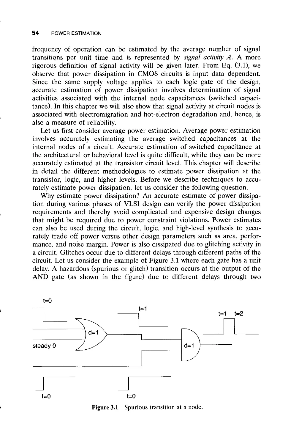
3.6 Sensitivity Analysis / 99
3.6.1 Power Sensitivity / 100
3.6.2 Power Sensitivity Estimation / 101
CONTENTS IX
3.6.3 Power Sensitivity Method to Estimate Minimum
and Maximum Average Power / 103
3.7 Power Estimation Using Input Vector Compaction / 108
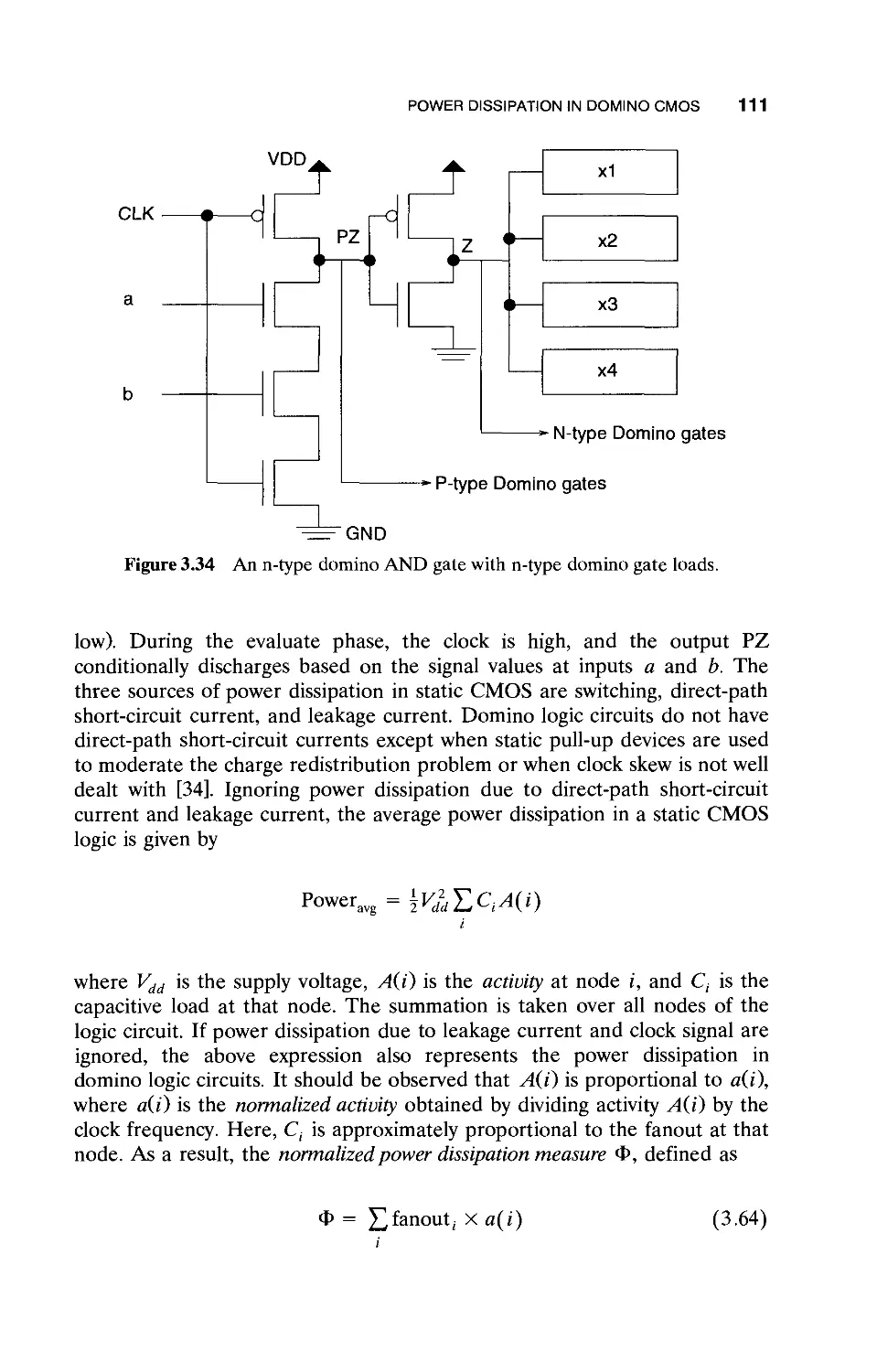
3.8 Power Dissipation in Domino CMOS / 110
3.9 Circuit Reliability / 113
3.10 Power Estimation at the Circuit Level / 116
3.10.1 Power Consumption of CMOS Gates / 116
3.11 High-Level Power Estimation / 119
3.12 Information-Theory-Based Approaches / 122
3.13 Estimation of Maximum Power / 125
3.13.1 Test-Generation-Based Approach / 126
3.13.2 Approach Using the Steepest Descent / 128
3.13.3 Genetic-Algorithm-Based Approach / 135
3.14 Summary and Conclusion / 136
References / 136
4 SYNTHESIS FOR LOW POWER 143
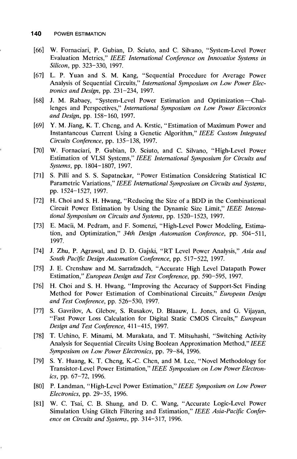
4.1 Behavioral Level Transforms / 144
4.1.1 Algorithm Level Transforms for Low Power / 144
4.1.2 Power-Constrained Least-Squares Optimization for
Adaptive and Nonadaptive Filters / 155
4.1.3 Circuit Activity Driven Architectural
Transformations / 158
4.1.4 Architecture-Driven Voltage Scaling / 161
4.1.5 Power Optimization Using Operation
Reduction / 163
4.1.6 Power Optimization Using Operation
Substitution / 164
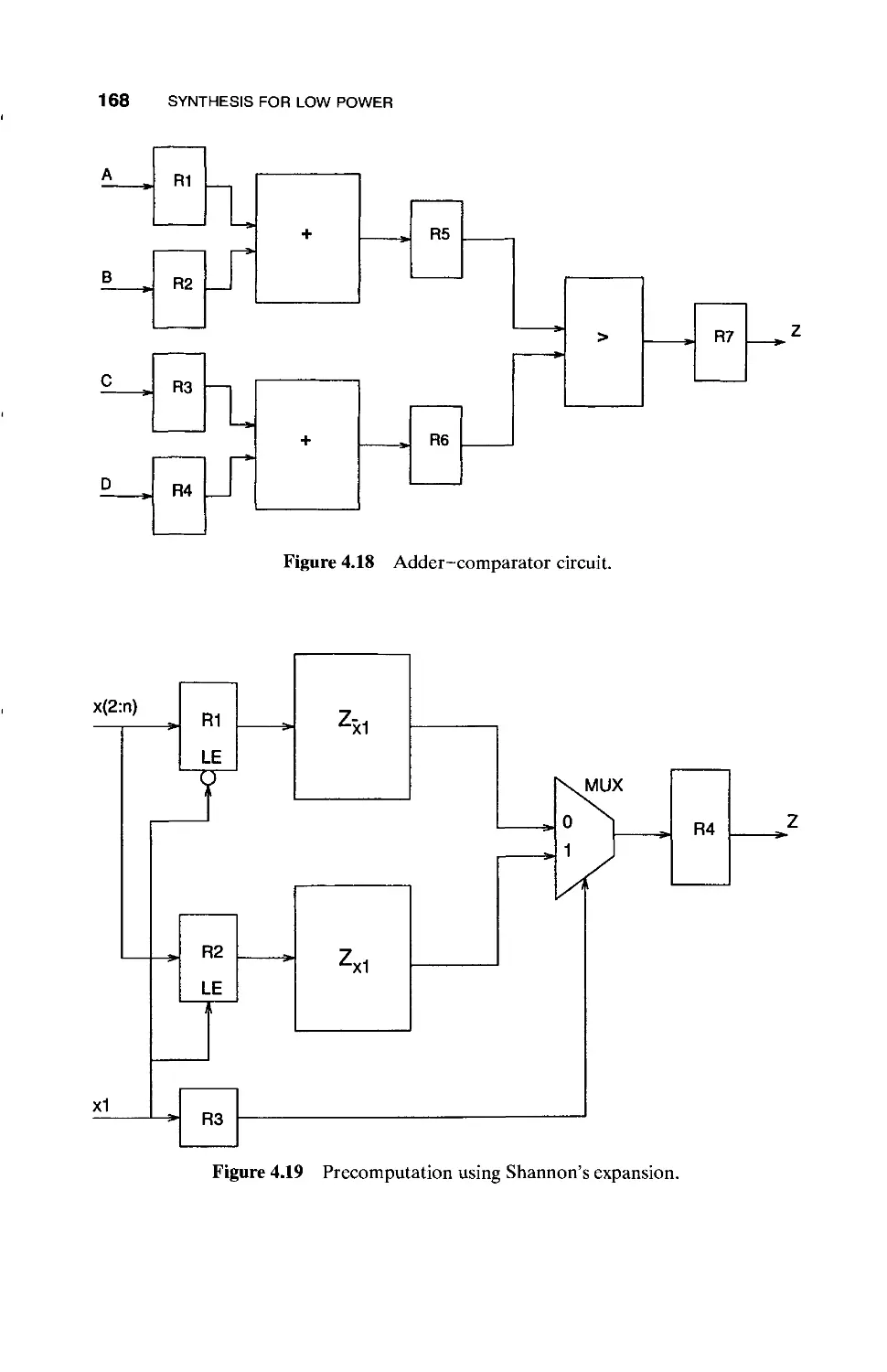
4.1.7 Precomputation-Based Optimization for Low
Power / 165
4.2 Logic Level Optimization for Low Power / 169
4.2.1 FSM and Combinational Logic Synthesis / 170
4.2.2 Technology Mapping / 183
4.3 Circuit Level / 185
4.3.1 Circuit Level Transforms / 186
4.3.2 CMOS Gates / 187
4.3.3 Transistor Sizing / 192
4.4 Summary and Future Directions / 194
References / 195
X CONTENTS
5 DESIGN AND TEST OF LOW-VOLTAGE CMOS CIRCUITS 201
5.1 Introduction / 201
5.2 Circuit Design Style / 203
5.2.1 Nonclocked Logic / 203
5.2.2 Clocked Logic Family / 207
5.3 Leakage Current in Deep Submicrometer
Transistors / 215
5.3.1 Transistor Leakage Mechanisms / 215
5.3.2 Leakage Current Estimation / 219
5.4 Deep Submicrometer Device Design Issues / 222
5.4.1 Short-Channel Threshold Voltage Roll-Off / 222
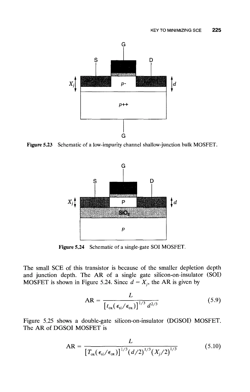
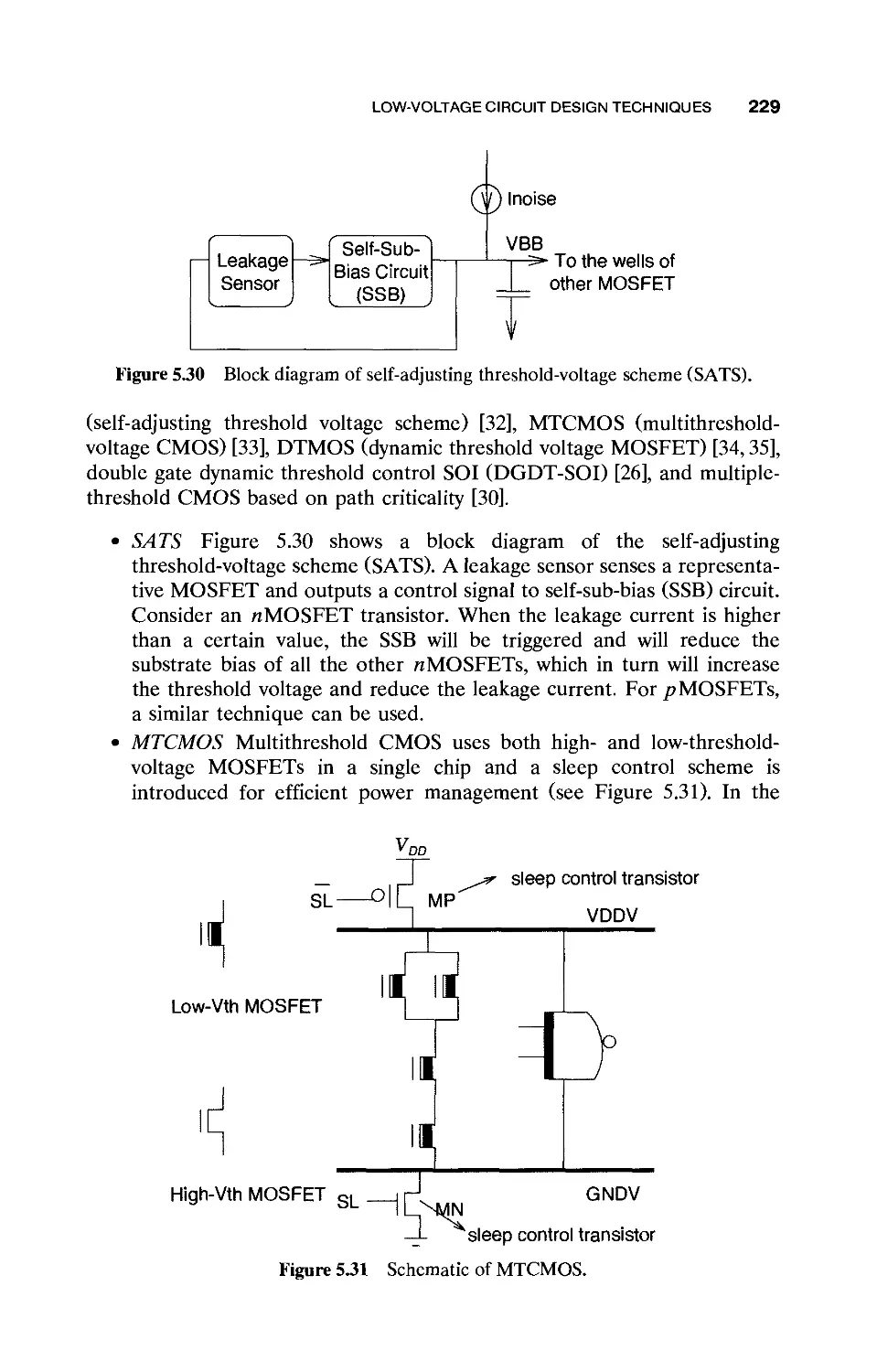
5.4.2 Drain-Induced Barrier Lowering / 224
5.5 Key to Minimizing SCE / 224
5.6 Low-Voltage Circuit Design Techniques / 226
5.6.1 Reverse Vgs / 226
5.6.2 Steeper Subthreshold Swing / 227
5.6.3 Multiple Threshold Voltage / 228
5.6.4 Multiple Threshold CMOS Based on Path
Criticality / 236
5.7 Testing Deep Submicrometer ICs with Elevated Intrinsic
Leakage / 240
5.8 Multiple Supply Voltages / 245
5.9 Conclusions / 249
References / 249
6 LOW-POWER STATIC RAM ARCHITECTURES 253
6.1 Introduction / 253
6.2 Organization of a Static RAM / 254
6.3 MOS Static RAM Memory Cell / 255
6.3.1 The 4T SRAM Cell / 256
6.3.2 The 6T SRAM Cell / 257
6.3.3 SRAM Cell Operation / 258
6.4 Banked Organization of SRAMs / 259
6.4.1 Divided Word Line Architecture / 260
6.5 Reducing Voltage Swings on Bit Lines / 260
6.5.1 Pulsed Word Lines / 261
6.5.2 Self-Timing the RAM Core / 261
CONTENTS XI
6.5.3 Precharge Voltage for Bit Lines / 262
6.6 Reducing Power in the Write Driver Circuits / 263
6.7 Reducing Power in Sense Amplifier Circuits / 265
6.8 Method for Achieving Low Core Voltages from a Single
Supply / 268
6.9 Summary / 269
References / 270
7 LOW-ENERGY COMPUTING USING ENERGY RECOVERY
TECHNIQUES 272
7.1 Energy Dissipation in Transistor Channel Using an RC
Model / 273
7.2 Energy Recovery Circuit Design / 277
7.3 Designs with Partially Reversible Logic / 280
7.3.1 Designs with Reversible Logic / 285
7.3.2 Simple Charge Recovery Logic Modified from
Static CMOS Circuits / 287
7.3.3 Adiabatic Dynamic Logic / 290
7.3.4 Energy Recovery SRAM Core / 293
7.3.5 Another Core Organization: Column-Activated
Memory Core / 296
7.3.6 Energy Dissipation in Memory Core / 298
7.3.7 Comparison of Two Memory Core
Organizations / 298
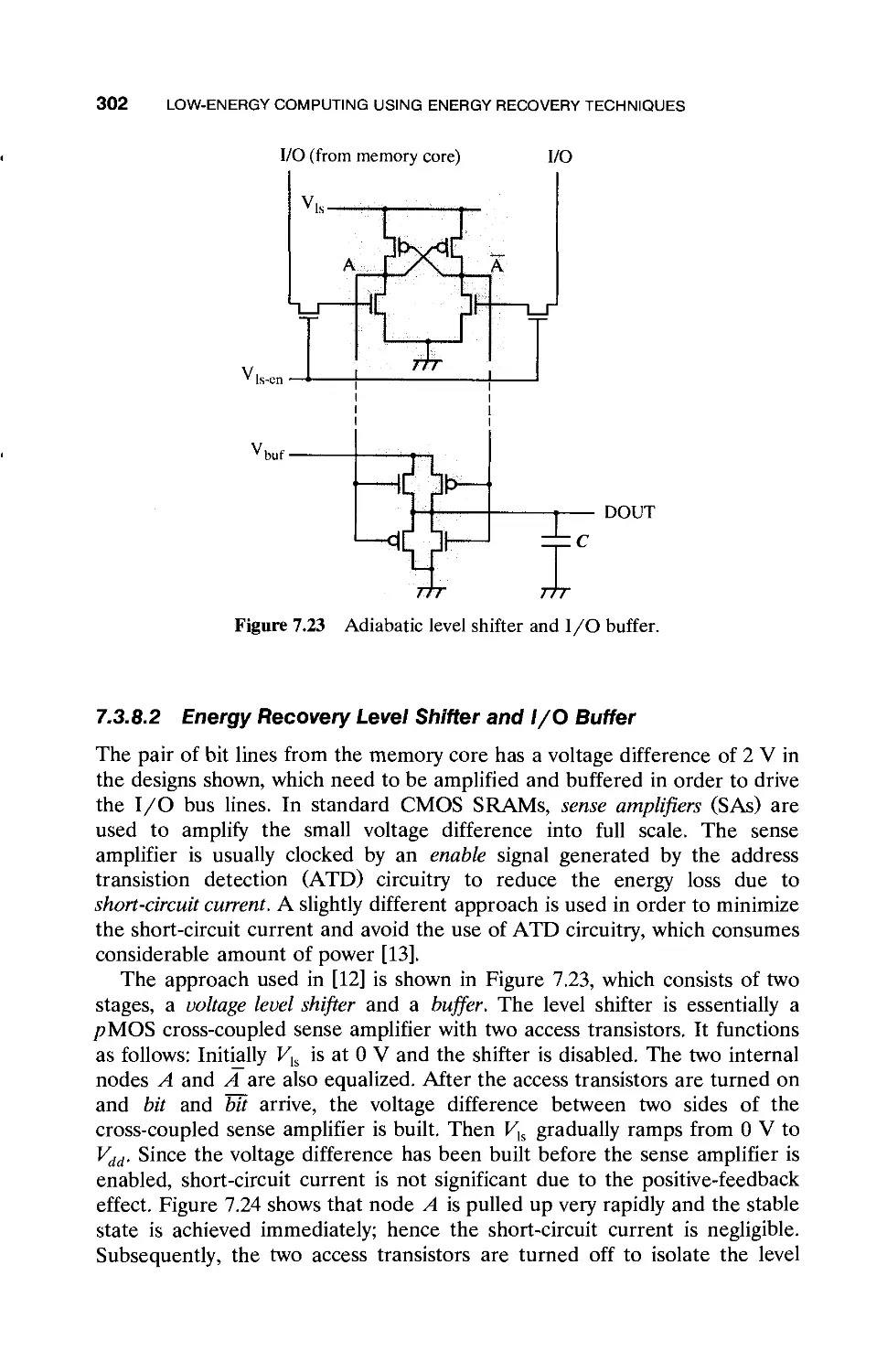
7.3.8 Design of Peripheral Circuits / 300
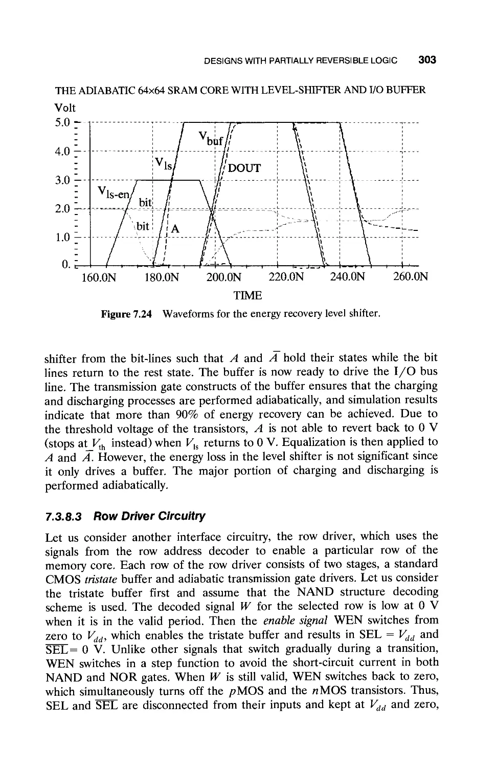
7.3.9 Optimal Voltage Selection / 304
7.4 Supply Clock Generation / 311
7.5 Summary and Conclusions / 319
References / 320
8 SOFTWARE DESIGN FOR LOW POWER 321
8.1 Introduction / 321
8.2 Sources of Software Power Dissipation / 322
8.3 Software Power Estimation / 324
8.3.1 Gate Level Power Estimation / 324
8.3.2 Architecture Level Power Estimation / 324
8.3.3 Bus Switching Activity / 325
8.3.4 Instruction Level Power Analysis / 325
XII CONTENTS
8.4 Software Power Optimizations / 329
8.4.1 Algorithm Transformations to Match
Computational Resources / 329
8.4.2 Minimizing Memory Access Costs / 332
8.4.3 Instruction Selection and Ordering / 339
8.4.4 Power Management / 341
8.5 Automated Low-Power Code Generation / 342
8.6 Codesign for Low Power / 344
8.6.1 Instruction Set Design / 345
8.6.2 Reconfigurable Computing / 346
8.6.3 Architecture and Circuit Level Decisions / 346
8.7 Summary / 346
References / 348
INDEX
351
PREFACE
The scaling of silicon technology has been ongoing for over forty years. We
are on our way to commercializing devices having a minimum feature size of
one-tenth of a micron. The push for miniaturization comes from the demand
for higher functionality and higher performance at a lower cost. As a result,
successively higher levels of integration have been driving up the power
consumption of chips. Today heat removal and power distribution are at the
forefront of the problems faced by chip designers.
In recent years portability has become important. Historically, portable
applications were characterized by low throughput requirements such as for a
wristwatch. This is no longer true. Among the new portable applications are
hand-held multimedia terminals with video display and capture, audio
reproduction and capture, voice recognition, and handwriting recognition
capabilities. These capabilities call for a tremendous amount of computational
capacity. This computational capacity has to be realized with very low power
requirements in order for the battery to have a satisfactory life span. This
book is an attempt to provide the reader with an in depth understanding of
the sources of power dissipation in digital CMOS circuits and to provide
techniques for the design of low-power circuit chips with high computational
capacity.
Chapter 1 is an introduction to the field of low power CMOS VLSI circuit
design.
In Chapter 2, the physics of power dissipation in MOSFET devices and
circuits is presented. Expressions for the different components of power
dissipation are derived. The emphasis is on submicron and deep-submicron
devices. Issues addressed include the short channel effects, for example, the
xiii
XIV PREFACE
threshold voltage shift and ways of combating undesirable consequences,
such as, increased leakage power. To conclude the chapter, limits on low
power CMOS technology are derived and ways of approaching those limits
are discussed.
Designing the multimillion transistor chips of today would be unthinkable
without appropriate computer design tools. The very first computer design
tool for low power design have to be power estimators. Power estimation is
the subject of Chapter 3. Both average and maximum power estimates are
considered. Conventional circuit simulation techniques as well as pattern
independent probabilistic techniques are presented. The problem of power
estimation in combinatorial logic circuits is difficult owing to spatial
correlation among internal signals. The problem of power dissipation in sequential
logic circuits is even more difficult owing to the presence of temporal
correlation in addition to the spatial correlation.
Computer-aided design (CAD) tools are also widely used to automatically
design circuits with gates in an ASIC library. A desired circuit is specified at
the register transfer level (RTL) or even the behavioral level. Automatic tools
are then used, quite often in an iterative loop, to generate a technology
independent logic gate realization to map the circuit to a specific technology
library, and finally to optimize the technology mapped circuit. Impressive
progress has been made in making these tools account for power dissipation
and produce more power-efficient designs. Tools for the automatic synthesis
of low power CMOS circuits is the subject of Chapter 4. Besides the tools,
the libraries themselves need to be optimized to reduce power dissipation.
Towards this goal, new circuit styles have been developed and existing ones
improved.
As lowering the supply voltage is a very effective way of lowering power
dissipation, Chapter 5 is devoted to the design and test of low-voltage
circuits. A large part of designing a low-voltage device is controlling leakage
currents. Chapter 5 includes a detailed discussion on controlling leakage
currents.
While some of the developments addressing circuit styles can be called
incremental, this does not include adiabatic or charge recovery circuits.
Adiabatic circuits are considered in Chapter 6. During an adiabatic process
no loss or gain of heat occurs. A quasi-adiabatic process approximates this
ideal. That very low energy computation could be possible using quasi-
adiabatic circuits follows from the second law of thermodynamics. The law
states that the entropy of a closed system remains unchanged or increases if
the thermodynamic processes in the system proceed from one equilibrium
state to another. In a computational process, only the steps that destroy
information and increase disorder are subject to a lower limit on energy
dissipation. Hence quasi-adiabatic circuits hold the promise of lower energy
consumption than the limits that the law imposes on conventional non-
adiabatic processes.
Chapter 7 focuses on the design of low power static random-access
memory (SRAM). Common forms of storage cells for SRAM are presented.
PREFACE XV
Then common design and architectural techniques for minimizing power are
described. The chapter concludes by presenting a model for quantifying the
various components of power dissipation in SRAM.
Chapter 8 looks at how the power dissipation of a system comprised of
software as well as hardware components can be reduced. In any system, all
of its modules may not be in use at all times. System power management is a
general term used to refer to a set of techniques that exploit this fact to
minimize power consumption. Modules of a system that are temporarily not
in use can have the supply to them turned off or the clock stopped.
In any system based on a stored-program processor, it is the program that
directs much of the activity of the hardware. Consequently, besides the
hardware, the program or the software can have a significant impact on the
power dissipation of such a system. The power dissipation model of a typical
application program is described. A variety of software power optimization
techniques are then presented. The chapter also highlights the difference
between power and energy consumption.
This book had its beginning while both authors were at the erstwhile VLSI
Design Laboratory at Texas Instruments (TI), Incorporated. We thank our
colleagues at TI, as well Purdue University, Samsung Telecommunications
America and Cisco Systems for encouragement and support. The book is a
result of nearly eight years of work at Texas Instruments and Purdue
University. We would like to thank the graduate students at Purdue who
helped form the foundations of many of the Chapters—Liqiong Wei, Dinesh
Somasekhar, Khurram Muhammad, Zhanping Chen, Tan-Li Chou, Mark
Johnson, Chuan-Yu Wang, Yibin Ye, Priya Patil, N. Sankarayya, Hendrawan
Soeleman, Sheldon Zhang, Shiyou Zhao, Rongtian Zhang, Magnus
Lundberg, and Ali Keshavarzi. We would also like to thank Rwitti Roy for
spending hours reading and correcting the manuscript. We have tried to give
appropriate credit to the sources that we have used. We offer apologies for
any omissions. Any omission is unintentional and we take full blame for it.
All the pieces of our work that we have chosen to include in this book have
been published in refereed journals or conferences. We thank the staff of
Wiley Interscience and our editor for having patience as we made progress
through this book at a highly varying rate. Writing a book while holding down
full-time positions invariably leads to trading off some leisure and family time
for time at the keyboard. We thank members of our family for being
supportive.
Kaushik Roy
Sharat Prasad
May 1999
CHAPTER 1
LOW-POWER CMOS VLSI DESIGN
1.1 INTRODUCTION
Arguably, invention of the transistor was a giant leap forward for low-power
microelectronics that has remained unequaled to date, even by the virtual
torrent of developments it forbore. Operation of a vacuum tube required
several hundred volts of anode voltage and few watts of power. In
comparison the transistor required only milliwatts of power. Since the invention of
the transistor, decades ago, through the years leading to the 1990's, power
dissipation, though not entirely ignored, was of little concern. The greater
emphasis was on performance and miniaturization. Applications powered by
a battery—pocket calculators, hearing aids, implantable pacemakers, portable
military equipment used by individual soldier and, most importantly, wrist-
watches—drove low-power electronics. In all such applications, it is
important to prolong the battery life as much as possible. And now, with the
growing trend towards portable computing and wireless communication,
power dissipation has become one of the most critical factors in the
continued development of the microelectronics technology. There are two reasons
for this:
I. To continue to improve the performance of the circuits and to
integrate more functions into each chip, feature size has to continue to
shrink. As a result the magnitude of power per unit area is growing
and the accompanying problem of heat removal and cooling is
worsening. Examples are the general-purpose microprocessors. Even with the
scaling down of the supply voltage from 5 to 3.3 and then 3.3 to 2.5 V,
1
2 LOW-POWER CMOS VLSI DESIGN
power dissipation has not come down. A plateau at about 30 W,
possibly as a consequence of the escalating packaging and cooling costs
for power densities of the order of 50 W/cm2 [1], seems to have been
reached. If this problem is not addressed, either the very large cost and
volume of the cooling subsystem or curtailment in the functionality will
have to be accepted.
II. Portable battery-powered applications of the past were characterized
by low computational requirement. The last few years have seen the
emergence of portable applications that require processing power up
until now. Two vanguards of these new applications are the notebook
computer and the digital personal communication services (PCSs).
People are beginning to expect to have access to same computing
power, information resources, and communication abilities when they
are traveling as they do when they are at their desk. A representative
of what the very near future holds is the portable multimedia terminal.
Such terminals will accept voice input as well as hand-written (with a
special pen on a touch-sensitive surface) input. Unfortunately, with the
technology available today, effective speech or hand-writing
recognition requires significant amounts of space and power. For example, a
full board and 20 W of power are required to realize a 20,000-word
dictation vocabulary [1]. Conventional nickel-cadmium battery
technology only provides a 26 W of power for each pound of weight [2-4].
Once again, advances in the area of low-power microelectronics are
required to make the vision of the inexpensive and portable
multimedia terminal a reality.
As a result, today, in the late 1990s, it is widely accepted that power
efficiency is a design goal at par in importance with miniaturization and
performance. In spite of this acceptance, the practice of low-power design
methodologies is being adopted at a slow pace due to the widespread
changes called for by these methodologies. Minimizing power consumption
calls for conscious effort at each abstraction level and at each phase of the
design process.
1.2 SOURCES OF POWER DISSIPATION
There are three sources of power dissipation in a digital complementary
metal-oxide-semiconductor (CMOS) circuit. The first source are the logic
transitions. As the "nodes" in a digital CMOS circuit transition back and
forth between the two logic levels, the parasitic capacitances are charged
and discharged. Current flows through the channel resistance of the
transistors, and electrical energy is converted into heat and dissipated away. As
suggested by this informal description, this component of power dissipation is
DESIGNING FOR LOW POWER 3
proportional to the supply voltage, node voltage swing, and the average
switched capacitance per cycle. As the voltage swing in most cases is simply
equal to the supply voltage, the dissipation due to transitions varies overall as
the square of the supply voltage. Short-circuit currents that flow directly from
supply to ground when the n-subnetwork and the p-subnetwork of a CMOS
gate both conduct simultaneously are the second source of power dissipation.
With input(s) to the gate stable at either logic level, only one of the two
subnetworks conduct and no short-circuit currents flow. But when the output
of a gate is changing in response to change in input(s), both subnetworks
conduct simultaneously for a brief interval. The duration of the interval
depends on the input and the output transition (rise or fall) times and so
does the short-circuit dissipation. Both of the above sources of power
dissipation in CMOS circuits are related to transitions at gate outputs and
are therefore collectively referred to as dynamic dissipation. In contrast, the
third and the last source of dissipation is the leakage current that flows when
the input(s) to, and therefore the outputs of, a gate are not changing. This is
called static dissipation. In current day technology the magnitude of leakage
current is low and is usually neglected. But as the supply voltage is being
scaled down to reduce dynamic power, MOS field-effect transistors
(MOSFETs) with low threshold voltages have to be used. The lower the
threshold voltage, the lower the degree to which MOSFETs in the logic gates
are turned off and the higher is the standby leakage current.
1.3 DESIGNING FOR LOW POWER
The power dissipation attributable to the three sources described above can
be influenced at different levels of the overall design process.
Since the dominant component of power dissipation in CMOS circuits
(due to logic transitions) varies as the square of the supply voltage, significant
savings in power dissipation can be obtained from operation at a reduced
supply voltage. If the supply voltage is reduced while the threshold voltages
stay the same, reduced noise margins result. To improve noise margins, the
threshold voltages need to be made smaller too. However, the subthreshold
leakage current increases exponentially when the threshold voltage is
reduced. The higher static dissipation may offset the reduction in
transitions component of the dissipation. Hence the devices need to be designed
to have threshold voltages that maximize the net reduction in the
dissipation.
The transitions component of the dissipation also depends on the
frequency or the probability of occurrence of the transitions. If a high
probability of transitions is assumed and correspondingly low supply and threshold
voltages chosen, to reduce the transitions component of the power
dissipation and provide acceptable noise margins, respectively, the increase in the
4 LOW-POWER CMOS VLSI DESIGN
static dissipation may be large. As the supply voltage is reduced, the
power-delay product of CMOS circuits decreases and the delays increase
monotonically. Hence, while it is desirable to use the lowest possible supply
voltage, in practice only as low a supply voltage can be used as corresponds to
a delay that can be compensated by other means, and steps can be taken to
retain the system level throughput at the desired level.
One way of influencing the delay of a CMOS circuit is by changing the
channel-width-to-channel-length ratio of the devices in the circuit. The
power-delay product for an inverter driving another inverter through an
interconnect of certain length varies with the width-to-length ratio of the
devices. If the interconnect capacitance is not insignificant, the power-delay
product initially decreases and then increases when the width-to-length ratio
is increased and the supply voltage is reduced to keep the delay constant.
Hence, there exists a combination of the supply voltage and the width-
to-length ratio that is optimal from the power-delay product
consideration.
The way to assure that the system level throughput does not degrade as
supply voltage is reduced is by exploiting parallelism and pipelining. Hence
as the supply voltage is reduced, the degree of parallelism or the number of
stages of pipelining is increased to compensate for the increased delay. But
then the latency increases. Overhead control circuitry also has to be added.
As such circuitry itself consumes power, there exists a point beyond which
power, rather than decreasing, increases. Even so, great reductions in power
dissipation by factors as large as 10, have been shown to be obtainable
theoretically [4] as well as in practice [5].
Phenomena that were nonexistent or insignificant earlier are important
issues in the submicrometer regime. One of these, the hot-carrier effect, is
exhibited when feature size is scaled down while keeping the supply voltage
constant. High electric fields result and cause the devices to degrade:
Threshold voltages increase, transconductance decreases, and subthreshold
currents increase. One solution is to use the lightly doped drain (LDD)
structure. As the LDD structure exhibits higher series parasitic resistance, an
optimum supply voltage again exists. For larger values of supply voltage, the
delay increases. The occurrence of velocity saturation in submicrometer
devices makes delay relatively independent of supply voltage [6]. Hence, for
not too large a delay penalty, reducing the supply voltage can reduce power
dissipation.
As more circuit can be accommodated per unit area, off-chip
input-output (I/0)-power may become the dominant power-consuming function [7]
unless a significant amount of memory [usually static random-access memory
(RAM) and in some cases dynamic RAM] and analog functions are
integrated on-chip.
The analog functions may require only 5% of the total transistors but
present a complex circuit design and technology challenge. Perhaps a
novel substrate technology such as silicon on insulator (SOI) with its much
CONCLUSIONS 5
better crosstalk characteristics [8] will enable easier integration of analog and
digital circuits.
Circuit level choices also impact the power dissipation of CMOS circuits.
Usually a number of approaches and topologies are available for
implementing various logic and arithmetic functions. Choices between static versus
dynamic style, pass-gate versus normal CMOS realization versus
asynchronous circuits have to be made.
At the logic level, automatic tools can be used to locally transform the
circuit and select realizations for its pieces from a precharacterized library so
as to reduce transitions and parasitic capacitance at circuit nodes and
therefore circuit power dissipation. At a higher level various structural
choices exist for realizing any given logic functions; for example for an
adder one can select one of ripple-carry, carry-look-ahead, or carry-select
realizations.
In synchronous circuits, even when the outputs computed by a block of
combinatorial logic are not required, the block keeps computing its outputs
from observed inputs every clock cycle. In order to save power, entire
execution units comprising of combinatorial logic and their state registers can
be put in stand-by mode by disabling the clock and/or powering down the
unit. Special circuitry is required to detect and power-down unused units and
then power them up again when they need to be used.
The rate of increase in the total amount of memory per chip as well as
rate of increase in the memory requirement of new applications has more
than kept pace with the rate of reduction in power dissipation per bit of
memory. As a result, in spite of the tremendous reductions in power
dissipation obtained from each generation of memory to the next, in many
applications, the major portion of the instantaneous peak-power dissipation
occurs in the memory.
In case of dynamic RAM (DRAM) memory, the most effective way to
reduce power of any memory size is to lower the voltage and increase the
effective capacitance to maintain sufficient charge in the cell. The new array
organizations introduced recently [9] present many possibilities of lowering
the power. A far greater challenge at this point in time is to get to the next
generation of memory chips with a capacity of 4 Gb. At the 1-Gb generation,
there is no design margin remaining after the required bit area is subtracted
from the available bit area. The implications are that it may not be possible
to implement the capacitor-and-transistor cell for the 4 Gb memory in the
conventional folded bit line architecture.
1.4 CONCLUSIONS
This chapter was an aerial view of the designing low-power CMOS circuits
landscape. The motivations and challenges were emphasized. In the following
chapters, we will return to these topics again and address them in detail.
6 LOW-POWER CMOS VLSI DESIGN
REFERENCES
[1] J. M. C. Stork, "Technology Leverage for Ultra-Low Power Information Systems,"
Proc. IEEE, vol. 83, no. 4, 1995.
[2] T. Bell, "Incredible Shrinking Computers," IEEE Spectrum, pp. 37-43, May
1991.
[3] B. Eager, "Advances in Rechargeable Batteries Pace Portable Computer
Growth," paper presented at the Silicon Valley Computer Conference, 1991, pp.
693-697.
[4] A. P. Chandrakashan, "Low Power CMOS Digital Design," IEEE. J. Solid State
Circuits, vol. 27, no. 4, pp. 473-483, 1992.
[5] A. P. Chandrakashan et al., "A Low Power Chipset for Portable MultiMedia
Applications," Proc. IEEE ISSCC, pp. 82-83, 1994.
[6] H. K. Bakoglu, Circuits, Interconnections and Packaging for VLSI, Addison-
Wesley, Reading, MA, 1990.
[7] D. K. Liu and C. Svensson, "Power Consumption Estimation in CMOS VLSI
Chips," IEEE J. Solid State Circuits, vol. 29, pp. 663-670, 1994.
[8] R. B. Merrill et al., "Effect of Substrate Material on Crosstalk in Mixed
Analog/Digital Circuits," IEDM Dig. Tech. Papers, pp. 433-436, 1994.
[9] M. Takada, "Low Power Memory Design," IEDM Short Course Program, 1993.
CHAPTER 2
PHYSICS OF POWER DISSIPATION
IN CMOS FET DEVICES
2.1 INTRODUCTION
This chapter begins with a study of the physics of small geometry MOSFET
devices. Many phenomena that are absent in larger geometry devices occur in
submicrometer devices and greatly affect performance and power
consumption. These phenomena and ways of combating their undesirable effects are
described. We begin with the metal-insulator-semiconductor (MIS)
structure in Section 2.2.1. Analytical expressions for the threshold voltage of a
MIS diode, the depth of the depletion region, the quanta of charges in the
inversion layer, and the thickness of the inversion layer are derived. Section
2.2.2 considers the long-channel MOSFET. Impact of the body effect on the
threshold voltage is analyzed. A model of the subthreshold behavior of
MOSFETs is presented and used to estimate the subthreshold current. The
important device characteristic called the subthreshold swing is introduced.
Many phenomena, which are absent in larger geometry devices, occur in
sub-micron devices and greatly affect several aspects of their performance
including their power consumption. These phenomena and ways of
combating their undesirable effects are described in this section. In Section 2.2.3, a
model of the submicrometer MOSFETs based on drain-induced barrier
lowering is used to study the shift in the threshold voltage due to the short-channel
effect. Other submicrometer phenomena—narrow-gate-width effects, substrate
bias dependence, and the reverse short-channel effects—are studied in
following sections. Section 2.2.3.2 discusses the subsurface punchthrough and ways
of preventing it.
7
8 PHYSICS OF POWER DISSIPATION IN CMOS FET DEVICES
1
:
r
X
Metal
\ 'y
Insulator \
_. /
1
Figure 2.1 The MIS structure.
This study of the physics of MOSFET devices prepares us for the second
section, which examines various components of overall power consumption in
CMOS very large scale integrated (VLSI) circuit chips. The final section of
the chapter derives limits on how far we may be able to lower the power
consumption and discusses ways of approaching those limits.
2.2 PHYSICS OF POWER DISSIPATION IN MOSFET DEVICES
2.2.1 The MIS Structure
The stability and reliability of all semiconductor devices are intimately
related to their surface conditions. Semiconductor surface conditions heavily
influence even the basic working of some devices (e.g., the MOSFET). The
MIS structure, besides being a device (a voltage variable capacitor and a
diode), is an excellent tool for the study of semiconductor surfaces. In this
section the ideal MIS diode will be discussed. Nonideal characteristics will be
briefly introduced at the end of the section.
Figure 2.1 shows the MIS structure. A layer of thickness d of insulating
material is sandwiched between a metal plate and the semiconductor
substrate. For the present discussion, let the semiconductor be of p-type. A
voltage V is applied between the metal plate and the substrate. Let us first
consider the case when V = 0. As we are considering an ideal MIS diode, the
energy difference <f>ms between the metal work function1 4>m and the semi-
'The work function is defined as the minimum energy necessary for a metal electron in a
metal-vacuum system to escape into the vacuum from an initial energy at the Fermi level. In a
metal-semiconductor system, the metal work function may still be used but only with the
free-space permittivity e0 replaced by the permittivity es of the semiconductor medium.
PHYSICS OF POWER DISSIPATION IN MOSFET DEVICES 9
q<t>n
///////////
Vacuum level
qx
V2„
<M
ivy.?
77777777777777 e„
d
Metal Insulator Semiconductor
Figure 2.2 Energy bands in an unbiased MIS diode.
conductor work function is zero, that is,
<t>ms = <t>m ~ I X + ~ + <Afl
(2.1)
where x is tne semiconductor electron affinity,2 Eg the band gap, <$>B the
potential barrier3 between the metal and the insulator, and \pB the potential
difference between the Fermi level EF and the intrinsic Fermi level Er
Furthermore, in an ideal MIS diode the insulator has infinite resistance and
does not have either mobile charge carriers or charge centers. As a result, the
Fermi level in the metal lines up with the Fermi level in the semiconductor.
The Fermi level in the metal itself is same throughout (consequence of the
assumption of uniform doping). This is called the flat-band condition as in
the energy band diagram, the energy levels Ec, Eu, and Et appear as straight
lines (Figure 2.2).
When the voltage V is negative, the holes in the p-type semiconductor are
attracted to and accumulate at the semiconductor surface in contact with the
insulator layer. Therefore this condition is called accumulation. In the
absence of a current flow, the carriers in the semiconductor are in a state of
equilibrium and the Fermi level appears as a straight line. The
Maxwell-Boltzmann statistics relates the equilibrium hole concentration to
the intrinsic Fermi level:
Pa
«: e
{Et-EF)/kT
(2.2)
The electron affinity of a semiconductor is the difference in potential between an electron at
the vacuum level and an electron at the bottom of the conduction band.
• The barrier height is simply the difference between the metal work function and the electron
affinity of the semiconductor.
10 PHYSICS OF POWER DISSIPATION IN CMOS FET DEVICES
////////
-Ec
E.
^
V7777777777 ev
Metal Insulator Semiconductor
Figure 2.3 Energy bands when a negative bias is applied.
So the intrinsic Fermi level has a higher value at the surface than at a point
deep in the substrate and the energy levels Ec, Eu, and £, bend upward near
the surface (Figure 2.3). The Fermi level EF in the semiconductor is now
— qV below the Fermi level in the metal gate.
When the applied voltage V is positive but small, the holes in the p-type
semiconductor are repelled away from the surface and leave negatively
charged acceptor ions behind. A depletion region, extending from the surface
into the semiconductor, is created. This is the depletion condition. Besides
repelling the holes, the positive voltage on the gate attracts electrons in the
semiconductor to the surface. The surface is said to have begun to get
inverted from the original p-type to n-type. While V is small, the
concentration of holes is still larger than the concentration of electrons. This is the
weak-inversion condition and is important to the study of power dissipation in
MOSFET circuits. The bands at this stage bend downward near the surface
(Figure 2.4).
If the applied voltage is increased sufficiently, the bands bend far enough
that level Et at the surface crosses over to the other side of level EF. This is
///////A
Metal
■Ec
E.
,7777777777777 Ev
Insulator Semiconductor
Figure 2.4 Energy bands when a small positive bias is applied.
PHYSICS OF POWER DISSIPATION IN MOSFET DEVICES 11
7777777A
Metal
^
Ec
E,
EF
7777777777 Ev
Insulator Semiconductor
Figure 2.5 Energy bands in strong inversion.
brought about by the tendency of carriers to occupy states with the lowest
total energy. The kinetic energy of electrons is zero when they occupy a state
at the bottom edge of the conduction band. In the present condition of
inversion the level Et bends to be closer to level Ec and electrons outnumber
holes at the surface. The electron density at the surface is still smaller than
the hole density deep inside the semiconductor. When V is increased to the
extent that the electron density at the surface ns becomes greater than the
hole density (~ NA, the concentration of acceptor impurities) in the bulk,
onset of strong inversion is said to have occurred. This condition is depicted
in Figure 2.5. As we will see in the following section, Et at the surface now is
below EF by an amount of energy equal to 2i/ffl, where \\iB is the potential
difference between the Fermi level EF and the intrinsic Fermi level £, in the
bulk. The value of V necessary to reach the onset of strong inversion is called
the threshold voltage.
2.2.1.1 Surface Space Charge Region and the Threshold Voltage
In this section we will build a mathematical model of the MIS diode. This
model is known as the charge-sheet model [1,2]. Unlike the simpler model [3]
based on the depletion approximation that is accurate only in the strong-
inversion and beyond regions of operation, the charge-sheet model remains
valid in the weak-inversion and preceding regions of operation. The latter
regions are important when power dissipated in submicrometer MOSFETs
is considered.
We begin with the Poisson equation
V- D = p(x,y,z)
(2.3)
where D, the electric displacement vector, is equal to ssE under low-frequency
or static conditions; es is the permittivity of Si; E the electric field vector;
and p(x, y, z) the total electric charge density. In a MIS diode the electric
12
PHYSICS OF POWER DISSIPATION IN CMOS FET DEVICES
Insulator
I
q<l>B
I
Semiconductor
<?#•
Ei
EF
Ev
Figure 2.6 Energy bands at the insulator-semiconductor surface.
field due to the applied voltage is normal to the insulator (Si02). If the
fringing fields at the edges are neglected, the variation of the electrostatic
potential </> can be considered to be only along the x axis (Figure 2.6), that is,
E„
d<f>
E2 = — = 0
dz
Noting that p(x) = q X [p(x) - n(x) + ND(x) - NA{x)], (2.3) is
transformed to
d2(j> q
-£2 = —(Pp ~ np + ND - NA)
(2.4)
where ND is the concentration of donor impurities, A^ the concentration of
acceptor impurities, n the mobile electron density, and pp the mobile hole
density. The subscript p is to emphasize that p-type semiconductor is being
considered. The two carrier densities at a point x are related to the intrinsic
carrier density «,, Fermi potential <j)F, and the electrostatic potential <j>(x)
according to Boltzmann statistics:
pp(x) =/!,. g«("(*)-*,)/*r
np(x) =n.g«(*(*)-*,)/*r
(2.5)
(2.6)
The Fermi potential <j>F corresponds to the Fermi energy level EF(= —q<f>F).
Electrostatic potential is a relative quantity. In the following discussion we
measure electrostatic potential relative to the potential which corresponds to
the intrinsic Fermi energy level in the bulk E;(x = °°), that is, the absolute
value of (j>(x) = <j>(x) + <j>(°°). We will denote the equilibrium hole and
electron densities in the bulk by pp°( = pp(°°) = «, exp q[<j)F - <j>(°°)]/kT) and
no, respectively. Simplifying the right-hand sides of (2.5) and (2.6),
substituting in (2.4), multiplying both sides of the resulting equation by 2d<j>/dx,
PHYSICS OF POWER DISSIPATION IN MOSFET DEVICES 13
rearranging, and integrating from a point deep in the bulk to an arbitrary
point x [4], we get
[X d<f> d2<f> rx d I dcf> \
'^ dx dx2 •'oo dx\ dx J
= /*2—(PpB eWkT - V e^x)/kT + ND- NA) d<!>
(2.7)
At relatively elevated temperatures, most of the donors and acceptors are
ionized. So pa ~ NA and npo ~ ND = n2/NA. Assuming Boltzmann statistics,
np» = «, e'V** = /y e~2W\ where )3 = kT/q. Then
d(f> 2qNA \e'^ 1 , e^ l\
dx y ' V ^ V >3 >3 \ |8 V j8/
(2.8)
The electric field at the surface E^ can be obtained by substituting for </> the
value of the potential at the surface (j>s. To determine the total charges in the
semiconductor Qs, we make use of Gauss's law and obtain
2qesNA
Qs = esEs = - y -^-LJL Je-e*- + M, - 1 + e-W'ie"- - fty, - 1)
(2.9)
Since <j)(x = °°) = 0, part of the applied voltage V appears across the
insulator and the remaining across the semiconductor, or
i, j. j. Q* J. Q*d J.
v = h + h = — + <k = — + &
C, et
where C,, et, and d are the capacitance, permittivity, and thickness of the
insulator. At the onset of strong inversion (f>s = 2<j)B, and so
QXstrong inversion) X d
VT = — + 24>B (2.10)
Or,
2d ,
VT = —yJqesNA<t>B{l - e~2e+«) + 2<j>B (2.11)
14 PHYSICS OF POWER DISSIPATION IN CMOS FET DEVICES
The assumptions made to facilitate the derivation of the expression for the
threshold voltage are never strictly true. In particular, the work function
difference <f>ms is never zero and there may be charges present in the
insulator or at the insulator-semiconductor boundary. The latter include
mobile ionic charges, fixed oxide charges, interface trap charges, and oxide
trap charges. Let QT be the effective net charge per unit area. The total
voltage needed to offset the effect of nonzero work function difference and
the presence of the charges is referred to as the flat-band voltage VFB. Hence,
QTd
VrB = Ks (2-12)
Ei
The voltage V that must be applied to reach the onset of strong inversion
must include the flat-band voltage as well. Therefore
2d ,
VT =VFB + — y/qe.N^il-e-2^) + 2<f>B (2.13)
Ei
2.2.1.2 Depth of Depletion Region
The MIS structure is in the depletion condition when a small positive bias V
is applied between the metal plate and the semiconductor bulk. The inversion
condition exists when V is large enough as to attract enough minority carriers
(electrons) to the surface that their density exceeds the free-hole density in
the bulk. It is once again assumed that the semiconductor region is uniformly
doped. Two additional simplifying assumptions are invoked. The depletion
assumption allows us to regard the depletion region as being completely
devoid of mobile charges. In the inversion condition the attracted minority
carriers are all assumed to be in a very thin inversion layer near the
semiconductor surface. The one-sided abrupt-junction assumption allows us to
regard that the carrier concentrations abruptly change to their intrinsic
values at a distance W beneath the surface, where W is the depth of the
depletion region. The exponential relation (as we will see shortly) between
the total charge in the semiconductor Qc and d requires negligible increase
in d in order to balance the increased charge on the metal when V is
increased beyond the onset of strong inversion. Hence it is assumed that d
reaches a maximum value of Wm and does not increase further. Similarly the
potential at the surface <j>s does not increase beyond 2<j)B.
Once again we start with the Poisson equation
d2<j) q
^T = —(pp-np+ND-NA)
The assumptions above and the fact that ND = 0 in p-type semiconductor
PHYSICS OF POWER DISSIPATION IN MOSFET DEVICES 15
allow us to simplify the above to
d2(f)
Ik1
qNA
— 0<x<d ,„_
ss (2.14)
,0 x ^ d
Integrating twice and applying boundary conditions <f>(x = 0) = <j>s and
<t>(x =W) = 0 yields
<t>(x) = 4>,[l - ^) (2.15)
Therefore,
Solving for W,
2<t>S 9
± qNA
w2
2<l>ses
qNA
When W = Wm, 4>s = 2<f>B. Therefore,
W (2.16)
"'--'/ W (217)
2.2.1.3 Charge in the Inversion Layer
In a previous section Qs, the total charge in the semiconductor, was seen to
depend on the parameters of the MIS structure according to the following
relation:
2qesNA
Qs = esEs =-]j -^Y~ je'13*- + M, ~ 1 + e-2»+°(ee+- - M, - l)
(2.18)
In this section we will determine the charge in the depletion region due to
the ionized atoms left behind when the holes are repelled away by the
positive potential on the metal and, in turn, the charge in the inversion layer.
The inversion of the semiconductor surface does not begin until (f>s > <j>B.
For the range of doping concentrations used in MOSFETs and for the range
of temperatures of interest, 9 <, f5<j)B < 16, the other terms in (2.20) are
negligible in comparison with the second and the fourth terms and can be
16 PHYSICS OF POWER DISSIPATION IN CMOS FET DEVICES
dropped. Thus,
Qs = \l 2-3f^A- M, + <"*'-2M (2-19)
Now the charge per unit area in the semiconductor Qs is the sum of the
charge per unit area in the inversion layer Qt and the charge per unit area in
the depletion region Qd. The charge in the depletion region is due to the
acceptor atoms using an extra electron to complete their covalent bonds.
Therefore,
Qd = qNAW= yl2qesNA<i>s (2.20)
From (2.21) and (2.22),
Qi = QS-Qd- ^fiq^\ \j — ~a yfa\ (2.21)
We noted above that, in the desired range of values of parameters,
exp(-/3<k) <sc 1 < (5<j)s. Then in weak inversion, where <f>s < 2<j)B, /3<^ >
e0(<k~2 4>fl) an(j usjng tne fjrst ^g terms in the Taylor series expansion about
eP(<t>s-2<t>B) _ Q
1
v/^ + e^-2^» = Jm; + _=g«*.-2*») (2.22)
Substituting in (2.23),
Q = V h ,a eMi-24,B) (2.23)
2.2.1.4 Inversion Layer Thickness
As the next step, we will derive an approximation for the thickness of the
inversion layer. This is done by assuming that the charge density in the
inversion layer is much higher than the density of ionic charge in the bulk
and that the inversion layer is very thin. Thus dEx/dx in the inversion layer
is much greater than in the bulk. Here, Ex/dx can be approximated by
considering the value of the electric field at the bottom edge of the inversion
layer to be zero (Figure 2.7).
The concentration of electrons at some point in the semiconductor is
exponentially dependent upon the potential, with the exponential constant
being /3 = kT/q. This implies that the majority of the charge is contained
within a distance from the surface over which (f> drops by kT/q. To illustrate,
PHYSICS OF POWER DISSIPATION IN MOSFET DEVICES 17
Vertical
Field Ex
Wm
Figure 2.7
field.
Variation of the vertical electrical
at the point where the potential drops kT/q below <f>s, the electron density
will have dropped to 1/e = 0.37 of its value at x = 0. Then we can
approximate f, by this distance. Furthermore, if the electric field in the inversion
layer is approximated by the ratio of the potential difference across this layer
(= /3) divided by its thickness t0
Er
(2.24)
or
(2.25)
Since in weak inversion <j)s < 2<j)B, the expression (2.21) for Qs can be further
simplified by regarding e^*^2***' negligible in comparison to /3</>s. Then
E.
Qs
pqMAcf>s
(2.26)
2.2.2 Long-Channel MOSFET
2.2.2.1 Body Effect
The analysis in the previous section assumes the substrate or the bulk
electrode to be at zero potential and the voltages at the other terminals are
measured with respect to it. When MOSFETs are used in real circuits, the
terminal voltages are expressed with respect to the source terminal and the
bulk, relative to the source, may be at a nonzero voltage. Since VGS =
VGB — VBS, if the potential at the surface when the bulk is at zero potential,
is (j>s, it becomes <t>s + VBS relative to the source terminal. If the analysis of
the previous section is carried out with potentials measured relative to the
source terminal, the right-hand side of Eq. (2.13) is found to be
d
VFB + -^2qesNA(2ct>B + VBS)(l-e-
H~VH
) + 2</>B + VBS (2.27)
18 PHYSICS OF POWER DISSIPATION IN CMOS FET DEVICES
Hence, relative to the source terminal
VT = VFB + -J2qesNA(2cf>B + VBS)(1 - r2"*.-"«) + 2</>B (2.28)
The VT value obtained from the above equation is greater than the one
obtained from Eq. (2.13). This increase in the VT when the bulk bias voltage
VBS is nonzero is termed the body effect.
2.2.2.2 Subthreshold Current
In n-channel MOSFETs, when the gate-to-source voltage VGS is less than the
threshold voltage VT, the condition identified as weak inversion in the
discussion of the MIS structure exists. The minority-carrier concentration in
the channel is small but not zero. Figure 2.8 shows the variation of minority-
carrier concentration along the length of the channel.
Let us consider that the source of an n-channel MOSFET is grounded,
VGS < VT, and the drain-to-source voltage \VDS\ > 0.1 V. In this condition
of weak inversion, VDS drops almost entirely across the reverse-biased
substrate-drain p-n junction. As a result, the variation along the channel
(the y axis) in the electrostatic potential <j)s at the semiconductor surface is
small. The y component E of the electric field vector E, being equal to
d(f>/dy, is also small. With both the number of mobile carriers and the
longitudinal electric field small, the drift component of the subthreshold
drain-to-source current IDst is negligible. In addition, the long channel
allows the gradient of the electric field along the channel to also be
considered small and the gradual-channel approximation to be used.
Earlier we observed that if we measure potential relative to the potential
deep in the bulk,
np = ^-e^ (2.29)
Because of the exponential dependence of the minority-carrier concentration
np on the surface potential <j)s, dnp{y)/dy can be relatively large. Since
Z_
Figure 2.8 Variation of minority concentration in the channel of a MOSEFET
biased in weak inversion.
PHYSICS OF POWER DISSIPATION IN MOSFET DEVICES 19
diffusion current is proportional to the carrier concentration gradient, carrier
diffusion can and does produce a significant ID st. The diffusion current is
given by
dn{y) dn{y) dQt(y)
Wion = Effusion = AqDn—-— = ZtiqD„——- = ZD„— (2.30)
ay dy dy
where A is the cross-sectional area of the channel, Dn the electron diffusion
coefficient, Z the width of the channel, tt the thickness of the inversion layer,
and Qh the per-unit area charge in the inversion layer, is equal to t^qniy).
The equilibrium electron concentration is given by
np = {n2i/NA)exp(qp<]>s).
The charge in the inversion layer in the weak-inversion condition can then be
written as
Qi = ¥My) * q h\ , jj-e"*- (2.31)
}J2qNA^s NA
If n] in the right-hand side of the above equation is replaced by its
approximate value expressed as NA exp(-2qp<j)B\ we see that the above
expression is the same as the one derived earlier for Qt:
j2qe,NA
One respect in which a MOSFET differs from a MIS diode is the presence of
a potential gradient along the y axis. With the source grounded (i.e.,
VSB = 0), the electron density at the source end of the channel is as given by
the expression above with <j>s(y) replaced by <j)s(y = 0). At the drain end of
the channel, however, VDS must be considered. Then,
Qiy = o) - q , Jl -Le«»*y-°>
]/2qNA(f>s(y = 0) NA
QAy =L)= q . V ==-le*[W.O'-o>-''*»]
U,U ' * fiqNMy = 0) NA
At temperatures higher than room temperature, the exp( — VDS/fi) term is
smaller than exp( — 4). Neglecting this term, the electron concentration
gradient along the channel can be approximated as
3Qj{y) = Qiiy = L)- Q,(y = 0) Q,(y = 0)
dy L L
20 PHYSICS OF POWER DISSIPATION IN CMOS FET DEVICES
Therefore,
dQi(y) qDnZ pJZ n]
*y L pqNA4>s(y = 0) A^
It is seen that in long-channel MOSFETs, the subthreshold drain-source
current remains independent of the drain-source voltage. As <j)s(y = 0)
varies exponentially with the applied gate voltage [3], so does the drain-source
current. The independence of /DjSt from VDS ceases even in MOSFET with
L as large as 2 /xm when VDS is large enough that the source and drain
depletion regions merge. This short-channel effect is called punchthrough.
Punchthrough must be prevented as it causes ID st to become independent
of F. This normally means that the punchthrough current must be kept
smaller than the long-channel /D]St value. In Section 2.2.3.2, methods of
using implants to control the punchthrough current will be studied.
2.2.2.3 Subthreshold Swing
The inverse of the slope of the log ID st versus VGS characteristic is called the
subthreshold swing. For uniformly doped MOSFETs,
s"=log|^) '-23fi[1 + k)-2A1+^)<232)
where Cd is the capacitance of the gate depletion layer, C, the capacitance of
the insulator layer, es the permittivity of the semiconductor, et the
permittivity of the insulator, d the thickness of the insulator, and W the thickness of
the depletion layer. The term Sst indicates how effectively the flow of the
drain current of a device can be stopped when VGS is decreased below VT.
As device dimensions and the supply voltage are being scaled down to
enhance performance, power efficiency, and reliability, this characteristic
becomes a limitation on how small a power supply voltage can be used.
The parameter Sst is measured in millivolts per decade. For the limiting
case of d -» 0 and at room temperature, Sst ~ 60 mV/decade. In practice,
the Sst of a typical submicrometer MOSFET is = 100 mV/decade. This is
due to the nonzero oxide thickness and other deviations from the ideal
condition. A Sst of 100 mV/decade reduces the ID>st from a value of
1 ixA/ixm at VGS = VT = 0.6 V to 1 pA/Aim at VGS = 0 V.
It can be noted from the above expression for Sst that it can be made
smaller by using a thinner oxide (insulator) layer to reduce d or a lower
substrate doping concentration (resulting in larger W). Changes in operating
conditions, namely lower temperature or a substrate bias, also causes Sst
to decrease.
PHYSICS OF POWER DISSIPATION IN MOSFET DEVICES 21
2.2.3 Submicron MOSFET
Since the invention of integrated circuits (ICs), both the amount of circuitry
on a chip and the speed the circuitry operates at have continued to grow
exponentially. In order to accommodate larger amounts of circuitry, the
dimensions of the devices—L and Z—have been made progressively smaller.
Continuing to increase the speed of operation of the devices has also
required the dimensions L and d of the devices to be shrunk every
generation. The latter is due to the need to increase ID ,, the drain current in the
saturation state of a device, so that the parasitic capacitances can be charged
and discharged faster.
When ICs incorporating devices with gate length L < 2 /xm were
fabricated, effects in the behaviors of the devices were observed that could not be
explained using the prevalent theories of long-channel devices. Of greater
immediate interest to us is the fact that the threshold voltage VT and the
subthreshold current ID st predicted by analyses in previous sections are not
in agreement with observed values for the cases of L < 2 /im. Here, VT,
expected to be independent of L, Z, and VDS, decreases when L is
decreased, varies with Z, and decreases when the drain-source voltage VDS is
increased. Also, VT is seen to increase less rapidly with VBS than in the case
of longer channel lengths. In case of devices with L > 2 /xm, ID st is
independent of VDS and increases linearly as L decreases. Also, ID st
increases with increasing VDS and increases more rapidly than linearly as L
decreases for the cases of L < 2 /xm.
In this section we will study the effects that are thought to cause these
differences in the behavior of MOSFETs with smaller dimensions. In most
cases it is not possible to establish an analytical relation between the device
characteristics and device parameters. Prevalent theories attempt to provide
a qualitative explanation or rely on numerical analysis.
2.2.3.1 Effects Influencing Threshold Voltage
The term VT, expected to be independent of L, Z, and VDS, decreases when
L is decreased, varies with Z, and decreases when the drain-source voltage
VDS is increased. Also, VT is seen to increase less rapidly with VBS than in
the case of longer channel lengths. In this section the short-channel-length
effect, the narrow-gate-width effect, and the reverse short-channel-length
effects and their impacts on the threshold voltage will be examined.
Short-Channel-Length Effect The undesirability of the VT decrease with
decreasing L and increasing VDS cannot be emphasized enough. The
enhancement mode FETs in CMOS are designed to operate at 0.6 V < VT < 0.8
V. Even a small decrease in VT causes the leakage currents to become
excessive. Also VT values in the range from 0.6 to 0.8 V in MOSFETs with
lightly doped substrates can only be achieved by using V^-adjust implants to
increase the doping concentration at the surface. In the presence of short-
channel-length effects, an even higher doping concentration may be required
22 PHYSICS OF POWER DISSIPATION IN CMOS FET DEVICES
to compensate for the additional VT decrease. Higher doping concentration,
however, has an adverse effect on carrier mobility, subthreshold current, and
other device characteristics.
The VT values obtained from the analyses in the previous section and
observed values do not agree when L < 2 /im. The simplifying assumptions
made to facilitate the analyses included that the space charge under the gate
is not influenced by VDS. When the channel is relatively long, the drain-
substrate and substrate-source depletion regions account for only a small
section of the total distance between the drain and the source regions. When
L is of the same order of magnitude as the width of the drain-substrate or
the substrate-source depletion region, the ionic charge present in these
depletion regions represents a reduction in the amount of charge the gate
bias has to contribute to the total space charge necessary to bring about
inversion. As a result, a smaller VGS appears to suffice to turn on the device.
The drain depletion region expands further into the substrate, making the
turn-on voltage even smaller when the reverse bias across the drain-
substrate junction is increased.
To consider the effect of VDS on the space charge under the gate, the
t two-dimensional form of the Poisson equation needs to be solved. Exact
solution of the two-dimensional Poisson equation can only be obtained
numerically. To analytically solve the Poisson equation, various
simplifications have been proposed. One of the first simplifications, the charge-sharing
model [5], considers the charge in the channel to be shared among source,
gate, and drain. Assuming the charge controlled by the gate lies within a
trapezoidal region, the Poisson equation is reduced to a one-dimensional
form and solved to obtain the shift in the threshold voltage. This simple
model fails to give good quantitative agreement with observed values.
Drain-induced barrier lowering (DIBL) is the basis for a number of more
complex models of the threshold voltage shift. It refers to the decrease in
threshold voltage due to the depletion region charges in the potential energy
. barrier between the source and the channel at the semiconductor surface. In
one DIBL-based model, according to Hsu et al. [6], the two-dimensional
Poisson equation is reduced to a one-dimensional form by essentially
approximating the d2<j)/dx2 term as a constant. This and other DIBL-based models
are capable of achieving good agreement with measured data for L as small
as 0.8 /im and VDS as large as 3 V.
A recent model, according to Liu et al. predicts the short-channel
threshold voltage shift WT sc accurately even for devices with channel length below
0.5 /xm [7]. Liu et al. adopt a quasi two-dimensional approach to solving the
two-dimensional Poisson equation. The electric field vector E is regarded as
having a horizontal component E and a vertical component Ex. The term
Ey is the drain field. The drain field has only a horizontal component.
i Similarly, Ex is due to the charge on the gate and is the only component of
the field due to the charge on the gate. Here, Ey varies with y but not with
x; Ex assumes its maximum value at the source end of the channel and then
PHYSICS OF POWER DISSIPATION IN MOSFET DEVICES 23
varies (decreases) with y to a minimum value at the drain end. Also, Ex(x, y)
has a value at the insulator-semiconductor surface given by Ex(0, y) and goes
to zero at the bottom edge of the depletion region, that is, EX(W, y) = 0.
Most importantly, it is assumed that dEx/dx at each point (x, y) can be
replaced with the average of its value at (0, y) and at (W, y) given by
dE^ ^ Ex(0,y)-Ex(W,y) = Ex(0,y)
ox W W *■ ' '
From the condition of continuity of the electric displacement vector,
Ex(0,y) = — Eox(y) (2.34)
Furthermore,
EoAy) = ~d (2-35)
Invoking the depletion approximation again, the charge in the depletion
region is simply the ionic charge, that is, p(x, y) = qNA. Substituting these in
the Poisson equation,
+ = - V ' (2.36)
dx dy es J
we get
VT-Vm-<l>£y) . £sWm dEJy)
£:
+ ^J2.—2^=qNAWm (2.37)
d 7] dy
where r) is an empirical fitting parameter and W = Wm at the onset of strong
inversion. Or,
71— + et = qNAWm (2.38)
r] dy a
Under boundary conditions </>s(0) = Vbi and </>/L) = Vbi + VDS, the solution
</>s()0 to the above equation is
sinh(y//)
sinh([L -y]/l)
24 PHYSICS OF POWER DISSIPATION IN CMOS FET DEVICES
where VsL = VGS - VT, Vb; is the built-in potential at the drain-substrate
and substrate-source p-n junctions, and / is the characteristic length
defined as
/ =
esWmd
Etf
(2.40)
AVT sc is now found by subtracting the long-channel value of <j>s at VT from
the minimum of <t>s(y) given by Eq. (2.39). The minimum of (j>s(y) is found by
evaluating the right-hand side of Eq. (2.39) for a handful of values of y,
0 <y < L, plotting and fitting a curve to them. Figure 2.9 shows the
variation of the surface potential along the channel for channel lengths of
0.35 and 0.8 /xm. For each channel length, surface potential has been plotted
for VDS = 0.05 V and VDS = 1.5 V.
The surface potential of the device with L = 0.8 /xm is seen to remain
constant over a significant portion of the channel. This characteristic
becomes more pronounced in cases of longer channel lengths. The surface
potential of the device with L = 0.35 /xm, however, does not exhibit a region
where its value is unvarying. The minimum surface potential value for the
device with L = 0.35 /xm is greater than that for the device with L = 0.8
/xm. In fact, the minimum value of the surface potential increases with
decreasing channel length and increasing VDS.
5
4
3
2
1
0
1
-
-
-
V
-=
•
/
r
/ /
/ /
i
1
!
/
!
■
/
/
••'"' ....-■•••"'
' I
/ t = .8,Vns = 1.5V / /
' L = .8, VDS = .05 V -— / /
L = .35, VDS = 1.5 V / /
L = .35, VDS = .05 V / /
/ /
/ /
/
/
/
_^yy
• i
0.2 0.4 0.6 0.8
Figure 2.9 Surface potential along the channel for two lengths.
PHYSICS OF POWER DISSIPATION IN MOSFET DEVICES 25
If the expression for the minimum value of (f>s(y) is subtracted from the
right-hand side of Eq. (2.39), an expression for AFr is obtained. The
general form of this expression is complex. When L > 51, the expression for
AVT sc can be simplified to
WT,sc~[3(Vbi-2<f>B) + VDS]e
-L/l
+ 2^{Vbi - 2cf>B)(Vbi - 2cf>B + VDS) e'L^1 (2.41)
Equation (2.41) can be further simplified for small values of VDS to obtain
AVT,SC » [2(Vbl - 2cf>B) + VDS](e'^2' + 2eL") (2.42)
The values of VT computed from the above two equations have been
compared with measured values [7] and have been found to be in good
agreement.
The fitting parameter r] in the expression [Eq. (2.37)] for the characteristic
length / makes the expression unsuitable for determining the exact value of /.
The exact value of / needs to be obtained from measurements of VT carried
out on fabricated devices.
To facilitate empirical determination of /, it can be expressed in an
alternative form by relating it to the minimum channel length Lmin a
MOSFET must have so that it exhibits long-channel characteristics. Brew
et al. give an empirical expression for Lmin [8]:
Lrain = 0Al(WjdW^)1/3 (2.43)
If it is assumed that Lmin is 41, then
/ = 0.l(WjdW*f/3 (2.44)
It can be shown that for ^-channel MOSFETs with an n + polysilicon gate, to
maintain VT, given by
d 4e,<j>R
VT = VFB + 2d>B + —- (2.45)
at a certain value (e.g., 0.7 V), it is necessary that
d 4s, <hR 2 s,
w™ = - v vi* * ~7d (2'46)
el VT - VFB - 2(pB et
From (2.44) and (2.46),
/ = 0.0007W//3d (2.47)
26 PHYSICS OF POWER DISSIPATION IN CMOS FET DEVICES
and for n-channel MOSFETs with a p+ polysilicon gate [where, assuming
VT = 1.2 V, Wm » A{es/£i)d\
I = O.OOllW^d (2.48)
Dependence on VBS Equation (2.15), which gives the threshold voltage of a
long channel MOSFET, can be rewritten as
VT = VFB + 7^(2^ + VBS) + 2cf>B (2.49)
where the e~2W'~KflS term has been dropped as being negligibly small and
y = {d/el)^2qesNA . For shorter channel lengths and higher drain biases, VT
is less sensitive to VBS than specified by the above equation. Here, VT
becomes altogether independent of VBS for all values of VBS when L = 0.7
ixm [9] and for large values of VBS in all cases.
Narrow-Gate-Width Effects In general, the three narrow-gate-width effects
discussed in this section have a smaller impact on VT than the short-channel
effects discussed earlier. The first two effects cause VT to increase and are
exhibited in MOSFETs fabricated with either raised field-oxide isolation
structures or semirecessed local oxidation (LOCOS) isolation structures. The
third effect causes VT to decrease and is exhibited in MOSFETs fabricated
with fully recessed LOCOS or trench isolation structures.
To understand the reason behind the first effect, the channel can be
viewed as a rectangle in a horizontal cross section. Two parallel edges border
the drain and the source and therefore, fall on depletion regions. The other
two edges do not have depletion region under them. The presence of charges
under the first two edges brings about a decrease in the amount of charge to
be contributed by the voltage on the gate, so the absence of a depletion
region under the other two edges implies a larger VGS is required to invert
the channel. The effect is an increase in VT [10].
The second effect arises from the higher channel doping along the edges
along the width dimension [11]. The higher doping is due to the channel stop
dopants [boron and intentional in case of rc-type MOS transistors (NMOST)
and a result of oxidation of the piled-up phosphorus in case of p-type MOS
transistors (PMOSTs)] encroaching under the gate. Due to the higher doping,
a higher voltage must be applied to the gate to completely invert the channel.
In MOSFETs with trench or fully recessed isolation, when the gate is
biased, the field lines from the region of the gate overlapping the channel are
focused by the edge geometry [12]. Thus an inversion layer is formed at the
edges at a lower voltage than that required for the center and gives rise to
the third effect.
Reverse Short-Channel Effect Experimental measurements of VT with
decreasing channel lengths do not bear out the steady decrease expected
from the theories outlined in the previous two sections. Reverse short-channel
PHYSICS OF POWER DISSIPATION IN MOSFET DEVICES 27
effect is the name given to the phenomenon whereby, as the channel length is
reduced from L ~ 3 (im, VT initially increases until L ~ 0.7 /xm [13]. As L
is decreased below 0.7 fj.m, VT decreases at a faster rate than predicted by
the theories. Researchers have sought and proposed new explanations [13-19],
and the effects continue to attract further research.
2.2.3.2 Subsurface Drain-Induced Barrier Lowering (Punchthrough)
The depletion regions at the drain-substrate and the substrate-source
junctions extend some distance into the channel. Were the doping to be kept
constant as L is decreased, the separation between the depletion region
boundaries decreases. Increase in the reverse bias across the junctions
also leads to the boundaries being pushed farther away from the junction and
nearer to each other. When the combination of the channel length and
junction reverse biases is such that the depletion regions merge, punchthrough
is said to have occurred. In submicrometer MOSFETs a V^-adjust implant is
used to raise the doping at the surface of the semiconductor to a level above
that in the bulk of the semiconductor. This causes greater expansion in the
portion of the depletion regions below the surface (due to the smaller doping
there) than at the surface. Thus punchthrough is first established below the
surface.
Any increase in the drain voltage beyond that required to establish
punchthrough lowers the potential energy barrier for the majority carriers in
the source. A larger number of these carriers thus come to have enough
energy to cross over and enter the substrate. Some of these carriers are
collected by the drain. The net effect is an increase in the subthreshold
current 7Dst. Furthermore if log(7D st) is plotted versus VGS, the slope of the
curve (5st) becomes smaller (i.e., the curve becomes flatter) if subsurface
punchthrough has occurred [20].
While 5st, or rather an increase in its measured value, serves as an
indication of subsurface punchthrough, the device parameter most commonly
used to characterize punchthrough behavior is the punchthrough voltage FPT
defined as the value of VDS at which IDst reaches some specific magnitude
with VGS = 0. The parameter VPT can be roughly approximated as the value
of VDS for which the sum of the widths of the source and the drain depletion
regions becomes equal to L [21]:
VPT a NB(L - Wjf (2.50)
where the bulk doping concentration is represented by NB to distinguish it
from the surface doping concentration NA.
The undesirability of subsurface punchthrough currents for low-power
devices cannot be emphasized enough. As these currents flow when the
device is off, even a tiny current represents an unproductive leakage. Several
techniques have been developed for eliminating subsurface punchthrough.
28 PHYSICS OF POWER DISSIPATION IN CMOS FET DEVICES
The obvious one is to suitably select NB and NA, on the one hand, to achieve
the VT adjustment, and, on the other hand, to increase the doping in the
substrate to reduce depletion region widths. The rule of thumb proposed by
Klassen [22] is NB > NA/10. While this approach has the advantage of
requiring only one implant, it fails to satisfy the requirements when L < 1
/urn. Therefore, other approaches use additional implants, either to form a
layer of higher doping at a depth equal to that of the bottom of the junction
depletion regions [23] or to form a tip or halo at the leading edge of (toward
the drain for the source and vice-versa) the drain and the source regions
[24,25].
2.2.4 Gate-Induced Drain Leakage
A large field exists in the oxide in the region where the n+ drain of a
MOSFET is underneath its gate and the drain and the gate are at VDD and
ground potential, respectively (Figure 2.10).
In accordance with Gauss's law, a charge Qs = e0XE0X is induced in the
drain electrode. The charge Qs is provided by a depletion layer in the drain.
Because the substrate is at a lower potential for the minority carriers, any
minority carriers that may have accumulated and formed an inversion layer at
the surface of the drain underneath the gate are swept laterally to the
substrate. For this reason the nonequilibrium surface region is called
"incipient inversion layer" and the nonequilibrium depletion layer is called "deep
depletion layer."
If the field in the oxide, Eox, is large enough, the voltage drop across the
depletion layer suffices to enable tunneling in the drain via a near-surface
trap. Several trap-assisted tunnelings are thought to be possible [26].
Whatever the mechanism, the minority carriers emitted to the incipient inversion
layer are laterally removed to the substrate, completing a path for a gate-
induced drain leakage (GIDL) current. In CMOS circuits this leakage
current contributes to standby power. The GIDL can be controlled by increasing
n+-Poly
gate
Figure 2.10 Gate-induced drain leakage
in MOSFET.
p-Substrate
vt^depletion edge
n*- Drain
i*-\—Drain
Tunnel « ' depletion
assisted pair edge
creation
POWER DISSIPATION IN CMOS 29
the oxide thickness (reducing the field for a given voltage), increasing the
doping in the drain (to limit the depletion width and the tunneling volume),
or eliminating traps (assuming voltages and fields low enough that trap-free
band-to-band tunneling is not possible).
2.3 POWER DISSIPATION IN CMOS
The first ICs ever fabricated used a PMOS process. This was due to the
simplicity of fabrication of a p-channel enhancement mode MOS field-effect
transistor (PMOST) with threshold voltage VT < 0. But soon thereafter the
PMOS was replaced by the NMOS as the process of choice for fabricating
ICs. The drain-source current in a PMOST results from flow of positively
charged holes and in an NMOST from the flow of negatively charged
electrons. Since the electron mobility fin is always larger than hole mobility
fj,p and the switching time for an inverter is inversely proportional to the
carrier (hole or electron) mobility, an NMOS inverter has a (J-n/fJip = 2.5
times faster transient response than a PMOS inverter. This fact caused the
move to the NMOS process. Today NMOS is no longer the dominant
process, CMOS is. This change has been brought about by the very
consideration central to us, that of power dissipation.
The NMOS inverter dissipates significant amount of power even when its
input is not changing (for this reason this component of power dissipation is
called static power dissipation). Static power dissipation in CMOS is due to
leakage currents and is small in comparison to other components. This
advantage of CMOS over NMOS has proven to be important enough that the
shortcomings of CMOS are overlooked. The CMOS process is more complex
than the NMOS, the CMOS requires use of guard-rings to get around the
latch-up problem, and CMOS circuits require more transistors than the
equivalent NMOS circuits.
Figure 2.11 shows a CMOS inverter. When Vin = 0, the NMOST is in
cutoff and when Vm = Vdd, the PMOS is in cutoff. Hence with the input
to ground. A very small
stable at either 0 or Vdd, no current flows from Vdd
J
1
Figure 2.11 A CMOS inverter.
30 PHYSICS OF POWER DISSIPATION IN CMOS FET DEVICES
amount of power dissipation, though, does take place. This is due to the
leakage currents. With Vm = 0, the PMOST is conducting and the NMOST is
in cutoff. The output capacitor is charged up to Vdd. As Vin is increased
beyond VT , the NMOST starts to come out of cutoff and enters the
saturation region. The output capacitor starts to discharge through the
NMOST and Vout decreases. At this time, a conducting path exists for current
to flow directly from Vdd to ground. When the gate-to-source voltage Vgs and
the drain-to-source voltage Vds of the PMOST satisfy \Vgs\ < \Vds\ - \VT I, the
PMOST also enters saturation. Here, Vout begins to drop steeply until the
increasing Vm makes the gate-to-source voltage of the NMOST VT greater
than its Vds. Then the NMOST becomes nonsaturated. Finally when Vm has
increased to the point that Vdd - Vm < \VT |, the PMOST goes into cutoff
and the flow of current from Vdd to ground ceases. Hence we saw that the
current flow consisted of two components, one due to the output capacitor
discharging through the NMOST and the second straight from Vdd to ground.
Changing Vin from 0 to Vdd elicits a similar behavior. The current flow
consists of a F^-to-ground component and an output capacitor charging
component. In either cases the two components of the current flow give rise
to power dissipation, referred to as dynamic power dissipation, as it occurs
when the gate output is changing. The component of power dissipation due
to the flow of current from Vdd direct to ground is called short-circuit power
dissipation. The power dissipated in charging and discharging the load
capacitances is called switching power.
At this point, two facts about the dynamic component of power dissipation
are of interest: It is by far the dominant component and it is proportional to
the product of load capacitance CL and the square of the supply voltage Vdd.
Hence reduction of dynamic power voltages VT and VT become critical
parameters. The threshold voltages place a limit on the minimum supply
voltage that can be used without incurring unreasonable delay penalties. As
low as possible values of threshold voltages are desirable. Unfortunately, if
the threshold voltage is too low, the static component of the power due to
subthreshold currents becomes significant. Detailed analysis of subthreshold
leakage is given in Chapter 5. Thus design of devices and selection of supply
and threshold voltage requires trade-offs.
2.3.1 Short-Circuit Dissipation
In static CMOS circuits, while VTn < Vjn < VDD -\VT\, where Vm is the
voltage at a changing, say the 2th, input and the voltage at remaining inputs
are steady, both the NMOST subnetwork and the PMOST subnetwork
conduct and a short-circuit path exists for direct current flow from VDD to
the ground terminal. The mean short-circuit power dissipation is then given
by ImemVDD. Analysis of any static CMOS gate using a circuit analysis
program shows that the short-circuit dissipation of the gate varies with the
output load and the input signal slope [27]. The short-circuit dissipation
decreases in both absolute terms and as a fraction of total dissipation as the
POWER DISSIPATION IN CMOS 31
V,„
Figure 2.12 An inverter.
L
Tr
« ►.
...
A
T
: tf
\
A
I
v V"
V
A
t. t2 t3 t
Figure 2.13 Short-circuit current.
output load is increased. Exact analysis of the short-circuit dissipation for a
loaded inverter [28] is complex. The following analysis, while simplified,
offers insights into the short-circuit dissipation and gives an upper bound.
For simplicity a symmetrical inverter (i.e., fiN = /3P and VT = ~VT;
Figure 2.12) and a symmetrical input signal (i.e., rise time tr = fall time
tf = t; Figure 2.13) are considered. The input signal is also periodic with
period equal to T. During the interval from f, to t2, the short-circuit current
increases from 0 to 7max. As, for the NMOST, VDS > VGS - VT, it will be in
saturation. The simple square-law formula then gives the drain current:
I = P/2(Vin - VT)2 forO </</„
(2.51)
Due to the assumption of the symmetry of the inverter, this current will reach
its peak when Vm = VDD/2 and its waveform will be symmetric about the
vertical axis t = t2.
The mean current is given by dividing by T the result of integrating the
instantaneous current from t = 0 to t = T:
1 fTI(t)dt = 2jf2^(Vm(t)-VT)2dt
TJ0
(2.52)
Assuming the rising and falling portions of the input voltage waveform to be
linear ramps,
vin(0
' DD
(2.53)
32 PHYSICS OF POWER DISSIPATION IN CMOS FET DEVICES
Solving Kin(0) = 0, VJitJ = VDD, and V-Jt2) = 0, we obtain
-t and t2 = - (2.54)
VT T
i = -j^T and t2 = -
VDD L
Substituting (2.51), (2.53), and (2.54) into (2.52), we get
2 mi PtVj
T hvT/vDDyr 2 \ t
Let 0 = (VT/r)t - VT; then
2-/"T/ - — t-VT\ dt (2.55)
2
I^-^-r'^BdB (2.56)
't/2
Solving,
Therefore, the short-circuit power dissipation of an unloaded inverter is
^sc = -^(Vdd- Vt?J (2.58)
We see from Eq. (2.58) that Psc depends upon frequency (= 1/70, the
supply voltage, and the rise and fall times of the input signal.
The short-circuit power dissipation characteristic of an inverter with a load
capacitance CL can be studied using simulation [27]. It is seen that if the
input and the output signal have equal rise and fall times, the short-circuit
dissipation is small. However, if the inverter is lightly loaded, causing output
rise and fall times that are relatively shorter than the input rise and fall
times, the short-circuit dissipation increases to become comparable to
dynamic dissipation. Therefore, to minimize dissipation, an inverter should be
designed in such a way so that the input rise and fall times are about equal to
the output rise and fall times.
2.3.2 Dynamic Dissipation
For an inverter, the average dynamic dissipation can be obtained by summing
the average dynamic dissipation in the NMOST and the PMOST (Figure
2.14). Assuming that the input Vin is a square wave having a period T and
that the rise and fall times of the input are much less than the repetition
period, the dynamic dissipation is given by
1 rT/2 1 rT
Pd=~ iN(t)Kut dt+- iP(t)(VDD - Vout) dt (2.59)
/ -'n / J-rn
POWER DISSIPATION IN CMOS
33
Since iN(t) = CL dV0Ut/dt and analogously, for iP(t),
PD = ^/KDXut dV0Ui + ^/° (VDD - Vout) d(VDD - Vout) = ClVdD
T
(2.60)
The important thing to note in the above expression for the dynamic power is
that it is proportional to switching frequency and the square of the supply
voltage but is independent of the device parameters. Since 2/T is the
average number of transitions per second, CLV^D/2 is the energy transferred
per transition. In the following we will consider another method of
computing the energy per transition.
2.3.2.1 Energy per Transition—Method 2
Since,
P(t)
dE
dt
VDD X iDD(t)
(2.61)
assuming that the input voltage is a step applied at t = 0 and that leakage
current is negligible,
dV0
(2.62)
Hence the energy transferred out of the power-supply during a low-to-high
transition at the gate output is given by
£<,-! = f'dP(t) dt = VDDCLfVdV0 = CLVDDV
(2.63)
An"
Vdd
PMOS
Network
NMOS
Network
1DD
Cl
Vo
Figure 2.14 Energy per transition.
34 PHYSICS OF POWER DISSIPATION IN CMOS FET DEVICES
Vdd.
cL
J
Vn
+
V0
Figure 2.15 Switching energy per transition: partial swing.
where V is the maximum voltage that the load capacitor charges to. Equation
(2.61) follows from the assumption that CL is independent of V0 and does
not vary with time. When V = VDD, E0^l = CLV£D. When energy stored in a
capacitor with capacitance CL and voltage VDD across its plates is CLV^D/2,
the rest of the energy, another CLV^D/2, is converted into heat. This is
because of the finite source-drain channel resistance of the PMOSTs that
provide the path for the charging current. The remaining CLV£D/2 energy
stored in the load capacitor is converted into heat when the gate output
makes a high-to-low transition and the capacitor discharges through the
on-resistance of the NMOSTs. During a high-to-low transition, no additional
energy is transferred out of the power-supply. Hence the £0 -> i m (2-61) is
the power dissipated during a pair of transitions, one low-to-high and one
high-to-low.
In many instances, a circuit node may not charge to full VDD. Nodes in
networks of pass transistors are such cases (Figure 2.15). In Figure 2.15
V0 < VDD — Vt. Hence, from (2.63), energy transferred during a low-to-high
transition ofVo,E0^i = CLVDD(VDD - Vt).
In dynamic circuits, during the evaluate phase, redistribution of the net
charge stored on all the node capacitances occurs. Transient currents flow
from one floating circuit node to another through conducting MOSTs and
power is consumed. Consider the example circuit in Figure 2.16. During the
evaluate phase the node V0 discharges from VDD to VDD - AK During the
precharge phase, it is charged back from VDD - LV to VDD. The discharge of
node V0 occurs as a result of charge sharing with the node Vint via the
conducting MOST with input A. Both the nodes V0 and V-m are floating due
to the absence of conducting paths to either the VDD or the ground terminal.
Assuming Vint < VDD — Vt (so that it is assured that the MOST with input
A is conducting), VDD — &V = Vint. Since at the start of the evaluate phase,
capacitor Cint is completely discharged, at the end of the evaluate phase the
charge stored in Cint is equal to the charge given up by CL
Cint(VDD-AV)=CLAV (2.64)
Therefore, q
AV= r Tr V™ (2'65)
POWER DISSIPATION IN CMOS 35
Clk
Figure 2.16 Charge sharing in dynamic circuits.
Energy transferred during a complete cycle, Etot, comprising of a precharge
and an evaluate phase, is given by
VDDQ = VDDCLAV
t-L^ii
cL + c„
V£D = (CL\\Cint)V*D (2.66)
2.3.3 The Load Capacitance
It can be observed from (2.60) and (2.66) that the power dissipation of a
CMOS inverter is directly proportional to the load capacitance. Besides gates
that are in-chip output buffers and that drive chip output and input pins
through printed wiring board (PWB) interconnects, all gates in the interior of
a chip only drive other gates through on-chip interconnects. The load
capacitance of such a gate comprises of a number of parasitic components
some of which are shown in Figure 2.17.
V,-
Ml
1 C
_J
Cgdi
Cgd^
c
M2
h
\Cdbi
7
v0
Ci„,J=
7Cdb2
c
c
—J-c
Ml
V,-
hi
—c
M2
V0
CL:
Figure 2.17 An inverter driving another and its model (on the right of the arrow) for
computing the parasitic load capacitance.
36 PHYSICS OF POWER DISSIPATION IN CMOS FET DEVICES
TABLE 2.1 Average Gate Capacitance of a MOS Transistor in the Three Regions
of Operation
Operation Region
Cutoff
Triode
Saturation
cgb
C Wl
y"ox"Ljexx
0
0
r
<~gs
0
(2/3)CoxWLexx
cgd
0
^'ca."'-,exx/Z
0
The overall load capacitance is modeled as the parallel combination of
four capacitances—the gate capacitance Cg, the overlap capacitance Cov, the
diffusion capacitance Cdiff, and the interconnect capacitance Cim.
2.3.3.1 The Gate Capacitance
The gate capacitance is the largest of the four components. It is the
equivalent capacitance of three capacitors in parallel and is given by
Cg = Cgs + Cgd + Cgb (2.67)
where C b is the sum of the gate-to-bulk capacitances of the two MOSTs in
the load inverter and the other two capacitances are the sum of the gate-to-
drain/source capacitances of the MOSTs in the load inverter. The value of
an individual component capacitance depends on the region of operation of
the respective MOST. The values are given in Table 2.1.
The W in Table 2.1 is the sum of the channel widths of the PMOST and
the NMOST of the load inverter, Cox = sm/tox and Leff is the identical
channel width of the two MOSTs.
2.3.3.2 The Overlap Capacitance
The overlap capacitances arise from the unwanted lateral diffusion of the
drain and source impurities into the channel region under the gate (Figure
2.18). The gate-drain overlap capacitances of the driver inverter need to be
considered in addition to the load inverter. Because of the Miller effect, the
gate-drain overlap capacitances of the driver inverter appear to be larger
than a similar sized load inverter. The gate-drain overlap capacitances of the
MOSTs in the driver inverter are given by
Cgdl = Cgd2 = 2CoxxdW (2.68)
whereas the gate-to-source/drain capacitances or the MOSTs in the load
inverter are given by
Cgd3 = CgM = Cgs3 = Cgs4 = CoxxdW (2.69)
POWER DISSIPATION IN CMOS 37
Source
+
n
Xd
Polysilicon
Gate :
iw Dra+in
n
tGate-bulk
overlap
toxj
Source
+
n
Drain
+
n
Figure 2.18 Overlap capacitances of a MOS field-effect transistor.
The total overlap capacitance is simply the sum of all the above:
Cov = Cgdl + Cgdl + CgdT, + Cgdi + Cgsl + Cgs4 (2.70)
2.3.3.3 Diffusion Capacitance
The overall diffusion capacitance is the sum of the diffusion capacitances of
the two MOSTs in the driver inverter. Diffusion capacitance for a MOST
itself has two components, the bottomwall area capacitance and the sidewall
capacitance. The bottomwall capacitance is given by
Cbw-KeqCjo- (Fw_FJ(1_m)
[(*„ -vHrm-(^-vLrm\c10
(2.71)
where C-0 is the junction capacitance per unit area under zero bias, </>0 ~ 0.6
V is the built-in potential for silicon p-rt junction, m ~ \ is the grading
coefficient, VH ~ VDD, and VL ~ 0. Observe that CJ0 and hence Cbw increase
as VDD decreases.
The sidewall capacitance has contributions from each of the four walls and
is given by
Csw = WCjsWs + (W+2L)CjsWi
(2.72)
38 PHYSICS OF POWER DISSIPATION IN CMOS FET DEVICES
where Cjsw and Cjsw, are the gate and the insulation side per unit gate-width
capacitances. C-sw depends on the type of insulation and is high for LOCOS
and very low for shallow trench isolation (STI).
2.3.3.4 Interconnect Capacitance
As the feature size continues to shrink, there is a corresponding pressure to
reduce metal-widths and metal spacing. The small oxide thickness and metal
spacing make it necessary to consider, besides the parallel-plate capacitance
between the metal and substrate, the effect of fringing fields and of coupling
between neighboring wire. The combined parallel-plate and fringing-field
capacitance is given by
C
int „ °ox
« c„
W H
t It
+
2tt
H
W
XL
■ WL when — «1 and — » 1
«C
w w
when 0 and > 0
H t„
(2.73)
where W, H, and L are the width, length and height of the metal wire.
The mutual coupling between two wires and that between a wire and the
ground plane contribute to the interconnect capacitance. While the mutual-
coupling capacitance decreases with increasing design rule, both the
parallel-plate capacitance and the ground-coupling capacitance increase
linearly. As a result the total interconnect capacitance first decreases with
increasing design rule and then increases [47].
2.4 LOW-POWER VLSI DESIGN: LIMITS
Since the fabrication of the first transistor in the late 1940s, microelectronics
has advanced at a breathtaking rate from one transistor per chip to nearly 50
million transistors per chip today. This growth has come about as a net effect
of a decline by a factor of 1/50 in the minimum feature size, a growth by a
factor of 170 in the die area, and an improvement in the number of devices
per minimum feature area by a factor of 100. In 1975 Gordon Moore of Intel
made the astute observation that, for the preceding two decades, the number
of transistors per chip had been doubling every year. This observation has
become known as Moore's law, and the exponential nature of growth implied
LOW-POWER VLSI DESIGN; LIMITS 39
by the law remains valid two decades later today, albeit the rate has slowed
to 1.5 times per year. The growth in number of transistors per chip has been
accompanied by an increase in reliability while the price has remained
virtually unchanged. What is of more immediate interest to us is that in the
same time period the power-delay product Ptd or the energy E consumed
(transformed from electrical energy to heat and dissipated away) by a binary
transition has declined by a factor of 1/105. The decline in the power-delay
product per binary transition has been, largely but not entirely, a by-product
of scaling. It has nevertheless been an indispensable by-product for without it
the problem of heat removal would have become serious enough to come in
the way of continued scaling. Microelectronics being undoubtedly the most
important technology in the present information era, much attention [29-32]
is being paid to the limits upon this scaling that may arise from power
dissipation or from any of the other considerations. This section considers
the different limits that apply to continued scaling, the state of the VLSI
circuit technology vis-a-vis the limits, and ways of realizing and possibly going
beyond these limits.
Researchers began to ponder over limits as far back as 1983 [33]. More
recently Nagata [29] reviewed physical limitations on MOS devices and the
ways in which the limitations constrain the way the devices scale. Hu also
considers scaling of MOS devices [30] but with focus on reliability constraints.
Meindl described a hierarchy of limits [31] that would govern the realization
of billion-transistor chips. Most recently Taur et al. [32] addressed the
challenges in further scaling the MOS devices into the sub-100-nm region in
light of fundamental physical effects and practical considerations.
2.4.1 Principles of Low-Power Design
To deduce the limits on low-power design, it is important to understand
the different aspects—from fundamental physical laws to practical
considerations—that govern it. There are three key principles [31,34] of low-power
design: (1) using the lowest possible supply voltage, (2) using the smallest
geometry, highest frequency devices but operating them at the lowest
possible frequency, (3) using parallelism and pipelining to lower required
frequency of operation, (4) power management by disconnecting the power
source when the system is idle, and (5) designing systems to have lowest
requirements on subsystem performance for the given user level functionality.
2.4.2 Hierarchy of Limits
Meindl [31] defines a hierarchy of limits that has five levels: (1) fundamental,
(2) material, (3) device, (4) circuit, and (5) systems. At each level two types of
limits exist: (1) from theoretical considerations and (2) from practical
considerations.
40 PHYSICS OF POWER DISSIPATION IN CMOS FET DEVICES
1e+30
1e+20
5- 1e+10
1e-40
1e-10
Transition interval t (seconds)
Figure 2.19 Average power transfer during a switching transistor versus the
transition interval.
In order to graphically represent the various limits we are about to study,
the average power transfer P during a binary switching transition have been
plotted versus the transition time /, in Figure 2.19. Limits imposed by
interconnections have been graphically represented by plotting the square of
the reciprocal of interconnect length (1/L2) versus the response time t in
Figure 2.20. For logarithmic scales, diagonal lines in the /'-versus-^ plane
represent loci of constant switching energy. Similarly, for logarithmic scales,
diagonal lines in the length- (1/L2) versus-r plane represent loci of constant
distributed resistance-capacitance product for an interconnect.
2.4.3 Fundamental Limits
The fundamental limits are independent of devices, materials, and circuits.
They are derived from the basic principles of thermodynamics, quantum
mechanics, and electromagnetics.
The limit from thermodynamic principles results from the need to have, at
any node with an equivalent resistor R to the ground, the signal power Ps
exceed the available noise power Pavail:
AkTRB 1
VP«
4 R
R
ykTB
LOW-POWER VLSI DESIGN: LIMITS 41
1e+20
Response time t (s)
Figure 2.20 Square of reciprocal length of an interconnect versus interconnect
circuit response time.
where y > 1 is some constant factor, e2n is open-circuit mean-square voltage
across the equivalent resistor, k is Boltzmann's constant, T is the absolute
temperature, and B is the bandwidth of the node. The corresponding loci is
labeled Pl(t) in Figure 2.19. Because of consideration that we will discuss in
a later section, y = 4 is recommended. Then at T = 300 K, Ps must be larger
than 0.104 eV. In practice the signal power today is larger by a factor of
nearly 107.
The quantum theoretic limit on low power comes from the Heisenberg
uncertainty principle. In order to be able to measure the effect of a switching
transition of duration At, it must involve an energy greater than h/ At:
h
P^ 2
where h is the Planck's constant. The corresponding loci is labeled P2(t) in
Figure 2.19. Finally the fundamental limit based on electromagnetic theory
results in the velocity of propagation of a high-speed pulse on an intercon-
42 PHYSICS OF POWER DISSIPATION IN CMOS FET DEVICES
nect to be always less than the speed of light in free space, c0:
L
where L is the length of the interconnect and t is the interconnect transit
time. The corresponding loci is labeled iL2a(r) in Figure 2.20.
2.4.4 Material Limits
Material limits are independent of the particular devices built with the
materials and, in turn, the particular circuits composed from those devices.
The attributes of a semiconductor material that determine the properties of a
device built with the material are (1) carrier mobility fi, (2) carrier saturation
velocity, as, (3) self-ionizing electric field strength Ec, and (4) thermal
conductivity K.
Semiconductor material limits that are independent of the structures and
the geometry of devices can be calculated by considering a cube of the
undoped material of dimension Ax that is imbedded in a three-dimensional
matrix of similar cubes. The voltage difference V0 across a pair of its opposite
faces is just as large as necessary to produce an electric field equal to the
self-ionizing electric field strength ec, that is, V0/Ax = Ec. The limit on
switching energy and the switching time can then be calculated as the amount
of electrostatic energy stored in the cube and the transit time of a carrier
through the cube:
D *mn3 A V0
Ptd = E— and td >
" 2£c d asEc
Solving,
p = 1F F2rr3t2
r 2emr'c'7s ld
The corresponding loci is labeled P3(t) in Figure 2.19.
The second material level limit arises from heat removal considerations.
To derive this limit, an isolated generic device that resides in an ideal heat
sink maintained at temperature T0 is considered. The device is hemispherical
in shape with a radius of rs = astd. The power or the rate of transfer of the
heat energy from the device to the heat sink is then given by
Q dT J AT\
P=-= ~KA—= -Kn(astd)2\-—-\ =nKa,ATtd
td dx \ <jstd)
where we have used Fourier's law of heat conduction, K is the thermal
conductivity of the semiconductor material, A is the surface area through
LOW-POWER VLSI DESIGN: LIMITS 43
which the heat flow is occurring, and dT/cbc is the temperature gradient. The
corresponding locus is labeled P4(t) in Figure 2.19.
An interesting use of the above limit is to compare suitability of GaAs and
Si for low-power applications. Using representative values, P/td comes out
to be 0.21 nS/W for Si and 0.69 ns/W for GaAs. This shows that while GaAs
has the speed advantage demonstrated earlier, it needs to conduct away
three times as much heat for the same transition time.
If we now consider an SOI structure by surrounding the above generic
device in a hemispherical shell of SiOz of radius r„ the thermal conductivity
of the structure as a whole is given by [31]
By substituting Kox ~ 0AKSi and rt = 1.5rs,2rs,4rs, we obtain K ~
0.029 ,KSi, 0.02 ,KSi,0.013.KSi, indicating a two-order-of-magnitude reduction in
thermal conductivity.
The interconnect material limit again arises from speed-of-light
considerations. The propagation time through an interconnect of length L of a
material with a relative dielectric constant er must satisfy
L
C0/VSr
The corresponding locus is labeled iL2b(r) in Figure 2.20.
2.4.5 Device Limits
The device limits are independent of the circuits that may have been
composed with the devices. As the MOSFET device is used significantly
more than any other, it will be considered in this section. The most important
attribute of a MOSFET is its allowable minimum effective channel length
Lmin [35]. As we saw earlier in the chapter, MOSFET devices with small
effective channel length exhibit the undesirable short-channel effects. Hence
means of achieving Lmin while minimizing the short-channel effects are
required. In order to achieve Lmin, both the gate oxide thickness Tox and
source-drain junction depth X- should be as small as possible [36,37].
Decreasing Tox leads to increased tunneling leakage currents [29] and
decreasing Xj leads to increase in parasitic source-drain conductance [38].
As we saw earlier, short-channel effects in bulk MOSFETs can be
controlled by using channels with lower impurity concentration and abrupt
retrograde doping profiles. Studies have shown the use of dual gates on the
two sides of a channel as being effective in controlling short-channel effects
[39-41]. Agarwal et al. [36] analyzed six different MOSFET structures using a
K
eq
KoxKSiri
44 PHYSICS OF POWER DISSIPATION IN CMOS FET DEVICES
combination of options from deep versus shallow junction and uniform versus
low-impurity channel in case of bulk MOSFETs and single versus dual gate
in case of SOI MOSFETs. The results of analysis indicate the possibility of
shallow-junction retrograde channel profile bulk MOSFETs with channel
length as short as 60 nm and dual-gate or delta MOSFETs with channel
length as short as 30 nm.
Besides the channel length, the thickness of the oxide layer and its
permittivity are important parameters for controlling the short-channel-length
effects as indicated by the expression for the threshold voltage shift given
below (derived earlier in the chapter):
MOSFET device leakage current and its overall reliability are affected by
factors other than the threshold voltage shift, for example, bulk punchthrough,
gate-induced drain barrier lowering, and impact ionization. In determining
the MOSFET device limits, the latter need to be considered too.
The energy transferred during a switching transition is stored on the gate
of a MOSFET prior to the transition. Therefore, the minimum effective
channel length translates into a limit on the switching energy given by
-C I2 V2
Since
Ptd = P-
L„
P = HC0Lmin)
XL
L
"sat'd
min
If the minimum transition times corresponding to material and device limits
are computed for even conservative value of Lmin, and Tox equal to 100 and 3
nm, respectively, it is seen that the difference between them is small [loci
labeled P4(t) and Pl{t) in Figure 2.19]. This indicates that the MOSFET
device limits are already pushing against the material limits of silicon.
At the device level, a global interconnect can be modeled as a canonical
distributed resistance-capacitance network. When such a network is driven
by an ideal voltage source that applies a unit step function, the 0-90%
response time of the network is given by [31]
t = RC = L2
HpHe
LOW-POWER VLSI DESIGN: LIMITS 45
where p/Hp is the conductor sheet resistance in ohms per square, e/Hs is
the sheet capacitance in farads, per square centimeter, and L is the length of
the interconnect. The above expression specifies a limit on the minimum
response time of an interconnect given its length.
2.4.6 Circuit Limits
The circuit level limits are independent of the architecture of a particular
system. There are four principal circuit level limits.
To be able to distinguish between the "zero" and "one" logic levels with
very nearly zero error is the most basic requirement of a digital logic gate.
For a static CMOS logic gate this means that at the transition point of the
static transfer characteristics of the gate (i.e., where output voltage is equal
to the input voltage), the incremental voltage gain av must exceed unity in
absolute value. A CMOS inverter can only satisfy this requirement if its
supply voltage is larger than a minimum limit Vdd mjn [42]
2kT[ Cfs \ [ C0\ pkT
where Cfs is channel fast surface state, C0 is gate oxide capacitance, Cd is
channel depletion region capacitance, and /3 is typically between 2 and 4. At
T = 300 K, Vdd mjn s 0.1 V. This also is the reason for selecting the constant
y = 4 in the fundamental limit on switching energy E = ykT.
In practice, a value of Vdd = 0.1 V cannot be used because the threshold
voltage V, would need to be so small that the drain leakage current in the off
state of the MOSFET would be unacceptably large. In considering logic and
memory circuit behavior, Vdd = 1.0 V appears to be a good compromise for
small dynamic and static power dissipation.
The second generic circuit limit for CMOS technology is the often
discussed switching energy per transition
E = Ptd = {CmVi
where Cro is taken as the total load capacitance of a ring oscillator stage,
including output diffusion capacitance, wiring capacitance, and input gate
capacitance for an inverter that occupies a substrate area of 100F2 (F =
minimum feature size = 0.1 jum).
The third generic circuit limit is on the intrinsic gate delay and is given by
the time taken to charge/discharge the load capacitance Cro. Hence,
td 2 J
46 PHYSICS OF POWER DISSIPATION IN CMOS FET DEVICES
Assuming carrier velocity saturation in the MOSFET, an approximate value
for the drain saturation current Ids is
Ids = ZC0Ps(Vg ~ Vt)
where Z is the channel width, Vt is the threshold voltage, and the gate
voltage V = V0. Therefore,
h
1 Cc V0
2 ZvsC0 (V0 - Vt)
Combining with the expression for energy per switching transition,
P = 4^(Zv,C0)3tj
which, given one of P, the power consumption during a transition, or td, the
duration of the transition, specifies a lower bound on the other. The
corresponding locus is labeled P9(t) in Figure 2.19.
The fourth generic circuit limit considers a global (i.e., extending from one
corner of the chip to the other) interconnect represented as a distributed
resistance-capacitance network. The response time of this interconnect
circuit is [43]
T=(2.3i?tr+JRint)Cint
where Rtr is the output resistance of the driving transistor and Rint and Cint
are the total resistance and capacitance, respectively, of the global
interconnect. The circuit should be designed so that i?int < 2.3i?tr to ensure the delay
due to wiring resistance is not excessive. Then,
t~ 23RttCint = 23RucintL
where cint is the capacitance per unit length of the interconnect. If we model
the interconnect as a nearly lossless transmission electron microscopy (TEM)
mode line, then the distributed capacitance is given by cim = l/vZ0, where
v = c0/ }fe~r is the wave propagation velocity of the line, sr is the relative
permittivity of its dielectric, Z0 = ^fjL0/s0sr is its characteristic impedance,
and c0 = y/l/s0fji0 is the velocity of light in free space.
The global interconnect response time limit is then given by
,.23*„Cl.-23(£)(i
The corresponding locus is labeled iL2c(r) in Figure 2.20.
LOW-POWER VLSI DESIGN: LIMITS 47
2.4.7 System Limits
System limits depend on all the other limits and are the most restrictive ones
in the hierarchy. There are five generic system limits that are given rise to by
(1) the architecture of the chip, (2) the power-delay product of the CMOS
technology used to implement the chip, (3) the heat removal capacity of the
chip package, (4) the clock frequency, and (5) its physical size. To illustrate
these limits, a broadly applicable architecture is selected. The system is a
systolic array [44] of 1024 identical square macrocells measuring L to a side.
Communication is assumed to occur only among neighboring macrocells at
the shared boundary. A five-level clock distribution H-tree delivers an
unskewed clock signal to each macrocell. The maximum Manhattan distance
the clock signal has to travel within a macrocell is L and the same for a logic
signal is 2L.
Before we can progress further, a set of boundary conditions need to be
assumed: (1) the number of gates N in each macrocell is 1 billion divided by
1024, (2) the feature size used is a conservative 0.1 fjum, (3) the package
cooling coefficient is 50 W/cm2, (4) the clock frequency is 1 GHz, and (5) the
system is implemented as a single chip.
Using Rent's rule [45], the average length of an interconnect in gate
pitches is
2
*"=9
0.5
7(Ngr-°-5 - l) lNf
4^-0.5 _ ^ i _ 4P-O.5
1 - 4P-1
1-tf/-
where p = 0.45 (determined empirically for microprocessors [43]) is Rent's
exponent. Evaluation returns Rd ~ 6 under the present set of assumptions.
The total wire length a gate has to drive is then
/,, = MRAJAA
where M is the fanout of the gate and Art the gate area. Typical values for
them are M = 3 and Arl = 200F2. The gate area is also assumed to be
limited by the transistor packing density. The assumption causes stringent
demands to be placed on the local wiring area, which requires a logic gate
dimension [43]
[AA\"=RAM
eu,n„
where nw is the number of wiring levels, pw is the wiring pitch, and ew is the
wiring efficiency factor. The gate logic area is found to be logic limited for
values nw = 4, pw = 0.2 jum, and ew = 0.75 as well as nw = 6, pw = 0.2 ^m,
and ew = 0.5.
The system switching energy limit is defined by a composite gate that
characterizes the critical path within a macrocell. The critical path is
assumed to pass through ncp random logic gates and include a total
interconnect length corresponding to the corner-to-corner Manhattan distance 2L
48 PHYSICS OF POWER DISSIPATION IN CMOS FET DEVICES
[46]. Then the prorated capacitance loading per gate is Crl + Ccc/ncp where
Crl includes the MOSFET diffusion capacitance, wiring capacitance for an
interconnect of length /rl, and the MOSFET gate capacitance and Ccc is the
capacitance of the corner-to-corner interconnect. The switching energy of the
composite gate therefore is
E =Pt
d
c
v02
The effective propagation delay time of the composite gate can be
analogously formulated as
*d = 'drl +
«cp
where tM is the delay time of a random logic gate and Tcc is the response
time of the corner-to-corner interconnect.
The system heat removal limit is defined by the requirement that the
average power dissipation of a composite gate P must be less than the
cooling capacity of the packaging or
_ aE
P = ^r<QA
c
where E is the average switching energy of the composite gate, a the
probability that a gate switches during a clock interval, Tc = l//c is the clock
interval, Q is the package cooling coefficient, and A is the substrate area
occupied by the critical path composite gate. The substrate area A has a
prorated share of the area Acc due to the corner-to-corner driver in addition
to the random logic gate area Atl. Let
-^rl Ql
c„
Hence,
A =AJl + Cr
cp
Since the number of gates on the critical path is assumed to be «cp if the
small clock skew is taken into account using a factor scp > 1, the clock period
can be expressed as
■*c ^cp^cp'd
Combining the above four expressions,
p * sJ&lqaJi + C
^cp^rl
LOW-POWER VLSI DESIGN: LIMITS 49
gives the limit on P that is a result of the finite cooling capacity of the
package. Combining with the expression for the switching energy,
The corresponding locus is labeled Pllit) in Figure 2.19. Typical values for
some of the parameters used are C^ = 100 fF, Crl = 3.28 fF, scp = 1.11, R-mt
= 23Rtt, Hp = He = 0.3 /im, and L2 = NgAtV
At the system level, the longest interconnect obviously needs to be focused
on for the (l/L)2-versus-/d limit. The system cycle time limit is given by
*c — -*cs + ■'cp = ^cs "*~ ■'cc ~*~ ^cp'drl
where Tcs is the maximum clock skew within a macrocell and Tcc is response
time of the global interconnect of length 2L.
2.4.8 Practical Limits
The basis for practical limits is the opinion that beyond a certain point in
scaling, the cost of designing, manufacturing, testing, and packaging will
cause the cost per function to level off and begin to increase. To facilitate
further analysis, the number of transistors per chip N can be expressed as
N = F~2 £>2PE.
The optimistic predictions for the minimum feature size F are to reach
0.0625 fjim by the second decade of the millennium, for the chip area D to
reach over (50 mm)2, and for the packing efficiency PE to reach one
transistor per minimum feature area [31]. This would make 100 billion
transistor chips economically viable in addition to being technically possible.
2.4.9 Quasi-Adiabatic Microelectronics
In any thermodynamic system that proceeds from one equilibrium process to
another, the entropy of a closed system either remains unchanged or
increases. In a computational process, it is only those steps that discard
information or increase disorder that have a lower limit on the energy
dissipation. During an adiabatic process no loss or gain of heat
occurs—consequently the intriguing prospect of inventing quasi-adiabatic computational
technology and reducing the power dissipation to levels beyond the limits of
nonadiabatic computation. In a following chapter of this book the quasi-
adiabatic circuits will be examined in detail.
The P-versus-td limits can also be formulated for quasi-adiabatic
microelectronics [31]. At the fundamental level of the hierarchy, Ed = ykT, when
the rise/fall time of input voltage Td = 2td, the propagation or the response
time is td. At the material level Ed = sSiV/2E^ , and at the device level
Ed = C0L2llinF02/2. Unlike the unchanging materials and device structures,
50 PHYSICS OF POWER DISSIPATION IN CMOS FET DEVICES
the circuit configurations used for quasi-adiabatic operations must change
significantly. Without identifying specific circuit configurations and system
architectures, the respective limits cannot be analyzed.
2.5 CONCLUSIONS
In this chapter we studied the physics of power consumption in CMOS VLSI
circuits. We derived the threshold voltage of an MIS diode and then the
threshold voltage and the subthreshold current of a long-channel MOSFET.
i When a low supply voltage is used to minimize the dynamic component of
overall power consumption, correspondingly low threshold voltage has to be
used to ensure sufficient noise margin. However, we saw that the
subthreshold current increases exponentially with reducing threshold voltage and
results in a larger static component to overall power consumption. Submi-
crometer MOSFET was considered next. The threshold voltage shift due to
the various short-channel effects was examined and an expression for it was
derived using a model based on DIBL.
The different components of overall power consumption in CMOS VLSI
circuits were discussed. The dynamic component of power consumption itself
comprises switching and short-circuit subcomponents. The dynamic
component, though still the dominant component, may not be so as supply voltage
i continues to decrease.
The hierarchy of theoretical limits on microelectronics summarized in the
preceding discussion indicates that the trend of ever more transistors per
chip should not continue unabated through the first few decades of the new
millennium. The paramount issue from practical consideration is whether
there will continue to be sufficient economic incentives to risk the
ever-growing capital investments required for further reduction of the cost per function
of chips.
REFERENCES
' [1] G. Baccarani et al., "Analytical IGFET Model Including Drift and Diffusion
Currents," IEE J. Solid State Electron, Devices, vol. 2, p. 62, 1978.
[2] J. R. Brews, "A Charge-Sheet Model of the MOSFET," Solid State Electron.,
vol. 21, p. 345, 1978.
[3] S. M. Sze, Physics of Semiconductor Devices, Wiley-Interscience, New York,
1969.
[4] C. G. B. Garett and W. H. Brattain, "Physical Theory of Semiconductor
Surfaces," Phys. Rev., vol. 99, p. 376, 1955.
[5] L. D. Yau, "A Simple Theory to Predict the Threshold Voltage in Short-
Channel IGFETs," Solid-State Electron., vol. 17, p. 1059, 1974.
[6] F.-C. Hsu et al., "An Analytical Breakdown Model for Short-Channel MOFETs,"
IEEE Trans. Electron. Dev., vol. 30, p. 571, 1983.
REFERENCES 51
[7] Z.-H. Liu et al, "Threshold Voltage Model for Deep-Submicrometer
MOSFETs," IEEE Trans. Electron. Dev., vol. 40, p. 86, 1993.
[8] J. R. Brews et al., "Generalized Guide for MOSFET Miniaturization," IEEE
Electron. Dev. Lett., vol. 1, p. 2, 1980.
[9] G. W. Taylor, Solid State Electron., vol. 22, p. 701, 1979.
[10] G. Merkel, "A Simple Model of the Threshold Voltage of Short and Narrow
Channel MOSFETs," Solid State Electron., vol. 23, p. 1207, 1983.
[11] C. R. Ji and C. T. Shah, "Two-Dimensional Analysis of the Narrow-Gate Effect
in MOSFETs," IEEE Trans. Electron. Dev., vol. 30, p. 635, 1983.
[12] S. S. Chung and T.-C. Li, "An Analytical Threshold Voltage Model of the
Trench-Isolated MOS Devices with Nonuniformly Doped Substrates," IEEE
Trans. Electron. Devices, vol. 13, p. 614, 1992.
[13] C. Y. Lu and J. M. Sung, "Reverse Short-Channel Effects on Threshold Voltage
in Submicron Salicide Devices," IEEE Electron Dev. Lett, vol. 10, p. 446, 1989.
[14] M. Orlowski et al., "Submicron Short-Channel Effects Due to Gate Reoxidation
Induced Lateral Diffusion," IEDM Tech. Dig., vol. 32, p. 632, 1987.
[15] N. D. Arora and M. S. Sharma, "Modelling the Anomalous Threshold Voltage
Behavior of Submicron MOSFETs," IEEE Electron. Dev. Lett., vol. 13, p. 92,
1992.
[16] H. Hanafi et al., "A Model for Anomalous Short-Channel Behavior in
MOSFET," IEEE Electron. Dev. Lett., vol. 14, p. 575, 1993.
[17] D. Sadana et al, "Enhanced Short-Channel Effects in NMOSFETs Due to
Boron Redistribution Introduced by Arsenic Source and Drain Implant," IEDM
Tech. Dig., vol. 37, p. 849, 1992.
[18] H. Jacobs et al., "MOSFET Short Channel Effect Due to Silicon Interstitial
Capture in Gate Oxide," IEDM Tech. Dig., vol. 38, p. 307, 1993.
[19] C. S. Rafferty et al., "Explanation of Reverse Short-Channel Effect by Defect
Gradients," IEDM Tech. Dig., vol. 38, p. 311, 1993.
[20] J. Zhu et al., "Punchthrough Current for Submicrometer MOSFETs in CMOS
VLSI," IEEE Trans. Electron. Dev., vol. 35, p. 145, 1988.
[21] C. Hu, "Future CMOS Scaling and Reliability," Proc. IEEE, vol. 81, p. 682,
1993.
[22] F. M. Klassen, "Design and Performance of Micron-Sized Devices," Solid State
Electron., vol. 21, p. 565, 1978.
[23] T. Shibata et al., "An Optimally Designed Process for Submicrometer
MOSFETs," IEEE Trans. Electron. Dev., vol. 29, p. 531, 1982.
[24] C. F. Codella and S. Ogura, "Halo Doping Effects in Submicron DI-LDD
Device Design," IEDM Tech. Dig., p. 230, 1985.
[25] A. Hori et al., "A Self Aligned Pocket Implantation (SPI) Technology for
0.2 yum—Dual Gate CMOS,"/£DM Tech. Dig., vol. 36, p. 642, 1991.
[26] J. R. Brews, "Subthreshold Behavior of Uniformly and Non-Uniformly Doped
Long-Channel MOSFETs," IEEE Trans. Electron. Devices, vol. ED-26, no. 9,
p. 1282, 1979.
[27] H. Veendrick, "Short Circuit Dissipation of Static CMOS Circuitry and its
Impact on the Design of Buffer Circuits," IEEE J. Solid-State Circuits, vol. 19,
no. 4, Aug. 1984.
52
PHYSICS OF POWER DISSIPATION IN CMOS FET DEVICES
[28] L. Bisdounis, O. Koufopavlou, and S. Nikolaidis, "Accurate Evaluation of
CMOS Short Circuit Power Dissipation for Short Channel Devices,"
International Symposium on Low Power Electronics & Design, Monterey, CA, Aug.
1996, pp. 181-192.
[29] M. Nagata, "Limitations, Innovations and Challenges of Circuits and Devices
into a Half Micrometer and Beyond," IEEE J. Solid-State Circuits, vol. 27,
pp. 465-472, 1992.
[30] C. Hu, "MOSFET Scaling in the Next Decade and Beyond,"Proc. International
Semiconductor Device Research Symp., Semicon. Int., pp. 105-114, June 1994.
[31] J. D. Meindl, "Low Power Microelectronics: Retrospect and Prospect," Proc.
IEEE, vol. 83, no. 4, pp. 619-635, 1995.
[32] Y. Taur et al., "High-Performance 0.1 mm, CMOS Devices with 1.5 V Power
Supply," IEDM Tech. Dig., vol. 38, pp. 127-130, 1993.
[33] J. D. Meindl, "Theoretical, Practical, and Analogical Limits in ULSI," IEDM
Tech. Dig., vol. 28, pp. 8-13, 1983.
[34] A. P. Chandrakasan et al., "Low Power CMOS Digital Design," IEEE J.
Solid-State Circuits, vol. 27, pp. 473-484, 1992.
[35] K. N. Ratnakumer et al., "Short-Channel MOSFET Threshold Voltage Model,"
IEEE J. Solid-State Circuits, vol. SC-17, pp. 937-947, 1982.
[36] B. Agarwla et al., "Opportunities for Scaling MOSFETs for GSI," Proc.
ESSDERC 1993, vol. 25, pp. 919-926, September 1993.
[37] C. Fiegna et al., "A New Scaling Method for 0.1-0.25 Micron MOSFET," Symp.
VLSI Tech. Dig., pp. 33-34, May 1993.
[38] M. Ono et al, "Sub-59 nm Gate Length N-MOSFET's with 10 nm Phosphorous
S/D Junctions," IEDM Tech. Dig., vol. 38, pp. 119-121, 1993.
[39] D. Hisamoto et al., "A Fully Depleted Lean Channel Transistor (DELTA-) a
Novel Vertical Ultrathin SOI MOSFET," IEEE Electron. Devices Lett., vol. 11,
pp. 36-38, 1990.
[40] D. J. Frank et al., "Monte-Carlo Simulation of a 30 nm Dual Gate MOSFET:
How Short Can Si Go?" IEDM Tech. Dig., vol. 37, pp. 553-556, 1992.
[41] T. Tanaka et al., "Ultrafast Low Power Operation of P + N + Double-Gate
SOI MOSFETS," Symp. VLSI Tech. Dig., pp. 11-12, 1994.
[42] R. M. Swanson et al., "Ion-Implanted Complimentary MOS Transistors in
Low-Voltage Circuits," IEEE J. Solid-State Circuits, vol. SC-7, pp. 146-152,
1972.
[43] B. Bakoglu, Circuits, Interconnections and Packaging for VLSI, Addison-Wesley,
Reading, MA, pp. 198-200, 1990.
[44] H. S. Stone et al., "Computer Architecture in the 1990s," IEEE Computer, vol.
24, pp. 30-38, Sept. 1991.
[45] B. S. Landrum and R. L. Russo, "On Pin Versus Block Relationship for
Partitioning of Logic Graphs," IEEE Trans, on Computers, vol. C-20, pp.
1469-1479, Dec. 1971.
[46] A. Masaki, "Possibilities of Deep Submicrometer CMOS for Very High-Speed
Computer Logic," Proc. IEEE, vol. 81, pp. 1311-1324, 1993.
[47] M. Shoji, CMOS Digital Circuit Technology, Prentice Hall, New Jersey, 1988.
CHAPTER 3
POWER ESTIMATION
When designing VLSI circuits, the designers accurately estimate the silicon
area and the expected performance before the circuit goes into fabrication.
However, with the requirements for low power, the designers are faced with
the added burden of qualifying their designs with respect to power
dissipation. Hence, work has started in earnest to accurately estimate power
dissipation at different levels of design abstraction. In this chapter we will
describe in detail algorithms for estimation of both average and maximum
power in CMOS circuits. The readers should note that average power
determines battery life while maximum or peak power is related to circuit
reliability and the proper design of power and ground lines.
In Chapter 2, we noted that the power dissipation in CMOS circuits is
mainly due to dynamic (switching and short-circuit) current and the
subthreshold leakage current. With the scaling down of device sizes and
transistor threshold, the subthreshold current will increase and can become a
sizable component of total power dissipation. However, in the current-day
technology, the dominant component power is still the switching component
(about 80% of the total power dissipation). Therefore, in this chapter we will
devote a considerable effort in estimation of switching power in CMOS
circuits. In Chapter 5 we will consider estimation of leakage power in CMOS
circuits when the supply voltage and the transistor thresholds are low. If we
ignore internal capacitances of a logic gate, the average power dissipation
due to charging and discharging of load capacitance of a logic gate is given by
^avg = \VldCf (3.1)
where Vdd is the supply voltage, C is the load capacitance of the gate under
consideration, and / is the frequency of operation. For aperiodic signals, the
53
54 POWER ESTIMATION
frequency of operation can be estimated by the average number of signal
transitions per unit time and is represented by signal activity A. A more
rigorous definition of signal activity will be given later. From Eq. (3.1), we
observe that power dissipation in CMOS circuits is input data dependent.
Since the same supply voltage applies to each logic gate of the design,
accurate estimation of power dissipation involves determination of signal
activities associated with the internal node capacitances (switched
capacitance). In this chapter we will also show that signal activity at circuit nodes is
associated with electromigration and hot-electron degradation and, hence, is
also a measure of reliability.
Let us first consider average power estimation. Average power estimation
involves accurately estimating the average switched capacitances at the
internal nodes of a circuit. Accurate estimation of switched capacitance at
the architectural or behavioral level is quite difficult, while they can be more
accurately estimated at the transistor circuit level. This chapter will describe
in detail the different methodologies to estimate power dissipation at the
transistor, logic, and higher levels. Before we describe techniques to
accurately estimate power dissipation, let us consider the following question.
Why estimate power dissipation? An accurate estimate of power
dissipation during various phases of VLSI design can verify the power dissipation
requirements and thereby avoid complicated and expensive design changes
that might be required due to power constraint violations. Power estimates
can also be used during the circuit, logic, and high-level synthesis to
accurately trade off power versus other design parameters such as area,
performance, and noise margin. Power is also dissipated due to glitching activity in
a circuit. Glitches occur due to different delays through different paths of the
circuit. Let us consider the example of Figure 3.1 where each gate has a unit
delay. A hazardous (spurious or glitch) transition occurs at the output of the
AND gate (as shown in the figure) due to different delays through two
t=0
1 t=1
1 t=1 t=2
steady 0
t=0 t=0
l Figure 3.1 Spurious transition at a node.
POWER ESTIMATION 55
different paths converging at the inputs to the AND gate. The width of the
glitch depends on the delays through the logic gates and interconnects. It
should also be noted that the glitches can die while propagating through a
logic gate if the width of the glitch is much smaller than the inertial delay of
the logic gate. Since a glitch causes extra switching activity it adds to the total
power dissipation. Hence, if one can accurately predict the glitching activity
at various nodes of a circuit, the power dissipation due to the glitches can be
accurately estimated. Such estimates might be helpful in reducing the
glitching activity during circuit or logic synthesis.
In Chapter 2 we noted that the majority of power dissipation in CMOS
circuits is due to signal transitions at circuit nodes. Therefore, accurate
methods are required to estimate the switching activity at the internal nodes
of logic circuits to determine average power dissipation. The problem of
determining when and how often transitions occur at a node in a digital
circuit is difficult because they depend on the applied input vectors and the
sequence in which they are applied. Hence, the easiest solution is to use
circuit simulation. Based on a given set of inputs, the power supply current
can be monitored to determine the average power dissipation. The major
problem with this approach is that circuit simulation is too slow for large
circuits. Besides being slow, the technique is strongly input pattern
dependent. Hence, pattern-independent probabilistic techniques are required to
quickly estimate the average number of transitions per circuit node.
The two alternative flows for the estimation of power dissipation are
shown in Figure 3.2 [1]. The conventional circuit simulation technique
considers a large number of input patterns. Based on each of the input patterns,
circuit simulation is conducted to determine the current waveforms from the
supply voltage. Average power dissipation is then calculated by determining
A Large
Number
of Input
Paterns
r
_n
_Ti
_r
LTL!
!
i
i
i
■in_n_ j
l
Many Circuit
Simulation Runs
Circuit
Simulator
Average
A Large
Current
Waveforms
Probability
Values
»■
Average
Analysis
Tools
»■
Power
Power
Figure 3.2 Estimation of power dissipation.
56 POWER ESTIMATION
the average current from the power supply. However, a major problem is to
determine a priori the number of simulation runs required. And simulation
of large circuits is very expensive from a computation point of view. In the
pattern-independent probabilistic technique, based on the set of real-life
inputs, one determines the input signal distributions in terms of "some"
probability values. Then, an analysis tool, the details of which will be given
later in this chapter, determines the average power dissipation based on the
input signal distributions. It should be observed that the analysis tool runs
once as opposed to the simulation-based technique where the number of runs
is equal to the number of different inputs. The analysis tool should provide
reasonably good estimates of power dissipation with little computational
effort. We will consider probabilistic and statistical analysis tools to estimate
power dissipation. However, before we consider such tools, we will have to
understand how digital signals are modeled.
3.1 MODELING OF SIGNALS
In this section we will briefly describe the concepts of signal probability and
activity that are used to model the digital signals [3]. Let g(t), t e (- », + »),
be a stochastic process that takes the values of logical 0 or logical 1,
transitioning from one to the other at random times. A stochastic process is
said to be strict-sense stationary (SSS) if its statistical properties are invariant
to a shift of the time origin. More importantly, the mean of such a process
does not change with time. If a constant-mean process git) has a finite
variance and is such that git) and g(t + t) become uncorrected as t -> »,
then git) is mean ergodic. We use the term mean ergodic to refer to regular
processes that are mean ergodic and satisfy the two conditions of finite
variance and decaying autocorrelation. For such a signal we can define the
following terms:
Definition 3.1 (Signal Probability) The signal probability of signal g(t) is
given by
P(g) = ^Jff^SiOdt
Definition 3.2 (Signal Activity) The signal activity of a logic signal git) is
given by
A(g) = lim -^
T-><x 1
where ng(t) is the number of transitions of git) in the time interval between
- T/2 and + T/2.
MODELING OF SIGNALS 57
If the primary inputs to the circuit are modeled as mutually independent SSS
mean-ergodic 0-1 processes, then the probability of signal git) assuming the
logic value 1 at any given time t becomes a constant, independent of time
and is referred to as the equilibrium signal probability of random quantity git)
and is denoted by Pig = 1), which we refer to simply as signal probability.
Hence, Aig) becomes the expected number of transitions per unit time.
Najm [3] has shown that the above convergence results are true if git) =
git + t), where t is a random variable. He has also shown that the model is
suitable for logic circuits. Let us consider a multi-input, multi-output logic
module M that implements a Boolean function. Here, M can be a single
logic gate or a higher level circuit block. We assume that the inputs to M,
g1, g2,... ,gn are mutually independent processes each having a signal
probability Pig,) and a signal activity Aigt), i < n. The calculation of signal
probability at the output can be described as follows. If Px and P2 are the
input signal probabilities to a two-input AND gate, the output signal
probability is given by PXP2, whereas, for an OR gate the output signal probability
is 1 - (1 - Px)i\ - P2) = Px + P2 - PlP2. In this derivation we have
assumed that the input signals are mutually independent. For an inverter, the
output signal probability is simply 1 — Px, where Px is the input signal
probability. Figure 3.3 shows the propagation of signal probabilities through
the basic gates such as AND, OR, and NOT gates. It can be noted that one
can only assume that the primary input signals are mutually independent.
Due to reconvergent fanout, the internal signals can be correlated. Hence,
accurate methods of estimating the signal probabilities at the internal nodes
of a logic circuit are required for correlated signals. In the following section,
we describe a general symbolic method to estimate signal activity at the
internal nodes of a circuit.
P1
1 -P1
P1
P2
P1.P2
P1
P2
1 -(1 -P1)(1 -P2)
Figure 3.3 Propagation of signal probabilities through basic gates.
58 POWER ESTIMATION
3.2 SIGNAL PROBABILITY CALCULATION
We will find out later in this chapter that signal probability is used for
accurate estimation of signal activity. Therefore, it is essential to accurately
calculate signal probability for further use in estimating activity. A general
algorithm for estimating signal probability at the internal nodes of a logic
circuit was proposed by Parker and McCluskey [2]. The algorithm is given
below:
Algorithm: Compute Signal Probabilities
Inputs: Signal probabilities of all the inputs to a circuit.
Output: Signal probabilities for all nodes of the circuit.
Step 1: For each input signal and gate output in the circuit, assign a
unique variable.
Step 2: Starting at the inputs and proceeding to the outputs, write the
expression for the output of each gate as a function (using standard
expressions for each gate type for probability of its output signal in terms of its
mutually independent primary input signals) of its input expressions.
Step 3: Suppress all exponents in a given expression to obtain the correct
probability for that signal.
The primary inputs are assumed to be independent of each other, and the
symbolic probability expressions for the internal nodes are expressed in terms
of signal probabilities of the primary inputs. However, the internal nodes of a
circuit can be correlated due to reconvergent fanout. Reconvergent fanout
can produce expressions for the signal probability of internal nodes having
exponents greater than 1. Intuitively, in probability expressions involving
independent primary inputs, such exponents cannot be present. Hence, step
3 of the above algorithm suppresses exponents to handle signal correlations.
A Boolean function /, representing an internal node or an output node of
a logic circuit, can always be written in a canonical sum of products of
primary inputs. It can be observed from the above algorithm that the signal
probability P(f) can be expressed as a sum of primary input signal probability
product terms E/L, ai{I\nk=l Pmi-k{xk)), where n is the number of the
independent inputs to the circuit and a, is some integer. The exponent mik is
either 1 or 0. The sum has p products terms. For convenience, this form will
be referred to as the sum of probability products of /. Also for convenience,
P(xt) is defined as P{xt) and equals 1 - P(x). Therefore, P(f) can be
expressed as Ef=] afH"k=x pmi-k(xk)Pl''k(xk)), where mt k and lt k are either
1 or 0 but both cannot be 1 simultaneously. Since
P(xk)P(xk) =P(xk)(l -P(xk)) =P(xk) -P\xk)
and equals 0 after exponent suppression, the product term Pm'-k(xk)Pl,-k(xk)
will be eliminated from P(f) if mik = lik = 1. Let / be written in a
SIGNAL PROBABILITY CALCULATION 59
canonical sum of products of primary inputs as follows: /= Ef=1(njJ=1 sk),
where sk is either xk or xk. Since the product terms inside the summation
are mutually independent, we have P(f) = Ef=](njJ=] P(skJ). This
expression is defined as the canonical sum of probability products of /.
The following example shows the use of the algorithm to calculate signal
probability.
Example 3.1 Given y = xxx2 + xxx3, where xt, i = 1,2,3 are mutually
independent. If z = xxx2 +y, then P(z) can be determined as follows:
Determine P(y). Without suppressing the exponents,
P(y) = P(xxx2) + P(xxx3) - P(xxx2)P(xxx3)
But we know that P(xxx2) = Pix^Pix^ and P(xxx3) = P{xx)P{x3). Hence,
after the exponent of P(xx) is suppressed,
P(y) = P(xx)P(x2)+P(xx)P(x3) -P(xx)P(x2)P(x3)
Now the symbolic probabilities of all the inputs of z are known. So without
suppressing the exponents (and assuming that all signals are independent),
P(z)=P(xxx2) +P(y) -P(xxx2)P(y)
= P(x1)Pjx^)+P(x1)P(x2) + P{xx)P(x3) -P(xx)P(x2)P(x3)
- P(xx)P(x^j(P(xx)P(x2) + P(xx)P(x3) - P(xx)P(x2)P(x3))
where Pjx~i)= 1 - Kx,). Note that P(x2)P(x2) = P{x2\l - P(x2)) = 0.
Therefore, after suppressing the exponents, we have
P(z) = P(xx)P(x2) + P(xx)P(x2) + P(xx)P(x3)
-P(xx)P(x2)P(x3) - P(xx)P(x^)P(x3) =P(Xl)
In fact, z = xx by Boolean algebraic manipulation.
3.2.1 Signal Probability Using Binary Decision Diagrams
Signal probability of any arbitrary Boolean expression can be easily
calculated using binary decision diagrams (BDDs) [37-39]. Binary decision
diagrams graphically represent the functionality of a logic function. Let us
consider a function f(xx, x2,..., xn) of variables xx, x2,..., xn. Function /
can be represented using Shannon's expansion [36] as follows:
f = xj-f(xx,...,xj_1,l,xi+x,...,xn) +xj-f(xx,...,xi_x,0,xi+x,...,xn)
60 POWER ESTIMATION
Figure 3.4 Binary decision diagram example.
The cofactors of / with respect to xi and xt respectively are defined as
fxj = t(Xl> ■ ■ ■ ■> Xi-\ ■> 1' xi + l ■> ■ ■ ■ ■> Xn)
and
jj = j(X],..., x,_], 0, xi+l,... ,xn)
Functions fx and f- can be obtained by replacing variable x, with logic 1
and logic 0, respectively. Each node of the BDD represents an input xt and
the edges coming out of node xi represent the value of input xi—either
logic 0 or logic 1. By simply traversing the BDD from its root, one can
determine the value of the function / by sequentially examining the values of
the inputs. Let us consider an example where / = ab + c. The BDD of the
function is shown in Figure 3.4. The leaf nodes represent the value of
function /. For example, if one traverses the path of the graph by edges
a = 1, b = 0, and c = 1, then the function equals logic 1. The tree rooted
to the left of a represents function fs, while the tree rooted to the right of a
represents function fa. One should also notice that the ordering of the nodes
of the BDD has direct implications on the complexity of the BDD.
Let us now consider the calculation of signal probability using BDDs.
From Eq. 3.2.1, 3.2.1, and 3.2.1 we have
P(f)
>(*i -fXl + *i 7^)
P{xx-fx)+P{Tx-fT)
n*i)-p{h) + p(xd-p{fT)
(3.2)
(3.3)
(3.4)
The above equation shows that the BDD can be used to evaluate P(f). The
probability of the cofactors can now be represented in terms of its cofactors
and so on. A depth-first traversal of the BDD, with a post order evaluation of
P() at every node is required for evaluation of P(f).
PROBABILISTIC TECHNIQUES FOR SIGNAL ACTIVITY ESTIMATION 61
3.3 PROBABILISTIC TECHNIQUES FOR SIGNAL ACTIVITY
ESTIMATION
The average number of transitions per unit time at a circuit node is referred
to as signal activity. Now, let us consider how to estimate signal activity
values at the internal nodes of a circuit when the signal probabilities and
activities at the primary input signals are known. Combinational circuits will
be considered first followed by a description for sequential circuits.
3.3.1 Switching Activity in Combinational Logic
Let xt, i = 1,..., n, represent the n inputs to a logic gate M with outputs /■,
j = 1,..., m. Let us also assume the delay through the logic gate is
decoupled from the gate function. In order to accurately evaluate signal activities,
one has to consider the nature of logic signals. It was shown in Section 3.2
that spatial correlation may exist due to reconvergent fanout. Logic signals
can also be temporally correlated. Temporal correlation states that the logic
signals can be correlated in time. For simplicity, we will first consider
temporal independence in the evaluation of signal activity. A rigorous
analysis using temporal correlation will be shown later.
To understand how the propagation algorithm works, we will use the
concept of Boolean difference. Let fi be a function that depends on input xt.
The Boolean difference of /■ with respect to x, is defined as follows:
^-/,l,..»/,U («>
where © denotes the exclusive-or operation. The Boolean difference
signifies the condition under which output /■ is sensitized to input xt. Najm [3]
has shown that if the primary inputs xt, i = 1,...,«, to logic gate M are not
spatially correlated, then the signal activity at output /; is given by
A(fj)= Zp\^A(Xi) (3.6)
The Boolean difference dfj/dxi represents the condition for sensitizing
input xi to output /• as noted in Eq. (3.5). Therefore, P(dfj/dx) signifies
the probability of sensitizing input x-t to output j-, while P(dfj/dx)A(x) is
the contribution of switching activity at output /• due to input x, only.
Hence, the contribution of switching activity due to all the inputs is obtained
by taking the summation over all the inputs of M. Signal probability
P(dfj)/dxt) can be easily calculated using the BDD-based technique
described in Section 3.2.1. Figure 3.5 shows the signal activity at the output of
basic gates when the input signal probability and activity are given.
62 POWER ESTIMATION
P, A
P1, A1
P2, A2
P1.A2 + P2.A1
P1, A1
(1-P1).A2 + (1-P2).A1
P2, A2
Figure 3.5 Propagation of signal activities through basic gates.
Equation (3.6) fails to consider the effect of simultaneous switching of
signals at logic gate inputs and, hence, can grossly overestimate signal
activity. This is due to the fact that temporal correlation among signals are
not considered. Let us consider the XOR logic gate of Figure 3.6. If the
signals at the input to the XOR gate are switching as shown in the figure,
the output switching activity will be zero. Hence, simultaneous switching
at the input to logic gates has to be considered to accurately estimate the
signal activity.
Let us consider an extension of the above model to include simultaneous
switching of signals [4]. When more than one primary input, say xi and x-,
are switching simultaneously, the Boolean differences dy/dxi and dy/dXj
are undefined at those time instants. Hence, Eq. (3.6) is no longer valid for
this situation. Now let us try to determine an accurate expression for
calculating the activity of static combinational circuits. The formulation
considers both signal correlation and simultaneous switching. Let a node y of
a module be observed at the leading edge of the clock. If one selects a clock
cycle at random, the probability of having a transition at the leading edge of
this clock cycle at node y is A(y)/f and is denoted by a(y). Here A(y) is the
activity at the node and / is the clock frequency. The following definition will
_T1 TLTL
~U LTLT
"ONE"
Figure 3.6 Signal activities for XOR logic.
PROBABILISTIC TECHNIQUES FOR SIGNAL ACTIVITY ESTIMATION 63
be useful in understanding the approach to deriving the accurate expression
for signal activity.
Definition 3.3 (Generalized Boolean Difference) Let y be a Boolean
expression andXj, i = 1,..., n, be mutually independent primary inputs ofy. We define
V © V
dX;,dX; ■■■ dX: ' Xh = b ■>• *H = b h • ' ' ' > Xit =* ■* ' K = b h- Xh ' h -V ' ' • *>* = b h
'l' '2 '*
where k is a positive integer, b, is logic 1 or 0 and xt, j = \,...,k, are distinct
mutually independent primary inputs ofy.
Let us examine the above definition closely. Because the operator © is
commutative,
dky\bvbir...,b,k dky\i
k^ ,5,
dX: dX: ••• dX: dX; dX: "• dX:
(3.7)
It follows from the definition that if the generalized Boolean difference is
logical 1, then the simultaneous transitions at (x-, xt■ ,..., xt ) from
(bh, bh, . . . , bik) to (bii,bii,...,bH) or from (bi{, \, . . . ,\) to
(bt, b^,. ..,bi ), while the rest of the primary inputs remain constant, will
cause a transition at y. We define Pc(dky\b. ,b, ,...,b, )/dxt dxt ■■■ dxik) as
the conditional probability of having a transition at time t while xi,xi ,..., xt
switch at t and the rest of the inputs do not. Here t is some leading edge of
the clock. Under this condition, the probability of x;-(£ {x-, xt■. ,..., jc,-})
being logic 1 in the time interval (t, t + T] is [P(xj) — a(xj)/2]/[l - a(xj)]
rather than P(xj), where T is the clock cycle. The above expression can be
derived as follows: Xj(t - T)xj(t) = 1 and Xj(t - T)xj(t) = 1 signify that x,
does not switch at time t and remain logic 1 and logic 0, respectively.
Similarly, Xj(t - T)xj(t) = 1 and Xj(t - T)Xj(t) = 1 signify that Xj has a
transition from logic 1 to logic 0 and from logic 0 to logic 1, respectively.
Therefore, since x- is SSS, the following equations hold:
P(xJ(t-T)xj(t)+xj(t-T)xJ(t))
= P(X](t - T)xj(t)) + P(Xj(t - T)xj(t)) = 1 - a(Xj)
P(xj(t-T)xJ(t)+xj(t-T)xj(t))
= P(Xj(t - T)xj(t)) + P(Xj(t - T)xj(t)) = a(xj)
P(Xj(t - T)) = P(Xj(t - T)xj(t)) + P(Xj(t - T)xj(t)) (3.8)
P{Xj(t)) = P(Xj(t - T)Xj(t)) + P(Xj(t - T)xj(t)) (3.9)
64 POWER ESTIMATION
However, since x; is SSS,
P(Xj(t - T)) = P(X](t)) = P(xj) (3.10)
and
P(Xj(t - T)) = P(Xj(t)) = P(Xj) = 1 - P(xj) (3.11)
Therefore, equating Eqs. (3.8) and (3.9), we obtain
P(Xj(t - T)xj(t)) = P(Xj(t - T)Xj(t)) = ±a(Xj) (3.12)
In fact, one can notice that each transition from 1 to 0 will be followed
by a transition from 0 to 1. Since Xj(t - T)xj(t) + xfx — T)xj(t) = Xj(t),
it follows that P(xj) = Pixjit)) = P(x}(t - T)xj(t) + xfx - T)xj(tJ) =
j Pixjit + T)Xj(t)) + P(xj(t - T)xj(t)X Hence,
P(Xj(t - T)xj(t)) = P(xj) - lia(xj) (3-13)
Similarly,
P(Xj(t - T)xj(t)) = 1 - P(Xj) - \a(Xj) (3.14)
The conditional probability of x- being 1 in the time interval 0, t + T] while
it does not switch at time t, denoted as Pc(x;), is given by
i
P(Xj(t) = l\{Xj(t - T)xj(t) +Xj(t - T)xj(t) = 1})
P{xj(t)(xj(t - T)xj(t) +Xj(t - T)xj(t)) - 1)
P(xj(t-T)xj(t)+xj(t-T)xj(t) = l)
= P(*j(t - T)xj(t)) P(xj)-a(xj)/2
P(X](t - T)xj(t)) + P(xj(t - T)xj(t)) 1 - a(Xj)
Under the assumption that the primary inputs are mutually independent
I and the logic signals can be modeled as SSS mean-ergodic 0-1 discrete-time
stochastic processes with logic modules having zero delays, the following
theorem holds.
PROBABILISTIC TECHNIQUES FOR SIGNAL ACTIVITY ESTIMATION 65
Theorem 3.1 (3-Inputs) If y is a Boolean expression and xh i = 1,..., 3, are
mutually independent primary inputs ofy, then
™ - zA^li™ u li"o<x')|)
1<;'<3
+ ■
l<i<;'<3
PC
d2y\
00
d%; dX:
+ Pc
d2y\m
dxt dXj
X
(a(Xi)a(Xj) ft [!-«(*/)])
V /e{l,2,3}-{i,;} >\
1
+ 4
Pc
o'^loOO
dXl dx2 dx2
+ Pc
d^y\m
dxl dx2 dx2
+ Pc
+ Pc
d'y\
on
dX, dX7 dX-,
d3y\ow
dX] dx2 dx3
Ua(x,)\ (3.15)
where
d2y\
oo
Pel — LPc
dX: I \ dX; dX
.,Pc
^^lon
dX1 dx2 dx3
are conditional probabilities under the condition that only some primary inputs
switch and the rest do not at the leading edge of the clock cycle.
Proof: Because we assume that the module under consideration has zero
delay and the primary inputs switch only at the leading edge of the clock
cycle, switching times can only be discrete-time points that coincide with
some leading edges of the clock signal.
At time /, which is some leading edge of the clock signal, let B0 be the
event that none of the inputs are switching. Let Bt, i = 1,2,3, be the events
that only xt is switching, Bi ., (i,j) = (1,2), (2,3), (1,3), be the events that
only xt and jc- are switching and, finally, fii>2>3 be the event that all three
inputs are switching at time t.
According to the above definitions, the union of all these events is the
sample space. All the events are also mutually exclusive {or disjoint).
Therefore, they form a partition of the sample space. Because xl,x2,xJ are
mutually independent,
P(B0) = [1 - *(*,)] [1 " a(x2)] [1 - a(x3)]
66 POWER ESTIMATION
Similarly,
P(Bi)=a(xl) J! [l-fl(^)] / = 1,2,3
1<;<3
P(Bitj) = a(xi)a(xj)[l - a(x,)] l<i<3,i*j
and
p(B\,2,i) = a(Xl)a(x2)a(x3)
Let A be the event that y is switching at time /. Using the total probability
theorem of [17], we derive
P(A) = P(A\B0)P(B0) + Y.PiAlB^PiB,)
1 = 1
+ E P(A\Bu)P(Bu)+P(A\B123)P(Bl23) (3.16)
l</<;'<3
However, we know that if no primary inputs are switching at time t, y cannot
be switching. If only xt is switching at time t, P(A\Bi) = Pidy/dx^. Since a
rising transition at any node has to be followed by a falling transition and vice
versa, we have P(xt = T jc ■ = t) = P(xt = i •*/ = i) = P(xi = 1 •*,■ = T) =
P(x; = 1 Xj = 1) = ^P(B;;), where | denotes a rising transition and I
denotes a falling one. Therefore, the conditional probabilities can be
expressed as follows:
P(A\B0) = 0
P^|B«)=PC(^)
^l*u) = \
P{MBX^) = -
+ Pc + Pc
1 ^Xj dX2 dX3 I 1 o'Xj dX2 dX3 J
After substituting the above expressions into Eq. (3.16) and using Eq. (3.7),
we obtain Eq. (3.15) of Theorem 3.1. □
Pc
d2y\w v
dX; dx
+ Pc
d2y\*
> I
dXt dXj
PC
d yloOO
dxx dx2 dX3
+ PC
d3y\on
dxx dX2 dx3
PROBABILISTIC TECHNIQUES FOR SIGNAL ACTIVITY ESTIMATION 67
The generalization of Theorem 3.1 for ^-inputs is given below. The proof
is very similar to the proof of Theorem 3.1 and is omitted for brevity.
Theorem 3.2 (ra-Inputs) Ify is a Boolean expression andxt, i = l,...,n, are
mutually independent primary inputs ofy. Then
1 <j<n
;' = 1
dXj
+ -■
\<i<j<n
PC
^yloo
dxt dXj
+ Pc
d2y\m '
dxi dXj
where
+
(a(xi)a(xj) n [!-«(*/)]) +
V /e{l,2,...,n}-{<,;} >]
d"y\oo...o \ I d"y\oo...i
PC
dXx dx2 ■■■ dxn
+ PC
+ Pc
dxx dx2 ■•• dxn
dnyW...x
dxx dx2 ■■■ dxn
Pel —|,Pc
dx
dny\
00... 0
dxx dx2 ••• dXn
,...,Pc
Yla(x,)
dnyW...i
dxx dx2 •■■ dxn
are conditional probabilities under the condition that only some primary inputs
switch and the rest do not at the leading edge of the clock cycle.
If the effect of simultaneous switching is neglected, Pcidy/dXj) =
P(dy/dx) and {a(*,-)n,-#,yi <;< „[1 - «(*,)]} is equal to a(x,) and the above
expression becomes identical to Eq. (3.6). □
Example 3.2 y = x1x2xJ + xlx2xJ + xxx2x3. Determine a(y)7
dy - I- - \
— (x2x3 + x2x3) ffi (x2x3) — x2 + x3
uXx
and by symmetry
dy_
dX~,
■ Xx + X3
dy_
dx-.
d2y\
oo
dXx dx2
— U £B Xi — Xi
68 POWER ESTIMATION
Again, by symmetry,
S2y\oo _ d2y\
oo
dx, dx-, dx7 dx
u3
It is also easy to see that
^yLo d3y\
001
dX, dx7 dx-, dx, dx1 dX-,
<?3;yloio d3y\
Oil
dX] dx2 dx3 dX1 dx2 dx3
Let Pit a(y), and a, respectively denote the signal probability of xt, the
normalized activity at y and at x;. Ignoring simultaneous switching and using
Eq. (3.6), we have
a(y) = (P2 + P3- P2P3)ax + (P1 + P3 - PxP3)a2 + (PX+P2- PxP2)a3
However, the accurate activity given by Theorem 3.2 can be obtained as
follows:
a(y) = (Pc2 + Pc3 - Pc2Pc3)«1(l - a2)(l - a3)
+ (Pc, + Pc3 - PClPc3)«2(l - fll)(l - a3)
+ (Pc, + Pc2 - Pc1Pc2)a3(l - fll)(l - a2)
+ 1/2(1 -Pc3)fl1fl2(l-fl3)
+ 1/2(1-Pc2)fllfl3(l-fl2)
+ 1/2(1 - Pci)a2a3(l - flj) + 3/4a,a2a3
Note that the probabilities Pc,'s are conditional probabilities, that is, Pc; =
(Pt - l/2fl|.)/l - *,,
However, if Theorem 3.2 is applied to evaluate the exact activity, one must
compute
jj.1 | .VI... \ I ^l„-,
dXt j I dxx dX2 ••• dXn j I dXx dX2 ••• dxn j
This can be CPU time intensive. In the following section, we will show how to
utilize symbolic probability to calculate accurate activity [4].
i
PROBABILISTIC TECHNIQUES FOR SIGNAL ACTIVITY ESTIMATION 69
3.3.2 Derivation of Activities for Static CMOS from Signal Probabilities
We know from Eq. (3.13) that P(y(t - T)y(t)) = P(y(t)) - \a{y) =
P(y) - \a(y), where y is some node in a circuit. Hence, a(y) = 2[Piy) -
P(y(t - T)y(t))]. Assume that the circuit under consideration has n
independent inputs, x1,x2,...,x„. Recall from Section 3.2 that P(y) can be
expressed as a sum of probability products £f_, a,(n£ = 1 Pm'kiPl'-kixk)),
where n is the number of independent inputs to the circuit and a, is some
integer. The sum has p product terms. Let
U(y(0) = E«y Y\Pm'k{xk(t))P^(xk(t))
(3.17)
Therefore,
i = i
U(y(t-T))= YJa\Y[Pm'k{xk(t-T))P>-k{xk(t-T))\ (3.18)
fc = i
Here, Uiyit)) and Uiyit - T)) represent the sums of probability products of
yit) and yit — T). Hence, we have
U{y{t - T)U(y(t))
i-l
P
E«,\UPmi'k{xk{t-T))Pl>.^xk{t-T))\
k = l
L ^\YlPm'H^(0)p''H^O - t))\
fc=i
E «,«. YlPm'-kMt - T))Pn-\xk(t - T))
\<ij<p \k = \
xP^{xkit))P^(xkit))\ (3.19)
The following theorem enables us to compute Piyit - T)yit)) and therefore
aiy) from the sum of probability products of Piy).
Theorem 3.3 For each product term in Eq. (3_.19), if Pixkit - T))Pixkit)) is
replaced with Pixkit - T)xkit)\ Pixkit - T))Pixkit)) with Pixkit - T)xkit)\
Pixkit - T))Pixkit)) with Pixkit - T)xkit)), and Pixkit - T))Pixkit)) with
Pixkit — T)xkit)), then Eq. (3.19) becomes
U{y(t - T)U(y(t))
E a,a\ YlP(xk'Ht ~ n*H' " T))P(x^(t)x'^(t))\
\<i,j<p \k = \ I
(3.20)
and is equal to Piyit — T)yit)).
70 POWER ESTIMATION
Proof: All sum-of-products expressions of a Boolean function y
correspond to a unique canonical sum [2]. Hence, every sum of probability
products of P(y) can be rearranged to have the same form as the unique
canonical sum. Therefore, we will assume in the following that P(y) is
expressed as the canonical sum of probability products for simplicity.
Accordingly, Eq. (3.19) becomes
U(y(t - T)U(y(t)) = E ( ft H^O ~ T))P(wk(t))) (3.21)
1 <(',/</) \k = l I
where sk and wk are either xk or xk.
On the other hand,
P(y(t - T)y(t)) = P
hlflHskit-T))) E(ftfK(0))
i = l U = l ) \[i = l U = l )
E [hPM-T)Wk(t))\ (3.22)
l<i,j<P
If we replace P(sk(t - T))P(wk(t)) with P(sk(t - T)wk(t)) in Eq. (3.21),
the new equation is exactly the same as Eq. (3.22). □
We use Theorem 3.3 and apply Eq. (3.10)-(3.14) to compute the numerical
value of P(y(t - T)y(t)). The following example demonstrates the method.
Example 3,3 Let y = x1 + x2. Therefore, P(y) = P{xx) + P(xl)P(x2),
where P(x1) = P(xx) = 1 - P(x{). Calculate P(y(t - T)y(t)) and a(y):
U(y(t - T))U(y(t)) = \P{xx(t - T)) + P(Xl(t - T))P(x2(t - T))]
[P(Xl(t)) + P(Xl(t))P(x2(t))]
= P(Xl(t - T))P(Xl(t)
+ [P(xl(t - T))P(Xl(t))P(x2(t))
+ P(Xl(t - T))P(Xl(t))P(x2(t - T))
+ P(xl(t-T))P(x1(t))P(x2(t - T))P(x2(t))]
Then from Theorem 3.3, we have
P(y(t-T)y(t))
= P(Xl(t - T)xt(t)) + [P(Xl(t - T)Xl(t))P(x2(t))
+ P(xl{t - T)Xl(t))P(x2(t - T))
+P(xl(t - T))Xl(t))P(x2(t - T)x2(t))]
= [P(Xl) - l/2a(xx)} + l/2a(Xl)P(x2) + l/2a(Xl)P(x2)
+ [l-P(Xl) - l/2a(Xl)][P(x2) - l/2a(x2)]
PROBABILISTIC TECHNIQUES FOR SIGNAL ACTIVITY ESTIMATION 71
After rearranging and simplifying the terms, we have
a(y) = [1 -P(xl)]a(x2) + [l - P(x2)]a(Xl) - l/2a(Xl)a(x2)
Given the sum of probability products of y, the following algorithm
computes the numerical value of P(y(t - T)y(t)).
Compute
P(y(t - T)y(t))
Input: Sum of probability products of P(y).
Output: Numerical value of P(y(t - T)y(t)).
result = 0;
For each probability product term Qt{
For each probability product term Qj{
P = 1:
For each independent input xk{
If (0, contains P(xk)){
If (Qj contains P(xk))
P = P X (P(xk) -Ja(y)>,
Else if (Qj contains P(xk))
P = PX \a(y);
Else
P = PxP(xk);
}
Else if (<2, contains P(xk)){
If (Qj contains P(xk))
P = Px \a(y);
Else if (Qj contains P(xk))
P = PX(1- P(y) - \a(y));
Else
P = P X (1 - P(xk));
}
Else{
If (Qj contains P(xkJ)
P = PX P(xk);
Else if (Qj contains P(xk))
P = PX(1- P(xk))\
}
}
}
result = result + P X at X a;;
}
return result;
72 POWER ESTIMATION
Here <2, corresponds to a probability product term U(y(t - T)) in Eq.
(3.18) and <2; to a probability product term U(y(t)) in Eq. (3.17). Notice that
U(y(t - T)) and U(y(t)) are expressed explicitly in terms of Pix^it - T))
and P(xj(t)) in Example 3.3. Recall that U(y(t - T)) and U(y(t)) are sums
of probability products of y(t - T) and y(t), respectively. Hence, it seems
that we need memory space for storing both sums of probability products of
y(t - T) and y(t). However, from the algorithm it is clear that only a copy of
the sum of probability products of y is required, thereby making it memory
efficient.
3.3.3 Switching Activity in Sequential Circuits
Accurate estimation of power dissipation or switching activity in sequential
circuits is considerably more difficult than combinational circuits. This is
mainly due to the fact that the signal probabilities and activities at the state
input bits are not known ahead of time, unlike the combinational circuits
where the switching activities at all the primary inputs are given/known.
Hence, before the signal activities at the internal nodes of a sequential circuit
can be estimated, one has to first determine the probabilities of being in
different states of the sequential circuit in the steady state.
Let us first assume that the sequential circuits implement a finite state
machine (FSM) where the states follow Markov process (future is
independent of past once the present state is specified). A methodology to estimate
the signal probability at the present-state input bits is proposed in [21,25],
which takes spatial correlations of signals into consideration but ignore any
temporal correlations (method 1). We will first describe the estimation
technique in brief. Then we will consider techniques to accurately estimate
switching activity in sequential circuits using spatio temporal correlation
among signals (method 2).
Let Pin = [pj, p2, ■ ■ ■, pn] be a vector representing the signal probabilities
of the n independent primary inputs of a combinational logic circuit. The
output signal probability vector Pout is given by F(Pin), where function F is
determined by the combinational logic. Figure 3.7 represents an FSM, where
the inputs to the combinational part of the circuit consists of a set of primary
inputs / and a set of present state inputs S and the output consists of a set of
primary outputs O and a set of next-state outputs N. In general, the signal
probabilities of the primary inputs are known, and hence,
P0 = F(P„PS) (3.23)
where the signal probabilities of the S inputs be given in a vector form as Ps.
Hence, the signal probability vector for the next-state inputs is
PN = F'(P„PS)
(3.24)
PROBABILISTIC TECHNIQUES FOR SIGNAL ACTIVITY ESTIMATION 73
Figure 3.7 A general model for sequential logic circuit.
The above equations can be solved for Ps and PN by noting that Ps = PN in
the steady state. Iterative Newton-Raphson techniques can be used to solve
the set of equations for state probabilities.
The above technique to estimate signal activities can be extended to
accurately estimate signal activity under spatio-temporal correlations among
signals [22-24]—method 2. In method 1, the input signals were assumed to
be temporally uncorrelated. That is, the input signal at time t is independent
of the same input signal at time t + T, where T is the clock cycle. Therefore,
when input signals are temporally correlated, the activities can be very
different from the ones under the assumption given in [21,25]. Let us
consider the circuit of Figure 3.8 and its state transition graph (STG) in
Figure 3.7. Under the assumption of having temporally uncorrelated signals,
the normalized activity a (also called transition probability) of the input
signal equals 2P(l - P), where P is the signal probability. However, if each
input signal is temporally correlated, which means that the inputs can have
normalized activities other than 0.5, the probabilities and activities at the
internal nodes can be different. Table 3.1 shows the different probabilities
and activities at nodes nsl, nsl, and n corresponding to different activities of
the input signals. The results were obtained using logic level simulation. The
signal probability of the input / is assumed to be 0.5. If the primary input is
temporally uncorrelated, its normalized activity equals to (2 X 0.5X1 — 0.5)
= 0.5.
Let us assume that the input signal distributions are represented by
probabilities and activities of the inputs. Therefore, given an STG of an FSM,
74 POWER ESTIMATION
r\
S1
—\
\^^
\> '
y^
^
S2
Figure 3.8 Example sequential circuit.
TABLE 3.1 Probabilities and Normalized Activities Corresponding to Different
Activities of Input Signals
Normalized
Activity of /
0.5
0.3
0.1
P
0.21
0.26
0.3
nsl
a
0.29
0.29
0.3
P
0.29
0.63
0.68
nsl
a
0.56
0.45
0.34
n
P
0.06
0.11
0.14
a
0.13
0.21
0.28
we can create an extended state transition graph (ESTG). Each state in
ESTG is represented by a present state in STG and the next primary input
vector (corresponding to the next state). The temporal correlation of the
input signals are explicitly represented by an ESTG. In method 1, since the
temporal correlation is neglected, the transition probability of the STG (the
probability of transition from one state to another state) is completely
determined by the present input vector. We present an exact method to
estimate signal activity that similar to method 1. However, we apply the
Chapman-Kolmogorov equations to the ESTG rather than to the STG. The
exact method requires the solution of a linear system of equations of size at
least 2M and at most 2M+N, where M is the number of latches (flip-flops) and
N is the number of primary inputs. For large circuits, the method may be
computation time intensive. Hence, an approximate solution method is also
presented to estimate the probabilities and activities at the internal nodes of
a circuit.
The approximate solution method first unrolls the circuit k times with
assigned initial values at the state bits. The signal probabilities and activities
of the state inputs are then calculated by applying a method similar to the
one proposed for combinational logic. Since the approximate method does
S>
PROBABILISTIC TECHNIQUES FOR SIGNAL ACTIVITY ESTIMATION 75
not assume the knowledge of an STG, it is applicable to general sequential
circuits. However, this method, like the one for combinational circuits must
trade off accuracy for speed.
3.3.3.1 Representation of Sequential Logic Circuits
A general model for a synchronous sequential circuit (Mealy machine) is
shown in Figure 3.9. We denote the input vector to the combinational logic
as U. The terms U_T, U0, and UT represent U at time —T, 0, and T,
respectively, where T is the system clock cycle. Input vector U consists of two
parts: primary inputs / and state inputs S. Accordingly, (I_T,BS), </0,PS>,
and </j-,NS> correspond to U_T, U0, and UT. Here I_T, I0, and IT are
primary inputs at time - T, 0, and T. Particularly, we denote state inputs at
— T, 0, and T as previous state BS, present state PS, and next state NS
respectively. Here PS is completely determined by </^r,BS) or U_T, and
NSby </0,PS> or U0.
The STG is represented by a directed graph G(V, E), where each vertex
St e V represents a state of the FSM and each edge ei ■ e E represents a
transition from 5,- to 5-. Each state St also corresponds to an instance of the
vector S (state inputs). The term F(St, I) = 5- denotes that the machine
makes a transition from state 5, to 5- due to the primary input vector /. We
call F(-) the next state function. Therefore, we have F(PS, I0) = NS and
F(BS, I_T) = PS. We assume that the implemented sequential circuit or the
STG does not contain periodic states.
3.3.3.2 Signal Activity Considering Temporal Correlation of the Input
Signals
In this section, we will derive an accurate method of calculating signal
activity. Some basic assumptions of the exact method will be introduced first.
Based on some of the assumptions, we will extend STG to an ESTG and
Primary
inputs
\
>
-y
Combinational
logic
~7
\ Primary
/ outputs
Present-state inputs
Latches
A.
<Q Next-state inputs
Figure 3.9 General synchronous sequential logic circuit.
76 POWER ESTIMATION
derive state probabilities by applying Chapman-Kolmogorov equations to the
ESTG.
Assumptions for the Accurate Method For our analysis let us assume that
the glitches can be neglected if all the paths are balanced and the logic depth
is reduced. Delays are decoupled from the circuits and are assumed to be
neglected. Also, we assume that primary inputs to a sequential circuit are
modeled as mutually independent (SSS) mean-ergodic 0-1 process. Each
primary input is associated with a signal probability and an activity. For
combinational circuits, these assumptions will completely determine all the
internal and output nodes of the circuits. However, more information is
necessary for sequential circuits. The NS of the sequential circuits depends
on </0,PS>, PS on </_r,BS>, and hence, NS on (I_T, 70,BS>. We can
extend this procedure and reach the conclusion that NS depends on
(I0,I_T, I_2T,...), that is, the whole history of the primary inputs. This
makes the calculation complicated and computationally forbidden.
Therefore, we assume that for each primary input x,, xt(t) only depends on
xL(t - T), making it a discrete-time Markov chain [17] with two states, 0 and
1. Therefore, if xt(t - T) is known, from Eqs. (3.8-3.14) the probability of
Xj(t) is determined by its signal probability and activity as follows:
P(x,(t)\Xi(t - T))
PixMlx^t - T))
P(*i) ~ 2 Xfl(*i)
P(*i)
i xa(*«)
P(*i)
\ X a(xi)
'Wone - t)) - j^
1 - P(x,) - y X a(x:)
/>(*,(0I*,0 - T)) = i-f^,) (3-25)
As a result of the assumption of Markov chain inputs, the following
equations hold:
P(Xi(t)\Xi(t - T) - x,(t - nT)) = P{xi(t)\xl(t - T))
P{Xi(t)Xl{t - T) - xt(t - nT)\Xi(t - T) - x,(t ~ nT))
= P(Xi(t)\Xi(t - T)) (3.26)
The assumption that the primary input signal is a discrete-time Markov chain
implies that there is an underlying ESTG for the FSM. We will explain it in
the following section.
i
PROBABILISTIC TECHNIQUES FOR SIGNAL ACTIVITY ESTIMATION 77
3.3.3.3 State Probability Calculation from ESTG
Given the STG of a sequential circuit or an FSM, we can build an ESTG and
calculate the probability of a state of the ESTG. Consider the STG of Figure
3.7. Let P(Si) denote the state probability, that is, the probability of the
machine making a transition from state 5, to S-. However, P(el■ •) depends
not only on present primary inputs but also on the previous inputs, and hence
it depends on 5,-. As a result, P(et •) is not equal to the probability of the
present primary input vector / that satisfies F(St, I) = S-, where F(-)
denotes the next-state function mentioned. That is, P(NS|PS) ¥= P(I0\ where
P(NS|PS) denotes the transition probability from PS to NS and F(PS, /„)
= NS. Since P(etj) is not known, we cannot apply Chapman-Kolmogorov
equations to the STG. This motivates us to create an ESTG from the STG.
The ESTG is represented by a directed graph G(V, E'), where each
vertex 5,' e V represents a state of the FSM and each edge e\ • e E'
represents a transition from 5,' to 5]. Each state 5,' also corresponds to an
instance of the vector (S, I) (state inputs and primary inputs). Therefore, if
the sequential circuit under consideration has N independent primary inputs
and M state inputs, the number of the states of the ESTG can be 2N+M.
That is, a state S in the STG is split into 2N states in the ESTG. Therefore,
each state in the ESTG keeps track of the value of the present primary
input vector.
For example, consider the STG of Figure 3.7. The corresponding ESTG is
state shown in Figure 3.10, in which each state is represented by two present
state bits and one present input, that is, psl, ps2,10. The variable attached to
each edge in Figure 3.10 is the next input (input at time 7"). The state SI in
the STG of Figure 3.7 is split into 510 and 51, in the ESTG.
Figure 3.10 Extended state transition graph.
78 POWER ESTIMATION
By definition, the machine will make a transition from state (BS, I_T) to
(PS, /0) if the present primary input vector is /0 and from (PS, /0) to
(NS, IT) if the next primary input vector is IT. Therefore, the transition
probability from (P, 70> to (NS, IT), denoted as P((NS, /7->|(PS, 70», equals
P(/rl<PS, /0» if F'((PS, 70>, IT) = (NS, IT), where F'(5,', IT) = S'} denotes
that the machine makes a transition from state S't to S'j due to the next
primary input vector. Furthermore, since the primary inputs are assumed to
be Markov chain, IT depends on I0 only, P(IT\(PS, /0» = P(IT\I0). We have
(P(IT\I0) iiF'((PS,I0),IT) = <NS,/r>
p«Ns,,r>KPs./1»-(0>^'» itf,;<PS,;:>,;;5,<NS,;:>
(3.27)
where P(IT\I0) is the conditional probability.
For instance, let us assume that the FSM is in STG state 51 (Figure 3.7)
with primary input value of 1. The next STG state will be 52. However, in the
ESTG (Figure 3.10) the state transition is different. At first, the FSM is in
ESTG state 51j since the primary input value is 1 (if the primary input value
is 0, it is in 510 instead). Up to this point, we know that the next ESTG state
is either 520 or 52,, corresponding to a STG state S2. But the exact next
ESTG state depends on the next primary input value. Because the present
input value is 1 and the next input value is 1 (0), the transition probability
from 51, to 52, (520) is P(IT\I0)[P(IT\I0)].
Since we assume that the primary inputs are mutually independent,
we have
Wo) = n^wnkw) (3.28)
/=i
where x, is one of the N primary inputs. Equation (3.28) can be calculated
using Eq. (3.25). For the ESTG, we can obtain its state probabilities by
solving the Chapman-Kolmogorov equation [17] as follows:
P(5j)= E Pil^PiS'j) / = 1,2,...L-1
;eIN_STATE(i)
1= LP(S'j) (3.29)
where P(5,0 = ^((5,, /,» and IN_STATE(/) is the set of fanin states of 5,' in
the ESTG. Let us assume that the ESTG has L states. For the STG, we can
obtain its state probabilities by summing all the ESTG states that correspond
to the same state in the STG. That is,
P(S,)= E P(<S},Ij)) (3.30)
V5,- = 5;
PROBABILISTIC TECHNIQUES FOR SIGNAL ACTIVITY ESTIMATION 79
3.3.3.4 Signal Probability and Activity
We first consider the signal probabilities and activities of the internal nodes
and the primary outputs. Let y denote an internal node or a primary output.
Node y can be represented by a logic function f((S, /» with state inputs S
and primary inputs /. Let y(0) and y(T) denote /«PS, 70» and /«NS, IT)\
respectively. Since y is SSS and NS = F«PS, /0», we have
P(y) = J>(/(<PS,/0») =P(f((m,IT)))
and
a(y) = P(y(0)®y(T))
= P(/(<PS,/0>)e/(<NS,/r>))
= P(f((?S, /„>) © /(<F«PS, /0>), /r>))
By summing up all the terms over all possible ESTG states, that is, by the
total probability theorem [17], we have
P(y)= E /«ps,/0>)p(<ps,/0»
<PS,/0>e{all ESTG states}
a(y)= E p(/«ps,/0»)
<PS,/0>e{all ESTG states}
© /(<F(<PS, /„>), /r>)|<PS, I0))P((PS, /0>)
Notice that given a state <PS, I0) in the ESTG,
P(/(<PS, /0>) © /(<F(<PS, /0>, /r)|<PS, /0>)
is a function of IT only.
Given the state encoding, each STG state is represented by state inputs
50,5!,..., sM_Y, where M is the number of flip-flops. Similarly, each ESTG
state is represented by state inputs s0, sv ..., iM_, and primary input vector
I0. Therefore, for the node of the state input s,-, we can calculate its
probability by summing up all the probabilities of ESTG states whose st
value is 1 in its representation. That is,
P(Si)= E P((PS,I0))= £ /'(PS) (3.31)
PSeS_EN(0 PseS_EN(0
where S (/) is the set of states whose encodings have the /th bit equal to 1. In
the sarnie way, by summing all the probabilities of ESTG states whose st
value is v at present time 0 and is v at next time T, we have
«(*,-)= E ^(<ps,/0>)
PSe S _EN(ONS £ S _EN(0
+ E P((PS,I0>) (3.32)
PS£S EN(ONSeS EN(0
80 POWER ESTIMATION
Pl_1 PL(fc-1)
)—-
)—-
>
0th stage
—•»■
NS_0
1 st stage
,
PS_(A-1)
(fe-1 )th
stage
NS_(fe-1)
Probabilities and activities of state input feedback in phase II
Figure 3.11 Unrolling of the sequential circuits k times.
3.3.4 An Approximate Solution Method
As mentioned before, the exact method may require solving for a linear
system of equations of size 2N+M, where N is the number of primary inputs
and M is the number of flip-flops. For large circuits with a large number of
primary inputs and flip-flops, the exact method is computationally expensive.
Therefore, we propose an approximate method that takes temporal
correlations of primary inputs into account. We unroll the sequential circuit by k
time frames as shown in Figure 3.11. As k approaches infinity, the unrolled
circuit is conceptually the same as the sequential circuit. However, it is
computationally expensive to unroll the circuit infinite times. As a result, we
unroll it k times and approximately capture the spatial and temporal
correlations. At first, we need the signal probabilities and activities of the present
state bits of the zeroth stage (PS0) to calculate the signal probabilities and
activities at the internal nodes and outputs. In sequential circuits, the signal
probabilities and activities at PS0 are the same as those at the next-state bits
of the (k - l)th stage (NSfc_,) if glitches are neglected. Though this is not
true for the ^-unrolled circuits, it implies a method to determine initial
values for PS0. We can obtain the approximate signal probabilities and
activities at the PS0 by assigning initial values to PS0, calculating the signal
probabilities and activities at NSA_!, and assigning the values of NSA_j to
PS0. Once we have the more accurate initial values, we can compute the
signal probabilities and activities at all nodes at the (k - l)th stage. We will
explain the details of the solution method by dividing it into two phases.
3.3.4.1 Phase I: Calculating Probabilities and Activities of State Inputs
In this phase, the circuit is unrolled k time frames, as shown in Figure 3.11.
Since, the correlations among PS0 are unknown to us, the present-state
inputs of the zeroth stage are assumed to be uncorrelated and independent
of the primary input signals. They have the same property described in
Section 3.3.3 as that of the primary inputs. For the primary input signals
(PI0), we assume that the signal probabilities and activities are available
through system level simulation of the circuit under real life inputs. For PS0,
PROBABILISTIC TECHNIQUES FOR SIGNAL ACTIVITY ESTIMATION 81
we assign some initial values. Since we have the information of all the inputs
to the unrolled circuit, we can calculate the probabilities and activities at
NS,_ j using the method described earlier for combinational circuits.
However, there are two important considerations that call for special attention.
First, for combinational circuits we only need to consider primary inputs I0
and IT [22]. For sequential circuits, we must take the correlation among
I0, IT2,I(k_1)T into account. In [21,25], the circuit was unrolled in a similar
manner. However, the correlation of the primary inputs was not considered.
The following example illustrates how correlations can be considered.
Example 3.4 Express P(x2TxTx0\ P(x2TxTx0), and P(x2Tx0) in terms of
its probabilities P (Px) and normalized activities a (ax):
r y X2jXjXq J r yX2jXjX^\XjXQyryX-j-X^XQ Jr y Xq J
= P(x2T\xTx0)P(xT\x0)P(x0)
= P(x2T\xT)P(xT\x0)P(x0)
P -\a P -\a
P
Note that P(x2T\xTx0) = P(x2T\xT) is based on the assumption described in
Section 3.3.3. Similarly,
P(x2TxTx0) = P{x2TxTx0\xTx0)P{xTx0\x0)P{x0)
= P(x2T\xTx0)P(xT\x0)P(x0) = P(x2T\xT)P(xT\x0)P(x0)
] 1 12
= X X P =
1 -p p l-p
Therefore, we have
P(x2Tx0) = P(x2TxTx0) + P[x2TxTx0)
The second consideration concerns reconvergent nodes of sequential
nodes that are different from those of the combinational ones. Consider
the circuit of Figure 3.12, which is a two-unrolled circuit of Figure 3.8. Only
from topological analysis, it seems that IT and ns2° are independent of each
other. That is, there does not exist a common ancestor of node IT and node
ns2°. An ancestor y of a node z is defined as a node such that there is a
(P - \af
w
82 POWER ESTIMATION
Temporalqorrejation
Oth stage 1 st stage
Figure 3.12 Example of a temporally reconvergent node in the unrolled circuit of
Figure 3.1.
directed path from y to z. However, ns2° is topologically dependent on node
7°, and the primary inputs 7° and IT are temporally correlated. As a result,
IT and ns2° are not independent. Here node 7 is defined as a temporally
reconvergent node as opposed to a topologically reconvergent node.
Following the calculation of the probabilities and the activities of next-state inputs
of the (k - l)th stage, we can calculate the total power dissipation of the
circuit in phase II.
3.3.4.2 Phase II: Calculating Probabilities and Activities
of Internal Nodes
In this phase, the probabilities and the activities of the state inputs of the
zeroth stage are set equal to those of the next-state inputs of the (k - l)th
stage. Under the same assumptions as those of phase I, we can (by the same
method) calculate all the probabilities and the activities of the internal nodes,
including the primary outputs and the next-state inputs of the (k - l)th
stage.
Before we leave this section, it is worth mentioning that the approximate
method is in fact exact for pipelined circuits. This is due to the fact that
pipelined circuits do not have feedback (present-state inputs).
3.4 STATISTICAL TECHNIQUES
One of the problems with the above methods is that the estimate of circuit
activity at the internal nodes of the circuit is a lower bound on the actual
number of transitions. Due to the use of the zero-delay model, the glitching
STATISTICAL TECHNIQUES 83
activity of the circuit has been ignored. The statistical techniques of power
estimation that we will cover next can easily include delay models in its
analysis and hence can accurately estimate both switching and glitching
power.
The idea behind the statistical technique is very simple. The circuit is
simulated repeatedly using a logic simulator and the switching activities at
various nodes are noted. The main issue in this kind of simulation is to
determine the type of input to be applied to the circuit and when to stop
simulation. Burch et al. [11] used randomly generated inputs for the circuit
under consideration. Statistical mean estimation techniques [16] are used in
determining the stopping criteria in the Monte Carlo simulations. One of the
advantages of this method is that the delay model can be used during the
logic simulation and, hence, glitching power can be accurately estimated.
3.4.1 Estimating Average Power in Combinational Circuits
Average power can be estimated by simulating the circuit with a large
number N of inputs. If the successive input patterns are independent, then
the average power can be estimated from the node switching activity for large
N. However, in order to determine the value of N, statistical mean
estimation techniques can be used to determine the stopping criteria.
Burch et al. [11] experimentally determined that the power consumed by a
circuit over a period t has a normal distribution. Let p and s be the
measured average and the standard deviation of the random sample of the
power measured over time T, respectively. Then with (1 — a) X 100%
confidence we can write the following inequality:
where ta/2 is obtained from a t-distribution with N - I degrees of freedom
and P is the true average power. Hence, one can write
\P -favgl la/2S
p p~4n
From the above inequality one can notice that the right-hand side of the
inequality should be less than e, the desired percentage error, for the given
confidence level (1 - a) X 100%. Hence, the following condition should be
satisfied:
tc/2S
—T= < e
p4n
84 POWER ESTIMATION
Therefore, from the above equation one can determine the required number
of simulations N for obtaining a given confidence level and desired
percentage error:
One of the main advantages of the technique is that the accuracy required
by the user can be specified up-front and based on that, the number of
simulation runs can be obtained. It has been found that for reasonable
accuracy, the number of runs required for some of the circuits can be as low
as 10. Hence, the CPU time required for the Monte Carlo simulations to
estimate average power can be comparable to that of the probabilistic
techniques.
The above technique provides an accurate estimate of average power
dissipation; however, one of the main disadvantages is that it does not
provide accurate estimates of the power consumed by individual gates of the
circuit. Some of the internal gates switch very infrequently, and hence, it will
take a very large number of simulation runs to estimate the power dissipation
of those nodes. A simple modification to the above Monte Carlo technique
can be used to accurately estimate the internal-node power dissipation by
considering the absolute error bound for low-activity nodes rather than the
percentage error bound [18].
Let us consider a circuit that is simulated N times for a time interval T.
Let the number of transitions measured at a node every time be nt, 1 < i < N.
Hence, the average number of transitions at the node is given by n = nJN.
Then, according to the central limit theorem [16], n has a distribution that is
close to normal for large values of N. If /3 is the true expected value of the
average number of transitions at the node under consideration and s is the
measured standard deviation of N values of nh then for the following
inequality holds with (1 - a) X 100% confidence:
- < -^=- (3.33)
where za/2 is obtained from the normal distribution. For the above
inequality to be valid, N should be larger than 30. As before, if the percentage error
that can be tolerated is e, then the number of required simulations is
It is clear from the above inequality that if n is very small, then the number
of simulation runs N will be very large. Xakellis et al. [18] classified the
low-activity nodes as those nodes for which n < j8min, where /3min is some
STATISTICAL TECHNIQUES 85
user-specified value. Hence, for the low-activity nodes, the following
modified stopping criteria can be used:
N>'Za/2^2
Hence, from inequality (3.33) one can write the following condition with
(1 - a) X 100% confidence:
\p-n\<Z-^- <pmine
Therefore /3min e is an absolute error bound for the low-activity nodes.
It should be observed that the low-activity nodes take the longest time to
converge; however, they have the least effect on the average power
dissipation of a circuit. Therefore, the penalty associated with a higher percentage
error with the low-activity nodes is minimal in terms of average power
dissipation. Electromigration and hot-electron degradation due to circuit
node can be attributed to the average node activity as described in Section
3.9. Hence, the contribution of low-activity nodes toward circuit reliability is
also minimal.
3.4.2 Estimating Average Power in Sequential Circuits
The above Monte-Carlo-based technique cannot be directly applied to
sequential circuits because the steady-state probability for each state can be
different. The problem is even more complicated due to the possible
presence of "near-closed sets of states" in a state transition graph. In the
presence of such a set of states, we also derive a technique to estimate power
dissipation in sequential circuits.
The basic idea of Monte Carlo methods for estimating activity of
individual nodes is to simulate a circuit by applying random-pattern inputs. The
convergence of simulation can be obtained when the activities of
individual nodes satisfy some stopping criteria. The procedure is outlined in
Figure 3.13.
In sequential circuits, things are different due to the state-bit feedback.
One of the approaches is to monitor the state-bit probabilities to determine
the convergence [89]. In order to have (1 - a) X 100% confidence and some
error e (upper bound on absolute error of the state-bit probabilities), one
must perform at least K > max(Af12, N22, Nf) runs, where
N, Z"/2
N-
2e
za/2 V2e+0.1 + ^(6 + 0.1)2^ + 36
2 1
2e
1/63 + za/2
N3 = 2^a/2 (3.34)
86 POWER ESTIMATION
Start
1
Generate a Random Circuit State
V
Generate Inputs (a,P) and Sample
Coverage?
^\^Nc
>
Yes
End
Figure 3.13 Monte-Carlo-based technique flow chart.
However, to derive each sample probability of a state bit is a problem since
the probability depends on the state the sequential circuit is in. This can be
resolved as follows. Assume that the state of the machine at time k (&th
clock cycle) becomes independent of its initial state at time 0 as k -> oo. As a
result, the probability that the state bit signal st(k) is logical 1 at time k with
initial state 5(0) being S0, denoted as P(st(k) = 1|S(0) = 50) [abbreviated as
/^(sjISq)], has the following property:
Similarly,
\imPk(Si\S0) = Hm/>t(Sj = 1) =P(st)
Km PfalS,) = P(st)
A:->co
(3.35)
(3.36)
That is, the probability will be independent of the initial state as k -» oo.
Based on this property, two runs starting from two different initial states S0
and S, are performed at the same time. During the simulation, the difference
and average of PA(s,|50) and Pk(sk\S^) are monitored. If both the difference
and average remain within a window of width of ew for a certain
user-specified number of consecutive clock cycles, it is declared that /\(s,|.S0) and
/^(sJSj) have converged. This convergent value of probability is a sample
value. The sample procedure is repeated K times to meet the user-specified
error and confidence level, as mentioned earlier. However, there are some
circuits in which the above technique may not directly apply.
STATISTICAL TECHNIQUES 87
\ x3x2x1 f
S1S0 ) ( S1S0
x1 /
x3x2xll /x5x4x3x2x1
x1 \x- <
S1S0 J S1S0
x5x4x3x2x1
Figure 3.14 Example 3.2: Another STG of a sequential logic circuit.
Let us consider the STG of Figure 3.14. Let Gx and G2 denote the set of
states given by {slsO, slsO} and {slsO, slsO}, respectively. Assume that the
probability of making a transition between the set of states in G: and the set
of states in G2 is very low. As a result, most of the samples are collected
from G^ if the initial states are slsO(,S0) or .slJOCSj). These sets G^ and
G2 are called sets of near-closed states. Let y be the output node given
by y = (slsO + slsO)xl. Considering only the set of states in Gv
y = (slsO + slsO)xl = xl, while considering only the set of states in G2,
y = (slsO + slsO)xl = 0. Therefore, P(y) = P(xx) in G1 and P(y) = 0 in
G2. That is, the probability behavior is very different in two different groups
of states. Data sampled from a particular group are biased, giving errors. As
a matter of fact, if we assume all the primary inputs have the same
probability and normalized activity of 0.2 and 0.3, respectively, the
normalized activity of y sampled from G, is 0.3 [a(y, G,)] and is 0.02 [a(y, G2)]
from G2.
A solution to this problem is as follows. Let us assume that we know the
values of P(G^) and P(G2) of the previous example. The normalized activity
a(y) can be computed as follows:
a(y) =P(GX) Xa(y,Gx)+P(G2) Xa(y,G2) (3.37)
If a STG is given, P(G1) and P(G2) may be computed by assuming that the
primary inputs are either temporally uncorrelated (which may give errors
when they are not) or Markov. A primary input is Markov if its future value
depends on the present value and does not depend on its past. However, if
88 POWER ESTIMATION
no STG knowledge is assumed, can we find out P(Gj) and P{G2)1 Under
the assumption that the primary inputs are Markov, it turns out that we can
implicitly compute <P(Gj) and P(G2). Based on the assumption that the
primary inputs are Markov, a new STG called an extended STG (ESTG) is
built by transforming the original STG as mentioned earlier. The resultant
ESTG (rather than the STG) is Markov [22]. Therefore, there is a transition
matrix that corresponds to the ESTG. It is found that P4rmup(G(), the
probability of reaching one of the states of Gt at the end of k clock cycles
(k > a certain period of time called the warmup period), with any initial state
is very close to P(Gt). The error specified by the user determines the
warmup period according to the following empirical inequality derived in [6]:
\PL™p(Gi) ~ p(Gt)\ < N,\\2\k (338)
where A2 is the second largest eigenvalue (absolute value) of the transition
matrix and Ns is the number of ESTG states. The upper bound on the
number of states of the ESTG is 2'+;, where i and j are the number of state
bits and the number of inputs, respectively. Therefore, if we specify the
upper bound on the relative error eG that P(G,) can have, we have
ln[N,/eGP(G,)]
k > L n (3.39)
In 1/A2
Equation (3.38) implies that, starting with a randomly generated initial state,
if we simulate the circuit for a warmup period of clock cycles and then
sample data, the probability of sampling data from among the states of Gt is
PiGj). If we repeat the same procedure N times, we will have N-PiGy)
samples from G1 and N ■ P(G2) samples from G2. Let fl;(_y|G,) represent the
jth sample taken from G,. Hence the mean of the samples taken from G( is
L^G,)aj(y\Gi)/N • P(GtX denoted as (Ky\G,l As a result, the mean of
these samples is
E aj(y\G,)+ E aj(y\G2)\
N
= JV-FCGQa^lG,) + JV-F(G2)a(y|G2)
N
= P{G,)a(y\Gx) + P{G2)a(y\G2)
which is not biased. However, since the STG is not given, the ESTG and its
corresponding transition matrix (and hence A2 and Ns) cannot be derived. To
be conservative, we may choose A2 to be 0.9 and Ns to be 2r (r is the number
of primary inputs and state bits), which is an upper bound on the number of
STATISTICAL TECHNIQUES 89
Start
Generate a random circuit state
Combinational
circuit
Sequential
circuit
Bun simulation for a warmup period
T~
Generate inputs (a,P) and sample
^V
At the end of warmup,
new initial state is
generated in the circuit.
End
Figure 3.15 Monte-Carlo-based technique flow chart for both sequential and
combinational circuits.
ESTG states. The modified version of the Monte-Carlo-based technique for
sequential circuits is outlined in Figure 3.15. It is worth mentioning that the
warmup period simulation does not need any delay model. What matters is
the steady-state logic value of the state bits rather than the transient
behavior.
Lastly, there is only one problem left. If we examine the assumption of the
stopping criterion [inequality (3.35)], it is assumed that the mean a has a
normal distribution. But in the previous example, apparently a(y) has a
bimodal distribution. Can we apply the same stopping criterion to the
bimodal distribution in this case? In order to answer this question, we will
compare the user-specified relative error [e' in inequality (3.35)] with the
actual relative error (eb) resulting from applying the stopping criterion
[inequality (3.35)] to be bimodal distribution. Let us assume that the bimodal
distribution function is a linear combination of two normal distribution
functions fi(x) and f2(x). That is,
f(x)=P(G1)-f1(x)+P(G2)-f2(x)
(3.40)
where PiG^ and P(G2) are steady-state probabilities of two groups of
states, as mentioned earlier (two near-closed sets), and PiG^ + P(G2) = 1.
90 POWER ESTIMATION
P(G,)*f|(x)
Figure 3.16 Bimodal distribution as a linear combination of two normal
distributions.
The term /,(•) represents the population of G,. It is justified by assuming
T > 30 that fi is normal, where T is the number of clock cycles in each
sample. It is illustrated pictorially in Figure 3.16.
Assume that in each sample we start to take data after simulating the
sequential circuit for a warmup period. If a total number of N samples are
taken when the stopping criterion is met, we have A/,-( = N • P(G,)) samples
collected from Gt. Here, N is determined by the stopping criterion
[inequality (3.35)] to meet the user-specified relative error e and (1 - a) x
100% confidence level. However, it is based on the assumption that the
distribution is normal rather than bimodal. Without loss of generality, let us
assume PiG^ < P(G2). If we use Nt samples to estimate jn;, we have s, and
m, as the sample standard deviation and the sample mean. It can be shown
that eb/e', the ratio of the resultant relative error to the user-specified
relative error, with the same confidence level is
rmrrSm^a/2
/2
i/N - 1
-a/2
i
r2 2
m rsm
{NX-1) + {N2-1)
(3.41)
where rm = mx/m2, rrsm = s1/m1/s2/m2, and ta/2 and za/2 are obtained
from the f-distribution and normal distribution [7,16]. A few plots showing
the impact of the ratio of relative error are shown in Figures 3.17-3.20.
Surprisingly the ratios are less than 1.5 for most of the values of P(G^). This
implies that in order to ensure the actual relative error to be less than eb,
e' in the stopping criterion [inequality (3.35)] has to be less than efc/1.5. For
example, if we assume 7.5% error to be tolerable (eb = 0.075), then e' must
be less than 7.5/1.5 = 5% (e' = 0.05). The worst case only occurs when
PiG^ is very small (that is, when only a couple of samples are collected from
Gj). Several other observations can also be made. The larger the rm is (m, is
greater than m2), the higher is the ratio of the relative error when P(Gj)
is very small (< 0.05). This is shown in Figure 3.17 and can be explained as
STATISTICAL TECHNIQUES 91
P(G,)
Figure 3.17 Relative error ratio with rrsm = 1 and N = 120.
Eft 1-6
e'
1.5
1.4
1.3
1.2
1,1
1
0 0.05 0.1 0.15 0.2 0.25 0.3 0.35 0.4 0.45 0.5
P(G,)
Figure 3.18 Relative error ratio with rrsm = 1 and N = 120.
follows. Since only a few samples are collected from Gj (m, » m2), we may
expect higher error ratio when the ratio rm(m1/m2) is larger. On the other
hand, when m1 is smaller than m2 (Figure 3.18) and even when only a couple
of samples are from Gv it does not really affect the error since P(G^) is very
small. It is also observed (Figure 3.19) that with more samples (> N) the
error ratio is smaller when P(Gj) is small. Another factor that affects the
error ratio is rrsm, which is the ratio of the relative sample standard deviation
s1/m1 to s2/m2, as shown in Figure 3.20.
In the above analysis, we have assumed that there are only two near-closed
sets. But there can be more than two near-closed sets in a sequential circuit.
The technique can be extended to cases having multiple near-closed sets.
However, the experimental results show that accurate results can be obtained
for the sequential ISCAS benchmark circuits [8] under the above assumption.
92 POWER ESTIMATION
Figure 3.19 Relative error ratio with rrsm = 1 and rm = 5.
£b »
'rem — O
rrsm= 2
r™= 0.5
Figure 3.20 Relative error ratio with rm = 5 and N = 120.
3.5 ESTIMATION OF GLITCHING POWER
The statistical power estimators use a logic or a timing simulator to estimate
the switching activity at circuit nodes. The accuracy of the switching activity
at the internal nodes is dependent on the logic or circuit simulator under
consideration. Hence, if accurate delay models are used, the simulator can
efficiently estimate power dissipation due to both functional and spurious
transitions. In this section, we will briefly describe techniques to estimate the
glitching activity in a logic circuit using logic simulation techniques. To
clearly understand the technique, the following definitions for hazards will
be useful.
ESTIMATION OF GLITCHING POWER 93
Definition 3.4 (Static Hazard) A static hazard is defined as the possible
occurrence of a transient pulse on signal line whose static value is not supposed to
change. For example, if there is a rising and a falling transition at the two inputs
of an AND gate (e.g., Figure 3.1), there may be a spurious transition 0 -» 1 -» 0
at the output. The static signal value at the output of the AND gate is 0, while
depending on the input signal transition times, a static 0 hazard appears at
the output.
Definition 3.5 (Dynamic Hazard) A dynamic hazard is the possible
occurrence of a spurious transition during the occurrence of a functional 0 -» 1 or a
1 -» 0 transition.
Let us first consider how static hazard is detected using logic simulation.
Let S(t) and S(t + 1) be the values of a signal line at time instants t and
t + 1. If S(t) and S(t + 1) are different, then the exact time in which the
signal changed value is unknown during logic simulation. Let t' represent a
time unit between time t and t + 1 during which the value of S(t') is
unknown (X) [26-29]. A sequence of signal values S(t)S(t')S(t + 1) = 1JT0
represents one of the sequences in the set {100,110). The two sequences can
be represented as a fast or a slow 1 -» 0 transition. Now let us revisit the
two-input AND gate with inputs A and B. If the signal values for A and B
at time instants t, t', and t + 1 are 0X1 and 1X0, respectively, then bit wise
ANDing of signals A and B produces signal 0X0 at the output C (the table
showing the AND operations using three-valued logic 0,1, X is given in
Table 3.2). The possible output sequences are 000 or 010 depending on how
fast or slow the input transitions were. Hence, the static hazard can be
detected by introducing the time unit t'. Therefore logic simulation can be
used to detect probable static hazards by using a six-valued logic. The
six-valued logic for simulating static hazard is shown in Table 3.3. The
TABLE 3.2 Three-Valued Logic Simulation for AND Gate
AND
0
1
X
0
0
0
0
1
0
1
X
X
0
X
X
TABLE 3.3 Six-Valued Logic for Static Hazard Analysis
Logic Representation Bit Sequences at t,t',t + 1
0—Static 0 000
1—Static 1 111
R—Rising 0U1
F—Falling 1U0
SH0—Static 0 hazard 0U0
SHI—Static 1 hazard 1U1
94
POWER ESTIMATION
TABLE 3.4 AND Operation with Six-Valued Logic
AND
0
1
R
F
SHO
SHI
0
0
0
0
0
0
0
1
0
1
R
F
SHO
SHI
R
0
R
R
SHO
SHO
R
F
0
F
SHO
F
SHO
F
SHO
0
SHO
SHO
SHO
SHO
SHO
SHI
0
SHI
R
F
SHO
SHI
TABLE 3.5 Eight-Valued Logic for Dynamic Hazard Analysis
Logic Representation
Bit Sequence at t, t', t", t + 1
0—Static 0
1—Static 1
R—Rising
F—Falling
SHO—Static 0 hazard
SHI—Static 1 hazard
DHO—Static 0 hazard
DH1—Dynamic 1 hazard
0000
1111
{0001,0011,0111}
{1000,1100,1110}
{0000,0100,0010,0110}
{1111,1011,1101,1001}
{1110,1100,1000,1010}
{0001,0011,0111,0101}
corresponding truth table for a two-input AND gate is shown in Table 3.4.
However, it should be observed that the estimate is pessimistic because some
of these hazards might not be present under certain delay conditions.
Dynamic hazards can be similarly detected by using 4-bit sequences to
represent logic values. A good 1 -> 0 transition between time t and t + 1
would correspond to the following set consisting of 4-bit sequences—
{1000,1100,1110} corresponding to fast, medium, and slow falling signals.
Eight-valued logic is required for logic simulation to detect dynamic hazard.
Table 3.5 shows the eight-valued logic required for dynamic hazard analysis.
It can be observed that the simulation technique described above
considers all potential hazards and, hence, is an upper bound of glitches that can
possibly occur. In the following section we will consider a Monte-Carlo-based
technique that can efficiently estimate glitches under different delay models.
3.5.1 Monte-Carlo-Based Estimation of ditching Power
It turns out that minor delay model inaccuracies may lead to large errors in
estimated activity. Therefore, delay models are crucial to the statistical
estimation of activity. Probabilistic delay models used in the estimation will
be introduced to capture the uncertainty of gate delays. Based on the
probabilistic delay models, we will generalize the Monte Carlo approach.
ESTIMATION OF GLITCHING POWER 95
3.5.2 Delay Models
In the design phase, a designer is faced with different sources of uncertainty
that affect the delays of the circuit. These sources can be grouped into two
classes: systematic and random [19]. The systematic class includes
approximations made to simplify the model for improving simulation time,
approximations made to estimate device and interconnect parasitics prior to layout, and
uncertainty in the final process center and distribution when design proceeds
in parallel with process development. On the other hand, the random class
includes uncontrolled variations in photolithography, die-to-die variations,
wafer-to-wafer variations, lot-to-lot variations, operating temperature, power
supply voltage, and so on. In [20], it has been shown that a circuit node where
two reconvergent paths with different delays meet may have a large number
of spurious transitions. However, even in a tree-structured circuit with
balanced paths (without reconvergent fanout) there can be a large number of
spurious transitions due to slight variations in delays. These variations can be
caused by any of the above sources of uncertainty.
Let us consider the circuit of Figure 3.21. All gates are assumed to have
the same delay. Because the tree has perfectly balanced paths, there are no
glitches at all. The final output has normalized activity of 0.5 when all the
a=0.5
99
gio
a=0.5
g13
a=0.5
gn
a=0.5
g14
912
a=0.5
gis
a=0.5
a=0.5
Figure 3.21 Circuit with nominal delays.
96 POWER ESTIMATION
g1:1.47ns I ]jg;P
g2:0.90ns
g3:0.82ns •
g4:1.99ns
g5:0.93ns
g6:1.33ns
g7:1.85ns
g8:1.89ns * ]jg}>
ns
^a=1.01
g9:1.02ns
g10:1.85ns
a=0.98 g11:2.1 Ons
g12:1.38ns
g13:2.02ns
g 14:0.70ns
g15:1.05ns
a=0.51
Figure 3.22 Circuit with random delays.
primary inputs are assumed to be synchronous. However, due to sources of
uncertainty, the gate delays may have variations (shown in Figure 3.22). As a
result, glitches do occur and the values of activities at individual nodes
change. This is shown in Figure 3.22. The inertial delays are assumed to be
half of the values of transport delays for the simulation. Notice that the final
output-normalized activity becomes 1.30 rather than 0.5. In order to capture
this random behavior in statistical design, these sources of uncertainty are
represented by probability distribution, while in worst-case design, the
extreme cases are taken into account.
We choose a transport delay (d) model with inertial delay id,). However,
it should be noted that the technique is not restricted to such a delay model.
The point is to model the parameters of chosen delay models as random
variables in order to capture the probabilistic behavior of gate delays. The
transport delay is modeled as a random variable of truncated normal
distribution with mean ixd and standard deviation crd, as shown in Figure 3.23.
The mean is the nominal value of transport delay d and the deviation is
either assigned by users or determined by feedback from the fabricated chips.
Moreover, if a random delay is less than a minimum value min, it is
discarded since in real circuits it must be larger than some positive value.
Similarly, if a random delay is greater than a maximum value max, it is
truncated since it can be considered as a delay fault.
ESTIMATION OF GLITCHING POWER 97
°d
Min \i^ Max
Figure 3.23 Random delay with truncated normal distribution.
3.5.2.1 Statistical Estimation
Recall that in a Monte-Carlo-based technique the primary input patterns are
generated conforming to a given activity and probability of the input signals.
In a more abstract viewpoint, we can think of activity (a) at a node as a
function of primary input vectors PI. Each component of PI is a stochastic
process. Therefore, a is also a stochastic process and can be expressed
as follows,
a = F(PI) (3.42)
Earlier we applied Monte-Carlo-based techniques to estimate the expected
value of a, E(a). However, what is missing in this approach is the information
about the delay. In other words, the delays of the gates of the circuit are
assumed to be some constants (deterministic). Now assume that gate delays
are not deterministic and each gate delay can be represented by a random
variable dt. If D is a random vector consisting of all the random variables of
gate delays, a can be represented as
a = F(PI, D) (3.43)
Therefore, when applying Monte-Carlo-based techniques to estimating
F(PI, D), delays are modeled as random variables and should be generated
from time to time along the simulation. The rationale behind this is that
whenever we generate a new set of delays, they correspond to another die or
even the same die but with different operating conditions such as
temperature and power supply voltage. In contrast to Figure 3.13, Figure 3.24
outlines the procedure of how the modified Monte-Carlo-based technique
works.
The effect of delay models on power dissipation can be best understood by
considering Figures 3.25 and 3.26, which plot the relative dynamic power
98 POWER ESTIMATION
Start
Generate a random circuit state
Combinational
circuit
Sequential
circuit
Run simulation for a warmup period
X
Generate a new set of delays
Generate inputs (a,P) and sample
At the end of warmup,
new initial state is
generated in the circuit.
Figure 3.24 Modified Monte-Carlo-based technique flow chart.
1362.4
a, 1089.9
w
3
V>
(0
«j 817.4
w
0)
§ 544.9
0-
272.5
0.0
I Power of Probabilistic Delay Models
Power of Nominal Delay Models
I Power of Unit Delay Models
i
Figure 3.25 Relative dynamic power.
SENSITIVITY ANALYSIS 99
57299.9
47749.9
S> 38199.9
3
V>
(0
5 28650.0
w
0)
£ 19100.0
9550.0
0.0
f# / f<? / /
o o o o o
Figure 3.26 Power under different delay models.
dissipation in ISCAS benchmark circuits due to different delay models.
While the different nonzero-delay models do track each other (except for one
circuit, C6288, which has a depth of about 120 levels), it is clear that the
nonzero-delay models can produce very different results compared to the
zero-delay case. The difference is due to the glitching activity.
3.6 SENSITIVITY ANALYSIS
The techniques mentioned above can be used to accurately estimate power
dissipation provided exact signal probabilities and activities of primary inputs
are known. However, accurate signal probability or activity values for primary
inputs may not often be available. Since power dissipation strongly depends
on the input signal properties, uncertainties in specifications of input signal
properties makes the estimation process difficult. In fact, average power
dissipation of a circuit should be represented as a range given by
[Powermin, Powermax ]. Traditional power estimation techniques cannot deal
with the complexity of the problem since it is practically impossible to try all
ranges of signal properties to estimate the minimum and maximum average
power dissipation when the number of primary inputs is large. Let us
consider a small benchmark circuit C432 with 36 primary inputs as an
example. It takes 2.3 seconds of CPU time (SPARC 5) to do one symbolic
simulation [9], If the activity of each primary input varies from a minimum to
a maximum possible value, there are 236 activity combinations. In order to
obtain bounds for minimum and maximum average power, all 236 possibilities
have to be exhausted. This will take 2.3 X 236 (more than 5000 years) of CPU
time. If we use a Monte Carlo based method to simulate the circuits, it will
I Power of Probabilistic Delay Models
Power of Nominal Delay Models
Power of Unit Delay Models
100 POWER ESTIMATION
take an even longer time. In this section we will consider a power sensitivity
method to accurately estimate the maximum and minimum bounds for
average power dissipation. The sensitivities are calculated using an efficient
statistical technique and, hence, can be obtained as a by-product of the
statistical power estimation process.
3.6.1 Power Sensitivity
Since power dissipation in CMOS circuits is heavily dependent on the signal
properties of the primary inputs, both primary input probability and activity
variations can result in uncertainties in the estimation of power dissipation.
To measure this effect, we define power sensitivity to primary input activity Sa,
and power sensitivity to primary input probability SP as follows:
d Power av„
Sai = , g (3-44
dat
<?Powerav„
SP = —^ (3.45)
p> dP, v '
where ai and P, are the activity and probability of primary input i,
respectively.
Poweraug is proportional to normalized power dissipation measure $.
Therefore, we can define normalized power sensitivity to primary input activity £a and
normalized power sensitivity to primary input probability £P. in terms of 4> as
follows:
<?<*> „ da,
4,= — = E fanoutO)-^ (3.46)
dUi ye all nodes dai
<?<*> „ da,
£pr-TW= E fanout(;W (3.47)
0ri ye all nodes °ri
where a- is the activity of each internal node and primary output.
A naive approach to estimate power sensitivity would be to simulate a
circuit to obtain the average power dissipation based on nominal values of
primary input signal probabilities and activities and then to assign a small
property variation to only one primary input and resimulate the circuit. After
all the primary inputs have been exhausted, power sensitivity can be obtained
using A Power,/A 0;, where 6, can be P, or a,. This naive method can easily
be implemented. However, it involves n + 1 times of power estimation. If the
number of primary inputs is large, this method can be computationally
expensive. Therefore, the naive simulation method is impractical for large
circuits with a large number of primary inputs. A practical symbolic method
was proposed in [9]. However, to apply this approach to large circuits, circuit
partitioning is required, which can introduce error. In this section we present
an efficient technique (STEPS) to estimate power sensitivities as a
by-product of statistical power estimation using a Monte-Carlo-based approach.
SENSITIVITY ANALYSIS 101
3.6.2 Power Sensitivity Estimation
In Section 3.4 we noted that Monte-Carlo-based power estimation
determines the node activities simulated by a sequence of primary input vectors.
Let us consider the case for which such techniques can be used to estimate
power sensitivities.
A multilevel logic circuit can be described by a set of completely specified
Boolean functions. Each Boolean function / maps a primary input vector to
an internal or primary output signal. The activity of an internal node or
primary output j can be obtained as follows:
a;=P(/(V°)e/(VT))
= £ P(V°VT)[/(V°) 9f(VT)] (3.48)
v°,vT
where V° = (7°, 7°,..., 7°) and VT = (If, if,..., if) are primary input
vectors and If* equals i° or i° and if equals iT or iT. The superscripts
denote time and T is the clock cycle. Therefore, the statistics of internal and
primary output signals are completely determined by logic transitions at
primary inputs. The instantaneous power dissipation of a circuit is completely
determined by two consecutive input vectors. Now, the expected value of
average power can be expressed as follows:
$ = £[Pwr]
= £ Power(V°VT)P(V°VT) (3.49)
v°,vT
The power consumption in every clock cycle is a random variable and is
denoted as Pwr. Power(V°VT) represents the power consumption due to the
pair of input vectors V° and VT. For a particular pair of consecutive vectors,
Power(V° VT) is independent of the probability and activity values of primary
inputs. The probability of having consecutive input vectors V° followed by VT
is represented by 7>(V°VT). Therefore, power sensitivity can be expressed as
follows:
<?£[Pwr]
ddt
v. / AP(V°VT)\
= £ Power(V°VT) \ (3.50)
All the primary inputs are assumed to be spatially independent. Therefore,
we have
P(V°VT) = />(/»//■) - P(l»If) - P{l°lf)
102 POWER ESTIMATION
and
) P(I?I[)- \'a ' ' - P(/,°/,r)
SO,
dOt
(3.51)
From basic calculus, we have
P(l?I?)
*ln[/>(W)]
dOi v ' ' ' det
Substituting Eq. (3.52) into (3.51) and then into Eq. (3.50), we obtain
(3.52)
&, = E Power(V°VT)P(V°VT) V \' ' ;;
v°,vT\
d\n(P{I?lT)\
d6:
Pwr-
d6:
(3.53)
As mentioned earlier, statistical techniques to estimate average power
calculates the instantaneous power Pwr. Multiplying Pwr by a factor
6 ln[P(/i°/,T)]/(?0,, we obtain a sample of power sensitivity. The only
expression left to be evaluated is 6 \n[P(ll>lf)]/66i. Since I? is either i° or 1° and
ij is either iT or iT, we have the following four combinations for P(/1°/iT):
P(i°iT), P(l0iT), P(i°iT), and P(i°iT). Each of the expressions can be
expressed in terms of probability and activity (Pt and at) by Eqs. (3.12),
(3.13), and (3.14) [note that i(t - T) and i(t) are replaced by i° and iT,
respectively]. Therefore, 6 ln[P(//)/,T)]/(?ai can be calculated as follows:
6\n[P(i°iT)] dln^-fa)
6a,
da-
Pi - k
(3.54)
d\n[p('i°'iT)] _ d ln(l - Pt - ifl.)
da.
da.
1 -P,
(3.55)
2"i
(?ln[P(/0/T)] ^ln(lfli)
da.
da;
1
a.
(3.56)
SENSITIVITY ANALYSIS 103
dln[P(i°iT)] d\n(\at)
dat dat
1
fl«
and d ln[P(I°ll)]/dPi has the following four combinations:
d\n[P(i°iT)\ dlnfr-fa)
dPi
dln[p(l°iT)]
dPi
d\n[p(i°'iT)]
dPl
d\n[p(?iT)]
dPi
=
=
=
dPi
1
Pi ~ fo
d ln(l - Pt -
dPi
-1
1 " Pi ~ \*i
d ln(^)
dPi
0
d ln(^)
dPi
0
K>
(3.57)
(3.58)
(3.59)
(3.60)
(3.61)
3.6.3 Power Sensitivity Method to Estimate Minimum
and Maximum Average Power
Section 3.6.2 shows that STEPS can estimate power sensitivity as a
byproduct of average power estimation with nominal values of signal probability
and activity. Hence, the minimum and maximum average power of a circuit
can easily be computed as follows:
*m,„=*avg- E £,JAfl,-l (3-62)
('eall Pi's
*max=*avg+ E Q^t\ (3.63)
1'eall Pi's
where (f> is the average normalized power dissipation measure (proportional
to the switched capacitance). It can be estimated during the average power
estimation process using STEPS with nominal values of primary input signal
properties. The term £a is the power sensitivity to activity at of primary
104 POWER ESTIMATION
( Start J
Generate a random circuit state
I
Generate input vector pair V ,V
Simulate the circuit to obtain
Power(V°VT)
I
Multiply Power(VuV) by
Figure 3.27 Power sensitivity technique to obtain bound average power.
input /; A a, is the activity variation. It should be noted that since the
statistical techniques to estimate power can handle different delay models for
logic gates, STEPS can also handle different delay models and includes
spurious transitions in its analysis. Figure 3.27 gives the flow of the power
sensitivity technique to obtain minimum and maximum average power
dissipation.
Results of using the naive long run simulation method to obtain power
sensitivity are shown in Figure 3.28, where the y axes represent power
sensitivity to primary input activity and x axes represent primary inputs. All
the primary inputs are assumed to have probability and activity values
(nominal) of 0.5 and 0.26, respectively. The sample number used in this
experiment was 3000, while an activity variation of 0.05 was assumed for all
SENSITIVITY ANALYSIS 105
I II I | I I I I | I I I I | II I I | I I I I
0.0 20.0 40.0 60.0 80.0 100.0 120.0 140.0
Primary input number
Figure 3.28 Power sensitivity £a. obtained by simulation for circuit i3.
0.0 20.0 40.0 60.0 80.0 100.0 120.0 140.0
Primary input number
Figure 3.29 Power sensitivity £a. obtained by STEPS for circuit i3.
the inputs. The results obtained by STEPS are shown in Figure 3.29. Results
indicate that for some circuits power dissipation is much more sensitive to
some primary inputs than others. A small activity variation of such highly
sensitive primary inputs will result in a dramatic change of the average
power. The power sensitivity to the activity of each of the other primary
inputs is less than 4. If the activities of the first and second primary inputs
have a variation of +0.05, the power dissipation may change by 30%.
106 POWER ESTIMATION
Therefore, for power conscious designs, those sensitive primary inputs have
to be accurately specified for accurate estimation of average power. For some
circuits, the difference among power sensitivities to different primary inputs
is really small, showing that the activity variation of different primary inputs
may have almost the same effect on average power dissipation.
The long run simulation method (naive technique described in Section
3.6.1) is used as a figure of merit for STEPS. To compare the results obtained
by simulation with those obtained by STEPS, we compute the percentage
difference using the expression
E l^(SIM) -^(STEPS)|
all Pi's
E C,(sim)
all Pi's
where £,. (STEPS) is the power sensitivity obtained by STEPS and £,(SIM) is
the power sensitivity obtained by simulation. The comparison is shown in
Table 3.6. The CPU time is also shown for a SPARC 5 workstation. Since the
long run simulation method repeats the estimation procedure n + 1 times (n
is the number of primary inputs), execution time may be unacceptably long
TABLE 3.6 Comparison of Two Methods
Circuit
Chosen
il
i2
i3
i4
i5
i6
i7
i8
i9
ilO
C432
C499
C880
C1355
C1908
C2670
C3540
C5315
C6288
C7552
Pi's
#
25
201
132
192
133
138
199
133
88
257
36
41
60
41
33
233
50
178
32
207
Gate
#
33
36
70
94
199
344
406
1183
353
2497
160
202
357
514
880
1161
1667
2290
2416
3466
CPU Time (s)
SIM
519
15502
7896
16960
23326
38877
78514
119088
33581
290744
8085
11615
5675
15791
19007
160436
48719
—
46219
—
STEPS
19
78
57
95
223
328
422
852
341
1313
220
222
104
426
649
848
930
1827
2110
4093
Diff
%
2.1
1.4
1.2
0.2
2.0
1.8
0.3
1.2
7.2
4.0
1.4
10.7
6.7
6.8
10.4
2.6
2.3
—
11.9
—
SENSITIVITY ANALYSIS 107
for large n. Let us consider circuit C7552. It takes approximately 4093 of
CPU time to complete one simulation run. The circuit has 207 primary
inputs. It would take approximately 8.5 X 10⁵ (9.8 days) of CPU time to
obtain power sensitivities. Circuits with prohibitively long execution time are
identified by dashes in the SIM and Diff% columns of Table 3.6. The column
labeled Diff% represents percent difference between the results obtained by
simulation and STEPS. STEPS can estimate power sensitivity simultaneously
with average power, and hence, it can be several orders of magnitude faster
than the naive-simulation-based approach. Consider circuit ilO. It takes
290,744 seconds of CPU time to obtain power sensitivity to each primary
input using the naive method while it takes only 1313 seconds of CPU time
using STEPS, which is more than 220 times faster.
After obtaining power sensitivities, we use Eqs. (3.62) and (3.63) to
compute the minimum and maximum average power for each simulated
circuit. For simplicity, all primary inputs are assumed to have the same
activity variation of +0.05. Also for simplicity, we assume that there is no
probability variation for each primary input. However, the method is not
limited to such assumptions. Results of the minimum and maximum average
power based on the zero-delay model are shown in Figures 3.30 and 3.31.
Results indicate that for some circuits minimum and maximum average
power can vary widely if uncertain specifications of primary inputs exist.
2129.0
1774.2
2129.0
1774.2
1419.3
1064.5
709.7
354.8
c? cf <? / / c*> # # # #
Figure 3.30 Minimum and maximum average power obtained using zero-delay
model for ISCAS benchmark circuits.
108 POWER ESTIMATION
1227.0
1022.5
1227.0
1022.5
818.0
613.5
409.0
204.5
Figure 3.31 Minimum and maximum average power obtained using zero-delay
model for MCNC benchmark circuits.
Consider circuit i2: maximum average power dissipation is 79 units, which is
about 46% larger than minimum average power, which is 53 units.
All the results shown above are obtained using the zero-delay model. Note
that we do not assume any delay models in deriving Eq. (3.53). Therefore,
STEPS can handle different delay models for logic gates. Figures 3.32 and
3.33 shows the minimum and maximum bounds for average power dissipation
obtained using the unit-delay model. Due to the delay of each logic gate,
paths arriving at any internal gate may have different propagation delays.
The delay mismatch of different paths causes spurious transitions. Let us
consider circuit C6288. With the zero-delay model, minimum and maximum
average power are 1484 and 1710 units, respectively. However, using the
unit-delay model, the minimum and maximum bounds change to 38,881 and
47,574, respectively. They are 20 times greater than those obtained using the
zero-delay model.
3.7 POWER ESTIMATION USING INPUT VECTOR COMPACTION
As noted earlier in this chapter, the active power dissipation in CMOS
circuits is dependent on the input signal statistics. The techniques presented
in the previous sections are input pattern independent or weakly pattern
dependent. In this section we will consider power dissipation due to long
POWER ESTIMATION USING INPUT VECTOR COMPACTION 109
47574.0 ™- 47574.0
39645.0
IMinimumAveragePpvyer....
Maximum Average Power
31716.0 ■ 31716.0
J 23787.0 ----- ■- --23787.0
15858.0 15858.0
7929.0 -- 7929.0
39645.0
c? <? <? cf <f & <$ # # rf5
Figure 3.32 Minimum and maximum average power obtained using unit-delay model
for ISCAS benchmark circuits.
2869.0
2390.8
2869.0
2390.8
1912.7
1434.5
956.3
478.2
Figure 3.33 Minimum and maximum average power obtained using unit-delay model
for MCNC benchmark circuits.
110 POWER ESTIMATION
input sequences. Power estimation at lower levels of design abstraction for
such input sequences can be very time consuming. One solution is to
generate a compact vector set that is representative of the original vector set
and can be simulated in a reasonable time [41]. Hence, given an input vector
sequence Sx of length Lx with some property Px, the problem is to generate
another vector sequence S2 of length L2 with property P2 such that Px and
P2 are nearly the same. Here, R = L1/L2 is defined as the compaction ratio.
For estimation of power in digital circuits, P1 or P2 should represent the
joint probabilities of signal lines. However, in general, using pairwise
transition probabilities can be a good approximation. The pairwise transition
probabilities of the input set S1 should closely match that of vector set S2. To
measure how closely the compacted vector set resembles the original vector
set, a metric C can be defined that measures the error in pairwise transition
probabilities among all possible combinations of inputs:
C="t E Diff(*,,*,)
i'=l ;' = i'+l
where
1111
Diff(*,-,*,)= L L L E absfiV x -Px x )
\ li ] / I—I I—I I—I I—I y xHo-b)xHc-'d) xHu-b)xj(c^d)J
a = 0 b = 0 e = 0 d = 0
where x{ is the ith input signal and P} „ and P? „ are
the pairwise transition probabilities of signals x and y for Sx and S2,
respectively.
Tsui et al. [41] have developed a technique to generate a sequence S2 of
length L2 such that C is minimized given an input sequence Sx of length Lx
and a target compaction ratio R. The problem of observing pairwise
transition probabilities is reduced to that of observing pairwise signal probabilities.
The technique then generates an input stream S2 consisting of input vectors
Vl,V2,...,VL2 using a greedy approach. The parameter V1 is generated first
followed by V2,...,VL such that the required spatio-temporal correlations
are maintained. Results show that large compaction ratios (about 20 times)
can be obtained while keeping the error in estimation to within 5%. The
technique can be extended to sequential circuits by modeling the binary input
streams as Markov sources of fixed order.
3.8 POWER DISSIPATION IN DOMINO CMOS
Unlike static CMOS logic, domino CMOS works using a precharging circuit.
The output of a logic gate can be precharged high or low. Figure 3.34 shows a
domino CMOS AND gate with precharge high (PZ is high when the clock is
POWER DISSIPATION IN DOMINO CMOS 111
VDD
f
1
CLK
-C
PZ
°-
x1
x2
x3
x4
N-type Domino gates
■ P-type Domino gates
"GND
Figure 3.34 An n-type domino AND gate with n-type domino gate loads.
low). During the evaluate phase, the clock is high, and the output PZ
conditionally discharges based on the signal values at inputs a and b. The
three sources of power dissipation in static CMOS are switching, direct-path
short-circuit current, and leakage current. Domino logic circuits do not have
direct-path short-circuit currents except when static pull-up devices are used
to moderate the charge redistribution problem or when clock skew is not well
dealt with [34]. Ignoring power dissipation due to direct-path short-circuit
current and leakage current, the average power dissipation in a static CMOS
logic is given by
Powerav g = i^EC^(i)
where Vdd is the supply voltage, A(i) is the activity at node i, and C, is the
capacitive load at that node. The summation is taken over all nodes of the
logic circuit. If power dissipation due to leakage current and clock signal are
ignored, the above expression also represents the power dissipation in
domino logic circuits. It should be observed that A(i) is proportional to a(i\
where a(i) is the normalized activity obtained by dividing activity A(i) by the
clock frequency. Here, C, is approximately proportional to the fanout at that
node. As a result, the normalized power dissipation measure <J>, defined as
<J> = £fanout; x a(i)
(3.64)
112 POWER ESTIMATION
is proportional to the average power dissipation in both static and domino
CMOS circuits. The parameter fanout, is the number of fanouts at node i.
However, for a domino circuit, each input only drives one n-type (or p-type)
rather than n- and p-type transistors. In order to compare static and domino
logic circuits, we assume that the C, of a domino circuit is half of that of a
corresponding static (complementary) CMOS circuit. Furthermore, every
transition at the leading edge of the clock is followed by another transition
(precharge) at the falling edge of the clock. Therefore <J> of an n-type
domino circuit is given by
E(| x fanout,-) {2 X [l - P(i)]} = £fanout,[l - P(i)] (3.65)
i i
while that of a /?-type is
£ (± x fanout,)[2 X P(i)] = £ fanout ,P(i) (3.66)
where P(i) is the probability that node i is logic 1. When the power
consumed by the buffer (inverter) of the n-type domino gate (Figure 3.34) is
considered, the power dissipation measure $ of an n-type domino gate is
given by
E[fx (fanout,- + 2)](2 X [l - P(i)]} = ^(fanout,- + 2)[l - P(i)]
i i
(3.67)
and that of the p-type. is
D[| X (fanout, + 2)] [2 X P(i)] = £ (fanout, + 2)P(i) (3.68)
i i
Let us consider the domino AND gate and the static NAND gate of Figures
3.34 and 3.35 to justify these assumptions. Circuit simulator SPICE was used
to simulate both circuits with different loads. The results are shown in Table
3.7. Load Xt represents an n-type domino AND gate in Figure 3.34 and a
static NAND gate in Figure 3.35. In order to make the table readable, the
power has been normalized so that the average power of a transition at a
static CMOS node with one load is 2. Table 3.7 shows that the average power
consumption of a transition at the static gate output (Z in Figure 3.35), the
domino gate output (PZ in Figure 3.34), and the domino buffer output (Z in
Figure 3.34) can be approximated as 2n X p, 2 X p, and n Xp, respectively.
CIRCUIT RELIABILITY 113
VDD
...Jf
a ^
k:
b -
<
1
k
7
X1
X2
X3
X4
GND
Figure 3.35 A static NAND gate with static gate loads.
TABLE 3.7 Normalized Average Power Consumption of Transition for Static
and Domino Circuits
Number
Static Power (Figure 3.35) Domino Power (Figure 3.34)
of Loads
1
2
3
4
Z
2
3.78
5.37
6.92
PZ
2.08
2.16
2.13
2.15
Z
0.8
1.82
2.64
4.25
3.9 CIRCUIT RELIABILITY
Signal activity is also a good measure of electromigration and hot-electron
degradation of a circuit. In this section let us consider how to model
electromigration and hot-electron reliability in terms of signal activity
estimates at the internal nodes of a CMOS circuit.
Electromigration is a major reliability problem caused by transport of
atoms in a metal line due to the electron flow and it affects both MOS and
bipolar components. Thermally activated ions of the conductor that normally
self-diffuse in all directions are given a direction of net motion due to
momentum transfer from the conducting electrons. Hence, the ions move
"downstream" with the electrons [30]. A divergence of the ion flux ultimately
gives rise to a circuit failure. A positive divergence leads to an accumulation
of vacancies to form a void in the metal and ultimately an open circuit. A
negative divergence leads to a buildup of metal, called a hillock, which can
114 POWER ESTIMATION
ultimately lead to a short circuit to adjacent or overlying metal. Electromigra-
tion is a wearout mechanism and is caused by persistent current stress. The
time-to-failure is a lognormally distributed random variable. It is
characterized by the mean time to failure (MTF), which depends on the current density
in the metal line. Some recent models [31] of MTF predict that, at least
under pulsed-DC conditions, the average current is sufficient to predict MTF
as follows:
K
MTF = -j (3.69)
where K has a statistical distribution and is independent of / and / is the
average current density. Hence, MTF a/"2. The dependence of MTF on
current density at least represents a first order approximation of current
stress in a wire.
Let us consider the average power dissipation given by Eq. (3.1). If the
average current from the supply voltage Vdd is Idd, then the average power
dissipation can also be represented by VddIdd. Hence, the average current is
given by
hd = \VddAC
The above equation represents the average current through a logic gate in
terms of average signal activity and average capacitance C. In turn current
density is proportional to the average current. Hence, signal activity can be
used to model electromigration effect E to the first order of approximation.
For a logic gate, E is minimized if I2 is minimized or if / is minimized.
Hence, from Eq. (3.9), E can be minimized if the following expression is
minimized:
\vdd E ctAt
/eall nodes
where At and Ci respectively represent the signal activity and capacitance
associated with node i of a circuit. As Vdd is constant over all the gates of the
circuit, the electromigration effect can be represented as:
E=LCiAl (3.70)
i
where the summation is taken over all the gates.
As MOSFET devices are scaled down to small dimensions, certain
physical mechanisms start to cause degradation in the device parameters, causing
major reliability problems. One such mechanism is the injection of hot
carriers into the MOS gate oxide layer [30]. Trapping of these carriers in the
gate insulator layer causes degradation in the transistor transconductance
and threshold voltage. Moreover, because oxide charging is cummulative over
time, the phenomenon limit the useful life of a device. Hot carriers are
CIRCUIT RELIABILITY 115
electrons and holes in the channel and pinch-off regions of a transistor that
have gained so much energy from lateral electric field produced by the
source-drain voltage that their energy distribution is much greater than
would be predicted if they were in thermal equilibrium with the lattice. The
higher mobility of the electrons in silicon makes the impact worse in n-chan-
nel transistors. After the electrons have gained about 1.5 eV of energy, they
can lose it via impact ionization (electron-hole pair creation), which in turn
gives rise to hole substrate current. It is widely accepted that the MOSFET
substrate current is a good indicator of the severity of the degradation. The
average substrate current is given by [32]
4* = -rrhsiKs ~ {/rf,sat)exp
n as\ as a, sat / —r^i t/ t/
Ui \ Vds ~ Ki.sat
where C;, 5, are parameters independent of current and Ids and Vds
respectively represent the drain-source current and voltage. The magnitude of 7sub
is dependent on the switching activity of MOS transistors and the duration a
transistor stays in the saturation region. Since hot carrier degradation occurs
when a transistor is in saturation the region, which in CMOS circuits happens
only during transitions, it follows that the higher the signal activity at the gate
output, the more damage a transistor experiences. The duration a transistor
stays in the saturation region is dependent on input slew rate and the load
capacitance of a gate. The load capacitance is in turn dependent on the
fanout of the gate. Hence, the first-order approximation of hot-electron
degradation at the gate level (Hate) can be modeled in terms of signal
activity of a gate output and its fanout as follows:
H = A ■ f
gate ^gate /gate
where Agate and / te represent the signal activity and fanout of a gate.
One can write the age of a transistor that has been operating for time T as
follow [31]:
where Ids and 7sub are the MOSFET drain-to-source and substrate currents,
respectively; W is the channel width, and H and m are parameters
independent of transistor currents.
It can be observed from the equations for E and Hgate that for designing
hot-carrier and electromigration-resistant circuits at the gate level, the
following expression has to minimized:
2-i^gate '/gate \^-'^)
summing over all the gates of the circuit. The above expression is given by R
and can be thought of as the reliability factor. The larger is the value of R, the
larger will be the unreliability of the circuit.
116 POWER ESTIMATI ON
3.10 POWER ESTIMATION AT THE CIRCUIT LEVEL
Unlike at the logic level, more accurate information about the capacitances
at the internal nodes of a complex logic gate are available at the circuit level.
It is well known that a transistor is associated with a gate capacitance due to
the parallel-plate capacitor being formed between the polysilicon gate and
the channel and the diffusion capacitance due to the source and the drain
regions of the transistor. These capacitances, though smaller than the load
capacitances of a logic gate, get charged and discharged based on the
switching activities of the inputs. Hence, for more accurate estimation of
power dissipation, one needs to consider the switching activities due to the
capacitances at the internal nodes of a logic gate. The charging/discharging
mechanism for the logic gates will be apparent when we consider an example
in the following section.
3.10.1 Power Consumption of CMOS Gates
Consider the CMOS gate in Figure 3.36. Input pattern x, = T, x2 = 0, x3 = 1
causes a falling transition at the output and so does the input pattern
xl = 0, x2 = T, x3 = 1. But in case of the first pattern, the capacitance being
discharged equals Cy + Cz which is more than C , the capacitance being
discharged in case of the second pattern. This simple example points out
x3
Zi
z2
1
\v
x3—c
x2
Y
— c
Oy
Figure 3.36 CMOS gate y = (xj + x2)x3
POWER ESTIMATION AT THE CIRCUIT LEVEL 117
two things:
1. The gate presents a variable capacitance to the power/ground rails.
The magnitude of this capacitance depends on the logic values at the
inputs to the gate.
2. Two signals A and B are to be connected to the two equivalent inputs
x, and x2 of the gate in Figure 1.14 such that very often A has a
transition and B stays zero then A should be connected to x2 and B to
x, as this results in lower power consumption than the other case.
Capacitances at the internal nodes of a CMOS gate charge and discharge
resulting in additional power consumption. Some of these, but not all,
happen at the same time instants as the charging and discharging of the
capacitance at the gate output. For example, when the input to the gate in
Figure 1 is (xY = |, x2 = 1, x3 = 1) there may be a rising transition at z,
though y remains at 0. On the other hand when the input is {xl = T,
x2 = 0, x3 = 1) there is a falling transition at both z0 and y. Therefore,
internal nodes of a gate need to be treated as circuit nodes distinct from
(though related to) the output node of the gate. Hence, the average power
dissipation is given by
Wau = Vd2df(cydy+ZCzdz)i (3.73)
where z/sare the internal nodes of the gate and dz is the normalized activity
of the "signal" at node z,.
In [47] the authors show that determining pztX= dz) is np-hard. The
difficulty in determining pzz arises from the fact that for a rising transition to
occur at an internal node at the beginning of a clock cycle, (i) the logic signal
at the node must have had value 0 in the immediately previous clock cycle,
and (ii) the conduction state of at least one path from the node to Vdd must
have changed from off to on at the beginning of the clock cycle. The
probability of a conducting path existing between any two nodes of a gate can
be determined under the assumption that inputs to the gate are mutually
independent. But determining the logic value at an internal node is difficult
because an internal node may have been isolated from both Vdd and ground
during the immediately previous clock cycle and possibly in all of the zero or
more clock cycles immediately preceding that. In effect it is required to keep
track of the past transitions at the node potentially going back to — °°—an
impossible task. The problem can be resolved by assuming, whenever the
state of an internal node cannot be determined, that it is such that a
transition occurs. This is done by using, in place of pi, the probability that
the number of conducting paths from z, to Vdd changes from zero to a
number larger than zero. The latter probability is an upper limit on p?. This
118 POWER ESTIMATION
is well suited for the problem of determining the worst-case peak supply
current. In this analysis it is required that to make a comparison between
power dissipated in the same gate for two different input orderings, the
errors need to be small and comparable in the two cases.
A more accurate upper limit on pi can be obtained from the observation
that for a pair of complementary transitions to occur at an internal node, the
number of conducting paths from the node to Vdd must change from zero to
a number larger than zero followed by a similar change in that to ground. If
the number of conducting paths from a node to Vdd changes from zero to a
number larger than zero once every 40 clock cycles but that to ground
changes only once every 100 clock cycles, then the node cannot have more
than two transitions every 100 clock cycles. Therefore,
ftplvu<Plv„
otherwise
where pltZ. is the probability that the number of conducting paths from zt to
Zj changes from zero to greater than zero.
The pi 2?s can be determined by applying a reduction procedure to a
graph obtained from the schematic of the gate. To each node of the gate
there corresponds a vertex in the graph. Hence there is a vertex for ground,
Vdd, y, and each of the z,'s. To each transistor with its drain and source
connected to two nodes, there corresponds an edge between the
corresponding vertices. Each edge e has two labels pe and p}. Here, pe denotes the
probability that edge e is on or conducting and pj denotes the probability
that edge e turns from off to on. Note pe equals px if e corresponds to an
NMOS transistor with logic signal xt connected to its gate and equals 1 - px
otherwise. Transition probability pj is simply dx./2 in both the cases. These
graphs are a restricted class of graphs called series-parallel graphs [46].
The required path conduction probabilities can now be determined using
an operation termed graph reduction in [48]. Let ep (es) denote the single
edge equivalent to the parallel (series) combination of two edges et and
e2; then
Per=Pel+Pe2-PelPe2 (3-74)
Pe,=PelPe1 (375)
Pe\ = Pe\ (1 " Pe2) + p/2(l " Pe) ~ Pe\Pe\ (3-76)
Pe, = Pe\Pe2 + Pe\Pe, ~ Pe\Pe\ (3-77)
Let the path from node xt to node x • be reduced to edge er; then
'Kk,.
\PLv„
Pxi,Xj=Per
HIGH LEVEL POWER ESTIMATION 119
3.10.1.1 Characterization of Gates in the Library
For any given n, the total number of functions with n inputs is 22", a very
large number even for small n. Most typical semicustom libraries will have
gates corresponding to a very small subset of these and usually limited to
n < 6. In that case, it is efficient to analyze each of these in advance.
Subsequently the results of the analysis are used when processing a circuit
containing these gates.
The characterization process can derive symbolic expressions for pi v
and pi v for each internal node z, of each gate in the library. The symbols
in these expressions are the px's and p^'s, where x,'s denote the input
signals to the gate.
In addition, the node capacitances Cz for each internal node z, of each
gate are also computed.
3.11 HIGH LEVEL POWER ESTIMATION
It is very difficult to estimate the switching activity at higher levels of design
abstraction such as the system or architectural level. Landman and Rabaey
[99] have proposed a power estimation technique for digital signal processing
(DSP) circuits based on high-level description of the system. The DSP
circuits usually use logic primitives such as adders, comparators, multipliers,
and registers. Hence, estimation of switching activity at the output of such
logic primitives are required, given the input signal probabilities and
switching activities. Such estimation technique can be used by a high-level synthesis
system for estimating power dissipation and thereby help in the synthesis of
DSP systems for low power.
A stochastic modeling technique can be used for high level power
estimation using high-level statistics such as mean, variance, and autocorrelation.
The estimation technique follows the gate level power estimation technique.
While in the gate level estimation technique, the primitives are AND,
NAND, OR, NOR, and other complex gates, the high-level estimation
technique involves multipliers, adder, registers, and so on. The estimation
technique recognizes that there exists a direct relationship between bit level
probabilities and word level statistics. It has been seen that for three common
DSP input signals such as speech, music, and image, the signal and transition
probabilities follow a similar pattern that can be represented by the piece-
wise linear curve of Figure 3.37. The figure shows that the signal probabilities
of the lower order bits of a word [the least significant bits (LSBs)] are
essentially uncorrelated in space and time with a signal probability of 0.5 and
switching activity of 0.25 and are essentially independent of the data
distributions. This is expected; for example, the LSB switches from 0 to 1 and 1 to 0
based on whether the data are even or odd. If one assumes that the odd or
even data are equally likely (a valid assumption), then the result expected for
120 POWER ESTIMATION
Probability/
Activity Q5
0.25-
LSB
BPO BP1
Figure 3.37 Word level data model.
MSB
the least order bits is as shown in the figure. The higher order bits [the most
significant bits (MSBs)] show complete dependence because they represent
the sign extensions in two's complement representation. It can be noted
that there are two breakpoints (BP0 and BPj) in the model and the values
of the breakpoints, the signal probabilities, and the transition activities can
be represented in terms of the statistical parameters such as the mean
(p,), the variance (a-2), and the lag one correlation coefficient [ p, =
covCA^, Xt+l)/a2]. The value of the breakpoint, BP0, signifying the end of
the low-order bits, is related to the variance of the signal distribution and is
empirically given by
BPn
3(7
log2| 3J
It turns out that BP0 represents the breakpoint for the signal probability
curve, while a correction term has to be added for the breakpoint of the
switching activity curve. The empirical representation of BP0 for the
switching activity curve with highly correlated inputs is given by
BP0 = log;
32
log2(l " P?)
0.5
The probabilities and switching activities for the higher order bits (MSBs) are
respectively given by
and
Fit
MSBs r 1
1 a
a -wit:
^MSBs ^011 ' Pi
a
HIGH LEVEL POWER ESTIMATION 121
The exact probabilities and activities depend on the signal distribution. It has
been noticed that DSP signals can be approximated by Gaussian processes.
For such processes, the univariate and bivariate normal distribution functions
are substituted for F} and F01, respectively. The other breakpoint BPj for the
MSBs is given by
BP, =log2(|/n| + 3o-)
How about the range of bits between BP0 and BPj? The correlation between
these midrange bits falls between the LSBs and the MSBs, and hence, a
linear approximation is used in Figure 3.37.
Having considered the derivation of bit level probabilities and activities
from word level statistics, one has to consider how to propagate the values of
the statistical parameters through the logic primitives such as the adder and
multiplier. Just like the gate level approach, Landman and Rabaey [99]
considered the estimation of p,2, az2, and pf at the output of logic primitives,
given the input statistics. If the inputs to a two-input (x and y) adder are
independent, then the output statistics in terms of the input are given by
AS = AS + AS (3-78)
< = <rx2 + <ry2 (3.79)
pfo2 + p{cTy2
o;
If the inputs to the adder are correlated, then the output statistics are
given by
AS = AS + AS
(Jz2 = Ox + (J2 + lp\y(Jx<J
z ptf + pwtipr + pn&y2
Pi - 2
or
(3.81)
(3.82)
(3.83)
where p{y and p{x represent the pairwise cross-correlations between the
inputs. Another common function used in DSP applications is a multiplier
with an input that is a constant (C). For such a multiplier, the output
statistics are given by
AS = Cp.x (3.84)
a? = C V (3.85)
Pi = Pxi (3-86)
122 POWER ESTIMATION
One may try to trade off computational complexity and accuracy by ignoring
the correlations existing among signals. However, the presence of feedbacks
in dataflow graphs introduces another difficulty in calculation of the
statistical parameters at the internal nodes of a dataflow graph. The statistical
parameters for the internal nodes may depend on each other due to
feedback. An approximate solution is suggested in [99] by breaking the feedback
loops.
3.12 INFORMATION-THEORY-BASED APPROACHES
Recently, information theory has also been used quite effectively to estimate
power at the RT (register transfer) level of design abstraction [49]. The RT
level abstraction assumes that the Boolean functionality of the circuit is
known while the details of the implementation are unknown. In the following
analysis we will consider an entropy-based approach to determine average
power in CMOS combinational circuits [49]. It has been shown that the
output entropy of Boolean functions can be used to predict the average
minimized area of CMOS combinational circuits. Area is roughly proportional
to the switched capacitance of the circuit under consideration. Hence, if
entropy can be shown to track the switching activity of a circuit, then it will
be easy to predict the power dissipation. Let us consider the approach in
more detail.
If x is a random variable with a signal probability p, then the entropy of x
is defined as
1 1
H(x) =plog2- + (1 -p)log2-
P l ~ P
The plot of H versus p is shown in Figure 3.38. It can be observed that
entropy has a maximum when p = 0.5. Intuitively, the signal can carry the
most information when p = 0.5 and can have the maximum number of
transitions.
For a discrete variable x, which can take n different values, the entropy is
defined as
£ 1
H(x) = LPitogi —
i-i Pi
where pt is the probability that x takes the jth value xt.
Let Y = f(X) be a Boolean function where X represents the input vector
with n and Y represents the output vector with m bits. Therefore, X can
possibly take 2" values while Y can take 2m values. The input of entropy of
X is defined as
2" I
H(X) = Eftlog2-
i-i Pi
INFORMATION-THEORY-BASED APPROACHES 123
0.7
0.6
0.5
I 0.4
LU
0.3
0.2
0.1
"0 0.1 0.2 0.3 0.4 0.5 0.6 0.7 0.8 0.9 1
Probability p
Figure 3.38 Entropy of a Boolean variable.
and the output entropy is defined as
H(Y)= Eftlog2-
i = i Pi
Given the input signal probabilities of 0.5, the output entropy of the Boolean
function can be used to predict the area of its average minimized
implementation as
2"
A =K—H(Y)
n
where A is the area of the implementation and K is the proportionality
constant [50]. For small circuits, empirical results show that 2nH(Y) provides
a good measure of area. Hence, it can be observed that entropy can provide a
good measure of area.
Now lets consider the relationship between switching activity and entropy.
If we ignore temporal correlation among signals, the probability of a signal
switching from 1 to 0 or 0 to 1 between two consecutive clock cycles is given
by 2p(l — p), where p is the probability that the signal assumes a logic 1
within a clock cycle. The analysis assumes that logic gates have zero delays,
and hence, any glitching activity is ignored. Now let us consider Figure 3.39
which shows the plot of entropy and two times activity [4p(l - /?)]. The plot
124 POWER ESTIMATION
1
0.9
0.8
0.7
0.6
0.5
0.4
0.3
0.2
0.1
"0 0.1 0.2 0.3 0.4 0.5 0.6 0.7 0.8 0.9 1
Probability p
Figure 3.39 Activity vs. entropy.
clearly shows that activity tracks entropy provided temporal correlation
among signals can be ignored.
Now let us consider power dissipation. Average power dissipation due to
function Y = f(X) can be approximated as
PA Z NCt (3.87)
i = i
where A is the average switching activity at the nodes, C, is the capacitance
at each node i, and TV is the total number of nodes in the circuit. Here, A is
defined as A = l/NT,"=lA{xi). Note that E,=1./VC,. represents the area (a)
of the circuit, which can be estimated using the output entropy of function
Y = f(x) and the number of primary inputs n. Therefore, average power
Pa A (3.88)
can be estimated using the entropy of the inputs and outputs and the number
of primary inputs and primary outputs of the circuit. The method can be
extended to determine an estimate for sequential circuits. The bounds for
power dissipation using the above technique can be loose, and hence,
research in this area is needed to make this technique viable. The technique
to estimate average power can also be used for power macromodeling.
ESTIMATION OF MAXIMUM POWER 125
Hence, a high-level technique to estimate power can use the following
three steps:
• Determine the input/output entropies of combinational logic block by
running RTL simulation of sequential circuits.
• From the input/output entropies, determine the switching activity, area,
and estimate of average power.
• Combine with latch and clock power to determine the total power
dissipation.
3.13 ESTIMATION OF MAXIMUM POWER
Earlier in this chapter we considered estimation of average dynamic power
for static and domino CMOS circuits. Average power dissipation is important
in mobile applications where battery life is important. In desktop
applications, it is sometimes important to consider the maximum instantaneous
power or the maximum sustained power in a circuit. Such estimation is
important for the design of power and ground lines, voltage drop on lines,
and package requirements. With the scaling down of device sizes, the
designers are putting more transistors in a die, and hence, the instantaneous
current can be large due to the simultaneous switching of a large number of
logic gates. Since the power ground pins are associated with some inductance
L, the voltage drop due to such a change in current is equal to Ldi(t)/dt,
where i(t) is the dynamic current from the supply line. For future designs,
such voltage drop can be significant. Therefore, there is a need to accurately
estimate the instantaneous current.
Estimation of maximum dynamic power (or current) requires that we are
able to determine the primary input vectors of a circuit to induce maximum
switching of capacitance. Such estimation is sometimes complicated by the
fact that logic gates have finite delays. Hence, one has to determine the
primary input vectors such that the total switched capacitance due to both
functional and spurious transitions is maximized. The problem of the
maximum power estimation is difficult because the problem is np-complete.
However, the aim of this chapter is to determine good lower bounds of power
so that the bounds can be efficiently used during the design of VLSI circuits
and systems. Several research articles have appeared for estimation of
maximum power [51-55,57,58,60,62]. Several approaches have been
proposed to estimate the maximum power consumption for CMOS circuits.
Devadas et al. [53] formulated the power dissipation of CMOS circuits as a
Boolean function in term of the primary inputs. They tried to maximize the
function by solving a weighted max-satisfiability problem. During the branch-
and-bound process that maximizes the objective function, the lower bound
can be improved successively. However, the time complexity to obtain the
126 POWER ESTIMATION
objective function and to optimize the objective function are both
exponential functions of the number of primary inputs (Pis). Hence, this approach is
only feasible for small circuits. Kriplani et al. [51,52] addressed the problem
of determining an upper bound for the maximum power dissipation. They
first generated an upper bound by propagating the signal uncertainty through
the circuit. The bound was then successively made tighter by considering
spatial correlation of signals at the outputs of logic gates. In this approach,
the time to obtain the initial upper bound is linear in the number of gates,
and the branch-and-bound strategy to improve the upper bound is, of course,
CPU time intensive.
To generate a lower bound, traditional simulation-based approaches search
for two consecutive input binary vectors to maximize the instantaneous power
dissipation. The process is CPU time intensive. Furthermore, for a circuit
with large number of Pis, simulation tends to generate a loose lower bound.
In this section we will describe two approaches to determining lower
bounds of maximum dynamic power in static CMOS circuits: deterministic
(automatic test generation based) and simulation-based approaches.
3.13.1 Test-Generation-Based Approach
In standard CMOS circuits, the power dissipation during the active mode of
operation is dominated by the dynamic current, and hence the instantaneous
power dissipation due to two consecutive input binary vectors is
proportional to
Pi= L Hg)C(g) (3.89)
for all gates
where C(g) denotes the output capacitance of gate g and T(g) is a binary
variable that indicates whether gate g switches or not corresponding to the
two input vectors. Here, T(g) equals 1 if gate g switches and is 0 if gate g
does not switch. To maximize Pt efficiently, we sort the gates by the output
capacitance [C(*)] in nonincreasing order and then assign transitions to
gates [i.e., let T(*) = 1] from the sorted list of gates with the largest output
capacitance. To justify the transitions [i.e., to see if T(*) = 1 is achievable],
the modified justification mechanism in a 9-V D algorithm [65] (an ATG
algorithm for stuck-at faults) is used. This algorithm was originally used to
justify the fault propagation paths in combinational circuits. Experimentally,
the execution time of the algorithm is approximately proportional to the
number of gates in the circuit and is comparable to the time of simulating the
circuit once. In addition, experiments show the quality of the estimates are
superior to the results from simulation.
In CMOS circuits, the capacitive load of a logic gate can be approximated
by the fanout of the gate. Hence, the dynamic power dissipation due to two
consecutive input vectors is proportional to
Pt= £ U{Vx)®g{V2)]-F{g) (3.90)
for all gates
ESTIMATION OF MAXIMUM POWER 127
where Vx, V2 denote two consecutive input binary vectors to the circuit, g(*)
represents the Boolean function of gate g in term of Pi's, and F(g) denotes
the number of fanouts of gate g. The term Pt is a measure of the power
dissipation due to two consecutive input vectors and is the objective function
to be maximized.
To maximize Pt, instead of searching for appropriate Vx and V2, we
greedily assign transitions to the gates with large fanout. The gates are first
sorted by the fanout number in nonincreasing order. Then, in each iteration,
we select a gate g that is untried and currently has the largest fanout number
F(g) to justify the assignment: g(Vx) © g(V2) = 1. The justification
mechanism in the algorithm includes two processes—backtmcing and implication. If
the justification for assigning transitions to a gate fails, the state of the circuit
from the incorrect decision will be recovered and the next gate will be tried.
The gates in the circuit are assigned and justified one by one until all gates
have been processed.
To recover the state of the circuit from incorrect decisions, we store all the
values that have been either assigned or implied to the gates in the circuit.
Each gate g is associated with a stack to store all the composite logic values
a/b that have been assigned to g [a and b denotes g(Vx) and g(V2),
respectively]. The variables a and b can be 1, 0, or u {unknown value). At
each gate, the top of the stack stores the most recently updated value for the
gate.
For example, in Figure 3.40, the top of the stacks of gates x, y, and z are
0/u, u/u, and u/1, respectively. After assigning a rising transition (0/1) to
x, y(V2) of y is forced to be 1, and y(Vt) is still left unknown. Hence, u/1 is
pushed into the stack of y to be gate y's current value. Then, the most
Contents of Value Stacks
X Y Z
0/u u,
'u u/1
after assigning 0/1 to X
Contents of Value Stacks
X Y _Z_
-0/1 ru/1 u/1
0/u / u/u
assigned implied
Figure 3.40 Stacks for justification and backtracking.
128 POWER ESTIMATION
recently updated values for x, y, and z turn out to be 0/1, w/1, and «/l,
respectively. We know x and y are the gates whose values have changed. If it
is determined later that assigning 0/1 to x causes conflicts, the stacks of gate
x and y are popped to recover the state of the circuit from the incorrect
decision. To make a gate switch, either 0/1 or 1/0 can be tried if the current
value of the gate is not in "conflict" with the new assignment. We define two
composite values to be in conflict if they have 0 and 1 at the same position.
For example, 1/0 cannot be assigned to gate x in Figure 3.40, since 1/0 is in
conflict with 0/«.
Experiments show the test generation approach is superior to the
traditional simulation-based technique in both efficiency and the quality of the
results. Within a very short CPU time, the ATG-based estimation can
generate estimates superior to the results from simulating the circuit for a
long period of time. Considering the speed of ATG-based estimation, it not
only serves as an estimator that is superior to simulation, but also may be the
only practical way to estimate the maximum power for very large circuits.
3.13.2 Approach Using the Steepest Descent
For synchronous circuits, let us assume that the switching of Pis are
synchronized at the leading edge of each clock cycle. However, spurious transitions
may occur at internal gates due to different propagation delays through
different paths. The output of a gate may have transient pulses (spurious
transitions) before it is finally stabilized. Such spurious transitions consume
power and hence, such a phenomenon should be considered in the maximum
power estimation.
In a CMOS circuit, the total energy dissipated due to two consecutive
input vectors can be described as E = jVd2dT,VimCioad(g)* T(g), where T(g)
denotes the transition count at the output of gate g during the clock cycle
and Cload(g) represents the capacitive load of g. Hence, the average value of
the instantaneous power over the clock cycle is pav = E/\T\, where |T|
denotes the length of a clock cycle. Under the assumptions that (i)
instantaneous power is a continuous function of time and (ii) |T| is sufficiently small,
it is reasonable to view pavs. as the instantaneous power during the clock
cycle. C,oad(*) can be approximated by the fanout [F(*)] of logic gates.
Therefore, instantaneous power is proportional to
P{VX,V2)= LF(g)-Hg) (3.91)
Vgate
where Vx and V2 denote the two consecutive input binary vectors applied to
the circuit.
To calculate the transition count [T(*)] of a gate in a clock cycle, one can
associate with each gate a certain data structure to record the gate's output
pattern. We call each such structure a time sequence (a sequence of time
ESTIMATION OF MAXIMUM POWER 129
instants at which the gate might switch). The time sequence of a gate can be
implemented as a linked list, in which each node represents a time instant at
which the gate might switch. To avoid confusion, we refer to the nodes in
time sequences as elements. Each element in a time sequence is associated
with
1. a start time that denotes the corresponding switching time of the gate
and
2. a logic value (0 or 1) that denotes the value at the output of the gate
during a time interval beginning at the starting time of the element and
ending at the starting time of the next element.
The use of these structures is described below.
Based on static timing analysis [64], we present a procedure with linear
complexity (in terms of the number of gates in the circuit) to create the time
sequences for a given circuit. By propagating the possible switching events
level by level from Pis to POs, the procedure can decide all the possible
switching events at each node in the circuit and equip the node with an
appropriate structure of time sequence. Let us use the circuit in Figure 3.41
as an example, in which, each primary input (a, b, c, or d) is associated with
two elements (with starting time 0 and 0). Since the propagation delay of
gate A is assumed to be 2, the time sequence of node e is comprised of two
elements with starting time 0 and 2. Similarly, the time sequence of node /
can be built from that of primary input d. Finally, the time sequence at the
fanout of gate B is built by merging the time sequences of nodes e, c, and /.
Based on the time sequences, T(g) in Eq. (3.94) can be formulated as
T(g) = EfH)_1(/g(/) ®fg[i + 1])- Here we use n(g) to denote the number of
elements in the time sequence of gate g and / (0 to denote the logic value
associated with the ith element of the time sequence of gate g. Hence, we
a I—I—I
o-o °°
b i—i—i
o-o °°
c I—I—I
o-o °°
d I—I—I
o-o°°
:£>
e I—I—I
0- 2 °°
Delay = 2
Delay = 1
IT
i—i—i—i—i
0-1 2 3 °°
f mh
Delay =1 0"1 °°
Figure 3.41 Building time sequences for a circuit.
130 POWER ESTIMATION
can define our problem as follows:
n(.g)-\
Maximize: P(Vr,V2) = £ F(g) • £ (/,(i) e/,(i + 1))
Vgate i = 1
Subject to: W = {spatial correlation between logic gates}
Note that /g(/) (denoting the value of the jth element of gate g) is decided
by the value of the corresponding elements of the fanins of gate g. If we
expand fg(j) from gate g toward primary inputs gate by gate, fg(j) can be
represented as a Boolean function in terms of the entries of input vectors Vx
and V2. Here, W represents the structure of the logic circuit and is the
constraint set in this combinatorial optimization problem.
The above model describes the problem of maximum power estimation in
circuits implemented with static CMOS gates. In the following section, we
discuss how to transform P(V1,V2) into a function that is defined over the
Euclidean space.
3.13.2.1 Transformation to Continuous Domain
We describe below a transformation that turns Boolean operators into
arithmetic ones. After such a transformation, P(VV V2) is well defined even if
the entries in Vx and V2 are real numbers.
Any Boolean function can be transformed into an arithmetic function by
repeatedly applying the following fundamental rules:
1. aVb=a+b- ab,
2. a A b = a ■ b (a multiplied by b), and
3. ~ a = 1 — a,
where V, A, and ~ on the left-hand side are Boolean operators, while +,
-, and • on the right-hand side are arithmetic operators. Any function
transformed from some Boolean function according to these three rules
preserves its original values at all vertices of [0,1]M, where M is the number
of dimensions of the function.
In the following discussion, we relax the entries in input vectors V1 and V2
from the discrete set {0,1} to a continuous range [0,1]. To avoid ambiguity,
let us use P(VU V2) to denote the function P(VX, V2) after the relaxation. It
can be noted that P(*) is continuous and differentiate everywhere in [0, l]2",
where n is the number of primary inputs of the circuit. Hence, the gradient of
P(*) (i.e., VP) is defined everywhere in [0, l]2". This justifies our application
of continuous optimization technique to P( *).
Due to the smoothness and continuity of P(*), we reach the following
conclusion:
• Within the hypercube [0, l]2", if point a is sufficiently close to point b,
the values of P(a) and P(b) tend to the same. In other words, \\P(a) -
P{b)\\ -» 0 if \\a - b\\ -» 0.
ESTIMATION OF MAXIMUM POWER 131
Suppose a relative maximum point u of P(*) is sufficiently close to some
vertex u of the hypercube [0, l]2". The vertex u is a good choice to maximize
the original combinatorial function P( *) if u is sufficiently good for
maximizing P( *). This argument directly follows the above conclusion. Note that the
maximum value of P(*) over [0, l]2" is an upper bound of the maximum
value of />(*)over{0, l}2".
Since we are only interested in the discrete solutions, it is desired that the
distance between the maxima [of P(*)] and vertices of the hypercube is as
small as possible. Obviously there is no guarantee this is always the case.
Hence, P(*) is modified to favor this requirement. Some nonbiasing term
T(*) is subtracted from the function P(*) to make the maximum of P(*)
move toward the vertices of the hypercube [0, l]2". We call the term "non-
biasing" because the term should vanish at the vertices. In all the
experiments, we determine the nonbiasing term as a summation of 2n concave
functions: T(X) = E^^Cl — xt). Here n is the number of primary inputs
and xt is the /th entry of vector X. It can be noted that T{*) reaches
its maximum value at X = [0.5,0.5„ 0.5,..., 0.5] and is also symmetric to
this point. The resultant function P{X) = P(X) - wT(X) = P(X)
— wll]l1xi(l — *,-) will be the objective function to be maximized. Here w is
some positive real number used to adjust the shape of P(*). For
convenience, the notation P(X) = P(X) - wT,j2iX^l -*,-) will be used in the
rest of this chapter.
Let X denote the concatenation of the two input vectors Vx and V2. From
the above discussion, the corresponding continuous problem for maximum
power estimation can be defined as follows:
n(g)-\
Maximize: P(X) = £ F(g) • £ [fg(i) + fg(i + 1) - 2fg(i)fg(i + 1)]
Vgate (' = 1
In
Subject to: g7 = {spatial correlation between signals}
where n is the number of primary inputs of the circuit. This constrained
optimization problem can be solved based on the gradient method, which will
be discussed next.
3.13.2.2 Optimization
We present a steepest descent strategy to find the maxima of the above
constrained optimization problem. Starting from the neutral point (i.e.,
[0.5,0.5,0.5,..., 0.5]) of [0, l]2", the following procedure will be performed
iteratively until one of the stopping criteria is met:
1. Calculate VP [gradient of P(*)] at the point.
2. From the point, move along the direction of VP as far as possible until
P(*) starts to decrease. Go to step 1.
132 POWER ESTIMATION
The above iteration stops under any of the following conditions:
1. The search reaches some relative maximum point at which VP -» 0.
2. The search is stuck at some point on the boundary of the hypercube
[0, l]2", where the gradient of P(*) is normal to the boundary.
During the search, the curve gradually moves toward the boundary of
[0, l]2". Keep measuring the distance between the search curve and the
vertices of [0, l]2". The following expression is used in the experiments to
represent the distance d(P) = E2"j0.5 — ||0.5 — pt\\. Here P is a point on the
curve, pt denotes the /th entry of P, and n is the number of primary inputs.
The term d(P) -* 0+ denotes that P is sufficiently close to some vertex of
[0, l]2". Under such a condition, the vertex will be reported as a satisfactory
solution for maximizing the original combinatorial function P{*) (i.e., the
instantaneous power).
At each iteration of the gradient method, the gradient at a point X is
calculated as VP(X) = (dP/dxv dP/dx2, SP/Sx3, ..., dP/dx2n), where
dP/dXj = (P(x1,X2,. . . ,Xi_1, X( + kx,Xi + l,...,X2n) - P(xx,X2,. . .,Xj_1,
X;, xi + l,..., x2n))/\x, Ajc -» 0+. Determining the exact expression for P(*)
(in terms of primary inputs) is CPU time intensive, especially for large-scale
circuits. However, it is not necessary to obtain the expression for P(*) to
calculate the gradient. Instead, the value of P(X) at a point X is obtained by
simulating the circuit with the input vector V1 = (xv x2, ■ ■., xn) followed
by V2 = (xn + i,x„+2,...,x2„). Here xt is the /th entry of X and is a real
number between 0 and 1.
During the steepest descent process, it is possible that the search is stuck
at some local maximum that is far away from the vertices of [0, l]2". In this
case, no conclusion can be drawn about which vertex is most likely to
maximize the instantaneous power. Two approaches can be used to cope with
this situation:
• Choose a different starting point (instead of using the neutral point) to
start the steepest descent process. A different starting point may result
in a local maximum that is close to some vertex of [0, l]2".
• Increase w (weight of the nonbiasing term) to adjust the shape of the
objective function. Using a larger w will reduce the distance between
the local maxima of P{*) and the vertices of [0, l]2".
The second approach is adopted to show experimental results. We need to
use a different setting (larger) of w for two circuits to make the search
converge out of a total of forty circuits.
Let us try to compare the results obtained using the ATPG and gradient
search-based techniques. Figure 3.42 (zero-delay model) shows that the
ATPG based technique and the gradient-based approach produce much
ESTIMATION OF MAXIMUM POWER 133
Maximum Power of ISCAS85 Ckts under Unit-Delay Model
(power of C6288 has been scaled down by 10)
15563.0 r-, 15563.0
a>
5
o
a.
w
o
a>
c
£
to
E
E
'x
to
12969.2
10375.3
S 7781.5
5187.7
2593.8
0.0
Gradient Serach based Estimation
ATPG based Estimation
Simulation based Estimation
12969.2
10375.3
7781.5
5187.7
2593.8
i i i
# <§> £ 4? 4? <§> ,#
Figure 3.42 Comparison of ATPG vs. gradient vs. simulation-based technique for
unit-delay model.
better estimates of maximum cycle power than the simulation-based
technique. Similar results are also true for the nonzero-delay model, where the
delay of each gate is modeled to be proportional to the fanout (Figure 3.43).
Figures 3.44 and 3.45 show the CPU time required to estimate maximum
cycle power for the ISCAS benchmark circuits. Results again show that
ATPG-based technique can be orders of magnitude faster than the gradient-
based or simulation-based technique. However, it should be noted that the
gradient-based technique can very easily capture different kinds of delay
models while the ATPG-based technique is not that versatile. One of the
drawbacks of the gradient-based approach is that the optimization can get
stuck in local minimas.
From the above graphs we can conclude the following significances of this
continuous optimization approach:
Compared to the traditional simulation-based technique (SIM), this
approach is superior in both speed and performance. This approach
generates a tighter lower bound (1.16 times larger, on an average). For
the 40 circuits, the mean value of the ratio of CPU time of the
continuous optimization approach to CPU time of the simulation-based
technique is 0.41.
134 POWER ESTIMATION
Maximum Power of ISCAS85 Ckts under Fanout-Delay Model
(power of C6288 has been scaled down by 10)
18279.0 _ 18279.0
| 15232.5
o
a.
w
o 12186.0
a>
c
B
2 9139.5
E
I 6093.0
'55
to
3046.5
0.0
I Gradient Serach based Estimation
ATPG based Estimation
Simulation based Estimation
15232.5
12186.0
9139.5
6093.0
3046.5
0.0
# # «§* ^ ^ /^ i#* ^ „* i^
u u & tf tf # <3> # (5s £
Figure 3.43 Comparison of ATPG vs. gradient vs. simulation-based technique for
fanout delay model.
(CPU Time for C6288 has been scaled down by 10)
4627.0
3855.8
3084.7
w 2313.5
CO
1542.3
771.2
0.0
y
Gradient Serach based Estimation
ATPG based Estimation
Simulation based Estimation
, -nMirj[JnlilJilln
r& r& r& & & <P <& £> <& &
4627.0
3855.8
3084.7
2313.5
1542.3
771.2
0.0
Figure 3.44 CPU time comparison for unit-delay circuits.
ESTIMATION OF MAXIMUM POWER 135
(CPU Time for C6288 has been scaled down by 10)
6129.0
5107.5
4086.0
41 3064.5
CO
2043.0
1021.5
0.0
i
Gradient Serach based Estimation
ATPG based Estimation
Simulation based Estimation
XL
# # <#
& & &
# <§» /? 4? ^
& $ «f $ <§>
6129.0
5107.5
4086.0
3064.5
2043.0
1021.5
0.0
Figure 3.45 CPU time comparison for fanout delay circuits.
2. Although the technique does not converge as fast as the ATPG-based
technique, the approach is favored under the following conditions:
a. To estimate the power of a circuit under certain complicated
delay models in which the ATPG-based technique cannot be easily
applied.
b. This approach generated better estimate of maximum power (1.19
times larger on average) than the ATPG-based technique for 24 out
of 40 circuits tested. A lower bound of high quality can be decided
by these two approaches together.
3.13.3 Genetic-Algorithm-Based Approach
Another approach to estimate power in CMOS circuits uses a probabilistic
technique like a genetic algorithm to generate a set of input vectors that can
induce maximum switching (weighted by the fanouts of logic gates) at the
internal nodes of a circuit. We will not be able devote considerable effort to
describe the genetic algorithm in detail. (Readers are referred to [63].) One
of the salient features of the approach is that within the framework of the
genetic algorithm, one can estimate good lower bounds of maximum power
per cycle or the maximum sustained power under different delay models.
However, it should be noted that genetic algorithms can be slow, and hence,
parallel processing approaches may be required to solve the problems within
reasonable time [61].
136 POWER ESTIMATION
3.14 SUMMARY AND CONCLUSION
In this chapter we have presented various techniques to estimate average and
maximum synamic power in CMOS digital circuits. Accurate estimation of
power dissipation is critical in evaluating and synthesizing designs for low-
power at various levels of design abstraction. Power dissipation is also related
hot electron and electromigration reliability and hence, low-power circuits
are possibly more reliable.
REFERENCES
[1] F. Najm, "A Survey of Power Estimation Techniques in VLSI Circuits," IEEE
Trans. Very Large Scale Integration (VLSI) Syst., pp. 446-455, Dec. 1994.
[2] K. P. Parker and E. J. McCluskey, "Probabilistic Treatment of General
Combinatorial Networks," IEEE Trans. Computers, vol. C-24, pp. 668-670,
1975.
[3] F. Najm, "Transition Density, a Stochastic Measure of Activity in Digital
Circuits," ACM/IEEE Design Automation Conference, pp. 644-649, 1991.
[4] T.-L. Chou, K. Roy, and S. Prasad, "Estimation of Circuit Activity Considering
Signal Correlations and Simultaneous Switching," ACM/IEEE International
Conference on Computer-Aided Design, pp. 300-303, Nov. 1994.
[5] T.-L. Chou and K. Roy, "Estimation of Activity for Static and Domino CMOS
Circuits Considering Signal Correlations and Simultaneous Switching," IEEE
Trans, on Computer-Aided Design Integrated Circuits, pp. 1257-1265, Oct. 1996.
[6] T.-L. Chou and K. Roy, "Accurate Estimation of Power Dissipation in CMOS
Sequential Circuits," IEEE Trans. VLSI Systems, pp. 369-380, Sept. 1996.
[7] T.L. Chou and K. Roy, "Statistical Estimation of Digital Circuit Activity
Considering Uncertainty of Gate Delays," IEICE (Japan) Trans. Fundamentals
Electron. Commun. Computer Sci., special issue on VLSI Design and CAD
Algorithms, accepted for publication.
[8] F. Brglez, IEEE Int. Symp. Circuits Syst., 1985.
[9] Z. Chen, K. Roy, and T.-L. Chou, "Sensitivity of Power Dissipation to
Uncertainties in Primary Input Specification," IEEE Custom Integrated Circuits
Conference, pp. 487-490, 1997.
[10] Z. Chen, K. Roy, and T.-L. Chou, "Power Sensitivity—A New Method to
Estimate Power Considering Uncertain Specifications of Primary Inputs,"
ACM/IEEE International Conference on Computer-Aided Design, pp. 40-44,
1997.
[11] R. Burch, F. Najm, P. Yang, and T. Trick, "A Monte Carlo Approach for
Power Estimation," IEEE Trans. VLSI Syst., pp. 63-71, Mar. 1993.
[12] S. Devadas, K. Keutzer, and J. White, "Estimation of Power Dissipation in
CMOS Combinational Circuits," IEEE Custom Integrated Circuits Conference,
pp. 19.7.1-19.7.6, 1990.
REFERENCES 137
R. Marculescu, D. Marculescu, and M. Pedram, "Efficient Power Estimation
for Highly Correlated Input Streams," ACM/IEEE Design Automation
Conference, pp. 628-634, 1995.
R. Marculescu, D. Marculescu, and M. Pedram, "Switching Activity Analysis
Considering Spatiotemporal Correlations," IEEE International Conference on
Computer-Aided Design, pp. 294-299, 1994.
A. Ghosh, S. Devadas, K. Keutzer, and J. White, "Estimation of Average
Switching Activity in Combinational and Sequential Circuits," ACM IEEE
Design Automation Conference, pp. 253-259, 1992.
I. Miller and J. Freund, Probability and Statistics for Engineers, Prentice-Hall,
Englewood Cliffs, NJ, 1985.
A. Papoulis, Probability, Random Variables, and Stochastic Processes, 3rd ed.,
McGraw-Hill, New York.
M. Xakellis and F. Najm, "Statistical Estimate of the Switching Activity in
Digital Circuits," ACM/IEEE Design Automation Conference, pp. 728-733,
1994.
S. G. Duvall, "A Practical Methodology for the Statistical Design of Complex
Logic Products for Performance," IEEE Trans. VLSI Syst., pp. 112-123, Mar.
1995.
F. N. Najm and M. Y. Zhang, "Extreme Delay Sensitivity and the Worst-Case
Switching Activity in VLSI Circuits," ACM/IEEE Design Automation
Conference, pp. 623-627, 1995.
J. Monteiro and S. Devadas, "A Methodology for Efficient Estimation of
Switching Activity in Sequential Circuits," ACM/IEEE Design Automation
Conference, pp. 12-17, 1994.
T.-L. Chou and K. Roy, "Estimation of Sequential Circuit Activity Considering
Spatial and Temporal Correlations," IEEE International Conference on
Computer Design, Austin, TX, Oct. 1995.
T.-L. Chou and K. Roy, "Accurate Estimation of Power Dissipation in CMOS
Sequential Circuits," IEEE A SIC Conference, Austin, TX, Sept. 1995.
T.-L. Chou and K. Roy, "Accurate Estimation of Signal Activity in CMOS
Sequential Circuits Considering Spatio-Temporal Correlations," IEEE/ACM
International Conference on Computer-Aided Design, Nov. 1995.
C.-Y. Tsui, M. Pedram, and A. Despain, "Exact and Approximate Methods for
Calculating Signal and Transition Probabilities in FSMs," ACM/IEEE Design
Automation Conference, pp. 18-23, 1994.
E. Eichelberger, "Hazard Detection in Combinational and Sequential Circuits,"
IBM J. Res. Deu., pp. 90-99, Mar. 1965.
M. Yeoli and S. Rinon, "Application of Ternary Algebra to the Study of Static
Hazard," /. of ACM, pp. 84-97, Jan. 1964.
J. Hayes, "Uncertainty, Energy, and Multiple-Valued Logic," IEEE Trans.
Computers, 107-114, Feb. 1986.
M. Abramovici, M. Breuer, and A. Friedman, Digital Systems Testing and
Testable Design, IEEE Press, New York, 1994.
M. Woods, "MOS VLSI Reliability and Yield Trends," Proc. IEEE, pp.
1715-1729, Dec. 1986.
138 POWER ESTIMATION
[31] C. Hu, "Reliability Issues of MOS and Bipolar ICs," International Conference
on Computer Design, pp. 438-442, 1989.
[32] P. Li and I. Hajj, "Computer-Aided Redesign of VLSI Circuits for Hot-Carrier
Reliability," International Conference on Computer Design, 1993.
[33] K. Roy and S. Prasad, "Circuit Activity Based Logic Synthesis for Low Power
Reliable Operations," IEEE Trans, on VLSI Systems, pp. 503-513, Dec. 1993.
[34] N. Weste and K. Eshraghian, Principles of CMOS VLSI Design, Addison-
Wesley, Reading, MA, 1984.
[35] S. Ercolani, M. Favalli, M. Damiani, P. Olivio, and B. Ricco, "Estimation of
Signal Probability in Combinational Logic Network," 1989 European Test
Conference, pp. 132-138.
[36] C. Shannon, "The Synthesis of Two-Terminal Switching Circuits," Bell Sys.
Tech. J., 1948.
[37] C. Lee, "Representing of Switching Circuits by Binary Decision Diagrams,"
Bell Syst. Tech. J., pp. 985-999, July 1959.
[38] S. Akers, "Binary Decision Diagrams," IEEE Trans. Computers, pp. 509-516,
June 1978.
[39] R. Bryant, "Graph-Based Algorithms for Boolean Function Manipulation,"
IEEE Trans. Computer-Aided Design, pp. 677-691, Aug. 1986.
[40] P. Landman and J. Rabaey, "Power Estimation for High Level Synthesis,"
European Design Automation Conference, pp. 361-366, 1993.
[41] C.-Y. Tsui, R. Marculescu, D. Marculescu, and M. Pedram, "Improving the
Efficiency of Power Simulators by Input Vector Compaction," ACM Design
Automation Conference, 1996.
[42] D. Marculescu, R. Marculescu, and K. Roy, "Sequence Compaction for
Probabilistic Analysis of Finite State Machines," ACM Design Automation
Conference, 1997.
[43] K. Chaudhary and M. Pedram, "A Near Optimal Algorithm for Technology
Mapping Minimizing Area Under Delay Constraints," Proc. 29th ACM / IEEE
Design Automation Conference, pp. 492-498, 1992.
[44] H. J. Touati, C. W. Moon, R. K. Brayton, and A. Wang, "Performance-
Oriented Technology Mapping," Proceedings of the 6th MIT Conference
Advanced Research in VLSI, E. J. Dally, Ed., pp. 79-97, 1990.
[45] T. Sakurai and A. R. Newton, "Delay Analysis of Series-Connected MOSFET
Circuits," IEEE J. Solid-State Circuits, vol. 26, no. 2, pp. 122-131, 1991.
[46] F. Harary, "Combinatorial Problems in Graphical Enumeration," in Applied
Combinatorial Mathematics, E. F. Beckenbach, Ed., Wiley, New York, 1984.
[47] F. N. Najm and I. Hajj, "The Complexity of Test Generation at Transistor
Level," Report No. UILU-ENG-87-2280, Coordinated Science Lab, University
of Illinois at Urbana Champaign, Dec. 1987.
[48] F. Najm, R. Burch, P. Yang, and I. Hajj, "Probabilistic Simulation for
Reliability Analysis of CMOS VLSI Circuits," IEEE Trans. Computer-Aided Design,
vol. 9, no. 4, pp. 439-450, 1990.
[49] M. Nemani and F. N. Najm, "Towards a High-Level Power Estimation
Capability," IEEE Trans. Computer-Aided Design, vol. 15, no. 6, pp. 588-598,
1996.
REFERENCES 139
[50] N. Pippenger, "Information Theory and Complexity of Boolean Functions," in
Mathematical Systems Theory, vol. 10, Springer-Verlag, New York, pp. 126-167,
1977.
[51] H. Kriplani, F. N. Najm, and I. Hajj, "Pattern Independent Maximum Current
Estimation in Power and Ground Buses of CMOS VLSI Circuits: Algorithms,
Signal Correlations, and Their Resolution," IEEE Trans. Computer-Aided
Design, vol. 14, no. 8, pp. 998-1012, 1995.
[52] H. Kriplani, F. Najm, and I. Hajj, "Maximum Current Estimation in CMOS
Circuits," in Proc. DAC, 1992.
[53] S. Devadas, K. Keutzer, and J. White, "Estimation of Power Dissipation in
CMOS Combinational Circuits Using Boolean Function Manipulation," IEEE
Trans. Computer-Aided Design IC's, pp. 373-383, Mar. 1992.
[54] C.-Y. Wang and K. Roy, "Maximum Power Estimation for CMOS Circuits
Using Deterministic and Statistical Techniques," IEEE Trans. VLSI Systems,
accepted for publication.
[55] C.-Y. Wang, K. Roy, and T.-L. Chou, "Maximum Power Estimation for
Sequential Circuits Using a Test Generation Based Technique," IEEE Custom
Integrated Circuits Conference, pp. 229-232, May 1996.
[56] C.-Y. Wang, T.-L. Chou, and K. Roy, "Maximum Power Estimation for CMOS
Circuits Under Arbitrary Delay Model," IEEE International Symposium on
Circuits and Systems, May 1996.
[57] C.-Y. Wang, K. Roy, and T.-L. Chou, "Maximum Power Estimation for
Sequential Circuits Using a Test Generation Based Technique," IEEE Custom
Integrated Circuits Conference, pp. 229-232, May 1996.
[58] C.-Y. Wang and K. Roy, "COSMOS: A Continuous Optimization Approach
for Maximum Power Estimation of CMOS Circuits," ACM/IEEE International
Conference on Computer-Aided Design, 1997.
[59] S. Manne, A. Pardo, R. Bahar, G. Hachtel, F. Somenzi, E. Macii, and M.
Poncino, "Computing the Maximum Power Cycles of a Sequential Circuit," in
Proc. of DAC, 1995.
[60] M. Hsiao, E. Rudnick, and J. Patel, "Effects of Delay Models on Peak Power
Estimation of VLSI Sequential Circuits," Proc IEEE /ACM International
Conference Computer-Aided Design, 1997.
[61] M. Hsiao, E. Rudnick, and J. Patel, "K2: An Estimator for Peak Sustainable
Power of VLSI Circuits," International Symposium on Low Power Electronics
and Design, Monterrey, 1997.
[62] S. Manich and J. Figueras, "Maximizing the Weighted Switching Activity in
Combinational CMOS Circuits Under Variable Delay Model," Proc. Eur.
Design Test Conf., pp. 597-602, 1997.
[63] D. Goldberg, Genetic Algorithms in Search, Optimization, and Machine
Learning, Addison-Wesley, Reading, MA, 1989.
[64] R. B. Hitchcock, "Timing Verification and Timing Analysis Program,"in Proc.
of DAC, 1982.
[65] M. Abramovici, M. Breuer, and A. Friedman, Digital Systems Testing and
Testable Design, Computer Science Press, 1990.
140 POWER ESTIMATION
[66] W. Fornaciari, P. Gubian, D. Sciuto, and C. Silvano, "System-Level Power
Evaluation Metrics," IEEE International Conference on Innovative Systems in
Silicon, pp. 323-330, 1997.
[67] L. P. Yuan and S. M. Kang, "Sequential Procedure for Average Power
Analysis of Sequential Circuits," International Symposium on Low Power
Electronics and Design, pp. 231-234, 1997.
[68] J. M. Rabaey, "System-Level Power Estimation and
Optimization—Challenges and Perspectives," International Symposium on Low Power Electronics
and Design, pp. 158-160, 1997.
[69] Y. M. Jiang, K. T. Cheng, and A. Krstic, "Estimation of Maximum Power and
Instantaneous Current Using a Genetic Algorithm," IEEE Custom Integrated
Circuits Conference, pp. 135-138, 1997.
[70] W. Fornaciari, P. Gubian, D. Sciuto, and C. Silvano, "High-Level Power
Estimation of VLSI Systems," IEEE International Symposium for Circuits and
Systems, pp. 1804-1807, 1997.
[71] S. Pilli and S. S. Sapatnekar, "Power Estimation Considering Statistical IC
Parametric Variations," IEEE International Symposium on Circuits and Systems,
pp. 1524-1527, 1997.
[72] H. Choi and S. H. Hwang, "Reducing the Size of a BDD in the Combinational
Circuit Power Estimation by Using the Dynamic Size Limit," IEEE
International Symposium on Circuits and Systems, pp. 1520-1523, 1997.
[73] E. Macii, M. Pedram, and F. Somenzi, "High-Level Power Modeling,
Estimation, and Optimization," 34th Design Automation Conference, pp. 504-511,
1997.
[74] J. Zhu, P. Agrawal, and D. D. Gajski, "RT Level Power Analysis," Asia and
South Pacific Design Automation Conference, pp. 517-522, 1997.
[75] J. E. Crenshaw and M. Sarrafzadeh, "Accurate High Level Datapath Power
Estimation," European Design and Test Conference, pp. 590-595, 1997.
[76] H. Choi and S. H. Hwang, "Improving the Accuracy of Support-Set Finding
Method for Power Estimation of Combinational Circuits," European Design
and Test Conference, pp. 526-530, 1997.
[77] S. Gavrilov, A. Glebov, S. Rusakov, D. Blaauw, L. Jones, and G. Vijayan,
"Fast Power Loss Calculation for Digital Static CMOS Circuits," European
Design and Test Conference, 411-415, 1997.
[78] T. Uchino, F. Minami, M. Murakata, and T. Mitsuhashi, "Switching Activity
Analysis for Sequential Circuits Using Boolean Approximation Method," IEEE
Symposium on Low Power Electronics, pp. 79-84, 1996.
[79] S. Y. Huang, K. T. Cheng, K.-C. Chen, and M. Lee, "Novel Methodology for
Transistor-Level Power Estimation," IEEE Symposium on Low Power
Electronics, pp. 67-72, 1996.
[80] P. Landman, "High-Level Power Estimation," IEEE Symposium on Low Power
Electronics, pp. 29-35, 1996.
[81] W. C. Tsai, C. B. Shung, and D. C. Wang, "Accurate Logic-Level Power
Simulation Using Glitch Filtering and Estimation," IEEE Asia-Pacific
Conference on Circuits and Systems, pp. 314-317, 1996.
REFERENCES 141
A. Raghunathan, S. Dey, and N. K. Jha, "Register-Transfer Level Estimation
Techniques for Switching Activity and Power Consumption," IEEE /ACM
International Conference on Computer-Aided Design, pp. 158-165, 1996.
D. I. Cheng, K.-T. Cheng, D. C. Wang, and M. Marek-Sadowska, "New Hybrid
Methodology for Power Estimation," Design Automation Conference, pp.
439-444, 1996.
A. Bogliolo, L. Benini, and B. Ricco, "Power Estimation of Cell-Based CMOS
Circuits," Design Automation Conference, pp. 433-438, 1996.
G. I. Stamoulis, "Monte-Carlo Approach for the Accurate and Efficient
Estimation of Average Transition Probabilities in Sequential Logic Circuits,"
Custom Integrated Circuits Conference, pp. 221-224, 1996.
C. P. Ravikumar, M. R. Prasad, and L. S. Hora, "Estimation of Power from
Module-Level Netlists," IEEE International Conference on VLSI Design, pp.
324-325, 1996.
P. H. Schneider, U. Schlichtmann, and B. Wurth, "Fast Power Estimation of
Large Circuits," IEEE Design Test Computers, vol. 13, no. 1, pp. 70-78, 1996.
T. Uchino, F. Minami, T. Mitsuhashi, and N. Goto, "Switching Activity
Analysis Using Boolean Approximation Method," IEEE/ACM International
Conference on Computer-Aided Design, pp. 20-25, 1995.
F. Najm, S. Goel, and I. Hajj, "Power Estimation in Sequential Circuits,"
ACM/IEEE Design Automation Conference, pp. 635-640, 1995.
C. S. Ding, Q. Wu, C.-T. Hsieh, and M. Pedram, "Statistical Estimation of the
Cumulative Distribution Function for Power Dissipation in VLSI Circuits,"
34th ACM / IEEE Design Automation Conference, 1997.
L. P. Yuan, C. C. Teng, and S. M. Kang, "Statistical Estimation of Average
Power Dissipation in Sequential Circuits," 34th ACM / IEEE Design
Automation Conference, 1997.
S. Ramprasad, N. R. Shanbhag, and I. N. Hajj, "Analytical Estimation of
Transition Activity from Word-Level Signal Statistics," 34th ACM / IEEE
Design Automation Conference, 1997.
H. Choi and S. H. Hwang, "Time-Stamped Transition Density for the
Estimation of Delay Dependent Switching Activities," 1997 International Conference
Computer Design, pp. 68-73.
J. N. Kozhaya and F. N. Najm, "Accurate Power Estimation for Large
Sequential Circuits," IEEE International Conference on Computer-Aided Design,
1997.
Z. Chen and K. Roy, "A Novel Power Macromodeling Technique Based on
Power Sensitivity," 35th ACM / IEEE Design Automation Conference, 1998.
J. Y. Lin, W.-Z. Shen, and J.-Y. Jou, "A Power Modeling and Characterization
Method for Macrocells Using Structure Information," IEEE International
Conference on Computer-Aided Design, 1997.
L. Benini and G. D. Micheli, "Fast Power Estimation for Deterministic Input
Streams," IEEE International Conference on Computer-Aided Design, 1997.
S. Gupta and F. Najm, "Power Macromodeling for High Level Power
Estimation," 34th ACM / IEEE Design Automation Conference, 1997.
142 POWER ESTIMATION
[99] P. E. Landman and J. M. Rabaey, "Architectural Power Analysis: The Dual
Bit Type Method," IEEE Trans. VLSI, pp. 173-187, 1995.
[100] D. Marculescu, R. Marculescu, and M. Pedram, "Information Theoretic
Measures of Energy Consumption at Register Transfer Level," ACM /IEEE
International Symposium on Low Power Design, pp. 87-92, 1995.
[101] H. Mehta, R. M. Owens, and M. J. Irwin, "Energy Characterization Based on
Clustering," 33rd ACM / IEEE Design Automation Conference, pp. 702-707,
1996.
[102] A. Raghunathan, S. Dey, and N. K. Jha, "Register-Transfer Level Estimation
Techniques for Switching Activity and Power Consumption," IEEE
International Conference on Computer-Aided Design, pp. 158-165, 1996.
[103] Q. Qiu, Q. Wu, and M. Pedram, "Cycle-Accurate Macro-Models for RT-Level
Power Analysis," Proc. 1997 Int. Symp. Low Power Electron. Design, pp.
125-130, Aug. 1997.
[104] S. R. Powell and P. M. Chau, "Estimating Power Dissipation of VLSI Signal
Processing Chips: The PFA Technique," VLSI Process., vol. 7, pp. 250-259,
1990.
[105] Q. Wu, C. Ding, C. Hsieh, and M. Pedram, "Statistical Design of Macromod-
els for RT-Level Power Estimation," Proc. Asia South Pacific Design
Automation Conf, pp. 523-528, Jan. 1997.
CHAPTER 4
SYNTHESIS FOR LOW POWER
In order to meet functionality, performance, cost-efficiency, and other
requirements, automatic synthesis tools for IC design have become
indispensable. The designs are described at the Register Transfer or higher level. A
technology-independent logic/architectural level realization is generated
next. The logic level realization is then mapped to a specific technology
library. Finally the technology-mapped circuits is optimized to ensure that all
requirements have been met. The process has multiple steps as the problem
of realizing the specified functionality with gates in a given library to meet all
the requirements is too complex to be solved in one step.
Tools have been developed to carry out each of these steps automatically.
In the beginning, the synthesis tools attempted to reduce area alone and did
not consider delay. Next came improved algorithms that, in addition to
reducing the area, ensured that the maximum delay through the circuit did
not increase or at least remained within the specified maximum bound. With
the exponential growth in the number of gates that can be accommodated on
a chip continuing unabated, the area has become less of a concern and is
increasingly being substituted for by performance and power dissipation.
As we will see later, a large fraction of the total research effort to reduce
power dissipation has been justifiably devoted to lowering the supply voltage
in conjunction with techniques to compensate for accompanying loss of
performance. However, independent of and in addition to the supply voltage
scaling, it is possible to make logic and circuit level transformations to
achieve considerable improvement in power dissipation. These
transformations try to minimize dynamic power dissipation based on the switching
activity of the signals at circuit nodes. Switching activity at circuit nodes is
143
144 SYNTHESIS FOR LOW POWER
related to input signal probabilities and activities. The input signal
probabilities and activities can be obtained by system level simulation of the function
with real-life inputs, as described in Chapter 3. Hence, circuits having the
same functionality but operating in different environments requiring
different input signal probabilities and activities are synthesized differently for
improving power dissipation. In this chapter we focus on reduction of
dynamic power dissipation. Techniques to reduce leakage power during both
stand-by and active modes of operation are covered later in Chapter 5.
The recent trend has been to consider power dissipation at all phases of
the design cycle. The design space can be very efficiently explored starting at
any behavioral and/or algorithmic level. Architectural transforms and
tradeoffs can be conveniently applied at that level to optimize power dissipation.
However, efficient means of accurately estimating power dissipation at the
behavioral level are required so that meaningful transforms can be applied.
Various means of estimating the circuit activity and, hence, the average
power dissipation have been considered in Chapter 3. In the following
sections, synthesis and optimization procedures for low power dissipation at
the algorithm, architecture, logic, and circuit level are considered.
4.1 BEHAVIORAL LEVEL TRANSFORMS
Because of the many degrees of freedom available, the behavioral level has
the potential of producing a large improvement in power dissipation. At this
level, since operations have not been assigned, the execution times and
hardware allocation is not yet performed, a design point with given power
dissipation, delay, and area can be found if one exists in the design space at
all. Hence, there is a great need to systematically explore the design space.
Traditionally, behavioral synthesis has targeted optimization of the amount
of hardware resources required and optimization of the average number of
clock cycles per task required to perform a given set of tasks. In the past few
years, a handful of studies have been carried out to examine the efficacy of
behavioral level techniques to reduce power dissipation. All reported
techniques consider DSP circuits and fall in one of the three classes discussed in
the next three sections.
4.1.1 Algorithm Level Transforms for Low Power
It has been observed that large improvements in power dissipation are
possible at higher levels of design abstraction while pure combinational logic
synthesis can only produce a moderate level of improvement. This is mainly
due to the fact that the flexibility of making changes to random logic is rather
limited. However, technology combined with innovative circuit design
techniques can also produce a large improvement in power dissipation. Figure 4.1
shows a conceptual level diagram of the possible improvements in power
BEHAVIORAL LEVEL TRANSFORMS 145
Behavioral and Algorithm Level
Architectural Level
Logic/Circuit
Technology/Circuits
Figure 4.1 Improvements at various levels of design abstraction.
dissipation at various levels of abstraction. However, it should be clear that
the improvements in power should be considered under performance
constraint.
Let us consider two algorithm level techniques for improvement in power
dissipation targeted for digital filters; both techniques try to reduce
computation to achieve low power. The first technique uses differential coefficient
representation to reduce the dynamic range of computation while the other
technique optimizes the number of l's in coefficients representation to
reduce the number of additions (or switching activity). Other techniques try
to use multiplier-less implementations for low-power and high-performance
[7,8]. Since digital signal processing techniques are very well represented
mathematically, algorithm level techniques can be easily applied.
4.1.1.1 Differential Coefficients for Finite Impulse Response Filters
One of the most basic operations performed in DSP applications is the finite
impulse response (FIR) computation. As is well known, the output of a linear
time-invariant (LTI) system can be obtained by convolving in the time
domain the input to the system and the transfer function of the system. For
discrete-time LTI-FIR systems, this can be expressed mathematically as
Yj= t Cn-X}_n (4.1)
n = Q
The notation Ar is used to denote the rth term of the sequence A. The
parameters X and Y are the discrete-time input and output signals,
respectively, represented as sequences. The sequence C represents the transfer
function of the system. For FIR filters, C also corresponds to the set of filter
coefficients and the length of the sequence N is called the number of taps or
the length of the filter.
The differential coefficients method (DCM) [15,16] is an algorithm level
technique for realization of low-power FIR filters with a large number of taps
146 SYNTHESIS FOR LOW POWER
(N of the order of hundreds). The DCM relies on reducing computations to
reduce power. The computation of the convolution, in the canonical form for
the FIR filter output as given by Eq. (4.1), by using the multiply-and-
accumulate sequence as defined earlier (computing the product of each
coefficient with the appropriate input data and accumulating the products),
will be termed direct-form computation. The algorithms for the DCM use
various orders of differences between the coefficients (the various orders of
differences will be precisely defined later on) in conjunction with stored
precomputed results rather than the coefficients themselves to compute the
canonical form convolution. These algorithms result in less computations per
convolution as compared to direct form computation. However, they require
more storage and storage accesses and hence more energy for storage
operations. Net energy savings using the DCM is dependent on various
parameters, like the order of differences used, energy dissipated in a storage
access, and the word widths used for the digitized input data and coefficients.
The DCM can also lead to a reduction in the time needed for computing
each convolution and thus one may obtain an added advantage of higher
speed of computation. Analogous to the savings in energy, the speed
enhancement obtained is dependent on the order of differences used and
various other parameters.
4.1.1.2 Algorithm Using First-Order Differences
The first-order differences algorithm is based on the following observation. The
notation {Pk}t=j will be used to denote the kth product term of the FIR
output at the yth discrete-time instant. For convenience we will also use the
shorter notation time t = j to refer to the yth discrete-time instant.
Expanding Eq. (4.1) for any three consecutive samples of the output Y at times t = j,
j + 1, and j + 2, we get
Yj = C0Xj + C,Xj_x + C2Xj_2 + .- + CN_1XJ_N+1 (4.2)
^y+i = Q^O+i + Ci-Xj + C2Xj_1 + ••• +CN_1Xj_N+2 (4.3)
Yj+2 = C0Xj+2 + C,Xj+1 + C2Xj + - +CN_1Xj_N+3 (4.4)
Notice that each input data multiplied by every coefficient exactly once in
turn appears as a product term in the sum for successive outputs. Therefore,
excepting the first, each product term in the sum for Y-+1 can be written as
the following identity:
CkXj_k+1 =Ck_1Xj_k+1 +(Ck-Ck_,)Xj_k+1 foik = l,...,N-l
(4.5)
Since the Ck_1Xj_k+1 terms in identity (4.5) above have already been
computed for the previous output Yj, one needs to only compute the
BEHAVIORAL LEVEL TRANSFORMS 147
C,
d->n
aN-2/N-l
Figure 4.2 Different orders of differences.
(Ck — Ck_1)Xj_k+1 terms and add them to the already
Ct
■iXj-
■k + 1
terms. The first product term in the sum for Y
j' + i
computed
, which is
C0Xj+1, has to be computed without recourse to this scheme. Hence, all the
N product terms are now available for generating Yj+X.
Summarizing the above, one can say that, excepting C0, each and every
coefficient can be expressed as the sum of the preceding coefficient and the
difference between it and the preceding coefficient. Therefore, each
coefficient can now be expressed as the recurrence relation
C, = Cb
-1 + °k-\/k
for k = 1,...,N - 1
(4.6)
where 5/
1/& is termed the first-order difference between coefficients Ck and
Ck_1, as shown in Figure 4.2. Equation (4.6) is used to define the first-order
difference 8l_1/k between two consecutive coefficients for k in the specified
range. Substituting in Eq. (4.1) the expression for Ck from Eq. (4.6) we get all
the product terms {Pk}t=]-+1, excepting the first, for computing the FIR
output YJ+1. Therefore {Pk}t=] + 1 can be written as
{Pklt=j + 1
CkXj-
k + l
c.
-i*;-
(t+i
+
«*'-
i/kxj-
■k + l
for k = l,
N - 1
(4.7)
The left-hand side of the above equation is called a product term in the
convolution given by Eq. (4.1), whereas the terminology partial product will
be used for the term b\_x/kXj_k+l in the above equation. Both the partial
product and the term Ck_1XJ_k+1 in the above equation will be called
intermediate results used in the computation of the product term CkXj_k + 1.
The range of the subscripts of the first intermediate result in Eq. (4.7) can be
changed to give an equivalent range as follows:
Cb
-l^V'-lt + l
ioxk = l,...,N -1 = CkXj_k for 0,..., JV - 2 (4.8)
148 SYNTHESIS FOR LOW POWER
They are therefore identical to the first N — 1 product terms of the FIR
output at the immediately preceding instant of time, that is, at time t = j,
which are
{Pk}M + CkXj_k foTk~0,...,N-2 (4.9)
Therefore, if they are stored for reuse, one can compute all the product
terms {Pk},=J+1, excepting the first, for the FIR output at time t = j + 1, by
only computing the partial products 8k-i/kXj_k + l in Eq. (4.7) above and
adding them to the appropriate stored product terms {Pk}t=j computed for
the FIR output at time t = j. Thus we see that only one intermediate result
storage variable and one extra addition per product term are needed.
Furthermore, since the first coefficient C0 along with the N — I first-order
differences 8k_1/k are used for computing the FIR output, instead of storing
all the coefficients, one needs to store only C0 and the 8k_1/ks. The above
algorithm is called the first-order differences algorithm for generating the FIR
filter output. The additional storage accesses and additions incurred using
this algorithm will be termed overheads.
If the differences 8k_l/k are small compared to the coefficients Ck, then
in the multiplication for computing a product term {Pk}t=J + l using this
algorithm, one is trading a long multiplier (with Xj_k as the multiplicand) for
a short one and overheads. The advantage of using this algorithm lies in the
fact that if the computational cost (in terms of energy or delay) of the former
is greater than the net computational cost of the latter then we make a net
savings in computation as compared to using the direct form.
4.1.1.3 Algorithm Using Second-Order Differences
Higher orders of differences can also be used for expressing the coefficients
as a function of differences. Let us define the second-order difference 8k_2/ k
(Figure 4.2) between two consecutive first-order differences using the
relation
St2-2/t = St1_1/t-St1-2/t-i iork = 2,...,N-l (4.10)
Using first- and second-order differences only, we can express the
coefficients as follows:
Co = C0
C\ = C0 + 50/i
C2 = Cj + 80/1 + o0/2
C3 = C2 + o0/,j + 50/2 + "i/3
CN_1 — CN_2 + o0/1 + <50/2 + S1/3 + ••• + oN_3/ N_1
BEHAVIORAL LEVEL TRANSFORMS 149
Hence, except C0 and C1, all other coefficients can be expressed compactly
as follows:
Q = Q-i +St1_2/t_1 + Sk2_2/k fork = 2,...,N-l (4.11)
which follows from substituting in Eq. (4.6) the expression for Sl_ v k from
Eq. (4.10). Multiplying both sides of Eq. (4.11) above by Xj_k+1, we obtain
the product terms {Pk)t=j+l for computing Y-+1 as
C/cXj-k+l = Q-l^j-it + l + °k-2/k-\Xj-k + l + "k-2/k^j-k + \
fork = 2,...,N-l (4.12)
Using terminology analogous to that used for the first-order differences
algorithm, let us call the last two terms on the right-hand side of the above
equation as partial products and all three terms on the right-hand side as
intermediate results in the computation of the product term {Pk}t=j+l. The
computation of the FIR output Yy+1 by using the relationship in Eq. (4.12)
will be termed the second-order differences algorithm.
One can take advantage of the above recurrence relation to compute any
product term in the convolution incrementally using the minimally required
storage for intermediate results as follows. We also show below that one
needs just two extra storage variables and two extra additions per product
term for computing the FIR output using the second-order differences
algorithm.
Let D[k] and P[k] be the two storage variables used for intermediate
results for computing the kth product term of the FIR output at time t = /.
Since there are N product terms in the output, we will use two array
variables for storage, both of array size N (D[k] and P[k], with k = 0,...,
N — 1). Here, D[k] and P[k] will be used for storing the partial product
8l-2/k-iXj_k+1 and the intermediate result Ck_1Xj_k+1, respectively, as
computed using Eq. (4.12), both of which will be intermediate results for the
FIR output at the next time step, that is, at time t = j + 2. Of course, in
addition to D[k] and P[k], one has to store C0, Sq^, and the N — 2
second-order differences Sk_2/kk = 2,..., N - 1, instead of the N
coefficients, which would have had to be stored for direct-form computation.
Let us begin at time t = j, with the variables £>[0] and P[0] both initialized
to zero. The first product term {Pj,=j = C0Xj of the FIR output at time
t = j has to be computed directly and is stored in P[0] with the contents of
D[0] remaining unchanged at zero:
t=j: D[0],P[0]-^0: Initialize
P[0]~C0Xj
At the next time step, at time t = j + 1, £>[0] and P[0] would be used for
computing the second product term {P2)t=j + i of the FIR output at time
150 SYNTHESIS FOR LOW POWER
t = j + 1, which is C1Xj, as follows:
t=j + l: D[0]~D[0] + 8^Xj
P[0]^P[0] +D[0]
Thus at the end of this computation £>[0] contains Sq/i^O anc^ ^0] contains
CxXj. At the following time step, at time t = ;' + 2, £>[0] and P[0] would be
used for computing the third product term {P3}t=j+2 of the FIR output at
time t = j + 2, which is C2X, as follows:
t=j + 2: D[0]~D[0] + 8t/2Xj
P[0]~P[0] +D[0]
Thus at the end of this computation £>[0] contains 8{/2Xj and P[0] contains
C2X}.
This process would be continued and £>[0] and P[0] would accumulate
results for TV time steps, after which they would be reset to zero, and the
process would start all over again. The remaining TV — 1 pairs of D and P
variables go through the same process, except that the initialization times of
all the TV pairs are unique. At any instant of time one and only one pair is
initialized and at the next instant of time the next sequential (modulo TV)
pair is initialized.
Thus we see that using this technique only two additional variables per
product term are required to store the intermediate results. Since we have TV
product terms, we need a total of 2TV extra storage variables, as compared to
direct-form computation. Two more additions per product term (as compared
to the direct form), one each to update D[k] and P[k], are also needed.
4.1.1.4 Algorithm Using Generalized Mth-Order Differences
We can now generalize the algorithm to use up to mth-order differences,
with the mth order difference defined as
K-m/k = K-^/k-K^/k-r foik = m,...,N-l;m = 2,...,N-l
(4.13)
We can obtain the recurrence relationship between the coefficients (Figure
4.2) using mth-order differences as
m — 1
Q = Ck_1 + }-, ^k-i-1/k-1 + "k-m/k
1 = 1
for k = m,...,N - \; m = 2,..., TV- 1 (4.14)
BEHAVIORAL LEVEL TRANSFORMS 151
which follows by substituting in Eq. (4.6), the definition for the first-order
difference in terms of the second-order difference as given by Eq. (4.10), then
substituting for the second-order difference in terms of the third-order
difference as defined by Eq. (4.13) above with m = 3, and so on, recursively,
up to the mth-order difference.
We can again compute each product term incrementally as shown before
for the second-order differences algorithm. However, we now need to store
m intermediate results for each product term that will be stored using the
same technique as for the second-order differences algorithm in the m array
variables D}[k], D2[k], D3[k],..., Dm_}[k], P[k]. Each array will be of size
N. Therefore we need a total of mN storage variables in addition to the
storage requirements of the direct form. We also need m additions per
product term to update the intermediate results storage variables. Therefore
a total of mN more additions per convolution are needed as compared to the
direct form.
4.1.1.5 Negative Differences
The differences between coefficients can be positive or negative. When the
differences are negative, the differential coefficients method can still be used
without any major modifications. As an example consider the first-order
differences method for computing {Pk}t=J + 1. We are computing {Pk}t=j+1 =
{Pk-i\=j + Sl_]/l(Xj_k+1 for each product term in the sum for Yj+1, where
8l_ 1/ k may be positive or negative. Irrespective of the sign of h\_ 1/ k, we can
get the absolute value of the partial product by computing the product
l^-i/itH^j-it+i I- We can then add it to or subtract it from the term {/>A:_1},=J
depending on the product of the signs of 8l_]/k and Xj_k+1 to obtain
{Pk}t=j+\- We have no control over the sign of the partial product anyway
(irrespective of the sign of the difference Sl_1/k) since it depends on the sign
of Xj_k + ]. This technique can also be used for algorithms using greater
order differences.
4.1.1.6 Sorted Recursive Differences
One limitation of DCM is that it can be applied only to systems where the
envelope generated by the coefficient sequence (and various orders of
differences) is a smoothly varying continuous function; thus it was beneficial
largely for low-pass FIR filters. We present an improved version of DCM,
called the sorted recursive differences (SRD) method, which uses recursive
sorting of coefficients and various orders of differences to maximize the
computational reduction. This recursive sorting is made possible by the
transposed direct form of FIR output computation. Thus there are no restrictions
on the coefficient sequence to which it is applicable (or the sequences of
various orders of differences). The effective word length reduction using
the DCM was not the same for each coefficient. Instead of pessimistically
using the worst case reduction as mentioned earlier, one can use a simple
152 SYNTHESIS FOR LOW POWER
statistical estimate for the effective reduction in the number of l's in the
coefficients [16].
4.1.1.7 Transposed Direct-Form Computation
In a transposed direct form (TDF) FIR computation, all N product terms
involving a particular data are computed before any product term with the
next sequential data is computed. The product terms are accumulated in N
different registers since they belong to N sequential outputs. The effective
throughput remains the same as direct-form computation. Signal flow graphs
for direct-form and TDF computation are shown in Figures 4.3 and 4.4,
respectively.
One advantage of using TDF computation lies in the fact that it does not
matter in which order we compute the product terms involving a particular
data so long as we accumulate them in the right registers. Therefore we can
sort the coefficients in nondecreasing (or nonincreasing) order before taking
first-order differences. It can be shown that this ordering minimizes the sum
of the absolute value of first-order differences. Sorting can also be applied to
differences. Thus we can generate the second-order differences from the
x[n] Z"' Z1 Z"'
—» . » . > . » ►—
—»
C(0)
f\
C(l)
M
' Z en'
, »
f 1
- z"'
C(N/2-2)
f\
C(Nrt-l)
»■
fi
■ *"
z-
y[n]
Figure 4.3 Signal flow graph for direct form realization of an even-length FIR
system.
1 ■«
C(N/2-l)
\
\
/:
CCN/2.2)
\
>N
1
4
C(2)
\
\
m
4
1
C(l)
'\
1
^
4—
C(0)
X
1
xln]
\ fc
Tin]
z-1 z-1 z1
Figure 4.4 Signal flow graph for transposed direct form realization of the same FIR
system as in Figure 4.3.
BEHAVIORAL LEVEL TRANSFORMS 153
sorted set of first-order differences. This could be recursively done up to any
order of differences. The various permutations of the sets of different orders
of differences needed for a correct restoration could be hardwired in the
control unit. This would enable it to accumulate partial products in
appropriate locations so that the correct output is produced. Thus if the DCM is
applied in a TDF realization with recursive sorting, we can eliminate the
restrictions that were earlier imposed on the coefficients and various orders
of differences for the DCM to be viable.
Whereas sorting guarantees that differences of all orders will be nonnega-
tive, the coefficients can be positive or negative. When two consecutive
coefficients in the sorted sequence are of opposite signs, the magnitude of
the algebraic difference between them is larger than the magnitude of either
one. To decrease the range of the coefficients (hence smaller differences),
one can use absolute values to compute differences and then manipulate the
sign. As an example, consider two consecutive coefficients Cr,Cr+} with
values + 0.8 and - 0.9. The first-order differences algorithm would compute
Cr+1Xj as CrXj + 8r}/r+1Xj. Let 8r1/r+1 be generated as the difference
between the absolute values of Cr and Cr+V which in this case is +0.1. Then
we can compute the partial product + 0.1Xj, add it to CrXj, and complement
the sign bit of the sum to obtain the correct value of Cr+1Xj. The sign-bit
manipulation could be handled by the control unit, and if the differences are
known in advance, the necessary sequence of sign-bit manipulations could be
hardwired in the control unit. As another example, suppose the two terms
had values -0.7 and +0.6. In this case too we could compute + 0.lXj, add it
to CrXj, and complement the sign bit of the sum to obtain the correct value
of Cr+1Xj. Thus we see that a sign-magnitude number representation is very
suitable for SRD and differences can be computed between absolute values
of terms, and it is assumed that necessary sign-bit changes are done by the
control unit.
The results of simulating four different kinds of linear phase LTI-FIR
systems of 51, 101, and 201 tap lengths are presented below. The simulator
tracks the exact number of adds and shifts required for direct-form and SRD
computations. The metrics are for computation of all [N/2] product terms
with randomly generated data. The coefficients of these systems and the data
were generated as floating point numbers with four different mantissa word
widths of 8, 12, 16, and 24 bits. Table 4.1 shows the maximum percentage
savings in the net number of adds using SRD over DF computation and the
order m at which the maximum savings was obtained. Though higher order
differences reduce the multiplication complexity, the overhead additions
required by SRD increase with increasing orders of differences. Thus there is
a point at which the overall number of adds is minimized. This is explicitly
shown in Figure 4.6, which plots the net savings in adds as a function of the
order of differences for a low-pass FIR filter. It can be seen that there is a
maxima at a different order for each of the three tap lengths. It can also be
seen that the maximum savings increases with tap length. Table 4.2 shows the
154
SYNTHESIS FOR LOW POWER
TABLE 4.1 Maximum Savings in Adds Using SRD
FIR
System
Low pass
Band stop
Band pass
High pass
N
51
101
201
51
101
201
51
101
201
51
101
201
8 bits
37.9,2
56.0,2
63.5,2
46.0,2
50.4,2
62.2,2
43.5,2
51.4,2
62.9,2
34.9,2
53.9,2
62.8,2
Simulated max
12 bits
24.9,3
44.3,3
56.5,4
31.1,3
44.7,3
55.5,2
32.7,3
43.8,3
55.8,3
21.5,3
43.6,3
56.2,4
Sadd, °Pt m
16 bits
23.8,4
39.8,4
52.5,3
23.5,4
36.9,4
50.1,3
23.9,4
36.9,3
50.2,4
23.0,4
39.6,3
52.6,3
24 bits
11.0,1
30.7,5
45.1,5
11.5,6
30.2,4
43.9,5
12.4,3
30.3,4
43.4,5
12.4,1
31.9,5
45.5,6
20
CO
"D
C
a>
en
c
o
n
en
a>
O
c
a>
3
O
o
a>
o
3
TO
CO
0
-20
-40
-60
-80
-100
-120
i —r- ■ ■
V\
\
201 Taps
^v 51 Taps
\ 101\
\Taps \ ^__^^
•
I
0.4
0.65
0.45 0.5 0.55 0.6
Angular frequency from 0.4Pi to 0.65Pi
Figure 4.5 Detail of frequency response for the example low-pass filter in Tables 4.1
and 4.2 designed using a Hamming window.
BEHAVIORAL LEVEL TRANSFORMS 155
Low Pass FIR Filter
50%
40%
30%
20%
10%
12 3 4 5 6 7 8
Order of Differences used : m
Figure 4.6 Savings in adds for the low-pass filter of Figure 4.5 as a function of the
order of differences using 16-bit mantissas. The black bars are for N = 201, the grey
bars are for N = 101, the white bars are for N = 51.
TABLE 4.2 Savings in Shifts Using SRD
FIR
System
Low pass
Band stop
Band pass
High pass
N
51
101
201
51
101
201
51
101
201
51
101
201
8 bits
87.10
95.19
98.64
89.13
94.19
98.51
88.17
94.80
98.52
86.05
95.56
98.61
Simulated SSHIFT at opt m
12 bits
82.27
94.27
99.29
84.83
93.40
89.62
85.42
93.03
97.99
82.09
94.85
99.46
16 bits
82.81
93.33
94.35
81.22
92.71
92.86
81.63
82.51
97.48
84.32
84.60
94.82
24 bits
19.35
83.62
93.51
74.14
74.16
93.13
46.71
74.28
92.78
20.96
85.15
96.44
percentage savings in the net number of shifts at the optimum order m at
which the net adds are minimized. It is also possible to arrive at an optimum
order based on the minimum weighted sum of net adds and shifts.
4.1.2 Power-Constrained Least-Squares Optimization
for Adaptive and Nonadaptive Filters
The power constrained least-squares (PCLS) technique can be applied to
both nonadaptive digital filters [46]. The basic idea in this technique is to
reduce the number of l's in the representation of the coefficients such that
the number of additions in a multiplier can be reduced, thus achieving
low-power dissipation. However, due to changes in the coefficients
representation, the performance of the filter can change. Hence, changes in the filter
156 SYNTHESIS FOR LOW POWER
coefficients can be allowed within a range such that the change in
performance is within the tolerance limit.
Complexity reduction is one of the oldest topics in the classical signal
processing literature [47,48]. However, the goal pursued historically targeted
making proposed filter implementation possible for practical state-of-the-art
applications. Another motivation has been to reduce the cost of
implementation. Higher speed translates to low power using a voltage scaling approach
[45]. Further, lower complexity in terms of number of operations directly
improves power. A classical measure of complexity has been to compute the
total number of add and multiply operations. Further, power consumption is
related to such a measure, however, only indirectly. A direct estimate
considers number of switching events and a more complex algorithm may
consume lower power if it causes less switching activity [45]. Hence, a
low-power algorithm design approach is one that attempts to reduce the
overall switching activity.
Recall that PCLS (Power Constrained Least Squares) coefficients attempt
to reduce the switching activity by reducing the number of 1 bits in the
coefficients. Since each 1 bit corresponds to a shift-and-add (SAA) operation,
it consumes energy. Hence, by constraining 1 bits, we can constrain the
dissipated power.
4.1.2.1 Constrained Least-Squares Technique for Nonadaptive Filters
In this section, we will present the constrained least-squares (CLS) approach
used to compute the modified coefficient vector k = [k0, kv..., kM_} V.The
original coefficient vector is represented by c = c0, c,,..., cM_1]T. We define
the code class of a number, a, as the number of 1 bits in its binary
representation. Then, the maximum code class allowable per coefficient will
be represented by k. The vector k obtained using the minimization technique
replaces c when in the actual implementation.
To formulate a CLS problem, we first need to decompose the coefficient
vectors into constituent bits. For simplicity we will ignore the sign bits of the
coefficient values and concentrate only on the magnitude. Further, we will
assume sign-magnitude representation of numbers. Now, our goal is to find a
vector k that is closest to a given coefficient vector c in a least squares sense,
constrained by a maximum number of allowable add operations. Clearly
solution to this problem will not invert the sign bit in a component of k
relative to the corresponding component in c, as we can always find another
solution yielding a smaller or equal least-squares estimator (LSE) without
having the sign bit inverted. Hence, the sign bits of the individual
components of the solution will be assumed identical to the sign bit of the
corresponding component of the original coefficient vector.
In the sequel, the bit-decomposed ith coefficient c(, shall be represented
as c, = [c,:0, cl:>1,... ,cl:<N-2Y, where cl, ■ represents the y'th bit of the ith
coefficient (note that kiN_x = ciN_x is the sign bit). Then, the power
BEHAVIORAL LEVEL TRANSFORMS 157
constraint can be expressed as Efi^Efj^k^j = Mk. Let us also define a
matrix W = [c0, c},..., cM_1 ]T, such that the (/, y')th entry of & represents
the y'th bit of the ith coefficient. Let 3T be defined similarly for entries in k.
To account for binary weighting of constituent bits of a coefficient, we define
a binary weight vector w = [2°, 2\ ..., 2N~2]T. Hence, c = £?w and k =^w.
Note that this formulation is correct as sign bit in k is already preselected to
the correct value. We will now present the CLS solution for two different
LSE definitions, which will be referred to as error definitions I and //,
respectively.
Error Definitions for the CLS Problem The first error definition computes
LSE «, asa sum of squares of the differences between each
corresponding bit of Cj and kh 0 < i < M — 1, weighted appropriately according to
the position of the bit. We define c, = [cj, c], . . . , c^_,]r, k, =
[&0, k[,..., kTM_x ]T, and w, = [wT,wT,... ,wT]T such that w, is a column
vector of size (N - 1)M. The subscript / has been placed to remind the
reader that the coefficient vectors are formulated to define ex which is
given as
e, = (c, - kO^wftc, - k,) (4.15)
Note that the error surface e} is convex as d2ex/dk]^ > 0 and
d2ex/dkt ■ dkL m = 0 for i ¥= I, j ¥= m. It is important to note that the more
closely we match kj to c, by assigning l's to the positions where they differ,
the smaller s, we will get. In fact, the optimal solution to power
unconstrained least squares problem is simply kj = cv However, the objective is to
identify a strategy using the LSE that can be minimized for a given power
constraint.
In the sequel, we will use the term assignment to mean that if kl■ ■ = 0 and
ci j = 1, for some /, j (where 0 < / < M - 1 and 0 < ;' < TV - 2), we assign a
1 to kt j. Hence, assignment means matching a bit in kj to the corresponding
bit in Cj. Note that an assignment of 1 to a bit in kj results in an add
operation when an input data is multiplied by k,.
Error definition II computes LSE en, using a more natural definition of
error [47]:
en = (c - k)r(c - k) = wr(^ -5?)T{W -JT)w (4.16)
Note that this definition is a sum of squares of differences, c, - k0 for
0 < i < M - 1. We further note that d2sn/dklj > 0, d2exx/dkt ■jdki m > 0,
and d2el}/'dkt- dklm = 0 for / # /. To obtain the CLS solution sum, we
must minimize differences between corresponding components of the two
vectors in such a way that the given power constraint is not violated.
The CLS solutions that minimize £, and sn, respectively, are integer
programming problems that require a branch-and-bound technique to arrive
158 SYNTHESIS FOR LOW POWER
at an integer solution [46]. As these methods are computationally expensive,
it provides a motivation to arrive at a solution using simplistic approaches
using greedy search. Results on low-power filters suggest that the technique
can reduce additions in computation by more than 40%.
4.1.3 Circuit Activity Driven Architectural Transformations
The digital filters, a very important class of DSP circuits, can be represented
by state equations on which architectural transforms can be applied. Chatter-
jee and Roy [53] have considered heuristic transforms based on properties of
associativity and commutativity of linear operations on linear time invariant
digital circuits. Figure 4.7 shows the data flow graph of an infinite impulse
response (IIR) filter. The computation tree for s^it + 1), for example, is
described by Eq. s^t + 1) = c1s1(t) + c3s2(t) + ku(t). The filter can be
implemented using either word-parallel or bit-serial arithmetic. In the word-
parallel case, each signal (arc) of the data flow graph of Figure 4.7 represents
W bits of data comprising a data word. The W bits bw, bw_}, ...,/>, are fed
in parallel to the respective adders and multipliers. The delays are designed
to hold W bits in parallel. At time t + 1, let z out of W bits have different
logic values than at time t. The signal activity is defined as the ratio of z over
W and is given by /3(0 = z/W. The variable )8(0 is a random variable for
different values of t and represents a stochastic process. The authors define
the average activity d(t, t + AO of a signal over TV consecutive time frames as
I i = t + N
e(t,t + N) = — E 0(0
(4.17)
In case of bit-serial arithmetic, the bit values of the data word are
transmitted serially over a single data line over consecutive time steps. Thus
u(t)
■e
e-e
d
81W
C2
S2(t)
■e
C4
s3(t)
C5
S4(t)
c3 C6
Figure 4.7 Data flow graph of IIR filter.
BEHAVIORAL LEVEL TRANSFORMS 159
it is not inter-word differences in bit values, but intra-word bit differences
that cause node activity. Experiments over large values of TV show that the
average activity 0(0, N) remains constant, showing that the stochastic process
is strict sense stationary. Average power dissipation in this case is
proportional to
Cost
E0,-(O,AO*C,.
(4.18)
( = 1
where 0, is the average activity at node i (out of y such nodes) and C, is the
capacitive load on the /th node.
The architectural transforms on the DSP filters are based on the following
observations obtained through extensive simulation [53]. Consider a word-
parallel computation tree with / inputs i1, i2,---, ij and output y = Ejl{ a-6-,
a- being rational constants. For simplicity, let I = 2l — 1, where / is the
number of levels in a perfectly balanced adder tree, as shown in Figure 4.8. If
input values of the tree are mutually independent, then:
• The minimum average value of 0, over all nodes of a balanced adder
tree with / inputs is obtained when (a) a1 > a2> ••• > a, or (b)
a, < a, < ■■■ < a,.
l2
i,.
Figure 4.8 Balanced computation tree for 1 = 2.
160 SYNTHESIS FOR LOW POWER
Figure 4.9 Linear array of adders.
e-
©■
For the case of a linear array of adders as shown in Figure 4.9:
The minimum 0, over all the nodes of a computation tree is achieved
when a, < a0 < •■■a,.
The observations above are for mutually independent inputs. Due to
reconvergent fanout, signals can become correlated at the internal nodes.
However, the transformations seem to apply reasonably well even with such
correlated signals. The synthesis algorithm is based on the above observations
and on simulation. The given circuit is simulated at the functional level
with random, mutually independent circuit input values. The activities at the
inputs to all adders are noted. By applying the above two hypotheses,
the adder trees are restructured and the average activities recomputed. The
above analysis is carried out until there are no further improvements. The
procedure forces additions with high activity to be moved closer to the root
of a computation tree and vice versa. Note that no assumptions were made
regarding the implementation details of the adders or the multipliers.
Assuming that the capacitances at the internal nodes are all equal, improvement of
up to 23% in power dissipation can be achieved.
BEHAVIORAL LEVEL TRANSFORMS 161
4.1.4 Architecture-Driven Voltage Scaling
As noted in Chapter 2, a large improvement in power dissipation can be
obtained if the supply voltage is scaled down, as Vdd appears as a square term
in the expression for average power dissipation. However, one immediate
side effect is the increase in circuit delay due to the voltage reduction. The
increase in circuit delay can be possibly compensated for by scaling down the
device sizes. However, in the submicrometer range the interconnect
capacitances do not scale proportionately and can become dominant. Hence, it is
worth looking at architectural transformations to compensate for the delay to
achieve lower power dissipation by scaling down the supply voltage [56,80].
One simple way to maintain throughout while reducing the supply voltage is
to utilize parallel or pipelined architecture.
Let us consider an example from [56]. A simple data path with an adder
and a comparator is shown in Figure 4.10. Let the power dissipation for the
data path be given by P = CV2f, where C is the total effective capacitance
being switched per clock cycle. Due to voltage scaling by a factor of 40%,
assume that the data path unit works at half the speed. To maintain the
throughput if one uses the parallel configuration shown in Figure 4.11, the
effective capacitance is almost doubled. In fact, the effective capacitance is
more than doubled due to the extra routing required. Assuming that the
capacitance is increased by a factor of 2.15, the power dissipation is given by
par
(2.15C)(0.58K)2(0.5/) » 0.36P
(4.19)
This method of using parallelism to reduce power has the overhead of more
than twice the area and is not suitable for area constrained designs.
Figure 4.10 Data path operator.
162 SYNTHESIS FOR LOW POWER
,/T >
IfT
Comparator
m
1/2T ^>
1/2T
Comparator
^^^
1/2T
Figure 4.11 Parallel implementation.
Another approach described in [56] is pipelining which has the advantage
of smaller area overhead. With the additional pipeline latch (Figure 4.12, the
critical path becomes max[Tadder, Tcomparator ], allowing the adder and the
comparator to operate at a slower speed. If one assumes the two delays to be
equal, the supply voltage can again be reduced from 5 to 2.9 V, the voltage at
which the delay doubles, with no loss in throughput. Due to the addition of
the extra latch, if the effective capacitance increases by a factor of 1.15, then
pipe
(1.15C)(0.58K)2(/) » 0.39P
(4.20)
As an added bonus in pipelining, increasing the levels of pipelining has the
effect of reducing logic depth and hence power contributed due to hazards.
An obvious extension is to use a combination of pipelining and parallelism to
obtain area and power constrained design.
BEHAVIORAL LEVEL TRANSFORMS 163
^^^ in
Figure 4.12 Pipelined implementation.
4.1.5 Power Optimization Using Operation Reduction
The easiest way to reduce the weighted capacitance being switched is to
reduce the number of operations performed in the data flow graph. Reducing
the operations count reduces the total capacitance associated with the system
and, hence, can reduce the power dissipation [55]. However, reduction in the
number of operations can have adverse effect on critical paths.
Let us consider the implementation of function X2 + AX + B. A
straightforward implementation is shown in Figure 4.13a. However, the
implementation of Figure 4.13b has one less multiplier. The critical path lengths for both
implementations are the same. Hence, the second design is preferable from
both power and area points of view. However, operations reduction
sometimes increases the critical path length, as shown in Figure 4.14. The figure
computes the polynomial given by X3 + AX1 + BX + C. Figure 4.14a shows
Gh-O
(a) (b)
Figure 4.13 Reducing operations maintaining throughput.
164 SYNTHESIS FOR LOW POWER
(a) (b)
Figure 4.14 Reducing operations with less throughput.
an implementation with four multipliers and three adders while the
implementation of Figure 4.14b has two multipliers and three adders. The latter
implementation is suitable for area and power; however, the critical path is
longer than the former one.
4.1.6 Power Optimization Using Operation Substitution
It is well known that certain operations require more computational energy
than others. In DSP circuits, multiplication and addition are the two most
important operations performed. Multiplication consumes more energy per
computation than addition. Hence, during high-level synthesis, if
multiplication can be replaced by addition, one cannot only save area but also achieve
improvement in power dissipation [55]. However, such transformations are
usually associated with an increase in the critical path of the design. Let us
consider the example shown in Figure 4.15. Using the concept of distributiv-
ity and common subexpression utilization, the circuit of Figure 4.15a can be
transformed into the circuit of Figure 4.15b. The critical path length of the
transformed circuit is longer than the critical path of circuit (a); however, it is
possible to substitute a multiplication operation by an addition operation,
thereby reducing the energy of computation.
Other useful transformations can be noted. The multiplication with
constants is widely used in discrete cosine transforms (DCT), filters, and so on. If
the multiplication is replaced by shift-and-add operations, then considerable
savings in power can be achieved. Experiments on an 11-tap FIR filter shows
that the power consumed by the execution unit is lowered by one-eighth of
the original power and the power consumed by the registers is also reduced.
A small penalty is paid in the controller power. An overall improvement of
62% in power dissipation was seen for the FIR filter [55].
BEHAVIORAL LEVEL TRANSFORMS 165
Xi\
Ar-
XL
Ai
Xr
Ar
Ai-Ar
o
Yr
Q-:
(a) (b)
Figure 4.15 Substituting addition for multiplication.
4.1.7 Precomputation-Based Optimization for Low Power
Alidina et al. [82] presented an optimization technique that precomputes the
output logic values of the circuit one clock cycle before they are required.
The precomputed logic values are used in the following clock cycle to reduce
the switching activity at the internal nodes of a circuit. The main problem
with this scheme is that the precomputation logic can not only add to the
total area but also slow down the clock period. However, for a certain class of
circuits, the precomputation scheme can save significant power.
The precomputation architecture is shown in Figure 4.16. The block
labeled Comb represents a combinational logic fed by register Rl and R2
and has one output, as shown in the figure. A set of inputs x1,...,xm are fed
to register Rl, while set of inputs Xj,...,xn are fed to register R2. The
inputs to register Rl are also fed to the logic blocks marked fl and f2, which
are the predictor functions given by the relation
/i=l
1
/2 = 1
0
It can be observed that f1 and f2 will never simultaneously evaluate to logic
1. Therefore, during clock cycle t, if either fl or f2 evaluates to 1, then the
load-enable line of register R2 is turned off and, hence, the outputs of
register R2 during clock cycle t + 1 do not change. However, the outputs of
register Rl change and, hence, Z evaluates to the correct logic value. It can
be noted that only a subset of the input values to the combinational logic is
changing. Therefore, the switching activity at the internal nodes of Comb are
166 SYNTHESIS FOR LOW POWER
I
>■
R1
>
»
R2
LE
I
>
,
f1
'
f2
Comb
iV-
dV
L^
R3
Figure 4.16 Precomputation architecture.
minimized. However, depending on the complexity of the logic functions fi
and f2, the switching activity at the internal nodes of fl or f2 can be
significant. Hence, for the precomputation scheme to work effectively, the set
of inputs fed to register R 2 should be large, while the complexity of the logic
blocks /j and f2 should be small. One would also like to have the signal
probability of fx + f2 that is, P(fx) + P{f2) - P{fx)P{f2) to be large for the
scheme to work effectively on an average. It has been noted that for some
common functions considerable savings in power can be achieved by properly
selecting the set of inputs for register R\ and R2. Let us consider such
examples.
Figure 4.17 shows an n-bit comparator circuit using the precomputation
configuration of Figure 4.16. The combinational logic implements function
A > B.lt can be easily observed that if the MSBs of A and B [i.e., A(n - 1)
and B(n — 1)] differ, one can determine whether A is greater than B or not.
And if they do differ, it is possible to turn the latch enable of register R 2 off
at time t + 1. Any switching of signals on lines A(n - 2) and B(n - 2)
through A(0) and .6(0) will not be seen by the combinational logic, and
hence, the internal nodes of the combinational logic will have very few
switching. The parameter Z can still be evaluated accurately using A(n - 1)
and B(n — 1). Let us now consider the representation of function f1 and f2.
They are given by
f^Ain-V-Bin-l) f2 = A{n - 1) ■ B{n - 1)
Here, fx and f2 still obey the constraints given earlier. Notice that the
combination of fx,f2, and the NOR gate of Figure 4.16 can be optimized to
BEHAVIORAL LEVEL TRANSFORMS
167
A(n-1)
B(n-1)
R1
A(n-2)
B(n-2)
A(0)
B(0)
R2
LE
Comparator
A>B
R3
Figure 4.17 n-bit comparator.
one XNOR gate, shown in Figure 4.17. If one assumes a uniform signal
probability of 0.5 for the primary inputs, then the signal at the output of the
XNOR gate will be logic 1 50% of the time regardless of n. Hence, for large
n, one can neglect the power dissipation due to the XNOR gate, and a 50%
savings in power can be achieved. Note that A(n - 2) and B(n - 2) can
possibly be fed to register Rl to try to achieve even larger savings in power.
However, care should be taken not to offset the savings in power from the
combinational logic by extra dissipation due to the precomputation logic f1
and /2.
It is possible to precompute output values that are not required in the
succeeding clock cycle but are required two or more cycles later. Let us
consider the adder-comparator circuit of Figure 4.18. The function Z is
computed in two clock cycles. In this case, two-cycle precomputation can
reduce the switching activity by close to 12.5%, as shown below. If functions
fi and f2 are given by
/, =A(n - 1) B(n - l)-C(n - 1) • D(n - 1)
f2 =A(n - l)B(n - \)-C{n - 1) • D(n - 1)
where f1 and f2 satisfy the constraints. It can be easily seen that signal
probability P(f1 + f2) is equal to ^, or 0.125. Hence, the registers A(n - 2:0),
Bin -2:0), C(n - 2: 0), and D(n -2:0) can be disabled 12.5% of the time
resulting in switching activity reduction.
The precomputation circuits described above work well only for certain
logic operations. However, a precomputation scheme can be used for all logic
circuits using Shannon's expansion, as shown in Figure 4.19. A logic function
168 SYNTHESIS FOR LOW POWER
Figure 4.18 Adder-comparator circuit.
x(2:n)
x1
'
R1
LE
R2
LE
,
,
r
10
Z-x1
Zxl
J
[S
n
^
V
MUX
R4
Figure 4.19 Precomputation using Shannon's expansion.
LOGIC LEVEL OPTIMIZATIONS FOR LOW POWER 169
Z with input set X = {x1,..., xn] can be expressed as follows using Shannon's
expansion:
J Aj J Aj
where Zx and Z- are the cofactors of Z with respect to x- For Figure 4.19,
depending on the value of xp only one of the cofactors is evaluated while the
other is disabled by disabling the load-enable line. Input Xj is also used to
select the proper output using the multiplexer. Note that no precomputation
logic is required in this case and the method is applicable to all circuits. One
of the disadvantages of the architecture is that the number of registers for
the inputs is duplicated. The selection of the splitting variable for Shannon's
expansion is important for minimization of area and power. One of the
heuristics for the selection of the splitting variable is to use the most binate
variable present in function Z [84]. A variable is defined as the most binate
in a function Z based on the number of times it appears in complemented
and uncomplemented form. If such a variable is used for splitting, then the
complexities of function Zx and Z- are minimized.
4.2 LOGIC LEVEL OPTIMIZATIONS FOR LOW POWER
When, to begin with, a design is described at the behavior level, first
behavioral synthesis and then logic synthesis are performed. Unfortunately
for the proponents of behavioral synthesis, it has not received very wide
acceptance. Most designs are initially described at the Register Transfer or
logic level. Hence logic synthesis tools are often the first tools in the synthesis
flow. The data path sections of the designs usually have regular and preopti-
mized structures. As a result, logic optimization of data path sections is
usually limited to binding the logic gates to the cells or gates in the
technology library. The control sections, on the other hand, require
technology-independent optimizations to achieve small area and delay.
For FSMs found in the control logic, state assignment has to be carried
out. State assignment strongly influences the random logic associated with
the FSMs. Hence, proper state assignment for low-power dissipation is
required. For the random logic, which can be looked upon as a set of
Boolean functions to map the inputs into outputs [60], logic synthesis involves
determining the common set of subfunctions between the given Boolean
equations so that area is optimized. However, it has been observed that
minimum area is not always associated with minimum power dissipation for
CMOS circuits [79,58]. Hence, based on signal activity values defined in
Chapter 3, the common subexpressions can be selected so that the signal
activity of each node times the capacitance associated with it (which is
proportional to the average power dissipation due to that node) is minimized
over all nodes of the circuit. For custom VLSI designs, the complex CMOS
170 SYNTHESIS FOR LOW POWER
gates obtained using the above procedure can be sized properly to obtain a
design optimized for power, area, and delay. However, for library-based
designs a technology mapping phase after logic synthesis is required to map
the design into the logic elements of the library. For FSM synthesis, there is a
state assignment phase that defines the combinational logic. In the following
sections, we first consider FSM state assignment and logic synthesis for
custom VLSI applications followed by technology mapping for low power.
4.2.1 FSM and Combinational Logic Synthesis
Finite-state machine assignment and combinational logic synthesis have been
conventionally targeted at reducing area and critical path delay [85-87].
However, power dissipation during the logic synthesis process has begun to
be considered only recently. The synthesis process consists of two parts: state
assignment, which determines the combinational logic function, and
multilevel optimization of the combinational logic, which tries to minimize area
while trying to reduce the sum over all circuit nodes, the product of the
circuit activity at a node, and the capacitance at the node.
The state assignment scheme considers the likelihood of state
transitions—the probability of a state transition (say, from state St to state
S2) when the primary input signal probabilities are given. The state
assignment minimizes the total number of transitions occurring at the V inputs (or
the present state inputs) of the state machine shown in Figure 4.20. It can be
observed that scaled-down supply voltage technologies can still be applied
after logic synthesis to further reduce power dissipation. The multilevel logic
optimization process is iterative. During each iteration, the best
subexpression from among all promising common subexpressions is selected. The
-7^-*
Combinational Logic
FF's
U
Figure 4.20 State machine representation.
LOGIC LEVEL OPTIMIZATIONS FOR LOW POWER 171
objective function is based on both area and power savings. The selected
subexpression is factored out of all affected expressions.
4.2.1.1 Representation of FSMs
Finite-state machines are represented by probabilistic state transition graphs
(PSTGs). Probabilistic STGs are directed graphs consisting of a set of nodes
S and a set of edges E. Each node S, e S represents a state of the FSM.
There is a directed edge 5, - Sj between nodes 5, and Sj if there exists input
set /, which when applied to the machine at state 5, produces a transition
from state 5, to state Sj with output O. Hence, each edge is associated with a
label Ljj that carries information on the values of primary inputs that caused
the transition and the value of the primary outputs corresponding to the state
transition. Each edge is also associated with a number pip 0 < pVj < 1, which
denotes the conditional probability of a state transition from state St to Sj,
given that the state machine is at state 5, and is directly related to the signal
probabilities of the primary input nodes. The cardinality of set S, Ns, gives
the total number of states in the machine. The number of primary inputs and
primary outputs are denoted by N{ and N0, respectively. Only completely
specified FSMs are considered in this analysis. Hence, if there are m
outgoing edges from node S-, each associated with a probability of pjm, then
T.Pjm = 1
m
If a machine is incompletely specified, then self-loops are introduced at each
state Sj corresponding to the don't care input to that state to make the
machine completely specified. Figure 4.21 shows a state machine with five
Figure 4.21 State transition diagram.
172 SYNTHESIS FOR LOW POWER
states where state S, has three outgoing edges each associated with a
transition probability such that pn + pn + pu = 1. For node S3, p33 + p}5
The state assignment problem involves assigning unique Boolean numbers
to different states of an FSM so as to satisfy some given criteria. Given a
state assignment, the Hamming distance between any two states St and Sj is
given by
H{Si,Sj)=^{Si®S])
where © represents the exclusive-or operation. The function 5\x)
determines the number of 1 in a Boolean representation of x. In other words,
H(St, Sj) denotes the total number of bits in which states S, and S- differ.
Now, the expression for average power dissipation in a CMOS circuit can
be written as
Poweravg = MoZCMi)
summing over all circuit nodes i. The term D( is the signal activity at node i
and is explained in Chapter 3. During the multilevel logic synthesis process,
the capacitive load C, at each node of a circuit is approximated by the fanout
factor at that node. If Vdd is assumed to be constant and the capacitive load
at node i is proportional to the fanout at node i, then average power
dissipation is proportional to <J> and is given by
<J> = £fanout,D(7)
i
where fanout; is the number of fanouts at node i.
4.2.1.2 State Assignment for Finite-State Machines
This section addresses the problem of encoding of states synchronous
sequential machines based on input signal probabilities and activities. The state
encoding scheme uses the likelihood of state transition information. Let us
consider the PSTG of Figure 4.21. State S] has three outgoing and three
incoming edges. Let us assume that p12 is much larger than both pn and
pu. From the diagram it is clear that p5l = p6X = p2\ = 1> because there is
one outgoing edge from each of the states S5, S6, and S2, and the machine is
assumed to be completely specified. Hence, the likelihood of state transition
from state S1 to S2, or vice versa, is high. Therefore, states 5j and S2 should
be assigned codes such that there are a minimum number of transitions
between these two states, that is, H(SV S2) should be minimum. For
example, if state Sj is assigned a 4-bit code of 0000 and state S2 is assigned a 4-bit
code of 1000, then H(SU S2) = 1. When there is a transition from S1 to S2,
only one flip-flop of Figure 4.21 will undergo transition from a logic value of
LOGIC LEVEL OPTIMIZATIONS FOR LOW POWER 173
0 to 1. However, if S2 is assigned a code of 1111 instead of 1000, then all the
four flip-flops will undergo a transition from 0 to 1.
Let pij and LVj respectively denote the conditional state transition
probability (given that the FSM is in state S,-, ptj is the probability that the next
state is Sj) and the label associated with an edge 5, - Sj of a PSTG with Nr
primary inputs each having a signal probability Px, x < Nr Each primary
input x in L(- ■, which causes the state transition to occur, can assume a logic
value value(x), from the set {1,0,- }, where - represents the "dont care"
condition. Here, Px is the probability that value(x) = 1. Hence, (1 - Px)
denotes the probability that value(x) = 0. The condition value(x) = -
obviously occurs with a probability of 1. Assuming that the inputs are mutually
independent, the state transition probability ptj is given by
Pi; II Wx
xe inputs in L,y
where
IPX if value(x) = 1
1 - Px ifvalue(x) = 0
1 ifvalue(x) = -
The signal probabilities and the activities of the primary inputs can be
obtained by system level simulation of the circuit over a large number of
clock periods and noting the signal values and transitions at the boundary
pins.
The state assignment algorithm tries to minimize the number of transitions
or the transition activity at the present state inputs to the state machine. The
basic assumption is that if the transitions at the present state inputs are
minimized, then the combinational portion of the state machine can be more
efficiently synthesized for low-power dissipation. The higher the input
transition activities at the input to a combinational circuit, the higher is the rate at
which the internal nodes of the circuit will switch, dissipating more power.
If there are Ns states, then the minimum number of flip-flops required for
coding is flog2 Ns]. It should be noted that if one-hot coding [86] with Ns
flip-flops is used, the Hamming distance between any two states is always 2,
and hence, an optimum assignment to minimize the number of switching at
the present state inputs might not be obtainable. Besides, one-hot coding also
increases the number of present state inputs to the combinational logic of
Figure 4.20. The average number of switching at the present state inputs to a
state machine can be minimized if the state assignment scheme is such that
the following objective function is minimized:
y= E PiMst,Sj)
over all edges
The above function represents the summation of all Hamming distances
between two adjacent states weighted by the state transition probability. The
174 SYNTHESIS FOR LOW POWER
higher the state transition probability between two states, the lower should
be the Hamming distance between those two states.
Due to the complex nature of the objective function y, simulated
annealing can be used to solve the problem. It starts with a random assignment of
states with the prescribed number of bits. Two types of moves are allowed
during annealing: interchanging the codes of two states or assigning an
unassigned code to the state that is randomly picked for exchange. The move
is accepted if the new assignment decreases y. If the move increases the
value of the objective function y, the move is accepted with a probability of
e-|S(r)l/Temp^ where |g(y)| js the absolute value of the change in the objective
function, and Temp denotes the annealing temperature. When Temp is high,
moves that increase y are accepted with a higher probability so that the
solution does not get stuck at any local minima. As the annealing
temperature decreases, the probability of accepting such a move decreases.
Figure 4.22 shows a state machine that produces an output 1 whenever a
sequence of five l's appears, else it outputs a 0. The machine was
implemented using three D-type flip-flops using the two assignment schemes
shown in the table. The input signal probability is assumed to be 0.5, and
hence, each edge of the state transition graph has a state transition
probability of 0.5. For coding 1, y = 10, whereas for coding 2, y = 5.5. Both machines
Coding 1 Coding 2
S1
S2
S3
S4
S5
010
101
000
111
100
000
100
111
010
011
Figure 4.22 State assignment.
LOGIC LEVEL OPTIMIZATIONS FOR LOW POWER 175
can be implemented using 34 transistors and 3 flip-flops. Circuit simulation
using SPICE with random inputs shows that the time average power
dissipation with the first encoding is about 15% more than the second one.
4.2.1.3 Signal Probabilities and Activities
at Present State Inputs
State assignment determines the functionality of combinational logic. The
combinational logic is represented by &~(I, V), where / is the set of primary
inputs and V represents the present state inputs (refer to Figure 4.20). The
signal probabilities and transition activities are given for each input ik e /.
Given the combinational logic ,?"(/, V), the signal probabilities and activities
for the V inputs have to be determined in order to synthesize multilevel
combinational logic based on power dissipation measures. The V inputs are
the same as U outputs but are delayed by a clock period. Hence, for a
steady-state stationary process, the signal probabilities and the activities of V
inputs are equal to the corresponding values for the U outputs. After state
assignment, the state machine is simulated with different inputs to determine
the signal probabilities and activities at the present state inputs. Otherwise,
one can use the analysis shown in Chapter 3 to determine the signal
distribution at the V inputs using probabilistic technique.
The simulation proceeds as follows. Primary input signals are randomly
generated such that the signal probabilities and transition densities conform
to the given distribution. The state machine is simulated to determine the
percentage of time bit v- of the state machine has a logical value of 1.
Similarly, the number of transitions occurring at bit Vj of the machine is also
determined. The number of transitions divided by the total number of
simulations gives transition activity at input D(u-). The unit of D(u-) is
transitions per clock period. The simulations can be carried out very fast
because the state transition diagram is only simulated.
4.2.1.4 Multilevel Logic Representation
Multilevel logic can be described by a set !F of completely specified Boolean
functions. Each Boolean function / e &, maps one or more input and
intermediate signals to an output or a new intermediate signal. A circuit is
represented as a Boolean network. Each node has a Boolean variable and a
Boolean expression associated with it. There is a directed edge to a node g
from a node / if the expression associated with node g contains in it the
variable associated with / in either true or complemented form. A circuit is
also viewed as a set of gates. Each gate has one or more input pins and
(generally) one output pin. Several pins are electrically tied together by a
signal. Each signal connects to the output pin of exactly one gate, called the
driver gate.
176 SYNTHESIS FOR LOW POWER
4.2.7.5 Power Dissipation Driven Multilevel Logic Optimization
A complicated two-level Boolean function is often implemented to have
additional levels between inputs and outputs. Multilevel optimization of a set
of such Boolean functions involves creating new intermediate signals and/or
removing some of the existing ones to achieve reduction in area and to meet
other design constraints such as performance. The global area optimization
process of MIS [85] turned out to be very well suited for extensions to
consider the impact on power dissipation of the circuit. The input to the
optimization process is a set of Boolean functions. A procedure called kernel
finds some or all cube-free multiple or single-cube divisors of each of the
functions and retains those divisors that are common to two or more
functions. The best few common divisors are factored out, and the affected
functions are simplified by a second procedure called substitution. This
process is repeated until no common divisors can be found. The "good"ness
of a divisor is measured by the magnitude or area saving it brings about.
Roy and Prasad [59] have extended this to also take power saving into
account.
4.2.1.6 Factoring and Power Saving
In this section the effect of factoring out a common subexpression from
several expressions is considered. Let g = g{ux, u2, ■ ■., uK), K > 1, be a
common subexpression of functions fx, f2,- ■ -,fL, L > 2. Let vx,v2,...,vM,
M > 0, be the nodes internal to g. Each input uk to g is either primary input
or the output of a node in the circuit. Figure 4.23 is a pictorial representation
of the circuit. When g is factored out of fx, f2,---,fL, the signal
probabilities and activities at all the nodes of the Boolean network remain unchanged.
However, the capacitances at the output of the driver gates of ux, u2,.. .,uK
change. Each such gate now drives L — 1 fewer gates than before. This
results in a reduction in the power dissipation, which is given by
K
(L-l)Vd2dC0ZnuD(uk)
k = \
Here D(x) is the activity at node x, nu is the number of gates belonging to
node g and driven by signal uk (there are gates not belonging to g that are
also driven by uk), and C0 is the load capacitance due to a fanout equal to
one gate.
The driver gate of the newly created node g drives exactly as many gates
as the driver gates of all its copies (which existed prior to factorization) taken
together, so there is no change in this component of the total power
dissipation. Since there is only one copy of g in place of L, there are L - 1
fewer copies of internal nodes vx,v2,...,vM switching and dissipating power.
LOGIC LEVEL OPTIMIZATIONS FOR LOW POWER 177
Figure 4.23 Factoring a common subexpression.
The saving in power is given by
M
(L - l)Vd2dC0 £ nvD(vm)
m = \
Here nu is the number of gates driven by signal vm.
The total power saving on factoring out g is the sum of the above two
components and is given by
IK M \
AW(g) = (L - l)VddC0\ £ nuD(uk) + £ nvD{vm) (4.21)
\*:=1 m = l /
The magnitude of the saving AW(g) depends on the transition activities at
the boundary and internal nodes of g.
178 SYNTHESIS FOR LOW POWER
The area saving AA(g) due to a divisor g is found as in [85]. Let T(g) be
the number of literals in the factored form of g. Then,
AA(g) = (L - l)[T(g) - 1] -1
The net saving is given by
S(g) = aw ■ —^- + aA ■ —±±L (4.22)
Here WT and AT are the area and average power dissipation of the input
Boolean network, and aw and aA are weight factors: 0 < aA, aw < 1, and
aw + aA = 1.0.
4.2.1.7 The Optimization Procedure
At the beginning of the optimization procedure, signal probabilities and
activities for each internal and output node are computed. Each time a
common divisor g = g(ul,u2,.. .,uK) is factored out, the P(uk = 1) and
D(uk), 1 < k < K, are known but P(vm = 1) and D(vm), 1 ^ m <, M, are
not. The latter are computed when AW(g) is being evaluated and are
retained. Thus, once again, P(s = 1) and D(s) for each node 5 are known.
The parameter N0 is used to control the number of kernel intersections
(cube-free divisors common to two or more functions) that are substituted
into all the functions before the set of kernel intersections is recomputed.
Recomputing after a single substitution is wasteful, as only some of the
functions have changed. On the other hand, with each substitution, some of
the kernel intersections become invalid.
Algorithm: Power Dissipation Driven Multilevel Logic Optimization
Inputs: Boolean network F, input signal probability P(xt = 1) and
transition activity D(xt) for each primary input xt, N0.
Output: Optimized Boolean network F', P(s = 1) and D(s) for each node
in the optimized network.
Step 0: Compute P(s = 1) and D(s) for each node 5 in F.
Step 1: Repeat steps 2-4.
Step 2: G' = \JfeFK(f), where K(f) = set of all divisors of /. The set
of kernels (cube-free divisors) is computed for each function. G' is the union
of all the sets of kernels.
Step 3: G = {g|g(e G') A (g e K(ft)) A (g e K(fj)) A (i #/)}. The set
of kernel intersections, G, is the set of those kernels that apply to more than
one function.
Step 4: Repeat steps 5-7 yV0 times.
Step 5: Find g,pg,dg such that
(g e G) A (V/i e G)[S(g) > S(h)] A [p = P(g = 1)] A [dg = D(g)]
LOGIC LEVEL OPTIMIZATIONS FOR LOW POWER 179
If AA(g) < 0, terminate procedure. The kernel intersection g brings about
the largest net saving. The signal probability and transition activity of the
output signal of g are remembered. If the area component of net saving is
negative, there are no more multiple-cube divisors common to two or more
functions and so we stop.
Step 6: For all / such that / e F A g e K(f), substitute variable g in / in
place of the subexpression g(u1,u2,...,uK). Each function, which has the
expression g as one of its kernels, has the new variable g substituted into it
in place of the expression.
Step 7: F = F\J{g}, G = G- {g}. Here, P(g = 1) = pg, Dig) = dg. The
new function g is added to the set of functions F. The newly added node is
assigned signal probability and activity values from step 5.
An Example
Let us consider a small circuit to illustrate the application of the above
procedure.
Let F = {fx,f2} be a two-output circuit given by
/, = ad + bed, ae + f2 = a + be + dh + eh
The signal probabilities and the transition activities at the primary inputs
are assumed to be
P(a) = P(b) = P(c) = P(d) = P(e) = P(h) = 0.5
D(a) = 0.1, D(b) = 0.6, D(c) = 3.6, D(d) = 21.6,
D(e) = 129.6, D(h) = 3.6
Since F is a small circuit, we recompute the set of kernel intersections
after every substitution, that is, N0 = 1.
Figure 4.24 shows the circuit F as an interconnection of logic gates.
The area and power dissipation of the unoptimized circuit are
AT(F) = 6 + 6 = 12 WT{F) = 503.35 units
The sets of kernels for fx and f2 are computed:
K(fi) = {« + bc,d + e} K(f2) = {a + bc,d + e}
The union of the sets of kernels of all the functions, G', is computed as
G' = {a + bc,d + e]
The set of kernel intersections, G, that is, those kernels that apply to two or
more functions, is computed as
G = {a + bc,d + e]
180 SYNTHESIS FOR LOW POWER
Figure 4.24 Unoptimized circuit.
Let us first consider aA = 1.0, aw = 0 (area optimization only). The net
saving due to each of the kernel intersections, g e G, is determined and the
kernel intersection corresponding to the largest net saving is selected:
g = a+bc,AA(g) = l, AW(g)=6.4, P(g) = 0.625,
D(g) = 1.125, S(g) =0.083
g = d + e,AA(g) =0, AW(g) = 151.2, />(g) = 0.75,
Z)(g) =75.6, 5(g) =0
Hence, g = a + be is selected. It is substituted into functions in F and
added to F to give F*:
F* = {fuf2,h}
LOGIC LEVEL OPTIMIZATIONS FOR LOW POWER 181
Oo-*
Figure 4.25 Complex gate implementation of the circuit optimized for area alone.
where
f3=a+bc
f\ =fid + ae
f2=f3+dh+ eh
The total area and power dissipation of circuit F* are
AT(F*) =3 + 4 + 4 = 11 WT(F*) = 476.5 units
No more kernel intersections can be found and the procedure terminates.
The complex logic gate implementation of the optimized circuit is shown in
Figure 4.25. It requires 28 transistors.
Next we consider aA = 0, aw = 1.0, which causes optimization for low-
power dissipation. Once again each of the kernel intersections g e G is
evaluated and the best is selected:
g = a+bc,P(g) =0.625, D(g) = 1.125, AA(g) = 1,
AW(g) = 6.4, S(g) = 0.013
g = d + e,AA(g) =0, AW(g) = 151.2, P(g) = 0.75,
D(g) = 75.6, s(g) = 0.3
182 SYNTHESIS FOR LOW POWER
This time g = d + e is selected. It is substituted into functions in F and
added to F to give F**:
where
F** = {fiJ2,h)
f3=d + e
f\ =/s« + bed
f2= a + be +f3h
The total area and power dissipation of circuit F** are
AT(F**) =2 + 5 + 5 = 12 WT(F**) = 423.12 units
No more kernel intersections can be found. The complex logic gate
implementation of the optimized circuit is shown in Figure 4.26. It requires
30 transistors.
{»-*
Figure 4.26 Complex gate implementation of the circuit optimized for power.
LOGIC LEVEL OPTIMIZATIONS FOR LOW POWER 183
Hence using aA = 0, aw = 1.0, gives us a large area (12 literals vs. 11
literals or 30 transistors vs. 28 transistors) but a smaller power dissipation
(423.12 vs. 476.12).
4.2.7.8 Results
The synthesis problem is broken up into two parts: the state assignment
problem, where the objective function y is minimized so as to reduce the
activities at the present state inputs V, and the multilevel combinational logic
synthesis process based on power dissipation measure and area. The state
assignment and the subsequent logic synthesis process can get greatly
affected if the primary input signal probabilities and activities are altered.
Results on MCNC benchmarks show that more than 25% improvement in
power dissipation with about 5% increase in area can be achieved compared
to circuits optimized for area only.
4.2.2 Technology Mapping
The generic technology mapping problem can be stated as follows: Given a
Boolean network potentially optimized by technology independent
optimization procedures and a target library, find a binding of nodes in the network
to gates in the library such that some given cost is optimized [61]. To
facilitate mapping, the logic-synthesized circuit is decomposed into a set of
base functions, such as two-input NAND/NOR gates. The technology
mapping algorithms identify possible gate matching at nodes, such that the circuit
graph is covered with the elements from the library with minimum cost. The
tree covering problem can be used for technology mapping, as shown by
Keutzer [62]. The circuit is decomposed into trees, and the tree covering
problem is used on all the trees separately. There exists efficient tree
covering algorithms using dynamic programming. Given a match g at a node
in the subject graph, area costs of the best matches at the inputs to g are
independent of each other. In case of the minimum cost for area, the
following cost function is used:
Area(g) + £ MinArea(n;) (4.23)
n,einputs (g)
For the above cost function, the dynamic programming algorithm would
traverse the tree once from the leaves to the root, visiting each node exactly
once.
Lin and de Man [61] have considered power dissipation in the cost
function for technology mapping. The power dissipation model that was used
is similar to the one used in logic synthesis. The formula to estimate power
dissipation is given by
Power = Z -V/^iCJ (4.24)
« = 1 Z
184 SYNTHESIS FOR LOW POWER
where / is the clock frequency and C( is the capacitive load associated with
node i. The switching activity factor ai is defined as IPfX — Pt) and defines
the probability of a transition (logic 0 to 1 or 1 to 0). Here Pi denotes the
probability that the signal at node / assumes a value logic 1 and has the same
significance as described in Chapter 3. Glitches can be ignored if a zero-delay
model is used for estimating power dissipation.
The key to the approach of lowering power dissipation during technology
mapping is to estimate the partial power consumption of intermediate
solutions during the dynamic programming procedure. Hence, the cost
function for power dissipation during tree mapping can be formulated as
power(g, n) = power(g) + ]£ MinPower(n() (4.25)
n,einputs (g)
where power(g, n) is the power cost of choosing gate g to match at node n.
The term E„ e inputs( g)MinPower(n() is the sum of minimum power costs for
the corresponding subtrees rooted at the input pins of g. The term power(g)
indicates the power contribution of gate g to implement node n and is
given by
power(g) =KaiCi (4.26)
The term K is a constant and is equal to 0.5JVd2d, a, is the switching
probability at node i, and C, is the equivalent capacitive load. Hence, the
contribution of power(g) cannot be determined until the fanouts of g have
been mapped. However, the best match at node / can be determined from the
term E„ einputs(g)MinPower(n,) because Aj3,C; is the same for all matches at
the node. The tree mapping problem for area-power optimization under
delay constraints can now be formulated as follows:
Minimize wP + (1 - w)R such that T < Tmm
where P and R represent the total power dissipation and area, respectively,
and w is the weight factor that reflects the relative importance of power
versus area and is a number between 0 and 1. The parameter T measures the
worst-case delay through the circuit and must satisfy a given timing constraint
Tmax. However, it should be noted that the delay cost of a match cannot be
determined until matches have been obtained for its fanout nodes since the
delay cost is determined by the fanout factor. Hence, a set of partial solutions
is computed and stored with each node in the tree during the forward pass of
the algorithm [61]. The partial solutions are represented by a set of triplets
(t,p, r) representing timing, power, and area. The set of solutions is referred
to as a trade-off curve. Separate trade-off curves for each possible fanout load
is used by rounding the possible load values to a coarser grid. The point
(t, p,r) on a curve represents the arrival time at the output of the node, the
CIRCUIT LEVEL 185
partial power cost, and the partial gate area cost for a match under load
value C, corresponding to the curve. A partial solution (tx, px, rx) is said to
dominate another partial solution (t2,p2,r2) if and only if one of the
following holds:
• tx < t2, px </?2 and rx < r2
• tx < t2, px <p2 and rx < r2
• tx < t2, px <p2 and rx < r2
At each node, partial solutions that are dominated by other solutions under
the same load values are removed from the solution set. To further prune the
number of partial solutions, two additional removal rules are used:
• tx < t2, wpx + (1 - w)rx < wp2 + (1 - w)r2 + e
• tx < t2, wpx + (1 - w)rx < wp2 + (1 - w)r2 + e
where e is a user-defined threshold.
The overall topological pass proceeds from the leaves to the root of the
tree. Let us consider mapping at an intermediate node n. Let match(n) be
the set of matches. For each gate g e match(n), it is assumed that the inputs
to g have already been processed. For the sake of explaining, let us consider
that there are two input nodes na and nb for gate g. For each partial
solution x for the trade-off curve in na, the partial solutions for the
corresponding trade-ojf curve in nb whose arrival times are less than or equal to
the arrivals of x are determined. Based on that, the trade-off curves for the
matching gates are computed.
After the forward pass, a reverse pass from the root of the tree is
performed to construct the solution. Starting from the root, the minimum-cost
solution according to the condition for area, power, and delay trade-off that
satisfies the required time at the root is selected. The matching gate, g, and
the corresponding set of inputs are identified. Similar calculations are done
for all the fanin nodes of gate g. The reverse pass continues until all the leaf
nodes have been reached.
Experimental results show that average power consumption can be
reduced by 22% while maintaining similar delay performance. However, in
some cases area increases can be as high as 39%, which demonstrates once
again that area and power minimization objectives do not necessarily
correlate.
4.3 CIRCUIT LEVEL
The circuit design style, circuit optimization, and transistor sizing can also be
used to further minimize power dissipation. In this section, we will first
consider circuit optimization techniques such as transistor input reordering
186 SYNTHESIS FOR LOW POWER
and transistor sizing. The effect circuit design style on power dissipation is
considered in Chapter 5.
4.3.1 Circuit Level Transforms
Most performance-driven circuit optimization algorithms are based on
iterative improvement. Any such algorithm has four components:
1. a method for determining which gates in the circuit to examine next,
2. a set of transformations to apply to the gates being examined,
3. methods for computing the overall improvement due to
transformations, and
4. a method for updating the circuit after each transformation.
In the case of an algorithm for power minimization that has to work with
more than one transformation, the methods referred to in 1 and 4 should be
independent of the individual transformations. Some of the transformations
referred to in 2 should be able to influence the power consumption of the
circuit. Methods referred to in 3 should be able to evaluate the effect of
transformations on the power consumption of the circuit.
For our analysis we will only consider synchronous circuits composed of
gates from a library. Each gate has one or more input pins and one output
pin. Several pins are electrically tied together by a signal. Each signal
connects to the output pin of exactly one gate, called the driver gate.
4.3.1.1 Gate Delay Model
The delay characteristics of all the gates in the library are known and are in
the form of a pair {T- j{G), Rt j(G)} for every pair of an input terminal /, and
an output terminal Oj of every gate G. Here T- ;(G) is the fanout load
independent delay and is called the intrinsic delay. The superscript i is for
"intrinsic," Rtj(G) is the additional delay per unit fanout load. Each input
terminal li of each gate G has a capacitance C^G) associated with it. The
total propagation delay through a gate G from a given input terminal /, to a
given output terminal O- is given by
T/jiG) + Ru(G)Cj(G)
where CfG) is the total fanout load capacitance at Oj. Separate delays are
associated with rising and falling transitions.
4.3.1.2 Switching Event Probabilities
The signal probability py of the logic signal y(t) at node y is the probability
that y(t) = 1 at a given instant of time t. Then 1 - py is the probability that
it is a 0. Let us assume, without any loss of generality, that all signal
CIRCUIT LEVEL 187
transitions occur at the leading edge of the clock. Let y be the node in the
circuit that has been monitored for a large number N of clock cycles. Let
the node be observed at a point in the clock cycle that is separated from the
leading edge of the clock by a long enough interval to allow the logic level at
the node to reach its stable value. Then it follows that we would have
observed a 1 during pyN clock cycles and a 0 during (1 - py)N clock cycles.
We normalize all activities by dividing them by the transition activity of the
clock (= 2/, where / is the clock frequency). The normalized activity dy, a
real number between 0 and 1, of the node y is the probability that if we
selected a clock cycle at random, there would be a transition at the node at
the beginning of the clock cycle. Then 1 - d is the probability that there
would be no transition. We denote the probability of a rising or a falling
transition at node y by p * . Hence,
P} = dy (4.27)
Since a rising transition at any node (including an internal node) has the
same probability of occurring as a falling transition (because a rising
transition has to be followed by a falling transition and vice versa),
P'y = Py' = hp} (4-28)
where pyr is the probability of a rising transition at node y and p * is the
probability of a falling transition at node y.
4.3.2 CMOS Gates
As submicrometer feature sizes become commonplace and the push to shrink
feature sizes further continues, the changing electrical properties of the
circuit structures affect their usefulness. An example is CMOS gates with
series-connected transistors. Because the delay scales linearly with number of
transistors in series, large NAND/NOR/complex gates are used
infrequently. However, Sakurai et al. [65] report a result that should encourage
more extensive use of NAND/NOR/complex gates. They show that the ratio
of the delay of NAND/NOR to the delay of the inverter becomes smaller in
the submicrometer region. This is because the Vds and V of each transistor
in a series connection of several transistors are smaller than those of a
transistor in an inverter. The smaller voltages make carrier velocity saturation
less severe of a problem.
Another reason for infrequent use of complex gates in particular is the
lack of broad availability of good technology mapping tools. In the very
recent past a number of technology mapping algorithms have been reported
in the literature that are able to explicitly minimize delay [66,67].
If and when larger NAND/NOR/complex gates begin to be used, it will
become even more important to order the series-connected transistors in
188 SYNTHESIS FOR LOW POWER
them properly. For example, in the case of a four-input CMOS NAND gate
in the Texas Instruments BICMOS gate-array library, for a load of 13
inverters (ignoring interconnect), the delay varies by 20% and power
dissipation by 10% between the good and the bad transistor order. For this reason
we have selected transistor reordering or gate input reordering as the sample
transformation to use with our optimization algorithm. It is to be noted that
this transformation has the nice feature that it has negligible impact on area.
4.3.2.7 Power Consumption of CMOS Gates
Consider the CMOS gate in Figure 4.27. Input pattern xl = t, x2 = 0, x3 = 1
causes a falling transition at the output and so does the input pattern
x1 = 0, x2 = t, x3 = 1. But in case of the first pattern, the capacitance being
discharged equals Cy + Cx, which is more than C , the capacitance being
discharged in the second pattern. This simple example points out two things:
1. The gate presents a variable capacitance to the power/ground rails.
The magnitude of this capacitance depends on the logic values at the
inputs to the gate.
2. Given two signals A and B that are connected to the two equivalent
inputs xl and x2 of the gate in Figure 4.27, if A has much longer signal
activity than B then A should be connected to x2 and B to xx. This
results in lower power consumption.
Capacitances at the internal nodes of a CMOS gate charge and discharge,
resulting in additional power consumption. Some of these, but not all,
happen at the same time instants as the charging and discharging of the
capacitance at the gate output. For example, when the input to the gate in
Figure 4.27 is (x1 = J,, x2 = 1, x3 = 1), there may be a rising transition at z1
though y remains at 0. On the other hand, when the input is xl = t, x2 = 0,
x3 = 1, there is a falling transition at both zl and y. Therefore, internal
*-M[
A-M[
VM
'^C3 t
Figure 4.27 CMOS gate y = (xl + x2)xy
CIRCUIT LEVEL 189
nodes of a gate need to be treated as circuit nodes distinct from (though
related to) the output node of the gate. Hence, the average power dissipation
is given by
Wau = Vd2j[cydy + LCzdA (4.29)
where the z,-'s are the internal nodes of the gate and dz is the normalized
transition activity of the "signal" at node zt. It should be noted that the
internal node voltage savings is given by (Vdd — Vxh) and is not reflected in
Eq. (4.29).
In [68] the authors show that determining p*(=dz) is NP-hard. The
difficulty in determining pi arises from the fact that for a rising transition to
occur at an internal node at the beginning of a clock cycle, (i) the logic signal
at the node must have had value 0 in the immediately previous clock cycle
and (ii) the conduction state of at least one path from node to Vdd must have
changed from off to on at the beginning of the clock cycle. The probability of
a conducting path existing between any two nodes of a gate can be
determined under the assumption that inputs to the gate are mutually
independent. But determining the logic value at an internal node is difficult because
an internal node may have been isolated from both Vdd and ground during
the immediately previous clock cycle and possibly in all of the zero or more
clock cycles immediately preceding that. In effect, it is required to keep track
of the past transitions at the node potentially going back to — =°—an
impossible task. The problem can be resolved by assuming that whenever the
state of an internal node cannot be determined, a transition occurs. This is
done by using, in place of pi, the probability that the number of conducting
paths from zt to Vdd changes from zero to a number larger than zero. The
latter probability is an upper limit on pi. This is well suited for the problem
of determining the worst-case peak supply current. In this analysis it is
required that to make a comparison between power dissipated in the same
gate for two different input orderings, the errors need to be small and
comparable in the two cases.
A more accurate upper limit on pi can be obtained from the observation
that for a pair of complementary transitions to occur at an internal node, the
number of conducting paths from the node to Vdd must change from zero to
a number larger than zero followed by a similar change in that to ground. If
the number of conducting paths from a node to Vdd changes from zero to a
number larger than zero once every 40 clock cycles but that to ground only
once every 100 clock cycles, then the node cannot have more than two
transitions every 100 clock cycles. Therefore,
I Pz„ v„ otherwise
190 SYNTHESIS FOR LOW POWER
where pi is the probability that the number of conducting paths from zi to
Zj changes from zero to greater than zero.
The pll<z's can be determined by applying a reduction procedure to a
graph obtained from the schematic of the gate. To each node of the gate
there corresponds a vertex in the graph. Hence there is a vertex for ground,
Vdd, y, and each of the z,'s. To each transistor with its drain and source
connected to two nodes, there corresponds an edge between the
corresponding vertices. Each edge e has two labels pe and pi, where pe denotes the
probability that edge e is on or conducting, and pi denotes the probability
that edge e turns from off to on. Note pe equals px if e corresponds to an
nMOS transistor with logic signal xt connected to its gate and equals 1 — px
otherwise. Transition probability pi is simply dx./2 in both cases. These
graphs are a restricted class of graphs called series-parallel graphs [69].
The required path conduction probabilities can now be determined using
an operation termed graph reduction [70]. Let ep (es) denote the single edge
equivalent to the parallel (series) combination of two edges e{ and e2; then
Pep = Pe, +Pe2 ~ PexPe2 (4.30)
Pe,=PexPe2 (4-31)
Pe\ =/>/,(! ~Pe2) +P/2(1 ~Pei) -Pe\Pl2 (4.32)
Pe\ =Pe\Pe2 + Pe2Ptl ~ Pe,Pe2 (4-33)
Let the path from node xt to node jc- be reduced to edge er; then
Px„x, =Pl
4.3.2.2 Characterization of Gates in the Library
For any given n, the total number of functions with n inputs is 22", a very
large number even for small n. Most typical semicustom libraries will have
gates corresponding to a very small subset of these and usually limited to
n < 6. In that case, it is efficient to analyze each of these in advance.
Subsequently the results of the analysis are used when processing a circuit
containing these gates.
The characterization process derives symbolic expressions for pi v and
pi v for each internal node zt of each gate in the library. The symbols in
these expressions are the px 's and pi's, where x-'s denote the input signals
to the gate.
In addition, the node capacitances Cz for each internal node zi of each
gate are also computed.
4.3.2.3 Transistor Reordering
Delay Since the load capacitance at the output of every gate in the circuit is
known, given a gate, the propagation delays from each of its inputs to its
output is known. As a result of timing analysis, the total delay for the longest
paths through each input of the gate is also known. When the gate is a
CIRCUIT LEVEL 191
NAND or a NOR gate, to reorder its inputs to reduce delay, the latest
arriving signal is connected to the input with the smallest delay, and so on.
When the gate is a complex gate, the set of input terminals is divided into
permutable sets. For example, for the complex gate in Figure 4.27 the result is
{{x,, x2}{x3}} and only input signals connected to xl and x2 may be
interchanged. The set of input signals is also analogously divided. Now each
subset of input terminals and the corresponding subset of input signals is
taken and reordering is carried out. In full-custom-design styles, it is possible
to swap a transistor or a parallel connection of transistors with another
transistor or a parallel connection of transistors connected in series with the
first. But in semi-custom-design styles, one is restricted to using the gates
available in the library without being able to modify their internal
connections. Hence in semi-custom-design styles, gate input reordering is a more
appropriate name for this transformation than transistor reordering.
Power Consumption Because of the complex dependence of the power
consumption of a gate on signal transition probabilities of its inputs, it is not
possible to tell with small computational effort which input order is the best.
Hence both exhaustive enumeration method as well as a heuristic method
can be used. As most gates only have a small number of transistors in series,
exhaustive enumeration is viable. All possible orderings are enumerated and
the power consumption in each is computed.
The heuristic we present of computing, for each signal, the probability of
the event that it will be switching and all other signals in the same
permutable set will have the "on"value (i.e., a 1 for nMOS and a 0 for pMOS).
Then the signal with the largest value is connected to the input closest to the
output terminal. To understand the reasoning behind the heuristic, consider
the case when the signal with the largest value is connected to the input
closest to F^/ground. Each time the signal has an off-to-on transition with
the other transistors in series in the on state, all the internal node
capacitances discharge/charge. When the signal has an on-to-off transition with the
other transistors in series in the on state, internal node capacitances
charge/discharge, causing power to be consumed.
Optimization Algorithm The algorithm is based on breadth-first traversals of
the circuit. A traversal going from primary inputs and register outputs to
primary outputs and register input is referred to as a forward traversal and
the one in reverse direction is called a backward traversal. Each forward
traversal allows us to compute for each gate G the delay of the longest path
from a primary input or register output to this gate output, which we denote
by Tf(G). Similarly the backward traversal allows us to compute or
recompute for each gate the delay of the longest path from this gate output to a
primary output or a register input, which we denote by Tb(G). Obviously
the total length of the longest path through a gate G is given by T'(G) =
Tf(G) + Tb(G). Both traversals require time, which is a linear function of
the size of the circuit [71].
192 SYNTHESIS FOR LOW POWER
First we try to meet the performance goal. To do this, let us begin by
performing a forward traversal and then a backward traversal. Hence when a
gate G is reached during the backward traversal, T'(G) is known as Tf(G)
was computed earlier and Tb(G) has just been computed. If T'(G) is smaller
than the specified delay, nothing is done. If T'(G) is greater than the
specified delay, we try to reorder the inputs of G to reduce T'(G). If we
succeed in doing this, the delay through G would have changed and the
T^GO'sfor each gate G' in the fanout cone of G and Tb(G")'sfor each gate
G" in the fanin cone of G become invalid. But we do not need either of
them during the current traversal! The current backward traversal has
already finished with gates G' in the fanout cone of G and is in the process
of computing T*(G")'sfor each gate G" in the fanin cone of G. When this
backward traversal is completed, there exist valid T*(G)'s for each gate G,
but if any reordering took place, then not all Tf(G)'s are valid. If no
reorderings took place then either the performance goal has been met or the
performance of the circuit cannot be improved further. In both cases we
proceed to power minimization.
If some reorderings took place, then we perform a forward traversal next.
Once again, when a gate G is reached, T'(G) is known as Tb(G) was
computed during the backward traversal just completed and Tf(G) has just
been computed. Just as during the backward traversal described above, we
continue the forward traversal, trying to reorder gate inputs when T'(G) is
larger than specified.
The alternating forward and backward traversals are continued until
during a traversal no reorderings take place. When that happens, either the
performance goal has been met or the performance of the circuit cannot be
improved further. In both cases we proceed to power minimization.
Power minimization is also carried out using alternating forward and
backward traversals. But now each gate is evaluated differently. We
determine the increase in delay for the input order xorresponding to the least
estimated power dissipation. If the increase in delay is less than the available
slack, the inputs are reordered. The available slack is defined as the
difference between two delay values. The first delay value is the larger of the
specified maximum acceptable delay and the delay of the longest path in the
circuit. The second delay value is the delay of the longest path through
the gate.
Results on the MCNC synthesis benchmark show power dissipation
improvement of 7-8% without any increase in critical path delays. However, it
should be noted that due to input reordering there is very little area penalty.
The penalty is due to the change in routing complexity.
4.3.3 Transistor Sizing
Independent of supply voltage scaling or the logic family being used to
implement logic operations, transistor sizing plays an important role in power
dissipation minimization. Datta, Nag, and Roy have considered transistor
CIRCUIT LEVEL 193
sizing for low-power and high-performance static CMOS circuits [72]. The
transistors on the critical path(s) of a logic circuit are sized to obtain a better
power and delay performance. To improve the switching speed and the
output transition characteristics of a particular circuit block on the critical
path, one may seek to increase the widths of the transistors in the block. This
results in an increased current drive and better output transition time. Faster
input/output transition times imply both faster switching speeds and lower
rush-through current, hence smaller short-circuit power dissipation. Thus, we
can target lower delay and smaller short-circuit power dissipation at the same
time because their requirements are not conflicting. A sluggish input ramp
not only causes the transistors of a gate to switch late but also causes a
substantial amount of power dissipation. To see this, let us consider a simple
inverter at the transistor level. A rising step input turns the pMOS transistor
off and the nMOS transistor on at the same time (instantaneously), and so
there is no short-circuit current. But when the input is a slow ramp, as is
often the case in real life, for some time along the rising (or falling) slope,
both the pMOS and the nMOS transistors are on, opening a direct path
from power to ground, leading to a considerable amount of short-circuit
current. This short-circuit current gives rise to a power dissipation called
the short-circuit or the rush-through power. It is to be noted, however, that
even though the delay of a particular block and the rush-through power of
the succeeding block are reduced, an increase in the transistor widths of the
block also increases the capacitive loading of the preceding block (on the
same path) and may adversely affect its delay and switching power.
Moreover, an increased current drive for the present block, coupled with a slower
transition time at the output of the preceding block (due to an increased
loading), may result in a slow input transition for the present block, thereby
increasing its short-circuit power dissipation. Thus, the issues regarding the
delay and the power dissipation are fairly interlinked. The optimization
technique attempts to size the transistors such that the resulting solution is a
satisfactory trade-off between them. Since the area calculation is
straightforward and directly related to the size of the transistors, we incorporate an
area metric in our optimization scheme so that an area constraint can also be
taken into account while optimizing a circuit for power and delay.
The algorithm minimizes the delay, the area, and the power dissipation (or
a combination thereof) of a circuit by optimizing the sizes of the gates on the
N most critical paths of the circuit. The critical paths are obtained from a
timing analyzer. In the course of the optimization process, there may arise a
situation where an alteration in the size of a component can reduce the delay
of a specific critical path at the expense of increasing the delay of some other
path(s). In such a case, the change is effected only if the resultant maximum
delay of all the paths after the size change is less than the maximum delay
before the change. The global picture of the circuit is taken into account, and
hence, no circuit changes are made that actually worsen the overall
performance. Thus, it is possible to optimize the power performance of a circuit,
given the delay constraints.
194 SYNTHESIS FOR LOW POWER
Accurate analytical models are used in the formulation of the optimization
cost function and use closed-form equations for calculating the gate delay
and the power dissipation. The delay and the power approximations for
inverter circuits are based on Sakurai's a-power law MOSFET model [73],
which accounts for the velocity saturation effect. This model has been found
to be in reasonable agreement with SPICE [88] for typical circuit sizes and
loading. For static gates other than the inverter, each gate is mapped to an
equivalent inverter having an equivalent output capacitance [74]. The size of
the inverter and the value of the modeling capacitor depend upon the gate
type, the gate size, the switching input, the input transition, and the process
technology.
The optimization technique is based on simulated annealing. Given a
particular combinational logic circuit, the sizes of the transistors are
optimized on the critical paths of interest in order to minimize the delay, the
power dissipation, and/or the area of the circuit. It is to be noted that the
closed-form expressions used to predict the delay and the power of each
block on a certain critical path are functions not only of the parameters (the
transistor widths) of the particular block but also of those of the preceding
and the succeeding blocks on the path. The output transition time of the
preceding block and the input capacitance of the succeeding block
determine, respectively, the input transition time and the output loading of the
current block. The input transition time and the transistor sizes characterize
the short-circuit power, whereas the loading capacitance determines the
switching power dissipation. This interdependence of blocks makes it almost
impossible to derive (and hence optimize) a single closed-form expression
connecting the delay and the power dissipation of all the circuit blocks.
Added to this is the need to consider a global picture of the circuit during the
optimization. As a result, the objective function to be minimized takes a
complicated form, and simulated annealing seemed to be a prudent choice
for optimizing such an objective function.
The optimization algorithm can be tailored to yield suitable trade-offs
between delay, power, and area, depending upon which parameter is more
critical for the design under consideration. This is achieved by suitably
choosing the weights for these parameters. Each weight is a number in the
closed interval [0,1] and determines the relative sensitivity of the
optimization cost function to a change in the corresponding parameter value. It is this
concept of relative weights that enables a reduction in the power dissipation
of a circuit, given a delay and/or area constraint.
4.4 SUMMARY AND FUTURE DIRECTIONS
In this chapter, we have described automatic synthesis of digital logic circuits
for low-power dissipation. We first considered behavioral or architectural
level synthesis, which probably has the most potential in minimizing power
REFERENCES 195
dissipation by exploring the entire design space efficiently. Most of the
research for behavioral synthesis has been in the area of signal processing, in
which the systems can be represented by state variable equations. We also
considered supply voltage directed architecture synthesis. Scaling down of
supply voltage can considerably reduce power dissipation at the cost of
increased delay. Hence, parallel or pipelined processing can possibly be used
along with supply voltage reduction to achieve the same performance with
lower power dissipation but increased area. Next we considered logic
synthesis for low-power dissipation. In the technology-independent phase we
considered state assignment and combination logic synthesis, which is based on
the MIS algorithm. In the technology mapping phase the circuit graph
(DAG) is broken up into a large number of trees so that a dynamic
programming-based tree matching algorithm can be used to cover the trees.
The cost function for power dissipation is based on the switching probability
at each node of the circuit graph. Finally we considered circuit level
optimization for low power by transistor resizing and input signal reordering to
the equivalent inputs of complex CMOS logic gates.
With the increasing use of portable electronic systems, research is
required to minimize power dissipation at all possible levels in VLSI design.
One expects lower improvements in power as we go from the behavioral
down to the transistor level. More formal methods need to be developed at
the behavioral or data flow level to explore the design space efficiently.
Along with this, efficient means of estimating power dissipation at that level
is required. Scheduling and allocation algorithms [75] should be extended to
incorporate power dissipation. Some of the recent scheduling techniques
using multiple supply voltages to achieve low power under performance
constraints have been covered in Chapter 5.
REFERENCES
[1] A. Chatterjee, R. K. Roy, and M. A. d'Abreu, "Greedy Hardware Optimization
for Linear Digital Systems Using Number Splitting and Repeated Factorization,"
Sixth International Conference VLSI Design, India, Jan. 1993, pp. 154-159.
[2] A. G. Dempster and M. D. Macleod, "Use of Minimum-Adder Multiplier
Blocks in FIR Digital Filters," IEEE Trans. Circuits Syst. II—Analog Digital
Signal Process., vol. 42, no. 9, pp. 569-577, 1995.
[3] A. P. Chandrakashan and R. Brodersen, Low Power Digital CMOS Design,
Kluwer Academic, 1996.
[4] D. M. Kodek and K. Steiglitz, "Filter-Length Word-Length Tradeoffs in FIR
Digital Filter Design,"IEEE Trans. Acoustics, Speech, SignalProc, vol. ASSP-28,
no. 6, pp. 739-744, 1980.
[5] H. J. Shin et al., "Custom Design of CMOS Low-Power High-Performance
Digital Signal-Processing Macro for Hard-Disk-Drive Applications," IBM J. Res.
Dev., vol. 39, nos. 1-2, pp. 83-90, 1995.
196 SYNTHESIS FOR LOW POWER
[6] H. Samueli, "An Improved Search Algorithm for the Design of Multiplierless
FIR Filters with Powers-of-Two Coefficients," IEEE Trans. Circuits Syst., vol.
36, no. 7, pp. 1044-1047, 1989.
[7] J. Anderson, S. Seth, and K. Roy, "A Coarse-Grained FPGA Architecture for
High-Performance FIR Filtering," Sixth International Symposium on Field
Programmable Gate Arrays, Monterrey, CA, 1998.
[8] J. Rabaey, "Reconfigurable Computing: The Solution to Low Power
Programmable DSP," ICASSP, Munich, April 1997.
[9] J. W. Adams and A. N. Willson, Jr., "A New Approach to FIR Digital Filters
with Fewer Multipliers and Reduced Sensitivity," IEEE Trans. Circuits Syst. vol.
CAS-30, no. 5, pp. 277-283, 1983.
[10] J. W. Adams and A. N. Willson, Jr., "Some Efficient Digital Prefilter
Structures," IEEE Trans. Circuits Syst., vol. CAS-31, no. 3, pp. 260-265, 1984.
[11] L. R. Rabiner and R. E. Crochiere, "A Novel Implementation for Narrow-Band
FIR Digital Filters," IEEE Trans, on Acoustics, Speech, SignalProc. vol. ASSP-23,
no. 5, pp. 457-464, 1975.
[12] M. A. Soderstrand and K. Al-Marayati, "VLSI Implementation of Very-High
Order FIR Filters," IEEE Int. Symp. Circuits Syst., vol. 2, pp. 1436-1439, 1995.
[13] M. Mehendale, S. D. Sherlekar, and G. Venkatesh, "Coefficient Optimization
for Low Power Realization of FIR Filters," IEEE Workshop on VLSI Signal
Processing, Japan, 1995.
[14] M. Yagyu, A. Nishihara, and N. Fujii, "Fast FIR Digital Filter Structures Using
Minimal Number of Adders and Its Application to Filter Design," IEICE Trans.
Fund., vol. E79-A, no. 8, pp. 1120-1128, 1996.
[15] N. Sankarayya, K. Roy, and D. Bhattacharya, "Algorithms for Low-Power and
High Speed FIR Filter Realization Using Differential Coefficients," IEEE
Trans. Circuits Syst. II—Analog Digital Signal Proc, vol. 44, no. 6, pp. 488-497,
1997.
[16] N. Sankarayya, K. Roy, and D. Bhattacharya, "Optimizing Computations for
Reducing Energy Dissipation in Realization of High Speed LTI-FIR Systems,"
ACM/IEEE International Conference on Computer-Aided Design, Santa Clara,
1997, pp. 120-125.
[17] O. Monkewich and W. Steenaart, "Stored Product Digital Filtering with Non-
Linear Quantization," IEEE International Symposium Circuits and Systems, 1976,
pp. 157-160.
[18] P. W. Wong and R. M. Gray, "FIR Filters with Sigma-Delta Modulation
Encoding," IEEE Trans. Acoustics, Speech, Signal Proc, vol. 38, no. 6, pp.
979-989, 1990.
[19] P. P. Vaidyanathan, "Efficient and Multiplierless Design of FIR Filters with
Very Sharp Cutoff Via Maximally Flat Building Blocks," IEEE Trans. Circuits
Syst. vol. CAS-32, no. 3, pp. 236-244, 1985.
[20] R. Hartley, "Optimization of CSD Multipliers for Filter Design," IEEE
International Symposium on Circuits and Systems, vol. 4, 1991, pp. 1992-1995.
[21] S. R. Powell and P. M. Chau, "Efficient Narrow-Band FIR and IFIR Filters
Based on Powers-of-Two Sigma-Delta Coefficient Truncation," IEEE Trans.
Circuits Syst. II—Analog, Digital Signal Proc, vol. 41, no. 8, pp. 497-505, 1994.
REFERENCES 197
[22] T. Saramaki, "Design of FIR Filters as a Tapped Cascaded Interconnection of
Identical Subfilters," IEEE Trans. Circuits Syst., vol. CAS-34, no. 9, pp.
1011-1029, 1988.
[23] T. Saramaki, Y. Neuvo, and S. K. Mitra, "Design of Computationally Efficient
Interpolated FIR Filters," IEEE Trans. Circuits Syst., vol. 35, no. 1, pp. 70-87,
1988.
[24] Y. C. Lim and S. R. Parker, "FIR Filter Design Over a Discrete Powers-of-Two
Coefficient Space," IEEE Trans. Acoustics, Speech, Signal Proc, vol. ASSP-31,
no. 3, pp. 583-590, 1983.
[25] Y. C. Lim, "Predictive Coding for FIR Filter Word-Length Reduction," IEEE
Trans. Circuits Syst., vol. CAS-32, no. 4, pp. 365-371, 1985.
[26] Y. C. Lim, "Frequency-Response Masking Approach for the Synthesis of Sharp
Linear Phase Digital Filters," IEEE Trans. Circuits Syst., vol. CAS-33, no. 4,
pp. 357-364, 1986.
[27] A. P. Chandrakashan, S. Sheng, and R. Brodersen, "Low Power CMOS Digital
Design," IEEE Trans. Solid-State Circuits, vol. 27, no. 4, pp. 473-483, 1992.
[28] A. P. Chandrakashan et al., "Optimizing Power Using Transformations," IEEE
Trans, on Computer-Aided Design Integrated Circuits and Systems, vol. 14, no. 1,
pp. 12-31. 1995.
[29] K. Roy and S. Prasad, "Circuit Activity Based Logic Synthesis for Low Power
Reliable Operations," IEEE Trans. VLSI Syst. pp. 503-513, 1993.
[30] S. Prasad and K. Roy, "Circuit Optimization for Minimization of Power
Consumption Under Delay Constraint," International Workshop on Low Power
Design, Napa Valley, 1994.
[31] T.-L. Chou, K. Roy, and S. Prasad, "Estimation of Circuit Activity Considering
Signal Correlations and Simultaneous Switching," IEEE International Conference
on Computer-Aided Design, 1994.
[32] B. P. Brandt and B. A. Wooley, "A Low-Power Area-Efficient Digital Filter for
Decimation and Interpolation," IEEE J. Solid State Circuits, pp. 679-686, June
1994.
[33] C. Gebotys, "ILP Model for Simultaneous Scheduling and Partitioning for Low
Power System Mapping," Dept. of ECE, VLSI Group Technical Report, April
1995.
[34] M. Mehendale, S. D. Sherlekar, and G. Venkatesh, "Low Power Realization of
FIR Filters Using Multirate Architectures," International Conference on VLSI
Design, India, 1996.
[35] M. Mehendale, S. D. Sherlekar, and G. Venkatesh, "Techniques for Low Power
Realization of FIR Filters," Asia and South Pacific Design Automation
Conference, Japan, 1995.
[36] M. Mehendale, S. D. Sherlekar, and G. Venkatesh, "Coefficient Optimization
for Low Power Realization of FIR Filters," IEEE Workshop on VLSI Signal
Processing, Japan, 1995.
[37] M. Mehendale, S. D. Sherlekar, and G. Venkatesh, "Synthesis of Multiplierless
FIR Filters with Minimum Number of Additions," IEEE International
Conference on Computer-Aided Design, Nov. 1995, pp. 668-671.
198
SYNTHESIS FOR LOW POWER
[38] M. Mehendale, S. D. Sherlekar, and G. Venkatesh, "Optimized Code
Generation of Multiplication-Free Linear Transforms," paper presented at the
ACM/IEEE Design Automation Conference, Las Vegas, June 1996.
[39] A. Chatterjee and R. K. Roy, "Synthesis of Low Power Linear DSP Circuits
Using Activity Metrics," Seventh International Conference on VLSI Design, Jan.
1994, pp. 265-270.
[40] T. Burd, "Low-Power CMOS Library Design Methodology," M.S. Thesis,
University of California, Berkeley, 1994.
[41] N. Weste and K. Eshraghian, Principles of CMOS VLSI Design, Addison-Wesley,
Reading, MA, 1984.
[42] A. V. Oppenheim and R. W. Schafer, Discrete-Time Signal Processing, Prentice-
Hall, Englewood Cliffs, NJ, 1989.
[43] R. J. Higgins, Digital Signal Processing in VLSI, Prentice-Hall, Englewood Cliffs,
NJ, 1990.
[44] A. Bellaoar and M. I. Elmasry, Low-Power Digital VLSI Design, Kluwer
Academic, 1995.
[45] J. M. Rabaey, Digital Integrated Circuits: A Design Perspective, Prentice-Hall,
Englewood Cliffs, NJ, 1996.
[46] K. Muhammad and K. Roy, "On Complexity Reduction of FIR Digital Filters
Using Constrained Least Squares Solution," in Proc. 1997 IEEE International
Conference on Computer Design (ICCD), pp. 196-201, Oct. 1997.
[47] S. Haykin, Adaptive Filter Theory, Prentice-Hall, Englewood Cliffs, NJ, 1996.
[48] L. L. Scharf, Statistical Signal Processing: Detection, Estimation, and Time Series
Analysis, Addison-Wesley, Reading, MA, 1991.
[49] E. K. P. Chong, An Introduction to Optimization, Wiley, New York, 1996.
[50] C. Mead and L. Conway, Introduction to VLSI Systems, Addison-
Wesley, Menlo Park, CA, 1980.
[51] H. B. Bakoglu, Circuits, Interconnections, and Packaging for VLSI,
Addison-Wesley, Menlo Park, CA, 1990.
[52] F. N. Najm, "Transition Density, a Stochastic Measure of Activity in Digital
Circuits," ACM/IEEE Design Automation Conference, 1991.
[53] A. Chatterjee and R. Roy, "Synthesis of Low Power Linear DSP Circuits
Using Activity Metrics," Seventh International Conference on VLSI Design, 1994,
pp. 265-270.
[54] A. Chandrakasen, M. Potkonjak, J. Rabaey, and R. Brodersen, "HYPER-LP: A
System for Power Minimization Using Architectural Transforms," International
Conference on Computer-Aided Design, 1992, pp. 300-303.
[55] A. Chandrakasan, M. Potkonjak, R. Mehra, J. Rabaey, and R. Bordersen,
"Optimizing Power Using Transformations," IEEE Trans. Computer-Aided
Design, pp. 12-31, Jan. 1995.
[56] A. Chandrakasen, S. Sheng, and R. Brodersen, "Low-Power CMOS Digital
Design," IEEE J. Solid State Circuits, pp. 473-484, Apr. 1992.
[57] R. Brodersen, A. Chandrakasen, and S. Sheng, "Technologies for Personal
Communications," VSLI Circuits Symposium, 1992, pp. 5-9.
REFERENCES 199
K. Roy and S. Prasad, "Circuit Activity Based Logic Synthesis for Power
Reliable Operations," IEEE Trans. VLSI Syst., pp. 503-513, Dec. 1993.
K. Roy and S. Prasad, "SYCLOP: Synthesis of CMOS Logic for Low Power
Applications," IEEE International Conference on Computer Design, 1992, pp.
464-467.
S. Prasad and K. Roy, "Circuit Activity Driven Multilevel Logic Optimization
for Low Power Reliable Operations," European Design Automation Conference,
1993, pp. 368-372.
B. Lin and H. de Man, "Low-Power Driven Technology Mapping Under Timing
Constraints," International Workshop on Logic Synthesis, 1993, pp. 9a-l-9a-16.
K. Keutzer, "DAGON: Technology Binding and Local Optimization,"
ACM/IEEE Design Automation Conference, 1987, pp. 341-347.
C. Tsui, M. Pedram, and A. Despain, "Technology Decomposition and
Mapping Targeting Low Power Dissipation," ACM/IEEE Design Automation
Conference, 1993, pp. 68-73.
V. Tiwari, P. Ashar, and S. Malik, "Technology Mapping for Low Power,"
ACM/IEEE Design Automation Conference, 1993, pp. 74-79.
T. Sakurai and A. R. Newton, "Delay Analysis of Series-Connected MOSFET
Circuits," IEEE J. Solid-State Circuits, vol. 26, no. 2, pp. 122-131, 1991.
K. Chaudhary and M. Pedram, "A Near Optimal Algorithm for Technology
Mapping Minimizing Area Under Delay Constraints," Proc. 29th ACM/IEEE
Design Automation Conf, pp. 492-498, 1992.
H. J. Touati, C. W. Moon, R. K. Brayton, and A. Wang, "Performance-
Oriented Technology Mapping," Proc. 6th MIT Conf, Advanced Res. VLSI,
E. J. Dally, Ed., pp. 79-97, 1990.
F. N. Najm and I. Hajj, "The Complexity of Test Generation at Transistor
Level," Report No. UILU-ENG-87-2280, Coordinated Science Lab., University
of Illinois at Urbana Champaign, Dec. 1987.
F. Harary, "Combinatorial Problems in Graphical Enumeration," in Applied
Combinatorial Mathematics, E. F. Beckenbach, Ed., Wiley, New York, 1984.
F. Najm, R. Burch, P. Yang, and I. Hajj, "Probabilistic Simulation for
Reliability Analysis of CMOS VLSI Circuits," IEEE Trans. Computer-Aided Design,
vol. 9, no. 4, pp. 439-450, 1990.
R. B. Hitchcock, G. L. Smith, and D. D. Cheng, "Timing Analysis of Computer
Hardware," IBM J. Res. Dev., vol. 26, no. 1, pp. 100-105, 1982.
S. Data, S. Nag, and K. Roy, "ASAP: A Transistor Sizing Tool for Area, Delay,
and Power Optimization of CMOS Circuits, International Conference on Circuits
and Systems, 1994.
T. Sakurai and R. Newton, "Alpha-Power Law MOSFET Model and Its
Applications to CMOS Inverter Delay and Other Formulas," Proc. IEEE J.
Solid-State Circuits, vol. 25, pp. 584-593, 1990.
H. Chen and S. Dutta, "A Timing Model for Static CMOS Gates," Proc. IEEE
International Conference on CAD, pp. 72-75, 1989.
D. Gajski, N. Dutt, A. Wu, and S. Lin, High-Level Synthesis: Introduction to Chip
and System Design, Kluwer Academic, Boston, 1992.
200 SYNTHESIS FOR LOW POWER
[76] A. Ghosh, S. Devdas, K. Keutzer, and J. White, "Estimation of Average
Switching Activity in Combinational and Sequential Circuits," ACM/IEEE
Design Automation Conference, 1992.
[77] R. Iyer, D. Rossetti, and M. Hsueh, "Measurement and Modeling of Computer
Reliability as Affected by System Activity," ACM Trans. Computer Systems, vol.
4, no. 3, pp. 214-237, 1986.
[78] T. Lengauer and K. Melhorn, "On the Complexity of VLSI Computations,"
in Proceedings of CMU Conference on VLSI, Computer Science Press, 1981,
pp. 89-99.
[79] G. Kissin, "Measuring Energy Consumption in VLSI Circuits: A Foundation,"
14th Annual ACM Symposium on Theory of Computing, 1982, pp. 99-104.
[80] R. W. Brodersen, A. Chandrakashan, and S. Sheng, "Technologies for Personal
Communications," 7997 Symposium on VLSI Circuits, Tokyo, pp. 5-9.
[81] A. P. Chandrakashan, S. Sheng, and R. Brodersen, "Low Power CMOS Digital
Design," IEEE Trans. Solid-State Circuits, vol. 27, no. 4, pp. 473-483, 1992.
[82] M. Alidina, J. Monteiro, S. Davadas, A. Ghosh, and M. Papaefthymiou,
"Precomputation-Based Sequential Logic Optimization for Low Power," IEEE
International Conference on Computer-Aided Design, 1994, pp. 74-81.
[83] K. Yano et al., "A 3.8-ns CMOS 16 X 16 Multiplier Using Complementary Pass
Transistor Logic," IEEE J. Solid-State Circuits, 388-395, 1990.
[84] R. Bryaton et al., "Fast Recursive Boolean Function Manipulation,"
International Conference on Circuits and Systems, 1982, pp. 58-62.
[85] R. Brayton, R. Rudell, A. Sangiovanni-Vincentelli, and A. Wang, "MIS:
A Multiple-Level Logic Optimization System," IEEE Trans. Computer-Aided
Design, pp. 1062-1081, 1987.
[86] G. De Micheli, R. Brayton, and A. Sangiovanni-Vincentelli, "Optimal State
Assignment of Finite State Machines," IEEE Trans. Computer-Aided Design,
pp. 269-284, 1985.
[87] S. Devadas, H-K T. Ma, A. Newton, and A. Sangiovanni-Vincentelli,
"MUSTANG: State Assignment of Finite State Machines Targeting Multi-Level
Logic Implementations," IEEE Trans. Computer-Aided Design pp. 1290-1300,
1988.
[88] L. Nagel, "SPICE2: A Computer Program to Simulate Semiconductor Circuits,"
Memo ERL-M520, University of California, Berkeley, May 9, 1975.
[89] D. Pickens, "Power Simulator for CMOS Circuits," Texas Instruments, Dallas,
TX, unpublished report, 1993.
CHAPTER 5
DESIGN AND TEST OF
LOW-VOLTAGE CMOS CIRCUITS
5.1 INTRODUCTION
We have noted earlier that power dissipation in CMOS circuits consists of
dynamic and static components. Since dynamic power is proportional to
Vdd and static power is proportional to Vdd, lowering the supply voltage
is one of the most effective ways to reduce power dissipation in CMOS
circuits. With the scaling of supply voltage and device dimensions, the
transistor threshold voltage also has to be scaled to achieve the required
performance. Unfortunately, such scaling does not come for free and can
increase the leakage current. Due to the exponential nature of leakage
current in the subthreshold regime of the transistor, leakage current can no
longer be ignored. In fact, leakage current can be a major component of the
total power dissipation in CMOS circuits. Figure 5.1 plots power dissipation
of an inverter with respect to supply voltage and transistor threshold. The
plot clearly shows that the power dissipation can exponentially increase when
the threshold of the transistors is very low. The figure also suggests that there
is an optimum value of supply voltage and transistor threshold to obtain the
minimum power dissipation for iso-performance. Therefore, techniques to
reduce the leakage current should be considered in low-voltage CMOS
circuit design. Hence, a major portion of the chapter is devoted to leakage
control techniques.
It can be observed that, for a large design, the different sections of the
design can possibly run at different speeds. Since delay through a logic block
is inversely proportional to the supply voltage and the power dissipation is
proportional to the square of the supply voltage, the slower parts of the
201
202 DESIGN AND TEST OF LOW-VOLTAGE CMOS CIRCUITS
Power Mgmt on, eon=0.00, emin=0.18atvdd= 1.00, vt= 0.34, tlat= 2.00, tcyc= 2.00
Figure 5.1 Power dissipation as a function of supply and threshold (Vth) voltage.
circuit can possibly run at a lower voltage than the parts of the circuit that
are more critical in terms of speed. This will considerably reduce the power
dissipation without any performance penalty. In this chapter we consider
multiple-supply design style and discuss the pros and cons of using multiple
supply voltage.
Circuit design style also plays an important role in determining the
performance, power dissipation, and supply threshold voltage scalability
(noise considerations). For example, fully complementary designs are usually
robust and dissipate lower power but cannot achieve the performance of
domino or other precharged logic styles. However, fully complementary
designs are probably more scalable than domino circuits. Hence, it is
essential to consider different circuit styles when low voltage designs are
considered. We will devote a section in this chapter to consider different logic
styles, their scalability, and their impact on the design of low-power, high-
performance circuits.
High leakage current can also make current testing techniques invalid. Let
us consider quiescent power supply current UDDq) monitoring technique to
detect the defects and analyze failures in CMOS ICs. The basic idea behind
such testing technique is that the quiescent current in static CMOS circuits
during standby mode is small. In the presence of faults (such as bridging
faults) the IDDQ can be large. Any large enough deviation of quiescent
CIRCUIT DESIGN STYLE 203
current from nominal value can be considered due to the presence of faults
[8]. However, if the intrinsic leakage of a design is high, a defect may not
produce a large percentage difference in quiescent current compared to the
nonfaulty value. Hence, modified IDDQ test techniques are required to
achieve high defect coverage. We will present some recent techniques to
achieve high defect coverage using modified IDDq.
This chapter is organized as follows. We will first consider different logic
styles and their impact on power dissipation. That discussion will be followed
by leakage mechanisms in deep submicrometer transistors and how such
leakage can influence circuit design and test issues. Finally, we will consider
the pros and cons of using multiple supply voltages and its impact on
low-power design.
5.2 CIRCUIT DESIGN STYLE
Circuit performance and power dissipation depend largely on the circuit
design style. Circuit design styles can be broadly classified as nonclocked and
clocked types. The clocked design styles are usually faster but consume more
power. Let us analyze some representative logic families from the different
logic styles to determine the power dissipation, performance, and scalability
issues. Our aim in this analysis is not to be exhaustive but to give our readers
the feel for the importance of design styles from a power dissipation point of
view. A volume of literature exists on how these logic families operate [3,4].
A designer mainly chooses the style of design based on circuit speed, circuit
size, power dissipation, wiring complexity, noise margin, and ease of design.
5.2.1 Nonclocked Logic
In this section we will analyze some of the representative logic families, like
fully complementary logic, pass transistor logic, and cascode voltage switch
logic.
5.2.1.1 Fully Complementary Logic
Fully complementary CMOS (or conventional CMOS) logic has excellent
properties in many areas, such as ease of design, low-power dissipation, low
sensitivity to noise and process variations, and scalability. However, the logic
family suffers from lower performance, especially for large fanin gates. Let us
analyze the power dissipation and performance of fully complementary
CMOS in greater detail.
• Dynamic power consists of both switching and short-circuit components,
and due to different delays through different paths of the circuit,
glitches or spurious transitions can occur. As we have noticed earlier,
such spurious transitions can be a significant component of total power
in completely unbalanced designs.
204
DESIGN AND TEST OF LOW-VOLTAGE CMOS CIRCUITS
• During the stand-by mode of operation, power dissipation is only due to
leakage current through the transistors, and for designs having
comparatively large Vth, this component of power dissipation can be neglected.
• Since fully complementary designs have high noise margin, the design
style is more scalable than dynamic logic circuits. Hence, transistor
threshold voltages can be lower than dynamic circuits. The lower
threshold can possibly help in achieving better performance for
ultra-low-voltage designs.
• The circuit performance sometimes suffers due to large PMOS
transistors resulting in large input capacitances and weak output driving
capability caused by series transistors. Performance also suffers due to
the presence of short-circuit current in standard CMOS designs.
5.2.1.2 NMOS and Pseudo-nMOS Logic
Pseudo-rcMOS logic is a ratioed logic that uses pMOS transistor load with
the gate connected to Vss. This logic style is very similar to NMOS logic with
depletion load with the gate connected to the source (since Vth < 0, the load
is always on). To keep the low noise margin high, it is important to have the
resistance of the load much larger than the resistance of the pull-down
network. The logic family is called ratioed because a careful ratioing of
the pull-up and the pull-down network is required for proper operation.
Figure 5.2 shows the schematic of a depletion load NMOS and a pseudo-
«MOS logic. The salient features of the logic family are as follows:
• Reduced complexity of logic and hence, lower capacitance, and faster
speed.
Vdd
Vdd
dC
In
s3
-&-
-Out
Pull-Down
Network
In
Out
Pull-Down
Network
(a)
(b)
Figure 5.2 Ratioed logic.
CIRCUIT DESIGN STYLE 205
Vdd
Vdd
Out
In-
Pull-Down
Network 1
Out
Pull-Down
Network 2
Figure 5.3 DCVS logic.
• The NMOS logic, with depletion load has the source of the load
connected to the output, and hence as the output voltage changes, the
threshold of the transistor also changes due to the body effect. The drive
current also changes due to such Vth variation. Therefore, pseudo-NMOS
is a better choice because the load device is not body affected.
• A ratioed design style is better suited for large fanin gates such as NOR.
Each input connects to a single transistor, presenting a smaller load to
the preceding gate.
• The power dissipation in this logic family is usually higher than
conventional CMOS design, because static current always flows through the
logic gate whenever the pull-down network is on.
5.2.1.3 Differential Cascade Voltage Switch (DCVS) Logic
The DCVS logic is shown in Figure 5.3. Here a differential output signal is
available, and a careful analysis indicates that the logic family eliminates any
static power dissipation that is present in ratioed logic style. However, DCVS
logic still has the speed advantage of ratioed logic. The two pull-down
networks implement complementary functions (Out and Out), and hence, the
logic style has larger area or switched capacitance. The switching power
dissipation of this logic family is high. However, it should be noted that it is
sometimes possible to share some logic in the two pull-down networks to
reduce the area. The complementary outputs can also help eliminate
inverters, which might otherwise be required.
5.2.1.4 Pass-Transistor Logic
Pass-transistor logic (PTL) uses pass-transistor networks to implement
different logic functions. A combination of AND (pass transistors or switches in
series implement AND functions) and OR (pass transistors or switches in
parallel) functions implements different functional networks. Figure 5.4 shows
206 DESIGN AND TEST OF LOW-VOLTAGE CMOS CIRCUITS
Out
B
Figure 5.4 Pass-transistor logic style.
the implementation of an AND gate. The PTL has the advantage of being
fast, and complex logic gates can be implemented with minimal number of
transistors. However, the «MOS pass transistors do not transmit a good 1
(Vdd - Vth), and hence, level restorers may be required at the output of logic
gates. Therefore, the designs can have reduced noise margin. Second, static
power dissipation is possible when the nonrestored logic values are applied to
standard CMOS logic.
It is possible to implement the above logic style with zero-threshold
transistors and differential input and output signals. Such a logic family is
called complementary pass-transistor logic (CPL). Figure 5.5 shows the
implementation of simple AND/NAND and XOR/XNOR gates. It can be
noted that very simple implementation of XOR functions is possible making
this kind of logic suitable for adders and multipliers. The main advantages of
this design style are that the designs can be modular while differential output
signals are available. Differential outputs can help eliminate inverters and
can make the designs faster. The logic family has reduced internal
capacitances and is suitable for power efficient implementation coupled with the
A
B
A
B
_AB
AB
A
A
A
A
ra
A O B
A O B
(a) (6)
Figure 5.5 CPL (a) NAND/AND and (b) XOR/XNOR gates.
CIRCUIT DESIGN STYLE 207
fact that reduced voltage swing is possible in this logic family. Recent
comparison of CPL and standard CMOS logic [14] shows that for a 32-bit
adder (buffered parallel prefix adder) the power-delay product of CPL is
about 10% better than standard CMOS logic. Earlier comparisons
predicted CPL to have considerably better power-delay product than standard
CMOS [1].
5.2.2 Clocked Logic Family
The clocked logic families that we will discuss are usually faster than the
static logic families described above. However, the performance usually
comes at the expense of higher power dissipation. First we will consider the
domino logic family. The second logic family that we consider, called
differential current switch logic (DCSL), has better power-delay product than
domino circuits due to low internal node voltage swing and the possibility of
having large fanin logic gates.
5.2.2.1 Domino Logic
Figure 5.6 shows a two-input domino NAND gate. When the clock signal is
low, the output of the logic gate is precharged to logic 1. When the clock is
high, the output is conditionally discharged. The inverter at the output helps
in cascading similar stages. The pMOS keeper transistor (small size) at the
output helps keep the output at logic 1 and is especially useful when the
Vdd
Clk
-C
1 r^~[
Out
Figure 5.6 Domino NAND gate.
208 DESIGN AND TEST OF LOW-VOLTAGE CMOS CIRCUITS
transistors are leaky. The salient features of the logic family are as follows:
• Domino circuits only implement noninverting logic gates, and hence, it
is not easy to use the domino design style.
• Domino design style is better suited for large fanin gates such as NOR.
Each input connects to single transistor, presenting smaller load to the
preceding gate. Hence, it is possible to achieve high performance.
• The output of a gate is sometimes precharged only to discharge in the
evaluation phase. Therefore, the signal activity at the output can be
high. Increased signal activity along with the extra load that the clock
line has to drive is primarily responsible for high power dissipation in
domino compared to static CMOS circuits (see Chapter 3 on power
estimation).
• Spurious transitions are not possible in domino circuits since the output
can only make a 1 to 0 transition.
• It has been shown that domino circuits are not as scalable as standard
CMOS due to lower noise immunity in domino compared to standard
CMOS circuits. Hence, the domino circuits will usually require a higher
transistor threshold for proper operation [15].
5.2.2.2 Differential Current Switch Logic
Differential current switch logic (DCSL) belongs to the class of clocked
differential cascode voltage switch logic circuits. It is a generic methodology
that applies to clocked DCVS gates to reduce internal node voltage swings.
The circuit topology of precharged high DCSL is shown in Figure 5.7 [16].
The precharged high DCSL (DCSL1) consists of an «MOS evaluation
tree, a cross-coupled inverter pair (T2, T3, T6, and T7), and precharge
transistors (Tl and T4). The presence of transistors T5 and T8 is what
differentiates this gate from other DCVS logic gates. Operation of the gate
starts with CLK low and nodes Q and Q being charged high. Gate evaluation
begins with stable inputs to the «MOS tree and CLK going high. The CLK
high switches T9, T10, and Til on while Q and_Q being high ensures that
T5, T6, T7, and T8 are switched on. Here Q and Q discharge towards ground
through T6, T7, and T10. The discharge of Q and Q is not symmetrical
because the «MOS tree assures that one of the outputs,_say Q, has a stronger
path to ground. This causes Q to fall faster than Q. The cross-coupled
inverter functions as a sense amplifier and boosts the output voltage
differential in the right direction. Once the inverter switch threshold is crossed by
Q, Q swings high. The low going transition of Q disconnects the «MOS tree
from Q by progressively cutting off transistor T8. Hence the rising node Q is
isolated from the «MOS evaluation tree. This action limits the charge up of
internal nodes in the «MOS tree. This is unlike other DCVS circuits where
the «MOS pull-down tree is never disconnected from the output. The DCVS
CIRCUIT DESIGN STYLE 209
NMOS
TREE
Figure 5.7 Precharge high DCSL (DCSL1).
circuits charge the internal nodes of the «MOS tree up to Vcc - Vtn (Vln is
the threshold voltage of «MOS transistor), where Vcc is the supply voltage
(5 V) and Vtn is the threshold voltage of the «MOS device (of the order of
1 V). In contrast, DCSL charges internal nodes to much smaller voltages.
SPICE simulations show that internal node voltage swings for DCSL are of
the order of 1 V with a_supply voltage of 5 V. The gate comes to rest in a
state with Q low and Q high. Transistor T12 may be required to prevent
charge buildup on internal nodes of the gate.
On completion of the evaluation, the fact that the high output (Q in the
previous case) is disconnected from the «MOS tree assures us that further
changes in inputs do not propagate to the output. This is unlike most CMOS
logic styles, where changes in the inputs of clocked logic cause DC through
currents or the gate output being destroyed. Strict adherence to the design
constraint of building DCVS «MOS trees is no longer required. Gate inputs
may cause paths to ground in both halves of the «MOS tree. However,
assuring that one of the paths has a stronger pull-down than the other allows
the DCSL gate to evaluate its inputs. On completion of the evaluation, no
static current paths from Vcc to ground exist.
The circuit has strongly driven outputs in all phases of gate operation. A
completion signal may be generated by taking a NAND of the two outputs.
The addition of transistors T5 and T8 increases the capacitance of the output
210 DESIGN AND TEST OF LOW-VOLTAGE CMOS CIRCUITS
Q
T1
<l
I
T2
5T
T5
—rtHh~T6—'w ttt—
3r
HI
T3
DONE
-o
Q
-o
IE
T8
T12
INPUTS
P /-H
*!
NMOS
TREE
Figure 5.8 Precharge low DCSL (DCSL2).
nodes. However, decoupling the «MOS tree from gate outputs reduces the
effective internal node capacitance seen at the gate output. The gate
becomes increasingly better than SSDL [9] in terms of power consumed and
propagation delay as the «MOS tree height rises.
The previous discussion considers DCSL logic with outputs precharged
high. Figure 5.8 shows a DCSL gate (DCSL2) with outputs charged low. The
gate imposes a lower clock load and has the advantage of generating a
completion signal (DONE).
DCSL2 is similar to EDCL [10]. The circuit is in the precharged state with
Q and Q low when CLK is high. The circuit evaluates with CLK going high.
Since the gate outputs are initially low, the «MOS evaluation tree is
disconnected from the gate outputs by T5 and T8. The circuit enters the evaluate
mode with the CLK going low. Since evaluation starts only after the outputs
have crossed Vtn, the gate propagation delay degrades.
Further refinement of this circuit topology gives DCSL3, shown in
Figure 5.9. The circuit has better speed characteristics than the circuit shown in
Figure 5.8. The improvement is obtained by removing the pull-down
transistors T9 and T10 in Figure 5.8 and replacing them by the single transistor T9
in Figure 5.9. Gate operation starts with CLK high, T9 on and nodes Q and
Q equalized. In addition, this causes transistors T5, T6, T7, and T8 to have
their gate drains connected. Hence Q and Q discharge to a voltage that is Vtn
or lower, through transistors T6 and T7. Limiting the discharge voltage to Vt
CIRCUIT DESIGN STYLE 211
o-t-
CLK
^h -Hg
INPUTS
NMOS
TREE
Figure 5.9 An improved precharge low DCSL (DCSL3).
lowers the power dissipation. Additionally, performance as compared to
DCSL2 improves marginally because of the smaller voltage swing needed at
the outputs. However, unlike DCSL1 and DCSL2, the outputs are not always
at 0 or 5 V (supply voltage). Evaluation starts with a low going CLK.
Transistor Tl switches on, and charges the output nodes high through T2 and
T3, which are on because of the existing low-voltage precharge at the
outputs. The output node, which has a path to ground through the «MOS
tree, is prevented from rising. The other node charges up, leading to the
inverter loop taking on the correct state.
To carry out a comparison of similar clocked circuit structures, the layout
of a parity generator circuit was carried out using the MOSIS 1.2-/u,m
SCMOS process design rules. SPICE simulations of the extracted circuits
were carried out. Results obtained with various «MOS tree heights (fanin)
for a parity generator circuit are shown in Figures 5.10 and 5.11. SPICE
simulations are carried out using the level 3 SPICE model at 27°C. The
following circuits were compared: SSDL, ECDL, dynamic cascode voltage
switch logic (CVSL), and the DCSL circuits shown in Figures 5.7-5.9.
Figure 5.10 shows the energy consumption per clock cycle for the various
logic styles. The graph does not include the power expended in clocking the
circuits. The power advantage of DCSL is greater than a factor of 2 as
212
DESIGN AND TEST OF LOW-VOLTAGE CMOS CIRCUITS
x 1 o12 Energy vs. NMOS tree height
Tree height
Figure 5.10 Energy consumption.
<n
o
a)
<n
•>,
CO
De
4.5
4
3.5
3
2.5
2
x10?
Settling time to 10%/90%
I
1
1
1
1
1
(
1
1
1
1
1
1
1
1 ^0-^
^^-l
J—•0^0^"^
^^*-**,"l
1 1 ■ 1 ■ ' 1 ' ■ 1
i i ■ i i
1 1 ' 1
i i ■*" 1 i ^s>f
1 ' ' X^^^XX
ecdl>^/j
1 ^< ' >^i i
i j<^*"*^--^'*~" -T~' ■*■ "^
t^l r- DCSL3j^j^-^
1 =^-_ _ L _ _ _ 1 _ _ _ J DCg|_1 _ _ _
1 1 1 1 1
1 1 1 1 1 1 1
1 1 1 1 1 1 1
1.5
1
0.5
0
23456789 10
Tree Height
Figure 5.11 Comparison of CLK-to-Q (90%/10%) delay.
compared to similar DCVS logic with tree heights greater than 8. Of the
three DCSL topologies, DCSL3 is better in terms of power dissipation. The
power dissipation of DCSL shows a weaker dependence on the «MOS tree
height. The power advantage is primarily because of the very low internal
voltage swings. Internal node voltages in standard CMOS gates (supply
voltage of 5 V) is of the order of 4 V when a transistor threshold of 1 V is
used. Internal node voltage swings for the DCSL circuit in Figures 5.7 and
CIRCUIT DESIGN STYLE 213
5.8 are of the order of 1 V and 0.3 V, respectively. Such low-voltage swing at
the internal nodes produces a large savings in energy dissipation.
The CLK-to-Q delay of the various logic families as a function of tree
height is compared in Figures 5.11 and 5.12. In general, DCSL exhibits
superior settling times by a factor of 2 at tree heights greater than 8. Unlike
CVSL, SSDL, and EDCL, in which increasing «MOS tree height progres-
2.5
x ■) (f> Time Delay to reach 50%
42. 1.5
JO
CD
O
0.5
es
I I I I I I
I I I I i I s *"
I I I i i J- **
I I I I I ^ - ** I
i i i i j~ i
i i <,' i i i *
i i , 'i i i .f
i,' i i i * \ i
>- t „- * . . DC9L3
i j' \ i i i
! i 1 ! °c?li ;
n "T : : : ssdl
°2 3456789
Tree Height
Figure 5.12 Comparison of CLK-to-Q (50%) delay.
10
3
2.5
X1020
Energy x Delay
o
CD
CO
_cd 2
3
o
J1 1.5
CD
o
£ 1
en
CD
fi 0.5
0
I
1 I
1 ec'dl
JS(
^ ssdlL^
1 ^-^^^^
> DCSL1
1
i/T
/ CVSL L/
«^^ i ,
! DCSL2
' " ■ r »» ' ^
M-DCSL3
3 4 5 6 7 8 9
Tree Height
Figure 5.13 Energy X delay vs. tree height.
10
214 DESIGN AND TEST OF LOW-VOLTAGE CMOS CIRCUITS
sively worsens gate propagation delays, DCSL delays are substantially
independent of «MOS tree heights.
Figure 5.13 plots the energy-delay product for the various logic families
and clearly shows that the performance and power advantage of DCSL
increases with increasing gate heights. This is because the gate delay and
energy consumption are weakly dependent on the «MOS tree height, unlike
the other logic families. The DCSL logic favors implementing
high-complexity gates.
A low-voltage DCSL is also proposed in [17] that is able to operate at
much lower supply voltage and a comparatively high transistor threshold.
5.3 LEAKAGE CURRENT IN DEEP SUBMICROMETER TRANSISTORS
We have seen earlier that the scaling of supply voltage and transistor
threshold has a large impact on the leakage current. Transistor off-state
current is the drain current when the gate-source voltage is zero. The
off-state leakage in long-channel devices is dominated by drain-well and
well-substrate reverse-bias pn junctions. For short-channel transistors, the
off-state current is influenced by threshold voltage, channel physical
dimensions, channel/surface doping profile, drain/source junction depths, gate
oxide thickness, the supply voltage (Vdd), the drain, and the gate voltages. We
will first delineate the components of transistor leakage that contribute to the
total off-state current and then present some experimental data from [39]
that will help in the design of circuits with "leaky transistors."
5.3.1 Transistor Leakage Mechanisms
For long-channel transistors, the leakage current is dominated by the pn-
junction leakage and the weak-inversion current. Other leakage mechanisms
are peculiar to the small geometries themselves. Figure 5.14 shows the
summary of leakage mechanism in a short-channel transistor.
GateQ
WellO
Figure 5.14 Leakage mechanism in short-channel transistors.
LEAKAGE CURRENT IN DEEP SUBMICROMETER TRANSISTORS 215
5.3.1.1 pn Reverse-Bias Current (/,)
A reverse-bias pn-junction leakage (7\) has two main components: one is the
minority-carrier drift near the edge of the depletion region and the other is
due to electron-hole pair generation in the depletion region of the reverse-
bias junction [6]. If both n and p regions are heavily doped, Zener tunneling
may also be present. For an MOS transistor, additional leakage can occur
between the drain and well junction from gated diode device action (overlap
and vicinity of gate to drain to well pn junctions) or carrier generation in
drain-to-well depletion regions with influences of the gate on these current
components [7]. The pn reverse-bias leakage (IREV) is a function of junction
area and doping concentration [6,8]. The IREV for pure diode structures is
usually a minimal contributor to total transistor Iotl.
5.3.1.2 Weak Inversion (72)
Weak-inversion current between source and drain in a MOS transistor occurs
when gate voltage is below the threshold voltage Vth. The weak-inversion
region is shown in Figure 5.15 as the linear portion of the curve (plotted on a
log scale for a 3.5^ technology). The channel has virtually no horizontal
electric field, and hence, the carriers move by diffusion similar to charge
transport across the base of bipolar transistors. The exponential relation
between driving voltage on the gate and the drain current is a straight line in
a log plot. Weak inversion typically dominates modern device off-state
leakage due to the low Vth that is used.
Table 5.1 shows transistor log(/D) versus VG subthreshold slopes (S) for
the different technologies listed in Table 5.2. For the test transistors, S was
about 80 mV/decade at room temperature. And S has not increased as
^
1E-02
1E-03
1E-04
1E-05
1E-06
1E-07
1E-08
1E-09
1E-10
1E-11
1E-12
1E-13
1E-14
- 70„ = 398 pA = 20 pA/um @ (V>2.5 V)
= 80.7 pA = 4 pA/um @ (V„=0.1 V)
i ' i ' i ' i ' i ' i ' i ' i ' i
2.5
VG(V)
Figure 5.15 ID vs. VG.
216
DESIGN AND TEST OF LOW-VOLTAGE CMOS CIRCUITS
TABLE 5.1 Subthreshold Slopes of Various Technologies at Room Temperature
Technology
(/nm)
0.8-/nm,5-VCMOS
0.6-/nm,5-VCMOS
0.35-/u.m, 3.3-V BiCMOS
0.35-fim, 2.5-V CMOS
0.25-fim, 1.8-V CMOS
Doping
LDD
LDD
LDD
HDD
HDD"
s,
(mV/decade)
86
80
80
78
85
"From [16].
TABLE 5.2 Comparison of Process Technologies
Technology
(/nm)
1.0
0.8
0.6
0.35
0.25
0.18
vDD
(V)
5
5
3.3
2.5
1.8
1.6
T
(A)
200
150
80
60
45
30
VT
(V)
n/a
0.60
0.58
0.47
0.43
0.40
^eff
(/nm)
0.80
0.55
0.35
0.25
0.15
0.10
'off
(pA//nm)
4.1 x 10"4
5.8 X 10"2
0.15
8.9
24
86
technologies advance mainly because tox (gate oxide thickness) has been
scaled and substrate doping profiles have improved. Here, S is a function of
gate oxide thickness and the surface doping adjust implants. An S of 100
mV/decade is an indication that the device technology is leaky and
unsuitable for high-volume manufacturing. Lower S values indicate better control
of SCE (short-channel effect) and a lower /off for a given threshold voltage.
5.3.1.3 Drain-Induced Barrier-Lowering Effect (/3)
Drain-induced barrier lowering (DIBL) occurs when the depletion region of
the drain interacts with the source near the channel surface to lower the
source potential barrier. The source then injects carriers into the channel
surface without the gate playing a role. Thus DIBL is enhanced at higher
drain voltage and shorter Leff. Surface DIBL typically happens before deep
bulk punchthrough. Ideally, DIBL does not change the subthreshold slope S
but does lower Vth. Higher surface and channel doping and shallow
source/drain junction depths reduce the DIBL leakage current mechanism
[11,12].
Figure 5.16 illustrates the DIBL effect as it moves the curve up and to the
right as VD increases. DIBL can be measured at constant VG as the change in
ID for a change in VD. For VD between 0.1 and 2.7 V, ID changed 1.68
decades, giving a DIBL of 1.55 mV/decade change of ID (for the technology
reported in [39]).
LEAKAGE CURRENT IN DEEP SUBMICROMETER TRANSISTORS 217
-0.5 0 0.5 1 1.5 2
VG(V)
Figure 5.16 An n-channel ID vs. VG showing DIBL, GIDL, weak inversion, and
pn-junction reverse-bias leakage components.
5.3.1.4 Gate-Induced Drain Leakage (74)
Gate induced drain leakage (GIDL) current arises in the high electric field
under the gate/drain overlap region causing deep depletion [12]. GIDL
occurs at a low VG and high VD bias and generates carriers into the substrate
and drain from surface traps or band-to-band tunneling. It is localized along
the channel width between the gate and drain. The GIDL current is seen as
the "hook"in the waveform of Figure 5.16 that shows increasing current for
negative values of Vc. Thinner tox, higher VDD, and LDD (lightly doped
drain) structures enhance the electric-field-dependent GIDL. GIDL is a
major obstacle in /off reduction.
The GIDL current was isolated by measuring source current log(/j) versus
Vc [39]. It is seen as the dotted line extension of the VD = 4.0 V curve in
Figure 5.16. The GIDL contribution to /off is small at 2.7 V, but as the drain
voltage rises to 4.0 V (close to burn-in voltage), the off-state current on the
VD = 4.0 V curve increases from 6 nA (at the dotted line intersection with
Kc = 0V) to 42 nA for a GIDL of 36 nA.
5.3.1.5 Punchthrough (I5)
Punchthrough occurs when the drain and source depletion region approach
each other and electrically "touch" deep in the channel. Punchthrough is a
space-charge condition that allows channel current to exist deep in the
subgate region, causing the gate to lose control of the subgate channel
region. Punchthrough current varies quadratically with drain voltage and S
increases, reflecting the increase in drain leakage [6, p. 134]. Punchthrough is
regarded as a subsurface version of DIBL.
218 DESIGN AND TEST OF LOW-VOLTAGE CMOS CIRCUITS
5.3.1.6 Narrow-Width Effect (/6)
Transistor Vth in non-trench-isolated technologies increases for geometric
gate widths on the order of 0.5 /xm. An opposite and more complex effect is
seen for trench-isolated technologies that show decrease in Vth for effective
channel widths on the order of W < 0.5 /xm [13].
5.3.1.7 Gate Oxide Tunneling (/7)
Gate oxide tunneling current /ox from high electric field (Eox) can cause
direct tunneling through the gate or Fowler-Nordheim (FN) tunneling
through the oxide bands [Eq. (5.1)] [6]. Fowler-Nordheim tunneling typically
lies at a higher field strength than found at product use conditions and
will probably remain so and has a constant slope for Eox > 6.5 MV/cm
(Figure 5.17). Figure 5.17 also shows significant direct tunneling at lower Eox
for thin oxide:
^nv ^^nv ^
(5.1)
Oxide tunneling current is presently not an issue but could surpass weak
inversion and DIBL as a dominant leakage mechanism in the future as oxides
get thinner.
>
E
u
<
Iff
3
1e-07 t
1e-08
1e-09 t
1e-10
1e-11
1e-12
1e-13
1e-14
1e-15
FN tunneling
Direct oxide tunneling
\
60-80A
* *
*
0.1
0.15
0.2
0.25
1/£ (MV/cm)-1
Figure 5.17 Fowler-Nordheim and direct tunneling in n-channel transistor oxide.
The 60-80-A curve shows dominance of FN tunneling while the < 50-A curve shows
FN at high £ox but significant direct tunneling at low electric fields.
LEAKAGE CURRENT IN DEEP SUBMICROMETER TRANSISTORS 219
1E-7
1E-8
1E-9 +
1E-10
1E-11 +
1E-12
1E-13
Weak inversion + pn junction + DIBL + GIDL
@ VD = 3.9 V
Weak inversion + pn junction + DIBL
@ VD = 2.7 V
Weak inversion + pn junction
(80mV/dec& VD = 0A V)
pn Junction
1. No punchthrough
2. No width effect
3. No gate leakage
Leakage (T0(f) current (A)
Figure 5.18 Leakage summary.
5.3.1.8 Hot-Carrier Injection (/8)
Short-channel transistors are more susceptible to injection of hot carriers
(holes and electrons) into the oxide. These charges are a reliability risk and
are measurable as gate and substrate currents. While past and present
transistor technologies have controlled this component, it increases in
amplitude as Leff is reduced unless VDD is scaled accordingly.
Figure 5.18 summarizes relative contributions of all components of
intrinsic leakage for a typical 0.35-jtim CMOS technology. We can see that, for a
typical drain voltage of 2.7 V (consistent with typical power supply voltage of
the technology), DIBL is the dominant component of leakage. At elevated
burn-in voltage of 3.9 V, GIDL dominates. Finally, at low VD, weak inversion
is the primary leakage mechanism.
5.3.2 Leakage Current Estimation
The leakage power of a CMOS circuit is determined by the leakage current
through each transistor, which has two main sources: reversed-biased diode
junction leakage current and subthreshold leakage current. Diode junction
leakage is very small and can be ignored [3]. Subthreshold leakage
exponentially increases with the reduction of threshold voltage [19], making it critical
for low-voltage circuit design. Therefore, let us first focus on subthreshold
leakage power estimation.
In order to estimate leakage power accurately, a general transistor model
[20] that considers subzero gate-to-source voltage (VGS) for nMOS and
superzero VGS for pMOS (occurs when multiple series-connected transistors
are turned off), body effect, and DIBL is used. The following analysis is done
for nMOSFETs but is equally applicable to pMOSFETs.
220 DESIGN AND TEST OF LOW-VOLTAGE CMOS CIRCUITS
From the BSIM2 MOS transistor model [22-24], the subthreshold current
of a MOSFET can be modeled as
/sub =A^-^(VG -Vs- Vtho - y'Vs + r,FDS)) 1 - exp|
-qVL
DS
kT
(5.2)
where
We{{ I kT
2
^eff \ H I
Here Cox is the gate oxide capacitance per unit area, /jl0 is the zero-bias
mobility, n' is the subthreshold swing coefficient of the transistor, and Vth is
the zero-bias threshold voltage. The body effect for small values of Vs is very
nearly linear. It is represented by the term y'Vs, where y' is the linearized
body effect coefficient. Here t] is the DIBL coefficient.
If transistors are connected in parallel and are both turned off (such as in
the pull-down network of a NOR gate), then the values of VDS and Vs are
the same for each transistor. The leakage contribution of each transistor can
be calculated separately and added together. However, things become more
complicated if they are in series. Consider the pull-down network of an
TV-input NAND gate. Without loss of generality, we consider the case where
all TV nMOS transistors are turned off. The quiescent subthreshold through
each transistor must be identical, given that other leakage components are
negligible. So we equate the current of the first (top) and second transistor.
Equation (5.3) can be obtained by solving for VDS in terms of Vdd (we
assume that Vs «: Vdd):
n'kT l A \
vds = —r, ~ 7Tln -T-eq7lV--/n'kT + 1 (5.3)
DS> q(l+2V+y') \A2 J V }
n'kT [A \
^-i(rT7)T + ^(1-'""/"",*-,)) <5'4>
One can similarly equate the current through the (i — l)th and ith
transistors, solving for VDS in terms of VDS._ . This results in Eq. (5.4) (a more
detailed derivation of Eqs. (5.3) and (5.4) can be found in [20]).
Equation (5.4) can be used iteratively to find VDS for each transistor, starting with
the third transistor in the stack. Finally, the voltage offset at the source of
each transistor is given by VSj = T,f=i+iVDS., and VDSi can be determined by
Vdd — Vs . Now Eq. (5.2) can be used to calculate the quiescent leakage (IDS )
for any transistor in the stack, which should be the same for each transistor.
Finally, the total leakage power can be determined as the sum of VDS X IDS
LEAKAGE CURRENT IN DEEP SUBMICROMETER TRANSISTORS 221
over all transistors:
P^ = LIdsVds,, (5-5)
i
The general method of computing leakage power for a large circuit
involves the following steps. Given a particular set of circuit input values,
determine which pull-up and pull-down networks are turned off. Within each
network, consider transistors that are turned on to be short circuits.
Transistors that are parallel to a transistor that is turned on can be eliminated from
the leakage calculation. Given the resulting simplified network, estimate VDS
for the remaining transistors using Eqs. (5.3) and (5.4). Finally, the magnitude
of leakage current and resulting leakage power can be computed.
The above method is very suitable for leakage power estimation during the
standby mode. In the active mode, the time required for the leakage current
in transistor stacks to converge to its final value is determined by the internal
node capacitance, input conditions, and subthreshold leakage current [21].
Subthreshold leakage current strongly depends on the threshold voltage and
temperature. If the internal node capacitance is small and active temperature
is high, the given method can also be used to estimate active leakage power
of low-Fth circuits, especially at low switching activities. Considering
the fact that standby leakage current depends on input signal levels, the
average leakage power can be evaluated with random patterns applied to
primary inputs.
From Eqs. (5.2) and (5.5), we can get the sensitivity of standby leakage
power with respect to Vth by
dPs „ dlm(i) q
-rrr = E -f^DS(0 = - -£-/>, (5.6)
dVth ,. dVth nkT
Clearly, such sensitivity is proportional to leakage power itself.
5.3.2.1 Proper Input Selection for Stand-By Mode
The leakage estimation technique uses accurate modeling of transistor stacks
to estimate leakage. The analysis clearly suggests that vectors at the input to
logic gates have a large impact on the leakage current. A genetic algorithm
(GA) based technique to estimate the standby leakage power in CMOS
circuits has been developed in [18]. The supply voltage Vdd and the zero bias
threshold voltage Vth0 used in this experiment are 1.0 and 0.2 V, respectively.
The subthreshold swing coefficient is 1.5, which corresponds to the
subthreshold slope of 89.8 mV/decade. The parameters 17 and y' are 0.05 and
0.24 for nMOS and 0.047 and 0.11 for pMOS, respectively. For simplicity, all
transistors are assumed to have the same channel length of 0.3 /xm while the
channel widths for pMOSFETs and nMOSFETs are assumed to be 3.6
and 1.8 jam, respectively. However, the method is not limited to such
assumptions.
222 DESIGN AND TEST OF LOW-VOLTAGE CMOS CIRCUITS
TABLE 5.3 Minimum and Maximum Leakage Current
Qrcujt Minimum Leakage Power (/nW) Maximum Leakage Power (/nW)
Chosen HSPICE GA Diff (%) HSPICE GA Diff (%)
Three-input NAND 0.022 0.021 4.5 0.492 0.485 1.4
Full adder 1.818 1.909 5.0 2.220 2.281 2.7
2-Bit multiplier 1.842 1.894 2.8 3.049 3.055 0.2
Table 5.3 shows the minimum and maximum leakage currents for some
benchmark circuits. The table clearly suggests that by applying proper input
vectors to a circuit during the stand-by mode of operation, it is possible to
reduce the static current considerably. It should be noted that, for stand-by
leakage management, using proper input selection requires that the states of
the flip-flops be saved. States can be saved using modified flip-flops [25].
5.4 DEEP SUBMICROMETER DEVICE DESIGN ISSUES
Scaling down feature size is an important issue for high-performance and
high-density VLSI circuits. However, some second order effects become
serious for short-channel devices [6,41], which have to be considered in
device and circuit designs. Actually, the short-channel-effect (SCE)
reduction, which includes threshold voltage roll-off and DIBL, has become a major
challenge in deep submicrometer devices and circuits [42].
5.4.1 Short-Channel Threshold Voltage Roll-Off
Figure 5.19 shows a schematic of a MOS transistor. Here L is the channel
length and X- is the source and drain junction depth. The surface potentials
G
s
1
;—■
I.
X
D
I
i
-■"'■ n
B
Figure 5.19 Schematic of a MOS transistor.
DEEP SUBMICROMETER DEVICE DESIGN ISSUES 223
of short channel and long-channel devices before strong inversion are shown
in Figure 5.20. The drain, source, and body voltages are all zero. For a long
channel transistor, the barrier (<&bl) is a constant. Hence, the threshold
voltage is not sensitive to the channel length variation. As for a short-channel
device, the barrier (<J>fc2) is reduced along with the scaling of channel length.
Therefore, the smaller the channel length, the lower the threshold voltage.
The relationship between threshold voltage and transistor channel length is
shown in Figure 5.21. In order to make the device work properly, dVth/dL
cannot be too large. This will determine the minimum channel length (Lmin).
c
£
"o
a.
CD
o
CO
tz
VS=VD=VB=0 VG<Vt
\
V^
Tb1
— i
Tb2
(|)bi
^
x/L
Figure 5.20 Surface potentials of short- and long-channel devices (Kfl = 0 V).
CD
£
>
o
.c
CO
CD
Figure 5.21 Threshold voltage vs. channel length.
224
DESIGN AND TEST OF LOW-VOLTAGE CMOS CIRCUITS
«
c
pote
CD
Surfac
Ks=
*v
-vR=
=0,
Vn>
0, VG<V,
♦ ,„
iMy
bt
+ VM J
/
/ \
\i
J
/
x/L
Figure 5.22 Surface potentials of long- and short-channel devices (VD > 0).
5.4.2 Drain-Induced Barrier Lowering
Figure 5.22 shows the surface potentials of long-channel and short-channel
devices at a large drain voltage (VD). For a long-channel device, the barrier is
not sensitive to VD. However, the barrier of a short-channel device will
reduce along with the increase of drain voltage, which will cause a higher
subthreshold current and lower threshold voltage, as noted earlier.
5.5 KEY TO MINIMIZING SCE
In order to minimize a short-channel effect, a sufficient large aspect ratio
(AR) of the device is required. AR is defined as
AR
dimension
lateral
dimension
(5.7)
vertical
For a MOSFET, AR can be expressed as
AR
L
[a^si/or d^x;
-1/3
(5.8)
Where esi and eox are silicon and oxide permittivities and L, tox, d, and X-
are channel length, gate oxide thickness, depletion depth, and junction
depth, respectively. From Eq. (5.8), we can see that reducing tox, d, and X-
will reduce the SCE of a MOSFET.
In order to minimize SCE, a modified MOSFET structure can be used.
Figure 5.23 shows the low-impurity channel shallow-junction MOSFET [40].
G
KEY TO MINIMIZING SCE
Xi
Figure 5.23 Schematic of a low-impurity channel shallow-junction bulk MOSFET.
D
*4
W. .-'■.V-:-:
P
MMtM
SiOa
P
\<
Figure 5.24 Schematic of a single-gate SOI MOSFET.
The small SCE of this transistor is because of the smaller depletion depth
and junction depth. The AR of a single gate silicon-on-insulator (SOI)
MOSFET is shown in Figure 5.24. Since d = Xj, the AR is given by
AR
L
K(esi/eox)] l/id^
(5.9)
Figure 5.25 shows a double-gate silicon-on-insulator (DGSOI) MOSFET.
The AR of DGSOI MOSFET is
AR
L
1/3/^/0\l/3/' v /0\l/3
[^Ui/orwrw2)
(5.10)
226 DESIGN AND TEST OF LOW-VOLTAGE CMOS CIRCUITS
o
v.
o
n
<■..«&■-.*£#!
■. ■....■■.-J...
Figure 5.25 Schematic of a DGSOI MOSFET.
It is clear that the effective junction depth and the depletion width are
reduced to half of that of a bulk MOSFET. Therefore, the SCE of a DGSOI
MOSFET is much smaller than a bulk silicon MOSFET, which makes it a
good candidate for deep submicrometer applications [43].
Short-channel threshold voltage roll-off and DIBL are two short-channel
effects, which will complicate the transistor operation and degrade device
performance. In order to minimize SCE, a sufficient large aspect ratio is
required and novel MOSFET structures can be used.
5.6 LOW-VOLTAGE CIRCUIT DESIGN TECHNIQUES
The subthreshold current can be expressed as
kexp
S/ln 10
1 - exp —
'ds
(5.11)
where A: is a function of the technology, Vlh is the threshold voltage, S is the
subthreshold swing and VT is the thermal voltage (KT/q). The subthreshold
leakage is independent of Vds if Vds is approximately larger than 0.1 V [1].
From the above equation, we know that the subthreshold current can be
reduced by lowering Vgs and increasing 5 and Vlh. Based on the above
discussions, a few low-voltage circuit design techniques are described below.
5.6.1 Reverse Vgs
The principle to reverse the Vgs of MOSFETs (in the case of «MOSFETs) in
the standby mode of operation [2] can be best understood by considering the
transistor characteristic shown in Figure 5.26. As Vth is scaled from Vthi to
Vlh , the drain current at Vgs = 0 (leakage current in the standby mode)
LOW-VOLTAGE CIRCUIT DESIGN TECHNIQUES 227
1 —
Vgr
Ids.
lo
xy
i
Vth2
^■^Vth Scaling
Vth1
Vgs
Figure 5.26 Principle of subthreshold reduction.
increases from Ij to I2. However, if Vgs can be reversed to V in the standby
mode of operation, the leakage current in the standby mode could be the
same as that before scaling.
5.6.2 Steeper Subthreshold Swing
A steeper subthreshold swing helps achieve low leakage. The subthreshold
swing S of a MOSFET can be expressed as follows [41]:
KT In 10
1 +
c
(5.12)
where K is the Boltzmann constant, T is the absolute temperature, q is the
elementary charge, and Cd and Cox are the capacitance of the depletion layer
and gate oxide. One way of reducing the subthreshold swing is to operate the
circuit at liquid nitrogen temperature, however, that would increase the cost.
Besides, for portable applications, room temperature operation is essential.
The SOI device structure (Figure 5.27) has the steepest subthreshold swing.
For SOI transistors, Cd/Cox is close to zero as the depletion capacitance is
negligible. The SOI circuit also has better performance than the bulk silicon
circuit because of the smaller parasitic capacitance. Figure 5.28 shows the
subthreshold characteristics of bulk silicon and SOI «MOSFETs. For the
same drain current at V = 0, the Vth of the SOI device is less than that of
the bulk silicon device. In other words, the leakage current of the SOI device
in the standby mode is much lower than that of the bulk silicon device for the
same threshold voltage.
228 DESIGN AND TEST OF LOW-VOLTAGE CMOS CIRCUITS
L~3Polysilicon Vg
SiOz W'
□ Si
Figure 5.27 SOI structure.
~2L
vb
Figure 5.28 Subthreshold characteristics of
SOI and bulk silicon devices.
5.6.3 Multiple Threshold Voltage
It is clear from the above discussions that threshold voltage is one of the
most important parameters for device and circuit design. For the active
mode, the low Vlh is preferred because of the higher performance. However,
for the standby mode of operation, high Vlb is useful for reduction of leakage
power. Hence, if different threshold voltages could be used during the
different modes of operation, large improvements in performance are
possible without sacrificing the speed. Different threshold voltages can be
developed by multiple Vtb implantation during the fabrication, by changing the
substrate and source bias (body effect), by controlling the back gate of
double-gate SOI devices (Figure 5.29) [31], and so on. Let us consider some
multiple-threshold techniques to achieve low leakage under performance
constraint. In particular, we will consider the following techniques: SATS
I Polysilicon
V„
3Si02
Si
V.
V„
V,
Figure 5.29 Double-gate SOI structure.
LOW-VOLTAGE CIRCUIT DESIGN TECHNIQUES 229
Leakage
Sensor
J
-^-
Self-Sub-
Bias Circuit
(SSB) ,
(\T) I noise
VBB
To the wells of
other MOSFET
Figure 5.30 Block diagram of self-adjusting threshold-voltage scheme (SATS).
(self-adjusting threshold voltage scheme) [32], MTCMOS (multithreshold-
voltage CMOS) [33], DTMOS (dynamic threshold voltage MOSFET) [34,35],
double gate dynamic threshold control SOI (DGDT-SOI) [26], and multiple-
threshold CMOS based on path criticality [30].
• SATS Figure 5.30 shows a block diagram of the self-adjusting
threshold-voltage scheme (SATS). A leakage sensor senses a
representative MOSFET and outputs a control signal to self-sub-bias (SSB) circuit.
Consider an hMOSFET transistor. When the leakage current is higher
than a certain value, the SSB will be triggered and will reduce the
substrate bias of all the other hMOSFETs, which in turn will increase
the threshold voltage and reduce the leakage current. For pMOSFETs,
a similar technique can be used.
• MTCMOS Multithreshold CMOS uses both high- and low-threshold-
voltage MOSFETs in a single chip and a sleep control scheme is
introduced for efficient power management (see Figure 5.31). In the
i
SL °|L MP
Low-Vth MOSFET
sleep control transistor
High-Vth MOSFET SL i H . GNDV
sleep control transistor
Figure 5.31 Schematic of MTCMOS.
230 DESIGN AND TEST OF LOW-VOLTAGE CMOS CIRCUITS
V,
DD
IN
Figure 5.32 Schematic of DTMOS
inverter.
■^lE-
OUT
active mode, SL is set high and the sleep control transistors (MP and
MN) are turned on. The on resistances of the sleep control transistors
are small. Hence VDDV and GNDV function as real power and ground
lines. In the standby mode, SL is set low, MN and MP are turned off
and VDDV and GNDV are floating. The leakage current is suppressed
by the high-Fth MOSFETs—MN and MP. The technique is simple and
achieves a large improvement in leakage current. However, one of the
main disadvantages is the use of sleep control transistors, which can
affect performance. It should also be noted that the sleep control
transistors can be large and, hence, the capacitance being switched for
turning on or off those transistors can be large.
DTMOS For DTMOS, the gate and substrate of the transistors are tied
together. Figure 5.32 shows the schematic of DTCMOS inverter.
Because of the "body effect," the threshold voltage of MOSFETs can be
changed dynamically during the different mode of operation. When IN
is "low,"pMOS is "on"with low Vlh and «MOS is "off'with normal Vlb
(high Vth). In the active mode, the circuit switches from low to high with
a higher speed because of the low-Fth pMOS. In the standby mode, the
static leakage current is decided by the subthreshold current of the
high-Fth «MOS and is smaller. When IN is "high," the situation is just
the opposite. The supply voltage of DTMOS is limited by the diode
built-in potential. The prc-junction diode between source and body
should not be forward biased. So this technique is only suitable for
ultra-low-voltage (0.6-V and below) circuits.
DGDT-SOI Thin-film fully depleted (FD) SOI MOSFETs have nearly
ideal subthreshold slope and small parasitic capacitance, which makes it
attractive in low-voltage, high-performance applications. However, it is
difficult to control the threshold voltage of FD SOI MOSFETs.
Considering that the back gate can be used to control the front-gate
LOW-VOLTAGE CIRCUIT DESIGN TECHNIQUES 231
^x , y ,
lsro2
Si
v.
n+
mi
p
vd
n+
n+
m
p
n+
m
m
^W
i *si
\ 'oh
(a) (b)
Figure 5.33 Structures of (a) FD SOI and (b) DGDT SOI MOSFET.
threshold voltage [27-30] and reduce the sensitivity of threshold voltage
to the thin silicon film, DTMOSs can be achieved by double-gate FD
SOI devices. The DGDT voltage SOI MOSFETs combine the
advantages of DTMOSs and FD SOI MOSFETs without the limitation of the
supply voltage.
Figure 5.33 shows the structures of the FDSOI MOSFET and the
DGDT SOI MOSFET. The back-gate oxide of DGDT SOI MOSFETs
is thick enough to make the threshold voltage of the back gate larger
than the supply voltage. Since the front-gate and back-gate surface
potentials are strongly coupled to each other, the front gate can be
regarded as a conducting gate while the back gate acts as a controlling
gate for the front gate. Figure 5.34 shows the I-V characteristics of FD
SOI MOSFETs and DGDT SOI MOSFETs. The design presumes
0.5-/im channel lengths and dual polysilicon gates. The front-gate oxide
thickness (tof), silicon layer thickness (tsi), and back-gate oxide thickness
(/ob) are 7, 50, and 20 nm, respectively. The body doping densities of
rcMOSFETs and pMOSFETs are 2.5 X 1017 cm"3 and 3.2 X 1017 cm"3,
respectively. For FD hMOSFETs (pMOSFETs), the threshold voltage
can vary from 0.13 V (-0.13 V) to 0.35 V (-0.36 V) as the back-gate-
to-source bias is changed from 1 V (-1 V) to 0 V. The DGDT SOI
MOSFETs show better subthreshold characteristics than FD SOI
MOSFETs and the threshold voltage can be altered dynamically to suit the
operating state of the circuit. A high threshold voltage in the standby
mode gives low leakage current (Io{{), while a low threshold allows for
higher current drives (/on) in the active mode of operation. Figure 5.35
shows the variation in the range of threshold voltage for different tsi and
tob. The thinner the silicon layer thickness, the smaller is the threshold
voltage. This results in a higher drive current, but also larger leakage
current. Thinning tob can improve the controllability of the back gate to
the front gate, which increases the threshold voltage variation range.
i
232 DESIGN AND TEST OF LOW-VOLTAGE CMOS CIRCUITS
10-2
10-3
IO-4
IO-5
KT6
10-7
10-8
10"
O 10-1°
10-11
10"12
10-13
10-14
10"15
CO
T3
10
,-16
1
r
ir-
=
r
—-
[
1
~w
!
1
=~
=
r
=
—
=
w
-
r
=
1
PMOSFET
~^^~^Z***«c?»
NX-._^_ .
1 N\ i
! \\! '
i \/
W/L= 10/0.5 i ft
tol = 7nm j / i \
tsi = 50nm : / ; V
tob = 20nm : /' : /
IVdsl = 50mv I / ! /
/ i //
i v i
! V !
i // i
\y/ i
i i i
s''''
.<'' /
—/—/■*
>x
)
A
1 i
\ i
\ i
V
p
I
I
1
1
i
i
/ / 1
// i
'< i
' \
H,
i\ !
\\ !
\\ 1
N-
1 =
NMOSFET 1
"1^^"^*
s ^
/ 1
=
I
"s
z
\ 1
=
\ -1
IVgbsl = OV l
IVgbsl = 1V =
DGDT SOI 1
~
=
~M
=
^lm 1
1 -
-1.0
-0.5
0.5
0.0
Vgfs (V)
Figure 5.34 Current-voltage characteristics of FD SOI and DGDT SOI MOSFETs.
1.0
Even though the back-gate capacitance will also increase, it is much
smaller than the front-gate capacitance If the back-gate oxide thickness
is compatible with the front-gate oxide thickness, the back channel may
conduct. It can improve the drive current, but the leakage current and
gate capacitance will strongly increase. Table 5.4 shows the comparison
of /on//off for different FD SOI MOSFETs and DGDT SOI MOSFETs.
For typical FD SOI p MOSFETs, the negative back-gate-to-source bias
(J^bsp) lowers the threshold voltage, and makes the leakage current too
high to be used in low-voltage circuits. The DGDT SOI MOSFET
shows symmetric characteristics and the best Ion/Io{{.
Figure 5.36 shows the DGDT SOI inverter voltage transfer
characteristics (VTC) for different supply voltages. Good noise margin can be
seen even when the supply voltage is scaled down to 0.15 V. A full adder
(Figure 5.37) was simulated for DGDT SOI and "modified" FDSOI
(Fgbsp = 0 V) structures with a supply voltage of 1 V. The propagation
delays are 0.625 ns and 0.75 ns while the average power consumptions
are 11.5 mW and 10.5 mW for DGDT SOI and "modified" FDSOI full
adders, respectively. Simulation results indicate that DGDT voltage SOI
MOSFETs are very attractive for low-power, high-performance designs.
LOW-VOLTAGE CIRCUIT DESIGN TECHNIQUES 233
0.50
0.40
0)
D)
2 0.30
w
D)
CO
■t—'
o
>
o
x:
CO
0)
i__
x:
I-
0.20
0.10
0.00
0.0
£si=50 nm
tsi=40 nm
£si=60 nm
50.0
150.0
100.0
tab (nm)
Figure 5.35 Threshold voltage variation range for different tsi and tob.
200.0
TABLE 5.4 Comparison of /„„ / /„„ for Different FD SOI MOSFETs
and DGDT SOI MOSFETs
FDSOI NMOS
FDSOI PMOS
(Vgbs= -IV)
FDSOI PMOS
(vgb = ov)
DGDT SOI NMOS
DGST SOI PMOS
^th(V)
0.35
-0.13
-0.36
0.13-0.35
-0.13-0.36
7on/w at
1 V(10-5A/,um)
6.12
-5.54
-3.46
10.02
-5.55
IoS/w at
1 V(10-nA/,um)
1.33
-6800
-0.735
1.33
-0.735
W-U at
IV (106)
4.6
0.0008
4.7
7.53
7.55
It is possible to combine some of the above techniques to achieve even
better performance. Let us consider some such techniques.
SSI CMOS The switched source impedance (SSI) CMOS circuit [36] is
shown in Figure 5.38. A switched impedance is set at the source of
transistor MN, which consists of a resistor (Rs) and a switch (Ss). Here,
Ss is turned on during the active mode and turned off during the
234 DESIGN AND TEST OF LOW-VOLTAGE CMOS CIRCUITS
>
S
1.0
0.9
0.8
0.7
0.6
0.5
0.4
0.3
0.2
0.1
0.0
"t - | 1 U. ^^ ,
-
"I
-
0.?
A
0.3 V
" 0.15V
v
Li_
>v
0.75 V
I
L_J_ V^^ S-—_..
■■ i > i '
^=1 V
Wp=2W„=20 (xm
L=0.5 (xm
Tof=7 um
Tob=20 nm
Tsi=50 nm
L , ■
0.0 0.2 0.4 0.6
Vin(V)
Figure 5.36 VTC of DGDT SOI inverter.
0.8
1.0
Vdd
vdd vdd a,T,
B
!M_p] c„[U ^$h ^h
^~ B^
Back gate
Figure 5.37 Schematic of a mirror full adder.
LOW-VOLTAGE CIRCUIT DESIGN TECHNIQUES 235
Vn
MP,
o|g-
IN(
MN
J
MP
'£
Ss ZRs
(OUT
Ids A
(a) (b)
Figure 5.38 (a) Schematic of SSI CMOS inverter, (b) Principle of SSI CMOS.
standby mode. For hMOSFETs, in the standby mode, V is reversed to
V because of the resistor, and hence, the threshold voltage becomes
larger due to the increased bias of the source. From the active to the
standby mode, the state of hMOSFETs changes from state a to state c.
Similar switched impedance can be set at the source of MP. The reader
can very easily see the similarity of this logic with MTCMOS. The
high-Fth MOSFETs in MTCMOSs are equivalent to the switched
impedances in SSI CMOS.
• DTMOSs on SOI Structure Although DTMOS can be developed in bulk
silicon technology, the advantages of this logic family are more evident
| Polysilicon
lSi02 v-
Si
Buried oxide
Substrate
Gate-to-body contact
13
n+
n+
Figure 5.39 Schematics of SOI DTNMOS structure and layout.
236 DESIGN AND TEST OF LOW-VOLTAGE CMOS CIRCUITS
i
Vn
Low-Vth MOSFET
MD
?
SL
MP
High-Vth MOSFET
Figure 5.40 Sleep control scheme of MTCMOS SIMOX circuit.
using SOI technology. Figure 5.39 shows the schematic of DTMOS on
SOI structure. The structure is simpler and has better characteristics. It
has been shown in [35] that excellent DC inverter characteristics down
to 0.2 V and good ring oscillator performance down to 0.3 V can be
achieved using this method.
DTMOS Pass-Gate Circuit on SOI Structure Pass-transistor logic families,
such as CPL and DPL, are very promising for high-performance and
low-power applications. By connecting the body of the SOI pass gate to
the input gate, a DTMOS pass-gate SOI logic can be obtained. A 0.5 V
full adder was developed using this method [37] that has a Vth of 0.4 V
at 0 V body-bias (standby mode) and 0.17 V at 0.5 V body bias (active
mode). The delay was reduced to one third of that of the conventional
SOI CPL circuit.
MTCMOS with DTMOS on SOI Structure The 0.5-V MTCMOS circuit of
Figure 5.40 has been developed on SIMOX/SOI material [38]. The
sleep control scheme is achieved by a modified DTMOS (see Figure
5.40). The body of high Vlb is connected to the gates through a
reverse-biased MOS diode (MD) whose size is about one-tenth of the
size of a high-Fth MOSFET (MP). So a wider supply voltage range can
be applied and the noise problem for DTMOSs can be reduced.
5.6.4 Multiple Threshold CMOS Based on Path Criticality
We noted in earlier sections that multiple threshold voltage can reduce
leakage power dissipation. Computer-aided design techniques can also be
used to reduce leakage current using logic gates having different threshold
transistors. Consider a logic circuit. A higher threshold voltage can be
assigned to some transistors on noncritical paths so as to reduce leakage
current, while the performance is maintained due to the low-threshold
LOW-VOLTAGE CIRCUIT DESIGN TECHNIQUES 237
transistors in the critical path(s). Recently, a dual-Fth MOSFET process was
developed [44], which makes the implementation of dual-Fth logic circuits
more feasible.
Due to complexity of logic circuits, not all the transistors on noncritical
paths can be assigned a high threshold voltage; otherwise, the critical path
may change, thereby increasing the critical path delay. An algorithm
developed in [30] initially assigns low threshold voltage to all transistors of the
design. The threshold voltage is selected based on the supply voltage, critical
path delay, and noise considerations. The algorithm then selectively assigns
higher threshold voltage in the noncritical paths of the design to reduce
leakage current. It can be observed that the leakage power dissipation during
both the standby and active modes of operation can be reduced.
The method to reduce leakage power using dual-threshold-voltage
transistors was implemented using NAND gates, NOR gates, and inverters. A
channel length of 0.3 fim was used. The channel widths for pMOSFETs and
hMOSFETs were considered to be same (and were 3.6 and 1.8 /im),
respectively.
Figure 5.41 gives an example circuit to show how the algorithm works.
Figure 5.41a is the original single-Fth circuit, where the supply voltage is 1 V
and the threshold voltage is 0.2 V. Figure 5Alb-d show the dual-Fth circuits
with high threshold voltages of 0.25, 0.395, and 0.46 V, respectively. The low
Vth is 02Vdd. Note that the critical paths and critical delay are maintained
after the assignment.
Figure 5.42 shows the standby leakage power of the above example circuit
with different high thresholds (Vth2). Here, Vthi varies from 0.2 to 0.5 V
(Vth = 0.2 V represents the single low-threshold circuit). The squares
represent the leakage power obtained by the estimation technique [30] while the
circles denote the leakage power obtained by HSPICE.
For a CMOS digital circuit, total power dissipation includes dynamic and
static components in the active mode. Ignoring power dissipation due to
the short-circuit current, total active power dissipation can be expressed
as follows:
p = p + p
1 T 1 dyn ' 1 static
= L«iCiVlVddfdk+IsMkVdd (5.13)
where ai is the switching activity (the probability of switching), C, are the
load and parasitic capacitances, /dk is the operating frequency, and Vi is the
voltage swing which equals Vdd at the output node and Vdd — Vth at internal
nodes. The summation is taken over all nodes of the circuit. The term 7static
is the leakage current through the circuit.
Consider the example circuit (Figure 5.41). Figure 5.43 shows the HSPICE
simulation results of the total active power dissipations of single-Fth and
dual-Fth circuits at different frequencies. The circuits were simulated at 1 V
238 DESIGN AND TEST OF LOW-VOLTAGE CMOS CIRCUITS
H>~'
a-H>-
rr?€>—^
,d4>-c>^
fO1
^>—>-
(a)
nodes in critical path (low-Vth)
I I nodes
with low-Vth
nodes with high-Vth
Figure 5.41 Example circuit: (a) 1 - Vth Vdd = 1 V, vth = 0.2 V; (b)-(d) 2 - Vth,
K
dd
1 V, Kth, = 0.2 V; (b) Kth, = 0.25 V; (c) Kth, = 0.395 V; (d) Kth, = 0.46 V.
supply voltage and at 110°C. The threshold voltage of the single-Vth circuit
was 0.2 V. The low and high threshold voltages of the dual-Fth circuit were
0.2 and 0.396 V, respectively. At low frequency, the active power savings of
the dual-Fth circuit, mainly because of the static power reduction, is about
50%. For high-frequency circuits, the active power dissipation is dominated
by dynamic consumption. In addition to leakage power saving, the dynamic
power is reduced due to the reduction of internal node voltage swing for high
LOW-VOLTAGE CIRCUIT DESIGN TECHNIQUES 239
2.0
1.9
1.8
1.7
1.6
1.5
1.4
1.2
1.2
1.1
1.0
0.9
0.8
0.7
0.6
1
_
o
D
-
_
-
r
5
^=1 V
Leff=0.32 urn
Wp.,,*,=10.5 urn
Tox=9.8 nm
Temp=25°C
D
□ D g
.1.1,1
> | i | i
OHSP1CE J
Q Estimation 1
•
-
<P
d d :
0.15 0.20 0.25 0.30 0.35 0.40 0.45 0.50 0.55
Figure 5.42 Standby leakage power with different Vth .
10
c
o
10'
' 1 Vth, Vth=0.2V
I 2 Vth, Vth1=0.2V, Vth2=0.396V
Leff=0.32u
Wpeff=10.5u
Wneff=3u
Tox=9.8nm
Vdd=1V
Temp=110degC
10' 10 10
Frequency (MHz)
Figure 5.43 Active power dissipation at different frequencies.
10'
i
240 DESIGN AND TEST OF LOW-VOLTAGE CMOS CIRCUITS
379.0
315.8
~ 252.6
<0
o
Q.
© 189.5
CT>
CO
JC
CO
J)
>> 126.3
T3
C
(0
55
63.2
0.0
EH]l-VthVth:0.2Vdd
HI 2-Vth vthl :0.2Vdd, Vth2:opt_Vth2
■ 379.0
■315.8
$ <? 9 i i i i i i
A
#
Figure 5.44 Standby leakage power saving for ISCAS benchmarks (Vdd = 1 V).
threshold gates. In this example, the total power saving can be around 13%
at 100 MHz frequency.
Figure 5.44 shows the optimal high threshold and static power saving for
ISCAS benchmark circuits (after technology mapping). The percentages of
high-threshold-voltage transistors and gates over total transistors and gates
for different benchmarks are illustrated in Figure 5.45. A Vdd of 1 V was used
for all experiments with Vlh of 0.2 V. Results indicate that the percentage of
high threshold voltage transistors can be more than 60% and standby leakage
power can be reduced by around 50% for most circuits. Even though the
optimal high threshold voltage varies for different circuits, most of them are
between 03Vdd and 0AVdd.
5.7 TESTING DEEP SUBMICROMETER ICs WITH ELEVATED
INTRINSIC LEAKAGE
The high leakage current in deep submicron, short-channel transistors is
threatening well-established quiescent current (IDDq) based testing
techniques [39]. The deep submicron device properties can be applied to a test
application that combines IDDQ and ICs maximum operating frequency
(Fmax) to establish a two-parameter test limit for distinguishing intrinsic
and extrinsic (defect) leakages in microprocessors and ICs with high
background leakage.
TESTING DEEP SUBMICROMETER ICs WITH ELEVATED INTRINSIC LEAKAGE 241
80.0
o 60.0
Ik
c
CO
>
I
40.0
CD
D3
£
Q)
CJ
CD
0.
0.0
20.0
# f
#
#
f
<?
&
I I
-
'
1
. I . '
1
r
I ,
■ i
i i i i i i i i
i
i
i
i
!
>
1
\ .
1 '
1 .
J (
!
j
.
J ■
i 1
1 '
1
1!
- - r1
IV
i •<-
: rl
, *f
'
-
-
■f
/?
Figure 5.45 Percentage of high threshold gates and transistors for ISCAS
benchmarks (Vdd = 1 V).
A common IC design practice increases the maximum operating frequency
(Fmax) for a given CMOS technology by lithographically reducing transistor
channel lengths and Leff to less than a given process target. This increases
transistor intrinsic off-state leakage, but the shortened Leff provides higher
IC operating clock frequencies. As transistor /off increases, the standby
current (7SB) and IDDq increase.
A cumulative distribution of 7SB is shown for a population of experimental
data on a microprocessor with intrinsically short channel lengths (Figure
5.46). Curve (b) shows die that are intrinsically leakier than those in curve (a)
because wafer (b) has die with smaller Leff transistors. The 7SB (Iddq) values
are large due to measurement at 85°C for a population of die with very short
channel lengths. The shorter Leff on the die increased 7SB, causing the
observed tail. The 7SB measured at the IC level is a summation of the leakage
for all transistors in the IC and is dominated by the transistors with minimum
channel length.
An important observation is that the microprocessors in distribution
Figure 5.466 are markedly faster than those in (a). Two key observations: (1)
no punchthrough existed and (2) no extrinsic defect leakage in the
distribution was observed (based on controlled experiment with effective channel
length).
The critical parameter that affects device speed and off-state leakage is
the transistor effective length, not the geometric length. Several properties
242 DESIGN AND TEST OF LOW-VOLTAGE CMOS CIRCUITS
T3
.1
J?
=>
E
=>
o
99.9
99.5
99 4-
95
90
80
70
60
50
40
30
20
10
5
2
1
0.5
0.1
(a)
(b)
(a)
(b)
Short Le„
Very short Leff
10
20
30
40
ISB (mA)
50
60
70
80
Figure 5.46 Intrinsic cumulative distribution for ISB at 85°C for ICs with (a) short
L te and (b) very short L
gate-
-0.21
-0.25
_ -0.30
-0.4
-0.45
♦
*
-0.5
*•
0.17 0.18 0.19 0.2 0.21 0.22 0.23 0.24
Leff (\im) normalized
Figure 5.47 Vth vs. Lc{{ for short /(-channel transistors.
change as the intrinsic Leff becomes smaller. First, DIBL increases, allowing
more charge to enter the channel from the source and threshold voltage goes
down. Figure 5.47 shows this Vth effect measured on a distribution of
intrinsically short p-channel transistors. The test transistors were measured
in the wafer scribe lines. The data in Figures 5.47-5.51 were modified for
publication (absolute values are not necessary to show these effects).
A related effect is the increase in /off as Leff becomes smaller (Figure
5.48). Here, /off has a log-linear response to Leff while Vth has a linear
response to Leff.
TESTING DEEP SUBMICROMETER ICs WITH ELEVATED INTRINSIC LEAKAGE 243
1E-04T
1E-05
1E-06
1E-07-
1E-08
1E-09 +
1E-10
>%%
0.17 0.18 0.19 0.2 0.21 0.22 0.23 0.24
£etf (nm) normalized
Figure 5.48 7off vs. Leff for short /(-channel transistors.
1E-04
1E-05
1E-06
^ 1E-07
1E-08
1E-09
1E-10
va*«7
>~
-0.5 -0.45 -0.40 -0.35 -0.30 -0.25 -0.2
VT(V) nomalized
Figure 5.49 7off vs. Vth for short p-channel transistors.
The log-linear relation between /off and Vth is shown in Figure 5.49. This
exponential relation shows orders-of-magnitude reduction in /off for smaller
magnitude changes in Vth.
Shorter channel lengths reduce the transit time of carriers moving from
source to drain so that the device and circuit are faster. A lower Vth allows
stronger drive to transistors with shorter channel length, but the reduced Vth
increases /off. If the same gate voltage is applied to a distribution of Leff
transistors, then shorter transistors will show more drain current response
(gm) or 7D(sat). Drain current in the saturated state is an indicator of
how fast a transistor can charge and discharge load capacitance during
logic transition.
Figure 5.50 shows these relations with 7D(sat) versus 1/Leff
measurements. Transistors with shorter Leff will charge and discharge load
capacitances faster than long transistors. Equation (5.14) is the saturation current
244 DESIGN AND TEST OF LOW-VOLTAGE CMOS CIRCUITS
0.01
0.009
i 0.008
CO
CO
0.007
0.006J
0.005
^
**
or
»♦*«**
.»>
7 8 9
1/Leff (nnr1) normalized
Figure 5.50 ID(sai) vs. l/Lef{ for p-channel transistors.
CO
-S5
CO
•*—*
tn
-a
CD
,N
"5
E
\A.
0"
'••> .■'■ ■■■■ ■'.. ."■ ■■" ■'■■ ■■" ..I. ■■'.
iiii'ini'iiiihni'itiihiiiMiiiMiiiMniMiiiMiii'iiiiMiiiMin'iiiiMiiiMni'iMiMiiimii'iiH'iiii'iiiiMiiiMiiiniii'iiii'tiit1
Normalized maximum frequency (Fmax)
Figure 5.51 7SB vs. Fmax for 32-bit microprocessor.
equation for a MOSFET and shows 7D(sat) as a linear function of 1/Leff [6].
Here K is the conduction constant:
7D(sat)
W
Le
-K(y,s - vthf
(5.14)
Importantly, Figure 5.50 supports evidence that the ICs in Figure 5.46 are
not in punchthrough; the ICs from the distribution tail are leakier due to
weak-inversion and DIBL effects. Therefore, there is a clear correlation
between IDDq (/Sb) and the maximum operating frequency (fmax) of a
microprocessor as both are functions of Leff.
Figure 5.51 summarizes the previous figures, showing how Fmax and 7^B
track each other. The parameters 7SB and Fmax are fundamentally related as
MULTIPLE SUPPLY VOLTAGES
• Defects
Upper Limit
FmaxvsIsb
Fmax
Figure 5.52 Test application.
both are functions of channel length. This relation can be used in testing. An
adjustable 7SB limit can be set based upon the parameters 7SB and Fmax to
establish a two-parameter test limit that distinguishes fast and slow die from
those that are defective. The concept allows for improved signal-to-noise
ratio for defect detection for high-performance ICs with high background
leakage levels.
Figure 5.52 further illustrates the test application. We have assumed a
linear dependency for simplicity. Intrinsic values of 7SB can be distinguished
from extrinsic (defect-driven) 7SB values and a limit set up to reject the
defective ICs. The 7SB limit moves up as Fmax increases.
The test technique shows that IDDq testing can be effective testing
methodology even for deep submicron designs provided it is coupled with the
^max parameter.
5.8 MULTIPLE SUPPLY VOLTAGES
Since power dissipation decreases quadratically with the scaling of supply
voltage, while the delay is proportional to Vdd/(Vdd - Vth)2, it is possible to
use high supply voltage in the critical paths of a design to achieve the
required performance while the off-critical paths of the design use lower
supply voltage to achieve low-power dissipation [45-49]. In [46], dual supplies
have been used at the gate level of the design. The concept is very similar to
the multiple-threshold design shown in Section 5.6.4. Whenever a logic gate
operating at a low voltage is driving a logic gate operating at a higher voltage,
level converters are required. Such a level converter may not be required
when a logic gate operating at a higher voltage drives logic operating at a
lower voltage. A DCVS type of level converter is shown in Figure 5.53 [50].
246 DESIGN AND TEST OF LOW-VOLTAGE CMOS CIRCUITS
'out, B
M1P P-
—£
In
Vi
W=2.0[im_
-C
M1N
M3P
M3N
W = 1.6 (.im
-q M2P
H v«
out
M2N
All transistors 0.8 ^m length
and 4.0 ^m width except where
noted
Figure 5.53 A DCVS voltage level converter.
A model is needed that could accurately indicate the power dissipation and
propagation delay of the DCVS level converter as a function of the input
logic supply voltage Vx, output logic supply voltage V2, and load capacitance.
Multiple supply voltages have also been used for digital signal processing
data path designs [45,47-49]. During the scheduling of data flow graphs,
when each operation of the data path is scheduled to meet the timing under
resource constraints, different supply voltages are assigned to different
functional blocks such as adders and multipliers. The basic concept is to slow
down the operations using lower supply voltages if the operations are not
in the critical path. Level converters are required for driving functional
blocks operating at higher voltages with blocks operating at lower voltages.
Figure 5.54a shows an example data flow graph. The scheduled data flow
graph with multiple supplies is shown in Figure 5.54b. It is clear that multiple
supply voltage helps in meeting the latency constraint while the functional
blocks on noncritical paths and operating at lower supplies help reduce the
power dissipation. In [45], an ILP (integer linear programming) based
approach has been used to schedule data flow graphs for a number of digital
filters. Results in Figure 5.55 show the improvements in energy dissipation of
multiple-supply designs compared to a design using an optimum supply
voltage.
The preceding results permit several observations to be made regarding
the effect of latency, circuit resource, and supply voltage constraints on
energy savings, area costs, and execution time. Because the primary objective
has been to minimize energy dissipation through use of multiple voltages, it
will be especially important to compare the multiple-supply-voltage results to
minimum single-supply-voltage results. Energy savings ranging from 0 to 50%
were observed when comparing multiple- to single-voltage results.
MULTIPLE SUPPLY VOLTAGES 247
Multiple Voz>schedule
[-max latency]
[#] indicates minimum latency
Clock
cycle
Resource constraints
(1+.2-)
4V
•
4V
+
4V
+
4V
| 3 V |
Max latency = 5
Figure 5.54 Example of multiple-supply design.
No. of
Voltages
□
A = Minimum Latency, Unlimited Resources B = 1.5 x Minimum Latency, Unlimited Resources
C = 1.5 x Minimum Latency, Unlimited Resources D = Minimum Latency, Unlimited Resources
Figure 5.55 Multiple-supply voltage results.
i
248 DESIGN AND TEST OF LOW-VOLTAGE CMOS CIRCUITS
If one considers the impact of latency constraints alone, effects on area
and energy are easier to observe. In most cases, multiple-voltage-area
penalties were greatest for the minimum-latency unlimited-resource test cases.
One can also observe that increasing latency constraints always led to the
same or lower energy for a given number of supply voltages. However, the
effect of latency constraints on the single- versus multiple-voltage trade-off
varied greatly from one example to another. Results for multiple voltages are
most favorable in situations where the single-supply-voltage solution did not
benefit from increased latency.
The effects of resource constraints on energy savings are also relatively
easy to observe. Not surprisingly, resource constraints tend to produce the
lowest area penalties. The only reason for any area penalty at all in the
resource-constrained case is that sometimes the minimum single-supply
solution does not require all of the resources that were permitted. Energy
estimates based on resource-constrained schedules were consistently the
same or higher than estimates based on unlimited resource schedules.
There are several design issues that a designer will need to take into
consideration when a multiple-voltage design is targeted for fabrication. In
particular, the effects of multiple-voltage operation on IC layout and power
supply requirements should be considered. Following are some ways that
multiple-voltage design may affect IC layout:
1. If the multiple supplies are generated off-chip, additional power and
ground pins will be required.
2. It may be necessary to partition the chip into separate regions, where
all operations in a region operate at the same supply voltage.
3. Some kind of isolation will be needed between regions operated at
different voltages.
4. There may be some limit on the voltage difference that can be tolerated
between regions.
5. Protection against latch-up may be needed at the logic interfaces
between regions of different voltage.
6. New design rules for routing may be needed to deal with signals at one
voltage passing through a region at another voltage.
Isolation requirements between different voltage regions can probably be
adequately addressed by increased use of substrate contacts, separate routing
of power and ground, increased minimum spacing between routes (for
example, between one signal having a 2-V swing and another with a 5-V
swing), and slightly increased spacing between wells. While these practices
will increase circuit area somewhat, the effect should be small in comparison
to increased circuitry (adders, multipliers, registers, etc.) needed to support
parallel operations at reduced supply voltages. Area for isolation will be
further mitigated by grouping together resources at a particular voltage into a
common region. Isolation is then only needed at the periphery of the region.
REFERENCES 249
Some of these layout issues can be incorporated into multiple-voltage
scheduling. Perhaps the greatest impact will be related to grouping
operations of a particular supply voltage into a common region. Closely
intermingled operations at different voltages could lead to complex routing between
regions, increased need for level conversions, and increased risk of latch-up.
Assigning highly connected operations to the same voltage not only could
improve routing, but also should lead to fewer voltage regions on the chip,
less space lost to isolation between voltage regions, and fewer signals passing
between regions operating at different voltages.
5.9 CONCLUSIONS
Low-voltage circuit design has become more and more important because of
the increasing demand for low-power mobile electronic equipment. For
low-voltage circuits, there is a trade-off between performance and leakage
power dissipation. Proper device optimization along with optimum values of
supply voltage and transistor thresholds can achieve low power under
performance constraints. The testing of circuits with elevated intrinsic leakage is
also tricky. Two-parameter testing based on IDDQ and Fmax shows that the
testing technique can be effectively used to screen defects in
high-performance, low-power, low-Fth CMOS ICs.
REFERENCES
[1] A. P. Chandrakasan and R. W. Brodersen, "Minimizing Power Consumption in
Digital CMOS Circuits," Proc. IEEE, vol. 83, no. 4, pp. 498-523, 1993.
[2] A. Bellaouar and M. I. Elmasry, Low Power Digital VLSI Design, Kluwer
Academic, Boston, 1995.
[3] J. Rabaey, Digital Integrated Circuits: A Design Perspective, Prentice-Hall, Engle-
wood Cliffs, NJ, 1996.
[4] K. Eshraghian, Principles of CMOS VLSI Design, Addison-Wesley, Reading,
MA, 1993.
[5] A. Keshavarzi, K. Roy, and C. Hawkins, "Intrinsic IDDQ- Origins, Reduction,
and Applications in Deep Sub-/u- Low-Power CMOS ICs, IEEE International
Test Conference, 1997, pp. 146-155.
[6] R. Pierret, Semiconductor Device Fundamentals, Addison-Wesley, Reading, MA,
1996.
[7] A. S. Grove, Physics and Technology of Semiconductor Devices, Wiley, New York,
1967.
[8] A. W. Righter, J. M. Soden, and R. W. Beegle, "High Resolution IDDQ
Characterization and Testing—Practical Issues," International Test Conference,
Oct. 1996, pp. 259-268.
[9] W. Lee, U. Ko, and P. Balsara, "A Comparative Study on CMOS Digital Circuit
Families for Low-Power Applications," Proc. International Workshop Low Power
Design pp. 129-131, 1996.
250
DESIGN AND TEST OF LOW-VOLTAGE CMOS CIRCUITS
[10] S.-L. Lu and M. Ercegovac, "Evaluation of Two-Summand Adders
Implemented in EDCL CMOS Differential Logic," IEEE J. of Solid State Circuits, vol.
26, no. 8, pp. 1152-1160, Aug. 1991.
[11] Y. P. Tsividis, Operation and Modeling of the MOS Transistor, McGraw-Hill, New
York, 1987.
[12] J. R. Brews High Speed Semiconductor Devices, Ed., S. M. Sze, Wiley, New
York, 1990, Chap. 3.
[13] M. Bohr et al., "A High Performance 0.25 mm Logic Technology Optimized for
1.8 V Operation," IEDM Tech. Dig., pp. 847-851, Dec. 1996.
[14] R. Zimmermann and R. Gupta, "Low-Power Logic Styles: CMOS vs. CPL,"
European Solid-State Circuits Conference, 1996.
[15] S. Thompson, I. Young, J. Greason, and M. Bohr, "Dual Threshold Voltages
and Substrate Bias: Keys to High Performance, Low Power, 0.1 /u-m Logic
Designs," 1997 Symposium on VLSI Technology, 1997, pp. 69-70.
[16] D. Somasekhar and K. Roy, "Differential Current Switch Logic: A Low-Power
DCVS Logic Family," IEEE J. Solid-State Circuits, pp. 981-991, July 1996.
[17] D. Somasekhar and K. Roy, "LVDCSL: Low Voltage Differential Current
Switch Logic, a Robust Low Power DCSL Family," 1997 International
Symposium on Low Power Electronics and Design, pp. 18-23.
[18] Z. Chen, M. Johnson, L. Wei, and K. Roy, "Estimation of Standby Leakage
Power in CMOS Circuits," International Symposium on Low Power Electronics
and Design, Monterrey, CA, Aug. 1998.
[19] C. Hu, "Device and Technology Impact on Low Power Electronics," in Low
Power Design Methodologies, Kluwer Academic, Boston, pp. 21-36, 1996.
[20] M. C. Johnson, K. Roy, and D. Somasekhar, "A Model for Leakage Control by
Transistor Stacking," Technical Report TR-ECE 97-12, Purdue University,
Department of ECE.
[21] Y. Ye, S. Borkar, and V. De, "Standby Leakage Reduction in High-Perfor-
mance Circuits Using Transistor Stack Effects," 1998 Symposium on VLSI
Circuits.
[22] J. Sheu et al., "BSIM: Berkeley Short-Channel IGFET Model for MOS
Transistors," IEEE J. Solid-State Circuits, vol. SC-22, 1987.
[23] M.-C. Jeng, "Design and Modeling of Deep-Submicrometer MOSFETs,"
Electronics Research Laboratory, Report No. ERL-M90/90, University of
California, Berkeley, 1990.
[24] HSPICE User's Manual, Vol. II, 1996.
[25] J. Halter and F. Najm, "A Gate-Level Leakage Power Reduction Method for
Ultra Low-Power CMOS Circuits," IEEE Custom Integrated Circuits Conference,
1997, pp. 475-478.
[26] L. Wei, Z. Chen, and K. Roy, "Double Gate Dynamic Threshold Voltage
(DGDT) SOI MOSFETs for Low Power High Performance Designs," IEEE SOI
Conference, 1997, pp. 82-83.
[27] I. Y. Yang, C. Vieri, A. Chandrakasan, and D. A. Antoniads, "Back Gated
CMOS on SOIAS for Dynamic Threshold Voltage Control," International
Electron Devices Meeting, 1995, pp. 877-880.
REFERENCES 251
[28] J. P. Denton and G. W. Neudeck, "Fully Depleted Dual-Gated Thin-Film SOI
PMOSFET's Fabricated in SOI Islands with an Isolated Buried Polysilicon
Backgate," IEEE Electron Device Letters, vol. 17, no. 11, pp. 509-511, Nov. 1996.
[29] P. C. Yeh and J. G. Fossum, "Viable Deep-Submicron FD/SOI CMOS Design
for Low-Voltage Applications," IEEE International SOI Conference, 1994,
pp. 23-24.
[30] L. Wei, Z. Chen, and K. Roy, "Design and Optimization of Low Voltage High
Performance Dual Threshold CMOS Circuits," IEEE /ACM Design Automation
Conference, 1998.
[31] Carlin Vieri et al., "SOIAS: Dynamically Variable Threshold SOI with Active
Substrate," IEEE Symposium on Low Power Electronics, 1995, p. 86.
[32] T. Kobayashi and T. Sakurai, "Self Adjusting Threshold Voltage Scheme
(SATS) for Low Voltage High Speed Operation," IEEE 1994 Custom Integrated
Circuit Conference, 1994, p. 271.
[33] S. Mutoh et al., "1-V Power Supply High-Speed Digital Circuit Technology with
Multithreshold-Voltage CMOS," IEEE J. of Solid-State Circuits, vol. 30, no. 8,
p. 847, 1995.
[34] T. Andoh et al., "Design Methodology for Low Voltage MOSFETs," IEDM
Tech. Dig., p. 79, 1994.
[35] Fariborz Assaderaghi et al., "A Dynamic Threshold Voltage MOSFET(DTMOS)
for Ultra-Low Voltage Operation," IEDM Tech. Dig., p. 809, 1994.
[36] M. Horiguchi et al., "Switched-Source-Impedance CMOS Circuit for Low
Standby Subthreshold Current Giga-Scale LSI's," IEEE J. of Solid-State Circuits,
vol. 28, no. 11, p. 1131, 1993.
[37] T. Fuse et al., "0.5V SOI CMOS Pass-Gate Logic," ISSCC Dig. Tech. Papers,
p. 88, 1996.
[38] T. Douseki et al., "A 0.5V SIMOX-MTCMOS Circuit with 200ps Logic Gate,"
ISSCC Dig. Tech. Papers, p. 84, 1996.
[39] A. Keshavarzi, K. Roy, and C. Hawkins, "Intrinsic IDDQ: Origins, Reduction,
and Applications in Deep Sub-/j, Low-Power CMOS IC's," IEEE International
Test Conference, 1997, pp. 146-155.
[40] J. D. Meindl, "Low Power Microelectronics: Retrospect and Prospect," Proc.
IEEE, vol. 83, no. 4, p. 619, April 1995.
[41] S. M. Sze, Physics of Semiconductor Devices, 2nd ed., Wiley-Interscience, New
York, 1981.
[42] C. H. Wann, K. Noda, T. Tanaka, M. Yoshida, and C. Hu, "A Comparative
Study of Advanced MOSFET Concepts," IEEE Trans. Electron Devices, vol. 43,
no. 10, pp. 1742-1753, 1996.
[43] R. Yan, A. Ourmazd, and K. F. Lee, "Scaling the Si MOSFET: From Bulk to
SOI to Bulk," IEEE Trans. Electron Devices, vol. 39, no. 7, pp. 1704-1710, 1992.
[44] Z. Chen et al., "0.18/Lim Dual Vt MOSFET Process and Energy-Delay
Measurement," IEDM Dig., p. 851, 1996.
[45] M. Johnson and K. Roy, "Datapath Scheduling with Multiple Supply Voltages
and Voltage Converters," ACM Trans, on Design Automation Electron. Syst.,
July 1997.
252 DESIGN AND TEST OF LOW-VOLTAGE CMOS CIRCUITS
[46] K. Usami et al., "Automated Low-Power Techniques Exploiting Multiple
Supply Voltages Applied to a Media Processor," IEEE Custom Integrated Circuits
Conference, 1997, pp. 131-134.
[47] C. Gebotys, "An ILP Model for Simultaneous Scheduling and Partitioning for
Low Power System Mapping," Technical Report (April), University of
Waterloo, Department of Electrical and Computer Engineering, VLSI Group.
[48] J. Chang and M. Pedram, "Energy Minimization Using Multiple Supply
Voltages," Proc. Int. Symp. Low Power Electron. Design, pp. 157-162, 1996.
[49] S. Raje and M. Sarrafzadeh, "Variable Voltage Scheduling," International
Symposium on Low Power Design, 1995, pp. 9-14.
[50] K. Usami and M. Horowitz, "Clustered Voltage Scaling Technique for Low-
Power Design," Proc. Int. Symp. Low Power Design, pp. 3-8, 1995.
CHAPTER 6
LOW-POWER STATIC
RAM ARCHITECTURES
DINESH SOMASHEKAR and KAUSHIK ROY
6.1 INTRODUCTION
Memory structures have become an indivisible part of modern VLSI systems.
Semiconductor memory is now present not just as stand-alone memory chips
but also as an integral part of complex VLSI systems. While the predominant
criterion for memory optimization is often to squeeze in as much memory as
possible in a given area, the trend toward portable computing (without
impacting performance) has led to power issues in memory coming to the
forefront.
The basic storage elements of semiconductor memory have remained
fundamentally unchanged for quite some time. This does not imply that other
forms of storage cells cannot be conceived of; rather these cells offer the best
trade-off between design factors such as layout efficiency, performance, and
noise sensitivity. In this chapter, we are concerned with read/write MOS
random-access memories (RAMs). Traditional RAMs have been classified
into dynamic RAMs (DRAMs) and static RAMs (SRAMs). The former is
typically implemented using a single-transistor storage element, where the
cell state is stored as charge on a capacitor. The term dynamic refers to the
This chapter is included with permission from Kluwer Academic Publishers. An earlier version
of this chapter appeared as "Software Design for Low Power", in Low Power Design in Deep
Submicron Electronics, Editors Wolfgang Nebel and Jean Mermet, © 1997 Kluwer Academic
Publishers, pp. 433-460. No part of this material protected by this copyright notice may be
reproduced or utilized in any form or by any means, electronic or mechanical, including
photycopying, recording or by any information storage and retrieval system, without written
permission from the copyright owner.
253
254 LOW-POWER STATIC RAM ARCHITECTURES
need to periodically refresh the charge on nonideal storage capacitors. Static
RAMs, in contrast, use a bistable element such as an inverter loop to store
the cell state as a voltage differential. These elements can hold their state
without the need for refreshing as long as power is applied. The basic SRAM
cell is considerably more complex and occupies a larger area as compared to
a DRAM cell.
We shall focus primarily on the design of low-power MOS SRAMs. Two
modes of operation can be conceived of for SRAMs: normal mode of
operation where reads and writes are being performed in the core and a
standby mode of operation where the RAM holds previously written values.
Low-power design considerations will be separated based upon the mode of
operation. We begin by presenting the common forms of storage cells for
SRAMs. The architecture of a typical SRAM is described to understand the
various components that contribute to overall power. We describe common
design and architectural techniques for minimizing power. To illustrate the
breadth of design techniques that have been employed for reducing power
consumption, some representative approaches reported in published
literature are discussed.
6.2 ORGANIZATION OF A STATIC RAM
While there are a vast array of possible RAM configurations, a generic RAM
organization that illustrates the basic features of most RAMs is shown in
Figure 6.1. We identify the following blocks in a SRAM:
Memory Core The actual storage of information is done in a
two-dimensional array of memory cells called the memory core. This structure can
access any cell by accessing a particular row and a column. A row is
activated by a global line spanning all cells of the row and is termed the
word line. This line enables the cells to be written into or read out.
Every column can now be accessed individually through vertical bit
lines that span individual columns of the memory array. In general,
there is no restriction on the number of word lines or bit lines per row
or column. The most common configuration uses a single word line to
connect cells on to a differential pair of bit lines. Notice that activating
a row enables all cells in a row and discharges every pair of bit lines.
Such a structure, while not energy efficient, is to be preferred for
packing as many cells as possible in a given area and for allowing a
simple enough access scheme. A group of columns that may be less
than the total number of columns are read out at a time to form a word
of data. To summarize, individual cells in the memory core can be
accessed by activating a word line and reading data out on a particular
set of bit lines.
Word Decoders The set of cells that generate the word line signals form
the word decoders. This structure takes a set of n address lines and
ORGANIZATION OF A STATIC RAM 255
Memory
Core
bitlines
S'
I/O
Precharge cells
Column multiplexers
Sense amplifiers
Input/output buffers
Figure 6.1 Organization of a RAM.
generates 2" word lines. At most one of the word lines is active at
a time.
Column Decoders Column decoders select particular bit lines for being
connected to sense amplifiers. This is accomplished either by sensing
every bit line and gating a few of them out or by using pass gates to
enable them to a few sense amplifier inputs.
Precharge Differential read/write schemes are used for memory cells.
This requires bit lines to be set up in a well-defined state before an
access. Precharge cells accomplish this. Dynamic schemes use a clocked
precharge cell to charge bit lines. Static schemes leave the precharge
continuously on, in which case they resemble a load cell on the bit lines.
Precharge cells also accomplish equalization of differential bit line
voltages.
Sense Amplifiers These circuits accomplish the conversion of bit line
differentials to logic levels. Sense amplifiers are analog circuits, often
resembling simple differential amplifiers.
We describe some of the above components in greater detail in the
following sections.
256 LOW-POWER STATIC RAM ARCHITECTURES
3
O
>
Vin
Stable Lo
Vout
Figure 6.2 Transfer characteristic of an inverter loop.
6.3 MOS STATIC RAM MEMORY CELL
Any static bistable element, say a flip-flop, is a possible candidate for a
memory cell. Of interest is the need to place as many of these cells in a given
area. We can translate this to the layout issue of minimizing area and the
total number of global interconnects. The type of predominant cell is formed
of a pair of inverters in a closed loop. Such an element is bistable. We
illustrate this in Figure 6.2, which shows the input-output characteristics of a
pair of inverters superimposed to show the stable points. While CMOS is the
MOS family of choice for implementing logic, the need for minimized area
often leads to all NMOS implementation of inverters. Consequently two
forms of SRAM cells have become popular and are classified based upon the
number of transistors in the cell. These are the four-transistor (4T) SRAM
cell, which is all NMOS, and the six-transistor (6T) CMOS SRAM cell.
6.3.1 The 4T SRAM Cell
The circuit topology of the 4T NMOS cell is shown in Figure 6.3. Inverters in
this cell use an NMOS transistor with a resistive load. The resistive load is
accomplished by generating high-valued resistors using undoped polysilicon.
It should be apparent that this often leads to the cell being at a disadvantage
in a normal logic process that uses strongly doped polysilicon. The greatest
advantage this cell enjoys is the high degree of compactness in its layout.
MOS STATIC RAM MEMORY CELL 257
Bit Bitbar
Word
Line
Gnd
Figure 6.3 Four-transistor SRAM bit cell. A possible layout of the cell in a double-
polysilicon process is shown.
A lower transistor count, the absence of ra-well areas, and process
techniques that allow contacts from active areas of polysilicon all contribute to a
lower area.
It may seem that the cell should have a heightened power consumption
because of continuous current drawn by the NMOS-only inverters; however,
a look at typical values of resistances employed in commercial DRAMs show
that the current requirement of such cells is extremely small. While it is clear
that a higher resistance reduces current consumption and leads to lower
standby power consumption, it seriously impacts the noise sensitivity of
the cell. The extreme case of the resistances being absent leads to a 4-T
DRAM cell.
The design of the 4T SRAM cell is concerned with getting an appropriate
ratio of the pass transistors T1/T2 with respect to the pull-down transistor
T3/T4. We shall refer to this as the aspect ratio of the cell. It is clear that
the aspect ratio should ensure that at no time internal cell voltages rise to a
value large enough to upset the cell state. We should note that the energy
dissipation due to discharge of bit line capacitances is considerably larger
than the energy required to switch the cell.
6.3.2 The 6T SRAM Cell
The CMOS implementation of the 4T SRAM cell replaces the inverters by
fully complementary CMOS inverters. The supply current drawn by this 6T
SRAM cell is limited to the leakage current of transistors in the stable state
(Figure 6.4). The PMOS devices play the role of the resistors and are often
minimum geometry. The inverters usually have a large NMOS width as
compared to PMOS width and are not comparable to inverters found in
CMOS cell libraries. This often causes the switch threshold of the inverters
to be close to the NMOS threshold voltages. Considerations for getting the
aspect ratio is the same as that for the 4T SRAM cell.
i
258 LOW-POWER STATIC RAM ARCHITECTURES
Word-
Line
" 1
1
1
i"
i
^
r
<
"l i"
1 i
1
i—
Bit Bitbar
Figure 6.4 Six-transistor RAM cell.
6.3.3 SRAM Cell Operation
An SRAM cell can be in one of three possible states. It can be in the stable
state with the cell holding a value or it can be in the process of carrying out a
read or a write. The stable state of the cell occurs with the word line
connected to T1/T2 being driven low. The cell is effectively disconnected in
this mode of operation.
A read operation is initiated by precharging the bit lines high and
activating the word line. One of the bit lines discharges through the bit cell,
and a differential voltage is set up across the bit line. This voltage is sensed
and amplified to logic levels. A write to the cell is carried out by driving the
bit lines to the required state and activating the word line.
In standard logic, energy consumption is reduced by reducing one of four
factors: total switched capacitance, voltage swing, activity factor, or frequency
of operation. In memory cells, it is usually the voltage swing at various points
that can easily be manipulated by a circuit designer without impacting other
specifications of the memory. It is clear that to achieve the goal for lower
power, reduced voltage swings on bit lines and word lines are essential. The
lower limit of supply voltages is determined by our inability to resolve small
voltage differentials at adequate speed, degraded signal integrity, and
increasing soft error rates (SERs).1
'Soft error rates are the observed phenomenon of randomly upset bits in a memory core. These
arise because of high-energy particles traversing through silicon. Large numbers of electron-hole
pairs created in this process aggregate toward internal nodes of a memory cell. Alpha particles
(doubly ionized helium) are the primary source of electron-hole pair generation. It is intuitively
apparent that the higher the stored charge at dynamic nodes, the better the alpha particle
immunity of the circuit. This factor drives one to chose higher voltages and larger capacitances at
bit cell internal nodes.
BANKED ORGANIZATION OF SRAMs 259
6.4 BANKED ORGANIZATION OF SRAMs
Banking is an organization technique that targets total switched capacitance
to achieve reduced power and improved speed. Our previous discussion of
the SRAM memory core shows that an ra-bit memory needs a R X C
memory core, where R is the number of rows and C is the number of
columns. An unfortunate outcome of such an organization is that any access
to the core causes R cells to be enabled and the entire set of bit lines to be
toggled. In general, if Ccen is the capacitance of the bit line per cell, a total
capacitance of R X C X CceU is switched.
Clearly splitting the memory into a set of smaller memories is an efficient
way to reduce the total switched capacitance. Figure 6.5 shows the
organization of a banked SRAM. An additional set of decoders is now necessary to
select one of B banks (we have B = 4 in Figure 6.5). While an additional
delay is incurred in selecting the bank, it is offset by the much lower
capacitance that is switched per bank, which is clearly (R X C X Ccen)/B. In
actual cases it is possible to find an optimum number of banks given the
SRAM size and the form of decoding employed. Banking is clearly a
technique to be preferred for large RAMs [11,12], as it reduces the overall
power consumption by the bank size. Banking also allows some flexibility in
Common Sianals An-1 An
Figure 6.5 Banked organization of SRAMs.
260 LOW-POWER STATIC RAM ARCHITECTURES
Global Word-Line
£h>
Group 0
i»
Local
Word-Line Group N
Figure 6.6 Divided word line architecture.
SRAM design since failure of a bank still allows one to package a part with a
smaller amount of total memory.
6.4.1 Divided Word Line Architecture
Divided word line architecture (Figure 6.6) applies the above technique to
the word lines alone. Word lines are no longer a single line spanning all
memory cells in a row of the memory core. We differentiate word lines into
global and local word lines. Memory cells along a row are grouped into a
smaller number of cells. Each group has local gating and a driver to generate
the local word lines from the global word lines. The scheme is actually
developed to overcome word line delays along very long word lines.
Both of the above techniques, banking and divided word lines, attempt at
reducing power by reducing the total area of memory core that toggles bit
lines. Extra overheads incurred in dividing the memory core into smaller
chunks limit the extent to which the above approaches can be applied.
6.5 REDUCING VOLTAGE SWINGS ON BIT LINES
For achieving performance, SRAMs use a set of sense amplifiers to detect
differential voltages developed across bit lines. A read operation in an
SRAM can be curtailed as soon as this detection is accomplished. In other
words, it is only necessary that the bit cells develop just the correct
differential for operation. This technique of limiting the voltage swing on the bit lines
allows saving a fraction of the power expended in the core during reads. In
general, if A I7 is the voltage swing across bit lines, VCOK is the supply voltage
to the core, r is the fraction of operations that are reads, and / is the
frequency of core operations, then we can model the power expended during
reads as \CeffVmve tsVrf. The naive observation that increasing sense
amplifier sensitivity and reducing AV, is often not feasible in practice, since it
affects noise sensitivity, complexity of sense amplifiers, and the performance
of the RAM core. Figure 6.7 illustrates this technique and shows waveforms
for a RAM with limited bit cell swings.
REDUCING VOLTAGE SWINGS ON BIT LINES 261
Word-line
Bit line
Bitbar line
Sense amp
output
- Without word-line
termination
Figure 6.7 Early termination of word lines to reduce bit line swings.
6.5.1 Pulsed Word Lines
To limit the bit line voltage discharge, it is sufficient to enable word lines for
precisely the time needed to develop the bit cell voltage discharge. A circuit
that accomplishes this using a pulse generator is shown in Figure 6.8. This
circuit gates the word line and the sense amplifiers by a pulse generated
using delay cells (inverters in Figure 6.8). While the technique is fairly simple,
it has the disadvantage that it does not track the actual operation of the
sense amplifiers. A designer needs to estimate the actual access time of the
RAM and insert a sufficient margin to determine the worst-case pulse width.
6.5.2 Self-Timing the RAM Core
In general, the speed of access to various rows is not identical. Clearly the
rows closest to the sense amplifiers should give the fastest access times.
Similarly columns closest to the word line drivers are enabled first. To utilize
a pulsed word line to its best advantage, we should tailor the width of the
pulse according to the access time of the RAM.
J\
Odd number of inversions
Figure 6.8 Pulse generator.
i
262
LOW-POWER STATIC RAM ARCHITECTURES
c
E
J3
o
O
E
E
Q
Accessed Row
Memory Core
,>
Q
o
o
o
a>
Q
O
SA
Sense Amplifiers
Q
R S
reset from dummy sense-amp Word enab|e
Figure 6.9 Dummy column.
The technique for achieving this uses a "dummy column" in the RAM to
time the flow of signals through the core. A dummy column is an additional
column of bit cells, sense amplifier, and support circuit placed at the side
farthest from the word drivers. Bit cells in the dummy column are forced to a
known state by shorting one of the internal nodes to a given voltage. The
circuit that accomplishes the pulse generation is shown in Figure 6.9.
The sequence of operations that occurs is as follows: The SR flip-flop is
set and the word line is triggered. Cells along the row are enabled with the
dummy column being the last cell enabled. By the time the sense amplifier
corresponding to the dummy cell generates a high signal, the rest of the
columns would have been sensed. The high signal from the sense amplifier
resets the SR flip-flop and turns off the word line. This method handles the
case of nonuniform access time across rows. The dummy column often adds
insignificant overhead to the entire RAM. Consequently it is often a
preferred technique for pulsing the word line. This circuitry is also at times
termed word line kill circuitry.
6.5.3 Precharge Voltage for Bit Lines
SRAMs employ one of two forms of precharge techniques. The first
technique uses a static load formed by a MOS device functioning as a resistive
load cell. Enhancement mode NMOS devices operating in their active region,
depletion mode NMOS, or standard PMOS devices operating in the
saturation region are employed. The second technique clocks the precharge cir-
REDUCING POWER IN THE WRITE DRIVER CIRCUITS 263
cuitry to ensure that precharge occurs when the core is not being accessed.
It should be apparent that the clocked technique avoids static power
consumption at the expense of power required to drive the clocked precharge.
Which method is more advantageous can only be determined on a case-by-
case basis.
Reducing the precharge voltage clearly reduces the power consumption,
since the effective voltage swings on bit lines is reduced. We would expect
precharge through enhancement mode NMOS devices to be more effective
from a power viewpoint, since the bit line voltage rises to at most Vcc — Vtn.
While it would be reasonable to assume that setting the precharge voltage to
Vcc/2 would be optimal, since the voltage swings would be minimal, it may
not be practically feasible because of the structure of the bit cell. We should
remember that a read operation activates the access transistors of the SRAM
cell, which leads to the internal nodes of the bit cell being forced toward the
bit line voltage. The relatively large NMOS in the cell prevents the internal
nodes from rising high. However, a bit line precharged to a low enough
voltage (lower than Vcc — Vtp) forces internal nodes of the cell low. This is
counteracted by the PMOS in the cell, whose drive is very small (which has to
be the case or else it would be impossible to write into the cell). We can then
foresee a situation where the read operation destroys the old data held in the
cell. It is this factor that limits the reduction of the precharge voltage. A
reduced aspect ratio may be used due to the reduced precharge voltage (see
Section 6.3.1). This results in cell size reduction. It is possible to get over the
above problem of reads corrupting the cell state by employing different
voltages on the word line for read and write. In particular, we arrange
circuitry to ensure that a lower voltage on the word line is employed for the
read as opposed to that for the write.
6.6 REDUCING POWER IN THE WRITE DRIVER CIRCUITS
In this section we shall tackle the problem of reducing power consumption of
write driver circuitry, namely, the word line drivers and word line decoders.
The reader should recognize that the write driver, while being large, because
of the need for driving long, heavily loaded word lines, contributes to the
overall power to a small extent, since at most one of the drivers is activated at
a time. As opposed to power reduction techniques described previously,
which attempt to reduce voltage, write circuits often have supply voltages
determined by other factors. In other words, the word line voltages employed
is determined by the core, while the decoders work at supply voltages
required by surrounding logic. Word line drivers are usually simple buffers
designed to fit in the row pitch of a memory cell. Little opportunity for power
optimization is present in these circuits.
In general, we would prefer row decoding to be as fast as possible, since it
directly affects access time for a RAM. While there exists a huge variety of
row decoder structures, we shall restrict our attention to two of the most
264 LOW-POWER STATIC RAM ARCHITECTURES
J~l
II
II
I\
?
...II
I\
?
t
rx-J"i
jl
O
Word n
Wordl
WordO
Word CLK
AO
A1 Am
Figure 6.10 Domino NAND decoder.
common forms, the NOR-type decoder and the NAND-type row decoder. A
NAND decoder changes the output of the decoder along one row. Its
structure is shown in Figure 6.10. In contrast, a NOR decoder activates the
outputs of all but one row. Its structure is shown in Figure 6.11. A NOR
decoder is consequently faster because of the smaller height of the evaluation
NMOS stack. Unfortunately, its operation results in N — 1 rows changing
their state, as opposed to only one row changing state. Consequently the
activity of signals is much higher in a NOR decoder, resulting in a higher
power consumption than in NAND decoders.
If we accept the viewpoint that the NAND form decoder is desirable from
a power perspective, we should attempt to improve the performance of the
NAND decoder. A technique similar to the previously mentioned banked
architecture for memories may be employed for decoder structures. Instead
of decoding A address lines into one of 2A word lines, we can split the
decode process into a number of steps. Specifically, we first decode Al <A
address lines and use the 2Al lines to activate one of a set of second-
stage decoders. The second-stage decoders now decode A — A1 lines into
2<-A~Ai'> lines. In all we have 2Al second-stage decoders, giving us a total
2Al X 2^A~Al) = 2A lines. This procedure can be repeated to give us a tree
REDUCING POWER IN SENSE AMPLIFIER CIRCUITS 265
/77
H
fiAi- n
U A1bar U
NOR
Decoder
A2, NOR
A2bar CLK
Vcc
T
Word Enable
Gate
Word
CLK
Word
Figure 6.11 NOR decoder.
structure with a number of intermediate decoders and is illustrated in
Figure 6.12. At the extreme end when we decode only one address line at a
time, we get a tree decoder.
6.7 REDUCING POWER IN SENSE AMPLIFIER CIRCUITS
The function of the sense amplifier is to amplify small differential bit line
voltages into logic levels. This operation should be performed as fast as
possible.
While numerous sense amplifiers exist, some of the common forms
employed for SRAMs are either simple differential amplifiers (Figure 6.13) or
charge amplifiers that are similar to bit cells (Figure 6.14). A natural
trade-off occurs between speed and power for such sense amplifiers. Larger
currents improve sense amplifier speed. The analog nature of sense
amplifiers often results in their consuming an appreciable fraction of the total
power. Sense amplifiers are enabled by a sense amplifier enable signal.
Schemes employed for reducing the power requirements of sense
amplifiers can be differentiated based upon the point at which they are activated.
The first form limits sense amplifier currents by precisely timing the
activation of the sense amplifier for just the period required. The second scheme
employs sense amplifiers that automatically cut off after the sense operation.
We have in fact already detailed the technique required to achieve the
former. The self-timed RAM core can be extended for obtaining the sense
i
266 LOW-POWER STATIC RAM ARCHITECTURES
<►
o
i
Group 2m-i
Group 0
■►5iZ>->o-i-
f«E~>->4-
S A
AO Am Am+1 to An
Figure 6.12 Multistage decoder.
amplifier enable signal. We show this in Figure 6.15. The enable sense
amplifier signal is used to set up an SR flip-flop in the set state. Once the
dummy sense amplifier has finished sensing, it resets the SR flip-flop,
which in turn disables the enable for the sense amplifiers. We rely on every
sense amplifier having completed the sense action before the dummy sense
amplifier.
An alternative method shapes the tail current of differential amplifiers by
activating pull-down transistors of different transistors in sequence.
Self-latching sense amplifiers accomplish an automatic limiting of
currents after sense. The structure of a latched sense amplifier is shown in
Figure 6.16. The structure can be visualized as a cross-coupled amplifying
inverter loop, with additional transistors to transfer bit line voltages to the
inverter loop.
REDUCING POWER IN SENSE AMPLIFIER CIRCUITS 267
Figure 6.13 Differential sense amplifier.
m
Vcc
T_
k
Vcc
to
JD
_o_
i
T
Enable SA
1,
Q.
E
<
c
<D
C/3
Enable SA 1
/77
Figure 6.14 Differential charge amplifier.
268 LOW-POWER STATIC RAM ARCHITECTURES
Dummy
+
SA
0
SA
1
"l- 1
SA
n-1
SA
n
I I
Sense
Enable
QS
R
SA
Strobe
Dummy Sense Output
Figure 6.15 Self-timing the enable for sense amplifiers.
6.8 METHOD FOR ACHIEVING LOW CORE VOLTAGES
FROM A SINGLE SUPPLY
Many of the techniques mentioned previously exploit reduction in supply
voltage as a technique for reducing power consumption. This is especially
true for the memory core, where a square law relationship exists for both
standby and dynamic power with respect to the core voltage. While it is
obvious that a lower core voltage is beneficial, we have side-stepped the issue
of generating this lower supply voltage. Commodity RAMs often have a
single external supply voltage, which must be stepped down in a
power-efficient fashion to get the lower core voltage.
Reference [7] details a technique for achieving half the supply voltage for
the core. The method described places two identical portions of the DRAM
core in series. If we assume that the average power consumption from the
RAM core is fairly constant, placing the RAM cores in series effectively
results in a potential divider. The top core sees a voltage of Vcc - Vcc/2 =
Vcc/2, while the lower core sees a voltage of Vcc/2 — 0 = Vcc/2. Such a
structure is, however, complicated by the need for voltage level shifts at some
section. This technique may or may not be considered practical, but it does
illustrate a general way of using existing circuitry to form potential dividers.
The simplicity of the technique is probably its greatest merit. The problem of
designing step-down circuits at low DC voltages with a significant current
SUMMARY 269
Figure 6.16 Latched sense amplifier.
drain is not trivial. While charge pump circuits have been used to generate
static voltages for low-drain, high-impedance supplies, power-efficient
circuits for high-drain supplies at very low voltages are difficult to implement.
On-chip voltage step-down circuits cannot rely on inductors and pulse width
control methods. Typically, they are implemented by charging N capacitors
in series from the supply Vcc. A parallel connection of the capacitors is
obtained by opening and closing a set of switches. This results in the voltage
being stepped down to Vcc/N. Switching operations when carried out at a
sufficiently high rate result in a smooth output waveform. To achieve high
efficiencies, these techniques need near-ideal switches and reactive elements
(capacitors in this case), both of which are difficult to achieve in monolithic
integrated circuits.
6.9 SUMMARY
Commonly used techniques for minimizing power consumption in CMOS
SRAMs have been presented in this chapter. These techniques can be
subdivided into two classes: those that attempt to reduce the total capaci-
i
270 LOW-POWER STATIC RAM ARCHITECTURES
tance that is switched and those that reduce the voltage swing across
switched capacitances.
Often times, techniques that reduce the total switched capacitance are
presented from the viewpoint of improving performance with the attendant
power benefit being considered an added advantage. Banked organization of
RAMs and divided word lines fall into this class. It should be remembered
that these two techniques are equally applicable to DRAM and regular array
designs. Decoder circuits presented in this chapter are also equally applicable
in DRAM designs.
Techniques that reduce the voltage swings on lines can be viewed as being
similar to methods used to reduce the power consumption of on-chip buses.
These include early cutoff of word-lines, reducing bit line swings, and
self-timing the RAM core. We mention in passing that reducing leakage
currents in SRAMs is often times the primary design constraint for certain
types of applications, for example, zero power of battery back-up RAMs.
Circuit design techniques of back-biasing the substrate utilizing MOS device
stacks are applicable in this area.
REFERENCES
[1] T. Seki, E. Itoh, C. Furukawa, I. Maeno, T. Ozawa, H. Sano, and N. Suzuki,
"6-ns-l-Mb CMOS SRAM with Latched Sense Amplifier," IEEE J. Solid State
Circuits, vol. 28, no. 4, pp. 478-482, 1993.
[2] M. Heshami and B. A. Wooley, "250-MHz Skewed-Clock Pipelined Dual-Port
Embedded DRAM," Proc. Custom Integrated Circuits Conf., pp. 143-146, 1995.
[3] T. Kobayashi, K. Nogami, T. Shirotori, and Y. Fujimoto, "Current-Controlled
Latch Sense Amplifier and a Static Power-Saving Input Buffer for Low-Power
Architecture," IEEE J. Solid State Circuits, vol. 28, no. 4, pp. 523-527, 1993.
[4] K. Sasaki, K. Ishibashi, K. Ueda, K. Komiyaji, T. Yamanaka, and N. Hashimoto,
"A 7-ns 140-mW 1-Mb CMOS SRAM with Current Sense Amplifier," IEEE J.
Solid State Circuits, vol. 27, no. 11, pp. 1511-1518, 1992.
[5] K. Sasaki, K. Ueda, K. Takasugi, H. Toyoshima, K. Ishibashi, T. Yamanaka,
N. Hashimoto, and N. Ohki, "16-Mb CMOS SRAM with a 2.3-mu m2 Single-
Bit-Line Memory Cell," IEEE J. Solid State Circuits, vol. 28, no. 11, pp.
1125-1130, 1993.
[6] M. Ukita, S. Murakami, T. Yamagata, H. Kurijama, Y. Nishimura, and
K. Anami, "Single-Bit-Line Cross-Point Cell Activation (SCPA) Architecture
for Ultra-Low-Power SRAMs," IEEE J. Solid State Circuits, vol. 28, no. 11, pp.
1114-1118, 1993.
[7] T. Sakata, "2D Power-Line Selection Scheme for Multi-Gigabit DRAMs,"
IEEE J. Solid State Circuits, vol. 29, no. 8, pp. 887-894, 1994.
[8] H. Hikada et al., "Twisted Bit-Line Architectures for Multi-Megabit DRAM's,"
IEEE J. Solid State Circuits, vol. 24, no. 1, pp. 21-34, 1989.
REFERENCES 271
[9] R. C. Foss, "Taking DRAM from 4 MBytes/s to 4 GBytes/s," Proc. ESSIRC
{European Solid State Circuits Conference), 1996.
[10] T. Tanizaki, T. Fujino, M. Tsukude, F. Morishita, T. Amano, H. Kato, M.
Kobayashi, and K. Arimoto, "Practical Low Power Design Architecture for 256
Mb VRAM," Proc. ESSIRC {European Solid State Circuits Conference), 1997.
[11] T. Sugibayashi et al., "A 30ns 256 Mb DRAM with Multi-Divided Array
Structure," ISSCC Dig. Tech. Papers, pp. 50-51, 1993.
[12] M. Nakamura et al., "A 29ns 64Mb DRAM with Hierarchical Array
Architecture," ISSCC Dig. Tech. Papers, pp. 246-247, 1995.
[13] T. Sakata, "Subthreshold-Current Reduction Circuits for Multi-Gigabit
DRAMs," IEEE J. Solid State Circuits, vol. 29, no. 7, pp. 761-769, 1994.
i
CHAPTER 7
LOW-ENERGY COMPUTING USING
ENERGY RECOVERY TECHNIQUES
The popularity of complementary MOS technology can be mainly attributed
to inherently lower power dissipation and high levels of integration.
However, the current trend toward ultra-low power has made researchers search
for techniques to recover/recycle energy from circuits. In the early studies
[1-4], researchers largely focused on the possibility of having physical
machines that consume almost zero energy while computing and tried to find
the lower bound of energy consumption. They found that if the physical
processes associated with computing are nondissipative, the natural laws
require that the physical entropy is conserved. Entropy conservation means
that the processes must be physically reversible. One of the conclusions from
the earlier studies is that the abstract logic operations composing the
computing tasks must be reversible, that is, the information entropy must be
conserved, in order to be performed by physically nondissipative hardware.
Nevertheless, logical reversibility is only the necessary condition. Reversible
logic operations can be realized by either reversible or nonreversible
hardware.
The energy recovery techniques are sometimes referred to as adiabatic or
quasi-adiabatic computing. The word adiabatic comes from a Greek word that
describes a process that occurs without any loss or gain of heat. In real-life
computing, such an ideal process cannot be achieved because of the presence
of dissipative elements like resistances in a circuit. However, one can achieve
very low energy dissipation by slowing down the speed of operation and only
switching transistors under certain conditions. The word adiabatic is used
rather loosely in this chapter, and in most of the cases we are really talking
about quasi-adiabatic or energy recovery techniques. In order to understand
272
ENERGY DISSIPATION IN TRANSISTOR CHANNEL USING AN RC MODEL 273
<1>
AWWA-
Vc
(a)
A /
Vdd /
y /
*T *
(b)
A /
T / t
v 1 vt
^ T* *
(c)
*
Figure 7.1 An .RC model.
the concept behind adiabatic logic, let us use a linear RC model to analyze
the energy dissipation due to the channel resistance of a transistor. Then a
nonlinear RC model will be used to calculate the dissipation due to threshold
voltage.
7.1 ENERGY DISSIPATION IN TRANSISTOR CHANNEL
USING AN RC MODEL
In this section, we use a simple RC model to compute the energy dissipation
in a transistor channel while working in the linear region. Let us consider a
pMOS pass transistor, as shown in Figure 7.1 b. When the voltage at the
power/clock terminal swings from 0 to Vdd to charge node capacitance
through a transistor channel, there is a voltage drop (and hence energy
dissipation) in the channel due to the channel resistance. The RC model
representing such a phenomenon is shown in Figure 7.2 a. Let us consider the
amount of energy dissipated when charging capacitance C from 0 to Vdd in
time T with a linear power supply voltage of Figure 1.2b. We have
dVc
RC\ —- I + K = *
(7.1)
where
i
274 LOW-ENERGY COMPUTING USING ENERGY RECOVERY TECHNIQUES
X _
^■L,
4>:
(a)
(6)
<I>1
<D2
x=0
H
■JT-qatel —*-
P1
ri
yi
-|T-qate)~
P2
y2
stage 2
01 :
*2 :
yi:
y2:
V V
(c)
01
x=0
'< \
1
m In ^
01
"lT-qatej
y v
V
y
02
* iT-qate.
L-JH"JCy
gale I "^ 7 1—
P1 'T:' 4='
«) (e)
Figure 7.2 Basic recovery processes.
The solution of the above equation is given by
(0
i
hf^1
<1>2
J"
K={
I RC\
*" l-jr)^(l -«-'/J,c).
f < 0
o <? < r
(7.2)
$
(^r)^(i-^r/*cK("r)/*c '*r
The energy dissipation in the above charging process can be calculated as
follows:
linear = /" V* dt = f iVR dt + f iVR dt (7.3)
Jr\ Jr\ Jt
ENERGY DISSIPATION IN TRANSISTOR CHANNEL USING AN RC MODEL 275
The first term of Eq. (7.4) can be written as
I iVR dt= I - — dt
h h R
-L
t[(Vm/T)RC(1 -e-"<)X
0
R2C2
~f2~
RC
Y
Rdt
aa^(.-.—,'^)
— \cvdd
3 ( RC\ ( RC"
1-2(^)+2(^'e
T /RC
1 (RC
2\ T
,-2T/RC
And the second term can be written as
,2
liV«dt = L—ir-dt
RC
CVd2d(l - e-T^RC)2fe-^'~T^RCUt
RC\2
~y] cvd2d
-(l-e-T/RC)2
2V '
Finally we have
J linear
RC\ I RC
— \cvU\- —
RC RC
+
,-T/RC
rj-> I CI CI I rj-> r~T<
Let us consider the two extreme cases. When T » RC,
RC
■'linear
ck
dd
and when T ■« RC, as in normal CMOS,
J linear
RC\ RC RC
■2J1 +
T T
■jcv/Ji
T 1 / T V
1 ~ ~RC + 2\R~CJ
(7.4)
(7.5)
= -CV2
2 Vdd
(7.6)
It is clear from Eq. (7.5) that the energy dissipation through the dissipative
medium can be made arbitrarily small by making the transition time T
276 LOW-ENERGY COMPUTING USING ENERGY RECOVERY TECHNIQUES
arbitrarily large. This observation also points to the fact that for low-power
dissipation a MOS device (or switch) should not be turned on unless the
potential across it is zero or a switch should not be disabled if current is
flowing through it. Such requirements will be considered in the next section
while designing energy recovery logic circuits.
The above analysis ignores the threshold voltage drop of a transistor. Let
us consider Figure 7.1a. When the voltage 4> at the power terminal swings
from 0 to Vdd (as shown in the figure) to charge node capacitance, the />MOS
transistor does not turn on until 3> exceeds the threshold voltage Vth. There
is voltage drop Vds ~ Vth between the drain and source ends when the
transistor jumps from the cutoff region to the linear region, which results in
energy dissipation. Since an amount of CVth charge is required to build the
voltage to the Vth level, the energy loss due to the threshold voltage can be
approximated by
Eth * \CVl (7.7)
Due to channel resistance, there is still a small voltage drop (and hence
energy dissipation) in the channel when the transistor works in the linear
region. We use £linear to represent this amount of energy loss.
Let us use the model shown in Figure 7.1a to calculate the energy
dissipation. Let us consider charging C from 0 to Vdd in time T with the
linear power supply voltage of Figure 7.1c (note that the power supply
voltage shown in the figure considers the effect of transistor threshold
voltage drop). We have
*C(-J+Ke-* (7.8)
where 3> is shown in Figure 7.16. The solution of the above equation is
given by
t<t0
eC-'oVflC) + y^-u-ioVRC 0<t0<t<T
e-{T-l0)/RCy-(l-T)/RC _ y -(l-'oVRC ( > J
(7.9)
where t0 = (VxJVdd)T.
The energy dissipation in the above charging process can be calculated as
follows:
/•°° rT r00
dissipated = / iVR dt = f iVR dt + J iVR dt (7.10)
K={
(0
$
/RC\
(RC\
ENERGY RECOVERY CIRCUIT DESIGN 277
The above equation results in
„ (RC\ I RC RC \
dissipated = \CV2 + (^rj^1 ~Jf + Jf' )
(RC\ IRC RC \
+ \CV,V,J e-PT/RC e-liT/RC
\ T r^dd\[3T (3T6 J
= linear + Eth (7.11)
where p = 1 - Vth/Vdd, £,inear = (RC/T)CVd2d, and 0((RC/T)2) represents
all other terms of the order of (RC/T)2, which are very small for the energy
recovery circuits.
Assume Vtb = 1.2 V and Vdd = 5 V; then we have QCV2)/(^CV2d) =
0.0576. Discharging consumes the same amount of energy, and hence, 11.5%
of energy is consumed because of the threshold voltage. Since this threshold
dissipation is independent of the transition time, it dominates the power
consumption when the operating frequency is low, while linear dissipation is
more significant in the higher frequency region.
7.2 ENERGY RECOVERY CIRCUIT DESIGN
In standard CMOS circuits charges are fed from the power supply, steered
through MOSFET devices, and then dumped into the ground terminal. To
change a node's voltage with associated capacitance C, as shown in Figure
7.2a, VddQ (= CVdd) of energy is extracted from the Vdd terminal. Half of the
energy (^CVdd) is stored in the capacitance temporarily, and the other half is
dissipated in the path. Although energy is dissipated in the channel
resistance and wire resistance, the amount of dissipated energy (\VddQ) only
depends on the voltage and the amount of charge that flows through and is
independent of the resistance. Later, when this node is connected to the
ground, the stored energy is again dissipated. In a cycle, all VddQ of energy is
converted into heat.
Whenever there is a conducting path, energy is dissipated if there is a
potential difference between the endpoints of the path (e.g., power supply
terminal and the internal node in the circuit). The amount of energy
dissipated is AFavg Q, where AFavg is the average potential difference between
the endpoints and Q is the amount of charge that flows through the path.
This implies that the circuit should switch adiabatically to avoid the energy
dissipation. Let us consider Figure 7.2 b, where the power supply terminal
swings gradually from 0 to Vdd, stays at Vdd for a while, and then swings back
278 LOW-ENERGY COMPUTING USING ENERGY RECOVERY TECHNIQUES
to zero. If x = 0, and the initial charge on capacitance C is zero, then node y
follows the power supply to Vdd during its upward swing. Similarly, while
discharging, the potential of node y follows the power supply terminal,
swinging gradually from Vdd to zero, so that there is little potential difference
across the path (from the power supply terminal to node y) in the whole
transition process. Hence only a small amount of energy is dissipated. The
question is: Can an internal node's voltage level follow the change in the
power supply terminal? Let At be the transition time of the power supply
terminal from zero to Vdd (or from Vdd to zero), and the time constant in
a conducting path is RC, where R is the effective resistance in the path
and C is the effective load capacitance. If the transition at the power
supply terminal is sufficiently slow, that is, AT » RC, then the voltage drop
between the power supply terminal $ and node y is small at any time instant
during the transition, and hence, there is very low power dissipation.
A simple model to estimate the power dissipation in this case is (from
Section 7.1)
-lRC\
■^dissipation = I ~^~ J CVdd (7-12)
Since RC ~ 1 ns for a moderate fanout and At ~ 1//, £dissipation is small for
operating frequency / < 10 MHz.
So far, the load is simply viewed as a dummy capacitance. In a circuit, an
output of a gate drives other gate(s). Let us consider Figure 7.2c. The power
supply/clock waveform $j can be divided into four phases: <£>{ is in the idle
phase when <S>1 = 0 and is in the evaluation phase when <S>1 goes up from
zero to Vdd. The time interval in which &t remains high, that is, $j = Vdd, is
defined as the hold phase. Finally, the phase when $j goes from Vdd down to
zero is defined as the restoration phase. After evaluation, the output yl of the
first stage must hold for a while in order to be sampled by the second stage.
There must also exist some device, say, a transmission gate, denoted by a
"T-gate"in Figure 7.2c, to isolate the input x and the output yv Otherwise x
cannot change its value as long as yx needs to hold its value, and y1 cannot
change its value as long as y2 needs to hold its value, which implies that an
input has to be held constant until the signal propagates all the way to the
last stage of the logic level. A consequence of the isolation is that the charge
may not flow back to the power/clock terminal along the original charging
path. Thus, another path has to be created to let the potential of yl follow
$! going down to zero. However, unlike the charging path controlled by the
inputs, the turning on of the discharging path depends on the logic value of
yv When yl = 1, a charge can flow back to the power terminal through the
path shown in Figure 7.2c during the restoration phase. If yl = 0, this path
must be open to prevent current leaking from ^S>1 to yu which not only will
consume energy but might set a wrong logic value to node yx as well.
Then the question is: How can the voltage level at the output of a gate be
detected and the recovery path be controlled? It is basically the control
ENERGY RECOVERY CIRCUIT DESIGN 279
schemes that differ in the various designs currently available. The output
voltage to control the restoration path is simple and is shown in Figure 7.2 d.
Such control schemes are referred to as self-control schemes.
Self-control is not perfect because the voltage controlling the channel of
M is also varying along with the voltage levels being controlled. The gate, the
source, and the drain ends cannot have the same potential at the same time
when the channel is conducting. The voltage drop across the channel of the
control transistor, Vds ~ Vth, causes as much as CVthVdd of energy dissipation
in each restoration. Note that the control transistor M is equivalent to a
diode since its gate terminal and drain terminal are connected together. The
perfect controlling signal should hold a correct and constant voltage during
the restoration process. Let us consider Figure 7.2e. Such a controlling signal
Cy can be inversely generated from the next stage signals, that is, from the
inverse logic function F21, if the logic function F2 itself is reversible. Since
Cy is isolated from node y and is in a phase later than that of y, it holds
constant (in the hold phase) during the restoration phase of node y.
The power supply/clock waveforms can be generated using some simple
schemes [5, 6] that consist of two stages, as shown in Figure 7.3. The first
stage is the DC power supply, and the second stage generates alternating
current/clock wave forms, which are controlled by external clock signal(s) to
maintain the constant frequency. Multiple phases of supply are required such
that logic gates can be cascaded in the circuits. If the circuit viewed by the
power/clock generator is modeled as a simple and constant capacitive load,
the entire system is effectively an RLC resonator. The dissipated energy is
replenished by the first-stage DC power supply by restoring the peak voltage
of the second-stage circuit to the Vdd level in each cycle. However, there
might be a problem in some existing designs since the number of gates
charging and discharging varies from cycle to cycle during computation,
which violates the constant-capacitance condition. When the amount of
energy feeding into the circuit and recovering from it behaves like a random
DC power supply
*
AC power supply 1 clock
waveform generator
,
<t>l
■
<P2 • • • 1 <bn
•4—4
exterr
Energy recovery circuit
using adiabatic-switching principles
Figure 7.3 Framework for power supply and circuit.
280 LOW-ENERGY COMPUTING USING ENERGY RECOVERY TECHNIQUES
process, voltage waveforms and the frequency in the second-stage power
supply will be unstable, which in turn forces the first-stage DC power supply
to stabilize the waveform. Restoration of the voltage waveform is
accompanied by power dissipation.
7.3 DESIGNS WITH PARTIALLY REVERSIBLE LOGIC
We discussed in Section 7.2 that the adiabatic operation can be implemented
if ideal charging and discharging paths are set up correctly. If every logic
function primitive in the circuit is reversible, the controlling signal for the
discharging path can be produced by an inverse function with correct timing.
Theoretically, only reversible logic operations can be performed without
accompanying energy dissipation [1-3]. Unfortunately, many common logic
primitives, like NAND, NOR, and XOR are irreversible. Irreversibility does
not mean that all energies involved have to be wasted. The theoretical lower
bound for an isolated irreversible operation is kT. However, in CMOS
technology, the lower bound is related to the threshold voltage Vth and the
amount of charges to build the voltage level to Vth.
We present three designs and their modified versions, which are not based
on reversible logic primitives. However, the designs recover most of the
energy involved in the operations. The obvious advantage of these designs
includes the simplicity as well as practicality for implementation. These
designs are essentially based on the self-control scheme, where the recovery
path is controlled by a signal generated from output. The goal is to achieve
lowest possible dissipation without requiring inverse logic functions.
Let us first consider a diode-based logic family that dissipates about
CVddVth of energy, where C is the output capacitance, Vdd is the supply
voltage, and Vth is the transistor threshold voltage. The logic family is
referred to as 2N-2N2D by Denker et al. [7] and considers a
constant-capacitance condition. Let us explain the operations of a 2N-2N2D inverter/buffer
using Figure 7.4 The logic uses differential signaling, and hence, each signal
is represented by itself and its complement. A logical 0 is represented by a
downward pulse on c while a logical 1 is represented by a downward pulse
on d. Signals can be inverted by exchanging the signal wires.
The four stages of the clock cycle required for this design is shown in
Figure 7.2. At the beginning of the cycle, the clock is high {Vdd) and the
diodes ensure that the outputs are high. The evaluate phase begins when the
clock ramps down from Vdd to 0 V. During this phase, the inputs have to be
valid. Let us assume that input a = 0 and 6 = 1. Since a = 0, no current
flows in that branch and the output c remains high. However, all transistors
in the right evaluation branch are on because 6 = c = 1. Hence, signal d
follows the clock down. The evaluation phase is followed by the hold phase
when the output is a valid logic signal and can be sampled by other logic
gates. Also, the input does not have to be valid at this time since both the
DESIGNS WITH PARTIALLY REVERSIBLE LOGIC 281
Clk
Figure 7.4 A 2N-2N2D inverter/buffer.
clock and signal d are low at this time, and turning the right evaluation
branch on or off does not affect the output. Similarly, just because signal d is
low, the left evaluation branch is off, and the output d remains at logical 1
irrespective of the inputs. The last phase is the recharge phase when the
clock ramps up from 0 V to Vdd. Because of the diodes, whichever output was
low follows the clock to a logical high. Note that for cascading such logic
gates, the second gate has to be operated from a different clock because the
output is valid only during the hold phase while the inputs are required to be
valid during the evaluation phase.
A basic logic gate (NAND/AND) is shown in Figure 7.5(a) [8]. It uses
differential signaling: Both input signals and their complements are required
and an output signal and its complement are generated. The circuit consists
of two branches. In each cycle, one branch is charging and the other is not.
Thus, the constant-load-capacitance condition is satisfied. Without loss of
generality, let us assume xx = 1 and x2 = 1. At the beginning of a cycle, 3> is
at zero and the gate is in the idle phase. Both outputs y and y are not valid
and are equal to zero at this phase. During the evaluation phase, 3> swings to
Vdd, Node y follows 3> to high as ISl turns on while y stays at zero. The
output is now valid and can be sampled by other gates in the subsequent
stages it is driving. Importantly, the inputs and the outputs are in effect
isolated at this phase because the isolation transistor IS2 is turned off and
75, remains on and does not affect the output y in its branch. Thus, the
input needs do not remain valid and can restore to O's while the output of the
gate still holds its logic values. Following the hold phase, let us examine how
the recovery paths are set up in the restoration phase. The transmission gates
in recovery paths are turned on in this phase. The controlling signal C, is
from y and is equal to zero. It turns on the discharging path and node y
follows 3>, going downward to zero. The other controlling signal, C2, is from
J^'
282
LOW-ENERGY COMPUTING USING ENERGY RECOVERY TECHNIQUES
O—j-p
XHl IHTl
X2% Vs P< >p
<D
Y=X1X2
IS21
#71
Y=X1X2
(a)
xi-
xi-
X2~
X?~
NAND
i i
P P
(b)
- Y
- Y
Xt
Xi
NAND
PI PI
<D7|
#2
*J
Q>4
NAND
NAND
i—r~
P2 P2
1NV
INV
P3 P3
—\—r-
P4 P4
Yt = Xt_IeYt_1
PI PI
Yt = Xt_l®Yt_l
(c)
<D7
*2
<t>4
(d)
Figure 7.5 Design with adiabatic switchings: (a) NAND; (b) symbol; (c) serial adder
(mod 2); (d) timing diagram.
y. Since C2( = y) is changing together with $, the />MOS control transistor,
C2, will not turn on in the whole discharging phase. The energy dissipation
comes from the threshold voltage of the isolation transistor ISl and control
transistor Cu which are in the cutoff region until Vgs > Vtb. The dissipation
due to the threshold voltage is modeled and computed in Section 7.1. A
diode is put in each branch to ensure that nodes y and y restore to a low
voltage in the idle phase.
Extension to complex gates is straightforward. A logic function F can be
constructed by two branches of a T-gate tree, which are in dual form.
Figure 7.5c shows the four-phase power supply required in this design. As
an example, to show how a circuit can be built using the logic primitives, let
DESIGNS WITH PARTIALLY REVERSIBLE LOGIC 283
us consider a serial adder (mod 2) in Figure 1.5b. Three NAND gates form
the logic function. By using differential signaling, all NAND, NOR, AND,
and OR gates have the same structure with different connections at the
inputs and the outputs. Two additional buffers are used to fit the four-phase
power/clock line. Note that the transmission gate control signals P1 and P^
only turn on in the restoration phase and therefore can be overlapped with
$2 and $4, that is, Px = 3>2, Pi = ^4 an<3 so on. Clock phases will be further
discussed in the next section.
One can modify the design to further reduce power dissipation by
replacing the isolation transistor by a transmission gate. Dissipation due to the
threshold voltage of an isolation transistor is avoided and the channel
resistance is reduced. However, due to additional control signals, six-phase
power/clock lines are now required in this modified version.
Measurement of energy savings for adiabatic circuits can be complicated.
The energy recovered from the circuits is dependent on the efficiency of the
power supply oscillator. We will consider a power supply design in more
detail later in this chapter. In the following analysis, we will assume that the
power supply is 100% efficient and estimate the energy recovery of the circuit
itself. To measure the power savings in the circuits, one can compute the
"net energy" E(t), which is defined as follows:
E(t) = f'i(t)<i>(t) dt (7.13)
•'o
Here E(t) is the net energy flowing into the circuit from the power supply
line. The voltage and the current waveforms can be obtained from SPICE
simulation.
As discussed earlier in this chapter, energy transfers between the
controlling signals and the controlled signals. Therefore, the net energy can be
computed by summing up the energy in power supply lines. Within a cycle
(charging and discharging), energy flows into the circuit and is recovered
back from it. The level difference of E(t) in two consecutive cycles reflects
the energy loss in a full cycle. The effect of energy transfers between the
controlling and the controlled signals lead to the energy transferring from
one phase of power supply to another. However, if the amount of energy
transferred is steady in the design, not varying from cycle to cycle, then
energy can be efficiently recycled.
The circuits described earlier in this section were simulated using SPICE
to obtain the voltage and current waveforms, from which the net energy
function E(t) was calculated. The transistor model is from 1.2-^,m CMOS
processing technology from MOSIS. The difference of the net energy
between two consecutive cycles is the amount of energy dissipated in the circuit
in such a cycle. With a few exceptions mentioned later, transistors used in
this analysis are of the same size, with W = 3.6 /xm and L = 1.2 /xm. The
"energy dissipation percentage" is defined as the ratio of the amount of
284 LOW-ENERGY COMPUTING USING ENERGY RECOVERY TECHNIQUES
-12 Comparison of Net Energy Function
iff 1
0.5
-0.5
■
design 1
— design2
I " J
I ' n K
J i tv
ij '
I
\ V
1 V—/'**
i — •
, s
i _l _
i
1
A r i
1 J 1 f ' l
j i
i i '
/
i i
\ i,
U
• aI
* — rJ i /" \x
v-
\j
■ i i i i
-
/'
f
1
/
0 0.5 1 1.5
Figure 7.6 Measurement of energy flows from SPICE simulation
2 2.5 3 3.5 6 4
time(s) x 10
UJ0.15
0.1
0.05
10
10' 10'
Frequency (MHz)
10°
Figure 7.7 Energy dissipation of a gate (buffer) in different operating frequencies.
DESIGNS WITH PARTIALLY REVERSIBLE LOGIC 285
dissipated energy and the amount of energy entering the circuit from the
power supply in a complete cycle.
The design shown in Figure 7.5 along with a modified version of the
design (the isolation transistor replaced by transmission gate), referred to as
"design 2," was simulated. For an inverter (buffer), the net energy function
E(t) from these two designs is shown in Figure 7.6. The load in each branch
is 0.04 pF, which is fairly large considering the fact that the gate capacitance
Cg < 0.01 pF for the transistors used in the design. In Figure 7.7, the "energy
dissipation percentages" for these two designs have been compared. Results
show that this percentage is around 10% at 1 MHz and increases when the
frequency goes higher. The revised version has smaller power dissipation but
needs six phases of power supply/clock, while the design 1 needs only four.
The serial adder (mod 2) with partially reversible logic (shown in Figure
7.5) was also simulated. At 1.1 MHz, the serial adder can recover about 90%
of energy, the reversible buffer chain recovers 93% of energy. At 111 MHz,
the circuit can still recover more than 40% of energy entering the circuit.
7.3.1 Designs with Reversible Logic
Reversible logic is desired since nondissipative operations can only be
realized in this type of logic. As discussed in the previous sections, we need the
inverse logic function to control the discharging path of the original gate.
We begin with the naturally reversible logic, the buffer (inverter) chain.
Figure 7.8a shows the design of such a buffer (inverter) [8]. One can observe
that it is constructed with transmission gates, which reduces the channel
resistance and has no threshold voltage drop when it is "on." The
functionality of the four transmission gates in each branch is as follows: the input xi
and Xj control the charging path to set up the logic value of the gate output.
The isolation gate controlled by ISt and IS, essentially ensures that the
charging path is "on" only during certain time instants. The gate in the
discharging path (controlled by signals C and C) functions similarly, turning
on during the discharging phase. The discharging path is set up by another
transmission gate, controlled by the next gate outputs xi+2 and xi+2, instead
of the local signal as in the previous designs. Thus, a buffer chain can be
constructed as in Figure 7.8c.
Six phases of power/clock are required for this design (Figure 7.8). Here
IS, has the phase earlier than that of x, in order to perform the isolation,
and x, has the phase earlier than <&l. Hence, IS, is two phases earlier than
<!>,. Moreover, ISt is still in the hold phase when $, is in the evaluation
phase. One can immediately observe that six phases are required in this
design. Although it is possible to reduce the number of phases by signal
encoding [5] for a buffer chain, the six-phase clocks are generally required for
reversible logic. Also note that there is no need to introduce additional
control signals for the isolation gate and control gate by observing that
IS, = <D,_2, Wt= <D,.+1, C, = <D,+2, C,. = <&,._„ and so on.
286 LOW-ENERGY COMPUTING USING ENERGY RECOVERY TECHNIQUES
Or
Or
xi+2-\L >*/.
nur ISi
nL Jr isi
^>
<ISi
(a)
i+2
A. Ci-\l j\y-Ci
o
ISi
Xi+J
xi+2HC Vx.
+2
-i- CHL J|>-Ci
*«+v
Xi+7
-^i+V
75/ a
(b)
<D7
*2 _
03 V
<S>6 V
"N / \ /^
^ \ / V
y
y~
"X /"
"X.
v v.
V"
\ / \ r
\
\ / \ / \_
(d)
Figure 7.8 A design example with reversible logic, the buffer (inverter) chain, (a)
buffer (inverter); (b) symbol; (c) buffer (inverter) chain; (d) timing diagram.
The generalization to other gates is straightforward; however, the signal to
set up the discharging path is not available unless reversible logic is used.
There are two directions to design reversible logic circuits. One is to
introduce reversible logic primitives, as the Fredkin gate in [2]. The Fredkin
gate has some good properties since it is not only logically reversible but also
conservative. However, besides the difficulty to implement the gate in
electronic circuit, reversible logic primitives may have more outputs than one
may need; that is, produce redundant (garbage) outputs.
DESIGNS WITH PARTIALLY REVERSIBLE LOGIC 287
Although conventional logic primitives are mainly irreversible, it is easy to
modify them to be reversible; for example, by simply buffering the input
signals and augmenting them to the outputs. Hence, one can obtain a
reversible logic circuit from synthesis of conventional logic gates. But again,
the reversible logic circuit based on some conventional gate will usually
produce redundant output signals, and the energy involved in the redundant
output signals is wasted. However, in theory, one can always find a reversible
logic design in which the number of garbage signals is, at most, the number of
primary input bits for the whole circuitry [2,4].
The reversible buffer chain of Figure 7.8 was also implemented and
simulated with SPICE. The technology was the same as the one described
earlier. The buffer chain can recover 93% of energy at 1.1 MHz (assuming
the power supply to be 100% efficient).
7.3.2 Simple Charge Recovery Logic Modified
from Static CMOS Circuits
Although we focused on the reversible and partially reversible logic earlier, it
is attractive to have a quasi-adiabatic circuit with simplicity comparable to
the static CMOS circuit [9]. It should be observed that the adiabatic circuits
described in this chapter have constant energy dissipation irrespective of the
switching activity of the inputs. In the extreme case when the switching
activities of the inputs are zero, the energy dissipation in standard static
CMOS circuits will only be due to leakage current, while the adiabatic
circuits will still dissipate constant energy. Hence, power management
techniques are required to switch between standard static CMOS and adiabatic
circuits. Figure 7.9 shows such an adder directly modified from the static
CMOS circuit [10]. Two supply lines with complementary phases 3> and 3>
suffice for this circuit. The supply waveform consists of two phases,
evaluation and hold, as shown in Figure 7.9. The circuit is designed to work in two
modes, the adiabatic mode or CMOS mode, which is selected by the external
signal SEL. _
Let us consider the adiabatic (or quasi-adiabatic) mode. When 3> and 3>
are in the evaluate phase, there is a conducting path(s) in either pMOS
devices or nMOS devices. Node CARRY may evaluate from low to high or
from high to low or remain unchanged, which resembles the static CMOS
circuit. Thus, there is no need to restore the node voltage to zero (or Vdd)
every cycle. When $ and $ are in the hold phase, node CARRY holds its
value in spite of the fact that 3> and 3> are changing their values. The reader
can find that such is the case by observing the function of diodes and the fact
that the inputs of a gate have a different phase with the output (A, B, and C
are in the evaluation phase while CARRY is in the hold phase).
Finding the actual energy savings of these designs over static CMOS is
nontrivial. The area increases by more than twofold, and hence, the
capacitance increases. Signal switching activities are important for power dissipa-
288 LOW-ENERGY COMPUTING USING ENERGY RECOVERY TECHNIQUES
O
SEL
SEL
O
O
O
kirv W tfv ^ry ^ry ^ry ^ry
A-c|[
A ~C A ~% B -cj[, A ~c|[| B -cJL C -% B -A
B<[
B H[
A H[
C-c|[
CARRY
r<[
C^[
c-<\
HU b-Iu a HE, b-Ju cHE| bH
aH[
^e|y rHEJy jHL^y rHEJy ^e|y nft h
evaluate
evaluate
J-
Vdd
SUM
Figure 7.9 Adiabatic adder modified from static CMOS circuit.
tion and are virtually 1 in the adiabatic circuits with both partially and
completely reversible logic. In CMOS circuits, signal activities are lower and
depend on the applications under consideration. However, in adiabatic
designs, the signals are generated with their complements, and also are
self-buffered. Hence, some inverters and registers can be eliminated. Let us
consider the serial adder (mod 2) of Figure 7.5. The CMOS circuit would use
two NAND gates, one NOR gate, two inverters, and one register. Thus, two
inverters and one register can be eliminated in this design in principle. Also,
area overhead could be significantly reduced if efficient circuit topologies
are used.
Direct comparison with CMOS circuits is possible for the adiabatic circuits
of Figure 7.9, which can work in both the adiabatic mode and the static
CMOS mode, as discussed in this section. A 2 X 2 multiplier using this type
of logic was measured in both modes. Figure 7.10 shows the four output
signal waveforms (inverted) in the adiabatic mode. The ratio of energy
DESIGNS WITH PARTIALLY REVERSIBLE LOGIC 289
0
5
CD
& 0
> 5
E3
ICT^IP^F
fld:Rfl:;:FHf^;
o
0 0.2 0.4 0.6 0.8 1 1.2 1.4 1.6 1.8 2
us
Figure 7.10 Four-output signal waveforms in 2 X 2 adiabatic multiplier.
CD
g» 0.6
■*-»
c
CD
1 0.55
c
o
ts
a.
co 0.5
CO
>,
s>
<g 0.45
UJ
0.4
10° 101 102
Frequency (MHz)
Figure 7.11 Energy dissipation comparing with static CMOS in a 2 X 2 multiplier.
dissipation between the adiabatic mode and the static CMOS mode is shown
in Figure 7.11. Sixty percent of energy can be saved over static CMOS at
20 MHz, and there is still 35% less energy consumption at 100 MHz. For
high frequencies (> 50 MHz), the transistors in the CARRY generator
should be appropriately sized for proper operations since the CARRY is
driving 10 transistors. Alternatively, a buffer can be inserted between two
290 LOW-ENERGY COMPUTING USING ENERGY RECOVERY TECHNIQUES
cascaded CARRY circuits to avoid sizing up the transistors. The fairness in
the comparison is still not easy to justify in the high-frequency region, since
the additional efforts required for adiabatic circuits are not required for
static CMOS circuits.
7.3.3 Adiabatic Dynamic Logic
The adiabatic dynamic logic (ADL) circuits proposed by Dickinson and
Denker [11] combines adiabatic theory with conventional dynamic CMOS.
A conventional dynamic CMOS inverter is shown in Figure 7.12. When the
clock Clk is low, the pMOS transistor is on and the output is precharged to
logical 1. During the evaluation phase, the clock is high and the output
capacitor C conditionally discharges if the input to the inverter is logical 1.
The charging and the discharging are abrupt and hence nonadiabatic in
nature. There is also some energy dissipation due to current flowing from
supply to ground due to the n- and p-transistors being simultaneously on for
a short period of time. The corresponding adiabatic inverter is very simple
and is shown in Figure 7.13.
Let us now consider the operation of the ADL inverter. The clock or the
supply voltage swings are shown in Figure 7.13 The precharge phase is
defined by the clock swing from zero to Vdd when the diode is turned on and
the output voltage Vout follows the clock swing to Vdd — VD, where VD is the
voltage drop across the diode. In the evaluate phase, the clock voltage ramps
Vdd
Vout
Figure 7.12 Conventional CMOS dynamic inverter.
DESIGNS WITH PARTIALLY REVERSIBLE LOGIC 291
Vout
Figure 7.13 An ADL CMOS inverter.
down from Vdd to 0. Notice that the diode is in the reverse-bias condition and
the output will follow the clock down to zero if Vin is high. Else, if Vin is low,
the output capacitance retains the charge stored on it. Also note that an
inversion occurs between the input and the output.
As in the case of other adiabatic circuits described in this chapter, several
other considerations need to be addressed for cascading ADL gates. Note
that the clock signal has to be modified to include a stage of constant voltage
of Vdd between the precharge and the evaluate phase so that the input
voltage can safely make a transition without making a nonadiabatic transition
within the circuit. Similarly, a constant voltage stage of 0 V is added between
evaluate and precharge to ensure that the output is latched for a finite time
and can be sampled by the next stage. The clock waveform along with four
interconnected ADL inverters is shown in Figure 7.14 [11]. Let us now
consider how the set of cascaded gates work. To connect two logic gates, it is
necessary to synchronize their respective clock supplies such that when the
output of the first stage is latched, the second stage starts evaluating.
Another consideration is that when the first stage is evaluating, the second
stage should not undergo any nonadiabatic transition. Hence, one can use
the clocking scheme shown in Figure 7.14. Note that four clock phases are
necessary for cascading such gates. Because there are four stages in a clock
cycle, it is necessary to place four gates in series before the last gate can feed
the first one.
Another important consideration during cascading is due to clock voltage.
When precharging the output of the nMOS transistor to Vdd — VD, the next
stage (precharge low pMOS inverter) is in the hold phase, and hence, the
pMOS transistor should not turn on during this phase. However, if Vdd — VD
is less than the turn-on point of the pMOS transistor (Vdd - Vth), it will turn
on the pMOS transistor, that is, VD > Vth. This problem can be solved either
292 LOW-ENERGY COMPUTING USING ENERGY RECOVERY TECHNIQUES
c
MC
nr
^U
Clk1
Clk2
Clk3
Clk4
Clk1
Clk2
Clk3
Clk4
Figure 7.14 Cascaded ADL gates.
by ensuring that VD < Vth or by off-setting the clock voltages. For example,
the first and the third gates of the inverters of Figure 7.14 should have a
positive off-set compared to that of the second and the fourth gate for
correct operations.
Modification of the ADL inverter to any complex logic gate is
straightforward. Figure 7.15 shows a two-input NAND gate. The reader can verify that
the circuit really behaves as an ADL NAND gate.
Figure 7.15 Two-input ADL NAND gate. Clk
DESIGNS WITH PARTIALLY REVERSIBLE LOGIC 293
7.3.4 Energy Recovery SRAM Core
Today's VLSI systems integrate both random logic and assorted memories.
Hence, it is natural to apply the adiabatic switching principle to memories to
achieve similar large savings as in random logic. However, the application of
such methods should not cause drastic increases in either size or circuit
complexity. Let us consider the design of a static RAM (SRAM, which is
capable of recovering on the order of 75% of energy for both read and write
operations. This can be achieved without increasing the complexity of the
memory cell and with a low area overhead over conventional SRAM.
In this section, we first briefly describe the organization of SRAM and
then describe the topology of the memory cell and SRAM core in details [12].
Figure 7.16 shows the energy recovery SRAM organization. Compared to the
standard CMOS SRAM, a row driver is inserted that generates the
appropriate voltage signals to drive the memory core. Also note that sense amplifiers
are replaced by the voltage level shifters.
Figure 7.17 shows the memory cell, which is identical in topology to the
six-transistor RAM cell used in the standard SRAM. The cell consists of a
cross-coupled inverter pair and a pair of read/write access transistors. The
pair of access transistors is enabled by the word line. A block of SRAM core
is composed of a multiplicity of these cells arrayed horizontally and vertically,
and the memory core is again composed of multiple blocks. Within a block,
the word lines of adjacent cells are connected along the horizontal axis, while
the bit and Wt lines are connected for all cells in a column.
Row Address
Row Decoder
DIN -2*
OUT-e-
•
•
•
•
Row Driver
DATA
I/O buffer
•
•
•
•
Memory Cell Array
1
\
> '
! \
1
Voltage Level Shifter
/
[ 1
• • • •
I
Column Decoder
t .... t
Column Address
Figure 7.16 SRAM organization.
294 LOW-ENERGY COMPUTING USING ENERGY RECOVERY TECHNIQUES
cselH
I/O LINE
Figure 7.17 Memory core organization.
With reference to Figure 7.17, a conventional SRAM ties Vhi and Klow to
the supply Vdd and ground, respectively. For a discussion on the operation of
a six-transistor SRAM, we refer readers to Chapter 6 on low-power SRAMs.
The design of the cell ratios the size of M3 and M5 {MA and M6) so that
the value stored in the cell is not upset. The layout of the memory core
emphasizes compactness and is usually flipped for two adjacent rows to share
the power supply. The dominant component of energy dissipation arises from
switching the large capacitance on the bit lines and the word lines. Other
significant components of energy consumption are row and column address
decoders and the sense amplifier. We will discuss energy reduction
techniques in each component by applying the energy recovery principles.
7.3.4.1 Operations of Adiabatic SRAM Core
In the energy recovery SRAM core of Figure 7.17, Vhi and K,ow are no longer
static. The parameters Vhi, Vlov/, and Kword are generated by the row driver
circuitry, which is shown in Figure 7.18. The row driver will be discussed in
detail in Section 7.3.9. For the time being, it is sufficient for readers to
realize the following: Row selection signals W0, WU...,WM_X, which are
generated from the row address decoder, enable the drivers for a particular
row. Now, Vhi, Klow, and Kword of the enabled row may be controlled
independently by global supply lines Ghi, Glow, and Gword, respectively. For
DESIGNS WITH PARTIALLY REVERSIBLE LOGIC 295
(from row
decoder)
Figure 7.18 Row driver circuit.
the unselected rows, Vhi, Vlow, and Kword are connected to the static power
supply lines Shi, Slow, and ground, respectively. Figure 7.17 also shows the bit
line equalization transistor. Bit line precharge circuits of the standard CMOS
SRAM are not required in adiabatic SRAM.
We now show that by the proper application of stimulus at Ghi, Glow, and
Gword, it is possible to operate the memory core in an adiabatic fashion. For
the purpose of discussion, we shall assume the DC supply voltage of Shi =
Vdd = 5 V, Slow = 2 V, and a transistor threshold \Vt\ of 1 V. The SRAM core
starts out in the rest state with all rows disabled. The row driver circuit
ensures that Vhi is at Shi = 5 V, Klow is at 5low = 2 V, and Kword is pulled to
ground. The bit-line is assumed precharged midway to 2 V. A read operation
starts with the row selection being applied and the Vwmd being smoothly
ramped up to 3 V by Gword. Now Vhi and Klow are ramped down to 3 and
0 V, respectively. (The waveforms are shown later in Figure 7.28. The reader
can also refer to the circuit model of Figure 7.26b for the read operation in
Section 7.3.10.) If we assume that internal node A was low = (Vlow) and B
was high (= Vhi), both Ml and M5 are on and, hence, bit follows Vlov/,
smoothly ramping down to zero. On the other hand, bit remains at 2 V since
296 LOW-ENERGY COMPUTING USING ENERGY RECOVERY TECHNIQUES
node B is at Vhi (> 3 V) and Kword is at 3 V, which prevents access transistor
M6 from turning on. The bit line differential is amplified by an adiabatic
level shifter to generate the logic output. Unlike the conventional SRAM,
where precharge circuitry is required to precharge the bit-lines after each
operation, bit-lines are charged back to 2 V by the same cells being read.
Indeed, bit reverts back to the rest state through M5 and Ml when Vhi and
Klow ramp up to their rest state. This process replenishes the charge on bit,
and hence, the bit line peripheral circuitry can be eliminated in adiabatic
SRAM. Subsequently, Gword is pulled low, turning off the row and equalizing
the bit lines. The stimulus applied on Vhi and Klow ensures a constant cell
voltage all the time.
The write operation requires that the bit information stored in a cell be
overwritten by signals carried in the bit lines. This is accomplished by
applying the row selection, pulling up Kword to enable the word line, and
pulling down Vhi to 3 V. Thus, the voltage difference across the cell is
Vu — Klow = 1 V = Vt, which is high enough to ensure that the cell state is
held for columns that are not being written and low enough to easily flip the
cell state for the selected columns. Now Klow and bit are simultaneously and
smoothly ramped down from 2 V to 0 V. Then B is pulled down by bit and
the cell state flips (as we have assumed in the read operation, A was low and
B was high). Thus, a 0 is written into B, as illustrated later in Figure 7.28.
Returning to the rest state is accomplished in a fashion similar to the read
operation when Klow and bit revert back to 2 V and word is disabled.
7.3.5 Another Core Organization: Column-Activated
Memory Core
One phenomenon in the operation of SRAM is that all cells in the selected
row within a memory block are activated. Although only the selected columns
in a block are multiplexed to sense amplifiers and I/O buffers, all columns
are active, discharging the bit lines and charging them back to high
subsequently. For instance, considering a 64 X 64 block of memory core in an
SRAM chip with eight I/O pins, a read only reads out 8 bit-lines while the
rest of the 56 bit lines also perform the read operations. The energy involved
in charging these 56 bit lines is actually wasted. If we only activate the
selected columns, less energy will be dissipated in each operation. Another
memory core organization is presented that only enables the selected columns
and consumes significantly less energy under certain memory organizations.
Figure 7.19 shows this memory core organization. The unique modification
from the core configuration of Figure 7.17 is that Vhi and Klow now run
vertically and are generated by column driver circuitry, which can be
implemented analog to the row driver circuitry. The selection signals generated
from the column address decoder enable the driver for the selected columns.
For these columns Vhi and Klow are then controlled by Ghi and Glow,
respectively. A row driver is still required because Kword runs horizontally.
DESIGNS WITH PARTIALLY REVERSIBLE LOGIC 297
(jword
Vword
Figure 7.19 Another memory core organization; Khi and Klow run vertically and are
generated by column driver circuitry. In this core organization, only selected columns
are activated.
The cell structure remains the same. The memory core starts out in the rest
state with all rows disabled. The column driver circuitry ensures that Vhi is at
Shi = 5 V, Klow is at 5low = 2 V, and Kword is pulled down to ground by the
row driver circuitry. A read operation starts with Vmrd in the selected row
being ramped up to 2.5 V by Gword. In the selected columns Vhi and Klow are
now ramped down to 3 and 0 V, respectively. The selected columns operate
identically as described in Section 7.3.4. Let us consider the unselected
columns. The gate terminals of access transistors M5 and M6 are tied to
Kword and at 2.5 V during the read operation. However, Vhi and Klow of the
cell are not ramping and stay at 5 and 2 V, respectively. Assume that internal
node A is at low = Klow and B at high = Vhi (refer to the cell shown in
Figure 7.19). Since Kword ramps up to 2.5 V only, neither of the access
transistors M5 and M6 is turned on. Thus, the pair of bit lines of the cell
stays at rest state 2 V. We have obtained a memory core in which only the
selected columns are active. A write operation is performed in a similar way
such that only the writing columns are active.
In this core organization, each active column is driven by its own driver,
and hence only small-size transmission gates are required to drive Vhi and
Klow for each column in the column driver circuitry. As a comparison, the
previous core organization needs substantially larger transmission gates in
the row driver circuitry because Vhi and Klow in one selected row are driving
298 LOW-ENERGY COMPUTING USING ENERGY RECOVERY TECHNIQUES
all the bit lines (remember that every cell in the selected row is discharging
and charging its bit line). Cell size in this new core organization is slightly
larger than the previous case. The actual power advantage depends on the
overall SRAM memory organization, which will be further discussed in
Section 7.3.7.
7.3.6 Energy Dissipation in Memory Core
The choice of voltages described earlier is governed by having a safe
differential Kkeep (selected as 1 V) across the cell to hold its state. Assuming
that Vdd is the supply voltage, Vhi swings between Vdd and (Vdd + Vkeep)/2
and Klow swings between (Vdd — Vkeep)/2 and zero. Very high energy
recovery can be achieved if the read process is gradual enough. This is because the
charging and discharging paths for read operation are identical, and no cell
flips its state. Hence, the energy dissipation is dominated by resistive loss,
which is modeled by Eq. (7.1). Threshold loss is negligible due to the fact that
Kvord ~~ ^iow ~ Kh at the beginning of a read operation.
The write operation is not truly reversible. The bit of information stored in
the cell is destroyed by switching the inverter loop through a voltage Vkeep.
Thus, there is a certain amount of energy dissipated in the cell being written,
which is inevitable because of the irreversible nature of erasing information.
However, the capacitances of the long bit lines are much more significant
than the capacitance of a single cell. Hence, the major portion of charging
and discharging is performed adiabatically. The above analysis concludes that
the energy consumption of the memory core for both read and write
operations can be greatly minimized if the processes are sufficiently slow. Resistive
loss is the dominant factor of energy dissipation, which is inversely
proportional to the signal transition time T.
7.3.7 Comparison of Two Memory Core Organizations
Let us compare energy dissipation of the two memory core organizations,
which might have a major impact on total power dissipation and chip
architecture. If the signal transition time T and the supply voltage Vdd are
fixed and are the same for both core organizations, the energy dissipation
depends on the capacitances to be charged/discharged, which are modeled
and compared below. The main difference between the two core
organizations is that the second one activates selected columns only, which usually
make up a small portion of the total number of columns in a memory core
block. However, all cells on the selected columns participate in the voltage
swings, while in the first core organization, only those cells in a single
selected row are enabled. As a matter of fact, the total capacitance
associated with cells in one column is more significant than the peripheral
capacitance of the bit line, which implies that the actual capacitance being charged
DESIGNS WITH PARTIALLY REVERSIBLE LOGIC 299
110
read in design 1
5 10
Transition Time (ns)
100
Figure 7.20 Comparison of energy dissipation in two memory core organizations.
during an operation depends on the geometry of the core block. Assume that
both designs have the same recovery rate, and one column of the cells is
associated with capacitance Ccell and the bit line has the peripheral
capacitance Cbit. Further assume that a block of memory core consists of M X N
bits, with n bits read or written in each operation. Then the ratio of the
effective capacitances of the two core organizations is given by
*" 1st organization •*'*-'bit ' \ ™/*™ 7*^cell
c
2nd organization
«(Cbit + Qell)
C
bit
Ch;t + C.
'bit
cell
(7.14)
Figure 7.20 compares the SPICE simulation results of the two core
organizations for a 64 X 64 block (with n = 8 I/O pins). The column-activated
approach consumes slightly less energy than the regular row-activated
organization. However, as one can observe from Eq. (7.14), when the ratio N/n is
large, the second approach will certainly be superior to the first one. For
example, in a 256 X 256 block, the row-activated approach would consume
approximately 4 times the energy of the column-activated counterpart. Thus,
the designs can provide a potential space for architectural level optimization
of the SRAM.
300 LOW-ENERGY COMPUTING USING ENERGY RECOVERY TECHNIQUES
7.3.8 Design of Peripheral Circuits
7.3.8.1 Energy Recovery Address Decoder
Another major component of power dissipation in SRAMs is due to the
address decoder. In order to reduce the total power consumption, it is
desirable to design the address decoder, which can be operated adiabatically
as well. Figure 7.21 shows two implementations of 2-to-4 adiabatic address
decoders—NAND and NOR implementation. The only difference in the
configuration of the adiabatic decoder from the conventional dynamic
decoder is that the precharge pMOS transistors are replaced by «MOS
transistors, which no longer function as precharge transistors. Let us first
show how the NOR decoder can operate in the adiabatic fashion. The
decoder starts out in the rest state with Klow at Vdd and all row lines
W0,W1,W2, W3 at Vdd - Vth (guaranteed by the transistors at the leftmost
column). After the address signals settle down, Klow gradually swings down
from Vdd to zero, and all the row lines follow Klow down to zero except the
selected row staying at Vdd - Vth. Note that the transistors in the leftmost
column are disabled in this discharging process since their gate terminals are
also tied to Klow. During the period when Klow stays at 0 V, the row selection
signals W0,Wl,W2,W3 are valid and are sampled by the row driver, which
then enables the selected row in the memory core. Reverting back to the rest
state is accomplished by ramping up Klow to Vdd, which pulls up all row lines
to their rest state at Vdd - Vth. Subsequently, all address signals return to
zero. The waveforms of the adiabatic NOR decoder are shown in Figure 7.22.
In a similar fashion, the adiabatic decoder can be implemented in a
NAND array, which is shown in Figure 7.21b. Again, the precharge transistor
in each row of a dynamic NAND decoder is replaced by an «MOS transistor,
which ensures that every row line returns to high at Vdd - Vth after a
Vhh Vlr
n £h
n £'±
dh
dhlh
dh
dh
lh
(a)
-W,
-W,
-W,
-wn
n.
Vlnw/ Vfir
it
£b
r^-Ih
r^dh
A0 S0 A,
(6)
■w3
• w2
■w0
Figure 7.21 Configurations of adiabatic address decoder: (a) 2-to-4 adiabatic NOR
decoder; (b) 2-to-4 adiabatic NAND decoder.
DESIGNS WITH PARTIALLY REVERSIBLE LOGIC 301
THE ADIABATIC 6-TO-64 ADDRESS DECODER
Volt
5.0
4.0
3.0-
2.0 •
1.0 :
\*-V\
low
w.
sel
-y wt
un.se 1
J_
^A.
j_
7
/
120.0N 140.0N 160.0N 180.0N
Time
Figure 7.22 Waveforms of adiabatic address decoder.
200.0N
decoding operation. The operation process is similar to the NOR decoder. In
the NAND decoder, however, only one row is selected each time. The
selected row line follows Klow ramping down to zero while all the other row
lines stay at the rest state voltage Vdd — Vth. Because of this, the adiabatic
NAND decoder consumes much less energy than the NOR decoder. In a
NAND structure decoder, transistors in each row are serially connected,
which makes it inappropriate to be used in large decoders. Hence, the choice
between the NOR and NAND structure depends on the size of the decoder
and the speed required.
Adiabatic decoders can also be realized in two stages with predecoding, in
which less transistors are used. However, two phases of decoding have to be
introduced as well, and hence, the total time required for address decoding is
2 times the transition time of Klow. By using the predecoding stage, the total
effective capacitance of the decoder is substantially smaller since less
transistors are required. Moreover, the RC time constant in each stage is reduced,
which results in higher percentage of energy recovery. Two-level
implementation is a better choice for adiabatic decoders of large size.
Unlike the standard CMOS SRAM, where row decoders and column
decoders are usually implemented in different styles, the same decoding
scheme is adopted for both row and column decoders in the adiabatic SRAM
design. It is also interesting to note that the geometric structure of the
address decoder is identical to the read-only memories (ROMs), differing
only in the data pattern. Thus, the same designs for address decoders can be
applied to adiabatic ROMs.
302 LOW-ENERGY COMPUTING USING ENERGY RECOVERY TECHNIQUES
I/O (from memory core)
DOUT
TTT
Figure 7.23 Adiabatic level shifter and I/O buffer.
7.3.8.2 Energy Recovery Level Shifter and I/O Buffer
The pair of bit lines from the memory core has a voltage difference of 2 V in
the designs shown, which need to be amplified and buffered in order to drive
the I/O bus lines. In standard CMOS SRAMs, sense amplifiers (SAs) are
used to amplify the small voltage difference into full scale. The sense
amplifier is usually clocked by an enable signal generated by the address
transistion detection (ATD) circuitry to reduce the energy loss due to
short-circuit current. A slightly different approach is used in order to minimize
the short-circuit current and avoid the use of ATD circuitry, which consumes
considerable amount of power [13].
The approach used in [12] is shown in Figure 7.23, which consists of two
stages, a voltage level shifter and a buffer. The level shifter is essentially a
pMOS cross-coupled sense amplifier with two access transistors. It functions
as follows: Initially Kls is at 0 V and the shifter is disabled. The two internal
nodes A and A are also equalized. After the access transistors are turned on
and bit and bit arrive, the voltage difference between two sides of the
cross-coupled sense amplifier is built. Then Vh gradually ramps from 0 V to
Vdd. Since the voltage difference has been built before the sense amplifier is
enabled, short-circuit current is not significant due to the positive-feedback
effect. Figure 7.24 shows that node A is pulled up very rapidly and the stable
state is achieved immediately; hence the short-circuit current is negligible.
Subsequently, the two access transistors are turned off to isolate the level
DESIGNS WITH PARTIALLY REVERSIBLE LOGIC 303
THE ADIABATIC 64x64 SRAM CORE WITH LEVEL-SHIFTER AND VO BUFFER
Volt
5.0-
160.0N 180.0N 200.0N 220.0N 240.0N 260.0N
TIME
Figure 7.24 Waveforms for the energy recovery level shifter.
shifter from the bit-lines such that A and A hold their states while the bit
lines return to the rest state. The buffer is now ready to drive the I/O bus
line. The transmission gate constructs of the buffer ensures that the charging
and discharging processes are performed adiabatically, and simulation results
indicate that more than 90% of energy recovery can be achieved. Due to
the threshold voltage of the transistors, A is not able to revert back to 0 V
(stops at_Kth instead) when Vh returns to 0 V. Equalization is then applied to
A and A. However, the energy loss in the level shifter is not significant since
it only drives a buffer. The major portion of charging and discharging is
performed adiabatically.
7.3.8.3 Row Driver Circuitry
Let us consider another interface circuitry, the row driver, which uses the
signals from the row address decoder to enable a particular row of the
memory core. Each row of the row driver consists of two stages, a standard
CMOS tristate buffer and adiabatic transmission gate drivers. Let us consider
the tristate buffer first and assume that the NAND structure decoding
scheme is used. The decoded signal W for the selected row is low at 0 V
when it is in the valid period. Then the enable signal WEN switches from
zero to Vdd, which enables the tristate buffer and results in SEL = Vdd and
SEL= 0 V. Unlike other signals that switch gradually during a transition,
WEN switches in a step function to avoid the short-circuit current in both
NAND and NOR gates. When W is still valid, WEN switches back to zero,
which simultaneously turns off the /?MOS and the nMOS transistors. Thus,
SEL and SEL are disconnected from their inputs and kept at Vdd and zero,
304 LOW-ENERGY COMPUTING USING ENERGY RECOVERY TECHNIQUES
Addresses:
Word:
Memory Core:
Levelshifter:
Buffer:
"V
access time ■
cycle time
Figure 7.25 Overall supply schemes for the adiabatic SRAM.
respectively. The reason for using the standard CMOS tristate buffer is as
follows: only one of the M rows is selected at each time; hence two rows have
transition at most, that is, the selected row in the last cycle is unselected, and
a new row is selected. Therefore, the rest of M - 2 rows do not have
transition by using the tristate buffer, and hence, do not consume energy
(ignoring the leakage current).
The second stage of the row driver is three transmission gate drivers for
Vhi, Klow, and Kword, respectively. For the particular row selected, SEL = Vdd
and SEL= 0. Hence, Vhi, Klow, and Kword are controlled by Ghi, Glow, and
Gword, respectively. For all other M-\ rows, Vhi, Klow, and Kword are
connected to the DC supplies Shi, 5low, and ground, respectively. The overall
clocking scheme for the SRAM is shown in Figure 7.25.
7.3.9 Optimal Voltage Selection
In conventional CMOS digital systems, energy consumption decreases in
proportion to the square of the supply voltage Vdd. This is not the case for
adiabatic circuits in general. Instead, there might exist an optimal voltage
swing that leads to the minimal energy dissipation in adiabatic circuits [14]. In
this section, let us examine the optimal voltage swing problem and derive a
method to find the optimal voltage for the adiabatic SRAM as well as for
general adiabatic circuits.
Let us consider charging a load capacitance CL through a MOSFET to
deliver a charge CLVdd over a time period T. The energy dissipation through
the channel of the MOSFET is given by
Ediss = C AVidt = fT(AV)2gdt = T((AV)2g) (7.15)
DESIGNS WITH PARTIALLY REVERSIBLE LOGIC 305
where g is the MOSFET channel conductance, AV is the voltage drop across
the channel, and ( • > denotes the average over time period T. Now,
CLVdd = Fidt = FbVgdt = (AVg)T
Hence,
(AVg) = CLVdd/T
We use the following approximation to simplify Ediss:
((AV)2g)(g) « <AKg>2
Substituting Eq. (7.17) and (7.18) into Eq. (7.15), we get
Jdiss
CLVdd\2((AV)2gY I C
(AVg)2
(g>T
cLv/d
(7.16)
(7.17)
(7.18)
(7.19)
The approximation of Eq. (7.18) turns out to be exact if AV is a constant
throughout the charging process. More detailed analysis and simulations
suggest only a small variance of AV, which promises the accuracy of the
approximation.
We now consider a transmission gate shown in Figure 7.26 a, which is a
fundamental circuit construct for many adiabatic approaches, to drive a
Vx
vdd -\L 3l^o
777-
Vh:
'low
vword
z/Z
/:
Vr
(a) (b)
Figure 7.26 Circuit models of adiabatic charging/discharging.
306 LOW-ENERGY COMPUTING USING ENERGY RECOVERY TECHNIQUES
capacitive load CL. The conductance of the «MOS channel is
(K(Kd-vx-vt) vx<vdd-vt
g"io vx±v„-vt ^
where kn is a constant given by (fjun e/tox\W/L), where W and L are the
width and length of the transistor, fjun is the mobility of electrons, e is
the permittivity of silicon dioxide, and tox is the gate oxide thickness. The
average conductance is then given by
1 j
<8n> = -^f Sndt
= -Lfv"'-v*kn(vdd~vx-vth)dvx
VddJ0
" (Kd-Kh)2 (7.21)
2Vdd
The waveform has been assumed to be switching linearly so that the average
over time can be obtained by integrating over voltage. Similarly,
(gP>=^h(Vdd-Vih)2 (7.22)
Lvdd
Thus, we have
<£> = <£„> + <gP) = kjh^JL{Vdd - Vth)2 (7.23)
LVdd
and hence, the energy dissipation is
da
(kn+kp)T{Vdd-Vth)
-^T-gate — /-,, , ,. \rr ,,T T, s2 ('-24)
The energy dissipation i?T.gate has a minimum at Vdd = 3Kth. When the
difference in threshold voltage between nMOS and pMOS is accounted for,
the optimal Vdd lies between Wtn and 3Vlp. Although the second-order
effects (e.g., the body effect) have not been taken into account, SPICE
simulations verify that 3Kth is close to the minimum energy dissipation. In
SRAM designs considered in this chapter, transmission gate drivers have
been used in I/O buffers, the supply drivers for Vhi and Klow of the memory
core, the word line drivers, and the address signal drivers.
Let us now consider another major component of energy dissipation—the
bit lines in the memory core. A circuit model of discharging a bit line
DESIGNS WITH PARTIALLY REVERSIBLE LOGIC 307
capacitance is shown in Figure 7.26b. The conductance of transistors Ml and
M5 are
Sill = kniK\ ~ Kow " Kh) = kn(Smrd ~ Kh)
8 MS = *«(Sword ~ Kl ~ Kh)
where VA «low. Set Kkeep = Vth. We have 5word - Kkeep = 5word - Kth = Slow.
The serial connection of Ml and M5 gives
1 1 1
S Sm\ Sm5
(7.25)
Hence,
g =
SmiSms
Smi + 8ms
*«(Sword ~ Mh)(^low — Kow)
<£>
J word ° low ' th low
(Sword Kh)
( ^word Kh )
SWord ~*~ ^low Kh Kow
1
f'-gdvlc
Slow ''O
*«( Sword — Kh)
"/.
(SWOrd Kh)
low 0 Jword ~l~ Jlow v Va
+ s„
Kk - K,
■dK
(7.26)
low
low
, ._ T. . , (Sword Kh) . / Sword + Slow Kh \ . .
^(Sword - Kh) " K In - | (7.27)
Mow
Sword Kh
On the other hand, we have SWOrd = <Vdd + Kkeep)/2 = (Vdd + Vj/2 and
Slow = (Vdd - Kkeep)/2 = (Vdd - VJ/2. Substituting Slow and Sword into the
above equation gives
(g)=K
1-
Kn
K
(Vdd
\
(i-
—
2
In
Kh
2)
U^JL\\n2
{vdd ~ Kh)
(7.28)
308 LOW-ENERGY COMPUTING USING ENERGY RECOVERY TECHNIQUES
Thus, we obtain the energy dissipation on a bit line to be
' = 1 TpYt I ' w
2Cbit Cbit[(Vdd-Vih)/2]2
kn(l-ln2)T Vdd-Vth
= 2kJ-\n2)TC^-V^ (^
which is proportional to Vdd - Vth. Hence, the smaller the voltage swing, the
smaller is the energy dissipation. However, there are other constraints on the
voltage swing. For the level shifter considered in this chapter, 5low > Vih
must hold to make it work properly, which results in Vdd > 3Vth. Therefore,
for the design of the SRAM, the optimal voltage swing lies between 3Kth and
4Kth. The more accurate value can be determined by simulations. It also
depends on the particular design of the level shifter (remember that there
are plenty of choices for the level shifter).
In [2], the circuits were implemented using a MOSIS 1.2-fim CMOS
process. The layout of the cell of the two core organizations (referred to as
design 1 and design 2) is shown in Figure 7.27. The cell size of the two
designs is 27A X 40A and 32A X 38A, respectively, where A = 0.6 /um.
Unlike standard RAM cells, a memory cell working in an adiabatic fashion does
not require the high aspect ratio between the pass and the pull-down
Figure 7.27 Layout of two SRAM cell configurations. Cell on the left is for
row-activated memory core organization, and cell on the right is for column-activated
memory core organization, in which only selected columns are active. Supply lines Vhi
and Klow run horizontally in the left cell and vertically in the right cell.
DESIGNS WITH PARTIALLY REVERSIBLE LOGIC 309
THE ADIABATIC 64 x 64 SRAM CORE
Volt
150 200 250 300 350
Time (ns)
•* read *■ -« write *■
Figure 7.28 Waveforms for SRAM core.
transistor. The ratio of transistors M3 and M5 {MA and M6) is unity in the
designs. Although the topology of the cell in design 1 is identical to a
standard six-transistor RAM cell, the fact that separate Vhi and K,ow lines are
needed for each row results in additional area overhead. For comparison, a
conventional cell takes area 27A X 36.6 A. The cell of design 2 takes the
largest area due to the vertically laying of Vhi and Klow lines.
Results of SPICE simulations show that for a block of SRAM core of 64
rows by 64 show large savings in power dissipation. Waveforms from
simulations for both core organizations are similar and results for the first core
organization are shown in Figure 7.28. The first operation was a read
followed by a write. Figure 7.29 shows the fraction of energy recovered at
various speeds of operation. For the stimulus with transition time of 10 ns,
energy recovery was around 50% for both read and write operations.
The circuits of 6-to-64 NOR and NAND decoders were also simulated
in the same technology, the results of which are shown in Figure 7.30.
Results indicate that approximately 90% of energy can be recovered for both
organizations when the stimulus has a transition time of 10 ns. However, as
Figure 7.31 suggests, the energy dissipation of the NAND array decoder is far
less than the NOR array decoder. The reason is due to the fact that only a
single row is pulled down in the NAND decoder while N — 1 rows are pulled
down in the NOR decoder.
Although a level shifter with high energy recovery is difficult to design, it
should be noted that it only drives a buffer. The energy loss at the voltage
level-shift stage is insignificant. The I/O buffer, which has heavy capacitive
load, can perform in an adiabatic fashion and can recover most of the energy
310
LOW-ENERGY COMPUTING USING ENERGY RECOVERY TECHNIQUES
read in design 2
write in design 2
""ll'—-*'
read in design 1
write in design 1
10 20 30 40 50 60 70 80 100
Transition Time (ns)
Figure 7.29 Energy recovery in adiabatic memory core.
NAND decoder
NOR decoder
0.1 1 10
Transition Time (ns)
Figure 7.30 Energy recovery in 6-to-64 adiabatic NAND and NOR decoders.
SUPPLY CLOCK GENERATION 311
Transition Time (ns)
Figure 7.31 Comparison of energy dissipation in adiabatic NAND and NOR
decoder.
by using the transmission gate construct. The simulation results indicate that
more than 90% of energy recovery can be achieved with 1 pF capacitive load
at 10 ns stimulus transition time.
7.4 SUPPLY CLOCK GENERATION
Research on the design of highly efficient resonant drivers for generating
adiabatic supply clocks has started in earnest [6,11,15,16]. The clock
generator should be able to operate with high efficiency at high clock frequencies.
In addition, the clock generator should work at a frequency determined by an
external reference frequency.
The underlying idea of adiabatic clock generation circuits is to use a
resonant driver. Let us first consider a generic resonant driver, shown in
Figure 7.32. Ideally, the circuit oscillates between zero and 2Vref. The circuit
starts to oscillate when S0 is turned on and ceases oscillating when S0 is
turned off. There is a pull-up path and a pull-down path that can replenish
the energy dissipated by the resistances in the load. The pull-up />MOS
transistor S is turned on and the pull-down «MOS transistor Sn is turned
off when voltage at node y is higher than Vret. Conversely, the pull-down
path is on and the pull-up path is off when voltage at y is below Vxet. Thus,
the control signals at S and Sn are 180° out of phase. The size of replenish
312 LOW-ENERGY COMPUTING USING ENERGY RECOVERY TECHNIQUES
VrefO
so
pull-up /
/
/
\
-Vdd x
^Sp-C^
I \
,'*H
l
l
\ I l
\ 7TT I
\ /
push-down \ /
\
/
\ ■ /
iTTTl
77T
Figure 7.32 Generic resonant scheme for adiabatic clock (power supply) generation
circuits.
transistors S and Sn should be determined to maintain the desired
amplitude of oscillation.
The generic circuitry exhibits the following problems:
The serial-connected control transistor S0 has finite resistance, which
decreases the energy efficiency substantially.
The control signals for Sp in the pull-up path and Sn in the pull-down
path have to be generated by extra circuitry.
The circuitry requires an additional reference voltage source Vxet other
than the supply Vdd.
All energy used for charging the gate capacitances of 50, Sp, and Sn is
dissipated. Since these transistors have large size, the energy dissipation
can be significant.
The circuitry generates a single-phase clock, which is not enough for
general adiabatic circuits. Hence, more than one clock generation
circuitry is required.
SUPPLY CLOCK GENERATION 313
Vref
77/
Figure 7.33 Previous scheme of resonant driver for generating adiabatic power
supply/clocks.
A clock generation scheme is proposed in [15], which is shown in Figure
7.33. It consists of two branches that are 180° out of phase. Two almost
nonoverlapping clock signals are generated. Only a pull-down path is used in
each branch for replenishing energy and maintaining undamped oscillation.
Nonsinusoidal "blip" waveforms are produced for lack of pull-up path. For
resonant circuits, a sinusoidal waveform has the highest energy recycling
percentage. Any other waveform contains a base sinusoidal component and
higher order harmonics. The component of base frequency /„ can be
efficiently recycled (determined by the Q value of the resonant circuit), while all
other components in higher frequencies (2/0,3/0,4/0,...) are almost
completely dissipated, as illustrated in Figure 7.34. Therefore, the energy
efficiency of this scheme can still be substantially improved. In addition, two
inductors and an extra reference voltage source is used in this scheme.
Two possible variations are illustrated in Figure 7.35 and 7.36,
respectively. Note that the reference voltage source can be removed and the two
inductors can be further replaced by one inductor in both schemes. The two
branches in the scheme of Figure 7.35 are not symmetric. A pull-up path is
used in one branch while a pull-down branch is used in the other branch. In
the scheme of Figure 7.36, both pull-up and pull-down paths are used in each
branch; thus the generated waveforms are closer to the sinusoidal curve.
While the sinusoidal waveform is important for higher energy efficiency, this
scheme has a severe shortcoming. Within a certain period of time in every
cycle, both «MOS and />MOS transistors are on when the voltage Vx or V2 is
in the vicinity of Vdd/2. Hence, short-circuit current dissipates a significant
amount of energy.
314 LOW-ENERGY COMPUTING USING ENERGY RECOVERY TECHNIQUES
2 2.5
f/fO
Figure 7.34 Normalized energy efficiency versus frequency.
Vref
Figure 7.35 Another resonant driver for generating adiabatic supply clocks. Two
branches are not symmetric. Pull-up path is used in one branch while pull-down
branch is used in the other branch.
SUPPLY CLOCK GENERATION 315
Vref
Figure 7.36 Another scheme of a resonant driver for generating adiabatic supply
clocks. Both pull-up and pull-down paths are used in each branch.
Another scheme for clock generation considers some of the shortcomings
of the previous scheme to generate better sinusoidal waveforms while
achieving lower short-circuit current. The clock generation circuitry is shown in
Figure 7.37. The oscillator generates two complementary phases of nearly
sinusoidal waveforms. Two />MOS transistors (.P, and P2) and two «MOS
transistors (TV, and N2) are used for energy replenishment and frequency
phase lock-up. The circuitry starts to oscillate when the control signal
enable = 1 and ceases to oscillate when enable = 0 (because the pull-down
transistors TV, and N2 are turned on and the pull-up transistors Px and P2
are turned off). The size of these four transistors are determined by the
operating frequency and the capacitive loads the circuitry is driving. The
higher the frequency and/or the larger the capacitive load, the larger the
transistors should be, such that the peak oscillating voltage Vdd is achieved.
The optimal size can be found by simulations. Unlike the previous scheme,
no reference voltage source is needed. There is no serial-connected transistor
in the driver circuitry, and hence the energy efficiency is mainly determined
by the load, that is, the resistance R in the clock distribution lines and the
capacitive load C. One inductor is sufficient. The value of the inductor is
determined by the resonant condition at the given frequency. Simulation
results indicated that L should be slightly larger than the theoretically
calculated value for optimal efficiency. The PLL (phase-locked loop) samples
the clock signal(s) at the load and produces two control signals Cx and C2 at
the frequency of the reference clock, which in turn forces the circuitry to
316 LOW-ENERGY COMPUTING USING ENERGY RECOVERY TECHNIQUES
ref_clock
-O enable
olo<f
|>>H=>
77T
7TT
Figure 7.37 New scheme of resonant driver for generating adiabatic power
supply/clocks.
oscillate at the frequency of the reference clock. The two control signals C,
and C2 are 180° out of phase, each of which is a pulse signal with 25% duty
cycle only. The transistors of the inverters (INVl, INV2), NAND gates
(NAND1, NAND2) and NOR gates (NOR1, NOR2), which are controlling
the replenishing transistors, should be much smaller than the replenishing
transistors (e.g., approximately 1/20 of the replenishing transistors at 100
MHz). Thus, the voltage at the gate of a replenishing transistor has finite rise
and fall times. Approximately a triangular waveform is produced at the gate
of each replenishing transistor. The optimal rise and fall times should be
close to 25% of a clock cycle such that each replenish transistor is on for
approximately 50% of time. The advantages of the above scheme are as
follows:
• The replenishing transistors turn on and off gradually so that only small
interferences are imposed on resonant circuitry, which ensures that the
waveforms at both sides of the inductor are nearly sinusoidal. Sinusoidal
waveforms have the highest energy efficiency. Energy for the higher
order harmonic components are almost completely dissipated in the
resistances of clock distribution lines and resistive loads.
• The />MOS and «MOS replenishing transistors in one side (e.g., Px and
Nj) are never turned on simultaneously to prevent the short-circuit
current.
SUPPLY CLOCK GENERATION 317
Wave Symbol
DO:AO:v(ctr1_1 Q - -
DO:AO:v(ctri_2 A - -
(lin)
age
vol
Wave Symbol
DO:AO:v(n1 X
DO:AO:v(n2 © - -
(lin)
Voltage
3.5 -
2.5 -
2 "
1.5 -
1 -
500m "
0
.
.„„ 102n
3 "
2.5 "
2 "
1.5 "
1 "
500m "
0 -
l)
■ \
; i
i i
i \
i \
i \
i \
„ 10211
a resonant driver for adiabatic supply-clock generation
,
;
104n
■. /.
I
1
1
1 :
/
/
/
/
;
/
/
/
104n
]
I
I
I
106n 108n 110n 112n
Time (lin) (TIME)
Panel 2
/ \ '
/ \ >
/ \ \
/ \ *
/ v \
/ \ ' *
/ \ ■ *
/ \ ■ *
/ \ \
/ : \ 'i
I \ : \
I \ x
106n 108n 110n 112n
Time (lin) (TIME)
I
I
I
I
I
I
I
1
1
1
1
1
114n
... s .
/
/
/
/
/
/
/
/
/
/
114n
116n
116n
-"]
118n
-—-"
118n
•
■ I
120n
— \ i
1 i
\
i !
vi
v \
120n
Panel 3
Wave Symbol
DO:AO:v(phi_aO X
DO:AO:v(phi_bO©--
(lin)
Voltage
2.5 "
2 -
1.5 "
1 "
500m -
0 i
1 /
i \ /
' y
[" A
,/ \
i V- -
« \
1
i
i ' i
.„ 102r
/
.-/ ■
/
/
1 I
104n
/ \ /
' v /
V V
A f\
;-\ /■■ v ■•■■
\ / x
106n 108n 110n 112n
Time (lin) (TIME)
/
/
/ ■
/
/
114n
/
1
\ l
■A
/ \
116n
/
118n
v >
\ '
\ k
/*
120n
Figure 7.38 Waveforms of the resonant driver.
• All transistors in the control gates (INV1, INV2, NAND1, etc.) are
small. The energy consumed in these control gates are negligible.
Figure 7.38 shows the waveforms of a control signal C, from the PLL (top
of Figure 7.38), voltage at the gate of replenishing transistors Px and Nx
(middle of Figure 7.38), and the clock waveforms produced at the output
(bottom of Figure 7.38).
Let us define the energy efficiency of the supply clock generation as the
ratio of energy delivered from DC (equals to the energy dissipated) and CV2,
318 LOW-ENERGY COMPUTING USING ENERGY RECOVERY TECHNIQUES
100
102
Frequency (MHz)
Figure 7.39 Energy efficiency of adiabatic clock generation circuitry.
10J
where V is the peak voltage. The replenishing transistors are sized to satisfy
"peak ' dd'
Figure 7.39 shows the energy efficiency of the scheme, which is obtained
from simulations for R = Rx = R2 = 0.5 il and C = CX + C2 = 100 pF. The
energy efficiency is approximately 95% at 100 MHz for the chosen R and C
values. It is essential to minimize R in the supply clock distribution network
to obtain high energy efficiency. When the load capacitances are excessively
large, multiple clock generation circuits connected in parallel are needed to
have high energy efficiency.
There are other possible variations of this clock generation circuitry.
Figure 7.40 shows a slightly different version of the scheme. The main
difference is that the pair of />MOS transistors are self-controlled in a
cross-coupled fashion. The advantage of this change is that energy for
charging the />MOS transistors can be recycled while the oscillating
frequency is still locked to the external reference frequency.
Simulation also indicates that the proposed clock generation circuitry
offers large tolerance on the process and load variation. There is only a slight
decrease in energy efficiency for 10% mismatch between Cx and C2- When
Cx and C2 have 50% mismatch, the clock frequency is still locked to the
reference clock, although it severely deviates from a sinusoidal waveform.
The impacts from other process variations are less significant. It should
be noted that the power supply generation circuitry described in this chapter
SUMMARY AND CONCLUSIONS 319
ref_clock
<3 enable
<^><J
[>>^
77T
77T
Figure 7.40 Alternative scheme of resonant driver for generating adiabatic power
supply/clocks, in which two pMOS replenishing transistors are self-controlled in a
cross-coupled fashion.
is ideally suited for the quasi-static energy recovery techniques described
earlier.
7.5 SUMMARY AND CONCLUSIONS
For low-energy computing, recovered energy circuitry can produce a large
improvement in energy dissipation at the cost of area and slowing down the
clock speed. However, there are several practical aspects that need to be
considered to harness the maximum possible energy recovery from these
circuits. First, the switching power supply has to be very efficient with a very
high Q factor. Second, the use of totally reversible logic can produce a
number of redundant signals. The redundant signals can dissipate energy.
Hence, methodologies for logic synthesis of reversible logic is required such
that the number of redundant signals is optimized. Hence, the use of
quasi-static CMOS circuits that resemble fully static circuits is more practical.
Some changes in the standard CMOS processing technology would also be
helpful for implementing adiabatic circuits. The standard CMOS processes
do not have diodes, though parasitic diodes are produced as a by-product of
the CMOS process. The current methodology for simulating diodes in CMOS
connects the gate and source of a transistor. However, the voltage drop and
the performance of such diodes can be intolerable for adiabatic circuits.
320 LOW-ENERGY COMPUTING USING ENERGY RECOVERY TECHNIQUES
REFERENCES
C. H. Bennett, "The Thermodynamics of Computation—a Review," Int. J.
Theoret. Phys., vol. 21, no. 12, pp. 905-940, 1982.
E. Fredkin and T. Toffoli, "Conservative Logic," Int. J. Theoret. Phys. vol. 21,
no. 3/4, pp. 219-253, 1982.
R. Landauer, "Dissipation and Noise Immunity in Computation and
Communication," Nature, vol. 335, pp. 779-784, 1988.
R. P. Feynman, "Quantum Mechanical Computers,"Found. Phys. vol. 16, no. 6,
1986.
W. C. Athas, L. "J". Svensson, J. G. Koller, N. Tzartzanis, and E. Chou,
"A Framework for Practical Low-Power Digital CMOS Systems Using
Adiabatic-Switching Principles," International Workshop on Low Power Design,
Napa Valley, CA, 1994, pp. 189-194.
S. G. Younis and T. F. Knight, "Asymptotically Zero Energy Split-Level Charge
Recovery Logic," International Workshop on Low Power Design, Napa Valley,
CA, 1994, pp. 177-182.
J. S. Denker, S. C. Avery, A. G. Dickinson, A. Kramer, and T. R. Wik,
"Adiabatic Computing with the 2N-2N2D logic Family," International Workshop
on Low Power Design, Napa Valley, CA, 1994, pp. 183-187.
Y. Ye and K. Roy, "Ultra Low Power Circuit Design using Adiabatic Switching
Principle," IEEE Midwest Symposium on Circuits and Systems, 1995.
Y. Ye and K. Roy, "QSERL: Quasi-Static Energy Recovery Logic," IEEE J. of
Solid-State Circuits, accepted for publication.
Y. Ye and K. Roy, "Energy Recovery Circuits Using Reversible and Partially
Reversible Logic," IEEE Trans, on Circuits and Syst. I, pp. 769-778. Sept. 1996.
A. G. Dickinson and J. S. Denker, "Adiabatic Dynamic Logic," IEEE J.
Solid-State Circuits, vol. 30, no. 3, pp. 311-315, 1995.
D. Domasekhar, Y. Ye, and K. Roy, "An Energy Recovery Static RAM
Memory Core," IEEE Symposium on Low Power Electronics, San Jose, Sept.
1995.
S. Flannagan et al, "8-ns CMOS 64K X 4 and 256K X 1 SRAM's," IEEE J.
Solid-State Circuits, vol. 25, no. 5, pp. 10.49-1056, 1995.
W. C. Athas, L. "J". Svensson, J. G. Koller, N. Tzartzanis, and E. Chou,
"Low-Power Digital Systems Based on Adiabatic-Switching Principles," IEEE
Trans. VLSI Systems, vol. 2, no. 4, pp. 398-407, 1994.
W. C. Athas, L. "J". Svensson and N. Tzartzanis, "A Resonant Signal Driver for
Two-Phase, Almost-Non-Overlapping Clocks," ISCAS-96.
Y. Ye, K. Roy, and G. Stamoulis, "Quasi-Static Energy Recovery Logic and
Supply Clock Generation Circuits," IEEE /ACM International Symposium on
Low Power Electronics and Design, Monterey, CA, Aug. 1997.
V. De and J. D. Meindl, "Complementary Adiabatic MOS Logic Families for
Gigascale Integration," Dig. Tech. Papers, ISSCC, pp. 298-299, 1996.
M. C. Knapp, P. J. Kindlmann and M. C. Papaefthymiou, "Implementing and
Evaluating Adiabatic Arithmetic Units," IEEE Custom Integrated Circuits
Conference, San Diego, CA, 1996, pp. 115-118.
I. M. Gottlieb, Power Supplies, Switching Regulators, Inverters, and Converters,
McGraw-Hill, New York, 1994.
CHAPTER 8
SOFTWARE DESIGN
FOR LOW POWER
MARK C. JOHNSON and KAUSHIK ROY
8.1 INTRODUCTION
Most efforts in controlling power dissipation of digital systems have been and
continue to be focused on hardware design. There is good reason for this
since hardware is the physical means by which power is converted into useful
computation. However, it would be unwise to ignore the influence of
software on power dissipation. In systems based on digital processors or
controllers, it is software that directs much of the activity of the hardware.
Consequently, the manner in which software uses the hardware can have a
substantial impact on the power dissipation of a system. An analogy drawn
from automobiles can help explain this further. The manner in which one
drives can have a significant effect on total fuel consumption.
Until recently, there were no efficient and accurate tools to estimate the
overall effect of a software design on power dissipation. Without a power
estimator there was no way to reliably optimize software to minimize power.
Some software design techniques are already known to reduce certain
components of power dissipation, but the global effect is more difficult to
quantify. For example, it is often advantageous to optimize software to
minimize memory accesses, but there may be energy-consuming side effects,
such as an increase in number of instructions. Not all low-power software
design problems have been solved, but progress has been made. In this
chapter, we present a variety of software design techniques for low power.
Some will address specific sources of power dissipation, but there are others
that take a more global approach.
321
322 SOFTWARE DESIGN FOR LOW POWER
We will start by exploring the sources of power dissipation that should be
most influenced by software. The next section will look at how power
dissipation can be modeled to facilitate power estimation of a particular
application program. The core of this chapter will be a presentation of a
variety of software power optimization techniques found in recent literature.
The techniques will encompass these general categories: algorithm
optimizations, minimizing memory accesses, optimal selection and sequencing of
machine instructions, and power management. We find that low-power
software design, much like low-power hardware design, requires
optimizations at several levels of abstraction. In the case of software, these levels
range from algorithm design all the way down to machine code or even
microcode. Ultimately, one cannot fully optimize a design without
considering trade-offs between hardware and software. The chapter will close with a
summary of the most important techniques to consider when designing
software for a low-power system.
8.2 SOURCES OF SOFTWARE POWER DISSIPATION
There are several contributors to CPU power dissipation that can be
influenced significantly by software. The memory system takes a substantial
fraction of the power budget (on the order of one-tenth to one-fourth) for
portable computers [1], and it can be the dominant source of power
dissipation in some memory-intensive DSP applications such as video processing [2].
System buses (address, instruction, and data) are a high-capacitance
component [3] for which switching activity is largely determined by the software.
Data paths in integer arithmetic logic units (ALUs) and floating-point units
(FPUs) are demanding of power, especially if all operational units (e.g.,
adder, multiplier) or pipeline stages are activated at all times. Power
overhead for control logic and clock distribution are relevant since their
contribution to a program's energy dissipation is proportional to the number of
execution cycles of the program [4]. Power management [5] should further
increase the influence of software on power in at least two ways. As the
power of idle components are reduced, there should be an increase in the
proportion of power given to carrying out the work actually ordered by
software. In addition, some processors allow for direct control by software of
some power savings modes.
Memory accesses are expensive for several reasons. Reading or writing a
memory location involves switching on highly capacitive data and address
lines going to the memory, row and column decode logic, and word and data
lines within the memory that have a high fanout. The mapping of data
structures into multiple memory banks can influence the degree to which
parallel loading of multiple words are possible [6]. Parallel loads not only
improve performance but are more energy efficient [7]. The memory access
SOURCES OF SOFTWARE POWER DISSIPATION 323
patterns of a program can greatly affect the cache performance of a system.
Unfavorable access patterns (or a cache that is too small) will lead to cache
misses and a lot of costly memory accesses. In multidimensional signal
processing algorithms, the order and nesting of loops can alter memory size
and bandwidth requirements by orders of magnitude [8]. Compact machine
code decreases memory activity by reducing the number of instructions to be
fetched and reducing the probability of cache misses [9]. Cache accesses are
more energy efficient than main memory accesses. The cache is closer to the
CPU than is main memory, resulting in shorter and less capacitive address
and data lines. The cache is also much smaller than main memory, leading to
smaller internal capacitance on word and data lines.
Buses in an instruction processing system typically have high load
capacitances due to the number of modules connected to each bus and the length
of the bus routes. The switching activity on these buses is determined to a
large degree by software [3]. Switching on an instruction bus is determined by
the sequence of instruction op-codes to be executed. Similarly, switching on
an address bus is determined by the sequence of data and instruction
accesses. Both effects can often be accounted for at compile time. Data-
related switching is much harder to predict at compile time since most input
data to a program are not provided until execution time.
Data paths for ALUs and FPUs make up a large portion of the logic
power dissipation in a CPU. Even if the exact data input sequences to the
ALU and FPU are hard to predict, the sequence of operations and data
dependencies are determined during software design and compilation. The
energy to evaluate an arithmetic expression might vary considerably with
respect to the choice of instructions. A simple example is the common
compiler optimization technique of reduction in strength where an integer
multiplication by 2 could be replaced by a cheaper shift-left operation. Poor
scheduling of operations might result in unnecessary energy-wasting pipeline
stalls. There are many other software design decisions that can affect data
path power, but these will be discussed in Section 8.4.
Some sources of power dissipation such as clock distribution and control
logic overhead might not seem to have any bearing on software design
decisions. However, each execution cycle of a program incurs an energy cost
from such overhead. The longer a program requires to execute, the greater
will be this energy cost. In fact, Tiwari et al. [4] found that the shortest code
sequence was invariably the lowest energy code sequence for a variety of
microprocessor and DSP devices. In no case was the lower average power
dissipation of a slightly longer code sequence enough to overcome the
overhead energy costs associated with the extra execution cycles. However,
this situation may change as power management techniques are more
commonly used. In particular, power management commonly takes the form of
removing the clock from idle components. This reduces the clock load as well
as prevents unwanted computations.
324 SOFTWARE DESIGN FOR LOW POWER
8.3 SOFTWARE POWER ESTIMATION
The first step toward optimizing software for low power is to be able to
estimate the power dissipation of a piece of code. This has been
accomplished at two basic levels of abstraction. The lower level is to use existing
gate level simulation and power estimation tools on a gate level description
of an instruction processing system. A higher level approach is to estimate
power based on the frequency of execution of each type of instruction or
instruction sequence (i.e., the execution profile). The execution profile can be
used a variety of ways. Architectural power estimation [10] determines which
major components of a processor will be active during each execution cycle of
a program. Power estimates for each active component are then taken from a
look-up table and added into the power estimate for the program. Another
approach is based on the premise that the switching activity on buses
(address, instruction, and data) is representative of switching activity (and
power dissipation) in the entire processor. Bus switching activity can be
estimated based on the sequence of instruction op-codes and memory
addresses [3]. The final approach we will consider is referred to as instruction
level power analysis [11]. This approach requires that power costs associated
with individual instructions and certain instruction sequences be
characterized empirically for the target processor. These costs can be applied to the
instruction execution sequence of a program to obtain an overall power
estimate.
8.3.1 Gate Level Power Estimation
Gate level power estimation [12,13] of a processor running a program is the
most accurate method available, assuming that a detailed gate level
description including layout parasitics is available for the target processor. Such a
detailed processor description is most likely not available to a software
developer, especially if the processor is not an in-house design. Even if the
details are available, this approach will be too slow for low-power
optimization of a program. Gate level power estimates are important in evaluating the
power dissipation behavior of a processor design and in characterizing the
processor for the more efficient instruction level power estimation
approaches.
8.3.2 Architecture Level Power Estimation
Architecture level power estimation is less precise but much faster than gate
level estimation. This approach requires a model of the processor at the
major component level (ALU, register file, etc.) along with power dissipation
estimates for each component. It also requires a model of the specific
components which will be active as a function of the instructions being
SOFTWARE POWER ESTIMATION 325
executed. The architecture level approach is implemented in a power
estimation simulator called ESP [10] (Early design Stage Power and performance
simulator). ESP simulates the execution of a program, determining which
system components are active in each execution cycle and adding the power
contribution of each component.
8.3.3 Bus Switching Activity
Bus switching activity is another indicator of software power based on a
simplified model of processor power dissipation. In this simplified model, bus
activity is assumed to be representative of the overall switching activity in a
processor. Modeling bus switching activity requires knowledge of the bus
architecture of a processor, op-codes for the instruction set, a representative
set (or statistics) of input data to a program, and the manner in which code
and data are mapped into the address space. By simulating the execution of a
program, one can determine the sequence of op-codes, addresses, the data
values appearing on the various buses. Switching statistics can be computed
directly from these sequences of binary values. Su, Tsui, and Despain
implement bus switching activity in their cold scheduling algorithm for
instruction scheduling [3]. In this algorithm, only instruction- and address-
related switching are considered due to the unpredictability of data values.
However, for signal processing applications it is often possible to even predict
switching activities due to correlations in sampled signal data [14].
8.3.4 Instruction Level Power Analysis
Instruction level power analysis (ILPA) [4] defines an empirical method for
characterizing the power dissipation of short instruction sequences and for
using these results to estimate the power (or energy) dissipation of a
program. A detailed description of the internal design of the target processor
is not required. However, some understanding of the processor architecture
is important in order to appropriately choose the types of instruction
sequences to be characterized. This understanding becomes even more
important when looking at ways to optimize a program based on the power
estimate.
The first requirement for ILPA is to characterize the average power
dissipation associated with each instruction or instruction sequence of
interest. Three approaches have been documented for accomplishing this
characterization. The most straightforward method, if the hardware configuration
permits, is to directly measure the current drawn by the processor in the
target system as it executes various instruction sequences. If this is not
practical, another method is to first use a hardware description language
model (such as Verilog or VHDL) of the processor to simulate execution of
the instruction sequences. An actual processor can then be placed in an
326 SOFTWARE DESIGN FOR LOW POWER
automated IC tester and exercised using test vectors obtained from the
simulation. An ammeter is used to measure the current draw of the processor
in the test system. A third approach is to use gate level power simulation of
the processor to obtain instruction level estimates.
The choice of instruction sequences for characterization is critical to the
success of this method. As a minimum, it is necessary to determine the base
cost of individual instructions. Base cost refers to the portion of the power
dissipation of an instruction that is independent of the prior state of the
processor. Base cost excludes the effect of such things as pipeline stalls,
cache misses, and bus switching due to the difference in op-codes for
consecutive instructions. The base cost of an instruction can be determined
by putting several instances of that instruction into an infinite loop. Average
power supply current is measured while the loop executes. The loop should
be made as long as possible so as to minimize estimation error due to loop
overhead (the jump statement at the end of the loop). However, the loop
must not be made so large as to cause cache misses. Power and energy
estimates for the instruction are calculated from the average current draw,
the supply voltage, and the number of execution cycles per instruction.
Base costs for each instruction are not always adequate for a precise
software power estimate. Additional instruction sequences are needed in
order to take into account the effect of prior processor state on the power
dissipation of each instruction. Pipeline stalls, buffer stalls, and cache misses
are obvious energy-consuming events whose occurrence depends on the prior
state of the processor. Instruction sequences can be created that induce each
of these events so that current measurements can be made. However, stalls
and cache misses are effects that require a large scale analysis or simulation
of program execution in order to appropriately factor them into a program's
energy estimate. There are other energy costs that can be directly attributed
to localized processor state changes resulting from the execution of a pair of
instructions. These costs are referred to as circuit state effects. Consider the
following code sequence as an example:
ADD A <- 6, C
MULT C <- A, B
The foremost circuit state effect is probably the energy cost associated
with the change in the state of the instruction bus as the op-code switches
from that of an addition operation to that of a multiplication operation.
Other circuit state effects for this example could include switching of control
lines to disable addition and enable multiplication, mode changes within the
ALU, and switching of data lines to reroute signals between the ALU and
register file. Although this example examines a pair of adjacent instructions,
it is also possible for circuit state effects to span an arbitrary number of
execution cycles. This could happen if consecutive activations of a processor
component are triggered by widely separated instructions. In such cases, the
SOFTWARE POWER ESTIMATION 327
state of a component may have been determined by the last instruction to use
that component.
The circuit state cost associated with each possible pair of consecutive
instructions is characterized for instruction level power analysis by measuring
power supply current while executing alternating sequences of the two
instructions in an infinite loop. Unfortunately, it is not possible to separate
the cost of an A -> B transition from a B -* A transition, since the current
measurement is an average over many execution cycles.
Equation (8.1) from [4] concisely describes how the instruction level power
measurements can be used to estimate the energy dissipation of a program:
EP = £(£, X TV,) + £(0,,y X TV,,,) + ZEk (8.1)
where EP is the overall energy cost of a program, decomposed into base
costs, circuit state overhead, and stalls and cache misses. The first summation
represents base costs, where Bi is the base cost of an instruction of type i and
TV, is the number of type i instructions in the execution profile of a program.
The second summation represents circuit state effects where Ol: • is the cost
incurred when an instruction of type i is followed by an instruction of type j.
Because of the way Ot j is measured, we have O,, • = Oj,. Here, Nt j is the
number of occurrences where instruction type / is immediately followed by
instruction type j. The last sum accounts for other effects, such as stalls and
cache misses. Each Ek represents the cost of one such effect found in the
program execution profile.
A simple example will illustrate the estimation method. Let there be a
hypothetical DSP called MyDSP whose instruction set includes those listed in
Table 8.1. MyDSP has registers named A, B, C, and D. Each instruction on
MyDSP executes in one cycle, which is 25 ns. Assume that someone has
measured the currents for each instruction and instruction pair in the
manner described earlier. The currents were then used to calculate the base
energy cost for each instruction and circuit state effect energy for each
TABLE 8.1 Instruction Set, Base Costs, and Circuit State Effects for MyDSP
gase Circuit State Effects (pJ)
Instruction Cost LOAD LOAD
Name (pJ) LOAD DLOAD ADD MULT ADD MULT
LOAD 1.98 0.13 0.15 1.19 0.92 1.25 1.06
DLOAD 2.37 0.17 1.19 0.92 1.32 1.06
ADD 0.99 0.26 0.53 0.86 0.99
MULT 1.19 0.66 0.79 0.96
LOAD; ADD 2.10 0.40 0.53
LOAD; MULT 2.25 0.79
328 SOFTWARE DESIGN FOR LOW POWER
possible instruction pair. These costs are shown in Table 8.1. In reality, these
numbers were contrived to resemble a Fujitsu DSP documented in [4]. The
numbers will be used later to illustrate the effect of some code optimizations.
Let us analyze the energy and average power associated with the following
code fragment running on MyDSP that evaluates the expression (x + y) + z,
where x, y, and z are memory variables. We will assume that the code
fragment does not cause any stalls or cache misses:
DLOADA «- x, B «- y # prior instruction was ADD
LOAD C <-z; MULTD *^-A,B # LOAD & MULT packed together
ADD A <- C,D # A now contains (x X y) + z
The energy and power estimate can be tabulated as follows:
Base Circuit
Instruction Cost State
Name (pj) (pj)
DLOAD 2.37 1.19
LOAD;MULT 2.25 1.06
ADD 0.99 0.99
Totals 5.61 3.24 Total energy = 8.85 pj
Average power = 8.85 pJ/75 ns = 118 /uW
The base cost for each instruction is taken from the second column of
Table 8.1. We have to look at adjacent pairs of instructions in order to
determine the circuit state costs. We will assume that the DLOAD
instruction was preceded by an ADD. The circuit state cost for DLOAD can then
be found at the intersection of the row labeled DLOAD and the column
labeled ADD. Similarly, the intersection of row DLOAD and column
LOAD;MULT gives the circuit state cost for LOAD;MULT. The base and
circuit state costs are all added together to obtain the energy cost of the code
sequence. Energy is divided by execution time to obtain average power.
The previous example demonstrates the concept of ILPA for a trivial code
fragment. The procedure is automated and integrated into a process for
analyzing the power dissipation of real-world applications. Basic blocks are
first extracted from the assembly or object code for a program. Instruction
level base costs and circuit state effects are totaled for each block. The
frequency and cost of stalls for each basic block are estimated and added into
the basic block cost. A program profiler determines how many times each
basic block is executed in order to accumulate the total basic block costs for
the program. Finally, a cache simulator is used to estimate the frequency of
cache misses so that cache miss costs can be added to the total program
energy.
SOFTWARE POWER OPTIMIZATIONS 329
8.4 SOFTWARE POWER OPTIMIZATIONS
Software optimizations for minimum power or energy tend to fall into one or
more of the following categories: selection of the least expensive instructions
or instruction sequences, minimizing the frequency or cost of memory
accesses, and exploiting power minimization features of hardware. The
following sections will discuss each of these categories, present several optimization
techniques that have been documented, and relate the techniques back to the
sources of software power dissipation identified in Section 8.2.
A prerequisite to optimizing a program for low power must always be to
design an algorithm that maps well to available hardware and is efficient for
the problem at hand in terms of both time and storage complexity. Given
such an algorithm, the next requirement is to write code that maximizes
performance, exploiting the performance features and parallel processing
capacity of the hardware as much as possible. In doing so, we will have gone
a long way to minimize the energy consumption of the program [4].
Maximizing performance also gives increased latitude to apply other power
optimization techniques such as reduced supply voltages, reduced clock rates, and
shutting off idle components.
It should be clarified that the energy optimization objectives differ with
respect to the intended application. In battery-powered systems, the total
energy dissipation of a processing task is what determines how quickly the
battery is spent. In systems where the power constraint is determined by heat
dissipation and reliability considerations, instantaneous or average power
dissipation will be an important optimization objective or constraint. An
instantaneous power dissipation constraint could lead to situations where one
would need to deliberately degrade system performance through software or
hardware techniques. A hardware technique is preferable since hardware
performance degradation can be achieved through energy-saving techniques
(lower voltage, lower clock rate). Software performance degradation is likely
to increase energy consumption by increasing the number of execution cycles
of a program.
8.4.1 Algorithm Transformations to Match
Computational Resources
The general problem of efficient algorithm design is a large area of study that
goes well beyond the scope of this chapter. However, many algorithm design
approaches have significant implications for software-related power
dissipation. One impact of algorithm design is on memory requirements, but we will
defer that problem to the next section. Another impact is on the efficient use
of computational resources. This problem has been addressed extensively in
parallel processor applications and in lower-power DSP synthesis.
In parallel processor applications, a typical problem is to structure
software in a way that maximizes the available parallelism. Parallel computing
330 SOFTWARE DESIGN FOR LOW POWER
resources can then be used to speed up program execution. In low-power
DSP synthesis, a typical problem is to design an algorithm to allow a circuit
implementation that minimizes power dissipation given throughput and area
constraints. Often a low-power DSP design will also exploit parallelism in an
algorithm, but the objective is to shorten critical paths so that supply voltages
can be lowered while maintaining overall performance [15]. A similar trade-off
is possible in multiple-processor or superscalar systems. If a piece of software
makes sufficient use of parallel resources, it may become possible to lower
the supply voltage and clock rate of the processor to achieve power savings.
This is already an option if one is designing an application-specific processor.
Researchers are working to make such a trade-off possible in
general-purpose processors through dynamic scaling of supply voltage and clock rate
under control of the operation system [16].
Reduction operations are an example of a common class of operations
that lend themselves to a trade-off between resource usage and execution
time. A simple example is the summation of a sequence. Figures 8.1-8.3
illustrate what can be done as the number of adder units is changed.
If only one adder is available, then Figure 8.1 is a sensible approach.
Parallelizing the summation would only force us to use additional registers to
store intermediate sums. If two adders are available, then the algorithm
illustrated in Figure 8.2 makes sense because it permits two additions to be
performed simultaneously. Similarly, Figure 8.3 fits a system with four adders
by virtue of making four different independent operations available at each
time step.
In the general case, one cannot manipulate the parallelism of an algorithm
quite so conveniently. However, the principle is still applicable. The basic
principle is to try to match the degree of parallelism in an algorithm to the
number of parallel resources available.
A(0) A(1)
sum = 0
for i = 0 to n
Figure 8.1 Summation with single adder. sum = sum + A(i)
SOFTWARE POWER OPTIMIZATIONS 331
A(0) A(1)
sum=0
for i=0 to n/2 -1
tmp = A(2i) + A(2i+1)
sum = sum + tmp
Figure 8.2 Summation with two adders.
sum=0
for i=0 to n/4 - 1
tmpl =A(4i) + A(4i+1)
tmp2 = A(4i+2) + A(4i+3)
tmp = tmpl + tmp2
sum = sum + tmp
Figure 8.3 Summation with four adders.
332 SOFTWARE DESIGN FOR LOW POWER
8.4.2 Minimizing Memory Access Costs
Since memory often represents a large fraction of a system's power budget,
there is a clear motivation to minimize the memory power cost. Happily,
software design techniques that have been used to improve memory system
efficiency can also be helpful in reducing the power or energy dissipation of a
program. This is largely due to memory being both a power and a
performance bottleneck. If memory accesses are both slow and power hungry, then
software techniques that minimize memory accesses tend to have both a
performance and a power benefit. Lower memory requirements also help by
allowing total RAM to be smaller (leading to lower capacitance) and
improving the percentage of operations that only need to access registers or cache.
Power minimization techniques related to memory concentrate on one or
more of the following objectives:
Minimize the number of memory accesses required by an algorithm.
Minimize the total memory required by an algorithm.
Put memory accesses as close as possible to the processor. Choose
registers first, cache next, and external RAM last.
Make the most efficient use of the available memory bandwidth; for
example, use multiple-word parallel loads instead of single-word loads
as much as possible.
For multidimensional signal processing applications, the nesting of loops
controlling array operations and the order of operations can substantially
influence the number of memory transfers and the total storage
requirements. Catthoor et al. [8] presented three simple examples, representative of
some typical signal processing loop structures, that illustrate the impact of
loop nesting and operation ordering. These examples are reproduced below
along with brief discussions. In each case, M and N are large integer values.
Example 8.1
Before After
FOR i •= 1 TO N DO FOR i == 1 TO N DO BEGIN
B[i] := f(A[i]); B[i] == f(A[i]);
FOR i := 1 TO N DO C[i] := g(B[i]);
C{i] = g(B[i]); END;
In Example 8.1, the B array is too large to store in registers, so memory
transfers are required to store and retrieve the intermediate values stored in
B. Rearranging the loops allows the intermediate values to be kept in a
register. The 27V memory transfers are replaced by cheaper register accesses
and N memory locations are no longer needed.
SOFTWARE POWER OPTIMIZATIONS
333
Example 8.2
Before
After
FOR i == 1 TO N DO
B[i] := f(A[i]);
FORj == 1 TON DO
D:=g(C[)-],D);
FORj — 1 TON DO
D == g(C[j], D);
FOR i - 1 to N DO
B[i] := f(A[i]);
Example 8.3
Before
After
FORj >= ltoMDO
FOR i == 1 TO N DO
A[i][j]:=g(A[i][)'-l],D);
FOR i := 1 to N DO
OUT[i] := A[i][M];
FOR i - 1 TO N DO BEGIN
FORj — 1 TOM DO
A[i][j]:=g(A[i][j-l],D);
OUT[i] := A[i][M];
END;
The transformations shown in Examples 8.2 and 8.3 do not improve on the
number of memory transfers, but space requirements are reduced. In
Example 8.2, if C is not needed afterward, operations are reorganized so that B
can be mapped into the same storage as C, eliminating N storage locations.
In Example 8.3, storage for intermediate values ^4[/][M] can be reduced
from N locations to 1 by restructuring and combining loops.
An example where careful mapping of an algorithm to hardware was
beneficial in terms of memory performance, size requirements, and power
was accomplished by DeGreef [2]. DeGreef evaluated the mapping of a video
motion estimation algorithm onto a variety of digital signal processors. The
algorithm requires enormous memory bandwidth since 5.3 X 109 pixels must
be processed per second to support real-time processing of a standard
television signal. Use of a cache was essential, but cache protocols such as a
least recently used replacement policy can lead to unacceptable variations in
execution time for such a time-critical application. Many signal processing
algorithms such as motion estimation can have very predictable control flow
and memory access patterns. Consequently, it may be possible to derive an
optimal cache policy. DeGreef used the on-chip memory of a DSP as a data
cache for which storage and replacement decisions could be made at compile
time. With a cache as small as 23 k bytes, it was possible to reduce accesses
to external memory by a factor of more than 100 as compared to no cache at
all. Another technique applied by DeGreef was to minimize loop control
overhead and insert dummy code to synchronize the DSP software to the
video I/O data rate. This allowed I/O, current, and previous video frame
buffers to be merged into one frame buffer. Synchronization was already
known as a useful tool to reduce buffers, but there should also be a power
benefit resulting from a smaller memory and simpler I/O management.
334 SOFTWARE DESIGN FOR LOW POWER
s
s
Figure 8.4 Binary codebook search.
Another recent example of a beneficial mapping of an algorithm to an
architecture was presented by Lidsky [17]. The application was vector
quantization of video data. Each 4x4 pixel region of an image had to be quantized
to the nearest vector in a 256-element codebook of precomputed vectors.
Decoding a quantized image requires a simple table lookup. However,
encoding a 4 X 4 pixel region requires a search of the entire codebook.
Lidsky organized the codebook into a binary search tree, as illustrated in
Figure 8.4. The number shown inside each node indicates a level in the tree.
Starting at the top node, a vector to be quantized is compared to two
codebook entries in the next level down. The closer node determines the
branch that is followed in the search tree. The tree below the farther node is
eliminated from the search. The process is repeated until a leaf of the tree is
reached. This kind of search requires OQog^) operations to search the tree.
A full linear search would be required O(A0 operations.
The binary search algorithm is not only much more efficient than linear
search but also permits a fast pipelined implementation. A separate memory
and processing element can be used for each level of the search tree. The
encoding process can then proceed in a pipelined manner, handling eight
vectors simultaneously. The clock rate can be reduced by a factor of 8 from a
serial implementation. This architecture increases memory area more than
twofold, but short critical paths and reduced clock permit a supply voltage
reduction from 3 to 1.1 V. Overall, memory accesses were reduced by a factor
of 30 and power was scaled down by a factor of 17 compared to a system with
a single serial access memory.
In general-purpose systems it may not be practical to craft the software
and hardware so finely together, but there are techniques that are more
readily applicable to a wide variety of problems. One of these techniques is to
maximize parallel loads of multiple words from memory. Dual loads are
beneficial for energy reduction but not necessarily for power reduction
because the instantaneous power dissipation of a dual load is somewhat
higher than for two single loads. Tiwari et al. [4] demonstrated energy savings
SOFTWARE POWER OPTIMIZATIONS 335
RAMA
RAMB
Figure 8.5 Data path example for dual memory load.
of as much as 47% by maximizing dual loads. Achieving this savings required
two phases. The first phase optimized the memory allocation of a program
to maximize opportunities for using dual loads. Memory accesses were
then combined as much as possible. Suppose that the data path depicted in
Figure 8.5 is required to evaluate the expression (x X y) + z, as in the
example from Section 8.3.4. Suppose also that there are two memory banks,
all operations must be performed on register values, and the processor
supports dual loads and packing together of ALU and memory operations.
Depending on the memory allocation and objective chosen, the optimal
instruction sequence choice can vary. Table 8.2 uses the hypothetical
characterization of MyDSP (Table 8.1) to illustrate what could happen. In case (a)
TABLE 8.2 Effect of Memory Mapping on Energy and Power of MyDSP
RAMA
RAMB
Energy (pJ)
Power (fiW)
Case (a)
x,y,z
LOAD B <- x
LOAD C <- y
LOAD A <- z;
MULT B <- B,
ADD ,4 <^A,B
10.57
105.7
C
Case (b)
x,y
z
DLOAD B <- x, A <-
LOAD C <- y
MULT B <- B, C
ADD A <- A, B
9.32
93.2
Case (c)
x, z
y
z DLOAD B <- x, C <- y
LOAD A^z;
MULT B-^B.C
ADDy4 <^A,B
8.85
118.0
336 SOFTWARE DESIGN FOR LOW POWER
all variables are in the same memory block, so no dual loads were possible. It
was possible to overlap a load and a multiply. In (b), x and z could be loaded
in parallel but no other operations could be overlapped. In (c), a dual load of
x and y and parallel execution of a load and multiply were both possible. The
lowest energy solution occurred when the memory allocation permitted
maximization parallelism of operations. Lower average power solutions were
obtained at the expense of execution cycles and total energy.
The previous example illustrates the energy benefit of favorable memory
allocation, but algorithms are needed to obtain this benefit for entire
programs, not just code fragments. Researchers have dealt previously with the
problem of automated memory allocation for optimal performance; examples
include [18] and [6]. Although performance was their target, reduced program
execution times translate directly to reduced program energy consumption
and can also provide opportunities for voltage and clock frequency reduction.
Lee and Tiwari [7] have presented a memory allocation technique targeted
specifically for energy reduction on systems with partitioned memory.
Davidson [18] listed several practices that minimize memory bandwidth
requirements:
Register allocation to minimize external memory references.
Cache blocking, that is, transformations on array computations so that
blocks of array elements only have to be read into cache once.
Register blocking, similar to cache blocking, except that redundant
register loading of array elements is eliminated.
Recurrence detection and optimization, that is, use of registers for values
that are carried over from one level of recursion to the next.
Compact multiple memory references into a single reference.
All of the researchers just cited focus on combining memory references,
but they take substantially different approaches. Combining of memory
references is of special interest in part because it is an objective that was not
well addressed by earlier compiler technology. We will briefly review the
methods applied by Davidson, Sudarsanam, and Lee.
Davidson's approach [18] evaluates the benefit of loop unrolling on overall
performance and on the degree to which memory reference compaction (also
called memory access coalescing) opportunities are uncovered. Loop unrolling
transforms several iterations of a loop into a block of straight-line code. The
straight-line code is then iterated fewer times to accomplish the same work as
the original loop. The purpose of the transformation is to make it easier to
analyze data dependencies when determining where to combine memory
references. Davidson found that the performance benefit of loop unrolling
and memory access coalescing varied a great deal depending on the
processor. Speedups as much as 40% for a DEC alpha and 25% for a Motorola
88100 were observed. On the other hand, performance was reduced on a
Motorola 68030.
SOFTWARE POWER OPTIMIZATIONS 337
Red edge:
ADD regu <-regv ,regw
Green edge:
DLOAD regv <- vary ; regw <- varw
X-Mem Y-Mem
var„) fvar„
Black edges:
ADD reg <- reg ,req
XO YO A
Figure 8.6 Sample memory and register allocation constraints.
Sudarsanam [6] combines register and memory bank allocation into a
unified optimization phase after instruction selection. First, all straight-line
blocks of code in a program are compacted, combining two memory
operations or a memory and an ALU operation as much as possible without
changing the order of operations. A constraint graph is then generated that
represents register or memory allocation constraints that are implied by the
compacted code. In the constraint graph, each vertex represents a symbolic
register or variable. Each edge represents an allocation constraint on the pair
of vertices joined by the edge.
Several types of edges are defined and color coded to represent different
types of constraints. Figure 8.6 provides examples of some of these edge
types. The label inside the circle for each vertex indicates a variable
(e.g., var,,), a symbolic register name (e.g., reg,,), or a physical register name
(e.g., X). The label just outside of each circle indicates the assignment of a
physical register name to a symbolic register or a memory bank name to a
variable. A red edge indicates that two register values are active at the same
time and should be assigned to different physical registers. A green edge
identifies a parallel memory to register transfer that should be preserved.
Brown, blue, and yellow edges all indicate other types of parallel data
transfers such as a memory access in parallel with a register-register transfer.
338 SOFTWARE DESIGN FOR LOW POWER
The brown, blue, and yellow edges have a similar structure to the green edge.
The vertices representing two destination registers or variables are connected
by an edge. At each end of the edge, a pointer is attached to the source
register or variable. Black edges indicate limitations on operand usage
imposed by the target processor (perhaps only certain registers can be used
as input to ALU operations). A black edge is connected at one end to a
symbolic register name. The other end is connected to a physical register
name. Each black edge identifies an impossible register assignment.
Every edge has a weight (not shown in Figure 8.6) that indicates the
penalty of violating the constraint. The register and memory bank allocation
is then accomplished by using a simulated annealing algorithm to label each
vertex.
Lee and Tiwari [7] present an algorithm for memory bank assignment that
is formulated as a graph-partitioning problem and solved by simulated
annealing. Each vertex represents a variable. Each edge indicates that there
exists an ALU operation that requires a particular pair of variables as
arguments. Consider the following code fragment:
ADD ft, «- a, e
ADD ft2 «- e, b
ADD ft3 «- a, b
ADD ft4 «- b, d
ADD ft5 «- a, C
ADD ft6 «- c , d
The access graph for this code could be drawn as shown in Figure 8.7.
A two-way partition of this graph directly corresponds to a memory bank
assignment. All the variables (vertices) in one partition are assigned to the
same memory bank. The cost of a partition is evaluated in terms of the
number of execution cycles required to accomplish all of the memory
transfers indicated by the graph. If an edge lies entirely in one side of the
partition, two memory transfers will be required for the indicated variables.
If an edge crosses the partition, then the memory accesses for those two
variables can be compacted into a dual-load operation at a cost of one
execution cycle. The partition shown in Figure 8.8 maximizes the number of
edges crossing the partition. The cost of this partition is 7:2 for the a, e edge
and 1 for all other edges. Clearly this cost is an upper bound on the optimum
J$) ®
Figure 8.7 Access graph for code fragment.
SOFTWARE POWER OPTIMIZATIONS 339
Bank A
Figure 8.8 Partitioned access graph.
number of loads since appropriate allocation of registers and sequencing
of instructions could reduce the cost to two parallel loads and one single
word load.
Cache locking, if the processor supports it, provides another way to
minimize memory accesses. Locking prevents any memory reads and writes
from going to main memory. The real benefit comes from cache write hits not
being written through to main memory. For read hits there would be no
reference to main memory even if the cache were unlocked. The cost of
memory writes have been measured for both locked and unlocked caches
[19]. For a Fujitsu SPARClite MB86934 32-bit RISC processor, writing a
value of 0 drew 341 mA from the power supply when the cache was unlocked
but just 194 mA with the cache locked. Similar results have been reported for
a variety of write operations.
8.4.3 Instruction Selection and Ordering
In Section 8.3, we looked at various ways that the power and energy of a
program can be estimated from assembly or machine code. Since there are
usually many possible code sequences that accomplish the same task, it
should be possible to select a code sequence that minimizes power or energy.
In fact, many code optimization techniques (for speed or code size) should be
equally applicable to power or energy optimization; the main difference is
the objective function used in code generation decisions. We will not attempt
to give a comprehensive presentation of general code optimization
techniques. Such techniques are well documented in compiler literature. Instead,
we will attempt to provide a basis for judging how different kinds of coding
techniques are likely to affect energy usage. We will also discuss some
specific techniques that researchers have evaluated for their energy savings:
instruction packing, minimizing circuit state effects, and operand swapping.
These techniques are described in greater detail in [11].
Given the benefits of high-performance code with respect to energy
savings, optimizations that improve speed should be especially helpful. Code
size minimization may be necessary, especially in embedded systems, but it is
not quite as directly linked to energy savings. Regarding performance and
energy minimization, cache performance is a greater concern. Large code
and a small cache can lead to frequent cache misses with a high power
penalty. Code size and cache performance are concerns that motivate the
effort to maximize code density for embedded processors [9].
340
SOFTWARE DESIGN FOR LOW POWER
Instruction packing is a feature of a Fujitsu DSP [4] and a number of other
processors. Instruction packing permits an ALU operation and a memory
data transfer to be packed into a single instruction. Much of the cost of each
individual instruction is overhead that is not duplicated when operations are
executed in parallel. Consequently, there can be nearly a 50% reduction in
energy associated with the packing of two instructions. Similar benefits can
be achieved by parallel loading of multiple words from different banks of
memory. Optimization of memory accesses is a broad topic that is covered in
Section 8.4, including an example that illustrates the benefit of parallel loads
and instruction packing. Concurrent execution of integer and floating-point
operations represents still another opportunity to minimize the total energy
of a group of operations. All of these techniques are really special cases of
the types of coding that can be done in VLIW (very long instruction word)
and superscalar architectures where opportunities for instruction packing will
be much more extensive.
Instruction ordering for low power attempts to minimize the energy
associated with the circuit state effect. Circuit state effect, if you recall, is the
energy dissipated as a result of the processor switching from execution of one
type of instruction to another. On some types of processors, especially DSP,
the magnitude of the circuit state effect can vary substantially depending on
the pair of instructions involved. In Section 8.4, we described techniques for
measuring or estimating the circuit state effect for different pairs of
consecutive instructions. Given a table of circuit state costs, one can tabulate the
total circuit state cost for a sequence of instructions. Instruction ordering
then involves reordering instructions to minimize the total circuit state cost
without altering program behavior. Researchers have found that in no case
do circuit state effects outweight the benefit of minimizing program
execution cycles [4]. Circuit state effects are found to be much more significant for
DSPs than for general-purpose architectures.
Accumulator spilling and mode switching are two DSP behaviors that are
sensitive to instruction ordering [20] and are likely to have a power impact. In
some DSP architectures, the accumulator is the only general-purpose
register. With a single accumulator, any time an operation writes to a new
program variable, the previous accumulator value will need to be spilled to
memory, incurring the energy cost of a memory write. In some DSPs,
operations are modal. Depending on the mode setting (such as the sign
extension mode), data path operations will be handled differently. There has
been work on techniques to minimize mode switches [21], but we have not
seen mode switching evaluated with respect to the effect on energy costs.
Operand swapping attempts to swap operands to ALU or floating-point
operations in a way that minimizes the switching activity associated with the
operation. One way operand swapping could help is to minimize switching
related to the sequence of input values. If latches are located at the inputs of
a functional unit to keep the inputs from switching during idle periods, then
there could be an advantage to swapping operands to minimize switching at
SOFTWARE POWER OPTIMIZATIONS 341
the inputs to the functional unit. For example, if two consecutive additions
have one operand that stays the same (say x + 7 and y + 7), then switching
would be minimized if the common operand was applied to the same adder
input both times.
Ordering of operands can have an even greater effect if the operands to a
commutative operation are not treated symmetrically. For example, the
number of additions and subtractions performed in a Booth multiplier
depends on the bit pattern of the second operand. The number of additions
and subtractions required is referred to as the recoding weight of the second
operand. Given a pair of values to be multiplied, power should be reduced if
we put the value with the lower recoding weight into the second input of the
Booth multiplier. We rarely know ahead of time the value of both operands,
but it is not unusual to know the value (and recoding weight) of one operand.
Following is a simple and effective heuristic to apply this knowledge. If an
operand is known to have a high recoding weight, put it in the first operand
position. If an operand is known to have a low recoding weight, put it in the
second position. Lee [11] did this for several sets of operand values and
demonstrated that in a majority of cases a substantial energy savings per
operation on the order of 10-30% was realized. For the few cases when
swapping was not beneficial, the penalty was modest, less than 6%.
8.4.4 Power Management
Most of the low-power software optimizations that we have discussed already
exploit specific hardware features to achieve maximum benefit. Many of
these features are not unique to low-power designs. However, considerable
hardware design effort has been applied to designing processors that avoid
dissipation of power in circuitry that is idle.
The degree to which software has control over power management varies
from one processor to another. It is possible for power management to be
entirely controlled by hardware, but typically software has the ability to at
least initiate a power-down mode. For event-driven applications such as user
interfaces, system activity typically comes in bursts. If the time a system is
idle exceeds some threshold, it is likely that the system will continue to be
idle for an extended time. Based on this phenomenon, a common approach is
to initiate a shutdown when the system is idle for a certain length of time.
Unfortunately, the system continues to draw power while waiting for the
threshold to be exceeded. Predictive techniques [23] take into account the
recent computation history to estimate the expected idle time. This permits
the power down to be initiated at the beginning of the period of idle time.
Several processors support varying levels of software control over power
management. Some examples include the Fujitsu SPARClite MB86934 [19],
Hitachi SH3 [9], Intel486SL [22], and the PowerPC 603 and 604 [23]. The
SPARClite has a power-down register that masks or enables clock
distribution to the SDRAM interface, DMA module, FPU, and floating-point queues.
342 SOFTWARE DESIGN FOR LOW POWER
The Hitachi SH3 provides two power reduction modes, standby and sleep,
along with control over the CPU and peripheral clock frequencies. In the
sleep mode, all operations except the real-time clock stop. In the standby
mode, the CPU core is stopped, but the peripheral controller, but controller,
and memory refresh operations are maintained. The Intel486SL provides a
System Management Mode (SMM), a distinct operating mode that is
transparent to the operating system and user applications. The SMM is entered by
means of an asynchronous interrupt. Software for the SMM is able to enable,
disable, and switch between fast and slow clocks for the CPU and ISA bus.
The PowerPC 603 and 604 offer both dynamic and static power management
modes. Dynamic power management removes clocking from execution units
if it is not needed to support currently executing instructions. This allows for
significant savings even while the processor is fully up and running. Savings
on the order of 8-16% have been observed for some common benchmarks
[24]. No software intervention is needed, except to put the processor into the
power management mode. The PowerPC has three static power management
modes: "doze," "nap," and "sleep". They are listed here in order of
increasing power savings and increasing delay to restart the processor. The doze
mode shuts off most functional units but keeps bus snooping enabled in
order to maintain data cache coherency. The nap mode shuts off bus
snooping and can set a timer to automatically wake up the processor. It keeps
a phase-locked loop running to permit quick restart of clocking. The sleep
mode shuts off the phase-locked loop. Nap and sleep modes can each be
initiated by software, but a hardware handshake is required to protect data
cache coherency.
A trade-off must be made regarding the merits of software control versus
hardware control of power management. Software-based power management
has the advantage of additional information upon which to base power
management decisions. Purely hardware-based power management has to
make its decisions by monitoring processor activity. An incorrect decision to
power down can hurt performance and power dissipation due to the cost of
restoring power and system state [25]. Processors with integrated power
management provide ways to efficiently save and restore the processor state
in the event of a power-down. Program execution cycles committed to power
management represent a down side to software-based power management.
8.5 AUTOMATED LOW-POWER CODE GENERATION
Section 8.4 described a variety of optimizations and software design
approaches that can minimize energy consumption. To be used extensively,
those techniques need to be incorporated into automated software
development tools. There are two levels of tools: tools that generate code from an
algorithm specification and compiler level optimizations.
AUTOMATED LOW-POWER CODE GENERATION 343
We have not located any comprehensive high-level tools intended for
low-power code development, but several technologies appear to be available
to build such tools, especially for DSP applications. Graphical [26] and
textual languages [27] have been available for some time that enable one to
specify a DSP algorithm in a way that does not obscure the natural
parallelism and data flow. HYPER-LP [15] is a DSP data path synthesis system
that incorporates several algorithm level transformations to uncover
parallelism and minimize critical paths so that the data path supply voltage can be
minimized. Even though HYPER-LP is targeted for data path circuit
synthesis, the same types of transformations should be useful in adapting an
algorithm to exploit parallel resources in a DSP processor or multiprocessor
system (in fact HYPER has been used to evaluate algorithm choices prior to
choice of implementation platform [28]). MASAI [8] is a tool that reorganizes
loops in order to minimize memory transfers and size. Finally, to complete
the tool set, there exist compilers [3,11,29] that either already optimize DSP
code for low power or could be enhanced to apply the techniques that have
been discussed.
Compiler technology for low power appears to be further along than the
high-level tools, in part because well-understood performance optimizations
are adaptable to energy minimization. This is true more for general-purpose
processors than for DSP processors. Digital signal processing compiler
technology faces difficulties in dealing with a small register set (possibly just an
accumulator), irregular data paths, and making full use of parallel resources.
The rest of this section describes two examples of power reduction
techniques that have been incorporated into compilers.
Su [3] presented a cold scheduling algorithm that is an instruction
scheduling algorithm that reduces bus switching activity related to the change in
state when execution moves from one instruction type to another. The
algorithm is a list scheduler that prioritizes the selection of each instruction
based on the power cost (bus switching activity) of placing that instruction
next into the schedule. Following is the ordering of compilation phases that
Su proposed in order to incorporate cold scheduling:
1. Allocate registers.
2. Pre-assemble: Calculate target addresses, index symbol table, and
transform instructions to binary.
3. Schedule instructions using cold scheduling algorithm.
4. Post-assemble: Complete the assembly process.
The assembly process was split into two phases to accommodate the cold
scheduler. Cold scheduling could not be performed prior to preassembly
because the binary codes for instructions are needed to determine the effect
of an instruction on switching activity. Scheduling could not be the last phase
since completion of the assembly process requires an ordering of instructions.
344 SOFTWARE DESIGN FOR LOW POWER
Su pointed out that one limitation of this approach is that it becomes difficult
to schedule instructions across basic block boundaries because of the early
determination of target addresses. Cold scheduling was found to obtain a
20-30% switching activity reduction with a performance loss of 2-4%. It is
easy to imagine that the instruction level power model (section 8.3.4) could
also be used to prioritize instruction selection during cold scheduling.
Lee et al. proposed a code generation and optimization methodology that
encompasses several of the techniques discussed in Section 8.4. Following is
the sequence of phases that they proposed:
1. Allocate registers and select instructions.
2. Build a data flow graph (DFG) for each basic block.
3. Optimize memory bank assignments by simulated annealing.
4. Perform as soon as possible (ASAP) packing of instructions.
5. Perform list scheduling of instructions (similar to cold scheduling).
6. Swap instruction operands where beneficial.
The optimization phases appear to be sequenced in order from greatest to
least incremental benefit. Overall energy savings on four benchmarks ranged
from 26 to 73% compared to results that did not incorporate instruction
packing or optimize memory bank assignments.
8.6 CODESIGN FOR LOW POWER
The emphasis of this chapter has been on software design techniques for low
power. However, it is probably obvious by now that many of these techniques
are dependent in some way upon the hardware in order for a power savings
to be realized. Hardware/software codesign for low power is a more formal
term for this problem of crafting a mixture of hardware and software that
provides required functionality, minimizes power consumption, and satisfies
objectives that could include latency, throughput, and area. Instruction set
design and implementation seems to be one of the most well defined of the
codesign problems. In this section, we will first look at instruction set design
techniques and their relationship to low power design. Another variation of
the codesign problem is to use a processor for which some portion of the
interconnect and logic is reconfigurable. Reconfigurable processors allow
much of the codesign problem to be delayed until the software design and
compilation phase. For a nonreconfigurable processor, there is much less
opportunity to optimize the hardware once the processor design is fixed.
Finally, we will survey the hardware/software trade-offs that have come up
in our consideration of power optimization of software.
CODESIGN FOR LOW POWER 345
8.6.1 Instruction Set Design
Some of the most recent efforts at instruction set optimization were
presented by Sato et al. [30], Binh et al. [31], and Huang and Despain [32]. The
work of both Sato and Binh is related to the PEAS-I system (Practical
Environment for ASIP development-version I). PEAS-I is a system that
synthesizes an HDL (hardware description language) description of a CPU
core along with a C compiler, assembler, and simulator for that CPU. Inputs
to PEAS-I are a set of design constraints (including chip area and power
consumption), a hardware module database, and a sample application
program and program dataset. PEAS-I optimizes the instruction set and
instruction implementations for the application program and dataset that was given.
PEAS-I defines an extended set of instructions by starting with a core
instruction set that would be needed to implement any C program. The core
set is augmented with instructions corresponding to any C operators not
already represented by a single instruction. The set could be further
expanded to include any predefined or user-defined functions. For each
possible instruction, alternative implementations are defined, including hardware,
microprogram, and software options. Optimal selection of implementation
methods for each instruction is defined as an integer program and solved by a
branch-and-bound algorithm. The power and area contribution of each
instruction implementation is estimated and added together to include in
power and area constraints. The number of execution cycles of each
instruction is multiplied by the frequency of occurrence in the sample application
and added together to form the objective function for the optimization.
Binh's contribution was to extend the instruction selection formulation to
account for pipeline hazards.
Huang and Despain's [32] approach is similar in one respect to PEAS-I, in
that it optimizes the instruction set for sample applications. The most
significant difference is that Huang's approach groups micro-operations
(MOPS) together to form higher level instructions. Each benchmark is
expressed as a set of MOPS with dependencies to be satisfied. MOPS are
merged together as a byproduct of the scheduling process. MOPS that are
scheduled to the same clock cycle are combined. For any candidate schedule
and instruction set, instruction width (bits), instruction set size, and hardware
resource requirements are constrained. The scheduling problem is solved by
simulated annealing with an objective of minimizing execution cycles and
instruction set size.
It would seem that any of the power estimation techniques described in
Section 8.3 could fit nicely into PEAS-I or Huang's approach. Either
approach relies on instruction level application profiles to prioritize decisions
regarding the instruction set. The challenging task would be determining
appropriate instruction level power estimates and circuit state effects for an
unsynthesized CPU. Op-code selection is another design decision that could
be optimized for low power, considering the impact of the op-codes on circuit
state effects.
346 SOFTWARE DESIGN FOR LOW POWER
8.6.2 Reconfigurable Computing
"Reconfigurable computing"is a growing area of research in processor design
that could motivate radical new requirements for software design tools. It
also presents new opportunities and challenges for low-power systems design
[33]. In reconfigurable processors, some portion of the interconnect and logic
can be modified at run time. This should allow the processor to be closely
optimized to each of a wide variety of applications. Reconfiguration can be
implemented at any of several levels of granularity, ranging from the gate
level up to architectural level changes [33]. The reconfigurable components
are commonly implemented using field programmable gate arrays. The
portion of the processor given to be reconfigurable can also vary widely.
The reconfigurable portion can be limited to a coprocessor or it can
encompass a large portion of the processor architecture.
Software and compiler design for reconfigurable architectures is an open
area of research. Software design methodologies will vary depending on the
archictecture. Nevertheless, many of the hardware/software trade-offs we
have discussed should still be relevant. The biggest change is that the
software designer will have a much greater opportunity to tailor the software
and processor to fit each other even after the hardware design is fixed.
8.6.3 Architecture and Circuit Level Decisions
A survey of the preceding sections of this chapter should make it evident that
software optimizations for power minimization are heavily dependent on
the available hardware. Up to this point we have emphasized software
techniques that exploit particular hardware features to minimize power.
However, this information should also provide guidance to a system architect. In
Tables 8.3-8.5 we summarize this chapter from the system architect's
perspective, highlighting the impact of processor design decisions on
opportunities for power minimization in software. These design decisions are organized
into three categories: memory system design, processor architecture, and
power management. Each table addresses one category.
8.7 SUMMARY
In this chapter, we have dealt with several questions pertinent to the design
of software for low-power instruction processing systems. Why does software
matter in a low-power system? How does software contribute to system
power? How can one estimate the impact of software design decisions on
system power? How can one minimize the software contribution to power
dissipation? How can the hardware and software design fit together for a
low-power system? Several answers to each of these questions have been
extracted from recent literature.
SUMMARY 347
TABLE 8.3 Memory System Considerations for Low-Power Software
Memory System
Feature
Low-Power Software Impact
Total memory size
Partitioning into
banks; how many,
how big
Wide data bus
Proximity to CPU
Cache size
Cache protocol
Cache locking
Minimizing total memory requirements through code
compaction and algorithm transformations allows for a smaller
memory system with lower capacitances and improved
performance. However, this benefit might have to be traded off
against a faster algorithm that requires more memory.
Needed if parallel loads are to be used. The size of
application, data structures, and access patterns should
determine this.
Needed for parallel loads.
Memory close to CPU reduces capacitances; makes memory
use less expensive.
Should be sized to minimize cache misses for the intended
application. Software should apply techniques such as cache
blocking to maintain high degree of spatial and temporal
locality.
If an application's memory access patterns are well defined,
the protocol can be optimized.
If significant portions of an application can run entirely from
cache, this can be used to prevent any external memory
accesses while those portions of code are executing.
TABLE 8.4 Architectural Considerations for Low Power Software
Architectural Feature
Low-Power Software Impact
Class of processor
DSP/RISC/CISC
Parallel processing
VLIW, Superscalar
SIMD, MIMD. How
much parallelism?
Bus architecture
Register file size
Application dependent. How well does the instruction
set fit the application? Is there hardware support for
operations common to the application? Does the
hardware implement functions not needed by the
application?
Does the level and type of parallelism in an algorithm
fit one of these architectures? If so, the parallel
architecture can greatly improve performance and allow
reduced voltages and clock rates to be used.
Separate buses (e.g., address, data, instruction, I/O)
can make it easier to optimize instruction sequences,
addressing patterns, and data correlations to minimize
bus switching.
Increased register count eases register allocation and
reduces memory accesses, but too large of a register file
can make register accesses as expensive as a cache
access.
348 SOFTWARE DESIGN FOR LOW POWER
TABLE 8.5 Power Management Considerations for Low-Power Software
Power Management
Feature Low-Power Software Impact
Software control allows power management to be tailored
to the application at the cost of added execution cycles.
Some kind of shutdown modes are needed in order to
realize a benefit from minimized execution times.
If there is a schedule slack associated with a software task,
reduce power by slowing down the clock and reducing the
supply voltage.
Latch the inputs of functional units to prevent meaningless
calculations when outputs of units are not being used. This
increases the power reduction from reduction in strength
and operand swapping.
The primary objective of this activity has been to help in making software
design decisions consistent with the objective of power minimization. Key
objectives to be considered are the following. Choose the best algorithm for
the problem at hand and make sure it fits well with the computational
hardware. Failure to do this can lead to costs far exceeding the benefit of
more localized power optimizations. Minimize memory size and expensive
memory accesses through algorithm transformations, efficient mapping of
data into memory, and optimal use of memory bandwidth, registers, and
cache. Optimize the performance of the application, making maximum use of
available parallelism. Take advantage of hardware support for power
management. Finally, select instructions, sequence them, and order operations in
a way that minimizes switching in the CPU and data path.
REFERENCES
[1] E. P. Harris, S. W. Depp, W. E. Pence, S. Kirkpatrick, M. Sri-Jayantha, and
R. R. Troutman, "Technology Directions for Portable Computers," Proc. IEEE,
vol. 83, no. 4, pp. 636-657, 1995.
[2] E. DeGreef, F. Catthoor, and H. DeMan, "Memory Organization for Video
Algorithms on Programmable Signal Processors," In Proceedings of the IEEE
International Conference on Computer Design: VLSI in Computers and Processors,
pp. 552-557, 1995.
[3] C.-L. Su, C.-Y. Tsui, and A. M. Despain, " Low Power Architecture Design and
Compilation Techniques for High-Performance Processors," in Proceedings of
IEEE COMPCON, pp. 489-498, 1994.
[4] V. Tiwari, S. Malik, A. Wolfe, and M. T.-C. Lee, "Instruction Level Power
Analysis and Optimization of Software," J. VLSI Signal Process, vol. 13,
nos. 2/3, pp. 223-238, 1996.
Software vs. hardware
control
Clock/voltage removal:
At what level of
granularity?
Clock/voltage reduction
Guarded evaluation
REFERENCES 349
[5] V. Tiwari, R. Donnelly, S. Malik, and R. Gonzalez, "Dynamic Power
Management for Microprocessors: A Case Study," in Proceedings, Tenth International
Conference on VLSI Design, pp. 185-192, 1997.
[6] A. Sudarsanam, and S. Malik, "Memory Bank and Register Allocation in
Software Synthesis for ASIP's, "in Proceedings of the International Conference on
Computer-Aided Design, pp. 388-392, 1995.
[7] M. T.-C. Lee, and V. Tiwari, "A Memory Allocation Technique for Low-
Energy Embedded DSP Software," in Proceedings of the Symposium on Low
Power Electronics, pp. 44-45, 1995.
[8] F. Catthoor, F. Franssen, S. Wuytack, L. Nachtergaele, and H. DeMan, "Global
Communication and Memory Optimizing Transformations for Low Power
Signal Processing Systems," in Proceedings, IEEE Workshop on VLSI Signal
Processing, pp. 178-187, 1994.
[9] A. Hasegawa, I. Kawasaki, K. Yamada, S. Yoshioka, S. Kawasaki, and P.
Biswas, "SH3: High Code Density, Low Power," IEEE Micro., pp. 11-19, 1995.
[10] T. Sato, Y. Ootaguro, M. Nagamatsu, and H. Tago, "Evaluation of
Architecture-Level Power Estimation for CMOS RISC Processors," in Proceedings of the
Symposium on Low Power Electronics, pp. 44-45, 1995.
[11] M. T.-C. Lee, V. Tiwari, S. Malik, and M. Fujita, "Power Analysis and
Minimization Techniques for Embedded DSP Software," IEEE Trans. Very
Large Scale Integration (VLSI) Syst., vol. 5, no. 1, pp. 123-135, 1997.
[12] T. Chou and K. Roy, "Accurate Estimation of Power Dissipation in CMOS
sequential circuits," IEEE Trans. Very Large Scale Integration (VLSI) Syst., 1996.
[13] F. N. Najm, "A Survey of Power Estimation Techniques in VLSI Circuits,"
IEEE Trans. Very Large Scale Integration (VLSI) Syst., vol. 2, no. 4, pp. 446-455,
1994.
[14] A. Chandrakasan, R. Allmon, A. Stratakos, and R. Brodersen, "Design of
Portable Systems," In IEEE Custom Integrated Circuits Conference, pp. 259-266,
1994.
[15] A. Chandrakasan et al., "Optimizing Power Using Transformations," IEEE
Trans. Computer-Aided Design Integrated Circuits Syst., vol. 14 no. 1, pp. 12-31,
1995.
[16] M. Weiser, B. Welch, A. Demers, and S. Shenker, "Scheduling for Reduced
CPU Energy," in Proceedings, First USENIX Symposium on Operating System
Design and Implementation (OSDI), pp. 13-23, 1994.
[17] D. B. Lidsky and J. M. Rabaey, "Low Power Design of Memory Intensive
Functions. Case Study: Vector Quantization," in IEEE Workshop on VLSI
Signal Processing, Proceedings, pp. 378-387, 1994.
[18] J. W. Davidson and S. Jinturkar, "Memory Access Coalescing: A Technique for
Eliminating Redundant Memory Accesses," ACM SIGPLAN Notices, vol. 29,
no. 6, 1994.
[19] V. Tiwari and M. T.-C. Lee, "Power Analysis of a 32-Bit Embedded
Microcontroller, in Proceedings of the Asia and South Pacific Design Automation
Conference, pp. 141-148, 1995.
[20] S. Liao, S. Devadas, K. Keutzer, S. Tijang, and A. Wang, "Code Optimization
Techniques for Embedded DSP Microprocessors," in Proceedings of the Design
Automation Conference, pp. 599-604, 1995.
350 SOFTWARE DESIGN FOR LOW POWER
[21] T. Wilson and G. Grewal, "A Global Mode Instruction Minimization Technique
for Embedded DSPs," in Proceedings, The Sixth Great Lakes Symposium on
VLSI, pp. 18-21, 1996.
[22] S. Ellis, "The Low Power Intel486SL Microprocessor," in IEEE COMPCON,
pp. 88-95, 1993.
[23] B. W. Suessmith and G. P. II, "PowerPC 603 Microprocessor Power
Management," Commun. ACM, vol. 37, no. 6, pp. 43-46, 1994.
[24] S. Gary, C. Dietz, J. Eno, G. Gerosa, S. Park, and H. Sanchez, "The PowerPC
(TM) 603 Microprocessor: A Low-Power Design for Portable Applications," in
Digest of Papers, Spring COMPCON 94, pp. 307-315, 1994.
[25] M. B. Srivastava, A. P. Chandrakasan, and R. W. Brodersen, "Predictive System
Shutdown and Other Architectural Techniques for Energy Efficient
Programmable Computation," IEEE Trans. Very Large Scale Integration {VLSI)
Syst., vol. 4, no. 1, pp. 42-54, 1996.
[26] R. Lauwereins, M. Engels, J. Peperstraete, and E. Steegmans, "GRAPE:
A CASE Tool for Digital Signal Parallel Processing," IEEE ASSP Mag., vol. 7,
no. 2, pp. 32-43, 1990.
[27] P. N. Hilfinger, Silage reference manual, draft release 2.0,
http://infopad.eecs.berkeley.edu/~ hyper/Hyper/Intro/Silage/reference.ps,
University of California, Berkeley, 1993.
[28] M. Potkonjak and J. M. Rabaey, "Power Minimization in DSP Application
Specific Systems Using Algorithm Selection," in Proceedings, International
Conference on Acoustics, Speech, and Signal Processing, pp. 2639-2642, 1995.
[29] D. Genin, J. DeMoortel, D. Desmet, and E. V. deVelde, "System Design,
Optimization and Intelligent Code Generation for Standard Digital Signal
Processors," in Proceedings of the International Symposium on Circuits and
Systems, pp. 565-569, 1989.
[30] J. Sato, A. Y. Alomary, Y. Honma, T. Nakata, A. Shiomi, N. Hikichi, and M.
Imai, "PEAS-I: A Hardware/Software Codesign System for ASIP
Development," IEICE. Trans. Fund. Electron. Commun. Computer Sci., vol. E77A, no. 3,
pp. 483-490, 1994.
[31] N. N. Binh, M. Imai, A. Shiomi, and N. Hikichi, "An Instruction Set
Optimization Algorithm for Pipelined ASIP's," IEICE Trans. Fund. Electron. Commun.
Computer Sci., vol. E78A, no. 12, pp. 1707-1714, 1995.
[32] I.-J. Huang, and A. M. Despain, "Synthesis of Instruction Sets for Pipelined
Microprocessors," in Proceedings, Design Automation Conference, pp. 5-11,
1994.
[33] J. M. Rabaey, "Reconfigurable Processing: The Solution to Low-Power
Programmable DSP," in Proceedings, International Conference on Acoustics, Speech,
and Signal Processing, pp. 275-278, 1997.
INDEX
Access graph, code fragment, 338
Accumulation, 9
Adder-comparator circuit, 167-168
Adders
adiabatic, modified from static CMOS
circuit, 287-288
linear array, 160
Address decoder
adiabatic
configurations, 300
waveforms, 300-301
energy recovery, 300-301
Adiabatic computing, 272
Adiabatic dynamic logic, 290-292
Adiabatic mode, 287
Adiabatic switchings, 281-282
ADL CMOS inverter, 290-291
ADL NAND gate, 292
Algorithm
9-VD algorithm, 126
design, impact on power dissipation,
329-331
power dissipation driven multilevel logic
optimization, 178-179
using first-order differences, 146-148
using generalized nth-order differences,
150-151
using second-order differences, 148-150
Alpha particles, 258
AND gate
n-type domino, 110-111
six-valued logic, 94
three-valued logic simulation, 93
Architecture
considerations, 347
transformations, circuit activity driven,
158-160
Architecture-driven voltage scaling, 161-163
Architecture level
decisions, 346
power estimation, 324-325
Aspect ratio, 224
ATPG based technique, 132-135
Backtracing, 127
Banked organization, SRAMs, 259-260
Barrier, subsurface drain-induced lowering,
27-28
Base cost, 326
Battery-powered applications, 1-2
Behavioral level transforms, 144-169
algorithm level, 144-155
algorithm using
first-order differences, 146-148
generalized nth-order differences,
150-151
second-order differences, 148-150
architecture-driven voltage scaling, 161-163
circuit activity driven architectural
transformations, 158-160
351
352 INDEX
differential coefficients, finite impulse
response filters, 145-146
negative differences, 151
power-constrained least-squares
optimization, adaptive, and nonadaptive
filters, 155-158
power optimization
using operation reduction, 163-164
using operation substitution, 164-165
precomputation-based optimization, low
power, 165-169
sorted recursive differences, 151-152
transposed direct-form computation,
152-155
Bimodal distribution, 90
Binary codebook search, 334
Binary decision diagrams, 59-60
Bit lines
energy dissipation, 308
precharge voltage, 262-263
reducing voltage swings, 260-263
Body effect, 17-18
Boltzmann statistics, 12-13
Boolean difference, 61
generalized, 63
Boolean function, transformation into
arithmetic function, 130
Boolean network, 175
Boolean variable, entropy, 122-123
Breakpoints, 120
Buffer, 302-303
Bus, switching activity, 323, 325
Cache access, 323
Cache misses, 323
Carrier densities, 12
Cascaded ADL gates, 291-292
Channel length, versus threshold voltage, 223
Chapman-Kolmogorov equation, 78
Charge sharing
dynamic circuits, 34-35
model, 22
Circuit
adiabatic, energy savings, 283
with nominal delays, 95
optimization, 185-194
CMOS gates, 187-192
transistor, sizing, 192-194
with random delays, 96
reliability, 113-115
Circuit activity driven architectural
transformations, 158-160
Circuit level
decisions, 346
transforms, 186-187
Circuit state effects, 326-327
minimizing, 340
Clock cycle, stages, 280-281
CMOS circuits, 201-249
clocked logic family, 207-214
differential current switch logic, 208-214
domino logic, 207-209
minimizing short-channel-effect, 224-226
multiple supply voltages, 245-249
multiple threshold
based on path criticality, 236-240
voltage, 228-236
nonclocked logic, 203-207
differential cascade voltage switch logic,
205
fully complementary, 203-204
NMOS and pseudo-nMOS, 204-205
pass-transistor logic, 205-207
power dissipation, 201
reverse V,„ 226-227
static, charge recovery logic, 287-290
subthreshold current, 226
see also Leakage current, deep
submicrometer transistors
CMOS dynamic inverter, 290
CMOS gates
average power dissipation, 117
characterization, 190
library, 119
circuit optimization, 187-192
power consumption, 116-119, 188-190, 191
transistor reordering, 190-192
CMOS inverter, 29-30
supply voltage, 45
CMOS mode, 287
Cold scheduling algorithm, 343-344
Column-activated memory core, 296-298
Column decoders, 254
Combinational circuits, estimating average
power, 83-85
Combinational logic, switching activity, 61-68
Combinational logic synthesis, finite state
machine, 170-183
Constrained least-squares technique
error definitions, 157-158
nonadaptive filters, 156-158
Constraint graph, 337
CPU time comparison, 134-135
Critical paths, multiple threshold CMOS,
236-240
DCVS voltage level converter, 245-246
Deep submicrometer transistor
INDEX 353
design, 222-224
with elevated intrinsic leakage, 240-245
Delay models, 95-99
Depletion condition, 10
Depletion region, depth, 14-15
Differential cascade voltage switch logic, 205
Differential charge amplifier, 267
Differential coefficients, finite impulse
response filters, 145-146
Differential coefficients method, 145-146, 153
Differential current switch logic, 208-214
CLK-to-2 delay, 212-213
energy consumption, 211-213
energy-delay product, 213-214
precharged high, 208-210
precharged low, 210-211
Differential sense amplifier, 267
Diffusion capacitance, 37-38
Diffusion current, long-channel MOSFET, 19
Digital signal processing circuits, power
estimation, 119
Diode-based logic family, 280
Direct-form computation, 146
Divided word line architecture, 260
Domino CMOS, power dissipation, 110-113
Domino logic, 207-209
Domino NAND decoder, 264
Drain-induced barrier lowering, 7, 22, 216, 224
Drain leakage, gate-induced, submicron
MOSFET, 28-29
DTMOS pass-gate circuit on SOI structure,
236
Dual loads, 334-335
Dummy column, 262
Dynamic hazard, 93-94
Dynamic hazard analysis, eight-valued logic,
94
Dynamic logic, adiabatic, 290-292
Dynamic power dissipation, 32-36
energy per transition, 33-35
Dynamic threshold MOS, 230
on SOI structure, 235-236
MOSFETs, 230-234
Electromigration, 113-114
Electrostatic potential, 12
Elements, 129
Energy bands
insulator-semiconductor surface, 12
negative bias applied, 10
small positive bias applied, 10
string inversion, 10-11
Energy dissipation
adiabatic NAND and NOR decoders, 309,
311
bit line, 308
memory core, 298
MOSFET, 304
transistor channel, RC model, 273-277
Energy efficiency, 317-318
Energy loss, threshold voltage, 276
Energy per transition, 33-35
Energy recovery
address decoder, 300-301
adiabatic memory core, 309-310
adiabatic NAND and NOR decoders,
309-310
level shifter and I/O buffer, 302-303
optimal voltage selection, 304-311
SRAM core, 293-296
supply clock generation, 311-319
Energy recovery techniques, 272-319
adiabatic dynamic logic, 290-292
circuit design, 277-280
column-activated memory core, 296-298
comparison of memory core organizations,
298-299
designs with partially reversible logic,
280-285
energy dissipation in transistor channel,
273-277
with reversible logic, 285-287
row driver circuitry, 303-304
simple charge recovery logic modified from
static CMOS circuits, 287-290
Entropy
Boolean variable, 122-123
output, 123
versus signal activity, 123-124
Extended state transition graph, 74, 88
state probability calculation, 77-78
Factoring, power saving, 176-178
Fanout delay model, 133-135
Fermi level, 9-10
Fermi potential, 12
FET devices, 7-50
Filters, power-constrained least-squares
optimization, 155-158
Finite impulse response filters, differential
coefficients, 145-146
Finite state machine (FSM)
combinational logic synthesis, 170-183
representation, 171-172
state assignment, 172-175
First-order differences algorithm, 146-148
354 INDEX
Flat-band voltage, 14
threshold voltage dependence on, 26
Fredkin gate, 286
Full adder, 232, 234
Fully complementary CMOS, 203-204
Fully depleted silicon-on-insulator MOSFET,
230-233
Gate capacitance, MOS transistor, 36
Gate delay model, 186
Gate-induced drain leakage, 217
Gate level power estimation, 324
Gate oxide tunneling, 218
Genetic-algorithm-based approach, maximum,
power estimation, 135
Glitching power
estimation, 92-99
delay models, 95-99
statistical estimation, 97-99
Monte-Carlo-based estimation, 94
Hamming distance, 173-174
Hardware/software codesign, 344-346
Hazard
dynamic, 93
static, 93
Heat removal limit, 48
Hillock, 113-114
Hot carrier, 114-115
degradation, 115
effect, 4
injection, 219
Hot-electron reliability, 113
IC layout, multiple-voltage design, 248
Implication, 127
Infinite impulse response filter, data flow
graph, 158
Input signals, temporal correlation, signal
activity, 75-76
Input vector compaction, 108-110
Instruction level power analysis, 324-328
Instructions
packing, 340
selection and ordering, 339-341
set design, 345
Insulator-semiconductor surface, energy
bands, 12
Interconnect
capacitance, 38
circuit, response time, 46
length, gate pitches, 47
Internal node
activity, 101
calculating probabilities and activities, 82
transitions, 118
Intrinsic delay, 186
Inversion layer
charge in, 15-16
thickness, 16-17
Inverter loop, transfer characteristic, 256
ISCAS benchmark circuits, 240-241
Justification mechanism, 127
Latched sense amplifier, 269
Leakage current, 202-203
high, deep submicrometer ICs, 240-245
deep submicrometer transistors, 214-222
current estimation, 219-222
leakage mechanics, 214-219
stand-by mode, input selection, 221-222
steeper subthreshold swing, 227-228
Lightly doped drain (LDD) structure, 4
Likelihood of state transition, 172
Limits, 49
circuit, 45-46
device, 43-45
fundamental, 40-42
heat removal, 48
hierarchy, 39-40
material, 42-43
switching energy, 44
system, 47-49
Load capacitance, 35-38
parasitic, 35
Logic
partially reversible, energy recovery
techniques, 280-285
reversible, energy recovery techniques,
285-287
Logic family, diode-based, 280
Logic level optimizations, low power, 169-185
FSM and combinational logic synthesis,
170-183
factoring and power saving, 176-178
FSM representation, 171-172
FSM state assignment, 172-175
multilevel logic representation, 175
optimization procedure, 178-183
power dissipation driven multilevel logic
optimization, 176
results, 183
signal probabilities and activities, 175
technology mapping, 183-185
Loop unrolling, 336
Low core voltages, from single supply, 268-269
Low-power, 143-195
INDEX 355
algorithm level transforms, 144-155
circuit optimization, 185-194
designing for, 3-5
see also Behavioral level transforms; Logic
level optimizations, low power
Low-power code generation, automated,
342-344
Low-power VLSI design, 38-50
circuit limits, 45-46
device limits, 43-45
fundamental limits, 40-42
hierarchy of limits, 39-40
material limits, 42-43
practical limits, 49
principles, 39
quasi-adiabatic microelectronics, 49-50
system limits, 47-49
Manhattan distance, 47
Markov chain, inputs, 76
Mean time to failure, 114
Memory access, 322-323
coalescing, 336
minimizing costs, 332-339
beneficial mapping of algorithm, 333-334
nest of loops, 332-333
Memory bandwidth requirements, minimizing,
336
Memory bank assignment, algorithm, 338
Memory core, 254
adiabatic, energy recovery, 309-310
column-activated, 296-298
energy dissipation, 298
organization, 293-294
comparisons, 298-299
Memory reference compaction, 336
Memory system, considerations, 347
Microelectronics, quasi-adiabatic, 49-50
MIS diode
charge in inversion layer, 15-16
depth of depletion region, 14-15
energy bands, 9
inversion layer thickness, 16-17
power dissipation physics, 8-17
surface space charge region and threshold
voltage, 11-14
Monte Carlo approach, glitching power, 94
Monte Carlo-based technique flow chart,
85-86, 89
modified, 97-98
Monte Carlo simulations, 84
MOSFET
energy dissipation, 304
gate-induced drain leakage, 28-29
limits, 43-44
long-channel, 17-20
body effect, 17-18
subthreshold current, 18-20
subthreshold swing, 20
low-impurity channel shallow-junction bulk,
224-225
MIS structure, 8-17
silicon-on-insulator, 225
double-gate, 225-226, 228
submicron, 21-28
effects influencing threshold voltage,
21-27
gate-induced drain leakage, 28-29
subsurface drain-induced barrier
lowering, 27-28
surface potential, 24
substrate current, 115
subthreshold current, 220
MOS SRAM memory cell, 255-258
MOS transistor
gate capacitance, 36
schematic, 222
MTCMOS with DTMOS on SOI structure,
236
Multilevel logic, representation, 175
Multiplier, 121
adiabatic, 288-289
Multistage decoder, 264-266
Multithreshold CMOS, 229-230
NAND decoder
adiabatic, energy recovery, 309-310
domino, 264
Narrow-gate-width, effects, 218
submicron MOSFET, 26
Negative differences, 151
Net energy, 283
NMOS
4T cell, 256-257
channel, conductance, 306
inverter, 29
logic, 204-205
NMOST, 29-30
Nonadaptive filters, constrained least-squares
technique, 156-158
NOR decoder, 265
adiabatic, energy recovery, 309-310
One-sided abrupt-junction assumption, 14
Operand swapping, 340-341
Operation reduction, power optimization
using, 163-164
356 INDEX
Operation substitution, power optimization
using, 164-165
Optimization
algorithm, 191-192
power
using operation reduction, 163-164
using operation substitution, 164-165
power-constrained least-squares, 155-158
precomputation-based, 165-169
procedure, 178-183
steepest descent strategy, 131-135
see also Circuit optimization; Logic level
optimizations, low power
Overlap capacitance, 36-37
Parallel implementation, 161-162
Parallelism, degree of, 4
Partitioned access graph, 338-339
Pass-transistor logic, 205-207
Peripheral circuits, design, 300-304
Pipelining, 162-163
stages, 4
PMOST, 29-30
Poisson equation, 11, 14, 23
Power
consumption, CMOS gates, 116-119,
188-190, 191
estimation of maximum and minimum,
103-108
instantaneous, 128
reducing in write driver circuits, 263-266
see also Low-power
Power-delay product, 4, 39
Power dissipation, 7-50, 53
active, 237, 239
average, 124
CMOS circuits, 201
CMOS gate, 189
cost function
during tree mapping, 184
technology mapping, 183-184
delay model effect, 97-99
designing for low power, 3-5
diffusion capacitance, 37-38
domino CMOS, 110-113
dynamic, 32-35, 126-127
estimation, 55-56
factor in microelectronics development, 1-2
as function of supply and threshold voltage,
201-202
gate capacitance, 36
instantaneous, 126
interconnect capacitance, 38
load capacitance, 35-38
normalized measure, 111-112
overlap capacitance, 36-37
short-circuit dissipation, 30-32
sources, 2-3
software, 322-323
transitions component, 3-4
Power dissipation driven multilevel logic
optimization, 176
Power estimation, 53-136
architecture level, 324-325
average, 54
at circuit level, 116-119
circuit reliability, 113-115
gate level, 324
glitching power, 92-99
high level, 119-122
information-theory-based approaches,
122-125
maximum power, 125-135
approach using steepest descent, 128-135
genetic-algorithm-based approach, 135
optimization, 131-135
test-generation-based approach, 126-128
transformation to continuous domain,
130-131
purposes, 54
sensitivity analysis, see Power sensitivity
sequential circuits, 85-92
signal modeling, 56-57
signal probability, calculation, 58-60
software, 324-328
statistical techniques, 82-92
average power, combinational circuits,
83-85
using input vector compaction, 108-110
see also Signal activity, estimation
Power management, 341-342, 348
Power optimization
using operation reduction, 163-164
using operation substitution, 164-165
see also Software, power optimizations
Power reduction modes, 341-342
Power saving, factoring, 176-178
Power sensitivity, 100
estimation, 101-103
method to estimate minimum and maximum
average power, 103-108
Power transfer, 40
Precharge, 255
voltage, bit lines, 262-263
Precomputation-based optimization, low
power, 165-169
Probabilistic state transition graphs, FSM
representation, 171
INDEX 357
Propagation delays, 190
Pseudo-nMOS logic, 204-205
Pulsed word lines, 261
Pulse generator, 261
Punchthrough, 217
submicron MOSFET, 27-28
Quasi-adiabatic computing, 272
Quasi-adiabatic microelectronics, 49-50
RAM architectures, see SRAM, architectures
RAM core, self-timing, 261-262
Ratioed logic, 204
RC model, 272-273
energy dissipation in transistor channel,
273-277
Reconfigurable computing, 346
Relative error ratio, 90-92
Reliability factor, 115
Reverse-bias pn-junction leakage, 215
Reverse short-channel effect, submicron
MOSFET, 26-27
Row decoding, 263-264
Row driver circuit, 294-295, 303-304
Second-order differences algorithm, 148-150
Self-adjusting threshold-voltage scheme,
228-229
Self-control, 279
Self-timing, RAM core, 261-262
Sense amplifiers, 255
circuits, power reduction, 265-269
differential, 267
Sensitivity analysis, power estimation, see
Power sensitivity
Sequential circuits
estimating average power, 85-92
switching activity, 72-80
Sequential logic circuit
model, 73
representation, 75
STG, 87
Shannon's expansion, 59
precomputation using, 167-169
Short-channel-effect
minimizing, 224-226
threshold voltage, 21-26
Short-channel threshold voltage roll-off,
222-224
Short-circuit current, 31
Short-circuit dissipation, 30-32
Signal activity, 54, 56
versus entropy, 123-124
estimation, 61-82
approximate solution method, 80-82
conditional probabilities, 66
derivation for static CMOS from signal
probabilities, 69-72
sequential circuits, 72-80
switching activity in combinational logic,
61-68
logic level optimizations, low power, 175
modeling electromigration effect, 114
Signal flow graph, transposed direct form, 152
Signal probability, 56-57, 79-80
breakpoint, 120
calculation, 58-60
circuit level, 186-187
internal nodes, calculating, 82
logic level optimizations, low power, 175
signal activity derivation, static CMOS,
69-72
state inputs, calculating, 80-82
using binary decision diagrams, 59-60
vector for next-state inputs, 72
Signals, modeling, 56-57
Simulation-based technique, 132-134
Soft error rates, 258
Software, 321-348
automated low-power code generation,
342-344
codesign, 344-346
power dissipation sources, 322-323
power estimation, 324-328
power optimizations, 329-342
algorithm transformations, 329-331
instruction selection and ordering,
339-341
minimizing memory access costs, 332-339
power management, 341-342
Sorted recursive differences method, 151-152
SPICE simulation, 283-284, 299
SRAM
architectures, 253-270
4T NMOS cell, 256-257
6T cell, 257-258
banked organization, 259-260
cell operation, 258
divided word line architecture, 260
low core voltages from single supply,
268-269
MOS memory cell, 255-258
organization, 254-255
reducing power
sense amplifier circuits, 265-269
write driver circuits, 263-266
reducing voltage swings on bit lines,
260-263
cell configurations, 308
358 INDEX
core
adiabatic, operations, 294-296
energy recovery, 293-296
waveforms, 309
organization, 293
Stacks, 127-128
Standby current, 241-242
Standby leakage power, 237, 239-240
Stand-by mode, input selection, 221-222
State assignment algorithm, 173
State inputs, calculating probabilities and
activities, 80-82
State probability, calculation from ESTG,
77-78
State transition graph, 73
sequential logic circuit, 87
Static CMOS
circuits, charge recovery logic, 287-290
signal activity derivation from signal
probabilities, 69-72
Static hazard, 93
Static NAND gate, 112-113
Static RAM, see SRAM
Static timing analysis, 129
Statistical estimation, glitching power, 97-99
Statistical techniques, see Power estimation,
statistical techniques
Steepest descent, maximum, power estimation,
128-135
STEPS, 101-103
Stochastic modeling, high level power
estimation, 119
Stopping criterion, 88-89
Submicron MOSFET, 21-28
effects influencing threshold voltage, 21-27
gate-induced drain leakage, 28-29
subsurface drain-induced barrier lowering,
27-28
surface potential, 24
Subthreshold current, long-channel MOSFET,
18-20
Subthreshold swing, 7, 20
steeper, 227-228
Supply clock generation, 311-319
normalized energy efficiency versus
frequency, 313-314
resonant driver, 313
scheme, 311-312
waveforms, 317
Supply voltages, multiple, 245-249
Surface potential, submicron MOSFET, 24
Surface space charge region, MIS diode, 11-14
Switched source impedance CMOS circuit,
233, 235
Switching activity
combinational logic, 61-68
sequential circuits, 72-80
signal probability and activity, 79-80
state probability calculation from ESTG,
77-78
temporal correlation of input signals,
75-76
Switching energy
limit on, 44
per transition, 34, 45
Switching event probabilities, 186-187
Switching power, 30
Technology mapping, 183-185
Test-generation-based approach, maximum,
power estimation, 126-128
Thermal conductivity, 43
Threshold voltage, 3
versus channel length, 223
dependence on VBS, 26
energy loss, 276
MIS diode, 11-14
narrow-gate-width effects, 26
reverse short-channel effect, 26-27
shift, 44
short-channel-length effect, 21-26
Time sequence, 128-129
Trade-off curve, 184-185
Transformation, to continuous domain,
130-131
Transistor
channel, energy dissipation, RC model,
273-277
deep submicrometer design, 222-224. See
also Leakage current, deep
submicrometer transistors
invention, 1
leakage mechanisms, 214-219
drain-induced barrier-lowering effect, 216
gate-induced drain leakage, 217
gate oxide tunneling, 218
hot-carrier injection, 219
narrow-width effect, 218
pn reverse-bias current, 215
punchthrough, 217
weak inversion, 215-216
reordering, 190-192
sizing, 192-194
Transposed direct-form computation, 152-155
Tree mapping, 184
Voltage
flat-band, 14
INDEX 359
level shifter, energy recovery, 302-303
multiple-threshold, 228-236
optimal selection, energy recovery, 304-311
scaling, architecture-driven, 161-163
swings, reducing on bit lines, 260-263
transfer characteristics, DGDT SOI inverter,
232, 234
Word decoders, 254
Word level data model, 119-120
Write driver circuits, power reduction,
263-266
XOR gate, signal activities, 62
Weak-inversion current, 215-216
Zero-delay model, 107-109
A comprehensive look at the rapidly growing field of
low-power VLSI design
Low-power VLSI circuit design is a dynamic research area driven by the growing reliance
on battery-powered portable computing and wireless communications products. In
addition, it has become critical to the continued progress of high-performance and reliable
microelectronic systems. This self-contained volume clearly introduces each topic,
incorporates dozens of illustrations, and concludes chapters with summaries and references.
VLSI circuit and CAD engineers as well as researchers in universities and industry will
find ample information on tools and techniques for design and optimization of low-power
electronic systems. Topics include:
Fundamentals of power dissipation in microelectronic devices
Estimation of power dissipation due to switching, short circuit, subthreshold leakage,
and diode leakage currents
Design and test of low-voltage CMOS circuits
Power-conscious logic and high-level synthesis
Low-power static RAM architecture
Energy recovery techniques
Software power estimation and optimization
KAUSHIK ROY is a professor in the School of Electrical and Computer Engineering at
Purdue University, West Lafayette, Indiana. SHARAT C. PRASAD is a system
architecture (hardware) engineer with Cisco Systems.
WILEY-INTERSCIENCE
John Wiley & Sons, Inc.
Scientific, Technical, and Medical Division
605 Third Avenue, New York, NY. 10158-0012
New York " Chichester " Weinheim
Brisbane • Singapore ■ Toronto
ISBN 0-M71-
9 78047l"l14888
L14AB-X
90000