/


Tags: электротехника схемы
Year: 2000
Similar


Text
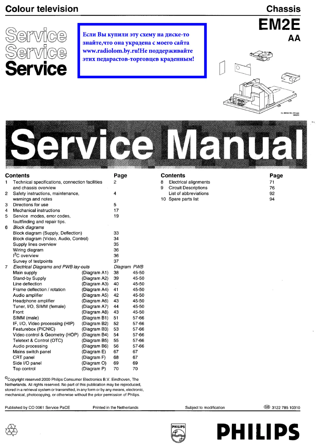
Colour television
Chassis
Service
Если Вы купили эту схему на диске-то
знайте,что она украдена с моего сайта
www.radiolom.by.ruIHe поддерживайте
этих педарастов-торговцев краденным!
ЕМ2Е
АА
ш®.
Manual
Contents Page Contents Page
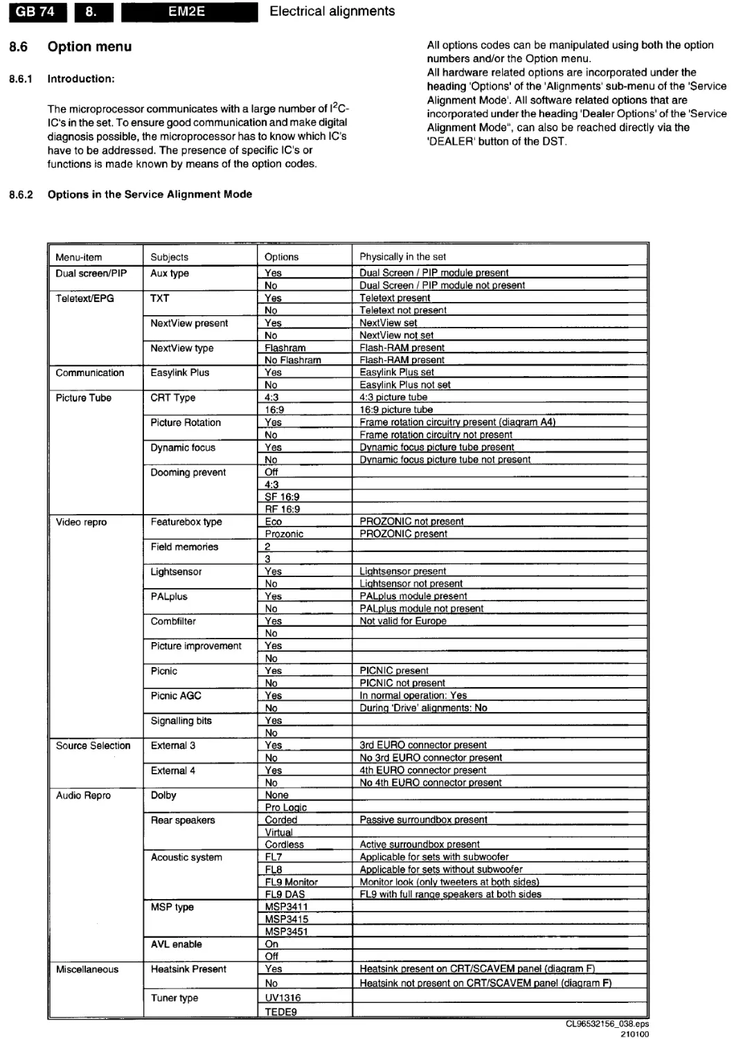
1 Technical specifications, connection facilities 2 8 Electrical alignments 71
and chassis overview 9 Circuit Descriptions 76
2 Safety instructions, maintenance, 4 List of abbreviations 92
warnings and notes 10 Spare parts list 94
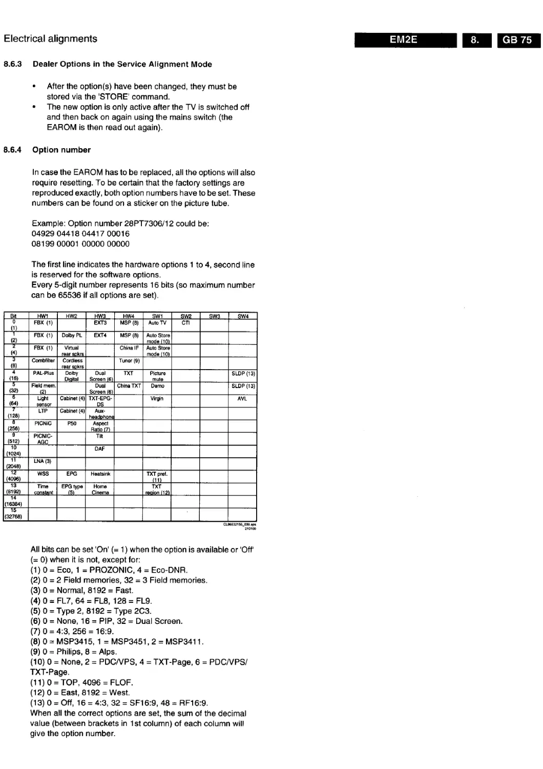
3
4
5
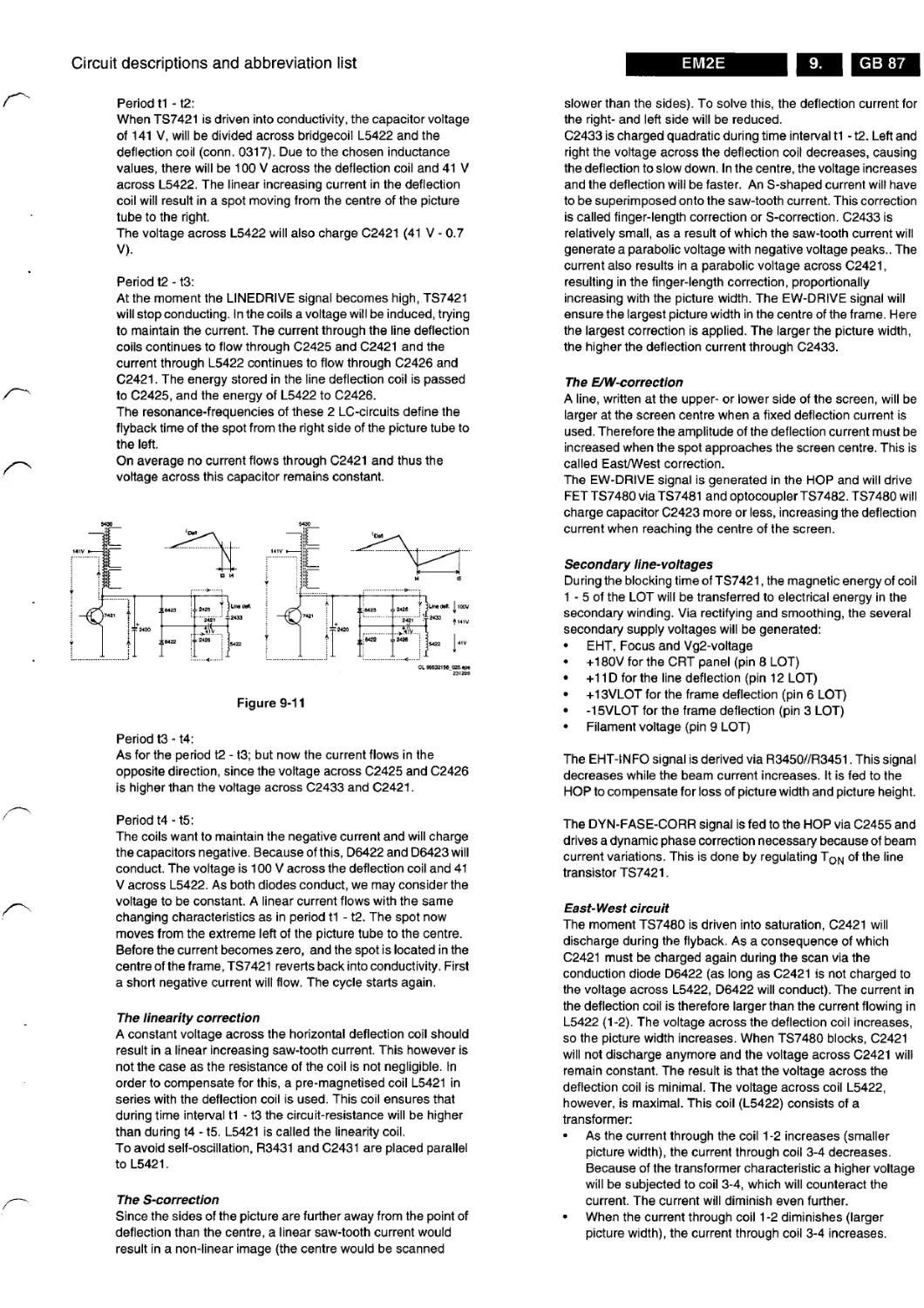
5
17
19
6
Directions for use
Mechanical instructions
Service modes, error codes,
faultfinding and repair tips.
Block diagrams
Block diagram (Supply, Deflection)
33
7
Block diagram (Video, Audio, Control) 34
Supply lines overview Wiring diagram l2C overview Survey of testpoints Electrical Diagrams and PWB lay-outs 35 36 36 37 Diagram PWB
Main supply (Diagram A1) 38 45-50
Stand-by Supply (Diagram A2) 39 45-50
Line deflection (Diagram A3) 40 45-50
Frame deflection / rotation (Diagram A4) 41 45-50
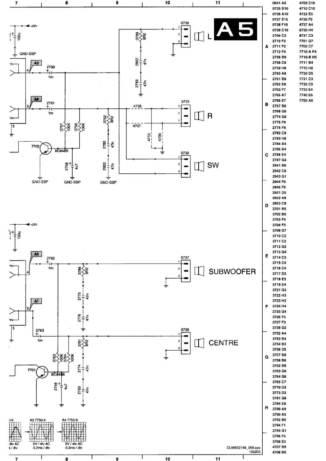
Audio amplifier (Diagram A5) 42 45-50
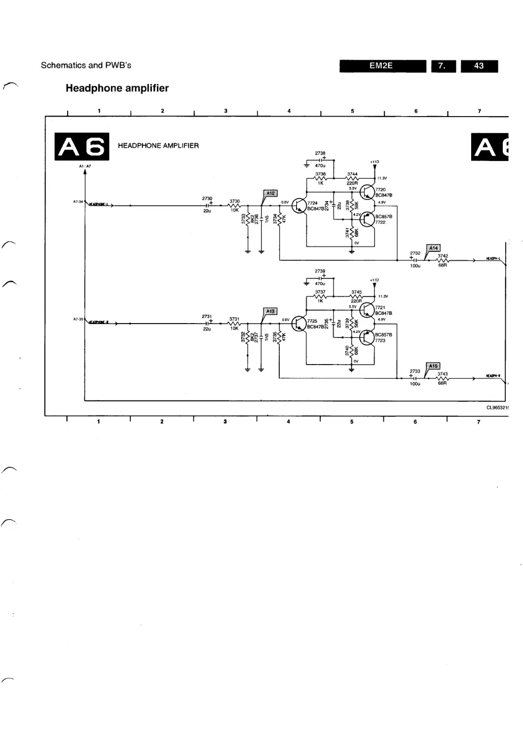
Headphone amplifier (Diagram A6) 43 45-50
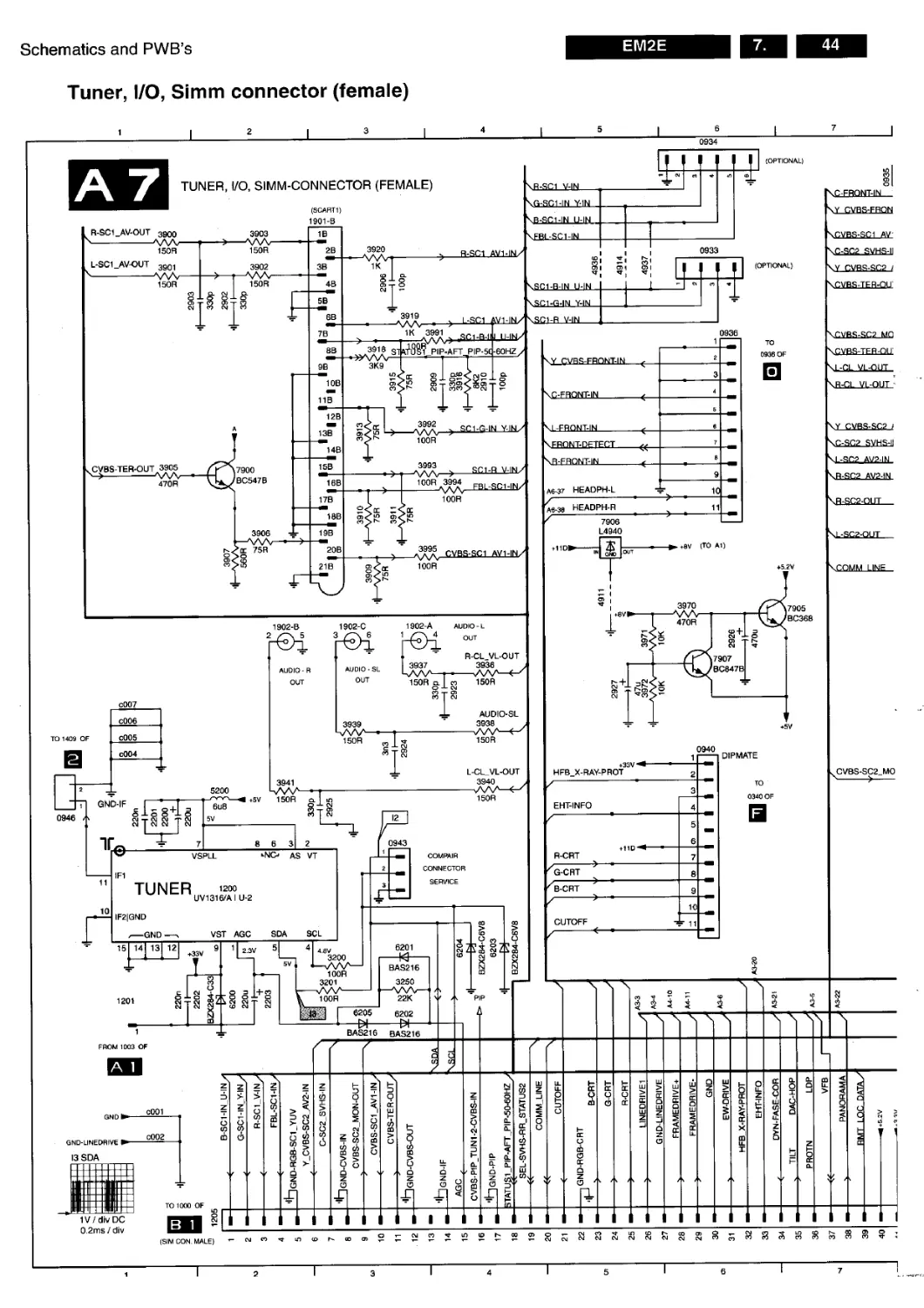
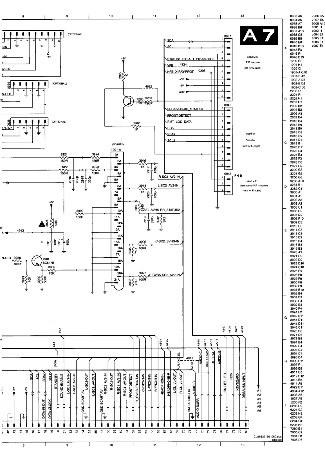
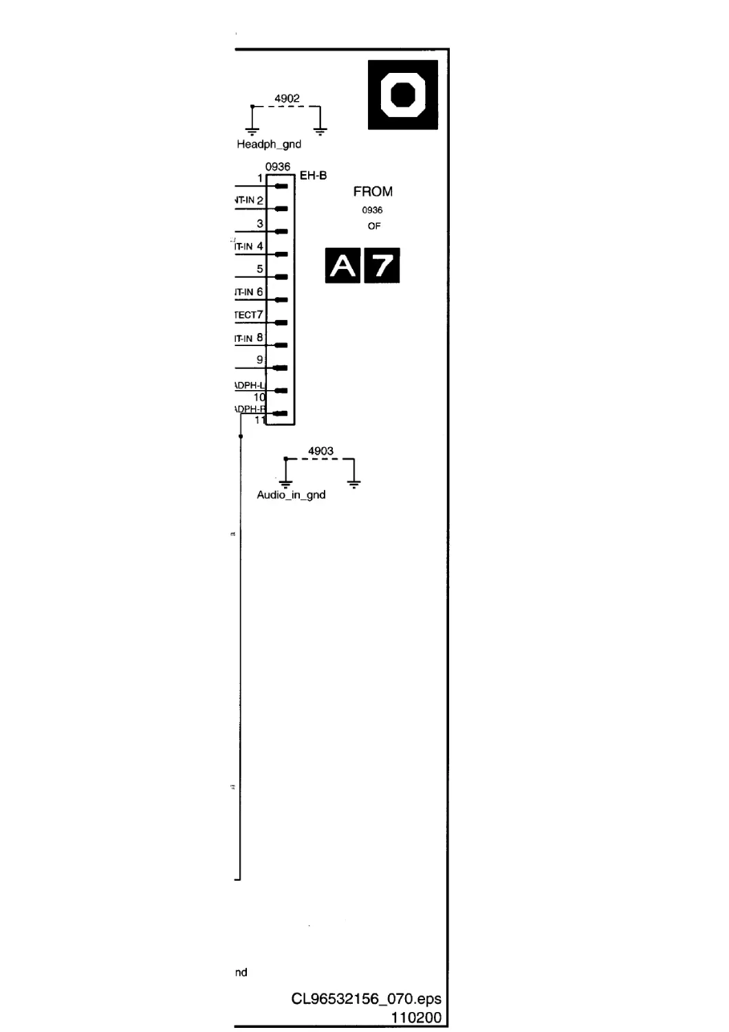
Tuner, I/O, SIMM (female) (Diagram A7) 44 45-50
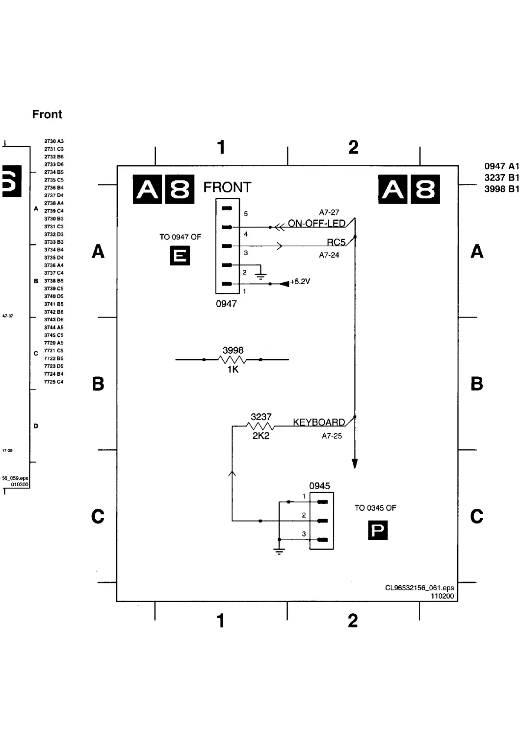
Front (Diagram A8) 43 45-50
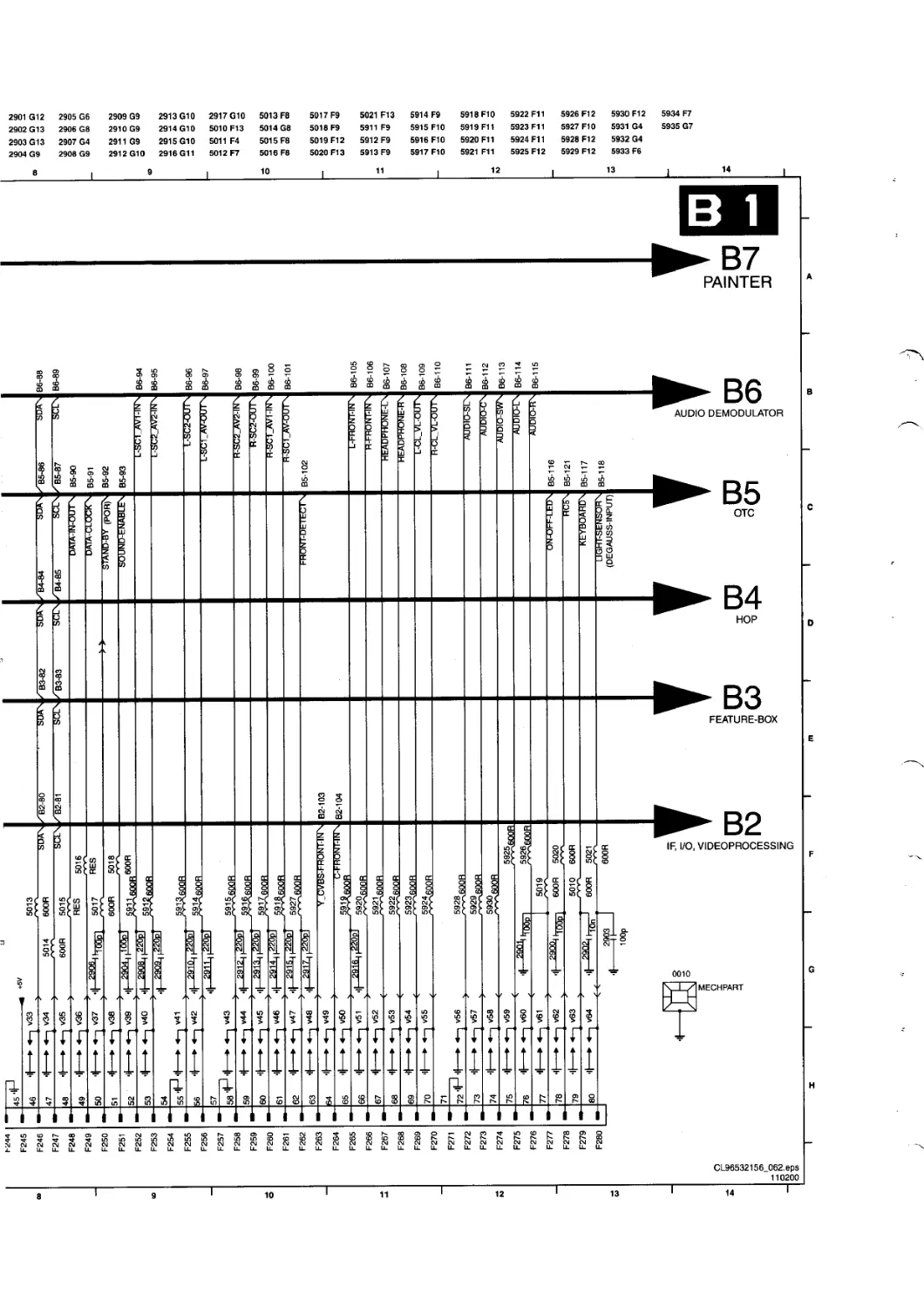
SIMM (male) (Diagram B1) 51 57-66
IF, I/O, Video processing (HIP) (Diagram B2) 52 57-66
Featurebox (PICNIC) (Diagram B3) 53 57-66
Video control & Geometry (HOP) (Diagram B4) 54 57-66
Teletext & Control (OTC) (Diagram B5) 55 57-66
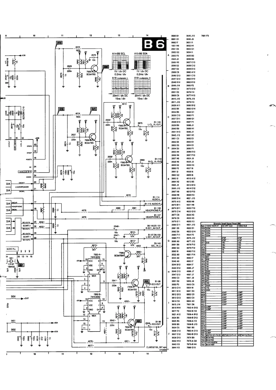
Audio processing (Diagram B6) 56 57-66
Mains switch panel (Diagram E) 67 67
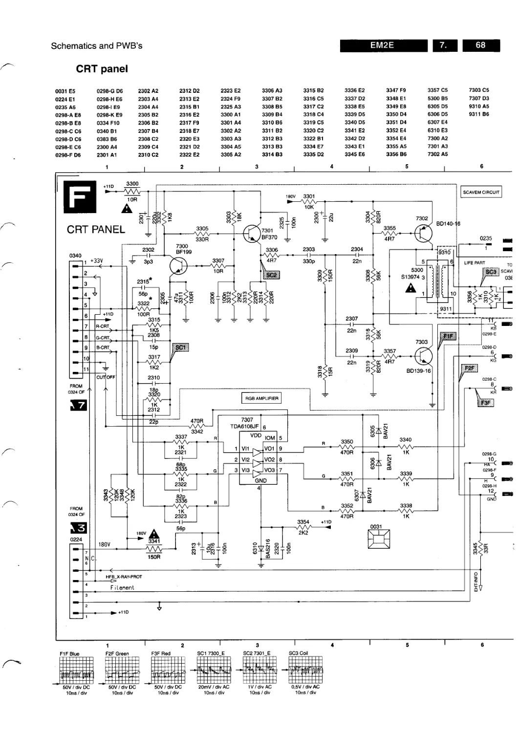
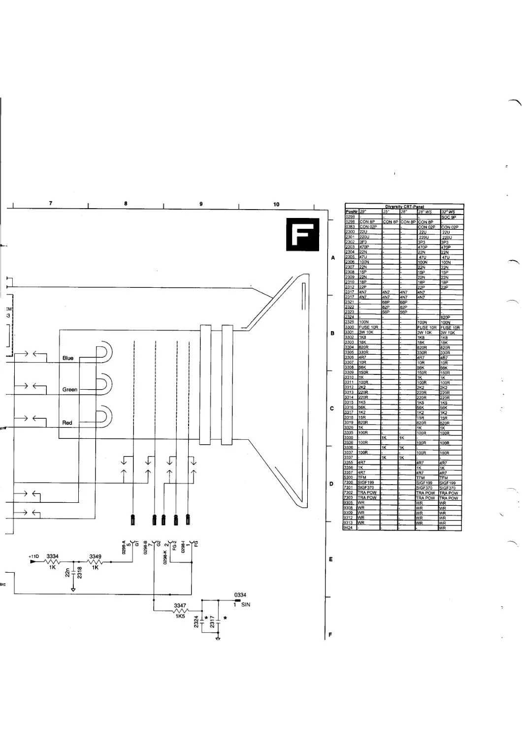
CRT panel (Diagram F) 68 67
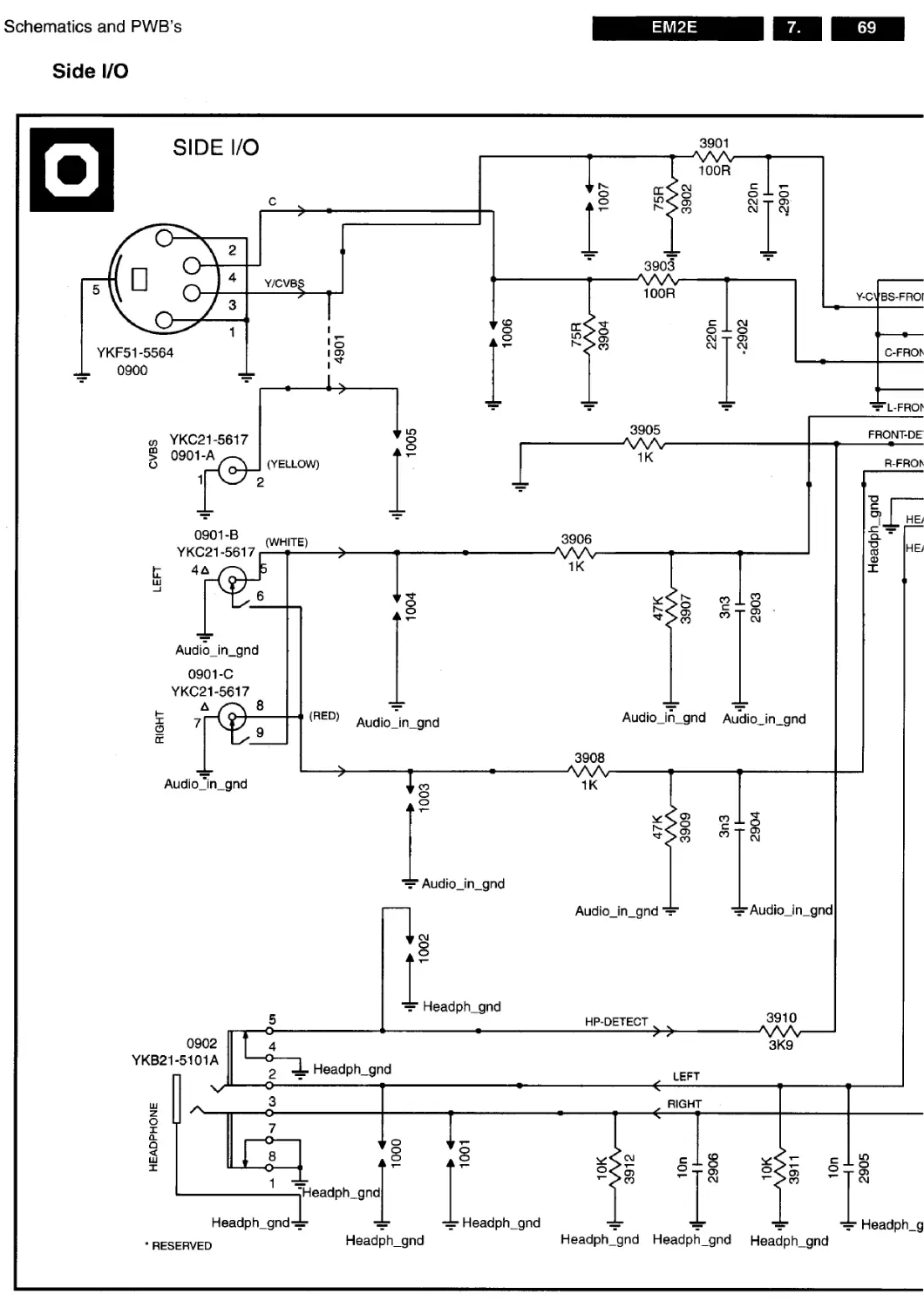
Side I/O panel (Diagram O) 69 69
Top control (Diagram P) 70 70
Copyright reserved 2000 Philips Consumer Electronics B.V. Eindhoven, The
Netherlands. All rights reserved. No part of this publication may be reproduced,
stored in a retrieval system or transmitted, in any form or by any means, electronic,
mechanical, photocopying, or otherwise without the prior permission of Philips.
Published by CO 0061 Service PaCE
Printed in the Netherlands
Subject to modification
® 3122 785 10310
PHILIPS
PHILIPS
GB 26
5.
EM2E
Service modes, error codes, protections, faultfinding and repair tips
protection will take place if the SDA and SCL are whether short
circuited to ground or to each other. An l2C error can also
occur, if the power supply of the IC is missing (e.g.
TUNER_PROT (error 12) & FBX_PROT (error 16)).
OTC related protections
If a protection is detected at an input of the OTC, all protection
inputs of the OTC will be scanned every 200 msec, for 5 times.
If the protection on one of the inputs is still activated after 1
sec., then the set will be put in the protection-mode. Before the
scanning is started a so-called ESD-refresh will be carried out
first, because the interrupt on one of the inputs may be caused
either by a FLASH or by ESD. As a FLASH or ESD can harm
the settings of some IC's, the HOP-HIP-MSP-PICNIC-NVM
and Tuner are initialised again to ensure the normal picture and
sound conditions of the set.
• 8.6 V and 5.2 V protection. The presence of the 8.6 V and
5.2 V is sensed by the OTC. If these voltages are not
present, then an error code is stored in the error buffer of
the NVM, and the set is put in the protection-mode.
HOP related protections
Every 200 msec, the status register of the HOP is read by the
OTC via l2C. If a protection signal is detected on one of the
inputs of the HOP, then the relevant error bit in the HOP
register is set to ‘high’. If the error bit is still ‘high’ after 1 sec.,
the OTC will store the error code in the error buffer (NVM) and
depending on the relevancy of the error bit the set will either go
into the protection-mode or not.
• HFB: Horizontal Flyback. If the horizontal flyback is not
present, then this is detected via the HOP (HFB_X-
RAY_PROT). One status bit is set to ‘high’. The error code
is stored in the error buffer and the set will go into the
protection mode
• Flash detection. From the EHT-info, via D6303 and T7303
a flash will stop the H-drive and line output stage
immediately. The FLS-bit in the status register of the HOP
is set to ‘high’. As the duration of a flash is very short the
FLS-bit will be reset to ‘low’ again after the flash refresh, so
via a slow start the set will be started again.
Hardware related protections
Due to the architecture (with hot' deflection) there are two
protections that are 'unknown' to the microprocessor, namely
the 'BRIDGE_PROT‘ from the line-stage and the 'NO_VFB'
protection form the frame-stage. If one of these protections is
triggered, the set is positioned in ‘Standby’-mode. The OTC will
now try to re-start the set. If this will not succeed after 5 times
(after ~ 1 minute), the OTC will generate error 15 (Flash
protection) and will start the blinking red LED.
EM2E
Service modes, error codes, protections, faultfinding and repair tips
GB 28
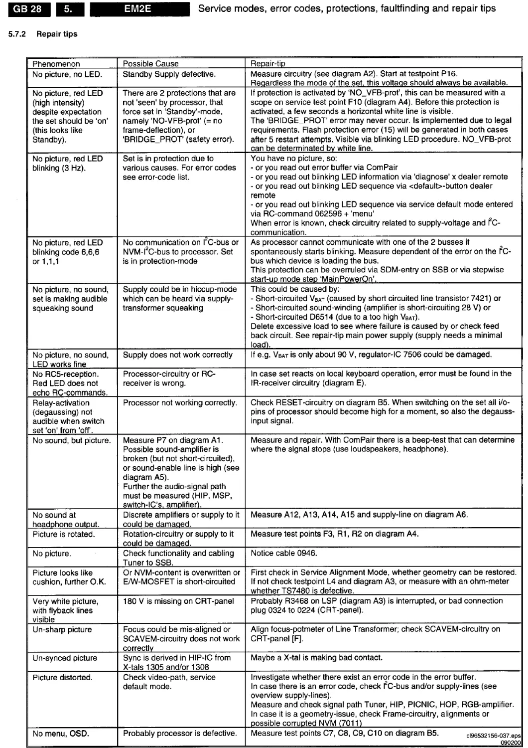
5.7.2 Repair tips
Phenomenon Possible Cause Repair-tip
No picture, no LED. Standby Supply defective. Measure circuitry (see diagram A2). Start at testpoint P16. Reqardless the mode of the set, this voltaae should always be available.
No picture, red LED (high intensity) despite expectation the set should be ‘on’ (this looks like Standby). There are 2 protections that are not 'seen' by processor, that force set in ‘Standby’-mode, namely 'NO-VFB-prot’ (= no frame-deflection), or 'BRIDGE_PROT' (safety error). If protection is activated by ‘NO_VFB-prot’, this can be measured with a scope on service test point F10 (diagram A4). Before this protection is activated, a few seconds a horizontal white line is visible. The 'BRIDGE_PROT' error may never occur. Is implemented due to legal requirements. Flash protection error (15) will be generated in both cases after 5 restart attempts. Visible via blinking LED procedure. NO_VFB-prot can be determinated by white line.
No picture, red LED blinking (3 Hz). Set is in protection due to various causes. For error codes see error-code list. You have no picture, so: - or you read out error buffer via ComPair - or you read out blinking LED information via 'diagnose' x dealer remote - or you read out blinking LED sequence via <default>-button dealer remote - or you read out blinking LED sequence via service default mode entered via RC-command 062596 + 'menu' When error is known, check circuitry related to supply-voltage and fc- communication.
No picture, red LED blinking code 6,6,6 or 1,1,1 No communication on l2C-bus or NVM-l2C-bus to processor. Set is in protection-mode As processor cannot communicate with one of the 2 busses it spontaneously starts blinking. Measure dependent of the error on the fC- bus which device is loading the bus. This protection can be overruled via SDM-entry on SSB or via stepwise start-up mode step ‘MainPowerOn’.
No picture, no sound, set is making audible squeaking sound Supply could be in hiccup-mode which can be heard via supply- transformer squeaking This could be caused by: - Short-circuited Vbat (caused by short circuited line transistor 7421) or - Short-circuited sound-winding (amplifier is short-circuiting 28 V) or - Short-circuited D6514 (due to a too high Vbat). Delete excessive load to see where failure is caused by or check feed back circuit. See repair-tip main power supply (supply needs a minimal load).
No picture, no sound, LED works fine Supply does not work correctly If e.g. Vbat is only about 90 V, regulator-IC 7506 could be damaged.
No RC5-reception. Red LED does not echo RC-commands. Processor-circuitry or RC- receiver is wrong. In case set reacts on local keyboard operation, error must be found in the IR-receiver circuitry (diagram E).
Relay-activation (degaussing) not audible when switch set ‘on‘ from ‘off’. Processor not working correctly. Check RESET-circuitry on diagram B5. When switching on the set all i/o- pins of processor should become high for a moment, so also the degauss- input signal.
No sound, but picture. Measure P7 on diagram A1. Possible sound-amplifier is broken (but not short-circuited), or sound-enable line is high (see diagram A5). Further the audio-signal path must be measured (HIP, MSP, switch-IC’s, amplifier). Measure and repair. With ComPair there is a beep-test that can determine where the signal stops (use loudspeakers, headphone).
No sound at headphone output. Discrete amplifiers or supply to it could be damaaed. Measure A12, A13, A14, A15 and supply-line on diagram A6.
Picture is rotated. Rotation-circuitry or supply to it could be damaaed. Measure test points F3, R1, R2 on diagram A4.
No picture. Check functionality and cabling Tuner to SSB. Notice cable 0946.
Picture looks like cushion, further O.K. Or NVM-content is overwritten or E/W-MOSFET is short-circuited First check in Service Alignment Mode, whether geometry can be restored. If not check testpoint L4 and diagram A3, or measure with an ohm-meter whether TS7480 is defective.
Very white picture, with flyback lines visible 180 V is missing on CRT-panel Probably R3468 on LSP (diagram A3) is interrupted, or bad connection plug 0324 to 0224 (CRT-panel).
Un-sharp picture Focus could be mis-aligned or SCAVEM-circuitry does not work correctly Align focus-potmeter of Line Transformer; check SCAVEM-circuitry on CRT-panel [F],
Un-synced picture Sync is derived in HIP-IC from X-tals 1305 and/or 1308 Maybe a X-tal is making bad contact.
Picture distorted. Check video-path, service default mode. Investigate whether there exist an error code in the error buffer. In case there is an error code, check fC-bus and/or supply-lines (see overview supply-lines). Measure and check signal path Tuner, HIP, PICNIC, HOP, RGB-amplifier. In case it is a geometry-issue, check Frame-circuitry, alignments or possible corrupted NVM (7011)
No menu, OSD. Probably processor is defective. Measure test points C7, C8, C9, C10 on diagram B5. ci96532i56-037.eps 090200
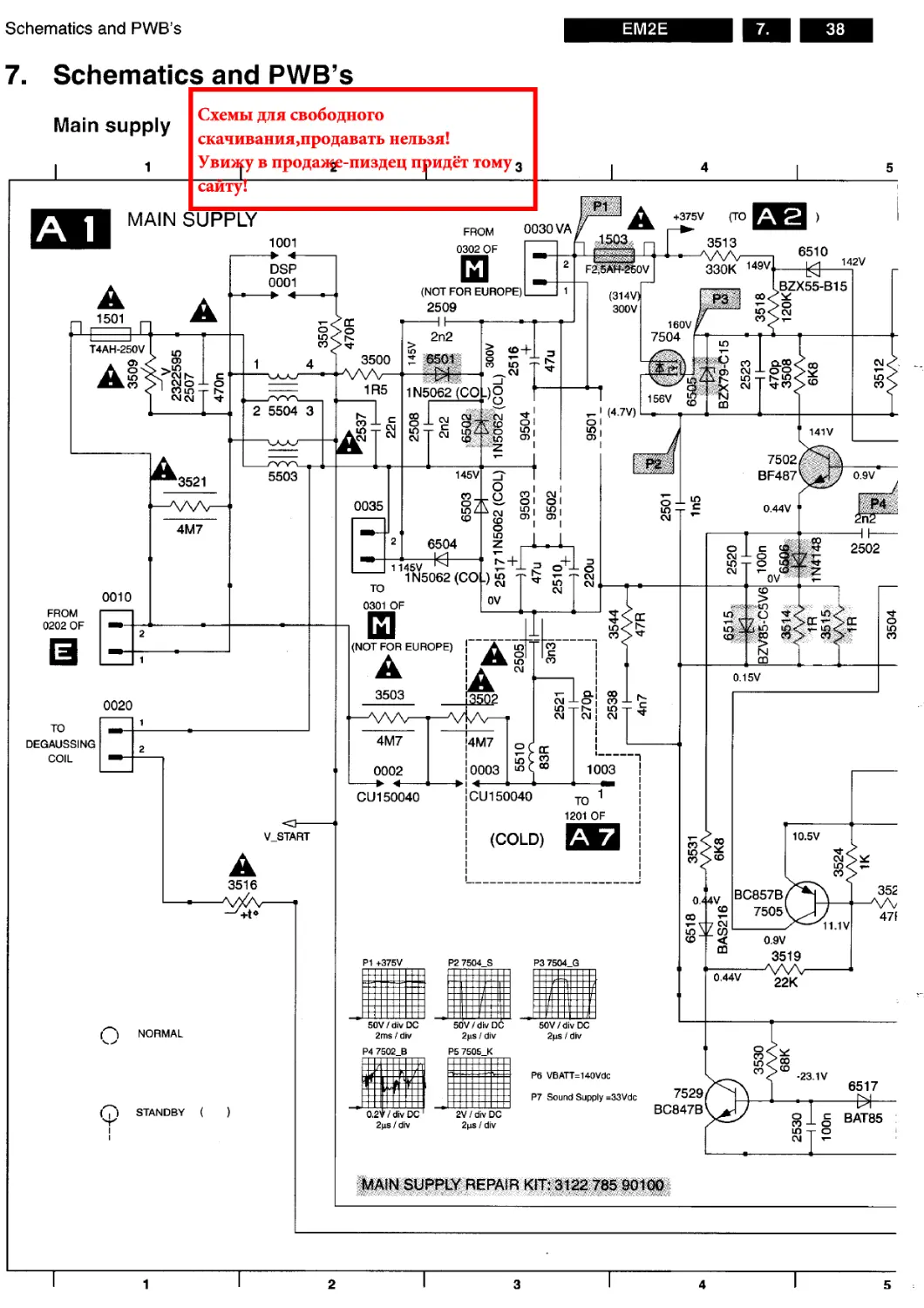
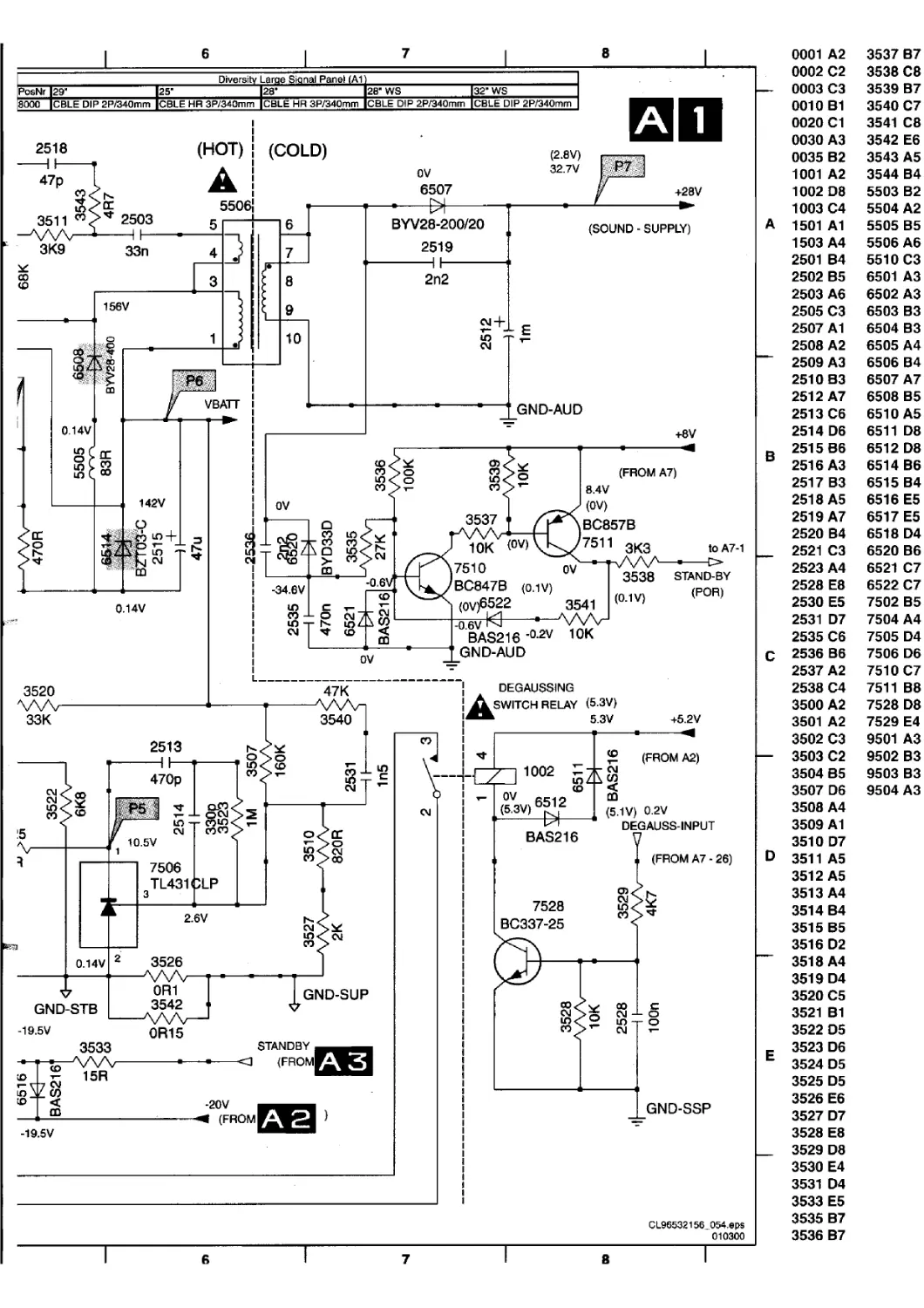
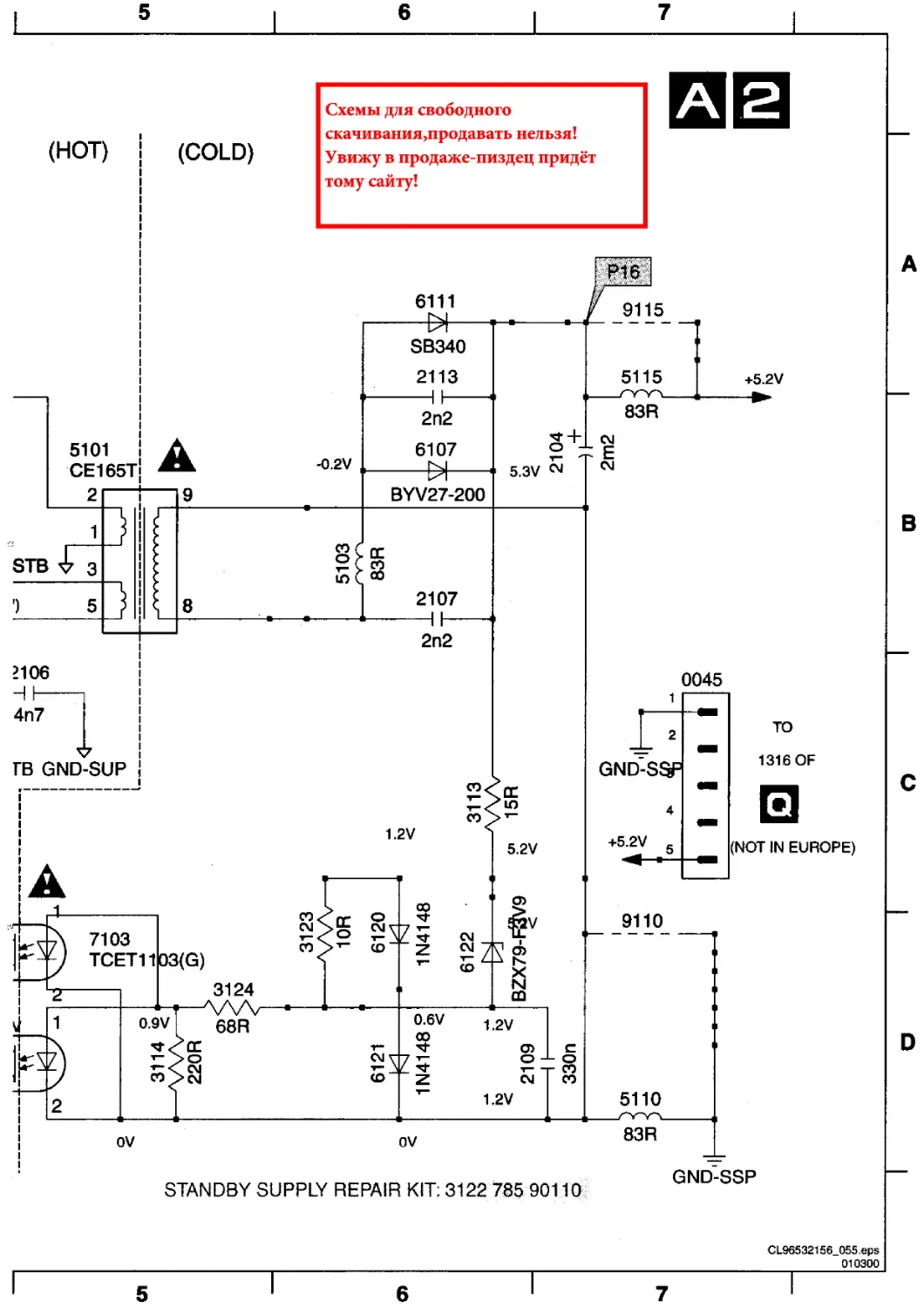
Schematics and PWB’s
EM2E I 7. 38
Schematics and PWB’s
Main supply
1
Схемы для свободного
скачивания,продавать нельзя!
Увиарг в продая^е-пиздец придёт тому 3
сайту!
MAIN SUPPLY
1001
1501
DSP
0001
T4AH-250V
in
o>
1
4
CM о О
CO in -r h*
CMOJ ’Ф
3521
4M7
2 5504 3
5503
0010
FROM
0202 OF
0020
TO
DEGAUSSING
COIL
2
V_START
NORMAL
3516
4
0030 VA у
2
330K 149V'
F2.5AH-250V
BZX55-B15
2n2
’ 6501
3500
1R5
(4.7V)
0035
2
1145V
0003
CU150040
TO
0301 OF
160V
7504
(TO g
3513
o°
O
m -r
OJ
(314V)
300V
6510
1^1 142V
Ю т й
5<g
1П< Г'-
156 V
145 V
2502
4M7
1003
0002
CU150040
10.5V
352
to
47f
to
0.9V
3519
BC857B
7505
0.44V
co
FROM
0302 OF
(NOT FOR EUROPE)
2509
1N5062 (СОР О
6504
-M-
1N5062 (COL) £
0V
(NOT FOR
3503
3502
4M7
STANDBY (
7502
BF487
0.44V
CM О
LD -г О
0.15V
CO -L-
Ю -r
CXJ
TO
1201 OF
m
R2 7504 S
P3 7504_G
50V/div DC
2ps / div
50V/div DC
2ps / div
P5 7505-K
P6 VBATT=140Vdc
P7 Sound Supply =33Vdc
2V / div DC
2ps / div
MAIN SUPPLY REPAIR KIT: 3122 785 90100
22K
0.44V
23.1V
7529
BC847B
6517
----OF—
£ BAT85
1
2
3
4
5
6
7
8
Diversity Large Signal Panel (A1)
PosNr 29" 125- 28" 28" WS 32" WS
8000 CBLE DIP2P/340mm ICBLE HR 3P/340mm CBLE HR 3P/340mm CBLE DIP2P/340mm CBLE DIP 2P/340mm
2518
(HOT)
(COLD)
□D
47p
5506
5
0V
6507
(2.8V)
32.7V
P7j
+28V
3511 2503
3K9
co
33n
3
4
6
8
7
BYV28-200/20
2519
2n2
156 V
9
10
GND-AUD
3540
2+1 E
tn T
CM
VBATT
0.14V
cc
CO
(ov)6522
0.14V
DEGAUSSING
3520
33K
2513
470p
CM
CM
tn
о
tn
tn
О
-34.6V
in
__I in
(&3V) 2
o/tt
tn<*°
CO >00
о >o
CO >1-
CM
CM
tn
co
!5
-L о CM
т «12
coco
tn +
142V
47K
10.5V
(SOUND - SUPPLY)
+8V
(FROM A7)
8.4V
(0V)
BC857B
7511 3K3
to A7-1
A
В
3541
-0 6V v v
BAS216 '°-2V 10K
GND-AUD
BAS216
3538
(0.1V)
<0
4
0.14V
7506
TL431CLP
з
2.6V
CM
tn< cm
co >
GND-STB
-19.5 V
г- v7 GJ
n V CO
10 <
CD
-19.5 V
2 3526
0R1
3542
^GND-SUP
7528
BC337-25
3533
15R
0R15
STANDBY --
(FROM^J
20V —
< (FROM
)
STAND-BY
(POR)
+5.2V
(FROM A2)
CO
(5.1V)
DEGAUSS-INPUT
у
,, (FROMA7-26)
0.2V
c
D
cn
CM
ID
QO
CM >5 CM -L
io< co t
CO >^ CM
GND-SSP
CL96532156.054.eps
010300
E
0001 A2
0002 02
0003 C3
0010 B1
0020 C1
0030 A3
0035 B2
1001 A2
1002 D8
1003 C4
1501 A1
1503 A4
2501 B4
2502 B5
2503 A6
2505 03
2507 A1
2508 A2
2509 A3
2510 B3
2512 A7
2513 C6
2514 D6
2515 B6
2516 A3
2517 B3
2518 A5
2519 A7
2520 B4
2521 03
2523 A4
2528 E8
2530 E5
2531 D7
2535 06
2536 B6
2537 A2
2538 C4
3500 A2
3501 A2
3502 03
3503 02
3504 B5
3507 D6
3508 A4
3509 A1
3510 D7
3511 A5
3512 A5
3513 A4
3514 B4
3515 B5
3516 D2
3518 A4
3519 D4
3520 C5
3521 B1
3522 D5
3523 D6
3524 D5
3525 D5
3526 E6
3527 D7
3528 E8
3529 D8
3530 E4
3531 D4
3533 E5
3535 B7
3536 B7
3537 B7
3538 08
3539 B7
3540 07
3541 08
3542 E6
3543 A5
3544 B4
5503 B2
5504 A2
5505 B5
5506 A6
5510 03
6501 A3
6502 A3
6503 B3
6504 B3
6505 A4
6506 B4
6507 A7
6508 B5
6510 A5
6511 D8
6512 D8
6514 B6
6515 B4
6516 E5
6517 E5
6518 D4
6520 B6
6521 07
6522 07
7502 B5
7504 A4
7505 D4
7506 D6
7510 07
7511 B8
7528 D8
7529 E4
9501 A3
9502 B3
9503 B3
9504 A3
6
7
8
Schematics and PWB’s
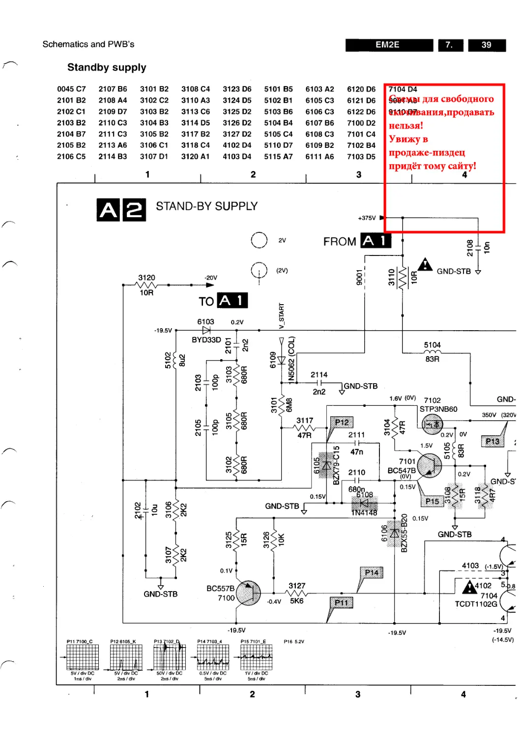
EM2E I 7. I 39
Standby supply
0045 C7
2101 B2
2102 C1
2103 B2
2104 B7
2105 B2
2106 C5
2107 B6 3101 B2 3108 C4 3123 D6 5101 B5 6103 A2 6120 D6
2108 A4 3102 C2 3110 A3 3124 D5 5102 B1 6105 C3 6121 D6
2109 D7 3103 B2 3113 C6 3125 D2 5103 B6 6106 C3 6122 D6
2110 C3 3104 B3 3114 D5 3126 D2 5104 B4 6107 B6 7100 D2
2111 C3 3105 B2 3117 B2 3127 D2 5105 C4 6108 C3 7101 C4
2113 A6 3106 C1 3118 C4 4102 D4 5110 D7 6109 B2 7102 B4
2114 B3 3107 D1 3120 A1 4103 D4 5115 A7 6111 A6 7103 D5
1
2
□ 2
STAND-BY SUPPLY
2V
3120
(2V)
10R
-20V
-19.
6103
□c
cc
in
CM
CM
c
CM
0.2V
CO,
v
oj
о
О
см
in
<D
CM
CM
CM
GND-STB
CM
10
CM
3127
5K6
0.15V
GND-STB £
0.1V
BC557B
7104 D4
ЙТО для свободного
@КЮШЬания,продавать
нельзя!
Увижу в
продаже-пиздец
придет тому сайту
FROM
+375V
GND-STB
2114
—11 1GND-STB
2n2 V
1.6V (0V)
3117
47R
in
<o
5104
83R
7102
STP3NB60
GND-
P12 |
CC
in
47n
688?08
1N4148
CM
350V (320V
-19.5V
7101
BC547BV
(QV)
0.15V
4—-^0.2vT 0V -------
Р13
0.2V
0.15V
СГ
iD
GND-STB
GND-S'
a:
A.
4103 (-1.5V)
N
CD
7104
TCDT1102G
-19.5V
-19.5V
(-14.5V)
1 । 2 । 3 । 4
5
6
7
(HOT)
(COLD)
Схемы для свободного
скачивания,продавать нельзя!
Увижу в продаже-пиздец придёт
тому сайту!
6111
9115
SB340
2113
5115
+5.2V
2n2
83R
-0.2V
cc
5101
СЕ165Т
2
6107
BYV27-200
2107
’106
2n2
5.3V
- СМ
± Е
см
В
4n7
ГВ GND-SUP
<2<сс
7103
TCET11
03(G)
3124
0 9V | 68R
ОС
о
см
см
1.2V
0.6V
5.2V
CM
CM
№
CD
1.2V
ст>
см
1.2V
9110
5110
83R
2
GND-SSP
4
0045
1
+5.2V „
. о
(NOT IN EUROPE)
TO
1316 OF
D
STANDBY SUPPLY REPAIR KIT: 3122 785 90110
GND-SSP
CL96532156_055.eps
010300
5
6
7
Schematics and PWB’s
EM2E I 7. I 40
A
В
c
D
E
G
Line deflection
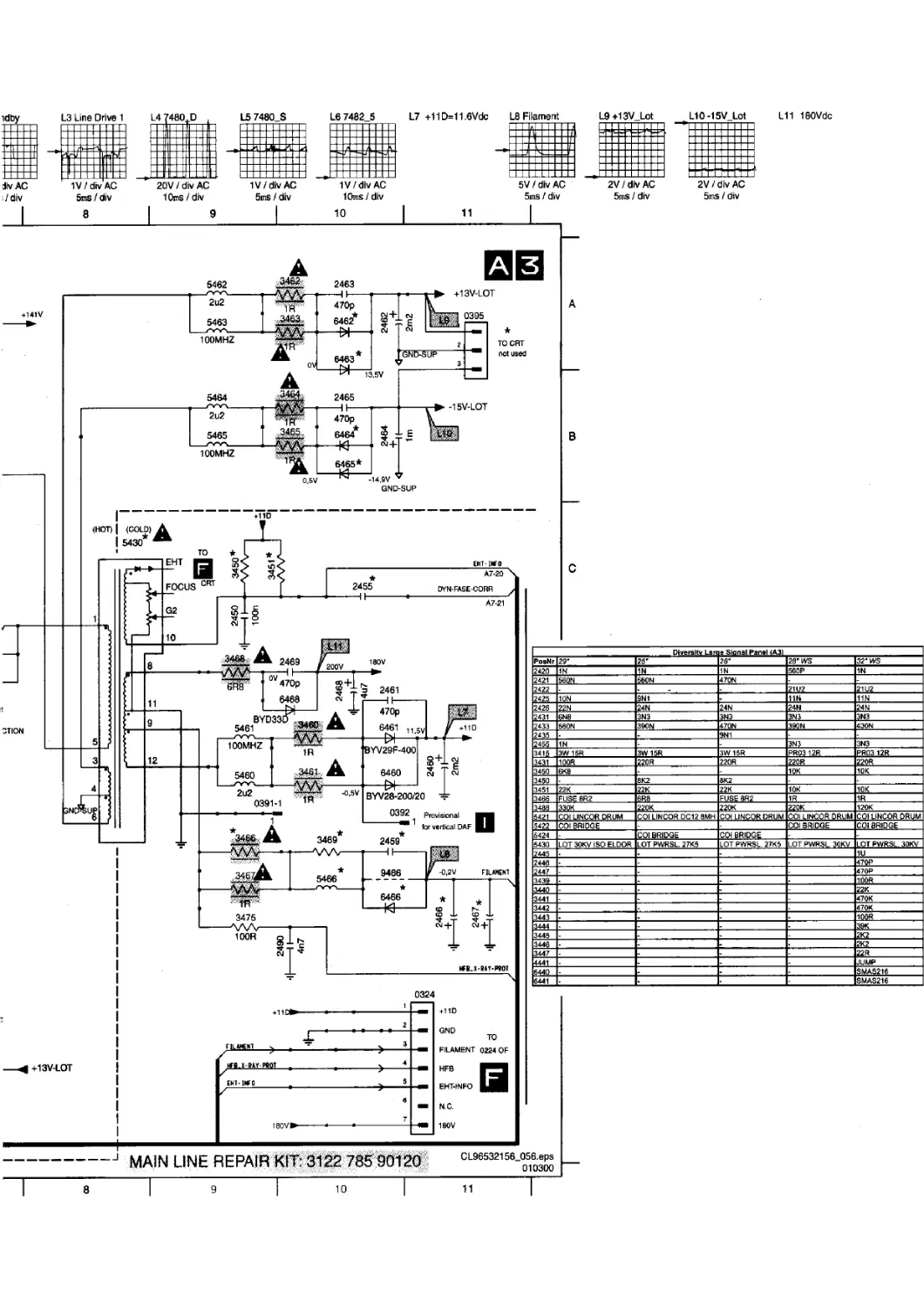
2400 A7 2421 F6 2450 C9 2469 D10 3406 E1 3426 C5 3468 D9 3491 D6 5423 B5 5467 E5 6465 B10 7482 G3
2401 C7 2422 F6 2455 C10 2480 E6 3407 E2 3431 E7 3469 ЕЮ 3495 E4 5424 F7 6406 E1 6466 F10 7483 F3
2409 E2 2423 F5 2459 ЕЮ 2488 A5 3409 B3 3450 C9 3475 F9 3499 G5 5425 C5 6407 C2 6468 D10 9401 D7
2412 D2 2425 B5 2460 D11 2489 G7 3410 A2 3451 C9 3481 E6 4417 C3 5426 A4 6408 B2 6480 D4 9408 B3
2413 D2 2426 B5 2461 D10 2490 F10 3411 C2 3460 D10 3483 F3 4482 G3 5430 C8 6421 A5 6481 E6 9423 B5
2414 D3 2429 D4 2462 A10 2491 D6 3414 E2 3461 ЕЮ 3484 F2 4483 F3 5460 E9 6422 B5 6482 F2 9425 C5
1 | 2 | 3 | 4 I 5 I 6
t tA1:A7
SIUHtCI «
' TOA1
UNEDR1VE1
2492
A7-3 220n
3'
CNO-UMEOeiVE
A7-4 0V
EU-MIVE
A7-6
LINE DEFLECTION
2495
3410
100n
15R
(COLD)
(HOT)
+11D
+5.2V
3406
100R
CM
CM
11,3V 6408
BYD33D
52V 6407
BAS216
3n3
GND-SUP
2414
(TO A4)
2429
CM
0,45V
PAROBOLE
INFORMATION
7409
BC847B
2409
3409
BU2520DX
Ж
560n
CM
CM
GND-SUP
RES
5411
RES
9408
_2416_ GND-SSP
VBATT
47П
4n7
26,8V
10ms/div
5ms
5400
33u §
GND-SUP
RES
2401
RES
3401
4n7 RES 47R
5401
3414
330R
7408
3*
GND-SUP
3
8
BC368
RES
47p
0V
CM
CM
3ND-
+8V
1,6V
CM
2
(COLD)
ov
BC557B
7481 6482
-r——
BAS216
3
4 0,2V
GND-SUP
7483
TCET1102
>8
cm
CM
GND-SUP
7482
TCDT1102G
GND-SUP
GND-SUP
+141V
18U
9401
0317
3418
3491
TO
270K
150K
LINE DEFLE
4,3V
100R
5467 4 27V —STP3NB60
looMHz 4.3V
GND-SUP
GND-SUP
GND-SUP
GND-SUP GND-SlfiND-SUP1
4
5
EMG
GND-SUP
+12V<
? T
3489
2K2
GND-SUP
6
14tV
L3 Line Drive 1
1V/divAC
5ms/div
8
20V/div AC
10ms / div
9
5ms/div 10ms/div
10 |11
5ms / div 5ms / div 5ms / div
В
Diversttv Lart a Sional Panel 4A31
PosNr 29“ 25’ 28“ 28“ WS 32“ WS
2420 IN 1N 1N 560P 1N
2421 560N 560 N 470N
2422 21U2 21U2
2425 ION 9N1 1Ш 11N
2426 22N 24N 24N 24N 24 N
2431 6N8 3N3 3N3 3N3 3N3
2433 560N 390N 470N 390N 430N
2435 9N1
2455 IN 3N3 3N3
3415 3W 15R 3W15R 3W15R PR0312R PR03 12R
3431 100R 220R 220R 220R 22OR
3450 6KB 10K 10K
3450 8K2 8K2
3451 22K 22K 22K 10K 10K
3466 FUSE 8R2 6R8 FUSE 8R2 1R 1R
3466 330K 220K 220K 220K 120K
5421 COI LINCOR DRUM COI LINCOR DC12 8MH COI LINCOR DRUM COI LINCOR DRUM COI LINCOR DRUM
5422 COI BRIDGE COI BRIDGE COI BRIDGE
5424 COI BRIDGE COI BRIDGE
5430 LOT 30KVISO ELDOR LOT PWRSL. 27K5 LOT PWRSL. 27K5 LOT PWRSL. 30KV LOT PWRSL. 30KV
2445 1U
2446 47OP
2447 470P
3439 100R
3440 22K
3441 470K
3442 470K
3443 100R
3444 39K
3445 2K2
3446 Ж2
3447 22R
4441 JUMP
6440 SMAS216
6441 SMAS216
+13V-LOT
TO
0224 OF
----J MAIN LINE REPAIR KIT: 3122 785 90120
8 | 9 | 10 |
CL96532156_056.eps
010300
n Г"
Schematics and PWB’s
EM2E
7.
41
A
В
C
D
E
F
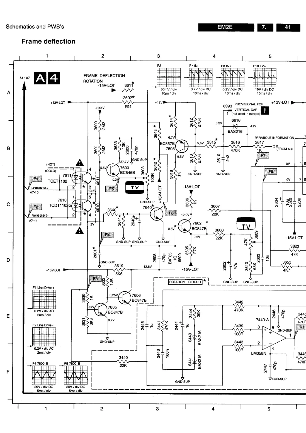
Frame deflection
1
2
3
4
5
Al :A7
FRAME DEFLECTION
ROTATION
-15V-LOT
3611
3602*
F1
FCANEQPIVE4
A7-10
Г FRAMEDRIVE-
A7-11
+13V-LOT ►
RES
+141V
(HOT)
(COLD)
7611
TCET 102
7610
TCDTHOi
2
GND-SUP GND-SUP
4
GND-SUP
7640’
3
13,51
GND-SUP
7 3619
5
2V
+13V-LOT
5ms / div
3640
F5 7600 E
0,7V
GND-SUP
20V / div DC
5ms / div
7605
BC847B
10ms / div
10ms / div
10^s I div
10ms/div
+12V>
0393 PR0VISI0NAL F0R +13V-LOT^
—м VERTICAL DAF IV
1 (not used in еигоре)ИЯ
6,2V
-41V
3615
3616
470K
CM
GND-SUP
0,5V
12,6V
5K6
3440
22K
6616
—Ю—
BAS216
CM
<S
37,7V
7600
BC546B
CM
3607
22K
22K
GND-SUP
GND-SUP
3442
470K
7440-A
3439
3
100R
3443
2
100R
LM358N
CM
GND-SUP
0,25V
7606
BC847B
6,7V
BC857B
7603
GND-SUP
5,6V
GND-SUP
GND-SUP
+13V-LOT
12,9V
7602 1
BC847B
3608
0,5V
-15V-LOT
| ROTATION CIRCUIT |
PARABOLE INFORMATION
3617
(FROM A3)
7
1K
to
0V
ov
T t
CM
CM
CM
-15V-LOT
3623
47K
3653
4K7
344’
CM
GND-SUP
vGND-SUP
470F
R1
344f
470F
1
2
3
4
5
6
3,5V
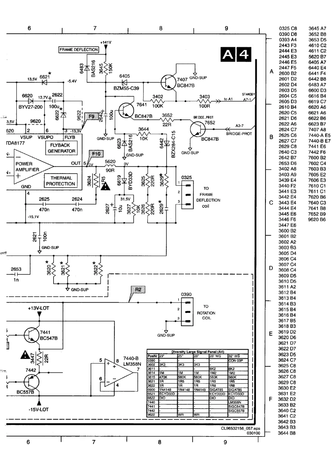
| FRAME DEFLECTION |
0325 С8
0390 D8
13 5V 6621
к
+141V
6405
BZM55-C39
6613,7V-|-2622
BYV27-200
100u
9620
2
620
VSUP
FDA8177
ll-
si+
GND
POWER
AMPLIFIER
-5,4V
6
VSUPO
3644
10K
GND-SUP
FLYBACK
GENERATOR
F10 |
5620
3 -13,3V
FLYB
7641 100k
3402
7407 GND-SUP
BC847B
3403
100R
OUT
BC847B 3652
GND-SUP
22R
CM
s
CO
О
CM
X
N
m
STANDBY
to А1 А7-1/
BRIDC£_PeO1
7652
GND-SUP
BC847B
«---------'
BRIDGE-PROT
THERMAL
PROTECTION
CO
90R
ov
Q
co
QQ
ю>сс
CM< о
CD >CM
CD's, CM
CM
co
4
2625
2624
31,5V
470n
470n
-15,1V
CM
co
CM
CM
CD
co>CC
CM< о
CD >CM
ГО<СМ
CM -L
CD -r
CM
0325
2
3
TO
FRAME
DEFLECTION
coil
GND-SUP
0390
TO
ROTATION
COIL
GND-SUP
Diversity Larg e Signal Panel (A4)
PosNr 29" 25" 28" 28” WS 32" WS
0390 - - CON 03P
3602 3K3 3K3 3K3 -
3611 - - 8K2 8K2
3614 1M 1M 1M 1M2 1M2
3615 470K 560K 560K 560K 560K
3621 1R 1R5 1R5 1R5 1R5
3622 1R 1R 1R 1R8 1R8
6600 1N4148 1N4146 1N4148 SIGAT85 SIGAT85
6621 ECYD33D - - ECYD33D ECYD33D
6622 DIO DIO DIO
7440 - - LM358N
7441 - • - SIGC547B
7442 - - SIGC557B
9622 - WR WR - -
CL96532156_057.eps
030100
0393 A4
2443 F3
2444 E3
2445 E3
2446 E5
2447 F5
2600 B2
2601 D2
2602 D4
2603 D5
2604 05
2605 D3
2610 B4
2620 05
2621 D6
2622 A6
2624 07
2625 C6
2627 07
2629 08
2640 C3
2642 B7
2653 D6
3402 A8
3403 A9
3439 E4
3440 F2
3441 E3
3442 E4
3443 E4
3444 E4
3445 E6
3446 F6
3447 E6
3600 B2
3601 B2
3602 A2
3603 B3
3605 D4
3606 C4
3607 C4
3608 C4
3609 D5
3610 D5
3611 A2
3612 B4
3613 B4
3614 B3
3615 B4
3616 B4
3617 B5
3618 B3
3619 D2
3620 D6
3621 D7
3622 D7
3623 D5
3624 C7
3625 08
3626 C8
3627 08
3629 08
3630 E2
3631 E2
3632 D2
3633 B2
3640 C2
3641 C2
3642 B3
3643 B3
3644 B8
3645 A7
3652 B8
3653 D5
4610 02
4611 C2
5620 B7
6405 A7
6440 E4
6441 F4
6442 B8
6483 A7
6600 D3
6616 B4
6619 07
6620 A6
6621 A6
6622 B6
6623 B7
7407 A8
7440-A E5
7440-B E7
7441 E6
7442 F6
7600 B2
7602 04
7603 B3
7605 E2
7606 E3
7610 01
7611 01
7620 B6
7640 03
7641 B8
7652 B9
9620 B6
6
7
8
Schematics and PWB’s
EM2E I 7. I 42
Audio amplifier
AUDIO AMPLIFIER
4737
GND-SSP
ч AUDIO-R 3792
\=-n--------------------------.-------------------------------------------------—HI-----.---VA
AM 4 680n 1K8
4 AUDIO-SL
аГзз *
AUDIO-SW
A6-17
GND-SSP GND-SSP
\AUDIQ-C
2710
—II—
680n
2786
3798
GND-SSP GND-SSP
A7-18
i ; г
Schematics and PWB’s
EM2E I 7. I 43
Headphone amplifier
CL965321!
1
Front
A7-37
2730 A3
2731 C3
2732 B6
2733 D6
2734 B5
2735 C5
2736 B4
2737 D4
2736 A4
2739 C4
3730 B3
3731 C3
3732 D3
3733 B3
3734 B4
3735 D4
3736 A4
3737 C4
3738 B5
3739 C5
3740 D5
3741 B5
3742 B6
3743 D6
3744 A5
3745 C5
7720 A5
7721 C5
7722 B5
7723 D5
7724 B4
7725 C4
A
В
V7-38
56_059.eps
010300
I
2
FRONT
TO 0947 OF
5
4
3
1
0947
3998
1K
3237
2K2
A7-27
« ON-OFF-LED/
x________BC5?
0+5.2V
A7-24
keyboard/'
A7-25
0945
0947 A1
___ 3237 B1
3998 B1
в
TO 0345 OF
CL96532156_061.eps
110200
2
Schematics and PWB’s
EM2E
7.
44
Tuner, I/O, Simm connector (female)
3
2
TUNER, I/O, SIMM-CONNECTOR (FEMALE)
R-SC1_AV-OUT 39oo
3903
\CVBS-SC1 AV-
3920
150R
2B
4C.SC2 SVHS-II
1K
3902
3B
\Y CVBS-SC2 I
150R
4B
\CVBS-TER.QU-
CM
5?
5B
CM
3919
KCVBS-SC2 MO
\CVBS-TER-OU
\R-CL VL-OUT
\C-FRONT-IN
13B
100R
\FRONT-DETECT
14B
\R-FRONT-1N
3993
15B
16B
A6-37 HEADPH-L
17B
\R-SC2-DUT
1SB
19B
’or 75R
20B
1902-C
1902-B
R-CL_ VL-OUT
3937
150R
150R o.
CM
c007
AUDIO-SL
C006
3939
C005
150R
150R
c004
3941
5200
150R
GND-IF
VSPLL
AS VT
SERVICE
10
1F2IGND
9
S 2 ? S
22K
COMPAIR
CONNECTOR
7900
BC547B
3918 д
3K9
\Y CVBS-SC2 /
4C-SC2 SVHS-II
4L-SC2 AVP-IN
4R-SC2 AV2-W
AUDIO - R
OUT
AUDIO - SL
OUT
L-CL_VL-OUT
3940
6201
-43-
BAS216
3250
. CVBS-TER-OUT 3905
-------———VA
470R
AfrW HEADPH-R
VST AGO SDA SCL
150R
L-SC1 .AV-OUT 39Q1
\C-FRONT-IN
\Y CVBS-FRON
1902-A AUDIO - L
OUT
4SC1-B-IN U-IN
VSC1-G-IN Y-IN
(SCART1)
1901-B
1B
150R
CM Q.
StS
см ст
3^5, QVBS-SC1 AV1-IN7
100R
ЧСОММ LINE
3970
470R
CUTOFF
C001
GND
C002
GND-LINEDRIVE
X a o
ст ст
ст г? $ ст S
В 1
\R-SC1 V-IN
KB-SC1-IN U-IN
\FBL-SC1-IN
R-SC1 ALL-IN/
6B
7B
SB
PIP-5(
9B
106
3906
,SC.1-B-III U-IN/
-60HZ/
12B
SC1-G-IN Y-IKM
SC1-R V-IN/
FBL-SG1-INZ
100R
(OPTIONAL)
(OPTIONAL)
4Y CVBS-FBONT-IN
7906
L4940
7905
BC368
7907
BC847B
TO 1409 OF
IF1
TUNER ’zoo
UV1316/A I U-2
HFB-X-RAY-PROT
DIPMATE
4CVBS-SC2_MO
sis 8+1
CM T
"I
FROM 1003 OF
TO 1000 OF
100R
3201
100R
6205 6202
-Й--------И-
BAS216 BAS216
(SIM CON. MALE)
EHT-INFO
R-CRT
G-CRT
B-CRT
22__________L
0933 A6
0934 A6
(SCART2)
3946
3944
u> —
g>SEL-SVHS-RR_STATUS2^
\Ш
\2CL_
0937
\STATUS1 PIP-AFT PIP-50-60HZ
WFB _4_934 s
\HFB X-RAY-PROT _9®8. _________•
+5V
+6V
+33V
\SEL-SVHS-HR STATUS2
\FRONT-DETECT______
\RMT LOC DATA______
\BC5_______________
\SQA2______________
\SGL2
R-SC2 AV24Ny
L-SC2_AV2-IN
PH-B
used with
Gemstar or PIP - module
(not for Europe)
used wtth
PIP -module
(not tor Europe)
used for
Gemstar
(not for Europe)
11A
12A
13A
0935 A7
0936 B6
0937 A13
0938 C8
0939 B8
0940 E6
0942 B13
0943 F3
0946 F1
0948 013
1200 G2
1201 H1
1205 I2
1901-AGIO
1901-B A2
1902-A D3
1902-B D2
1902-C D3
2200 F1
2201 F1
2202 H1
2203 H2
2902 B2
2903 B2
2906 A3
2909 B4
2910 84
2912 E9
2913 E9
2915 D9
2916 D9
2917 D11
2919 E11
2920 D11
2923 E4
2924 E3
2925 F3
2926 D6
2927 E5
3200 G3
3201 G3
3250 G3
3280 A10
3281 B11
3282 C11
3900 A1
3901 A1
3902 A2
3903 A2
3905 C1
3906 D2
3907 D2
3908 F10
3909 D3
3910 C3
3911 C3
3913 C3
3915 B3
3916 B4
3918 B3
3919 B3
3920 A3
3921 09
3922 D9
3923 D10
3924C10
3925 E9
3928 F8
3929 F8
3930 F8
3932 F9
3935 ЕЮ
3936 E4
3937 E3
3938 E4
3939 E3
3940 F4
3941 F2
3942 E11
3944 D11
3945 D11
3946C11
3970 D6
3971 D5
3972 E5
3991 B4
3992 C4
3993 C4
3994 C4
3995 D4
3996 E11
3997 F11
3999 E9
4911 D5
4912 H12
4913 E8
4914 A5
4922 B11
4934 A12
4936 A5
4937 A5
5200 F2
6200 H2
6201 G3
6202 H3
6203 G4
6204 G4
6205 H3
7280 B11
7900 C2
7901 F8
7905 D7
7906 C5
7907 E6
9208 A1
c001 11
CQ02 11
c004 E1
C005 E1
c006 E1
C007 E1
Schematics and PWB’s
EM2E
7. I 46
LSP (copper side overview)
2 i 3 । 4 , 5
0010 А9 2467 А5 2920 Е1 3510 D6 3735 Е5 4521 07
0020 С8 2468 А5 2923 F1 3511 D7 3736 D5 4522 D7
0030 А7 2469 А4 2924 F1 3512 С7 3737 Е5 4610 D1
0035 А7 2480 С6 2925 F1 3513 В7 3738 D5 4611 D1
0040 D5 2488 С4 2926 ЕЗ 3514 07 3739 Е5 4701 F5
0041 G5 2489 С1 2927 F3 3515 В6 3740 Е5 4702 G5
0045 F7 2490 А6 2941 G4 3516 08 3741 D5 4707 F5
0317 В4 2491 D2 2942 G4 3518 07 3742 F5 4708 F6
0324 А6 2492 D4 2943 F5 3519 07 3743 Е5 4709 F6
A 0325 А1 2495 D3 2944 G5 3520 07 3744 D5 4710 F6
0390 D1 2498 В5 2946 G6 3521 А9 3745 Е5 4722 F5
0391 А2 2499 С5 2951 G5 3522 07 3752 F5 4723 G6
0392 А4 2501 С7 2952 F6 3523 D7 3753 F5 4724 F5
0393 01 2502 С7 2953 F4 3524 07 3754 F5 4736 F5
0395 В1 2503 D7 3101 С9 3525 07 3756 G5 4737 F5
0735 F6 2505 А6 3102 D9 3526 86 3757 F6 4910 Е1
0736 F6 2507 В8 3103 D9 3527 D6 3758 F5 4911 F2
0737 F7 2508 А7 3104 09 3528 Е8 3762 F4 4912 Е4
0738 F6 2509 А7 3105 D9 3529 Е8 3763 G6 4913 F1
0739 F5 2510 В6 3106 Е9 3530 D7 3764 F6 4914 Е1
0933 F1 2512 Е6 3107 D9 3531 07 3765 G5 4916 G1
0934 Е1 2513 D7 3108 09 3533 D6 3770 F5 4917 F1
0935 F1 2514 D7 3110 08 3535 Е6 3773 F5 4919 Е4
R 0936 Е4 2515 С6 3113 Е9 3536 Е6 3781 F6 4920 Е1
0937 G2 2516 В7 3114 Е9 3537 Е6 3784 F7 4922 G3
г~Я ГТ 1 0938 F1 2517 А6 3117 D9 3538 Е6 3789 F6 4923 Е5
I Ul I 1 0939 F2 2518 С7 3118 09 3539 Е6 3790 G4 4924 Е5
0940 Е2 2519 Е7 3120 Е9 3540 D6 3792 G5 4925 Е5
0942 G3 2520 С7 3123 Е9 3541 Е6 3794 F5 4926 F5
0943 G1 2521 А6 3124 Е9 3542 В6 3795 F5 4927 F5
0945 ЕЮ 2523 С6 3125 010 3543 С7 3796 F5 4928 F5
0946 G2 2528 Е8 3126 010 3544 В7 3798 G5 4929 G1
0947 АЮ 2530 D7 3127 09 3600 01 3900 D1 4932 Е1
0948 G2 2531 D6 3200 G1 3601 01 3901 D1 4934 G3
1001 А8 2535 Е6 3201 G1 3602 В1 3902 01 4935 Е1
1002 D8 2536 Е7 3237 Е9 3603 В1 3903 D1 4936 Е1
1003 А6 2537 А8 3250 G1 3605 А1 3905 Е1 4937 Е1
1200 G1 2538 В7 3280 G3 3606 В1 3906 Е1 5101 Е8
1201 F1 2600 С1 3281 G3 3607 А1 3907 Е1 5102 09
1205 ЕЗ 2601 С1 3282 G3 3608 А1 3908 F1 5103 Е8
1501 В9 2602 В1 3401 В4 3609 А1 3909 F1 5104 08
1503 В7 2603 А1 3402 D3 3610 А1 3910 Е1 5105 С8
1901 Е1 2604 А1 3403 D3 3611 В1 3911 Е1 5110 Е7
1902 F1 2605 С1 3404 D3 3612 В1 3913 Е1 5115 Е7
2101 D9 2610 В1 3406 04 3613 В1 3915 Е1 5200 G2
2102 D9 2620 А1 3407 D4 3614 В1 3916 Е1 5400 А6
2103 D9 2621 А1 3409 02 3615 81 3918 Е1 5401 В4
2104 ЕВ 2622 А1 3410 D4 3616 81 3919 Е1 5410 D2
2105 С9 2624 А1 3411 D3 3617 01 3920 D1 5411 СЗ
2106 С9 2625 А1 3414 D4 3618 В1 3921 D2 5421 В4
2107 Е9 2627 А1 3415 D4 3619 С1 3922 Е2 5422 С6
r\ 2108 С9 2629 А1 3416 D4 3620 01 3923 D1 5423 С5
"hr 210У ЕУ 2640 В1 341/ U4 3621 81 3924 D1 5424 U5
2110 С9 2642 С2 3418 06 3622 В1 3925 F1 5425 С5
2111 С9 2653 А1 3423 04 3623 А1 3928 F1 5428 С4
2113 Е8 2704 G4 3425 05 3624 А1 3929 F1 5430 ВЗ
2114 В9 2710 F5 3426 05 3625 А1 3930 F1 5460 АЗ
2200 F1 2711 F4 3431 В4 3626 А1 3932 F1 5461 АЗ
2201 G1 2712 F4 3439 01 3627 В1 3935 F1 5462 С2
2202 G1 2730 D4 3440 01 3629 А1 3936 F1 5463 С2
2203 G1 2731 Е4 3441 01 3630 D1 3937 F1 5464 СЗ
2400 В5 2732 Е6 3442 01 3631 D1 3938 F1 5465 СЗ
2401 В4 2733 Е6 3443 01 3632 С1 3939 F1 5466 А5
2409 D3 2734 D5 3444 D1 3633 01 3940 F1 5467 С5
2412 D3 2735 Е5 3445 01 3640 В1 3941 F1 5503 В8
2413 D3 2736 Е5 3446 01 3641 В1 3942 Е1 5504 В8
p 2414 D3 2737 Е5 3447 01 3642 В1 3944 Е1 5505 С7
k- 2415 D4 2738 D5 3450 А6 3643 В1 3945 Е1 5506 D7
2416 D3 2739 Е5 3451 А5 3644 А1 3946 D1 5510 А6
2417 D4 2756 F6 3460 А4 3645 02 3970 F3 5620 А1
2418 СЗ 2758 F5 3461 А4 3652 СЗ 3971 F3 6103 D9
2419 С5 2759 G6 3462 02 3653 А1 3972 F3 6105 D9
2420 СЗ 2760 F6 3463 01 3701 G4 3991 Е1 6106 С9
2421 В6 2761 F3 3464 03 3702 G3 3992 Е1 6107 Е8
2422 В6 2762 G6 3465 02 3703 G6 3993 Е1 6108 В9
2423 В5 2763 G6 3466 А5 3704 G5 3994 Е1 6109 В9
2425 С4 2765 G4 3467 А5 3708 G5 3995 Е2 6111 Е8
2426 С4 2766 F7 3468 А4 3710 G4 3996 Е2 6120 Е9
ил ИТ < 2429 05 2767 G4 3469 А5 3711 G4 3997 Е2 6121 Е9
2430 С6 2768 G6 3475 А5 3712 F4 3998 ЕЮ 6122 Е9
C" 2431 В4 2774 F6 3481 D6 3713 F4 3999 F2 6200 G1 ;
r 2432 В5 2775 F7 3483 D2 3714 G4 4102 Е9 6201 G1
2433 В4 2776 F7 3484 D2 3715 G4 4103 Е9 6202 G1
2434 В5 2782 F4 3485 D2 3716 G4 4401 С1 6203 G1
2435 С4 2783 F6 3486 D2 3717 G4 4402 С1 6204 G1
2443 С1 2784 G5 3487 D2 3718 G5 4403 А1 6205 G1
2444 D1 2785 G5 3488 D1 3719 G6 4404 С6 6405 С2
2445 D1 2786 G5 3489 В1 3721 F4 4405 D2 6406 D4
2446 С1 2787 F5 3490 D6 3722 F4 4406 А1 6407 D4
2447 С1 2902 D1 3491 D1 3723 F4 4407 А1 6408 D4
2450 А2 2903 D1 3495 05 3724 F4 4408 В1 6421 D4
2455 D2 2906 D1 3499 С5 3725 F5 4409 С1 6422 D5
2459 А5 2909 Е1 3500 А8 3726 F4 4417 D4 6423 С4
2460 А4 2910 Е1 3501 А8 3727 F4 4418 С6 6440 D1
2461 А4 2912 F1 3502 А7 3728 F4 4441 D1 6441 D1
G 2462 С1 2913 F1 3503 А9 3730 D5 4442 D3 6442 А1
2463 С1 2915 D1 3504 07 3731 Е5 4443 D3 6460 А4
2464 С2 2916 D1 3507 D6 3732 Е5 4444 D3 6461 А4
2465 С2 2917 D1 3508 07 3733 Е5 4482 D2 6462 С1
2466 А6 2919 Е1 3509 В9 3734 Е5 4483 D2 6463 С1
CL96532156 085.pdf
180200
1 i I 9 1 R । Д 1 5 Г
6 I 7
6464 02 9202 F2 9929 F3
6465 02 9203 F5 9930 E1
6466 A5 9204 F6 9931 G1
6468 A4 9205 F6 9932 E2
6480 05 9206 F5 9933 E3
6481 D6 9207 E4 9934 F3
6482 D2 9208 G2 9935 F2
6483 02 9209 E4 9936 E4
6499 05 9210 G3 9943 E3
6501 A7 9211 G3 9944 E4
6502 A7 9212 G2 9945 E5
6503 A7 9213 E1 9946 F3
6504 A6 9214 E5 9947 E5
6505 06 9215 E4 9948 D4
6506 07 9216 F2 9950 D4
6507 E7 9217 E2 9951 D5
6508 07 9218 E1 9952 D4
6510 B6 9220 E1 9957 F3
6511 D8 9221 G2 9958 E5
6512 D8 9222 F6 9960 E3
6514 D6 9223 F4 9961 F3
6515 B8 9224 F6 9962 F3
6516 D7 9225 D1 9963 F5
6517 D6 9226 F1 9964 F5
6518 07 9227 F1 9965 F2
6520 E7 9228 F1 9966 F5
6521 E6 9229 G1 9967 D5
6522 E6 9230 E2 9968 D6
6600 01 9231 E2 9969 F3
6616 B1 9401 B4 9970 F2
6619 A1 9402 B1 9971 F2
6620 A1 9403 B1 9972 G1
6621 A1 9404 B1 9976 D1
6622 A1 9408 C2 9980 E2
6623 B2 9412 C3 9981 F1
6730 G4 9414 03 9982 F1
6731 G4 9418 B1 9983 F1
7100 09 9421 C2 9984 F2
7101 C9 9423 C4 9985 G2
7102 D8 9424 D1 9987 F2
7103 E9 9425 C5 9988 F2
7104 E9 9426 C4 9989 E3
7280 G3 9428 C2 9990 E2
7407 D3 9429 04 9991 F4
7408 D3 9430 C3 9992 F4
7409 D4 9431 A1 9993 F2
7421 D3 9466 A5 9994 F2
7440 C1 9480 C5 9995 F2
7441 C1 9501 B7 9996 F3
7442 01 9502 B7 9997 G2
- 7480 D5 9503 B7 9998 G3
7481 D2 9504 B7 9999 F4
7482 □2 9505 D8
7483 D2 9511 C7
7502 C8 9512 C7
7504 07 9513 C7
7505 08 9514 08
7506 D8 9515 E6
7510 E6 9517 E7
7511 E6 9518 07
7528 E7 9519 08
7529 D7 9520 E6
7600 01 9523 D7
7602 B1 9524 07
7603 B1 9525 C7
7605 C1 9526 A7
7606 01 9620 A1
7610 D1 9622 A1
7611 D1 9623 B2
7620 A1 9624 B3
7640 B1 9705 G7
7641 02 9707 G4
7652 B6 9712 F5
7701 G6 9713 G4
7702 F4 9714 G4
7710 F4 9715 G4
7711 F5 9718 G4
7716 F4 9720 G3
7720 □5 9721 G6
- 7721 E5 9722 G4
7722 D5 9723 F5
7723 E5 9906 D6
7724 D5 9907 E3
7725 E5 9908 E3
7730 G4 9909 E2
7731 G4 9910 E2
7732 G4 9911 E2
7733 G6 9912 E2
7740 G5 9913 E2
7750 G4 9914 E3
7900 E1 9915 E3
7901 F1 9916 E3
7905 E3 9917 E3
7906 F2 9918 E3
7907 F3 9919 E3
9001 C9 9922 E2
9102 D9 9925 F2
9110 E7 9026 F2
9115 E7 9927 F3
9201 G3 9928 F3
CL96532156_090.eps
030300
8______________________________________।__________________________________9______________________________________।_________________________________10.
Part 2
CL96532156_084.pdf
180200
E
Part 4
CL96532156_086.pdf
180200
CL96532156_073.eps
030300
6
7
8
9
1 0
Schematics and PWB’s
EM2E | 7. I 51
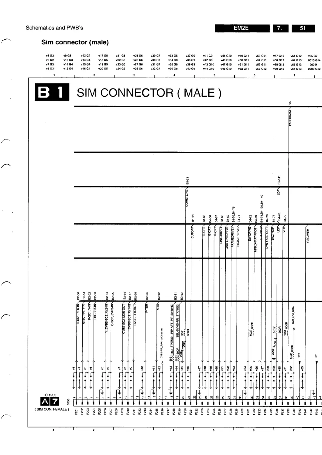
Sim connector (male)
V5G2 V9G3 V13G4 V17G5 v21 G5 v25 G6 v29 G7 v33 G8 v37 G9 v41 G9 V45G10 V49G11 v53 G11 V57G12 v61 G12 v65 G7
v6G2 v10G3 v14 G4 v18G5 v22 G5 v26 G6 v30 G7 v34 G8 v38 G9 v42 G9 v46G10 v50G11 v54 G11 V58G12 v62 G13 0010 G14
v7G3 V11 G4 V15G4 V19G5 V23 G6 v27 G6 v31 G7 v35 G8 v39 G9 V43G10 V47G10 v51 G11 v55 G11 V59G12 V63G13 1000 H1
v8G3 v12G4 V16G4 v20 G5 v24 G6 v28 G6 v32 G7 v36 G8 v40 G9 V44G10 V48G10 V52G11 v56 G12 v60 G12 v64G13 2900G12
1 L_ 2 I 3 I 4 I 5 I I 6 I 7 I
В 1
SIM CONNECTOR ( MALE )
TO 1205
ESQ i
( SIM CON. FEMALE )
ГГЛГГГГГГ
ШШШ
т-мс0^1ЛФЬ.дйсЪО^смЛ^-1Л<Ог«.оо<»0’-см
OOOOOOOCO’-’-’-’-’-’-’-’-’-’-CMOJOJ
<N су см gjgjgjgjgiojgjgjgjgigj cmgjgigjgicjgjcj
г
соч-кпсог'-соотот-смо^юсог'-веаот-смсо
GJ OdGJGJOJGJCMCOTOCOOTO
GJCMGlCMOJGJGIGdGJGIGIGJGIGJGJGJGJGJCMGlGJ
2901 G12 2905 G6 2909 G9 2913 G10 2917 G10 5013 F8 5017 F9 5021 F13 5914 F9 5918 F10 5922 F11 5926 F12 5930 F12 5934 F7
2902G13 2906 G8 2910G9 2914G10 5010 F13 5014G8 5018F9 5911 F9 5915 F10 5919F11 5923F11 5927 F10 5931 G4 5935 G7
2903G13 2907G4 2911 G9 2915G10 5011 F4 5015F8 5019F12 5912 F9 5916 F10 5920 F11 5924F11 5928F12 5932 G4
2904G9 2908G9 2912G1O 2916G11 5O12F7 5016F8 5020F13 5913F9 5917 F10 5921 F11 5925F12 5929F12 5933 F6
8
CL96532156_062.eps
110200
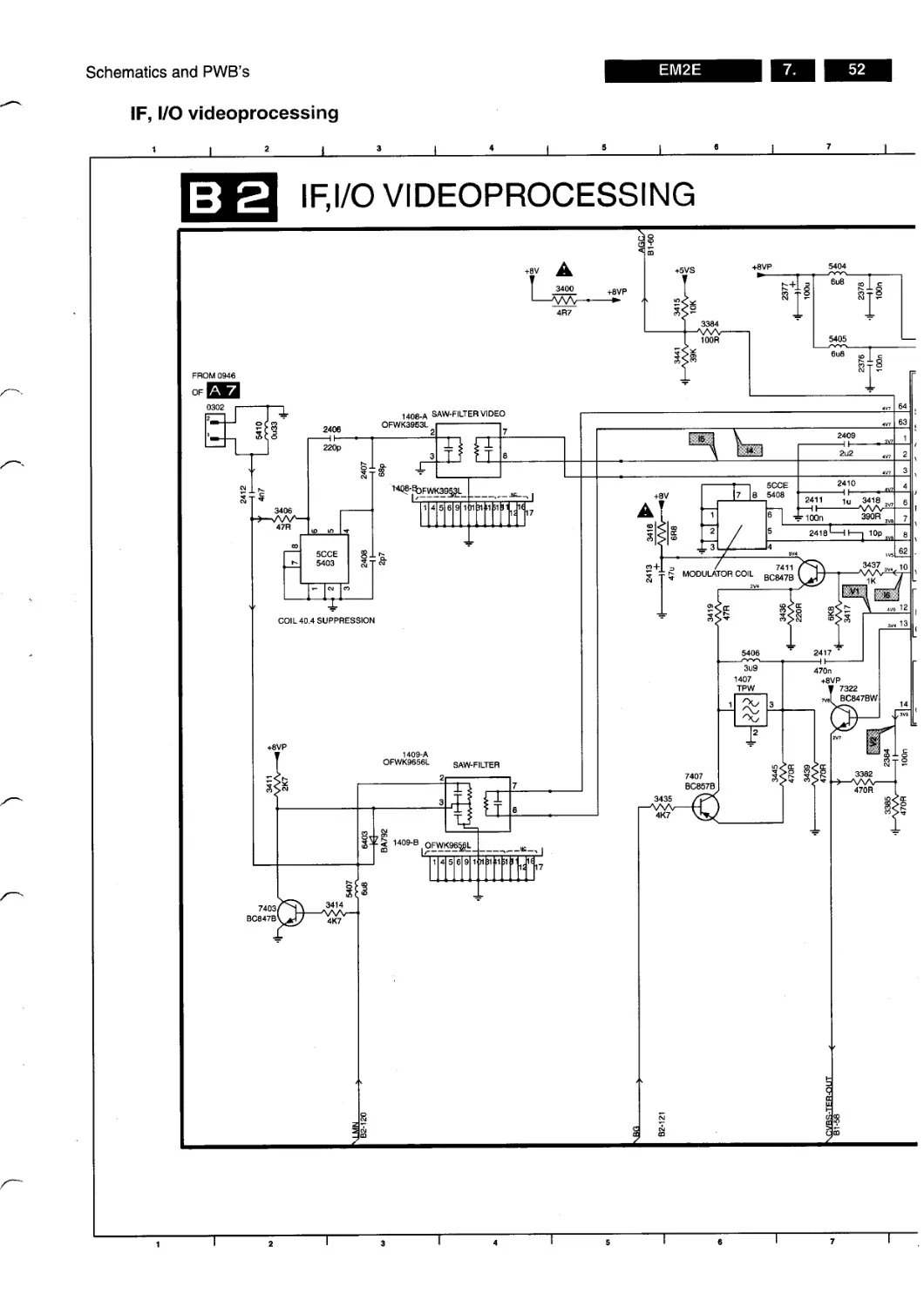
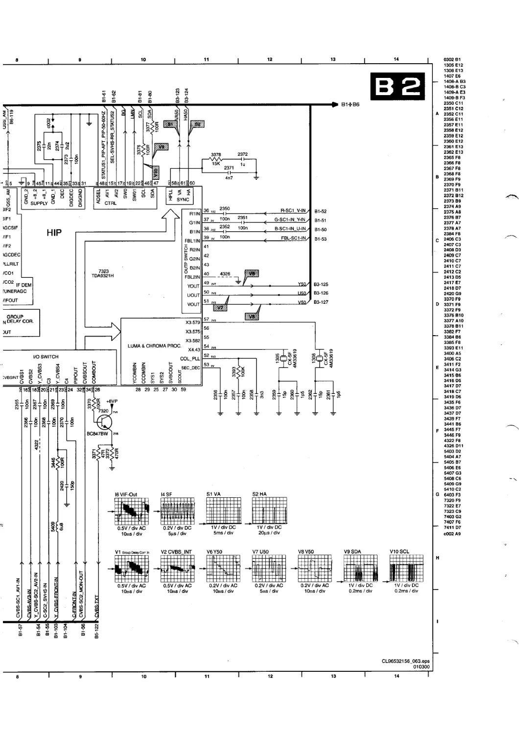
Schematics and PWB’s
EM2E I 7. 52
IF, I/O videoprocessing
4
5
6
I L
IF,I/O VIDEOPROCESSING
BV57 4CVBS-SC1_AV1-IN
4CVBS-AV3-IN____________
B1-54 4Y~CVBS-SC2_AV2-IN
B1-55 4C-SC2_SVHS-IN
B1-103 4Y CVBS-FRONT-IN
4322
B1-56
\C-FRONT-lN_______
4CVBS-SC2_MON-OUT
5409
6u8 2420
-l|------II-
150p
3446
2365
--------II----
2366----ioon-®
-II----------“
100n 2367 a>
---------11 ae
2368-----100n S
b>6 2369 К
2370 100n 8
------1|----:—_—ш
1 1 Ю
J 100n *•
B5-122t\CVBS-TXT
CL96532156_063.eps
010300
3370
3371
470R
S
47R
3372
2361
Sqss.am
CVBS1
CVBS2
2375
Y.CVBS3
C3
C002
22n
2374
Y_CVBS4
C4
PtPOUT
2V8
CVBSOUT
COMBOUT
<100R
SEL-SVHS-RR_STATUS2
YCOMBIN
3376
CCOMBIN
100R
SYS1
SYS2
SVBCOUT
SCOUT
2356
100n
2357
100n
2358
3n3
2359
15p
2360
1p5
2362
15p
□ CJ
GND_1
DEC
DIGDEC
DIGGND
ADSEL
AV2
swo
SW01
3377 SDA
SDA
1OOR
HPLL
/A50y
НА50/
DUTP SWITCH
о HA
3393
100K
1308 ,
ЫН
CX-5F
4M33619
B6-119
1305
]—l[]H
CX-5F
4M33619
GND_2
c +8_2
+8_1
£ STATUS1_PIP-AFT_PIP-50-60HZ
1p5
Q AV1
B1-61
B1-62
ov
SCL/
SCL
B1-81
B1-8O
E5 VA
B3-123
B3-124
00
CO
N
Schematics and PWB’s
EM2E
7. I 53
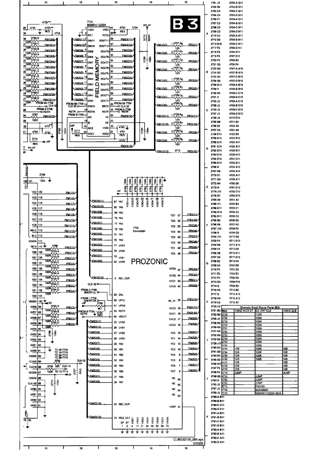
Feature box
i
B3
FEATURE BOX
**: only for PHILIPS DNR memory
a
CZ
г
_4720«
4721 2Г
7714
MSM54V12222A
VSS1
VS89
+5VA
\ЕШЖ
2
NC1
VCC3
DIN11
DOUT11
ЧЕШШ
DOUTIO
DIN10
5
DIN9
DOUT9
5701
♦SP
3V3JNT
+30
our e
+3A
A'l
1
+5M
SNERT-CLO-
TO 62-7708
TO 61-7708
SNERT-DAo-
5704
1R5
3720
5706
3V3JNT
SCL
SDA
100R e
3710
WD-RST
2771
7702
BC847BW
3747
VA
68R
TO 16-7714 AND 7715 й
RSTWO-
TO 25-7714 AND 7715
TO 60-7708 RSTRO-
4703
GND-ADJ
7^
22“
7713
MC33269O
.5VF 5703
BC857BW
5ms / div
B1-83.B3-
sni
B1-82.B3-
SDA
B4-128
Y100
04-129
U100
B4-130
VIM
S5Y-IN
0.2V/div AC
10mS / div
B4-131.B5-148
MD100 (
B4-132
YD1M
B2-125
V-PIP+MAIN-IN
B2-126
LI-PIP+MA1N-1N
B2-127
V-P1P+MAIN-IN
B2-124
HASP
В2-12Э
VA50
2ms / div
390R
чет 14
чет
че(4) 18
чет 18
_____17
16
Яйцу
31 ^141/
32
+5V*
Й'
w
I
чЕШШ
ЧРМ11Й1
ЧЕМ1Ш
DINB
0IN7
DIN6
Doma
cc
о
DOUT7
DOUT6
Й
ci
8
4FM1I<81
10
0IN5
D1N4
LU
DOUT5
DOUT4
7716
SOCKET PLCC32
(PICNIC-EPROM)
12 .
DIN3
□
DOUT3
2
13 .
DIN2
Ш
DOUT2
3 EH2V
£_E®/
DIN1
DOUT1
ЧЕМ1Ц11) 141
FROM 88-7709 15
CLK-ieo-»-----I
DINO
DOUTO
SRCK
SWCK
16 ,
RSTW
WE
sEMiim
IE
NC2
VCC1
4723
142 141 140 134
SN-DA
SN-CL
VSS06
RSTW
JWM-™9 17,
RE
OE
VSS2
4790**
VCG2
+30
1K 154 152
152 15
147 144 14:
1441143
124123
i
BUSC
MICRO-PROCESSOR
CLK
за a
7709 16dl59 158 1571
100R 3705 5
UP-RST
PSP
TIMING
RSTR
57
2713
4r 100л
133 132 131 130 129 12q 127 12€ 125
ea
RSTW
RSTR
5u6
FBL
2720
3712
3748
VD0A1
68R
390R
5u6
2724
3749
68R
5707
600R
7704
PMBT2369
3716
S714
VSSA1
U-OUT
V-OUT
VSSA2
BGEXT
DIFFIN
VDDA2
680p
47R
VSSA3
3754
PLL
10R
VDDA4
VSSA4
2733
3755
VSSX
3757
ж
3759
1R
22n
BST
IDO
3728
и
41 |42 43 44
10OR
3V3JWF
100R
3733
AGND
Y-IN
VDDA3
-IN
VIN
HREF-EXT
£
OSC-I
OSC-O
TEST
TRST
TMS
TDI
S6 H-A
2V/divAC
10ms/div
S7V-A
1V/divAC
5ms / div
3XDAC
V13V-IN
V14Y-OUT
0.2V/div AC
10ms/div
0.2V/div AC
5ms/div
ANALOG
PROCESSING ♦ 3XADC
CLK
TIMING
V18SDA
1V/div DC
0.2ms / div
FRONT
END
BACK END
PEAKING
PICNIC
SAA4978H
V15 V-OUT
0.2V/div AC
5ms / div
V16 U-OUT
0.2V/div AC
5ms / div
V17SCL
TIMING
MUX
MID
NOISE
s s, s, M
45 46 47 48 49 50 51
2796
X 100n
«3D
END
BUS'
REDUCTION
TBC/SRC
MUX
8 И H
1V/div DC
0.2 ms/div
52 53 54
65 58 57 58 S9 60 61 62 163
2767 I—
64 165
66
67
68
69
70
72
74
75
76
78
+30
10
£
в ise
в
в
FM1IUV
;s
’6'
Д
2
г? г г г г г г г г г г
338g§3 Згггггггггг
3 ??e-E BEBSSJtiSiS
&
g g
2 2
ii ±J
g
3
VDDIw
VDD2»
p
VDDSB
J3
VSS2
1
VDD4B
VSS3
VDD5*
К VSS4
2
<5
w
V)
8
S
£
Е
3
£
„ г™ веши
3 s
2774
100n
ФЯвв-в
|sVS
ё «>
2797
100n
В 8 8
S &
12 2 2
s = =
ш
*“ VSS1
g VSS5
гЗ VSS6
S VSS7
ы VSS8
sg
3
8
тй!
5
3?
Si
о-ё
_ о «
4gg g|
ГПЖ гп_
35 5§
, 5^ ₽1
g 2
и и
3 S
S 8
is 6
MU
N
VDD6*
VDD7<5
VDD8a
275^ 1ООП
275^ 1ООП
276^^000
278^1000
276^ 100h
276^1000
276^ НЮп
276^^ ООП
2792
s й Й Й
г
Schematics and PWB’s
EM2E
7.
54
HOP
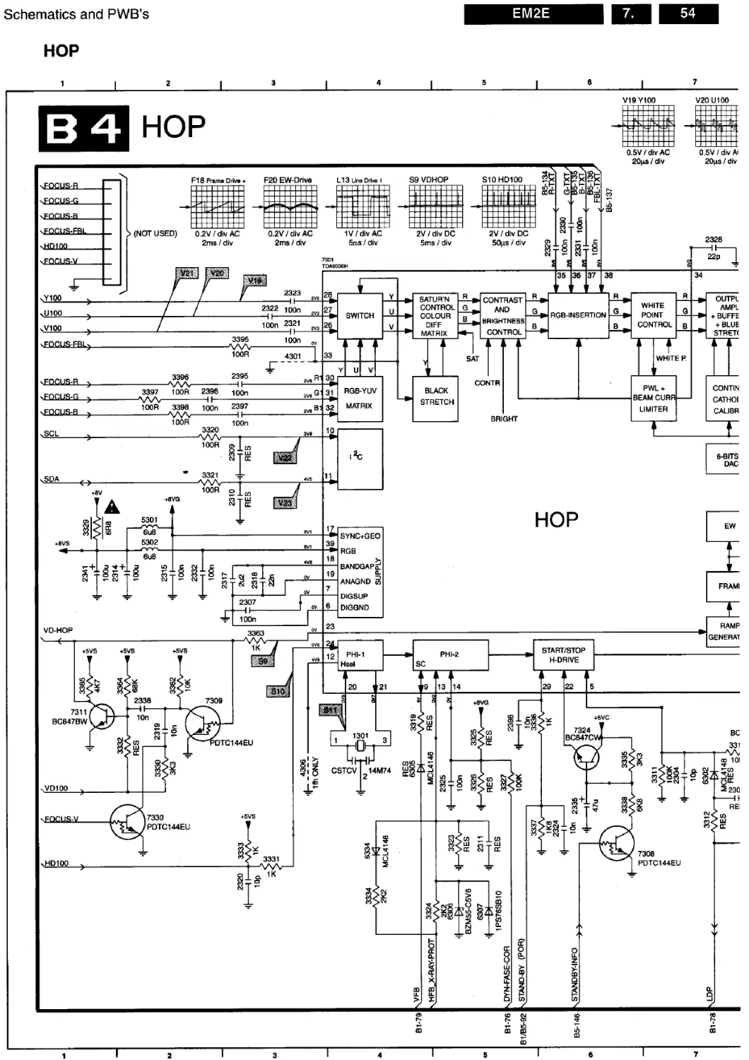
2
sEOCUSi
FOCUS-B
FOCUS-FBL
> (NOT USED)
0.2V/div AC
2ms / div
3
vHDIOO
kY100
on 00
tV100
3395
FOCUS-FBL>
EQCUSi
sEQGUS-V
FOCUSER >
rOCUS-G >
sFQCUS-B >
.SCL
.SPA
+8VS
5
6
20цз / div
20gs / div
F10 Frame Drive
2323
3396
100R
2395
3397 100R 2396 юОп
100R 3398 100П 2397
100R 1(Юп
3320
100R
3321
100R
+eVG
5301
6u8
5302
g. .<л
й-гЩ
CM
Хсл
тш
CE
5ms 1 div
7301
TDA9330H
2V0
28
100П w
2321
_l I___2V3
100П Oy
4301 I
27
-►I SWITCH
26
33
2V8 R'
30
2V8 Q
2V8 B1
ave
4VS
31
32
10
8V1
50ps / div
Str
Si8
CM 1-
s
2328
SATUR’N
CONTROL
COLOUR
DIFF
MATRIX
£
35 :
I
36 I
3
37"
I
22p
R
* CONTRAST
AND
В BRIGHTNESS
CONTROL
<3
R
u
SAT
G
T
RGB’YUV
MATRIX
BLACK
STRETCH
CONTR
BRIGHT
RGB-INSERTION
OUTPl
AMPL
BUFFE
+ BLUE
STRETC
WHITE
POINT
CONTROL
WHITE P.
PWL +
BEAM CURR
LIMITER
CONTIN
CATHOI
CALIBR
17 ---------
-> SYNC+GEO
39
HOP
t
6-BITS
DAC
EW
RGB
6u8
18
BANDGAPq.
±
ANAGND «
FRAMI
100П
VD-HOP
PHI-2
BC
331
? 101
VD100
FOCUS-V
xHDIOO
DIGSUP
DIGGND
PHI-1
Hsei
START/STOP
H-DRIVE
RAMP
GENERA!
19
23
3363
+5VS
+5VS
+5VS
10n
’DTC144EU
CSTCV
14M74
cm
5
§
3S*
ОТ
Ш
CC
7330
PDTC144EU
$
2338
7308
PDTC144EU
I
« T $2
CM
7311
BC847BW
7309
2307
12
2 230
RE:
I
от
ub
m is
8
9
10
11
12
3301
10R
I 1301 G4
2300110
2303 E8
2304 G7
2305 G7
д 2306 H9
2307 ЕЗ
2308 F8
2309 D3
2310 D3
— 2311 Н5
2313 F8
2314 Е2
2315 Е2
2317 ЕЗ
в 2318 ЕЗ
2319 G2
2320 НЗ
2321 СЗ
_ 2322 СЗ
2323 ВЗ
2324 G6
2325 G5
2328 В7
С 2329 В6
2330 В6
2331 В6
2332 Е2
2333 D10
— 2334 D8
2335 G6
2336 D8
2338 F2
2339 ЕЮ
D
2340 111
2341 Е1
2395 СЗ
2398 С2
— 2397 СЗ
2398 F5
3300 НЮ
3301 А11
3304 Н11
Е 3306 Е8
3307 Е9
3308 Е9
3309 Е11
3310 D8
3311 G7
3312 G7
3313 Н8
3314 G7
F 3315 F8
3316 Н9
3317 F9
3318 F8
3319 F4
— 3320 D2
3321 D2
3322 012
3323 Н5
л 3324 Н4
G
3325 G5
3326 G5
3327 G5
3328 Е8
__ 3329 Е1
3330 G2
3331 НЗ
3332 G2
3333 НЗ
Н 3334 Н4
3335 G6
3336 F5
3337 G5
_ 3338 G6
3340 В9
3341 В9
3342 С9
3343 С11
| 3344 D10
3345 С8
3346 С8
СЮ
СЮ
F2
F3
F2
F1
F9
Е9
Е9
F9
F11
F12
□10
D9
D9
F11
ЕЮ
D8
СЗ
С2
С2
С2
В12
СЗ
G3
ЕЮ
F12
Е2
Е2
ЕЮ
G7
Н8
Н9
G4
Н5
Н5
D11
D10
D11
F12
Е12
Е11
□8
С9
С8
Н4
ВЗ
G8
СЮ
Н6
F3
F11
F1
D9
G6
G2
А12
G10
3349
3350
3362
3363
3364
3365
3366
3367
3368
3369
3386
3387
3388
3389
3390
3391
3392
3394
3395
3396
3397
3398
3399
4301
4306
4310
4311
5301
5302
6301
6302
6303
6304
6305
6306
6307
6309
6310
6311
6315
6317
6318
6319
6320
6321
6334
7301
7303
7306
7308
7309
7310
7311
7312
7324
7330
7340
+8V3
7340
BC847BW
B14-B6
££Х/ B5-120
3340
100R
3341
100R
R-CRTy B1-67
G-CRT/
B1-66
100R
3342
3349
3345
10K
+8VS
47K
3388
1K
3308
680K
— 18
RES
6321.
—Ю-
MCL4148
7312
BC847BW
RES
6301
--------K—
MCL4148
3368
2? co
3306
3369
RES
3317
220R
C001
7310
PDTC144EU
+WS I 15K
a
8
В-CRT/
B1-65
6320
-Й-
CUTOFF/
B1-64
’S
>E
N
OR
857BW
4 7303
5
3313
RES
3328
6319
—
MCL4148 ____
3390
3389
RES REg
7306
PDTC144EU
3343
68 К
MCL4148 BZM55-C22 3322
—M-------И-
6309 6311
1K
220R
39K 2313
100n
6303 6304
—Й---------H—
BZM55-C47 MCL4148
3316
12K
CM
8
STAND-BY (POR)y
EHT-INFQ /
> FRAMEDRIVE+/
РАС-НОР/
EW-DRIVE/
B1/B5-92
B1-140
B1-75
B1-77
B1-72
RES RES
6318 6317
-Й---------Kb"
RES BZX284-C22 MCL4148
UL ONLY
3309
3386
22K
EHT-INFQ/
B1-74
HFB_X-RAY-PROT /
VD-НОР/
VSYNC/
B1-73
B4-133
B5-142
RES
6315
43—
RES MCL4148
CASE NO FBX
3387
4311
+5V2
+5V
3
10
11
12
VFB/
B1-79
B1-71
FRAMEDRIVE-/
FRAMEDRIVE+/
r LiNEDRiVEi /
GND-LINEDRIVEy
B1-70
B1-68
B1-69
EHT-INFQ/ B1-139
CL96532156_065.eps
Q1Q3Q0
3347 С8
3348 С9
Schematics and PWB’s
EM2E
7. I 55
OTC
B1-B2-61
4STATUS1 PIP-AFT PIP-50-60HZ____________
+3V3 INTOTC
81-118
OTC
3071
RES
+3V3 INTOTC
(DEGAUSS-INPUT)
MJGHT-SENSOR <
3091 470R 106
B6-145
B1-116
\SEL IN 2
B1-121
B4-120
B1-117
B4-146
B6-144
B1-141
B1/B4-92
B1-63
B1-90
B1-91
B1-86
B1-87
B1-93
B6-147
B4-141
\QN-QFF-LED___
6K8
+5V2
3058
\BQ5_
\BGL
3075
^KEYBOARD
\STANDBY-INFO
\SEL 1N_1
4.LDP (PROTN)
^STAND-BY (РОВД
-±-220R
£DA_
\SGL
^DATA-IN-PUT
KDATA-CLOCK
\COMM_LINE
3025
7008
BC847BW
4SOUND-ENABLE
^RESET-AUDIO
KDATA-IN-QUT
\SDA.
4DATA-CLOCK
\SGL
RESET
\VSYNC
в2’122 \CVBS-TXT
4003
4004
3041
5K6
A(
3079 Ю5
P2-2|ADCD
P2-3|ADC1
АЩ/
kA(‘
470R
120
P3-7|CBB
P3-6|TTC
119
sAG
SAM 118 P3-5|TTD
220R
3090
P3-4
Аф,
470R
A^
f+3V3_INTOTC
A(7)/
A^
110 P2-7|ADC5
RES
P2-6|ADC4
109
AQIb
3078
P2-5|ADC3
108
A(12t
3087
220R
P2-4|ADC2
107
220R
3085
P2-1|PWM1
104
470R
3083
P2-0|PWM0
103
470R
3076
P1-7|RC
100
470R
3086
P1-6|INT3
99
220R
3092
+3V3_INTOTCI
P1-5|INT2
98
A(18b
P1-4|INT1
97
АЦ9Ь
♦3V3_INTOTC|
P1-3|INT0
96
A^
4RC
SDM 95
P1-2|T2
+3V3JNTOTC|
92
PO-7
PO-6|CORN
91
+3V3JNTOTC|
90
P0-5|TxDo
89
P0-4|RxDo
3064-D
P0-3|SDA1
88
0(2).
PQ-2|SCL1
DJ3)/
100R 3064-B
D(4)/
3073
100R
D(6)/
220R
3074
220R
13V3_INTOTCI
-Оф/
VSS
WC_
SCL
6
D(151/
27p
19|OSCGND
NVM
E1
RESET
2
E0
VCC
ROM_CS/
WE/
4-3V3 INTOTC
2
0(13)/
D(14);
0(71/
D(81/
AJ3)/
A^
0(10)/
D(11}/
D(12)/
M24C32
7011
6001
L^_
BAT254
4005 RES
3081
+3V3 INTOTC 220R
A(10)/
AOS/
A(16}/
A(1ZV
L__ SDA
3039
7010
♦3V3JNTOTC 3Qgg
8
8
s
49
101
OTC
53
55
\АЦ
{57
59
A8
61
A9
62
60
58
56
A13
52
A14
A15
48
46
A16
A17
63
A18
A19
65
SRC
A20
64
A21
66
A22
67
68
A23
DO
36
32
D2
28
24
23
27
D6
31
35
D8
34
30
D9
D10
26
D11
22
D12
25
D13
29
D14
33
37
D15
40
ROM_OEn
RAM_OEn
43
ROM_CSn
+3V3JNTOTC
PSENn
42
RASn
69
CASLn
CASHn
WEn
100n
47i
11211 112 113
з
3
° i
RAM_CS/
3035-D аде .
AAA------□*§/
72 1 °°R CASL /
71 100R3035-B CASH/
70 3035-C100R
BC857B
+6V2
3064-C100R
«3V3JNTOTC
8
7001
SAA5801H
117
P3-3
P3-2
P3-1|LED1
P3-OILEDO
87
3064-A100R
P0-1|SDA0
PO-Q|SCLO
P1-0IT0
Р1-ЦТ1
2001
OSCOUT
OSCIN
74
33p
2002
2008
t- c <o с л c
sis sis sis
HSYNC
VSYNC
FRAME
CVBSO
CVBS0_R
CVBS1
CVBS1_R
IREF_DEC
IREF
REF+
STNIBLACK
8
A6
A10
A12
D3
D5
EAn
FADING
ROM_OE/
41 303^J00R RAM_OE/
DATA
VIDEOn
is s s S
ts? te ia e
100R
+3V3 JNTOTC [
2031 [
f 100п
25
I) _ 24
I) . 23
•) 22
В .. . 21
Э. . 20
1) 19
4 18
n 8
u 7
Im . о
in 5
!2i 4
1Я1 3
141 2
L
ifii 48
17) 17
18) 16
19) 9
Xli 4002 res 47
3031
26
АО
А1
>M_CS1QK
3029
28
>M OE
3030
_____12
J i*
ЮК
3061
ЮК
~I 37
VCC VPP
3062
7006
LH28F160BV
** FLASH-RAM
A3 (Set SW) doo
DQ1
А4
А5
А6
А7
А8
А9
A1Q
А11
А12
А13
А14
А15
А16
А17
А18
А19
BYTE.
СЕ_
WE_
ОЕ_
RP_
WP_
fGND-)
100П
2038
+3V3JNTOTC
100n
2032
7007
MSM51V18165D
\A12J.
ЧА0Х
\AIZI
\A131
W
вда.
.WE
AO
18
A1
О
О
19
20
23
24
25
26
27
28
14
31
30
13
1AM QE/KrAM OE 29
;й8т§ота
w Gl
A2
A3
A4
A5
A6
A7
A8
A9
DQ2
DQ3
DQ4
DQ5
DQ6
007
008
DQ9
OQ10
DQ11
DQ12
DQ13
DQ14
DQ15
RY|BY_
NC
46 Гю
0.2ms / div 2ms / div
B5
29 owl
31 0ЦУ
33 Щ21/
35 й^а>/
38 ОШ/
40 цщ/
42 ша/
44 ощ/
30 ЩЩ/
32 Р(9)У
34 И 10)7
36 ЩИ}/
39 DU21/
41 РИЗ)/
43 01141/
45 РИ51/
C5 VSYNC
j
15
I+3V3JNTOTC
+3V3JNTCTC
100n
—ii----q
2019
6
GJ
21
8 DQ1
о
> DQ2
DRAM
(TXT)
RAS_
LCAS_
UCAS_
WE_
15
OE_
NC _
I 07
I co
co
co
2
3
W
DQ3
DQ4
DQ5
DQ6
DQ7
DOB
DQ9
DQ10
DQ11
DQ12
DQ13
DQ14
DQ15
DQ16
8 NC
42
5
7
8
9
10
33
34
35
36
38
39
40
41
16
32
ХЦ2)/
w
W
D(15)/
-0(14)7
.0(12)/
0(11)/
1V/divAC
2ms / div
C6 CVBS_TXT
20mV / div AC
10ms/ div
___B4-134___R-TXT/
___B4-135___Q-TXT/
> B4-136___В-ТХТ/
> В4-1Э7 FBL-TXT/
CL96532156_066.eps
010300
1001 G4
2001 G3
2002 G3
2003 J4
2004 J4
A 2005 J3
2006 J3
2007 J2
2008 H3
2009 I8
~ 2010 19
2011 I9
201219
2013 G11
B 2014 G11
2015 G13
2016 G13
2017 H12
2019 E10
— 2020 01
2022 E2
2023 A4
2Q24 A4
2025 A5
c 2026 A5
2027 A6
2028 A6
2029 A6
_ 2031 A9
2032 E9
2033 H7
2034 H8
2035 H8
D 2036 H8
2037 H8
2038 E9
3001 F3
3002 F3
— 3003 J3
3006 J5
3007-A J5
3007-B J6
3007-C J6
E
3007-D J6
300B-A 16
3008-B 16
3008-C 17
_ 3008-D17
3009 J7
301017
3011 I7
3012 I8
F 3013 G12
3014 G12
3015 H12
3016 H12
_ 3017 G13
3018 A3
3019 A3
3020 A3
3021 A3
G 302318
3024 D2
3025 E1
3026 E3
3027 E2
~ 3028 I8
3029 D8
3030 E8
3031 D8
H 303218
3033 B4
3034 G6
3035-A H6
3035-B H7
— 3035-C H6
3035-D H7
3039 B3
3040 12
3041 H1
1 3044-A E2
3044-B E3
3044-C E3
3044-D E3
_ 3058 C1
3059 B1
3050 C2
3061 E8
3062 A10
j 3064-A F3
3064-В E4
3064-C E3
3064-D E4
3071 A2
3072
3073
3074
3075
3076
3077
3078
3079
3080
3081
3083
3084
3085
3086
3087
3088
3090
3091
3092
4002
4003
4004
4005
4006
6001
6003
7001
7002
7003
7004
7005
7006
7007
7008
7009
7010
7011
A3
F3
F3
C1
D4
C2
C4
A4
82
B3
D3
C2
C4
D3
C3
C4
B3
B4
D4
D8
F1
F1
B3
E4
E2
E3
A4
G11
H12
H13
F12
A9
F9
E1
D3
B3
G2
Schematics and PWB’s
EM2E
7.
56
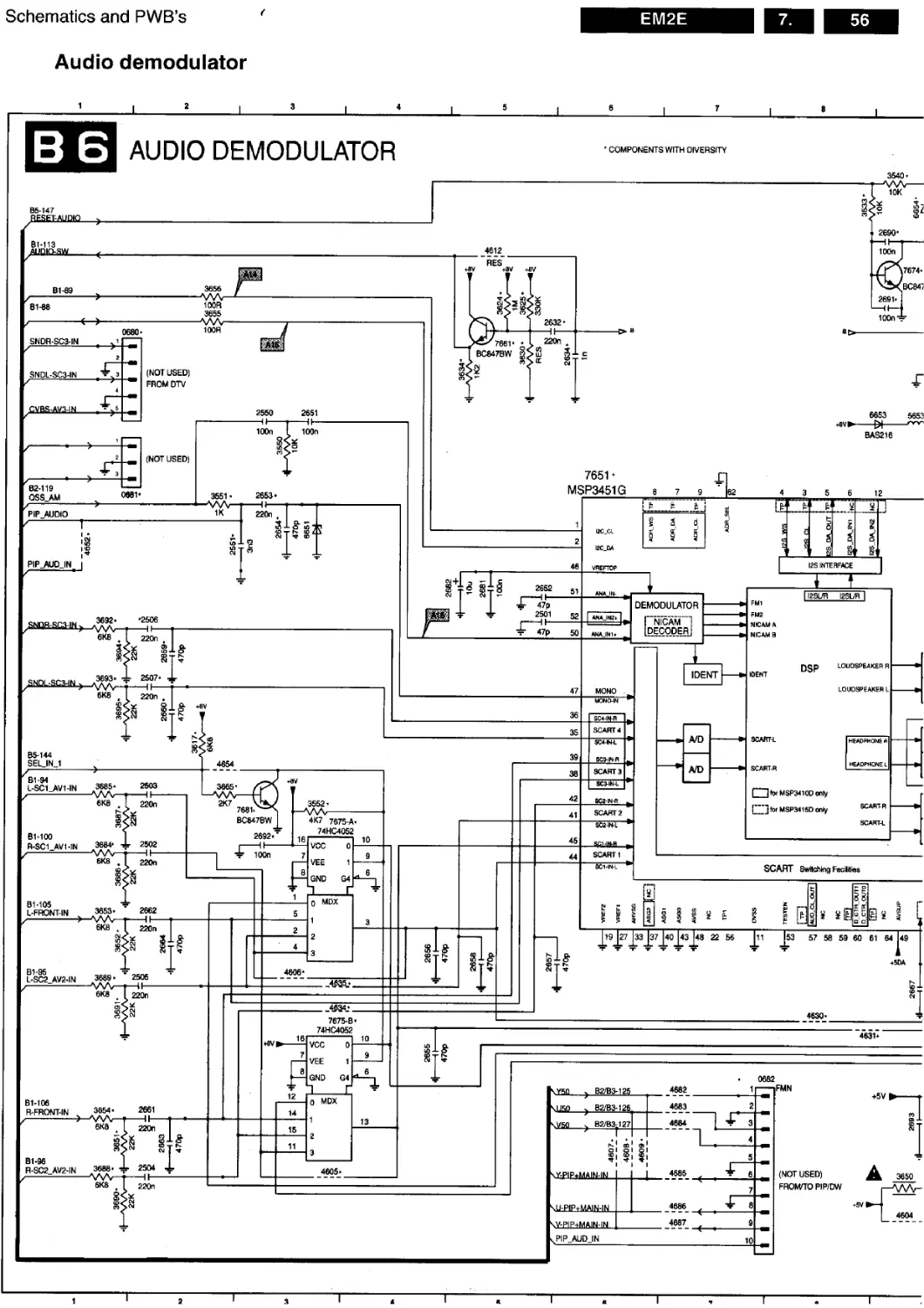
Audio demodulator
AUDIO DEMODULATOR
2
3
4
5
6
8
COMPONENTS WITH DIVERSITY
3540
. I ЮК
co <3
3656
Bl-89
81-88
100R
220n
SNDR-SC3-IN
SNDL-SC3-IN
CVBS-AV3-IN
2550
100n
(NOT USED)
2653*
3551
1K
220n
46
ANAJN-
FMl
DEMODULATOR
| ANAJNZ-t'
2506
47p
50
ANAJN1-
220n
IDENT
IOENT
47
36
35
A/D
SC44N-L
39
A/D
38
SC34N-L
42
4
100R
3655
(NOT USED)
FROM DTV
2651
ЧН
100n
85-147
^RESET-AUDIO
7661* • I
BC847BW |>ш
§
CM
r’NiCAM "I
I DECODERi
47p
2501 52
2652 S1
«м >2 w >c
| I 2632
_______4_612 _________
res"
*8V +3V +8V
SC4-IH-R
SCART 4
SC3-IN-R
SCART 3
SC2-IN-R
SCART 2
SC2-IN-L
AfiUttf-
SCART 1
SCHN-L
MONO .
MONO-IN
PIP.AUDIO
2507* X-
3693*
SNDL-SC3-IN
6K8
SCART-L
SCART-R
6K8
3684*
6K8
220n
3653*
6K8
220n
48 22 56
4m*
6K8
VEE
4682
В2/ВЭ-125
\I5E
0 MDX
4683
82/83-126
\U5D
3654»
4684
6K8
2
3
2504
4605*
4685
>Y-P!PtMAIN-IN
6K8
22Qn
4686
\U-PIP+ MAIN-IN
4687
PIP_AUD_IN
02-119
QSS-AM
85-144
SELJN_1
4V-PIP+MAIN-IN
4PIP_AUD_IN
81-105
L-FRONT-IN
81-95
L-SC2_AV2-IN
B1-106
R-FRONT-IN
81-100
R-SC1.AV1-IN
.SNOH-SCa-IN)
6KB
B2/B3-127
B1-94
L-SC1_AV1-IN
81-96
R-SC2_AV2-IN .3®08‘
81-113
/upio-aw
3552’
4K7 7675-A
74HC4052
VCC
VEE
GND
2662
о MDX
3689* 2505
—II—
220n
2661
41-
220n
7675-B
74HC4052
VCC
2690*
7674-
3C84'
6653
----£1—
BAS216
5653
7651 ‘
MSP3451G
i 3 3
5 6
I2C_DA
I2S INTERFACE
VREFTOP
FM2
NIC AM A
NICAM В
II2SL/R I2SL/R1
12
7Г
DSP
LOUDSPEAKER R
LOUDSPEAKER L
HEADPHONE A
HEADPHONE L
Г~~! ftxMSP3410D only
I j for MSP341SD only
SCART-R
SCART-L
SCART Switching Facilities
i i sеЦЦшs
3
57 58 59 60 61 64 149
4630*
4631
+5DA
8
10
A15-B6 SDA
<-5 DB
В
E
DACM-fl
D/A
LOUDSPEAKER
D/A
OACM-L
ОАСА-Я
D/A
B1-115 AUDIO-Ry
D/A
D/A “•
D/A -•
SC2-OUT-L
28
G
B6-149.B1-101
R-SC1_AV-OUTy
B1-97.B6-150
L-SC1_AV-OUTy
B1-114
AUDIO-Ly
B5-145
SEU_IN_2Z
B1-99
SC2-OUT
B1-110
R-CLVL-OUJ
B1-108
HEADPHONE-R/
B1-107
HEADPHONE-Ly
HEADPHONE
B1-109
L-CL_VL-OUT
18M432 I™
I lb
B6
AUDIO PLL I
---------.J g £ g
1651 , 55 ’= M 15
5654
------►+5VF
8С2-ОЦТ-Я
SCART2
SC1-OUT-R
SCART 1
SCt-OUT-L
R+& +w
A14-B6 SCL
220n
BW
2636*
220n
4678
4679
2641*
О MDX
4676
4677
13
14
7656-
BC847BS
7658-
BC847BS
7656
BC847BS
4614
RES
2546’
±<f-
10u
2547’
10u
CL96532156_067.eps
010300
7658-
BC847BS
+8V
2670
10n
2629
St
8 '
2637
220П
I OACM-SUB EtpI
AGNDC
26 4633
3673’
4K7
IV/div DC
0.2ms / div
1V/div DC
0.2ms / div
0680 81
0681 D1
068217
1651 H9
2501 E5
2502 G2
2503 F2
2504 J2
2505 K2
2506 E2
2507 E2
2508 C9
2546G13
2547G13
2548 H14
2549 J14
2550 C3
2551 D2
2609 C9
2610 J10
2611 J10
2675
4613
lOu
2638*
220П
gSffi BC847BS,
4615
3613'
47K
7652-A*
74HC4052
*7680
BC847BW
VCC
VEE
0 MDX
22Qn
7652-B.
74HC4O52
VCC
VEE
GND
AV
B1-94
^ь-зсг-оит
2629
2632
2634
2636
2637
2638
2639
2640
2641
2642
2651
2652
2653
2654
2655
2656
2657
2658
2659
2660
2661
2662
2663
2664
2665
2666
2667
2668
2669
2670
2673
2674
2675
2677
2678
2679
2680
2681
2682
2685
2686
2690
2691
2692
2693
3532
3533
3540
3544
3545
3546
3547
3550
3551
3552
3610
3611
3612
3613
3614
3615
3616
3617
3621
3624
3625
3630
3634
3636
3637
3638
3642
3643
A11
B5
B6
C13
D11
D13
B9
B9
H13
J13
C3
E5
D3
D3
H4
H4
H5
H5
E2
F2
I2
G2
I2
H2
J9
J10
H9
H9
D14
A12
B11
D11
C14
C9
C9
E11
E11
D5
D5
F11
F11
A9
B9
G3
19
A9
A8
A9
B12
D12
C13
E13
C3
D2
F3
C14
E14
G13
G13
114
J14
H14
F2
A12
B5
B5
B5
C5
C13
C12
D13
H13
113
3645 J13
3650 J9
3651 11
3652 HI
3653 G1
3654 11
3655 B2
3656 B2
3657C13
3658 Cl 2
3659D13
3660A12
3661 C13
3662D12
3663 E13
3665 F2
3673G12
3676114
3677 H13
3678 J13
3679113
3680 B12
3683G14
3684 G1
3685 F1
3686 G1
3687 Fl
3688 J1
3689 H1
3690 JI
3691 H1
3692 El
3693 E1
3694 E1
3695 F1
3696 E10
3697 F10
4604 J9
4605 J3
4606 H3
460716
460816
460916
4610A12
4612 B5
4613 813
4614C12
4615 F13
4620114
4621 J13
4630 H8
4631 H8
4632 F10
4633G10
4634 H3
4635 H3
4650 113
4651 J13
4652 D1
4653G14
4654 F2
4676 JI 2
4677 J12
4678 F12
4679 Fl 2
4680 F13
4681 F14
4682 I7
4683 I7
468417
4685 J7
4686 J7
4687 J7
5651 J9
5652 J9
5653 C9
565419
6651 D3
6652 C9
6653 C9
6654 A9
7651 D6
7652-A G12
7652-8 112
7656-A B12
7656-B D12
7658-AI13
7658-B J13
7661 B5
7663-AC13
7663-B D13
7674 B9
7675-A G4
7675-8 H4
7680 G13
7681 F3
Diversity Small Signal Panel B6)
Item |iooh2 ikifi ST VIRT BLS ioW2 ЫВ
SSEIESiSB^BH
470P 470P
470P 470P
10U 10U
10U 10U
^DBHBI 10U 10U
ЖЯИ—— 1N 1N
1N 1N
к;ял!1
1ГОЗППЗ——
^^BBH
EEQ3E5BBBB
ЕШЗЕШ^^^^В
ESEliE^BBBI
esqeez^^^^b
JUMP JUMP
JUMP JUMP
[ИОВВВВВВ JUMP JUMP
JUMP JUMP
JUMP JUMP
gw— JUMP JUMP
ЕШ1 EISuliBBIB
ЕЕШШШН^^В
g£E4——^М JUMP JUMP
ЕШ1^^^ВВН JUMP JUMP
JUMP JUMP
JUMP JUMP
JUMP JUMP
JUMP JUMP
JUMP JUMP
JUMP JUMP
ЕЛ
7651 IMSP3415D-FH-B3 USP34S1G‘FH‘A1 VSP3451G-FH-A1
7658 |bC847BS
766з|вС847В8
7675174HC4052PW
7681 |BC847BW
Schematics and PWB’s
EM2E I 7. I 68
CRT panel
0031 E5 0298-G D6 2302 A2 2312 D2 2323 E2 3306 A3 3315 B2 3336 E2 3347 F9 3357 C5 7303 C5
0224 E1 0298-H E6 2303 A4 2313 E2 2324 F9 3307 B2 3316 C5 3337 D2 3348 E1 5300 B5 7307 D3
0235 A6 0298-I E9 2304 A4 2315 B1 2325 A3 3308 B5 3317 C2 3338 E5 3349 E8 6305 D5 9310 A5
0298-A E8 0298-K E9 2305 B2 2316 E2 3300 A1 3309 B4 3318 C4 3339 D5 3350 D4 6306 D5 9311 B6
0298-B E8 0334 F10 2306 B2 2317 F9 3301 A4 3310 B6 3319 C5 3340 D5 3351 D4 6307 E4
0298-C C6 0340 B1 2307 B4 2318 E7 3302 A2 3311 B2 3320 C2 3341 E2 3352 E4 6310 E3
0298-D C6 0383 B6 2308 C2 2320 E3 3303 A3 3312 B3 3322 B1 3342 D2 3354 E4 7300 A2
0298-E C6 2300 A4 2309 C4 2321 D2 3304 A5 3313 B3 3334 E7 3343 E1 3355 A5 7301 A3
0298-F D6 2301 A1 2310 C2 2322 E2 3305 A2 3314 B3 3335 D2 3345 E6 3356 B6 7302 A5
4 i 5 i 6
3300
CRT PANEL
0340
! + 33V
2
3
5
г-I +11D
6
R-CRT
G-CRTS
B’CRT
FROM
0324 OF
FROM
0324 OF
0224
HFB_X-RAY-PROT
180V
SCAVEM CIRCUIT
10R
10K
7302
BD140-16
3355
3305
0235
4R7
2303
2304
3306
3307
330p
22n
LIFE PART
2315
56p
3322
15p
CUT OFF
1K5
2308
TO
SC3 avi
03?
180V 3301
330R
7300
BF199
2302
10R
7303
KG
1K2
BD139-16
2310
0298-C
18p
3320
470R
•22p
5
R
3340
3350
R
VO1
9
1K
470R
VI2
VO2
6
68p
3335
VI3
VO3
7
G
3339
3351
G
1K
470R
4
82p
3336
GND
В
3338
3352
в
1K
2312
1K
2321
1K
2322
| RGB AMPLIFIER
KB
0298-E
0298-D
6,
0298-G
10r
HA <
0298-F
0298-H
12-
VDD IOM
3342
3337
7307
TDA6108JF 6
7301 W
BF370 .
3p3
100R
3315
2307
22n
2309
3317
1K
2323
150R
56p
22n
F ilament
19310
3357
cr 4R7
5300
S13974 3
VI1
GND
3354
470R
1K
2K2
0031
6
F
Diversl tv CRT-P nel
PosNr 29" 25” 28" 28" WS 32" WS
0298 SOC 9P
0298 CON 8P CON 8P CON 8P CON 8P
0383 CON 02P CON 02P CON 02P
2300 22U 22U 22U
2301 220U 220U 220U
2302 3P3 3P3 3P3
2303 470P 470P 470P
2304 22 N 22N 22 N
2305 47 U 47U 47U
2306 100N 100N 100N
2307 22N 22 N 22N
2308 15P 15P 15P
2309 22N 22N 22N
2310 18P 18P 18P
2312 22P 22P 22P
2317 4N7 4N7 4N7 4N7
2317 4N7 4N7 4N7 4N7
2321 68P 68P
2322 82P 82P
2323 56P 56P
2324 820P
2325 100N 100N 100N
3300 FUSE 10R FUSE 10R FUSE 10R
3301 3W 10K 3W 10K 3W 10K
3302 1K8 1K8 1K8
3303 18K 18K 1BK
3304 820R 820R 820R
3305 330R 330R 330R
3306 4R7 4R7 4R7
3307 10R 10R 10R
3308 56K 56K 56K
3309 150R 150R 150R
3310 1K 1K 1K
3311 100R 100R 100R
3312 2K2 2K2 2K2
3313 220R 220R 220R
3314 220R 220R 220R
3315 1K5 1K5 1K5
3316 56K 56K 56K
3317 1K2 1K2 1K2
3318 15R 15R 15R
3319 820R 820R 820R
3320 1K 1K 1K
3335 100R 100R 100R
3335 1K 1K
3336 100R 100R 100R
3336 1K 1K
3337 100R 100R 100R
3337 1K 1K
3355 4R7 4R7 4R7
3356 1K 1K 1K
3357 4R7 4R7 4R7
5300 TFM TFM TFM
7300 SIGF199 SIGF199 SIGF199
7301 SIGF370 SIGF370 SIGF370
7302 TRA POW TRA POW TRA POW
7303 TRA POW TRAPOW TRA POW
9305 WR WR WR
9308 WR WR WR
9309 WR WR WR
9312 WR WR WR
9313 WR WR WR
9424 WR
Schematics and PWB’s
EM2E
7. I 69
Side I/O
4902
Headph_gnd
______1^
IT-IN 2
______3
IT-IN 4
5
IT-IN 6
ГЕСТ7
IT-IN 8
9
IDPH-L
\DPH-F
11
EH-B
FROM
0936
OF
4903
Audio_in_gnd
nd
CL96532156_070.eps
110200
GB 74
8.
EM2E
Electrical alignments
8.6 Option menu
8.6.1 Introduction:
The microprocessor communicates with a large number of RO-
IC's in the set. To ensure good communication and make digital
diagnosis possible, the microprocessor has to know which IC's
have to be addressed. The presence of specific IC's or
functions is made known by means of the option codes.
All options codes can be manipulated using both the option
numbers and/or the Option menu.
All hardware related options are incorporated under the
heading 'Options' of the 'Alignments' sub-menu of the 'Service
Alignment Mode'. All software related options that are
incorporated under the heading 'Dealer Options' of the 'Service
Alignment Mode", can also be reached directly via the
'DEALER' button of the DST.
8.6.2 Options in the Service Alignment Mode
Menu-item Subjects Options Physically in the set
Dual screen/PIP Aux type Yes Dual Screen / PIP module present
No Dual Screen / PIP module not present
Teletext/EPG TXT Yes Teletext present
No Teletext not present
NextView present Yes NextView set
No NextView not set
NextView type Flashram Flash-RAM present
No Flashram Flash-RAM present
Communication Easylink Plus Yes Easylink Plus set
No Easylink Plus not set
Picture Tube CRT Type 4:3 4:3 picture tube
16:9 16:9 picture tube
Picture Rotation Yes Frame rotation circuitry present (diagram A4)
No Frame rotation circuitry not present
Dynamic focus Yes Dynamic focus picture tube present
No Dynamic focus picture tube not present
Dooming prevent Off
4:3
SF 16:9
RF 16:9
Video repro Featurebox type ECO PROZONIC not present
Prozonic PROZONIC present
Field memories 2
3
Lightsensor Yes Lightsensor present
No Liahtsensor not present
PALplus Yes PALplus module present
No PALplus module not present
Combfilter Yes Not valid for Europe
No
Picture improvement Yes
No
Picnic Yes PICNIC present
No PICNIC not present
Picnic AGC Yes In normal operation: Yes
No Durina ‘Drive’ alignments: No
Signalling bits Yes
No
Source Selection External 3 Yes 3rd EURO connector present
No No 3rd EURO connector present
External 4 Yes 4th EURO connector present
No No 4th EURO connector present
Audio Repro Dolby None
Pro Loaic
Rear speakers Corded Passive surroundbox present
Virtual
Cordless Active surroundbox present
Acoustic system FL7 Applicable for sets with subwoofer
FL8 Applicable for sets without subwoofer
FL9 Monitor Monitor look (only tweeters at both sides)
FL9 DAS FL9 with full range speakers at both sides
MSP type MSP3411
MSP3415
MSP3451
AVL enable On
Off
Miscellaneous Heatsink Present Yes Heatsink present on CRT/SCAVEM panel (diagram F)
No Heatsink not present on CRT/SCAVEM panel (diagram F)
Tuner type UV1316
TEDE9
CL96532156_038.eps
210W0
Electrical alignments
EM2E
8.
GB 75
8.6.3 Dealer Options in the Service Alignment Mode
• After the option(s) have been changed, they must be
stored via the 'STORE' command.
• The new option is only active after the TV is switched off
and then back on again using the mains switch (the
EAROM is then read out again).
8.6.4 Option number
In case the EAROM has to be replaced, all the options will also
require resetting. To be certain that the factory settings are
reproduced exactly, both option numbers have to be set. These
numbers can be found on a sticker on the picture tube.
Example: Option number 28PT7306/12 could be:
04929 04418 04417 00016
08199 00001 00000 00000
The first line indicates the hardware options 1 to 4, second line
is reserved for the software options.
Every 5-digit number represents 16 bits (so maximum number
can be 65536 if all options are set).
Bit HW1 HW2 HW3 HW4 SW1 SW2 SW3 SW4
0 (1) FBX (1) EXT3 MSP (8) Auto TV CTI
1 (2) FBX (1) Dolby PL EXT4 MSP (8) Auto Store mode (10)
2 (4) FBX (1) Virtual rear sokrs China IF Auto Store mode (10)
9 (8) Combfilter Cordless rear spkrs Tuner (9)
4 (16) PAL-Plus Dolby Digital Dual Screen (6) TXT Picture mute SLDP (13)
b (32) Field mem, (2) Dual Screen (6) China TXT Demo SLDP (13)
6 (64) Light sensor Cabinet (4) TXT-EPG- DS Virgin AVL
7 (128) LTP Cabinet (4) Aux- headphone
Й (256) PICNIC P50 Aspect Ratio (7)
9 (512) PICNIC- AGC Tilt
“IT (1024) DAF
11 (2048) LNA (3)
(4096) wss EPG Heatsink TXT pref. (11)
13 (8192) Time constant EPG type (5) Home Cinema TXT reaion (12)
14 (16384)
lb (32768)
CL9M 32156_039.eps
210100
All bits can be set 'On' (= 1) when the option is available or 'Off
(= 0) when it is not, except for:
(1)0= Eco, 1 = PROZONIC, 4 = Eco-DNR.
(2) 0 = 2 Field memories, 32 = 3 Field memories.
(3) 0 = Normal, 8192 = Fast.
(4) 0 = FL7, 64 = FL8, 128 = FL9.
(5) 0 = Type 2, 8192 = Type 2C3.
(6) 0 = None, 16 = PIP, 32 = Dual Screen.
(7) 0 = 4:3, 256 = 16:9.
(8) 0 = MSP3415, 1 = MSP3451,2 = MSP3411.
(9) 0 = Philips, 8 = Alps.
(10) 0 = None, 2 = PDC/VPS, 4 = TXT-Page, 6 = PDC/VPS/
TXT-Page.
(11)0 = TOP, 4096 = FLOF.
(12)0= East, 8192 = West.
(13) 0 = Off, 16 = 4:3, 32 = SF16:9, 48 = RF16:9.
When all the correct options are set, the sum of the decimal
value (between brackets in 1st column) of each column will
give the option number.
GB 76
9.
EM2E
Circuit descriptions and abbreviation list
9. Circuit descriptions and abbreviation list
9.1 Circuit descriptions
The following circuits are described:
1. Introduction
2. Block diagrams
3. Power supply
4. Control
5. Tuner & IF
6. Video: High-end Input Processor
7. Video: Feature box
8. Video: High-end Output Processor
9. Synchronisation
10. Horizontal deflection
11. Vertical deflection
12. Audio
13. Teletext/NexTView
14. CRT / SCAVEM / Rotation
15. Software related features
9.1.1 Introduction
The EM2E Europe is a lower specified MG-chassis. EM stands
for Eco-MG, 2 for the used processor (1 = Painter, 2 = OTC)
and E stands for Europe. This will be, at the moment of launch,
the cheapest realised 100 Hz set.
The architecture consist of a conventional large signal panel
(LSP) and a small signal board (SSB) module, placed into a so
called SIMM-connector (Standard Interface, 80 pins).
The LSP is built up very conventional, with hardly any surface
mounted components on the copper side. Difference with the
MG-chassis is that the EM2E LSP has a very large 'hot' part,
including the deflection coil.
The SSB is a high tech module (2 sides reflow technology, full
SMC) with very high component density and complete
shielding for EMC-reasons. Despite this, it is designed in such
a way, that repair on component level will be possible. To
achieve this, attention has been paid to:
• The position of service test lands (Tuner side).
• Accessibility (Tuner side).
• Clearance around surface mounted IC’s (for replacing).
• Diagnostics & Fault Finding via ComPair.
Due to the low amount of cabling etc., expectation is that the
FCR will be low.
Attention: During the first 4 to 6 months of production, the
EM2E set-software will be integrated into a flash-RAM on the
SSB. After that period, a mask-ROM will be used. Which IC is
used is not of interest for service, but for both solutions it means
that Service Workshops must be equipped with dedicated
(de)solder equipment for exchanging these IC’s.
In case flash-RAM or mask-ROM has to be replaced in the
field, dealer will receive always an up-to-date flash-RAM.
Warning: Be aware that half of the LSP-circuitry is 'hot',
including the deflection coil.
Protection: The start-up behaviour of the EM2E is different then
that of the MG-chassis, meaning that there does not exist a
situation as in the MG where we have 'supply ON / deflection
circuit OFF'.
This means that isolating failures in the EM2E must be done in
a different way. See Chapter 5 of this manual.
Circuit descriptions and abbreviation list
EM2E
9. I GB 79
3120
20V 4
10R
5102 6103
2102
-)hr
10g
_2101
-г2п2
3107 3106
-V/HWh
2K2 2K2
6105
15V
3113
15R
2109
ЧН
330N
+5V2
7103/04
CL 96532156_021.eps
250100
Figure 9-4
To apply this on the EM2E (diagram A2): replace Switch 'S' by
FETTS7102, coil L by L5101, diode D by D6107//D6111 and C
by C2104.
Time interval to -11:
After switching on the set, the gate of MOSFET TS7102 will be
high (max. 15 V due to zenerdiode D6105). This will drive the
FET into saturation (Uds = 0 V). The DC-voltage Umains wil1 be
transposed across the primary winding of L5101 (3,5) resulting
in a linear increasing current through this coil.
The voltage across the co-coupled coil (1, 2) is also positive
and will keep the FET into conductivity via C2101, R3103,
R3102 and R3117 for some time. The slope of the primary
current is determined by the self-induction of the coil and on the
magnitude of the supply voltage (+375 V).
The maximum current is determined by the time the FET stays
into conductance (tO -11). This time is directly determined by
the voltage across R3108//R3118. This voltage is a measure of
the current and if it exceeds 1.4 V, TS7101 will be driven into
conductivity and consequently connect the gate of TS7102 to
earth; the FET will block. The current will be: 1.4 V/ (15//4.7
ohm) = 0.39 A.
The voltage across the secondary winding (8,9) will be
negative, diodes D6111 and D6107 will block.
Time interval t1 -12:
The sudden current interruption in the primary coil, will induce
a counter-e.m.f. that wants to maintain the current. The voltage
on the drain of the FET will increase. The secondary voltage (8,
9) will become positive and will charge C2104 via D6107 and
D6111. All energy that was stored in L5101 during to -11 will be
transferred into the load. Due to the transformer principle, a
voltage will now be induced in the primary winding (3, 5) and
the co-coupled winding (1,2). This voltage will be: N * Usec (N
= winding ratio).
The voltage across the co-coupled coil will be negative,
keeping the FET blocked.
Time t2:
At t2, the current through the secondary coil will be reduced to
zero, as C2104 is no longer charged. As a consequence, the
voltages will decay and will change polarity. The gate of the
FET will be again made positive, is driven into conductivity and
the cycle starts again.
Feedback, stabilisation:
The Standby Power Supply always oscillates at maximum
power, the only limiting factor is the maximum primary current
which has been pre-set with R3108//3118.
U0UT is determined by R3114, R3124 and zenerdiode D6122.
If the voltage across R3114 exceeds the threshold voltage of
the diode of the optocoupler 7104 (±1 V) or, in other words,
UOut exceeds 5.2 V, the transistor of the optocoupler will
conduct.
Transistor TS7100 will be driven and a negative voltage will be
transposed to the emitter of TS7101. When TS7101 conducts,
the gate of the FET is at earth potential forcing the oscillator
stop. Due to the load, the secondary voltage Uqut wil1
decrease. At a certain voltage, optocoupler TS7103/04 will
block and the oscillator will start again.
Since there are no capacitors and there is a high amplification-
factor in the feedback circuit, the feedback is ultra-fast. This is
why the ripple on UOUT is minimal. The negative supply voltage
(-20 V) used in the feedback circuit originates from the co-
coupling coil and is rectified through D6103.
Stabilisation is not effected through duty-cycle control but
through burst-mode of TS7100.
Burst-mode is load dependent. If the power supply is less
loaded, the secondary voltage will have the tendency to
increase more rapidly. If the load on the power supply
GB 80
9.
EM2E
Circuit descriptions and abbreviation list
increases, then the oscillator stops less often, right up to the
moment that the oscillator is operating continuously: maximum
load. If the power supply is now loaded even more, the output
voltage will decay. The maximum load is determined by the
maximum primary current set by R3108//3118.
Protection:
If the optocoupler would fail, the secondary voltage will
increase. This would have disastrous consequences since
many IC's (e.g. OTC, flash-RAM, DRAM) are fed with this 5.2
V. In other words, very expensive repairs would be required.
We already know that the negative supply is directly dependent
upon the secondary 5.2 V, as a consequence of which the
negative supply will increase proportionally as the secondary
voltage increases.
If the negative supply in the mean time reaches -30 V, D6106
will start to zener and as a consequence TS7101 will start
conducting. Basically, D6106 will take over the stabilisation
task of the optocoupler, however, with a considerable spread:
from -20 V to -30 V is a 50 % increase, thus Uqut will increase
from 5.2 V to max. 7.5 V.
Main supply (diagram A1)
Some important notes on beforehand:
’ Vbat's no* isolated from the mains supply ('hot').
• vbat is alignment free.
The Main Power Supply, generates the 141 V (VBAT) and the
28 V for the audio part and is based on the so-called 'down
converter' principle.
Vbat = MI
96532156_022.eps
060100
• After closing switch 'S', the linear in time increasing current
lT,, will charge capacitor C.
• Opening switch 'S' will generate a counter-e.m.f. in coil L,
trying to maintain current lT. This is possible via diode D
(this diode is also called 'freewheel diode'). So after
opening 'S', the magnetic energy stored in coil L will be
transferred to electrostatic energy in capacitor C. The V|N
will only supply current during the time that 'S' is closed
while a constant current is flowing through RL.
* vbat is directly proportional with V|N and the time that 'S' is
closed and reverse proportional with period time T. So by
changing the duty cycle, it will be possible to control VBAT.
Figure 9-6
At start-up of the main supply, C2515 can be assumed as being
a shortcircuit. UAB will be 15 V (R3513, D6510) and UGS of the
FET will be +5.4 V (voltage division over R3512 and R3518).
The FET will be driven into saturation (same as closing switch
'S'). The drain-current will increase linear in time. With other
words: resistors R3513 and R3518 will start the oscillator.
The voltage across the co-coup!ed coil (4, 5) is also positive
and will keep the FET into conductivity.
The drain-current will also flow through R3514//R3515. The
voltage on the base of TS7502 will be +0.8 V due to the
stabilisation circuit (which is explained further). At increasing
current, the emitter-voltage of TS7502 will get more negative.
When this voltage reaches -0.7 V, TS7502 will be driven into
conductivity and consequently connect the gate of TS7504 to
earth; the FET will block (same as opening switch 'S'). The
maximum drain-current is: 0.7 V / (R3514//R3515) = 1.4 A.
The voltage polarities on L5506 will invert, keeping the gate of
TS7504 negative via the co-coupled coil (4, 5). The voltage on
the secondary winding of L5506 (7, 8) will be positive,
generating the +28 V audio supply voltage via D6507 and
C2512.
The sudden current interruption in the primary coil, will induce
a counter-e.m.f. that wants to maintain the current via the
'freewheel' diode D6508. This current is linear decreasing in
time and as it is also flowing through R3414//R3415, TS7502
will be blocked after a certain time period. The gate of the FET
will be again made positive, is driven into conductivity and the
cycle starts again.
Stabilisation of VBAT:
The output voltage VBAT will be determined by: VBAT = V|N *
ton ! (ton + Toff) = vin * duty-cycle.
To stabilise the output voltage, a feedback loop is
implemented, which will reduce T0N when VBAT increases and
vice versa.
Via a voltage divider, excisting of (1 %) resistors R3507, R3510
and R3527, a voltage of 2.5 V (when VBAT = 141 V) is fed to the
input of precision shunt regulator 7506. This regulator will
Circuit descriptions and abbreviation list
EM2E
9. I GB 81
conduct, a current will flow through R3524 and TS7505 will be
driven into conductivity. The base of TS7502 will now be set at
a certain positive voltage. As this transistor switches the FET
TS7504 on and off, this circuit can determine the dutycycle.
E.g. when the load increases, VBAT will decrease. As a
consequence, the input-voltage of regulator 7506 will
decrease, resulting in a lower current. Through that the emitter-
base voltage of TS7505 will diminish.
The current through R3504 will decline, changing the base-
voltage of TS7502 and through that the TON (will increase) of
the FET. The output voltage VBAT will rise.
If the load continues to increase, the regulator will block at a
certain moment, the collector-current of TS7505 will now be
zero. If there flows no current through R3504, TON will now be
maximum (Imax = 1 4 A). This is the point where VBAT will be
below 141 V, and at further increasing load will be switched off
(The voltage across the co-coupled coil (4,5) will decrease due
to the increasing load. Therefore the voltage on the gate of
TS7504 comes below the threshold voltage. The supply
switches off and an audible hiccuping can be heard).
On the other hand when the load decreases, VBAT will rise. As
a consequence, the input-voltage of 7506 will also rise resulting
in a higher current. The current through R3504 will rise,
changing the base-voltage of TS7502 and through that the TON
(will decrease) of the FET. The output voltage VBAT will be
reduced.
If, for instance, V|N will decrease (e.g. UMA|NS is 180 V i.s.o.
240 V), the slope of the drain-current will be flattened, through
which the FET will be longer into conductance, keeping VqUT
constant.
If, for any reason, the stabilisation circuit might fail, the output
voltage VBAT can never exceed 200 V (via D6514). D6514 will
form a shortcircuit, VBAT will drop and the set will switch off (this
will result in an audible hiccuping of the supply).
Set to 'STANDBY" (via RC):
When the set is switched to 'STANDBY' via the Remote
Control, the Main supply will be switched off.
This is done by the circuit around TS7529 (see diagram A1):
During 'ON'-state the Main supply is fed with line pulses via the
STANDBY line. They are rectified and smoothed via D6517,
D6516 and C2530 and fed to TS7529. Because they are less
than -20 V, this transistor will be blocked.
When these pulses are stopped (STANDBY), TS7529 will be
saturated and TS7502 will be switched off. This will switch off
the Main supply.
Set to'ON' (via 'STANDBY'):
At the moment the set is switched 'ON', the HOP is not working
(as much as possible IC's are made voltageless during
'STANDBY'). Therefore it is impossible that the STANDBY line
carries line-pulses, so the main supply cannot start up. This
problem is solved via the 'low power start-up' possibility of the
HOP.
Via pin 22, the HOP receives, via the STANDBYJNFO line
from the OTC, a voltage of 5.2 V coming from the Standby
supply. The result will be that the HOP will generate pulses with
a nominal TOFF and TON growing from 0 to 30 % of the nominal
value.
This signal is unchanged until the Main supply is switched 'ON'
and the HOP the correct l2C-command POR-bit) has received.
Guarding circuit:
The negative pulses on the secondary winding of L5506 are
rectified by D6520 and smoothed by C2535. The resulting
negative DC-voltage will keep TS7510 blocked, even as
TS7511.
When something happens in the Main supply through which
these pulses will decrease, the DC-voltage will increase.
TS7510 starts to conduct, even as TS7511. Via R3541 and
D6522 this situation will be maintained (thyristor principle). The
collector of TS7511 drives via R3538 a positive pulse back to
the OTC (named STANDBY(POR)). The OTC will now switch
off the Main supply via the STANDBYJNFO signal.
SSB
There are 5 different voltages located on the SSB: +33 V, +11D
V, +8 V, +5.2 V and +5 V.
+5.2 V is the Standby voltage, it should always be present. The
8 V is derived from the 11D V with stabiliser 7906. The 11D
voltage is only present when the line-drive pulses start the
deflection.
The 8 V is used to switch the +5.2 V with transistor 7905 to
supply the +5 V.
GB 82 I 9. I EM2E
Circuit descriptions and abbreviation list
9.1.4 Control (diagram B5)
A0...A19 D0...D15
SAA5801
CVBS-TXT
, ^3
ON/OFF-LED 113
----------------» 107
----------------» 106
----------------1 105
4----------------104
» 100
I TUNER UV13XX
HIP
-^21^ 85/86
109 < FRONT DETECT
108 «----------
99 LDP (res)
g7 P50-IN
96 <-------------§DM
95 SOUND ENABLE,. |
RESET AUDIO,. l4006
I
MSP 3415/3451/3411
FBX PICNIC
DNR MEMORY
77,78,79,80 RGB, BLENDING,
HOP
CL96532156_016.eps
280200
Figure 9-7
OTC
The SAA5801 (IC7001) is called the OTC (OSD, TXT and
Control). In this IC, the microprocessor and the TXT-decoder
(level 2.5) are integrated.
Some of its functions are:
• Set control.
• TXT/OSD acquisition.
• RGB-outputs to the HOP
• Menu blending; for blending the contrast is software
controlled.
• l/O-ports for l2C, RC5, LED, and service modes.
• Error code generation.
The software for EM2E can be 2 MB (Megabyte).
For TXT-data 1000 pages can be stored in IC7007. This is a
DRAM of 4 Mbit and this IC is also used to store data of a
working set.
The Non Volatile Memory IC7011 is a 4 кВ version
M24C32W6.
All ICs in this part are supplied with 3V3. For this voltage a 3V3
stabiliser is used (IC7005).
When the 3.3 V is available, a POR is generated with TS7003/
7004 to wake up the OTC. During the reset all I/O pins are high.
When a POR is generated the TV-set is in Standby mode.
Via pins 105 and 106 the 8 V and the 5 V are sensed. If one of
them is not present, the Main supply is switched off (set in
protection and the red LED will blink at 3 Hz). The OTC will
generate an error code to indicate what was wrong.
The horizontal (HD100) and vertical (VSYNC) sync pulses are
also fed to the OTC for stable OSD and TXT.
The RGB-outputs (77/78/79) together with fading (pin 80) are
fed to the HOP. The fading pin has a double function: it is used
for making a transparent menu and as fast-blanking signal for
TXT.
PC-busses
In the EM2E-chassis with OTC-processor there are two l2C-
busses used:
• Slow (max. 100 kHz) hardware l2C-bus (called l2C1), used
for all IC communication.
• Separate short bus (called l2C3) for the Non Volatile
Memory (NVM) to avoid data corruption.
NVM
The Non Volatile Memory contains all set related data that must
be kept permanently, such as:
• Software identification.
• Operational hours.
• Error-codes.
• Option codes.
• All factory alignments.
• Last Status items for the customer + a complete factory
recall.
* Txt featuring (keeping habit watch data).
• EPG data.
9.1.5 Tuner & IF (diagram A7 & B2)
The tuner UV1316 is l2C-controlled and is capable of receiving
off-air, S- (cable) and Hyperband channels:
• Low 44- 156 MHz
• Mid 156-441 MHz
• High 141 -865 MHz
The tuning is done via l2C. The reference voltage on pin 9 is 33
V. This voltage is derived from the 180 V (from the LOT) via a
resistor of 120 kt2 and a zenerdiode. The OTC together with the
HIP control the tuning procedure. There is also automatic
switching for the different video systems.
The IF-filter is integrated in a SAW (Surface Acoustic Wave)
filter. The type of this filter is depending of the standard(s) that
has to be received. Two SAW filters are used: One for filtering
picture-IF and the second-one for sound-IF. An extra filter
(5403), tuned at 40.4 MHz, is necessary for L/L’ sets with 6.5
MHz sound to suppress the neighbour channel.
The output of the tuner is controlled via an IF-amplifier with
AGC-control. This is a voltage feedback from pin 62 of the HIP
to pin 1 of the tuner. AGC take-over point is adjusted via the
service alignment mode’Tuner AGO. If there is too much noise
in the picture, then it could be that the AGC setting is wrong.
The AGC-setting could also be mis-aligned if the picture
deforms with perfect signal. The IF-amplifier amplifies too
much.
The video IF-signal is fed to pins 2/3 of the PLL-controlled IF-
demodulator. The voltage controlled oscillator of the PLL is
adjusted via the service menu ‘IF AFC. If the alignment is
correct then the displayed frequency in the installation menu is
the same as the applied frequency from a generator. The
external coil L5408 connected between pins 7/8 is used as
reference. The demodulated IF-video signal is available at pin
Circuit descriptions and abbreviation list
EM2E
9. I GB 83
10 of the HIP. In this video signal there is a rest of sound
carrier, which is filtered by the sound trap 1407.
Then the signal is again fed to the HIP on pin 12 where the
group delay can be corrected, dependent on the standard that
is received. On pin 13 the CVBS-signal becomes available
which is used for further processing in the television. Via
TS7322 the signal is supplied to EXT1 and back into the HIP
on pin 14 to the source/record selection.
To realise quasi split sound the IF-signal is fed to the HIP on
pin 63/64 via SAW-filter 1405. The FM (or AM for L-norm) -
modulated signal is available on pin 5 and is fed to the audio
demodulator MSP34xx.
9.1.6 Video: High-end Input Processor (HIP, diagram B2))
In the EM2E the TDA932xH input processor is used, which
contains the following functions:
• IF demodulation.
• Group delay correction.
• AFC signal generation, used to track drifting transmitters.
• Sound carrier re-generation (SIF).
• AM demodulation.
• Sync acquisition, delivering HA and VA.
• Switching off IF-filtering.
The HIP has various inputs.
• Full matrix switch with:
- 2 CVBS inputs
- 2 Y/C (or additional CVBS) inputs
- 1 CVBS front end input
• Two RGB inputs and 2 status-inputs
Outputs: Three separate switchable outputs can be used:
• 1 YUV-output is fed to the PICNIC
• 2 CVBS outputs: One for Teletext Dual Screen and the
other for output to EXT2 to have WYSIWYR (What you see
is what you record)
l/O-switching: The external signals are fed directly to the I/O
part of the HIP with status from pin 8 of SCART. On the HIP
there are two status inputs available (pins 15,17) with two
voltage levels:
• 4:3 -> 2.2 V
• 16:9 -> 5.5 V
The input signals from the Front I/O are fed to the HIP and front
detection is also fed to the OTC.
EXT 1 is full SCART: thus CVBS and RGB. The RGB-selection
is done in the HIP.
EXT2 is meant for VCR and has therefore some additional
signals in relation to EXT1 but no RGB. EXT2 has also the
possibility for Y/CJn and Easylink-Plus (P50). YJn is with pin
20 and Chroma in with pin 15. Easylink is handled via pin 10
of the SCART and this is a bi-directional communication.
Easylink supports the next features:
• Signal quality and aspect ratio matching
• One touch play
• One touch text
• PIP
• Pre-set download
• WYSIWYR
• Automatic Standby
With Easylink-Plus is added:
• Country and language installation
• System Standby
* Intelligent set top box features
• NexTView download
• Timer record control
• VCR control feature
Video processing
The sandcastle-pulse of the HIP will not be used for
synchronisation. The HOP will generate synchronisation signal
derived from the feature box (PICNIC) signals. If a VCR is
connected, there is also an automatic correction for
Macrovision. This is active for the external sources and the pre-
sets 0, 90-99.
The HIP itself (no external voltage) controls the Y/C switch in
the HIP.
The chrominance decoder in the HIP is full multistandard: PAU
SECAM/NTSC.
Two different crystals can be connected to the pins 54 & 57
without any alignment. The crystals are also used as a
reference for the synchronisation. A digital control circuit that is
locked to the reference signal of the colour decoder determines
the start-up of the sync. This crystal may only be replaced by
the original one. If just a crystal is taken, the internal
capacitance will be different and the effect will be that there is
no colour.
In the HIP a sync separation has been integrated; the HIP
delivers the HA and VA 50Hz/60Hz to the PICNIC. On pin 59
there is the 1 fH sandcastle but this is not connected to any
circuit and only used internally for the colour demodulator. The
2fH-sandcastle signal is generated by the HOP.
9.1.7 Video: Feature box (PICNIC, diagram B3))
Introduction
The basic function of the Feature box (FBX6) is picture
improvement, and depending on the version, several scan
conversion methods can be applied. The PICNIC (SAA4978H)
is the central key component.
In the EM2E-chassis the featurebox is integrated on the SSB.
The PICNIC is used for the 100Hz conversion. In the PICNIC
the following functions are present:
• The ADC.
• The DAC.
• The 100 Hz conversion.
• The Panorama mode.
• The noise limiter (DNR).
• The contrast improvement.
All these functions are integrated in one IC: SAA4978H, 160
pins QFP
ADC/DAC
Analogue to Digital conversion is done with three identical 9-bit
ADC's.
Digital to Analogue conversion uses three identical 10-bit
DAC's.
In the PICNIC there are three 9 bits ADCs present for Y,U,V.
For digitising the Y (luminance) 9 bits are used, to realise a
more detailed picture. The 9 bits are only internally used. Via
dithering the 9 bits are reduced to 8 bits and that data is stored
into the memory. The data in the memory is fed back to the
PICNIC and via undithering the data is again reproduced 9 bits
for processing.
U/V (colour difference signals) is also sampled with 9 bits.
These two 9 bit data streams are multiplexed to 4 bits data
streams. This reduction can be allowed, as the perception for
colours by the human eye is less sensitive as for luminance.
100 Hz conversion
The main task of the PICNIC is the conversion from 50Hz to
100Hz for YUV and HV-sync. In order to remove 'large area
flicker' (especially visible in a white picture), the field-rate of the
video is doubled by the FBX6. A 50/60 Hz frame frequency is
converted to 100/120 Hz. Also the line frequency (16 kHz) is
doubled (32 kHz). Basically, when the video input contains
fields A, В etc..., the conversion provides an AABB sequence
on the display. The actual conversion is done in the first Field
Memory by reading it twice at double speed, while writing it
once.
GB 84
9.
EM2E
Circuit descriptions and abbreviation list
PROZONIC
Y DEC
U DEC
VDEC
HA
VA
YFEAT
U FEAT
VFEAT
H0100
VD100
VZ/ZZZZZ
YDEC
UDEC
VDEC
HA
VA
BUS A
BUS в
BUSC
busd
PICNIC/SAA4978H
|"C
DIGITAL SCAN
Figure 9-8
YFEAT
U FEAT
VFEAT
HD100
VD100
CL 96532156_017.eps
110100
To the PICNIC external IC's are connected dependent of the
features.
If EM2E has only 100Hz then only one memory-IC is used to
store one frame.
For sets with Digital Scan the PROZONIC (IC7708,
SAA4990H) has been added with two memory-ICs (1С7714/
7715). It is an abbreviation for PROgressive scan Zoom and
Noise reduction IC.
When applying this, the 2nd Field Memory has to be installed.
The following functions are available:
• Line flicker reduction (Digital Scan): this is a feature to
reduce the 25 Hz interlace line flicker.
• Dynamic Noise Reduction: noise affected signals can be
improved by combining the pixel values of the current and
past video fields. This is however only possible in areas
without movement.
• Variable Vertical Sample Rate Conversion
• Synchronous No Parity Eight bit Reception an
Transmission interface (SNERT-bus)
Depending on the chassis model, the FBX6 can have the
following specification:
Featurebox 6 diversity
Set Chipset
EMG IfH
EMG 2fH 1 Memory
EMG 2fH DNR 1 Memory incl. DNR
EMG 2fH Dig. Scan PROZONIC + 2 Memories
Dual Screen compression
The PICNIC can provide horizontal video compression up to 50
%. The compress mode can be used to display dual screens for
instance with Teletext (only for widescreen sets).
Panorama
To fit 4:3 pictures into a 16:9 display, a panoramic horizontal
distortion can be applied to make a screen-fitting picture
without having black sidebars or lost video.
The centre horizontal gain is programmable and the side gain
is automatically adapted to make a screen-fit.
Automatic Aspect Ratio Adaptation (AARA)
This feature uses data from the 'black bar detection circuit' to
adapt the vertical and horizontal amplitude to an aspect ratio
belonging to the display without showing the black bars.
CTI
At CVBS video signals, the bandwidth of colour signals is
limited to 1/4 of the luminance bandwidth. Transients between
areas of different colours are therefore not very sharp. The
PICNIC can steepen these transients artificially with a time
manipulation algorithm.
Dynamic Contrast
To make the contrast (black/white) range wider, Philips has
invented Dynamic Contrast. It uses the digital memory used in
100 Hz sets. It measures every А-field (25x/s) and digitally
analyses where on the greyscale most of the image is located.
If it's a relatively dark image, the lighter part of that image is
stretched towards white, so that more contrast will become
visible in that picture. If it's a relatively light image, the darker
part of that image is stretched towards black, so that these
darker parts will have more contrast. When the image is in the
middle of the greyscale, both dark and light parts are stretched.
9.1.8 Video: High-end Output Processor (HOP, diagram B4)
General
In the HOP (High-end Output Processor, TDA9330) the video
processor and digital deflection processor are integrated. The
main functions of the HOP are;
• Video control (contrast, brightness, saturation, etc.).
• 2nd RGB interface for OSD/TXT.
• Peak White Limiting.
• Cut-off control and White Drive (RGB outputs).
• Geometry control.
The YUV-signals from the PICNIC are fed to the HOP. In the
HOP, the video and geometry control parts are integrated. Also
the RGB-signals from TXT/OSD are inserted via the HOP. This
IC has all functions from a video processor and geometry
control (like the DDP in MD2). The geometry part delivers the
H-drive, EW-drive and also a drive signal for rotation. The
internal V-drive circuit of the HOP is not used (is explained
further on).
Video Control
After conversion to RGB again, the signals can be controlled
for Saturation, Contrast and Brightness.
2nd RGB interface for OSD/TXT
On pins 35 - 38 the RGB and fast blanking from the OTC (OSD
and TXT) are inserted.
Peak White Limiting
On pin 43 there is a Peak White Limiting signal line (PWL). If
the beam current (EHT-info line) increases, then the EHT-info
voltage will decrease. PWL is controlled by average limiting via
R3343/C2333.
Cut-off control
Switching the TV to Standby:
1. Vertical scan is completed.
2. Vertical flyback is completed (the horizontal output is gated
with the flyback pulse, so that the horizontal output
transistor cannot be switched on during the flyback pulse).
3. Slow stop of the horizontal output is started, by gradually
reducing the 'on' time at the horizontal output from nominal
to zero (this will take 50 ms).
Circuit descriptions and abbreviation list
EM2E
9. I GB 85
4. At the same time the fixed beam current is forced via the
black current loop for 25 ms. This is done by setting the
RGB outputs to a maximum voltage of 5.6V.
In the EM2E a 'one-point' cut-off control is used:
A current of 8 |iA (for cut-off) is fed to pin 44 of the HOP. This
is done with a measurement pulse during the frame flyback.
During the 1 st frame, 3 pulses are generated to adjust the cut-
off voltage at a current of 8 pA.With this measurement the black
level at the RGB-outputs is adjusted. So at start-up there is no
monitor pulse anymore. At start-up, the HOP measures the
pulses which come back via pin 44. The RGB-outputs have to
be between 1.5 V and 3.5 V. If one of the outputs is higher than
3.5 V or one of them lower then 1.5 V, the RGB-outputs will be
blanked.
Geometry control
All geometry control is done via l2C and the data is stored in the
NVM (IC7011) of the SSB.
Line drive (LINEDRIVE1).
Line drive is derived from an internal VCO of 13.75 MHz. As a
reference an external resonator is used (1301). The internal
VCO is locked with the HD100-pulse, which comes from the
PICNIC. The 'PHI-2' part in the HOP receives the HFB_X-
RAY_PROT (pin 13) to correct the phase of the line drive. The
EHT-info is supplied to pin 14 (DYN-PHASE-CORR) to
compensate picture breathing depending on the beam current.
Service tip: This is not used at the moment, therefore EHT-
compensation in the service menu is put to zero.
Frame drive (FRAMEDRIVE+).
The VD100 signal from the PICNIC will be extended for 16.5
lines by the circuit around TS7309 and 7311. The resulting
signal (VDHOP) will drive TS7310. This will result in the
(asymmetric) FRAMEDRIVE+ signal.
Note: The Frame outputs (pins 1/2) of the HOP are not used!
East/West drive.
At pin 3 the E/W-drive is available. Pin 4 is a feedback input for
the EHT-info and is used to prevent pumping of the picture.
EHT varies also dependent of the beam current. For
widescreen without load this is 31.5 kV and with load (1.5 mA)
29.5 kV.
Frame rotation (only for 16:9 sets):
For frame rotation a control voltage is used from pin 25 of the
HOP. This voltage can vary from 0.4 V till 4 V.
Guarding protections:
• Flash detection:
When a flash occurs, the EHT-info will become negative very
fast. Via D6303/D6304/R3316, TS7303 starts to conduct. This
makes pin 5 of HOP high. When pin 5 of HOP is high, then the
output (pin 8) is immediately stopped. If H-drive stops then also
pin 5 will be low again, which will reset the flash detection. A bit
(FLS) will be set in an output status register, so via the OTC it
can be seen when there was a flash. This FLS-bit will be reset
when the OTC has read that register.
• HFB protection:
If the HFB is not present then this detected via the HOP. The
OTC puts the TV into protection and reads a register in the
HOP. An error code will be generated.
9.1.9 Synchronisation (diagram B3 & B4)
The HIP video processor provides vertical and horizontal sync
pulses VA and HA that are synchronised with the incoming
CVBS signal. These pulses are fed to the PICNIC where they
are doubled to be synchronous with the 100 Hz picture. The
outgoing pulses, VD100 and HD100 are fed to the HOP that
supplies the vertical and horizontal drive pulses and the 100 Hz
(2fH) sandcastle pulse.
The VD100 pulse from the PICNIC is only one line long.
Therefore this pulse is converted into a VDHOP signal by a 530
us monostable oscillator (extended by 16.5 lines). This signal
is on block function level equal to VSYNC and FRAMEDRIVE+.
The OTC is synchronised on the HD100 pulse from the FBX
and on the VSYNC for the synchronisation of TXT/OSD/EPG
When no CVBS is offered to the video processor, the VA and
HA pulses are switched off by the HIP, and the VD and HD
pulses are then generated by the PICNIC. This to assure a
stable OSD.
GB 86 I 9.
EM2E
Circuit descriptions and abbreviation list
9.1.10 Horizontal (line) deflection (diagram A3)
Driving the line output stage
Figure 9-9
The HOP (located on the SSB) generates the line-drive pulses
(LINEDRIVE1), which have a frequency of 31250 Hz (T = 32
US).
When the LINEDRIVE1 signal is high, TS7409 and TS7408 will
conduct. A constant DC voltage will be applied across L5410,
causing a linear increasing current through this coil. The
secondary voltage of L5410 has a negative polarity so that
TS7421 will block. When switching on the set, the current
through L5410 is supplied by the 5V2 Standby supply (via
D6407), and taken over by the +11D voltage (via D6408) of the
main supply.
When the LINEDRIVE1 signal becomes low, TS7409 and
TS7408 will block. The voltage polarity across the primary
winding of L5410 will invert. The positive voltage on the
secondary winding will now drive TS7421 into conductivity.
Because of the storage time of the line transistor (TS7421),
L5410 cannot transfer its energy immediately to the secondary
side. This may result in high voltage peaks on the collector of
TS7409 and TS7408. Tо prevent that these peaks will damage
the transistors, a 'snubber' circuit (C2414, C2412 and R3411)
will suppress them.
When the LINEDRIVE1 signal is high again, the above-
described sequence starts again. Circuit L5411 and R3409 will
increase the switch-off time of the line transistor.
The line stage will be started via the 'slow start' principle.
During start-up, the HOP generates line drive pulses with a
small Ton and a high frequency (50 kHz); TOFF will be constant
and T0N will be gradually increased until the duty-cycle is 50 %
(normal condition). The time interval from start to normal
condition takes about 150 ms. When switching off, the same
procedure is followed, but now in reverse order.
Operation of the line output stage
To explain the operation of the line output stage, we use the
following start conditions:
• C2433 is charged to max. 141 V (VBAT)
• TS7421 is driven into conductivity.
Figure 9-10
Circuit descriptions and abbreviation list
EIVI2E
9.
GB 87
Period t1 -12:
When TS7421 is driven into conductivity, the capacitor voltage
of 141 V, will be divided across bridgecoil L5422 and the
deflection coil (conn. 0317). Due to the chosen inductance
values, there will be 100 V across the deflection coil and 41 V
across L5422. The linear increasing current in the deflection
coil will result in a spot moving from the centre of the picture
tube to the right.
The voltage across L5422 will also charge C2421 (41 V - 0.7
V).
Period t2 -13:
At the moment the LINEDRIVE signal becomes high, TS7421
will stop conducting. In the coils a voltage will be induced, trying
to maintain the current. The current through the line deflection
coils continues to flow through C2425 and C2421 and the
current through L5422 continues to flow through C2426 and
C2421. The energy stored in the line deflection coil is passed
to C2425, and the energy of L5422 to C2426.
The resonance-frequencies of these 2 LC-circuits define the
flyback time of the spot from the right side of the picture tube to
the left.
On average no current flows through C2421 and thus the
voltage across this capacitor remains constant.
Period t3 -14:
As for the period t2 -13; but now the current flows in the
opposite direction, since the voltage across C2425 and C2426
is higher than the voltage across C2433 and C2421.
Period t4 -15:
The coils want to maintain the negative current and will charge
the capacitors negative. Because of this, D6422 and D6423 will
conduct. The voltage is 100 V across the deflection coil and 41
V across L5422. As both diodes conduct, we may consider the
voltage to be constant. A linear current flows with the same
changing characteristics as in period t1 -12. The spot now
moves from the extreme left of the picture tube to the centre.
Before the current becomes zero, and the spot is located in the
centre of the frame, TS7421 reverts back into conductivity. First
a short negative current will flow. The cycle starts again.
The linearity correction
A constant voltage across the horizontal deflection coil should
result in a linear increasing saw-tooth current. This however is
not the case as the resistance of the coil is not negligible. In
order to compensate for this, a pre-magnetised coil L5421 in
series with the deflection coil is used. This coil ensures that
during time interval t1 -13 the circuit-resistance will be higher
than during t4 -15. L5421 is called the linearity coil.
To avoid self-oscillation, R3431 and C2431 are placed parallel
to L5421.
The S-correction
Since the sides of the picture are further away from the point of
deflection than the centre, a linear saw-tooth current would
result in a non-linear image (the centre would be scanned
slower than the sides). To solve this, the deflection current for
the right- and left side will be reduced.
C2433 is charged quadratic during time interval t1 -12. Left and
right the voltage across the deflection coil decreases, causing
the deflection to slow down. In the centre, the voltage increases
and the deflection will be faster. An S-shaped current will have
to be superimposed onto the saw-tooth current. This correction
is called finger-length correction or S-correction. C2433 is
relatively small, as a result of which the saw-tooth current will
generate a parabolic voltage with negative voltage peaks.. The
current also results in a parabolic voltage across C2421,
resulting in the finger-length correction, proportionally
increasing with the picture width. The EW-DRIVE signal will
ensure the largest picture width in the centre of the frame. Here
the largest correction is applied. The larger the picture width,
the higher the deflection current through C2433.
The E/W-correction
A line, written at the upper- or lower side of the screen, will be
larger at the screen centre when a fixed deflection current is
used. Therefore the amplitude of the deflection current must be
increased when the spot approaches the screen centre. This is
called East/West correction.
The EW-DRIVE signal is generated in the HOP and will drive
FET TS7480 via TS7481 and optocoupler TS7482. TS7480 will
charge capacitor C2423 more or less, increasing the deflection
current when reaching the centre of the screen.
Secondary line-voltages
During the blocking time of TS7421, the magnetic energy of coil
1 - 5 of the LOT will be transferred to electrical energy in the
secondary winding. Via rectifying and smoothing, the several
secondary supply voltages will be generated:
• EHT, Focus and Vg2-voltage
• +180V for the CRT panel (pin 8 LOT)
• +11D for the line deflection (pin 12 LOT)
• +13VLOT for the frame deflection (pin 6 LOT)
• -15VLOT for the frame deflection (pin 3 LOT)
• Filament voltage (pin 9 LOT)
The EHT-INFO signal is derived via R3450//R3451. This signal
decreases while the beam current increases. It is fed to the
HOP to compensate for loss of picture width and picture height.
The DYN-FASE-CORR signal is fed to the HOP via C2455 and
drives a dynamic phase correction necessary because of beam
current variations. This is done by regulating TON of the line
transistor TS7421.
East-West circuit
The moment TS7480 is driven into saturation, C2421 will
discharge during the flyback. As a consequence of which
C2421 must be charged again during the scan via the
conduction diode D6422 (as long as C2421 is not charged to
the voltage across L5422, D6422 will conduct). The current in
the deflection coil is therefore larger than the current flowing in
L5422 (1-2). The voltage across the deflection coil increases,
so the picture width increases. When TS7480 blocks, C2421
will not discharge anymore and the voltage across C2421 will
remain constant. The result is that the voltage across the
deflection coil is minimal. The voltage across coil L5422,
however, is maximal. This coil (L5422) consists of a
transformer:
• As the current through the coil 1-2 increases (smaller
picture width), the current through coil 3-4 decreases.
Because of the transformer characteristic a higher voltage
will be subjected to coil 3-4, which will counteract the
current. The current will diminish even further.
• When the current through coil 1-2 diminishes (larger
picture width), the current through coil 3-4 increases.
GB 88 I 9.
EM2E
Circuit descriptions and abbreviation list
The EW Drive
The EW drive signal originates in the HOP and is supplied to
TS7480. The shape of this signal determines the various
geometric correction parameters:
• H amplitude
• EW-parabola
• EW-corner
• EW-trapezium
• Horizontal parallelogram
• Horizontal bow
Beam current correction
The EHT-info at point 10 of the LOT is dependent on the value
of the beam current and the voltage divider R3450, R3451 and
C2450. The EHT-info is fed to the HOP to trim the contrast and
to compensate for the changes in picture-width as a function of
the EHT-info, when the high-voltage is decreased. The EHT-
info is integrated via C2450 and sent to the gate of the E/W FET
(TS7480) as a DC-voltage to correct the EW-current.
9.1.11 Vertical (frame) deflection (diagram A4)
Driving the frame output stage
COLD । HOT
Figure 9-12
The HOP drives the frame output stage. As the HOP is 'cold'
and the frame output stage is 'hot1, they must be galvanic
isolated by means of an optocoupler. In the MG-chassis the
HOP generates 3 signals needed for the frame output stage:
VDPOS, VDNEG and FRAME ROTATION. To avoid the costs
of 3 optocouplers, the frame drive pulse and rotation DC-
voltage are added together and then fed to optocoupler
TS7610.
This is done as follows: The VD100 signal from the PICNIC
(diagram B3 pin 19) is extended for 16.5 lines and inverted via
a monostable multivibrator (TS7311 & TS7309, diagram B4).
The output signal VDHOP is then superimposed on a DC-
voltage from pin 25 of the HOP. The resulting signal is called
FRAMEDRIVE+ and is fed to optocoupler 7610 (diagram A4).
So this signal contains info for both the frame deflection and the
frame rotation.
The circuit around IC7440 will amplify this signal and the output
current will flow through the rotation coil. The vertical pulses on
this signal are filtered by C2445 to ensure that only a DC-
voltage will be supplied to the rotation coil.
The output voltage of the rotation circuit is between -8 and +8
V.
Figure 9-13
The sawtooth voltage for the frame output stage is not
generated by the HOP but by a discrete circuit after the
optocoupler 7610: via R3600 and R3601 a linear increasing
voltage over C2601 is built up with a large time constant.
The circuit around TS7603 is a current source, driving C2601
with a current value derived from the E/W modulator. This will
result in an S-shaped voltage on C2601 (also known as EW-
correction).
Flyback generator
The frame output stage is supplied via the +13 V and -15 V
coming from the LOT. The output of the amplifier is 0 VDC, so
a coupling capacitor is not required.
During the (forward) scan, a supply of +13 and -15 V is
sufficient to respond to the slow changing current. The flyback
generator puts a voltage of -15 V on pin 3. Because of the
voltage drop over zenerdiode D6622 (8.2 V), C2622 will be
charged to 19 V: being 13 + (15 - 8.2 - 0.7) V.
During the flyback scan, the change in current per time is much
larger, so a higher voltage is required. The flyback generator
will now generate a voltage of +13 V on pin 3. Added to the
charge on C2622 this will give a flyback voltage of 32 V
(depending on the CRT size, this value can differ).
The IC amplifier (IC7620, pin 5) supplies the sawtooth current
to the frame deflection coil. The current through this coil is
measured via R3620//R3621//R3622 and fed back to the
inverting input of the amplifier.
R3624 and C2624 on the output of the amplifier, form a filter for
high frequencies and in that way also prevents oscillations.
Peak voltages on the output, e.g. as a result of a possible flash,
are damped by the clamp circuit consisting of D6619, C2627
and R3627. The network consisting of R3625, R3629 and
C2629 form an extra damping circuit.
Protection circuit for bridge-coil and frame output stage
The secondary voltage of bridge coil L5422 is guarded at the
diode modulator (D6421/22) via a detection circuit consisting of
an 8.2 V zenerdiode (diagram A3). When the bridge-coil is
working properly, the average voltage on D6422 is such that
this zenerdiode will conduct and will drive TS7652 into
saturation via the BRIDGE_PROT signal (see diagram A4).
When, for any reason, the secondary side of the bridge-coil is
shorted, the average voltage on D6422 will drop below the
zener-voltage and TS7652 will block. Now capacitor C2642 will
be charged. Transistor TS7407 will start conducting and the
STANDBY signal will be grounded via R3403. This will switch
off the main supply (see diagram Al).
Circuit descriptions and abbreviation list
EM2E
9. I GB 89
Via the circuit built around TS7641 the frame output stage is
guarded. If the frame output stage is working properly, TS7641
and TS7652 will both conduct and thereby discharging C2642.
TS7407 is blocked now, causing the STANDBY signal to be
high-ohmic.
If there are frame pulses missing, TS7641 will block and
capacitor C2642 can be charged. Transistor TS7407 will now
start conducting and the STANDBY signal will be grounded via
R3403. This will switch off the main supply (see diagram A1).
9.1.12 Audio (diagram B6, A5 & A6)
Introduction
All EM2E sets contain one of ITT's Multistandard Sound
Processing ID's for sound decoding. The diversity arises
because each member of the MSP-family handles its own set
of sound standards:
• MSP3415D: Europe & AP decoding, Stereo incl.
NICAM.
• MSP3451G: Global decoding, Virtual Dolby.
This IC takes care of the main FM sound decoding. AM
decoding for the L system is done by the HIP. The demodulated
L sound is then again source selected and processed in the
MSP. The reason for this is the bad AM detection performance
of the MSP. In case of NICAM L however, this is handled by the
MSP.
All MSP versions contain digital audio processing, used for the
basic left/right stereo sound, such as bass, treble, balance,
incredible sound and spatial. In addition to that, the MSP3451
is also able to perform Virtual Dolby, a Dolby approved sound
mode for surround sound reproduction with left/right speakers
only.
Audio source selection
• MSP3515D (stereo)
This IC is an economised version of the MSP3410 that is used
in the MG-chassis. It can cover 2 stereo and 1 mono (AM)
input. Since more inputs are required, a separate source
selector is used (HEF4052, IC7675). This selector has EXT1,
EXT2, FRONT and SC1-OUT (Tuner) as input and is
connected to the SCART 1 input of the MSP3415. The SCART2
input is not used.
Since the MSP3415 has only one SCART output, which is
connected to the SCART1, a constant level output and
connection to SCART2 is not available. This is fixed by
connecting the HEF4052 input selector to the constant level
output and to SCART2 via a so-called 'Regimbeau' switch
(IC7652).
This switch is needed to prevent feedback (Larsen effect).
When EXT2 is chosen as input signal, and the output of
SCART2 is selected, this means that the main picture is also
EXT2 and wil! cause the Larsen effect. To prevent this, the
record select must be switched to Tuner. This is especially
important when decoders are used, behind a 'transparent' VCR
connected to EXT2.
To get a constant level output if the Tuner is selected, the
SCART1 output (Tuner at any time), has to be fed back to the
input selector and selected as input for the MSP (SCART1
input).
The MSP3415 has no separate output to drive a headphone.
The headphone is therefore hardwired (on the LSP) to the main
sound output.
• MSP3451G (Virtual Dolby)
The MSP3451, which is used in all versions supporting Virtual
Dolby, is capable of supporting 4 stereo inputs and 1 mono
(AM) INPUT. Therefore the extra input selector (HEF4052) is
not needed.
The MSP3451 is also capable of supporting 2 SCART outputs,
so the trick used in the MSP3415 set-up to get a constant level
output is not needed.
The MSP3451 has a separate headphone output, so sound
control be done separate from the speakers.
Audio decoding
At the input a choice can be made between two IF-signals; SIF
and SIFM.
The selected signal is fed to the AGC. After this, an ADC
converts the IF-signal to digital.
This digital signal can be processed by 2 demodulation
channels. The first one is able to handle FM and NICAM
signals. The second one can handle FM and AM signals.
Each channel contains a mixer to shift the incoming signal in
the frequency domain. This shift is determined by the value of
a DCO.
After the down-mix, the signal is fed, via a filter, to a
discriminator. From here the AM, FM or NICAM demodulation
can be performed.
Both channels contain an 'automatic carrier mute' function,
which automatically mutes the output of the analogue section
when no carrier is detected.
After demodulation, the FM-signals are subjected to a de-
emphasis operation. After that the matrix of the stereo system
is applied.
Audio processing
The sound processing in EM2E is completely done by the
MSP3415D for 'Stereo' sets or the MSP3451G for 'Virtual
Dolby' sets:
• Volume control is done by the user via the SOUND menu.
• Tone control in 'Stereo' sets is done via the BASS/TR EBLE
control, in 'Virtual Dolby' sets via the 5-band equaliser.
• Headphone control in 'Stereo'-sets is done via the
loudspeaker output of the MSP, no sound control possible.
In 'Virtual Dolby'-sets, the MSP has a separate Headphone
output so separate sound control is possible.
• Mute control can be done in different ways:
- Via the SOUND_ENABLE line of the OTC. Used during
start-up/switch-off conditions, in order to avoid audible
plops.
- Via the decoding part of the MSP.
- Via the processing part of the MSP.
The mute on the RC or in the Ul is per today a combination of
processing mute and SOUND_ENABLE line. When a user
mute is done, the processing mute will turn down the volume,
after which the SOUND_ENABLE line is switched. De-muting
is the other way around. The reasons for this is a technical
problem with crosstalk of the headphone into the loudspeakers.
Automatic Volume Levelling (AVL)
One of the features of the MSP-family is AVL. If used, it limits
the big volume differences in the broadcast between e.g. news
transmissions and commercials or within a movie.
To be able to get a Dolby approval (for the Virtual Dolby sets),
the AVL feature must be switchable. Therefore, the AVL
feature is customer switchable via the menu.
Audio amplification
The audio amplifier part is very straight forward. It uses an
integrated power amplifier IC, the TDA2616. It delivers an
GB 90 I 9.
EM2E
Circuit descriptions and abbreviation list
output of 2 x 10 WRMS to 2 full range speakers. A subwoofer
is not implemented.
The supply voltage is +28 V, generated by the main supply via
L5506.
Muting is done via the SOUND-ENABLE line connected to pin
2 of the amplifier-IC and coming from the OTC. This signal is
inverted by TS7730, as a result of which at a high level of the
SOUND-ENABLE signal, current is sinked from pin 2 and the
IC mutes.
9.1.13 Teletext / NexTView (diagram B5)
Teletext
The TXT-decoder in the OTC gets its video signal directly on
pin 5 (from the HIP).
The RGB-outputs are available on pins 77/78/79. Fast blanking
is realised via pen 80.
In the previous chassis there was separate memory to store the
TXT information. In EM2E the DRAM (IC7007) of the
microprocessor is also used for the TXT-decoder.
NexTView
NexTView allows the user to display a program guide on the TV
screen that contains extensive information for each program.
This information can be displayed in a number of different
summaries:
• DAY: The daily summary shows, from the current moment,
the program schedule for several stations for a short time
ahead.
• CHANNEL: The channel summary shows the program
schedule for one station.
• THEME: The theme summary shows, for each theme, the
program schedule of the various stations. These themes
consist of sport, film, culture, etc. and is determined from
the station side.
NexTView does not have to restrict itself to information about
the station that is being viewed, but also offers information
about other stations. In the various summaries 3 different
commands can be given for the various program overviews.
These commands appear as follows:
• WATCH: The set immediately switches over to the station
concerned.
• REMINDER: The start time and date and the station of the
program concerned is stored in the TV reminder list. The
TV will give an OSD-message with the program
information, or switch on the set at the correct moment
(provided the set is in Standby) and tune to the station
concerned.
• RECORD: The timer of the video recorder with ‘Easylink
Plus’ is programmed with the data of the program
concerned. There has to be a video recorder (with Easylink
Plus) connected to SCART2 otherwise the ‘RECORD’
function will not be highlighted. The connection is via pin 10
from SCART. This means that it has to be a full SCART or
at least pin 10 has to be wired.
In order to be able to realise NexTView, two teletext type data
flows, Data stream 1 and 2, are transmitted with various sub-
code pages of information. This data flow can transport limited
information (max. 40 pages). Data stream 1 is quick repeating
with a repetition time of approximately 20 to 30 seconds.
However, Data stream 2 has a much longer repetition time of
approximately half an hour and has a large transport capacity.
• Data stream 1 contains information of the station that is
being viewed.
• Data stream 2 contains up to one week of advance
information from various stations that are covered by the
provider.
9.1.14 CRT /SCAVEM I Rotation (diagram F)
RGB amplifiers
On the CRT panel, the RGB amplifier (TDA6108, IC7307) is
located. Via the outputs 9, 8 and 7 the cathodes of the picture
tube are driven.
The supply voltage for the amplifier is 180 V and is derived from
the LOT.
SCAVEM
The SCAVEM-circuitry is implemented in the layout of the
picture tube panel. It is thus not an extra module. SCAVEM
means SCAn VEIocity Modulation. This means that the
horizontal deflection is influenced by the picture content. In an
ideal square wave, the sides are limited in slope by a limited
bandwidth (5 MHz).
SCAVEM will improve the slope as follows: At a positive slope,
a SCAVEM-current is generated which supports the deflection
current. The first half of the slope the spot is accelerated and
the picture is darker, while at the second half of the slope, the
spot is delayed and the slope becomes steeper.
At the end of the slope, the SCAVEM-current decays to zero
and the spot is at the original position. An overshoot occurs
which improves the impression of sharpness. At the negative
slope, the SCAVEM-current counteracts the deflection.
During the first half of the slope, the spot is delayed, the slope
becomes steeper.
During the second half the spot accelerates, the SCAVEM-
current is zero at the end of the slope.
Via the three resistors R33315, R33317 and R3320, Red,
Green and Blue are added together and offered to the emitter
TS7300. On the collector of this transistor, configured in a
common base, the sum of these 3 signals is obtained. Via the
emitter follower formed with TS7301, this signal is conveyed to
the differentiator C2303, R3309 and R3318. Only the high
frequencies are differentiated (small RC-time).
The positive and negative pulses of this signal drive
respectively TS7303 and TS7302 into conductivity. The DC
setting of the output stage is set by R3304, R3308, R3316 and
R3319. The working voltage of the transistors is settled at half
the supply voltage.
At the positive section of the pulse, the current flows through
R3318, C2307, the SCAVEM-coil and TS7303. At the negative
section of the pulse, the current flows through R3318, C2409,
the SCAVEM-coil and TS7302.
Rotation
In sets with a rotation coil (widescreen sets > 32"), the amount
of frame rotation is adjusted with the DAC-output of the HOP
(see also 'Vertical Deflection').
9.1.15 Software related features
Following features are described:
• Smart Local Doming Prevention (SLDP)
• Auto TV
• Switch ON behaviour
Smart Local Doming Prevention (SLDP)
A CRT with an iron shadow mask shows a considerable
amount of local doming (due to local heating), resulting in
unwanted colour artefacts.
SLDP helps to reduce these artefacts for both 16:9 and 4:3 sets
to an acceptable level. It measures the beam current in areas
that are sensitive to local doming and reduces the contrast if
the beam current in these places exceeds a pre-set threshold.
The chosen solution in EM2E, is based on the PICNIC
hardware and software and it uses the histogram measurement
of the PICNIC to make a prediction of the local heating of the
CRT shadow mask.
Circuit descriptions and abbreviation list
EM2E
9. I GB 91
With SLDP, local doming is diminished to an acceptable level
at the cost of contrast reduction. By using a 'smart' solution for
a part of the necessary contrast reduction, the resulting picture
remains even more acceptable.
SLDP is not a feature. It’s an algorithm that diminishes local
doming effects. These effects occur whenever iron mask (and
in a limited way invar mask) tubes are applied. Therefore, there
is no reason to make it switchable for the customer. However,
SLDP can be switched off via the Service Alignment Mode
(SAM).
AutoTV
The AutoTV (or 'Automatic Picture Control' or Active Control')
aims at giving the customer the best possible picture
performance at any time. Therefor it does real time processing
of the video signal and as a result, it decides to adapt several
video parameters throughout the whole chassis.
The AutoTV feature integrates traditional picture performance,
AutoTV functionality and 'smart controls' in order to come to a
kind of 'supersmart' TV. It can be subdivided in:
• Auto Noise Reduction. This algorithm measures the
amount of noise in the incoming video signal (this is done
by the LIMERIC part of the PICNIC). As a result of this
measurement, the amount of noise in the picture is
corrected, starting from that noise level which is annoying
for the customer. Which parameters exactly can be used is
depending on the hardware.
• Auto Sharpness. This algorithm measures the amount of
sharpness via the bandwidth of the incoming video signal
and adapts the peaking frequency in the PICNIC according
to this info. If the 'sharpness meter' sees the video content
as 'sharp', high frequency peaking will be used. On the
other hand, if the picture content is seen as 'not sharp', a
low/mid frequency peaking is used. There is a coupling
between the Auto Noise and the Auto Sharpness
algorithm: if noise is present in the video content, then in
general the sharpness will be made less aggressive.
Special care has to be taken to the interaction of the
LIMERIC and the vertical peaking of the PICNIC: a too big
amount of vertical peaking increases the visibility of the
2DNR artefacts.
In the EM2E a limited AutoTV control function is used: only a
combination of above described features is used in the
background in order to improve the set performance, specially
focussed on noise reduction.
Switch ON behaviour
First of all, the microprocessor needs to start up: After the
power is applied, the 'Standby supply' starts oscillating,
generating the +5V2 and +3V3. When ready, a reset (POR) is
generated and the OTC is awakened.
During reset, the OTC puts a high level on all his outputs,
causing the degaussing relay to close. After the reset, the
outputs and inputs of the OTC must be initialised to their default
state. The degaussing output of the OTC must stay high for 12
seconds.
Next step is the check whether the set needs to be in Standby
or not. Therefore, the NVM content is read and the Standby-bit
is checked. If the set is to stay in Standby, there is no further
action.
If the set has to be switched 'on', the Standby-info line is pulled
low. This results in the low power mode start-up of the HOP.
The line drive starts to run on 50 kHz, wakes up the main
supply and the +5 V, +8 V and +141 V supplies become
available. The OTC waits until the +8 V is fully present. This is
done by checking the ADC input of the OTC. A positive result
means three times a positive +8 V detection in a row (time
between each polling approx. 5 ms). If this detection still fails
after 1 second, an error should be generated and the set must
be switched to protection (error: “+8 V).
After detection of the +8 V, the MSP must be reset, since it can
disturb l2C traffic when not properly reset. From this moment
on, l2C traffic is possible.
To be sure that the HOP is properly started up, the POR bit of
the HOP should be read. If this is not successful, the Standby
info has to be put high again and an error code (code 11: HOP)
will be generated. If the reading of the POR bit is successful,
the starting procedure can be continued.
The Standby info line must be switched high again. The sync
mode and the black current stabilisation loop of the HOP must
be disabled in order to have a smooth start-up. Within 23.5 ms
after reading the HOP POR bit, the HOP has to be started up
via the HOP_start commando. If this condition is not fulfilled,
the HOP will stop his line drive again and the set will not be able
to start up.
During start-up of the deflection, l2C traffic must be disabled for
250 ms to avoid data corruption. If flashes or spikes are
generated during EHT start-up, l2C data could be disturbed or
corrupted.
After deflection is powered up completely, all protection
algorithms are set active.
The rest of the NVM content can now be read and the IC’s can
be initialised according this info.
If SLDP is present in the set, an initialisation of SLDP has to be
performed, including a calibration of the beamcurrent ADC.
The sync-mode of the HOP must be switched to active and the
black current stabilisation loop in the HOP is switched on.
Some extra checking is done to ensure that the loops are
completely stabilised. Software sets all the necessary
parameters for a correct sound and image and unblanks the
picture.
A provision is foreseen to avoid sets in the field that will never
unblank, if the picture tube is severely worn out. If the black
current stabilisation does not become stable within a time
frame of 30 seconds, the picture is unblanked anyway